ARM Architecture Reference Manual ARMv8, For ARMv8 A Profile AArch64
User Manual:
Open the PDF directly: View PDF ![]() .
.
Page Count: 5158 [warning: Documents this large are best viewed by clicking the View PDF Link!]
- ARM Architecture Reference Manual ARMv8, for ARMv8-A architecture profile
- Contents
- Preface
- About this manual
- Using this manual
- Part A, Introduction and Architecture Overview
- Part B, The AArch64 Application Level Architecture
- Part C, The A64 Instruction Set
- Part D, The AArch64 System Level Architecture
- Part E, The AArch32 Application Level Architecture
- Part F, The AArch32 Instruction Sets
- Part G, The AArch32 System Level Architecture
- Part H, External Debug
- Part I, Memory-mapped Components of the ARMv8 Architecture
- Part J, Appendixes
- Conventions
- Additional reading
- Feedback
- Part A: ARMv8 Architecture Introduction and Overview
- A1: Introduction to the ARMv8 Architecture
- A1.1 About the ARM architecture
- A1.2 Architecture profiles
- A1.3 ARMv8 architectural concepts
- A1.4 Supported data types
- A1.5 Floating-point and Advanced SIMD support
- A1.6 Cryptographic Extension
- A1.7 The ARM memory model
- Part B: The AArch64 Application Level Architecture
- B1: The AArch64 Application Level Programmers’ Model
- B2: The AArch64 Application Level Memory Model
- B2.1 Address space
- B2.2 Memory type overview
- B2.3 Caches and memory hierarchy
- B2.4 Alignment support
- B2.5 Endian support
- B2.6 Atomicity in the ARM architecture
- B2.7 Memory ordering
- B2.8 Memory types and attributes
- B2.9 Mismatched memory attributes
- B2.10 Synchronization and semaphores
- B2.10.1 Exclusive access instructions and Non-shareable memory locations
- B2.10.2 Exclusive access instructions and Shareable memory locations
- B2.10.3 Marking and the size of the marked memory block
- B2.10.4 Context switch support
- B2.10.5 Load-Exclusive and Store-Exclusive instruction usage restrictions
- B2.10.6 Use of WFE and SEV instructions by spin-locks
- Part C: The AArch64 Instruction Set
- C1: The A64 Instruction Set
- C2: A64 Instruction Set Overview
- C2.1 Branches, Exception generating, and System instructions
- C2.2 Loads and stores
- C2.2.1 Load/Store register
- C2.2.2 Load/Store register (unscaled offset)
- C2.2.3 Load/Store Pair
- C2.2.4 Load/Store Non-temporal Pair
- C2.2.5 Load/Store Unprivileged
- C2.2.6 Load-Exclusive/Store-Exclusive
- C2.2.7 Load-Acquire/Store-Release
- C2.2.8 Load/Store scalar SIMD and floating-point
- C2.2.9 Load/Store Vector
- C2.2.10 Prefetch memory
- C2.3 Data processing - immediate
- C2.4 Data processing - register
- C2.5 Data processing - SIMD and floating-point
- C2.5.1 Common features of SIMD instructions
- C2.5.2 Floating-point move (register)
- C2.5.3 Floating-point move (immediate)
- C2.5.4 Floating-point conversion
- C2.5.5 Floating-point round to integral
- C2.5.6 Floating-point multiply-add
- C2.5.7 Floating-point arithmetic (one source)
- C2.5.8 Floating-point arithmetic (two sources)
- C2.5.9 Floating-point minimum and maximum
- C2.5.10 Floating-point comparison
- C2.5.11 Floating-point conditional select
- C2.5.12 SIMD move
- C2.5.13 SIMD arithmetic
- C2.5.14 SIMD compare
- C2.5.15 SIMD widening and narrowing arithmetic
- C2.5.16 SIMD unary arithmetic
- C2.5.17 SIMD by element arithmetic
- C2.5.18 SIMD permute
- C2.5.19 SIMD immediate
- C2.5.20 SIMD shift (immediate)
- C2.5.21 SIMD floating-point and integer conversion
- C2.5.22 SIMD reduce (across vector lanes)
- C2.5.23 SIMD pairwise arithmetic
- C2.5.24 SIMD table lookup
- C2.5.25 Cryptography extensions
- C3: A64 Instruction Set Encoding
- C3.1 A64 instruction index by encoding
- C3.2 Branches, exception generating and system instructions
- C3.3 Loads and stores
- C3.3.1 AdvSIMD load/store multiple structures
- C3.3.2 AdvSIMD load/store multiple structures (post-indexed)
- C3.3.3 AdvSIMD load/store single structure
- C3.3.4 AdvSIMD load/store single structure (post-indexed)
- C3.3.5 Load register (literal)
- C3.3.6 Load/store exclusive
- C3.3.7 Load/store no-allocate pair (offset)
- C3.3.8 Load/store register (immediate post-indexed)
- C3.3.9 Load/store register (immediate pre-indexed)
- C3.3.10 Load/store register (register offset)
- C3.3.11 Load/store register (unprivileged)
- C3.3.12 Load/store register (unscaled immediate)
- C3.3.13 Load/store register (unsigned immediate)
- C3.3.14 Load/store register pair (offset)
- C3.3.15 Load/store register pair (post-indexed)
- C3.3.16 Load/store register pair (pre-indexed)
- C3.4 Data processing - immediate
- C3.5 Data processing - register
- C3.5.1 Add/subtract (extended register)
- C3.5.2 Add/subtract (shifted register)
- C3.5.3 Add/subtract (with carry)
- C3.5.4 Conditional compare (immediate)
- C3.5.5 Conditional compare (register)
- C3.5.6 Conditional select
- C3.5.7 Data-processing (1 source)
- C3.5.8 Data-processing (2 source)
- C3.5.9 Data-processing (3 source)
- C3.5.10 Logical (shifted register)
- C3.6 Data processing - SIMD and floating point
- C3.6.1 AdvSIMD EXT
- C3.6.2 AdvSIMD TBL/TBX
- C3.6.3 AdvSIMD ZIP/UZP/TRN
- C3.6.4 AdvSIMD across lanes
- C3.6.5 AdvSIMD copy
- C3.6.6 AdvSIMD modified immediate
- C3.6.7 AdvSIMD scalar copy
- C3.6.8 AdvSIMD scalar pairwise
- C3.6.9 AdvSIMD scalar shift by immediate
- C3.6.10 AdvSIMD scalar three different
- C3.6.11 AdvSIMD scalar three same
- C3.6.12 AdvSIMD scalar two-reg misc
- C3.6.13 AdvSIMD scalar x indexed element
- C3.6.14 AdvSIMD shift by immediate
- C3.6.15 AdvSIMD three different
- C3.6.16 AdvSIMD three same
- C3.6.17 AdvSIMD two-reg misc
- C3.6.18 AdvSIMD vector x indexed element
- C3.6.19 Crypto AES
- C3.6.20 Crypto three-reg SHA
- C3.6.21 Crypto two-reg SHA
- C3.6.22 Floating-point compare
- C3.6.23 Floating-point conditional compare
- C3.6.24 Floating-point conditional select
- C3.6.25 Floating-point data-processing (1 source)
- C3.6.26 Floating-point data-processing (2 source)
- C3.6.27 Floating-point data-processing (3 source)
- C3.6.28 Floating-point immediate
- C3.6.29 Floating-point<->fixed-point conversions
- C3.6.30 Floating-point<->integer conversions
- C4: The AArch64 System Instruction Class
- C4.1 About the System instruction and System register descriptions
- C4.2 The System instruction class encoding space
- C4.2.1 Principles of the System instruction class encoding
- C4.2.2 System instruction class encoding overview
- C4.2.3 Op0==0b00, architectural hints, barriers and CLREX, and PSTATE access
- C4.2.4 Op0==0b01, cache maintenance, TLB maintenance, and address translation instructions
- C4.2.5 Op0==0b10, Moves to and from debug, trace, and Execution environment System registers
- C4.2.6 Op0==0b11, Moves to and from non-debug System registers and special-purpose registers
- C4.2.7 Reserved control space for IMPLEMENTATION DEFINED functionality
- C4.3 PSTATE and special purpose registers
- C4.3.1 CurrentEL, Current Exception Level
- C4.3.2 DAIF, Interrupt Mask Bits
- C4.3.3 DLR_EL0, Debug Link Register
- C4.3.4 DSPSR_EL0, Debug Saved Program Status Register
- C4.3.5 ELR_EL1, Exception Link Register (EL1)
- C4.3.6 ELR_EL2, Exception Link Register (EL2)
- C4.3.7 ELR_EL3, Exception Link Register (EL3)
- C4.3.8 FPCR, Floating-point Control Register
- C4.3.9 FPSR, Floating-point Status Register
- C4.3.10 NZCV, Condition Flags
- C4.3.11 SP_EL0, Stack Pointer (EL0)
- C4.3.12 SP_EL1, Stack Pointer (EL1)
- C4.3.13 SP_EL2, Stack Pointer (EL2)
- C4.3.14 SP_EL3, Stack Pointer (EL3)
- C4.3.15 SPSel, Stack Pointer Select
- C4.3.16 SPSR_abt, Saved Program Status Register (Abort mode)
- C4.3.17 SPSR_EL1, Saved Program Status Register (EL1)
- C4.3.18 SPSR_EL2, Saved Program Status Register (EL2)
- C4.3.19 SPSR_EL3, Saved Program Status Register (EL3)
- C4.3.20 SPSR_fiq, Saved Program Status Register (FIQ mode)
- C4.3.21 SPSR_irq, Saved Program Status Register (IRQ mode)
- C4.3.22 SPSR_und, Saved Program Status Register (Undefined mode)
- C4.4 A64 system instructions for cache maintenance
- C4.4.1 DC CISW, Data or unified Cache line Clean and Invalidate by Set/Way
- C4.4.2 DC CIVAC, Data or unified Cache line Clean and Invalidate by VA to PoC
- C4.4.3 DC CSW, Data or unified Cache line Clean by Set/Way
- C4.4.4 DC CVAC, Data or unified Cache line Clean by VA to PoC
- C4.4.5 DC CVAU, Data or unified Cache line Clean by VA to PoU
- C4.4.6 DC ISW, Data or unified Cache line Invalidate by Set/Way
- C4.4.7 DC IVAC, Data or unified Cache line Invalidate by VA to PoC
- C4.4.8 DC ZVA, Data Cache Zero by VA
- C4.4.9 IC IALLU, Instruction Cache Invalidate All to PoU
- C4.4.10 IC IALLUIS, Instruction Cache Invalidate All to PoU, Inner Shareable
- C4.4.11 IC IVAU, Instruction Cache line Invalidate by VA to PoU
- C4.5 A64 system instructions for address translation
- C4.5.1 AT S12E0R, Address Translate Stages 1 and 2 EL0 Read
- C4.5.2 AT S12E0W, Address Translate Stages 1 and 2 EL0 Write
- C4.5.3 AT S12E1R, Address Translate Stages 1 and 2 EL1 Read
- C4.5.4 AT S12E1W, Address Translate Stages 1 and 2 EL1 Write
- C4.5.5 AT S1E0R, Address Translate Stage 1 EL0 Read
- C4.5.6 AT S1E0W, Address Translate Stage 1 EL0 Write
- C4.5.7 AT S1E1R, Address Translate Stage 1 EL1 Read
- C4.5.8 AT S1E1W, Address Translate Stage 1 EL1 Write
- C4.5.9 AT S1E2R, Address Translate Stage 1 EL2 Read
- C4.5.10 AT S1E2W, Address Translate Stage 1 EL2 Write
- C4.5.11 AT S1E3R, Address Translate Stage 1 EL3 Read
- C4.5.12 AT S1E3W, Address Translate Stage 1 EL3 Write
- C4.6 A64 system instructions for TLB maintenance
- C4.6.1 TLBI ALLE1, TLB Invalidate All entries, EL1
- C4.6.2 TLBI ALLE1IS, TLB Invalidate All entries, EL1, Inner Shareable
- C4.6.3 TLBI ALLE2, TLB Invalidate All entries, EL2
- C4.6.4 TLBI ALLE2IS, TLB Invalidate All entries, EL2, Inner Shareable
- C4.6.5 TLBI ALLE3, TLB Invalidate All entries, EL3
- C4.6.6 TLBI ALLE3IS, TLB Invalidate All entries, EL3, Inner Shareable
- C4.6.7 TLBI ASIDE1, TLB Invalidate by ASID, EL1
- C4.6.8 TLBI ASIDE1IS, TLB Invalidate by ASID, EL1, Inner Shareable
- C4.6.9 TLBI IPAS2E1, TLB Invalidate by Intermediate Physical Address, Stage 2, EL1
- C4.6.10 TLBI IPAS2E1IS, TLB Invalidate by Intermediate Physical Address, Stage 2, EL1, Inner Shareable
- C4.6.11 TLBI IPAS2LE1, TLB Invalidate by Intermediate Physical Address, Stage 2, Last level, EL1
- C4.6.12 TLBI IPAS2LE1IS, TLB Invalidate by Intermediate Physical Address, Stage 2, Last level, EL1, Inner Shareable
- C4.6.13 TLBI VAAE1, TLB Invalidate by VA, All ASID, EL1
- C4.6.14 TLBI VAAE1IS, TLB Invalidate by VA, All ASID, EL1, Inner Shareable
- C4.6.15 TLBI VAALE1, TLB Invalidate by VA, All ASID, Last level, EL1
- C4.6.16 TLBI VAALE1IS, TLB Invalidate by VA, All ASID, EL1, Inner Shareable
- C4.6.17 TLBI VAE1, TLB Invalidate by VA, EL1
- C4.6.18 TLBI VAE1IS, TLB Invalidate by VA, EL1, Inner Shareable
- C4.6.19 TLBI VAE2, TLB Invalidate by VA, EL2
- C4.6.20 TLBI VAE2IS, TLB Invalidate by VA, EL2, Inner Shareable
- C4.6.21 TLBI VAE3, TLB Invalidate by VA, EL3
- C4.6.22 TLBI VAE3IS, TLB Invalidate by VA, EL3, Inner Shareable
- C4.6.23 TLBI VALE1, TLB Invalidate by VA, Last level, EL1
- C4.6.24 TLBI VALE1IS, TLB Invalidate by VA, Last level, EL1, Inner Shareable
- C4.6.25 TLBI VALE2, TLB Invalidate by VA, Last level, EL2
- C4.6.26 TLBI VALE2IS, TLB Invalidate by VA, Last level, EL2, Inner Shareable
- C4.6.27 TLBI VALE3, TLB Invalidate by VA, Last level, EL3
- C4.6.28 TLBI VALE3IS, TLB Invalidate by VA, Last level, EL3, Inner Shareable
- C4.6.29 TLBI VMALLE1, TLB Invalidate by VMID, All entries at stage 1, EL1
- C4.6.30 TLBI VMALLE1IS, TLB Invalidate by VMID, All entries at stage 1, EL1, Inner Shareable
- C4.6.31 TLBI VMALLS12E1, TLB Invalidate by VMID, All entries at Stage 1 and 2, EL1
- C4.6.32 TLBI VMALLS12E1IS, TLB Invalidate by VMID, All entries at Stage 1 and 2, EL1, Inner Shareable
- C5: A64 Base Instruction Descriptions
- C5.1 Introduction
- C5.2 Register size
- C5.3 Use of the PC
- C5.4 Use of the stack pointer
- C5.5 Condition flags and related instructions
- C5.6 Alphabetical list of instructions
- C5.6.1 ADC
- C5.6.2 ADCS
- C5.6.3 ADD (extended register)
- C5.6.4 ADD (immediate)
- C5.6.5 ADD (shifted register)
- C5.6.6 ADDS (extended register)
- C5.6.7 ADDS (immediate)
- C5.6.8 ADDS (shifted register)
- C5.6.9 ADR
- C5.6.10 ADRP
- C5.6.11 AND (immediate)
- C5.6.12 AND (shifted register)
- C5.6.13 ANDS (immediate)
- C5.6.14 ANDS (shifted register)
- C5.6.15 ASR (register)
- C5.6.16 ASR (immediate)
- C5.6.17 ASRV
- C5.6.18 AT
- C5.6.19 B.cond
- C5.6.20 B
- C5.6.21 BFI
- C5.6.22 BFM
- C5.6.23 BFXIL
- C5.6.24 BIC (shifted register)
- C5.6.25 BICS (shifted register)
- C5.6.26 BL
- C5.6.27 BLR
- C5.6.28 BR
- C5.6.29 BRK
- C5.6.30 CBNZ
- C5.6.31 CBZ
- C5.6.32 CCMN (immediate)
- C5.6.33 CCMN (register)
- C5.6.34 CCMP (immediate)
- C5.6.35 CCMP (register)
- C5.6.36 CINC
- C5.6.37 CINV
- C5.6.38 CLREX
- C5.6.39 CLS
- C5.6.40 CLZ
- C5.6.41 CMN (extended register)
- C5.6.42 CMN (immediate)
- C5.6.43 CMN (shifted register)
- C5.6.44 CMP (extended register)
- C5.6.45 CMP (immediate)
- C5.6.46 CMP (shifted register)
- C5.6.47 CNEG
- C5.6.48 CRC32B, CRC32H, CRC32W, CRC32X
- C5.6.49 CRC32CB, CRC32CH, CRC32CW, CRC32CX
- C5.6.50 CSEL
- C5.6.51 CSET
- C5.6.52 CSETM
- C5.6.53 CSINC
- C5.6.54 CSINV
- C5.6.55 CSNEG
- C5.6.56 DC
- C5.6.57 DCPS1
- C5.6.58 DCPS2
- C5.6.59 DCPS3
- C5.6.60 DMB
- C5.6.61 DRPS
- C5.6.62 DSB
- C5.6.63 EON (shifted register)
- C5.6.64 EOR (immediate)
- C5.6.65 EOR (shifted register)
- C5.6.66 ERET
- C5.6.67 EXTR
- C5.6.68 HINT
- C5.6.69 HLT
- C5.6.70 HVC
- C5.6.71 IC
- C5.6.72 ISB
- C5.6.73 LDAR
- C5.6.74 LDARB
- C5.6.75 LDARH
- C5.6.76 LDAXP
- C5.6.77 LDAXR
- C5.6.78 LDAXRB
- C5.6.79 LDAXRH
- C5.6.80 LDNP
- C5.6.81 LDP
- C5.6.82 LDPSW
- C5.6.83 LDR (immediate)
- C5.6.84 LDR (literal)
- C5.6.85 LDR (register)
- C5.6.86 LDRB (immediate)
- C5.6.87 LDRB (register)
- C5.6.88 LDRH (immediate)
- C5.6.89 LDRH (register)
- C5.6.90 LDRSB (immediate)
- C5.6.91 LDRSB (register)
- C5.6.92 LDRSH (immediate)
- C5.6.93 LDRSH (register)
- C5.6.94 LDRSW (immediate)
- C5.6.95 LDRSW (literal)
- C5.6.96 LDRSW (register)
- C5.6.97 LDTR
- C5.6.98 LDTRB
- C5.6.99 LDTRH
- C5.6.100 LDTRSB
- C5.6.101 LDTRSH
- C5.6.102 LDTRSW
- C5.6.103 LDUR
- C5.6.104 LDURB
- C5.6.105 LDURH
- C5.6.106 LDURSB
- C5.6.107 LDURSH
- C5.6.108 LDURSW
- C5.6.109 LDXP
- C5.6.110 LDXR
- C5.6.111 LDXRB
- C5.6.112 LDXRH
- C5.6.113 LSL (register)
- C5.6.114 LSL (immediate)
- C5.6.115 LSLV
- C5.6.116 LSR (register)
- C5.6.117 LSR (immediate)
- C5.6.118 LSRV
- C5.6.119 MADD
- C5.6.120 MNEG
- C5.6.121 MOV (to/from SP)
- C5.6.122 MOV (inverted wide immediate)
- C5.6.123 MOV (wide immediate)
- C5.6.124 MOV (bitmask immediate)
- C5.6.125 MOV (register)
- C5.6.126 MOVK
- C5.6.127 MOVN
- C5.6.128 MOVZ
- C5.6.129 MRS
- C5.6.130 MSR (immediate)
- C5.6.131 MSR (register)
- C5.6.132 MSUB
- C5.6.133 MUL
- C5.6.134 MVN
- C5.6.135 NEG
- C5.6.136 NEGS
- C5.6.137 NGC
- C5.6.138 NGCS
- C5.6.139 NOP
- C5.6.140 ORN (shifted register)
- C5.6.141 ORR (immediate)
- C5.6.142 ORR (shifted register)
- C5.6.143 PRFM (immediate)
- C5.6.144 PRFM (literal)
- C5.6.145 PRFM (register)
- C5.6.146 PRFUM
- C5.6.147 RBIT
- C5.6.148 RET
- C5.6.149 REV
- C5.6.150 REV16
- C5.6.151 REV32
- C5.6.152 ROR (immediate)
- C5.6.153 ROR (register)
- C5.6.154 RORV
- C5.6.155 SBC
- C5.6.156 SBCS
- C5.6.157 SBFIZ
- C5.6.158 SBFM
- C5.6.159 SBFX
- C5.6.160 SDIV
- C5.6.161 SEV
- C5.6.162 SEVL
- C5.6.163 SMADDL
- C5.6.164 SMC
- C5.6.165 SMNEGL
- C5.6.166 SMSUBL
- C5.6.167 SMULH
- C5.6.168 SMULL
- C5.6.169 STLR
- C5.6.170 STLRB
- C5.6.171 STLRH
- C5.6.172 STLXP
- C5.6.173 STLXR
- C5.6.174 STLXRB
- C5.6.175 STLXRH
- C5.6.176 STNP
- C5.6.177 STP
- C5.6.178 STR (immediate)
- C5.6.179 STR (register)
- C5.6.180 STRB (immediate)
- C5.6.181 STRB (register)
- C5.6.182 STRH (immediate)
- C5.6.183 STRH (register)
- C5.6.184 STTR
- C5.6.185 STTRB
- C5.6.186 STTRH
- C5.6.187 STUR
- C5.6.188 STURB
- C5.6.189 STURH
- C5.6.190 STXP
- C5.6.191 STXR
- C5.6.192 STXRB
- C5.6.193 STXRH
- C5.6.194 SUB (extended register)
- C5.6.195 SUB (immediate)
- C5.6.196 SUB (shifted register)
- C5.6.197 SUBS (extended register)
- C5.6.198 SUBS (immediate)
- C5.6.199 SUBS (shifted register)
- C5.6.200 SVC
- C5.6.201 SXTB
- C5.6.202 SXTH
- C5.6.203 SXTW
- C5.6.204 SYS
- C5.6.205 SYSL
- C5.6.206 TBNZ
- C5.6.207 TBZ
- C5.6.208 TLBI
- C5.6.209 TST (immediate)
- C5.6.210 TST (shifted register)
- C5.6.211 UBFIZ
- C5.6.212 UBFM
- C5.6.213 UBFX
- C5.6.214 UDIV
- C5.6.215 UMADDL
- C5.6.216 UMNEGL
- C5.6.217 UMSUBL
- C5.6.218 UMULH
- C5.6.219 UMULL
- C5.6.220 UXTB
- C5.6.221 UXTH
- C5.6.222 WFE
- C5.6.223 WFI
- C5.6.224 YIELD
- C6: A64 SIMD and Floating-point Instruction Descriptions
- C6.1 Introduction
- C6.2 About the SIMD and floating-point instructions
- C6.3 Alphabetical list of floating-point and Advanced SIMD instructions
- C6.3.1 ABS
- C6.3.2 ADD (vector)
- C6.3.3 ADDHN, ADDHN2
- C6.3.4 ADDP (scalar)
- C6.3.5 ADDP (vector)
- C6.3.6 ADDV
- C6.3.7 AESD
- C6.3.8 AESE
- C6.3.9 AESIMC
- C6.3.10 AESMC
- C6.3.11 AND (vector)
- C6.3.12 BIC (vector, immediate)
- C6.3.13 BIC (vector, register)
- C6.3.14 BIF
- C6.3.15 BIT
- C6.3.16 BSL
- C6.3.17 CLS (vector)
- C6.3.18 CLZ (vector)
- C6.3.19 CMEQ (register)
- C6.3.20 CMEQ (zero)
- C6.3.21 CMGE (register)
- C6.3.22 CMGE (zero)
- C6.3.23 CMGT (register)
- C6.3.24 CMGT (zero)
- C6.3.25 CMHI (register)
- C6.3.26 CMHS (register)
- C6.3.27 CMLE (zero)
- C6.3.28 CMLT (zero)
- C6.3.29 CMTST
- C6.3.30 CNT
- C6.3.31 DUP (element)
- C6.3.32 DUP (general)
- C6.3.33 EOR (vector)
- C6.3.34 EXT
- C6.3.35 FABD
- C6.3.36 FABS (vector)
- C6.3.37 FABS (scalar)
- C6.3.38 FACGE
- C6.3.39 FACGT
- C6.3.40 FADD (vector)
- C6.3.41 FADD (scalar)
- C6.3.42 FADDP (scalar)
- C6.3.43 FADDP (vector)
- C6.3.44 FCCMP
- C6.3.45 FCCMPE
- C6.3.46 FCMEQ (register)
- C6.3.47 FCMEQ (zero)
- C6.3.48 FCMGE (register)
- C6.3.49 FCMGE (zero)
- C6.3.50 FCMGT (register)
- C6.3.51 FCMGT (zero)
- C6.3.52 FCMLE (zero)
- C6.3.53 FCMLT (zero)
- C6.3.54 FCMP
- C6.3.55 FCMPE
- C6.3.56 FCSEL
- C6.3.57 FCVT
- C6.3.58 FCVTAS (vector)
- C6.3.59 FCVTAS (scalar)
- C6.3.60 FCVTAU (vector)
- C6.3.61 FCVTAU (scalar)
- C6.3.62 FCVTL, FCVTL2
- C6.3.63 FCVTMS (vector)
- C6.3.64 FCVTMS (scalar)
- C6.3.65 FCVTMU (vector)
- C6.3.66 FCVTMU (scalar)
- C6.3.67 FCVTN, FCVTN2
- C6.3.68 FCVTNS (vector)
- C6.3.69 FCVTNS (scalar)
- C6.3.70 FCVTNU (vector)
- C6.3.71 FCVTNU (scalar)
- C6.3.72 FCVTPS (vector)
- C6.3.73 FCVTPS (scalar)
- C6.3.74 FCVTPU (vector)
- C6.3.75 FCVTPU (scalar)
- C6.3.76 FCVTXN, FCVTXN2
- C6.3.77 FCVTZS (vector, fixed-point)
- C6.3.78 FCVTZS (vector, integer)
- C6.3.79 FCVTZS (scalar, fixed-point)
- C6.3.80 FCVTZS (scalar, integer)
- C6.3.81 FCVTZU (vector, fixed-point)
- C6.3.82 FCVTZU (vector, integer)
- C6.3.83 FCVTZU (scalar, fixed-point)
- C6.3.84 FCVTZU (scalar, integer)
- C6.3.85 FDIV (vector)
- C6.3.86 FDIV (scalar)
- C6.3.87 FMADD
- C6.3.88 FMAX (vector)
- C6.3.89 FMAX (scalar)
- C6.3.90 FMAXNM (vector)
- C6.3.91 FMAXNM (scalar)
- C6.3.92 FMAXNMP (scalar)
- C6.3.93 FMAXNMP (vector)
- C6.3.94 FMAXNMV
- C6.3.95 FMAXP (scalar)
- C6.3.96 FMAXP (vector)
- C6.3.97 FMAXV
- C6.3.98 FMIN (vector)
- C6.3.99 FMIN (scalar)
- C6.3.100 FMINNM (vector)
- C6.3.101 FMINNM (scalar)
- C6.3.102 FMINNMP (scalar)
- C6.3.103 FMINNMP (vector)
- C6.3.104 FMINNMV
- C6.3.105 FMINP (scalar)
- C6.3.106 FMINP (vector)
- C6.3.107 FMINV
- C6.3.108 FMLA (by element)
- C6.3.109 FMLA (vector)
- C6.3.110 FMLS (by element)
- C6.3.111 FMLS (vector)
- C6.3.112 FMOV (vector, immediate)
- C6.3.113 FMOV (register)
- C6.3.114 FMOV (general)
- C6.3.115 FMOV (scalar, immediate)
- C6.3.116 FMSUB
- C6.3.117 FMUL (by element)
- C6.3.118 FMUL (vector)
- C6.3.119 FMUL (scalar)
- C6.3.120 FMULX (by element)
- C6.3.121 FMULX
- C6.3.122 FNEG (vector)
- C6.3.123 FNEG (scalar)
- C6.3.124 FNMADD
- C6.3.125 FNMSUB
- C6.3.126 FNMUL
- C6.3.127 FRECPE
- C6.3.128 FRECPS
- C6.3.129 FRECPX
- C6.3.130 FRINTA (vector)
- C6.3.131 FRINTA (scalar)
- C6.3.132 FRINTI (vector)
- C6.3.133 FRINTI (scalar)
- C6.3.134 FRINTM (vector)
- C6.3.135 FRINTM (scalar)
- C6.3.136 FRINTN (vector)
- C6.3.137 FRINTN (scalar)
- C6.3.138 FRINTP (vector)
- C6.3.139 FRINTP (scalar)
- C6.3.140 FRINTX (vector)
- C6.3.141 FRINTX (scalar)
- C6.3.142 FRINTZ (vector)
- C6.3.143 FRINTZ (scalar)
- C6.3.144 FRSQRTE
- C6.3.145 FRSQRTS
- C6.3.146 FSQRT (vector)
- C6.3.147 FSQRT (scalar)
- C6.3.148 FSUB (vector)
- C6.3.149 FSUB (scalar)
- C6.3.150 INS (element)
- C6.3.151 INS (general)
- C6.3.152 LD1 (multiple structures)
- C6.3.153 LD1 (single structure)
- C6.3.154 LD1R
- C6.3.155 LD2 (multiple structures)
- C6.3.156 LD2 (single structure)
- C6.3.157 LD2R
- C6.3.158 LD3 (multiple structures)
- C6.3.159 LD3 (single structure)
- C6.3.160 LD3R
- C6.3.161 LD4 (multiple structures)
- C6.3.162 LD4 (single structure)
- C6.3.163 LD4R
- C6.3.164 LDNP (SIMD&FP)
- C6.3.165 LDP (SIMD&FP)
- C6.3.166 LDR (immediate, SIMD&FP)
- C6.3.167 LDR (literal, SIMD&FP)
- C6.3.168 LDR (register, SIMD&FP)
- C6.3.169 LDUR (SIMD&FP)
- C6.3.170 MLA (by element)
- C6.3.171 MLA (vector)
- C6.3.172 MLS (by element)
- C6.3.173 MLS (vector)
- C6.3.174 MOV (scalar)
- C6.3.175 MOV (element)
- C6.3.176 MOV (from general)
- C6.3.177 MOV (vector)
- C6.3.178 MOV (to general)
- C6.3.179 MOVI
- C6.3.180 MUL (by element)
- C6.3.181 MUL (vector)
- C6.3.182 MVN
- C6.3.183 MVNI
- C6.3.184 NEG (vector)
- C6.3.185 NOT
- C6.3.186 ORN (vector)
- C6.3.187 ORR (vector, immediate)
- C6.3.188 ORR (vector, register)
- C6.3.189 PMUL
- C6.3.190 PMULL, PMULL2
- C6.3.191 RADDHN, RADDHN2
- C6.3.192 RBIT (vector)
- C6.3.193 REV16 (vector)
- C6.3.194 REV32 (vector)
- C6.3.195 REV64
- C6.3.196 RSHRN, RSHRN2
- C6.3.197 RSUBHN, RSUBHN2
- C6.3.198 SABA
- C6.3.199 SABAL, SABAL2
- C6.3.200 SABD
- C6.3.201 SABDL, SABDL2
- C6.3.202 SADALP
- C6.3.203 SADDL, SADDL2
- C6.3.204 SADDLP
- C6.3.205 SADDLV
- C6.3.206 SADDW, SADDW2
- C6.3.207 SCVTF (vector, fixed-point)
- C6.3.208 SCVTF (vector, integer)
- C6.3.209 SCVTF (scalar, fixed-point)
- C6.3.210 SCVTF (scalar, integer)
- C6.3.211 SHA1C
- C6.3.212 SHA1H
- C6.3.213 SHA1M
- C6.3.214 SHA1P
- C6.3.215 SHA1SU0
- C6.3.216 SHA1SU1
- C6.3.217 SHA256H2
- C6.3.218 SHA256H
- C6.3.219 SHA256SU0
- C6.3.220 SHA256SU1
- C6.3.221 SHADD
- C6.3.222 SHL
- C6.3.223 SHLL, SHLL2
- C6.3.224 SHRN, SHRN2
- C6.3.225 SHSUB
- C6.3.226 SLI
- C6.3.227 SMAX
- C6.3.228 SMAXP
- C6.3.229 SMAXV
- C6.3.230 SMIN
- C6.3.231 SMINP
- C6.3.232 SMINV
- C6.3.233 SMLAL, SMLAL2 (by element)
- C6.3.234 SMLAL, SMLAL2 (vector)
- C6.3.235 SMLSL, SMLSL2 (by element)
- C6.3.236 SMLSL, SMLSL2 (vector)
- C6.3.237 SMOV
- C6.3.238 SMULL, SMULL2 (by element)
- C6.3.239 SMULL, SMULL2 (vector)
- C6.3.240 SQABS
- C6.3.241 SQADD
- C6.3.242 SQDMLAL, SQDMLAL2 (by element)
- C6.3.243 SQDMLAL, SQDMLAL2 (vector)
- C6.3.244 SQDMLSL, SQDMLSL2 (by element)
- C6.3.245 SQDMLSL, SQDMLSL2 (vector)
- C6.3.246 SQDMULH (by element)
- C6.3.247 SQDMULH (vector)
- C6.3.248 SQDMULL, SQDMULL2 (by element)
- C6.3.249 SQDMULL, SQDMULL2 (vector)
- C6.3.250 SQNEG
- C6.3.251 SQRDMULH (by element)
- C6.3.252 SQRDMULH (vector)
- C6.3.253 SQRSHL
- C6.3.254 SQRSHRN, SQRSHRN2
- C6.3.255 SQRSHRUN, SQRSHRUN2
- C6.3.256 SQSHL (immediate)
- C6.3.257 SQSHL (register)
- C6.3.258 SQSHLU
- C6.3.259 SQSHRN, SQSHRN2
- C6.3.260 SQSHRUN, SQSHRUN2
- C6.3.261 SQSUB
- C6.3.262 SQXTN, SQXTN2
- C6.3.263 SQXTUN, SQXTUN2
- C6.3.264 SRHADD
- C6.3.265 SRI
- C6.3.266 SRSHL
- C6.3.267 SRSHR
- C6.3.268 SRSRA
- C6.3.269 SSHL
- C6.3.270 SSHLL, SSHLL2
- C6.3.271 SSHR
- C6.3.272 SSRA
- C6.3.273 SSUBL, SSUBL2
- C6.3.274 SSUBW, SSUBW2
- C6.3.275 ST1 (multiple structures)
- C6.3.276 ST1 (single structure)
- C6.3.277 ST2 (multiple structures)
- C6.3.278 ST2 (single structure)
- C6.3.279 ST3 (multiple structures)
- C6.3.280 ST3 (single structure)
- C6.3.281 ST4 (multiple structures)
- C6.3.282 ST4 (single structure)
- C6.3.283 STNP (SIMD&FP)
- C6.3.284 STP (SIMD&FP)
- C6.3.285 STR (immediate, SIMD&FP)
- C6.3.286 STR (register, SIMD&FP)
- C6.3.287 STUR (SIMD&FP)
- C6.3.288 SUB (vector)
- C6.3.289 SUBHN, SUBHN2
- C6.3.290 SUQADD
- C6.3.291 SXTL
- C6.3.292 TBL
- C6.3.293 TBX
- C6.3.294 TRN1
- C6.3.295 TRN2
- C6.3.296 UABA
- C6.3.297 UABAL, UABAL2
- C6.3.298 UABD
- C6.3.299 UABDL, UABDL2
- C6.3.300 UADALP
- C6.3.301 UADDL, UADDL2
- C6.3.302 UADDLP
- C6.3.303 UADDLV
- C6.3.304 UADDW, UADDW2
- C6.3.305 UCVTF (vector, fixed-point)
- C6.3.306 UCVTF (vector, integer)
- C6.3.307 UCVTF (scalar, fixed-point)
- C6.3.308 UCVTF (scalar, integer)
- C6.3.309 UHADD
- C6.3.310 UHSUB
- C6.3.311 UMAX
- C6.3.312 UMAXP
- C6.3.313 UMAXV
- C6.3.314 UMIN
- C6.3.315 UMINP
- C6.3.316 UMINV
- C6.3.317 UMLAL, UMLAL2 (by element)
- C6.3.318 UMLAL, UMLAL2 (vector)
- C6.3.319 UMLSL, UMLSL2 (by element)
- C6.3.320 UMLSL, UMLSL2 (vector)
- C6.3.321 UMOV
- C6.3.322 UMULL, UMULL2 (by element)
- C6.3.323 UMULL, UMULL2 (vector)
- C6.3.324 UQADD
- C6.3.325 UQRSHL
- C6.3.326 UQRSHRN, UQRSHRN2
- C6.3.327 UQSHL (immediate)
- C6.3.328 UQSHL (register)
- C6.3.329 UQSHRN
- C6.3.330 UQSUB
- C6.3.331 UQXTN, UQXTN2
- C6.3.332 URECPE
- C6.3.333 URHADD
- C6.3.334 URSHL
- C6.3.335 URSHR
- C6.3.336 URSQRTE
- C6.3.337 URSRA
- C6.3.338 USHL
- C6.3.339 USHLL, USHLL2
- C6.3.340 USHR
- C6.3.341 USQADD
- C6.3.342 USRA
- C6.3.343 USUBL, USUBL2
- C6.3.344 USUBW, USUBW2
- C6.3.345 UXTL
- C6.3.346 UZP1
- C6.3.347 UZP2
- C6.3.348 XTN, XTN2
- C6.3.349 ZIP1
- C6.3.350 ZIP2
- Part D: The AArch64 System Level Architecture
- D1: The AArch64 System Level Programmers’ Model
- D1.1 Exception levels
- D1.2 Exception terminology
- D1.3 Execution state
- D1.4 Security state
- D1.5 Virtualization
- D1.6 Registers for instruction processing and exception handling
- D1.7 Process state, PSTATE
- D1.8 Program counter and stack pointer alignment
- D1.9 Reset
- D1.10 Exception entry
- D1.11 Exception return
- D1.12 The Exception level hierarchy
- D1.13 Synchronous exception types, routing and priorities
- D1.14 Asynchronous exception types, routing, masking and priorities
- D1.15 Trapping functionality to higher Exception levels
- D1.15.1 Trapping to EL1 using AArch64
- Traps to EL1 of EL0 accesses to cache maintenance operations
- Traps to EL1 of EL0 execution of WFE and WFI instructions
- Traps to EL1 of EL0 execution of DC ZVA instructions
- Traps to EL1 of EL0 accesses to the PSTATE.{D, A, I, F} interrupt masks
- Traps to EL1 of EL0 accesses to AArch32 deprecated functionality
- Traps to EL1 of EL1 and EL0 System register accesses to the trace registers
- Traps to EL1 of EL1 and EL0 accesses to SIMD and floating-point functionality
- Traps to EL1 of EL0 accesses to the Debug Communications Channel (DCC) registers
- Traps to EL1 of EL0 accesses to Performance Monitors registers
- D1.15.2 Trapping to EL2 using AArch64
- Traps to EL2 of System register access instructions
- Traps to EL2 of Non-secure EL1 accesses to virtual memory control registers
- Disabling Non-secure state execution of HVC instructions
- Traps to EL2 of Non-secure EL1 and EL0 execution of DC ZVA instructions
- Traps to EL2 of Non-secure EL1 execution of TLB maintenance instructions
- Traps to EL2 of Non-secure EL1 and EL0 execution of cache maintenance instructions
- Traps to EL2 of Non-secure EL1 and EL0 accesses to the Auxiliary Control Register
- Traps to EL2 of Non-secure EL1 and EL0 accesses to lockdown, DMA, and TCM operations
- Traps to EL2 of Non-secure EL1 execution of SMC instructions
- Traps to EL2 of Non-secure EL1 and EL0 reads of ID registers
- Traps to EL2 of Non-secure EL1 and EL0 execution of WFE and WFI instructions
- Traps to EL2 of Non-secure EL1 accesses to SIMD and floating-point functionality
- Traps to EL2 of EL2, and Non-secure EL1 and EL0, System register accesses to the trace registers
- Traps to EL2 of Non-secure EL1 and EL0 accesses to the T32EE configuration registers, from AArch32 state only
- Generic trapping to EL2 of Non-secure EL1 and EL0 accesses to System registers, from AArch32 state only
- Traps to EL2 of Non-secure EL1 and EL0 System register accesses to debug registers
- Traps to EL2 of Non-secure EL1 and EL0 accesses to Performance Monitors registers
- D1.15.3 Trapping to EL3 using AArch64
- Traps to EL3 of System register access instructions
- Traps to EL3 of monitor functionality from Secure EL1 using AArch32
- Traps to EL3 of EL2, EL1, and EL0 execution of WFE and WFI instructions
- Traps to EL3 of Secure EL1 accesses to the Counter-timer Physical Secure timer registers
- Enabling EL3, EL2, and EL1 execution of HVC instructions
- Disabling EL3, EL2, and EL1 execution of SMC instructions
- Trapping to EL3 of EL2 accesses to the CPTR_EL2 or HCPTR, and EL1 and EL0 accesses to the CPACR_EL1 or CPACR
- Traps to EL3 of all System register accesses to the trace registers
- Traps to EL3 of all accesses to the SIMD and floating-point registers
- Traps to EL3 of EL2, EL1, and EL0 System register accesses to debug registers
- Traps to EL3 of EL2, EL1, and EL0 accesses to Performance Monitors registers
- D1.15.1 Trapping to EL1 using AArch64
- D1.16 System calls
- D1.17 Use of the ESR_EL1, ESR_EL2, and ESR_EL3
- D1.17.1 Encoding of ISS[24:20] when used for a condition code and valid bit
- D1.17.2 Exceptions with an unknown reason
- D1.17.3 Exception from a WFI or WFE instruction, from AArch32 or AArch64 state
- D1.17.4 Exception from an MCR or MRC access from AArch32 state
- D1.17.5 Exception from an MCRR or MRRC access from AArch32 state
- D1.17.6 Exception from an LDC or STC access to CP14 from AArch32 state
- D1.17.7 Exception from an access to SIMD or floating-point registers, from AArch32 or AArch64
- D1.17.8 Exception from an illegal Execution state, misaligned PC, or misaligned stack pointer
- D1.17.9 Exception from HVC or SVC instruction execution
- D1.17.10 Exception from SMC instruction execution in AArch32 state
- D1.17.11 Exception from SMC instruction execution in AArch64 state
- D1.17.12 Exception from MSR, MRS, or System instruction execution in AArch64 state
- D1.17.13 Exception from an Instruction abort
- D1.17.14 Exception from a Data abort
- D1.17.15 Floating-point exceptions
- D1.17.16 SError interrupt
- D1.17.17 Breakpoint exception or Vector Catch exception
- D1.17.18 Watchpoint exception
- D1.17.19 Software Step exception
- D1.17.20 Software Breakpoint Instruction exception
- D1.18 Mechanisms for entering a low-power state
- D1.19 Self-hosted debug
- D1.20 Performance Monitors extension
- D1.21 Interprocessing
- D1.22 Supported configurations
- D2: Debug Exceptions
- D2.1 Introduction to debug exceptions
- D2.2 Legacy debug exceptions
- D2.3 Understanding the descriptions for AArch64 state and AArch32 state
- D2.4 Software Breakpoint Instruction exceptions
- D2.4.1 About Software Breakpoint Instruction exceptions
- D2.4.2 Breakpoint instructions in the ARMv8-A architecture
- D2.4.3 Exception syndrome information provided by the PE
- D2.4.4 Breakpoint instructions as the first instruction in an IT block
- D2.4.5 Pseudocode description of Software Breakpoint Instruction exceptions
- D2.5 Breakpoint exceptions
- D2.5.1 About Breakpoint exceptions
- D2.5.2 Enable controls for Breakpoint exceptions
- D2.5.3 Conditions for generating a Breakpoint exception
- D2.5.4 About Breakpoint Control Registers
- D2.5.5 Breakpoint types and linking of breakpoints
- D2.5.6 Instruction address comparisons for Breakpoint exception generation
- D2.5.7 Specifying the halfword-aligned address that an address comparison is successful on
- D2.5.8 Context comparisons for Breakpoint exception generation
- D2.5.9 Linked comparisons for Breakpoint exception generation
- D2.5.10 Using breakpoints
- D2.5.11 Summary of breakpoint matching for different breakpoint types
- D2.5.12 Pseudocode descriptions of Breakpoint exceptions taken from AArch64 state
- D2.5.13 Pseudocode descriptions of Breakpoint exceptions taken from AArch32 state
- D2.6 Watchpoint exceptions
- D2.6.1 About Watchpoint exceptions
- D2.6.2 Enable controls for Watchpoint exceptions
- D2.6.3 Conditions for generating a Watchpoint exception
- D2.6.4 About Watchpoint Control Registers
- D2.6.5 Linking of watchpoints
- D2.6.6 Data address comparisons for Watchpoint exception generation
- D2.6.7 Taking into account the size of the data access
- D2.6.8 Programming a watchpoint with eight bytes or fewer
- D2.6.9 Programming a watchpoint with eight or more bytes
- D2.6.10 Programming dependencies of the BAS and MASK fields
- D2.6.11 Linked comparisons for Watchpoint exception generation
- D2.6.12 Determining the memory location that caused a Watchpoint debug event
- D2.6.13 Using watchpoints
- D2.6.14 Summary of watchpoint matching
- D2.6.15 Pseudocode description of Watchpoint exceptions taken from AArch64 state
- D2.6.16 Pseudocode description of Watchpoint exceptions taken from AArch32 state
- D2.7 Vector Catch exceptions
- D2.7.1 About Vector Catch exceptions
- D2.7.2 Enable controls for Vector Catch exceptions
- D2.7.3 Exception vectors that Vector Catch exceptions can be enabled for
- D2.7.4 Generation of Vector Catch exceptions
- D2.7.5 Constraints to consider when programming vector catch
- D2.7.6 Pseudocode description of Vector Catch exceptions
- D2.8 Software Step exceptions
- D2.8.1 About Software Step exceptions
- D2.8.2 Enable controls for software step
- D2.8.3 The software step state machine
- D2.8.4 Rules for enabling software step
- D2.8.5 Entering the active-not-pending state
- D2.8.6 Behavior in the active-not-pending state
- D2.8.7 Entering the active-pending state
- D2.8.8 Behavior in the active-pending state
- D2.8.9 Stepping T32 IT instructions
- D2.8.10 Syndrome information that the PE provides
- D2.8.11 Additional considerations
- D2.8.12 Pseudocode description of Software Step exceptions
- D2.9 Synchronization and debug exceptions
- D3: The Debug Exception Model
- D3.1 About debug exceptions
- D3.2 The debug exceptions enable controls
- D3.3 Routing debug exceptions
- D3.4 Enabling debug exceptions from current Exception level and Security state
- D3.5 The effect of powerdown on debug exceptions
- D3.6 Summary of permitted routing and enabling of debug exceptions
- D3.7 Debug exception behavior
- D3.8 Pseudocode descriptions of debug exceptions
- D4: The AArch64 System Level Memory Model
- D4.1 About the memory system architecture
- D4.2 Address space
- D4.3 Mixed-endian support
- D4.4 Cache support
- D4.4.1 General behavior of the caches
- D4.4.2 Cache identification
- D4.4.3 Cacheability, cache allocation hints, and cache transient hints
- D4.4.4 Behavior of caches at reset
- D4.4.5 Cache enabling and disabling
- D4.4.6 Non-cacheable accesses and instruction caches
- D4.4.7 Cache maintenance operations
- D4.4.8 Cache maintenance instructions
- Instruction cache maintenance instructions (IC*)
- Data cache maintenance instructions (DC*)
- General requirements for the scope of maintenance instructions
- Effects of instructions that operate to the point of coherency
- Effects of instructions that do not operate to the point of coherency
- Effects of virtualization and security on the cache maintenance instructions
- Boundary conditions for cache maintenance instructions
- Ordering and completion of data and instruction cache instructions
- Performing cache maintenance instructions
- D4.4.9 Data cache zero instruction
- D4.4.10 Cache lockdown
- D4.4.11 System level caches
- D4.4.12 Branch prediction
- D4.5 External aborts
- D4.6 Memory barrier instructions
- D4.7 Pseudocode details of general memory system instructions
- D5: The AArch64 Virtual Memory System Architecture
- D5.1 About the Virtual Memory System Architecture (VMSA)
- D5.2 The VMSAv8-64 address translation system
- D5.2.1 About the VMSAv8-64 address translation system
- D5.2.2 Controlling address translation stages
- D5.2.3 Memory translation granule size
- D5.2.4 Translation tables and the translation process
- D5.2.5 Overview of the VMSAv8-64 address translation stages
- D5.2.6 The VMSAv8-64 translation table format
- D5.2.7 The algorithm for finding the translation table entries
- D5.2.8 The effects of disabling a stage of address translation
- D5.2.9 The implemented Exception levels and the resulting translation stages and regimes
- D5.2.10 Pseudocode details of VMSAv8-64 address translation
- D5.2.11 Address translation operations
- D5.3 Translation table walk examples
- D5.3.1 Examples of performing the initial lookup
- D5.3.2 Full translation flows for VMSAv8-64 address translation
- The address and properties fields shown in the translation flows
- Full translation flow using the 4KB granule and starting at the zero level
- Full translation flow using the 4KB granule and starting at the first level
- Full translation flow using the 64KB granule and starting at the first level
- Full translation flow using the 64KB granule and starting at the second level
- D5.4 VMSAv8-64 translation table format descriptors
- D5.5 Access controls and memory region attributes
- D5.5.1 Memory access control
- D5.5.2 Memory region attributes
- D5.5.3 Combining the stage 1 and stage 2 attributes, Non-secure EL1&0 translation regime
- Combining the stage 1 and stage 2 data access permissions
- Combining the stage 1 and stage 2 instruction execution permissions
- Combining the stage 1 and stage 2 memory type attributes
- Combining the stage 1 and stage 2 cacheability attributes for Normal memory
- Combining the stage 1 and stage 2 shareability attributes for Normal memory
- D5.6 MMU faults
- D5.7 Translation Lookaside Buffers (TLBs)
- D5.8 Caches in a VMSA implementation
- D6: The Performance Monitors Extension
- D6.1 About the Performance Monitors
- D6.2 Accuracy of the Performance Monitors
- D6.3 Behavior on overflow
- D6.4 Attributability
- D6.5 Effect of EL3 and EL2
- D6.6 Event filtering
- D6.7 Performance Monitors and Debug state
- D6.8 Counter enables
- D6.9 Counter access
- D6.10 Event numbers and mnemonics
- D6.11 Performance Monitors Extension registers
- D6.12 Pseudocode details
- D7: The Generic Timer
- D8: AArch64 System Register Descriptions
- D8.1 About the AArch64 System registers
- D8.2 General system control registers
- D8.2.1 ACTLR_EL1, Auxiliary Control Register (EL1)
- D8.2.2 ACTLR_EL2, Auxiliary Control Register (EL2)
- D8.2.3 ACTLR_EL3, Auxiliary Control Register (EL3)
- D8.2.4 AFSR0_EL1, Auxiliary Fault Status Register 0 (EL1)
- D8.2.5 AFSR0_EL2, Auxiliary Fault Status Register 0 (EL2)
- D8.2.6 AFSR0_EL3, Auxiliary Fault Status Register 0 (EL3)
- D8.2.7 AFSR1_EL1, Auxiliary Fault Status Register 1 (EL1)
- D8.2.8 AFSR1_EL2, Auxiliary Fault Status Register 1 (EL2)
- D8.2.9 AFSR1_EL3, Auxiliary Fault Status Register 1 (EL3)
- D8.2.10 AIDR_EL1, Auxiliary ID Register
- D8.2.11 AMAIR_EL1, Auxiliary Memory Attribute Indirection Register (EL1)
- D8.2.12 AMAIR_EL2, Auxiliary Memory Attribute Indirection Register (EL2)
- D8.2.13 AMAIR_EL3, Auxiliary Memory Attribute Indirection Register (EL3)
- D8.2.14 CCSIDR_EL1, Current Cache Size ID Register
- D8.2.15 CLIDR_EL1, Cache Level ID Register
- D8.2.16 CONTEXTIDR_EL1, Context ID Register
- D8.2.17 CPACR_EL1, Architectural Feature Access Control Register
- D8.2.18 CPTR_EL2, Architectural Feature Trap Register (EL2)
- D8.2.19 CPTR_EL3, Architectural Feature Trap Register (EL3)
- D8.2.20 CSSELR_EL1, Cache Size Selection Register
- D8.2.21 CTR_EL0, Cache Type Register
- D8.2.22 DACR32_EL2, Domain Access Control Register
- D8.2.23 DCZID_EL0, Data Cache Zero ID register
- D8.2.24 ESR_EL1, Exception Syndrome Register (EL1)
- D8.2.25 ESR_EL2, Exception Syndrome Register (EL2)
- D8.2.26 ESR_EL3, Exception Syndrome Register (EL3)
- D8.2.27 FAR_EL1, Fault Address Register (EL1)
- D8.2.28 FAR_EL2, Fault Address Register (EL2)
- D8.2.29 FAR_EL3, Fault Address Register (EL3)
- D8.2.30 FPEXC32_EL2, Floating-point Exception Control register
- D8.2.31 HACR_EL2, Hypervisor Auxiliary Control Register
- D8.2.32 HCR_EL2, Hypervisor Configuration Register
- D8.2.33 HPFAR_EL2, Hypervisor IPA Fault Address Register
- D8.2.34 HSTR_EL2, Hypervisor System Trap Register
- D8.2.35 ID_AA64AFR0_EL1, AArch64 Auxiliary Feature Register 0
- D8.2.36 ID_AA64AFR1_EL1, AArch64 Auxiliary Feature Register 1
- D8.2.37 ID_AA64DFR0_EL1, AArch64 Debug Feature Register 0
- D8.2.38 ID_AA64DFR1_EL1, AArch64 Debug Feature Register 1
- D8.2.39 ID_AA64ISAR0_EL1, AArch64 Instruction Set Attribute Register 0
- D8.2.40 ID_AA64ISAR1_EL1, AArch64 Instruction Set Attribute Register 1
- D8.2.41 ID_AA64MMFR0_EL1, AArch64 Memory Model Feature Register 0
- D8.2.42 ID_AA64MMFR1_EL1, AArch64 Memory Model Feature Register 1
- D8.2.43 ID_AA64PFR0_EL1, AArch64 Processor Feature Register 0
- D8.2.44 ID_AA64PFR1_EL1, AArch64 Processor Feature Register 1
- D8.2.45 ID_AFR0_EL1, AArch32 Auxiliary Feature Register 0
- D8.2.46 ID_DFR0_EL1, AArch32 Debug Feature Register 0
- D8.2.47 ID_ISAR0_EL1, AArch32 Instruction Set Attribute Register 0
- D8.2.48 ID_ISAR1_EL1, AArch32 Instruction Set Attribute Register 1
- D8.2.49 ID_ISAR2_EL1, AArch32 Instruction Set Attribute Register 2
- D8.2.50 ID_ISAR3_EL1, AArch32 Instruction Set Attribute Register 3
- D8.2.51 ID_ISAR4_EL1, AArch32 Instruction Set Attribute Register 4
- D8.2.52 ID_ISAR5_EL1, AArch32 Instruction Set Attribute Register 5
- D8.2.53 ID_MMFR0_EL1, AArch32 Memory Model Feature Register 0
- D8.2.54 ID_MMFR1_EL1, AArch32 Memory Model Feature Register 1
- D8.2.55 ID_MMFR2_EL1, AArch32 Memory Model Feature Register 2
- D8.2.56 ID_MMFR3_EL1, AArch32 Memory Model Feature Register 3
- D8.2.57 ID_PFR0_EL1, AArch32 Processor Feature Register 0
- D8.2.58 ID_PFR1_EL1, AArch32 Processor Feature Register 1
- D8.2.59 IFSR32_EL2, Instruction Fault Status Register (EL2)
- D8.2.60 ISR_EL1, Interrupt Status Register
- D8.2.61 MAIR_EL1, Memory Attribute Indirection Register (EL1)
- D8.2.62 MAIR_EL2, Memory Attribute Indirection Register (EL2)
- D8.2.63 MAIR_EL3, Memory Attribute Indirection Register (EL3)
- D8.2.64 MIDR_EL1, Main ID Register
- D8.2.65 MPIDR_EL1, Multiprocessor Affinity Register
- D8.2.66 MVFR0_EL1, Media and VFP Feature Register 0
- D8.2.67 MVFR1_EL1, Media and VFP Feature Register 1
- D8.2.68 MVFR2_EL1, Media and VFP Feature Register 2
- D8.2.69 PAR_EL1, Physical Address Register
- D8.2.70 REVIDR_EL1, Revision ID Register
- D8.2.71 RMR_EL1, Reset Management Register (if EL2 and EL3 not implemented)
- D8.2.72 RMR_EL2, Reset Management Register (if EL3 not implemented)
- D8.2.73 RMR_EL3, Reset Management Register (if EL3 implemented)
- D8.2.74 RVBAR_EL1, Reset Vector Base Address Register (if EL2 and EL3 not implemented)
- D8.2.75 RVBAR_EL2, Reset Vector Base Address Register (if EL3 not implemented)
- D8.2.76 RVBAR_EL3, Reset Vector Base Address Register (if EL3 implemented)
- D8.2.77 S3_<op1>_<Cn>_<Cm>_<op2>, IMPLEMENTATION DEFINED registers
- D8.2.78 SCR_EL3, Secure Configuration Register
- D8.2.79 SCTLR_EL1, System Control Register (EL1)
- D8.2.80 SCTLR_EL2, System Control Register (EL2)
- D8.2.81 SCTLR_EL3, System Control Register (EL3)
- D8.2.82 TCR_EL1, Translation Control Register (EL1)
- D8.2.83 TCR_EL2, Translation Control Register (EL2)
- D8.2.84 TCR_EL3, Translation Control Register (EL3)
- D8.2.85 TEECR32_EL1, T32EE Configuration Register
- D8.2.86 TEEHBR32_EL1, T32EE Handler Base Register
- D8.2.87 TPIDR_EL0, Thread Pointer / ID Register (EL0)
- D8.2.88 TPIDR_EL1, Thread Pointer / ID Register (EL1)
- D8.2.89 TPIDR_EL2, Thread Pointer / ID Register (EL2)
- D8.2.90 TPIDR_EL3, Thread Pointer / ID Register (EL3)
- D8.2.91 TPIDRRO_EL0, Thread Pointer / ID Register, Read-Only (EL0)
- D8.2.92 TTBR0_EL1, Translation Table Base Register 0 (EL1)
- D8.2.93 TTBR0_EL2, Translation Table Base Register 0 (EL2)
- D8.2.94 TTBR0_EL3, Translation Table Base Register 0 (EL3)
- D8.2.95 TTBR1_EL1, Translation Table Base Register 1
- D8.2.96 VBAR_EL1, Vector Base Address Register (EL1)
- D8.2.97 VBAR_EL2, Vector Base Address Register (EL2)
- D8.2.98 VBAR_EL3, Vector Base Address Register (EL3)
- D8.2.99 VMPIDR_EL2, Virtualization Multiprocessor ID Register
- D8.2.100 VPIDR_EL2, Virtualization Processor ID Register
- D8.2.101 VTCR_EL2, Virtualization Translation Control Register
- D8.2.102 VTTBR_EL2, Virtualization Translation Table Base Register
- D8.3 Debug registers
- D8.3.1 DBGAUTHSTATUS_EL1, Debug Authentication Status register
- D8.3.2 DBGBCR<n>_EL1, Debug Breakpoint Control Registers, n = 0 - 15
- D8.3.3 DBGBVR<n>_EL1, Debug Breakpoint Value Registers, n = 0 - 15
- D8.3.4 DBGCLAIMCLR_EL1, Debug Claim Tag Clear register
- D8.3.5 DBGCLAIMSET_EL1, Debug Claim Tag Set register
- D8.3.6 DBGDTR_EL0, Debug Data Transfer Register, half-duplex
- D8.3.7 DBGDTRRX_EL0, Debug Data Transfer Register, Receive
- D8.3.8 DBGDTRTX_EL0, Debug Data Transfer Register, Transmit
- D8.3.9 DBGPRCR_EL1, Debug Power Control Register
- D8.3.10 DBGVCR32_EL2, Debug Vector Catch Register
- D8.3.11 DBGWCR<n>_EL1, Debug Watchpoint Control Registers, n = 0 - 15
- D8.3.12 DBGWVR<n>_EL1, Debug Watchpoint Value Registers, n = 0 - 15
- D8.3.13 DLR_EL0, Debug Link Register
- D8.3.14 DSPSR_EL0, Debug Saved Program Status Register
- D8.3.15 MDCCINT_EL1, Monitor DCC Interrupt Enable Register
- D8.3.16 MDCCSR_EL0, Monitor DCC Status Register
- D8.3.17 MDCR_EL2, Monitor Debug Configuration Register (EL2)
- D8.3.18 MDCR_EL3, Monitor Debug Configuration Register (EL3)
- D8.3.19 MDRAR_EL1, Monitor Debug ROM Address Register
- D8.3.20 MDSCR_EL1, Monitor Debug System Control Register
- D8.3.21 OSDLR_EL1, OS Double Lock Register
- D8.3.22 OSDTRRX_EL1, OS Lock Data Transfer Register, Receive
- D8.3.23 OSDTRTX_EL1, OS Lock Data Transfer Register, Transmit
- D8.3.24 OSECCR_EL1, OS Lock Exception Catch Control Register
- D8.3.25 OSLAR_EL1, OS Lock Access Register
- D8.3.26 OSLSR_EL1, OS Lock Status Register
- D8.3.27 SDER32_EL3, AArch32 Secure Debug Enable Register
- D8.4 Performance Monitors registers
- D8.4.1 PMCCFILTR_EL0, Performance Monitors Cycle Count Filter Register
- D8.4.2 PMCCNTR_EL0, Performance Monitors Cycle Count Register
- D8.4.3 PMCEID0_EL0, Performance Monitors Common Event Identification register 0
- D8.4.4 PMCEID1_EL0, Performance Monitors Common Event Identification register 1
- D8.4.5 PMCNTENCLR_EL0, Performance Monitors Count Enable Clear register
- D8.4.6 PMCNTENSET_EL0, Performance Monitors Count Enable Set register
- D8.4.7 PMCR_EL0, Performance Monitors Control Register
- D8.4.8 PMEVCNTR<n>_EL0, Performance Monitors Event Count Registers, n = 0 - 30
- D8.4.9 PMEVTYPER<n>_EL0, Performance Monitors Event Type Registers, n = 0 - 30
- D8.4.10 PMINTENCLR_EL1, Performance Monitors Interrupt Enable Clear register
- D8.4.11 PMINTENSET_EL1, Performance Monitors Interrupt Enable Set register
- D8.4.12 PMOVSCLR_EL0, Performance Monitors Overflow Flag Status Clear Register
- D8.4.13 PMOVSSET_EL0, Performance Monitors Overflow Flag Status Set register
- D8.4.14 PMSELR_EL0, Performance Monitors Event Counter Selection Register
- D8.4.15 PMSWINC_EL0, Performance Monitors Software Increment register
- D8.4.16 PMUSERENR_EL0, Performance Monitors User Enable Register
- D8.4.17 PMXEVCNTR_EL0, Performance Monitors Selected Event Count Register
- D8.4.18 PMXEVTYPER_EL0, Performance Monitors Selected Event Type Register
- D8.5 Generic Timer registers
- D8.5.1 CNTFRQ_EL0, Counter-timer Frequency register
- D8.5.2 CNTHCTL_EL2, Counter-timer Hypervisor Control register
- D8.5.3 CNTHP_CTL_EL2, Counter-timer Hypervisor Physical Timer Control register
- D8.5.4 CNTHP_CVAL_EL2, Counter-timer Hypervisor Physical Timer CompareValue register
- D8.5.5 CNTHP_TVAL_EL2, Counter-timer Hypervisor Physical Timer TimerValue register
- D8.5.6 CNTKCTL_EL1, Counter-timer Kernel Control register
- D8.5.7 CNTP_CTL_EL0, Counter-timer Physical Timer Control register
- D8.5.8 CNTP_CVAL_EL0, Counter-timer Physical Timer CompareValue register
- D8.5.9 CNTP_TVAL_EL0, Counter-timer Physical Timer TimerValue register
- D8.5.10 CNTPCT_EL0, Counter-timer Physical Count register
- D8.5.11 CNTPS_CTL_EL1, Counter-timer Physical Secure Timer Control register
- D8.5.12 CNTPS_CVAL_EL1, Counter-timer Physical Secure Timer CompareValue register
- D8.5.13 CNTPS_TVAL_EL1, Counter-timer Physical Secure Timer TimerValue register
- D8.5.14 CNTV_CTL_EL0, Counter-timer Virtual Timer Control register
- D8.5.15 CNTV_CVAL_EL0, Counter-timer Virtual Timer CompareValue register
- D8.5.16 CNTV_TVAL_EL0, Counter-timer Virtual Timer TimerValue register
- D8.5.17 CNTVCT_EL0, Counter-timer Virtual Count register
- D8.5.18 CNTVOFF_EL2, Counter-timer Virtual Offset register
- D8.6 Generic Interrupt Controller CPU interface registers
- D8.6.1 ICC_AP0R0_EL1, Interrupt Controller Active Priorities Register (0,0)
- D8.6.2 ICC_AP0R1_EL1, Interrupt Controller Active Priorities Register (0,1)
- D8.6.3 ICC_AP0R2_EL1, Interrupt Controller Active Priorities Register (0,2)
- D8.6.4 ICC_AP0R3_EL1, Interrupt Controller Active Priorities Register (0,3)
- D8.6.5 ICC_AP1R0_EL1, Interrupt Controller Active Priorities Register (1,0)
- D8.6.6 ICC_AP1R1_EL1, Interrupt Controller Active Priorities Register (1,1)
- D8.6.7 ICC_AP1R2_EL1, Interrupt Controller Active Priorities Register (1,2)
- D8.6.8 ICC_AP1R3_EL1, Interrupt Controller Active Priorities Register (1,3)
- D8.6.9 ICC_ASGI1R_EL1, Interrupt Controller Alias Software Generated Interrupt group 1 Register
- D8.6.10 ICC_BPR0_EL1, Interrupt Controller Binary Point Register 0
- D8.6.11 ICC_BPR1_EL1, Interrupt Controller Binary Point Register 1
- D8.6.12 ICC_CTLR_EL1, Interrupt Controller Control Register (EL1)
- D8.6.13 ICC_CTLR_EL3, Interrupt Controller Control Register (EL3)
- D8.6.14 ICC_DIR_EL1, Interrupt Controller Deactivate Interrupt Register
- D8.6.15 ICC_EOIR0_EL1, Interrupt Controller End Of Interrupt Register 0
- D8.6.16 ICC_EOIR1_EL1, Interrupt Controller End Of Interrupt Register 1
- D8.6.17 ICC_HPPIR0_EL1, Interrupt Controller Highest Priority Pending Interrupt Register 0
- D8.6.18 ICC_HPPIR1_EL1, Interrupt Controller Highest Priority Pending Interrupt Register 1
- D8.6.19 ICC_IAR0_EL1, Interrupt Controller Interrupt Acknowledge Register 0
- D8.6.20 ICC_IAR1_EL1, Interrupt Controller Interrupt Acknowledge Register 1
- D8.6.21 ICC_IGRPEN0_EL1, Interrupt Controller Interrupt Group 0 Enable register
- D8.6.22 ICC_IGRPEN1_EL1, Interrupt Controller Interrupt Group 1 Enable register
- D8.6.23 ICC_IGRPEN1_EL3, Interrupt Controller Interrupt Group 1 Enable register (EL3)
- D8.6.24 ICC_PMR_EL1, Interrupt Controller Interrupt Priority Mask Register
- D8.6.25 ICC_RPR_EL1, Interrupt Controller Running Priority Register
- D8.6.26 ICC_SEIEN_EL1, Interrupt Controller System Error Interrupt Enable register
- D8.6.27 ICC_SGI0R_EL1, Interrupt Controller Software Generated Interrupt group 0 Register
- D8.6.28 ICC_SGI1R_EL1, Interrupt Controller Software Generated Interrupt group 1 Register
- D8.6.29 ICC_SRE_EL1, Interrupt Controller System Register Enable register (EL1)
- D8.6.30 ICC_SRE_EL2, Interrupt Controller System Register Enable register (EL2)
- D8.6.31 ICC_SRE_EL3, Interrupt Controller System Register Enable register (EL3)
- D8.6.32 ICH_AP0R0_EL2, Interrupt Controller Hyp Active Priorities Register (0,0)
- D8.6.33 ICH_AP0R1_EL2, Interrupt Controller Hyp Active Priorities Register (0,1)
- D8.6.34 ICH_AP0R2_EL2, Interrupt Controller Hyp Active Priorities Register (0,2)
- D8.6.35 ICH_AP0R3_EL2, Interrupt Controller Hyp Active Priorities Register (0,3)
- D8.6.36 ICH_AP1R0_EL2, Interrupt Controller Hyp Active Priorities Register (1,0)
- D8.6.37 ICH_AP1R1_EL2, Interrupt Controller Hyp Active Priorities Register (1,1)
- D8.6.38 ICH_AP1R2_EL2, Interrupt Controller Hyp Active Priorities Register (1,2)
- D8.6.39 ICH_AP1R3_EL2, Interrupt Controller Hyp Active Priorities Register (1,3)
- D8.6.40 ICH_EISR_EL2, Interrupt Controller End of Interrupt Status Register
- D8.6.41 ICH_ELSR_EL2, Interrupt Controller Empty List Register Status Register
- D8.6.42 ICH_HCR_EL2, Interrupt Controller Hyp Control Register
- D8.6.43 ICH_LR<n>_EL2, Interrupt Controller List Registers, n = 0 - 15
- D8.6.44 ICH_MISR_EL2, Interrupt Controller Maintenance Interrupt State Register
- D8.6.45 ICH_VMCR_EL2, Interrupt Controller Virtual Machine Control Register
- D8.6.46 ICH_VSEIR_EL2, Interrupt Controller Virtual System Error Interrupt Register
- D8.6.47 ICH_VTR_EL2, Interrupt Controller VGIC Type Register
- Part E: The AArch32 Application Level Architecture
- E1: The AArch32 Application Level Programmers’ Model
- E1.1 About the Application level programmers’ model
- E1.2 Additional information about the programmers’ model in AArch32 state
- E1.3 Advanced SIMD and floating-point instructions
- E1.3.1 Floating-point standards, and terminology
- E1.3.2 The Advanced SIMD and floating-point register file
- E1.3.3 Data types supported by the Advanced SIMD implementation
- E1.3.4 Advanced SIMD and Floating-point system registers
- E1.3.5 Trapping of floating-point exception
- E1.3.6 Floating-point data types and arithmetic
- E1.3.7 Floating-point exceptions
- E1.3.8 Implications of not including Advanced SIMD and floating-point support
- E1.3.9 Pseudocode details of floating-point operations
- Generation of specific floating-point values
- Floating-point negation and absolute value
- Floating-point value unpacking
- Floating-point exception and NaN handling
- Floating-point rounding
- Selection of ARM standard floating-point arithmetic
- Floating-point comparisons
- Floating-point maximum and minimum
- Floating-point addition and subtraction
- Floating-point multiplication and division
- Floating-point fused multiply-add
- Floating-point reciprocal estimate and step
- Floating-point square root
- Floating-point reciprocal square root estimate and step
- Floating-point conversions
- E1.4 Coprocessor support
- E1.5 Exceptions and debug events
- E2: The AArch32 Application Level Memory Model
- E2.1 Address space
- E2.2 Memory type overview
- E2.3 Caches and memory hierarchy
- E2.4 Alignment support
- E2.5 Endian support
- E2.6 Atomicity in the ARM architecture
- E2.7 Memory ordering
- E2.8 Memory types and attributes
- E2.9 Mismatched memory attributes
- E2.10 Synchronization and semaphores
- E2.10.1 Exclusive access instructions and Non-shareable memory locations
- E2.10.2 Exclusive access instructions and Shareable memory locations
- E2.10.3 Marking and the size of the marked memory block
- E2.10.4 Context switch support
- E2.10.5 Load-Exclusive and Store-Exclusive instruction usage restrictions
- E2.10.6 Use of WFE and SEV instructions by spin-locks
- Part F: The AArch32 Instruction Sets
- F1: The AArch32 Instruction Sets Overview
- F1.1 Unified Assembler Language
- F1.2 Branch instructions
- F1.3 Data-processing instructions
- F1.3.1 Standard data-processing instructions
- F1.3.2 Shift instructions
- F1.3.3 Multiply instructions
- F1.3.4 Saturating instructions
- F1.3.5 Saturating addition and subtraction instructions
- F1.3.6 Packing and unpacking instructions
- F1.3.7 Parallel addition and subtraction instructions
- F1.3.8 Divide instructions
- F1.3.9 Miscellaneous data-processing instructions
- F1.4 Status register access instructions
- F1.5 Load/store instructions
- F1.6 Load/store multiple instructions
- F1.7 Miscellaneous instructions
- F1.8 Exception-generating and exception-handling instructions
- F1.9 Coprocessor instructions
- F1.10 Advanced SIMD and floating-point load/store instructions
- F1.11 Advanced SIMD and floating-point register transfer instructions
- F1.12 Advanced SIMD data-processing instructions
- F1.12.1 Advanced SIMD parallel addition and subtraction
- F1.12.2 Bitwise Advanced SIMD data-processing instructions
- F1.12.3 Advanced SIMD comparison instructions
- F1.12.4 Advanced SIMD shift instructions
- F1.12.5 Advanced SIMD multiply instructions
- F1.12.6 Miscellaneous Advanced SIMD data-processing instructions
- F1.13 Floating-point data-processing instructions
- F2: About the T32 and A32 Instruction Descriptions
- F2.1 Format of instruction descriptions
- F2.2 Standard assembler syntax fields
- F2.3 Conditional execution
- F2.4 Shifts applied to a register
- F2.5 Memory accesses
- F2.6 Integer arithmetic in the T32 and A32 instruction sets
- F2.7 Encoding of lists of general-purpose registers and the PC
- F2.8 Additional pseudocode support for instruction descriptions
- F3: T32 Base Instruction Set Encoding
- F3.1 T32 instruction set encoding
- F3.2 16-bit T32 instruction encoding
- F3.3 32-bit T32 instruction encoding
- F3.3.1 Data-processing (modified immediate)
- F3.3.2 Modified immediate constants in T32 instructions
- F3.3.3 Data-processing (plain binary immediate)
- F3.3.4 Branches and miscellaneous control
- F3.3.5 Load/store multiple
- F3.3.6 Load/store dual, load/store exclusive, table branch
- F3.3.7 Load word
- F3.3.8 Load halfword, memory hints
- F3.3.9 Load byte, memory hints
- F3.3.10 Store single data item
- F3.3.11 Data-processing (shifted register)
- F3.3.12 Data-processing (register)
- F3.3.13 Parallel addition and subtraction, signed
- F3.3.14 Parallel addition and subtraction, unsigned
- F3.3.15 Miscellaneous operations
- F3.3.16 Multiply, multiply accumulate, and absolute difference
- F3.3.17 Long multiply, long multiply accumulate, and divide
- F3.3.18 Coprocessor, Advanced SIMD, and floating-point instructions
- F4: A32 Base Instruction Set Encoding
- F4.1 A32 instruction set encoding
- F4.2 Data-processing and miscellaneous instructions
- F4.2.1 Data-processing (register)
- F4.2.2 Data-processing (register-shifted register)
- F4.2.3 Data-processing (immediate)
- F4.2.4 Modified immediate constants in A32 instructions
- F4.2.5 Multiply and multiply accumulate
- F4.2.6 Saturating addition and subtraction
- F4.2.7 Halfword multiply and multiply accumulate
- F4.2.8 Extra load/store instructions
- F4.2.9 Extra load/store instructions, unprivileged
- F4.2.10 Synchronization primitives
- F4.2.11 MSR (immediate), and hints
- F4.2.12 Miscellaneous instructions
- F4.3 Load/store word and unsigned byte
- F4.4 Media instructions
- F4.5 Branch, branch with link, and block data transfer
- F4.6 Coprocessor instructions, and Supervisor Call
- F4.7 Unconditional instructions
- F5: T32 and A32 Instruction Sets Advanced SIMD and floating-point Encodings
- F5.1 Overview
- F5.2 Advanced SIMD and floating-point instruction syntax
- F5.3 Register encoding
- F5.4 Advanced SIMD data-processing instructions
- F5.5 Floating-point data-processing instructions
- F5.6 Extension register load/store instructions
- F5.7 Advanced SIMD element or structure load/store instructions
- F5.8 8, 16, and 32-bit transfer between general-purpose and extension registers
- F5.9 64-bit transfers between general-purpose and extension registers
- F6: ARMv8 Changes to the T32 and A32 Instruction Sets
- F6.1 The A32 and T32 instruction sets
- F6.2 Partial Deprecation of IT
- F6.3 New A32 and T32 Load-Acquire/Store-Release instructions
- F6.4 New A32 and T32 scalar floating-point instructions
- F6.4.1 A32 and T32 floating-point conditional select
- F6.4.2 A32 and T32 floating-point minimum and maximum numeric
- F6.4.3 A32 and T32 floating-point to integer conversion
- F6.4.4 A32 and T32 floating-point conversion between half-precision and double-precision
- F6.4.5 A32 and T32 floating-point round to integral
- F6.5 New A32 and T32 Advanced SIMD floating-point instructions
- F6.6 New A32 and T32 cryptography instructions
- F6.7 New A32 and T32 System instructions
- F7: T32 and A32 Base Instruction Set Instruction Descriptions
- F7.1 Alphabetical list of T32 and A32 base instruction set instructions
- F7.1.1 ADC (immediate)
- F7.1.2 ADC (register)
- F7.1.3 ADC (register-shifted register)
- F7.1.4 ADD (immediate, T32)
- F7.1.5 ADD (immediate, A32)
- F7.1.6 ADD (register, T32)
- F7.1.7 ADD (register, A32)
- F7.1.8 ADD (register-shifted register)
- F7.1.9 ADD (SP plus immediate)
- F7.1.10 ADD (SP plus register, T32)
- F7.1.11 ADD (SP plus register, A32)
- F7.1.12 ADR
- F7.1.13 AND (immediate)
- F7.1.14 AND (register)
- F7.1.15 AND (register-shifted register)
- F7.1.16 ASR (immediate)
- F7.1.17 ASR (register)
- F7.1.18 B
- F7.1.19 BFC
- F7.1.20 BFI
- F7.1.21 BIC (immediate)
- F7.1.22 BIC (register)
- F7.1.23 BIC (register-shifted register)
- F7.1.24 BKPT
- F7.1.25 BL, BLX (immediate)
- F7.1.26 BLX (register)
- F7.1.27 BX
- F7.1.28 BXJ
- F7.1.29 CBNZ, CBZ
- F7.1.30 CDP, CDP2
- F7.1.31 CLREX
- F7.1.32 CLZ
- F7.1.33 CMN (immediate)
- F7.1.34 CMN (register)
- F7.1.35 CMN (register-shifted register)
- F7.1.36 CMP (immediate)
- F7.1.37 CMP (register)
- F7.1.38 CMP (register-shifted register)
- F7.1.39 CPS
- F7.1.40 CPY
- F7.1.41 CRC32, CRC32C
- F7.1.42 DBG
- F7.1.43 DCPS1, DCPS2, DCPS3
- F7.1.44 DMB
- F7.1.45 DSB
- F7.1.46 EOR (immediate)
- F7.1.47 EOR (register)
- F7.1.48 EOR (register-shifted register)
- F7.1.49 ERET
- F7.1.50 HLT
- F7.1.51 HVC
- F7.1.52 ISB
- F7.1.53 IT
- F7.1.54 LDA
- F7.1.55 LDAB
- F7.1.56 LDAEX
- F7.1.57 LDAEXB
- F7.1.58 LDAEXD
- F7.1.59 LDAEXH
- F7.1.60 LDAH
- F7.1.61 LDC, LDC2 (immediate)
- F7.1.62 LDC, LDC2 (literal)
- F7.1.63 LDM/LDMIA/LDMFD (T32)
- F7.1.64 LDM/LDMIA/LDMFD (A32)
- F7.1.65 LDMDA/LDMFA
- F7.1.66 LDMDB/LDMEA
- F7.1.67 LDMIB/LDMED
- F7.1.68 LDR (immediate, T32)
- F7.1.69 LDR (immediate, A32)
- F7.1.70 LDR (literal)
- F7.1.71 LDR (register, T32)
- F7.1.72 LDR (register, A32)
- F7.1.73 LDRB (immediate, T32)
- F7.1.74 LDRB (immediate, A32)
- F7.1.75 LDRB (literal)
- F7.1.76 LDRB (register)
- F7.1.77 LDRBT
- F7.1.78 LDRD (immediate)
- F7.1.79 LDRD (literal)
- F7.1.80 LDRD (register)
- F7.1.81 LDREX
- F7.1.82 LDREXB
- F7.1.83 LDREXD
- F7.1.84 LDREXH
- F7.1.85 LDRH (immediate, T32)
- F7.1.86 LDRH (immediate, A32)
- F7.1.87 LDRH (literal)
- F7.1.88 LDRH (register)
- F7.1.89 LDRHT
- F7.1.90 LDRSB (immediate)
- F7.1.91 LDRSB (literal)
- F7.1.92 LDRSB (register)
- F7.1.93 LDRSBT
- F7.1.94 LDRSH (immediate)
- F7.1.95 LDRSH (literal)
- F7.1.96 LDRSH (register)
- F7.1.97 LDRSHT
- F7.1.98 LDRT
- F7.1.99 LSL (immediate)
- F7.1.100 LSL (register)
- F7.1.101 LSR (immediate)
- F7.1.102 LSR (register)
- F7.1.103 MCR, MCR2
- F7.1.104 MCRR, MCRR2
- F7.1.105 MLA
- F7.1.106 MLS
- F7.1.107 MOV (immediate)
- F7.1.108 MOV (register, T32)
- F7.1.109 MOV (register, A32)
- F7.1.110 MOV (shifted register)
- F7.1.111 MOVT
- F7.1.112 MRC, MRC2
- F7.1.113 MRRC, MRRC2
- F7.1.114 MRS
- F7.1.115 MRS (Banked register)
- F7.1.116 MSR (immediate)
- F7.1.117 MSR (register)
- F7.1.118 MSR (Banked register)
- F7.1.119 MUL
- F7.1.120 MVN (immediate)
- F7.1.121 MVN (register)
- F7.1.122 MVN (register-shifted register)
- F7.1.123 NEG
- F7.1.124 NOP
- F7.1.125 ORN (immediate)
- F7.1.126 ORN (register)
- F7.1.127 ORR (immediate)
- F7.1.128 ORR (register)
- F7.1.129 ORR (register-shifted register)
- F7.1.130 PKH
- F7.1.131 PLD, PLDW (immediate)
- F7.1.132 PLD (literal)
- F7.1.133 PLD, PLDW (register)
- F7.1.134 PLI (immediate, literal)
- F7.1.135 PLI (register)
- F7.1.136 POP (T32)
- F7.1.137 POP (A32)
- F7.1.138 PUSH
- F7.1.139 QADD
- F7.1.140 QADD8
- F7.1.141 QADD16
- F7.1.142 QASX
- F7.1.143 QDADD
- F7.1.144 QDSUB
- F7.1.145 QSAX
- F7.1.146 QSUB
- F7.1.147 QSUB8
- F7.1.148 QSUB16
- F7.1.149 RBIT
- F7.1.150 REV
- F7.1.151 REV16
- F7.1.152 REVSH
- F7.1.153 RFE
- F7.1.154 ROR (immediate)
- F7.1.155 ROR (register)
- F7.1.156 RRX
- F7.1.157 RSB (immediate)
- F7.1.158 RSB (register)
- F7.1.159 RSB (register-shifted register)
- F7.1.160 RSC (immediate)
- F7.1.161 RSC (register)
- F7.1.162 RSC (register-shifted register)
- F7.1.163 SADD8
- F7.1.164 SADD16
- F7.1.165 SASX
- F7.1.166 SBC (immediate)
- F7.1.167 SBC (register)
- F7.1.168 SBC (register-shifted register)
- F7.1.169 SBFX
- F7.1.170 SDIV
- F7.1.171 SEL
- F7.1.172 SETEND
- F7.1.173 SEV
- F7.1.174 SEVL
- F7.1.175 SHADD8
- F7.1.176 SHADD16
- F7.1.177 SHASX
- F7.1.178 SHSAX
- F7.1.179 SHSUB8
- F7.1.180 SHSUB16
- F7.1.181 SMC (previously SMI)
- F7.1.182 SMLABB, SMLABT, SMLATB, SMLATT
- F7.1.183 SMLAD
- F7.1.184 SMLAL
- F7.1.185 SMLALBB, SMLALBT, SMLALTB, SMLALTT
- F7.1.186 SMLALD
- F7.1.187 SMLAWB, SMLAWT
- F7.1.188 SMLSD
- F7.1.189 SMLSLD
- F7.1.190 SMMLA
- F7.1.191 SMMLS
- F7.1.192 SMMUL
- F7.1.193 SMUAD
- F7.1.194 SMULBB, SMULBT, SMULTB, SMULTT
- F7.1.195 SMULL
- F7.1.196 SMULWB, SMULWT
- F7.1.197 SMUSD
- F7.1.198 SRS
- F7.1.199 SSAT
- F7.1.200 SSAT16
- F7.1.201 SSAX
- F7.1.202 SSUB8
- F7.1.203 SSUB16
- F7.1.204 STC, STC2
- F7.1.205 STL
- F7.1.206 STLB
- F7.1.207 STLEX
- F7.1.208 STLEXB
- F7.1.209 STLEXD
- F7.1.210 STLEXH
- F7.1.211 STLH
- F7.1.212 STM (STMIA, STMEA)
- F7.1.213 STMDA (STMED)
- F7.1.214 STMDB (STMFD)
- F7.1.215 STMIB (STMFA)
- F7.1.216 STR (immediate, T32)
- F7.1.217 STR (immediate, A32)
- F7.1.218 STR (register)
- F7.1.219 STRB (immediate, T32)
- F7.1.220 STRB (immediate, A32)
- F7.1.221 STRB (register)
- F7.1.222 STRBT
- F7.1.223 STRD (immediate)
- F7.1.224 STRD (register)
- F7.1.225 STREX
- F7.1.226 STREXB
- F7.1.227 STREXD
- F7.1.228 STREXH
- F7.1.229 STRH (immediate, T32)
- F7.1.230 STRH (immediate, A32)
- F7.1.231 STRH (register)
- F7.1.232 STRHT
- F7.1.233 STRT
- F7.1.234 SUB (immediate, T32)
- F7.1.235 SUB (immediate, A32)
- F7.1.236 SUB (register)
- F7.1.237 SUB (register-shifted register)
- F7.1.238 SUB (SP minus immediate)
- F7.1.239 SUB (SP minus register)
- F7.1.240 SUBS PC, LR and related instructions
- F7.1.241 SVC (previously SWI)
- F7.1.242 SXTAB
- F7.1.243 SXTAB16
- F7.1.244 SXTAH
- F7.1.245 SXTB
- F7.1.246 SXTB16
- F7.1.247 SXTH
- F7.1.248 TBB, TBH
- F7.1.249 TEQ (immediate)
- F7.1.250 TEQ (register)
- F7.1.251 TEQ (register-shifted register)
- F7.1.252 TST (immediate)
- F7.1.253 TST (register)
- F7.1.254 TST (register-shifted register)
- F7.1.255 UADD8
- F7.1.256 UADD16
- F7.1.257 UASX
- F7.1.258 UBFX
- F7.1.259 UDF
- F7.1.260 UDIV
- F7.1.261 UHADD8
- F7.1.262 UHADD16
- F7.1.263 UHASX
- F7.1.264 UHSAX
- F7.1.265 UHSUB8
- F7.1.266 UHSUB16
- F7.1.267 UMAAL
- F7.1.268 UMLAL
- F7.1.269 UMULL
- F7.1.270 UQADD8
- F7.1.271 UQADD16
- F7.1.272 UQASX
- F7.1.273 UQSAX
- F7.1.274 UQSUB8
- F7.1.275 UQSUB16
- F7.1.276 USAD8
- F7.1.277 USADA8
- F7.1.278 USAT
- F7.1.279 USAT16
- F7.1.280 USAX
- F7.1.281 USUB8
- F7.1.282 USUB16
- F7.1.283 UXTAB
- F7.1.284 UXTAB16
- F7.1.285 UXTAH
- F7.1.286 UXTB
- F7.1.287 UXTB16
- F7.1.288 UXTH
- F7.1.289 WFE
- F7.1.290 WFI
- F7.1.291 YIELD
- F7.2 General restrictions on system instructions
- F7.3 Encoding and use of Banked register transfer instructions
- F7.4 Alphabetical list of system instructions
- F7.4.1 CPS (T32)
- F7.4.2 CPS (A32)
- F7.4.3 ERET
- F7.4.4 HVC
- F7.4.5 LDM (exception return)
- F7.4.6 LDM (User registers)
- F7.4.7 LDRBT, LDRHT, LDRSBT, LDRSHT, and LDRT
- F7.4.8 MRS
- F7.4.9 MRS (Banked register)
- F7.4.10 MSR (Banked register)
- F7.4.11 MSR (immediate)
- F7.4.12 MSR (register)
- F7.4.13 RFE
- F7.4.14 SMC (previously SMI)
- F7.4.15 SRS (T32)
- F7.4.16 SRS (A32)
- F7.4.17 STM (User registers)
- F7.4.18 STRBT, STRHT, and STRT
- F7.4.19 SUBS PC, LR and related instructions (T32)
- F7.4.20 SUBS PC, LR and related instructions (A32)
- F7.4.21 VMRS
- F7.4.22 VMSR
- F7.1 Alphabetical list of T32 and A32 base instruction set instructions
- F8: T32 and A32 Advanced SIMD and floating-point Instruction Descriptions
- F8.1 Alphabetical list of floating-point and Advanced SIMD instructions
- F8.1.1 AESD
- F8.1.2 AESE
- F8.1.3 AESIMC
- F8.1.4 AESMC
- F8.1.5 F*, former floating-point instruction mnemonics
- F8.1.6 SHA1C
- F8.1.7 SHA1H
- F8.1.8 SHA1M
- F8.1.9 SHA1P
- F8.1.10 SHA1SU0
- F8.1.11 SHA1SU1
- F8.1.12 SHA256H
- F8.1.13 SHA256H2
- F8.1.14 SHA256SU0
- F8.1.15 SHA256SU1
- F8.1.16 VABA, VABAL
- F8.1.17 VABD, VABDL (integer)
- F8.1.18 VABD (floating-point)
- F8.1.19 VABS
- F8.1.20 VACGE, VACGT, VACLE, VACLT
- F8.1.21 VADD (integer)
- F8.1.22 VADD (floating-point)
- F8.1.23 VADDHN
- F8.1.24 VADDL, VADDW
- F8.1.25 VAND (immediate)
- F8.1.26 VAND (register)
- F8.1.27 VBIC (immediate)
- F8.1.28 VBIC (register)
- F8.1.29 VBIF, VBIT, VBSL
- F8.1.30 VCEQ (register)
- F8.1.31 VCEQ (immediate #0)
- F8.1.32 VCGE (register)
- F8.1.33 VCGE (immediate #0)
- F8.1.34 VCGT (register)
- F8.1.35 VCGT (immediate #0)
- F8.1.36 VCLE (register)
- F8.1.37 VCLE (immediate #0)
- F8.1.38 VCLS
- F8.1.39 VCLT (register)
- F8.1.40 VCLT (immediate #0)
- F8.1.41 VCLZ
- F8.1.42 VCMP, VCMPE
- F8.1.43 VCNT
- F8.1.44 VCVT (between floating-point and integer, Advanced SIMD)
- F8.1.45 VCVT, VCVTR (between floating-point and integer, floating-point)
- F8.1.46 VCVT (between floating-point and fixed-point, Advanced SIMD)
- F8.1.47 VCVT (between floating-point and fixed-point, floating-point)
- F8.1.48 VCVT (between double-precision and single-precision)
- F8.1.49 VCVT (between half-precision and single-precision, Advanced SIMD)
- F8.1.50 VCVTA, VCVTN, VCVTP, VCVTM (between floating-point and integer, Advanced SIMD)
- F8.1.51 VCVTA, VCVTN, VCVTP, VCVTM (between floating-point and integer, floating-point)
- F8.1.52 VCVTB, VCVTT
- F8.1.53 VDIV
- F8.1.54 VDUP (scalar)
- F8.1.55 VDUP (general-purpose register)
- F8.1.56 VEOR
- F8.1.57 VEXT
- F8.1.58 VFMA, VFMS
- F8.1.59 VFNMA, VFNMS
- F8.1.60 VHADD, VHSUB
- F8.1.61 VLD1 (multiple single elements)
- F8.1.62 VLD1 (single element to one lane)
- F8.1.63 VLD1 (single element to all lanes)
- F8.1.64 VLD2 (multiple 2-element structures)
- F8.1.65 VLD2 (single 2-element structure to one lane)
- F8.1.66 VLD2 (single 2-element structure to all lanes)
- F8.1.67 VLD3 (multiple 3-element structures)
- F8.1.68 VLD3 (single 3-element structure to one lane)
- F8.1.69 VLD3 (single 3-element structure to all lanes)
- F8.1.70 VLD4 (multiple 4-element structures)
- F8.1.71 VLD4 (single 4-element structure to one lane)
- F8.1.72 VLD4 (single 4-element structure to all lanes)
- F8.1.73 VLDM
- F8.1.74 VLDR
- F8.1.75 VMAX, VMIN (integer)
- F8.1.76 VMAX, VMIN (floating-point)
- F8.1.77 VMAXNM, VMINNM
- F8.1.78 VMLA, VMLAL, VMLS, VMLSL (integer)
- F8.1.79 VMLA, VMLS (floating-point)
- F8.1.80 VMLA, VMLAL, VMLS, VMLSL (by scalar)
- F8.1.81 VMOV (immediate)
- F8.1.82 VMOV (register)
- F8.1.83 VMOV (general-purpose register to scalar)
- F8.1.84 VMOV (scalar to general-purpose register)
- F8.1.85 VMOV (between general-purpose register and single-precision register)
- F8.1.86 VMOV (between two general-purpose registers and two single-precision registers)
- F8.1.87 VMOV (between two general-purpose registers and a doubleword extension register)
- F8.1.88 VMOVL
- F8.1.89 VMOVN
- F8.1.90 VMRS
- F8.1.91 VMSR
- F8.1.92 VMUL, VMULL (integer and polynomial)
- F8.1.93 VMUL (floating-point)
- F8.1.94 VMUL, VMULL (by scalar)
- F8.1.95 VMVN (immediate)
- F8.1.96 VMVN (register)
- F8.1.97 VNEG
- F8.1.98 VNMLA, VNMLS, VNMUL
- F8.1.99 VORN (immediate)
- F8.1.100 VORN (register)
- F8.1.101 VORR (immediate)
- F8.1.102 VORR (register)
- F8.1.103 VPADAL
- F8.1.104 VPADD (integer)
- F8.1.105 VPADD (floating-point)
- F8.1.106 VPADDL
- F8.1.107 VPMAX, VPMIN (integer)
- F8.1.108 VPMAX, VPMIN (floating-point)
- F8.1.109 VPOP
- F8.1.110 VPUSH
- F8.1.111 VQABS
- F8.1.112 VQADD
- F8.1.113 VQDMLAL, VQDMLSL
- F8.1.114 VQDMULH
- F8.1.115 VQDMULL
- F8.1.116 VQMOVN, VQMOVUN
- F8.1.117 VQNEG
- F8.1.118 VQRDMULH
- F8.1.119 VQRSHL
- F8.1.120 VQRSHRN, VQRSHRUN
- F8.1.121 VQSHL (register)
- F8.1.122 VQSHL, VQSHLU (immediate)
- F8.1.123 VQSHRN, VQSHRUN
- F8.1.124 VQSUB
- F8.1.125 VRADDHN
- F8.1.126 VRECPE
- F8.1.127 VRECPS
- F8.1.128 VREV16, VREV32, VREV64
- F8.1.129 VRHADD
- F8.1.130 VRINTA, VRINTN, VRINTP, VRINTM (Advanced SIMD)
- F8.1.131 VRINTA, VRINTN, VRINTP, VRINTM (floating-point)
- F8.1.132 VRINTX (Advanced SIMD)
- F8.1.133 VRINTX (floating-point)
- F8.1.134 VRINTZ (Advanced SIMD)
- F8.1.135 VRINTZ, VRINTR (floating-point)
- F8.1.136 VRSHL
- F8.1.137 VRSHR
- F8.1.138 VRSHRN
- F8.1.139 VRSQRTE
- F8.1.140 VRSQRTS
- F8.1.141 VRSRA
- F8.1.142 VRSUBHN
- F8.1.143 VSEL
- F8.1.144 VSHL (immediate)
- F8.1.145 VSHL (register)
- F8.1.146 VSHLL
- F8.1.147 VSHR
- F8.1.148 VSHRN
- F8.1.149 VSLI
- F8.1.150 VSQRT
- F8.1.151 VSRA
- F8.1.152 VSRI
- F8.1.153 VST1 (multiple single elements)
- F8.1.154 VST1 (single element from one lane)
- F8.1.155 VST2 (multiple 2-element structures)
- F8.1.156 VST2 (single 2-element structure from one lane)
- F8.1.157 VST3 (multiple 3-element structures)
- F8.1.158 VST3 (single 3-element structure from one lane)
- F8.1.159 VST4 (multiple 4-element structures)
- F8.1.160 VST4 (single 4-element structure from one lane)
- F8.1.161 VSTM
- F8.1.162 VSTR
- F8.1.163 VSUB (integer)
- F8.1.164 VSUB (floating-point)
- F8.1.165 VSUBHN
- F8.1.166 VSUBL, VSUBW
- F8.1.167 VSWP
- F8.1.168 VTBL, VTBX
- F8.1.169 VTRN
- F8.1.170 VTST
- F8.1.171 VUZP
- F8.1.172 VZIP
- F8.1 Alphabetical list of floating-point and Advanced SIMD instructions
- Part G: The AArch32 System Level Architecture
- G1: The AArch32 System Level Programmers’ Model
- G1.1 About the AArch32 System level programmers’ model
- G1.2 Exception levels
- G1.3 Exception terminology
- G1.4 Execution state
- G1.5 Instruction Set state
- G1.6 Debug state
- G1.7 Security state
- G1.8 Virtualization
- G1.9 AArch32 PE modes, general-purpose registers, and the PC
- G1.10 Instruction set states
- G1.11 Handling exceptions that are taken to an Exception level using AArch32
- G1.11.1 Exception vectors and the exception base address
- G1.11.2 Exception priority order
- G1.11.3 Overview of exception entry
- G1.11.4 PE mode for taking exceptions
- G1.11.5 PE state on exception entry
- G1.11.6 Routing general exceptions to EL2
- G1.11.7 Routing Debug exceptions to Hyp mode
- G1.11.8 Exception return to an Exception level using AArch32
- G1.11.9 Wait For Event and Send Event
- G1.11.10 Wait For Interrupt
- G1.12 Asynchronous exception behavior for exceptions taken from AArch32 state
- G1.13 AArch32 state exception descriptions
- G1.13.1 Reset
- G1.13.2 Undefined Instruction exception
- G1.13.3 Hyp Trap exception
- G1.13.4 Supervisor Call (SVC) exception
- G1.13.5 Secure Monitor Call (SMC) exception
- G1.13.6 Hypervisor Call (HVC) exception
- G1.13.7 Prefetch Abort exception
- G1.13.8 Data Abort exception
- G1.13.9 Virtual Abort exception
- G1.13.10 IRQ exception
- G1.13.11 Virtual IRQ exception
- G1.13.12 FIQ exception
- G1.13.13 Virtual FIQ exception
- G1.13.14 Additional pseudocode functions for exception handling
- G1.14 The conceptual coprocessor interface and system control
- G1.15 Advanced SIMD and floating-point support
- G1.16 AArch32 control of traps to the hypervisor
- G1.16.1 General information about traps to the hypervisor
- G1.16.2 Trapping ID mechanisms
- G1.16.3 Trapping accesses to lockdown, DMA, and TCM operations
- G1.16.4 Trapping accesses to cache maintenance operations
- G1.16.5 Trapping accesses to TLB maintenance operations
- G1.16.6 Trapping accesses to the Auxiliary Control Register
- G1.16.7 Trapping accesses to the Performance Monitors Extension
- G1.16.8 Trapping use of the SMC instruction
- G1.16.9 Trapping use of the WFI and WFE instructions
- G1.16.10 Trapping accesses to the T32EE configuration registers
- G1.16.11 Trapping accesses to coprocessors
- G1.16.12 Trapping writes to virtual memory control registers
- G1.16.13 Generic trapping of accesses to CP15 system control registers
- G1.16.14 Trapping CP14 accesses to debug registers
- G1.16.15 Trapping CP14 accesses to trace registers
- G1.16.16 Summary of trap controls
- G2: The AArch32 System Level Memory Model
- G2.1 About the memory system architecture
- G2.2 Address space
- G2.3 Mixed-endian support
- G2.4 Cache support
- G2.4.1 General behavior of the caches
- G2.4.2 Cache identification
- G2.4.3 Cacheability, cache allocation hints, and cache transient hints
- G2.4.4 Behavior of caches at reset
- G2.4.5 Cache enabling and disabling
- G2.4.6 The ARMv8 cache maintenance functionality
- G2.4.7 Branch predictors
- G2.4.8 Cache maintenance instructions
- Instruction cache maintenance instructions (IC*)
- Data cache maintenance instructions (DC*)
- General requirements for the scope of cache and branch predictor maintenance instructions
- Effects of instructions that operate to the point of coherency
- Effects of instructions that do not operate to the point of coherency
- Effects of virtualization and security on the cache maintenance instructions
- Boundary conditions for cache maintenance instructions
- Ordering of cache and branch predictor maintenance instructions
- Performing cache maintenance instructions
- G2.4.9 Cache lockdown
- G2.4.10 System level caches
- G2.5 ARMv8 CP15 register support for IMPLEMENTATION DEFINED features
- G2.6 External aborts
- G2.7 Memory barrier instructions
- G2.8 Pseudocode details of general memory system instructions
- G3: The AArch32 Virtual Memory System Architecture
- G3.1 Execution privilege, Exception levels, and AArch32 Privilege levels
- G3.2 About VMSAv8-32
- G3.3 The effects of disabling address translation stages on VMSAv8-32 behavior
- G3.4 Translation tables
- G3.4.1 Translation table walks for memory accesses using VMSAv8-32 translation regimes
- G3.4.2 Information returned by a translation table lookup
- G3.4.3 Determining the translation table base address in the VMSAv8-32 translation regimes
- G3.4.4 Control of translation table walks on a TLB miss
- G3.4.5 Access to the Secure or Non-secure physical address map
- G3.5 The VMSAv8-32 Short-descriptor translation table format
- G3.5.1 VMSAv8-32 Short-descriptor translation table format descriptors
- G3.5.2 Memory attributes in the VMSAv8-32 Short-descriptor translation table format descriptors
- G3.5.3 Control of Secure or Non-secure memory access, VMSAv8-32 Short-descriptor format
- G3.5.4 Selecting between TTBR0 and TTBR1, VMSAv8-32 Short-descriptor translation table format
- G3.5.5 Translation table walks, when using the VMSAv8-32 Short-descriptor translation table format
- G3.6 The VMSAv8-32 Long-descriptor translation table format
- G3.6.1 Overview of VMSAv8-32 address translation using Long-descriptor translation tables
- G3.6.2 VMSAv8-32 Long-descriptor translation table format descriptors
- G3.6.3 Memory attributes in the VMSAv8-32 Long-descriptor translation table format descriptors
- G3.6.4 Control of Secure or Non-secure memory access, VMSAv8-32 Long-descriptor format
- G3.6.5 Selecting between TTBR0 and TTBR1, VMSAv8-32 Long-descriptor translation table format
- G3.6.6 VMSAv8-32 Long-descriptor translation table format address lookup levels
- G3.6.7 Translation table walks, when using the VMSAv8-32 Long-descriptor translation table format
- G3.7 Memory access control
- G3.8 Memory region attributes
- G3.8.1 Overview of memory region attributes for stage 1 translations
- G3.8.2 Short-descriptor format memory region attributes, without TEX remap
- G3.8.3 Short-descriptor format memory region attributes, with TEX remap
- G3.8.4 VMSAv8-32 Long-descriptor format memory region attributes
- G3.8.5 EL2 control of Non-secure memory region attributes
- G3.9 Translation Lookaside Buffers (TLBs)
- G3.10 TLB maintenance requirements
- G3.11 Caches in VMSAv8-32
- G3.12 VMSAv8-32 memory aborts
- G3.13 Exception reporting in a VMSAv8-32 implementation
- G3.13.1 About exception reporting
- G3.13.2 Reporting exceptions taken to PL1 modes
- G3.13.3 Fault reporting in PL1 modes
- G3.13.4 Summary of register updates on faults taken to PL1 modes
- G3.13.5 Reporting exceptions taken to Hyp mode
- G3.13.6 Use of the HSR
- G3.13.7 Summary of register updates on exceptions taken to Hyp mode
- G3.14 Virtual Address to Physical Address translation operations
- G3.15 About the System registers for VMSAv8-32
- G3.16 Organization of the CP14 registers in VMSAv8-32
- G3.17 Organization of the CP15 registers in VMSAv8-32
- G3.17.1 CP15 32-bit register summary by coprocessor register number, CRn
- VMSAv8-32 CP15 c0 register summary
- VMSAv8-32 CP15 c1 register summary
- VMSAv8-32 CP15 c2 and c3 register summary
- VMSAv8-32 CP15 c4 register summary
- VMSAv8-32 CP15 c5 and c6 register summary
- VMSAv8-32 CP15 c7 register summary
- VMSAv8-32 CP15 c8 register summary
- VMSAv8-32 CP15 c9 register summary
- VMSAv8-32 CP15 c10 register summary
- VMSAv8-32 CP15 c11 register summary
- VMSAv8-32 CP15 c12 register summary
- VMSAv8-32 CP15 c13 register summary
- VMSAv8-32 CP15 c14 register summary
- VMSAv8-32 CP15 c15 register summary
- G3.17.2 Full list of VMSAv8-32 CP15 registers, by coprocessor register number
- G3.17.3 Views of the CP15 registers
- G3.17.1 CP15 32-bit register summary by coprocessor register number, CRn
- G3.18 Functional grouping of VMSAv8-32 System registers
- G3.18.1 Identification registers, functional group
- G3.18.2 Other system control registers, functional group
- G3.18.3 Virtual memory control registers, functional group
- G3.18.4 Virtualization registers, functional group
- G3.18.5 Security registers, functional group
- G3.18.6 Exception and fault handling registers, functional group
- G3.18.7 Reset management registers, functional group
- G3.18.8 Thread and process ID registers, functional group
- G3.18.9 Cache maintenance operations, functional group
- G3.18.10 TLB maintenance operations, functional group
- G3.18.11 Address translation operations, functional group
- G3.18.12 Lockdown, DMA, and TCM features, functional group
- G3.18.13 Performance Monitors Extension registers, functional group
- G3.18.14 Generic Timer Extension registers, functional group
- G3.18.15 Generic Interrupt Controller CPU interface registers, functional group
- G3.18.16 Legacy feature registers, functional group
- G3.18.17 IMPLEMENTATION DEFINED registers, functional group
- G3.18.18 Floating-point registers, functional group
- G3.18.19 Debug registers, functional group
- G3.19 Pseudocode details of VMSAv8-32 memory system operations
- G4: AArch32 System Register Descriptions
- G4.1 About the AArch32 System registers
- G4.2 General system control registers
- G4.2.1 ACTLR, Auxiliary Control Register
- G4.2.2 ADFSR, Auxiliary Data Fault Status Register
- G4.2.3 AIDR, Auxiliary ID Register
- G4.2.4 AIFSR, Auxiliary Instruction Fault Status Register
- G4.2.5 AMAIR0, Auxiliary Memory Attribute Indirection Register 0
- G4.2.6 AMAIR1, Auxiliary Memory Attribute Indirection Register 1
- G4.2.7 APSR, Application Program Status Register
- G4.2.8 ATS12NSOPR, Address Translate Stages 1 and 2 Non-secure Only PL1 Read
- G4.2.9 ATS12NSOPW, Address Translate Stages 1 and 2 Non-secure Only PL1 Write
- G4.2.10 ATS12NSOUR, Address Translate Stages 1 and 2 Non-secure Only Unprivileged Read
- G4.2.11 ATS12NSOUW, Address Translate Stages 1 and 2 Non-secure Only Unprivileged Write
- G4.2.12 ATS1CPR, Address Translate Stage 1 Current state PL1 Read
- G4.2.13 ATS1CPW, Address Translate Stage 1 Current state PL1 Write
- G4.2.14 ATS1CUR, Address Translate Stage 1 Current state Unprivileged Read
- G4.2.15 ATS1CUW, Address Translate Stage 1 Current state Unprivileged Write
- G4.2.16 ATS1HR, Address Translate Stage 1 Hyp mode Read
- G4.2.17 ATS1HW, Address Translate Stage 1 Hyp mode Write
- G4.2.18 BPIALL, Branch Predictor Invalidate All
- G4.2.19 BPIALLIS, Branch Predictor Invalidate All, Inner Shareable
- G4.2.20 BPIMVA, Branch Predictor Invalidate VA
- G4.2.21 CCSIDR, Current Cache Size ID Register
- G4.2.22 CLIDR, Cache Level ID Register
- G4.2.23 CONTEXTIDR, Context ID Register
- G4.2.24 CP15DMB, CP15 Data Memory Barrier operation
- G4.2.25 CP15DSB, CP15 Data Synchronization Barrier operation
- G4.2.26 CP15ISB, CP15 Instruction Synchronization Barrier operation
- G4.2.27 CPACR, Architectural Feature Access Control Register
- G4.2.28 CPSR, Current Program Status Register
- G4.2.29 CSSELR, Cache Size Selection Register
- G4.2.30 CTR, Cache Type Register
- G4.2.31 DACR, Domain Access Control Register
- G4.2.32 DCCIMVAC, Data Cache line Clean and Invalidate by VA to PoC
- G4.2.33 DCCISW, Data Cache line Clean and Invalidate by Set/Way
- G4.2.34 DCCMVAC, Data Cache line Clean by VA to PoC
- G4.2.35 DCCMVAU, Data Cache line Clean by VA to PoU
- G4.2.36 DCCSW, Data Cache line Clean by Set/Way
- G4.2.37 DCIMVAC, Data Cache line Invalidate by VA to PoC
- G4.2.38 DCISW, Data Cache line Invalidate by Set/Way
- G4.2.39 DFAR, Data Fault Address Register
- G4.2.40 DFSR, Data Fault Status Register
- G4.2.41 DTLBIALL, Data TLB Invalidate All entries
- G4.2.42 DTLBIASID, Data TLB Invalidate by ASID match
- G4.2.43 DTLBIMVA, Data TLB Invalidate entry by VA
- G4.2.44 ELR_hyp, Exception Link Register (Hyp mode)
- G4.2.45 FCSEIDR, FCSE Process ID register
- G4.2.46 FPEXC, Floating-Point Exception Control register
- G4.2.47 FPSCR, Floating-Point Status and Control Register
- G4.2.48 FPSID, Floating-Point System ID register
- G4.2.49 HACR, Hyp Auxiliary Configuration Register
- G4.2.50 HACTLR, Hyp Auxiliary Control Register
- G4.2.51 HADFSR, Hyp Auxiliary Data Fault Status Register
- G4.2.52 HAIFSR, Hyp Auxiliary Instruction Fault Status Register
- G4.2.53 HAMAIR0, Hyp Auxiliary Memory Attribute Indirection Register 0
- G4.2.54 HAMAIR1, Hyp Auxiliary Memory Attribute Indirection Register 1
- G4.2.55 HCPTR, Hyp Architectural Feature Trap Register
- G4.2.56 HCR, Hyp Configuration Register
- G4.2.57 HCR2, Hyp Configuration Register 2
- G4.2.58 HDFAR, Hyp Data Fault Address Register
- G4.2.59 HIFAR, Hyp Instruction Fault Address Register
- G4.2.60 HMAIR0, Hyp Memory Attribute Indirection Register 0
- G4.2.61 HMAIR1, Hyp Memory Attribute Indirection Register 1
- G4.2.62 HPFAR, Hyp IPA Fault Address Register
- G4.2.63 HRMR, Hyp Reset Management Register
- G4.2.64 HSCTLR, Hyp System Control Register
- G4.2.65 HSR, Hyp Syndrome Register
- G4.2.66 HSTR, Hyp System Trap Register
- G4.2.67 HTCR, Hyp Translation Control Register
- G4.2.68 HTPIDR, Hyp Thread Pointer / ID Register
- G4.2.69 HTTBR, Hyp Translation Table Base Register
- G4.2.70 HVBAR, Hyp Vector Base Address Register
- G4.2.71 ICIALLU, Instruction Cache Invalidate All to PoU
- G4.2.72 ICIALLUIS, Instruction Cache Invalidate All to PoU, Inner Shareable
- G4.2.73 ICIMVAU, Instruction Cache line Invalidate by VA to PoU
- G4.2.74 ID_AFR0, Auxiliary Feature Register 0
- G4.2.75 ID_DFR0, Debug Feature Register 0
- G4.2.76 ID_ISAR0, Instruction Set Attribute Register 0
- G4.2.77 ID_ISAR1, Instruction Set Attribute Register 1
- G4.2.78 ID_ISAR2, Instruction Set Attribute Register 2
- G4.2.79 ID_ISAR3, Instruction Set Attribute Register 3
- G4.2.80 ID_ISAR4, Instruction Set Attribute Register 4
- G4.2.81 ID_ISAR5, Instruction Set Attribute Register 5
- G4.2.82 ID_MMFR0, Memory Model Feature Register 0
- G4.2.83 ID_MMFR1, Memory Model Feature Register 1
- G4.2.84 ID_MMFR2, Memory Model Feature Register 2
- G4.2.85 ID_MMFR3, Memory Model Feature Register 3
- G4.2.86 ID_PFR0, Processor Feature Register 0
- G4.2.87 ID_PFR1, Processor Feature Register 1
- G4.2.88 IFAR, Instruction Fault Address Register
- G4.2.89 IFSR, Instruction Fault Status Register
- G4.2.90 ISR, Interrupt Status Register
- G4.2.91 ITLBIALL, Instruction TLB Invalidate All entries
- G4.2.92 ITLBIASID, Instruction TLB Invalidate by ASID match
- G4.2.93 ITLBIMVA, Instruction TLB Invalidate entry by VA
- G4.2.94 JIDR, Jazelle ID Register
- G4.2.95 JMCR, Jazelle Main Configuration Register
- G4.2.96 JOSCR, Jazelle OS Control Register
- G4.2.97 MAIR0, Memory Attribute Indirection Register 0
- G4.2.98 MAIR1, Memory Attribute Indirection Register 1
- G4.2.99 MIDR, Main ID Register
- G4.2.100 MPIDR, Multiprocessor Affinity Register
- G4.2.101 MVBAR, Monitor Vector Base Address Register
- G4.2.102 MVFR0, Media and VFP Feature Register 0
- G4.2.103 MVFR1, Media and VFP Feature Register 1
- G4.2.104 MVFR2, Media and VFP Feature Register 2
- G4.2.105 NMRR, Normal Memory Remap Register
- G4.2.106 NSACR, Non-Secure Access Control Register
- G4.2.107 PAR, Physical Address Register
- G4.2.108 PRRR, Primary Region Remap Register
- G4.2.109 REVIDR, Revision ID Register
- G4.2.110 RMR (at EL1), Reset Management Register
- G4.2.111 RMR (at EL3), Reset Management Register
- G4.2.112 RVBAR, Reset Vector Base Address Register
- G4.2.113 SCR, Secure Configuration Register
- G4.2.114 SCTLR, System Control Register
- G4.2.115 SPSR, Saved Program Status Register
- G4.2.116 SPSR_abt, Saved Program Status Register (Abort mode)
- G4.2.117 SPSR_fiq, Saved Program Status Register (FIQ mode)
- G4.2.118 SPSR_hyp, Saved Program Status Register (Hyp mode)
- G4.2.119 SPSR_irq, Saved Program Status Register (IRQ mode)
- G4.2.120 SPSR_mon, Saved Program Status Register (Monitor mode)
- G4.2.121 SPSR_svc, Saved Program Status Register (Sup. Call mode)
- G4.2.122 SPSR_und, Saved Program Status Register (Undefined mode)
- G4.2.123 TCMTR, TCM Type Register
- G4.2.124 TEECR, T32EE Configuration Register
- G4.2.125 TEEHBR, T32EE Handler Base Register
- G4.2.126 TLBIALL, TLB Invalidate All entries
- G4.2.127 TLBIALLH, TLB Invalidate All entries, Hyp mode
- G4.2.128 TLBIALLHIS, TLB Invalidate All entries, Hyp mode, Inner Shareable
- G4.2.129 TLBIALLIS, TLB Invalidate All entries, Inner Shareable
- G4.2.130 TLBIALLNSNH, TLB Invalidate All entries, Non-Secure Non-Hyp
- G4.2.131 TLBIALLNSNHIS, TLB Invalidate All entries, Non-Secure Non-Hyp, Inner Shareable
- G4.2.132 TLBIASID, TLB Invalidate entry by ASID match
- G4.2.133 TLBIASIDIS, TLB Invalidate entry by ASID match, Inner Shareable
- G4.2.134 TLBIIPAS2, TLB Invalidate entry by Intermediate Physical Address, Stage 2
- G4.2.135 TLBIIPAS2IS, TLB Invalidate entry by Intermediate Physical Address, Stage 2, Inner Shareable
- G4.2.136 TLBIIPAS2L, TLB Invalidate entry by Intermediate Physical Address, Stage 2, Last level
- G4.2.137 TLBIIPAS2LIS, TLB Invalidate entry by Intermediate Physical Address, Stage 2, Last level, Inner Shareable
- G4.2.138 TLBIMVA, TLB Invalidate entry by VA
- G4.2.139 TLBIMVAA, TLB Invalidate entry by VA, All ASID
- G4.2.140 TLBIMVAAIS, TLB Invalidate entry by VA, All ASID, Inner Shareable
- G4.2.141 TLBIMVAAL, TLB Invalidate entry by VA, All ASID, Last level
- G4.2.142 TLBIMVAALIS, TLB Invalidate entry by VA, All ASID, Last level, Inner Shareable
- G4.2.143 TLBIMVAH, TLB Invalidate entry by VA, Hyp mode
- G4.2.144 TLBIMVAHIS, TLB Invalidate entry by VA, Hyp mode, Inner Shareable
- G4.2.145 TLBIMVAIS, TLB Invalidate entry by VA, Inner Shareable
- G4.2.146 TLBIMVAL, TLB Invalidate entry by VA, Last level
- G4.2.147 TLBIMVALH, TLB Invalidate entry by VA, Last level, Hyp mode
- G4.2.148 TLBIMVALHIS, TLB Invalidate entry by VA, Last level, Hyp mode, Inner Shareable
- G4.2.149 TLBIMVALIS, TLB Invalidate entry by VA, Last level, Inner Shareable
- G4.2.150 TLBTR, TLB Type Register
- G4.2.151 TPIDRPRW, Thread Pointer / ID Register, Privileged Read-Write
- G4.2.152 TPIDRURO, Thread Pointer / ID Register, Unprivileged Read-Only
- G4.2.153 TPIDRURW, Thread Pointer / ID Register, Unprivileged Read-Write
- G4.2.154 TTBCR, Translation Table Base Control Register
- G4.2.155 TTBR0, Translation Table Base Register 0
- G4.2.156 TTBR1, Translation Table Base Register 1
- G4.2.157 VBAR, Vector Base Address Register
- G4.2.158 VMPIDR, Virtualization Multiprocessor ID Register
- G4.2.159 VPIDR, Virtualization Processor ID Register
- G4.2.160 VTCR, Virtualization Translation Control Register
- G4.2.161 VTTBR, Virtualization Translation Table Base Register
- G4.3 Debug registers
- G4.3.1 DBGAUTHSTATUS, Debug Authentication Status register
- G4.3.2 DBGBCR<n>, Debug Breakpoint Control Registers, n = 0 - 15
- G4.3.3 DBGBVR<n>, Debug Breakpoint Value Registers, n = 0 - 15
- G4.3.4 DBGBXVR<n>, Debug Breakpoint Extended Value Registers, n = 0 - 15
- G4.3.5 DBGCLAIMCLR, Debug Claim Tag Clear register
- G4.3.6 DBGCLAIMSET, Debug Claim Tag Set register
- G4.3.7 DBGDCCINT, DCC Interrupt Enable Register
- G4.3.8 DBGDEVID, Debug Device ID register 0
- G4.3.9 DBGDEVID1, Debug Device ID register 1
- G4.3.10 DBGDEVID2, Debug Device ID register 2
- G4.3.11 DBGDIDR, Debug ID Register
- G4.3.12 DBGDRAR, Debug ROM Address Register
- G4.3.13 DBGDSAR, Debug Self Address Register
- G4.3.14 DBGDSCRext, Debug Status and Control Register, External View
- G4.3.15 DBGDSCRint, Debug Status and Control Register, Internal View
- G4.3.16 DBGDTRRXext, Debug Data Transfer Register, Receive, External View
- G4.3.17 DBGDTRRXint, Debug Data Transfer Register, Receive, Internal View
- G4.3.18 DBGDTRTXext, Debug Data Transfer Register, Transmit, External View
- G4.3.19 DBGDTRTXint, Debug Data Transfer Register, Transmit, Internal View
- G4.3.20 DBGOSDLR, Debug OS Double Lock Register
- G4.3.21 DBGOSECCR, Debug OS Lock Exception Catch Control Register
- G4.3.22 DBGOSLAR, Debug OS Lock Access Register
- G4.3.23 DBGOSLSR, Debug OS Lock Status Register
- G4.3.24 DBGPRCR, Debug Power Control Register
- G4.3.25 DBGVCR, Debug Vector Catch Register
- G4.3.26 DBGWCR<n>, Debug Watchpoint Control Registers, n = 0 - 15
- G4.3.27 DBGWFAR, Debug Watchpoint Fault Address Register
- G4.3.28 DBGWVR<n>, Debug Watchpoint Value Registers, n = 0 - 15
- G4.3.29 DLR, Debug Link Register
- G4.3.30 DSPSR, Debug Saved Program Status Register
- G4.3.31 HDCR, Hyp Debug Control Register
- G4.3.32 SDCR, Secure Debug Configuration Register
- G4.3.33 SDER, Secure Debug Enable Register
- G4.4 Performance Monitors registers
- G4.4.1 PMCCFILTR, Performance Monitors Cycle Count Filter Register
- G4.4.2 PMCCNTR, Performance Monitors Cycle Count Register
- G4.4.3 PMCEID0, Performance Monitors Common Event Identification register 0
- G4.4.4 PMCEID1, Performance Monitors Common Event Identification register 1
- G4.4.5 PMCNTENCLR, Performance Monitors Count Enable Clear register
- G4.4.6 PMCNTENSET, Performance Monitors Count Enable Set register
- G4.4.7 PMCR, Performance Monitors Control Register
- G4.4.8 PMEVCNTR<n>, Performance Monitors Event Count Registers, n = 0 - 30
- G4.4.9 PMEVTYPER<n>, Performance Monitors Event Type Registers, n = 0 - 30
- G4.4.10 PMINTENCLR, Performance Monitors Interrupt Enable Clear register
- G4.4.11 PMINTENSET, Performance Monitors Interrupt Enable Set register
- G4.4.12 PMOVSR, Performance Monitors Overflow Flag Status Register
- G4.4.13 PMOVSSET, Performance Monitors Overflow Flag Status Set register
- G4.4.14 PMSELR, Performance Monitors Event Counter Selection Register
- G4.4.15 PMSWINC, Performance Monitors Software Increment register
- G4.4.16 PMUSERENR, Performance Monitors User Enable Register
- G4.4.17 PMXEVCNTR, Performance Monitors Selected Event Count Register
- G4.4.18 PMXEVTYPER, Performance Monitors Selected Event Type Register
- G4.5 Generic Timer registers
- G4.5.1 CNTFRQ, Counter-timer Frequency register
- G4.5.2 CNTHCTL, Counter-timer Hyp Control register
- G4.5.3 CNTHP_CTL, Counter-timer Hyp Physical Timer Control register
- G4.5.4 CNTHP_CVAL, Counter-timer Hyp Physical CompareValue register
- G4.5.5 CNTHP_TVAL, Counter-timer Hyp Physical Timer TimerValue register
- G4.5.6 CNTKCTL, Counter-timer Kernel Control register
- G4.5.7 CNTP_CTL, Counter-timer Physical Timer Control register
- G4.5.8 CNTP_CVAL, Counter-timer Physical Timer CompareValue register
- G4.5.9 CNTP_TVAL, Counter-timer Physical Timer TimerValue register
- G4.5.10 CNTPCT, Counter-timer Physical Count register
- G4.5.11 CNTV_CTL, Counter-timer Virtual Timer Control register
- G4.5.12 CNTV_CVAL, Counter-timer Virtual Timer CompareValue register
- G4.5.13 CNTV_TVAL, Counter-timer Virtual Timer TimerValue register
- G4.5.14 CNTVCT, Counter-timer Virtual Count register
- G4.5.15 CNTVOFF, Counter-timer Virtual Offset register
- G4.6 Generic Interrupt Controller CPU interface registers
- G4.6.1 ICC_AP0R0, Interrupt Controller Active Priorities Register (0,0)
- G4.6.2 ICC_AP0R1, Interrupt Controller Active Priorities Register (0,1)
- G4.6.3 ICC_AP0R2, Interrupt Controller Active Priorities Register (0,2)
- G4.6.4 ICC_AP0R3, Interrupt Controller Active Priorities Register (0,3)
- G4.6.5 ICC_AP1R0, Interrupt Controller Active Priorities Register (1,0)
- G4.6.6 ICC_AP1R1, Interrupt Controller Active Priorities Register (1,1)
- G4.6.7 ICC_AP1R2, Interrupt Controller Active Priorities Register (1,2)
- G4.6.8 ICC_AP1R3, Interrupt Controller Active Priorities Register (1,3)
- G4.6.9 ICC_ASGI1R, Interrupt Controller Alias Software Generated Interrupt group 1 Register
- G4.6.10 ICC_BPR0, Interrupt Controller Binary Point Register 0
- G4.6.11 ICC_BPR1, Interrupt Controller Binary Point Register 1
- G4.6.12 ICC_CTLR, Interrupt Controller Control Register
- G4.6.13 ICC_DIR, Interrupt Controller Deactivate Interrupt Register
- G4.6.14 ICC_EOIR0, Interrupt Controller End Of Interrupt Register 0
- G4.6.15 ICC_EOIR1, Interrupt Controller End Of Interrupt Register 1
- G4.6.16 ICC_HPPIR0, Interrupt Controller Highest Priority Pending Interrupt Register 0
- G4.6.17 ICC_HPPIR1, Interrupt Controller Highest Priority Pending Interrupt Register 1
- G4.6.18 ICC_HSRE, Interrupt Controller Hyp System Register Enable register
- G4.6.19 ICC_IAR0, Interrupt Controller Interrupt Acknowledge Register 0
- G4.6.20 ICC_IAR1, Interrupt Controller Interrupt Acknowledge Register 1
- G4.6.21 ICC_IGRPEN0, Interrupt Controller Interrupt Group 0 Enable register
- G4.6.22 ICC_IGRPEN1, Interrupt Controller Interrupt Group 1 Enable register
- G4.6.23 ICC_MCTLR, Interrupt Controller Monitor Control Register
- G4.6.24 ICC_MGRPEN1, Interrupt Controller Monitor Interrupt Group 1 Enable register
- G4.6.25 ICC_MSRE, Interrupt Controller Monitor System Register Enable register
- G4.6.26 ICC_PMR, Interrupt Controller Interrupt Priority Mask Register
- G4.6.27 ICC_RPR, Interrupt Controller Running Priority Register
- G4.6.28 ICC_SEIEN, Interrupt Controller System Error Interrupt Enable register
- G4.6.29 ICC_SGI0R, Interrupt Controller Software Generated Interrupt group 0 Register
- G4.6.30 ICC_SGI1R, Interrupt Controller Software Generated Interrupt group 1 Register
- G4.6.31 ICC_SRE, Interrupt Controller System Register Enable register
- G4.6.32 ICH_AP0R0, Interrupt Controller Hyp Active Priorities Register (0,0)
- G4.6.33 ICH_AP0R1, Interrupt Controller Hyp Active Priorities Register (0,1)
- G4.6.34 ICH_AP0R2, Interrupt Controller Hyp Active Priorities Register (0,2)
- G4.6.35 ICH_AP0R3, Interrupt Controller Hyp Active Priorities Register (0,3)
- G4.6.36 ICH_AP1R0, Interrupt Controller Hyp Active Priorities Register (1,0)
- G4.6.37 ICH_AP1R1, Interrupt Controller Hyp Active Priorities Register (1,1)
- G4.6.38 ICH_AP1R2, Interrupt Controller Hyp Active Priorities Register (1,2)
- G4.6.39 ICH_AP1R3, Interrupt Controller Hyp Active Priorities Register (1,3)
- G4.6.40 ICH_EISR, Interrupt Controller End of Interrupt Status Register
- G4.6.41 ICH_ELSR, Interrupt Controller Empty List Register Status Register
- G4.6.42 ICH_HCR, Interrupt Controller Hyp Control Register
- G4.6.43 ICH_LRC<n>, Interrupt Controller List Registers, n = 0 - 15
- G4.6.44 ICH_LR<n>, Interrupt Controller List Registers, n = 0 - 15
- G4.6.45 ICH_MISR, Interrupt Controller Maintenance Interrupt State Register
- G4.6.46 ICH_VMCR, Interrupt Controller Virtual Machine Control Register
- G4.6.47 ICH_VSEIR, Interrupt Controller Virtual System Error Interrupt Register
- G4.6.48 ICH_VTR, Interrupt Controller VGIC Type Register
- Part H: External Debug
- H1: Introduction to External Debug
- H2: Debug State
- H2.1 About Debug state
- H2.2 Halting the PE on debug events
- H2.2.1 Halting allowed and halting prohibited
- H2.2.2 Halting debug events
- H2.2.3 Breakpoint and Watchpoint debug events
- H2.2.4 Other debug exceptions
- H2.2.5 Debug state entry and debug event prioritization
- H2.2.6 Forcing entry to Debug state
- H2.2.7 Summary of actions from debug events
- H2.2.8 Pseudocode details of Halting on debug events
- H2.3 Entering Debug state
- H2.4 Behavior in Debug state
- H2.4.1 Process state (PSTATE) in Debug state
- H2.4.2 Executing instructions in Debug state
- H2.4.3 Debug state unallocated decode tables
- H2.4.4 Instructions that debuggers might use in Debug state
- H2.4.5 Security in Debug state
- H2.4.6 Privilege in Debug state
- H2.4.7 Debug state instructions, DCPS, DRPS, MRS, MSR
- H2.4.8 Exceptions in Debug state
- H2.4.9 Accessing registers in Debug state
- H2.4.10 Accessing memory in Debug state
- H2.5 Exiting Debug state
- H3: Halting Debug Events
- H3.1 Introduction to Halting debug events
- H3.2 Halting Step debug event
- H3.2.1 Overview of a Halting Step debug event
- H3.2.2 The Halting Step state machine
- H3.2.3 Using Halting Step
- H3.2.4 Detailed Halting Step state machine behavior
- H3.2.5 Synchronization and the Halting Step state machine
- H3.2.6 Stepping T32 IT instructions
- H3.2.7 Disabling interrupts while stepping
- H3.2.8 Syndrome information on Halting Step
- H3.2.9 Pseudocode details for Halting Step debug events
- H3.3 Halt Instruction debug event
- H3.4 Exception Catch debug event
- H3.5 External Debug Request debug event
- H3.6 OS Unlock Catch debug event
- H3.7 Reset Catch debug event
- H3.8 Software Access debug event
- H3.9 Synchronization and Halting debug events
- H4: The Debug Communication Channel and Instruction Transfer Register
- H5: The Embedded Cross Trigger Interface
- H6: Debug Reset and Powerdown Support
- H7: The Sample-based Profiling Extension
- H7.1 Sample-based profiling
- H7.1.1 The implemented Sample-based profiling registers
- H7.1.2 Reads of the External Debug Program Counter Sampling Registers
- H7.1.3 Reads of the External Debug Virtual Context Sample Register
- H7.1.4 Accuracy of sampling
- H7.1.5 Sample-based Profiling and security
- H7.1.6 Pseudocode details of Sample-based Profiling
- H7.1 Sample-based profiling
- H8: About the External Debug Registers
- H8.1 Relationship between external debug and System registers
- H8.2 Supported access sizes
- H8.3 Synchronization of changes to the external debug registers
- H8.4 Memory-mapped accesses to the external debug interface
- H8.5 External debug interface register access permissions
- H8.5.1 External debug over powerdown and locks
- H8.5.2 External access disabled
- H8.5.3 Behavior of a not permitted access
- H8.5.4 Trapping software access to debug registers
- H8.5.5 External debug interface register access permissions summary
- H8.5.6 implementation defined registers
- H8.5.7 optional CoreSight management registers
- H8.5.8 Reserved and unallocated registers
- H8.6 External debug interface registers
- H8.7 Cross-trigger interface registers
- H8.8 Reset and debug
- H8.9 External debug register resets
- H9: External Debug Register Descriptions
- H9.1 Introduction
- H9.2 Debug registers
- H9.2.1 DBGAUTHSTATUS_EL1, Debug Authentication Status register
- H9.2.2 DBGBCR<n>_EL1, Debug Breakpoint Control Registers, n = 0 - 15
- H9.2.3 DBGBVR<n>_EL1, Debug Breakpoint Value Registers, n = 0 - 15
- H9.2.4 DBGCLAIMCLR_EL1, Debug Claim Tag Clear register
- H9.2.5 DBGCLAIMSET_EL1, Debug Claim Tag Set register
- H9.2.6 DBGDTRRX_EL0, Debug Data Transfer Register, Receive
- H9.2.7 DBGDTRTX_EL0, Debug Data Transfer Register, Transmit
- H9.2.8 DBGWCR<n>_EL1, Debug Watchpoint Control Registers, n = 0 - 15
- H9.2.9 DBGWVR<n>_EL1, Debug Watchpoint Value Registers, n = 0 - 15
- H9.2.10 EDACR, External Debug Auxiliary Control Register
- H9.2.11 EDCIDR0, External Debug Component Identification Register 0
- H9.2.12 EDCIDR1, External Debug Component Identification Register 1
- H9.2.13 EDCIDR2, External Debug Component Identification Register 2
- H9.2.14 EDCIDR3, External Debug Component Identification Register 3
- H9.2.15 EDCIDSR, External Debug Context ID Sample Register
- H9.2.16 EDDEVAFF0, External Debug Device Affinity register 0
- H9.2.17 EDDEVAFF1, External Debug Device Affinity register 1
- H9.2.18 EDDEVARCH, External Debug Device Architecture register
- H9.2.19 EDDEVID, External Debug Device ID register 0
- H9.2.20 EDDEVID1, External Debug Device ID register 1
- H9.2.21 EDDEVID2, External Debug Device ID register 2
- H9.2.22 EDDEVTYPE, External Debug Device Type register
- H9.2.23 EDECCR, External Debug Exception Catch Control Register
- H9.2.24 EDECR, External Debug Execution Control Register
- H9.2.25 EDESR, External Debug Event Status Register
- H9.2.26 EDITCTRL, External Debug Integration mode Control register
- H9.2.27 EDITR, External Debug Instruction Transfer Register
- H9.2.28 EDLAR, External Debug Lock Access Register
- H9.2.29 EDLSR, External Debug Lock Status Register
- H9.2.30 EDPCSR, External Debug Program Counter Sample Register
- H9.2.31 EDPIDR0, External Debug Peripheral Identification Register 0
- H9.2.32 EDPIDR1, External Debug Peripheral Identification Register 1
- H9.2.33 EDPIDR2, External Debug Peripheral Identification Register 2
- H9.2.34 EDPIDR3, External Debug Peripheral Identification Register 3
- H9.2.35 EDPIDR4, External Debug Peripheral Identification Register 4
- H9.2.36 EDPRCR, External Debug Power/Reset Control Register
- H9.2.37 EDPRSR, External Debug Processor Status Register
- H9.2.38 EDRCR, External Debug Reserve Control Register
- H9.2.39 EDSCR, External Debug Status and Control Register
- H9.2.40 EDVIDSR, External Debug Virtual Context Sample Register
- H9.2.41 EDWAR, External Debug Watchpoint Address Register
- H9.2.42 ID_AA64DFR0_EL1, Debug Feature Register 0
- H9.2.43 ID_AA64DFR1_EL1, Debug Feature Register 1
- H9.2.44 ID_AA64ISAR0_EL1, Instruction Set Attribute Register 0
- H9.2.45 ID_AA64ISAR1_EL1, Instruction Set Attribute Register 1
- H9.2.46 ID_AA64MMFR0_EL1, Memory Model Feature Register 0
- H9.2.47 ID_AA64MMFR1_EL1, Memory Model Feature Register 1
- H9.2.48 ID_AA64PFR0_EL1, Processor Feature Register 0
- H9.2.49 ID_AA64PFR1_EL1, Processor Feature Register 1
- H9.2.50 MIDR_EL1, Main ID Register
- H9.2.51 OSLAR_EL1, OS Lock Access Register
- H9.3 Cross-Trigger Interface registers
- H9.3.1 ASICCTL, CTI External Multiplexer Control register
- H9.3.2 CTIAPPCLEAR, CTI Application Trigger Clear register
- H9.3.3 CTIAPPPULSE, CTI Application Pulse register
- H9.3.4 CTIAPPSET, CTI Application Trigger Set register
- H9.3.5 CTIAUTHSTATUS, CTI Authentication Status register
- H9.3.6 CTICHINSTATUS, CTI Channel In Status register
- H9.3.7 CTICHOUTSTATUS, CTI Channel Out Status register
- H9.3.8 CTICIDR0, CTI Component Identification Register 0
- H9.3.9 CTICIDR1, CTI Component Identification Register 1
- H9.3.10 CTICIDR2, CTI Component Identification Register 2
- H9.3.11 CTICIDR3, CTI Component Identification Register 3
- H9.3.12 CTICLAIMCLR, CTI Claim Tag Clear register
- H9.3.13 CTICLAIMSET, CTI Claim Tag Set register
- H9.3.14 CTICONTROL, CTI Control register
- H9.3.15 CTIDEVAFF0, CTI Device Affinity register 0
- H9.3.16 CTIDEVAFF1, CTI Device Affinity register 1
- H9.3.17 CTIDEVARCH, CTI Device Architecture register
- H9.3.18 CTIDEVID, CTI Device ID register 0
- H9.3.19 CTIDEVID1, CTI Device ID register 1
- H9.3.20 CTIDEVID2, CTI Device ID register 2
- H9.3.21 CTIDEVTYPE, CTI Device Type register
- H9.3.22 CTIGATE, CTI Channel Gate Enable register
- H9.3.23 CTIINEN<n>, CTI Input Trigger to Output Channel Enable registers, n = 0 - 31
- H9.3.24 CTIINTACK, CTI Output Trigger Acknowledge register
- H9.3.25 CTIITCTRL, CTI Integration mode Control register
- H9.3.26 CTILAR, CTI Lock Access Register
- H9.3.27 CTILSR, CTI Lock Status Register
- H9.3.28 CTIOUTEN<n>, CTI Input Channel to Output Trigger Enable registers, n = 0 - 31
- H9.3.29 CTIPIDR0, CTI Peripheral Identification Register 0
- H9.3.30 CTIPIDR1, CTI Peripheral Identification Register 1
- H9.3.31 CTIPIDR2, CTI Peripheral Identification Register 2
- H9.3.32 CTIPIDR3, CTI Peripheral Identification Register 3
- H9.3.33 CTIPIDR4, CTI Peripheral Identification Register 4
- H9.3.34 CTITRIGINSTATUS, CTI Trigger In Status register
- H9.3.35 CTITRIGOUTSTATUS, CTI Trigger Out Status register
- Part I: Memory-mapped Components of the ARMv8 Architecture
- I1: Memory-Mapped System Register Descriptions
- I1.1 Introduction
- I1.2 Performance Monitors registers
- I1.2.1 PMAUTHSTATUS, Performance Monitors Authentication Status register
- I1.2.2 PMCCFILTR_EL0, Performance Monitors Cycle Counter Filter Register
- I1.2.3 PMCCNTR_EL0, Performance Monitors Cycle Counter
- I1.2.4 PMCEID0_EL0, Performance Monitors Common Event Identification register 0
- I1.2.5 PMCEID1_EL0, Performance Monitors Common Event Identification register 1
- I1.2.6 PMCFGR, Performance Monitors Configuration Register
- I1.2.7 PMCIDR0, Performance Monitors Component Identification Register 0
- I1.2.8 PMCIDR1, Performance Monitors Component Identification Register 1
- I1.2.9 PMCIDR2, Performance Monitors Component Identification Register 2
- I1.2.10 PMCIDR3, Performance Monitors Component Identification Register 3
- I1.2.11 PMCNTENCLR_EL0, Performance Monitors Count Enable Clear register
- I1.2.12 PMCNTENSET_EL0, Performance Monitors Count Enable Set register
- I1.2.13 PMCR_EL0, Performance Monitors Control Register
- I1.2.14 PMDEVAFF0, Performance Monitors Device Affinity register 0
- I1.2.15 PMDEVAFF1, Performance Monitors Device Affinity register 1
- I1.2.16 PMDEVARCH, Performance Monitors Device Architecture register
- I1.2.17 PMDEVTYPE, Performance Monitors Device Type register
- I1.2.18 PMEVCNTR<n>_EL0, Performance Monitors Event Count Registers, n = 0 - 30
- I1.2.19 PMEVTYPER<n>_EL0, Performance Monitors Event Type Registers, n = 0 - 30
- I1.2.20 PMINTENCLR_EL1, Performance Monitors Interrupt Enable Clear register
- I1.2.21 PMINTENSET_EL1, Performance Monitors Interrupt Enable Set register
- I1.2.22 PMITCTRL, Performance Monitors Integration mode Control register
- I1.2.23 PMLAR, Performance Monitors Lock Access Register
- I1.2.24 PMLSR, Performance Monitors Lock Status Register
- I1.2.25 PMOVSCLR_EL0, Performance Monitors Overflow Flag Status Clear register
- I1.2.26 PMOVSSET_EL0, Performance Monitors Overflow Flag Status Set register
- I1.2.27 PMPIDR0, Performance Monitors Peripheral Identification Register 0
- I1.2.28 PMPIDR1, Performance Monitors Peripheral Identification Register 1
- I1.2.29 PMPIDR2, Performance Monitors Peripheral Identification Register 2
- I1.2.30 PMPIDR3, Performance Monitors Peripheral Identification Register 3
- I1.2.31 PMPIDR4, Performance Monitors Peripheral Identification Register 4
- I1.2.32 PMSWINC_EL0, Performance Monitors Software Increment register
- I1.3 Generic Timer registers
- I1.3.1 CNTACR<n>, Counter-timer Access Control Registers, n = 0 - 7
- I1.3.2 CNTCR, Counter Control Register
- I1.3.3 CNTCV, Counter Count Value register
- I1.3.4 CNTEL0ACR, Counter-timer EL0 Access Control Register
- I1.3.5 CNTFID0, Counter Frequency ID
- I1.3.6 CNTFID<n>, Counter Frequency IDs, n = 1 - 23
- I1.3.7 CNTFRQ, Counter-timer Frequency
- I1.3.8 CNTNSAR, Counter-timer Non-secure Access Register
- I1.3.9 CNTP_CTL, Counter-timer Physical Timer Control
- I1.3.10 CNTP_CVAL, Counter-timer Physical Timer CompareValue
- I1.3.11 CNTP_TVAL, Counter-timer Physical Timer TimerValue
- I1.3.12 CNTPCT, Counter-timer Physical Count
- I1.3.13 CNTSR, Counter Status Register
- I1.3.14 CNTTIDR, Counter-timer Timer ID Register
- I1.3.15 CNTV_CTL, Counter-timer Virtual Timer Control
- I1.3.16 CNTV_CVAL, Counter-timer Virtual Timer CompareValue
- I1.3.17 CNTV_TVAL, Counter-timer Virtual Timer TimerValue
- I1.3.18 CNTVCT, Counter-timer Virtual Count
- I1.3.19 CNTVOFF, Counter-timer Virtual Offset
- I1.3.20 CNTVOFF<n>, Counter-timer Virtual Offsets, n = 0 - 7
- I1.3.21 CounterID<n>, Counter ID registers, n = 0 - 11
- I2: System Level Implementation of the Generic Timer
- I2.1 About the Generic Timer specification
- I2.2 Memory-mapped counter module
- I2.3 Counter module control and status register summary
- I2.4 About the memory-mapped view of the counter and timer
- I2.5 The CNTBaseN and CNTPL0BaseN frames
- I2.6 The CNTCTLBase frame
- I2.7 Providing a complete set of counter and timer features
- I2.8 Gray-count scheme for timer distribution scheme
- I3: Recommended Memory-mapped Interfaces to the Performance Monitors
- I3.1 About the memory-mapped views of the Performance Monitors registers
- I3.1.1 Differences in the memory-mapped views of the Performance Monitors registers
- I3.1.2 Synchronization of changes to the memory-mapped views
- I3.1.3 Performance Monitors memory-mapped register views
- I3.1.4 Access permissions for memory-mapped views of the Performance Monitors
- I3.1.5 Power domains and Performance Monitors registers reset
- I3.1 About the memory-mapped views of the Performance Monitors registers
- Part J: Appendixes
- A: Architectural Constraints on UNPREDICTABLE behaviors
- A.1 AArch32 CONSTRAINED UNPREDICTABLE behaviors
- A.1.1 Overview of the constraints on ARMv7 UNPREDICTABLE behaviors
- A.1.2 CONSTRAINED UNPREDICTABLE behavior for A32 and T32 instructions
- BFC
- BFI
- BKPT
- CLZ
- CMP (register)
- CRC32, CRC32C
- HLT
- IT
- LDC/LDC2 (literal)
- LDM/LDMIA/LDMFD (T32)
- LDM/LDMIA/LDMFD (A32)
- LDMDA/LDMFA
- LDMIB/LDMED
- LDMDB/LDMEA
- LDR (immediate, T32)
- LDR (immediate, A32)
- LDR (register, A32)
- LDRB (immediate, T32)
- LDRB (immediate, A32)
- LDRB (register)
- LDRBT
- LDRH (immediate, T32)
- LDRH (immediate, A32)
- LDRH (register)
- LDRHT
- LDRSB (immediate)
- LDRSB (register)
- LDRSBT
- LDRSH (immediate)
- LDRSH (register)
- LDRSHT
- LDRT
- LDR (literal)
- LDRB (literal)
- LDRH (literal)
- LDRSB (literal)
- LDRSH (literal)
- LDRD (immediate)
- LDRD (register)
- LDRD (literal)
- LDREX
- LDREXH
- LDREXB
- LDAEX
- LDAEXH
- LDAEXB
- LDREXD
- LDAEXD
- MOV (register, T32)
- MRRC, MRRC2
- MSR (register)
- POP (T32)
- POP (A32)
- PUSH
- RBIT
- REV
- REV16
- REVSH
- SBFX
- UBFX
- SDIV
- UDIV
- SMULL
- SMLAL
- SMLALBB, SMLALBT, SMLALTB, SMLALTT
- SMLALD
- SMLSLD
- UMULL
- UMAAL
- UMLAL
- STC, STC2
- STM (STMIA, STMEA)
- STMDA (STMED)
- STMIB (STMFA)
- STMDB (STMFD)
- STR (immediate, T32)
- STR (immediate, A32)
- STR (register)
- STRB (immediate, T32)
- STRB (immediate, A32)
- STRB (register)
- STRBT
- STRH (immediate, T32)
- STRH (immediate, A32)
- STRH (register)
- STRHT
- STRT
- STRD (immediate)
- STRD (register)
- STREX
- STREXB
- STREXD
- STREXH
- STLEX
- STLEXB
- STLEXD
- STLEXH
- VCVT (between floating-point and fixed-point)
- VLD1 (multiple single elements)
- VLD1 (single element to all lanes)
- VLD2 (multiple 2-element structures)
- VLD2 (single 2-element structure to one lane)
- VLD2 (single 2-element structure to all lanes)
- VLD3 (multiple 3-element structures)
- VLD3 (single 3-element structure to one lane)
- VLD3 (single 3-element structure to all lanes)
- VLD4 (multiple 4-element structures)
- VLD4 (single 4-element structure to one lane)
- VLD4 (single 4-element structure to all lanes)
- VLDM
- VPOP
- VMOV (between two general-purpose registers and two single-precision registers)
- VMOV (between two general-purpose registers and a doubleword extension register)
- VST1 (multiple single elements)
- VST2 (multiple 2-element structures)
- VST2 (single 2-element structure from one lane)
- VST3 (multiple 3-element structures)
- VST3 (single 3-element structure from one lane)
- VST4 (multiple 4-element structures)
- VST4 (single 4-element structure from one lane)
- VSTM
- VPUSH
- VTBL, VTBX
- A.1.3 CONSTRAINED UNPREDICTABLE behavior, A32 and T32 system instructions
- A.1.4 CONSTRAINED UNPREDICTABLE behavior in Debug state
- A.1.5 Using R13
- A.1.6 Using R15
- A.1.7 SBZ or SBO fields in instructions
- A.1.8 CONSTRAINED UNPREDICTABLE behavior in an IT block
- A.1.9 Branching into an IT block
- A.1.10 Syndrome register handling for CONSTRAINED UNPREDICTABLE instructions treated as UNDEFINED
- A.1.11 Unallocated values in register fields of CP14 and CP 15 registers and translation table entries
- A.1.12 Unallocated CP14 and CP15 instructions
- A.1.13 Loads and Stores to unaligned locations
- A.1.14 Branching to an unaligned PC
- A.1.15 Unpredictable CPACR and NSACR settings
- A.1.16 Instruction fetches from Device memory
- A.1.17 Multi-access instructions that load the PC from Device memory
- A.1.18 Out of range virtual address
- A.1.19 Translation Table Base Address alignment
- A.2 Constraints on AArch64 state UNPREDICTABLE behaviors
- A.1 AArch32 CONSTRAINED UNPREDICTABLE behaviors
- B: Recommended External Debug Interface
- B.1 About the recommended external debug interface
- B.2 PMUEVENT bus
- B.3 DBGCPUDONE
- B.4 Recommended authentication interface
- B.4.1 Pseudocode details for AArch32 Self-Hosted Secure Privileged Invasive Debug Enabled
- B.4.2 Pseudocode details for External Invasive Debug Enabled
- B.4.3 Pseudocode details for External Secure Invasive Debug Enabled
- B.4.4 Pseudocode details for External Non-invasive Debug Enabled
- B.4.5 Pseudocode details for External Secure Non-invasive Debug Enabled
- B.5 Management registers and CoreSight compliance
- C: Recommendations for Performance Monitors Event Numbers for IMPLEMENTATION DEFINED Events
- D: Example OS Save and Restore sequences
- E: Additional Guidance
- F: Barrier Litmus Tests
- F.1 Introduction
- F.2 Load-Acquire, Store-Release and barriers
- F.3 Load-Acquire Exclusive, Store-Release Exclusive and barriers
- F.4 Using a mailbox to send an interrupt
- F.5 Cache and TLB maintenance operations and barriers
- F.6 ARMv7 compatible approaches for ordering, using DMB and DSB barriers
- G: ARMv8 Pseudocode Library
- G.1 Library pseudocode for AArch64
- G.1.1 aarch64/debug
- G.1.2 aarch64/exceptions
- G.1.3 aarch64/functions
- G.1.4 aarch64/instrs
- aarch64/instrs/branch/eret
- aarch64/instrs/countop
- aarch64/instrs/extendreg
- aarch64/instrs/float/arithmetic/max-min/fpmaxminop
- aarch64/instrs/float/arithmetic/unary/fpunaryop
- aarch64/instrs/float/convert/fpconvop
- aarch64/instrs/integer/arithmetic/rev/revop
- aarch64/instrs/integer/bitfield/bfxpreferred
- aarch64/instrs/integer/bitmasks
- aarch64/instrs/integer/ins-ext/insert/movewide/movewideop
- aarch64/instrs/integer/logical/movwpreferred
- aarch64/instrs/integer/shiftreg
- aarch64/instrs/logicalop
- aarch64/instrs/memory/memop
- aarch64/instrs/memory/prefetch
- aarch64/instrs/system/barriers/barrierop
- aarch64/instrs/system/hints/syshintop
- aarch64/instrs/system/register/cpsr/pstatefield
- aarch64/instrs/system/sysops/sysop
- aarch64/instrs/vector/arithmetic/binary/uniform/logical/bsl-eor/vbitop
- aarch64/instrs/vector/arithmetic/unary/cmp/compareop
- aarch64/instrs/vector/crypto/enabled
- aarch64/instrs/vector/logical/immediateop
- aarch64/instrs/vector/reduce/reduceop
- G.1.5 aarch64/translation
- G.2 Library pseudocode for AArch32
- G.3 Common library pseudocode
- G.3.1 shared/debug
- shared/debug/CONTEXTIDR_GEN
- shared/debug/ClearStickyErrors
- shared/debug/DebugTarget
- shared/debug/DoubleLockStatus
- shared/debug/FindWatchpoint
- shared/debug/authentication
- shared/debug/cti
- shared/debug/dccanditr
- shared/debug/halting
- shared/debug/haltingevents
- shared/debug/interrupts
- shared/debug/pmu
- shared/debug/samplebasedprofiling
- shared/debug/softwarestep
- G.3.2 shared/exceptions
- G.3.3 shared/functions
- shared/functions/aborts
- shared/functions/common
- shared/functions/crc
- shared/functions/crypto
- shared/functions/exclusive
- shared/functions/float
- shared/functions/gray
- shared/functions/integer
- shared/functions/memory
- shared/functions/registers
- shared/functions/sysregisters
- shared/functions/system
- shared/functions/unpredictable
- shared/functions/vector
- G.3.4 shared/translation
- G.3.1 shared/debug
- G.1 Library pseudocode for AArch64
- H: ARM Pseudocode Definition
- H.1 About the ARM pseudocode
- H.2 Pseudocode for instruction descriptions
- H.3 Data types
- H.4 Expressions
- H.5 Operators and built-in functions
- H.5.1 Operations on generic types
- H.5.2 Operations on Booleans
- H.5.3 Bitstring manipulation
- Bitstring length and most significant bit
- Bitstring concatenation and replication
- Bitstring extraction
- Logical operations on bitstrings
- Bitstring count
- Testing a bitstring for being all zero or all ones
- Lowest and highest set bits of a bitstring
- Zero-extension and sign-extension of bitstrings
- Converting bitstrings to integers
- H.5.4 Arithmetic
- H.6 Statements and program structure
- H.7 Miscellaneous helper procedures and functions
- H.7.1 ArchVersion()
- H.7.2 EndOfInstruction()
- H.7.3 GenerateAlignmentException()
- H.7.4 GenerateCoprocessorException()
- H.7.5 Hint_Debug()
- H.7.6 Hint_PreloadData()
- H.7.7 Hint_PreloadDataForWrite()
- H.7.8 Hint_PreloadInstr()
- H.7.9 Hint_Yield()
- H.7.10 IntegerZeroDivideTrappingEnabled()
- H.7.11 IsExternalAbort()
- H.7.12 IsAsyncAbort()
- H.7.13 JazelleAcceptsExecution()
- H.7.14 LSInstructionSyndrome()
- H.7.15 ProcessorID()
- H.7.16 RemapRegsHaveResetValues()
- H.7.17 ThisInstr()
- H.7.18 ThisInstrLength()
- I: Pseudocode Index
- J: Registers Index
- J.1 Introduction and register disambiguation
- J.2 Alphabetical index of AArch64 registers and system instructions
- J.3 Functional index of AArch64 registers and system instructions
- J.3.1 Special-purpose registers
- J.3.2 VMSA-specific registers
- J.3.3 ID registers
- J.3.4 Performance monitors registers
- J.3.5 Debug registers
- J.3.6 Generic timer registers
- J.3.7 Generic Interrupt Controller CPU interface registers
- J.3.8 Cache maintenance system instructions
- J.3.9 Address translation system instructions
- J.3.10 TLB maintenance system instructions
- J.3.11 Base system registers
- J.4 Alphabetical index of AArch32 registers and system instructions
- J.5 Functional index of AArch32 registers and system instructions
- J.5.1 Special-purpose registers
- J.5.2 VMSA-specific registers
- J.5.3 ID registers
- J.5.4 Performance monitors registers
- J.5.5 Debug registers
- J.5.6 Generic timer registers
- J.5.7 Generic Interrupt Controller CPU interface registers
- J.5.8 Cache maintenance system instructions
- J.5.9 Address translation system instructions
- J.5.10 TLB maintenance system instructions
- J.5.11 Legacy feature registers and system instructions
- J.5.12 Base system registers
- J.6 Alphabetical index of memory-mapped registers
- J.7 Functional index of memory-mapped registers
- Glossary

Copyright © 2013 ARM Limited. All rights reserved.
ARM DDI 0487A.a (ID090413)
ARM® Architecture Reference Manual
ARMv8, for ARMv8-A architecture profile
Beta

ii Copyright © 2013 ARM Limited. All rights reserved. ARM DDI 0487A.a
Non-Confidential - Beta ID090413
ARM Architecture Reference Manual
ARMv8, for ARMv8-A architecture profile
Copyright © 2013 ARM Limited. All rights reserved.
Release Information
The following releases of this document have been made.
Proprietary Notice
This document is protected by copyright and other related rights and the practice or implementation of the information contained
in this document may be protected by one or more patents or pending patent applications. No part of this document may be
reproduced in any form by any means without the express prior written permission of ARM Limited (“ARM”). No license,
express or implied, by estoppel or otherwise to any intellectual property rights is granted by this document unless
specifically stated.
Your access to the information in this document is conditional upon your acceptance that you will not use or permit others to use
the information for the purposes of determining whether implementations infringe any third party patents.
THIS DOCUMENT IS PROVIDED “AS IS”. ARM PROVIDES NO REPRESENTATIONS AND NO WARRANTIES,
EXPRESS, IMPLIED OR STATUTORY, INCLUDING, WITHOUT LIMITATION, THE IMPLIED WARRANTIES OF
MERCHANTABILITY, SATISFACTORY QUALITY, NON-INFRINGEMENT OR FITNESS FOR A PARTICULAR
PURPOSE WITH RESPECT TO THE DOCUMENT. For the avoidance of doubt, ARM makes no representation with respect to,
and has undertaken no analysis to identify or understand the scope and content of, third party patents, copyrights, trade secrets, or
other rights.
This document may include technical inaccuracies or typographical errors.
TO THE EXTENT NOT PROHIBITED BY LAW, IN NO EVENT WILL ARM BE LIABLE FOR ANY DAMAGES,
INCLUDING WITHOUT LIMITATION ANY DIRECT, INDIRECT, SPECIAL, INCIDENTAL, PUNITIVE, OR
CONSEQUENTIAL DAMAGES, HOWEVER CAUSED AND REGARDLESS OF THE THEORY OF LIABILITY, ARISING
OUT OF ANY USE OF THIS DOCUMENT, EVEN IF ARM HAS BEEN ADVISED OF THE POSSIBILITY OF SUCH
DAMAGES.
This document consists solely of commercial items. You shall be responsible for ensuring that any use, duplication or disclosure
of this document complies fully with any relevant export laws and regulations to assure that this document or any portion thereof
is not exported, directly or indirectly, in violation of such export laws. Use of the word “partner” in reference to ARM’s customers
is not intended to create or refer to any partnership relationship with any other company. ARM may make changes to this document
at any time and without notice.
If any of the provisions contained in these terms conflict with any of the provisions of any signed written agreement specifically
covering this document with ARM, then the signed written agreement prevails over and supersedes the conflicting provisions of
these terms.
Words and logos marked with ® or ™ are registered trademarks or trademarks of ARM Limited or its affiliates in the EU and/or
elsewhere. All rights reserved. Other brands and names mentioned in this document may be the trademarks of their respective
owners. You must follow the ARM trademark usage guidelines, http://www.arm.com/about/trademark-usage-guidelines.php.
This document is Non-Confidential but any disclosure by you is subject to you providing the recipient the conditions set out in
this notice and procuring the acceptance by the recipient of the conditions set out in this notice.
Copyright © 2013 ARM Limited or its affiliates. All rights reserved.
ARM Limited. Company 02557590 registered in England.
110 Fulbourn Road, Cambridge, England CB1 9NJ.
LES-PRE-20327
In this document, where the term ARM is used to refer to the company it means “ARM or any of its subsidiaries as appropriate”.
Release history
Date Issue Confidentiality Change
30 April 2013 A.a-1 Confidential-Beta Draft Beta draft of first issue, limited circulation
12 June 2013 A.a-2 Confidential-Beta Draft Second beta draft of first issue, limited circulation
04 September 2013 A.a Non-Confidential Beta Beta release.

ARM DDI 0487A.a Copyright © 2013 ARM Limited. All rights reserved. iii
ID090413 Non-Confidential - Beta
Note
The term ARM can refer to versions of the ARM architecture, for example ARMv7 refers to version 7 of the ARM architecture.
The context makes it clear when the term is used in this way.
Web Address
http://www.arm.com

iv Copyright © 2013 ARM Limited. All rights reserved. ARM DDI 0487A.a
Non-Confidential - Beta ID090413

ARM DDI 0487A.a Copyright © 2013 ARM Limited. All rights reserved. v
ID090413 Non-Confidential - Beta
Contents
ARM Architecture Reference Manual ARMv8, for
ARMv8-A architecture profile
Preface
About this manual ..................................................................................................... xvi
Using this manual ................................................................................................... xviii
Conventions ............................................................................................................ xxiii
Additional reading .................................................................................................... xxv
Feedback ................................................................................................................ xxvi
Part A ARMv8 Architecture Introduction and Overview
Chapter A1 Introduction to the ARMv8 Architecture
A1.1 About the ARM architecture ................................................................................. A1-30
A1.2 Architecture profiles ............................................................................................. A1-32
A1.3 ARMv8 architectural concepts ............................................................................. A1-33
A1.4 Supported data types ........................................................................................... A1-36
A1.5 Floating-point and Advanced SIMD support ........................................................ A1-46
A1.6 Cryptographic Extension ...................................................................................... A1-52
A1.7 The ARM memory model ..................................................................................... A1-53
Part B The AArch64 Application Level Architecture
Chapter B1 The AArch64 Application Level Programmers’ Model
B1.1 About the Application level programmers’ model ................................................. B1-58
B1.2 Registers in AArch64 Execution state .................................................................. B1-59
B1.3 Software control features and EL0 ....................................................................... B1-65

vi Copyright © 2013 ARM Limited. All rights reserved. ARM DDI 0487A.a
Non-Confidential - Beta ID090413
Chapter B2 The AArch64 Application Level Memory Model
B2.1 Address space ..................................................................................................... B2-68
B2.2 Memory type overview ........................................................................................ B2-69
B2.3 Caches and memory hierarchy ........................................................................... B2-70
B2.4 Alignment support ............................................................................................... B2-75
B2.5 Endian support .................................................................................................... B2-76
B2.6 Atomicity in the ARM architecture ....................................................................... B2-79
B2.7 Memory ordering ................................................................................................. B2-82
B2.8 Memory types and attributes ............................................................................... B2-89
B2.9 Mismatched memory attributes ........................................................................... B2-98
B2.10 Synchronization and semaphores ..................................................................... B2-100
Part C The AArch64 Instruction Set
Chapter C1 The A64 Instruction Set
C1.1 Introduction ........................................................................................................ C1-112
C1.2 Structure of the A64 assembler language ......................................................... C1-113
C1.3 Address generation ........................................................................................... C1-118
C1.4 Instruction aliases .............................................................................................. C1-121
Chapter C2 A64 Instruction Set Overview
C2.1 Branches, Exception generating, and System instructions ............................... C2-124
C2.2 Loads and stores ............................................................................................... C2-129
C2.3 Data processing - immediate ............................................................................. C2-140
C2.4 Data processing - register ................................................................................. C2-145
C2.5 Data processing - SIMD and floating-point ........................................................ C2-152
Chapter C3 A64 Instruction Set Encoding
C3.1 A64 instruction index by encoding ..................................................................... C3-172
C3.2 Branches, exception generating and system instructions ................................. C3-173
C3.3 Loads and stores ............................................................................................... C3-176
C3.4 Data processing - immediate ............................................................................. C3-193
C3.5 Data processing - register ................................................................................. C3-196
C3.6 Data processing - SIMD and floating point ........................................................ C3-203
Chapter C4 The AArch64 System Instruction Class
C4.1 About the System instruction and System register descriptions ....................... C4-230
C4.2 The System instruction class encoding space .................................................. C4-232
C4.3 PSTATE and special purpose registers ............................................................ C4-251
C4.4 A64 system instructions for cache maintenance ............................................... C4-306
C4.5 A64 system instructions for address translation ................................................ C4-322
C4.6 A64 system instructions for TLB maintenance .................................................. C4-335
Chapter C5 A64 Base Instruction Descriptions
C5.1 Introduction ........................................................................................................ C5-386
C5.2 Register size ...................................................................................................... C5-387
C5.3 Use of the PC .................................................................................................... C5-388
C5.4 Use of the stack pointer ..................................................................................... C5-389
C5.5 Condition flags and related instructions ............................................................ C5-390
C5.6 Alphabetical list of instructions .......................................................................... C5-391
Chapter C6 A64 SIMD and Floating-point Instruction Descriptions
C6.1 Introduction ........................................................................................................ C6-776
C6.2 About the SIMD and floating-point instructions ................................................. C6-777
C6.3 Alphabetical list of floating-point and Advanced SIMD instructions ................... C6-779

ARM DDI 0487A.a Copyright © 2013 ARM Limited. All rights reserved. vii
ID090413 Non-Confidential - Beta
Part D The AArch64 System Level Architecture
Chapter D1 The AArch64 System Level Programmers’ Model
D1.1 Exception levels ............................................................................................... D1-1408
D1.2 Exception terminology ...................................................................................... D1-1409
D1.3 Execution state ................................................................................................ D1-1411
D1.4 Security state ................................................................................................... D1-1412
D1.5 Virtualization .................................................................................................... D1-1414
D1.6 Registers for instruction processing and exception handling ........................... D1-1416
D1.7 Process state, PSTATE ................................................................................... D1-1421
D1.8 Program counter and stack pointer alignment ................................................. D1-1423
D1.9 Reset ................................................................................................................ D1-1426
D1.10 Exception entry ................................................................................................ D1-1429
D1.11 Exception return ............................................................................................... D1-1439
D1.12 The Exception level hierarchy .......................................................................... D1-1443
D1.13 Synchronous exception types, routing and priorities ....................................... D1-1450
D1.14 Asynchronous exception types, routing, masking and priorities ...................... D1-1456
D1.15 Trapping functionality to higher Exception levels ............................................. D1-1462
D1.16 System calls ..................................................................................................... D1-1511
D1.17 Use of the ESR_EL1, ESR_EL2, and ESR_EL3 ............................................. D1-1512
D1.18 Mechanisms for entering a low-power state .................................................... D1-1533
D1.19 Self-hosted debug ............................................................................................ D1-1539
D1.20 Performance Monitors extension ..................................................................... D1-1541
D1.21 Interprocessing ................................................................................................ D1-1542
D1.22 Supported configurations ................................................................................. D1-1554
Chapter D2 Debug Exceptions
D2.1 Introduction to debug exceptions ..................................................................... D2-1560
D2.2 Legacy debug exceptions ................................................................................ D2-1564
D2.3 Understanding the descriptions for AArch64 state and AArch32 state ............ D2-1565
D2.4 Software Breakpoint Instruction exceptions ..................................................... D2-1566
D2.5 Breakpoint exceptions ...................................................................................... D2-1569
D2.6 Watchpoint exceptions ..................................................................................... D2-1606
D2.7 Vector Catch exceptions .................................................................................. D2-1627
D2.8 Software Step exceptions ................................................................................ D2-1634
D2.9 Synchronization and debug exceptions ........................................................... D2-1647
Chapter D3 The Debug Exception Model
D3.1 About debug exceptions .................................................................................. D3-1650
D3.2 The debug exceptions enable controls ............................................................ D3-1651
D3.3 Routing debug exceptions ............................................................................... D3-1652
D3.4 Enabling debug exceptions from current Exception level and Security state .. D3-1656
D3.5 The effect of powerdown on debug exceptions ............................................... D3-1661
D3.6 Summary of permitted routing and enabling of debug exceptions ................... D3-1662
D3.7 Debug exception behavior ............................................................................... D3-1665
D3.8 Pseudocode descriptions of debug exceptions ................................................ D3-1669
Chapter D4 The AArch64 System Level Memory Model
D4.1 About the memory system architecture ........................................................... D4-1672
D4.2 Address space ................................................................................................. D4-1673
D4.3 Mixed-endian support ...................................................................................... D4-1674
D4.4 Cache support .................................................................................................. D4-1675
D4.5 External aborts ................................................................................................. D4-1694
D4.6 Memory barrier instructions ............................................................................. D4-1696
D4.7 Pseudocode details of general memory system instructions ........................... D4-1697
Chapter D5 The AArch64 Virtual Memory System Architecture
D5.1 About the Virtual Memory System Architecture (VMSA) .................................. D5-1708

viii Copyright © 2013 ARM Limited. All rights reserved. ARM DDI 0487A.a
Non-Confidential - Beta ID090413
D5.2 The VMSAv8-64 address translation system .................................................. D5-1710
D5.3 Translation table walk examples ..................................................................... D5-1760
D5.4 VMSAv8-64 translation table format descriptors ............................................. D5-1772
D5.5 Access controls and memory region attributes ............................................... D5-1781
D5.6 MMU faults ...................................................................................................... D5-1796
D5.7 Translation Lookaside Buffers (TLBs) ............................................................. D5-1804
D5.8 Caches in a VMSA implementation ................................................................. D5-1818
Chapter D6 The Performance Monitors Extension
D6.1 About the Performance Monitors ..................................................................... D6-1822
D6.2 Accuracy of the Performance Monitors ........................................................... D6-1824
D6.3 Behavior on overflow ....................................................................................... D6-1826
D6.4 Attributability .................................................................................................... D6-1828
D6.5 Effect of EL3 and EL2 ..................................................................................... D6-1829
D6.6 Event filtering ................................................................................................... D6-1831
D6.7 Performance Monitors and Debug state .......................................................... D6-1832
D6.8 Counter enables .............................................................................................. D6-1833
D6.9 Counter access ............................................................................................... D6-1834
D6.10 Event numbers and mnemonics ...................................................................... D6-1836
D6.11 Performance Monitors Extension registers ..................................................... D6-1851
D6.12 Pseudocode details ......................................................................................... D6-1854
Chapter D7 The Generic Timer
D7.1 About the Generic Timer ................................................................................. D7-1856
D7.2 About the Generic Timer registers .................................................................. D7-1864
Chapter D8 AArch64 System Register Descriptions
D8.1 About the AArch64 System registers .............................................................. D8-1866
D8.2 General system control registers ..................................................................... D8-1870
D8.3 Debug registers ............................................................................................... D8-2077
D8.4 Performance Monitors registers ...................................................................... D8-2134
D8.5 Generic Timer registers ................................................................................... D8-2170
D8.6 Generic Interrupt Controller CPU interface registers ....................................... D8-2194
Part E The AArch32 Application Level Architecture
Chapter E1 The AArch32 Application Level Programmers’ Model
E1.1 About the Application level programmers’ model ............................................ E1-2288
E1.2 Additional information about the programmers’ model in AArch32 state ......... E1-2289
E1.3 Advanced SIMD and floating-point instructions ............................................... E1-2303
E1.4 Coprocessor support ....................................................................................... E1-2331
E1.5 Exceptions and debug events ......................................................................... E1-2332
Chapter E2 The AArch32 Application Level Memory Model
E2.1 Address space ................................................................................................. E2-2334
E2.2 Memory type overview .................................................................................... E2-2336
E2.3 Caches and memory hierarchy ....................................................................... E2-2337
E2.4 Alignment support ........................................................................................... E2-2341
E2.5 Endian support ................................................................................................ E2-2343
E2.6 Atomicity in the ARM architecture ................................................................... E2-2346
E2.7 Memory ordering ............................................................................................. E2-2350
E2.8 Memory types and attributes ........................................................................... E2-2357
E2.9 Mismatched memory attributes ....................................................................... E2-2366
E2.10 Synchronization and semaphores ................................................................... E2-2369

ARM DDI 0487A.a Copyright © 2013 ARM Limited. All rights reserved. ix
ID090413 Non-Confidential - Beta
Part F The AArch32 Instruction Sets
Chapter F1 The AArch32 Instruction Sets Overview
F1.1 Unified Assembler Language ........................................................................... F1-2380
F1.2 Branch instructions .......................................................................................... F1-2382
F1.3 Data-processing instructions ............................................................................ F1-2383
F1.4 Status register access instructions .................................................................. F1-2391
F1.5 Load/store instructions ..................................................................................... F1-2392
F1.6 Load/store multiple instructions ....................................................................... F1-2394
F1.7 Miscellaneous instructions ............................................................................... F1-2395
F1.8 Exception-generating and exception-handling instructions .............................. F1-2396
F1.9 Coprocessor instructions ................................................................................. F1-2397
F1.10 Advanced SIMD and floating-point load/store instructions .............................. F1-2398
F1.11 Advanced SIMD and floating-point register transfer instructions ..................... F1-2400
F1.12 Advanced SIMD data-processing instructions ................................................. F1-2401
F1.13 Floating-point data-processing instructions ..................................................... F1-2408
Chapter F2 About the T32 and A32 Instruction Descriptions
F2.1 Format of instruction descriptions .................................................................... F2-2410
F2.2 Standard assembler syntax fields .................................................................... F2-2415
F2.3 Conditional execution ....................................................................................... F2-2416
F2.4 Shifts applied to a register ............................................................................... F2-2419
F2.5 Memory accesses ............................................................................................ F2-2422
F2.6 Integer arithmetic in the T32 and A32 instruction sets ..................................... F2-2423
F2.7 Encoding of lists of general-purpose registers and the PC .............................. F2-2426
F2.8 Additional pseudocode support for instruction descriptions ............................. F2-2427
Chapter F3 T32 Base Instruction Set Encoding
F3.1 T32 instruction set encoding ............................................................................ F3-2432
F3.2 16-bit T32 instruction encoding ........................................................................ F3-2435
F3.3 32-bit T32 instruction encoding ........................................................................ F3-2442
Chapter F4 A32 Base Instruction Set Encoding
F4.1 A32 instruction set encoding ............................................................................ F4-2466
F4.2 Data-processing and miscellaneous instructions ............................................. F4-2468
F4.3 Load/store word and unsigned byte ................................................................. F4-2480
F4.4 Media instructions ............................................................................................ F4-2481
F4.5 Branch, branch with link, and block data transfer ............................................ F4-2486
F4.6 Coprocessor instructions, and Supervisor Call ................................................ F4-2487
F4.7 Unconditional instructions ................................................................................ F4-2488
Chapter F5 T32 and A32 Instruction Sets Advanced SIMD and floating-point
Encodings
F5.1 Overview .......................................................................................................... F5-2492
F5.2 Advanced SIMD and floating-point instruction syntax ...................................... F5-2493
F5.3 Register encoding ............................................................................................ F5-2497
F5.4 Advanced SIMD data-processing instructions ................................................. F5-2499
F5.5 Floating-point data-processing instructions ..................................................... F5-2511
F5.6 Extension register load/store instructions ........................................................ F5-2514
F5.7 Advanced SIMD element or structure load/store instructions .......................... F5-2515
F5.8 8, 16, and 32-bit transfer between general-purpose and extension registers .. F5-2518
F5.9 64-bit transfers between general-purpose and extension registers ................. F5-2519
Chapter F6 ARMv8 Changes to the T32 and A32 Instruction Sets
F6.1 The A32 and T32 instruction sets .................................................................... F6-2522
F6.2 Partial Deprecation of IT .................................................................................. F6-2523
F6.3 New A32 and T32 Load-Acquire/Store-Release instructions ........................... F6-2524

xCopyright © 2013 ARM Limited. All rights reserved. ARM DDI 0487A.a
Non-Confidential - Beta ID090413
F6.4 New A32 and T32 scalar floating-point instructions ........................................ F6-2525
F6.5 New A32 and T32 Advanced SIMD floating-point instructions ........................ F6-2528
F6.6 New A32 and T32 cryptography instructions ................................................... F6-2530
F6.7 New A32 and T32 System instructions ........................................................... F6-2531
Chapter F7 T32 and A32 Base Instruction Set Instruction Descriptions
F7.1 Alphabetical list of T32 and A32 base instruction set instructions ................... F7-2534
F7.2 General restrictions on system instructions ..................................................... F7-3028
F7.3 Encoding and use of Banked register transfer instructions ............................. F7-3029
F7.4 Alphabetical list of system instructions ............................................................ F7-3033
Chapter F8 T32 and A32 Advanced SIMD and floating-point Instruction Descriptions
F8.1 Alphabetical list of floating-point and Advanced SIMD instructions ................. F8-3076
Part G The AArch32 System Level Architecture
Chapter G1 The AArch32 System Level Programmers’ Model
G1.1 About the AArch32 System level programmers’ model ................................... G1-3400
G1.2 Exception levels .............................................................................................. G1-3401
G1.3 Exception terminology ..................................................................................... G1-3402
G1.4 Execution state ................................................................................................ G1-3404
G1.5 Instruction Set state ......................................................................................... G1-3406
G1.6 Debug state ..................................................................................................... G1-3406
G1.7 Security state ................................................................................................... G1-3407
G1.8 Virtualization .................................................................................................... G1-3410
G1.9 AArch32 PE modes, general-purpose registers, and the PC .......................... G1-3412
G1.10 Instruction set states ....................................................................................... G1-3429
G1.11 Handling exceptions that are taken to an Exception level using AArch32 ...... G1-3431
G1.12 Asynchronous exception behavior for exceptions taken from AArch32 state . G1-3465
G1.13 AArch32 state exception descriptions ............................................................. G1-3475
G1.14 The conceptual coprocessor interface and system control ............................. G1-3492
G1.15 Advanced SIMD and floating-point support ..................................................... G1-3494
G1.16 AArch32 control of traps to the hypervisor ...................................................... G1-3503
Chapter G2 The AArch32 System Level Memory Model
G2.1 About the memory system architecture ........................................................... G2-3520
G2.2 Address space ................................................................................................. G2-3521
G2.3 Mixed-endian support ...................................................................................... G2-3522
G2.4 Cache support ................................................................................................. G2-3524
G2.5 ARMv8 CP15 register support for IMPLEMENTATION DEFINED features .... G2-3545
G2.6 External aborts ................................................................................................ G2-3546
G2.7 Memory barrier instructions ............................................................................. G2-3548
G2.8 Pseudocode details of general memory system instructions .......................... G2-3549
Chapter G3 The AArch32 Virtual Memory System Architecture
G3.1 Execution privilege, Exception levels, and AArch32 Privilege levels ............... G3-3560
G3.2 About VMSAv8-32 ........................................................................................... G3-3562
G3.3 The effects of disabling address translation stages on VMSAv8-32 behavior G3-3569
G3.4 Translation tables ............................................................................................ G3-3573
G3.5 The VMSAv8-32 Short-descriptor translation table format .............................. G3-3578
G3.6 The VMSAv8-32 Long-descriptor translation table format .............................. G3-3591
G3.7 Memory access control ................................................................................... G3-3609
G3.8 Memory region attributes ................................................................................. G3-3618
G3.9 Translation Lookaside Buffers (TLBs) ............................................................. G3-3630
G3.10 TLB maintenance requirements ...................................................................... G3-3633
G3.11 Caches in VMSAv8-32 .................................................................................... G3-3644
G3.12 VMSAv8-32 memory aborts ............................................................................ G3-3647

ARM DDI 0487A.a Copyright © 2013 ARM Limited. All rights reserved. xi
ID090413 Non-Confidential - Beta
G3.13 Exception reporting in a VMSAv8-32 implementation ..................................... G3-3659
G3.14 Virtual Address to Physical Address translation operations ............................ G3-3685
G3.15 About the System registers for VMSAv8-32 ................................................... G3-3691
G3.16 Organization of the CP14 registers in VMSAv8-32 ......................................... G3-3713
G3.17 Organization of the CP15 registers in VMSAv8-32 ......................................... G3-3716
G3.18 Functional grouping of VMSAv8-32 System registers .................................... G3-3735
G3.19 Pseudocode details of VMSAv8-32 memory system operations .................... G3-3755
Chapter G4 AArch32 System Register Descriptions
G4.1 About the AArch32 System registers .............................................................. G4-3772
G4.2 General system control registers .................................................................... G4-3773
G4.3 Debug registers ............................................................................................... G4-4101
G4.4 Performance Monitors registers ...................................................................... G4-4170
G4.5 Generic Timer registers .................................................................................. G4-4208
G4.6 Generic Interrupt Controller CPU interface registers ...................................... G4-4230
Part H External Debug
Chapter H1 Introduction to External Debug
H1.1 Introduction to external debug ......................................................................... H1-4324
H1.2 External debug ................................................................................................. H1-4325
Chapter H2 Debug State
H2.1 About Debug state ........................................................................................... H2-4328
H2.2 Halting the PE on debug events ...................................................................... H2-4329
H2.3 Entering Debug state ....................................................................................... H2-4337
H2.4 Behavior in Debug state ................................................................................... H2-4341
H2.5 Exiting Debug state .......................................................................................... H2-4361
Chapter H3 Halting Debug Events
H3.1 Introduction to Halting debug events ............................................................... H3-4364
H3.2 Halting Step debug event ................................................................................. H3-4366
H3.3 Halt Instruction debug event ............................................................................ H3-4376
H3.4 Exception Catch debug event .......................................................................... H3-4377
H3.5 External Debug Request debug event ............................................................. H3-4380
H3.6 OS Unlock Catch debug event ......................................................................... H3-4381
H3.7 Reset Catch debug event ................................................................................ H3-4382
H3.8 Software Access debug event ......................................................................... H3-4383
H3.9 Synchronization and Halting debug events ...................................................... H3-4384
Chapter H4 The Debug Communication Channel and Instruction Transfer Register
H4.1 Introduction ...................................................................................................... H4-4388
H4.2 DCC and ITR registers ..................................................................................... H4-4389
H4.3 DCC and ITR access modes ........................................................................... H4-4391
H4.4 Flow-control of the DCC and ITR registers ...................................................... H4-4395
H4.5 Synchronization of DCC and ITR accesses ..................................................... H4-4398
H4.6 Interrupt-driven use of the DCC ....................................................................... H4-4402
H4.7 Pseudocode details for the operation of the DCC and ITR registers ............... H4-4403
Chapter H5 The Embedded Cross Trigger Interface
H5.1 About the Embedded Cross Trigger (ECT) ...................................................... H5-4408
H5.2 Basic operation on the ECT ............................................................................. H5-4410
H5.3 Cross-triggers on a PE in an ARMv8 implementation ...................................... H5-4414
H5.4 Description and allocation of CTI triggers ........................................................ H5-4415
H5.5 CTI registers programmers’ model .................................................................. H5-4418
H5.6 Examples ......................................................................................................... H5-4419

xii Copyright © 2013 ARM Limited. All rights reserved. ARM DDI 0487A.a
Non-Confidential - Beta ID090413
Chapter H6 Debug Reset and Powerdown Support
H6.1 About Debug over powerdown ........................................................................ H6-4424
H6.2 Power domains and debug .............................................................................. H6-4425
H6.3 Core power domain power states .................................................................... H6-4426
H6.4 Emulating low-power states ............................................................................ H6-4428
H6.5 Debug OS Save and Restore sequences ....................................................... H6-4430
Chapter H7 The Sample-based Profiling Extension
H7.1 Sample-based profiling .................................................................................... H7-4436
Chapter H8 About the External Debug Registers
H8.1 Relationship between external debug and System registers .......................... H8-4442
H8.2 Supported access sizes .................................................................................. H8-4444
H8.3 Synchronization of changes to the external debug registers ........................... H8-4445
H8.4 Memory-mapped accesses to the external debug interface ............................ H8-4449
H8.5 External debug interface register access permissions .................................... H8-4451
H8.6 External debug interface registers ................................................................... H8-4456
H8.7 Cross-trigger interface registers ...................................................................... H8-4461
H8.8 Reset and debug ............................................................................................. H8-4463
H8.9 External debug register resets ........................................................................ H8-4465
Chapter H9 External Debug Register Descriptions
H9.1 Introduction ...................................................................................................... H9-4468
H9.2 Debug registers ............................................................................................... H9-4469
H9.3 Cross-Trigger Interface registers ..................................................................... H9-4554
Part I Memory-mapped Components of the ARMv8 Architecture
Chapter I1 Memory-Mapped System Register Descriptions
I1.1 Introduction ........................................................................................................ I1-4598
I1.2 Performance Monitors registers ........................................................................ I1-4599
I1.3 Generic Timer registers ..................................................................................... I1-4647
Chapter I2 System Level Implementation of the Generic Timer
I2.1 About the Generic Timer specification .............................................................. I2-4680
I2.2 Memory-mapped counter module ..................................................................... I2-4681
I2.3 Counter module control and status register summary ....................................... I2-4684
I2.4 About the memory-mapped view of the counter and timer ................................ I2-4686
I2.5 The CNTBaseN and CNTPL0BaseN frames .................................................... I2-4687
I2.6 The CNTCTLBase frame ................................................................................... I2-4689
I2.7 Providing a complete set of counter and timer features .................................... I2-4690
I2.8 Gray-count scheme for timer distribution scheme ............................................. I2-4692
Chapter I3 Recommended Memory-mapped Interfaces to the Performance Monitors
I3.1 About the memory-mapped views of the Performance Monitors registers ........ I3-4694
Part J Appendixes
Appendix A Architectural Constraints on UNPREDICTABLE behaviors
A.1 AArch32 CONSTRAINED UNPREDICTABLE behaviors .......................... AppxA-4702
A.2 Constraints on AArch64 state UNPREDICTABLE behaviors .................... AppxA-4765
Appendix B Recommended External Debug Interface
B.1 About the recommended external debug interface ................................... AppxB-4774
B.2 PMUEVENT bus ........................................................................................ AppxB-4777

ARM DDI 0487A.a Copyright © 2013 ARM Limited. All rights reserved. xiii
ID090413 Non-Confidential - Beta
B.3 DBGCPUDONE ......................................................................................... AppxB-4778
B.4 Recommended authentication interface .................................................... AppxB-4779
B.5 Management registers and CoreSight compliance .................................... AppxB-4782
Appendix C Recommendations for Performance Monitors Event Numbers for
IMPLEMENTATION DEFINED Events
C.1 ARM recommendations for IMPLEMENTATION DEFINED event numbers ..................
AppxC-4790
C.2 Summary of events taken to an Exception Level using AArch64 ............. AppxC-4801
Appendix D Example OS Save and Restore sequences
D.1 Save Debug registers ............................................................................... AppxD-4804
D.2 Restore Debug registers ........................................................................... AppxD-4806
Appendix E Additional Guidance
E.1 Implementation guidance for multiple views of Debug registers ................ AppxE-4810
E.2 AArch32 equivalent Advanced SIMD Mnemonics ..................................... AppxE-4813
E.3 Identifying the cache resources in ARMv8 ................................................. AppxE-4821
E.4 Memory access mode in Debug state ........................................................ AppxE-4822
Appendix F Barrier Litmus Tests
F.1 Introduction ................................................................................................ AppxF-4828
F.2 Load-Acquire, Store-Release and barriers ................................................ AppxF-4831
F.3 Load-Acquire Exclusive, Store-Release Exclusive and barriers ................ AppxF-4839
F.4 Using a mailbox to send an interrupt ......................................................... AppxF-4845
F.5 Cache and TLB maintenance operations and barriers .............................. AppxF-4846
F.6 ARMv7 compatible approaches for ordering, using DMB and DSB barriers .................
AppxF-4859
Appendix G ARMv8 Pseudocode Library
G.1 Library pseudocode for AArch64 .............................................................. AppxG-4878
G.2 Library pseudocode for AArch32 .............................................................. AppxG-4927
G.3 Common library pseudocode .................................................................... AppxG-4986
Appendix H ARM Pseudocode Definition
H.1 About the ARM pseudocode ..................................................................... AppxH-5060
H.2 Pseudocode for instruction descriptions ................................................... AppxH-5061
H.3 Data types ................................................................................................. AppxH-5063
H.4 Expressions .............................................................................................. AppxH-5067
H.5 Operators and built-in functions ................................................................ AppxH-5069
H.6 Statements and program structure ........................................................... AppxH-5074
H.7 Miscellaneous helper procedures and functions ....................................... AppxH-5078
Appendix I Pseudocode Index
I.1 Pseudocode operators and keywords ......................................................... AppxI-5082
I.2 Pseudocode indexes ................................................................................... AppxI-5085
Appendix J Registers Index
J.1 Introduction and register disambiguation ................................................... AppxJ-5088
J.2 Alphabetical index of AArch64 registers and system instructions .............. AppxJ-5092
J.3 Functional index of AArch64 registers and system instructions ................. AppxJ-5102
J.4 Alphabetical index of AArch32 registers and system instructions .............. AppxJ-5113
J.5 Functional index of AArch32 registers and system instructions ................. AppxJ-5122
J.6 Alphabetical index of memory-mapped registers ....................................... AppxJ-5133
J.7 Functional index of memory-mapped registers .......................................... AppxJ-5138
Glossary

xiv Copyright © 2013 ARM Limited. All rights reserved. ARM DDI 0487A.a
Non-Confidential - Beta ID090413

ARM DDI 0487A.a Copyright © 2013 ARM Limited. All rights reserved. xv
ID090413 Non-Confidential - Beta
Preface
This preface introduces the ARM Architecture Reference Manual, ARMv8, for ARMv8-A architecture profile. It
contains the following sections:
•About this manual on page xvi
•Using this manual on page xviii
•Conventions on page xxiii
•Additional reading on page xxv
•Feedback on page xxvi.

Preface
About this manual
xvi Copyright © 2013 ARM Limited. All rights reserved. ARM DDI 0487A.a
Non-Confidential - Beta ID090413
About this manual
This manual describes the ARM® architecture v8, ARMv8. The architecture describes the operation of an
ARMv8-A Processing element (PE), and this manual includes descriptions of:
• The two Execution states, AArch64 and AArch32.
• The instruction sets:
— In AArch32 state, the A32 and T32 instruction sets, that are compatible with earlier versions of the
ARM architecture.
— In AArch64 state, the A64 instruction set.
• The states that determine how a PE operates, including the current Exception level and Security state, and in
AArch32 state the PE mode.
• The Exception model.
• The interprocessing model, that supports transitions between AArch64 state and AArch32 state.
• The memory model, that defines memory ordering and memory management. This manual covers a single
architecture profile, ARMv8-A, that defines a Virtual Memory System Architecture (VMSA).
• The programmers’ model, and its interfaces to System registers that control most PE and memory system
features, and provide status information.
• The Advanced SIMD and floating-point instructions, that provide high-performance:
— Single-precision and double-precision floating-point operations
— Conversions between double-precision, single-precision, and half-precision floating-point values.
— Integer, single-precision floating-point, and in A64, double-precision vector operations in all
instruction sets.
— Double-precision floating-point vector operations in the A64 instruction set.
• The security model, that provides two security states to support secure applications.
• The virtualization model, that support the virtualization of Non-secure operation.
• The Debug architecture, that provides software access to debug features.
This manual gives the assembler syntax for the instructions it describes, meaning that it describes instructions in
textual form. However, this manual is not a tutorial for ARM assembler language, nor does it describe ARM
assembler language, except at a very basic level. To make effective use of ARM assembler language, read the
documentation supplied with the assembler being used.
This manual is organized into parts:
Part A Provides an introduction to the ARMv8-A architecture, and an overview of the AArch64 and
AArch32 Execution states.
Part B Describes the application level view of the AArch64 Execution state, meaning the view from EL0.
It describes the application level view of the programmers’ model and the memory model.
Part C Describes the A64 instruction set, that is available in the AArch64 Execution state. The descriptions
for each instruction also include the precise effects of each instruction when executed at EL0,
described as unprivileged execution, including any restrictions on its use, and how the effects of the
instruction differ at higher Exception levels. This information is of primary importance to authors
and users of compilers, assemblers, and other programs that generate ARM machine code.
Part D Describes the system level view of the AArch64 Execution state. It includes details of the System
registers, most of which are not accessible from EL0, and the system level view of the programmers’
model and the memory model. This part includes the description of self-hosted debug.
Part E Describes the application level view of the AArch32 Execution state, meaning the view from the
EL0. It describes the application level view of the programmers’ model and the memory model.

Preface
About this manual
ARM DDI 0487A.a Copyright © 2013 ARM Limited. All rights reserved. xvii
ID090413 Non-Confidential - Beta
Note
In AArch32 state, execution at EL0 is execution in User mode.
Part F Describes the T32 and A32 instruction sets, that are available in the AArch32 Execution state. These
instruction sets are backwards-compatible with earlier versions of the ARM architecture. This part
describes the precise effects of each instruction when executed in User mode, described as
unprivileged execution or execution at EL0, including any restrictions on its use, and how the effects
of the instruction differ at higher Exception levels. This information is of primary importance to
authors and users of compilers, assemblers, and other programs that generate ARM machine code.
Note
User mode is the only mode where software execution is unprivileged.
Part G Describes the system level view of the AArch32 Execution state, that is generally compatible with
earlier versions of the ARM architecture. This part includes details of the System registers, most of
which are not accessible from EL0, and the conceptual coprocessor interface to those registers. It
also describes the system level view of the programmers’ model and the memory model.
Part H Describes the Debug architecture for external debug. This provides configuration, breakpoint and
watchpoint support, and a Debug Communications Channel (DCC) to a debug host.
Part I Describes additional features of the architecture that are not closely coupled to a processing element
(PE), and therefore are accessed through memory-mapped interfaces. Some of these features are
OPTIONAL.
Appendixes Provide additional information that is not part of the ARMv8 architectural requirements.

Preface
Using this manual
xviii Copyright © 2013 ARM Limited. All rights reserved. ARM DDI 0487A.a
Non-Confidential - Beta ID090413
Using this manual
The information in this manual is organized into parts, as described in this section.
Part A, Introduction and Architecture Overview
Part A gives an overview of the ARMv8-A architecture profile, including its relationship to the other ARM PE
architectures. It introduces the terminology used to describe the architecture, and gives an overview of the
Executions states, AArch64 and AArch32. It contains the following chapter:
Chapter A1 Introduction to the ARMv8 Architecture
Read this for an introduction to the ARMv8 architecture.
Part B, The AArch64 Application Level Architecture
Part B describes the application level view of the architecture in AArch64 state. It contains the following chapters:
Chapter B1 The AArch64 Application Level Programmers’ Model
Read this for an application level description of the programmers’ model for software executing in
AArch64 state. It describes execution at EL0 when EL0 is using AArch64 state.
Chapter B2 The AArch64 Application Level Memory Model
Read this for an application level description of the memory model for software executing in
AArch64 state. It describes the memory model for execution in EL0 when EL0 is using AArch64
state. It includes information about ARM memory types, attributes, and memory access controls.
Part C, The A64 Instruction Set
Part C describes the A64 instruction set, that is used in AArch64 state. It contains the following chapters:
Chapter C1 The A64 Instruction Set
Read this for a description of the A64 instruction set and common instruction operation details.
Chapter C2 A64 Instruction Set Overview
Read this for an overview of the individual A64 instructions, that are divided into five functional
groups.
Chapter C3 A64 Instruction Set Encoding
Read this for a description of the A64 instruction set encoding.
Chapter C4 The AArch64 System Instruction Class
Read this for a description of the AArch64 system instructions and register descriptions, and the
system instruction class encoding space.
Chapter C5 A64 Base Instruction Descriptions
Read this for information on key aspects of the A64 base instructions and for descriptions of the
individual instructions, which are listed in alphabetical order.
Chapter C6 A64 SIMD and Floating-point Instruction Descriptions
Read this for information on key aspects of the A64 Advanced SIMD and floating-point instructions
and for descriptions of the individual instructions, which are listed in alphabetical order.
Part D, The AArch64 System Level Architecture
Part D describes the AArch64 the system level view of the architecture. It contains the following chapters:
Chapter D1 The AArch64 System Level Programmers’ Model
Read this for a description of the AArch64 system level view of the programmers’ model.

Preface
Using this manual
ARM DDI 0487A.a Copyright © 2013 ARM Limited. All rights reserved. xix
ID090413 Non-Confidential - Beta
Chapter D2 Debug Exceptions
Read this for an introduction to, and a description of, different software debug events.
Chapter D3 The Debug Exception Model
Read this for a description of debug exceptions.
Chapter D4 The AArch64 System Level Memory Model
Read this for a description of the AArch64 system level view of the general features of the memory
system.
Chapter D5 The AArch64 Virtual Memory System Architecture
Read this for a system level view of the AArch64 Virtual Memory System Architecture (VMSA),
the memory system architecture of an ARMv8 implementation that is executing in AArch64 state.
Chapter D6 The Performance Monitors Extension
Read this for a description of an implementation of the ARM Performance Monitors, that are an
optional non-invasive debug component.
Chapter D7 The Generic Timer
Read this for a description of an implementation of the ARM Generic Timer, that is an extension to
an ARMv8 PE implementation.
Chapter D8 AArch64 System Register Descriptions
Read this for an introduction to, and description of, each of the AArch64 system registers.
Part E, The AArch32 Application Level Architecture
Part E describes the AArch32 application level view of the architecture. It contains the following chapters:
Chapter E1 The AArch32 Application Level Programmers’ Model
Read this for an application level description of the programmers’ model for software executing in
AArch32 state. It describes execution at EL0 when EL0 is using AArch32 state.
Chapter E2 The AArch32 Application Level Memory Model
Read this for an application level description of the memory model for software executing in
AArch32 state. It describes the memory model for execution in EL0 when EL0 is using AArch32
state. It includes information about ARM memory types, attributes, and memory access controls.
Part F, The AArch32 Instruction Sets
Part F describes the T32 and A32 instruction sets, that are used in AArch32 state. It contains the following chapters:
Chapter F1 The AArch32 Instruction Sets Overview
Read this for an overview of the T32 and A32 instruction sets.
Chapter F2 About the T32 and A32 Instruction Descriptions
Read this for a description of the T32 and A32 instructions.
Chapter F3 T32 Base Instruction Set Encoding
Read this for an introduction to the T32 instruction set and a description of how the T32 instruction
set uses the ARM programmers’ model.
Chapter F4 A32 Base Instruction Set Encoding
Read this for a description of the A32 base instruction set encoding.
Chapter F5 T32 and A32 Instruction Sets Advanced SIMD and floating-point Encodings
Read this for an overview of the T32 and A32 Advanced SIMD and floating-point instruction sets.

Preface
Using this manual
xx Copyright © 2013 ARM Limited. All rights reserved. ARM DDI 0487A.a
Non-Confidential - Beta ID090413
Chapter F6 ARMv8 Changes to the T32 and A32 Instruction Sets
Read this for a summary of the changes that are introduced to the T32 and A32 instruction sets in
ARMv8.
Chapter F7 T32 and A32 Base Instruction Set Instruction Descriptions
Read this for a description of each T32 and A32 base instruction.
Chapter F8 T32 and A32 Advanced SIMD and floating-point Instruction Descriptions
Read this for a description of each T32 and A32 Advanced SIMD and floating-point instruction.
Part G, The AArch32 System Level Architecture
Part G describes the AArch32 system level view of the architecture. It contains the following chapters:
Chapter G1 The AArch32 System Level Programmers’ Model
Read this for a description of the AArch32 system level view of the programmers’ model for
execution in an Exception level that is using AArch32.
Chapter G2 The AArch32 System Level Memory Model
Read this for a system level view of the general features of the memory system.
Chapter G3 The AArch32 Virtual Memory System Architecture
Read this for a description of the AArch32 Virtual Memory System Architecture (VMSA).
Chapter G4 AArch32 System Register Descriptions
Read this for a description of each of the AArch32 system registers.
Part H, External Debug
Part H describes the architecture for external debug. It contains the following chapters:
Chapter H1 Introduction to External Debug
Read this for an introduction to external debug, and a definition of the scope of this part of the
manual.
Chapter H2 Debug State
Read this for a description of debug state, which the PE might enter as the result of a Halting debug
event.
Chapter H3 Halting Debug Events
Read this for a description of the external debug events referred to as Halting debug events.
Chapter H4 The Debug Communication Channel and Instruction Transfer Register
Read this for a description of the communication between a debugger and the PE debug logic using
the Debug Communications Channel and the Instruction Transfer register.
Chapter H5 The Embedded Cross Trigger Interface
Read this for a description of the embedded cross-trigger interface.
Chapter H6 Debug Reset and Powerdown Support
Read this for a description of reset and powerdown support in the Debug architecture.
Chapter H7 The Sample-based Profiling Extension
Read this for a description of the Sample-based Profiling extension that is an optional extension to
the ARMv8 architecture.

Preface
Using this manual
ARM DDI 0487A.a Copyright © 2013 ARM Limited. All rights reserved. xxi
ID090413 Non-Confidential - Beta
Chapter H8 About the External Debug Registers
Read this for some additional information about the external debug registers.
Chapter H9 External Debug Register Descriptions
Read this for a description of each external debug register.
Part I, Memory-mapped Components of the ARMv8 Architecture
Part I describes the memory-mapped components in the architecture. It contains the following chapters:
Chapter I1 Memory-Mapped System Register Descriptions
Read this for a description of each memory-mapped system register.
Chapter I2 System Level Implementation of the Generic Timer
Read this for a definition of a system level implementation of the Generic Timer.
Chapter I3 Recommended Memory-mapped Interfaces to the Performance Monitors
Read this for a description of the recommended memory-mapped and external debug interfaces to
the Performance Monitors.
Part J, Appendixes
This manual contains the following appendixes:
Appendix A Architectural Constraints on UNPREDICTABLE behaviors
Read this for a description of the architecturally-required constraints on UNPREDICTABLE behaviors
in the ARMv8 architecture, including AArch32 behaviors that were UNPREDICTABLE in previous
versions of the architecture.
Appendix B Recommended External Debug Interface
Read this for a description of the recommended external debug interface.
Note
This description is not part of the ARM architecture specification. It is included here as
supplementary information, for the convenience of developers and users who might require this
information.
Appendix C Recommendations for Performance Monitors Event Numbers for IMPLEMENTATION
DEFINED Events
Read this for a description of ARM recommendations for the use of the IMPLEMENTATION DEFINED
event numbers.
Note
This description is not part of the ARM architecture specification. It is included here as
supplementary information, for the convenience of developers and users who might require this
information.
Appendix D Example OS Save and Restore sequences
Read this for software examples that perform the OS Save and Restore sequences for an ARMv8
debug implementation.
Note
Chapter H6 Debug Reset and Powerdown Support describes the OS Save and Restore mechanism.

Preface
Using this manual
xxii Copyright © 2013 ARM Limited. All rights reserved. ARM DDI 0487A.a
Non-Confidential - Beta ID090413
Appendix E Additional Guidance
Read this for information about implementing and using the ARM architecture.
Note
This description is not part of the ARM architecture specification. It is included here as
supplementary information, for the convenience of developers and users who might require this
information.
Appendix F Barrier Litmus Tests
Read this for examples of the use of barrier instructions provided by the ARMv8 architecture.
Note
This description is not part of the ARM architecture specification. It is included here as
supplementary information, for the convenience of developers and users who might require this
information.
Appendix G ARMv8 Pseudocode Library
Read this for the pseudocode definitions that are shared between AArch32 and AArch64.
Appendix H ARM Pseudocode Definition
Read this for definitions of the AArch32 pseudocode.
Appendix I Pseudocode Index
Read this for an index of the pseudocode.
Appendix J Registers Index
Read this for an alphabetic and functional index of AArch32 and AArch64 registers, and
memory-mapped registers.

Preface
Conventions
ARM DDI 0487A.a Copyright © 2013 ARM Limited. All rights reserved. xxiii
ID090413 Non-Confidential - Beta
Conventions
The following sections describe conventions that this book can use:
•Typographic conventions.
•Signals.
•Numbers.
•Pseudocode descriptions.
•Assembler syntax descriptions on page xxiv.
Typographic conventions
The typographical conventions are:
italic Introduces special terminology, and denotes citations.
bold Denotes signal names, and is used for terms in descriptive lists, where appropriate.
monospace
Used for assembler syntax descriptions, pseudocode, and source code examples.
Also used in the main text for instruction mnemonics and for references to other items appearing in
assembler syntax descriptions, pseudocode, and source code examples.
SMALL CAPITALS
Used in body text for a few terms that have specific technical meanings, and are defined in the
Glossary.
Colored text Indicates a link. This can be:
• A URL, for example,
http://infocenter.arm.com
.
• A cross-reference, that includes the page number of the referenced information if it is not on
the current page, for example, Pseudocode descriptions.
• A link, to a chapter or appendix, or to a glossary entry, or to the section of the document that
defines the colored term, for example Simple sequential execution or SCTLR.
Signals
In general this specification does not define hardware signals, but it does include some signal examples and
recommendations. The signal conventions are:
Signal level The level of an asserted signal depends on whether the signal is active-HIGH or
active-LOW. Asserted means:
• HIGH for active-HIGH signals.
• LOW for active-LOW signals.
Lower-case n At the start or end of a signal name denotes an active-LOW signal.
Numbers
Numbers are normally written in decimal. Binary numbers are preceded by
0b
, and hexadecimal numbers by
0x
. In
both cases, the prefix and the associated value are written in a
monospace
font, for example
0xFFFF0000
. To improve
readability, long numbers can be written with an underscore separator between every four characters, for example
0xFFFF_0000_0000_0000
. Ignore any underscores when interpreting the value of a number.
Pseudocode descriptions
This manual uses a form of pseudocode to provide precise descriptions of the specified functionality. This
pseudocode is written in
monospace
font, and is described in Appendix H ARM Pseudocode Definition.

Preface
Conventions
xxiv Copyright © 2013 ARM Limited. All rights reserved. ARM DDI 0487A.a
Non-Confidential - Beta ID090413
Assembler syntax descriptions
This manual contains numerous syntax descriptions for assembler instructions and for components of assembler
instructions. These are shown in a
monospace
font, and use the conventions described in Structure of the A64
assembler language on page C1-113, Appendix H ARM Pseudocode Definition, and Pseudocode operators and
keywords on page AppxI-5082.

Preface
Additional reading
ARM DDI 0487A.a Copyright © 2013 ARM Limited. All rights reserved. xxv
ID090413 Non-Confidential - Beta
Additional reading
This section lists relevant publications from ARM and third parties.
See the Infocenter,
http://infocenter.arm.com
, for access to ARM documentation.
ARM publications
•ARM® Architecture Reference Manual, ARMv7-A and ARMv7-R edition (ARM DDI 0406).
•ARM® Debug Interface Architecture Specification, ADIv5.0 to ADIv5.2 (ARM IHI 0031).
•CoreSight™ Program Flow Trace Architecture Specification (ARM IHI 0035).
•ARM®Embedded Trace Macrocell Architecture Specification, ETMv4 (ARM IHI 0064).
•ARM® Generic Interrupt Controller Architecture Specification, GIC architecture version 3.0
(ARM IHI 0048).
•CoreSight™ SoC Technical Reference Manual (ARM DDI 0480).
•ARM® Procedure Call Standard for the ARM 64-bit Architecture (ARM IHI 0055).
Other publications
The following publications are referred to in this manual, or provide more information:
•Announcing the Advanced Encryption Standard (AES), Federal Information Processing Standards
Publication 197, November 2001.
• IEEE 754-2008, IEEE Standard for Floating-point Arithmetic, August 2008.
•Secure Hash Standard (SHA), Federal Information Processing Standards Publication 180-2, August 2002.
•The Galois/Counter Mode of Operation, McGraw, D. and Viega, J., Submission to NIST Modes of Operation
Process, January 2004.
•Memory Consistency Models for Shared Memory-Multiprocessors, Gharachorloo, Kourosh, 1995, Stanford
University Technical Report CSL-TR-95-685.

Preface
Feedback
xxvi Copyright © 2013 ARM Limited. All rights reserved. ARM DDI 0487A.a
Non-Confidential - Beta ID090413
Feedback
ARM welcomes feedback on its documentation.
Feedback on this manual
If you have comments on the content of this manual, send e-mail to
errata@arm.com
. Give:
• The title.
• The number, ARM DDI 0487A.a.
• The page numbers to which your comments apply.
• A concise explanation of your comments.
ARM also welcomes general suggestions for additions and improvements.
Part A
ARMv8 Architecture Introduction and Overview

ARM DDI 0487A.a Copyright © 2013 ARM Limited. All rights reserved. A1-29
ID090413 Non-Confidential - Beta
Chapter A1
Introduction to the ARMv8 Architecture
This chapter introduces the ARM architecture and contains the following sections:
•About the ARM architecture on page A1-30.
•Architecture profiles on page A1-32.
•ARMv8 architectural concepts on page A1-33.
•Supported data types on page A1-36.
•Floating-point and Advanced SIMD support on page A1-46.
•Cryptographic Extension on page A1-52.
•The ARM memory model on page A1-53.

A1 Introduction to the ARMv8 Architecture
A1.1 About the ARM architecture
A1-30 Copyright © 2013 ARM Limited. All rights reserved. ARM DDI 0487A.a
Non-Confidential - Beta ID090413
A1.1 About the ARM architecture
The ARM architecture-described in this Architecture Reference Manual-defines the behavior of an abstract
machine, referred to as a Processing Element, often abbreviated to PE. Implementations compliant with the ARM
architecture must conform to the described behavior of the Processing Element. It is not intended to describe how
to build an implementation of the PE, nor to limit the scope of such implementations beyond the defined behaviors.
Except where the architecture specifies differently, the programmer-visible behavior of an implementation that is
compliant with the ARM architecture must be the same as a simple sequential execution of the program on the
processing element. This programmer-visible behavior does not include the execution time of the program.
The ARM Architecture Reference Manual also describes rules for software to use the Processing Element.
The ARM architecture includes definitions of:
• An associated debug architecture, see Debug architecture versions on page A1-32 and Part H of this manual.
• Associated trace architectures, that define trace macrocells that implementers can implement with the
associated processor hardware. For more information see the Embedded Trace Macrocell Architecture
Specification and the CoreSight Program Flow Trace Architecture Specification.
The ARM architecture is a Reduced Instruction Set Computer (RISC) architecture with the following RISC
architecture features:
• A large uniform register file.
•A load/store architecture, where data-processing operations only operate on register contents, not directly on
memory contents.
• Simple addressing modes, with all load/store addresses determined from register contents and instruction
fields only.
The architecture defines the interaction of the Processing Element with memory, including caches, and includes a
memory translation system. It also describes how multiple Processing Elements interact with each other and with
other observers in a system.
This document defines the ARMv8 version of the A profile. See Architecture profiles on page A1-32 for more
information on architecture profiles.
The ARM architecture supports implementations across a wide range of performance points. Implementation size,
performance, and very low power consumption are key attributes of the ARM architecture.
An important feature of the ARMv8 architecture is backwards compatibility, combined with the freedom for optimal
implementation in a wide range of standard and more specialized use cases. The ARMv8 architecture supports:
• A 64-bit Execution state, AArch64.
• A 32-bit Execution state, AArch32, that is compatible with previous versions of the ARM architecture.
Note
The AArch32 Execution state is compatible with the ARMv7-A architecture profile, and enhances that profile to
support some features included in the AArch64 Execution state.
Both Execution states support SIMD and floating-point instructions.

A1 Introduction to the ARMv8 Architecture
A1.1 About the ARM architecture
ARM DDI 0487A.a Copyright © 2013 ARM Limited. All rights reserved. A1-31
ID090413 Non-Confidential - Beta
Note
• AArch32 state provides both:
— SIMD instructions in the base instruction sets, that operate on the 32-bit general-purpose registers.
— SIMD instructions that operate on 64-bit SIMD and floating-point registers, and are identified as
Advanced SIMD instructions.
• AArch64 state provides only SIMD instructions that operate on 128-bit SIMD and floating-point registers.
AArch64 state descriptions use SIMD as a synonym for Advanced SIMD.
•See Conventions on page xxiii for information about conventions used in this manual, including the use of
SMALL CAPITALS for the terms CONSTRAINED UNPREDICTABLE, IMPLEMENTATION DEFINED,
OPTIONAL, RES0, RES1, UNDEFINED, UNKNOWN, and UNPREDICTABLE, that have ARM-specific
meanings that are defined in the Glossary

A1 Introduction to the ARMv8 Architecture
A1.2 Architecture profiles
A1-32 Copyright © 2013 ARM Limited. All rights reserved. ARM DDI 0487A.a
Non-Confidential - Beta ID090413
A1.2 Architecture profiles
The ARM architecture has evolved significantly since its introduction, and ARM continues to develop it. Eight
major versions of the architecture have been defined to date, denoted by the version numbers 1 to 8. Of these, the
first three versions are now obsolete.
The generic names AArch64 and AArch32 describe the 64-bit and 32-bit Execution states:
AArch64 Is the 64-bit Execution state, meaning addresses are held in 64-bit registers, and instructions in the
base instruction set can use 64-bit registers for their processing. AArch64 state supports the A64
instruction set.
AArch32 Is the 32-bit Execution state, meaning addresses are held in 32-bit registers, and instructions in the
base instruction sets use 32-bit registers for their processing. AArch32 state supports the T32 and
A32 instruction sets.
See sections Execution state on page A1-33 and The ARM instruction sets on page A1-34 for more information.
ARM defines three architecture profiles:
A Application profile, described in this manual:
• Supports a Virtual Memory System Architecture (VMSA) based on a Memory Management
Unit (MMU).
Note
An ARMv8-A implementation can be called an AArchv8-A implementation.
• Supports the A64, A32 and T32 instruction sets.
R Real-time profile:
• Supports a Protected Memory System Architecture (PMSA) based on a Memory Protection
Unit (MPU).
• Supports the A32 and T32 instruction sets.
M Microcontroller profile:
• Implements a programmers' model designed for low-latency interrupt processing, with
hardware stacking of registers and support for writing interrupt handlers in high-level
languages.
• Implements a variant of the R-profile PMSA.
• Supports a variant of the T32 instruction set.
Note
This Architecture Reference Manual describes only the ARMv8-A profile.
For information about the R and M architecture profiles, and earlier ARM architecture versions see:
• The ARM® Architecture Reference Manual, ARMv7-A and ARMv7-R edition.
• The ARM®v7-M Architecture Reference Manual.
• The ARM®v6-M Architecture Reference Manual.
A1.2.1 Debug architecture versions
From ARMv7 the ARM debug architecture is fully integrated with the architecture version.
For information about earlier ARM debug architecture versions, see the ARM® Architecture Reference Manual,
ARMv7-A and ARMv7-R edition.
For more information, see Chapter H1 Introduction to External Debug.

A1 Introduction to the ARMv8 Architecture
A1.3 ARMv8 architectural concepts
ARM DDI 0487A.a Copyright © 2013 ARM Limited. All rights reserved. A1-33
ID090413 Non-Confidential - Beta
A1.3 ARMv8 architectural concepts
ARMv8 introduces major changes to the ARM architecture, while maintaining a high level of consistency with
previous versions of the architecture. The ARMv8 Architecture Reference Manual includes significant changes in
the terminology used to describe the architecture, and this section introduces both the ARMv8 architectural concepts
and the associated terminology.
The following subsections describe key ARMv8 architectural concepts. Each section introduces the corresponding
terms that are used to describe the architecture:
•Execution state.
•The ARM instruction sets on page A1-34.
•System registers on page A1-34.
•ARMv8 Debug on page A1-35.
A1.3.1 Execution state
The Execution state defines the PE execution environment, including:
• The supported register widths.
• The supported instruction sets.
• Significant aspects of:
— The exception model.
— The Virtual Memory System Architecture (VMSA).
— The programmers’ model.
The Execution states are:
AArch64 The 64-bit Execution state. This Execution state:
• Provides 31 64-bit general-purpose registers, of which X30 is used as the procedure link
register.
• Provides a 64-bit program counter (PC), stack pointers (SPs), and exception link registers
(ELRs).
• Provides 32 128-bit registers for SIMD vector and scalar floating-point support.
• Provides a single instruction set, A64. For more information, see The ARM instruction sets
on page A1-34.
• Defines the ARMv8 Exception model, with up to four Exception levels, EL0 - EL3, that
provide an execution privilege hierarchy, see Exception levels on page D1-1408.
• Support for 64-bit virtual addressing. For more information, including the limits on address
ranges, see Chapter D5 The AArch64 Virtual Memory System Architecture.
• Defines a number of PSTATE elements that hold PE state. The A64 instruction set includes
instructions that operate directly on various PSTATE elements.
• Names each system register using a suffix that indicates the lowest Exception level at which
the register can be accessed.
AArch32 The 32-bit Execution state. This Execution state:
• Provides 13 32-bit general-purpose registers, and a 32-bit PC, SP, and link register (LR).The
LR is used as both an ELR and a procedure link register.
Some of these registers have multiple banked instances for use in different PE modes.
• Provides a single ELR, for exception returns from Hyp mode.
• Provides 32 64-bit registers for Advanced SIMD vector and scalar floating-point support.
• Provides two instruction sets, A32 and T32. For more information, see The ARM instruction
sets on page A1-34.
• Supports the ARMv7-A exception model, based on PE modes, and maps this onto the
ARMv8 Exception model, that is based on the Exception levels, see Exception levels on
page G1-3401.

A1 Introduction to the ARMv8 Architecture
A1.3 ARMv8 architectural concepts
A1-34 Copyright © 2013 ARM Limited. All rights reserved. ARM DDI 0487A.a
Non-Confidential - Beta ID090413
• Uses 32-bit virtual addresses.
• Uses a single Current Program State Register (CPSR) to hold the PE state.
Later subsections give more information about the different properties of the Execution states.
Making transitions between the AArch64 and AArch32 execution states is known as interprocessing.The PE can
move between execution states only on a change of Exception level, and subject to the rules given in Interprocessing
on page D1-1542. This means different software layers, such as an application, an operating system kernel, and a
hypervisor, executing at different Exception levels, can execute in different execution states.
A1.3.2 The ARM instruction sets
In ARMv8 the possible instruction sets depend on the execution state:
AArch64 AArch64 state supports only a single instruction set, called A64. This is a fixed-length instruction
set that uses 32-bit instruction encodings.
For information on the A64 instruction set, see Chapter C2 A64 Instruction Set Overview.
AArch32 AArch32 state supports the following instruction sets:
A32 This is a fixed-length instruction set that uses 32-bit instruction encodings. It is
compatible with the ARMv7 ARM instruction set.
T32 This is a variable-length instruction set that uses both 16-bit and 32-bit instruction
encodings. It is compatible with the ARMv7 Thumb® instruction set
In previous documentation, these instruction sets were called the ARM and Thumb instruction sets.
ARMv8 extends each of these instruction sets. The PE Instruction set state determines the
instruction set that the PE executes.
For information on the A32 and T32 instruction sets, see Chapter F1 The AArch32 Instruction Sets
Overview.
The ARMv8 instruction sets support SIMD and scalar floating-point instructions. See Floating-point and Advanced
SIMD support on page A1-46.
A1.3.3 System registers
System registers provide control and status information of architected features.
The System registers use a standard naming format: <register_name>.<bit_field_name> to identify specific
registers as well as control and status bits within a register.
Bits can also be described by their numerical position in the form <register_name>[x:y] or the generic form
bits[x:y].
In addition, in AArch64 state, most register names include the lowest Exception level that can access the register as
a suffix to the register name:
• <register_name>_ELx, where x is 0, 1, 2, or 3.
For information about Exception levels, see Exception levels on page D1-1408.
The System registers comprise:
• General system control registers.
• Debug registers.
• Generic Timer registers.
• Optionally, Performance Monitor registers.
• Optionally, Trace registers.
• Optionally, Generic Interrupt Controller (GIC) CPU interface registers.
The Embedded Trace Macrocell Architecture Specification, ETMv4 defines the Trace registers. This ARMv8
reference manual describes all the other System registers.

A1 Introduction to the ARMv8 Architecture
A1.3 ARMv8 architectural concepts
ARM DDI 0487A.a Copyright © 2013 ARM Limited. All rights reserved. A1-35
ID090413 Non-Confidential - Beta
For information about the AArch64 System registers, see Chapter D8 AArch64 System Register Descriptions.
For information about the AArch32 System registers, see Chapter G4 AArch32 System Register Descriptions.
The ARM Generic Interrupt Controller CPU interface
Version 3 of the ARM Generic Interrupt Controller architecture, GICv3, defines a system register interface to the
GIC CPU interface. The System register descriptions in this ARMv8 manual include these registers, see Generic
Interrupt Controller CPU interface registers on page D8-2194.
Note
The programmers’ model for earlier versions of the GIC architecture is wholly memory-mapped.
For more information about the ARM Generic Interrupt Controller, see the ARM Generic Interrupt Controller
Architecture Specification, GIC architecture version 3.0.
A1.3.4 ARMv8 Debug
ARMv8 supports the following:
Self-hosted debug
In this model, the PE generates debug exceptions. Debug exceptions are part of the ARMv8
Exception model.
External debug
In this model, debug events cause the PE to enter Debug state. In Debug state the PE is controlled
by an external debugger.
All ARMv8 implementations support both models. The model chosen by a particular user depends on the debug
requirements during different stages of the design and development life cycle of the product. For example, external
debug might be used during debugging of the hardware implementation and OS bring-up, and self-hosted debug
might be used during application development.
For more information about self-hosted debug, see:
•Chapter D2 Debug Exceptions.
•Chapter D3 The Debug Exception Model.
For more information about external debug, see Part H External Debug.

A1 Introduction to the ARMv8 Architecture
A1.4 Supported data types
A1-36 Copyright © 2013 ARM Limited. All rights reserved. ARM DDI 0487A.a
Non-Confidential - Beta ID090413
A1.4 Supported data types
The ARMv8 architecture supports the following integer data types:
Byte 8 bits.
Halfword 16 bits.
Word 32 bits.
Doubleword 64 bits.
Quadword 128 bits.
The architecture also supports the following floating-point data types:
• Half-precision, see Half-precision floating-point formats on page A1-40 for details.
• Single-precision, see Single-precision floating-point format on page A1-42 for details.
• Double-precision, see Double-precision floating-point format on page A1-43 for details.
It also supports:
• Fixed-point interpretation of words and doublewords. See Fixed-point format on page A1-44.
• Vectors, where a register holds multiple elements, each of the same data type. See Vector formats on
page A1-37 for details.
The ARMv8 architecture provides two register files:
• A general-purpose register file.
• A SIMD and floating-point register file.
In each of these, the possible register widths depend on the Execution state.
In AArch64 state:
• A general-purpose register file contains 64-bit registers:
— Many instructions can access these registers as 64-bit registers or as 32-bit registers, using only the
bottom 32 bits.
• A SIMD and floating-point register file contains 128-bit registers:
— The quadword integer data types only apply to the SIMD and floating-point register file.
— The floating-point data types only apply to the SIMD and floating-point register file.
— While the AArch64 vector registers support 128-bit vectors, the effective vector length can be 64-bits
or 128-bits depending on the A64 instruction encoding used, see Instruction Mnemonics on
page C1-113
For more information on the register files in AArch64, see Registers in AArch64 Execution state on page B1-59.
In AArch32 state:
• A general-purpose register file contains 32-bit registers:
— Two 32-bit registers can support a doubleword.
— Vector formatting is supported, see Figure A1-4 on page A1-40.
• A SIMD and floating-point register file contains 64-bit registers:
— AArch32 state does not support quadword integer or floating-point data types.
Note
Two consecutive 64-bit registers can be used as a 128-bit register.
For more information on the register files in AArch32, see The general-purpose registers, and the PC, in AArch32
state on page E1-2294

A1 Introduction to the ARMv8 Architecture
A1.4 Supported data types
ARM DDI 0487A.a Copyright © 2013 ARM Limited. All rights reserved. A1-37
ID090413 Non-Confidential - Beta
A1.4.1 Vector formats
In an implementation that includes the SIMD instructions that operate on the SIMD and floating-point register file,
a register can hold one or more packed elements, all of the same size and type. The combination of a register and a
data type describes a vector of elements. The vector is considered to be an array of elements of the data type
specified in the instruction. The number of elements in the vector is implied by the size of the data elements and the
size of the register.
Vector indices are in the range 0 to (number of elements – 1). An index of 0 refers to the least significant end of the
vector.
Vector formats in AArch64 state
In AArch64 state, the SIMD and floating-point registers are generically known by the name Vn, where n is a value
from 0 to 31 that identifies 1 of 32 registers.
The SIMD and floating-point registers support three data formats for loads, stores and data processing operations:
• A single, scalar, element in the least significant bits of the register.
• A 64-bit vector of byte, halfword, or word elements.
• A 128-bit vector of byte, halfword, word or doubleword elements.
The element sizes are defined in Table A1-1 with the vector format described as:
• For a 128-bit vector: Vn{.2D, .4S, .8H, .16B}.
• For a 64-bit vector: Vn{.1D, .2S, .4H, .8B}.
Figure A1-1 on page A1-38 shows the SIMD vectors in AArch64 state.
Table A1-1 SIMD elements
Mnemonic Size
B
8 bits
H
16 bits
S
32 bits
D
64 bits

A1 Introduction to the ARMv8 Architecture
A1.4 Supported data types
A1-38 Copyright © 2013 ARM Limited. All rights reserved. ARM DDI 0487A.a
Non-Confidential - Beta ID090413
Figure A1-1 SIMD vectors in AArch64 state
Vector formats in AArch32 state
Table A1-2 shows the available formats. Each instruction description specifies the data types that the instruction
supports.
Polynomial arithmetic over {0, 1} on page A1-45 describes the polynomial data type.
The
.F16
data type is the half-precision data type selected by the FPSCR.AHP bit.
The
.F32
data type is the ARM standard single-precision floating-point data type, see Single-precision
floating-point format on page A1-42.
The instruction definitions use a data type specifier to define the data types appropriate to the operation. Figure A1-2
on page A1-39 shows the hierarchy of the Advanced SIMD data types.
127 0
Vn
.S .S .S .S
[3] [2] [1] [0]
.H .H .H .H .H .H .H .H
[7] [6] [5] [4] [3] [2] [1] [0]
063
Vn
.S .S
[1] [0]
.H .H .H .H
[3] [2] [1] [0]
128-bit vector of 32-bit elements (.4S)
128-bit vector of 16-bit elements (.8H)
64-bit vector of 32-bit elements (.2S)
64-bit vector of 16-bit elements (.4H)
64 6396 95 32 31 16 1548 4780 79112 111
32 31 16 1548 47
.D .D128-bit vector of 64-bit elements (.2D)
[0][1]
.B .B .B .B .B .B .B .B
[14] [12] [10] [8] [6] [4] [2] [0]
128-bit vector of 8-bit elements (.16B) .B
[15] [13] [11] [9] [7] [5] [3] [1]
.B .B .B .B .B .B .B
.B .B .B .B
[7] [5] [3] [1]
64-bit vector of 8-bit elements (.8B) .B .B .B .B
[6] [4] [2] [0]
Table A1-2 Advanced SIMD data types in AArch32
Data type specifier Meaning
.<size>
Any element of
<size>
bits
.F<size>
Floating-point number of
<size>
bits
.I<size>
Signed or unsigned integer of
<size>
bits
.P<size>
Polynomial over {0, 1} of degree less than
<size>
.S<size>
Signed integer of
<size>
bits
.U<size>
Unsigned integer of
<size>
bits

A1 Introduction to the ARMv8 Architecture
A1.4 Supported data types
ARM DDI 0487A.a Copyright © 2013 ARM Limited. All rights reserved. A1-39
ID090413 Non-Confidential - Beta
Figure A1-2 Advanced SIMD data type hierarchy in AArch32
For example, a multiply instruction must distinguish between integer and floating-point data types.
An integer multiply instruction that generates a double-width (long) result must specify the input data types as
signed or unsigned. However, some integer multiply instructions use modulo arithmetic, and therefore do not have
to distinguish between signed and unsigned inputs.
Figure A1-3 on page A1-40 shows the Advanced SIMD vectors in AArch32 state.
Note
In AArch32 state, a pair of even and following odd numbered doubleword registers can be concatenated and treated
as a single quadword register.
† Output format only. See VMULL instruction description.
.64
.32
.16
.8
.I8
.S64
.U64
.I64
.F32
-
-
.S8
.U8
.P8
-
.I16 .S16
.U16
.P16 †
.F16
.I32 .S32
.U32
.P64 ‡
‡ Available only if the Cyptographic Extension is implemented.
See VMULL instruction description.

A1 Introduction to the ARMv8 Architecture
A1.4 Supported data types
A1-40 Copyright © 2013 ARM Limited. All rights reserved. ARM DDI 0487A.a
Non-Confidential - Beta ID090413
Figure A1-3 Advanced SIMD vectors in AArch32
The general-purpose registers support vector formatting in the AArch32 Execution state only, as shown in
Figure A1-4.
This means that a general-purpose register can be treated as either a two halfwords or four bytes.
Figure A1-4 Vector formatting in AArch32
A1.4.2 Half-precision floating-point formats
ARMv8 supports two half-precision floating-point formats:
• IEEE half-precision, as described in the IEEE 754-2008 standard
• Alternative half-precision.
Note
Half-precision floating-point formats can only be converted to and from other floating-point formats. They cannot
be used in any other data processing operations. This applies to both AArch32 state and AArch64 state.
127 0
Qn
.32 .32 .32 .32
[3] [2] [1] [0]
.16 .16 .16 .16 .16 .16 .16 .16
[7] [6] [5] [4] [3] [2] [1] [0]
063
Dn
.32 .32
[1] [0]
.16 .16 .16 .16
[3] [2] [1] [0]
128-bit vector of single-precision
(32-bit) elements
128-bit vector of 16-bit elements
64-bit vector of 32-bit elements
64-bit vector of 16-bit elements
64 6396 95 32 31 16 1548 4780 79112 111
32 31 16 1548 47
.8 .8 .8 .8 .8 .8 .8 .8
[14] [12] [10] [8] [6] [4] [2] [0]
128-bit vector of 8-bit elements .8 .8 .8 .8 .8 .8 .8 .8
[15] [13] [11] [9] [7] [5] [3] [1]
.64 .64
[1] [0]
128-bit vector of double-precision
(64-bit) elements
.8 .8 .8 .8
[6] [4] [2] [0]
64-bit vector of 8-bit elements .8 .8 .8 .8
[7] [5] [3] [1]
31 0
Rn
.8 .8 .8 .8
[3] [2] [1] [0]
16 1524 23 8 7
.16 .16
[1] [0]
32-bit general-purpose register
as a set of two halfwords
32-bit general-purpose register
as a set of four bytes

A1 Introduction to the ARMv8 Architecture
A1.4 Supported data types
ARM DDI 0487A.a Copyright © 2013 ARM Limited. All rights reserved. A1-41
ID090413 Non-Confidential - Beta
The description of IEEE half-precision includes ARM-specific details that are left open by the standard, and is only
an introduction to the formats and to the values they can contain. For more information, especially on the handling
of infinities, NaNs and signed zeros, see the IEEE 754 standard.
For both half-precision floating-point formats, the layout of the 16-bit format is the same. The format is:
The interpretation of the format depends on the value of the exponent field, bits[14:10] and on which half-precision
format is being used.
0 < exponent <
0x1F
The value is a normalized number and is equal to:
(–1)S×2
(exponent-15) × (1.fraction)
The minimum positive normalized number is 2–14, or approximately 6.104 × 10⁻⁵.
The maximum positive normalized number is (2 – 2–10)×2
15, or 65504.
Larger normalized numbers can be expressed using the alternative format when the
exponent ==
0x1F
.
exponent == 0
The value is either a zero or a denormalized number, depending on the fraction bits:
fraction == 0
The value is a zero. There are two distinct zeros:
+0 when S==0
–0 when S==1.
fraction != 0
The value is a denormalized number and is equal to:
(–1)S × 2–14 × (0.fraction)
The minimum positive denormalized number is 2–24, or approximately 5.960 × 10⁻⁸.
exponent ==
0x1F
The value depends on which half-precision format is being used:
IEEE half-precision
The value is either an infinity or a Not a Number (NaN), depending on the fraction bits:
fraction == 0
The value is an infinity. There are two distinct infinities:
+infinity When S==0. This represents all positive numbers that are too
big to be represented accurately as a normalized number.
-infinity When S==1. This represents all negative numbers with an
absolute value that is too big to be represented accurately as a
normalized number.
fraction != 0
The value is a NaN, and is either a quiet NaN or a signaling NaN.
The two types of NaN are distinguished by their most significant fraction
bit, bit[9]:
bit[9] == 0 The NaN is a signaling NaN. The sign bit can take any value,
and the remaining fraction bits can take any value except all
zeros.
bit[9] == 1 The NaN is a quiet NaN. The sign bit and remaining fraction
bits can take any value.
15 14 10 9 0
Sexponent fraction
A1 Introduction to the ARMv8 Architecture
A1.4 Supported data types
A1-42 Copyright © 2013 ARM Limited. All rights reserved. ARM DDI 0487A.a
Non-Confidential - Beta ID090413
Alternative half-precision
The value is a normalized number and is equal to:
-1S × 216 × (1.fraction)
The maximum positive normalized number is (2-2-10) × 216 or 131008.
A1.4.3 Single-precision floating-point format
The single-precision floating-point format is as defined by the IEEE 754 standard.
This description includes ARM-specific details that are left open by the standard. It is only intended as an
introduction to the formats and to the values they can contain. For full details, especially of the handling of infinities,
NaNs and signed zeros, see the IEEE 754 standard.
A single-precision value is a 32-bit word with the format:
The interpretation of the format depends on the value of the exponent field, bits[30:23]:
0 < exponent <
0xFF
The value is a normalized number and is equal to:
(–1)S×2
(exponent – 127) × (1.fraction)
The minimum positive normalized number is 2–126, or approximately 1.175 × 10–38.
The maximum positive normalized number is (2 – 2–23)×2
127, or approximately 3.403 × 1038.
exponent == 0
The value is either a zero or a denormalized number, depending on the fraction bits:
fraction == 0
The value is a zero. There are two distinct zeros:
+0 When S==0.
–0 When S==1.
These usually behave identically. In particular, the result is equal if +0 and –0 are
compared as floating-point numbers. However, they yield different results in some
circumstances. For example, the sign of the infinity produced as the result of dividing
by zero depends on the sign of the zero. The two zeros can be distinguished from each
other by performing an integer comparison of the two words.
fraction != 0
The value is a denormalized number and is equal to:
(–1)S × 2–126 × (0.fraction)
The minimum positive denormalized number is 2–149, or approximately 1.401 × 10–45.
Denormalized numbers are always flushed to zero in AArch32 Advanced SIMD processing. They
are optionally flushed to zero in floating-point processing and AArch64 SIMD. For details see
Flush-to-zero on page A1-49.
exponent ==
0xFF
The value is either an infinity or a Not a Number (NaN), depending on the fraction bits:
fraction == 0
The value is an infinity. There are two distinct infinities:
+infinity When S==0. This represents all positive numbers that are too big to be
represented accurately as a normalized number.
-infinity When S==1. This represents all negative numbers with an absolute value
that is too big to be represented accurately as a normalized number.
fractionS
31 30 23 22 0
exponent

A1 Introduction to the ARMv8 Architecture
A1.4 Supported data types
ARM DDI 0487A.a Copyright © 2013 ARM Limited. All rights reserved. A1-43
ID090413 Non-Confidential - Beta
fraction != 0
The value is a NaN, and is either a quiet NaN or a signaling NaN.
The two types of NaN are distinguished by their most significant fraction bit, bit[22]:
bit[22] == 0
The NaN is a signaling NaN. The sign bit can take any value, and the
remaining fraction bits can take any value except all zeros.
bit[22] == 1
The NaN is a quiet NaN. The sign bit and remaining fraction bits can take
any value.
For details of the default NaN see NaN handling and the Default NaN on page A1-50.
Note
NaNs with different sign or fraction bits are distinct NaNs, but this does not mean software can use floating-point
comparison instructions to distinguish them. This is because the IEEE 754 standard specifies that a NaN compares
as unordered with everything, including itself.
A1.4.4 Double-precision floating-point format
The double-precision floating-point format is as defined by the IEEE 754 standard. Double-precision floating-point
is supported by both floating-point and SIMD instructions in AArch64 state, and only by floating-point instructions
in AArch32 state.
This description includes implementation-specific details that are left open by the standard. It is only intended as an
introduction to the formats and to the values they can contain. For full details, especially of the handling of infinities,
NaNs and signed zeros, see the IEEE 754 standard.
A double-precision value is a 64-bit doubleword, with the format:
Double-precision values represent numbers, infinities and NaNs in a similar way to single-precision values, with
the interpretation of the format depending on the value of the exponent:
0 < exponent <
0x7FF
The value is a normalized number and is equal to:
(–1)S × 2(exponent–1023) × (1.fraction)
The minimum positive normalized number is 2–1022, or approximately 2.225 × 10–308.
The maximum positive normalized number is (2 – 2–52) × 21023, or approximately 1.798 × 10308.
exponent == 0
The value is either a zero or a denormalized number, depending on the fraction bits:
fraction == 0
The value is a zero. There are two distinct zeros that behave in the same way as the two
single-precision zeros:
+0 when S==0
–0 when S==1.
fraction != 0
The value is a denormalized number and is equal to:
(-1)S × 2–1022 × (0.fraction)
The minimum positive denormalized number is 2–1074, or approximately 4.941 × 10–324.
S
63 62 52 51 32 31 0
exponent fraction

A1 Introduction to the ARMv8 Architecture
A1.4 Supported data types
A1-44 Copyright © 2013 ARM Limited. All rights reserved. ARM DDI 0487A.a
Non-Confidential - Beta ID090413
Optionally, denormalized numbers are flushed to zero in floating-point calculations. For details see
Flush-to-zero on page A1-49.
exponent ==
0x7FF
The value is either an infinity or a NaN, depending on the fraction bits:
fraction == 0
the value is an infinity. As for single-precision, there are two infinities:
+infinity When S==0.
-infinity When S==1.
fraction != 0
The value is a NaN, and is either a quiet NaN or a signaling NaN.
The two types of NaN are distinguished by their most significant fraction bit, bit[19] of
the most significant word:
bit[19] == 0
The NaN is a signaling NaN. The sign bit can take any value, and the
remaining fraction bits can take any value except all zeros.
bit[19] == 1
The NaN is a quiet NaN. The sign bit and the remaining fraction bits can
take any value.
For details of the default NaN see NaN handling and the Default NaN on page A1-50.
Note
NaNs with different sign or fraction bits are distinct NaNs, but this does not mean software can use floating-point
comparison instructions to distinguish them. This is because the IEEE 754 standard specifies that a NaN compares
as unordered with everything, including itself.
A1.4.5 Fixed-point format
Fixed-point formats are used only for conversions between floating-point and fixed-point values. They apply to
general-purpose registers.
Fixed-point values can be signed or unsigned, and can be 16-bit or 32-bit. Conversion instructions take an argument
that specifies the number of fraction bits in the fixed-point number. That is, it specifies the position of the binary
point.
A1.4.6 Conversion between floating-point and fixed-point values
ARMv8 supports the conversion of a scalar floating-point to or from a signed or unsigned fixed-point value in a
general-purpose register.
The instruction argument #fbits indicates that the general-purpose register holds a fixed-point number with fbits bits
after the binary point, where fbits is in the range 1 to 64 for a 64-bit general-purpose register, or 1 to 32 for a 32-bit
general-purpose register.
More specifically:
• For a 64-bit register Xd:
— The integer part is Xd[63:#fbits].
— The fractional part is Xd[(#fbits-1):0].
• For a 32-bit register Wd or Rd:
— The integer part is Wd[31:#fbits] or Rd[31:#fbits].
— The fractional part is Wd[(#fbits-1):0] or Rd[(#fbits-1):0].

A1 Introduction to the ARMv8 Architecture
A1.4 Supported data types
ARM DDI 0487A.a Copyright © 2013 ARM Limited. All rights reserved. A1-45
ID090413 Non-Confidential - Beta
These instructions might generate the following exceptions:
Invalid Operation When the floating-point input is NaN or Infinity or when a numerical value cannot be
represented within the destination register.
Inexact When the numeric result differs from the input.
Input Denormal When flush-to-zero mode is enabled and the denormal input is replaced by a zero.
Note
An out of range fixed-point result is saturated to the destination size.
A1.4.7 Polynomial arithmetic over {0, 1}
Some SIMD instructions that operate on SIMD and floating-point registers can operate on polynomials over {0, 1},
see Supported data types on page A1-36. The polynomial data type represents a polynomial in x of the form bn–1xn–1
+ … + b1x + b0 where bk is bit[k] of the value.
The coefficients 0 and 1 are manipulated using the rules of Boolean arithmetic:
• 0 + 0 = 1 + 1 = 0
• 0 + 1 = 1 + 0 = 1
• 0 × 0 = 0 × 1 = 1 × 0 = 0
• 1 × 1 = 1.
That is:
• Adding two polynomials over {0, 1} is the same as a bitwise exclusive OR.
• Multiplying two polynomials over {0, 1} is the same as integer multiplication except that partial products are
exclusive-ORed instead of being added.
A64, A32 and T32 provide instructions for performing polynomial multiplication of 8-bit values. For AArch32, see
VMUL, VMULL (integer and polynomial) on page F8-3236. For AArch64 see PMUL on page C6-1095 and
PMULL, PMULL2 on page C6-1096.
The Cryptographic Extension adds the ability to perform long polynomial multiplies of 64-bit values. See PMULL,
PMULL2 on page C6-1096.
Pseudocode details of polynomial multiplication
In pseudocode, polynomial addition is described by the EOR operation on bitstrings.
Polynomial multiplication is described by the
PolynomialMult()
function:
// PolynomialMult()
// ================
bits(M+N) PolynomialMult(bits(M) op1, bits(N) op2)
result = Zeros(M+N);
extended_op2 = ZeroExtend(op2, M+N);
for i=0 to M-1
if op1<i> == ‘1’ then
result = result EOR LSL(extended_op2, i);
return result;

A1 Introduction to the ARMv8 Architecture
A1.5 Floating-point and Advanced SIMD support
A1-46 Copyright © 2013 ARM Limited. All rights reserved. ARM DDI 0487A.a
Non-Confidential - Beta ID090413
A1.5 Floating-point and Advanced SIMD support
Note
In AArch32 state, the SIMD instructions that operate on SIMD and floating-point registers are always described as
the Advanced SIMD instructions, to distinguish them from the SIMD instructions in the base instruction sets, that
operate on the 32-bit general-purpose registers. The A64 instruction set does not provide any SIMD instructions that
operate on the general-purpose registers, and therefore some AArch64 state descriptions use SIMD as a synonym
for Advanced SIMD. Unless the context clearly indicates otherwise, this section describes the support for SIMD
instructions that operate on SIMD and floating-point registers.
ARMv8 can support the following levels of support for floating-point and Advanced SIMD instructions:
• Full floating-point and SIMD support without exception trapping.
• Full floating-point and SIMD support with exception trapping.
• No floating-point or SIMD support. This option is licensed only for implementations targeting specialised
markets.
Note
All systems that support standard operating systems with rich application environments provide hardware
support for floating-point and Advanced SIMD. It is a requirement of the ARM Procedure Call Standard for
AArch64, see Procedure Call Standard for the ARM 64-bit Architecture.
ARMv8 supports single-precision (32-bit) and double-precision (64-bit) floating-point data types and arithmetic as
defined by the IEEE 754 floating-point standard. It also supports the half-precision (16-bit) floating-point data type
for data storage only, by supporting conversions between single-precision and half-precision data types and
double-precision and half-precision data types.
The SIMD instructions provide packed Single Instruction Multiple Data (SIMD) and single-element scalar
operations, and support:
• Single-precision and double-precision arithmetic in AArch64 state.
• Single-precision arithmetic only in AArch32 state.
Floating-point support in AArch64 state SIMD is IEEE 754-2008 compliant with:
• Configurable rounding modes.
• Configurable Default NaN behavior.
• Configurable Flush-to-zero behavior.
Floating-point computation using AArch32 Advanced SIMD instructions remains unchanged from ARMv7. A32
and T32 Advanced SIMD floating-point always uses ARM standard floating-point arithmetic and performs
IEEE 754 floating-point arithmetic with the following restrictions:
• Denormalized numbers are flushed to zero, see Flush-to-zero on page A1-49.
• Only default NaNs are supported, see NaN handling and the Default NaN on page A1-50.
• The Round to Nearest rounding mode is used.
• Untrapped exception handling is used for all floating-point exceptions.
ARMv8 introduces new instructions for AArch32 state:
• Floating-point selection, see VSEL on page F8-3336.
• Floating-point maximum and minimum numbers, see VMAXNM, VMINNM on page F8-3206.
• Floating-point integer conversions with directed rounding modes, see VCVTA, VCVTN, VCVTP, VCVTM
(between floating-point and integer, Advanced SIMD) on page F8-3152 and VCVTA, VCVTN, VCVTP,
VCVTM (between floating-point and integer, floating-point) on page F8-3154.

A1 Introduction to the ARMv8 Architecture
A1.5 Floating-point and Advanced SIMD support
ARM DDI 0487A.a Copyright © 2013 ARM Limited. All rights reserved. A1-47
ID090413 Non-Confidential - Beta
• Floating-point round to integral floating-point, see VRINTA, VRINTN, VRINTP, VRINTM (Advanced SIMD)
on page F8-3310, VRINTA, VRINTN, VRINTP, VRINTM (floating-point) on page F8-3312, VRINTX
(Advanced SIMD) on page F8-3314, VRINTX (floating-point) on page F8-3316, VRINTZ (Advanced SIMD)
on page F8-3318 and VRINTZ, VRINTR (floating-point) on page F8-3320.
• Floating-point conversions between half-precision and double-precision, see VCVTB, VCVTT on
page F8-3156.
If trapping is supported, Floating-point exceptions, such as overflow or division by zero, can be handled without
trapping. This applies to both floating-point and SIMD operations. When handled in this way, a Floating-point
exception causes a cumulative status register bit to be set to 1 and a default result to be produced by the operation.
For more information about Floating-point exceptions, see Supported data types on page A1-36.
In AArch64 state, the following registers control floating-point operation and return floating-point status
information:
• The Floating-Point Control Register, FPCR, controls:
— The half-precision format where applicable, FPCR.AHP bit.
— Default NaN behavior, FPCR.DN bit.
— Flush to zero behavior, FPCR.FZ bit.
— Rounding mode support, FPCR.Rmode field.
— Optional LEN and STRIDE fields associated with AArch32 execution, only supported for a context
save and restore in AArch64. These fields are obsolete in ARMv8 and are either RAZ/WI or, when
nonzero, cause an UNDEFINED instruction trap when an affected AArch32 instruction is executed.
— Optional exception trap controls, the FPCR.{IDE, IXE, UFE, OFE, DZE, IOE} bits, see
Floating-point Exception traps on page D1-1454.
• The Floating-Point Status Register, FPSR, provides:
— Cumulative flags, FPSR.{IDC, IXC, UFC, OFC, DZC, IOC and QC}.
— TheAArch32 floating-point comparison flags {N,Z,C,V}. These bits are RES0 if AArch32
floating-point is not supported.
Note
In AArch64, the process state flags, PSTATE.{N,Z,C,V} are used for all data processing compares and
any associated conditional execution.
AArch32 state provides a single Floating-Point Status and Control Register, FPSCR, combining the FPCR and
FPSR fields.
For system level information about the SIMD and floating-point support, see Advanced SIMD and floating-point
support on page G1-3494.
A1.5.1 Instruction support
The floating-point and SIMD support includes the following types of instructions:
• Load and store for single elements and vectors of multiple elements.
Note
Single elements are also referred to as scalar elements.
• Data processing on single and multiple elements for both integer and floating-point data types.
• Floating-point conversion:
— Half-precision, single-precision, and double-precision conversions.
— Single-precision, double-precision, and fixed point integer conversions.
— Single-precision, double-precision, and integer conversions.

A1 Introduction to the ARMv8 Architecture
A1.5 Floating-point and Advanced SIMD support
A1-48 Copyright © 2013 ARM Limited. All rights reserved. ARM DDI 0487A.a
Non-Confidential - Beta ID090413
• Floating-point rounding.
For more information on the floating-point and SIMD instructions in AArch64 state, see Chapter C2 A64
Instruction Set Overview.
For more information on the floating-point and Advanced SIMD instructions in AArch32 state, see Chapter F5 T32
and A32 Instruction Sets Advanced SIMD and floating-point Encodings
A1.5.2 Floating-point standards, and terminology
The ARM includes support for all the required features of ANSI/IEEE Std 754-2008, IEEE Standard for Binary
Floating-Point Arithmetic, referred to as IEEE 754-2008. However, some terms in this manual are based on the
1985 version of this standard, referred to as IEEE 754-1985:
• ARM floating-point terminology generally uses the IEEE 754-1985 terms. This section summarizes how
IEEE 754-2008 changes these terms.
• References to IEEE 754 that do not include the issue year apply to either issue of the standard.
Table A1-3 shows how the terminology in this manual differs from that used in IEEE 754-2008.
A1.5.3 ARM standard floating-point input and output values
ARMv8 provides full IEEE 754 floating-point arithmetic support. In AArch32, floating-point operations performed
using Advanced SIMD instructions are limited to ARM standard floating-point operation, regardless of the selected
rounding mode in the FPSCR. Unlike AArch32, AArch64 SIMD floating point arithmetic is performed using the
rounding mode selected by the FPCR.
ARM standard floating-point arithmetic supports the following input formats defined by the IEEE 754
floating-point standard:
• Zeros.
• Normalized numbers.
• Denormalized numbers are flushed to 0 before floating-point operations, see Flush-to-zero on page A1-49.
•NaNs.
• Infinities.
ARM standard floating-point arithmetic supports the Round to Nearest rounding mode defined by the IEEE 754
standard.
Table A1-3 Floating-point terminology
This manual IEEE 754-2008
Normalized a
a. Normalized number is used in preference to normal number, because of the other
specific uses of normal in this manual.
Normal
Denormal, or denormalized Subnormal
Round towards Minus Infinity (RM) roundTowardsNegative
Round towards Plus Infinity (RP) roundTowardsPositive
Round towards Zero (RZ) roundTowardZero
Round to Nearest (RN) roundTiesToEven
Round to Nearest with Ties to Away roundTiesToAway
Rounding mode Rounding-direction attribute

A1 Introduction to the ARMv8 Architecture
A1.5 Floating-point and Advanced SIMD support
ARM DDI 0487A.a Copyright © 2013 ARM Limited. All rights reserved. A1-49
ID090413 Non-Confidential - Beta
ARM standard floating-point arithmetic supports the following output result formats defined by the IEEE 754
standard:
• Zeros.
• Normalized numbers.
• Results that are less than the minimum normalized number are flushed to zero, see Flush-to-zero.
• NaNs produced in floating-point operations are always the default NaN, see NaN handling and the Default
NaN on page A1-50.
• Infinities.
A1.5.4 Flush-to-zero
The performance of floating-point processing can be reduced when doing calculations involving denormalized
numbers and Underflow exceptions. In many algorithms, this performance can be recovered, without significantly
affecting the accuracy of the final result, by replacing the denormalized operands and intermediate results with
zeros. To permit this optimization, ARM floating-point implementations have a special processing mode called
Flush-to-zero mode. AArch32 Advanced SIMD floating-point instructions always use Flush-to-zero mode.
Behavior in Flush-to-zero mode differs from normal IEEE 754 arithmetic in the following ways:
• All inputs to floating-point operations that are double-precision denormalized numbers or single-precision
denormalized numbers are treated as though they were zero. This causes an Input Denormal exception, but
does not cause an Inexact exception. The Input Denormal exception occurs only in Flush-to-zero mode.
In AArch32, the FPSCR contains a cumulative exception bit FPSCR.IDC and optional trap enable bit
FPSCR.IDE corresponding to Input Denormal exception.
In AArch64 the FPSR contains a cumulative exception bit FPSR.IDC and optional trap enable bit FPCR.IDE
corresponding to the Input Denormal exception.
The occurrence of all exceptions except Input Denormal is determined using the input values after
flush-to-zero processing has occurred.
• The result of a floating-point operation is flushed to zero if the result of the operation before rounding
satisfies the condition:
0 <
Abs(result)
< MinNorm, where:
—MinNorm is2
-126 for single-precision
—MinNorm is2
-1022 for double-precision.
This causes the FPSR.UFC bit to be set to 1, and prevents any Inexact exception from occurring for the
operation.
Underflow exceptions occur only when a result is flushed to zero.
In all implementations Underflow exceptions that occur in Flush-to-zero mode are always treated as
untrapped, even when the Underflow trap enable bit, FPCR.UFE, is set to 1.
• An Inexact exception does not occur if the result is flushed to zero, even though the final result of zero is not
equivalent to the value that would be produced if the operation were performed with unbounded precision
and exponent range.
When an input or a result is flushed to zero the value of the sign bit of the zero is preserved. That is, the sign bit of
the zero matches the sign bit of the input or result that is being flushed to zero.
Flush-to-zero mode has no effect on half-precision numbers that are inputs to floating-point operations, or results
from floating-point operations.

A1 Introduction to the ARMv8 Architecture
A1.5 Floating-point and Advanced SIMD support
A1-50 Copyright © 2013 ARM Limited. All rights reserved. ARM DDI 0487A.a
Non-Confidential - Beta ID090413
Note
Flush-to-zero mode is incompatible with the IEEE 754 standard, and must not be used when IEEE 754 compatibility
is a requirement. Flush-to-zero mode must be used with care. Although it can improve performance on some
algorithms, there are significant limitations on its use. These are application dependent:
• On many algorithms, it has no noticeable effect, because the algorithm does not normally use denormalized
numbers.
• On other algorithms, it can cause exceptions to occur or seriously reduce the accuracy of the results of the
algorithm.
A1.5.5 NaN handling and the Default NaN
The IEEE 754 standard specifies that:
• an operation that produces an Invalid Operation floating-point exception generates a quiet NaN as its result
if that exception is untrapped
• an operation involving a quiet NaN operand, but not a signaling NaN operand, returns an input NaN as its
result.
The floating-point processing behavior when Default NaN mode is disabled adheres to this, with the following
additions:
• If an untrapped Invalid Operation floating-point exception is produced, the quiet NaN result is derived from:
— the first signaling NaN operand, if the exception was produced because at least one of the operands is
a signaling NaN
— otherwise, the default NaN
• If an untrapped Invalid Operation floating-point exception is not produced, but at least one of the operands
is a quiet NaN, the result is derived from the first quiet NaN operand.
Depending on the operation, the exact value of a derived quiet NaN result may differ in both sign and number of
fraction bits from its source.For a quiet NaN result derived from signaling NaN operand, the most-significant
fraction bit is set to 1.
Note
• In these descriptions, first operand relates to the left-to-right ordering of the arguments to the pseudocode
function that describes the operation.
• The IEEE 754 standard specifies that the sign bit of a NaN has no significance.
The floating-point and SIMD processing behavior when Default NaN mode is enabled is that the Default NaN is
the result of all floating-point operations that either:
• generate untrapped Invalid Operation floating-point exceptions
• have one or more quiet NaN inputs, but no signaling NaN inputs.
Table A1-4 on page A1-51 shows the format of the default NaN for ARM floating-point operations.
Default NaN mode is selected for the floating-point processing by setting the FPCR.DN bit to 1.
Other aspects of the functionality of the Invalid Operation exception are not affected by Default NaN mode. These
are that:
• If untrapped, it causes the FPSR.IOC bit be set to 1.
• If trapped, it causes a user trap handler to be invoked.

A1 Introduction to the ARMv8 Architecture
A1.5 Floating-point and Advanced SIMD support
ARM DDI 0487A.a Copyright © 2013 ARM Limited. All rights reserved. A1-51
ID090413 Non-Confidential - Beta
Table A1-4 Default NaN encoding
Half-precision, IEEE Format Single-precision Double-precision
Sign bit 0 0 0
Exponent
0x1F 0xFF 0x7FF
Fraction Bit[9] == 1, bits[8:0] == 0 bit[22] == 1, bits[21:0] == 0 bit[51] == 1, bits[50:0] == 0

A1 Introduction to the ARMv8 Architecture
A1.6 Cryptographic Extension
A1-52 Copyright © 2013 ARM Limited. All rights reserved. ARM DDI 0487A.a
Non-Confidential - Beta ID090413
A1.6 Cryptographic Extension
The presence of this extension in an implementation is subject to export license controls. The Cryptographic
Extension is an extension of the SIMD support and operates on the vector register file. It provides instructions for
the acceleration of encryption and decryption to support the following:
•AES
• SHA1
• SHA2-256
Large polynomial multiplies are included as part of the Cryptographic Extension, see PMULL, PMULL2 on
page C6-1096.

A1 Introduction to the ARMv8 Architecture
A1.7 The ARM memory model
ARM DDI 0487A.a Copyright © 2013 ARM Limited. All rights reserved. A1-53
ID090413 Non-Confidential - Beta
A1.7 The ARM memory model
The ARM memory model supports:
• Generating an exception on an unaligned memory access.
• Restricting access by applications to specified areas of memory.
• Translating virtual addresses provided by executing instructions into physical addresses.
• Altering the interpretation of multi-byte data between big-endian and little-endian.
• Controlling the order of accesses to memory.
• Controlling caches and address translation structures.
• Synchronizing access to shared memory by multiple PEs.
Virtual address (VA) support depends on the Execution state, as follows:
AArch64 state
Supports 64-bit virtual addressing, with the Translation Control Register determining the supported
VA range. Execution at EL1 and EL0 supports two independent VA ranges, each with its own
translation controls.
AArch32 state
Supports 32-bit virtual addressing, with the Translation Control Register determining the supported
VA range. For execution at EL1 and EL0, system software can split the VA range into two
subranges, each with its own translation controls.
The supported physical address space is IMPLEMENTATION DEFINED, and can be discovered by system software.
Regardless of the Execution state, the Virtual Memory System Architecture (VMSA) can translate VAs to blocks or
pages of memory anywhere within the supported physical address space.
For more information, see:
For execution in AArch64 state
•Chapter B2 The AArch64 Application Level Memory Model.
•Chapter D4 The AArch64 System Level Memory Model.
•Chapter D5 The AArch64 Virtual Memory System Architecture.
For execution in AArch32 state
•Chapter E2 The AArch32 Application Level Memory Model.
•Chapter G2 The AArch32 System Level Memory Model.
•Chapter G3 The AArch32 Virtual Memory System Architecture.

A1 Introduction to the ARMv8 Architecture
A1.7 The ARM memory model
A1-54 Copyright © 2013 ARM Limited. All rights reserved. ARM DDI 0487A.a
Non-Confidential - Beta ID090413
Part B
The AArch64 Application Level Architecture

ARM DDI 0487A.a Copyright © 2013 ARM Limited. All rights reserved. B1-57
ID090413 Non-Confidential - Beta
Chapter B1
The AArch64 Application Level Programmers’ Model
This chapter gives an application level view of the ARM programmers’ model. It contains the following sections:
•About the Application level programmers’ model on page B1-58.
•Registers in AArch64 Execution state on page B1-59.
•Software control features and EL0 on page B1-65.

B1 The AArch64 Application Level Programmers’ Model
B1.1 About the Application level programmers’ model
B1-58 Copyright © 2013 ARM Limited. All rights reserved. ARM DDI 0487A.a
Non-Confidential - Beta ID090413
B1.1 About the Application level programmers’ model
This chapter contains the programmers’ model information required for application development.
The information in this chapter is distinct from the system information required to service and support application
execution under an operating system, or higher level of system software. However, some knowledge of the system
information is needed to put the Application level programmers' model into context.
Depending on the implementation choices, the architecture supports multiple levels of execution privilege,
indicated by different Exception levels that number upwards from EL0 to EL3. EL0 corresponds to the lowest
privilege level and is often described as unprivileged. The Application level programmers’ model is the
programmers’ model for software executing at EL0. For more information see Exception levels on page D1-1408.
System software determines the Exception level, and therefore the level of privilege, at which software runs. When
an operating system supports execution at both EL1 and EL0, an application usually runs unprivileged at EL0. This:
• Permits the operating system to allocate system resources to an application in a unique or shared manner.
• Provides a degree of protection from other processes, and so helps protect the operating system from
malfunctioning software.
This chapter indicates where some system level understanding is necessary, and where relevant it gives a reference
to the system level description.
Execution at any Exception level above EL0 is often referred to as privileged execution.
For more information on the system level view of the architecture refer to Chapter D1 The AArch64 System Level
Programmers’ Model.

B1 The AArch64 Application Level Programmers’ Model
B1.2 Registers in AArch64 Execution state
ARM DDI 0487A.a Copyright © 2013 ARM Limited. All rights reserved. B1-59
ID090413 Non-Confidential - Beta
B1.2 Registers in AArch64 Execution state
This section describes the registers and process state visible at EL0 when executing in the AArch64 state. It includes
the following:
•Registers in AArch64 state
•Process state, PSTATE on page B1-63
•System registers on page B1-63
B1.2.1 Registers in AArch64 state
In the AArch64 application level view, an ARM Processing element has:
R0-R30 31 general-purpose registers, R0 to R30. Each register can be accessed as:
• A 64-bit general-purpose register named X0 to X30.
• A 32-bit general-purpose register named W0 to W30.
See the register name mapping in Figure B1-1.
Figure B1-1 General-purpose register naming
The X30 general-purpose register is used as the procedure call link register.
Note
In instruction encodings, the value
0b11111
(31) is used to indicate the ZR (zero register). This
indicates that the argument takes the value zero, but does not indicate that the ZR is implemented
as a physical register.
SP A 64-bit dedicated Stack Pointer register. The least significant 32-bits of the stack-pointer can be
accessed via the register name WSP.
The use of SP as an operand in an instruction, indicates the use of the current stack pointer.
Note
Stack pointer alignment to a 16-byte boundary is configurable at EL1. For more information see the
Procedure Call Standard for the ARM 64-bit Architecture.
PC A 64-bit Program Counter holding the address of the current instruction.
Software cannot write directly to the PC. It can only be updated on a branch, exception entry or
exception return.
Note
Attempting to execute an A64 instruction that is not word-aligned generates an Alignment fault, see
PC alignment checking on page D1-1423.
V0-V31 32 SIMD and floating-point registers, V0 to V31. Each register can be accessed as:
• A 128-bit register named Q0 to Q31.
• A 64-bit register named D0 to D31.
• A 32-bit register named S0 to S31.
• A 16-bit register named H0 to H31.
• An 8-bit register named B0 to B31.
63 32 31 0
Rn
Wn
Xn

B1 The AArch64 Application Level Programmers’ Model
B1.2 Registers in AArch64 Execution state
B1-60 Copyright © 2013 ARM Limited. All rights reserved. ARM DDI 0487A.a
Non-Confidential - Beta ID090413
• A 128-bit vector of elements.
• A 64-bit vector of elements.
Where the number of bits described by a register name does not occupy an entire SIMD and
floating-point register, it refers to the least significant bits. See Figure B1-2.
Figure B1-2 SIMD and floating-point register naming
For more information about data types and vector formats, see Supported data types on page A1-36.
FPCR, FPSR Two SIMD and floating-point control and status registers, FPCR and FPSR.
See Registers for instruction processing and exception handling on page D1-1416 for more information on the
registers.
Pseudocode details of registers in AArch64 state
In the pseudocode functions that access registers:
• The assignment form is used for register writes.
• The non-assignment for register reads.
The uses of the
X[]
function are:
• Reading or writing X0-X30, using n to index the required register.
• Reading the zero register ZR, accessed as
X[31]
.
Note
The pseudocode use of X[31] to represent the zero register does not indicate that hardware must implement this
register.
// X[] - assignment form
// =====================
// Write to general-purpose register from either a 32-bit and 64-bit value.
X[integer n] = bits(width) value
assert n >= 0 && n <= 31;
assert width IN {32,64};
if n != 31 then
_R[n] = ZeroExtend(value);
return;
// X[] - non-assignment form
127 64 63 16 1532 31 7 08
Vn
Bn
Hn
Sn
Dn
Qn

B1 The AArch64 Application Level Programmers’ Model
B1.2 Registers in AArch64 Execution state
ARM DDI 0487A.a Copyright © 2013 ARM Limited. All rights reserved. B1-61
ID090413 Non-Confidential - Beta
// =========================
// Read from general-purpose register with implicit slice of 8, 16, 32 or 64 bits.
bits(width) X[integer n]
assert n >= 0 && n <= 31;
assert width IN {8,16,32,64};
if n != 31 then
return _R[n]<width-1:0>;
else
return Zeros(width);
The
_R[]
function provides a view of the physical array of the physical general-purpose registers.
array bits(64) _R[0..30];
The use of the
SP[]
function is reading or writing the current SP. This function has prototypes:
SP[] = bits(width) value;
bits(width) SP[];
The use of the
PC[]
function is reading the PC. This function has prototype:
bits(64) PC[];
The
_V[]
function provides a view of the physical array of the physical SIMD and floating-point registers.
array bits(128) _V[0..31];
The use of the
V[]
function is reading or writing V0-V31, using
n
to index the required register.
// V[] - assignment form
// =====================
// Write to SIMD&FP register with implicit extension from
// 8, 16, 32, 64 or 128 bits.
V[integer n] = bits(width) value
assert n >= 0 && n <= 31;
assert width IN {8,16,32,64,128};
_V[n] = ZeroExtend(value);
return;
// V[] - non-assignment form
// =========================
// Read from SIMD&FP register with implicit slice of 8, 16
// 32, 64 or 128 bits.
bits(width) V[integer n]

B1 The AArch64 Application Level Programmers’ Model
B1.2 Registers in AArch64 Execution state
B1-62 Copyright © 2013 ARM Limited. All rights reserved. ARM DDI 0487A.a
Non-Confidential - Beta ID090413
assert n >= 0 && n <= 31;
assert width IN {8,16,32,64,128};
return _V[n]<width-1:0>;
The use of the
Vpart[]
function is reading or writing the lower or upper half of V0-V31, using
n
to index the required
register, and
part
to indicate the required half.
// Vpart[] - non-assignment form
// =============================
// Read lower half of a SIMD&FP register with implicit slice
// of 8, 16, 32 or 64 bits, or read upper half as 64 bits.
bits(width) Vpart[integer n, integer part]
assert n >= 0 && n <= 31;
assert part IN {0, 1};
if part == 0 then
assert width IN {8,16,32,64};
return _V[n]<width-1:0>;
else
assert width == 64;
return _V[n]<127:64>;
// Vpart[] - assignment form
// =========================
// Write lower half of a SIMD&FP register with implicit extension
// from 8, 16, 32, or 64 bits, or write upper half from 64 bits.
Vpart[integer n, integer part] = bits(width) value
assert n >= 0 && n <= 31;
assert part IN {0, 1};
if part == 0 then
assert width IN {8,16,32,64};
_V[n] = ZeroExtend(value);
else
assert width == 64;
_V[n]<127:64> = value<63:0>;

B1 The AArch64 Application Level Programmers’ Model
B1.2 Registers in AArch64 Execution state
ARM DDI 0487A.a Copyright © 2013 ARM Limited. All rights reserved. B1-63
ID090413 Non-Confidential - Beta
B1.2.2 Process state, PSTATE
For AArch64, PSTATE holds process state related information. The following PSTATE information is accessible
at EL0
The Data processing flags
N Negative condition flag. If the result is regarded as a two's complement signed integer,
then the PE sets N to 1 if the result is negative, and sets N to 0 if it is positive or zero.
Z Zero condition flag. Set to 1 if the result of the instruction is zero, and to 0 otherwise. A
result of zero often indicates an equal result from a comparison.
C Carry condition flag. Set to 1 if the instruction results in a carry condition, for example
an unsigned overflow that is the result of an addition.
V Overflow condition flag. Set to 1 if the instruction results in an overflow condition, for
example a signed overflow that is the result of an addition.
The Exception masking bits
D Debug exception mask bit. When EL0 is enabled to modify the mask bits, this bit is
visible and can be modified. However, this bit is architecturally ignored at EL0.
A System error mask bit, referred to as an external asynchronous abort bit in the earlier
versions of the architecture.
I IRQ mask bit.
F FIQ mask bit.
The possible values of each bit are:
0 Exception not masked
1 Exception masked
See Process state, PSTATE on page D1-1421 for the system level view of PSTATE.
B1.2.3 System registers
System registers provide support for execution control, status and general system configuration. The majority of the
System registers are not accessible at EL0.
However, some system registers can be configured to allow access from software executing at EL0. Any access
from EL0 to a system register with the access right disabled causes the instruction to behave as an UNDEFINED
instruction. The registers that can be accessed from EL0 are:
Cache ID registers The CTR_EL0 and DCZID_EL0 registers provide implementation parameters for EL0
cache management support.
Debug registers A debug communications channel is supported by the MDCCSR_EL0, DBGDTR_EL0,
DBGDTRRX_EL0 and DBGDTRTX_EL0 registers.
Performance Monitors registers
See Performance Monitors support on page B1-64.
Thread registers The TPIDR_EL0 and TPIDRRO_EL0 registers are two thread ID registers with different
access rights.
Timer registers In ARMv8 the following operations are performed:
• Read access to the system counter clock frequency using CNTFRQ_EL0.
• Physical and virtual timer count registers, CNTPCT_EL0 and CNTVCT_EL0.
• Physical up-count comparison, down-count value and timer control registers,
CNTP_CVAL_EL0, CNTP_TVAL_EL0, and CNTP_CTL_EL0.
• Virtual up-count comparison, down-count value and timer control registers,
CNTV_CVAL_EL0, CNTV_TVAL_EL0, and CNTV_CTL_EL0.

B1 The AArch64 Application Level Programmers’ Model
B1.2 Registers in AArch64 Execution state
B1-64 Copyright © 2013 ARM Limited. All rights reserved. ARM DDI 0487A.a
Non-Confidential - Beta ID090413
Performance Monitors support
The ARMv8 architecture defines optional Performance Monitors.
The basic form of the Performance Monitors is:
• A 64-bit cycle counter.
• Up to a maximum of 32 IMPLEMENTATION DEFINED event counters, where the number is identified by the
PMCR_EL0.N field.
• System register access to the cycle counter and event registers, and related controls for:
— Enabling and resetting counters.
— Flagging overflows.
— Generating interrupts on overflow.
Software can enable the cycle counter independently of the event counters.
Software executing at EL1 or a higher Exception level, for example an operating system, can enable access to the
counters from EL0. This allows an application to monitor its own performance with fine grain control without
requiring operating system support. For example, an application might implement per-function performance
monitoring.
For details on the features, configuration and control of the Performance Monitors, see Chapter D6 The
Performance Monitors Extension.
EL0 access to Performance Monitors
To allow application code to make use of the Performance Monitors, software executing at a higher Exception level
must set the following bits in the PMUSERENR_EL0 system register:
EN When set to 1, access to all Performance Monitors registers is allowed at EL0, except for writes to
PMUSERENR_EL0, and reads/writes of PMINTENSET_EL1 and PMINTENCLR_EL1.
ER When set to 1, read access to event counters is allowed at EL0. This includes read/write access to
PMSELR_EL0, so that the event counter to read through PMXEVCNTR_EL0 can be set.
CR When set to 1, read access to PMCCNTR_EL0 is allowed at EL0.
SW When set to 1, write access to PMSWINC_EL0 is allowed at EL0.
Note
Register PMUSERENR_EL0 is always read-only at EL0.

B1 The AArch64 Application Level Programmers’ Model
B1.3 Software control features and EL0
ARM DDI 0487A.a Copyright © 2013 ARM Limited. All rights reserved. B1-65
ID090413 Non-Confidential - Beta
B1.3 Software control features and EL0
The following sections describe the EL0 view of the ARMv8 software control features:
•Exception handling
•Wait for Interrupt and Wait for Event
•The YIELD instruction
•Application level cache management
•Debug events on page B1-66
B1.3.1 Exception handling
In the ARM architecture, an exception causes a change of program flow. Execution of an exception handler starts,
at an Exception level higher than EL0, from a defined vector that relates to the exception taken.
Exceptions include:
• Interrupts.
• Memory system aborts.
• Undefined instructions.
• System calls.
• Secure monitor or Hypervisor traps.
Most details of exception handling are not visible to application level software, and are described in Chapter D1 The
AArch64 System Level Programmers’ Model.
The
SVC
instruction causes a Supervisor Call exception. This provides a mechanism for unprivileged software to
make a system call to an operating system.
B1.3.2 Wait for Interrupt and Wait for Event
Issuing a
WFI
instruction indicates that no further execution is required until a WFI wake-up event occurs, see Wait
For Interrupt on page D1-1536. This permits entry to a low-power state.
Issuing a
WFE
instruction indicates that no further execution is required until a WFE wake-up event occurs, see Wait
for Event mechanism and Send event on page D1-1533. This permits entry to a low-power state.
B1.3.3 The YIELD instruction
The
YIELD
instruction provides a hint that the task performed by a thread is of low importance so that it could yield,
see YIELD on page C5-773. This mechanism can be used to improve overall performance in an Symmetric
Multi-Threading (SMT) or Symmetric Multi-Processing (SMP) system.
Examples of when the
YIELD
instruction might be used include a thread that is sitting in a spin-lock, or where the
arbitration priority of the snoop but in an SMP system is modified. The
YIELD
instruction permits binary
compatibility between SMT and SMP systems.
The
YIELD
instruction is a NOP (No Operation) hint instruction.
The
YIELD
instruction has no effect in a single-threaded system, but developers of such systems can use the
instruction to flag its intended use for future migration to a multiprocessor or multithreading system. Operating
systems can use
YIELD
in places where a yield hint is wanted, knowing that it will be treated as a NOP if there is no
implementation benefit.
B1.3.4 Application level cache management
A small number of cache management instructions can be enabled at EL0 from higher levels of privilege using the
SCTLR_EL1 system register. Any access from EL0 to an operation with the access right disabled causes the
instruction to behave as an UNDEFINED instruction.
About the available operations, see Application level cache instructions on page B2-72.

B1 The AArch64 Application Level Programmers’ Model
B1.3 Software control features and EL0
B1-66 Copyright © 2013 ARM Limited. All rights reserved. ARM DDI 0487A.a
Non-Confidential - Beta ID090413
B1.3.5 Debug events
The debug logic is responsible for generating debug events. Most aspects of debug events are not visible to
application level software, and are described in Chapter H1 Introduction to External Debug. Aspects that are visible
to application level software include:
• The
BKPT
instruction, which causes a BKPT instruction debug event to occur.
• The
DBG
instruction, which provides a hint to the debug system.
• The
HLT
instruction, which causes entry to Debug state.

ARM DDI 0487A.a Copyright © 2013 ARM Limited. All rights reserved. B2-67
ID090413 Non-Confidential - Beta
Chapter B2
The AArch64 Application Level Memory Model
This chapter gives an application level view of the memory model. It contains the following sections:
•Address space on page B2-68.
•Memory type overview on page B2-69.
•Caches and memory hierarchy on page B2-70.
•Alignment support on page B2-75.
•Endian support on page B2-76.
•Atomicity in the ARM architecture on page B2-79.
•Memory ordering on page B2-82.
•Memory types and attributes on page B2-89.
•Mismatched memory attributes on page B2-98.
•Synchronization and semaphores on page B2-100.
Note
In this chapter, system register names usually link to the description of the register in Chapter D8 AArch64 System
Register Descriptions, for example SCTLR_EL1.

B2 The AArch64 Application Level Memory Model
B2.1 Address space
B2-68 Copyright © 2013 ARM Limited. All rights reserved. ARM DDI 0487A.a
Non-Confidential - Beta ID090413
B2.1 Address space
Address calculations are performed using 64-bit registers. However, supervisory software can configure the top
eight address bits for use as a tag, as described in Address tagging in AArch64 state on page D5-1708. If this is done,
address bits[63:56]:
• Are not considered when determining whether the address is valid.
• Are never propagated to the program counter.
Supervisory software determines the valid address range. Attempting to access an address that is not valid generates
an MMU fault.
Address calculations are performed modulo 264.
The result of an address calculation is UNKNOWN if it overflows or underflows:
• The 64-bit address range A[63:0], where tagged addressing is not used.
• The 56-bit address range A[55:0], where tagged addressing is used.
Memory accesses use the
Mem[]
function.
The
Mem[]
function makes an access of the required type. If supervisory software configures the top eight address
bits for use as a tag, the top eight address bits are ignored.
bits(size*8) Mem[bits(64) address, integer size, AccType acctype]
assert size IN {1, 2, 4, 8, 16};
Mem[bits(64) address, integer size, AccType acctype] = bits(size*8) value;
The
AccType
enumeration defines the different access types:
enumeration AccType {AccType_NORMAL, AccType_VEC, // Normal loads and stores
AccType_STREAM, AccType_VECSTREAM, // Streaming loads and stores
AccType_ATOMIC, // Atomic loads and stores
AccType_ORDERED, // Load-Acquire and Store-Release
AccType_UNPRIV, // Load and store unprivileged
AccType_IFETCH, // Instruction fetch
AccType_PTW, // Page table walk
// Other operations
AccType_DC, // Data cache maintenance
AccType_IC, // Instruction cache maintenance
AccType_AT}; // Address translation
Note
• Chapter D4 The AArch64 System Level Memory Model and Chapter D5 The AArch64 Virtual Memory System
Architecture include descriptions of memory system features that are transparent to the application, including
memory access, address translation, memory maintenance instructions, and alignment checking and the
associated fault handling. These chapters also include pseudocode descriptions of these operations.
• For information on the pseudocode that relates to memory accesses, see Basic memory access on
page D4-1698, Unaligned memory access on page D4-1699, and Aligned memory access on page D4-1698.

B2 The AArch64 Application Level Memory Model
B2.2 Memory type overview
ARM DDI 0487A.a Copyright © 2013 ARM Limited. All rights reserved. B2-69
ID090413 Non-Confidential - Beta
B2.2 Memory type overview
ARMv8 provides the following mutually-exclusive memory types:
Normal This is generally used for bulk memory operations, both read-write and read-only operations.
Device The ARM architecture forbids speculative reads of any type of Device memory. This means Device
memory types are suitable attributes for read-sensitive locations.
Locations of the memory map that are assigned to peripherals are usually assigned the Device
memory attribute.
Device memory has additional attributes that have the following effects:
• They prevent aggregation of reads and writes, maintaining the number and size of the
specified memory accesses. See Gathering on page B2-94.
• They preserve the access order and synchronization requirements, both for accesses to a
single peripheral and where there is a synchronization requirement on the observability of
one or more memory write and read accesses. See Reordering on page B2-95
• They indicate whether a write can be acknowledged other than at the end point. See Early
Write Acknowledgement on page B2-96.
For more information on Normal memory and Device memory, see Memory types and attributes on page B2-89.
Note
Earlier versions of the ARM architecture defined a single Device memory type and a Strongly-Ordered memory
type. A Note in Device memory on page B2-92 describes how these memory types map onto the ARMv8 memory
types.

B2 The AArch64 Application Level Memory Model
B2.3 Caches and memory hierarchy
B2-70 Copyright © 2013 ARM Limited. All rights reserved. ARM DDI 0487A.a
Non-Confidential - Beta ID090413
B2.3 Caches and memory hierarchy
The implementation of a memory system depends heavily on the microarchitecture and therefore many details of
the memory system are IMPLEMENTATION DEFINED. ARMv8 defines the application level interface to the memory
system, including a hierarchical memory system with multiple levels of cache. This section describes an application
level view of this system. It contains the subsections:
•Introduction to caches.
•Memory hierarchy.
•Application level cache instructions on page B2-72
•Implication of caches for the application programmer on page B2-72.
•Preloading caches on page B2-73.
B2.3.1 Introduction to caches
A cache is a block of high-speed memory that contains a number of entries, each consisting of:
• Main memory address information, commonly known as a tag.
• The associated data.
Caches increase the average speed of a memory access. Caching takes account of two principles of locality:
Spatial locality
An access to one location is likely to be followed by accesses to adjacent locations. Examples of this
principle are:
• Sequential instruction execution.
• Accessing a data structure.
Temporal locality
An access to an area of memory is likely to be repeated in a short time period. An example of this
principle is the execution of a software loop.
To minimize the quantity of control information stored, the spatial locality property groups several locations
together under the same tag. This logical block is commonly known as a cache line. When data is loaded into a
cache, access times for subsequent loads and stores are reduced, resulting in overall performance benefits. An access
to information already in a cache is known as a cache hit, and other accesses are called cache misses.
Normally, caches are self-managing, with the updates occurring automatically. Whenever the PE accesses a
cacheable memory location, the cache is checked. If the access is a cache hit, the access occurs in the cache.
Otherwise, the access is made to memory. Typically, when making this access, a cache location is allocated and the
cache line loaded from memory. ARMv8 permits different cache topologies and access policies, provided they
comply with the memory coherency model described in this manual.
Caches introduce a number of potential problems, mainly because:
• Memory accesses can occur at times other than when the programmer would expect them.
• A data item can be held in multiple physical locations.
B2.3.2 Memory hierarchy
Typically memory close to a PE has very low latency, but is limited in size and expensive to implement. Further
from the PE it is common to implement larger blocks of memory but these have increased latency. To optimize
overall performance, an ARMv8 memory system can include multiple levels of cache in a hierarchical memory
system that exploits this trade-off between size and latency. Figure B2-1 on page B2-71 shows an example of such
a system in an ARMv8-A system that supports virtual addressing.
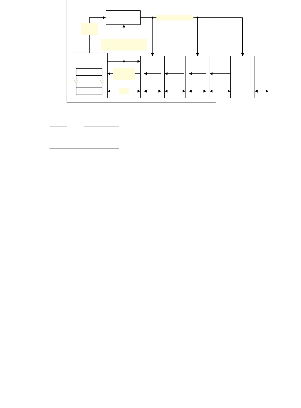
B2 The AArch64 Application Level Memory Model
B2.3 Caches and memory hierarchy
ARM DDI 0487A.a Copyright © 2013 ARM Limited. All rights reserved. B2-71
ID090413 Non-Confidential - Beta
Figure B2-1 Multiple levels of cache in a memory hierarchy
Note
In this manual, in a hierarchical memory system, Level 1 refers to the level closest to the Processing Element, as
shown in Figure B2-1.
Instructions and data can be held in separate caches or in a unified cache. A cache hierarchy can have one or more
levels of separate instruction and data caches, with one or more unified caches located at the levels closest to the
main memory. Memory coherency for cache topologies can be defined by two conceptual points:
Point of Unification (PoU)
The point at which the instruction cache, data cache, and translation table walks of a particular PE
are guaranteed to see the same copy of a memory location. In many cases, the point of unification
is the point in a uniprocessor memory system by which the instruction and data caches and the
translation table walks have merged. The point of unification might coincide with the point of
coherency.
Point of Coherency (PoC)
The point at which all agents that can access memory are guaranteed to see the same copy of a
memory location. In many cases this is effectively the main system memory, although the
architecture does not prohibit the implementation of caches beyond the PoC that have no effect on
the coherency between memory system agents.
See also Cache maintenance operations on page D4-1680.
The cacheability and shareability memory attributes
Cacheability and shareability are two attributes that describe the memory hierarchy in a multiprocessing system:
Cacheability This term defines whether memory locations are allowed to be allocated into a cache or not.
Cacheability can be defined independently for Inner and Outer cacheability locations.
Shareability This term defines whether memory locations are shareable between different agents in a system.
Marking a memory location as shareable for a particular domain requires hardware to ensure that
the location is coherent for all agents in that domain. Shareability can be defined independently for
Inner and Outer shareability domains.
For more information about cacheability and shareability see Memory types and attributes on page B2-89.
Processing
Element
PE,
AArch64 state
Instruction
fetch
Data
Level 1
Cache
Level 2
Cache
Level 3
DRAM
SRAM
Flash
ROM
Level 4
for example,
memory card,
disk
Address
translation
System configuration
and control
X30
X0
Physical address
Virtual
address

B2 The AArch64 Application Level Memory Model
B2.3 Caches and memory hierarchy
B2-72 Copyright © 2013 ARM Limited. All rights reserved. ARM DDI 0487A.a
Non-Confidential - Beta ID090413
B2.3.3 Application level cache instructions
In the ARM architecture, the application level is defined as Exception level 0 (EL0). The architecture defines a set
of cache maintenance instructions that software can use to manage cache coherency. Software executing at a higher
Exception level can enable EL0 access to the following:
• The data cache maintenance instructions,
DC CVAU
,
DC CVAC
, and
DC CIVAC
. See Data cache maintenance
instructions (DC*) on page D4-1685.
• The instruction cache maintenance instruction,
IC IVAU
. See Instruction cache maintenance instructions
(IC*) on page D4-1684.
• The cache type register. See CTR_EL0.
• The data cache zero instruction,
DC ZVA
. See Data cache zero instruction on page D4-1690.
These instructions are UNDEFINED from EL0 unless software executing at a higher Exception level has enabled
them. See Cache maintenance instructions on page D4-1684.
For all of these instructions, if the addresses do not have read access permission at EL0, executing these instructions
at EL0 generates a Permission fault.
For more information about the system controls, see Cache support on page D4-1675.
B2.3.4 Implication of caches for the application programmer
In normal operation, the caches are largely invisible to the application programmer. However they can become
visible when there is a breakdown in the coherency of the caches. Such a breakdown can occur:
• When memory locations are updated by other agents in the system that do not use hardware management of
coherency.
• When memory updates made from the application software must be made visible to other agents in the
system, without the use of hardware management of coherency.
For example:
• In the absence of hardware management of coherency of DMA accesses, in a system with a DMA controller
that reads memory locations that are held in the data cache of a PE, a breakdown of coherency occurs when
the PE has written new data in the data cache, but the DMA controller reads the old data held in memory.
• In a Harvard cache implementation, where there are separate instruction and data caches, a breakdown of
coherency occurs when new instruction data has been written into the data cache, but the instruction cache
still contains the old instruction data.
Data coherency issues
Software can ensure the data coherency of caches in the following ways:
• By not using the caches in situations where coherency issues can arise. This can be achieved by:
— Using Non-cacheable or, in some cases, Write-Through Cacheable memory.
— Not enabling caches in the system.
• By using cache maintenance instructions to manage the coherency issues in software. See Application level
cache instructions.
• By using hardware coherency mechanisms to ensure the coherency of data accesses to memory for cacheable
locations by observers within the different shareability domains, see Non-shareable Normal memory on
page B2-91 and Shareable, Inner Shareable, and Outer Shareable Normal memory on page B2-90.

B2 The AArch64 Application Level Memory Model
B2.3 Caches and memory hierarchy
ARM DDI 0487A.a Copyright © 2013 ARM Limited. All rights reserved. B2-73
ID090413 Non-Confidential - Beta
Note
The performance of these hardware coherency mechanisms is highly implementation-specific. In some
implementations the mechanism suppresses the ability to cache shareable locations. In other
implementations, cache coherency hardware can hold data in caches while managing coherency between
observers within the shareability domains.
Note
Not all these mechanisms are directly available to software operating at EL0 and might involve interaction with
software operating at a higher Exception level.
Synchronization and coherency issues between data and instruction accesses
How far ahead of the current point of execution instructions are fetched from is IMPLEMENTATION DEFINED. Such
prefetching can be either a fixed or a dynamically varying number of instructions, and can follow any or all possible
future execution paths. For all types of memory:
• The PE might have fetched the instructions from memory at any time since the last Context synchronization
operation on that PE.
• Any instructions fetched in this way might be executed multiple times, if this is required by the execution of
the program, without being re-fetched from memory.
The ARM architecture does not require the hardware to ensure coherency between instruction caches and memory,
even for locations of shared memory. This means that for cacheable locations of memory, an instruction cache can
hold instructions that were fetched from memory before any Context synchronization operation.
If software requires coherency between instruction execution and memory, it must manage this coherency using the
ISB
and
DSB
memory barriers and cache maintenance instructions. The following code sequence can be used for this
purpose:
; Coherency example for data and instruction accesses within the same Inner Shareable domain.
; Enter this code with <Wt> containing a new 32-bit instruction,
; to be held in non-cacheable space at a location pointed to by Xn.
STR <Wt>, [Xn]
DC CVAU, Xn ; Clean data cache by VA to point of unification (PoU)
DSB ISH ; Ensure visibility of the data cleaned from cache
IC IVAU, Xn ; Invalidate instruction cache by VA to PoU
DSB ISH ; Ensure completion of the invalidations
ISB ; Synchronize the fetched instruction stream
B2.3.5 Preloading caches
The ARM architecture provides memory system hints
PRFM
,
LDNP
, and
STNP
that software can use to communicate
the expected use of memory locations to the hardware. The memory system can respond by taking actions that are
expected to speed up the memory accesses if they occur. The effect of these memory system hints is
IMPLEMENTATION DEFINED. Typically, implementations use this information to bring the data or instruction
locations into caches.
The Preload instructions are hints, and so implementations can treat them as
NOP
s without affecting the functional
behavior of the device. The instructions cannot generate synchronous Data Abort exceptions, but the resulting
memory system operations might, under exceptional circumstances, generate an asynchronous external abort, which
is taken using an SError interrupt exception. For more information, see Exception from a Data abort on
page D1-1525.

B2 The AArch64 Application Level Memory Model
B2.3 Caches and memory hierarchy
B2-74 Copyright © 2013 ARM Limited. All rights reserved. ARM DDI 0487A.a
Non-Confidential - Beta ID090413
PrefetchHint{}
defines the prefetch hint types:
enumeration PrefetchHint {Prefetch_READ, Prefetch_WRITE, Prefetch_EXEC};
The
Hint_Prefetch()
function signals to the memory system that memory accesses of the type
hint
to or from the
specified
address
are likely to occur in the near future. The memory system might take some action to speed-up the
memory accesses when they do occur, such as preloading the specified address into one or more caches as indicated
by the innermost cache level
target
and non-temporal hint
stream
.
Hint_Prefetch(bits(64) address, PrefetchHint hint, integer target, boolean stream);
For more information on
PRFM
and Load/Store instructions that provide hints to the memory system, see Prefetch
memory on page C2-138 and Load/Store SIMD and Floating-point Non-temporal pair on page C2-136.

B2 The AArch64 Application Level Memory Model
B2.4 Alignment support
ARM DDI 0487A.a Copyright © 2013 ARM Limited. All rights reserved. B2-75
ID090413 Non-Confidential - Beta
B2.4 Alignment support
This section describes alignment support. It contains the following subsections:
•Instruction alignment.
•Alignment of data accesses.
•Unaligned data access restrictions.
B2.4.1 Instruction alignment
A64 instructions must be word-aligned.
Attempting to fetch an instruction from a misaligned location results in a Misaligned PC fault. See PC alignment
checking on page D1-1423.
B2.4.2 Alignment of data accesses
An unaligned access to any type of Device memory causes an Alignment fault.
The alignment requirements for accesses to Normal memory are as follows:
• For all instructions that load or store a single or multiple registers, other than
Load-Exclusive/Store-Exclusive and Load-Acquire/Store-Release, if the address that is accessed is not
aligned to the size of the data element being accessed, then one of the following occurs:
— An Alignment fault is generated.
— An unaligned access is performed.
SCTLR_ELx.A at the current Exception level can be configured to enable an alignment check, and thereby
determine which of these two options is used.
Note
— The SCTLR_EL1.A bit that is applicable to software running at EL0, can only be accessed from EL1
or above.
— Alignment checks are based on element size, not overall access size. This affects SIMD element and
structure loads and stores, and also Load/Store pair instructions.
• For all Load-Exclusive/Store-Exclusive and Load-Acquire/Store-Release memory accesses that access a
single element or a pair of elements, an alignment fault is generated if the address being accessed is not
aligned to the size of the data structure being accessed.
A failed alignment check results in an Alignment fault, which is taken as a Data Abort exception. These exceptions
are taken at the lowest Exception level that can handle the exception, consistent with the basic requirement that the
Exception level never decreases on an exception. Therefore:
• Alignment faults at EL0 or EL1 are taken at EL1 unless redirected by HCR_EL2.TGE
• Alignment faults at EL2 are taken at EL2.
• Alignment faults at EL3 are taken at EL3.
B2.4.3 Unaligned data access restrictions
The following points apply to unaligned data accesses in ARMv8:
• Accesses are not guaranteed to be single-copy atomic except at the byte access level, see Atomicity in the
ARM architecture on page B2-79.
• Unaligned accesses typically takes a number of additional cycles to complete compared to a naturally-aligned
access.
• An operation that performs an unaligned access can abort on any memory access that it makes, and can abort
on more than one access. This means that an unaligned access that occurs across a page boundary can
generate an abort on either side of the boundary.
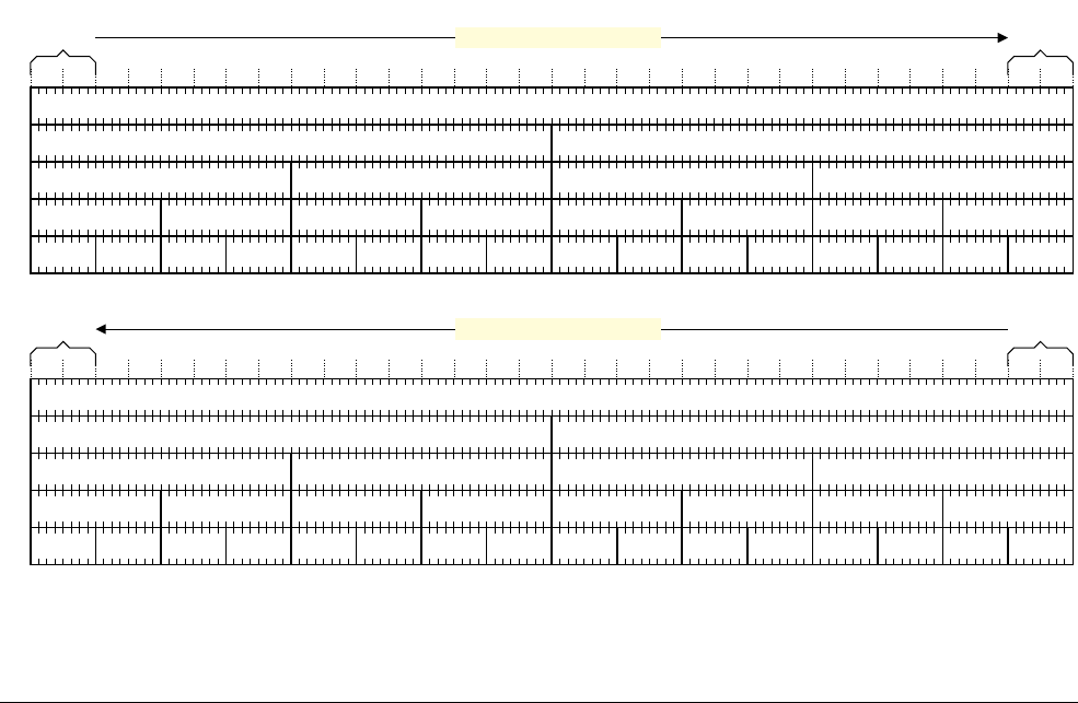
B2 The AArch64 Application Level Memory Model
B2.5 Endian support
B2-76 Copyright © 2013 ARM Limited. All rights reserved. ARM DDI 0487A.a
Non-Confidential - Beta ID090413
B2.5 Endian support
General description of endianness in the ARM architecture describes the relationship between endianness and
memory addressing in the ARM architecture.
The following subsections then describe the endianness schemes supported by the architecture:
•Instruction endianness on page B2-77.
•Data endianness on page B2-77.
B2.5.1 General description of endianness in the ARM architecture
This section only describes memory addressing and the effects of endianness for data elements up to quadwords of
128 bits. However, this description can be extended to apply to larger data elements.
For an address A, Figure B2-2 shows, for big-endian and little-endian memory systems, the relationship between:
• The quadword at address A.
• The doubleword at address A and A+8.
• The words at addresses A, A+4, A+8, and A+12.
• The halfwords at addresses A, A+2, A+4, A+6, A+8, A+10, A+12, and A+14.
• The bytes at addresses A, A+1, A+2, A+3, A+4, A+5, A+6, A+7, A+8, A+9, A+10, A+11, A+12, A+13,
A+14, and A+15.
The terms in Figure B2-2 have the following definitions:
B_A Byte at address A.
HW_A Halfword at address A.
MSByte Most-significant byte.
LSByte Least-significant byte.
Figure B2-2 Endianness relationships
Big-endian memory system
Little-endian memory system
B_A+15 B_A+14 B_A+13 B_A+12 B_A+11 B_A+10 B_A+9 B_A+8 B_A+7 B_A+6 B_A+5 B_A+4 B_A+3 B_A+2 B_A+1 B_A
HW_A+14 HW_A+12 HW_A+10 HW_A+8 HW_A+6 HW_A+4 HW_A+2 HW_A
Word at address A+12 Word at address A+8 Word at address A+4 Word at address A
Doubleword at address A+8 Doubleword at address A
Quadword at address A
Incrementing byte address
LSByteMSByte
Incrementing byte address
B_A+15B_A+14B_A+13B_A+12B_A+11B_A+10B_A+9B_A+8B_A+7B_A+6B_A+5B_A+4B_A+3B_A+2B_A+1B_A
HW_A+14HW_A+12HW_A+10HW_A+8HW_A+6HW_A+4HW_A+2HW_A
Word at address A+12Word at address A+8Word at address A+4Word at address A
Doubleword at address A+8Doubleword at address A
Quadword at address A
LSByteMSByte

B2 The AArch64 Application Level Memory Model
B2.5 Endian support
ARM DDI 0487A.a Copyright © 2013 ARM Limited. All rights reserved. B2-77
ID090413 Non-Confidential - Beta
The big-endian and little-endian mapping schemes determine the order in which the bytes of a quadword,
doubleword, word or halfword are interpreted. For example, a load of a word from address
0x1000
always results in
an access to the bytes at memory locations
0x1000
,
0x1001
,
0x1002
, and
0x1003
. The endianness mapping scheme
determines the significance of these four bytes.
B2.5.2 Instruction endianness
In ARMv8-A, A64 instructions have a fixed length of 32 bits and are always little-endian.
B2.5.3 Data endianness
SCTLR_EL1.E0E, configurable at EL1 or higher, determines the data endianness for execution at EL0.
The data size used for endianness conversions:
• Is the size of the data value that is loaded or stored for SIMD and floating-point register and general-purpose
register loads and stores.
• Is the size of the data element that is loaded or stored for SIMD element and data structure loads and stores.
For more information see Endianness in SIMD operations.
Instructions to reverse bytes in a general-purpose register or a SIMD and floating-point
register
An application or device driver might have to interface to memory-mapped peripheral registers or shared memory
structures that are not the same endianness as the internal data structures. Similarly, the endianness of the operating
system might not match that of the peripheral registers or shared memory. In these cases, the PE requires an efficient
method to transform explicitly the endianness of the data.
Table B2-1 shows the instructions that provide this functionality:
Endianness in SIMD operations
SIMD element Load/Store instructions transfer vectors of elements between memory and the SIMD and
floating-point register file. An instruction specifies both the length of the transfer and the size of the data elements
being transferred. This information is used to load and store data correctly in both big-endian and little-endian
systems.
For example:
LD1 {V0.4H}, [X1]
Table B2-1 Byte reversal instructions
Function Instructions Notes
Reverse bytes in 32-bit word or wordsaREV32 For use with general-purpose registers
Reverse bytes in whole register REV For use with general-purpose registers
Reverse bytes in 16-bit halfwords REV16 For use with general-purpose registers
Reverse elements in doublewords, vector REV64 For use with SIMD and floating-point registers
Reverse elements in words, vector REV32 For use with SIMD and floating-point registers
Reverse elements in halfwords, vector REV16 For use with SIMD and floating-point registers
a. Can operate on multiple words.
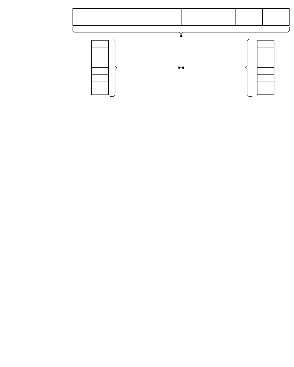
B2 The AArch64 Application Level Memory Model
B2.5 Endian support
B2-78 Copyright © 2013 ARM Limited. All rights reserved. ARM DDI 0487A.a
Non-Confidential - Beta ID090413
This loads a 64-bit register with four 16-bit values. The four elements appear in the register in array order, with the
lowest indexed element fetched from the lowest address. The order of bytes in the elements depends on the
endianness configuration, as shown in Figure B2-3. Therefore, the order of the elements in the registers is the same
regardless of the endianness configuration.
Figure B2-3 SIMD byte order example
The
BigEndian()
function determines the current endianness of the data:
boolean BigEndian();
The pseudocode function for
BigEndianReverse()
is as follows:
// BigEndianReverse()
// ==================
bits(width) BigEndianReverse (bits(width) value)
assert width IN {8, 16, 32, 64, 128};
integer half = width DIV 2;
if width == 8 then return value;
return BigEndianReverse(value<half-1:0>) : BigEndianReverse(value<width-1:half>);
D[15:8] D[7:0] C[15:8] C[7:0] B[15:8] B[7:0] A[15:8] A[7:0]
64-bit register containing four 16-bit elements
0
1
2
3
4
5
6 D[7:0]
C[15:8]
C[7:0]
B[15:8]
B[7:0]
A[15:8]
A[7:0] 0
1
2
3
4
5
6
D[7:0]
D[15:8]
C[7:0]
C[15:8]
B[7:0]
B[15:8]
A[7:0]
A[15:8]
Memory system with
little-endian addressing (LE)
Memory system with
big-endian addressing (BE)
LD1 {V0.4H}, [X1] LD1 {V0.4H}, [X1]
77 D[15:8]

B2 The AArch64 Application Level Memory Model
B2.6 Atomicity in the ARM architecture
ARM DDI 0487A.a Copyright © 2013 ARM Limited. All rights reserved. B2-79
ID090413 Non-Confidential - Beta
B2.6 Atomicity in the ARM architecture
Atomicity is a feature of memory accesses, described as atomic accesses. The ARM architecture description refers
to two types of atomicity, defined in:
•Single-copy atomicity.
•Multi-copy atomicity.
In the ARMv8 architecture, the atomicity requirements for memory accesses depends on the memory type, and
whether the access is explicit or implicit. For more information, see:
•Memory type overview on page B2-69.
•Requirements for single-copy atomicity.
•Requirements for multi-copy atomicity on page B2-80.
B2.6.1 Single-copy atomicity
A read or write operation is single-copy atomic if the following conditions are both true:
• After any number of write operations to a memory location, the value of the memory location is the value
written by one of the write operations. It is impossible for part of the value of the memory location to come
from one write operation and another part of the value to come from a different write operation.
• When a read operation and a write operation are made to the same memory location, the value obtained by
the read operation is either:
— The value of the memory location before the write operation.
— The value of the memory location after the write operation.
It is never the case that the value of the read operation is partly the value of the memory location before the
write operation and partly the value of the memory location after the write operation.
B2.6.2 Multi-copy atomicity
In a multiprocessing system, writes to a memory location are multi-copy atomic if the following conditions are both
true:
• All writes to the same location are serialized, meaning they are observed in the same order by all observers,
although some observers might not observe all of the writes.
• A read of a location does not return the value of a write until all observers observe that write.
Note
Writes that are not coherent are not multi-copy atomic.
B2.6.3 Requirements for single-copy atomicity
For explicit memory accesses generated from an Exception level the following rules apply:
• All reads generated by load instructions that load a single general-purpose register and that are aligned to the
size of the read in that instruction are single-copy atomic.
• All writes generated by store instructions that store a single general-purpose register and that are aligned to
the size of the write in that instruction are single-copy atomic.
• Reads of general-purpose registers generated by Load Pair instructions that are aligned to the size of the load
to each register are treated as two single-copy atomic reads, one for each register being loaded.
• Writes of general-purpose registers generated by Store pair instructions that are aligned to the size of the store
of each register are treated as two single-copy atomic writes, one for each register being stored.
• Load-Exclusive Pair instructions of two 32-bit quantities and Store-Exclusive Pair instructions of 32-bit
quantities are single-copy atomic.

B2 The AArch64 Application Level Memory Model
B2.6 Atomicity in the ARM architecture
B2-80 Copyright © 2013 ARM Limited. All rights reserved. ARM DDI 0487A.a
Non-Confidential - Beta ID090413
• When the Store-Exclusive of a Load-Exclusive /Store-Exclusive pair instruction using two 64-bit quantities
succeeds, it causes a single-copy atomic update of the entire memory location being updated.
Note
To atomically load two 64-bit quantities, perform a Load-Exclusive pair/Store-Exclusive pair sequence of
reading and writing the same value for which the Store-Exclusive pair succeeds, and use the read values from
the Load-Exclusive pair.
• Where translation table walks generate a read of a translation table entry, this read is single-copy atomic.
• When a store that, by the rules given in this section, would be single-copy atomic is made to a memory
location at a time when there is at least one store to the same memory location that has not completed, and
that would be single-copy atomic at a different size, then the architecture does not give any assurance of
atomicity between accesses to the bytes of that location.
• For the atomicity of instruction fetches, see Concurrent modification and execution of instructions on
page B2-91.
All other memory accesses are regarded as streams of accesses to bytes, and no atomicity between accesses to
different bytes is ensured by the architecture.
All accesses to any byte are single-copy atomic.
Note
No memory accesses involving SIMD and floating-point registers, or memory accesses from Data cache zero
instructions, have single-copy atomicity of any quantity greater than individual bytes.
B2.6.4 Requirements for multi-copy atomicity
In a multiprocessing system, coherent writes to a memory location are multi-copy atomic if the read of a location
returns the value of a write only when all observers have observed that write.
For Normal memory, writes are not required to be multi-copy atomic.
For Device memory with the non-Gathering attribute, writes that are single-copy atomic are also multi-copy atomic.
For Device memory with the Gathering attribute, writes are not required to be multi-copy atomic.
B2.6.5 Concurrent modification and execution of instructions
The ARMv8 architecture limits the set of instructions that can be executed by one thread of execution as they are
being modified by another thread of execution without requiring explicit synchronization.
Concurrent modification and execution of instructions can lead to the resulting instruction performing any behavior
that can be achieved by executing any sequence of instructions that can be executed from the same Exception level,
except where the instruction before modification and the instruction after modification is a
B
,
BL
,
NOP
,
BKPT
,
SVC
,
HVC
,
or
SMC
instruction.
For the
B
,
BL
,
NOP
,
BKPT
,
SVC
,
HVC
, and
SMC
instructions the architecture guarantees that, after modification of the
instruction, behavior is consistent with execution of either:
• The instruction originally fetched.
• A fetch of the modified instruction.
For more information about the required synchronization operation, see Synchronization and coherency issues
between data and instruction accesses on page B2-73.
If one thread of execution changes a conditional branch instruction, such as
B
or
BL
, to another conditional instruction
and the change affects both the condition field and the branch target, execution of the changed instruction by another
thread of execution before the change is synchronized can lead to either:
• The old condition being associated with the new target address.

B2 The AArch64 Application Level Memory Model
B2.6 Atomicity in the ARM architecture
ARM DDI 0487A.a Copyright © 2013 ARM Limited. All rights reserved. B2-81
ID090413 Non-Confidential - Beta
• The new condition being associated with the old target address.
These possibilities apply regardless of whether the condition, either before or after the change to the branch
instruction, is the always condition.
Note
For information about memory accesses caused by instruction fetches, see Ordering requirements on page B2-83.

B2 The AArch64 Application Level Memory Model
B2.7 Memory ordering
B2-82 Copyright © 2013 ARM Limited. All rights reserved. ARM DDI 0487A.a
Non-Confidential - Beta ID090413
B2.7 Memory ordering
This section describes observation ordering. It contains the following subsections:
•Observability and completion.
•Ordering requirements on page B2-83.
•Memory barriers on page B2-85.
For information on endpoint ordering of memory accesses, see Reordering on page B2-95.
In the ARMv8 memory model, the shareability memory attribute indicates whether hardware must ensure memory
coherency.
The ARMv8 memory system architecture defines additional attributes and associated behaviors, defined in the
system level section of this manual. See:
•Chapter D4 The AArch64 System Level Memory Model.
•Chapter D5 The AArch64 Virtual Memory System Architecture.
See also Mismatched memory attributes on page B2-98.
B2.7.1 Observability and completion
An observer is a master in the system that is capable of observing memory accesses. For a PE, the following
mechanisms must be treated as independent observers:
• The mechanism that performs reads or writes to memory.
• A mechanism that causes an instruction cache to be filled from memory or that fetches instructions to be
executed directly from memory. These are treated as reads.
• A mechanism that performs translation table walks. These are treated as reads.
The set of observers that can observe a memory access is defined by the system.
In the definitions in this subsection, subsequent means whichever of the following is appropriate to the context:
• After the point in time where the location is observed by that observer.
• After the point in time where the location is globally observed.
For all memory:
• A write to a location in memory is said to be observed by an observer when:
— A subsequent read of the location by the same observer returns the value written by the observed write,
or written by a write to that location by any observer that is sequenced in the Coherence order of the
location after the observed write.
— A subsequent write of the location by the same observer is sequenced in the Coherence order of the
location after the observed write.
• A write to a location in memory is said to be globally observed for a shareability domain or set of observers
when:
— A subsequent read of the location by any observer in that shareability domain returns the value written
by the globally observed write, or written by a write to that location by any observer that is sequenced
in the Coherence order of the location after the globally observed write.
— A subsequent write of the location by any observer in that shareability domain is sequenced in the
Coherence order of the location after the globally observed write.
• A read of a location in memory is said to be observed by an observer when a subsequent write to the location
by the same observer has no effect on the value returned by the read.
• A read of a location in memory is said to be globally observed for a shareability domain when a subsequent
write to the location by any observer in that shareability domain has no effect on the value returned by the
read.

B2 The AArch64 Application Level Memory Model
B2.7 Memory ordering
ARM DDI 0487A.a Copyright © 2013 ARM Limited. All rights reserved. B2-83
ID090413 Non-Confidential - Beta
Additionally, for Device-nGnRnE memory:
• A read or write of a memory-mapped location in a peripheral that exhibits side-effects is said to be observed,
and globally observed, only when the read or write:
— Meets the general conditions listed.
— Can begin to affect the state of the memory-mapped peripheral.
— Can trigger all associated side-effects, whether they affect other peripheral devices, PEs, or memory.
Note
This definition is consistent with the memory access having reached the peripheral.
For all memory, the completion rules are defined as:
• A read or write is complete for a shareability domain when all of the following are true:
— The read or write is globally observed for that shareability domain.
— Any translation table walks associated with the read or write are complete for that shareability domain.
• A translation table walk is complete for a shareability domain when the memory accesses associated with the
translation table walk are globally observed for that shareability domain, and the TLB is updated.
• A cache or TLB maintenance instruction is complete for a shareability domain when the effects of the
instruction are globally observed for that shareability domain, and any translation table walks that arise from
the instruction are complete for that shareability domain.
The completion of any cache or TLB maintenance instruction includes its completion on all PEs that are
affected by both the instruction and the
DSB
operation that is required to guarantee visibility of the
maintenance instruction.
Completion of side-effects of accesses to Device memory
The completion of a memory access to Device memory other than Device-nGnRnE is not guaranteed to be sufficient
to determine that the side-effects of the memory access are visible to all observers. The mechanism that ensures the
visibility of side-effects of a memory access is IMPLEMENTATION DEFINED.
B2.7.2 Ordering requirements
ARMv8 defines restrictions for the permitted ordering of memory accesses. These restrictions depend on the
memory locations that are being accessed. See Memory types and attributes on page B2-89.
The following additional restrictions apply to the order in which accesses to Normal memory are observed:
• Reads and writes can be observed in any order provided the following constraints are met:
— If an address dependency exists between two reads or between a read and a write, then those memory
accesses are observed in program order by all observers within the shareability domain of the memory
address being accessed.
The ARMv8 architecture relaxes this rule for execution where the second read is generated by a Load
Non-Temporal Pair instruction. See Load/Store Non-temporal Pair on page C2-132 and Load/Store
SIMD and Floating-point Non-temporal pair on page C2-136.
— Writes that would not occur in a simple sequential execution of the program cannot be observed by
other observers. This implies that where a control, address or data dependency exists between a read
and a write, those memory accesses are observed in program order by all observers within the
shareability domain of the memory addresses being accessed.
— Ordering can be achieved by using a
DMB
or
DSB
barrier. For more information on
DMB
and
DSB
instructions, see Memory barriers on page B2-85.
• Reads and writes to the same location are coherent within the shareability domain of the memory address
being accessed.

B2 The AArch64 Application Level Memory Model
B2.7 Memory ordering
B2-84 Copyright © 2013 ARM Limited. All rights reserved. ARM DDI 0487A.a
Non-Confidential - Beta ID090413
• Two reads of the same location by the same observer are observed in program order by all observers within
the shareability domain of the memory address being accessed.
• Writes are not required to be multi-copy atomic. This means that in the absence of barriers, the observation
of a store by one observer does not imply the observation of the store by another observer.
• Instructions that access multiple elements have no defined ordering requirements for the memory accesses
relative to each other.
Memory accesses caused by instruction fetches are not required to be observed in program order, unless they are
separated by an
ISB
or other context synchronization event.
Address dependencies and order
In the ARMv8 architecture, a register data dependency creates order between a load instruction and a subsequent
memory transaction, that is between the data value returned from the load and the address used by the subsequent
memory transaction.
A register data dependency exists between a first data value and a second data value exists when either:
• The register, excluding the zero register (XZR or WZR), used to hold the first data value is used in the
calculation of the second data value, and the calculation between the first data value and the second data value
does not consist of either:
— A conditional branch whose condition is determined by the first data value.
— A conditional selection, move, or computation whose condition is determined by the first data value,
where the input data values for the selection, move, or computation do not have a data dependency on
the first data value.
• There is a register data dependency between the first data value and a third data value, and between the third
data value and the second data value.
Note
A register data dependency can exist even if the value of the first data value is discarded as part of the calculation,
as might be the case if it is ANDed with
0x0
or if arithmetic using the first data value cancels out its contribution.
For example, each of the following code snippets exhibits order between the memory transactions:
1. LDR X1, [X2]
1. AND X1, X1, XZR
1. LDR X4, [X3, X1]
2. LDR X1, [X2]
3. ADD X3, X3, X1
4. SUB X3, X3, X1
5. STR X4, [X3]
Address dependencies of Load Non-temporal Pair instructions
Where an address dependency exists between two reads, and the second read was generated by a Load
Non-temporal Pair instruction, then in the absence of any other barrier mechanism to achieve order, those memory
accesses can be observed in any order by other observers within the shareability domain of the memory addresses
being accessed.
This affects the following instruction:
•LDNP on page C5-509.

B2 The AArch64 Application Level Memory Model
B2.7 Memory ordering
ARM DDI 0487A.a Copyright © 2013 ARM Limited. All rights reserved. B2-85
ID090413 Non-Confidential - Beta
B2.7.3 Memory barriers
The ARM architecture is a weakly ordered memory architecture that supports out of order completion. Memory
barrier is the general term applied to an instruction, or sequence of instructions, that forces synchronization events
by a PE with respect to retiring Load/Store instructions. The memory barriers defined by the ARMv8 architecture
provide a range of functionality, including:
• Ordering of Load/Store instructions.
• Completion of Load/Store instructions.
• Context synchronization.
The following subsections describe the ARMv8 memory barrier instructions:
•Instruction Synchronization Barrier (ISB)
•Data Memory Barrier (DMB).
•Data Synchronization Barrier (DSB) on page B2-86.
•Shareability and access limitations on the data barrier operations on page B2-87.
•Load-Acquire, Store-Release on page B2-87.
Note
Depending on the required synchronization, a program might use memory barriers on their own, or it might use them
in conjunction with cache maintenance and memory management instructions that in general are only available
when software execution is at EL1 or higher.
The
DMB
and
DSB
memory barriers affect reads and writes to the memory system generated by Load/Store instructions
and data or unified cache maintenance instructions being executed by the PE. Instruction fetches or accesses caused
by a hardware translation table access are not explicit accesses.
Instruction Synchronization Barrier (ISB)
An
ISB
instruction flushes the pipeline in the PE, so that all instructions that come after the
ISB
instruction in
program order are fetched from the cache or memory only after the
ISB
instruction has completed. Using an
ISB
ensures that the effects of context-changing operations executed before the
ISB
are visible to the instructions fetched
after the
ISB
instruction. Examples of context-changing operations that require the insertion of an
ISB
instruction to
ensure the effects of the operation are visible to instructions fetched after the
ISB
instruction are:
• Completed cache and TLB maintenance instructions.
• Changes to system control registers.
Any context-changing operations appearing in program order after the
ISB
instruction only take effect after the
ISB
has been executed.
InstructionSynchronizationBarrier();
See also Memory barriers on page D4-1705.
Data Memory Barrier (DMB)
The
DMB
instruction is a data memory barrier. The PE that executes the
DMB
instruction is referred to as the executing
PE, PEe. The
DMB
instruction takes the required shareability domain and required access types as arguments:
DataMemoryBarrier(MBReqDomain domain, MBReqTypes types);
See Shareability and access limitations on the data barrier operations on page B2-87.
If the required shareability is Full system then the operation applies to all observers within the system.
A
DMB
creates two groups of memory accesses, Group A and Group B:
Group A Contains:
• All explicit memory accesses of the required access types from observers in the same
required shareability domain as PEe that are observed by PEe before the
DMB
instruction.
These accesses include any accesses of the required access types performed by PEe.

B2 The AArch64 Application Level Memory Model
B2.7 Memory ordering
B2-86 Copyright © 2013 ARM Limited. All rights reserved. ARM DDI 0487A.a
Non-Confidential - Beta ID090413
• All loads of required access types from an observer PEx in the same required shareability
domain as PEe that have been observed by any given different observer, PEy, in the same
required shareability domain as PEe before PEy has performed a memory access that is a
member of Group A.
Group B Contains:
• All explicit memory accesses of the required access types by PEe that occur in program order
after the
DMB
instruction.
• All explicit memory accesses of the required access types by any given observer PEx in the
same required shareability domain as PEe that can only occur after a load by PEx has returned
the result of a store that is a member of Group B.
Any observer with the same required shareability domain as PEe observes all members of Group A before it
observes any member of Group B to the extent that those group members are required to be observed, as determined
by the shareability and cacheability of the memory locations accessed by the group members.
If members of Group A and members of Group B access the same memory-mapped peripheral of arbitrary
system-defined size, then members of Group A that are accessing Device or Normal Non-cacheable memory arrive
at that peripheral before members of Group B that are accessing Device or Normal Non-cacheable memory. Where
the members of Group A and Group B that must be ordered are from the same PE, a
DMB NSH
is sufficient for this
guarantee.
Note
• A memory access might be in neither Group A nor Group B. The
DMB
does not affect the order of observation
of such a memory access.
• The second part of the definition of Group A is recursive. Ultimately, membership of Group A derives from
the observation by PEy of a load before PEy performs an access that is a member of Group A as a result of
the first part of the definition of Group A.
• The second part of the definition of Group B is recursive. Ultimately, membership of Group B derives from
the observation by any observer of an access by PEe that is a member of Group B as a result of the first part
of the definition of Group B.
DMB
only affects memory accesses and the operation of data cache and unified cache maintenance instructions, see
Cache maintenance instructions on page D4-1684. It has no effect on the ordering of any other instructions
executing on the PE.
See also Memory barriers on page D4-1705.
Data Synchronization Barrier (DSB)
The
DSB
instruction is a special memory barrier, that synchronizes the execution stream with memory accesses.
The
DSB
instruction takes the required shareability domain and required access types as arguments:
DataSynchronizationBarrier(MBReqDomain domain, MBReqTypes types);
See Shareability and access limitations on the data barrier operations on page B2-87.
If the required shareability is Full system then the operation applies to all observers within the system.
A
DSB
behaves as a
DMB
with the same arguments, and also has the additional properties defined in this section. The
PE that executes the
DSB
instruction is referred to as the executing PE, PEe
A
DSB
completes when all of the following apply:
• All explicit memory accesses that are observed by PEe before the
DSB
is executed and are of the required
access types, and are from observers in the same required shareability domain as PEe, are complete for the
set of observers in the required shareability domain.

B2 The AArch64 Application Level Memory Model
B2.7 Memory ordering
ARM DDI 0487A.a Copyright © 2013 ARM Limited. All rights reserved. B2-87
ID090413 Non-Confidential - Beta
• All cache maintenance instructions issued by PEe before the
DSB
are complete for the required shareability
domain.
• If the required access types of the
DSB
is reads and writes, all TLB maintenance instructions issued by PEe
before the
DSB
are complete for the required shareability domain.
In addition, no instruction that appears in program order after the
DSB
instruction can execute until the
DSB
completes.
See also Memory barriers on page D4-1705.
Shareability and access limitations on the data barrier operations
The
DMB
and
DSB
instructions can each take an optional limitation argument that specifies:
• The shareability domain over which the instruction must operate. This is one of:
— Full system.
— Outer Shareable.
— Inner Shareable.
— Non-shareable.
• The accesses for which the instruction operates. This is one of:
— Read and write accesses in Group A and Group B.
— Write accesses only in Group A and Group B.
— Read access only in Group A.
Note
This is occasionally referred to as a Load-Load/Store barrier.
— Read and write accesses in Group B.
Note
This is occasionally referred to as a Load-Load/Store barrier.
If no specifiers are used then each instruction operates for read and write accesses, over the full system. See the
instruction descriptions for more information about these arguments.
Note
ISB
also supports an optional limitation argument that can only contain one value that corresponds to full system
operation.
Load-Acquire, Store-Release
ARMv8 provides a set of instructions with Acquire semantics for loads, and Release semantics for stores. See
Load-Acquire/Store-Release on page C2-134.
For all memory types, these instructions have the following ordering requirements:
• A Store-Release followed by a Load-Acquire is observed in program order by each observer within the
shareability domain of the memory address being accessed by the Store-Release and the memory address
being accessed by the Load-Acquire.
• A Load-Acquire is a read that must be observed by all observers in the shareability domain of the accessed
memory location before any other read or write that both:
— Is caused by an instruction that appears in program order after the Load-Acquire.
— Accesses memory in the shareability domain accessed by the Load-Acquire.
• A Load-Acquire places no additional ordering constraints on any loads or stores appearing before the
Load-Acquire.

B2 The AArch64 Application Level Memory Model
B2.7 Memory ordering
B2-88 Copyright © 2013 ARM Limited. All rights reserved. ARM DDI 0487A.a
Non-Confidential - Beta ID090413
• Store-Release is a write:
— Where the reads and writes generated by loads and stores appearing in program order before the
Store-Release are observed as required by the shareability domains of the memory addresses being
accessed by those loads and stores by each observer within the shareability domain of the memory
address being accessed by the Store-Release, before that observer observes the write generated by the
Store-Release.
— Where any writes that have been observed before the Store-Release by the processing element
executing the Store-Release are observed as required by the shareability domains of the memory
addresses being accessed by those loads and store by each observer within the shareability domain of
the memory address being accessed by the Store-Release, before that observer observes the write
generated by the Store-Release.
• The Store-Release places no additional ordering constraints on any loads or stores appearing after the
Store-Release instruction.
• All Store-Release instructions must be multi-copy atomic when they are observed with Load-Acquire
instructions. This means that if one observer has seen the Store-Release, then all observers have seen the
Store-Release.
Load-Acquire and Store-Release, other than Load-Acquire Exclusive Pair and Store-Release-Exclusive Pair, access
only a single data element. This access is single-copy atomic. The address of the data object must be aligned to the
size of the data element being accessed, otherwise the access generates an Alignment fault.
Load-Acquire Exclusive Pair and Store-Release Exclusive Pair access two data elements. The address supplied to
the instructions must be aligned to twice the size of the element being loaded, otherwise the access generates an
Alignment fault.
A Store-Release Exclusive instruction only has the release semantics if the store is successful.
Note
• Each Load-Acquire Exclusive and Store-Release Exclusive instruction is essentially a variant of the
equivalent Load-Exclusive or Store-Exclusive instruction. All usage restrictions and single-copy atomicity
properties that apply to the Load-Exclusive or Store-Exclusive instructions also apply to the Load-Acquire
Exclusive or Store-Release Exclusive instructions.
• The Load-Acquire/Store-Release instructions can remove the requirement to use the explicit DMB memory
barrier instruction.

B2 The AArch64 Application Level Memory Model
B2.8 Memory types and attributes
ARM DDI 0487A.a Copyright © 2013 ARM Limited. All rights reserved. B2-89
ID090413 Non-Confidential - Beta
B2.8 Memory types and attributes
In ARMv8 the ordering of accesses for locations of memory, referred to as the memory order model, is defined by
the memory attributes. The following sections describe this model:
•Normal memory.
•Device memory on page B2-92.
B2.8.1 Normal memory
The Normal memory type attribute applies to most memory in a system. It indicates that the hardware might perform
speculative data read accesses to these locations.
The Normal memory type has the following properties:
• A write to a memory location with the Normal attribute completes in finite time. This means that it is globally
observed for the shareability domain of the memory location in finite time. For a Non-cacheable location, the
location is observed by all observers in finite time.
• A completed write to a memory location with the Normal attribute is globally observed for the shareability
domain of the memory location in finite time without the need for explicit cache maintenance instructions or
barriers. For a Non-cacheable location, the completed write is globally observed for all observers in finite
time without the need for explicit cache maintenance instructions or barriers.
• Writes to a memory location with the Normal memory attribute that are Non-cacheable must reach the
endpoint for that location in the memory system in finite time.
• Unaligned memory accesses can access Normal memory if the system is configured to generate such
accesses.
• There is no requirement for the memory system beyond the PE to be able to identify the elements accessed
by multi-register Load/Store instructions. See Multi-register loads and stores that access Normal memory on
page B2-92.
Note
• The Normal memory attribute is appropriate for locations of memory that are idempotent, meaning that they
exhibit all of the following properties:
— Read accesses can be repeated with no side-effects.
— Repeated read accesses return the last value written to the resource being read.
— Read accesses can fetch additional memory locations with no side-effects.
— Write accesses can be repeated with no side-effects if the contents of the location accessed are
unchanged between the repeated writes or as the result of an exception, as described in this section.
— Unaligned accesses can be supported.
— Accesses can be merged before accessing the target memory system.
• An instruction that generates a sequence of accesses as described in Atomicity in the ARM architecture on
page B2-79 might be abandoned as a result of an exception being taken during the sequence of accesses. On
return from the exception the instruction is restarted, and therefore one or more of the memory locations
might be accessed multiple times. This can result in repeated write accesses to a location that has been
changed between the write accesses.
The following sections describe the other attributes for Normal memory:
•Shareable Normal memory on page B2-90.
•Non-shareable Normal memory on page B2-91.

B2 The AArch64 Application Level Memory Model
B2.8 Memory types and attributes
B2-90 Copyright © 2013 ARM Limited. All rights reserved. ARM DDI 0487A.a
Non-Confidential - Beta ID090413
See also:
•Atomicity in the ARM architecture on page B2-79.
•Memory barriers on page B2-85. For accesses to Normal memory, a
DMB
instruction is required to ensure the
required ordering.
•Concurrent modification and execution of instructions on page B2-80.
Shareable Normal memory
A Normal memory location has a Shareability attribute that is:
• Defined independently for the Inner Shareable and Outer Shareable shareability domains.
• Defined, for each shareability domain, as being either Shareable or Non-shareable.
The shareability attributes define the data coherency requirements of the location, that hardware must enforce. They
do not affect the coherency requirements of instruction fetches, see Synchronization and coherency issues between
data and instruction accesses on page B2-73.
Note
• System designers can use the shareability attribute to specify the locations in Normal memory for which
coherency must be maintained. However, software developers must not assume that specifying a memory
location as Non-shareable permits software to make assumptions about the incoherency of the location
between different PEs in a shared memory system. Such assumptions are not portable between different
multiprocessing implementations that might use the shareability attribute. Any multiprocessing
implementation might implement caches that are shared, inherently, between different processing elements.
• This architecture assumes that all PEs that use the same operating system or hypervisor are in the same Inner
Shareable shareability domain.
Shareable, Inner Shareable, and Outer Shareable Normal memory
The ARM architecture abstracts the system as a series of Inner and Outer Shareability domains.
Each Inner Shareability domain contains a set of observers that are data coherent for each member of that set for
data accesses with the Inner Shareable attribute made by any member of that set.
Each Outer Shareability domain contains a set of observers that are data coherent for each member of that set for
data accesses with the Outer Shareable attribute made by any member of that set.
The following properties also hold:
• Each observer is only a member of a single Inner Shareability domain.
• Each observer is only a member of a single Outer Shareability domain.
• All observers in an Inner Shareability domain are always members of the same Outer Shareability domain.
This means that an Inner Shareability domain is a subset of an Outer Shareability domain, although it is not
required to be a proper subset.
Note
• Because all data accesses to Non-cacheable locations are data coherent to all observers, Non-cacheable
locations are always treated as Outer Shareable.
• The Inner Shareable domain is expected to be the set of PEs controlled by a single hypervisor or operating
system.

B2 The AArch64 Application Level Memory Model
B2.8 Memory types and attributes
ARM DDI 0487A.a Copyright © 2013 ARM Limited. All rights reserved. B2-91
ID090413 Non-Confidential - Beta
The details of the use of the shareability attributes are system-specific. Example B2-1 shows how they might be
used.
Example B2-1 Use of shareability attributes
In an implementation, a particular subsystem with two clusters of PEs has the requirement that:
• In each cluster, the data caches or unified caches of the PEs in the cluster are transparent for all data accesses
to memory locations with the Inner Shareable attribute.
• However, between the two clusters, the caches:
— Are not required to be coherent for data accesses that have only the Inner Shareable attribute.
— Are coherent for data accesses that have the Outer Shareable attribute.
In this system, each cluster is in a different shareability domain for the Inner Shareable attribute, but all components
of the subsystem are in the same shareability domain for the Outer Shareable attribute.
A system might implement two such subsystems. If the data caches or unified caches of one subsystem are not
transparent to the accesses from the other subsystem, this system has two Outer Shareable shareability domains.
Having two levels of shareability means system designers can reduce the performance and power overhead for
shared memory locations that do not need to be part of the Outer Shareable shareability domain.
For Shareable Normal memory, the Load-Exclusive and Store-Exclusive synchronization primitives take account
of the possibility of accesses by more than one observer in the same Shareability domain.
Non-shareable Normal memory
For Normal memory locations, the Non-shareable attribute identifies Normal memory that is likely to be accessed
only by a single PE.
A location in Normal memory with the Non-shareable attribute does not require the hardware to make data accesses
by different observers coherent, unless the memory is Non-cacheable. For a Non-shareable location, if other
observers share the memory system, software must use cache maintenance instructions, if the presence of caches
might lead to coherency issues when communicating between the observers. This cache maintenance requirement
is in addition to the barrier operations that are required to ensure memory ordering.
For Non-shareable Normal memory, it is IMPLEMENTATION DEFINED whether the Load-Exclusive and
Store-Exclusive synchronization primitives take account of the possibility of accesses by more than one observer.
Concurrent modification and execution of instructions
The ARMv8 architecture limits the set of instructions that can be executed by one thread of execution as they are
being modified by another thread of execution without requiring explicit synchronization.
Except where the instruction before modification or the instruction after modification is explicitly identified in this
section, concurrent modification and execution of instructions can lead to the resulting instruction performing any
behavior that can be achieved by executing any sequence of instructions that can be executed from the same
Exception level.
For the instructions explicitly identified in this section, the architecture guarantees that, after modification of the
instruction, behavior is consistent with execution of either:
• The instruction originally fetched.
• A fetch of the modified instruction.
The instructions to which this applies are the
B
,
BL
,
NOP
,
BKPT
,
SVC
,
HVC
, and
SMC
instructions.

B2 The AArch64 Application Level Memory Model
B2.8 Memory types and attributes
B2-92 Copyright © 2013 ARM Limited. All rights reserved. ARM DDI 0487A.a
Non-Confidential - Beta ID090413
For all other instructions, to avoid UNPREDICTABLE behavior, instruction modifications must be explicitly
synchronized before they are executed. The required synchronization is as follows:
1. To ensure that the modified instructions are observable, the thread of execution that is modifying the
instructions must issue the following sequence of instructions and operations:
; Coherency example for self-modifying code
; Enter this code with Wt containing a new 32-bit instruction,
; to be held in non-cacheable space at a location pointed to by Xn.
STR Wt, [Xn]
DSB ISH ; Ensure visibility of the data stored
IC IVAU, Xn ; Invalidate instruction cache by VA to PoU
DSB ISH ; Ensure completion of the invalidations
2. Once the modified instructions are observable, the thread of execution that is executing the modified
instructions must issue the following instruction to ensure execution of the modified instructions:
ISB SY ; Synchronize fetched instruction stream
For both instruction sets, if one thread of execution changes a conditional branch instruction to another conditional
branch instruction, and the change affects both the condition field and the branch target, execution of the changed
instruction by another thread of execution before the change is synchronized can lead to either:
• The old condition being associated with the new target address.
• The new condition being associated with the old target address.
These possibilities apply regardless of whether the condition, either before or after the change to the branch
instruction, is the always condition.
Multi-register loads and stores that access Normal memory
For all instructions that load or store more than one general-purpose register from an Exception level there is no
requirement for the memory system beyond the PE to be able to identify the size of the elements accessed by these
load or store instructions.
For all instructions that load or store more than one general-purpose register from an Exception level the order in
which the registers are accessed is not defined by the architecture.
For all instructions that load or store one or more SIMD and floating-point register from an Exception level there is
no requirement for the memory system beyond the PE to be able to identify the size of the element accessed by these
load or store instructions.
B2.8.2 Device memory
The Device memory type attributes define memory locations where an access to the location can cause side-effects,
or where the value returned for a load can vary depending on the number of loads performed. Typically, the Device
memory attributes are used for memory-mapped peripherals and similar locations.
The attributes for ARMv8 Device memory are:
Gathering Identified as G or nG, see Gathering on page B2-94.
Reordering Identified as R or nR, see Reordering on page B2-95.
Early Write Acknowledgement hint
Identified as E or nE, see Early Write Acknowledgement on page B2-96.
The ARMv8 Device memory types are:
Device-nGnRnE Device non-Gathering, non-Reordering, No Early write acknowledgement.
Equivalent to the Strongly-ordered memory type in earlier versions of the architecture.

B2 The AArch64 Application Level Memory Model
B2.8 Memory types and attributes
ARM DDI 0487A.a Copyright © 2013 ARM Limited. All rights reserved. B2-93
ID090413 Non-Confidential - Beta
Device-nGnRE Device non-Gathering, non-Reordering, Early Write Acknowledgement.
Equivalent to the Device memory type in earlier versions of the architecture.
Device-nGRE Device non-Gathering, Reordering, Early Write Acknowledgement.
ARMv8 adds this memory type to the translation table formats found in earlier versions of
the architecture. The use of barriers is required to order accesses to Device-nGRE memory.
Device-GRE Device Gathering, Reordering, Early Write Acknowledgement.
ARMv8 adds this memory type to the translation table formats found in earlier versions of
the architecture. Device-GRE memory has the fewest constraints. It behaves similar to
Normal memory, with the restriction that speculative accesses to Device-GRE memory is
forbidden.
Collectively these are referred to as any Device memory type. Going down the list, the memory types are described
as getting weaker; conversely the going up the list the memory types are described as getting stronger.
Note
• As the list of types shows, these additional attributes are hierarchical. For example, a memory location that
permits Gathering must also permit Reordering and Early Write Acknowledgement.
• The architecture does not require an implementation to distinguish between each of these memory types and
ARM recognizes that not all implementations will do so. The subsection that describes each of the attributes,
describes the implementation rules for the attribute.
• Earlier versions of the ARM architecture defined the following memory types:
— Strongly-ordered memory. This is the equivalent of the Device-nGnRnE memory type.
— Device memory. This is the equivalent of the Device-nGnRE memory type.
All of these memory types have the following properties:
• Speculative data accesses are not permitted to any memory location with any Device memory attribute. This
means that each memory access to any Device memory type must be one that would be generated by a simple
sequential execution of the program.
Three exceptions to this apply:
— Reads generated by the SIMD and floating-point instructions can access bytes that are not explicitly
accessed by the instruction if the bytes accessed are in a 16-byte window, aligned to 16-bytes, that
contains at least one byte that is explicitly accessed by the instruction.
— For Device memory with the Gathering attribute, reads generated by the
LDNP
instructions are
permitted to access bytes that are not explicitly accessed by the instruction, provided that the bytes
accessed are in a 128-byte window, aligned to 128-bytes, that contains at least one byte that is
explicitly accessed by the instruction.
— Where a load or store instruction performs a sequence of memory accesses, as opposed to one
single-copy atomic access as defined in the rules for single-copy atomicity, these accesses might occur
multiple times as a result of executing the load or store instruction. See Single-copy atomicity on
page B2-79.
Note
— An instruction that generates a sequence of accesses as described in Atomicity in the ARM architecture
on page B2-79 might be abandoned as a result of an exception being taken during the sequence of
accesses. On return from the exception the instruction is restarted, and therefore one or more of the
memory locations might be accessed multiple times. This can result in repeated accesses to a location
where the program only defines a single access. For this reason, ARM strongly recommends that no
accesses to Device memory are performed from a single instruction that spans the boundary of a
translation granule or which in some other way could lead to some of the accesses being aborted.
— Write speculation that is visible to other observers is prohibited for all memory types.

B2 The AArch64 Application Level Memory Model
B2.8 Memory types and attributes
B2-94 Copyright © 2013 ARM Limited. All rights reserved. ARM DDI 0487A.a
Non-Confidential - Beta ID090413
• A write to a memory location with any Device memory attribute completes in finite time. This means that it
is globally observed for all observers in the system in finite time.
• If a location with any Device memory attribute changes without an explicit write by an observer, this change
must also be globally observed for all observers in the system in finite time. Such a change might occur in a
peripheral location that holds status information.
• A completed write to a memory location with any Device memory attribute is globally observed for all
observers in finite time without the need for explicit maintenance.
• Data accesses to memory locations are coherent for all observers in the system, and correspondingly are
treated as being Outer Shareable.
• A memory location with any Device memory attribute cannot be allocated into a cache.
• Writes to a memory location with any Device memory attribute must reach the endpoint for that address in
the memory system in finite time. Typically, the endpoint is a peripheral or some physical memory.
• All accesses to memory with any Device memory attribute must be aligned. Any unaligned access generates
an Alignment fault at the first stage of translation that defined the location as being Device.
Note
In the Non-secure EL1 translation regime in systems where HCR_EL2.TGE == 1 and HCR_EL2.DC == 0,
any Alignment fault that results from the fact that all locations are treated as Device is a fault at the first stage
of translation. This causes ESR_EL2.ISS.[24] to be 0.
• Hardware does not prevent speculative instruction fetches from a memory location with any of the Device
memory attributes unless the memory location is also marked as Execute-never for all Exception levels.
Note
This means that to prevent speculative instruction fetches from memory locations with Device memory
attributes, any location that is assigned any Device memory type must also be marked as Execute-never for
all Exception levels. Failure to mark a memory location with any Device memory attribute as Execute-never
for all Exception levels is a programming error.
For instruction fetches, if branches cause the program counter to point to an area of memory with the Device
attribute which is not marked as Execute-never for the current Exception level, an implementation can either:
• Treat the instruction fetch as if it were to a memory location with the Normal Non-cacheable attribute.
• Take a Permission fault.
Gathering
In the Device memory attribute:
G Indicates that the location has the Gathering attribute.
nG Indicates that the location does not have the Gathering attribute, meaning it is non-Gathering.
The Gathering attribute determines whether it is permissible for either:
• Multiple memory accesses of the same type, read or write, to the same memory location to be merged into a
single transaction.
• Multiple memory accesses of the same type, read or write, to different memory locations to be merged into
a single memory transaction on an interconnect.
Note
This also applies to writebacks from the cache, whether caused by a Natural eviction or as a result of a cache
maintenance instruction.

B2 The AArch64 Application Level Memory Model
B2.8 Memory types and attributes
ARM DDI 0487A.a Copyright © 2013 ARM Limited. All rights reserved. B2-95
ID090413 Non-Confidential - Beta
For memory types with the Gathering attribute, either of these behaviors is permitted, provided that the ordering and
coherency rules of the memory location are followed.
For memory types with the non-Gathering attribute, neither of these behaviors is permitted. As a result:
• The number of memory accesses that are made corresponds to the number that would be generated by a
simple sequential execution of the program.
• All access occur at their programmed size, except that there is no requirement for the memory system beyond
the PE to be able to identify the elements accessed by multi-register Load/Store instructions. See
Multi-register loads and stores that access Device memory on page B2-97.
Gathering between memory accesses separated by a memory barrier that affects those memory accesses is not
permitted. This applies if one memory access is in Group A and one memory access is in Group B. That is, gathering
is not permitted between a memory access in Group A and a memory access in Group B if the two accesses are
separated by a barrier that affects at least one of the accesses.
Gathering between two memory accesses generated by a Load-Acquire/Store-Release is not permitted.
A read from a memory location with the non-Gathering attribute cannot come from a cache or a buffer, but must
come from the endpoint for that address in the memory system. Typically this is a peripheral or physical memory.
Note
• A read from a memory location with the Gathering attribute can come from intermediate buffering of a
previous write, provided that:
— The accesses are not separated by a
DMB
or
DSB
barrier that affects both of the accesses, for example if
one access is in Group A and the other is in Group B.
— The accesses are not separated by other ordering constructions that require that the accesses are in
order. Such a construction might be a combination of Load-Acquire and Store-Release.
— The accesses are not generated by a Store-Release instruction.
• The ARM architecture only defines programmer visible behavior. Therefore, gathering can be performed if
a programmer cannot tell whether gathering has occurred.
An implementation is permitted to perform an access with the Gathering attribute in a manner consistent with the
requirements specified by the Non-gathering attribute.
An implementation is not permitted to perform an access with the Non-gathering attribute in a manner consistent
with the relaxations allowed by the Gathering attribute.
Reordering
In the Device memory attribute:
R Indicates that the location has the Reordering attribute.
nR Indicates that the location does not have the Reordering attribute, meaning it is non-Reordering.
For all memory types with the non-Reordering attribute, the order of memory accesses arriving at a single peripheral
of IMPLEMENTATION DEFINED size, as defined by the peripheral, must be the same order that occurs in a simple
sequential execution of the program.That is, the accesses appear in program order. This ordering applies to all
accesses using any of the memory types with the non-Reordering attribute. As a result, if there is a mixture of
Device-nGnRE and Device-nGnRnE accesses to the same peripheral, these occur in program order. If the memory
accesses are not to a peripheral, then this attribute imposes no restrictions.
Note
• The IMPLEMENTATION DEFINED size of the single peripheral is the same as applies for the ordering guarantee
provided by the
DMB
instruction.
• The ARM architecture only defines programmer visible behavior. Therefore, reordering can be performed if
a programmer cannot tell whether reordering has occurred.

B2 The AArch64 Application Level Memory Model
B2.8 Memory types and attributes
B2-96 Copyright © 2013 ARM Limited. All rights reserved. ARM DDI 0487A.a
Non-Confidential - Beta ID090413
An implementation is permitted to perform an access with the Reordering attribute in a manner consistent with the
requirements specified by the non-Reordering attribute.
An additional relaxation is that an implementation is not permitted to perform an access with the non-Reordering
attribute in a manner consistent with the relaxations allowed by the Reordering attribute.
The non-Reordering attribute does not require any additional ordering, other than that which applies to Normal
memory, between:
• Accesses with the non-Reordering attribute and accesses with the Reordering attribute.
• Accesses with the non-Reordering attribute and accesses to Normal memory.
• Accesses with the non-Reordering attribute and accesses to different peripherals of IMPLEMENTATION
DEFINED size.
The non-Reordering attribute has no effect on the ordering of cache maintenance instructions, even if the memory
location specified in the instruction has the non-Reordering attribute.
Early Write Acknowledgement
In the Device memory attribute:
E Indicates that the location has the Early Write Acknowledgement attribute.
nE Indicates that the location has the No Early Write Acknowledgement attribute.
Early Write Acknowledgement is a hint to the platform memory system. Assigning the No Early Write
Acknowledgement attribute to a Device memory location recommends that only the endpoint of the write access
returns a write acknowledgement of the access, and that no earlier point in the memory system returns a write
acknowledge. This means that a
DSB
barrier, executed by the PE that performed the write to the No Early Write
Acknowledgement location, completes only after the write has reached its endpoint in the memory system.
Typically, this endpoint is a peripheral or physical memory.
When the Early Write Acknowledgement attribute is assigned to a Device memory location, there is no such
recommendation for the handling of accesses to that location.
Note
• The Early Write Acknowledgement hint has no effect on the ordering rules. The purpose of signalling no
Early Write Acknowledgement is to signal to the interconnect that the peripheral requires the ability to signal
the acknowledgement. The No Write Acknowledgement signal also provides an additional semantic that can
be interpreted by the driver that is accessing the peripheral.
• This attribute is treated as a hint, as the exact nature of the interconnects accessed by a PE is outside the scope
of the ARM architecture definition, and not all interconnects provide a mechanism to ensure that a write has
reached the physical endpoint of the memory system.
• ARM recommends that writes with the No Early Write Acknowledgement hint are used for PCIe
configuration writes. However, the mechanisms by which PCIe configuration writes are identified are
IMPLEMENTATION DEFINED.
• ARM strongly recommends that the Early Write Acknowledgement hint is not ignored by a PE, but is made
available for use by the system.
Because the No Early Write Acknowledgement attribute is a hint:
• An implementation is permitted to perform an access with the Early Write Acknowledgement attribute in a
manner consistent with the requirements specified by the No Early Write Acknowledgement attribute.
• An implementation is permitted to perform an access with the No Early Write Acknowledgement attribute
in a manner consistent with the relaxations allowed by the Early Write Acknowledgement attribute.

B2 The AArch64 Application Level Memory Model
B2.8 Memory types and attributes
ARM DDI 0487A.a Copyright © 2013 ARM Limited. All rights reserved. B2-97
ID090413 Non-Confidential - Beta
Multi-register loads and stores that access Device memory
For all instructions that load or store more than one general-purpose register from an Exception level there is no
requirement for the memory system beyond the PE to be able to identify the size of the elements accessed by these
load or store instructions.
For all instructions that load or store more than one general-purpose register from an Exception level the order in
which the registers are accessed is not defined by the architecture. This applies even to accesses to any type of
Device memory.
For all instructions that load or store one or more floating-point and SIMD register from an Exception level there is
no requirement for the memory system beyond the PE to be able to identify the size of the element accessed by these
load or store instructions, even for access to any type of Device memory.

B2 The AArch64 Application Level Memory Model
B2.9 Mismatched memory attributes
B2-98 Copyright © 2013 ARM Limited. All rights reserved. ARM DDI 0487A.a
Non-Confidential - Beta ID090413
B2.9 Mismatched memory attributes
Memory attributes are controlled by privileged software. For more information, see Chapter D5 The AArch64
Virtual Memory System Architecture.
Physical memory locations are accessed with mismatched attributes if all accesses to the location do not use a
common definition of all of the following attributes of that location:
• Memory type, Device or Normal.
• Shareability.
• Cacheability, for the same level of the inner or outer cache, but excluding any cache allocation hints.
Collectively these are referred to as memory attributes.
Note
The terms location and memory location refer to any byte within the current coherency granule and are used
interchangeably.
The following rules apply when a physical memory location is accessed with mismatched attributes:
1. When a memory location is accessed with mismatched attributes the only software visible effects are one or
more of the following:
• Uniprocessor semantics for reads and writes to that memory location might be lost. This means:
— A read of the memory location by one agent might not return the value most recently written to
that memory location by the same agent.
— Multiple writes to the memory location by one agent with different memory attributes might not
be ordered in program order.
• There might be a loss of coherency when multiple agents attempt to access a memory location.
• There might be a loss of properties derived from the memory type, as described in later bullets in this
section.
• If all Load-Exclusive/Store-Exclusive instructions executed across all threads to access a given
memory location do not use consistent memory attributes, the exclusive monitor state becomes
UNKNOWN.
• Bytes written without the Write-Back cacheable attribute within the same Write-Back granule as bytes
written with the Write-Back cacheable attribute might have their values reverted to the old values as
a result of cache Write-Back.
2. The loss of properties associated with mismatched memory type attributes refers only to the following
properties of Device memory that are additional to the properties of Normal memory:
• Prohibition of speculative read accesses.
• Prohibition on Gathering.
• Prohibition on Re-ordering.
• The Write Acknowledgement guarantee with respect to the endpoint of the access.
If the only memory type mismatch associated with a memory location across all users of the memory location
is between different types of Device memory, then all accesses might take the properties of the weakest
Device memory type.
3. If all aliases of a memory location that permit write access to the location assign the same shareability and
cacheability attributes to that location, and all these aliases use a definition of the shareability attribute that
includes all the threads of execution that can access the location, then any agent that reads the memory
location using these shareability and cacheability attributes accesses it coherently, to the extent required by
that common definition of the memory attributes.
4. The possible loss of software-visible effects caused by mismatched attributes for a memory location are
defined more precisely if all of the mismatched attributes define the memory location as one of:
• Any Device memory type.
• Normal Inner Non-cacheable, Outer Non-cacheable memory.

B2 The AArch64 Application Level Memory Model
B2.9 Mismatched memory attributes
ARM DDI 0487A.a Copyright © 2013 ARM Limited. All rights reserved. B2-99
ID090413 Non-Confidential - Beta
In these cases, the only permitted software-visible effects of the mismatched attributes are one or more of the
following:
• Possible loss of properties described in point 2 page B2-98, derived from the memory type when
multiple agents attempt to access the memory location.
• Possible reordering of memory transactions to the memory location with different memory attributes,
potentially leading to a loss of coherency or uniprocessor semantics. Any possible loss of coherency
or uniprocessor semantics can be avoided by inserting
DMB
barrier instructions between accesses to the
same memory location that might use different attributes.
5. If the mismatched attributes for a memory location all assign the same shareability attribute to the location,
any loss of uniprocessor semantics or coherency within a shareability domain can be avoided by use of
software cache management. To do so, software must use the techniques that are required for the software
management of the coherency of cacheable locations between agents a in different shareability domains. This
means:
• Before writing to a location not using the Write-Back attribute, software must invalidate, or clean, a
location from the caches if any agent might have written to the location with the Write-Back attribute.
This avoids the possibility of overwriting the location with stale data.
• After writing to a location with the Write-Back attribute, software must clean the location from the
caches, to make the write visible to external memory.
• Before reading the location with a cacheable attribute, software must invalidate the location from the
caches, to ensure that any value held in the caches reflects the last value made visible in external
memory.
In all cases:
• Location refers to any byte within the current coherency granule.
• A clean and invalidate instruction can be used instead of a clean instruction, or instead of an invalidate
instruction.
• In the sequences outlined in this section, all cache maintenance instructions and memory transactions
must be completed, or ordered by the use of barrier operations, if they are not naturally ordered by the
use of a common address, see Ordering and completion of data and instruction cache instructions on
page D4-1689.
Note
With software management of coherency, race conditions can cause loss of data. A race condition occurs
when different agents write simultaneously to bytes that are in the same location, and the invalidate, write,
clean sequence of one agent overlaps with the equivalent sequence of another agent. A race condition also
occurs if the first operation of either sequence is a clean, rather than an invalidate.
6. If the mismatched attributes for a location mean that multiple cacheable accesses to the location might be
made with different shareability attributes, then coherency is guaranteed only if processing elements that
accesses the location with a cacheable attribute performs a clean and invalidate of the location before and
after accessing that location.
Note
The Note in rule 5 on page B2-99 about possible race conditions also applies to this rule.
In addition, if multiple agents attempt to use Load-Exclusive or Store-Exclusive instructions to access a location,
and the accesses from the different agents have different memory attributes associated with the location, the
exclusive monitor state becomes UNKNOWN.
ARM strongly recommends that software does not use mismatched attributes for aliases of the same location. An
implementation might not optimize the performance of a system that uses mismatched aliases.

B2 The AArch64 Application Level Memory Model
B2.10 Synchronization and semaphores
B2-100 Copyright © 2013 ARM Limited. All rights reserved. ARM DDI 0487A.a
Non-Confidential - Beta ID090413
B2.10 Synchronization and semaphores
ARMv8 provides non-blocking synchronization of shared memory, using synchronization primitives. The
information in this section about memory accesses by synchronization primitives applies to accesses to both Normal
and Device memory.
Note
Use of the ARMv8 synchronization primitives scales for multiprocessing system designs.
Table B2-2 shows the synchronization primitives and the associated
CLREX
instruction.
The model for the use of a Load-Exclusive/Store-Exclusive instruction pair accessing a non-aborting memory
address x is:
• The Load-Exclusive instruction reads a value from memory address x.
• The corresponding Store-Exclusive instruction succeeds in writing back to memory address x only if no other
observer, process, or thread has performed a more recent store to address x. The Store-Exclusive instruction
returns a status bit that indicates whether the memory write succeeded.
A Load-Exclusive instruction marks a small block of memory for exclusive access. The size of the marked block is
IMPLEMENTATION DEFINED, see Marking and the size of the marked memory block on page B2-105. A
Store-Exclusive instruction to any address in the marked block clears the marking.
Note
In this section, the term PE includes any observer that can generate a Load-Exclusive or a Store-Exclusive
instruction.
Table B2-2 Synchronization primitives and associated instruction
Function Instruction
Load-Exclusive
Paira
LDXP
,
LDAXP
Registera
a. The instruction operates on a doubleword if accessing an
X register, or on a word if accessing a W register.
LDXR
,
LDAXR
Halfword
LDXRH
,
LDAXRH
Byte
LDXRB
,
LDAXRB
Store-Exclusive
Paira
STXP
,
STLXP
Registera
STXR
,
STLXR
Halfword
STXRH
,
STLXRH
Byte
STXRB
,
STLXRB
Clear-Exclusive
CLREX
B2 The AArch64 Application Level Memory Model
B2.10 Synchronization and semaphores
ARM DDI 0487A.a Copyright © 2013 ARM Limited. All rights reserved. B2-101
ID090413 Non-Confidential - Beta
B2.10.1 Exclusive access instructions and Non-shareable memory locations
For memory locations that do not have the Shareable attribute, the exclusive access instructions rely on a local
monitor that marks any address from which the PE executes a Load-Exclusive instruction. Any non-aborted attempt
by the same PE to use a Store-Exclusive instruction to modify any address is guaranteed to clear the marking.
A Load-Exclusive instruction performs a load from memory, and:
• The executing PE marks the physical memory address for exclusive access.
• The local monitor of the executing PE transitions to the Exclusive Access state.
A Store-Exclusive instruction performs a conditional store to memory that depends on the state of the local monitor:
If the local monitor is in the Exclusive Access state
• If the address of the Store-Exclusive instruction is the same as the address that has been
marked in the monitor by an earlier Load-Exclusive instruction, then the store occurs.
Otherwise, it is IMPLEMENTATION DEFINED whether the store occurs.
• A status value is returned to a register:
— If the store took place the status value is 0.
— Otherwise, the status value is 1.
• The local monitor of the executing PE transitions to the Open Access state.
If the local monitor is in the Open Access state
• No store takes place.
• A status value of 1 is returned to a register.
• The local monitor remains in the Open Access state.
The Store-Exclusive instruction defines the register to which the status value is returned.
When a PE writes using any instruction other than a Store-Exclusive instruction:
• If the write is to a physical address that is not tagged by its local monitor it is IMPLEMENTATION DEFINED
whether the write affects the state of the local monitor.
• If the write is to a physical address that is tagged by its local monitor it is IMPLEMENTATION DEFINED whether
the write affects the state of the local monitor.
It is IMPLEMENTATION DEFINED whether a store to a marked physical address causes a mark in the local monitor to
be cleared if that store is by an observer other than the one that caused the physical address to be marked.
Figure B2-4 shows the state machine for the local monitor and the effect of each of the operations shown in the
figure.
Figure B2-4 Local monitor state machine diagram
Open
Access
Exclusive
Access
LoadExcl(x) LoadExcl(x)
CLREX
StoreExcl(x)
Store(x)
CLREX Store(!Marked_address)
Store(Marked_address)*
Operations marked * are possible alternative IMPLEMENTATION DEFINED options.
Store(Marked_address)*
StoreExcl(Marked_address)
StoreExcl(!Marked_address)
Store(!Marked_address)*
In the diagram: LoadExcl represents any Load-Exclusive instruction
StoreExcl represents any Store-Exclusive instruction
Store represents any other store instruction.
Any LoadExcl operation updates the marked address to the most significant bits of the address x used for the operation.

B2 The AArch64 Application Level Memory Model
B2.10 Synchronization and semaphores
B2-102 Copyright © 2013 ARM Limited. All rights reserved. ARM DDI 0487A.a
Non-Confidential - Beta ID090413
For more information about marking see Marking and the size of the marked memory block on page B2-105.
Note
For the local monitor state machine, as shown in Figure B2-4 on page B2-101:
• The IMPLEMENTATION DEFINED options for the local monitor are consistent with the local monitor being
constructed so that it does not hold any physical address, but instead treats any access as matching the address
of the previous Load-Exclusive instruction.
• A local monitor implementation can be unaware of Load-Exclusive and Store-Exclusive instructions from
other PEs.
• The architecture does not require a load instruction by another PE, that is not a Load-Exclusive instruction,
to have any effect on the local monitor.
• It is IMPLEMENTATION DEFINED whether the transition from Exclusive Access to Open Access state occurs
when the
Store
or
StoreExcl
is from another observer.
Changes to the local monitor state resulting from speculative execution
The architecture permits a local monitor to transition to the Open Access state as a result of speculation, or from
some other cause. This is in addition to the transitions to Open Access state caused by the architectural execution
of an operation shown in Figure B2-4 on page B2-101.
An implementation must ensure that:
• The local monitor cannot be seen to transition to the Exclusive Access state except as a result of the
architectural execution of one of the operations shown in Figure B2-4 on page B2-101.
• Any transition of the local monitor to the Open Access state not caused by the architectural execution of an
operation shown in Figure B2-4 on page B2-101 must not indefinitely delay forward progress of execution.
B2.10.2 Exclusive access instructions and Shareable memory locations
For memory locations that have the Shareable attribute, exclusive access instructions rely on:
•A local monitor for each PE in the system, that marks any address from which the PE executes a
Load-Exclusive. The local monitor operates as described in Exclusive access instructions and Non-shareable
memory locations on page B2-101, except that for Shareable memory any Store-Exclusive is then subject to
checking by the global monitor if it is described in that section as doing at least one of the following:
— Updating memory.
— Returning a status value of 0.
The local monitor can ignore accesses from other PEs in the system.
•A global monitor that marks a physical address as exclusive access for a particular PE. This marking is used
later to determine whether a Store-Exclusive to that address that has not been failed by the local monitor can
occur. Any successful write to the marked block by any other observer in the shareability domain of the
memory location is guaranteed to clear the marking. For each PE in the system, the global monitor:
— Can hold one marked block.
— Maintains a state machine for each marked block it can hold.
Note
For each PE, the architecture only requires global monitor support for a single marked address. Any situation
that might benefit from the use of multiple marked addresses on a single PE is UNPREDICTABLE, see
Load-Exclusive and Store-Exclusive instruction usage restrictions on page B2-106.

B2 The AArch64 Application Level Memory Model
B2.10 Synchronization and semaphores
ARM DDI 0487A.a Copyright © 2013 ARM Limited. All rights reserved. B2-103
ID090413 Non-Confidential - Beta
Note
The global monitor can either reside within the PE, or exist as a secondary monitor at the memory interfaces.The
IMPLEMENTATION DEFINED aspects of the monitors mean that the global monitor and local monitor can be combined
into a single unit, provided that the unit performs the global monitor and local monitor functions defined in this
manual.
For Shareable locations of memory, in some implementations and for some memory types, the properties of the
global monitor require functionality outside the PE. Some system implementations might not implement this
functionality for all locations of memory. In particular, this can apply to:
• Any type of memory in the system implementation that does not support hardware cache coherency.
• Non-cacheable memory, or memory treated as Non-cacheable, in an implementation that does support
hardware cache coherency.
In such a system, it is defined by the system:
• Whether the global monitor is implemented.
• If the global monitor is implemented, which address ranges or memory types it monitors.
Note
To support the use of the Load-Exclusive/Store-Exclusive mechanism when address translation is disabled, a
system might define at least one location of memory, of at least the size of the translation granule, in the system
memory map to support the global monitor for all ARM PEs within a common Inner Shareable domain. However,
this is not an architectural requirement. Therefore, architecturally-compliant software that requires mutual
exclusion must not rely on using the Load-Exclusive/Store-Exclusive mechanism, and must instead use a software
algorithm such as Lamport’s Bakery algorithm to achieve mutual exclusion.
If the global monitor is not implemented for an address range or memory type, then performing a
Load-Exclusive/Store-Exclusive instruction to such a location has one or more of the following effects:
• The instruction generates an external abort.
• The instruction generates an IMPLEMENTATION DEFINED MMU fault. This is reported using the Fault Status
code of ESR_ELx.DFSC = 110101.
• The instruction is treated as a
NOP
.
• The Load-Exclusive instruction is treated as if it were accessing a Non-shareable location, but the state of the
local monitor becomes UNKNOWN.
• The Store-Exclusive instruction is treated as if it were accessing a Non-shareable location, but the state of the
local monitor becomes UNKNOWN.
• The value held in the result register of the Store-Exclusive instruction becomes UNKNOWN.
In addition, for write transactions generated by non-PE observers that do not implement exclusive accesses or other
atomic access mechanisms, the effect that writes have on the global and local monitors used by ARM PEs is
IMPLEMENTATION DEFINED. The writes might not clear the global monitors of other PEs for:
• Some address ranges.
• Some memory types.
Operation of the global monitor
A Load-Exclusive instruction from Shareable memory performs a load from memory, and causes the physical
address of the access to be marked as exclusive access for the requesting PE. This access also causes the exclusive
access mark to be removed from any other physical address that has been marked by the requesting PE.
Note
The global monitor only supports a single outstanding exclusive access to Shareable memory per PE.
A Load-Exclusive instruction by one PE has no effect on the global monitor state for any other PE.

B2 The AArch64 Application Level Memory Model
B2.10 Synchronization and semaphores
B2-104 Copyright © 2013 ARM Limited. All rights reserved. ARM DDI 0487A.a
Non-Confidential - Beta ID090413
A Store-Exclusive instruction performs a conditional store to memory:
• The store is guaranteed to succeed only if the physical address accessed is marked as exclusive access for the
requesting PE and both the local monitor and the global monitor state machines for the requesting PE are in
the Exclusive Access state. In this case:
— A status value of 0 is returned to a register to acknowledge the successful store.
— The final state of the global monitor state machine for the requesting PE is IMPLEMENTATION DEFINED.
— If the address accessed is marked for exclusive access in the global monitor state machine for any other
PE then that state machine transitions to Open Access state.
• If no address is marked as exclusive access for the requesting PE, the store does not succeed:
— A status value of 1 is returned to a register to indicate that the store failed.
— The global monitor is not affected and remains in Open Access state for the requesting PE.
• If a different physical address is marked as exclusive access for the requesting PE, it is IMPLEMENTATION
DEFINED whether the store succeeds or not:
— If the store succeeds a status value of 0 is returned to a register, otherwise a value of 1 is returned.
— If the global monitor state machine for the PE was in the Exclusive Access state before the
Store-Exclusive instruction it is IMPLEMENTATION DEFINED whether that state machine transitions to
the Open Access state.
The Store-Exclusive instruction defines the register to which the status value is returned.
In a shared memory system, the global monitor implements a separate state machine for each PE in the system. The
state machine for accesses to Shareable memory by PE(n) can respond to all the Shareable memory accesses visible
to it. This means it responds to:
• Accesses generated by PE(n).
• Accesses generated by the other observers in the shareability domain of the memory location. These accesses
are identified as (!n).
In a shared memory system, the global monitor implements a separate state machine for each observer that can
generate a Load-Exclusive or a Store-Exclusive instruction in the system.
Clear global monitor event
Whenever the global monitor state for a PE changes from Exclusive access to Open access, an event is generated
and held in the Event register for that PE. This register is used by the Wait for Event mechanism, see Mechanisms
for entering a low-power state on page D1-1533.
Figure B2-5 on page B2-105 shows the state machine for PE(n) in a global monitor.
B2 The AArch64 Application Level Memory Model
B2.10 Synchronization and semaphores
ARM DDI 0487A.a Copyright © 2013 ARM Limited. All rights reserved. B2-105
ID090413 Non-Confidential - Beta
Figure B2-5 Global monitor state machine diagram for PE(n) in a multiprocessor system
For more information about marking see Marking and the size of the marked memory block.
Note
For the global monitor state machine, as shown in Figure B2-5:
• The architecture does not require a load instruction by another PE, that is not a Load-Exclusive instruction,
to have any effect on the global monitor.
• Whether a Store-Exclusive instruction successfully updates memory or not depends on whether the address
accessed matches the marked Shareable memory address for the PE issuing the Store-Exclusive instruction,
and whether the local and global monitors are in the exclusive state. For this reason, Figure B2-5 only shows
how the operations by (!n) cause state transitions of the state machine for PE(n).
• A Load-Exclusive instruction can only update the marked Shareable memory address for the PE issuing the
Load-Exclusive instruction.
• When the global monitor is in the Exclusive Access state, it is IMPLEMENTATION DEFINED whether a
CLREX
instruction causes the global monitor to transition from Exclusive Access to Open Access state.
• It is IMPLEMENTATION DEFINED:
— Whether a modification to a Non-shareable memory location can cause a global monitor to transition
from Exclusive Access to Open Access state.
— Whether a Load-Exclusive instruction to a Non-shareable memory location can cause a global monitor
to transition from Open Access to Exclusive Access state.
B2.10.3 Marking and the size of the marked memory block
When a Load-Exclusive instruction is executed, the resulting marked block ignores the least significant bits of the
64-bit memory address.
When a
LDXR
instruction is executed, a marked block of size 2a is created by ignoring the least significant bits of the
memory address. A marked address is any address within this marked block. For example, in an implementation
where a is 4, a successful
LDXRB
of address
0x341B4
defines a marked block using bits[47:4] of the address. This
means that the four words of memory from
0x341B0
to
0x341BF
are marked for exclusive access.
Any LoadExcl operation updates the marked address to the most significant bits of the address x used for the operation.
Open
Access
Exclusive
Access
LoadExcl(x,n) LoadExcl(x,n)
CLREX(n)
StoreExcl(x,n)
CLREX(n)*
StoreExcl(Marked_address,!n)‡
Store(Marked_address,!n)
StoreExcl(Marked_address,n)*
Store(!Marked_address,n)
Operations marked * are possible alternative IMPLEMENTATION DEFINED options.
In the diagram: LoadExcl represents any Load-Exclusive instruction
StoreExcl represents any Store-Exclusive instruction
Store represents any other store instruction.
LoadExcl(x,!n)
StoreExcl(x,!n)
Store(x,n)
StoreExcl(!Marked_address,n)*
Store(Marked_address,n)*
StoreExcl(Marked_address,!n)‡
StoreExcl(Marked_address,n)*
StoreExcl(!Marked_address,n)*
Store(Marked_address,n)*
CLREX(n)*
StoreExcl(!Marked_address,!n)
Store(!Marked_address,!n)
CLREX(!n)
‡StoreExcl(Marked_address,!n) clears the monitor only if the StoreExcl updates memory
Store(x,!n)
CLREX(!n)

B2 The AArch64 Application Level Memory Model
B2.10 Synchronization and semaphores
B2-106 Copyright © 2013 ARM Limited. All rights reserved. ARM DDI 0487A.a
Non-Confidential - Beta ID090413
The size of the marked memory block is called the Exclusives Reservation Granule. The Exclusives Reservation
Granule is IMPLEMENTATION DEFINED in the range 2 - 512 words:
• 3 words in an implementation where a is 4.
• 512 words in an implementation where a is 11.
In some implementations the CTR identifies the Exclusives Reservation Granule, see CTR_EL0. Otherwise,
software must assume that the maximum Exclusives Reservation Granule, 512 words, is implemented.
B2.10.4 Context switch support
An exception return clears the local monitor. As a result, performing a
CLREX
instruction as part of a context switch
is not required in most situations.
Note
Context switching is not an application level operation. However, this information is included here to complete the
description of the exclusive operations.
B2.10.5 Load-Exclusive and Store-Exclusive instruction usage restrictions
The Load-Exclusive and Store-Exclusive instructions are intended to work together as a pair, for example a
LDXP
/
STXP
pair or a
LDXR/STXR
pair. To support different implementations of these functions, software must follow
the notes and restrictions given here.
The following notes describe use of a Load-Exclusive/Store-Exclusive pair,
LoadExcl
/
StoreExcl
, to indicate the use
of any of the Load-Exclusive/Store-Exclusive instruction pairs shown in Table B2-2 on page B2-100:
• The exclusives support a single outstanding exclusive access for each PE thread that is executed. The
architecture makes use of this by not requiring an address or size check as part of the
IsExclusiveLocal()
function. If the target virtual address of a
StoreExcl
is different from the virtual address of the preceding
LoadExcl
instruction in the same thread of execution, behavior can be UNPREDICTABLE. As a result, a
LoadExcl
/
StoreExcl
pair can only be relied upon to eventually succeed if the
LoadExc
l and the
StoreExcl
are
executed with the same address.
•If two
StoreExcl
instructions are executed without an intervening
LoadExcl
instruction the second
StoreExcl
instruction returns a status value of 1. This means that:
— ARM recommends that, in a given thread of execution, every
StoreExcl
instruction has a preceding
LoadExcl
instruction associated with it.
It is not necessary for every
LoadExcl
instruction to have a subsequent
StoreExcl
instruction.
• An implementation of the Load-Exclusive and Store-Exclusive instructions can require that, in any thread of
execution, the transaction size of a Store-Exclusive instruction is the same as the transaction size of the
preceding Load-Exclusive instruction executed in that thread. If the transaction size of a Store-Exclusive
instruction is different from the preceding Load-Exclusive instruction in the same thread of execution,
behavior can be UNPREDICTABLE. As a result, software can rely on an
LoadExcl
/
StoreExcl
pair to eventually
succeed only if they have the same size.
• An implementation might clear an exclusive monitor between the
LoadExcl
instruction and the
StoreExcl
,
instruction without any application-related cause. For example, this might happen because of cache evictions.
Software must, in any single thread of execution, avoid having any explicit memory accesses or cache
maintenance instructions between the
LoadExcl
instruction and the associated
StoreExcl
instruction.
• Implementations can benefit from keeping the
LoadExcl
and
StoreExcl
operations close together in a single
thread of execution. This minimizes the likelihood of the exclusive monitor state being cleared between the
LoadExcl
instruction and the
StoreExcl
instruction. Therefore, for best performance, ARM strongly
recommends a limit of 128 bytes between
LoadExcl
and
StoreExcl
instructions in a single thread of execution.

B2 The AArch64 Application Level Memory Model
B2.10 Synchronization and semaphores
ARM DDI 0487A.a Copyright © 2013 ARM Limited. All rights reserved. B2-107
ID090413 Non-Confidential - Beta
• The architecture sets an upper limit of 2048 bytes on the exclusive reservation granule that can be marked as
exclusive. For performance reasons, ARM recommends that objects that are accessed by exclusive accesses
are separated by the size of the exclusive reservations granule. This is a performance guideline rather than a
functional requirement.
• After taking a Data Abort exception, the state of the exclusive monitors is UNKNOWN.
• If the memory attributes for the memory being accessed by a
LoadExcl
/
StoreExcl
pair are changed between
the
LoadExcl
instruction and the
StoreExcl
instruction, behavior is UNPREDICTABLE.
• The effect of a cache invalidation instruction on a local or global exclusive monitor that is in the Exclusive
Access state is UNPREDICTABLE. The instruction might clear the monitor, or it might leave it in the Exclusive
Access state. For address-based invalidation this also applies to the monitors of other PEs in the same
shareability domain as the PE executing the cache invalidation instruction, as determined by the shareability
domain of the address being invalidated.
Note
ARM strongly recommends that implementations ensure that the use of such maintenance instructions by a
PE in the Non-secure state cannot cause a denial of service on a PE in the Secure state.
Note
In the event of repeatedly-contending Load-Exclusive/Store-Exclusive instruction sequences from multiple PEs, an
implementation must ensure that forward progress is made by at least one PE.
B2.10.6 Use of WFE and SEV instructions by spin-locks
ARMv8 provides Wait For Event, Send Event, and Send Event Local instructions,
WFE
,
SEV
, and
SEVL
, that can assist
with reducing power consumption and bus contention caused by PEs repeatedly attempting to obtain a spin-lock.
These instructions can be used at the application level, but a complete understanding of what they do depends on a
system level understanding of exceptions. They are described in Wait for Event mechanism and Send event on
page D1-1533. However, in ARMv8, when the global monitor for a PE changes from Exclusive Access state to
Open Access state, an event is generated.
Note
This is equivalent to issuing an
SEV
instruction on the PE for which the monitor state has changed. It removes the
need for spinlock code to include an
SEV
instruction after clearing a spinlock.

B2 The AArch64 Application Level Memory Model
B2.10 Synchronization and semaphores
B2-108 Copyright © 2013 ARM Limited. All rights reserved. ARM DDI 0487A.a
Non-Confidential - Beta ID090413
Part C
The AArch64 Instruction Set

ARM DDI 0487A.a Copyright © 2013 ARM Limited. All rights reserved. C1-111
ID090413 Non-Confidential - Beta
Chapter C1
The A64 Instruction Set
This chapter describes the A64 instruction set. It contains the following sections:
•Introduction on page C1-112.
•Structure of the A64 assembler language on page C1-113.
•Address generation on page C1-118.
•Instruction aliases on page C1-121.

C1 The A64 Instruction Set
C1.1 Introduction
C1-112 Copyright © 2013 ARM Limited. All rights reserved. ARM DDI 0487A.a
Non-Confidential - Beta ID090413
C1.1 Introduction
The instruction set supported in the AArch64 execution state is known as A64.
All A64 instructions have a width of 32 bits. The A64 encoding structure breaks down into the following functional
groups:
• A miscellaneous group of branch instructions, exception generating instructions, and system instructions.
• Data processing instructions associated with general-purpose registers. These instructions are supported by
two functional groups, depending on whether the operands:
— Are all held in registers.
— Include an operand with a constant immediate value.
• Load and store instructions associated with the general-purpose register file and the SIMD and floating-point
register file.
• SIMD and scalar floating-point data processing instructions that operate on the SIMD and floating-point
registers.
The encoding hierarchy within a functional group breaks down as follows:
• A functional group consists of a set of related instruction classes. A64 instruction index by encoding on
page C3-172 provides an overview of the instruction encodings in the form of a list of instruction classes
within their functional groups.
• An instruction class consists of a set of related instruction forms. Instruction forms are documented in one of
two alphabetic lists:
— The load, store, and data processing instructions associated with the general-purpose registers,
together with those in the other instruction classes. See Chapter C5 A64 Base Instruction Descriptions.
— The load, store, and data processing instructions associated with the SIMD and floating-point support.
See Chapter C6 A64 SIMD and Floating-point Instruction Descriptions.
• An instruction form might support a single instruction syntax. Where an instruction supports more than one
syntax, each syntax is an instruction variant. Instruction variants can occur because of differences in:
— The size or format of the operands.
— The register file used for the operands.
— The addressing mode used for load/load/store memory operands.
Instruction variants might also arise as the result of other factors.
Instruction variants are described in the instruction description for the individual instructions.
A64 instructions have a regular bit encoding structure:
• 5-bit register operand fields at fixed positions within the instruction. For general-purpose register operands,
the values 0-30 select one of 31 registers. The value 31 is used as a special case that can:
— Indicate use of the current stack pointer, when identifying a load/store base register or in a limited set
of data processing instructions. See The stack pointer registers on page D1-1416.
— Indicate the value zero when used as a source register operand.
— Indicate discarding the result when used as a destination register operand.
For SIMD and floating-point register access, the value used selects one of 32 registers.
• Immediate bits that provide constant data processing values or address offsets are placed in contiguous bit
fields. Some computed values in instruction variants use one or more immediate bit fields together with the
secondary encoding bit fields.
All encodings that are not fully defined are described as UNALLOCATED. An attempt to execute an UNALLOCATED
instruction results in an Undefined Instruction exception, unless otherwise defined in the Exception model.

C1 The A64 Instruction Set
C1.2 Structure of the A64 assembler language
ARM DDI 0487A.a Copyright © 2013 ARM Limited. All rights reserved. C1-113
ID090413 Non-Confidential - Beta
C1.2 Structure of the A64 assembler language
The letter W denotes a general-purpose register holding a 32-bit word, and X denotes a general-purpose register
holding a 64-bit doubleword.
An A64 assembler recognizes both upper-case and lower-case variants of the instruction mnemonics and register
names, but not mixed case variants. An A64 disassembler can output either upper-case or lower-case mnemonics
and register names. Program and data labels are case-sensitive.
The A64 assembly language does not require the # character to introduce constant immediate operands, but an
assembler must allow immediate values introduced with or without the # character. ARM recommends that an A64
disassembler outputs a # before an immediate operand.
In Example C1-1 on page C1-114 the sequence // is used as a comment leader and A64 assemblers are encouraged
to accept this syntax.
C1.2.1 Common syntax terms
The following syntax terms are used frequently throughout the A64 instruction set description.
UPPER
Text in upper-case letters is fixed. Text in lower-case letters is variable. This means that register
name
Xn
indicates that the
X
is required, followed by a variable register number, for example
X29
.
< >
Any text enclosed by angle braces, < >, is a value that the user supplies. Subsequent text might
supply additional information.
{}
Any item enclosed by curly brackets, { }, is optional. A description of the item and how its presence
or absence affects the instruction is normally supplied by subsequent text. In some cases curly
braces are actual symbols in the syntax, for example when they surround a register list. These cases
are called out in the surrounding text.
[]
Any items enclosed by square brackets, [ ], constitute a list of alternative characters. A single one
of the characters can be used in that position and the subsequent text describes the meaning of the
alternatives. In some case the square brackets are part of the syntax itself, such as addressing modes
or vector elements. These cases are called out in the surrounding text.
a|b
Alternative words are separated by a vertical bar, |, and can be surrounded by parentheses to delimit
them. For example,
U(ADD|SUB)W
represents
UADDW
or
USUBW
.
±
This indicates an optional + or - sign. If neither is used then + is assumed.
uimmn
An n-bit unsigned, positive, immediate value.
simmn
An n-bit two’s complement, signed immediate value, where n includes the sign bit.
SP
See Register names on page C1-114.
Wn
See Register names on page C1-114.
WSP
See Register names on page C1-114.
WZR
See Register names on page C1-114.
Xn
See Register names on page C1-114.
XZR
See Register names on page C1-114
C1.2.2 Instruction Mnemonics
The A64 assembly language overloads instruction mnemonics and distinguishes between the different forms of an
instruction based on the operand types. For example, the following
ADD
instructions all have different opcodes.
However, the programmer must only remember one mnemonic, as the assembler automatically chooses the correct
opcode based on the operands. The disassembler follows the same procedure in reverse.

C1 The A64 Instruction Set
C1.2 Structure of the A64 assembler language
C1-114 Copyright © 2013 ARM Limited. All rights reserved. ARM DDI 0487A.a
Non-Confidential - Beta ID090413
Example C1-1 ADD instructions with different opcodes
ADD W0, W1, W2 // add 32-bit register
ADD X0, X1, X2 // add 64-bit register
ADD X0, X1, W2, SXTW // add 64-bit extended register
ADD X0, X1, #42 // add 64-bit immediate
C1.2.3 Condition Code
The A64 ISA has some instructions that set condition flags or test condition codes or both. For information about
instructions that set the condition flags or use the condition mnemonics, see Condition flags and related instructions
on page C5-390.
Table C1-1 shows the available condition codes.
C1.2.4 Register names
This section describes the AArch64 registers. It contains the following subsections:
•General-purpose register file and the stack pointer on page C1-115.
•SIMD and floating-point register file on page C1-115.
•SIMD and floating-point scalar register names on page C1-116.
•SIMD vector register names on page C1-116.
Table C1-1 Condition codes
cond Mnemonic Meaning (integer) Meaning (floating-point)aCondition flags
0000 EQ
Equal Equal Z == 1
0001 NE
Not equal Not equal or unordered Z == 0
0010 CS
or
HS
Carry set Greater than, equal, or unordered C == 1
0011 CC
or
LO
Carry clear Less than C == 0
0100 MI
Minus, negative Less than N == 1
0101 PL
Plus, positive or zero Greater than, equal, or unordered N == 0
0110 VS
Overflow Unordered V == 1
0111 VC
No overflow Ordered V == 0
1000 HI
Unsigned higher Greater than, or unordered C ==1 && Z == 0
1001 LS
Unsigned lower or same Less than or equal !(C ==1 && Z ==0)
1010 GE
Signed greater than or equal Greater than or equal N == V
1011 LT
Signed less than Less than, or unordered N! = V
1100 GT
Signed greater than Greater than Z == 0 && N == V
1101 LE
Signed less than or equal Less than, equal, or unordered !(Z == 0 && N == V)
1110 AL
Always Always Any
1111 NV
bAlways Always Any
a. Unordered means at least one NaN operand.
b. The condition code
NV
exists only to provide a valid disassembly of the
0b1111
encoding, otherwise its behavior is identical to
AL
.

C1 The A64 Instruction Set
C1.2 Structure of the A64 assembler language
ARM DDI 0487A.a Copyright © 2013 ARM Limited. All rights reserved. C1-115
ID090413 Non-Confidential - Beta
•SIMD vector element names on page C1-116.
General-purpose register file and the stack pointer
The 31 general-purpose registers in the general-purpose register file are named R0-R30 and encoded in the
instruction register fields with values 0-30. A general-purpose register field that encodes the value 31 represents
represents either the current stack pointer or the zero register, depending on the instruction and the operand position.
When the registers are used in a specific instruction variant, they must be qualified to indicate the operand data size,
32 bits or 64 bits, and the data size of the instruction.
When the data size is 32 bits, the lower 32 bits of the register are used and the upper 32 bits are ignored on a read
and cleared to zero on a write.
Table C1-2 shows the qualified names for registers, where n is a register number 0-30.
The following list provides further details relating to Table C1-2.
• The names Xn and Wn both refer to the same general-purpose register, Rn.
• There is no register named W31 or X31.
• The name SP represents the stack pointer for 64-bit operands where an encoding of the value 31 in the
corresponding register field is interpreted as a read or write of the current stack pointer. When instructions
do not interpret this operand encoding as the stack pointer, use of the name SP is an error.
• The name WSP represents the current stack pointer in a 32-bit context.
• The name XZR represents the zero register for 64-bit operands where an encoding of the value 31 in the
corresponding register field is interpreted as returning zero when read or discarding the result when written.
When instructions do not interpret this operand encoding as the zero register, use of the name XZR is an error.
• The name WZR represents the zero register in a 32-bit context.
• The architecture does not define a special name for general-purpose register R30 that reflects its special role
as the link register on procedure calls. An A64 assembler must always use W30 and X30. Additional software
names might be defined as part of the Procedure Call Standard, see Procedure Call Standard for the ARM
64-bit Architecture.
SIMD and floating-point register file
The 32 registers in the SIMD and floating-point register file, V0-V31, hold floating-point operands for the scalar
floating-point instructions, and both scalar and vector operands for the SIMD instructions. When they are used in a
specific instruction form, the names must be further qualified to indicate the data shape, that is the data element size
and the number of elements or lanes within the register. A similar requirement is placed on the general-purpose
registers. See General-purpose register file and the stack pointer.
Table C1-2 General-purpose register names
Name Size Encoding Description
Wn 32 bits 0-30 General-purpose register 0-30
Xn 64 bits 0-30 General-purpose register 0-30
WZR 32 bits 31 Zero register
XZR 64 bits 31 Zero register
WSP 32 bits 31 Current stack pointer
SP 64 bits 31 Current stack pointer

C1 The A64 Instruction Set
C1.2 Structure of the A64 assembler language
C1-116 Copyright © 2013 ARM Limited. All rights reserved. ARM DDI 0487A.a
Non-Confidential - Beta ID090413
Note
The data type is described by the instruction mnemonics that operate on the data. The data type is not described by
the register name. The data type is the interpretation of bits within each register or vector element, whether these
are integers, floating-point values, polynomials or cryptographic hashes.
SIMD and floating-point scalar register names
SIMD and floating-point instructions that operate on scalar data only access the lower bits of a SIMD and
floating-point register. The unused high bits are ignored on a read and cleared to 0 on a write.
Table C1-3 shows the qualified names for accessing scalar SIMD and floating-point registers. The letter n denotes
a register number between 0 and 31.
SIMD vector register names
If a register holds multiple data elements on which arithmetic is performed in a parallel, SIMD, manner, then a
qualifier describes the vector shape. The vector shape is the element size and the number of elements or lanes. If the
element size in bits multiplied by the number of lanes does not equal 128, then the upper 64 bits of the register are
ignored on a read and cleared to zero on a write.
Table C1-4 shows the SIMD vector register names. The letter n denotes a register number between 0 and 31.
SIMD vector element names
Appending a constant, zero-based element index to the register name inside square brackets indicates that a single
element from a SIMD and floating-point register is used as a scalar operand. The number of lanes is not represented,
as it is not encoded in the instruction and can only be inferred from the index value.
Table C1-3 SIMD and floating-point scalar register names
Size Name
8 bits
Bn
16 bits
Hn
32 bits
Sn
64 bits
Dn
128 bits
Qn
Table C1-4 SIMD vector register names
Shape Name
8 bits × 8 lanes
Vn.8B
8 bits × 16 lanes
Vn.16B
16 bits × 4 lanes
Vn.4H
16 bits × 8 lanes
Vn.8H
32 bits × 2 lanes
Vn.2S
32 bits × 4 lanes
Vn.4S
64 bits × 1 lane
Vn.1D
64 bits × 2 lanes
Vn.2D

C1 The A64 Instruction Set
C1.2 Structure of the A64 assembler language
ARM DDI 0487A.a Copyright © 2013 ARM Limited. All rights reserved. C1-117
ID090413 Non-Confidential - Beta
Table C1-5 shows the vector register names and the element index. The letter i denotes the element index.
An assembler must accept a fully qualified SIMD register name, if the number of lanes is greater than the index
value. See SIMD vector register names on page C1-116. For example, an assembler must accept all of the following
forms as the name for the 32-bit element in bits [63:32] of the SIMD and floating-point register V9:
V9.S[1] //standard disassembly
V9.2S[1] //optional number of lanes
V9.4S[1] //optional number of lanes
Note
The SIMD and floating-point register element name
Vn.S[0]
is not equivalent to the scalar SIMD and floating-point
register name
Sn
. Although they represent the same bits in the register, they select different instruction encoding
forms, either the vector element or the scalar form.
SIMD vector register list
Where an instruction operates on multiple SIMD and floating-point registers, for example vector Load/Store
structure and table lookup operations, the registers are specified as a list enclosed by curly braces. This list consists
of either a sequence of registers separated by commas, or a register range separated by a hyphen. The registers must
be numbered in increasing order, modulo 32, in increments of one. The hyphenated form is preferred for
disassembly if there are more than two registers in the list and the register number are increasing. The following
examples are equivalent representations of a set of four registers
V4
to
V7
, each holding four lanes of 32-bit elements:
{ V4.4S - V7.4S } //standard disassembly
{ V4.4S, V5.4S, V6.4S, V7.4S } //alternative representation
SIMD vector element list
Registers in a list can also have a vector element form. For example, the
LD4
instruction can load one element into
each of four registers, and in this case the index is appended to the list as follows:
{ V4.S - V7.S }[3] //standard disassembly
{ V4.4S, V5.4S, V6.4S, V7.4S }[3] //alternative with optional number of lanes
Table C1-5 Vector register names with element index
Size Name
8 bits
Vn.B[i]
16 bits
Vn.H[i]
32 bits
Vn.S[i]
64 bits
Vn.D[i]

C1 The A64 Instruction Set
C1.3 Address generation
C1-118 Copyright © 2013 ARM Limited. All rights reserved. ARM DDI 0487A.a
Non-Confidential - Beta ID090413
C1.3 Address generation
The A64 instruction set supports 64-bit addresses. The valid address range is determined by the following factors:
• The size of the implemented virtual address space.
• Memory Management Unit (MMU) configuration settings.
The top 8 bits of the 64-bit address can be used as a tag, see Address tagging in AArch64 state on page D5-1708.
For more information on memory management and address translation, see Chapter D5 The AArch64 Virtual
Memory System Architecture.
C1.3.1 Register indexed addressing
The A64 instruction set allows a 64-bit index register to be added to the 64-bit base register, with optional scaling
of the index by the access size. Additionally it allows for sign-extension or zero-extension of a 32-bit value within
an index register, followed by optional scaling.
C1.3.2 PC-relative addressing
The A64 instruction set has support for position-independent code and data addressing:
• PC-relative literal loads have an offset range of ± 1MB.
• Process state flag and compare based conditional branches have a range of ± 1MB. Test bit conditional
branches have a restricted range of ± 32KB.
• Unconditional branches, including branch and link, have a range of ± 128MB.
PC-relative Load/Store operations, and address generation with a range of ± 4GB can be performed using two
instructions.
C1.3.3 Load/Store addressing modes
Load/Store addressing modes in the A64 instruction set require a 64-bit base address from a general-purpose register
X0-X30 or the current stack pointer,
SP
, with an optional immediate or register offset. Table C1-6 shows the
assembler syntax for the complete set of Load/Store addressing modes.
Table C1-6 A64 Load/Store addressing modes
Addressing Mode Offset
Immediate Register Extended Register
Base register only (no
offset)
[base{, #0}]
--
Base plus offset
[base{, #imm}] [base, Xm{, LSL #imm}] [base, Wm, (S|U)XTW {#imm}]
Pre-indexed
[base, #imm]!
--
Post-indexed
[base], #imm [base], Xm
a
a. The post-indexed by register offset mode can be used with the SIMD Load/Store structure instructions described in
Load/Store Vector on page C2-137. Otherwise the post-indexed by register offset mode is not available.
-
Literal (PC-relative)
label
--

C1 The A64 Instruction Set
C1.3 Address generation
ARM DDI 0487A.a Copyright © 2013 ARM Limited. All rights reserved. C1-119
ID090413 Non-Confidential - Beta
Some types of Load/Store instruction support only a subset of the Load/Store addressing modes listed in Table C1-6
on page C1-118. Details of the supported modes are as follows:
• Base plus offset addressing means that the address is the value in the 64-bit base register plus an offset.
• Pre-indexed addressing means that the address is the sum of the value in the 64-bit base register and an offset,
and the address is then written back to the base register.
• Post-indexed addressing means that the address is the value in the 64-bit base register, and the sum of the
address and the offset is then written back to the base register.
• Literal addressing means that the address is the value of the 64-bit program counter for this instruction plus
a 19-bit signed word offset. This means that it is a 4 byte aligned address within ±1MB of the address of this
instruction with no offset. Literal addressing can only be used for loads of at least 32 bits and for prefetch
instructions. The PC cannot be referenced using any other addressing modes. The syntax for labels is specific
to individual toolchains.
• An immediate offset can be unsigned or signed, and scaled or unscaled, depending on the type of Load/Store
instruction. When the immediate offset is scaled it is encoded as a multiple of the transfer size, although the
assembly language always uses a byte offset, and the assembler or disassembler performs the necessary
conversion. The usable byte offsets therefore depend on the type of Load/Store instruction and the transfer
size.
Table C1-7 shows the offset and the type of Load/Store instruction.
• A register offset means that the offset is the 64 bits from a general-purpose register, Xm, optionally scaled
by the transfer size, in bytes, if
LSL #imm
is present and where
imm
must be equal to log2(transfer_size).
• An extended register offset means that offset is the bottom 32 bits from a general-purpose register Wm,
sign-extended or zero-extended to 64 bits, and then scaled by the transfer size if so indicated by
#imm
, where
imm must be equal to log2(transfer_size). An assembler must accept Wm or Xm as an extended register
offset, but Wm is preferred for disassembly.
• Generating an address lower than the value in the base register requires a negative signed immediate offset
or a register offset holding a negative value.
• When stack alignment checking is enabled by system software and the base register is the SP, the current
stack pointer must be initially quadword aligned, that is aligned to 16 bytes. Misalignment generates a Stack
Alignment fault. The offset does not have to be a multiple of 16 bytes unless the specific Load/Store
instruction requires this. SP can not be used as a register offset.
Address calculation
General-purpose arithmetic instructions can calculate the result of most addressing modes and write the address to
a general-purpose register or, in most cases, to the current stack pointer.
Table C1-7 Immediate offsets and the type of Load/Store instruction
Offset bits Sign Scaling Write-Back Load/Store type
0 - - - Exclusive/acquire/release
7 Signed Scaled Optional Register pair
9 Signed Unscaled Optional Single register
12 Unsigned Scaled No Single register

C1 The A64 Instruction Set
C1.3 Address generation
C1-120 Copyright © 2013 ARM Limited. All rights reserved. ARM DDI 0487A.a
Non-Confidential - Beta ID090413
Table C1-8 shows the arithmetic instructions that can compute addressing modes.
Note
• To calculate a base plus immediate offset the
ADD
instructions defined in Arithmetic (immediate) on
page C2-140 accept an unsigned 12-bit immediate offset, with an optional left shift by 12. This means that a
single
ADD
instruction cannot support the full range of byte offsets available to a single register Load/Store
with a scaled 12-bit immediate offset. For example, a quadword
LDR
effectively has a 16-bit byte offset. To
calculate an address with a byte offset that requires more than 12 bits it is necessary to use two
ADD
instructions. The following example shows this:
ADD Xd, base, #(imm & 0xFFF)
ADD Xd, Xd, #(imm>>12), LSL #12
• To calculate a base plus extended register offset, the
ADD
instructions defined in Arithmetic (extended register)
on page C2-145 provide a superset of the addressing mode that also supports sign-extension or
zero-extension of a byte or halfword value with any shift amount between 0 and 4, for example:
ADD Xd, base, Wm, SXTW #3 // Xd = base + (SignExtend(Wm) LSL 3)
ADD Xd, base, Wm, UXTH #4 // Xd = base + (ZeroExtend(Wm<15:0>) LSL 4)
• If the same extended register offset is used by more than one Load/Store instruction, then, depending on the
implementation, it might be more efficient to calculate the extended and scaled intermediate result just once,
and then re-use it as a simple register offset. The extend and scale calculation can be performed using the
SBFIZ
and
UBFIZ
bitfield instructions defined in Bitfield move on page C2-142, for example:
SBFIZ Xd, Xm, #3, #32 //Xd = “Wm, SXTW #3”
UBFIZ Xd, Xm, #4, #16 //Xd = “Wm, UXTH #4”
Table C1-8 Arithmetic instructions to compute addressing modes
Addressing
Form
Offset
Immediate Register Extended Register
Base register (no
offset)
MOV Xd|SP, base
--
Base plus offset
ADD Xd|SP, base, #imm
or
SUB Xd|SP, base, #imm
ADD <Xd|SP>, base, Xm{,LSL#imm} ADD <Xd|SP>, base, Wm,(S|U)XT(W|H|B|) {#imm}
Pre-indexed - - -
Post-indexed - - -
Literal
(PC-relative)
ADR Xd, label
--

C1 The A64 Instruction Set
C1.4 Instruction aliases
ARM DDI 0487A.a Copyright © 2013 ARM Limited. All rights reserved. C1-121
ID090413 Non-Confidential - Beta
C1.4 Instruction aliases
Some instructions have an associated architecture alias that is used for disassembly of the encoding when the
associated conditions are met. Architecture alias instructions are included in the alphabetic lists of instruction types
and clearly presented as an alias form in descriptions for the individual instructions.

C1 The A64 Instruction Set
C1.4 Instruction aliases
C1-122 Copyright © 2013 ARM Limited. All rights reserved. ARM DDI 0487A.a
Non-Confidential - Beta ID090413

ARM DDI 0487A.a Copyright © 2013 ARM Limited. All rights reserved. C2-123
ID090413 Non-Confidential - Beta
Chapter C2
A64 Instruction Set Overview
This chapter provides an overview of the A64 instruction set. It contains the following sections:
•Branches, Exception generating, and System instructions on page C2-124.
•Loads and stores on page C2-129.
•Data processing - immediate on page C2-140.
•Data processing - register on page C2-145.
•Data processing - SIMD and floating-point on page C2-152.
For a structured breakdown of instruction groups by encoding, see Chapter C3 A64 Instruction Set Encoding.

C2 A64 Instruction Set Overview
C2.1 Branches, Exception generating, and System instructions
C2-124 Copyright © 2013 ARM Limited. All rights reserved. ARM DDI 0487A.a
Non-Confidential - Beta ID090413
C2.1 Branches, Exception generating, and System instructions
This section describes the branch, exception generating, and system instructions. It contains the following
subsections:
•Conditional branch.
•Unconditional branch (immediate).
•Unconditional branch (register) on page C2-125.
•Exception generation and return on page C2-125.
•System register instructions on page C2-126.
•System instructions on page C2-126.
•Hint instructions on page C2-127.
•Barriers and CLREX instructions on page C2-127.
For information about the encoding structure of the instructions in this instruction group, see Branches, exception
generating and system instructions on page C3-173.
Note
Software must:
• Use only
BLR
or
BL
to perform a nested subroutine call when that subroutine is expected to return to the
immediately following instruction, that is, the instruction with the address of the
BLR
or
BL
instruction
incremented by four.
• Use only
RET
to perform a subroutine return, when that subroutine is expected to have been entered by a
BL
or
BLR
instruction.
• Use only
B
,
BR
, or the instructions listed in Table C2-1 to perform a control transfer that is not a subroutine
call or subroutine return described in this Note.
C2.1.1 Conditional branch
Conditional branches change the flow of execution depending on the current state of the condition flags or the value
in a general-purpose register. See Table C1-1 on page C1-114 for a list of the condition codes that can be used for
cond
.
Table C2-1 shows the Conditional branch instructions.
C2.1.2 Unconditional branch (immediate)
Unconditional branch (immediate) instructions change the flow of execution unconditionally by adding an
immediate offset with a range of ±128MB to the value of the program counter that fetched the instruction. The
BL
instruction also writes the address of the sequentially following instruction to general-purpose register, X30.
Table C2-1 Conditional branch instructions
Mnemonic Instruction Branch offset range from the PC See
B.cond
Branch conditionally ±1MB B.cond on page C5-420
CBNZ
Compare and branch if nonzero ±1MB CBNZ on page C5-434
CBZ
Compare and branch if zero ±1MB CBZ on page C5-435
TBNZ
Test bit and branch if nonzero ±32KB TBNZ on page C5-754
TBZ
Test bit and branch if zero ±32KB TBZ on page C5-755

C2 A64 Instruction Set Overview
C2.1 Branches, Exception generating, and System instructions
ARM DDI 0487A.a Copyright © 2013 ARM Limited. All rights reserved. C2-125
ID090413 Non-Confidential - Beta
Table C2-2 shows the Unconditional branch instructions with an immediate branch offset.
C2.1.3 Unconditional branch (register)
Unconditional branch (register) instructions change the flow of execution unconditionally by setting the program
counter to the value in a general-purpose register. The
BLR
instruction also writes the address of the sequentially
following instruction to general-purpose register X30. The
RET
instruction behaves identically to
BR
, but provides an
additional hint to the PE that this is a return from a subroutine.Table C2-3 shows Unconditional branch instructions
that jump directly to an address held in a general-purpose register.
C2.1.4 Exception generation and return
This section describes the following exceptions:
•Exception generating.
•Exception return on page C2-126.
•Debug state on page C2-126.
Exception generating
Table C2-4 shows the Exception generating instructions.
Table C2-2 Unconditional branch instructions (immediate)
Mnemonic Instruction Immediate branch offset range
from the PC See
B
Branch unconditionally ±128MB B on page C5-421
BL
Branch with link ±128MB BL on page C5-430
Table C2-3 Unconditional branch instructions (register)
Mnemonic Instruction See
BLR
Branch with link to register BLR on page C5-431
BR
Branch to register BR on page C5-432
RET
Return from subroutine RET on page C5-642
Table C2-4 Exception generating instructions
Mnemonic Instruction See
BRK
Software breakpoint instruction BRK on page C5-433
HLT
Halting software breakpoint instruction HLT on page C5-484
HVC
Generate exception targeting Exception level 2 HVC on page C5-485
SMC
Generate exception targeting Exception level 3 SMC on page C5-663
SVC
Generate exception targeting Exception level 1 SVC on page C5-748

C2 A64 Instruction Set Overview
C2.1 Branches, Exception generating, and System instructions
C2-126 Copyright © 2013 ARM Limited. All rights reserved. ARM DDI 0487A.a
Non-Confidential - Beta ID090413
Exception return
Table C2-5 shows the Exception return instructions.
Debug state
Table C2-6 shows the Debug state instructions.
C2.1.5 System register instructions
For detailed information about the System register instructions, see Chapter C4 The AArch64 System Instruction
Class. Table C2-7 shows the System register instructions.
C2 .1 . 6 Sy s te m i n st ru c ti on s
For detailed information about the System instructions, see Chapter C4 The AArch64 System Instruction Class.
Table C2-8 shows the System instructions.
Table C2-5 Exception return instructions
Mnemonic Instruction See
ERET
Exception return using current ELR and SPSR ERET on page C5-479
Table C2-6 Debug state instructions
Mnemonic Instruction See
DCPS1
Debug switch to Exception level 1 DCPS1 on page C5-466
DCPS2
Debug switch to Exception level 2 DCPS2 on page C5-467
DCPS3
Debug switch to Exception level 3 DCPS3 on page C5-468
DRPS
Debug restore PE state DRPS on page C5-471
Table C2-7 System register instructions
Mnemonic Instruction See
MRS
Move system register to general-purpose register MRS on page C5-610
MSR
• Move general-purpose register to system register
• Move immediate to PE state field
•MSR (register) on page C5-613
•MSR (immediate) on page C5-611
Table C2-8 System instructions
Mnemonic Instruction See
SYS
System instruction SYS on page C5-752
SYSL
System instruction with result SYSL on page C5-753
IC
Instruction cache maintenance IC on page C5-486 and Table C4-2 on page C4-237

C2 A64 Instruction Set Overview
C2.1 Branches, Exception generating, and System instructions
ARM DDI 0487A.a Copyright © 2013 ARM Limited. All rights reserved. C2-127
ID090413 Non-Confidential - Beta
C2.1.7 Hint instructions
Table C2-9 shows the Hint instructions.
C2.1.8 Barriers and CLREX instructions
Table C2-10 shows the barrier and
CLREX
instructions.
Table C2-11 shows the allocated options for the data barriers. UNALLOCATED values behave as
SY
, but might be
allocated to other barrier functionality in future revisions of the architecture.
DC
Data cache maintenance DC on page C5-465 and Table C4-2 on page C4-237
AT
Address translation AT on page C5-419 and Table C4-3 on page C4-238
TLBI TLB
Invalidate TLBI on page C5-756 and Table C4-4 on page C4-239
Table C2-8 System instructions (continued)
Mnemonic Instruction See
Table C2-9 Hint instructions
Mnemonic Instruction See
NOP
No operation NOP on page C5-622
YIELD
Yield hint YIELD on page C5-773.
WFE
Wait for event WFE on page C5-771.
WFI
Wait for interrupt WFI on page C5-772
SEV
Send event SEV on page C5-660
SEVL
Send event local SEVL on page C5-661
HINT
Unallocated hint HINT on page C5-482
Table C2-10 Barriers and CLREX instructions
Mnemonic Instruction See
CLREX
Clear exclusive monitor CLREX on page C5-442
DSB
Data synchronization barrier DSB on page C5-472
DMB
Data memory barrier DMB on page C5-469
ISB
Instruction synchronization barrier ISB on page C5-487
Table C2-11 Allocated values for the data barriers
Option Shareability Domain Ordered-accesses
(before-after)
OSHLD
Outer Shareable Load-Load/Store
OSHST
Store-Store
OSH
Any-Any

C2 A64 Instruction Set Overview
C2.1 Branches, Exception generating, and System instructions
C2-128 Copyright © 2013 ARM Limited. All rights reserved. ARM DDI 0487A.a
Non-Confidential - Beta ID090413
NSHLD
Non-shareable Load-Load/Store
NSHST
Store-Store
NSH
Any-Any
ISHLD
Inner Shareable Load-Load/Store
ISHST
Store-Store
ISH
Any-Any
LD
Full System Load-Load/Store
ST
Store-Store
SY
Any-Any
Table C2-11 Allocated values for the data barriers (continued)
Option Shareability Domain Ordered-accesses
(before-after)

C2 A64 Instruction Set Overview
C2.2 Loads and stores
ARM DDI 0487A.a Copyright © 2013 ARM Limited. All rights reserved. C2-129
ID090413 Non-Confidential - Beta
C2.2 Loads and stores
This section describes the Load/Store instructions. It contains the following subsections:
•Load/Store register.
•Load/Store register (unscaled offset) on page C2-130.
•Load/Store Pair on page C2-131.
•Load/Store Non-temporal Pair on page C2-132.
•Load/Store Unprivileged on page C2-132.
•Load-Exclusive/Store-Exclusive on page C2-133.
•Load-Acquire/Store-Release on page C2-134.
•Load/Store scalar SIMD and floating-point on page C2-134.
•Load/Store Vector on page C2-137.
•Prefetch memory on page C2-138.
Apart from Load-Exclusive, Store-Exclusive, Load-Acquire, and Store-Release, addresses can have any alignment
unless strict alignment checking is enabled, that is if SCTLR_ELx.A == 1.
The additional control bits SCTLR_ELx.SA and SCTLR_EL1.SA0 control whether the stack pointer must be
quadword aligned when used as a base register. See Stack pointer alignment checking on page D1-1424. Using a
misaligned stack pointer generates a Stack Alignment exception.
For information about the encoding structure of the instructions in this instruction group, see Loads and stores on
page C3-176.
Note
In some cases, Load/Store instructions can lead to CONSTRAINED UNPREDICTABLE behavior. See Appendix A
Constraints on AArch64 UNPREDICTABLE behavior.
C2.2.1 Load/Store register
The Load/Store register instructions support the following addressing modes:
• Base plus a scaled 12-bit unsigned immediate offset or base plus an unscaled 9-bit signed immediate offset.
• Base plus a 64-bit register offset, optionally scaled.
• Base plus a 32-bit extended register offset, optionally scaled.
• Pre-indexed by an unscaled 9-bit signed immediate offset.
• Post-indexed by an unscaled 9-bit signed immediate offset.
• PC-relative literal for loads of 32 bits or more.
See also Load/Store addressing modes on page C1-118.
If a Load instruction specifies writeback and the register being loaded is also the base register, then one of the
following behaviors occurs:
• The instruction is UNALLOCATED.
• The instruction is treated as a NOP.
• The instruction performs the load using the specified addressing mode and the base register becomes
UNKNOWN. In addition, if an exception occurs during the execution of such an instruction, the base address
might be corrupted so that the instruction cannot be repeated.
If a Store instruction performs a writeback and the register that is stored is also the base register, then one of the
following behaviors occurs:
• The instruction is UNALLOCATED.
• The instruction is treated as a NOP.

C2 A64 Instruction Set Overview
C2.2 Loads and stores
C2-130 Copyright © 2013 ARM Limited. All rights reserved. ARM DDI 0487A.a
Non-Confidential - Beta ID090413
• The instruction performs the store to the designated register using the specified addressing mode, but the
value stored is UNKNOWN.
Table C2-12 shows the Load/Store Register instructions.
C2.2.2 Load/Store register (unscaled offset)
The Load/Store register instructions with an unscaled offset support only one addressing mode:
• Base plus an unscaled 9-bit signed immediate offset.
See Load/Store addressing modes on page C1-118.
The Load/Store register (unscaled offset) instructions are required to disambiguate this instruction class from the
Load/Store register instruction forms that support an addressing mode of base plus a scaled, unsigned 12-bit
immediate offset, because that can represent some offset values in the same range.
The ambiguous immediate offsets are byte offsets that are both:
• In the range 0-255, inclusive.
• Naturally aligned to the access size.
Other byte offsets in the range -256 to 255 inclusive are unambiguous. An assembler program translating a
Load/Store instruction, for example
LDR
, is required to encode an unambiguous offset using the unscaled 9-bit offset
form, and to encode an ambiguous offset using the scaled 12-bit offset form. A programmer might force the
Table C2-12 Load/Store register instructions
Mnemonic Instruction See
LDR
• Load register (register offset)
• Load register (immediate offset)
• Load register (PC-relative literal)
•LDR (register) on page C5-521
•LDR (immediate) on page C5-517
•LDR (literal) on page C5-520
LDRB
• Load byte (register offset)
• Load byte (immediate offset)
•LDRB (register) on page C5-527
•LDRB (immediate) on page C5-524
LDRSB
• Load signed byte (register offset)
• Load signed byte (immediate offset)
•LDRSB (register) on page C5-539
•LDRSB (immediate) on page C5-536
LDRH
• Load halfword (register offset)
• Load halfword (immediate offset)
•LDRH (register) on page C5-533
•LDRH (immediate) on page C5-530
LDRSH
• Load signed halfword (register offset)
• Load signed halfword (immediate offset)
•LDRSH (register) on page C5-545
•LDRSH (immediate) on page C5-542
LDRSW
• Load signed word (register offset)
• Load signed word (immediate offset)
• Load signed word (PC-relative literal)
•LDRSW (register) on page C5-552
•LDRSW (immediate) on page C5-548
•LDRSW (literal) on page C5-551
STR
• Store register (register offset)
• Store register (immediate offset)
•STR (register) on page C5-697
•STR (immediate) on page C5-694
STRB
• Store byte (register offset)
• Store byte (immediate offset)
•STRB (register) on page C5-703
•STRB (immediate) on page C5-700
STRH
• Store halfword (register offset)
• Store halfword (immediate offset)
•STRH (register) on page C5-709
•STRH (immediate) on page C5-706

C2 A64 Instruction Set Overview
C2.2 Loads and stores
ARM DDI 0487A.a Copyright © 2013 ARM Limited. All rights reserved. C2-131
ID090413 Non-Confidential - Beta
generation of the unscaled 9-bit form by using one of the mnemonics in Table C2-13. ARM recommends that a
disassembler outputs all unscaled 9-bit offset forms using one of these mnemonics, but unambiguous offsets can be
output using a Load/Store single register mnemonic, for example,
LDR
.
Table C2-13 shows the Load/Store register instructions with an unscaled offset.
C2.2.3 Load/Store Pair
The Load/Store Pair instructions support the following addressing modes:
• Base plus a scaled 7-bit signed immediate offset.
• Pre-indexed by a scaled 7-bit signed immediate offset.
• Post-indexed by a scaled 7-bit signed immediate offset.
See also Load/Store addressing modes on page C1-118.
If a Load Pair instruction specifies the same register for the two register that are being loaded, then one of the
following behaviors occurs:
• The instruction is UNALLOCATED.
• The instruction is treated as a NOP.
• The instruction performs all the loads using the specified addressing mode and the register that is loaded takes
an UNKNOWN value.
If a Load Pair instruction specifies writeback and one of the registers being loaded is also the base register, then one
of the following behaviors occurs:
• The instruction is UNALLOCATED.
• The instruction is treated as a NOP.
• The instruction performs all of the loads using the specified addressing mode, and the base register becomes
UNKNOWN. In addition, if an exception occurs during the instruction, the base address might be corrupted so
that the instruction cannot be repeated.
If a Store Pair instruction performs a writeback and one of the registers being stored is also the base register, then
one of the following behaviors occurs:
• The instruction is UNALLOCATED.
• The instruction is treated as a NOP.
Table C2-13 Load/Store register (unscaled offset) instructions
Mnemonic Instruction See
LDUR
Load register (unscaled offset) LDUR on page C5-567
LDURB
Load byte (unscaled offset) LDURB on page C5-569
LDURSB
Load signed byte (unscaled offset) LDURSB on page C5-573
LDURH
Load halfword (unscaled offset) LDURH on page C5-571
LDURSH
Load signed halfword (unscaled offset) LDURSH on page C5-575
LDURSW
Load signed word (unscaled offset) LDURSW on page C5-577
STUR
Store register (unscaled offset) STUR on page C5-718
STURB
Store byte (unscaled offset) STURB on page C5-720
STURH
Store halfword (unscaled offset) STURH on page C5-722

C2 A64 Instruction Set Overview
C2.2 Loads and stores
C2-132 Copyright © 2013 ARM Limited. All rights reserved. ARM DDI 0487A.a
Non-Confidential - Beta ID090413
• The instruction performs all the stores of the registers indicated by the specified addressing mode, but the
value stored for the base register is UNKNOWN.
Table C2-14 shows the Load/Store Pair instructions.
C2.2.4 Load/Store Non-temporal Pair
The Load/Store Non-temporal Pair instructions support only one addressing mode:
• Base plus a scaled 7-bit signed immediate offset.
See Load/Store addressing modes on page C1-118.
The Load/Store Non-temporal Pair instructions provide a hint to the memory system that an access is non-temporal
or streaming, and unlikely to be repeated in the near future. This means that data caching is not required. However,
depending on the memory type, the instructions might permit memory reads to be preloaded and memory writes to
be gathered to accelerate bulk memory transfers.
In addition there is a special exception to the normal memory ordering rules. If an address dependency exists
between two memory reads, and a Load Non-temporal Pair instruction generated the second read, then in the
absence of any other barrier mechanism to achieve order, the memory accesses can be observed in any order by the
other observers within the shareability domain of the memory addresses being accessed.
If a Load Non-Temporal Pair instruction specifies the same register for the two registers that are being loaded, then
one of the following can occur:
• The instruction is UNALLOCATED.
• The instruction is treated as a NOP.
• The instruction performs all the loads using the specified addressing mode and the register that is loaded takes
an UNKNOWN value.
Table C2-15 shows the Load/Store Non-temporal Pair instructions.
C2.2.5 Load/Store Unprivileged
The Load/Store Unprivileged instructions support only one addressing mode:
• Base plus an unscaled 9-bit signed immediate offset.
See Load/Store addressing modes on page C1-118.
The Load/Store Unprivileged instructions can be used when the PE is at EL1 to perform unprivileged memory
accesses. If the PE is executing in any other Exception level, then a normal memory access for that level is
performed.
Table C2-14 Load/Store Pair instructions
Mnemonic Instruction See
LDP
Load Pair LDP on page C5-511
LDPSW
Load Pair signed words LDPSW on page C5-514
STP
Store Pair STP on page C5-691
Table C2-15 Load/Store Non-temporal Pair instructions
Mnemonic Instruction See
LDNP
Load Non-temporal Pair LDNP on page C5-509
STNP
Store Non-temporal Pair STNP on page C5-689

C2 A64 Instruction Set Overview
C2.2 Loads and stores
ARM DDI 0487A.a Copyright © 2013 ARM Limited. All rights reserved. C2-133
ID090413 Non-Confidential - Beta
Table C2-16 shows the Load/Store Unprivileged instructions.
C2.2.6 Load-Exclusive/Store-Exclusive
The Load-Exclusive/Store-Exclusive instructions support only one addressing mode:
• Base register with no offset.
See Load/Store addressing modes on page C1-118.
The Load-Exclusive instructions mark the physical address being accessed as an exclusive access. This exclusive
access mark is checked by the Store-Exclusive instruction, permitting the construction of atomic read-modify-write
operations on shared memory variables, semaphores, mutexes, and spinlocks. See Load-Acquire Exclusive,
Store-Release Exclusive and barriers on page AppxF-4839.
Natural alignment is required and an unaligned address generates an Alignment fault. Memory accesses generated
by Load-Exclusive pair or Store-Exclusive pair instructions must be aligned to the size of the pair. When a
Store-Exclusive pair succeeds, it causes a single-copy atomic update of the entire memory location.
Table C2-17 shows the Load-Exclusive/Store-Exclusive instructions.
Table C2-16 Load-Store Unprivileged instructions
Mnemonic Instruction See
LDTR
Load Unprivileged register LDTR on page C5-555
LDTRB
Load Unprivileged byte LDTRB on page C5-557
LDTRSB
Load Unprivileged signed byte LDTRSB on page C5-561
LDTRH
Load Unprivileged halfword LDTRH on page C5-559
LDTRSH
Load Unprivileged signed halfword LDTRSH on page C5-563
LDTRSW
Load Unprivileged signed word LDTRSW on page C5-565
STTR
Store Unprivileged register STTR on page C5-712
STTR
Store Unprivileged register STTR on page C5-712
STTRB
Store Unprivileged byte STTRB on page C5-714
STTRH
Store Unprivileged halfword STTRH on page C5-716
Table C2-17 Load-Exclusive/Store-Exclusive instructions
Mnemonic Instruction See
LDXR
Load Exclusive register LDXR on page C5-582
LDXRB
Load Exclusive byte LDXRB on page C5-585
LDXRH
Load Exclusive halfword LDXRH on page C5-588
LDXP
Load Exclusive pair LDXP on page C5-579
STXR
Store Exclusive register STXR on page C5-727
STXRB
Store Exclusive byte STXRB on page C5-730.
STXRH
Store Exclusive halfword STXRH on page C5-733
STXP
Store Exclusive pair STXP on page C5-724

C2 A64 Instruction Set Overview
C2.2 Loads and stores
C2-134 Copyright © 2013 ARM Limited. All rights reserved. ARM DDI 0487A.a
Non-Confidential - Beta ID090413
C2.2.7 Load-Acquire/Store-Release
The Load-Acquire/Store-Release instructions support only one addressing mode:
• Base register with no offset.
See Load/Store addressing modes on page C1-118.
The Load-Acquire/Store-Release instructions can remove the requirement to use the explicit DMB memory barrier
instruction. For more information about the ordering of Load-Acquire/Store-Release, see Load-Acquire,
Store-Release on page B2-87.
Table C2-18 shows the Non-exclusive Load-Acquire/Store-Release instructions.
Table C2-19 shows the Exclusive Load-Acquire/Store-Release instructions.
C2.2.8 Load/Store scalar SIMD and floating-point
The Load/Store scalar SIMD and floating-point instructions operate on scalar values in the SIMD and floating-point
register file as described in SIMD and floating-point scalar register names on page C1-116. The memory addressing
modes available, described in Load/Store addressing modes on page C1-118, are identical to the general-purpose
register Load/Store instructions, and like those instructions permit arbitrary address alignment unless strict
alignment checking is enabled. However, unlike the Load/Store instructions that transfer general-purpose registers,
Load/Store scalar SIMD and floating-point instructions make no guarantee of atomicity, even when the address is
naturally aligned to the size of the data.
Table C2-18 Non-exclusive Load-Acquire and Store-Release instructions
Mnemonic Instruction See
LDAR
Load-Acquire register LDAR on page C5-488
LDARB
Load-Acquire byte LDARB on page C5-491
LDARH
Load-Acquire halfword LDARH on page C5-494
STLR
Store-Release register STLR on page C5-668
STLRB
Store-Release byte STLRB on page C5-671
STLRH
Store-Release halfword STLRH on page C5-674
Table C2-19 Exclusive Load-Acquire and Store-Release instructions
Mnemonic Instruction See
LDAXR
Load-Acquire Exclusive register LDAXR on page C5-500
LDAXRB
Load-Acquire Exclusive byte LDAXRB on page C5-503
LDAXRH
Load-Acquire Exclusive halfword LDAXRH on page C5-506
LDAXP
Load-Acquire Exclusive pair LDAXP on page C5-497
STLXR
Store-Release Exclusive register STLXR on page C5-680
STLXRB
Store-Release Exclusive byte STLXRB on page C5-683.
STLXRH
Store-Release Exclusive halfword STLXRH on page C5-686
STLXP
Store-Release Exclusive pair STLXP on page C5-677

C2 A64 Instruction Set Overview
C2.2 Loads and stores
ARM DDI 0487A.a Copyright © 2013 ARM Limited. All rights reserved. C2-135
ID090413 Non-Confidential - Beta
Load/Store scalar SIMD and floating-point register
The Load/Store scalar SIMD and floating-point register instructions support the following addressing modes:
• Base plus a scaled 12-bit unsigned immediate offset or base plus unscaled 9-bit signed immediate offset.
• Base plus 64-bit register offset, optionally scaled.
• Base plus 32-bit extended register offset, optionally scaled.
• Pre-indexed by an unscaled 9-bit signed immediate offset.
• Post-indexed by an unscaled 9-bit signed immediate offset.
• PC-relative literal for loads of 32 bits or more.
For more information on the addressing modes, see Load/Store addressing modes on page C1-118.
Note
The unscaled 9-bit signed immediate offset address mode requires its own instruction form, see Load/Store scalar
SIMD and floating-point register (unscaled offset).
Table C2-20 shows the Load/Store instructions for a single SIMD and floating-point register.
Load/Store scalar SIMD and floating-point register (unscaled offset)
The Load /Store scalar SIMD and floating-point register instructions support only one addressing mode:
• Base plus an unscaled 9-bit signed immediate offset.
See also Load/Store addressing modes on page C1-118.
The Load/Store scalar SIMD and floating-point register (unscaled offset) instructions are required to disambiguate
this instruction class from the Load/Store single SIMD and floating-point instruction forms that support an
addressing mode of base plus a scaled, unsigned 12-bit immediate offset. This is similar to the Load/Store register
(unscaled offset) instructions, that disambiguate this instruction class from the Load/Store register instruction, see
Load/Store register (unscaled offset) on page C2-130.
Table C2-21 shows the Load/Store SIMD and floating-point register instructions with an unscaled offset.
Table C2-20 Load/Store single SIMD and floating-point register instructions
Mnemonic Instruction See
LDR
• Load scalar SIMD&FP register (register offset)
• Load scalar SIMD&FP register (immediate offset)
• Load scalar SIMD &FP register (PC-relative literal)
•LDR (register, SIMD&FP) on page C6-1061
•LDR (immediate, SIMD&FP) on
page C6-1057
•LDR (literal, SIMD&FP) on page C6-1060
STR
• Store scalar SIMD &FP register (register offset)
• Store scalar SIMD &FP register (immediate offset)
•STR (register, SIMD&FP) on page C6-1290
•STR (immediate, SIMD&FP) on
page C6-1287
Table C2-21 Load/Store SIMD and floating-point register instructions
Mnemonic Instruction See
LDUR
Load scalar SIMD&FP register (unscaled offset) LDUR (SIMD&FP) on page C6-1064
STUR
Store scalar SIMD&FP register (unscaled offset) STUR (SIMD&FP) on page C6-1293

C2 A64 Instruction Set Overview
C2.2 Loads and stores
C2-136 Copyright © 2013 ARM Limited. All rights reserved. ARM DDI 0487A.a
Non-Confidential - Beta ID090413
Load/Store SIMD and Floating-point register pair
The Load/Store SIMD and floating-point register pair instructions support the following addressing modes:
• Base plus a scaled 7-bit signed immediate offset.
• Pre-indexed by a scaled 7-bit signed immediate offset.
• Post-indexed by a scaled 7-bit signed immediate offset.
See also Load/Store addressing modes on page C1-118.
If a Load pair instruction specifies the same register for the two registers that are being loaded, then one of the
following occurs:
• The instruction is UNALLOCATED.
• The instruction is treated as a NOP.
• The instruction performs all of the loads using the specified addressing mode and the register being loaded
takes an UNKNOWN value.
Table C2-22 shows the Load/Store SIMD and floating-point register pair instructions.
Load/Store SIMD and Floating-point Non-temporal pair
The Load/Store SIMD and Floating-point Non-temporal pair instructions support only one addressing mode:
• Base plus a scaled 7-bit signed immediate offset.
See also Load/Store addressing modes on page C1-118.
The Load/Store Non-temporal pair instructions provide a hint to the memory system that an access is non-temporal
or streaming, and unlikely to be repeated in the near future. This means that data caching is not required. However,
depending on the memory type, the instructions might permit memory reads to be preloaded and memory writes to
be gathered to accelerate bulk memory transfers.
In addition there is a special exception to the normal memory ordering rules. If an address dependency exists
between two memory reads, and a Load non-temporal pair instruction generated the second read, then in the absence
of any other barrier mechanism to achieve order, those memory accesses can be observed in any order by the other
observers within the shareability domain of the memory addresses being accessed.
If a Load Non-temporal pair instruction specifies the same register for the two registers that are being loaded, then
one of the following occurs:
• The instruction is UNALLOCATED.
• The instruction is treated as a NOP.
• The instruction performs all the loads using the specified addressing mode and the register that is loaded takes
an UNKNOWN value.
Table C2-22 Load/Store SIMD and floating-point register pair instructions
Mnemonic Instruction See
LDP
Load pair of scalar SIMD&FP registers LDP (SIMD&FP) on page C6-1054
STP
Store pair of scalar SIMD&FP registers STP (SIMD&FP) on page C6-1284

C2 A64 Instruction Set Overview
C2.2 Loads and stores
ARM DDI 0487A.a Copyright © 2013 ARM Limited. All rights reserved. C2-137
ID090413 Non-Confidential - Beta
Table C2-23 shows the Load/Store SIMD and floating-point Non-temporal pair instructions.
C2.2.9 Load/Store Vector
The Vector Load/Store structure instructions support the following addressing modes:
• Base register only.
• Post-indexed by a 64-bit register.
• Post-indexed by an immediate, equal to the number of bytes transferred.
Load/Store vector instructions, like other Load/Store instructions, allow any address alignment, unless strict
alignment checking is enabled. If strict alignment checking is enabled, then alignment checking to the size of the
element is performed. However, unlike the Load/Store instructions that transfer general-purpose registers, the
Load/Store vector instructions do not guarantee atomicity, even when the address is naturally aligned to the size of
the element.
Load/Store structures
Table C2-24 shows the Load/Store structure instructions. A post-increment immediate offset, if present, must be 8,
16, 24, 32, 48, or 64, depending on the number of elements transferred.
Table C2-23 Load/Store SIMD and floating-point Non-temporal pair instructions
Mnemonic Instruction See
LDNP
Load pair of scalar SIMD&FP registers LDNP (SIMD&FP) on page C6-1052
STNP
Store pair of scalar SIMD&FP registers STNP (SIMD&FP) on page C6-1282
Table C2-24 Load/Store multiple structures instructions
Mnemonic Instruction See
LD1
• Load single 1-element structure to one lane of one register
• Load multiple 1-element structures to one register or to two,
three or four consecutive registers
•LD1 (single structure) on
page C6-1019
•LD1 (multiple structures) on
page C6-1016
LD2
• Load single 2-element structure to one lane of two consecutive
registers
• Load multiple 2-element structures to two consecutive registers
•LD2 (single structure) on
page C6-1028
•LD2 (multiple structures) on
page C6-1025
LD3
• Load single 3-element structure to one lane of three
consecutive registers
• Load multiple 3-element structures to three consecutive
registers
•LD3 (single structure) on
page C6-1037
•LD3 (multiple structures) on
page C6-1034
LD4
• Load single 4-element structure to one lane of four consecutive
registers
• Load multiple 4-element structures to four consecutive
registers
•LD4 (single structure) on
page C6-1046
•LD4 (multiple structures) on
page C6-1043
ST1
• Store single 1-element structure from one lane of one register
• Store multiple 1-element structures from one register, or from
two, three or four consecutive registers
•ST1 (single structure) on
page C6-1261
•ST1 (multiple structures) on
page C6-1258

C2 A64 Instruction Set Overview
C2.2 Loads and stores
C2-138 Copyright © 2013 ARM Limited. All rights reserved. ARM DDI 0487A.a
Non-Confidential - Beta ID090413
Load single structure and replicate
Table C2-25 shows the Load single structure and replicate instructions. A post-increment immediate offset, if
present, must be 1, 2, 3, 4, 6, 8, 12, 16, 24, or 32, depending on the number of elements transferred.
C2.2.10 Prefetch memory
The Prefetch memory instructions support the following addressing modes:
• Base plus a scaled 12-bit unsigned immediate offset or base plus an unscaled 9-bit signed immediate offset.
• Base plus a 64-bit register offset. This can be optionally scaled by 8-bits, for example
LSL
#3.
• Base plus a 32-bit extended register offset. This can be optionally scaled by 8-bits.
• PC-relative literal.
The prefetch memory instructions signal to the memory system that memory accesses from a specified address are
likely to occur in the near future. The memory system can respond by taking actions that are expected to speed up
the memory access when they do occur, such as pre-loading the specified address into one or more caches. Because
these signals are only hints, it is valid for the PE to treat any or all prefetch instructions as a
NOP
.
Because they are hints to the memory system, the operation of a
PRFM
instruction cannot cause a synchronous
exception. However, a memory operation performed as a result of one of these memory system hints might in
exceptional cases trigger an asynchronous event, and thereby influence the execution of the PE. An example of an
asynchronous event that might be triggered is a System error interrupt.
A
PRFM
instruction can only have an effect on software visible structures, such as caches and translation lookaside
buffers associated with memory locations that can be accessed by reads, writes, or execution as defined in the
translation regime of the current Exception level.
A
PRFM
instruction is guaranteed not to access Device memory.
ST2
• Store single 2-element structure from one lane of two
consecutive registers
• Store multiple 2-element structures from two consecutive
registers
•ST2 (single structure) on
page C6-1267
•ST2 (multiple structures) on
page C6-1264
ST3
• Store single 3-element structure from one lane of three
consecutive registers
• Store multiple 3-element structures from three consecutive
registers
•ST3 (single structure) on
page C6-1273
•ST3 (multiple structures) on
page C6-1270
ST4
• Store single 4-element structure from one lane of four
consecutive registers
• Store multiple 4-element structures from four consecutive
registers
•ST4 (single structure) on
page C6-1279
•ST4 (multiple structures) on
page C6-1276
Table C2-24 Load/Store multiple structures instructions (continued)
Mnemonic Instruction See
Table C2-25 Load single structure and replicate instructions
Mnemonic Instruction See
LD1R
Load single 1-element structure and replicate to all lanes of one register LD1R on page C6-1022
LD2R
Load single 2-element structure and replicate to all lanes of two registers LD2R on page C6-1031
LD3R
Load single 3-element structure and replicate to all lanes of three registers LD3R on page C6-1040
LD4R
Load single 4-element structure and replicate to all lanes of four registers LD4R on page C6-1049

C2 A64 Instruction Set Overview
C2.2 Loads and stores
ARM DDI 0487A.a Copyright © 2013 ARM Limited. All rights reserved. C2-139
ID090413 Non-Confidential - Beta
A
PRFM
instruction using a
PLI
hint must not result in any access that could not be performed by the PE speculatively
fetching an instruction. Therefore, if all associated MMUs are disabled, a
PLI
hint cannot access any memory
location that cannot be accessed by instruction fetches.
The
PRFM
instructions require an additional
<prfop>
operand to be specified, which must be one of the following:
PLDL1KEEP, PLDL1STRM, PLDL2KEEP, PLDL2STRM, PLDL3KEEP, PLDL3STRM
PSTL1KEEP, PSTL1STRM, PSTL2KEEP, PSTL2STRM, PSTL3KEEP, PSTL3STRM
PLIL1KEEP
,
PLIL1STRM
,
PLIL2KEEP
,
PLIL2STRM
,
PLIL3KEEP
,
PLIL3STRM
<prfop>
is defined as
<type><target><policy>.
Here:
<type>
Is one of:
PLD
Prefetch for load.
PST
Prefetch for store.
PLI
Preload instructions.
<target>
Is one of:
L1
Level 1 cache.
L2
Level 2 cache.
L3
Level 3 cache.
<policy>
Is one of:
KEEP
Retained or temporal prefetch, allocated in the cache normally.
STRM
Streaming or non-temporal prefetch, for data that is used only once.
PRFUM
explicitly uses the unscaled 9-bit signed immediate offset addressing mode, as described in Load/Store
register (unscaled offset) on page C2-130.
Table C2-26 shows the Prefetch memory instructions.
Table C2-26 Prefetch memory instructions
Mnemonic Instruction See
PRFM
• Prefetch memory (register offset)
• Prefetch memory (immediate offset)
• Prefetch memory (PC-relative offset)
•PRFM (register) on page C5-634
•PRFM (immediate) on page C5-629
•PRFM (literal) on page C5-632
PRFUM
Prefetch memory (unscaled offset) PRFUM on page C5-637

C2 A64 Instruction Set Overview
C2.3 Data processing - immediate
C2-140 Copyright © 2013 ARM Limited. All rights reserved. ARM DDI 0487A.a
Non-Confidential - Beta ID090413
C2.3 Data processing - immediate
This section describes the instruction groups for data processing with immediate operands. It contains the following
subsections:
•Arithmetic (immediate).
•Logical (immediate).
•Move (wide immediate) on page C2-141.
•Move (immediate) on page C2-141.
•PC-relative address calculation on page C2-142.
•Bitfield move on page C2-142.
•Bitfield insert and extract on page C2-143
•Extract register on page C2-143.
•Shift (immediate) on page C2-143.
•Sign-extend and Zero-extend on page C2-143.
For information about the encoding structure of the instructions in this instruction group, see Data processing -
immediate on page C3-193.
C2.3.1 Arithmetic (immediate)
The Arithmetic (immediate) instructions accept a 12-bit unsigned immediate value, optionally shifted left by 12 bits.
The Arithmetic (immediate) instructions that do not set condition flags can read from and write to the current stack
pointer. The flag setting instructions can read from the stack pointer, but they cannot write to it.
Table C2-27 shows the Arithmetic instructions with an immediate offset.
C2.3.2 Logical (immediate)
The Logical (immediate) instructions accept a bitmask immediate value that is a 32-bit pattern or a 64-bit pattern
viewed as a vector of identical elements of size e = 2, 4, 8, 16, 32 or, 64 bits. Each element contains the same
sub-pattern, that is a single run of 1 to (e - 1) nonzero bits from bit 0 followed by zero bits, then rotated by 0 to (e -
1) bits. This mechanism can generate 5334 unique 64-bit patterns as 2667 pairs of pattern and their bitwise inverse.
Note
Values that consist of only zeros or only ones cannot be described in this way.
The Logical (immediate) instructions that do not set the condition flags can write to the current stack pointer, for
example to align the stack pointer in a function prologue.
Table C2-27 Arithmetic instructions with an immediate
Mnemonic Instruction See
ADD
Add ADD (immediate) on page C5-396
ADDS
Add and set flags ADDS (immediate) on page C5-402
SUB
Subtract SUB (immediate) on page C5-738
SUBS
Subtract and set flags SUBS (immediate) on page C5-744
CMP
Compare CMP (immediate) on page C5-451.
CMN
Compare negative CMN (immediate) on page C5-447

C2 A64 Instruction Set Overview
C2.3 Data processing - immediate
ARM DDI 0487A.a Copyright © 2013 ARM Limited. All rights reserved. C2-141
ID090413 Non-Confidential - Beta
Note
Apart from
ANDS
, and its
TST
alias, Logical (immediate) instructions do not set the condition flags. However, the final
results of a bitwise operation can be tested by a
CBZ
,
CBNZ
,
TBZ
, or
TBNZ
conditional branch.
Table C2-28 shows the Logical immediate instructions.
C2.3.3 Move (wide immediate)
The Move (wide immediate) instructions insert a 16-bit immediate, or inverted immediate, into a 16-bit aligned
position in the destination register. The value of the other bits in the destination register depends on the variant used.
The optional shift amount can be any multiple of 16 that is smaller than the register size.
Table C2-29 shows the Move (wide immediate) instructions.
C2.3.4 Move (immediate)
The Move (immediate) instructions are aliases for a single
MOVZ
,
MOVN
, or
ORR
(immediate with zero register),
instruction to load an immediate value into the destination register. An assembler must permit a signed or unsigned
immediate, as long as its binary representation can be generated using one of these instructions, and an assembler
error results if the immediate cannot be generated in this way. On disassembly it is unspecified whether the
immediate is output as a signed or an unsigned value.
If there is a choice between the
MOVZ
,
MOVN
, and
ORR
instruction to encode the immediate, then an assembler must
prefer
MOVZ
to
MOVN
, and
MOVZ
or
MOVN
to
ORR
, to ensure reversability. A disassembler must output
ORR
(immediate with
zero register)
MOVZ,
and
MOVN
, as a
MOV
mnemonic except that the underlying instruction must be used when:
•
ORR
has an immediate that can be generated by a
MOVZ
or
MOVN
instruction.
•A
MOVN
instruction has an immediate that can be encoded by
MOVZ
.
•
MOVZ #0
or
MOVN #0
have a shift amount other than
LSL #0
.
Table C2-28 Logical immediate instructions
Mnemonic Instruction See
AND
Bitwise
AND
AND (immediate) on page C5-408
ANDS
Bitwise
AND
and set flags ANDS (immediate) on page C5-412
EOR
Bitwise exclusive
OR
EOR (immediate) on page C5-476
ORR
Bitwise inclusive
OR
ORR (immediate) on page C5-625
TST
Test bits TST (immediate) on page C5-757
Table C2-29 Move (wide immediate) instructions
Mnemonic Instruction See
MOVZ
Move wide with zero MOVZ on page C5-608
MOVN
Move wide with NOT MOVN on page C5-606
MOVK
Move wide with keep MOVK on page C5-605

C2 A64 Instruction Set Overview
C2.3 Data processing - immediate
C2-142 Copyright © 2013 ARM Limited. All rights reserved. ARM DDI 0487A.a
Non-Confidential - Beta ID090413
Table C2-30 shows the Move (immediate) instructions.
C2.3.5 PC-relative address calculation
The
ADR
instruction adds a signed, 21-bit immediate to the value of the program counter that fetched this instruction,
and then writes the result to a general-purpose register. This permits the calculation of any byte address within
±1MB of the current PC.
The
ADRP
instruction shifts a signed, 21-bit immediate left by 12 bits, adds it to the value of the program counter with
the bottom 12 bits cleared to zero, and then writes the result to a general-purpose register. This permits the
calculation of the address at a 4KB aligned memory region. In conjunction with an
ADD
(immediate) instruction, or
a Load/Store instruction with a 12-bit immediate offset, this allows for the calculation of, or access to, any address
within ±4GB of the current PC.
Note
The term page used in the
ADRP
description is short-hand for the 4KB memory region, and is not related to the virtual
memory translation granule size.
Table C2-31 shows the instructions used for PC-relative address calculations are as follows:
C2.3.6 Bitfield move
The Bitfield move instructions copy a bitfield of constant width from bit 0 in the source register to a constant bit
position in the destination register, or from a constant bit position in the source register to bit 0 in the destination
register. The remaining bits in the destination register are set as follows:
• For
BFM
the remaining bits are unchanged.
• For
UBFM
the lower bits, if any, and upper bits, if any, are set to zero.
• For
SBFM
the lower bits, if any, are set to zero, and the upper bits, if any, are set to a copy of the
most-significant bit in the copied bitfield.
Table C2-32 shows the Bitfield move instructions.
Table C2-30 Move (immediate) instructions
Mnemonic Instruction See
MOV
• Move (inverted wide immediate)
• Move (wide immediate)
• Move (bitmask immediate)
•MOV (inverted wide immediate) on page C5-601
•MOV (wide immediate) on page C5-602
•MOV (bitmask immediate) on page C5-603
Table C2-31 PC-relative address calculation instructions
Mnemonic Instruction See
ADRP
Compute address of 4KB page at a PC-relative offset ADRP on page C5-407
ADR
Compute address of label at a PC-relative offset. ADR on page C5-406
Table C2-32 Bitfield move instructions
Mnemonic Instruction See
BFM
Bitfield move BFM on page C5-423
SBFM
Signed bitfield move SBFM on page C5-656
UBFM
Unsigned bitfield move (32-bit) UBFM on page C5-760

C2 A64 Instruction Set Overview
C2.3 Data processing - immediate
ARM DDI 0487A.a Copyright © 2013 ARM Limited. All rights reserved. C2-143
ID090413 Non-Confidential - Beta
C2.3.7 Bitfield insert and extract
The Bitfield insert and extract instructions are implemented as aliases of the Bitfield move instructions. Table C2-33
shows the Bitfield insert and extract aliases.
C2.3.8 Extract register
Depending on the register width of the operands, the Extract register instruction copies a 32-bit or 64-bit field from
a constant bit position within a double-width value formed by the concatenation of a pair of source registers to a
destination register.
Table C2-34 shows the Extract (immediate) instructions.
C2.3.9 Shift (immediate)
Shifts and rotates by a constant amount are implemented as aliases of the Bitfield move or Extract register
instructions. The shift or rotate amount must be in the range 0 to one less than the register width of the instruction,
inclusive.
Table C2-35 shows the aliases that can be used as immediate shift and rotate instructions.
C2.3.10 Sign-extend and Zero-extend
The Sign-extend and Zero-extend instructions are implemented as aliases of the Bitfield move instructions.
Table C2-36 on page C2-144 shows the aliases that can be used as zero-extend and sign-extend instructions.
Table C2-33 Bitfield insert and extract instructions
Mnemonic Instruction See
BFI
Bitfield insert BFI on page C5-422
BFXIL
Bitfield extract and insert low BFXIL on page C5-425
SBFIZ
Signed bitfield insert in zero SBFIZ on page C5-655
SBFX
Signed bitfield extract SBFX on page C5-658
UBFIZ
Unsigned bitfield insert in zero UBFIZ on page C5-759
UBFX
Unsigned bitfield extract UBFX on page C5-762
Table C2-34 Extract register instructions
Mnemonic Instruction See
EXTR
Extract register from pair EXTR on page C5-480
Table C2-35 Aliases for immediate shift and rotate instructions
Mnemonic Instruction See
ASR
Arithmetic shift right ASR (immediate) on page C5-417
LSL
Logical shift left LSL (immediate) on page C5-592
LSR
Logical shift right LSR (immediate) on page C5-595
ROR
Rotate right ROR (immediate) on page C5-648

C2 A64 Instruction Set Overview
C2.3 Data processing - immediate
C2-144 Copyright © 2013 ARM Limited. All rights reserved. ARM DDI 0487A.a
Non-Confidential - Beta ID090413
Table C2-36 Zero-extend and sign-extend instructions
Mnemonic Instruction See
SXTB
Sign-extend byte SXTB on page C5-749
SXTH
Sign-extend halfword SXTH on page C5-750
SXTW
Sign-extend word SXTW on page C5-751
UXTB
Unsigned extend byte UXTB on page C5-769
UXTH
Unsigned extend halfword UXTH on page C5-770

C2 A64 Instruction Set Overview
C2.4 Data processing - register
ARM DDI 0487A.a Copyright © 2013 ARM Limited. All rights reserved. C2-145
ID090413 Non-Confidential - Beta
C2.4 Data processing - register
This section describes the instruction groups for data processing with all register operands. It contains the following
subsections:
•Arithmetic (shifted register).
•Arithmetic (extended register).
•Arithmetic with carry on page C2-146.
•Logical (shifted register) on page C2-147.
•Move (register) on page C2-148.
•Shift (register) on page C2-148.
•Multiply and divide on page C2-148.
•CRC32 on page C2-150.
•Bit operation on page C2-150.
•Conditional select on page C2-150.
•Conditional comparison on page C2-151.
For information about the encoding structure of the instructions in this instruction group, see Data processing -
register on page C3-196.
C2.4.1 Arithmetic (shifted register)
The Arithmetic (shifted register) instructions apply an optional shift operator to the second source register value
before performing the arithmetic operation. The register width of the instruction controls whether the new bits are
fed into the intermediate result on a right shift or rotate at bit[63] or bit[31].
The shift operators
LSL
,
ASR
and
LSR
accept an immediate shift amount in the range 0 to one less than the register
width of the instruction, inclusive.
Omitting the shift operator implies
LSL #0
, which means that there is no shift. A disassembler must not output
LSL
#0.
However, a disassembler must output all other shifts by zero.
The current stack pointer, SP or WSP, cannot be used with this class of instructions. See Arithmetic (extended
register) for arithmetic instructions that can operate on the current stack pointer.
Table C2-37 shows the Arithmetic (shifted register) instructions.
C2.4.2 Arithmetic (extended register)
The extended register instructions provide an optional sign-extension or zero-extension of a portion of the second
source register value, followed by an optional left shift by a constant amount of 1-4, inclusive.
Table C2-37 Arithmetic (shifted register) instructions
Mnemonic Instruction See
ADD
Add ADD (shifted register) on page C5-398
ADDS
Add and set flags ADDS (shifted register) on page C5-404
SUB
Subtract SUB (shifted register) on page C5-740
SUBS
Subtract and set flags SUBS (shifted register) on page C5-746
CMN
Compare negative CMN (shifted register) on page C5-448
CMP
Compare CMP (shifted register) on page C5-452
NEG
Negate NEG on page C5-618
NEGS
Negate and set flags NEGS on page C5-619

C2 A64 Instruction Set Overview
C2.4 Data processing - register
C2-146 Copyright © 2013 ARM Limited. All rights reserved. ARM DDI 0487A.a
Non-Confidential - Beta ID090413
The extended shift is described by the mandatory extend operator
SXTB
,
SXTH
,
SXTW
,
UXTB
,
UXTH
,or
UXTW.
This is
followed by an optional left shift amount. If the shift amount is not specified, the default shift amount is zero. A
disassembler must not output a shift amount of zero.
For 64-bit instruction forms the additional operators
UXTX
and
SXTX
use all 64 bits of the second source register with
an optional shift. In that case ARM recommends
UXTX
as the operator. If and only if at least one register is SP, ARM
recommends use of the
LSL
operator name, rather than
UXTX
, and when the shift amount is also zero then both the
operator and the shift amount can be omitted.
For 32-bit instruction forms the operators
UXTW
and
SXTW
both use all 32 bits of the second source register with an
optional shift. In that case ARM recommends
UXTW
as the operator. If and only if at least one register is WSP, ARM
recommends use of the
LSL
operator name, rather than
UXTW
, and when the shift amount is also zero then both the
operator and the shift amount can be omitted.
The non-flag setting variants of the extended register instruction permit the use of the current stack pointer as either
the destination register and the first source register. The flag setting variants only permit the stack pointer to be used
as the first source register.
In the 64-bit form of these instructions the final register operand is written as
Wm
for all except the
UXTX
/
LSL
and
SXTX
extend operators. For example:
CMP X4, W5, SXTW
ADD X1, X2, W3, UXTB #2
SUB SP, SP, X1 // SUB SP, SP, X1, UXTX #0
Table C2-38 shows the Arithmetic (extended register) instructions.
C2.4.3 Arithmetic with carry
The Arithmetic with carry instructions accept two source registers, with the carry flag as an additional input to the
calculation. They do not support shifting of the second source register.
Table C2-39 shows the Arithmetic with carry instructions
Table C2-38 Arithmetic (extended register) instructions
Mnemonic Instruction See
ADD
Add ADD (extended register) on page C5-394
ADDS
Add and set flags ADDS (extended register) on page C5-400
SUB
Subtract SUB (extended register) on page C5-736
SUBS
Subtract and set flags SUBS (extended register) on page C5-742
CMN
Compare negative CMN (extended register) on page C5-445
CMP
Compare CMP (extended register) on page C5-449
Table C2-39 Arithmetic with carry instructions
Mnemonic Instruction See
ADC
Add with carry ADC on page C5-392
ADCS
Add with carry and set flags ADCS on page C5-393
SBC
Subtract with carry SBC on page C5-651

C2 A64 Instruction Set Overview
C2.4 Data processing - register
ARM DDI 0487A.a Copyright © 2013 ARM Limited. All rights reserved. C2-147
ID090413 Non-Confidential - Beta
C2.4.4 Logical (shifted register)
The Logical (shifted register) instructions apply an optional shift operator to the second source register value before
performing the main operation. The register width of the instruction controls whether the new bits are fed into the
intermediate result on a right shift or rotate at bit[63] or bit[31].
The shift operators
LSL
,
ASR
,
LSR
and
ROR
accept a constant immediate shift amount in the range 0 to one less than the
register width of the instruction, inclusive.
Omitting the shift operator and amount implies
LSL #0
, which means that there is no shift. A disassembler must not
output
LSL #0.
However, a disassembler must output all other shifts by zero.
Note
Apart from
ANDS,TST
and
BICS
the logical instructions do not set the condition flags, but the final result of a bit
operation can usually directly control a
CBZ
,
CBNZ
,
TBZ
, or
TBNZ
conditional branch.
Table C2-40 shows the Logical (shifted register) instructions.
SBCS
Subtract with carry and set flags SBCS on page C5-653
NGC
Negate with carry NGC on page C5-620
NGCS
Negate with carry and set flags NGCS on page C5-621
Table C2-39 Arithmetic with carry instructions (continued)
Mnemonic Instruction See
Table C2-40 Logical (shifted register) instructions
Mnemonic Instruction See
AND
Bitwise AND AND (shifted register) on page C5-410
ANDS
Bitwise AND and set flags ANDS (shifted register) on page C5-414
BIC
Bitwise bit clear BIC (shifted register) on page C5-426
BICS
Bitwise bit clear and set flags BICS (shifted register) on page C5-428
EON
Bitwise exclusive OR NOT EON (shifted register) on page C5-474
EOR
Bitwise exclusive OR EOR (shifted register) on page C5-477
ORR
Bitwise inclusive OR ORR (shifted register) on page C5-627
MVN
Bitwise NOT MVN on page C5-617
ORN
Bitwise inclusive OR NOT ORN (shifted register) on page C5-623
TST
Test bits TST (shifted register) on page C5-758

C2 A64 Instruction Set Overview
C2.4 Data processing - register
C2-148 Copyright © 2013 ARM Limited. All rights reserved. ARM DDI 0487A.a
Non-Confidential - Beta ID090413
C2.4.5 Move (register)
The Move (register) instructions are aliases for other data processing instructions. They copy a value from a
general-purpose register to another general-purpose register or the current stack pointer, or from the current stack
pointer to a general-purpose register.
C2.4.6 Shift (register)
In the Shift (register) instructions, the shift amount is the positive value in the second source register modulo the
register size. The register width of the instruction controls whether the new bits are fed into the result on a right shift
or rotate at bit[63] or bit[31].
Table C2-42 shows the Shift (register) instructions.
However, the Shift (register) instructions have a preferred set of aliases that match the shift immediate aliases
described in Shift (immediate) on page C2-143.
Table C2-43 shows the aliases for Shift (register) instructions.
C2.4.7 Multiply and divide
This section describes the instructions used for integer multiplication and division. It contains the following
subsections:
•Multiply on page C2-149.
•Divide on page C2-149.
Table C2-41 MOV register instructions
Mnemonic Instruction See
MOV
• Move register
• Move register to SP or move SP to register
•MOV (register) on page C5-604
•MOV (to/from SP) on page C5-600
Table C2-42 Shift (register) instructions
Mnemonic Instruction See
ASRV
Arithmetic shift right variable ASRV on page C5-418
LSLV
Logical shift left variable LSLV on page C5-593
LSRV
Logical shift right variable LSRV on page C5-596
RORV
Rotate right variable RORV on page C5-650
Table C2-43 Aliases for Variable shift instructions
Mnemonic Instruction See
ASR
Arithmetic shift right ASR (register) on page C5-416
LSL
Logical shift left LSL (register) on page C5-591
LSR
Logical shift right LSR (register) on page C5-594
ROR
Rotate right ROR (register) on page C5-649

C2 A64 Instruction Set Overview
C2.4 Data processing - register
ARM DDI 0487A.a Copyright © 2013 ARM Limited. All rights reserved. C2-149
ID090413 Non-Confidential - Beta
Multiply
The Multiply instructions write to a single 32-bit or 64-bit destination register, and are built around the fundamental
four operand multiply-add and multiply-subtract operation, together with 32-bit to 64-bit widening variants. A
64-bit to 128-bit widening multiple can be constructed with two instructions, using
SMULH
or
UMULH
to generate the
upper 64 bits. Table C2-44 shows the Multiply instructions.
Divide
The Divide instructions compute the quotient of a division, rounded towards zero. The remainder can then be
computed as (numerator - (quotient × denominator)), using the
MSUB
instruction.
If a signed integer division (
INT_MIN / -1)
is performed where
INT_MIN
is the most negative integer value
representable in the selected register size, then the result overflows the signed integer range. No indication of this
overflow is produced and the result that is written to the destination register is
INT_MIN
.
A division by zero results in a zero being written to the destination register, without any indication that the division
by zero occurred.
Table C2-45 shows the Divide instructions.
Table C2-44 Multiply integer instructions
Mnemonic Instruction See
MADD
Multiply-add MADD on page C5-597
MSUB
Multiply-subtract MSUB on page C5-614
MNEG
Multiply-negate MNEG on page C5-599
MUL
Multiply MUL on page C5-616
SMADDL
Signed multiply-add long SMADDL on page C5-662
SMSUBL
Signed multiply-subtract long SMSUBL on page C5-665
SMNEGL
Signed multiply-negate long SMNEGL on page C5-664
SMULL
Signed multiply long SMULL on page C5-667
SMULH
Signed multiply high SMULH on page C5-666
UMADDL
Unsigned multiply-add long UMADDL on page C5-764.
UMSUBL
Unsigned multiply-subtract long UMSUBL on page C5-766
UMNEGL
Unsigned multiply-negate long UMNEGL on page C5-765
UMULL
Unsigned multiply long UMULL on page C5-768
UMULH
Unsigned multiply high UMULH on page C5-767
Table C2-45 Divide instructions
Mnemonic Instruction See
SDIV
Signed divide SDIV on page C5-659
UDIV
Unsigned divide UDIV on page C5-763

C2 A64 Instruction Set Overview
C2.4 Data processing - register
C2-150 Copyright © 2013 ARM Limited. All rights reserved. ARM DDI 0487A.a
Non-Confidential - Beta ID090413
C2.4.8 CRC32
The optional
CRC32
instructions operate on the general-purpose register file to update a 32-bit CRC value from an
input value comprising 1, 2, 4, or 8 bytes. There are two different classes of
CRC
instructions,
CRC32
and
CRC32C
, that
support two commonly used 32-bit polynomials, known as CRC-32 and CRC-32C.
To fit with common usage, the bit order of the values is reversed as part of the operation.
When bits[19:16] of ID_AA64ISAR0_EL1 are set to
0b0001
the
CRC
instructions are implemented.
Table C2-46 shows the
CRC
instructions.
C2.4.9 Bit operation
Table C2-47 shows the Bit operation instructions.
C2.4.10 Conditional select
The Conditional select instructions select between the first or second source register, depending on the current state
of the condition flags. When the named condition is true, the first source register is selected and its value is copied
without modification to the destination register. When the condition is false the second source register is selected
and its value might not be optionally inverted, negated, or incremented by one, before writing to the destination
register.
Other useful conditional set and conditional unary operations are implemented as aliases of the four Conditional
select instructions.
Table C2-46 CRC32 instructions
Mnemonic Instruction See
CRC32B
CRC-32 sum from byte CRC32B, CRC32H, CRC32W, CRC32X on page C5-454
CRC32H
CRC-32 sum from halfword CRC32B, CRC32H, CRC32W, CRC32X on page C5-454
CRC32W
CRC-32 sum from word CRC32B, CRC32H, CRC32W, CRC32X on page C5-454
CRC32X
CRC-32 sum from doubleword CRC32B, CRC32H, CRC32W, CRC32X on page C5-454
CRC32CB
CRC-32C sum from byte CRC32CB, CRC32CH, CRC32CW, CRC32CX on page C5-455
CRC32CH
CRC-32C sum from halfword CRC32CB, CRC32CH, CRC32CW, CRC32CX on page C5-455
CRC32CW
CRC-32C sum from word CRC32CB, CRC32CH, CRC32CW, CRC32CX on page C5-455
CRC32CX
CRC-32C sum from doubleword CRC32CB, CRC32CH, CRC32CW, CRC32CX on page C5-455
Table C2-47 Bit operation instructions
Mnemonic Instruction See
CLS
Count leading sign bits CLS on page C5-443
CLZ
Count leading zero bits CLZ on page C5-444
RBIT
Reverse bit order RBIT on page C5-640
REV
Reverse bytes in register REV on page C5-643.
REV16
Reverse bytes in halfwords REV16 on page C5-645
REV32
Reverses bytes in words REV32 on page C5-647

C2 A64 Instruction Set Overview
C2.4 Data processing - register
ARM DDI 0487A.a Copyright © 2013 ARM Limited. All rights reserved. C2-151
ID090413 Non-Confidential - Beta
Table C2-48 shows the Conditional select instructions.
C2.4.11 Conditional comparison
The Conditional comparison instructions provide a conditional select for the NZCV condition flags, setting the flags
to the result of an arithmetic comparison of its two source register values if the named input condition is true, or to
an immediate value if the input condition is false. There are register and immediate forms. The immediate form
compares the source register to a small 5-bit unsigned value.
Table C2-49 shows the Conditional comparison instructions.
Table C2-48 Conditional select instructions
Mnemonic Instruction See
CSEL
Conditional select CSEL on page C5-456
CSINC
Conditional select increment CSINC on page C5-459
CSINV
Conditional select inversion CSINV on page C5-461
CSNEG
Conditional select negation CSNEG on page C5-463
CSET
Conditional set CSET on page C5-457
CSETM
Conditional set mask CSETM on page C5-458
CINC
Conditional increment CINC on page C5-440
CINV
Conditional invert CINV on page C5-441
CNEG
Conditional negate CNEG on page C5-453
Table C2-49 Conditional comparison instructions
Mnemonic Instruction See
CCMN
Conditional compare negative (register) CCMN (register) on page C5-437
CCMN
Conditional compare negative (immediate) CCMN (immediate) on page C5-436
CCMP
Conditional compare (register) CCMP (register) on page C5-439
CCMP
Conditional compare (immediate) CCMP (immediate) on page C5-438

C2 A64 Instruction Set Overview
C2.5 Data processing - SIMD and floating-point
C2-152 Copyright © 2013 ARM Limited. All rights reserved. ARM DDI 0487A.a
Non-Confidential - Beta ID090413
C2.5 Data processing - SIMD and floating-point
This section describes the instruction groups for data processing with SIMD and floating-point register operands.
It contains the following subsections that describe the scalar floating-point data processing instructions:
•Floating-point move (register) on page C2-153.
•Floating-point move (immediate) on page C2-153.
•Floating-point conversion on page C2-154.
•Floating-point round to integral on page C2-155.
•Floating-point multiply-add on page C2-156.
•Floating-point arithmetic (one source) on page C2-156.
•Floating-point arithmetic (two sources) on page C2-156.
•Floating-point minimum and maximum on page C2-156.
•Floating-point comparison on page C2-157.
•Floating-point conditional select on page C2-157.
It also contains the following subsections that describe the SIMD data processing instructions:
•SIMD move on page C2-158
•SIMD arithmetic on page C2-158.
•SIMD compare on page C2-160.
•SIMD widening and narrowing arithmetic on page C2-161.
•SIMD unary arithmetic on page C2-162.
•SIMD by element arithmetic on page C2-164.
•SIMD permute on page C2-165.
•SIMD immediate on page C2-165.
•SIMD shift (immediate) on page C2-166.
•SIMD floating-point and integer conversion on page C2-167.
•SIMD reduce (across vector lanes) on page C2-168.
•SIMD pairwise arithmetic on page C2-168.
•SIMD table lookup on page C2-169.
•Cryptography extensions on page C2-169.
For information about the encoding structure of the instructions in this instruction group, see Data processing -
SIMD and floating point on page C3-203.
For information about the Floating-point exceptions, see Floating-point Exception traps on page D1-1454.
C2.5.1 Common features of SIMD instructions
A number of SIMD instructions come in three forms:
•Wide:
— This is indicated by the suffix W. The element width of the destination register and the first source
operand is double that of the second source operand.
• Long:
— This is indicated by the suffix L. The element width of the destination register is double that of both
source operands.
• Narrow:
— This is indicated by the suffix N. The element width of the destination register is half that of both
source operands.

C2 A64 Instruction Set Overview
C2.5 Data processing - SIMD and floating-point
ARM DDI 0487A.a Copyright © 2013 ARM Limited. All rights reserved. C2-153
ID090413 Non-Confidential - Beta
Furthermore, each vector form of the instruction is part of a pair, with a second and upper half suffix of 2, to identify
the variant of the instruction:
• Where a SIMD operation widens or lengthens a 64-bit vector to a 128-bit vector, the instruction provides a
second part operation that can extract the source from the upper 64-bits of the source registers.
• Where a SIMD operation narrows a 128-bit vector to a 64-bit vector, the instruction provides a second-part
operation that can pack the result of a second operation into the upper part of the same destination register.
Note
This is referred to as a lane set specifier.
C2.5.2 Floating-point move (register)
The Floating-point move (register) instructions copy a scalar floating-point value from one register to another
register without performing any conversion.
Some of the Floating-point move (register) instructions overlap with the functionality provided by the Advanced
SIMD instructions
DUP
,
INS
, and
UMOV
. However, ARM recommends using the
FMOV
instructions when operating on
scalar floating-point data to avoid the creation of scalar floating-point code that depends on the availability of the
Advanced SIMD instruction set.
Table C2-50 shows the Floating-point move (register) instructions.
C2.5.3 Floating-point move (immediate)
The Floating-point move (immediate) instructions convert a small constant immediate floating-point value into a
single-precision or double-precision scalar floating-point value in a SIMD and floating-point register.
The floating-point constant can be specified either in decimal notation, such as 12.0 or -1.2e1, or as a string
beginning with
0x
followed by a hexadecimal representation of the IEEE 754 single-precision or double-precision
encoding. ARM recommends that a disassembler uses the decimal notation, provided that this displays the value
precisely.
The floating-point value must be expressible as (± n/16 × 2r), where n is an integer in the range 16 ≤ n ≤ 31 and r is
an integer in the range of -3 ≤ r ≤ 4, that is a normalized binary floating-point encoding with one sign bit, four bits
of fraction, and a 3-bit exponent.
Note
This encoding does not include the floating-point constant 0.0. There are several instructions that can store zero in
a SIMD and floating-point register, but ARM recommends that software uses
FMOV Sd, WZR
or
FMOV Dd, XZR
to
provide consistency across a range of microarchitectures.
Table C2-51 shows the Floating-point move (immediate) instruction:
Table C2-50 Floating-point move (register) instructions
Mnemonic Instruction See
FMOV
• Floating-point move register without conversion
• Floating-point move to or from general-purpose register without
conversion
•FMOV (register) on page C6-962
•FMOV (general) on page C6-963
Table C2-51 Floating-point move (immediate) instruction
Mnemonic Instruction See
FMOV
Floating-point move immediate FMOV (scalar, immediate) on page C6-965

C2 A64 Instruction Set Overview
C2.5 Data processing - SIMD and floating-point
C2-154 Copyright © 2013 ARM Limited. All rights reserved. ARM DDI 0487A.a
Non-Confidential - Beta ID090413
C2.5.4 Floating-point conversion
The following subsections describe the conversion of floating-point values:
•Convert floating-point precision.
•Convert between floating-point and integer or fixed-point.
Convert floating-point precision
These instructions convert a floating-point scalar with one precision to a floating-point scalar with a different
precision, using the current rounding mode as specified by FPCR.RMode.
Table C2-52 shows the Floating-point precision conversion instruction.
Convert between floating-point and integer or fixed-point
These instructions convert a floating-point scalar in a SIMD and floating-point register to or from a signed or
unsigned integer or fixed-point in a general-purpose register. For a fixed-point value, a final immediate operand
indicates that the general-purpose register holds a fixed-point number and
fbits
indicates the number of bits after
the binary point.
fbits
is in the range 1- 32 inclusive for a 32-bit general-purpose register name, and 1-64 inclusive
for a 64-bit general-purpose register name.
These instructions generate the Invalid Operation exception, in response to a floating-point input of NaN, infinity,
or a numerical value that cannot be represented within the destination register. An out-of-range integer or
fixed-point result is saturated to the size of the destination register. A numeric result that differs from the input
generates an Inexact exception. When flush-to-zero mode is enabled, zero replaces a denormal input and generates
an Input Denormal exception.
Table C2-53 shows the Floating-point and fixed-point conversion instructions.
Table C2-52 Floating-point precision conversion instruction
Mnemonic Instruction See
FCVT
Floating-point convert precision (scalar) FCVT on page C6-868
Table C2-53 Floating-point and integer or fixed-point conversion instructions
Mnemonic Instruction See
FCVTAS
Floating-point scalar convert to signed integer, rounding to
nearest with ties to away (scalar form) FCVTAS (scalar) on page C6-872
FCVTAU
Floating-point scalar convert to unsigned integer, rounding
to nearest with ties to away (scalar form) FCVTAU (scalar) on page C6-876
FCVTMS
Floating-point scalar convert to signed integer, rounding
toward minus infinity (scalar form) FCVTMS (scalar) on page C6-881.
FCVTMU
Floating-point scalar convert to unsigned integer, rounding
toward minus infinity (scalar form) FCVTMU (scalar) on page C6-885
FCVTNS
Floating-point scalar convert to signed integer, rounding to
nearest with ties to even (scalar form) FCVTNS (scalar) on page C6-890.
FCVTNU
Floating-point scalar convert to unsigned integer, rounding
to nearest with ties to even (scalar form) FCVTNU (scalar) on page C6-894
FCVTPS
Floating-point scalar convert to signed integer, rounding
toward positive infinity (scalar form) FCVTPS (scalar) on page C6-898

C2 A64 Instruction Set Overview
C2.5 Data processing - SIMD and floating-point
ARM DDI 0487A.a Copyright © 2013 ARM Limited. All rights reserved. C2-155
ID090413 Non-Confidential - Beta
C2.5.5 Floating-point round to integral
The Floating-point round to integral instructions round a floating-point value to an integral floating-point value of
the same size.
These instructions generate the Invalid Operation exception in response to a signaling NaN input, or the Input
Denormal exception in response to a denormal input when flush-to-zero mode is enabled. The
FRINTX
instruction
can also generate the Inexact exception if the result is numeric and does not have the same numerical value as the
input. A zero input gives a zero result with the same sign, an infinite input gives an infinite result with the same sign,
and a NaN is propagated as in normal floating-point arithmetic.
Table C2-54 shows the Floating-point round to integral instructions.
FCVTPU
Floating-point scalar convert to unsigned integer, rounding
toward positive infinity (scalar form) FCVTPU (scalar) on page C6-902
FCVTZS
• Floating-point scalar convert to signed integer,
rounding toward zero (scalar form)
• Floating-point convert to signed fixed-point,
rounding toward zero (scalar form)
•FCVTZS (scalar, integer) on page C6-912
•FCVTZS (scalar, fixed-point) on page C6-910
FCVTZU
• Floating-point scalar convert to unsigned integer,
rounding toward zero (scalar form)
• Floating-point scalar convert to unsigned fixed-point,
rounding toward zero (scalar form)
•FCVTZU (scalar, integer) on page C6-920
•FCVTZU (scalar, fixed-point) on page C6-918
SCVTF
• Signed integer scalar convert to floating-point, using
the current rounding mode (scalar form)
• Signed fixed-point convert to floating-point, using
the current rounding mode (scalar form)
•SCVTF (vector, integer) on page C6-1128
•SCVTF (scalar, fixed-point) on page C6-1130
UCVTF
• Unsigned integer scalar convert to floating-point,
using the current rounding mode (scalar form)
• Unsigned fixed-point convert to floating-point, using
the current rounding mode (scalar form)
•UCVTF (vector, integer) on page C6-1325
•UCVTF (scalar, fixed-point) on page C6-1327
Table C2-53 Floating-point and integer or fixed-point conversion instructions (continued)
Mnemonic Instruction See
Table C2-54 Floating-point round to integral instructions
Mnemonic Instruction See
FRINTA
Floating-point round to integral, to nearest with ties to away FRINTA (scalar) on page C6-991
FRINTI
Floating-point round to integral, using current rounding mode FRINTI (scalar) on page C6-993.
FRINTM
Floating-point round to integral, toward minus infinity FRINTM (scalar) on page C6-995
FRINTN
Floating-point round to integral, to nearest with ties to even FRINTN (scalar) on page C6-997
FRINTP
Floating-point round to integral, toward positive infinity FRINTP (scalar) on page C6-999
FRINTX
Floating-point round to integral exact, using current rounding mode FRINTX (scalar) on page C6-1001.
FRINTZ
Floating-point round to integral, toward zero FRINTZ (scalar) on page C6-1003

C2 A64 Instruction Set Overview
C2.5 Data processing - SIMD and floating-point
C2-156 Copyright © 2013 ARM Limited. All rights reserved. ARM DDI 0487A.a
Non-Confidential - Beta ID090413
C2.5.6 Floating-point multiply-add
Table C2-55 shows the Floating-point multiply-add instructions that require three source register operands.
C2.5.7 Floating-point arithmetic (one source)
Table C2-56 shows the Floating-point arithmetic instructions that require a single source register operand.
C2.5.8 Floating-point arithmetic (two sources)
Table C2-57 shows the Floating-point arithmetic instructions that require two source register operands.
C2.5.9 Floating-point minimum and maximum
The
min(x,y)
and
max(x,y)
operations return a quiet NaN when either x or y is NaN. In flush-to-zero mode
subnormal operands are flushed to zero before comparison, and if the result of the comparison is the flushed value,
then a zero value is returned. Where both x and y are zero, or subnormal values flushed to zero, with different signs,
then +0.0 is returned by
max()
and -0.0 by
min()
.
The
minNum(x,y)
and
maxNum(x,y)
operations follow the IEEE 754-2008 standard and return the numerical operand
when one operand is numerical and the other a quiet NaN. Apart from this additional handling of a single quiet NaN
the result is then identical to
min(x,y)
and
max(x,y)
.
Table C2-55 Floating-point multiply-add instructions
Mnemonic Instruction See
FMADD
Floating-point scalar fused multiply-add FMADD on page C6-924
FMSUB
Floating-point scalar fused multiply-subtract FMSUB on page C6-966
FNMADD
Floating-point scalar negated fused multiply-add FNMADD on page C6-980
FNMSUB
Floating-point scalar negated fused multiply-subtract FNMSUB on page C6-982
Table C2-56 Floating-point arithmetic instructions with one source register
Mnemonic Instructions See
FABS
Floating-point scalar absolute value FABS (scalar) on page C6-838
FNEG
Floating-point scalar negate FNEG (scalar) on page C6-979
FSQRT
Floating-point scalar square root FSQRT (scalar) on page C6-1009
Table C2-57 Floating-point arithmetic instructions with two source registers
Mnemonic Instruction See
FADD
Floating-point scalar add FADD (scalar) on page C6-844
FDIV
Floating-point scalar divide FDIV (scalar) on page C6-923
FMUL
Floating-point scalar multiply FMUL (scalar) on page C6-972
FNMUL
Floating-point scalar multiply-negate FNMUL on page C6-984
FSUB
Floating-point scalar subtract FSUB (scalar) on page C6-1011

C2 A64 Instruction Set Overview
C2.5 Data processing - SIMD and floating-point
ARM DDI 0487A.a Copyright © 2013 ARM Limited. All rights reserved. C2-157
ID090413 Non-Confidential - Beta
Table C2-58 shows the Floating-point instructions that can perform floating-point minimum and maximum
operations.
C2.5.10 Floating-point comparison
These instructions set the NZCV condition flags in PSTATE, based on the result of a comparison of two operands.
If the floating-point comparisons are unordered, where one or both operands are a form of NaN, the C and V bits
are set to 1 and the N and Z bits are cleared to 0.
Note
The NZCV flags in the FPSR are associated with AArch32 state. The A64 floating-point comparison instructions
do not change the condition flags in the FPSR.
For the conditional Floating-point comparison instructions, if the condition is TRUE, the flags are updated to the
result of the comparison, otherwise the flags are updated to the immediate value that is defined in the instruction
encoding.
The quiet compare instructions generate an Invalid Operation exception if either of the source operands is a
signaling NaN. The signaling compare instructions generate an Invalid Operation exception if either of the source
operands is any type of NaN.
Table C2-59 shows the Floating-point comparison instructions.
C2.5.11 Floating-point conditional select
Table C2-60 shows the Floating-point conditional select instructions.
Table C2-58 Floating-point minimum and maximum instructions
Mnemonic Instruction See
FMAX
Floating-point scalar maximum FMAX (scalar) on page C6-928.
FMAXNM
Floating-point scalar maximum number FMAXNM (scalar) on page C6-931
FMIN
Floating-point scalar minimum FMIN (scalar) on page C6-942
FMINNM
Floating-point scalar minimum number FMINNM (scalar) on page C6-945
Table C2-59 Floating-point comparison instructions
Mnemonic Instruction See
FCMP
Floating-point quiet compare FCMP on page C6-865.
FCMPE
Floating-point signaling compare FCMPE on page C6-866.
FCCMP
Floating-point conditional quiet
compare FCCMP on page C6-847
FCCMPE
Floating-point conditional
signaling compare FCCMPE on page C6-848.
Table C2-60 Floating-point conditional select instructions
Mnemonic Instruction See
FCSEL
Floating-point scalar conditional select FCSEL on page C6-867

C2 A64 Instruction Set Overview
C2.5 Data processing - SIMD and floating-point
C2-158 Copyright © 2013 ARM Limited. All rights reserved. ARM DDI 0487A.a
Non-Confidential - Beta ID090413
C2.5.12 SIMD move
The functionality of some data movement instructions overlaps with that provided by the scalar floating-point
FMOV
instructions described in Floating-point move (register) on page C2-153.
Table C2-61 shows the SIMD move instructions.
C2.5.13 SIMD arithmetic
Table C2-62 shows the SIMD arithmetic instructions.
Table C2-61 SIMD move instructions
Mnemonic Instruction See
DUP
• Duplicate vector element to vector or scalar
• Duplicate general-purpose register to vector
•DUP (element) on page C6-828
•DUP (general) on page C6-830
INS
• Insert vector element from another vector element
• Insert vector element from general-purpose register
Note
Normally disassembled as
MOV
.
•INS (element) on page C6-1012
•INS (general) on page C6-1014
MOV
• Move vector element to vector element
• Move general-purpose register to vector element
• Move vector element to scalar
• Move vector element to general-purpose register
•MOV (element) on page C6-1075
•MOV (from general) on page C6-1076
•MOV (scalar) on page C6-1074
•MOV (to general) on page C6-1078
UMOV
Unsigned move vector element to general-purpose register UMOV on page C6-1349
SMOV
Signed move vector element to general-purpose register SMOV on page C6-1170
Table C2-62 SIMD arithmetic instructions
Mnemonic Instruction See
ADD
Add (vector and scalar form) ADD (vector) on page C6-782
AND
Bitwise AND (vector form) AND (vector) on page C6-793
BIC
Bitwise bit clear (register) (vector form) BIC (vector, register) on page C6-796
BIF
Bitwise insert if false (vector form) BIF on page C6-797
BIT
Bitwise insert if true (vector form) BIT on page C6-799
BSL
Bitwise select (vector form) BSL on page C6-801
EOR
Bitwise exclusive OR (vector form) EOR (vector) on page C6-832
FABD
Floating-point absolute difference (vector and scalar form) FABD on page C6-835
FADD
Floating-point add (vector form) FADD (scalar) on page C6-844
FDIV
Floating-point divide (vector form) FDIV (vector) on page C6-922
FMAX
Floating-point maximum (vector form) FMAXP (vector) on page C6-937
FMAXNM
Floating-point maximum number (vector form) FMAXNM (vector) on page C6-929

C2 A64 Instruction Set Overview
C2.5 Data processing - SIMD and floating-point
ARM DDI 0487A.a Copyright © 2013 ARM Limited. All rights reserved. C2-159
ID090413 Non-Confidential - Beta
FMIN
Floating-point minimum (vector form) FMIN (vector) on page C6-940
FMINNM
Floating-point minimum number (vector form) FMINNM (vector) on page C6-943
FMLA
Floating-point fused multiply-add (vector form) FMLA (vector) on page C6-956
FMLS
Floating-point fused multiply-subtract (vector form) FMLS (vector) on page C6-959
FMUL
Floating-point multiply (vector form) FMUL (vector) on page C6-971
FMULX
Floating-point multiply extended (vector and scalar form) FMULX on page C6-976
FRECPS
Floating-point reciprocal step (vector and scalar form) FRECPS on page C6-987
FRSQRTS
Floating-point reciprocal square root step (vector and scalar form) FRSQRTS on page C6-1006
FSUB
Floating-point subtract (vector form) FSUB (vector) on page C6-1010
MLA
Multiply-add (vector form) MLA (vector) on page C6-1068
MLS
Multiply-subtract (vector form) MLS (vector) on page C6-1072
MUL
Multiply (vector form) MUL (vector) on page C6-1083
MOV
Move vector register (vector form) MOV (vector) on page C6-1077.
ORN
Bitwise inclusive OR NOT (vector form) ORN (vector) on page C6-1091
ORR
Bitwise inclusive OR (register) (vector form) ORR (vector, register) on page C6-1094
PMUL
Polynomial multiply (vector form) PMUL on page C6-1095
SABA
Signed absolute difference and accumulate (vector form) SABA on page C6-1111
SABD
Signed absolute difference (vector form) SABD on page C6-1114
SHADD
Signed halving add (vector form) SHADD on page C6-1144
SHSUB
Signed halving subtract (vector form) SHSUB on page C6-1151
SMAX
Signed maximum (vector form) SMAX on page C6-1154
SMIN
Signed minimum (vector form) SMIN on page C6-1158
SQADD
Signed saturating add (vector and scalar form) SQADD on page C6-1178
SQDMULH
Signed saturating doubling multiply returning high half (vector and
scalar form) SQDMULH (vector) on page C6-1195
SQRSHL
Signed saturating rounding shift left (register) (vector and scalar form) SQRSHL on page C6-1209
SQRDMULH
Signed saturating rounding doubling multiply returning high half
(vector and scalar form) SQRDMULH (vector) on page C6-1207
SQSHL
Signed saturating shift left (register) (vector and scalar form) SQSHL (register) on page C6-1220
SQSUB
Signed saturating subtract (vector and scalar form) SQSUB on page C6-1231
SRHADD
Signed rounding halving add (vector form) SRHADD on page C6-1237
SRSHL
Signed rounding shift left (register) (vector and scalar form) SRSHL on page C6-1240
SSHL
Signed shift left (register) (vector and scalar form) SSHL on page C6-1246
Table C2-62 SIMD arithmetic instructions (continued)
Mnemonic Instruction See

C2 A64 Instruction Set Overview
C2.5 Data processing - SIMD and floating-point
C2-160 Copyright © 2013 ARM Limited. All rights reserved. ARM DDI 0487A.a
Non-Confidential - Beta ID090413
C2.5.14 SIMD compare
The SIMD compare instructions compare vector or scalar elements according to the specified condition and set the
destination vector element to all ones if the condition holds, or to zero if the condition does not hold.
Note
Some of the comparisons, such as LS, LE, LO, and LT, can be made by reversing the operands and using the
opposite comparison, HS, GE, HI, or GT.
Table C2-63 shows that SIMD compare instructions.
SUB
Subtract (vector and scalar form) SUB (vector) on page C6-1295
UABA
Unsigned absolute difference and accumulate (vector form) UABA on page C6-1308
UABD
Unsigned absolute difference (vector form) UABD on page C6-1311
UHADD
Unsigned halving add (vector form) UHADD on page C6-1331
UHSUB
Unsigned halving subtract (vector form) UHSUB on page C6-1332
UMAX
Unsigned maximum (vector form) UMAX on page C6-1333
UMIN
Unsigned minimum (vector form) UMIN on page C6-1337
UQADD
Unsigned saturating add (vector and scalar form) UQADD on page C6-1355
UQRSHL
Unsigned saturating rounding shift left (register) (vector and scalar
form) UQRSHL on page C6-1357
UQSHL
Unsigned saturating shift left (register) (vector and scalar form) UQSHL (register) on page C6-1365
UQSUB
Unsigned saturating subtract (vector and scalar form) UQSUB on page C6-1370
URHADD
Unsigned rounding halving add (vector form) URHADD on page C6-1375
URSHL
Unsigned rounding shift left (register) (vector and scalar form) URSHL on page C6-1376
USHL
Unsigned shift left (register) (vector and scalar form) USHL on page C6-1383
Table C2-62 SIMD arithmetic instructions (continued)
Mnemonic Instruction See
Table C2-63 SIMD compare instructions
Mnemonic Instruction See
CMEQ
• Compare bitwise equal (vector and scalar form)
• Compare bitwise equal to zero (vector and scalar form)
•CMEQ (register) on page C6-805
•CMEQ (zero) on page C6-807
CMHS
Compare unsigned higher or same (vector and scalar form) CMHS (register) on page C6-819
CMGE
• Compare signed greater than or equal (vector and scalar
form)
• Compare signed greater than or equal to zero (vector and
scalar form)
•CMGE (register) on page C6-809
•CMGE (zero) on page C6-811
CMHI
Compare unsigned higher (vector and scalar form) CMHI (register) on page C6-817
CMGT
• Compare signed greater than (vector and scalar form)
• Compare signed greater than zero (vector and scalar form)
•CMGT (register) on page C6-813
•CMGT (zero) on page C6-815

C2 A64 Instruction Set Overview
C2.5 Data processing - SIMD and floating-point
ARM DDI 0487A.a Copyright © 2013 ARM Limited. All rights reserved. C2-161
ID090413 Non-Confidential - Beta
C2.5.15 SIMD widening and narrowing arithmetic
For information about the variants of these instructions, see Common features of SIMD instructions on page C2-152.
Table C2-64 shows the SIMD widening and narrowing arithmetic instructions.
CMLE
Compare signed less than or equal to zero (vector and scalar form) CMLE (zero) on page C6-821
CMLT
Compare signed less than zero (vector and scalar form) CMLT (zero) on page C6-823
CMTST
Compare bitwise test bits nonzero (vector and scalar form) CMTST on page C6-825
FCMEQ
• Floating-point compare equal (vector and scalar form)
• Floating-point compare equal to zero (vector and scalar
form)
•FCMEQ (register) on page C6-849
•FCMEQ (zero) on page C6-851
FCMGE
• Floating-point compare greater than or equal (vector and
scalar form)
• Floating-point compare greater than or equal to zero (vector
and scalar form)
•FCMGE (register) on page C6-853
•FCMGE (zero) on page C6-855
FCMGT
• Floating-point compare greater than (vector and scalar form)
• Floating-point compare greater than zero (vector and scalar
form)
•FCMGT (register) on page C6-857
•FCMGT (zero) on page C6-859
FCMLE
Floating-point compare less than or equal to zero (vector and scalar
form) FCMLE (zero) on page C6-861
FCMLT
Floating-point compare less than zero (vector and scalar form) FCMLT (zero) on page C6-863
FACGE
Floating-point absolute compare greater than or equal (vector and
scalar form) FACGE on page C6-839
FACGT
Floating-point absolute compare greater than (vector and scalar
form) FACGT on page C6-841
Table C2-63 SIMD compare instructions (continued)
Mnemonic Instruction See
Table C2-64 SIMD widening and narrowing arithmetic instructions
Mnemonic Instruction See
ADDHN
,
ADDHN2
Add returning high, narrow (vector form) ADDHN, ADDHN2 on page C6-784
PMULL
,
PMULL2
Polynomial multiply long (vector form) PMULL, PMULL2 on page C6-1096
See also Cryptography extensions on
page C2-169
RADDHN
,
RADDHN2
Rounding add returning high, narrow (vector form) RADDHN, RADDHN2 on page C6-1098
RSUBHN
,
RSUBHN2
Rounding subtract returning high, narrow (vector form) RSUBHN, RSUBHN2 on page C6-1109
SABAL
,
SABAL2
Signed absolute difference and accumulate long (vector form) SABAL, SABAL2 on page C6-1112
SABDL, SABDL2
Signed absolute difference long (vector form) SABDL, SABDL2 on page C6-1115
SADDL, SADDL2
Signed add long (vector form) SADDL, SADDL2 on page C6-1119
SADDW, SADDW2
Signed add wide (vector form) SADDW, SADDW2 on page C6-1124
SMLAL
,
SMLAL2
Signed multiply-add long (vector form) SMLAL, SMLAL2 (vector) on page C6-1164

C2 A64 Instruction Set Overview
C2.5 Data processing - SIMD and floating-point
C2-162 Copyright © 2013 ARM Limited. All rights reserved. ARM DDI 0487A.a
Non-Confidential - Beta ID090413
C2.5.16 SIMD unary arithmetic
For information about the variants of these instructions, see Common features of SIMD instructions on page C2-152.
Table C2-65 shows the SIMD unary arithmetic instructions.
SMLSL, SMLSL2
Signed multiply-subtract long (vector form) SMLSL, SMLSL2 (vector) on page C6-1168
SMULL, SMULL2
Signed multiply long (vector form) SMULL, SMULL2 (vector) on page C6-1174
SQDMLAL, SQDMLAL2
Signed saturating doubling multiply-add long (vector and
scalar form) SQDMLAL, SQDMLAL2 (vector) on
page C6-1183
SQDMLSL, SQDMLSL2
Signed saturating doubling multiply-subtract long (vector and
scalar form) SQDMLSL, SQDMLSL2 (vector) on
page C6-1189
SQDMULL, SQDMULL2
Signed saturating doubling multiply long (vector and scalar
form) SQDMULL, SQDMULL2 (vector) on
page C6-1200
SSUBL, SSUBL2
Signed subtract long (vector form) SSUBL, SSUBL2 on page C6-1254
SSUBW, SSUBW2
Signed subtract wide (vector form) SSUBW, SSUBW2 on page C6-1256
SUBHN, SUBHN2
Subtract returning high, narrow (vector form) SUBHN, SUBHN2 on page C6-1297
UABAL, UABAL2
Unsigned absolute difference and accumulate long (vector
form) UABAL, UABAL2 on page C6-1309
UABDL, UABDL2
Unsigned absolute difference long (vector form) UABDL, UABDL2 on page C6-1312
UADDL, UADDL2
Unsigned add long (vector form) UADDL, UADDL2 on page C6-1316
UADDW, UADDW2
Unsigned add wide (vector form) UADDW, UADDW2 on page C6-1321
UMLAL, UMLAL2
Unsigned multiply-add long (vector form) UMLAL, UMLAL2 (vector) on page C6-1343
UMLSL, UMLSL2
Unsigned multiply-subtract long (vector form) UMLSL, UMLSL2 (vector) on page C6-1347
UMULL, UMULL2
Unsigned multiply long (vector form) UMULL, UMULL2 (vector) on page C6-1353
USUBL, USUBL2
Unsigned subtract long (vector form) USUBL, USUBL2 on page C6-1393
USUBW, USUBW2
Unsigned subtract wide (vector form) USUBW, USUBW2 on page C6-1395
Table C2-64 SIMD widening and narrowing arithmetic instructions (continued)
Mnemonic Instruction See
Table C2-65 SIMD unary arithmetic instructions
Mnemonic Instruction See
ABS
Absolute value (vector and scalar form) ABS on page C6-780
CLS
Count leading sign bits (vector form) CLS (vector) on page C6-803
CLZ
Count leading zero bits (vector form) CLZ (vector) on page C6-804
CNT
Population count per byte (vector form) CNT on page C6-827
FABS
Floating-point absolute (vector form) FABS (vector) on page C6-837
FCVTL
,
FCVTL2
Floating-point convert to higher precision long (vector form) FCVTL, FCVTL2 on page C6-878
FCVTN
,
FCVTN2
Floating-point convert to lower precision narrow (vector form) FCVTN, FCVTN2 on page C6-887

C2 A64 Instruction Set Overview
C2.5 Data processing - SIMD and floating-point
ARM DDI 0487A.a Copyright © 2013 ARM Limited. All rights reserved. C2-163
ID090413 Non-Confidential - Beta
FCVTXN
,
FCVTXN2
Floating-point convert to lower precision narrow, rounding to odd
(vector and scalar form) FCVTXN, FCVTXN2 on
page C6-904
FNEG
Floating-point negate (vector form) FNEG (vector) on page C6-978
FRECPE
Floating-point reciprocal estimate (vector and scalar form) FRECPE on page C6-985
FRECPX
Floating-point reciprocal square root (scalar form) FRECPX on page C6-989
FRINTA
Floating-point round to integral, to nearest with ties to away (vector
form) FRINTA (scalar) on page C6-991
FRINTI
Floating-point round to integral, using current rounding mode (vector
form) FRINTI (vector) on page C6-992
FRINTM
Floating-point round to integral, toward minus infinity (vector form) FRINTM (vector) on page C6-994
FRINTN
Floating-point round to integral, to nearest with ties to even (vector
form) FRINTN (vector) on page C6-996
FRINTP
Floating-point round to integral, toward positive infinity (vector form) FRINTP (vector) on page C6-998
FRINTX
Floating-point round to integral exact, using current rounding mode
(vector form) FRINTX (vector) on page C6-1000
FRINTZ
Floating-point round to integral, toward zero (vector form) FRINTZ (vector) on page C6-1002
FRSQRTE
Floating-point reciprocal square root estimate (vector and scalar form) FRSQRTE on page C6-1004
FSQRT
Floating-point square root (vector form) FSQRT (vector) on page C6-1008
MVN
Bitwise NOT (vector form) MVN on page C6-1085
NEG
Negate (vector and scalar form) NEG (vector) on page C6-1088
NOT
Bitwise NOT (vector form) NOT on page C6-1090
RBIT
Bitwise reverse (vector form) RBIT (vector) on page C6-1100
REV16
Reverse elements in 16-bit halfwords (vector form) REV16 (vector) on page C6-1101
REV32
Reverse elements in 32-bit words (vector form) REV32 (vector) on page C6-1103
REV64
Reverse elements in 64-bit doublewords (vector form) REV64 on page C6-1105
SADALP
Signed add and accumulate long pairwise (vector form) SADALP on page C6-1117
SADDLP
Signed add long pairwise (vector form) SADDLP on page C6-1121
SQABS
Signed saturating absolute value (vector and scalar form) SQABS on page C6-1176
SQNEG
Signed saturating negate (vector and scalar form) SQNEG on page C6-1202
SQXTN
,
SQXTN2
Signed saturating extract narrow (vector form) SQXTN, SQXTN2 on
page C6-1233
SQXTUN
,
SQXTUN2
Signed saturating extract unsigned narrow (vector and scalar form) SQXTUN, SQXTUN2 on
page C6-1235
SUQADD
Signed saturating accumulate of unsigned value (vector and scalar
form) SUQADD on page C6-1299
Table C2-65 SIMD unary arithmetic instructions (continued)
Mnemonic Instruction See

C2 A64 Instruction Set Overview
C2.5 Data processing - SIMD and floating-point
C2-164 Copyright © 2013 ARM Limited. All rights reserved. ARM DDI 0487A.a
Non-Confidential - Beta ID090413
C2.5.17 SIMD by element arithmetic
For information about the variants of these instructions, see Common features of SIMD instructions on page C2-152.
Table C2-66 shows the SIMD by element arithmetic instructions.
SXTL
,
SXTL2
Signed extend long SXTL on page C6-1301
UADALP
Unsigned add and accumulate long pairwise (vector form) UADALP on page C6-1314
UADDLP
Unsigned add long pairwise (vector form) UADDLP on page C6-1318
UQXTN
,
UQXTN
2 Unsigned saturating extract narrow (vector form) UQXTN, UQXTN2 on
page C6-1372
URECPE
Unsigned reciprocal estimate (vector form) URECPE on page C6-1374
URSQRTE
Unsigned reciprocal square root estimate (vector form) URSQRTE on page C6-1380
USQADD
Unsigned saturating accumulate of signed value (vector and scalar
form) USQADD on page C6-1389
UXTL, UXTL2
Unsigned extend long UXTL on page C6-1397
XTN
,
XTN2
Extract narrow (vector form) XTN, XTN2 on page C6-1400
Table C2-65 SIMD unary arithmetic instructions (continued)
Mnemonic Instruction See
Table C2-66 SIMD by element arithmetic instructions
Mnemonic Instruction See
FMLA
Floating-point fused multiply-add (vector and scalar form) FMLA (by element) on page C6-954
FMLS
Floating-point fused multiply-subtract (vector and scalar form) FMLS (by element) on page C6-957.
FMUL
Floating-point multiply (vector and scalar form) FMUL (by element) on page C6-968
FMULX
Floating-point multiply extended (vector and scalar form) FMULX (by element) on page C6-973
MLA
Multiply-add (vector form) MLA (by element) on page C6-1066
MLS
Multiply-subtract (vector form) MLS (by element) on page C6-1070
MUL
Multiply (vector form) MUL (by element) on page C6-1081
SMLAL
,
SMLAL2
Signed multiply-add long (vector form) SMLAL, SMLAL2 (by element) on
page C6-1162
SMLSL
,
SMLSL2
Signed multiply-subtract long (vector form) SMLSL, SMLSL2 (by element) on
page C6-1166
SMULL
,
SMULL2
Signed multiply long (vector form) SMULL, SMULL2 (by element) on
page C6-1172
SQDMLAL
,
SQDMLAL2
Signed saturating doubling multiply-add long (vector and scalar
form) SQDMLAL, SQDMLAL2 (by element) on
page C6-1180
SQDMLSL
,
SQDMLSL2
Signed saturating doubling multiply-subtract long (vector form) SQDMLSL, SQDMLSL2 (by element) on
page C6-1186
SQDMULH
Signed saturating doubling multiply returning high half (vector
and scalar form) SQDMULH (by element) on page C6-1192

C2 A64 Instruction Set Overview
C2.5 Data processing - SIMD and floating-point
ARM DDI 0487A.a Copyright © 2013 ARM Limited. All rights reserved. C2-165
ID090413 Non-Confidential - Beta
C2.5.18 SIMD permute
Table C2-67 shows the SIMD permute instructions.
C2.5.19 SIMD immediate
Table C2-68 shows the SIMD immediate instructions.
C2.5.20 SIMD shift (immediate)
For information about the variants of these instructions, see Common features of SIMD instructions on page C2-152.
SQDMULL
,
SQDMULL2
Signed saturating doubling multiply long (vector and scalar form) SQDMULL, SQDMULL2 (by element) on
page C6-1197
SQRDMULH
Signed saturating rounding doubling multiply returning high half
(vector and scalar form) SQRDMULH (by element) on page C6-1204
UMLAL
,
UMLAL2
Unsigned multiply-add long (vector form) UMLAL, UMLAL2 (by element) on
page C6-1341
UMLSL
,
UMLSL2
Unsigned multiply-subtract long (vector form) UMLSL, UMLSL2 (by element) on
page C6-1345
UMULL
,
UMULL2
Unsigned multiply long (vector form) UMULL, UMULL2 (by element) on
page C6-1351
Table C2-66 SIMD by element arithmetic instructions (continued)
Mnemonic Instruction See
Table C2-67 SIMD permute instructions
Mnemonic Instruction See
EXT
Extract vector from a pair of vectors EXT on page C6-834
TRN1
Transpose vectors (primary) TRN1 on page C6-1306
TRN2
Transpose vectors (secondary) TRN2 on page C6-1307
UZP1
Unzip vectors (primary) UZP1 on page C6-1398
UZP2
Unzip vectors (secondary) UZP2 on page C6-1399
ZIP1
Zip vectors (primary) ZIP1 on page C6-1402
ZIP2
Zip vectors (secondary) ZIP2 on page C6-1403
Table C2-68 SIMD immediate instructions
Mnemonic Instruction See
BIC
Bitwise bit clear immediate BIC (vector, immediate) on page C6-794
FMOV
Floating-point move immediate FMOV (vector, immediate) on page C6-960
MOVI
Move immediate MOVI on page C6-1079
MVNI
Move inverted immediate MVNI on page C6-1086
ORR
Bitwise inclusive OR immediate ORR (vector, immediate) on page C6-1092

C2 A64 Instruction Set Overview
C2.5 Data processing - SIMD and floating-point
C2-166 Copyright © 2013 ARM Limited. All rights reserved. ARM DDI 0487A.a
Non-Confidential - Beta ID090413
Table C2-69 shows the SIMD shift immediate instructions.
Table C2-69 SIMD shift (immediate) instructions
Mnemonic Instruction See
RSHRN
,
RSHRN2
Rounding shift right narrow immediate (vector form) RSHRN, RSHRN2 on page C6-1107
SHL
Shift left immediate (vector and scalar form) SHL on page C6-1145
SHLL
,
SHLL2
Shift left long (by element size) (vector form) SHLL, SHLL2 on page C6-1147
SHRN
,
SHRN2
Shift right narrow immediate (vector form) SHRN, SHRN2 on page C6-1149
SLI
Shift left and insert immediate (vector and scalar form) SLI on page C6-1152
SQRSHRN
,
SQRSHRN2
Signed saturating rounded shift right narrow immediate (vector
and scalar form) SQRSHRN, SQRSHRN2 on
page C6-1211
SQRSHRUN
,
SQRSHRUN2
Signed saturating shift right unsigned narrow immediate (vector
and scalar form) SQRSHRUN, SQRSHRUN2 on
page C6-1214
SQSHL
Signed saturating shift left immediate (vector and scalar form) SQSHL (immediate) on page C6-1217
SQSHLU
Signed saturating shift left unsigned immediate (vector and scalar
form) SQSHLU on page C6-1222
SQSHRN
,
SQSHRN2
Signed saturating shift right narrow immediate (vector and scalar
form) SQSHRN, SQSHRN2 on page C6-1225
SQSHRUN
,
SQSHRUN2
Signed saturating shift right unsigned narrow immediate (vector
and scalar form) SQSHRUN, SQSHRUN2 on
page C6-1228
SRI
Shift right and insert immediate (vector and scalar form) SRI on page C6-1238
SRSHR
Signed rounding shift right immediate (vector and scalar form) SRSHR on page C6-1242
SRSRA
Signed rounding shift right and accumulate immediate (vector and
scalar form) SRSRA on page C6-1244.
SSHLL
,
SSHLL2
Signed shift left long immediate (vector form) SSHLL, SSHLL2 on page C6-1248
SSHR
Signed shift right immediate (vector and scalar form) SSHR on page C6-1250
SSRA
Signed integer shift right and accumulate immediate (vector and
scalar form) SSRA on page C6-1252
SXTL
,
SXTL2
Signed integer extend (vector only) SXTL on page C6-1301
UQRSHRN
,
UQRSHRN2
Unsigned saturating rounded shift right narrow immediate (vector
and scalar form) UQRSHRN, UQRSHRN2 on
page C6-1359
UQSHL
Unsigned saturating shift left immediate (vector and scalar form) UQSHL (immediate) on page C6-1362
UQSHRN
,
UQSHRN2
Unsigned saturating shift right narrow immediate (vector and
scalar form) UQSHRN on page C6-1367
URSHR
Unsigned rounding shift right immediate (vector and scalar form) URSHR on page C6-1378
URSRA
Unsigned integer rounding shift right and accumulate immediate
(vector and scalar form) URSRA on page C6-1381
USHLL
,
USHLL2
Unsigned shift left long immediate (vector form) USHLL, USHLL2 on page C6-1385

C2 A64 Instruction Set Overview
C2.5 Data processing - SIMD and floating-point
ARM DDI 0487A.a Copyright © 2013 ARM Limited. All rights reserved. C2-167
ID090413 Non-Confidential - Beta
C2.5.21 SIMD floating-point and integer conversion
The SIMD floating-point and integer conversion instructions generate the Invalid Operation exception in response
to a floating-point input of NaN, infinity, or a numerical value that cannot be represented within the destination
register. An out-of-range integer or a fixed-point result is saturated to the size of the destination register. A numeric
result that differs from the input raises the Inexact exception.
Table C2-70 shows the SIMD floating-point and integer conversion instructions.
USHR
Unsigned shift right immediate (vector and scalar form) USHR on page C6-1387
USRA
Unsigned shift right and accumulate immediate (vector and scalar
form) USRA on page C6-1391
UXTL
,
UXTL2
Unsigned integer extend (vector only) UXTL on page C6-1397
Table C2-69 SIMD shift (immediate) instructions (continued)
Mnemonic Instruction See
Table C2-70 SIMD floating-point and integer conversion instructions
Mnemonic Instruction See
FCVTAS
Floating-point convert to signed integer, rounding to nearest with ties
to away (vector and scalar form) FCVTAS (vector) on page C6-870
FCVTAU
Floating-point convert to unsigned integer, rounding to nearest with ties
to away (vector and scalar form) FCVTAU (vector) on page C6-874
FCVTMS
Floating-point convert to signed integer, rounding toward minus
infinity (vector and scalar form) FCVTMS (vector) on page C6-879
FCVTMU
Floating-point convert to unsigned integer, rounding toward minus
infinity (vector and scalar form) FCVTMU (vector) on page C6-883
FCVTNS
Floating-point convert to signed integer, rounding to nearest with ties
to even (vector and scalar form) FCVTNS (vector) on page C6-888
FCVTNU
Floating-point convert to unsigned integer, rounding to nearest with ties
to even (vector and scalar form) FCVTNU (vector) on page C6-892
FCVTPS
Floating-point convert to signed integer, rounding toward positive
infinity (vector and scalar form) FCVTPS (vector) on page C6-896
FCVTPU
Floating-point convert to unsigned integer, rounding toward positive
infinity (vector and scalar form) FCVTPU (vector) on page C6-900
FCVTZS
• Floating-point convert to signed integer, rounding toward zero
(vector and scalar form)
• Floating-point convert to signed fixed-point, rounding toward
zero (vector and scalar form)
•FCVTZS (vector, integer) on
page C6-908
•FCVTZS (vector, fixed-point) on
page C6-906

C2 A64 Instruction Set Overview
C2.5 Data processing - SIMD and floating-point
C2-168 Copyright © 2013 ARM Limited. All rights reserved. ARM DDI 0487A.a
Non-Confidential - Beta ID090413
C2.5.22 SIMD reduce (across vector lanes)
The SIMD reduce (across vector lanes) instructions perform arithmetic operations horizontally, that is across all
lanes of the input vector. They deliver a single scalar result.
Table C2-71 shows the SIMD reduce (across vector lanes) instructions.
C2.5.23 SIMD pairwise arithmetic
The SIMD pairwise arithmetic instructions perform operations on pairs of adjacent elements and deliver a vector
result.
FCVTZU
• Floating-point convert to unsigned integer, rounding toward zero
(vector and scalar form)
• Floating-point convert to unsigned fixed-point, rounding toward
zero, (vector and scalar form)
•FCVTZU (vector, integer) on
page C6-916
•FCVTZU (vector, fixed-point) on
page C6-914
SCVTF
• Signed integer convert to floating-point (vector and scalar form)
• Signed fixed-point convert to floating-point (vector and scalar
form)
•SCVTF (vector, integer) on
page C6-1128
•SCVTF (vector, fixed-point) on
page C6-1126
UCVTF
• Unsigned integer convert to floating-point (vector and scalar
form)
• Unsigned fixed-point convert to floating-point (vector and scalar
form)
•UCVTF (vector, integer) on
page C6-1325
•UCVTF (vector, fixed-point) on
page C6-1323
Table C2-70 SIMD floating-point and integer conversion instructions (continued)
Mnemonic Instruction See
Table C2-71 SIMD reduce (across vector lanes) instructions
Mnemonic Instruction See
ADDV
Add (across vector) ADDV on page C6-788
FMAXNMV
Floating-point maximum number (across vector) FMAXNMV on page C6-935
FMAXV
Floating-point maximum (across vector) FMAXV on page C6-939
FMINNMV
Floating-point minimum number (across vector) FMINNMV on page C6-949
FMINV
Floating-point minimum (across vector) FMINV on page C6-953
SADDLV
Signed add long (across vector) SADDLV on page C6-1123
SMAXV
Signed maximum (across vector) SMAXV on page C6-1156
SMINV
Signed minimum (across vector) SMINV on page C6-1160
UADDLV
Unsigned add long (across vector) UADDLV on page C6-1320
UMAXV
Unsigned maximum (across vector) UMAXV on page C6-1335
UMINV
Unsigned minimum (across vector) UMINV on page C6-1339

C2 A64 Instruction Set Overview
C2.5 Data processing - SIMD and floating-point
ARM DDI 0487A.a Copyright © 2013 ARM Limited. All rights reserved. C2-169
ID090413 Non-Confidential - Beta
Table C2-72 shows the SIMD pairwise arithmetic instructions.
C2.5.24 SIMD table lookup
Table C2-73 shows the SIMD table lookup instructions.
C2.5.25 Cryptography extensions
The optional Cryptography extension instructions share the SIMD and floating-point register file. For more
information see:
•Announcing the Advanced Encryption Standard.
•The Galois/Counter Mode of Operation.
•Announcing the Secure Hash Standard.
Table C2-72 SIMD pairwise arithmetic instructions
Mnemonic Instruction See
ADDP
Add pairwise (vector and scalar form) • ADDP (vector) on page C6-787
•ADDP (scalar) on page C6-786
FADDP
Floating-point add pairwise (vector and scalar form) • FADDP (vector) on page C6-846
•FADDP (scalar) on page C6-845
FMAXNMP
Floating-point maximum number pairwise (vector and scalar
form) •FMAXNMP (vector) on page C6-933
•FMAXNMP (scalar) on page C6-932
FMAXP
Floating-point maximum pairwise (vector and scalar form) • FMAXP (vector) on page C6-937
•FMAXP (scalar) on page C6-936
FMINNMP
Floating-point minimum number pairwise (vector and scalar form) • FMINNMP (vector) on page C6-947
•FMINNMP (scalar) on page C6-946
FMINP
Floating-point minimum pairwise (vector and scalar form) • FMINP (vector) on page C6-951
•FMINP (scalar) on page C6-950
SMAXP
Signed maximum pairwise SMAXP on page C6-1155
SMINP
Signed minimum pairwise SMINP on page C6-1159
UMAXP
Unsigned maximum pairwise UMAXP on page C6-1334
UMINP
Unsigned minimum pairwise UMINP on page C6-1338
Table C2-73 SIMD table lookup instructions
Mnemonic Instruction See
TBL
Table vector lookup TBL on page C6-1302
TBX
Table vector lookup extension TBX on page C6-1304

C2 A64 Instruction Set Overview
C2.5 Data processing - SIMD and floating-point
C2-170 Copyright © 2013 ARM Limited. All rights reserved. ARM DDI 0487A.a
Non-Confidential - Beta ID090413
Table C2-74 shows the Cryptography extension instructions.
Table C2-74 Cryptography extension instructions
Mnemonic Instruction See
AESD
AES single round decryption AESD on page C6-789
AESE
AES single round encryption AESE on page C6-790
AESIMC
AES inverse mix columns AESIMC on page C6-791
AESMC
AES mix columns AESMC on page C6-792
PMULL
Polynomial multiply long PMULL, PMULL2 on page C6-1096
SHA1C
SHA1 hash update (choose) SHA1C on page C6-1134
SHA1H
SHA1 fixed rotate SHA1H on page C6-1135
SHA1M
SHA1 hash update (majority) SHA1M on page C6-1136
SHA1P
SHA1 hash update (parity) SHA1P on page C6-1137
SHA1SU0
SHA1 schedule update 0 SHA1SU0 on page C6-1138
SHA1SU1
SHA1 schedule update 1 SHA1SU1 on page C6-1139
SHA256H
SHA256 hash update (part 1) SHA256H on page C6-1141
SHA256H2
SHA256 hash update (part 2) SHA256H2 on page C6-1140
SHA256SU0
SHA256 schedule update 0 SHA256SU0 on page C6-1142
SHA256SU1
SHA256 schedule update 1 SHA256SU1 on page C6-1143

ARM DDI 0487A.a Copyright © 2013 ARM Limited. All rights reserved. C3-171
ID090413 Non-Confidential - Beta
Chapter C3
A64 Instruction Set Encoding
This chapter describes the A64 instruction set encoding. It contains an encoding index followed by a set of
functional groups. Each group contains an alphabetical list of instructions that have similar function within the
instruction set.
It contains the following sections:
•A64 instruction index by encoding on page C3-172.
•Branches, exception generating and system instructions on page C3-173
•Loads and stores on page C3-176
•Data processing - immediate on page C3-193
•Data processing - register on page C3-196
•Data processing - SIMD and floating point on page C3-203

C3 A64 Instruction Set Encoding
C3.1 A64 instruction index by encoding
C3-172 Copyright © 2013 ARM Limited. All rights reserved. ARM DDI 0487A.a
Non-Confidential - Beta ID090413
C3.1 A64 instruction index by encoding
Table C3-1 A64 main encoding table
Instruction bits Encoding Group
31 30 29 28 27 26 25 24 23 22 21 20 19 18 17 16 15 14 13 12 11 10
---00-----------------
UNALLOCATED
---100----------------
Data processing - immediate
---101----------------
Branch, exception generation and
system instructions
----1-0---------------
Loads and stores
----101---------------
Data processing - register
---0111---------------
Data processing - SIMD and floating
point
---1111---------------
Data processing - SIMD and floating
point
C3 A64 Instruction Set Encoding
C3.2 Branches, exception generating and system instructions
ARM DDI 0487A.a Copyright © 2013 ARM Limited. All rights reserved. C3-173
ID090413 Non-Confidential - Beta
C3.2 Branches, exception generating and system instructions
This section describes the encoding of the instruction classes in the Branch, exception generation and system
instruction group, and shows how each instruction class encodes the different instruction forms. For additional
information on this functional group of instructions, see Branches, Exception generating, and System instructions
on page C2-124.
C3.2.1 Compare & branch (immediate)
C3.2.2 Conditional branch (immediate)
Table C3-2 Encoding table for the Branches, Exception Generating and System instructions functional group
Instruction bits Instruction class
31 30 29 28 27 26 25 24 23 22 21 20 19 18 17 16 15 14 13 12 11 10
-00101----------------
Unconditional branch (immediate)
-011010---------------
Compare & branch (immediate)
-011011---------------
Test & branch (immediate)
0101010---------------
Conditional branch (immediate)
11010100--------------
Exception generation
1101010100------------
System
1101011---------------
Unconditional branch (register)
Decode fields Instruction Page Variant
sf op
00
CBZ 32-bit
01
CBNZ 32-bit
10
CBZ 64-bit
11
CBNZ 64-bit
sf 011010op imm19 Rt
31 30 29 28 27 26 25 24 23 5 4 0
Decode fields Instruction Page Variant
o1 o0
00
B.cond -
0101010o1 imm19 o0 cond
31 30 29 28 27 26 25 24 23 5 4 3 0

C3 A64 Instruction Set Encoding
C3.2 Branches, exception generating and system instructions
C3-174 Copyright © 2013 ARM Limited. All rights reserved. ARM DDI 0487A.a
Non-Confidential - Beta ID090413
C3.2.3 Exception generation
C3.2.4 System
Decode fields Instruction Page Variant
opc op2 LL
000 000 01
SVC -
000 000 10
HVC -
000 000 11
SMC -
001 000 00
BRK -
010 000 00
HLT -
101 000 01
DCPS1 -
101 000 10
DCPS2 -
101 000 11
DCPS3 -
11010100 opc imm16 op2 LL
31 30 29 28 27 26 25 24 23 21 20 5 4 2 1 0
Decode fields Instruction Page Variant
L op0 op1 CRn op2 Rt
0 00 - 0100 - 11111
MSR (immediate) -
0 00 011 0010 - 11111
HINT -
0 00 011 0011 010 11111
CLREX -
0 00 011 0011 100 11111
DSB -
0 00 011 0011 101 11111
DMB -
0 00 011 0011 110 11111
ISB -
001 - - - -
SYS -
01x - - - -
MSR (register) -
101 - - - -
SYSL -
11x - - - -
MRS -
1101010100L op0 op1 CRn CRm op2 Rt
31 30 29 28 27 26 25 24 23 22 21 20 19 18 16 15 12 11 8 7 5 4 0

C3 A64 Instruction Set Encoding
C3.2 Branches, exception generating and system instructions
ARM DDI 0487A.a Copyright © 2013 ARM Limited. All rights reserved. C3-175
ID090413 Non-Confidential - Beta
C3.2.5 Test & branch (immediate)
C3.2.6 Unconditional branch (immediate)
C3.2.7 Unconditional branch (register)
Decode fields Instruction Page Variant
op
0
TBZ -
1
TBNZ -
b5 011011op b40 imm14 Rt
31 30 29 28 27 26 25 24 23 19 18 5 4 0
Decode fields Instruction Page Variant
op
0
B-
1
BL -
op 00101 imm26
31 30 29 28 27 26 25 0
Decode fields Instruction Page Variant
opc op2 op3 Rn op4
0000 11111 000000 - 00000
BR -
0001 11111 000000 - 00000
BLR -
0010 11111 000000 - 00000
RET -
0100 11111 000000 11111 00000
ERET -
0101 11111 000000 11111 00000
DRPS -
1101011 opc op2 op3 Rn op4
31 30 29 28 27 26 25 24 21 20 16 15 10 9 5 4 0

C3 A64 Instruction Set Encoding
C3.3 Loads and stores
C3-176 Copyright © 2013 ARM Limited. All rights reserved. ARM DDI 0487A.a
Non-Confidential - Beta ID090413
C3.3 Loads and stores
This section describes the encoding of the instruction classes in the Loads and stores instruction group, and shows
how each instruction class encodes the different instruction forms. For additional information on this functional
group of instructions, see Loads and stores on page C2-129.
C3.3.1 AdvSIMD load/store multiple structures
Table C3-3 Encoding table for the Loads and Stores functional group
Instruction bits Instruction class
31 30 29 28 27 26 25 24 23 22 21 20 19 18 17 16 15 14 13 12 11 10
--001000--------------
Load/store exclusive
--011-00--------------
Load register (literal)
--101-000-------------
Load/store no-allocate pair (offset)
--101-001-------------
Load/store register pair (post-indexed)
--101-010-------------
Load/store register pair (offset)
--101-011-------------
Load/store register pair (pre-indexed)
--111-00--0---------00
Load/store register (unscaled
immediate)
--111-00--0---------01
Load/store register (immediate
post-indexed)
--111-00--0---------10
Load/store register (unprivileged)
--111-00--0---------11
Load/store register (immediate
pre-indexed)
--111-00--1---------10
Load/store register (register offset)
--111-01--------------
Load/store register (unsigned
immediate)
0-0011000-000000------
AdvSIMD load/store multiple structures
0-0011001-0-----------
AdvSIMD load/store multiple structures
(post-indexed)
0-0011010--00000------
AdvSIMD load/store single structure
0-0011011-------------
AdvSIMD load/store single structure
(post-indexed)
Decode
fields Instruction Page Variant
L opcode
00000
ST4 (multiple structures) No offset
00010
ST1 (multiple structures) Four registers
00100
ST3 (multiple structures) No offset
00110
ST1 (multiple structures) Three registers
0 Q 0011000L000000 opcode size Rn Rt
31 30 29 28 27 26 25 24 23 22 21 20 19 18 17 16 15 12 11 10 9 5 4 0

C3 A64 Instruction Set Encoding
C3.3 Loads and stores
ARM DDI 0487A.a Copyright © 2013 ARM Limited. All rights reserved. C3-177
ID090413 Non-Confidential - Beta
C3.3.2 AdvSIMD load/store multiple structures (post-indexed)
00111
ST1 (multiple structures) One register
01000
ST2 (multiple structures) No offset
01010
ST1 (multiple structures) Two registers
10000
LD4 (multiple structures) No offset
10010
LD1 (multiple structures) Four registers
10100
LD3 (multiple structures) No offset
10110
LD1 (multiple structures) Three registers
10111
LD1 (multiple structures) One register
11000
LD2 (multiple structures) No offset
11010
LD1 (multiple structures) Two registers
Decode
fields Instruction Page Variant
L opcode
Decode fields Instruction Page Variant
L Rm opcode
0 != 11111 0000
ST4 (multiple structures) Register offset
0 != 11111 0010
ST1 (multiple structures) Four registers, register offset
0 != 11111 0100
ST3 (multiple structures) Register offset
0 != 11111 0110
ST1 (multiple structures) Three registers, register offset
0 != 11111 0111
ST1 (multiple structures) One register, register offset
0 != 11111 1000
ST2 (multiple structures) Register offset
0 != 11111 1010
ST1 (multiple structures) Two registers, register offset
0 11111 0000
ST4 (multiple structures) Immediate offset
0 11111 0010
ST1 (multiple structures) Four registers, immediate offset
0 11111 0100
ST3 (multiple structures) Immediate offset
0 11111 0110
ST1 (multiple structures) Three registers, immediate offset
0 11111 0111
ST1 (multiple structures) One register, immediate offset
0 11111 1000
ST2 (multiple structures) Immediate offset
0 11111 1010
ST1 (multiple structures) Two registers, immediate offset
0 Q 0011001L 0 Rm opcode size Rn Rt
31 30 29 28 27 26 25 24 23 22 21 20 16 15 12 11 10 9 5 4 0

C3 A64 Instruction Set Encoding
C3.3 Loads and stores
C3-178 Copyright © 2013 ARM Limited. All rights reserved. ARM DDI 0487A.a
Non-Confidential - Beta ID090413
C3.3.3 AdvSIMD load/store single structure
1 != 11111 0000
LD4 (multiple structures) Register offset
1 != 11111 0010
LD1 (multiple structures) Four registers, register offset
1 != 11111 0100
LD3 (multiple structures) Register offset
1 != 11111 0110
LD1 (multiple structures) Three registers, register offset
1 != 11111 0111
LD1 (multiple structures) One register, register offset
1 != 11111 1000
LD2 (multiple structures) Register offset
1 != 11111 1010
LD1 (multiple structures) Two registers, register offset
1 11111 0000
LD4 (multiple structures) Immediate offset
1 11111 0010
LD1 (multiple structures) Four registers, immediate offset
1 11111 0100
LD3 (multiple structures) Immediate offset
1 11111 0110
LD1 (multiple structures) Three registers, immediate offset
1 11111 0111
LD1 (multiple structures) One register, immediate offset
1 11111 1000
LD2 (multiple structures) Immediate offset
1 11111 1010
LD1 (multiple structures) Two registers, immediate offset
Decode fields Instruction Page Variant
L Rm opcode
Decode fields Instruction Page Variant
L R opcode S size
0 0 000 - -
ST1 (single structure) 8-bit
0 0 001 - -
ST3 (single structure) 8-bit
0 0 010 - x0
ST1 (single structure) 16-bit
0 0 011 - x0
ST3 (single structure) 16-bit
0 0 100 - 00
ST1 (single structure) 32-bit
0 0 100 0 01
ST1 (single structure) 64-bit
0 0 101 - 00
ST3 (single structure) 32-bit
0 0 101 0 01
ST3 (single structure) 64-bit
0 1 000 - -
ST2 (single structure) 8-bit
0 1 001 - -
ST4 (single structure) 8-bit
0 Q 0011010L R 00000opcode S size Rn Rt
31 30 29 28 27 26 25 24 23 22 21 20 19 18 17 16 15 13 12 11 10 9 5 4 0

C3 A64 Instruction Set Encoding
C3.3 Loads and stores
ARM DDI 0487A.a Copyright © 2013 ARM Limited. All rights reserved. C3-179
ID090413 Non-Confidential - Beta
0 1 010 - x0
ST2 (single structure) 16-bit
0 1 011 - x0
ST4 (single structure) 16-bit
0 1 100 - 00
ST2 (single structure) 32-bit
0 1 100 0 01
ST2 (single structure) 64-bit
0 1 101 - 00
ST4 (single structure) 32-bit
0 1 101 0 01
ST4 (single structure) 64-bit
1 0 000 - -
LD1 (single structure) 8-bit
1 0 001 - -
LD3 (single structure) 8-bit
1 0 010 - x0
LD1 (single structure) 16-bit
1 0 011 - x0
LD3 (single structure) 16-bit
1 0 100 - 00
LD1 (single structure) 32-bit
1 0 100 0 01
LD1 (single structure) 64-bit
1 0 101 - 00
LD3 (single structure) 32-bit
1 0 101 0 01
LD3 (single structure) 64-bit
1 0 110 0 -
LD1R No offset
1 0 111 0 -
LD3R No offset
1 1 000 - -
LD2 (single structure) 8-bit
1 1 001 - -
LD4 (single structure) 8-bit
1 1 010 - x0
LD2 (single structure) 16-bit
1 1 011 - x0
LD4 (single structure) 16-bit
1 1 100 - 00
LD2 (single structure) 32-bit
1 1 100 0 01
LD2 (single structure) 64-bit
1 1 101 - 00
LD4 (single structure) 32-bit
1 1 101 0 01
LD4 (single structure) 64-bit
1 1 110 0 -
LD2R No offset
1 1 111 0 -
LD4R No offset
Decode fields Instruction Page Variant
L R opcode S size

C3 A64 Instruction Set Encoding
C3.3 Loads and stores
C3-180 Copyright © 2013 ARM Limited. All rights reserved. ARM DDI 0487A.a
Non-Confidential - Beta ID090413
C3.3.4 AdvSIMD load/store single structure (post-indexed)
Decode fields Instruction Page Variant
L R Rm opcode S size
0 0 != 11111 000 - -
ST1 (single structure) 8-bit, register offset
0 0 != 11111 001 - -
ST3 (single structure) 8-bit, register offset
0 0 != 11111 010 - x0
ST1 (single structure) 16-bit, register offset
0 0 != 11111 011 - x0
ST3 (single structure) 16-bit, register offset
0 0 != 11111 100 - 00
ST1 (single structure) 32-bit, register offset
0 0 != 11111 100 0 01
ST1 (single structure) 64-bit, register offset
0 0 != 11111 101 - 00
ST3 (single structure) 32-bit, register offset
0 0 != 11111 101 0 01
ST3 (single structure) 64-bit, register offset
0 0 11111 000 - -
ST1 (single structure) 8-bit, immediate offset
0 0 11111 001 - -
ST3 (single structure) 8-bit, immediate offset
0 0 11111 010 - x0
ST1 (single structure) 16-bit, immediate offset
0 0 11111 011 - x0
ST3 (single structure) 16-bit, immediate offset
0 0 11111 100 - 00
ST1 (single structure) 32-bit, immediate offset
0 0 11111 100 0 01
ST1 (single structure) 64-bit, immediate offset
0 0 11111 101 - 00
ST3 (single structure) 32-bit, immediate offset
0 0 11111 101 0 01
ST3 (single structure) 64-bit, immediate offset
0 1 != 11111 000 - -
ST2 (single structure) 8-bit, register offset
0 1 != 11111 001 - -
ST4 (single structure) 8-bit, register offset
0 1 != 11111 010 - x0
ST2 (single structure) 16-bit, register offset
0 1 != 11111 011 - x0
ST4 (single structure) 16-bit, register offset
0 1 != 11111 100 - 00
ST2 (single structure) 32-bit, register offset
0 1 != 11111 100 0 01
ST2 (single structure) 64-bit, register offset
0 1 != 11111 101 - 00
ST4 (single structure) 32-bit, register offset
0 1 != 11111 101 0 01
ST4 (single structure) 64-bit, register offset
0 1 11111 000 - -
ST2 (single structure) 8-bit, immediate offset
0 1 11111 001 - -
ST4 (single structure) 8-bit, immediate offset
0 1 11111 010 - x0
ST2 (single structure) 16-bit, immediate offset
0 Q 0011011L R Rm opcode S size Rn Rt
31 30 29 28 27 26 25 24 23 22 21 20 16 15 13 12 11 10 9 5 4 0

C3 A64 Instruction Set Encoding
C3.3 Loads and stores
ARM DDI 0487A.a Copyright © 2013 ARM Limited. All rights reserved. C3-181
ID090413 Non-Confidential - Beta
0 1 11111 011 - x0
ST4 (single structure) 16-bit, immediate offset
0 1 11111 100 - 00
ST2 (single structure) 32-bit, immediate offset
0 1 11111 100 0 01
ST2 (single structure) 64-bit, immediate offset
0 1 11111 101 - 00
ST4 (single structure) 32-bit, immediate offset
0 1 11111 101 0 01
ST4 (single structure) 64-bit, immediate offset
1 0 != 11111 000 - -
LD1 (single structure) 8-bit, register offset
1 0 != 11111 001 - -
LD3 (single structure) 8-bit, register offset
1 0 != 11111 010 - x0
LD1 (single structure) 16-bit, register offset
1 0 != 11111 011 - x0
LD3 (single structure) 16-bit, register offset
1 0 != 11111 100 - 00
LD1 (single structure) 32-bit, register offset
1 0 != 11111 100 0 01
LD1 (single structure) 64-bit, register offset
1 0 != 11111 101 - 00
LD3 (single structure) 32-bit, register offset
1 0 != 11111 101 0 01
LD3 (single structure) 64-bit, register offset
1 0 != 11111 110 0 -
LD1R Register offset
1 0 != 11111 111 0 -
LD3R Register offset
1 0 11111 000 - -
LD1 (single structure) 8-bit, immediate offset
1 0 11111 001 - -
LD3 (single structure) 8-bit, immediate offset
1 0 11111 010 - x0
LD1 (single structure) 16-bit, immediate offset
1 0 11111 011 - x0
LD3 (single structure) 16-bit, immediate offset
1 0 11111 100 - 00
LD1 (single structure) 32-bit, immediate offset
1 0 11111 100 0 01
LD1 (single structure) 64-bit, immediate offset
1 0 11111 101 - 00
LD3 (single structure) 32-bit, immediate offset
1 0 11111 101 0 01
LD3 (single structure) 64-bit, immediate offset
1 0 11111 110 0 -
LD1R Immediate offset
1 0 11111 111 0 -
LD3R Immediate offset
1 1 != 11111 000 - -
LD2 (single structure) 8-bit, register offset
1 1 != 11111 001 - -
LD4 (single structure) 8-bit, register offset
1 1 != 11111 010 - x0
LD2 (single structure) 16-bit, register offset
1 1 != 11111 011 - x0
LD4 (single structure) 16-bit, register offset
1 1 != 11111 100 - 00
LD2 (single structure) 32-bit, register offset
1 1 != 11111 100 0 01
LD2 (single structure) 64-bit, register offset
1 1 != 11111 101 - 00
LD4 (single structure) 32-bit, register offset
Decode fields Instruction Page Variant
L R Rm opcode S size

C3 A64 Instruction Set Encoding
C3.3 Loads and stores
C3-182 Copyright © 2013 ARM Limited. All rights reserved. ARM DDI 0487A.a
Non-Confidential - Beta ID090413
C3.3.5 Load register (literal)
1 1 != 11111 101 0 01
LD4 (single structure) 64-bit, register offset
1 1 != 11111 110 0 -
LD2R Register offset
1 1 != 11111 111 0 -
LD4R Register offset
1 1 11111 000 - -
LD2 (single structure) 8-bit, immediate offset
1 1 11111 001 - -
LD4 (single structure) 8-bit, immediate offset
1 1 11111 010 - x0
LD2 (single structure) 16-bit, immediate offset
1 1 11111 011 - x0
LD4 (single structure) 16-bit, immediate offset
1 1 11111 100 - 00
LD2 (single structure) 32-bit, immediate offset
1 1 11111 100 0 01
LD2 (single structure) 64-bit, immediate offset
1 1 11111 101 - 00
LD4 (single structure) 32-bit, immediate offset
1 1 11111 101 0 01
LD4 (single structure) 64-bit, immediate offset
1 1 11111 110 0 -
LD2R Immediate offset
1 1 11111 111 0 -
LD4R Immediate offset
Decode fields Instruction Page Variant
L R Rm opcode S size
Decode fields Instruction Page Variant
opc V
00 0
LDR (literal) 32-bit
00 1
LDR (literal, SIMD&FP) 32-bit
01 0
LDR (literal) 64-bit
01 1
LDR (literal, SIMD&FP) 64-bit
10 0
LDRSW (literal) -
10 1
LDR (literal, SIMD&FP) 128-bit
11 0
PRFM (literal) -
opc 011V00 imm19 Rt
31 30 29 28 27 26 25 24 23 5 4 0

C3 A64 Instruction Set Encoding
C3.3 Loads and stores
ARM DDI 0487A.a Copyright © 2013 ARM Limited. All rights reserved. C3-183
ID090413 Non-Confidential - Beta
C3.3.6 Load/store exclusive
Decode fields Instruction Page Variant
size o2 L o1 o0
00 0 0 0 0
STXRB -
00 0 0 0 1
STLXRB -
00 0 1 0 0
LDXRB -
00 0 1 0 1
LDAXRB -
00 1 0 0 1
STLRB -
00 1 1 0 1
LDARB -
01 0 0 0 0
STXRH -
01 0 0 0 1
STLXRH -
01 0 1 0 0
LDXRH -
01 0 1 0 1
LDAXRH -
01 1 0 0 1
STLRH -
01 1 1 0 1
LDARH -
10 0 0 0 0
STXR 32-bit
10 0 0 0 1
STLXR 32-bit
10 0 0 1 0
STXP 32-bit
10 0 0 1 1
STLXP 32-bit
10 0 1 0 0
LDXR 32-bit
10 0 1 0 1
LDAXR 32-bit
10 0 1 1 0
LDXP 32-bit
10 0 1 1 1
LDAXP 32-bit
10 1 0 0 1
STLR 32-bit
10 1 1 0 1
LDAR 32-bit
11 0 0 0 0
STXR 64-bit
11 0 0 0 1
STLXR 64-bit
11 0 0 1 0
STXP 64-bit
11 0 0 1 1
STLXP 64-bit
11 0 1 0 0
LDXR 64-bit
size 001000o2 L o1 Rs o0 Rt2 Rn Rt
31 30 29 28 27 26 25 24 23 22 21 20 16 15 14 10 9 5 4 0

C3 A64 Instruction Set Encoding
C3.3 Loads and stores
C3-184 Copyright © 2013 ARM Limited. All rights reserved. ARM DDI 0487A.a
Non-Confidential - Beta ID090413
C3.3.7 Load/store no-allocate pair (offset)
11 0 1 0 1
LDAXR 64-bit
11 0 1 1 0
LDXP 64-bit
11 0 1 1 1
LDAXP 64-bit
11 1 0 0 1
STLR 64-bit
11 1 1 0 1
LDAR 64-bit
Decode fields Instruction Page Variant
size o2 L o1 o0
Decode fields Instruction Page Variant
opc V L
00 0 0
STNP 32-bit
00 0 1
LDNP 32-bit
00 1 0
STNP (SIMD&FP) 32-bit
00 1 1
LDNP (SIMD&FP) 32-bit
01 1 0
STNP (SIMD&FP) 64-bit
01 1 1
LDNP (SIMD&FP) 64-bit
10 0 0
STNP 64-bit
10 0 1
LDNP 64-bit
10 1 0
STNP (SIMD&FP) 128-bit
10 1 1
LDNP (SIMD&FP) 128-bit
opc 101V000L imm7 Rt2 Rn Rt
31 30 29 28 27 26 25 24 23 22 21 15 14 10 9 5 4 0

C3 A64 Instruction Set Encoding
C3.3 Loads and stores
ARM DDI 0487A.a Copyright © 2013 ARM Limited. All rights reserved. C3-185
ID090413 Non-Confidential - Beta
C3.3.8 Load/store register (immediate post-indexed)
Decode fields Instruction Page Variant
size V opc
00 0 00
STRB (immediate) Post-index
00 0 01
LDRB (immediate) Post-index
00 0 10
LDRSB (immediate) 64-bit
00 0 11
LDRSB (immediate) 32-bit
00 1 00
STR (immediate, SIMD&FP) 8-bit
00 1 01
LDR (immediate, SIMD&FP) 8-bit
00 1 10
STR (immediate, SIMD&FP) 128-bit
00 1 11
LDR (immediate, SIMD&FP) 128-bit
01 0 00
STRH (immediate) Post-index
01 0 01
LDRH (immediate) Post-index
01 0 10
LDRSH (immediate) 64-bit
01 0 11
LDRSH (immediate) 32-bit
01 1 00
STR (immediate, SIMD&FP) 16-bit
01 1 01
LDR (immediate, SIMD&FP) 16-bit
10 0 00
STR (immediate) 32-bit
10 0 01
LDR (immediate) 32-bit
10 0 10
LDRSW (immediate) Post-index
10 1 00
STR (immediate, SIMD&FP) 32-bit
10 1 01
LDR (immediate, SIMD&FP) 32-bit
11 0 00
STR (immediate) 64-bit
11 0 01
LDR (immediate) 64-bit
11 1 00
STR (immediate, SIMD&FP) 64-bit
11 1 01
LDR (immediate, SIMD&FP) 64-bit
size 111V00 opc 0 imm9 01 Rn Rt
31 30 29 28 27 26 25 24 23 22 21 20 12 11 10 9 5 4 0

C3 A64 Instruction Set Encoding
C3.3 Loads and stores
C3-186 Copyright © 2013 ARM Limited. All rights reserved. ARM DDI 0487A.a
Non-Confidential - Beta ID090413
C3.3.9 Load/store register (immediate pre-indexed)
Decode fields Instruction Page Variant
size V opc
00 0 00
STRB (immediate) Pre-index
00 0 01
LDRB (immediate) Pre-index
00 0 10
LDRSB (immediate) 64-bit
00 0 11
LDRSB (immediate) 32-bit
00 1 00
STR (immediate, SIMD&FP) 8-bit
00 1 01
LDR (immediate, SIMD&FP) 8-bit
00 1 10
STR (immediate, SIMD&FP) 128-bit
00 1 11
LDR (immediate, SIMD&FP) 128-bit
01 0 00
STRH (immediate) Pre-index
01 0 01
LDRH (immediate) Pre-index
01 0 10
LDRSH (immediate) 64-bit
01 0 11
LDRSH (immediate) 32-bit
01 1 00
STR (immediate, SIMD&FP) 16-bit
01 1 01
LDR (immediate, SIMD&FP) 16-bit
10 0 00
STR (immediate) 32-bit
10 0 01
LDR (immediate) 32-bit
10 0 10
LDRSW (immediate) Pre-index
10 1 00
STR (immediate, SIMD&FP) 32-bit
10 1 01
LDR (immediate, SIMD&FP) 32-bit
11 0 00
STR (immediate) 64-bit
11 0 01
LDR (immediate) 64-bit
11 1 00
STR (immediate, SIMD&FP) 64-bit
11 1 01
LDR (immediate, SIMD&FP) 64-bit
size 111V00 opc 0 imm9 11 Rn Rt
31 30 29 28 27 26 25 24 23 22 21 20 12 11 10 9 5 4 0

C3 A64 Instruction Set Encoding
C3.3 Loads and stores
ARM DDI 0487A.a Copyright © 2013 ARM Limited. All rights reserved. C3-187
ID090413 Non-Confidential - Beta
C3.3.10 Load/store register (register offset)
Decode fields Instruction Page Variant
size V opc option
00 0 00 -
STRB (register) -
00 0 01 -
LDRB (register) -
00 0 10 -
LDRSB (register) 64-bit
00 0 11 -
LDRSB (register) 32-bit
00 1 00 -
STR (register, SIMD&FP) 8-bit
00 1 01 -
LDR (register, SIMD&FP) 8-bit
00 1 10 -
STR (register, SIMD&FP) 128-bit
00 1 11 -
LDR (register, SIMD&FP) 128-bit
01 0 00 -
STRH (register) -
01 0 01 -
LDRH (register) -
01 0 10 -
LDRSH (register) 64-bit
01 0 11 -
LDRSH (register) 32-bit
01 1 00 -
STR (register, SIMD&FP) 16-bit
01 1 01 -
LDR (register, SIMD&FP) 16-bit
10 0 00 -
STR (register) 32-bit
10 0 01 -
LDR (register) 32-bit
10 0 10 -
LDRSW (register) -
10 1 00 -
STR (register, SIMD&FP) 32-bit
10 1 01 -
LDR (register, SIMD&FP) 32-bit
11 0 00 -
STR (register) 64-bit
11 0 01 -
LDR (register) 64-bit
11 0 10 -
PRFM (register) -
11 1 00 -
STR (register, SIMD&FP) 64-bit
11 1 01 -
LDR (register, SIMD&FP) 64-bit
size 111V00 opc 1 Rm option S 10 Rn Rt
31 30 29 28 27 26 25 24 23 22 21 20 16 15 13 12 11 10 9 5 4 0

C3 A64 Instruction Set Encoding
C3.3 Loads and stores
C3-188 Copyright © 2013 ARM Limited. All rights reserved. ARM DDI 0487A.a
Non-Confidential - Beta ID090413
C3.3.11 Load/store register (unprivileged)
C3.3.12 Load/store register (unscaled immediate)
Decode fields Instruction Page Variant
size V opc
00 0 00
STTRB -
00 0 01
LDTRB -
00 0 10
LDTRSB 64-bit
00 0 11
LDTRSB 32-bit
01 0 00
STTRH -
01 0 01
LDTRH -
01 0 10
LDTRSH 64-bit
01 0 11
LDTRSH 32-bit
10 0 00
STTR 32-bit
10 0 01
LDTR 32-bit
10 0 10
LDTRSW -
11 0 00
STTR 64-bit
11 0 01
LDTR 64-bit
size 111V00 opc 0 imm9 10 Rn Rt
31 30 29 28 27 26 25 24 23 22 21 20 12 11 10 9 5 4 0
Decode fields Instruction Page Variant
size V opc
00 0 00
STURB -
00 0 01
LDURB -
00 0 10
LDURSB 64-bit
00 0 11
LDURSB 32-bit
00 1 00
STUR (SIMD&FP) 8-bit
00 1 01
LDUR (SIMD&FP) 8-bit
00 1 10
STUR (SIMD&FP) 128-bit
size 111V00 opc 0 imm9 00 Rn Rt
31 30 29 28 27 26 25 24 23 22 21 20 12 11 10 9 5 4 0

C3 A64 Instruction Set Encoding
C3.3 Loads and stores
ARM DDI 0487A.a Copyright © 2013 ARM Limited. All rights reserved. C3-189
ID090413 Non-Confidential - Beta
C3.3.13 Load/store register (unsigned immediate)
00 1 11
LDUR (SIMD&FP) 128-bit
01 0 00
STURH -
01 0 01
LDURH -
01 0 10
LDURSH 64-bit
01 0 11
LDURSH 32-bit
01 1 00
STUR (SIMD&FP) 16-bit
01 1 01
LDUR (SIMD&FP) 16-bit
10 0 00
STUR 32-bit
10 0 01
LDUR 32-bit
10 0 10
LDURSW -
10 1 00
STUR (SIMD&FP) 32-bit
10 1 01
LDUR (SIMD&FP) 32-bit
11 0 00
STUR 64-bit
11 0 01
LDUR 64-bit
11 0 10
PRFUM -
11 1 00
STUR (SIMD&FP) 64-bit
11 1 01
LDUR (SIMD&FP) 64-bit
Decode fields Instruction Page Variant
size V opc
Decode fields Instruction Page Variant
size V opc
00 0 00
STRB (immediate) Unsigned offset
00 0 01
LDRB (immediate) Unsigned offset
00 0 10
LDRSB (immediate) 64-bit
00 0 11
LDRSB (immediate) 32-bit
00 1 00
STR (immediate, SIMD&FP) 8-bit
00 1 01
LDR (immediate, SIMD&FP) 8-bit
00 1 10
STR (immediate, SIMD&FP) 128-bit
size 111V01 opc imm12 Rn Rt
31 30 29 28 27 26 25 24 23 22 21 10 9 5 4 0

C3 A64 Instruction Set Encoding
C3.3 Loads and stores
C3-190 Copyright © 2013 ARM Limited. All rights reserved. ARM DDI 0487A.a
Non-Confidential - Beta ID090413
C3.3.14 Load/store register pair (offset)
00 1 11
LDR (immediate, SIMD&FP) 128-bit
01 0 00
STRH (immediate) Unsigned offset
01 0 01
LDRH (immediate) Unsigned offset
01 0 10
LDRSH (immediate) 64-bit
01 0 11
LDRSH (immediate) 32-bit
01 1 00
STR (immediate, SIMD&FP) 16-bit
01 1 01
LDR (immediate, SIMD&FP) 16-bit
10 0 00
STR (immediate) 32-bit
10 0 01
LDR (immediate) 32-bit
10 0 10
LDRSW (immediate) Unsigned offset
10 1 00
STR (immediate, SIMD&FP) 32-bit
10 1 01
LDR (immediate, SIMD&FP) 32-bit
11 0 00
STR (immediate) 64-bit
11 0 01
LDR (immediate) 64-bit
11 0 10
PRFM (immediate) -
11 1 00
STR (immediate, SIMD&FP) 64-bit
11 1 01
LDR (immediate, SIMD&FP) 64-bit
Decode fields Instruction Page Variant
size V opc
Decode fields Instruction Page Variant
opc V L
00 0 0
STP 32-bit
00 0 1
LDP 32-bit
00 1 0
STP (SIMD&FP) 32-bit
00 1 1
LDP (SIMD&FP) 32-bit
01 0 1
LDPSW Signed offset
01 1 0
STP (SIMD&FP) 64-bit
01 1 1
LDP (SIMD&FP) 64-bit
opc 101V010L imm7 Rt2 Rn Rt
31 30 29 28 27 26 25 24 23 22 21 15 14 10 9 5 4 0

C3 A64 Instruction Set Encoding
C3.3 Loads and stores
ARM DDI 0487A.a Copyright © 2013 ARM Limited. All rights reserved. C3-191
ID090413 Non-Confidential - Beta
C3.3.15 Load/store register pair (post-indexed)
10 0 0
STP 64-bit
10 0 1
LDP 64-bit
10 1 0
STP (SIMD&FP) 128-bit
10 1 1
LDP (SIMD&FP) 128-bit
Decode fields Instruction Page Variant
opc V L
Decode fields Instruction Page Variant
opc V L
00 0 0
STP 32-bit
00 0 1
LDP 32-bit
00 1 0
STP (SIMD&FP) 32-bit
00 1 1
LDP (SIMD&FP) 32-bit
01 0 1
LDPSW Post-index
01 1 0
STP (SIMD&FP) 64-bit
01 1 1
LDP (SIMD&FP) 64-bit
10 0 0
STP 64-bit
10 0 1
LDP 64-bit
10 1 0
STP (SIMD&FP) 128-bit
10 1 1
LDP (SIMD&FP) 128-bit
opc 101V001L imm7 Rt2 Rn Rt
31 30 29 28 27 26 25 24 23 22 21 15 14 10 9 5 4 0

C3 A64 Instruction Set Encoding
C3.3 Loads and stores
C3-192 Copyright © 2013 ARM Limited. All rights reserved. ARM DDI 0487A.a
Non-Confidential - Beta ID090413
C3.3.16 Load/store register pair (pre-indexed)
Decode fields Instruction Page Variant
opc V L
00 0 0
STP 32-bit
00 0 1
LDP 32-bit
00 1 0
STP (SIMD&FP) 32-bit
00 1 1
LDP (SIMD&FP) 32-bit
01 0 1
LDPSW Pre-index
01 1 0
STP (SIMD&FP) 64-bit
01 1 1
LDP (SIMD&FP) 64-bit
10 0 0
STP 64-bit
10 0 1
LDP 64-bit
10 1 0
STP (SIMD&FP) 128-bit
10 1 1
LDP (SIMD&FP) 128-bit
opc 101V011L imm7 Rt2 Rn Rt
31 30 29 28 27 26 25 24 23 22 21 15 14 10 9 5 4 0

C3 A64 Instruction Set Encoding
C3.4 Data processing - immediate
ARM DDI 0487A.a Copyright © 2013 ARM Limited. All rights reserved. C3-193
ID090413 Non-Confidential - Beta
C3.4 Data processing - immediate
This section describes the encoding of the instruction classes in the Data processing (immediate) instruction group,
and shows how each instruction class encodes the different instruction forms. For additional information on this
functional group of instructions, see Data processing - immediate on page C2-140.
C3.4.1 Add/subtract (immediate)
Table C3-4 Encoding table for the Data Processing - Immediate functional group
Instruction bits Instruction class
31 30 29 28 27 26 25 24 23 22 21 20 19 18 17 16 15 14 13 12 11 10
---10000--------------
PC-rel. addressing
---10001--------------
Add/subtract (immediate)
---100100-------------
Logical (immediate)
---100101-------------
Move wide (immediate)
---100110-------------
Bitfield
---100111-------------
Extract
Decode fields Instruction Page Variant
sf op S shift
000-
ADD (immediate) 32-bit
001-
ADDS (immediate) 32-bit
010-
SUB (immediate) 32-bit
011-
SUBS (immediate) 32-bit
100-
ADD (immediate) 64-bit
101-
ADDS (immediate) 64-bit
110-
SUB (immediate) 64-bit
111-
SUBS (immediate) 64-bit
sf op S 10001shift imm12 Rn Rd
31 30 29 28 27 26 25 24 23 22 21 10 9 5 4 0

C3 A64 Instruction Set Encoding
C3.4 Data processing - immediate
C3-194 Copyright © 2013 ARM Limited. All rights reserved. ARM DDI 0487A.a
Non-Confidential - Beta ID090413
C3.4.2 Bitfield
C3.4.3 Extract
C3.4.4 Logical (immediate)
Decode fields Instruction Page Variant
sf opc N
000 0
SBFM 32-bit
001 0
BFM 32-bit
010 0
UBFM 32-bit
100 1
SBFM 64-bit
101 1
BFM 64-bit
110 1
UBFM 64-bit
sf opc 100110N immr imms Rn Rd
31 30 29 28 27 26 25 24 23 22 21 16 15 10 9 5 4 0
Decode fields Instruction Page Variant
sf op21 N o0 imms
0 00 0 0 0xxxxx
EXTR 32-bit
100 10-
EXTR 64-bit
sf op21 100111N o0 Rm imms Rn Rd
31 30 29 28 27 26 25 24 23 22 21 20 16 15 10 9 5 4 0
Decode fields Instruction Page Variant
sf opc N
000 0
AND (immediate) 32-bit
001 0
ORR (immediate) 32-bit
010 0
EOR (immediate) 32-bit
011 0
ANDS (immediate) 32-bit
sf opc 100100N immr imms Rn Rd
31 30 29 28 27 26 25 24 23 22 21 16 15 10 9 5 4 0

C3 A64 Instruction Set Encoding
C3.4 Data processing - immediate
ARM DDI 0487A.a Copyright © 2013 ARM Limited. All rights reserved. C3-195
ID090413 Non-Confidential - Beta
C3.4.5 Move wide (immediate)
C3.4.6 PC-rel. addressing
100 -
AND (immediate) 64-bit
101 -
ORR (immediate) 64-bit
110 -
EOR (immediate) 64-bit
111 -
ANDS (immediate) 64-bit
Decode fields Instruction Page Variant
sf opc N
Decode fields Instruction Page Variant
sf opc hw
000 -
MOVN 32-bit
010 -
MOVZ 32-bit
011 -
MOVK 32-bit
100 -
MOVN 64-bit
110 -
MOVZ 64-bit
111 -
MOVK 64-bit
sf opc 100101 hw imm16 Rd
31 30 29 28 27 26 25 24 23 22 21 20 5 4 0
Decode fields Instruction Page Variant
op
0
ADR -
1
ADRP -
op immlo 10000 immhi Rd
31 30 29 28 27 26 25 24 23 5 4 0
C3 A64 Instruction Set Encoding
C3.5 Data processing - register
C3-196 Copyright © 2013 ARM Limited. All rights reserved. ARM DDI 0487A.a
Non-Confidential - Beta ID090413
C3.5 Data processing - register
This section describes the encoding of the instruction classes in the Data processing (register) instruction group, and
shows how each instruction class encodes the different instruction forms. For additional information on this
functional group of instructions, see Data processing - register on page C2-145.
C3.5.1 Add/subtract (extended register)
Table C3-5 Encoding table for the Data Processing - Register functional group
Instruction bits Instruction class
31 30 29 28 27 26 25 24 23 22 21 20 19 18 17 16 15 14 13 12 11 10
---01010--------------
Logical (shifted register)
---01011--0-----------
Add/subtract (shifted register)
---01011--1-----------
Add/subtract (extended register)
---11010000-----------
Add/subtract (with carry)
---11010010---------0-
Conditional compare (register)
---11010010---------1-
Conditional compare (immediate)
---11010100-----------
Conditional select
---11011--------------
Data-processing (3 source)
-0-11010110-----------
Data-processing (2 source)
-1-11010110-----------
Data-processing (1 source)
Decode fields Instruction Page Variant
sf op S opt imm3
00000 -
ADD (extended register) 32-bit
00100 -
ADDS (extended register) 32-bit
01000 -
SUB (extended register) 32-bit
01100 -
SUBS (extended register) 32-bit
10000 -
ADD (extended register) 64-bit
10100 -
ADDS (extended register) 64-bit
11000 -
SUB (extended register) 64-bit
11100 -
SUBS (extended register) 64-bit
sf op S 01011 opt 1 Rm option imm3 Rn Rd
31 30 29 28 27 26 25 24 23 22 21 20 16 15 13 12 10 9 5 4 0

C3 A64 Instruction Set Encoding
C3.5 Data processing - register
ARM DDI 0487A.a Copyright © 2013 ARM Limited. All rights reserved. C3-197
ID090413 Non-Confidential - Beta
C3.5.2 Add/subtract (shifted register)
C3.5.3 Add/subtract (with carry)
Decode fields Instruction Page Variant
sf op S shift imm6
000- -
ADD (shifted register) 32-bit
001- -
ADDS (shifted register) 32-bit
010- -
SUB (shifted register) 32-bit
011- -
SUBS (shifted register) 32-bit
100- -
ADD (shifted register) 64-bit
101- -
ADDS (shifted register) 64-bit
110- -
SUB (shifted register) 64-bit
111- -
SUBS (shifted register) 64-bit
sf op S 01011shift 0 Rm imm6 Rn Rd
31 30 29 28 27 26 25 24 23 22 21 20 16 15 10 9 5 4 0
Decode fields Instruction Page Variant
sf op S opcode2
0 0 0 000000
ADC 32-bit
0 0 1 000000
ADCS 32-bit
0 1 0 000000
SBC 32-bit
0 1 1 000000
SBCS 32-bit
1 0 0 000000
ADC 64-bit
1 0 1 000000
ADCS 64-bit
1 1 0 000000
SBC 64-bit
1 1 1 000000
SBCS 64-bit
sf op S 11010000 Rm opcode2 Rn Rd
31 30 29 28 27 26 25 24 23 22 21 20 16 15 10 9 5 4 0
C3 A64 Instruction Set Encoding
C3.5 Data processing - register
C3-198 Copyright © 2013 ARM Limited. All rights reserved. ARM DDI 0487A.a
Non-Confidential - Beta ID090413
C3.5.4 Conditional compare (immediate)
C3.5.5 Conditional compare (register)
C3.5.6 Conditional select
Decode fields Instruction Page Variant
sf op S o2 o3
00100
CCMN (immediate) 32-bit
01100
CCMP (immediate) 32-bit
10100
CCMN (immediate) 64-bit
11100
CCMP (immediate) 64-bit
sf op S 11010010 imm5 cond 1 o2 Rn o3 nzcv
31 30 29 28 27 26 25 24 23 22 21 20 16 15 12 11 10 9 5 4 3 0
Decode fields Instruction Page Variant
sf op S o2 o3
00100
CCMN (register) 32-bit
01100
CCMP (register) 32-bit
10100
CCMN (register) 64-bit
11100
CCMP (register) 64-bit
sf op S 11010010 Rm cond 0 o2 Rn o3 nzcv
31 30 29 28 27 26 25 24 23 22 21 20 16 15 12 11 10 9 5 4 3 0
Decode fields Instruction Page Variant
sf op S op2
00000
CSEL 32-bit
00001
CSINC 32-bit
01000
CSINV 32-bit
01001
CSNEG 32-bit
sf op S 11010100 Rm cond op2 Rn Rd
31 30 29 28 27 26 25 24 23 22 21 20 16 15 12 11 10 9 5 4 0

C3 A64 Instruction Set Encoding
C3.5 Data processing - register
ARM DDI 0487A.a Copyright © 2013 ARM Limited. All rights reserved. C3-199
ID090413 Non-Confidential - Beta
C3.5.7 Data-processing (1 source)
10000
CSEL 64-bit
10001
CSINC 64-bit
11000
CSINV 64-bit
11001
CSNEG 64-bit
Decode fields Instruction Page Variant
sf op S op2
Decode fields Instruction Page Variant
sf S opcode2 opcode
0 0 00000 000000
RBIT 32-bit
0 0 00000 000001
REV16 32-bit
0 0 00000 000010
REV 32-bit
0 0 00000 000100
CLZ 32-bit
0 0 00000 000101
CLS 32-bit
1 0 00000 000000
RBIT 64-bit
1 0 00000 000001
REV16 64-bit
1 0 00000 000010
REV32 -
1 0 00000 000011
REV 64-bit
1 0 00000 000100
CLZ 64-bit
1 0 00000 000101
CLS 64-bit
sf 1 S 11010110 opcode2 opcode Rn Rd
31 30 29 28 27 26 25 24 23 22 21 20 16 15 10 9 5 4 0

C3 A64 Instruction Set Encoding
C3.5 Data processing - register
C3-200 Copyright © 2013 ARM Limited. All rights reserved. ARM DDI 0487A.a
Non-Confidential - Beta ID090413
C3.5.8 Data-processing (2 source)
Decode fields Instruction Page Variant
sf S opcode
0 0 000010
UDIV 32-bit
0 0 000011
SDIV 32-bit
0 0 001000
LSLV 32-bit
0 0 001001
LSRV 32-bit
0 0 001010
ASRV 32-bit
0 0 001011
RORV 32-bit
0 0 010000
CRC32B, CRC32H, CRC32W, CRC32X CRC32B
0 0 010001
CRC32B, CRC32H, CRC32W, CRC32X CRC32H
0 0 010010
CRC32B, CRC32H, CRC32W, CRC32X CRC32W
0 0 010100
CRC32CB, CRC32CH, CRC32CW, CRC32CX CRC32CB
0 0 010101
CRC32CB, CRC32CH, CRC32CW, CRC32CX CRC32CH
0 0 010110
CRC32CB, CRC32CH, CRC32CW, CRC32CX CRC32CW
1 0 000010
UDIV 64-bit
1 0 000011
SDIV 64-bit
1 0 001000
LSLV 64-bit
1 0 001001
LSRV 64-bit
1 0 001010
ASRV 64-bit
1 0 001011
RORV 64-bit
1 0 010011
CRC32B, CRC32H, CRC32W, CRC32X CRC32X
1 0 010111
CRC32CB, CRC32CH, CRC32CW, CRC32CX CRC32CX
sf 0 S 11010110 Rm opcode Rn Rd
31 30 29 28 27 26 25 24 23 22 21 20 16 15 10 9 5 4 0

C3 A64 Instruction Set Encoding
C3.5 Data processing - register
ARM DDI 0487A.a Copyright © 2013 ARM Limited. All rights reserved. C3-201
ID090413 Non-Confidential - Beta
C3.5.9 Data-processing (3 source)
C3.5.10 Logical (shifted register)
Decode fields Instruction Page Variant
sf op54 op31 o0
0 00 000 0
MADD 32-bit
0 00 000 1
MSUB 32-bit
1 00 000 0
MADD 64-bit
1 00 000 1
MSUB 64-bit
1 00 001 0
SMADDL -
1 00 001 1
SMSUBL -
1 00 010 0
SMULH -
1 00 101 0
UMADDL -
1 00 101 1
UMSUBL -
1 00 110 0
UMULH -
sf op54 11011 op31 Rm o0 Ra Rn Rd
31 30 29 28 27 26 25 24 23 21 20 16 15 14 10 9 5 4 0
Decode fields Instruction Page Variant
sf opc N imm6
000 0-
AND (shifted register) 32-bit
000 1-
BIC (shifted register) 32-bit
001 0-
ORR (shifted register) 32-bit
001 1-
ORN (shifted register) 32-bit
010 0-
EOR (shifted register) 32-bit
010 1-
EON (shifted register) 32-bit
011 0-
ANDS (shifted register) 32-bit
011 1-
BICS (shifted register) 32-bit
100 0-
AND (shifted register) 64-bit
100 1-
BIC (shifted register) 64-bit
sf opc 01010shift N Rm imm6 Rn Rd
31 30 29 28 27 26 25 24 23 22 21 20 16 15 10 9 5 4 0

C3 A64 Instruction Set Encoding
C3.5 Data processing - register
C3-202 Copyright © 2013 ARM Limited. All rights reserved. ARM DDI 0487A.a
Non-Confidential - Beta ID090413
101 0-
ORR (shifted register) 64-bit
101 1-
ORN (shifted register) 64-bit
110 0-
EOR (shifted register) 64-bit
110 1-
EON (shifted register) 64-bit
111 0-
ANDS (shifted register) 64-bit
111 1-
BICS (shifted register) 64-bit
Decode fields Instruction Page Variant
sf opc N imm6

C3 A64 Instruction Set Encoding
C3.6 Data processing - SIMD and floating point
ARM DDI 0487A.a Copyright © 2013 ARM Limited. All rights reserved. C3-203
ID090413 Non-Confidential - Beta
C3.6 Data processing - SIMD and floating point
This section describes the encoding of the instruction classes in the Data processing (SIMD and floating-point)
instruction group, and shows how each instruction class encodes the different instruction forms. For additional
information on this functional group of instructions, see Data processing - SIMD and floating-point on
page C2-152.
Table C3-6 Encoding table for the Data Processing - Scalar Floating-Point and Advanced SIMD functional group
Instruction bits Instruction class
31 30 29 28 27 26 25 24 23 22 21 20 19 18 17 16 15 14 13 12 11 10
-0-11110--0-----------
Floating-point<->fixed-point
conversions
-0-11110--1---------01
Floating-point conditional compare
-0-11110--1---------10
Floating-point data-processing (2
source)
-0-11110--1---------11
Floating-point conditional select
-0-11110--1--------100
Floating-point immediate
-0-11110--1-------1000
Floating-point compare
-0-11110--1------10000
Floating-point data-processing (1
source)
-0-11110--1-----000000
Floating-point<->integer conversions
-0-11111--------------
Floating-point data-processing (3
source)
0--01110--1----------1
AdvSIMD three same
0--01110--1---------00
AdvSIMD three different
0--01110--10000-----10
AdvSIMD two-reg misc
0--01110--11000-----10
AdvSIMD across lanes
0--01110000-----0----1
AdvSIMD copy
0--01111-------------0
AdvSIMD vector x indexed element
0--0111100000--------1
AdvSIMD modified immediate
0--011110!= 0000 --------1
AdvSIMD shift by immediate
0-001110--0-----0---00
AdvSIMD TBL/TBX
0-001110--0-----0---10
AdvSIMD ZIP/UZP/TRN
0-101110--0-----0----0
AdvSIMD EXT
01-11110--1----------1
AdvSIMD scalar three same
01-11110--1---------00
AdvSIMD scalar three different
01-11110--10000-----10
AdvSIMD scalar two-reg misc
01-11110--11000-----10
AdvSIMD scalar pairwise
01-11110000-----0----1
AdvSIMD scalar copy
01-11111-------------0
AdvSIMD scalar x indexed element
01-111110------------1
AdvSIMD scalar shift by immediate
01001110--10100-----10
Crypto AES
01011110--0-----0---00
Crypto three-reg SHA
01011110--10100-----10
Crypto two-reg SHA

C3 A64 Instruction Set Encoding
C3.6 Data processing - SIMD and floating point
C3-204 Copyright © 2013 ARM Limited. All rights reserved. ARM DDI 0487A.a
Non-Confidential - Beta ID090413
C3.6.1 AdvSIMD EXT
C3.6.2 AdvSIMD TBL/TBX
C3.6.3 AdvSIMD ZIP/UZP/TRN
Decode fields Instruction Page Variant
op2
00
EXT -
0 Q 101110 op2 0 Rm 0 imm4 0 Rn Rd
31 30 29 28 27 26 25 24 23 22 21 20 16 15 14 11 10 9 5 4 0
Decode fields Instruction Page Variant
op2 len op
00 00 0
TBL Single register table
00 00 1
TBX Single register table
00 01 0
TBL Two register table
00 01 1
TBX Two register table
00 10 0
TBL Three register table
00 10 1
TBX Three register table
00 11 0
TBL Four register table
00 11 1
TBX Four register table
0 Q 001110 op2 0 Rm 0 len op 00 Rn Rd
31 30 29 28 27 26 25 24 23 22 21 20 16 15 14 13 12 11 10 9 5 4 0
Decode fields Instruction Page Variant
opcode
001
UZP1 -
010
TRN1 -
011
ZIP1 -
0 Q 001110size 0 Rm 0 opcode 10 Rn Rd
31 30 29 28 27 26 25 24 23 22 21 20 16 15 14 12 11 10 9 5 4 0

C3 A64 Instruction Set Encoding
C3.6 Data processing - SIMD and floating point
ARM DDI 0487A.a Copyright © 2013 ARM Limited. All rights reserved. C3-205
ID090413 Non-Confidential - Beta
C3.6.4 AdvSIMD across lanes
C3.6.5 AdvSIMD copy
101
UZP2 -
110
TRN2 -
111
ZIP2 -
Decode fields Instruction Page Variant
opcode
Decode fields Instruction Page Variant
U size opcode
0 - 00011
SADDLV -
0 - 01010
SMAXV -
0 - 11010
SMINV -
0 - 11011
ADDV -
1 - 00011
UADDLV -
1 - 01010
UMAXV -
1 - 11010
UMINV -
1 0x 01100
FMAXNMV -
1 0x 01111
FMAXV -
1 1x 01100
FMINNMV -
1 1x 01111
FMINV -
0 Q U 01110 size 11000 opcode 10 Rn Rd
31 30 29 28 27 26 25 24 23 22 21 20 19 18 17 16 12 11 10 9 5 4 0
Decode fields Instruction Page Variant
Q op imm5 imm4
- 0 - 0000
DUP (element) Vector
- 0 - 0001
DUP (general) -
0 0 - 0101
SMOV 32-bit
0 Q op 01110000 imm5 0 imm4 1 Rn Rd
31 30 29 28 27 26 25 24 23 22 21 20 16 15 14 11 10 9 5 4 0

C3 A64 Instruction Set Encoding
C3.6 Data processing - SIMD and floating point
C3-206 Copyright © 2013 ARM Limited. All rights reserved. ARM DDI 0487A.a
Non-Confidential - Beta ID090413
C3.6.6 AdvSIMD modified immediate
0 0 - 0111
UMOV 32-bit
1 0 - 0011
INS (general) -
1 0 - 0101
SMOV 64-bit
1 0 - 0111
UMOV 64-bit
11 - -
INS (element) -
Decode fields Instruction Page Variant
Q op imm5 imm4
Decode fields Instruction Page Variant
Q op cmode o2
- 0 0xx0 0
MOVI 32-bit shifted immediate
- 0 0xx1 0
ORR (vector, immediate) 32-bit
- 0 10x0 0
MOVI 16-bit shifted immediate
- 0 10x1 0
ORR (vector, immediate) 16-bit
- 0 110x 0
MOVI 32-bit shifting ones
- 0 1110 0
MOVI 8-bit
- 0 1111 0
FMOV (vector, immediate) Single-precision
- 1 0xx0 0
MVNI 32-bit shifted immediate
- 1 0xx1 0
BIC (vector, immediate) 32-bit
- 1 10x0 0
MVNI 16-bit shifted immediate
- 1 10x1 0
BIC (vector, immediate) 16-bit
- 1 110x 0
MVNI 32-bit shifting ones
0 1 1110 0
MOVI 64-bit scalar
1 1 1110 0
MOVI 64-bit vector
1 1 1111 0
FMOV (vector, immediate) Double-precision
0 Q op 0111100000a b c cmode o2 1 d e f g h Rd
31 30 29 28 27 26 25 24 23 22 21 20 19 18 17 16 15 12 11 10 9 8 7 6 5 4 0

C3 A64 Instruction Set Encoding
C3.6 Data processing - SIMD and floating point
ARM DDI 0487A.a Copyright © 2013 ARM Limited. All rights reserved. C3-207
ID090413 Non-Confidential - Beta
C3.6.7 AdvSIMD scalar copy
C3.6.8 AdvSIMD scalar pairwise
C3.6.9 AdvSIMD scalar shift by immediate
Decode fields Instruction Page Variant
op imm5 imm4
0 - 0000
DUP (element) Scalar
01op 11110000 imm5 0 imm4 1 Rn Rd
31 30 29 28 27 26 25 24 23 22 21 20 16 15 14 11 10 9 5 4 0
Decode fields Instruction Page Variant
U size opcode
0 - 11011
ADDP (scalar) -
1 0x 01100
FMAXNMP (scalar) -
1 0x 01101
FADDP (scalar) -
1 0x 01111
FMAXP (scalar) -
1 1x 01100
FMINNMP (scalar) -
1 1x 01111
FMINP (scalar) -
01U11110 size 11000 opcode 10 Rn Rd
31 30 29 28 27 26 25 24 23 22 21 20 19 18 17 16 12 11 10 9 5 4 0
Decode fields Instruction Page Variant
U immh opcode
0 != 0000 00000
SSHR Scalar
0 != 0000 00010
SSRA Scalar
0 != 0000 00100
SRSHR Scalar
0 != 0000 00110
SRSRA Scalar
0 != 0000 01010
SHL Scalar
01U111110 immh immb opcode 1 Rn Rd
31 30 29 28 27 26 25 24 23 22 19 18 16 15 11 10 9 5 4 0

C3 A64 Instruction Set Encoding
C3.6 Data processing - SIMD and floating point
C3-208 Copyright © 2013 ARM Limited. All rights reserved. ARM DDI 0487A.a
Non-Confidential - Beta ID090413
C3.6.10 AdvSIMD scalar three different
0 != 0000 01110
SQSHL (immediate) Scalar
0 != 0000 10010
SQSHRN, SQSHRN2 Scalar
0 != 0000 10011
SQRSHRN, SQRSHRN2 Scalar
0 != 0000 11100
SCVTF (vector, fixed-point) Scalar
0 != 0000 11111
FCVTZS (vector, fixed-point) Scalar
1 != 0000 00000
USHR Scalar
1 != 0000 00010
USRA Scalar
1 != 0000 00100
URSHR Scalar
1 != 0000 00110
URSRA Scalar
1 != 0000 01000
SRI Scalar
1 != 0000 01010
SLI Scalar
1 != 0000 01100
SQSHLU Scalar
1 != 0000 01110
UQSHL (immediate) Scalar
1 != 0000 10000
SQSHRUN, SQSHRUN2 Scalar
1 != 0000 10001
SQRSHRUN, SQRSHRUN2 Scalar
1 != 0000 10010
UQSHRN Scalar
1 != 0000 10011
UQRSHRN, UQRSHRN2 Scalar
1 != 0000 11100
UCVTF (vector, fixed-point) Scalar
1 != 0000 11111
FCVTZU (vector, fixed-point) Scalar
Decode fields Instruction Page Variant
U immh opcode
Decode fields Instruction Page Variant
U opcode
01001
SQDMLAL, SQDMLAL2 (vector) Scalar
01011
SQDMLSL, SQDMLSL2 (vector) Scalar
01101
SQDMULL, SQDMULL2 (vector) Scalar
01U11110 size 1 Rm opcode 00 Rn Rd
31 30 29 28 27 26 25 24 23 22 21 20 16 15 12 11 10 9 5 4 0

C3 A64 Instruction Set Encoding
C3.6 Data processing - SIMD and floating point
ARM DDI 0487A.a Copyright © 2013 ARM Limited. All rights reserved. C3-209
ID090413 Non-Confidential - Beta
C3.6.11 AdvSIMD scalar three same
Decode fields Instruction Page Variant
U size opcode
0 - 00001
SQADD Scalar
0 - 00101
SQSUB Scalar
0 - 00110
CMGT (register) Scalar
0 - 00111
CMGE (register) Scalar
0 - 01000
SSHL Scalar
0 - 01001
SQSHL (register) Scalar
0 - 01010
SRSHL Scalar
0 - 01011
SQRSHL Scalar
0 - 10000
ADD (vector) Scalar
0 - 10001
CMTST Scalar
0 - 10110
SQDMULH (vector) Scalar
0 0x 11011
FMULX Scalar
0 0x 11100
FCMEQ (register) Scalar
0 0x 11111
FRECPS Scalar
0 1x 11111
FRSQRTS Scalar
1 - 00001
UQADD Scalar
1 - 00101
UQSUB Scalar
1 - 00110
CMHI (register) Scalar
1 - 00111
CMHS (register) Scalar
1 - 01000
USHL Scalar
1 - 01001
UQSHL (register) Scalar
1 - 01010
URSHL Scalar
1 - 01011
UQRSHL Scalar
1 - 10000
SUB (vector) Scalar
1 - 10001
CMEQ (register) Scalar
1 - 10110
SQRDMULH (vector) Scalar
1 0x 11100
FCMGE (register) Scalar
01U11110 size 1 Rm opcode 1 Rn Rd
31 30 29 28 27 26 25 24 23 22 21 20 16 15 11 10 9 5 4 0

C3 A64 Instruction Set Encoding
C3.6 Data processing - SIMD and floating point
C3-210 Copyright © 2013 ARM Limited. All rights reserved. ARM DDI 0487A.a
Non-Confidential - Beta ID090413
C3.6.12 AdvSIMD scalar two-reg misc
1 0x 11101
FACGE Scalar
1 1x 11010
FABD Scalar
1 1x 11100
FCMGT (register) Scalar
1 1x 11101
FACGT Scalar
Decode fields Instruction Page Variant
U size opcode
Decode fields Instruction Page Variant
U size opcode
0 - 00011
SUQADD Scalar
0 - 00111
SQABS Scalar
0 - 01000
CMGT (zero) Scalar
0 - 01001
CMEQ (zero) Scalar
0 - 01010
CMLT (zero) Scalar
0 - 01011
ABS Scalar
0 - 10100
SQXTN, SQXTN2 Scalar
0 0x 11010
FCVTNS (vector) Scalar
0 0x 11011
FCVTMS (vector) Scalar
0 0x 11100
FCVTAS (vector) Scalar
0 0x 11101
SCVTF (vector, integer) Scalar
0 1x 01100
FCMGT (zero) Scalar
0 1x 01101
FCMEQ (zero) Scalar
0 1x 01110
FCMLT (zero) Scalar
0 1x 11010
FCVTPS (vector) Scalar
0 1x 11011
FCVTZS (vector, integer) Scalar
0 1x 11101
FRECPE Scalar
0 1x 11111
FRECPX -
1 - 00011
USQADD Scalar
1 - 00111
SQNEG Scalar
01U11110 size 10000 opcode 10 Rn Rd
31 30 29 28 27 26 25 24 23 22 21 20 19 18 17 16 12 11 10 9 5 4 0

C3 A64 Instruction Set Encoding
C3.6 Data processing - SIMD and floating point
ARM DDI 0487A.a Copyright © 2013 ARM Limited. All rights reserved. C3-211
ID090413 Non-Confidential - Beta
C3.6.13 AdvSIMD scalar x indexed element
1 - 01000
CMGE (zero) Scalar
1 - 01001
CMLE (zero) Scalar
1 - 01011
NEG (vector) Scalar
1 - 10010
SQXTUN, SQXTUN2 Scalar
1 - 10100
UQXTN, UQXTN2 Scalar
1 0x 10110
FCVTXN, FCVTXN2 Scalar
1 0x 11010
FCVTNU (vector) Scalar
1 0x 11011
FCVTMU (vector) Scalar
1 0x 11100
FCVTAU (vector) Scalar
1 0x 11101
UCVTF (vector, integer) Scalar
1 1x 01100
FCMGE (zero) Scalar
1 1x 01101
FCMLE (zero) Scalar
1 1x 11010
FCVTPU (vector) Scalar
1 1x 11011
FCVTZU (vector, integer) Scalar
1 1x 11101
FRSQRTE Scalar
Decode fields Instruction Page Variant
U size opcode
Decode fields Instruction Page Variant
Usize opcode
0 - 0011
SQDMLAL, SQDMLAL2 (by element) Scalar
0 - 0111
SQDMLSL, SQDMLSL2 (by element) Scalar
0 - 1011
SQDMULL, SQDMULL2 (by element) Scalar
0 - 1100
SQDMULH (by element) Scalar
0 - 1101
SQRDMULH (by element) Scalar
0 1x 0001
FMLA (by element) Scalar
0 1x 0101
FMLS (by element) Scalar
0 1x 1001
FMUL (by element) Scalar
1 1x 1001
FMULX (by element) Scalar
01U11111 size L M Rm opcode H 0 Rn Rd
31 30 29 28 27 26 25 24 23 22 21 20 19 16 15 12 11 10 9 5 4 0

C3 A64 Instruction Set Encoding
C3.6 Data processing - SIMD and floating point
C3-212 Copyright © 2013 ARM Limited. All rights reserved. ARM DDI 0487A.a
Non-Confidential - Beta ID090413
C3.6.14 AdvSIMD shift by immediate
Decode fields Instruction Page Variant
U opcode
0 00000
SSHR Vector
0 00010
SSRA Vector
0 00100
SRSHR Vector
0 00110
SRSRA Vector
0 01010
SHL Vector
0 01110
SQSHL (immediate) Vector
0 10000
SHRN, SHRN2 -
0 10001
RSHRN, RSHRN2 -
0 10010
SQSHRN, SQSHRN2 Vector
0 10011
SQRSHRN, SQRSHRN2 Vector
0 10100
SSHLL, SSHLL2 -
0 11100
SCVTF (vector, fixed-point) Vector
0 11111
FCVTZS (vector, fixed-point) Vector
1 00000
USHR Vector
1 00010
USRA Vector
1 00100
URSHR Vector
1 00110
URSRA Vector
1 01000
SRI Vector
1 01010
SLI Vector
1 01100
SQSHLU Vector
1 01110
UQSHL (immediate) Vector
1 10000
SQSHRUN, SQSHRUN2 Vector
1 10001
SQRSHRUN, SQRSHRUN2 Vector
1 10010
UQSHRN Vector
1 10011
UQRSHRN, UQRSHRN2 Vector
0 Q U 011110 immh immb opcode 1 Rn Rd
31 30 29 28 27 26 25 24 23 22 18 16 15 11 10 9 5 4 0

C3 A64 Instruction Set Encoding
C3.6 Data processing - SIMD and floating point
ARM DDI 0487A.a Copyright © 2013 ARM Limited. All rights reserved. C3-213
ID090413 Non-Confidential - Beta
C3.6.15 AdvSIMD three different
1 10100
USHLL, USHLL2 -
1 11100
UCVTF (vector, fixed-point) Vector
1 11111
FCVTZU (vector, fixed-point) Vector
Decode fields Instruction Page Variant
U opcode
Decode fields Instruction Page Variant
U opcode
00000
SADDL, SADDL2 -
00001
SADDW, SADDW2 -
00010
SSUBL, SSUBL2 -
00011
SSUBW, SSUBW2 -
00100
ADDHN, ADDHN2 -
00101
SABAL, SABAL2 -
00110
SUBHN, SUBHN2 -
00111
SABDL, SABDL2 -
01000
SMLAL, SMLAL2 (vector) -
01001
SQDMLAL, SQDMLAL2 (vector) Vector
01010
SMLSL, SMLSL2 (vector) -
01011
SQDMLSL, SQDMLSL2 (vector) Vector
01100
SMULL, SMULL2 (vector) -
01101
SQDMULL, SQDMULL2 (vector) Vector
01110
PMULL, PMULL2 -
10000
UADDL, UADDL2 -
10001
UADDW, UADDW2 -
10010
USUBL, USUBL2 -
10011
USUBW, USUBW2 -
10100
RADDHN, RADDHN2 -
10101
UABAL, UABAL2 -
0 Q U 01110 size 1 Rm opcode 00 Rn Rd
31 30 29 28 27 26 25 24 23 22 21 20 16 15 12 11 10 9 5 4 0

C3 A64 Instruction Set Encoding
C3.6 Data processing - SIMD and floating point
C3-214 Copyright © 2013 ARM Limited. All rights reserved. ARM DDI 0487A.a
Non-Confidential - Beta ID090413
C3.6.16 AdvSIMD three same
10110
RSUBHN, RSUBHN2 -
10111
UABDL, UABDL2 -
11000
UMLAL, UMLAL2 (vector) -
11010
UMLSL, UMLSL2 (vector) -
11100
UMULL, UMULL2 (vector) -
Decode fields Instruction Page Variant
U opcode
Decode fields Instruction Page Variant
U size opcode
0 - 00000
SHADD -
0 - 00001
SQADD Vector
0 - 00010
SRHADD -
0 - 00100
SHSUB -
0 - 00101
SQSUB Vector
0 - 00110
CMGT (register) Vector
0 - 00111
CMGE (register) Vector
0 - 01000
SSHL Vector
0 - 01001
SQSHL (register) Vector
0 - 01010
SRSHL Vector
0 - 01011
SQRSHL Vector
0 - 01100
SMAX -
0 - 01101
SMIN -
0 - 01110
SABD -
0 - 01111
SABA -
0 - 10000
ADD (vector) Vector
0 - 10001
CMTST Vector
0 - 10010
MLA (vector) -
0 - 10011
MUL (vector) -
0 Q U 01110 size 1 Rm opcode 1 Rn Rd
31 30 29 28 27 26 25 24 23 22 21 20 16 15 11 10 9 5 4 0

C3 A64 Instruction Set Encoding
C3.6 Data processing - SIMD and floating point
ARM DDI 0487A.a Copyright © 2013 ARM Limited. All rights reserved. C3-215
ID090413 Non-Confidential - Beta
0 - 10100
SMAXP -
0 - 10101
SMINP -
0 - 10110
SQDMULH (vector) Vector
0 - 10111
ADDP (vector) -
0 0x 11000
FMAXNM (vector) -
0 0x 11001
FMLA (vector) -
0 0x 11010
FADD (vector) -
0 0x 11011
FMULX Vector
0 0x 11100
FCMEQ (register) Vector
0 0x 11110
FMAX (vector) -
0 0x 11111
FRECPS Vector
0 00 00011
AND (vector) -
0 01 00011
BIC (vector, register) -
0 1x 11000
FMINNM (vector) -
0 1x 11001
FMLS (vector) -
0 1x 11010
FSUB (vector) -
0 1x 11110
FMIN (vector) -
0 1x 11111
FRSQRTS Vector
0 10 00011
ORR (vector, register) -
0 11 00011
ORN (vector) -
1 - 00000
UHADD -
1 - 00001
UQADD Vector
1 - 00010
URHADD -
1 - 00100
UHSUB -
1 - 00101
UQSUB Vector
1 - 00110
CMHI (register) Vector
1 - 00111
CMHS (register) Vector
1 - 01000
USHL Vector
1 - 01001
UQSHL (register) Vector
1 - 01010
URSHL Vector
1 - 01011
UQRSHL Vector
1 - 01100
UMAX -
Decode fields Instruction Page Variant
U size opcode

C3 A64 Instruction Set Encoding
C3.6 Data processing - SIMD and floating point
C3-216 Copyright © 2013 ARM Limited. All rights reserved. ARM DDI 0487A.a
Non-Confidential - Beta ID090413
1 - 01101
UMIN -
1 - 01110
UABD -
1 - 01111
UABA -
1 - 10000
SUB (vector) Vector
1 - 10001
CMEQ (register) Vector
1 - 10010
MLS (vector) -
1 - 10011
PMUL -
1 - 10100
UMAXP -
1 - 10101
UMINP -
1 - 10110
SQRDMULH (vector) Vector
1 0x 11000
FMAXNMP (vector) -
1 0x 11010
FADDP (vector) -
1 0x 11011
FMUL (vector) -
1 0x 11100
FCMGE (register) Vector
1 0x 11101
FACGE Vector
1 0x 11110
FMAXP (vector) -
1 0x 11111
FDIV (vector) -
1 00 00011
EOR (vector) -
1 01 00011
BSL -
1 1x 11000
FMINNMP (vector) -
1 1x 11010
FABD Vector
1 1x 11100
FCMGT (register) Vector
1 1x 11101
FACGT Vector
1 1x 11110
FMINP (vector) -
1 10 00011
BIT -
1 11 00011
BIF -
Decode fields Instruction Page Variant
U size opcode

C3 A64 Instruction Set Encoding
C3.6 Data processing - SIMD and floating point
ARM DDI 0487A.a Copyright © 2013 ARM Limited. All rights reserved. C3-217
ID090413 Non-Confidential - Beta
C3.6.17 AdvSIMD two-reg misc
Decode fields Instruction Page Variant
U size opcode
0 - 00000
REV64 -
0 - 00001
REV16 (vector) -
0 - 00010
SADDLP -
0 - 00011
SUQADD Vector
0 - 00100
CLS (vector) -
0 - 00101
CNT -
0 - 00110
SADALP -
0 - 00111
SQABS Vector
0 - 01000
CMGT (zero) Vector
0 - 01001
CMEQ (zero) Vector
0 - 01010
CMLT (zero) Vector
0 - 01011
ABS Vector
0 - 10010
XTN, XTN2 -
0 - 10100
SQXTN, SQXTN2 Vector
0 0x 10110
FCVTN, FCVTN2 -
0 0x 10111
FCVTL, FCVTL2 -
0 0x 11000
FRINTN (vector) -
0 0x 11001
FRINTM (vector) -
0 0x 11010
FCVTNS (vector) Vector
0 0x 11011
FCVTMS (vector) Vector
0 0x 11100
FCVTAS (vector) Vector
0 0x 11101
SCVTF (vector, integer) Vector
0 1x 01100
FCMGT (zero) Vector
0 1x 01101
FCMEQ (zero) Vector
0 1x 01110
FCMLT (zero) Vector
0 1x 01111
FABS (vector) -
0 1x 11000
FRINTP (vector) -
0 Q U 01110 size 10000 opcode 10 Rn Rd
31 30 29 28 27 26 25 24 23 22 21 20 19 18 17 16 12 11 10 9 5 4 0

C3 A64 Instruction Set Encoding
C3.6 Data processing - SIMD and floating point
C3-218 Copyright © 2013 ARM Limited. All rights reserved. ARM DDI 0487A.a
Non-Confidential - Beta ID090413
0 1x 11001
FRINTZ (vector) -
0 1x 11010
FCVTPS (vector) Vector
0 1x 11011
FCVTZS (vector, integer) Vector
0 1x 11100
URECPE -
0 1x 11101
FRECPE Vector
1 - 00000
REV32 (vector) -
1 - 00010
UADDLP -
1 - 00011
USQADD Vector
1 - 00100
CLZ (vector) -
1 - 00110
UADALP -
1 - 00111
SQNEG Vector
1 - 01000
CMGE (zero) Vector
1 - 01001
CMLE (zero) Vector
1 - 01011
NEG (vector) Vector
1 - 10010
SQXTUN, SQXTUN2 Vector
1 - 10011
SHLL, SHLL2 -
1 - 10100
UQXTN, UQXTN2 Vector
1 0x 10110
FCVTXN, FCVTXN2 Vector
1 0x 11000
FRINTA (vector) -
1 0x 11001
FRINTX (vector) -
1 0x 11010
FCVTNU (vector) Vector
1 0x 11011
FCVTMU (vector) Vector
1 0x 11100
FCVTAU (vector) Vector
1 0x 11101
UCVTF (vector, integer) Vector
1 00 00101
NOT -
1 01 00101
RBIT (vector) -
1 1x 01100
FCMGE (zero) Vector
1 1x 01101
FCMLE (zero) Vector
1 1x 01111
FNEG (vector) -
1 1x 11001
FRINTI (vector) -
1 1x 11010
FCVTPU (vector) Vector
1 1x 11011
FCVTZU (vector, integer) Vector
Decode fields Instruction Page Variant
U size opcode

C3 A64 Instruction Set Encoding
C3.6 Data processing - SIMD and floating point
ARM DDI 0487A.a Copyright © 2013 ARM Limited. All rights reserved. C3-219
ID090413 Non-Confidential - Beta
C3.6.18 AdvSIMD vector x indexed element
1 1x 11100
URSQRTE -
1 1x 11101
FRSQRTE Vector
1 1x 11111
FSQRT (vector) -
Decode fields Instruction Page Variant
U size opcode
Decode fields Instruction Page Variant
Usize opcode
0 - 0010
SMLAL, SMLAL2 (by element) -
0 - 0011
SQDMLAL, SQDMLAL2 (by element) Vector
0 - 0110
SMLSL, SMLSL2 (by element) -
0 - 0111
SQDMLSL, SQDMLSL2 (by element) Vector
0 - 1000
MUL (by element) -
0 - 1010
SMULL, SMULL2 (by element) -
0 - 1011
SQDMULL, SQDMULL2 (by element) Vector
0 - 1100
SQDMULH (by element) Vector
0 - 1101
SQRDMULH (by element) Vector
0 1x 0001
FMLA (by element) Vector
0 1x 0101
FMLS (by element) Vector
0 1x 1001
FMUL (by element) Vector
1 - 0000
MLA (by element) -
1 - 0010
UMLAL, UMLAL2 (by element) -
1 - 0100
MLS (by element) -
1 - 0110
UMLSL, UMLSL2 (by element) -
1 - 1010
UMULL, UMULL2 (by element) -
1 1x 1001
FMULX (by element) Vector
0 Q U 01111 size L M Rm opcode H 0 Rn Rd
31 30 29 28 27 26 25 24 23 22 21 20 19 16 15 12 11 10 9 5 4 0

C3 A64 Instruction Set Encoding
C3.6 Data processing - SIMD and floating point
C3-220 Copyright © 2013 ARM Limited. All rights reserved. ARM DDI 0487A.a
Non-Confidential - Beta ID090413
C3.6.19 Crypto AES
C3.6.20 Crypto three-reg SHA
Decode fields Instruction Page Variant
size opcode
00 00100
AESE -
00 00101
AESD -
00 00110
AESMC -
00 00111
AESIMC -
01001110size 10100 opcode 10 Rn Rd
31 30 29 28 27 26 25 24 23 22 21 20 19 18 17 16 12 11 10 9 5 4 0
Decode fields Instruction Page Variant
size opcode
00 000
SHA1C -
00 001
SHA1P -
00 010
SHA1M -
00 011
SHA1SU0 -
00 100
SHA256H -
00 101
SHA256H2 -
00 110
SHA256SU1 -
01011110size 0 Rm 0 opcode 00 Rn Rd
31 30 29 28 27 26 25 24 23 22 21 20 16 15 14 12 11 10 9 5 4 0

C3 A64 Instruction Set Encoding
C3.6 Data processing - SIMD and floating point
ARM DDI 0487A.a Copyright © 2013 ARM Limited. All rights reserved. C3-221
ID090413 Non-Confidential - Beta
C3.6.21 Crypto two-reg SHA
C3.6.22 Floating-point compare
Decode fields Instruction Page Variant
size opcode
00 00000
SHA1H -
00 00001
SHA1SU1 -
00 00010
SHA256SU0 -
01011110size 10100 opcode 10 Rn Rd
31 30 29 28 27 26 25 24 23 22 21 20 19 18 17 16 12 11 10 9 5 4 0
Decode fields Instruction Page Variant
M S type op opcode2
0 0 00 00 00000
FCMP Single-precision
0 0 00 00 01000
FCMP Single-precision, zero
0 0 00 00 10000
FCMPE Single-precision
0 0 00 00 11000
FCMPE Single-precision, zero
0 0 01 00 00000
FCMP Double-precision
0 0 01 00 01000
FCMP Double-precision, zero
0 0 01 00 10000
FCMPE Double-precision
0 0 01 00 11000
FCMPE Double-precision, zero
M 0 S 11110type 1 Rm op 1000 Rn opcode2
31 30 29 28 27 26 25 24 23 22 21 20 16 15 14 13 12 11 10 9 5 4 0

C3 A64 Instruction Set Encoding
C3.6 Data processing - SIMD and floating point
C3-222 Copyright © 2013 ARM Limited. All rights reserved. ARM DDI 0487A.a
Non-Confidential - Beta ID090413
C3.6.23 Floating-point conditional compare
C3.6.24 Floating-point conditional select
C3.6.25 Floating-point data-processing (1 source)
Decode fields Instruction Page Variant
M S type op
0000 0
FCCMP Single-precision
0000 1
FCCMPE Single-precision
0001 0
FCCMP Double-precision
0001 1
FCCMPE Double-precision
M 0 S 11110type 1 Rm cond 01 Rn op nzcv
31 30 29 28 27 26 25 24 23 22 21 20 16 15 12 11 10 9 5 4 3 0
Decode fields Instruction Page Variant
MStype
0000
FCSEL Single-precision
0001
FCSEL Double-precision
M 0 S 11110type 1 Rm cond 11 Rn Rd
31 30 29 28 27 26 25 24 23 22 21 20 16 15 12 11 10 9 5 4 0
Decode fields Instruction Page Variant
M S type opcode
0 0 00 000000
FMOV (register) Single-precision
0 0 00 000001
FABS (scalar) Single-precision
0 0 00 000010
FNEG (scalar) Single-precision
0 0 00 000011
FSQRT (scalar) Single-precision
0 0 00 000101
FCVT Single-precision to double-precision
0 0 00 000111
FCVT Single-precision to half-precision
M 0 S 11110type 1 opcode 10000 Rn Rd
31 30 29 28 27 26 25 24 23 22 21 20 15 14 13 12 11 10 9 5 4 0

C3 A64 Instruction Set Encoding
C3.6 Data processing - SIMD and floating point
ARM DDI 0487A.a Copyright © 2013 ARM Limited. All rights reserved. C3-223
ID090413 Non-Confidential - Beta
0 0 00 001000
FRINTN (scalar) Single-precision
0 0 00 001001
FRINTP (scalar) Single-precision
0 0 00 001010
FRINTM (scalar) Single-precision
0 0 00 001011
FRINTZ (scalar) Single-precision
0 0 00 001100
FRINTA (scalar) Single-precision
0 0 00 001110
FRINTX (scalar) Single-precision
0 0 00 001111
FRINTI (scalar) Single-precision
0 0 01 000000
FMOV (register) Double-precision
0 0 01 000001
FABS (scalar) Double-precision
0 0 01 000010
FNEG (scalar) Double-precision
0 0 01 000011
FSQRT (scalar) Double-precision
0 0 01 000100
FCVT Double-precision to single-precision
0 0 01 000111
FCVT Double-precision to half-precision
0 0 01 001000
FRINTN (scalar) Double-precision
0 0 01 001001
FRINTP (scalar) Double-precision
0 0 01 001010
FRINTM (scalar) Double-precision
0 0 01 001011
FRINTZ (scalar) Double-precision
0 0 01 001100
FRINTA (scalar) Double-precision
0 0 01 001110
FRINTX (scalar) Double-precision
0 0 01 001111
FRINTI (scalar) Double-precision
0 0 11 000100
FCVT Half-precision to single-precision
0 0 11 000101
FCVT Half-precision to double-precision
Decode fields Instruction Page Variant
M S type opcode

C3 A64 Instruction Set Encoding
C3.6 Data processing - SIMD and floating point
C3-224 Copyright © 2013 ARM Limited. All rights reserved. ARM DDI 0487A.a
Non-Confidential - Beta ID090413
C3.6.26 Floating-point data-processing (2 source)
Decode fields Instruction Page Variant
M S type opcode
0000 0000
FMUL (scalar) Single-precision
0000 0001
FDIV (scalar) Single-precision
0000 0010
FADD (scalar) Single-precision
0000 0011
FSUB (scalar) Single-precision
0000 0100
FMAX (scalar) Single-precision
0000 0101
FMIN (scalar) Single-precision
0000 0110
FMAXNM (scalar) Single-precision
0000 0111
FMINNM (scalar) Single-precision
0000 1000
FNMUL Single-precision
0001 0000
FMUL (scalar) Double-precision
0001 0001
FDIV (scalar) Double-precision
0001 0010
FADD (scalar) Double-precision
0001 0011
FSUB (scalar) Double-precision
0001 0100
FMAX (scalar) Double-precision
0001 0101
FMIN (scalar) Double-precision
0001 0110
FMAXNM (scalar) Double-precision
0001 0111
FMINNM (scalar) Double-precision
0001 1000
FNMUL Double-precision
M 0 S 11110type 1 Rm opcode 10 Rn Rd
31 30 29 28 27 26 25 24 23 22 21 20 16 15 12 11 10 9 5 4 0

C3 A64 Instruction Set Encoding
C3.6 Data processing - SIMD and floating point
ARM DDI 0487A.a Copyright © 2013 ARM Limited. All rights reserved. C3-225
ID090413 Non-Confidential - Beta
C3.6.27 Floating-point data-processing (3 source)
C3.6.28 Floating-point immediate
Decode fields Instruction Page Variant
M S type o1 o0
0000 0 0
FMADD Single-precision
0000 0 1
FMSUB Single-precision
0000 1 0
FNMADD Single-precision
0000 1 1
FNMSUB Single-precision
0001 0 0
FMADD Double-precision
0001 0 1
FMSUB Double-precision
0001 1 0
FNMADD Double-precision
0001 1 1
FNMSUB Double-precision
M 0 S 11111type o1 Rm o0 Ra Rn Rd
31 30 29 28 27 26 25 24 23 22 21 20 16 15 14 10 9 5 4 0
Decode fields Instruction Page Variant
M S type imm5
0 0 00 00000
FMOV (scalar, immediate) Single-precision
0 0 01 00000
FMOV (scalar, immediate) Double-precision
M 0 S 11110type 1 imm8 100 imm5 Rd
31 30 29 28 27 26 25 24 23 22 21 20 13 12 11 10 9 5 4 0

C3 A64 Instruction Set Encoding
C3.6 Data processing - SIMD and floating point
C3-226 Copyright © 2013 ARM Limited. All rights reserved. ARM DDI 0487A.a
Non-Confidential - Beta ID090413
C3.6.29 Floating-point<->fixed-point conversions
C3.6.30 Floating-point<->integer conversions
sf 0 S 11110type 0 rmode opcode scale Rn Rd
31 30 29 28 27 26 25 24 23 22 21 20 19 18 16 15 10 9 5 4 0
Decode fields Instruction Page Variant
sf S type rmode opcode scale
0 0 00 00 010 -
SCVTF (scalar, fixed-point) 32-bit to single-precision
0 0 00 00 011 -
UCVTF (scalar, fixed-point) 32-bit to single-precision
0 0 00 11 000 -
FCVTZS (scalar, fixed-point) Single-precision to 32-bit
0 0 00 11 001 -
FCVTZU (scalar, fixed-point) Single-precision to 32-bit
0 0 01 00 010 -
SCVTF (scalar, fixed-point) 32-bit to double-precision
0 0 01 00 011 -
UCVTF (scalar, fixed-point) 32-bit to double-precision
0 0 01 11 000 -
FCVTZS (scalar, fixed-point) Double-precision to 32-bit
0 0 01 11 001 -
FCVTZU (scalar, fixed-point) Double-precision to 32-bit
1 0 00 00 010 -
SCVTF (scalar, fixed-point) 64-bit to single-precision
1 0 00 00 011 -
UCVTF (scalar, fixed-point) 64-bit to single-precision
1 0 00 11 000 -
FCVTZS (scalar, fixed-point) Single-precision to 64-bit
1 0 00 11 001 -
FCVTZU (scalar, fixed-point) Single-precision to 64-bit
1 0 01 00 010 -
SCVTF (scalar, fixed-point) 64-bit to double-precision
1 0 01 00 011 -
UCVTF (scalar, fixed-point) 64-bit to double-precision
1 0 01 11 000 -
FCVTZS (scalar, fixed-point) Double-precision to 64-bit
1 0 01 11 001 -
FCVTZU (scalar, fixed-point) Double-precision to 64-bit
sf 0 S 11110type 1 rmode opcode 000000 Rn Rd
31 30 29 28 27 26 25 24 23 22 21 20 19 18 16 15 14 13 12 11 10 9 5 4 0
Decode fields Instruction Page Variant
sf S type rmode opcode
0 0 00 00 000
FCVTNS (scalar) Single-precision to 32-bit
0 0 00 00 001
FCVTNU (scalar) Single-precision to 32-bit
0 0 00 00 010
SCVTF (scalar, integer) 32-bit to single-precision
0 0 00 00 011
UCVTF (scalar, integer) 32-bit to single-precision

C3 A64 Instruction Set Encoding
C3.6 Data processing - SIMD and floating point
ARM DDI 0487A.a Copyright © 2013 ARM Limited. All rights reserved. C3-227
ID090413 Non-Confidential - Beta
0 0 00 00 100
FCVTAS (scalar) Single-precision to 32-bit
0 0 00 00 101
FCVTAU (scalar) Single-precision to 32-bit
0 0 00 00 110
FMOV (general) Single-precision to 32-bit
0 0 00 00 111
FMOV (general) 32-bit to single-precision
0 0 00 01 000
FCVTPS (scalar) Single-precision to 32-bit
0 0 00 01 001
FCVTPU (scalar) Single-precision to 32-bit
0 0 00 10 000
FCVTMS (scalar) Single-precision to 32-bit
0 0 00 10 001
FCVTMU (scalar) Single-precision to 32-bit
0 0 00 11 000
FCVTZS (scalar, integer) Single-precision to 32-bit
0 0 00 11 001
FCVTZU (scalar, integer) Single-precision to 32-bit
0 0 01 00 000
FCVTNS (scalar) Double-precision to 32-bit
0 0 01 00 001
FCVTNU (scalar) Double-precision to 32-bit
0 0 01 00 010
SCVTF (scalar, integer) 32-bit to double-precision
0 0 01 00 011
UCVTF (scalar, integer) 32-bit to double-precision
0 0 01 00 100
FCVTAS (scalar) Double-precision to 32-bit
0 0 01 00 101
FCVTAU (scalar) Double-precision to 32-bit
0 0 01 01 000
FCVTPS (scalar) Double-precision to 32-bit
0 0 01 01 001
FCVTPU (scalar) Double-precision to 32-bit
0 0 01 10 000
FCVTMS (scalar) Double-precision to 32-bit
0 0 01 10 001
FCVTMU (scalar) Double-precision to 32-bit
0 0 01 11 000
FCVTZS (scalar, integer) Double-precision to 32-bit
0 0 01 11 001
FCVTZU (scalar, integer) Double-precision to 32-bit
1 0 00 00 000
FCVTNS (scalar) Single-precision to 64-bit
1 0 00 00 001
FCVTNU (scalar) Single-precision to 64-bit
1 0 00 00 010
SCVTF (scalar, integer) 64-bit to single-precision
1 0 00 00 011
UCVTF (scalar, integer) 64-bit to single-precision
1 0 00 00 100
FCVTAS (scalar) Single-precision to 64-bit
1 0 00 00 101
FCVTAU (scalar) Single-precision to 64-bit
1 0 00 01 000
FCVTPS (scalar) Single-precision to 64-bit
1 0 00 01 001
FCVTPU (scalar) Single-precision to 64-bit
1 0 00 10 000
FCVTMS (scalar) Single-precision to 64-bit
1 0 00 10 001
FCVTMU (scalar) Single-precision to 64-bit
Decode fields Instruction Page Variant
sf S type rmode opcode

C3 A64 Instruction Set Encoding
C3.6 Data processing - SIMD and floating point
C3-228 Copyright © 2013 ARM Limited. All rights reserved. ARM DDI 0487A.a
Non-Confidential - Beta ID090413
1 0 00 11 000
FCVTZS (scalar, integer) Single-precision to 64-bit
1 0 00 11 001
FCVTZU (scalar, integer) Single-precision to 64-bit
1 0 01 00 000
FCVTNS (scalar) Double-precision to 64-bit
1 0 01 00 001
FCVTNU (scalar) Double-precision to 64-bit
1 0 01 00 010
SCVTF (scalar, integer) 64-bit to double-precision
1 0 01 00 011
UCVTF (scalar, integer) 64-bit to double-precision
1 0 01 00 100
FCVTAS (scalar) Double-precision to 64-bit
1 0 01 00 101
FCVTAU (scalar) Double-precision to 64-bit
1 0 01 00 110
FMOV (general) Double-precision to 64-bit
1 0 01 00 111
FMOV (general) 64-bit to double-precision
1 0 01 01 000
FCVTPS (scalar) Double-precision to 64-bit
1 0 01 01 001
FCVTPU (scalar) Double-precision to 64-bit
1 0 01 10 000
FCVTMS (scalar) Double-precision to 64-bit
1 0 01 10 001
FCVTMU (scalar) Double-precision to 64-bit
1 0 01 11 000
FCVTZS (scalar, integer) Double-precision to 64-bit
1 0 01 11 001
FCVTZU (scalar, integer) Double-precision to 64-bit
1 0 10 01 110
FMOV (general) Top half of 128-bit to 64-bit
1 0 10 01 111
FMOV (general) 64-bit to top half of 128-bit
Decode fields Instruction Page Variant
sf S type rmode opcode

ARM DDI 0487A.a Copyright © 2013 ARM Limited. All rights reserved. C4-229
ID090413 Non-Confidential - Beta
Chapter C4
The AArch64 System Instruction Class
This chapter describes the AArch64 system instructions and registers, and the system instruction class encoding
space. It contains the following sections:
•About the System instruction and System register descriptions on page C4-230.
•The System instruction class encoding space on page C4-232.
•PSTATE and special purpose registers on page C4-251.
•A64 system instructions for cache maintenance on page C4-306.
•A64 system instructions for address translation on page C4-322
•A64 system instructions for TLB maintenance on page C4-335

C4 The AArch64 System Instruction Class
C4.1 About the System instruction and System register descriptions
C4-230 Copyright © 2013 ARM Limited. All rights reserved. ARM DDI 0487A.a
Non-Confidential - Beta ID090413
C4.1 About the System instruction and System register descriptions
This section provides general information about the System instructions and the System register descriptions.
The terms defined in Fixed values in instruction and register descriptions apply throughout this manual. That is,
they are not restricted to the System instruction and the System register descriptions.
C4.1.1 Fixed values in instruction and register descriptions
In register descriptions, the meaning of some bits depends on the PE state. This affects the definitions of RES0 and
RES1 given in this section. These definitions are more detailed than those given in the Glossary.
The following terms are used to describe bits or fields with fixed values:
RAZ In any implementation:
• The field must read as zero.
• Writes to the field must be ignored.
•Software:
— Can rely on the field reading as zero.
— Must use an SBZP policy to write to the field.
In diagrams, a RAZ bit can be shown as 0.
RES0 In diagrams, and sometimes in other descriptions, a RES0 bit can be shown as
(0)
. This notation can
be expanded for bitfields, so a three-bit RES0 field can be shown as either
(0)(0)(0)
or as
(000)
.
Within the architecture, there are a small number of cases where a register bit or bitfield:
•Is
RES0 in some defined architectural context.
• Has different defined behavior in a different architectural context.
The definition of RES0 is modified for those bits.
This means the definition of RES0 is:
If a bit is RES0 in all contexts
• The bit must read as 0.
• Writes to the bit must be ignored.
• Software:
— Must not rely on the bit reading as 0.
— Must use an SBZP policy to write to the bit.
If a register bit is RES0 only in some contexts, when that bit is described as RES0
• A read of the bit must return the value last successfully written to the bit,
regardless of the use of the register when the bit was written.
If the bit has not been successfully written since reset, then the read of the bit
returns the reset value if there is one, or otherwise returns an UNKNOWN value.
• A write to the bit must update a storage location associated with the bit.
• While the use of the register is such that the bit is described as RES0, the value of
the bit must have no effect on the operation of the PE, other than determining the
value read back from that bit.
• Software:
— Must not rely on the bit reading as 0.
— Must use an SBZP policy to write to the bit.
The RES0 description can be applied to bits or bitfields that are read-only, or are write-only:
• For a read-only bit, RES0 indicates that the bit reads as 0, but software must treat the bit as
UNKNOWN.
• For a write-only bit, RES0 indicates that software must treat the bit as SBZ.
RAO In any implementation:
• The field must read as all 1s.
• Writes to the field must be ignored.
•Software:
— Can rely on the field reading as all 1s.

C4 The AArch64 System Instruction Class
C4.1 About the System instruction and System register descriptions
ARM DDI 0487A.a Copyright © 2013 ARM Limited. All rights reserved. C4-231
ID090413 Non-Confidential - Beta
— Must use an SBOP policy to write to the field.
In diagrams, a RAZ bit can be shown as 0.
RES1 In diagrams, and sometimes in other descriptions, a RES1 bit can be shown as
(1)
. This notation can
be expanded for bitfields, so a three-bit RES1 field can be shown as either
(1)(1)(1)
or as
(111)
.
Within the architecture, there are a small number of cases where a register bit or bitfield:
•Is
RES1 in some defined architectural context.
• Has different defined behavior in a different architectural context.
The definition of RES1 is modified for those bits.
This means the definition of RES1 is:
If a bit is RES1 in all contexts
• The bit must read as 1.
• Writes to the bit must be ignored.
• Software:
— Must not rely on the bit reading as 1.
— Must use an SBOP policy to write to the bit.
If a register bit is RES1 only in some contexts, when that bit is described as RES1
• A read of the bit must return the value last successfully written to the bit,
regardless of the use of the register when the bit was written.
If the bit has not been successfully written since reset, then the read of the bit
returns the reset value if there is one, or otherwise returns an UNKNOWN value.
• A write to the bit must update a storage location associated with the bit.
• While the use of the register is such that the bit is described as RES1, the value of
the bit must have no effect on the operation of the PE, other than determining the
value read back from that bit.
• Software:
— Must not rely on the bit reading as 1.
— Must use an SBOP policy to write to the bit.
The RES1 description can be applied to bits or bitfields that are read-only, or are write-only:
• For a read-only bit, RES1 indicates that the bit reads as 1, but software must treat the bit as
UNKNOWN.
• For a write-only bit, RES1 indicates that software must treat the bit as SBO.

C4 The AArch64 System Instruction Class
C4.2 The System instruction class encoding space
C4-232 Copyright © 2013 ARM Limited. All rights reserved. ARM DDI 0487A.a
Non-Confidential - Beta ID090413
C4.2 The System instruction class encoding space
Part of the A64 instruction encoding space is assigned to instructions that access the system register space. These
instructions provide:
• Access to System registers, including the debug registers, that provide system control, and system status
information.
• Access to special-purpose registers such as SPSR_ELx on page AppxJ-5091, ELR_ELx on page AppxJ-5091,
and the equivalent fields of the Process State.
• The cache and TLB maintenance instructions and address translation instructions.
• Barriers and the
CLREX
instruction.
• Architectural hint instructions.
This section describes the general model for accessing this functionality.
Note
In ARMv7 and earlier versions of the ARM architecture, this functionality is provided through conceptual
coprocessors CP14 and CP15, and in part through CP10 and CP11. These are accessed through a generic
coprocessor interface. For compatibility:
• ARMv8 AArch32 state retains this conceptual coprocessor model. However, it adds register and operation
aliases, to simplify access to this functionality.
• In the instruction encoding descriptions, AArch64 state retains the naming of the instruction arguments as
Op1, CRn, CRm, and Op2. However, there is no functional distinction between the Opn arguments and the
CRx arguments.
Principles of the System instruction class encoding describes some general properties of these encodings. System
instruction class encoding overview on page C4-233 then describes the top-level encoding of these instructions, and
the following sections then describe the next level of the encoding hierarchy:
•Op0==0b00, architectural hints, barriers and CLREX, and PSTATE access on page C4-234.
•Op0==0b01, cache maintenance, TLB maintenance, and address translation instructions on page C4-237.
•Op0==0b10, Moves to and from debug, trace, and Execution environment System registers on page C4-240.
•Op0==0b11, Moves to and from non-debug System registers and special-purpose registers on page C4-242.
•Reserved control space for IMPLEMENTATION DEFINED functionality on page C4-250.
C4.2.1 Principles of the System instruction class encoding
In ARMv8, an encoding in the System instruction space is identified by a set of arguments,
Op0
,
Op1
,
CRn
,
CRm
, and
Op2
. These form an encoding hierarchy, where:
Op0
Defines the top-level division of the encoding space, see System instruction class encoding overview
on page C4-233.
Op1
Identifies the lowest Exception level at which the encoding is accessible, as follows:
Accessible at EL0
Op1
has the value 3.
Accessible at EL1
Op1
has the value 0, 1, or 2. The value is the same as the
Op1
value used to
access the equivalent AArch32 register.
Accessible at EL2
Op1
has the value 4.
Accessible at EL3
Op1
has the value 6.
ARM strongly recommends that implementers adopt this use of
Op1
when using the IMPLEMENTATION DEFINED
regions of the encoding space described in Reserved control space for IMPLEMENTATION DEFINED functionality
on page C4-250.

C4 The AArch64 System Instruction Class
C4.2 The System instruction class encoding space
ARM DDI 0487A.a Copyright © 2013 ARM Limited. All rights reserved. C4-233
ID090413 Non-Confidential - Beta
C4.2.2 System instruction class encoding overview
The encoding of the System instruction class describes each instruction as being either:
• A transfer to a System register. This is a System instruction with the semantics of a write.
• A transfer from a System register. This is a System instruction with the semantics of a read.
A System instruction that initiate an operation operates as if it was making a transfer to a register.
In the AArch64 instruction set, the decode structure for the System instruction class is:
The value of
L
indicates the transfer direction:
0 Transfer to system register.
1 Transfer from system register.
The
Op0
field is the top level encoding of the System instruction type. Its possible values are:
0b00
These encodings provide:
• Instructions with an immediate field for accessing PSTATE, the current PE state.
• The architectural hint instructions.
• Barriers and the
CLREX
instruction.
For more information about these encodings, see Op0==0b00, architectural hints, barriers and
CLREX, and PSTATE access on page C4-234.
0b01
These encodings provide the cache maintenance, TLB maintenance, and address translation
operations.
Note
These are equivalent to operations in the AArch32 CP15 space.
For more information, see Op0==0b01, cache maintenance, TLB maintenance, and address
translation instructions on page C4-237.
0b10
These encodings provide moves to and from:
• Legacy AArch32 System registers for execution environments, to provide access to these
registers from higher exception levels that are using AArch64.
• Debug and trace registers.
Note
These are equivalent to the registers in the AArch32 CP14 space,.
For more information, see Op0==0b10, Moves to and from debug, trace, and Execution
environment System registers on page C4-240.
0b11
These encodings provide:
• Moves to and from System registers for software execution in Non-debug state. These
registers provide Non-debug state system control, and system status information.
Note
These are equivalent to the registers in the AArch32 CP15 space,.
• Instructions for accessing special-purpose registers.
For more information, see Instructions for accessing special-purpose registers on page C4-248 and
Instructions for accessing non-debug System registers on page C4-242.
Rt1
31 30 29 28 27 26 25 24 23 22 21 20 19 18 16 15 12 11 8 7 5 4 0
101010100L Op1 CRn CRm Op2Op0
C4 The AArch64 System Instruction Class
C4.2 The System instruction class encoding space
C4-234 Copyright © 2013 ARM Limited. All rights reserved. ARM DDI 0487A.a
Non-Confidential - Beta ID090413
UNDEFINED behaviors
In the System register instruction encoding space, the following principles apply:
• All unallocated encodings are treated as UNDEFINED.
• All encodings with
L
==1 and
Op0
==
0b0x
are UNDEFINED, except for encodings in the area reserved for
IMPLEMENTATION DEFINED use, see Reserved control space for IMPLEMENTATION DEFINED
functionality on page C4-250.
For registers and operations that are accessible from a particular Exception level, any attempt to access those
registers from a lower Exception level is UNDEFINED.
If a particular Exception level:
• Defines a register to be RO then any attempt to write to that register, at that Exception level, is UNDEFINED.
This means that any access to that register with
L
==0 is UNDEFINED.
• A register to be WO then any attempt to read from that register, at that Exception level, is UNDEFINED. This
means that any access to that register with
L
==1 is UNDEFINED.
For IMPLEMENTATION DEFINED encoding spaces, the treatment of the encodings is IMPLEMENTATION DEFINED, but
see the recommendation in Principles of the System instruction class encoding on page C4-232.
C4.2.3
Op0
==
0b00
, architectural hints, barriers and
CLREX
, and PSTATE access
The different groups of System register instructions with
Op0
==
0b00
:
• Are identified by the value of
CRn
.
• Are always encoded with a value of
0b11111
in the
Rt
field.
The encoding of these instructions is:
The encoding of the
CRn
field is as follows:
0b0010 See Architectural hint instructions.
0b0011 See Barriers and CLREX on page C4-235.
0b0100 See Instructions for accessing the PSTATE fields on page C4-236.
Architectural hint instructions
The architectural hint instructions are identified by
CRn
having the value
0b0010
. The encoding of these instructions
is:
The value of
Op<6:0>
, formed by concatenating the
CRm
and
Op2
fields, determines the hint instruction as follows:
0b0000000
NOP
instruction. This has no effect on architectural state other than to advance the PC.
0b0000001
YIELD
instruction.
0b0000010
WFE
instruction.
0b0000011
WFI
instruction.
0b0000100
SEV
instruction.
0b0000101
SEVL
instruction.
0b0000110
-
0b1111111
Unallocated values. These behave as a
NOP
.
Note
• Instruction encodings with bits[4:0] not set to
0b11111
are UNDEFINED.
Rt
1
31 30 29 28 27 26 25 24 23 22 21 20 19 18 16 15 12 11 8 7 5 4 0
101010100L Op1 CRn CRm Op2
Op0
00 11111
1
31 30 29 28 27 26 25 24 23 22 21 20 19 18 16 15 12 11 5 4 0
1010101000 Op<6:0>00 0010 11111011
RtOp1 CRn CRm Op2Op0

C4 The AArch64 System Instruction Class
C4.2 The System instruction class encoding space
ARM DDI 0487A.a Copyright © 2013 ARM Limited. All rights reserved. C4-235
ID090413 Non-Confidential - Beta
• The operation of the A64 instructions for architectural hints are identical to the corresponding A32 and T32
instructions.
For more information about:
• The
WFE
,
WFI
,
SEV
, and
SEVL
instructions, see Mechanisms for entering a low-power state on page D1-1533.
• The
YIELD
instruction, see Software control features and EL0 on page B1-65.
Barriers and
CLREX
The barriers and
CLREX
instructions are identified by
CRn
having the value
0b0011
. The encoding of these instructions
is:
The value of
Op2
determines the instruction, as follows. For the
DSB
and
DMB
instructions,
CRm
controls the instruction
options.
0b010
CLREX
instruction. The value of
CRm
is ignored.
0b100
DSB
instruction. The value of
CRm
sets the option type, see Table C4-1.
0b101
DMB
instruction. The value of
CRm
sets the option type, see Table C4-1.
0b110
ISB
instruction. The value of
CRm
is ignored.
0b000
,
0b001
,
0b011
,
0b111
UNDEFINED.
Note
Instruction encodings with bits[4:0] not set to
0b11111
are UNDEFINED.
Table C4-1 shows the
CRm
encodings for the data barrier option types.
Table C4-1
CRm
encoding for
DMB
and
DSB
instructions
CRm value Option, for
DMB
and
DSB
Meaning
0001 OSHLD
Outer Shareable, load
0010 OSHST
Outer Shareable, store
0011 OSH
Outer Shareable, all
0101 NSHLD
Non-shareable, load
0110 NSHST
Non-shareable, store
0111 NSH
Non-shareable, all
1001 ISHLD
Inner Shareable, load
1010 ISHST
Inner Shareable, store
1011 ISH
Inner Shareable, all
1101 LD
Full system, load
1110 ST
Full system, store
0000
,
0100
,
1000
,
1111 SYS
Full system, all
1
31 30 29 28 27 26 25 24 23 22 21 20 19 18 16 15 12 11 8 7 5 4 0
1010101000 CRm Op200 0011 11111011
RtOp1 CRn CRm Op2Op0

C4 The AArch64 System Instruction Class
C4.2 The System instruction class encoding space
C4-236 Copyright © 2013 ARM Limited. All rights reserved. ARM DDI 0487A.a
Non-Confidential - Beta ID090413
Note
The operation of the A64 instructions for barriers and
CLREX
are identical to the corresponding A32 and T32
instructions.
For more information about:
• The barrier instructions, see Memory barriers on page B2-85.
• The
CLREX
instruction, see Synchronization and semaphores on page B2-100.
Instructions for accessing the PSTATE fields
The A64 instruction set provides instructions that can be used to modify PSTATE fields directly. These instructions
are:
MSR DAIFSet, #Imm4 ; Used to set any or all of DAIF to 1
MSR DAIFClr, #Imm4 ; Used to clear any or all of DAIF to 0
MSR SPSel, #Imm1 ; Used to select the Stack Pointer, between SP_EL0 and SP_ELx
The PSTATE field update instructions are identified by
CRn
having the value
0b0100
. The encoding of these
instructions is:
The value of
Op2
selects the instruction form, which defines the constraints on the values of the
Op1
and
Imm4
arguments, as follows:
Op2
==
0b101
Selects the
MSR SPSel
instruction.
Op1
must be
0b000
.
This instruction is accessible at EL1 or higher.
Imm4<0>
selects the accessed stack pointer, as follows:
0 Selects SP_EL0.
1 Selects SP_ELx on page AppxJ-5091, where x is the number of the current Exception
level, 1, 2, or 3.
Imm4<3:1>
are RES0.
Op2
==
0b110
Selects the
MSR DAIFSet
instruction, that sets the specified PSTATE.{D, A, I, F} bits to 1.
Op1
must be
0b011
.
This instruction is accessible at EL1 or higher, and when the value of the SCTLR_EL1.UMA bit is
1 it is also accessible at EL0.
Imm4
determines which of the PSTATE.{D, A, I, F} bits are set to 1, as follows:
Imm4<3>
If this bit is set to 1 then the D bit is set to 1, otherwise the D bit is not changed.
Imm4<2>
If this bit is set to 1 then the A bit is set to 1, otherwise the A bit is not changed.
Imm4<1>
If this bit is set to 1 then the I bit is set to 1, otherwise the I bit is not changed.
Imm4<0>
If this bit is set to 1 then the F bit is set to 1, otherwise the F bit is not changed.
Op2
==
0b111
Selects the
MSR DAIFClr
instruction, that clears the specified PSTATE.{D, A, I, F} bits to 0.
Op1
must be
0b011
.
This instruction is accessible at EL1 or higher, and when the value of the SCTLR_EL1.UMA bit is
1 it is also accessible at EL0.
Imm4
determines which of the PSTATE.{D, A, I, F} bits is cleared to 0, as follows:
Imm4<3>
If this bit is set to 1 then the D bit is cleared to 0, otherwise the D bit is not changed.
Imm4<2>
If this bit is set to 1 then the A bit is cleared to 0, otherwise the A bit is not changed.
1
31 30 29 28 27 26 25 24 23 22 21 20 19 18 16 15 12 11 8 7 5 4 0
1010101000 Op1 Imm4 Op200 0100 11111
RtOp1 CRn CRm Op2Op0

C4 The AArch64 System Instruction Class
C4.2 The System instruction class encoding space
ARM DDI 0487A.a Copyright © 2013 ARM Limited. All rights reserved. C4-237
ID090413 Non-Confidential - Beta
Imm4<1>
If this bit is set to 1 then the I bit is cleared to 0, otherwise the I bit is not changed.
Imm4<0>
If this bit is set to 1 then the F bit is cleared to 0, otherwise the F bit is not changed.
All other combinations of
Op1
and
Op2
are reserved, and the corresponding instructions are UNDEFINED.
Note
For PSTATE updates, instruction encodings with bits[4:0] not set to
0b11111
are UNDEFINED.
Writes to PSTATE.{D, A, I, F} occur in program order without the need for additional synchronization. Changing
PSTATE.SPSel to use EL0 synchronizes any updates to SP_EL0 that have been written by an
MSR
to SP_EL0,
without the need for additional synchronization.
For more information about PSTATE, see Process state, PSTATE on page D1-1421.
C4.2.4
Op0
==
0b01
, cache maintenance, TLB maintenance, and address translation instructions
The System instructions are encoded with
Op0
==
0b01
. The different groups of System instructions are identified by
the values of
CRn
and
CRm
, except that some of this encoding space is reserved for IMPLEMENTATION DEFINED
functionality. The encoding of these instructions is:
The grouping of these instructions depending on the
CRn
and
CRm
fields is as follows:
CRn
==7 The instruction group is determined by the value of
CRm
, as follows:
CRm
=={1, 5} Instruction cache maintenance operations.
CRm
==4 Data cache zero operation.
CRm
=={6, 10, 11, 14} Data cache maintenance operations.
See Cache maintenance instructions, and data cache zero.
CRm
==8 See Address translation instructions on page C4-238.
CRn
==8 See TLB maintenance instructions on page C4-239.
CRn
=={11, 15} See Reserved control space for IMPLEMENTATION DEFINED functionality on page C4-250.
Cache maintenance instructions, and data cache zero
Table C4-2 lists the Cache maintenance instructions and their encodings. Instructions that take an argument include
Xt
in the instruction syntax. For instructions that do not take an argument, the Xt field is encoded as
0b11111
.
Xt1
31 30 29 28 27 26 25 24 23 22 21 20 19 18 16 15 12 11 8 7 5 4 0
1010101000 Op1 CRn CRm Op201
Op0
Table C4-2 Cache maintenance instructions
Instruction Access instruction encoding Notes
Op1 CRn CRm Op2
Instruction cache maintenance operations
IC IALLUIS 0710Accessible from EL1 or higher.
IC IALLU 50
IC IVAU
,Xt
3751When SCTLR_EL1.UCI == 1, accessible from EL0 or higher.
Otherwise, accessible from EL1 or higher.
Data cache maintenance operations

C4 The AArch64 System Instruction Class
C4.2 The System instruction class encoding space
C4-238 Copyright © 2013 ARM Limited. All rights reserved. ARM DDI 0487A.a
Non-Confidential - Beta ID090413
For more information about these instructions, see Cache maintenance operations on page D4-1680 and Cache
maintenance instructions on page D4-1684.
Address translation instructions
Table C4-3 lists the Address translation instructions and their encodings. The syntax of the instructions includes
Xt
,
that provides the address to be translated.
For more information about these instructions, see Address translation operations on page D5-1756.
DC IVAC
,Xt
0761Accessible from EL1 or higher.
DC ISW
,Xt
2
DC CSW
,Xt
10 2
DC CISW
,Xt
14 2
DC CVAC
,Xt
3 7 10 1 When SCTLR_EL1.UCI == 1, accessible from EL0 or higher.
Otherwise, accessible from EL1 or higher.
DC CVAU
,Xt
11 1
DC CIVAC
,Xt
14 1
Data cache zero operation
DC ZVA
,Xt
3741When SCTLR_EL1.UCI == 1, accessible from EL0 or higher.
Otherwise, accessible from EL1 or higher.
Table C4-2 Cache maintenance instructions (continued)
Instruction Access instruction encoding Notes
Op1 CRn CRm Op2
Table C4-3 Address translation instructions
Instruction Access instruction encoding Notes
Op1 CRn CRm Op2
AT S1E1R
,Xt
0780Accessible from EL1 or higher.
AT S1E1W
,Xt
1
AT S1E0R
,Xt
2
AT S1E0W
,Xt
3
AT S1E2R
,Xt
4780Accessible from EL2 or higher.
AT S1E2W
,Xt
1
AT S12E1R
,Xt
4
AT S12E1W
,Xt
5
AT S12E0R
,Xt
6
AT S12E0W
,Xt
7
AT S1E3R
,Xt
6780Accessible only from EL3.
AT S1E3W
,Xt
1

C4 The AArch64 System Instruction Class
C4.2 The System instruction class encoding space
ARM DDI 0487A.a Copyright © 2013 ARM Limited. All rights reserved. C4-239
ID090413 Non-Confidential - Beta
TLB maintenance instructions
Table C4-4 lists the TLB maintenance instructions and their encodings. Instructions that take an argument include
Xt
in the instruction syntax. For instructions that do not take an argument, the Xt field is encoded as
0b11111
.
Table C4-4 TLB maintenance instructions
Instruction Access instruction encoding Notes
Op1 CRn CRm Op2
TLBI VMALLE1IS 0830Accessible from EL1 or higher.
TLBI VAE1IS
,Xt
1
TLBI ASIDE1IS
,Xt
2
TLBI VAAE1IS
,Xt
3
TLBI VALE1IS
,Xt
5
TLBI VAALE1IS
,Xt
7
TLBI VMALLE1 7 0 Accessible from EL1 or higher.
TLBI VAE1
,Xt
1
TLBI ASIDE1
,Xt
2
TLBI VAAE1
,Xt
3
TLBI VALE1
,Xt
5
TLBI VAALE1
,Xt
7
TLBI IPAS2E1IS
,Xt
4801Accessible from EL2 or higher.
TLBI IPAS2LE1IS
,Xt
5
TLBI ALLE2IS 30
TLBI VAE2IS
,Xt
1
TLBI ALLE1IS 4
TLBI VALE2IS
,Xt
5
TLBI VMALLS12E1IS 6
TLBI IPAS2E1
,Xt
41
TLBI IPAS2LE1
,Xt
5
TLBI ALLE2 70
TLBI VAE2
,Xt
1
TLBI ALLE1 4
TLBI VALE2
,Xt
5
TLBI VMALLS12E1 6

C4 The AArch64 System Instruction Class
C4.2 The System instruction class encoding space
C4-240 Copyright © 2013 ARM Limited. All rights reserved. ARM DDI 0487A.a
Non-Confidential - Beta ID090413
For more information about these instructions, see TLB maintenance instructions on page D5-1808.
C4.2.5
Op0
==
0b10
, Moves to and from debug, trace, and Execution environment System registers
The instructions that move data to and from the debug, Execution environment, and trace system registers are
encoded with
Op0
==
0b10
. This means the encoding of these instructions is:
Note
These encodings access the registers that are equivalent to the AArch32 CP14 registers.
The value of Op1 provides the next level of decode of these instructions, as follows:
Op1 == {0, 3, 4}
Debug. See Instructions for accessing debug System registers
Op1 == 1 Trace. See the appropriate trace architecture specification.
Op1 == 2 Execution environment. See Instructions for accessing AArch32 Execution environment registers
on page C4-241.
Instructions for accessing debug System registers
The instructions for accessing debug System registers are:
MSR <System register>, Xt ; Write to System register
MRS Xt, <System register> ; Read from System register
Where
<System_register>
is the register name, for example MDCCSR_EL0.
This section includes only the System register access encodings for which both:
•
Op0
is
0b10
.
• The value of
Op1
is one of {0, 3, 4}.
Note
These encodings access the registers that are equivalent to the AArch32 CP14 registers.
TLBI ALLE3IS 6830Accessible only from EL3.
TLBI VAE3IS
,Xt
1
TLBI VALE3IS
,Xt
5
TLBI ALLE3 70
TLBI VAE3
,Xt
1
TLBI VALE3
,Xt
5
Table C4-4 TLB maintenance instructions (continued)
Instruction Access instruction encoding Notes
Op1 CRn CRm Op2
Rt1
31 30 29 28 27 26 25 24 23 22 21 20 19 18 16 15 12 11 8 7 5 4 0
101010100L Op1 CRn CRm Op2
Op0
10

C4 The AArch64 System Instruction Class
C4.2 The System instruction class encoding space
ARM DDI 0487A.a Copyright © 2013 ARM Limited. All rights reserved. C4-241
ID090413 Non-Confidential - Beta
Table C4-5 shows the mapping of the System register encodings for debug System register access.
For more information see Mapping of the System registers between the Execution states on page D1-1545.
Instructions for accessing AArch32 Execution environment registers
The instructions for accessing the deprecated and OPTIONAL AArch32 Execution environment registers are:
MSR <System register>, Xt ; Write to System register
MRS Xt, <System register> ; Read from System register
Where
<System_register>
is the register name, for example TEECR32_EL1.
Table C4-5 System instruction encodings for debug System register access
Register Access instruction encoding Permitted
accesses
Op1 CRn CRm Op2
OSDTRRX_EL1 00 0 2 RW
MDCCINT_EL1 20RW
MDSCR_EL1 2RW
OSDTRTX_EL1 32RW
OSECCR_EL1 62RW
DBGBVR<n>_EL1 0-15a
a. Unimplemented breakpoint and watchpoint register access instructions are UNALLOCATED. If EL2 is not
implemented or breakpoint n is not context-aware, DBGBXVRn_ EL1 is unallocated. CRm encodes n, the
breakpoint or watchpoint number.
4RW
DBGBCR<n>_EL1 0-15a5RW
DBGWVR<n>_EL1 0-15a6RW
DBGWCR<n>_EL1 0-15a7RW
MDRAR_EL1 10 0RO
OSLAR_EL1 4WO
OSLSR_EL1 14RO
OSDLR_EL1 34RW
DBGPRCR_EL1 44RW
DBGCLAIMSET_EL1 78 6RW
DBGCLAIMCLR_EL1 96RW
DBGAUTHSTATUS_EL1 14 6 RO
MDCCSR_EL0 30 1 0 RO
DBGDTR_EL0 40RW
DBGDTRRX_EL0 5 0 RO
DBGDTRTX_EL0 WO
DBGVCR32_EL2 40 7 0 RW

C4 The AArch64 System Instruction Class
C4.2 The System instruction class encoding space
C4-242 Copyright © 2013 ARM Limited. All rights reserved. ARM DDI 0487A.a
Non-Confidential - Beta ID090413
This section includes only the System register access encodings for which both:
•
Op0
is
0b10
.
• The value of
Op1
is 2.
Note
These encodings access the registers that are equivalent to the AArch32 CP14 registers.
Table C4-6 shows the mapping of the System register encodings for AArch32 Execution environment register
access.
C4.2.6
Op0
==
0b11
, Moves to and from non-debug System registers and special-purpose registers
The instructions that move data to and from non-debug system registers are encoded with
Op0
==
0b11
, except that
some of this encoding space is reserved for IMPLEMENTATION DEFINED functionality. The encoding of these
instructions is:
The value of
CRn
provides the next level of decode of these instructions, as follows:
CRn
=={0, 1, 2, 3, 5, 6, 7, 9, 10, 12, 13, 14}
See Instructions for accessing non-debug System registers.
CRn
==4 See Instructions for accessing special-purpose registers on page C4-248.
CRn
=={11, 15} See Reserved control space for IMPLEMENTATION DEFINED functionality on page C4-250.
Instructions for accessing non-debug System registers
The A64 instructions for accessing System registers are:
MSR <System register>, Xt ; Write to System register
MRS Xt, <System register> ; Read from System register
Where
<System_register>
is the register name, for example MIDR_EL1.
This section includes only the System register access encodings for which both:
•
Op0
is
0b11
.
• The value of
CRn
is one of {0, 1, 2, 3, 5, 6, 7, 9, 10, 12, 13, 14}.
Note
These encodings access the registers that are equivalent to the AArch32 CP15 registers.
Table C4-6 System instruction encodings for AArch32 Execution environment register access
Register Access instruction encoding Notes
Op1 CRn CRm Op2
The following registers are defined to allow access from AArch64 state to registers that are only used in AArch32 state
TEECR32_EL1 2000RW.
TEEHBR32_EL1 1 0 0 If EL0 cannot use AArch32, this register is UNDEFINED.
Rt1
31 30 29 28 27 26 25 24 23 22 21 20 19 18 16 15 12 11 8 7 5 4 0
101010100L Op1 CRn CRm Op2
Op0
11

C4 The AArch64 System Instruction Class
C4.2 The System instruction class encoding space
ARM DDI 0487A.a Copyright © 2013 ARM Limited. All rights reserved. C4-243
ID090413 Non-Confidential - Beta
The instruction encoding for these accesses is:
Table C4-7 shows the encodings of the register access instructions. For these registers,
CRn
often indicates register
grouping, and therefore
CRn
is given as the first column of the encoding. Registers appended with [63:0] are 64-bit
registers. All other registers are 32-bit registers for which bits [63:32] of the 64-bit register value are RES0.
Rt1
31 30 29 28 27 26 25 24 23 22 21 20 19 18 16 15 12 11 8 7 5 4 0
101010100L Op1 CRn CRm Op2
Op0
11
See text for permitted values of CRn
Table C4-7 System instruction encodings for System register accesses
Register accessed Access instruction encoding Notes
CRn Op1 CRm Op2
MIDR_EL1 000 0RO.
MPIDR_EL1[63:0] 5 RO.
REVIDR_EL1 6RO.
ID_PFR0_EL1 1 0 RO, but RAZ if AArch32 is not implemented.
ID_PFR1_EL1 1
ID_DFR0_EL1 2
ID_AFR0_EL1 3
ID_MMFR0_EL1 4
ID_MMFR1_EL1 5
ID_MMFR2_EL1 6
ID_MMFR3_EL1 7
ID_ISAR0_EL1 0 0 2 0 RO, but RAZ if AArch32 is not implemented.
ID_ISAR1_EL1 1
ID_ISAR2_EL1 2
ID_ISAR3_EL1 3
ID_ISAR4_EL1 4
ID_ISAR5_EL1 5

C4 The AArch64 System Instruction Class
C4.2 The System instruction class encoding space
C4-244 Copyright © 2013 ARM Limited. All rights reserved. ARM DDI 0487A.a
Non-Confidential - Beta ID090413
MVFR0_EL1 003 0RO.
MVFR1_EL1 1
MVFR2_EL1 2
Reserved, RAZ nFor n=3-7.
ID_AA64PFR0_EL1 40RO.
ID_AA64PFR1_EL1 1RO.
Reserved, RAZ nFor n=2-7.
ID_AA64DFR0_EL1 50RO.
ID_AA64DFR1_EL1 1RO.
ID_AA64AFR0_EL1 4RO.
ID_AA64AFR1_EL1 5RO.
Reserved, RAZ nFor n={2, 3, 6, 7}.
ID_AA64ISAR0_EL1 60RO.
ID_AA64ISAR1_EL1 1RO.
Reserved, RAZ nFor n=2-7.
ID_AA64MMFR0_EL1 70RO.
ID_AA64MMFR1_EL1 1RO.
Reserved, RAZ nFor n=2-7.
CCSIDR_EL1 010 0RO.
CLIDR_EL1 1
AIDR_EL1 7
CSSELR_EL1 020 0RW.
CTR_EL0 0 3 0 1 RO and configurable to enable access at EL0.
DCZID_EL0 7RO.
VPIDR_EL2 040 0RW.
VMPIDR_EL2[63:0] 5
SCTLR_EL1 100 0RW.
ACTLR_EL1 1IMPLEMENTATION DEFINED.
CPACR_EL1 2 Floating-point and Advanced SIMD only.
Table C4-7 System instruction encodings for System register accesses (continued)
Register accessed Access instruction encoding Notes
CRn Op1 CRm Op2

C4 The AArch64 System Instruction Class
C4.2 The System instruction class encoding space
ARM DDI 0487A.a Copyright © 2013 ARM Limited. All rights reserved. C4-245
ID090413 Non-Confidential - Beta
SCTLR_EL2 140 0RW.
ACTLR_EL2 1IMPLEMENTATION DEFINED.
HCR_EL2[63:0] 1 0 RW.
MDCR_EL2 1
CPTR_EL2 2 Floating-point and Advanced SIMD only.
HSTR_EL2 3RW.
HACR_EL2 7IMPLEMENTATION DEFINED.
SCTLR_EL3 160 0RW.
ACTLR_EL3 1IMPLEMENTATION DEFINED.
SCR_EL3 10RW.
CPTR_EL3 2 Floating-point and Advanced SIMD only.
MDCR_EL3 31RW.
TTBR0_EL1[63:0] 2 0 0 0 RW.
TTBR1_EL1[63:0] 1
TCR_EL1[63:0] 2
TTBR0_EL2[63:0] 2 4 0 0 RW.
TCR_EL2 2
VTTBR_EL2[63:0] 1 0 RW.
VTCR_EL2 2
TTBR0_EL3[63:0] 2 6 0 0 RW.
TCR_EL3 2
AFSR0_EL1 501 0IMPLEMENTATION DEFINED.
AFSR1_EL1 1
ESR_EL1 20RW.
AFSR0_EL2 541 0IMPLEMENTATION DEFINED.
AFSR1_EL2 1
ESR_EL2 20RW.
AFSR0_EL3 561 0IMPLEMENTATION DEFINED.
AFSR1_EL3 1
ESR_EL3 20RW.
FAR_EL1[63:0] 6 0 0 0 RW.
Table C4-7 System instruction encodings for System register accesses (continued)
Register accessed Access instruction encoding Notes
CRn Op1 CRm Op2

C4 The AArch64 System Instruction Class
C4.2 The System instruction class encoding space
C4-246 Copyright © 2013 ARM Limited. All rights reserved. ARM DDI 0487A.a
Non-Confidential - Beta ID090413
FAR_EL2[63:0] 6 4 0 0 RW.
HPFAR_EL2[63:0] 4
FAR_EL3[63:0] 6 6 0 0 RW.
PAR_EL1[63:0] 7 0 4 0 RW.
PMINTENSET_EL1 9014 1RW
PMINTENCLR_EL1 2RW
PMCR_EL0 3 12 0 Configurable whether accesses at EL0 are permitted.
PMCNTENSET_EL0 1
PMCNTENCLR_EL0 2
PMOVSCLR_EL0 3
PMSWINC_EL0 4 WO. Configurable whether accesses at EL0 are permitted.
PMSELR_EL0 5 Configurable whether accesses at EL0 are permitted.
PMCEID0_EL0 6 RO. Configurable whether accesses at EL0 are permitted.
PMCEID1_EL0 7
PMCCNTR_EL0 13 0 Configurable whether accesses at EL0 are permitted.
PMXEVTYPER_EL0 1
PMXEVCNTR_EL0 2
PMUSERENR_EL0 14 0 RO at EL0 but can be written at other Exception levels
PMOVSSET_EL0 3 Configurable whether accesses at EL0 are permitted.
PMEVCNTR<n>_EL0 14 3 {8-10} {0-7} CRm and op2 encode n, the counter number. Configurable
whether accesses at EL0 are permitted.
11 {0-6}
PMEVTYPER<n>_EL0 {12-14} {0-7}
15 {0-6}
PMCCFILTR_EL0 7 Configurable whether accesses at EL0 are permitted.
MAIR_EL1[63:0] 10 0 2 0 RW.
AMAIR_EL1[63:0] 3 0 IMPLEMENTATION DEFINED.
MAIR_EL2[63:0] 10 4 2 0 RW.
AMAIR_EL2[63:0] 3 0 IMPLEMENTATION DEFINED.
MAIR_EL3[63:0] 10 6 2 0 RW.
AMAIR_EL3[63:0] 3 0 IMPLEMENTATION DEFINED.
Table C4-7 System instruction encodings for System register accesses (continued)
Register accessed Access instruction encoding Notes
CRn Op1 CRm Op2

C4 The AArch64 System Instruction Class
C4.2 The System instruction class encoding space
ARM DDI 0487A.a Copyright © 2013 ARM Limited. All rights reserved. C4-247
ID090413 Non-Confidential - Beta
VBAR_EL1[63:0] 12 0 0 0 RW.
RVBAR_EL1[63:0] 1 RO. Implemented only if EL2 and EL3 are not
implemented.
RMR_EL1[63:0] 2 Implemented only if both of the following conditions
apply:
• EL1 is capable of using AArch32 and AArch64
• EL2 and EL3 are not implemented.
ISR_EL1 10RO.
VBAR_EL2[63:0] 12 4 0 0 RW.
RVBAR_EL2[63:0] 1 RO. Implemented only if EL3 is not implemented.
RMR_EL2[63:0] 2 Implemented only if both of the following conditions
apply:
• EL2 is capable of using AArch32 and AArch64
• EL3 is not implemented.
VBAR_EL3[63:0] 12 6 0 0 RW.
RVBAR_EL3[63:0] 1 RO.
RMR_EL3[63:0] 2 Implemented only if EL3 can use both AArch32 and
AArch64.
CONTEXTIDR_EL1 1300 1RW.
TPIDR_EL1[63:0] 4
TPIDR_EL0[63:0] 13 3 0 2 RW.
TPIDRRO_EL0[63:0] 3
TPIDR_EL2[63:0] 13 4 0 2 RW.
TPIDR_EL3[63:0] 13 6 0 2 RW.
Timer registers
CNTKCTL_EL1 1401 0RW.
Table C4-7 System instruction encodings for System register accesses (continued)
Register accessed Access instruction encoding Notes
CRn Op1 CRm Op2

C4 The AArch64 System Instruction Class
C4.2 The System instruction class encoding space
C4-248 Copyright © 2013 ARM Limited. All rights reserved. ARM DDI 0487A.a
Non-Confidential - Beta ID090413
Instructions for accessing special-purpose registers
The A64 instructions for accessing special-purpose registers are:
MSR <special-purpose register>, Xt ; Write to special-purpose register
MRS Xt, <special-purpose register> ; Read from special-purpose register
For these accesses,
CRn
has the value 4. The encoding for special-purpose register accesses is:
CNTFRQ_EL0 14 3 0 0 RO at EL1 but can be written at the highest Exception
Level implemented. Configurable to enable access at EL0.
CNTPCT_EL0[63:0] 1 RO. Configurable whether accesses at EL0 are permitted.
CNTVCT_EL0[63:0] 2
CNTP_TVAL_EL0 2 0 Configurable whether accesses at EL0 are permitted.
CNTP_CTL_EL0 1
CNTP_CVAL_EL0[63:0] 2
CNTV_TVAL_EL0 3 0 Configurable whether accesses at EL0 are permitted.
CNTV_CTL_EL0 1
CNTV_CVAL_EL0[63:0] 2
CNTHCTL_EL2 1441 0RW.
CNTHP_TVAL_EL2 1442 0RW.
CNTHP_CTL_EL2 1
CNTHP_CVAL_EL2[63:0] 2
CNTPS_TVAL_EL1 14 7 2 0 Accessible at EL3. Configurable whether Secure accesses
at EL1 are permitted.
CNTPS_CTL_EL1 1
CNTPS_CVAL_EL1[63:0] 2
The following registers are defined to allow access from AArch64 state to registers that are only used in AArch32 state
SDER32_EL3 1 6 1 1 If EL1 cannot use AArch32, this register is UNDEFINED.
DACR32_EL2 3 4 0 0 If EL1 cannot use AArch32, this register is UNDEFINED.
IFSR32_EL2 5 4 0 1 If EL1 cannot use AArch32, this register is UNDEFINED.
FPEXC32_EL2 3 0 If EL1 cannot use AArch32, this register is UNDEFINED.
Table C4-7 System instruction encodings for System register accesses (continued)
Register accessed Access instruction encoding Notes
CRn Op1 CRm Op2
Rt1
31 30 29 28 27 26 25 24 23 22 21 20 19 18 16 15 12 11 8 7 5 4 0
101010100L Op1 CRm Op211 0100
Op0 CRn

C4 The AArch64 System Instruction Class
C4.2 The System instruction class encoding space
ARM DDI 0487A.a Copyright © 2013 ARM Limited. All rights reserved. C4-249
ID090413 Non-Confidential - Beta
Table C4-8 lists the encodings for
Op1
,
CRm
, and
Op2
fields for accesses to the special-purpose registers in AArch64.
For the accesses to the special-purpose registers shown in Table C4-8:
• Any write to the FPCR must be synchronized, by a Context synchronization operation, before its effect on
subsequent instructions can be relied upon.
• All other reads and writes to the registers appear to occur in program order relative to other instructions.
Table C4-8 Special-purpose register accesses
Register Access instruction encoding: Notes
Op1 CRm Op2
SPSR_EL1 000Accessible from EL1 or higher.
ELR_EL1 1
SP_EL0 1 0 Accessible from EL1 or higher. If SP_EL0 is the current stack
pointer then the access is UNDEFINED.
SPSel 2 0 Accessible from EL1 or higher.
CurrentEL 2 RO. Accessible from EL1 or higher.
DAIF 321Configurable whether accesses at EL0 are permitted.
NZCV 0 Accessible from EL0 or higher.
FPCR 4 0 Accessible from EL0 or higher.
FPSR 1
DSPSR_EL0 5 0 Accessible only in Debug state, from EL0 or higher.
DLR_EL0 1
SPSR_EL2 400Accessible from EL2 or higher.
ELR_EL2 1
SP_EL1 10
SPSR_irq 30
SPSR_abt 1
SPSR_und 2
SPSR_fiq 3
SPSR_EL3 600Accessible from EL3 or higher.
ELR_EL3 1
SP_EL2 10
C4 The AArch64 System Instruction Class
C4.2 The System instruction class encoding space
C4-250 Copyright © 2013 ARM Limited. All rights reserved. ARM DDI 0487A.a
Non-Confidential - Beta ID090413
C4.2.7 Reserved control space for IMPLEMENTATION DEFINED functionality
The A64 instruction set reserves the following space for IMPLEMENTATION DEFINED instructions:
The value of
L
defines the use of
Rt
as follows:
0
Rt
is an argument supplied to the instruction.
1
Rt
is a result returned by the instruction.
The A64 instruction set reserves the following space for IMPLEMENTATION DEFINED registers:
The value of
L
defines the access type and the use of
Rt
as follows:
0 Write the value in
Rt
to the IMPLEMENTATION DEFINED register.
L==1 Read the value of the IMPLEMENTATION DEFINED register to
Rt
.
Rt1
31 30 29 28 27 26 25 24 23 22 21 20 19 18 16 15 12 4 0
101010100L01 1x11
IMPLEMENTATION
DEFINED IMPLEMENTATION
DEFINED
11 5
Rt1
31 30 29 28 27 26 25 24 23 22 21 20 19 18 16 15 12 4 0
101010100L11 1x11
IMPLEMENTATION
DEFINED IMPLEMENTATION
DEFINED
11 5

C4 The AArch64 System Instruction Class
C4.3 PSTATE and special purpose registers
ARM DDI 0487A.a Copyright © 2013 ARM Limited. All rights reserved. C4-251
ID090413 Non-Confidential - Beta
C4.3 PSTATE and special purpose registers
This section describes the following registers:
•CurrentEL, that software can read to determine the current Exception level.
•DAIF, that specifies the current interrupt mask bits.
•dlr_el0, that holds the address to return to for a return from Debug state.
•dspsr_el0, that holds process state on entry to Debug state.
•ELR_EL1, that holds the address to return to for an exception return from EL1.
•ELR_EL2, that holds the address to return to for an exception return from EL2.
•ELR_EL3, that holds the address to return to for an exception return from EL3.
•FPCR, that provides control of floating-point operation.
•FPSR, that provides floating-point status information.
•NZCV, that holds the condition flags.
•SP_EL0, that holds the stack pointer for EL0.
•SP_EL1, that holds the stack pointer for EL1.
•SP_EL2, that holds the stack pointer for EL2.
•SP_EL3, that holds the stack pointer for EL3.
•SPSel, that at EL1 or higher selects between the SP for the current Exception level and SP_EL0.
•SPSR_abt, that holds process state on taking an exception to AArch32 Abort mode.
•SPSR_EL1, that holds process state on taking an exception to AArch64 EL1.
•SPSR_EL2, that holds process state on taking an exception to AArch64 EL2.
•SPSR_EL3, that holds process state on taking an exception to AArch64 EL3.
•SPSR_fiq, that holds process state on taking an exception to AArch32 FIQ mode.
•SPSR_irq, that holds process state on taking an exception to AArch32 IRQ mode.
•SPSR_und, that holds process state on taking an exception to AArch32 Undefined mode.
The PSRs hold the PE state from immediately before taking the exception or entering Debug state. This means they
hold the state required for the return from Debug state, or for the exception return.

C4 The AArch64 System Instruction Class
C4.3 PSTATE and special purpose registers
C4-252 Copyright © 2013 ARM Limited. All rights reserved. ARM DDI 0487A.a
Non-Confidential - Beta ID090413
C4.3.1 CurrentEL, Current Exception Level
The CurrentEL characteristics are:
Purpose
Holds the current exception level.
This register is part of the Process state registers functional group.
Usage constraints
This register is accessible as shown below:
A write to the CurrentEL register is UNDEFINED.
Configurations
There are no configuration notes.
Attributes
CurrentEL is a 32-bit register.
The CurrentEL bit assignments are:
Bits [31:4]
Reserved, RES0.
EL, bits [3:2]
Current exception level. Possible values of this field are:
00
EL0
01
EL1
10
EL2
11
EL3
Resets to an IMPLEMENTATION DEFINED value.
Bits [1:0]
Reserved, RES0.
Accessing the CurrentEL:
To access the CurrentEL:
MRS <Xt>, CurrentEL ; Read CurrentEL into Xt
EL0 EL1 (NS) EL1 (S) EL2 EL3 (SCR.NS=1) EL3 (SCR.NS=0)
-RO RO RORO RO
RES0
31 4
EL
3210
RES0

C4 The AArch64 System Instruction Class
C4.3 PSTATE and special purpose registers
ARM DDI 0487A.a Copyright © 2013 ARM Limited. All rights reserved. C4-253
ID090413 Non-Confidential - Beta
Register access is encoded as follows:
op0 op1 CRn CRm op2
11 000 0100 0010 010

C4 The AArch64 System Instruction Class
C4.3 PSTATE and special purpose registers
C4-254 Copyright © 2013 ARM Limited. All rights reserved. ARM DDI 0487A.a
Non-Confidential - Beta ID090413
C4.3.2 DAIF, Interrupt Mask Bits
The DAIF characteristics are:
Purpose
Allows access to the interrupt mask bits.
This register is part of the Process state registers functional group.
Usage constraints
This register is accessible as shown below:
This register is accessible at EL0 when SCTLR_EL1.UMA is set to 1.
Configurations
There are no configuration notes.
Attributes
DAIF is a 32-bit register.
The DAIF bit assignments are:
Bits [31:10]
Reserved, RES0.
D, bit [9]
Process state D mask. The possible values of this bit are:
0
Debug exceptions from Watchpoint, Breakpoint, and Software step debug events
targeted at the current exception level are not masked.
1
Debug exceptions from Watchpoint, Breakpoint, and Software step debug events
targeted at the current exception level are masked.
When the target exception level of the debug exception is not than the current exception level, the
exception is not masked by this bit.
Resets to 1.
A, bit [8]
SError (System Error) mask bit. The possible values of this bit are:
0
Exception not masked.
1
Exception masked.
Resets to 1.
I, bit [7]
IRQ mask bit. The possible values of this bit are:
0
Exception not masked.
1
Exception masked.
EL0 EL1 (NS) EL1 (S) EL2 EL3 (SCR.NS=1) EL3 (SCR.NS=0)
Config-RW RW RW RW RW RW
RES0
31 10
D
9
A
8
I
7
F
6
RES0
50

C4 The AArch64 System Instruction Class
C4.3 PSTATE and special purpose registers
ARM DDI 0487A.a Copyright © 2013 ARM Limited. All rights reserved. C4-255
ID090413 Non-Confidential - Beta
Resets to 1.
F, bit [6]
FIQ mask bit. The possible values of this bit are:
0
Exception not masked.
1
Exception masked.
Resets to 1.
Bits [5:0]
Reserved, RES0.
Accessing the DAIF:
To access the DAIF:
MRS <Xt>, DAIF ; Read DAIF into Xt
MSR DAIF, <Xt> ; Write Xt to DAIF
Register access is encoded as follows:
op0 op1 CRn CRm op2
11 011 0100 0010 001

C4 The AArch64 System Instruction Class
C4.3 PSTATE and special purpose registers
C4-256 Copyright © 2013 ARM Limited. All rights reserved. ARM DDI 0487A.a
Non-Confidential - Beta ID090413
C4.3.3 DLR_EL0, Debug Link Register
The DLR_EL0 characteristics are:
Purpose
In Debug state, holds the address to restart from.
This register is part of:
• the Debug registers functional group
• the Special purpose registers functional group.
Usage constraints
This register is accessible as shown below:
Access to this register is from Debug state only. During normal execution this register is
UNALLOCATED.
Configurations
DLR_EL0[31:0] is architecturally mapped to AArch32 register DLR.
Attributes
DLR_EL0 is a 64-bit register.
DLR_EL0 is a member of multiple register groups and is defined elsewhere. For the full definition, see DLR_EL0,
Debug Link Register on page D8-2103.
EL0 EL1 (NS) EL1 (S) EL2 EL3 (SCR.NS=1) EL3 (SCR.NS=0)
RW RW RW RW RW RW

C4 The AArch64 System Instruction Class
C4.3 PSTATE and special purpose registers
ARM DDI 0487A.a Copyright © 2013 ARM Limited. All rights reserved. C4-257
ID090413 Non-Confidential - Beta
C4.3.4 DSPSR_EL0, Debug Saved Program Status Register
The DSPSR_EL0 characteristics are:
Purpose
Holds the saved processor state on entry to Debug state.
This register is part of:
• the Debug registers functional group
• the Special purpose registers functional group.
Usage constraints
This register is accessible as shown below:
Access to this register is from Debug state only. During normal execution this register is
UNALLOCATED.
Configurations
DSPSR_EL0 is architecturally mapped to AArch32 register DSPSR.
Attributes
DSPSR_EL0 is a 32-bit register.
DSPSR_EL0 is a member of multiple register groups and is defined elsewhere. For the full definition, see
DSPSR_EL0, Debug Saved Program Status Register on page D8-2104.
EL0 EL1 (NS) EL1 (S) EL2 EL3 (SCR.NS=1) EL3 (SCR.NS=0)
RW RW RW RW RW RW

C4 The AArch64 System Instruction Class
C4.3 PSTATE and special purpose registers
C4-258 Copyright © 2013 ARM Limited. All rights reserved. ARM DDI 0487A.a
Non-Confidential - Beta ID090413
C4.3.5 ELR_EL1, Exception Link Register (EL1)
The ELR_EL1 characteristics are:
Purpose
When taking an exception to EL1, holds the address to return to.
This register is part of the Special purpose registers functional group.
Usage constraints
This register is accessible as shown below:
Configurations
There are no configuration notes.
Attributes
ELR_EL1 is a 64-bit register.
The ELR_EL1 bit assignments are:
Bits [63:0]
Return address.
Accessing the ELR_EL1:
To access the ELR_EL1:
MRS <Xt>, ELR_EL1 ; Read ELR_EL1 into Xt
MSR ELR_EL1, <Xt> ; Write Xt to ELR_EL1
Register access is encoded as follows:
EL0 EL1 (NS) EL1 (S) EL2 EL3 (SCR.NS=1) EL3 (SCR.NS=0)
-RW RW RWRW RW
Return address
63 0
op0 op1 CRn CRm op2
11 000 0100 0000 001

C4 The AArch64 System Instruction Class
C4.3 PSTATE and special purpose registers
ARM DDI 0487A.a Copyright © 2013 ARM Limited. All rights reserved. C4-259
ID090413 Non-Confidential - Beta
C4.3.6 ELR_EL2, Exception Link Register (EL2)
The ELR_EL2 characteristics are:
Purpose
When taking an exception to EL2, holds the address to return to.
This register is part of the Special purpose registers functional group.
Usage constraints
This register is accessible as shown below:
When EL2 is using AArch32 and an exception is taken from EL0, EL1, or EL2 to EL3 and AArch64
execution, the upper 32-bits of ELR_EL2 are either set to 0 or hold the same value that they did
before AArch32 execution. The choice between these two options is determined by an
implementation, and might vary dynamically within an implementation. Correspondingly software
must regard the value as being an UNKNOWN choice between the two values.
Configurations
ELR_EL2 is architecturally mapped to AArch32 register ELR_hyp.
Attributes
ELR_EL2 is a 64-bit register.
The ELR_EL2 bit assignments are:
Bits [63:0]
Return address.
Accessing the ELR_EL2:
To access the ELR_EL2:
MRS <Xt>, ELR_EL2 ; Read ELR_EL2 into Xt
MSR ELR_EL2, <Xt> ; Write Xt to ELR_EL2
Register access is encoded as follows:
EL0 EL1 (NS) EL1 (S) EL2 EL3 (SCR.NS=1) EL3 (SCR.NS=0)
-- - RWRW RW
Return address
63 0
op0 op1 CRn CRm op2
11 100 0100 0000 001

C4 The AArch64 System Instruction Class
C4.3 PSTATE and special purpose registers
C4-260 Copyright © 2013 ARM Limited. All rights reserved. ARM DDI 0487A.a
Non-Confidential - Beta ID090413
C4.3.7 ELR_EL3, Exception Link Register (EL3)
The ELR_EL3 characteristics are:
Purpose
When taking an exception to EL3, holds the address to return to.
This register is part of the Special purpose registers functional group.
Usage constraints
This register is accessible as shown below:
Configurations
There are no configuration notes.
Attributes
ELR_EL3 is a 64-bit register.
The ELR_EL3 bit assignments are:
Bits [63:0]
Return address.
Accessing the ELR_EL3:
To access the ELR_EL3:
MRS <Xt>, ELR_EL3 ; Read ELR_EL3 into Xt
MSR ELR_EL3, <Xt> ; Write Xt to ELR_EL3
Register access is encoded as follows:
EL0 EL1 (NS) EL1 (S) EL2 EL3 (SCR.NS=1) EL3 (SCR.NS=0)
-- - -RW RW
Return address
63 0
op0 op1 CRn CRm op2
11 110 0100 0000 001

C4 The AArch64 System Instruction Class
C4.3 PSTATE and special purpose registers
ARM DDI 0487A.a Copyright © 2013 ARM Limited. All rights reserved. C4-261
ID090413 Non-Confidential - Beta
C4.3.8 FPCR, Floating-point Control Register
The FPCR characteristics are:
Purpose
Controls floating-point extension behavior.
This register is part of:
• the Special purpose registers functional group
• the Floating-point registers functional group.
Usage constraints
This register is accessible as shown below:
Configurations
The named fields in this register map to the equivalent fields in the AArch32 FPSCR.
It is IMPLEMENTATION DEFINED whether the Len and Stride fields can be programmed to non-zero
values, which will cause some AArch32 floating-point instruction encodings to be UNDEFINED, or
whether these fields are RAZ.
Attributes
FPCR is a 32-bit register.
The FPCR bit assignments are:
Bits [31:27]
Reserved, RES0.
AHP, bit [26]
Alternative half-precision control bit:
0
IEEE half-precision format selected.
1
Alternative half-precision format selected.
DN, bit [25]
Default NaN mode control bit:
0
NaN operands propagate through to the output of a floating-point operation.
1
Any operation involving one or more NaNs returns the Default NaN.
The value of this bit controls both scalar and Advanced SIMD floating-point arithmetic.
EL0 EL1 (NS) EL1 (S) EL2 EL3 (SCR.NS=1) EL3 (SCR.NS=0)
RW RW RW RW RW RW
RES0
31 27 26 25
FZ
24 23 22
Stride
21 20 19
Len
18 16 15 14 13 12 11 10 9 8
RES0
70
AHP
DN
RMode
RES0
IOE
DZE
OFE
UFE
IXE
RES0
IDE

C4 The AArch64 System Instruction Class
C4.3 PSTATE and special purpose registers
C4-262 Copyright © 2013 ARM Limited. All rights reserved. ARM DDI 0487A.a
Non-Confidential - Beta ID090413
FZ, bit [24]
Flush-to-zero mode control bit:
0
Flush-to-zero mode disabled. Behavior of the floating-point system is fully compliant
with the IEEE 754 standard.
1
Flush-to-zero mode enabled.
The value of this bit controls both scalar and Advanced SIMD floating-point arithmetic.
RMode, bits [23:22]
Rounding Mode control field. The encoding of this field is:
00
Round to Nearest (RN) mode
01
Round towards Plus Infinity (RP) mode
10
Round towards Minus Infinity (RM) mode
11
Round towards Zero (RZ) mode.
The specified rounding mode is used by both scalar and Advanced SIMD floating-point
instructions.
Stride, bits [21:20]
This field is ignored during AArch64 execution.
Bit [19]
Reserved, RES0.
Len, bits [18:16]
This field is ignored during AArch64 execution.
IDE, bit [15]
Input Denormal exception trap enable. Possible values are:
0
Untrapped exception handling selected. If the floating-point exception occurs then the
FPSR.IDC bit is set to 1.
1
Trapped exception handling selected. If the floating-point exception occurs, the PE does
not update the FPSR.IDC bit. The trap handling software can decide whether to set the
FPSR.IDC bit to 1.
The value of this bit controls both scalar and Advanced SIMD floating-point arithmetic.
If the implementation does not support this exception, this bit is RES0.
Bits [14:13]
Reserved, RES0.
IXE, bit [12]
Inexact exception trap enable. Possible values are:
0
Untrapped exception handling selected. If the floating-point exception occurs then the
FPSR.IXC bit is set to 1.
1
Trapped exception handling selected. If the floating-point exception occurs, the PE does
not update the FPSR.IXC bit. The trap handling software can decide whether to set the
FPSR.IXC bit to 1.
The value of this bit controls both scalar and Advanced SIMD floating-point arithmetic.
If the implementation does not support this exception, this bit is RES0.
UFE, bit [11]
Underflow exception trap enable. Possible values are:
0
Untrapped exception handling selected. If the floating-point exception occurs then the
FPSR.UFC bit is set to 1.

C4 The AArch64 System Instruction Class
C4.3 PSTATE and special purpose registers
ARM DDI 0487A.a Copyright © 2013 ARM Limited. All rights reserved. C4-263
ID090413 Non-Confidential - Beta
1
Trapped exception handling selected. If the floating-point exception occurs, the PE does
not update the FPSR.UFC bit. The trap handling software can decide whether to set the
FPSR.UFC bit to 1.
The value of this bit controls both scalar and Advanced SIMD floating-point arithmetic.
If the implementation does not support this exception, this bit is RES0.
OFE, bit [10]
Overflow exception trap enable. Possible values are:
0
Untrapped exception handling selected. If the floating-point exception occurs then the
FPSR.OFC bit is set to 1.
1
Trapped exception handling selected. If the floating-point exception occurs, the PE does
not update the FPSR.OFC bit. The trap handling software can decide whether to set the
FPSR.OFC bit to 1.
The value of this bit controls both scalar and Advanced SIMD floating-point arithmetic.
If the implementation does not support this exception, this bit is RES0.
DZE, bit [9]
Division by Zero exception trap enable. Possible values are:
0
Untrapped exception handling selected. If the floating-point exception occurs then the
FPSR.DZC bit is set to 1.
1
Trapped exception handling selected. If the floating-point exception occurs, the PE does
not update the FPSR.DZC bit. The trap handling software can decide whether to set the
FPSR.DZC bit to 1.
The value of this bit controls both scalar and Advanced SIMD floating-point arithmetic.
If the implementation does not support this exception, this bit is RES0.
IOE, bit [8]
Invalid Operation exception trap enable. Possible values are:
0
Untrapped exception handling selected. If the floating-point exception occurs then the
FPSR.IOC bit is set to 1.
1
Trapped exception handling selected. If the floating-point exception occurs, the PE does
not update the FPSR.IOC bit. The trap handling software can decide whether to set the
FPSR.IOC bit to 1.
The value of this bit controls both scalar and Advanced SIMD floating-point arithmetic.
If the implementation does not support this exception, this bit is RES0.
Bits [7:0]
Reserved, RES0.
Accessing the FPCR:
To access the FPCR:
MRS <Xt>, FPCR ; Read FPCR into Xt
MSR FPCR, <Xt> ; Write Xt to FPCR
Register access is encoded as follows:
op0 op1 CRn CRm op2
11 011 0100 0100 000
C4 The AArch64 System Instruction Class
C4.3 PSTATE and special purpose registers
C4-264 Copyright © 2013 ARM Limited. All rights reserved. ARM DDI 0487A.a
Non-Confidential - Beta ID090413
C4.3.9 FPSR, Floating-point Status Register
The FPSR characteristics are:
Purpose
Provides floating-point system status information.
This register is part of:
• the Special purpose registers functional group
• the Floating-point registers functional group.
Usage constraints
This register is accessible as shown below:
Configurations
The named fields in this register map to the equivalent fields in the AArch32 FPSCR.
Attributes
FPSR is a 32-bit register.
The FPSR bit assignments are:
N, bit [31]
Negative condition flag for AArch32 floating-point comparison operations. AArch64 floating-point
comparisons set the PSTATE.N flag instead.
Z, bit [30]
Zero condition flag for AArch32 floating-point comparison operations. AArch64 floating-point
comparisons set the PSTATE.Z flag instead.
C, bit [29]
Carry condition flag for AArch32 floating-point comparison operations. AArch64 floating-point
comparisons set the PSTATE.C flag instead.
V, bit [28]
Overflow condition flag for AArch32 floating-point comparison operations. AArch64
floating-point comparisons set the PSTATE.V flag instead.
EL0 EL1 (NS) EL1 (S) EL2 EL3 (SCR.NS=1) EL3 (SCR.NS=0)
RW RW RW RW RW RW
N
31
Z
30
C
29
V
28 27
RES0
26 8 7654 3 2 1 0
QC IOC
DZC
OFC
UFC
IXC
RES0
IDC

C4 The AArch64 System Instruction Class
C4.3 PSTATE and special purpose registers
ARM DDI 0487A.a Copyright © 2013 ARM Limited. All rights reserved. C4-265
ID090413 Non-Confidential - Beta
QC, bit [27]
Cumulative saturation bit, Advanced SIMD only. This bit is set to 1 to indicate that an Advanced
SIMD integer operation has saturated since 0 was last written to this bit.
Bits [26:8]
Reserved, RES0.
IDC, bit [7]
Input Denormal cumulative exception bit. This bit is set to 1 to indicate that the Input Denormal
exception has occurred since 0 was last written to this bit.
How scalar and Advanced SIMD floating-point instructions update this bit depends on the value of
the FPCR.IDE bit. This bit is only set to 1 to indicate an exception if FPCR.IDE is 0, or if trapping
software sets it.
Bits [6:5]
Reserved, RES0.
IXC, bit [4]
Inexact cumulative exception bit. This bit is set to 1 to indicate that the Inexact exception has
occurred since 0 was last written to this bit.
How scalar and Advanced SIMD floating-point instructions update this bit depends on the value of
the FPCR.IXE bit. This bit is only set to 1 to indicate an exception if FPCR.IXE is 0, or if trapping
software sets it.
UFC, bit [3]
Underflow cumulative exception bit. This bit is set to 1 to indicate that the Underflow exception has
occurred since 0 was last written to this bit.
How scalar and Advanced SIMD floating-point instructions update this bit depends on the value of
the FPCR.UFE bit. This bit is only set to 1 to indicate an exception if FPCR.UFE is 0, or if trapping
software sets it.
OFC, bit [2]
Underflow cumulative exception bit. This bit is set to 1 to indicate that the Underflow exception has
occurred since 0 was last written to this bit.
How scalar and Advanced SIMD floating-point instructions update this bit depends on the value of
the FPCR.OFE bit. This bit is only set to 1 to indicate an exception if FPCR.OFE is 0, or if trapping
software sets it.
DZC, bit [1]
Division by Zero cumulative exception bit. This bit is set to 1 to indicate that the Division by Zero
exception has occurred since 0 was last written to this bit.
How scalar and Advanced SIMD floating-point instructions update this bit depends on the value of
the FPCR.DZE bit. This bit is only set to 1 to indicate an exception if FPCR.DZE is 0, or if trapping
software sets it.
IOC, bit [0]
Invalid Operation cumulative exception bit. This bit is set to 1 to indicate that the Invalid Operation
exception has occurred since 0 was last written to this bit.
How scalar and Advanced SIMD floating-point instructions update this bit depends on the value of
the FPCR.IOE bit. This bit is only set to 1 to indicate an exception if FPCR.IOE is 0, or if trapping
software sets it.
Accessing the FPSR:
To access the FPSR:

C4 The AArch64 System Instruction Class
C4.3 PSTATE and special purpose registers
C4-266 Copyright © 2013 ARM Limited. All rights reserved. ARM DDI 0487A.a
Non-Confidential - Beta ID090413
MRS <Xt>, FPSR ; Read FPSR into Xt
MSR FPSR, <Xt> ; Write Xt to FPSR
Register access is encoded as follows:
op0 op1 CRn CRm op2
11 011 0100 0100 001

C4 The AArch64 System Instruction Class
C4.3 PSTATE and special purpose registers
ARM DDI 0487A.a Copyright © 2013 ARM Limited. All rights reserved. C4-267
ID090413 Non-Confidential - Beta
C4.3.10 NZCV, Condition Flags
The NZCV characteristics are:
Purpose
Allows access to the condition flags.
This register is part of the Process state registers functional group.
Usage constraints
This register is accessible as shown below:
Configurations
There are no configuration notes.
Attributes
NZCV is a 32-bit register.
The NZCV bit assignments are:
N, bit [31]
Negative condition flag. Set to bit[31] of the result of the last flag-setting instruction. If the result is
regarded as a two's complement signed integer, then the processor sets N to 1 if the result was
negative, and sets N to 0 if it was positive or zero.
Z, bit [30]
Zero condition flag. Set to 1 if the result of the last flag-setting instruction was zero, and to 0
otherwise. A result of zero often indicates an equal result from a comparison.
C, bit [29]
Carry condition flag. Set to 1 if the last flag-setting instruction resulted in a carry condition, for
example an unsigned overflow on an addition.
V, bit [28]
Overflow condition flag. Set to 1 if the last flag-setting instruction resulted in an overflow condition,
for example a signed overflow on an addition.
Bits [27:0]
Reserved, RES0.
Accessing the NZCV:
To access the NZCV:
MRS <Xt>, NZCV ; Read NZCV into Xt
MSR NZCV, <Xt> ; Write Xt to NZCV
EL0 EL1 (NS) EL1 (S) EL2 EL3 (SCR.NS=1) EL3 (SCR.NS=0)
RW RW RW RW RW RW
N
31
Z
30
C
29
V
28
RES0
27 0

C4 The AArch64 System Instruction Class
C4.3 PSTATE and special purpose registers
C4-268 Copyright © 2013 ARM Limited. All rights reserved. ARM DDI 0487A.a
Non-Confidential - Beta ID090413
Register access is encoded as follows:
op0 op1 CRn CRm op2
11 011 0100 0010 000

C4 The AArch64 System Instruction Class
C4.3 PSTATE and special purpose registers
ARM DDI 0487A.a Copyright © 2013 ARM Limited. All rights reserved. C4-269
ID090413 Non-Confidential - Beta
C4.3.11 SP_EL0, Stack Pointer (EL0)
The SP_EL0 characteristics are:
Purpose
Holds the stack pointer if SPSel.SP is 0, or the stack pointer for EL0 if SPSel.SP is 1.
This register is part of the Special purpose registers functional group.
Usage constraints
This register is accessible as shown below:
This register is also accessible at EL0 as the current stack pointer, and at any exception level as the
current stack pointer when SPSel.SP is 0.
If SPSel.SP is 0 (the stack pointer selected is SP_EL0) then any access to SP_EL0 using the MSR
or MRS instructions is UNDEFINED.
Configurations
There are no configuration notes.
Attributes
SP_EL0 is a 64-bit register.
The SP_EL0 bit assignments are:
Bits [63:0]
Stack pointer.
Accessing the SP_EL0:
To access the SP_EL0:
MRS <Xt>, SP_EL0 ; Read SP_EL0 into Xt
MSR SP_EL0, <Xt> ; Write Xt to SP_EL0
Register access is encoded as follows:
EL0 EL1 (NS) EL1 (S) EL2 EL3 (SCR.NS=1) EL3 (SCR.NS=0)
-RW RW RWRW RW
Stack pointer
63 0
op0 op1 CRn CRm op2
11 000 0100 0001 000

C4 The AArch64 System Instruction Class
C4.3 PSTATE and special purpose registers
C4-270 Copyright © 2013 ARM Limited. All rights reserved. ARM DDI 0487A.a
Non-Confidential - Beta ID090413
C4.3.12 SP_EL1, Stack Pointer (EL1)
The SP_EL1 characteristics are:
Purpose
Holds the stack pointer for EL1 if SPSel.SP is 1 (the stack pointer selected is SP_ELx).
This register is part of the Special purpose registers functional group.
Usage constraints
This register is accessible as shown below:
This register is also accessible at EL1 as the current stack pointer when SPSel.SP is 1.
Configurations
There are no configuration notes.
Attributes
SP_EL1 is a 64-bit register.
The SP_EL1 bit assignments are:
Bits [63:0]
Stack pointer.
Accessing the SP_EL1:
To access the SP_EL1:
MRS <Xt>, SP_EL1 ; Read SP_EL1 into Xt
MSR SP_EL1, <Xt> ; Write Xt to SP_EL1
Register access is encoded as follows:
EL0 EL1 (NS) EL1 (S) EL2 EL3 (SCR.NS=1) EL3 (SCR.NS=0)
-- - RWRW RW
Stack pointer
63 0
op0 op1 CRn CRm op2
11 100 0100 0001 000

C4 The AArch64 System Instruction Class
C4.3 PSTATE and special purpose registers
ARM DDI 0487A.a Copyright © 2013 ARM Limited. All rights reserved. C4-271
ID090413 Non-Confidential - Beta
C4.3.13 SP_EL2, Stack Pointer (EL2)
The SP_EL2 characteristics are:
Purpose
Holds the stack pointer for EL2 if SPSel.SP is 1 (the stack pointer selected is SP_ELx).
This register is part of the Special purpose registers functional group.
Usage constraints
This register is accessible as shown below:
This register is also accessible at EL2 as the current stack pointer when SPSel.SP is 1.
Configurations
There are no configuration notes.
Attributes
SP_EL2 is a 64-bit register.
The SP_EL2 bit assignments are:
Bits [63:0]
Stack pointer.
Accessing the SP_EL2:
To access the SP_EL2:
MRS <Xt>, SP_EL2 ; Read SP_EL2 into Xt
MSR SP_EL2, <Xt> ; Write Xt to SP_EL2
Register access is encoded as follows:
EL0 EL1 (NS) EL1 (S) EL2 EL3 (SCR.NS=1) EL3 (SCR.NS=0)
-- - -RW RW
Stack pointer
63 0
op0 op1 CRn CRm op2
11 110 0100 0001 000

C4 The AArch64 System Instruction Class
C4.3 PSTATE and special purpose registers
C4-272 Copyright © 2013 ARM Limited. All rights reserved. ARM DDI 0487A.a
Non-Confidential - Beta ID090413
C4.3.14 SP_EL3, Stack Pointer (EL3)
The SP_EL3 characteristics are:
Purpose
Holds the stack pointer for EL3 if SPSel.SP is 1 (the stack pointer selected is SP_ELx).
This register is part of the Special purpose registers functional group.
Usage constraints
Accessing this register depends on which field is being accessed; see the register field descriptions
for the states that they are accessible in.
This register is only accessible at EL3 as the current stack pointer when SPSel.SP is 1.
Configurations
There are no configuration notes.
Attributes
SP_EL3 is a 64-bit register.
The SP_EL3 bit assignments are:
Bits [63:0]
Stack pointer.
Stack pointer
63 0

C4 The AArch64 System Instruction Class
C4.3 PSTATE and special purpose registers
ARM DDI 0487A.a Copyright © 2013 ARM Limited. All rights reserved. C4-273
ID090413 Non-Confidential - Beta
C4.3.15 SPSel, Stack Pointer Select
The SPSel characteristics are:
Purpose
Allows the Stack Pointer to be selected between SP_EL0 and SP_ELx.
This register is part of the Process state registers functional group.
Usage constraints
This register is accessible as shown below:
Configurations
There are no configuration notes.
Attributes
SPSel is a 32-bit register.
The SPSel bit assignments are:
Bits [31:1]
Reserved, RES0.
SP, bit [0]
Stack pointer to use. Possible values of this bit are:
0
Use SP_EL0 at all exception levels.
1
Use SP_ELx for exception level ELx.
Resets to 1.
Accessing the SPSel:
To access the SPSel:
MRS <Xt>, SPSel ; Read SPSel into Xt
MSR SPSel, <Xt> ; Write Xt to SPSel
Register access is encoded as follows:
EL0 EL1 (NS) EL1 (S) EL2 EL3 (SCR.NS=1) EL3 (SCR.NS=0)
-RW RW RWRW RW
RES0
31 1
SP
0
op0 op1 CRn CRm op2
11 000 0100 0010 000

C4 The AArch64 System Instruction Class
C4.3 PSTATE and special purpose registers
C4-274 Copyright © 2013 ARM Limited. All rights reserved. ARM DDI 0487A.a
Non-Confidential - Beta ID090413
C4.3.16 SPSR_abt, Saved Program Status Register (Abort mode)
The SPSR_abt characteristics are:
Purpose
Holds the saved processor state when an exception is taken to Abort mode.
This register is part of the Special purpose registers functional group.
Usage constraints
This register is accessible as shown below:
Configurations
SPSR_abt is architecturally mapped to AArch32 register SPSR_abt.
If EL1 does not support execution in AArch32, this register is RES0.
Attributes
SPSR_abt is a 32-bit register.
The SPSR_abt bit assignments are:
N, bit [31]
Set to the value of CPSR.N on taking an exception to Abort mode, and copied to CPSR.N on
executing an exception return operation in Abort mode.
Z, bit [30]
Set to the value of CPSR.Z on taking an exception to Abort mode, and copied to CPSR.Z on
executing an exception return operation in Abort mode.
C, bit [29]
Set to the value of CPSR.C on taking an exception to Abort mode, and copied to CPSR.C on
executing an exception return operation in Abort mode.
V, bit [28]
Set to the value of CPSR.V on taking an exception to Abort mode, and copied to CPSR.V on
executing an exception return operation in Abort mode.
Q, bit [27]
Cumulative saturation bit. Set to 1 to indicate that overflow or saturation occurred in some
instructions.
IT[1:0], bits [26:25]
If-Then execution state bits for the T32 IT (If-Then) instruction. See IT[7:2] for explanation of this
field.
EL0 EL1 (NS) EL1 (S) EL2 EL3 (SCR.NS=1) EL3 (SCR.NS=0)
-- - RWRW RW
N
31
Z
30
C
29
V
28
Q
27 26 25
J
24
RES0
23 21
IL
20
GE
19 16
IT[7:2]
15 10
E
9
A
8
I
7
F
6
T
54
M[3:0]
30
IT[1:0] M[4]

C4 The AArch64 System Instruction Class
C4.3 PSTATE and special purpose registers
ARM DDI 0487A.a Copyright © 2013 ARM Limited. All rights reserved. C4-275
ID090413 Non-Confidential - Beta
J, bit [24]
Jazelle bit. Along with the T bit, determines the AArch32 instruction set state that the exception was
taken from. Possible values of this bit are:
0
Processor in A32 state if T is 0, or T32 state if T is 1.
1
Processor in an invalid state (Jazelle state before ARMv8) if T is 0, or T32EE state if T
is 1.
Since the Jazelle state is obsolete in ARMv8, J==1 and T==0 is an invalid combination, and
attempting to perform an exception return with those values is an illegal exception return.
If T32EE is not implemented, this bit is RES0, so the possible values of the T bit signify either A32
or T32 state.
Bits [23:21]
Reserved, RES0.
IL, bit [20]
Illegal Execution State bit. Shows the value of PSTATE.IL immediately before the exception was
taken.
GE, bits [19:16]
Greater than or Equal flags, for parallel addition and subtraction.
IT[7:2], bits [15:10]
If-Then execution state bits for the T32 IT (If-Then) instruction. This field must be interpreted in
two parts.
• IT[7:5] holds the base condition for the IT block. The base condition is the top 3 bits of the
condition code specified by the first condition field of the IT instruction.
• IT[4:0] encodes the size of the IT block, which is the number of instructions that are to be
conditionally executed, by the position of the least significant 1 in this field. It also encodes
the value of the least significant bit of the condition code for each instruction in the block.
The IT field is
0b00000000
when no IT block is active.
E, bit [9]
Endianness execution state bit. Controls the load and store endianness for data accesses:
0
Little-endian operation
1
Big-endian operation.
Instruction fetches ignore this bit.
When the reset value of the SCTLR.EE bit is defined by a configuration input signal, that value also
applies to the CPSR.E bit on reset, and therefore applies to software execution from reset.
If an implementation does not provide Big-endian support, this bit is RES0. If it does not provide
Little-endian support, this bit is RES1.
If an implementation provides Big-endian support but only at EL0, this bit is RES0 for an exception
return to any exception level other than EL0.
Likewise, if it provides Little-endian support only at EL0, this bit is RES1 for an exception return
to any exception level other than EL0.
A, bit [8]
Asynchronous data abort mask bit. The possible values of this bit are:
0
Exception not masked.
1
Exception masked.

C4 The AArch64 System Instruction Class
C4.3 PSTATE and special purpose registers
C4-276 Copyright © 2013 ARM Limited. All rights reserved. ARM DDI 0487A.a
Non-Confidential - Beta ID090413
I, bit [7]
IRQ mask bit. The possible values of this bit are:
0
Exception not masked.
1
Exception masked.
F, bit [6]
FIQ mask bit. The possible values of this bit are:
0
Exception not masked.
1
Exception masked.
T, bit [5]
Thumb execution state bit. Along with the J bit, determines the AArch32 instruction set state that
the exception was taken from. Possible values of this bit are:
0
Processor in A32 state if J is 0, or an invalid state (Jazelle state before ARMv8) if J is 1.
1
Processor in T32 state if J is 0, or T32EE state if J is 1.
Since the Jazelle state is obsolete in ARMv8, J==1 and T==0 is an invalid combination, and
attempting to perform an exception return with those values is an illegal exception return.
If T32EE is not implemented, the J bit is RES0, so the possible values of this bit signify either A32
or T32 state.
M[4], bit [4]
Register width that the exception was taken from. Possible values of this bit are:
1
Exception taken from AArch32.
M[3:0], bits [3:0]
Mode that an exception was taken from. For exceptions taken from AArch32, the possible values
are:
Other values are reserved.
Accessing the SPSR_abt:
To access the SPSR_abt:
MRS <Xt>, SPSR_abt ; Read SPSR_abt into Xt
MSR SPSR_abt, <Xt> ; Write Xt to SPSR_abt
M[3:0] Mode
0b0000
User
0b0001
FIQ
0b0010
IRQ
0b0011
Supervisor
0b0110
Monitor
0b0111
Abort
0b1010
Hyp
0b1011
Undefined
0b1111
System

C4 The AArch64 System Instruction Class
C4.3 PSTATE and special purpose registers
ARM DDI 0487A.a Copyright © 2013 ARM Limited. All rights reserved. C4-277
ID090413 Non-Confidential - Beta
Register access is encoded as follows:
op0 op1 CRn CRm op2
11 100 0100 0011 001
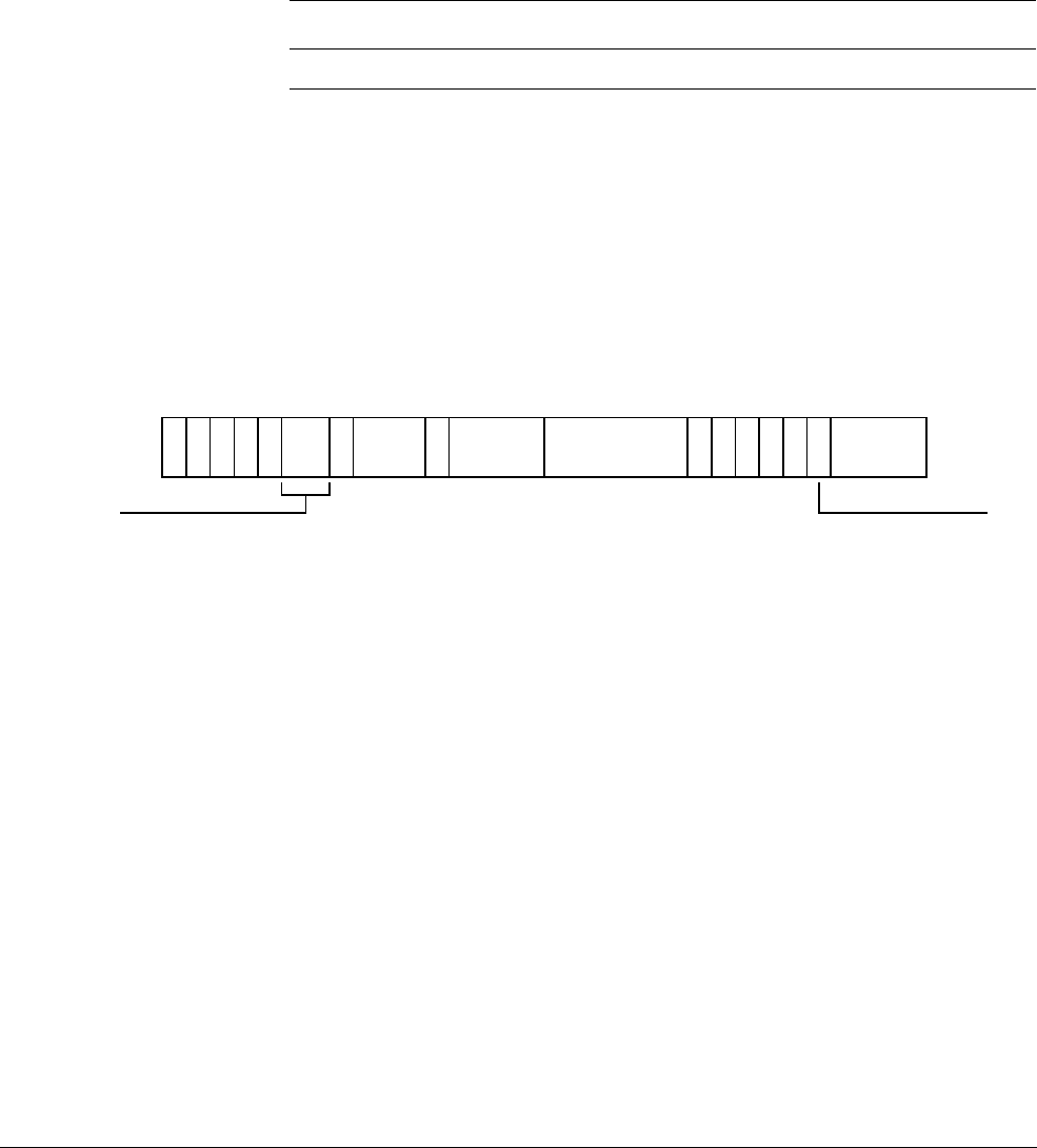
C4 The AArch64 System Instruction Class
C4.3 PSTATE and special purpose registers
C4-278 Copyright © 2013 ARM Limited. All rights reserved. ARM DDI 0487A.a
Non-Confidential - Beta ID090413
C4.3.17 SPSR_EL1, Saved Program Status Register (EL1)
The SPSR_EL1 characteristics are:
Purpose
Holds the saved processor state when an exception is taken to EL1.
This register is part of the Special purpose registers functional group.
Usage constraints
This register is accessible as shown below:
Configurations
SPSR_EL1 is architecturally mapped to AArch32 register SPSR_svc.
Attributes
SPSR_EL1 is a 32-bit register.
The SPSR_EL1 bit assignments are:
When exception taken from AArch32:
N, bit [31]
Set to the value of CPSR.N on taking an exception to Supervisor mode, and copied to CPSR.N on
executing an exception return operation in Supervisor mode.
Z, bit [30]
Set to the value of CPSR.Z on taking an exception to Supervisor mode, and copied to CPSR.Z on
executing an exception return operation in Supervisor mode.
C, bit [29]
Set to the value of CPSR.C on taking an exception to Supervisor mode, and copied to CPSR.C on
executing an exception return operation in Supervisor mode.
V, bit [28]
Set to the value of CPSR.V on taking an exception to Supervisor mode, and copied to CPSR.V on
executing an exception return operation in Supervisor mode.
Q, bit [27]
Cumulative saturation bit. Set to 1 to indicate that overflow or saturation occurred in some
instructions.
IT[1:0], bits [26:25]
If-Then execution state bits for the T32 IT (If-Then) instruction. See IT[7:2] for explanation of this
field.
EL0 EL1 (NS) EL1 (S) EL2 EL3 (SCR.NS=1) EL3 (SCR.NS=0)
-RW RW RWRW RW
N
31
Z
30
C
29
V
28
Q
27 26 25
J
24
RES0
23 21
IL
20
GE
19 16
IT[7:2]
15 10
E
9
A
8
I
7
F
6
T
54
M[3:0]
30
IT[1:0] M[4]

C4 The AArch64 System Instruction Class
C4.3 PSTATE and special purpose registers
ARM DDI 0487A.a Copyright © 2013 ARM Limited. All rights reserved. C4-279
ID090413 Non-Confidential - Beta
J, bit [24]
Jazelle bit. Along with the T bit, determines the AArch32 instruction set state that the exception was
taken from. Possible values of this bit are:
0
Processor in A32 state if T is 0, or T32 state if T is 1.
1
Processor in an invalid state (Jazelle state before ARMv8) if T is 0, or T32EE state if T
is 1.
Since the Jazelle state is obsolete in ARMv8, J==1 and T==0 is an invalid combination, and
attempting to perform an exception return with those values is an illegal exception return.
If T32EE is not implemented, this bit is RES0, so the possible values of the T bit signify either A32
or T32 state.
Bits [23:21]
Reserved, RES0.
IL, bit [20]
Illegal Execution State bit. Shows the value of PSTATE.IL immediately before the exception was
taken.
GE, bits [19:16]
Greater than or Equal flags, for parallel addition and subtraction.
IT[7:2], bits [15:10]
If-Then execution state bits for the T32 IT (If-Then) instruction. This field must be interpreted in
two parts.
• IT[7:5] holds the base condition for the IT block. The base condition is the top 3 bits of the
condition code specified by the first condition field of the IT instruction.
• IT[4:0] encodes the size of the IT block, which is the number of instructions that are to be
conditionally executed, by the position of the least significant 1 in this field. It also encodes
the value of the least significant bit of the condition code for each instruction in the block.
The IT field is
0b00000000
when no IT block is active.
E, bit [9]
Endianness execution state bit. Controls the load and store endianness for data accesses:
0
Little-endian operation
1
Big-endian operation.
Instruction fetches ignore this bit.
When the reset value of the SCTLR.EE bit is defined by a configuration input signal, that value also
applies to the CPSR.E bit on reset, and therefore applies to software execution from reset.
If an implementation does not provide Big-endian support, this bit is RES0. If it does not provide
Little-endian support, this bit is RES1.
If an implementation provides Big-endian support but only at EL0, this bit is RES0 for an exception
return to any exception level other than EL0.
Likewise, if it provides Little-endian support only at EL0, this bit is RES1 for an exception return
to any exception level other than EL0.
A, bit [8]
Asynchronous data abort mask bit. The possible values of this bit are:
0
Exception not masked.
1
Exception masked.

C4 The AArch64 System Instruction Class
C4.3 PSTATE and special purpose registers
C4-280 Copyright © 2013 ARM Limited. All rights reserved. ARM DDI 0487A.a
Non-Confidential - Beta ID090413
I, bit [7]
IRQ mask bit. The possible values of this bit are:
0
Exception not masked.
1
Exception masked.
F, bit [6]
FIQ mask bit. The possible values of this bit are:
0
Exception not masked.
1
Exception masked.
T, bit [5]
Thumb execution state bit. Along with the J bit, determines the AArch32 instruction set state that
the exception was taken from. Possible values of this bit are:
0
Processor in A32 state if J is 0, or an invalid state (Jazelle state before ARMv8) if J is 1.
1
Processor in T32 state if J is 0, or T32EE state if J is 1.
Since the Jazelle state is obsolete in ARMv8, J==1 and T==0 is an invalid combination, and
attempting to perform an exception return with those values is an illegal exception return.
If T32EE is not implemented, the J bit is RES0, so the possible values of this bit signify either A32
or T32 state.
M[4], bit [4]
Register width that the exception was taken from. Possible values of this bit are:
1
Exception taken from AArch32.
M[3:0], bits [3:0]
Mode that an exception was taken from. For exceptions taken from AArch32, the possible values
are:
Other values are reserved.
M[3:0] Mode
0b0000
User
0b0001
FIQ
0b0010
IRQ
0b0011
Supervisor
0b0111
Abort
0b1011
Undefined
0b1111
System

C4 The AArch64 System Instruction Class
C4.3 PSTATE and special purpose registers
ARM DDI 0487A.a Copyright © 2013 ARM Limited. All rights reserved. C4-281
ID090413 Non-Confidential - Beta
When exception taken from AArch64:
N, bit [31]
Set to the value of the N condition flag on taking an exception to EL1, and copied to the N condition
flag on executing an exception return operation in EL1.
Z, bit [30]
Set to the value of the Z condition flag on taking an exception to EL1, and copied to the Z condition
flag on executing an exception return operation in EL1.
C, bit [29]
Set to the value of the C condition flag on taking an exception to EL1, and copied to the C condition
flag on executing an exception return operation in EL1.
V, bit [28]
Set to the value of the V condition flag on taking an exception to EL1, and copied to the V condition
flag on executing an exception return operation in EL1.
Bits [27:22]
Reserved, RES0.
SS, bit [21]
Software step. Indicates whether software step was enabled when an exception was taken.
IL, bit [20]
Illegal Execution State bit. Shows the value of PSTATE.IL immediately before the exception was
taken.
Bits [19:10]
Reserved, RES0.
D, bit [9]
Process state D mask. The possible values of this bit are:
0
Debug exceptions from Watchpoint, Breakpoint, and Software step debug events
targeted at the current exception level are not masked.
1
Debug exceptions from Watchpoint, Breakpoint, and Software step debug events
targeted at the current exception level are masked.
When the target exception level of the debug exception is not than the current exception level, the
exception is not masked by this bit.
A, bit [8]
SError (System Error) mask bit. The possible values of this bit are:
0
Exception not masked.
1
Exception masked.
N
31
Z
30
C
29
V
28
RES0
27 22
SS
21
IL
20
RES0
19 10
D
9
A
8
I
7
F
65 4
M[3:0]
30
M[4]
RES0

C4 The AArch64 System Instruction Class
C4.3 PSTATE and special purpose registers
C4-282 Copyright © 2013 ARM Limited. All rights reserved. ARM DDI 0487A.a
Non-Confidential - Beta ID090413
I, bit [7]
IRQ mask bit. The possible values of this bit are:
0
Exception not masked.
1
Exception masked.
F, bit [6]
FIQ mask bit. The possible values of this bit are:
0
Exception not masked.
1
Exception masked.
Bit [5]
Reserved, RES0.
M[4], bit [4]
Register width that the exception was taken from. Possible values of this bit are:
0
Exception taken from AArch64.
M[3:0], bits [3:0]
Mode that an exception was taken from. For exceptions taken from AArch64, the possible values
are:
Other values are reserved.
For exceptions from AArch64:
• M[3:2] holds the Exception Level.
• M[1] is unused, and returning to an exception level that is using AArch64 with this bit set is
treated as an illegal exception return.
• M[0] is used to select the SP:
— 0 means the SP is always SP0.
— 1 means the exception SP is determined by the EL.
Accessing the SPSR_EL1:
To access the SPSR_EL1:
MRS <Xt>, SPSR_EL1 ; Read SPSR_EL1 into Xt
MSR SPSR_EL1, <Xt> ; Write Xt to SPSR_EL1
Register access is encoded as follows:
M[3:0] Mode
0b0000
EL0t
0b0100
EL1t
0b0101
EL1h
op0 op1 CRn CRm op2
11 000 0100 0000 000

C4 The AArch64 System Instruction Class
C4.3 PSTATE and special purpose registers
ARM DDI 0487A.a Copyright © 2013 ARM Limited. All rights reserved. C4-283
ID090413 Non-Confidential - Beta
C4.3.18 SPSR_EL2, Saved Program Status Register (EL2)
The SPSR_EL2 characteristics are:
Purpose
Holds the saved processor state when an exception is taken to EL2.
This register is part of the Special purpose registers functional group.
Usage constraints
This register is accessible as shown below:
Configurations
SPSR_EL2 is architecturally mapped to AArch32 register SPSR_hyp.
Attributes
SPSR_EL2 is a 32-bit register.
The SPSR_EL2 bit assignments are:
When exception taken from AArch32:
N, bit [31]
Set to the value of CPSR.N on taking an exception to Hyp mode, and copied to CPSR.N on
executing an exception return operation in Hyp mode.
Z, bit [30]
Set to the value of CPSR.Z on taking an exception to Hyp mode, and copied to CPSR.Z on executing
an exception return operation in Hyp mode.
C, bit [29]
Set to the value of CPSR.C on taking an exception to Hyp mode, and copied to CPSR.C on
executing an exception return operation in Hyp mode.
V, bit [28]
Set to the value of CPSR.V on taking an exception to Hyp mode, and copied to CPSR.V on
executing an exception return operation in Hyp mode.
Q, bit [27]
Cumulative saturation bit. Set to 1 to indicate that overflow or saturation occurred in some
instructions.
IT[1:0], bits [26:25]
If-Then execution state bits for the T32 IT (If-Then) instruction. See IT[7:2] for explanation of this
field.
EL0 EL1 (NS) EL1 (S) EL2 EL3 (SCR.NS=1) EL3 (SCR.NS=0)
-- - RWRW RW
N
31
Z
30
C
29
V
28
Q
27 26 25
J
24
RES0
23 21
IL
20
GE
19 16
IT[7:2]
15 10
E
9
A
8
I
7
F
6
T
54
M[3:0]
30
IT[1:0] M[4]

C4 The AArch64 System Instruction Class
C4.3 PSTATE and special purpose registers
C4-284 Copyright © 2013 ARM Limited. All rights reserved. ARM DDI 0487A.a
Non-Confidential - Beta ID090413
J, bit [24]
Jazelle bit. Along with the T bit, determines the AArch32 instruction set state that the exception was
taken from. Possible values of this bit are:
0
Processor in A32 state if T is 0, or T32 state if T is 1.
1
Processor in an invalid state (Jazelle state before ARMv8) if T is 0, or T32EE state if T
is 1.
Since the Jazelle state is obsolete in ARMv8, J==1 and T==0 is an invalid combination, and
attempting to perform an exception return with those values is an illegal exception return.
If T32EE is not implemented, this bit is RES0, so the possible values of the T bit signify either A32
or T32 state.
Bits [23:21]
Reserved, RES0.
IL, bit [20]
Illegal Execution State bit. Shows the value of PSTATE.IL immediately before the exception was
taken.
GE, bits [19:16]
Greater than or Equal flags, for parallel addition and subtraction.
IT[7:2], bits [15:10]
If-Then execution state bits for the T32 IT (If-Then) instruction. This field must be interpreted in
two parts.
• IT[7:5] holds the base condition for the IT block. The base condition is the top 3 bits of the
condition code specified by the first condition field of the IT instruction.
• IT[4:0] encodes the size of the IT block, which is the number of instructions that are to be
conditionally executed, by the position of the least significant 1 in this field. It also encodes
the value of the least significant bit of the condition code for each instruction in the block.
The IT field is
0b00000000
when no IT block is active.
E, bit [9]
Endianness execution state bit. Controls the load and store endianness for data accesses:
0
Little-endian operation
1
Big-endian operation.
Instruction fetches ignore this bit.
When the reset value of the SCTLR.EE bit is defined by a configuration input signal, that value also
applies to the CPSR.E bit on reset, and therefore applies to software execution from reset.
If an implementation does not provide Big-endian support, this bit is RES0. If it does not provide
Little-endian support, this bit is RES1.
If an implementation provides Big-endian support but only at EL0, this bit is RES0 for an exception
return to any exception level other than EL0.
Likewise, if it provides Little-endian support only at EL0, this bit is RES1 for an exception return
to any exception level other than EL0.
A, bit [8]
Asynchronous data abort mask bit. The possible values of this bit are:
0
Exception not masked.
1
Exception masked.

C4 The AArch64 System Instruction Class
C4.3 PSTATE and special purpose registers
ARM DDI 0487A.a Copyright © 2013 ARM Limited. All rights reserved. C4-285
ID090413 Non-Confidential - Beta
I, bit [7]
IRQ mask bit. The possible values of this bit are:
0
Exception not masked.
1
Exception masked.
F, bit [6]
FIQ mask bit. The possible values of this bit are:
0
Exception not masked.
1
Exception masked.
T, bit [5]
Thumb execution state bit. Along with the J bit, determines the AArch32 instruction set state that
the exception was taken from. Possible values of this bit are:
0
Processor in A32 state if J is 0, or an invalid state (Jazelle state before ARMv8) if J is 1.
1
Processor in T32 state if J is 0, or T32EE state if J is 1.
Since the Jazelle state is obsolete in ARMv8, J==1 and T==0 is an invalid combination, and
attempting to perform an exception return with those values is an illegal exception return.
If T32EE is not implemented, the J bit is RES0, so the possible values of this bit signify either A32
or T32 state.
M[4], bit [4]
Register width that the exception was taken from. Possible values of this bit are:
1
Exception taken from AArch32.
M[3:0], bits [3:0]
Mode that an exception was taken from. For exceptions taken from AArch32, the possible values
are:
Other values are reserved.
M[3:0] Mode
0b0000
User
0b0001
FIQ
0b0010
IRQ
0b0011
Supervisor
0b0111
Abort
0b1010
Hyp
0b1011
Undefined
0b1111
System

C4 The AArch64 System Instruction Class
C4.3 PSTATE and special purpose registers
C4-286 Copyright © 2013 ARM Limited. All rights reserved. ARM DDI 0487A.a
Non-Confidential - Beta ID090413
When exception taken from AArch64:
N, bit [31]
Set to the value of the N condition flag on taking an exception to EL2, and copied to the N condition
flag on executing an exception return operation in EL2.
Z, bit [30]
Set to the value of the Z condition flag on taking an exception to EL2, and copied to the Z condition
flag on executing an exception return operation in EL2.
C, bit [29]
Set to the value of the C condition flag on taking an exception to EL2, and copied to the C condition
flag on executing an exception return operation in EL2.
V, bit [28]
Set to the value of the V condition flag on taking an exception to EL2, and copied to the V condition
flag on executing an exception return operation in EL2.
Bits [27:22]
Reserved, RES0.
SS, bit [21]
Software step. Indicates whether software step was enabled when an exception was taken.
IL, bit [20]
Illegal Execution State bit. Shows the value of PSTATE.IL immediately before the exception was
taken.
Bits [19:10]
Reserved, RES0.
D, bit [9]
Process state D mask. The possible values of this bit are:
0
Debug exceptions from Watchpoint, Breakpoint, and Software step debug events
targeted at the current exception level are not masked.
1
Debug exceptions from Watchpoint, Breakpoint, and Software step debug events
targeted at the current exception level are masked.
When the target exception level of the debug exception is not than the current exception level, the
exception is not masked by this bit.
A, bit [8]
SError (System Error) mask bit. The possible values of this bit are:
0
Exception not masked.
1
Exception masked.
N
31
Z
30
C
29
V
28
RES0
27 22
SS
21
IL
20
RES0
19 10
D
9
A
8
I
7
F
65 4
M[3:0]
30
M[4]
RES0

C4 The AArch64 System Instruction Class
C4.3 PSTATE and special purpose registers
ARM DDI 0487A.a Copyright © 2013 ARM Limited. All rights reserved. C4-287
ID090413 Non-Confidential - Beta
I, bit [7]
IRQ mask bit. The possible values of this bit are:
0
Exception not masked.
1
Exception masked.
F, bit [6]
FIQ mask bit. The possible values of this bit are:
0
Exception not masked.
1
Exception masked.
Bit [5]
Reserved, RES0.
M[4], bit [4]
Register width that the exception was taken from. Possible values of this bit are:
0
Exception taken from AArch64.
M[3:0], bits [3:0]
Mode that an exception was taken from. For exceptions taken from AArch64, the possible values
are:
Other values are reserved.
For exceptions from AArch64:
• M[3:2] holds the Exception Level.
• M[1] is unused, and returning to an exception level that is using AArch64 with this bit set is
treated as an illegal exception return.
• M[0] is used to select the SP:
— 0 means the SP is always SP0.
— 1 means the exception SP is determined by the EL.
Accessing the SPSR_EL2:
To access the SPSR_EL2:
MRS <Xt>, SPSR_EL2 ; Read SPSR_EL2 into Xt
MSR SPSR_EL2, <Xt> ; Write Xt to SPSR_EL2
Register access is encoded as follows:
M[3:0] Mode
0b0000
EL0t
0b0100
EL1t
0b0101
EL1h
0b1000
EL2t
0b1001
EL2h
op0 op1 CRn CRm op2
11 100 0100 0000 000
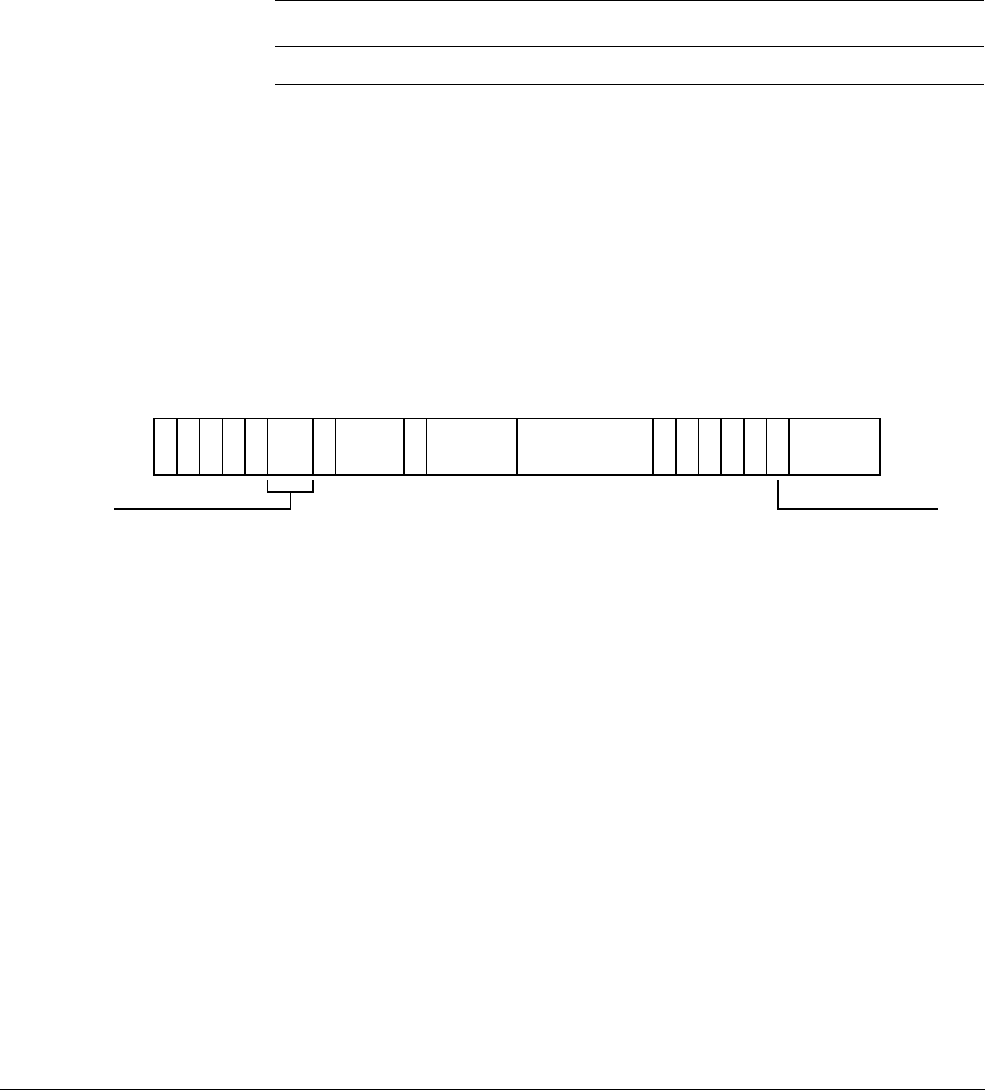
C4 The AArch64 System Instruction Class
C4.3 PSTATE and special purpose registers
C4-288 Copyright © 2013 ARM Limited. All rights reserved. ARM DDI 0487A.a
Non-Confidential - Beta ID090413
C4.3.19 SPSR_EL3, Saved Program Status Register (EL3)
The SPSR_EL3 characteristics are:
Purpose
Holds the saved processor state when an exception is taken to EL3.
This register is part of the Special purpose registers functional group.
Usage constraints
This register is accessible as shown below:
Configurations
SPSR_EL3 can be mapped to AArch32 register SPSR_mon, but this is not architecturally
mandated.
Attributes
SPSR_EL3 is a 32-bit register.
The SPSR_EL3 bit assignments are:
When exception taken from AArch32:
N, bit [31]
Set to the value of CPSR.N on taking an exception to Monitor mode, and copied to CPSR.N on
executing an exception return operation in Monitor mode.
Z, bit [30]
Set to the value of CPSR.Z on taking an exception to Monitor mode, and copied to CPSR.Z on
executing an exception return operation in Monitor mode.
C, bit [29]
Set to the value of CPSR.C on taking an exception to Monitor mode, and copied to CPSR.C on
executing an exception return operation in Monitor mode.
V, bit [28]
Set to the value of CPSR.V on taking an exception to Monitor mode, and copied to CPSR.V on
executing an exception return operation in Monitor mode.
Q, bit [27]
Cumulative saturation bit. Set to 1 to indicate that overflow or saturation occurred in some
instructions.
EL0 EL1 (NS) EL1 (S) EL2 EL3 (SCR.NS=1) EL3 (SCR.NS=0)
-- - -RW RW
N
31
Z
30
C
29
V
28
Q
27 26 25
J
24
RES0
23 21
IL
20
GE
19 16
IT[7:2]
15 10
E
9
A
8
I
7
F
6
T
54
M[3:0]
30
IT[1:0] M[4]

C4 The AArch64 System Instruction Class
C4.3 PSTATE and special purpose registers
ARM DDI 0487A.a Copyright © 2013 ARM Limited. All rights reserved. C4-289
ID090413 Non-Confidential - Beta
IT[1:0], bits [26:25]
If-Then execution state bits for the T32 IT (If-Then) instruction. See IT[7:2] for explanation of this
field.
J, bit [24]
Jazelle bit. Along with the T bit, determines the AArch32 instruction set state that the exception was
taken from. Possible values of this bit are:
0
Processor in A32 state if T is 0, or T32 state if T is 1.
1
Processor in an invalid state (Jazelle state before ARMv8) if T is 0, or T32EE state if T
is 1.
Since the Jazelle state is obsolete in ARMv8, J==1 and T==0 is an invalid combination, and
attempting to perform an exception return with those values is an illegal exception return.
If T32EE is not implemented, this bit is RES0, so the possible values of the T bit signify either A32
or T32 state.
Bits [23:21]
Reserved, RES0.
IL, bit [20]
Illegal Execution State bit. Shows the value of PSTATE.IL immediately before the exception was
taken.
GE, bits [19:16]
Greater than or Equal flags, for parallel addition and subtraction.
IT[7:2], bits [15:10]
If-Then execution state bits for the T32 IT (If-Then) instruction. This field must be interpreted in
two parts.
• IT[7:5] holds the base condition for the IT block. The base condition is the top 3 bits of the
condition code specified by the first condition field of the IT instruction.
• IT[4:0] encodes the size of the IT block, which is the number of instructions that are to be
conditionally executed, by the position of the least significant 1 in this field. It also encodes
the value of the least significant bit of the condition code for each instruction in the block.
The IT field is
0b00000000
when no IT block is active.
E, bit [9]
Endianness execution state bit. Controls the load and store endianness for data accesses:
0
Little-endian operation
1
Big-endian operation.
Instruction fetches ignore this bit.
When the reset value of the SCTLR.EE bit is defined by a configuration input signal, that value also
applies to the CPSR.E bit on reset, and therefore applies to software execution from reset.
If an implementation does not provide Big-endian support, this bit is RES0. If it does not provide
Little-endian support, this bit is RES1.
If an implementation provides Big-endian support but only at EL0, this bit is RES0 for an exception
return to any exception level other than EL0.
Likewise, if it provides Little-endian support only at EL0, this bit is RES1 for an exception return
to any exception level other than EL0.
A, bit [8]
Asynchronous data abort mask bit. The possible values of this bit are:
0
Exception not masked.
1
Exception masked.

C4 The AArch64 System Instruction Class
C4.3 PSTATE and special purpose registers
C4-290 Copyright © 2013 ARM Limited. All rights reserved. ARM DDI 0487A.a
Non-Confidential - Beta ID090413
I, bit [7]
IRQ mask bit. The possible values of this bit are:
0
Exception not masked.
1
Exception masked.
F, bit [6]
FIQ mask bit. The possible values of this bit are:
0
Exception not masked.
1
Exception masked.
T, bit [5]
Thumb execution state bit. Along with the J bit, determines the AArch32 instruction set state that
the exception was taken from. Possible values of this bit are:
0
Processor in A32 state if J is 0, or an invalid state (Jazelle state before ARMv8) if J is 1.
1
Processor in T32 state if J is 0, or T32EE state if J is 1.
Since the Jazelle state is obsolete in ARMv8, J==1 and T==0 is an invalid combination, and
attempting to perform an exception return with those values is an illegal exception return.
If T32EE is not implemented, the J bit is RES0, so the possible values of this bit signify either A32
or T32 state.
M[4], bit [4]
Register width that the exception was taken from. Possible values of this bit are:
1
Exception taken from AArch32.
M[3:0], bits [3:0]
Mode that an exception was taken from. For exceptions taken from AArch32, the possible values
are:
Other values are reserved.
M[3:0] Mode
0b0000
User
0b0001
FIQ
0b0010
IRQ
0b0011
Supervisor
0b0110
Monitor
0b0111
Abort
0b1010
Hyp
0b1011
Undefined
0b1111
System

C4 The AArch64 System Instruction Class
C4.3 PSTATE and special purpose registers
ARM DDI 0487A.a Copyright © 2013 ARM Limited. All rights reserved. C4-291
ID090413 Non-Confidential - Beta
When exception taken from AArch64:
N, bit [31]
Set to the value of the N condition flag on taking an exception to EL3, and copied to the N condition
flag on executing an exception return operation in EL3.
Z, bit [30]
Set to the value of the Z condition flag on taking an exception to EL3, and copied to the Z condition
flag on executing an exception return operation in EL3.
C, bit [29]
Set to the value of the C condition flag on taking an exception to EL3, and copied to the C condition
flag on executing an exception return operation in EL3.
V, bit [28]
Set to the value of the V condition flag on taking an exception to EL3, and copied to the V condition
flag on executing an exception return operation in EL3.
Bits [27:22]
Reserved, RES0.
SS, bit [21]
Software step. Indicates whether software step was enabled when an exception was taken.
IL, bit [20]
Illegal Execution State bit. Shows the value of PSTATE.IL immediately before the exception was
taken.
Bits [19:10]
Reserved, RES0.
D, bit [9]
Process state D mask. The possible values of this bit are:
0
Debug exceptions from Watchpoint, Breakpoint, and Software step debug events
targeted at the current exception level are not masked.
1
Debug exceptions from Watchpoint, Breakpoint, and Software step debug events
targeted at the current exception level are masked.
When the target exception level of the debug exception is not than the current exception level, the
exception is not masked by this bit.
A, bit [8]
SError (System Error) mask bit. The possible values of this bit are:
0
Exception not masked.
1
Exception masked.
N
31
Z
30
C
29
V
28
RES0
27 22
SS
21
IL
20
RES0
19 10
D
9
A
8
I
7
F
65 4
M[3:0]
30
M[4]
RES0

C4 The AArch64 System Instruction Class
C4.3 PSTATE and special purpose registers
C4-292 Copyright © 2013 ARM Limited. All rights reserved. ARM DDI 0487A.a
Non-Confidential - Beta ID090413
I, bit [7]
IRQ mask bit. The possible values of this bit are:
0
Exception not masked.
1
Exception masked.
F, bit [6]
FIQ mask bit. The possible values of this bit are:
0
Exception not masked.
1
Exception masked.
Bit [5]
Reserved, RES0.
M[4], bit [4]
Register width that the exception was taken from. Possible values of this bit are:
0
Exception taken from AArch64.
M[3:0], bits [3:0]
Mode that an exception was taken from. For exceptions taken from AArch64, the possible values
are:
Other values are reserved.
For exceptions from AArch64:
• M[3:2] holds the Exception Level.
• M[1] is unused, and returning to an exception level that is using AArch64 with this bit set is
treated as an illegal exception return.
• M[0] is used to select the SP:
— 0 means the SP is always SP0.
— 1 means the exception SP is determined by the EL.
Accessing the SPSR_EL3:
To access the SPSR_EL3:
MRS <Xt>, SPSR_EL3 ; Read SPSR_EL3 into Xt
MSR SPSR_EL3, <Xt> ; Write Xt to SPSR_EL3
M[3:0] Mode
0b0000
EL0t
0b0100
EL1t
0b0101
EL1h
0b1000
EL2t
0b1001
EL2h
0b1100
EL3t
0b1101
EL3h

C4 The AArch64 System Instruction Class
C4.3 PSTATE and special purpose registers
ARM DDI 0487A.a Copyright © 2013 ARM Limited. All rights reserved. C4-293
ID090413 Non-Confidential - Beta
Register access is encoded as follows:
op0 op1 CRn CRm op2
11 110 0100 0000 000

C4 The AArch64 System Instruction Class
C4.3 PSTATE and special purpose registers
C4-294 Copyright © 2013 ARM Limited. All rights reserved. ARM DDI 0487A.a
Non-Confidential - Beta ID090413
C4.3.20 SPSR_fiq, Saved Program Status Register (FIQ mode)
The SPSR_fiq characteristics are:
Purpose
Holds the saved processor state when an exception is taken to FIQ mode.
This register is part of the Special purpose registers functional group.
Usage constraints
This register is accessible as shown below:
Configurations
SPSR_fiq is architecturally mapped to AArch32 register SPSR_fiq.
If EL1 does not support execution in AArch32, this register is RES0.
Attributes
SPSR_fiq is a 32-bit register.
The SPSR_fiq bit assignments are:
N, bit [31]
Set to the value of CPSR.N on taking an exception to FIQ mode, and copied to CPSR.N on
executing an exception return operation in FIQ mode.
Z, bit [30]
Set to the value of CPSR.Z on taking an exception to FIQ mode, and copied to CPSR.Z on executing
an exception return operation in FIQ mode.
C, bit [29]
Set to the value of CPSR.C on taking an exception to FIQ mode, and copied to CPSR.C on executing
an exception return operation in FIQ mode.
V, bit [28]
Set to the value of CPSR.V on taking an exception to FIQ mode, and copied to CPSR.V on
executing an exception return operation in FIQ mode.
Q, bit [27]
Cumulative saturation bit. Set to 1 to indicate that overflow or saturation occurred in some
instructions.
IT[1:0], bits [26:25]
If-Then execution state bits for the T32 IT (If-Then) instruction. See IT[7:2] for explanation of this
field.
EL0 EL1 (NS) EL1 (S) EL2 EL3 (SCR.NS=1) EL3 (SCR.NS=0)
-- - RWRW RW
N
31
Z
30
C
29
V
28
Q
27 26 25
J
24
RES0
23 21
IL
20
GE
19 16
IT[7:2]
15 10
E
9
A
8
I
7
F
6
T
54
M[3:0]
30
IT[1:0] M[4]

C4 The AArch64 System Instruction Class
C4.3 PSTATE and special purpose registers
ARM DDI 0487A.a Copyright © 2013 ARM Limited. All rights reserved. C4-295
ID090413 Non-Confidential - Beta
J, bit [24]
Jazelle bit. Along with the T bit, determines the AArch32 instruction set state that the exception was
taken from. Possible values of this bit are:
0
Processor in A32 state if T is 0, or T32 state if T is 1.
1
Processor in an invalid state (Jazelle state before ARMv8) if T is 0, or T32EE state if T
is 1.
Since the Jazelle state is obsolete in ARMv8, J==1 and T==0 is an invalid combination, and
attempting to perform an exception return with those values is an illegal exception return.
If T32EE is not implemented, this bit is RES0, so the possible values of the T bit signify either A32
or T32 state.
Bits [23:21]
Reserved, RES0.
IL, bit [20]
Illegal Execution State bit. Shows the value of PSTATE.IL immediately before the exception was
taken.
GE, bits [19:16]
Greater than or Equal flags, for parallel addition and subtraction.
IT[7:2], bits [15:10]
If-Then execution state bits for the T32 IT (If-Then) instruction. This field must be interpreted in
two parts.
• IT[7:5] holds the base condition for the IT block. The base condition is the top 3 bits of the
condition code specified by the first condition field of the IT instruction.
• IT[4:0] encodes the size of the IT block, which is the number of instructions that are to be
conditionally executed, by the position of the least significant 1 in this field. It also encodes
the value of the least significant bit of the condition code for each instruction in the block.
The IT field is
0b00000000
when no IT block is active.
E, bit [9]
Endianness execution state bit. Controls the load and store endianness for data accesses:
0
Little-endian operation
1
Big-endian operation.
Instruction fetches ignore this bit.
When the reset value of the SCTLR.EE bit is defined by a configuration input signal, that value also
applies to the CPSR.E bit on reset, and therefore applies to software execution from reset.
If an implementation does not provide Big-endian support, this bit is RES0. If it does not provide
Little-endian support, this bit is RES1.
If an implementation provides Big-endian support but only at EL0, this bit is RES0 for an exception
return to any exception level other than EL0.
Likewise, if it provides Little-endian support only at EL0, this bit is RES1 for an exception return
to any exception level other than EL0.
A, bit [8]
Asynchronous data abort mask bit. The possible values of this bit are:
0
Exception not masked.
1
Exception masked.

C4 The AArch64 System Instruction Class
C4.3 PSTATE and special purpose registers
C4-296 Copyright © 2013 ARM Limited. All rights reserved. ARM DDI 0487A.a
Non-Confidential - Beta ID090413
I, bit [7]
IRQ mask bit. The possible values of this bit are:
0
Exception not masked.
1
Exception masked.
F, bit [6]
FIQ mask bit. The possible values of this bit are:
0
Exception not masked.
1
Exception masked.
T, bit [5]
Thumb execution state bit. Along with the J bit, determines the AArch32 instruction set state that
the exception was taken from. Possible values of this bit are:
0
Processor in A32 state if J is 0, or an invalid state (Jazelle state before ARMv8) if J is 1.
1
Processor in T32 state if J is 0, or T32EE state if J is 1.
Since the Jazelle state is obsolete in ARMv8, J==1 and T==0 is an invalid combination, and
attempting to perform an exception return with those values is an illegal exception return.
If T32EE is not implemented, the J bit is RES0, so the possible values of this bit signify either A32
or T32 state.
M[4], bit [4]
Register width that the exception was taken from. Possible values of this bit are:
1
Exception taken from AArch32.
M[3:0], bits [3:0]
Mode that an exception was taken from. For exceptions taken from AArch32, the possible values
are:
Other values are reserved.
Accessing the SPSR_fiq:
To access the SPSR_fiq:
MRS <Xt>, SPSR_fiq ; Read SPSR_fiq into Xt
MSR SPSR_fiq, <Xt> ; Write Xt to SPSR_fiq
M[3:0] Mode
0b0000
User
0b0001
FIQ
0b0010
IRQ
0b0011
Supervisor
0b0110
Monitor
0b0111
Abort
0b1010
Hyp
0b1011
Undefined
0b1111
System

C4 The AArch64 System Instruction Class
C4.3 PSTATE and special purpose registers
ARM DDI 0487A.a Copyright © 2013 ARM Limited. All rights reserved. C4-297
ID090413 Non-Confidential - Beta
Register access is encoded as follows:
op0 op1 CRn CRm op2
11 100 0100 0011 011
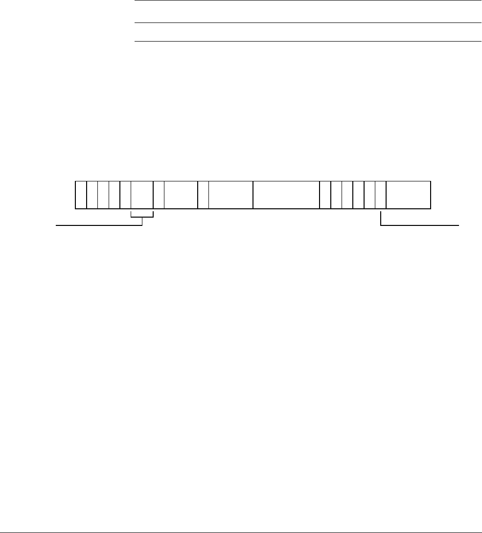
C4 The AArch64 System Instruction Class
C4.3 PSTATE and special purpose registers
C4-298 Copyright © 2013 ARM Limited. All rights reserved. ARM DDI 0487A.a
Non-Confidential - Beta ID090413
C4.3.21 SPSR_irq, Saved Program Status Register (IRQ mode)
The SPSR_irq characteristics are:
Purpose
Holds the saved processor state when an exception is taken to IRQ mode.
This register is part of the Special purpose registers functional group.
Usage constraints
This register is accessible as shown below:
Configurations
SPSR_irq is architecturally mapped to AArch32 register SPSR_irq.
If EL1 does not support execution in AArch32, this register is RES0.
Attributes
SPSR_irq is a 32-bit register.
The SPSR_irq bit assignments are:
N, bit [31]
Set to the value of CPSR.N on taking an exception to IRQ mode, and copied to CPSR.N on
executing an exception return operation in IRQ mode.
Z, bit [30]
Set to the value of CPSR.Z on taking an exception to IRQ mode, and copied to CPSR.Z on executing
an exception return operation in IRQ mode.
C, bit [29]
Set to the value of CPSR.C on taking an exception to IRQ mode, and copied to CPSR.C on
executing an exception return operation in IRQ mode.
V, bit [28]
Set to the value of CPSR.V on taking an exception to IRQ mode, and copied to CPSR.V on
executing an exception return operation in IRQ mode.
Q, bit [27]
Cumulative saturation bit. Set to 1 to indicate that overflow or saturation occurred in some
instructions.
IT[1:0], bits [26:25]
If-Then execution state bits for the T32 IT (If-Then) instruction. See IT[7:2] for explanation of this
field.
EL0 EL1 (NS) EL1 (S) EL2 EL3 (SCR.NS=1) EL3 (SCR.NS=0)
-- - RWRW RW
N
31
Z
30
C
29
V
28
Q
27 26 25
J
24
RES0
23 21
IL
20
GE
19 16
IT[7:2]
15 10
E
9
A
8
I
7
F
6
T
54
M[3:0]
30
IT[1:0] M[4]

C4 The AArch64 System Instruction Class
C4.3 PSTATE and special purpose registers
ARM DDI 0487A.a Copyright © 2013 ARM Limited. All rights reserved. C4-299
ID090413 Non-Confidential - Beta
J, bit [24]
Jazelle bit. Along with the T bit, determines the AArch32 instruction set state that the exception was
taken from. Possible values of this bit are:
0
Processor in A32 state if T is 0, or T32 state if T is 1.
1
Processor in an invalid state (Jazelle state before ARMv8) if T is 0, or T32EE state if T
is 1.
Since the Jazelle state is obsolete in ARMv8, J==1 and T==0 is an invalid combination, and
attempting to perform an exception return with those values is an illegal exception return.
If T32EE is not implemented, this bit is RES0, so the possible values of the T bit signify either A32
or T32 state.
Bits [23:21]
Reserved, RES0.
IL, bit [20]
Illegal Execution State bit. Shows the value of PSTATE.IL immediately before the exception was
taken.
GE, bits [19:16]
Greater than or Equal flags, for parallel addition and subtraction.
IT[7:2], bits [15:10]
If-Then execution state bits for the T32 IT (If-Then) instruction. This field must be interpreted in
two parts.
• IT[7:5] holds the base condition for the IT block. The base condition is the top 3 bits of the
condition code specified by the first condition field of the IT instruction.
• IT[4:0] encodes the size of the IT block, which is the number of instructions that are to be
conditionally executed, by the position of the least significant 1 in this field. It also encodes
the value of the least significant bit of the condition code for each instruction in the block.
The IT field is
0b00000000
when no IT block is active.
E, bit [9]
Endianness execution state bit. Controls the load and store endianness for data accesses:
0
Little-endian operation
1
Big-endian operation.
Instruction fetches ignore this bit.
When the reset value of the SCTLR.EE bit is defined by a configuration input signal, that value also
applies to the CPSR.E bit on reset, and therefore applies to software execution from reset.
If an implementation does not provide Big-endian support, this bit is RES0. If it does not provide
Little-endian support, this bit is RES1.
If an implementation provides Big-endian support but only at EL0, this bit is RES0 for an exception
return to any exception level other than EL0.
Likewise, if it provides Little-endian support only at EL0, this bit is RES1 for an exception return
to any exception level other than EL0.
A, bit [8]
Asynchronous data abort mask bit. The possible values of this bit are:
0
Exception not masked.
1
Exception masked.

C4 The AArch64 System Instruction Class
C4.3 PSTATE and special purpose registers
C4-300 Copyright © 2013 ARM Limited. All rights reserved. ARM DDI 0487A.a
Non-Confidential - Beta ID090413
I, bit [7]
IRQ mask bit. The possible values of this bit are:
0
Exception not masked.
1
Exception masked.
F, bit [6]
FIQ mask bit. The possible values of this bit are:
0
Exception not masked.
1
Exception masked.
T, bit [5]
Thumb execution state bit. Along with the J bit, determines the AArch32 instruction set state that
the exception was taken from. Possible values of this bit are:
0
Processor in A32 state if J is 0, or an invalid state (Jazelle state before ARMv8) if J is 1.
1
Processor in T32 state if J is 0, or T32EE state if J is 1.
Since the Jazelle state is obsolete in ARMv8, J==1 and T==0 is an invalid combination, and
attempting to perform an exception return with those values is an illegal exception return.
If T32EE is not implemented, the J bit is RES0, so the possible values of this bit signify either A32
or T32 state.
M[4], bit [4]
Register width that the exception was taken from. Possible values of this bit are:
1
Exception taken from AArch32.
M[3:0], bits [3:0]
Mode that an exception was taken from. For exceptions taken from AArch32, the possible values
are:
Other values are reserved.
Accessing the SPSR_irq:
To access the SPSR_irq:
MRS <Xt>, SPSR_irq ; Read SPSR_irq into Xt
MSR SPSR_irq, <Xt> ; Write Xt to SPSR_irq
M[3:0] Mode
0b0000
User
0b0001
FIQ
0b0010
IRQ
0b0011
Supervisor
0b0110
Monitor
0b0111
Abort
0b1010
Hyp
0b1011
Undefined
0b1111
System

C4 The AArch64 System Instruction Class
C4.3 PSTATE and special purpose registers
ARM DDI 0487A.a Copyright © 2013 ARM Limited. All rights reserved. C4-301
ID090413 Non-Confidential - Beta
Register access is encoded as follows:
op0 op1 CRn CRm op2
11 100 0100 0011 000

C4 The AArch64 System Instruction Class
C4.3 PSTATE and special purpose registers
C4-302 Copyright © 2013 ARM Limited. All rights reserved. ARM DDI 0487A.a
Non-Confidential - Beta ID090413
C4.3.22 SPSR_und, Saved Program Status Register (Undefined mode)
The SPSR_und characteristics are:
Purpose
Holds the saved processor state when an exception is taken to Undefined mode.
This register is part of the Special purpose registers functional group.
Usage constraints
This register is accessible as shown below:
Configurations
SPSR_und is architecturally mapped to AArch32 register SPSR_und.
If EL1 does not support execution in AArch32, this register is RES0.
Attributes
SPSR_und is a 32-bit register.
The SPSR_und bit assignments are:
N, bit [31]
Set to the value of CPSR.N on taking an exception to Undefined mode, and copied to CPSR.N on
executing an exception return operation in Undefined mode.
Z, bit [30]
Set to the value of CPSR.Z on taking an exception to Undefined mode, and copied to CPSR.Z on
executing an exception return operation in Undefined mode.
C, bit [29]
Set to the value of CPSR.C on taking an exception to Undefined mode, and copied to CPSR.C on
executing an exception return operation in Undefined mode.
V, bit [28]
Set to the value of CPSR.V on taking an exception to Undefined mode, and copied to CPSR.V on
executing an exception return operation in Undefined mode.
Q, bit [27]
Cumulative saturation bit. Set to 1 to indicate that overflow or saturation occurred in some
instructions.
IT[1:0], bits [26:25]
If-Then execution state bits for the T32 IT (If-Then) instruction. See IT[7:2] for explanation of this
field.
EL0 EL1 (NS) EL1 (S) EL2 EL3 (SCR.NS=1) EL3 (SCR.NS=0)
-- - RWRW RW
N
31
Z
30
C
29
V
28
Q
27 26 25
J
24
RES0
23 21
IL
20
GE
19 16
IT[7:2]
15 10
E
9
A
8
I
7
F
6
T
54
M[3:0]
30
IT[1:0] M[4]

C4 The AArch64 System Instruction Class
C4.3 PSTATE and special purpose registers
ARM DDI 0487A.a Copyright © 2013 ARM Limited. All rights reserved. C4-303
ID090413 Non-Confidential - Beta
J, bit [24]
Jazelle bit. Along with the T bit, determines the AArch32 instruction set state that the exception was
taken from. Possible values of this bit are:
0
Processor in A32 state if T is 0, or T32 state if T is 1.
1
Processor in an invalid state (Jazelle state before ARMv8) if T is 0, or T32EE state if T
is 1.
Since the Jazelle state is obsolete in ARMv8, J==1 and T==0 is an invalid combination, and
attempting to perform an exception return with those values is an illegal exception return.
If T32EE is not implemented, this bit is RES0, so the possible values of the T bit signify either A32
or T32 state.
Bits [23:21]
Reserved, RES0.
IL, bit [20]
Illegal Execution State bit. Shows the value of PSTATE.IL immediately before the exception was
taken.
GE, bits [19:16]
Greater than or Equal flags, for parallel addition and subtraction.
IT[7:2], bits [15:10]
If-Then execution state bits for the T32 IT (If-Then) instruction. This field must be interpreted in
two parts.
• IT[7:5] holds the base condition for the IT block. The base condition is the top 3 bits of the
condition code specified by the first condition field of the IT instruction.
• IT[4:0] encodes the size of the IT block, which is the number of instructions that are to be
conditionally executed, by the position of the least significant 1 in this field. It also encodes
the value of the least significant bit of the condition code for each instruction in the block.
The IT field is
0b00000000
when no IT block is active.
E, bit [9]
Endianness execution state bit. Controls the load and store endianness for data accesses:
0
Little-endian operation
1
Big-endian operation.
Instruction fetches ignore this bit.
When the reset value of the SCTLR.EE bit is defined by a configuration input signal, that value also
applies to the CPSR.E bit on reset, and therefore applies to software execution from reset.
If an implementation does not provide Big-endian support, this bit is RES0. If it does not provide
Little-endian support, this bit is RES1.
If an implementation provides Big-endian support but only at EL0, this bit is RES0 for an exception
return to any exception level other than EL0.
Likewise, if it provides Little-endian support only at EL0, this bit is RES1 for an exception return
to any exception level other than EL0.
A, bit [8]
Asynchronous data abort mask bit. The possible values of this bit are:
0
Exception not masked.
1
Exception masked.

C4 The AArch64 System Instruction Class
C4.3 PSTATE and special purpose registers
C4-304 Copyright © 2013 ARM Limited. All rights reserved. ARM DDI 0487A.a
Non-Confidential - Beta ID090413
I, bit [7]
IRQ mask bit. The possible values of this bit are:
0
Exception not masked.
1
Exception masked.
F, bit [6]
FIQ mask bit. The possible values of this bit are:
0
Exception not masked.
1
Exception masked.
T, bit [5]
Thumb execution state bit. Along with the J bit, determines the AArch32 instruction set state that
the exception was taken from. Possible values of this bit are:
0
Processor in A32 state if J is 0, or an invalid state (Jazelle state before ARMv8) if J is 1.
1
Processor in T32 state if J is 0, or T32EE state if J is 1.
Since the Jazelle state is obsolete in ARMv8, J==1 and T==0 is an invalid combination, and
attempting to perform an exception return with those values is an illegal exception return.
If T32EE is not implemented, the J bit is RES0, so the possible values of this bit signify either A32
or T32 state.
M[4], bit [4]
Register width that the exception was taken from. Possible values of this bit are:
1
Exception taken from AArch32.
M[3:0], bits [3:0]
Mode that an exception was taken from. For exceptions taken from AArch32, the possible values
are:
Other values are reserved.
Accessing the SPSR_und:
To access the SPSR_und:
MRS <Xt>, SPSR_und ; Read SPSR_und into Xt
MSR SPSR_und, <Xt> ; Write Xt to SPSR_und
M[3:0] Mode
0b0000
User
0b0001
FIQ
0b0010
IRQ
0b0011
Supervisor
0b0110
Monitor
0b0111
Abort
0b1010
Hyp
0b1011
Undefined
0b1111
System

C4 The AArch64 System Instruction Class
C4.3 PSTATE and special purpose registers
ARM DDI 0487A.a Copyright © 2013 ARM Limited. All rights reserved. C4-305
ID090413 Non-Confidential - Beta
Register access is encoded as follows:
op0 op1 CRn CRm op2
11 100 0100 0011 010

C4 The AArch64 System Instruction Class
C4.4 A64 system instructions for cache maintenance
C4-306 Copyright © 2013 ARM Limited. All rights reserved. ARM DDI 0487A.a
Non-Confidential - Beta ID090413
C4.4 A64 system instructions for cache maintenance
The following sections describe the cache maintenance system instructions in A64.
•DC CISW, Data or unified Cache line Clean and Invalidate by Set/Way on page C4-307
•DC CIVAC, Data or unified Cache line Clean and Invalidate by VA to PoC on page C4-309
•DC CSW, Data or unified Cache line Clean by Set/Way on page C4-310
•DC CVAC, Data or unified Cache line Clean by VA to PoC on page C4-312
•DC CVAU, Data or unified Cache line Clean by VA to PoU on page C4-313
•DC ISW, Data or unified Cache line Invalidate by Set/Way on page C4-314
•DC IVAC, Data or unified Cache line Invalidate by VA to PoC on page C4-316
•DC ZVA, Data Cache Zero by VA on page C4-317
•IC IALLU, Instruction Cache Invalidate All to PoU on page C4-319
•IC IALLUIS, Instruction Cache Invalidate All to PoU, Inner Shareable on page C4-320
•IC IVAU, Instruction Cache line Invalidate by VA to PoU on page C4-321

C4 The AArch64 System Instruction Class
C4.4 A64 system instructions for cache maintenance
ARM DDI 0487A.a Copyright © 2013 ARM Limited. All rights reserved. C4-307
ID090413 Non-Confidential - Beta
C4.4.1 DC CISW, Data or unified Cache line Clean and Invalidate by Set/Way
The DC CISW characteristics are:
Purpose
Clean and Invalidate data cache by set/way.
This register is part of the Cache maintenance operations functional group.
Usage constraints
This operation can be performed at the exception levels shown below:
Configurations
DC CISW performs the same function as AArch32 operation DCCISW.
Attributes
DC CISW is a 64-bit system operation.
The DC CISW input value bit assignments are:
Bits [63:32]
Reserved, RES0.
SetWay, bits [31:4]
Contains two fields:
• Way, bits[31:32-A], the number of the way to operate on.
• Set, bits[B-1:L], the number of the set to operate on.
Bits[L-1:4] are RES0.
A = Log2(ASSOCIATIVITY), L = Log2(LINELEN), B = (L + S), S = Log2(NSETS).
ASSOCIATIVITY, LINELEN (line length, in bytes), and NSETS (number of sets) have their usual
meanings and are the values for the cache level being operated on. The values of A and S are
rounded up to the next integer.
Level, bits [3:1]
Cache level to operate on, minus 1. For example, this field is 0 for operations on L1 cache, or 1 for
operations on L2 cache.
Bit [0]
Reserved, RES0.
Performing the DC CISW operation:
To perform the DC CISW operation:
DC CISW, <Xt>
EL0 EL1 (NS) EL1 (S) EL2 EL3 (SCR.NS=1) EL3 (SCR.NS=0)
-WO WO WOWO WO
RES0
63 32
SetWay
31 4
Level
31
0
RES0

C4 The AArch64 System Instruction Class
C4.4 A64 system instructions for cache maintenance
C4-308 Copyright © 2013 ARM Limited. All rights reserved. ARM DDI 0487A.a
Non-Confidential - Beta ID090413
The operation is encoded as follows:
op0 op1 CRn CRm op2
01 000 0111 1110 010

C4 The AArch64 System Instruction Class
C4.4 A64 system instructions for cache maintenance
ARM DDI 0487A.a Copyright © 2013 ARM Limited. All rights reserved. C4-309
ID090413 Non-Confidential - Beta
C4.4.2 DC CIVAC, Data or unified Cache line Clean and Invalidate by VA to PoC
The DC CIVAC characteristics are:
Purpose
Clean and Invalidate data cache by address to Point of Coherency.
This register is part of the Cache maintenance operations functional group.
Usage constraints
This operation can be performed at the exception levels shown below:
EL0 access is enabled when SCTLR_EL1.UCI is set to 1. When it is set to 0, this operation is
UNDEFINED at EL0.
If EL0 access is enabled, this operation is available at EL0 when the VA has read access permission,
otherwise it causes a Permission Fault.
Configurations
DC CIVAC performs the same function as AArch32 operation DCCIMVAC.
Attributes
DC CIVAC is a 64-bit system operation.
The DC CIVAC input value bit assignments are:
Bits [63:0]
Virtual address to use.
Performing the DC CIVAC operation:
To perform the DC CIVAC operation:
DC CIVAC, <Xt>
The operation is encoded as follows:
EL0 EL1 (NS) EL1 (S) EL2 EL3 (SCR.NS=1) EL3 (SCR.NS=0)
Config-WO WO WO WO WO WO
Virtual address to use
63 0
op0 op1 CRn CRm op2
01 011 0111 1110 001
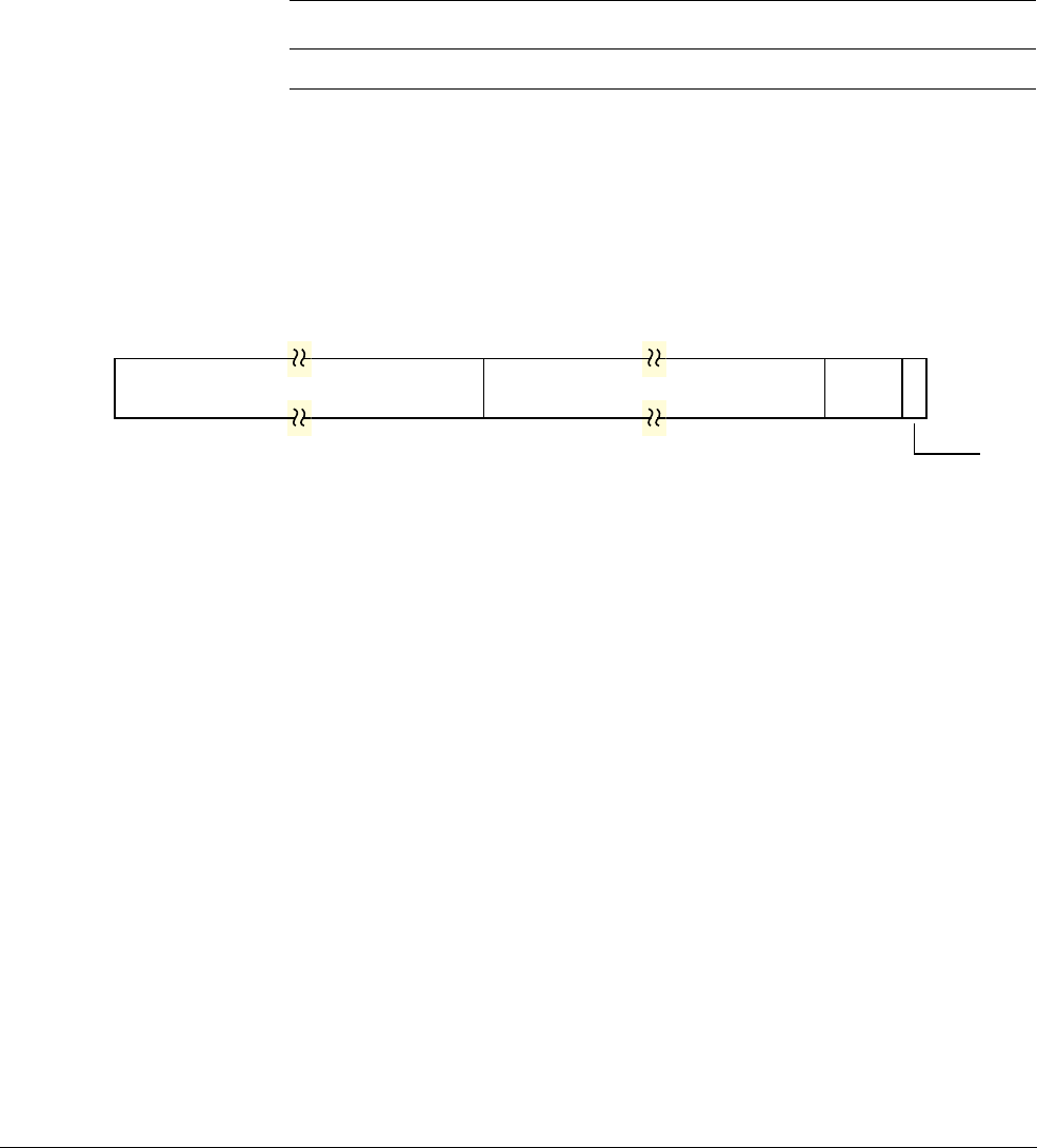
C4 The AArch64 System Instruction Class
C4.4 A64 system instructions for cache maintenance
C4-310 Copyright © 2013 ARM Limited. All rights reserved. ARM DDI 0487A.a
Non-Confidential - Beta ID090413
C4.4.3 DC CSW, Data or unified Cache line Clean by Set/Way
The DC CSW characteristics are:
Purpose
Clean data cache by set/way.
This register is part of the Cache maintenance operations functional group.
Usage constraints
This operation can be performed at the exception levels shown below:
Configurations
DC CSW performs the same function as AArch32 operation DCCSW.
Attributes
DC CSW is a 64-bit system operation.
The DC CSW input value bit assignments are:
Bits [63:32]
Reserved, RES0.
SetWay, bits [31:4]
Contains two fields:
• Way, bits[31:32-A], the number of the way to operate on.
• Set, bits[B-1:L], the number of the set to operate on.
Bits[L-1:4] are RES0.
A = Log2(ASSOCIATIVITY), L = Log2(LINELEN), B = (L + S), S = Log2(NSETS).
ASSOCIATIVITY, LINELEN (line length, in bytes), and NSETS (number of sets) have their usual
meanings and are the values for the cache level being operated on. The values of A and S are
rounded up to the next integer.
Level, bits [3:1]
Cache level to operate on, minus 1. For example, this field is 0 for operations on L1 cache, or 1 for
operations on L2 cache.
Bit [0]
Reserved, RES0.
Performing the DC CSW operation:
To perform the DC CSW operation:
DC CSW, <Xt>
EL0 EL1 (NS) EL1 (S) EL2 EL3 (SCR.NS=1) EL3 (SCR.NS=0)
-WO WO WOWO WO
RES0
63 32
SetWay
31 4
Level
31
0
RES0

C4 The AArch64 System Instruction Class
C4.4 A64 system instructions for cache maintenance
ARM DDI 0487A.a Copyright © 2013 ARM Limited. All rights reserved. C4-311
ID090413 Non-Confidential - Beta
The operation is encoded as follows:
op0 op1 CRn CRm op2
01 000 0111 1010 010

C4 The AArch64 System Instruction Class
C4.4 A64 system instructions for cache maintenance
C4-312 Copyright © 2013 ARM Limited. All rights reserved. ARM DDI 0487A.a
Non-Confidential - Beta ID090413
C4.4.4 DC CVAC, Data or unified Cache line Clean by VA to PoC
The DC CVAC characteristics are:
Purpose
Clean data cache by address to Point of Coherency.
This register is part of the Cache maintenance operations functional group.
Usage constraints
This operation can be performed at the exception levels shown below:
EL0 access is enabled when SCTLR_EL1.UCI is set to 1. When it is set to 0, this operation is
UNDEFINED at EL0.
If EL0 access is enabled, this operation is available at EL0 when the VA has read access permission,
otherwise it causes a Permission Fault.
Configurations
DC CVAC performs the same function as AArch32 operation DCCMVAC.
Attributes
DC CVAC is a 64-bit system operation.
The DC CVAC input value bit assignments are:
Bits [63:0]
Virtual address to use.
Performing the DC CVAC operation:
To perform the DC CVAC operation:
DC CVAC, <Xt>
The operation is encoded as follows:
EL0 EL1 (NS) EL1 (S) EL2 EL3 (SCR.NS=1) EL3 (SCR.NS=0)
Config-WO WO WO WO WO WO
Virtual address to use
63 0
op0 op1 CRn CRm op2
01 011 0111 1010 001

C4 The AArch64 System Instruction Class
C4.4 A64 system instructions for cache maintenance
ARM DDI 0487A.a Copyright © 2013 ARM Limited. All rights reserved. C4-313
ID090413 Non-Confidential - Beta
C4.4.5 DC CVAU, Data or unified Cache line Clean by VA to PoU
The DC CVAU characteristics are:
Purpose
Clean data cache by address to Point of Unification.
This register is part of the Cache maintenance operations functional group.
Usage constraints
This operation can be performed at the exception levels shown below:
EL0 access is enabled when SCTLR_EL1.UCI is set to 1. When it is set to 0, this operation is
UNDEFINED at EL0.
If EL0 access is enabled, this operation is available at EL0 when the VA has read access permission,
otherwise it causes a Permission Fault.
Configurations
DC CVAU performs the same function as AArch32 operation DCCMVAU.
Attributes
DC CVAU is a 64-bit system operation.
The DC CVAU input value bit assignments are:
Bits [63:0]
Virtual address to use.
Performing the DC CVAU operation:
To perform the DC CVAU operation:
DC CVAU, <Xt>
The operation is encoded as follows:
EL0 EL1 (NS) EL1 (S) EL2 EL3 (SCR.NS=1) EL3 (SCR.NS=0)
Config-WO WO WO WO WO WO
Virtual address to use
63 0
op0 op1 CRn CRm op2
01 011 0111 1011 001
C4 The AArch64 System Instruction Class
C4.4 A64 system instructions for cache maintenance
C4-314 Copyright © 2013 ARM Limited. All rights reserved. ARM DDI 0487A.a
Non-Confidential - Beta ID090413
C4.4.6 DC ISW, Data or unified Cache line Invalidate by Set/Way
The DC ISW characteristics are:
Purpose
Invalidate data cache by set/way.
This register is part of the Cache maintenance operations functional group.
Usage constraints
This operation can be performed at the exception levels shown below:
At EL1, this operation must be performed as DC CISW if all of the following apply:
• EL2 is implemented
•HCR_EL2.VM is set to 1
•SCR_EL3.NS is set to 1 or EL3 is not implemented.
Configurations
DC ISW performs the same function as AArch32 operation DCISW.
Attributes
DC ISW is a 64-bit system operation.
The DC ISW input value bit assignments are:
Bits [63:32]
Reserved, RES0.
SetWay, bits [31:4]
Contains two fields:
• Way, bits[31:32-A], the number of the way to operate on.
• Set, bits[B-1:L], the number of the set to operate on.
Bits[L-1:4] are RES0.
A = Log2(ASSOCIATIVITY), L = Log2(LINELEN), B = (L + S), S = Log2(NSETS).
ASSOCIATIVITY, LINELEN (line length, in bytes), and NSETS (number of sets) have their usual
meanings and are the values for the cache level being operated on. The values of A and S are
rounded up to the next integer.
Level, bits [3:1]
Cache level to operate on, minus 1. For example, this field is 0 for operations on L1 cache, or 1 for
operations on L2 cache.
Bit [0]
Reserved, RES0.
EL0 EL1 (NS) EL1 (S) EL2 EL3 (SCR.NS=1) EL3 (SCR.NS=0)
-WO WO WOWO WO
RES0
63 32
SetWay
31 4
Level
31
0
RES0

C4 The AArch64 System Instruction Class
C4.4 A64 system instructions for cache maintenance
ARM DDI 0487A.a Copyright © 2013 ARM Limited. All rights reserved. C4-315
ID090413 Non-Confidential - Beta
Performing the DC ISW operation:
To perform the DC ISW operation:
DC ISW, <Xt>
The operation is encoded as follows:
op0 op1 CRn CRm op2
01 000 0111 0110 010

C4 The AArch64 System Instruction Class
C4.4 A64 system instructions for cache maintenance
C4-316 Copyright © 2013 ARM Limited. All rights reserved. ARM DDI 0487A.a
Non-Confidential - Beta ID090413
C4.4.7 DC IVAC, Data or unified Cache line Invalidate by VA to PoC
The DC IVAC characteristics are:
Purpose
Invalidate instruction cache by address to Point of Coherency.
This register is part of the Cache maintenance operations functional group.
Usage constraints
This operation can be performed at the exception levels shown below:
This operation requires write access permission to the VA, otherwise it causes a Permission Fault.
At EL1, this operation must be performed as DC CIVAC if all of the following apply:
• EL2 is implemented.
•HCR_EL2.VM is set to 1.
•SCR_EL3.NS is set to 1 or EL3 is not implemented.
Configurations
DC IVAC performs the same function as AArch32 operation DCIMVAC.
Attributes
DC IVAC is a 64-bit system operation.
The DC IVAC input value bit assignments are:
Bits [63:0]
Virtual address to use.
Performing the DC IVAC operation:
To perform the DC IVAC operation:
DC IVAC, <Xt>
The operation is encoded as follows:
EL0 EL1 (NS) EL1 (S) EL2 EL3 (SCR.NS=1) EL3 (SCR.NS=0)
-WO WO WOWO WO
Virtual address to use
63 0
op0 op1 CRn CRm op2
01 000 0111 0110 001
C4 The AArch64 System Instruction Class
C4.4 A64 system instructions for cache maintenance
ARM DDI 0487A.a Copyright © 2013 ARM Limited. All rights reserved. C4-317
ID090413 Non-Confidential - Beta
C4.4.8 DC ZVA, Data Cache Zero by VA
The DC ZVA characteristics are:
Purpose
Zero data cache by address. Zeroes a naturally aligned block of N bytes, where the size of N is
identified in DCZID_EL0.
This register is part of the Cache maintenance operations functional group.
Usage constraints
This operation can be performed at the exception levels shown below:
There are two control bits associated with this instruction: SCTLR_EL1.DZE and HCR_EL2.TDZ.
• If execution at EL0 is disabled by the SCTLR_EL1.DZE bit being set to 0, the instruction is
UNDEFINED at EL0.
• In the Non-secure state, HCR_EL2.TDZ controls whether the instruction executes at EL0 or
EL1, or traps to EL2.
When UNDEFINED, the instruction always takes the EL1 UNDEFINED exception.
When the instruction is executed, it can generate memory faults or watchpoints which are prioritized
in the same way as other memory related faults or watchpoints. If a synchronous data abort fault or
a watchpoint is generated, the CM bit in the syndrome field is not set.
If the memory region being zeroed is any type of Device memory, these instructions give an
alignment fault which is prioritized in the same way as other alignment faults that are determined
by the memory type.
This instruction applies to Normal memory regardless of cacheability attributes.
The instruction behaves as a set of Stores to each byte within the block being accessed, and so it:
• Will cause a Permission Fault if the translation system does not permit writes to the locations.
• Requires the same considerations for ordering and the management of coherency as any other
store instructions.
Configurations
There are no configuration notes.
Attributes
DC ZVA is a 64-bit system operation.
The DC ZVA input value bit assignments are:
Bits [63:0]
Virtual address to use. There is no alignment restriction on the address within the block of N bytes
that is used.
EL0 EL1 (NS) EL1 (S) EL2 EL3 (SCR.NS=1) EL3 (SCR.NS=0)
Config-WO WO WO WO WO WO
Virtual address to use
63 0

C4 The AArch64 System Instruction Class
C4.4 A64 system instructions for cache maintenance
C4-318 Copyright © 2013 ARM Limited. All rights reserved. ARM DDI 0487A.a
Non-Confidential - Beta ID090413
Performing the DC ZVA operation:
To perform the DC ZVA operation:
DC ZVA, <Xt>
The operation is encoded as follows:
op0 op1 CRn CRm op2
01 011 0111 0100 001

C4 The AArch64 System Instruction Class
C4.4 A64 system instructions for cache maintenance
ARM DDI 0487A.a Copyright © 2013 ARM Limited. All rights reserved. C4-319
ID090413 Non-Confidential - Beta
C4.4.9 IC IALLU, Instruction Cache Invalidate All to PoU
The IC IALLU characteristics are:
Purpose
Invalidate all instruction caches to Point of Unification.
This register is part of the Cache maintenance operations functional group.
Usage constraints
This operation can be performed at the exception levels shown below:
Configurations
IC IALLU performs the same function as AArch32 operation ICIALLU.
Attributes
IC IALLU is a 64-bit system operation.
The IC IALLU operation ignores the value in the register specified by the instruction used to perform this operation.
Software does not have to write a value to the register before issuing this instruction.
Performing the IC IALLU operation:
To perform the IC IALLU operation:
IC IALLU
The operation is encoded as follows:
EL0 EL1 (NS) EL1 (S) EL2 EL3 (SCR.NS=1) EL3 (SCR.NS=0)
-WO WO WOWO WO
op0 op1 CRn CRm op2
01 000 0111 0101 000

C4 The AArch64 System Instruction Class
C4.4 A64 system instructions for cache maintenance
C4-320 Copyright © 2013 ARM Limited. All rights reserved. ARM DDI 0487A.a
Non-Confidential - Beta ID090413
C4.4.10 IC IALLUIS, Instruction Cache Invalidate All to PoU, Inner Shareable
The IC IALLUIS characteristics are:
Purpose
Invalidate all instruction caches in Inner Shareable domain to Point of Unification.
This register is part of the Cache maintenance operations functional group.
Usage constraints
This operation can be performed at the exception levels shown below:
Configurations
IC IALLUIS performs the same function as AArch32 operation ICIALLUIS.
Attributes
IC IALLUIS is a 64-bit system operation.
The IC IALLUIS operation ignores the value in the register specified by the instruction used to perform this
operation. Software does not have to write a value to the register before issuing this instruction.
Performing the IC IALLUIS operation:
To perform the IC IALLUIS operation:
IC IALLUIS
The operation is encoded as follows:
EL0 EL1 (NS) EL1 (S) EL2 EL3 (SCR.NS=1) EL3 (SCR.NS=0)
-WO WO WOWO WO
op0 op1 CRn CRm op2
01 000 0111 0001 000

C4 The AArch64 System Instruction Class
C4.4 A64 system instructions for cache maintenance
ARM DDI 0487A.a Copyright © 2013 ARM Limited. All rights reserved. C4-321
ID090413 Non-Confidential - Beta
C4.4.11 IC IVAU, Instruction Cache line Invalidate by VA to PoU
The IC IVAU characteristics are:
Purpose
Invalidate instruction cache by address to Point of Unification.
This register is part of the Cache maintenance operations functional group.
Usage constraints
This operation can be performed at the exception levels shown below:
EL0 access is enabled when SCTLR_EL1.UCI is set to 1. When it is set to 0, this operation is
UNDEFINED at EL0.
If EL0 access is enabled, this operation is available at EL0 when the VA has read access permission,
otherwise it causes a Permission Fault.
Configurations
IC IVAU performs the same function as AArch32 operation ICIMVAU.
Attributes
IC IVAU is a 64-bit system operation.
The IC IVAU input value bit assignments are:
Bits [63:0]
Virtual address to use.
Performing the IC IVAU operation:
To perform the IC IVAU operation:
IC IVAU, <Xt>
The operation is encoded as follows:
EL0 EL1 (NS) EL1 (S) EL2 EL3 (SCR.NS=1) EL3 (SCR.NS=0)
Config-WO WO WO WO WO WO
Virtual address to use
63 0
op0 op1 CRn CRm op2
01 011 0111 0101 001

C4 The AArch64 System Instruction Class
C4.5 A64 system instructions for address translation
C4-322 Copyright © 2013 ARM Limited. All rights reserved. ARM DDI 0487A.a
Non-Confidential - Beta ID090413
C4.5 A64 system instructions for address translation
The following sections describe the address translation instructions in A64.
•AT S12E0R, Address Translate Stages 1 and 2 EL0 Read on page C4-323
•AT S12E0W, Address Translate Stages 1 and 2 EL0 Write on page C4-324
•AT S12E1R, Address Translate Stages 1 and 2 EL1 Read on page C4-325
•AT S12E1W, Address Translate Stages 1 and 2 EL1 Write on page C4-326
•AT S1E0R, Address Translate Stage 1 EL0 Read on page C4-327
•AT S1E0W, Address Translate Stage 1 EL0 Write on page C4-328
•AT S1E1R, Address Translate Stage 1 EL1 Read on page C4-329
•AT S1E1W, Address Translate Stage 1 EL1 Write on page C4-330
•AT S1E2R, Address Translate Stage 1 EL2 Read on page C4-331
•AT S1E2W, Address Translate Stage 1 EL2 Write on page C4-332
•AT S1E3R, Address Translate Stage 1 EL3 Read on page C4-333
•AT S1E3W, Address Translate Stage 1 EL3 Write on page C4-334
C4 The AArch64 System Instruction Class
C4.5 A64 system instructions for address translation
ARM DDI 0487A.a Copyright © 2013 ARM Limited. All rights reserved. C4-323
ID090413 Non-Confidential - Beta
C4.5.1 AT S12E0R, Address Translate Stages 1 and 2 EL0 Read
The AT S12E0R characteristics are:
Purpose
Performs stage 1 and 2 address translations as defined for EL0, with permissions as if reading from
the given virtual address.
This register is part of the Address translation operations functional group.
Usage constraints
This operation can be performed at the exception levels shown below:
If EL2 does not exist, or stage 2 translation is disabled, this operation executes as AT S1E0R.
Configurations
There are no configuration notes.
Attributes
AT S12E0R is a 64-bit system operation.
The AT S12E0R input value bit assignments are:
Bits [63:0]
Virtual address to translate to a physical address. The resulting physical address can be read from
the PAR_EL1.
If the address translation instructions are targeting a translation regime that is using AArch32, and
so has a VA of only 32 bits, then VA[63:32] is RES0.
Performing the AT S12E0R operation:
To perform the AT S12E0R operation:
AT S12E0R, <Xt>
The operation is encoded as follows:
EL0 EL1 (NS) EL1 (S) EL2 EL3 (SCR.NS=1) EL3 (SCR.NS=0)
-- - WOWO WO
Virtual address to translate to a physical address
63 0
op0 op1 CRn CRm op2
01 100 0111 1000 110

C4 The AArch64 System Instruction Class
C4.5 A64 system instructions for address translation
C4-324 Copyright © 2013 ARM Limited. All rights reserved. ARM DDI 0487A.a
Non-Confidential - Beta ID090413
C4.5.2 AT S12E0W, Address Translate Stages 1 and 2 EL0 Write
The AT S12E0W characteristics are:
Purpose
Performs stage 1 and 2 address translations as defined for EL0, with permissions as if writing to the
given virtual address.
This register is part of the Address translation operations functional group.
Usage constraints
This operation can be performed at the exception levels shown below:
If EL2 does not exist, or stage 2 translation is disabled, this operation executes as AT S1E0W.
Configurations
There are no configuration notes.
Attributes
AT S12E0W is a 64-bit system operation.
The AT S12E0W input value bit assignments are:
Bits [63:0]
Virtual address to translate to a physical address. The resulting physical address can be read from
the PAR_EL1.
If the address translation instructions are targeting a translation regime that is using AArch32, and
so has a VA of only 32 bits, then VA[63:32] is RES0.
Performing the AT S12E0W operation:
To perform the AT S12E0W operation:
AT S12E0W, <Xt>
The operation is encoded as follows:
EL0 EL1 (NS) EL1 (S) EL2 EL3 (SCR.NS=1) EL3 (SCR.NS=0)
-- - WOWO WO
Virtual address to translate to a physical address
63 0
op0 op1 CRn CRm op2
01 100 0111 1000 111

C4 The AArch64 System Instruction Class
C4.5 A64 system instructions for address translation
ARM DDI 0487A.a Copyright © 2013 ARM Limited. All rights reserved. C4-325
ID090413 Non-Confidential - Beta
C4.5.3 AT S12E1R, Address Translate Stages 1 and 2 EL1 Read
The AT S12E1R characteristics are:
Purpose
Performs stage 1 and 2 address translations as defined for EL1, with permissions as if reading from
the given virtual address.
This register is part of the Address translation operations functional group.
Usage constraints
This operation can be performed at the exception levels shown below:
If EL2 does not exist, or stage 2 translation is disabled, this operation executes as AT S1E1R.
Configurations
There are no configuration notes.
Attributes
AT S12E1R is a 64-bit system operation.
The AT S12E1R input value bit assignments are:
Bits [63:0]
Virtual address to translate to a physical address. The resulting physical address can be read from
the PAR_EL1.
If the address translation instructions are targeting a translation regime that is using AArch32, and
so has a VA of only 32 bits, then VA[63:32] is RES0.
Performing the AT S12E1R operation:
To perform the AT S12E1R operation:
AT S12E1R, <Xt>
The operation is encoded as follows:
EL0 EL1 (NS) EL1 (S) EL2 EL3 (SCR.NS=1) EL3 (SCR.NS=0)
-- - WOWO WO
Virtual address to translate to a physical address
63 0
op0 op1 CRn CRm op2
01 100 0111 1000 100

C4 The AArch64 System Instruction Class
C4.5 A64 system instructions for address translation
C4-326 Copyright © 2013 ARM Limited. All rights reserved. ARM DDI 0487A.a
Non-Confidential - Beta ID090413
C4.5.4 AT S12E1W, Address Translate Stages 1 and 2 EL1 Write
The AT S12E1W characteristics are:
Purpose
Performs stage 1 and 2 address translations as defined for EL1, with permissions as if writing to the
given virtual address.
This register is part of the Address translation operations functional group.
Usage constraints
This operation can be performed at the exception levels shown below:
If EL2 does not exist, or stage 2 translation is disabled, this operation executes as AT S1E1W.
Configurations
There are no configuration notes.
Attributes
AT S12E1W is a 64-bit system operation.
The AT S12E1W input value bit assignments are:
Bits [63:0]
Virtual address to translate to a physical address. The resulting physical address can be read from
the PAR_EL1.
If the address translation instructions are targeting a translation regime that is using AArch32, and
so has a VA of only 32 bits, then VA[63:32] is RES0.
Performing the AT S12E1W operation:
To perform the AT S12E1W operation:
AT S12E1W, <Xt>
The operation is encoded as follows:
EL0 EL1 (NS) EL1 (S) EL2 EL3 (SCR.NS=1) EL3 (SCR.NS=0)
-- - WOWO WO
Virtual address to translate to a physical address
63 0
op0 op1 CRn CRm op2
01 100 0111 1000 101

C4 The AArch64 System Instruction Class
C4.5 A64 system instructions for address translation
ARM DDI 0487A.a Copyright © 2013 ARM Limited. All rights reserved. C4-327
ID090413 Non-Confidential - Beta
C4.5.5 AT S1E0R, Address Translate Stage 1 EL0 Read
The AT S1E0R characteristics are:
Purpose
Performs stage 1 address translation as defined for EL0, with permissions as if reading from the
given virtual address.
This register is part of the Address translation operations functional group.
Usage constraints
This operation can be performed at the exception levels shown below:
Configurations
There are no configuration notes.
Attributes
AT S1E0R is a 64-bit system operation.
The AT S1E0R input value bit assignments are:
Bits [63:0]
Virtual address to translate to a physical address. The resulting physical address can be read from
the PAR_EL1.
If the address translation instructions are targeting a translation regime that is using AArch32, and
so has a VA of only 32 bits, then VA[63:32] is RES0.
Performing the AT S1E0R operation:
To perform the AT S1E0R operation:
AT S1E0R, <Xt>
The operation is encoded as follows:
EL0 EL1 (NS) EL1 (S) EL2 EL3 (SCR.NS=1) EL3 (SCR.NS=0)
-WO WO WOWO WO
Virtual address to translate to a physical address
63 0
op0 op1 CRn CRm op2
01 000 0111 1000 010

C4 The AArch64 System Instruction Class
C4.5 A64 system instructions for address translation
C4-328 Copyright © 2013 ARM Limited. All rights reserved. ARM DDI 0487A.a
Non-Confidential - Beta ID090413
C4.5.6 AT S1E0W, Address Translate Stage 1 EL0 Write
The AT S1E0W characteristics are:
Purpose
Performs stage 1 address translation as defined for EL0, with permissions as if writing to the given
virtual address.
This register is part of the Address translation operations functional group.
Usage constraints
This operation can be performed at the exception levels shown below:
Configurations
There are no configuration notes.
Attributes
AT S1E0W is a 64-bit system operation.
The AT S1E0W input value bit assignments are:
Bits [63:0]
Virtual address to translate to a physical address. The resulting physical address can be read from
the PAR_EL1.
If the address translation instructions are targeting a translation regime that is using AArch32, and
so has a VA of only 32 bits, then VA[63:32] is RES0.
Performing the AT S1E0W operation:
To perform the AT S1E0W operation:
AT S1E0W, <Xt>
The operation is encoded as follows:
EL0 EL1 (NS) EL1 (S) EL2 EL3 (SCR.NS=1) EL3 (SCR.NS=0)
-WO WO WOWO WO
Virtual address to translate to a physical address
63 0
op0 op1 CRn CRm op2
01 000 0111 1000 011

C4 The AArch64 System Instruction Class
C4.5 A64 system instructions for address translation
ARM DDI 0487A.a Copyright © 2013 ARM Limited. All rights reserved. C4-329
ID090413 Non-Confidential - Beta
C4.5.7 AT S1E1R, Address Translate Stage 1 EL1 Read
The AT S1E1R characteristics are:
Purpose
Performs stage 1 address translation as defined for EL1, with permissions as if reading from the
given virtual address.
This register is part of the Address translation operations functional group.
Usage constraints
This operation can be performed at the exception levels shown below:
Configurations
There are no configuration notes.
Attributes
AT S1E1R is a 64-bit system operation.
The AT S1E1R input value bit assignments are:
Bits [63:0]
Virtual address to translate to a physical address. The resulting physical address can be read from
the PAR_EL1.
If the address translation instructions are targeting a translation regime that is using AArch32, and
so has a VA of only 32 bits, then VA[63:32] is RES0.
Performing the AT S1E1R operation:
To perform the AT S1E1R operation:
AT S1E1R, <Xt>
The operation is encoded as follows:
EL0 EL1 (NS) EL1 (S) EL2 EL3 (SCR.NS=1) EL3 (SCR.NS=0)
-WO WO WOWO WO
Virtual address to translate to a physical address
63 0
op0 op1 CRn CRm op2
01 000 0111 1000 000
C4 The AArch64 System Instruction Class
C4.5 A64 system instructions for address translation
C4-330 Copyright © 2013 ARM Limited. All rights reserved. ARM DDI 0487A.a
Non-Confidential - Beta ID090413
C4.5.8 AT S1E1W, Address Translate Stage 1 EL1 Write
The AT S1E1W characteristics are:
Purpose
Performs stage 1 address translation as defined for EL1, with permissions as if writing to the given
virtual address.
This register is part of the Address translation operations functional group.
Usage constraints
This operation can be performed at the exception levels shown below:
Configurations
There are no configuration notes.
Attributes
AT S1E1W is a 64-bit system operation.
The AT S1E1W input value bit assignments are:
Bits [63:0]
Virtual address to translate to a physical address. The resulting physical address can be read from
the PAR_EL1.
If the address translation instructions are targeting a translation regime that is using AArch32, and
so has a VA of only 32 bits, then VA[63:32] is RES0.
Performing the AT S1E1W operation:
To perform the AT S1E1W operation:
AT S1E1W, <Xt>
The operation is encoded as follows:
EL0 EL1 (NS) EL1 (S) EL2 EL3 (SCR.NS=1) EL3 (SCR.NS=0)
-WO WO WOWO WO
Virtual address to translate to a physical address
63 0
op0 op1 CRn CRm op2
01 000 0111 1000 001

C4 The AArch64 System Instruction Class
C4.5 A64 system instructions for address translation
ARM DDI 0487A.a Copyright © 2013 ARM Limited. All rights reserved. C4-331
ID090413 Non-Confidential - Beta
C4.5.9 AT S1E2R, Address Translate Stage 1 EL2 Read
The AT S1E2R characteristics are:
Purpose
Performs stage 1 address translation as defined for EL2, with permissions as if reading from the
given virtual address.
This register is part of the Address translation operations functional group.
Usage constraints
This operation can be performed at the exception levels shown below:
Performing this operation from EL3 is UNDEFINED if EL2 does not exist.
Configurations
There are no configuration notes.
Attributes
AT S1E2R is a 64-bit system operation.
The AT S1E2R input value bit assignments are:
Bits [63:0]
Virtual address to translate to a physical address. The resulting physical address can be read from
the PAR_EL1.
If the address translation instructions are targeting a translation regime that is using AArch32, and
so has a VA of only 32 bits, then VA[63:32] is RES0.
Performing the AT S1E2R operation:
To perform the AT S1E2R operation:
AT S1E2R, <Xt>
The operation is encoded as follows:
EL0 EL1 (NS) EL1 (S) EL2 EL3 (SCR.NS=1) EL3 (SCR.NS=0)
-- - WOWO -
Virtual address to translate to a physical address
63 0
op0 op1 CRn CRm op2
01 100 0111 1000 000

C4 The AArch64 System Instruction Class
C4.5 A64 system instructions for address translation
C4-332 Copyright © 2013 ARM Limited. All rights reserved. ARM DDI 0487A.a
Non-Confidential - Beta ID090413
C4.5.10 AT S1E2W, Address Translate Stage 1 EL2 Write
The AT S1E2W characteristics are:
Purpose
Performs stage 1 address translation as defined for EL2, with permissions as if writing to the given
virtual address.
This register is part of the Address translation operations functional group.
Usage constraints
This operation can be performed at the exception levels shown below:
Performing this operation from EL3 is UNDEFINED if EL2 does not exist.
Configurations
There are no configuration notes.
Attributes
AT S1E2W is a 64-bit system operation.
The AT S1E2W input value bit assignments are:
Bits [63:0]
Virtual address to translate to a physical address. The resulting physical address can be read from
the PAR_EL1.
If the address translation instructions are targeting a translation regime that is using AArch32, and
so has a VA of only 32 bits, then VA[63:32] is RES0.
Performing the AT S1E2W operation:
To perform the AT S1E2W operation:
AT S1E2W, <Xt>
The operation is encoded as follows:
EL0 EL1 (NS) EL1 (S) EL2 EL3 (SCR.NS=1) EL3 (SCR.NS=0)
-- - WOWO -
Virtual address to translate to a physical address
63 0
op0 op1 CRn CRm op2
01 100 0111 1000 001

C4 The AArch64 System Instruction Class
C4.5 A64 system instructions for address translation
ARM DDI 0487A.a Copyright © 2013 ARM Limited. All rights reserved. C4-333
ID090413 Non-Confidential - Beta
C4.5.11 AT S1E3R, Address Translate Stage 1 EL3 Read
The AT S1E3R characteristics are:
Purpose
Performs stage 1 address translation as defined for EL3, with permissions as if reading from the
given virtual address.
This register is part of the Address translation operations functional group.
Usage constraints
This operation can be performed at the exception levels shown below:
Configurations
There are no configuration notes.
Attributes
AT S1E3R is a 64-bit system operation.
The AT S1E3R input value bit assignments are:
Bits [63:0]
Virtual address to translate to a physical address. The resulting physical address can be read from
the PAR_EL1.
If the address translation instructions are targeting a translation regime that is using AArch32, and
so has a VA of only 32 bits, then VA[63:32] is RES0.
Performing the AT S1E3R operation:
To perform the AT S1E3R operation:
AT S1E3R, <Xt>
The operation is encoded as follows:
EL0 EL1 (NS) EL1 (S) EL2 EL3 (SCR.NS=1) EL3 (SCR.NS=0)
-- - -WO WO
Virtual address to translate to a physical address
63 0
op0 op1 CRn CRm op2
01 110 0111 1000 000

C4 The AArch64 System Instruction Class
C4.5 A64 system instructions for address translation
C4-334 Copyright © 2013 ARM Limited. All rights reserved. ARM DDI 0487A.a
Non-Confidential - Beta ID090413
C4.5.12 AT S1E3W, Address Translate Stage 1 EL3 Write
The AT S1E3W characteristics are:
Purpose
Performs stage 1 address translation as defined for EL3, with permissions as if writing to the given
virtual address.
This register is part of the Address translation operations functional group.
Usage constraints
This operation can be performed at the exception levels shown below:
Configurations
There are no configuration notes.
Attributes
AT S1E3W is a 64-bit system operation.
The AT S1E3W input value bit assignments are:
Bits [63:0]
Virtual address to translate to a physical address. The resulting physical address can be read from
the PAR_EL1.
If the address translation instructions are targeting a translation regime that is using AArch32, and
so has a VA of only 32 bits, then VA[63:32] is RES0.
Performing the AT S1E3W operation:
To perform the AT S1E3W operation:
AT S1E3W, <Xt>
The operation is encoded as follows:
EL0 EL1 (NS) EL1 (S) EL2 EL3 (SCR.NS=1) EL3 (SCR.NS=0)
-- - -WO WO
Virtual address to translate to a physical address
63 0
op0 op1 CRn CRm op2
01 110 0111 1000 001

C4 The AArch64 System Instruction Class
C4.6 A64 system instructions for TLB maintenance
ARM DDI 0487A.a Copyright © 2013 ARM Limited. All rights reserved. C4-335
ID090413 Non-Confidential - Beta
C4.6 A64 system instructions for TLB maintenance
The following sections describe the TLB maintenance instructions in A64.
•TLBI ALLE1, TLB Invalidate All entries, EL1 on page C4-336
•TLBI ALLE1IS, TLB Invalidate All entries, EL1, Inner Shareable on page C4-337
•TLBI ALLE2, TLB Invalidate All entries, EL2 on page C4-338
•TLBI ALLE2IS, TLB Invalidate All entries, EL2, Inner Shareable on page C4-339
•TLBI ALLE3, TLB Invalidate All entries, EL3 on page C4-340
•TLBI ALLE3IS, TLB Invalidate All entries, EL3, Inner Shareable on page C4-341
•TLBI ASIDE1, TLB Invalidate by ASID, EL1 on page C4-342
•TLBI ASIDE1IS, TLB Invalidate by ASID, EL1, Inner Shareable on page C4-343
•TLBI IPAS2E1, TLB Invalidate by Intermediate Physical Address, Stage 2, EL1 on page C4-344
•TLBI IPAS2E1IS, TLB Invalidate by Intermediate Physical Address, Stage 2, EL1, Inner Shareable on
page C4-345
•TLBI IPAS2LE1, TLB Invalidate by Intermediate Physical Address, Stage 2, Last level, EL1 on page C4-346
•TLBI IPAS2LE1IS, TLB Invalidate by Intermediate Physical Address, Stage 2, Last level, EL1, Inner
Shareable on page C4-347
•TLBI VAAE1, TLB Invalidate by VA, All ASID, EL1 on page C4-348
•TLBI VAAE1IS, TLB Invalidate by VA, All ASID, EL1, Inner Shareable on page C4-350
•TLBI VAALE1, TLB Invalidate by VA, All ASID, Last level, EL1 on page C4-352
•TLBI VAALE1IS, TLB Invalidate by VA, All ASID, EL1, Inner Shareable on page C4-354
•TLBI VAE1, TLB Invalidate by VA, EL1 on page C4-356
•TLBI VAE1IS, TLB Invalidate by VA, EL1, Inner Shareable on page C4-358
•TLBI VAE2, TLB Invalidate by VA, EL2 on page C4-360
•TLBI VAE2IS, TLB Invalidate by VA, EL2, Inner Shareable on page C4-362
•TLBI VAE3, TLB Invalidate by VA, EL3 on page C4-364
•TLBI VAE3IS, TLB Invalidate by VA, EL3, Inner Shareable on page C4-366
•TLBI VALE1, TLB Invalidate by VA, Last level, EL1 on page C4-368
•TLBI VALE1IS, TLB Invalidate by VA, Last level, EL1, Inner Shareable on page C4-370
•TLBI VALE2, TLB Invalidate by VA, Last level, EL2 on page C4-372
•TLBI VALE2IS, TLB Invalidate by VA, Last level, EL2, Inner Shareable on page C4-374
•TLBI VALE3, TLB Invalidate by VA, Last level, EL3 on page C4-376
•TLBI VALE3IS, TLB Invalidate by VA, Last level, EL3, Inner Shareable on page C4-378
•TLBI VMALLE1, TLB Invalidate by VMID, All entries at stage 1, EL1 on page C4-380
•TLBI VMALLE1IS, TLB Invalidate by VMID, All entries at stage 1, EL1, Inner Shareable on page C4-381
•TLBI VMALLS12E1, TLB Invalidate by VMID, All entries at Stage 1 and 2, EL1 on page C4-382
•TLBI VMALLS12E1IS, TLB Invalidate by VMID, All entries at Stage 1 and 2, EL1, Inner Shareable on
page C4-383

C4 The AArch64 System Instruction Class
C4.6 A64 system instructions for TLB maintenance
C4-336 Copyright © 2013 ARM Limited. All rights reserved. ARM DDI 0487A.a
Non-Confidential - Beta ID090413
C4.6.1 TLBI ALLE1, TLB Invalidate All entries, EL1
The TLBI ALLE1 characteristics are:
Purpose
Invalidate all EL1&0 regime stage 1 and 2 TLB entries.
This register is part of the TLB maintenance operations functional group.
Usage constraints
This operation can be performed at the exception levels shown below:
If EL3 is implemented, the translations that are invalidated are those associated with either the
Secure or Non-secure address space, depending on the value of SCR_EL3.NS.
Configurations
There are no configuration notes.
Attributes
TLBI ALLE1 is a 64-bit system operation.
The TLBI ALLE1 operation ignores the value in the register specified by the instruction used to perform this
operation. Software does not have to write a value to the register before issuing this instruction.
Performing the TLBI ALLE1 operation:
To perform the TLBI ALLE1 operation:
TLBI ALLE1
The operation is encoded as follows:
EL0 EL1 (NS) EL1 (S) EL2 EL3 (SCR.NS=1) EL3 (SCR.NS=0)
-- - WOWO WO
op0 op1 CRn CRm op2
01 100 1000 0111 100

C4 The AArch64 System Instruction Class
C4.6 A64 system instructions for TLB maintenance
ARM DDI 0487A.a Copyright © 2013 ARM Limited. All rights reserved. C4-337
ID090413 Non-Confidential - Beta
C4.6.2 TLBI ALLE1IS, TLB Invalidate All entries, EL1, Inner Shareable
The TLBI ALLE1IS characteristics are:
Purpose
Invalidate all EL1&0 regime stage 1 and 2 TLB entries on all PEs in the same Inner Shareable
domain.
This register is part of the TLB maintenance operations functional group.
Usage constraints
This operation can be performed at the exception levels shown below:
If EL3 is implemented, the translations that are invalidated are those associated with either the
Secure or Non-secure address space, depending on the value of SCR_EL3.NS.
Configurations
There are no configuration notes.
Attributes
TLBI ALLE1IS is a 64-bit system operation.
The TLBI ALLE1IS operation ignores the value in the register specified by the instruction used to perform this
operation. Software does not have to write a value to the register before issuing this instruction.
Performing the TLBI ALLE1IS operation:
To perform the TLBI ALLE1IS operation:
TLBI ALLE1IS
The operation is encoded as follows:
EL0 EL1 (NS) EL1 (S) EL2 EL3 (SCR.NS=1) EL3 (SCR.NS=0)
-- - WOWO WO
op0 op1 CRn CRm op2
01 100 1000 0011 100

C4 The AArch64 System Instruction Class
C4.6 A64 system instructions for TLB maintenance
C4-338 Copyright © 2013 ARM Limited. All rights reserved. ARM DDI 0487A.a
Non-Confidential - Beta ID090413
C4.6.3 TLBI ALLE2, TLB Invalidate All entries, EL2
The TLBI ALLE2 characteristics are:
Purpose
Invalidate all EL2 regime stage 1 TLB entries.
This register is part of the TLB maintenance operations functional group.
Usage constraints
This operation can be performed at the exception levels shown below:
Performing this operation from EL3 is UNDEFINED if EL2 does not exist.
Configurations
There are no configuration notes.
Attributes
TLBI ALLE2 is a 64-bit system operation.
The TLBI ALLE2 operation ignores the value in the register specified by the instruction used to perform this
operation. Software does not have to write a value to the register before issuing this instruction.
Performing the TLBI ALLE2 operation:
To perform the TLBI ALLE2 operation:
TLBI ALLE2
The operation is encoded as follows:
EL0 EL1 (NS) EL1 (S) EL2 EL3 (SCR.NS=1) EL3 (SCR.NS=0)
-- - WOWO -
op0 op1 CRn CRm op2
01 100 1000 0111 000

C4 The AArch64 System Instruction Class
C4.6 A64 system instructions for TLB maintenance
ARM DDI 0487A.a Copyright © 2013 ARM Limited. All rights reserved. C4-339
ID090413 Non-Confidential - Beta
C4.6.4 TLBI ALLE2IS, TLB Invalidate All entries, EL2, Inner Shareable
The TLBI ALLE2IS characteristics are:
Purpose
Invalidate all EL2 regime stage 1 TLB entries on all PEs in the same Inner Shareable domain.
This register is part of the TLB maintenance operations functional group.
Usage constraints
This operation can be performed at the exception levels shown below:
Performing this operation from EL3 is UNDEFINED if EL2 does not exist.
Configurations
There are no configuration notes.
Attributes
TLBI ALLE2IS is a 64-bit system operation.
The TLBI ALLE2IS operation ignores the value in the register specified by the instruction used to perform this
operation. Software does not have to write a value to the register before issuing this instruction.
Performing the TLBI ALLE2IS operation:
To perform the TLBI ALLE2IS operation:
TLBI ALLE2IS
The operation is encoded as follows:
EL0 EL1 (NS) EL1 (S) EL2 EL3 (SCR.NS=1) EL3 (SCR.NS=0)
-- - WOWO -
op0 op1 CRn CRm op2
01 100 1000 0011 000

C4 The AArch64 System Instruction Class
C4.6 A64 system instructions for TLB maintenance
C4-340 Copyright © 2013 ARM Limited. All rights reserved. ARM DDI 0487A.a
Non-Confidential - Beta ID090413
C4.6.5 TLBI ALLE3, TLB Invalidate All entries, EL3
The TLBI ALLE3 characteristics are:
Purpose
Invalidate all EL3 regime stage 1 TLB entries.
This register is part of the TLB maintenance operations functional group.
Usage constraints
This operation can be performed at the exception levels shown below:
Configurations
There are no configuration notes.
Attributes
TLBI ALLE3 is a 64-bit system operation.
The TLBI ALLE3 operation ignores the value in the register specified by the instruction used to perform this
operation. Software does not have to write a value to the register before issuing this instruction.
Performing the TLBI ALLE3 operation:
To perform the TLBI ALLE3 operation:
TLBI ALLE3
The operation is encoded as follows:
EL0 EL1 (NS) EL1 (S) EL2 EL3 (SCR.NS=1) EL3 (SCR.NS=0)
-- - -WO WO
op0 op1 CRn CRm op2
01 110 1000 0111 000

C4 The AArch64 System Instruction Class
C4.6 A64 system instructions for TLB maintenance
ARM DDI 0487A.a Copyright © 2013 ARM Limited. All rights reserved. C4-341
ID090413 Non-Confidential - Beta
C4.6.6 TLBI ALLE3IS, TLB Invalidate All entries, EL3, Inner Shareable
The TLBI ALLE3IS characteristics are:
Purpose
Invalidate all EL3 regime stage 1 TLB entries on all PEs in the same Inner Shareable domain.
This register is part of the TLB maintenance operations functional group.
Usage constraints
This operation can be performed at the exception levels shown below:
Configurations
There are no configuration notes.
Attributes
TLBI ALLE3IS is a 64-bit system operation.
The TLBI ALLE3IS operation ignores the value in the register specified by the instruction used to perform this
operation. Software does not have to write a value to the register before issuing this instruction.
Performing the TLBI ALLE3IS operation:
To perform the TLBI ALLE3IS operation:
TLBI ALLE3IS
The operation is encoded as follows:
EL0 EL1 (NS) EL1 (S) EL2 EL3 (SCR.NS=1) EL3 (SCR.NS=0)
-- - -WO WO
op0 op1 CRn CRm op2
01 110 1000 0011 000
C4 The AArch64 System Instruction Class
C4.6 A64 system instructions for TLB maintenance
C4-342 Copyright © 2013 ARM Limited. All rights reserved. ARM DDI 0487A.a
Non-Confidential - Beta ID090413
C4.6.7 TLBI ASIDE1, TLB Invalidate by ASID, EL1
The TLBI ASIDE1 characteristics are:
Purpose
Invalidate EL1&0 regime stage 1 TLB entries for the given ASID and the current VMID.
This register is part of the TLB maintenance operations functional group.
Usage constraints
This operation can be performed at the exception levels shown below:
Configurations
There are no configuration notes.
Attributes
TLBI ASIDE1 is a 64-bit system operation.
The TLBI ASIDE1 input value bit assignments are:
ASID, bits [63:48]
ASID value to match. Any appropriate TLB entries that match the ASID values will be affected by
this operation.
If the implementation supports 16 bits of ASID, but only 8 bits are being used in the context being
invalidated, the upper bits are considered RES0 and must be written to 0 by software performing the
TLB maintenance.
Bits [47:0]
Reserved, RES0.
Performing the TLBI ASIDE1 operation:
To perform the TLBI ASIDE1 operation:
TLBI ASIDE1, <Xt>
The operation is encoded as follows:
EL0 EL1 (NS) EL1 (S) EL2 EL3 (SCR.NS=1) EL3 (SCR.NS=0)
-WO WO WOWO WO
ASID
63 48
RES0
47 0
op0 op1 CRn CRm op2
01 000 1000 0111 010
C4 The AArch64 System Instruction Class
C4.6 A64 system instructions for TLB maintenance
ARM DDI 0487A.a Copyright © 2013 ARM Limited. All rights reserved. C4-343
ID090413 Non-Confidential - Beta
C4.6.8 TLBI ASIDE1IS, TLB Invalidate by ASID, EL1, Inner Shareable
The TLBI ASIDE1IS characteristics are:
Purpose
Invalidate EL1&0 regime stage 1 TLB entries for the given ASID and the current VMID on all PEs
in the same Inner Shareable domain.
This register is part of the TLB maintenance operations functional group.
Usage constraints
This operation can be performed at the exception levels shown below:
Configurations
There are no configuration notes.
Attributes
TLBI ASIDE1IS is a 64-bit system operation.
The TLBI ASIDE1IS input value bit assignments are:
ASID, bits [63:48]
ASID value to match. Any appropriate TLB entries that match the ASID values will be affected by
this operation.
If the implementation supports 16 bits of ASID, but only 8 bits are being used in the context being
invalidated, the upper bits are considered RES0 and must be written to 0 by software performing the
TLB maintenance.
Bits [47:0]
Reserved, RES0.
Performing the TLBI ASIDE1IS operation:
To perform the TLBI ASIDE1IS operation:
TLBI ASIDE1IS, <Xt>
The operation is encoded as follows:
EL0 EL1 (NS) EL1 (S) EL2 EL3 (SCR.NS=1) EL3 (SCR.NS=0)
-WO WO WOWO WO
ASID
63 48
RES0
47 0
op0 op1 CRn CRm op2
01 000 1000 0011 010

C4 The AArch64 System Instruction Class
C4.6 A64 system instructions for TLB maintenance
C4-344 Copyright © 2013 ARM Limited. All rights reserved. ARM DDI 0487A.a
Non-Confidential - Beta ID090413
C4.6.9 TLBI IPAS2E1, TLB Invalidate by Intermediate Physical Address, Stage 2, EL1
The TLBI IPAS2E1 characteristics are:
Purpose
Invalidate EL1&0 regime stage 2 TLB entries for the given IPA and the current VMID.
This register is part of:
• the TLB maintenance operations functional group
• the Virtualization registers functional group.
Usage constraints
This operation can be performed at the exception levels shown below:
If SCR_EL3.NS==0, or EL2 is not implemented, this instruction is a NOP.
This instruction must apply to structures that contain only stage 2 translation information, but does
not need to apply to structures that contain combined stage 1 and stage 2 translation information.
Configurations
There are no configuration notes.
Attributes
TLBI IPAS2E1 is a 64-bit system operation.
The TLBI IPAS2E1 input value bit assignments are:
Bits [63:36]
Reserved, RES0.
IPA[47:12], bits [35:0]
Bits[47:12] of the intermediate physical address to match.
Performing the TLBI IPAS2E1 operation:
To perform the TLBI IPAS2E1 operation:
TLBI IPAS2E1, <Xt>
The operation is encoded as follows:
EL0 EL1 (NS) EL1 (S) EL2 EL3 (SCR.NS=1) EL3 (SCR.NS=0)
-- - WOWO WO
RES0
63 36
IPA[47:12]
35 0
op0 op1 CRn CRm op2
01 100 1000 0100 001
C4 The AArch64 System Instruction Class
C4.6 A64 system instructions for TLB maintenance
ARM DDI 0487A.a Copyright © 2013 ARM Limited. All rights reserved. C4-345
ID090413 Non-Confidential - Beta
C4.6.10 TLBI IPAS2E1IS, TLB Invalidate by Intermediate Physical Address, Stage 2, EL1, Inner
Shareable
The TLBI IPAS2E1IS characteristics are:
Purpose
Invalidate EL1&0 regime stage 2 TLB entries for the given IPA and the current VMID on all PEs
in the same Inner Shareable domain.
This register is part of:
• the TLB maintenance operations functional group
• the Virtualization registers functional group.
Usage constraints
This operation can be performed at the exception levels shown below:
If SCR_EL3.NS==0, or EL2 is not implemented, this instruction is a NOP.
This instruction must apply to structures that contain only stage 2 translation information, but does
not need to apply to structures that contain combined stage 1 and stage 2 translation information.
Configurations
There are no configuration notes.
Attributes
TLBI IPAS2E1IS is a 64-bit system operation.
The TLBI IPAS2E1IS input value bit assignments are:
Bits [63:36]
Reserved, RES0.
IPA[47:12], bits [35:0]
Bits[47:12] of the intermediate physical address to match.
Performing the TLBI IPAS2E1IS operation:
To perform the TLBI IPAS2E1IS operation:
TLBI IPAS2E1IS, <Xt>
The operation is encoded as follows:
EL0 EL1 (NS) EL1 (S) EL2 EL3 (SCR.NS=1) EL3 (SCR.NS=0)
-- - WOWO WO
RES0
63 36
IPA[47:12]
35 0
op0 op1 CRn CRm op2
01 100 1000 0000 001
C4 The AArch64 System Instruction Class
C4.6 A64 system instructions for TLB maintenance
C4-346 Copyright © 2013 ARM Limited. All rights reserved. ARM DDI 0487A.a
Non-Confidential - Beta ID090413
C4.6.11 TLBI IPAS2LE1, TLB Invalidate by Intermediate Physical Address, Stage 2, Last level, EL1
The TLBI IPAS2LE1 characteristics are:
Purpose
Invalidate EL1&0 regime stage 2 TLB entries for the last level of translation, the given IPA, and the
current VMID.
This register is part of:
• the TLB maintenance operations functional group
• the Virtualization registers functional group.
Usage constraints
This operation can be performed at the exception levels shown below:
If SCR_EL3.NS==0, or EL2 is not implemented, this instruction is a NOP.
This instruction must apply to structures that contain only stage 2 translation information, but does
not need to apply to structures that contain combined stage 1 and stage 2 translation information.
Configurations
There are no configuration notes.
Attributes
TLBI IPAS2LE1 is a 64-bit system operation.
The TLBI IPAS2LE1 input value bit assignments are:
Bits [63:36]
Reserved, RES0.
IPA[47:12], bits [35:0]
Bits[47:12] of the intermediate physical address to match.
Performing the TLBI IPAS2LE1 operation:
To perform the TLBI IPAS2LE1 operation:
TLBI IPAS2LE1, <Xt>
The operation is encoded as follows:
EL0 EL1 (NS) EL1 (S) EL2 EL3 (SCR.NS=1) EL3 (SCR.NS=0)
-- - WOWO WO
RES0
63 36
IPA[47:12]
35 0
op0 op1 CRn CRm op2
01 100 1000 0100 101

C4 The AArch64 System Instruction Class
C4.6 A64 system instructions for TLB maintenance
ARM DDI 0487A.a Copyright © 2013 ARM Limited. All rights reserved. C4-347
ID090413 Non-Confidential - Beta
C4.6.12 TLBI IPAS2LE1IS, TLB Invalidate by Intermediate Physical Address, Stage 2, Last level, EL1,
Inner Shareable
The TLBI IPAS2LE1IS characteristics are:
Purpose
Invalidate EL1&0 regime stage 2 TLB entries for the last level of translation, the given IPA, and the
current VMID, on all PEs in the same Inner Shareable domain.
This register is part of:
• the TLB maintenance operations functional group
• the Virtualization registers functional group.
Usage constraints
This operation can be performed at the exception levels shown below:
If SCR_EL3.NS==0, or EL2 is not implemented, this instruction is a NOP.
This instruction must apply to structures that contain only stage 2 translation information, but does
not need to apply to structures that contain combined stage 1 and stage 2 translation information.
Configurations
There are no configuration notes.
Attributes
TLBI IPAS2LE1IS is a 64-bit system operation.
The TLBI IPAS2LE1IS input value bit assignments are:
Bits [63:36]
Reserved, RES0.
IPA[47:12], bits [35:0]
Bits[47:12] of the intermediate physical address to match.
Performing the TLBI IPAS2LE1IS operation:
To perform the TLBI IPAS2LE1IS operation:
TLBI IPAS2LE1IS, <Xt>
The operation is encoded as follows:
EL0 EL1 (NS) EL1 (S) EL2 EL3 (SCR.NS=1) EL3 (SCR.NS=0)
-- - WOWO WO
RES0
63 36
IPA[47:12]
35 0
op0 op1 CRn CRm op2
01 100 1000 0000 101
C4 The AArch64 System Instruction Class
C4.6 A64 system instructions for TLB maintenance
C4-348 Copyright © 2013 ARM Limited. All rights reserved. ARM DDI 0487A.a
Non-Confidential - Beta ID090413
C4.6.13 TLBI VAAE1, TLB Invalidate by VA, All ASID, EL1
The TLBI VAAE1 characteristics are:
Purpose
Invalidate EL1&0 regime stage 1 TLB entries for the given VA and the current VMID.
This register is part of the TLB maintenance operations functional group.
Usage constraints
This operation can be performed at the exception levels shown below:
If EL3 is implemented, the translations that are invalidated are those associated with either the
Secure or Non-secure address space, depending on the value of SCR_EL3.NS.
Configurations
There are no configuration notes.
Attributes
TLBI VAAE1 is a 64-bit system operation.
The TLBI VAAE1 input value bit assignments are:
Bits [63:44]
Reserved, RES0.
VA[55:12], bits [43:0]
Bits[55:12] of the virtual address to match. Any appropriate TLB entries that match the VA will be
affected by this operation, regardless of the ASID.
If the TLB maintenance instructions are targeting a translation regime that is using AArch32, and
so has a VA of only 32 bits, then the software must treat bits[55:32] as RES0.
The treatment of the low-order bits of this field depends on the translation granule size, as follows:
• Where a 4KB translation granule is being used, all bits are valid and used for the invalidation.
• Where a 16KB translation granule is being used, bits [1:0] of this field are RES0 and ignored
when the instruction is executed, because VA[13:12] have no effect on the operation of the
instruction.
• Where a 64KB translation granule is being used, bits [3:0] of this field are RES0 and ignored
when the instruction is executed, because VA[15:12] have no effect on the operation of the
instruction.
Performing the TLBI VAAE1 operation:
To perform the TLBI VAAE1 operation:
TLBI VAAE1, <Xt>
EL0 EL1 (NS) EL1 (S) EL2 EL3 (SCR.NS=1) EL3 (SCR.NS=0)
-WO WO WOWO WO
RES0
63 44
VA[55:12]
43 0

C4 The AArch64 System Instruction Class
C4.6 A64 system instructions for TLB maintenance
ARM DDI 0487A.a Copyright © 2013 ARM Limited. All rights reserved. C4-349
ID090413 Non-Confidential - Beta
The operation is encoded as follows:
op0 op1 CRn CRm op2
01 000 1000 0111 011
C4 The AArch64 System Instruction Class
C4.6 A64 system instructions for TLB maintenance
C4-350 Copyright © 2013 ARM Limited. All rights reserved. ARM DDI 0487A.a
Non-Confidential - Beta ID090413
C4.6.14 TLBI VAAE1IS, TLB Invalidate by VA, All ASID, EL1, Inner Shareable
The TLBI VAAE1IS characteristics are:
Purpose
Invalidate EL1&0 regime stage 1 TLB entries for the given VA and the current VMID on all PEs in
the same Inner Shareable domain.
This register is part of the TLB maintenance operations functional group.
Usage constraints
This operation can be performed at the exception levels shown below:
If EL3 is implemented, the translations that are invalidated are those associated with either the
Secure or Non-secure address space, depending on the value of SCR_EL3.NS.
Configurations
There are no configuration notes.
Attributes
TLBI VAAE1IS is a 64-bit system operation.
The TLBI VAAE1IS input value bit assignments are:
Bits [63:44]
Reserved, RES0.
VA[55:12], bits [43:0]
Bits[55:12] of the virtual address to match. Any appropriate TLB entries that match the VA will be
affected by this operation, regardless of the ASID.
If the TLB maintenance instructions are targeting a translation regime that is using AArch32, and
so has a VA of only 32 bits, then the software must treat bits[55:32] as RES0.
The treatment of the low-order bits of this field depends on the translation granule size, as follows:
• Where a 4KB translation granule is being used, all bits are valid and used for the invalidation.
• Where a 16KB translation granule is being used, bits [1:0] of this field are RES0 and ignored
when the instruction is executed, because VA[13:12] have no effect on the operation of the
instruction.
• Where a 64KB translation granule is being used, bits [3:0] of this field are RES0 and ignored
when the instruction is executed, because VA[15:12] have no effect on the operation of the
instruction.
Performing the TLBI VAAE1IS operation:
To perform the TLBI VAAE1IS operation:
TLBI VAAE1IS, <Xt>
EL0 EL1 (NS) EL1 (S) EL2 EL3 (SCR.NS=1) EL3 (SCR.NS=0)
-WO WO WOWO WO
RES0
63 44
VA[55:12]
43 0

C4 The AArch64 System Instruction Class
C4.6 A64 system instructions for TLB maintenance
ARM DDI 0487A.a Copyright © 2013 ARM Limited. All rights reserved. C4-351
ID090413 Non-Confidential - Beta
The operation is encoded as follows:
op0 op1 CRn CRm op2
01 000 1000 0011 011

C4 The AArch64 System Instruction Class
C4.6 A64 system instructions for TLB maintenance
C4-352 Copyright © 2013 ARM Limited. All rights reserved. ARM DDI 0487A.a
Non-Confidential - Beta ID090413
C4.6.15 TLBI VAALE1, TLB Invalidate by VA, All ASID, Last level, EL1
The TLBI VAALE1 characteristics are:
Purpose
Invalidate EL1&0 regime stage 1 TLB entries for the last level of translation table walk, the given
VA, and the current VMID.
This register is part of the TLB maintenance operations functional group.
Usage constraints
This operation can be performed at the exception levels shown below:
If EL3 is implemented, the translations that are invalidated are those associated with either the
Secure or Non-secure address space, depending on the value of SCR_EL3.NS.
Configurations
There are no configuration notes.
Attributes
TLBI VAALE1 is a 64-bit system operation.
The TLBI VAALE1 input value bit assignments are:
Bits [63:44]
Reserved, RES0.
VA[55:12], bits [43:0]
Bits[55:12] of the virtual address to match. Any appropriate TLB entries that match the VA will be
affected by this operation, regardless of the ASID.
If the TLB maintenance instructions are targeting a translation regime that is using AArch32, and
so has a VA of only 32 bits, then the software must treat bits[55:32] as RES0.
The treatment of the low-order bits of this field depends on the translation granule size, as follows:
• Where a 4KB translation granule is being used, all bits are valid and used for the invalidation.
• Where a 16KB translation granule is being used, bits [1:0] of this field are RES0 and ignored
when the instruction is executed, because VA[13:12] have no effect on the operation of the
instruction.
• Where a 64KB translation granule is being used, bits [3:0] of this field are RES0 and ignored
when the instruction is executed, because VA[15:12] have no effect on the operation of the
instruction.
Performing the TLBI VAALE1 operation:
To perform the TLBI VAALE1 operation:
TLBI VAALE1, <Xt>
EL0 EL1 (NS) EL1 (S) EL2 EL3 (SCR.NS=1) EL3 (SCR.NS=0)
-WO WO WOWO WO
RES0
63 44
VA[55:12]
43 0

C4 The AArch64 System Instruction Class
C4.6 A64 system instructions for TLB maintenance
ARM DDI 0487A.a Copyright © 2013 ARM Limited. All rights reserved. C4-353
ID090413 Non-Confidential - Beta
The operation is encoded as follows:
op0 op1 CRn CRm op2
01 000 1000 0111 111

C4 The AArch64 System Instruction Class
C4.6 A64 system instructions for TLB maintenance
C4-354 Copyright © 2013 ARM Limited. All rights reserved. ARM DDI 0487A.a
Non-Confidential - Beta ID090413
C4.6.16 TLBI VAALE1IS, TLB Invalidate by VA, All ASID, EL1, Inner Shareable
The TLBI VAALE1IS characteristics are:
Purpose
Invalidate EL1&0 regime stage 1 TLB entries for the last level of translation table walk, the given
VA, and the current VMID, on all PEs in the same Inner Shareable domain.
This register is part of the TLB maintenance operations functional group.
Usage constraints
This operation can be performed at the exception levels shown below:
If EL3 is implemented, the translations that are invalidated are those associated with either the
Secure or Non-secure address space, depending on the value of SCR_EL3.NS.
Configurations
There are no configuration notes.
Attributes
TLBI VAALE1IS is a 64-bit system operation.
The TLBI VAALE1IS input value bit assignments are:
Bits [63:44]
Reserved, RES0.
VA[55:12], bits [43:0]
Bits[55:12] of the virtual address to match. Any appropriate TLB entries that match the VA will be
affected by this operation, regardless of the ASID.
If the TLB maintenance instructions are targeting a translation regime that is using AArch32, and
so has a VA of only 32 bits, then the software must treat bits[55:32] as RES0.
The treatment of the low-order bits of this field depends on the translation granule size, as follows:
• Where a 4KB translation granule is being used, all bits are valid and used for the invalidation.
• Where a 16KB translation granule is being used, bits [1:0] of this field are RES0 and ignored
when the instruction is executed, because VA[13:12] have no effect on the operation of the
instruction.
• Where a 64KB translation granule is being used, bits [3:0] of this field are RES0 and ignored
when the instruction is executed, because VA[15:12] have no effect on the operation of the
instruction.
Performing the TLBI VAALE1IS operation:
To perform the TLBI VAALE1IS operation:
TLBI VAALE1IS, <Xt>
EL0 EL1 (NS) EL1 (S) EL2 EL3 (SCR.NS=1) EL3 (SCR.NS=0)
-WO WO WOWO WO
RES0
63 44
VA[55:12]
43 0

C4 The AArch64 System Instruction Class
C4.6 A64 system instructions for TLB maintenance
ARM DDI 0487A.a Copyright © 2013 ARM Limited. All rights reserved. C4-355
ID090413 Non-Confidential - Beta
The operation is encoded as follows:
op0 op1 CRn CRm op2
01 000 1000 0011 111

C4 The AArch64 System Instruction Class
C4.6 A64 system instructions for TLB maintenance
C4-356 Copyright © 2013 ARM Limited. All rights reserved. ARM DDI 0487A.a
Non-Confidential - Beta ID090413
C4.6.17 TLBI VAE1, TLB Invalidate by VA, EL1
The TLBI VAE1 characteristics are:
Purpose
Invalidate EL1&0 regime stage 1 TLB entries for the given VA and ASID and the current VMID.
This register is part of the TLB maintenance operations functional group.
Usage constraints
This operation can be performed at the exception levels shown below:
If EL3 is implemented, the translations that are invalidated are those associated with either the
Secure or Non-secure address space, depending on the value of SCR_EL3.NS.
Configurations
There are no configuration notes.
Attributes
TLBI VAE1 is a 64-bit system operation.
The TLBI VAE1 input value bit assignments are:
ASID, bits [63:48]
ASID value to match. Any TLB entries that match the ASID value and VA value will be affected
by this operation.
Global TLB entries that match the VA value will be affected by this operation, regardless of the
value of the ASID field.
If the implementation supports 16 bits of ASID, but only 8 bits are being used in the context being
invalidated, the upper bits are considered RES0 and must be written to 0 by software performing the
TLB maintenance.
Bits [47:44]
Reserved, RES0.
VA[55:12], bits [43:0]
Bits[55:12] of the virtual address to match. Any appropriate TLB entries that match the ASID value
(if appropriate) and VA will be affected by this operation.
If the TLB maintenance instructions are targeting a translation regime that is using AArch32, and
so has a VA of only 32 bits, then the software must treat bits[55:32] as RES0.
The treatment of the low-order bits of this field depends on the translation granule size, as follows:
• Where a 4KB translation granule is being used, all bits are valid and used for the invalidation.
• Where a 16KB translation granule is being used, bits [1:0] of this field are RES0 and ignored
when the instruction is executed, because VA[13:12] have no effect on the operation of the
instruction.
EL0 EL1 (NS) EL1 (S) EL2 EL3 (SCR.NS=1) EL3 (SCR.NS=0)
-WO WO WOWO WO
ASID
63 48
RES0
47 44
VA[55:12]
43 0

C4 The AArch64 System Instruction Class
C4.6 A64 system instructions for TLB maintenance
ARM DDI 0487A.a Copyright © 2013 ARM Limited. All rights reserved. C4-357
ID090413 Non-Confidential - Beta
• Where a 64KB translation granule is being used, bits [3:0] of this field are RES0 and ignored
when the instruction is executed, because VA[15:12] have no effect on the operation of the
instruction.
Performing the TLBI VAE1 operation:
To perform the TLBI VAE1 operation:
TLBI VAE1, <Xt>
The operation is encoded as follows:
op0 op1 CRn CRm op2
01 000 1000 0111 001

C4 The AArch64 System Instruction Class
C4.6 A64 system instructions for TLB maintenance
C4-358 Copyright © 2013 ARM Limited. All rights reserved. ARM DDI 0487A.a
Non-Confidential - Beta ID090413
C4.6.18 TLBI VAE1IS, TLB Invalidate by VA, EL1, Inner Shareable
The TLBI VAE1IS characteristics are:
Purpose
Invalidate EL1&0 regime stage 1 TLB entries for the given VA and ASID, and the current VMID,
on all PEs in the same Inner Shareable domain.
This register is part of the TLB maintenance operations functional group.
Usage constraints
This operation can be performed at the exception levels shown below:
If EL3 is implemented, the translations that are invalidated are those associated with either the
Secure or Non-secure address space, depending on the value of SCR_EL3.NS.
Configurations
There are no configuration notes.
Attributes
TLBI VAE1IS is a 64-bit system operation.
The TLBI VAE1IS input value bit assignments are:
ASID, bits [63:48]
ASID value to match. Any TLB entries that match the ASID value and VA value will be affected
by this operation.
Global TLB entries that match the VA value will be affected by this operation, regardless of the
value of the ASID field.
If the implementation supports 16 bits of ASID, but only 8 bits are being used in the context being
invalidated, the upper bits are considered RES0 and must be written to 0 by software performing the
TLB maintenance.
Bits [47:44]
Reserved, RES0.
VA[55:12], bits [43:0]
Bits[55:12] of the virtual address to match. Any appropriate TLB entries that match the ASID value
(if appropriate) and VA will be affected by this operation.
If the TLB maintenance instructions are targeting a translation regime that is using AArch32, and
so has a VA of only 32 bits, then the software must treat bits[55:32] as RES0.
The treatment of the low-order bits of this field depends on the translation granule size, as follows:
• Where a 4KB translation granule is being used, all bits are valid and used for the invalidation.
• Where a 16KB translation granule is being used, bits [1:0] of this field are RES0 and ignored
when the instruction is executed, because VA[13:12] have no effect on the operation of the
instruction.
EL0 EL1 (NS) EL1 (S) EL2 EL3 (SCR.NS=1) EL3 (SCR.NS=0)
-WO WO WOWO WO
ASID
63 48
RES0
47 44
VA[55:12]
43 0

C4 The AArch64 System Instruction Class
C4.6 A64 system instructions for TLB maintenance
ARM DDI 0487A.a Copyright © 2013 ARM Limited. All rights reserved. C4-359
ID090413 Non-Confidential - Beta
• Where a 64KB translation granule is being used, bits [3:0] of this field are RES0 and ignored
when the instruction is executed, because VA[15:12] have no effect on the operation of the
instruction.
Performing the TLBI VAE1IS operation:
To perform the TLBI VAE1IS operation:
TLBI VAE1IS, <Xt>
The operation is encoded as follows:
op0 op1 CRn CRm op2
01 000 1000 0011 001
C4 The AArch64 System Instruction Class
C4.6 A64 system instructions for TLB maintenance
C4-360 Copyright © 2013 ARM Limited. All rights reserved. ARM DDI 0487A.a
Non-Confidential - Beta ID090413
C4.6.19 TLBI VAE2, TLB Invalidate by VA, EL2
The TLBI VAE2 characteristics are:
Purpose
Invalidate EL2 regime stage 1 TLB entries for the given VA.
This register is part of the TLB maintenance operations functional group.
Usage constraints
This operation can be performed at the exception levels shown below:
Performing this operation from EL3 is UNDEFINED if EL2 does not exist.
Configurations
There are no configuration notes.
Attributes
TLBI VAE2 is a 64-bit system operation.
The TLBI VAE2 input value bit assignments are:
Bits [63:44]
Reserved, RES0.
VA[55:12], bits [43:0]
Bits[55:12] of the virtual address to match. Any appropriate TLB entries that match the ASID value
(if appropriate) and VA will be affected by this operation.
If the TLB maintenance instructions are targeting a translation regime that is using AArch32, and
so has a VA of only 32 bits, then the software must treat bits[55:32] as RES0.
The treatment of the low-order bits of this field depends on the translation granule size, as follows:
• Where a 4KB translation granule is being used, all bits are valid and used for the invalidation.
• Where a 16KB translation granule is being used, bits [1:0] of this field are RES0 and ignored
when the instruction is executed, because VA[13:12] have no effect on the operation of the
instruction.
• Where a 64KB translation granule is being used, bits [3:0] of this field are RES0 and ignored
when the instruction is executed, because VA[15:12] have no effect on the operation of the
instruction.
Performing the TLBI VAE2 operation:
To perform the TLBI VAE2 operation:
TLBI VAE2, <Xt>
EL0 EL1 (NS) EL1 (S) EL2 EL3 (SCR.NS=1) EL3 (SCR.NS=0)
-- - WOWO -
RES0
63 44
VA[55:12]
43 0

C4 The AArch64 System Instruction Class
C4.6 A64 system instructions for TLB maintenance
ARM DDI 0487A.a Copyright © 2013 ARM Limited. All rights reserved. C4-361
ID090413 Non-Confidential - Beta
The operation is encoded as follows:
op0 op1 CRn CRm op2
01 100 1000 0111 001
C4 The AArch64 System Instruction Class
C4.6 A64 system instructions for TLB maintenance
C4-362 Copyright © 2013 ARM Limited. All rights reserved. ARM DDI 0487A.a
Non-Confidential - Beta ID090413
C4.6.20 TLBI VAE2IS, TLB Invalidate by VA, EL2, Inner Shareable
The TLBI VAE2IS characteristics are:
Purpose
Invalidate EL2 regime stage 1 TLB entries for the given VA on all PEs in the same Inner Shareable
domain.
This register is part of the TLB maintenance operations functional group.
Usage constraints
This operation can be performed at the exception levels shown below:
Performing this operation from EL3 is UNDEFINED if EL2 does not exist.
Configurations
There are no configuration notes.
Attributes
TLBI VAE2IS is a 64-bit system operation.
The TLBI VAE2IS input value bit assignments are:
Bits [63:44]
Reserved, RES0.
VA[55:12], bits [43:0]
Bits[55:12] of the virtual address to match. Any appropriate TLB entries that match the ASID value
(if appropriate) and VA will be affected by this operation.
If the TLB maintenance instructions are targeting a translation regime that is using AArch32, and
so has a VA of only 32 bits, then the software must treat bits[55:32] as RES0.
The treatment of the low-order bits of this field depends on the translation granule size, as follows:
• Where a 4KB translation granule is being used, all bits are valid and used for the invalidation.
• Where a 16KB translation granule is being used, bits [1:0] of this field are RES0 and ignored
when the instruction is executed, because VA[13:12] have no effect on the operation of the
instruction.
• Where a 64KB translation granule is being used, bits [3:0] of this field are RES0 and ignored
when the instruction is executed, because VA[15:12] have no effect on the operation of the
instruction.
Performing the TLBI VAE2IS operation:
To perform the TLBI VAE2IS operation:
TLBI VAE2IS, <Xt>
EL0 EL1 (NS) EL1 (S) EL2 EL3 (SCR.NS=1) EL3 (SCR.NS=0)
-- - WOWO -
RES0
63 44
VA[55:12]
43 0

C4 The AArch64 System Instruction Class
C4.6 A64 system instructions for TLB maintenance
ARM DDI 0487A.a Copyright © 2013 ARM Limited. All rights reserved. C4-363
ID090413 Non-Confidential - Beta
The operation is encoded as follows:
op0 op1 CRn CRm op2
01 100 1000 0011 001
C4 The AArch64 System Instruction Class
C4.6 A64 system instructions for TLB maintenance
C4-364 Copyright © 2013 ARM Limited. All rights reserved. ARM DDI 0487A.a
Non-Confidential - Beta ID090413
C4.6.21 TLBI VAE3, TLB Invalidate by VA, EL3
The TLBI VAE3 characteristics are:
Purpose
Invalidate EL3 regime stage 1 TLB entries for the given VA.
This register is part of the TLB maintenance operations functional group.
Usage constraints
This operation can be performed at the exception levels shown below:
Configurations
There are no configuration notes.
Attributes
TLBI VAE3 is a 64-bit system operation.
The TLBI VAE3 input value bit assignments are:
Bits [63:44]
Reserved, RES0.
VA[55:12], bits [43:0]
Bits[55:12] of the virtual address to match. Any appropriate TLB entries that match the ASID value
(if appropriate) and VA will be affected by this operation.
If the TLB maintenance instructions are targeting a translation regime that is using AArch32, and
so has a VA of only 32 bits, then the software must treat bits[55:32] as RES0.
The treatment of the low-order bits of this field depends on the translation granule size, as follows:
• Where a 4KB translation granule is being used, all bits are valid and used for the invalidation.
• Where a 16KB translation granule is being used, bits [1:0] of this field are RES0 and ignored
when the instruction is executed, because VA[13:12] have no effect on the operation of the
instruction.
• Where a 64KB translation granule is being used, bits [3:0] of this field are RES0 and ignored
when the instruction is executed, because VA[15:12] have no effect on the operation of the
instruction.
Performing the TLBI VAE3 operation:
To perform the TLBI VAE3 operation:
TLBI VAE3, <Xt>
EL0 EL1 (NS) EL1 (S) EL2 EL3 (SCR.NS=1) EL3 (SCR.NS=0)
-- - -WO WO
RES0
63 44
VA[55:12]
43 0

C4 The AArch64 System Instruction Class
C4.6 A64 system instructions for TLB maintenance
ARM DDI 0487A.a Copyright © 2013 ARM Limited. All rights reserved. C4-365
ID090413 Non-Confidential - Beta
The operation is encoded as follows:
op0 op1 CRn CRm op2
01 110 1000 0111 001

C4 The AArch64 System Instruction Class
C4.6 A64 system instructions for TLB maintenance
C4-366 Copyright © 2013 ARM Limited. All rights reserved. ARM DDI 0487A.a
Non-Confidential - Beta ID090413
C4.6.22 TLBI VAE3IS, TLB Invalidate by VA, EL3, Inner Shareable
The TLBI VAE3IS characteristics are:
Purpose
Invalidate EL3 regime stage 1 TLB entries for the given VA on all PEs in the same Inner Shareable
domain.
This register is part of the TLB maintenance operations functional group.
Usage constraints
This operation can be performed at the exception levels shown below:
Configurations
There are no configuration notes.
Attributes
TLBI VAE3IS is a 64-bit system operation.
The TLBI VAE3IS input value bit assignments are:
Bits [63:44]
Reserved, RES0.
VA[55:12], bits [43:0]
Bits[55:12] of the virtual address to match. Any appropriate TLB entries that match the ASID value
(if appropriate) and VA will be affected by this operation.
If the TLB maintenance instructions are targeting a translation regime that is using AArch32, and
so has a VA of only 32 bits, then the software must treat bits[55:32] as RES0.
The treatment of the low-order bits of this field depends on the translation granule size, as follows:
• Where a 4KB translation granule is being used, all bits are valid and used for the invalidation.
• Where a 16KB translation granule is being used, bits [1:0] of this field are RES0 and ignored
when the instruction is executed, because VA[13:12] have no effect on the operation of the
instruction.
• Where a 64KB translation granule is being used, bits [3:0] of this field are RES0 and ignored
when the instruction is executed, because VA[15:12] have no effect on the operation of the
instruction.
Performing the TLBI VAE3IS operation:
To perform the TLBI VAE3IS operation:
TLBI VAE3IS, <Xt>
EL0 EL1 (NS) EL1 (S) EL2 EL3 (SCR.NS=1) EL3 (SCR.NS=0)
-- - -WO WO
RES0
63 44
VA[55:12]
43 0

C4 The AArch64 System Instruction Class
C4.6 A64 system instructions for TLB maintenance
ARM DDI 0487A.a Copyright © 2013 ARM Limited. All rights reserved. C4-367
ID090413 Non-Confidential - Beta
The operation is encoded as follows:
op0 op1 CRn CRm op2
01 110 1000 0011 001
C4 The AArch64 System Instruction Class
C4.6 A64 system instructions for TLB maintenance
C4-368 Copyright © 2013 ARM Limited. All rights reserved. ARM DDI 0487A.a
Non-Confidential - Beta ID090413
C4.6.23 TLBI VALE1, TLB Invalidate by VA, Last level, EL1
The TLBI VALE1 characteristics are:
Purpose
Invalidate EL1&0 regime stage 1 TLB entries for the last level of translation table walk, the given
VA and ASID, and the current VMID.
This register is part of the TLB maintenance operations functional group.
Usage constraints
This operation can be performed at the exception levels shown below:
If EL3 is implemented, the translations that are invalidated are those associated with either the
Secure or Non-secure address space, depending on the value of SCR_EL3.NS.
Configurations
There are no configuration notes.
Attributes
TLBI VALE1 is a 64-bit system operation.
The TLBI VALE1 input value bit assignments are:
ASID, bits [63:48]
ASID value to match. Any TLB entries that match the ASID value and VA value will be affected
by this operation.
Global TLB entries that match the VA value will be affected by this operation, regardless of the
value of the ASID field.
If the implementation supports 16 bits of ASID, but only 8 bits are being used in the context being
invalidated, the upper bits are considered RES0 and must be written to 0 by software performing the
TLB maintenance.
Bits [47:44]
Reserved, RES0.
VA[55:12], bits [43:0]
Bits[55:12] of the virtual address to match. Any appropriate TLB entries that match the ASID value
(if appropriate) and VA will be affected by this operation.
If the TLB maintenance instructions are targeting a translation regime that is using AArch32, and
so has a VA of only 32 bits, then the software must treat bits[55:32] as RES0.
The treatment of the low-order bits of this field depends on the translation granule size, as follows:
• Where a 4KB translation granule is being used, all bits are valid and used for the invalidation.
• Where a 16KB translation granule is being used, bits [1:0] of this field are RES0 and ignored
when the instruction is executed, because VA[13:12] have no effect on the operation of the
instruction.
EL0 EL1 (NS) EL1 (S) EL2 EL3 (SCR.NS=1) EL3 (SCR.NS=0)
-WO WO WOWO WO
ASID
63 48
RES0
47 44
VA[55:12]
43 0

C4 The AArch64 System Instruction Class
C4.6 A64 system instructions for TLB maintenance
ARM DDI 0487A.a Copyright © 2013 ARM Limited. All rights reserved. C4-369
ID090413 Non-Confidential - Beta
• Where a 64KB translation granule is being used, bits [3:0] of this field are RES0 and ignored
when the instruction is executed, because VA[15:12] have no effect on the operation of the
instruction.
Performing the TLBI VALE1 operation:
To perform the TLBI VALE1 operation:
TLBI VALE1, <Xt>
The operation is encoded as follows:
op0 op1 CRn CRm op2
01 000 1000 0111 101

C4 The AArch64 System Instruction Class
C4.6 A64 system instructions for TLB maintenance
C4-370 Copyright © 2013 ARM Limited. All rights reserved. ARM DDI 0487A.a
Non-Confidential - Beta ID090413
C4.6.24 TLBI VALE1IS, TLB Invalidate by VA, Last level, EL1, Inner Shareable
The TLBI VALE1IS characteristics are:
Purpose
Invalidate EL1&0 regime stage 1 TLB entries for the last level of translation table walk, the given
VA and ASID, and the current VMID, on all PEs in the same Inner Shareable domain.
This register is part of the TLB maintenance operations functional group.
Usage constraints
This operation can be performed at the exception levels shown below:
If EL3 is implemented, the translations that are invalidated are those associated with either the
Secure or Non-secure address space, depending on the value of SCR_EL3.NS.
Configurations
There are no configuration notes.
Attributes
TLBI VALE1IS is a 64-bit system operation.
The TLBI VALE1IS input value bit assignments are:
ASID, bits [63:48]
ASID value to match. Any TLB entries that match the ASID value and VA value will be affected
by this operation.
Global TLB entries that match the VA value will be affected by this operation, regardless of the
value of the ASID field.
If the implementation supports 16 bits of ASID, but only 8 bits are being used in the context being
invalidated, the upper bits are considered RES0 and must be written to 0 by software performing the
TLB maintenance.
Bits [47:44]
Reserved, RES0.
VA[55:12], bits [43:0]
Bits[55:12] of the virtual address to match. Any appropriate TLB entries that match the ASID value
(if appropriate) and VA will be affected by this operation.
If the TLB maintenance instructions are targeting a translation regime that is using AArch32, and
so has a VA of only 32 bits, then the software must treat bits[55:32] as RES0.
The treatment of the low-order bits of this field depends on the translation granule size, as follows:
• Where a 4KB translation granule is being used, all bits are valid and used for the invalidation.
• Where a 16KB translation granule is being used, bits [1:0] of this field are RES0 and ignored
when the instruction is executed, because VA[13:12] have no effect on the operation of the
instruction.
EL0 EL1 (NS) EL1 (S) EL2 EL3 (SCR.NS=1) EL3 (SCR.NS=0)
-WO WO WOWO WO
ASID
63 48
RES0
47 44
VA[55:12]
43 0

C4 The AArch64 System Instruction Class
C4.6 A64 system instructions for TLB maintenance
ARM DDI 0487A.a Copyright © 2013 ARM Limited. All rights reserved. C4-371
ID090413 Non-Confidential - Beta
• Where a 64KB translation granule is being used, bits [3:0] of this field are RES0 and ignored
when the instruction is executed, because VA[15:12] have no effect on the operation of the
instruction.
Performing the TLBI VALE1IS operation:
To perform the TLBI VALE1IS operation:
TLBI VALE1IS, <Xt>
The operation is encoded as follows:
op0 op1 CRn CRm op2
01 000 1000 0011 101

C4 The AArch64 System Instruction Class
C4.6 A64 system instructions for TLB maintenance
C4-372 Copyright © 2013 ARM Limited. All rights reserved. ARM DDI 0487A.a
Non-Confidential - Beta ID090413
C4.6.25 TLBI VALE2, TLB Invalidate by VA, Last level, EL2
The TLBI VALE2 characteristics are:
Purpose
Invalidate EL2 regime stage 1 TLB entries for the last level of translation table walk and the given
VA.
This register is part of the TLB maintenance operations functional group.
Usage constraints
This operation can be performed at the exception levels shown below:
Performing this operation from EL3 is UNDEFINED if EL2 does not exist.
Configurations
There are no configuration notes.
Attributes
TLBI VALE2 is a 64-bit system operation.
The TLBI VALE2 input value bit assignments are:
Bits [63:44]
Reserved, RES0.
VA[55:12], bits [43:0]
Bits[55:12] of the virtual address to match. Any appropriate TLB entries that match the ASID value
(if appropriate) and VA will be affected by this operation.
If the TLB maintenance instructions are targeting a translation regime that is using AArch32, and
so has a VA of only 32 bits, then the software must treat bits[55:32] as RES0.
The treatment of the low-order bits of this field depends on the translation granule size, as follows:
• Where a 4KB translation granule is being used, all bits are valid and used for the invalidation.
• Where a 16KB translation granule is being used, bits [1:0] of this field are RES0 and ignored
when the instruction is executed, because VA[13:12] have no effect on the operation of the
instruction.
• Where a 64KB translation granule is being used, bits [3:0] of this field are RES0 and ignored
when the instruction is executed, because VA[15:12] have no effect on the operation of the
instruction.
Performing the TLBI VALE2 operation:
To perform the TLBI VALE2 operation:
TLBI VALE2, <Xt>
EL0 EL1 (NS) EL1 (S) EL2 EL3 (SCR.NS=1) EL3 (SCR.NS=0)
-- - WOWO -
RES0
63 44
VA[55:12]
43 0

C4 The AArch64 System Instruction Class
C4.6 A64 system instructions for TLB maintenance
ARM DDI 0487A.a Copyright © 2013 ARM Limited. All rights reserved. C4-373
ID090413 Non-Confidential - Beta
The operation is encoded as follows:
op0 op1 CRn CRm op2
01 100 1000 0111 101

C4 The AArch64 System Instruction Class
C4.6 A64 system instructions for TLB maintenance
C4-374 Copyright © 2013 ARM Limited. All rights reserved. ARM DDI 0487A.a
Non-Confidential - Beta ID090413
C4.6.26 TLBI VALE2IS, TLB Invalidate by VA, Last level, EL2, Inner Shareable
The TLBI VALE2IS characteristics are:
Purpose
Invalidate EL2 regime stage 1 TLB entries for the last level of translation table walk and the given
VA on all PEs in the same Inner Shareable domain.
This register is part of the TLB maintenance operations functional group.
Usage constraints
This operation can be performed at the exception levels shown below:
Performing this operation from EL3 is UNDEFINED if EL2 does not exist.
Configurations
There are no configuration notes.
Attributes
TLBI VALE2IS is a 64-bit system operation.
The TLBI VALE2IS input value bit assignments are:
Bits [63:44]
Reserved, RES0.
VA[55:12], bits [43:0]
Bits[55:12] of the virtual address to match. Any appropriate TLB entries that match the ASID value
(if appropriate) and VA will be affected by this operation.
If the TLB maintenance instructions are targeting a translation regime that is using AArch32, and
so has a VA of only 32 bits, then the software must treat bits[55:32] as RES0.
The treatment of the low-order bits of this field depends on the translation granule size, as follows:
• Where a 4KB translation granule is being used, all bits are valid and used for the invalidation.
• Where a 16KB translation granule is being used, bits [1:0] of this field are RES0 and ignored
when the instruction is executed, because VA[13:12] have no effect on the operation of the
instruction.
• Where a 64KB translation granule is being used, bits [3:0] of this field are RES0 and ignored
when the instruction is executed, because VA[15:12] have no effect on the operation of the
instruction.
Performing the TLBI VALE2IS operation:
To perform the TLBI VALE2IS operation:
TLBI VALE2IS, <Xt>
EL0 EL1 (NS) EL1 (S) EL2 EL3 (SCR.NS=1) EL3 (SCR.NS=0)
-- - WOWO -
RES0
63 44
VA[55:12]
43 0

C4 The AArch64 System Instruction Class
C4.6 A64 system instructions for TLB maintenance
ARM DDI 0487A.a Copyright © 2013 ARM Limited. All rights reserved. C4-375
ID090413 Non-Confidential - Beta
The operation is encoded as follows:
op0 op1 CRn CRm op2
01 100 1000 0011 101
C4 The AArch64 System Instruction Class
C4.6 A64 system instructions for TLB maintenance
C4-376 Copyright © 2013 ARM Limited. All rights reserved. ARM DDI 0487A.a
Non-Confidential - Beta ID090413
C4.6.27 TLBI VALE3, TLB Invalidate by VA, Last level, EL3
The TLBI VALE3 characteristics are:
Purpose
Invalidate EL3 regime stage 1 TLB entries for the last level of translation table walk and the given
VA.
This register is part of the TLB maintenance operations functional group.
Usage constraints
This operation can be performed at the exception levels shown below:
Configurations
There are no configuration notes.
Attributes
TLBI VALE3 is a 64-bit system operation.
The TLBI VALE3 input value bit assignments are:
Bits [63:44]
Reserved, RES0.
VA[55:12], bits [43:0]
Bits[55:12] of the virtual address to match. Any appropriate TLB entries that match the ASID value
(if appropriate) and VA will be affected by this operation.
If the TLB maintenance instructions are targeting a translation regime that is using AArch32, and
so has a VA of only 32 bits, then the software must treat bits[55:32] as RES0.
The treatment of the low-order bits of this field depends on the translation granule size, as follows:
• Where a 4KB translation granule is being used, all bits are valid and used for the invalidation.
• Where a 16KB translation granule is being used, bits [1:0] of this field are RES0 and ignored
when the instruction is executed, because VA[13:12] have no effect on the operation of the
instruction.
• Where a 64KB translation granule is being used, bits [3:0] of this field are RES0 and ignored
when the instruction is executed, because VA[15:12] have no effect on the operation of the
instruction.
Performing the TLBI VALE3 operation:
To perform the TLBI VALE3 operation:
TLBI VALE3, <Xt>
EL0 EL1 (NS) EL1 (S) EL2 EL3 (SCR.NS=1) EL3 (SCR.NS=0)
-- - -WO WO
RES0
63 44
VA[55:12]
43 0

C4 The AArch64 System Instruction Class
C4.6 A64 system instructions for TLB maintenance
ARM DDI 0487A.a Copyright © 2013 ARM Limited. All rights reserved. C4-377
ID090413 Non-Confidential - Beta
The operation is encoded as follows:
op0 op1 CRn CRm op2
01 110 1000 0111 101

C4 The AArch64 System Instruction Class
C4.6 A64 system instructions for TLB maintenance
C4-378 Copyright © 2013 ARM Limited. All rights reserved. ARM DDI 0487A.a
Non-Confidential - Beta ID090413
C4.6.28 TLBI VALE3IS, TLB Invalidate by VA, Last level, EL3, Inner Shareable
The TLBI VALE3IS characteristics are:
Purpose
Invalidate EL3 regime stage 1 TLB entries for the last level of translation table walk and the given
VA on all PEs in the same Inner Shareable domain.
This register is part of the TLB maintenance operations functional group.
Usage constraints
This operation can be performed at the exception levels shown below:
Configurations
There are no configuration notes.
Attributes
TLBI VALE3IS is a 64-bit system operation.
The TLBI VALE3IS input value bit assignments are:
Bits [63:44]
Reserved, RES0.
VA[55:12], bits [43:0]
Bits[55:12] of the virtual address to match. Any appropriate TLB entries that match the ASID value
(if appropriate) and VA will be affected by this operation.
If the TLB maintenance instructions are targeting a translation regime that is using AArch32, and
so has a VA of only 32 bits, then the software must treat bits[55:32] as RES0.
The treatment of the low-order bits of this field depends on the translation granule size, as follows:
• Where a 4KB translation granule is being used, all bits are valid and used for the invalidation.
• Where a 16KB translation granule is being used, bits [1:0] of this field are RES0 and ignored
when the instruction is executed, because VA[13:12] have no effect on the operation of the
instruction.
• Where a 64KB translation granule is being used, bits [3:0] of this field are RES0 and ignored
when the instruction is executed, because VA[15:12] have no effect on the operation of the
instruction.
Performing the TLBI VALE3IS operation:
To perform the TLBI VALE3IS operation:
TLBI VALE3IS, <Xt>
EL0 EL1 (NS) EL1 (S) EL2 EL3 (SCR.NS=1) EL3 (SCR.NS=0)
-- - -WO WO
RES0
63 44
VA[55:12]
43 0

C4 The AArch64 System Instruction Class
C4.6 A64 system instructions for TLB maintenance
ARM DDI 0487A.a Copyright © 2013 ARM Limited. All rights reserved. C4-379
ID090413 Non-Confidential - Beta
The operation is encoded as follows:
op0 op1 CRn CRm op2
01 110 1000 0011 101

C4 The AArch64 System Instruction Class
C4.6 A64 system instructions for TLB maintenance
C4-380 Copyright © 2013 ARM Limited. All rights reserved. ARM DDI 0487A.a
Non-Confidential - Beta ID090413
C4.6.29 TLBI VMALLE1, TLB Invalidate by VMID, All entries at stage 1, EL1
The TLBI VMALLE1 characteristics are:
Purpose
Invalidate all EL1&0 regime stage 1 TLB entries for the current VMID.
This register is part of the TLB maintenance operations functional group.
Usage constraints
This operation can be performed at the exception levels shown below:
If EL3 is implemented, the translations that are invalidated are those associated with either the
Secure or Non-secure address space, depending on the value of SCR_EL3.NS.
Configurations
There are no configuration notes.
Attributes
TLBI VMALLE1 is a 64-bit system operation.
The TLBI VMALLE1 operation ignores the value in the register specified by the instruction used to perform this
operation. Software does not have to write a value to the register before issuing this instruction.
Performing the TLBI VMALLE1 operation:
To perform the TLBI VMALLE1 operation:
TLBI VMALLE1
The operation is encoded as follows:
EL0 EL1 (NS) EL1 (S) EL2 EL3 (SCR.NS=1) EL3 (SCR.NS=0)
-WO WO WOWO WO
op0 op1 CRn CRm op2
01 000 1000 0111 000

C4 The AArch64 System Instruction Class
C4.6 A64 system instructions for TLB maintenance
ARM DDI 0487A.a Copyright © 2013 ARM Limited. All rights reserved. C4-381
ID090413 Non-Confidential - Beta
C4.6.30 TLBI VMALLE1IS, TLB Invalidate by VMID, All entries at stage 1, EL1, Inner Shareable
The TLBI VMALLE1IS characteristics are:
Purpose
Invalidate all EL1&0 regime stage 1 TLB entries for the current VMID on all PEs in the same Inner
Shareable domain.
This register is part of the TLB maintenance operations functional group.
Usage constraints
This operation can be performed at the exception levels shown below:
If EL3 is implemented, the translations that are invalidated are those associated with either the
Secure or Non-secure address space, depending on the value of SCR_EL3.NS.
Configurations
There are no configuration notes.
Attributes
TLBI VMALLE1IS is a 64-bit system operation.
The TLBI VMALLE1IS operation ignores the value in the register specified by the instruction used to perform this
operation. Software does not have to write a value to the register before issuing this instruction.
Performing the TLBI VMALLE1IS operation:
To perform the TLBI VMALLE1IS operation:
TLBI VMALLE1IS
The operation is encoded as follows:
EL0 EL1 (NS) EL1 (S) EL2 EL3 (SCR.NS=1) EL3 (SCR.NS=0)
-WO WO WOWO WO
op0 op1 CRn CRm op2
01 000 1000 0011 000

C4 The AArch64 System Instruction Class
C4.6 A64 system instructions for TLB maintenance
C4-382 Copyright © 2013 ARM Limited. All rights reserved. ARM DDI 0487A.a
Non-Confidential - Beta ID090413
C4.6.31 TLBI VMALLS12E1, TLB Invalidate by VMID, All entries at Stage 1 and 2, EL1
The TLBI VMALLS12E1 characteristics are:
Purpose
Invalidate all EL1&0 regime stage 1 and 2 TLB entries for the current VMID.
This register is part of the TLB maintenance operations functional group.
Usage constraints
This operation can be performed at the exception levels shown below:
If EL3 is implemented, the translations that are invalidated are those associated with either the
Secure or Non-secure address space, depending on the value of SCR_EL3.NS.
Configurations
There are no configuration notes.
Attributes
TLBI VMALLS12E1 is a 64-bit system operation.
The TLBI VMALLS12E1 operation ignores the value in the register specified by the instruction used to perform
this operation. Software does not have to write a value to the register before issuing this instruction.
Performing the TLBI VMALLS12E1 operation:
To perform the TLBI VMALLS12E1 operation:
TLBI VMALLS12E1
The operation is encoded as follows:
EL0 EL1 (NS) EL1 (S) EL2 EL3 (SCR.NS=1) EL3 (SCR.NS=0)
-- - WOWO WO
op0 op1 CRn CRm op2
01 100 1000 0111 110

C4 The AArch64 System Instruction Class
C4.6 A64 system instructions for TLB maintenance
ARM DDI 0487A.a Copyright © 2013 ARM Limited. All rights reserved. C4-383
ID090413 Non-Confidential - Beta
C4.6.32 TLBI VMALLS12E1IS, TLB Invalidate by VMID, All entries at Stage 1 and 2, EL1, Inner
Shareable
The TLBI VMALLS12E1IS characteristics are:
Purpose
Invalidate all EL1&0 regime stage 1 and 2 TLB entries for the current VMID on all PEs in the same
Inner Shareable domain.
This register is part of the TLB maintenance operations functional group.
Usage constraints
This operation can be performed at the exception levels shown below:
If EL3 is implemented, the translations that are invalidated are those associated with either the
Secure or Non-secure address space, depending on the value of SCR_EL3.NS.
Configurations
There are no configuration notes.
Attributes
TLBI VMALLS12E1IS is a 64-bit system operation.
The TLBI VMALLS12E1IS operation ignores the value in the register specified by the instruction used to perform
this operation. Software does not have to write a value to the register before issuing this instruction.
Performing the TLBI VMALLS12E1IS operation:
To perform the TLBI VMALLS12E1IS operation:
TLBI VMALLS12E1IS
The operation is encoded as follows:
EL0 EL1 (NS) EL1 (S) EL2 EL3 (SCR.NS=1) EL3 (SCR.NS=0)
-- - WOWO WO
op0 op1 CRn CRm op2
01 100 1000 0011 110

C4 The AArch64 System Instruction Class
C4.6 A64 system instructions for TLB maintenance
C4-384 Copyright © 2013 ARM Limited. All rights reserved. ARM DDI 0487A.a
Non-Confidential - Beta ID090413

ARM DDI 0487A.a Copyright © 2013 ARM Limited. All rights reserved. C5-385
ID090413 Non-Confidential - Beta
Chapter C5
A64 Base Instruction Descriptions
This chapter describes the A64 base instructions.
It contains the following sections:
•Introduction on page C5-386.
•Register size on page C5-387.
•Use of the PC on page C5-388.
•Use of the stack pointer on page C5-389.
•Condition flags and related instructions on page C5-390.
•Alphabetical list of instructions on page C5-391.

C5 A64 Base Instruction Descriptions
C5.1 Introduction
C5-386 Copyright © 2013 ARM Limited. All rights reserved. ARM DDI 0487A.a
Non-Confidential - Beta ID090413
C5.1 Introduction
This chapter provides information on key aspects of the base instructions, and an alphabetic list of instructions from
the following functional groups:
• Branch, Exception generation, and system instructions.
• Loads and stores associated with the general-purpose registers.
• Data processing (immediate).
• Data processing (register).
A64 instruction index by encoding on page C3-172 provides an overview of the instruction encodings as well as of
the instruction classes within their functional groups.
The base instruction descriptions include:
•Register size on page C5-387.
•Use of the PC on page C5-388.
•Use of the stack pointer on page C5-389.
•Condition flags and related instructions on page C5-390.

C5 A64 Base Instruction Descriptions
C5.2 Register size
ARM DDI 0487A.a Copyright © 2013 ARM Limited. All rights reserved. C5-387
ID090413 Non-Confidential - Beta
C5.2 Register size
Most data processing, comparison, and conversion instructions that use the general-purpose registers as the source
or destination operand have two instruction variants that operate on either a 32-bit or a 64-bit value.
Where a 32-bit instruction form is selected, the following holds:
• The upper 32 bits of the source registers are ignored.
• The upper 32 bits of the destination register are set to zero.
• Right shifts and right rotates inject at bit[31], not at bit[63].
• The condition flags, where set by the instruction, are computed from the lower 32 bits.
This distinction applies even when the results of a 32-bit instruction form are indistinguishable from the lower 32
bits computed by the equivalent 64-bit instruction form. For example, a 32-bit bitwise
ORR
could be performed using
a 64-bit
ORR
and simply ignoring the top 32 bits of the result. However, the A64 instruction set includes separate
32-bit and 64-bit forms of the
ORR
instruction.
As well as distinct sign-extend or zero-extend instructions, the A64 instruction set also provides the ability to extend
and shift the final source register of an
ADD
,
SUB
,
ADDS
,
or SUBS
instruction and the index register of a Load/Store
instruction. This enables array index calculations involving a 64-bit array pointer and a 32-bit array index to be
implemented efficiently.
The assembly language notation enables the distinct identification of registers holding 32-bit values and registers
holding 64-bit values. See Register names on page C1-114 and Register indexed addressing on page C1-118.

C5 A64 Base Instruction Descriptions
C5.3 Use of the PC
C5-388 Copyright © 2013 ARM Limited. All rights reserved. ARM DDI 0487A.a
Non-Confidential - Beta ID090413
C5.3 Use of the PC
A64 instructions have limited access to the PC. The only instructions that can read the PC are those that generate a
PC relative address:
•ADR and ADRP.
• The Load register (literal) instruction class.
• Direct branches that use an immediate offset.
• The unconditional branch with link instructions, BL and BLR, that use the PC to create the return link
address.
Only explicit control flow instructions can modify the PC:
• Conditional and unconditional branch and return instructions.
• Exception generation and exception return instructions.
For more details on instructions that can modify the PC, see Branches, Exception generating, and System
instructions on page C2-124.

C5 A64 Base Instruction Descriptions
C5.4 Use of the stack pointer
ARM DDI 0487A.a Copyright © 2013 ARM Limited. All rights reserved. C5-389
ID090413 Non-Confidential - Beta
C5.4 Use of the stack pointer
A64 instructions can use the stack pointer only in a limited number of cases:
• Load/Store instructions use the current stack pointer as the base address:
— When stack alignment checking is enabled by system software and the base register is SP, the current
stack pointer must be initially quadword aligned, That is, it must be aligned to 16 bytes. Misalignment
generates a Stack Alignment fault. See Stack pointer alignment checking on page D1-1424 for more
information.
• Add and subtract data processing instructions in their immediate and extended register forms, use the current
stack pointer as a source register or the destination register or both.
• Logical data processing instructions in their immediate form use the current stack pointer as the destination
register.

C5 A64 Base Instruction Descriptions
C5.5 Condition flags and related instructions
C5-390 Copyright © 2013 ARM Limited. All rights reserved. ARM DDI 0487A.a
Non-Confidential - Beta ID090413
C5.5 Condition flags and related instructions
The A64 base instructions that use the condition flags as an input are:
• Conditional branch. The conditional branch instruction is
B.cond
.
• Add or subtract with carry. These instruction types include instructions to perform multi-precision arithmetic
and calculate checksums. The add or subtract with carry instructions are
ADC
,
ADCS
,
SBC
, and
SBCS
, or an
architectural alias for these instructions.
• Conditional select with increment, negate, or invert.This instruction type conditionally selects between one
source register and a second, incremented, negated, inverted, or unmodified source register. The conditional
select with increment, negate, or invert instructions are
CSINC
,
CSINV
, and
CSNEG
.
These instructions also implement:
— Conditional select or move. The condition flags select one of two source registers as the destination
register. Short conditional sequences can be replaced by unconditional instructions followed by a
conditional select,
CSEL
.
— Conditional set. Conditionally selects between 0 and 1, or 0 and -1. This can be used to convert the
condition flags to a Boolean value or mask in a general-purpose register, for example. These
instructions include
CSET
and
CSETM
.
• Conditional compare. This instruction type sets the condition flags to the result of a comparison if the original
condition is true, otherwise it sets the condition flags to an immediate value. It permits the flattening of nested
conditional expressions without using conditional branches or performing Boolean arithmetic within the
general-purpose registers.The conditional compare instructions are
CCMP
and
CCMN
.
The A64 base instructions that update the condition flags as an output are:
• Flag-setting data processing instructions, such as
ADCS
,
ADDS
,
ANDS
,
BICS
,
SBCS
, and
SUBS
, and the aliases
CMN
,
CMP
, and
TST
.
• Conditional compare instructions such as
CCMN
,
CCMP
.
The flags can be directly accessed for a read/write using the NZCV, Condition Flags on page C4-267.
The A64 base instructions also include conditional branch instructions that do not use the condition flags as an input:
• Compare and branch if a register is zero or nonzero,
CBZ
and
CBNZ
.
• Test a single bit in a register and branch if the bit is zero or nonzero,
TBZ
and
TBNZ
.

C5 A64 Base Instruction Descriptions
C5.6 Alphabetical list of instructions
ARM DDI 0487A.a Copyright © 2013 ARM Limited. All rights reserved. C5-391
ID090413 Non-Confidential - Beta
C5.6 Alphabetical list of instructions
This section lists every instruction in the base category of the A64 instruction set. For details of the format used, see
Structure of the A64 assembler language on page C1-113.

C5 A64 Base Instruction Descriptions
C5.6 Alphabetical list of instructions
C5-392 Copyright © 2013 ARM Limited. All rights reserved. ARM DDI 0487A.a
Non-Confidential - Beta ID090413
C5.6.1 ADC
Add with carry:
Rd = Rn + Rm + C
integer d = UInt(Rd);
integer n = UInt(Rn);
integer m = UInt(Rm);
integer datasize = if sf == '1' then 64 else 32;
boolean sub_op = (op == '1');
boolean setflags = (S == '1');
Assembler Symbols
<Wd>
Is the 32-bit name of the general-purpose destination register, encoded in the "Rd" field.
<Wn>
Is the 32-bit name of the first general-purpose source register, encoded in the "Rn" field.
<Wm>
Is the 32-bit name of the second general-purpose source register, encoded in the "Rm" field.
<Xd>
Is the 64-bit name of the general-purpose destination register, encoded in the "Rd" field.
<Xn>
Is the 64-bit name of the first general-purpose source register, encoded in the "Rn" field.
<Xm>
Is the 64-bit name of the second general-purpose source register, encoded in the "Rm" field.
Operation
bits(datasize) result;
bits(datasize) operand1 = X[n];
bits(datasize) operand2 = X[m];
bits(4) nzcv;
if sub_op then
operand2 = NOT(operand2);
(result, nzcv) = AddWithCarry(operand1, operand2, PSTATE.C);
if setflags then
PSTATE.<N,Z,C,V> = nzcv;
X[d] = result;
32-bit variant (sf = 0)
ADC <Wd>, <Wn>, <Wm>
64-bit variant (sf = 1)
ADC <Xd>, <Xn>, <Xm>
sf
op
0
S
011010000 Rm 000000 Rn Rd
31 30 29 28 27 26 25 24 23 22 21 20 16 15 14 13 12 11 10 9 5 4 0

C5 A64 Base Instruction Descriptions
C5.6 Alphabetical list of instructions
ARM DDI 0487A.a Copyright © 2013 ARM Limited. All rights reserved. C5-393
ID090413 Non-Confidential - Beta
C5.6.2 ADCS
Add with carry, setting the condition flags:
Rd = Rn + Rm + C
integer d = UInt(Rd);
integer n = UInt(Rn);
integer m = UInt(Rm);
integer datasize = if sf == '1' then 64 else 32;
boolean sub_op = (op == '1');
boolean setflags = (S == '1');
Assembler Symbols
<Wd>
Is the 32-bit name of the general-purpose destination register, encoded in the "Rd" field.
<Wn>
Is the 32-bit name of the first general-purpose source register, encoded in the "Rn" field.
<Wm>
Is the 32-bit name of the second general-purpose source register, encoded in the "Rm" field.
<Xd>
Is the 64-bit name of the general-purpose destination register, encoded in the "Rd" field.
<Xn>
Is the 64-bit name of the first general-purpose source register, encoded in the "Rn" field.
<Xm>
Is the 64-bit name of the second general-purpose source register, encoded in the "Rm" field.
Operation
bits(datasize) result;
bits(datasize) operand1 = X[n];
bits(datasize) operand2 = X[m];
bits(4) nzcv;
if sub_op then
operand2 = NOT(operand2);
(result, nzcv) = AddWithCarry(operand1, operand2, PSTATE.C);
if setflags then
PSTATE.<N,Z,C,V> = nzcv;
X[d] = result;
32-bit variant (sf = 0)
ADCS <Wd>, <Wn>, <Wm>
64-bit variant (sf = 1)
ADCS <Xd>, <Xn>, <Xm>
sf
op
0
S
111010000 Rm 000000 Rn Rd
31 30 29 28 27 26 25 24 23 22 21 20 16 15 14 13 12 11 10 9 5 4 0

C5 A64 Base Instruction Descriptions
C5.6 Alphabetical list of instructions
C5-394 Copyright © 2013 ARM Limited. All rights reserved. ARM DDI 0487A.a
Non-Confidential - Beta ID090413
C5.6.3 ADD (extended register)
Add (extended register):
Rd = Rn + LSL(extend(Rm), amount)
integer d = UInt(Rd);
integer n = UInt(Rn);
integer m = UInt(Rm);
integer datasize = if sf == '1' then 64 else 32;
boolean sub_op = (op == '1');
boolean setflags = (S == '1');
ExtendType extend_type = DecodeRegExtend(option);
integer shift = UInt(imm3);
if shift > 4 then ReservedValue();
Assembler Symbols
<Wd|WSP>
Is the 32-bit name of the destination general-purpose register or stack pointer, encoded in the "Rd"
field.
<Wn|WSP>
Is the 32-bit name of the first source general-purpose register or stack pointer, encoded in the "Rn"
field.
<Wm>
Is the 32-bit name of the second general-purpose source register, encoded in the "Rm" field.
<Xd|SP>
Is the 64-bit name of the destination general-purpose register or stack pointer, encoded in the "Rd"
field.
<Xn|SP>
Is the 64-bit name of the first source general-purpose register or stack pointer, encoded in the "Rn"
field.
<R>
Is a width specifier,
W when option =
00x
W when option =
010
X when option =
x11
W when option =
10x
W when option =
110
<m>
Is the number [0-30] of the second general-purpose source register or the name ZR (31), encoded in
the "Rm" field.
<extend>
For the 32-bit variant: is the extension to be applied to the second source operand,
UXTB when option =
000
UXTH when option =
001
LSL|UXTW when option =
010
UXTX when option =
011
32-bit variant (sf = 0)
ADD <Wd|WSP>, <Wn|WSP>, <Wm>{, <extend> {#<amount>}}
64-bit variant (sf = 1)
ADD <Xd|SP>, <Xn|SP>, <R><m>{, <extend> {#<amount>}}
sf
op
0
S
001011001 Rm option imm3 Rn Rd
31 30 29 28 27 26 25 24 23 22 21 20 16 15 13 12 10 9 5 4 0

C5 A64 Base Instruction Descriptions
C5.6 Alphabetical list of instructions
ARM DDI 0487A.a Copyright © 2013 ARM Limited. All rights reserved. C5-395
ID090413 Non-Confidential - Beta
SXTB when option =
100
SXTH when option =
101
SXTW when option =
110
SXTX when option =
111
The LSL form can only be used when at least one of "Rd" or "Rn" is '11111' (i.e. WSP) and in that
case is also the default. In all other cases <extend> must be present.
<extend>
For the 64-bit variant: is the extension to be applied to the second source operand,
UXTB when option =
000
UXTH when option =
001
UXTW when option =
010
LSL|UXTX when option =
011
SXTB when option =
100
SXTH when option =
101
SXTW when option =
110
SXTX when option =
111
The LSL form can only be used when at least one of "Rd" or "Rn" is '11111' (i.e. SP) and in that case
is also the default. In all other cases <extend> must be present.
<amount>
Is the left shift amount in the range 0 to 4, which is optional with a default of 0 when <extend> is
not LSL, encoded in the "imm3" field.
Operation
bits(datasize) result;
bits(datasize) operand1 = if n == 31 then SP[] else X[n];
bits(datasize) operand2 = ExtendReg(m, extend_type, shift);
bits(4) nzcv;
bit carry_in;
if sub_op then
operand2 = NOT(operand2);
carry_in = '1';
else
carry_in = '0';
(result, nzcv) = AddWithCarry(operand1, operand2, carry_in);
if setflags then
PSTATE.<N,Z,C,V> = nzcv;
if d == 31 && !setflags then
SP[] = result;
else
X[d] = result;

C5 A64 Base Instruction Descriptions
C5.6 Alphabetical list of instructions
C5-396 Copyright © 2013 ARM Limited. All rights reserved. ARM DDI 0487A.a
Non-Confidential - Beta ID090413
C5.6.4 ADD (immediate)
Add (immediate):
Rd = Rn + shift(imm)
This instruction is used by the alias MOV (to/from SP).See the Alias conditions table for details of when each alias
is preferred.
integer d = UInt(Rd);
integer n = UInt(Rn);
integer datasize = if sf == '1' then 64 else 32;
boolean sub_op = (op == '1');
boolean setflags = (S == '1');
bits(datasize) imm;
case shift of
when '00' imm = ZeroExtend(imm12, datasize);
when '01' imm = ZeroExtend(imm12 : Zeros(12), datasize);
when '1x' ReservedValue();
Alias conditions
Assembler Symbols
<Wd|WSP>
Is the 32-bit name of the destination general-purpose register or stack pointer, encoded in the "Rd"
field.
<Wn|WSP>
Is the 32-bit name of the source general-purpose register or stack pointer, encoded in the "Rn" field.
<Xd|SP>
Is the 64-bit name of the destination general-purpose register or stack pointer, encoded in the "Rd"
field.
<Xn|SP>
Is the 64-bit name of the source general-purpose register or stack pointer, encoded in the "Rn" field.
<imm>
Is an unsigned immediate, in the range 0 to 4095, encoded in the "imm12" field.
<shift>
Is the optional left shift to apply to the immediate, defaulting to LSL #0 and
LSL #0 when shift =
00
LSL #12 when shift =
01
RESERVED when shift =
1x
32-bit variant (sf = 0)
ADD <Wd|WSP>, <Wn|WSP>, #<imm>{, <shift>}
64-bit variant (sf = 1)
ADD <Xd|SP>, <Xn|SP>, #<imm>{, <shift>}
Alias is preferred when
MOV (to/from SP)
(Rd == '11111' || Rn == '11111') && IsZero(shift:imm12)
sf
op
0
S
010001shift imm12 Rn Rd
31 30 29 28 27 26 25 24 23 22 21 10 9 5 4 0

C5 A64 Base Instruction Descriptions
C5.6 Alphabetical list of instructions
ARM DDI 0487A.a Copyright © 2013 ARM Limited. All rights reserved. C5-397
ID090413 Non-Confidential - Beta
Operation
bits(datasize) result;
bits(datasize) operand1 = if n == 31 then SP[] else X[n];
bits(datasize) operand2 = imm;
bits(4) nzcv;
bit carry_in;
if sub_op then
operand2 = NOT(operand2);
carry_in = '1';
else
carry_in = '0';
(result, nzcv) = AddWithCarry(operand1, operand2, carry_in);
if setflags then
PSTATE.<N,Z,C,V> = nzcv;
if d == 31 && !setflags then
SP[] = result;
else
X[d] = result;

C5 A64 Base Instruction Descriptions
C5.6 Alphabetical list of instructions
C5-398 Copyright © 2013 ARM Limited. All rights reserved. ARM DDI 0487A.a
Non-Confidential - Beta ID090413
C5.6.5 ADD (shifted register)
Add (shifted register):
Rd = Rn + shift(Rm, amount)
integer d = UInt(Rd);
integer n = UInt(Rn);
integer m = UInt(Rm);
integer datasize = if sf == '1' then 64 else 32;
boolean sub_op = (op == '1');
boolean setflags = (S == '1');
if shift == '11' then ReservedValue();
if sf == '0' && imm6<5> == '1' then ReservedValue();
ShiftType shift_type = DecodeShift(shift);
integer shift_amount = UInt(imm6);
Assembler Symbols
<Wd>
Is the 32-bit name of the general-purpose destination register, encoded in the "Rd" field.
<Wn>
Is the 32-bit name of the first general-purpose source register, encoded in the "Rn" field.
<Wm>
Is the 32-bit name of the second general-purpose source register, encoded in the "Rm" field.
<Xd>
Is the 64-bit name of the general-purpose destination register, encoded in the "Rd" field.
<Xn>
Is the 64-bit name of the first general-purpose source register, encoded in the "Rn" field.
<Xm>
Is the 64-bit name of the second general-purpose source register, encoded in the "Rm" field.
<shift>
Is the optional shift type to be applied to the second source operand, defaulting to LSL and
LSL when shift =
00
LSR when shift =
01
ASR when shift =
10
RESERVED when shift =
11
<amount>
For the 32-bit variant: is the shift amount, in the range 0 to 31, defaulting to 0 and encoded in the
"imm6" field.
<amount>
For the 64-bit variant: is the shift amount, in the range 0 to 63, defaulting to 0 and encoded in the
"imm6" field.
32-bit variant (sf = 0)
ADD <Wd>, <Wn>, <Wm>{, <shift> #<amount>}
64-bit variant (sf = 1)
ADD <Xd>, <Xn>, <Xm>{, <shift> #<amount>}
sf
op
0
S
001011shift 0 Rm imm6 Rn Rd
31 30 29 28 27 26 25 24 23 22 21 20 16 15 10 9 5 4 0

C5 A64 Base Instruction Descriptions
C5.6 Alphabetical list of instructions
ARM DDI 0487A.a Copyright © 2013 ARM Limited. All rights reserved. C5-399
ID090413 Non-Confidential - Beta
Operation
bits(datasize) result;
bits(datasize) operand1 = X[n];
bits(datasize) operand2 = ShiftReg(m, shift_type, shift_amount);
bits(4) nzcv;
bit carry_in;
if sub_op then
operand2 = NOT(operand2);
carry_in = '1';
else
carry_in = '0';
(result, nzcv) = AddWithCarry(operand1, operand2, carry_in);
if setflags then
PSTATE.<N,Z,C,V> = nzcv;
X[d] = result;

C5 A64 Base Instruction Descriptions
C5.6 Alphabetical list of instructions
C5-400 Copyright © 2013 ARM Limited. All rights reserved. ARM DDI 0487A.a
Non-Confidential - Beta ID090413
C5.6.6 ADDS (extended register)
Add (extended register), setting the condition flags:
Rd = Rn + LSL(extend(Rm), amount)
This instruction is used by the alias CMN (extended register).See the Alias conditions table for details of when each
alias is preferred.
integer d = UInt(Rd);
integer n = UInt(Rn);
integer m = UInt(Rm);
integer datasize = if sf == '1' then 64 else 32;
boolean sub_op = (op == '1');
boolean setflags = (S == '1');
ExtendType extend_type = DecodeRegExtend(option);
integer shift = UInt(imm3);
if shift > 4 then ReservedValue();
Alias conditions
Assembler Symbols
<Wd>
Is the 32-bit name of the general-purpose destination register, encoded in the "Rd" field.
<Wn|WSP>
Is the 32-bit name of the first source general-purpose register or stack pointer, encoded in the "Rn"
field.
<Wm>
Is the 32-bit name of the second general-purpose source register, encoded in the "Rm" field.
<Xd>
Is the 64-bit name of the general-purpose destination register, encoded in the "Rd" field.
<Xn|SP>
Is the 64-bit name of the first source general-purpose register or stack pointer, encoded in the "Rn"
field.
<R>
Is a width specifier,
W when option =
00x
W when option =
010
X when option =
x11
W when option =
10x
W when option =
110
<m>
Is the number [0-30] of the second general-purpose source register or the name ZR (31), encoded in
the "Rm" field.
32-bit variant (sf = 0)
ADDS <Wd>, <Wn|WSP>, <Wm>{, <extend> {#<amount>}}
64-bit variant (sf = 1)
ADDS <Xd>, <Xn|SP>, <R><m>{, <extend> {#<amount>}}
Alias is preferred when
CMN (extended register)
Rd == '11111'
sf
op
0
S
101011001 Rm option imm3 Rn Rd
31 30 29 28 27 26 25 24 23 22 21 20 16 15 13 12 10 9 5 4 0

C5 A64 Base Instruction Descriptions
C5.6 Alphabetical list of instructions
ARM DDI 0487A.a Copyright © 2013 ARM Limited. All rights reserved. C5-401
ID090413 Non-Confidential - Beta
<extend>
For the 32-bit variant: is the extension to be applied to the second source operand,
UXTB when option =
000
UXTH when option =
001
LSL|UXTW when option =
010
UXTX when option =
011
SXTB when option =
100
SXTH when option =
101
SXTW when option =
110
SXTX when option =
111
The LSL form can only be used when "Rn" is '11111' (i.e. WSP) and in that case is also the default.
In all other cases <extend> must be present.
<extend>
For the 64-bit variant: is the extension to be applied to the second source operand,
UXTB when option =
000
UXTH when option =
001
UXTW when option =
010
LSL|UXTX when option =
011
SXTB when option =
100
SXTH when option =
101
SXTW when option =
110
SXTX when option =
111
The LSL form can only be used when "Rn" is '11111' (i.e. SP) and in that case is also the default. In
all other cases <extend> must be present.
<amount>
Is the left shift amount in the range 0 to 4, which is optional with a default of 0 when <extend> is
not LSL, encoded in the "imm3" field.
Operation
bits(datasize) result;
bits(datasize) operand1 = if n == 31 then SP[] else X[n];
bits(datasize) operand2 = ExtendReg(m, extend_type, shift);
bits(4) nzcv;
bit carry_in;
if sub_op then
operand2 = NOT(operand2);
carry_in = '1';
else
carry_in = '0';
(result, nzcv) = AddWithCarry(operand1, operand2, carry_in);
if setflags then
PSTATE.<N,Z,C,V> = nzcv;
if d == 31 && !setflags then
SP[] = result;
else
X[d] = result;

C5 A64 Base Instruction Descriptions
C5.6 Alphabetical list of instructions
C5-402 Copyright © 2013 ARM Limited. All rights reserved. ARM DDI 0487A.a
Non-Confidential - Beta ID090413
C5.6.7 ADDS (immediate)
Add (immediate), setting the condition flags:
Rd = Rn + shift(imm)
This instruction is used by the alias CMN (immediate).See the Alias conditions table for details of when each alias
is preferred.
integer d = UInt(Rd);
integer n = UInt(Rn);
integer datasize = if sf == '1' then 64 else 32;
boolean sub_op = (op == '1');
boolean setflags = (S == '1');
bits(datasize) imm;
case shift of
when '00' imm = ZeroExtend(imm12, datasize);
when '01' imm = ZeroExtend(imm12 : Zeros(12), datasize);
when '1x' ReservedValue();
Alias conditions
Assembler Symbols
<Wd>
Is the 32-bit name of the general-purpose destination register, encoded in the "Rd" field.
<Wn|WSP>
Is the 32-bit name of the source general-purpose register or stack pointer, encoded in the "Rn" field.
<Xd>
Is the 64-bit name of the general-purpose destination register, encoded in the "Rd" field.
<Xn|SP>
Is the 64-bit name of the source general-purpose register or stack pointer, encoded in the "Rn" field.
<imm>
Is an unsigned immediate, in the range 0 to 4095, encoded in the "imm12" field.
<shift>
Is the optional left shift to apply to the immediate, defaulting to LSL #0 and
LSL #0 when shift =
00
LSL #12 when shift =
01
RESERVED when shift =
1x
32-bit variant (sf = 0)
ADDS <Wd>, <Wn|WSP>, #<imm>{, <shift>}
64-bit variant (sf = 1)
ADDS <Xd>, <Xn|SP>, #<imm>{, <shift>}
Alias is preferred when
CMN (immediate)
Rd == '11111'
sf
op
0
S
110001shift imm12 Rn Rd
31 30 29 28 27 26 25 24 23 22 21 10 9 5 4 0

C5 A64 Base Instruction Descriptions
C5.6 Alphabetical list of instructions
ARM DDI 0487A.a Copyright © 2013 ARM Limited. All rights reserved. C5-403
ID090413 Non-Confidential - Beta
Operation
bits(datasize) result;
bits(datasize) operand1 = if n == 31 then SP[] else X[n];
bits(datasize) operand2 = imm;
bits(4) nzcv;
bit carry_in;
if sub_op then
operand2 = NOT(operand2);
carry_in = '1';
else
carry_in = '0';
(result, nzcv) = AddWithCarry(operand1, operand2, carry_in);
if setflags then
PSTATE.<N,Z,C,V> = nzcv;
if d == 31 && !setflags then
SP[] = result;
else
X[d] = result;

C5 A64 Base Instruction Descriptions
C5.6 Alphabetical list of instructions
C5-404 Copyright © 2013 ARM Limited. All rights reserved. ARM DDI 0487A.a
Non-Confidential - Beta ID090413
C5.6.8 ADDS (shifted register)
Add (shifted register), setting the condition flags:
Rd = Rn + shift(Rm, amount)
This instruction is used by the alias CMN (shifted register).See the Alias conditions table for details of when each
alias is preferred.
integer d = UInt(Rd);
integer n = UInt(Rn);
integer m = UInt(Rm);
integer datasize = if sf == '1' then 64 else 32;
boolean sub_op = (op == '1');
boolean setflags = (S == '1');
if shift == '11' then ReservedValue();
if sf == '0' && imm6<5> == '1' then ReservedValue();
ShiftType shift_type = DecodeShift(shift);
integer shift_amount = UInt(imm6);
Alias conditions
32-bit variant (sf = 0)
ADDS <Wd>, <Wn>, <Wm>{, <shift> #<amount>}
64-bit variant (sf = 1)
ADDS <Xd>, <Xn>, <Xm>{, <shift> #<amount>}
Alias is preferred when
CMN (shifted register)
Rd == '11111'
sf
op
0
S
101011shift 0 Rm imm6 Rn Rd
31 30 29 28 27 26 25 24 23 22 21 20 16 15 10 9 5 4 0

C5 A64 Base Instruction Descriptions
C5.6 Alphabetical list of instructions
ARM DDI 0487A.a Copyright © 2013 ARM Limited. All rights reserved. C5-405
ID090413 Non-Confidential - Beta
Assembler Symbols
<Wd>
Is the 32-bit name of the general-purpose destination register, encoded in the "Rd" field.
<Wn>
Is the 32-bit name of the first general-purpose source register, encoded in the "Rn" field.
<Wm>
Is the 32-bit name of the second general-purpose source register, encoded in the "Rm" field.
<Xd>
Is the 64-bit name of the general-purpose destination register, encoded in the "Rd" field.
<Xn>
Is the 64-bit name of the first general-purpose source register, encoded in the "Rn" field.
<Xm>
Is the 64-bit name of the second general-purpose source register, encoded in the "Rm" field.
<shift>
Is the optional shift type to be applied to the second source operand, defaulting to LSL and
LSL when shift =
00
LSR when shift =
01
ASR when shift =
10
RESERVED when shift =
11
<amount>
For the 32-bit variant: is the shift amount, in the range 0 to 31, defaulting to 0 and encoded in the
"imm6" field.
<amount>
For the 64-bit variant: is the shift amount, in the range 0 to 63, defaulting to 0 and encoded in the
"imm6" field.
Operation
bits(datasize) result;
bits(datasize) operand1 = X[n];
bits(datasize) operand2 = ShiftReg(m, shift_type, shift_amount);
bits(4) nzcv;
bit carry_in;
if sub_op then
operand2 = NOT(operand2);
carry_in = '1';
else
carry_in = '0';
(result, nzcv) = AddWithCarry(operand1, operand2, carry_in);
if setflags then
PSTATE.<N,Z,C,V> = nzcv;
X[d] = result;

C5 A64 Base Instruction Descriptions
C5.6 Alphabetical list of instructions
C5-406 Copyright © 2013 ARM Limited. All rights reserved. ARM DDI 0487A.a
Non-Confidential - Beta ID090413
C5.6.9 ADR
Address of label at a PC-relative offset
integer d = UInt(Rd);
boolean page = (op == '1');
bits(64) imm;
if page then
imm = SignExtend(immhi:immlo:Zeros(12), 64);
else
imm = SignExtend(immhi:immlo, 64);
Assembler Symbols
<Xd>
Is the 64-bit name of the general-purpose destination register, encoded in the "Rd" field.
<label>
Is the program label whose address is to be calculated. Its offset from the address of this instruction,
in the range +/-1MB, is encoded in "immhi:immlo".
Operation
bits(64) base = PC[];
if page then
base<11:0> = Zeros(12);
X[d] = base + imm;
Literal variant
ADR <Xd>, <label>
op
0 immlo 10000 immhi Rd
31 30 29 28 27 26 25 24 23 5 4 0

C5 A64 Base Instruction Descriptions
C5.6 Alphabetical list of instructions
ARM DDI 0487A.a Copyright © 2013 ARM Limited. All rights reserved. C5-407
ID090413 Non-Confidential - Beta
C5.6.10 ADRP
Address of 4KB page at a PC-relative offset
integer d = UInt(Rd);
boolean page = (op == '1');
bits(64) imm;
if page then
imm = SignExtend(immhi:immlo:Zeros(12), 64);
else
imm = SignExtend(immhi:immlo, 64);
Assembler Symbols
<Xd>
Is the 64-bit name of the general-purpose destination register, encoded in the "Rd" field.
<label>
Is the program label whose 4KB page address is to be calculated. Its offset from the page address of
this instruction, in the range +/-4GB, is encoded as "immhi:immlo" times 4096.
Operation
bits(64) base = PC[];
if page then
base<11:0> = Zeros(12);
X[d] = base + imm;
Literal variant
ADRP <Xd>, <label>
op
1 immlo 10000 immhi Rd
31 30 29 28 27 26 25 24 23 5 4 0

C5 A64 Base Instruction Descriptions
C5.6 Alphabetical list of instructions
C5-408 Copyright © 2013 ARM Limited. All rights reserved. ARM DDI 0487A.a
Non-Confidential - Beta ID090413
C5.6.11 AND (immediate)
Bitwise AND (immediate):
Rd = Rn AND imm
integer d = UInt(Rd);
integer n = UInt(Rn);
integer datasize = if sf == '1' then 64 else 32;
boolean setflags;
LogicalOp op;
case opc of
when '00' op = LogicalOp_AND; setflags = FALSE;
when '01' op = LogicalOp_ORR; setflags = FALSE;
when '10' op = LogicalOp_EOR; setflags = FALSE;
when '11' op = LogicalOp_AND; setflags = TRUE;
bits(datasize) imm;
if sf == '0' && N != '0' then ReservedValue();
(imm, -) = DecodeBitMasks(N, imms, immr, TRUE);
Assembler Symbols
<Wd|WSP>
Is the 32-bit name of the destination general-purpose register or stack pointer, encoded in the "Rd"
field.
<Wn>
Is the 32-bit name of the general-purpose source register, encoded in the "Rn" field.
<Xd|SP>
Is the 64-bit name of the destination general-purpose register or stack pointer, encoded in the "Rd"
field.
<Xn>
Is the 64-bit name of the general-purpose source register, encoded in the "Rn" field.
<imm>
Is the bitmask immediate, encoded in "N:imms:immr".
32-bit variant (sf = 0, N = 0)
AND <Wd|WSP>, <Wn>, #<imm>
64-bit variant (sf = 1)
AND <Xd|SP>, <Xn>, #<imm>
sf
opc
00100100N immr imms Rn Rd
31 30 29 28 27 26 25 24 23 22 21 16 15 10 9 5 4 0

C5 A64 Base Instruction Descriptions
C5.6 Alphabetical list of instructions
ARM DDI 0487A.a Copyright © 2013 ARM Limited. All rights reserved. C5-409
ID090413 Non-Confidential - Beta
Operation
bits(datasize) result;
bits(datasize) operand1 = X[n];
bits(datasize) operand2 = imm;
case op of
when LogicalOp_AND result = operand1 AND operand2;
when LogicalOp_ORR result = operand1 OR operand2;
when LogicalOp_EOR result = operand1 EOR operand2;
if setflags then
PSTATE.<N,Z,C,V> = result<datasize-1>:IsZeroBit(result):'00';
if d == 31 && !setflags then
SP[] = result;
else
X[d] = result;

C5 A64 Base Instruction Descriptions
C5.6 Alphabetical list of instructions
C5-410 Copyright © 2013 ARM Limited. All rights reserved. ARM DDI 0487A.a
Non-Confidential - Beta ID090413
C5.6.12 AND (shifted register)
Bitwise AND (shifted register):
Rd = Rn AND shift(Rm, amount)
integer d = UInt(Rd);
integer n = UInt(Rn);
integer m = UInt(Rm);
integer datasize = if sf == '1' then 64 else 32;
boolean setflags;
LogicalOp op;
case opc of
when '00' op = LogicalOp_AND; setflags = FALSE;
when '01' op = LogicalOp_ORR; setflags = FALSE;
when '10' op = LogicalOp_EOR; setflags = FALSE;
when '11' op = LogicalOp_AND; setflags = TRUE;
if sf == '0' && imm6<5> == '1' then ReservedValue();
ShiftType shift_type = DecodeShift(shift);
integer shift_amount = UInt(imm6);
boolean invert = (N == '1');
Assembler Symbols
<Wd>
Is the 32-bit name of the general-purpose destination register, encoded in the "Rd" field.
<Wn>
Is the 32-bit name of the first general-purpose source register, encoded in the "Rn" field.
<Wm>
Is the 32-bit name of the second general-purpose source register, encoded in the "Rm" field.
<Xd>
Is the 64-bit name of the general-purpose destination register, encoded in the "Rd" field.
<Xn>
Is the 64-bit name of the first general-purpose source register, encoded in the "Rn" field.
<Xm>
Is the 64-bit name of the second general-purpose source register, encoded in the "Rm" field.
<shift>
Is the optional shift to be applied to the final source, defaulting to LSL and
LSL when shift =
00
LSR when shift =
01
ASR when shift =
10
ROR when shift =
11
<amount>
For the 32-bit variant: is the shift amount, in the range 0 to 31, defaulting to 0 and encoded in the
"imm6" field.
<amount>
For the 64-bit variant: is the shift amount, in the range 0 to 63, defaulting to 0 and encoded in the
"imm6" field,.
32-bit variant (sf = 0)
AND <Wd>, <Wn>, <Wm>{, <shift> #<amount>}
64-bit variant (sf = 1)
AND <Xd>, <Xn>, <Xm>{, <shift> #<amount>}
sf
opc
0001010shift
N
0 Rm imm6 Rn Rd
31 30 29 28 27 26 25 24 23 22 21 20 16 15 10 9 5 4 0

C5 A64 Base Instruction Descriptions
C5.6 Alphabetical list of instructions
ARM DDI 0487A.a Copyright © 2013 ARM Limited. All rights reserved. C5-411
ID090413 Non-Confidential - Beta
Operation
bits(datasize) operand1 = X[n];
bits(datasize) operand2 = ShiftReg(m, shift_type, shift_amount);
if invert then operand2 = NOT(operand2);
case op of
when LogicalOp_AND result = operand1 AND operand2;
when LogicalOp_ORR result = operand1 OR operand2;
when LogicalOp_EOR result = operand1 EOR operand2;
if setflags then
PSTATE.<N,Z,C,V> = result<datasize-1>:IsZeroBit(result):'00';
X[d] = result;

C5 A64 Base Instruction Descriptions
C5.6 Alphabetical list of instructions
C5-412 Copyright © 2013 ARM Limited. All rights reserved. ARM DDI 0487A.a
Non-Confidential - Beta ID090413
C5.6.13 ANDS (immediate)
Bitwise AND (immediate), setting the condition flags:
Rd = Rn AND imm
This instruction is used by the alias TST (immediate).See the Alias conditions table for details of when each alias
is preferred.
integer d = UInt(Rd);
integer n = UInt(Rn);
integer datasize = if sf == '1' then 64 else 32;
boolean setflags;
LogicalOp op;
case opc of
when '00' op = LogicalOp_AND; setflags = FALSE;
when '01' op = LogicalOp_ORR; setflags = FALSE;
when '10' op = LogicalOp_EOR; setflags = FALSE;
when '11' op = LogicalOp_AND; setflags = TRUE;
bits(datasize) imm;
if sf == '0' && N != '0' then ReservedValue();
(imm, -) = DecodeBitMasks(N, imms, immr, TRUE);
Alias conditions
Assembler Symbols
<Wd>
Is the 32-bit name of the general-purpose destination register, encoded in the "Rd" field.
<Wn>
Is the 32-bit name of the general-purpose source register, encoded in the "Rn" field.
<Xd>
Is the 64-bit name of the general-purpose destination register, encoded in the "Rd" field.
<Xn>
Is the 64-bit name of the general-purpose source register, encoded in the "Rn" field.
<imm>
Is the bitmask immediate, encoded in "N:imms:immr".
Operation
bits(datasize) result;
bits(datasize) operand1 = X[n];
bits(datasize) operand2 = imm;
case op of
when LogicalOp_AND result = operand1 AND operand2;
32-bit variant (sf = 0, N = 0)
ANDS <Wd>, <Wn>, #<imm>
64-bit variant (sf = 1)
ANDS <Xd>, <Xn>, #<imm>
Alias is preferred when
TST (immediate)
Rd == '11111'
sf
opc
11100100N immr imms Rn Rd
31 30 29 28 27 26 25 24 23 22 21 16 15 10 9 5 4 0

C5 A64 Base Instruction Descriptions
C5.6 Alphabetical list of instructions
ARM DDI 0487A.a Copyright © 2013 ARM Limited. All rights reserved. C5-413
ID090413 Non-Confidential - Beta
when LogicalOp_ORR result = operand1 OR operand2;
when LogicalOp_EOR result = operand1 EOR operand2;
if setflags then
PSTATE.<N,Z,C,V> = result<datasize-1>:IsZeroBit(result):'00';
if d == 31 && !setflags then
SP[] = result;
else
X[d] = result;

C5 A64 Base Instruction Descriptions
C5.6 Alphabetical list of instructions
C5-414 Copyright © 2013 ARM Limited. All rights reserved. ARM DDI 0487A.a
Non-Confidential - Beta ID090413
C5.6.14 ANDS (shifted register)
Bitwise AND (shifted register), setting the condition flags:
Rd = Rn AND shift(Rm, amount)
This instruction is used by the alias TST (shifted register).See the Alias conditions table for details of when each
alias is preferred.
integer d = UInt(Rd);
integer n = UInt(Rn);
integer m = UInt(Rm);
integer datasize = if sf == '1' then 64 else 32;
boolean setflags;
LogicalOp op;
case opc of
when '00' op = LogicalOp_AND; setflags = FALSE;
when '01' op = LogicalOp_ORR; setflags = FALSE;
when '10' op = LogicalOp_EOR; setflags = FALSE;
when '11' op = LogicalOp_AND; setflags = TRUE;
if sf == '0' && imm6<5> == '1' then ReservedValue();
ShiftType shift_type = DecodeShift(shift);
integer shift_amount = UInt(imm6);
boolean invert = (N == '1');
Alias conditions
Assembler Symbols
<Wd>
Is the 32-bit name of the general-purpose destination register, encoded in the "Rd" field.
<Wn>
Is the 32-bit name of the first general-purpose source register, encoded in the "Rn" field.
<Wm>
Is the 32-bit name of the second general-purpose source register, encoded in the "Rm" field.
<Xd>
Is the 64-bit name of the general-purpose destination register, encoded in the "Rd" field.
<Xn>
Is the 64-bit name of the first general-purpose source register, encoded in the "Rn" field.
<Xm>
Is the 64-bit name of the second general-purpose source register, encoded in the "Rm" field.
<shift>
Is the optional shift to be applied to the final source, defaulting to LSL and
LSL when shift =
00
LSR when shift =
01
32-bit variant (sf = 0)
ANDS <Wd>, <Wn>, <Wm>{, <shift> #<amount>}
64-bit variant (sf = 1)
ANDS <Xd>, <Xn>, <Xm>{, <shift> #<amount>}
Alias is preferred when
TST (shifted register)
Rd == '11111'
sf
opc
1101010shift
N
0 Rm imm6 Rn Rd
31 30 29 28 27 26 25 24 23 22 21 20 16 15 10 9 5 4 0

C5 A64 Base Instruction Descriptions
C5.6 Alphabetical list of instructions
ARM DDI 0487A.a Copyright © 2013 ARM Limited. All rights reserved. C5-415
ID090413 Non-Confidential - Beta
ASR when shift =
10
ROR when shift =
11
<amount>
For the 32-bit variant: is the shift amount, in the range 0 to 31, defaulting to 0 and encoded in the
"imm6" field.
<amount>
For the 64-bit variant: is the shift amount, in the range 0 to 63, defaulting to 0 and encoded in the
"imm6" field,.
Operation
bits(datasize) operand1 = X[n];
bits(datasize) operand2 = ShiftReg(m, shift_type, shift_amount);
if invert then operand2 = NOT(operand2);
case op of
when LogicalOp_AND result = operand1 AND operand2;
when LogicalOp_ORR result = operand1 OR operand2;
when LogicalOp_EOR result = operand1 EOR operand2;
if setflags then
PSTATE.<N,Z,C,V> = result<datasize-1>:IsZeroBit(result):'00';
X[d] = result;

C5 A64 Base Instruction Descriptions
C5.6 Alphabetical list of instructions
C5-416 Copyright © 2013 ARM Limited. All rights reserved. ARM DDI 0487A.a
Non-Confidential - Beta ID090413
C5.6.15 ASR (register)
Arithmetic shift right (register):
Rd = ASR(Rn, Rm)
This instruction is an alias of the ASRV instruction.
Assembler Symbols
<Wd>
Is the 32-bit name of the general-purpose destination register, encoded in the "Rd" field.
<Wn>
Is the 32-bit name of the first general-purpose source register, encoded in the "Rn" field.
<Wm>
Is the 32-bit name of the second general-purpose source register holding a shift amount from 0 to
31 in its bottom 5 bits, encoded in the "Rm" field.
<Xd>
Is the 64-bit name of the general-purpose destination register, encoded in the "Rd" field.
<Xn>
Is the 64-bit name of the first general-purpose source register, encoded in the "Rn" field.
<Xm>
Is the 64-bit name of the second general-purpose source register holding a shift amount from 0 to
63 in its bottom 6 bits, encoded in the "Rm" field.
32-bit variant (sf = 0)
ASR <Wd>, <Wn>, <Wm>
is equivalent to
ASRV <Wd>, <Wn>, <Wm>
and is always the preferred disassembly.
64-bit variant (sf = 1)
ASR <Xd>, <Xn>, <Xm>
is equivalent to
ASRV <Xd>, <Xn>, <Xm>
and is always the preferred disassembly.
sf 0 0 11010110 Rm 0010
op2
10 Rn Rd
31 30 29 28 27 26 25 24 23 22 21 20 16 15 14 13 12 11 10 9 5 4 0

C5 A64 Base Instruction Descriptions
C5.6 Alphabetical list of instructions
ARM DDI 0487A.a Copyright © 2013 ARM Limited. All rights reserved. C5-417
ID090413 Non-Confidential - Beta
C5.6.16 ASR (immediate)
Arithmetic shift right (immediate):
Rd = ASR(Rn, shift)
This instruction is an alias of the SBFM instruction.
Assembler Symbols
<Wd>
Is the 32-bit name of the general-purpose destination register, encoded in the "Rd" field.
<Wn>
Is the 32-bit name of the general-purpose source register, encoded in the "Rn" field.
<Xd>
Is the 64-bit name of the general-purpose destination register, encoded in the "Rd" field.
<Xn>
Is the 64-bit name of the general-purpose source register, encoded in the "Rn" field.
<shift>
For the 32-bit variant: is the shift amount, in the range 0 to 31.
<shift>
For the 64-bit variant: is the shift amount, in the range 0 to 63.
32-bit variant (sf = 0, N = 0)
ASR <Wd>, <Wn>, #<shift>
is equivalent to
SBFM <Wd>, <Wn>, #<shift>, #31
and is the preferred disassembly when
imms == '011111'
.
64-bit variant (sf = 1, N = 1)
ASR <Xd>, <Xn>, #<shift>
is equivalent to
SBFM <Xd>, <Xn>, #<shift>, #63
and is the preferred disassembly when
imms == '111111'
.
sf
opc
00100110N immr imms Rn Rd
31 30 29 28 27 26 25 24 23 22 21 16 15 10 9 5 4 0

C5 A64 Base Instruction Descriptions
C5.6 Alphabetical list of instructions
C5-418 Copyright © 2013 ARM Limited. All rights reserved. ARM DDI 0487A.a
Non-Confidential - Beta ID090413
C5.6.17 ASRV
Arithmetic shift right variable:
Rd = ASR(Rn, Rm)
This instruction is used by the alias ASR (register). The alias is always the preferred disassembly.
integer d = UInt(Rd);
integer n = UInt(Rn);
integer m = UInt(Rm);
integer datasize = if sf == '1' then 64 else 32;
ShiftType shift_type = DecodeShift(op2);
Assembler Symbols
<Wd>
Is the 32-bit name of the general-purpose destination register, encoded in the "Rd" field.
<Wn>
Is the 32-bit name of the first general-purpose source register, encoded in the "Rn" field.
<Wm>
Is the 32-bit name of the second general-purpose source register holding a shift amount from 0 to
31 in its bottom 5 bits, encoded in the "Rm" field.
<Xd>
Is the 64-bit name of the general-purpose destination register, encoded in the "Rd" field.
<Xn>
Is the 64-bit name of the first general-purpose source register, encoded in the "Rn" field.
<Xm>
Is the 64-bit name of the second general-purpose source register holding a shift amount from 0 to
63 in its bottom 6 bits, encoded in the "Rm" field.
Operation
bits(datasize) result;
bits(datasize) operand2 = X[m];
result = ShiftReg(n, shift_type, UInt(operand2) MOD datasize);
X[d] = result;
32-bit variant (sf = 0)
ASRV <Wd>, <Wn>, <Wm>
64-bit variant (sf = 1)
ASRV <Xd>, <Xn>, <Xm>
sf 0 0 11010110 Rm 0010
op2
10 Rn Rd
31 30 29 28 27 26 25 24 23 22 21 20 16 15 14 13 12 11 10 9 5 4 0

C5 A64 Base Instruction Descriptions
C5.6 Alphabetical list of instructions
ARM DDI 0487A.a Copyright © 2013 ARM Limited. All rights reserved. C5-419
ID090413 Non-Confidential - Beta
C5.6.18 AT
Address translate
This instruction is an alias of the SYS instruction.
Assembler Symbols
<at_op>
Is an AT operation name, as listed for the AT system operation group, encoded in the
"op1:CRn:CRm:op2".
<op1>
Is a 3-bit unsigned immediate, in the range 0 to 7, encoded in the "op1" field.
<Cn>
Is a name 'Cn', with 'n' in the range 0 to 15, encoded in the "CRn" field.
<Cm>
Is a name 'Cm', with 'm' in the range 0 to 15, encoded in the "CRm" field.
<op2>
Is a 3-bit unsigned immediate, in the range 0 to 7, encoded in the "op2" field.
<Xt>
Is the 64-bit name of the general-purpose source register, encoded in the "Rt" field.
System variant
AT <at_op>, <Xt>
is equivalent to
SYS #<op1>, <Cn>, <Cm>, #<op2>, <Xt>
and is the preferred disassembly when
SysOp(op1,CRn,CRm,op2) == Sys_AT
.
1101010100
L
001 op1 CRn CRm op2 Rt
31 30 29 28 27 26 25 24 23 22 21 20 19 18 16 15 12 11 8 7 5 4 0

C5 A64 Base Instruction Descriptions
C5.6 Alphabetical list of instructions
C5-420 Copyright © 2013 ARM Limited. All rights reserved. ARM DDI 0487A.a
Non-Confidential - Beta ID090413
C5.6.19 B.cond
Branch conditionally to a label at a PC-relative offset, with a hint that this is not a subroutine call or return
bits(64) offset = SignExtend(imm19:'00', 64);
bits(4) condition = cond;
Assembler Symbols
<cond>
Is one of the standard conditions, encoded in the "cond" field in the standard way.
<label>
Is the program label to be conditionally branched to. Its offset from the address of this instruction,
in the range +/-1MB, is encoded as "imm19" times 4.
Operation
if ConditionHolds(condition) then
BranchTo(PC[] + offset, BranchType_JMP);
19-bit signed PC-relative branch offset variant
B.<cond> <label>
01010100 imm19 0 cond
31 30 29 28 27 26 25 24 23 5 4 3 0

C5 A64 Base Instruction Descriptions
C5.6 Alphabetical list of instructions
ARM DDI 0487A.a Copyright © 2013 ARM Limited. All rights reserved. C5-421
ID090413 Non-Confidential - Beta
C5.6.20 B
Branch unconditionally to a label at a PC-relative offset, with a hint that this is not a subroutine call or return
BranchType branch_type = if op == '1' then BranchType_CALL else BranchType_JMP;
bits(64) offset = SignExtend(imm26:'00', 64);
Assembler Symbols
<label>
Is the program label to be unconditionally branched to. Its offset from the address of this instruction,
in the range +/-128MB, is encoded as "imm26" times 4.
Operation
if branch_type == BranchType_CALL then X[30] = PC[] + 4;
BranchTo(PC[] + offset, branch_type);
26-bit signed PC-relative branch offset variant
B <label>
op
000101 imm26
31 30 29 28 27 26 25 0

C5 A64 Base Instruction Descriptions
C5.6 Alphabetical list of instructions
C5-422 Copyright © 2013 ARM Limited. All rights reserved. ARM DDI 0487A.a
Non-Confidential - Beta ID090413
C5.6.21 BFI
Bitfield insert, leaving other bits unchanged
This instruction is an alias of the BFM instruction.
Assembler Symbols
<Wd>
Is the 32-bit name of the general-purpose destination register, encoded in the "Rd" field.
<Wn>
Is the 32-bit name of the general-purpose source register, encoded in the "Rn" field.
<Xd>
Is the 64-bit name of the general-purpose destination register, encoded in the "Rd" field.
<Xn>
Is the 64-bit name of the general-purpose source register, encoded in the "Rn" field.
<lsb>
For the 32-bit variant: is the bit number of the lsb of the source bitfield, in the range 0 to 31.
<lsb>
For the 64-bit variant: is the bit number of the lsb of the source bitfield, in the range 0 to 63.
<width>
For the 32-bit variant: is the width of the bitfield, in the range 1 to 32-<lsb>.
<width>
For the 64-bit variant: is the width of the bitfield, in the range 1 to 64-<lsb>.
32-bit variant (sf = 0, N = 0)
BFI <Wd>, <Wn>, #<lsb>, #<width>
is equivalent to
BFM <Wd>, <Wn>, #(-<lsb> MOD 32), #(<width>-1)
and is the preferred disassembly when
UInt(imms) < UInt(immr)
.
64-bit variant (sf = 1, N = 1)
BFI <Xd>, <Xn>, #<lsb>, #<width>
is equivalent to
BFM <Xd>, <Xn>, #(-<lsb> MOD 64), #(<width>-1)
and is the preferred disassembly when
UInt(imms) < UInt(immr)
.
sf
opc
01100110N immr imms Rn Rd
31 30 29 28 27 26 25 24 23 22 21 16 15 10 9 5 4 0

C5 A64 Base Instruction Descriptions
C5.6 Alphabetical list of instructions
ARM DDI 0487A.a Copyright © 2013 ARM Limited. All rights reserved. C5-423
ID090413 Non-Confidential - Beta
C5.6.22 BFM
Bitfield move, leaving other bits unchanged
This instruction is used by the aliases BFI and BFXIL.See the Alias conditions table for details of when each alias
is preferred.
integer d = UInt(Rd);
integer n = UInt(Rn);
integer datasize = if sf == '1' then 64 else 32;
boolean inzero;
boolean extend;
integer R;
integer S;
bits(datasize) wmask;
bits(datasize) tmask;
case opc of
when '00' inzero = TRUE; extend = TRUE; // SBFM
when '01' inzero = FALSE; extend = FALSE; // BFM
when '10' inzero = TRUE; extend = FALSE; // UBFM
when '11' UnallocatedEncoding();
if sf == '1' && N != '1' then ReservedValue();
if sf == '0' && (N != '0' || immr<5> != '0' || imms<5> != '0') then ReservedValue();
R = UInt(immr);
S = UInt(imms);
(wmask, tmask) = DecodeBitMasks(N, imms, immr, FALSE);
Alias conditions
Assembler Symbols
<Wd>
Is the 32-bit name of the general-purpose destination register, encoded in the "Rd" field.
<Wn>
Is the 32-bit name of the general-purpose source register, encoded in the "Rn" field.
<Xd>
Is the 64-bit name of the general-purpose destination register, encoded in the "Rd" field.
<Xn>
Is the 64-bit name of the general-purpose source register, encoded in the "Rn" field.
32-bit variant (sf = 0, N = 0)
BFM <Wd>, <Wn>, #<immr>, #<imms>
64-bit variant (sf = 1, N = 1)
BFM <Xd>, <Xn>, #<immr>, #<imms>
Alias is preferred when
BFI
UInt(imms) < UInt(immr)
BFXIL
UInt(imms) >= UInt(immr)
sf
opc
01100110N immr imms Rn Rd
31 30 29 28 27 26 25 24 23 22 21 16 15 10 9 5 4 0

C5 A64 Base Instruction Descriptions
C5.6 Alphabetical list of instructions
C5-424 Copyright © 2013 ARM Limited. All rights reserved. ARM DDI 0487A.a
Non-Confidential - Beta ID090413
<immr>
For the 32-bit variant: is the right rotate amount, in the range 0 to 31, encoded in the "immr" field.
<immr>
For the 64-bit variant: is the right rotate amount, in the range 0 to 63, encoded in the "immr" field.
<imms>
For the 32-bit variant: is the leftmost bit number to be moved from the source, in the range 0 to 31,
encoded in the "imms" field.
<imms>
For the 64-bit variant: is the leftmost bit number to be moved from the source, in the range 0 to 63,
encoded in the "imms" field.
Operation
bits(datasize) dst = if inzero then Zeros() else X[d];
bits(datasize) src = X[n];
// perform bitfield move on low bits
bits(datasize) bot = (dst AND NOT(wmask)) OR (ROR(src, R) AND wmask);
// determine extension bits (sign, zero or dest register)
bits(datasize) top = if extend then Replicate(src<S>) else dst;
// combine extension bits and result bits
X[d] = (top AND NOT(tmask)) OR (bot AND tmask);

C5 A64 Base Instruction Descriptions
C5.6 Alphabetical list of instructions
ARM DDI 0487A.a Copyright © 2013 ARM Limited. All rights reserved. C5-425
ID090413 Non-Confidential - Beta
C5.6.23 BFXIL
Bitfield extract and insert at low end, leaving other bits unchanged
This instruction is an alias of the BFM instruction.
Assembler Symbols
<Wd>
Is the 32-bit name of the general-purpose destination register, encoded in the "Rd" field.
<Wn>
Is the 32-bit name of the general-purpose source register, encoded in the "Rn" field.
<Xd>
Is the 64-bit name of the general-purpose destination register, encoded in the "Rd" field.
<Xn>
Is the 64-bit name of the general-purpose source register, encoded in the "Rn" field.
<lsb>
For the 32-bit variant: is the bit number of the lsb of the source bitfield, in the range 0 to 31.
<lsb>
For the 64-bit variant: is the bit number of the lsb of the source bitfield, in the range 0 to 63.
<width>
For the 32-bit variant: is the width of the bitfield, in the range 1 to 32-<lsb>.
<width>
For the 64-bit variant: is the width of the bitfield, in the range 1 to 64-<lsb>.
32-bit variant (sf = 0, N = 0)
BFXIL <Wd>, <Wn>, #<lsb>, #<width>
is equivalent to
BFM <Wd>, <Wn>, #<lsb>, #(<lsb>+<width>-1)
and is the preferred disassembly when
UInt(imms) >= UInt(immr)
.
64-bit variant (sf = 1, N = 1)
BFXIL <Xd>, <Xn>, #<lsb>, #<width>
is equivalent to
BFM <Xd>, <Xn>, #<lsb>, #(<lsb>+<width>-1)
and is the preferred disassembly when
UInt(imms) >= UInt(immr)
.
sf
opc
01100110N immr imms Rn Rd
31 30 29 28 27 26 25 24 23 22 21 16 15 10 9 5 4 0

C5 A64 Base Instruction Descriptions
C5.6 Alphabetical list of instructions
C5-426 Copyright © 2013 ARM Limited. All rights reserved. ARM DDI 0487A.a
Non-Confidential - Beta ID090413
C5.6.24 BIC (shifted register)
Bitwise bit clear (shifted register):
Rd = Rn AND NOT shift(Rm, amount)
integer d = UInt(Rd);
integer n = UInt(Rn);
integer m = UInt(Rm);
integer datasize = if sf == '1' then 64 else 32;
boolean setflags;
LogicalOp op;
case opc of
when '00' op = LogicalOp_AND; setflags = FALSE;
when '01' op = LogicalOp_ORR; setflags = FALSE;
when '10' op = LogicalOp_EOR; setflags = FALSE;
when '11' op = LogicalOp_AND; setflags = TRUE;
if sf == '0' && imm6<5> == '1' then ReservedValue();
ShiftType shift_type = DecodeShift(shift);
integer shift_amount = UInt(imm6);
boolean invert = (N == '1');
Assembler Symbols
<Wd>
Is the 32-bit name of the general-purpose destination register, encoded in the "Rd" field.
<Wn>
Is the 32-bit name of the first general-purpose source register, encoded in the "Rn" field.
<Wm>
Is the 32-bit name of the second general-purpose source register, encoded in the "Rm" field.
<Xd>
Is the 64-bit name of the general-purpose destination register, encoded in the "Rd" field.
<Xn>
Is the 64-bit name of the first general-purpose source register, encoded in the "Rn" field.
<Xm>
Is the 64-bit name of the second general-purpose source register, encoded in the "Rm" field.
<shift>
Is the optional shift to be applied to the final source, defaulting to LSL and
LSL when shift =
00
LSR when shift =
01
ASR when shift =
10
ROR when shift =
11
<amount>
For the 32-bit variant: is the shift amount, in the range 0 to 31, defaulting to 0 and encoded in the
"imm6" field.
<amount>
For the 64-bit variant: is the shift amount, in the range 0 to 63, defaulting to 0 and encoded in the
"imm6" field,.
32-bit variant (sf = 0)
BIC <Wd>, <Wn>, <Wm>{, <shift> #<amount>}
64-bit variant (sf = 1)
BIC <Xd>, <Xn>, <Xm>{, <shift> #<amount>}
sf
opc
0001010shift
N
1 Rm imm6 Rn Rd
31 30 29 28 27 26 25 24 23 22 21 20 16 15 10 9 5 4 0

C5 A64 Base Instruction Descriptions
C5.6 Alphabetical list of instructions
ARM DDI 0487A.a Copyright © 2013 ARM Limited. All rights reserved. C5-427
ID090413 Non-Confidential - Beta
Operation
bits(datasize) operand1 = X[n];
bits(datasize) operand2 = ShiftReg(m, shift_type, shift_amount);
if invert then operand2 = NOT(operand2);
case op of
when LogicalOp_AND result = operand1 AND operand2;
when LogicalOp_ORR result = operand1 OR operand2;
when LogicalOp_EOR result = operand1 EOR operand2;
if setflags then
PSTATE.<N,Z,C,V> = result<datasize-1>:IsZeroBit(result):'00';
X[d] = result;

C5 A64 Base Instruction Descriptions
C5.6 Alphabetical list of instructions
C5-428 Copyright © 2013 ARM Limited. All rights reserved. ARM DDI 0487A.a
Non-Confidential - Beta ID090413
C5.6.25 BICS (shifted register)
Bitwise bit clear (shifted register), setting the condition flags:
Rd = Rn AND NOT shift(Rm, amount)
integer d = UInt(Rd);
integer n = UInt(Rn);
integer m = UInt(Rm);
integer datasize = if sf == '1' then 64 else 32;
boolean setflags;
LogicalOp op;
case opc of
when '00' op = LogicalOp_AND; setflags = FALSE;
when '01' op = LogicalOp_ORR; setflags = FALSE;
when '10' op = LogicalOp_EOR; setflags = FALSE;
when '11' op = LogicalOp_AND; setflags = TRUE;
if sf == '0' && imm6<5> == '1' then ReservedValue();
ShiftType shift_type = DecodeShift(shift);
integer shift_amount = UInt(imm6);
boolean invert = (N == '1');
Assembler Symbols
<Wd>
Is the 32-bit name of the general-purpose destination register, encoded in the "Rd" field.
<Wn>
Is the 32-bit name of the first general-purpose source register, encoded in the "Rn" field.
<Wm>
Is the 32-bit name of the second general-purpose source register, encoded in the "Rm" field.
<Xd>
Is the 64-bit name of the general-purpose destination register, encoded in the "Rd" field.
<Xn>
Is the 64-bit name of the first general-purpose source register, encoded in the "Rn" field.
<Xm>
Is the 64-bit name of the second general-purpose source register, encoded in the "Rm" field.
<shift>
Is the optional shift to be applied to the final source, defaulting to LSL and
LSL when shift =
00
LSR when shift =
01
ASR when shift =
10
ROR when shift =
11
<amount>
For the 32-bit variant: is the shift amount, in the range 0 to 31, defaulting to 0 and encoded in the
"imm6" field.
<amount>
For the 64-bit variant: is the shift amount, in the range 0 to 63, defaulting to 0 and encoded in the
"imm6" field,.
32-bit variant (sf = 0)
BICS <Wd>, <Wn>, <Wm>{, <shift> #<amount>}
64-bit variant (sf = 1)
BICS <Xd>, <Xn>, <Xm>{, <shift> #<amount>}
sf
opc
1101010shift
N
1 Rm imm6 Rn Rd
31 30 29 28 27 26 25 24 23 22 21 20 16 15 10 9 5 4 0

C5 A64 Base Instruction Descriptions
C5.6 Alphabetical list of instructions
ARM DDI 0487A.a Copyright © 2013 ARM Limited. All rights reserved. C5-429
ID090413 Non-Confidential - Beta
Operation
bits(datasize) operand1 = X[n];
bits(datasize) operand2 = ShiftReg(m, shift_type, shift_amount);
if invert then operand2 = NOT(operand2);
case op of
when LogicalOp_AND result = operand1 AND operand2;
when LogicalOp_ORR result = operand1 OR operand2;
when LogicalOp_EOR result = operand1 EOR operand2;
if setflags then
PSTATE.<N,Z,C,V> = result<datasize-1>:IsZeroBit(result):'00';
X[d] = result;

C5 A64 Base Instruction Descriptions
C5.6 Alphabetical list of instructions
C5-430 Copyright © 2013 ARM Limited. All rights reserved. ARM DDI 0487A.a
Non-Confidential - Beta ID090413
C5.6.26 BL
Branch with link, calls a subroutine at a PC-relative offset, setting register X30 to PC + 4
BranchType branch_type = if op == '1' then BranchType_CALL else BranchType_JMP;
bits(64) offset = SignExtend(imm26:'00', 64);
Assembler Symbols
<label>
Is the program label to be unconditionally branched to. Its offset from the address of this instruction,
in the range +/-128MB, is encoded as "imm26" times 4.
Operation
if branch_type == BranchType_CALL then X[30] = PC[] + 4;
BranchTo(PC[] + offset, branch_type);
26-bit signed PC-relative branch offset variant
BL <label>
op
100101 imm26
31 30 29 28 27 26 25 0

C5 A64 Base Instruction Descriptions
C5.6 Alphabetical list of instructions
ARM DDI 0487A.a Copyright © 2013 ARM Limited. All rights reserved. C5-431
ID090413 Non-Confidential - Beta
C5.6.27 BLR
Branch with link to register, calls a subroutine at an address in a register, setting register X30 to PC + 4
integer n = UInt(Rn);
BranchType branch_type;
case op of
when '00' branch_type = BranchType_JMP;
when '01' branch_type = BranchType_CALL;
when '10' branch_type = BranchType_RET;
otherwise UnallocatedEncoding();
Assembler Symbols
<Xn>
Is the 64-bit name of the general-purpose register holding the address to be branched to, encoded in
the "Rn" field.
Operation
bits(64) target = X[n];
if branch_type == BranchType_CALL then X[30] = PC[] + 4;
BranchTo(target, branch_type);
Integer variant
BLR <Xn>
110101100
op
0111111000000 Rn 00000
31 30 29 28 27 26 25 24 23 22 21 20 19 18 17 16 15 14 13 12 11 10 9 5 4 3 2 1 0

C5 A64 Base Instruction Descriptions
C5.6 Alphabetical list of instructions
C5-432 Copyright © 2013 ARM Limited. All rights reserved. ARM DDI 0487A.a
Non-Confidential - Beta ID090413
C5.6.28 BR
Branch to register, branches unconditionally to an address in a register, with a hint that this is not a subroutine return
integer n = UInt(Rn);
BranchType branch_type;
case op of
when '00' branch_type = BranchType_JMP;
when '01' branch_type = BranchType_CALL;
when '10' branch_type = BranchType_RET;
otherwise UnallocatedEncoding();
Assembler Symbols
<Xn>
Is the 64-bit name of the general-purpose register holding the address to be branched to, encoded in
the "Rn" field.
Operation
bits(64) target = X[n];
if branch_type == BranchType_CALL then X[30] = PC[] + 4;
BranchTo(target, branch_type);
Integer variant
BR <Xn>
110101100
op
0011111000000 Rn 00000
31 30 29 28 27 26 25 24 23 22 21 20 19 18 17 16 15 14 13 12 11 10 9 5 4 3 2 1 0

C5 A64 Base Instruction Descriptions
C5.6 Alphabetical list of instructions
ARM DDI 0487A.a Copyright © 2013 ARM Limited. All rights reserved. C5-433
ID090413 Non-Confidential - Beta
C5.6.29 BRK
Monitor debug-mode breakpoint
bits(16) comment = imm16;
Assembler Symbols
<imm>
Is a 16-bit unsigned immediate, in the range 0 to 65535, encoded in the "imm16" field.
Operation
AArch64.SoftwareBreakpoint(comment);
System variant
BRK #<imm>
11010100001 imm16 00000
31 30 29 28 27 26 25 24 23 22 21 20 5 4 3 2 1 0

C5 A64 Base Instruction Descriptions
C5.6 Alphabetical list of instructions
C5-434 Copyright © 2013 ARM Limited. All rights reserved. ARM DDI 0487A.a
Non-Confidential - Beta ID090413
C5.6.30 CBNZ
Compare and branch if nonzero to a label at a PC-relative offset, without affecting the condition flags, and with a
hint that this is not a subroutine call or return
integer t = UInt(Rt);
integer datasize = if sf == '1' then 64 else 32;
boolean iszero = (op == '0');
bits(64) offset = SignExtend(imm19:'00', 64);
Assembler Symbols
<Wt>
Is the 32-bit name of the general-purpose register to be tested, encoded in the "Rt" field.
<Xt>
Is the 64-bit name of the general-purpose register to be tested, encoded in the "Rt" field.
<label>
Is the program label to be conditionally branched to. Its offset from the address of this instruction,
in the range +/-1MB, is encoded as "imm19" times 4.
Operation
bits(datasize) operand1 = X[t];
if IsZero(operand1) == iszero then
BranchTo(PC[] + offset, BranchType_JMP);
32-bit variant (sf = 0)
CBNZ <Wt>, <label>
64-bit variant (sf = 1)
CBNZ <Xt>, <label>
sf 011010
op
1 imm19 Rt
31 30 29 28 27 26 25 24 23 5 4 0

C5 A64 Base Instruction Descriptions
C5.6 Alphabetical list of instructions
ARM DDI 0487A.a Copyright © 2013 ARM Limited. All rights reserved. C5-435
ID090413 Non-Confidential - Beta
C5.6.31 CBZ
Compare and branch if zero to a label at a PC-relative offset, without affecting the condition flags, and with a hint
that this is not a subroutine call or return
integer t = UInt(Rt);
integer datasize = if sf == '1' then 64 else 32;
boolean iszero = (op == '0');
bits(64) offset = SignExtend(imm19:'00', 64);
Assembler Symbols
<Wt>
Is the 32-bit name of the general-purpose register to be tested, encoded in the "Rt" field.
<Xt>
Is the 64-bit name of the general-purpose register to be tested, encoded in the "Rt" field.
<label>
Is the program label to be conditionally branched to. Its offset from the address of this instruction,
in the range +/-1MB, is encoded as "imm19" times 4.
Operation
bits(datasize) operand1 = X[t];
if IsZero(operand1) == iszero then
BranchTo(PC[] + offset, BranchType_JMP);
32-bit variant (sf = 0)
CBZ <Wt>, <label>
64-bit variant (sf = 1)
CBZ <Xt>, <label>
sf 011010
op
0 imm19 Rt
31 30 29 28 27 26 25 24 23 5 4 0

C5 A64 Base Instruction Descriptions
C5.6 Alphabetical list of instructions
C5-436 Copyright © 2013 ARM Limited. All rights reserved. ARM DDI 0487A.a
Non-Confidential - Beta ID090413
C5.6.32 CCMN (immediate)
Conditional compare negative (immediate), setting condition flags to result of comparison or an immediate value:
flags = if cond then compare(Rn, #-imm) else #nzcv
integer n = UInt(Rn);
integer datasize = if sf == '1' then 64 else 32;
boolean sub_op = (op == '1');
bits(4) condition = cond;
bits(4) flags = nzcv;
bits(datasize) imm = ZeroExtend(imm5, datasize);
Assembler Symbols
<Wn>
Is the 32-bit name of the first general-purpose source register, encoded in the "Rn" field.
<Xn>
Is the 64-bit name of the first general-purpose source register, encoded in the "Rn" field.
<imm>
Is a five bit unsigned (positive) immediate encoded in the "imm5" field.
<nzcv>
Is the flag bit specifier, an immediate in the range 0 to 15, giving the alternative state for the 4-bit
NZCV condition flags, encoded in the "nzcv" field.
<cond>
Is one of the standard conditions, encoded in the "cond" field in the standard way.
Operation
bits(datasize) operand1 = X[n];
bits(datasize) operand2 = imm;
bit carry_in = '0';
if ConditionHolds(condition) then
if sub_op then
operand2 = NOT(operand2);
carry_in = '1';
(-, flags) = AddWithCarry(operand1, operand2, carry_in);
PSTATE.<N,Z,C,V> = flags;
32-bit variant (sf = 0)
CCMN <Wn>, #<imm>, #<nzcv>, <cond>
64-bit variant (sf = 1)
CCMN <Xn>, #<imm>, #<nzcv>, <cond>
sf
op
0 1 11010010 imm5 cond 1 0 Rn 0 nzcv
31 30 29 28 27 26 25 24 23 22 21 20 16 15 12 11 10 9 5 4 3 0

C5 A64 Base Instruction Descriptions
C5.6 Alphabetical list of instructions
ARM DDI 0487A.a Copyright © 2013 ARM Limited. All rights reserved. C5-437
ID090413 Non-Confidential - Beta
C5.6.33 CCMN (register)
Conditional compare negative (register), setting condition flags to result of comparison or an immediate value:
flags = if cond then compare(Rn, -Rm) else #nzcv
integer n = UInt(Rn);
integer m = UInt(Rm);
integer datasize = if sf == '1' then 64 else 32;
boolean sub_op = (op == '1');
bits(4) condition = cond;
bits(4) flags = nzcv;
Assembler Symbols
<Wn>
Is the 32-bit name of the first general-purpose source register, encoded in the "Rn" field.
<Wm>
Is the 32-bit name of the second general-purpose source register, encoded in the "Rm" field.
<Xn>
Is the 64-bit name of the first general-purpose source register, encoded in the "Rn" field.
<Xm>
Is the 64-bit name of the second general-purpose source register, encoded in the "Rm" field.
<nzcv>
Is the flag bit specifier, an immediate in the range 0 to 15, giving the alternative state for the 4-bit
NZCV condition flags, encoded in the "nzcv" field.
<cond>
Is one of the standard conditions, encoded in the "cond" field in the standard way.
Operation
bits(datasize) operand1 = X[n];
bits(datasize) operand2 = X[m];
bit carry_in = '0';
if ConditionHolds(condition) then
if sub_op then
operand2 = NOT(operand2);
carry_in = '1';
(-, flags) = AddWithCarry(operand1, operand2, carry_in);
PSTATE.<N,Z,C,V> = flags;
32-bit variant (sf = 0)
CCMN <Wn>, <Wm>, #<nzcv>, <cond>
64-bit variant (sf = 1)
CCMN <Xn>, <Xm>, #<nzcv>, <cond>
sf
op
0 1 11010010 Rm cond 0 0 Rn 0 nzcv
31 30 29 28 27 26 25 24 23 22 21 20 16 15 12 11 10 9 5 4 3 0

C5 A64 Base Instruction Descriptions
C5.6 Alphabetical list of instructions
C5-438 Copyright © 2013 ARM Limited. All rights reserved. ARM DDI 0487A.a
Non-Confidential - Beta ID090413
C5.6.34 CCMP (immediate)
Conditional compare (immediate), setting condition flags to result of comparison or an immediate value:
flags =
if cond then compare(Rn, #imm) else #nzcv
integer n = UInt(Rn);
integer datasize = if sf == '1' then 64 else 32;
boolean sub_op = (op == '1');
bits(4) condition = cond;
bits(4) flags = nzcv;
bits(datasize) imm = ZeroExtend(imm5, datasize);
Assembler Symbols
<Wn>
Is the 32-bit name of the first general-purpose source register, encoded in the "Rn" field.
<Xn>
Is the 64-bit name of the first general-purpose source register, encoded in the "Rn" field.
<imm>
Is a five bit unsigned (positive) immediate encoded in the "imm5" field.
<nzcv>
Is the flag bit specifier, an immediate in the range 0 to 15, giving the alternative state for the 4-bit
NZCV condition flags, encoded in the "nzcv" field.
<cond>
Is one of the standard conditions, encoded in the "cond" field in the standard way.
Operation
bits(datasize) operand1 = X[n];
bits(datasize) operand2 = imm;
bit carry_in = '0';
if ConditionHolds(condition) then
if sub_op then
operand2 = NOT(operand2);
carry_in = '1';
(-, flags) = AddWithCarry(operand1, operand2, carry_in);
PSTATE.<N,Z,C,V> = flags;
32-bit variant (sf = 0)
CCMP <Wn>, #<imm>, #<nzcv>, <cond>
64-bit variant (sf = 1)
CCMP <Xn>, #<imm>, #<nzcv>, <cond>
sf
op
1 1 11010010 imm5 cond 1 0 Rn 0 nzcv
31 30 29 28 27 26 25 24 23 22 21 20 16 15 12 11 10 9 5 4 3 0

C5 A64 Base Instruction Descriptions
C5.6 Alphabetical list of instructions
ARM DDI 0487A.a Copyright © 2013 ARM Limited. All rights reserved. C5-439
ID090413 Non-Confidential - Beta
C5.6.35 CCMP (register)
Conditional compare (register), setting condition flags to result of comparison or an immediate value:
flags = if
cond then compare(Rn, Rm) else #nzcv
integer n = UInt(Rn);
integer m = UInt(Rm);
integer datasize = if sf == '1' then 64 else 32;
boolean sub_op = (op == '1');
bits(4) condition = cond;
bits(4) flags = nzcv;
Assembler Symbols
<Wn>
Is the 32-bit name of the first general-purpose source register, encoded in the "Rn" field.
<Wm>
Is the 32-bit name of the second general-purpose source register, encoded in the "Rm" field.
<Xn>
Is the 64-bit name of the first general-purpose source register, encoded in the "Rn" field.
<Xm>
Is the 64-bit name of the second general-purpose source register, encoded in the "Rm" field.
<nzcv>
Is the flag bit specifier, an immediate in the range 0 to 15, giving the alternative state for the 4-bit
NZCV condition flags, encoded in the "nzcv" field.
<cond>
Is one of the standard conditions, encoded in the "cond" field in the standard way.
Operation
bits(datasize) operand1 = X[n];
bits(datasize) operand2 = X[m];
bit carry_in = '0';
if ConditionHolds(condition) then
if sub_op then
operand2 = NOT(operand2);
carry_in = '1';
(-, flags) = AddWithCarry(operand1, operand2, carry_in);
PSTATE.<N,Z,C,V> = flags;
32-bit variant (sf = 0)
CCMP <Wn>, <Wm>, #<nzcv>, <cond>
64-bit variant (sf = 1)
CCMP <Xn>, <Xm>, #<nzcv>, <cond>
sf
op
1 1 11010010 Rm cond 0 0 Rn 0 nzcv
31 30 29 28 27 26 25 24 23 22 21 20 16 15 12 11 10 9 5 4 3 0

C5 A64 Base Instruction Descriptions
C5.6 Alphabetical list of instructions
C5-440 Copyright © 2013 ARM Limited. All rights reserved. ARM DDI 0487A.a
Non-Confidential - Beta ID090413
C5.6.36 CINC
Conditional increment:
Rd = if cond then Rn+1 else Rn
This instruction is an alias of the CSINC instruction.
Assembler Symbols
<Wd>
Is the 32-bit name of the general-purpose destination register, encoded in the "Rd" field.
<Wn>
Is the 32-bit name of the general-purpose source register, encoded in the "Rn" and "Rm" fields.
<Xd>
Is the 64-bit name of the general-purpose destination register, encoded in the "Rd" field.
<Xn>
Is the 64-bit name of the general-purpose source register, encoded in the "Rn" and "Rm" fields.
<cond>
Is one of the standard conditions, excluding AL and NV, encoded in the "cond" field with its least
significant bit inverted.
32-bit variant (sf = 0)
CINC <Wd>, <Wn>, <cond>
is equivalent to
CSINC <Wd>, <Wn>, <Wn>, invert(<cond>)
and is the preferred disassembly when
Rn == Rm && Rn != '11111' && cond != '111x'
.
64-bit variant (sf = 1)
CINC <Xd>, <Xn>, <cond>
is equivalent to
CSINC <Xd>, <Xn>, <Xn>, invert(<cond>)
and is the preferred disassembly when
Rn == Rm && Rn != '11111' && cond != '111x'
.
sf
op
0 0 11010100 Rm cond 0
o2
1 Rn Rd
31 30 29 28 27 26 25 24 23 22 21 20 16 15 12 11 10 9 5 4 0

C5 A64 Base Instruction Descriptions
C5.6 Alphabetical list of instructions
ARM DDI 0487A.a Copyright © 2013 ARM Limited. All rights reserved. C5-441
ID090413 Non-Confidential - Beta
C5.6.37 CINV
Conditional invert:
Rd = if cond then NOT(Rn) else Rn
This instruction is an alias of the CSINV instruction.
Assembler Symbols
<Wd>
Is the 32-bit name of the general-purpose destination register, encoded in the "Rd" field.
<Wn>
Is the 32-bit name of the general-purpose source register, encoded in the "Rn" and "Rm" fields.
<Xd>
Is the 64-bit name of the general-purpose destination register, encoded in the "Rd" field.
<Xn>
Is the 64-bit name of the general-purpose source register, encoded in the "Rn" and "Rm" fields.
<cond>
Is one of the standard conditions, excluding AL and NV, encoded in the "cond" field with its least
significant bit inverted.
32-bit variant (sf = 0)
CINV <Wd>, <Wn>, <cond>
is equivalent to
CSINV <Wd>, <Wn>, <Wn>, invert(<cond>)
and is the preferred disassembly when
Rn == Rm && Rn != '11111' && cond != '111x'
.
64-bit variant (sf = 1)
CINV <Xd>, <Xn>, <cond>
is equivalent to
CSINV <Xd>, <Xn>, <Xn>, invert(<cond>)
and is the preferred disassembly when
Rn == Rm && Rn != '11111' && cond != '111x'
.
sf
op
1 0 11010100 Rm cond 0
o2
0 Rn Rd
31 30 29 28 27 26 25 24 23 22 21 20 16 15 12 11 10 9 5 4 0

C5 A64 Base Instruction Descriptions
C5.6 Alphabetical list of instructions
C5-442 Copyright © 2013 ARM Limited. All rights reserved. ARM DDI 0487A.a
Non-Confidential - Beta ID090413
C5.6.38 CLREX
Clear exclusive monitor
// CRm field is ignored
Assembler Symbols
<imm>
Is an optional 4-bit unsigned immediate, in the range 0 to 15, defaulting to 15 and encoded in the
"CRm" field.
Operation
ClearExclusiveLocal(ProcessorID());
System variant
CLREX {#<imm>}
11010101000000110011 CRm 01011111
31 30 29 28 27 26 25 24 23 22 21 20 19 18 17 16 15 14 13 12 11 8 7 6 5 4 3 2 1 0

C5 A64 Base Instruction Descriptions
C5.6 Alphabetical list of instructions
ARM DDI 0487A.a Copyright © 2013 ARM Limited. All rights reserved. C5-443
ID090413 Non-Confidential - Beta
C5.6.39 CLS
Count leading sign bits:
Rd = CLS(Rn)
integer d = UInt(Rd);
integer n = UInt(Rn);
integer datasize = if sf == '1' then 64 else 32;
CountOp opcode = if op == '0' then CountOp_CLZ else CountOp_CLS;
Assembler Symbols
<Wd>
Is the 32-bit name of the general-purpose destination register, encoded in the "Rd" field.
<Wn>
Is the 32-bit name of the general-purpose source register, encoded in the "Rn" field.
<Xd>
Is the 64-bit name of the general-purpose destination register, encoded in the "Rd" field.
<Xn>
Is the 64-bit name of the general-purpose source register, encoded in the "Rn" field.
Operation
integer result;
bits(datasize) operand1 = X[n];
if opcode == CountOp_CLZ then
result = CountLeadingZeroBits(operand1);
else
result = CountLeadingSignBits(operand1);
X[d] = result<datasize-1:0>;
32-bit variant (sf = 0)
CLS <Wd>, <Wn>
64-bit variant (sf = 1)
CLS <Xd>, <Xn>
sf 1 0 110101100000000010
op
1 Rn Rd
31 30 29 28 27 26 25 24 23 22 21 20 19 18 17 16 15 14 13 12 11 10 9 5 4 0

C5 A64 Base Instruction Descriptions
C5.6 Alphabetical list of instructions
C5-444 Copyright © 2013 ARM Limited. All rights reserved. ARM DDI 0487A.a
Non-Confidential - Beta ID090413
C5.6.40 CLZ
Count leading zero bits:
Rd = CLZ(Rn)
integer d = UInt(Rd);
integer n = UInt(Rn);
integer datasize = if sf == '1' then 64 else 32;
CountOp opcode = if op == '0' then CountOp_CLZ else CountOp_CLS;
Assembler Symbols
<Wd>
Is the 32-bit name of the general-purpose destination register, encoded in the "Rd" field.
<Wn>
Is the 32-bit name of the general-purpose source register, encoded in the "Rn" field.
<Xd>
Is the 64-bit name of the general-purpose destination register, encoded in the "Rd" field.
<Xn>
Is the 64-bit name of the general-purpose source register, encoded in the "Rn" field.
Operation
integer result;
bits(datasize) operand1 = X[n];
if opcode == CountOp_CLZ then
result = CountLeadingZeroBits(operand1);
else
result = CountLeadingSignBits(operand1);
X[d] = result<datasize-1:0>;
32-bit variant (sf = 0)
CLZ <Wd>, <Wn>
64-bit variant (sf = 1)
CLZ <Xd>, <Xn>
sf 1 0 110101100000000010
op
0 Rn Rd
31 30 29 28 27 26 25 24 23 22 21 20 19 18 17 16 15 14 13 12 11 10 9 5 4 0

C5 A64 Base Instruction Descriptions
C5.6 Alphabetical list of instructions
ARM DDI 0487A.a Copyright © 2013 ARM Limited. All rights reserved. C5-445
ID090413 Non-Confidential - Beta
C5.6.41 CMN (extended register)
Compare negative (extended register), setting the condition flags and discarding the result:
Rn + LSL(extend(Rm),
amount)
This instruction is an alias of the ADDS (extended register) instruction.
Assembler Symbols
<Wn|WSP>
Is the 32-bit name of the first source general-purpose register or stack pointer, encoded in the "Rn"
field.
<Wm>
Is the 32-bit name of the second general-purpose source register, encoded in the "Rm" field.
<Xn|SP>
Is the 64-bit name of the first source general-purpose register or stack pointer, encoded in the "Rn"
field.
<R>
Is a width specifier, encoded in "option", where x11->X, otherwise W.
<m>
Is the number [0-30] of the second general-purpose source register or the name ZR (31), encoded in
the "Rm" field.
<extend>
For the 32-bit variant: is the extension to be applied to the second source operand,
UXTB when option =
000
UXTH when option =
001
LSL|UXTW when option =
010
UXTX when option =
011
SXTB when option =
100
SXTH when option =
101
SXTW when option =
110
SXTX when option =
111
The LSL form can only be used when "Rn" is '11111' (i.e. WSP) and in that case is also the default.
In all other cases <extend> must be present.
<extend>
For the 64-bit variant: is the extension to be applied to the second source operand,
UXTB when option =
000
UXTH when option =
001
32-bit variant (sf = 0)
CMN <Wn|WSP>, <Wm>{, <extend> {#<amount>}}
is equivalent to
ADDS WZR, <Wn|WSP>, <Wm>{, <extend> {#<amount>}}
and is the preferred disassembly when
Rd == '11111'
.
64-bit variant (sf = 1)
CMN <Xn|SP>, <R><m>{, <extend> {#<amount>}}
is equivalent to
ADDS XZR, <Xn|SP>, <R><m>{, <extend> {#<amount>}}
and is the preferred disassembly when
Rd == '11111'
.
sf
op
0
S
101011001 Rm option imm3 Rn Rd
31 30 29 28 27 26 25 24 23 22 21 20 16 15 13 12 10 9 5 4 0

C5 A64 Base Instruction Descriptions
C5.6 Alphabetical list of instructions
C5-446 Copyright © 2013 ARM Limited. All rights reserved. ARM DDI 0487A.a
Non-Confidential - Beta ID090413
UXTW when option =
010
LSL|UXTX when option =
011
SXTB when option =
100
SXTH when option =
101
SXTW when option =
110
SXTX when option =
111
The LSL form can only be used when "Rn" is '11111' (i.e. SP) and in that case is also the default. In
all other cases <extend> must be present.
<amount>
Is the left shift amount in the range 0 to 4, which is optional with a default of 0 when <extend> is
not LSL, encoded in the "imm3" field.

C5 A64 Base Instruction Descriptions
C5.6 Alphabetical list of instructions
ARM DDI 0487A.a Copyright © 2013 ARM Limited. All rights reserved. C5-447
ID090413 Non-Confidential - Beta
C5.6.42 CMN (immediate)
Compare negative (immediate), setting the condition flags and discarding the result:
Rn + shift(imm)
This instruction is an alias of the ADDS (immediate) instruction.
Assembler Symbols
<Wn|WSP>
Is the 32-bit name of the source general-purpose register or stack pointer, encoded in the "Rn" field.
<Xn|SP>
Is the 64-bit name of the source general-purpose register or stack pointer, encoded in the "Rn" field.
<imm>
Is an unsigned immediate, in the range 0 to 4095, encoded in the "imm12" field.
<shift>
Is the optional left shift to apply to the immediate, defaulting to LSL #0 and
LSL #0 when shift =
00
LSL #12 when shift =
01
RESERVED when shift =
1x
32-bit variant (sf = 0)
CMN <Wn|WSP>, #<imm>{, <shift>}
is equivalent to
ADDS WZR, <Wn|WSP>, #<imm> {, <shift>}
and is the preferred disassembly when
Rd == '11111'
.
64-bit variant (sf = 1)
CMN <Xn|SP>, #<imm>{, <shift>}
is equivalent to
ADDS XZR, <Xn|SP>, #<imm> {, <shift>}
and is the preferred disassembly when
Rd == '11111'
.
sf
op
0
S
110001shift imm12 Rn Rd
31 30 29 28 27 26 25 24 23 22 21 10 9 5 4 0

C5 A64 Base Instruction Descriptions
C5.6 Alphabetical list of instructions
C5-448 Copyright © 2013 ARM Limited. All rights reserved. ARM DDI 0487A.a
Non-Confidential - Beta ID090413
C5.6.43 CMN (shifted register)
Compare negative (shifted register), setting the condition flags and discarding the result:
Rn + shift(Rm, amount)
This instruction is an alias of the ADDS (shifted register) instruction.
Assembler Symbols
<Wn>
Is the 32-bit name of the first general-purpose source register, encoded in the "Rn" field.
<Wm>
Is the 32-bit name of the second general-purpose source register, encoded in the "Rm" field.
<Xn>
Is the 64-bit name of the first general-purpose source register, encoded in the "Rn" field.
<Xm>
Is the 64-bit name of the second general-purpose source register, encoded in the "Rm" field.
<shift>
Is the optional shift type to be applied to the second source operand, defaulting to LSL and
LSL when shift =
00
LSR when shift =
01
ASR when shift =
10
RESERVED when shift =
11
<amount>
For the 32-bit variant: is the shift amount, in the range 0 to 31, defaulting to 0 and encoded in the
"imm6" field.
<amount>
For the 64-bit variant: is the shift amount, in the range 0 to 63, defaulting to 0 and encoded in the
"imm6" field.
32-bit variant (sf = 0)
CMN <Wn>, <Wm>{, <shift> #<amount>}
is equivalent to
ADDS WZR, <Wn>, <Wm> {, <shift> #<amount>}
and is the preferred disassembly when
Rd == '11111'
.
64-bit variant (sf = 1)
CMN <Xn>, <Xm>{, <shift> #<amount>}
is equivalent to
ADDS XZR, <Xn>, <Xm> {, <shift> #<amount>}
and is the preferred disassembly when
Rd == '11111'
.
sf
op
0
S
101011shift 0 Rm imm6 Rn Rd
31 30 29 28 27 26 25 24 23 22 21 20 16 15 10 9 5 4 0

C5 A64 Base Instruction Descriptions
C5.6 Alphabetical list of instructions
ARM DDI 0487A.a Copyright © 2013 ARM Limited. All rights reserved. C5-449
ID090413 Non-Confidential - Beta
C5.6.44 CMP (extended register)
Compare (extended register), setting the condition flags and discarding the result:
Rn - LSL(extend(Rm), amount)
This instruction is an alias of the SUBS (extended register) instruction.
Assembler Symbols
<Wn|WSP>
Is the 32-bit name of the first source general-purpose register or stack pointer, encoded in the "Rn"
field.
<Wm>
Is the 32-bit name of the second general-purpose source register, encoded in the "Rm" field.
<Xn|SP>
Is the 64-bit name of the first source general-purpose register or stack pointer, encoded in the "Rn"
field.
<R>
Is a width specifier, encoded in "option", where x11->X, otherwise W.
<m>
Is the number [0-30] of the second general-purpose source register or the name ZR (31), encoded in
the "Rm" field.
<extend>
For the 32-bit variant: is the extension to be applied to the second source operand,
UXTB when option =
000
UXTH when option =
001
LSL|UXTW when option =
010
UXTX when option =
011
SXTB when option =
100
SXTH when option =
101
SXTW when option =
110
SXTX when option =
111
The LSL form can only be used when "Rn" is '11111' (i.e. WSP) and in that case is also the default.
In all other cases <extend> must be present.
<extend>
For the 64-bit variant: is the extension to be applied to the second source operand,
UXTB when option =
000
UXTH when option =
001
UXTW when option =
010
32-bit variant (sf = 0)
CMP <Wn|WSP>, <Wm>{, <extend> {#<amount>}}
is equivalent to
SUBS WZR, <Wn|WSP>, <Wm>{, <extend> {#<amount>}}
and is the preferred disassembly when
Rd == '11111'
.
64-bit variant (sf = 1)
CMP <Xn|SP>, <R><m>{, <extend> {#<amount>}}
is equivalent to
SUBS XZR, <Xn|SP>, <R><m>{, <extend> {#<amount>}}
and is the preferred disassembly when
Rd == '11111'
.
sf
op
1
S
101011001 Rm option imm3 Rn Rd
31 30 29 28 27 26 25 24 23 22 21 20 16 15 13 12 10 9 5 4 0

C5 A64 Base Instruction Descriptions
C5.6 Alphabetical list of instructions
C5-450 Copyright © 2013 ARM Limited. All rights reserved. ARM DDI 0487A.a
Non-Confidential - Beta ID090413
LSL|UXTX when option =
011
SXTB when option =
100
SXTH when option =
101
SXTW when option =
110
SXTX when option =
111
The LSL form can only be used when "Rn" is '11111' (i.e. SP) and in that case is also the default. In
all other cases <extend> must be present.
<amount>
Is the left shift amount in the range 0 to 4, which is optional with a default of 0 when <extend> is
not LSL, encoded in the "imm3" field.

C5 A64 Base Instruction Descriptions
C5.6 Alphabetical list of instructions
ARM DDI 0487A.a Copyright © 2013 ARM Limited. All rights reserved. C5-451
ID090413 Non-Confidential - Beta
C5.6.45 CMP (immediate)
Compare (immediate), setting the condition flags and discarding the result:
Rn - shift(imm)
This instruction is an alias of the SUBS (immediate) instruction.
Assembler Symbols
<Wn|WSP>
Is the 32-bit name of the source general-purpose register or stack pointer, encoded in the "Rn" field.
<Xn|SP>
Is the 64-bit name of the source general-purpose register or stack pointer, encoded in the "Rn" field.
<imm>
Is an unsigned immediate, in the range 0 to 4095, encoded in the "imm12" field.
<shift>
Is the optional left shift to apply to the immediate, defaulting to LSL #0 and
LSL #0 when shift =
00
LSL #12 when shift =
01
RESERVED when shift =
1x
32-bit variant (sf = 0)
CMP <Wn|WSP>, #<imm>{, <shift>}
is equivalent to
SUBS WZR, <Wn|WSP>, #<imm> {, <shift>}
and is the preferred disassembly when
Rd == '11111'
.
64-bit variant (sf = 1)
CMP <Xn|SP>, #<imm>{, <shift>}
is equivalent to
SUBS XZR, <Xn|SP>, #<imm> {, <shift>}
and is the preferred disassembly when
Rd == '11111'
.
sf
op
1
S
110001shift imm12 Rn Rd
31 30 29 28 27 26 25 24 23 22 21 10 9 5 4 0

C5 A64 Base Instruction Descriptions
C5.6 Alphabetical list of instructions
C5-452 Copyright © 2013 ARM Limited. All rights reserved. ARM DDI 0487A.a
Non-Confidential - Beta ID090413
C5.6.46 CMP (shifted register)
Compare (shifted register), setting the condition flags and discarding the result:
Rn - shift(Rm,amount)
This instruction is an alias of the SUBS (shifted register) instruction.
Assembler Symbols
<Wn>
Is the 32-bit name of the first general-purpose source register, encoded in the "Rn" field.
<Wm>
Is the 32-bit name of the second general-purpose source register, encoded in the "Rm" field.
<Xn>
Is the 64-bit name of the first general-purpose source register, encoded in the "Rn" field.
<Xm>
Is the 64-bit name of the second general-purpose source register, encoded in the "Rm" field.
<shift>
Is the optional shift type to be applied to the second source operand, defaulting to LSL and
LSL when shift =
00
LSR when shift =
01
ASR when shift =
10
RESERVED when shift =
11
<amount>
For the 32-bit variant: is the shift amount, in the range 0 to 31, defaulting to 0 and encoded in the
"imm6" field.
<amount>
For the 64-bit variant: is the shift amount, in the range 0 to 63, defaulting to 0 and encoded in the
"imm6" field.
32-bit variant (sf = 0)
CMP <Wn>, <Wm>{, <shift> #<amount>}
is equivalent to
SUBS WZR, <Wn>, <Wm> {, <shift> #<amount>}
and is the preferred disassembly when
Rd == '11111'
.
64-bit variant (sf = 1)
CMP <Xn>, <Xm>{, <shift> #<amount>}
is equivalent to
SUBS XZR, <Xn>, <Xm> {, <shift> #<amount>}
and is the preferred disassembly when
Rd == '11111'
.
sf
op
1
S
101011shift 0 Rm imm6 Rn Rd
31 30 29 28 27 26 25 24 23 22 21 20 16 15 10 9 5 4 0

C5 A64 Base Instruction Descriptions
C5.6 Alphabetical list of instructions
ARM DDI 0487A.a Copyright © 2013 ARM Limited. All rights reserved. C5-453
ID090413 Non-Confidential - Beta
C5.6.47 CNEG
Conditional negate:
Rd = if cond then -Rn else Rn
This instruction is an alias of the CSNEG instruction.
Assembler Symbols
<Wd>
Is the 32-bit name of the general-purpose destination register, encoded in the "Rd" field.
<Wn>
Is the 32-bit name of the general-purpose source register, encoded in the "Rn" and "Rm" fields.
<Xd>
Is the 64-bit name of the general-purpose destination register, encoded in the "Rd" field.
<Xn>
Is the 64-bit name of the general-purpose source register, encoded in the "Rn" and "Rm" fields.
<cond>
Is one of the standard conditions, excluding AL and NV, encoded in the "cond" field with its least
significant bit inverted.
32-bit variant (sf = 0)
CNEG <Wd>, <Wn>, <cond>
is equivalent to
CSNEG <Wd>, <Wn>, <Wn>, invert(<cond>)
and is the preferred disassembly when
Rn == Rm && cond != '111x'
.
64-bit variant (sf = 1)
CNEG <Xd>, <Xn>, <cond>
is equivalent to
CSNEG <Xd>, <Xn>, <Xn>, invert(<cond>)
and is the preferred disassembly when
Rn == Rm && cond != '111x'
.
sf
op
1 0 11010100 Rm cond 0
o2
1 Rn Rd
31 30 29 28 27 26 25 24 23 22 21 20 16 15 12 11 10 9 5 4 0

C5 A64 Base Instruction Descriptions
C5.6 Alphabetical list of instructions
C5-454 Copyright © 2013 ARM Limited. All rights reserved. ARM DDI 0487A.a
Non-Confidential - Beta ID090413
C5.6.48 CRC32B, CRC32H, CRC32W, CRC32X
CRC-32 checksum from byte, halfword, word or doubleword:
Wd = CRC32(Wn, Rm<n:0>) // n = 7, 15, 31, 63
integer d = UInt(Rd);
integer n = UInt(Rn);
integer m = UInt(Rm);
if ! HaveCRCExt() then UnallocatedEncoding();
if sf == '1' && sz != '11' then UnallocatedEncoding();
if sf == '0' && sz == '11' then UnallocatedEncoding();
integer size = 8 << UInt(sz); // 2-bit size field -> 8, 16, 32, 64
boolean crc32c = (C == '1');
Assembler Symbols
<Wd>
Is the 32-bit name of the general-purpose accumulator output register, encoded in the "Rd" field.
<Wn>
Is the 32-bit name of the general-purpose accumulator input register, encoded in the "Rn" field.
<Xm>
Is the 64-bit name of the general-purpose data source register, encoded in the "Rm" field.
<Wm>
Is the 32-bit name of the general-purpose data source register, encoded in the "Rm" field.
Operation
bits(32) acc = X[n]; // accumulator
bits(size) val = X[m]; // input value
bits(32) poly = (if crc32c then 0x1EDC6F41 else 0x04C11DB7)<31:0>;
bits(32+size) tempacc = BitReverse(acc): Zeros(size);
bits(size+32) tempval = BitReverse(val): Zeros(32);
// Poly32Mod2 on a bitstring does a polynomial Modulus over {0,1} operation
X[d] = BitReverse(Poly32Mod2(tempacc EOR tempval, poly));
CRC32B variant (sf = 0, sz = 00)
CRC32B <Wd>, <Wn>, <Wm>
CRC32H variant (sf = 0, sz = 01)
CRC32H <Wd>, <Wn>, <Wm>
CRC32W variant (sf = 0, sz = 10)
CRC32W <Wd>, <Wn>, <Wm>
CRC32X variant (sf = 1, sz = 11)
CRC32X <Wd>, <Wn>, <Xm>
sf 0 0 11010110 Rm 010
C
0 sz Rn Rd
31 30 29 28 27 26 25 24 23 22 21 20 16 15 14 13 12 11 10 9 5 4 0

C5 A64 Base Instruction Descriptions
C5.6 Alphabetical list of instructions
ARM DDI 0487A.a Copyright © 2013 ARM Limited. All rights reserved. C5-455
ID090413 Non-Confidential - Beta
C5.6.49 CRC32CB, CRC32CH, CRC32CW, CRC32CX
CRC-32C checksum from byte, halfword, word, or doubleword:
Wd = CRC32C(Wn, Rm<n:0>) // n = 7, 15, 31, 63
integer d = UInt(Rd);
integer n = UInt(Rn);
integer m = UInt(Rm);
if ! HaveCRCExt() then UnallocatedEncoding();
if sf == '1' && sz != '11' then UnallocatedEncoding();
if sf == '0' && sz == '11' then UnallocatedEncoding();
integer size = 8 << UInt(sz); // 2-bit size field -> 8, 16, 32, 64
boolean crc32c = (C == '1');
Assembler Symbols
<Wd>
Is the 32-bit name of the general-purpose accumulator output register, encoded in the "Rd" field.
<Wn>
Is the 32-bit name of the general-purpose accumulator input register, encoded in the "Rn" field.
<Xm>
Is the 64-bit name of the general-purpose data source register, encoded in the "Rm" field.
<Wm>
Is the 32-bit name of the general-purpose data source register, encoded in the "Rm" field.
Operation
bits(32) acc = X[n]; // accumulator
bits(size) val = X[m]; // input value
bits(32) poly = (if crc32c then 0x1EDC6F41 else 0x04C11DB7)<31:0>;
bits(32+size) tempacc = BitReverse(acc) : Zeros(size);
bits(size+32) tempval = BitReverse(val) : Zeros(32);
// Poly32Mod2 on a bitstring does a polynomial Modulus over {0,1} operation
X[d] = BitReverse(Poly32Mod2(tempacc EOR tempval, poly));
CRC32CB variant (sf = 0, sz = 00)
CRC32CB <Wd>, <Wn>, <Wm>
CRC32CH variant (sf = 0, sz = 01)
CRC32CH <Wd>, <Wn>, <Wm>
CRC32CW variant (sf = 0, sz = 10)
CRC32CW <Wd>, <Wn>, <Wm>
CRC32CX variant (sf = 1, sz = 11)
CRC32CX <Wd>, <Wn>, <Xm>
sf 0 0 11010110 Rm 010
C
1 sz Rn Rd
31 30 29 28 27 26 25 24 23 22 21 20 16 15 14 13 12 11 10 9 5 4 0

C5 A64 Base Instruction Descriptions
C5.6 Alphabetical list of instructions
C5-456 Copyright © 2013 ARM Limited. All rights reserved. ARM DDI 0487A.a
Non-Confidential - Beta ID090413
C5.6.50 CSEL
Conditional select, returning the first or second input:
Rd = if cond then Rn else Rm
integer d = UInt(Rd);
integer n = UInt(Rn);
integer m = UInt(Rm);
integer datasize = if sf == '1' then 64 else 32;
bits(4) condition = cond;
boolean else_inv = (op == '1');
boolean else_inc = (o2 == '1');
Assembler Symbols
<Wd>
Is the 32-bit name of the general-purpose destination register, encoded in the "Rd" field.
<Wn>
Is the 32-bit name of the first general-purpose source register, encoded in the "Rn" field.
<Wm>
Is the 32-bit name of the second general-purpose source register, encoded in the "Rm" field.
<Xd>
Is the 64-bit name of the general-purpose destination register, encoded in the "Rd" field.
<Xn>
Is the 64-bit name of the first general-purpose source register, encoded in the "Rn" field.
<Xm>
Is the 64-bit name of the second general-purpose source register, encoded in the "Rm" field.
<cond>
Is one of the standard conditions, encoded in the "cond" field in the standard way.
Operation
bits(datasize) result;
bits(datasize) operand1 = X[n];
bits(datasize) operand2 = X[m];
if ConditionHolds(condition) then
result = operand1;
else
result = operand2;
if else_inv then result = NOT(result);
if else_inc then result = result + 1;
X[d] = result;
32-bit variant (sf = 0)
CSEL <Wd>, <Wn>, <Wm>, <cond>
64-bit variant (sf = 1)
CSEL <Xd>, <Xn>, <Xm>, <cond>
sf
op
0 0 11010100 Rm cond 0
o2
0 Rn Rd
31 30 29 28 27 26 25 24 23 22 21 20 16 15 12 11 10 9 5 4 0

C5 A64 Base Instruction Descriptions
C5.6 Alphabetical list of instructions
ARM DDI 0487A.a Copyright © 2013 ARM Limited. All rights reserved. C5-457
ID090413 Non-Confidential - Beta
C5.6.51 CSET
Conditional set:
Rd = if cond then 1 else 0
This instruction is an alias of the CSINC instruction.
Assembler Symbols
<Wd>
Is the 32-bit name of the general-purpose destination register, encoded in the "Rd" field.
<Xd>
Is the 64-bit name of the general-purpose destination register, encoded in the "Rd" field.
<cond>
Is one of the standard conditions, excluding AL and NV, encoded in the "cond" field with its least
significant bit inverted.
32-bit variant (sf = 0)
CSET <Wd>, <cond>
is equivalent to
CSINC <Wd>, WZR, WZR, invert(<cond>)
and is the preferred disassembly when
Rn == Rm && Rn == '11111' && cond != '111x'
.
64-bit variant (sf = 1)
CSET <Xd>, <cond>
is equivalent to
CSINC <Xd>, XZR, XZR, invert(<cond>)
and is the preferred disassembly when
Rn == Rm && Rn == '11111' && cond != '111x'
.
sf
op
0 0 11010100 Rm cond 0
o2
1 Rn Rd
31 30 29 28 27 26 25 24 23 22 21 20 16 15 12 11 10 9 5 4 0

C5 A64 Base Instruction Descriptions
C5.6 Alphabetical list of instructions
C5-458 Copyright © 2013 ARM Limited. All rights reserved. ARM DDI 0487A.a
Non-Confidential - Beta ID090413
C5.6.52 CSETM
Conditional set mask:
Rd = if cond then -1 else 0
This instruction is an alias of the CSINV instruction.
Assembler Symbols
<Wd>
Is the 32-bit name of the general-purpose destination register, encoded in the "Rd" field.
<Xd>
Is the 64-bit name of the general-purpose destination register, encoded in the "Rd" field.
<cond>
Is one of the standard conditions, excluding AL and NV, encoded in the "cond" field with its least
significant bit inverted.
32-bit variant (sf = 0)
CSETM <Wd>, <cond>
is equivalent to
CSINV <Wd>, WZR, WZR, invert(<cond>)
and is the preferred disassembly when
Rn == Rm && Rn == '11111' && cond != '111x'
.
64-bit variant (sf = 1)
CSETM <Xd>, <cond>
is equivalent to
CSINV <Xd>, XZR, XZR, invert(<cond>)
and is the preferred disassembly when
Rn == Rm && Rn == '11111' && cond != '111x'
.
sf
op
1 0 11010100 Rm cond 0
o2
0 Rn Rd
31 30 29 28 27 26 25 24 23 22 21 20 16 15 12 11 10 9 5 4 0

C5 A64 Base Instruction Descriptions
C5.6 Alphabetical list of instructions
ARM DDI 0487A.a Copyright © 2013 ARM Limited. All rights reserved. C5-459
ID090413 Non-Confidential - Beta
C5.6.53 CSINC
Conditional select increment, returning the first input or incremented second input:
Rd = if cond then Rn else (Rm
+ 1)
This instruction is used by the aliases CINC and CSET.See the Alias conditions table for details of when each alias
is preferred.
integer d = UInt(Rd);
integer n = UInt(Rn);
integer m = UInt(Rm);
integer datasize = if sf == '1' then 64 else 32;
bits(4) condition = cond;
boolean else_inv = (op == '1');
boolean else_inc = (o2 == '1');
Alias conditions
Assembler Symbols
<Wd>
Is the 32-bit name of the general-purpose destination register, encoded in the "Rd" field.
<Wn>
Is the 32-bit name of the first general-purpose source register, encoded in the "Rn" field.
<Wm>
Is the 32-bit name of the second general-purpose source register, encoded in the "Rm" field.
<Xd>
Is the 64-bit name of the general-purpose destination register, encoded in the "Rd" field.
<Xn>
Is the 64-bit name of the first general-purpose source register, encoded in the "Rn" field.
<Xm>
Is the 64-bit name of the second general-purpose source register, encoded in the "Rm" field.
<cond>
Is one of the standard conditions, encoded in the "cond" field in the standard way.
Operation
bits(datasize) result;
bits(datasize) operand1 = X[n];
bits(datasize) operand2 = X[m];
if ConditionHolds(condition) then
result = operand1;
32-bit variant (sf = 0)
CSINC <Wd>, <Wn>, <Wm>, <cond>
64-bit variant (sf = 1)
CSINC <Xd>, <Xn>, <Xm>, <cond>
Alias is preferred when
CINC
Rn == Rm && Rn != '11111' && cond != '111x'
CSET
Rn == Rm && Rn == '11111' && cond != '111x'
sf
op
0 0 11010100 Rm cond 0
o2
1 Rn Rd
31 30 29 28 27 26 25 24 23 22 21 20 16 15 12 11 10 9 5 4 0


C5 A64 Base Instruction Descriptions
C5.6 Alphabetical list of instructions
ARM DDI 0487A.a Copyright © 2013 ARM Limited. All rights reserved. C5-461
ID090413 Non-Confidential - Beta
C5.6.54 CSINV
Conditional select inversion, returning the first input or inverted second input:
Rd = if cond then Rn else NOT (Rm)
This instruction is used by the aliases CINV and CSETM.See the Alias conditions table for details of when each
alias is preferred.
integer d = UInt(Rd);
integer n = UInt(Rn);
integer m = UInt(Rm);
integer datasize = if sf == '1' then 64 else 32;
bits(4) condition = cond;
boolean else_inv = (op == '1');
boolean else_inc = (o2 == '1');
Alias conditions
Assembler Symbols
<Wd>
Is the 32-bit name of the general-purpose destination register, encoded in the "Rd" field.
<Wn>
Is the 32-bit name of the first general-purpose source register, encoded in the "Rn" field.
<Wm>
Is the 32-bit name of the second general-purpose source register, encoded in the "Rm" field.
<Xd>
Is the 64-bit name of the general-purpose destination register, encoded in the "Rd" field.
<Xn>
Is the 64-bit name of the first general-purpose source register, encoded in the "Rn" field.
<Xm>
Is the 64-bit name of the second general-purpose source register, encoded in the "Rm" field.
<cond>
Is one of the standard conditions, encoded in the "cond" field in the standard way.
Operation
bits(datasize) result;
bits(datasize) operand1 = X[n];
bits(datasize) operand2 = X[m];
if ConditionHolds(condition) then
result = operand1;
else
32-bit variant (sf = 0)
CSINV <Wd>, <Wn>, <Wm>, <cond>
64-bit variant (sf = 1)
CSINV <Xd>, <Xn>, <Xm>, <cond>
Alias is preferred when
CINV
Rn == Rm && Rn != '11111' && cond != '111x'
CSETM
Rn == Rm && Rn == '11111' && cond != '111x'
sf
op
1 0 11010100 Rm cond 0
o2
0 Rn Rd
31 30 29 28 27 26 25 24 23 22 21 20 16 15 12 11 10 9 5 4 0


C5 A64 Base Instruction Descriptions
C5.6 Alphabetical list of instructions
ARM DDI 0487A.a Copyright © 2013 ARM Limited. All rights reserved. C5-463
ID090413 Non-Confidential - Beta
C5.6.55 CSNEG
Conditional select negation, returning the first input or negated second input:
Rd = if cond then Rn else -Rm
This instruction is used by the alias CNEG.See the Alias conditions table for details of when each alias is preferred.
integer d = UInt(Rd);
integer n = UInt(Rn);
integer m = UInt(Rm);
integer datasize = if sf == '1' then 64 else 32;
bits(4) condition = cond;
boolean else_inv = (op == '1');
boolean else_inc = (o2 == '1');
Alias conditions
Assembler Symbols
<Wd>
Is the 32-bit name of the general-purpose destination register, encoded in the "Rd" field.
<Wn>
Is the 32-bit name of the first general-purpose source register, encoded in the "Rn" field.
<Wm>
Is the 32-bit name of the second general-purpose source register, encoded in the "Rm" field.
<Xd>
Is the 64-bit name of the general-purpose destination register, encoded in the "Rd" field.
<Xn>
Is the 64-bit name of the first general-purpose source register, encoded in the "Rn" field.
<Xm>
Is the 64-bit name of the second general-purpose source register, encoded in the "Rm" field.
<cond>
Is one of the standard conditions, encoded in the "cond" field in the standard way.
Operation
bits(datasize) result;
bits(datasize) operand1 = X[n];
bits(datasize) operand2 = X[m];
if ConditionHolds(condition) then
result = operand1;
else
result = operand2;
if else_inv then result = NOT(result);
32-bit variant (sf = 0)
CSNEG <Wd>, <Wn>, <Wm>, <cond>
64-bit variant (sf = 1)
CSNEG <Xd>, <Xn>, <Xm>, <cond>
Alias is preferred when
CNEG
Rn == Rm && cond != '111x'
sf
op
1 0 11010100 Rm cond 0
o2
1 Rn Rd
31 30 29 28 27 26 25 24 23 22 21 20 16 15 12 11 10 9 5 4 0


C5 A64 Base Instruction Descriptions
C5.6 Alphabetical list of instructions
ARM DDI 0487A.a Copyright © 2013 ARM Limited. All rights reserved. C5-465
ID090413 Non-Confidential - Beta
C5.6.56 DC
Data cache operation
This instruction is an alias of the SYS instruction.
Assembler Symbols
<dc_op>
Is a DC operation name, as listed for the DC system operation group, encoded in
"op1:CRn:CRm:op2".
<op1>
Is a 3-bit unsigned immediate, in the range 0 to 7, encoded in the "op1" field.
<Cn>
Is a name 'Cn', with 'n' in the range 0 to 15, encoded in the "CRn" field.
<Cm>
Is a name 'Cm', with 'm' in the range 0 to 15, encoded in the "CRm" field.
<op2>
Is a 3-bit unsigned immediate, in the range 0 to 7, encoded in the "op2" field.
<Xt>
Is the 64-bit name of the general-purpose source register, encoded in the "Rt" field.
System variant
DC <dc_op>, <Xt>
is equivalent to
SYS #<op1>, <Cn>, <Cm>, #<op2>, <Xt>
and is the preferred disassembly when
SysOp(op1,CRn,CRm,op2) == Sys_DC
.
1101010100
L
001 op1 CRn CRm op2 Rt
31 30 29 28 27 26 25 24 23 22 21 20 19 18 16 15 12 11 8 7 5 4 0

C5 A64 Base Instruction Descriptions
C5.6 Alphabetical list of instructions
C5-466 Copyright © 2013 ARM Limited. All rights reserved. ARM DDI 0487A.a
Non-Confidential - Beta ID090413
C5.6.57 DCPS1
Debug switch to exception level 1
bits(2) target_level = LL;
if !Halted() || LL == '00' then UnallocatedEncoding();
Assembler Symbols
<imm>
Is an optional 16-bit unsigned immediate, in the range 0 to 65535, defaulting to 0 and encoded in
the "imm16" field.
Operation
DCPSInstruction(target_level);
System variant
DCPS1 {#<imm>}
11010100101 imm16 000
LL
01
31 30 29 28 27 26 25 24 23 22 21 20 5 4 3 2 1 0

C5 A64 Base Instruction Descriptions
C5.6 Alphabetical list of instructions
ARM DDI 0487A.a Copyright © 2013 ARM Limited. All rights reserved. C5-467
ID090413 Non-Confidential - Beta
C5.6.58 DCPS2
Debug switch to exception level 2
bits(2) target_level = LL;
if !Halted() || LL == '00' then UnallocatedEncoding();
Assembler Symbols
<imm>
Is an optional 16-bit unsigned immediate, in the range 0 to 65535, defaulting to 0 and encoded in
the "imm16" field.
Operation
DCPSInstruction(target_level);
System variant
DCPS2 {#<imm>}
11010100101 imm16 000
LL
10
31 30 29 28 27 26 25 24 23 22 21 20 5 4 3 2 1 0

C5 A64 Base Instruction Descriptions
C5.6 Alphabetical list of instructions
C5-468 Copyright © 2013 ARM Limited. All rights reserved. ARM DDI 0487A.a
Non-Confidential - Beta ID090413
C5.6.59 DCPS3
Debug switch to exception level 3
bits(2) target_level = LL;
if !Halted() || LL == '00' then UnallocatedEncoding();
Assembler Symbols
<imm>
Is an optional 16-bit unsigned immediate, in the range 0 to 65535, defaulting to 0 and encoded in
the "imm16" field.
Operation
DCPSInstruction(target_level);
System variant
DCPS3 {#<imm>}
11010100101 imm16 000
LL
11
31 30 29 28 27 26 25 24 23 22 21 20 5 4 3 2 1 0

C5 A64 Base Instruction Descriptions
C5.6 Alphabetical list of instructions
ARM DDI 0487A.a Copyright © 2013 ARM Limited. All rights reserved. C5-469
ID090413 Non-Confidential - Beta
C5.6.60 DMB
Data memory barrier
MemBarrierOp op;
MBReqDomain domain;
MBReqTypes types;
case opc of
when '00' op = MemBarrierOp_DSB;
when '01' op = MemBarrierOp_DMB;
when '10' op = MemBarrierOp_ISB;
otherwise UnallocatedEncoding();
case CRm<3:2> of
when '00' domain = MBReqDomain_OuterShareable;
when '01' domain = MBReqDomain_Nonshareable;
when '10' domain = MBReqDomain_InnerShareable;
when '11' domain = MBReqDomain_FullSystem;
case CRm<1:0> of
when '01' types = MBReqTypes_Reads;
when '10' types = MBReqTypes_Writes;
when '11' types = MBReqTypes_All;
otherwise
types = MBReqTypes_All;
domain = MBReqDomain_FullSystem;
Assembler Symbols
<option>
Is a barrier option name,
OSHLD when CRm =
0001
OSHST when CRm =
0010
OSH when CRm =
0011
NSHLD when CRm =
0101
NSHST when CRm =
0110
NSH when CRm =
0111
#uimm4 when CRm =
xx00
ISHLD when CRm =
1001
ISHST when CRm =
1010
ISH when CRm =
1011
LD when CRm =
1101
ST when CRm =
1110
SY when CRm =
1111
<imm>
Is a 4-bit unsigned immediate, in the range 0 to 15, encoded in the "CRm" field.
System variant
DMB <option>|#<imm>
11010101000000110011 CRm 1
opc
0111111
31 30 29 28 27 26 25 24 23 22 21 20 19 18 17 16 15 14 13 12 11 8 7 6 5 4 3 2 1 0

C5 A64 Base Instruction Descriptions
C5.6 Alphabetical list of instructions
C5-470 Copyright © 2013 ARM Limited. All rights reserved. ARM DDI 0487A.a
Non-Confidential - Beta ID090413
Operation
case op of
when MemBarrierOp_DSB
DataSynchronizationBarrier(domain, types);
when MemBarrierOp_DMB
DataMemoryBarrier(domain, types);
when MemBarrierOp_ISB
InstructionSynchronizationBarrier();

C5 A64 Base Instruction Descriptions
C5.6 Alphabetical list of instructions
ARM DDI 0487A.a Copyright © 2013 ARM Limited. All rights reserved. C5-471
ID090413 Non-Confidential - Beta
C5.6.61 DRPS
Debug restore processor state
if !Halted() || PSTATE.EL == EL0 then UnallocatedEncoding();
Operation
DRPSInstruction();
System variant
DRPS
11010110101111110000001111100000
31 30 29 28 27 26 25 24 23 22 21 20 19 18 17 16 15 14 13 12 11 10 9 8 7 6 5 4 3 2 1 0

C5 A64 Base Instruction Descriptions
C5.6 Alphabetical list of instructions
C5-472 Copyright © 2013 ARM Limited. All rights reserved. ARM DDI 0487A.a
Non-Confidential - Beta ID090413
C5.6.62 DSB
Data synchronization barrier
MemBarrierOp op;
MBReqDomain domain;
MBReqTypes types;
case opc of
when '00' op = MemBarrierOp_DSB;
when '01' op = MemBarrierOp_DMB;
when '10' op = MemBarrierOp_ISB;
otherwise UnallocatedEncoding();
case CRm<3:2> of
when '00' domain = MBReqDomain_OuterShareable;
when '01' domain = MBReqDomain_Nonshareable;
when '10' domain = MBReqDomain_InnerShareable;
when '11' domain = MBReqDomain_FullSystem;
case CRm<1:0> of
when '01' types = MBReqTypes_Reads;
when '10' types = MBReqTypes_Writes;
when '11' types = MBReqTypes_All;
otherwise
types = MBReqTypes_All;
domain = MBReqDomain_FullSystem;
Assembler Symbols
<option>
Is a barrier option name,
OSHLD when CRm =
0001
OSHST when CRm =
0010
OSH when CRm =
0011
NSHLD when CRm =
0101
NSHST when CRm =
0110
NSH when CRm =
0111
#uimm4 when CRm =
xx00
ISHLD when CRm =
1001
ISHST when CRm =
1010
ISH when CRm =
1011
LD when CRm =
1101
ST when CRm =
1110
SY when CRm =
1111
<imm>
Is a 4-bit unsigned immediate, in the range 0 to 15, encoded in the "CRm" field.
System variant
DSB <option>|#<imm>
11010101000000110011 CRm 1
opc
0011111
31 30 29 28 27 26 25 24 23 22 21 20 19 18 17 16 15 14 13 12 11 8 7 6 5 4 3 2 1 0

C5 A64 Base Instruction Descriptions
C5.6 Alphabetical list of instructions
ARM DDI 0487A.a Copyright © 2013 ARM Limited. All rights reserved. C5-473
ID090413 Non-Confidential - Beta
Operation
case op of
when MemBarrierOp_DSB
DataSynchronizationBarrier(domain, types);
when MemBarrierOp_DMB
DataMemoryBarrier(domain, types);
when MemBarrierOp_ISB
InstructionSynchronizationBarrier();

C5 A64 Base Instruction Descriptions
C5.6 Alphabetical list of instructions
C5-474 Copyright © 2013 ARM Limited. All rights reserved. ARM DDI 0487A.a
Non-Confidential - Beta ID090413
C5.6.63 EON (shifted register)
Bitwise exclusive OR NOT (shifted register):
Rd = Rn EOR NOT shift(Rm, amount)
integer d = UInt(Rd);
integer n = UInt(Rn);
integer m = UInt(Rm);
integer datasize = if sf == '1' then 64 else 32;
boolean setflags;
LogicalOp op;
case opc of
when '00' op = LogicalOp_AND; setflags = FALSE;
when '01' op = LogicalOp_ORR; setflags = FALSE;
when '10' op = LogicalOp_EOR; setflags = FALSE;
when '11' op = LogicalOp_AND; setflags = TRUE;
if sf == '0' && imm6<5> == '1' then ReservedValue();
ShiftType shift_type = DecodeShift(shift);
integer shift_amount = UInt(imm6);
boolean invert = (N == '1');
Assembler Symbols
<Wd>
Is the 32-bit name of the general-purpose destination register, encoded in the "Rd" field.
<Wn>
Is the 32-bit name of the first general-purpose source register, encoded in the "Rn" field.
<Wm>
Is the 32-bit name of the second general-purpose source register, encoded in the "Rm" field.
<Xd>
Is the 64-bit name of the general-purpose destination register, encoded in the "Rd" field.
<Xn>
Is the 64-bit name of the first general-purpose source register, encoded in the "Rn" field.
<Xm>
Is the 64-bit name of the second general-purpose source register, encoded in the "Rm" field.
<shift>
Is the optional shift to be applied to the final source, defaulting to LSL and
LSL when shift =
00
LSR when shift =
01
ASR when shift =
10
ROR when shift =
11
<amount>
For the 32-bit variant: is the shift amount, in the range 0 to 31, defaulting to 0 and encoded in the
"imm6" field.
<amount>
For the 64-bit variant: is the shift amount, in the range 0 to 63, defaulting to 0 and encoded in the
"imm6" field,.
32-bit variant (sf = 0)
EON <Wd>, <Wn>, <Wm>{, <shift> #<amount>}
64-bit variant (sf = 1)
EON <Xd>, <Xn>, <Xm>{, <shift> #<amount>}
sf
opc
1001010shift
N
1 Rm imm6 Rn Rd
31 30 29 28 27 26 25 24 23 22 21 20 16 15 10 9 5 4 0

C5 A64 Base Instruction Descriptions
C5.6 Alphabetical list of instructions
ARM DDI 0487A.a Copyright © 2013 ARM Limited. All rights reserved. C5-475
ID090413 Non-Confidential - Beta
Operation
bits(datasize) operand1 = X[n];
bits(datasize) operand2 = ShiftReg(m, shift_type, shift_amount);
if invert then operand2 = NOT(operand2);
case op of
when LogicalOp_AND result = operand1 AND operand2;
when LogicalOp_ORR result = operand1 OR operand2;
when LogicalOp_EOR result = operand1 EOR operand2;
if setflags then
PSTATE.<N,Z,C,V> = result<datasize-1>:IsZeroBit(result):'00';
X[d] = result;

C5 A64 Base Instruction Descriptions
C5.6 Alphabetical list of instructions
C5-476 Copyright © 2013 ARM Limited. All rights reserved. ARM DDI 0487A.a
Non-Confidential - Beta ID090413
C5.6.64 EOR (immediate)
Bitwise exclusive OR (immediate):
Rd = Rn EOR imm
integer d = UInt(Rd);
integer n = UInt(Rn);
integer datasize = if sf == '1' then 64 else 32;
boolean setflags;
LogicalOp op;
case opc of
when '00' op = LogicalOp_AND; setflags = FALSE;
when '01' op = LogicalOp_ORR; setflags = FALSE;
when '10' op = LogicalOp_EOR; setflags = FALSE;
when '11' op = LogicalOp_AND; setflags = TRUE;
bits(datasize) imm;
if sf == '0' && N != '0' then ReservedValue();
(imm, -) = DecodeBitMasks(N, imms, immr, TRUE);
Assembler Symbols
<Wd|WSP>
Is the 32-bit name of the destination general-purpose register or stack pointer, encoded in the "Rd"
field.
<Wn>
Is the 32-bit name of the general-purpose source register, encoded in the "Rn" field.
<Xd|SP>
Is the 64-bit name of the destination general-purpose register or stack pointer, encoded in the "Rd"
field.
<Xn>
Is the 64-bit name of the general-purpose source register, encoded in the "Rn" field.
<imm>
Is the bitmask immediate, encoded in "N:imms:immr".
Operation
bits(datasize) result;
bits(datasize) operand1 = X[n];
bits(datasize) operand2 = imm;
case op of
when LogicalOp_AND result = operand1 AND operand2;
when LogicalOp_ORR result = operand1 OR operand2;
when LogicalOp_EOR result = operand1 EOR operand2;
if setflags then
PSTATE.<N,Z,C,V> = result<datasize-1>:IsZeroBit(result):'00';
if d == 31 && !setflags then
SP[] = result;
else
X[d] = result;
32-bit variant (sf = 0, N = 0)
EOR <Wd|WSP>, <Wn>, #<imm>
64-bit variant (sf = 1)
EOR <Xd|SP>, <Xn>, #<imm>
sf
opc
10100100N immr imms Rn Rd
31 30 29 28 27 26 25 24 23 22 21 16 15 10 9 5 4 0

C5 A64 Base Instruction Descriptions
C5.6 Alphabetical list of instructions
ARM DDI 0487A.a Copyright © 2013 ARM Limited. All rights reserved. C5-477
ID090413 Non-Confidential - Beta
C5.6.65 EOR (shifted register)
Bitwise exclusive OR (shifted register):
Rd = Rn EOR shift(Rm, amount)
integer d = UInt(Rd);
integer n = UInt(Rn);
integer m = UInt(Rm);
integer datasize = if sf == '1' then 64 else 32;
boolean setflags;
LogicalOp op;
case opc of
when '00' op = LogicalOp_AND; setflags = FALSE;
when '01' op = LogicalOp_ORR; setflags = FALSE;
when '10' op = LogicalOp_EOR; setflags = FALSE;
when '11' op = LogicalOp_AND; setflags = TRUE;
if sf == '0' && imm6<5> == '1' then ReservedValue();
ShiftType shift_type = DecodeShift(shift);
integer shift_amount = UInt(imm6);
boolean invert = (N == '1');
Assembler Symbols
<Wd>
Is the 32-bit name of the general-purpose destination register, encoded in the "Rd" field.
<Wn>
Is the 32-bit name of the first general-purpose source register, encoded in the "Rn" field.
<Wm>
Is the 32-bit name of the second general-purpose source register, encoded in the "Rm" field.
<Xd>
Is the 64-bit name of the general-purpose destination register, encoded in the "Rd" field.
<Xn>
Is the 64-bit name of the first general-purpose source register, encoded in the "Rn" field.
<Xm>
Is the 64-bit name of the second general-purpose source register, encoded in the "Rm" field.
<shift>
Is the optional shift to be applied to the final source, defaulting to LSL and
LSL when shift =
00
LSR when shift =
01
ASR when shift =
10
ROR when shift =
11
<amount>
For the 32-bit variant: is the shift amount, in the range 0 to 31, defaulting to 0 and encoded in the
"imm6" field.
<amount>
For the 64-bit variant: is the shift amount, in the range 0 to 63, defaulting to 0 and encoded in the
"imm6" field,.
32-bit variant (sf = 0)
EOR <Wd>, <Wn>, <Wm>{, <shift> #<amount>}
64-bit variant (sf = 1)
EOR <Xd>, <Xn>, <Xm>{, <shift> #<amount>}
sf
opc
1001010shift
N
0 Rm imm6 Rn Rd
31 30 29 28 27 26 25 24 23 22 21 20 16 15 10 9 5 4 0

C5 A64 Base Instruction Descriptions
C5.6 Alphabetical list of instructions
C5-478 Copyright © 2013 ARM Limited. All rights reserved. ARM DDI 0487A.a
Non-Confidential - Beta ID090413
Operation
bits(datasize) operand1 = X[n];
bits(datasize) operand2 = ShiftReg(m, shift_type, shift_amount);
if invert then operand2 = NOT(operand2);
case op of
when LogicalOp_AND result = operand1 AND operand2;
when LogicalOp_ORR result = operand1 OR operand2;
when LogicalOp_EOR result = operand1 EOR operand2;
if setflags then
PSTATE.<N,Z,C,V> = result<datasize-1>:IsZeroBit(result):'00';
X[d] = result;

C5 A64 Base Instruction Descriptions
C5.6 Alphabetical list of instructions
ARM DDI 0487A.a Copyright © 2013 ARM Limited. All rights reserved. C5-479
ID090413 Non-Confidential - Beta
C5.6.66 ERET
Exception return using current ELR and SPSR
if PSTATE.EL == EL0 then UnallocatedEncoding();
Operation
AArch64.ExceptionReturn(ELR[], SPSR[]);
System variant
ERET
11010110100111110000001111100000
31 30 29 28 27 26 25 24 23 22 21 20 19 18 17 16 15 14 13 12 11 10 9 8 7 6 5 4 3 2 1 0

C5 A64 Base Instruction Descriptions
C5.6 Alphabetical list of instructions
C5-480 Copyright © 2013 ARM Limited. All rights reserved. ARM DDI 0487A.a
Non-Confidential - Beta ID090413
C5.6.67 EXTR
Extract register from pair of registers
This instruction is used by the alias ROR (immediate).See the Alias conditions table for details of when each alias
is preferred.
integer d = UInt(Rd);
integer n = UInt(Rn);
integer m = UInt(Rm);
integer datasize = if sf == '1' then 64 else 32;
integer lsb;
if N != sf then UnallocatedEncoding();
if sf == '0' && imms<5> == '1' then ReservedValue();
lsb = UInt(imms);
Alias conditions
Assembler Symbols
<Wd>
Is the 32-bit name of the general-purpose destination register, encoded in the "Rd" field.
<Wn>
Is the 32-bit name of the first general-purpose source register, encoded in the "Rn" field.
<Wm>
Is the 32-bit name of the second general-purpose source register, encoded in the "Rm" field.
<Xd>
Is the 64-bit name of the general-purpose destination register, encoded in the "Rd" field.
<Xn>
Is the 64-bit name of the first general-purpose source register, encoded in the "Rn" field.
<Xm>
Is the 64-bit name of the second general-purpose source register, encoded in the "Rm" field.
<lsb>
For the 32-bit variant: is the least significant bit position from which to extract, in the range 0 to 31,
encoded in the "imms" field.
<lsb>
For the 64-bit variant: is the least significant bit position from which to extract, in the range 0 to 63,
encoded in the "imms" field.
Operation
bits(datasize) result;
bits(datasize) operand1 = X[n];
bits(datasize) operand2 = X[m];
32-bit variant (sf = 0, N = 0, imms = 0xxxxx)
EXTR <Wd>, <Wn>, <Wm>, #<lsb>
64-bit variant (sf = 1, N = 1)
EXTR <Xd>, <Xn>, <Xm>, #<lsb>
Alias is preferred when
ROR (immediate)
Rn == Rm
sf 00100111N 0 Rm imms Rn Rd
31 30 29 28 27 26 25 24 23 22 21 20 16 15 10 9 5 4 0


C5 A64 Base Instruction Descriptions
C5.6 Alphabetical list of instructions
C5-482 Copyright © 2013 ARM Limited. All rights reserved. ARM DDI 0487A.a
Non-Confidential - Beta ID090413
C5.6.68 HINT
Hint instruction
This instruction is used by the aliases NOP, SEVL, SEV, WFE, WFI, and YIELD.See the Alias conditions table for
details of when each alias is preferred.
SystemHintOp op;
case CRm:op2 of
when '0000 000' op = SystemHintOp_NOP;
when '0000 001' op = SystemHintOp_YIELD;
when '0000 010' op = SystemHintOp_WFE;
when '0000 011' op = SystemHintOp_WFI;
when '0000 100' op = SystemHintOp_SEV;
when '0000 101' op = SystemHintOp_SEVL;
otherwise op = SystemHintOp_NOP;
Alias conditions
Assembler Symbols
<imm>
Is a 7-bit unsigned immediate, in the range 0 to 127, encoded in "CRm:op2".
Operation
case op of
when SystemHintOp_YIELD
Hint_Yield();
when SystemHintOp_WFE
if EventRegistered() then
ClearEventRegister();
else
if PSTATE.EL == EL0 && SCTLR_EL1.nTWE == '0' then
AArch64.WFxTrap(EL1, TRUE);
elsif HaveEL(EL2) && !IsSecure() && PSTATE.EL != EL2 && HCR_EL2.TWE == '1' then
AArch64.WFxTrap(EL2, TRUE);
System variant
HINT #<imm>
Alias is preferred when
NOP
UInt(CRm:op2) == 0
SEVL
UInt(CRm:op2) == 5
SEV
UInt(CRm:op2) == 4
WFE
UInt(CRm:op2) == 2
WFI
UInt(CRm:op2) == 3
YIELD
UInt(CRm:op2) == 1
11010101000000110010 CRm op2 11111
31 30 29 28 27 26 25 24 23 22 21 20 19 18 17 16 15 14 13 12 11 8 7 5 4 3 2 1 0

C5 A64 Base Instruction Descriptions
C5.6 Alphabetical list of instructions
ARM DDI 0487A.a Copyright © 2013 ARM Limited. All rights reserved. C5-483
ID090413 Non-Confidential - Beta
elsif HaveEL(EL3) && PSTATE.EL != EL3 && SCR_EL3.TWE == '1' then
AArch64.WFxTrap(EL3, TRUE);
else
WaitForEvent();
when SystemHintOp_WFI
if !InterruptPending() then
if PSTATE.EL == EL0 && SCTLR_EL1.nTWI == '0' then
AArch64.WFxTrap(EL1, FALSE);
elsif HaveEL(EL2) && !IsSecure() && PSTATE.EL != EL2 && HCR_EL2.TWI == '1' then
AArch64.WFxTrap(EL2, FALSE);
elsif HaveEL(EL3) && PSTATE.EL != EL3 && SCR_EL3.TWI == '1' then
AArch64.WFxTrap(EL3, FALSE);
else
WaitForInterrupt();
when SystemHintOp_SEV
SendEvent();
when SystemHintOp_SEVL
EventRegisterSet();
otherwise // do nothing

C5 A64 Base Instruction Descriptions
C5.6 Alphabetical list of instructions
C5-484 Copyright © 2013 ARM Limited. All rights reserved. ARM DDI 0487A.a
Non-Confidential - Beta ID090413
C5.6.69 HLT
Halting debug-mode breakpoint
if EDSCR.HDE == '0' || !HaltingAllowed() then UnallocatedEncoding();
Assembler Symbols
<imm>
Is a 16-bit unsigned immediate, in the range 0 to 65535, encoded in the "imm16" field.
Operation
Halt(DebugHalt_HaltInstruction);
System variant
HLT #<imm>
11010100010 imm16 00000
31 30 29 28 27 26 25 24 23 22 21 20 5 4 3 2 1 0

C5 A64 Base Instruction Descriptions
C5.6 Alphabetical list of instructions
ARM DDI 0487A.a Copyright © 2013 ARM Limited. All rights reserved. C5-485
ID090413 Non-Confidential - Beta
C5.6.70 HVC
Generate exception targeting exception level 2
bits(16) imm = imm16;
Assembler Symbols
<imm>
Is a 16-bit unsigned immediate, in the range 0 to 65535, encoded in the "imm16" field.
Operation
if !HaveEL(EL2) || PSTATE.EL == EL0 || (PSTATE.EL == EL1 && IsSecure()) then
UnallocatedEncoding();
hvc_enable = if HaveEL(EL3) then SCR_EL3.HCE else NOT(HCR_EL2.HCD);
if hvc_enable == '0' then
UnallocatedEncoding();
else
AArch64.CallHypervisor(imm);
System variant
HVC #<imm>
11010100000 imm16 00010
31 30 29 28 27 26 25 24 23 22 21 20 5 4 3 2 1 0

C5 A64 Base Instruction Descriptions
C5.6 Alphabetical list of instructions
C5-486 Copyright © 2013 ARM Limited. All rights reserved. ARM DDI 0487A.a
Non-Confidential - Beta ID090413
C5.6.71 IC
Instruction cache operation
This instruction is an alias of the SYS instruction.
Assembler Symbols
<ic_op>
Is an IC operation name, as listed for the IC system operation pages, encoded in
"op1:CRn:CRm:op2".
<op1>
Is a 3-bit unsigned immediate, in the range 0 to 7, encoded in the "op1" field.
<Cn>
Is a name 'Cn', with 'n' in the range 0 to 15, encoded in the "CRn" field.
<Cm>
Is a name 'Cm', with 'm' in the range 0 to 15, encoded in the "CRm" field.
<op2>
Is a 3-bit unsigned immediate, in the range 0 to 7, encoded in the "op2" field.
<Xt>
Is the 64-bit name of the optional general-purpose source register, defaulting to '11111', encoded in
the "Rt" field.
System variant
IC <ic_op>{, <Xt>}
is equivalent to
SYS #<op1>, <Cn>, <Cm>, #<op2>{, <Xt>}
and is the preferred disassembly when
SysOp(op1,CRn,CRm,op2) == Sys_IC
.
1101010100
L
001 op1 CRn CRm op2 Rt
31 30 29 28 27 26 25 24 23 22 21 20 19 18 16 15 12 11 8 7 5 4 0

C5 A64 Base Instruction Descriptions
C5.6 Alphabetical list of instructions
ARM DDI 0487A.a Copyright © 2013 ARM Limited. All rights reserved. C5-487
ID090413 Non-Confidential - Beta
C5.6.72 ISB
Instruction synchronization barrier
MemBarrierOp op;
MBReqDomain domain;
MBReqTypes types;
case opc of
when '00' op = MemBarrierOp_DSB;
when '01' op = MemBarrierOp_DMB;
when '10' op = MemBarrierOp_ISB;
otherwise UnallocatedEncoding();
case CRm<3:2> of
when '00' domain = MBReqDomain_OuterShareable;
when '01' domain = MBReqDomain_Nonshareable;
when '10' domain = MBReqDomain_InnerShareable;
when '11' domain = MBReqDomain_FullSystem;
case CRm<1:0> of
when '01' types = MBReqTypes_Reads;
when '10' types = MBReqTypes_Writes;
when '11' types = MBReqTypes_All;
otherwise
types = MBReqTypes_All;
domain = MBReqDomain_FullSystem;
Assembler Symbols
<option>
Is the barrier option name SY, encoded as '1111' in the "CRm" field.
<imm>
Is an optional 4-bit unsigned immediate, in the range 0 to 15, defaulting to 15 and encoded in the
"CRm" field.
Operation
case op of
when MemBarrierOp_DSB
DataSynchronizationBarrier(domain, types);
when MemBarrierOp_DMB
DataMemoryBarrier(domain, types);
when MemBarrierOp_ISB
InstructionSynchronizationBarrier();
System variant
ISB {<option>|#<imm>}
11010101000000110011 CRm 1
opc
1011111
31 30 29 28 27 26 25 24 23 22 21 20 19 18 17 16 15 14 13 12 11 8 7 6 5 4 3 2 1 0

C5 A64 Base Instruction Descriptions
C5.6 Alphabetical list of instructions
C5-488 Copyright © 2013 ARM Limited. All rights reserved. ARM DDI 0487A.a
Non-Confidential - Beta ID090413
C5.6.73 LDAR
Load-acquire register
integer n = UInt(Rn);
integer t = UInt(Rt);
integer t2 = UInt(Rt2); // ignored by load/store single register
integer s = UInt(Rs); // ignored by all loads and store-release
if o2:o1:o0 == '100' || o2:o1:o0 == '11x' then UnallocatedEncoding();
if o1 == '1' && size<1> == '0' then UnallocatedEncoding();
AccType acctype = if o0 == '1' then AccType_ORDERED else AccType_ATOMIC;
boolean excl = (o2 == '0');
boolean pair = (o1 == '1');
MemOp memop = if L == '1' then MemOp_LOAD else MemOp_STORE;
integer elsize = 8 << UInt(size);
integer regsize = if elsize == 64 then 64 else 32;
integer datasize = if pair then elsize * 2 else elsize;
Assembler Symbols
<Wt>
Is the 32-bit name of the general-purpose register to be transferred, encoded in the "Rt" field.
<Xt>
Is the 64-bit name of the general-purpose register to be transferred, encoded in the "Rt" field.
<Xn|SP>
Is the 64-bit name of the general-purpose base register or stack pointer, encoded in the "Rn" field.
Operation
bits(64) address;
bits(datasize) data;
constant integer dbytes = datasize DIV 8;
boolean rt_unknown = FALSE;
boolean rn_unknown = FALSE;
if memop == MemOp_LOAD && pair && t == t2 then
Constraint c = ConstrainUnpredictable();
assert c IN {Constraint_UNKNOWN, Constraint_UNDEF, Constraint_NOP};
case c of
when Constraint_UNKNOWN rt_unknown = TRUE; // result is UNKNOWN
when Constraint_UNDEF UnallocatedEncoding();
when Constraint_NOP EndOfInstruction();
if memop == MemOp_STORE && excl then
if s == t || (pair && s == t2) then
Constraint c = ConstrainUnpredictable();
assert c IN {Constraint_UNKNOWN, Constraint_NONE, Constraint_UNDEF, Constraint_NOP};
case c of
when Constraint_UNKNOWN rt_unknown = TRUE; // store UNKNOWN value
when Constraint_NONE rt_unknown = FALSE; // store original value
32-bit variant (size = 10)
LDAR <Wt>, [<Xn|SP>{,#0}]
64-bit variant (size = 11)
LDAR <Xt>, [<Xn|SP>{,#0}]
size
1x001000
o2
1
L
1
o1
0
Rs
(1) (1) (1) (1) (1)
o0
1
Rt2
(1) (1) (1) (1) (1) Rn Rt
31 30 29 28 27 26 25 24 23 22 21 20 19 18 17 16 15 14 13 12 11 10 9 5 4 0

C5 A64 Base Instruction Descriptions
C5.6 Alphabetical list of instructions
ARM DDI 0487A.a Copyright © 2013 ARM Limited. All rights reserved. C5-489
ID090413 Non-Confidential - Beta
when Constraint_UNDEF UnallocatedEncoding();
when Constraint_NOP EndOfInstruction();
if s == n && n != 31 then
Constraint c = ConstrainUnpredictable();
assert c IN {Constraint_UNKNOWN, Constraint_NONE, Constraint_UNDEF, Constraint_NOP};
case c of
when Constraint_UNKNOWN rn_unknown = TRUE; // address is UNKNOWN
when Constraint_NONE rn_unknown = FALSE; // address is original base
when Constraint_UNDEF UnallocatedEncoding();
when Constraint_NOP EndOfInstruction();
if n == 31 then
CheckSPAlignment();
address = SP[];
elsif rn_unknown then
address = bits(64) UNKNOWN;
else
address = X[n];
case memop of
when MemOp_STORE
if rt_unknown then
data = bits(datasize) UNKNOWN;
elsif pair then
assert excl;
bits(datasize DIV 2) el1 = X[t];
bits(datasize DIV 2) el2 = X[t2];
data = if BigEndian() then el1 : el2 else el2 : el1;
else
data = X[t];
if excl then
// store {release} exclusive register|pair (atomic)
bit status = '1';
// Check whether the Exclusive Monitors are set to include the
// physical memory locations corresponding to virtual address
// range [address, address+dbytes-1].
if AArch64.ExclusiveMonitorsPass(address, dbytes) then
// This atomic write will be rejected if it does not refer
// to the same physical locations after address translation.
Mem[address, dbytes, acctype] = data;
status = ExclusiveMonitorsStatus();
X[s] = ZeroExtend(status, 32);
else
// store release register (atomic)
Mem[address, dbytes, acctype] = data;
when MemOp_LOAD
if excl then
// Tell the Exclusive Monitors to record a sequence of one or more atomic
// memory reads from virtual address range [address, address+dbytes-1].
// The Exclusive Monitor will only be set if all the reads are from the
// same dbytes-aligned physical address, to allow for the possibility of
// an atomicity break if the translation is changed between reads.
AArch64.SetExclusiveMonitors(address, dbytes);
if pair then
// load exclusive pair
assert excl;
if rt_unknown then
// ConstrainedUNPREDICTABLE case
X[t] = bits(datasize) UNKNOWN;
elsif elsize == 32 then
// 32-bit load exclusive pair (atomic)
data = Mem[address, dbytes, acctype];
if BigEndian() then
X[t] = data<datasize-1:elsize>;
X[t2] = data<elsize-1:0>;

C5 A64 Base Instruction Descriptions
C5.6 Alphabetical list of instructions
C5-490 Copyright © 2013 ARM Limited. All rights reserved. ARM DDI 0487A.a
Non-Confidential - Beta ID090413
else
X[t] = data<elsize-1:0>;
X[t2] = data<datasize-1:elsize>;
else // elsize == 64
// 64-bit load exclusive pair (not atomic),
// but must be 128-bit aligned
if address != Align(address, dbytes) then
iswrite = FALSE;
secondstage = FALSE;
AArch64.Abort(address, AArch64.AlignmentFault(acctype, iswrite, secondstage));
X[t] = Mem[address + 0, 8, acctype];
X[t2] = Mem[address + 8, 8, acctype];
else
// load {acquire} {exclusive} single register
data = Mem[address, dbytes, acctype];
X[t] = ZeroExtend(data, regsize);

C5 A64 Base Instruction Descriptions
C5.6 Alphabetical list of instructions
ARM DDI 0487A.a Copyright © 2013 ARM Limited. All rights reserved. C5-491
ID090413 Non-Confidential - Beta
C5.6.74 LDARB
Load-acquire register byte
integer n = UInt(Rn);
integer t = UInt(Rt);
integer t2 = UInt(Rt2); // ignored by load/store single register
integer s = UInt(Rs); // ignored by all loads and store-release
if o2:o1:o0 == '100' || o2:o1:o0 == '11x' then UnallocatedEncoding();
if o1 == '1' && size<1> == '0' then UnallocatedEncoding();
AccType acctype = if o0 == '1' then AccType_ORDERED else AccType_ATOMIC;
boolean excl = (o2 == '0');
boolean pair = (o1 == '1');
MemOp memop = if L == '1' then MemOp_LOAD else MemOp_STORE;
integer elsize = 8 << UInt(size);
integer regsize = if elsize == 64 then 64 else 32;
integer datasize = if pair then elsize * 2 else elsize;
Assembler Symbols
<Wt>
Is the 32-bit name of the general-purpose register to be transferred, encoded in the "Rt" field.
<Xn|SP>
Is the 64-bit name of the general-purpose base register or stack pointer, encoded in the "Rn" field.
Operation
bits(64) address;
bits(datasize) data;
constant integer dbytes = datasize DIV 8;
boolean rt_unknown = FALSE;
boolean rn_unknown = FALSE;
if memop == MemOp_LOAD && pair && t == t2 then
Constraint c = ConstrainUnpredictable();
assert c IN {Constraint_UNKNOWN, Constraint_UNDEF, Constraint_NOP};
case c of
when Constraint_UNKNOWN rt_unknown = TRUE; // result is UNKNOWN
when Constraint_UNDEF UnallocatedEncoding();
when Constraint_NOP EndOfInstruction();
if memop == MemOp_STORE && excl then
if s == t || (pair && s == t2) then
Constraint c = ConstrainUnpredictable();
assert c IN {Constraint_UNKNOWN, Constraint_NONE, Constraint_UNDEF, Constraint_NOP};
case c of
when Constraint_UNKNOWN rt_unknown = TRUE; // store UNKNOWN value
when Constraint_NONE rt_unknown = FALSE; // store original value
when Constraint_UNDEF UnallocatedEncoding();
when Constraint_NOP EndOfInstruction();
if s == n && n != 31 then
Constraint c = ConstrainUnpredictable();
assert c IN {Constraint_UNKNOWN, Constraint_NONE, Constraint_UNDEF, Constraint_NOP};
No offset variant
LDARB <Wt>, [<Xn|SP>{,#0}]
size
00001000
o2
1
L
1
o1
0
Rs
(1) (1) (1) (1) (1)
o0
1
Rt2
(1) (1) (1) (1) (1) Rn Rt
31 30 29 28 27 26 25 24 23 22 21 20 19 18 17 16 15 14 13 12 11 10 9 5 4 0

C5 A64 Base Instruction Descriptions
C5.6 Alphabetical list of instructions
C5-492 Copyright © 2013 ARM Limited. All rights reserved. ARM DDI 0487A.a
Non-Confidential - Beta ID090413
case c of
when Constraint_UNKNOWN rn_unknown = TRUE; // address is UNKNOWN
when Constraint_NONE rn_unknown = FALSE; // address is original base
when Constraint_UNDEF UnallocatedEncoding();
when Constraint_NOP EndOfInstruction();
if n == 31 then
CheckSPAlignment();
address = SP[];
elsif rn_unknown then
address = bits(64) UNKNOWN;
else
address = X[n];
case memop of
when MemOp_STORE
if rt_unknown then
data = bits(datasize) UNKNOWN;
elsif pair then
assert excl;
bits(datasize DIV 2) el1 = X[t];
bits(datasize DIV 2) el2 = X[t2];
data = if BigEndian() then el1 : el2 else el2 : el1;
else
data = X[t];
if excl then
// store {release} exclusive register|pair (atomic)
bit status = '1';
// Check whether the Exclusive Monitors are set to include the
// physical memory locations corresponding to virtual address
// range [address, address+dbytes-1].
if AArch64.ExclusiveMonitorsPass(address, dbytes) then
// This atomic write will be rejected if it does not refer
// to the same physical locations after address translation.
Mem[address, dbytes, acctype] = data;
status = ExclusiveMonitorsStatus();
X[s] = ZeroExtend(status, 32);
else
// store release register (atomic)
Mem[address, dbytes, acctype] = data;
when MemOp_LOAD
if excl then
// Tell the Exclusive Monitors to record a sequence of one or more atomic
// memory reads from virtual address range [address, address+dbytes-1].
// The Exclusive Monitor will only be set if all the reads are from the
// same dbytes-aligned physical address, to allow for the possibility of
// an atomicity break if the translation is changed between reads.
AArch64.SetExclusiveMonitors(address, dbytes);
if pair then
// load exclusive pair
assert excl;
if rt_unknown then
// ConstrainedUNPREDICTABLE case
X[t] = bits(datasize) UNKNOWN;
elsif elsize == 32 then
// 32-bit load exclusive pair (atomic)
data = Mem[address, dbytes, acctype];
if BigEndian() then
X[t] = data<datasize-1:elsize>;
X[t2] = data<elsize-1:0>;
else
X[t] = data<elsize-1:0>;
X[t2] = data<datasize-1:elsize>;
else // elsize == 64
// 64-bit load exclusive pair (not atomic),

C5 A64 Base Instruction Descriptions
C5.6 Alphabetical list of instructions
ARM DDI 0487A.a Copyright © 2013 ARM Limited. All rights reserved. C5-493
ID090413 Non-Confidential - Beta
// but must be 128-bit aligned
if address != Align(address, dbytes) then
iswrite = FALSE;
secondstage = FALSE;
AArch64.Abort(address, AArch64.AlignmentFault(acctype, iswrite, secondstage));
X[t] = Mem[address + 0, 8, acctype];
X[t2] = Mem[address + 8, 8, acctype];
else
// load {acquire} {exclusive} single register
data = Mem[address, dbytes, acctype];
X[t] = ZeroExtend(data, regsize);

C5 A64 Base Instruction Descriptions
C5.6 Alphabetical list of instructions
C5-494 Copyright © 2013 ARM Limited. All rights reserved. ARM DDI 0487A.a
Non-Confidential - Beta ID090413
C5.6.75 LDARH
Load-acquire register halfword
integer n = UInt(Rn);
integer t = UInt(Rt);
integer t2 = UInt(Rt2); // ignored by load/store single register
integer s = UInt(Rs); // ignored by all loads and store-release
if o2:o1:o0 == '100' || o2:o1:o0 == '11x' then UnallocatedEncoding();
if o1 == '1' && size<1> == '0' then UnallocatedEncoding();
AccType acctype = if o0 == '1' then AccType_ORDERED else AccType_ATOMIC;
boolean excl = (o2 == '0');
boolean pair = (o1 == '1');
MemOp memop = if L == '1' then MemOp_LOAD else MemOp_STORE;
integer elsize = 8 << UInt(size);
integer regsize = if elsize == 64 then 64 else 32;
integer datasize = if pair then elsize * 2 else elsize;
Assembler Symbols
<Wt>
Is the 32-bit name of the general-purpose register to be transferred, encoded in the "Rt" field.
<Xn|SP>
Is the 64-bit name of the general-purpose base register or stack pointer, encoded in the "Rn" field.
Operation
bits(64) address;
bits(datasize) data;
constant integer dbytes = datasize DIV 8;
boolean rt_unknown = FALSE;
boolean rn_unknown = FALSE;
if memop == MemOp_LOAD && pair && t == t2 then
Constraint c = ConstrainUnpredictable();
assert c IN {Constraint_UNKNOWN, Constraint_UNDEF, Constraint_NOP};
case c of
when Constraint_UNKNOWN rt_unknown = TRUE; // result is UNKNOWN
when Constraint_UNDEF UnallocatedEncoding();
when Constraint_NOP EndOfInstruction();
if memop == MemOp_STORE && excl then
if s == t || (pair && s == t2) then
Constraint c = ConstrainUnpredictable();
assert c IN {Constraint_UNKNOWN, Constraint_NONE, Constraint_UNDEF, Constraint_NOP};
case c of
when Constraint_UNKNOWN rt_unknown = TRUE; // store UNKNOWN value
when Constraint_NONE rt_unknown = FALSE; // store original value
when Constraint_UNDEF UnallocatedEncoding();
when Constraint_NOP EndOfInstruction();
if s == n && n != 31 then
Constraint c = ConstrainUnpredictable();
assert c IN {Constraint_UNKNOWN, Constraint_NONE, Constraint_UNDEF, Constraint_NOP};
No offset variant
LDARH <Wt>, [<Xn|SP>{,#0}]
size
01001000
o2
1
L
1
o1
0
Rs
(1) (1) (1) (1) (1)
o0
1
Rt2
(1) (1) (1) (1) (1) Rn Rt
31 30 29 28 27 26 25 24 23 22 21 20 19 18 17 16 15 14 13 12 11 10 9 5 4 0

C5 A64 Base Instruction Descriptions
C5.6 Alphabetical list of instructions
ARM DDI 0487A.a Copyright © 2013 ARM Limited. All rights reserved. C5-495
ID090413 Non-Confidential - Beta
case c of
when Constraint_UNKNOWN rn_unknown = TRUE; // address is UNKNOWN
when Constraint_NONE rn_unknown = FALSE; // address is original base
when Constraint_UNDEF UnallocatedEncoding();
when Constraint_NOP EndOfInstruction();
if n == 31 then
CheckSPAlignment();
address = SP[];
elsif rn_unknown then
address = bits(64) UNKNOWN;
else
address = X[n];
case memop of
when MemOp_STORE
if rt_unknown then
data = bits(datasize) UNKNOWN;
elsif pair then
assert excl;
bits(datasize DIV 2) el1 = X[t];
bits(datasize DIV 2) el2 = X[t2];
data = if BigEndian() then el1 : el2 else el2 : el1;
else
data = X[t];
if excl then
// store {release} exclusive register|pair (atomic)
bit status = '1';
// Check whether the Exclusive Monitors are set to include the
// physical memory locations corresponding to virtual address
// range [address, address+dbytes-1].
if AArch64.ExclusiveMonitorsPass(address, dbytes) then
// This atomic write will be rejected if it does not refer
// to the same physical locations after address translation.
Mem[address, dbytes, acctype] = data;
status = ExclusiveMonitorsStatus();
X[s] = ZeroExtend(status, 32);
else
// store release register (atomic)
Mem[address, dbytes, acctype] = data;
when MemOp_LOAD
if excl then
// Tell the Exclusive Monitors to record a sequence of one or more atomic
// memory reads from virtual address range [address, address+dbytes-1].
// The Exclusive Monitor will only be set if all the reads are from the
// same dbytes-aligned physical address, to allow for the possibility of
// an atomicity break if the translation is changed between reads.
AArch64.SetExclusiveMonitors(address, dbytes);
if pair then
// load exclusive pair
assert excl;
if rt_unknown then
// ConstrainedUNPREDICTABLE case
X[t] = bits(datasize) UNKNOWN;
elsif elsize == 32 then
// 32-bit load exclusive pair (atomic)
data = Mem[address, dbytes, acctype];
if BigEndian() then
X[t] = data<datasize-1:elsize>;
X[t2] = data<elsize-1:0>;
else
X[t] = data<elsize-1:0>;
X[t2] = data<datasize-1:elsize>;
else // elsize == 64
// 64-bit load exclusive pair (not atomic),

C5 A64 Base Instruction Descriptions
C5.6 Alphabetical list of instructions
C5-496 Copyright © 2013 ARM Limited. All rights reserved. ARM DDI 0487A.a
Non-Confidential - Beta ID090413
// but must be 128-bit aligned
if address != Align(address, dbytes) then
iswrite = FALSE;
secondstage = FALSE;
AArch64.Abort(address, AArch64.AlignmentFault(acctype, iswrite, secondstage));
X[t] = Mem[address + 0, 8, acctype];
X[t2] = Mem[address + 8, 8, acctype];
else
// load {acquire} {exclusive} single register
data = Mem[address, dbytes, acctype];
X[t] = ZeroExtend(data, regsize);

C5 A64 Base Instruction Descriptions
C5.6 Alphabetical list of instructions
ARM DDI 0487A.a Copyright © 2013 ARM Limited. All rights reserved. C5-497
ID090413 Non-Confidential - Beta
C5.6.76 LDAXP
Load-acquire exclusive pair of registers
integer n = UInt(Rn);
integer t = UInt(Rt);
integer t2 = UInt(Rt2); // ignored by load/store single register
integer s = UInt(Rs); // ignored by all loads and store-release
if o2:o1:o0 == '100' || o2:o1:o0 == '11x' then UnallocatedEncoding();
if o1 == '1' && size<1> == '0' then UnallocatedEncoding();
AccType acctype = if o0 == '1' then AccType_ORDERED else AccType_ATOMIC;
boolean excl = (o2 == '0');
boolean pair = (o1 == '1');
MemOp memop = if L == '1' then MemOp_LOAD else MemOp_STORE;
integer elsize = 8 << UInt(size);
integer regsize = if elsize == 64 then 64 else 32;
integer datasize = if pair then elsize * 2 else elsize;
Assembler Symbols
<Wt1>
Is the 32-bit name of the first general-purpose register to be transferred, encoded in the "Rt" field.
<Wt2>
Is the 32-bit name of the second general-purpose register to be transferred, encoded in the "Rt2"
field.
<Xt1>
Is the 64-bit name of the first general-purpose register to be transferred, encoded in the "Rt" field.
<Xt2>
Is the 64-bit name of the second general-purpose register to be transferred, encoded in the "Rt2"
field.
<Xn|SP>
Is the 64-bit name of the general-purpose base register or stack pointer, encoded in the "Rn" field.
Operation
bits(64) address;
bits(datasize) data;
constant integer dbytes = datasize DIV 8;
boolean rt_unknown = FALSE;
boolean rn_unknown = FALSE;
if memop == MemOp_LOAD && pair && t == t2 then
Constraint c = ConstrainUnpredictable();
assert c IN {Constraint_UNKNOWN, Constraint_UNDEF, Constraint_NOP};
case c of
when Constraint_UNKNOWN rt_unknown = TRUE; // result is UNKNOWN
when Constraint_UNDEF UnallocatedEncoding();
when Constraint_NOP EndOfInstruction();
if memop == MemOp_STORE && excl then
32-bit variant (size = 10)
LDAXP <Wt1>, <Wt2>, [<Xn|SP>{,#0}]
64-bit variant (size = 11)
LDAXP <Xt1>, <Xt2>, [<Xn|SP>{,#0}]
size
1x001000
o2
0
L
1
o1
1
Rs
(1) (1) (1) (1) (1)
o0
1 Rt2 Rn Rt
31 30 29 28 27 26 25 24 23 22 21 20 19 18 17 16 15 14 10 9 5 4 0

C5 A64 Base Instruction Descriptions
C5.6 Alphabetical list of instructions
C5-498 Copyright © 2013 ARM Limited. All rights reserved. ARM DDI 0487A.a
Non-Confidential - Beta ID090413
if s == t || (pair && s == t2) then
Constraint c = ConstrainUnpredictable();
assert c IN {Constraint_UNKNOWN, Constraint_NONE, Constraint_UNDEF, Constraint_NOP};
case c of
when Constraint_UNKNOWN rt_unknown = TRUE; // store UNKNOWN value
when Constraint_NONE rt_unknown = FALSE; // store original value
when Constraint_UNDEF UnallocatedEncoding();
when Constraint_NOP EndOfInstruction();
if s == n && n != 31 then
Constraint c = ConstrainUnpredictable();
assert c IN {Constraint_UNKNOWN, Constraint_NONE, Constraint_UNDEF, Constraint_NOP};
case c of
when Constraint_UNKNOWN rn_unknown = TRUE; // address is UNKNOWN
when Constraint_NONE rn_unknown = FALSE; // address is original base
when Constraint_UNDEF UnallocatedEncoding();
when Constraint_NOP EndOfInstruction();
if n == 31 then
CheckSPAlignment();
address = SP[];
elsif rn_unknown then
address = bits(64) UNKNOWN;
else
address = X[n];
case memop of
when MemOp_STORE
if rt_unknown then
data = bits(datasize) UNKNOWN;
elsif pair then
assert excl;
bits(datasize DIV 2) el1 = X[t];
bits(datasize DIV 2) el2 = X[t2];
data = if BigEndian() then el1 : el2 else el2 : el1;
else
data = X[t];
if excl then
// store {release} exclusive register|pair (atomic)
bit status = '1';
// Check whether the Exclusive Monitors are set to include the
// physical memory locations corresponding to virtual address
// range [address, address+dbytes-1].
if AArch64.ExclusiveMonitorsPass(address, dbytes) then
// This atomic write will be rejected if it does not refer
// to the same physical locations after address translation.
Mem[address, dbytes, acctype] = data;
status = ExclusiveMonitorsStatus();
X[s] = ZeroExtend(status, 32);
else
// store release register (atomic)
Mem[address, dbytes, acctype] = data;
when MemOp_LOAD
if excl then
// Tell the Exclusive Monitors to record a sequence of one or more atomic
// memory reads from virtual address range [address, address+dbytes-1].
// The Exclusive Monitor will only be set if all the reads are from the
// same dbytes-aligned physical address, to allow for the possibility of
// an atomicity break if the translation is changed between reads.
AArch64.SetExclusiveMonitors(address, dbytes);
if pair then
// load exclusive pair
assert excl;
if rt_unknown then
// ConstrainedUNPREDICTABLE case
X[t] = bits(datasize) UNKNOWN;

C5 A64 Base Instruction Descriptions
C5.6 Alphabetical list of instructions
ARM DDI 0487A.a Copyright © 2013 ARM Limited. All rights reserved. C5-499
ID090413 Non-Confidential - Beta
elsif elsize == 32 then
// 32-bit load exclusive pair (atomic)
data = Mem[address, dbytes, acctype];
if BigEndian() then
X[t] = data<datasize-1:elsize>;
X[t2] = data<elsize-1:0>;
else
X[t] = data<elsize-1:0>;
X[t2] = data<datasize-1:elsize>;
else // elsize == 64
// 64-bit load exclusive pair (not atomic),
// but must be 128-bit aligned
if address != Align(address, dbytes) then
iswrite = FALSE;
secondstage = FALSE;
AArch64.Abort(address, AArch64.AlignmentFault(acctype, iswrite, secondstage));
X[t] = Mem[address + 0, 8, acctype];
X[t2] = Mem[address + 8, 8, acctype];
else
// load {acquire} {exclusive} single register
data = Mem[address, dbytes, acctype];
X[t] = ZeroExtend(data, regsize);

C5 A64 Base Instruction Descriptions
C5.6 Alphabetical list of instructions
C5-500 Copyright © 2013 ARM Limited. All rights reserved. ARM DDI 0487A.a
Non-Confidential - Beta ID090413
C5.6.77 LDAXR
Load-acquire exclusive register
integer n = UInt(Rn);
integer t = UInt(Rt);
integer t2 = UInt(Rt2); // ignored by load/store single register
integer s = UInt(Rs); // ignored by all loads and store-release
if o2:o1:o0 == '100' || o2:o1:o0 == '11x' then UnallocatedEncoding();
if o1 == '1' && size<1> == '0' then UnallocatedEncoding();
AccType acctype = if o0 == '1' then AccType_ORDERED else AccType_ATOMIC;
boolean excl = (o2 == '0');
boolean pair = (o1 == '1');
MemOp memop = if L == '1' then MemOp_LOAD else MemOp_STORE;
integer elsize = 8 << UInt(size);
integer regsize = if elsize == 64 then 64 else 32;
integer datasize = if pair then elsize * 2 else elsize;
Assembler Symbols
<Wt>
Is the 32-bit name of the general-purpose register to be transferred, encoded in the "Rt" field.
<Xt>
Is the 64-bit name of the general-purpose register to be transferred, encoded in the "Rt" field.
<Xn|SP>
Is the 64-bit name of the general-purpose base register or stack pointer, encoded in the "Rn" field.
Operation
bits(64) address;
bits(datasize) data;
constant integer dbytes = datasize DIV 8;
boolean rt_unknown = FALSE;
boolean rn_unknown = FALSE;
if memop == MemOp_LOAD && pair && t == t2 then
Constraint c = ConstrainUnpredictable();
assert c IN {Constraint_UNKNOWN, Constraint_UNDEF, Constraint_NOP};
case c of
when Constraint_UNKNOWN rt_unknown = TRUE; // result is UNKNOWN
when Constraint_UNDEF UnallocatedEncoding();
when Constraint_NOP EndOfInstruction();
if memop == MemOp_STORE && excl then
if s == t || (pair && s == t2) then
Constraint c = ConstrainUnpredictable();
assert c IN {Constraint_UNKNOWN, Constraint_NONE, Constraint_UNDEF, Constraint_NOP};
case c of
when Constraint_UNKNOWN rt_unknown = TRUE; // store UNKNOWN value
when Constraint_NONE rt_unknown = FALSE; // store original value
32-bit variant (size = 10)
LDAXR <Wt>, [<Xn|SP>{,#0}]
64-bit variant (size = 11)
LDAXR <Xt>, [<Xn|SP>{,#0}]
size
1x001000
o2
0
L
1
o1
0
Rs
(1) (1) (1) (1) (1)
o0
1
Rt2
(1) (1) (1) (1) (1) Rn Rt
31 30 29 28 27 26 25 24 23 22 21 20 19 18 17 16 15 14 13 12 11 10 9 5 4 0

C5 A64 Base Instruction Descriptions
C5.6 Alphabetical list of instructions
ARM DDI 0487A.a Copyright © 2013 ARM Limited. All rights reserved. C5-501
ID090413 Non-Confidential - Beta
when Constraint_UNDEF UnallocatedEncoding();
when Constraint_NOP EndOfInstruction();
if s == n && n != 31 then
Constraint c = ConstrainUnpredictable();
assert c IN {Constraint_UNKNOWN, Constraint_NONE, Constraint_UNDEF, Constraint_NOP};
case c of
when Constraint_UNKNOWN rn_unknown = TRUE; // address is UNKNOWN
when Constraint_NONE rn_unknown = FALSE; // address is original base
when Constraint_UNDEF UnallocatedEncoding();
when Constraint_NOP EndOfInstruction();
if n == 31 then
CheckSPAlignment();
address = SP[];
elsif rn_unknown then
address = bits(64) UNKNOWN;
else
address = X[n];
case memop of
when MemOp_STORE
if rt_unknown then
data = bits(datasize) UNKNOWN;
elsif pair then
assert excl;
bits(datasize DIV 2) el1 = X[t];
bits(datasize DIV 2) el2 = X[t2];
data = if BigEndian() then el1 : el2 else el2 : el1;
else
data = X[t];
if excl then
// store {release} exclusive register|pair (atomic)
bit status = '1';
// Check whether the Exclusive Monitors are set to include the
// physical memory locations corresponding to virtual address
// range [address, address+dbytes-1].
if AArch64.ExclusiveMonitorsPass(address, dbytes) then
// This atomic write will be rejected if it does not refer
// to the same physical locations after address translation.
Mem[address, dbytes, acctype] = data;
status = ExclusiveMonitorsStatus();
X[s] = ZeroExtend(status, 32);
else
// store release register (atomic)
Mem[address, dbytes, acctype] = data;
when MemOp_LOAD
if excl then
// Tell the Exclusive Monitors to record a sequence of one or more atomic
// memory reads from virtual address range [address, address+dbytes-1].
// The Exclusive Monitor will only be set if all the reads are from the
// same dbytes-aligned physical address, to allow for the possibility of
// an atomicity break if the translation is changed between reads.
AArch64.SetExclusiveMonitors(address, dbytes);
if pair then
// load exclusive pair
assert excl;
if rt_unknown then
// ConstrainedUNPREDICTABLE case
X[t] = bits(datasize) UNKNOWN;
elsif elsize == 32 then
// 32-bit load exclusive pair (atomic)
data = Mem[address, dbytes, acctype];
if BigEndian() then
X[t] = data<datasize-1:elsize>;
X[t2] = data<elsize-1:0>;

C5 A64 Base Instruction Descriptions
C5.6 Alphabetical list of instructions
C5-502 Copyright © 2013 ARM Limited. All rights reserved. ARM DDI 0487A.a
Non-Confidential - Beta ID090413
else
X[t] = data<elsize-1:0>;
X[t2] = data<datasize-1:elsize>;
else // elsize == 64
// 64-bit load exclusive pair (not atomic),
// but must be 128-bit aligned
if address != Align(address, dbytes) then
iswrite = FALSE;
secondstage = FALSE;
AArch64.Abort(address, AArch64.AlignmentFault(acctype, iswrite, secondstage));
X[t] = Mem[address + 0, 8, acctype];
X[t2] = Mem[address + 8, 8, acctype];
else
// load {acquire} {exclusive} single register
data = Mem[address, dbytes, acctype];
X[t] = ZeroExtend(data, regsize);

C5 A64 Base Instruction Descriptions
C5.6 Alphabetical list of instructions
ARM DDI 0487A.a Copyright © 2013 ARM Limited. All rights reserved. C5-503
ID090413 Non-Confidential - Beta
C5.6.78 LDAXRB
Load-acquire exclusive register byte
integer n = UInt(Rn);
integer t = UInt(Rt);
integer t2 = UInt(Rt2); // ignored by load/store single register
integer s = UInt(Rs); // ignored by all loads and store-release
if o2:o1:o0 == '100' || o2:o1:o0 == '11x' then UnallocatedEncoding();
if o1 == '1' && size<1> == '0' then UnallocatedEncoding();
AccType acctype = if o0 == '1' then AccType_ORDERED else AccType_ATOMIC;
boolean excl = (o2 == '0');
boolean pair = (o1 == '1');
MemOp memop = if L == '1' then MemOp_LOAD else MemOp_STORE;
integer elsize = 8 << UInt(size);
integer regsize = if elsize == 64 then 64 else 32;
integer datasize = if pair then elsize * 2 else elsize;
Assembler Symbols
<Wt>
Is the 32-bit name of the general-purpose register to be transferred, encoded in the "Rt" field.
<Xn|SP>
Is the 64-bit name of the general-purpose base register or stack pointer, encoded in the "Rn" field.
Operation
bits(64) address;
bits(datasize) data;
constant integer dbytes = datasize DIV 8;
boolean rt_unknown = FALSE;
boolean rn_unknown = FALSE;
if memop == MemOp_LOAD && pair && t == t2 then
Constraint c = ConstrainUnpredictable();
assert c IN {Constraint_UNKNOWN, Constraint_UNDEF, Constraint_NOP};
case c of
when Constraint_UNKNOWN rt_unknown = TRUE; // result is UNKNOWN
when Constraint_UNDEF UnallocatedEncoding();
when Constraint_NOP EndOfInstruction();
if memop == MemOp_STORE && excl then
if s == t || (pair && s == t2) then
Constraint c = ConstrainUnpredictable();
assert c IN {Constraint_UNKNOWN, Constraint_NONE, Constraint_UNDEF, Constraint_NOP};
case c of
when Constraint_UNKNOWN rt_unknown = TRUE; // store UNKNOWN value
when Constraint_NONE rt_unknown = FALSE; // store original value
when Constraint_UNDEF UnallocatedEncoding();
when Constraint_NOP EndOfInstruction();
if s == n && n != 31 then
Constraint c = ConstrainUnpredictable();
assert c IN {Constraint_UNKNOWN, Constraint_NONE, Constraint_UNDEF, Constraint_NOP};
No offset variant
LDAXRB <Wt>, [<Xn|SP>{,#0}]
size
00001000
o2
0
L
1
o1
0
Rs
(1) (1) (1) (1) (1)
o0
1
Rt2
(1) (1) (1) (1) (1) Rn Rt
31 30 29 28 27 26 25 24 23 22 21 20 19 18 17 16 15 14 13 12 11 10 9 5 4 0

C5 A64 Base Instruction Descriptions
C5.6 Alphabetical list of instructions
C5-504 Copyright © 2013 ARM Limited. All rights reserved. ARM DDI 0487A.a
Non-Confidential - Beta ID090413
case c of
when Constraint_UNKNOWN rn_unknown = TRUE; // address is UNKNOWN
when Constraint_NONE rn_unknown = FALSE; // address is original base
when Constraint_UNDEF UnallocatedEncoding();
when Constraint_NOP EndOfInstruction();
if n == 31 then
CheckSPAlignment();
address = SP[];
elsif rn_unknown then
address = bits(64) UNKNOWN;
else
address = X[n];
case memop of
when MemOp_STORE
if rt_unknown then
data = bits(datasize) UNKNOWN;
elsif pair then
assert excl;
bits(datasize DIV 2) el1 = X[t];
bits(datasize DIV 2) el2 = X[t2];
data = if BigEndian() then el1 : el2 else el2 : el1;
else
data = X[t];
if excl then
// store {release} exclusive register|pair (atomic)
bit status = '1';
// Check whether the Exclusive Monitors are set to include the
// physical memory locations corresponding to virtual address
// range [address, address+dbytes-1].
if AArch64.ExclusiveMonitorsPass(address, dbytes) then
// This atomic write will be rejected if it does not refer
// to the same physical locations after address translation.
Mem[address, dbytes, acctype] = data;
status = ExclusiveMonitorsStatus();
X[s] = ZeroExtend(status, 32);
else
// store release register (atomic)
Mem[address, dbytes, acctype] = data;
when MemOp_LOAD
if excl then
// Tell the Exclusive Monitors to record a sequence of one or more atomic
// memory reads from virtual address range [address, address+dbytes-1].
// The Exclusive Monitor will only be set if all the reads are from the
// same dbytes-aligned physical address, to allow for the possibility of
// an atomicity break if the translation is changed between reads.
AArch64.SetExclusiveMonitors(address, dbytes);
if pair then
// load exclusive pair
assert excl;
if rt_unknown then
// ConstrainedUNPREDICTABLE case
X[t] = bits(datasize) UNKNOWN;
elsif elsize == 32 then
// 32-bit load exclusive pair (atomic)
data = Mem[address, dbytes, acctype];
if BigEndian() then
X[t] = data<datasize-1:elsize>;
X[t2] = data<elsize-1:0>;
else
X[t] = data<elsize-1:0>;
X[t2] = data<datasize-1:elsize>;
else // elsize == 64
// 64-bit load exclusive pair (not atomic),

C5 A64 Base Instruction Descriptions
C5.6 Alphabetical list of instructions
ARM DDI 0487A.a Copyright © 2013 ARM Limited. All rights reserved. C5-505
ID090413 Non-Confidential - Beta
// but must be 128-bit aligned
if address != Align(address, dbytes) then
iswrite = FALSE;
secondstage = FALSE;
AArch64.Abort(address, AArch64.AlignmentFault(acctype, iswrite, secondstage));
X[t] = Mem[address + 0, 8, acctype];
X[t2] = Mem[address + 8, 8, acctype];
else
// load {acquire} {exclusive} single register
data = Mem[address, dbytes, acctype];
X[t] = ZeroExtend(data, regsize);

C5 A64 Base Instruction Descriptions
C5.6 Alphabetical list of instructions
C5-506 Copyright © 2013 ARM Limited. All rights reserved. ARM DDI 0487A.a
Non-Confidential - Beta ID090413
C5.6.79 LDAXRH
Load-acquire exclusive register halfword
integer n = UInt(Rn);
integer t = UInt(Rt);
integer t2 = UInt(Rt2); // ignored by load/store single register
integer s = UInt(Rs); // ignored by all loads and store-release
if o2:o1:o0 == '100' || o2:o1:o0 == '11x' then UnallocatedEncoding();
if o1 == '1' && size<1> == '0' then UnallocatedEncoding();
AccType acctype = if o0 == '1' then AccType_ORDERED else AccType_ATOMIC;
boolean excl = (o2 == '0');
boolean pair = (o1 == '1');
MemOp memop = if L == '1' then MemOp_LOAD else MemOp_STORE;
integer elsize = 8 << UInt(size);
integer regsize = if elsize == 64 then 64 else 32;
integer datasize = if pair then elsize * 2 else elsize;
Assembler Symbols
<Wt>
Is the 32-bit name of the general-purpose register to be transferred, encoded in the "Rt" field.
<Xn|SP>
Is the 64-bit name of the general-purpose base register or stack pointer, encoded in the "Rn" field.
Operation
bits(64) address;
bits(datasize) data;
constant integer dbytes = datasize DIV 8;
boolean rt_unknown = FALSE;
boolean rn_unknown = FALSE;
if memop == MemOp_LOAD && pair && t == t2 then
Constraint c = ConstrainUnpredictable();
assert c IN {Constraint_UNKNOWN, Constraint_UNDEF, Constraint_NOP};
case c of
when Constraint_UNKNOWN rt_unknown = TRUE; // result is UNKNOWN
when Constraint_UNDEF UnallocatedEncoding();
when Constraint_NOP EndOfInstruction();
if memop == MemOp_STORE && excl then
if s == t || (pair && s == t2) then
Constraint c = ConstrainUnpredictable();
assert c IN {Constraint_UNKNOWN, Constraint_NONE, Constraint_UNDEF, Constraint_NOP};
case c of
when Constraint_UNKNOWN rt_unknown = TRUE; // store UNKNOWN value
when Constraint_NONE rt_unknown = FALSE; // store original value
when Constraint_UNDEF UnallocatedEncoding();
when Constraint_NOP EndOfInstruction();
if s == n && n != 31 then
Constraint c = ConstrainUnpredictable();
assert c IN {Constraint_UNKNOWN, Constraint_NONE, Constraint_UNDEF, Constraint_NOP};
No offset variant
LDAXRH <Wt>, [<Xn|SP>{,#0}]
size
01001000
o2
0
L
1
o1
0
Rs
(1) (1) (1) (1) (1)
o0
1
Rt2
(1) (1) (1) (1) (1) Rn Rt
31 30 29 28 27 26 25 24 23 22 21 20 19 18 17 16 15 14 13 12 11 10 9 5 4 0

C5 A64 Base Instruction Descriptions
C5.6 Alphabetical list of instructions
ARM DDI 0487A.a Copyright © 2013 ARM Limited. All rights reserved. C5-507
ID090413 Non-Confidential - Beta
case c of
when Constraint_UNKNOWN rn_unknown = TRUE; // address is UNKNOWN
when Constraint_NONE rn_unknown = FALSE; // address is original base
when Constraint_UNDEF UnallocatedEncoding();
when Constraint_NOP EndOfInstruction();
if n == 31 then
CheckSPAlignment();
address = SP[];
elsif rn_unknown then
address = bits(64) UNKNOWN;
else
address = X[n];
case memop of
when MemOp_STORE
if rt_unknown then
data = bits(datasize) UNKNOWN;
elsif pair then
assert excl;
bits(datasize DIV 2) el1 = X[t];
bits(datasize DIV 2) el2 = X[t2];
data = if BigEndian() then el1 : el2 else el2 : el1;
else
data = X[t];
if excl then
// store {release} exclusive register|pair (atomic)
bit status = '1';
// Check whether the Exclusive Monitors are set to include the
// physical memory locations corresponding to virtual address
// range [address, address+dbytes-1].
if AArch64.ExclusiveMonitorsPass(address, dbytes) then
// This atomic write will be rejected if it does not refer
// to the same physical locations after address translation.
Mem[address, dbytes, acctype] = data;
status = ExclusiveMonitorsStatus();
X[s] = ZeroExtend(status, 32);
else
// store release register (atomic)
Mem[address, dbytes, acctype] = data;
when MemOp_LOAD
if excl then
// Tell the Exclusive Monitors to record a sequence of one or more atomic
// memory reads from virtual address range [address, address+dbytes-1].
// The Exclusive Monitor will only be set if all the reads are from the
// same dbytes-aligned physical address, to allow for the possibility of
// an atomicity break if the translation is changed between reads.
AArch64.SetExclusiveMonitors(address, dbytes);
if pair then
// load exclusive pair
assert excl;
if rt_unknown then
// ConstrainedUNPREDICTABLE case
X[t] = bits(datasize) UNKNOWN;
elsif elsize == 32 then
// 32-bit load exclusive pair (atomic)
data = Mem[address, dbytes, acctype];
if BigEndian() then
X[t] = data<datasize-1:elsize>;
X[t2] = data<elsize-1:0>;
else
X[t] = data<elsize-1:0>;
X[t2] = data<datasize-1:elsize>;
else // elsize == 64
// 64-bit load exclusive pair (not atomic),

C5 A64 Base Instruction Descriptions
C5.6 Alphabetical list of instructions
C5-508 Copyright © 2013 ARM Limited. All rights reserved. ARM DDI 0487A.a
Non-Confidential - Beta ID090413
// but must be 128-bit aligned
if address != Align(address, dbytes) then
iswrite = FALSE;
secondstage = FALSE;
AArch64.Abort(address, AArch64.AlignmentFault(acctype, iswrite, secondstage));
X[t] = Mem[address + 0, 8, acctype];
X[t2] = Mem[address + 8, 8, acctype];
else
// load {acquire} {exclusive} single register
data = Mem[address, dbytes, acctype];
X[t] = ZeroExtend(data, regsize);

C5 A64 Base Instruction Descriptions
C5.6 Alphabetical list of instructions
ARM DDI 0487A.a Copyright © 2013 ARM Limited. All rights reserved. C5-509
ID090413 Non-Confidential - Beta
C5.6.80 LDNP
Load pair of registers, with non-temporal hint
boolean wback = FALSE;
boolean postindex = FALSE;
Assembler Symbols
<Wt1>
Is the 32-bit name of the first general-purpose register to be transferred, encoded in the "Rt" field.
<Wt2>
Is the 32-bit name of the second general-purpose register to be transferred, encoded in the "Rt2"
field.
<Xt1>
Is the 64-bit name of the first general-purpose register to be transferred, encoded in the "Rt" field.
<Xt2>
Is the 64-bit name of the second general-purpose register to be transferred, encoded in the "Rt2"
field.
<Xn|SP>
Is the 64-bit name of the general-purpose base register or stack pointer, encoded in the "Rn" field.
<imm>
For the 32-bit variant: is the optional signed immediate byte offset, a multiple of 4 in the range -256
to 252, defaulting to 0 and encoded in the "imm7" field as <imm>/4.
<imm>
For the 64-bit variant: is the optional signed immediate byte offset, a multiple of 8 in the range -512
to 504, defaulting to 0 and encoded in the "imm7" field as <imm>/8.
Shared decode for all variants
integer n = UInt(Rn);
integer t = UInt(Rt);
integer t2 = UInt(Rt2);
AccType acctype = AccType_STREAM;
MemOp memop = if L == '1' then MemOp_LOAD else MemOp_STORE;
if opc<0> == '1' then UnallocatedEncoding();
integer scale = 2 + UInt(opc<1>);
integer datasize = 8 << scale;
bits(64) offset = LSL(SignExtend(imm7, 64), scale);
Operation
bits(64) address;
bits(datasize) data1;
bits(datasize) data2;
constant integer dbytes = datasize DIV 8;
boolean rt_unknown = FALSE;
if memop == MemOp_LOAD && t == t2 then
Constraint c = ConstrainUnpredictable();
assert c IN {Constraint_UNKNOWN, Constraint_UNDEF, Constraint_NOP};
32-bit variant (opc = 00)
LDNP <Wt1>, <Wt2>, [<Xn|SP>{, #<imm>}]
64-bit variant (opc = 10)
LDNP <Xt1>, <Xt2>, [<Xn|SP>{, #<imm>}]
opc
x01010000
L
1 imm7 Rt2 Rn Rt
31 30 29 28 27 26 25 24 23 22 21 15 14 10 9 5 4 0

C5 A64 Base Instruction Descriptions
C5.6 Alphabetical list of instructions
C5-510 Copyright © 2013 ARM Limited. All rights reserved. ARM DDI 0487A.a
Non-Confidential - Beta ID090413
case c of
when Constraint_UNKNOWN rt_unknown = TRUE; // result is UNKNOWN
when Constraint_UNDEF UnallocatedEncoding();
when Constraint_NOP EndOfInstruction();
if n == 31 then
CheckSPAlignment();
address = SP[];
else
address = X[n];
if ! postindex then
address = address + offset;
case memop of
when MemOp_STORE
if rt_unknown && t == n then
data1 = bits(datasize) UNKNOWN;
else
data1 = X[t];
if rt_unknown && t2 == n then
data2 = bits(datasize) UNKNOWN;
else
data2 = X[t2];
Mem[address + 0 , dbytes, acctype] = data1;
Mem[address + dbytes, dbytes, acctype] = data2;
when MemOp_LOAD
data1 = Mem[address + 0 , dbytes, acctype];
data2 = Mem[address + dbytes, dbytes, acctype];
if rt_unknown then
data1 = bits(datasize) UNKNOWN;
data2 = bits(datasize) UNKNOWN;
X[t] = data1;
X[t2] = data2;
if wback then
if postindex then
address = address + offset;
if n == 31 then
SP[] = address;
else
X[n] = address;

C5 A64 Base Instruction Descriptions
C5.6 Alphabetical list of instructions
ARM DDI 0487A.a Copyright © 2013 ARM Limited. All rights reserved. C5-511
ID090413 Non-Confidential - Beta
C5.6.81 LDP
Load pair of registers
It has encodings from 3 classes:Post-index, Pre-index and Signed offset
Post-index
boolean wback = TRUE;
boolean postindex = TRUE;
Pre-index
boolean wback = TRUE;
boolean postindex = FALSE;
Signed offset
boolean wback = FALSE;
boolean postindex = FALSE;
Assembler Symbols
<Wt1>
Is the 32-bit name of the first general-purpose register to be transferred, encoded in the "Rt" field.
<Wt2>
Is the 32-bit name of the second general-purpose register to be transferred, encoded in the "Rt2"
field.
32-bit variant (opc = 00)
LDP <Wt1>, <Wt2>, [<Xn|SP>], #<imm>
64-bit variant (opc = 10)
LDP <Xt1>, <Xt2>, [<Xn|SP>], #<imm>
32-bit variant (opc = 00)
LDP <Wt1>, <Wt2>, [<Xn|SP>, #<imm>]!
64-bit variant (opc = 10)
LDP <Xt1>, <Xt2>, [<Xn|SP>, #<imm>]!
32-bit variant (opc = 00)
LDP <Wt1>, <Wt2>, [<Xn|SP>{, #<imm>}]
64-bit variant (opc = 10)
LDP <Xt1>, <Xt2>, [<Xn|SP>{, #<imm>}]
opc
x01010001
L
1 imm7 Rt2 Rn Rt
31 30 29 28 27 26 25 24 23 22 21 15 14 10 9 5 4 0
opc
x01010011
L
1 imm7 Rt2 Rn Rt
31 30 29 28 27 26 25 24 23 22 21 15 14 10 9 5 4 0
opc
x01010010
L
1 imm7 Rt2 Rn Rt
31 30 29 28 27 26 25 24 23 22 21 15 14 10 9 5 4 0

C5 A64 Base Instruction Descriptions
C5.6 Alphabetical list of instructions
C5-512 Copyright © 2013 ARM Limited. All rights reserved. ARM DDI 0487A.a
Non-Confidential - Beta ID090413
<Xt1>
Is the 64-bit name of the first general-purpose register to be transferred, encoded in the "Rt" field.
<Xt2>
Is the 64-bit name of the second general-purpose register to be transferred, encoded in the "Rt2"
field.
<Xn|SP>
Is the 64-bit name of the general-purpose base register or stack pointer, encoded in the "Rn" field.
<imm>
For the 32-bit post-index and 32-bit pre-index variant: is the signed immediate byte offset, a
multiple of 4 in the range -256 to 252, encoded in the "imm7" field as <imm>/4.
<imm>
For the 32-bit signed offset variant: is the optional signed immediate byte offset, a multiple of 4 in
the range -256 to 252, defaulting to 0 and encoded in the "imm7" field as <imm>/4.
<imm>
For the 64-bit post-index and 64-bit pre-index variant: is the signed immediate byte offset, a
multiple of 8 in the range -512 to 504, encoded in the "imm7" field as <imm>/8.
<imm>
For the 64-bit signed offset variant: is the optional signed immediate byte offset, a multiple of 8 in
the range -512 to 504, defaulting to 0 and encoded in the "imm7" field as <imm>/8.
Shared decode for all variants
integer n = UInt(Rn);
integer t = UInt(Rt);
integer t2 = UInt(Rt2);
AccType acctype = AccType_NORMAL;
MemOp memop = if L == '1' then MemOp_LOAD else MemOp_STORE;
if L:opc<0> == '01' || opc == '11' then UnallocatedEncoding();
boolean signed = (opc<0> != '0');
integer scale = 2 + UInt(opc<1>);
integer datasize = 8 << scale;
bits(64) offset = LSL(SignExtend(imm7, 64), scale);
Operation for all classes
bits(64) address;
bits(datasize) data1;
bits(datasize) data2;
constant integer dbytes = datasize DIV 8;
boolean rt_unknown = FALSE;
boolean wb_unknown = FALSE;
if memop == MemOp_LOAD && wback && (t == n || t2 == n) && n != 31 then
c = ConstrainUnpredictable();
assert c IN {Constraint_WBSUPPRESS, Constraint_UNKNOWN, Constraint_UNDEF, Constraint_NOP};
case c of
when Constraint_WBSUPPRESS wback = FALSE; // writeback is suppressed
when Constraint_UNKNOWN wb_unknown = TRUE; // writeback is UNKNOWN
when Constraint_UNDEF UnallocatedEncoding();
when Constraint_NOP EndOfInstruction();
if memop == MemOp_STORE && wback && (t == n || t2 == n) && n != 31 then
c = ConstrainUnpredictable();
assert c IN {Constraint_NONE, Constraint_UNKNOWN, Constraint_UNDEF, Constraint_NOP};
case c of
when Constraint_NONE rt_unknown = FALSE; // value stored is pre-writeback
when Constraint_UNKNOWN rt_unknown = TRUE; // value stored is UNKNOWN
when Constraint_UNDEF UnallocatedEncoding();
when Constraint_NOP EndOfInstruction();
if memop == MemOp_LOAD && t == t2 then
Constraint c = ConstrainUnpredictable();
assert c IN {Constraint_UNKNOWN, Constraint_UNDEF, Constraint_NOP};
case c of
when Constraint_UNKNOWN rt_unknown = TRUE; // result is UNKNOWN
when Constraint_UNDEF UnallocatedEncoding();
when Constraint_NOP EndOfInstruction();

C5 A64 Base Instruction Descriptions
C5.6 Alphabetical list of instructions
ARM DDI 0487A.a Copyright © 2013 ARM Limited. All rights reserved. C5-513
ID090413 Non-Confidential - Beta
if n == 31 then
CheckSPAlignment();
address = SP[];
else
address = X[n];
if ! postindex then
address = address + offset;
case memop of
when MemOp_STORE
if rt_unknown && t == n then
data1 = bits(datasize) UNKNOWN;
else
data1 = X[t];
if rt_unknown && t2 == n then
data2 = bits(datasize) UNKNOWN;
else
data2 = X[t2];
Mem[address + 0 , dbytes, acctype] = data1;
Mem[address + dbytes, dbytes, acctype] = data2;
when MemOp_LOAD
data1 = Mem[address + 0 , dbytes, acctype];
data2 = Mem[address + dbytes, dbytes, acctype];
if rt_unknown then
data1 = bits(datasize) UNKNOWN;
data2 = bits(datasize) UNKNOWN;
if signed then
X[t] = SignExtend(data1, 64);
X[t2] = SignExtend(data2, 64);
else
X[t] = data1;
X[t2] = data2;
if wback then
if wb_unknown then
address = bits(64) UNKNOWN;
elsif postindex then
address = address + offset;
if n == 31 then
SP[] = address;
else
X[n] = address;

C5 A64 Base Instruction Descriptions
C5.6 Alphabetical list of instructions
C5-514 Copyright © 2013 ARM Limited. All rights reserved. ARM DDI 0487A.a
Non-Confidential - Beta ID090413
C5.6.82 LDPSW
Load pair of registers signed word
It has encodings from 3 classes:Post-index, Pre-index and Signed offset
Post-index
boolean wback = TRUE;
boolean postindex = TRUE;
Pre-index
boolean wback = TRUE;
boolean postindex = FALSE;
Signed offset
boolean wback = FALSE;
boolean postindex = FALSE;
Assembler Symbols
<Xt1>
Is the 64-bit name of the first general-purpose register to be transferred, encoded in the "Rt" field.
<Xt2>
Is the 64-bit name of the second general-purpose register to be transferred, encoded in the "Rt2"
field.
<Xn|SP>
Is the 64-bit name of the general-purpose base register or stack pointer, encoded in the "Rn" field.
<imm>
For the post-index and pre-index variant: is the signed immediate byte offset, a multiple of 4 in the
range -256 to 252, encoded in the "imm7" field as <imm>/4.
<imm>
For the signed offset variant: is the optional signed immediate byte offset, a multiple of 4 in the
range -256 to 252, defaulting to 0 and encoded in the "imm7" field as <imm>/4.
Post-index variant
LDPSW <Xt1>, <Xt2>, [<Xn|SP>], #<imm>
Pre-index variant
LDPSW <Xt1>, <Xt2>, [<Xn|SP>, #<imm>]!
Signed offset variant
LDPSW <Xt1>, <Xt2>, [<Xn|SP>{, #<imm>}]
opc
011010001
L
1 imm7 Rt2 Rn Rt
31 30 29 28 27 26 25 24 23 22 21 15 14 10 9 5 4 0
opc
011010011
L
1 imm7 Rt2 Rn Rt
31 30 29 28 27 26 25 24 23 22 21 15 14 10 9 5 4 0
opc
011010010
L
1 imm7 Rt2 Rn Rt
31 30 29 28 27 26 25 24 23 22 21 15 14 10 9 5 4 0

C5 A64 Base Instruction Descriptions
C5.6 Alphabetical list of instructions
ARM DDI 0487A.a Copyright © 2013 ARM Limited. All rights reserved. C5-515
ID090413 Non-Confidential - Beta
Shared decode for all variants
integer n = UInt(Rn);
integer t = UInt(Rt);
integer t2 = UInt(Rt2);
AccType acctype = AccType_NORMAL;
MemOp memop = if L == '1' then MemOp_LOAD else MemOp_STORE;
if L:opc<0> == '01' || opc == '11' then UnallocatedEncoding();
boolean signed = (opc<0> != '0');
integer scale = 2 + UInt(opc<1>);
integer datasize = 8 << scale;
bits(64) offset = LSL(SignExtend(imm7, 64), scale);
Operation for all classes
bits(64) address;
bits(datasize) data1;
bits(datasize) data2;
constant integer dbytes = datasize DIV 8;
boolean rt_unknown = FALSE;
boolean wb_unknown = FALSE;
if memop == MemOp_LOAD && wback && (t == n || t2 == n) && n != 31 then
c = ConstrainUnpredictable();
assert c IN {Constraint_WBSUPPRESS, Constraint_UNKNOWN, Constraint_UNDEF, Constraint_NOP};
case c of
when Constraint_WBSUPPRESS wback = FALSE; // writeback is suppressed
when Constraint_UNKNOWN wb_unknown = TRUE; // writeback is UNKNOWN
when Constraint_UNDEF UnallocatedEncoding();
when Constraint_NOP EndOfInstruction();
if memop == MemOp_STORE && wback && (t == n || t2 == n) && n != 31 then
c = ConstrainUnpredictable();
assert c IN {Constraint_NONE, Constraint_UNKNOWN, Constraint_UNDEF, Constraint_NOP};
case c of
when Constraint_NONE rt_unknown = FALSE; // value stored is pre-writeback
when Constraint_UNKNOWN rt_unknown = TRUE; // value stored is UNKNOWN
when Constraint_UNDEF UnallocatedEncoding();
when Constraint_NOP EndOfInstruction();
if memop == MemOp_LOAD && t == t2 then
Constraint c = ConstrainUnpredictable();
assert c IN {Constraint_UNKNOWN, Constraint_UNDEF, Constraint_NOP};
case c of
when Constraint_UNKNOWN rt_unknown = TRUE; // result is UNKNOWN
when Constraint_UNDEF UnallocatedEncoding();
when Constraint_NOP EndOfInstruction();
if n == 31 then
CheckSPAlignment();
address = SP[];
else
address = X[n];
if ! postindex then
address = address + offset;
case memop of
when MemOp_STORE
if rt_unknown && t == n then
data1 = bits(datasize) UNKNOWN;
else
data1 = X[t];
if rt_unknown && t2 == n then
data2 = bits(datasize) UNKNOWN;
else
data2 = X[t2];

C5 A64 Base Instruction Descriptions
C5.6 Alphabetical list of instructions
C5-516 Copyright © 2013 ARM Limited. All rights reserved. ARM DDI 0487A.a
Non-Confidential - Beta ID090413
Mem[address + 0 , dbytes, acctype] = data1;
Mem[address + dbytes, dbytes, acctype] = data2;
when MemOp_LOAD
data1 = Mem[address + 0 , dbytes, acctype];
data2 = Mem[address + dbytes, dbytes, acctype];
if rt_unknown then
data1 = bits(datasize) UNKNOWN;
data2 = bits(datasize) UNKNOWN;
if signed then
X[t] = SignExtend(data1, 64);
X[t2] = SignExtend(data2, 64);
else
X[t] = data1;
X[t2] = data2;
if wback then
if wb_unknown then
address = bits(64) UNKNOWN;
elsif postindex then
address = address + offset;
if n == 31 then
SP[] = address;
else
X[n] = address;

C5 A64 Base Instruction Descriptions
C5.6 Alphabetical list of instructions
ARM DDI 0487A.a Copyright © 2013 ARM Limited. All rights reserved. C5-517
ID090413 Non-Confidential - Beta
C5.6.83 LDR (immediate)
Load register (immediate offset)
It has encodings from 3 classes:Post-index, Pre-index and Unsigned offset
Post-index
boolean wback = TRUE;
boolean postindex = TRUE;
integer scale = UInt(size);
bits(64) offset = SignExtend(imm9, 64);
Pre-index
boolean wback = TRUE;
boolean postindex = FALSE;
integer scale = UInt(size);
bits(64) offset = SignExtend(imm9, 64);
Unsigned offset
boolean wback = FALSE;
boolean postindex = FALSE;
integer scale = UInt(size);
bits(64) offset = LSL(ZeroExtend(imm12, 64), scale);
32-bit variant (size = 10)
LDR <Wt>, [<Xn|SP>], #<simm>
64-bit variant (size = 11)
LDR <Xt>, [<Xn|SP>], #<simm>
32-bit variant (size = 10)
LDR <Wt>, [<Xn|SP>, #<simm>]!
64-bit variant (size = 11)
LDR <Xt>, [<Xn|SP>, #<simm>]!
32-bit variant (size = 10)
LDR <Wt>, [<Xn|SP>{, #<pimm>}]
64-bit variant (size = 11)
LDR <Xt>, [<Xn|SP>{, #<pimm>}]
size
1x111000
opc
010 imm9 01 Rn Rt
31 30 29 28 27 26 25 24 23 22 21 20 12 11 10 9 5 4 0
size
1x111000
opc
010 imm9 11 Rn Rt
31 30 29 28 27 26 25 24 23 22 21 20 12 11 10 9 5 4 0
size
1x111001
opc
01 imm12 Rn Rt
31 30 29 28 27 26 25 24 23 22 21 10 9 5 4 0

C5 A64 Base Instruction Descriptions
C5.6 Alphabetical list of instructions
C5-518 Copyright © 2013 ARM Limited. All rights reserved. ARM DDI 0487A.a
Non-Confidential - Beta ID090413
Assembler Symbols
<Wt>
Is the 32-bit name of the general-purpose register to be transferred, encoded in the "Rt" field.
<Xt>
Is the 64-bit name of the general-purpose register to be transferred, encoded in the "Rt" field.
<Xn|SP>
Is the 64-bit name of the general-purpose base register or stack pointer, encoded in the "Rn" field.
<simm>
Is the signed immediate byte offset, in the range -256 to 255, encoded in the "imm9" field.
<pimm>
For the 32-bit variant: is the optional positive immediate byte offset, a multiple of 4 in the range 0
to 16380, defaulting to 0 and encoded in the "imm12" field as <pimm>/4.
<pimm>
For the 64-bit variant: is the optional positive immediate byte offset, a multiple of 8 in the range 0
to 32760, defaulting to 0 and encoded in the "imm12" field as <pimm>/8.
Shared decode for all variants
integer n = UInt(Rn);
integer t = UInt(Rt);
AccType acctype = AccType_NORMAL;
MemOp memop;
boolean signed;
integer regsize;
if opc<1> == '0' then
// store or zero-extending load
memop = if opc<0> == '1' then MemOp_LOAD else MemOp_STORE;
regsize = if size == '11' then 64 else 32;
signed = FALSE;
else
if size == '11' then
memop = MemOp_PREFETCH;
if opc<0> == '1' then UnallocatedEncoding();
else
// sign-extending load
memop = MemOp_LOAD;
if size == '10' && opc<0> == '1' then UnallocatedEncoding();
regsize = if opc<0> == '1' then 32 else 64;
signed = TRUE;
integer datasize = 8 << scale;
Operation for all classes
bits(64) address;
bits(datasize) data;
boolean wb_unknown = FALSE;
boolean rt_unknown = FALSE;
if memop == MemOp_LOAD && wback && n == t && n != 31 then
c = ConstrainUnpredictable();
assert c IN {Constraint_WBSUPPRESS, Constraint_UNKNOWN, Constraint_UNDEF, Constraint_NOP};
case c of
when Constraint_WBSUPPRESS wback = FALSE; // writeback is suppressed
when Constraint_UNKNOWN wb_unknown = TRUE; // writeback is UNKNOWN
when Constraint_UNDEF UnallocatedEncoding();
when Constraint_NOP EndOfInstruction();
if memop == MemOp_STORE && wback && n == t && n != 31 then
c = ConstrainUnpredictable();
assert c IN {Constraint_NONE, Constraint_UNKNOWN, Constraint_UNDEF, Constraint_NOP};
case c of
when Constraint_NONE rt_unknown = FALSE; // value stored is original value
when Constraint_UNKNOWN rt_unknown = TRUE; // value stored is UNKNOWN
when Constraint_UNDEF UnallocatedEncoding();

C5 A64 Base Instruction Descriptions
C5.6 Alphabetical list of instructions
ARM DDI 0487A.a Copyright © 2013 ARM Limited. All rights reserved. C5-519
ID090413 Non-Confidential - Beta
when Constraint_NOP EndOfInstruction();
if n == 31 then
if memop != MemOp_PREFETCH then CheckSPAlignment();
address = SP[];
else
address = X[n];
if ! postindex then
address = address + offset;
case memop of
when MemOp_STORE
if rt_unknown then
data = bits(datasize) UNKNOWN;
else
data = X[t];
Mem[address, datasize DIV 8, acctype] = data;
when MemOp_LOAD
data = Mem[address, datasize DIV 8, acctype];
if signed then
X[t] = SignExtend(data, regsize);
else
X[t] = ZeroExtend(data, regsize);
when MemOp_PREFETCH
Prefetch(address, t<4:0>);
if wback then
if wb_unknown then
address = bits(64) UNKNOWN;
elsif postindex then
address = address + offset;
if n == 31 then
SP[] = address;
else
X[n] = address;

C5 A64 Base Instruction Descriptions
C5.6 Alphabetical list of instructions
C5-520 Copyright © 2013 ARM Limited. All rights reserved. ARM DDI 0487A.a
Non-Confidential - Beta ID090413
C5.6.84 LDR (literal)
Load register (PC-relative literal)
integer t = UInt(Rt);
MemOp memop = MemOp_LOAD;
boolean signed = FALSE;
integer size;
bits(64) offset;
case opc of
when '00'
size = 4;
when '01'
size = 8;
when '10'
size = 4;
signed = TRUE;
when '11'
memop = MemOp_PREFETCH;
offset = SignExtend(imm19:'00', 64);
Assembler Symbols
<Wt>
Is the 32-bit name of the general-purpose register to be loaded, encoded in the "Rt" field.
<Xt>
Is the 64-bit name of the general-purpose register to be loaded, encoded in the "Rt" field.
<label>
Is the program label from which the data is to be loaded. Its offset from the address of this
instruction, in the range +/-1MB, is encoded as "imm19" times 4.
Operation
bits(64) address = PC[] + offset;
bits(size*8) data;
case memop of
when MemOp_LOAD
data = Mem[address, size, AccType_NORMAL];
if signed then
X[t] = SignExtend(data, 64);
else
X[t] = data;
when MemOp_PREFETCH
Prefetch(address, t<4:0>);
32-bit variant (opc = 00)
LDR <Wt>, <label>
64-bit variant (opc = 01)
LDR <Xt>, <label>
opc
0x011000 imm19 Rt
31 30 29 28 27 26 25 24 23 5 4 0

C5 A64 Base Instruction Descriptions
C5.6 Alphabetical list of instructions
ARM DDI 0487A.a Copyright © 2013 ARM Limited. All rights reserved. C5-521
ID090413 Non-Confidential - Beta
C5.6.85 LDR (register)
Load register (register offset)
boolean wback = FALSE;
boolean postindex = FALSE;
integer scale = UInt(size);
if option<1> == '0' then UnallocatedEncoding(); // sub-word index
ExtendType extend_type = DecodeRegExtend(option);
integer shift = if S == '1' then scale else 0;
Assembler Symbols
<Wt>
Is the 32-bit name of the general-purpose register to be transferred, encoded in the "Rt" field.
<Xt>
Is the 64-bit name of the general-purpose register to be transferred, encoded in the "Rt" field.
<Xn|SP>
Is the 64-bit name of the general-purpose base register or stack pointer, encoded in the "Rn" field.
<R>
Is the index width specifier,
RESERVED when option =
00x
W when option =
x10
X when option =
x11
RESERVED when option =
10x
<m>
Is the number [0-30] of the general-purpose index register or the name ZR (31), encoded in the "Rm"
field.
<extend>
Is the index extend/shift specifier, defaulting to LSL and
RESERVED when option =
00x
UXTW when option =
010
LSL when option =
011
RESERVED when option =
10x
SXTW when option =
110
SXTX when option =
111
<amount>
For the 32-bit variant: is the index shift amount, optional and defaulting to #0 when <extend> is not
LSL,
#0 when S =
0
#2 when S =
1
<amount>
For the 64-bit variant: is the index shift amount, optional and defaulting to #0 when <extend> is not
LSL,
#0 when S =
0
32-bit variant (size = 10)
LDR <Wt>, [<Xn|SP>, <R><m>{, <extend> {<amount>}}]
64-bit variant (size = 11)
LDR <Xt>, [<Xn|SP>, <R><m>{, <extend> {<amount>}}]
size
1x111000
opc
011 Rm option S 10 Rn Rt
31 30 29 28 27 26 25 24 23 22 21 20 16 15 13 12 11 10 9 5 4 0

C5 A64 Base Instruction Descriptions
C5.6 Alphabetical list of instructions
C5-522 Copyright © 2013 ARM Limited. All rights reserved. ARM DDI 0487A.a
Non-Confidential - Beta ID090413
#3 when S =
1
Shared decode for all variants
integer n = UInt(Rn);
integer t = UInt(Rt);
integer m = UInt(Rm);
AccType acctype = AccType_NORMAL;
MemOp memop;
boolean signed;
integer regsize;
if opc<1> == '0' then
// store or zero-extending load
memop = if opc<0> == '1' then MemOp_LOAD else MemOp_STORE;
regsize = if size == '11' then 64 else 32;
signed = FALSE;
else
if size == '11' then
memop = MemOp_PREFETCH;
if opc<0> == '1' then UnallocatedEncoding();
else
// sign-extending load
memop = MemOp_LOAD;
if size == '10' && opc<0> == '1' then UnallocatedEncoding();
regsize = if opc<0> == '1' then 32 else 64;
signed = TRUE;
integer datasize = 8 << scale;
Operation
bits(64) offset = ExtendReg(m, extend_type, shift);
bits(64) address;
bits(datasize) data;
boolean wb_unknown = FALSE;
boolean rt_unknown = FALSE;
if memop == MemOp_LOAD && wback && n == t && n != 31 then
c = ConstrainUnpredictable();
assert c IN {Constraint_WBSUPPRESS, Constraint_UNKNOWN, Constraint_UNDEF, Constraint_NOP};
case c of
when Constraint_WBSUPPRESS wback = FALSE; // writeback is suppressed
when Constraint_UNKNOWN wb_unknown = TRUE; // writeback is UNKNOWN
when Constraint_UNDEF UnallocatedEncoding();
when Constraint_NOP EndOfInstruction();
if memop == MemOp_STORE && wback && n == t && n != 31 then
c = ConstrainUnpredictable();
assert c IN {Constraint_NONE, Constraint_UNKNOWN, Constraint_UNDEF, Constraint_NOP};
case c of
when Constraint_NONE rt_unknown = FALSE; // value stored is original value
when Constraint_UNKNOWN rt_unknown = TRUE; // value stored is UNKNOWN
when Constraint_UNDEF UnallocatedEncoding();
when Constraint_NOP EndOfInstruction();
if n == 31 then
if memop != MemOp_PREFETCH then CheckSPAlignment();
address = SP[];
else
address = X[n];
if ! postindex then
address = address + offset;
case memop of

C5 A64 Base Instruction Descriptions
C5.6 Alphabetical list of instructions
ARM DDI 0487A.a Copyright © 2013 ARM Limited. All rights reserved. C5-523
ID090413 Non-Confidential - Beta
when MemOp_STORE if rt_unknown then
data = bits(datasize) UNKNOWN;
else
data = X[t];
Mem[address, datasize DIV 8, acctype] = data;
when MemOp_LOAD
data = Mem[address, datasize DIV 8, acctype];
if signed then
X[t] = SignExtend(data, regsize);
else
X[t] = ZeroExtend(data, regsize);
when MemOp_PREFETCH
Prefetch(address, t<4:0>);
if wback then
if wb_unknown then
address = bits(64) UNKNOWN;
elsif postindex then
address = address + offset;
if n == 31 then
SP[] = address;
else
X[n] = address;
C5 A64 Base Instruction Descriptions
C5.6 Alphabetical list of instructions
C5-524 Copyright © 2013 ARM Limited. All rights reserved. ARM DDI 0487A.a
Non-Confidential - Beta ID090413
C5.6.86 LDRB (immediate)
Load register byte (immediate offset)
It has encodings from 3 classes:Post-index, Pre-index and Unsigned offset
Post-index
boolean wback = TRUE;
boolean postindex = TRUE;
integer scale = UInt(size);
bits(64) offset = SignExtend(imm9, 64);
Pre-index
boolean wback = TRUE;
boolean postindex = FALSE;
integer scale = UInt(size);
bits(64) offset = SignExtend(imm9, 64);
Unsigned offset
boolean wback = FALSE;
boolean postindex = FALSE;
integer scale = UInt(size);
bits(64) offset = LSL(ZeroExtend(imm12, 64), scale);
Assembler Symbols
<Wt>
Is the 32-bit name of the general-purpose register to be transferred, encoded in the "Rt" field.
<Xn|SP>
Is the 64-bit name of the general-purpose base register or stack pointer, encoded in the "Rn" field.
<simm>
Is the signed immediate byte offset, in the range -256 to 255, encoded in the "imm9" field.
<pimm>
Is the optional positive immediate byte offset, in the range 0 to 4095, defaulting to 0 and encoded
in the "imm12" field.
Post-index variant
LDRB <Wt>, [<Xn|SP>], #<simm>
Pre-index variant
LDRB <Wt>, [<Xn|SP>, #<simm>]!
Unsigned offset variant
LDRB <Wt>, [<Xn|SP>{, #<pimm>}]
size
00111000
opc
010 imm9 01 Rn Rt
31 30 29 28 27 26 25 24 23 22 21 20 12 11 10 9 5 4 0
size
00111000
opc
010 imm9 11 Rn Rt
31 30 29 28 27 26 25 24 23 22 21 20 12 11 10 9 5 4 0
size
00111001
opc
01 imm12 Rn Rt
31 30 29 28 27 26 25 24 23 22 21 10 9 5 4 0

C5 A64 Base Instruction Descriptions
C5.6 Alphabetical list of instructions
ARM DDI 0487A.a Copyright © 2013 ARM Limited. All rights reserved. C5-525
ID090413 Non-Confidential - Beta
Shared decode for all variants
integer n = UInt(Rn);
integer t = UInt(Rt);
AccType acctype = AccType_NORMAL;
MemOp memop;
boolean signed;
integer regsize;
if opc<1> == '0' then
// store or zero-extending load
memop = if opc<0> == '1' then MemOp_LOAD else MemOp_STORE;
regsize = if size == '11' then 64 else 32;
signed = FALSE;
else
if size == '11' then
memop = MemOp_PREFETCH;
if opc<0> == '1' then UnallocatedEncoding();
else
// sign-extending load
memop = MemOp_LOAD;
if size == '10' && opc<0> == '1' then UnallocatedEncoding();
regsize = if opc<0> == '1' then 32 else 64;
signed = TRUE;
integer datasize = 8 << scale;
Operation for all classes
bits(64) address;
bits(datasize) data;
boolean wb_unknown = FALSE;
boolean rt_unknown = FALSE;
if memop == MemOp_LOAD && wback && n == t && n != 31 then
c = ConstrainUnpredictable();
assert c IN {Constraint_WBSUPPRESS, Constraint_UNKNOWN, Constraint_UNDEF, Constraint_NOP};
case c of
when Constraint_WBSUPPRESS wback = FALSE; // writeback is suppressed
when Constraint_UNKNOWN wb_unknown = TRUE; // writeback is UNKNOWN
when Constraint_UNDEF UnallocatedEncoding();
when Constraint_NOP EndOfInstruction();
if memop == MemOp_STORE && wback && n == t && n != 31 then
c = ConstrainUnpredictable();
assert c IN {Constraint_NONE, Constraint_UNKNOWN, Constraint_UNDEF, Constraint_NOP};
case c of
when Constraint_NONE rt_unknown = FALSE; // value stored is original value
when Constraint_UNKNOWN rt_unknown = TRUE; // value stored is UNKNOWN
when Constraint_UNDEF UnallocatedEncoding();
when Constraint_NOP EndOfInstruction();
if n == 31 then
if memop != MemOp_PREFETCH then CheckSPAlignment();
address = SP[];
else
address = X[n];
if ! postindex then
address = address + offset;
case memop of
when MemOp_STORE
if rt_unknown then
data = bits(datasize) UNKNOWN;
else
data = X[t];

C5 A64 Base Instruction Descriptions
C5.6 Alphabetical list of instructions
C5-526 Copyright © 2013 ARM Limited. All rights reserved. ARM DDI 0487A.a
Non-Confidential - Beta ID090413
Mem[address, datasize DIV 8, acctype] = data;
when MemOp_LOAD
data = Mem[address, datasize DIV 8, acctype];
if signed then
X[t] = SignExtend(data, regsize);
else
X[t] = ZeroExtend(data, regsize);
when MemOp_PREFETCH
Prefetch(address, t<4:0>);
if wback then
if wb_unknown then
address = bits(64) UNKNOWN;
elsif postindex then
address = address + offset;
if n == 31 then
SP[] = address;
else
X[n] = address;

C5 A64 Base Instruction Descriptions
C5.6 Alphabetical list of instructions
ARM DDI 0487A.a Copyright © 2013 ARM Limited. All rights reserved. C5-527
ID090413 Non-Confidential - Beta
C5.6.87 LDRB (register)
Load register byte (register offset)
boolean wback = FALSE;
boolean postindex = FALSE;
integer scale = UInt(size);
if option<1> == '0' then UnallocatedEncoding(); // sub-word index
ExtendType extend_type = DecodeRegExtend(option);
integer shift = if S == '1' then scale else 0;
Assembler Symbols
<Wt>
Is the 32-bit name of the general-purpose register to be transferred, encoded in the "Rt" field.
<Xn|SP>
Is the 64-bit name of the general-purpose base register or stack pointer, encoded in the "Rn" field.
<R>
Is the index width specifier,
RESERVED when option =
00x
W when option =
x10
X when option =
x11
RESERVED when option =
10x
<m>
Is the number [0-30] of the general-purpose index register or the name ZR (31), encoded in the "Rm"
field.
<extend>
Is the index extend/shift specifier, defaulting to LSL and
RESERVED when option =
00x
UXTW when option =
010
LSL when option =
011
RESERVED when option =
10x
SXTW when option =
110
SXTX when option =
111
<amount>
Is the index shift amount, optional and defaulting to #0 when <extend> is not LSL,
[absent] when S =
0
#0 when S =
1
Shared decode for all variants
integer n = UInt(Rn);
integer t = UInt(Rt);
integer m = UInt(Rm);
AccType acctype = AccType_NORMAL;
MemOp memop;
boolean signed;
integer regsize;
32-bit variant
LDRB <Wt>, [<Xn|SP>, <R><m>{, <extend> {<amount>}}]
size
00111000
opc
011 Rm option S 10 Rn Rt
31 30 29 28 27 26 25 24 23 22 21 20 16 15 13 12 11 10 9 5 4 0

C5 A64 Base Instruction Descriptions
C5.6 Alphabetical list of instructions
C5-528 Copyright © 2013 ARM Limited. All rights reserved. ARM DDI 0487A.a
Non-Confidential - Beta ID090413
if opc<1> == '0' then
// store or zero-extending load
memop = if opc<0> == '1' then MemOp_LOAD else MemOp_STORE;
regsize = if size == '11' then 64 else 32;
signed = FALSE;
else
if size == '11' then
memop = MemOp_PREFETCH;
if opc<0> == '1' then UnallocatedEncoding();
else
// sign-extending load
memop = MemOp_LOAD;
if size == '10' && opc<0> == '1' then UnallocatedEncoding();
regsize = if opc<0> == '1' then 32 else 64;
signed = TRUE;
integer datasize = 8 << scale;
Operation
bits(64) offset = ExtendReg(m, extend_type, shift);
bits(64) address;
bits(datasize) data;
boolean wb_unknown = FALSE;
boolean rt_unknown = FALSE;
if memop == MemOp_LOAD && wback && n == t && n != 31 then
c = ConstrainUnpredictable();
assert c IN {Constraint_WBSUPPRESS, Constraint_UNKNOWN, Constraint_UNDEF, Constraint_NOP};
case c of
when Constraint_WBSUPPRESS wback = FALSE; // writeback is suppressed
when Constraint_UNKNOWN wb_unknown = TRUE; // writeback is UNKNOWN
when Constraint_UNDEF UnallocatedEncoding();
when Constraint_NOP EndOfInstruction();
if memop == MemOp_STORE && wback && n == t && n != 31 then
c = ConstrainUnpredictable();
assert c IN {Constraint_NONE, Constraint_UNKNOWN, Constraint_UNDEF, Constraint_NOP};
case c of
when Constraint_NONE rt_unknown = FALSE; // value stored is original value
when Constraint_UNKNOWN rt_unknown = TRUE; // value stored is UNKNOWN
when Constraint_UNDEF UnallocatedEncoding();
when Constraint_NOP EndOfInstruction();
if n == 31 then
if memop != MemOp_PREFETCH then CheckSPAlignment();
address = SP[];
else
address = X[n];
if ! postindex then
address = address + offset;
case memop of
when MemOp_STORE
if rt_unknown then
data = bits(datasize) UNKNOWN;
else
data = X[t];
Mem[address, datasize DIV 8, acctype] = data;
when MemOp_LOAD
data = Mem[address, datasize DIV 8, acctype];
if signed then
X[t] = SignExtend(data, regsize);
else

C5 A64 Base Instruction Descriptions
C5.6 Alphabetical list of instructions
ARM DDI 0487A.a Copyright © 2013 ARM Limited. All rights reserved. C5-529
ID090413 Non-Confidential - Beta
X[t] = ZeroExtend(data, regsize);
when MemOp_PREFETCH
Prefetch(address, t<4:0>);
if wback then
if wb_unknown then
address = bits(64) UNKNOWN;
elsif postindex then
address = address + offset;
if n == 31 then
SP[] = address;
else
X[n] = address;

C5 A64 Base Instruction Descriptions
C5.6 Alphabetical list of instructions
C5-530 Copyright © 2013 ARM Limited. All rights reserved. ARM DDI 0487A.a
Non-Confidential - Beta ID090413
C5.6.88 LDRH (immediate)
Load register halfword (register offset)
It has encodings from 3 classes:Post-index, Pre-index and Unsigned offset
Post-index
boolean wback = TRUE;
boolean postindex = TRUE;
integer scale = UInt(size);
bits(64) offset = SignExtend(imm9, 64);
Pre-index
boolean wback = TRUE;
boolean postindex = FALSE;
integer scale = UInt(size);
bits(64) offset = SignExtend(imm9, 64);
Unsigned offset
boolean wback = FALSE;
boolean postindex = FALSE;
integer scale = UInt(size);
bits(64) offset = LSL(ZeroExtend(imm12, 64), scale);
Assembler Symbols
<Wt>
Is the 32-bit name of the general-purpose register to be transferred, encoded in the "Rt" field.
<Xn|SP>
Is the 64-bit name of the general-purpose base register or stack pointer, encoded in the "Rn" field.
<simm>
Is the signed immediate byte offset, in the range -256 to 255, encoded in the "imm9" field.
<pimm>
Is the optional positive immediate byte offset, a multiple of 2 in the range 0 to 8190, defaulting to 0
and encoded in the "imm12" field as <pimm>/2.
Post-index variant
LDRH <Wt>, [<Xn|SP>], #<simm>
Pre-index variant
LDRH <Wt>, [<Xn|SP>, #<simm>]!
Unsigned offset variant
LDRH <Wt>, [<Xn|SP>{, #<pimm>}]
size
01111000
opc
010 imm9 01 Rn Rt
31 30 29 28 27 26 25 24 23 22 21 20 12 11 10 9 5 4 0
size
01111000
opc
010 imm9 11 Rn Rt
31 30 29 28 27 26 25 24 23 22 21 20 12 11 10 9 5 4 0
size
01111001
opc
01 imm12 Rn Rt
31 30 29 28 27 26 25 24 23 22 21 10 9 5 4 0

C5 A64 Base Instruction Descriptions
C5.6 Alphabetical list of instructions
ARM DDI 0487A.a Copyright © 2013 ARM Limited. All rights reserved. C5-531
ID090413 Non-Confidential - Beta
Shared decode for all variants
integer n = UInt(Rn);
integer t = UInt(Rt);
AccType acctype = AccType_NORMAL;
MemOp memop;
boolean signed;
integer regsize;
if opc<1> == '0' then
// store or zero-extending load
memop = if opc<0> == '1' then MemOp_LOAD else MemOp_STORE;
regsize = if size == '11' then 64 else 32;
signed = FALSE;
else
if size == '11' then
memop = MemOp_PREFETCH;
if opc<0> == '1' then UnallocatedEncoding();
else
// sign-extending load
memop = MemOp_LOAD;
if size == '10' && opc<0> == '1' then UnallocatedEncoding();
regsize = if opc<0> == '1' then 32 else 64;
signed = TRUE;
integer datasize = 8 << scale;
Operation for all classes
bits(64) address;
bits(datasize) data;
boolean wb_unknown = FALSE;
boolean rt_unknown = FALSE;
if memop == MemOp_LOAD && wback && n == t && n != 31 then
c = ConstrainUnpredictable();
assert c IN {Constraint_WBSUPPRESS, Constraint_UNKNOWN, Constraint_UNDEF, Constraint_NOP};
case c of
when Constraint_WBSUPPRESS wback = FALSE; // writeback is suppressed
when Constraint_UNKNOWN wb_unknown = TRUE; // writeback is UNKNOWN
when Constraint_UNDEF UnallocatedEncoding();
when Constraint_NOP EndOfInstruction();
if memop == MemOp_STORE && wback && n == t && n != 31 then
c = ConstrainUnpredictable();
assert c IN {Constraint_NONE, Constraint_UNKNOWN, Constraint_UNDEF, Constraint_NOP};
case c of
when Constraint_NONE rt_unknown = FALSE; // value stored is original value
when Constraint_UNKNOWN rt_unknown = TRUE; // value stored is UNKNOWN
when Constraint_UNDEF UnallocatedEncoding();
when Constraint_NOP EndOfInstruction();
if n == 31 then
if memop != MemOp_PREFETCH then CheckSPAlignment();
address = SP[];
else
address = X[n];
if ! postindex then
address = address + offset;
case memop of
when MemOp_STORE
if rt_unknown then
data = bits(datasize) UNKNOWN;
else
data = X[t];

C5 A64 Base Instruction Descriptions
C5.6 Alphabetical list of instructions
C5-532 Copyright © 2013 ARM Limited. All rights reserved. ARM DDI 0487A.a
Non-Confidential - Beta ID090413
Mem[address, datasize DIV 8, acctype] = data;
when MemOp_LOAD
data = Mem[address, datasize DIV 8, acctype];
if signed then
X[t] = SignExtend(data, regsize);
else
X[t] = ZeroExtend(data, regsize);
when MemOp_PREFETCH
Prefetch(address, t<4:0>);
if wback then
if wb_unknown then
address = bits(64) UNKNOWN;
elsif postindex then
address = address + offset;
if n == 31 then
SP[] = address;
else
X[n] = address;

C5 A64 Base Instruction Descriptions
C5.6 Alphabetical list of instructions
ARM DDI 0487A.a Copyright © 2013 ARM Limited. All rights reserved. C5-533
ID090413 Non-Confidential - Beta
C5.6.89 LDRH (register)
Load register halfword (register offset)
boolean wback = FALSE;
boolean postindex = FALSE;
integer scale = UInt(size);
if option<1> == '0' then UnallocatedEncoding(); // sub-word index
ExtendType extend_type = DecodeRegExtend(option);
integer shift = if S == '1' then scale else 0;
Assembler Symbols
<Wt>
Is the 32-bit name of the general-purpose register to be transferred, encoded in the "Rt" field.
<Xn|SP>
Is the 64-bit name of the general-purpose base register or stack pointer, encoded in the "Rn" field.
<R>
Is the index width specifier,
RESERVED when option =
00x
W when option =
x10
X when option =
x11
RESERVED when option =
10x
<m>
Is the number [0-30] of the general-purpose index register or the name ZR (31), encoded in the "Rm"
field.
<extend>
Is the index extend/shift specifier, defaulting to LSL and
RESERVED when option =
00x
UXTW when option =
010
LSL when option =
011
RESERVED when option =
10x
SXTW when option =
110
SXTX when option =
111
<amount>
Is the index shift amount, optional and defaulting to #0 when <extend> is not LSL,
#0 when S =
0
#1 when S =
1
Shared decode for all variants
integer n = UInt(Rn);
integer t = UInt(Rt);
integer m = UInt(Rm);
AccType acctype = AccType_NORMAL;
MemOp memop;
boolean signed;
integer regsize;
32-bit variant
LDRH <Wt>, [<Xn|SP>, <R><m>{, <extend> {<amount>}}]
size
01111000
opc
011 Rm option S 10 Rn Rt
31 30 29 28 27 26 25 24 23 22 21 20 16 15 13 12 11 10 9 5 4 0

C5 A64 Base Instruction Descriptions
C5.6 Alphabetical list of instructions
C5-534 Copyright © 2013 ARM Limited. All rights reserved. ARM DDI 0487A.a
Non-Confidential - Beta ID090413
if opc<1> == '0' then
// store or zero-extending load
memop = if opc<0> == '1' then MemOp_LOAD else MemOp_STORE;
regsize = if size == '11' then 64 else 32;
signed = FALSE;
else
if size == '11' then
memop = MemOp_PREFETCH;
if opc<0> == '1' then UnallocatedEncoding();
else
// sign-extending load
memop = MemOp_LOAD;
if size == '10' && opc<0> == '1' then UnallocatedEncoding();
regsize = if opc<0> == '1' then 32 else 64;
signed = TRUE;
integer datasize = 8 << scale;
Operation
bits(64) offset = ExtendReg(m, extend_type, shift);
bits(64) address;
bits(datasize) data;
boolean wb_unknown = FALSE;
boolean rt_unknown = FALSE;
if memop == MemOp_LOAD && wback && n == t && n != 31 then
c = ConstrainUnpredictable();
assert c IN {Constraint_WBSUPPRESS, Constraint_UNKNOWN, Constraint_UNDEF, Constraint_NOP};
case c of
when Constraint_WBSUPPRESS wback = FALSE; // writeback is suppressed
when Constraint_UNKNOWN wb_unknown = TRUE; // writeback is UNKNOWN
when Constraint_UNDEF UnallocatedEncoding();
when Constraint_NOP EndOfInstruction();
if memop == MemOp_STORE && wback && n == t && n != 31 then
c = ConstrainUnpredictable();
assert c IN {Constraint_NONE, Constraint_UNKNOWN, Constraint_UNDEF, Constraint_NOP};
case c of
when Constraint_NONE rt_unknown = FALSE; // value stored is original value
when Constraint_UNKNOWN rt_unknown = TRUE; // value stored is UNKNOWN
when Constraint_UNDEF UnallocatedEncoding();
when Constraint_NOP EndOfInstruction();
if n == 31 then
if memop != MemOp_PREFETCH then CheckSPAlignment();
address = SP[];
else
address = X[n];
if ! postindex then
address = address + offset;
case memop of
when MemOp_STORE
if rt_unknown then
data = bits(datasize) UNKNOWN;
else
data = X[t];
Mem[address, datasize DIV 8, acctype] = data;
when MemOp_LOAD
data = Mem[address, datasize DIV 8, acctype];
if signed then
X[t] = SignExtend(data, regsize);
else

C5 A64 Base Instruction Descriptions
C5.6 Alphabetical list of instructions
ARM DDI 0487A.a Copyright © 2013 ARM Limited. All rights reserved. C5-535
ID090413 Non-Confidential - Beta
X[t] = ZeroExtend(data, regsize);
when MemOp_PREFETCH
Prefetch(address, t<4:0>);
if wback then
if wb_unknown then
address = bits(64) UNKNOWN;
elsif postindex then
address = address + offset;
if n == 31 then
SP[] = address;
else
X[n] = address;

C5 A64 Base Instruction Descriptions
C5.6 Alphabetical list of instructions
C5-536 Copyright © 2013 ARM Limited. All rights reserved. ARM DDI 0487A.a
Non-Confidential - Beta ID090413
C5.6.90 LDRSB (immediate)
Load register signed byte (immediate offset)
It has encodings from 3 classes:Post-index, Pre-index and Unsigned offset
Post-index
boolean wback = TRUE;
boolean postindex = TRUE;
integer scale = UInt(size);
bits(64) offset = SignExtend(imm9, 64);
Pre-index
boolean wback = TRUE;
boolean postindex = FALSE;
integer scale = UInt(size);
bits(64) offset = SignExtend(imm9, 64);
Unsigned offset
boolean wback = FALSE;
boolean postindex = FALSE;
integer scale = UInt(size);
bits(64) offset = LSL(ZeroExtend(imm12, 64), scale);
32-bit variant (opc = 11)
LDRSB <Wt>, [<Xn|SP>], #<simm>
64-bit variant (opc = 10)
LDRSB <Xt>, [<Xn|SP>], #<simm>
32-bit variant (opc = 11)
LDRSB <Wt>, [<Xn|SP>, #<simm>]!
64-bit variant (opc = 10)
LDRSB <Xt>, [<Xn|SP>, #<simm>]!
32-bit variant (opc = 11)
LDRSB <Wt>, [<Xn|SP>{, #<pimm>}]
64-bit variant (opc = 10)
LDRSB <Xt>, [<Xn|SP>{, #<pimm>}]
size
00111000
opc
1x0 imm9 01 Rn Rt
31 30 29 28 27 26 25 24 23 22 21 20 12 11 10 9 5 4 0
size
00111000
opc
1x0 imm9 11 Rn Rt
31 30 29 28 27 26 25 24 23 22 21 20 12 11 10 9 5 4 0
size
00111001
opc
1x imm12 Rn Rt
31 30 29 28 27 26 25 24 23 22 21 10 9 5 4 0

C5 A64 Base Instruction Descriptions
C5.6 Alphabetical list of instructions
ARM DDI 0487A.a Copyright © 2013 ARM Limited. All rights reserved. C5-537
ID090413 Non-Confidential - Beta
Assembler Symbols
<Wt>
Is the 32-bit name of the general-purpose register to be transferred, encoded in the "Rt" field.
<Xt>
Is the 64-bit name of the general-purpose register to be transferred, encoded in the "Rt" field.
<Xn|SP>
Is the 64-bit name of the general-purpose base register or stack pointer, encoded in the "Rn" field.
<simm>
Is the signed immediate byte offset, in the range -256 to 255, encoded in the "imm9" field.
<pimm>
Is the optional positive immediate byte offset, in the range 0 to 4095, defaulting to 0 and encoded
in the "imm12" field.
Shared decode for all variants
integer n = UInt(Rn);
integer t = UInt(Rt);
AccType acctype = AccType_NORMAL;
MemOp memop;
boolean signed;
integer regsize;
if opc<1> == '0' then
// store or zero-extending load
memop = if opc<0> == '1' then MemOp_LOAD else MemOp_STORE;
regsize = if size == '11' then 64 else 32;
signed = FALSE;
else
if size == '11' then
memop = MemOp_PREFETCH;
if opc<0> == '1' then UnallocatedEncoding();
else
// sign-extending load
memop = MemOp_LOAD;
if size == '10' && opc<0> == '1' then UnallocatedEncoding();
regsize = if opc<0> == '1' then 32 else 64;
signed = TRUE;
integer datasize = 8 << scale;
Operation for all classes
bits(64) address;
bits(datasize) data;
boolean wb_unknown = FALSE;
boolean rt_unknown = FALSE;
if memop == MemOp_LOAD && wback && n == t && n != 31 then
c = ConstrainUnpredictable();
assert c IN {Constraint_WBSUPPRESS, Constraint_UNKNOWN, Constraint_UNDEF, Constraint_NOP};
case c of
when Constraint_WBSUPPRESS wback = FALSE; // writeback is suppressed
when Constraint_UNKNOWN wb_unknown = TRUE; // writeback is UNKNOWN
when Constraint_UNDEF UnallocatedEncoding();
when Constraint_NOP EndOfInstruction();
if memop == MemOp_STORE && wback && n == t && n != 31 then
c = ConstrainUnpredictable();
assert c IN {Constraint_NONE, Constraint_UNKNOWN, Constraint_UNDEF, Constraint_NOP};
case c of
when Constraint_NONE rt_unknown = FALSE; // value stored is original value
when Constraint_UNKNOWN rt_unknown = TRUE; // value stored is UNKNOWN
when Constraint_UNDEF UnallocatedEncoding();
when Constraint_NOP EndOfInstruction();
if n == 31 then

C5 A64 Base Instruction Descriptions
C5.6 Alphabetical list of instructions
C5-538 Copyright © 2013 ARM Limited. All rights reserved. ARM DDI 0487A.a
Non-Confidential - Beta ID090413
if memop != MemOp_PREFETCH then CheckSPAlignment();
address = SP[];
else
address = X[n];
if ! postindex then
address = address + offset;
case memop of
when MemOp_STORE
if rt_unknown then
data = bits(datasize) UNKNOWN;
else
data = X[t];
Mem[address, datasize DIV 8, acctype] = data;
when MemOp_LOAD
data = Mem[address, datasize DIV 8, acctype];
if signed then
X[t] = SignExtend(data, regsize);
else
X[t] = ZeroExtend(data, regsize);
when MemOp_PREFETCH
Prefetch(address, t<4:0>);
if wback then
if wb_unknown then
address = bits(64) UNKNOWN;
elsif postindex then
address = address + offset;
if n == 31 then
SP[] = address;
else
X[n] = address;

C5 A64 Base Instruction Descriptions
C5.6 Alphabetical list of instructions
ARM DDI 0487A.a Copyright © 2013 ARM Limited. All rights reserved. C5-539
ID090413 Non-Confidential - Beta
C5.6.91 LDRSB (register)
Load register signed byte (register offset)
boolean wback = FALSE;
boolean postindex = FALSE;
integer scale = UInt(size);
if option<1> == '0' then UnallocatedEncoding(); // sub-word index
ExtendType extend_type = DecodeRegExtend(option);
integer shift = if S == '1' then scale else 0;
Assembler Symbols
<Wt>
Is the 32-bit name of the general-purpose register to be transferred, encoded in the "Rt" field.
<Xt>
Is the 64-bit name of the general-purpose register to be transferred, encoded in the "Rt" field.
<Xn|SP>
Is the 64-bit name of the general-purpose base register or stack pointer, encoded in the "Rn" field.
<R>
Is the index width specifier,
RESERVED when option =
00x
W when option =
x10
X when option =
x11
RESERVED when option =
10x
<m>
Is the number [0-30] of the general-purpose index register or the name ZR (31), encoded in the "Rm"
field.
<extend>
Is the index extend/shift specifier, defaulting to LSL and
RESERVED when option =
00x
UXTW when option =
010
LSL when option =
011
RESERVED when option =
10x
SXTW when option =
110
SXTX when option =
111
<amount>
Is the index shift amount, optional and defaulting to #0 when <extend> is not LSL,
[absent] when S =
0
#0 when S =
1
32-bit variant (opc = 11)
LDRSB <Wt>, [<Xn|SP>, <R><m>{, <extend> {<amount>}}]
64-bit variant (opc = 10)
LDRSB <Xt>, [<Xn|SP>, <R><m>{, <extend> {<amount>}}]
size
00111000
opc
1x1 Rm option S 10 Rn Rt
31 30 29 28 27 26 25 24 23 22 21 20 16 15 13 12 11 10 9 5 4 0

C5 A64 Base Instruction Descriptions
C5.6 Alphabetical list of instructions
C5-540 Copyright © 2013 ARM Limited. All rights reserved. ARM DDI 0487A.a
Non-Confidential - Beta ID090413
Shared decode for all variants
integer n = UInt(Rn);
integer t = UInt(Rt);
integer m = UInt(Rm);
AccType acctype = AccType_NORMAL;
MemOp memop;
boolean signed;
integer regsize;
if opc<1> == '0' then
// store or zero-extending load
memop = if opc<0> == '1' then MemOp_LOAD else MemOp_STORE;
regsize = if size == '11' then 64 else 32;
signed = FALSE;
else
if size == '11' then
memop = MemOp_PREFETCH;
if opc<0> == '1' then UnallocatedEncoding();
else
// sign-extending load
memop = MemOp_LOAD;
if size == '10' && opc<0> == '1' then UnallocatedEncoding();
regsize = if opc<0> == '1' then 32 else 64;
signed = TRUE;
integer datasize = 8 << scale;
Operation
bits(64) offset = ExtendReg(m, extend_type, shift);
bits(64) address;
bits(datasize) data;
boolean wb_unknown = FALSE;
boolean rt_unknown = FALSE;
if memop == MemOp_LOAD && wback && n == t && n != 31 then
c = ConstrainUnpredictable();
assert c IN {Constraint_WBSUPPRESS, Constraint_UNKNOWN, Constraint_UNDEF, Constraint_NOP};
case c of
when Constraint_WBSUPPRESS wback = FALSE; // writeback is suppressed
when Constraint_UNKNOWN wb_unknown = TRUE; // writeback is UNKNOWN
when Constraint_UNDEF UnallocatedEncoding();
when Constraint_NOP EndOfInstruction();
if memop == MemOp_STORE && wback && n == t && n != 31 then
c = ConstrainUnpredictable();
assert c IN {Constraint_NONE, Constraint_UNKNOWN, Constraint_UNDEF, Constraint_NOP};
case c of
when Constraint_NONE rt_unknown = FALSE; // value stored is original value
when Constraint_UNKNOWN rt_unknown = TRUE; // value stored is UNKNOWN
when Constraint_UNDEF UnallocatedEncoding();
when Constraint_NOP EndOfInstruction();
if n == 31 then
if memop != MemOp_PREFETCH then CheckSPAlignment();
address = SP[];
else
address = X[n];
if ! postindex then
address = address + offset;
case memop of
when MemOp_STORE

C5 A64 Base Instruction Descriptions
C5.6 Alphabetical list of instructions
ARM DDI 0487A.a Copyright © 2013 ARM Limited. All rights reserved. C5-541
ID090413 Non-Confidential - Beta
if rt_unknown then
data = bits(datasize) UNKNOWN;
else
data = X[t];
Mem[address, datasize DIV 8, acctype] = data;
when MemOp_LOAD
data = Mem[address, datasize DIV 8, acctype];
if signed then
X[t] = SignExtend(data, regsize);
else
X[t] = ZeroExtend(data, regsize);
when MemOp_PREFETCH
Prefetch(address, t<4:0>);
if wback then
if wb_unknown then
address = bits(64) UNKNOWN;
elsif postindex then
address = address + offset;
if n == 31 then
SP[] = address;
else
X[n] = address;

C5 A64 Base Instruction Descriptions
C5.6 Alphabetical list of instructions
C5-542 Copyright © 2013 ARM Limited. All rights reserved. ARM DDI 0487A.a
Non-Confidential - Beta ID090413
C5.6.92 LDRSH (immediate)
Load register signed halfword (immediate offset)
It has encodings from 3 classes:Post-index, Pre-index and Unsigned offset
Post-index
boolean wback = TRUE;
boolean postindex = TRUE;
integer scale = UInt(size);
bits(64) offset = SignExtend(imm9, 64);
Pre-index
boolean wback = TRUE;
boolean postindex = FALSE;
integer scale = UInt(size);
bits(64) offset = SignExtend(imm9, 64);
Unsigned offset
boolean wback = FALSE;
boolean postindex = FALSE;
integer scale = UInt(size);
bits(64) offset = LSL(ZeroExtend(imm12, 64), scale);
32-bit variant (opc = 11)
LDRSH <Wt>, [<Xn|SP>], #<simm>
64-bit variant (opc = 10)
LDRSH <Xt>, [<Xn|SP>], #<simm>
32-bit variant (opc = 11)
LDRSH <Wt>, [<Xn|SP>, #<simm>]!
64-bit variant (opc = 10)
LDRSH <Xt>, [<Xn|SP>, #<simm>]!
32-bit variant (opc = 11)
LDRSH <Wt>, [<Xn|SP>{, #<pimm>}]
64-bit variant (opc = 10)
LDRSH <Xt>, [<Xn|SP>{, #<pimm>}]
size
01111000
opc
1x0 imm9 01 Rn Rt
31 30 29 28 27 26 25 24 23 22 21 20 12 11 10 9 5 4 0
size
01111000
opc
1x0 imm9 11 Rn Rt
31 30 29 28 27 26 25 24 23 22 21 20 12 11 10 9 5 4 0
size
01111001
opc
1x imm12 Rn Rt
31 30 29 28 27 26 25 24 23 22 21 10 9 5 4 0

C5 A64 Base Instruction Descriptions
C5.6 Alphabetical list of instructions
ARM DDI 0487A.a Copyright © 2013 ARM Limited. All rights reserved. C5-543
ID090413 Non-Confidential - Beta
Assembler Symbols
<Wt>
Is the 32-bit name of the general-purpose register to be transferred, encoded in the "Rt" field.
<Xt>
Is the 64-bit name of the general-purpose register to be transferred, encoded in the "Rt" field.
<Xn|SP>
Is the 64-bit name of the general-purpose base register or stack pointer, encoded in the "Rn" field.
<simm>
Is the signed immediate byte offset, in the range -256 to 255, encoded in the "imm9" field.
<pimm>
Is the optional positive immediate byte offset, a multiple of 2 in the range 0 to 8190, defaulting to 0
and encoded in the "imm12" field as <pimm>/2.
Shared decode for all variants
integer n = UInt(Rn);
integer t = UInt(Rt);
AccType acctype = AccType_NORMAL;
MemOp memop;
boolean signed;
integer regsize;
if opc<1> == '0' then
// store or zero-extending load
memop = if opc<0> == '1' then MemOp_LOAD else MemOp_STORE;
regsize = if size == '11' then 64 else 32;
signed = FALSE;
else
if size == '11' then
memop = MemOp_PREFETCH;
if opc<0> == '1' then UnallocatedEncoding();
else
// sign-extending load
memop = MemOp_LOAD;
if size == '10' && opc<0> == '1' then UnallocatedEncoding();
regsize = if opc<0> == '1' then 32 else 64;
signed = TRUE;
integer datasize = 8 << scale;
Operation for all classes
bits(64) address;
bits(datasize) data;
boolean wb_unknown = FALSE;
boolean rt_unknown = FALSE;
if memop == MemOp_LOAD && wback && n == t && n != 31 then
c = ConstrainUnpredictable();
assert c IN {Constraint_WBSUPPRESS, Constraint_UNKNOWN, Constraint_UNDEF, Constraint_NOP};
case c of
when Constraint_WBSUPPRESS wback = FALSE; // writeback is suppressed
when Constraint_UNKNOWN wb_unknown = TRUE; // writeback is UNKNOWN
when Constraint_UNDEF UnallocatedEncoding();
when Constraint_NOP EndOfInstruction();
if memop == MemOp_STORE && wback && n == t && n != 31 then
c = ConstrainUnpredictable();
assert c IN {Constraint_NONE, Constraint_UNKNOWN, Constraint_UNDEF, Constraint_NOP};
case c of
when Constraint_NONE rt_unknown = FALSE; // value stored is original value
when Constraint_UNKNOWN rt_unknown = TRUE; // value stored is UNKNOWN
when Constraint_UNDEF UnallocatedEncoding();
when Constraint_NOP EndOfInstruction();
if n == 31 then

C5 A64 Base Instruction Descriptions
C5.6 Alphabetical list of instructions
C5-544 Copyright © 2013 ARM Limited. All rights reserved. ARM DDI 0487A.a
Non-Confidential - Beta ID090413
if memop != MemOp_PREFETCH then CheckSPAlignment();
address = SP[];
else
address = X[n];
if ! postindex then
address = address + offset;
case memop of
when MemOp_STORE
if rt_unknown then
data = bits(datasize) UNKNOWN;
else
data = X[t];
Mem[address, datasize DIV 8, acctype] = data;
when MemOp_LOAD
data = Mem[address, datasize DIV 8, acctype];
if signed then
X[t] = SignExtend(data, regsize);
else
X[t] = ZeroExtend(data, regsize);
when MemOp_PREFETCH
Prefetch(address, t<4:0>);
if wback then
if wb_unknown then
address = bits(64) UNKNOWN;
elsif postindex then
address = address + offset;
if n == 31 then
SP[] = address;
else
X[n] = address;

C5 A64 Base Instruction Descriptions
C5.6 Alphabetical list of instructions
ARM DDI 0487A.a Copyright © 2013 ARM Limited. All rights reserved. C5-545
ID090413 Non-Confidential - Beta
C5.6.93 LDRSH (register)
Load register signed halfword (register offset)
boolean wback = FALSE;
boolean postindex = FALSE;
integer scale = UInt(size);
if option<1> == '0' then UnallocatedEncoding(); // sub-word index
ExtendType extend_type = DecodeRegExtend(option);
integer shift = if S == '1' then scale else 0;
Assembler Symbols
<Wt>
Is the 32-bit name of the general-purpose register to be transferred, encoded in the "Rt" field.
<Xt>
Is the 64-bit name of the general-purpose register to be transferred, encoded in the "Rt" field.
<Xn|SP>
Is the 64-bit name of the general-purpose base register or stack pointer, encoded in the "Rn" field.
<R>
Is the index width specifier,
RESERVED when option =
00x
W when option =
x10
X when option =
x11
RESERVED when option =
10x
<m>
Is the number [0-30] of the general-purpose index register or the name ZR (31), encoded in the "Rm"
field.
<extend>
Is the index extend/shift specifier, defaulting to LSL and
RESERVED when option =
00x
UXTW when option =
010
LSL when option =
011
RESERVED when option =
10x
SXTW when option =
110
SXTX when option =
111
<amount>
Is the index shift amount, optional and defaulting to #0 when <extend> is not LSL,
#0 when S =
0
#1 when S =
1
32-bit variant (opc = 11)
LDRSH <Wt>, [<Xn|SP>, <R><m>{, <extend> {<amount>}}]
64-bit variant (opc = 10)
LDRSH <Xt>, [<Xn|SP>, <R><m>{, <extend> {<amount>}}]
size
01111000
opc
1x1 Rm option S 10 Rn Rt
31 30 29 28 27 26 25 24 23 22 21 20 16 15 13 12 11 10 9 5 4 0

C5 A64 Base Instruction Descriptions
C5.6 Alphabetical list of instructions
C5-546 Copyright © 2013 ARM Limited. All rights reserved. ARM DDI 0487A.a
Non-Confidential - Beta ID090413
Shared decode for all variants
integer n = UInt(Rn);
integer t = UInt(Rt);
integer m = UInt(Rm);
AccType acctype = AccType_NORMAL;
MemOp memop;
boolean signed;
integer regsize;
if opc<1> == '0' then
// store or zero-extending load
memop = if opc<0> == '1' then MemOp_LOAD else MemOp_STORE;
regsize = if size == '11' then 64 else 32;
signed = FALSE;
else
if size == '11' then
memop = MemOp_PREFETCH;
if opc<0> == '1' then UnallocatedEncoding();
else
// sign-extending load
memop = MemOp_LOAD;
if size == '10' && opc<0> == '1' then UnallocatedEncoding();
regsize = if opc<0> == '1' then 32 else 64;
signed = TRUE;
integer datasize = 8 << scale;
Operation
bits(64) offset = ExtendReg(m, extend_type, shift);
bits(64) address;
bits(datasize) data;
boolean wb_unknown = FALSE;
boolean rt_unknown = FALSE;
if memop == MemOp_LOAD && wback && n == t && n != 31 then
c = ConstrainUnpredictable();
assert c IN {Constraint_WBSUPPRESS, Constraint_UNKNOWN, Constraint_UNDEF, Constraint_NOP};
case c of
when Constraint_WBSUPPRESS wback = FALSE; // writeback is suppressed
when Constraint_UNKNOWN wb_unknown = TRUE; // writeback is UNKNOWN
when Constraint_UNDEF UnallocatedEncoding();
when Constraint_NOP EndOfInstruction();
if memop == MemOp_STORE && wback && n == t && n != 31 then
c = ConstrainUnpredictable();
assert c IN {Constraint_NONE, Constraint_UNKNOWN, Constraint_UNDEF, Constraint_NOP};
case c of
when Constraint_NONE rt_unknown = FALSE; // value stored is original value
when Constraint_UNKNOWN rt_unknown = TRUE; // value stored is UNKNOWN
when Constraint_UNDEF UnallocatedEncoding();
when Constraint_NOP EndOfInstruction();
if n == 31 then
if memop != MemOp_PREFETCH then CheckSPAlignment();
address = SP[];
else
address = X[n];
if ! postindex then
address = address + offset;
case memop of
when MemOp_STORE

C5 A64 Base Instruction Descriptions
C5.6 Alphabetical list of instructions
ARM DDI 0487A.a Copyright © 2013 ARM Limited. All rights reserved. C5-547
ID090413 Non-Confidential - Beta
if rt_unknown then
data = bits(datasize) UNKNOWN;
else
data = X[t];
Mem[address, datasize DIV 8, acctype] = data;
when MemOp_LOAD
data = Mem[address, datasize DIV 8, acctype];
if signed then
X[t] = SignExtend(data, regsize);
else
X[t] = ZeroExtend(data, regsize);
when MemOp_PREFETCH
Prefetch(address, t<4:0>);
if wback then
if wb_unknown then
address = bits(64) UNKNOWN;
elsif postindex then
address = address + offset;
if n == 31 then
SP[] = address;
else
X[n] = address;

C5 A64 Base Instruction Descriptions
C5.6 Alphabetical list of instructions
C5-548 Copyright © 2013 ARM Limited. All rights reserved. ARM DDI 0487A.a
Non-Confidential - Beta ID090413
C5.6.94 LDRSW (immediate)
Load register signed word (immediate offset)
It has encodings from 3 classes:Post-index, Pre-index and Unsigned offset
Post-index
boolean wback = TRUE;
boolean postindex = TRUE;
integer scale = UInt(size);
bits(64) offset = SignExtend(imm9, 64);
Pre-index
boolean wback = TRUE;
boolean postindex = FALSE;
integer scale = UInt(size);
bits(64) offset = SignExtend(imm9, 64);
Unsigned offset
boolean wback = FALSE;
boolean postindex = FALSE;
integer scale = UInt(size);
bits(64) offset = LSL(ZeroExtend(imm12, 64), scale);
Assembler Symbols
<Xt>
Is the 64-bit name of the general-purpose register to be transferred, encoded in the "Rt" field.
<Xn|SP>
Is the 64-bit name of the general-purpose base register or stack pointer, encoded in the "Rn" field.
<simm>
Is the signed immediate byte offset, in the range -256 to 255, encoded in the "imm9" field.
<pimm>
Is the optional positive immediate byte offset, a multiple of 4 in the range 0 to 16380, defaulting to
0 and encoded in the "imm12" field as <pimm>/4.
Post-index variant
LDRSW <Xt>, [<Xn|SP>], #<simm>
Pre-index variant
LDRSW <Xt>, [<Xn|SP>, #<simm>]!
Unsigned offset variant
LDRSW <Xt>, [<Xn|SP>{, #<pimm>}]
size
10111000
opc
100 imm9 01 Rn Rt
31 30 29 28 27 26 25 24 23 22 21 20 12 11 10 9 5 4 0
size
10111000
opc
100 imm9 11 Rn Rt
31 30 29 28 27 26 25 24 23 22 21 20 12 11 10 9 5 4 0
size
10111001
opc
10 imm12 Rn Rt
31 30 29 28 27 26 25 24 23 22 21 10 9 5 4 0

C5 A64 Base Instruction Descriptions
C5.6 Alphabetical list of instructions
ARM DDI 0487A.a Copyright © 2013 ARM Limited. All rights reserved. C5-549
ID090413 Non-Confidential - Beta
Shared decode for all variants
integer n = UInt(Rn);
integer t = UInt(Rt);
AccType acctype = AccType_NORMAL;
MemOp memop;
boolean signed;
integer regsize;
if opc<1> == '0' then
// store or zero-extending load
memop = if opc<0> == '1' then MemOp_LOAD else MemOp_STORE;
regsize = if size == '11' then 64 else 32;
signed = FALSE;
else
if size == '11' then
memop = MemOp_PREFETCH;
if opc<0> == '1' then UnallocatedEncoding();
else
// sign-extending load
memop = MemOp_LOAD;
if size == '10' && opc<0> == '1' then UnallocatedEncoding();
regsize = if opc<0> == '1' then 32 else 64;
signed = TRUE;
integer datasize = 8 << scale;
Operation for all classes
bits(64) address;
bits(datasize) data;
boolean wb_unknown = FALSE;
boolean rt_unknown = FALSE;
if memop == MemOp_LOAD && wback && n == t && n != 31 then
c = ConstrainUnpredictable();
assert c IN {Constraint_WBSUPPRESS, Constraint_UNKNOWN, Constraint_UNDEF, Constraint_NOP};
case c of
when Constraint_WBSUPPRESS wback = FALSE; // writeback is suppressed
when Constraint_UNKNOWN wb_unknown = TRUE; // writeback is UNKNOWN
when Constraint_UNDEF UnallocatedEncoding();
when Constraint_NOP EndOfInstruction();
if memop == MemOp_STORE && wback && n == t && n != 31 then
c = ConstrainUnpredictable();
assert c IN {Constraint_NONE, Constraint_UNKNOWN, Constraint_UNDEF, Constraint_NOP};
case c of
when Constraint_NONE rt_unknown = FALSE; // value stored is original value
when Constraint_UNKNOWN rt_unknown = TRUE; // value stored is UNKNOWN
when Constraint_UNDEF UnallocatedEncoding();
when Constraint_NOP EndOfInstruction();
if n == 31 then
if memop != MemOp_PREFETCH then CheckSPAlignment();
address = SP[];
else
address = X[n];
if ! postindex then
address = address + offset;
case memop of
when MemOp_STORE
if rt_unknown then
data = bits(datasize) UNKNOWN;
else
data = X[t];

C5 A64 Base Instruction Descriptions
C5.6 Alphabetical list of instructions
C5-550 Copyright © 2013 ARM Limited. All rights reserved. ARM DDI 0487A.a
Non-Confidential - Beta ID090413
Mem[address, datasize DIV 8, acctype] = data;
when MemOp_LOAD
data = Mem[address, datasize DIV 8, acctype];
if signed then
X[t] = SignExtend(data, regsize);
else
X[t] = ZeroExtend(data, regsize);
when MemOp_PREFETCH
Prefetch(address, t<4:0>);
if wback then
if wb_unknown then
address = bits(64) UNKNOWN;
elsif postindex then
address = address + offset;
if n == 31 then
SP[] = address;
else
X[n] = address;

C5 A64 Base Instruction Descriptions
C5.6 Alphabetical list of instructions
ARM DDI 0487A.a Copyright © 2013 ARM Limited. All rights reserved. C5-551
ID090413 Non-Confidential - Beta
C5.6.95 LDRSW (literal)
Load register signed word (PC-relative literal)
integer t = UInt(Rt);
MemOp memop = MemOp_LOAD;
boolean signed = FALSE;
integer size;
bits(64) offset;
case opc of
when '00'
size = 4;
when '01'
size = 8;
when '10'
size = 4;
signed = TRUE;
when '11'
memop = MemOp_PREFETCH;
offset = SignExtend(imm19:'00', 64);
Assembler Symbols
<Xt>
Is the 64-bit name of the general-purpose register to be loaded, encoded in the "Rt" field.
<label>
Is the program label from which the data is to be loaded. Its offset from the address of this
instruction, in the range +/-1MB, is encoded as "imm19" times 4.
Operation
bits(64) address = PC[] + offset;
bits(size*8) data;
case memop of
when MemOp_LOAD
data = Mem[address, size, AccType_NORMAL];
if signed then
X[t] = SignExtend(data, 64);
else
X[t] = data;
when MemOp_PREFETCH
Prefetch(address, t<4:0>);
Literal variant
LDRSW <Xt>, <label>
opc
10011000 imm19 Rt
31 30 29 28 27 26 25 24 23 5 4 0

C5 A64 Base Instruction Descriptions
C5.6 Alphabetical list of instructions
C5-552 Copyright © 2013 ARM Limited. All rights reserved. ARM DDI 0487A.a
Non-Confidential - Beta ID090413
C5.6.96 LDRSW (register)
Load register signed word (register offset)
boolean wback = FALSE;
boolean postindex = FALSE;
integer scale = UInt(size);
if option<1> == '0' then UnallocatedEncoding(); // sub-word index
ExtendType extend_type = DecodeRegExtend(option);
integer shift = if S == '1' then scale else 0;
Assembler Symbols
<Xt>
Is the 64-bit name of the general-purpose register to be transferred, encoded in the "Rt" field.
<Xn|SP>
Is the 64-bit name of the general-purpose base register or stack pointer, encoded in the "Rn" field.
<R>
Is the index width specifier,
RESERVED when option =
00x
W when option =
x10
X when option =
x11
RESERVED when option =
10x
<m>
Is the number [0-30] of the general-purpose index register or the name ZR (31), encoded in the "Rm"
field.
<extend>
Is the index extend/shift specifier, defaulting to LSL and
RESERVED when option =
00x
UXTW when option =
010
LSL when option =
011
RESERVED when option =
10x
SXTW when option =
110
SXTX when option =
111
<amount>
Is the index shift amount, optional and defaulting to #0 when <extend> is not LSL,
#0 when S =
0
#2 when S =
1
Shared decode for all variants
integer n = UInt(Rn);
integer t = UInt(Rt);
integer m = UInt(Rm);
AccType acctype = AccType_NORMAL;
MemOp memop;
boolean signed;
integer regsize;
64-bit variant
LDRSW <Xt>, [<Xn|SP>, <R><m>{, <extend> {<amount>}}]
size
10111000
opc
101 Rm option S 10 Rn Rt
31 30 29 28 27 26 25 24 23 22 21 20 16 15 13 12 11 10 9 5 4 0

C5 A64 Base Instruction Descriptions
C5.6 Alphabetical list of instructions
ARM DDI 0487A.a Copyright © 2013 ARM Limited. All rights reserved. C5-553
ID090413 Non-Confidential - Beta
if opc<1> == '0' then
// store or zero-extending load
memop = if opc<0> == '1' then MemOp_LOAD else MemOp_STORE;
regsize = if size == '11' then 64 else 32;
signed = FALSE;
else
if size == '11' then
memop = MemOp_PREFETCH;
if opc<0> == '1' then UnallocatedEncoding();
else
// sign-extending load
memop = MemOp_LOAD;
if size == '10' && opc<0> == '1' then UnallocatedEncoding();
regsize = if opc<0> == '1' then 32 else 64;
signed = TRUE;
integer datasize = 8 << scale;
Operation
bits(64) offset = ExtendReg(m, extend_type, shift);
bits(64) address;
bits(datasize) data;
boolean wb_unknown = FALSE;
boolean rt_unknown = FALSE;
if memop == MemOp_LOAD && wback && n == t && n != 31 then
c = ConstrainUnpredictable();
assert c IN {Constraint_WBSUPPRESS, Constraint_UNKNOWN, Constraint_UNDEF, Constraint_NOP};
case c of
when Constraint_WBSUPPRESS wback = FALSE; // writeback is suppressed
when Constraint_UNKNOWN wb_unknown = TRUE; // writeback is UNKNOWN
when Constraint_UNDEF UnallocatedEncoding();
when Constraint_NOP EndOfInstruction();
if memop == MemOp_STORE && wback && n == t && n != 31 then
c = ConstrainUnpredictable();
assert c IN {Constraint_NONE, Constraint_UNKNOWN, Constraint_UNDEF, Constraint_NOP};
case c of
when Constraint_NONE rt_unknown = FALSE; // value stored is original value
when Constraint_UNKNOWN rt_unknown = TRUE; // value stored is UNKNOWN
when Constraint_UNDEF UnallocatedEncoding();
when Constraint_NOP EndOfInstruction();
if n == 31 then
if memop != MemOp_PREFETCH then CheckSPAlignment();
address = SP[];
else
address = X[n];
if ! postindex then
address = address + offset;
case memop of
when MemOp_STORE
if rt_unknown then
data = bits(datasize) UNKNOWN;
else
data = X[t];
Mem[address, datasize DIV 8, acctype] = data;
when MemOp_LOAD
data = Mem[address, datasize DIV 8, acctype];
if signed then
X[t] = SignExtend(data, regsize);
else

C5 A64 Base Instruction Descriptions
C5.6 Alphabetical list of instructions
C5-554 Copyright © 2013 ARM Limited. All rights reserved. ARM DDI 0487A.a
Non-Confidential - Beta ID090413
X[t] = ZeroExtend(data, regsize);
when MemOp_PREFETCH
Prefetch(address, t<4:0>);
if wback then
if wb_unknown then
address = bits(64) UNKNOWN;
elsif postindex then
address = address + offset;
if n == 31 then
SP[] = address;
else
X[n] = address;

C5 A64 Base Instruction Descriptions
C5.6 Alphabetical list of instructions
ARM DDI 0487A.a Copyright © 2013 ARM Limited. All rights reserved. C5-555
ID090413 Non-Confidential - Beta
C5.6.97 LDTR
Load register (unprivileged)
boolean wback = FALSE;
boolean postindex = FALSE;
integer scale = UInt(size);
bits(64) offset = SignExtend(imm9, 64);
Assembler Symbols
<Wt>
Is the 32-bit name of the general-purpose register to be transferred, encoded in the "Rt" field.
<Xt>
Is the 64-bit name of the general-purpose register to be transferred, encoded in the "Rt" field.
<Xn|SP>
Is the 64-bit name of the general-purpose base register or stack pointer, encoded in the "Rn" field.
<simm>
Is the optional signed immediate byte offset, in the range -256 to 255, defaulting to 0 and encoded
in the "imm9" field.
Shared decode for all variants
integer n = UInt(Rn);
integer t = UInt(Rt);
AccType acctype = AccType_UNPRIV;
MemOp memop;
boolean signed;
integer regsize;
if opc<1> == '0' then
// store or zero-extending load
memop = if opc<0> == '1' then MemOp_LOAD else MemOp_STORE;
regsize = if size == '11' then 64 else 32;
signed = FALSE;
else
if size == '11' then
// no unprivileged prefetch
UnallocatedEncoding();
else
// sign-extending load
memop = MemOp_LOAD;
if size == '10' && opc<0> == '1' then UnallocatedEncoding();
regsize = if opc<0> == '1' then 32 else 64;
signed = TRUE;
integer datasize = 8 << scale;
32-bit variant (size = 10)
LDTR <Wt>, [<Xn|SP>{, #<simm>}]
64-bit variant (size = 11)
LDTR <Xt>, [<Xn|SP>{, #<simm>}]
size
1x111000
opc
010 imm9 10 Rn Rt
31 30 29 28 27 26 25 24 23 22 21 20 12 11 10 9 5 4 0

C5 A64 Base Instruction Descriptions
C5.6 Alphabetical list of instructions
C5-556 Copyright © 2013 ARM Limited. All rights reserved. ARM DDI 0487A.a
Non-Confidential - Beta ID090413
Operation
bits(64) address;
bits(datasize) data;
boolean wb_unknown = FALSE;
boolean rt_unknown = FALSE;
if memop == MemOp_LOAD && wback && n == t && n != 31 then
c = ConstrainUnpredictable();
assert c IN {Constraint_WBSUPPRESS, Constraint_UNKNOWN, Constraint_UNDEF, Constraint_NOP};
case c of
when Constraint_WBSUPPRESS wback = FALSE; // writeback is suppressed
when Constraint_UNKNOWN wb_unknown = TRUE; // writeback is UNKNOWN
when Constraint_UNDEF UnallocatedEncoding();
when Constraint_NOP EndOfInstruction();
if memop == MemOp_STORE && wback && n == t && n != 31 then
c = ConstrainUnpredictable();
assert c IN {Constraint_NONE, Constraint_UNKNOWN, Constraint_UNDEF, Constraint_NOP};
case c of
when Constraint_NONE rt_unknown = FALSE; // value stored is original value
when Constraint_UNKNOWN rt_unknown = TRUE; // value stored is UNKNOWN
when Constraint_UNDEF UnallocatedEncoding();
when Constraint_NOP EndOfInstruction();
if n == 31 then
if memop != MemOp_PREFETCH then CheckSPAlignment();
address = SP[];
else
address = X[n];
if ! postindex then
address = address + offset;
case memop of
when MemOp_STORE
if rt_unknown then
data = bits(datasize) UNKNOWN;
else
data = X[t];
Mem[address, datasize DIV 8, acctype] = data;
when MemOp_LOAD
data = Mem[address, datasize DIV 8, acctype];
if signed then
X[t] = SignExtend(data, regsize);
else
X[t] = ZeroExtend(data, regsize);
when MemOp_PREFETCH
Prefetch(address, t<4:0>);
if wback then
if wb_unknown then
address = bits(64) UNKNOWN;
elsif postindex then
address = address + offset;
if n == 31 then
SP[] = address;
else
X[n] = address;

C5 A64 Base Instruction Descriptions
C5.6 Alphabetical list of instructions
ARM DDI 0487A.a Copyright © 2013 ARM Limited. All rights reserved. C5-557
ID090413 Non-Confidential - Beta
C5.6.98 LDTRB
Load register byte (unprivileged)
boolean wback = FALSE;
boolean postindex = FALSE;
integer scale = UInt(size);
bits(64) offset = SignExtend(imm9, 64);
Assembler Symbols
<Wt>
Is the 32-bit name of the general-purpose register to be transferred, encoded in the "Rt" field.
<Xn|SP>
Is the 64-bit name of the general-purpose base register or stack pointer, encoded in the "Rn" field.
<simm>
Is the optional signed immediate byte offset, in the range -256 to 255, defaulting to 0 and encoded
in the "imm9" field.
Shared decode for all variants
integer n = UInt(Rn);
integer t = UInt(Rt);
AccType acctype = AccType_UNPRIV;
MemOp memop;
boolean signed;
integer regsize;
if opc<1> == '0' then
// store or zero-extending load
memop = if opc<0> == '1' then MemOp_LOAD else MemOp_STORE;
regsize = if size == '11' then 64 else 32;
signed = FALSE;
else
if size == '11' then
// no unprivileged prefetch
UnallocatedEncoding();
else
// sign-extending load
memop = MemOp_LOAD;
if size == '10' && opc<0> == '1' then UnallocatedEncoding();
regsize = if opc<0> == '1' then 32 else 64;
signed = TRUE;
integer datasize = 8 << scale;
Operation
bits(64) address;
bits(datasize) data;
boolean wb_unknown = FALSE;
boolean rt_unknown = FALSE;
if memop == MemOp_LOAD && wback && n == t && n != 31 then
Unsigned offset variant
LDTRB <Wt>, [<Xn|SP>{, #<simm>}]
size
00111000
opc
010 imm9 10 Rn Rt
31 30 29 28 27 26 25 24 23 22 21 20 12 11 10 9 5 4 0

C5 A64 Base Instruction Descriptions
C5.6 Alphabetical list of instructions
C5-558 Copyright © 2013 ARM Limited. All rights reserved. ARM DDI 0487A.a
Non-Confidential - Beta ID090413
c = ConstrainUnpredictable();
assert c IN {Constraint_WBSUPPRESS, Constraint_UNKNOWN, Constraint_UNDEF, Constraint_NOP};
case c of
when Constraint_WBSUPPRESS wback = FALSE; // writeback is suppressed
when Constraint_UNKNOWN wb_unknown = TRUE; // writeback is UNKNOWN
when Constraint_UNDEF UnallocatedEncoding();
when Constraint_NOP EndOfInstruction();
if memop == MemOp_STORE && wback && n == t && n != 31 then
c = ConstrainUnpredictable();
assert c IN {Constraint_NONE, Constraint_UNKNOWN, Constraint_UNDEF, Constraint_NOP};
case c of
when Constraint_NONE rt_unknown = FALSE; // value stored is original value
when Constraint_UNKNOWN rt_unknown = TRUE; // value stored is UNKNOWN
when Constraint_UNDEF UnallocatedEncoding();
when Constraint_NOP EndOfInstruction();
if n == 31 then
if memop != MemOp_PREFETCH then CheckSPAlignment();
address = SP[];
else
address = X[n];
if ! postindex then
address = address + offset;
case memop of
when MemOp_STORE
if rt_unknown then
data = bits(datasize) UNKNOWN;
else
data = X[t];
Mem[address, datasize DIV 8, acctype] = data;
when MemOp_LOAD
data = Mem[address, datasize DIV 8, acctype];
if signed then
X[t] = SignExtend(data, regsize);
else
X[t] = ZeroExtend(data, regsize);
when MemOp_PREFETCH
Prefetch(address, t<4:0>);
if wback then
if wb_unknown then
address = bits(64) UNKNOWN;
elsif postindex then
address = address + offset;
if n == 31 then
SP[] = address;
else
X[n] = address;

C5 A64 Base Instruction Descriptions
C5.6 Alphabetical list of instructions
ARM DDI 0487A.a Copyright © 2013 ARM Limited. All rights reserved. C5-559
ID090413 Non-Confidential - Beta
C5.6.99 LDTRH
Load register halfword (unprivileged)
boolean wback = FALSE;
boolean postindex = FALSE;
integer scale = UInt(size);
bits(64) offset = SignExtend(imm9, 64);
Assembler Symbols
<Wt>
Is the 32-bit name of the general-purpose register to be transferred, encoded in the "Rt" field.
<Xn|SP>
Is the 64-bit name of the general-purpose base register or stack pointer, encoded in the "Rn" field.
<simm>
Is the optional signed immediate byte offset, in the range -256 to 255, defaulting to 0 and encoded
in the "imm9" field.
Shared decode for all variants
integer n = UInt(Rn);
integer t = UInt(Rt);
AccType acctype = AccType_UNPRIV;
MemOp memop;
boolean signed;
integer regsize;
if opc<1> == '0' then
// store or zero-extending load
memop = if opc<0> == '1' then MemOp_LOAD else MemOp_STORE;
regsize = if size == '11' then 64 else 32;
signed = FALSE;
else
if size == '11' then
// no unprivileged prefetch
UnallocatedEncoding();
else
// sign-extending load
memop = MemOp_LOAD;
if size == '10' && opc<0> == '1' then UnallocatedEncoding();
regsize = if opc<0> == '1' then 32 else 64;
signed = TRUE;
integer datasize = 8 << scale;
Operation
bits(64) address;
bits(datasize) data;
boolean wb_unknown = FALSE;
boolean rt_unknown = FALSE;
if memop == MemOp_LOAD && wback && n == t && n != 31 then
Unsigned offset variant
LDTRH <Wt>, [<Xn|SP>{, #<simm>}]
size
01111000
opc
010 imm9 10 Rn Rt
31 30 29 28 27 26 25 24 23 22 21 20 12 11 10 9 5 4 0

C5 A64 Base Instruction Descriptions
C5.6 Alphabetical list of instructions
C5-560 Copyright © 2013 ARM Limited. All rights reserved. ARM DDI 0487A.a
Non-Confidential - Beta ID090413
c = ConstrainUnpredictable();
assert c IN {Constraint_WBSUPPRESS, Constraint_UNKNOWN, Constraint_UNDEF, Constraint_NOP};
case c of
when Constraint_WBSUPPRESS wback = FALSE; // writeback is suppressed
when Constraint_UNKNOWN wb_unknown = TRUE; // writeback is UNKNOWN
when Constraint_UNDEF UnallocatedEncoding();
when Constraint_NOP EndOfInstruction();
if memop == MemOp_STORE && wback && n == t && n != 31 then
c = ConstrainUnpredictable();
assert c IN {Constraint_NONE, Constraint_UNKNOWN, Constraint_UNDEF, Constraint_NOP};
case c of
when Constraint_NONE rt_unknown = FALSE; // value stored is original value
when Constraint_UNKNOWN rt_unknown = TRUE; // value stored is UNKNOWN
when Constraint_UNDEF UnallocatedEncoding();
when Constraint_NOP EndOfInstruction();
if n == 31 then
if memop != MemOp_PREFETCH then CheckSPAlignment();
address = SP[];
else
address = X[n];
if ! postindex then
address = address + offset;
case memop of
when MemOp_STORE
if rt_unknown then
data = bits(datasize) UNKNOWN;
else
data = X[t];
Mem[address, datasize DIV 8, acctype] = data;
when MemOp_LOAD
data = Mem[address, datasize DIV 8, acctype];
if signed then
X[t] = SignExtend(data, regsize);
else
X[t] = ZeroExtend(data, regsize);
when MemOp_PREFETCH
Prefetch(address, t<4:0>);
if wback then
if wb_unknown then
address = bits(64) UNKNOWN;
elsif postindex then
address = address + offset;
if n == 31 then
SP[] = address;
else
X[n] = address;

C5 A64 Base Instruction Descriptions
C5.6 Alphabetical list of instructions
ARM DDI 0487A.a Copyright © 2013 ARM Limited. All rights reserved. C5-561
ID090413 Non-Confidential - Beta
C5.6.100 LDTRSB
Load register signed byte (unprivileged)
boolean wback = FALSE;
boolean postindex = FALSE;
integer scale = UInt(size);
bits(64) offset = SignExtend(imm9, 64);
Assembler Symbols
<Wt>
Is the 32-bit name of the general-purpose register to be transferred, encoded in the "Rt" field.
<Xt>
Is the 64-bit name of the general-purpose register to be transferred, encoded in the "Rt" field.
<Xn|SP>
Is the 64-bit name of the general-purpose base register or stack pointer, encoded in the "Rn" field.
<simm>
Is the optional signed immediate byte offset, in the range -256 to 255, defaulting to 0 and encoded
in the "imm9" field.
Shared decode for all variants
integer n = UInt(Rn);
integer t = UInt(Rt);
AccType acctype = AccType_UNPRIV;
MemOp memop;
boolean signed;
integer regsize;
if opc<1> == '0' then
// store or zero-extending load
memop = if opc<0> == '1' then MemOp_LOAD else MemOp_STORE;
regsize = if size == '11' then 64 else 32;
signed = FALSE;
else
if size == '11' then
// no unprivileged prefetch
UnallocatedEncoding();
else
// sign-extending load
memop = MemOp_LOAD;
if size == '10' && opc<0> == '1' then UnallocatedEncoding();
regsize = if opc<0> == '1' then 32 else 64;
signed = TRUE;
integer datasize = 8 << scale;
32-bit variant (opc = 11)
LDTRSB <Wt>, [<Xn|SP>{, #<simm>}]
64-bit variant (opc = 10)
LDTRSB <Xt>, [<Xn|SP>{, #<simm>}]
size
00111000
opc
1x0 imm9 10 Rn Rt
31 30 29 28 27 26 25 24 23 22 21 20 12 11 10 9 5 4 0

C5 A64 Base Instruction Descriptions
C5.6 Alphabetical list of instructions
C5-562 Copyright © 2013 ARM Limited. All rights reserved. ARM DDI 0487A.a
Non-Confidential - Beta ID090413
Operation
bits(64) address;
bits(datasize) data;
boolean wb_unknown = FALSE;
boolean rt_unknown = FALSE;
if memop == MemOp_LOAD && wback && n == t && n != 31 then
c = ConstrainUnpredictable();
assert c IN {Constraint_WBSUPPRESS, Constraint_UNKNOWN, Constraint_UNDEF, Constraint_NOP};
case c of
when Constraint_WBSUPPRESS wback = FALSE; // writeback is suppressed
when Constraint_UNKNOWN wb_unknown = TRUE; // writeback is UNKNOWN
when Constraint_UNDEF UnallocatedEncoding();
when Constraint_NOP EndOfInstruction();
if memop == MemOp_STORE && wback && n == t && n != 31 then
c = ConstrainUnpredictable();
assert c IN {Constraint_NONE, Constraint_UNKNOWN, Constraint_UNDEF, Constraint_NOP};
case c of
when Constraint_NONE rt_unknown = FALSE; // value stored is original value
when Constraint_UNKNOWN rt_unknown = TRUE; // value stored is UNKNOWN
when Constraint_UNDEF UnallocatedEncoding();
when Constraint_NOP EndOfInstruction();
if n == 31 then
if memop != MemOp_PREFETCH then CheckSPAlignment();
address = SP[];
else
address = X[n];
if ! postindex then
address = address + offset;
case memop of
when MemOp_STORE
if rt_unknown then
data = bits(datasize) UNKNOWN;
else
data = X[t];
Mem[address, datasize DIV 8, acctype] = data;
when MemOp_LOAD
data = Mem[address, datasize DIV 8, acctype];
if signed then
X[t] = SignExtend(data, regsize);
else
X[t] = ZeroExtend(data, regsize);
when MemOp_PREFETCH
Prefetch(address, t<4:0>);
if wback then
if wb_unknown then
address = bits(64) UNKNOWN;
elsif postindex then
address = address + offset;
if n == 31 then
SP[] = address;
else
X[n] = address;

C5 A64 Base Instruction Descriptions
C5.6 Alphabetical list of instructions
ARM DDI 0487A.a Copyright © 2013 ARM Limited. All rights reserved. C5-563
ID090413 Non-Confidential - Beta
C5.6.101 LDTRSH
Load register signed halfword (unprivileged)
boolean wback = FALSE;
boolean postindex = FALSE;
integer scale = UInt(size);
bits(64) offset = SignExtend(imm9, 64);
Assembler Symbols
<Wt>
Is the 32-bit name of the general-purpose register to be transferred, encoded in the "Rt" field.
<Xt>
Is the 64-bit name of the general-purpose register to be transferred, encoded in the "Rt" field.
<Xn|SP>
Is the 64-bit name of the general-purpose base register or stack pointer, encoded in the "Rn" field.
<simm>
Is the optional signed immediate byte offset, in the range -256 to 255, defaulting to 0 and encoded
in the "imm9" field.
Shared decode for all variants
integer n = UInt(Rn);
integer t = UInt(Rt);
AccType acctype = AccType_UNPRIV;
MemOp memop;
boolean signed;
integer regsize;
if opc<1> == '0' then
// store or zero-extending load
memop = if opc<0> == '1' then MemOp_LOAD else MemOp_STORE;
regsize = if size == '11' then 64 else 32;
signed = FALSE;
else
if size == '11' then
// no unprivileged prefetch
UnallocatedEncoding();
else
// sign-extending load
memop = MemOp_LOAD;
if size == '10' && opc<0> == '1' then UnallocatedEncoding();
regsize = if opc<0> == '1' then 32 else 64;
signed = TRUE;
integer datasize = 8 << scale;
32-bit variant (opc = 11)
LDTRSH <Wt>, [<Xn|SP>{, #<simm>}]
64-bit variant (opc = 10)
LDTRSH <Xt>, [<Xn|SP>{, #<simm>}]
size
01111000
opc
1x0 imm9 10 Rn Rt
31 30 29 28 27 26 25 24 23 22 21 20 12 11 10 9 5 4 0

C5 A64 Base Instruction Descriptions
C5.6 Alphabetical list of instructions
C5-564 Copyright © 2013 ARM Limited. All rights reserved. ARM DDI 0487A.a
Non-Confidential - Beta ID090413
Operation
bits(64) address;
bits(datasize) data;
boolean wb_unknown = FALSE;
boolean rt_unknown = FALSE;
if memop == MemOp_LOAD && wback && n == t && n != 31 then
c = ConstrainUnpredictable();
assert c IN {Constraint_WBSUPPRESS, Constraint_UNKNOWN, Constraint_UNDEF, Constraint_NOP};
case c of
when Constraint_WBSUPPRESS wback = FALSE; // writeback is suppressed
when Constraint_UNKNOWN wb_unknown = TRUE; // writeback is UNKNOWN
when Constraint_UNDEF UnallocatedEncoding();
when Constraint_NOP EndOfInstruction();
if memop == MemOp_STORE && wback && n == t && n != 31 then
c = ConstrainUnpredictable();
assert c IN {Constraint_NONE, Constraint_UNKNOWN, Constraint_UNDEF, Constraint_NOP};
case c of
when Constraint_NONE rt_unknown = FALSE; // value stored is original value
when Constraint_UNKNOWN rt_unknown = TRUE; // value stored is UNKNOWN
when Constraint_UNDEF UnallocatedEncoding();
when Constraint_NOP EndOfInstruction();
if n == 31 then
if memop != MemOp_PREFETCH then CheckSPAlignment();
address = SP[];
else
address = X[n];
if ! postindex then
address = address + offset;
case memop of
when MemOp_STORE
if rt_unknown then
data = bits(datasize) UNKNOWN;
else
data = X[t];
Mem[address, datasize DIV 8, acctype] = data;
when MemOp_LOAD
data = Mem[address, datasize DIV 8, acctype];
if signed then
X[t] = SignExtend(data, regsize);
else
X[t] = ZeroExtend(data, regsize);
when MemOp_PREFETCH
Prefetch(address, t<4:0>);
if wback then
if wb_unknown then
address = bits(64) UNKNOWN;
elsif postindex then
address = address + offset;
if n == 31 then
SP[] = address;
else
X[n] = address;

C5 A64 Base Instruction Descriptions
C5.6 Alphabetical list of instructions
ARM DDI 0487A.a Copyright © 2013 ARM Limited. All rights reserved. C5-565
ID090413 Non-Confidential - Beta
C5.6.102 LDTRSW
Load register signed word (unprivileged)
boolean wback = FALSE;
boolean postindex = FALSE;
integer scale = UInt(size);
bits(64) offset = SignExtend(imm9, 64);
Assembler Symbols
<Xt>
Is the 64-bit name of the general-purpose register to be transferred, encoded in the "Rt" field.
<Xn|SP>
Is the 64-bit name of the general-purpose base register or stack pointer, encoded in the "Rn" field.
<simm>
Is the optional signed immediate byte offset, in the range -256 to 255, defaulting to 0 and encoded
in the "imm9" field.
Shared decode for all variants
integer n = UInt(Rn);
integer t = UInt(Rt);
AccType acctype = AccType_UNPRIV;
MemOp memop;
boolean signed;
integer regsize;
if opc<1> == '0' then
// store or zero-extending load
memop = if opc<0> == '1' then MemOp_LOAD else MemOp_STORE;
regsize = if size == '11' then 64 else 32;
signed = FALSE;
else
if size == '11' then
// no unprivileged prefetch
UnallocatedEncoding();
else
// sign-extending load
memop = MemOp_LOAD;
if size == '10' && opc<0> == '1' then UnallocatedEncoding();
regsize = if opc<0> == '1' then 32 else 64;
signed = TRUE;
integer datasize = 8 << scale;
Operation
bits(64) address;
bits(datasize) data;
boolean wb_unknown = FALSE;
boolean rt_unknown = FALSE;
if memop == MemOp_LOAD && wback && n == t && n != 31 then
Unsigned offset variant
LDTRSW <Xt>, [<Xn|SP>{, #<simm>}]
size
10111000
opc
100 imm9 10 Rn Rt
31 30 29 28 27 26 25 24 23 22 21 20 12 11 10 9 5 4 0

C5 A64 Base Instruction Descriptions
C5.6 Alphabetical list of instructions
C5-566 Copyright © 2013 ARM Limited. All rights reserved. ARM DDI 0487A.a
Non-Confidential - Beta ID090413
c = ConstrainUnpredictable();
assert c IN {Constraint_WBSUPPRESS, Constraint_UNKNOWN, Constraint_UNDEF, Constraint_NOP};
case c of
when Constraint_WBSUPPRESS wback = FALSE; // writeback is suppressed
when Constraint_UNKNOWN wb_unknown = TRUE; // writeback is UNKNOWN
when Constraint_UNDEF UnallocatedEncoding();
when Constraint_NOP EndOfInstruction();
if memop == MemOp_STORE && wback && n == t && n != 31 then
c = ConstrainUnpredictable();
assert c IN {Constraint_NONE, Constraint_UNKNOWN, Constraint_UNDEF, Constraint_NOP};
case c of
when Constraint_NONE rt_unknown = FALSE; // value stored is original value
when Constraint_UNKNOWN rt_unknown = TRUE; // value stored is UNKNOWN
when Constraint_UNDEF UnallocatedEncoding();
when Constraint_NOP EndOfInstruction();
if n == 31 then
if memop != MemOp_PREFETCH then CheckSPAlignment();
address = SP[];
else
address = X[n];
if ! postindex then
address = address + offset;
case memop of
when MemOp_STORE
if rt_unknown then
data = bits(datasize) UNKNOWN;
else
data = X[t];
Mem[address, datasize DIV 8, acctype] = data;
when MemOp_LOAD
data = Mem[address, datasize DIV 8, acctype];
if signed then
X[t] = SignExtend(data, regsize);
else
X[t] = ZeroExtend(data, regsize);
when MemOp_PREFETCH
Prefetch(address, t<4:0>);
if wback then
if wb_unknown then
address = bits(64) UNKNOWN;
elsif postindex then
address = address + offset;
if n == 31 then
SP[] = address;
else
X[n] = address;

C5 A64 Base Instruction Descriptions
C5.6 Alphabetical list of instructions
ARM DDI 0487A.a Copyright © 2013 ARM Limited. All rights reserved. C5-567
ID090413 Non-Confidential - Beta
C5.6.103 LDUR
Load register (unscaled offset)
boolean wback = FALSE;
boolean postindex = FALSE;
integer scale = UInt(size);
bits(64) offset = SignExtend(imm9, 64);
Assembler Symbols
<Wt>
Is the 32-bit name of the general-purpose register to be transferred, encoded in the "Rt" field.
<Xt>
Is the 64-bit name of the general-purpose register to be transferred, encoded in the "Rt" field.
<Xn|SP>
Is the 64-bit name of the general-purpose base register or stack pointer, encoded in the "Rn" field.
<simm>
Is the optional signed immediate byte offset, in the range -256 to 255, defaulting to 0 and encoded
in the "imm9" field.
Shared decode for all variants
integer n = UInt(Rn);
integer t = UInt(Rt);
AccType acctype = AccType_NORMAL;
MemOp memop;
boolean signed;
integer regsize;
if opc<1> == '0' then
// store or zero-extending load
memop = if opc<0> == '1' then MemOp_LOAD else MemOp_STORE;
regsize = if size == '11' then 64 else 32;
signed = FALSE;
else
if size == '11' then
memop = MemOp_PREFETCH;
if opc<0> == '1' then UnallocatedEncoding();
else
// sign-extending load
memop = MemOp_LOAD;
if size == '10' && opc<0> == '1' then UnallocatedEncoding();
regsize = if opc<0> == '1' then 32 else 64;
signed = TRUE;
integer datasize = 8 << scale;
32-bit variant (size = 10)
LDUR <Wt>, [<Xn|SP>{, #<simm>}]
64-bit variant (size = 11)
LDUR <Xt>, [<Xn|SP>{, #<simm>}]
size
1x111000
opc
010 imm9 00 Rn Rt
31 30 29 28 27 26 25 24 23 22 21 20 12 11 10 9 5 4 0

C5 A64 Base Instruction Descriptions
C5.6 Alphabetical list of instructions
C5-568 Copyright © 2013 ARM Limited. All rights reserved. ARM DDI 0487A.a
Non-Confidential - Beta ID090413
Operation
bits(64) address;
bits(datasize) data;
boolean wb_unknown = FALSE;
boolean rt_unknown = FALSE;
if memop == MemOp_LOAD && wback && n == t && n != 31 then
c = ConstrainUnpredictable();
assert c IN {Constraint_WBSUPPRESS, Constraint_UNKNOWN, Constraint_UNDEF, Constraint_NOP};
case c of
when Constraint_WBSUPPRESS wback = FALSE; // writeback is suppressed
when Constraint_UNKNOWN wb_unknown = TRUE; // writeback is UNKNOWN
when Constraint_UNDEF UnallocatedEncoding();
when Constraint_NOP EndOfInstruction();
if memop == MemOp_STORE && wback && n == t && n != 31 then
c = ConstrainUnpredictable();
assert c IN {Constraint_NONE, Constraint_UNKNOWN, Constraint_UNDEF, Constraint_NOP};
case c of
when Constraint_NONE rt_unknown = FALSE; // value stored is original value
when Constraint_UNKNOWN rt_unknown = TRUE; // value stored is UNKNOWN
when Constraint_UNDEF UnallocatedEncoding();
when Constraint_NOP EndOfInstruction();
if n == 31 then
if memop != MemOp_PREFETCH then CheckSPAlignment();
address = SP[];
else
address = X[n];
if ! postindex then
address = address + offset;
case memop of
when MemOp_STORE
if rt_unknown then
data = bits(datasize) UNKNOWN;
else
data = X[t];
Mem[address, datasize DIV 8, acctype] = data;
when MemOp_LOAD
data = Mem[address, datasize DIV 8, acctype];
if signed then
X[t] = SignExtend(data, regsize);
else
X[t] = ZeroExtend(data, regsize);
when MemOp_PREFETCH
Prefetch(address, t<4:0>);
if wback then
if wb_unknown then
address = bits(64) UNKNOWN;
elsif postindex then
address = address + offset;
if n == 31 then
SP[] = address;
else
X[n] = address;

C5 A64 Base Instruction Descriptions
C5.6 Alphabetical list of instructions
ARM DDI 0487A.a Copyright © 2013 ARM Limited. All rights reserved. C5-569
ID090413 Non-Confidential - Beta
C5.6.104 LDURB
Load register byte (unscaled offset)
boolean wback = FALSE;
boolean postindex = FALSE;
integer scale = UInt(size);
bits(64) offset = SignExtend(imm9, 64);
Assembler Symbols
<Wt>
Is the 32-bit name of the general-purpose register to be transferred, encoded in the "Rt" field.
<Xn|SP>
Is the 64-bit name of the general-purpose base register or stack pointer, encoded in the "Rn" field.
<simm>
Is the optional signed immediate byte offset, in the range -256 to 255, defaulting to 0 and encoded
in the "imm9" field.
Shared decode for all variants
integer n = UInt(Rn);
integer t = UInt(Rt);
AccType acctype = AccType_NORMAL;
MemOp memop;
boolean signed;
integer regsize;
if opc<1> == '0' then
// store or zero-extending load
memop = if opc<0> == '1' then MemOp_LOAD else MemOp_STORE;
regsize = if size == '11' then 64 else 32;
signed = FALSE;
else
if size == '11' then
memop = MemOp_PREFETCH;
if opc<0> == '1' then UnallocatedEncoding();
else
// sign-extending load
memop = MemOp_LOAD;
if size == '10' && opc<0> == '1' then UnallocatedEncoding();
regsize = if opc<0> == '1' then 32 else 64;
signed = TRUE;
integer datasize = 8 << scale;
Operation
bits(64) address;
bits(datasize) data;
boolean wb_unknown = FALSE;
boolean rt_unknown = FALSE;
if memop == MemOp_LOAD && wback && n == t && n != 31 then
Unsigned offset variant
LDURB <Wt>, [<Xn|SP>{, #<simm>}]
size
00111000
opc
010 imm9 00 Rn Rt
31 30 29 28 27 26 25 24 23 22 21 20 12 11 10 9 5 4 0

C5 A64 Base Instruction Descriptions
C5.6 Alphabetical list of instructions
C5-570 Copyright © 2013 ARM Limited. All rights reserved. ARM DDI 0487A.a
Non-Confidential - Beta ID090413
c = ConstrainUnpredictable();
assert c IN {Constraint_WBSUPPRESS, Constraint_UNKNOWN, Constraint_UNDEF, Constraint_NOP};
case c of
when Constraint_WBSUPPRESS wback = FALSE; // writeback is suppressed
when Constraint_UNKNOWN wb_unknown = TRUE; // writeback is UNKNOWN
when Constraint_UNDEF UnallocatedEncoding();
when Constraint_NOP EndOfInstruction();
if memop == MemOp_STORE && wback && n == t && n != 31 then
c = ConstrainUnpredictable();
assert c IN {Constraint_NONE, Constraint_UNKNOWN, Constraint_UNDEF, Constraint_NOP};
case c of
when Constraint_NONE rt_unknown = FALSE; // value stored is original value
when Constraint_UNKNOWN rt_unknown = TRUE; // value stored is UNKNOWN
when Constraint_UNDEF UnallocatedEncoding();
when Constraint_NOP EndOfInstruction();
if n == 31 then
if memop != MemOp_PREFETCH then CheckSPAlignment();
address = SP[];
else
address = X[n];
if ! postindex then
address = address + offset;
case memop of
when MemOp_STORE
if rt_unknown then
data = bits(datasize) UNKNOWN;
else
data = X[t];
Mem[address, datasize DIV 8, acctype] = data;
when MemOp_LOAD
data = Mem[address, datasize DIV 8, acctype];
if signed then
X[t] = SignExtend(data, regsize);
else
X[t] = ZeroExtend(data, regsize);
when MemOp_PREFETCH
Prefetch(address, t<4:0>);
if wback then
if wb_unknown then
address = bits(64) UNKNOWN;
elsif postindex then
address = address + offset;
if n == 31 then
SP[] = address;
else
X[n] = address;

C5 A64 Base Instruction Descriptions
C5.6 Alphabetical list of instructions
ARM DDI 0487A.a Copyright © 2013 ARM Limited. All rights reserved. C5-571
ID090413 Non-Confidential - Beta
C5.6.105 LDURH
Load register halfword (unscaled offset)
boolean wback = FALSE;
boolean postindex = FALSE;
integer scale = UInt(size);
bits(64) offset = SignExtend(imm9, 64);
Assembler Symbols
<Wt>
Is the 32-bit name of the general-purpose register to be transferred, encoded in the "Rt" field.
<Xn|SP>
Is the 64-bit name of the general-purpose base register or stack pointer, encoded in the "Rn" field.
<simm>
Is the optional signed immediate byte offset, in the range -256 to 255, defaulting to 0 and encoded
in the "imm9" field.
Shared decode for all variants
integer n = UInt(Rn);
integer t = UInt(Rt);
AccType acctype = AccType_NORMAL;
MemOp memop;
boolean signed;
integer regsize;
if opc<1> == '0' then
// store or zero-extending load
memop = if opc<0> == '1' then MemOp_LOAD else MemOp_STORE;
regsize = if size == '11' then 64 else 32;
signed = FALSE;
else
if size == '11' then
memop = MemOp_PREFETCH;
if opc<0> == '1' then UnallocatedEncoding();
else
// sign-extending load
memop = MemOp_LOAD;
if size == '10' && opc<0> == '1' then UnallocatedEncoding();
regsize = if opc<0> == '1' then 32 else 64;
signed = TRUE;
integer datasize = 8 << scale;
Operation
bits(64) address;
bits(datasize) data;
boolean wb_unknown = FALSE;
boolean rt_unknown = FALSE;
if memop == MemOp_LOAD && wback && n == t && n != 31 then
Unsigned offset variant
LDURH <Wt>, [<Xn|SP>{, #<simm>}]
size
01111000
opc
010 imm9 00 Rn Rt
31 30 29 28 27 26 25 24 23 22 21 20 12 11 10 9 5 4 0

C5 A64 Base Instruction Descriptions
C5.6 Alphabetical list of instructions
C5-572 Copyright © 2013 ARM Limited. All rights reserved. ARM DDI 0487A.a
Non-Confidential - Beta ID090413
c = ConstrainUnpredictable();
assert c IN {Constraint_WBSUPPRESS, Constraint_UNKNOWN, Constraint_UNDEF, Constraint_NOP};
case c of
when Constraint_WBSUPPRESS wback = FALSE; // writeback is suppressed
when Constraint_UNKNOWN wb_unknown = TRUE; // writeback is UNKNOWN
when Constraint_UNDEF UnallocatedEncoding();
when Constraint_NOP EndOfInstruction();
if memop == MemOp_STORE && wback && n == t && n != 31 then
c = ConstrainUnpredictable();
assert c IN {Constraint_NONE, Constraint_UNKNOWN, Constraint_UNDEF, Constraint_NOP};
case c of
when Constraint_NONE rt_unknown = FALSE; // value stored is original value
when Constraint_UNKNOWN rt_unknown = TRUE; // value stored is UNKNOWN
when Constraint_UNDEF UnallocatedEncoding();
when Constraint_NOP EndOfInstruction();
if n == 31 then
if memop != MemOp_PREFETCH then CheckSPAlignment();
address = SP[];
else
address = X[n];
if ! postindex then
address = address + offset;
case memop of
when MemOp_STORE
if rt_unknown then
data = bits(datasize) UNKNOWN;
else
data = X[t];
Mem[address, datasize DIV 8, acctype] = data;
when MemOp_LOAD
data = Mem[address, datasize DIV 8, acctype];
if signed then
X[t] = SignExtend(data, regsize);
else
X[t] = ZeroExtend(data, regsize);
when MemOp_PREFETCH
Prefetch(address, t<4:0>);
if wback then
if wb_unknown then
address = bits(64) UNKNOWN;
elsif postindex then
address = address + offset;
if n == 31 then
SP[] = address;
else
X[n] = address;

C5 A64 Base Instruction Descriptions
C5.6 Alphabetical list of instructions
ARM DDI 0487A.a Copyright © 2013 ARM Limited. All rights reserved. C5-573
ID090413 Non-Confidential - Beta
C5.6.106 LDURSB
Load register signed byte (unscaled offset)
boolean wback = FALSE;
boolean postindex = FALSE;
integer scale = UInt(size);
bits(64) offset = SignExtend(imm9, 64);
Assembler Symbols
<Wt>
Is the 32-bit name of the general-purpose register to be transferred, encoded in the "Rt" field.
<Xt>
Is the 64-bit name of the general-purpose register to be transferred, encoded in the "Rt" field.
<Xn|SP>
Is the 64-bit name of the general-purpose base register or stack pointer, encoded in the "Rn" field.
<simm>
Is the optional signed immediate byte offset, in the range -256 to 255, defaulting to 0 and encoded
in the "imm9" field.
Shared decode for all variants
integer n = UInt(Rn);
integer t = UInt(Rt);
AccType acctype = AccType_NORMAL;
MemOp memop;
boolean signed;
integer regsize;
if opc<1> == '0' then
// store or zero-extending load
memop = if opc<0> == '1' then MemOp_LOAD else MemOp_STORE;
regsize = if size == '11' then 64 else 32;
signed = FALSE;
else
if size == '11' then
memop = MemOp_PREFETCH;
if opc<0> == '1' then UnallocatedEncoding();
else
// sign-extending load
memop = MemOp_LOAD;
if size == '10' && opc<0> == '1' then UnallocatedEncoding();
regsize = if opc<0> == '1' then 32 else 64;
signed = TRUE;
integer datasize = 8 << scale;
32-bit variant (opc = 11)
LDURSB <Wt>, [<Xn|SP>{, #<simm>}]
64-bit variant (opc = 10)
LDURSB <Xt>, [<Xn|SP>{, #<simm>}]
size
00111000
opc
1x0 imm9 00 Rn Rt
31 30 29 28 27 26 25 24 23 22 21 20 12 11 10 9 5 4 0

C5 A64 Base Instruction Descriptions
C5.6 Alphabetical list of instructions
C5-574 Copyright © 2013 ARM Limited. All rights reserved. ARM DDI 0487A.a
Non-Confidential - Beta ID090413
Operation
bits(64) address;
bits(datasize) data;
boolean wb_unknown = FALSE;
boolean rt_unknown = FALSE;
if memop == MemOp_LOAD && wback && n == t && n != 31 then
c = ConstrainUnpredictable();
assert c IN {Constraint_WBSUPPRESS, Constraint_UNKNOWN, Constraint_UNDEF, Constraint_NOP};
case c of
when Constraint_WBSUPPRESS wback = FALSE; // writeback is suppressed
when Constraint_UNKNOWN wb_unknown = TRUE; // writeback is UNKNOWN
when Constraint_UNDEF UnallocatedEncoding();
when Constraint_NOP EndOfInstruction();
if memop == MemOp_STORE && wback && n == t && n != 31 then
c = ConstrainUnpredictable();
assert c IN {Constraint_NONE, Constraint_UNKNOWN, Constraint_UNDEF, Constraint_NOP};
case c of
when Constraint_NONE rt_unknown = FALSE; // value stored is original value
when Constraint_UNKNOWN rt_unknown = TRUE; // value stored is UNKNOWN
when Constraint_UNDEF UnallocatedEncoding();
when Constraint_NOP EndOfInstruction();
if n == 31 then
if memop != MemOp_PREFETCH then CheckSPAlignment();
address = SP[];
else
address = X[n];
if ! postindex then
address = address + offset;
case memop of
when MemOp_STORE
if rt_unknown then
data = bits(datasize) UNKNOWN;
else
data = X[t];
Mem[address, datasize DIV 8, acctype] = data;
when MemOp_LOAD
data = Mem[address, datasize DIV 8, acctype];
if signed then
X[t] = SignExtend(data, regsize);
else
X[t] = ZeroExtend(data, regsize);
when MemOp_PREFETCH
Prefetch(address, t<4:0>);
if wback then
if wb_unknown then
address = bits(64) UNKNOWN;
elsif postindex then
address = address + offset;
if n == 31 then
SP[] = address;
else
X[n] = address;

C5 A64 Base Instruction Descriptions
C5.6 Alphabetical list of instructions
ARM DDI 0487A.a Copyright © 2013 ARM Limited. All rights reserved. C5-575
ID090413 Non-Confidential - Beta
C5.6.107 LDURSH
Load register signed halfword (unscaled offset)
boolean wback = FALSE;
boolean postindex = FALSE;
integer scale = UInt(size);
bits(64) offset = SignExtend(imm9, 64);
Assembler Symbols
<Wt>
Is the 32-bit name of the general-purpose register to be transferred, encoded in the "Rt" field.
<Xt>
Is the 64-bit name of the general-purpose register to be transferred, encoded in the "Rt" field.
<Xn|SP>
Is the 64-bit name of the general-purpose base register or stack pointer, encoded in the "Rn" field.
<simm>
Is the optional signed immediate byte offset, in the range -256 to 255, defaulting to 0 and encoded
in the "imm9" field.
Shared decode for all variants
integer n = UInt(Rn);
integer t = UInt(Rt);
AccType acctype = AccType_NORMAL;
MemOp memop;
boolean signed;
integer regsize;
if opc<1> == '0' then
// store or zero-extending load
memop = if opc<0> == '1' then MemOp_LOAD else MemOp_STORE;
regsize = if size == '11' then 64 else 32;
signed = FALSE;
else
if size == '11' then
memop = MemOp_PREFETCH;
if opc<0> == '1' then UnallocatedEncoding();
else
// sign-extending load
memop = MemOp_LOAD;
if size == '10' && opc<0> == '1' then UnallocatedEncoding();
regsize = if opc<0> == '1' then 32 else 64;
signed = TRUE;
integer datasize = 8 << scale;
32-bit variant (opc = 11)
LDURSH <Wt>, [<Xn|SP>{, #<simm>}]
64-bit variant (opc = 10)
LDURSH <Xt>, [<Xn|SP>{, #<simm>}]
size
01111000
opc
1x0 imm9 00 Rn Rt
31 30 29 28 27 26 25 24 23 22 21 20 12 11 10 9 5 4 0

C5 A64 Base Instruction Descriptions
C5.6 Alphabetical list of instructions
C5-576 Copyright © 2013 ARM Limited. All rights reserved. ARM DDI 0487A.a
Non-Confidential - Beta ID090413
Operation
bits(64) address;
bits(datasize) data;
boolean wb_unknown = FALSE;
boolean rt_unknown = FALSE;
if memop == MemOp_LOAD && wback && n == t && n != 31 then
c = ConstrainUnpredictable();
assert c IN {Constraint_WBSUPPRESS, Constraint_UNKNOWN, Constraint_UNDEF, Constraint_NOP};
case c of
when Constraint_WBSUPPRESS wback = FALSE; // writeback is suppressed
when Constraint_UNKNOWN wb_unknown = TRUE; // writeback is UNKNOWN
when Constraint_UNDEF UnallocatedEncoding();
when Constraint_NOP EndOfInstruction();
if memop == MemOp_STORE && wback && n == t && n != 31 then
c = ConstrainUnpredictable();
assert c IN {Constraint_NONE, Constraint_UNKNOWN, Constraint_UNDEF, Constraint_NOP};
case c of
when Constraint_NONE rt_unknown = FALSE; // value stored is original value
when Constraint_UNKNOWN rt_unknown = TRUE; // value stored is UNKNOWN
when Constraint_UNDEF UnallocatedEncoding();
when Constraint_NOP EndOfInstruction();
if n == 31 then
if memop != MemOp_PREFETCH then CheckSPAlignment();
address = SP[];
else
address = X[n];
if ! postindex then
address = address + offset;
case memop of
when MemOp_STORE
if rt_unknown then
data = bits(datasize) UNKNOWN;
else
data = X[t];
Mem[address, datasize DIV 8, acctype] = data;
when MemOp_LOAD
data = Mem[address, datasize DIV 8, acctype];
if signed then
X[t] = SignExtend(data, regsize);
else
X[t] = ZeroExtend(data, regsize);
when MemOp_PREFETCH
Prefetch(address, t<4:0>);
if wback then
if wb_unknown then
address = bits(64) UNKNOWN;
elsif postindex then
address = address + offset;
if n == 31 then
SP[] = address;
else
X[n] = address;

C5 A64 Base Instruction Descriptions
C5.6 Alphabetical list of instructions
ARM DDI 0487A.a Copyright © 2013 ARM Limited. All rights reserved. C5-577
ID090413 Non-Confidential - Beta
C5.6.108 LDURSW
Load register signed word (unscaled offset)
boolean wback = FALSE;
boolean postindex = FALSE;
integer scale = UInt(size);
bits(64) offset = SignExtend(imm9, 64);
Assembler Symbols
<Xt>
Is the 64-bit name of the general-purpose register to be transferred, encoded in the "Rt" field.
<Xn|SP>
Is the 64-bit name of the general-purpose base register or stack pointer, encoded in the "Rn" field.
<simm>
Is the optional signed immediate byte offset, in the range -256 to 255, defaulting to 0 and encoded
in the "imm9" field.
Shared decode for all variants
integer n = UInt(Rn);
integer t = UInt(Rt);
AccType acctype = AccType_NORMAL;
MemOp memop;
boolean signed;
integer regsize;
if opc<1> == '0' then
// store or zero-extending load
memop = if opc<0> == '1' then MemOp_LOAD else MemOp_STORE;
regsize = if size == '11' then 64 else 32;
signed = FALSE;
else
if size == '11' then
memop = MemOp_PREFETCH;
if opc<0> == '1' then UnallocatedEncoding();
else
// sign-extending load
memop = MemOp_LOAD;
if size == '10' && opc<0> == '1' then UnallocatedEncoding();
regsize = if opc<0> == '1' then 32 else 64;
signed = TRUE;
integer datasize = 8 << scale;
Operation
bits(64) address;
bits(datasize) data;
boolean wb_unknown = FALSE;
boolean rt_unknown = FALSE;
if memop == MemOp_LOAD && wback && n == t && n != 31 then
Unsigned offset variant
LDURSW <Xt>, [<Xn|SP>{, #<simm>}]
size
10111000
opc
100 imm9 00 Rn Rt
31 30 29 28 27 26 25 24 23 22 21 20 12 11 10 9 5 4 0

C5 A64 Base Instruction Descriptions
C5.6 Alphabetical list of instructions
C5-578 Copyright © 2013 ARM Limited. All rights reserved. ARM DDI 0487A.a
Non-Confidential - Beta ID090413
c = ConstrainUnpredictable();
assert c IN {Constraint_WBSUPPRESS, Constraint_UNKNOWN, Constraint_UNDEF, Constraint_NOP};
case c of
when Constraint_WBSUPPRESS wback = FALSE; // writeback is suppressed
when Constraint_UNKNOWN wb_unknown = TRUE; // writeback is UNKNOWN
when Constraint_UNDEF UnallocatedEncoding();
when Constraint_NOP EndOfInstruction();
if memop == MemOp_STORE && wback && n == t && n != 31 then
c = ConstrainUnpredictable();
assert c IN {Constraint_NONE, Constraint_UNKNOWN, Constraint_UNDEF, Constraint_NOP};
case c of
when Constraint_NONE rt_unknown = FALSE; // value stored is original value
when Constraint_UNKNOWN rt_unknown = TRUE; // value stored is UNKNOWN
when Constraint_UNDEF UnallocatedEncoding();
when Constraint_NOP EndOfInstruction();
if n == 31 then
if memop != MemOp_PREFETCH then CheckSPAlignment();
address = SP[];
else
address = X[n];
if ! postindex then
address = address + offset;
case memop of
when MemOp_STORE
if rt_unknown then
data = bits(datasize) UNKNOWN;
else
data = X[t];
Mem[address, datasize DIV 8, acctype] = data;
when MemOp_LOAD
data = Mem[address, datasize DIV 8, acctype];
if signed then
X[t] = SignExtend(data, regsize);
else
X[t] = ZeroExtend(data, regsize);
when MemOp_PREFETCH
Prefetch(address, t<4:0>);
if wback then
if wb_unknown then
address = bits(64) UNKNOWN;
elsif postindex then
address = address + offset;
if n == 31 then
SP[] = address;
else
X[n] = address;

C5 A64 Base Instruction Descriptions
C5.6 Alphabetical list of instructions
ARM DDI 0487A.a Copyright © 2013 ARM Limited. All rights reserved. C5-579
ID090413 Non-Confidential - Beta
C5.6.109 LDXP
Load exclusive pair of registers
integer n = UInt(Rn);
integer t = UInt(Rt);
integer t2 = UInt(Rt2); // ignored by load/store single register
integer s = UInt(Rs); // ignored by all loads and store-release
if o2:o1:o0 == '100' || o2:o1:o0 == '11x' then UnallocatedEncoding();
if o1 == '1' && size<1> == '0' then UnallocatedEncoding();
AccType acctype = if o0 == '1' then AccType_ORDERED else AccType_ATOMIC;
boolean excl = (o2 == '0');
boolean pair = (o1 == '1');
MemOp memop = if L == '1' then MemOp_LOAD else MemOp_STORE;
integer elsize = 8 << UInt(size);
integer regsize = if elsize == 64 then 64 else 32;
integer datasize = if pair then elsize * 2 else elsize;
Assembler Symbols
<Wt1>
Is the 32-bit name of the first general-purpose register to be transferred, encoded in the "Rt" field.
<Wt2>
Is the 32-bit name of the second general-purpose register to be transferred, encoded in the "Rt2"
field.
<Xt1>
Is the 64-bit name of the first general-purpose register to be transferred, encoded in the "Rt" field.
<Xt2>
Is the 64-bit name of the second general-purpose register to be transferred, encoded in the "Rt2"
field.
<Xn|SP>
Is the 64-bit name of the general-purpose base register or stack pointer, encoded in the "Rn" field.
Operation
bits(64) address;
bits(datasize) data;
constant integer dbytes = datasize DIV 8;
boolean rt_unknown = FALSE;
boolean rn_unknown = FALSE;
if memop == MemOp_LOAD && pair && t == t2 then
Constraint c = ConstrainUnpredictable();
assert c IN {Constraint_UNKNOWN, Constraint_UNDEF, Constraint_NOP};
case c of
when Constraint_UNKNOWN rt_unknown = TRUE; // result is UNKNOWN
when Constraint_UNDEF UnallocatedEncoding();
when Constraint_NOP EndOfInstruction();
if memop == MemOp_STORE && excl then
32-bit variant (size = 10)
LDXP <Wt1>, <Wt2>, [<Xn|SP>{,#0}]
64-bit variant (size = 11)
LDXP <Xt1>, <Xt2>, [<Xn|SP>{,#0}]
size
1x001000
o2
0
L
1
o1
1
Rs
(1) (1) (1) (1) (1)
o0
0 Rt2 Rn Rt
31 30 29 28 27 26 25 24 23 22 21 20 19 18 17 16 15 14 10 9 5 4 0

C5 A64 Base Instruction Descriptions
C5.6 Alphabetical list of instructions
C5-580 Copyright © 2013 ARM Limited. All rights reserved. ARM DDI 0487A.a
Non-Confidential - Beta ID090413
if s == t || (pair && s == t2) then
Constraint c = ConstrainUnpredictable();
assert c IN {Constraint_UNKNOWN, Constraint_NONE, Constraint_UNDEF, Constraint_NOP};
case c of
when Constraint_UNKNOWN rt_unknown = TRUE; // store UNKNOWN value
when Constraint_NONE rt_unknown = FALSE; // store original value
when Constraint_UNDEF UnallocatedEncoding();
when Constraint_NOP EndOfInstruction();
if s == n && n != 31 then
Constraint c = ConstrainUnpredictable();
assert c IN {Constraint_UNKNOWN, Constraint_NONE, Constraint_UNDEF, Constraint_NOP};
case c of
when Constraint_UNKNOWN rn_unknown = TRUE; // address is UNKNOWN
when Constraint_NONE rn_unknown = FALSE; // address is original base
when Constraint_UNDEF UnallocatedEncoding();
when Constraint_NOP EndOfInstruction();
if n == 31 then
CheckSPAlignment();
address = SP[];
elsif rn_unknown then
address = bits(64) UNKNOWN;
else
address = X[n];
case memop of
when MemOp_STORE
if rt_unknown then
data = bits(datasize) UNKNOWN;
elsif pair then
assert excl;
bits(datasize DIV 2) el1 = X[t];
bits(datasize DIV 2) el2 = X[t2];
data = if BigEndian() then el1 : el2 else el2 : el1;
else
data = X[t];
if excl then
// store {release} exclusive register|pair (atomic)
bit status = '1';
// Check whether the Exclusive Monitors are set to include the
// physical memory locations corresponding to virtual address
// range [address, address+dbytes-1].
if AArch64.ExclusiveMonitorsPass(address, dbytes) then
// This atomic write will be rejected if it does not refer
// to the same physical locations after address translation.
Mem[address, dbytes, acctype] = data;
status = ExclusiveMonitorsStatus();
X[s] = ZeroExtend(status, 32);
else
// store release register (atomic)
Mem[address, dbytes, acctype] = data;
when MemOp_LOAD
if excl then
// Tell the Exclusive Monitors to record a sequence of one or more atomic
// memory reads from virtual address range [address, address+dbytes-1].
// The Exclusive Monitor will only be set if all the reads are from the
// same dbytes-aligned physical address, to allow for the possibility of
// an atomicity break if the translation is changed between reads.
AArch64.SetExclusiveMonitors(address, dbytes);
if pair then
// load exclusive pair
assert excl;
if rt_unknown then
// ConstrainedUNPREDICTABLE case
X[t] = bits(datasize) UNKNOWN;

C5 A64 Base Instruction Descriptions
C5.6 Alphabetical list of instructions
ARM DDI 0487A.a Copyright © 2013 ARM Limited. All rights reserved. C5-581
ID090413 Non-Confidential - Beta
elsif elsize == 32 then
// 32-bit load exclusive pair (atomic)
data = Mem[address, dbytes, acctype];
if BigEndian() then
X[t] = data<datasize-1:elsize>;
X[t2] = data<elsize-1:0>;
else
X[t] = data<elsize-1:0>;
X[t2] = data<datasize-1:elsize>;
else // elsize == 64
// 64-bit load exclusive pair (not atomic),
// but must be 128-bit aligned
if address != Align(address, dbytes) then
iswrite = FALSE;
secondstage = FALSE;
AArch64.Abort(address, AArch64.AlignmentFault(acctype, iswrite, secondstage));
X[t] = Mem[address + 0, 8, acctype];
X[t2] = Mem[address + 8, 8, acctype];
else
// load {acquire} {exclusive} single register
data = Mem[address, dbytes, acctype];
X[t] = ZeroExtend(data, regsize);

C5 A64 Base Instruction Descriptions
C5.6 Alphabetical list of instructions
C5-582 Copyright © 2013 ARM Limited. All rights reserved. ARM DDI 0487A.a
Non-Confidential - Beta ID090413
C5.6.110 LDXR
Load exclusive register
integer n = UInt(Rn);
integer t = UInt(Rt);
integer t2 = UInt(Rt2); // ignored by load/store single register
integer s = UInt(Rs); // ignored by all loads and store-release
if o2:o1:o0 == '100' || o2:o1:o0 == '11x' then UnallocatedEncoding();
if o1 == '1' && size<1> == '0' then UnallocatedEncoding();
AccType acctype = if o0 == '1' then AccType_ORDERED else AccType_ATOMIC;
boolean excl = (o2 == '0');
boolean pair = (o1 == '1');
MemOp memop = if L == '1' then MemOp_LOAD else MemOp_STORE;
integer elsize = 8 << UInt(size);
integer regsize = if elsize == 64 then 64 else 32;
integer datasize = if pair then elsize * 2 else elsize;
Assembler Symbols
<Wt>
Is the 32-bit name of the general-purpose register to be transferred, encoded in the "Rt" field.
<Xt>
Is the 64-bit name of the general-purpose register to be transferred, encoded in the "Rt" field.
<Xn|SP>
Is the 64-bit name of the general-purpose base register or stack pointer, encoded in the "Rn" field.
Operation
bits(64) address;
bits(datasize) data;
constant integer dbytes = datasize DIV 8;
boolean rt_unknown = FALSE;
boolean rn_unknown = FALSE;
if memop == MemOp_LOAD && pair && t == t2 then
Constraint c = ConstrainUnpredictable();
assert c IN {Constraint_UNKNOWN, Constraint_UNDEF, Constraint_NOP};
case c of
when Constraint_UNKNOWN rt_unknown = TRUE; // result is UNKNOWN
when Constraint_UNDEF UnallocatedEncoding();
when Constraint_NOP EndOfInstruction();
if memop == MemOp_STORE && excl then
if s == t || (pair && s == t2) then
Constraint c = ConstrainUnpredictable();
assert c IN {Constraint_UNKNOWN, Constraint_NONE, Constraint_UNDEF, Constraint_NOP};
case c of
when Constraint_UNKNOWN rt_unknown = TRUE; // store UNKNOWN value
when Constraint_NONE rt_unknown = FALSE; // store original value
32-bit variant (size = 10)
LDXR <Wt>, [<Xn|SP>{,#0}]
64-bit variant (size = 11)
LDXR <Xt>, [<Xn|SP>{,#0}]
size
1x001000
o2
0
L
1
o1
0
Rs
(1) (1) (1) (1) (1)
o0
0
Rt2
(1) (1) (1) (1) (1) Rn Rt
31 30 29 28 27 26 25 24 23 22 21 20 19 18 17 16 15 14 13 12 11 10 9 5 4 0

C5 A64 Base Instruction Descriptions
C5.6 Alphabetical list of instructions
ARM DDI 0487A.a Copyright © 2013 ARM Limited. All rights reserved. C5-583
ID090413 Non-Confidential - Beta
when Constraint_UNDEF UnallocatedEncoding();
when Constraint_NOP EndOfInstruction();
if s == n && n != 31 then
Constraint c = ConstrainUnpredictable();
assert c IN {Constraint_UNKNOWN, Constraint_NONE, Constraint_UNDEF, Constraint_NOP};
case c of
when Constraint_UNKNOWN rn_unknown = TRUE; // address is UNKNOWN
when Constraint_NONE rn_unknown = FALSE; // address is original base
when Constraint_UNDEF UnallocatedEncoding();
when Constraint_NOP EndOfInstruction();
if n == 31 then
CheckSPAlignment();
address = SP[];
elsif rn_unknown then
address = bits(64) UNKNOWN;
else
address = X[n];
case memop of
when MemOp_STORE
if rt_unknown then
data = bits(datasize) UNKNOWN;
elsif pair then
assert excl;
bits(datasize DIV 2) el1 = X[t];
bits(datasize DIV 2) el2 = X[t2];
data = if BigEndian() then el1 : el2 else el2 : el1;
else
data = X[t];
if excl then
// store {release} exclusive register|pair (atomic)
bit status = '1';
// Check whether the Exclusive Monitors are set to include the
// physical memory locations corresponding to virtual address
// range [address, address+dbytes-1].
if AArch64.ExclusiveMonitorsPass(address, dbytes) then
// This atomic write will be rejected if it does not refer
// to the same physical locations after address translation.
Mem[address, dbytes, acctype] = data;
status = ExclusiveMonitorsStatus();
X[s] = ZeroExtend(status, 32);
else
// store release register (atomic)
Mem[address, dbytes, acctype] = data;
when MemOp_LOAD
if excl then
// Tell the Exclusive Monitors to record a sequence of one or more atomic
// memory reads from virtual address range [address, address+dbytes-1].
// The Exclusive Monitor will only be set if all the reads are from the
// same dbytes-aligned physical address, to allow for the possibility of
// an atomicity break if the translation is changed between reads.
AArch64.SetExclusiveMonitors(address, dbytes);
if pair then
// load exclusive pair
assert excl;
if rt_unknown then
// ConstrainedUNPREDICTABLE case
X[t] = bits(datasize) UNKNOWN;
elsif elsize == 32 then
// 32-bit load exclusive pair (atomic)
data = Mem[address, dbytes, acctype];
if BigEndian() then
X[t] = data<datasize-1:elsize>;
X[t2] = data<elsize-1:0>;

C5 A64 Base Instruction Descriptions
C5.6 Alphabetical list of instructions
C5-584 Copyright © 2013 ARM Limited. All rights reserved. ARM DDI 0487A.a
Non-Confidential - Beta ID090413
else
X[t] = data<elsize-1:0>;
X[t2] = data<datasize-1:elsize>;
else // elsize == 64
// 64-bit load exclusive pair (not atomic),
// but must be 128-bit aligned
if address != Align(address, dbytes) then
iswrite = FALSE;
secondstage = FALSE;
AArch64.Abort(address, AArch64.AlignmentFault(acctype, iswrite, secondstage));
X[t] = Mem[address + 0, 8, acctype];
X[t2] = Mem[address + 8, 8, acctype];
else
// load {acquire} {exclusive} single register
data = Mem[address, dbytes, acctype];
X[t] = ZeroExtend(data, regsize);

C5 A64 Base Instruction Descriptions
C5.6 Alphabetical list of instructions
ARM DDI 0487A.a Copyright © 2013 ARM Limited. All rights reserved. C5-585
ID090413 Non-Confidential - Beta
C5.6.111 LDXRB
Load exclusive register byte
integer n = UInt(Rn);
integer t = UInt(Rt);
integer t2 = UInt(Rt2); // ignored by load/store single register
integer s = UInt(Rs); // ignored by all loads and store-release
if o2:o1:o0 == '100' || o2:o1:o0 == '11x' then UnallocatedEncoding();
if o1 == '1' && size<1> == '0' then UnallocatedEncoding();
AccType acctype = if o0 == '1' then AccType_ORDERED else AccType_ATOMIC;
boolean excl = (o2 == '0');
boolean pair = (o1 == '1');
MemOp memop = if L == '1' then MemOp_LOAD else MemOp_STORE;
integer elsize = 8 << UInt(size);
integer regsize = if elsize == 64 then 64 else 32;
integer datasize = if pair then elsize * 2 else elsize;
Assembler Symbols
<Wt>
Is the 32-bit name of the general-purpose register to be transferred, encoded in the "Rt" field.
<Xn|SP>
Is the 64-bit name of the general-purpose base register or stack pointer, encoded in the "Rn" field.
Operation
bits(64) address;
bits(datasize) data;
constant integer dbytes = datasize DIV 8;
boolean rt_unknown = FALSE;
boolean rn_unknown = FALSE;
if memop == MemOp_LOAD && pair && t == t2 then
Constraint c = ConstrainUnpredictable();
assert c IN {Constraint_UNKNOWN, Constraint_UNDEF, Constraint_NOP};
case c of
when Constraint_UNKNOWN rt_unknown = TRUE; // result is UNKNOWN
when Constraint_UNDEF UnallocatedEncoding();
when Constraint_NOP EndOfInstruction();
if memop == MemOp_STORE && excl then
if s == t || (pair && s == t2) then
Constraint c = ConstrainUnpredictable();
assert c IN {Constraint_UNKNOWN, Constraint_NONE, Constraint_UNDEF, Constraint_NOP};
case c of
when Constraint_UNKNOWN rt_unknown = TRUE; // store UNKNOWN value
when Constraint_NONE rt_unknown = FALSE; // store original value
when Constraint_UNDEF UnallocatedEncoding();
when Constraint_NOP EndOfInstruction();
if s == n && n != 31 then
Constraint c = ConstrainUnpredictable();
assert c IN {Constraint_UNKNOWN, Constraint_NONE, Constraint_UNDEF, Constraint_NOP};
No offset variant
LDXRB <Wt>, [<Xn|SP>{,#0}]
size
00001000
o2
0
L
1
o1
0
Rs
(1) (1) (1) (1) (1)
o0
0
Rt2
(1) (1) (1) (1) (1) Rn Rt
31 30 29 28 27 26 25 24 23 22 21 20 19 18 17 16 15 14 13 12 11 10 9 5 4 0

C5 A64 Base Instruction Descriptions
C5.6 Alphabetical list of instructions
C5-586 Copyright © 2013 ARM Limited. All rights reserved. ARM DDI 0487A.a
Non-Confidential - Beta ID090413
case c of
when Constraint_UNKNOWN rn_unknown = TRUE; // address is UNKNOWN
when Constraint_NONE rn_unknown = FALSE; // address is original base
when Constraint_UNDEF UnallocatedEncoding();
when Constraint_NOP EndOfInstruction();
if n == 31 then
CheckSPAlignment();
address = SP[];
elsif rn_unknown then
address = bits(64) UNKNOWN;
else
address = X[n];
case memop of
when MemOp_STORE
if rt_unknown then
data = bits(datasize) UNKNOWN;
elsif pair then
assert excl;
bits(datasize DIV 2) el1 = X[t];
bits(datasize DIV 2) el2 = X[t2];
data = if BigEndian() then el1 : el2 else el2 : el1;
else
data = X[t];
if excl then
// store {release} exclusive register|pair (atomic)
bit status = '1';
// Check whether the Exclusive Monitors are set to include the
// physical memory locations corresponding to virtual address
// range [address, address+dbytes-1].
if AArch64.ExclusiveMonitorsPass(address, dbytes) then
// This atomic write will be rejected if it does not refer
// to the same physical locations after address translation.
Mem[address, dbytes, acctype] = data;
status = ExclusiveMonitorsStatus();
X[s] = ZeroExtend(status, 32);
else
// store release register (atomic)
Mem[address, dbytes, acctype] = data;
when MemOp_LOAD
if excl then
// Tell the Exclusive Monitors to record a sequence of one or more atomic
// memory reads from virtual address range [address, address+dbytes-1].
// The Exclusive Monitor will only be set if all the reads are from the
// same dbytes-aligned physical address, to allow for the possibility of
// an atomicity break if the translation is changed between reads.
AArch64.SetExclusiveMonitors(address, dbytes);
if pair then
// load exclusive pair
assert excl;
if rt_unknown then
// ConstrainedUNPREDICTABLE case
X[t] = bits(datasize) UNKNOWN;
elsif elsize == 32 then
// 32-bit load exclusive pair (atomic)
data = Mem[address, dbytes, acctype];
if BigEndian() then
X[t] = data<datasize-1:elsize>;
X[t2] = data<elsize-1:0>;
else
X[t] = data<elsize-1:0>;
X[t2] = data<datasize-1:elsize>;
else // elsize == 64
// 64-bit load exclusive pair (not atomic),

C5 A64 Base Instruction Descriptions
C5.6 Alphabetical list of instructions
ARM DDI 0487A.a Copyright © 2013 ARM Limited. All rights reserved. C5-587
ID090413 Non-Confidential - Beta
// but must be 128-bit aligned
if address != Align(address, dbytes) then
iswrite = FALSE;
secondstage = FALSE;
AArch64.Abort(address, AArch64.AlignmentFault(acctype, iswrite, secondstage));
X[t] = Mem[address + 0, 8, acctype];
X[t2] = Mem[address + 8, 8, acctype];
else
// load {acquire} {exclusive} single register
data = Mem[address, dbytes, acctype];
X[t] = ZeroExtend(data, regsize);

C5 A64 Base Instruction Descriptions
C5.6 Alphabetical list of instructions
C5-588 Copyright © 2013 ARM Limited. All rights reserved. ARM DDI 0487A.a
Non-Confidential - Beta ID090413
C5.6.112 LDXRH
Load exclusive register halfword
integer n = UInt(Rn);
integer t = UInt(Rt);
integer t2 = UInt(Rt2); // ignored by load/store single register
integer s = UInt(Rs); // ignored by all loads and store-release
if o2:o1:o0 == '100' || o2:o1:o0 == '11x' then UnallocatedEncoding();
if o1 == '1' && size<1> == '0' then UnallocatedEncoding();
AccType acctype = if o0 == '1' then AccType_ORDERED else AccType_ATOMIC;
boolean excl = (o2 == '0');
boolean pair = (o1 == '1');
MemOp memop = if L == '1' then MemOp_LOAD else MemOp_STORE;
integer elsize = 8 << UInt(size);
integer regsize = if elsize == 64 then 64 else 32;
integer datasize = if pair then elsize * 2 else elsize;
Assembler Symbols
<Wt>
Is the 32-bit name of the general-purpose register to be transferred, encoded in the "Rt" field.
<Xn|SP>
Is the 64-bit name of the general-purpose base register or stack pointer, encoded in the "Rn" field.
Operation
bits(64) address;
bits(datasize) data;
constant integer dbytes = datasize DIV 8;
boolean rt_unknown = FALSE;
boolean rn_unknown = FALSE;
if memop == MemOp_LOAD && pair && t == t2 then
Constraint c = ConstrainUnpredictable();
assert c IN {Constraint_UNKNOWN, Constraint_UNDEF, Constraint_NOP};
case c of
when Constraint_UNKNOWN rt_unknown = TRUE; // result is UNKNOWN
when Constraint_UNDEF UnallocatedEncoding();
when Constraint_NOP EndOfInstruction();
if memop == MemOp_STORE && excl then
if s == t || (pair && s == t2) then
Constraint c = ConstrainUnpredictable();
assert c IN {Constraint_UNKNOWN, Constraint_NONE, Constraint_UNDEF, Constraint_NOP};
case c of
when Constraint_UNKNOWN rt_unknown = TRUE; // store UNKNOWN value
when Constraint_NONE rt_unknown = FALSE; // store original value
when Constraint_UNDEF UnallocatedEncoding();
when Constraint_NOP EndOfInstruction();
if s == n && n != 31 then
Constraint c = ConstrainUnpredictable();
assert c IN {Constraint_UNKNOWN, Constraint_NONE, Constraint_UNDEF, Constraint_NOP};
No offset variant
LDXRH <Wt>, [<Xn|SP>{,#0}]
size
01001000
o2
0
L
1
o1
0
Rs
(1) (1) (1) (1) (1)
o0
0
Rt2
(1) (1) (1) (1) (1) Rn Rt
31 30 29 28 27 26 25 24 23 22 21 20 19 18 17 16 15 14 13 12 11 10 9 5 4 0

C5 A64 Base Instruction Descriptions
C5.6 Alphabetical list of instructions
ARM DDI 0487A.a Copyright © 2013 ARM Limited. All rights reserved. C5-589
ID090413 Non-Confidential - Beta
case c of
when Constraint_UNKNOWN rn_unknown = TRUE; // address is UNKNOWN
when Constraint_NONE rn_unknown = FALSE; // address is original base
when Constraint_UNDEF UnallocatedEncoding();
when Constraint_NOP EndOfInstruction();
if n == 31 then
CheckSPAlignment();
address = SP[];
elsif rn_unknown then
address = bits(64) UNKNOWN;
else
address = X[n];
case memop of
when MemOp_STORE
if rt_unknown then
data = bits(datasize) UNKNOWN;
elsif pair then
assert excl;
bits(datasize DIV 2) el1 = X[t];
bits(datasize DIV 2) el2 = X[t2];
data = if BigEndian() then el1 : el2 else el2 : el1;
else
data = X[t];
if excl then
// store {release} exclusive register|pair (atomic)
bit status = '1';
// Check whether the Exclusive Monitors are set to include the
// physical memory locations corresponding to virtual address
// range [address, address+dbytes-1].
if AArch64.ExclusiveMonitorsPass(address, dbytes) then
// This atomic write will be rejected if it does not refer
// to the same physical locations after address translation.
Mem[address, dbytes, acctype] = data;
status = ExclusiveMonitorsStatus();
X[s] = ZeroExtend(status, 32);
else
// store release register (atomic)
Mem[address, dbytes, acctype] = data;
when MemOp_LOAD
if excl then
// Tell the Exclusive Monitors to record a sequence of one or more atomic
// memory reads from virtual address range [address, address+dbytes-1].
// The Exclusive Monitor will only be set if all the reads are from the
// same dbytes-aligned physical address, to allow for the possibility of
// an atomicity break if the translation is changed between reads.
AArch64.SetExclusiveMonitors(address, dbytes);
if pair then
// load exclusive pair
assert excl;
if rt_unknown then
// ConstrainedUNPREDICTABLE case
X[t] = bits(datasize) UNKNOWN;
elsif elsize == 32 then
// 32-bit load exclusive pair (atomic)
data = Mem[address, dbytes, acctype];
if BigEndian() then
X[t] = data<datasize-1:elsize>;
X[t2] = data<elsize-1:0>;
else
X[t] = data<elsize-1:0>;
X[t2] = data<datasize-1:elsize>;
else // elsize == 64
// 64-bit load exclusive pair (not atomic),

C5 A64 Base Instruction Descriptions
C5.6 Alphabetical list of instructions
C5-590 Copyright © 2013 ARM Limited. All rights reserved. ARM DDI 0487A.a
Non-Confidential - Beta ID090413
// but must be 128-bit aligned
if address != Align(address, dbytes) then
iswrite = FALSE;
secondstage = FALSE;
AArch64.Abort(address, AArch64.AlignmentFault(acctype, iswrite, secondstage));
X[t] = Mem[address + 0, 8, acctype];
X[t2] = Mem[address + 8, 8, acctype];
else
// load {acquire} {exclusive} single register
data = Mem[address, dbytes, acctype];
X[t] = ZeroExtend(data, regsize);

C5 A64 Base Instruction Descriptions
C5.6 Alphabetical list of instructions
ARM DDI 0487A.a Copyright © 2013 ARM Limited. All rights reserved. C5-591
ID090413 Non-Confidential - Beta
C5.6.113 LSL (register)
Logical shift left (register):
Rd = LSL(Rn, Rm)
This instruction is an alias of the LSLV instruction.
Assembler Symbols
<Wd>
Is the 32-bit name of the general-purpose destination register, encoded in the "Rd" field.
<Wn>
Is the 32-bit name of the first general-purpose source register, encoded in the "Rn" field.
<Wm>
Is the 32-bit name of the second general-purpose source register holding a shift amount from 0 to
31 in its bottom 5 bits, encoded in the "Rm" field.
<Xd>
Is the 64-bit name of the general-purpose destination register, encoded in the "Rd" field.
<Xn>
Is the 64-bit name of the first general-purpose source register, encoded in the "Rn" field.
<Xm>
Is the 64-bit name of the second general-purpose source register holding a shift amount from 0 to
63 in its bottom 6 bits, encoded in the "Rm" field.
32-bit variant (sf = 0)
LSL <Wd>, <Wn>, <Wm>
is equivalent to
LSLV <Wd>, <Wn>, <Wm>
and is always the preferred disassembly.
64-bit variant (sf = 1)
LSL <Xd>, <Xn>, <Xm>
is equivalent to
LSLV <Xd>, <Xn>, <Xm>
and is always the preferred disassembly.
sf 0 0 11010110 Rm 0010
op2
00 Rn Rd
31 30 29 28 27 26 25 24 23 22 21 20 16 15 14 13 12 11 10 9 5 4 0

C5 A64 Base Instruction Descriptions
C5.6 Alphabetical list of instructions
C5-592 Copyright © 2013 ARM Limited. All rights reserved. ARM DDI 0487A.a
Non-Confidential - Beta ID090413
C5.6.114 LSL (immediate)
Logical shift left (immediate):
Rd = LSL(Rn, shift)
This instruction is an alias of the UBFM instruction.
Assembler Symbols
<Wd>
Is the 32-bit name of the general-purpose destination register, encoded in the "Rd" field.
<Wn>
Is the 32-bit name of the general-purpose source register, encoded in the "Rn" field.
<Xd>
Is the 64-bit name of the general-purpose destination register, encoded in the "Rd" field.
<Xn>
Is the 64-bit name of the general-purpose source register, encoded in the "Rn" field.
<shift>
For the 32-bit variant: is the shift amount, in the range 0 to 31.
<shift>
For the 64-bit variant: is the shift amount, in the range 0 to 63.
32-bit variant (sf = 0, N = 0)
LSL <Wd>, <Wn>, #<shift>
is equivalent to
UBFM <Wd>, <Wn>, #(-<shift> MOD 32), #(31-<shift>)
and is the preferred disassembly when
imms != '011111' && imms + 1 == immr
.
64-bit variant (sf = 1, N = 1)
LSL <Xd>, <Xn>, #<shift>
is equivalent to
UBFM <Xd>, <Xn>, #(-<shift> MOD 64), #(63-<shift>)
and is the preferred disassembly when
imms != '111111' && imms + 1 == immr
.
sf
opc
10100110N immr imms Rn Rd
31 30 29 28 27 26 25 24 23 22 21 16 15 10 9 5 4 0

C5 A64 Base Instruction Descriptions
C5.6 Alphabetical list of instructions
ARM DDI 0487A.a Copyright © 2013 ARM Limited. All rights reserved. C5-593
ID090413 Non-Confidential - Beta
C5.6.115 LSLV
Logical shift left variable:
Rd = LSL(Rn, Rm)
This instruction is used by the alias LSL (register). The alias is always the preferred disassembly.
integer d = UInt(Rd);
integer n = UInt(Rn);
integer m = UInt(Rm);
integer datasize = if sf == '1' then 64 else 32;
ShiftType shift_type = DecodeShift(op2);
Assembler Symbols
<Wd>
Is the 32-bit name of the general-purpose destination register, encoded in the "Rd" field.
<Wn>
Is the 32-bit name of the first general-purpose source register, encoded in the "Rn" field.
<Wm>
Is the 32-bit name of the second general-purpose source register holding a shift amount from 0 to
31 in its bottom 5 bits, encoded in the "Rm" field.
<Xd>
Is the 64-bit name of the general-purpose destination register, encoded in the "Rd" field.
<Xn>
Is the 64-bit name of the first general-purpose source register, encoded in the "Rn" field.
<Xm>
Is the 64-bit name of the second general-purpose source register holding a shift amount from 0 to
63 in its bottom 6 bits, encoded in the "Rm" field.
Operation
bits(datasize) result;
bits(datasize) operand2 = X[m];
result = ShiftReg(n, shift_type, UInt(operand2) MOD datasize);
X[d] = result;
32-bit variant (sf = 0)
LSLV <Wd>, <Wn>, <Wm>
64-bit variant (sf = 1)
LSLV <Xd>, <Xn>, <Xm>
sf 0 0 11010110 Rm 0010
op2
00 Rn Rd
31 30 29 28 27 26 25 24 23 22 21 20 16 15 14 13 12 11 10 9 5 4 0

C5 A64 Base Instruction Descriptions
C5.6 Alphabetical list of instructions
C5-594 Copyright © 2013 ARM Limited. All rights reserved. ARM DDI 0487A.a
Non-Confidential - Beta ID090413
C5.6.116 LSR (register)
Logical shift right (register) :
Rd = LSR(Rn, Rm)
This instruction is an alias of the LSRV instruction.
Assembler Symbols
<Wd>
Is the 32-bit name of the general-purpose destination register, encoded in the "Rd" field.
<Wn>
Is the 32-bit name of the first general-purpose source register, encoded in the "Rn" field.
<Wm>
Is the 32-bit name of the second general-purpose source register holding a shift amount from 0 to
31 in its bottom 5 bits, encoded in the "Rm" field.
<Xd>
Is the 64-bit name of the general-purpose destination register, encoded in the "Rd" field.
<Xn>
Is the 64-bit name of the first general-purpose source register, encoded in the "Rn" field.
<Xm>
Is the 64-bit name of the second general-purpose source register holding a shift amount from 0 to
63 in its bottom 6 bits, encoded in the "Rm" field.
32-bit variant (sf = 0)
LSR <Wd>, <Wn>, <Wm>
is equivalent to
LSRV <Wd>, <Wn>, <Wm>
and is always the preferred disassembly.
64-bit variant (sf = 1)
LSR <Xd>, <Xn>, <Xm>
is equivalent to
LSRV <Xd>, <Xn>, <Xm>
and is always the preferred disassembly.
sf 0 0 11010110 Rm 0010
op2
01 Rn Rd
31 30 29 28 27 26 25 24 23 22 21 20 16 15 14 13 12 11 10 9 5 4 0

C5 A64 Base Instruction Descriptions
C5.6 Alphabetical list of instructions
ARM DDI 0487A.a Copyright © 2013 ARM Limited. All rights reserved. C5-595
ID090413 Non-Confidential - Beta
C5.6.117 LSR (immediate)
Logical shift right (immediate):
Rd = LSR(Rn, shift)
This instruction is an alias of the UBFM instruction.
Assembler Symbols
<Wd>
Is the 32-bit name of the general-purpose destination register, encoded in the "Rd" field.
<Wn>
Is the 32-bit name of the general-purpose source register, encoded in the "Rn" field.
<Xd>
Is the 64-bit name of the general-purpose destination register, encoded in the "Rd" field.
<Xn>
Is the 64-bit name of the general-purpose source register, encoded in the "Rn" field.
<shift>
For the 32-bit variant: is the shift amount, in the range 0 to 31.
<shift>
For the 64-bit variant: is the shift amount, in the range 0 to 63.
32-bit variant (sf = 0, N = 0)
LSR <Wd>, <Wn>, #<shift>
is equivalent to
UBFM <Wd>, <Wn>, #<shift>, #31
and is the preferred disassembly when
imms == '011111'
.
64-bit variant (sf = 1, N = 1)
LSR <Xd>, <Xn>, #<shift>
is equivalent to
UBFM <Xd>, <Xn>, #<shift>, #63
and is the preferred disassembly when
imms == '111111'
.
sf
opc
10100110N immr imms Rn Rd
31 30 29 28 27 26 25 24 23 22 21 16 15 10 9 5 4 0

C5 A64 Base Instruction Descriptions
C5.6 Alphabetical list of instructions
C5-596 Copyright © 2013 ARM Limited. All rights reserved. ARM DDI 0487A.a
Non-Confidential - Beta ID090413
C5.6.118 LSRV
Logical shift right variable:
Rd = LSR(Rn, Rm)
This instruction is used by the alias LSR (register). The alias is always the preferred disassembly.
integer d = UInt(Rd);
integer n = UInt(Rn);
integer m = UInt(Rm);
integer datasize = if sf == '1' then 64 else 32;
ShiftType shift_type = DecodeShift(op2);
Assembler Symbols
<Wd>
Is the 32-bit name of the general-purpose destination register, encoded in the "Rd" field.
<Wn>
Is the 32-bit name of the first general-purpose source register, encoded in the "Rn" field.
<Wm>
Is the 32-bit name of the second general-purpose source register holding a shift amount from 0 to
31 in its bottom 5 bits, encoded in the "Rm" field.
<Xd>
Is the 64-bit name of the general-purpose destination register, encoded in the "Rd" field.
<Xn>
Is the 64-bit name of the first general-purpose source register, encoded in the "Rn" field.
<Xm>
Is the 64-bit name of the second general-purpose source register holding a shift amount from 0 to
63 in its bottom 6 bits, encoded in the "Rm" field.
Operation
bits(datasize) result;
bits(datasize) operand2 = X[m];
result = ShiftReg(n, shift_type, UInt(operand2) MOD datasize);
X[d] = result;
32-bit variant (sf = 0)
LSRV <Wd>, <Wn>, <Wm>
64-bit variant (sf = 1)
LSRV <Xd>, <Xn>, <Xm>
sf 0 0 11010110 Rm 0010
op2
01 Rn Rd
31 30 29 28 27 26 25 24 23 22 21 20 16 15 14 13 12 11 10 9 5 4 0

C5 A64 Base Instruction Descriptions
C5.6 Alphabetical list of instructions
ARM DDI 0487A.a Copyright © 2013 ARM Limited. All rights reserved. C5-597
ID090413 Non-Confidential - Beta
C5.6.119 MADD
Multiply-add:
Rd = Ra + Rn * Rm
This instruction is used by the alias MUL.See the Alias conditions table for details of when each alias is preferred.
integer d = UInt(Rd);
integer n = UInt(Rn);
integer m = UInt(Rm);
integer a = UInt(Ra);
integer destsize = if sf == '1' then 64 else 32;
integer datasize = destsize;
boolean sub_op = (o0 == '1');
Alias conditions
Assembler Symbols
<Wd>
Is the 32-bit name of the general-purpose destination register, encoded in the "Rd" field.
<Wn>
Is the 32-bit name of the first general-purpose source register holding the multiplicand, encoded in
the "Rn" field.
<Wm>
Is the 32-bit name of the second general-purpose source register holding the multiplier, encoded in
the "Rm" field.
<Wa>
Is the 32-bit name of the third general-purpose source register holding the addend, encoded in the
"Ra" field.
<Xd>
Is the 64-bit name of the general-purpose destination register, encoded in the "Rd" field.
<Xn>
Is the 64-bit name of the first general-purpose source register holding the multiplicand, encoded in
the "Rn" field.
<Xm>
Is the 64-bit name of the second general-purpose source register holding the multiplier, encoded in
the "Rm" field.
<Xa>
Is the 64-bit name of the third general-purpose source register holding the addend, encoded in the
"Ra" field.
32-bit variant (sf = 0)
MADD <Wd>, <Wn>, <Wm>, <Wa>
64-bit variant (sf = 1)
MADD <Xd>, <Xn>, <Xm>, <Xa>
Alias is preferred when
MUL
Ra == '11111'
sf 0011011000 Rm
o0
0 Ra Rn Rd
31 30 29 28 27 26 25 24 23 22 21 20 16 15 14 10 9 5 4 0

C5 A64 Base Instruction Descriptions
C5.6 Alphabetical list of instructions
C5-598 Copyright © 2013 ARM Limited. All rights reserved. ARM DDI 0487A.a
Non-Confidential - Beta ID090413
Operation
bits(datasize) operand1 = X[n];
bits(datasize) operand2 = X[m];
bits(destsize) operand3 = X[a];
integer result;
if sub_op then
result = UInt(operand3) - (UInt(operand1) * UInt(operand2));
else
result = UInt(operand3) + (UInt(operand1) * UInt(operand2));
X[d] = result<destsize-1:0>;

C5 A64 Base Instruction Descriptions
C5.6 Alphabetical list of instructions
ARM DDI 0487A.a Copyright © 2013 ARM Limited. All rights reserved. C5-599
ID090413 Non-Confidential - Beta
C5.6.120 MNEG
Multiply-negate:
Rd = -(Rn * Rm)
This instruction is an alias of the MSUB instruction.
Assembler Symbols
<Wd>
Is the 32-bit name of the general-purpose destination register, encoded in the "Rd" field.
<Wn>
Is the 32-bit name of the first general-purpose source register holding the multiplicand, encoded in
the "Rn" field.
<Wm>
Is the 32-bit name of the second general-purpose source register holding the multiplier, encoded in
the "Rm" field.
<Xd>
Is the 64-bit name of the general-purpose destination register, encoded in the "Rd" field.
<Xn>
Is the 64-bit name of the first general-purpose source register holding the multiplicand, encoded in
the "Rn" field.
<Xm>
Is the 64-bit name of the second general-purpose source register holding the multiplier, encoded in
the "Rm" field.
32-bit variant (sf = 0)
MNEG <Wd>, <Wn>, <Wm>
is equivalent to
MSUB <Wd>, <Wn>, <Wm>, WZR
and is the preferred disassembly when
Ra == '11111'
.
64-bit variant (sf = 1)
MNEG <Xd>, <Xn>, <Xm>
is equivalent to
MSUB <Xd>, <Xn>, <Xm>, XZR
and is the preferred disassembly when
Ra == '11111'
.
sf 0011011000 Rm
o0
1 Ra Rn Rd
31 30 29 28 27 26 25 24 23 22 21 20 16 15 14 10 9 5 4 0

C5 A64 Base Instruction Descriptions
C5.6 Alphabetical list of instructions
C5-600 Copyright © 2013 ARM Limited. All rights reserved. ARM DDI 0487A.a
Non-Confidential - Beta ID090413
C5.6.121 MOV (to/from SP)
Move between register and stack pointer:
Rd = Rn
This instruction is an alias of the ADD (immediate) instruction.
Assembler Symbols
<Wd|WSP>
Is the 32-bit name of the destination general-purpose register or stack pointer, encoded in the "Rd"
field.
<Wn|WSP>
Is the 32-bit name of the source general-purpose register or stack pointer, encoded in the "Rn" field.
<Xd|SP>
Is the 64-bit name of the destination general-purpose register or stack pointer, encoded in the "Rd"
field.
<Xn|SP>
Is the 64-bit name of the source general-purpose register or stack pointer, encoded in the "Rn" field.
32-bit variant (sf = 0)
MOV <Wd|WSP>, <Wn|WSP>
is equivalent to
ADD <Wd|WSP>, <Wn|WSP>, #0
and is the preferred disassembly when
(Rd == '11111' || Rn == '11111') && IsZero(shift:imm12)
.
64-bit variant (sf = 1)
MOV <Xd|SP>, <Xn|SP>
is equivalent to
ADD <Xd|SP>, <Xn|SP>, #0
and is the preferred disassembly when
(Rd == '11111' || Rn == '11111') && IsZero(shift:imm12)
.
sf
op
0
S
010001shift imm12 Rn Rd
31 30 29 28 27 26 25 24 23 22 21 10 9 5 4 0

C5 A64 Base Instruction Descriptions
C5.6 Alphabetical list of instructions
ARM DDI 0487A.a Copyright © 2013 ARM Limited. All rights reserved. C5-601
ID090413 Non-Confidential - Beta
C5.6.122 MOV (inverted wide immediate)
Move inverted 16-bit immediate to register:
Rd = imm
This instruction is an alias of the MOVN instruction.
Assembler Symbols
<Wd>
Is the 32-bit name of the general-purpose destination register, encoded in the "Rd" field.
<Xd>
Is the 64-bit name of the general-purpose destination register, encoded in the "Rd" field.
<imm>
For the 32-bit variant: is a 32-bit immediate, the bitwise inverse of which can be encoded in
"imm16:hw", but excluding 0xffff0000 and 0x0000ffff
<imm>
For the 64-bit variant: is a 64-bit immediate, the bitwise inverse of which can be encoded in
"imm16:hw".
<imm16>
Is the computed 16-bit immediate which, together with <shift>, encodes NOT(<imm>).
<shift>
For the 32-bit variant: is the computed minimum left shift of 0 or 16 which applied to <imm16> will
encode the value of NOT(<imm>).
<shift>
For the 64-bit variant: is the computed minimum left shift of 0, 16, 32 or 48 which applied to
<imm16> will encode the value of NOT(<imm>).
32-bit variant (sf = 0)
MOV <Wd>, #<imm>
is equivalent to
MOVN <Wd>, #<imm16>, LSL #<shift>
and is the preferred disassembly when
! (IsZeros(imm16) && hw != '00') && ! IsOnes(imm16)
.
64-bit variant (sf = 1)
MOV <Xd>, #<imm>
is equivalent to
MOVN <Xd>, #<imm16>, LSL #<shift>
and is the preferred disassembly when
! (IsZeros(imm16) && hw != '00')
.
sf
opc
00100101 hw imm16 Rd
31 30 29 28 27 26 25 24 23 22 21 20 5 4 0

C5 A64 Base Instruction Descriptions
C5.6 Alphabetical list of instructions
C5-602 Copyright © 2013 ARM Limited. All rights reserved. ARM DDI 0487A.a
Non-Confidential - Beta ID090413
C5.6.123 MOV (wide immediate)
Move 16-bit immediate to register:
Rd = imm
This instruction is an alias of the MOVZ instruction.
Assembler Symbols
<Wd>
Is the 32-bit name of the general-purpose destination register, encoded in the "Rd" field.
<Xd>
Is the 64-bit name of the general-purpose destination register, encoded in the "Rd" field.
<imm>
For the 32-bit variant: is a 32-bit immediate which can be encoded in "imm16:hw".
<imm>
For the 64-bit variant: is a 64-bit immediate which can be encoded in "imm16:hw".
<imm16>
Is the computed 16-bit immediate which, together with <shift>, encodes <imm>.
<shift>
For the 32-bit variant: is the computed minimum left shift of 0 or 16 which applied to <imm16> will
encode the value of <imm>.
<shift>
For the 64-bit variant: is the computed minimum left shift of 0, 16, 32 or 48 which applied to
<imm16> will encode the value of <imm>.
32-bit variant (sf = 0)
MOV <Wd>, #<imm>
is equivalent to
MOVZ <Wd>, #<imm16>, LSL #<shift>
and is the preferred disassembly when
! (IsZeros(imm16) && hw != '00')
.
64-bit variant (sf = 1)
MOV <Xd>, #<imm>
is equivalent to
MOVZ <Xd>, #<imm16>, LSL #<shift>
and is the preferred disassembly when
! (IsZeros(imm16) && hw != '00')
.
sf
opc
10100101 hw imm16 Rd
31 30 29 28 27 26 25 24 23 22 21 20 5 4 0

C5 A64 Base Instruction Descriptions
C5.6 Alphabetical list of instructions
ARM DDI 0487A.a Copyright © 2013 ARM Limited. All rights reserved. C5-603
ID090413 Non-Confidential - Beta
C5.6.124 MOV (bitmask immediate)
Move bitmask immediate to register:
Rd = imm
This instruction is an alias of the ORR (immediate) instruction.
Assembler Symbols
<Wd|WSP>
Is the 32-bit name of the destination general-purpose register or stack pointer, encoded in the "Rd"
field.
<Xd|SP>
Is the 64-bit name of the destination general-purpose register or stack pointer, encoded in the "Rd"
field.
<imm>
Is the bitmask immediate, encoded in "N:imms:immr", but excluding values which could be
encoded by MOVZ or MOVN.
32-bit variant (sf = 0, N = 0)
MOV <Wd|WSP>, #<imm>
is equivalent to
ORR <Wd|WSP>, WZR, #<imm>
and is the preferred disassembly when
! MoveWidePreferred(sf, N, imms, immr)
.
64-bit variant (sf = 1)
MOV <Xd|SP>, #<imm>
is equivalent to
ORR <Xd|SP>, XZR, #<imm>
and is the preferred disassembly when
! MoveWidePreferred(sf, N, imms, immr)
.
sf
opc
01100100N immr imms Rn Rd
31 30 29 28 27 26 25 24 23 22 21 16 15 10 9 5 4 0

C5 A64 Base Instruction Descriptions
C5.6 Alphabetical list of instructions
C5-604 Copyright © 2013 ARM Limited. All rights reserved. ARM DDI 0487A.a
Non-Confidential - Beta ID090413
C5.6.125 MOV (register)
Move register to register:
Rd = Rm
This instruction is an alias of the ORR (shifted register) instruction.
Assembler Symbols
<Wd>
Is the 32-bit name of the general-purpose destination register, encoded in the "Rd" field.
<Wm>
Is the 32-bit name of the general-purpose source register, encoded in the "Rm" field.
<Xd>
Is the 64-bit name of the general-purpose destination register, encoded in the "Rd" field.
<Xm>
Is the 64-bit name of the general-purpose source register, encoded in the "Rm" field.
32-bit variant (sf = 0)
MOV <Wd>, <Wm>
is equivalent to
ORR <Wd>, WZR, <Wm>
and is the preferred disassembly when
Rn == '11111' && IsZero(shift:imm6)
.
64-bit variant (sf = 1)
MOV <Xd>, <Xm>
is equivalent to
ORR <Xd>, XZR, <Xm>
and is the preferred disassembly when
Rn == '11111' && IsZero(shift:imm6)
.
sf
opc
0101010shift
N
0 Rm imm6 Rn Rd
31 30 29 28 27 26 25 24 23 22 21 20 16 15 10 9 5 4 0

C5 A64 Base Instruction Descriptions
C5.6 Alphabetical list of instructions
ARM DDI 0487A.a Copyright © 2013 ARM Limited. All rights reserved. C5-605
ID090413 Non-Confidential - Beta
C5.6.126 MOVK
Move 16-bit immediate into register, keeping other bits unchanged:
Rd<shift+15:shift> = imm16
integer d = UInt(Rd);
integer datasize = if sf == '1' then 64 else 32;
bits(16) imm = imm16;
integer pos;
MoveWideOp opcode;
case opc of
when '00' opcode = MoveWideOp_N;
when '10' opcode = MoveWideOp_Z;
when '11' opcode = MoveWideOp_K;
otherwise UnallocatedEncoding();
if sf == '0' && hw<1> == '1' then UnallocatedEncoding();
pos = UInt(hw:'0000');
Assembler Symbols
<Wd>
Is the 32-bit name of the general-purpose destination register, encoded in the "Rd" field.
<Xd>
Is the 64-bit name of the general-purpose destination register, encoded in the "Rd" field.
<imm>
Is the 16-bit unsigned immediate, in the range 0 to 65535, encoded in the "imm16" field.
<shift>
For the 32-bit variant: is the amount by which to shift the immediate left, either 0 (the default) or
16, encoded in the "hw" field as <shift>/16.
<shift>
For the 64-bit variant: is the amount by which to shift the immediate left, either 0 (the default), 16,
32 or 48, encoded in the "hw" field as <shift>/16.
Operation
bits(datasize) result;
if opcode == MoveWideOp_K then
result = X[d];
else
result = Zeros();
result<pos+15:pos> = imm;
if opcode == MoveWideOp_N then
result = NOT(result);
X[d] = result;
32-bit variant (sf = 0)
MOVK <Wd>, #<imm>{, LSL #<shift>}
64-bit variant (sf = 1)
MOVK <Xd>, #<imm>{, LSL #<shift>}
sf
opc
11100101 hw imm16 Rd
31 30 29 28 27 26 25 24 23 22 21 20 5 4 0

C5 A64 Base Instruction Descriptions
C5.6 Alphabetical list of instructions
C5-606 Copyright © 2013 ARM Limited. All rights reserved. ARM DDI 0487A.a
Non-Confidential - Beta ID090413
C5.6.127 MOVN
Move inverse of shifted 16-bit immediate to register:
Rd = NOT (LSL (imm16, shift))
This instruction is used by the alias MOV (inverted wide immediate).See the Alias conditions table for details of
when each alias is preferred.
integer d = UInt(Rd);
integer datasize = if sf == '1' then 64 else 32;
bits(16) imm = imm16;
integer pos;
MoveWideOp opcode;
case opc of
when '00' opcode = MoveWideOp_N;
when '10' opcode = MoveWideOp_Z;
when '11' opcode = MoveWideOp_K;
otherwise UnallocatedEncoding();
if sf == '0' && hw<1> == '1' then UnallocatedEncoding();
pos = UInt(hw:'0000');
Alias conditions
Assembler Symbols
<Wd>
Is the 32-bit name of the general-purpose destination register, encoded in the "Rd" field.
<Xd>
Is the 64-bit name of the general-purpose destination register, encoded in the "Rd" field.
<imm>
Is the 16-bit unsigned immediate, in the range 0 to 65535, encoded in the "imm16" field.
<shift>
For the 32-bit variant: is the amount by which to shift the immediate left, either 0 (the default) or
16, encoded in the "hw" field as <shift>/16.
<shift>
For the 64-bit variant: is the amount by which to shift the immediate left, either 0 (the default), 16,
32 or 48, encoded in the "hw" field as <shift>/16.
32-bit variant (sf = 0)
MOVN <Wd>, #<imm>{, LSL #<shift>}
64-bit variant (sf = 1)
MOVN <Xd>, #<imm>{, LSL #<shift>}
Alias of variant is preferred when
MOV (inverted wide immediate) 64-bit
! (IsZeros(imm16) && hw != '00')
MOV (inverted wide immediate) 32-bit
! (IsZeros(imm16) && hw != '00') && ! IsOnes(imm16)
sf
opc
00100101 hw imm16 Rd
31 30 29 28 27 26 25 24 23 22 21 20 5 4 0

C5 A64 Base Instruction Descriptions
C5.6 Alphabetical list of instructions
ARM DDI 0487A.a Copyright © 2013 ARM Limited. All rights reserved. C5-607
ID090413 Non-Confidential - Beta
Operation
bits(datasize) result;
if opcode == MoveWideOp_K then
result = X[d];
else
result = Zeros();
result<pos+15:pos> = imm;
if opcode == MoveWideOp_N then
result = NOT(result);
X[d] = result;

C5 A64 Base Instruction Descriptions
C5.6 Alphabetical list of instructions
C5-608 Copyright © 2013 ARM Limited. All rights reserved. ARM DDI 0487A.a
Non-Confidential - Beta ID090413
C5.6.128 MOVZ
Move shifted 16-bit immediate to register:
Rd = LSL (imm16, shift)
This instruction is used by the alias MOV (wide immediate).See the Alias conditions table for details of when each
alias is preferred.
integer d = UInt(Rd);
integer datasize = if sf == '1' then 64 else 32;
bits(16) imm = imm16;
integer pos;
MoveWideOp opcode;
case opc of
when '00' opcode = MoveWideOp_N;
when '10' opcode = MoveWideOp_Z;
when '11' opcode = MoveWideOp_K;
otherwise UnallocatedEncoding();
if sf == '0' && hw<1> == '1' then UnallocatedEncoding();
pos = UInt(hw:'0000');
Alias conditions
Assembler Symbols
<Wd>
Is the 32-bit name of the general-purpose destination register, encoded in the "Rd" field.
<Xd>
Is the 64-bit name of the general-purpose destination register, encoded in the "Rd" field.
<imm>
Is the 16-bit unsigned immediate, in the range 0 to 65535, encoded in the "imm16" field.
<shift>
For the 32-bit variant: is the amount by which to shift the immediate left, either 0 (the default) or
16, encoded in the "hw" field as <shift>/16.
<shift>
For the 64-bit variant: is the amount by which to shift the immediate left, either 0 (the default), 16,
32 or 48, encoded in the "hw" field as <shift>/16.
Operation
bits(datasize) result;
if opcode == MoveWideOp_K then
result = X[d];
32-bit variant (sf = 0)
MOVZ <Wd>, #<imm>{, LSL #<shift>}
64-bit variant (sf = 1)
MOVZ <Xd>, #<imm>{, LSL #<shift>}
Alias is preferred when
MOV (wide immediate)
! (IsZeros(imm16) && hw != '00')
sf
opc
10100101 hw imm16 Rd
31 30 29 28 27 26 25 24 23 22 21 20 5 4 0


C5 A64 Base Instruction Descriptions
C5.6 Alphabetical list of instructions
C5-610 Copyright © 2013 ARM Limited. All rights reserved. ARM DDI 0487A.a
Non-Confidential - Beta ID090413
C5.6.129 MRS
Move from system register
CheckSystemAccess(op1);
integer t = UInt(Rt);
integer sys_op0 = 2 + UInt(o0);
integer sys_op1 = UInt(op1);
integer sys_op2 = UInt(op2);
integer sys_crn = UInt(CRn);
integer sys_crm = UInt(CRm);
boolean read = (L == '1');
Assembler Symbols
<Xt>
Is the 64-bit name of the general-purpose destination register, encoded in the "Rt" field.
<systemreg>
Is a system register name, encoded in the "o0:op1:CRn:CRm:op2".
Operation
if read then
X[t] = System_Get(sys_op0, sys_op1, sys_crn, sys_crm, sys_op2);
else
System_Put(sys_op0, sys_op1, sys_crn, sys_crm, sys_op2, X[t]);
System variant
MRS <Xt>, <systemreg>
1101010100
L
1 1 o0 op1 CRn CRm op2 Rt
31 30 29 28 27 26 25 24 23 22 21 20 19 18 16 15 12 11 8 7 5 4 0

C5 A64 Base Instruction Descriptions
C5.6 Alphabetical list of instructions
ARM DDI 0487A.a Copyright © 2013 ARM Limited. All rights reserved. C5-611
ID090413 Non-Confidential - Beta
C5.6.130 MSR (immediate)
Move immediate to processor state field
CheckSystemAccess(op1);
// Check that an AArch64 MSR/MRS access to the DAIF flags is permitted
if op1 == '011' && PSTATE.EL == EL0 && SCTLR_EL1.UMA == '0' then
AArch64.SystemRegisterTrap(EL1, '00', op2, op1, '0100', Rt, CRm, '0');
bits(4) operand = CRm;
PSTATEField field;
case op1:op2 of
when '000 101' field = PSTATEField_SP;
when '011 110' field = PSTATEField_DAIFSet;
when '011 111' field = PSTATEField_DAIFClr;
otherwise UnallocatedEncoding();
Assembler Symbols
<pstatefield>
Is a PSTATE field name,
RESERVED when op1 =
000
, op2 =
0xx
RESERVED when op1 =
000
, op2 =
100
SPSel when op1 =
000
, op2 =
101
RESERVED when op1 =
000
, op2 =
11x
RESERVED when op1 =
001
, op2 =
xxx
RESERVED when op1 =
010
, op2 =
xxx
RESERVED when op1 =
011
, op2 =
0xx
RESERVED when op1 =
011
, op2 =
10x
DAIFSet when op1 =
011
, op2 =
110
DAIFClr when op1 =
011
, op2 =
111
RESERVED when op1 =
1xx
, op2 =
xxx
<imm>
Is a 4-bit unsigned immediate, in the range 0 to 15, encoded in the "CRm" field.
Operation
case field of
when PSTATEField_SP
PSTATE.SP = operand<0>;
when PSTATEField_DAIFSet
PSTATE.D = PSTATE.D OR operand<3>;
PSTATE.A = PSTATE.A OR operand<2>;
PSTATE.I = PSTATE.I OR operand<1>;
PSTATE.F = PSTATE.F OR operand<0>;
when PSTATEField_DAIFClr
PSTATE.D = PSTATE.D AND NOT(operand<3>);
System variant
MSR <pstatefield>, #<imm>
1101010100000 op1 0100 CRm op2
Rt
11111
31 30 29 28 27 26 25 24 23 22 21 20 19 18 16 15 14 13 12 11 8 7 5 4 3 2 1 0

C5 A64 Base Instruction Descriptions
C5.6 Alphabetical list of instructions
C5-612 Copyright © 2013 ARM Limited. All rights reserved. ARM DDI 0487A.a
Non-Confidential - Beta ID090413
PSTATE.A = PSTATE.A AND NOT(operand<2>);
PSTATE.I = PSTATE.I AND NOT(operand<1>);
PSTATE.F = PSTATE.F AND NOT(operand<0>);

C5 A64 Base Instruction Descriptions
C5.6 Alphabetical list of instructions
ARM DDI 0487A.a Copyright © 2013 ARM Limited. All rights reserved. C5-613
ID090413 Non-Confidential - Beta
C5.6.131 MSR (register)
Move to system register
CheckSystemAccess(op1);
integer t = UInt(Rt);
integer sys_op0 = 2 + UInt(o0);
integer sys_op1 = UInt(op1);
integer sys_op2 = UInt(op2);
integer sys_crn = UInt(CRn);
integer sys_crm = UInt(CRm);
boolean read = (L == '1');
Assembler Symbols
<systemreg>
Is a system register name, encoded in the "o0:op1:CRn:CRm:op2".
<Xt>
Is the 64-bit name of the general-purpose source register, encoded in the "Rt" field.
Operation
if read then
X[t] = System_Get(sys_op0, sys_op1, sys_crn, sys_crm, sys_op2);
else
System_Put(sys_op0, sys_op1, sys_crn, sys_crm, sys_op2, X[t]);
System variant
MSR <systemreg>, <Xt>
1101010100
L
0 1 o0 op1 CRn CRm op2 Rt
31 30 29 28 27 26 25 24 23 22 21 20 19 18 16 15 12 11 8 7 5 4 0

C5 A64 Base Instruction Descriptions
C5.6 Alphabetical list of instructions
C5-614 Copyright © 2013 ARM Limited. All rights reserved. ARM DDI 0487A.a
Non-Confidential - Beta ID090413
C5.6.132 MSUB
Multiply-subtract:
Rd = Ra - Rn * Rm
This instruction is used by the alias MNEG.See the Alias conditions table for details of when each alias is preferred.
integer d = UInt(Rd);
integer n = UInt(Rn);
integer m = UInt(Rm);
integer a = UInt(Ra);
integer destsize = if sf == '1' then 64 else 32;
integer datasize = destsize;
boolean sub_op = (o0 == '1');
Alias conditions
Assembler Symbols
<Wd>
Is the 32-bit name of the general-purpose destination register, encoded in the "Rd" field.
<Wn>
Is the 32-bit name of the first general-purpose source register holding the multiplicand, encoded in
the "Rn" field.
<Wm>
Is the 32-bit name of the second general-purpose source register holding the multiplier, encoded in
the "Rm" field.
<Wa>
Is the 32-bit name of the third general-purpose source register holding the minuend, encoded in the
"Ra" field.
<Xd>
Is the 64-bit name of the general-purpose destination register, encoded in the "Rd" field.
<Xn>
Is the 64-bit name of the first general-purpose source register holding the multiplicand, encoded in
the "Rn" field.
<Xm>
Is the 64-bit name of the second general-purpose source register holding the multiplier, encoded in
the "Rm" field.
<Xa>
Is the 64-bit name of the third general-purpose source register holding the minuend, encoded in the
"Ra" field.
32-bit variant (sf = 0)
MSUB <Wd>, <Wn>, <Wm>, <Wa>
64-bit variant (sf = 1)
MSUB <Xd>, <Xn>, <Xm>, <Xa>
Alias is preferred when
MNEG
Ra == '11111'
sf 0011011000 Rm
o0
1 Ra Rn Rd
31 30 29 28 27 26 25 24 23 22 21 20 16 15 14 10 9 5 4 0

C5 A64 Base Instruction Descriptions
C5.6 Alphabetical list of instructions
ARM DDI 0487A.a Copyright © 2013 ARM Limited. All rights reserved. C5-615
ID090413 Non-Confidential - Beta
Operation
bits(datasize) operand1 = X[n];
bits(datasize) operand2 = X[m];
bits(destsize) operand3 = X[a];
integer result;
if sub_op then
result = UInt(operand3) - (UInt(operand1) * UInt(operand2));
else
result = UInt(operand3) + (UInt(operand1) * UInt(operand2));
X[d] = result<destsize-1:0>;

C5 A64 Base Instruction Descriptions
C5.6 Alphabetical list of instructions
C5-616 Copyright © 2013 ARM Limited. All rights reserved. ARM DDI 0487A.a
Non-Confidential - Beta ID090413
C5.6.133 MUL
Multiply:
Rd = Rn * Rm
This instruction is an alias of the MADD instruction.
Assembler Symbols
<Wd>
Is the 32-bit name of the general-purpose destination register, encoded in the "Rd" field.
<Wn>
Is the 32-bit name of the first general-purpose source register holding the multiplicand, encoded in
the "Rn" field.
<Wm>
Is the 32-bit name of the second general-purpose source register holding the multiplier, encoded in
the "Rm" field.
<Xd>
Is the 64-bit name of the general-purpose destination register, encoded in the "Rd" field.
<Xn>
Is the 64-bit name of the first general-purpose source register holding the multiplicand, encoded in
the "Rn" field.
<Xm>
Is the 64-bit name of the second general-purpose source register holding the multiplier, encoded in
the "Rm" field.
32-bit variant (sf = 0)
MUL <Wd>, <Wn>, <Wm>
is equivalent to
MADD <Wd>, <Wn>, <Wm>, WZR
and is the preferred disassembly when
Ra == '11111'
.
64-bit variant (sf = 1)
MUL <Xd>, <Xn>, <Xm>
is equivalent to
MADD <Xd>, <Xn>, <Xm>, XZR
and is the preferred disassembly when
Ra == '11111'
.
sf 0011011000 Rm
o0
0 Ra Rn Rd
31 30 29 28 27 26 25 24 23 22 21 20 16 15 14 10 9 5 4 0

C5 A64 Base Instruction Descriptions
C5.6 Alphabetical list of instructions
ARM DDI 0487A.a Copyright © 2013 ARM Limited. All rights reserved. C5-617
ID090413 Non-Confidential - Beta
C5.6.134 MVN
Bitwise NOT (shifted register):
Rd = NOT shift(Rm, amount)
This instruction is an alias of the ORN (shifted register) instruction.
Assembler Symbols
<Wd>
Is the 32-bit name of the general-purpose destination register, encoded in the "Rd" field.
<Wm>
Is the 32-bit name of the general-purpose source register, encoded in the "Rm" field.
<Xd>
Is the 64-bit name of the general-purpose destination register, encoded in the "Rd" field.
<Xm>
Is the 64-bit name of the general-purpose source register, encoded in the "Rm" field.
<shift>
Is the optional shift to be applied to the final source, defaulting to LSL and
LSL when shift =
00
LSR when shift =
01
ASR when shift =
10
ROR when shift =
11
<amount>
For the 32-bit variant: is the shift amount, in the range 0 to 31, defaulting to 0 and encoded in the
"imm6" field.
<amount>
For the 64-bit variant: is the shift amount, in the range 0 to 63, defaulting to 0 and encoded in the
"imm6" field,
32-bit variant (sf = 0)
MVN <Wd>, <Wm>{, <shift> #<amount>}
is equivalent to
ORN <Wd>, WZR, <Wm>{, <shift> #<amount>}
and is the preferred disassembly when
Rn == '11111'
.
64-bit variant (sf = 1)
MVN <Xd>, <Xm>{, <shift> #<amount>}
is equivalent to
ORN <Xd>, XZR, <Xm>{, <shift> #<amount>}
and is the preferred disassembly when
Rn == '11111'
.
sf
opc
0101010shift
N
1 Rm imm6 Rn Rd
31 30 29 28 27 26 25 24 23 22 21 20 16 15 10 9 5 4 0

C5 A64 Base Instruction Descriptions
C5.6 Alphabetical list of instructions
C5-618 Copyright © 2013 ARM Limited. All rights reserved. ARM DDI 0487A.a
Non-Confidential - Beta ID090413
C5.6.135 NEG
Negate:
Rd = 0 - shift(Rm, amount)
This instruction is an alias of the SUB (shifted register) instruction.
Assembler Symbols
<Wd>
Is the 32-bit name of the general-purpose destination register, encoded in the "Rd" field.
<Wm>
Is the 32-bit name of the general-purpose source register, encoded in the "Rm" field.
<Xd>
Is the 64-bit name of the general-purpose destination register, encoded in the "Rd" field.
<Xm>
Is the 64-bit name of the general-purpose source register, encoded in the "Rm" field.
<shift>
Is the optional shift type to be applied to the second source operand, defaulting to LSL and
LSL when shift =
00
LSR when shift =
01
ASR when shift =
10
RESERVED when shift =
11
<amount>
For the 32-bit variant: is the shift amount, in the range 0 to 31, defaulting to 0 and encoded in the
"imm6" field.
<amount>
For the 64-bit variant: is the shift amount, in the range 0 to 63, defaulting to 0 and encoded in the
"imm6" field.
32-bit variant (sf = 0)
NEG <Wd>, <Wm>{, <shift> #<amount>}
is equivalent to
SUB <Wd>, WZR, <Wm> {, <shift> #<amount>}
and is the preferred disassembly when
Rn == '11111'
.
64-bit variant (sf = 1)
NEG <Xd>, <Xm>{, <shift> #<amount>}
is equivalent to
SUB <Xd>, XZR, <Xm> {, <shift> #<amount>}
and is the preferred disassembly when
Rn == '11111'
.
sf
op
1
S
001011shift 0 Rm imm6 Rn Rd
31 30 29 28 27 26 25 24 23 22 21 20 16 15 10 9 5 4 0

C5 A64 Base Instruction Descriptions
C5.6 Alphabetical list of instructions
ARM DDI 0487A.a Copyright © 2013 ARM Limited. All rights reserved. C5-619
ID090413 Non-Confidential - Beta
C5.6.136 NEGS
Negate, setting the condition flags:
Rd = 0 - shift(Rm, amount)
This instruction is an alias of the SUBS (shifted register) instruction.
Assembler Symbols
<Wd>
Is the 32-bit name of the general-purpose destination register, encoded in the "Rd" field.
<Wm>
Is the 32-bit name of the general-purpose source register, encoded in the "Rm" field.
<Xd>
Is the 64-bit name of the general-purpose destination register, encoded in the "Rd" field.
<Xm>
Is the 64-bit name of the general-purpose source register, encoded in the "Rm" field.
<shift>
Is the optional shift type to be applied to the second source operand, defaulting to LSL and
LSL when shift =
00
LSR when shift =
01
ASR when shift =
10
RESERVED when shift =
11
<amount>
For the 32-bit variant: is the shift amount, in the range 0 to 31, defaulting to 0 and encoded in the
"imm6" field.
<amount>
For the 64-bit variant: is the shift amount, in the range 0 to 63, defaulting to 0 and encoded in the
"imm6" field.
32-bit variant (sf = 0)
NEGS <Wd>, <Wm>{, <shift> #<amount>}
is equivalent to
SUBS <Wd>, WZR, <Wm> {, <shift> #<amount>}
and is the preferred disassembly when
Rn == '11111'
.
64-bit variant (sf = 1)
NEGS <Xd>, <Xm>{, <shift> #<amount>}
is equivalent to
SUBS <Xd>, XZR, <Xm> {, <shift> #<amount>}
and is the preferred disassembly when
Rn == '11111'
.
sf
op
1
S
101011shift 0 Rm imm6 Rn Rd
31 30 29 28 27 26 25 24 23 22 21 20 16 15 10 9 5 4 0

C5 A64 Base Instruction Descriptions
C5.6 Alphabetical list of instructions
C5-620 Copyright © 2013 ARM Limited. All rights reserved. ARM DDI 0487A.a
Non-Confidential - Beta ID090413
C5.6.137 NGC
Negate with carry:
Rd = 0 - Rm - 1 + C
This instruction is an alias of the SBC instruction.
Assembler Symbols
<Wd>
Is the 32-bit name of the general-purpose destination register, encoded in the "Rd" field.
<Wm>
Is the 32-bit name of the general-purpose source register, encoded in the "Rm" field.
<Xd>
Is the 64-bit name of the general-purpose destination register, encoded in the "Rd" field.
<Xm>
Is the 64-bit name of the general-purpose source register, encoded in the "Rm" field.
32-bit variant (sf = 0)
NGC <Wd>, <Wm>
is equivalent to
SBC <Wd>, WZR, <Wm>
and is the preferred disassembly when
Rn == '11111'
.
64-bit variant (sf = 1)
NGC <Xd>, <Xm>
is equivalent to
SBC <Xd>, XZR, <Xm>
and is the preferred disassembly when
Rn == '11111'
.
sf
op
1
S
011010000 Rm 000000 Rn Rd
31 30 29 28 27 26 25 24 23 22 21 20 16 15 14 13 12 11 10 9 5 4 0

C5 A64 Base Instruction Descriptions
C5.6 Alphabetical list of instructions
ARM DDI 0487A.a Copyright © 2013 ARM Limited. All rights reserved. C5-621
ID090413 Non-Confidential - Beta
C5.6.138 NGCS
Negate with carry, setting the condition flags:
Rd = 0 - Rm - 1 + C
This instruction is an alias of the SBCS instruction.
Assembler Symbols
<Wd>
Is the 32-bit name of the general-purpose destination register, encoded in the "Rd" field.
<Wm>
Is the 32-bit name of the general-purpose source register, encoded in the "Rm" field.
<Xd>
Is the 64-bit name of the general-purpose destination register, encoded in the "Rd" field.
<Xm>
Is the 64-bit name of the general-purpose source register, encoded in the "Rm" field.
32-bit variant (sf = 0)
NGCS <Wd>, <Wm>
is equivalent to
SBCS <Wd>, WZR, <Wm>
and is the preferred disassembly when
Rn == '11111'
.
64-bit variant (sf = 1)
NGCS <Xd>, <Xm>
is equivalent to
SBCS <Xd>, XZR, <Xm>
and is the preferred disassembly when
Rn == '11111'
.
sf
op
1
S
111010000 Rm 000000 Rn Rd
31 30 29 28 27 26 25 24 23 22 21 20 16 15 14 13 12 11 10 9 5 4 0

C5 A64 Base Instruction Descriptions
C5.6 Alphabetical list of instructions
C5-622 Copyright © 2013 ARM Limited. All rights reserved. ARM DDI 0487A.a
Non-Confidential - Beta ID090413
C5.6.139 NOP
No operation
This instruction is an alias of the HINT instruction.
System variant
NOP
is equivalent to
HINT #0
and is the preferred disassembly when
UInt(CRm:op2) == 0
.
11010101000000110010 CRm op2 11111
31 30 29 28 27 26 25 24 23 22 21 20 19 18 17 16 15 14 13 12 11 8 7 5 4 3 2 1 0

C5 A64 Base Instruction Descriptions
C5.6 Alphabetical list of instructions
ARM DDI 0487A.a Copyright © 2013 ARM Limited. All rights reserved. C5-623
ID090413 Non-Confidential - Beta
C5.6.140 ORN (shifted register)
Bitwise inclusive OR NOT (shifted register):
Rd = Rn OR NOT shift(Rm, amount)
This instruction is used by the alias MVN.See the Alias conditions table for details of when each alias is preferred.
integer d = UInt(Rd);
integer n = UInt(Rn);
integer m = UInt(Rm);
integer datasize = if sf == '1' then 64 else 32;
boolean setflags;
LogicalOp op;
case opc of
when '00' op = LogicalOp_AND; setflags = FALSE;
when '01' op = LogicalOp_ORR; setflags = FALSE;
when '10' op = LogicalOp_EOR; setflags = FALSE;
when '11' op = LogicalOp_AND; setflags = TRUE;
if sf == '0' && imm6<5> == '1' then ReservedValue();
ShiftType shift_type = DecodeShift(shift);
integer shift_amount = UInt(imm6);
boolean invert = (N == '1');
Alias conditions
Assembler Symbols
<Wd>
Is the 32-bit name of the general-purpose destination register, encoded in the "Rd" field.
<Wn>
Is the 32-bit name of the first general-purpose source register, encoded in the "Rn" field.
<Wm>
Is the 32-bit name of the second general-purpose source register, encoded in the "Rm" field.
<Xd>
Is the 64-bit name of the general-purpose destination register, encoded in the "Rd" field.
<Xn>
Is the 64-bit name of the first general-purpose source register, encoded in the "Rn" field.
<Xm>
Is the 64-bit name of the second general-purpose source register, encoded in the "Rm" field.
<shift>
Is the optional shift to be applied to the final source, defaulting to LSL and
LSL when shift =
00
LSR when shift =
01
ASR when shift =
10
32-bit variant (sf = 0)
ORN <Wd>, <Wn>, <Wm>{, <shift> #<amount>}
64-bit variant (sf = 1)
ORN <Xd>, <Xn>, <Xm>{, <shift> #<amount>}
Alias is preferred when
MVN
Rn == '11111'
sf
opc
0101010shift
N
1 Rm imm6 Rn Rd
31 30 29 28 27 26 25 24 23 22 21 20 16 15 10 9 5 4 0

C5 A64 Base Instruction Descriptions
C5.6 Alphabetical list of instructions
C5-624 Copyright © 2013 ARM Limited. All rights reserved. ARM DDI 0487A.a
Non-Confidential - Beta ID090413
ROR when shift =
11
<amount>
For the 32-bit variant: is the shift amount, in the range 0 to 31, defaulting to 0 and encoded in the
"imm6" field.
<amount>
For the 64-bit variant: is the shift amount, in the range 0 to 63, defaulting to 0 and encoded in the
"imm6" field,.
Operation
bits(datasize) operand1 = X[n];
bits(datasize) operand2 = ShiftReg(m, shift_type, shift_amount);
if invert then operand2 = NOT(operand2);
case op of
when LogicalOp_AND result = operand1 AND operand2;
when LogicalOp_ORR result = operand1 OR operand2;
when LogicalOp_EOR result = operand1 EOR operand2;
if setflags then
PSTATE.<N,Z,C,V> = result<datasize-1>:IsZeroBit(result):'00';
X[d] = result;

C5 A64 Base Instruction Descriptions
C5.6 Alphabetical list of instructions
ARM DDI 0487A.a Copyright © 2013 ARM Limited. All rights reserved. C5-625
ID090413 Non-Confidential - Beta
C5.6.141 ORR (immediate)
Bitwise inclusive OR (immediate):
Rd = Rn OR imm
This instruction is used by the alias MOV (bitmask immediate).See the Alias conditions table for details of when
each alias is preferred.
integer d = UInt(Rd);
integer n = UInt(Rn);
integer datasize = if sf == '1' then 64 else 32;
boolean setflags;
LogicalOp op;
case opc of
when '00' op = LogicalOp_AND; setflags = FALSE;
when '01' op = LogicalOp_ORR; setflags = FALSE;
when '10' op = LogicalOp_EOR; setflags = FALSE;
when '11' op = LogicalOp_AND; setflags = TRUE;
bits(datasize) imm;
if sf == '0' && N != '0' then ReservedValue();
(imm, -) = DecodeBitMasks(N, imms, immr, TRUE);
Alias conditions
Assembler Symbols
<Wd|WSP>
Is the 32-bit name of the destination general-purpose register or stack pointer, encoded in the "Rd"
field.
<Wn>
Is the 32-bit name of the general-purpose source register, encoded in the "Rn" field.
<Xd|SP>
Is the 64-bit name of the destination general-purpose register or stack pointer, encoded in the "Rd"
field.
<Xn>
Is the 64-bit name of the general-purpose source register, encoded in the "Rn" field.
<imm>
Is the bitmask immediate, encoded in "N:imms:immr".
Operation
bits(datasize) result;
bits(datasize) operand1 = X[n];
bits(datasize) operand2 = imm;
32-bit variant (sf = 0, N = 0)
ORR <Wd|WSP>, <Wn>, #<imm>
64-bit variant (sf = 1)
ORR <Xd|SP>, <Xn>, #<imm>
Alias is preferred when
MOV (bitmask immediate)
! MoveWidePreferred(sf, N, imms, immr)
sf
opc
01100100N immr imms Rn Rd
31 30 29 28 27 26 25 24 23 22 21 16 15 10 9 5 4 0

C5 A64 Base Instruction Descriptions
C5.6 Alphabetical list of instructions
C5-626 Copyright © 2013 ARM Limited. All rights reserved. ARM DDI 0487A.a
Non-Confidential - Beta ID090413
case op of
when LogicalOp_AND result = operand1 AND operand2;
when LogicalOp_ORR result = operand1 OR operand2;
when LogicalOp_EOR result = operand1 EOR operand2;
if setflags then
PSTATE.<N,Z,C,V> = result<datasize-1>:IsZeroBit(result):'00';
if d == 31 && !setflags then
SP[] = result;
else
X[d] = result;

C5 A64 Base Instruction Descriptions
C5.6 Alphabetical list of instructions
ARM DDI 0487A.a Copyright © 2013 ARM Limited. All rights reserved. C5-627
ID090413 Non-Confidential - Beta
C5.6.142 ORR (shifted register)
Bitwise inclusive OR (shifted register):
Rd = Rn OR shift(Rm, amount)
This instruction is used by the alias MOV (register).See the Alias conditions table for details of when each alias is
preferred.
integer d = UInt(Rd);
integer n = UInt(Rn);
integer m = UInt(Rm);
integer datasize = if sf == '1' then 64 else 32;
boolean setflags;
LogicalOp op;
case opc of
when '00' op = LogicalOp_AND; setflags = FALSE;
when '01' op = LogicalOp_ORR; setflags = FALSE;
when '10' op = LogicalOp_EOR; setflags = FALSE;
when '11' op = LogicalOp_AND; setflags = TRUE;
if sf == '0' && imm6<5> == '1' then ReservedValue();
ShiftType shift_type = DecodeShift(shift);
integer shift_amount = UInt(imm6);
boolean invert = (N == '1');
Alias conditions
Assembler Symbols
<Wd>
Is the 32-bit name of the general-purpose destination register, encoded in the "Rd" field.
<Wn>
Is the 32-bit name of the first general-purpose source register, encoded in the "Rn" field.
<Wm>
Is the 32-bit name of the second general-purpose source register, encoded in the "Rm" field.
<Xd>
Is the 64-bit name of the general-purpose destination register, encoded in the "Rd" field.
<Xn>
Is the 64-bit name of the first general-purpose source register, encoded in the "Rn" field.
<Xm>
Is the 64-bit name of the second general-purpose source register, encoded in the "Rm" field.
<shift>
Is the optional shift to be applied to the final source, defaulting to LSL and
LSL when shift =
00
LSR when shift =
01
32-bit variant (sf = 0)
ORR <Wd>, <Wn>, <Wm>{, <shift> #<amount>}
64-bit variant (sf = 1)
ORR <Xd>, <Xn>, <Xm>{, <shift> #<amount>}
Alias is preferred when
MOV (register)
Rn == '11111' && IsZero(shift:imm6)
sf
opc
0101010shift
N
0 Rm imm6 Rn Rd
31 30 29 28 27 26 25 24 23 22 21 20 16 15 10 9 5 4 0

C5 A64 Base Instruction Descriptions
C5.6 Alphabetical list of instructions
C5-628 Copyright © 2013 ARM Limited. All rights reserved. ARM DDI 0487A.a
Non-Confidential - Beta ID090413
ASR when shift =
10
ROR when shift =
11
<amount>
For the 32-bit variant: is the shift amount, in the range 0 to 31, defaulting to 0 and encoded in the
"imm6" field.
<amount>
For the 64-bit variant: is the shift amount, in the range 0 to 63, defaulting to 0 and encoded in the
"imm6" field,.
Operation
bits(datasize) operand1 = X[n];
bits(datasize) operand2 = ShiftReg(m, shift_type, shift_amount);
if invert then operand2 = NOT(operand2);
case op of
when LogicalOp_AND result = operand1 AND operand2;
when LogicalOp_ORR result = operand1 OR operand2;
when LogicalOp_EOR result = operand1 EOR operand2;
if setflags then
PSTATE.<N,Z,C,V> = result<datasize-1>:IsZeroBit(result):'00';
X[d] = result;

C5 A64 Base Instruction Descriptions
C5.6 Alphabetical list of instructions
ARM DDI 0487A.a Copyright © 2013 ARM Limited. All rights reserved. C5-629
ID090413 Non-Confidential - Beta
C5.6.143 PRFM (immediate)
Prefetch memory (immediate offset)
boolean wback = FALSE;
boolean postindex = FALSE;
integer scale = UInt(size);
bits(64) offset = LSL(ZeroExtend(imm12, 64), scale);
Assembler Symbols
<prfop>
Is the prefetch operation,
PLDL1KEEP when Rt =
00000
PLDL1STRM when Rt =
00001
PLDL2KEEP when Rt =
00010
PLDL2STRM when Rt =
00011
PLDL3KEEP when Rt =
00100
PLDL3STRM when Rt =
00101
#uimm5 when Rt =
0011x
PLIL1KEEP when Rt =
01000
PLIL1STRM when Rt =
01001
PLIL2KEEP when Rt =
01010
PLIL2STRM when Rt =
01011
PLIL3KEEP when Rt =
01100
PLIL3STRM when Rt =
01101
#uimm5 when Rt =
0111x
PSTL1KEEP when Rt =
10000
PSTL1STRM when Rt =
10001
PSTL2KEEP when Rt =
10010
PSTL2STRM when Rt =
10011
PSTL3KEEP when Rt =
10100
PSTL3STRM when Rt =
10101
#uimm5 when Rt =
1011x
#uimm5 when Rt =
11xxx
<Xn|SP>
Is the 64-bit name of the general-purpose base register or stack pointer, encoded in the "Rn" field.
<pimm>
Is the optional positive immediate byte offset, a multiple of 8 in the range 0 to 32760, defaulting to
0 and encoded in the "imm12" field as <pimm>/8.
Unsigned offset variant
PRFM <prfop>, [<Xn|SP>{, #<pimm>}]
size
11111001
opc
10 imm12 Rn Rt
31 30 29 28 27 26 25 24 23 22 21 10 9 5 4 0

C5 A64 Base Instruction Descriptions
C5.6 Alphabetical list of instructions
C5-630 Copyright © 2013 ARM Limited. All rights reserved. ARM DDI 0487A.a
Non-Confidential - Beta ID090413
Shared decode for all variants
integer n = UInt(Rn);
integer t = UInt(Rt);
AccType acctype = AccType_NORMAL;
MemOp memop;
boolean signed;
integer regsize;
if opc<1> == '0' then
// store or zero-extending load
memop = if opc<0> == '1' then MemOp_LOAD else MemOp_STORE;
regsize = if size == '11' then 64 else 32;
signed = FALSE;
else
if size == '11' then
memop = MemOp_PREFETCH;
if opc<0> == '1' then UnallocatedEncoding();
else
// sign-extending load
memop = MemOp_LOAD;
if size == '10' && opc<0> == '1' then UnallocatedEncoding();
regsize = if opc<0> == '1' then 32 else 64;
signed = TRUE;
integer datasize = 8 << scale;
Operation
bits(64) address;
bits(datasize) data;
boolean wb_unknown = FALSE;
boolean rt_unknown = FALSE;
if memop == MemOp_LOAD && wback && n == t && n != 31 then
c = ConstrainUnpredictable();
assert c IN {Constraint_WBSUPPRESS, Constraint_UNKNOWN, Constraint_UNDEF, Constraint_NOP};
case c of
when Constraint_WBSUPPRESS wback = FALSE; // writeback is suppressed
when Constraint_UNKNOWN wb_unknown = TRUE; // writeback is UNKNOWN
when Constraint_UNDEF UnallocatedEncoding();
when Constraint_NOP EndOfInstruction();
if memop == MemOp_STORE && wback && n == t && n != 31 then
c = ConstrainUnpredictable();
assert c IN {Constraint_NONE, Constraint_UNKNOWN, Constraint_UNDEF, Constraint_NOP};
case c of
when Constraint_NONE rt_unknown = FALSE; // value stored is original value
when Constraint_UNKNOWN rt_unknown = TRUE; // value stored is UNKNOWN
when Constraint_UNDEF UnallocatedEncoding();
when Constraint_NOP EndOfInstruction();
if n == 31 then
if memop != MemOp_PREFETCH then CheckSPAlignment();
address = SP[];
else
address = X[n];
if ! postindex then
address = address + offset;
case memop of
when MemOp_STORE
if rt_unknown then
data = bits(datasize) UNKNOWN;
else
data = X[t];

C5 A64 Base Instruction Descriptions
C5.6 Alphabetical list of instructions
ARM DDI 0487A.a Copyright © 2013 ARM Limited. All rights reserved. C5-631
ID090413 Non-Confidential - Beta
Mem[address, datasize DIV 8, acctype] = data;
when MemOp_LOAD
data = Mem[address, datasize DIV 8, acctype];
if signed then
X[t] = SignExtend(data, regsize);
else
X[t] = ZeroExtend(data, regsize);
when MemOp_PREFETCH
Prefetch(address, t<4:0>);
if wback then
if wb_unknown then
address = bits(64) UNKNOWN;
elsif postindex then
address = address + offset;
if n == 31 then
SP[] = address;
else
X[n] = address;

C5 A64 Base Instruction Descriptions
C5.6 Alphabetical list of instructions
C5-632 Copyright © 2013 ARM Limited. All rights reserved. ARM DDI 0487A.a
Non-Confidential - Beta ID090413
C5.6.144 PRFM (literal)
Prefetch memory (PC-relative offset)
integer t = UInt(Rt);
MemOp memop = MemOp_LOAD;
boolean signed = FALSE;
integer size;
bits(64) offset;
case opc of
when '00'
size = 4;
when '01'
size = 8;
when '10'
size = 4;
signed = TRUE;
when '11'
memop = MemOp_PREFETCH;
offset = SignExtend(imm19:'00', 64);
Assembler Symbols
<prfop>
Is the prefetch operation,
PLDL1KEEP when Rt =
00000
PLDL1STRM when Rt =
00001
PLDL2KEEP when Rt =
00010
PLDL2STRM when Rt =
00011
PLDL3KEEP when Rt =
00100
PLDL3STRM when Rt =
00101
#uimm5 when Rt =
0011x
PLIL1KEEP when Rt =
01000
PLIL1STRM when Rt =
01001
PLIL2KEEP when Rt =
01010
PLIL2STRM when Rt =
01011
PLIL3KEEP when Rt =
01100
PLIL3STRM when Rt =
01101
#uimm5 when Rt =
0111x
PSTL1KEEP when Rt =
10000
PSTL1STRM when Rt =
10001
PSTL2KEEP when Rt =
10010
PSTL2STRM when Rt =
10011
Literal variant
PRFM <prfop>, <label>
opc
11011000 imm19 Rt
31 30 29 28 27 26 25 24 23 5 4 0

C5 A64 Base Instruction Descriptions
C5.6 Alphabetical list of instructions
ARM DDI 0487A.a Copyright © 2013 ARM Limited. All rights reserved. C5-633
ID090413 Non-Confidential - Beta
PSTL3KEEP when Rt =
10100
PSTL3STRM when Rt =
10101
#uimm5 when Rt =
1011x
#uimm5 when Rt =
11xxx
<label>
Is the program label from which the data is to be loaded. Its offset from the address of this
instruction, in the range +/-1MB, is encoded as "imm19" times 4.
Operation
bits(64) address = PC[] + offset;
bits(size*8) data;
case memop of
when MemOp_LOAD
data = Mem[address, size, AccType_NORMAL];
if signed then
X[t] = SignExtend(data, 64);
else
X[t] = data;
when MemOp_PREFETCH
Prefetch(address, t<4:0>);

C5 A64 Base Instruction Descriptions
C5.6 Alphabetical list of instructions
C5-634 Copyright © 2013 ARM Limited. All rights reserved. ARM DDI 0487A.a
Non-Confidential - Beta ID090413
C5.6.145 PRFM (register)
Prefetch memory (register offset)
boolean wback = FALSE;
boolean postindex = FALSE;
integer scale = UInt(size);
if option<1> == '0' then UnallocatedEncoding(); // sub-word index
ExtendType extend_type = DecodeRegExtend(option);
integer shift = if S == '1' then scale else 0;
Assembler Symbols
<prfop>
Is the prefetch operation,
PLDL1KEEP when Rt =
00000
PLDL1STRM when Rt =
00001
PLDL2KEEP when Rt =
00010
PLDL2STRM when Rt =
00011
PLDL3KEEP when Rt =
00100
PLDL3STRM when Rt =
00101
#uimm5 when Rt =
0011x
PLIL1KEEP when Rt =
01000
PLIL1STRM when Rt =
01001
PLIL2KEEP when Rt =
01010
PLIL2STRM when Rt =
01011
PLIL3KEEP when Rt =
01100
PLIL3STRM when Rt =
01101
#uimm5 when Rt =
0111x
PSTL1KEEP when Rt =
10000
PSTL1STRM when Rt =
10001
PSTL2KEEP when Rt =
10010
PSTL2STRM when Rt =
10011
PSTL3KEEP when Rt =
10100
PSTL3STRM when Rt =
10101
#uimm5 when Rt =
1011x
#uimm5 when Rt =
11xxx
<Xn|SP>
Is the 64-bit name of the general-purpose base register or stack pointer, encoded in the "Rn" field.
<R>
Is the index width specifier,
RESERVED when option =
00x
W when option =
x10
Integer variant
PRFM <prfop>, [<Xn|SP>, <R><m>{, <extend> {<amount>}}]
size
11111000
opc
101 Rm option S 10 Rn Rt
31 30 29 28 27 26 25 24 23 22 21 20 16 15 13 12 11 10 9 5 4 0

C5 A64 Base Instruction Descriptions
C5.6 Alphabetical list of instructions
ARM DDI 0487A.a Copyright © 2013 ARM Limited. All rights reserved. C5-635
ID090413 Non-Confidential - Beta
X when option =
x11
RESERVED when option =
10x
<m>
Is the number [0-30] of the general-purpose index register or the name ZR (31), encoded in the "Rm"
field.
<extend>
Is the index extend/shift specifier, defaulting to LSL and
RESERVED when option =
00x
UXTW when option =
010
LSL when option =
011
RESERVED when option =
10x
SXTW when option =
110
SXTX when option =
111
<amount>
Is the index shift amount, optional and defaulting to #0 when <extend> is not LSL,
#0 when S =
0
#3 when S =
1
Shared decode for all variants
integer n = UInt(Rn);
integer t = UInt(Rt);
integer m = UInt(Rm);
AccType acctype = AccType_NORMAL;
MemOp memop;
boolean signed;
integer regsize;
if opc<1> == '0' then
// store or zero-extending load
memop = if opc<0> == '1' then MemOp_LOAD else MemOp_STORE;
regsize = if size == '11' then 64 else 32;
signed = FALSE;
else
if size == '11' then
memop = MemOp_PREFETCH;
if opc<0> == '1' then UnallocatedEncoding();
else
// sign-extending load
memop = MemOp_LOAD;
if size == '10' && opc<0> == '1' then UnallocatedEncoding();
regsize = if opc<0> == '1' then 32 else 64;
signed = TRUE;
integer datasize = 8 << scale;
Operation
bits(64) offset = ExtendReg(m, extend_type, shift);
bits(64) address;
bits(datasize) data;
boolean wb_unknown = FALSE;
boolean rt_unknown = FALSE;
if memop == MemOp_LOAD && wback && n == t && n != 31 then
c = ConstrainUnpredictable();
assert c IN {Constraint_WBSUPPRESS, Constraint_UNKNOWN, Constraint_UNDEF, Constraint_NOP};
case c of
when Constraint_WBSUPPRESS wback = FALSE; // writeback is suppressed
when Constraint_UNKNOWN wb_unknown = TRUE; // writeback is UNKNOWN
when Constraint_UNDEF UnallocatedEncoding();

C5 A64 Base Instruction Descriptions
C5.6 Alphabetical list of instructions
C5-636 Copyright © 2013 ARM Limited. All rights reserved. ARM DDI 0487A.a
Non-Confidential - Beta ID090413
when Constraint_NOP EndOfInstruction();
if memop == MemOp_STORE && wback && n == t && n != 31 then
c = ConstrainUnpredictable();
assert c IN {Constraint_NONE, Constraint_UNKNOWN, Constraint_UNDEF, Constraint_NOP};
case c of
when Constraint_NONE rt_unknown = FALSE; // value stored is original value
when Constraint_UNKNOWN rt_unknown = TRUE; // value stored is UNKNOWN
when Constraint_UNDEF UnallocatedEncoding();
when Constraint_NOP EndOfInstruction();
if n == 31 then
if memop != MemOp_PREFETCH then CheckSPAlignment();
address = SP[];
else
address = X[n];
if ! postindex then
address = address + offset;
case memop of
when MemOp_STORE
if rt_unknown then
data = bits(datasize) UNKNOWN;
else
data = X[t];
Mem[address, datasize DIV 8, acctype] = data;
when MemOp_LOAD
data = Mem[address, datasize DIV 8, acctype];
if signed then
X[t] = SignExtend(data, regsize);
else
X[t] = ZeroExtend(data, regsize);
when MemOp_PREFETCH
Prefetch(address, t<4:0>);
if wback then
if wb_unknown then
address = bits(64) UNKNOWN;
elsif postindex then
address = address + offset;
if n == 31 then
SP[] = address;
else
X[n] = address;

C5 A64 Base Instruction Descriptions
C5.6 Alphabetical list of instructions
ARM DDI 0487A.a Copyright © 2013 ARM Limited. All rights reserved. C5-637
ID090413 Non-Confidential - Beta
C5.6.146 PRFUM
Prefetch memory (unscaled offset)
boolean wback = FALSE;
boolean postindex = FALSE;
integer scale = UInt(size);
bits(64) offset = SignExtend(imm9, 64);
Assembler Symbols
<prfop>
Is the prefetch operation,
PLDL1KEEP when Rt =
00000
PLDL1STRM when Rt =
00001
PLDL2KEEP when Rt =
00010
PLDL2STRM when Rt =
00011
PLDL3KEEP when Rt =
00100
PLDL3STRM when Rt =
00101
#uimm5 when Rt =
0011x
PLIL1KEEP when Rt =
01000
PLIL1STRM when Rt =
01001
PLIL2KEEP when Rt =
01010
PLIL2STRM when Rt =
01011
PLIL3KEEP when Rt =
01100
PLIL3STRM when Rt =
01101
#uimm5 when Rt =
0111x
PSTL1KEEP when Rt =
10000
PSTL1STRM when Rt =
10001
PSTL2KEEP when Rt =
10010
PSTL2STRM when Rt =
10011
PSTL3KEEP when Rt =
10100
PSTL3STRM when Rt =
10101
#uimm5 when Rt =
1011x
#uimm5 when Rt =
11xxx
<Xn|SP>
Is the 64-bit name of the general-purpose base register or stack pointer, encoded in the "Rn" field.
<simm>
Is the optional signed immediate byte offset, in the range -256 to 255, defaulting to 0 and encoded
in the "imm9" field.
Unsigned offset variant
PRFUM <prfop>, [<Xn|SP>{, #<simm>}]
size
11111000
opc
100 imm9 00 Rn Rt
31 30 29 28 27 26 25 24 23 22 21 20 12 11 10 9 5 4 0

C5 A64 Base Instruction Descriptions
C5.6 Alphabetical list of instructions
C5-638 Copyright © 2013 ARM Limited. All rights reserved. ARM DDI 0487A.a
Non-Confidential - Beta ID090413
Shared decode for all variants
integer n = UInt(Rn);
integer t = UInt(Rt);
AccType acctype = AccType_NORMAL;
MemOp memop;
boolean signed;
integer regsize;
if opc<1> == '0' then
// store or zero-extending load
memop = if opc<0> == '1' then MemOp_LOAD else MemOp_STORE;
regsize = if size == '11' then 64 else 32;
signed = FALSE;
else
if size == '11' then
memop = MemOp_PREFETCH;
if opc<0> == '1' then UnallocatedEncoding();
else
// sign-extending load
memop = MemOp_LOAD;
if size == '10' && opc<0> == '1' then UnallocatedEncoding();
regsize = if opc<0> == '1' then 32 else 64;
signed = TRUE;
integer datasize = 8 << scale;
Operation
bits(64) address;
bits(datasize) data;
boolean wb_unknown = FALSE;
boolean rt_unknown = FALSE;
if memop == MemOp_LOAD && wback && n == t && n != 31 then
c = ConstrainUnpredictable();
assert c IN {Constraint_WBSUPPRESS, Constraint_UNKNOWN, Constraint_UNDEF, Constraint_NOP};
case c of
when Constraint_WBSUPPRESS wback = FALSE; // writeback is suppressed
when Constraint_UNKNOWN wb_unknown = TRUE; // writeback is UNKNOWN
when Constraint_UNDEF UnallocatedEncoding();
when Constraint_NOP EndOfInstruction();
if memop == MemOp_STORE && wback && n == t && n != 31 then
c = ConstrainUnpredictable();
assert c IN {Constraint_NONE, Constraint_UNKNOWN, Constraint_UNDEF, Constraint_NOP};
case c of
when Constraint_NONE rt_unknown = FALSE; // value stored is original value
when Constraint_UNKNOWN rt_unknown = TRUE; // value stored is UNKNOWN
when Constraint_UNDEF UnallocatedEncoding();
when Constraint_NOP EndOfInstruction();
if n == 31 then
if memop != MemOp_PREFETCH then CheckSPAlignment();
address = SP[];
else
address = X[n];
if ! postindex then
address = address + offset;
case memop of
when MemOp_STORE
if rt_unknown then
data = bits(datasize) UNKNOWN;
else
data = X[t];

C5 A64 Base Instruction Descriptions
C5.6 Alphabetical list of instructions
ARM DDI 0487A.a Copyright © 2013 ARM Limited. All rights reserved. C5-639
ID090413 Non-Confidential - Beta
Mem[address, datasize DIV 8, acctype] = data;
when MemOp_LOAD
data = Mem[address, datasize DIV 8, acctype];
if signed then
X[t] = SignExtend(data, regsize);
else
X[t] = ZeroExtend(data, regsize);
when MemOp_PREFETCH
Prefetch(address, t<4:0>);
if wback then
if wb_unknown then
address = bits(64) UNKNOWN;
elsif postindex then
address = address + offset;
if n == 31 then
SP[] = address;
else
X[n] = address;

C5 A64 Base Instruction Descriptions
C5.6 Alphabetical list of instructions
C5-640 Copyright © 2013 ARM Limited. All rights reserved. ARM DDI 0487A.a
Non-Confidential - Beta ID090413
C5.6.147 RBIT
Reverse bit order
integer d = UInt(Rd);
integer n = UInt(Rn);
integer datasize = if sf == '1' then 64 else 32;
RevOp op;
case opc of
when '00'
op = RevOp_RBIT;
when '01'
op = RevOp_REV16;
when '10'
op = RevOp_REV32;
when '11'
if sf == '0' then UnallocatedEncoding();
op = RevOp_REV64;
Assembler Symbols
<Wd>
Is the 32-bit name of the general-purpose destination register, encoded in the "Rd" field.
<Wn>
Is the 32-bit name of the general-purpose source register, encoded in the "Rn" field.
<Xd>
Is the 64-bit name of the general-purpose destination register, encoded in the "Rd" field.
<Xn>
Is the 64-bit name of the general-purpose source register, encoded in the "Rn" field.
Operation
bits(datasize) result;
bits(6) V;
integer vbit;
case op of
when RevOp_REV16 V = '001000';
when RevOp_REV32 V = '011000';
when RevOp_REV64 V = '111000';
when RevOp_RBIT V = if datasize == 64 then '111111' else '011111';
result = X[n];
for vbit = 0 to 5
// Swap pairs of 2^vbit bits in result
if V<vbit> == '1' then
bits(datasize) tmp = result;
integer vsize = 1 << vbit;
integer base = 0;
while base < datasize do
32-bit variant (sf = 0)
RBIT <Wd>, <Wn>
64-bit variant (sf = 1)
RBIT <Xd>, <Xn>
sf 1 0 11010110000000000
opc
00 Rn Rd
31 30 29 28 27 26 25 24 23 22 21 20 19 18 17 16 15 14 13 12 11 10 9 5 4 0

C5 A64 Base Instruction Descriptions
C5.6 Alphabetical list of instructions
ARM DDI 0487A.a Copyright © 2013 ARM Limited. All rights reserved. C5-641
ID090413 Non-Confidential - Beta
result<base+vsize-1:base> = tmp<base+(2*vsize)-1:base+vsize>;
result<base+(2*vsize)-1:base+vsize> = tmp<base+vsize-1:base>;
base = base + (2 * vsize);
X[d] = result;

C5 A64 Base Instruction Descriptions
C5.6 Alphabetical list of instructions
C5-642 Copyright © 2013 ARM Limited. All rights reserved. ARM DDI 0487A.a
Non-Confidential - Beta ID090413
C5.6.148 RET
Return from subroutine, branches unconditionally to an address in a register, with a hint that this is a subroutine
return
integer n = UInt(Rn);
BranchType branch_type;
case op of
when '00' branch_type = BranchType_JMP;
when '01' branch_type = BranchType_CALL;
when '10' branch_type = BranchType_RET;
otherwise UnallocatedEncoding();
Assembler Symbols
<Xn>
Is the 64-bit name of the general-purpose register holding the address to be branched to, encoded in
the "Rn" field. Defaults to X30 if absent.
Operation
bits(64) target = X[n];
if branch_type == BranchType_CALL then X[30] = PC[] + 4;
BranchTo(target, branch_type);
Integer variant
RET {<Xn>}
110101100
op
1011111000000 Rn 00000
31 30 29 28 27 26 25 24 23 22 21 20 19 18 17 16 15 14 13 12 11 10 9 5 4 3 2 1 0

C5 A64 Base Instruction Descriptions
C5.6 Alphabetical list of instructions
ARM DDI 0487A.a Copyright © 2013 ARM Limited. All rights reserved. C5-643
ID090413 Non-Confidential - Beta
C5.6.149 REV
Reverse bytes
integer d = UInt(Rd);
integer n = UInt(Rn);
integer datasize = if sf == '1' then 64 else 32;
RevOp op;
case opc of
when '00'
op = RevOp_RBIT;
when '01'
op = RevOp_REV16;
when '10'
op = RevOp_REV32;
when '11'
if sf == '0' then UnallocatedEncoding();
op = RevOp_REV64;
Assembler Symbols
<Wd>
Is the 32-bit name of the general-purpose destination register, encoded in the "Rd" field.
<Wn>
Is the 32-bit name of the general-purpose source register, encoded in the "Rn" field.
<Xd>
Is the 64-bit name of the general-purpose destination register, encoded in the "Rd" field.
<Xn>
Is the 64-bit name of the general-purpose source register, encoded in the "Rn" field.
Operation
bits(datasize) result;
bits(6) V;
integer vbit;
case op of
when RevOp_REV16 V = '001000';
when RevOp_REV32 V = '011000';
when RevOp_REV64 V = '111000';
when RevOp_RBIT V = if datasize == 64 then '111111' else '011111';
result = X[n];
for vbit = 0 to 5
// Swap pairs of 2^vbit bits in result
if V<vbit> == '1' then
bits(datasize) tmp = result;
integer vsize = 1 << vbit;
integer base = 0;
while base < datasize do
32-bit variant (sf = 0, opc = 10)
REV <Wd>, <Wn>
64-bit variant (sf = 1, opc = 11)
REV <Xd>, <Xn>
sf 1 0 11010110000000000
opc
1x Rn Rd
31 30 29 28 27 26 25 24 23 22 21 20 19 18 17 16 15 14 13 12 11 10 9 5 4 0

C5 A64 Base Instruction Descriptions
C5.6 Alphabetical list of instructions
C5-644 Copyright © 2013 ARM Limited. All rights reserved. ARM DDI 0487A.a
Non-Confidential - Beta ID090413
result<base+vsize-1:base> = tmp<base+(2*vsize)-1:base+vsize>;
result<base+(2*vsize)-1:base+vsize> = tmp<base+vsize-1:base>;
base = base + (2 * vsize);
X[d] = result;

C5 A64 Base Instruction Descriptions
C5.6 Alphabetical list of instructions
ARM DDI 0487A.a Copyright © 2013 ARM Limited. All rights reserved. C5-645
ID090413 Non-Confidential - Beta
C5.6.150 REV16
Reverse bytes in 16-bit halfwords
integer d = UInt(Rd);
integer n = UInt(Rn);
integer datasize = if sf == '1' then 64 else 32;
RevOp op;
case opc of
when '00'
op = RevOp_RBIT;
when '01'
op = RevOp_REV16;
when '10'
op = RevOp_REV32;
when '11'
if sf == '0' then UnallocatedEncoding();
op = RevOp_REV64;
Assembler Symbols
<Wd>
Is the 32-bit name of the general-purpose destination register, encoded in the "Rd" field.
<Wn>
Is the 32-bit name of the general-purpose source register, encoded in the "Rn" field.
<Xd>
Is the 64-bit name of the general-purpose destination register, encoded in the "Rd" field.
<Xn>
Is the 64-bit name of the general-purpose source register, encoded in the "Rn" field.
Operation
bits(datasize) result;
bits(6) V;
integer vbit;
case op of
when RevOp_REV16 V = '001000';
when RevOp_REV32 V = '011000';
when RevOp_REV64 V = '111000';
when RevOp_RBIT V = if datasize == 64 then '111111' else '011111';
result = X[n];
for vbit = 0 to 5
// Swap pairs of 2^vbit bits in result
if V<vbit> == '1' then
bits(datasize) tmp = result;
integer vsize = 1 << vbit;
integer base = 0;
while base < datasize do
32-bit variant (sf = 0)
REV16 <Wd>, <Wn>
64-bit variant (sf = 1)
REV16 <Xd>, <Xn>
sf 1 0 11010110000000000
opc
01 Rn Rd
31 30 29 28 27 26 25 24 23 22 21 20 19 18 17 16 15 14 13 12 11 10 9 5 4 0

C5 A64 Base Instruction Descriptions
C5.6 Alphabetical list of instructions
C5-646 Copyright © 2013 ARM Limited. All rights reserved. ARM DDI 0487A.a
Non-Confidential - Beta ID090413
result<base+vsize-1:base> = tmp<base+(2*vsize)-1:base+vsize>;
result<base+(2*vsize)-1:base+vsize> = tmp<base+vsize-1:base>;
base = base + (2 * vsize);
X[d] = result;

C5 A64 Base Instruction Descriptions
C5.6 Alphabetical list of instructions
ARM DDI 0487A.a Copyright © 2013 ARM Limited. All rights reserved. C5-647
ID090413 Non-Confidential - Beta
C5.6.151 REV32
Reverse bytes in 32-bit words
integer d = UInt(Rd);
integer n = UInt(Rn);
integer datasize = if sf == '1' then 64 else 32;
RevOp op;
case opc of
when '00'
op = RevOp_RBIT;
when '01'
op = RevOp_REV16;
when '10'
op = RevOp_REV32;
when '11'
if sf == '0' then UnallocatedEncoding();
op = RevOp_REV64;
Assembler Symbols
<Xd>
Is the 64-bit name of the general-purpose destination register, encoded in the "Rd" field.
<Xn>
Is the 64-bit name of the general-purpose source register, encoded in the "Rn" field.
Operation
bits(datasize) result;
bits(6) V;
integer vbit;
case op of
when RevOp_REV16 V = '001000';
when RevOp_REV32 V = '011000';
when RevOp_REV64 V = '111000';
when RevOp_RBIT V = if datasize == 64 then '111111' else '011111';
result = X[n];
for vbit = 0 to 5
// Swap pairs of 2^vbit bits in result
if V<vbit> == '1' then
bits(datasize) tmp = result;
integer vsize = 1 << vbit;
integer base = 0;
while base < datasize do
result<base+vsize-1:base> = tmp<base+(2*vsize)-1:base+vsize>;
result<base+(2*vsize)-1:base+vsize> = tmp<base+vsize-1:base>;
base = base + (2 * vsize);
X[d] = result;
64-bit variant
REV32 <Xd>, <Xn>
sf
1 1 0 11010110000000000
opc
10 Rn Rd
31 30 29 28 27 26 25 24 23 22 21 20 19 18 17 16 15 14 13 12 11 10 9 5 4 0

C5 A64 Base Instruction Descriptions
C5.6 Alphabetical list of instructions
C5-648 Copyright © 2013 ARM Limited. All rights reserved. ARM DDI 0487A.a
Non-Confidential - Beta ID090413
C5.6.152 ROR (immediate)
Rotate right (immediate):
Rd = ROR(Rs, shift)
This instruction is an alias of the EXTR instruction.
Assembler Symbols
<Wd>
Is the 32-bit name of the general-purpose destination register, encoded in the "Rd" field.
<Ws>
Is the 32-bit name of the general-purpose source register, encoded in the "Rn" and "Rm" fields.
<Xd>
Is the 64-bit name of the general-purpose destination register, encoded in the "Rd" field.
<Xs>
Is the 64-bit name of the general-purpose source register, encoded in the "Rn" and "Rm" fields.
<shift>
For the 32-bit variant: is the amount by which to rotate, in the range 0 to 31, encoded in the "imms"
field.
<shift>
For the 64-bit variant: is the amount by which to rotate, in the range 0 to 63, encoded in the "imms"
field.
32-bit variant (sf = 0, N = 0, imms = 0xxxxx)
ROR <Wd>, <Ws>, #<shift>
is equivalent to
EXTR <Wd>, <Ws>, <Ws>, #<shift>
and is the preferred disassembly when
Rn == Rm
.
64-bit variant (sf = 1, N = 1)
ROR <Xd>, <Xs>, #<shift>
is equivalent to
EXTR <Xd>, <Xs>, <Xs>, #<shift>
and is the preferred disassembly when
Rn == Rm
.
sf 00100111N 0 Rm imms Rn Rd
31 30 29 28 27 26 25 24 23 22 21 20 16 15 10 9 5 4 0

C5 A64 Base Instruction Descriptions
C5.6 Alphabetical list of instructions
ARM DDI 0487A.a Copyright © 2013 ARM Limited. All rights reserved. C5-649
ID090413 Non-Confidential - Beta
C5.6.153 ROR (register)
Rotate right (register):
Rd = ROR(Rn, Rm)
This instruction is an alias of the RORV instruction.
Assembler Symbols
<Wd>
Is the 32-bit name of the general-purpose destination register, encoded in the "Rd" field.
<Wn>
Is the 32-bit name of the first general-purpose source register, encoded in the "Rn" field.
<Wm>
Is the 32-bit name of the second general-purpose source register holding a shift amount from 0 to
31 in its bottom 5 bits, encoded in the "Rm" field.
<Xd>
Is the 64-bit name of the general-purpose destination register, encoded in the "Rd" field.
<Xn>
Is the 64-bit name of the first general-purpose source register, encoded in the "Rn" field.
<Xm>
Is the 64-bit name of the second general-purpose source register holding a shift amount from 0 to
63 in its bottom 6 bits, encoded in the "Rm" field.
32-bit variant (sf = 0)
ROR <Wd>, <Wn>, <Wm>
is equivalent to
RORV <Wd>, <Wn>, <Wm>
and is always the preferred disassembly.
64-bit variant (sf = 1)
ROR <Xd>, <Xn>, <Xm>
is equivalent to
RORV <Xd>, <Xn>, <Xm>
and is always the preferred disassembly.
sf 0 0 11010110 Rm 0010
op2
11 Rn Rd
31 30 29 28 27 26 25 24 23 22 21 20 16 15 14 13 12 11 10 9 5 4 0

C5 A64 Base Instruction Descriptions
C5.6 Alphabetical list of instructions
C5-650 Copyright © 2013 ARM Limited. All rights reserved. ARM DDI 0487A.a
Non-Confidential - Beta ID090413
C5.6.154 RORV
Rotate right variable:
Rd = ROR(Rn, Rm)
This instruction is used by the alias ROR (register). The alias is always the preferred disassembly.
integer d = UInt(Rd);
integer n = UInt(Rn);
integer m = UInt(Rm);
integer datasize = if sf == '1' then 64 else 32;
ShiftType shift_type = DecodeShift(op2);
Assembler Symbols
<Wd>
Is the 32-bit name of the general-purpose destination register, encoded in the "Rd" field.
<Wn>
Is the 32-bit name of the first general-purpose source register, encoded in the "Rn" field.
<Wm>
Is the 32-bit name of the second general-purpose source register holding a shift amount from 0 to
31 in its bottom 5 bits, encoded in the "Rm" field.
<Xd>
Is the 64-bit name of the general-purpose destination register, encoded in the "Rd" field.
<Xn>
Is the 64-bit name of the first general-purpose source register, encoded in the "Rn" field.
<Xm>
Is the 64-bit name of the second general-purpose source register holding a shift amount from 0 to
63 in its bottom 6 bits, encoded in the "Rm" field.
Operation
bits(datasize) result;
bits(datasize) operand2 = X[m];
result = ShiftReg(n, shift_type, UInt(operand2) MOD datasize);
X[d] = result;
32-bit variant (sf = 0)
RORV <Wd>, <Wn>, <Wm>
64-bit variant (sf = 1)
RORV <Xd>, <Xn>, <Xm>
sf 0 0 11010110 Rm 0010
op2
11 Rn Rd
31 30 29 28 27 26 25 24 23 22 21 20 16 15 14 13 12 11 10 9 5 4 0

C5 A64 Base Instruction Descriptions
C5.6 Alphabetical list of instructions
ARM DDI 0487A.a Copyright © 2013 ARM Limited. All rights reserved. C5-651
ID090413 Non-Confidential - Beta
C5.6.155 SBC
Subtract with carry:
Rd = Rn - Rm - 1 + C
This instruction is used by the alias NGC.See the Alias conditions table for details of when each alias is preferred.
integer d = UInt(Rd);
integer n = UInt(Rn);
integer m = UInt(Rm);
integer datasize = if sf == '1' then 64 else 32;
boolean sub_op = (op == '1');
boolean setflags = (S == '1');
Alias conditions
Assembler Symbols
<Wd>
Is the 32-bit name of the general-purpose destination register, encoded in the "Rd" field.
<Wn>
Is the 32-bit name of the first general-purpose source register, encoded in the "Rn" field.
<Wm>
Is the 32-bit name of the second general-purpose source register, encoded in the "Rm" field.
<Xd>
Is the 64-bit name of the general-purpose destination register, encoded in the "Rd" field.
<Xn>
Is the 64-bit name of the first general-purpose source register, encoded in the "Rn" field.
<Xm>
Is the 64-bit name of the second general-purpose source register, encoded in the "Rm" field.
Operation
bits(datasize) result;
bits(datasize) operand1 = X[n];
bits(datasize) operand2 = X[m];
bits(4) nzcv;
if sub_op then
operand2 = NOT(operand2);
(result, nzcv) = AddWithCarry(operand1, operand2, PSTATE.C);
if setflags then
32-bit variant (sf = 0)
SBC <Wd>, <Wn>, <Wm>
64-bit variant (sf = 1)
SBC <Xd>, <Xn>, <Xm>
Alias is preferred when
NGC
Rn == '11111'
sf
op
1
S
011010000 Rm 000000 Rn Rd
31 30 29 28 27 26 25 24 23 22 21 20 16 15 14 13 12 11 10 9 5 4 0


C5 A64 Base Instruction Descriptions
C5.6 Alphabetical list of instructions
ARM DDI 0487A.a Copyright © 2013 ARM Limited. All rights reserved. C5-653
ID090413 Non-Confidential - Beta
C5.6.156 SBCS
Subtract with carry, setting the condition flags:
Rd = Rn - Rm - 1 + C
This instruction is used by the alias NGCS.See the Alias conditions table for details of when each alias is preferred.
integer d = UInt(Rd);
integer n = UInt(Rn);
integer m = UInt(Rm);
integer datasize = if sf == '1' then 64 else 32;
boolean sub_op = (op == '1');
boolean setflags = (S == '1');
Alias conditions
Assembler Symbols
<Wd>
Is the 32-bit name of the general-purpose destination register, encoded in the "Rd" field.
<Wn>
Is the 32-bit name of the first general-purpose source register, encoded in the "Rn" field.
<Wm>
Is the 32-bit name of the second general-purpose source register, encoded in the "Rm" field.
<Xd>
Is the 64-bit name of the general-purpose destination register, encoded in the "Rd" field.
<Xn>
Is the 64-bit name of the first general-purpose source register, encoded in the "Rn" field.
<Xm>
Is the 64-bit name of the second general-purpose source register, encoded in the "Rm" field.
Operation
bits(datasize) result;
bits(datasize) operand1 = X[n];
bits(datasize) operand2 = X[m];
bits(4) nzcv;
if sub_op then
operand2 = NOT(operand2);
(result, nzcv) = AddWithCarry(operand1, operand2, PSTATE.C);
if setflags then
32-bit variant (sf = 0)
SBCS <Wd>, <Wn>, <Wm>
64-bit variant (sf = 1)
SBCS <Xd>, <Xn>, <Xm>
Alias is preferred when
NGCS
Rn == '11111'
sf
op
1
S
111010000 Rm 000000 Rn Rd
31 30 29 28 27 26 25 24 23 22 21 20 16 15 14 13 12 11 10 9 5 4 0


C5 A64 Base Instruction Descriptions
C5.6 Alphabetical list of instructions
ARM DDI 0487A.a Copyright © 2013 ARM Limited. All rights reserved. C5-655
ID090413 Non-Confidential - Beta
C5.6.157 SBFIZ
Signed bitfield insert in zero, with sign replication to left and zeros to right.
This instruction is an alias of the SBFM instruction.
Assembler Symbols
<Wd>
Is the 32-bit name of the general-purpose destination register, encoded in the "Rd" field.
<Wn>
Is the 32-bit name of the general-purpose source register, encoded in the "Rn" field.
<Xd>
Is the 64-bit name of the general-purpose destination register, encoded in the "Rd" field.
<Xn>
Is the 64-bit name of the general-purpose source register, encoded in the "Rn" field.
<lsb>
For the 32-bit variant: is the bit number of the lsb of the source bitfield, in the range 0 to 31.
<lsb>
For the 64-bit variant: is the bit number of the lsb of the source bitfield, in the range 0 to 63.
<width>
For the 32-bit variant: is the width of the bitfield, in the range 1 to 32-<lsb>.
<width>
For the 64-bit variant: is the width of the bitfield, in the range 1 to 64-<lsb>.
32-bit variant (sf = 0, N = 0)
SBFIZ <Wd>, <Wn>, #<lsb>, #<width>
is equivalent to
SBFM <Wd>, <Wn>, #(-<lsb> MOD 32), #(<width>-1)
and is the preferred disassembly when
UInt(imms) < UInt(immr)
.
64-bit variant (sf = 1, N = 1)
SBFIZ <Xd>, <Xn>, #<lsb>, #<width>
is equivalent to
SBFM <Xd>, <Xn>, #(-<lsb> MOD 64), #(<width>-1)
and is the preferred disassembly when
UInt(imms) < UInt(immr)
.
sf
opc
00100110N immr imms Rn Rd
31 30 29 28 27 26 25 24 23 22 21 16 15 10 9 5 4 0

C5 A64 Base Instruction Descriptions
C5.6 Alphabetical list of instructions
C5-656 Copyright © 2013 ARM Limited. All rights reserved. ARM DDI 0487A.a
Non-Confidential - Beta ID090413
C5.6.158 SBFM
Signed bitfield move, with sign replication to left and zeros to right.
This instruction is used by the aliases ASR (immediate), SBFIZ, SBFX, SXTB, SXTH, and SXTW.See the Alias
conditions on page C5-657 table for details of when each alias is preferred.
integer d = UInt(Rd);
integer n = UInt(Rn);
integer datasize = if sf == '1' then 64 else 32;
boolean inzero;
boolean extend;
integer R;
integer S;
bits(datasize) wmask;
bits(datasize) tmask;
case opc of
when '00' inzero = TRUE; extend = TRUE; // SBFM
when '01' inzero = FALSE; extend = FALSE; // BFM
when '10' inzero = TRUE; extend = FALSE; // UBFM
when '11' UnallocatedEncoding();
if sf == '1' && N != '1' then ReservedValue();
if sf == '0' && (N != '0' || immr<5> != '0' || imms<5> != '0') then ReservedValue();
R = UInt(immr);
S = UInt(imms);
(wmask, tmask) = DecodeBitMasks(N, imms, immr, FALSE);
32-bit variant (sf = 0, N = 0)
SBFM <Wd>, <Wn>, #<immr>, #<imms>
64-bit variant (sf = 1, N = 1)
SBFM <Xd>, <Xn>, #<immr>, #<imms>
sf
opc
00100110N immr imms Rn Rd
31 30 29 28 27 26 25 24 23 22 21 16 15 10 9 5 4 0

C5 A64 Base Instruction Descriptions
C5.6 Alphabetical list of instructions
ARM DDI 0487A.a Copyright © 2013 ARM Limited. All rights reserved. C5-657
ID090413 Non-Confidential - Beta
Alias conditions
Assembler Symbols
<Wd>
Is the 32-bit name of the general-purpose destination register, encoded in the "Rd" field.
<Wn>
Is the 32-bit name of the general-purpose source register, encoded in the "Rn" field.
<Xd>
Is the 64-bit name of the general-purpose destination register, encoded in the "Rd" field.
<Xn>
Is the 64-bit name of the general-purpose source register, encoded in the "Rn" field.
<immr>
For the 32-bit variant: is the right rotate amount, in the range 0 to 31, encoded in the "immr" field.
<immr>
For the 64-bit variant: is the right rotate amount, in the range 0 to 63, encoded in the "immr" field.
<imms>
For the 32-bit variant: is the leftmost bit number to be moved from the source, in the range 0 to 31,
encoded in the "imms" field.
<imms>
For the 64-bit variant: is the leftmost bit number to be moved from the source, in the range 0 to 63,
encoded in the "imms" field.
Operation
bits(datasize) dst = if inzero then Zeros() else X[d];
bits(datasize) src = X[n];
// perform bitfield move on low bits
bits(datasize) bot = (dst AND NOT(wmask)) OR (ROR(src, R) AND wmask);
// determine extension bits (sign, zero or dest register)
bits(datasize) top = if extend then Replicate(src<S>) else dst;
// combine extension bits and result bits
X[d] = (top AND NOT(tmask)) OR (bot AND tmask);
Alias of variant is preferred when
ASR (immediate) 32-bit
imms == '011111'
ASR (immediate) 64-bit
imms == '111111'
SBFIZ -
UInt(imms) < UInt(immr)
SBFX -
BFXPreferred(sf, opc<1>, imms, immr)
SXTB -
immr == '000000' && imms == '000111'
SXTH -
immr == '000000' && imms == '001111'
SXTW -
immr == '000000' && imms == '011111'

C5 A64 Base Instruction Descriptions
C5.6 Alphabetical list of instructions
C5-658 Copyright © 2013 ARM Limited. All rights reserved. ARM DDI 0487A.a
Non-Confidential - Beta ID090413
C5.6.159 SBFX
Signed bitfield extract
This instruction is an alias of the SBFM instruction.
Assembler Symbols
<Wd>
Is the 32-bit name of the general-purpose destination register, encoded in the "Rd" field.
<Wn>
Is the 32-bit name of the general-purpose source register, encoded in the "Rn" field.
<Xd>
Is the 64-bit name of the general-purpose destination register, encoded in the "Rd" field.
<Xn>
Is the 64-bit name of the general-purpose source register, encoded in the "Rn" field.
<lsb>
For the 32-bit variant: is the bit number of the lsb of the source bitfield, in the range 0 to 31.
<lsb>
For the 64-bit variant: is the bit number of the lsb of the source bitfield, in the range 0 to 63.
<width>
For the 32-bit variant: is the width of the bitfield, in the range 1 to 32-<lsb>.
<width>
For the 64-bit variant: is the width of the bitfield, in the range 1 to 64-<lsb>.
32-bit variant (sf = 0, N = 0)
SBFX <Wd>, <Wn>, #<lsb>, #<width>
is equivalent to
SBFM <Wd>, <Wn>, #<lsb>, #(<lsb>+<width>-1)
and is the preferred disassembly when
BFXPreferred(sf, opc<1>, imms, immr)
.
64-bit variant (sf = 1, N = 1)
SBFX <Xd>, <Xn>, #<lsb>, #<width>
is equivalent to
SBFM <Xd>, <Xn>, #<lsb>, #(<lsb>+<width>-1)
and is the preferred disassembly when
BFXPreferred(sf, opc<1>, imms, immr)
.
sf
opc
00100110N immr imms Rn Rd
31 30 29 28 27 26 25 24 23 22 21 16 15 10 9 5 4 0

C5 A64 Base Instruction Descriptions
C5.6 Alphabetical list of instructions
ARM DDI 0487A.a Copyright © 2013 ARM Limited. All rights reserved. C5-659
ID090413 Non-Confidential - Beta
C5.6.160 SDIV
Signed divide:
Rd = Rn / Rm
integer d = UInt(Rd);
integer n = UInt(Rn);
integer m = UInt(Rm);
integer datasize = if sf == '1' then 64 else 32;
boolean unsigned = (o1 == '0');
Assembler Symbols
<Wd>
Is the 32-bit name of the general-purpose destination register, encoded in the "Rd" field.
<Wn>
Is the 32-bit name of the first general-purpose source register, encoded in the "Rn" field.
<Wm>
Is the 32-bit name of the second general-purpose source register, encoded in the "Rm" field.
<Xd>
Is the 64-bit name of the general-purpose destination register, encoded in the "Rd" field.
<Xn>
Is the 64-bit name of the first general-purpose source register, encoded in the "Rn" field.
<Xm>
Is the 64-bit name of the second general-purpose source register, encoded in the "Rm" field.
Operation
bits(datasize) operand1 = X[n];
bits(datasize) operand2 = X[m];
integer result;
if IsZero(operand2) then
result = 0;
else
result = RoundTowardsZero (Int(operand1, unsigned) / Int(operand2, unsigned));
X[d] = result<datasize-1:0>;
32-bit variant (sf = 0)
SDIV <Wd>, <Wn>, <Wm>
64-bit variant (sf = 1)
SDIV <Xd>, <Xn>, <Xm>
sf 0 0 11010110 Rm 00001
o1
1 Rn Rd
31 30 29 28 27 26 25 24 23 22 21 20 16 15 14 13 12 11 10 9 5 4 0

C5 A64 Base Instruction Descriptions
C5.6 Alphabetical list of instructions
C5-660 Copyright © 2013 ARM Limited. All rights reserved. ARM DDI 0487A.a
Non-Confidential - Beta ID090413
C5.6.161 SEV
Send event
This instruction is an alias of the HINT instruction.
System variant
SEV
is equivalent to
HINT #4
and is the preferred disassembly when
UInt(CRm:op2) == 4
.
11010101000000110010 CRm op2 11111
31 30 29 28 27 26 25 24 23 22 21 20 19 18 17 16 15 14 13 12 11 8 7 5 4 3 2 1 0

C5 A64 Base Instruction Descriptions
C5.6 Alphabetical list of instructions
ARM DDI 0487A.a Copyright © 2013 ARM Limited. All rights reserved. C5-661
ID090413 Non-Confidential - Beta
C5.6.162 SEVL
Send event locally
This instruction is an alias of the HINT instruction.
System variant
SEVL
is equivalent to
HINT #5
and is the preferred disassembly when
UInt(CRm:op2) == 5
.
11010101000000110010 CRm op2 11111
31 30 29 28 27 26 25 24 23 22 21 20 19 18 17 16 15 14 13 12 11 8 7 5 4 3 2 1 0

C5 A64 Base Instruction Descriptions
C5.6 Alphabetical list of instructions
C5-662 Copyright © 2013 ARM Limited. All rights reserved. ARM DDI 0487A.a
Non-Confidential - Beta ID090413
C5.6.163 SMADDL
Signed multiply-add long:
Xd = Xa + Wn * Wm
This instruction is used by the alias SMULL.See the Alias conditions table for details of when each alias is preferred.
integer d = UInt(Rd);
integer n = UInt(Rn);
integer m = UInt(Rm);
integer a = UInt(Ra);
integer destsize = 64;
integer datasize = 32;
boolean sub_op = (o0 == '1');
boolean unsigned = (U == '1');
Alias conditions
Assembler Symbols
<Xd>
Is the 64-bit name of the general-purpose destination register, encoded in the "Rd" field.
<Wn>
Is the 32-bit name of the first general-purpose source register holding the multiplicand, encoded in
the "Rn" field.
<Wm>
Is the 32-bit name of the second general-purpose source register holding the multiplier, encoded in
the "Rm" field.
<Xa>
Is the 64-bit name of the third general-purpose source register holding the addend, encoded in the
"Ra" field.
Operation
bits(datasize) operand1 = X[n];
bits(datasize) operand2 = X[m];
bits(destsize) operand3 = X[a];
integer result;
if sub_op then
result = Int(operand3, unsigned) - (Int(operand1, unsigned) * Int(operand2, unsigned));
else
result = Int(operand3, unsigned) + (Int(operand1, unsigned) * Int(operand2, unsigned));
X[d] = result<63:0>;
64-bit variant
SMADDL <Xd>, <Wn>, <Wm>, <Xa>
Alias is preferred when
SMULL
Ra == '11111'
10011011
U
001 Rm
o0
0 Ra Rn Rd
31 30 29 28 27 26 25 24 23 22 21 20 16 15 14 10 9 5 4 0

C5 A64 Base Instruction Descriptions
C5.6 Alphabetical list of instructions
ARM DDI 0487A.a Copyright © 2013 ARM Limited. All rights reserved. C5-663
ID090413 Non-Confidential - Beta
C5.6.164 SMC
Generate exception targeting exception level 3
bits(16) imm = imm16;
Assembler Symbols
<imm>
Is a 16-bit unsigned immediate, in the range 0 to 65535, encoded in the "imm16" field.
Operation
if !HaveEL(EL3) || PSTATE.EL == EL0 then
UnallocatedEncoding();
route_to_el2 = HaveEL(EL2) && !IsSecure() && HCR_EL2.TSC == '1';
if route_to_el2 then
AArch64.SMCTrap();
elsif SCR_EL3.SMD == '1' then
// SMC disabled
if IsSecure() then
// Executes either as a NOP or UNALLOCATED.
c = ConstrainUnpredictable();
assert c IN {Constraint_NOP, Constraint_UNDEF};
if c == Constraint_NOP then EndOfInstruction();
UnallocatedEncoding();
else
AArch64.CallSecureMonitor(imm);
System variant
SMC #<imm>
11010100000 imm16 00011
31 30 29 28 27 26 25 24 23 22 21 20 5 4 3 2 1 0

C5 A64 Base Instruction Descriptions
C5.6 Alphabetical list of instructions
C5-664 Copyright © 2013 ARM Limited. All rights reserved. ARM DDI 0487A.a
Non-Confidential - Beta ID090413
C5.6.165 SMNEGL
Signed multiply-negate long:
Xd = -(Wn * Wm)
This instruction is an alias of the SMSUBL instruction.
Assembler Symbols
<Xd>
Is the 64-bit name of the general-purpose destination register, encoded in the "Rd" field.
<Wn>
Is the 32-bit name of the first general-purpose source register holding the multiplicand, encoded in
the "Rn" field.
<Wm>
Is the 32-bit name of the second general-purpose source register holding the multiplier, encoded in
the "Rm" field.
64-bit variant
SMNEGL <Xd>, <Wn>, <Wm>
is equivalent to
SMSUBL <Xd>, <Wn>, <Wm>, XZR
and is the preferred disassembly when
Ra == '11111'
.
10011011
U
001 Rm
o0
1 Ra Rn Rd
31 30 29 28 27 26 25 24 23 22 21 20 16 15 14 10 9 5 4 0

C5 A64 Base Instruction Descriptions
C5.6 Alphabetical list of instructions
ARM DDI 0487A.a Copyright © 2013 ARM Limited. All rights reserved. C5-665
ID090413 Non-Confidential - Beta
C5.6.166 SMSUBL
Signed multiply-subtract long:
Xd = Xa - Wn * Wm
This instruction is used by the alias SMNEGL.See the Alias conditions table for details of when each alias is
preferred.
integer d = UInt(Rd);
integer n = UInt(Rn);
integer m = UInt(Rm);
integer a = UInt(Ra);
integer destsize = 64;
integer datasize = 32;
boolean sub_op = (o0 == '1');
boolean unsigned = (U == '1');
Alias conditions
Assembler Symbols
<Xd>
Is the 64-bit name of the general-purpose destination register, encoded in the "Rd" field.
<Wn>
Is the 32-bit name of the first general-purpose source register holding the multiplicand, encoded in
the "Rn" field.
<Wm>
Is the 32-bit name of the second general-purpose source register holding the multiplier, encoded in
the "Rm" field.
<Xa>
Is the 64-bit name of the third general-purpose source register holding the minuend, encoded in the
"Ra" field.
Operation
bits(datasize) operand1 = X[n];
bits(datasize) operand2 = X[m];
bits(destsize) operand3 = X[a];
integer result;
if sub_op then
result = Int(operand3, unsigned) - (Int(operand1, unsigned) * Int(operand2, unsigned));
else
result = Int(operand3, unsigned) + (Int(operand1, unsigned) * Int(operand2, unsigned));
X[d] = result<63:0>;
64-bit variant
SMSUBL <Xd>, <Wn>, <Wm>, <Xa>
Alias is preferred when
SMNEGL
Ra == '11111'
10011011
U
001 Rm
o0
1 Ra Rn Rd
31 30 29 28 27 26 25 24 23 22 21 20 16 15 14 10 9 5 4 0

C5 A64 Base Instruction Descriptions
C5.6 Alphabetical list of instructions
C5-666 Copyright © 2013 ARM Limited. All rights reserved. ARM DDI 0487A.a
Non-Confidential - Beta ID090413
C5.6.167 SMULH
Signed multiply high:
Xd = bits<127:64> of Xn * Xm
integer d = UInt(Rd);
integer n = UInt(Rn);
integer m = UInt(Rm);
integer a = UInt(Ra); // ignored by UMULH/SMULH
integer destsize = 64;
integer datasize = destsize;
boolean unsigned = (U == '1');
Assembler Symbols
<Xd>
Is the 64-bit name of the general-purpose destination register, encoded in the "Rd" field.
<Xn>
Is the 64-bit name of the first general-purpose source register holding the multiplicand, encoded in
the "Rn" field.
<Xm>
Is the 64-bit name of the second general-purpose source register holding the multiplier, encoded in
the "Rm" field.
Operation
bits(datasize) operand1 = X[n];
bits(datasize) operand2 = X[m];
integer result;
result = Int(operand1, unsigned) * Int(operand2, unsigned);
X[d] = result<127:64>;
64-bit variant
SMULH <Xd>, <Xn>, <Xm>
10011011
U
010 Rm 0
Ra
(1) (1) (1) (1) (1) Rn Rd
31 30 29 28 27 26 25 24 23 22 21 20 16 15 14 13 12 11 10 9 5 4 0

C5 A64 Base Instruction Descriptions
C5.6 Alphabetical list of instructions
ARM DDI 0487A.a Copyright © 2013 ARM Limited. All rights reserved. C5-667
ID090413 Non-Confidential - Beta
C5.6.168 SMULL
Signed multiply long:
Xd = Wn * Wm
This instruction is an alias of the SMADDL instruction.
Assembler Symbols
<Xd>
Is the 64-bit name of the general-purpose destination register, encoded in the "Rd" field.
<Wn>
Is the 32-bit name of the first general-purpose source register holding the multiplicand, encoded in
the "Rn" field.
<Wm>
Is the 32-bit name of the second general-purpose source register holding the multiplier, encoded in
the "Rm" field.
64-bit variant
SMULL <Xd>, <Wn>, <Wm>
is equivalent to
SMADDL <Xd>, <Wn>, <Wm>, XZR
and is the preferred disassembly when
Ra == '11111'
.
10011011
U
001 Rm
o0
0 Ra Rn Rd
31 30 29 28 27 26 25 24 23 22 21 20 16 15 14 10 9 5 4 0

C5 A64 Base Instruction Descriptions
C5.6 Alphabetical list of instructions
C5-668 Copyright © 2013 ARM Limited. All rights reserved. ARM DDI 0487A.a
Non-Confidential - Beta ID090413
C5.6.169 STLR
Store-release register
integer n = UInt(Rn);
integer t = UInt(Rt);
integer t2 = UInt(Rt2); // ignored by load/store single register
integer s = UInt(Rs); // ignored by all loads and store-release
if o2:o1:o0 == '100' || o2:o1:o0 == '11x' then UnallocatedEncoding();
if o1 == '1' && size<1> == '0' then UnallocatedEncoding();
AccType acctype = if o0 == '1' then AccType_ORDERED else AccType_ATOMIC;
boolean excl = (o2 == '0');
boolean pair = (o1 == '1');
MemOp memop = if L == '1' then MemOp_LOAD else MemOp_STORE;
integer elsize = 8 << UInt(size);
integer regsize = if elsize == 64 then 64 else 32;
integer datasize = if pair then elsize * 2 else elsize;
Assembler Symbols
<Wt>
Is the 32-bit name of the general-purpose register to be transferred, encoded in the "Rt" field.
<Xt>
Is the 64-bit name of the general-purpose register to be transferred, encoded in the "Rt" field.
<Xn|SP>
Is the 64-bit name of the general-purpose base register or stack pointer, encoded in the "Rn" field.
Operation
bits(64) address;
bits(datasize) data;
constant integer dbytes = datasize DIV 8;
boolean rt_unknown = FALSE;
boolean rn_unknown = FALSE;
if memop == MemOp_LOAD && pair && t == t2 then
Constraint c = ConstrainUnpredictable();
assert c IN {Constraint_UNKNOWN, Constraint_UNDEF, Constraint_NOP};
case c of
when Constraint_UNKNOWN rt_unknown = TRUE; // result is UNKNOWN
when Constraint_UNDEF UnallocatedEncoding();
when Constraint_NOP EndOfInstruction();
if memop == MemOp_STORE && excl then
if s == t || (pair && s == t2) then
Constraint c = ConstrainUnpredictable();
assert c IN {Constraint_UNKNOWN, Constraint_NONE, Constraint_UNDEF, Constraint_NOP};
case c of
when Constraint_UNKNOWN rt_unknown = TRUE; // store UNKNOWN value
when Constraint_NONE rt_unknown = FALSE; // store original value
32-bit variant (size = 10)
STLR <Wt>, [<Xn|SP>{,#0}]
64-bit variant (size = 11)
STLR <Xt>, [<Xn|SP>{,#0}]
size
1x001000
o2
1
L
0
o1
0
Rs
(1) (1) (1) (1) (1)
o0
1
Rt2
(1) (1) (1) (1) (1) Rn Rt
31 30 29 28 27 26 25 24 23 22 21 20 19 18 17 16 15 14 13 12 11 10 9 5 4 0

C5 A64 Base Instruction Descriptions
C5.6 Alphabetical list of instructions
ARM DDI 0487A.a Copyright © 2013 ARM Limited. All rights reserved. C5-669
ID090413 Non-Confidential - Beta
when Constraint_UNDEF UnallocatedEncoding();
when Constraint_NOP EndOfInstruction();
if s == n && n != 31 then
Constraint c = ConstrainUnpredictable();
assert c IN {Constraint_UNKNOWN, Constraint_NONE, Constraint_UNDEF, Constraint_NOP};
case c of
when Constraint_UNKNOWN rn_unknown = TRUE; // address is UNKNOWN
when Constraint_NONE rn_unknown = FALSE; // address is original base
when Constraint_UNDEF UnallocatedEncoding();
when Constraint_NOP EndOfInstruction();
if n == 31 then
CheckSPAlignment();
address = SP[];
elsif rn_unknown then
address = bits(64) UNKNOWN;
else
address = X[n];
case memop of
when MemOp_STORE
if rt_unknown then
data = bits(datasize) UNKNOWN;
elsif pair then
assert excl;
bits(datasize DIV 2) el1 = X[t];
bits(datasize DIV 2) el2 = X[t2];
data = if BigEndian() then el1 : el2 else el2 : el1;
else
data = X[t];
if excl then
// store {release} exclusive register|pair (atomic)
bit status = '1';
// Check whether the Exclusive Monitors are set to include the
// physical memory locations corresponding to virtual address
// range [address, address+dbytes-1].
if AArch64.ExclusiveMonitorsPass(address, dbytes) then
// This atomic write will be rejected if it does not refer
// to the same physical locations after address translation.
Mem[address, dbytes, acctype] = data;
status = ExclusiveMonitorsStatus();
X[s] = ZeroExtend(status, 32);
else
// store release register (atomic)
Mem[address, dbytes, acctype] = data;
when MemOp_LOAD
if excl then
// Tell the Exclusive Monitors to record a sequence of one or more atomic
// memory reads from virtual address range [address, address+dbytes-1].
// The Exclusive Monitor will only be set if all the reads are from the
// same dbytes-aligned physical address, to allow for the possibility of
// an atomicity break if the translation is changed between reads.
AArch64.SetExclusiveMonitors(address, dbytes);
if pair then
// load exclusive pair
assert excl;
if rt_unknown then
// ConstrainedUNPREDICTABLE case
X[t] = bits(datasize) UNKNOWN;
elsif elsize == 32 then
// 32-bit load exclusive pair (atomic)
data = Mem[address, dbytes, acctype];
if BigEndian() then
X[t] = data<datasize-1:elsize>;
X[t2] = data<elsize-1:0>;

C5 A64 Base Instruction Descriptions
C5.6 Alphabetical list of instructions
C5-670 Copyright © 2013 ARM Limited. All rights reserved. ARM DDI 0487A.a
Non-Confidential - Beta ID090413
else
X[t] = data<elsize-1:0>;
X[t2] = data<datasize-1:elsize>;
else // elsize == 64
// 64-bit load exclusive pair (not atomic),
// but must be 128-bit aligned
if address != Align(address, dbytes) then
iswrite = FALSE;
secondstage = FALSE;
AArch64.Abort(address, AArch64.AlignmentFault(acctype, iswrite, secondstage));
X[t] = Mem[address + 0, 8, acctype];
X[t2] = Mem[address + 8, 8, acctype];
else
// load {acquire} {exclusive} single register
data = Mem[address, dbytes, acctype];
X[t] = ZeroExtend(data, regsize);

C5 A64 Base Instruction Descriptions
C5.6 Alphabetical list of instructions
ARM DDI 0487A.a Copyright © 2013 ARM Limited. All rights reserved. C5-671
ID090413 Non-Confidential - Beta
C5.6.170 STLRB
Store-release register byte
integer n = UInt(Rn);
integer t = UInt(Rt);
integer t2 = UInt(Rt2); // ignored by load/store single register
integer s = UInt(Rs); // ignored by all loads and store-release
if o2:o1:o0 == '100' || o2:o1:o0 == '11x' then UnallocatedEncoding();
if o1 == '1' && size<1> == '0' then UnallocatedEncoding();
AccType acctype = if o0 == '1' then AccType_ORDERED else AccType_ATOMIC;
boolean excl = (o2 == '0');
boolean pair = (o1 == '1');
MemOp memop = if L == '1' then MemOp_LOAD else MemOp_STORE;
integer elsize = 8 << UInt(size);
integer regsize = if elsize == 64 then 64 else 32;
integer datasize = if pair then elsize * 2 else elsize;
Assembler Symbols
<Wt>
Is the 32-bit name of the general-purpose register to be transferred, encoded in the "Rt" field.
<Xn|SP>
Is the 64-bit name of the general-purpose base register or stack pointer, encoded in the "Rn" field.
Operation
bits(64) address;
bits(datasize) data;
constant integer dbytes = datasize DIV 8;
boolean rt_unknown = FALSE;
boolean rn_unknown = FALSE;
if memop == MemOp_LOAD && pair && t == t2 then
Constraint c = ConstrainUnpredictable();
assert c IN {Constraint_UNKNOWN, Constraint_UNDEF, Constraint_NOP};
case c of
when Constraint_UNKNOWN rt_unknown = TRUE; // result is UNKNOWN
when Constraint_UNDEF UnallocatedEncoding();
when Constraint_NOP EndOfInstruction();
if memop == MemOp_STORE && excl then
if s == t || (pair && s == t2) then
Constraint c = ConstrainUnpredictable();
assert c IN {Constraint_UNKNOWN, Constraint_NONE, Constraint_UNDEF, Constraint_NOP};
case c of
when Constraint_UNKNOWN rt_unknown = TRUE; // store UNKNOWN value
when Constraint_NONE rt_unknown = FALSE; // store original value
when Constraint_UNDEF UnallocatedEncoding();
when Constraint_NOP EndOfInstruction();
if s == n && n != 31 then
Constraint c = ConstrainUnpredictable();
assert c IN {Constraint_UNKNOWN, Constraint_NONE, Constraint_UNDEF, Constraint_NOP};
No offset variant
STLRB <Wt>, [<Xn|SP>{,#0}]
size
00001000
o2
1
L
0
o1
0
Rs
(1) (1) (1) (1) (1)
o0
1
Rt2
(1) (1) (1) (1) (1) Rn Rt
31 30 29 28 27 26 25 24 23 22 21 20 19 18 17 16 15 14 13 12 11 10 9 5 4 0

C5 A64 Base Instruction Descriptions
C5.6 Alphabetical list of instructions
C5-672 Copyright © 2013 ARM Limited. All rights reserved. ARM DDI 0487A.a
Non-Confidential - Beta ID090413
case c of
when Constraint_UNKNOWN rn_unknown = TRUE; // address is UNKNOWN
when Constraint_NONE rn_unknown = FALSE; // address is original base
when Constraint_UNDEF UnallocatedEncoding();
when Constraint_NOP EndOfInstruction();
if n == 31 then
CheckSPAlignment();
address = SP[];
elsif rn_unknown then
address = bits(64) UNKNOWN;
else
address = X[n];
case memop of
when MemOp_STORE
if rt_unknown then
data = bits(datasize) UNKNOWN;
elsif pair then
assert excl;
bits(datasize DIV 2) el1 = X[t];
bits(datasize DIV 2) el2 = X[t2];
data = if BigEndian() then el1 : el2 else el2 : el1;
else
data = X[t];
if excl then
// store {release} exclusive register|pair (atomic)
bit status = '1';
// Check whether the Exclusive Monitors are set to include the
// physical memory locations corresponding to virtual address
// range [address, address+dbytes-1].
if AArch64.ExclusiveMonitorsPass(address, dbytes) then
// This atomic write will be rejected if it does not refer
// to the same physical locations after address translation.
Mem[address, dbytes, acctype] = data;
status = ExclusiveMonitorsStatus();
X[s] = ZeroExtend(status, 32);
else
// store release register (atomic)
Mem[address, dbytes, acctype] = data;
when MemOp_LOAD
if excl then
// Tell the Exclusive Monitors to record a sequence of one or more atomic
// memory reads from virtual address range [address, address+dbytes-1].
// The Exclusive Monitor will only be set if all the reads are from the
// same dbytes-aligned physical address, to allow for the possibility of
// an atomicity break if the translation is changed between reads.
AArch64.SetExclusiveMonitors(address, dbytes);
if pair then
// load exclusive pair
assert excl;
if rt_unknown then
// ConstrainedUNPREDICTABLE case
X[t] = bits(datasize) UNKNOWN;
elsif elsize == 32 then
// 32-bit load exclusive pair (atomic)
data = Mem[address, dbytes, acctype];
if BigEndian() then
X[t] = data<datasize-1:elsize>;
X[t2] = data<elsize-1:0>;
else
X[t] = data<elsize-1:0>;
X[t2] = data<datasize-1:elsize>;
else // elsize == 64
// 64-bit load exclusive pair (not atomic),

C5 A64 Base Instruction Descriptions
C5.6 Alphabetical list of instructions
ARM DDI 0487A.a Copyright © 2013 ARM Limited. All rights reserved. C5-673
ID090413 Non-Confidential - Beta
// but must be 128-bit aligned
if address != Align(address, dbytes) then
iswrite = FALSE;
secondstage = FALSE;
AArch64.Abort(address, AArch64.AlignmentFault(acctype, iswrite, secondstage));
X[t] = Mem[address + 0, 8, acctype];
X[t2] = Mem[address + 8, 8, acctype];
else
// load {acquire} {exclusive} single register
data = Mem[address, dbytes, acctype];
X[t] = ZeroExtend(data, regsize);

C5 A64 Base Instruction Descriptions
C5.6 Alphabetical list of instructions
C5-674 Copyright © 2013 ARM Limited. All rights reserved. ARM DDI 0487A.a
Non-Confidential - Beta ID090413
C5.6.171 STLRH
Store-release register halfword
integer n = UInt(Rn);
integer t = UInt(Rt);
integer t2 = UInt(Rt2); // ignored by load/store single register
integer s = UInt(Rs); // ignored by all loads and store-release
if o2:o1:o0 == '100' || o2:o1:o0 == '11x' then UnallocatedEncoding();
if o1 == '1' && size<1> == '0' then UnallocatedEncoding();
AccType acctype = if o0 == '1' then AccType_ORDERED else AccType_ATOMIC;
boolean excl = (o2 == '0');
boolean pair = (o1 == '1');
MemOp memop = if L == '1' then MemOp_LOAD else MemOp_STORE;
integer elsize = 8 << UInt(size);
integer regsize = if elsize == 64 then 64 else 32;
integer datasize = if pair then elsize * 2 else elsize;
Assembler Symbols
<Wt>
Is the 32-bit name of the general-purpose register to be transferred, encoded in the "Rt" field.
<Xn|SP>
Is the 64-bit name of the general-purpose base register or stack pointer, encoded in the "Rn" field.
Operation
bits(64) address;
bits(datasize) data;
constant integer dbytes = datasize DIV 8;
boolean rt_unknown = FALSE;
boolean rn_unknown = FALSE;
if memop == MemOp_LOAD && pair && t == t2 then
Constraint c = ConstrainUnpredictable();
assert c IN {Constraint_UNKNOWN, Constraint_UNDEF, Constraint_NOP};
case c of
when Constraint_UNKNOWN rt_unknown = TRUE; // result is UNKNOWN
when Constraint_UNDEF UnallocatedEncoding();
when Constraint_NOP EndOfInstruction();
if memop == MemOp_STORE && excl then
if s == t || (pair && s == t2) then
Constraint c = ConstrainUnpredictable();
assert c IN {Constraint_UNKNOWN, Constraint_NONE, Constraint_UNDEF, Constraint_NOP};
case c of
when Constraint_UNKNOWN rt_unknown = TRUE; // store UNKNOWN value
when Constraint_NONE rt_unknown = FALSE; // store original value
when Constraint_UNDEF UnallocatedEncoding();
when Constraint_NOP EndOfInstruction();
if s == n && n != 31 then
Constraint c = ConstrainUnpredictable();
assert c IN {Constraint_UNKNOWN, Constraint_NONE, Constraint_UNDEF, Constraint_NOP};
No offset variant
STLRH <Wt>, [<Xn|SP>{,#0}]
size
01001000
o2
1
L
0
o1
0
Rs
(1) (1) (1) (1) (1)
o0
1
Rt2
(1) (1) (1) (1) (1) Rn Rt
31 30 29 28 27 26 25 24 23 22 21 20 19 18 17 16 15 14 13 12 11 10 9 5 4 0

C5 A64 Base Instruction Descriptions
C5.6 Alphabetical list of instructions
ARM DDI 0487A.a Copyright © 2013 ARM Limited. All rights reserved. C5-675
ID090413 Non-Confidential - Beta
case c of
when Constraint_UNKNOWN rn_unknown = TRUE; // address is UNKNOWN
when Constraint_NONE rn_unknown = FALSE; // address is original base
when Constraint_UNDEF UnallocatedEncoding();
when Constraint_NOP EndOfInstruction();
if n == 31 then
CheckSPAlignment();
address = SP[];
elsif rn_unknown then
address = bits(64) UNKNOWN;
else
address = X[n];
case memop of
when MemOp_STORE
if rt_unknown then
data = bits(datasize) UNKNOWN;
elsif pair then
assert excl;
bits(datasize DIV 2) el1 = X[t];
bits(datasize DIV 2) el2 = X[t2];
data = if BigEndian() then el1 : el2 else el2 : el1;
else
data = X[t];
if excl then
// store {release} exclusive register|pair (atomic)
bit status = '1';
// Check whether the Exclusive Monitors are set to include the
// physical memory locations corresponding to virtual address
// range [address, address+dbytes-1].
if AArch64.ExclusiveMonitorsPass(address, dbytes) then
// This atomic write will be rejected if it does not refer
// to the same physical locations after address translation.
Mem[address, dbytes, acctype] = data;
status = ExclusiveMonitorsStatus();
X[s] = ZeroExtend(status, 32);
else
// store release register (atomic)
Mem[address, dbytes, acctype] = data;
when MemOp_LOAD
if excl then
// Tell the Exclusive Monitors to record a sequence of one or more atomic
// memory reads from virtual address range [address, address+dbytes-1].
// The Exclusive Monitor will only be set if all the reads are from the
// same dbytes-aligned physical address, to allow for the possibility of
// an atomicity break if the translation is changed between reads.
AArch64.SetExclusiveMonitors(address, dbytes);
if pair then
// load exclusive pair
assert excl;
if rt_unknown then
// ConstrainedUNPREDICTABLE case
X[t] = bits(datasize) UNKNOWN;
elsif elsize == 32 then
// 32-bit load exclusive pair (atomic)
data = Mem[address, dbytes, acctype];
if BigEndian() then
X[t] = data<datasize-1:elsize>;
X[t2] = data<elsize-1:0>;
else
X[t] = data<elsize-1:0>;
X[t2] = data<datasize-1:elsize>;
else // elsize == 64
// 64-bit load exclusive pair (not atomic),

C5 A64 Base Instruction Descriptions
C5.6 Alphabetical list of instructions
C5-676 Copyright © 2013 ARM Limited. All rights reserved. ARM DDI 0487A.a
Non-Confidential - Beta ID090413
// but must be 128-bit aligned
if address != Align(address, dbytes) then
iswrite = FALSE;
secondstage = FALSE;
AArch64.Abort(address, AArch64.AlignmentFault(acctype, iswrite, secondstage));
X[t] = Mem[address + 0, 8, acctype];
X[t2] = Mem[address + 8, 8, acctype];
else
// load {acquire} {exclusive} single register
data = Mem[address, dbytes, acctype];
X[t] = ZeroExtend(data, regsize);

C5 A64 Base Instruction Descriptions
C5.6 Alphabetical list of instructions
ARM DDI 0487A.a Copyright © 2013 ARM Limited. All rights reserved. C5-677
ID090413 Non-Confidential - Beta
C5.6.172 STLXP
Store-release exclusive pair of registers, returning status
integer n = UInt(Rn);
integer t = UInt(Rt);
integer t2 = UInt(Rt2); // ignored by load/store single register
integer s = UInt(Rs); // ignored by all loads and store-release
if o2:o1:o0 == '100' || o2:o1:o0 == '11x' then UnallocatedEncoding();
if o1 == '1' && size<1> == '0' then UnallocatedEncoding();
AccType acctype = if o0 == '1' then AccType_ORDERED else AccType_ATOMIC;
boolean excl = (o2 == '0');
boolean pair = (o1 == '1');
MemOp memop = if L == '1' then MemOp_LOAD else MemOp_STORE;
integer elsize = 8 << UInt(size);
integer regsize = if elsize == 64 then 64 else 32;
integer datasize = if pair then elsize * 2 else elsize;
Assembler Symbols
<Ws>
Is the 32-bit name of the general-purpose register into which the status result of the store exclusive
is written, encoded in the "Rs" field.
<Xt1>
Is the 64-bit name of the first general-purpose register to be transferred, encoded in the "Rt" field.
<Xt2>
Is the 64-bit name of the second general-purpose register to be transferred, encoded in the "Rt2"
field.
<Wt1>
Is the 32-bit name of the first general-purpose register to be transferred, encoded in the "Rt" field.
<Wt2>
Is the 32-bit name of the second general-purpose register to be transferred, encoded in the "Rt2"
field.
<Xn|SP>
Is the 64-bit name of the general-purpose base register or stack pointer, encoded in the "Rn" field.
Operation
bits(64) address;
bits(datasize) data;
constant integer dbytes = datasize DIV 8;
boolean rt_unknown = FALSE;
boolean rn_unknown = FALSE;
if memop == MemOp_LOAD && pair && t == t2 then
Constraint c = ConstrainUnpredictable();
assert c IN {Constraint_UNKNOWN, Constraint_UNDEF, Constraint_NOP};
case c of
when Constraint_UNKNOWN rt_unknown = TRUE; // result is UNKNOWN
32-bit variant (size = 10)
STLXP <Ws>, <Wt1>, <Wt2>, [<Xn|SP>{,#0}]
64-bit variant (size = 11)
STLXP <Ws>, <Xt1>, <Xt2>, [<Xn|SP>{,#0}]
size
1x001000
o2
0
L
0
o1
1 Rs
o0
1 Rt2 Rn Rt
31 30 29 28 27 26 25 24 23 22 21 20 16 15 14 10 9 5 4 0

C5 A64 Base Instruction Descriptions
C5.6 Alphabetical list of instructions
C5-678 Copyright © 2013 ARM Limited. All rights reserved. ARM DDI 0487A.a
Non-Confidential - Beta ID090413
when Constraint_UNDEF UnallocatedEncoding();
when Constraint_NOP EndOfInstruction();
if memop == MemOp_STORE && excl then
if s == t || (pair && s == t2) then
Constraint c = ConstrainUnpredictable();
assert c IN {Constraint_UNKNOWN, Constraint_NONE, Constraint_UNDEF, Constraint_NOP};
case c of
when Constraint_UNKNOWN rt_unknown = TRUE; // store UNKNOWN value
when Constraint_NONE rt_unknown = FALSE; // store original value
when Constraint_UNDEF UnallocatedEncoding();
when Constraint_NOP EndOfInstruction();
if s == n && n != 31 then
Constraint c = ConstrainUnpredictable();
assert c IN {Constraint_UNKNOWN, Constraint_NONE, Constraint_UNDEF, Constraint_NOP};
case c of
when Constraint_UNKNOWN rn_unknown = TRUE; // address is UNKNOWN
when Constraint_NONE rn_unknown = FALSE; // address is original base
when Constraint_UNDEF UnallocatedEncoding();
when Constraint_NOP EndOfInstruction();
if n == 31 then
CheckSPAlignment();
address = SP[];
elsif rn_unknown then
address = bits(64) UNKNOWN;
else
address = X[n];
case memop of
when MemOp_STORE
if rt_unknown then
data = bits(datasize) UNKNOWN;
elsif pair then
assert excl;
bits(datasize DIV 2) el1 = X[t];
bits(datasize DIV 2) el2 = X[t2];
data = if BigEndian() then el1 : el2 else el2 : el1;
else
data = X[t];
if excl then
// store {release} exclusive register|pair (atomic)
bit status = '1';
// Check whether the Exclusive Monitors are set to include the
// physical memory locations corresponding to virtual address
// range [address, address+dbytes-1].
if AArch64.ExclusiveMonitorsPass(address, dbytes) then
// This atomic write will be rejected if it does not refer
// to the same physical locations after address translation.
Mem[address, dbytes, acctype] = data;
status = ExclusiveMonitorsStatus();
X[s] = ZeroExtend(status, 32);
else
// store release register (atomic)
Mem[address, dbytes, acctype] = data;
when MemOp_LOAD
if excl then
// Tell the Exclusive Monitors to record a sequence of one or more atomic
// memory reads from virtual address range [address, address+dbytes-1].
// The Exclusive Monitor will only be set if all the reads are from the
// same dbytes-aligned physical address, to allow for the possibility of
// an atomicity break if the translation is changed between reads.
AArch64.SetExclusiveMonitors(address, dbytes);
if pair then
// load exclusive pair

C5 A64 Base Instruction Descriptions
C5.6 Alphabetical list of instructions
ARM DDI 0487A.a Copyright © 2013 ARM Limited. All rights reserved. C5-679
ID090413 Non-Confidential - Beta
assert excl;
if rt_unknown then
// ConstrainedUNPREDICTABLE case
X[t] = bits(datasize) UNKNOWN;
elsif elsize == 32 then
// 32-bit load exclusive pair (atomic)
data = Mem[address, dbytes, acctype];
if BigEndian() then
X[t] = data<datasize-1:elsize>;
X[t2] = data<elsize-1:0>;
else
X[t] = data<elsize-1:0>;
X[t2] = data<datasize-1:elsize>;
else // elsize == 64
// 64-bit load exclusive pair (not atomic),
// but must be 128-bit aligned
if address != Align(address, dbytes) then
iswrite = FALSE;
secondstage = FALSE;
AArch64.Abort(address, AArch64.AlignmentFault(acctype, iswrite, secondstage));
X[t] = Mem[address + 0, 8, acctype];
X[t2] = Mem[address + 8, 8, acctype];
else
// load {acquire} {exclusive} single register
data = Mem[address, dbytes, acctype];
X[t] = ZeroExtend(data, regsize);

C5 A64 Base Instruction Descriptions
C5.6 Alphabetical list of instructions
C5-680 Copyright © 2013 ARM Limited. All rights reserved. ARM DDI 0487A.a
Non-Confidential - Beta ID090413
C5.6.173 STLXR
Store-release exclusive register, returning status
integer n = UInt(Rn);
integer t = UInt(Rt);
integer t2 = UInt(Rt2); // ignored by load/store single register
integer s = UInt(Rs); // ignored by all loads and store-release
if o2:o1:o0 == '100' || o2:o1:o0 == '11x' then UnallocatedEncoding();
if o1 == '1' && size<1> == '0' then UnallocatedEncoding();
AccType acctype = if o0 == '1' then AccType_ORDERED else AccType_ATOMIC;
boolean excl = (o2 == '0');
boolean pair = (o1 == '1');
MemOp memop = if L == '1' then MemOp_LOAD else MemOp_STORE;
integer elsize = 8 << UInt(size);
integer regsize = if elsize == 64 then 64 else 32;
integer datasize = if pair then elsize * 2 else elsize;
Assembler Symbols
<Ws>
Is the 32-bit name of the general-purpose register into which the status result of the store exclusive
is written, encoded in the "Rs" field.
<Xt>
Is the 64-bit name of the general-purpose register to be transferred, encoded in the "Rt" field.
<Wt>
Is the 32-bit name of the general-purpose register to be transferred, encoded in the "Rt" field.
<Xn|SP>
Is the 64-bit name of the general-purpose base register or stack pointer, encoded in the "Rn" field.
Operation
bits(64) address;
bits(datasize) data;
constant integer dbytes = datasize DIV 8;
boolean rt_unknown = FALSE;
boolean rn_unknown = FALSE;
if memop == MemOp_LOAD && pair && t == t2 then
Constraint c = ConstrainUnpredictable();
assert c IN {Constraint_UNKNOWN, Constraint_UNDEF, Constraint_NOP};
case c of
when Constraint_UNKNOWN rt_unknown = TRUE; // result is UNKNOWN
when Constraint_UNDEF UnallocatedEncoding();
when Constraint_NOP EndOfInstruction();
if memop == MemOp_STORE && excl then
if s == t || (pair && s == t2) then
Constraint c = ConstrainUnpredictable();
assert c IN {Constraint_UNKNOWN, Constraint_NONE, Constraint_UNDEF, Constraint_NOP};
32-bit variant (size = 10)
STLXR <Ws>, <Wt>, [<Xn|SP>{,#0}]
64-bit variant (size = 11)
STLXR <Ws>, <Xt>, [<Xn|SP>{,#0}]
size
1x001000
o2
0
L
0
o1
0 Rs
o0
1
Rt2
(1) (1) (1) (1) (1) Rn Rt
31 30 29 28 27 26 25 24 23 22 21 20 16 15 14 13 12 11 10 9 5 4 0

C5 A64 Base Instruction Descriptions
C5.6 Alphabetical list of instructions
ARM DDI 0487A.a Copyright © 2013 ARM Limited. All rights reserved. C5-681
ID090413 Non-Confidential - Beta
case c of
when Constraint_UNKNOWN rt_unknown = TRUE; // store UNKNOWN value
when Constraint_NONE rt_unknown = FALSE; // store original value
when Constraint_UNDEF UnallocatedEncoding();
when Constraint_NOP EndOfInstruction();
if s == n && n != 31 then
Constraint c = ConstrainUnpredictable();
assert c IN {Constraint_UNKNOWN, Constraint_NONE, Constraint_UNDEF, Constraint_NOP};
case c of
when Constraint_UNKNOWN rn_unknown = TRUE; // address is UNKNOWN
when Constraint_NONE rn_unknown = FALSE; // address is original base
when Constraint_UNDEF UnallocatedEncoding();
when Constraint_NOP EndOfInstruction();
if n == 31 then
CheckSPAlignment();
address = SP[];
elsif rn_unknown then
address = bits(64) UNKNOWN;
else
address = X[n];
case memop of
when MemOp_STORE
if rt_unknown then
data = bits(datasize) UNKNOWN;
elsif pair then
assert excl;
bits(datasize DIV 2) el1 = X[t];
bits(datasize DIV 2) el2 = X[t2];
data = if BigEndian() then el1 : el2 else el2 : el1;
else
data = X[t];
if excl then
// store {release} exclusive register|pair (atomic)
bit status = '1';
// Check whether the Exclusive Monitors are set to include the
// physical memory locations corresponding to virtual address
// range [address, address+dbytes-1].
if AArch64.ExclusiveMonitorsPass(address, dbytes) then
// This atomic write will be rejected if it does not refer
// to the same physical locations after address translation.
Mem[address, dbytes, acctype] = data;
status = ExclusiveMonitorsStatus();
X[s] = ZeroExtend(status, 32);
else
// store release register (atomic)
Mem[address, dbytes, acctype] = data;
when MemOp_LOAD
if excl then
// Tell the Exclusive Monitors to record a sequence of one or more atomic
// memory reads from virtual address range [address, address+dbytes-1].
// The Exclusive Monitor will only be set if all the reads are from the
// same dbytes-aligned physical address, to allow for the possibility of
// an atomicity break if the translation is changed between reads.
AArch64.SetExclusiveMonitors(address, dbytes);
if pair then
// load exclusive pair
assert excl;
if rt_unknown then
// ConstrainedUNPREDICTABLE case
X[t] = bits(datasize) UNKNOWN;
elsif elsize == 32 then
// 32-bit load exclusive pair (atomic)
data = Mem[address, dbytes, acctype];

C5 A64 Base Instruction Descriptions
C5.6 Alphabetical list of instructions
C5-682 Copyright © 2013 ARM Limited. All rights reserved. ARM DDI 0487A.a
Non-Confidential - Beta ID090413
if BigEndian() then
X[t] = data<datasize-1:elsize>;
X[t2] = data<elsize-1:0>;
else
X[t] = data<elsize-1:0>;
X[t2] = data<datasize-1:elsize>;
else // elsize == 64
// 64-bit load exclusive pair (not atomic),
// but must be 128-bit aligned
if address != Align(address, dbytes) then
iswrite = FALSE;
secondstage = FALSE;
AArch64.Abort(address, AArch64.AlignmentFault(acctype, iswrite, secondstage));
X[t] = Mem[address + 0, 8, acctype];
X[t2] = Mem[address + 8, 8, acctype];
else
// load {acquire} {exclusive} single register
data = Mem[address, dbytes, acctype];
X[t] = ZeroExtend(data, regsize);

C5 A64 Base Instruction Descriptions
C5.6 Alphabetical list of instructions
ARM DDI 0487A.a Copyright © 2013 ARM Limited. All rights reserved. C5-683
ID090413 Non-Confidential - Beta
C5.6.174 STLXRB
Store-release exclusive register byte, returning status
integer n = UInt(Rn);
integer t = UInt(Rt);
integer t2 = UInt(Rt2); // ignored by load/store single register
integer s = UInt(Rs); // ignored by all loads and store-release
if o2:o1:o0 == '100' || o2:o1:o0 == '11x' then UnallocatedEncoding();
if o1 == '1' && size<1> == '0' then UnallocatedEncoding();
AccType acctype = if o0 == '1' then AccType_ORDERED else AccType_ATOMIC;
boolean excl = (o2 == '0');
boolean pair = (o1 == '1');
MemOp memop = if L == '1' then MemOp_LOAD else MemOp_STORE;
integer elsize = 8 << UInt(size);
integer regsize = if elsize == 64 then 64 else 32;
integer datasize = if pair then elsize * 2 else elsize;
Assembler Symbols
<Ws>
Is the 32-bit name of the general-purpose register into which the status result of the store exclusive
is written, encoded in the "Rs" field.
<Wt>
Is the 32-bit name of the general-purpose register to be transferred, encoded in the "Rt" field.
<Xn|SP>
Is the 64-bit name of the general-purpose base register or stack pointer, encoded in the "Rn" field.
Operation
bits(64) address;
bits(datasize) data;
constant integer dbytes = datasize DIV 8;
boolean rt_unknown = FALSE;
boolean rn_unknown = FALSE;
if memop == MemOp_LOAD && pair && t == t2 then
Constraint c = ConstrainUnpredictable();
assert c IN {Constraint_UNKNOWN, Constraint_UNDEF, Constraint_NOP};
case c of
when Constraint_UNKNOWN rt_unknown = TRUE; // result is UNKNOWN
when Constraint_UNDEF UnallocatedEncoding();
when Constraint_NOP EndOfInstruction();
if memop == MemOp_STORE && excl then
if s == t || (pair && s == t2) then
Constraint c = ConstrainUnpredictable();
assert c IN {Constraint_UNKNOWN, Constraint_NONE, Constraint_UNDEF, Constraint_NOP};
case c of
when Constraint_UNKNOWN rt_unknown = TRUE; // store UNKNOWN value
when Constraint_NONE rt_unknown = FALSE; // store original value
when Constraint_UNDEF UnallocatedEncoding();
when Constraint_NOP EndOfInstruction();
No offset variant
STLXRB <Ws>, <Wt>, [<Xn|SP>{,#0}]
size
00001000
o2
0
L
0
o1
0 Rs
o0
1
Rt2
(1) (1) (1) (1) (1) Rn Rt
31 30 29 28 27 26 25 24 23 22 21 20 16 15 14 13 12 11 10 9 5 4 0

C5 A64 Base Instruction Descriptions
C5.6 Alphabetical list of instructions
C5-684 Copyright © 2013 ARM Limited. All rights reserved. ARM DDI 0487A.a
Non-Confidential - Beta ID090413
if s == n && n != 31 then
Constraint c = ConstrainUnpredictable();
assert c IN {Constraint_UNKNOWN, Constraint_NONE, Constraint_UNDEF, Constraint_NOP};
case c of
when Constraint_UNKNOWN rn_unknown = TRUE; // address is UNKNOWN
when Constraint_NONE rn_unknown = FALSE; // address is original base
when Constraint_UNDEF UnallocatedEncoding();
when Constraint_NOP EndOfInstruction();
if n == 31 then
CheckSPAlignment();
address = SP[];
elsif rn_unknown then
address = bits(64) UNKNOWN;
else
address = X[n];
case memop of
when MemOp_STORE
if rt_unknown then
data = bits(datasize) UNKNOWN;
elsif pair then
assert excl;
bits(datasize DIV 2) el1 = X[t];
bits(datasize DIV 2) el2 = X[t2];
data = if BigEndian() then el1 : el2 else el2 : el1;
else
data = X[t];
if excl then
// store {release} exclusive register|pair (atomic)
bit status = '1';
// Check whether the Exclusive Monitors are set to include the
// physical memory locations corresponding to virtual address
// range [address, address+dbytes-1].
if AArch64.ExclusiveMonitorsPass(address, dbytes) then
// This atomic write will be rejected if it does not refer
// to the same physical locations after address translation.
Mem[address, dbytes, acctype] = data;
status = ExclusiveMonitorsStatus();
X[s] = ZeroExtend(status, 32);
else
// store release register (atomic)
Mem[address, dbytes, acctype] = data;
when MemOp_LOAD
if excl then
// Tell the Exclusive Monitors to record a sequence of one or more atomic
// memory reads from virtual address range [address, address+dbytes-1].
// The Exclusive Monitor will only be set if all the reads are from the
// same dbytes-aligned physical address, to allow for the possibility of
// an atomicity break if the translation is changed between reads.
AArch64.SetExclusiveMonitors(address, dbytes);
if pair then
// load exclusive pair
assert excl;
if rt_unknown then
// ConstrainedUNPREDICTABLE case
X[t] = bits(datasize) UNKNOWN;
elsif elsize == 32 then
// 32-bit load exclusive pair (atomic)
data = Mem[address, dbytes, acctype];
if BigEndian() then
X[t] = data<datasize-1:elsize>;
X[t2] = data<elsize-1:0>;
else
X[t] = data<elsize-1:0>;

C5 A64 Base Instruction Descriptions
C5.6 Alphabetical list of instructions
ARM DDI 0487A.a Copyright © 2013 ARM Limited. All rights reserved. C5-685
ID090413 Non-Confidential - Beta
X[t2] = data<datasize-1:elsize>;
else // elsize == 64
// 64-bit load exclusive pair (not atomic),
// but must be 128-bit aligned
if address != Align(address, dbytes) then
iswrite = FALSE;
secondstage = FALSE;
AArch64.Abort(address, AArch64.AlignmentFault(acctype, iswrite, secondstage));
X[t] = Mem[address + 0, 8, acctype];
X[t2] = Mem[address + 8, 8, acctype];
else
// load {acquire} {exclusive} single register
data = Mem[address, dbytes, acctype];
X[t] = ZeroExtend(data, regsize);

C5 A64 Base Instruction Descriptions
C5.6 Alphabetical list of instructions
C5-686 Copyright © 2013 ARM Limited. All rights reserved. ARM DDI 0487A.a
Non-Confidential - Beta ID090413
C5.6.175 STLXRH
Store-release exclusive register halfword, returning status
integer n = UInt(Rn);
integer t = UInt(Rt);
integer t2 = UInt(Rt2); // ignored by load/store single register
integer s = UInt(Rs); // ignored by all loads and store-release
if o2:o1:o0 == '100' || o2:o1:o0 == '11x' then UnallocatedEncoding();
if o1 == '1' && size<1> == '0' then UnallocatedEncoding();
AccType acctype = if o0 == '1' then AccType_ORDERED else AccType_ATOMIC;
boolean excl = (o2 == '0');
boolean pair = (o1 == '1');
MemOp memop = if L == '1' then MemOp_LOAD else MemOp_STORE;
integer elsize = 8 << UInt(size);
integer regsize = if elsize == 64 then 64 else 32;
integer datasize = if pair then elsize * 2 else elsize;
Assembler Symbols
<Ws>
Is the 32-bit name of the general-purpose register into which the status result of the store exclusive
is written, encoded in the "Rs" field.
<Wt>
Is the 32-bit name of the general-purpose register to be transferred, encoded in the "Rt" field.
<Xn|SP>
Is the 64-bit name of the general-purpose base register or stack pointer, encoded in the "Rn" field.
Operation
bits(64) address;
bits(datasize) data;
constant integer dbytes = datasize DIV 8;
boolean rt_unknown = FALSE;
boolean rn_unknown = FALSE;
if memop == MemOp_LOAD && pair && t == t2 then
Constraint c = ConstrainUnpredictable();
assert c IN {Constraint_UNKNOWN, Constraint_UNDEF, Constraint_NOP};
case c of
when Constraint_UNKNOWN rt_unknown = TRUE; // result is UNKNOWN
when Constraint_UNDEF UnallocatedEncoding();
when Constraint_NOP EndOfInstruction();
if memop == MemOp_STORE && excl then
if s == t || (pair && s == t2) then
Constraint c = ConstrainUnpredictable();
assert c IN {Constraint_UNKNOWN, Constraint_NONE, Constraint_UNDEF, Constraint_NOP};
case c of
when Constraint_UNKNOWN rt_unknown = TRUE; // store UNKNOWN value
when Constraint_NONE rt_unknown = FALSE; // store original value
when Constraint_UNDEF UnallocatedEncoding();
when Constraint_NOP EndOfInstruction();
No offset variant
STLXRH <Ws>, <Wt>, [<Xn|SP>{,#0}]
size
01001000
o2
0
L
0
o1
0 Rs
o0
1
Rt2
(1) (1) (1) (1) (1) Rn Rt
31 30 29 28 27 26 25 24 23 22 21 20 16 15 14 13 12 11 10 9 5 4 0

C5 A64 Base Instruction Descriptions
C5.6 Alphabetical list of instructions
ARM DDI 0487A.a Copyright © 2013 ARM Limited. All rights reserved. C5-687
ID090413 Non-Confidential - Beta
if s == n && n != 31 then
Constraint c = ConstrainUnpredictable();
assert c IN {Constraint_UNKNOWN, Constraint_NONE, Constraint_UNDEF, Constraint_NOP};
case c of
when Constraint_UNKNOWN rn_unknown = TRUE; // address is UNKNOWN
when Constraint_NONE rn_unknown = FALSE; // address is original base
when Constraint_UNDEF UnallocatedEncoding();
when Constraint_NOP EndOfInstruction();
if n == 31 then
CheckSPAlignment();
address = SP[];
elsif rn_unknown then
address = bits(64) UNKNOWN;
else
address = X[n];
case memop of
when MemOp_STORE
if rt_unknown then
data = bits(datasize) UNKNOWN;
elsif pair then
assert excl;
bits(datasize DIV 2) el1 = X[t];
bits(datasize DIV 2) el2 = X[t2];
data = if BigEndian() then el1 : el2 else el2 : el1;
else
data = X[t];
if excl then
// store {release} exclusive register|pair (atomic)
bit status = '1';
// Check whether the Exclusive Monitors are set to include the
// physical memory locations corresponding to virtual address
// range [address, address+dbytes-1].
if AArch64.ExclusiveMonitorsPass(address, dbytes) then
// This atomic write will be rejected if it does not refer
// to the same physical locations after address translation.
Mem[address, dbytes, acctype] = data;
status = ExclusiveMonitorsStatus();
X[s] = ZeroExtend(status, 32);
else
// store release register (atomic)
Mem[address, dbytes, acctype] = data;
when MemOp_LOAD
if excl then
// Tell the Exclusive Monitors to record a sequence of one or more atomic
// memory reads from virtual address range [address, address+dbytes-1].
// The Exclusive Monitor will only be set if all the reads are from the
// same dbytes-aligned physical address, to allow for the possibility of
// an atomicity break if the translation is changed between reads.
AArch64.SetExclusiveMonitors(address, dbytes);
if pair then
// load exclusive pair
assert excl;
if rt_unknown then
// ConstrainedUNPREDICTABLE case
X[t] = bits(datasize) UNKNOWN;
elsif elsize == 32 then
// 32-bit load exclusive pair (atomic)
data = Mem[address, dbytes, acctype];
if BigEndian() then
X[t] = data<datasize-1:elsize>;
X[t2] = data<elsize-1:0>;
else
X[t] = data<elsize-1:0>;

C5 A64 Base Instruction Descriptions
C5.6 Alphabetical list of instructions
C5-688 Copyright © 2013 ARM Limited. All rights reserved. ARM DDI 0487A.a
Non-Confidential - Beta ID090413
X[t2] = data<datasize-1:elsize>;
else // elsize == 64
// 64-bit load exclusive pair (not atomic),
// but must be 128-bit aligned
if address != Align(address, dbytes) then
iswrite = FALSE;
secondstage = FALSE;
AArch64.Abort(address, AArch64.AlignmentFault(acctype, iswrite, secondstage));
X[t] = Mem[address + 0, 8, acctype];
X[t2] = Mem[address + 8, 8, acctype];
else
// load {acquire} {exclusive} single register
data = Mem[address, dbytes, acctype];
X[t] = ZeroExtend(data, regsize);

C5 A64 Base Instruction Descriptions
C5.6 Alphabetical list of instructions
ARM DDI 0487A.a Copyright © 2013 ARM Limited. All rights reserved. C5-689
ID090413 Non-Confidential - Beta
C5.6.176 STNP
Store pair of registers, with non-temporal hint
boolean wback = FALSE;
boolean postindex = FALSE;
Assembler Symbols
<Wt1>
Is the 32-bit name of the first general-purpose register to be transferred, encoded in the "Rt" field.
<Wt2>
Is the 32-bit name of the second general-purpose register to be transferred, encoded in the "Rt2"
field.
<Xt1>
Is the 64-bit name of the first general-purpose register to be transferred, encoded in the "Rt" field.
<Xt2>
Is the 64-bit name of the second general-purpose register to be transferred, encoded in the "Rt2"
field.
<Xn|SP>
Is the 64-bit name of the general-purpose base register or stack pointer, encoded in the "Rn" field.
<imm>
For the 32-bit variant: is the optional signed immediate byte offset, a multiple of 4 in the range -256
to 252, defaulting to 0 and encoded in the "imm7" field as <imm>/4.
<imm>
For the 64-bit variant: is the optional signed immediate byte offset, a multiple of 8 in the range -512
to 504, defaulting to 0 and encoded in the "imm7" field as <imm>/8.
Shared decode for all variants
integer n = UInt(Rn);
integer t = UInt(Rt);
integer t2 = UInt(Rt2);
AccType acctype = AccType_STREAM;
MemOp memop = if L == '1' then MemOp_LOAD else MemOp_STORE;
if opc<0> == '1' then UnallocatedEncoding();
integer scale = 2 + UInt(opc<1>);
integer datasize = 8 << scale;
bits(64) offset = LSL(SignExtend(imm7, 64), scale);
Operation
bits(64) address;
bits(datasize) data1;
bits(datasize) data2;
constant integer dbytes = datasize DIV 8;
boolean rt_unknown = FALSE;
if memop == MemOp_LOAD && t == t2 then
Constraint c = ConstrainUnpredictable();
assert c IN {Constraint_UNKNOWN, Constraint_UNDEF, Constraint_NOP};
32-bit variant (opc = 00)
STNP <Wt1>, <Wt2>, [<Xn|SP>{, #<imm>}]
64-bit variant (opc = 10)
STNP <Xt1>, <Xt2>, [<Xn|SP>{, #<imm>}]
opc
x01010000
L
0 imm7 Rt2 Rn Rt
31 30 29 28 27 26 25 24 23 22 21 15 14 10 9 5 4 0

C5 A64 Base Instruction Descriptions
C5.6 Alphabetical list of instructions
C5-690 Copyright © 2013 ARM Limited. All rights reserved. ARM DDI 0487A.a
Non-Confidential - Beta ID090413
case c of
when Constraint_UNKNOWN rt_unknown = TRUE; // result is UNKNOWN
when Constraint_UNDEF UnallocatedEncoding();
when Constraint_NOP EndOfInstruction();
if n == 31 then
CheckSPAlignment();
address = SP[];
else
address = X[n];
if ! postindex then
address = address + offset;
case memop of
when MemOp_STORE
if rt_unknown && t == n then
data1 = bits(datasize) UNKNOWN;
else
data1 = X[t];
if rt_unknown && t2 == n then
data2 = bits(datasize) UNKNOWN;
else
data2 = X[t2];
Mem[address + 0 , dbytes, acctype] = data1;
Mem[address + dbytes, dbytes, acctype] = data2;
when MemOp_LOAD
data1 = Mem[address + 0 , dbytes, acctype];
data2 = Mem[address + dbytes, dbytes, acctype];
if rt_unknown then
data1 = bits(datasize) UNKNOWN;
data2 = bits(datasize) UNKNOWN;
X[t] = data1;
X[t2] = data2;
if wback then
if postindex then
address = address + offset;
if n == 31 then
SP[] = address;
else
X[n] = address;
C5 A64 Base Instruction Descriptions
C5.6 Alphabetical list of instructions
ARM DDI 0487A.a Copyright © 2013 ARM Limited. All rights reserved. C5-691
ID090413 Non-Confidential - Beta
C5.6.177 STP
Store pair of registers
It has encodings from 3 classes:Post-index, Pre-index and Signed offset
Post-index
boolean wback = TRUE;
boolean postindex = TRUE;
Pre-index
boolean wback = TRUE;
boolean postindex = FALSE;
Signed offset
boolean wback = FALSE;
boolean postindex = FALSE;
Assembler Symbols
<Wt1>
Is the 32-bit name of the first general-purpose register to be transferred, encoded in the "Rt" field.
<Wt2>
Is the 32-bit name of the second general-purpose register to be transferred, encoded in the "Rt2"
field.
32-bit variant (opc = 00)
STP <Wt1>, <Wt2>, [<Xn|SP>], #<imm>
64-bit variant (opc = 10)
STP <Xt1>, <Xt2>, [<Xn|SP>], #<imm>
32-bit variant (opc = 00)
STP <Wt1>, <Wt2>, [<Xn|SP>, #<imm>]!
64-bit variant (opc = 10)
STP <Xt1>, <Xt2>, [<Xn|SP>, #<imm>]!
32-bit variant (opc = 00)
STP <Wt1>, <Wt2>, [<Xn|SP>{, #<imm>}]
64-bit variant (opc = 10)
STP <Xt1>, <Xt2>, [<Xn|SP>{, #<imm>}]
opc
x01010001
L
0 imm7 Rt2 Rn Rt
31 30 29 28 27 26 25 24 23 22 21 15 14 10 9 5 4 0
opc
x01010011
L
0 imm7 Rt2 Rn Rt
31 30 29 28 27 26 25 24 23 22 21 15 14 10 9 5 4 0
opc
x01010010
L
0 imm7 Rt2 Rn Rt
31 30 29 28 27 26 25 24 23 22 21 15 14 10 9 5 4 0

C5 A64 Base Instruction Descriptions
C5.6 Alphabetical list of instructions
C5-692 Copyright © 2013 ARM Limited. All rights reserved. ARM DDI 0487A.a
Non-Confidential - Beta ID090413
<Xt1>
Is the 64-bit name of the first general-purpose register to be transferred, encoded in the "Rt" field.
<Xt2>
Is the 64-bit name of the second general-purpose register to be transferred, encoded in the "Rt2"
field.
<Xn|SP>
Is the 64-bit name of the general-purpose base register or stack pointer, encoded in the "Rn" field.
<imm>
For the 32-bit post-index and 32-bit pre-index variant: is the signed immediate byte offset, a
multiple of 4 in the range -256 to 252, encoded in the "imm7" field as <imm>/4.
<imm>
For the 32-bit signed offset variant: is the optional signed immediate byte offset, a multiple of 4 in
the range -256 to 252, defaulting to 0 and encoded in the "imm7" field as <imm>/4.
<imm>
For the 64-bit post-index and 64-bit pre-index variant: is the signed immediate byte offset, a
multiple of 8 in the range -512 to 504, encoded in the "imm7" field as <imm>/8.
<imm>
For the 64-bit signed offset variant: is the optional signed immediate byte offset, a multiple of 8 in
the range -512 to 504, defaulting to 0 and encoded in the "imm7" field as <imm>/8.
Shared decode for all variants
integer n = UInt(Rn);
integer t = UInt(Rt);
integer t2 = UInt(Rt2);
AccType acctype = AccType_NORMAL;
MemOp memop = if L == '1' then MemOp_LOAD else MemOp_STORE;
if L:opc<0> == '01' || opc == '11' then UnallocatedEncoding();
boolean signed = (opc<0> != '0');
integer scale = 2 + UInt(opc<1>);
integer datasize = 8 << scale;
bits(64) offset = LSL(SignExtend(imm7, 64), scale);
Operation for all classes
bits(64) address;
bits(datasize) data1;
bits(datasize) data2;
constant integer dbytes = datasize DIV 8;
boolean rt_unknown = FALSE;
boolean wb_unknown = FALSE;
if memop == MemOp_LOAD && wback && (t == n || t2 == n) && n != 31 then
c = ConstrainUnpredictable();
assert c IN {Constraint_WBSUPPRESS, Constraint_UNKNOWN, Constraint_UNDEF, Constraint_NOP};
case c of
when Constraint_WBSUPPRESS wback = FALSE; // writeback is suppressed
when Constraint_UNKNOWN wb_unknown = TRUE; // writeback is UNKNOWN
when Constraint_UNDEF UnallocatedEncoding();
when Constraint_NOP EndOfInstruction();
if memop == MemOp_STORE && wback && (t == n || t2 == n) && n != 31 then
c = ConstrainUnpredictable();
assert c IN {Constraint_NONE, Constraint_UNKNOWN, Constraint_UNDEF, Constraint_NOP};
case c of
when Constraint_NONE rt_unknown = FALSE; // value stored is pre-writeback
when Constraint_UNKNOWN rt_unknown = TRUE; // value stored is UNKNOWN
when Constraint_UNDEF UnallocatedEncoding();
when Constraint_NOP EndOfInstruction();
if memop == MemOp_LOAD && t == t2 then
Constraint c = ConstrainUnpredictable();
assert c IN {Constraint_UNKNOWN, Constraint_UNDEF, Constraint_NOP};
case c of
when Constraint_UNKNOWN rt_unknown = TRUE; // result is UNKNOWN
when Constraint_UNDEF UnallocatedEncoding();
when Constraint_NOP EndOfInstruction();

C5 A64 Base Instruction Descriptions
C5.6 Alphabetical list of instructions
ARM DDI 0487A.a Copyright © 2013 ARM Limited. All rights reserved. C5-693
ID090413 Non-Confidential - Beta
if n == 31 then
CheckSPAlignment();
address = SP[];
else
address = X[n];
if ! postindex then
address = address + offset;
case memop of
when MemOp_STORE
if rt_unknown && t == n then
data1 = bits(datasize) UNKNOWN;
else
data1 = X[t];
if rt_unknown && t2 == n then
data2 = bits(datasize) UNKNOWN;
else
data2 = X[t2];
Mem[address + 0 , dbytes, acctype] = data1;
Mem[address + dbytes, dbytes, acctype] = data2;
when MemOp_LOAD
data1 = Mem[address + 0 , dbytes, acctype];
data2 = Mem[address + dbytes, dbytes, acctype];
if rt_unknown then
data1 = bits(datasize) UNKNOWN;
data2 = bits(datasize) UNKNOWN;
if signed then
X[t] = SignExtend(data1, 64);
X[t2] = SignExtend(data2, 64);
else
X[t] = data1;
X[t2] = data2;
if wback then
if wb_unknown then
address = bits(64) UNKNOWN;
elsif postindex then
address = address + offset;
if n == 31 then
SP[] = address;
else
X[n] = address;

C5 A64 Base Instruction Descriptions
C5.6 Alphabetical list of instructions
C5-694 Copyright © 2013 ARM Limited. All rights reserved. ARM DDI 0487A.a
Non-Confidential - Beta ID090413
C5.6.178 STR (immediate)
Store register (immediate offset)
It has encodings from 3 classes:Post-index, Pre-index and Unsigned offset
Post-index
boolean wback = TRUE;
boolean postindex = TRUE;
integer scale = UInt(size);
bits(64) offset = SignExtend(imm9, 64);
Pre-index
boolean wback = TRUE;
boolean postindex = FALSE;
integer scale = UInt(size);
bits(64) offset = SignExtend(imm9, 64);
Unsigned offset
boolean wback = FALSE;
boolean postindex = FALSE;
integer scale = UInt(size);
bits(64) offset = LSL(ZeroExtend(imm12, 64), scale);
32-bit variant (size = 10)
STR <Wt>, [<Xn|SP>], #<simm>
64-bit variant (size = 11)
STR <Xt>, [<Xn|SP>], #<simm>
32-bit variant (size = 10)
STR <Wt>, [<Xn|SP>, #<simm>]!
64-bit variant (size = 11)
STR <Xt>, [<Xn|SP>, #<simm>]!
32-bit variant (size = 10)
STR <Wt>, [<Xn|SP>{, #<pimm>}]
64-bit variant (size = 11)
STR <Xt>, [<Xn|SP>{, #<pimm>}]
size
1x111000
opc
000 imm9 01 Rn Rt
31 30 29 28 27 26 25 24 23 22 21 20 12 11 10 9 5 4 0
size
1x111000
opc
000 imm9 11 Rn Rt
31 30 29 28 27 26 25 24 23 22 21 20 12 11 10 9 5 4 0
size
1x111001
opc
00 imm12 Rn Rt
31 30 29 28 27 26 25 24 23 22 21 10 9 5 4 0

C5 A64 Base Instruction Descriptions
C5.6 Alphabetical list of instructions
ARM DDI 0487A.a Copyright © 2013 ARM Limited. All rights reserved. C5-695
ID090413 Non-Confidential - Beta
Assembler Symbols
<Wt>
Is the 32-bit name of the general-purpose register to be transferred, encoded in the "Rt" field.
<Xt>
Is the 64-bit name of the general-purpose register to be transferred, encoded in the "Rt" field.
<Xn|SP>
Is the 64-bit name of the general-purpose base register or stack pointer, encoded in the "Rn" field.
<simm>
Is the signed immediate byte offset, in the range -256 to 255, encoded in the "imm9" field.
<pimm>
For the 32-bit variant: is the optional positive immediate byte offset, a multiple of 4 in the range 0
to 16380, defaulting to 0 and encoded in the "imm12" field as <pimm>/4.
<pimm>
For the 64-bit variant: is the optional positive immediate byte offset, a multiple of 8 in the range 0
to 32760, defaulting to 0 and encoded in the "imm12" field as <pimm>/8.
Shared decode for all variants
integer n = UInt(Rn);
integer t = UInt(Rt);
AccType acctype = AccType_NORMAL;
MemOp memop;
boolean signed;
integer regsize;
if opc<1> == '0' then
// store or zero-extending load
memop = if opc<0> == '1' then MemOp_LOAD else MemOp_STORE;
regsize = if size == '11' then 64 else 32;
signed = FALSE;
else
if size == '11' then
memop = MemOp_PREFETCH;
if opc<0> == '1' then UnallocatedEncoding();
else
// sign-extending load
memop = MemOp_LOAD;
if size == '10' && opc<0> == '1' then UnallocatedEncoding();
regsize = if opc<0> == '1' then 32 else 64;
signed = TRUE;
integer datasize = 8 << scale;
Operation for all classes
bits(64) address;
bits(datasize) data;
boolean wb_unknown = FALSE;
boolean rt_unknown = FALSE;
if memop == MemOp_LOAD && wback && n == t && n != 31 then
c = ConstrainUnpredictable();
assert c IN {Constraint_WBSUPPRESS, Constraint_UNKNOWN, Constraint_UNDEF, Constraint_NOP};
case c of
when Constraint_WBSUPPRESS wback = FALSE; // writeback is suppressed
when Constraint_UNKNOWN wb_unknown = TRUE; // writeback is UNKNOWN
when Constraint_UNDEF UnallocatedEncoding();
when Constraint_NOP EndOfInstruction();
if memop == MemOp_STORE && wback && n == t && n != 31 then
c = ConstrainUnpredictable();
assert c IN {Constraint_NONE, Constraint_UNKNOWN, Constraint_UNDEF, Constraint_NOP};
case c of
when Constraint_NONE rt_unknown = FALSE; // value stored is original value
when Constraint_UNKNOWN rt_unknown = TRUE; // value stored is UNKNOWN
when Constraint_UNDEF UnallocatedEncoding();

C5 A64 Base Instruction Descriptions
C5.6 Alphabetical list of instructions
C5-696 Copyright © 2013 ARM Limited. All rights reserved. ARM DDI 0487A.a
Non-Confidential - Beta ID090413
when Constraint_NOP EndOfInstruction();
if n == 31 then
if memop != MemOp_PREFETCH then CheckSPAlignment();
address = SP[];
else
address = X[n];
if ! postindex then
address = address + offset;
case memop of
when MemOp_STORE
if rt_unknown then
data = bits(datasize) UNKNOWN;
else
data = X[t];
Mem[address, datasize DIV 8, acctype] = data;
when MemOp_LOAD
data = Mem[address, datasize DIV 8, acctype];
if signed then
X[t] = SignExtend(data, regsize);
else
X[t] = ZeroExtend(data, regsize);
when MemOp_PREFETCH
Prefetch(address, t<4:0>);
if wback then
if wb_unknown then
address = bits(64) UNKNOWN;
elsif postindex then
address = address + offset;
if n == 31 then
SP[] = address;
else
X[n] = address;

C5 A64 Base Instruction Descriptions
C5.6 Alphabetical list of instructions
ARM DDI 0487A.a Copyright © 2013 ARM Limited. All rights reserved. C5-697
ID090413 Non-Confidential - Beta
C5.6.179 STR (register)
Store register (register offset)
boolean wback = FALSE;
boolean postindex = FALSE;
integer scale = UInt(size);
if option<1> == '0' then UnallocatedEncoding(); // sub-word index
ExtendType extend_type = DecodeRegExtend(option);
integer shift = if S == '1' then scale else 0;
Assembler Symbols
<Wt>
Is the 32-bit name of the general-purpose register to be transferred, encoded in the "Rt" field.
<Xt>
Is the 64-bit name of the general-purpose register to be transferred, encoded in the "Rt" field.
<Xn|SP>
Is the 64-bit name of the general-purpose base register or stack pointer, encoded in the "Rn" field.
<R>
Is the index width specifier,
RESERVED when option =
00x
W when option =
x10
X when option =
x11
RESERVED when option =
10x
<m>
Is the number [0-30] of the general-purpose index register or the name ZR (31), encoded in the "Rm"
field.
<extend>
Is the index extend/shift specifier, defaulting to LSL and
RESERVED when option =
00x
UXTW when option =
010
LSL when option =
011
RESERVED when option =
10x
SXTW when option =
110
SXTX when option =
111
<amount>
For the 32-bit variant: is the index shift amount, optional and defaulting to #0 when <extend> is not
LSL,
#0 when S =
0
#2 when S =
1
<amount>
For the 64-bit variant: is the index shift amount, optional and defaulting to #0 when <extend> is not
LSL,
#0 when S =
0
32-bit variant (size = 10)
STR <Wt>, [<Xn|SP>, <R><m>{, <extend> {<amount>}}]
64-bit variant (size = 11)
STR <Xt>, [<Xn|SP>, <R><m>{, <extend> {<amount>}}]
size
1x111000
opc
001 Rm option S 10 Rn Rt
31 30 29 28 27 26 25 24 23 22 21 20 16 15 13 12 11 10 9 5 4 0

C5 A64 Base Instruction Descriptions
C5.6 Alphabetical list of instructions
C5-698 Copyright © 2013 ARM Limited. All rights reserved. ARM DDI 0487A.a
Non-Confidential - Beta ID090413
#3 when S =
1
Shared decode for all variants
integer n = UInt(Rn);
integer t = UInt(Rt);
integer m = UInt(Rm);
AccType acctype = AccType_NORMAL;
MemOp memop;
boolean signed;
integer regsize;
if opc<1> == '0' then
// store or zero-extending load
memop = if opc<0> == '1' then MemOp_LOAD else MemOp_STORE;
regsize = if size == '11' then 64 else 32;
signed = FALSE;
else
if size == '11' then
memop = MemOp_PREFETCH;
if opc<0> == '1' then UnallocatedEncoding();
else
// sign-extending load
memop = MemOp_LOAD;
if size == '10' && opc<0> == '1' then UnallocatedEncoding();
regsize = if opc<0> == '1' then 32 else 64;
signed = TRUE;
integer datasize = 8 << scale;
Operation
bits(64) offset = ExtendReg(m, extend_type, shift);
bits(64) address;
bits(datasize) data;
boolean wb_unknown = FALSE;
boolean rt_unknown = FALSE;
if memop == MemOp_LOAD && wback && n == t && n != 31 then
c = ConstrainUnpredictable();
assert c IN {Constraint_WBSUPPRESS, Constraint_UNKNOWN, Constraint_UNDEF, Constraint_NOP};
case c of
when Constraint_WBSUPPRESS wback = FALSE; // writeback is suppressed
when Constraint_UNKNOWN wb_unknown = TRUE; // writeback is UNKNOWN
when Constraint_UNDEF UnallocatedEncoding();
when Constraint_NOP EndOfInstruction();
if memop == MemOp_STORE && wback && n == t && n != 31 then
c = ConstrainUnpredictable();
assert c IN {Constraint_NONE, Constraint_UNKNOWN, Constraint_UNDEF, Constraint_NOP};
case c of
when Constraint_NONE rt_unknown = FALSE; // value stored is original value
when Constraint_UNKNOWN rt_unknown = TRUE; // value stored is UNKNOWN
when Constraint_UNDEF UnallocatedEncoding();
when Constraint_NOP EndOfInstruction();
if n == 31 then
if memop != MemOp_PREFETCH then CheckSPAlignment();
address = SP[];
else
address = X[n];
if ! postindex then
address = address + offset;

C5 A64 Base Instruction Descriptions
C5.6 Alphabetical list of instructions
ARM DDI 0487A.a Copyright © 2013 ARM Limited. All rights reserved. C5-699
ID090413 Non-Confidential - Beta
case memop of
when MemOp_STORE
if rt_unknown then
data = bits(datasize) UNKNOWN;
else
data = X[t];
Mem[address, datasize DIV 8, acctype] = data;
when MemOp_LOAD
data = Mem[address, datasize DIV 8, acctype];
if signed then
X[t] = SignExtend(data, regsize);
else
X[t] = ZeroExtend(data, regsize);
when MemOp_PREFETCH
Prefetch(address, t<4:0>);
if wback then
if wb_unknown then
address = bits(64) UNKNOWN;
elsif postindex then
address = address + offset;
if n == 31 then
SP[] = address;
else
X[n] = address;

C5 A64 Base Instruction Descriptions
C5.6 Alphabetical list of instructions
C5-700 Copyright © 2013 ARM Limited. All rights reserved. ARM DDI 0487A.a
Non-Confidential - Beta ID090413
C5.6.180 STRB (immediate)
Store register byte (immediate offset)
It has encodings from 3 classes:Post-index, Pre-index and Unsigned offset
Post-index
boolean wback = TRUE;
boolean postindex = TRUE;
integer scale = UInt(size);
bits(64) offset = SignExtend(imm9, 64);
Pre-index
boolean wback = TRUE;
boolean postindex = FALSE;
integer scale = UInt(size);
bits(64) offset = SignExtend(imm9, 64);
Unsigned offset
boolean wback = FALSE;
boolean postindex = FALSE;
integer scale = UInt(size);
bits(64) offset = LSL(ZeroExtend(imm12, 64), scale);
Assembler Symbols
<Wt>
Is the 32-bit name of the general-purpose register to be transferred, encoded in the "Rt" field.
<Xn|SP>
Is the 64-bit name of the general-purpose base register or stack pointer, encoded in the "Rn" field.
<simm>
Is the signed immediate byte offset, in the range -256 to 255, encoded in the "imm9" field.
<pimm>
Is the optional positive immediate byte offset, in the range 0 to 4095, defaulting to 0 and encoded
in the "imm12" field.
Post-index variant
STRB <Wt>, [<Xn|SP>], #<simm>
Pre-index variant
STRB <Wt>, [<Xn|SP>, #<simm>]!
Unsigned offset variant
STRB <Wt>, [<Xn|SP>{, #<pimm>}]
size
00111000
opc
000 imm9 01 Rn Rt
31 30 29 28 27 26 25 24 23 22 21 20 12 11 10 9 5 4 0
size
00111000
opc
000 imm9 11 Rn Rt
31 30 29 28 27 26 25 24 23 22 21 20 12 11 10 9 5 4 0
size
00111001
opc
00 imm12 Rn Rt
31 30 29 28 27 26 25 24 23 22 21 10 9 5 4 0

C5 A64 Base Instruction Descriptions
C5.6 Alphabetical list of instructions
ARM DDI 0487A.a Copyright © 2013 ARM Limited. All rights reserved. C5-701
ID090413 Non-Confidential - Beta
Shared decode for all variants
integer n = UInt(Rn);
integer t = UInt(Rt);
AccType acctype = AccType_NORMAL;
MemOp memop;
boolean signed;
integer regsize;
if opc<1> == '0' then
// store or zero-extending load
memop = if opc<0> == '1' then MemOp_LOAD else MemOp_STORE;
regsize = if size == '11' then 64 else 32;
signed = FALSE;
else
if size == '11' then
memop = MemOp_PREFETCH;
if opc<0> == '1' then UnallocatedEncoding();
else
// sign-extending load
memop = MemOp_LOAD;
if size == '10' && opc<0> == '1' then UnallocatedEncoding();
regsize = if opc<0> == '1' then 32 else 64;
signed = TRUE;
integer datasize = 8 << scale;
Operation for all classes
bits(64) address;
bits(datasize) data;
boolean wb_unknown = FALSE;
boolean rt_unknown = FALSE;
if memop == MemOp_LOAD && wback && n == t && n != 31 then
c = ConstrainUnpredictable();
assert c IN {Constraint_WBSUPPRESS, Constraint_UNKNOWN, Constraint_UNDEF, Constraint_NOP};
case c of
when Constraint_WBSUPPRESS wback = FALSE; // writeback is suppressed
when Constraint_UNKNOWN wb_unknown = TRUE; // writeback is UNKNOWN
when Constraint_UNDEF UnallocatedEncoding();
when Constraint_NOP EndOfInstruction();
if memop == MemOp_STORE && wback && n == t && n != 31 then
c = ConstrainUnpredictable();
assert c IN {Constraint_NONE, Constraint_UNKNOWN, Constraint_UNDEF, Constraint_NOP};
case c of
when Constraint_NONE rt_unknown = FALSE; // value stored is original value
when Constraint_UNKNOWN rt_unknown = TRUE; // value stored is UNKNOWN
when Constraint_UNDEF UnallocatedEncoding();
when Constraint_NOP EndOfInstruction();
if n == 31 then
if memop != MemOp_PREFETCH then CheckSPAlignment();
address = SP[];
else
address = X[n];
if ! postindex then
address = address + offset;
case memop of
when MemOp_STORE
if rt_unknown then
data = bits(datasize) UNKNOWN;
else
data = X[t];

C5 A64 Base Instruction Descriptions
C5.6 Alphabetical list of instructions
C5-702 Copyright © 2013 ARM Limited. All rights reserved. ARM DDI 0487A.a
Non-Confidential - Beta ID090413
Mem[address, datasize DIV 8, acctype] = data;
when MemOp_LOAD
data = Mem[address, datasize DIV 8, acctype];
if signed then
X[t] = SignExtend(data, regsize);
else
X[t] = ZeroExtend(data, regsize);
when MemOp_PREFETCH
Prefetch(address, t<4:0>);
if wback then
if wb_unknown then
address = bits(64) UNKNOWN;
elsif postindex then
address = address + offset;
if n == 31 then
SP[] = address;
else
X[n] = address;

C5 A64 Base Instruction Descriptions
C5.6 Alphabetical list of instructions
ARM DDI 0487A.a Copyright © 2013 ARM Limited. All rights reserved. C5-703
ID090413 Non-Confidential - Beta
C5.6.181 STRB (register)
Store register byte (register offset)
boolean wback = FALSE;
boolean postindex = FALSE;
integer scale = UInt(size);
if option<1> == '0' then UnallocatedEncoding(); // sub-word index
ExtendType extend_type = DecodeRegExtend(option);
integer shift = if S == '1' then scale else 0;
Assembler Symbols
<Wt>
Is the 32-bit name of the general-purpose register to be transferred, encoded in the "Rt" field.
<Xn|SP>
Is the 64-bit name of the general-purpose base register or stack pointer, encoded in the "Rn" field.
<R>
Is the index width specifier,
RESERVED when option =
00x
W when option =
x10
X when option =
x11
RESERVED when option =
10x
<m>
Is the number [0-30] of the general-purpose index register or the name ZR (31), encoded in the "Rm"
field.
<extend>
Is the index extend/shift specifier, defaulting to LSL and
RESERVED when option =
00x
UXTW when option =
010
LSL when option =
011
RESERVED when option =
10x
SXTW when option =
110
SXTX when option =
111
<amount>
Is the index shift amount, optional and defaulting to #0 when <extend> is not LSL,
[absent] when S =
0
#0 when S =
1
Shared decode for all variants
integer n = UInt(Rn);
integer t = UInt(Rt);
integer m = UInt(Rm);
AccType acctype = AccType_NORMAL;
MemOp memop;
boolean signed;
integer regsize;
32-bit variant
STRB <Wt>, [<Xn|SP>, <R><m>{, <extend> {<amount>}}]
size
00111000
opc
001 Rm option S 10 Rn Rt
31 30 29 28 27 26 25 24 23 22 21 20 16 15 13 12 11 10 9 5 4 0

C5 A64 Base Instruction Descriptions
C5.6 Alphabetical list of instructions
C5-704 Copyright © 2013 ARM Limited. All rights reserved. ARM DDI 0487A.a
Non-Confidential - Beta ID090413
if opc<1> == '0' then
// store or zero-extending load
memop = if opc<0> == '1' then MemOp_LOAD else MemOp_STORE;
regsize = if size == '11' then 64 else 32;
signed = FALSE;
else
if size == '11' then
memop = MemOp_PREFETCH;
if opc<0> == '1' then UnallocatedEncoding();
else
// sign-extending load
memop = MemOp_LOAD;
if size == '10' && opc<0> == '1' then UnallocatedEncoding();
regsize = if opc<0> == '1' then 32 else 64;
signed = TRUE;
integer datasize = 8 << scale;
Operation
bits(64) offset = ExtendReg(m, extend_type, shift);
bits(64) address;
bits(datasize) data;
boolean wb_unknown = FALSE;
boolean rt_unknown = FALSE;
if memop == MemOp_LOAD && wback && n == t && n != 31 then
c = ConstrainUnpredictable();
assert c IN {Constraint_WBSUPPRESS, Constraint_UNKNOWN, Constraint_UNDEF, Constraint_NOP};
case c of
when Constraint_WBSUPPRESS wback = FALSE; // writeback is suppressed
when Constraint_UNKNOWN wb_unknown = TRUE; // writeback is UNKNOWN
when Constraint_UNDEF UnallocatedEncoding();
when Constraint_NOP EndOfInstruction();
if memop == MemOp_STORE && wback && n == t && n != 31 then
c = ConstrainUnpredictable();
assert c IN {Constraint_NONE, Constraint_UNKNOWN, Constraint_UNDEF, Constraint_NOP};
case c of
when Constraint_NONE rt_unknown = FALSE; // value stored is original value
when Constraint_UNKNOWN rt_unknown = TRUE; // value stored is UNKNOWN
when Constraint_UNDEF UnallocatedEncoding();
when Constraint_NOP EndOfInstruction();
if n == 31 then
if memop != MemOp_PREFETCH then CheckSPAlignment();
address = SP[];
else
address = X[n];
if ! postindex then
address = address + offset;
case memop of
when MemOp_STORE
if rt_unknown then
data = bits(datasize) UNKNOWN;
else
data = X[t];
Mem[address, datasize DIV 8, acctype] = data;
when MemOp_LOAD
data = Mem[address, datasize DIV 8, acctype];
if signed then
X[t] = SignExtend(data, regsize);
else

C5 A64 Base Instruction Descriptions
C5.6 Alphabetical list of instructions
ARM DDI 0487A.a Copyright © 2013 ARM Limited. All rights reserved. C5-705
ID090413 Non-Confidential - Beta
X[t] = ZeroExtend(data, regsize);
when MemOp_PREFETCH
Prefetch(address, t<4:0>);
if wback then
if wb_unknown then
address = bits(64) UNKNOWN;
elsif postindex then
address = address + offset;
if n == 31 then
SP[] = address;
else
X[n] = address;

C5 A64 Base Instruction Descriptions
C5.6 Alphabetical list of instructions
C5-706 Copyright © 2013 ARM Limited. All rights reserved. ARM DDI 0487A.a
Non-Confidential - Beta ID090413
C5.6.182 STRH (immediate)
Store register halfword (immediate offset)
It has encodings from 3 classes:Post-index, Pre-index and Unsigned offset
Post-index
boolean wback = TRUE;
boolean postindex = TRUE;
integer scale = UInt(size);
bits(64) offset = SignExtend(imm9, 64);
Pre-index
boolean wback = TRUE;
boolean postindex = FALSE;
integer scale = UInt(size);
bits(64) offset = SignExtend(imm9, 64);
Unsigned offset
boolean wback = FALSE;
boolean postindex = FALSE;
integer scale = UInt(size);
bits(64) offset = LSL(ZeroExtend(imm12, 64), scale);
Assembler Symbols
<Wt>
Is the 32-bit name of the general-purpose register to be transferred, encoded in the "Rt" field.
<Xn|SP>
Is the 64-bit name of the general-purpose base register or stack pointer, encoded in the "Rn" field.
<simm>
Is the signed immediate byte offset, in the range -256 to 255, encoded in the "imm9" field.
<pimm>
Is the optional positive immediate byte offset, a multiple of 2 in the range 0 to 8190, defaulting to 0
and encoded in the "imm12" field as <pimm>/2.
Post-index variant
STRH <Wt>, [<Xn|SP>], #<simm>
Pre-index variant
STRH <Wt>, [<Xn|SP>, #<simm>]!
Unsigned offset variant
STRH <Wt>, [<Xn|SP>{, #<pimm>}]
size
01111000
opc
000 imm9 01 Rn Rt
31 30 29 28 27 26 25 24 23 22 21 20 12 11 10 9 5 4 0
size
01111000
opc
000 imm9 11 Rn Rt
31 30 29 28 27 26 25 24 23 22 21 20 12 11 10 9 5 4 0
size
01111001
opc
00 imm12 Rn Rt
31 30 29 28 27 26 25 24 23 22 21 10 9 5 4 0

C5 A64 Base Instruction Descriptions
C5.6 Alphabetical list of instructions
ARM DDI 0487A.a Copyright © 2013 ARM Limited. All rights reserved. C5-707
ID090413 Non-Confidential - Beta
Shared decode for all variants
integer n = UInt(Rn);
integer t = UInt(Rt);
AccType acctype = AccType_NORMAL;
MemOp memop;
boolean signed;
integer regsize;
if opc<1> == '0' then
// store or zero-extending load
memop = if opc<0> == '1' then MemOp_LOAD else MemOp_STORE;
regsize = if size == '11' then 64 else 32;
signed = FALSE;
else
if size == '11' then
memop = MemOp_PREFETCH;
if opc<0> == '1' then UnallocatedEncoding();
else
// sign-extending load
memop = MemOp_LOAD;
if size == '10' && opc<0> == '1' then UnallocatedEncoding();
regsize = if opc<0> == '1' then 32 else 64;
signed = TRUE;
integer datasize = 8 << scale;
Operation for all classes
bits(64) address;
bits(datasize) data;
boolean wb_unknown = FALSE;
boolean rt_unknown = FALSE;
if memop == MemOp_LOAD && wback && n == t && n != 31 then
c = ConstrainUnpredictable();
assert c IN {Constraint_WBSUPPRESS, Constraint_UNKNOWN, Constraint_UNDEF, Constraint_NOP};
case c of
when Constraint_WBSUPPRESS wback = FALSE; // writeback is suppressed
when Constraint_UNKNOWN wb_unknown = TRUE; // writeback is UNKNOWN
when Constraint_UNDEF UnallocatedEncoding();
when Constraint_NOP EndOfInstruction();
if memop == MemOp_STORE && wback && n == t && n != 31 then
c = ConstrainUnpredictable();
assert c IN {Constraint_NONE, Constraint_UNKNOWN, Constraint_UNDEF, Constraint_NOP};
case c of
when Constraint_NONE rt_unknown = FALSE; // value stored is original value
when Constraint_UNKNOWN rt_unknown = TRUE; // value stored is UNKNOWN
when Constraint_UNDEF UnallocatedEncoding();
when Constraint_NOP EndOfInstruction();
if n == 31 then
if memop != MemOp_PREFETCH then CheckSPAlignment();
address = SP[];
else
address = X[n];
if ! postindex then
address = address + offset;
case memop of
when MemOp_STORE
if rt_unknown then
data = bits(datasize) UNKNOWN;
else
data = X[t];

C5 A64 Base Instruction Descriptions
C5.6 Alphabetical list of instructions
C5-708 Copyright © 2013 ARM Limited. All rights reserved. ARM DDI 0487A.a
Non-Confidential - Beta ID090413
Mem[address, datasize DIV 8, acctype] = data;
when MemOp_LOAD
data = Mem[address, datasize DIV 8, acctype];
if signed then
X[t] = SignExtend(data, regsize);
else
X[t] = ZeroExtend(data, regsize);
when MemOp_PREFETCH
Prefetch(address, t<4:0>);
if wback then
if wb_unknown then
address = bits(64) UNKNOWN;
elsif postindex then
address = address + offset;
if n == 31 then
SP[] = address;
else
X[n] = address;

C5 A64 Base Instruction Descriptions
C5.6 Alphabetical list of instructions
ARM DDI 0487A.a Copyright © 2013 ARM Limited. All rights reserved. C5-709
ID090413 Non-Confidential - Beta
C5.6.183 STRH (register)
Store register halfword (register offset)
boolean wback = FALSE;
boolean postindex = FALSE;
integer scale = UInt(size);
if option<1> == '0' then UnallocatedEncoding(); // sub-word index
ExtendType extend_type = DecodeRegExtend(option);
integer shift = if S == '1' then scale else 0;
Assembler Symbols
<Wt>
Is the 32-bit name of the general-purpose register to be transferred, encoded in the "Rt" field.
<Xn|SP>
Is the 64-bit name of the general-purpose base register or stack pointer, encoded in the "Rn" field.
<R>
Is the index width specifier,
RESERVED when option =
00x
W when option =
x10
X when option =
x11
RESERVED when option =
10x
<m>
Is the number [0-30] of the general-purpose index register or the name ZR (31), encoded in the "Rm"
field.
<extend>
Is the index extend/shift specifier, defaulting to LSL and
RESERVED when option =
00x
UXTW when option =
010
LSL when option =
011
RESERVED when option =
10x
SXTW when option =
110
SXTX when option =
111
<amount>
Is the index shift amount, optional and defaulting to #0 when <extend> is not LSL,
#0 when S =
0
#1 when S =
1
Shared decode for all variants
integer n = UInt(Rn);
integer t = UInt(Rt);
integer m = UInt(Rm);
AccType acctype = AccType_NORMAL;
MemOp memop;
boolean signed;
integer regsize;
32-bit variant
STRH <Wt>, [<Xn|SP>, <R><m>{, <extend> {<amount>}}]
size
01111000
opc
001 Rm option S 10 Rn Rt
31 30 29 28 27 26 25 24 23 22 21 20 16 15 13 12 11 10 9 5 4 0

C5 A64 Base Instruction Descriptions
C5.6 Alphabetical list of instructions
C5-710 Copyright © 2013 ARM Limited. All rights reserved. ARM DDI 0487A.a
Non-Confidential - Beta ID090413
if opc<1> == '0' then
// store or zero-extending load
memop = if opc<0> == '1' then MemOp_LOAD else MemOp_STORE;
regsize = if size == '11' then 64 else 32;
signed = FALSE;
else
if size == '11' then
memop = MemOp_PREFETCH;
if opc<0> == '1' then UnallocatedEncoding();
else
// sign-extending load
memop = MemOp_LOAD;
if size == '10' && opc<0> == '1' then UnallocatedEncoding();
regsize = if opc<0> == '1' then 32 else 64;
signed = TRUE;
integer datasize = 8 << scale;
Operation
bits(64) offset = ExtendReg(m, extend_type, shift);
bits(64) address;
bits(datasize) data;
boolean wb_unknown = FALSE;
boolean rt_unknown = FALSE;
if memop == MemOp_LOAD && wback && n == t && n != 31 then
c = ConstrainUnpredictable();
assert c IN {Constraint_WBSUPPRESS, Constraint_UNKNOWN, Constraint_UNDEF, Constraint_NOP};
case c of
when Constraint_WBSUPPRESS wback = FALSE; // writeback is suppressed
when Constraint_UNKNOWN wb_unknown = TRUE; // writeback is UNKNOWN
when Constraint_UNDEF UnallocatedEncoding();
when Constraint_NOP EndOfInstruction();
if memop == MemOp_STORE && wback && n == t && n != 31 then
c = ConstrainUnpredictable();
assert c IN {Constraint_NONE, Constraint_UNKNOWN, Constraint_UNDEF, Constraint_NOP};
case c of
when Constraint_NONE rt_unknown = FALSE; // value stored is original value
when Constraint_UNKNOWN rt_unknown = TRUE; // value stored is UNKNOWN
when Constraint_UNDEF UnallocatedEncoding();
when Constraint_NOP EndOfInstruction();
if n == 31 then
if memop != MemOp_PREFETCH then CheckSPAlignment();
address = SP[];
else
address = X[n];
if ! postindex then
address = address + offset;
case memop of
when MemOp_STORE
if rt_unknown then
data = bits(datasize) UNKNOWN;
else
data = X[t];
Mem[address, datasize DIV 8, acctype] = data;
when MemOp_LOAD
data = Mem[address, datasize DIV 8, acctype];
if signed then
X[t] = SignExtend(data, regsize);
else

C5 A64 Base Instruction Descriptions
C5.6 Alphabetical list of instructions
ARM DDI 0487A.a Copyright © 2013 ARM Limited. All rights reserved. C5-711
ID090413 Non-Confidential - Beta
X[t] = ZeroExtend(data, regsize);
when MemOp_PREFETCH
Prefetch(address, t<4:0>);
if wback then
if wb_unknown then
address = bits(64) UNKNOWN;
elsif postindex then
address = address + offset;
if n == 31 then
SP[] = address;
else
X[n] = address;

C5 A64 Base Instruction Descriptions
C5.6 Alphabetical list of instructions
C5-712 Copyright © 2013 ARM Limited. All rights reserved. ARM DDI 0487A.a
Non-Confidential - Beta ID090413
C5.6.184 STTR
Store register (unprivileged)
boolean wback = FALSE;
boolean postindex = FALSE;
integer scale = UInt(size);
bits(64) offset = SignExtend(imm9, 64);
Assembler Symbols
<Wt>
Is the 32-bit name of the general-purpose register to be transferred, encoded in the "Rt" field.
<Xt>
Is the 64-bit name of the general-purpose register to be transferred, encoded in the "Rt" field.
<Xn|SP>
Is the 64-bit name of the general-purpose base register or stack pointer, encoded in the "Rn" field.
<simm>
Is the optional signed immediate byte offset, in the range -256 to 255, defaulting to 0 and encoded
in the "imm9" field.
Shared decode for all variants
integer n = UInt(Rn);
integer t = UInt(Rt);
AccType acctype = AccType_UNPRIV;
MemOp memop;
boolean signed;
integer regsize;
if opc<1> == '0' then
// store or zero-extending load
memop = if opc<0> == '1' then MemOp_LOAD else MemOp_STORE;
regsize = if size == '11' then 64 else 32;
signed = FALSE;
else
if size == '11' then
// no unprivileged prefetch
UnallocatedEncoding();
else
// sign-extending load
memop = MemOp_LOAD;
if size == '10' && opc<0> == '1' then UnallocatedEncoding();
regsize = if opc<0> == '1' then 32 else 64;
signed = TRUE;
integer datasize = 8 << scale;
32-bit variant (size = 10)
STTR <Wt>, [<Xn|SP>{, #<simm>}]
64-bit variant (size = 11)
STTR <Xt>, [<Xn|SP>{, #<simm>}]
size
1x111000
opc
000 imm9 10 Rn Rt
31 30 29 28 27 26 25 24 23 22 21 20 12 11 10 9 5 4 0

C5 A64 Base Instruction Descriptions
C5.6 Alphabetical list of instructions
ARM DDI 0487A.a Copyright © 2013 ARM Limited. All rights reserved. C5-713
ID090413 Non-Confidential - Beta
Operation
bits(64) address;
bits(datasize) data;
boolean wb_unknown = FALSE;
boolean rt_unknown = FALSE;
if memop == MemOp_LOAD && wback && n == t && n != 31 then
c = ConstrainUnpredictable();
assert c IN {Constraint_WBSUPPRESS, Constraint_UNKNOWN, Constraint_UNDEF, Constraint_NOP};
case c of
when Constraint_WBSUPPRESS wback = FALSE; // writeback is suppressed
when Constraint_UNKNOWN wb_unknown = TRUE; // writeback is UNKNOWN
when Constraint_UNDEF UnallocatedEncoding();
when Constraint_NOP EndOfInstruction();
if memop == MemOp_STORE && wback && n == t && n != 31 then
c = ConstrainUnpredictable();
assert c IN {Constraint_NONE, Constraint_UNKNOWN, Constraint_UNDEF, Constraint_NOP};
case c of
when Constraint_NONE rt_unknown = FALSE; // value stored is original value
when Constraint_UNKNOWN rt_unknown = TRUE; // value stored is UNKNOWN
when Constraint_UNDEF UnallocatedEncoding();
when Constraint_NOP EndOfInstruction();
if n == 31 then
if memop != MemOp_PREFETCH then CheckSPAlignment();
address = SP[];
else
address = X[n];
if ! postindex then
address = address + offset;
case memop of
when MemOp_STORE
if rt_unknown then
data = bits(datasize) UNKNOWN;
else
data = X[t];
Mem[address, datasize DIV 8, acctype] = data;
when MemOp_LOAD
data = Mem[address, datasize DIV 8, acctype];
if signed then
X[t] = SignExtend(data, regsize);
else
X[t] = ZeroExtend(data, regsize);
when MemOp_PREFETCH
Prefetch(address, t<4:0>);
if wback then
if wb_unknown then
address = bits(64) UNKNOWN;
elsif postindex then
address = address + offset;
if n == 31 then
SP[] = address;
else
X[n] = address;

C5 A64 Base Instruction Descriptions
C5.6 Alphabetical list of instructions
C5-714 Copyright © 2013 ARM Limited. All rights reserved. ARM DDI 0487A.a
Non-Confidential - Beta ID090413
C5.6.185 STTRB
Store register byte (unprivileged)
boolean wback = FALSE;
boolean postindex = FALSE;
integer scale = UInt(size);
bits(64) offset = SignExtend(imm9, 64);
Assembler Symbols
<Wt>
Is the 32-bit name of the general-purpose register to be transferred, encoded in the "Rt" field.
<Xn|SP>
Is the 64-bit name of the general-purpose base register or stack pointer, encoded in the "Rn" field.
<simm>
Is the optional signed immediate byte offset, in the range -256 to 255, defaulting to 0 and encoded
in the "imm9" field.
Shared decode for all variants
integer n = UInt(Rn);
integer t = UInt(Rt);
AccType acctype = AccType_UNPRIV;
MemOp memop;
boolean signed;
integer regsize;
if opc<1> == '0' then
// store or zero-extending load
memop = if opc<0> == '1' then MemOp_LOAD else MemOp_STORE;
regsize = if size == '11' then 64 else 32;
signed = FALSE;
else
if size == '11' then
// no unprivileged prefetch
UnallocatedEncoding();
else
// sign-extending load
memop = MemOp_LOAD;
if size == '10' && opc<0> == '1' then UnallocatedEncoding();
regsize = if opc<0> == '1' then 32 else 64;
signed = TRUE;
integer datasize = 8 << scale;
Operation
bits(64) address;
bits(datasize) data;
boolean wb_unknown = FALSE;
boolean rt_unknown = FALSE;
if memop == MemOp_LOAD && wback && n == t && n != 31 then
Unsigned offset variant
STTRB <Wt>, [<Xn|SP>{, #<simm>}]
size
00111000
opc
000 imm9 10 Rn Rt
31 30 29 28 27 26 25 24 23 22 21 20 12 11 10 9 5 4 0

C5 A64 Base Instruction Descriptions
C5.6 Alphabetical list of instructions
ARM DDI 0487A.a Copyright © 2013 ARM Limited. All rights reserved. C5-715
ID090413 Non-Confidential - Beta
c = ConstrainUnpredictable();
assert c IN {Constraint_WBSUPPRESS, Constraint_UNKNOWN, Constraint_UNDEF, Constraint_NOP};
case c of
when Constraint_WBSUPPRESS wback = FALSE; // writeback is suppressed
when Constraint_UNKNOWN wb_unknown = TRUE; // writeback is UNKNOWN
when Constraint_UNDEF UnallocatedEncoding();
when Constraint_NOP EndOfInstruction();
if memop == MemOp_STORE && wback && n == t && n != 31 then
c = ConstrainUnpredictable();
assert c IN {Constraint_NONE, Constraint_UNKNOWN, Constraint_UNDEF, Constraint_NOP};
case c of
when Constraint_NONE rt_unknown = FALSE; // value stored is original value
when Constraint_UNKNOWN rt_unknown = TRUE; // value stored is UNKNOWN
when Constraint_UNDEF UnallocatedEncoding();
when Constraint_NOP EndOfInstruction();
if n == 31 then
if memop != MemOp_PREFETCH then CheckSPAlignment();
address = SP[];
else
address = X[n];
if ! postindex then
address = address + offset;
case memop of
when MemOp_STORE
if rt_unknown then
data = bits(datasize) UNKNOWN;
else
data = X[t];
Mem[address, datasize DIV 8, acctype] = data;
when MemOp_LOAD
data = Mem[address, datasize DIV 8, acctype];
if signed then
X[t] = SignExtend(data, regsize);
else
X[t] = ZeroExtend(data, regsize);
when MemOp_PREFETCH
Prefetch(address, t<4:0>);
if wback then
if wb_unknown then
address = bits(64) UNKNOWN;
elsif postindex then
address = address + offset;
if n == 31 then
SP[] = address;
else
X[n] = address;

C5 A64 Base Instruction Descriptions
C5.6 Alphabetical list of instructions
C5-716 Copyright © 2013 ARM Limited. All rights reserved. ARM DDI 0487A.a
Non-Confidential - Beta ID090413
C5.6.186 STTRH
Store register halfword (unprivileged)
boolean wback = FALSE;
boolean postindex = FALSE;
integer scale = UInt(size);
bits(64) offset = SignExtend(imm9, 64);
Assembler Symbols
<Wt>
Is the 32-bit name of the general-purpose register to be transferred, encoded in the "Rt" field.
<Xn|SP>
Is the 64-bit name of the general-purpose base register or stack pointer, encoded in the "Rn" field.
<simm>
Is the optional signed immediate byte offset, in the range -256 to 255, defaulting to 0 and encoded
in the "imm9" field.
Shared decode for all variants
integer n = UInt(Rn);
integer t = UInt(Rt);
AccType acctype = AccType_UNPRIV;
MemOp memop;
boolean signed;
integer regsize;
if opc<1> == '0' then
// store or zero-extending load
memop = if opc<0> == '1' then MemOp_LOAD else MemOp_STORE;
regsize = if size == '11' then 64 else 32;
signed = FALSE;
else
if size == '11' then
// no unprivileged prefetch
UnallocatedEncoding();
else
// sign-extending load
memop = MemOp_LOAD;
if size == '10' && opc<0> == '1' then UnallocatedEncoding();
regsize = if opc<0> == '1' then 32 else 64;
signed = TRUE;
integer datasize = 8 << scale;
Operation
bits(64) address;
bits(datasize) data;
boolean wb_unknown = FALSE;
boolean rt_unknown = FALSE;
if memop == MemOp_LOAD && wback && n == t && n != 31 then
Unsigned offset variant
STTRH <Wt>, [<Xn|SP>{, #<simm>}]
size
01111000
opc
000 imm9 10 Rn Rt
31 30 29 28 27 26 25 24 23 22 21 20 12 11 10 9 5 4 0

C5 A64 Base Instruction Descriptions
C5.6 Alphabetical list of instructions
ARM DDI 0487A.a Copyright © 2013 ARM Limited. All rights reserved. C5-717
ID090413 Non-Confidential - Beta
c = ConstrainUnpredictable();
assert c IN {Constraint_WBSUPPRESS, Constraint_UNKNOWN, Constraint_UNDEF, Constraint_NOP};
case c of
when Constraint_WBSUPPRESS wback = FALSE; // writeback is suppressed
when Constraint_UNKNOWN wb_unknown = TRUE; // writeback is UNKNOWN
when Constraint_UNDEF UnallocatedEncoding();
when Constraint_NOP EndOfInstruction();
if memop == MemOp_STORE && wback && n == t && n != 31 then
c = ConstrainUnpredictable();
assert c IN {Constraint_NONE, Constraint_UNKNOWN, Constraint_UNDEF, Constraint_NOP};
case c of
when Constraint_NONE rt_unknown = FALSE; // value stored is original value
when Constraint_UNKNOWN rt_unknown = TRUE; // value stored is UNKNOWN
when Constraint_UNDEF UnallocatedEncoding();
when Constraint_NOP EndOfInstruction();
if n == 31 then
if memop != MemOp_PREFETCH then CheckSPAlignment();
address = SP[];
else
address = X[n];
if ! postindex then
address = address + offset;
case memop of
when MemOp_STORE
if rt_unknown then
data = bits(datasize) UNKNOWN;
else
data = X[t];
Mem[address, datasize DIV 8, acctype] = data;
when MemOp_LOAD
data = Mem[address, datasize DIV 8, acctype];
if signed then
X[t] = SignExtend(data, regsize);
else
X[t] = ZeroExtend(data, regsize);
when MemOp_PREFETCH
Prefetch(address, t<4:0>);
if wback then
if wb_unknown then
address = bits(64) UNKNOWN;
elsif postindex then
address = address + offset;
if n == 31 then
SP[] = address;
else
X[n] = address;

C5 A64 Base Instruction Descriptions
C5.6 Alphabetical list of instructions
C5-718 Copyright © 2013 ARM Limited. All rights reserved. ARM DDI 0487A.a
Non-Confidential - Beta ID090413
C5.6.187 STUR
Store register (unscaled offset)
boolean wback = FALSE;
boolean postindex = FALSE;
integer scale = UInt(size);
bits(64) offset = SignExtend(imm9, 64);
Assembler Symbols
<Wt>
Is the 32-bit name of the general-purpose register to be transferred, encoded in the "Rt" field.
<Xt>
Is the 64-bit name of the general-purpose register to be transferred, encoded in the "Rt" field.
<Xn|SP>
Is the 64-bit name of the general-purpose base register or stack pointer, encoded in the "Rn" field.
<simm>
Is the optional signed immediate byte offset, in the range -256 to 255, defaulting to 0 and encoded
in the "imm9" field.
Shared decode for all variants
integer n = UInt(Rn);
integer t = UInt(Rt);
AccType acctype = AccType_NORMAL;
MemOp memop;
boolean signed;
integer regsize;
if opc<1> == '0' then
// store or zero-extending load
memop = if opc<0> == '1' then MemOp_LOAD else MemOp_STORE;
regsize = if size == '11' then 64 else 32;
signed = FALSE;
else
if size == '11' then
memop = MemOp_PREFETCH;
if opc<0> == '1' then UnallocatedEncoding();
else
// sign-extending load
memop = MemOp_LOAD;
if size == '10' && opc<0> == '1' then UnallocatedEncoding();
regsize = if opc<0> == '1' then 32 else 64;
signed = TRUE;
integer datasize = 8 << scale;
32-bit variant (size = 10)
STUR <Wt>, [<Xn|SP>{, #<simm>}]
64-bit variant (size = 11)
STUR <Xt>, [<Xn|SP>{, #<simm>}]
size
1x111000
opc
000 imm9 00 Rn Rt
31 30 29 28 27 26 25 24 23 22 21 20 12 11 10 9 5 4 0

C5 A64 Base Instruction Descriptions
C5.6 Alphabetical list of instructions
ARM DDI 0487A.a Copyright © 2013 ARM Limited. All rights reserved. C5-719
ID090413 Non-Confidential - Beta
Operation
bits(64) address;
bits(datasize) data;
boolean wb_unknown = FALSE;
boolean rt_unknown = FALSE;
if memop == MemOp_LOAD && wback && n == t && n != 31 then
c = ConstrainUnpredictable();
assert c IN {Constraint_WBSUPPRESS, Constraint_UNKNOWN, Constraint_UNDEF, Constraint_NOP};
case c of
when Constraint_WBSUPPRESS wback = FALSE; // writeback is suppressed
when Constraint_UNKNOWN wb_unknown = TRUE; // writeback is UNKNOWN
when Constraint_UNDEF UnallocatedEncoding();
when Constraint_NOP EndOfInstruction();
if memop == MemOp_STORE && wback && n == t && n != 31 then
c = ConstrainUnpredictable();
assert c IN {Constraint_NONE, Constraint_UNKNOWN, Constraint_UNDEF, Constraint_NOP};
case c of
when Constraint_NONE rt_unknown = FALSE; // value stored is original value
when Constraint_UNKNOWN rt_unknown = TRUE; // value stored is UNKNOWN
when Constraint_UNDEF UnallocatedEncoding();
when Constraint_NOP EndOfInstruction();
if n == 31 then
if memop != MemOp_PREFETCH then CheckSPAlignment();
address = SP[];
else
address = X[n];
if ! postindex then
address = address + offset;
case memop of
when MemOp_STORE
if rt_unknown then
data = bits(datasize) UNKNOWN;
else
data = X[t];
Mem[address, datasize DIV 8, acctype] = data;
when MemOp_LOAD
data = Mem[address, datasize DIV 8, acctype];
if signed then
X[t] = SignExtend(data, regsize);
else
X[t] = ZeroExtend(data, regsize);
when MemOp_PREFETCH
Prefetch(address, t<4:0>);
if wback then
if wb_unknown then
address = bits(64) UNKNOWN;
elsif postindex then
address = address + offset;
if n == 31 then
SP[] = address;
else
X[n] = address;

C5 A64 Base Instruction Descriptions
C5.6 Alphabetical list of instructions
C5-720 Copyright © 2013 ARM Limited. All rights reserved. ARM DDI 0487A.a
Non-Confidential - Beta ID090413
C5.6.188 STURB
Store register byte (unscaled offset)
boolean wback = FALSE;
boolean postindex = FALSE;
integer scale = UInt(size);
bits(64) offset = SignExtend(imm9, 64);
Assembler Symbols
<Wt>
Is the 32-bit name of the general-purpose register to be transferred, encoded in the "Rt" field.
<Xn|SP>
Is the 64-bit name of the general-purpose base register or stack pointer, encoded in the "Rn" field.
<simm>
Is the optional signed immediate byte offset, in the range -256 to 255, defaulting to 0 and encoded
in the "imm9" field.
Shared decode for all variants
integer n = UInt(Rn);
integer t = UInt(Rt);
AccType acctype = AccType_NORMAL;
MemOp memop;
boolean signed;
integer regsize;
if opc<1> == '0' then
// store or zero-extending load
memop = if opc<0> == '1' then MemOp_LOAD else MemOp_STORE;
regsize = if size == '11' then 64 else 32;
signed = FALSE;
else
if size == '11' then
memop = MemOp_PREFETCH;
if opc<0> == '1' then UnallocatedEncoding();
else
// sign-extending load
memop = MemOp_LOAD;
if size == '10' && opc<0> == '1' then UnallocatedEncoding();
regsize = if opc<0> == '1' then 32 else 64;
signed = TRUE;
integer datasize = 8 << scale;
Operation
bits(64) address;
bits(datasize) data;
boolean wb_unknown = FALSE;
boolean rt_unknown = FALSE;
if memop == MemOp_LOAD && wback && n == t && n != 31 then
Unsigned offset variant
STURB <Wt>, [<Xn|SP>{, #<simm>}]
size
00111000
opc
000 imm9 00 Rn Rt
31 30 29 28 27 26 25 24 23 22 21 20 12 11 10 9 5 4 0

C5 A64 Base Instruction Descriptions
C5.6 Alphabetical list of instructions
ARM DDI 0487A.a Copyright © 2013 ARM Limited. All rights reserved. C5-721
ID090413 Non-Confidential - Beta
c = ConstrainUnpredictable();
assert c IN {Constraint_WBSUPPRESS, Constraint_UNKNOWN, Constraint_UNDEF, Constraint_NOP};
case c of
when Constraint_WBSUPPRESS wback = FALSE; // writeback is suppressed
when Constraint_UNKNOWN wb_unknown = TRUE; // writeback is UNKNOWN
when Constraint_UNDEF UnallocatedEncoding();
when Constraint_NOP EndOfInstruction();
if memop == MemOp_STORE && wback && n == t && n != 31 then
c = ConstrainUnpredictable();
assert c IN {Constraint_NONE, Constraint_UNKNOWN, Constraint_UNDEF, Constraint_NOP};
case c of
when Constraint_NONE rt_unknown = FALSE; // value stored is original value
when Constraint_UNKNOWN rt_unknown = TRUE; // value stored is UNKNOWN
when Constraint_UNDEF UnallocatedEncoding();
when Constraint_NOP EndOfInstruction();
if n == 31 then
if memop != MemOp_PREFETCH then CheckSPAlignment();
address = SP[];
else
address = X[n];
if ! postindex then
address = address + offset;
case memop of
when MemOp_STORE
if rt_unknown then
data = bits(datasize) UNKNOWN;
else
data = X[t];
Mem[address, datasize DIV 8, acctype] = data;
when MemOp_LOAD
data = Mem[address, datasize DIV 8, acctype];
if signed then
X[t] = SignExtend(data, regsize);
else
X[t] = ZeroExtend(data, regsize);
when MemOp_PREFETCH
Prefetch(address, t<4:0>);
if wback then
if wb_unknown then
address = bits(64) UNKNOWN;
elsif postindex then
address = address + offset;
if n == 31 then
SP[] = address;
else
X[n] = address;

C5 A64 Base Instruction Descriptions
C5.6 Alphabetical list of instructions
C5-722 Copyright © 2013 ARM Limited. All rights reserved. ARM DDI 0487A.a
Non-Confidential - Beta ID090413
C5.6.189 STURH
Store register halfword (unscaled offset)
boolean wback = FALSE;
boolean postindex = FALSE;
integer scale = UInt(size);
bits(64) offset = SignExtend(imm9, 64);
Assembler Symbols
<Wt>
Is the 32-bit name of the general-purpose register to be transferred, encoded in the "Rt" field.
<Xn|SP>
Is the 64-bit name of the general-purpose base register or stack pointer, encoded in the "Rn" field.
<simm>
Is the optional signed immediate byte offset, in the range -256 to 255, defaulting to 0 and encoded
in the "imm9" field.
Shared decode for all variants
integer n = UInt(Rn);
integer t = UInt(Rt);
AccType acctype = AccType_NORMAL;
MemOp memop;
boolean signed;
integer regsize;
if opc<1> == '0' then
// store or zero-extending load
memop = if opc<0> == '1' then MemOp_LOAD else MemOp_STORE;
regsize = if size == '11' then 64 else 32;
signed = FALSE;
else
if size == '11' then
memop = MemOp_PREFETCH;
if opc<0> == '1' then UnallocatedEncoding();
else
// sign-extending load
memop = MemOp_LOAD;
if size == '10' && opc<0> == '1' then UnallocatedEncoding();
regsize = if opc<0> == '1' then 32 else 64;
signed = TRUE;
integer datasize = 8 << scale;
Operation
bits(64) address;
bits(datasize) data;
boolean wb_unknown = FALSE;
boolean rt_unknown = FALSE;
if memop == MemOp_LOAD && wback && n == t && n != 31 then
Unsigned offset variant
STURH <Wt>, [<Xn|SP>{, #<simm>}]
size
01111000
opc
000 imm9 00 Rn Rt
31 30 29 28 27 26 25 24 23 22 21 20 12 11 10 9 5 4 0

C5 A64 Base Instruction Descriptions
C5.6 Alphabetical list of instructions
ARM DDI 0487A.a Copyright © 2013 ARM Limited. All rights reserved. C5-723
ID090413 Non-Confidential - Beta
c = ConstrainUnpredictable();
assert c IN {Constraint_WBSUPPRESS, Constraint_UNKNOWN, Constraint_UNDEF, Constraint_NOP};
case c of
when Constraint_WBSUPPRESS wback = FALSE; // writeback is suppressed
when Constraint_UNKNOWN wb_unknown = TRUE; // writeback is UNKNOWN
when Constraint_UNDEF UnallocatedEncoding();
when Constraint_NOP EndOfInstruction();
if memop == MemOp_STORE && wback && n == t && n != 31 then
c = ConstrainUnpredictable();
assert c IN {Constraint_NONE, Constraint_UNKNOWN, Constraint_UNDEF, Constraint_NOP};
case c of
when Constraint_NONE rt_unknown = FALSE; // value stored is original value
when Constraint_UNKNOWN rt_unknown = TRUE; // value stored is UNKNOWN
when Constraint_UNDEF UnallocatedEncoding();
when Constraint_NOP EndOfInstruction();
if n == 31 then
if memop != MemOp_PREFETCH then CheckSPAlignment();
address = SP[];
else
address = X[n];
if ! postindex then
address = address + offset;
case memop of
when MemOp_STORE
if rt_unknown then
data = bits(datasize) UNKNOWN;
else
data = X[t];
Mem[address, datasize DIV 8, acctype] = data;
when MemOp_LOAD
data = Mem[address, datasize DIV 8, acctype];
if signed then
X[t] = SignExtend(data, regsize);
else
X[t] = ZeroExtend(data, regsize);
when MemOp_PREFETCH
Prefetch(address, t<4:0>);
if wback then
if wb_unknown then
address = bits(64) UNKNOWN;
elsif postindex then
address = address + offset;
if n == 31 then
SP[] = address;
else
X[n] = address;

C5 A64 Base Instruction Descriptions
C5.6 Alphabetical list of instructions
C5-724 Copyright © 2013 ARM Limited. All rights reserved. ARM DDI 0487A.a
Non-Confidential - Beta ID090413
C5.6.190 STXP
Store exclusive pair of registers, returning status
integer n = UInt(Rn);
integer t = UInt(Rt);
integer t2 = UInt(Rt2); // ignored by load/store single register
integer s = UInt(Rs); // ignored by all loads and store-release
if o2:o1:o0 == '100' || o2:o1:o0 == '11x' then UnallocatedEncoding();
if o1 == '1' && size<1> == '0' then UnallocatedEncoding();
AccType acctype = if o0 == '1' then AccType_ORDERED else AccType_ATOMIC;
boolean excl = (o2 == '0');
boolean pair = (o1 == '1');
MemOp memop = if L == '1' then MemOp_LOAD else MemOp_STORE;
integer elsize = 8 << UInt(size);
integer regsize = if elsize == 64 then 64 else 32;
integer datasize = if pair then elsize * 2 else elsize;
Assembler Symbols
<Ws>
Is the 32-bit name of the general-purpose register into which the status result of the store exclusive
is written, encoded in the "Rs" field.
<Xt1>
Is the 64-bit name of the first general-purpose register to be transferred, encoded in the "Rt" field.
<Xt2>
Is the 64-bit name of the second general-purpose register to be transferred, encoded in the "Rt2"
field.
<Wt1>
Is the 32-bit name of the first general-purpose register to be transferred, encoded in the "Rt" field.
<Wt2>
Is the 32-bit name of the second general-purpose register to be transferred, encoded in the "Rt2"
field.
<Xn|SP>
Is the 64-bit name of the general-purpose base register or stack pointer, encoded in the "Rn" field.
Operation
bits(64) address;
bits(datasize) data;
constant integer dbytes = datasize DIV 8;
boolean rt_unknown = FALSE;
boolean rn_unknown = FALSE;
if memop == MemOp_LOAD && pair && t == t2 then
Constraint c = ConstrainUnpredictable();
assert c IN {Constraint_UNKNOWN, Constraint_UNDEF, Constraint_NOP};
case c of
when Constraint_UNKNOWN rt_unknown = TRUE; // result is UNKNOWN
32-bit variant (size = 10)
STXP <Ws>, <Wt1>, <Wt2>, [<Xn|SP>{,#0}]
64-bit variant (size = 11)
STXP <Ws>, <Xt1>, <Xt2>, [<Xn|SP>{,#0}]
size
1x001000
o2
0
L
0
o1
1 Rs
o0
0 Rt2 Rn Rt
31 30 29 28 27 26 25 24 23 22 21 20 16 15 14 10 9 5 4 0

C5 A64 Base Instruction Descriptions
C5.6 Alphabetical list of instructions
ARM DDI 0487A.a Copyright © 2013 ARM Limited. All rights reserved. C5-725
ID090413 Non-Confidential - Beta
when Constraint_UNDEF UnallocatedEncoding();
when Constraint_NOP EndOfInstruction();
if memop == MemOp_STORE && excl then
if s == t || (pair && s == t2) then
Constraint c = ConstrainUnpredictable();
assert c IN {Constraint_UNKNOWN, Constraint_NONE, Constraint_UNDEF, Constraint_NOP};
case c of
when Constraint_UNKNOWN rt_unknown = TRUE; // store UNKNOWN value
when Constraint_NONE rt_unknown = FALSE; // store original value
when Constraint_UNDEF UnallocatedEncoding();
when Constraint_NOP EndOfInstruction();
if s == n && n != 31 then
Constraint c = ConstrainUnpredictable();
assert c IN {Constraint_UNKNOWN, Constraint_NONE, Constraint_UNDEF, Constraint_NOP};
case c of
when Constraint_UNKNOWN rn_unknown = TRUE; // address is UNKNOWN
when Constraint_NONE rn_unknown = FALSE; // address is original base
when Constraint_UNDEF UnallocatedEncoding();
when Constraint_NOP EndOfInstruction();
if n == 31 then
CheckSPAlignment();
address = SP[];
elsif rn_unknown then
address = bits(64) UNKNOWN;
else
address = X[n];
case memop of
when MemOp_STORE
if rt_unknown then
data = bits(datasize) UNKNOWN;
elsif pair then
assert excl;
bits(datasize DIV 2) el1 = X[t];
bits(datasize DIV 2) el2 = X[t2];
data = if BigEndian() then el1 : el2 else el2 : el1;
else
data = X[t];
if excl then
// store {release} exclusive register|pair (atomic)
bit status = '1';
// Check whether the Exclusive Monitors are set to include the
// physical memory locations corresponding to virtual address
// range [address, address+dbytes-1].
if AArch64.ExclusiveMonitorsPass(address, dbytes) then
// This atomic write will be rejected if it does not refer
// to the same physical locations after address translation.
Mem[address, dbytes, acctype] = data;
status = ExclusiveMonitorsStatus();
X[s] = ZeroExtend(status, 32);
else
// store release register (atomic)
Mem[address, dbytes, acctype] = data;
when MemOp_LOAD
if excl then
// Tell the Exclusive Monitors to record a sequence of one or more atomic
// memory reads from virtual address range [address, address+dbytes-1].
// The Exclusive Monitor will only be set if all the reads are from the
// same dbytes-aligned physical address, to allow for the possibility of
// an atomicity break if the translation is changed between reads.
AArch64.SetExclusiveMonitors(address, dbytes);
if pair then
// load exclusive pair

C5 A64 Base Instruction Descriptions
C5.6 Alphabetical list of instructions
C5-726 Copyright © 2013 ARM Limited. All rights reserved. ARM DDI 0487A.a
Non-Confidential - Beta ID090413
assert excl;
if rt_unknown then
// ConstrainedUNPREDICTABLE case
X[t] = bits(datasize) UNKNOWN;
elsif elsize == 32 then
// 32-bit load exclusive pair (atomic)
data = Mem[address, dbytes, acctype];
if BigEndian() then
X[t] = data<datasize-1:elsize>;
X[t2] = data<elsize-1:0>;
else
X[t] = data<elsize-1:0>;
X[t2] = data<datasize-1:elsize>;
else // elsize == 64
// 64-bit load exclusive pair (not atomic),
// but must be 128-bit aligned
if address != Align(address, dbytes) then
iswrite = FALSE;
secondstage = FALSE;
AArch64.Abort(address, AArch64.AlignmentFault(acctype, iswrite, secondstage));
X[t] = Mem[address + 0, 8, acctype];
X[t2] = Mem[address + 8, 8, acctype];
else
// load {acquire} {exclusive} single register
data = Mem[address, dbytes, acctype];
X[t] = ZeroExtend(data, regsize);

C5 A64 Base Instruction Descriptions
C5.6 Alphabetical list of instructions
ARM DDI 0487A.a Copyright © 2013 ARM Limited. All rights reserved. C5-727
ID090413 Non-Confidential - Beta
C5.6.191 STXR
Store exclusive register, returning status
integer n = UInt(Rn);
integer t = UInt(Rt);
integer t2 = UInt(Rt2); // ignored by load/store single register
integer s = UInt(Rs); // ignored by all loads and store-release
if o2:o1:o0 == '100' || o2:o1:o0 == '11x' then UnallocatedEncoding();
if o1 == '1' && size<1> == '0' then UnallocatedEncoding();
AccType acctype = if o0 == '1' then AccType_ORDERED else AccType_ATOMIC;
boolean excl = (o2 == '0');
boolean pair = (o1 == '1');
MemOp memop = if L == '1' then MemOp_LOAD else MemOp_STORE;
integer elsize = 8 << UInt(size);
integer regsize = if elsize == 64 then 64 else 32;
integer datasize = if pair then elsize * 2 else elsize;
Assembler Symbols
<Ws>
Is the 32-bit name of the general-purpose register into which the status result of the store exclusive
is written, encoded in the "Rs" field.
<Xt>
Is the 64-bit name of the general-purpose register to be transferred, encoded in the "Rt" field.
<Wt>
Is the 32-bit name of the general-purpose register to be transferred, encoded in the "Rt" field.
<Xn|SP>
Is the 64-bit name of the general-purpose base register or stack pointer, encoded in the "Rn" field.
Operation
bits(64) address;
bits(datasize) data;
constant integer dbytes = datasize DIV 8;
boolean rt_unknown = FALSE;
boolean rn_unknown = FALSE;
if memop == MemOp_LOAD && pair && t == t2 then
Constraint c = ConstrainUnpredictable();
assert c IN {Constraint_UNKNOWN, Constraint_UNDEF, Constraint_NOP};
case c of
when Constraint_UNKNOWN rt_unknown = TRUE; // result is UNKNOWN
when Constraint_UNDEF UnallocatedEncoding();
when Constraint_NOP EndOfInstruction();
if memop == MemOp_STORE && excl then
if s == t || (pair && s == t2) then
Constraint c = ConstrainUnpredictable();
assert c IN {Constraint_UNKNOWN, Constraint_NONE, Constraint_UNDEF, Constraint_NOP};
32-bit variant (size = 10)
STXR <Ws>, <Wt>, [<Xn|SP>{,#0}]
64-bit variant (size = 11)
STXR <Ws>, <Xt>, [<Xn|SP>{,#0}]
size
1x001000
o2
0
L
0
o1
0 Rs
o0
0
Rt2
(1) (1) (1) (1) (1) Rn Rt
31 30 29 28 27 26 25 24 23 22 21 20 16 15 14 13 12 11 10 9 5 4 0

C5 A64 Base Instruction Descriptions
C5.6 Alphabetical list of instructions
C5-728 Copyright © 2013 ARM Limited. All rights reserved. ARM DDI 0487A.a
Non-Confidential - Beta ID090413
case c of
when Constraint_UNKNOWN rt_unknown = TRUE; // store UNKNOWN value
when Constraint_NONE rt_unknown = FALSE; // store original value
when Constraint_UNDEF UnallocatedEncoding();
when Constraint_NOP EndOfInstruction();
if s == n && n != 31 then
Constraint c = ConstrainUnpredictable();
assert c IN {Constraint_UNKNOWN, Constraint_NONE, Constraint_UNDEF, Constraint_NOP};
case c of
when Constraint_UNKNOWN rn_unknown = TRUE; // address is UNKNOWN
when Constraint_NONE rn_unknown = FALSE; // address is original base
when Constraint_UNDEF UnallocatedEncoding();
when Constraint_NOP EndOfInstruction();
if n == 31 then
CheckSPAlignment();
address = SP[];
elsif rn_unknown then
address = bits(64) UNKNOWN;
else
address = X[n];
case memop of
when MemOp_STORE
if rt_unknown then
data = bits(datasize) UNKNOWN;
elsif pair then
assert excl;
bits(datasize DIV 2) el1 = X[t];
bits(datasize DIV 2) el2 = X[t2];
data = if BigEndian() then el1 : el2 else el2 : el1;
else
data = X[t];
if excl then
// store {release} exclusive register|pair (atomic)
bit status = '1';
// Check whether the Exclusive Monitors are set to include the
// physical memory locations corresponding to virtual address
// range [address, address+dbytes-1].
if AArch64.ExclusiveMonitorsPass(address, dbytes) then
// This atomic write will be rejected if it does not refer
// to the same physical locations after address translation.
Mem[address, dbytes, acctype] = data;
status = ExclusiveMonitorsStatus();
X[s] = ZeroExtend(status, 32);
else
// store release register (atomic)
Mem[address, dbytes, acctype] = data;
when MemOp_LOAD
if excl then
// Tell the Exclusive Monitors to record a sequence of one or more atomic
// memory reads from virtual address range [address, address+dbytes-1].
// The Exclusive Monitor will only be set if all the reads are from the
// same dbytes-aligned physical address, to allow for the possibility of
// an atomicity break if the translation is changed between reads.
AArch64.SetExclusiveMonitors(address, dbytes);
if pair then
// load exclusive pair
assert excl;
if rt_unknown then
// ConstrainedUNPREDICTABLE case
X[t] = bits(datasize) UNKNOWN;
elsif elsize == 32 then
// 32-bit load exclusive pair (atomic)
data = Mem[address, dbytes, acctype];

C5 A64 Base Instruction Descriptions
C5.6 Alphabetical list of instructions
ARM DDI 0487A.a Copyright © 2013 ARM Limited. All rights reserved. C5-729
ID090413 Non-Confidential - Beta
if BigEndian() then
X[t] = data<datasize-1:elsize>;
X[t2] = data<elsize-1:0>;
else
X[t] = data<elsize-1:0>;
X[t2] = data<datasize-1:elsize>;
else // elsize == 64
// 64-bit load exclusive pair (not atomic),
// but must be 128-bit aligned
if address != Align(address, dbytes) then
iswrite = FALSE;
secondstage = FALSE;
AArch64.Abort(address, AArch64.AlignmentFault(acctype, iswrite, secondstage));
X[t] = Mem[address + 0, 8, acctype];
X[t2] = Mem[address + 8, 8, acctype];
else
// load {acquire} {exclusive} single register
data = Mem[address, dbytes, acctype];
X[t] = ZeroExtend(data, regsize);

C5 A64 Base Instruction Descriptions
C5.6 Alphabetical list of instructions
C5-730 Copyright © 2013 ARM Limited. All rights reserved. ARM DDI 0487A.a
Non-Confidential - Beta ID090413
C5.6.192 STXRB
Store exclusive register byte, returning status
integer n = UInt(Rn);
integer t = UInt(Rt);
integer t2 = UInt(Rt2); // ignored by load/store single register
integer s = UInt(Rs); // ignored by all loads and store-release
if o2:o1:o0 == '100' || o2:o1:o0 == '11x' then UnallocatedEncoding();
if o1 == '1' && size<1> == '0' then UnallocatedEncoding();
AccType acctype = if o0 == '1' then AccType_ORDERED else AccType_ATOMIC;
boolean excl = (o2 == '0');
boolean pair = (o1 == '1');
MemOp memop = if L == '1' then MemOp_LOAD else MemOp_STORE;
integer elsize = 8 << UInt(size);
integer regsize = if elsize == 64 then 64 else 32;
integer datasize = if pair then elsize * 2 else elsize;
Assembler Symbols
<Ws>
Is the 32-bit name of the general-purpose register into which the status result of the store exclusive
is written, encoded in the "Rs" field.
<Wt>
Is the 32-bit name of the general-purpose register to be transferred, encoded in the "Rt" field.
<Xn|SP>
Is the 64-bit name of the general-purpose base register or stack pointer, encoded in the "Rn" field.
Operation
bits(64) address;
bits(datasize) data;
constant integer dbytes = datasize DIV 8;
boolean rt_unknown = FALSE;
boolean rn_unknown = FALSE;
if memop == MemOp_LOAD && pair && t == t2 then
Constraint c = ConstrainUnpredictable();
assert c IN {Constraint_UNKNOWN, Constraint_UNDEF, Constraint_NOP};
case c of
when Constraint_UNKNOWN rt_unknown = TRUE; // result is UNKNOWN
when Constraint_UNDEF UnallocatedEncoding();
when Constraint_NOP EndOfInstruction();
if memop == MemOp_STORE && excl then
if s == t || (pair && s == t2) then
Constraint c = ConstrainUnpredictable();
assert c IN {Constraint_UNKNOWN, Constraint_NONE, Constraint_UNDEF, Constraint_NOP};
case c of
when Constraint_UNKNOWN rt_unknown = TRUE; // store UNKNOWN value
when Constraint_NONE rt_unknown = FALSE; // store original value
when Constraint_UNDEF UnallocatedEncoding();
when Constraint_NOP EndOfInstruction();
No offset variant
STXRB <Ws>, <Wt>, [<Xn|SP>{,#0}]
size
00001000
o2
0
L
0
o1
0 Rs
o0
0
Rt2
(1) (1) (1) (1) (1) Rn Rt
31 30 29 28 27 26 25 24 23 22 21 20 16 15 14 13 12 11 10 9 5 4 0

C5 A64 Base Instruction Descriptions
C5.6 Alphabetical list of instructions
ARM DDI 0487A.a Copyright © 2013 ARM Limited. All rights reserved. C5-731
ID090413 Non-Confidential - Beta
if s == n && n != 31 then
Constraint c = ConstrainUnpredictable();
assert c IN {Constraint_UNKNOWN, Constraint_NONE, Constraint_UNDEF, Constraint_NOP};
case c of
when Constraint_UNKNOWN rn_unknown = TRUE; // address is UNKNOWN
when Constraint_NONE rn_unknown = FALSE; // address is original base
when Constraint_UNDEF UnallocatedEncoding();
when Constraint_NOP EndOfInstruction();
if n == 31 then
CheckSPAlignment();
address = SP[];
elsif rn_unknown then
address = bits(64) UNKNOWN;
else
address = X[n];
case memop of
when MemOp_STORE
if rt_unknown then
data = bits(datasize) UNKNOWN;
elsif pair then
assert excl;
bits(datasize DIV 2) el1 = X[t];
bits(datasize DIV 2) el2 = X[t2];
data = if BigEndian() then el1 : el2 else el2 : el1;
else
data = X[t];
if excl then
// store {release} exclusive register|pair (atomic)
bit status = '1';
// Check whether the Exclusive Monitors are set to include the
// physical memory locations corresponding to virtual address
// range [address, address+dbytes-1].
if AArch64.ExclusiveMonitorsPass(address, dbytes) then
// This atomic write will be rejected if it does not refer
// to the same physical locations after address translation.
Mem[address, dbytes, acctype] = data;
status = ExclusiveMonitorsStatus();
X[s] = ZeroExtend(status, 32);
else
// store release register (atomic)
Mem[address, dbytes, acctype] = data;
when MemOp_LOAD
if excl then
// Tell the Exclusive Monitors to record a sequence of one or more atomic
// memory reads from virtual address range [address, address+dbytes-1].
// The Exclusive Monitor will only be set if all the reads are from the
// same dbytes-aligned physical address, to allow for the possibility of
// an atomicity break if the translation is changed between reads.
AArch64.SetExclusiveMonitors(address, dbytes);
if pair then
// load exclusive pair
assert excl;
if rt_unknown then
// ConstrainedUNPREDICTABLE case
X[t] = bits(datasize) UNKNOWN;
elsif elsize == 32 then
// 32-bit load exclusive pair (atomic)
data = Mem[address, dbytes, acctype];
if BigEndian() then
X[t] = data<datasize-1:elsize>;
X[t2] = data<elsize-1:0>;
else
X[t] = data<elsize-1:0>;

C5 A64 Base Instruction Descriptions
C5.6 Alphabetical list of instructions
C5-732 Copyright © 2013 ARM Limited. All rights reserved. ARM DDI 0487A.a
Non-Confidential - Beta ID090413
X[t2] = data<datasize-1:elsize>;
else // elsize == 64
// 64-bit load exclusive pair (not atomic),
// but must be 128-bit aligned
if address != Align(address, dbytes) then
iswrite = FALSE;
secondstage = FALSE;
AArch64.Abort(address, AArch64.AlignmentFault(acctype, iswrite, secondstage));
X[t] = Mem[address + 0, 8, acctype];
X[t2] = Mem[address + 8, 8, acctype];
else
// load {acquire} {exclusive} single register
data = Mem[address, dbytes, acctype];
X[t] = ZeroExtend(data, regsize);

C5 A64 Base Instruction Descriptions
C5.6 Alphabetical list of instructions
ARM DDI 0487A.a Copyright © 2013 ARM Limited. All rights reserved. C5-733
ID090413 Non-Confidential - Beta
C5.6.193 STXRH
Store exclusive register halfword, returning status
integer n = UInt(Rn);
integer t = UInt(Rt);
integer t2 = UInt(Rt2); // ignored by load/store single register
integer s = UInt(Rs); // ignored by all loads and store-release
if o2:o1:o0 == '100' || o2:o1:o0 == '11x' then UnallocatedEncoding();
if o1 == '1' && size<1> == '0' then UnallocatedEncoding();
AccType acctype = if o0 == '1' then AccType_ORDERED else AccType_ATOMIC;
boolean excl = (o2 == '0');
boolean pair = (o1 == '1');
MemOp memop = if L == '1' then MemOp_LOAD else MemOp_STORE;
integer elsize = 8 << UInt(size);
integer regsize = if elsize == 64 then 64 else 32;
integer datasize = if pair then elsize * 2 else elsize;
Assembler Symbols
<Ws>
Is the 32-bit name of the general-purpose register into which the status result of the store exclusive
is written, encoded in the "Rs" field.
<Wt>
Is the 32-bit name of the general-purpose register to be transferred, encoded in the "Rt" field.
<Xn|SP>
Is the 64-bit name of the general-purpose base register or stack pointer, encoded in the "Rn" field.
Operation
bits(64) address;
bits(datasize) data;
constant integer dbytes = datasize DIV 8;
boolean rt_unknown = FALSE;
boolean rn_unknown = FALSE;
if memop == MemOp_LOAD && pair && t == t2 then
Constraint c = ConstrainUnpredictable();
assert c IN {Constraint_UNKNOWN, Constraint_UNDEF, Constraint_NOP};
case c of
when Constraint_UNKNOWN rt_unknown = TRUE; // result is UNKNOWN
when Constraint_UNDEF UnallocatedEncoding();
when Constraint_NOP EndOfInstruction();
if memop == MemOp_STORE && excl then
if s == t || (pair && s == t2) then
Constraint c = ConstrainUnpredictable();
assert c IN {Constraint_UNKNOWN, Constraint_NONE, Constraint_UNDEF, Constraint_NOP};
case c of
when Constraint_UNKNOWN rt_unknown = TRUE; // store UNKNOWN value
when Constraint_NONE rt_unknown = FALSE; // store original value
when Constraint_UNDEF UnallocatedEncoding();
when Constraint_NOP EndOfInstruction();
No offset variant
STXRH <Ws>, <Wt>, [<Xn|SP>{,#0}]
size
01001000
o2
0
L
0
o1
0 Rs
o0
0
Rt2
(1) (1) (1) (1) (1) Rn Rt
31 30 29 28 27 26 25 24 23 22 21 20 16 15 14 13 12 11 10 9 5 4 0

C5 A64 Base Instruction Descriptions
C5.6 Alphabetical list of instructions
C5-734 Copyright © 2013 ARM Limited. All rights reserved. ARM DDI 0487A.a
Non-Confidential - Beta ID090413
if s == n && n != 31 then
Constraint c = ConstrainUnpredictable();
assert c IN {Constraint_UNKNOWN, Constraint_NONE, Constraint_UNDEF, Constraint_NOP};
case c of
when Constraint_UNKNOWN rn_unknown = TRUE; // address is UNKNOWN
when Constraint_NONE rn_unknown = FALSE; // address is original base
when Constraint_UNDEF UnallocatedEncoding();
when Constraint_NOP EndOfInstruction();
if n == 31 then
CheckSPAlignment();
address = SP[];
elsif rn_unknown then
address = bits(64) UNKNOWN;
else
address = X[n];
case memop of
when MemOp_STORE
if rt_unknown then
data = bits(datasize) UNKNOWN;
elsif pair then
assert excl;
bits(datasize DIV 2) el1 = X[t];
bits(datasize DIV 2) el2 = X[t2];
data = if BigEndian() then el1 : el2 else el2 : el1;
else
data = X[t];
if excl then
// store {release} exclusive register|pair (atomic)
bit status = '1';
// Check whether the Exclusive Monitors are set to include the
// physical memory locations corresponding to virtual address
// range [address, address+dbytes-1].
if AArch64.ExclusiveMonitorsPass(address, dbytes) then
// This atomic write will be rejected if it does not refer
// to the same physical locations after address translation.
Mem[address, dbytes, acctype] = data;
status = ExclusiveMonitorsStatus();
X[s] = ZeroExtend(status, 32);
else
// store release register (atomic)
Mem[address, dbytes, acctype] = data;
when MemOp_LOAD
if excl then
// Tell the Exclusive Monitors to record a sequence of one or more atomic
// memory reads from virtual address range [address, address+dbytes-1].
// The Exclusive Monitor will only be set if all the reads are from the
// same dbytes-aligned physical address, to allow for the possibility of
// an atomicity break if the translation is changed between reads.
AArch64.SetExclusiveMonitors(address, dbytes);
if pair then
// load exclusive pair
assert excl;
if rt_unknown then
// ConstrainedUNPREDICTABLE case
X[t] = bits(datasize) UNKNOWN;
elsif elsize == 32 then
// 32-bit load exclusive pair (atomic)
data = Mem[address, dbytes, acctype];
if BigEndian() then
X[t] = data<datasize-1:elsize>;
X[t2] = data<elsize-1:0>;
else
X[t] = data<elsize-1:0>;

C5 A64 Base Instruction Descriptions
C5.6 Alphabetical list of instructions
ARM DDI 0487A.a Copyright © 2013 ARM Limited. All rights reserved. C5-735
ID090413 Non-Confidential - Beta
X[t2] = data<datasize-1:elsize>;
else // elsize == 64
// 64-bit load exclusive pair (not atomic),
// but must be 128-bit aligned
if address != Align(address, dbytes) then
iswrite = FALSE;
secondstage = FALSE;
AArch64.Abort(address, AArch64.AlignmentFault(acctype, iswrite, secondstage));
X[t] = Mem[address + 0, 8, acctype];
X[t2] = Mem[address + 8, 8, acctype];
else
// load {acquire} {exclusive} single register
data = Mem[address, dbytes, acctype];
X[t] = ZeroExtend(data, regsize);

C5 A64 Base Instruction Descriptions
C5.6 Alphabetical list of instructions
C5-736 Copyright © 2013 ARM Limited. All rights reserved. ARM DDI 0487A.a
Non-Confidential - Beta ID090413
C5.6.194 SUB (extended register)
Subtract (extended register):
Rd = Rn - LSL(extend(Rm), amount)
integer d = UInt(Rd);
integer n = UInt(Rn);
integer m = UInt(Rm);
integer datasize = if sf == '1' then 64 else 32;
boolean sub_op = (op == '1');
boolean setflags = (S == '1');
ExtendType extend_type = DecodeRegExtend(option);
integer shift = UInt(imm3);
if shift > 4 then ReservedValue();
Assembler Symbols
<Wd|WSP>
Is the 32-bit name of the destination general-purpose register or stack pointer, encoded in the "Rd"
field.
<Wn|WSP>
Is the 32-bit name of the first source general-purpose register or stack pointer, encoded in the "Rn"
field.
<Wm>
Is the 32-bit name of the second general-purpose source register, encoded in the "Rm" field.
<Xd|SP>
Is the 64-bit name of the destination general-purpose register or stack pointer, encoded in the "Rd"
field.
<Xn|SP>
Is the 64-bit name of the first source general-purpose register or stack pointer, encoded in the "Rn"
field.
<R>
Is a width specifier,
W when option =
00x
W when option =
010
X when option =
x11
W when option =
10x
W when option =
110
<m>
Is the number [0-30] of the second general-purpose source register or the name ZR (31), encoded in
the "Rm" field.
<extend>
For the 32-bit variant: is the extension to be applied to the second source operand,
UXTB when option =
000
UXTH when option =
001
LSL|UXTW when option =
010
UXTX when option =
011
32-bit variant (sf = 0)
SUB <Wd|WSP>, <Wn|WSP>, <Wm>{, <extend> {#<amount>}}
64-bit variant (sf = 1)
SUB <Xd|SP>, <Xn|SP>, <R><m>{, <extend> {#<amount>}}
sf
op
1
S
001011001 Rm option imm3 Rn Rd
31 30 29 28 27 26 25 24 23 22 21 20 16 15 13 12 10 9 5 4 0

C5 A64 Base Instruction Descriptions
C5.6 Alphabetical list of instructions
ARM DDI 0487A.a Copyright © 2013 ARM Limited. All rights reserved. C5-737
ID090413 Non-Confidential - Beta
SXTB when option =
100
SXTH when option =
101
SXTW when option =
110
SXTX when option =
111
The LSL form can only be used when at least one of "Rd" or "Rn" is '11111' (i.e. WSP) and in that
case is also the default. In all other cases <extend> must be present.
<extend>
For the 64-bit variant: is the extension to be applied to the second source operand,
UXTB when option =
000
UXTH when option =
001
UXTW when option =
010
LSL|UXTX when option =
011
SXTB when option =
100
SXTH when option =
101
SXTW when option =
110
SXTX when option =
111
The LSL form can only be used when at least one of "Rd" or "Rn" is '11111' (i.e. SP) and in that case
is also the default. In all other cases <extend> must be present.
<amount>
Is the left shift amount in the range 0 to 4, which is optional with a default of 0 when <extend> is
not LSL, encoded in the "imm3" field.
Operation
bits(datasize) result;
bits(datasize) operand1 = if n == 31 then SP[] else X[n];
bits(datasize) operand2 = ExtendReg(m, extend_type, shift);
bits(4) nzcv;
bit carry_in;
if sub_op then
operand2 = NOT(operand2);
carry_in = '1';
else
carry_in = '0';
(result, nzcv) = AddWithCarry(operand1, operand2, carry_in);
if setflags then
PSTATE.<N,Z,C,V> = nzcv;
if d == 31 && !setflags then
SP[] = result;
else
X[d] = result;

C5 A64 Base Instruction Descriptions
C5.6 Alphabetical list of instructions
C5-738 Copyright © 2013 ARM Limited. All rights reserved. ARM DDI 0487A.a
Non-Confidential - Beta ID090413
C5.6.195 SUB (immediate)
Subtract (immediate):
Rd = Rn - shift(imm)
integer d = UInt(Rd);
integer n = UInt(Rn);
integer datasize = if sf == '1' then 64 else 32;
boolean sub_op = (op == '1');
boolean setflags = (S == '1');
bits(datasize) imm;
case shift of
when '00' imm = ZeroExtend(imm12, datasize);
when '01' imm = ZeroExtend(imm12 : Zeros(12), datasize);
when '1x' ReservedValue();
Assembler Symbols
<Wd|WSP>
Is the 32-bit name of the destination general-purpose register or stack pointer, encoded in the "Rd"
field.
<Wn|WSP>
Is the 32-bit name of the source general-purpose register or stack pointer, encoded in the "Rn" field.
<Xd|SP>
Is the 64-bit name of the destination general-purpose register or stack pointer, encoded in the "Rd"
field.
<Xn|SP>
Is the 64-bit name of the source general-purpose register or stack pointer, encoded in the "Rn" field.
<imm>
Is an unsigned immediate, in the range 0 to 4095, encoded in the "imm12" field.
<shift>
Is the optional left shift to apply to the immediate, defaulting to LSL #0 and
LSL #0 when shift =
00
LSL #12 when shift =
01
RESERVED when shift =
1x
Operation
bits(datasize) result;
bits(datasize) operand1 = if n == 31 then SP[] else X[n];
bits(datasize) operand2 = imm;
bits(4) nzcv;
bit carry_in;
if sub_op then
operand2 = NOT(operand2);
carry_in = '1';
else
carry_in = '0';
32-bit variant (sf = 0)
SUB <Wd|WSP>, <Wn|WSP>, #<imm>{, <shift>}
64-bit variant (sf = 1)
SUB <Xd|SP>, <Xn|SP>, #<imm>{, <shift>}
sf
op
1
S
010001shift imm12 Rn Rd
31 30 29 28 27 26 25 24 23 22 21 10 9 5 4 0

C5 A64 Base Instruction Descriptions
C5.6 Alphabetical list of instructions
ARM DDI 0487A.a Copyright © 2013 ARM Limited. All rights reserved. C5-739
ID090413 Non-Confidential - Beta
(result, nzcv) = AddWithCarry(operand1, operand2, carry_in);
if setflags then
PSTATE.<N,Z,C,V> = nzcv;
if d == 31 && !setflags then
SP[] = result;
else
X[d] = result;

C5 A64 Base Instruction Descriptions
C5.6 Alphabetical list of instructions
C5-740 Copyright © 2013 ARM Limited. All rights reserved. ARM DDI 0487A.a
Non-Confidential - Beta ID090413
C5.6.196 SUB (shifted register)
Subtract (shifted register):
Rd = Rn - shift(Rm, amount)
This instruction is used by the alias NEG.See the Alias conditions table for details of when each alias is preferred.
integer d = UInt(Rd);
integer n = UInt(Rn);
integer m = UInt(Rm);
integer datasize = if sf == '1' then 64 else 32;
boolean sub_op = (op == '1');
boolean setflags = (S == '1');
if shift == '11' then ReservedValue();
if sf == '0' && imm6<5> == '1' then ReservedValue();
ShiftType shift_type = DecodeShift(shift);
integer shift_amount = UInt(imm6);
Alias conditions
Assembler Symbols
<Wd>
Is the 32-bit name of the general-purpose destination register, encoded in the "Rd" field.
<Wn>
Is the 32-bit name of the first general-purpose source register, encoded in the "Rn" field.
<Wm>
Is the 32-bit name of the second general-purpose source register, encoded in the "Rm" field.
<Xd>
Is the 64-bit name of the general-purpose destination register, encoded in the "Rd" field.
<Xn>
Is the 64-bit name of the first general-purpose source register, encoded in the "Rn" field.
<Xm>
Is the 64-bit name of the second general-purpose source register, encoded in the "Rm" field.
<shift>
Is the optional shift type to be applied to the second source operand, defaulting to LSL and
LSL when shift =
00
LSR when shift =
01
ASR when shift =
10
RESERVED when shift =
11
<amount>
For the 32-bit variant: is the shift amount, in the range 0 to 31, defaulting to 0 and encoded in the
"imm6" field.
32-bit variant (sf = 0)
SUB <Wd>, <Wn>, <Wm>{, <shift> #<amount>}
64-bit variant (sf = 1)
SUB <Xd>, <Xn>, <Xm>{, <shift> #<amount>}
Alias is preferred when
NEG
Rn == '11111'
sf
op
1
S
001011shift 0 Rm imm6 Rn Rd
31 30 29 28 27 26 25 24 23 22 21 20 16 15 10 9 5 4 0

C5 A64 Base Instruction Descriptions
C5.6 Alphabetical list of instructions
ARM DDI 0487A.a Copyright © 2013 ARM Limited. All rights reserved. C5-741
ID090413 Non-Confidential - Beta
<amount>
For the 64-bit variant: is the shift amount, in the range 0 to 63, defaulting to 0 and encoded in the
"imm6" field.
Operation
bits(datasize) result;
bits(datasize) operand1 = X[n];
bits(datasize) operand2 = ShiftReg(m, shift_type, shift_amount);
bits(4) nzcv;
bit carry_in;
if sub_op then
operand2 = NOT(operand2);
carry_in = '1';
else
carry_in = '0';
(result, nzcv) = AddWithCarry(operand1, operand2, carry_in);
if setflags then
PSTATE.<N,Z,C,V> = nzcv;
X[d] = result;

C5 A64 Base Instruction Descriptions
C5.6 Alphabetical list of instructions
C5-742 Copyright © 2013 ARM Limited. All rights reserved. ARM DDI 0487A.a
Non-Confidential - Beta ID090413
C5.6.197 SUBS (extended register)
Subtract (extended register), setting the condition flags:
Rd = Rn - LSL(extend(Rm), amount)
This instruction is used by the alias CMP (extended register).See the Alias conditions table for details of when each
alias is preferred.
integer d = UInt(Rd);
integer n = UInt(Rn);
integer m = UInt(Rm);
integer datasize = if sf == '1' then 64 else 32;
boolean sub_op = (op == '1');
boolean setflags = (S == '1');
ExtendType extend_type = DecodeRegExtend(option);
integer shift = UInt(imm3);
if shift > 4 then ReservedValue();
Alias conditions
Assembler Symbols
<Wd>
Is the 32-bit name of the general-purpose destination register, encoded in the "Rd" field.
<Wn|WSP>
Is the 32-bit name of the first source general-purpose register or stack pointer, encoded in the "Rn"
field.
<Wm>
Is the 32-bit name of the second general-purpose source register, encoded in the "Rm" field.
<Xd>
Is the 64-bit name of the general-purpose destination register, encoded in the "Rd" field.
<Xn|SP>
Is the 64-bit name of the first source general-purpose register or stack pointer, encoded in the "Rn"
field.
<R>
Is a width specifier,
W when option =
00x
W when option =
010
X when option =
x11
W when option =
10x
W when option =
110
<m>
Is the number [0-30] of the second general-purpose source register or the name ZR (31), encoded in
the "Rm" field.
32-bit variant (sf = 0)
SUBS <Wd>, <Wn|WSP>, <Wm>{, <extend> {#<amount>}}
64-bit variant (sf = 1)
SUBS <Xd>, <Xn|SP>, <R><m>{, <extend> {#<amount>}}
Alias is preferred when
CMP (extended register)
Rd == '11111'
sf
op
1
S
101011001 Rm option imm3 Rn Rd
31 30 29 28 27 26 25 24 23 22 21 20 16 15 13 12 10 9 5 4 0

C5 A64 Base Instruction Descriptions
C5.6 Alphabetical list of instructions
ARM DDI 0487A.a Copyright © 2013 ARM Limited. All rights reserved. C5-743
ID090413 Non-Confidential - Beta
<extend>
For the 32-bit variant: is the extension to be applied to the second source operand,
UXTB when option =
000
UXTH when option =
001
LSL|UXTW when option =
010
UXTX when option =
011
SXTB when option =
100
SXTH when option =
101
SXTW when option =
110
SXTX when option =
111
The LSL form can only be used when "Rn" is '11111' (i.e. WSP) and in that case is also the default.
In all other cases <extend> must be present.
<extend>
For the 64-bit variant: is the extension to be applied to the second source operand,
UXTB when option =
000
UXTH when option =
001
UXTW when option =
010
LSL|UXTX when option =
011
SXTB when option =
100
SXTH when option =
101
SXTW when option =
110
SXTX when option =
111
The LSL form can only be used when "Rn" is '11111' (i.e. SP) and in that case is also the default. In
all other cases <extend> must be present.
<amount>
Is the left shift amount in the range 0 to 4, which is optional with a default of 0 when <extend> is
not LSL, encoded in the "imm3" field.
Operation
bits(datasize) result;
bits(datasize) operand1 = if n == 31 then SP[] else X[n];
bits(datasize) operand2 = ExtendReg(m, extend_type, shift);
bits(4) nzcv;
bit carry_in;
if sub_op then
operand2 = NOT(operand2);
carry_in = '1';
else
carry_in = '0';
(result, nzcv) = AddWithCarry(operand1, operand2, carry_in);
if setflags then
PSTATE.<N,Z,C,V> = nzcv;
if d == 31 && !setflags then
SP[] = result;
else
X[d] = result;

C5 A64 Base Instruction Descriptions
C5.6 Alphabetical list of instructions
C5-744 Copyright © 2013 ARM Limited. All rights reserved. ARM DDI 0487A.a
Non-Confidential - Beta ID090413
C5.6.198 SUBS (immediate)
Subtract (immediate), setting the condition flags:
Rd = Rn - shift(imm)
This instruction is used by the alias CMP (immediate).See the Alias conditions table for details of when each alias
is preferred.
integer d = UInt(Rd);
integer n = UInt(Rn);
integer datasize = if sf == '1' then 64 else 32;
boolean sub_op = (op == '1');
boolean setflags = (S == '1');
bits(datasize) imm;
case shift of
when '00' imm = ZeroExtend(imm12, datasize);
when '01' imm = ZeroExtend(imm12 : Zeros(12), datasize);
when '1x' ReservedValue();
Alias conditions
Assembler Symbols
<Wd>
Is the 32-bit name of the general-purpose destination register, encoded in the "Rd" field.
<Wn|WSP>
Is the 32-bit name of the source general-purpose register or stack pointer, encoded in the "Rn" field.
<Xd>
Is the 64-bit name of the general-purpose destination register, encoded in the "Rd" field.
<Xn|SP>
Is the 64-bit name of the source general-purpose register or stack pointer, encoded in the "Rn" field.
<imm>
Is an unsigned immediate, in the range 0 to 4095, encoded in the "imm12" field.
<shift>
Is the optional left shift to apply to the immediate, defaulting to LSL #0 and
LSL #0 when shift =
00
LSL #12 when shift =
01
RESERVED when shift =
1x
Operation
bits(datasize) result;
bits(datasize) operand1 = if n == 31 then SP[] else X[n];
bits(datasize) operand2 = imm;
32-bit variant (sf = 0)
SUBS <Wd>, <Wn|WSP>, #<imm>{, <shift>}
64-bit variant (sf = 1)
SUBS <Xd>, <Xn|SP>, #<imm>{, <shift>}
Alias is preferred when
CMP (immediate)
Rd == '11111'
sf
op
1
S
110001shift imm12 Rn Rd
31 30 29 28 27 26 25 24 23 22 21 10 9 5 4 0

C5 A64 Base Instruction Descriptions
C5.6 Alphabetical list of instructions
ARM DDI 0487A.a Copyright © 2013 ARM Limited. All rights reserved. C5-745
ID090413 Non-Confidential - Beta
bits(4) nzcv;
bit carry_in;
if sub_op then
operand2 = NOT(operand2);
carry_in = '1';
else
carry_in = '0';
(result, nzcv) = AddWithCarry(operand1, operand2, carry_in);
if setflags then
PSTATE.<N,Z,C,V> = nzcv;
if d == 31 && !setflags then
SP[] = result;
else
X[d] = result;

C5 A64 Base Instruction Descriptions
C5.6 Alphabetical list of instructions
C5-746 Copyright © 2013 ARM Limited. All rights reserved. ARM DDI 0487A.a
Non-Confidential - Beta ID090413
C5.6.199 SUBS (shifted register)
Subtract (shifted register), setting the condition flags:
Rd = Rn - shift(Rm, amount)
This instruction is used by the aliases CMP (shifted register) and NEGS.See the Alias conditions table for details of
when each alias is preferred.
integer d = UInt(Rd);
integer n = UInt(Rn);
integer m = UInt(Rm);
integer datasize = if sf == '1' then 64 else 32;
boolean sub_op = (op == '1');
boolean setflags = (S == '1');
if shift == '11' then ReservedValue();
if sf == '0' && imm6<5> == '1' then ReservedValue();
ShiftType shift_type = DecodeShift(shift);
integer shift_amount = UInt(imm6);
Alias conditions
Assembler Symbols
<Wd>
Is the 32-bit name of the general-purpose destination register, encoded in the "Rd" field.
<Wn>
Is the 32-bit name of the first general-purpose source register, encoded in the "Rn" field.
<Wm>
Is the 32-bit name of the second general-purpose source register, encoded in the "Rm" field.
<Xd>
Is the 64-bit name of the general-purpose destination register, encoded in the "Rd" field.
<Xn>
Is the 64-bit name of the first general-purpose source register, encoded in the "Rn" field.
<Xm>
Is the 64-bit name of the second general-purpose source register, encoded in the "Rm" field.
<shift>
Is the optional shift type to be applied to the second source operand, defaulting to LSL and
LSL when shift =
00
LSR when shift =
01
ASR when shift =
10
RESERVED when shift =
11
32-bit variant (sf = 0)
SUBS <Wd>, <Wn>, <Wm>{, <shift> #<amount>}
64-bit variant (sf = 1)
SUBS <Xd>, <Xn>, <Xm>{, <shift> #<amount>}
Alias is preferred when
CMP (shifted register)
Rd == '11111'
NEGS
Rn == '11111'
sf
op
1
S
101011shift 0 Rm imm6 Rn Rd
31 30 29 28 27 26 25 24 23 22 21 20 16 15 10 9 5 4 0

C5 A64 Base Instruction Descriptions
C5.6 Alphabetical list of instructions
ARM DDI 0487A.a Copyright © 2013 ARM Limited. All rights reserved. C5-747
ID090413 Non-Confidential - Beta
<amount>
For the 32-bit variant: is the shift amount, in the range 0 to 31, defaulting to 0 and encoded in the
"imm6" field.
<amount>
For the 64-bit variant: is the shift amount, in the range 0 to 63, defaulting to 0 and encoded in the
"imm6" field.
Operation
bits(datasize) result;
bits(datasize) operand1 = X[n];
bits(datasize) operand2 = ShiftReg(m, shift_type, shift_amount);
bits(4) nzcv;
bit carry_in;
if sub_op then
operand2 = NOT(operand2);
carry_in = '1';
else
carry_in = '0';
(result, nzcv) = AddWithCarry(operand1, operand2, carry_in);
if setflags then
PSTATE.<N,Z,C,V> = nzcv;
X[d] = result;

C5 A64 Base Instruction Descriptions
C5.6 Alphabetical list of instructions
C5-748 Copyright © 2013 ARM Limited. All rights reserved. ARM DDI 0487A.a
Non-Confidential - Beta ID090413
C5.6.200 SVC
Generate exception targeting exception level 1
bits(16) imm = imm16;
Assembler Symbols
<imm>
Is a 16-bit unsigned immediate, in the range 0 to 65535, encoded in the "imm16" field.
Operation
AArch64.CallSupervisor(imm);
System variant
SVC #<imm>
11010100000 imm16 00001
31 30 29 28 27 26 25 24 23 22 21 20 5 4 3 2 1 0

C5 A64 Base Instruction Descriptions
C5.6 Alphabetical list of instructions
ARM DDI 0487A.a Copyright © 2013 ARM Limited. All rights reserved. C5-749
ID090413 Non-Confidential - Beta
C5.6.201 SXTB
Signed extend byte:
Rd = SignExtend(Wn<7:0>)
This instruction is an alias of the SBFM instruction.
Assembler Symbols
<Wd>
Is the 32-bit name of the general-purpose destination register, encoded in the "Rd" field.
<Xd>
Is the 64-bit name of the general-purpose destination register, encoded in the "Rd" field.
<Xn>
Is the 64-bit name of the general-purpose source register, encoded in the "Rn" field.
<Wn>
Is the 32-bit name of the general-purpose source register, encoded in the "Rn" field.
32-bit variant (sf = 0, N = 0)
SXTB <Wd>, <Wn>
is equivalent to
SBFM <Wd>, <Wn>, #0, #7
and is the preferred disassembly when
immr == '000000' && imms == '000111'
.
64-bit variant (sf = 1, N = 1)
SXTB <Xd>, <Wn>
is equivalent to
SBFM <Xd>, <Xn>, #0, #7
and is the preferred disassembly when
immr == '000000' && imms == '000111'
.
sf
opc
00100110N immr imms Rn Rd
31 30 29 28 27 26 25 24 23 22 21 16 15 10 9 5 4 0

C5 A64 Base Instruction Descriptions
C5.6 Alphabetical list of instructions
C5-750 Copyright © 2013 ARM Limited. All rights reserved. ARM DDI 0487A.a
Non-Confidential - Beta ID090413
C5.6.202 SXTH
Signed extend halfword:
Rd = SignExtend(Wn<15:0>)
This instruction is an alias of the SBFM instruction.
Assembler Symbols
<Wd>
Is the 32-bit name of the general-purpose destination register, encoded in the "Rd" field.
<Xd>
Is the 64-bit name of the general-purpose destination register, encoded in the "Rd" field.
<Xn>
Is the 64-bit name of the general-purpose source register, encoded in the "Rn" field.
<Wn>
Is the 32-bit name of the general-purpose source register, encoded in the "Rn" field.
32-bit variant (sf = 0, N = 0)
SXTH <Wd>, <Wn>
is equivalent to
SBFM <Wd>, <Wn>, #0, #15
and is the preferred disassembly when
immr == '000000' && imms == '001111'
.
64-bit variant (sf = 1, N = 1)
SXTH <Xd>, <Wn>
is equivalent to
SBFM <Xd>, <Xn>, #0, #15
and is the preferred disassembly when
immr == '000000' && imms == '001111'
.
sf
opc
00100110N immr imms Rn Rd
31 30 29 28 27 26 25 24 23 22 21 16 15 10 9 5 4 0

C5 A64 Base Instruction Descriptions
C5.6 Alphabetical list of instructions
ARM DDI 0487A.a Copyright © 2013 ARM Limited. All rights reserved. C5-751
ID090413 Non-Confidential - Beta
C5.6.203 SXTW
Signed extend word:
Xd = SignExtend(Wn<31:0>)
This instruction is an alias of the SBFM instruction.
Assembler Symbols
<Xd>
Is the 64-bit name of the general-purpose destination register, encoded in the "Rd" field.
<Xn>
Is the 64-bit name of the general-purpose source register, encoded in the "Rn" field.
<Wn>
Is the 32-bit name of the general-purpose source register, encoded in the "Rn" field.
64-bit variant
SXTW <Xd>, <Wn>
is equivalent to
SBFM <Xd>, <Xn>, #0, #31
and is the preferred disassembly when
immr == '000000' && imms == '011111'
.
sf
1
opc
00100110
N
1 immr imms Rn Rd
31 30 29 28 27 26 25 24 23 22 21 16 15 10 9 5 4 0

C5 A64 Base Instruction Descriptions
C5.6 Alphabetical list of instructions
C5-752 Copyright © 2013 ARM Limited. All rights reserved. ARM DDI 0487A.a
Non-Confidential - Beta ID090413
C5.6.204 SYS
System instruction
This instruction is used by the aliases AT, DC, IC, and TLBI.See the Alias conditions table for details of when each
alias is preferred.
CheckSystemAccess(op1);
integer t = UInt(Rt);
integer sys_op0 = 1;
integer sys_op1 = UInt(op1);
integer sys_op2 = UInt(op2);
integer sys_crn = UInt(CRn);
integer sys_crm = UInt(CRm);
boolean has_result = (L == '1');
Alias conditions
Assembler Symbols
<op1>
Is a 3-bit unsigned immediate, in the range 0 to 7, encoded in the "op1" field.
<Cn>
Is a name 'Cn', with 'n' in the range 0 to 15, encoded in the "CRn" field.
<Cm>
Is a name 'Cm', with 'm' in the range 0 to 15, encoded in the "CRm" field.
<op2>
Is a 3-bit unsigned immediate, in the range 0 to 7, encoded in the "op2" field.
<Xt>
Is the 64-bit name of the optional general-purpose source register, defaulting to '11111', encoded in
the "Rt" field.
Operation
if has_result then
X[t] = SysOp_R(sys_op0, sys_op1, sys_crn, sys_crm, sys_op2);
else
SysOp_W(sys_op0, sys_op1, sys_crn, sys_crm, sys_op2, X[t]);
System variant
SYS #<op1>, <Cn>, <Cm>, #<op2>{, <Xt>}
Alias is preferred when
AT
SysOp(op1,CRn,CRm,op2) == Sys_AT
DC
SysOp(op1,CRn,CRm,op2) == Sys_DC
IC
SysOp(op1,CRn,CRm,op2) == Sys_IC
TLBI
SysOp(op1,CRn,CRm,op2) == Sys_TLBI
1101010100
L
001 op1 CRn CRm op2 Rt
31 30 29 28 27 26 25 24 23 22 21 20 19 18 16 15 12 11 8 7 5 4 0

C5 A64 Base Instruction Descriptions
C5.6 Alphabetical list of instructions
ARM DDI 0487A.a Copyright © 2013 ARM Limited. All rights reserved. C5-753
ID090413 Non-Confidential - Beta
C5.6.205 SYSL
System instruction with result
CheckSystemAccess(op1);
integer t = UInt(Rt);
integer sys_op0 = 1;
integer sys_op1 = UInt(op1);
integer sys_op2 = UInt(op2);
integer sys_crn = UInt(CRn);
integer sys_crm = UInt(CRm);
boolean has_result = (L == '1');
Assembler Symbols
<Xt>
Is the 64-bit name of the general-purpose destination register, encoded in the "Rt" field.
<op1>
Is a 3-bit unsigned immediate, in the range 0 to 7, encoded in the "op1" field.
<Cn>
Is a name 'Cn', with 'n' in the range 0 to 15, encoded in the "CRn" field.
<Cm>
Is a name 'Cm', with 'm' in the range 0 to 15, encoded in the "CRm" field.
<op2>
Is a 3-bit unsigned immediate, in the range 0 to 7, encoded in the "op2" field.
Operation
if has_result then
X[t] = SysOp_R(sys_op0, sys_op1, sys_crn, sys_crm, sys_op2);
else
SysOp_W(sys_op0, sys_op1, sys_crn, sys_crm, sys_op2, X[t]);
System variant
SYSL <Xt>, #<op1>, <Cn>, <Cm>, #<op2>
1101010100
L
101 op1 CRn CRm op2 Rt
31 30 29 28 27 26 25 24 23 22 21 20 19 18 16 15 12 11 8 7 5 4 0

C5 A64 Base Instruction Descriptions
C5.6 Alphabetical list of instructions
C5-754 Copyright © 2013 ARM Limited. All rights reserved. ARM DDI 0487A.a
Non-Confidential - Beta ID090413
C5.6.206 TBNZ
Test bit and branch if nonzero to a label at a PC-relative offset, without affecting the condition flags, and with a hint
that this is not a subroutine call or return
integer t = UInt(Rt);
integer datasize = if b5 == '1' then 64 else 32;
integer bit_pos = UInt(b5:b40);
bit bit_val = op;
bits(64) offset = SignExtend(imm14:'00', 64);
Assembler Symbols
<R>
Is a width specifier,
W when b5 =
0
X when b5 =
1
In assembler source code an 'X' specifier is always permitted, but a 'W' specifier is only permitted
when the bit number is less than 32.
<t>
Is the number [0-30] of the general-purpose register to be tested or the name ZR (31), encoded in
the "Rt" field.
<imm>
Is the bit number to be tested, in the range 0 to 63, encoded in "b5:b40".
<label>
Is the program label to be conditionally branched to. Its offset from the address of this instruction,
in the range +/-32KB, is encoded as "imm14" times 4.
Operation
bits(datasize) operand = X[t];
if operand<bit_pos> == bit_val then
BranchTo(PC[] + offset, BranchType_JMP);
14-bit signed PC-relative branch offset variant
TBNZ <R><t>, #<imm>, <label>
b5 011011
op
1 b40 imm14 Rt
31 30 29 28 27 26 25 24 23 19 18 5 4 0

C5 A64 Base Instruction Descriptions
C5.6 Alphabetical list of instructions
ARM DDI 0487A.a Copyright © 2013 ARM Limited. All rights reserved. C5-755
ID090413 Non-Confidential - Beta
C5.6.207 TBZ
Test bit and branch if zero to a label at a PC-relative offset, without affecting the condition flags, and with a hint
that this is not a subroutine call or return
integer t = UInt(Rt);
integer datasize = if b5 == '1' then 64 else 32;
integer bit_pos = UInt(b5:b40);
bit bit_val = op;
bits(64) offset = SignExtend(imm14:'00', 64);
Assembler Symbols
<R>
Is a width specifier,
W when b5 =
0
X when b5 =
1
In assembler source code an 'X' specifier is always permitted, but a 'W' specifier is only permitted
when the bit number is less than 32.
<t>
Is the number [0-30] of the general-purpose register to be tested or the name ZR (31), encoded in
the "Rt" field.
<imm>
Is the bit number to be tested, in the range 0 to 63, encoded in "b5:b40".
<label>
Is the program label to be conditionally branched to. Its offset from the address of this instruction,
in the range +/-32KB, is encoded as "imm14" times 4.
Operation
bits(datasize) operand = X[t];
if operand<bit_pos> == bit_val then
BranchTo(PC[] + offset, BranchType_JMP);
14-bit signed PC-relative branch offset variant
TBZ <R><t>, #<imm>, <label>
b5 011011
op
0 b40 imm14 Rt
31 30 29 28 27 26 25 24 23 19 18 5 4 0

C5 A64 Base Instruction Descriptions
C5.6 Alphabetical list of instructions
C5-756 Copyright © 2013 ARM Limited. All rights reserved. ARM DDI 0487A.a
Non-Confidential - Beta ID090413
C5.6.208 TLBI
TLB invalidate operation
This instruction is an alias of the SYS instruction.
Assembler Symbols
<op1>
Is a 3-bit unsigned immediate, in the range 0 to 7, encoded in the "op1" field.
<Cn>
Is a name 'Cn', with 'n' in the range 0 to 15, encoded in the "CRn" field.
<Cm>
Is a name 'Cm', with 'm' in the range 0 to 15, encoded in the "CRm" field.
<op2>
Is a 3-bit unsigned immediate, in the range 0 to 7, encoded in the "op2" field.
<tlbi_op>
Is a TLBI operation name, as listed for the TLBI system operation group, encoded in the
"op1:CRn:CRm:op2".
<Xt>
Is the 64-bit name of the optional general-purpose source register, defaulting to '11111', encoded in
the "Rt" field.
System variant
TLBI <tlbi_op>{, <Xt>}
is equivalent to
SYS #<op1>, <Cn>, <Cm>, #<op2>{, <Xt>}
and is the preferred disassembly when
SysOp(op1,CRn,CRm,op2) == Sys_TLBI
.
1101010100
L
001 op1 CRn CRm op2 Rt
31 30 29 28 27 26 25 24 23 22 21 20 19 18 16 15 12 11 8 7 5 4 0

C5 A64 Base Instruction Descriptions
C5.6 Alphabetical list of instructions
ARM DDI 0487A.a Copyright © 2013 ARM Limited. All rights reserved. C5-757
ID090413 Non-Confidential - Beta
C5.6.209 TST (immediate)
Test bits (immediate), setting the condition flags and discarding the result:
Rn AND imm
This instruction is an alias of the ANDS (immediate) instruction.
Assembler Symbols
<Wn>
Is the 32-bit name of the general-purpose source register, encoded in the "Rn" field.
<Xn>
Is the 64-bit name of the general-purpose source register, encoded in the "Rn" field.
<imm>
Is the bitmask immediate, encoded in "N:imms:immr".
32-bit variant (sf = 0, N = 0)
TST <Wn>, #<imm>
is equivalent to
ANDS WZR, <Wn>, #<imm>
and is the preferred disassembly when
Rd == '11111'
.
64-bit variant (sf = 1)
TST <Xn>, #<imm>
is equivalent to
ANDS XZR, <Xn>, #<imm>
and is the preferred disassembly when
Rd == '11111'
.
sf
opc
11100100N immr imms Rn Rd
31 30 29 28 27 26 25 24 23 22 21 16 15 10 9 5 4 0

C5 A64 Base Instruction Descriptions
C5.6 Alphabetical list of instructions
C5-758 Copyright © 2013 ARM Limited. All rights reserved. ARM DDI 0487A.a
Non-Confidential - Beta ID090413
C5.6.210 TST (shifted register)
Test bits (shifted register), setting the condition flags and discarding the result:
Rn AND shift(Rm, amount)
This instruction is an alias of the ANDS (shifted register) instruction.
Assembler Symbols
<Wn>
Is the 32-bit name of the first general-purpose source register, encoded in the "Rn" field.
<Wm>
Is the 32-bit name of the second general-purpose source register, encoded in the "Rm" field.
<Xn>
Is the 64-bit name of the first general-purpose source register, encoded in the "Rn" field.
<Xm>
Is the 64-bit name of the second general-purpose source register, encoded in the "Rm" field.
<shift>
Is the optional shift to be applied to the final source, defaulting to LSL and
LSL when shift =
00
LSR when shift =
01
ASR when shift =
10
ROR when shift =
11
<amount>
For the 32-bit variant: is the shift amount, in the range 0 to 31, defaulting to 0 and encoded in the
"imm6" field.
<amount>
For the 64-bit variant: is the shift amount, in the range 0 to 63, defaulting to 0 and encoded in the
"imm6" field,
32-bit variant (sf = 0)
TST <Wn>, <Wm>{, <shift> #<amount>}
is equivalent to
ANDS WZR, <Wn>, <Wm>{, <shift> #<amount>}
and is the preferred disassembly when
Rd == '11111'
.
64-bit variant (sf = 1)
TST <Xn>, <Xm>{, <shift> #<amount>}
is equivalent to
ANDS XZR, <Xn>, <Xm>{, <shift> #<amount>}
and is the preferred disassembly when
Rd == '11111'
.
sf
opc
1101010shift
N
0 Rm imm6 Rn Rd
31 30 29 28 27 26 25 24 23 22 21 20 16 15 10 9 5 4 0

C5 A64 Base Instruction Descriptions
C5.6 Alphabetical list of instructions
ARM DDI 0487A.a Copyright © 2013 ARM Limited. All rights reserved. C5-759
ID090413 Non-Confidential - Beta
C5.6.211 UBFIZ
Unsigned bitfield insert in zero, with zeros to left and right
This instruction is an alias of the UBFM instruction.
Assembler Symbols
<Wd>
Is the 32-bit name of the general-purpose destination register, encoded in the "Rd" field.
<Wn>
Is the 32-bit name of the general-purpose source register, encoded in the "Rn" field.
<Xd>
Is the 64-bit name of the general-purpose destination register, encoded in the "Rd" field.
<Xn>
Is the 64-bit name of the general-purpose source register, encoded in the "Rn" field.
<lsb>
For the 32-bit variant: is the bit number of the lsb of the source bitfield, in the range 0 to 31.
<lsb>
For the 64-bit variant: is the bit number of the lsb of the source bitfield, in the range 0 to 63.
<width>
For the 32-bit variant: is the width of the bitfield, in the range 1 to 32-<lsb>.
<width>
For the 64-bit variant: is the width of the bitfield, in the range 1 to 64-<lsb>.
32-bit variant (sf = 0, N = 0)
UBFIZ <Wd>, <Wn>, #<lsb>, #<width>
is equivalent to
UBFM <Wd>, <Wn>, #(-<lsb> MOD 32), #(<width>-1)
and is the preferred disassembly when
UInt(imms) < UInt(immr)
.
64-bit variant (sf = 1, N = 1)
UBFIZ <Xd>, <Xn>, #<lsb>, #<width>
is equivalent to
UBFM <Xd>, <Xn>, #(-<lsb> MOD 64), #(<width>-1)
and is the preferred disassembly when
UInt(imms) < UInt(immr)
.
sf
opc
10100110N immr imms Rn Rd
31 30 29 28 27 26 25 24 23 22 21 16 15 10 9 5 4 0

C5 A64 Base Instruction Descriptions
C5.6 Alphabetical list of instructions
C5-760 Copyright © 2013 ARM Limited. All rights reserved. ARM DDI 0487A.a
Non-Confidential - Beta ID090413
C5.6.212 UBFM
Unsigned bitfield move, with zeros to left and right
This instruction is used by the aliases LSL (immediate), LSR (immediate), UBFIZ, UBFX, UXTB, and UXTH.See
the Alias conditions on page C5-761 table for details of when each alias is preferred.
integer d = UInt(Rd);
integer n = UInt(Rn);
integer datasize = if sf == '1' then 64 else 32;
boolean inzero;
boolean extend;
integer R;
integer S;
bits(datasize) wmask;
bits(datasize) tmask;
case opc of
when '00' inzero = TRUE; extend = TRUE; // SBFM
when '01' inzero = FALSE; extend = FALSE; // BFM
when '10' inzero = TRUE; extend = FALSE; // UBFM
when '11' UnallocatedEncoding();
if sf == '1' && N != '1' then ReservedValue();
if sf == '0' && (N != '0' || immr<5> != '0' || imms<5> != '0') then ReservedValue();
R = UInt(immr);
S = UInt(imms);
(wmask, tmask) = DecodeBitMasks(N, imms, immr, FALSE);
32-bit variant (sf = 0, N = 0)
UBFM <Wd>, <Wn>, #<immr>, #<imms>
64-bit variant (sf = 1, N = 1)
UBFM <Xd>, <Xn>, #<immr>, #<imms>
sf
opc
10100110N immr imms Rn Rd
31 30 29 28 27 26 25 24 23 22 21 16 15 10 9 5 4 0

C5 A64 Base Instruction Descriptions
C5.6 Alphabetical list of instructions
ARM DDI 0487A.a Copyright © 2013 ARM Limited. All rights reserved. C5-761
ID090413 Non-Confidential - Beta
Alias conditions
Assembler Symbols
<Wd>
Is the 32-bit name of the general-purpose destination register, encoded in the "Rd" field.
<Wn>
Is the 32-bit name of the general-purpose source register, encoded in the "Rn" field.
<Xd>
Is the 64-bit name of the general-purpose destination register, encoded in the "Rd" field.
<Xn>
Is the 64-bit name of the general-purpose source register, encoded in the "Rn" field.
<immr>
For the 32-bit variant: is the right rotate amount, in the range 0 to 31, encoded in the "immr" field.
<immr>
For the 64-bit variant: is the right rotate amount, in the range 0 to 63, encoded in the "immr" field.
<imms>
For the 32-bit variant: is the leftmost bit number to be moved from the source, in the range 0 to 31,
encoded in the "imms" field.
<imms>
For the 64-bit variant: is the leftmost bit number to be moved from the source, in the range 0 to 63,
encoded in the "imms" field.
Operation
bits(datasize) dst = if inzero then Zeros() else X[d];
bits(datasize) src = X[n];
// perform bitfield move on low bits
bits(datasize) bot = (dst AND NOT(wmask)) OR (ROR(src, R) AND wmask);
// determine extension bits (sign, zero or dest register)
bits(datasize) top = if extend then Replicate(src<S>) else dst;
// combine extension bits and result bits
X[d] = (top AND NOT(tmask)) OR (bot AND tmask);
Alias of variant is preferred when
LSL (immediate) 32-bit
imms != '011111' && imms + 1 == immr
LSL (immediate) 64-bit
imms != '111111' && imms + 1 == immr
LSR (immediate) 32-bit
imms == '011111'
LSR (immediate) 64-bit
imms == '111111'
UBFIZ -
UInt(imms) < UInt(immr)
UBFX
-BFXPreferred(sf, opc<1>, imms, immr)
UXTB -
immr == '000000' && imms == '000111'
UXTH
- immr == '000000' && imms == '001111'

C5 A64 Base Instruction Descriptions
C5.6 Alphabetical list of instructions
C5-762 Copyright © 2013 ARM Limited. All rights reserved. ARM DDI 0487A.a
Non-Confidential - Beta ID090413
C5.6.213 UBFX
Unsigned bitfield extract
This instruction is an alias of the UBFM instruction.
Assembler Symbols
<Wd>
Is the 32-bit name of the general-purpose destination register, encoded in the "Rd" field.
<Wn>
Is the 32-bit name of the general-purpose source register, encoded in the "Rn" field.
<Xd>
Is the 64-bit name of the general-purpose destination register, encoded in the "Rd" field.
<Xn>
Is the 64-bit name of the general-purpose source register, encoded in the "Rn" field.
<lsb>
For the 32-bit variant: is the bit number of the lsb of the source bitfield, in the range 0 to 31.
<lsb>
For the 64-bit variant: is the bit number of the lsb of the source bitfield, in the range 0 to 63.
<width>
For the 32-bit variant: is the width of the bitfield, in the range 1 to 32-<lsb>.
<width>
For the 64-bit variant: is the width of the bitfield, in the range 1 to 64-<lsb>.
32-bit variant (sf = 0, N = 0)
UBFX <Wd>, <Wn>, #<lsb>, #<width>
is equivalent to
UBFM <Wd>, <Wn>, #<lsb>, #(<lsb>+<width>-1)
and is the preferred disassembly when
BFXPreferred(sf, opc<1>, imms, immr)
.
64-bit variant (sf = 1, N = 1)
UBFX <Xd>, <Xn>, #<lsb>, #<width>
is equivalent to
UBFM <Xd>, <Xn>, #<lsb>, #(<lsb>+<width>-1)
and is the preferred disassembly when
BFXPreferred(sf, opc<1>, imms, immr)
.
sf
opc
10100110N immr imms Rn Rd
31 30 29 28 27 26 25 24 23 22 21 16 15 10 9 5 4 0

C5 A64 Base Instruction Descriptions
C5.6 Alphabetical list of instructions
ARM DDI 0487A.a Copyright © 2013 ARM Limited. All rights reserved. C5-763
ID090413 Non-Confidential - Beta
C5.6.214 UDIV
Unsigned divide:
Rd = Rn / Rm
integer d = UInt(Rd);
integer n = UInt(Rn);
integer m = UInt(Rm);
integer datasize = if sf == '1' then 64 else 32;
boolean unsigned = (o1 == '0');
Assembler Symbols
<Wd>
Is the 32-bit name of the general-purpose destination register, encoded in the "Rd" field.
<Wn>
Is the 32-bit name of the first general-purpose source register, encoded in the "Rn" field.
<Wm>
Is the 32-bit name of the second general-purpose source register, encoded in the "Rm" field.
<Xd>
Is the 64-bit name of the general-purpose destination register, encoded in the "Rd" field.
<Xn>
Is the 64-bit name of the first general-purpose source register, encoded in the "Rn" field.
<Xm>
Is the 64-bit name of the second general-purpose source register, encoded in the "Rm" field.
Operation
bits(datasize) operand1 = X[n];
bits(datasize) operand2 = X[m];
integer result;
if IsZero(operand2) then
result = 0;
else
result = RoundTowardsZero (Int(operand1, unsigned) / Int(operand2, unsigned));
X[d] = result<datasize-1:0>;
32-bit variant (sf = 0)
UDIV <Wd>, <Wn>, <Wm>
64-bit variant (sf = 1)
UDIV <Xd>, <Xn>, <Xm>
sf 0 0 11010110 Rm 00001
o1
0 Rn Rd
31 30 29 28 27 26 25 24 23 22 21 20 16 15 14 13 12 11 10 9 5 4 0

C5 A64 Base Instruction Descriptions
C5.6 Alphabetical list of instructions
C5-764 Copyright © 2013 ARM Limited. All rights reserved. ARM DDI 0487A.a
Non-Confidential - Beta ID090413
C5.6.215 UMADDL
Unsigned multiply-add long:
Xd = Xa + Wn * Wm
This instruction is used by the alias UMULL.See the Alias conditions table for details of when each alias is
preferred.
integer d = UInt(Rd);
integer n = UInt(Rn);
integer m = UInt(Rm);
integer a = UInt(Ra);
integer destsize = 64;
integer datasize = 32;
boolean sub_op = (o0 == '1');
boolean unsigned = (U == '1');
Alias conditions
Assembler Symbols
<Xd>
Is the 64-bit name of the general-purpose destination register, encoded in the "Rd" field.
<Wn>
Is the 32-bit name of the first general-purpose source register holding the multiplicand, encoded in
the "Rn" field.
<Wm>
Is the 32-bit name of the second general-purpose source register holding the multiplier, encoded in
the "Rm" field.
<Xa>
Is the 64-bit name of the third general-purpose source register holding the addend, encoded in the
"Ra" field.
Operation
bits(datasize) operand1 = X[n];
bits(datasize) operand2 = X[m];
bits(destsize) operand3 = X[a];
integer result;
if sub_op then
result = Int(operand3, unsigned) - (Int(operand1, unsigned) * Int(operand2, unsigned));
else
result = Int(operand3, unsigned) + (Int(operand1, unsigned) * Int(operand2, unsigned));
X[d] = result<63:0>;
64-bit variant
UMADDL <Xd>, <Wn>, <Wm>, <Xa>
Alias is preferred when
UMULL
Ra == '11111'
10011011
U
101 Rm
o0
0 Ra Rn Rd
31 30 29 28 27 26 25 24 23 22 21 20 16 15 14 10 9 5 4 0

C5 A64 Base Instruction Descriptions
C5.6 Alphabetical list of instructions
ARM DDI 0487A.a Copyright © 2013 ARM Limited. All rights reserved. C5-765
ID090413 Non-Confidential - Beta
C5.6.216 UMNEGL
Unsigned multiply-negate long:
Xd = -(Wn * Wm)
This instruction is an alias of the UMSUBL instruction.
Assembler Symbols
<Xd>
Is the 64-bit name of the general-purpose destination register, encoded in the "Rd" field.
<Wn>
Is the 32-bit name of the first general-purpose source register holding the multiplicand, encoded in
the "Rn" field.
<Wm>
Is the 32-bit name of the second general-purpose source register holding the multiplier, encoded in
the "Rm" field.
64-bit variant
UMNEGL <Xd>, <Wn>, <Wm>
is equivalent to
UMSUBL <Xd>, <Wn>, <Wm>, XZR
and is the preferred disassembly when
Ra == '11111'
.
10011011
U
101 Rm
o0
1 Ra Rn Rd
31 30 29 28 27 26 25 24 23 22 21 20 16 15 14 10 9 5 4 0

C5 A64 Base Instruction Descriptions
C5.6 Alphabetical list of instructions
C5-766 Copyright © 2013 ARM Limited. All rights reserved. ARM DDI 0487A.a
Non-Confidential - Beta ID090413
C5.6.217 UMSUBL
Unsigned multiply-subtract long:
Xd = Xa - Wn * Wm
This instruction is used by the alias UMNEGL.See the Alias conditions table for details of when each alias is
preferred.
integer d = UInt(Rd);
integer n = UInt(Rn);
integer m = UInt(Rm);
integer a = UInt(Ra);
integer destsize = 64;
integer datasize = 32;
boolean sub_op = (o0 == '1');
boolean unsigned = (U == '1');
Alias conditions
Assembler Symbols
<Xd>
Is the 64-bit name of the general-purpose destination register, encoded in the "Rd" field.
<Wn>
Is the 32-bit name of the first general-purpose source register holding the multiplicand, encoded in
the "Rn" field.
<Wm>
Is the 32-bit name of the second general-purpose source register holding the multiplier, encoded in
the "Rm" field.
<Xa>
Is the 64-bit name of the third general-purpose source register holding the minuend, encoded in the
"Ra" field.
Operation
bits(datasize) operand1 = X[n];
bits(datasize) operand2 = X[m];
bits(destsize) operand3 = X[a];
integer result;
if sub_op then
result = Int(operand3, unsigned) - (Int(operand1, unsigned) * Int(operand2, unsigned));
else
result = Int(operand3, unsigned) + (Int(operand1, unsigned) * Int(operand2, unsigned));
X[d] = result<63:0>;
64-bit variant
UMSUBL <Xd>, <Wn>, <Wm>, <Xa>
Alias is preferred when
UMNEGL
Ra == '11111'
10011011
U
101 Rm
o0
1 Ra Rn Rd
31 30 29 28 27 26 25 24 23 22 21 20 16 15 14 10 9 5 4 0

C5 A64 Base Instruction Descriptions
C5.6 Alphabetical list of instructions
ARM DDI 0487A.a Copyright © 2013 ARM Limited. All rights reserved. C5-767
ID090413 Non-Confidential - Beta
C5.6.218 UMULH
Unsigned multiply high:
Xd = bits<127:64> of Xn * Xm
integer d = UInt(Rd);
integer n = UInt(Rn);
integer m = UInt(Rm);
integer a = UInt(Ra); // ignored by UMULH/SMULH
integer destsize = 64;
integer datasize = destsize;
boolean unsigned = (U == '1');
Assembler Symbols
<Xd>
Is the 64-bit name of the general-purpose destination register, encoded in the "Rd" field.
<Xn>
Is the 64-bit name of the first general-purpose source register holding the multiplicand, encoded in
the "Rn" field.
<Xm>
Is the 64-bit name of the second general-purpose source register holding the multiplier, encoded in
the "Rm" field.
Operation
bits(datasize) operand1 = X[n];
bits(datasize) operand2 = X[m];
integer result;
result = Int(operand1, unsigned) * Int(operand2, unsigned);
X[d] = result<127:64>;
64-bit variant
UMULH <Xd>, <Xn>, <Xm>
10011011
U
110 Rm 0
Ra
(1) (1) (1) (1) (1) Rn Rd
31 30 29 28 27 26 25 24 23 22 21 20 16 15 14 13 12 11 10 9 5 4 0

C5 A64 Base Instruction Descriptions
C5.6 Alphabetical list of instructions
C5-768 Copyright © 2013 ARM Limited. All rights reserved. ARM DDI 0487A.a
Non-Confidential - Beta ID090413
C5.6.219 UMULL
Unsigned multiply long:
Xd = Wn * Wm
This instruction is an alias of the UMADDL instruction.
Assembler Symbols
<Xd>
Is the 64-bit name of the general-purpose destination register, encoded in the "Rd" field.
<Wn>
Is the 32-bit name of the first general-purpose source register holding the multiplicand, encoded in
the "Rn" field.
<Wm>
Is the 32-bit name of the second general-purpose source register holding the multiplier, encoded in
the "Rm" field.
64-bit variant
UMULL <Xd>, <Wn>, <Wm>
is equivalent to
UMADDL <Xd>, <Wn>, <Wm>, XZR
and is the preferred disassembly when
Ra == '11111'
.
10011011
U
101 Rm
o0
0 Ra Rn Rd
31 30 29 28 27 26 25 24 23 22 21 20 16 15 14 10 9 5 4 0

C5 A64 Base Instruction Descriptions
C5.6 Alphabetical list of instructions
ARM DDI 0487A.a Copyright © 2013 ARM Limited. All rights reserved. C5-769
ID090413 Non-Confidential - Beta
C5.6.220 UXTB
Unsigned extend byte:
Wd = ZeroExtend(Wn<7:0>)
This instruction is an alias of the UBFM instruction.
Assembler Symbols
<Wd>
Is the 32-bit name of the general-purpose destination register, encoded in the "Rd" field.
<Wn>
Is the 32-bit name of the general-purpose source register, encoded in the "Rn" field.
32-bit variant
UXTB <Wd>, <Wn>
is equivalent to
UBFM <Wd>, <Wn>, #0, #7
and is the preferred disassembly when
immr == '000000' && imms == '000111'
.
sf
0
opc
10100110
N
0 immr imms Rn Rd
31 30 29 28 27 26 25 24 23 22 21 16 15 10 9 5 4 0

C5 A64 Base Instruction Descriptions
C5.6 Alphabetical list of instructions
C5-770 Copyright © 2013 ARM Limited. All rights reserved. ARM DDI 0487A.a
Non-Confidential - Beta ID090413
C5.6.221 UXTH
Unsigned extend halfword:
Wd = ZeroExtend(Wn<15:0>)
This instruction is an alias of the UBFM instruction.
Assembler Symbols
<Wd>
Is the 32-bit name of the general-purpose destination register, encoded in the "Rd" field.
<Wn>
Is the 32-bit name of the general-purpose source register, encoded in the "Rn" field.
32-bit variant
UXTH <Wd>, <Wn>
is equivalent to
UBFM <Wd>, <Wn>, #0, #15
and is the preferred disassembly when
immr == '000000' && imms == '001111'
.
sf
0
opc
10100110
N
0 immr imms Rn Rd
31 30 29 28 27 26 25 24 23 22 21 16 15 10 9 5 4 0

C5 A64 Base Instruction Descriptions
C5.6 Alphabetical list of instructions
ARM DDI 0487A.a Copyright © 2013 ARM Limited. All rights reserved. C5-771
ID090413 Non-Confidential - Beta
C5.6.222 WFE
Wait for event
This instruction is an alias of the HINT instruction.
System variant
WFE
is equivalent to
HINT #2
and is the preferred disassembly when
UInt(CRm:op2) == 2
.
11010101000000110010 CRm op2 11111
31 30 29 28 27 26 25 24 23 22 21 20 19 18 17 16 15 14 13 12 11 8 7 5 4 3 2 1 0

C5 A64 Base Instruction Descriptions
C5.6 Alphabetical list of instructions
C5-772 Copyright © 2013 ARM Limited. All rights reserved. ARM DDI 0487A.a
Non-Confidential - Beta ID090413
C5.6.223 WFI
Wait for interrupt
This instruction is an alias of the HINT instruction.
System variant
WFI
is equivalent to
HINT #3
and is the preferred disassembly when
UInt(CRm:op2) == 3
.
11010101000000110010 CRm op2 11111
31 30 29 28 27 26 25 24 23 22 21 20 19 18 17 16 15 14 13 12 11 8 7 5 4 3 2 1 0

C5 A64 Base Instruction Descriptions
C5.6 Alphabetical list of instructions
ARM DDI 0487A.a Copyright © 2013 ARM Limited. All rights reserved. C5-773
ID090413 Non-Confidential - Beta
C5.6.224 YIELD
Yield hint
This instruction is an alias of the HINT instruction.
System variant
YIELD
is equivalent to
HINT #1
and is the preferred disassembly when
UInt(CRm:op2) == 1
.
11010101000000110010 CRm op2 11111
31 30 29 28 27 26 25 24 23 22 21 20 19 18 17 16 15 14 13 12 11 8 7 5 4 3 2 1 0

C5 A64 Base Instruction Descriptions
C5.6 Alphabetical list of instructions
C5-774 Copyright © 2013 ARM Limited. All rights reserved. ARM DDI 0487A.a
Non-Confidential - Beta ID090413

ARM DDI 0487A.a Copyright © 2013 ARM Limited. All rights reserved. C6-775
ID090413 Non-Confidential - Beta
Chapter C6
A64 SIMD and Floating-point Instruction
Descriptions
This chapter describes the A64 SIMD and floating-point instructions.
It contains the following sections:
•Introduction on page C6-776.
•About the SIMD and floating-point instructions on page C6-777.
•Alphabetical list of floating-point and Advanced SIMD instructions on page C6-779.

C6 A64 SIMD and Floating-point Instruction Descriptions
C6.1 Introduction
C6-776 Copyright © 2013 ARM Limited. All rights reserved. ARM DDI 0487A.a
Non-Confidential - Beta ID090413
C6.1 Introduction
Alphabetical list of floating-point and Advanced SIMD instructions on page C6-779 is an alphabetical list of
instructions that are part of the following two functional groups:
• Loads and store instructions associated with the SIMD and floating-point registers.
• Data processing instructions with SIMD and floating-point registers.
A64 instruction index by encoding on page C3-172 in the A64 Instruction Encodings chapter provides an overview
of the instruction encodings as part of an instruction class within a functional group.

C6 A64 SIMD and Floating-point Instruction Descriptions
C6.2 About the SIMD and floating-point instructions
ARM DDI 0487A.a Copyright © 2013 ARM Limited. All rights reserved. C6-777
ID090413 Non-Confidential - Beta
C6.2 About the SIMD and floating-point instructions
This section provides a general description of the SIMD and floating-point instructions. It contains the following
subsections:
•Register size.
•Data types.
•Condition flags and related instructions on page C6-778.
•General capabilities on page C6-778.
C6.2.1 Register size
A64 provides a comprehensive set of packed Single Instruction Multiple Data (SIMD) and scalar operations using
data held in the 32 entry 128-bit wide SIMD and floating-point register file.
Each SIMD and floating-point register can be used to hold:
• A single scalar value of the floating-point or integer type.
• A 64-bit wide vector containing one or more elements.
• A 128-bit wide vector containing two or more elements.
Where the entire 128-bit wide register is not fully utilized, the vector or scalar quantity is held in the least significant
bits of the register, with the most significant bits being cleared to zero on a write, see Vector formats on page A1-37.
The following instructions can insert data into individual elements within a SIMD and floating-pointer register
without clearing the remaining bits to zero:
• Insert vector element from another vector element or general-purpose register,
INS
.
• Load structure into a single lane, for example
LD3
.
• All second-part narrowing operations, for example
SHRN2
.
C6.2.2 Data types
The A64 instruction set provides support for arithmetic, conversion, and bitwise operations on:
• Half-precision, single-precision, and double-precision floating points.
• Signed and unsigned integers.
• Polynomials over {0, 1}.
For all AArch64 floating-point operations, including SIMD operations, the rounding mode and exception trap
handling are controlled by the FPCR.
Note
AArch32 Advanced SIMD operations always use ARM standard floating-point arithmetic independent of the FPCR
and FPSCR rounding mode. In addition, floating-point multiply-addition operations in AArch64 are always
performed as fused operations, whereas AArch32 provides both fused and chained variants.
In addition to operations that consume and produce values of the same width and type, the A64 instruction set
supports SIMD and scalar operations that produce a wider or narrower vector result:
• Where a SIMD operation narrows a 128-bit vector to a 64-bit vector, the A64 instruction set provides a
second-part operation, for example
SHRN2
, that can pack the result of a second operation into the upper part
of the same destination register.
• Where a SIMD operation widens a 64-bit vector to a 128-bit vector, the A64 instruction set provides a
second-part operation, for example
SMLAL2
, that can extract the source from the upper 64 bits of the source
registers.
All SIMD operations that could produce side-effects that are not limited to the destination SIMD and floating-point
register, for example a potential update of FPSR.Q or FPSR.IDC, have a dedicated scalar variant to support the use
of SIMD with loops requiring specialised head or tail handling, or both.

C6 A64 SIMD and Floating-point Instruction Descriptions
C6.2 About the SIMD and floating-point instructions
C6-778 Copyright © 2013 ARM Limited. All rights reserved. ARM DDI 0487A.a
Non-Confidential - Beta ID090413
C6.2.3 Condition flags and related instructions
The A64 instruction set provides support for flag setting and conditional operations on the SIMD and floating-point
register file:
• Floating-point
FCSEL
and
FCCMP
instructions are equivalent to the integer
CSEL
and
CCMP
instructions.
• Floating-point
FCMP
.
FCMPE
,
FCCMP
, and
FCCMP
set the PSTATE.{N, Z, C, V} flags based on the result of the
floating-point comparison.
• Floating-point and integer instructions provide a means of producing either a scalar or a vector mask based
on a comparison in a SIMD and floating-point register, for example
FCMEQ
.
Note
FCMP
and
FCMPE
differ from the A32/T32
VCMP
and
VCMPE
instructions, which use the dedicated FPSCR.NZCV field
for the result. A64 instructions store the result of an
FCMP
or
FCMPE
operation in the PSTATE.{N, Z, C, V} field.
C6.2.4 General capabilities
A64 SIMD and floating-point instructions provide the following capabilities:
• General arithmetic on vector and scalar floating-point and integer values.
• Dedicated polynomial multiply over {0, 1}.
• Vector and scalar fused multiply-addition of single-precision and double-precision floating-points.
• Load and store of single and pairs of SIMD and floating-point registers.
• Load and store of structures and individual lanes of between one and four SIMD and floating-point registers.
• Direct conversion between 64-bit integers and floating-point values, with explicit rounding.
• Double-rounding free conversion between double-precision and half-precision floating-point values.
• Comprehensive SIMD with widening and narrowing support.
• Vector to scalar reduction returning the minimum or maximum value, or the sum.
• Floating-point to nearest integer in floating-point format.

C6 A64 SIMD and Floating-point Instruction Descriptions
C6.3 Alphabetical list of floating-point and Advanced SIMD instructions
ARM DDI 0487A.a Copyright © 2013 ARM Limited. All rights reserved. C6-779
ID090413 Non-Confidential - Beta
C6.3 Alphabetical list of floating-point and Advanced SIMD instructions
This section lists every section in the floating-point and Advanced SIMD categories of the A64 instruction set. For
details of the format used, see Structure of the A64 assembler language on page C1-113.

C6 A64 SIMD and Floating-point Instruction Descriptions
C6.3 Alphabetical list of floating-point and Advanced SIMD instructions
C6-780 Copyright © 2013 ARM Limited. All rights reserved. ARM DDI 0487A.a
Non-Confidential - Beta ID090413
C6.3.1 ABS
Absolute value (vector)
It has encodings from 2 classes:Scalar and Vector
Scalar
integer d = UInt(Rd);
integer n = UInt(Rn);
if size != '11' then ReservedValue();
integer esize = 8 << UInt(size);
integer datasize = esize;
integer elements = 1;
boolean neg = (U == '1');
Vector
integer d = UInt(Rd);
integer n = UInt(Rn);
if size:Q == '110' then ReservedValue();
integer esize = 8 << UInt(size);
integer datasize = if Q == '1' then 128 else 64;
integer elements = datasize DIV esize;
boolean neg = (U == '1');
Assembler Symbols
<V>
Is a width specifier,
RESERVED when size =
0x
RESERVED when size =
10
D when size =
11
<d>
Is the number of the SIMD&FP destination register, encoded in the "Rd" field.
<n>
Is the number of the SIMD&FP source register, encoded in the "Rn" field.
<Vd>
Is the name of the SIMD&FP destination register, encoded in the "Rd" field.
<T>
Is an arrangement specifier,
8B when size =
00
, Q =
0
Scalar variant
ABS <V><d>, <V><n>
Vector variant
ABS <Vd>.<T>, <Vn>.<T>
01
U
011110size 100000101110 Rn Rd
31 30 29 28 27 26 25 24 23 22 21 20 19 18 17 16 15 14 13 12 11 10 9 5 4 0
0 Q
U
001110size 100000101110 Rn Rd
31 30 29 28 27 26 25 24 23 22 21 20 19 18 17 16 15 14 13 12 11 10 9 5 4 0

C6 A64 SIMD and Floating-point Instruction Descriptions
C6.3 Alphabetical list of floating-point and Advanced SIMD instructions
ARM DDI 0487A.a Copyright © 2013 ARM Limited. All rights reserved. C6-781
ID090413 Non-Confidential - Beta
16B when size =
00
, Q =
1
4H when size =
01
, Q =
0
8H when size =
01
, Q =
1
2S when size =
10
, Q =
0
4S when size =
10
, Q =
1
RESERVED when size =
11
, Q =
0
2D when size =
11
, Q =
1
<Vn>
Is the name of the SIMD&FP source register, encoded in the "Rn" field.
Operation for all classes
CheckFPAdvSIMDEnabled64();
bits(datasize) operand = V[n];
bits(datasize) result;
integer element;
for e = 0 to elements-1
element = SInt(Elem[operand, e, esize]);
if neg then
element = -element;
else
element = Abs(element);
Elem[result, e, esize] = element<esize-1:0>;
V[d] = result;

C6 A64 SIMD and Floating-point Instruction Descriptions
C6.3 Alphabetical list of floating-point and Advanced SIMD instructions
C6-782 Copyright © 2013 ARM Limited. All rights reserved. ARM DDI 0487A.a
Non-Confidential - Beta ID090413
C6.3.2 ADD (vector)
Add (vector)
It has encodings from 2 classes:Scalar and Vector
Scalar
integer d = UInt(Rd);
integer n = UInt(Rn);
integer m = UInt(Rm);
if size != '11' then ReservedValue();
integer esize = 8 << UInt(size);
integer datasize = esize;
integer elements = 1;
boolean sub_op = (U == '1');
Vector
integer d = UInt(Rd);
integer n = UInt(Rn);
integer m = UInt(Rm);
if size:Q == '110' then ReservedValue();
integer esize = 8 << UInt(size);
integer datasize = if Q == '1' then 128 else 64;
integer elements = datasize DIV esize;
boolean sub_op = (U == '1');
Assembler Symbols
<V>
Is a width specifier,
RESERVED when size =
0x
RESERVED when size =
10
D when size =
11
<d>
Is the number of the SIMD&FP destination register, in the "Rd" field.
<n>
Is the number of the first SIMD&FP source register, encoded in the "Rn" field.
<m>
Is the number of the second SIMD&FP source register, encoded in the "Rm" field.
<Vd>
Is the name of the SIMD&FP destination register, encoded in the "Rd" field.
<T>
Is an arrangement specifier,
8B when size =
00
, Q =
0
Scalar variant
ADD <V><d>, <V><n>, <V><m>
Vector variant
ADD <Vd>.<T>, <Vn>.<T>, <Vm>.<T>
01
U
011110size 1 Rm 100001 Rn Rd
31 30 29 28 27 26 25 24 23 22 21 20 16 15 14 13 12 11 10 9 5 4 0
0 Q
U
001110size 1 Rm 100001 Rn Rd
31 30 29 28 27 26 25 24 23 22 21 20 16 15 14 13 12 11 10 9 5 4 0

C6 A64 SIMD and Floating-point Instruction Descriptions
C6.3 Alphabetical list of floating-point and Advanced SIMD instructions
ARM DDI 0487A.a Copyright © 2013 ARM Limited. All rights reserved. C6-783
ID090413 Non-Confidential - Beta
16B when size =
00
, Q =
1
4H when size =
01
, Q =
0
8H when size =
01
, Q =
1
2S when size =
10
, Q =
0
4S when size =
10
, Q =
1
RESERVED when size =
11
, Q =
0
2D when size =
11
, Q =
1
<Vn>
Is the name of the first SIMD&FP source register, encoded in the "Rn" field.
<Vm>
Is the name of the second SIMD&FP source register, encoded in the "Rm" field.
Operation for all classes
CheckFPAdvSIMDEnabled64();
bits(datasize) operand1 = V[n];
bits(datasize) operand2 = V[m];
bits(datasize) result;
bits(esize) element1;
bits(esize) element2;
for e = 0 to elements-1
element1 = Elem[operand1, e, esize];
element2 = Elem[operand2, e, esize];
if sub_op then
Elem[result, e, esize] = element1 - element2;
else
Elem[result, e, esize] = element1 + element2;
V[d] = result;

C6 A64 SIMD and Floating-point Instruction Descriptions
C6.3 Alphabetical list of floating-point and Advanced SIMD instructions
C6-784 Copyright © 2013 ARM Limited. All rights reserved. ARM DDI 0487A.a
Non-Confidential - Beta ID090413
C6.3.3 ADDHN, ADDHN2
Add returning high narrow
integer d = UInt(Rd);
integer n = UInt(Rn);
integer m = UInt(Rm);
if size == '11' then ReservedValue();
integer esize = 8 << UInt(size);
integer datasize = 64;
integer part = UInt(Q);
integer elements = datasize DIV esize;
boolean sub_op = (o1 == '1');
boolean round = (U == '1');
Assembler Symbols
2
Is the second and upper half specifier. If present it causes the operation to be performed on the upper
64 bits of the registers holding the narrower elements, and is
[absent] when Q =
0
[present] when Q =
1
<Vd>
Is the name of the SIMD&FP destination register, encoded in the "Rd" field.
<Tb>
Is an arrangement specifier,
8B when size =
00
, Q =
0
16B when size =
00
, Q =
1
4H when size =
01
, Q =
0
8H when size =
01
, Q =
1
2S when size =
10
, Q =
0
4S when size =
10
, Q =
1
RESERVED when size =
11
, Q =
x
<Vn>
Is the name of the first SIMD&FP source register, encoded in the "Rn" field.
<Ta>
Is an arrangement specifier,
8H when size =
00
4S when size =
01
2D when size =
10
RESERVED when size =
11
<Vm>
Is the name of the second SIMD&FP source register, encoded in the "Rm" field.
Three registers, not all the same type variant
ADDHN{2} <Vd>.<Tb>, <Vn>.<Ta>, <Vm>.<Ta>
0 Q
U
001110size 1 Rm 01
o1
0 0 00 Rn Rd
31 30 29 28 27 26 25 24 23 22 21 20 16 15 14 13 12 11 10 9 5 4 0

C6 A64 SIMD and Floating-point Instruction Descriptions
C6.3 Alphabetical list of floating-point and Advanced SIMD instructions
ARM DDI 0487A.a Copyright © 2013 ARM Limited. All rights reserved. C6-785
ID090413 Non-Confidential - Beta
Operation
CheckFPAdvSIMDEnabled64();
bits(2*datasize) operand1 = V[n];
bits(2*datasize) operand2 = V[m];
bits(datasize) result;
integer round_const = if round then 1 << (esize - 1) else 0;
bits(2*esize) element1;
bits(2*esize) element2;
bits(2*esize) sum;
for e = 0 to elements-1
element1 = Elem[operand1, e, 2*esize];
element2 = Elem[operand2, e, 2*esize];
if sub_op then
sum = element1 - element2;
else
sum = element1 + element2;
sum = sum + round_const;
Elem[result, e, esize] = sum<2*esize-1:esize>;
Vpart[d, part] = result;

C6 A64 SIMD and Floating-point Instruction Descriptions
C6.3 Alphabetical list of floating-point and Advanced SIMD instructions
C6-786 Copyright © 2013 ARM Limited. All rights reserved. ARM DDI 0487A.a
Non-Confidential - Beta ID090413
C6.3.4 ADDP (scalar)
Add pair of elements (scalar)
integer d = UInt(Rd);
integer n = UInt(Rn);
if size != '11' then ReservedValue();
integer esize = 8 << UInt(size);
integer datasize = esize * 2;
integer elements = 2;
ReduceOp op = ReduceOp_ADD;
Assembler Symbols
<V>
Is the destination width specifier,
RESERVED when size =
0x
RESERVED when size =
10
D when size =
11
<d>
Is the number of the SIMD&FP destination register, encoded in the "Rd" field.
<Vn>
Is the name of the SIMD&FP source register, encoded in the "Rn" field.
<T>
Is the source arrangement specifier,
RESERVED when size =
0x
RESERVED when size =
10
2D when size =
11
Operation
CheckFPAdvSIMDEnabled64();
bits(datasize) operand = V[n];
V[d] = Reduce(op, operand, esize);
Advanced SIMD variant
ADDP <V><d>, <Vn>.<T>
01011110size 110001101110 Rn Rd
31 30 29 28 27 26 25 24 23 22 21 20 19 18 17 16 15 14 13 12 11 10 9 5 4 0

C6 A64 SIMD and Floating-point Instruction Descriptions
C6.3 Alphabetical list of floating-point and Advanced SIMD instructions
ARM DDI 0487A.a Copyright © 2013 ARM Limited. All rights reserved. C6-787
ID090413 Non-Confidential - Beta
C6.3.5 ADDP (vector)
Add pairwise (vector)
integer d = UInt(Rd);
integer n = UInt(Rn);
integer m = UInt(Rm);
if size:Q == '110' then ReservedValue();
integer esize = 8 << UInt(size);
integer datasize = if Q == '1' then 128 else 64;
integer elements = datasize DIV esize;
Assembler Symbols
<Vd>
Is the name of the SIMD&FP destination register, encoded in the "Rd" field.
<T>
Is an arrangement specifier,
8B when size =
00
, Q =
0
16B when size =
00
, Q =
1
4H when size =
01
, Q =
0
8H when size =
01
, Q =
1
2S when size =
10
, Q =
0
4S when size =
10
, Q =
1
RESERVED when size =
11
, Q =
0
2D when size =
11
, Q =
1
<Vn>
Is the name of the first SIMD&FP source register, encoded in the "Rn" field.
<Vm>
Is the name of the second SIMD&FP source register, encoded in the "Rm" field.
Operation
CheckFPAdvSIMDEnabled64();
bits(datasize) operand1 = V[n];
bits(datasize) operand2 = V[m];
bits(datasize) result;
bits(2*datasize) concat = operand2:operand1;
bits(esize) element1;
bits(esize) element2;
for e = 0 to elements-1
element1 = Elem[concat, 2*e, esize];
element2 = Elem[concat, (2*e)+1, esize];
Elem[result, e, esize] = element1 + element2;
V[d] = result;
Three registers of the same type variant
ADDP <Vd>.<T>, <Vn>.<T>, <Vm>.<T>
0 Q 0 01110size 1 Rm 101111 Rn Rd
31 30 29 28 27 26 25 24 23 22 21 20 16 15 14 13 12 11 10 9 5 4 0

C6 A64 SIMD and Floating-point Instruction Descriptions
C6.3 Alphabetical list of floating-point and Advanced SIMD instructions
C6-788 Copyright © 2013 ARM Limited. All rights reserved. ARM DDI 0487A.a
Non-Confidential - Beta ID090413
C6.3.6 ADDV
Add across vector
integer d = UInt(Rd);
integer n = UInt(Rn);
if size:Q == '100' then ReservedValue();
if size == '11' then ReservedValue();
integer esize = 8 << UInt(size);
integer datasize = if Q == '1' then 128 else 64;
integer elements = datasize DIV esize;
ReduceOp op = ReduceOp_ADD;
Assembler Symbols
<V>
Is the destination width specifier,
B when size =
00
H when size =
01
S when size =
10
RESERVED when size =
11
<d>
Is the number of the SIMD&FP destination register, encoded in the "Rd" field.
<Vn>
Is the name of the SIMD&FP source register, encoded in the "Rn" field.
<T>
Is an arrangement specifier,
8B when size =
00
, Q =
0
16B when size =
00
, Q =
1
4H when size =
01
, Q =
0
8H when size =
01
, Q =
1
RESERVED when size =
10
, Q =
0
4S when size =
10
, Q =
1
RESERVED when size =
11
, Q =
x
Operation
CheckFPAdvSIMDEnabled64();
bits(datasize) operand = V[n];
V[d] = Reduce(op, operand, esize);
Advanced SIMD variant
ADDV <V><d>, <Vn>.<T>
0 Q 0 01110size 110001101110 Rn Rd
31 30 29 28 27 26 25 24 23 22 21 20 19 18 17 16 15 14 13 12 11 10 9 5 4 0

C6 A64 SIMD and Floating-point Instruction Descriptions
C6.3 Alphabetical list of floating-point and Advanced SIMD instructions
ARM DDI 0487A.a Copyright © 2013 ARM Limited. All rights reserved. C6-789
ID090413 Non-Confidential - Beta
C6.3.7 AESD
AES single round decryption
integer d = UInt(Rd);
integer n = UInt(Rn);
if ! HaveCryptoExt() then UnallocatedEncoding();
boolean decrypt = (D == '1');
Assembler Symbols
<Vd>
Is the name of the SIMD&FP source and destination register, encoded in the "Rd" field.
<Vn>
Is the name of the second SIMD&FP source register, encoded in the "Rn" field.
Operation
CheckCryptoEnabled64();
bits(128) operand1 = V[d];
bits(128) operand2 = V[n];
bits(128) result;
result = operand1 EOR operand2;
if decrypt then
result = AESInvSubBytes(AESInvShiftRows(result));
else
result = AESSubBytes(AESShiftRows(result));
V[d] = result;
Advanced SIMD variant
AESD <Vd>.16B, <Vn>.16B
0100111000101000010
D
110 Rn Rd
31 30 29 28 27 26 25 24 23 22 21 20 19 18 17 16 15 14 13 12 11 10 9 5 4 0

C6 A64 SIMD and Floating-point Instruction Descriptions
C6.3 Alphabetical list of floating-point and Advanced SIMD instructions
C6-790 Copyright © 2013 ARM Limited. All rights reserved. ARM DDI 0487A.a
Non-Confidential - Beta ID090413
C6.3.8 AESE
AES single round encryption
integer d = UInt(Rd);
integer n = UInt(Rn);
if ! HaveCryptoExt() then UnallocatedEncoding();
boolean decrypt = (D == '1');
Assembler Symbols
<Vd>
Is the name of the SIMD&FP source and destination register, encoded in the "Rd" field.
<Vn>
Is the name of the second SIMD&FP source register, encoded in the "Rn" field.
Operation
CheckCryptoEnabled64();
bits(128) operand1 = V[d];
bits(128) operand2 = V[n];
bits(128) result;
result = operand1 EOR operand2;
if decrypt then
result = AESInvSubBytes(AESInvShiftRows(result));
else
result = AESSubBytes(AESShiftRows(result));
V[d] = result;
Advanced SIMD variant
AESE <Vd>.16B, <Vn>.16B
0100111000101000010
D
010 Rn Rd
31 30 29 28 27 26 25 24 23 22 21 20 19 18 17 16 15 14 13 12 11 10 9 5 4 0

C6 A64 SIMD and Floating-point Instruction Descriptions
C6.3 Alphabetical list of floating-point and Advanced SIMD instructions
ARM DDI 0487A.a Copyright © 2013 ARM Limited. All rights reserved. C6-791
ID090413 Non-Confidential - Beta
C6.3.9 AESIMC
AES inverse mix columns
integer d = UInt(Rd);
integer n = UInt(Rn);
if ! HaveCryptoExt() then UnallocatedEncoding();
boolean decrypt = (D == '1');
Assembler Symbols
<Vd>
Is the name of the SIMD&FP destination register, encoded in the "Rd" field.
<Vn>
Is the name of the SIMD&FP source register, encoded in the "Rn" field.
Operation
CheckCryptoEnabled64();
bits(128) operand = V[n];
bits(128) result;
if decrypt then
result = AESInvMixColumns(operand);
else
result = AESMixColumns(operand);
V[d] = result;
Advanced SIMD variant
AESIMC <Vd>.16B, <Vn>.16B
0100111000101000011
D
110 Rn Rd
31 30 29 28 27 26 25 24 23 22 21 20 19 18 17 16 15 14 13 12 11 10 9 5 4 0

C6 A64 SIMD and Floating-point Instruction Descriptions
C6.3 Alphabetical list of floating-point and Advanced SIMD instructions
C6-792 Copyright © 2013 ARM Limited. All rights reserved. ARM DDI 0487A.a
Non-Confidential - Beta ID090413
C6.3.10 AESMC
AES mix columns
integer d = UInt(Rd);
integer n = UInt(Rn);
if ! HaveCryptoExt() then UnallocatedEncoding();
boolean decrypt = (D == '1');
Assembler Symbols
<Vd>
Is the name of the SIMD&FP destination register, encoded in the "Rd" field.
<Vn>
Is the name of the SIMD&FP source register, encoded in the "Rn" field.
Operation
CheckCryptoEnabled64();
bits(128) operand = V[n];
bits(128) result;
if decrypt then
result = AESInvMixColumns(operand);
else
result = AESMixColumns(operand);
V[d] = result;
Advanced SIMD variant
AESMC <Vd>.16B, <Vn>.16B
0100111000101000011
D
010 Rn Rd
31 30 29 28 27 26 25 24 23 22 21 20 19 18 17 16 15 14 13 12 11 10 9 5 4 0

C6 A64 SIMD and Floating-point Instruction Descriptions
C6.3 Alphabetical list of floating-point and Advanced SIMD instructions
ARM DDI 0487A.a Copyright © 2013 ARM Limited. All rights reserved. C6-793
ID090413 Non-Confidential - Beta
C6.3.11 AND (vector)
Bitwise AND (vector)
integer d = UInt(Rd);
integer n = UInt(Rn);
integer m = UInt(Rm);
integer esize = 8;
integer datasize = if Q == '1' then 128 else 64;
integer elements = datasize DIV esize;
boolean invert = (size<0> == '1');
LogicalOp op = if size<1> == '1' then LogicalOp_ORR else LogicalOp_AND;
Assembler Symbols
<Vd>
Is the name of the SIMD&FP destination register, encoded in the "Rd" field.
<T>
Is an arrangement specifier,
8B when Q =
0
16B when Q =
1
<Vn>
Is the name of the first SIMD&FP source register, encoded in the "Rn" field.
<Vm>
Is the name of the second SIMD&FP source register, encoded in the "Rm" field.
Operation
CheckFPAdvSIMDEnabled64();
bits(datasize) operand1 = V[n];
bits(datasize) operand2 = V[m];
bits(datasize) result;
if invert then operand2 = NOT(operand2);
case op of
when LogicalOp_AND result = operand1 AND operand2;
when LogicalOp_ORR
result = operand1 OR operand2;
V[d] = result;
Three registers of the same type variant
AND <Vd>.<T>, <Vn>.<T>, <Vm>.<T>
0 Q 0 01110
size
001 Rm 000111 Rn Rd
31 30 29 28 27 26 25 24 23 22 21 20 16 15 14 13 12 11 10 9 5 4 0

C6 A64 SIMD and Floating-point Instruction Descriptions
C6.3 Alphabetical list of floating-point and Advanced SIMD instructions
C6-794 Copyright © 2013 ARM Limited. All rights reserved. ARM DDI 0487A.a
Non-Confidential - Beta ID090413
C6.3.12 BIC (vector, immediate)
Bitwise bit clear (vector, immediate)
integer rd = UInt(Rd);
integer datasize = if Q == '1' then 128 else 64;
bits(datasize) imm;
bits(64) imm64;
ImmediateOp operation;
case cmode:op of
when '0xx00' operation = ImmediateOp_MOVI;
when '0xx01' operation = ImmediateOp_MVNI;
when '0xx10' operation = ImmediateOp_ORR;
when '0xx11' operation = ImmediateOp_BIC;
when '10x00' operation = ImmediateOp_MOVI;
when '10x01' operation = ImmediateOp_MVNI;
when '10x10' operation = ImmediateOp_ORR;
when '10x11' operation = ImmediateOp_BIC;
when '110x0' operation = ImmediateOp_MOVI;
when '110x1' operation = ImmediateOp_MVNI;
when '1110x' operation = ImmediateOp_MOVI;
when '11110' operation = ImmediateOp_MOVI;
when '11111'
// FMOV Dn,#imm is in main FP instruction set
if Q == '0' then UnallocatedEncoding();
operation = ImmediateOp_MOVI;
imm64 = AdvSIMDExpandImm(op, cmode, a:b:c:d:e:f:g:h);
imm = Replicate(imm64, datasize DIV 64);
Assembler Symbols
<Vd>
Is the name of the SIMD&FP register, encoded in the "Rd" field.
<T>
For the 16-bit variant: is an arrangement specifier,
4H when Q =
0
8H when Q =
1
<T>
For the 32-bit variant: is an arrangement specifier,
2S when Q =
0
4S when Q =
1
<imm8>
Is an 8-bit immediate encoded in "a:b:c:d:e:f:g:h".
<amount>
For the 16-bit variant: is the shift amount
0 when cmode<1> =
0
16-bit variant (cmode = 10x1)
BIC <Vd>.<T>, #<imm8>{, LSL #<amount>}
32-bit variant (cmode = 0xx1)
BIC <Vd>.<T>, #<imm8>{, LSL #<amount>}
0 Q
op
10111100000a b c
cmode
xxx10 1 d e f g h Rd
31 30 29 28 27 26 25 24 23 22 21 20 19 18 17 16 15 14 13 12 11 10 9 8 7 6 5 4 0

C6 A64 SIMD and Floating-point Instruction Descriptions
C6.3 Alphabetical list of floating-point and Advanced SIMD instructions
ARM DDI 0487A.a Copyright © 2013 ARM Limited. All rights reserved. C6-795
ID090413 Non-Confidential - Beta
8 when cmode<1> =
1
defaulting to 0 if LSL is omitted.
<amount>
For the 32-bit variant: is the shift amount
0 when cmode<2:1> =
00
8 when cmode<2:1> =
01
16 when cmode<2:1> =
10
24 when cmode<2:1> =
11
defaulting to 0 if LSL is omitted.
Operation
CheckFPAdvSIMDEnabled64();
bits(datasize) operand;
bits(datasize) result;
case operation of
when ImmediateOp_MOVI
result = imm;
when ImmediateOp_MVNI
result = NOT(imm);
when ImmediateOp_ORR
operand = V[rd];
result = operand OR imm;
when ImmediateOp_BIC
operand = V[rd];
result = operand AND NOT(imm);
V[rd] = result;

C6 A64 SIMD and Floating-point Instruction Descriptions
C6.3 Alphabetical list of floating-point and Advanced SIMD instructions
C6-796 Copyright © 2013 ARM Limited. All rights reserved. ARM DDI 0487A.a
Non-Confidential - Beta ID090413
C6.3.13 BIC (vector, register)
Bitwise bit clear (vector, register)
integer d = UInt(Rd);
integer n = UInt(Rn);
integer m = UInt(Rm);
integer esize = 8;
integer datasize = if Q == '1' then 128 else 64;
integer elements = datasize DIV esize;
boolean invert = (size<0> == '1');
LogicalOp op = if size<1> == '1' then LogicalOp_ORR else LogicalOp_AND;
Assembler Symbols
<Vd>
Is the name of the SIMD&FP destination register, encoded in the "Rd" field.
<T>
Is an arrangement specifier,
8B when Q =
0
16B when Q =
1
<Vn>
Is the name of the first SIMD&FP source register, encoded in the "Rn" field.
<Vm>
Is the name of the second SIMD&FP source register, encoded in the "Rm" field.
Operation
CheckFPAdvSIMDEnabled64();
bits(datasize) operand1 = V[n];
bits(datasize) operand2 = V[m];
bits(datasize) result;
if invert then operand2 = NOT(operand2);
case op of
when LogicalOp_AND
result = operand1 AND operand2;
when LogicalOp_ORR
result = operand1 OR operand2;
V[d] = result;
Three registers of the same type variant
BIC <Vd>.<T>, <Vn>.<T>, <Vm>.<T>
0 Q 0 01110
size
011 Rm 000111 Rn Rd
31 30 29 28 27 26 25 24 23 22 21 20 16 15 14 13 12 11 10 9 5 4 0

C6 A64 SIMD and Floating-point Instruction Descriptions
C6.3 Alphabetical list of floating-point and Advanced SIMD instructions
ARM DDI 0487A.a Copyright © 2013 ARM Limited. All rights reserved. C6-797
ID090413 Non-Confidential - Beta
C6.3.14 BIF
Bitwise insert if false
integer d = UInt(Rd);
integer n = UInt(Rn);
integer m = UInt(Rm);
integer esize = 8;
integer datasize = if Q == '1' then 128 else 64;
integer elements = datasize DIV esize;
VBitOp op;
case opc2 of
when '00' op = VBitOp_VEOR;
when '01' op = VBitOp_VBSL;
when '10' op = VBitOp_VBIT;
when '11' op = VBitOp_VBIF;
Assembler Symbols
<Vd>
Is the name of the SIMD&FP destination register, encoded in the "Rd" field.
<T>
Is an arrangement specifier,
8B when Q =
0
16B when Q =
1
<Vn>
Is the name of the first SIMD&FP source register, encoded in the "Rn" field.
<Vm>
Is the name of the second SIMD&FP source register, encoded in the "Rm" field.
Operation
CheckFPAdvSIMDEnabled64();
bits(datasize) operand1;
bits(datasize) operand2;
bits(datasize) operand3;
bits(datasize) operand4 = V[n];
case op of
when VBitOp_VEOR
operand1 = V[m];
operand2 = Zeros();
operand3 = Ones();
when VBitOp_VBSL
operand1 = V[m];
operand2 = operand1;
operand3 = V[d];
when VBitOp_VBIT
operand1 = V[d];
operand2 = operand1;
operand3 = V[m];
when VBitOp_VBIF
Three registers of the same type variant
BIF <Vd>.<T>, <Vn>.<T>, <Vm>.<T>
0 Q 1 01110
opc2
111 Rm 000111 Rn Rd
31 30 29 28 27 26 25 24 23 22 21 20 16 15 14 13 12 11 10 9 5 4 0

C6 A64 SIMD and Floating-point Instruction Descriptions
C6.3 Alphabetical list of floating-point and Advanced SIMD instructions
C6-798 Copyright © 2013 ARM Limited. All rights reserved. ARM DDI 0487A.a
Non-Confidential - Beta ID090413
operand1 = V[d];
operand2 = operand1;
operand3 = NOT(V[m]);
V[d] = operand1 EOR ((operand2 EOR operand4) AND operand3);

C6 A64 SIMD and Floating-point Instruction Descriptions
C6.3 Alphabetical list of floating-point and Advanced SIMD instructions
ARM DDI 0487A.a Copyright © 2013 ARM Limited. All rights reserved. C6-799
ID090413 Non-Confidential - Beta
C6.3.15 BIT
Bitwise insert if true
integer d = UInt(Rd);
integer n = UInt(Rn);
integer m = UInt(Rm);
integer esize = 8;
integer datasize = if Q == '1' then 128 else 64;
integer elements = datasize DIV esize;
VBitOp op;
case opc2 of
when '00' op = VBitOp_VEOR;
when '01' op = VBitOp_VBSL;
when '10' op = VBitOp_VBIT;
when '11' op = VBitOp_VBIF;
Assembler Symbols
<Vd>
Is the name of the SIMD&FP destination register, encoded in the "Rd" field.
<T>
Is an arrangement specifier,
8B when Q =
0
16B when Q =
1
<Vn>
Is the name of the first SIMD&FP source register, encoded in the "Rn" field.
<Vm>
Is the name of the second SIMD&FP source register, encoded in the "Rm" field.
Operation
CheckFPAdvSIMDEnabled64();
bits(datasize) operand1;
bits(datasize) operand2;
bits(datasize) operand3;
bits(datasize) operand4 = V[n];
case op of
when VBitOp_VEOR
operand1 = V[m];
operand2 = Zeros();
operand3 = Ones();
when VBitOp_VBSL
operand1 = V[m];
operand2 = operand1;
operand3 = V[d];
when VBitOp_VBIT
operand1 = V[d];
operand2 = operand1;
operand3 = V[m];
when VBitOp_VBIF
Three registers of the same type variant
BIT <Vd>.<T>, <Vn>.<T>, <Vm>.<T>
0 Q 1 01110
opc2
101 Rm 000111 Rn Rd
31 30 29 28 27 26 25 24 23 22 21 20 16 15 14 13 12 11 10 9 5 4 0

C6 A64 SIMD and Floating-point Instruction Descriptions
C6.3 Alphabetical list of floating-point and Advanced SIMD instructions
C6-800 Copyright © 2013 ARM Limited. All rights reserved. ARM DDI 0487A.a
Non-Confidential - Beta ID090413
operand1 = V[d];
operand2 = operand1;
operand3 = NOT(V[m]);
V[d] = operand1 EOR ((operand2 EOR operand4) AND operand3);

C6 A64 SIMD and Floating-point Instruction Descriptions
C6.3 Alphabetical list of floating-point and Advanced SIMD instructions
ARM DDI 0487A.a Copyright © 2013 ARM Limited. All rights reserved. C6-801
ID090413 Non-Confidential - Beta
C6.3.16 BSL
Bitwise select
integer d = UInt(Rd);
integer n = UInt(Rn);
integer m = UInt(Rm);
integer esize = 8;
integer datasize = if Q == '1' then 128 else 64;
integer elements = datasize DIV esize;
VBitOp op;
case opc2 of
when '00' op = VBitOp_VEOR;
when '01' op = VBitOp_VBSL;
when '10' op = VBitOp_VBIT;
when '11' op = VBitOp_VBIF;
Assembler Symbols
<Vd>
Is the name of the SIMD&FP destination register, encoded in the "Rd" field.
<T>
Is an arrangement specifier,
8B when Q =
0
16B when Q =
1
<Vn>
Is the name of the first SIMD&FP source register, encoded in the "Rn" field.
<Vm>
Is the name of the second SIMD&FP source register, encoded in the "Rm" field.
Operation
CheckFPAdvSIMDEnabled64();
bits(datasize) operand1;
bits(datasize) operand2;
bits(datasize) operand3;
bits(datasize) operand4 = V[n];
case op of
when VBitOp_VEOR
operand1 = V[m];
operand2 = Zeros();
operand3 = Ones();
when VBitOp_VBSL
operand1 = V[m];
operand2 = operand1;
operand3 = V[d];
when VBitOp_VBIT
operand1 = V[d];
operand2 = operand1;
operand3 = V[m];
when VBitOp_VBIF
Three registers of the same type variant
BSL <Vd>.<T>, <Vn>.<T>, <Vm>.<T>
0 Q 1 01110
opc2
011 Rm 000111 Rn Rd
31 30 29 28 27 26 25 24 23 22 21 20 16 15 14 13 12 11 10 9 5 4 0

C6 A64 SIMD and Floating-point Instruction Descriptions
C6.3 Alphabetical list of floating-point and Advanced SIMD instructions
C6-802 Copyright © 2013 ARM Limited. All rights reserved. ARM DDI 0487A.a
Non-Confidential - Beta ID090413
operand1 = V[d];
operand2 = operand1;
operand3 = NOT(V[m]);
V[d] = operand1 EOR ((operand2 EOR operand4) AND operand3);

C6 A64 SIMD and Floating-point Instruction Descriptions
C6.3 Alphabetical list of floating-point and Advanced SIMD instructions
ARM DDI 0487A.a Copyright © 2013 ARM Limited. All rights reserved. C6-803
ID090413 Non-Confidential - Beta
C6.3.17 CLS (vector)
Count leading sign bits (vector)
integer d = UInt(Rd);
integer n = UInt(Rn);
if size == '11' then ReservedValue();
integer esize = 8 << UInt(size);
integer datasize = if Q == '1' then 128 else 64;
integer elements = datasize DIV esize;
CountOp countop = if U == '1' then CountOp_CLZ else CountOp_CLS;
Assembler Symbols
<Vd>
Is the name of the SIMD&FP destination register, encoded in the "Rd" field.
<T>
Is an arrangement specifier,
8B when size =
00
, Q =
0
16B when size =
00
, Q =
1
4H when size =
01
, Q =
0
8H when size =
01
, Q =
1
2S when size =
10
, Q =
0
4S when size =
10
, Q =
1
RESERVED when size =
11
, Q =
x
<Vn>
Is the name of the SIMD&FP source register, encoded in the "Rn" field.
Operation
CheckFPAdvSIMDEnabled64();
bits(datasize) operand = V[n];
bits(datasize) result;
integer count;
for e = 0 to elements-1
if countop == CountOp_CLS then
count = CountLeadingSignBits(Elem[operand, e, esize]);
else
count = CountLeadingZeroBits(Elem[operand, e, esize]);
Elem[result, e, esize] = count<esize-1:0>;
V[d] = result;
Vector variant
CLS <Vd>.<T>, <Vn>.<T>
0 Q
U
001110size 100000010010 Rn Rd
31 30 29 28 27 26 25 24 23 22 21 20 19 18 17 16 15 14 13 12 11 10 9 5 4 0

C6 A64 SIMD and Floating-point Instruction Descriptions
C6.3 Alphabetical list of floating-point and Advanced SIMD instructions
C6-804 Copyright © 2013 ARM Limited. All rights reserved. ARM DDI 0487A.a
Non-Confidential - Beta ID090413
C6.3.18 CLZ (vector)
Count leading zero bits (vector)
integer d = UInt(Rd);
integer n = UInt(Rn);
if size == '11' then ReservedValue();
integer esize = 8 << UInt(size);
integer datasize = if Q == '1' then 128 else 64;
integer elements = datasize DIV esize;
CountOp countop = if U == '1' then CountOp_CLZ else CountOp_CLS;
Assembler Symbols
<Vd>
Is the name of the SIMD&FP destination register, encoded in the "Rd" field.
<T>
Is an arrangement specifier,
8B when size =
00
, Q =
0
16B when size =
00
, Q =
1
4H when size =
01
, Q =
0
8H when size =
01
, Q =
1
2S when size =
10
, Q =
0
4S when size =
10
, Q =
1
RESERVED when size =
11
, Q =
x
<Vn>
Is the name of the SIMD&FP source register, encoded in the "Rn" field.
Operation
CheckFPAdvSIMDEnabled64();
bits(datasize) operand = V[n];
bits(datasize) result;
integer count;
for e = 0 to elements-1
if countop == CountOp_CLS then
count = CountLeadingSignBits(Elem[operand, e, esize]);
else
count = CountLeadingZeroBits(Elem[operand, e, esize]);
Elem[result, e, esize] = count<esize-1:0>;
V[d] = result;
Vector variant
CLZ <Vd>.<T>, <Vn>.<T>
0 Q
U
101110size 100000010010 Rn Rd
31 30 29 28 27 26 25 24 23 22 21 20 19 18 17 16 15 14 13 12 11 10 9 5 4 0

C6 A64 SIMD and Floating-point Instruction Descriptions
C6.3 Alphabetical list of floating-point and Advanced SIMD instructions
ARM DDI 0487A.a Copyright © 2013 ARM Limited. All rights reserved. C6-805
ID090413 Non-Confidential - Beta
C6.3.19 CMEQ (register)
Compare bitwise equal (vector), setting destination vector element to all ones if the condition holds, else zero
It has encodings from 2 classes:Scalar and Vector
Scalar
integer d = UInt(Rd);
integer n = UInt(Rn);
integer m = UInt(Rm);
if size != '11' then ReservedValue();
integer esize = 8 << UInt(size);
integer datasize = esize;
integer elements = 1;
boolean and_test = (U == '0');
Vector
integer d = UInt(Rd);
integer n = UInt(Rn);
integer m = UInt(Rm);
if size:Q == '110' then ReservedValue();
integer esize = 8 << UInt(size);
integer datasize = if Q == '1' then 128 else 64;
integer elements = datasize DIV esize;
boolean and_test = (U == '0');
Assembler Symbols
<V>
Is a width specifier,
RESERVED when size =
0x
RESERVED when size =
10
D when size =
11
<d>
Is the number of the SIMD&FP destination register, in the "Rd" field.
<n>
Is the number of the first SIMD&FP source register, encoded in the "Rn" field.
<m>
Is the number of the second SIMD&FP source register, encoded in the "Rm" field.
<Vd>
Is the name of the SIMD&FP destination register, encoded in the "Rd" field.
<T>
Is an arrangement specifier,
8B when size =
00
, Q =
0
Scalar variant
CMEQ <V><d>, <V><n>, <V><m>
Vector variant
CMEQ <Vd>.<T>, <Vn>.<T>, <Vm>.<T>
01
U
111110size 1 Rm 100011 Rn Rd
31 30 29 28 27 26 25 24 23 22 21 20 16 15 14 13 12 11 10 9 5 4 0
0 Q
U
101110size 1 Rm 100011 Rn Rd
31 30 29 28 27 26 25 24 23 22 21 20 16 15 14 13 12 11 10 9 5 4 0

C6 A64 SIMD and Floating-point Instruction Descriptions
C6.3 Alphabetical list of floating-point and Advanced SIMD instructions
C6-806 Copyright © 2013 ARM Limited. All rights reserved. ARM DDI 0487A.a
Non-Confidential - Beta ID090413
16B when size =
00
, Q =
1
4H when size =
01
, Q =
0
8H when size =
01
, Q =
1
2S when size =
10
, Q =
0
4S when size =
10
, Q =
1
RESERVED when size =
11
, Q =
0
2D when size =
11
, Q =
1
<Vn>
Is the name of the first SIMD&FP source register, encoded in the "Rn" field.
<Vm>
Is the name of the second SIMD&FP source register, encoded in the "Rm" field.
Operation for all classes
CheckFPAdvSIMDEnabled64();
bits(datasize) operand1 = V[n];
bits(datasize) operand2 = V[m];
bits(datasize) result;
bits(esize) element1;
bits(esize) element2;
boolean test_passed;
for e = 0 to elements-1
element1 = Elem[operand1, e, esize];
element2 = Elem[operand2, e, esize];
if and_test then
test_passed = !IsZero(element1 AND element2);
else
test_passed = (element1 == element2);
Elem[result, e, esize] = if test_passed then Ones() else Zeros();
V[d] = result;
C6 A64 SIMD and Floating-point Instruction Descriptions
C6.3 Alphabetical list of floating-point and Advanced SIMD instructions
ARM DDI 0487A.a Copyright © 2013 ARM Limited. All rights reserved. C6-807
ID090413 Non-Confidential - Beta
C6.3.20 CMEQ (zero)
Compare bitwise equal to zero (vector), setting destination vector element to all ones if the condition holds, else zero
It has encodings from 2 classes:Scalar and Vector
Scalar
integer d = UInt(Rd);
integer n = UInt(Rn);
if size != '11' then ReservedValue();
integer esize = 8 << UInt(size);
integer datasize = esize;
integer elements = 1;
CompareOp comparison;
case op:U of
when '00' comparison = CompareOp_GT;
when '01' comparison = CompareOp_GE;
when '10' comparison = CompareOp_EQ;
when '11' comparison = CompareOp_LE;
Vector
integer d = UInt(Rd);
integer n = UInt(Rn);
if size:Q == '110' then ReservedValue();
integer esize = 8 << UInt(size);
integer datasize = if Q == '1' then 128 else 64;
integer elements = datasize DIV esize;
CompareOp comparison;
case op:U of
when '00' comparison = CompareOp_GT;
when '01' comparison = CompareOp_GE;
when '10' comparison = CompareOp_EQ;
when '11' comparison = CompareOp_LE;
Assembler Symbols
<V>
Is a width specifier,
RESERVED when size =
0x
RESERVED when size =
10
Scalar variant
CMEQ <V><d>, <V><n>, #0
Vector variant
CMEQ <Vd>.<T>, <Vn>.<T>, #0
01
U
011110size 100000100
op
110 Rn Rd
31 30 29 28 27 26 25 24 23 22 21 20 19 18 17 16 15 14 13 12 11 10 9 5 4 0
0 Q
U
001110size 100000100
op
110 Rn Rd
31 30 29 28 27 26 25 24 23 22 21 20 19 18 17 16 15 14 13 12 11 10 9 5 4 0

C6 A64 SIMD and Floating-point Instruction Descriptions
C6.3 Alphabetical list of floating-point and Advanced SIMD instructions
C6-808 Copyright © 2013 ARM Limited. All rights reserved. ARM DDI 0487A.a
Non-Confidential - Beta ID090413
D when size =
11
<d>
Is the number of the SIMD&FP destination register, encoded in the "Rd" field.
<n>
Is the number of the SIMD&FP source register, encoded in the "Rn" field.
<Vd>
Is the name of the SIMD&FP destination register, encoded in the "Rd" field.
<T>
Is an arrangement specifier,
8B when size =
00
, Q =
0
16B when size =
00
, Q =
1
4H when size =
01
, Q =
0
8H when size =
01
, Q =
1
2S when size =
10
, Q =
0
4S when size =
10
, Q =
1
RESERVED when size =
11
, Q =
0
2D when size =
11
, Q =
1
<Vn>
Is the name of the SIMD&FP source register, encoded in the "Rn" field.
Operation for all classes
CheckFPAdvSIMDEnabled64();
bits(datasize) operand = V[n];
bits(datasize) result;
integer element;
boolean test_passed;
for e = 0 to elements-1
element = SInt(Elem[operand, e, esize]);
case comparison of
when CompareOp_GT test_passed = element > 0;
when CompareOp_GE test_passed = element >= 0;
when CompareOp_EQ test_passed = element == 0;
when CompareOp_LE test_passed = element <= 0;
when CompareOp_LT test_passed = element < 0;
Elem[result, e, esize] = if test_passed then Ones() else Zeros();
V[d] = result;

C6 A64 SIMD and Floating-point Instruction Descriptions
C6.3 Alphabetical list of floating-point and Advanced SIMD instructions
ARM DDI 0487A.a Copyright © 2013 ARM Limited. All rights reserved. C6-809
ID090413 Non-Confidential - Beta
C6.3.21 CMGE (register)
Compare signed greater than or equal (vector)
It has encodings from 2 classes:Scalar and Vector
Scalar
integer d = UInt(Rd);
integer n = UInt(Rn);
integer m = UInt(Rm);
if size != '11' then ReservedValue();
integer esize = 8 << UInt(size);
integer datasize = esize;
integer elements = 1;
boolean unsigned = (U == '1');
boolean cmp_eq = (eq == '1');
Vector
integer d = UInt(Rd);
integer n = UInt(Rn);
integer m = UInt(Rm);
if size:Q == '110' then ReservedValue();
integer esize = 8 << UInt(size);
integer datasize = if Q == '1' then 128 else 64;
integer elements = datasize DIV esize;
boolean unsigned = (U == '1');
boolean cmp_eq = (eq == '1');
Assembler Symbols
<V>
Is a width specifier,
RESERVED when size =
0x
RESERVED when size =
10
D when size =
11
<d>
Is the number of the SIMD&FP destination register, in the "Rd" field.
<n>
Is the number of the first SIMD&FP source register, encoded in the "Rn" field.
<m>
Is the number of the second SIMD&FP source register, encoded in the "Rm" field.
<Vd>
Is the name of the SIMD&FP destination register, encoded in the "Rd" field.
Scalar variant
CMGE <V><d>, <V><n>, <V><m>
Vector variant
CMGE <Vd>.<T>, <Vn>.<T>, <Vm>.<T>
01
U
011110size 1 Rm 0011
eq
1 1 Rn Rd
31 30 29 28 27 26 25 24 23 22 21 20 16 15 14 13 12 11 10 9 5 4 0
0 Q
U
001110size 1 Rm 0011
eq
1 1 Rn Rd
31 30 29 28 27 26 25 24 23 22 21 20 16 15 14 13 12 11 10 9 5 4 0

C6 A64 SIMD and Floating-point Instruction Descriptions
C6.3 Alphabetical list of floating-point and Advanced SIMD instructions
C6-810 Copyright © 2013 ARM Limited. All rights reserved. ARM DDI 0487A.a
Non-Confidential - Beta ID090413
<T>
Is an arrangement specifier,
8B when size =
00
, Q =
0
16B when size =
00
, Q =
1
4H when size =
01
, Q =
0
8H when size =
01
, Q =
1
2S when size =
10
, Q =
0
4S when size =
10
, Q =
1
RESERVED when size =
11
, Q =
0
2D when size =
11
, Q =
1
<Vn>
Is the name of the first SIMD&FP source register, encoded in the "Rn" field.
<Vm>
Is the name of the second SIMD&FP source register, encoded in the "Rm" field.
Operation for all classes
CheckFPAdvSIMDEnabled64();
bits(datasize) operand1 = V[n];
bits(datasize) operand2 = V[m];
bits(datasize) result;
integer element1;
integer element2;
boolean test_passed;
for e = 0 to elements-1
element1 = Int(Elem[operand1, e, esize], unsigned);
element2 = Int(Elem[operand2, e, esize], unsigned);
test_passed = if cmp_eq then element1 >= element2 else element1 > element2;
Elem[result, e, esize] = if test_passed then Ones() else Zeros();
V[d] = result;
C6 A64 SIMD and Floating-point Instruction Descriptions
C6.3 Alphabetical list of floating-point and Advanced SIMD instructions
ARM DDI 0487A.a Copyright © 2013 ARM Limited. All rights reserved. C6-811
ID090413 Non-Confidential - Beta
C6.3.22 CMGE (zero)
Compare signed greater than or equal to zero (vector), setting destination vector element to all ones if the condition
holds, else zero
It has encodings from 2 classes:Scalar and Vector
Scalar
integer d = UInt(Rd);
integer n = UInt(Rn);
if size != '11' then ReservedValue();
integer esize = 8 << UInt(size);
integer datasize = esize;
integer elements = 1;
CompareOp comparison;
case op:U of
when '00' comparison = CompareOp_GT;
when '01' comparison = CompareOp_GE;
when '10' comparison = CompareOp_EQ;
when '11' comparison = CompareOp_LE;
Vector
integer d = UInt(Rd);
integer n = UInt(Rn);
if size:Q == '110' then ReservedValue();
integer esize = 8 << UInt(size);
integer datasize = if Q == '1' then 128 else 64;
integer elements = datasize DIV esize;
CompareOp comparison;
case op:U of
when '00' comparison = CompareOp_GT;
when '01' comparison = CompareOp_GE;
when '10' comparison = CompareOp_EQ;
when '11' comparison = CompareOp_LE;
Assembler Symbols
<V>
Is a width specifier,
RESERVED when size =
0x
RESERVED when size =
10
Scalar variant
CMGE <V><d>, <V><n>, #0
Vector variant
CMGE <Vd>.<T>, <Vn>.<T>, #0
01
U
111110size 100000100
op
010 Rn Rd
31 30 29 28 27 26 25 24 23 22 21 20 19 18 17 16 15 14 13 12 11 10 9 5 4 0
0 Q
U
101110size 100000100
op
010 Rn Rd
31 30 29 28 27 26 25 24 23 22 21 20 19 18 17 16 15 14 13 12 11 10 9 5 4 0

C6 A64 SIMD and Floating-point Instruction Descriptions
C6.3 Alphabetical list of floating-point and Advanced SIMD instructions
C6-812 Copyright © 2013 ARM Limited. All rights reserved. ARM DDI 0487A.a
Non-Confidential - Beta ID090413
D when size =
11
<d>
Is the number of the SIMD&FP destination register, encoded in the "Rd" field.
<n>
Is the number of the SIMD&FP source register, encoded in the "Rn" field.
<Vd>
Is the name of the SIMD&FP destination register, encoded in the "Rd" field.
<T>
Is an arrangement specifier,
8B when size =
00
, Q =
0
16B when size =
00
, Q =
1
4H when size =
01
, Q =
0
8H when size =
01
, Q =
1
2S when size =
10
, Q =
0
4S when size =
10
, Q =
1
RESERVED when size =
11
, Q =
0
2D when size =
11
, Q =
1
<Vn>
Is the name of the SIMD&FP source register, encoded in the "Rn" field.
Operation for all classes
CheckFPAdvSIMDEnabled64();
bits(datasize) operand = V[n];
bits(datasize) result;
integer element;
boolean test_passed;
for e = 0 to elements-1
element = SInt(Elem[operand, e, esize]);
case comparison of
when CompareOp_GT test_passed = element > 0;
when CompareOp_GE test_passed = element >= 0;
when CompareOp_EQ test_passed = element == 0;
when CompareOp_LE test_passed = element <= 0;
when CompareOp_LT test_passed = element < 0;
Elem[result, e, esize] = if test_passed then Ones() else Zeros();
V[d] = result;

C6 A64 SIMD and Floating-point Instruction Descriptions
C6.3 Alphabetical list of floating-point and Advanced SIMD instructions
ARM DDI 0487A.a Copyright © 2013 ARM Limited. All rights reserved. C6-813
ID090413 Non-Confidential - Beta
C6.3.23 CMGT (register)
Compare signed greater than (vector), setting destination vector element to all ones if the condition holds, else zero
It has encodings from 2 classes:Scalar and Vector
Scalar
integer d = UInt(Rd);
integer n = UInt(Rn);
integer m = UInt(Rm);
if size != '11' then ReservedValue();
integer esize = 8 << UInt(size);
integer datasize = esize;
integer elements = 1;
boolean unsigned = (U == '1');
boolean cmp_eq = (eq == '1');
Vector
integer d = UInt(Rd);
integer n = UInt(Rn);
integer m = UInt(Rm);
if size:Q == '110' then ReservedValue();
integer esize = 8 << UInt(size);
integer datasize = if Q == '1' then 128 else 64;
integer elements = datasize DIV esize;
boolean unsigned = (U == '1');
boolean cmp_eq = (eq == '1');
Assembler Symbols
<V>
Is a width specifier,
RESERVED when size =
0x
RESERVED when size =
10
D when size =
11
<d>
Is the number of the SIMD&FP destination register, in the "Rd" field.
<n>
Is the number of the first SIMD&FP source register, encoded in the "Rn" field.
<m>
Is the number of the second SIMD&FP source register, encoded in the "Rm" field.
<Vd>
Is the name of the SIMD&FP destination register, encoded in the "Rd" field.
Scalar variant
CMGT <V><d>, <V><n>, <V><m>
Vector variant
CMGT <Vd>.<T>, <Vn>.<T>, <Vm>.<T>
01
U
011110size 1 Rm 0011
eq
0 1 Rn Rd
31 30 29 28 27 26 25 24 23 22 21 20 16 15 14 13 12 11 10 9 5 4 0
0 Q
U
001110size 1 Rm 0011
eq
0 1 Rn Rd
31 30 29 28 27 26 25 24 23 22 21 20 16 15 14 13 12 11 10 9 5 4 0

C6 A64 SIMD and Floating-point Instruction Descriptions
C6.3 Alphabetical list of floating-point and Advanced SIMD instructions
C6-814 Copyright © 2013 ARM Limited. All rights reserved. ARM DDI 0487A.a
Non-Confidential - Beta ID090413
<T>
Is an arrangement specifier,
8B when size =
00
, Q =
0
16B when size =
00
, Q =
1
4H when size =
01
, Q =
0
8H when size =
01
, Q =
1
2S when size =
10
, Q =
0
4S when size =
10
, Q =
1
RESERVED when size =
11
, Q =
0
2D when size =
11
, Q =
1
<Vn>
Is the name of the first SIMD&FP source register, encoded in the "Rn" field.
<Vm>
Is the name of the second SIMD&FP source register, encoded in the "Rm" field.
Operation for all classes
CheckFPAdvSIMDEnabled64();
bits(datasize) operand1 = V[n];
bits(datasize) operand2 = V[m];
bits(datasize) result;
integer element1;
integer element2;
boolean test_passed;
for e = 0 to elements-1
element1 = Int(Elem[operand1, e, esize], unsigned);
element2 = Int(Elem[operand2, e, esize], unsigned);
test_passed = if cmp_eq then element1 >= element2 else element1 > element2;
Elem[result, e, esize] = if test_passed then Ones() else Zeros();
V[d] = result;

C6 A64 SIMD and Floating-point Instruction Descriptions
C6.3 Alphabetical list of floating-point and Advanced SIMD instructions
ARM DDI 0487A.a Copyright © 2013 ARM Limited. All rights reserved. C6-815
ID090413 Non-Confidential - Beta
C6.3.24 CMGT (zero)
Compare signed greater than zero (vector), setting destination vector element to all ones if the condition holds, else
zero
It has encodings from 2 classes:Scalar and Vector
Scalar
integer d = UInt(Rd);
integer n = UInt(Rn);
if size != '11' then ReservedValue();
integer esize = 8 << UInt(size);
integer datasize = esize;
integer elements = 1;
CompareOp comparison;
case op:U of
when '00' comparison = CompareOp_GT;
when '01' comparison = CompareOp_GE;
when '10' comparison = CompareOp_EQ;
when '11' comparison = CompareOp_LE;
Vector
integer d = UInt(Rd);
integer n = UInt(Rn);
if size:Q == '110' then ReservedValue();
integer esize = 8 << UInt(size);
integer datasize = if Q == '1' then 128 else 64;
integer elements = datasize DIV esize;
CompareOp comparison;
case op:U of
when '00' comparison = CompareOp_GT;
when '01' comparison = CompareOp_GE;
when '10' comparison = CompareOp_EQ;
when '11' comparison = CompareOp_LE;
Assembler Symbols
<V>
Is a width specifier,
RESERVED when size =
0x
RESERVED when size =
10
Scalar variant
CMGT <V><d>, <V><n>, #0
Vector variant
CMGT <Vd>.<T>, <Vn>.<T>, #0
01
U
011110size 100000100
op
010 Rn Rd
31 30 29 28 27 26 25 24 23 22 21 20 19 18 17 16 15 14 13 12 11 10 9 5 4 0
0 Q
U
001110size 100000100
op
010 Rn Rd
31 30 29 28 27 26 25 24 23 22 21 20 19 18 17 16 15 14 13 12 11 10 9 5 4 0

C6 A64 SIMD and Floating-point Instruction Descriptions
C6.3 Alphabetical list of floating-point and Advanced SIMD instructions
C6-816 Copyright © 2013 ARM Limited. All rights reserved. ARM DDI 0487A.a
Non-Confidential - Beta ID090413
D when size =
11
<d>
Is the number of the SIMD&FP destination register, encoded in the "Rd" field.
<n>
Is the number of the SIMD&FP source register, encoded in the "Rn" field.
<Vd>
Is the name of the SIMD&FP destination register, encoded in the "Rd" field.
<T>
Is an arrangement specifier,
8B when size =
00
, Q =
0
16B when size =
00
, Q =
1
4H when size =
01
, Q =
0
8H when size =
01
, Q =
1
2S when size =
10
, Q =
0
4S when size =
10
, Q =
1
RESERVED when size =
11
, Q =
0
2D when size =
11
, Q =
1
<Vn>
Is the name of the SIMD&FP source register, encoded in the "Rn" field.
Operation for all classes
CheckFPAdvSIMDEnabled64();
bits(datasize) operand = V[n];
bits(datasize) result;
integer element;
boolean test_passed;
for e = 0 to elements-1
element = SInt(Elem[operand, e, esize]);
case comparison of
when CompareOp_GT test_passed = element > 0;
when CompareOp_GE test_passed = element >= 0;
when CompareOp_EQ test_passed = element == 0;
when CompareOp_LE test_passed = element <= 0;
when CompareOp_LT test_passed = element < 0;
Elem[result, e, esize] = if test_passed then Ones() else Zeros();
V[d] = result;

C6 A64 SIMD and Floating-point Instruction Descriptions
C6.3 Alphabetical list of floating-point and Advanced SIMD instructions
ARM DDI 0487A.a Copyright © 2013 ARM Limited. All rights reserved. C6-817
ID090413 Non-Confidential - Beta
C6.3.25 CMHI (register)
Compare unsigned higher (vector), setting destination vector element to all ones if the condition holds, else zero
It has encodings from 2 classes:Scalar and Vector
Scalar
integer d = UInt(Rd);
integer n = UInt(Rn);
integer m = UInt(Rm);
if size != '11' then ReservedValue();
integer esize = 8 << UInt(size);
integer datasize = esize;
integer elements = 1;
boolean unsigned = (U == '1');
boolean cmp_eq = (eq == '1');
Vector
integer d = UInt(Rd);
integer n = UInt(Rn);
integer m = UInt(Rm);
if size:Q == '110' then ReservedValue();
integer esize = 8 << UInt(size);
integer datasize = if Q == '1' then 128 else 64;
integer elements = datasize DIV esize;
boolean unsigned = (U == '1');
boolean cmp_eq = (eq == '1');
Assembler Symbols
<V>
Is a width specifier,
RESERVED when size =
0x
RESERVED when size =
10
D when size =
11
<d>
Is the number of the SIMD&FP destination register, in the "Rd" field.
<n>
Is the number of the first SIMD&FP source register, encoded in the "Rn" field.
<m>
Is the number of the second SIMD&FP source register, encoded in the "Rm" field.
<Vd>
Is the name of the SIMD&FP destination register, encoded in the "Rd" field.
Scalar variant
CMHI <V><d>, <V><n>, <V><m>
Vector variant
CMHI <Vd>.<T>, <Vn>.<T>, <Vm>.<T>
01
U
111110size 1 Rm 0011
eq
0 1 Rn Rd
31 30 29 28 27 26 25 24 23 22 21 20 16 15 14 13 12 11 10 9 5 4 0
0 Q
U
101110size 1 Rm 0011
eq
0 1 Rn Rd
31 30 29 28 27 26 25 24 23 22 21 20 16 15 14 13 12 11 10 9 5 4 0

C6 A64 SIMD and Floating-point Instruction Descriptions
C6.3 Alphabetical list of floating-point and Advanced SIMD instructions
C6-818 Copyright © 2013 ARM Limited. All rights reserved. ARM DDI 0487A.a
Non-Confidential - Beta ID090413
<T>
Is an arrangement specifier,
8B when size =
00
, Q =
0
16B when size =
00
, Q =
1
4H when size =
01
, Q =
0
8H when size =
01
, Q =
1
2S when size =
10
, Q =
0
4S when size =
10
, Q =
1
RESERVED when size =
11
, Q =
0
2D when size =
11
, Q =
1
<Vn>
Is the name of the first SIMD&FP source register, encoded in the "Rn" field.
<Vm>
Is the name of the second SIMD&FP source register, encoded in the "Rm" field.
Operation for all classes
CheckFPAdvSIMDEnabled64();
bits(datasize) operand1 = V[n];
bits(datasize) operand2 = V[m];
bits(datasize) result;
integer element1;
integer element2;
boolean test_passed;
for e = 0 to elements-1
element1 = Int(Elem[operand1, e, esize], unsigned);
element2 = Int(Elem[operand2, e, esize], unsigned);
test_passed = if cmp_eq then element1 >= element2 else element1 > element2;
Elem[result, e, esize] = if test_passed then Ones() else Zeros();
V[d] = result;

C6 A64 SIMD and Floating-point Instruction Descriptions
C6.3 Alphabetical list of floating-point and Advanced SIMD instructions
ARM DDI 0487A.a Copyright © 2013 ARM Limited. All rights reserved. C6-819
ID090413 Non-Confidential - Beta
C6.3.26 CMHS (register)
Compare unsigned higher or same (vector), setting destination vector element to all ones if the condition holds, else
zero
It has encodings from 2 classes:Scalar and Vector
Scalar
integer d = UInt(Rd);
integer n = UInt(Rn);
integer m = UInt(Rm);
if size != '11' then ReservedValue();
integer esize = 8 << UInt(size);
integer datasize = esize;
integer elements = 1;
boolean unsigned = (U == '1');
boolean cmp_eq = (eq == '1');
Vector
integer d = UInt(Rd);
integer n = UInt(Rn);
integer m = UInt(Rm);
if size:Q == '110' then ReservedValue();
integer esize = 8 << UInt(size);
integer datasize = if Q == '1' then 128 else 64;
integer elements = datasize DIV esize;
boolean unsigned = (U == '1');
boolean cmp_eq = (eq == '1');
Assembler Symbols
<V>
Is a width specifier,
RESERVED when size =
0x
RESERVED when size =
10
D when size =
11
<d>
Is the number of the SIMD&FP destination register, in the "Rd" field.
<n>
Is the number of the first SIMD&FP source register, encoded in the "Rn" field.
<m>
Is the number of the second SIMD&FP source register, encoded in the "Rm" field.
<Vd>
Is the name of the SIMD&FP destination register, encoded in the "Rd" field.
Scalar variant
CMHS <V><d>, <V><n>, <V><m>
Vector variant
CMHS <Vd>.<T>, <Vn>.<T>, <Vm>.<T>
01
U
111110size 1 Rm 0011
eq
1 1 Rn Rd
31 30 29 28 27 26 25 24 23 22 21 20 16 15 14 13 12 11 10 9 5 4 0
0 Q
U
101110size 1 Rm 0011
eq
1 1 Rn Rd
31 30 29 28 27 26 25 24 23 22 21 20 16 15 14 13 12 11 10 9 5 4 0

C6 A64 SIMD and Floating-point Instruction Descriptions
C6.3 Alphabetical list of floating-point and Advanced SIMD instructions
C6-820 Copyright © 2013 ARM Limited. All rights reserved. ARM DDI 0487A.a
Non-Confidential - Beta ID090413
<T>
Is an arrangement specifier,
8B when size =
00
, Q =
0
16B when size =
00
, Q =
1
4H when size =
01
, Q =
0
8H when size =
01
, Q =
1
2S when size =
10
, Q =
0
4S when size =
10
, Q =
1
RESERVED when size =
11
, Q =
0
2D when size =
11
, Q =
1
<Vn>
Is the name of the first SIMD&FP source register, encoded in the "Rn" field.
<Vm>
Is the name of the second SIMD&FP source register, encoded in the "Rm" field.
Operation for all classes
CheckFPAdvSIMDEnabled64();
bits(datasize) operand1 = V[n];
bits(datasize) operand2 = V[m];
bits(datasize) result;
integer element1;
integer element2;
boolean test_passed;
for e = 0 to elements-1
element1 = Int(Elem[operand1, e, esize], unsigned);
element2 = Int(Elem[operand2, e, esize], unsigned);
test_passed = if cmp_eq then element1 >= element2 else element1 > element2;
Elem[result, e, esize] = if test_passed then Ones() else Zeros();
V[d] = result;

C6 A64 SIMD and Floating-point Instruction Descriptions
C6.3 Alphabetical list of floating-point and Advanced SIMD instructions
ARM DDI 0487A.a Copyright © 2013 ARM Limited. All rights reserved. C6-821
ID090413 Non-Confidential - Beta
C6.3.27 CMLE (zero)
Compare signed less than or equal to zero (vector), setting destination vector element to all ones if the condition
holds, else zero
It has encodings from 2 classes:Scalar and Vector
Scalar
integer d = UInt(Rd);
integer n = UInt(Rn);
if size != '11' then ReservedValue();
integer esize = 8 << UInt(size);
integer datasize = esize;
integer elements = 1;
CompareOp comparison;
case op:U of
when '00' comparison = CompareOp_GT;
when '01' comparison = CompareOp_GE;
when '10' comparison = CompareOp_EQ;
when '11' comparison = CompareOp_LE;
Vector
integer d = UInt(Rd);
integer n = UInt(Rn);
if size:Q == '110' then ReservedValue();
integer esize = 8 << UInt(size);
integer datasize = if Q == '1' then 128 else 64;
integer elements = datasize DIV esize;
CompareOp comparison;
case op:U of
when '00' comparison = CompareOp_GT;
when '01' comparison = CompareOp_GE;
when '10' comparison = CompareOp_EQ;
when '11' comparison = CompareOp_LE;
Assembler Symbols
<V>
Is a width specifier,
RESERVED when size =
0x
RESERVED when size =
10
Scalar variant
CMLE <V><d>, <V><n>, #0
Vector variant
CMLE <Vd>.<T>, <Vn>.<T>, #0
01
U
111110size 100000100
op
110 Rn Rd
31 30 29 28 27 26 25 24 23 22 21 20 19 18 17 16 15 14 13 12 11 10 9 5 4 0
0 Q
U
101110size 100000100
op
110 Rn Rd
31 30 29 28 27 26 25 24 23 22 21 20 19 18 17 16 15 14 13 12 11 10 9 5 4 0

C6 A64 SIMD and Floating-point Instruction Descriptions
C6.3 Alphabetical list of floating-point and Advanced SIMD instructions
C6-822 Copyright © 2013 ARM Limited. All rights reserved. ARM DDI 0487A.a
Non-Confidential - Beta ID090413
D when size =
11
<d>
Is the number of the SIMD&FP destination register, encoded in the "Rd" field.
<n>
Is the number of the SIMD&FP source register, encoded in the "Rn" field.
<Vd>
Is the name of the SIMD&FP destination register, encoded in the "Rd" field.
<T>
Is an arrangement specifier,
8B when size =
00
, Q =
0
16B when size =
00
, Q =
1
4H when size =
01
, Q =
0
8H when size =
01
, Q =
1
2S when size =
10
, Q =
0
4S when size =
10
, Q =
1
RESERVED when size =
11
, Q =
0
2D when size =
11
, Q =
1
<Vn>
Is the name of the SIMD&FP source register, encoded in the "Rn" field.
Operation for all classes
CheckFPAdvSIMDEnabled64();
bits(datasize) operand = V[n];
bits(datasize) result;
integer element;
boolean test_passed;
for e = 0 to elements-1
element = SInt(Elem[operand, e, esize]);
case comparison of
when CompareOp_GT test_passed = element > 0;
when CompareOp_GE test_passed = element >= 0;
when CompareOp_EQ test_passed = element == 0;
when CompareOp_LE test_passed = element <= 0;
when CompareOp_LT test_passed = element < 0;
Elem[result, e, esize] = if test_passed then Ones() else Zeros();
V[d] = result;

C6 A64 SIMD and Floating-point Instruction Descriptions
C6.3 Alphabetical list of floating-point and Advanced SIMD instructions
ARM DDI 0487A.a Copyright © 2013 ARM Limited. All rights reserved. C6-823
ID090413 Non-Confidential - Beta
C6.3.28 CMLT (zero)
Compare signed less than zero (vector), setting destination vector element to all ones if the condition holds, else zero
It has encodings from 2 classes:Scalar and Vector
Scalar
integer d = UInt(Rd);
integer n = UInt(Rn);
if size != '11' then ReservedValue();
integer esize = 8 << UInt(size);
integer datasize = esize;
integer elements = 1;
CompareOp comparison = CompareOp_LT;
Vector
integer d = UInt(Rd);
integer n = UInt(Rn);
if size:Q == '110' then ReservedValue();
integer esize = 8 << UInt(size);
integer datasize = if Q == '1' then 128 else 64;
integer elements = datasize DIV esize;
CompareOp comparison = CompareOp_LT;
Assembler Symbols
<V>
Is a width specifier,
RESERVED when size =
0x
RESERVED when size =
10
D when size =
11
<d>
Is the number of the SIMD&FP destination register, encoded in the "Rd" field.
<n>
Is the number of the SIMD&FP source register, encoded in the "Rn" field.
<Vd>
Is the name of the SIMD&FP destination register, encoded in the "Rd" field.
<T>
Is an arrangement specifier,
8B when size =
00
, Q =
0
Scalar variant
CMLT <V><d>, <V><n>, #0
Vector variant
CMLT <Vd>.<T>, <Vn>.<T>, #0
01011110size 100000101010 Rn Rd
31 30 29 28 27 26 25 24 23 22 21 20 19 18 17 16 15 14 13 12 11 10 9 5 4 0
0 Q 0 01110size 100000101010 Rn Rd
31 30 29 28 27 26 25 24 23 22 21 20 19 18 17 16 15 14 13 12 11 10 9 5 4 0

C6 A64 SIMD and Floating-point Instruction Descriptions
C6.3 Alphabetical list of floating-point and Advanced SIMD instructions
C6-824 Copyright © 2013 ARM Limited. All rights reserved. ARM DDI 0487A.a
Non-Confidential - Beta ID090413
16B when size =
00
, Q =
1
4H when size =
01
, Q =
0
8H when size =
01
, Q =
1
2S when size =
10
, Q =
0
4S when size =
10
, Q =
1
RESERVED when size =
11
, Q =
0
2D when size =
11
, Q =
1
<Vn>
Is the name of the SIMD&FP source register, encoded in the "Rn" field.
Operation for all classes
CheckFPAdvSIMDEnabled64();
bits(datasize) operand = V[n];
bits(datasize) result;
integer element;
boolean test_passed;
for e = 0 to elements-1
element = SInt(Elem[operand, e, esize]);
case comparison of
when CompareOp_GT test_passed = element > 0;
when CompareOp_GE test_passed = element >= 0;
when CompareOp_EQ test_passed = element == 0;
when CompareOp_LE test_passed = element <= 0;
when CompareOp_LT test_passed = element < 0;
Elem[result, e, esize] = if test_passed then Ones() else Zeros();
V[d] = result;

C6 A64 SIMD and Floating-point Instruction Descriptions
C6.3 Alphabetical list of floating-point and Advanced SIMD instructions
ARM DDI 0487A.a Copyright © 2013 ARM Limited. All rights reserved. C6-825
ID090413 Non-Confidential - Beta
C6.3.29 CMTST
Compare bitwise test bits nonzero (vector), setting destination vector element to all ones if the condition holds, else
zero
It has encodings from 2 classes:Scalar and Vector
Scalar
integer d = UInt(Rd);
integer n = UInt(Rn);
integer m = UInt(Rm);
if size != '11' then ReservedValue();
integer esize = 8 << UInt(size);
integer datasize = esize;
integer elements = 1;
boolean and_test = (U == '0');
Vector
integer d = UInt(Rd);
integer n = UInt(Rn);
integer m = UInt(Rm);
if size:Q == '110' then ReservedValue();
integer esize = 8 << UInt(size);
integer datasize = if Q == '1' then 128 else 64;
integer elements = datasize DIV esize;
boolean and_test = (U == '0');
Assembler Symbols
<V>
Is a width specifier,
RESERVED when size =
0x
RESERVED when size =
10
D when size =
11
<d>
Is the number of the SIMD&FP destination register, in the "Rd" field.
<n>
Is the number of the first SIMD&FP source register, encoded in the "Rn" field.
<m>
Is the number of the second SIMD&FP source register, encoded in the "Rm" field.
<Vd>
Is the name of the SIMD&FP destination register, encoded in the "Rd" field.
Scalar variant
CMTST <V><d>, <V><n>, <V><m>
Vector variant
CMTST <Vd>.<T>, <Vn>.<T>, <Vm>.<T>
01
U
011110size 1 Rm 100011 Rn Rd
31 30 29 28 27 26 25 24 23 22 21 20 16 15 14 13 12 11 10 9 5 4 0
0 Q
U
001110size 1 Rm 100011 Rn Rd
31 30 29 28 27 26 25 24 23 22 21 20 16 15 14 13 12 11 10 9 5 4 0

C6 A64 SIMD and Floating-point Instruction Descriptions
C6.3 Alphabetical list of floating-point and Advanced SIMD instructions
C6-826 Copyright © 2013 ARM Limited. All rights reserved. ARM DDI 0487A.a
Non-Confidential - Beta ID090413
<T>
Is an arrangement specifier,
8B when size =
00
, Q =
0
16B when size =
00
, Q =
1
4H when size =
01
, Q =
0
8H when size =
01
, Q =
1
2S when size =
10
, Q =
0
4S when size =
10
, Q =
1
RESERVED when size =
11
, Q =
0
2D when size =
11
, Q =
1
<Vn>
Is the name of the first SIMD&FP source register, encoded in the "Rn" field.
<Vm>
Is the name of the second SIMD&FP source register, encoded in the "Rm" field.
Operation for all classes
CheckFPAdvSIMDEnabled64();
bits(datasize) operand1 = V[n];
bits(datasize) operand2 = V[m];
bits(datasize) result;
bits(esize) element1;
bits(esize) element2;
boolean test_passed;
for e = 0 to elements-1
element1 = Elem[operand1, e, esize];
element2 = Elem[operand2, e, esize];
if and_test then
test_passed = !IsZero(element1 AND element2);
else
test_passed = (element1 == element2);
Elem[result, e, esize] = if test_passed then Ones() else Zeros();
V[d] = result;

C6 A64 SIMD and Floating-point Instruction Descriptions
C6.3 Alphabetical list of floating-point and Advanced SIMD instructions
ARM DDI 0487A.a Copyright © 2013 ARM Limited. All rights reserved. C6-827
ID090413 Non-Confidential - Beta
C6.3.30 CNT
Population count per byte
integer d = UInt(Rd);
integer n = UInt(Rn);
if size != '00' then ReservedValue();
integer esize = 8;
integer datasize = if Q == '1' then 128 else 64;
integer elements = datasize DIV 8;
Assembler Symbols
<Vd>
Is the name of the SIMD&FP destination register, encoded in the "Rd" field.
<T>
Is an arrangement specifier,
8B when size =
00
, Q =
0
16B when size =
00
, Q =
1
RESERVED when size =
01
, Q =
x
RESERVED when size =
1x
, Q =
x
<Vn>
Is the name of the SIMD&FP source register, encoded in the "Rn" field.
Operation
CheckFPAdvSIMDEnabled64();
bits(datasize) operand = V[n];
bits(datasize) result;
integer count;
for e = 0 to elements-1
count = BitCount(Elem[operand, e, esize]);
Elem[result, e, esize] = count<esize-1:0>;
V[d] = result;
Vector variant
CNT <Vd>.<T>, <Vn>.<T>
0 Q 0 01110size 100000010110 Rn Rd
31 30 29 28 27 26 25 24 23 22 21 20 19 18 17 16 15 14 13 12 11 10 9 5 4 0
C6 A64 SIMD and Floating-point Instruction Descriptions
C6.3 Alphabetical list of floating-point and Advanced SIMD instructions
C6-828 Copyright © 2013 ARM Limited. All rights reserved. ARM DDI 0487A.a
Non-Confidential - Beta ID090413
C6.3.31 DUP (element)
Duplicate vector element to vector or scalar
This instruction is used by the alias MOV (scalar). The alias is always the preferred disassembly.
It has encodings from 2 classes:Scalar and Vector
Scalar
integer d = UInt(Rd);
integer n = UInt(Rn);
integer size = LowestSetBit(imm5);
if size > 3 then UnallocatedEncoding();
integer index = UInt(imm5<4:size+1>);
integer idxdsize = if imm5<4> == '1' then 128 else 64;
integer esize = 8 << size;
integer datasize = esize;
integer elements = 1;
Vector
integer d = UInt(Rd);
integer n = UInt(Rn);
integer size = LowestSetBit(imm5);
if size > 3 then UnallocatedEncoding();
integer index = UInt(imm5<4:size+1>);
integer idxdsize = if imm5<4> == '1' then 128 else 64;
if size == 3 && Q == '0' then ReservedValue();
integer esize = 8 << size;
integer datasize = if Q == '1' then 128 else 64;
integer elements = datasize DIV esize;
Assembler Symbols
<T>
For the scalar variant: is the element width specifier,
RESERVED when imm5 =
x0000
B when imm5 =
xxxx1
H when imm5 =
xxx10
Scalar variant
DUP <V><d>, <Vn>.<T>[<index>]
Vector variant
DUP <Vd>.<T>, <Vn>.<Ts>[<index>]
01011110000 imm5 0 00001 Rn Rd
31 30 29 28 27 26 25 24 23 22 21 20 16 15 14 13 12 11 10 9 5 4 0
0 Q 0 01110000 imm5 0 00001 Rn Rd
31 30 29 28 27 26 25 24 23 22 21 20 16 15 14 13 12 11 10 9 5 4 0

C6 A64 SIMD and Floating-point Instruction Descriptions
C6.3 Alphabetical list of floating-point and Advanced SIMD instructions
ARM DDI 0487A.a Copyright © 2013 ARM Limited. All rights reserved. C6-829
ID090413 Non-Confidential - Beta
S when imm5 =
xx100
D when imm5 =
x1000
<T>
For the vector variant: is an arrangement specifier,
RESERVED when imm5 =
x0000
, Q =
x
8B when imm5 =
xxxx1
, Q =
0
16B when imm5 =
xxxx1
, Q =
1
4H when imm5 =
xxx10
, Q =
0
8H when imm5 =
xxx10
, Q =
1
2S when imm5 =
xx100
, Q =
0
4S when imm5 =
xx100
, Q =
1
RESERVED when imm5 =
x1000
, Q =
0
2D when imm5 =
x1000
, Q =
1
<Ts>
Is an element size specifier,
RESERVED when imm5 =
x0000
B when imm5 =
xxxx1
H when imm5 =
xxx10
S when imm5 =
xx100
D when imm5 =
x1000
<V>
Is the destination width specifier,
RESERVED when imm5 =
x0000
B when imm5 =
xxxx1
H when imm5 =
xxx10
S when imm5 =
xx100
D when imm5 =
x1000
<Vn>
Is the name of the SIMD&FP source register, encoded in the "Rn" field.
<index>
Is the element index
RESERVED when imm5 =
x0000
imm5<4:1> when imm5 =
xxxx1
imm5<4:2> when imm5 =
xxx10
imm5<4:3> when imm5 =
xx100
imm5<4> when imm5 =
x1000
<d>
Is the number of the SIMD&FP destination register, encoded in the "Rd" field.
<Vd>
Is the name of the SIMD&FP destination register, encoded in the "Rd" field.
Operation for all classes
CheckFPAdvSIMDEnabled64();
bits(idxdsize) operand = V[n];
bits(datasize) result;
bits(esize) element;
element = Elem[operand, index, esize];
for e = 0 to elements-1
Elem[result, e, esize] = element;
V[d] = result;

C6 A64 SIMD and Floating-point Instruction Descriptions
C6.3 Alphabetical list of floating-point and Advanced SIMD instructions
C6-830 Copyright © 2013 ARM Limited. All rights reserved. ARM DDI 0487A.a
Non-Confidential - Beta ID090413
C6.3.32 DUP (general)
Duplicate general-purpose register to vector
integer d = UInt(Rd);
integer n = UInt(Rn);
integer size = LowestSetBit(imm5);
if size > 3 then UnallocatedEncoding();
// imm5<4:size+1> is IGNORED
if size == 3 && Q == '0' then ReservedValue();
integer esize = 8 << size;
integer datasize = if Q == '1' then 128 else 64;
integer elements = datasize DIV esize;
Assembler Symbols
<Vd>
Is the name of the SIMD&FP destination register, encoded in the "Rd" field.
<T>
Is an arrangement specifier,
RESERVED when imm5 =
x0000
, Q =
x
8B when imm5 =
xxxx1
, Q =
0
16B when imm5 =
xxxx1
, Q =
1
4H when imm5 =
xxx10
, Q =
0
8H when imm5 =
xxx10
, Q =
1
2S when imm5 =
xx100
, Q =
0
4S when imm5 =
xx100
, Q =
1
RESERVED when imm5 =
x1000
, Q =
0
2D when imm5 =
x1000
, Q =
1
<R>
Is the width specifier for the general-purpose source register,
RESERVED when imm5 =
x0000
W when imm5 =
xxxx1
W when imm5 =
xxx10
W when imm5 =
xx100
X when imm5 =
x1000
Unspecified bits in "imm5" are ignored but should be set to zero by an assembler.
<n>
Is the number [0-30] of the general-purpose source register or ZR (31), encoded in the "Rn" field.
Advanced SIMD variant
DUP <Vd>.<T>, <R><n>
0 Q 0 01110000 imm5 0 00011 Rn Rd
31 30 29 28 27 26 25 24 23 22 21 20 16 15 14 13 12 11 10 9 5 4 0

C6 A64 SIMD and Floating-point Instruction Descriptions
C6.3 Alphabetical list of floating-point and Advanced SIMD instructions
ARM DDI 0487A.a Copyright © 2013 ARM Limited. All rights reserved. C6-831
ID090413 Non-Confidential - Beta
Operation
CheckFPAdvSIMDEnabled64();
bits(esize) element = X[n];
bits(datasize) result;
for e = 0 to elements-1
Elem[result, e, esize] = element;
V[d] = result;

C6 A64 SIMD and Floating-point Instruction Descriptions
C6.3 Alphabetical list of floating-point and Advanced SIMD instructions
C6-832 Copyright © 2013 ARM Limited. All rights reserved. ARM DDI 0487A.a
Non-Confidential - Beta ID090413
C6.3.33 EOR (vector)
Bitwise exclusive OR (vector)
integer d = UInt(Rd);
integer n = UInt(Rn);
integer m = UInt(Rm);
integer esize = 8;
integer datasize = if Q == '1' then 128 else 64;
integer elements = datasize DIV esize;
VBitOp op;
case opc2 of
when '00' op = VBitOp_VEOR;
when '01' op = VBitOp_VBSL;
when '10' op = VBitOp_VBIT;
when '11' op = VBitOp_VBIF;
Assembler Symbols
<Vd>
Is the name of the SIMD&FP destination register, encoded in the "Rd" field.
<T>
Is an arrangement specifier,
8B when Q =
0
16B when Q =
1
<Vn>
Is the name of the first SIMD&FP source register, encoded in the "Rn" field.
<Vm>
Is the name of the second SIMD&FP source register, encoded in the "Rm" field.
Operation
CheckFPAdvSIMDEnabled64();
bits(datasize) operand1;
bits(datasize) operand2;
bits(datasize) operand3;
bits(datasize) operand4 = V[n];
case op of
when VBitOp_VEOR
operand1 = V[m];
operand2 = Zeros();
operand3 = Ones();
when VBitOp_VBSL
operand1 = V[m];
operand2 = operand1;
operand3 = V[d];
when VBitOp_VBIT
operand1 = V[d];
operand2 = operand1;
operand3 = V[m];
when VBitOp_VBIF
Three registers of the same type variant
EOR <Vd>.<T>, <Vn>.<T>, <Vm>.<T>
0 Q 1 01110
opc2
001 Rm 000111 Rn Rd
31 30 29 28 27 26 25 24 23 22 21 20 16 15 14 13 12 11 10 9 5 4 0

C6 A64 SIMD and Floating-point Instruction Descriptions
C6.3 Alphabetical list of floating-point and Advanced SIMD instructions
ARM DDI 0487A.a Copyright © 2013 ARM Limited. All rights reserved. C6-833
ID090413 Non-Confidential - Beta
operand1 = V[d];
operand2 = operand1;
operand3 = NOT(V[m]);
V[d] = operand1 EOR ((operand2 EOR operand4) AND operand3);

C6 A64 SIMD and Floating-point Instruction Descriptions
C6.3 Alphabetical list of floating-point and Advanced SIMD instructions
C6-834 Copyright © 2013 ARM Limited. All rights reserved. ARM DDI 0487A.a
Non-Confidential - Beta ID090413
C6.3.34 EXT
Extract vector from pair of vectors
integer d = UInt(Rd);
integer n = UInt(Rn);
integer m = UInt(Rm);
if Q == '0' && imm4<3> == '1' then UnallocatedEncoding();
integer datasize = if Q == '1' then 128 else 64;
integer position = UInt(imm4) << 3;
Assembler Symbols
<Vd>
Is the name of the SIMD&FP destination register, encoded in the "Rd" field.
<T>
Is an arrangement specifier,
8B when Q =
0
16B when Q =
1
<Vn>
Is the name of the first SIMD&FP source register, encoded in the "Rn" field.
<Vm>
Is the name of the second SIMD&FP source register, encoded in the "Rm" field.
<index>
Is the lowest numbered byte element to be extracted,
imm4<2:0> when Q =
0
, imm4<3> =
0
RESERVED when Q =
0
, imm4<3> =
1
imm4 when Q =
1
, imm4<3> =
x
Operation
CheckFPAdvSIMDEnabled64();
bits(datasize) hi = V[m];
bits(datasize) lo = V[n];
bits(datasize*2) concat = hi : lo;
V[d] = concat<position+datasize-1:position>;
Advanced SIMD variant
EXT <Vd>.<T>, <Vn>.<T>, <Vm>.<T>, #<index>
0 Q 101110000 Rm 0 imm4 0 Rn Rd
31 30 29 28 27 26 25 24 23 22 21 20 16 15 14 11 10 9 5 4 0

C6 A64 SIMD and Floating-point Instruction Descriptions
C6.3 Alphabetical list of floating-point and Advanced SIMD instructions
ARM DDI 0487A.a Copyright © 2013 ARM Limited. All rights reserved. C6-835
ID090413 Non-Confidential - Beta
C6.3.35 FABD
Floating-point absolute difference (vector)
It has encodings from 2 classes:Scalar and Vector
Scalar
integer d = UInt(Rd);
integer n = UInt(Rn);
integer m = UInt(Rm);
integer esize = 32 << UInt(sz);
integer datasize = esize;
integer elements = 1;
boolean abs = TRUE;
Vector
integer d = UInt(Rd);
integer n = UInt(Rn);
integer m = UInt(Rm);
if sz:Q == '10' then ReservedValue();
integer esize = 32 << UInt(sz);
integer datasize = if Q == '1' then 128 else 64;
integer elements = datasize DIV esize;
boolean abs = (U == '1');
Assembler Symbols
<V>
Is a width specifier,
S when sz =
0
D when sz =
1
<d>
Is the number of the SIMD&FP destination register, in the "Rd" field.
<n>
Is the number of the first SIMD&FP source register, encoded in the "Rn" field.
<m>
Is the number of the second SIMD&FP source register, encoded in the "Rm" field.
<Vd>
Is the name of the SIMD&FP destination register, encoded in the "Rd" field.
<T>
Is an arrangement specifier,
2S when sz =
0
, Q =
0
4S when sz =
0
, Q =
1
Scalar variant
FABD <V><d>, <V><n>, <V><m>
Vector variant
FABD <Vd>.<T>, <Vn>.<T>, <Vm>.<T>
011111101 sz 1 Rm 110101 Rn Rd
31 30 29 28 27 26 25 24 23 22 21 20 16 15 14 13 12 11 10 9 5 4 0
0 Q
U
1011101 sz 1 Rm 110101 Rn Rd
31 30 29 28 27 26 25 24 23 22 21 20 16 15 14 13 12 11 10 9 5 4 0

C6 A64 SIMD and Floating-point Instruction Descriptions
C6.3 Alphabetical list of floating-point and Advanced SIMD instructions
C6-836 Copyright © 2013 ARM Limited. All rights reserved. ARM DDI 0487A.a
Non-Confidential - Beta ID090413
RESERVED when sz =
1
, Q =
0
2D when sz =
1
, Q =
1
<Vn>
Is the name of the first SIMD&FP source register, encoded in the "Rn" field.
<Vm>
Is the name of the second SIMD&FP source register, encoded in the "Rm" field.
Operation for all classes
CheckFPAdvSIMDEnabled64();
bits(datasize) operand1 = V[n];
bits(datasize) operand2 = V[m];
bits(datasize) result;
bits(esize) element1;
bits(esize) element2;
bits(esize) diff;
for e = 0 to elements-1
element1 = Elem[operand1, e, esize];
element2 = Elem[operand2, e, esize];
diff = FPSub(element1, element2, FPCR);
Elem[result, e, esize] = if abs then FPAbs(diff) else diff;
V[d] = result;

C6 A64 SIMD and Floating-point Instruction Descriptions
C6.3 Alphabetical list of floating-point and Advanced SIMD instructions
ARM DDI 0487A.a Copyright © 2013 ARM Limited. All rights reserved. C6-837
ID090413 Non-Confidential - Beta
C6.3.36 FABS (vector)
Floating-point absolute value (vector)
integer d = UInt(Rd);
integer n = UInt(Rn);
if sz:Q == '10' then ReservedValue();
integer esize = 32 << UInt(sz);
integer datasize = if Q == '1' then 128 else 64;
integer elements = datasize DIV esize;
boolean neg = (U == '1');
Assembler Symbols
<Vd>
Is the name of the SIMD&FP destination register, encoded in the "Rd" field.
<T>
Is an arrangement specifier,
2S when sz =
0
, Q =
0
4S when sz =
0
, Q =
1
RESERVED when sz =
1
, Q =
0
2D when sz =
1
, Q =
1
<Vn>
Is the name of the SIMD&FP source register, encoded in the "Rn" field.
Operation
CheckFPAdvSIMDEnabled64();
bits(datasize) operand = V[n];
bits(datasize) result;
bits(esize) element;
for e = 0 to elements-1
element = Elem[operand, e, esize];
if neg then
element = FPNeg(element);
else
element = FPAbs(element);
Elem[result, e, esize] = element;
V[d] = result;
Vector variant
FABS <Vd>.<T>, <Vn>.<T>
0 Q
U
0011101 sz 100000111110 Rn Rd
31 30 29 28 27 26 25 24 23 22 21 20 19 18 17 16 15 14 13 12 11 10 9 5 4 0

C6 A64 SIMD and Floating-point Instruction Descriptions
C6.3 Alphabetical list of floating-point and Advanced SIMD instructions
C6-838 Copyright © 2013 ARM Limited. All rights reserved. ARM DDI 0487A.a
Non-Confidential - Beta ID090413
C6.3.37 FABS (scalar)
Floating-point absolute value (scalar):
Vd = abs(Vn)
integer d = UInt(Rd);
integer n = UInt(Rn);
integer datasize;
case type of
when '00' datasize = 32;
when '01' datasize = 64;
when '1x' UnallocatedEncoding();
FPUnaryOp fpop;
case opc of
when '00' fpop = FPUnaryOp_MOV;
when '01' fpop = FPUnaryOp_ABS;
when '10' fpop = FPUnaryOp_NEG;
when '11' fpop = FPUnaryOp_SQRT;
Assembler Symbols
<Dd>
Is the 64-bit name of the SIMD&FP destination register, encoded in the "Rd" field.
<Dn>
Is the 64-bit name of the SIMD&FP source register, encoded in the "Rn" field.
<Sd>
Is the 32-bit name of the SIMD&FP destination register, encoded in the "Rd" field.
<Sn>
Is the 32-bit name of the SIMD&FP source register, encoded in the "Rn" field.
Operation
CheckFPAdvSIMDEnabled64();
bits(datasize) result;
bits(datasize) operand = V[n];
case fpop of
when FPUnaryOp_MOV result = operand;
when FPUnaryOp_ABS result = FPAbs(operand);
when FPUnaryOp_NEG result = FPNeg(operand);
when FPUnaryOp_SQRT result = FPSqrt(operand, FPCR);
V[d] = result;
Single-precision variant (type = 00)
FABS <Sd>, <Sn>
Double-precision variant (type = 01)
FABS <Dd>, <Dn>
0 0 0 11110
type
0x10000
opc
0110000 Rn Rd
31 30 29 28 27 26 25 24 23 22 21 20 19 18 17 16 15 14 13 12 11 10 9 5 4 0

C6 A64 SIMD and Floating-point Instruction Descriptions
C6.3 Alphabetical list of floating-point and Advanced SIMD instructions
ARM DDI 0487A.a Copyright © 2013 ARM Limited. All rights reserved. C6-839
ID090413 Non-Confidential - Beta
C6.3.38 FACGE
Floating-point absolute compare greater than or equal (vector)
It has encodings from 2 classes:Scalar and Vector
Scalar
integer d = UInt(Rd);
integer n = UInt(Rn);
integer m = UInt(Rm);
integer esize = 32 << UInt(sz);
integer datasize = esize;
integer elements = 1;
CompareOp cmp;
boolean abs;
case E:U:ac of
when '000' cmp = CompareOp_EQ; abs = FALSE;
when '010' cmp = CompareOp_GE; abs = FALSE;
when '011' cmp = CompareOp_GE; abs = TRUE;
when '110' cmp = CompareOp_GT; abs = FALSE;
when '111' cmp = CompareOp_GT; abs = TRUE;
otherwise UnallocatedEncoding();
Vector
integer d = UInt(Rd);
integer n = UInt(Rn);
integer m = UInt(Rm);
if sz:Q == '10' then ReservedValue();
integer esize = 32 << UInt(sz);
integer datasize = if Q == '1' then 128 else 64;
integer elements = datasize DIV esize;
CompareOp cmp;
boolean abs;
case E:U:ac of
when '000' cmp = CompareOp_EQ; abs = FALSE;
when '010' cmp = CompareOp_GE; abs = FALSE;
when '011' cmp = CompareOp_GE; abs = TRUE;
when '110' cmp = CompareOp_GT; abs = FALSE;
when '111' cmp = CompareOp_GT; abs = TRUE;
otherwise UnallocatedEncoding();
Scalar variant
FACGE <V><d>, <V><n>, <V><m>
Vector variant
FACGE <Vd>.<T>, <Vn>.<T>, <Vm>.<T>
01
U
111110
E
0 sz 1 Rm 1110
ac
1 1 Rn Rd
31 30 29 28 27 26 25 24 23 22 21 20 16 15 14 13 12 11 10 9 5 4 0
0 Q
U
101110
E
0 sz 1 Rm 1110
ac
1 1 Rn Rd
31 30 29 28 27 26 25 24 23 22 21 20 16 15 14 13 12 11 10 9 5 4 0

C6 A64 SIMD and Floating-point Instruction Descriptions
C6.3 Alphabetical list of floating-point and Advanced SIMD instructions
C6-840 Copyright © 2013 ARM Limited. All rights reserved. ARM DDI 0487A.a
Non-Confidential - Beta ID090413
Assembler Symbols
<V>
Is a width specifier,
S when sz =
0
D when sz =
1
<d>
Is the number of the SIMD&FP destination register, in the "Rd" field.
<n>
Is the number of the first SIMD&FP source register, encoded in the "Rn" field.
<m>
Is the number of the second SIMD&FP source register, encoded in the "Rm" field.
<Vd>
Is the name of the SIMD&FP destination register, encoded in the "Rd" field.
<T>
Is an arrangement specifier,
2S when sz =
0
, Q =
0
4S when sz =
0
, Q =
1
RESERVED when sz =
1
, Q =
0
2D when sz =
1
, Q =
1
<Vn>
Is the name of the first SIMD&FP source register, encoded in the "Rn" field.
<Vm>
Is the name of the second SIMD&FP source register, encoded in the "Rm" field.
Operation for all classes
CheckFPAdvSIMDEnabled64();
bits(datasize) operand1 = V[n];
bits(datasize) operand2 = V[m];
bits(datasize) result;
bits(esize) element1;
bits(esize) element2;
boolean test_passed;
for e = 0 to elements-1
element1 = Elem[operand1, e, esize];
element2 = Elem[operand2, e, esize];
if abs then
element1 = FPAbs(element1);
element2 = FPAbs(element2);
case cmp of
when CompareOp_EQ test_passed = FPCompareEQ(element1, element2, FPCR);
when CompareOp_GE test_passed = FPCompareGE(element1, element2, FPCR);
when CompareOp_GT test_passed = FPCompareGT(element1, element2, FPCR);
Elem[result, e, esize] = if test_passed then Ones() else Zeros();
V[d] = result;
C6 A64 SIMD and Floating-point Instruction Descriptions
C6.3 Alphabetical list of floating-point and Advanced SIMD instructions
ARM DDI 0487A.a Copyright © 2013 ARM Limited. All rights reserved. C6-841
ID090413 Non-Confidential - Beta
C6.3.39 FACGT
Floating-point absolute compare greater than (vector)
It has encodings from 2 classes:Scalar and Vector
Scalar
integer d = UInt(Rd);
integer n = UInt(Rn);
integer m = UInt(Rm);
integer esize = 32 << UInt(sz);
integer datasize = esize;
integer elements = 1;
CompareOp cmp;
boolean abs;
case E:U:ac of
when '000' cmp = CompareOp_EQ; abs = FALSE;
when '010' cmp = CompareOp_GE; abs = FALSE;
when '011' cmp = CompareOp_GE; abs = TRUE;
when '110' cmp = CompareOp_GT; abs = FALSE;
when '111' cmp = CompareOp_GT; abs = TRUE;
otherwise UnallocatedEncoding();
Vector
integer d = UInt(Rd);
integer n = UInt(Rn);
integer m = UInt(Rm);
if sz:Q == '10' then ReservedValue();
integer esize = 32 << UInt(sz);
integer datasize = if Q == '1' then 128 else 64;
integer elements = datasize DIV esize;
CompareOp cmp;
boolean abs;
case E:U:ac of
when '000' cmp = CompareOp_EQ; abs = FALSE;
when '010' cmp = CompareOp_GE; abs = FALSE;
when '011' cmp = CompareOp_GE; abs = TRUE;
when '110' cmp = CompareOp_GT; abs = FALSE;
when '111' cmp = CompareOp_GT; abs = TRUE;
otherwise UnallocatedEncoding();
Scalar variant
FACGT <V><d>, <V><n>, <V><m>
Vector variant
FACGT <Vd>.<T>, <Vn>.<T>, <Vm>.<T>
01
U
111110
E
1 sz 1 Rm 1110
ac
1 1 Rn Rd
31 30 29 28 27 26 25 24 23 22 21 20 16 15 14 13 12 11 10 9 5 4 0
0 Q
U
101110
E
1 sz 1 Rm 1110
ac
1 1 Rn Rd
31 30 29 28 27 26 25 24 23 22 21 20 16 15 14 13 12 11 10 9 5 4 0

C6 A64 SIMD and Floating-point Instruction Descriptions
C6.3 Alphabetical list of floating-point and Advanced SIMD instructions
C6-842 Copyright © 2013 ARM Limited. All rights reserved. ARM DDI 0487A.a
Non-Confidential - Beta ID090413
Assembler Symbols
<V>
Is a width specifier,
S when sz =
0
D when sz =
1
<d>
Is the number of the SIMD&FP destination register, in the "Rd" field.
<n>
Is the number of the first SIMD&FP source register, encoded in the "Rn" field.
<m>
Is the number of the second SIMD&FP source register, encoded in the "Rm" field.
<Vd>
Is the name of the SIMD&FP destination register, encoded in the "Rd" field.
<T>
Is an arrangement specifier,
2S when sz =
0
, Q =
0
4S when sz =
0
, Q =
1
RESERVED when sz =
1
, Q =
0
2D when sz =
1
, Q =
1
<Vn>
Is the name of the first SIMD&FP source register, encoded in the "Rn" field.
<Vm>
Is the name of the second SIMD&FP source register, encoded in the "Rm" field.
Operation for all classes
CheckFPAdvSIMDEnabled64();
bits(datasize) operand1 = V[n];
bits(datasize) operand2 = V[m];
bits(datasize) result;
bits(esize) element1;
bits(esize) element2;
boolean test_passed;
for e = 0 to elements-1
element1 = Elem[operand1, e, esize];
element2 = Elem[operand2, e, esize];
if abs then
element1 = FPAbs(element1);
element2 = FPAbs(element2);
case cmp of
when CompareOp_EQ test_passed = FPCompareEQ(element1, element2, FPCR);
when CompareOp_GE test_passed = FPCompareGE(element1, element2, FPCR);
when CompareOp_GT test_passed = FPCompareGT(element1, element2, FPCR);
Elem[result, e, esize] = if test_passed then Ones() else Zeros();
V[d] = result;

C6 A64 SIMD and Floating-point Instruction Descriptions
C6.3 Alphabetical list of floating-point and Advanced SIMD instructions
ARM DDI 0487A.a Copyright © 2013 ARM Limited. All rights reserved. C6-843
ID090413 Non-Confidential - Beta
C6.3.40 FADD (vector)
Floating-point add (vector)
integer d = UInt(Rd);
integer n = UInt(Rn);
integer m = UInt(Rm);
if sz:Q == '10' then ReservedValue();
integer esize = 32 << UInt(sz);
integer datasize = if Q == '1' then 128 else 64;
integer elements = datasize DIV esize;
boolean pair = (U == '1');
Assembler Symbols
<Vd>
Is the name of the SIMD&FP destination register, encoded in the "Rd" field.
<T>
Is an arrangement specifier,
2S when sz =
0
, Q =
0
4S when sz =
0
, Q =
1
RESERVED when sz =
1
, Q =
0
2D when sz =
1
, Q =
1
<Vn>
Is the name of the first SIMD&FP source register, encoded in the "Rn" field.
<Vm>
Is the name of the second SIMD&FP source register, encoded in the "Rm" field.
Operation
CheckFPAdvSIMDEnabled64();
bits(datasize) operand1 = V[n];
bits(datasize) operand2 = V[m];
bits(datasize) result;
bits(2*datasize) concat = operand2:operand1;
bits(esize) element1;
bits(esize) element2;
for e = 0 to elements-1
if pair then
element1 = Elem[concat, 2*e, esize];
element2 = Elem[concat, (2*e)+1, esize];
else
element1 = Elem[operand1, e, esize];
element2 = Elem[operand2, e, esize];
Elem[result, e, esize] = FPAdd(element1, element2, FPCR);
V[d] = result;
Three registers of the same type variant
FADD <Vd>.<T>, <Vn>.<T>, <Vm>.<T>
0 Q
U
0011100 sz 1 Rm 110101 Rn Rd
31 30 29 28 27 26 25 24 23 22 21 20 16 15 14 13 12 11 10 9 5 4 0

C6 A64 SIMD and Floating-point Instruction Descriptions
C6.3 Alphabetical list of floating-point and Advanced SIMD instructions
C6-844 Copyright © 2013 ARM Limited. All rights reserved. ARM DDI 0487A.a
Non-Confidential - Beta ID090413
C6.3.41 FADD (scalar)
Floating-point add (scalar):
Vd = Vn + Vm
integer d = UInt(Rd);
integer n = UInt(Rn);
integer m = UInt(Rm);
integer datasize;
case type of
when '00' datasize = 32;
when '01' datasize = 64;
when '1x' UnallocatedEncoding();
boolean sub_op = (op == '1');
Assembler Symbols
<Dd>
Is the 64-bit name of the SIMD&FP destination register, encoded in the "Rd" field.
<Dn>
Is the 64-bit name of the first SIMD&FP source register, encoded in the "Rn" field.
<Dm>
Is the 64-bit name of the second SIMD&FP source register, encoded in the "Rm" field.
<Sd>
Is the 32-bit name of the SIMD&FP destination register, encoded in the "Rd" field.
<Sn>
Is the 32-bit name of the first SIMD&FP source register, encoded in the "Rn" field.
<Sm>
Is the 32-bit name of the second SIMD&FP source register, encoded in the "Rm" field.
Operation
CheckFPAdvSIMDEnabled64();
bits(datasize) result;
bits(datasize) operand1 = V[n];
bits(datasize) operand2 = V[m];
if sub_op then
result = FPSub(operand1, operand2, FPCR);
else
result = FPAdd(operand1, operand2, FPCR);
V[d] = result;
Single-precision variant (type = 00)
FADD <Sd>, <Sn>, <Sm>
Double-precision variant (type = 01)
FADD <Dd>, <Dn>, <Dm>
0 0 0 11110
type
0x1 Rm 001
op
010 Rn Rd
31 30 29 28 27 26 25 24 23 22 21 20 16 15 14 13 12 11 10 9 5 4 0

C6 A64 SIMD and Floating-point Instruction Descriptions
C6.3 Alphabetical list of floating-point and Advanced SIMD instructions
ARM DDI 0487A.a Copyright © 2013 ARM Limited. All rights reserved. C6-845
ID090413 Non-Confidential - Beta
C6.3.42 FADDP (scalar)
Floating-point add pair of elements (scalar)
integer d = UInt(Rd);
integer n = UInt(Rn);
integer esize = 32 << UInt(sz);
integer datasize = esize * 2;
integer elements = 2;
ReduceOp op = ReduceOp_FADD;
Assembler Symbols
<V>
Is the destination width specifier,
S when sz =
0
D when sz =
1
<d>
Is the number of the SIMD&FP destination register, encoded in the "Rd" field.
<Vn>
Is the name of the SIMD&FP source register, encoded in the "Rn" field.
<T>
Is the source arrangement specifier,
2S when sz =
0
2D when sz =
1
Operation
CheckFPAdvSIMDEnabled64();
bits(datasize) operand = V[n];
V[d] = Reduce(op, operand, esize);
Advanced SIMD variant
FADDP <V><d>, <Vn>.<T>
011111100 sz 110000110110 Rn Rd
31 30 29 28 27 26 25 24 23 22 21 20 19 18 17 16 15 14 13 12 11 10 9 5 4 0

C6 A64 SIMD and Floating-point Instruction Descriptions
C6.3 Alphabetical list of floating-point and Advanced SIMD instructions
C6-846 Copyright © 2013 ARM Limited. All rights reserved. ARM DDI 0487A.a
Non-Confidential - Beta ID090413
C6.3.43 FADDP (vector)
Floating-point add pairwise (vector)
integer d = UInt(Rd);
integer n = UInt(Rn);
integer m = UInt(Rm);
if sz:Q == '10' then ReservedValue();
integer esize = 32 << UInt(sz);
integer datasize = if Q == '1' then 128 else 64;
integer elements = datasize DIV esize;
boolean pair = (U == '1');
Assembler Symbols
<Vd>
Is the name of the SIMD&FP destination register, encoded in the "Rd" field.
<T>
Is an arrangement specifier,
2S when sz =
0
, Q =
0
4S when sz =
0
, Q =
1
RESERVED when sz =
1
, Q =
0
2D when sz =
1
, Q =
1
<Vn>
Is the name of the first SIMD&FP source register, encoded in the "Rn" field.
<Vm>
Is the name of the second SIMD&FP source register, encoded in the "Rm" field.
Operation
CheckFPAdvSIMDEnabled64();
bits(datasize) operand1 = V[n];
bits(datasize) operand2 = V[m];
bits(datasize) result;
bits(2*datasize) concat = operand2:operand1;
bits(esize) element1;
bits(esize) element2;
for e = 0 to elements-1
if pair then
element1 = Elem[concat, 2*e, esize];
element2 = Elem[concat, (2*e)+1, esize];
else
element1 = Elem[operand1, e, esize];
element2 = Elem[operand2, e, esize];
Elem[result, e, esize] = FPAdd(element1, element2, FPCR);
V[d] = result;
Three registers of the same type variant
FADDP <Vd>.<T>, <Vn>.<T>, <Vm>.<T>
0 Q
U
1011100 sz 1 Rm 110101 Rn Rd
31 30 29 28 27 26 25 24 23 22 21 20 16 15 14 13 12 11 10 9 5 4 0

C6 A64 SIMD and Floating-point Instruction Descriptions
C6.3 Alphabetical list of floating-point and Advanced SIMD instructions
ARM DDI 0487A.a Copyright © 2013 ARM Limited. All rights reserved. C6-847
ID090413 Non-Confidential - Beta
C6.3.44 FCCMP
Floating-point conditional quiet compare (scalar), setting condition flags to result of comparison or an immediate
value:
flags = if cond then compareQuiet(Vn,Vm) else #nzcv
integer n = UInt(Rn);
integer m = UInt(Rm);
integer datasize;
case type of
when '00' datasize = 32;
when '01' datasize = 64;
when '1x' UnallocatedEncoding();
boolean signal_all_nans = (op == '1');
bits(4) condition = cond;
bits(4) flags = nzcv;
Assembler Symbols
<Dn>
Is the 64-bit name of the first SIMD&FP source register, encoded in the "Rn" field.
<Dm>
Is the 64-bit name of the second SIMD&FP source register, encoded in the "Rm" field.
<Sn>
Is the 32-bit name of the first SIMD&FP source register, encoded in the "Rn" field.
<Sm>
Is the 32-bit name of the second SIMD&FP source register, encoded in the "Rm" field.
<nzcv>
Is the flag bit specifier, an immediate in the range 0 to 15, giving the alternative state for the 4-bit
NZCV condition flags, encoded in the "nzcv" field.
<cond>
Is one of the standard conditions, encoded in the "cond" field in the standard way.
Operation
CheckFPAdvSIMDEnabled64();
bits(datasize) operand1 = V[n];
bits(datasize) operand2;
operand2 = V[m];
if ConditionHolds(condition) then
flags = FPCompare(operand1, operand2, signal_all_nans, FPCR);
PSTATE.<N,Z,C,V> = flags;
Single-precision variant (type = 00)
FCCMP <Sn>, <Sm>, #<nzcv>, <cond>
Double-precision variant (type = 01)
FCCMP <Dn>, <Dm>, #<nzcv>, <cond>
0 0 0 11110
type
0x1 Rm cond 01 Rn
op
0 nzcv
31 30 29 28 27 26 25 24 23 22 21 20 16 15 12 11 10 9 5 4 3 0

C6 A64 SIMD and Floating-point Instruction Descriptions
C6.3 Alphabetical list of floating-point and Advanced SIMD instructions
C6-848 Copyright © 2013 ARM Limited. All rights reserved. ARM DDI 0487A.a
Non-Confidential - Beta ID090413
C6.3.45 FCCMPE
Floating-point conditional signaling compare (scalar), setting condition flags to result of comparison or an
immediate value:
flags = if cond then compareSignaling(Vn,Vm) else #nzcv
integer n = UInt(Rn);
integer m = UInt(Rm);
integer datasize;
case type of
when '00' datasize = 32;
when '01' datasize = 64;
when '1x' UnallocatedEncoding();
boolean signal_all_nans = (op == '1');
bits(4) condition = cond;
bits(4) flags = nzcv;
Assembler Symbols
<Dn>
Is the 64-bit name of the first SIMD&FP source register, encoded in the "Rn" field.
<Dm>
Is the 64-bit name of the second SIMD&FP source register, encoded in the "Rm" field.
<Sn>
Is the 32-bit name of the first SIMD&FP source register, encoded in the "Rn" field.
<Sm>
Is the 32-bit name of the second SIMD&FP source register, encoded in the "Rm" field.
<nzcv>
Is the flag bit specifier, an immediate in the range 0 to 15, giving the alternative state for the 4-bit
NZCV condition flags, encoded in the "nzcv" field.
<cond>
Is one of the standard conditions, encoded in the "cond" field in the standard way.
Operation
CheckFPAdvSIMDEnabled64();
bits(datasize) operand1 = V[n];
bits(datasize) operand2;
operand2 = V[m];
if ConditionHolds(condition) then
flags = FPCompare(operand1, operand2, signal_all_nans, FPCR);
PSTATE.<N,Z,C,V> = flags;
Single-precision variant (type = 00)
FCCMPE <Sn>, <Sm>, #<nzcv>, <cond>
Double-precision variant (type = 01)
FCCMPE <Dn>, <Dm>, #<nzcv>, <cond>
0 0 0 11110
type
0x1 Rm cond 01 Rn
op
1 nzcv
31 30 29 28 27 26 25 24 23 22 21 20 16 15 12 11 10 9 5 4 3 0

C6 A64 SIMD and Floating-point Instruction Descriptions
C6.3 Alphabetical list of floating-point and Advanced SIMD instructions
ARM DDI 0487A.a Copyright © 2013 ARM Limited. All rights reserved. C6-849
ID090413 Non-Confidential - Beta
C6.3.46 FCMEQ (register)
Floating-point compare equal (vector), setting destination vector element to all ones if the condition holds, else zero
It has encodings from 2 classes:Scalar and Vector
Scalar
integer d = UInt(Rd);
integer n = UInt(Rn);
integer m = UInt(Rm);
integer esize = 32 << UInt(sz);
integer datasize = esize;
integer elements = 1;
CompareOp cmp;
boolean abs;
case E:U:ac of
when '000' cmp = CompareOp_EQ; abs = FALSE;
when '010' cmp = CompareOp_GE; abs = FALSE;
when '011' cmp = CompareOp_GE; abs = TRUE;
when '110' cmp = CompareOp_GT; abs = FALSE;
when '111' cmp = CompareOp_GT; abs = TRUE;
otherwise UnallocatedEncoding();
Vector
integer d = UInt(Rd);
integer n = UInt(Rn);
integer m = UInt(Rm);
if sz:Q == '10' then ReservedValue();
integer esize = 32 << UInt(sz);
integer datasize = if Q == '1' then 128 else 64;
integer elements = datasize DIV esize;
CompareOp cmp;
boolean abs;
case E:U:ac of
when '000' cmp = CompareOp_EQ; abs = FALSE;
when '010' cmp = CompareOp_GE; abs = FALSE;
when '011' cmp = CompareOp_GE; abs = TRUE;
when '110' cmp = CompareOp_GT; abs = FALSE;
when '111' cmp = CompareOp_GT; abs = TRUE;
otherwise UnallocatedEncoding();
Scalar variant
FCMEQ <V><d>, <V><n>, <V><m>
Vector variant
FCMEQ <Vd>.<T>, <Vn>.<T>, <Vm>.<T>
01
U
011110
E
0 sz 1 Rm 1110
ac
0 1 Rn Rd
31 30 29 28 27 26 25 24 23 22 21 20 16 15 14 13 12 11 10 9 5 4 0
0 Q
U
001110
E
0 sz 1 Rm 1110
ac
0 1 Rn Rd
31 30 29 28 27 26 25 24 23 22 21 20 16 15 14 13 12 11 10 9 5 4 0

C6 A64 SIMD and Floating-point Instruction Descriptions
C6.3 Alphabetical list of floating-point and Advanced SIMD instructions
C6-850 Copyright © 2013 ARM Limited. All rights reserved. ARM DDI 0487A.a
Non-Confidential - Beta ID090413
Assembler Symbols
<V>
Is a width specifier,
S when sz =
0
D when sz =
1
<d>
Is the number of the SIMD&FP destination register, in the "Rd" field.
<n>
Is the number of the first SIMD&FP source register, encoded in the "Rn" field.
<m>
Is the number of the second SIMD&FP source register, encoded in the "Rm" field.
<Vd>
Is the name of the SIMD&FP destination register, encoded in the "Rd" field.
<T>
Is an arrangement specifier,
2S when sz =
0
, Q =
0
4S when sz =
0
, Q =
1
RESERVED when sz =
1
, Q =
0
2D when sz =
1
, Q =
1
<Vn>
Is the name of the first SIMD&FP source register, encoded in the "Rn" field.
<Vm>
Is the name of the second SIMD&FP source register, encoded in the "Rm" field.
Operation for all classes
CheckFPAdvSIMDEnabled64();
bits(datasize) operand1 = V[n];
bits(datasize) operand2 = V[m];
bits(datasize) result;
bits(esize) element1;
bits(esize) element2;
boolean test_passed;
for e = 0 to elements-1
element1 = Elem[operand1, e, esize];
element2 = Elem[operand2, e, esize];
if abs then
element1 = FPAbs(element1);
element2 = FPAbs(element2);
case cmp of
when CompareOp_EQ test_passed = FPCompareEQ(element1, element2, FPCR);
when CompareOp_GE test_passed = FPCompareGE(element1, element2, FPCR);
when CompareOp_GT test_passed = FPCompareGT(element1, element2, FPCR);
Elem[result, e, esize] = if test_passed then Ones() else Zeros();
V[d] = result;

C6 A64 SIMD and Floating-point Instruction Descriptions
C6.3 Alphabetical list of floating-point and Advanced SIMD instructions
ARM DDI 0487A.a Copyright © 2013 ARM Limited. All rights reserved. C6-851
ID090413 Non-Confidential - Beta
C6.3.47 FCMEQ (zero)
Floating-point compare equal to zero (vector), setting destination vector element to all ones if the condition holds,
else zero
It has encodings from 2 classes:Scalar and Vector
Scalar
integer d = UInt(Rd);
integer n = UInt(Rn);
integer esize = 32 << UInt(sz);
integer datasize = esize;
integer elements = 1;
CompareOp comparison;
case op:U of
when '00' comparison = CompareOp_GT;
when '01' comparison = CompareOp_GE;
when '10' comparison = CompareOp_EQ;
when '11' comparison = CompareOp_LE;
Vector
integer d = UInt(Rd);
integer n = UInt(Rn);
if sz:Q == '10' then ReservedValue();
integer esize = 32 << UInt(sz);
integer datasize = if Q == '1' then 128 else 64;
integer elements = datasize DIV esize;
CompareOp comparison;
case op:U of
when '00' comparison = CompareOp_GT;
when '01' comparison = CompareOp_GE;
when '10' comparison = CompareOp_EQ;
when '11' comparison = CompareOp_LE;
Assembler Symbols
<V>
Is a width specifier,
S when sz =
0
D when sz =
1
Scalar variant
FCMEQ <V><d>, <V><n>, #0
Vector variant
FCMEQ <Vd>.<T>, <Vn>.<T>, #0
01
U
0111101 sz 100000110
op
110 Rn Rd
31 30 29 28 27 26 25 24 23 22 21 20 19 18 17 16 15 14 13 12 11 10 9 5 4 0
0 Q
U
0011101 sz 100000110
op
110 Rn Rd
31 30 29 28 27 26 25 24 23 22 21 20 19 18 17 16 15 14 13 12 11 10 9 5 4 0

C6 A64 SIMD and Floating-point Instruction Descriptions
C6.3 Alphabetical list of floating-point and Advanced SIMD instructions
C6-852 Copyright © 2013 ARM Limited. All rights reserved. ARM DDI 0487A.a
Non-Confidential - Beta ID090413
<d>
Is the number of the SIMD&FP destination register, encoded in the "Rd" field.
<n>
Is the number of the SIMD&FP source register, encoded in the "Rn" field.
<Vd>
Is the name of the SIMD&FP destination register, encoded in the "Rd" field.
<T>
Is an arrangement specifier,
2S when sz =
0
, Q =
0
4S when sz =
0
, Q =
1
RESERVED when sz =
1
, Q =
0
2D when sz =
1
, Q =
1
<Vn>
Is the name of the SIMD&FP source register, encoded in the "Rn" field.
Operation for all classes
CheckFPAdvSIMDEnabled64();
bits(datasize) operand = V[n];
bits(datasize) result;
bits(esize) zero = FPZero('0');
bits(esize) element;
boolean test_passed;
for e = 0 to elements-1
element = Elem[operand, e, esize];
case comparison of
when CompareOp_GT test_passed = FPCompareGT(element, zero, FPCR);
when CompareOp_GE test_passed = FPCompareGE(element, zero, FPCR);
when CompareOp_EQ test_passed = FPCompareEQ(element, zero, FPCR);
when CompareOp_LE test_passed = FPCompareGE(zero, element, FPCR);
when CompareOp_LT test_passed = FPCompareGT(zero, element, FPCR);
Elem[result, e, esize] = if test_passed then Ones() else Zeros();
V[d] = result;

C6 A64 SIMD and Floating-point Instruction Descriptions
C6.3 Alphabetical list of floating-point and Advanced SIMD instructions
ARM DDI 0487A.a Copyright © 2013 ARM Limited. All rights reserved. C6-853
ID090413 Non-Confidential - Beta
C6.3.48 FCMGE (register)
Floating-point compare greater than or equal (vector), setting destination vector element to all ones if the condition
holds, else zero
It has encodings from 2 classes:Scalar and Vector
Scalar
integer d = UInt(Rd);
integer n = UInt(Rn);
integer m = UInt(Rm);
integer esize = 32 << UInt(sz);
integer datasize = esize;
integer elements = 1;
CompareOp cmp;
boolean abs;
case E:U:ac of
when '000' cmp = CompareOp_EQ; abs = FALSE;
when '010' cmp = CompareOp_GE; abs = FALSE;
when '011' cmp = CompareOp_GE; abs = TRUE;
when '110' cmp = CompareOp_GT; abs = FALSE;
when '111' cmp = CompareOp_GT; abs = TRUE;
otherwise UnallocatedEncoding();
Vector
integer d = UInt(Rd);
integer n = UInt(Rn);
integer m = UInt(Rm);
if sz:Q == '10' then ReservedValue();
integer esize = 32 << UInt(sz);
integer datasize = if Q == '1' then 128 else 64;
integer elements = datasize DIV esize;
CompareOp cmp;
boolean abs;
case E:U:ac of
when '000' cmp = CompareOp_EQ; abs = FALSE;
when '010' cmp = CompareOp_GE; abs = FALSE;
when '011' cmp = CompareOp_GE; abs = TRUE;
when '110' cmp = CompareOp_GT; abs = FALSE;
when '111' cmp = CompareOp_GT; abs = TRUE;
otherwise UnallocatedEncoding();
Scalar variant
FCMGE <V><d>, <V><n>, <V><m>
Vector variant
FCMGE <Vd>.<T>, <Vn>.<T>, <Vm>.<T>
01
U
111110
E
0 sz 1 Rm 1110
ac
0 1 Rn Rd
31 30 29 28 27 26 25 24 23 22 21 20 16 15 14 13 12 11 10 9 5 4 0
0 Q
U
101110
E
0 sz 1 Rm 1110
ac
0 1 Rn Rd
31 30 29 28 27 26 25 24 23 22 21 20 16 15 14 13 12 11 10 9 5 4 0

C6 A64 SIMD and Floating-point Instruction Descriptions
C6.3 Alphabetical list of floating-point and Advanced SIMD instructions
C6-854 Copyright © 2013 ARM Limited. All rights reserved. ARM DDI 0487A.a
Non-Confidential - Beta ID090413
Assembler Symbols
<V>
Is a width specifier,
S when sz =
0
D when sz =
1
<d>
Is the number of the SIMD&FP destination register, in the "Rd" field.
<n>
Is the number of the first SIMD&FP source register, encoded in the "Rn" field.
<m>
Is the number of the second SIMD&FP source register, encoded in the "Rm" field.
<Vd>
Is the name of the SIMD&FP destination register, encoded in the "Rd" field.
<T>
Is an arrangement specifier,
2S when sz =
0
, Q =
0
4S when sz =
0
, Q =
1
RESERVED when sz =
1
, Q =
0
2D when sz =
1
, Q =
1
<Vn>
Is the name of the first SIMD&FP source register, encoded in the "Rn" field.
<Vm>
Is the name of the second SIMD&FP source register, encoded in the "Rm" field.
Operation for all classes
CheckFPAdvSIMDEnabled64();
bits(datasize) operand1 = V[n];
bits(datasize) operand2 = V[m];
bits(datasize) result;
bits(esize) element1;
bits(esize) element2;
boolean test_passed;
for e = 0 to elements-1
element1 = Elem[operand1, e, esize];
element2 = Elem[operand2, e, esize];
if abs then
element1 = FPAbs(element1);
element2 = FPAbs(element2);
case cmp of
when CompareOp_EQ test_passed = FPCompareEQ(element1, element2, FPCR);
when CompareOp_GE test_passed = FPCompareGE(element1, element2, FPCR);
when CompareOp_GT test_passed = FPCompareGT(element1, element2, FPCR);
Elem[result, e, esize] = if test_passed then Ones() else Zeros();
V[d] = result;

C6 A64 SIMD and Floating-point Instruction Descriptions
C6.3 Alphabetical list of floating-point and Advanced SIMD instructions
ARM DDI 0487A.a Copyright © 2013 ARM Limited. All rights reserved. C6-855
ID090413 Non-Confidential - Beta
C6.3.49 FCMGE (zero)
Floating-point compare greater than or equal to zero (vector), setting destination vector element to all ones if the
condition holds, else zero
It has encodings from 2 classes:Scalar and Vector
Scalar
integer d = UInt(Rd);
integer n = UInt(Rn);
integer esize = 32 << UInt(sz);
integer datasize = esize;
integer elements = 1;
CompareOp comparison;
case op:U of
when '00' comparison = CompareOp_GT;
when '01' comparison = CompareOp_GE;
when '10' comparison = CompareOp_EQ;
when '11' comparison = CompareOp_LE;
Vector
integer d = UInt(Rd);
integer n = UInt(Rn);
if sz:Q == '10' then ReservedValue();
integer esize = 32 << UInt(sz);
integer datasize = if Q == '1' then 128 else 64;
integer elements = datasize DIV esize;
CompareOp comparison;
case op:U of
when '00' comparison = CompareOp_GT;
when '01' comparison = CompareOp_GE;
when '10' comparison = CompareOp_EQ;
when '11' comparison = CompareOp_LE;
Assembler Symbols
<V>
Is a width specifier,
S when sz =
0
D when sz =
1
Scalar variant
FCMGE <V><d>, <V><n>, #0
Vector variant
FCMGE <Vd>.<T>, <Vn>.<T>, #0
01
U
1111101 sz 100000110
op
010 Rn Rd
31 30 29 28 27 26 25 24 23 22 21 20 19 18 17 16 15 14 13 12 11 10 9 5 4 0
0 Q
U
1011101 sz 100000110
op
010 Rn Rd
31 30 29 28 27 26 25 24 23 22 21 20 19 18 17 16 15 14 13 12 11 10 9 5 4 0

C6 A64 SIMD and Floating-point Instruction Descriptions
C6.3 Alphabetical list of floating-point and Advanced SIMD instructions
C6-856 Copyright © 2013 ARM Limited. All rights reserved. ARM DDI 0487A.a
Non-Confidential - Beta ID090413
<d>
Is the number of the SIMD&FP destination register, encoded in the "Rd" field.
<n>
Is the number of the SIMD&FP source register, encoded in the "Rn" field.
<Vd>
Is the name of the SIMD&FP destination register, encoded in the "Rd" field.
<T>
Is an arrangement specifier,
2S when sz =
0
, Q =
0
4S when sz =
0
, Q =
1
RESERVED when sz =
1
, Q =
0
2D when sz =
1
, Q =
1
<Vn>
Is the name of the SIMD&FP source register, encoded in the "Rn" field.
Operation for all classes
CheckFPAdvSIMDEnabled64();
bits(datasize) operand = V[n];
bits(datasize) result;
bits(esize) zero = FPZero('0');
bits(esize) element;
boolean test_passed;
for e = 0 to elements-1
element = Elem[operand, e, esize];
case comparison of
when CompareOp_GT test_passed = FPCompareGT(element, zero, FPCR);
when CompareOp_GE test_passed = FPCompareGE(element, zero, FPCR);
when CompareOp_EQ test_passed = FPCompareEQ(element, zero, FPCR);
when CompareOp_LE test_passed = FPCompareGE(zero, element, FPCR);
when CompareOp_LT test_passed = FPCompareGT(zero, element, FPCR);
Elem[result, e, esize] = if test_passed then Ones() else Zeros();
V[d] = result;

C6 A64 SIMD and Floating-point Instruction Descriptions
C6.3 Alphabetical list of floating-point and Advanced SIMD instructions
ARM DDI 0487A.a Copyright © 2013 ARM Limited. All rights reserved. C6-857
ID090413 Non-Confidential - Beta
C6.3.50 FCMGT (register)
Floating-point compare greater than (vector), setting destination vector element to all ones if the condition holds,
else zero
It has encodings from 2 classes:Scalar and Vector
Scalar
integer d = UInt(Rd);
integer n = UInt(Rn);
integer m = UInt(Rm);
integer esize = 32 << UInt(sz);
integer datasize = esize;
integer elements = 1;
CompareOp cmp;
boolean abs;
case E:U:ac of
when '000' cmp = CompareOp_EQ; abs = FALSE;
when '010' cmp = CompareOp_GE; abs = FALSE;
when '011' cmp = CompareOp_GE; abs = TRUE;
when '110' cmp = CompareOp_GT; abs = FALSE;
when '111' cmp = CompareOp_GT; abs = TRUE;
otherwise UnallocatedEncoding();
Vector
integer d = UInt(Rd);
integer n = UInt(Rn);
integer m = UInt(Rm);
if sz:Q == '10' then ReservedValue();
integer esize = 32 << UInt(sz);
integer datasize = if Q == '1' then 128 else 64;
integer elements = datasize DIV esize;
CompareOp cmp;
boolean abs;
case E:U:ac of
when '000' cmp = CompareOp_EQ; abs = FALSE;
when '010' cmp = CompareOp_GE; abs = FALSE;
when '011' cmp = CompareOp_GE; abs = TRUE;
when '110' cmp = CompareOp_GT; abs = FALSE;
when '111' cmp = CompareOp_GT; abs = TRUE;
otherwise UnallocatedEncoding();
Scalar variant
FCMGT <V><d>, <V><n>, <V><m>
Vector variant
FCMGT <Vd>.<T>, <Vn>.<T>, <Vm>.<T>
01
U
111110
E
1 sz 1 Rm 1110
ac
0 1 Rn Rd
31 30 29 28 27 26 25 24 23 22 21 20 16 15 14 13 12 11 10 9 5 4 0
0 Q
U
101110
E
1 sz 1 Rm 1110
ac
0 1 Rn Rd
31 30 29 28 27 26 25 24 23 22 21 20 16 15 14 13 12 11 10 9 5 4 0

C6 A64 SIMD and Floating-point Instruction Descriptions
C6.3 Alphabetical list of floating-point and Advanced SIMD instructions
C6-858 Copyright © 2013 ARM Limited. All rights reserved. ARM DDI 0487A.a
Non-Confidential - Beta ID090413
Assembler Symbols
<V>
Is a width specifier,
S when sz =
0
D when sz =
1
<d>
Is the number of the SIMD&FP destination register, in the "Rd" field.
<n>
Is the number of the first SIMD&FP source register, encoded in the "Rn" field.
<m>
Is the number of the second SIMD&FP source register, encoded in the "Rm" field.
<Vd>
Is the name of the SIMD&FP destination register, encoded in the "Rd" field.
<T>
Is an arrangement specifier,
2S when sz =
0
, Q =
0
4S when sz =
0
, Q =
1
RESERVED when sz =
1
, Q =
0
2D when sz =
1
, Q =
1
<Vn>
Is the name of the first SIMD&FP source register, encoded in the "Rn" field.
<Vm>
Is the name of the second SIMD&FP source register, encoded in the "Rm" field.
Operation for all classes
CheckFPAdvSIMDEnabled64();
bits(datasize) operand1 = V[n];
bits(datasize) operand2 = V[m];
bits(datasize) result;
bits(esize) element1;
bits(esize) element2;
boolean test_passed;
for e = 0 to elements-1
element1 = Elem[operand1, e, esize];
element2 = Elem[operand2, e, esize];
if abs then
element1 = FPAbs(element1);
element2 = FPAbs(element2);
case cmp of
when CompareOp_EQ test_passed = FPCompareEQ(element1, element2, FPCR);
when CompareOp_GE test_passed = FPCompareGE(element1, element2, FPCR);
when CompareOp_GT test_passed = FPCompareGT(element1, element2, FPCR);
Elem[result, e, esize] = if test_passed then Ones() else Zeros();
V[d] = result;

C6 A64 SIMD and Floating-point Instruction Descriptions
C6.3 Alphabetical list of floating-point and Advanced SIMD instructions
ARM DDI 0487A.a Copyright © 2013 ARM Limited. All rights reserved. C6-859
ID090413 Non-Confidential - Beta
C6.3.51 FCMGT (zero)
Floating-point compare greater than zero (vector), setting destination vector element to all ones if the condition
holds, else zero
It has encodings from 2 classes:Scalar and Vector
Scalar
integer d = UInt(Rd);
integer n = UInt(Rn);
integer esize = 32 << UInt(sz);
integer datasize = esize;
integer elements = 1;
CompareOp comparison;
case op:U of
when '00' comparison = CompareOp_GT;
when '01' comparison = CompareOp_GE;
when '10' comparison = CompareOp_EQ;
when '11' comparison = CompareOp_LE;
Vector
integer d = UInt(Rd);
integer n = UInt(Rn);
if sz:Q == '10' then ReservedValue();
integer esize = 32 << UInt(sz);
integer datasize = if Q == '1' then 128 else 64;
integer elements = datasize DIV esize;
CompareOp comparison;
case op:U of
when '00' comparison = CompareOp_GT;
when '01' comparison = CompareOp_GE;
when '10' comparison = CompareOp_EQ;
when '11' comparison = CompareOp_LE;
Assembler Symbols
<V>
Is a width specifier,
S when sz =
0
D when sz =
1
Scalar variant
FCMGT <V><d>, <V><n>, #0
Vector variant
FCMGT <Vd>.<T>, <Vn>.<T>, #0
01
U
0111101 sz 100000110
op
010 Rn Rd
31 30 29 28 27 26 25 24 23 22 21 20 19 18 17 16 15 14 13 12 11 10 9 5 4 0
0 Q
U
0011101 sz 100000110
op
010 Rn Rd
31 30 29 28 27 26 25 24 23 22 21 20 19 18 17 16 15 14 13 12 11 10 9 5 4 0

C6 A64 SIMD and Floating-point Instruction Descriptions
C6.3 Alphabetical list of floating-point and Advanced SIMD instructions
C6-860 Copyright © 2013 ARM Limited. All rights reserved. ARM DDI 0487A.a
Non-Confidential - Beta ID090413
<d>
Is the number of the SIMD&FP destination register, encoded in the "Rd" field.
<n>
Is the number of the SIMD&FP source register, encoded in the "Rn" field.
<Vd>
Is the name of the SIMD&FP destination register, encoded in the "Rd" field.
<T>
Is an arrangement specifier,
2S when sz =
0
, Q =
0
4S when sz =
0
, Q =
1
RESERVED when sz =
1
, Q =
0
2D when sz =
1
, Q =
1
<Vn>
Is the name of the SIMD&FP source register, encoded in the "Rn" field.
Operation for all classes
CheckFPAdvSIMDEnabled64();
bits(datasize) operand = V[n];
bits(datasize) result;
bits(esize) zero = FPZero('0');
bits(esize) element;
boolean test_passed;
for e = 0 to elements-1
element = Elem[operand, e, esize];
case comparison of
when CompareOp_GT test_passed = FPCompareGT(element, zero, FPCR);
when CompareOp_GE test_passed = FPCompareGE(element, zero, FPCR);
when CompareOp_EQ test_passed = FPCompareEQ(element, zero, FPCR);
when CompareOp_LE test_passed = FPCompareGE(zero, element, FPCR);
when CompareOp_LT test_passed = FPCompareGT(zero, element, FPCR);
Elem[result, e, esize] = if test_passed then Ones() else Zeros();
V[d] = result;
C6 A64 SIMD and Floating-point Instruction Descriptions
C6.3 Alphabetical list of floating-point and Advanced SIMD instructions
ARM DDI 0487A.a Copyright © 2013 ARM Limited. All rights reserved. C6-861
ID090413 Non-Confidential - Beta
C6.3.52 FCMLE (zero)
Floating-point compare less than or equal to zero (vector), setting destination vector element to all ones if the
condition holds, else zero
It has encodings from 2 classes:Scalar and Vector
Scalar
integer d = UInt(Rd);
integer n = UInt(Rn);
integer esize = 32 << UInt(sz);
integer datasize = esize;
integer elements = 1;
CompareOp comparison;
case op:U of
when '00' comparison = CompareOp_GT;
when '01' comparison = CompareOp_GE;
when '10' comparison = CompareOp_EQ;
when '11' comparison = CompareOp_LE;
Vector
integer d = UInt(Rd);
integer n = UInt(Rn);
if sz:Q == '10' then ReservedValue();
integer esize = 32 << UInt(sz);
integer datasize = if Q == '1' then 128 else 64;
integer elements = datasize DIV esize;
CompareOp comparison;
case op:U of
when '00' comparison = CompareOp_GT;
when '01' comparison = CompareOp_GE;
when '10' comparison = CompareOp_EQ;
when '11' comparison = CompareOp_LE;
Assembler Symbols
<V>
Is a width specifier,
S when sz =
0
D when sz =
1
Scalar variant
FCMLE <V><d>, <V><n>, #0
Vector variant
FCMLE <Vd>.<T>, <Vn>.<T>, #0
01
U
1111101 sz 100000110
op
110 Rn Rd
31 30 29 28 27 26 25 24 23 22 21 20 19 18 17 16 15 14 13 12 11 10 9 5 4 0
0 Q
U
1011101 sz 100000110
op
110 Rn Rd
31 30 29 28 27 26 25 24 23 22 21 20 19 18 17 16 15 14 13 12 11 10 9 5 4 0

C6 A64 SIMD and Floating-point Instruction Descriptions
C6.3 Alphabetical list of floating-point and Advanced SIMD instructions
C6-862 Copyright © 2013 ARM Limited. All rights reserved. ARM DDI 0487A.a
Non-Confidential - Beta ID090413
<d>
Is the number of the SIMD&FP destination register, encoded in the "Rd" field.
<n>
Is the number of the SIMD&FP source register, encoded in the "Rn" field.
<Vd>
Is the name of the SIMD&FP destination register, encoded in the "Rd" field.
<T>
Is an arrangement specifier,
2S when sz =
0
, Q =
0
4S when sz =
0
, Q =
1
RESERVED when sz =
1
, Q =
0
2D when sz =
1
, Q =
1
<Vn>
Is the name of the SIMD&FP source register, encoded in the "Rn" field.
Operation for all classes
CheckFPAdvSIMDEnabled64();
bits(datasize) operand = V[n];
bits(datasize) result;
bits(esize) zero = FPZero('0');
bits(esize) element;
boolean test_passed;
for e = 0 to elements-1
element = Elem[operand, e, esize];
case comparison of
when CompareOp_GT test_passed = FPCompareGT(element, zero, FPCR);
when CompareOp_GE test_passed = FPCompareGE(element, zero, FPCR);
when CompareOp_EQ test_passed = FPCompareEQ(element, zero, FPCR);
when CompareOp_LE test_passed = FPCompareGE(zero, element, FPCR);
when CompareOp_LT test_passed = FPCompareGT(zero, element, FPCR);
Elem[result, e, esize] = if test_passed then Ones() else Zeros();
V[d] = result;
C6 A64 SIMD and Floating-point Instruction Descriptions
C6.3 Alphabetical list of floating-point and Advanced SIMD instructions
ARM DDI 0487A.a Copyright © 2013 ARM Limited. All rights reserved. C6-863
ID090413 Non-Confidential - Beta
C6.3.53 FCMLT (zero)
Floating-point compare less than zero (vector), setting destination vector element to all ones if the condition holds,
else zero
It has encodings from 2 classes:Scalar and Vector
Scalar
integer d = UInt(Rd);
integer n = UInt(Rn);
integer esize = 32 << UInt(sz);
integer datasize = esize;
integer elements = 1;
CompareOp comparison = CompareOp_LT;
Vector
integer d = UInt(Rd);
integer n = UInt(Rn);
if sz:Q == '10' then ReservedValue();
integer esize = 32 << UInt(sz);
integer datasize = if Q == '1' then 128 else 64;
integer elements = datasize DIV esize;
CompareOp comparison = CompareOp_LT;
Assembler Symbols
<V>
Is a width specifier,
S when sz =
0
D when sz =
1
<d>
Is the number of the SIMD&FP destination register, encoded in the "Rd" field.
<n>
Is the number of the SIMD&FP source register, encoded in the "Rn" field.
<Vd>
Is the name of the SIMD&FP destination register, encoded in the "Rd" field.
<T>
Is an arrangement specifier,
2S when sz =
0
, Q =
0
4S when sz =
0
, Q =
1
Scalar variant
FCMLT <V><d>, <V><n>, #0
Vector variant
FCMLT <Vd>.<T>, <Vn>.<T>, #0
010111101 sz 100000111010 Rn Rd
31 30 29 28 27 26 25 24 23 22 21 20 19 18 17 16 15 14 13 12 11 10 9 5 4 0
0 Q 0 011101 sz 100000111010 Rn Rd
31 30 29 28 27 26 25 24 23 22 21 20 19 18 17 16 15 14 13 12 11 10 9 5 4 0

C6 A64 SIMD and Floating-point Instruction Descriptions
C6.3 Alphabetical list of floating-point and Advanced SIMD instructions
C6-864 Copyright © 2013 ARM Limited. All rights reserved. ARM DDI 0487A.a
Non-Confidential - Beta ID090413
RESERVED when sz =
1
, Q =
0
2D when sz =
1
, Q =
1
<Vn>
Is the name of the SIMD&FP source register, encoded in the "Rn" field.
Operation for all classes
CheckFPAdvSIMDEnabled64();
bits(datasize) operand = V[n];
bits(datasize) result;
bits(esize) zero = FPZero('0');
bits(esize) element;
boolean test_passed;
for e = 0 to elements-1
element = Elem[operand, e, esize];
case comparison of
when CompareOp_GT test_passed = FPCompareGT(element, zero, FPCR);
when CompareOp_GE test_passed = FPCompareGE(element, zero, FPCR);
when CompareOp_EQ test_passed = FPCompareEQ(element, zero, FPCR);
when CompareOp_LE test_passed = FPCompareGE(zero, element, FPCR);
when CompareOp_LT test_passed = FPCompareGT(zero, element, FPCR);
Elem[result, e, esize] = if test_passed then Ones() else Zeros();
V[d] = result;

C6 A64 SIMD and Floating-point Instruction Descriptions
C6.3 Alphabetical list of floating-point and Advanced SIMD instructions
ARM DDI 0487A.a Copyright © 2013 ARM Limited. All rights reserved. C6-865
ID090413 Non-Confidential - Beta
C6.3.54 FCMP
Floating-point quiet compare (scalar):
flags = compareQuiet(Vn, Vm) // with register
integer n = UInt(Rn);
integer m = UInt(Rm); // ignored when opc<0> == '1'
integer datasize;
case type of
when '00' datasize = 32;
when '01' datasize = 64;
when '1x' UnallocatedEncoding();
boolean signal_all_nans = (opc<1> == '1');
boolean cmp_with_zero = (opc<0> == '1');
Assembler Symbols
<Dn>
For the double-precision variant: is the 64-bit name of the first SIMD&FP source register, encoded
in the "Rn" field.
<Dn>
For the double-precision, zero variant: is the 64-bit name of the SIMD&FP source register, encoded
in the "Rn" field.
<Dm>
Is the 64-bit name of the second SIMD&FP source register, encoded in the "Rm" field.
<Sn>
For the single-precision variant: is the 32-bit name of the first SIMD&FP source register, encoded
in the "Rn" field.
<Sn>
For the single-precision, zero variant: is the 32-bit name of the SIMD&FP source register, encoded
in the "Rn" field.
<Sm>
Is the 32-bit name of the second SIMD&FP source register, encoded in the "Rm" field.
Operation
CheckFPAdvSIMDEnabled64();
bits(datasize) operand1 = V[n];
bits(datasize) operand2;
operand2 = if cmp_with_zero then FPZero('0') else V[m];
PSTATE.<N,Z,C,V> = FPCompare(operand1, operand2, signal_all_nans, FPCR);
Single-precision variant (type = 00, opc = 00)
FCMP <Sn>, <Sm>
Single-precision, zero variant (type = 00, Rm = (00000), opc = 01)
FCMP <Sn>, #0.0
Double-precision variant (type = 01, opc = 00)
FCMP <Dn>, <Dm>
Double-precision, zero variant (type = 01, Rm = (00000), opc = 01)
FCMP <Dn>, #0.0
0 0 0 11110
type
0x1 Rm 001000 Rn
opc
0x000
31 30 29 28 27 26 25 24 23 22 21 20 16 15 14 13 12 11 10 9 5 4 3 2 1 0

C6 A64 SIMD and Floating-point Instruction Descriptions
C6.3 Alphabetical list of floating-point and Advanced SIMD instructions
C6-866 Copyright © 2013 ARM Limited. All rights reserved. ARM DDI 0487A.a
Non-Confidential - Beta ID090413
C6.3.55 FCMPE
Floating-point signaling compare (scalar):
flags = compareSignaling(Vn, Vm) // with register
integer n = UInt(Rn);
integer m = UInt(Rm); // ignored when opc<0> == '1'
integer datasize;
case type of
when '00' datasize = 32;
when '01' datasize = 64;
when '1x' UnallocatedEncoding();
boolean signal_all_nans = (opc<1> == '1');
boolean cmp_with_zero = (opc<0> == '1');
Assembler Symbols
<Dn>
For the double-precision variant: is the 64-bit name of the first SIMD&FP source register, encoded
in the "Rn" field.
<Dn>
For the double-precision, zero variant: is the 64-bit name of the SIMD&FP source register, encoded
in the "Rn" field.
<Dm>
Is the 64-bit name of the second SIMD&FP source register, encoded in the "Rm" field.
<Sn>
For the single-precision variant: is the 32-bit name of the first SIMD&FP source register, encoded
in the "Rn" field.
<Sn>
For the single-precision, zero variant: is the 32-bit name of the SIMD&FP source register, encoded
in the "Rn" field.
<Sm>
Is the 32-bit name of the second SIMD&FP source register, encoded in the "Rm" field.
Operation
CheckFPAdvSIMDEnabled64();
bits(datasize) operand1 = V[n];
bits(datasize) operand2;
operand2 = if cmp_with_zero then FPZero('0') else V[m];
PSTATE.<N,Z,C,V> = FPCompare(operand1, operand2, signal_all_nans, FPCR);
Single-precision variant (type = 00, opc = 10)
FCMPE <Sn>, <Sm>
Single-precision, zero variant (type = 00, Rm = (00000), opc = 11)
FCMPE <Sn>, #0.0
Double-precision variant (type = 01, opc = 10)
FCMPE <Dn>, <Dm>
Double-precision, zero variant (type = 01, Rm = (00000), opc = 11)
FCMPE <Dn>, #0.0
0 0 0 11110
type
0x1 Rm 001000 Rn
opc
1x000
31 30 29 28 27 26 25 24 23 22 21 20 16 15 14 13 12 11 10 9 5 4 3 2 1 0

C6 A64 SIMD and Floating-point Instruction Descriptions
C6.3 Alphabetical list of floating-point and Advanced SIMD instructions
ARM DDI 0487A.a Copyright © 2013 ARM Limited. All rights reserved. C6-867
ID090413 Non-Confidential - Beta
C6.3.56 FCSEL
Floating-point conditional select (scalar):
Vd = if cond then Vn else Vm
integer d = UInt(Rd);
integer n = UInt(Rn);
integer m = UInt(Rm);
integer datasize;
case type of
when '00' datasize = 32;
when '01' datasize = 64;
when '1x' UnallocatedEncoding();
bits(4) condition = cond;
Assembler Symbols
<Dd>
Is the 64-bit name of the SIMD&FP destination register, encoded in the "Rd" field.
<Dn>
Is the 64-bit name of the first SIMD&FP source register, encoded in the "Rn" field.
<Dm>
Is the 64-bit name of the second SIMD&FP source register, encoded in the "Rm" field.
<Sd>
Is the 32-bit name of the SIMD&FP destination register, encoded in the "Rd" field.
<Sn>
Is the 32-bit name of the first SIMD&FP source register, encoded in the "Rn" field.
<Sm>
Is the 32-bit name of the second SIMD&FP source register, encoded in the "Rm" field.
<cond>
Is one of the standard conditions, encoded in the "cond" field in the standard way.
Operation
CheckFPAdvSIMDEnabled64();
bits(datasize) result;
result = if ConditionHolds(condition) then V[n] else V[m];
V[d] = result;
Single-precision variant (type = 00)
FCSEL <Sd>, <Sn>, <Sm>, <cond>
Double-precision variant (type = 01)
FCSEL <Dd>, <Dn>, <Dm>, <cond>
0 0 0 11110
type
0x1 Rm cond 11 Rn Rd
31 30 29 28 27 26 25 24 23 22 21 20 16 15 12 11 10 9 5 4 0

C6 A64 SIMD and Floating-point Instruction Descriptions
C6.3 Alphabetical list of floating-point and Advanced SIMD instructions
C6-868 Copyright © 2013 ARM Limited. All rights reserved. ARM DDI 0487A.a
Non-Confidential - Beta ID090413
C6.3.57 FCVT
Floating-point convert precision (scalar):
Vd = convertFormat(Vn)
integer d = UInt(Rd);
integer n = UInt(Rn);
integer srcsize;
case type of
when '00' srcsize = 32;
when '01' srcsize = 64;
when '10' UnallocatedEncoding();
when '11' srcsize = 16;
integer dstsize;
case opc of
when '00' dstsize = 32;
when '01' dstsize = 64;
when '10' UnallocatedEncoding();
when '11' dstsize = 16;
Assembler Symbols
<Dd>
Is the 64-bit name of the SIMD&FP destination register, encoded in the "Rd" field.
<Hd>
Is the 16-bit name of the SIMD&FP destination register, encoded in the "Rd" field.
<Sn>
Is the 32-bit name of the SIMD&FP source register, encoded in the "Rn" field.
<Sd>
Is the 32-bit name of the SIMD&FP destination register, encoded in the "Rd" field.
<Hn>
Is the 16-bit name of the SIMD&FP source register, encoded in the "Rn" field.
<Dn>
Is the 64-bit name of the SIMD&FP source register, encoded in the "Rn" field.
Half-precision to single-precision variant (type = 11, opc = 00)
FCVT <Sd>, <Hn>
Half-precision to double-precision variant (type = 11, opc = 01)
FCVT <Dd>, <Hn>
Single-precision to half-precision variant (type = 00, opc = 11)
FCVT <Hd>, <Sn>
Single-precision to double-precision variant (type = 00, opc = 01)
FCVT <Dd>, <Sn>
Double-precision to half-precision variant (type = 01, opc = 11)
FCVT <Hd>, <Dn>
Double-precision to single-precision variant (type = 01, opc = 00)
FCVT <Sd>, <Dn>
0 0 0 11110type 1 0001 opc 10000 Rn Rd
31 30 29 28 27 26 25 24 23 22 21 20 19 18 17 16 15 14 13 12 11 10 9 5 4 0

C6 A64 SIMD and Floating-point Instruction Descriptions
C6.3 Alphabetical list of floating-point and Advanced SIMD instructions
ARM DDI 0487A.a Copyright © 2013 ARM Limited. All rights reserved. C6-869
ID090413 Non-Confidential - Beta
Operation
CheckFPAdvSIMDEnabled64();
bits(dstsize) result;
bits(srcsize) operand = V[n];
result = FPConvert(operand, FPCR);
V[d] = result;

C6 A64 SIMD and Floating-point Instruction Descriptions
C6.3 Alphabetical list of floating-point and Advanced SIMD instructions
C6-870 Copyright © 2013 ARM Limited. All rights reserved. ARM DDI 0487A.a
Non-Confidential - Beta ID090413
C6.3.58 FCVTAS (vector)
Floating-point convert to signed integer, rounding to nearest with ties to away (vector)
It has encodings from 2 classes:Scalar and Vector
Scalar
integer d = UInt(Rd);
integer n = UInt(Rn);
integer esize = 32 << UInt(sz);
integer datasize = esize;
integer elements = 1;
FPRounding rounding = FPRounding_TIEAWAY;
boolean unsigned = (U == '1');
Vector
integer d = UInt(Rd);
integer n = UInt(Rn);
if sz:Q == '10' then ReservedValue();
integer esize = 32 << UInt(sz);
integer datasize = if Q == '1' then 128 else 64;
integer elements = datasize DIV esize;
FPRounding rounding = FPRounding_TIEAWAY;
boolean unsigned = (U == '1');
Assembler Symbols
<V>
Is a width specifier,
S when sz =
0
D when sz =
1
<d>
Is the number of the SIMD&FP destination register, encoded in the "Rd" field.
<n>
Is the number of the SIMD&FP source register, encoded in the "Rn" field.
<Vd>
Is the name of the SIMD&FP destination register, encoded in the "Rd" field.
<T>
Is an arrangement specifier,
2S when sz =
0
, Q =
0
Scalar variant
FCVTAS <V><d>, <V><n>
Vector variant
FCVTAS <Vd>.<T>, <Vn>.<T>
01
U
0111100 sz 100001110010 Rn Rd
31 30 29 28 27 26 25 24 23 22 21 20 19 18 17 16 15 14 13 12 11 10 9 5 4 0
0 Q
U
0011100 sz 100001110010 Rn Rd
31 30 29 28 27 26 25 24 23 22 21 20 19 18 17 16 15 14 13 12 11 10 9 5 4 0

C6 A64 SIMD and Floating-point Instruction Descriptions
C6.3 Alphabetical list of floating-point and Advanced SIMD instructions
ARM DDI 0487A.a Copyright © 2013 ARM Limited. All rights reserved. C6-871
ID090413 Non-Confidential - Beta
4S when sz =
0
, Q =
1
RESERVED when sz =
1
, Q =
0
2D when sz =
1
, Q =
1
<Vn>
Is the name of the SIMD&FP source register, encoded in the "Rn" field.
Operation for all classes
CheckFPAdvSIMDEnabled64();
bits(datasize) operand = V[n];
bits(datasize) result;
bits(esize) element;
for e = 0 to elements-1
element = Elem[operand, e, esize];
Elem[result, e, esize] = FPToFixed(element, 0, unsigned, FPCR, rounding);
V[d] = result;

C6 A64 SIMD and Floating-point Instruction Descriptions
C6.3 Alphabetical list of floating-point and Advanced SIMD instructions
C6-872 Copyright © 2013 ARM Limited. All rights reserved. ARM DDI 0487A.a
Non-Confidential - Beta ID090413
C6.3.59 FCVTAS (scalar)
Floating-point convert to signed integer, rounding to nearest with ties to away (scalar):
Rd =
signed_convertToIntegerExactTiesToAway(Vn)
integer d = UInt(Rd);
integer n = UInt(Rn);
integer intsize = if sf == '1' then 64 else 32;
integer fltsize;
FPConvOp op;
FPRounding rounding;
boolean unsigned;
integer part;
case type of
when '00'
fltsize = 32;
when '01'
fltsize = 64;
when '10'
if opcode<2:1>:rmode != '11 01' then UnallocatedEncoding();
fltsize = 128;
when '11'
UnallocatedEncoding();
case opcode<2:1>:rmode of
when '00 xx' // FCVT[NPMZ][US]
rounding = FPDecodeRounding(rmode);
unsigned = (opcode<0> == '1');
op = FPConvOp_CVT_FtoI;
when '01 00' // [US]CVTF
rounding = FPRoundingMode(FPCR);
unsigned = (opcode<0> == '1');
op = FPConvOp_CVT_ItoF;
when '10 00' // FCVTA[US]
rounding = FPRounding_TIEAWAY;
unsigned = (opcode<0> == '1');
op = FPConvOp_CVT_FtoI;
when '11 00' // FMOV
if fltsize != intsize then UnallocatedEncoding();
op = if opcode<0> == '1' then FPConvOp_MOV_ItoF else FPConvOp_MOV_FtoI;
part = 0;
when '11 01' // FMOV D[1]
if intsize != 64 || fltsize != 128 then UnallocatedEncoding();
Single-precision to 32-bit variant (sf = 0, type = 00)
FCVTAS <Wd>, <Sn>
Single-precision to 64-bit variant (sf = 1, type = 00)
FCVTAS <Xd>, <Sn>
Double-precision to 32-bit variant (sf = 0, type = 01)
FCVTAS <Wd>, <Dn>
Double-precision to 64-bit variant (sf = 1, type = 01)
FCVTAS <Xd>, <Dn>
sf 0 0 11110
type
0x1
rmode
00
opcode
100000000 Rn Rd
31 30 29 28 27 26 25 24 23 22 21 20 19 18 17 16 15 14 13 12 11 10 9 5 4 0

C6 A64 SIMD and Floating-point Instruction Descriptions
C6.3 Alphabetical list of floating-point and Advanced SIMD instructions
ARM DDI 0487A.a Copyright © 2013 ARM Limited. All rights reserved. C6-873
ID090413 Non-Confidential - Beta
op = if opcode<0> == '1' then FPConvOp_MOV_ItoF else FPConvOp_MOV_FtoI;
part = 1;
otherwise
UnallocatedEncoding();
Assembler Symbols
<Wd>
Is the 32-bit name of the general-purpose destination register, encoded in the "Rd" field.
<Xd>
Is the 64-bit name of the general-purpose destination register, encoded in the "Rd" field.
<Sn>
Is the 32-bit name of the SIMD&FP source register, encoded in the "Rn" field.
<Dn>
Is the 64-bit name of the SIMD&FP source register, encoded in the "Rn" field.
Operation
CheckFPAdvSIMDEnabled64();
bits(fltsize) fltval;
bits(intsize) intval;
case op of
when FPConvOp_CVT_FtoI
fltval = V[n];
intval = FPToFixed(fltval, 0, unsigned, FPCR, rounding);
X[d] = intval;
when FPConvOp_CVT_ItoF
intval = X[n];
fltval = FixedToFP(intval, 0, unsigned, FPCR, rounding);
V[d] = fltval;
when FPConvOp_MOV_FtoI
intval = Vpart[n,part];
X[d] = intval;
when FPConvOp_MOV_ItoF
intval = X[n];
Vpart[d,part] = intval;

C6 A64 SIMD and Floating-point Instruction Descriptions
C6.3 Alphabetical list of floating-point and Advanced SIMD instructions
C6-874 Copyright © 2013 ARM Limited. All rights reserved. ARM DDI 0487A.a
Non-Confidential - Beta ID090413
C6.3.60 FCVTAU (vector)
Floating-point convert to unsigned integer, rounding to nearest with ties to away (vector)
It has encodings from 2 classes:Scalar and Vector
Scalar
integer d = UInt(Rd);
integer n = UInt(Rn);
integer esize = 32 << UInt(sz);
integer datasize = esize;
integer elements = 1;
FPRounding rounding = FPRounding_TIEAWAY;
boolean unsigned = (U == '1');
Vector
integer d = UInt(Rd);
integer n = UInt(Rn);
if sz:Q == '10' then ReservedValue();
integer esize = 32 << UInt(sz);
integer datasize = if Q == '1' then 128 else 64;
integer elements = datasize DIV esize;
FPRounding rounding = FPRounding_TIEAWAY;
boolean unsigned = (U == '1');
Assembler Symbols
<V>
Is a width specifier,
S when sz =
0
D when sz =
1
<d>
Is the number of the SIMD&FP destination register, encoded in the "Rd" field.
<n>
Is the number of the SIMD&FP source register, encoded in the "Rn" field.
<Vd>
Is the name of the SIMD&FP destination register, encoded in the "Rd" field.
<T>
Is an arrangement specifier,
2S when sz =
0
, Q =
0
Scalar variant
FCVTAU <V><d>, <V><n>
Vector variant
FCVTAU <Vd>.<T>, <Vn>.<T>
01
U
1111100 sz 100001110010 Rn Rd
31 30 29 28 27 26 25 24 23 22 21 20 19 18 17 16 15 14 13 12 11 10 9 5 4 0
0 Q
U
1011100 sz 100001110010 Rn Rd
31 30 29 28 27 26 25 24 23 22 21 20 19 18 17 16 15 14 13 12 11 10 9 5 4 0

C6 A64 SIMD and Floating-point Instruction Descriptions
C6.3 Alphabetical list of floating-point and Advanced SIMD instructions
ARM DDI 0487A.a Copyright © 2013 ARM Limited. All rights reserved. C6-875
ID090413 Non-Confidential - Beta
4S when sz =
0
, Q =
1
RESERVED when sz =
1
, Q =
0
2D when sz =
1
, Q =
1
<Vn>
Is the name of the SIMD&FP source register, encoded in the "Rn" field.
Operation for all classes
CheckFPAdvSIMDEnabled64();
bits(datasize) operand = V[n];
bits(datasize) result;
bits(esize) element;
for e = 0 to elements-1
element = Elem[operand, e, esize];
Elem[result, e, esize] = FPToFixed(element, 0, unsigned, FPCR, rounding);
V[d] = result;

C6 A64 SIMD and Floating-point Instruction Descriptions
C6.3 Alphabetical list of floating-point and Advanced SIMD instructions
C6-876 Copyright © 2013 ARM Limited. All rights reserved. ARM DDI 0487A.a
Non-Confidential - Beta ID090413
C6.3.61 FCVTAU (scalar)
Floating-point convert to unsigned integer, rounding to nearest with ties to away (scalar):
Rd =
unsigned_convertToIntegerExactTiesToAway(Vn)
integer d = UInt(Rd);
integer n = UInt(Rn);
integer intsize = if sf == '1' then 64 else 32;
integer fltsize;
FPConvOp op;
FPRounding rounding;
boolean unsigned;
integer part;
case type of
when '00'
fltsize = 32;
when '01'
fltsize = 64;
when '10'
if opcode<2:1>:rmode != '11 01' then UnallocatedEncoding();
fltsize = 128;
when '11'
UnallocatedEncoding();
case opcode<2:1>:rmode of
when '00 xx' // FCVT[NPMZ][US]
rounding = FPDecodeRounding(rmode);
unsigned = (opcode<0> == '1');
op = FPConvOp_CVT_FtoI;
when '01 00' // [US]CVTF
rounding = FPRoundingMode(FPCR);
unsigned = (opcode<0> == '1');
op = FPConvOp_CVT_ItoF;
when '10 00' // FCVTA[US]
rounding = FPRounding_TIEAWAY;
unsigned = (opcode<0> == '1');
op = FPConvOp_CVT_FtoI;
when '11 00' // FMOV
if fltsize != intsize then UnallocatedEncoding();
op = if opcode<0> == '1' then FPConvOp_MOV_ItoF else FPConvOp_MOV_FtoI;
part = 0;
when '11 01' // FMOV D[1]
if intsize != 64 || fltsize != 128 then UnallocatedEncoding();
Single-precision to 32-bit variant (sf = 0, type = 00)
FCVTAU <Wd>, <Sn>
Single-precision to 64-bit variant (sf = 1, type = 00)
FCVTAU <Xd>, <Sn>
Double-precision to 32-bit variant (sf = 0, type = 01)
FCVTAU <Wd>, <Dn>
Double-precision to 64-bit variant (sf = 1, type = 01)
FCVTAU <Xd>, <Dn>
sf 0 0 11110
type
0x1
rmode
00
opcode
101000000 Rn Rd
31 30 29 28 27 26 25 24 23 22 21 20 19 18 17 16 15 14 13 12 11 10 9 5 4 0

C6 A64 SIMD and Floating-point Instruction Descriptions
C6.3 Alphabetical list of floating-point and Advanced SIMD instructions
ARM DDI 0487A.a Copyright © 2013 ARM Limited. All rights reserved. C6-877
ID090413 Non-Confidential - Beta
op = if opcode<0> == '1' then FPConvOp_MOV_ItoF else FPConvOp_MOV_FtoI;
part = 1;
otherwise
UnallocatedEncoding();
Assembler Symbols
<Wd>
Is the 32-bit name of the general-purpose destination register, encoded in the "Rd" field.
<Xd>
Is the 64-bit name of the general-purpose destination register, encoded in the "Rd" field.
<Sn>
Is the 32-bit name of the SIMD&FP source register, encoded in the "Rn" field.
<Dn>
Is the 64-bit name of the SIMD&FP source register, encoded in the "Rn" field.
Operation
CheckFPAdvSIMDEnabled64();
bits(fltsize) fltval;
bits(intsize) intval;
case op of
when FPConvOp_CVT_FtoI
fltval = V[n];
intval = FPToFixed(fltval, 0, unsigned, FPCR, rounding);
X[d] = intval;
when FPConvOp_CVT_ItoF
intval = X[n];
fltval = FixedToFP(intval, 0, unsigned, FPCR, rounding);
V[d] = fltval;
when FPConvOp_MOV_FtoI
intval = Vpart[n,part];
X[d] = intval;
when FPConvOp_MOV_ItoF
intval = X[n];
Vpart[d,part] = intval;

C6 A64 SIMD and Floating-point Instruction Descriptions
C6.3 Alphabetical list of floating-point and Advanced SIMD instructions
C6-878 Copyright © 2013 ARM Limited. All rights reserved. ARM DDI 0487A.a
Non-Confidential - Beta ID090413
C6.3.62 FCVTL, FCVTL2
Floating-point convert to higher precision long (vector)
integer d = UInt(Rd);
integer n = UInt(Rn);
integer esize = 16 << UInt(sz);
integer datasize = 64;
integer part = UInt(Q);
integer elements = datasize DIV esize;
Assembler Symbols
2
Is the second and upper half specifier. If present it causes the operation to be performed on the upper
64 bits of the registers holding the narrower elements, and is
[absent] when Q =
0
[present] when Q =
1
<Vd>
Is the name of the SIMD&FP destination register, encoded in the "Rd" field.
<Ta>
Is an arrangement specifier,
4S when sz =
0
2D when sz =
1
<Vn>
Is the name of the SIMD&FP source register, encoded in the "Rn" field.
<Tb>
Is an arrangement specifier,
4H when sz =
0
, Q =
0
8H when sz =
0
, Q =
1
2S when sz =
1
, Q =
0
4S when sz =
1
, Q =
1
Operation
CheckFPAdvSIMDEnabled64();
bits(datasize) operand = Vpart[n, part];
bits(2*datasize) result;
for e = 0 to elements-1
Elem[result, e, 2*esize] = FPConvert(Elem[operand, e, esize], FPCR);
V[d] = result;
Vector variant
FCVTL{2} <Vd>.<Ta>, <Vn>.<Tb>
0 Q 0 011100 sz 100001011110 Rn Rd
31 30 29 28 27 26 25 24 23 22 21 20 19 18 17 16 15 14 13 12 11 10 9 5 4 0

C6 A64 SIMD and Floating-point Instruction Descriptions
C6.3 Alphabetical list of floating-point and Advanced SIMD instructions
ARM DDI 0487A.a Copyright © 2013 ARM Limited. All rights reserved. C6-879
ID090413 Non-Confidential - Beta
C6.3.63 FCVTMS (vector)
Floating-point convert to signed integer, rounding toward minus infinity (vector)
It has encodings from 2 classes:Scalar and Vector
Scalar
integer d = UInt(Rd);
integer n = UInt(Rn);
integer esize = 32 << UInt(sz);
integer datasize = esize;
integer elements = 1;
FPRounding rounding = FPDecodeRounding(o1:o2);
boolean unsigned = (U == '1');
Vector
integer d = UInt(Rd);
integer n = UInt(Rn);
if sz:Q == '10' then ReservedValue();
integer esize = 32 << UInt(sz);
integer datasize = if Q == '1' then 128 else 64;
integer elements = datasize DIV esize;
FPRounding rounding = FPDecodeRounding(o1:o2);
boolean unsigned = (U == '1');
Assembler Symbols
<V>
Is a width specifier,
S when sz =
0
D when sz =
1
<d>
Is the number of the SIMD&FP destination register, encoded in the "Rd" field.
<n>
Is the number of the SIMD&FP source register, encoded in the "Rn" field.
<Vd>
Is the name of the SIMD&FP destination register, encoded in the "Rd" field.
<T>
Is an arrangement specifier,
2S when sz =
0
, Q =
0
Scalar variant
FCVTMS <V><d>, <V><n>
Vector variant
FCVTMS <Vd>.<T>, <Vn>.<T>
01
U
011110
o2
0 sz 100001101
o1
110 Rn Rd
31 30 29 28 27 26 25 24 23 22 21 20 19 18 17 16 15 14 13 12 11 10 9 5 4 0
0 Q
U
001110
o2
0 sz 100001101
o1
110 Rn Rd
31 30 29 28 27 26 25 24 23 22 21 20 19 18 17 16 15 14 13 12 11 10 9 5 4 0

C6 A64 SIMD and Floating-point Instruction Descriptions
C6.3 Alphabetical list of floating-point and Advanced SIMD instructions
C6-880 Copyright © 2013 ARM Limited. All rights reserved. ARM DDI 0487A.a
Non-Confidential - Beta ID090413
4S when sz =
0
, Q =
1
RESERVED when sz =
1
, Q =
0
2D when sz =
1
, Q =
1
<Vn>
Is the name of the SIMD&FP source register, encoded in the "Rn" field.
Operation for all classes
CheckFPAdvSIMDEnabled64();
bits(datasize) operand = V[n];
bits(datasize) result;
bits(esize) element;
for e = 0 to elements-1
element = Elem[operand, e, esize];
Elem[result, e, esize] = FPToFixed(element, 0, unsigned, FPCR, rounding);
V[d] = result;

C6 A64 SIMD and Floating-point Instruction Descriptions
C6.3 Alphabetical list of floating-point and Advanced SIMD instructions
ARM DDI 0487A.a Copyright © 2013 ARM Limited. All rights reserved. C6-881
ID090413 Non-Confidential - Beta
C6.3.64 FCVTMS (scalar)
Floating-point convert to signed integer, rounding toward minus infinity (scalar):
Rd =
signed_convertToIntegerExactTowardNegative(Vn)
integer d = UInt(Rd);
integer n = UInt(Rn);
integer intsize = if sf == '1' then 64 else 32;
integer fltsize;
FPConvOp op;
FPRounding rounding;
boolean unsigned;
integer part;
case type of
when '00'
fltsize = 32;
when '01'
fltsize = 64;
when '10'
if opcode<2:1>:rmode != '11 01' then UnallocatedEncoding();
fltsize = 128;
when '11'
UnallocatedEncoding();
case opcode<2:1>:rmode of
when '00 xx' // FCVT[NPMZ][US]
rounding = FPDecodeRounding(rmode);
unsigned = (opcode<0> == '1');
op = FPConvOp_CVT_FtoI;
when '01 00' // [US]CVTF
rounding = FPRoundingMode(FPCR);
unsigned = (opcode<0> == '1');
op = FPConvOp_CVT_ItoF;
when '10 00' // FCVTA[US]
rounding = FPRounding_TIEAWAY;
unsigned = (opcode<0> == '1');
op = FPConvOp_CVT_FtoI;
when '11 00' // FMOV
if fltsize != intsize then UnallocatedEncoding();
op = if opcode<0> == '1' then FPConvOp_MOV_ItoF else FPConvOp_MOV_FtoI;
part = 0;
when '11 01' // FMOV D[1]
if intsize != 64 || fltsize != 128 then UnallocatedEncoding();
Single-precision to 32-bit variant (sf = 0, type = 00)
FCVTMS <Wd>, <Sn>
Single-precision to 64-bit variant (sf = 1, type = 00)
FCVTMS <Xd>, <Sn>
Double-precision to 32-bit variant (sf = 0, type = 01)
FCVTMS <Wd>, <Dn>
Double-precision to 64-bit variant (sf = 1, type = 01)
FCVTMS <Xd>, <Dn>
sf 0 0 11110
type
0x1
rmode
10
opcode
000000000 Rn Rd
31 30 29 28 27 26 25 24 23 22 21 20 19 18 17 16 15 14 13 12 11 10 9 5 4 0

C6 A64 SIMD and Floating-point Instruction Descriptions
C6.3 Alphabetical list of floating-point and Advanced SIMD instructions
C6-882 Copyright © 2013 ARM Limited. All rights reserved. ARM DDI 0487A.a
Non-Confidential - Beta ID090413
op = if opcode<0> == '1' then FPConvOp_MOV_ItoF else FPConvOp_MOV_FtoI;
part = 1;
otherwise
UnallocatedEncoding();
Assembler Symbols
<Wd>
Is the 32-bit name of the general-purpose destination register, encoded in the "Rd" field.
<Xd>
Is the 64-bit name of the general-purpose destination register, encoded in the "Rd" field.
<Sn>
Is the 32-bit name of the SIMD&FP source register, encoded in the "Rn" field.
<Dn>
Is the 64-bit name of the SIMD&FP source register, encoded in the "Rn" field.
Operation
CheckFPAdvSIMDEnabled64();
bits(fltsize) fltval;
bits(intsize) intval;
case op of
when FPConvOp_CVT_FtoI
fltval = V[n];
intval = FPToFixed(fltval, 0, unsigned, FPCR, rounding);
X[d] = intval;
when FPConvOp_CVT_ItoF
intval = X[n];
fltval = FixedToFP(intval, 0, unsigned, FPCR, rounding);
V[d] = fltval;
when FPConvOp_MOV_FtoI
intval = Vpart[n,part];
X[d] = intval;
when FPConvOp_MOV_ItoF
intval = X[n];
Vpart[d,part] = intval;

C6 A64 SIMD and Floating-point Instruction Descriptions
C6.3 Alphabetical list of floating-point and Advanced SIMD instructions
ARM DDI 0487A.a Copyright © 2013 ARM Limited. All rights reserved. C6-883
ID090413 Non-Confidential - Beta
C6.3.65 FCVTMU (vector)
Floating-point convert to unsigned integer, rounding toward minus infinity (vector)
It has encodings from 2 classes:Scalar and Vector
Scalar
integer d = UInt(Rd);
integer n = UInt(Rn);
integer esize = 32 << UInt(sz);
integer datasize = esize;
integer elements = 1;
FPRounding rounding = FPDecodeRounding(o1:o2);
boolean unsigned = (U == '1');
Vector
integer d = UInt(Rd);
integer n = UInt(Rn);
if sz:Q == '10' then ReservedValue();
integer esize = 32 << UInt(sz);
integer datasize = if Q == '1' then 128 else 64;
integer elements = datasize DIV esize;
FPRounding rounding = FPDecodeRounding(o1:o2);
boolean unsigned = (U == '1');
Assembler Symbols
<V>
Is a width specifier,
S when sz =
0
D when sz =
1
<d>
Is the number of the SIMD&FP destination register, encoded in the "Rd" field.
<n>
Is the number of the SIMD&FP source register, encoded in the "Rn" field.
<Vd>
Is the name of the SIMD&FP destination register, encoded in the "Rd" field.
<T>
Is an arrangement specifier,
2S when sz =
0
, Q =
0
Scalar variant
FCVTMU <V><d>, <V><n>
Vector variant
FCVTMU <Vd>.<T>, <Vn>.<T>
01
U
111110
o2
0 sz 100001101
o1
110 Rn Rd
31 30 29 28 27 26 25 24 23 22 21 20 19 18 17 16 15 14 13 12 11 10 9 5 4 0
0 Q
U
101110
o2
0 sz 100001101
o1
110 Rn Rd
31 30 29 28 27 26 25 24 23 22 21 20 19 18 17 16 15 14 13 12 11 10 9 5 4 0

C6 A64 SIMD and Floating-point Instruction Descriptions
C6.3 Alphabetical list of floating-point and Advanced SIMD instructions
C6-884 Copyright © 2013 ARM Limited. All rights reserved. ARM DDI 0487A.a
Non-Confidential - Beta ID090413
4S when sz =
0
, Q =
1
RESERVED when sz =
1
, Q =
0
2D when sz =
1
, Q =
1
<Vn>
Is the name of the SIMD&FP source register, encoded in the "Rn" field.
Operation for all classes
CheckFPAdvSIMDEnabled64();
bits(datasize) operand = V[n];
bits(datasize) result;
bits(esize) element;
for e = 0 to elements-1
element = Elem[operand, e, esize];
Elem[result, e, esize] = FPToFixed(element, 0, unsigned, FPCR, rounding);
V[d] = result;

C6 A64 SIMD and Floating-point Instruction Descriptions
C6.3 Alphabetical list of floating-point and Advanced SIMD instructions
ARM DDI 0487A.a Copyright © 2013 ARM Limited. All rights reserved. C6-885
ID090413 Non-Confidential - Beta
C6.3.66 FCVTMU (scalar)
Floating-point convert to unsigned integer, rounding toward minus infinity (scalar):
Rd =
unsigned_convertToIntegerExactTowardNegative(Vn)
integer d = UInt(Rd);
integer n = UInt(Rn);
integer intsize = if sf == '1' then 64 else 32;
integer fltsize;
FPConvOp op;
FPRounding rounding;
boolean unsigned;
integer part;
case type of
when '00'
fltsize = 32;
when '01'
fltsize = 64;
when '10'
if opcode<2:1>:rmode != '11 01' then UnallocatedEncoding();
fltsize = 128;
when '11'
UnallocatedEncoding();
case opcode<2:1>:rmode of
when '00 xx' // FCVT[NPMZ][US]
rounding = FPDecodeRounding(rmode);
unsigned = (opcode<0> == '1');
op = FPConvOp_CVT_FtoI;
when '01 00' // [US]CVTF
rounding = FPRoundingMode(FPCR);
unsigned = (opcode<0> == '1');
op = FPConvOp_CVT_ItoF;
when '10 00' // FCVTA[US]
rounding = FPRounding_TIEAWAY;
unsigned = (opcode<0> == '1');
op = FPConvOp_CVT_FtoI;
when '11 00' // FMOV
if fltsize != intsize then UnallocatedEncoding();
op = if opcode<0> == '1' then FPConvOp_MOV_ItoF else FPConvOp_MOV_FtoI;
part = 0;
when '11 01' // FMOV D[1]
if intsize != 64 || fltsize != 128 then UnallocatedEncoding();
Single-precision to 32-bit variant (sf = 0, type = 00)
FCVTMU <Wd>, <Sn>
Single-precision to 64-bit variant (sf = 1, type = 00)
FCVTMU <Xd>, <Sn>
Double-precision to 32-bit variant (sf = 0, type = 01)
FCVTMU <Wd>, <Dn>
Double-precision to 64-bit variant (sf = 1, type = 01)
FCVTMU <Xd>, <Dn>
sf 0 0 11110
type
0x1
rmode
10
opcode
001000000 Rn Rd
31 30 29 28 27 26 25 24 23 22 21 20 19 18 17 16 15 14 13 12 11 10 9 5 4 0

C6 A64 SIMD and Floating-point Instruction Descriptions
C6.3 Alphabetical list of floating-point and Advanced SIMD instructions
C6-886 Copyright © 2013 ARM Limited. All rights reserved. ARM DDI 0487A.a
Non-Confidential - Beta ID090413
op = if opcode<0> == '1' then FPConvOp_MOV_ItoF else FPConvOp_MOV_FtoI;
part = 1;
otherwise
UnallocatedEncoding();
Assembler Symbols
<Wd>
Is the 32-bit name of the general-purpose destination register, encoded in the "Rd" field.
<Xd>
Is the 64-bit name of the general-purpose destination register, encoded in the "Rd" field.
<Sn>
Is the 32-bit name of the SIMD&FP source register, encoded in the "Rn" field.
<Dn>
Is the 64-bit name of the SIMD&FP source register, encoded in the "Rn" field.
Operation
CheckFPAdvSIMDEnabled64();
bits(fltsize) fltval;
bits(intsize) intval;
case op of
when FPConvOp_CVT_FtoI
fltval = V[n];
intval = FPToFixed(fltval, 0, unsigned, FPCR, rounding);
X[d] = intval;
when FPConvOp_CVT_ItoF
intval = X[n];
fltval = FixedToFP(intval, 0, unsigned, FPCR, rounding);
V[d] = fltval;
when FPConvOp_MOV_FtoI
intval = Vpart[n,part];
X[d] = intval;
when FPConvOp_MOV_ItoF
intval = X[n];
Vpart[d,part] = intval;

C6 A64 SIMD and Floating-point Instruction Descriptions
C6.3 Alphabetical list of floating-point and Advanced SIMD instructions
ARM DDI 0487A.a Copyright © 2013 ARM Limited. All rights reserved. C6-887
ID090413 Non-Confidential - Beta
C6.3.67 FCVTN, FCVTN2
Floating-point convert to lower precision narrow (vector)
integer d = UInt(Rd);
integer n = UInt(Rn);
integer esize = 16 << UInt(sz);
integer datasize = 64;
integer part = UInt(Q);
integer elements = datasize DIV esize;
Assembler Symbols
2
Is the second and upper half specifier. If present it causes the operation to be performed on the upper
64 bits of the registers holding the narrower elements, and is
[absent] when Q =
0
[present] when Q =
1
<Vd>
Is the name of the SIMD&FP destination register, encoded in the "Rd" field.
<Tb>
Is an arrangement specifier,
4H when sz =
0
, Q =
0
8H when sz =
0
, Q =
1
2S when sz =
1
, Q =
0
4S when sz =
1
, Q =
1
<Vn>
Is the name of the SIMD&FP source register, encoded in the "Rn" field.
<Ta>
Is an arrangement specifier,
4S when sz =
0
2D when sz =
1
Operation
CheckFPAdvSIMDEnabled64();
bits(2*datasize) operand = V[n];
bits(datasize) result;
for e = 0 to elements-1
Elem[result, e, esize] = FPConvert(Elem[operand, e, 2*esize], FPCR);
Vpart[d, part] = result;
Vector variant
FCVTN{2} <Vd>.<Tb>, <Vn>.<Ta>
0 Q 0 011100 sz 100001011010 Rn Rd
31 30 29 28 27 26 25 24 23 22 21 20 19 18 17 16 15 14 13 12 11 10 9 5 4 0

C6 A64 SIMD and Floating-point Instruction Descriptions
C6.3 Alphabetical list of floating-point and Advanced SIMD instructions
C6-888 Copyright © 2013 ARM Limited. All rights reserved. ARM DDI 0487A.a
Non-Confidential - Beta ID090413
C6.3.68 FCVTNS (vector)
Floating-point convert to signed integer, rounding to nearest with ties to even (vector)
It has encodings from 2 classes:Scalar and Vector
Scalar
integer d = UInt(Rd);
integer n = UInt(Rn);
integer esize = 32 << UInt(sz);
integer datasize = esize;
integer elements = 1;
FPRounding rounding = FPDecodeRounding(o1:o2);
boolean unsigned = (U == '1');
Vector
integer d = UInt(Rd);
integer n = UInt(Rn);
if sz:Q == '10' then ReservedValue();
integer esize = 32 << UInt(sz);
integer datasize = if Q == '1' then 128 else 64;
integer elements = datasize DIV esize;
FPRounding rounding = FPDecodeRounding(o1:o2);
boolean unsigned = (U == '1');
Assembler Symbols
<V>
Is a width specifier,
S when sz =
0
D when sz =
1
<d>
Is the number of the SIMD&FP destination register, encoded in the "Rd" field.
<n>
Is the number of the SIMD&FP source register, encoded in the "Rn" field.
<Vd>
Is the name of the SIMD&FP destination register, encoded in the "Rd" field.
<T>
Is an arrangement specifier,
2S when sz =
0
, Q =
0
Scalar variant
FCVTNS <V><d>, <V><n>
Vector variant
FCVTNS <Vd>.<T>, <Vn>.<T>
01
U
011110
o2
0 sz 100001101
o1
010 Rn Rd
31 30 29 28 27 26 25 24 23 22 21 20 19 18 17 16 15 14 13 12 11 10 9 5 4 0
0 Q
U
001110
o2
0 sz 100001101
o1
010 Rn Rd
31 30 29 28 27 26 25 24 23 22 21 20 19 18 17 16 15 14 13 12 11 10 9 5 4 0

C6 A64 SIMD and Floating-point Instruction Descriptions
C6.3 Alphabetical list of floating-point and Advanced SIMD instructions
ARM DDI 0487A.a Copyright © 2013 ARM Limited. All rights reserved. C6-889
ID090413 Non-Confidential - Beta
4S when sz =
0
, Q =
1
RESERVED when sz =
1
, Q =
0
2D when sz =
1
, Q =
1
<Vn>
Is the name of the SIMD&FP source register, encoded in the "Rn" field.
Operation for all classes
CheckFPAdvSIMDEnabled64();
bits(datasize) operand = V[n];
bits(datasize) result;
bits(esize) element;
for e = 0 to elements-1
element = Elem[operand, e, esize];
Elem[result, e, esize] = FPToFixed(element, 0, unsigned, FPCR, rounding);
V[d] = result;

C6 A64 SIMD and Floating-point Instruction Descriptions
C6.3 Alphabetical list of floating-point and Advanced SIMD instructions
C6-890 Copyright © 2013 ARM Limited. All rights reserved. ARM DDI 0487A.a
Non-Confidential - Beta ID090413
C6.3.69 FCVTNS (scalar)
Floating-point convert to signed integer, rounding to nearest with ties to even (scalar):
Rd =
signed_convertToIntegerExactTiesToEven(Vn)
integer d = UInt(Rd);
integer n = UInt(Rn);
integer intsize = if sf == '1' then 64 else 32;
integer fltsize;
FPConvOp op;
FPRounding rounding;
boolean unsigned;
integer part;
case type of
when '00'
fltsize = 32;
when '01'
fltsize = 64;
when '10'
if opcode<2:1>:rmode != '11 01' then UnallocatedEncoding();
fltsize = 128;
when '11'
UnallocatedEncoding();
case opcode<2:1>:rmode of
when '00 xx' // FCVT[NPMZ][US]
rounding = FPDecodeRounding(rmode);
unsigned = (opcode<0> == '1');
op = FPConvOp_CVT_FtoI;
when '01 00' // [US]CVTF
rounding = FPRoundingMode(FPCR);
unsigned = (opcode<0> == '1');
op = FPConvOp_CVT_ItoF;
when '10 00' // FCVTA[US]
rounding = FPRounding_TIEAWAY;
unsigned = (opcode<0> == '1');
op = FPConvOp_CVT_FtoI;
when '11 00' // FMOV
if fltsize != intsize then UnallocatedEncoding();
op = if opcode<0> == '1' then FPConvOp_MOV_ItoF else FPConvOp_MOV_FtoI;
part = 0;
when '11 01' // FMOV D[1]
if intsize != 64 || fltsize != 128 then UnallocatedEncoding();
Single-precision to 32-bit variant (sf = 0, type = 00)
FCVTNS <Wd>, <Sn>
Single-precision to 64-bit variant (sf = 1, type = 00)
FCVTNS <Xd>, <Sn>
Double-precision to 32-bit variant (sf = 0, type = 01)
FCVTNS <Wd>, <Dn>
Double-precision to 64-bit variant (sf = 1, type = 01)
FCVTNS <Xd>, <Dn>
sf 0 0 11110
type
0x1
rmode
00
opcode
000000000 Rn Rd
31 30 29 28 27 26 25 24 23 22 21 20 19 18 17 16 15 14 13 12 11 10 9 5 4 0

C6 A64 SIMD and Floating-point Instruction Descriptions
C6.3 Alphabetical list of floating-point and Advanced SIMD instructions
ARM DDI 0487A.a Copyright © 2013 ARM Limited. All rights reserved. C6-891
ID090413 Non-Confidential - Beta
op = if opcode<0> == '1' then FPConvOp_MOV_ItoF else FPConvOp_MOV_FtoI;
part = 1;
otherwise
UnallocatedEncoding();
Assembler Symbols
<Wd>
Is the 32-bit name of the general-purpose destination register, encoded in the "Rd" field.
<Xd>
Is the 64-bit name of the general-purpose destination register, encoded in the "Rd" field.
<Sn>
Is the 32-bit name of the SIMD&FP source register, encoded in the "Rn" field.
<Dn>
Is the 64-bit name of the SIMD&FP source register, encoded in the "Rn" field.
Operation
CheckFPAdvSIMDEnabled64();
bits(fltsize) fltval;
bits(intsize) intval;
case op of
when FPConvOp_CVT_FtoI
fltval = V[n];
intval = FPToFixed(fltval, 0, unsigned, FPCR, rounding);
X[d] = intval;
when FPConvOp_CVT_ItoF
intval = X[n];
fltval = FixedToFP(intval, 0, unsigned, FPCR, rounding);
V[d] = fltval;
when FPConvOp_MOV_FtoI
intval = Vpart[n,part];
X[d] = intval;
when FPConvOp_MOV_ItoF
intval = X[n];
Vpart[d,part] = intval;

C6 A64 SIMD and Floating-point Instruction Descriptions
C6.3 Alphabetical list of floating-point and Advanced SIMD instructions
C6-892 Copyright © 2013 ARM Limited. All rights reserved. ARM DDI 0487A.a
Non-Confidential - Beta ID090413
C6.3.70 FCVTNU (vector)
Floating-point convert to unsigned integer, rounding to nearest with ties to even (vector)
It has encodings from 2 classes:Scalar and Vector
Scalar
integer d = UInt(Rd);
integer n = UInt(Rn);
integer esize = 32 << UInt(sz);
integer datasize = esize;
integer elements = 1;
FPRounding rounding = FPDecodeRounding(o1:o2);
boolean unsigned = (U == '1');
Vector
integer d = UInt(Rd);
integer n = UInt(Rn);
if sz:Q == '10' then ReservedValue();
integer esize = 32 << UInt(sz);
integer datasize = if Q == '1' then 128 else 64;
integer elements = datasize DIV esize;
FPRounding rounding = FPDecodeRounding(o1:o2);
boolean unsigned = (U == '1');
Assembler Symbols
<V>
Is a width specifier,
S when sz =
0
D when sz =
1
<d>
Is the number of the SIMD&FP destination register, encoded in the "Rd" field.
<n>
Is the number of the SIMD&FP source register, encoded in the "Rn" field.
<Vd>
Is the name of the SIMD&FP destination register, encoded in the "Rd" field.
<T>
Is an arrangement specifier,
2S when sz =
0
, Q =
0
Scalar variant
FCVTNU <V><d>, <V><n>
Vector variant
FCVTNU <Vd>.<T>, <Vn>.<T>
01
U
111110
o2
0 sz 100001101
o1
010 Rn Rd
31 30 29 28 27 26 25 24 23 22 21 20 19 18 17 16 15 14 13 12 11 10 9 5 4 0
0 Q
U
101110
o2
0 sz 100001101
o1
010 Rn Rd
31 30 29 28 27 26 25 24 23 22 21 20 19 18 17 16 15 14 13 12 11 10 9 5 4 0

C6 A64 SIMD and Floating-point Instruction Descriptions
C6.3 Alphabetical list of floating-point and Advanced SIMD instructions
ARM DDI 0487A.a Copyright © 2013 ARM Limited. All rights reserved. C6-893
ID090413 Non-Confidential - Beta
4S when sz =
0
, Q =
1
RESERVED when sz =
1
, Q =
0
2D when sz =
1
, Q =
1
<Vn>
Is the name of the SIMD&FP source register, encoded in the "Rn" field.
Operation for all classes
CheckFPAdvSIMDEnabled64();
bits(datasize) operand = V[n];
bits(datasize) result;
bits(esize) element;
for e = 0 to elements-1
element = Elem[operand, e, esize];
Elem[result, e, esize] = FPToFixed(element, 0, unsigned, FPCR, rounding);
V[d] = result;

C6 A64 SIMD and Floating-point Instruction Descriptions
C6.3 Alphabetical list of floating-point and Advanced SIMD instructions
C6-894 Copyright © 2013 ARM Limited. All rights reserved. ARM DDI 0487A.a
Non-Confidential - Beta ID090413
C6.3.71 FCVTNU (scalar)
Floating-point convert to unsigned integer, rounding to nearest with ties to even (scalar):
Rd =
unsigned_convertToIntegerExactTiesToEven(Vn)
integer d = UInt(Rd);
integer n = UInt(Rn);
integer intsize = if sf == '1' then 64 else 32;
integer fltsize;
FPConvOp op;
FPRounding rounding;
boolean unsigned;
integer part;
case type of
when '00'
fltsize = 32;
when '01'
fltsize = 64;
when '10'
if opcode<2:1>:rmode != '11 01' then UnallocatedEncoding();
fltsize = 128;
when '11'
UnallocatedEncoding();
case opcode<2:1>:rmode of
when '00 xx' // FCVT[NPMZ][US]
rounding = FPDecodeRounding(rmode);
unsigned = (opcode<0> == '1');
op = FPConvOp_CVT_FtoI;
when '01 00' // [US]CVTF
rounding = FPRoundingMode(FPCR);
unsigned = (opcode<0> == '1');
op = FPConvOp_CVT_ItoF;
when '10 00' // FCVTA[US]
rounding = FPRounding_TIEAWAY;
unsigned = (opcode<0> == '1');
op = FPConvOp_CVT_FtoI;
when '11 00' // FMOV
if fltsize != intsize then UnallocatedEncoding();
op = if opcode<0> == '1' then FPConvOp_MOV_ItoF else FPConvOp_MOV_FtoI;
part = 0;
when '11 01' // FMOV D[1]
if intsize != 64 || fltsize != 128 then UnallocatedEncoding();
Single-precision to 32-bit variant (sf = 0, type = 00)
FCVTNU <Wd>, <Sn>
Single-precision to 64-bit variant (sf = 1, type = 00)
FCVTNU <Xd>, <Sn>
Double-precision to 32-bit variant (sf = 0, type = 01)
FCVTNU <Wd>, <Dn>
Double-precision to 64-bit variant (sf = 1, type = 01)
FCVTNU <Xd>, <Dn>
sf 0 0 11110
type
0x1
rmode
00
opcode
001000000 Rn Rd
31 30 29 28 27 26 25 24 23 22 21 20 19 18 17 16 15 14 13 12 11 10 9 5 4 0

C6 A64 SIMD and Floating-point Instruction Descriptions
C6.3 Alphabetical list of floating-point and Advanced SIMD instructions
ARM DDI 0487A.a Copyright © 2013 ARM Limited. All rights reserved. C6-895
ID090413 Non-Confidential - Beta
op = if opcode<0> == '1' then FPConvOp_MOV_ItoF else FPConvOp_MOV_FtoI;
part = 1;
otherwise
UnallocatedEncoding();
Assembler Symbols
<Wd>
Is the 32-bit name of the general-purpose destination register, encoded in the "Rd" field.
<Xd>
Is the 64-bit name of the general-purpose destination register, encoded in the "Rd" field.
<Sn>
Is the 32-bit name of the SIMD&FP source register, encoded in the "Rn" field.
<Dn>
Is the 64-bit name of the SIMD&FP source register, encoded in the "Rn" field.
Operation
CheckFPAdvSIMDEnabled64();
bits(fltsize) fltval;
bits(intsize) intval;
case op of
when FPConvOp_CVT_FtoI
fltval = V[n];
intval = FPToFixed(fltval, 0, unsigned, FPCR, rounding);
X[d] = intval;
when FPConvOp_CVT_ItoF
intval = X[n];
fltval = FixedToFP(intval, 0, unsigned, FPCR, rounding);
V[d] = fltval;
when FPConvOp_MOV_FtoI
intval = Vpart[n,part];
X[d] = intval;
when FPConvOp_MOV_ItoF
intval = X[n];
Vpart[d,part] = intval;

C6 A64 SIMD and Floating-point Instruction Descriptions
C6.3 Alphabetical list of floating-point and Advanced SIMD instructions
C6-896 Copyright © 2013 ARM Limited. All rights reserved. ARM DDI 0487A.a
Non-Confidential - Beta ID090413
C6.3.72 FCVTPS (vector)
Floating-point convert to signed integer, rounding toward positive infinity (vector)
It has encodings from 2 classes:Scalar and Vector
Scalar
integer d = UInt(Rd);
integer n = UInt(Rn);
integer esize = 32 << UInt(sz);
integer datasize = esize;
integer elements = 1;
FPRounding rounding = FPDecodeRounding(o1:o2);
boolean unsigned = (U == '1');
Vector
integer d = UInt(Rd);
integer n = UInt(Rn);
if sz:Q == '10' then ReservedValue();
integer esize = 32 << UInt(sz);
integer datasize = if Q == '1' then 128 else 64;
integer elements = datasize DIV esize;
FPRounding rounding = FPDecodeRounding(o1:o2);
boolean unsigned = (U == '1');
Assembler Symbols
<V>
Is a width specifier,
S when sz =
0
D when sz =
1
<d>
Is the number of the SIMD&FP destination register, encoded in the "Rd" field.
<n>
Is the number of the SIMD&FP source register, encoded in the "Rn" field.
<Vd>
Is the name of the SIMD&FP destination register, encoded in the "Rd" field.
<T>
Is an arrangement specifier,
2S when sz =
0
, Q =
0
Scalar variant
FCVTPS <V><d>, <V><n>
Vector variant
FCVTPS <Vd>.<T>, <Vn>.<T>
01
U
011110
o2
1 sz 100001101
o1
010 Rn Rd
31 30 29 28 27 26 25 24 23 22 21 20 19 18 17 16 15 14 13 12 11 10 9 5 4 0
0 Q
U
001110
o2
1 sz 100001101
o1
010 Rn Rd
31 30 29 28 27 26 25 24 23 22 21 20 19 18 17 16 15 14 13 12 11 10 9 5 4 0

C6 A64 SIMD and Floating-point Instruction Descriptions
C6.3 Alphabetical list of floating-point and Advanced SIMD instructions
ARM DDI 0487A.a Copyright © 2013 ARM Limited. All rights reserved. C6-897
ID090413 Non-Confidential - Beta
4S when sz =
0
, Q =
1
RESERVED when sz =
1
, Q =
0
2D when sz =
1
, Q =
1
<Vn>
Is the name of the SIMD&FP source register, encoded in the "Rn" field.
Operation for all classes
CheckFPAdvSIMDEnabled64();
bits(datasize) operand = V[n];
bits(datasize) result;
bits(esize) element;
for e = 0 to elements-1
element = Elem[operand, e, esize];
Elem[result, e, esize] = FPToFixed(element, 0, unsigned, FPCR, rounding);
V[d] = result;

C6 A64 SIMD and Floating-point Instruction Descriptions
C6.3 Alphabetical list of floating-point and Advanced SIMD instructions
C6-898 Copyright © 2013 ARM Limited. All rights reserved. ARM DDI 0487A.a
Non-Confidential - Beta ID090413
C6.3.73 FCVTPS (scalar)
Floating-point convert to signed integer, rounding toward positive infinity (scalar):
Rd =
signed_convertToIntegerExactTowardPositive(Vn)
integer d = UInt(Rd);
integer n = UInt(Rn);
integer intsize = if sf == '1' then 64 else 32;
integer fltsize;
FPConvOp op;
FPRounding rounding;
boolean unsigned;
integer part;
case type of
when '00'
fltsize = 32;
when '01'
fltsize = 64;
when '10'
if opcode<2:1>:rmode != '11 01' then UnallocatedEncoding();
fltsize = 128;
when '11'
UnallocatedEncoding();
case opcode<2:1>:rmode of
when '00 xx' // FCVT[NPMZ][US]
rounding = FPDecodeRounding(rmode);
unsigned = (opcode<0> == '1');
op = FPConvOp_CVT_FtoI;
when '01 00' // [US]CVTF
rounding = FPRoundingMode(FPCR);
unsigned = (opcode<0> == '1');
op = FPConvOp_CVT_ItoF;
when '10 00' // FCVTA[US]
rounding = FPRounding_TIEAWAY;
unsigned = (opcode<0> == '1');
op = FPConvOp_CVT_FtoI;
when '11 00' // FMOV
if fltsize != intsize then UnallocatedEncoding();
op = if opcode<0> == '1' then FPConvOp_MOV_ItoF else FPConvOp_MOV_FtoI;
part = 0;
when '11 01' // FMOV D[1]
if intsize != 64 || fltsize != 128 then UnallocatedEncoding();
Single-precision to 32-bit variant (sf = 0, type = 00)
FCVTPS <Wd>, <Sn>
Single-precision to 64-bit variant (sf = 1, type = 00)
FCVTPS <Xd>, <Sn>
Double-precision to 32-bit variant (sf = 0, type = 01)
FCVTPS <Wd>, <Dn>
Double-precision to 64-bit variant (sf = 1, type = 01)
FCVTPS <Xd>, <Dn>
sf 0 0 11110
type
0x1
rmode
01
opcode
000000000 Rn Rd
31 30 29 28 27 26 25 24 23 22 21 20 19 18 17 16 15 14 13 12 11 10 9 5 4 0

C6 A64 SIMD and Floating-point Instruction Descriptions
C6.3 Alphabetical list of floating-point and Advanced SIMD instructions
ARM DDI 0487A.a Copyright © 2013 ARM Limited. All rights reserved. C6-899
ID090413 Non-Confidential - Beta
op = if opcode<0> == '1' then FPConvOp_MOV_ItoF else FPConvOp_MOV_FtoI;
part = 1;
otherwise
UnallocatedEncoding();
Assembler Symbols
<Wd>
Is the 32-bit name of the general-purpose destination register, encoded in the "Rd" field.
<Xd>
Is the 64-bit name of the general-purpose destination register, encoded in the "Rd" field.
<Sn>
Is the 32-bit name of the SIMD&FP source register, encoded in the "Rn" field.
<Dn>
Is the 64-bit name of the SIMD&FP source register, encoded in the "Rn" field.
Operation
CheckFPAdvSIMDEnabled64();
bits(fltsize) fltval;
bits(intsize) intval;
case op of
when FPConvOp_CVT_FtoI
fltval = V[n];
intval = FPToFixed(fltval, 0, unsigned, FPCR, rounding);
X[d] = intval;
when FPConvOp_CVT_ItoF
intval = X[n];
fltval = FixedToFP(intval, 0, unsigned, FPCR, rounding);
V[d] = fltval;
when FPConvOp_MOV_FtoI
intval = Vpart[n,part];
X[d] = intval;
when FPConvOp_MOV_ItoF
intval = X[n];
Vpart[d,part] = intval;

C6 A64 SIMD and Floating-point Instruction Descriptions
C6.3 Alphabetical list of floating-point and Advanced SIMD instructions
C6-900 Copyright © 2013 ARM Limited. All rights reserved. ARM DDI 0487A.a
Non-Confidential - Beta ID090413
C6.3.74 FCVTPU (vector)
Floating-point convert to unsigned integer, rounding toward positive infinity (vector)
It has encodings from 2 classes:Scalar and Vector
Scalar
integer d = UInt(Rd);
integer n = UInt(Rn);
integer esize = 32 << UInt(sz);
integer datasize = esize;
integer elements = 1;
FPRounding rounding = FPDecodeRounding(o1:o2);
boolean unsigned = (U == '1');
Vector
integer d = UInt(Rd);
integer n = UInt(Rn);
if sz:Q == '10' then ReservedValue();
integer esize = 32 << UInt(sz);
integer datasize = if Q == '1' then 128 else 64;
integer elements = datasize DIV esize;
FPRounding rounding = FPDecodeRounding(o1:o2);
boolean unsigned = (U == '1');
Assembler Symbols
<V>
Is a width specifier,
S when sz =
0
D when sz =
1
<d>
Is the number of the SIMD&FP destination register, encoded in the "Rd" field.
<n>
Is the number of the SIMD&FP source register, encoded in the "Rn" field.
<Vd>
Is the name of the SIMD&FP destination register, encoded in the "Rd" field.
<T>
Is an arrangement specifier,
2S when sz =
0
, Q =
0
Scalar variant
FCVTPU <V><d>, <V><n>
Vector variant
FCVTPU <Vd>.<T>, <Vn>.<T>
01
U
111110
o2
1 sz 100001101
o1
010 Rn Rd
31 30 29 28 27 26 25 24 23 22 21 20 19 18 17 16 15 14 13 12 11 10 9 5 4 0
0 Q
U
101110
o2
1 sz 100001101
o1
010 Rn Rd
31 30 29 28 27 26 25 24 23 22 21 20 19 18 17 16 15 14 13 12 11 10 9 5 4 0

C6 A64 SIMD and Floating-point Instruction Descriptions
C6.3 Alphabetical list of floating-point and Advanced SIMD instructions
ARM DDI 0487A.a Copyright © 2013 ARM Limited. All rights reserved. C6-901
ID090413 Non-Confidential - Beta
4S when sz =
0
, Q =
1
RESERVED when sz =
1
, Q =
0
2D when sz =
1
, Q =
1
<Vn>
Is the name of the SIMD&FP source register, encoded in the "Rn" field.
Operation for all classes
CheckFPAdvSIMDEnabled64();
bits(datasize) operand = V[n];
bits(datasize) result;
bits(esize) element;
for e = 0 to elements-1
element = Elem[operand, e, esize];
Elem[result, e, esize] = FPToFixed(element, 0, unsigned, FPCR, rounding);
V[d] = result;

C6 A64 SIMD and Floating-point Instruction Descriptions
C6.3 Alphabetical list of floating-point and Advanced SIMD instructions
C6-902 Copyright © 2013 ARM Limited. All rights reserved. ARM DDI 0487A.a
Non-Confidential - Beta ID090413
C6.3.75 FCVTPU (scalar)
Floating-point convert to unsigned integer, rounding toward positive infinity (scalar):
Rd =
unsigned_convertToIntegerExactTowardPositive(Vn)
integer d = UInt(Rd);
integer n = UInt(Rn);
integer intsize = if sf == '1' then 64 else 32;
integer fltsize;
FPConvOp op;
FPRounding rounding;
boolean unsigned;
integer part;
case type of
when '00'
fltsize = 32;
when '01'
fltsize = 64;
when '10'
if opcode<2:1>:rmode != '11 01' then UnallocatedEncoding();
fltsize = 128;
when '11'
UnallocatedEncoding();
case opcode<2:1>:rmode of
when '00 xx' // FCVT[NPMZ][US]
rounding = FPDecodeRounding(rmode);
unsigned = (opcode<0> == '1');
op = FPConvOp_CVT_FtoI;
when '01 00' // [US]CVTF
rounding = FPRoundingMode(FPCR);
unsigned = (opcode<0> == '1');
op = FPConvOp_CVT_ItoF;
when '10 00' // FCVTA[US]
rounding = FPRounding_TIEAWAY;
unsigned = (opcode<0> == '1');
op = FPConvOp_CVT_FtoI;
when '11 00' // FMOV
if fltsize != intsize then UnallocatedEncoding();
op = if opcode<0> == '1' then FPConvOp_MOV_ItoF else FPConvOp_MOV_FtoI;
part = 0;
when '11 01' // FMOV D[1]
if intsize != 64 || fltsize != 128 then UnallocatedEncoding();
Single-precision to 32-bit variant (sf = 0, type = 00)
FCVTPU <Wd>, <Sn>
Single-precision to 64-bit variant (sf = 1, type = 00)
FCVTPU <Xd>, <Sn>
Double-precision to 32-bit variant (sf = 0, type = 01)
FCVTPU <Wd>, <Dn>
Double-precision to 64-bit variant (sf = 1, type = 01)
FCVTPU <Xd>, <Dn>
sf 0 0 11110
type
0x1
rmode
01
opcode
001000000 Rn Rd
31 30 29 28 27 26 25 24 23 22 21 20 19 18 17 16 15 14 13 12 11 10 9 5 4 0

C6 A64 SIMD and Floating-point Instruction Descriptions
C6.3 Alphabetical list of floating-point and Advanced SIMD instructions
ARM DDI 0487A.a Copyright © 2013 ARM Limited. All rights reserved. C6-903
ID090413 Non-Confidential - Beta
op = if opcode<0> == '1' then FPConvOp_MOV_ItoF else FPConvOp_MOV_FtoI;
part = 1;
otherwise
UnallocatedEncoding();
Assembler Symbols
<Wd>
Is the 32-bit name of the general-purpose destination register, encoded in the "Rd" field.
<Xd>
Is the 64-bit name of the general-purpose destination register, encoded in the "Rd" field.
<Sn>
Is the 32-bit name of the SIMD&FP source register, encoded in the "Rn" field.
<Dn>
Is the 64-bit name of the SIMD&FP source register, encoded in the "Rn" field.
Operation
CheckFPAdvSIMDEnabled64();
bits(fltsize) fltval;
bits(intsize) intval;
case op of
when FPConvOp_CVT_FtoI
fltval = V[n];
intval = FPToFixed(fltval, 0, unsigned, FPCR, rounding);
X[d] = intval;
when FPConvOp_CVT_ItoF
intval = X[n];
fltval = FixedToFP(intval, 0, unsigned, FPCR, rounding);
V[d] = fltval;
when FPConvOp_MOV_FtoI
intval = Vpart[n,part];
X[d] = intval;
when FPConvOp_MOV_ItoF
intval = X[n];
Vpart[d,part] = intval;

C6 A64 SIMD and Floating-point Instruction Descriptions
C6.3 Alphabetical list of floating-point and Advanced SIMD instructions
C6-904 Copyright © 2013 ARM Limited. All rights reserved. ARM DDI 0487A.a
Non-Confidential - Beta ID090413
C6.3.76 FCVTXN, FCVTXN2
Floating-point convert to lower precision narrow, rounding to odd (vector)
It has encodings from 2 classes:Scalar and Vector
Scalar
integer d = UInt(Rd);
integer n = UInt(Rn);
if sz == '0' then ReservedValue();
integer esize = 32;
integer datasize = esize;
integer elements = 1;
integer part = 0;
Vector
integer d = UInt(Rd);
integer n = UInt(Rn);
if sz == '0' then ReservedValue();
integer esize = 32;
integer datasize = 64;
integer elements = 2;
integer part = UInt(Q);
Assembler Symbols
2
Is the second and upper half specifier. If present it causes the operation to be performed on the upper
64 bits of the registers holding the narrower elements, and is
[absent] when Q =
0
[present] when Q =
1
<Vd>
Is the name of the SIMD&FP destination register, encoded in the "Rd" field.
<Tb>
Is an arrangement specifier,
RESERVED when sz =
0
, Q =
x
2S when sz =
1
, Q =
0
4S when sz =
1
, Q =
1
<Vn>
Is the name of the SIMD&FP source register, encoded in the "Rn" field.
Scalar variant
FCVTXN <Vb><d>, <Va><n>
Vector variant
FCVTXN{2} <Vd>.<Tb>, <Vn>.<Ta>
011111100 sz 100001011010 Rn Rd
31 30 29 28 27 26 25 24 23 22 21 20 19 18 17 16 15 14 13 12 11 10 9 5 4 0
0 Q 1 011100 sz 100001011010 Rn Rd
31 30 29 28 27 26 25 24 23 22 21 20 19 18 17 16 15 14 13 12 11 10 9 5 4 0

C6 A64 SIMD and Floating-point Instruction Descriptions
C6.3 Alphabetical list of floating-point and Advanced SIMD instructions
ARM DDI 0487A.a Copyright © 2013 ARM Limited. All rights reserved. C6-905
ID090413 Non-Confidential - Beta
<Ta>
Is an arrangement specifier,
RESERVED when sz =
0
2D when sz =
1
<Vb>
Is the destination width specifier,
RESERVED when sz =
0
S when sz =
1
<d>
Is the number of the SIMD&FP destination register, encoded in the "Rd" field.
<Va>
Is the source width specifier,
RESERVED when sz =
0
D when sz =
1
<n>
Is the number of the SIMD&FP source register, encoded in the "Rn" field.
Operation for all classes
CheckFPAdvSIMDEnabled64();
bits(2*datasize) operand = V[n];
bits(datasize) result;
for e = 0 to elements-1
Elem[result, e, esize] = FPConvert(Elem[operand, e, 2*esize], FPCR, FPRounding_ODD);
Vpart[d, part] = result;

C6 A64 SIMD and Floating-point Instruction Descriptions
C6.3 Alphabetical list of floating-point and Advanced SIMD instructions
C6-906 Copyright © 2013 ARM Limited. All rights reserved. ARM DDI 0487A.a
Non-Confidential - Beta ID090413
C6.3.77 FCVTZS (vector, fixed-point)
Floating-point convert to signed fixed-point, rounding toward zero (vector)
It has encodings from 2 classes:Scalar and Vector
Scalar
integer d = UInt(Rd);
integer n = UInt(Rn);
if immh == '00xx' then ReservedValue();
integer esize = 32 << UInt(immh<3>);
integer datasize = esize;
integer elements = 1;
integer fracbits = (esize * 2) - UInt(immh:immb);
boolean unsigned = (U == '1');
FPRounding rounding = FPRounding_ZERO;
Vector
integer d = UInt(Rd);
integer n = UInt(Rn);
if immh == '0000' then AdvSIMD modified immediate;
if immh == '00xx' then ReservedValue();
if immh<3>:Q == '10' then ReservedValue();
integer esize = 32 << UInt(immh<3>);
integer datasize = if Q == '1' then 128 else 64;
integer elements = datasize DIV esize;
integer fracbits = (esize * 2) - UInt(immh:immb);
boolean unsigned = (U == '1');
FPRounding rounding = FPRounding_ZERO;
Assembler Symbols
<V>
Is a width specifier,
RESERVED when immh =
00xx
S when immh =
01xx
D when immh =
1xxx
<d>
Is the number of the SIMD&FP destination register, in the "Rd" field.
Scalar variant
FCVTZS <V><d>, <V><n>, #<fbits>
Vector variant
FCVTZS <Vd>.<T>, <Vn>.<T>, #<fbits>
01
U
0111110 immh immb 111111 Rn Rd
31 30 29 28 27 26 25 24 23 22 18 16 15 14 13 12 11 10 9 5 4 0
0 Q
U
0011110 immh immb 111111 Rn Rd
31 30 29 28 27 26 25 24 23 22 18 16 15 14 13 12 11 10 9 5 4 0

C6 A64 SIMD and Floating-point Instruction Descriptions
C6.3 Alphabetical list of floating-point and Advanced SIMD instructions
ARM DDI 0487A.a Copyright © 2013 ARM Limited. All rights reserved. C6-907
ID090413 Non-Confidential - Beta
<n>
Is the number of the first SIMD&FP source register, encoded in the "Rn" field.
<Vd>
Is the name of the SIMD&FP destination register, encoded in the "Rd" field.
<T>
Is an arrangement specifier,
See AdvSIMD modified immediate. when immh =
0000
, Q =
x
RESERVED when immh =
0001
, Q =
x
RESERVED when immh =
001x
, Q =
x
2S when immh =
01xx
, Q =
0
4S when immh =
01xx
, Q =
1
RESERVED when immh =
1xxx
, Q =
0
2D when immh =
1xxx
, Q =
1
<Vn>
Is the name of the SIMD&FP source register, encoded in the "Rn" field.
<fbits>
For the scalar variant: is the number of fractional bits, in the range 1 to element bits,
RESERVED when immh =
00xx
(64-UInt(immh:immb)) when immh =
01xx
(128-UInt(immh:immb)) when immh =
1xxx
<fbits>
For the vector variant: is the number of fractional bits, in the range 1 to element bits,
See AdvSIMD modified immediate. when immh =
0000
RESERVED when immh =
0001
RESERVED when immh =
001x
(64-UInt(immh:immb)) when immh =
01xx
(128-UInt(immh:immb)) when immh =
1xxx
Operation for all classes
CheckFPAdvSIMDEnabled64();
bits(datasize) operand = V[n];
bits(datasize) result;
bits(esize) element;
for e = 0 to elements-1
element = Elem[operand, e, esize];
Elem[result, e, esize] = FPToFixed(element, fracbits, unsigned, FPCR, rounding);
V[d] = result;

C6 A64 SIMD and Floating-point Instruction Descriptions
C6.3 Alphabetical list of floating-point and Advanced SIMD instructions
C6-908 Copyright © 2013 ARM Limited. All rights reserved. ARM DDI 0487A.a
Non-Confidential - Beta ID090413
C6.3.78 FCVTZS (vector, integer)
Floating-point convert to signed integer, rounding toward zero (vector)
It has encodings from 2 classes:Scalar and Vector
Scalar
integer d = UInt(Rd);
integer n = UInt(Rn);
integer esize = 32 << UInt(sz);
integer datasize = esize;
integer elements = 1;
FPRounding rounding = FPDecodeRounding(o1:o2);
boolean unsigned = (U == '1');
Vector
integer d = UInt(Rd);
integer n = UInt(Rn);
if sz:Q == '10' then ReservedValue();
integer esize = 32 << UInt(sz);
integer datasize = if Q == '1' then 128 else 64;
integer elements = datasize DIV esize;
FPRounding rounding = FPDecodeRounding(o1:o2);
boolean unsigned = (U == '1');
Assembler Symbols
<V>
Is a width specifier,
S when sz =
0
D when sz =
1
<d>
Is the number of the SIMD&FP destination register, encoded in the "Rd" field.
<n>
Is the number of the SIMD&FP source register, encoded in the "Rn" field.
<Vd>
Is the name of the SIMD&FP destination register, encoded in the "Rd" field.
<T>
Is an arrangement specifier,
2S when sz =
0
, Q =
0
Scalar variant
FCVTZS <V><d>, <V><n>
Vector variant
FCVTZS <Vd>.<T>, <Vn>.<T>
01
U
011110
o2
1 sz 100001101
o1
110 Rn Rd
31 30 29 28 27 26 25 24 23 22 21 20 19 18 17 16 15 14 13 12 11 10 9 5 4 0
0 Q
U
001110
o2
1 sz 100001101
o1
110 Rn Rd
31 30 29 28 27 26 25 24 23 22 21 20 19 18 17 16 15 14 13 12 11 10 9 5 4 0

C6 A64 SIMD and Floating-point Instruction Descriptions
C6.3 Alphabetical list of floating-point and Advanced SIMD instructions
ARM DDI 0487A.a Copyright © 2013 ARM Limited. All rights reserved. C6-909
ID090413 Non-Confidential - Beta
4S when sz =
0
, Q =
1
RESERVED when sz =
1
, Q =
0
2D when sz =
1
, Q =
1
<Vn>
Is the name of the SIMD&FP source register, encoded in the "Rn" field.
Operation for all classes
CheckFPAdvSIMDEnabled64();
bits(datasize) operand = V[n];
bits(datasize) result;
bits(esize) element;
for e = 0 to elements-1
element = Elem[operand, e, esize];
Elem[result, e, esize] = FPToFixed(element, 0, unsigned, FPCR, rounding);
V[d] = result;

C6 A64 SIMD and Floating-point Instruction Descriptions
C6.3 Alphabetical list of floating-point and Advanced SIMD instructions
C6-910 Copyright © 2013 ARM Limited. All rights reserved. ARM DDI 0487A.a
Non-Confidential - Beta ID090413
C6.3.79 FCVTZS (scalar, fixed-point)
Floating-point convert to signed fixed-point, rounding toward zero (scalar):
Rd =
signed_convertToIntegerExactTowardZero(Vn*(2^fbits))
integer d = UInt(Rd);
integer n = UInt(Rn);
integer intsize = if sf == '1' then 64 else 32;
integer fltsize;
FPConvOp op;
FPRounding rounding;
boolean unsigned;
case type of
when '00' fltsize = 32;
when '01' fltsize = 64;
when '1x' UnallocatedEncoding();
if sf == '0' && scale<5> == '0' then UnallocatedEncoding();
integer fracbits = 64 - UInt(scale);
case opcode<2:1>:rmode of
when '00 11' // FCVTZ
rounding = FPRounding_ZERO;
unsigned = (opcode<0> == '1');
op = FPConvOp_CVT_FtoI;
when '01 00' // [US]CVTF
rounding = FPRoundingMode(FPCR);
unsigned = (opcode<0> == '1');
op = FPConvOp_CVT_ItoF;
otherwise
UnallocatedEncoding();
Assembler Symbols
<Wd>
Is the 32-bit name of the general-purpose destination register, encoded in the "Rd" field.
<Xd>
Is the 64-bit name of the general-purpose destination register, encoded in the "Rd" field.
<Sn>
Is the 32-bit name of the SIMD&FP source register, encoded in the "Rn" field.
<Dn>
Is the 64-bit name of the SIMD&FP source register, encoded in the "Rn" field.
Single-precision to 32-bit variant (sf = 0, type = 00)
FCVTZS <Wd>, <Sn>, #<fbits>
Single-precision to 64-bit variant (sf = 1, type = 00)
FCVTZS <Xd>, <Sn>, #<fbits>
Double-precision to 32-bit variant (sf = 0, type = 01)
FCVTZS <Wd>, <Dn>, #<fbits>
Double-precision to 64-bit variant (sf = 1, type = 01)
FCVTZS <Xd>, <Dn>, #<fbits>
sf 0 0 11110
type
0x0
rmode
11
opcode
000 scale Rn Rd
31 30 29 28 27 26 25 24 23 22 21 20 19 18 17 16 15 10 9 5 4 0

C6 A64 SIMD and Floating-point Instruction Descriptions
C6.3 Alphabetical list of floating-point and Advanced SIMD instructions
ARM DDI 0487A.a Copyright © 2013 ARM Limited. All rights reserved. C6-911
ID090413 Non-Confidential - Beta
<fbits>
For the double-precision to 32-bit and single-precision to 32-bit variant: is the number of bits after
the binary point in the fixed-point destination, in the range 1 to 32, encoded as 64 minus "scale".
<fbits>
For the double-precision to 64-bit and single-precision to 64-bit variant: is the number of bits after
the binary point in the fixed-point destination, in the range 1 to 64, encoded as 64 minus "scale".
Operation
CheckFPAdvSIMDEnabled64();
bits(fltsize) fltval;
bits(intsize) intval;
case op of
when FPConvOp_CVT_FtoI
fltval = V[n];
intval = FPToFixed(fltval, fracbits, unsigned, FPCR, rounding);
X[d] = intval;
when FPConvOp_CVT_ItoF
intval = X[n];
fltval = FixedToFP(intval, fracbits, unsigned, FPCR, rounding);
V[d] = fltval;

C6 A64 SIMD and Floating-point Instruction Descriptions
C6.3 Alphabetical list of floating-point and Advanced SIMD instructions
C6-912 Copyright © 2013 ARM Limited. All rights reserved. ARM DDI 0487A.a
Non-Confidential - Beta ID090413
C6.3.80 FCVTZS (scalar, integer)
Floating-point convert to signed integer, rounding toward zero (scalar):
Rd =
signed_convertToIntegerExactTowardZero(Vn)
integer d = UInt(Rd);
integer n = UInt(Rn);
integer intsize = if sf == '1' then 64 else 32;
integer fltsize;
FPConvOp op;
FPRounding rounding;
boolean unsigned;
integer part;
case type of
when '00'
fltsize = 32;
when '01'
fltsize = 64;
when '10'
if opcode<2:1>:rmode != '11 01' then UnallocatedEncoding();
fltsize = 128;
when '11'
UnallocatedEncoding();
case opcode<2:1>:rmode of
when '00 xx' // FCVT[NPMZ][US]
rounding = FPDecodeRounding(rmode);
unsigned = (opcode<0> == '1');
op = FPConvOp_CVT_FtoI;
when '01 00' // [US]CVTF
rounding = FPRoundingMode(FPCR);
unsigned = (opcode<0> == '1');
op = FPConvOp_CVT_ItoF;
when '10 00' // FCVTA[US]
rounding = FPRounding_TIEAWAY;
unsigned = (opcode<0> == '1');
op = FPConvOp_CVT_FtoI;
when '11 00' // FMOV
if fltsize != intsize then UnallocatedEncoding();
op = if opcode<0> == '1' then FPConvOp_MOV_ItoF else FPConvOp_MOV_FtoI;
part = 0;
when '11 01' // FMOV D[1]
if intsize != 64 || fltsize != 128 then UnallocatedEncoding();
Single-precision to 32-bit variant (sf = 0, type = 00)
FCVTZS <Wd>, <Sn>
Single-precision to 64-bit variant (sf = 1, type = 00)
FCVTZS <Xd>, <Sn>
Double-precision to 32-bit variant (sf = 0, type = 01)
FCVTZS <Wd>, <Dn>
Double-precision to 64-bit variant (sf = 1, type = 01)
FCVTZS <Xd>, <Dn>
sf 0 0 11110
type
0x1
rmode
11
opcode
000000000 Rn Rd
31 30 29 28 27 26 25 24 23 22 21 20 19 18 17 16 15 14 13 12 11 10 9 5 4 0

C6 A64 SIMD and Floating-point Instruction Descriptions
C6.3 Alphabetical list of floating-point and Advanced SIMD instructions
ARM DDI 0487A.a Copyright © 2013 ARM Limited. All rights reserved. C6-913
ID090413 Non-Confidential - Beta
op = if opcode<0> == '1' then FPConvOp_MOV_ItoF else FPConvOp_MOV_FtoI;
part = 1;
otherwise
UnallocatedEncoding();
Assembler Symbols
<Wd>
Is the 32-bit name of the general-purpose destination register, encoded in the "Rd" field.
<Xd>
Is the 64-bit name of the general-purpose destination register, encoded in the "Rd" field.
<Sn>
Is the 32-bit name of the SIMD&FP source register, encoded in the "Rn" field.
<Dn>
Is the 64-bit name of the SIMD&FP source register, encoded in the "Rn" field.
Operation
CheckFPAdvSIMDEnabled64();
bits(fltsize) fltval;
bits(intsize) intval;
case op of
when FPConvOp_CVT_FtoI
fltval = V[n];
intval = FPToFixed(fltval, 0, unsigned, FPCR, rounding);
X[d] = intval;
when FPConvOp_CVT_ItoF
intval = X[n];
fltval = FixedToFP(intval, 0, unsigned, FPCR, rounding);
V[d] = fltval;
when FPConvOp_MOV_FtoI
intval = Vpart[n,part];
X[d] = intval;
when FPConvOp_MOV_ItoF
intval = X[n];
Vpart[d,part] = intval;

C6 A64 SIMD and Floating-point Instruction Descriptions
C6.3 Alphabetical list of floating-point and Advanced SIMD instructions
C6-914 Copyright © 2013 ARM Limited. All rights reserved. ARM DDI 0487A.a
Non-Confidential - Beta ID090413
C6.3.81 FCVTZU (vector, fixed-point)
Floating-point convert to unsigned fixed-point, rounding toward zero (vector)
It has encodings from 2 classes:Scalar and Vector
Scalar
integer d = UInt(Rd);
integer n = UInt(Rn);
if immh == '00xx' then ReservedValue();
integer esize = 32 << UInt(immh<3>);
integer datasize = esize;
integer elements = 1;
integer fracbits = (esize * 2) - UInt(immh:immb);
boolean unsigned = (U == '1');
FPRounding rounding = FPRounding_ZERO;
Vector
integer d = UInt(Rd);
integer n = UInt(Rn);
if immh == '0000' then AdvSIMD modified immediate;
if immh == '00xx' then ReservedValue();
if immh<3>:Q == '10' then ReservedValue();
integer esize = 32 << UInt(immh<3>);
integer datasize = if Q == '1' then 128 else 64;
integer elements = datasize DIV esize;
integer fracbits = (esize * 2) - UInt(immh:immb);
boolean unsigned = (U == '1');
FPRounding rounding = FPRounding_ZERO;
Assembler Symbols
<V>
Is a width specifier,
RESERVED when immh =
00xx
S when immh =
01xx
D when immh =
1xxx
<d>
Is the number of the SIMD&FP destination register, in the "Rd" field.
Scalar variant
FCVTZU <V><d>, <V><n>, #<fbits>
Vector variant
FCVTZU <Vd>.<T>, <Vn>.<T>, #<fbits>
01
U
1111110 immh immb 111111 Rn Rd
31 30 29 28 27 26 25 24 23 22 18 16 15 14 13 12 11 10 9 5 4 0
0 Q
U
1011110 immh immb 111111 Rn Rd
31 30 29 28 27 26 25 24 23 22 18 16 15 14 13 12 11 10 9 5 4 0

C6 A64 SIMD and Floating-point Instruction Descriptions
C6.3 Alphabetical list of floating-point and Advanced SIMD instructions
ARM DDI 0487A.a Copyright © 2013 ARM Limited. All rights reserved. C6-915
ID090413 Non-Confidential - Beta
<n>
Is the number of the first SIMD&FP source register, encoded in the "Rn" field.
<Vd>
Is the name of the SIMD&FP destination register, encoded in the "Rd" field.
<T>
Is an arrangement specifier,
See AdvSIMD modified immediate. when immh =
0000
, Q =
x
RESERVED when immh =
0001
, Q =
x
RESERVED when immh =
001x
, Q =
x
2S when immh =
01xx
, Q =
0
4S when immh =
01xx
, Q =
1
RESERVED when immh =
1xxx
, Q =
0
2D when immh =
1xxx
, Q =
1
<Vn>
Is the name of the SIMD&FP source register, encoded in the "Rn" field.
<fbits>
For the scalar variant: is the number of fractional bits, in the range 1 to element bits,
RESERVED when immh =
00xx
(64-UInt(immh:immb)) when immh =
01xx
(128-UInt(immh:immb)) when immh =
1xxx
<fbits>
For the vector variant: is the number of fractional bits, in the range 1 to element bits,
See AdvSIMD modified immediate. when immh =
0000
RESERVED when immh =
0001
RESERVED when immh =
001x
(64-UInt(immh:immb)) when immh =
01xx
(128-UInt(immh:immb)) when immh =
1xxx
Operation for all classes
CheckFPAdvSIMDEnabled64();
bits(datasize) operand = V[n];
bits(datasize) result;
bits(esize) element;
for e = 0 to elements-1
element = Elem[operand, e, esize];
Elem[result, e, esize] = FPToFixed(element, fracbits, unsigned, FPCR, rounding);
V[d] = result;

C6 A64 SIMD and Floating-point Instruction Descriptions
C6.3 Alphabetical list of floating-point and Advanced SIMD instructions
C6-916 Copyright © 2013 ARM Limited. All rights reserved. ARM DDI 0487A.a
Non-Confidential - Beta ID090413
C6.3.82 FCVTZU (vector, integer)
Floating-point convert to unsigned integer, rounding toward zero (vector)
It has encodings from 2 classes:Scalar and Vector
Scalar
integer d = UInt(Rd);
integer n = UInt(Rn);
integer esize = 32 << UInt(sz);
integer datasize = esize;
integer elements = 1;
FPRounding rounding = FPDecodeRounding(o1:o2);
boolean unsigned = (U == '1');
Vector
integer d = UInt(Rd);
integer n = UInt(Rn);
if sz:Q == '10' then ReservedValue();
integer esize = 32 << UInt(sz);
integer datasize = if Q == '1' then 128 else 64;
integer elements = datasize DIV esize;
FPRounding rounding = FPDecodeRounding(o1:o2);
boolean unsigned = (U == '1');
Assembler Symbols
<V>
Is a width specifier,
S when sz =
0
D when sz =
1
<d>
Is the number of the SIMD&FP destination register, encoded in the "Rd" field.
<n>
Is the number of the SIMD&FP source register, encoded in the "Rn" field.
<Vd>
Is the name of the SIMD&FP destination register, encoded in the "Rd" field.
<T>
Is an arrangement specifier,
2S when sz =
0
, Q =
0
Scalar variant
FCVTZU <V><d>, <V><n>
Vector variant
FCVTZU <Vd>.<T>, <Vn>.<T>
01
U
111110
o2
1 sz 100001101
o1
110 Rn Rd
31 30 29 28 27 26 25 24 23 22 21 20 19 18 17 16 15 14 13 12 11 10 9 5 4 0
0 Q
U
101110
o2
1 sz 100001101
o1
110 Rn Rd
31 30 29 28 27 26 25 24 23 22 21 20 19 18 17 16 15 14 13 12 11 10 9 5 4 0

C6 A64 SIMD and Floating-point Instruction Descriptions
C6.3 Alphabetical list of floating-point and Advanced SIMD instructions
ARM DDI 0487A.a Copyright © 2013 ARM Limited. All rights reserved. C6-917
ID090413 Non-Confidential - Beta
4S when sz =
0
, Q =
1
RESERVED when sz =
1
, Q =
0
2D when sz =
1
, Q =
1
<Vn>
Is the name of the SIMD&FP source register, encoded in the "Rn" field.
Operation for all classes
CheckFPAdvSIMDEnabled64();
bits(datasize) operand = V[n];
bits(datasize) result;
bits(esize) element;
for e = 0 to elements-1
element = Elem[operand, e, esize];
Elem[result, e, esize] = FPToFixed(element, 0, unsigned, FPCR, rounding);
V[d] = result;

C6 A64 SIMD and Floating-point Instruction Descriptions
C6.3 Alphabetical list of floating-point and Advanced SIMD instructions
C6-918 Copyright © 2013 ARM Limited. All rights reserved. ARM DDI 0487A.a
Non-Confidential - Beta ID090413
C6.3.83 FCVTZU (scalar, fixed-point)
Floating-point convert to unsigned fixed-point, rounding toward zero (scalar):
Rd =
unsigned_convertToIntegerExactTowardZero(Vn*(2^fbits))
integer d = UInt(Rd);
integer n = UInt(Rn);
integer intsize = if sf == '1' then 64 else 32;
integer fltsize;
FPConvOp op;
FPRounding rounding;
boolean unsigned;
case type of
when '00' fltsize = 32;
when '01' fltsize = 64;
when '1x' UnallocatedEncoding();
if sf == '0' && scale<5> == '0' then UnallocatedEncoding();
integer fracbits = 64 - UInt(scale);
case opcode<2:1>:rmode of
when '00 11' // FCVTZ
rounding = FPRounding_ZERO;
unsigned = (opcode<0> == '1');
op = FPConvOp_CVT_FtoI;
when '01 00' // [US]CVTF
rounding = FPRoundingMode(FPCR);
unsigned = (opcode<0> == '1');
op = FPConvOp_CVT_ItoF;
otherwise
UnallocatedEncoding();
Assembler Symbols
<Wd>
Is the 32-bit name of the general-purpose destination register, encoded in the "Rd" field.
<Xd>
Is the 64-bit name of the general-purpose destination register, encoded in the "Rd" field.
<Sn>
Is the 32-bit name of the SIMD&FP source register, encoded in the "Rn" field.
<Dn>
Is the 64-bit name of the SIMD&FP source register, encoded in the "Rn" field.
Single-precision to 32-bit variant (sf = 0, type = 00)
FCVTZU <Wd>, <Sn>, #<fbits>
Single-precision to 64-bit variant (sf = 1, type = 00)
FCVTZU <Xd>, <Sn>, #<fbits>
Double-precision to 32-bit variant (sf = 0, type = 01)
FCVTZU <Wd>, <Dn>, #<fbits>
Double-precision to 64-bit variant (sf = 1, type = 01)
FCVTZU <Xd>, <Dn>, #<fbits>
sf 0 0 11110
type
0x0
rmode
11
opcode
001 scale Rn Rd
31 30 29 28 27 26 25 24 23 22 21 20 19 18 17 16 15 10 9 5 4 0

C6 A64 SIMD and Floating-point Instruction Descriptions
C6.3 Alphabetical list of floating-point and Advanced SIMD instructions
ARM DDI 0487A.a Copyright © 2013 ARM Limited. All rights reserved. C6-919
ID090413 Non-Confidential - Beta
<fbits>
For the double-precision to 32-bit and single-precision to 32-bit variant: is the number of bits after
the binary point in the fixed-point destination, in the range 1 to 32, encoded as 64 minus "scale".
<fbits>
For the double-precision to 64-bit and single-precision to 64-bit variant: is the number of bits after
the binary point in the fixed-point destination, in the range 1 to 64, encoded as 64 minus "scale".
Operation
CheckFPAdvSIMDEnabled64();
bits(fltsize) fltval;
bits(intsize) intval;
case op of
when FPConvOp_CVT_FtoI
fltval = V[n];
intval = FPToFixed(fltval, fracbits, unsigned, FPCR, rounding);
X[d] = intval;
when FPConvOp_CVT_ItoF
intval = X[n];
fltval = FixedToFP(intval, fracbits, unsigned, FPCR, rounding);
V[d] = fltval;

C6 A64 SIMD and Floating-point Instruction Descriptions
C6.3 Alphabetical list of floating-point and Advanced SIMD instructions
C6-920 Copyright © 2013 ARM Limited. All rights reserved. ARM DDI 0487A.a
Non-Confidential - Beta ID090413
C6.3.84 FCVTZU (scalar, integer)
Floating-point convert to unsigned integer, rounding toward zero (scalar):
Rd =
unsigned_convertToIntegerExactTowardZero(Vn)
integer d = UInt(Rd);
integer n = UInt(Rn);
integer intsize = if sf == '1' then 64 else 32;
integer fltsize;
FPConvOp op;
FPRounding rounding;
boolean unsigned;
integer part;
case type of
when '00'
fltsize = 32;
when '01'
fltsize = 64;
when '10'
if opcode<2:1>:rmode != '11 01' then UnallocatedEncoding();
fltsize = 128;
when '11'
UnallocatedEncoding();
case opcode<2:1>:rmode of
when '00 xx' // FCVT[NPMZ][US]
rounding = FPDecodeRounding(rmode);
unsigned = (opcode<0> == '1');
op = FPConvOp_CVT_FtoI;
when '01 00' // [US]CVTF
rounding = FPRoundingMode(FPCR);
unsigned = (opcode<0> == '1');
op = FPConvOp_CVT_ItoF;
when '10 00' // FCVTA[US]
rounding = FPRounding_TIEAWAY;
unsigned = (opcode<0> == '1');
op = FPConvOp_CVT_FtoI;
when '11 00' // FMOV
if fltsize != intsize then UnallocatedEncoding();
op = if opcode<0> == '1' then FPConvOp_MOV_ItoF else FPConvOp_MOV_FtoI;
part = 0;
when '11 01' // FMOV D[1]
if intsize != 64 || fltsize != 128 then UnallocatedEncoding();
Single-precision to 32-bit variant (sf = 0, type = 00)
FCVTZU <Wd>, <Sn>
Single-precision to 64-bit variant (sf = 1, type = 00)
FCVTZU <Xd>, <Sn>
Double-precision to 32-bit variant (sf = 0, type = 01)
FCVTZU <Wd>, <Dn>
Double-precision to 64-bit variant (sf = 1, type = 01)
FCVTZU <Xd>, <Dn>
sf 0 0 11110
type
0x1
rmode
11
opcode
001000000 Rn Rd
31 30 29 28 27 26 25 24 23 22 21 20 19 18 17 16 15 14 13 12 11 10 9 5 4 0

C6 A64 SIMD and Floating-point Instruction Descriptions
C6.3 Alphabetical list of floating-point and Advanced SIMD instructions
ARM DDI 0487A.a Copyright © 2013 ARM Limited. All rights reserved. C6-921
ID090413 Non-Confidential - Beta
op = if opcode<0> == '1' then FPConvOp_MOV_ItoF else FPConvOp_MOV_FtoI;
part = 1;
otherwise
UnallocatedEncoding();
Assembler Symbols
<Wd>
Is the 32-bit name of the general-purpose destination register, encoded in the "Rd" field.
<Xd>
Is the 64-bit name of the general-purpose destination register, encoded in the "Rd" field.
<Sn>
Is the 32-bit name of the SIMD&FP source register, encoded in the "Rn" field.
<Dn>
Is the 64-bit name of the SIMD&FP source register, encoded in the "Rn" field.
Operation
CheckFPAdvSIMDEnabled64();
bits(fltsize) fltval;
bits(intsize) intval;
case op of
when FPConvOp_CVT_FtoI
fltval = V[n];
intval = FPToFixed(fltval, 0, unsigned, FPCR, rounding);
X[d] = intval;
when FPConvOp_CVT_ItoF
intval = X[n];
fltval = FixedToFP(intval, 0, unsigned, FPCR, rounding);
V[d] = fltval;
when FPConvOp_MOV_FtoI
intval = Vpart[n,part];
X[d] = intval;
when FPConvOp_MOV_ItoF
intval = X[n];
Vpart[d,part] = intval;

C6 A64 SIMD and Floating-point Instruction Descriptions
C6.3 Alphabetical list of floating-point and Advanced SIMD instructions
C6-922 Copyright © 2013 ARM Limited. All rights reserved. ARM DDI 0487A.a
Non-Confidential - Beta ID090413
C6.3.85 FDIV (vector)
Floating-point divide (vector)
integer d = UInt(Rd);
integer n = UInt(Rn);
integer m = UInt(Rm);
if sz:Q == '10' then ReservedValue();
integer esize = 32 << UInt(sz);
integer datasize = if Q == '1' then 128 else 64;
integer elements = datasize DIV esize;
Assembler Symbols
<Vd>
Is the name of the SIMD&FP destination register, encoded in the "Rd" field.
<T>
Is an arrangement specifier,
2S when sz =
0
, Q =
0
4S when sz =
0
, Q =
1
RESERVED when sz =
1
, Q =
0
2D when sz =
1
, Q =
1
<Vn>
Is the name of the first SIMD&FP source register, encoded in the "Rn" field.
<Vm>
Is the name of the second SIMD&FP source register, encoded in the "Rm" field.
Operation
CheckFPAdvSIMDEnabled64();
bits(datasize) operand1 = V[n];
bits(datasize) operand2 = V[m];
bits(datasize) result;
bits(esize) element1;
bits(esize) element2;
for e = 0 to elements-1
element1 = Elem[operand1, e, esize];
element2 = Elem[operand2, e, esize];
Elem[result, e, esize] = FPDiv(element1, element2, FPCR);
V[d] = result;
Three registers of the same type variant
FDIV <Vd>.<T>, <Vn>.<T>, <Vm>.<T>
0 Q 1 011100 sz 1 Rm 111111 Rn Rd
31 30 29 28 27 26 25 24 23 22 21 20 16 15 14 13 12 11 10 9 5 4 0

C6 A64 SIMD and Floating-point Instruction Descriptions
C6.3 Alphabetical list of floating-point and Advanced SIMD instructions
ARM DDI 0487A.a Copyright © 2013 ARM Limited. All rights reserved. C6-923
ID090413 Non-Confidential - Beta
C6.3.86 FDIV (scalar)
Floating-point divide (scalar):
Vd = Vn / Vm
integer d = UInt(Rd);
integer n = UInt(Rn);
integer m = UInt(Rm);
integer datasize;
case type of
when '00' datasize = 32;
when '01' datasize = 64;
when '1x' UnallocatedEncoding();
Assembler Symbols
<Dd>
Is the 64-bit name of the SIMD&FP destination register, encoded in the "Rd" field.
<Dn>
Is the 64-bit name of the first SIMD&FP source register, encoded in the "Rn" field.
<Dm>
Is the 64-bit name of the second SIMD&FP source register, encoded in the "Rm" field.
<Sd>
Is the 32-bit name of the SIMD&FP destination register, encoded in the "Rd" field.
<Sn>
Is the 32-bit name of the first SIMD&FP source register, encoded in the "Rn" field.
<Sm>
Is the 32-bit name of the second SIMD&FP source register, encoded in the "Rm" field.
Operation
CheckFPAdvSIMDEnabled64();
bits(datasize) result;
bits(datasize) operand1 = V[n];
bits(datasize) operand2 = V[m];
result = FPDiv(operand1, operand2, FPCR);
V[d] = result;
Single-precision variant (type = 00)
FDIV <Sd>, <Sn>, <Sm>
Double-precision variant (type = 01)
FDIV <Dd>, <Dn>, <Dm>
0 0 0 11110
type
0x1 Rm 000110 Rn Rd
31 30 29 28 27 26 25 24 23 22 21 20 16 15 14 13 12 11 10 9 5 4 0

C6 A64 SIMD and Floating-point Instruction Descriptions
C6.3 Alphabetical list of floating-point and Advanced SIMD instructions
C6-924 Copyright © 2013 ARM Limited. All rights reserved. ARM DDI 0487A.a
Non-Confidential - Beta ID090413
C6.3.87 FMADD
Floating-point fused multiply-add (scalar):
Vd = Va + Vn*Vm
integer d = UInt(Rd);
integer a = UInt(Ra);
integer n = UInt(Rn);
integer m = UInt(Rm);
integer datasize;
case type of
when '00' datasize = 32;
when '01' datasize = 64;
when '1x' UnallocatedEncoding();
boolean opa_neg = (o1 == '1');
boolean op1_neg = (o0 != o1);
Assembler Symbols
<Dd>
Is the 64-bit name of the SIMD&FP destination register, encoded in the "Rd" field.
<Dn>
Is the 64-bit name of the first SIMD&FP source register holding the multiplicand, encoded in the
"Rn" field.
<Dm>
Is the 64-bit name of the second SIMD&FP source register holding the multiplier, encoded in the
"Rm" field.
<Da>
Is the 64-bit name of the third SIMD&FP source register holding the addend, encoded in the "Ra"
field.
<Sd>
Is the 32-bit name of the SIMD&FP destination register, encoded in the "Rd" field.
<Sn>
Is the 32-bit name of the first SIMD&FP source register holding the multiplicand, encoded in the
"Rn" field.
<Sm>
Is the 32-bit name of the second SIMD&FP source register holding the multiplier, encoded in the
"Rm" field.
<Sa>
Is the 32-bit name of the third SIMD&FP source register holding the addend, encoded in the "Ra"
field.
Operation
CheckFPAdvSIMDEnabled64();
bits(datasize) result;
bits(datasize) operanda = V[a];
bits(datasize) operand1 = V[n];
bits(datasize) operand2 = V[m];
Single-precision variant (type = 00)
FMADD <Sd>, <Sn>, <Sm>, <Sa>
Double-precision variant (type = 01)
FMADD <Dd>, <Dn>, <Dm>, <Da>
0 0 0 11111
type
0x
o1
0 Rm
o0
0 Ra Rn Rd
31 30 29 28 27 26 25 24 23 22 21 20 16 15 14 10 9 5 4 0

C6 A64 SIMD and Floating-point Instruction Descriptions
C6.3 Alphabetical list of floating-point and Advanced SIMD instructions
ARM DDI 0487A.a Copyright © 2013 ARM Limited. All rights reserved. C6-925
ID090413 Non-Confidential - Beta
if opa_neg then operanda = FPNeg(operanda);
if op1_neg then operand1 = FPNeg(operand1);
result = FPMulAdd(operanda, operand1, operand2, FPCR);
V[d] = result;

C6 A64 SIMD and Floating-point Instruction Descriptions
C6.3 Alphabetical list of floating-point and Advanced SIMD instructions
C6-926 Copyright © 2013 ARM Limited. All rights reserved. ARM DDI 0487A.a
Non-Confidential - Beta ID090413
C6.3.88 FMAX (vector)
Floating-point maximum (vector)
integer d = UInt(Rd);
integer n = UInt(Rn);
integer m = UInt(Rm);
if sz:Q == '10' then ReservedValue();
integer esize = 32 << UInt(sz);
integer datasize = if Q == '1' then 128 else 64;
integer elements = datasize DIV esize;
boolean pair = (U == '1');
boolean minimum = (o1 == '1');
Assembler Symbols
<Vd>
Is the name of the SIMD&FP destination register, encoded in the "Rd" field.
<T>
Is an arrangement specifier,
2S when sz =
0
, Q =
0
4S when sz =
0
, Q =
1
RESERVED when sz =
1
, Q =
0
2D when sz =
1
, Q =
1
<Vn>
Is the name of the first SIMD&FP source register, encoded in the "Rn" field.
<Vm>
Is the name of the second SIMD&FP source register, encoded in the "Rm" field.
Operation
CheckFPAdvSIMDEnabled64();
bits(datasize) operand1 = V[n];
bits(datasize) operand2 = V[m];
bits(datasize) result;
bits(2*datasize) concat = operand2:operand1;
bits(esize) element1;
bits(esize) element2;
for e = 0 to elements-1
if pair then
element1 = Elem[concat, 2*e, esize];
element2 = Elem[concat, (2*e)+1, esize];
else
element1 = Elem[operand1, e, esize];
element2 = Elem[operand2, e, esize];
if minimum then
Elem[result, e, esize] = FPMin(element1, element2, FPCR);
else
Three registers of the same type variant
FMAX <Vd>.<T>, <Vn>.<T>, <Vm>.<T>
0 Q
U
001110
o1
0 sz 1 Rm 111101 Rn Rd
31 30 29 28 27 26 25 24 23 22 21 20 16 15 14 13 12 11 10 9 5 4 0

C6 A64 SIMD and Floating-point Instruction Descriptions
C6.3 Alphabetical list of floating-point and Advanced SIMD instructions
ARM DDI 0487A.a Copyright © 2013 ARM Limited. All rights reserved. C6-927
ID090413 Non-Confidential - Beta
Elem[result, e, esize] = FPMax(element1, element2, FPCR);
V[d] = result;

C6 A64 SIMD and Floating-point Instruction Descriptions
C6.3 Alphabetical list of floating-point and Advanced SIMD instructions
C6-928 Copyright © 2013 ARM Limited. All rights reserved. ARM DDI 0487A.a
Non-Confidential - Beta ID090413
C6.3.89 FMAX (scalar)
Floating-point maximum (scalar):
Vd = max(Vn, Vm)
integer d = UInt(Rd);
integer n = UInt(Rn);
integer m = UInt(Rm);
integer datasize;
case type of
when '00' datasize = 32;
when '01' datasize = 64;
when '1x' UnallocatedEncoding();
FPMaxMinOp operation;
case op of
when '00' operation = FPMaxMinOp_MAX;
when '01' operation = FPMaxMinOp_MIN;
when '10' operation = FPMaxMinOp_MAXNUM;
when '11' operation = FPMaxMinOp_MINNUM;
Assembler Symbols
<Dd>
Is the 64-bit name of the SIMD&FP destination register, encoded in the "Rd" field.
<Dn>
Is the 64-bit name of the first SIMD&FP source register, encoded in the "Rn" field.
<Dm>
Is the 64-bit name of the second SIMD&FP source register, encoded in the "Rm" field.
<Sd>
Is the 32-bit name of the SIMD&FP destination register, encoded in the "Rd" field.
<Sn>
Is the 32-bit name of the first SIMD&FP source register, encoded in the "Rn" field.
<Sm>
Is the 32-bit name of the second SIMD&FP source register, encoded in the "Rm" field.
Operation
CheckFPAdvSIMDEnabled64();
bits(datasize) result;
bits(datasize) operand1 = V[n];
bits(datasize) operand2 = V[m];
case operation of
when FPMaxMinOp_MAX result = FPMax(operand1, operand2, FPCR);
when FPMaxMinOp_MIN result = FPMin(operand1, operand2, FPCR);
when FPMaxMinOp_MAXNUM result = FPMaxNum(operand1, operand2, FPCR);
when FPMaxMinOp_MINNUM result = FPMinNum(operand1, operand2, FPCR);
V[d] = result;
Single-precision variant (type = 00)
FMAX <Sd>, <Sn>, <Sm>
Double-precision variant (type = 01)
FMAX <Dd>, <Dn>, <Dm>
0 0 0 11110
type
0x1 Rm 01
op
0010 Rn Rd
31 30 29 28 27 26 25 24 23 22 21 20 16 15 14 13 12 11 10 9 5 4 0

C6 A64 SIMD and Floating-point Instruction Descriptions
C6.3 Alphabetical list of floating-point and Advanced SIMD instructions
ARM DDI 0487A.a Copyright © 2013 ARM Limited. All rights reserved. C6-929
ID090413 Non-Confidential - Beta
C6.3.90 FMAXNM (vector)
Floating-point maximum number (vector)
integer d = UInt(Rd);
integer n = UInt(Rn);
integer m = UInt(Rm);
if sz:Q == '10' then ReservedValue();
integer esize = 32 << UInt(sz);
integer datasize = if Q == '1' then 128 else 64;
integer elements = datasize DIV esize;
boolean pair = (U == '1');
boolean minimum = (o1 == '1');
Assembler Symbols
<Vd>
Is the name of the SIMD&FP destination register, encoded in the "Rd" field.
<T>
Is an arrangement specifier,
2S when sz =
0
, Q =
0
4S when sz =
0
, Q =
1
RESERVED when sz =
1
, Q =
0
2D when sz =
1
, Q =
1
<Vn>
Is the name of the first SIMD&FP source register, encoded in the "Rn" field.
<Vm>
Is the name of the second SIMD&FP source register, encoded in the "Rm" field.
Operation
CheckFPAdvSIMDEnabled64();
bits(datasize) operand1 = V[n];
bits(datasize) operand2 = V[m];
bits(datasize) result;
bits(2*datasize) concat = operand2:operand1;
bits(esize) element1;
bits(esize) element2;
for e = 0 to elements-1
if pair then
element1 = Elem[concat, 2*e, esize];
element2 = Elem[concat, (2*e)+1, esize];
else
element1 = Elem[operand1, e, esize];
element2 = Elem[operand2, e, esize];
if minimum then
Elem[result, e, esize] = FPMinNum(element1, element2, FPCR);
else
Three registers of the same type variant
FMAXNM <Vd>.<T>, <Vn>.<T>, <Vm>.<T>
0 Q
U
001110
o1
0 sz 1 Rm 110001 Rn Rd
31 30 29 28 27 26 25 24 23 22 21 20 16 15 14 13 12 11 10 9 5 4 0

C6 A64 SIMD and Floating-point Instruction Descriptions
C6.3 Alphabetical list of floating-point and Advanced SIMD instructions
C6-930 Copyright © 2013 ARM Limited. All rights reserved. ARM DDI 0487A.a
Non-Confidential - Beta ID090413
Elem[result, e, esize] = FPMaxNum(element1, element2, FPCR);
V[d] = result;

C6 A64 SIMD and Floating-point Instruction Descriptions
C6.3 Alphabetical list of floating-point and Advanced SIMD instructions
ARM DDI 0487A.a Copyright © 2013 ARM Limited. All rights reserved. C6-931
ID090413 Non-Confidential - Beta
C6.3.91 FMAXNM (scalar)
Floating-point maximum number (scalar):
Vd = maxNum(Vn, Vm)
integer d = UInt(Rd);
integer n = UInt(Rn);
integer m = UInt(Rm);
integer datasize;
case type of
when '00' datasize = 32;
when '01' datasize = 64;
when '1x' UnallocatedEncoding();
FPMaxMinOp operation;
case op of
when '00' operation = FPMaxMinOp_MAX;
when '01' operation = FPMaxMinOp_MIN;
when '10' operation = FPMaxMinOp_MAXNUM;
when '11' operation = FPMaxMinOp_MINNUM;
Assembler Symbols
<Dd>
Is the 64-bit name of the SIMD&FP destination register, encoded in the "Rd" field.
<Dn>
Is the 64-bit name of the first SIMD&FP source register, encoded in the "Rn" field.
<Dm>
Is the 64-bit name of the second SIMD&FP source register, encoded in the "Rm" field.
<Sd>
Is the 32-bit name of the SIMD&FP destination register, encoded in the "Rd" field.
<Sn>
Is the 32-bit name of the first SIMD&FP source register, encoded in the "Rn" field.
<Sm>
Is the 32-bit name of the second SIMD&FP source register, encoded in the "Rm" field.
Operation
CheckFPAdvSIMDEnabled64();
bits(datasize) result;
bits(datasize) operand1 = V[n];
bits(datasize) operand2 = V[m];
case operation of
when FPMaxMinOp_MAX result = FPMax(operand1, operand2, FPCR);
when FPMaxMinOp_MIN result = FPMin(operand1, operand2, FPCR);
when FPMaxMinOp_MAXNUM result = FPMaxNum(operand1, operand2, FPCR);
when FPMaxMinOp_MINNUM result = FPMinNum(operand1, operand2, FPCR);
V[d] = result;
Single-precision variant (type = 00)
FMAXNM <Sd>, <Sn>, <Sm>
Double-precision variant (type = 01)
FMAXNM <Dd>, <Dn>, <Dm>
0 0 0 11110
type
0x1 Rm 01
op
1010 Rn Rd
31 30 29 28 27 26 25 24 23 22 21 20 16 15 14 13 12 11 10 9 5 4 0

C6 A64 SIMD and Floating-point Instruction Descriptions
C6.3 Alphabetical list of floating-point and Advanced SIMD instructions
C6-932 Copyright © 2013 ARM Limited. All rights reserved. ARM DDI 0487A.a
Non-Confidential - Beta ID090413
C6.3.92 FMAXNMP (scalar)
Floating-point maximum number of pair of elements (scalar)
integer d = UInt(Rd);
integer n = UInt(Rn);
integer esize = 32 << UInt(sz);
integer datasize = esize * 2;
integer elements = 2;
ReduceOp op = if o1 == '1' then ReduceOp_FMINNUM else ReduceOp_FMAXNUM;
Assembler Symbols
<V>
Is the destination width specifier,
S when sz =
0
D when sz =
1
<d>
Is the number of the SIMD&FP destination register, encoded in the "Rd" field.
<Vn>
Is the name of the SIMD&FP source register, encoded in the "Rn" field.
<T>
Is the source arrangement specifier,
2S when sz =
0
2D when sz =
1
Operation
CheckFPAdvSIMDEnabled64();
bits(datasize) operand = V[n];
V[d] = Reduce(op, operand, esize);
Advanced SIMD variant
FMAXNMP <V><d>, <Vn>.<T>
01111110
o1
0 sz 110000110010 Rn Rd
31 30 29 28 27 26 25 24 23 22 21 20 19 18 17 16 15 14 13 12 11 10 9 5 4 0

C6 A64 SIMD and Floating-point Instruction Descriptions
C6.3 Alphabetical list of floating-point and Advanced SIMD instructions
ARM DDI 0487A.a Copyright © 2013 ARM Limited. All rights reserved. C6-933
ID090413 Non-Confidential - Beta
C6.3.93 FMAXNMP (vector)
Floating-point maximum number pairwise (vector)
integer d = UInt(Rd);
integer n = UInt(Rn);
integer m = UInt(Rm);
if sz:Q == '10' then ReservedValue();
integer esize = 32 << UInt(sz);
integer datasize = if Q == '1' then 128 else 64;
integer elements = datasize DIV esize;
boolean pair = (U == '1');
boolean minimum = (o1 == '1');
Assembler Symbols
<Vd>
Is the name of the SIMD&FP destination register, encoded in the "Rd" field.
<T>
Is an arrangement specifier,
2S when sz =
0
, Q =
0
4S when sz =
0
, Q =
1
RESERVED when sz =
1
, Q =
0
2D when sz =
1
, Q =
1
<Vn>
Is the name of the first SIMD&FP source register, encoded in the "Rn" field.
<Vm>
Is the name of the second SIMD&FP source register, encoded in the "Rm" field.
Operation
CheckFPAdvSIMDEnabled64();
bits(datasize) operand1 = V[n];
bits(datasize) operand2 = V[m];
bits(datasize) result;
bits(2*datasize) concat = operand2:operand1;
bits(esize) element1;
bits(esize) element2;
for e = 0 to elements-1
if pair then
element1 = Elem[concat, 2*e, esize];
element2 = Elem[concat, (2*e)+1, esize];
else
element1 = Elem[operand1, e, esize];
element2 = Elem[operand2, e, esize];
if minimum then
Elem[result, e, esize] = FPMinNum(element1, element2, FPCR);
else
Three registers of the same type variant
FMAXNMP <Vd>.<T>, <Vn>.<T>, <Vm>.<T>
0 Q
U
101110
o1
0 sz 1 Rm 110001 Rn Rd
31 30 29 28 27 26 25 24 23 22 21 20 16 15 14 13 12 11 10 9 5 4 0

C6 A64 SIMD and Floating-point Instruction Descriptions
C6.3 Alphabetical list of floating-point and Advanced SIMD instructions
C6-934 Copyright © 2013 ARM Limited. All rights reserved. ARM DDI 0487A.a
Non-Confidential - Beta ID090413
Elem[result, e, esize] = FPMaxNum(element1, element2, FPCR);
V[d] = result;

C6 A64 SIMD and Floating-point Instruction Descriptions
C6.3 Alphabetical list of floating-point and Advanced SIMD instructions
ARM DDI 0487A.a Copyright © 2013 ARM Limited. All rights reserved. C6-935
ID090413 Non-Confidential - Beta
C6.3.94 FMAXNMV
Floating-point maximum number across vector
integer d = UInt(Rd);
integer n = UInt(Rn);
if sz:Q != '01' then ReservedValue(); // .4S only
integer esize = 32 << UInt(sz);
integer datasize = if Q == '1' then 128 else 64;
integer elements = datasize DIV esize;
ReduceOp op = if o1 == '1' then ReduceOp_FMINNUM else ReduceOp_FMAXNUM;
Assembler Symbols
<V>
Is the destination width specifier,
S when sz =
0
RESERVED when sz =
1
<d>
Is the number of the SIMD&FP destination register, encoded in the "Rd" field.
<Vn>
Is the name of the SIMD&FP source register, encoded in the "Rn" field.
<T>
Is an arrangement specifier,
RESERVED when Q =
0
, sz =
x
4S when Q =
1
, sz =
0
RESERVED when Q =
1
, sz =
1
Operation
CheckFPAdvSIMDEnabled64();
bits(datasize) operand = V[n];
V[d] = Reduce(op, operand, esize);
Advanced SIMD variant
FMAXNMV <V><d>, <Vn>.<T>
0 Q 1 01110
o1
0 sz 110000110010 Rn Rd
31 30 29 28 27 26 25 24 23 22 21 20 19 18 17 16 15 14 13 12 11 10 9 5 4 0

C6 A64 SIMD and Floating-point Instruction Descriptions
C6.3 Alphabetical list of floating-point and Advanced SIMD instructions
C6-936 Copyright © 2013 ARM Limited. All rights reserved. ARM DDI 0487A.a
Non-Confidential - Beta ID090413
C6.3.95 FMAXP (scalar)
Floating-point maximum of pair of elements (scalar)
integer d = UInt(Rd);
integer n = UInt(Rn);
integer esize = 32 << UInt(sz);
integer datasize = esize * 2;
integer elements = 2;
ReduceOp op = if o1 == '1' then ReduceOp_FMIN else ReduceOp_FMAX;
Assembler Symbols
<V>
Is the destination width specifier,
S when sz =
0
D when sz =
1
<d>
Is the number of the SIMD&FP destination register, encoded in the "Rd" field.
<Vn>
Is the name of the SIMD&FP source register, encoded in the "Rn" field.
<T>
Is the source arrangement specifier,
2S when sz =
0
2D when sz =
1
Operation
CheckFPAdvSIMDEnabled64();
bits(datasize) operand = V[n];
V[d] = Reduce(op, operand, esize);
Advanced SIMD variant
FMAXP <V><d>, <Vn>.<T>
01111110
o1
0 sz 110000111110 Rn Rd
31 30 29 28 27 26 25 24 23 22 21 20 19 18 17 16 15 14 13 12 11 10 9 5 4 0

C6 A64 SIMD and Floating-point Instruction Descriptions
C6.3 Alphabetical list of floating-point and Advanced SIMD instructions
ARM DDI 0487A.a Copyright © 2013 ARM Limited. All rights reserved. C6-937
ID090413 Non-Confidential - Beta
C6.3.96 FMAXP (vector)
Floating-point maximum pairwise (vector)
integer d = UInt(Rd);
integer n = UInt(Rn);
integer m = UInt(Rm);
if sz:Q == '10' then ReservedValue();
integer esize = 32 << UInt(sz);
integer datasize = if Q == '1' then 128 else 64;
integer elements = datasize DIV esize;
boolean pair = (U == '1');
boolean minimum = (o1 == '1');
Assembler Symbols
<Vd>
Is the name of the SIMD&FP destination register, encoded in the "Rd" field.
<T>
Is an arrangement specifier,
2S when sz =
0
, Q =
0
4S when sz =
0
, Q =
1
RESERVED when sz =
1
, Q =
0
2D when sz =
1
, Q =
1
<Vn>
Is the name of the first SIMD&FP source register, encoded in the "Rn" field.
<Vm>
Is the name of the second SIMD&FP source register, encoded in the "Rm" field.
Operation
CheckFPAdvSIMDEnabled64();
bits(datasize) operand1 = V[n];
bits(datasize) operand2 = V[m];
bits(datasize) result;
bits(2*datasize) concat = operand2:operand1;
bits(esize) element1;
bits(esize) element2;
for e = 0 to elements-1
if pair then
element1 = Elem[concat, 2*e, esize];
element2 = Elem[concat, (2*e)+1, esize];
else
element1 = Elem[operand1, e, esize];
element2 = Elem[operand2, e, esize];
if minimum then
Elem[result, e, esize] = FPMin(element1, element2, FPCR);
else
Three registers of the same type variant
FMAXP <Vd>.<T>, <Vn>.<T>, <Vm>.<T>
0 Q
U
101110
o1
0 sz 1 Rm 111101 Rn Rd
31 30 29 28 27 26 25 24 23 22 21 20 16 15 14 13 12 11 10 9 5 4 0

C6 A64 SIMD and Floating-point Instruction Descriptions
C6.3 Alphabetical list of floating-point and Advanced SIMD instructions
C6-938 Copyright © 2013 ARM Limited. All rights reserved. ARM DDI 0487A.a
Non-Confidential - Beta ID090413
Elem[result, e, esize] = FPMax(element1, element2, FPCR);
V[d] = result;

C6 A64 SIMD and Floating-point Instruction Descriptions
C6.3 Alphabetical list of floating-point and Advanced SIMD instructions
ARM DDI 0487A.a Copyright © 2013 ARM Limited. All rights reserved. C6-939
ID090413 Non-Confidential - Beta
C6.3.97 FMAXV
Floating-point maximum across vector
integer d = UInt(Rd);
integer n = UInt(Rn);
if sz:Q != '01' then ReservedValue();
integer esize = 32 << UInt(sz);
integer datasize = if Q == '1' then 128 else 64;
integer elements = datasize DIV esize;
ReduceOp op = if o1 == '1' then ReduceOp_FMIN else ReduceOp_FMAX;
Assembler Symbols
<V>
Is the destination width specifier,
S when sz =
0
RESERVED when sz =
1
<d>
Is the number of the SIMD&FP destination register, encoded in the "Rd" field.
<Vn>
Is the name of the SIMD&FP source register, encoded in the "Rn" field.
<T>
Is an arrangement specifier,
RESERVED when Q =
0
, sz =
x
4S when Q =
1
, sz =
0
RESERVED when Q =
1
, sz =
1
Operation
CheckFPAdvSIMDEnabled64();
bits(datasize) operand = V[n];
V[d] = Reduce(op, operand, esize);
Advanced SIMD variant
FMAXV <V><d>, <Vn>.<T>
0 Q 1 01110
o1
0 sz 110000111110 Rn Rd
31 30 29 28 27 26 25 24 23 22 21 20 19 18 17 16 15 14 13 12 11 10 9 5 4 0

C6 A64 SIMD and Floating-point Instruction Descriptions
C6.3 Alphabetical list of floating-point and Advanced SIMD instructions
C6-940 Copyright © 2013 ARM Limited. All rights reserved. ARM DDI 0487A.a
Non-Confidential - Beta ID090413
C6.3.98 FMIN (vector)
Floating-point minimum (vector)
integer d = UInt(Rd);
integer n = UInt(Rn);
integer m = UInt(Rm);
if sz:Q == '10' then ReservedValue();
integer esize = 32 << UInt(sz);
integer datasize = if Q == '1' then 128 else 64;
integer elements = datasize DIV esize;
boolean pair = (U == '1');
boolean minimum = (o1 == '1');
Assembler Symbols
<Vd>
Is the name of the SIMD&FP destination register, encoded in the "Rd" field.
<T>
Is an arrangement specifier,
2S when sz =
0
, Q =
0
4S when sz =
0
, Q =
1
RESERVED when sz =
1
, Q =
0
2D when sz =
1
, Q =
1
<Vn>
Is the name of the first SIMD&FP source register, encoded in the "Rn" field.
<Vm>
Is the name of the second SIMD&FP source register, encoded in the "Rm" field.
Operation
CheckFPAdvSIMDEnabled64();
bits(datasize) operand1 = V[n];
bits(datasize) operand2 = V[m];
bits(datasize) result;
bits(2*datasize) concat = operand2:operand1;
bits(esize) element1;
bits(esize) element2;
for e = 0 to elements-1
if pair then
element1 = Elem[concat, 2*e, esize];
element2 = Elem[concat, (2*e)+1, esize];
else
element1 = Elem[operand1, e, esize];
element2 = Elem[operand2, e, esize];
if minimum then
Elem[result, e, esize] = FPMin(element1, element2, FPCR);
else
Three registers of the same type variant
FMIN <Vd>.<T>, <Vn>.<T>, <Vm>.<T>
0 Q
U
001110
o1
1 sz 1 Rm 111101 Rn Rd
31 30 29 28 27 26 25 24 23 22 21 20 16 15 14 13 12 11 10 9 5 4 0

C6 A64 SIMD and Floating-point Instruction Descriptions
C6.3 Alphabetical list of floating-point and Advanced SIMD instructions
ARM DDI 0487A.a Copyright © 2013 ARM Limited. All rights reserved. C6-941
ID090413 Non-Confidential - Beta
Elem[result, e, esize] = FPMax(element1, element2, FPCR);
V[d] = result;

C6 A64 SIMD and Floating-point Instruction Descriptions
C6.3 Alphabetical list of floating-point and Advanced SIMD instructions
C6-942 Copyright © 2013 ARM Limited. All rights reserved. ARM DDI 0487A.a
Non-Confidential - Beta ID090413
C6.3.99 FMIN (scalar)
Floating-point minimum (scalar):
Vd = min(Vn, Vm)
integer d = UInt(Rd);
integer n = UInt(Rn);
integer m = UInt(Rm);
integer datasize;
case type of
when '00' datasize = 32;
when '01' datasize = 64;
when '1x' UnallocatedEncoding();
FPMaxMinOp operation;
case op of
when '00' operation = FPMaxMinOp_MAX;
when '01' operation = FPMaxMinOp_MIN;
when '10' operation = FPMaxMinOp_MAXNUM;
when '11' operation = FPMaxMinOp_MINNUM;
Assembler Symbols
<Dd>
Is the 64-bit name of the SIMD&FP destination register, encoded in the "Rd" field.
<Dn>
Is the 64-bit name of the first SIMD&FP source register, encoded in the "Rn" field.
<Dm>
Is the 64-bit name of the second SIMD&FP source register, encoded in the "Rm" field.
<Sd>
Is the 32-bit name of the SIMD&FP destination register, encoded in the "Rd" field.
<Sn>
Is the 32-bit name of the first SIMD&FP source register, encoded in the "Rn" field.
<Sm>
Is the 32-bit name of the second SIMD&FP source register, encoded in the "Rm" field.
Operation
CheckFPAdvSIMDEnabled64();
bits(datasize) result;
bits(datasize) operand1 = V[n];
bits(datasize) operand2 = V[m];
case operation of
when FPMaxMinOp_MAX result = FPMax(operand1, operand2, FPCR);
when FPMaxMinOp_MIN result = FPMin(operand1, operand2, FPCR);
when FPMaxMinOp_MAXNUM result = FPMaxNum(operand1, operand2, FPCR);
when FPMaxMinOp_MINNUM result = FPMinNum(operand1, operand2, FPCR);
V[d] = result;
Single-precision variant (type = 00)
FMIN <Sd>, <Sn>, <Sm>
Double-precision variant (type = 01)
FMIN <Dd>, <Dn>, <Dm>
0 0 0 11110
type
0x1 Rm 01
op
0110 Rn Rd
31 30 29 28 27 26 25 24 23 22 21 20 16 15 14 13 12 11 10 9 5 4 0

C6 A64 SIMD and Floating-point Instruction Descriptions
C6.3 Alphabetical list of floating-point and Advanced SIMD instructions
ARM DDI 0487A.a Copyright © 2013 ARM Limited. All rights reserved. C6-943
ID090413 Non-Confidential - Beta
C6.3.100 FMINNM (vector)
Floating-point minimum number (vector)
integer d = UInt(Rd);
integer n = UInt(Rn);
integer m = UInt(Rm);
if sz:Q == '10' then ReservedValue();
integer esize = 32 << UInt(sz);
integer datasize = if Q == '1' then 128 else 64;
integer elements = datasize DIV esize;
boolean pair = (U == '1');
boolean minimum = (o1 == '1');
Assembler Symbols
<Vd>
Is the name of the SIMD&FP destination register, encoded in the "Rd" field.
<T>
Is an arrangement specifier,
2S when sz =
0
, Q =
0
4S when sz =
0
, Q =
1
RESERVED when sz =
1
, Q =
0
2D when sz =
1
, Q =
1
<Vn>
Is the name of the first SIMD&FP source register, encoded in the "Rn" field.
<Vm>
Is the name of the second SIMD&FP source register, encoded in the "Rm" field.
Operation
CheckFPAdvSIMDEnabled64();
bits(datasize) operand1 = V[n];
bits(datasize) operand2 = V[m];
bits(datasize) result;
bits(2*datasize) concat = operand2:operand1;
bits(esize) element1;
bits(esize) element2;
for e = 0 to elements-1
if pair then
element1 = Elem[concat, 2*e, esize];
element2 = Elem[concat, (2*e)+1, esize];
else
element1 = Elem[operand1, e, esize];
element2 = Elem[operand2, e, esize];
if minimum then
Elem[result, e, esize] = FPMinNum(element1, element2, FPCR);
else
Three registers of the same type variant
FMINNM <Vd>.<T>, <Vn>.<T>, <Vm>.<T>
0 Q
U
001110
o1
1 sz 1 Rm 110001 Rn Rd
31 30 29 28 27 26 25 24 23 22 21 20 16 15 14 13 12 11 10 9 5 4 0

C6 A64 SIMD and Floating-point Instruction Descriptions
C6.3 Alphabetical list of floating-point and Advanced SIMD instructions
C6-944 Copyright © 2013 ARM Limited. All rights reserved. ARM DDI 0487A.a
Non-Confidential - Beta ID090413
Elem[result, e, esize] = FPMaxNum(element1, element2, FPCR);
V[d] = result;

C6 A64 SIMD and Floating-point Instruction Descriptions
C6.3 Alphabetical list of floating-point and Advanced SIMD instructions
ARM DDI 0487A.a Copyright © 2013 ARM Limited. All rights reserved. C6-945
ID090413 Non-Confidential - Beta
C6.3.101 FMINNM (scalar)
Floating-point minimum number (scalar):
Vd = minNum(Vn, Vm)
integer d = UInt(Rd);
integer n = UInt(Rn);
integer m = UInt(Rm);
integer datasize;
case type of
when '00' datasize = 32;
when '01' datasize = 64;
when '1x' UnallocatedEncoding();
FPMaxMinOp operation;
case op of
when '00' operation = FPMaxMinOp_MAX;
when '01' operation = FPMaxMinOp_MIN;
when '10' operation = FPMaxMinOp_MAXNUM;
when '11' operation = FPMaxMinOp_MINNUM;
Assembler Symbols
<Dd>
Is the 64-bit name of the SIMD&FP destination register, encoded in the "Rd" field.
<Dn>
Is the 64-bit name of the first SIMD&FP source register, encoded in the "Rn" field.
<Dm>
Is the 64-bit name of the second SIMD&FP source register, encoded in the "Rm" field.
<Sd>
Is the 32-bit name of the SIMD&FP destination register, encoded in the "Rd" field.
<Sn>
Is the 32-bit name of the first SIMD&FP source register, encoded in the "Rn" field.
<Sm>
Is the 32-bit name of the second SIMD&FP source register, encoded in the "Rm" field.
Operation
CheckFPAdvSIMDEnabled64();
bits(datasize) result;
bits(datasize) operand1 = V[n];
bits(datasize) operand2 = V[m];
case operation of
when FPMaxMinOp_MAX result = FPMax(operand1, operand2, FPCR);
when FPMaxMinOp_MIN result = FPMin(operand1, operand2, FPCR);
when FPMaxMinOp_MAXNUM result = FPMaxNum(operand1, operand2, FPCR);
when FPMaxMinOp_MINNUM result = FPMinNum(operand1, operand2, FPCR);
V[d] = result;
Single-precision variant (type = 00)
FMINNM <Sd>, <Sn>, <Sm>
Double-precision variant (type = 01)
FMINNM <Dd>, <Dn>, <Dm>
0 0 0 11110
type
0x1 Rm 01
op
1110 Rn Rd
31 30 29 28 27 26 25 24 23 22 21 20 16 15 14 13 12 11 10 9 5 4 0

C6 A64 SIMD and Floating-point Instruction Descriptions
C6.3 Alphabetical list of floating-point and Advanced SIMD instructions
C6-946 Copyright © 2013 ARM Limited. All rights reserved. ARM DDI 0487A.a
Non-Confidential - Beta ID090413
C6.3.102 FMINNMP (scalar)
Floating-point minimum number of pair of elements (scalar)
integer d = UInt(Rd);
integer n = UInt(Rn);
integer esize = 32 << UInt(sz);
integer datasize = esize * 2;
integer elements = 2;
ReduceOp op = if o1 == '1' then ReduceOp_FMINNUM else ReduceOp_FMAXNUM;
Assembler Symbols
<V>
Is the destination width specifier,
S when sz =
0
D when sz =
1
<d>
Is the number of the SIMD&FP destination register, encoded in the "Rd" field.
<Vn>
Is the name of the SIMD&FP source register, encoded in the "Rn" field.
<T>
Is the source arrangement specifier,
2S when sz =
0
2D when sz =
1
Operation
CheckFPAdvSIMDEnabled64();
bits(datasize) operand = V[n];
V[d] = Reduce(op, operand, esize);
Advanced SIMD variant
FMINNMP <V><d>, <Vn>.<T>
01111110
o1
1 sz 110000110010 Rn Rd
31 30 29 28 27 26 25 24 23 22 21 20 19 18 17 16 15 14 13 12 11 10 9 5 4 0

C6 A64 SIMD and Floating-point Instruction Descriptions
C6.3 Alphabetical list of floating-point and Advanced SIMD instructions
ARM DDI 0487A.a Copyright © 2013 ARM Limited. All rights reserved. C6-947
ID090413 Non-Confidential - Beta
C6.3.103 FMINNMP (vector)
Floating-point minimum number pairwise (vector)
integer d = UInt(Rd);
integer n = UInt(Rn);
integer m = UInt(Rm);
if sz:Q == '10' then ReservedValue();
integer esize = 32 << UInt(sz);
integer datasize = if Q == '1' then 128 else 64;
integer elements = datasize DIV esize;
boolean pair = (U == '1');
boolean minimum = (o1 == '1');
Assembler Symbols
<Vd>
Is the name of the SIMD&FP destination register, encoded in the "Rd" field.
<T>
Is an arrangement specifier,
2S when sz =
0
, Q =
0
4S when sz =
0
, Q =
1
RESERVED when sz =
1
, Q =
0
2D when sz =
1
, Q =
1
<Vn>
Is the name of the first SIMD&FP source register, encoded in the "Rn" field.
<Vm>
Is the name of the second SIMD&FP source register, encoded in the "Rm" field.
Operation
CheckFPAdvSIMDEnabled64();
bits(datasize) operand1 = V[n];
bits(datasize) operand2 = V[m];
bits(datasize) result;
bits(2*datasize) concat = operand2:operand1;
bits(esize) element1;
bits(esize) element2;
for e = 0 to elements-1
if pair then
element1 = Elem[concat, 2*e, esize];
element2 = Elem[concat, (2*e)+1, esize];
else
element1 = Elem[operand1, e, esize];
element2 = Elem[operand2, e, esize];
if minimum then
Elem[result, e, esize] = FPMinNum(element1, element2, FPCR);
else
Three registers of the same type variant
FMINNMP <Vd>.<T>, <Vn>.<T>, <Vm>.<T>
0 Q
U
101110
o1
1 sz 1 Rm 110001 Rn Rd
31 30 29 28 27 26 25 24 23 22 21 20 16 15 14 13 12 11 10 9 5 4 0

C6 A64 SIMD and Floating-point Instruction Descriptions
C6.3 Alphabetical list of floating-point and Advanced SIMD instructions
C6-948 Copyright © 2013 ARM Limited. All rights reserved. ARM DDI 0487A.a
Non-Confidential - Beta ID090413
Elem[result, e, esize] = FPMaxNum(element1, element2, FPCR);
V[d] = result;

C6 A64 SIMD and Floating-point Instruction Descriptions
C6.3 Alphabetical list of floating-point and Advanced SIMD instructions
ARM DDI 0487A.a Copyright © 2013 ARM Limited. All rights reserved. C6-949
ID090413 Non-Confidential - Beta
C6.3.104 FMINNMV
Floating-point minimum number across vector
integer d = UInt(Rd);
integer n = UInt(Rn);
if sz:Q != '01' then ReservedValue(); // .4S only
integer esize = 32 << UInt(sz);
integer datasize = if Q == '1' then 128 else 64;
integer elements = datasize DIV esize;
ReduceOp op = if o1 == '1' then ReduceOp_FMINNUM else ReduceOp_FMAXNUM;
Assembler Symbols
<V>
Is the destination width specifier,
S when sz =
0
RESERVED when sz =
1
<d>
Is the number of the SIMD&FP destination register, encoded in the "Rd" field.
<Vn>
Is the name of the SIMD&FP source register, encoded in the "Rn" field.
<T>
Is an arrangement specifier,
RESERVED when Q =
0
, sz =
x
4S when Q =
1
, sz =
0
RESERVED when Q =
1
, sz =
1
Operation
CheckFPAdvSIMDEnabled64();
bits(datasize) operand = V[n];
V[d] = Reduce(op, operand, esize);
Advanced SIMD variant
FMINNMV <V><d>, <Vn>.<T>
0 Q 1 01110
o1
1 sz 110000110010 Rn Rd
31 30 29 28 27 26 25 24 23 22 21 20 19 18 17 16 15 14 13 12 11 10 9 5 4 0

C6 A64 SIMD and Floating-point Instruction Descriptions
C6.3 Alphabetical list of floating-point and Advanced SIMD instructions
C6-950 Copyright © 2013 ARM Limited. All rights reserved. ARM DDI 0487A.a
Non-Confidential - Beta ID090413
C6.3.105 FMINP (scalar)
Floating-point minimum of pair of elements (scalar)
integer d = UInt(Rd);
integer n = UInt(Rn);
integer esize = 32 << UInt(sz);
integer datasize = esize * 2;
integer elements = 2;
ReduceOp op = if o1 == '1' then ReduceOp_FMIN else ReduceOp_FMAX;
Assembler Symbols
<V>
Is the destination width specifier,
S when sz =
0
D when sz =
1
<d>
Is the number of the SIMD&FP destination register, encoded in the "Rd" field.
<Vn>
Is the name of the SIMD&FP source register, encoded in the "Rn" field.
<T>
Is the source arrangement specifier,
2S when sz =
0
2D when sz =
1
Operation
CheckFPAdvSIMDEnabled64();
bits(datasize) operand = V[n];
V[d] = Reduce(op, operand, esize);
Advanced SIMD variant
FMINP <V><d>, <Vn>.<T>
01111110
o1
1 sz 110000111110 Rn Rd
31 30 29 28 27 26 25 24 23 22 21 20 19 18 17 16 15 14 13 12 11 10 9 5 4 0

C6 A64 SIMD and Floating-point Instruction Descriptions
C6.3 Alphabetical list of floating-point and Advanced SIMD instructions
ARM DDI 0487A.a Copyright © 2013 ARM Limited. All rights reserved. C6-951
ID090413 Non-Confidential - Beta
C6.3.106 FMINP (vector)
Floating-point minimum pairwise (vector)
integer d = UInt(Rd);
integer n = UInt(Rn);
integer m = UInt(Rm);
if sz:Q == '10' then ReservedValue();
integer esize = 32 << UInt(sz);
integer datasize = if Q == '1' then 128 else 64;
integer elements = datasize DIV esize;
boolean pair = (U == '1');
boolean minimum = (o1 == '1');
Assembler Symbols
<Vd>
Is the name of the SIMD&FP destination register, encoded in the "Rd" field.
<T>
Is an arrangement specifier,
2S when sz =
0
, Q =
0
4S when sz =
0
, Q =
1
RESERVED when sz =
1
, Q =
0
2D when sz =
1
, Q =
1
<Vn>
Is the name of the first SIMD&FP source register, encoded in the "Rn" field.
<Vm>
Is the name of the second SIMD&FP source register, encoded in the "Rm" field.
Operation
CheckFPAdvSIMDEnabled64();
bits(datasize) operand1 = V[n];
bits(datasize) operand2 = V[m];
bits(datasize) result;
bits(2*datasize) concat = operand2:operand1;
bits(esize) element1;
bits(esize) element2;
for e = 0 to elements-1
if pair then
element1 = Elem[concat, 2*e, esize];
element2 = Elem[concat, (2*e)+1, esize];
else
element1 = Elem[operand1, e, esize];
element2 = Elem[operand2, e, esize];
if minimum then
Elem[result, e, esize] = FPMin(element1, element2, FPCR);
else
Three registers of the same type variant
FMINP <Vd>.<T>, <Vn>.<T>, <Vm>.<T>
0 Q
U
101110
o1
1 sz 1 Rm 111101 Rn Rd
31 30 29 28 27 26 25 24 23 22 21 20 16 15 14 13 12 11 10 9 5 4 0

C6 A64 SIMD and Floating-point Instruction Descriptions
C6.3 Alphabetical list of floating-point and Advanced SIMD instructions
C6-952 Copyright © 2013 ARM Limited. All rights reserved. ARM DDI 0487A.a
Non-Confidential - Beta ID090413
Elem[result, e, esize] = FPMax(element1, element2, FPCR);
V[d] = result;

C6 A64 SIMD and Floating-point Instruction Descriptions
C6.3 Alphabetical list of floating-point and Advanced SIMD instructions
ARM DDI 0487A.a Copyright © 2013 ARM Limited. All rights reserved. C6-953
ID090413 Non-Confidential - Beta
C6.3.107 FMINV
Floating-point minimum across vector
integer d = UInt(Rd);
integer n = UInt(Rn);
if sz:Q != '01' then ReservedValue();
integer esize = 32 << UInt(sz);
integer datasize = if Q == '1' then 128 else 64;
integer elements = datasize DIV esize;
ReduceOp op = if o1 == '1' then ReduceOp_FMIN else ReduceOp_FMAX;
Assembler Symbols
<V>
Is the destination width specifier,
S when sz =
0
RESERVED when sz =
1
<d>
Is the number of the SIMD&FP destination register, encoded in the "Rd" field.
<Vn>
Is the name of the SIMD&FP source register, encoded in the "Rn" field.
<T>
Is an arrangement specifier,
RESERVED when Q =
0
, sz =
x
4S when Q =
1
, sz =
0
RESERVED when Q =
1
, sz =
1
Operation
CheckFPAdvSIMDEnabled64();
bits(datasize) operand = V[n];
V[d] = Reduce(op, operand, esize);
Advanced SIMD variant
FMINV <V><d>, <Vn>.<T>
0 Q 1 01110
o1
1 sz 110000111110 Rn Rd
31 30 29 28 27 26 25 24 23 22 21 20 19 18 17 16 15 14 13 12 11 10 9 5 4 0

C6 A64 SIMD and Floating-point Instruction Descriptions
C6.3 Alphabetical list of floating-point and Advanced SIMD instructions
C6-954 Copyright © 2013 ARM Limited. All rights reserved. ARM DDI 0487A.a
Non-Confidential - Beta ID090413
C6.3.108 FMLA (by element)
Floating-point fused multiply-add to accumulator (by element)
It has encodings from 2 classes:Scalar and Vector
Scalar
integer idxdsize = if H == '1' then 128 else 64;
integer index;
bit Rmhi = M;
case sz:L of
when '0x' index = UInt(H:L);
when '10' index = UInt(H);
when '11' UnallocatedEncoding();
integer d = UInt(Rd);
integer n = UInt(Rn);
integer m = UInt(Rmhi:Rm);
integer esize = 32 << UInt(sz);
integer datasize = esize;
integer elements = 1;
boolean sub_op = (o2 == '1');
Vector
integer idxdsize = if H == '1' then 128 else 64;
integer index;
bit Rmhi = M;
case sz:L of
when '0x' index = UInt(H:L);
when '10' index = UInt(H);
when '11' UnallocatedEncoding();
integer d = UInt(Rd);
integer n = UInt(Rn);
integer m = UInt(Rmhi:Rm);
if sz:Q == '10' then ReservedValue();
integer esize = 32 << UInt(sz);
integer datasize = if Q == '1' then 128 else 64;
integer elements = datasize DIV esize;
boolean sub_op = (o2 == '1');
Scalar variant
FMLA <V><d>, <V><n>, <Vm>.<Ts>[<index>]
Vector variant
FMLA <Vd>.<T>, <Vn>.<T>, <Vm>.<Ts>[<index>]
010111111 sz L M Rm 0
o2
001H 0 Rn Rd
31 30 29 28 27 26 25 24 23 22 21 20 19 16 15 14 13 12 11 10 9 5 4 0
0 Q 0 011111 sz L M Rm 0
o2
001H 0 Rn Rd
31 30 29 28 27 26 25 24 23 22 21 20 19 16 15 14 13 12 11 10 9 5 4 0

C6 A64 SIMD and Floating-point Instruction Descriptions
C6.3 Alphabetical list of floating-point and Advanced SIMD instructions
ARM DDI 0487A.a Copyright © 2013 ARM Limited. All rights reserved. C6-955
ID090413 Non-Confidential - Beta
Assembler Symbols
<V>
Is a width specifier,
S when sz =
0
D when sz =
1
<d>
Is the number of the SIMD&FP destination register, encoded in the "Rd" field.
<n>
Is the number of the first SIMD&FP source register, encoded in the "Rn" field.
<Vd>
Is the name of the SIMD&FP destination register, encoded in the "Rd" field.
<T>
Is an arrangement specifier,
2S when Q =
0
, sz =
0
RESERVED when Q =
0
, sz =
1
4S when Q =
1
, sz =
0
2D when Q =
1
, sz =
1
<Vn>
Is the name of the first SIMD&FP source register, encoded in the "Rn" field.
<Vm>
For the scalar variant: is the name of the SIMD&FP source register, encoded in the
M:Rm
fields.
<Vm>
For the vector variant: is the name of the second SIMD&FP source register, encoded in the
M:Rm
fields.
<Ts>
For the scalar variant: is the element width specifier,
S when sz =
0
D when sz =
1
<Ts>
For the vector variant: is an element size specifier,
S when sz =
0
D when sz =
1
<index>
For the scalar variant: is the element index,
H:L when sz =
0
, L =
x
H when sz =
1
, L =
0
RESERVED when sz =
1
, L =
1
<index>
For the vector variant: is the element index
H:L when sz =
0
, L =
x
H when sz =
1
, L =
0
RESERVED when sz =
1
, L =
1
Operation for all classes
CheckFPAdvSIMDEnabled64();
bits(datasize) operand1 = V[n];
bits(idxdsize) operand2 = V[m];
bits(datasize) operand3 = V[d];
bits(datasize) result;
bits(esize) element1;
bits(esize) element2 = Elem[operand2, index, esize];
for e = 0 to elements-1
element1 = Elem[operand1, e, esize];
if sub_op then element1 = FPNeg(element1);
Elem[result, e, esize] = FPMulAdd(Elem[operand3, e, esize], element1, element2, FPCR);
V[d] = result;

C6 A64 SIMD and Floating-point Instruction Descriptions
C6.3 Alphabetical list of floating-point and Advanced SIMD instructions
C6-956 Copyright © 2013 ARM Limited. All rights reserved. ARM DDI 0487A.a
Non-Confidential - Beta ID090413
C6.3.109 FMLA (vector)
Floating-point fused multiply-add to accumulator (vector)
integer d = UInt(Rd);
integer n = UInt(Rn);
integer m = UInt(Rm);
if sz:Q == '10' then ReservedValue();
integer esize = 32 << UInt(sz);
integer datasize = if Q == '1' then 128 else 64;
integer elements = datasize DIV esize;
boolean sub_op = (op == '1');
Assembler Symbols
<Vd>
Is the name of the SIMD&FP destination register, encoded in the "Rd" field.
<T>
Is an arrangement specifier,
2S when sz =
0
, Q =
0
4S when sz =
0
, Q =
1
RESERVED when sz =
1
, Q =
0
2D when sz =
1
, Q =
1
<Vn>
Is the name of the first SIMD&FP source register, encoded in the "Rn" field.
<Vm>
Is the name of the second SIMD&FP source register, encoded in the "Rm" field.
Operation
CheckFPAdvSIMDEnabled64();
bits(datasize) operand1 = V[n];
bits(datasize) operand2 = V[m];
bits(datasize) operand3 = V[d];
bits(datasize) result;
bits(esize) element1;
bits(esize) element2;
for e = 0 to elements-1
element1 = Elem[operand1, e, esize];
element2 = Elem[operand2, e, esize];
if sub_op then element1 = FPNeg(element1);
Elem[result, e, esize] = FPMulAdd(Elem[operand3, e, esize], element1, element2, FPCR);
V[d] = result;
Three registers of the same type variant
FMLA <Vd>.<T>, <Vn>.<T>, <Vm>.<T>
0 Q 0 01110
op
0 sz 1 Rm 110011 Rn Rd
31 30 29 28 27 26 25 24 23 22 21 20 16 15 14 13 12 11 10 9 5 4 0

C6 A64 SIMD and Floating-point Instruction Descriptions
C6.3 Alphabetical list of floating-point and Advanced SIMD instructions
ARM DDI 0487A.a Copyright © 2013 ARM Limited. All rights reserved. C6-957
ID090413 Non-Confidential - Beta
C6.3.110 FMLS (by element)
Floating-point fused multiply-subtract from accumulator (by element)
It has encodings from 2 classes:Scalar and Vector
Scalar
integer idxdsize = if H == '1' then 128 else 64;
integer index;
bit Rmhi = M;
case sz:L of
when '0x' index = UInt(H:L);
when '10' index = UInt(H);
when '11' UnallocatedEncoding();
integer d = UInt(Rd);
integer n = UInt(Rn);
integer m = UInt(Rmhi:Rm);
integer esize = 32 << UInt(sz);
integer datasize = esize;
integer elements = 1;
boolean sub_op = (o2 == '1');
Vector
integer idxdsize = if H == '1' then 128 else 64;
integer index;
bit Rmhi = M;
case sz:L of
when '0x' index = UInt(H:L);
when '10' index = UInt(H);
when '11' UnallocatedEncoding();
integer d = UInt(Rd);
integer n = UInt(Rn);
integer m = UInt(Rmhi:Rm);
if sz:Q == '10' then ReservedValue();
integer esize = 32 << UInt(sz);
integer datasize = if Q == '1' then 128 else 64;
integer elements = datasize DIV esize;
boolean sub_op = (o2 == '1');
Scalar variant
FMLS <V><d>, <V><n>, <Vm>.<Ts>[<index>]
Vector variant
FMLS <Vd>.<T>, <Vn>.<T>, <Vm>.<Ts>[<index>]
010111111 sz L M Rm 0
o2
101H 0 Rn Rd
31 30 29 28 27 26 25 24 23 22 21 20 19 16 15 14 13 12 11 10 9 5 4 0
0 Q 0 011111 sz L M Rm 0
o2
101H 0 Rn Rd
31 30 29 28 27 26 25 24 23 22 21 20 19 16 15 14 13 12 11 10 9 5 4 0

C6 A64 SIMD and Floating-point Instruction Descriptions
C6.3 Alphabetical list of floating-point and Advanced SIMD instructions
C6-958 Copyright © 2013 ARM Limited. All rights reserved. ARM DDI 0487A.a
Non-Confidential - Beta ID090413
Assembler Symbols
<V>
Is a width specifier,
S when sz =
0
D when sz =
1
<d>
Is the number of the SIMD&FP destination register, encoded in the "Rd" field.
<n>
Is the number of the first SIMD&FP source register, encoded in the "Rn" field.
<Vd>
Is the name of the SIMD&FP destination register, encoded in the "Rd" field.
<T>
Is an arrangement specifier,
2S when Q =
0
, sz =
0
RESERVED when Q =
0
, sz =
1
4S when Q =
1
, sz =
0
2D when Q =
1
, sz =
1
<Vn>
Is the name of the first SIMD&FP source register, encoded in the "Rn" field.
<Vm>
For the scalar variant: is the name of the SIMD&FP source register, encoded in the "M:Rm" fields.
<Vm>
For the vector variant: is the name of the second SIMD&FP source register, encoded in the "M:Rm"
fields.
<Ts>
For the scalar variant: is the element width specifier,
S when sz =
0
D when sz =
1
<Ts>
For the vector variant: is an element size specifier,
S when sz =
0
D when sz =
1
<index>
For the scalar variant: is the element index,
H:L when sz =
0
, L =
x
H when sz =
1
, L =
0
RESERVED when sz =
1
, L =
1
<index>
For the vector variant: is the element index
H:L when sz =
0
, L =
x
H when sz =
1
, L =
0
RESERVED when sz =
1
, L =
1
Operation for all classes
CheckFPAdvSIMDEnabled64();
bits(datasize) operand1 = V[n];
bits(idxdsize) operand2 = V[m];
bits(datasize) operand3 = V[d];
bits(datasize) result;
bits(esize) element1;
bits(esize) element2 = Elem[operand2, index, esize];
for e = 0 to elements-1
element1 = Elem[operand1, e, esize];
if sub_op then element1 = FPNeg(element1);
Elem[result, e, esize] = FPMulAdd(Elem[operand3, e, esize], element1, element2, FPCR);
V[d] = result;

C6 A64 SIMD and Floating-point Instruction Descriptions
C6.3 Alphabetical list of floating-point and Advanced SIMD instructions
ARM DDI 0487A.a Copyright © 2013 ARM Limited. All rights reserved. C6-959
ID090413 Non-Confidential - Beta
C6.3.111 FMLS (vector)
Floating-point fused multiply-subtract from accumulator (vector)
integer d = UInt(Rd);
integer n = UInt(Rn);
integer m = UInt(Rm);
if sz:Q == '10' then ReservedValue();
integer esize = 32 << UInt(sz);
integer datasize = if Q == '1' then 128 else 64;
integer elements = datasize DIV esize;
boolean sub_op = (op == '1');
Assembler Symbols
<Vd>
Is the name of the SIMD&FP destination register, encoded in the "Rd" field.
<T>
Is an arrangement specifier,
2S when sz =
0
, Q =
0
4S when sz =
0
, Q =
1
RESERVED when sz =
1
, Q =
0
2D when sz =
1
, Q =
1
<Vn>
Is the name of the first SIMD&FP source register, encoded in the "Rn" field.
<Vm>
Is the name of the second SIMD&FP source register, encoded in the "Rm" field.
Operation
CheckFPAdvSIMDEnabled64();
bits(datasize) operand1 = V[n];
bits(datasize) operand2 = V[m];
bits(datasize) operand3 = V[d];
bits(datasize) result;
bits(esize) element1;
bits(esize) element2;
for e = 0 to elements-1
element1 = Elem[operand1, e, esize];
element2 = Elem[operand2, e, esize];
if sub_op then element1 = FPNeg(element1);
Elem[result, e, esize] = FPMulAdd(Elem[operand3, e, esize], element1, element2, FPCR);
V[d] = result;
Three registers of the same type variant
FMLS <Vd>.<T>, <Vn>.<T>, <Vm>.<T>
0 Q 0 01110
op
1 sz 1 Rm 110011 Rn Rd
31 30 29 28 27 26 25 24 23 22 21 20 16 15 14 13 12 11 10 9 5 4 0

C6 A64 SIMD and Floating-point Instruction Descriptions
C6.3 Alphabetical list of floating-point and Advanced SIMD instructions
C6-960 Copyright © 2013 ARM Limited. All rights reserved. ARM DDI 0487A.a
Non-Confidential - Beta ID090413
C6.3.112 FMOV (vector, immediate)
Floating-point move immediate (vector)
integer rd = UInt(Rd);
integer datasize = if Q == '1' then 128 else 64;
bits(datasize) imm;
bits(64) imm64;
ImmediateOp operation;
case cmode:op of
when '0xx00' operation = ImmediateOp_MOVI;
when '0xx01' operation = ImmediateOp_MVNI;
when '0xx10' operation = ImmediateOp_ORR;
when '0xx11' operation = ImmediateOp_BIC;
when '10x00' operation = ImmediateOp_MOVI;
when '10x01' operation = ImmediateOp_MVNI;
when '10x10' operation = ImmediateOp_ORR;
when '10x11' operation = ImmediateOp_BIC;
when '110x0' operation = ImmediateOp_MOVI;
when '110x1' operation = ImmediateOp_MVNI;
when '1110x' operation = ImmediateOp_MOVI;
when '11110' operation = ImmediateOp_MOVI;
when '11111'
// FMOV Dn,#imm is in main FP instruction set
if Q == '0' then UnallocatedEncoding();
operation = ImmediateOp_MOVI;
imm64 = AdvSIMDExpandImm(op, cmode, a:b:c:d:e:f:g:h);
imm = Replicate(imm64, datasize DIV 64);
Assembler Symbols
<Vd>
Is the name of the SIMD&FP destination register, encoded in the "Rd" field.
<T>
Is an arrangement specifier,
2S when Q =
0
4S when Q =
1
<imm>
Is a floating-point constant with sign, 3-bit exponent and normalized 4 bits of precision, encoded in
"a:b:c:d:e:f:g:h".
Operation
CheckFPAdvSIMDEnabled64();
bits(datasize) operand;
bits(datasize) result;
Single-precision variant (op = 0)
FMOV <Vd>.<T>, #<imm>
Double-precision variant (Q = 1, op = 1)
FMOV <Vd>.2D, #<imm>
0 Q op 0111100000a b c
cmode
11110 1 d e f g h Rd
31 30 29 28 27 26 25 24 23 22 21 20 19 18 17 16 15 14 13 12 11 10 9 8 7 6 5 4 0

C6 A64 SIMD and Floating-point Instruction Descriptions
C6.3 Alphabetical list of floating-point and Advanced SIMD instructions
ARM DDI 0487A.a Copyright © 2013 ARM Limited. All rights reserved. C6-961
ID090413 Non-Confidential - Beta
case operation of
when ImmediateOp_MOVI
result = imm;
when ImmediateOp_MVNI
result = NOT(imm);
when ImmediateOp_ORR
operand = V[rd];
result = operand OR imm;
when ImmediateOp_BIC
operand = V[rd];
result = operand AND NOT(imm);
V[rd] = result;

C6 A64 SIMD and Floating-point Instruction Descriptions
C6.3 Alphabetical list of floating-point and Advanced SIMD instructions
C6-962 Copyright © 2013 ARM Limited. All rights reserved. ARM DDI 0487A.a
Non-Confidential - Beta ID090413
C6.3.113 FMOV (register)
Floating-point move register without conversion:
Vd = Vn
integer d = UInt(Rd);
integer n = UInt(Rn);
integer datasize;
case type of
when '00' datasize = 32;
when '01' datasize = 64;
when '1x' UnallocatedEncoding();
FPUnaryOp fpop;
case opc of
when '00' fpop = FPUnaryOp_MOV;
when '01' fpop = FPUnaryOp_ABS;
when '10' fpop = FPUnaryOp_NEG;
when '11' fpop = FPUnaryOp_SQRT;
Assembler Symbols
<Dd>
Is the 64-bit name of the SIMD&FP destination register, encoded in the "Rd" field.
<Dn>
Is the 64-bit name of the SIMD&FP source register, encoded in the "Rn" field.
<Sd>
Is the 32-bit name of the SIMD&FP destination register, encoded in the "Rd" field.
<Sn>
Is the 32-bit name of the SIMD&FP source register, encoded in the "Rn" field.
Operation
CheckFPAdvSIMDEnabled64();
bits(datasize) result;
bits(datasize) operand = V[n];
case fpop of
when FPUnaryOp_MOV result = operand;
when FPUnaryOp_ABS result = FPAbs(operand);
when FPUnaryOp_NEG result = FPNeg(operand);
when FPUnaryOp_SQRT result = FPSqrt(operand, FPCR);
V[d] = result;
Single-precision variant (type = 00)
FMOV <Sd>, <Sn>
Double-precision variant (type = 01)
FMOV <Dd>, <Dn>
0 0 0 11110
type
0x10000
opc
0010000 Rn Rd
31 30 29 28 27 26 25 24 23 22 21 20 19 18 17 16 15 14 13 12 11 10 9 5 4 0

C6 A64 SIMD and Floating-point Instruction Descriptions
C6.3 Alphabetical list of floating-point and Advanced SIMD instructions
ARM DDI 0487A.a Copyright © 2013 ARM Limited. All rights reserved. C6-963
ID090413 Non-Confidential - Beta
C6.3.114 FMOV (general)
Floating-point move to or from general-purpose register without conversion
integer d = UInt(Rd);
integer n = UInt(Rn);
integer intsize = if sf == '1' then 64 else 32;
integer fltsize;
FPConvOp op;
FPRounding rounding;
boolean unsigned;
integer part;
case type of
when '00'
fltsize = 32;
when '01'
fltsize = 64;
when '10'
if opcode<2:1>:rmode != '11 01' then UnallocatedEncoding();
fltsize = 128;
when '11'
UnallocatedEncoding();
case opcode<2:1>:rmode of
when '00 xx' // FCVT[NPMZ][US]
rounding = FPDecodeRounding(rmode);
unsigned = (opcode<0> == '1');
op = FPConvOp_CVT_FtoI;
when '01 00' // [US]CVTF
rounding = FPRoundingMode(FPCR);
32-bit to single-precision variant (sf = 0, type = 00, rmode = 00, opcode =
111)
FMOV <Sd>, <Wn>
Single-precision to 32-bit variant (sf = 0, type = 00, rmode = 00, opcode =
110)
FMOV <Wd>, <Sn>
64-bit to double-precision variant (sf = 1, type = 01, rmode = 00, opcode
= 111)
FMOV <Dd>, <Xn>
64-bit to top half of 128-bit variant (sf = 1, type = 10, rmode = 01, opcode
= 111)
FMOV <Vd>.D[1], <Xn>
Double-precision to 64-bit variant (sf = 1, type = 01, rmode = 00, opcode
= 110)
FMOV <Xd>, <Dn>
Top half of 128-bit to 64-bit variant (sf = 1, type = 10, rmode = 01, opcode
= 110)
FMOV <Xd>, <Vn>.D[1]
sf 0 0 11110type 1
rmode
0x
opcode
11x000000 Rn Rd
31 30 29 28 27 26 25 24 23 22 21 20 19 18 17 16 15 14 13 12 11 10 9 5 4 0

C6 A64 SIMD and Floating-point Instruction Descriptions
C6.3 Alphabetical list of floating-point and Advanced SIMD instructions
C6-964 Copyright © 2013 ARM Limited. All rights reserved. ARM DDI 0487A.a
Non-Confidential - Beta ID090413
unsigned = (opcode<0> == '1');
op = FPConvOp_CVT_ItoF;
when '10 00' // FCVTA[US]
rounding = FPRounding_TIEAWAY;
unsigned = (opcode<0> == '1');
op = FPConvOp_CVT_FtoI;
when '11 00' // FMOV
if fltsize != intsize then UnallocatedEncoding();
op = if opcode<0> == '1' then FPConvOp_MOV_ItoF else FPConvOp_MOV_FtoI;
part = 0;
when '11 01' // FMOV D[1]
if intsize != 64 || fltsize != 128 then UnallocatedEncoding();
op = if opcode<0> == '1' then FPConvOp_MOV_ItoF else FPConvOp_MOV_FtoI;
part = 1;
otherwise
UnallocatedEncoding();
Assembler Symbols
<Dd>
Is the 64-bit name of the SIMD&FP destination register, encoded in the "Rd" field.
<Sd>
Is the 32-bit name of the SIMD&FP destination register, encoded in the "Rd" field.
<Wn>
Is the 32-bit name of the general-purpose source register, encoded in the "Rn" field.
<Vd>
Is the name of the SIMD&FP destination register, encoded in the "Rd" field.
<Xn>
Is the 64-bit name of the general-purpose source register, encoded in the "Rn" field.
<Wd>
Is the 32-bit name of the general-purpose destination register, encoded in the "Rd" field.
<Sn>
Is the 32-bit name of the SIMD&FP source register, encoded in the "Rn" field.
<Xd>
Is the 64-bit name of the general-purpose destination register, encoded in the "Rd" field.
<Vn>
Is the name of the SIMD&FP source register, encoded in the "Rn" field.
<Dn>
Is the 64-bit name of the SIMD&FP source register, encoded in the "Rn" field.
Operation
CheckFPAdvSIMDEnabled64();
bits(fltsize) fltval;
bits(intsize) intval;
case op of
when FPConvOp_CVT_FtoI
fltval = V[n];
intval = FPToFixed(fltval, 0, unsigned, FPCR, rounding);
X[d] = intval;
when FPConvOp_CVT_ItoF
intval = X[n];
fltval = FixedToFP(intval, 0, unsigned, FPCR, rounding);
V[d] = fltval;
when FPConvOp_MOV_FtoI
intval = Vpart[n,part];
X[d] = intval;
when FPConvOp_MOV_ItoF
intval = X[n];
Vpart[d,part] = intval;

C6 A64 SIMD and Floating-point Instruction Descriptions
C6.3 Alphabetical list of floating-point and Advanced SIMD instructions
ARM DDI 0487A.a Copyright © 2013 ARM Limited. All rights reserved. C6-965
ID090413 Non-Confidential - Beta
C6.3.115 FMOV (scalar, immediate)
Floating-point move immediate (scalar):
Vd=#imm
integer d = UInt(Rd);
integer datasize;
case type of
when '00' datasize = 32;
when '01' datasize = 64;
when '1x' UnallocatedEncoding();
bits(datasize) imm = VFPExpandImm(imm8);
Assembler Symbols
<Dd>
Is the 64-bit name of the SIMD&FP destination register, encoded in the "Rd" field.
<Sd>
Is the 32-bit name of the SIMD&FP destination register, encoded in the "Rd" field.
<imm>
Is a signed floating-point constant with 3-bit exponent and normalized 4 bits of precision, encoded
in the "imm8" field.
Operation
CheckFPAdvSIMDEnabled64();
V[d] = imm;
Single-precision variant (type = 00)
FMOV <Sd>, #<imm>
Double-precision variant (type = 01)
FMOV <Dd>, #<imm>
0 0 0 11110
type
0x1 imm8 10000000 Rd
31 30 29 28 27 26 25 24 23 22 21 20 13 12 11 10 9 8 7 6 5 4 0

C6 A64 SIMD and Floating-point Instruction Descriptions
C6.3 Alphabetical list of floating-point and Advanced SIMD instructions
C6-966 Copyright © 2013 ARM Limited. All rights reserved. ARM DDI 0487A.a
Non-Confidential - Beta ID090413
C6.3.116 FMSUB
Floating-point fused multiply-subtract (scalar):
Vd = Va + (-Vn)*Vm
integer d = UInt(Rd);
integer a = UInt(Ra);
integer n = UInt(Rn);
integer m = UInt(Rm);
integer datasize;
case type of
when '00' datasize = 32;
when '01' datasize = 64;
when '1x' UnallocatedEncoding();
boolean opa_neg = (o1 == '1');
boolean op1_neg = (o0 != o1);
Assembler Symbols
<Dd>
Is the 64-bit name of the SIMD&FP destination register, encoded in the "Rd" field.
<Dn>
Is the 64-bit name of the first SIMD&FP source register holding the multiplicand, encoded in the
"Rn" field.
<Dm>
Is the 64-bit name of the second SIMD&FP source register holding the multiplier, encoded in the
"Rm" field.
<Da>
Is the 64-bit name of the third SIMD&FP source register holding the minuend, encoded in the "Ra"
field.
<Sd>
Is the 32-bit name of the SIMD&FP destination register, encoded in the "Rd" field.
<Sn>
Is the 32-bit name of the first SIMD&FP source register holding the multiplicand, encoded in the
"Rn" field.
<Sm>
Is the 32-bit name of the second SIMD&FP source register holding the multiplier, encoded in the
"Rm" field.
<Sa>
Is the 32-bit name of the third SIMD&FP source register holding the minuend, encoded in the "Ra"
field.
Operation
CheckFPAdvSIMDEnabled64();
bits(datasize) result;
bits(datasize) operanda = V[a];
bits(datasize) operand1 = V[n];
bits(datasize) operand2 = V[m];
Single-precision variant (type = 00)
FMSUB <Sd>, <Sn>, <Sm>, <Sa>
Double-precision variant (type = 01)
FMSUB <Dd>, <Dn>, <Dm>, <Da>
0 0 0 11111
type
0x
o1
0 Rm
o0
1 Ra Rn Rd
31 30 29 28 27 26 25 24 23 22 21 20 16 15 14 10 9 5 4 0

C6 A64 SIMD and Floating-point Instruction Descriptions
C6.3 Alphabetical list of floating-point and Advanced SIMD instructions
ARM DDI 0487A.a Copyright © 2013 ARM Limited. All rights reserved. C6-967
ID090413 Non-Confidential - Beta
if opa_neg then operanda = FPNeg(operanda);
if op1_neg then operand1 = FPNeg(operand1);
result = FPMulAdd(operanda, operand1, operand2, FPCR);
V[d] = result;
C6 A64 SIMD and Floating-point Instruction Descriptions
C6.3 Alphabetical list of floating-point and Advanced SIMD instructions
C6-968 Copyright © 2013 ARM Limited. All rights reserved. ARM DDI 0487A.a
Non-Confidential - Beta ID090413
C6.3.117 FMUL (by element)
Floating-point multiply (by element)
It has encodings from 2 classes:Scalar and Vector
Scalar
integer idxdsize = if H == '1' then 128 else 64;
integer index;
bit Rmhi = M;
case sz:L of
when '0x' index = UInt(H:L);
when '10' index = UInt(H);
when '11' UnallocatedEncoding();
integer d = UInt(Rd);
integer n = UInt(Rn);
integer m = UInt(Rmhi:Rm);
integer esize = 32 << UInt(sz);
integer datasize = esize;
integer elements = 1;
boolean mulx_op = (U == '1');
Vector
integer idxdsize = if H == '1' then 128 else 64;
integer index;
bit Rmhi = M;
case sz:L of
when '0x' index = UInt(H:L);
when '10' index = UInt(H);
when '11' UnallocatedEncoding();
integer d = UInt(Rd);
integer n = UInt(Rn);
integer m = UInt(Rmhi:Rm);
if sz:Q == '10' then ReservedValue();
integer esize = 32 << UInt(sz);
integer datasize = if Q == '1' then 128 else 64;
integer elements = datasize DIV esize;
boolean mulx_op = (U == '1');
Scalar variant
FMUL <V><d>, <V><n>, <Vm>.<Ts>[<index>]
Vector variant
FMUL <Vd>.<T>, <Vn>.<T>, <Vm>.<Ts>[<index>]
01
U
0111111 sz L M Rm 1001H 0 Rn Rd
31 30 29 28 27 26 25 24 23 22 21 20 19 16 15 14 13 12 11 10 9 5 4 0
0 Q
U
0011111 sz L M Rm 1001H 0 Rn Rd
31 30 29 28 27 26 25 24 23 22 21 20 19 16 15 14 13 12 11 10 9 5 4 0

C6 A64 SIMD and Floating-point Instruction Descriptions
C6.3 Alphabetical list of floating-point and Advanced SIMD instructions
ARM DDI 0487A.a Copyright © 2013 ARM Limited. All rights reserved. C6-969
ID090413 Non-Confidential - Beta
Assembler Symbols
<V>
Is a width specifier,
S when sz =
0
D when sz =
1
<d>
Is the number of the SIMD&FP destination register, encoded in the "Rd" field.
<n>
Is the number of the first SIMD&FP source register, encoded in the "Rn" field.
<Vd>
Is the name of the SIMD&FP destination register, encoded in the "Rd" field.
<T>
Is an arrangement specifier,
2S when Q =
0
, sz =
0
RESERVED when Q =
0
, sz =
1
4S when Q =
1
, sz =
0
2D when Q =
1
, sz =
1
<Vn>
Is the name of the first SIMD&FP source register, encoded in the "Rn" field.
<Vm>
For the scalar variant: is the name of the SIMD&FP source register, encoded in the "M:Rm" fields.
<Vm>
For the vector variant: is the name of the second SIMD&FP source register, encoded in the "M:Rm"
fields.
<Ts>
For the scalar variant: is the element width specifier,
S when sz =
0
D when sz =
1
<Ts>
For the vector variant: is an element size specifier,
S when sz =
0
D when sz =
1
<index>
For the scalar variant: is the element index,
H:L when sz =
0
, L =
x
H when sz =
1
, L =
0
RESERVED when sz =
1
, L =
1
<index>
For the vector variant: is the element index
H:L when sz =
0
, L =
x
H when sz =
1
, L =
0
RESERVED when sz =
1
, L =
1
Operation for all classes
CheckFPAdvSIMDEnabled64();
bits(datasize) operand1 = V[n];
bits(idxdsize) operand2 = V[m];
bits(datasize) result;
bits(esize) element1;
bits(esize) element2 = Elem[operand2, index, esize];
for e = 0 to elements-1
element1 = Elem[operand1, e, esize];
if mulx_op then
Elem[result, e, esize] = FPMulX(element1, element2, FPCR);
else

C6 A64 SIMD and Floating-point Instruction Descriptions
C6.3 Alphabetical list of floating-point and Advanced SIMD instructions
C6-970 Copyright © 2013 ARM Limited. All rights reserved. ARM DDI 0487A.a
Non-Confidential - Beta ID090413
Elem[result, e, esize] = FPMul(element1, element2, FPCR);
V[d] = result;

C6 A64 SIMD and Floating-point Instruction Descriptions
C6.3 Alphabetical list of floating-point and Advanced SIMD instructions
ARM DDI 0487A.a Copyright © 2013 ARM Limited. All rights reserved. C6-971
ID090413 Non-Confidential - Beta
C6.3.118 FMUL (vector)
Floating-point multiply (vector)
integer d = UInt(Rd);
integer n = UInt(Rn);
integer m = UInt(Rm);
if sz:Q == '10' then ReservedValue();
integer esize = 32 << UInt(sz);
integer datasize = if Q == '1' then 128 else 64;
integer elements = datasize DIV esize;
Assembler Symbols
<Vd>
Is the name of the SIMD&FP destination register, encoded in the "Rd" field.
<T>
Is an arrangement specifier,
2S when sz =
0
, Q =
0
4S when sz =
0
, Q =
1
RESERVED when sz =
1
, Q =
0
2D when sz =
1
, Q =
1
<Vn>
Is the name of the first SIMD&FP source register, encoded in the "Rn" field.
<Vm>
Is the name of the second SIMD&FP source register, encoded in the "Rm" field.
Operation
CheckFPAdvSIMDEnabled64();
bits(datasize) operand1 = V[n];
bits(datasize) operand2 = V[m];
bits(datasize) result;
bits(esize) element1;
bits(esize) element2;
for e = 0 to elements-1
element1 = Elem[operand1, e, esize];
element2 = Elem[operand2, e, esize];
Elem[result, e, esize] = FPMul(element1, element2, FPCR);
V[d] = result;
Three registers of the same type variant
FMUL <Vd>.<T>, <Vn>.<T>, <Vm>.<T>
0 Q 1 011100 sz 1 Rm 110111 Rn Rd
31 30 29 28 27 26 25 24 23 22 21 20 16 15 14 13 12 11 10 9 5 4 0

C6 A64 SIMD and Floating-point Instruction Descriptions
C6.3 Alphabetical list of floating-point and Advanced SIMD instructions
C6-972 Copyright © 2013 ARM Limited. All rights reserved. ARM DDI 0487A.a
Non-Confidential - Beta ID090413
C6.3.119 FMUL (scalar)
Floating-point multiply (scalar):
Vd = Vn * Vm
integer d = UInt(Rd);
integer n = UInt(Rn);
integer m = UInt(Rm);
integer datasize;
case type of
when '00' datasize = 32;
when '01' datasize = 64;
when '1x' UnallocatedEncoding();
boolean negated = (op == '1');
Assembler Symbols
<Dd>
Is the 64-bit name of the SIMD&FP destination register, encoded in the "Rd" field.
<Dn>
Is the 64-bit name of the first SIMD&FP source register, encoded in the "Rn" field.
<Dm>
Is the 64-bit name of the second SIMD&FP source register, encoded in the "Rm" field.
<Sd>
Is the 32-bit name of the SIMD&FP destination register, encoded in the "Rd" field.
<Sn>
Is the 32-bit name of the first SIMD&FP source register, encoded in the "Rn" field.
<Sm>
Is the 32-bit name of the second SIMD&FP source register, encoded in the "Rm" field.
Operation
CheckFPAdvSIMDEnabled64();
bits(datasize) result;
bits(datasize) operand1 = V[n];
bits(datasize) operand2 = V[m];
result = FPMul(operand1, operand2, FPCR);
if negated then result = FPNeg(result);
V[d] = result;
Single-precision variant (type = 00)
FMUL <Sd>, <Sn>, <Sm>
Double-precision variant (type = 01)
FMUL <Dd>, <Dn>, <Dm>
0 0 0 11110
type
0x1 Rm
op
000010 Rn Rd
31 30 29 28 27 26 25 24 23 22 21 20 16 15 14 13 12 11 10 9 5 4 0

C6 A64 SIMD and Floating-point Instruction Descriptions
C6.3 Alphabetical list of floating-point and Advanced SIMD instructions
ARM DDI 0487A.a Copyright © 2013 ARM Limited. All rights reserved. C6-973
ID090413 Non-Confidential - Beta
C6.3.120 FMULX (by element)
Floating-point multiply extended (by element)
It has encodings from 2 classes:Scalar and Vector
Scalar
integer idxdsize = if H == '1' then 128 else 64;
integer index;
bit Rmhi = M;
case sz:L of
when '0x' index = UInt(H:L);
when '10' index = UInt(H);
when '11' UnallocatedEncoding();
integer d = UInt(Rd);
integer n = UInt(Rn);
integer m = UInt(Rmhi:Rm);
integer esize = 32 << UInt(sz);
integer datasize = esize;
integer elements = 1;
boolean mulx_op = (U == '1');
Vector
integer idxdsize = if H == '1' then 128 else 64;
integer index;
bit Rmhi = M;
case sz:L of
when '0x' index = UInt(H:L);
when '10' index = UInt(H);
when '11' UnallocatedEncoding();
integer d = UInt(Rd);
integer n = UInt(Rn);
integer m = UInt(Rmhi:Rm);
if sz:Q == '10' then ReservedValue();
integer esize = 32 << UInt(sz);
integer datasize = if Q == '1' then 128 else 64;
integer elements = datasize DIV esize;
boolean mulx_op = (U == '1');
Scalar variant
FMULX <V><d>, <V><n>, <Vm>.<Ts>[<index>]
Vector variant
FMULX <Vd>.<T>, <Vn>.<T>, <Vm>.<Ts>[<index>]
01
U
1111111 sz L M Rm 1001H 0 Rn Rd
31 30 29 28 27 26 25 24 23 22 21 20 19 16 15 14 13 12 11 10 9 5 4 0
0 Q
U
1011111 sz L M Rm 1001H 0 Rn Rd
31 30 29 28 27 26 25 24 23 22 21 20 19 16 15 14 13 12 11 10 9 5 4 0

C6 A64 SIMD and Floating-point Instruction Descriptions
C6.3 Alphabetical list of floating-point and Advanced SIMD instructions
C6-974 Copyright © 2013 ARM Limited. All rights reserved. ARM DDI 0487A.a
Non-Confidential - Beta ID090413
Assembler Symbols
<V>
Is a width specifier,
S when sz =
0
D when sz =
1
<d>
Is the number of the SIMD&FP destination register, encoded in the "Rd" field.
<n>
Is the number of the first SIMD&FP source register, encoded in the "Rn" field.
<Vd>
Is the name of the SIMD&FP destination register, encoded in the "Rd" field.
<T>
Is an arrangement specifier,
2S when Q =
0
, sz =
0
RESERVED when Q =
0
, sz =
1
4S when Q =
1
, sz =
0
2D when Q =
1
, sz =
1
<Vn>
Is the name of the first SIMD&FP source register, encoded in the "Rn" field.
<Vm>
For the scalar variant: is the name of the SIMD&FP source register, encoded in the "M:Rm" fields.
<Vm>
For the vector variant: is the name of the second SIMD&FP source register, encoded in the "M:Rm"
fields.
<Ts>
For the scalar variant: is the element width specifier,
S when sz =
0
D when sz =
1
<Ts>
For the vector variant: is an element size specifier,
S when sz =
0
D when sz =
1
<index>
For the scalar variant: is the element index,
H:L when sz =
0
, L =
x
H when sz =
1
, L =
0
RESERVED when sz =
1
, L =
1
<index>
For the vector variant: is the element index
H:L when sz =
0
, L =
x
H when sz =
1
, L =
0
RESERVED when sz =
1
, L =
1
Operation for all classes
CheckFPAdvSIMDEnabled64();
bits(datasize) operand1 = V[n];
bits(idxdsize) operand2 = V[m];
bits(datasize) result;
bits(esize) element1;
bits(esize) element2 = Elem[operand2, index, esize];
for e = 0 to elements-1
element1 = Elem[operand1, e, esize];
if mulx_op then
Elem[result, e, esize] = FPMulX(element1, element2, FPCR);
else

C6 A64 SIMD and Floating-point Instruction Descriptions
C6.3 Alphabetical list of floating-point and Advanced SIMD instructions
ARM DDI 0487A.a Copyright © 2013 ARM Limited. All rights reserved. C6-975
ID090413 Non-Confidential - Beta
Elem[result, e, esize] = FPMul(element1, element2, FPCR);
V[d] = result;

C6 A64 SIMD and Floating-point Instruction Descriptions
C6.3 Alphabetical list of floating-point and Advanced SIMD instructions
C6-976 Copyright © 2013 ARM Limited. All rights reserved. ARM DDI 0487A.a
Non-Confidential - Beta ID090413
C6.3.121 FMULX
Floating-point multiply extended
It has encodings from 2 classes:Scalar and Vector
Scalar
integer d = UInt(Rd);
integer n = UInt(Rn);
integer m = UInt(Rm);
integer esize = 32 << UInt(sz);
integer datasize = esize;
integer elements = 1;
Vector
integer d = UInt(Rd);
integer n = UInt(Rn);
integer m = UInt(Rm);
if sz:Q == '10' then ReservedValue();
integer esize = 32 << UInt(sz);
integer datasize = if Q == '1' then 128 else 64;
integer elements = datasize DIV esize;
Assembler Symbols
<V>
Is a width specifier,
S when sz =
0
D when sz =
1
<d>
Is the number of the SIMD&FP destination register, in the "Rd" field.
<n>
Is the number of the first SIMD&FP source register, encoded in the "Rn" field.
<m>
Is the number of the second SIMD&FP source register, encoded in the "Rm" field.
<Vd>
Is the name of the SIMD&FP destination register, encoded in the "Rd" field.
<T>
Is an arrangement specifier,
2S when sz =
0
, Q =
0
4S when sz =
0
, Q =
1
RESERVED when sz =
1
, Q =
0
2D when sz =
1
, Q =
1
Scalar variant
FMULX <V><d>, <V><n>, <V><m>
Vector variant
FMULX <Vd>.<T>, <Vn>.<T>, <Vm>.<T>
010111100 sz 1 Rm 110111 Rn Rd
31 30 29 28 27 26 25 24 23 22 21 20 16 15 14 13 12 11 10 9 5 4 0
0 Q 0 011100 sz 1 Rm 110111 Rn Rd
31 30 29 28 27 26 25 24 23 22 21 20 16 15 14 13 12 11 10 9 5 4 0

C6 A64 SIMD and Floating-point Instruction Descriptions
C6.3 Alphabetical list of floating-point and Advanced SIMD instructions
ARM DDI 0487A.a Copyright © 2013 ARM Limited. All rights reserved. C6-977
ID090413 Non-Confidential - Beta
<Vn>
Is the name of the first SIMD&FP source register, encoded in the "Rn" field.
<Vm>
Is the name of the second SIMD&FP source register, encoded in the "Rm" field.
Operation for all classes
CheckFPAdvSIMDEnabled64();
bits(datasize) operand1 = V[n];
bits(datasize) operand2 = V[m];
bits(datasize) result;
bits(esize) element1;
bits(esize) element2;
for e = 0 to elements-1
element1 = Elem[operand1, e, esize];
element2 = Elem[operand2, e, esize];
Elem[result, e, esize] = FPMulX(element1, element2, FPCR);
V[d] = result;

C6 A64 SIMD and Floating-point Instruction Descriptions
C6.3 Alphabetical list of floating-point and Advanced SIMD instructions
C6-978 Copyright © 2013 ARM Limited. All rights reserved. ARM DDI 0487A.a
Non-Confidential - Beta ID090413
C6.3.122 FNEG (vector)
Floating-point negate (vector)
integer d = UInt(Rd);
integer n = UInt(Rn);
if sz:Q == '10' then ReservedValue();
integer esize = 32 << UInt(sz);
integer datasize = if Q == '1' then 128 else 64;
integer elements = datasize DIV esize;
boolean neg = (U == '1');
Assembler Symbols
<Vd>
Is the name of the SIMD&FP destination register, encoded in the "Rd" field.
<T>
Is an arrangement specifier,
2S when sz =
0
, Q =
0
4S when sz =
0
, Q =
1
RESERVED when sz =
1
, Q =
0
2D when sz =
1
, Q =
1
<Vn>
Is the name of the SIMD&FP source register, encoded in the "Rn" field.
Operation
CheckFPAdvSIMDEnabled64();
bits(datasize) operand = V[n];
bits(datasize) result;
bits(esize) element;
for e = 0 to elements-1
element = Elem[operand, e, esize];
if neg then
element = FPNeg(element);
else
element = FPAbs(element);
Elem[result, e, esize] = element;
V[d] = result;
Vector variant
FNEG <Vd>.<T>, <Vn>.<T>
0 Q
U
1011101 sz 100000111110 Rn Rd
31 30 29 28 27 26 25 24 23 22 21 20 19 18 17 16 15 14 13 12 11 10 9 5 4 0

C6 A64 SIMD and Floating-point Instruction Descriptions
C6.3 Alphabetical list of floating-point and Advanced SIMD instructions
ARM DDI 0487A.a Copyright © 2013 ARM Limited. All rights reserved. C6-979
ID090413 Non-Confidential - Beta
C6.3.123 FNEG (scalar)
Floating-point negate (scalar):
Vd = -Vn
integer d = UInt(Rd);
integer n = UInt(Rn);
integer datasize;
case type of
when '00' datasize = 32;
when '01' datasize = 64;
when '1x' UnallocatedEncoding();
FPUnaryOp fpop;
case opc of
when '00' fpop = FPUnaryOp_MOV;
when '01' fpop = FPUnaryOp_ABS;
when '10' fpop = FPUnaryOp_NEG;
when '11' fpop = FPUnaryOp_SQRT;
Assembler Symbols
<Dd>
Is the 64-bit name of the SIMD&FP destination register, encoded in the "Rd" field.
<Dn>
Is the 64-bit name of the SIMD&FP source register, encoded in the "Rn" field.
<Sd>
Is the 32-bit name of the SIMD&FP destination register, encoded in the "Rd" field.
<Sn>
Is the 32-bit name of the SIMD&FP source register, encoded in the "Rn" field.
Operation
CheckFPAdvSIMDEnabled64();
bits(datasize) result;
bits(datasize) operand = V[n];
case fpop of
when FPUnaryOp_MOV result = operand;
when FPUnaryOp_ABS result = FPAbs(operand);
when FPUnaryOp_NEG result = FPNeg(operand);
when FPUnaryOp_SQRT result = FPSqrt(operand, FPCR);
V[d] = result;
Single-precision variant (type = 00)
FNEG <Sd>, <Sn>
Double-precision variant (type = 01)
FNEG <Dd>, <Dn>
0 0 0 11110
type
0x10000
opc
1010000 Rn Rd
31 30 29 28 27 26 25 24 23 22 21 20 19 18 17 16 15 14 13 12 11 10 9 5 4 0

C6 A64 SIMD and Floating-point Instruction Descriptions
C6.3 Alphabetical list of floating-point and Advanced SIMD instructions
C6-980 Copyright © 2013 ARM Limited. All rights reserved. ARM DDI 0487A.a
Non-Confidential - Beta ID090413
C6.3.124 FNMADD
Floating-point negated fused multiply-add (scalar):
Vd = (-Va) + (-Vn)*Vm
integer d = UInt(Rd);
integer a = UInt(Ra);
integer n = UInt(Rn);
integer m = UInt(Rm);
integer datasize;
case type of
when '00' datasize = 32;
when '01' datasize = 64;
when '1x' UnallocatedEncoding();
boolean opa_neg = (o1 == '1');
boolean op1_neg = (o0 != o1);
Assembler Symbols
<Dd>
Is the 64-bit name of the SIMD&FP destination register, encoded in the "Rd" field.
<Dn>
Is the 64-bit name of the first SIMD&FP source register holding the multiplicand, encoded in the
"Rn" field.
<Dm>
Is the 64-bit name of the second SIMD&FP source register holding the multiplier, encoded in the
"Rm" field.
<Da>
Is the 64-bit name of the third SIMD&FP source register holding the addend, encoded in the "Ra"
field.
<Sd>
Is the 32-bit name of the SIMD&FP destination register, encoded in the "Rd" field.
<Sn>
Is the 32-bit name of the first SIMD&FP source register holding the multiplicand, encoded in the
"Rn" field.
<Sm>
Is the 32-bit name of the second SIMD&FP source register holding the multiplier, encoded in the
"Rm" field.
<Sa>
Is the 32-bit name of the third SIMD&FP source register holding the addend, encoded in the "Ra"
field.
Operation
CheckFPAdvSIMDEnabled64();
bits(datasize) result;
bits(datasize) operanda = V[a];
bits(datasize) operand1 = V[n];
bits(datasize) operand2 = V[m];
Single-precision variant (type = 00)
FNMADD <Sd>, <Sn>, <Sm>, <Sa>
Double-precision variant (type = 01)
FNMADD <Dd>, <Dn>, <Dm>, <Da>
0 0 0 11111
type
0x
o1
1 Rm
o0
0 Ra Rn Rd
31 30 29 28 27 26 25 24 23 22 21 20 16 15 14 10 9 5 4 0

C6 A64 SIMD and Floating-point Instruction Descriptions
C6.3 Alphabetical list of floating-point and Advanced SIMD instructions
ARM DDI 0487A.a Copyright © 2013 ARM Limited. All rights reserved. C6-981
ID090413 Non-Confidential - Beta
if opa_neg then operanda = FPNeg(operanda);
if op1_neg then operand1 = FPNeg(operand1);
result = FPMulAdd(operanda, operand1, operand2, FPCR);
V[d] = result;

C6 A64 SIMD and Floating-point Instruction Descriptions
C6.3 Alphabetical list of floating-point and Advanced SIMD instructions
C6-982 Copyright © 2013 ARM Limited. All rights reserved. ARM DDI 0487A.a
Non-Confidential - Beta ID090413
C6.3.125 FNMSUB
Floating-point negated fused multiply-subtract (scalar):
Vd = (-Va) + Vn*Vm
integer d = UInt(Rd);
integer a = UInt(Ra);
integer n = UInt(Rn);
integer m = UInt(Rm);
integer datasize;
case type of
when '00' datasize = 32;
when '01' datasize = 64;
when '1x' UnallocatedEncoding();
boolean opa_neg = (o1 == '1');
boolean op1_neg = (o0 != o1);
Assembler Symbols
<Dd>
Is the 64-bit name of the SIMD&FP destination register, encoded in the "Rd" field.
<Dn>
Is the 64-bit name of the first SIMD&FP source register holding the multiplicand, encoded in the
"Rn" field.
<Dm>
Is the 64-bit name of the second SIMD&FP source register holding the multiplier, encoded in the
"Rm" field.
<Da>
Is the 64-bit name of the third SIMD&FP source register holding the minuend, encoded in the "Ra"
field.
<Sd>
Is the 32-bit name of the SIMD&FP destination register, encoded in the "Rd" field.
<Sn>
Is the 32-bit name of the first SIMD&FP source register holding the multiplicand, encoded in the
"Rn" field.
<Sm>
Is the 32-bit name of the second SIMD&FP source register holding the multiplier, encoded in the
"Rm" field.
<Sa>
Is the 32-bit name of the third SIMD&FP source register holding the minuend, encoded in the "Ra"
field.
Operation
CheckFPAdvSIMDEnabled64();
bits(datasize) result;
bits(datasize) operanda = V[a];
bits(datasize) operand1 = V[n];
bits(datasize) operand2 = V[m];
Single-precision variant (type = 00)
FNMSUB <Sd>, <Sn>, <Sm>, <Sa>
Double-precision variant (type = 01)
FNMSUB <Dd>, <Dn>, <Dm>, <Da>
0 0 0 11111
type
0x
o1
1 Rm
o0
1 Ra Rn Rd
31 30 29 28 27 26 25 24 23 22 21 20 16 15 14 10 9 5 4 0

C6 A64 SIMD and Floating-point Instruction Descriptions
C6.3 Alphabetical list of floating-point and Advanced SIMD instructions
ARM DDI 0487A.a Copyright © 2013 ARM Limited. All rights reserved. C6-983
ID090413 Non-Confidential - Beta
if opa_neg then operanda = FPNeg(operanda);
if op1_neg then operand1 = FPNeg(operand1);
result = FPMulAdd(operanda, operand1, operand2, FPCR);
V[d] = result;

C6 A64 SIMD and Floating-point Instruction Descriptions
C6.3 Alphabetical list of floating-point and Advanced SIMD instructions
C6-984 Copyright © 2013 ARM Limited. All rights reserved. ARM DDI 0487A.a
Non-Confidential - Beta ID090413
C6.3.126 FNMUL
Floating-point multiply-negate (scalar):
Vd = -(Vn * Vm)
integer d = UInt(Rd);
integer n = UInt(Rn);
integer m = UInt(Rm);
integer datasize;
case type of
when '00' datasize = 32;
when '01' datasize = 64;
when '1x' UnallocatedEncoding();
boolean negated = (op == '1');
Assembler Symbols
<Dd>
Is the 64-bit name of the SIMD&FP destination register, encoded in the "Rd" field.
<Dn>
Is the 64-bit name of the first SIMD&FP source register, encoded in the "Rn" field.
<Dm>
Is the 64-bit name of the second SIMD&FP source register, encoded in the "Rm" field.
<Sd>
Is the 32-bit name of the SIMD&FP destination register, encoded in the "Rd" field.
<Sn>
Is the 32-bit name of the first SIMD&FP source register, encoded in the "Rn" field.
<Sm>
Is the 32-bit name of the second SIMD&FP source register, encoded in the "Rm" field.
Operation
CheckFPAdvSIMDEnabled64();
bits(datasize) result;
bits(datasize) operand1 = V[n];
bits(datasize) operand2 = V[m];
result = FPMul(operand1, operand2, FPCR);
if negated then result = FPNeg(result);
V[d] = result;
Single-precision variant (type = 00)
FNMUL <Sd>, <Sn>, <Sm>
Double-precision variant (type = 01)
FNMUL <Dd>, <Dn>, <Dm>
0 0 0 11110
type
0x1 Rm
op
100010 Rn Rd
31 30 29 28 27 26 25 24 23 22 21 20 16 15 14 13 12 11 10 9 5 4 0

C6 A64 SIMD and Floating-point Instruction Descriptions
C6.3 Alphabetical list of floating-point and Advanced SIMD instructions
ARM DDI 0487A.a Copyright © 2013 ARM Limited. All rights reserved. C6-985
ID090413 Non-Confidential - Beta
C6.3.127 FRECPE
Floating-point reciprocal estimate
It has encodings from 2 classes:Scalar and Vector
Scalar
integer d = UInt(Rd);
integer n = UInt(Rn);
integer esize = 32 << UInt(sz);
integer datasize = esize;
integer elements = 1;
Vector
integer d = UInt(Rd);
integer n = UInt(Rn);
if sz:Q == '10' then ReservedValue();
integer esize = 32 << UInt(sz);
integer datasize = if Q == '1' then 128 else 64;
integer elements = datasize DIV esize;
Assembler Symbols
<V>
Is a width specifier,
S when sz =
0
D when sz =
1
<d>
Is the number of the SIMD&FP destination register, encoded in the "Rd" field.
<n>
Is the number of the SIMD&FP source register, encoded in the "Rn" field.
<Vd>
Is the name of the SIMD&FP destination register, encoded in the "Rd" field.
<T>
Is an arrangement specifier,
2S when sz =
0
, Q =
0
4S when sz =
0
, Q =
1
RESERVED when sz =
1
, Q =
0
2D when sz =
1
, Q =
1
<Vn>
Is the name of the SIMD&FP source register, encoded in the "Rn" field.
Scalar variant
FRECPE <V><d>, <V><n>
Vector variant
FRECPE <Vd>.<T>, <Vn>.<T>
010111101 sz 100001110110 Rn Rd
31 30 29 28 27 26 25 24 23 22 21 20 19 18 17 16 15 14 13 12 11 10 9 5 4 0
0 Q 0 011101 sz 100001110110 Rn Rd
31 30 29 28 27 26 25 24 23 22 21 20 19 18 17 16 15 14 13 12 11 10 9 5 4 0

C6 A64 SIMD and Floating-point Instruction Descriptions
C6.3 Alphabetical list of floating-point and Advanced SIMD instructions
C6-986 Copyright © 2013 ARM Limited. All rights reserved. ARM DDI 0487A.a
Non-Confidential - Beta ID090413
Operation for all classes
CheckFPAdvSIMDEnabled64();
bits(datasize) operand = V[n];
bits(datasize) result;
bits(esize) element;
for e = 0 to elements-1
element = Elem[operand, e, esize];
Elem[result, e, esize] = FPRecipEstimate(element, FPCR);
V[d] = result;

C6 A64 SIMD and Floating-point Instruction Descriptions
C6.3 Alphabetical list of floating-point and Advanced SIMD instructions
ARM DDI 0487A.a Copyright © 2013 ARM Limited. All rights reserved. C6-987
ID090413 Non-Confidential - Beta
C6.3.128 FRECPS
Floating-point reciprocal step
It has encodings from 2 classes:Scalar and Vector
Scalar
integer d = UInt(Rd);
integer n = UInt(Rn);
integer m = UInt(Rm);
integer esize = 32 << UInt(sz);
integer datasize = esize;
integer elements = 1;
Vector
integer d = UInt(Rd);
integer n = UInt(Rn);
integer m = UInt(Rm);
if sz:Q == '10' then ReservedValue();
integer esize = 32 << UInt(sz);
integer datasize = if Q == '1' then 128 else 64;
integer elements = datasize DIV esize;
Assembler Symbols
<V>
Is a width specifier,
S when sz =
0
D when sz =
1
<d>
Is the number of the SIMD&FP destination register, in the "Rd" field.
<n>
Is the number of the first SIMD&FP source register, encoded in the "Rn" field.
<m>
Is the number of the second SIMD&FP source register, encoded in the "Rm" field.
<Vd>
Is the name of the SIMD&FP destination register, encoded in the "Rd" field.
<T>
Is an arrangement specifier,
2S when sz =
0
, Q =
0
4S when sz =
0
, Q =
1
RESERVED when sz =
1
, Q =
0
2D when sz =
1
, Q =
1
Scalar variant
FRECPS <V><d>, <V><n>, <V><m>
Vector variant
FRECPS <Vd>.<T>, <Vn>.<T>, <Vm>.<T>
010111100 sz 1 Rm 111111 Rn Rd
31 30 29 28 27 26 25 24 23 22 21 20 16 15 14 13 12 11 10 9 5 4 0
0 Q 0 011100 sz 1 Rm 111111 Rn Rd
31 30 29 28 27 26 25 24 23 22 21 20 16 15 14 13 12 11 10 9 5 4 0

C6 A64 SIMD and Floating-point Instruction Descriptions
C6.3 Alphabetical list of floating-point and Advanced SIMD instructions
C6-988 Copyright © 2013 ARM Limited. All rights reserved. ARM DDI 0487A.a
Non-Confidential - Beta ID090413
<Vn>
Is the name of the first SIMD&FP source register, encoded in the "Rn" field.
<Vm>
Is the name of the second SIMD&FP source register, encoded in the "Rm" field.
Operation for all classes
CheckFPAdvSIMDEnabled64();
bits(datasize) operand1 = V[n];
bits(datasize) operand2 = V[m];
bits(datasize) result;
bits(esize) element1;
bits(esize) element2;
for e = 0 to elements-1
element1 = Elem[operand1, e, esize];
element2 = Elem[operand2, e, esize];
Elem[result, e, esize] = FPRecipStepFused(element1, element2);
V[d] = result;

C6 A64 SIMD and Floating-point Instruction Descriptions
C6.3 Alphabetical list of floating-point and Advanced SIMD instructions
ARM DDI 0487A.a Copyright © 2013 ARM Limited. All rights reserved. C6-989
ID090413 Non-Confidential - Beta
C6.3.129 FRECPX
Floating-point reciprocal exponent (scalar)
integer d = UInt(Rd);
integer n = UInt(Rn);
integer esize = 32 << UInt(sz);
integer datasize = esize;
integer elements = 1;
Assembler Symbols
<V>
Is a width specifier,
S when sz =
0
D when sz =
1
<d>
Is the number of the SIMD&FP destination register, encoded in the "Rd" field.
<n>
Is the number of the SIMD&FP source register, encoded in the "Rn" field.
Operation
CheckFPAdvSIMDEnabled64();
bits(datasize) operand = V[n];
bits(datasize) result;
bits(esize) element;
for e = 0 to elements-1
element = Elem[operand, e, esize];
Elem[result, e, esize] = FPRecpX(element, FPCR);
V[d] = result;
Scalar variant
FRECPX <V><d>, <V><n>
010111101 sz 100001111110 Rn Rd
31 30 29 28 27 26 25 24 23 22 21 20 19 18 17 16 15 14 13 12 11 10 9 5 4 0

C6 A64 SIMD and Floating-point Instruction Descriptions
C6.3 Alphabetical list of floating-point and Advanced SIMD instructions
C6-990 Copyright © 2013 ARM Limited. All rights reserved. ARM DDI 0487A.a
Non-Confidential - Beta ID090413
C6.3.130 FRINTA (vector)
Floating-point round to integral, to nearest with ties to away (vector)
integer d = UInt(Rd);
integer n = UInt(Rn);
if sz:Q == '10' then ReservedValue();
integer esize = 32 << UInt(sz);
integer datasize = if Q == '1' then 128 else 64;
integer elements = datasize DIV esize;
boolean exact = FALSE;
FPRounding rounding;
case U:o1:o2 of
when '0xx' rounding = FPDecodeRounding(o1:o2);
when '100' rounding = FPRounding_TIEAWAY;
when '101' UnallocatedEncoding();
when '110' rounding = FPRoundingMode(FPCR); exact = TRUE;
when '111' rounding = FPRoundingMode(FPCR);
Assembler Symbols
<Vd>
Is the name of the SIMD&FP destination register, encoded in the "Rd" field.
<T>
Is an arrangement specifier,
2S when sz =
0
, Q =
0
4S when sz =
0
, Q =
1
RESERVED when sz =
1
, Q =
0
2D when sz =
1
, Q =
1
<Vn>
Is the name of the SIMD&FP source register, encoded in the "Rn" field.
Operation
CheckFPAdvSIMDEnabled64();
bits(datasize) operand = V[n];
bits(datasize) result;
bits(esize) element;
for e = 0 to elements-1
element = Elem[operand, e, esize];
Elem[result, e, esize] = FPRoundInt(element, FPCR, rounding, exact);
V[d] = result;
Vector variant
FRINTA <Vd>.<T>, <Vn>.<T>
0 Q
U
101110
o2
0 sz 100001100
o1
010 Rn Rd
31 30 29 28 27 26 25 24 23 22 21 20 19 18 17 16 15 14 13 12 11 10 9 5 4 0

C6 A64 SIMD and Floating-point Instruction Descriptions
C6.3 Alphabetical list of floating-point and Advanced SIMD instructions
ARM DDI 0487A.a Copyright © 2013 ARM Limited. All rights reserved. C6-991
ID090413 Non-Confidential - Beta
C6.3.131 FRINTA (scalar)
Floating-point round to integral, to nearest with ties to away (scalar):
Vd = roundToIntegralTiesToAway(Vn)
integer d = UInt(Rd);
integer n = UInt(Rn);
integer datasize;
case type of
when '00' datasize = 32;
when '01' datasize = 64;
when '1x' UnallocatedEncoding();
boolean exact = FALSE;
FPRounding rounding;
case rmode of
when '0xx' rounding = FPDecodeRounding(rmode<1:0>);
when '100' rounding = FPRounding_TIEAWAY;
when '101' UnallocatedEncoding();
when '110' rounding = FPRoundingMode(FPCR); exact = TRUE;
when '111' rounding = FPRoundingMode(FPCR);
Assembler Symbols
<Dd>
Is the 64-bit name of the SIMD&FP destination register, encoded in the "Rd" field.
<Dn>
Is the 64-bit name of the SIMD&FP source register, encoded in the "Rn" field.
<Sd>
Is the 32-bit name of the SIMD&FP destination register, encoded in the "Rd" field.
<Sn>
Is the 32-bit name of the SIMD&FP source register, encoded in the "Rn" field.
Operation
CheckFPAdvSIMDEnabled64();
bits(datasize) result;
bits(datasize) operand = V[n];
result = FPRoundInt(operand, FPCR, rounding, exact);
V[d] = result;
Single-precision variant (type = 00)
FRINTA <Sd>, <Sn>
Double-precision variant (type = 01)
FRINTA <Dd>, <Dn>
0 0 0 11110
type
0x1001
rmode
10010000 Rn Rd
31 30 29 28 27 26 25 24 23 22 21 20 19 18 17 16 15 14 13 12 11 10 9 5 4 0

C6 A64 SIMD and Floating-point Instruction Descriptions
C6.3 Alphabetical list of floating-point and Advanced SIMD instructions
C6-992 Copyright © 2013 ARM Limited. All rights reserved. ARM DDI 0487A.a
Non-Confidential - Beta ID090413
C6.3.132 FRINTI (vector)
Floating-point round to integral, using current rounding mode (vector)
integer d = UInt(Rd);
integer n = UInt(Rn);
if sz:Q == '10' then ReservedValue();
integer esize = 32 << UInt(sz);
integer datasize = if Q == '1' then 128 else 64;
integer elements = datasize DIV esize;
boolean exact = FALSE;
FPRounding rounding;
case U:o1:o2 of
when '0xx' rounding = FPDecodeRounding(o1:o2);
when '100' rounding = FPRounding_TIEAWAY;
when '101' UnallocatedEncoding();
when '110' rounding = FPRoundingMode(FPCR); exact = TRUE;
when '111' rounding = FPRoundingMode(FPCR);
Assembler Symbols
<Vd>
Is the name of the SIMD&FP destination register, encoded in the "Rd" field.
<T>
Is an arrangement specifier,
2S when sz =
0
, Q =
0
4S when sz =
0
, Q =
1
RESERVED when sz =
1
, Q =
0
2D when sz =
1
, Q =
1
<Vn>
Is the name of the SIMD&FP source register, encoded in the "Rn" field.
Operation
CheckFPAdvSIMDEnabled64();
bits(datasize) operand = V[n];
bits(datasize) result;
bits(esize) element;
for e = 0 to elements-1
element = Elem[operand, e, esize];
Elem[result, e, esize] = FPRoundInt(element, FPCR, rounding, exact);
V[d] = result;
Vector variant
FRINTI <Vd>.<T>, <Vn>.<T>
0 Q
U
101110
o2
1 sz 100001100
o1
110 Rn Rd
31 30 29 28 27 26 25 24 23 22 21 20 19 18 17 16 15 14 13 12 11 10 9 5 4 0

C6 A64 SIMD and Floating-point Instruction Descriptions
C6.3 Alphabetical list of floating-point and Advanced SIMD instructions
ARM DDI 0487A.a Copyright © 2013 ARM Limited. All rights reserved. C6-993
ID090413 Non-Confidential - Beta
C6.3.133 FRINTI (scalar)
Floating-point round to integral, using current rounding mode (scalar):
Vd = roundToIntegral(Vn)
integer d = UInt(Rd);
integer n = UInt(Rn);
integer datasize;
case type of
when '00' datasize = 32;
when '01' datasize = 64;
when '1x' UnallocatedEncoding();
boolean exact = FALSE;
FPRounding rounding;
case rmode of
when '0xx' rounding = FPDecodeRounding(rmode<1:0>);
when '100' rounding = FPRounding_TIEAWAY;
when '101' UnallocatedEncoding();
when '110' rounding = FPRoundingMode(FPCR); exact = TRUE;
when '111' rounding = FPRoundingMode(FPCR);
Assembler Symbols
<Dd>
Is the 64-bit name of the SIMD&FP destination register, encoded in the "Rd" field.
<Dn>
Is the 64-bit name of the SIMD&FP source register, encoded in the "Rn" field.
<Sd>
Is the 32-bit name of the SIMD&FP destination register, encoded in the "Rd" field.
<Sn>
Is the 32-bit name of the SIMD&FP source register, encoded in the "Rn" field.
Operation
CheckFPAdvSIMDEnabled64();
bits(datasize) result;
bits(datasize) operand = V[n];
result = FPRoundInt(operand, FPCR, rounding, exact);
V[d] = result;
Single-precision variant (type = 00)
FRINTI <Sd>, <Sn>
Double-precision variant (type = 01)
FRINTI <Dd>, <Dn>
0 0 0 11110
type
0x1001
rmode
11110000 Rn Rd
31 30 29 28 27 26 25 24 23 22 21 20 19 18 17 16 15 14 13 12 11 10 9 5 4 0

C6 A64 SIMD and Floating-point Instruction Descriptions
C6.3 Alphabetical list of floating-point and Advanced SIMD instructions
C6-994 Copyright © 2013 ARM Limited. All rights reserved. ARM DDI 0487A.a
Non-Confidential - Beta ID090413
C6.3.134 FRINTM (vector)
Floating-point round to integral, toward minus infinity (vector)
integer d = UInt(Rd);
integer n = UInt(Rn);
if sz:Q == '10' then ReservedValue();
integer esize = 32 << UInt(sz);
integer datasize = if Q == '1' then 128 else 64;
integer elements = datasize DIV esize;
boolean exact = FALSE;
FPRounding rounding;
case U:o1:o2 of
when '0xx' rounding = FPDecodeRounding(o1:o2);
when '100' rounding = FPRounding_TIEAWAY;
when '101' UnallocatedEncoding();
when '110' rounding = FPRoundingMode(FPCR); exact = TRUE;
when '111' rounding = FPRoundingMode(FPCR);
Assembler Symbols
<Vd>
Is the name of the SIMD&FP destination register, encoded in the "Rd" field.
<T>
Is an arrangement specifier,
2S when sz =
0
, Q =
0
4S when sz =
0
, Q =
1
RESERVED when sz =
1
, Q =
0
2D when sz =
1
, Q =
1
<Vn>
Is the name of the SIMD&FP source register, encoded in the "Rn" field.
Operation
CheckFPAdvSIMDEnabled64();
bits(datasize) operand = V[n];
bits(datasize) result;
bits(esize) element;
for e = 0 to elements-1
element = Elem[operand, e, esize];
Elem[result, e, esize] = FPRoundInt(element, FPCR, rounding, exact);
V[d] = result;
Vector variant
FRINTM <Vd>.<T>, <Vn>.<T>
0 Q
U
001110
o2
0 sz 100001100
o1
110 Rn Rd
31 30 29 28 27 26 25 24 23 22 21 20 19 18 17 16 15 14 13 12 11 10 9 5 4 0

C6 A64 SIMD and Floating-point Instruction Descriptions
C6.3 Alphabetical list of floating-point and Advanced SIMD instructions
ARM DDI 0487A.a Copyright © 2013 ARM Limited. All rights reserved. C6-995
ID090413 Non-Confidential - Beta
C6.3.135 FRINTM (scalar)
Floating-point round to integral, toward minus infinity (scalar):
Vd = roundToIntegralTowardNegative(Vn)
integer d = UInt(Rd);
integer n = UInt(Rn);
integer datasize;
case type of
when '00' datasize = 32;
when '01' datasize = 64;
when '1x' UnallocatedEncoding();
boolean exact = FALSE;
FPRounding rounding;
case rmode of
when '0xx' rounding = FPDecodeRounding(rmode<1:0>);
when '100' rounding = FPRounding_TIEAWAY;
when '101' UnallocatedEncoding();
when '110' rounding = FPRoundingMode(FPCR); exact = TRUE;
when '111' rounding = FPRoundingMode(FPCR);
Assembler Symbols
<Dd>
Is the 64-bit name of the SIMD&FP destination register, encoded in the "Rd" field.
<Dn>
Is the 64-bit name of the SIMD&FP source register, encoded in the "Rn" field.
<Sd>
Is the 32-bit name of the SIMD&FP destination register, encoded in the "Rd" field.
<Sn>
Is the 32-bit name of the SIMD&FP source register, encoded in the "Rn" field.
Operation
CheckFPAdvSIMDEnabled64();
bits(datasize) result;
bits(datasize) operand = V[n];
result = FPRoundInt(operand, FPCR, rounding, exact);
V[d] = result;
Single-precision variant (type = 00)
FRINTM <Sd>, <Sn>
Double-precision variant (type = 01)
FRINTM <Dd>, <Dn>
0 0 0 11110
type
0x1001
rmode
01010000 Rn Rd
31 30 29 28 27 26 25 24 23 22 21 20 19 18 17 16 15 14 13 12 11 10 9 5 4 0

C6 A64 SIMD and Floating-point Instruction Descriptions
C6.3 Alphabetical list of floating-point and Advanced SIMD instructions
C6-996 Copyright © 2013 ARM Limited. All rights reserved. ARM DDI 0487A.a
Non-Confidential - Beta ID090413
C6.3.136 FRINTN (vector)
Floating-point round to integral, to nearest with ties to even (vector)
integer d = UInt(Rd);
integer n = UInt(Rn);
if sz:Q == '10' then ReservedValue();
integer esize = 32 << UInt(sz);
integer datasize = if Q == '1' then 128 else 64;
integer elements = datasize DIV esize;
boolean exact = FALSE;
FPRounding rounding;
case U:o1:o2 of
when '0xx' rounding = FPDecodeRounding(o1:o2);
when '100' rounding = FPRounding_TIEAWAY;
when '101' UnallocatedEncoding();
when '110' rounding = FPRoundingMode(FPCR); exact = TRUE;
when '111' rounding = FPRoundingMode(FPCR);
Assembler Symbols
<Vd>
Is the name of the SIMD&FP destination register, encoded in the "Rd" field.
<T>
Is an arrangement specifier,
2S when sz =
0
, Q =
0
4S when sz =
0
, Q =
1
RESERVED when sz =
1
, Q =
0
2D when sz =
1
, Q =
1
<Vn>
Is the name of the SIMD&FP source register, encoded in the "Rn" field.
Operation
CheckFPAdvSIMDEnabled64();
bits(datasize) operand = V[n];
bits(datasize) result;
bits(esize) element;
for e = 0 to elements-1
element = Elem[operand, e, esize];
Elem[result, e, esize] = FPRoundInt(element, FPCR, rounding, exact);
V[d] = result;
Vector variant
FRINTN <Vd>.<T>, <Vn>.<T>
0 Q
U
001110
o2
0 sz 100001100
o1
010 Rn Rd
31 30 29 28 27 26 25 24 23 22 21 20 19 18 17 16 15 14 13 12 11 10 9 5 4 0

C6 A64 SIMD and Floating-point Instruction Descriptions
C6.3 Alphabetical list of floating-point and Advanced SIMD instructions
ARM DDI 0487A.a Copyright © 2013 ARM Limited. All rights reserved. C6-997
ID090413 Non-Confidential - Beta
C6.3.137 FRINTN (scalar)
Floating-point round to integral, to nearest with ties to even (scalar):
Vd = roundToIntegralTiesToEven(Vn)
integer d = UInt(Rd);
integer n = UInt(Rn);
integer datasize;
case type of
when '00' datasize = 32;
when '01' datasize = 64;
when '1x' UnallocatedEncoding();
boolean exact = FALSE;
FPRounding rounding;
case rmode of
when '0xx' rounding = FPDecodeRounding(rmode<1:0>);
when '100' rounding = FPRounding_TIEAWAY;
when '101' UnallocatedEncoding();
when '110' rounding = FPRoundingMode(FPCR); exact = TRUE;
when '111' rounding = FPRoundingMode(FPCR);
Assembler Symbols
<Dd>
Is the 64-bit name of the SIMD&FP destination register, encoded in the "Rd" field.
<Dn>
Is the 64-bit name of the SIMD&FP source register, encoded in the "Rn" field.
<Sd>
Is the 32-bit name of the SIMD&FP destination register, encoded in the "Rd" field.
<Sn>
Is the 32-bit name of the SIMD&FP source register, encoded in the "Rn" field.
Operation
CheckFPAdvSIMDEnabled64();
bits(datasize) result;
bits(datasize) operand = V[n];
result = FPRoundInt(operand, FPCR, rounding, exact);
V[d] = result;
Single-precision variant (type = 00)
FRINTN <Sd>, <Sn>
Double-precision variant (type = 01)
FRINTN <Dd>, <Dn>
0 0 0 11110
type
0x1001
rmode
00010000 Rn Rd
31 30 29 28 27 26 25 24 23 22 21 20 19 18 17 16 15 14 13 12 11 10 9 5 4 0

C6 A64 SIMD and Floating-point Instruction Descriptions
C6.3 Alphabetical list of floating-point and Advanced SIMD instructions
C6-998 Copyright © 2013 ARM Limited. All rights reserved. ARM DDI 0487A.a
Non-Confidential - Beta ID090413
C6.3.138 FRINTP (vector)
Floating-point round to integral, toward positive infinity (vector)
integer d = UInt(Rd);
integer n = UInt(Rn);
if sz:Q == '10' then ReservedValue();
integer esize = 32 << UInt(sz);
integer datasize = if Q == '1' then 128 else 64;
integer elements = datasize DIV esize;
boolean exact = FALSE;
FPRounding rounding;
case U:o1:o2 of
when '0xx' rounding = FPDecodeRounding(o1:o2);
when '100' rounding = FPRounding_TIEAWAY;
when '101' UnallocatedEncoding();
when '110' rounding = FPRoundingMode(FPCR); exact = TRUE;
when '111' rounding = FPRoundingMode(FPCR);
Assembler Symbols
<Vd>
Is the name of the SIMD&FP destination register, encoded in the "Rd" field.
<T>
Is an arrangement specifier,
2S when sz =
0
, Q =
0
4S when sz =
0
, Q =
1
RESERVED when sz =
1
, Q =
0
2D when sz =
1
, Q =
1
<Vn>
Is the name of the SIMD&FP source register, encoded in the "Rn" field.
Operation
CheckFPAdvSIMDEnabled64();
bits(datasize) operand = V[n];
bits(datasize) result;
bits(esize) element;
for e = 0 to elements-1
element = Elem[operand, e, esize];
Elem[result, e, esize] = FPRoundInt(element, FPCR, rounding, exact);
V[d] = result;
Vector variant
FRINTP <Vd>.<T>, <Vn>.<T>
0 Q
U
001110
o2
1 sz 100001100
o1
010 Rn Rd
31 30 29 28 27 26 25 24 23 22 21 20 19 18 17 16 15 14 13 12 11 10 9 5 4 0

C6 A64 SIMD and Floating-point Instruction Descriptions
C6.3 Alphabetical list of floating-point and Advanced SIMD instructions
ARM DDI 0487A.a Copyright © 2013 ARM Limited. All rights reserved. C6-999
ID090413 Non-Confidential - Beta
C6.3.139 FRINTP (scalar)
Floating-point round to integral, toward positive infinity (scalar):
Vd = roundToIntegralTowardPositive(Vn)
integer d = UInt(Rd);
integer n = UInt(Rn);
integer datasize;
case type of
when '00' datasize = 32;
when '01' datasize = 64;
when '1x' UnallocatedEncoding();
boolean exact = FALSE;
FPRounding rounding;
case rmode of
when '0xx' rounding = FPDecodeRounding(rmode<1:0>);
when '100' rounding = FPRounding_TIEAWAY;
when '101' UnallocatedEncoding();
when '110' rounding = FPRoundingMode(FPCR); exact = TRUE;
when '111' rounding = FPRoundingMode(FPCR);
Assembler Symbols
<Dd>
Is the 64-bit name of the SIMD&FP destination register, encoded in the "Rd" field.
<Dn>
Is the 64-bit name of the SIMD&FP source register, encoded in the "Rn" field.
<Sd>
Is the 32-bit name of the SIMD&FP destination register, encoded in the "Rd" field.
<Sn>
Is the 32-bit name of the SIMD&FP source register, encoded in the "Rn" field.
Operation
CheckFPAdvSIMDEnabled64();
bits(datasize) result;
bits(datasize) operand = V[n];
result = FPRoundInt(operand, FPCR, rounding, exact);
V[d] = result;
Single-precision variant (type = 00)
FRINTP <Sd>, <Sn>
Double-precision variant (type = 01)
FRINTP <Dd>, <Dn>
0 0 0 11110
type
0x1001
rmode
00110000 Rn Rd
31 30 29 28 27 26 25 24 23 22 21 20 19 18 17 16 15 14 13 12 11 10 9 5 4 0

C6 A64 SIMD and Floating-point Instruction Descriptions
C6.3 Alphabetical list of floating-point and Advanced SIMD instructions
C6-1000 Copyright © 2013 ARM Limited. All rights reserved. ARM DDI 0487A.a
Non-Confidential - Beta ID090413
C6.3.140 FRINTX (vector)
Floating-point round to integral exact, using current rounding mode (vector)
integer d = UInt(Rd);
integer n = UInt(Rn);
if sz:Q == '10' then ReservedValue();
integer esize = 32 << UInt(sz);
integer datasize = if Q == '1' then 128 else 64;
integer elements = datasize DIV esize;
boolean exact = FALSE;
FPRounding rounding;
case U:o1:o2 of
when '0xx' rounding = FPDecodeRounding(o1:o2);
when '100' rounding = FPRounding_TIEAWAY;
when '101' UnallocatedEncoding();
when '110' rounding = FPRoundingMode(FPCR); exact = TRUE;
when '111' rounding = FPRoundingMode(FPCR);
Assembler Symbols
<Vd>
Is the name of the SIMD&FP destination register, encoded in the "Rd" field.
<T>
Is an arrangement specifier,
2S when sz =
0
, Q =
0
4S when sz =
0
, Q =
1
RESERVED when sz =
1
, Q =
0
2D when sz =
1
, Q =
1
<Vn>
Is the name of the SIMD&FP source register, encoded in the "Rn" field.
Operation
CheckFPAdvSIMDEnabled64();
bits(datasize) operand = V[n];
bits(datasize) result;
bits(esize) element;
for e = 0 to elements-1
element = Elem[operand, e, esize];
Elem[result, e, esize] = FPRoundInt(element, FPCR, rounding, exact);
V[d] = result;
Vector variant
FRINTX <Vd>.<T>, <Vn>.<T>
0 Q
U
101110
o2
0 sz 100001100
o1
110 Rn Rd
31 30 29 28 27 26 25 24 23 22 21 20 19 18 17 16 15 14 13 12 11 10 9 5 4 0

C6 A64 SIMD and Floating-point Instruction Descriptions
C6.3 Alphabetical list of floating-point and Advanced SIMD instructions
ARM DDI 0487A.a Copyright © 2013 ARM Limited. All rights reserved. C6-1001
ID090413 Non-Confidential - Beta
C6.3.141 FRINTX (scalar)
Floating-point round to integral exact, using current rounding mode (scalar):
Vd = roundToIntegralExact(Vn)
integer d = UInt(Rd);
integer n = UInt(Rn);
integer datasize;
case type of
when '00' datasize = 32;
when '01' datasize = 64;
when '1x' UnallocatedEncoding();
boolean exact = FALSE;
FPRounding rounding;
case rmode of
when '0xx' rounding = FPDecodeRounding(rmode<1:0>);
when '100' rounding = FPRounding_TIEAWAY;
when '101' UnallocatedEncoding();
when '110' rounding = FPRoundingMode(FPCR); exact = TRUE;
when '111' rounding = FPRoundingMode(FPCR);
Assembler Symbols
<Dd>
Is the 64-bit name of the SIMD&FP destination register, encoded in the "Rd" field.
<Dn>
Is the 64-bit name of the SIMD&FP source register, encoded in the "Rn" field.
<Sd>
Is the 32-bit name of the SIMD&FP destination register, encoded in the "Rd" field.
<Sn>
Is the 32-bit name of the SIMD&FP source register, encoded in the "Rn" field.
Operation
CheckFPAdvSIMDEnabled64();
bits(datasize) result;
bits(datasize) operand = V[n];
result = FPRoundInt(operand, FPCR, rounding, exact);
V[d] = result;
Single-precision variant (type = 00)
FRINTX <Sd>, <Sn>
Double-precision variant (type = 01)
FRINTX <Dd>, <Dn>
0 0 0 11110
type
0x1001
rmode
11010000 Rn Rd
31 30 29 28 27 26 25 24 23 22 21 20 19 18 17 16 15 14 13 12 11 10 9 5 4 0

C6 A64 SIMD and Floating-point Instruction Descriptions
C6.3 Alphabetical list of floating-point and Advanced SIMD instructions
C6-1002 Copyright © 2013 ARM Limited. All rights reserved. ARM DDI 0487A.a
Non-Confidential - Beta ID090413
C6.3.142 FRINTZ (vector)
Floating-point round to integral, toward zero (vector)
integer d = UInt(Rd);
integer n = UInt(Rn);
if sz:Q == '10' then ReservedValue();
integer esize = 32 << UInt(sz);
integer datasize = if Q == '1' then 128 else 64;
integer elements = datasize DIV esize;
boolean exact = FALSE;
FPRounding rounding;
case U:o1:o2 of
when '0xx' rounding = FPDecodeRounding(o1:o2);
when '100' rounding = FPRounding_TIEAWAY;
when '101' UnallocatedEncoding();
when '110' rounding = FPRoundingMode(FPCR); exact = TRUE;
when '111' rounding = FPRoundingMode(FPCR);
Assembler Symbols
<Vd>
Is the name of the SIMD&FP destination register, encoded in the "Rd" field.
<T>
Is an arrangement specifier,
2S when sz =
0
, Q =
0
4S when sz =
0
, Q =
1
RESERVED when sz =
1
, Q =
0
2D when sz =
1
, Q =
1
<Vn>
Is the name of the SIMD&FP source register, encoded in the "Rn" field.
Operation
CheckFPAdvSIMDEnabled64();
bits(datasize) operand = V[n];
bits(datasize) result;
bits(esize) element;
for e = 0 to elements-1
element = Elem[operand, e, esize];
Elem[result, e, esize] = FPRoundInt(element, FPCR, rounding, exact);
V[d] = result;
Vector variant
FRINTZ <Vd>.<T>, <Vn>.<T>
0 Q
U
001110
o2
1 sz 100001100
o1
110 Rn Rd
31 30 29 28 27 26 25 24 23 22 21 20 19 18 17 16 15 14 13 12 11 10 9 5 4 0

C6 A64 SIMD and Floating-point Instruction Descriptions
C6.3 Alphabetical list of floating-point and Advanced SIMD instructions
ARM DDI 0487A.a Copyright © 2013 ARM Limited. All rights reserved. C6-1003
ID090413 Non-Confidential - Beta
C6.3.143 FRINTZ (scalar)
Floating-point round to integral, toward zero (scalar):
Vd = roundToIntegralTowardZero(Vn)
integer d = UInt(Rd);
integer n = UInt(Rn);
integer datasize;
case type of
when '00' datasize = 32;
when '01' datasize = 64;
when '1x' UnallocatedEncoding();
boolean exact = FALSE;
FPRounding rounding;
case rmode of
when '0xx' rounding = FPDecodeRounding(rmode<1:0>);
when '100' rounding = FPRounding_TIEAWAY;
when '101' UnallocatedEncoding();
when '110' rounding = FPRoundingMode(FPCR); exact = TRUE;
when '111' rounding = FPRoundingMode(FPCR);
Assembler Symbols
<Dd>
Is the 64-bit name of the SIMD&FP destination register, encoded in the "Rd" field.
<Dn>
Is the 64-bit name of the SIMD&FP source register, encoded in the "Rn" field.
<Sd>
Is the 32-bit name of the SIMD&FP destination register, encoded in the "Rd" field.
<Sn>
Is the 32-bit name of the SIMD&FP source register, encoded in the "Rn" field.
Operation
CheckFPAdvSIMDEnabled64();
bits(datasize) result;
bits(datasize) operand = V[n];
result = FPRoundInt(operand, FPCR, rounding, exact);
V[d] = result;
Single-precision variant (type = 00)
FRINTZ <Sd>, <Sn>
Double-precision variant (type = 01)
FRINTZ <Dd>, <Dn>
0 0 0 11110
type
0x1001
rmode
01110000 Rn Rd
31 30 29 28 27 26 25 24 23 22 21 20 19 18 17 16 15 14 13 12 11 10 9 5 4 0
C6 A64 SIMD and Floating-point Instruction Descriptions
C6.3 Alphabetical list of floating-point and Advanced SIMD instructions
C6-1004 Copyright © 2013 ARM Limited. All rights reserved. ARM DDI 0487A.a
Non-Confidential - Beta ID090413
C6.3.144 FRSQRTE
Floating-point reciprocal square root estimate
It has encodings from 2 classes:Scalar and Vector
Scalar
integer d = UInt(Rd);
integer n = UInt(Rn);
integer esize = 32 << UInt(sz);
integer datasize = esize;
integer elements = 1;
Vector
integer d = UInt(Rd);
integer n = UInt(Rn);
if sz:Q == '10' then ReservedValue();
integer esize = 32 << UInt(sz);
integer datasize = if Q == '1' then 128 else 64;
integer elements = datasize DIV esize;
Assembler Symbols
<V>
Is a width specifier,
S when sz =
0
D when sz =
1
<d>
Is the number of the SIMD&FP destination register, encoded in the "Rd" field.
<n>
Is the number of the SIMD&FP source register, encoded in the "Rn" field.
<Vd>
Is the name of the SIMD&FP destination register, encoded in the "Rd" field.
<T>
Is an arrangement specifier,
2S when sz =
0
, Q =
0
4S when sz =
0
, Q =
1
RESERVED when sz =
1
, Q =
0
2D when sz =
1
, Q =
1
<Vn>
Is the name of the SIMD&FP source register, encoded in the "Rn" field.
Scalar variant
FRSQRTE <V><d>, <V><n>
Vector variant
FRSQRTE <Vd>.<T>, <Vn>.<T>
011111101 sz 100001110110 Rn Rd
31 30 29 28 27 26 25 24 23 22 21 20 19 18 17 16 15 14 13 12 11 10 9 5 4 0
0 Q 1 011101 sz 100001110110 Rn Rd
31 30 29 28 27 26 25 24 23 22 21 20 19 18 17 16 15 14 13 12 11 10 9 5 4 0

C6 A64 SIMD and Floating-point Instruction Descriptions
C6.3 Alphabetical list of floating-point and Advanced SIMD instructions
ARM DDI 0487A.a Copyright © 2013 ARM Limited. All rights reserved. C6-1005
ID090413 Non-Confidential - Beta
Operation for all classes
CheckFPAdvSIMDEnabled64();
bits(datasize) operand = V[n];
bits(datasize) result;
bits(esize) element;
for e = 0 to elements-1
element = Elem[operand, e, esize];
Elem[result, e, esize] = FPRSqrtEstimate(element, FPCR);
V[d] = result;
C6 A64 SIMD and Floating-point Instruction Descriptions
C6.3 Alphabetical list of floating-point and Advanced SIMD instructions
C6-1006 Copyright © 2013 ARM Limited. All rights reserved. ARM DDI 0487A.a
Non-Confidential - Beta ID090413
C6.3.145 FRSQRTS
Floating-point reciprocal square root step
It has encodings from 2 classes:Scalar and Vector
Scalar
integer d = UInt(Rd);
integer n = UInt(Rn);
integer m = UInt(Rm);
integer esize = 32 << UInt(sz);
integer datasize = esize;
integer elements = 1;
Vector
integer d = UInt(Rd);
integer n = UInt(Rn);
integer m = UInt(Rm);
if sz:Q == '10' then ReservedValue();
integer esize = 32 << UInt(sz);
integer datasize = if Q == '1' then 128 else 64;
integer elements = datasize DIV esize;
Assembler Symbols
<V>
Is a width specifier,
S when sz =
0
D when sz =
1
<d>
Is the number of the SIMD&FP destination register, in the "Rd" field.
<n>
Is the number of the first SIMD&FP source register, encoded in the "Rn" field.
<m>
Is the number of the second SIMD&FP source register, encoded in the "Rm" field.
<Vd>
Is the name of the SIMD&FP destination register, encoded in the "Rd" field.
<T>
Is an arrangement specifier,
2S when sz =
0
, Q =
0
4S when sz =
0
, Q =
1
RESERVED when sz =
1
, Q =
0
2D when sz =
1
, Q =
1
Scalar variant
FRSQRTS <V><d>, <V><n>, <V><m>
Vector variant
FRSQRTS <Vd>.<T>, <Vn>.<T>, <Vm>.<T>
010111101 sz 1 Rm 111111 Rn Rd
31 30 29 28 27 26 25 24 23 22 21 20 16 15 14 13 12 11 10 9 5 4 0
0 Q 0 011101 sz 1 Rm 111111 Rn Rd
31 30 29 28 27 26 25 24 23 22 21 20 16 15 14 13 12 11 10 9 5 4 0

C6 A64 SIMD and Floating-point Instruction Descriptions
C6.3 Alphabetical list of floating-point and Advanced SIMD instructions
ARM DDI 0487A.a Copyright © 2013 ARM Limited. All rights reserved. C6-1007
ID090413 Non-Confidential - Beta
<Vn>
Is the name of the first SIMD&FP source register, encoded in the "Rn" field.
<Vm>
Is the name of the second SIMD&FP source register, encoded in the "Rm" field.
Operation for all classes
CheckFPAdvSIMDEnabled64();
bits(datasize) operand1 = V[n];
bits(datasize) operand2 = V[m];
bits(datasize) result;
bits(esize) element1;
bits(esize) element2;
for e = 0 to elements-1
element1 = Elem[operand1, e, esize];
element2 = Elem[operand2, e, esize];
Elem[result, e, esize] = FPRSqrtStepFused(element1, element2);
V[d] = result;

C6 A64 SIMD and Floating-point Instruction Descriptions
C6.3 Alphabetical list of floating-point and Advanced SIMD instructions
C6-1008 Copyright © 2013 ARM Limited. All rights reserved. ARM DDI 0487A.a
Non-Confidential - Beta ID090413
C6.3.146 FSQRT (vector)
Floating-point square root (vector)
integer d = UInt(Rd);
integer n = UInt(Rn);
if sz:Q == '10' then ReservedValue();
integer esize = 32 << UInt(sz);
integer datasize = if Q == '1' then 128 else 64;
integer elements = datasize DIV esize;
Assembler Symbols
<Vd>
Is the name of the SIMD&FP destination register, encoded in the "Rd" field.
<T>
Is an arrangement specifier,
2S when sz =
0
, Q =
0
4S when sz =
0
, Q =
1
RESERVED when sz =
1
, Q =
0
2D when sz =
1
, Q =
1
<Vn>
Is the name of the SIMD&FP source register, encoded in the "Rn" field.
Operation
CheckFPAdvSIMDEnabled64();
bits(datasize) operand = V[n];
bits(datasize) result;
bits(esize) element;
for e = 0 to elements-1
element = Elem[operand, e, esize];
Elem[result, e, esize] = FPSqrt(element, FPCR);
V[d] = result;
Vector variant
FSQRT <Vd>.<T>, <Vn>.<T>
0 Q 1 011101 sz 100001111110 Rn Rd
31 30 29 28 27 26 25 24 23 22 21 20 19 18 17 16 15 14 13 12 11 10 9 5 4 0

C6 A64 SIMD and Floating-point Instruction Descriptions
C6.3 Alphabetical list of floating-point and Advanced SIMD instructions
ARM DDI 0487A.a Copyright © 2013 ARM Limited. All rights reserved. C6-1009
ID090413 Non-Confidential - Beta
C6.3.147 FSQRT (scalar)
Floating-point square root (scalar):
Vd = sqrt(Vn)
integer d = UInt(Rd);
integer n = UInt(Rn);
integer datasize;
case type of
when '00' datasize = 32;
when '01' datasize = 64;
when '1x' UnallocatedEncoding();
FPUnaryOp fpop;
case opc of
when '00' fpop = FPUnaryOp_MOV;
when '01' fpop = FPUnaryOp_ABS;
when '10' fpop = FPUnaryOp_NEG;
when '11' fpop = FPUnaryOp_SQRT;
Assembler Symbols
<Dd>
Is the 64-bit name of the SIMD&FP destination register, encoded in the "Rd" field.
<Dn>
Is the 64-bit name of the SIMD&FP source register, encoded in the "Rn" field.
<Sd>
Is the 32-bit name of the SIMD&FP destination register, encoded in the "Rd" field.
<Sn>
Is the 32-bit name of the SIMD&FP source register, encoded in the "Rn" field.
Operation
CheckFPAdvSIMDEnabled64();
bits(datasize) result;
bits(datasize) operand = V[n];
case fpop of
when FPUnaryOp_MOV result = operand;
when FPUnaryOp_ABS result = FPAbs(operand);
when FPUnaryOp_NEG result = FPNeg(operand);
when FPUnaryOp_SQRT result = FPSqrt(operand, FPCR);
V[d] = result;
Single-precision variant (type = 00)
FSQRT <Sd>, <Sn>
Double-precision variant (type = 01)
FSQRT <Dd>, <Dn>
0 0 0 11110
type
0x10000
opc
1110000 Rn Rd
31 30 29 28 27 26 25 24 23 22 21 20 19 18 17 16 15 14 13 12 11 10 9 5 4 0

C6 A64 SIMD and Floating-point Instruction Descriptions
C6.3 Alphabetical list of floating-point and Advanced SIMD instructions
C6-1010 Copyright © 2013 ARM Limited. All rights reserved. ARM DDI 0487A.a
Non-Confidential - Beta ID090413
C6.3.148 FSUB (vector)
Floating-point subtract (vector)
integer d = UInt(Rd);
integer n = UInt(Rn);
integer m = UInt(Rm);
if sz:Q == '10' then ReservedValue();
integer esize = 32 << UInt(sz);
integer datasize = if Q == '1' then 128 else 64;
integer elements = datasize DIV esize;
boolean abs = (U == '1');
Assembler Symbols
<Vd>
Is the name of the SIMD&FP destination register, encoded in the "Rd" field.
<T>
Is an arrangement specifier,
2S when sz =
0
, Q =
0
4S when sz =
0
, Q =
1
RESERVED when sz =
1
, Q =
0
2D when sz =
1
, Q =
1
<Vn>
Is the name of the first SIMD&FP source register, encoded in the "Rn" field.
<Vm>
Is the name of the second SIMD&FP source register, encoded in the "Rm" field.
Operation
CheckFPAdvSIMDEnabled64();
bits(datasize) operand1 = V[n];
bits(datasize) operand2 = V[m];
bits(datasize) result;
bits(esize) element1;
bits(esize) element2;
bits(esize) diff;
for e = 0 to elements-1
element1 = Elem[operand1, e, esize];
element2 = Elem[operand2, e, esize];
diff = FPSub(element1, element2, FPCR);
Elem[result, e, esize] = if abs then FPAbs(diff) else diff;
V[d] = result;
Three registers of the same type variant
FSUB <Vd>.<T>, <Vn>.<T>, <Vm>.<T>
0 Q
U
0011101 sz 1 Rm 110101 Rn Rd
31 30 29 28 27 26 25 24 23 22 21 20 16 15 14 13 12 11 10 9 5 4 0

C6 A64 SIMD and Floating-point Instruction Descriptions
C6.3 Alphabetical list of floating-point and Advanced SIMD instructions
ARM DDI 0487A.a Copyright © 2013 ARM Limited. All rights reserved. C6-1011
ID090413 Non-Confidential - Beta
C6.3.149 FSUB (scalar)
Floating-point subtract (scalar):
Vd = Vn - Vm
integer d = UInt(Rd);
integer n = UInt(Rn);
integer m = UInt(Rm);
integer datasize;
case type of
when '00' datasize = 32;
when '01' datasize = 64;
when '1x' UnallocatedEncoding();
boolean sub_op = (op == '1');
Assembler Symbols
<Dd>
Is the 64-bit name of the SIMD&FP destination register, encoded in the "Rd" field.
<Dn>
Is the 64-bit name of the first SIMD&FP source register, encoded in the "Rn" field.
<Dm>
Is the 64-bit name of the second SIMD&FP source register, encoded in the "Rm" field.
<Sd>
Is the 32-bit name of the SIMD&FP destination register, encoded in the "Rd" field.
<Sn>
Is the 32-bit name of the first SIMD&FP source register, encoded in the "Rn" field.
<Sm>
Is the 32-bit name of the second SIMD&FP source register, encoded in the "Rm" field.
Operation
CheckFPAdvSIMDEnabled64();
bits(datasize) result;
bits(datasize) operand1 = V[n];
bits(datasize) operand2 = V[m];
if sub_op then
result = FPSub(operand1, operand2, FPCR);
else
result = FPAdd(operand1, operand2, FPCR);
V[d] = result;
Single-precision variant (type = 00)
FSUB <Sd>, <Sn>, <Sm>
Double-precision variant (type = 01)
FSUB <Dd>, <Dn>, <Dm>
0 0 0 11110
type
0x1 Rm 001
op
110 Rn Rd
31 30 29 28 27 26 25 24 23 22 21 20 16 15 14 13 12 11 10 9 5 4 0

C6 A64 SIMD and Floating-point Instruction Descriptions
C6.3 Alphabetical list of floating-point and Advanced SIMD instructions
C6-1012 Copyright © 2013 ARM Limited. All rights reserved. ARM DDI 0487A.a
Non-Confidential - Beta ID090413
C6.3.150 INS (element)
Insert vector element from another vector element
This instruction is used by the alias MOV (element). The alias is always the preferred disassembly.
integer d = UInt(Rd);
integer n = UInt(Rn);
integer size = LowestSetBit(imm5);
if size > 3 then UnallocatedEncoding();
integer dst_index = UInt(imm5<4:size+1>);
integer src_index = UInt(imm4<3:size>);
integer idxdsize = if imm4<3> == '1' then 128 else 64;
// imm4<size-1:0> is IGNORED
integer esize = 8 << size;
Assembler Symbols
<Vd>
Is the name of the SIMD&FP destination register, encoded in the "Rd" field.
<Ts>
Is an element size specifier,
RESERVED when imm5 =
x0000
B when imm5 =
xxxx1
H when imm5 =
xxx10
S when imm5 =
xx100
D when imm5 =
x1000
<index1>
Is the destination element index
RESERVED when imm5 =
x0000
imm5<4:1> when imm5 =
xxxx1
imm5<4:2> when imm5 =
xxx10
imm5<4:3> when imm5 =
xx100
imm5<4> when imm5 =
x1000
<Vn>
Is the name of the SIMD&FP source register, encoded in the "Rn" field.
<index2>
Is the source element index
RESERVED when imm5 =
x0000
imm4<3:0> when imm5 =
xxxx1
imm4<3:1> when imm5 =
xxx10
imm4<3:2> when imm5 =
xx100
imm4<3> when imm5 =
x1000
Unspecified bits in "imm4" are ignored but should be set to zero by an assembler.
Advanced SIMD variant
INS <Vd>.<Ts>[<index1>], <Vn>.<Ts>[<index2>]
0 1 1 01110000 imm5 0 imm4 1 Rn Rd
31 30 29 28 27 26 25 24 23 22 21 20 16 15 14 11 10 9 5 4 0

C6 A64 SIMD and Floating-point Instruction Descriptions
C6.3 Alphabetical list of floating-point and Advanced SIMD instructions
ARM DDI 0487A.a Copyright © 2013 ARM Limited. All rights reserved. C6-1013
ID090413 Non-Confidential - Beta
Operation
CheckFPAdvSIMDEnabled64();
bits(idxdsize) operand = V[n];
bits(128) result;
result = V[d];
Elem[result, dst_index, esize] = Elem[operand, src_index, esize];
V[d] = result;

C6 A64 SIMD and Floating-point Instruction Descriptions
C6.3 Alphabetical list of floating-point and Advanced SIMD instructions
C6-1014 Copyright © 2013 ARM Limited. All rights reserved. ARM DDI 0487A.a
Non-Confidential - Beta ID090413
C6.3.151 INS (general)
Insert vector element from general-purpose register
This instruction is used by the alias MOV (from general). The alias is always the preferred disassembly.
integer d = UInt(Rd);
integer n = UInt(Rn);
integer size = LowestSetBit(imm5);
if size > 3 then UnallocatedEncoding();
integer index = UInt(imm5<4:size+1>);
integer esize = 8 << size;
integer datasize = 128;
Assembler Symbols
<Vd>
Is the name of the SIMD&FP destination register, encoded in the "Rd" field.
<Ts>
Is an element size specifier,
RESERVED when imm5 =
x0000
B when imm5 =
xxxx1
H when imm5 =
xxx10
S when imm5 =
xx100
D when imm5 =
x1000
<index>
Is the element index
RESERVED when imm5 =
x0000
imm5<4:1> when imm5 =
xxxx1
imm5<4:2> when imm5 =
xxx10
imm5<4:3> when imm5 =
xx100
imm5<4> when imm5 =
x1000
<R>
Is the width specifier for the general-purpose source register,
RESERVED when imm5 =
x0000
W when imm5 =
xxxx1
W when imm5 =
xxx10
W when imm5 =
xx100
X when imm5 =
x1000
<n>
Is the number [0-30] of the general-purpose source register or ZR (31), encoded in the "Rn" field.
Advanced SIMD variant
INS <Vd>.<Ts>[<index>], <R><n>
0 1 0 01110000 imm5 0 00111 Rn Rd
31 30 29 28 27 26 25 24 23 22 21 20 16 15 14 13 12 11 10 9 5 4 0

C6 A64 SIMD and Floating-point Instruction Descriptions
C6.3 Alphabetical list of floating-point and Advanced SIMD instructions
ARM DDI 0487A.a Copyright © 2013 ARM Limited. All rights reserved. C6-1015
ID090413 Non-Confidential - Beta
Operation
CheckFPAdvSIMDEnabled64();
bits(esize) element = X[n];
bits(datasize) result;
result = V[d];
Elem[result, index, esize] = element;
V[d] = result;

C6 A64 SIMD and Floating-point Instruction Descriptions
C6.3 Alphabetical list of floating-point and Advanced SIMD instructions
C6-1016 Copyright © 2013 ARM Limited. All rights reserved. ARM DDI 0487A.a
Non-Confidential - Beta ID090413
C6.3.152 LD1 (multiple structures)
Load multiple 1-element structures to one, two, three or four registers
It has encodings from 2 classes:No offset and Post-index
No offset
integer t = UInt(Rt);
integer n = UInt(Rn);
integer m = integer UNKNOWN;
boolean wback = FALSE;
Post-index
One register variant (opcode = 0111)
LD1 { <Vt>.<T> }, [<Xn|SP>]
Two registers variant (opcode = 1010)
LD1 { <Vt>.<T>, <Vt2>.<T> }, [<Xn|SP>]
Three registers variant (opcode = 0110)
LD1 { <Vt>.<T>, <Vt2>.<T>, <Vt3>.<T> }, [<Xn|SP>]
Four registers variant (opcode = 0010)
LD1 { <Vt>.<T>, <Vt2>.<T>, <Vt3>.<T>, <Vt4>.<T> }, [<Xn|SP>]
One register, immediate offset variant (Rm = 11111, opcode = 0111)
LD1 { <Vt>.<T> }, [<Xn|SP>], <imm>
One register, register offset variant (Rm != 11111, opcode = 0111)
LD1 { <Vt>.<T> }, [<Xn|SP>], <Xm>
Two registers, immediate offset variant (Rm = 11111, opcode = 1010)
LD1 { <Vt>.<T>, <Vt2>.<T> }, [<Xn|SP>], <imm>
Two registers, register offset variant (Rm != 11111, opcode = 1010)
LD1 { <Vt>.<T>, <Vt2>.<T> }, [<Xn|SP>], <Xm>
Three registers, immediate offset variant (Rm = 11111, opcode = 0110)
LD1 { <Vt>.<T>, <Vt2>.<T>, <Vt3>.<T> }, [<Xn|SP>], <imm>
Three registers, register offset variant (Rm != 11111, opcode = 0110)
LD1 { <Vt>.<T>, <Vt2>.<T>, <Vt3>.<T> }, [<Xn|SP>], <Xm>
Four registers, immediate offset variant (Rm = 11111, opcode = 0010)
LD1 { <Vt>.<T>, <Vt2>.<T>, <Vt3>.<T>, <Vt4>.<T> }, [<Xn|SP>], <imm>
Four registers, register offset variant (Rm != 11111, opcode = 0010)
LD1 { <Vt>.<T>, <Vt2>.<T>, <Vt3>.<T>, <Vt4>.<T> }, [<Xn|SP>], <Xm>
0 Q 0011000
L
1000000
opcode
xx1xsize Rn Rt
31 30 29 28 27 26 25 24 23 22 21 20 19 18 17 16 15 14 13 12 11 10 9 5 4 0
0 Q 0011001
L
1 0 Rm
opcode
xx1xsize Rn Rt
31 30 29 28 27 26 25 24 23 22 21 20 16 15 14 13 12 11 10 9 5 4 0

C6 A64 SIMD and Floating-point Instruction Descriptions
C6.3 Alphabetical list of floating-point and Advanced SIMD instructions
ARM DDI 0487A.a Copyright © 2013 ARM Limited. All rights reserved. C6-1017
ID090413 Non-Confidential - Beta
integer t = UInt(Rt);
integer n = UInt(Rn);
integer m = UInt(Rm);
boolean wback = TRUE;
Assembler Symbols
<Vt>
Is the name of the first or only SIMD&FP register to be transferred, encoded in the "Rt" field.
<T>
Is an arrangement specifier,
8B when size =
00
, Q =
0
16B when size =
00
, Q =
1
4H when size =
01
, Q =
0
8H when size =
01
, Q =
1
2S when size =
10
, Q =
0
4S when size =
10
, Q =
1
1D when size =
11
, Q =
0
2D when size =
11
, Q =
1
<Vt2>
Is the name of the second SIMD&FP register to be transferred, encoded as "Rt" plus 1 modulo 32.
<Vt3>
Is the name of the third SIMD&FP register to be transferred, encoded as "Rt" plus 2 modulo 32.
<Vt4>
Is the name of the fourth SIMD&FP register to be transferred, encoded as "Rt" plus 3 modulo 32.
<Xn|SP>
Is the 64-bit name of the general-purpose base register or stack pointer, encoded in the "Rn" field.
<imm>
For the one register, immediate offset variant: is the post-index immediate offset,
#8 when Q =
0
#16 when Q =
1
<imm>
For the two registers, immediate offset variant: is the post-index immediate offset,
#16 when Q =
0
#32 when Q =
1
<imm>
For the three registers, immediate offset variant: is the post-index immediate offset,
#24 when Q =
0
#48 when Q =
1
<imm>
For the four registers, immediate offset variant: is the post-index immediate offset,
#32 when Q =
0
#64 when Q =
1
<Xm>
Is the 64-bit name of the general-purpose post-index register, excluding XZR, encoded in the "Rm"
field.
Shared decode for all variants
MemOp memop = if L == '1' then MemOp_LOAD else MemOp_STORE;
integer datasize = if Q == '1' then 128 else 64;
integer esize = 8 << UInt(size);
integer elements = datasize DIV esize;
integer rpt; // number of iterations
integer selem; // structure elements
case opcode of
when '0000' rpt = 1; selem = 4; // LD/ST4 (4 registers)

C6 A64 SIMD and Floating-point Instruction Descriptions
C6.3 Alphabetical list of floating-point and Advanced SIMD instructions
C6-1018 Copyright © 2013 ARM Limited. All rights reserved. ARM DDI 0487A.a
Non-Confidential - Beta ID090413
when '0010' rpt = 4; selem = 1; // LD/ST1 (4 registers)
when '0100' rpt = 1; selem = 3; // LD/ST3 (3 registers)
when '0110' rpt = 3; selem = 1; // LD/ST1 (3 registers)
when '0111' rpt = 1; selem = 1; // LD/ST1 (1 register)
when '1000' rpt = 1; selem = 2; // LD/ST2 (2 registers)
when '1010' rpt = 2; selem = 1; // LD/ST1 (2 registers)
otherwise UnallocatedEncoding();
// .1D format only permitted with LD1 & ST1
if size:Q == '110' && selem != 1 then ReservedValue();
Operation for all classes
CheckFPAdvSIMDEnabled64();
bits(64) address;
bits(64) offs;
bits(datasize) rval;
integer e, r, s, tt;
constant integer ebytes = esize DIV 8;
if n == 31 then
CheckSPAlignment();
address = SP[];
else
address = X[n];
offs = Zeros();
for r = 0 to rpt-1
for e = 0 to elements-1
tt = (t + r) MOD 32;
for s = 0 to selem-1
rval = V[tt];
if memop == MemOp_LOAD then
Elem[rval, e, esize] = Mem[address + offs, ebytes, AccType_VEC];
V[tt] = rval;
else // memop == MemOp_STORE
Mem[address + offs, ebytes, AccType_VEC] = Elem[rval, e, esize];
offs = offs + ebytes;
tt = (tt + 1) MOD 32;
if wback then
if m != 31 then
offs = X[m];
if n == 31 then
SP[] = address + offs;
else
X[n] = address + offs;

C6 A64 SIMD and Floating-point Instruction Descriptions
C6.3 Alphabetical list of floating-point and Advanced SIMD instructions
ARM DDI 0487A.a Copyright © 2013 ARM Limited. All rights reserved. C6-1019
ID090413 Non-Confidential - Beta
C6.3.153 LD1 (single structure)
Load single 1-element structure to one lane of one register
It has encodings from 2 classes:No offset and Post-index
No offset
integer t = UInt(Rt);
integer n = UInt(Rn);
integer m = integer UNKNOWN;
boolean wback = FALSE;
Post-index
8-bit variant (opcode = 000)
LD1 { <Vt>.B }[<index>], [<Xn|SP>]
16-bit variant (opcode = 010, size = x0)
LD1 { <Vt>.H }[<index>], [<Xn|SP>]
32-bit variant (opcode = 100, size = 00)
LD1 { <Vt>.S }[<index>], [<Xn|SP>]
64-bit variant (opcode = 100, S = 0, size = 01)
LD1 { <Vt>.D }[<index>], [<Xn|SP>]
8-bit, immediate offset variant (Rm = 11111, opcode = 000)
LD1 { <Vt>.B }[<index>], [<Xn|SP>], #1
8-bit, register offset variant (Rm != 11111, opcode = 000)
LD1 { <Vt>.B }[<index>], [<Xn|SP>], <Xm>
16-bit, immediate offset variant (Rm = 11111, opcode = 010, size = x0)
LD1 { <Vt>.H }[<index>], [<Xn|SP>], #2
16-bit, register offset variant (Rm != 11111, opcode = 010, size = x0)
LD1 { <Vt>.H }[<index>], [<Xn|SP>], <Xm>
32-bit, immediate offset variant (Rm = 11111, opcode = 100, size = 00)
LD1 { <Vt>.S }[<index>], [<Xn|SP>], #4
32-bit, register offset variant (Rm != 11111, opcode = 100, size = 00)
LD1 { <Vt>.S }[<index>], [<Xn|SP>], <Xm>
64-bit, immediate offset variant (Rm = 11111, opcode = 100, S = 0, size =
01)
LD1 { <Vt>.D }[<index>], [<Xn|SP>], #8
0 Q 0011010
L
1
R
000000
opcode
xx0S size Rn Rt
31 30 29 28 27 26 25 24 23 22 21 20 19 18 17 16 15 14 13 12 11 10 9 5 4 0
0 Q 0011011
L
1
R
0 Rm
opcode
xx0S size Rn Rt
31 30 29 28 27 26 25 24 23 22 21 20 16 15 14 13 12 11 10 9 5 4 0

C6 A64 SIMD and Floating-point Instruction Descriptions
C6.3 Alphabetical list of floating-point and Advanced SIMD instructions
C6-1020 Copyright © 2013 ARM Limited. All rights reserved. ARM DDI 0487A.a
Non-Confidential - Beta ID090413
integer t = UInt(Rt);
integer n = UInt(Rn);
integer m = UInt(Rm);
boolean wback = TRUE;
Assembler Symbols
<Vt>
Is the name of the first or only SIMD&FP register to be transferred, encoded in the
Rt
field.
<index>
For the 8-bit variant: is the element index, encoded in
Q:S:size
.
<index>
For the 16-bit variant: is the element index, encoded in
Q:S:size<1>
.
<index>
For the 32-bit variant: is the element index, encoded in
Q:S
.
<index>
For the 64-bit variant: is the element index, encoded in
Q
.
<Xn|SP>
Is the 64-bit name of the general-purpose base register or stack pointer, encoded in the
Rn
field.
<Xm>
Is the 64-bit name of the general-purpose post-index register, excluding XZR, encoded in the
Rm
field.
Shared decode for all variants
integer scale = UInt(opcode<2:1>);
integer selem = UInt(opcode<0>:R) + 1;
boolean replicate = FALSE;
integer index;
case scale of
when 3
// load and replicate
if L == '0' || S == '1' then UnallocatedEncoding();
scale = UInt(size);
replicate = TRUE;
when 0
index = UInt(Q:S:size); // B[0-15]
when 1
if size<0> == '1' then UnallocatedEncoding();
index = UInt(Q:S:size<1>); // H[0-7]
when 2
if size<1> == '1' then UnallocatedEncoding();
if size<0> == '0' then
index = UInt(Q:S); // S[0-3]
else
if S == '1' then UnallocatedEncoding();
index = UInt(Q); // D[0-1]
scale = 3;
MemOp memop = if L == '1' then MemOp_LOAD else MemOp_STORE;
integer datasize = if Q == '1' then 128 else 64;
integer esize = 8 << scale;
Operation for all classes
CheckFPAdvSIMDEnabled64();
bits(64) address;
bits(64) offs;
bits(128) rval;
bits(esize) element;
integer s;
64-bit, register offset variant (Rm != 11111, opcode = 100, S = 0, size = 01)
LD1 { <Vt>.D }[<index>], [<Xn|SP>], <Xm>

C6 A64 SIMD and Floating-point Instruction Descriptions
C6.3 Alphabetical list of floating-point and Advanced SIMD instructions
ARM DDI 0487A.a Copyright © 2013 ARM Limited. All rights reserved. C6-1021
ID090413 Non-Confidential - Beta
constant integer ebytes = esize DIV 8;
if n == 31 then
CheckSPAlignment();
address = SP[];
else
address = X[n];
offs = Zeros();
if replicate then
// load and replicate to all elements
for s = 0 to selem-1
element = Mem[address + offs, ebytes, AccType_VEC];
// replicate to fill 128- or 64-bit register
V[t] = Replicate(element, datasize DIV esize);
offs = offs + ebytes;
t = (t + 1) MOD 32;
else
// load/store one element per register
for s = 0 to selem-1
rval = V[t];
if memop == MemOp_LOAD then
// insert into one lane of 128-bit register
Elem[rval, index, esize] = Mem[address + offs, ebytes, AccType_VEC];
V[t] = rval;
else // memop == MemOp_STORE
// extract from one lane of 128-bit register
Mem[address + offs, ebytes, AccType_VEC] = Elem[rval, index, esize];
offs = offs + ebytes;
t = (t + 1) MOD 32;
if wback then
if m != 31 then
offs = X[m];
if n == 31 then
SP[] = address + offs;
else
X[n] = address + offs;

C6 A64 SIMD and Floating-point Instruction Descriptions
C6.3 Alphabetical list of floating-point and Advanced SIMD instructions
C6-1022 Copyright © 2013 ARM Limited. All rights reserved. ARM DDI 0487A.a
Non-Confidential - Beta ID090413
C6.3.154 LD1R
Load single 1-element structure and replicate to all lanes (of one register)
It has encodings from 2 classes:No offset and Post-index
No offset
integer t = UInt(Rt);
integer n = UInt(Rn);
integer m = integer UNKNOWN;
boolean wback = FALSE;
Post-index
integer t = UInt(Rt);
integer n = UInt(Rn);
integer m = UInt(Rm);
boolean wback = TRUE;
Assembler Symbols
<Vt>
Is the name of the first or only SIMD&FP register to be transferred, encoded in the "Rt" field.
<T>
Is an arrangement specifier,
8B when size =
00
, Q =
0
16B when size =
00
, Q =
1
4H when size =
01
, Q =
0
8H when size =
01
, Q =
1
2S when size =
10
, Q =
0
4S when size =
10
, Q =
1
1D when size =
11
, Q =
0
2D when size =
11
, Q =
1
<Xn|SP>
Is the 64-bit name of the general-purpose base register or stack pointer, encoded in the "Rn" field.
<imm>
Is the post-index immediate offset,
#1 when size =
00
No offset variant
LD1R { <Vt>.<T> }, [<Xn|SP>]
Immediate offset variant (Rm = 11111)
LD1R { <Vt>.<T> }, [<Xn|SP>], <imm>
Register offset variant (Rm != 11111)
LD1R { <Vt>.<T> }, [<Xn|SP>], <Xm>
0 Q 0011010
L
1
R
000000
opcode
110
S
0 size Rn Rt
31 30 29 28 27 26 25 24 23 22 21 20 19 18 17 16 15 14 13 12 11 10 9 5 4 0
0 Q 0011011
L
1
R
0 Rm
opcode
110
S
0 size Rn Rt
31 30 29 28 27 26 25 24 23 22 21 20 16 15 14 13 12 11 10 9 5 4 0

C6 A64 SIMD and Floating-point Instruction Descriptions
C6.3 Alphabetical list of floating-point and Advanced SIMD instructions
ARM DDI 0487A.a Copyright © 2013 ARM Limited. All rights reserved. C6-1023
ID090413 Non-Confidential - Beta
#2 when size =
01
#4 when size =
10
#8 when size =
11
<Xm>
Is the 64-bit name of the general-purpose post-index register, excluding XZR, encoded in the "Rm"
field.
Shared decode for all variants
integer scale = UInt(opcode<2:1>);
integer selem = UInt(opcode<0>:R) + 1;
boolean replicate = FALSE;
integer index;
case scale of
when 3
// load and replicate
if L == '0' || S == '1' then UnallocatedEncoding();
scale = UInt(size);
replicate = TRUE;
when 0
index = UInt(Q:S:size); // B[0-15]
when 1
if size<0> == '1' then UnallocatedEncoding();
index = UInt(Q:S:size<1>); // H[0-7]
when 2
if size<1> == '1' then UnallocatedEncoding();
if size<0> == '0' then
index = UInt(Q:S); // S[0-3]
else
if S == '1' then UnallocatedEncoding();
index = UInt(Q); // D[0-1]
scale = 3;
MemOp memop = if L == '1' then MemOp_LOAD else MemOp_STORE;
integer datasize = if Q == '1' then 128 else 64;
integer esize = 8 << scale;
Operation for all classes
CheckFPAdvSIMDEnabled64();
bits(64) address;
bits(64) offs;
bits(128) rval;
bits(esize) element;
integer s;
constant integer ebytes = esize DIV 8;
if n == 31 then
CheckSPAlignment();
address = SP[];
else
address = X[n];
offs = Zeros();
if replicate then
// load and replicate to all elements
for s = 0 to selem-1
element = Mem[address + offs, ebytes, AccType_VEC];
// replicate to fill 128- or 64-bit register
V[t] = Replicate(element, datasize DIV esize);
offs = offs + ebytes;
t = (t + 1) MOD 32;
else

C6 A64 SIMD and Floating-point Instruction Descriptions
C6.3 Alphabetical list of floating-point and Advanced SIMD instructions
C6-1024 Copyright © 2013 ARM Limited. All rights reserved. ARM DDI 0487A.a
Non-Confidential - Beta ID090413
// load/store one element per register
for s = 0 to selem-1
rval = V[t];
if memop == MemOp_LOAD then
// insert into one lane of 128-bit register
Elem[rval, index, esize] = Mem[address + offs, ebytes, AccType_VEC];
V[t] = rval;
else // memop == MemOp_STORE
// extract from one lane of 128-bit register
Mem[address + offs, ebytes, AccType_VEC] = Elem[rval, index, esize];
offs = offs + ebytes;
t = (t + 1) MOD 32;
if wback then
if m != 31 then
offs = X[m];
if n == 31 then
SP[] = address + offs;
else
X[n] = address + offs;

C6 A64 SIMD and Floating-point Instruction Descriptions
C6.3 Alphabetical list of floating-point and Advanced SIMD instructions
ARM DDI 0487A.a Copyright © 2013 ARM Limited. All rights reserved. C6-1025
ID090413 Non-Confidential - Beta
C6.3.155 LD2 (multiple structures)
Load multiple 2-element structures to two registers
It has encodings from 2 classes:No offset and Post-index
No offset
integer t = UInt(Rt);
integer n = UInt(Rn);
integer m = integer UNKNOWN;
boolean wback = FALSE;
Post-index
integer t = UInt(Rt);
integer n = UInt(Rn);
integer m = UInt(Rm);
boolean wback = TRUE;
Assembler Symbols
<Vt>
Is the name of the first or only SIMD&FP register to be transferred, encoded in the "Rt" field.
<T>
Is an arrangement specifier,
8B when size =
00
, Q =
0
16B when size =
00
, Q =
1
4H when size =
01
, Q =
0
8H when size =
01
, Q =
1
2S when size =
10
, Q =
0
4S when size =
10
, Q =
1
RESERVED when size =
11
, Q =
0
2D when size =
11
, Q =
1
<Vt2>
Is the name of the second SIMD&FP register to be transferred, encoded as "Rt" plus 1 modulo 32.
<Xn|SP>
Is the 64-bit name of the general-purpose base register or stack pointer, encoded in the "Rn" field.
No offset variant
LD2 { <Vt>.<T>, <Vt2>.<T> }, [<Xn|SP>]
Immediate offset variant (Rm = 11111)
LD2 { <Vt>.<T>, <Vt2>.<T> }, [<Xn|SP>], <imm>
Register offset variant (Rm != 11111)
LD2 { <Vt>.<T>, <Vt2>.<T> }, [<Xn|SP>], <Xm>
0 Q 0011000
L
1000000
opcode
1000size Rn Rt
31 30 29 28 27 26 25 24 23 22 21 20 19 18 17 16 15 14 13 12 11 10 9 5 4 0
0 Q 0011001
L
1 0 Rm
opcode
1000size Rn Rt
31 30 29 28 27 26 25 24 23 22 21 20 16 15 14 13 12 11 10 9 5 4 0

C6 A64 SIMD and Floating-point Instruction Descriptions
C6.3 Alphabetical list of floating-point and Advanced SIMD instructions
C6-1026 Copyright © 2013 ARM Limited. All rights reserved. ARM DDI 0487A.a
Non-Confidential - Beta ID090413
<imm>
Is the post-index immediate offset,
#16 when Q =
0
#32 when Q =
1
<Xm>
Is the 64-bit name of the general-purpose post-index register, excluding XZR, encoded in the "Rm"
field.
Shared decode for all variants
MemOp memop = if L == '1' then MemOp_LOAD else MemOp_STORE;
integer datasize = if Q == '1' then 128 else 64;
integer esize = 8 << UInt(size);
integer elements = datasize DIV esize;
integer rpt; // number of iterations
integer selem; // structure elements
case opcode of
when '0000' rpt = 1; selem = 4; // LD/ST4 (4 registers)
when '0010' rpt = 4; selem = 1; // LD/ST1 (4 registers)
when '0100' rpt = 1; selem = 3; // LD/ST3 (3 registers)
when '0110' rpt = 3; selem = 1; // LD/ST1 (3 registers)
when '0111' rpt = 1; selem = 1; // LD/ST1 (1 register)
when '1000' rpt = 1; selem = 2; // LD/ST2 (2 registers)
when '1010' rpt = 2; selem = 1; // LD/ST1 (2 registers)
otherwise UnallocatedEncoding();
// .1D format only permitted with LD1 & ST1
if size:Q == '110' && selem != 1 then ReservedValue();
Operation for all classes
CheckFPAdvSIMDEnabled64();
bits(64) address;
bits(64) offs;
bits(datasize) rval;
integer e, r, s, tt;
constant integer ebytes = esize DIV 8;
if n == 31 then
CheckSPAlignment();
address = SP[];
else
address = X[n];
offs = Zeros();
for r = 0 to rpt-1
for e = 0 to elements-1
tt = (t + r) MOD 32;
for s = 0 to selem-1
rval = V[tt];
if memop == MemOp_LOAD then
Elem[rval, e, esize] = Mem[address + offs, ebytes, AccType_VEC];
V[tt] = rval;
else // memop == MemOp_STORE
Mem[address + offs, ebytes, AccType_VEC] = Elem[rval, e, esize];
offs = offs + ebytes;
tt = (tt + 1) MOD 32;
if wback then
if m != 31 then
offs = X[m];
if n == 31 then


C6 A64 SIMD and Floating-point Instruction Descriptions
C6.3 Alphabetical list of floating-point and Advanced SIMD instructions
C6-1028 Copyright © 2013 ARM Limited. All rights reserved. ARM DDI 0487A.a
Non-Confidential - Beta ID090413
C6.3.156 LD2 (single structure)
Load single 2-element structure to one lane of two registers
It has encodings from 2 classes:No offset and Post-index
No offset
integer t = UInt(Rt);
integer n = UInt(Rn);
integer m = integer UNKNOWN;
boolean wback = FALSE;
Post-index
8-bit variant (opcode = 000)
LD2 { <Vt>.B, <Vt2>.B }[<index>], [<Xn|SP>]
16-bit variant (opcode = 010, size = x0)
LD2 { <Vt>.H, <Vt2>.H }[<index>], [<Xn|SP>]
32-bit variant (opcode = 100, size = 00)
LD2 { <Vt>.S, <Vt2>.S }[<index>], [<Xn|SP>]
64-bit variant (opcode = 100, S = 0, size = 01)
LD2 { <Vt>.D, <Vt2>.D }[<index>], [<Xn|SP>]
8-bit, immediate offset variant (Rm = 11111, opcode = 000)
LD2 { <Vt>.B, <Vt2>.B }[<index>], [<Xn|SP>], #2
8-bit, register offset variant (Rm != 11111, opcode = 000)
LD2 { <Vt>.B, <Vt2>.B }[<index>], [<Xn|SP>], <Xm>
16-bit, immediate offset variant (Rm = 11111, opcode = 010, size = x0)
LD2 { <Vt>.H, <Vt2>.H }[<index>], [<Xn|SP>], #4
16-bit, register offset variant (Rm != 11111, opcode = 010, size = x0)
LD2 { <Vt>.H, <Vt2>.H }[<index>], [<Xn|SP>], <Xm>
32-bit, immediate offset variant (Rm = 11111, opcode = 100, size = 00)
LD2 { <Vt>.S, <Vt2>.S }[<index>], [<Xn|SP>], #8
32-bit, register offset variant (Rm != 11111, opcode = 100, size = 00)
LD2 { <Vt>.S, <Vt2>.S }[<index>], [<Xn|SP>], <Xm>
64-bit, immediate offset variant (Rm = 11111, opcode = 100, S = 0, size =
01)
LD2 { <Vt>.D, <Vt2>.D }[<index>], [<Xn|SP>], #16
0 Q 0011010
L
1
R
100000
opcode
xx0S size Rn Rt
31 30 29 28 27 26 25 24 23 22 21 20 19 18 17 16 15 14 13 12 11 10 9 5 4 0
0 Q 0011011
L
1
R
1 Rm
opcode
xx0S size Rn Rt
31 30 29 28 27 26 25 24 23 22 21 20 16 15 14 13 12 11 10 9 5 4 0

C6 A64 SIMD and Floating-point Instruction Descriptions
C6.3 Alphabetical list of floating-point and Advanced SIMD instructions
ARM DDI 0487A.a Copyright © 2013 ARM Limited. All rights reserved. C6-1029
ID090413 Non-Confidential - Beta
integer t = UInt(Rt);
integer n = UInt(Rn);
integer m = UInt(Rm);
boolean wback = TRUE;
Assembler Symbols
<Vt>
Is the name of the first or only SIMD&FP register to be transferred, encoded in the "Rt" field.
<Vt2>
Is the name of the second SIMD&FP register to be transferred, encoded as "Rt" plus 1 modulo 32.
<index>
For the 8-bit variant: is the element index, encoded in "Q:S:size".
<index>
For the 16-bit variant: is the element index, encoded in "Q:S:size<1>".
<index>
For the 32-bit variant: is the element index, encoded in "Q:S".
<index>
For the 64-bit variant: is the element index, encoded in "Q".
<Xn|SP>
Is the 64-bit name of the general-purpose base register or stack pointer, encoded in the "Rn" field.
<Xm>
Is the 64-bit name of the general-purpose post-index register, excluding XZR, encoded in the "Rm"
field.
Shared decode for all variants
integer scale = UInt(opcode<2:1>);
integer selem = UInt(opcode<0>:R) + 1;
boolean replicate = FALSE;
integer index;
case scale of
when 3
// load and replicate
if L == '0' || S == '1' then UnallocatedEncoding();
scale = UInt(size);
replicate = TRUE;
when 0
index = UInt(Q:S:size); // B[0-15]
when 1
if size<0> == '1' then UnallocatedEncoding();
index = UInt(Q:S:size<1>); // H[0-7]
when 2
if size<1> == '1' then UnallocatedEncoding();
if size<0> == '0' then
index = UInt(Q:S); // S[0-3]
else
if S == '1' then UnallocatedEncoding();
index = UInt(Q); // D[0-1]
scale = 3;
MemOp memop = if L == '1' then MemOp_LOAD else MemOp_STORE;
integer datasize = if Q == '1' then 128 else 64;
integer esize = 8 << scale;
Operation for all classes
CheckFPAdvSIMDEnabled64();
bits(64) address;
bits(64) offs;
bits(128) rval;
64-bit, register offset variant (Rm != 11111, opcode = 100, S = 0, size = 01)
LD2 { <Vt>.D, <Vt2>.D }[<index>], [<Xn|SP>], <Xm>

C6 A64 SIMD and Floating-point Instruction Descriptions
C6.3 Alphabetical list of floating-point and Advanced SIMD instructions
C6-1030 Copyright © 2013 ARM Limited. All rights reserved. ARM DDI 0487A.a
Non-Confidential - Beta ID090413
bits(esize) element;
integer s;
constant integer ebytes = esize DIV 8;
if n == 31 then
CheckSPAlignment();
address = SP[];
else
address = X[n];
offs = Zeros();
if replicate then
// load and replicate to all elements
for s = 0 to selem-1
element = Mem[address + offs, ebytes, AccType_VEC];
// replicate to fill 128- or 64-bit register
V[t] = Replicate(element, datasize DIV esize);
offs = offs + ebytes;
t = (t + 1) MOD 32;
else
// load/store one element per register
for s = 0 to selem-1
rval = V[t];
if memop == MemOp_LOAD then
// insert into one lane of 128-bit register
Elem[rval, index, esize] = Mem[address + offs, ebytes, AccType_VEC];
V[t] = rval;
else // memop == MemOp_STORE
// extract from one lane of 128-bit register
Mem[address + offs, ebytes, AccType_VEC] = Elem[rval, index, esize];
offs = offs + ebytes;
t = (t + 1) MOD 32;
if wback then
if m != 31 then
offs = X[m];
if n == 31 then
SP[] = address + offs;
else
X[n] = address + offs;
C6 A64 SIMD and Floating-point Instruction Descriptions
C6.3 Alphabetical list of floating-point and Advanced SIMD instructions
ARM DDI 0487A.a Copyright © 2013 ARM Limited. All rights reserved. C6-1031
ID090413 Non-Confidential - Beta
C6.3.157 LD2R
Load single 2-element structure and replicate to all lanes of two registers
It has encodings from 2 classes:No offset and Post-index
No offset
integer t = UInt(Rt);
integer n = UInt(Rn);
integer m = integer UNKNOWN;
boolean wback = FALSE;
Post-index
integer t = UInt(Rt);
integer n = UInt(Rn);
integer m = UInt(Rm);
boolean wback = TRUE;
Assembler Symbols
<Vt>
Is the name of the first or only SIMD&FP register to be transferred, encoded in the "Rt" field.
<T>
Is an arrangement specifier,
8B when size =
00
, Q =
0
16B when size =
00
, Q =
1
4H when size =
01
, Q =
0
8H when size =
01
, Q =
1
2S when size =
10
, Q =
0
4S when size =
10
, Q =
1
1D when size =
11
, Q =
0
2D when size =
11
, Q =
1
<Vt2>
Is the name of the second SIMD&FP register to be transferred, encoded as "Rt" plus 1 modulo 32.
<Xn|SP>
Is the 64-bit name of the general-purpose base register or stack pointer, encoded in the "Rn" field.
No offset variant
LD2R { <Vt>.<T>, <Vt2>.<T> }, [<Xn|SP>]
Immediate offset variant (Rm = 11111)
LD2R { <Vt>.<T>, <Vt2>.<T> }, [<Xn|SP>], <imm>
Register offset variant (Rm != 11111)
LD2R { <Vt>.<T>, <Vt2>.<T> }, [<Xn|SP>], <Xm>
0 Q 0011010
L
1
R
100000
opcode
110
S
0 size Rn Rt
31 30 29 28 27 26 25 24 23 22 21 20 19 18 17 16 15 14 13 12 11 10 9 5 4 0
0 Q 0011011
L
1
R
1 Rm
opcode
110
S
0 size Rn Rt
31 30 29 28 27 26 25 24 23 22 21 20 16 15 14 13 12 11 10 9 5 4 0

C6 A64 SIMD and Floating-point Instruction Descriptions
C6.3 Alphabetical list of floating-point and Advanced SIMD instructions
C6-1032 Copyright © 2013 ARM Limited. All rights reserved. ARM DDI 0487A.a
Non-Confidential - Beta ID090413
<imm>
Is the post-index immediate offset,
#2 when size =
00
#4 when size =
01
#8 when size =
10
#16 when size =
11
<Xm>
Is the 64-bit name of the general-purpose post-index register, excluding XZR, encoded in the "Rm"
field.
Shared decode for all variants
integer scale = UInt(opcode<2:1>);
integer selem = UInt(opcode<0>:R) + 1;
boolean replicate = FALSE;
integer index;
case scale of
when 3
// load and replicate
if L == '0' || S == '1' then UnallocatedEncoding();
scale = UInt(size);
replicate = TRUE;
when 0
index = UInt(Q:S:size); // B[0-15]
when 1
if size<0> == '1' then UnallocatedEncoding();
index = UInt(Q:S:size<1>); // H[0-7]
when 2
if size<1> == '1' then UnallocatedEncoding();
if size<0> == '0' then
index = UInt(Q:S); // S[0-3]
else
if S == '1' then UnallocatedEncoding();
index = UInt(Q); // D[0-1]
scale = 3;
MemOp memop = if L == '1' then MemOp_LOAD else MemOp_STORE;
integer datasize = if Q == '1' then 128 else 64;
integer esize = 8 << scale;
Operation for all classes
CheckFPAdvSIMDEnabled64();
bits(64) address;
bits(64) offs;
bits(128) rval;
bits(esize) element;
integer s;
constant integer ebytes = esize DIV 8;
if n == 31 then
CheckSPAlignment();
address = SP[];
else
address = X[n];
offs = Zeros();
if replicate then
// load and replicate to all elements
for s = 0 to selem-1
element = Mem[address + offs, ebytes, AccType_VEC];
// replicate to fill 128- or 64-bit register
V[t] = Replicate(element, datasize DIV esize);

C6 A64 SIMD and Floating-point Instruction Descriptions
C6.3 Alphabetical list of floating-point and Advanced SIMD instructions
ARM DDI 0487A.a Copyright © 2013 ARM Limited. All rights reserved. C6-1033
ID090413 Non-Confidential - Beta
offs = offs + ebytes;
t = (t + 1) MOD 32;
else
// load/store one element per register
for s = 0 to selem-1
rval = V[t];
if memop == MemOp_LOAD then
// insert into one lane of 128-bit register
Elem[rval, index, esize] = Mem[address + offs, ebytes, AccType_VEC];
V[t] = rval;
else // memop == MemOp_STORE
// extract from one lane of 128-bit register
Mem[address + offs, ebytes, AccType_VEC] = Elem[rval, index, esize];
offs = offs + ebytes;
t = (t + 1) MOD 32;
if wback then
if m != 31 then
offs = X[m];
if n == 31 then
SP[] = address + offs;
else
X[n] = address + offs;

C6 A64 SIMD and Floating-point Instruction Descriptions
C6.3 Alphabetical list of floating-point and Advanced SIMD instructions
C6-1034 Copyright © 2013 ARM Limited. All rights reserved. ARM DDI 0487A.a
Non-Confidential - Beta ID090413
C6.3.158 LD3 (multiple structures)
Load multiple 3-element structures to three registers
It has encodings from 2 classes:No offset and Post-index
No offset
integer t = UInt(Rt);
integer n = UInt(Rn);
integer m = integer UNKNOWN;
boolean wback = FALSE;
Post-index
integer t = UInt(Rt);
integer n = UInt(Rn);
integer m = UInt(Rm);
boolean wback = TRUE;
Assembler Symbols
<Vt>
Is the name of the first or only SIMD&FP register to be transferred, encoded in the "Rt" field.
<T>
Is an arrangement specifier,
8B when size =
00
, Q =
0
16B when size =
00
, Q =
1
4H when size =
01
, Q =
0
8H when size =
01
, Q =
1
2S when size =
10
, Q =
0
4S when size =
10
, Q =
1
RESERVED when size =
11
, Q =
0
2D when size =
11
, Q =
1
<Vt2>
Is the name of the second SIMD&FP register to be transferred, encoded as "Rt" plus 1 modulo 32.
<Vt3>
Is the name of the third SIMD&FP register to be transferred, encoded as "Rt" plus 2 modulo 32.
<Xn|SP>
Is the 64-bit name of the general-purpose base register or stack pointer, encoded in the "Rn" field.
No offset variant
LD3 { <Vt>.<T>, <Vt2>.<T>, <Vt3>.<T> }, [<Xn|SP>]
Immediate offset variant (Rm = 11111)
LD3 { <Vt>.<T>, <Vt2>.<T>, <Vt3>.<T> }, [<Xn|SP>], <imm>
Register offset variant (Rm != 11111)
LD3 { <Vt>.<T>, <Vt2>.<T>, <Vt3>.<T> }, [<Xn|SP>], <Xm>
0 Q 0011000
L
1000000
opcode
0100size Rn Rt
31 30 29 28 27 26 25 24 23 22 21 20 19 18 17 16 15 14 13 12 11 10 9 5 4 0
0 Q 0011001
L
1 0 Rm
opcode
0100size Rn Rt
31 30 29 28 27 26 25 24 23 22 21 20 16 15 14 13 12 11 10 9 5 4 0

C6 A64 SIMD and Floating-point Instruction Descriptions
C6.3 Alphabetical list of floating-point and Advanced SIMD instructions
ARM DDI 0487A.a Copyright © 2013 ARM Limited. All rights reserved. C6-1035
ID090413 Non-Confidential - Beta
<imm>
Is the post-index immediate offset,
#24 when Q =
0
#48 when Q =
1
<Xm>
Is the 64-bit name of the general-purpose post-index register, excluding XZR, encoded in the "Rm"
field.
Shared decode for all variants
MemOp memop = if L == '1' then MemOp_LOAD else MemOp_STORE;
integer datasize = if Q == '1' then 128 else 64;
integer esize = 8 << UInt(size);
integer elements = datasize DIV esize;
integer rpt; // number of iterations
integer selem; // structure elements
case opcode of
when '0000' rpt = 1; selem = 4; // LD/ST4 (4 registers)
when '0010' rpt = 4; selem = 1; // LD/ST1 (4 registers)
when '0100' rpt = 1; selem = 3; // LD/ST3 (3 registers)
when '0110' rpt = 3; selem = 1; // LD/ST1 (3 registers)
when '0111' rpt = 1; selem = 1; // LD/ST1 (1 register)
when '1000' rpt = 1; selem = 2; // LD/ST2 (2 registers)
when '1010' rpt = 2; selem = 1; // LD/ST1 (2 registers)
otherwise UnallocatedEncoding();
// .1D format only permitted with LD1 & ST1
if size:Q == '110' && selem != 1 then ReservedValue();
Operation for all classes
CheckFPAdvSIMDEnabled64();
bits(64) address;
bits(64) offs;
bits(datasize) rval;
integer e, r, s, tt;
constant integer ebytes = esize DIV 8;
if n == 31 then
CheckSPAlignment();
address = SP[];
else
address = X[n];
offs = Zeros();
for r = 0 to rpt-1
for e = 0 to elements-1
tt = (t + r) MOD 32;
for s = 0 to selem-1
rval = V[tt];
if memop == MemOp_LOAD then
Elem[rval, e, esize] = Mem[address + offs, ebytes, AccType_VEC];
V[tt] = rval;
else // memop == MemOp_STORE
Mem[address + offs, ebytes, AccType_VEC] = Elem[rval, e, esize];
offs = offs + ebytes;
tt = (tt + 1) MOD 32;
if wback then
if m != 31 then
offs = X[m];
if n == 31 then


C6 A64 SIMD and Floating-point Instruction Descriptions
C6.3 Alphabetical list of floating-point and Advanced SIMD instructions
ARM DDI 0487A.a Copyright © 2013 ARM Limited. All rights reserved. C6-1037
ID090413 Non-Confidential - Beta
C6.3.159 LD3 (single structure)
Load single 3-element structure to one lane of three registers)
It has encodings from 2 classes:No offset and Post-index
No offset
integer t = UInt(Rt);
integer n = UInt(Rn);
integer m = integer UNKNOWN;
boolean wback = FALSE;
Post-index
8-bit variant (opcode = 001)
LD3 { <Vt>.B, <Vt2>.B, <Vt3>.B }[<index>], [<Xn|SP>]
16-bit variant (opcode = 011, size = x0)
LD3 { <Vt>.H, <Vt2>.H, <Vt3>.H }[<index>], [<Xn|SP>]
32-bit variant (opcode = 101, size = 00)
LD3 { <Vt>.S, <Vt2>.S, <Vt3>.S }[<index>], [<Xn|SP>]
64-bit variant (opcode = 101, S = 0, size = 01)
LD3 { <Vt>.D, <Vt2>.D, <Vt3>.D }[<index>], [<Xn|SP>]
8-bit, immediate offset variant (Rm = 11111, opcode = 001)
LD3 { <Vt>.B, <Vt2>.B, <Vt3>.B }[<index>], [<Xn|SP>], #3
8-bit, register offset variant (Rm != 11111, opcode = 001)
LD3 { <Vt>.B, <Vt2>.B, <Vt3>.B }[<index>], [<Xn|SP>], <Xm>
16-bit, immediate offset variant (Rm = 11111, opcode = 011, size = x0)
LD3 { <Vt>.H, <Vt2>.H, <Vt3>.H }[<index>], [<Xn|SP>], #6
16-bit, register offset variant (Rm != 11111, opcode = 011, size = x0)
LD3 { <Vt>.H, <Vt2>.H, <Vt3>.H }[<index>], [<Xn|SP>], <Xm>
32-bit, immediate offset variant (Rm = 11111, opcode = 101, size = 00)
LD3 { <Vt>.S, <Vt2>.S, <Vt3>.S }[<index>], [<Xn|SP>], #12
32-bit, register offset variant (Rm != 11111, opcode = 101, size = 00)
LD3 { <Vt>.S, <Vt2>.S, <Vt3>.S }[<index>], [<Xn|SP>], <Xm>
64-bit, immediate offset variant (Rm = 11111, opcode = 101, S = 0, size =
01)
LD3 { <Vt>.D, <Vt2>.D, <Vt3>.D }[<index>], [<Xn|SP>], #24
0 Q 0011010
L
1
R
000000
opcode
xx1S size Rn Rt
31 30 29 28 27 26 25 24 23 22 21 20 19 18 17 16 15 14 13 12 11 10 9 5 4 0
0 Q 0011011
L
1
R
0 Rm
opcode
xx1S size Rn Rt
31 30 29 28 27 26 25 24 23 22 21 20 16 15 14 13 12 11 10 9 5 4 0

C6 A64 SIMD and Floating-point Instruction Descriptions
C6.3 Alphabetical list of floating-point and Advanced SIMD instructions
C6-1038 Copyright © 2013 ARM Limited. All rights reserved. ARM DDI 0487A.a
Non-Confidential - Beta ID090413
integer t = UInt(Rt);
integer n = UInt(Rn);
integer m = UInt(Rm);
boolean wback = TRUE;
Assembler Symbols
<Vt>
Is the name of the first or only SIMD&FP register to be transferred, encoded in the "Rt" field.
<Vt2>
Is the name of the second SIMD&FP register to be transferred, encoded as "Rt" plus 1 modulo 32.
<Vt3>
Is the name of the third SIMD&FP register to be transferred, encoded as "Rt" plus 2 modulo 32.
<index>
For the 8-bit variant: is the element index, encoded in "Q:S:size".
<index>
For the 16-bit variant: is the element index, encoded in "Q:S:size<1>".
<index>
For the 32-bit variant: is the element index, encoded in "Q:S".
<index>
For the 64-bit variant: is the element index, encoded in "Q".
<Xn|SP>
Is the 64-bit name of the general-purpose base register or stack pointer, encoded in the "Rn" field.
<Xm>
Is the 64-bit name of the general-purpose post-index register, excluding XZR, encoded in the "Rm"
field.
Shared decode for all variants
integer scale = UInt(opcode<2:1>);
integer selem = UInt(opcode<0>:R) + 1;
boolean replicate = FALSE;
integer index;
case scale of
when 3
// load and replicate
if L == '0' || S == '1' then UnallocatedEncoding();
scale = UInt(size);
replicate = TRUE;
when 0
index = UInt(Q:S:size); // B[0-15]
when 1
if size<0> == '1' then UnallocatedEncoding();
index = UInt(Q:S:size<1>); // H[0-7]
when 2
if size<1> == '1' then UnallocatedEncoding();
if size<0> == '0' then
index = UInt(Q:S); // S[0-3]
else
if S == '1' then UnallocatedEncoding();
index = UInt(Q); // D[0-1]
scale = 3;
MemOp memop = if L == '1' then MemOp_LOAD else MemOp_STORE;
integer datasize = if Q == '1' then 128 else 64;
integer esize = 8 << scale;
Operation for all classes
CheckFPAdvSIMDEnabled64();
bits(64) address;
64-bit, register offset variant (Rm != 11111, opcode = 101, S = 0, size = 01)
LD3 { <Vt>.D, <Vt2>.D, <Vt3>.D }[<index>], [<Xn|SP>], <Xm>

C6 A64 SIMD and Floating-point Instruction Descriptions
C6.3 Alphabetical list of floating-point and Advanced SIMD instructions
ARM DDI 0487A.a Copyright © 2013 ARM Limited. All rights reserved. C6-1039
ID090413 Non-Confidential - Beta
bits(64) offs;
bits(128) rval;
bits(esize) element;
integer s;
constant integer ebytes = esize DIV 8;
if n == 31 then
CheckSPAlignment();
address = SP[];
else
address = X[n];
offs = Zeros();
if replicate then
// load and replicate to all elements
for s = 0 to selem-1
element = Mem[address + offs, ebytes, AccType_VEC];
// replicate to fill 128- or 64-bit register
V[t] = Replicate(element, datasize DIV esize);
offs = offs + ebytes;
t = (t + 1) MOD 32;
else
// load/store one element per register
for s = 0 to selem-1
rval = V[t];
if memop == MemOp_LOAD then
// insert into one lane of 128-bit register
Elem[rval, index, esize] = Mem[address + offs, ebytes, AccType_VEC];
V[t] = rval;
else // memop == MemOp_STORE
// extract from one lane of 128-bit register
Mem[address + offs, ebytes, AccType_VEC] = Elem[rval, index, esize];
offs = offs + ebytes;
t = (t + 1) MOD 32;
if wback then
if m != 31 then
offs = X[m];
if n == 31 then
SP[] = address + offs;
else
X[n] = address + offs;

C6 A64 SIMD and Floating-point Instruction Descriptions
C6.3 Alphabetical list of floating-point and Advanced SIMD instructions
C6-1040 Copyright © 2013 ARM Limited. All rights reserved. ARM DDI 0487A.a
Non-Confidential - Beta ID090413
C6.3.160 LD3R
Load single 3-element structure and replicate to all lanes of three registers
It has encodings from 2 classes:No offset and Post-index
No offset
integer t = UInt(Rt);
integer n = UInt(Rn);
integer m = integer UNKNOWN;
boolean wback = FALSE;
Post-index
integer t = UInt(Rt);
integer n = UInt(Rn);
integer m = UInt(Rm);
boolean wback = TRUE;
Assembler Symbols
<Vt>
Is the name of the first or only SIMD&FP register to be transferred, encoded in the "Rt" field.
<T>
Is an arrangement specifier,
8B when size =
00
, Q =
0
16B when size =
00
, Q =
1
4H when size =
01
, Q =
0
8H when size =
01
, Q =
1
2S when size =
10
, Q =
0
4S when size =
10
, Q =
1
1D when size =
11
, Q =
0
2D when size =
11
, Q =
1
<Vt2>
Is the name of the second SIMD&FP register to be transferred, encoded as "Rt" plus 1 modulo 32.
<Vt3>
Is the name of the third SIMD&FP register to be transferred, encoded as "Rt" plus 2 modulo 32.
<Xn|SP>
Is the 64-bit name of the general-purpose base register or stack pointer, encoded in the "Rn" field.
No offset variant
LD3R { <Vt>.<T>, <Vt2>.<T>, <Vt3>.<T> }, [<Xn|SP>]
Immediate offset variant (Rm = 11111)
LD3R { <Vt>.<T>, <Vt2>.<T>, <Vt3>.<T> }, [<Xn|SP>], <imm>
Register offset variant (Rm != 11111)
LD3R { <Vt>.<T>, <Vt2>.<T>, <Vt3>.<T> }, [<Xn|SP>], <Xm>
0 Q 0011010
L
1
R
000000
opcode
111
S
0 size Rn Rt
31 30 29 28 27 26 25 24 23 22 21 20 19 18 17 16 15 14 13 12 11 10 9 5 4 0
0 Q 0011011
L
1
R
0 Rm
opcode
111
S
0 size Rn Rt
31 30 29 28 27 26 25 24 23 22 21 20 16 15 14 13 12 11 10 9 5 4 0

C6 A64 SIMD and Floating-point Instruction Descriptions
C6.3 Alphabetical list of floating-point and Advanced SIMD instructions
ARM DDI 0487A.a Copyright © 2013 ARM Limited. All rights reserved. C6-1041
ID090413 Non-Confidential - Beta
<imm>
Is the post-index immediate offset,
#3 when size =
00
#6 when size =
01
#12 when size =
10
#24 when size =
11
<Xm>
Is the 64-bit name of the general-purpose post-index register, excluding XZR, encoded in the "Rm"
field.
Shared decode for all variants
integer scale = UInt(opcode<2:1>);
integer selem = UInt(opcode<0>:R) + 1;
boolean replicate = FALSE;
integer index;
case scale of
when 3
// load and replicate
if L == '0' || S == '1' then UnallocatedEncoding();
scale = UInt(size);
replicate = TRUE;
when 0
index = UInt(Q:S:size); // B[0-15]
when 1
if size<0> == '1' then UnallocatedEncoding();
index = UInt(Q:S:size<1>); // H[0-7]
when 2
if size<1> == '1' then UnallocatedEncoding();
if size<0> == '0' then
index = UInt(Q:S); // S[0-3]
else
if S == '1' then UnallocatedEncoding();
index = UInt(Q); // D[0-1]
scale = 3;
MemOp memop = if L == '1' then MemOp_LOAD else MemOp_STORE;
integer datasize = if Q == '1' then 128 else 64;
integer esize = 8 << scale;
Operation for all classes
CheckFPAdvSIMDEnabled64();
bits(64) address;
bits(64) offs;
bits(128) rval;
bits(esize) element;
integer s;
constant integer ebytes = esize DIV 8;
if n == 31 then
CheckSPAlignment();
address = SP[];
else
address = X[n];
offs = Zeros();
if replicate then
// load and replicate to all elements
for s = 0 to selem-1
element = Mem[address + offs, ebytes, AccType_VEC];
// replicate to fill 128- or 64-bit register
V[t] = Replicate(element, datasize DIV esize);

C6 A64 SIMD and Floating-point Instruction Descriptions
C6.3 Alphabetical list of floating-point and Advanced SIMD instructions
C6-1042 Copyright © 2013 ARM Limited. All rights reserved. ARM DDI 0487A.a
Non-Confidential - Beta ID090413
offs = offs + ebytes;
t = (t + 1) MOD 32;
else
// load/store one element per register
for s = 0 to selem-1
rval = V[t];
if memop == MemOp_LOAD then
// insert into one lane of 128-bit register
Elem[rval, index, esize] = Mem[address + offs, ebytes, AccType_VEC];
V[t] = rval;
else // memop == MemOp_STORE
// extract from one lane of 128-bit register
Mem[address + offs, ebytes, AccType_VEC] = Elem[rval, index, esize];
offs = offs + ebytes;
t = (t + 1) MOD 32;
if wback then
if m != 31 then
offs = X[m];
if n == 31 then
SP[] = address + offs;
else
X[n] = address + offs;

C6 A64 SIMD and Floating-point Instruction Descriptions
C6.3 Alphabetical list of floating-point and Advanced SIMD instructions
ARM DDI 0487A.a Copyright © 2013 ARM Limited. All rights reserved. C6-1043
ID090413 Non-Confidential - Beta
C6.3.161 LD4 (multiple structures)
Load multiple 4-element structures to four registers
It has encodings from 2 classes:No offset and Post-index
No offset
integer t = UInt(Rt);
integer n = UInt(Rn);
integer m = integer UNKNOWN;
boolean wback = FALSE;
Post-index
integer t = UInt(Rt);
integer n = UInt(Rn);
integer m = UInt(Rm);
boolean wback = TRUE;
Assembler Symbols
<Vt>
Is the name of the first or only SIMD&FP register to be transferred, encoded in the "Rt" field.
<T>
Is an arrangement specifier,
8B when size =
00
, Q =
0
16B when size =
00
, Q =
1
4H when size =
01
, Q =
0
8H when size =
01
, Q =
1
2S when size =
10
, Q =
0
4S when size =
10
, Q =
1
RESERVED when size =
11
, Q =
0
2D when size =
11
, Q =
1
<Vt2>
Is the name of the second SIMD&FP register to be transferred, encoded as "Rt" plus 1 modulo 32.
<Vt3>
Is the name of the third SIMD&FP register to be transferred, encoded as "Rt" plus 2 modulo 32.
<Vt4>
Is the name of the fourth SIMD&FP register to be transferred, encoded as "Rt" plus 3 modulo 32.
No offset variant
LD4 { <Vt>.<T>, <Vt2>.<T>, <Vt3>.<T>, <Vt4>.<T> }, [<Xn|SP>]
Immediate offset variant (Rm = 11111)
LD4 { <Vt>.<T>, <Vt2>.<T>, <Vt3>.<T>, <Vt4>.<T> }, [<Xn|SP>], <imm>
Register offset variant (Rm != 11111)
LD4 { <Vt>.<T>, <Vt2>.<T>, <Vt3>.<T>, <Vt4>.<T> }, [<Xn|SP>], <Xm>
0 Q 0011000
L
1000000
opcode
0000size Rn Rt
31 30 29 28 27 26 25 24 23 22 21 20 19 18 17 16 15 14 13 12 11 10 9 5 4 0
0 Q 0011001
L
1 0 Rm
opcode
0000size Rn Rt
31 30 29 28 27 26 25 24 23 22 21 20 16 15 14 13 12 11 10 9 5 4 0

C6 A64 SIMD and Floating-point Instruction Descriptions
C6.3 Alphabetical list of floating-point and Advanced SIMD instructions
C6-1044 Copyright © 2013 ARM Limited. All rights reserved. ARM DDI 0487A.a
Non-Confidential - Beta ID090413
<Xn|SP>
Is the 64-bit name of the general-purpose base register or stack pointer, encoded in the "Rn" field.
<imm>
Is the post-index immediate offset,
#32 when Q =
0
#64 when Q =
1
<Xm>
Is the 64-bit name of the general-purpose post-index register, excluding XZR, encoded in the "Rm"
field.
Shared decode for all variants
MemOp memop = if L == '1' then MemOp_LOAD else MemOp_STORE;
integer datasize = if Q == '1' then 128 else 64;
integer esize = 8 << UInt(size);
integer elements = datasize DIV esize;
integer rpt; // number of iterations
integer selem; // structure elements
case opcode of
when '0000' rpt = 1; selem = 4; // LD/ST4 (4 registers)
when '0010' rpt = 4; selem = 1; // LD/ST1 (4 registers)
when '0100' rpt = 1; selem = 3; // LD/ST3 (3 registers)
when '0110' rpt = 3; selem = 1; // LD/ST1 (3 registers)
when '0111' rpt = 1; selem = 1; // LD/ST1 (1 register)
when '1000' rpt = 1; selem = 2; // LD/ST2 (2 registers)
when '1010' rpt = 2; selem = 1; // LD/ST1 (2 registers)
otherwise UnallocatedEncoding();
// .1D format only permitted with LD1 & ST1
if size:Q == '110' && selem != 1 then ReservedValue();
Operation for all classes
CheckFPAdvSIMDEnabled64();
bits(64) address;
bits(64) offs;
bits(datasize) rval;
integer e, r, s, tt;
constant integer ebytes = esize DIV 8;
if n == 31 then
CheckSPAlignment();
address = SP[];
else
address = X[n];
offs = Zeros();
for r = 0 to rpt-1
for e = 0 to elements-1
tt = (t + r) MOD 32;
for s = 0 to selem-1
rval = V[tt];
if memop == MemOp_LOAD then
Elem[rval, e, esize] = Mem[address + offs, ebytes, AccType_VEC];
V[tt] = rval;
else // memop == MemOp_STORE
Mem[address + offs, ebytes, AccType_VEC] = Elem[rval, e, esize];
offs = offs + ebytes;
tt = (tt + 1) MOD 32;
if wback then
if m != 31 then
offs = X[m];

C6 A64 SIMD and Floating-point Instruction Descriptions
C6.3 Alphabetical list of floating-point and Advanced SIMD instructions
ARM DDI 0487A.a Copyright © 2013 ARM Limited. All rights reserved. C6-1045
ID090413 Non-Confidential - Beta
if n == 31 then
SP[] = address + offs;
else
X[n] = address + offs;
C6 A64 SIMD and Floating-point Instruction Descriptions
C6.3 Alphabetical list of floating-point and Advanced SIMD instructions
C6-1046 Copyright © 2013 ARM Limited. All rights reserved. ARM DDI 0487A.a
Non-Confidential - Beta ID090413
C6.3.162 LD4 (single structure)
Load single 4-element structure to one lane of four registers
It has encodings from 2 classes:No offset and Post-index
No offset
integer t = UInt(Rt);
integer n = UInt(Rn);
integer m = integer UNKNOWN;
boolean wback = FALSE;
Post-index
8-bit variant (opcode = 001)
LD4 { <Vt>.B, <Vt2>.B, <Vt3>.B, <Vt4>.B }[<index>], [<Xn|SP>]
16-bit variant (opcode = 011, size = x0)
LD4 { <Vt>.H, <Vt2>.H, <Vt3>.H, <Vt4>.H }[<index>], [<Xn|SP>]
32-bit variant (opcode = 101, size = 00)
LD4 { <Vt>.S, <Vt2>.S, <Vt3>.S, <Vt4>.S }[<index>], [<Xn|SP>]
64-bit variant (opcode = 101, S = 0, size = 01)
LD4 { <Vt>.D, <Vt2>.D, <Vt3>.D, <Vt4>.D }[<index>], [<Xn|SP>]
8-bit, immediate offset variant (Rm = 11111, opcode = 001)
LD4 { <Vt>.B, <Vt2>.B, <Vt3>.B, <Vt4>.B }[<index>], [<Xn|SP>], #4
8-bit, register offset variant (Rm != 11111, opcode = 001)
LD4 { <Vt>.B, <Vt2>.B, <Vt3>.B, <Vt4>.B }[<index>], [<Xn|SP>], <Xm>
16-bit, immediate offset variant (Rm = 11111, opcode = 011, size = x0)
LD4 { <Vt>.H, <Vt2>.H, <Vt3>.H, <Vt4>.H }[<index>], [<Xn|SP>], #8
16-bit, register offset variant (Rm != 11111, opcode = 011, size = x0)
LD4 { <Vt>.H, <Vt2>.H, <Vt3>.H, <Vt4>.H }[<index>], [<Xn|SP>], <Xm>
32-bit, immediate offset variant (Rm = 11111, opcode = 101, size = 00)
LD4 { <Vt>.S, <Vt2>.S, <Vt3>.S, <Vt4>.S }[<index>], [<Xn|SP>], #16
32-bit, register offset variant (Rm != 11111, opcode = 101, size = 00)
LD4 { <Vt>.S, <Vt2>.S, <Vt3>.S, <Vt4>.S }[<index>], [<Xn|SP>], <Xm>
64-bit, immediate offset variant (Rm = 11111, opcode = 101, S = 0, size =
01)
LD4 { <Vt>.D, <Vt2>.D, <Vt3>.D, <Vt4>.D }[<index>], [<Xn|SP>], #32
0 Q 0011010
L
1
R
100000
opcode
xx1S size Rn Rt
31 30 29 28 27 26 25 24 23 22 21 20 19 18 17 16 15 14 13 12 11 10 9 5 4 0
0 Q 0011011
L
1
R
1 Rm
opcode
xx1S size Rn Rt
31 30 29 28 27 26 25 24 23 22 21 20 16 15 14 13 12 11 10 9 5 4 0

C6 A64 SIMD and Floating-point Instruction Descriptions
C6.3 Alphabetical list of floating-point and Advanced SIMD instructions
ARM DDI 0487A.a Copyright © 2013 ARM Limited. All rights reserved. C6-1047
ID090413 Non-Confidential - Beta
integer t = UInt(Rt);
integer n = UInt(Rn);
integer m = UInt(Rm);
boolean wback = TRUE;
Assembler Symbols
<Vt>
Is the name of the first or only SIMD&FP register to be transferred, encoded in the "Rt" field.
<Vt2>
Is the name of the second SIMD&FP register to be transferred, encoded as "Rt" plus 1 modulo 32.
<Vt3>
Is the name of the third SIMD&FP register to be transferred, encoded as "Rt" plus 2 modulo 32.
<Vt4>
Is the name of the fourth SIMD&FP register to be transferred, encoded as "Rt" plus 3 modulo 32.
<index>
For the 8-bit variant: is the element index, encoded in "Q:S:size".
<index>
For the 16-bit variant: is the element index, encoded in "Q:S:size<1>".
<index>
For the 32-bit variant: is the element index, encoded in "Q:S".
<index>
For the 64-bit variant: is the element index, encoded in "Q".
<Xn|SP>
Is the 64-bit name of the general-purpose base register or stack pointer, encoded in the "Rn" field.
<Xm>
Is the 64-bit name of the general-purpose post-index register, excluding XZR, encoded in the "Rm"
field.
Shared decode for all variants
integer scale = UInt(opcode<2:1>);
integer selem = UInt(opcode<0>:R) + 1;
boolean replicate = FALSE;
integer index;
case scale of
when 3
// load and replicate
if L == '0' || S == '1' then UnallocatedEncoding();
scale = UInt(size);
replicate = TRUE;
when 0
index = UInt(Q:S:size); // B[0-15]
when 1
if size<0> == '1' then UnallocatedEncoding();
index = UInt(Q:S:size<1>); // H[0-7]
when 2
if size<1> == '1' then UnallocatedEncoding();
if size<0> == '0' then
index = UInt(Q:S); // S[0-3]
else
if S == '1' then UnallocatedEncoding();
index = UInt(Q); // D[0-1]
scale = 3;
MemOp memop = if L == '1' then MemOp_LOAD else MemOp_STORE;
integer datasize = if Q == '1' then 128 else 64;
integer esize = 8 << scale;
64-bit, register offset variant (Rm != 11111, opcode = 101, S = 0, size = 01)
LD4 { <Vt>.D, <Vt2>.D, <Vt3>.D, <Vt4>.D }[<index>], [<Xn|SP>], <Xm>

C6 A64 SIMD and Floating-point Instruction Descriptions
C6.3 Alphabetical list of floating-point and Advanced SIMD instructions
C6-1048 Copyright © 2013 ARM Limited. All rights reserved. ARM DDI 0487A.a
Non-Confidential - Beta ID090413
Operation for all classes
CheckFPAdvSIMDEnabled64();
bits(64) address;
bits(64) offs;
bits(128) rval;
bits(esize) element;
integer s;
constant integer ebytes = esize DIV 8;
if n == 31 then
CheckSPAlignment();
address = SP[];
else
address = X[n];
offs = Zeros();
if replicate then
// load and replicate to all elements
for s = 0 to selem-1
element = Mem[address + offs, ebytes, AccType_VEC];
// replicate to fill 128- or 64-bit register
V[t] = Replicate(element, datasize DIV esize);
offs = offs + ebytes;
t = (t + 1) MOD 32;
else
// load/store one element per register
for s = 0 to selem-1
rval = V[t];
if memop == MemOp_LOAD then
// insert into one lane of 128-bit register
Elem[rval, index, esize] = Mem[address + offs, ebytes, AccType_VEC];
V[t] = rval;
else // memop == MemOp_STORE
// extract from one lane of 128-bit register
Mem[address + offs, ebytes, AccType_VEC] = Elem[rval, index, esize];
offs = offs + ebytes;
t = (t + 1) MOD 32;
if wback then
if m != 31 then
offs = X[m];
if n == 31 then
SP[] = address + offs;
else
X[n] = address + offs;

C6 A64 SIMD and Floating-point Instruction Descriptions
C6.3 Alphabetical list of floating-point and Advanced SIMD instructions
ARM DDI 0487A.a Copyright © 2013 ARM Limited. All rights reserved. C6-1049
ID090413 Non-Confidential - Beta
C6.3.163 LD4R
Load single 4-element structure and replicate to all lanes of four registers
It has encodings from 2 classes:No offset and Post-index
No offset
integer t = UInt(Rt);
integer n = UInt(Rn);
integer m = integer UNKNOWN;
boolean wback = FALSE;
Post-index
integer t = UInt(Rt);
integer n = UInt(Rn);
integer m = UInt(Rm);
boolean wback = TRUE;
Assembler Symbols
<Vt>
Is the name of the first or only SIMD&FP register to be transferred, encoded in the "Rt" field.
<T>
Is an arrangement specifier,
8B when size =
00
, Q =
0
16B when size =
00
, Q =
1
4H when size =
01
, Q =
0
8H when size =
01
, Q =
1
2S when size =
10
, Q =
0
4S when size =
10
, Q =
1
1D when size =
11
, Q =
0
2D when size =
11
, Q =
1
<Vt2>
Is the name of the second SIMD&FP register to be transferred, encoded as "Rt" plus 1 modulo 32.
<Vt3>
Is the name of the third SIMD&FP register to be transferred, encoded as "Rt" plus 2 modulo 32.
<Vt4>
Is the name of the fourth SIMD&FP register to be transferred, encoded as "Rt" plus 3 modulo 32.
No offset variant
LD4R { <Vt>.<T>, <Vt2>.<T>, <Vt3>.<T>, <Vt4>.<T> }, [<Xn|SP>]
Immediate offset variant (Rm = 11111)
LD4R { <Vt>.<T>, <Vt2>.<T>, <Vt3>.<T>, <Vt4>.<T> }, [<Xn|SP>], <imm>
Register offset variant (Rm != 11111)
LD4R { <Vt>.<T>, <Vt2>.<T>, <Vt3>.<T>, <Vt4>.<T> }, [<Xn|SP>], <Xm>
0 Q 0011010
L
1
R
100000
opcode
111
S
0 size Rn Rt
31 30 29 28 27 26 25 24 23 22 21 20 19 18 17 16 15 14 13 12 11 10 9 5 4 0
0 Q 0011011
L
1
R
1 Rm
opcode
111
S
0 size Rn Rt
31 30 29 28 27 26 25 24 23 22 21 20 16 15 14 13 12 11 10 9 5 4 0

C6 A64 SIMD and Floating-point Instruction Descriptions
C6.3 Alphabetical list of floating-point and Advanced SIMD instructions
C6-1050 Copyright © 2013 ARM Limited. All rights reserved. ARM DDI 0487A.a
Non-Confidential - Beta ID090413
<Xn|SP>
Is the 64-bit name of the general-purpose base register or stack pointer, encoded in the "Rn" field.
<imm>
Is the post-index immediate offset,
#4 when size =
00
#8 when size =
01
#16 when size =
10
#32 when size =
11
<Xm>
Is the 64-bit name of the general-purpose post-index register, excluding XZR, encoded in the "Rm"
field.
Shared decode for all variants
integer scale = UInt(opcode<2:1>);
integer selem = UInt(opcode<0>:R) + 1;
boolean replicate = FALSE;
integer index;
case scale of
when 3
// load and replicate
if L == '0' || S == '1' then UnallocatedEncoding();
scale = UInt(size);
replicate = TRUE;
when 0
index = UInt(Q:S:size); // B[0-15]
when 1
if size<0> == '1' then UnallocatedEncoding();
index = UInt(Q:S:size<1>); // H[0-7]
when 2
if size<1> == '1' then UnallocatedEncoding();
if size<0> == '0' then
index = UInt(Q:S); // S[0-3]
else
if S == '1' then UnallocatedEncoding();
index = UInt(Q); // D[0-1]
scale = 3;
MemOp memop = if L == '1' then MemOp_LOAD else MemOp_STORE;
integer datasize = if Q == '1' then 128 else 64;
integer esize = 8 << scale;
Operation for all classes
CheckFPAdvSIMDEnabled64();
bits(64) address;
bits(64) offs;
bits(128) rval;
bits(esize) element;
integer s;
constant integer ebytes = esize DIV 8;
if n == 31 then
CheckSPAlignment();
address = SP[];
else
address = X[n];
offs = Zeros();
if replicate then
// load and replicate to all elements
for s = 0 to selem-1
element = Mem[address + offs, ebytes, AccType_VEC];

C6 A64 SIMD and Floating-point Instruction Descriptions
C6.3 Alphabetical list of floating-point and Advanced SIMD instructions
ARM DDI 0487A.a Copyright © 2013 ARM Limited. All rights reserved. C6-1051
ID090413 Non-Confidential - Beta
// replicate to fill 128- or 64-bit register
V[t] = Replicate(element, datasize DIV esize);
offs = offs + ebytes;
t = (t + 1) MOD 32;
else
// load/store one element per register
for s = 0 to selem-1
rval = V[t];
if memop == MemOp_LOAD then
// insert into one lane of 128-bit register
Elem[rval, index, esize] = Mem[address + offs, ebytes, AccType_VEC];
V[t] = rval;
else // memop == MemOp_STORE
// extract from one lane of 128-bit register
Mem[address + offs, ebytes, AccType_VEC] = Elem[rval, index, esize];
offs = offs + ebytes;
t = (t + 1) MOD 32;
if wback then
if m != 31 then
offs = X[m];
if n == 31 then
SP[] = address + offs;
else
X[n] = address + offs;

C6 A64 SIMD and Floating-point Instruction Descriptions
C6.3 Alphabetical list of floating-point and Advanced SIMD instructions
C6-1052 Copyright © 2013 ARM Limited. All rights reserved. ARM DDI 0487A.a
Non-Confidential - Beta ID090413
C6.3.164 LDNP (SIMD&FP)
Load pair of SIMD&FP registers, with non-temporal hint
boolean wback = FALSE;
boolean postindex = FALSE;
Assembler Symbols
<Dt1>
Is the 64-bit name of the first SIMD&FP register to be transferred, encoded in the "Rt" field.
<Dt2>
Is the 64-bit name of the second SIMD&FP register to be transferred, encoded in the "Rt2" field.
<Qt1>
Is the 128-bit name of the first SIMD&FP register to be transferred, encoded in the "Rt" field.
<Qt2>
Is the 128-bit name of the second SIMD&FP register to be transferred, encoded in the "Rt2" field.
<St1>
Is the 32-bit name of the first SIMD&FP register to be transferred, encoded in the "Rt" field.
<St2>
Is the 32-bit name of the second SIMD&FP register to be transferred, encoded in the "Rt2" field.
<Xn|SP>
Is the 64-bit name of the general-purpose base register or stack pointer, encoded in the "Rn" field.
<imm>
For the 32-bit variant: is the optional signed immediate byte offset, a multiple of 4 in the range -256
to 252, defaulting to 0 and encoded in the "imm7" field as <imm>/4.
<imm>
For the 64-bit variant: is the optional signed immediate byte offset, a multiple of 8 in the range -512
to 504, defaulting to 0 and encoded in the "imm7" field as <imm>/8.
<imm>
For the 128-bit variant: is the optional signed immediate byte offset, a multiple of 16 in the range
-1024 to 1008, defaulting to 0 and encoded in the "imm7" field as <imm>/16.
Shared decode for all variants
integer n = UInt(Rn);
integer t = UInt(Rt);
integer t2 = UInt(Rt2);
AccType acctype = AccType_VECSTREAM;
MemOp memop = if L == '1' then MemOp_LOAD else MemOp_STORE;
if opc == '11' then UnallocatedEncoding();
integer scale = 2 + UInt(opc);
integer datasize = 8 << scale;
bits(64) offset = LSL(SignExtend(imm7, 64), scale);
32-bit variant (opc = 00)
LDNP <St1>, <St2>, [<Xn|SP>{, #<imm>}]
64-bit variant (opc = 01)
LDNP <Dt1>, <Dt2>, [<Xn|SP>{, #<imm>}]
128-bit variant (opc = 10)
LDNP <Qt1>, <Qt2>, [<Xn|SP>{, #<imm>}]
opc 1011000
L
1 imm7 Rt2 Rn Rt
31 30 29 28 27 26 25 24 23 22 21 15 14 10 9 5 4 0

C6 A64 SIMD and Floating-point Instruction Descriptions
C6.3 Alphabetical list of floating-point and Advanced SIMD instructions
ARM DDI 0487A.a Copyright © 2013 ARM Limited. All rights reserved. C6-1053
ID090413 Non-Confidential - Beta
Operation
CheckFPAdvSIMDEnabled64();
bits(64) address;
bits(datasize) data1;
bits(datasize) data2;
constant integer dbytes = datasize DIV 8;
boolean rt_unknown = FALSE;
if memop == MemOp_LOAD && t == t2 then
Constraint c = ConstrainUnpredictable();
assert c IN {Constraint_UNKNOWN, Constraint_UNDEF, Constraint_NOP};
case c of
when Constraint_UNKNOWN rt_unknown = TRUE; // result is UNKNOWN
when Constraint_UNDEF UnallocatedEncoding();
when Constraint_NOP EndOfInstruction();
if n == 31 then
CheckSPAlignment();
address = SP[];
else
address = X[n];
if ! postindex then
address = address + offset;
case memop of
when MemOp_STORE
data1 = V[t];
data2 = V[t2];
Mem[address + 0 , dbytes, acctype] = data1;
Mem[address + dbytes, dbytes, acctype] = data2;
when MemOp_LOAD
data1 = Mem[address + 0 , dbytes, acctype];
data2 = Mem[address + dbytes, dbytes, acctype];
if rt_unknown then
data1 = bits(datasize) UNKNOWN;
data2 = bits(datasize) UNKNOWN;
V[t] = data1;
V[t2] = data2;
if wback then
if postindex then
address = address + offset;
if n == 31 then
SP[] = address;
else
X[n] = address;

C6 A64 SIMD and Floating-point Instruction Descriptions
C6.3 Alphabetical list of floating-point and Advanced SIMD instructions
C6-1054 Copyright © 2013 ARM Limited. All rights reserved. ARM DDI 0487A.a
Non-Confidential - Beta ID090413
C6.3.165 LDP (SIMD&FP)
Load pair of SIMD&FP registers
It has encodings from 3 classes:Post-index, Pre-index and Signed offset
Post-index
boolean wback = TRUE;
boolean postindex = TRUE;
Pre-index
boolean wback = TRUE;
boolean postindex = FALSE;
Signed offset
32-bit variant (opc = 00)
LDP <St1>, <St2>, [<Xn|SP>], #<imm>
64-bit variant (opc = 01)
LDP <Dt1>, <Dt2>, [<Xn|SP>], #<imm>
128-bit variant (opc = 10)
LDP <Qt1>, <Qt2>, [<Xn|SP>], #<imm>
32-bit variant (opc = 00)
LDP <St1>, <St2>, [<Xn|SP>, #<imm>]!
64-bit variant (opc = 01)
LDP <Dt1>, <Dt2>, [<Xn|SP>, #<imm>]!
128-bit variant (opc = 10)
LDP <Qt1>, <Qt2>, [<Xn|SP>, #<imm>]!
32-bit variant (opc = 00)
LDP <St1>, <St2>, [<Xn|SP>{, #<imm>}]
64-bit variant (opc = 01)
LDP <Dt1>, <Dt2>, [<Xn|SP>{, #<imm>}]
128-bit variant (opc = 10)
LDP <Qt1>, <Qt2>, [<Xn|SP>{, #<imm>}]
opc 1011001
L
1 imm7 Rt2 Rn Rt
31 30 29 28 27 26 25 24 23 22 21 15 14 10 9 5 4 0
opc 1011011
L
1 imm7 Rt2 Rn Rt
31 30 29 28 27 26 25 24 23 22 21 15 14 10 9 5 4 0
opc 1011010
L
1 imm7 Rt2 Rn Rt
31 30 29 28 27 26 25 24 23 22 21 15 14 10 9 5 4 0

C6 A64 SIMD and Floating-point Instruction Descriptions
C6.3 Alphabetical list of floating-point and Advanced SIMD instructions
ARM DDI 0487A.a Copyright © 2013 ARM Limited. All rights reserved. C6-1055
ID090413 Non-Confidential - Beta
boolean wback = FALSE;
boolean postindex = FALSE;
Assembler Symbols
<Dt1>
Is the 64-bit name of the first SIMD&FP register to be transferred, encoded in the "Rt" field.
<Dt2>
Is the 64-bit name of the second SIMD&FP register to be transferred, encoded in the "Rt2" field.
<Qt1>
Is the 128-bit name of the first SIMD&FP register to be transferred, encoded in the "Rt" field.
<Qt2>
Is the 128-bit name of the second SIMD&FP register to be transferred, encoded in the "Rt2" field.
<St1>
Is the 32-bit name of the first SIMD&FP register to be transferred, encoded in the "Rt" field.
<St2>
Is the 32-bit name of the second SIMD&FP register to be transferred, encoded in the "Rt2" field.
<Xn|SP>
Is the 64-bit name of the general-purpose base register or stack pointer, encoded in the "Rn" field.
<imm>
For the 32-bit post-index and 32-bit pre-index variant: is the signed immediate byte offset, a
multiple of 4 in the range -256 to 252, encoded in the "imm7" field as <imm>/4.
<imm>
For the 32-bit signed offset variant: is the optional signed immediate byte offset, a multiple of 4 in
the range -256 to 252, defaulting to 0 and encoded in the "imm7" field as <imm>/4.
<imm>
For the 64-bit post-index and 64-bit pre-index variant: is the signed immediate byte offset, a
multiple of 8 in the range -512 to 504, encoded in the "imm7" field as <imm>/8.
<imm>
For the 64-bit signed offset variant: is the optional signed immediate byte offset, a multiple of 8 in
the range -512 to 504, defaulting to 0 and encoded in the "imm7" field as <imm>/8.
<imm>
For the 128-bit post-index and 128-bit pre-index variant: is the signed immediate byte offset, a
multiple of 16 in the range -1024 to 1008, encoded in the "imm7" field as <imm>/16.
<imm>
For the 128-bit signed offset variant: is the optional signed immediate byte offset, a multiple of 16
in the range -1024 to 1008, defaulting to 0 and encoded in the "imm7" field as <imm>/16.
Shared decode for all variants
integer n = UInt(Rn);
integer t = UInt(Rt);
integer t2 = UInt(Rt2);
AccType acctype = AccType_VEC;
MemOp memop = if L == '1' then MemOp_LOAD else MemOp_STORE;
if opc == '11' then UnallocatedEncoding();
integer scale = 2 + UInt(opc);
integer datasize = 8 << scale;
bits(64) offset = LSL(SignExtend(imm7, 64), scale);
Operation for all classes
CheckFPAdvSIMDEnabled64();
bits(64) address;
bits(datasize) data1;
bits(datasize) data2;
constant integer dbytes = datasize DIV 8;
boolean rt_unknown = FALSE;
if memop == MemOp_LOAD && t == t2 then
Constraint c = ConstrainUnpredictable();
assert c IN {Constraint_UNKNOWN, Constraint_UNDEF, Constraint_NOP};
case c of
when Constraint_UNKNOWN rt_unknown = TRUE; // result is UNKNOWN
when Constraint_UNDEF UnallocatedEncoding();

C6 A64 SIMD and Floating-point Instruction Descriptions
C6.3 Alphabetical list of floating-point and Advanced SIMD instructions
C6-1056 Copyright © 2013 ARM Limited. All rights reserved. ARM DDI 0487A.a
Non-Confidential - Beta ID090413
when Constraint_NOP EndOfInstruction();
if n == 31 then
CheckSPAlignment();
address = SP[];
else
address = X[n];
if ! postindex then
address = address + offset;
case memop of
when MemOp_STORE
data1 = V[t];
data2 = V[t2];
Mem[address + 0 , dbytes, acctype] = data1;
Mem[address + dbytes, dbytes, acctype] = data2;
when MemOp_LOAD
data1 = Mem[address + 0 , dbytes, acctype];
data2 = Mem[address + dbytes, dbytes, acctype];
if rt_unknown then
data1 = bits(datasize) UNKNOWN;
data2 = bits(datasize) UNKNOWN;
V[t] = data1;
V[t2] = data2;
if wback then
if postindex then
address = address + offset;
if n == 31 then
SP[] = address;
else
X[n] = address;

C6 A64 SIMD and Floating-point Instruction Descriptions
C6.3 Alphabetical list of floating-point and Advanced SIMD instructions
ARM DDI 0487A.a Copyright © 2013 ARM Limited. All rights reserved. C6-1057
ID090413 Non-Confidential - Beta
C6.3.166 LDR (immediate, SIMD&FP)
Load SIMD&FP register (immediate offset)
It has encodings from 3 classes:Post-index, Pre-index and Unsigned offset on page C6-1058
Post-index
boolean wback = TRUE;
boolean postindex = TRUE;
integer scale = UInt(opc<1>:size);
if scale > 4 then UnallocatedEncoding();
bits(64) offset = SignExtend(imm9, 64);
Pre-index
boolean wback = TRUE;
boolean postindex = FALSE;
integer scale = UInt(opc<1>:size);
if scale > 4 then UnallocatedEncoding();
bits(64) offset = SignExtend(imm9, 64);
8-bit variant (size = 00, opc = 01)
LDR <Bt>, [<Xn|SP>], #<simm>
16-bit variant (size = 01, opc = 01)
LDR <Ht>, [<Xn|SP>], #<simm>
32-bit variant (size = 10, opc = 01)
LDR <St>, [<Xn|SP>], #<simm>
64-bit variant (size = 11, opc = 01)
LDR <Dt>, [<Xn|SP>], #<simm>
128-bit variant (size = 00, opc = 11)
LDR <Qt>, [<Xn|SP>], #<simm>
8-bit variant (size = 00, opc = 01)
LDR <Bt>, [<Xn|SP>, #<simm>]!
16-bit variant (size = 01, opc = 01)
LDR <Ht>, [<Xn|SP>, #<simm>]!
32-bit variant (size = 10, opc = 01)
LDR <St>, [<Xn|SP>, #<simm>]!
64-bit variant (size = 11, opc = 01)
LDR <Dt>, [<Xn|SP>, #<simm>]!
128-bit variant (size = 00, opc = 11)
LDR <Qt>, [<Xn|SP>, #<simm>]!
size 111100
opc
x10 imm9 01 Rn Rt
31 30 29 28 27 26 25 24 23 22 21 20 12 11 10 9 5 4 0
size 111100
opc
x10 imm9 11 Rn Rt
31 30 29 28 27 26 25 24 23 22 21 20 12 11 10 9 5 4 0

C6 A64 SIMD and Floating-point Instruction Descriptions
C6.3 Alphabetical list of floating-point and Advanced SIMD instructions
C6-1058 Copyright © 2013 ARM Limited. All rights reserved. ARM DDI 0487A.a
Non-Confidential - Beta ID090413
Unsigned offset
boolean wback = FALSE;
boolean postindex = FALSE;
integer scale = UInt(opc<1>:size);
if scale > 4 then UnallocatedEncoding();
bits(64) offset = LSL(ZeroExtend(imm12, 64), scale);
Assembler Symbols
<Bt>
Is the 8-bit name of the SIMD&FP register to be transferred, encoded in the "Rt" field.
<Dt>
Is the 64-bit name of the SIMD&FP register to be transferred, encoded in the "Rt" field.
<Ht>
Is the 16-bit name of the SIMD&FP register to be transferred, encoded in the "Rt" field.
<Qt>
Is the 128-bit name of the SIMD&FP register to be transferred, encoded in the "Rt" field.
<St>
Is the 32-bit name of the SIMD&FP register to be transferred, encoded in the "Rt" field.
<Xn|SP>
Is the 64-bit name of the general-purpose base register or stack pointer, encoded in the "Rn" field.
<simm>
Is the signed immediate byte offset, in the range -256 to 255, encoded in the "imm9" field.
<pimm>
For the 8-bit variant: is the optional positive immediate byte offset, in the range 0 to 4095, defaulting
to 0 and encoded in the "imm12" field.
<pimm>
For the 16-bit variant: is the optional positive immediate byte offset, a multiple of 2 in the range 0
to 8190, defaulting to 0 and encoded in the "imm12" field as <pimm>/2.
<pimm>
For the 32-bit variant: is the optional positive immediate byte offset, a multiple of 4 in the range 0
to 16380, defaulting to 0 and encoded in the "imm12" field as <pimm>/4.
<pimm>
For the 64-bit variant: is the optional positive immediate byte offset, a multiple of 8 in the range 0
to 32760, defaulting to 0 and encoded in the "imm12" field as <pimm>/8.
<pimm>
For the 128-bit variant: is the optional positive immediate byte offset, a multiple of 16 in the range
0 to 65520, defaulting to 0 and encoded in the "imm12" field as <pimm>/16.
8-bit variant (size = 00, opc = 01)
LDR <Bt>, [<Xn|SP>{, #<pimm>}]
16-bit variant (size = 01, opc = 01)
LDR <Ht>, [<Xn|SP>{, #<pimm>}]
32-bit variant (size = 10, opc = 01)
LDR <St>, [<Xn|SP>{, #<pimm>}]
64-bit variant (size = 11, opc = 01)
LDR <Dt>, [<Xn|SP>{, #<pimm>}]
128-bit variant (size = 00, opc = 11)
LDR <Qt>, [<Xn|SP>{, #<pimm>}]
size 111101
opc
x1 imm12 Rn Rt
31 30 29 28 27 26 25 24 23 22 21 10 9 5 4 0

C6 A64 SIMD and Floating-point Instruction Descriptions
C6.3 Alphabetical list of floating-point and Advanced SIMD instructions
ARM DDI 0487A.a Copyright © 2013 ARM Limited. All rights reserved. C6-1059
ID090413 Non-Confidential - Beta
Shared decode for all variants
integer n = UInt(Rn);
integer t = UInt(Rt);
AccType acctype = AccType_VEC;
MemOp memop = if opc<0> == '1' then MemOp_LOAD else MemOp_STORE;
integer datasize = 8 << scale;
Operation for all classes
CheckFPAdvSIMDEnabled64();
bits(64) address;
bits(datasize) data;
if n == 31 then
CheckSPAlignment();
address = SP[];
else
address = X[n];
if ! postindex then
address = address + offset;
case memop of
when MemOp_STORE
data = V[t];
Mem[address, datasize DIV 8, acctype] = data;
when MemOp_LOAD
data = Mem[address, datasize DIV 8, acctype];
V[t] = data;
if wback then
if postindex then
address = address + offset;
if n == 31 then
SP[] = address;
else
X[n] = address;

C6 A64 SIMD and Floating-point Instruction Descriptions
C6.3 Alphabetical list of floating-point and Advanced SIMD instructions
C6-1060 Copyright © 2013 ARM Limited. All rights reserved. ARM DDI 0487A.a
Non-Confidential - Beta ID090413
C6.3.167 LDR (literal, SIMD&FP)
Load SIMD&FP register (PC-relative literal)
integer t = UInt(Rt);
integer size;
bits(64) offset;
case opc of
when '00'
size = 4;
when '01'
size = 8;
when '10'
size = 16;
when '11'
UnallocatedEncoding();
offset = SignExtend(imm19:'00', 64);
Assembler Symbols
<Dt>
Is the 64-bit name of the SIMD&FP register to be loaded, encoded in the "Rt" field.
<Qt>
Is the 128-bit name of the SIMD&FP register to be loaded, encoded in the "Rt" field.
<St>
Is the 32-bit name of the SIMD&FP register to be loaded, encoded in the "Rt" field.
<label>
Is the program label from which the data is to be loaded. Its offset from the address of this
instruction, in the range +/-1MB, is encoded as "imm19" times 4.
Operation
bits(64) address = PC[] + offset;
bits(size*8) data;
CheckFPAdvSIMDEnabled64();
data = Mem[address, size, AccType_VEC];
V[t] = data;
32-bit variant (opc = 00)
LDR <St>, <label>
64-bit variant (opc = 01)
LDR <Dt>, <label>
128-bit variant (opc = 10)
LDR <Qt>, <label>
opc 011100 imm19 Rt
31 30 29 28 27 26 25 24 23 5 4 0

C6 A64 SIMD and Floating-point Instruction Descriptions
C6.3 Alphabetical list of floating-point and Advanced SIMD instructions
ARM DDI 0487A.a Copyright © 2013 ARM Limited. All rights reserved. C6-1061
ID090413 Non-Confidential - Beta
C6.3.168 LDR (register, SIMD&FP)
Load SIMD&FP register (register offset)
boolean wback = FALSE;
boolean postindex = FALSE;
integer scale = UInt(opc<1>:size);
if scale > 4 then UnallocatedEncoding();
if option<1> == '0' then UnallocatedEncoding(); // sub-word index
ExtendType extend_type = DecodeRegExtend(option);
integer shift = if S == '1' then scale else 0;
Assembler Symbols
<Bt>
Is the 8-bit name of the SIMD&FP register to be transferred, encoded in the "Rt" field.
<Dt>
Is the 64-bit name of the SIMD&FP register to be transferred, encoded in the "Rt" field.
<Ht>
Is the 16-bit name of the SIMD&FP register to be transferred, encoded in the "Rt" field.
<Qt>
Is the 128-bit name of the SIMD&FP register to be transferred, encoded in the "Rt" field.
<St>
Is the 32-bit name of the SIMD&FP register to be transferred, encoded in the "Rt" field.
<Xn|SP>
Is the 64-bit name of the general-purpose base register or stack pointer, encoded in the "Rn" field.
<R>
Is the index width specifier,
RESERVED when option =
00x
W when option =
x10
X when option =
x11
RESERVED when option =
10x
<m>
Is the number [0-30] of the general-purpose index register or the name ZR (31), encoded in the "Rm"
field.
<extend>
Is the index extend/shift specifier, defaulting to LSL and
RESERVED when option =
00x
UXTW when option =
010
8-bit variant (size = 00, opc = 01)
LDR <Bt>, [<Xn|SP>, <R><m>{, <extend> {<amount>}}]
16-bit variant (size = 01, opc = 01)
LDR <Ht>, [<Xn|SP>, <R><m>{, <extend> {<amount>}}]
32-bit variant (size = 10, opc = 01)
LDR <St>, [<Xn|SP>, <R><m>{, <extend> {<amount>}}]
64-bit variant (size = 11, opc = 01)
LDR <Dt>, [<Xn|SP>, <R><m>{, <extend> {<amount>}}]
128-bit variant (size = 00, opc = 11)
LDR <Qt>, [<Xn|SP>, <R><m>{, <extend> {<amount>}}]
size 111100
opc
x11 Rm option S 10 Rn Rt
31 30 29 28 27 26 25 24 23 22 21 20 16 15 13 12 11 10 9 5 4 0

C6 A64 SIMD and Floating-point Instruction Descriptions
C6.3 Alphabetical list of floating-point and Advanced SIMD instructions
C6-1062 Copyright © 2013 ARM Limited. All rights reserved. ARM DDI 0487A.a
Non-Confidential - Beta ID090413
LSL when option =
011
RESERVED when option =
10x
SXTW when option =
110
SXTX when option =
111
<amount>
For the 8-bit variant: is the index shift amount, optional and defaulting to #0 when <extend> is not
LSL,
[absent] when S =
0
#0 when S =
1
<amount>
For the 16-bit variant: is the index shift amount, optional and defaulting to #0 when <extend> is not
LSL,
#0 when S =
0
#1 when S =
1
<amount>
For the 32-bit variant: is the index shift amount, optional and defaulting to #0 when <extend> is not
LSL,
#0 when S =
0
#2 when S =
1
<amount>
For the 64-bit variant: is the index shift amount, optional and defaulting to #0 when <extend> is not
LSL,
#0 when S =
0
#3 when S =
1
<amount>
For the 128-bit variant: is the index shift amount, optional and defaulting to #0 when <extend> is
not LSL,
#0 when S =
0
#4 when S =
1
Shared decode for all variants
integer n = UInt(Rn);
integer t = UInt(Rt);
integer m = UInt(Rm);
AccType acctype = AccType_VEC;
MemOp memop = if opc<0> == '1' then MemOp_LOAD else MemOp_STORE;
integer datasize = 8 << scale;
Operation
bits(64) offset = ExtendReg(m, extend_type, shift);
CheckFPAdvSIMDEnabled64();
bits(64) address;
bits(datasize) data;
if n == 31 then
CheckSPAlignment();
address = SP[];
else
address = X[n];
if ! postindex then
address = address + offset;
case memop of
when MemOp_STORE

C6 A64 SIMD and Floating-point Instruction Descriptions
C6.3 Alphabetical list of floating-point and Advanced SIMD instructions
ARM DDI 0487A.a Copyright © 2013 ARM Limited. All rights reserved. C6-1063
ID090413 Non-Confidential - Beta
data = V[t];
Mem[address, datasize DIV 8, acctype] = data;
when MemOp_LOAD
data = Mem[address, datasize DIV 8, acctype];
V[t] = data;
if wback then
if postindex then
address = address + offset;
if n == 31 then
SP[] = address;
else
X[n] = address;

C6 A64 SIMD and Floating-point Instruction Descriptions
C6.3 Alphabetical list of floating-point and Advanced SIMD instructions
C6-1064 Copyright © 2013 ARM Limited. All rights reserved. ARM DDI 0487A.a
Non-Confidential - Beta ID090413
C6.3.169 LDUR (SIMD&FP)
Load SIMD&FP register (unscaled offset)
boolean wback = FALSE;
boolean postindex = FALSE;
integer scale = UInt(opc<1>:size);
if scale > 4 then UnallocatedEncoding();
bits(64) offset = SignExtend(imm9, 64);
Assembler Symbols
<Bt>
Is the 8-bit name of the SIMD&FP register to be transferred, encoded in the "Rt" field.
<Dt>
Is the 64-bit name of the SIMD&FP register to be transferred, encoded in the "Rt" field.
<Ht>
Is the 16-bit name of the SIMD&FP register to be transferred, encoded in the "Rt" field.
<Qt>
Is the 128-bit name of the SIMD&FP register to be transferred, encoded in the "Rt" field.
<St>
Is the 32-bit name of the SIMD&FP register to be transferred, encoded in the "Rt" field.
<Xn|SP>
Is the 64-bit name of the general-purpose base register or stack pointer, encoded in the "Rn" field.
<simm>
Is the optional signed immediate byte offset, in the range -256 to 255, defaulting to 0 and encoded
in the "imm9" field.
Shared decode for all variants
integer n = UInt(Rn);
integer t = UInt(Rt);
AccType acctype = AccType_VEC;
MemOp memop = if opc<0> == '1' then MemOp_LOAD else MemOp_STORE;
integer datasize = 8 << scale;
Operation
CheckFPAdvSIMDEnabled64();
bits(64) address;
8-bit variant (size = 00, opc = 01)
LDUR <Bt>, [<Xn|SP>{, #<simm>}]
16-bit variant (size = 01, opc = 01)
LDUR <Ht>, [<Xn|SP>{, #<simm>}]
32-bit variant (size = 10, opc = 01)
LDUR <St>, [<Xn|SP>{, #<simm>}]
64-bit variant (size = 11, opc = 01)
LDUR <Dt>, [<Xn|SP>{, #<simm>}]
128-bit variant (size = 00, opc = 11)
LDUR <Qt>, [<Xn|SP>{, #<simm>}]
size 111100
opc
x10 imm9 00 Rn Rt
31 30 29 28 27 26 25 24 23 22 21 20 12 11 10 9 5 4 0

C6 A64 SIMD and Floating-point Instruction Descriptions
C6.3 Alphabetical list of floating-point and Advanced SIMD instructions
ARM DDI 0487A.a Copyright © 2013 ARM Limited. All rights reserved. C6-1065
ID090413 Non-Confidential - Beta
bits(datasize) data;
if n == 31 then
CheckSPAlignment();
address = SP[];
else
address = X[n];
if ! postindex then
address = address + offset;
case memop of
when MemOp_STORE
data = V[t];
Mem[address, datasize DIV 8, acctype] = data;
when MemOp_LOAD
data = Mem[address, datasize DIV 8, acctype];
V[t] = data;
if wback then
if postindex then
address = address + offset;
if n == 31 then
SP[] = address;
else
X[n] = address;

C6 A64 SIMD and Floating-point Instruction Descriptions
C6.3 Alphabetical list of floating-point and Advanced SIMD instructions
C6-1066 Copyright © 2013 ARM Limited. All rights reserved. ARM DDI 0487A.a
Non-Confidential - Beta ID090413
C6.3.170 MLA (by element)
Multiply-add to accumulator (vector, by element)
integer idxdsize = if H == '1' then 128 else 64;
integer index;
bit Rmhi;
case size of
when '01' index = UInt(H:L:M); Rmhi = '0';
when '10' index = UInt(H:L); Rmhi = M;
otherwise UnallocatedEncoding();
integer d = UInt(Rd);
integer n = UInt(Rn);
integer m = UInt(Rmhi:Rm);
integer esize = 8 << UInt(size);
integer datasize = if Q == '1' then 128 else 64;
integer elements = datasize DIV esize;
boolean sub_op = (o2 == '1');
Assembler Symbols
<Vd>
Is the name of the SIMD&FP destination register, encoded in the "Rd" field.
<T>
Is an arrangement specifier,
RESERVED when size =
00
, Q =
x
4H when size =
01
, Q =
0
8H when size =
01
, Q =
1
2S when size =
10
, Q =
0
4S when size =
10
, Q =
1
RESERVED when size =
11
, Q =
x
<Vn>
Is the name of the first SIMD&FP source register, encoded in the "Rn" field.
<Vm>
Is the name of the second SIMD&FP source register,
RESERVED when size =
00
0:Rm when size =
01
M:Rm when size =
10
RESERVED when size =
11
Restricted to V0-V15 when element size <Ts> is H.
<Ts>
Is an element size specifier,
RESERVED when size =
00
H when size =
01
S when size =
10
Vector variant
MLA <Vd>.<T>, <Vn>.<T>, <Vm>.<Ts>[<index>]
0 Q 1 01111size L M Rm 0
o2
000H 0 Rn Rd
31 30 29 28 27 26 25 24 23 22 21 20 19 16 15 14 13 12 11 10 9 5 4 0

C6 A64 SIMD and Floating-point Instruction Descriptions
C6.3 Alphabetical list of floating-point and Advanced SIMD instructions
ARM DDI 0487A.a Copyright © 2013 ARM Limited. All rights reserved. C6-1067
ID090413 Non-Confidential - Beta
RESERVED when size =
11
<index>
Is the element index
RESERVED when size =
00
H:L:M when size =
01
H:L when size =
10
RESERVED when size =
11
Operation
CheckFPAdvSIMDEnabled64();
bits(datasize) operand1 = V[n];
bits(idxdsize) operand2 = V[m];
bits(datasize) operand3 = V[d];
bits(datasize) result;
integer element1;
integer element2;
bits(esize) product;
element2 = UInt(Elem[operand2, index, esize]);
for e = 0 to elements-1
element1 = UInt(Elem[operand1, e, esize]);
product = (element1 * element2)<esize-1:0>;
if sub_op then
Elem[result, e, esize] = Elem[operand3, e, esize] - product;
else
Elem[result, e, esize] = Elem[operand3, e, esize] + product;
V[d] = result;

C6 A64 SIMD and Floating-point Instruction Descriptions
C6.3 Alphabetical list of floating-point and Advanced SIMD instructions
C6-1068 Copyright © 2013 ARM Limited. All rights reserved. ARM DDI 0487A.a
Non-Confidential - Beta ID090413
C6.3.171 MLA (vector)
Multiply-add to accumulator (vector)
integer d = UInt(Rd);
integer n = UInt(Rn);
integer m = UInt(Rm);
if size == '11' then ReservedValue();
integer esize = 8 << UInt(size);
integer datasize = if Q == '1' then 128 else 64;
integer elements = datasize DIV esize;
boolean sub_op = (U == '1');
Assembler Symbols
<Vd>
Is the name of the SIMD&FP destination register, encoded in the "Rd" field.
<T>
Is an arrangement specifier,
8B when size =
00
, Q =
0
16B when size =
00
, Q =
1
4H when size =
01
, Q =
0
8H when size =
01
, Q =
1
2S when size =
10
, Q =
0
4S when size =
10
, Q =
1
RESERVED when size =
11
, Q =
x
<Vn>
Is the name of the first SIMD&FP source register, encoded in the "Rn" field.
<Vm>
Is the name of the second SIMD&FP source register, encoded in the "Rm" field.
Operation
CheckFPAdvSIMDEnabled64();
bits(datasize) operand1 = V[n];
bits(datasize) operand2 = V[m];
bits(datasize) operand3 = V[d];
bits(datasize) result;
bits(esize) element1;
bits(esize) element2;
bits(esize) product;
for e = 0 to elements-1
element1 = Elem[operand1, e, esize];
element2 = Elem[operand2, e, esize];
product = (UInt(element1) * UInt(element2))<esize-1:0>;
if sub_op then
Elem[result, e, esize] = Elem[operand3, e, esize] - product;
else
Three registers of the same type variant
MLA <Vd>.<T>, <Vn>.<T>, <Vm>.<T>
0 Q
U
001110size 1 Rm 100101 Rn Rd
31 30 29 28 27 26 25 24 23 22 21 20 16 15 14 13 12 11 10 9 5 4 0

C6 A64 SIMD and Floating-point Instruction Descriptions
C6.3 Alphabetical list of floating-point and Advanced SIMD instructions
ARM DDI 0487A.a Copyright © 2013 ARM Limited. All rights reserved. C6-1069
ID090413 Non-Confidential - Beta
Elem[result, e, esize] = Elem[operand3, e, esize] + product;
V[d] = result;

C6 A64 SIMD and Floating-point Instruction Descriptions
C6.3 Alphabetical list of floating-point and Advanced SIMD instructions
C6-1070 Copyright © 2013 ARM Limited. All rights reserved. ARM DDI 0487A.a
Non-Confidential - Beta ID090413
C6.3.172 MLS (by element)
Multiply-subtract from accumulator (vector, by element)
integer idxdsize = if H == '1' then 128 else 64;
integer index;
bit Rmhi;
case size of
when '01' index = UInt(H:L:M); Rmhi = '0';
when '10' index = UInt(H:L); Rmhi = M;
otherwise UnallocatedEncoding();
integer d = UInt(Rd);
integer n = UInt(Rn);
integer m = UInt(Rmhi:Rm);
integer esize = 8 << UInt(size);
integer datasize = if Q == '1' then 128 else 64;
integer elements = datasize DIV esize;
boolean sub_op = (o2 == '1');
Assembler Symbols
<Vd>
Is the name of the SIMD&FP destination register, encoded in the "Rd" field.
<T>
Is an arrangement specifier,
RESERVED when size =
00
, Q =
x
4H when size =
01
, Q =
0
8H when size =
01
, Q =
1
2S when size =
10
, Q =
0
4S when size =
10
, Q =
1
RESERVED when size =
11
, Q =
x
<Vn>
Is the name of the first SIMD&FP source register, encoded in the "Rn" field.
<Vm>
Is the name of the second SIMD&FP source register,
RESERVED when size =
00
0:Rm when size =
01
M:Rm when size =
10
RESERVED when size =
11
Restricted to V0-V15 when element size <Ts> is H.
<Ts>
Is an element size specifier,
RESERVED when size =
00
H when size =
01
S when size =
10
Vector variant
MLS <Vd>.<T>, <Vn>.<T>, <Vm>.<Ts>[<index>]
0 Q 1 01111size L M Rm 0
o2
100H 0 Rn Rd
31 30 29 28 27 26 25 24 23 22 21 20 19 16 15 14 13 12 11 10 9 5 4 0

C6 A64 SIMD and Floating-point Instruction Descriptions
C6.3 Alphabetical list of floating-point and Advanced SIMD instructions
ARM DDI 0487A.a Copyright © 2013 ARM Limited. All rights reserved. C6-1071
ID090413 Non-Confidential - Beta
RESERVED when size =
11
<index>
Is the element index
RESERVED when size =
00
H:L:M when size =
01
H:L when size =
10
RESERVED when size =
11
Operation
CheckFPAdvSIMDEnabled64();
bits(datasize) operand1 = V[n];
bits(idxdsize) operand2 = V[m];
bits(datasize) operand3 = V[d];
bits(datasize) result;
integer element1;
integer element2;
bits(esize) product;
element2 = UInt(Elem[operand2, index, esize]);
for e = 0 to elements-1
element1 = UInt(Elem[operand1, e, esize]);
product = (element1 * element2)<esize-1:0>;
if sub_op then
Elem[result, e, esize] = Elem[operand3, e, esize] - product;
else
Elem[result, e, esize] = Elem[operand3, e, esize] + product;
V[d] = result;

C6 A64 SIMD and Floating-point Instruction Descriptions
C6.3 Alphabetical list of floating-point and Advanced SIMD instructions
C6-1072 Copyright © 2013 ARM Limited. All rights reserved. ARM DDI 0487A.a
Non-Confidential - Beta ID090413
C6.3.173 MLS (vector)
Multiply-subtract from accumulator (vector)
integer d = UInt(Rd);
integer n = UInt(Rn);
integer m = UInt(Rm);
if size == '11' then ReservedValue();
integer esize = 8 << UInt(size);
integer datasize = if Q == '1' then 128 else 64;
integer elements = datasize DIV esize;
boolean sub_op = (U == '1');
Assembler Symbols
<Vd>
Is the name of the SIMD&FP destination register, encoded in the "Rd" field.
<T>
Is an arrangement specifier,
8B when size =
00
, Q =
0
16B when size =
00
, Q =
1
4H when size =
01
, Q =
0
8H when size =
01
, Q =
1
2S when size =
10
, Q =
0
4S when size =
10
, Q =
1
RESERVED when size =
11
, Q =
x
<Vn>
Is the name of the first SIMD&FP source register, encoded in the "Rn" field.
<Vm>
Is the name of the second SIMD&FP source register, encoded in the "Rm" field.
Operation
CheckFPAdvSIMDEnabled64();
bits(datasize) operand1 = V[n];
bits(datasize) operand2 = V[m];
bits(datasize) operand3 = V[d];
bits(datasize) result;
bits(esize) element1;
bits(esize) element2;
bits(esize) product;
for e = 0 to elements-1
element1 = Elem[operand1, e, esize];
element2 = Elem[operand2, e, esize];
product = (UInt(element1) * UInt(element2))<esize-1:0>;
if sub_op then
Elem[result, e, esize] = Elem[operand3, e, esize] - product;
else
Three registers of the same type variant
MLS <Vd>.<T>, <Vn>.<T>, <Vm>.<T>
0 Q
U
101110size 1 Rm 100101 Rn Rd
31 30 29 28 27 26 25 24 23 22 21 20 16 15 14 13 12 11 10 9 5 4 0

C6 A64 SIMD and Floating-point Instruction Descriptions
C6.3 Alphabetical list of floating-point and Advanced SIMD instructions
ARM DDI 0487A.a Copyright © 2013 ARM Limited. All rights reserved. C6-1073
ID090413 Non-Confidential - Beta
Elem[result, e, esize] = Elem[operand3, e, esize] + product;
V[d] = result;

C6 A64 SIMD and Floating-point Instruction Descriptions
C6.3 Alphabetical list of floating-point and Advanced SIMD instructions
C6-1074 Copyright © 2013 ARM Limited. All rights reserved. ARM DDI 0487A.a
Non-Confidential - Beta ID090413
C6.3.174 MOV (scalar)
Move vector element to scalar
This instruction is an alias of the DUP (element) instruction.
Assembler Symbols
<V>
Is the destination width specifier,
RESERVED when imm5 =
x0000
B when imm5 =
xxxx1
H when imm5 =
xxx10
S when imm5 =
xx100
D when imm5 =
x1000
<d>
Is the number of the SIMD&FP destination register, encoded in the "Rd" field.
<Vn>
Is the name of the SIMD&FP source register, encoded in the "Rn" field.
<T>
Is the element width specifier,
RESERVED when imm5 =
x0000
B when imm5 =
xxxx1
H when imm5 =
xxx10
S when imm5 =
xx100
D when imm5 =
x1000
<index>
Is the element index
RESERVED when imm5 =
x0000
imm5<4:1> when imm5 =
xxxx1
imm5<4:2> when imm5 =
xxx10
imm5<4:3> when imm5 =
xx100
imm5<4> when imm5 =
x1000
Scalar variant
MOV <V><d>, <Vn>.<T>[<index>]
is equivalent to
DUP <V><d>, <Vn>.<T>[<index>]
and is always the preferred disassembly.
01011110000 imm5 0 00001 Rn Rd
31 30 29 28 27 26 25 24 23 22 21 20 16 15 14 13 12 11 10 9 5 4 0

C6 A64 SIMD and Floating-point Instruction Descriptions
C6.3 Alphabetical list of floating-point and Advanced SIMD instructions
ARM DDI 0487A.a Copyright © 2013 ARM Limited. All rights reserved. C6-1075
ID090413 Non-Confidential - Beta
C6.3.175 MOV (element)
Move vector element to another vector element
This instruction is an alias of the INS (element) instruction.
Assembler Symbols
<Vd>
Is the name of the SIMD&FP destination register, encoded in the "Rd" field.
<Ts>
Is an element size specifier,
RESERVED when imm5 =
x0000
B when imm5 =
xxxx1
H when imm5 =
xxx10
S when imm5 =
xx100
D when imm5 =
x1000
<index1>
Is the destination element index
RESERVED when imm5 =
x0000
imm5<4:1> when imm5 =
xxxx1
imm5<4:2> when imm5 =
xxx10
imm5<4:3> when imm5 =
xx100
imm5<4> when imm5 =
x1000
<Vn>
Is the name of the SIMD&FP source register, encoded in the "Rn" field.
<index2>
Is the source element index
RESERVED when imm5 =
x0000
imm4<3:0> when imm5 =
xxxx1
imm4<3:1> when imm5 =
xxx10
imm4<3:2> when imm5 =
xx100
imm4<3> when imm5 =
x1000
Unspecified bits in "imm4" are ignored but should be set to zero by an assembler.
Advanced SIMD variant
MOV <Vd>.<Ts>[<index1>], <Vn>.<Ts>[<index2>]
is equivalent to
INS <Vd>.<Ts>[<index1>], <Vn>.<Ts>[<index2>]
and is always the preferred disassembly.
0 1 1 01110000 imm5 0 imm4 1 Rn Rd
31 30 29 28 27 26 25 24 23 22 21 20 16 15 14 11 10 9 5 4 0

C6 A64 SIMD and Floating-point Instruction Descriptions
C6.3 Alphabetical list of floating-point and Advanced SIMD instructions
C6-1076 Copyright © 2013 ARM Limited. All rights reserved. ARM DDI 0487A.a
Non-Confidential - Beta ID090413
C6.3.176 MOV (from general)
Move general-purpose register to a vector element
This instruction is an alias of the INS (general) instruction.
Assembler Symbols
<Vd>
Is the name of the SIMD&FP destination register, encoded in the "Rd" field.
<Ts>
Is an element size specifier,
RESERVED when imm5 =
x0000
B when imm5 =
xxxx1
H when imm5 =
xxx10
S when imm5 =
xx100
D when imm5 =
x1000
<index>
Is the element index
RESERVED when imm5 =
x0000
imm5<4:1> when imm5 =
xxxx1
imm5<4:2> when imm5 =
xxx10
imm5<4:3> when imm5 =
xx100
imm5<4> when imm5 =
x1000
<R>
Is the width specifier for the general-purpose source register,
RESERVED when imm5 =
x0000
W when imm5 =
xxxx1
W when imm5 =
xxx10
W when imm5 =
xx100
X when imm5 =
x1000
<n>
Is the number [0-30] of the general-purpose source register or ZR (31), encoded in the "Rn" field.
Advanced SIMD variant
MOV <Vd>.<Ts>[<index>], <R><n>
is equivalent to
INS <Vd>.<Ts>[<index>], <R><n>
and is always the preferred disassembly.
0 1 0 01110000 imm5 0 00111 Rn Rd
31 30 29 28 27 26 25 24 23 22 21 20 16 15 14 13 12 11 10 9 5 4 0

C6 A64 SIMD and Floating-point Instruction Descriptions
C6.3 Alphabetical list of floating-point and Advanced SIMD instructions
ARM DDI 0487A.a Copyright © 2013 ARM Limited. All rights reserved. C6-1077
ID090413 Non-Confidential - Beta
C6.3.177 MOV (vector)
Move vector
This instruction is an alias of the ORR (vector, register) instruction.
Assembler Symbols
<Vd>
Is the name of the SIMD&FP destination register, encoded in the "Rd" field.
<T>
Is an arrangement specifier,
8B when Q =
0
16B when Q =
1
<Vn>
Is the name of the first SIMD&FP source register, encoded in the "Rn" field.
Three registers of the same type variant
MOV <Vd>.<T>, <Vn>.<T>
is equivalent to
ORR <Vd>.<T>, <Vn>.<T>, <Vn>.<T>
and is the preferred disassembly when
Rm == Rn
.
0 Q 0 01110
size
101 Rm 000111 Rn Rd
31 30 29 28 27 26 25 24 23 22 21 20 16 15 14 13 12 11 10 9 5 4 0

C6 A64 SIMD and Floating-point Instruction Descriptions
C6.3 Alphabetical list of floating-point and Advanced SIMD instructions
C6-1078 Copyright © 2013 ARM Limited. All rights reserved. ARM DDI 0487A.a
Non-Confidential - Beta ID090413
C6.3.178 MOV (to general)
Move vector element to general-purpose register
This instruction is an alias of the UMOV instruction.
Assembler Symbols
<Wd>
Is the 32-bit name of the general-purpose destination register, encoded in the "Rd" field.
<Xd>
Is the 64-bit name of the general-purpose destination register, encoded in the "Rd" field.
<Vn>
Is the name of the SIMD&FP source register, encoded in the "Rn" field.
<index>
For the 32-bit variant: is the element index
RESERVED when imm5 =
xx000
imm5<4:1> when imm5 =
xxxx1
imm5<4:2> when imm5 =
xxx10
imm5<4:3> when imm5 =
xx100
<index>
For the 64-bit variant: is the element index encoded in "imm5<4>".
32-bit variant (Q = 0)
MOV <Wd>, <Vn>.S[<index>]
is equivalent to
UMOV <Wd>, <Vn>.S[<index>]
and is the preferred disassembly when
imm5 == 'xx100'
.
64-bit variant (Q = 1)
MOV <Xd>, <Vn>.D[<index>]
is equivalent to
UMOV <Xd>, <Vn>.D[<index>]
and is always the preferred disassembly.
0 Q 0 01110000 imm5 0 011 1 1 Rn Rd
31 30 29 28 27 26 25 24 23 22 21 20 16 15 14 13 12 11 10 9 5 4 0

C6 A64 SIMD and Floating-point Instruction Descriptions
C6.3 Alphabetical list of floating-point and Advanced SIMD instructions
ARM DDI 0487A.a Copyright © 2013 ARM Limited. All rights reserved. C6-1079
ID090413 Non-Confidential - Beta
C6.3.179 MOVI
Move immediate (vector)
integer rd = UInt(Rd);
integer datasize = if Q == '1' then 128 else 64;
bits(datasize) imm;
bits(64) imm64;
ImmediateOp operation;
case cmode:op of
when '0xx00' operation = ImmediateOp_MOVI;
when '0xx01' operation = ImmediateOp_MVNI;
when '0xx10' operation = ImmediateOp_ORR;
when '0xx11' operation = ImmediateOp_BIC;
when '10x00' operation = ImmediateOp_MOVI;
when '10x01' operation = ImmediateOp_MVNI;
when '10x10' operation = ImmediateOp_ORR;
when '10x11' operation = ImmediateOp_BIC;
when '110x0' operation = ImmediateOp_MOVI;
when '110x1' operation = ImmediateOp_MVNI;
when '1110x' operation = ImmediateOp_MOVI;
when '11110' operation = ImmediateOp_MOVI;
when '11111'
// FMOV Dn,#imm is in main FP instruction set
if Q == '0' then UnallocatedEncoding();
operation = ImmediateOp_MOVI;
imm64 = AdvSIMDExpandImm(op, cmode, a:b:c:d:e:f:g:h);
imm = Replicate(imm64, datasize DIV 64);
Assembler Symbols
<Dd>
Is the 64-bit name of the SIMD&FP destination register, encoded in the "Rd" field.
<Vd>
Is the name of the SIMD&FP destination register, encoded in the "Rd" field.
8-bit variant (op = 0, cmode = 1110)
MOVI <Vd>.<T>, #<imm8>{, LSL #0}
16-bit shifted immediate variant (op = 0, cmode = 10x0)
MOVI <Vd>.<T>, #<imm8>{, LSL #<amount>}
32-bit shifted immediate variant (op = 0, cmode = 0xx0)
MOVI <Vd>.<T>, #<imm8>{, LSL #<amount>}
32-bit shifting ones variant (op = 0, cmode = 110x)
MOVI <Vd>.<T>, #<imm8>, MSL #<amount>
64-bit scalar variant (Q = 0, op = 1, cmode = 1110)
MOVI <Dd>, #<imm>
64-bit vector variant (Q = 1, op = 1, cmode = 1110)
MOVI <Vd>.2D, #<imm>
0 Q op 0111100000a b c cmode 0 1 d e f g h Rd
31 30 29 28 27 26 25 24 23 22 21 20 19 18 17 16 15 12 11 10 9 8 7 6 5 4 0

C6 A64 SIMD and Floating-point Instruction Descriptions
C6.3 Alphabetical list of floating-point and Advanced SIMD instructions
C6-1080 Copyright © 2013 ARM Limited. All rights reserved. ARM DDI 0487A.a
Non-Confidential - Beta ID090413
<imm>
Is a 64-bit immediate 'aaaaaaaabbbbbbbbccccccccddddddddeeeeeeeeffffffffgggggggghhhhhhhh',
encoded in "a:b:c:d:e:f:g:h".
<T>
For the 8-bit variant: is an arrangement specifier,
8B when Q =
0
16B when Q =
1
<T>
For the 16-bit variant: is an arrangement specifier,
4H when Q =
0
8H when Q =
1
<T>
For the 32-bit variant: is an arrangement specifier,
2S when Q =
0
4S when Q =
1
<imm8>
Is an 8-bit immediate encoded in "a:b:c:d:e:f:g:h".
<amount>
For the 16-bit shifted immediate variant: is the shift amount
0 when cmode<1> =
0
8 when cmode<1> =
1
defaulting to 0 if LSL is omitted.
<amount>
For the 32-bit shifted immediate variant: is the shift amount
0 when cmode<2:1> =
00
8 when cmode<2:1> =
01
16 when cmode<2:1> =
10
24 when cmode<2:1> =
11
defaulting to 0 if LSL is omitted.
<amount>
For the 32-bit shifting ones variant: is the shift amount
8 when cmode<0> =
0
16 when cmode<0> =
1
Operation
CheckFPAdvSIMDEnabled64();
bits(datasize) operand;
bits(datasize) result;
case operation of
when ImmediateOp_MOVI
result = imm;
when ImmediateOp_MVNI
result = NOT(imm);
when ImmediateOp_ORR
operand = V[rd];
result = operand OR imm;
when ImmediateOp_BIC
operand = V[rd];
result = operand AND NOT(imm);
V[rd] = result;

C6 A64 SIMD and Floating-point Instruction Descriptions
C6.3 Alphabetical list of floating-point and Advanced SIMD instructions
ARM DDI 0487A.a Copyright © 2013 ARM Limited. All rights reserved. C6-1081
ID090413 Non-Confidential - Beta
C6.3.180 MUL (by element)
Multiply (vector, by element)
integer idxdsize = if H == '1' then 128 else 64;
integer index;
bit Rmhi;
case size of
when '01' index = UInt(H:L:M); Rmhi = '0';
when '10' index = UInt(H:L); Rmhi = M;
otherwise UnallocatedEncoding();
integer d = UInt(Rd);
integer n = UInt(Rn);
integer m = UInt(Rmhi:Rm);
integer esize = 8 << UInt(size);
integer datasize = if Q == '1' then 128 else 64;
integer elements = datasize DIV esize;
Assembler Symbols
<Vd>
Is the name of the SIMD&FP destination register, encoded in the "Rd" field.
<T>
Is an arrangement specifier,
RESERVED when size =
00
, Q =
x
4H when size =
01
, Q =
0
8H when size =
01
, Q =
1
2S when size =
10
, Q =
0
4S when size =
10
, Q =
1
RESERVED when size =
11
, Q =
x
<Vn>
Is the name of the first SIMD&FP source register, encoded in the "Rn" field.
<Vm>
Is the name of the second SIMD&FP source register,
RESERVED when size =
00
0:Rm when size =
01
M:Rm when size =
10
RESERVED when size =
11
Restricted to V0-V15 when element size <Ts> is H.
<Ts>
Is an element size specifier,
RESERVED when size =
00
H when size =
01
S when size =
10
RESERVED when size =
11
Vector variant
MUL <Vd>.<T>, <Vn>.<T>, <Vm>.<Ts>[<index>]
0 Q 0 01111size L M Rm 1000H 0 Rn Rd
31 30 29 28 27 26 25 24 23 22 21 20 19 16 15 14 13 12 11 10 9 5 4 0

C6 A64 SIMD and Floating-point Instruction Descriptions
C6.3 Alphabetical list of floating-point and Advanced SIMD instructions
C6-1082 Copyright © 2013 ARM Limited. All rights reserved. ARM DDI 0487A.a
Non-Confidential - Beta ID090413
<index>
Is the element index
RESERVED when size =
00
H:L:M when size =
01
H:L when size =
10
RESERVED when size =
11
Operation
CheckFPAdvSIMDEnabled64();
bits(datasize) operand1 = V[n];
bits(idxdsize) operand2 = V[m];
bits(datasize) result;
integer element1;
integer element2;
bits(esize) product;
element2 = UInt(Elem[operand2, index, esize]);
for e = 0 to elements-1
element1 = UInt(Elem[operand1, e, esize]);
product = (element1 * element2)<esize-1:0>;
Elem[result, e, esize] = product;
V[d] = result;

C6 A64 SIMD and Floating-point Instruction Descriptions
C6.3 Alphabetical list of floating-point and Advanced SIMD instructions
ARM DDI 0487A.a Copyright © 2013 ARM Limited. All rights reserved. C6-1083
ID090413 Non-Confidential - Beta
C6.3.181 MUL (vector)
Multiply (vector)
integer d = UInt(Rd);
integer n = UInt(Rn);
integer m = UInt(Rm);
if U == '1' && size != '00' then ReservedValue();
if size == '11' then ReservedValue();
integer esize = 8 << UInt(size);
integer datasize = if Q == '1' then 128 else 64;
integer elements = datasize DIV esize;
boolean poly = (U == '1');
Assembler Symbols
<Vd>
Is the name of the SIMD&FP destination register, encoded in the "Rd" field.
<T>
Is an arrangement specifier,
8B when size =
00
, Q =
0
16B when size =
00
, Q =
1
4H when size =
01
, Q =
0
8H when size =
01
, Q =
1
2S when size =
10
, Q =
0
4S when size =
10
, Q =
1
RESERVED when size =
11
, Q =
x
<Vn>
Is the name of the first SIMD&FP source register, encoded in the "Rn" field.
<Vm>
Is the name of the second SIMD&FP source register, encoded in the "Rm" field.
Operation
CheckFPAdvSIMDEnabled64();
bits(datasize) operand1 = V[n];
bits(datasize) operand2 = V[m];
bits(datasize) result;
bits(esize) element1;
bits(esize) element2;
bits(esize) product;
for e = 0 to elements-1
element1 = Elem[operand1, e, esize];
element2 = Elem[operand2, e, esize];
if poly then
product = PolynomialMult(element1, element2)<esize-1:0>;
else
product = (UInt(element1) * UInt(element2))<esize-1:0>;
Three registers of the same type variant
MUL <Vd>.<T>, <Vn>.<T>, <Vm>.<T>
0 Q
U
001110size 1 Rm 100111 Rn Rd
31 30 29 28 27 26 25 24 23 22 21 20 16 15 14 13 12 11 10 9 5 4 0


C6 A64 SIMD and Floating-point Instruction Descriptions
C6.3 Alphabetical list of floating-point and Advanced SIMD instructions
ARM DDI 0487A.a Copyright © 2013 ARM Limited. All rights reserved. C6-1085
ID090413 Non-Confidential - Beta
C6.3.182 MVN
Bitwise NOT (vector)
This instruction is an alias of the NOT instruction.
Assembler Symbols
<Vd>
Is the name of the SIMD&FP destination register, encoded in the "Rd" field.
<T>
Is an arrangement specifier,
8B when Q =
0
16B when Q =
1
<Vn>
Is the name of the SIMD&FP source register, encoded in the "Rn" field.
Vector variant
MVN <Vd>.<T>, <Vn>.<T>
is equivalent to
NOT <Vd>.<T>, <Vn>.<T>
and is always the preferred disassembly.
0 Q 1 0111000100000010110 Rn Rd
31 30 29 28 27 26 25 24 23 22 21 20 19 18 17 16 15 14 13 12 11 10 9 5 4 0

C6 A64 SIMD and Floating-point Instruction Descriptions
C6.3 Alphabetical list of floating-point and Advanced SIMD instructions
C6-1086 Copyright © 2013 ARM Limited. All rights reserved. ARM DDI 0487A.a
Non-Confidential - Beta ID090413
C6.3.183 MVNI
Move inverted immediate (vector)
integer rd = UInt(Rd);
integer datasize = if Q == '1' then 128 else 64;
bits(datasize) imm;
bits(64) imm64;
ImmediateOp operation;
case cmode:op of
when '0xx00' operation = ImmediateOp_MOVI;
when '0xx01' operation = ImmediateOp_MVNI;
when '0xx10' operation = ImmediateOp_ORR;
when '0xx11' operation = ImmediateOp_BIC;
when '10x00' operation = ImmediateOp_MOVI;
when '10x01' operation = ImmediateOp_MVNI;
when '10x10' operation = ImmediateOp_ORR;
when '10x11' operation = ImmediateOp_BIC;
when '110x0' operation = ImmediateOp_MOVI;
when '110x1' operation = ImmediateOp_MVNI;
when '1110x' operation = ImmediateOp_MOVI;
when '11110' operation = ImmediateOp_MOVI;
when '11111'
// FMOV Dn,#imm is in main FP instruction set
if Q == '0' then UnallocatedEncoding();
operation = ImmediateOp_MOVI;
imm64 = AdvSIMDExpandImm(op, cmode, a:b:c:d:e:f:g:h);
imm = Replicate(imm64, datasize DIV 64);
Assembler Symbols
<Vd>
Is the name of the SIMD&FP destination register, encoded in the "Rd" field.
<T>
For the 16-bit variant: is an arrangement specifier,
4H when Q =
0
8H when Q =
1
<T>
For the 32-bit variant: is an arrangement specifier,
2S when Q =
0
4S when Q =
1
<imm8>
Is an 8-bit immediate encoded in "a:b:c:d:e:f:g:h".
16-bit shifted immediate variant (cmode = 10x0)
MVNI <Vd>.<T>, #<imm8>{, LSL #<amount>}
32-bit shifted immediate variant (cmode = 0xx0)
MVNI <Vd>.<T>, #<imm8>{, LSL #<amount>}
32-bit shifting ones variant (cmode = 110x)
MVNI <Vd>.<T>, #<imm8>, MSL #<amount>
0 Q
op
10111100000a b c cmode 0 1 d e f g h Rd
31 30 29 28 27 26 25 24 23 22 21 20 19 18 17 16 15 12 11 10 9 8 7 6 5 4 0

C6 A64 SIMD and Floating-point Instruction Descriptions
C6.3 Alphabetical list of floating-point and Advanced SIMD instructions
ARM DDI 0487A.a Copyright © 2013 ARM Limited. All rights reserved. C6-1087
ID090413 Non-Confidential - Beta
<amount>
For the 16-bit shifted immediate variant: is the shift amount
0 when cmode<1> =
0
8 when cmode<1> =
1
defaulting to 0 if LSL is omitted.
<amount>
For the 32-bit shifted immediate variant: is the shift amount
0 when cmode<2:1> =
00
8 when cmode<2:1> =
01
16 when cmode<2:1> =
10
24 when cmode<2:1> =
11
defaulting to 0 if LSL is omitted.
<amount>
For the 32-bit shifting ones variant: is the shift amount
8 when cmode<0> =
0
16 when cmode<0> =
1
Operation
CheckFPAdvSIMDEnabled64();
bits(datasize) operand;
bits(datasize) result;
case operation of
when ImmediateOp_MOVI
result = imm;
when ImmediateOp_MVNI
result = NOT(imm);
when ImmediateOp_ORR
operand = V[rd];
result = operand OR imm;
when ImmediateOp_BIC
operand = V[rd];
result = operand AND NOT(imm);
V[rd] = result;

C6 A64 SIMD and Floating-point Instruction Descriptions
C6.3 Alphabetical list of floating-point and Advanced SIMD instructions
C6-1088 Copyright © 2013 ARM Limited. All rights reserved. ARM DDI 0487A.a
Non-Confidential - Beta ID090413
C6.3.184 NEG (vector)
Negate (vector)
It has encodings from 2 classes:Scalar and Vector
Scalar
integer d = UInt(Rd);
integer n = UInt(Rn);
if size != '11' then ReservedValue();
integer esize = 8 << UInt(size);
integer datasize = esize;
integer elements = 1;
boolean neg = (U == '1');
Vector
integer d = UInt(Rd);
integer n = UInt(Rn);
if size:Q == '110' then ReservedValue();
integer esize = 8 << UInt(size);
integer datasize = if Q == '1' then 128 else 64;
integer elements = datasize DIV esize;
boolean neg = (U == '1');
Assembler Symbols
<V>
Is a width specifier,
RESERVED when size =
0x
RESERVED when size =
10
D when size =
11
<d>
Is the number of the SIMD&FP destination register, encoded in the "Rd" field.
<n>
Is the number of the SIMD&FP source register, encoded in the "Rn" field.
<Vd>
Is the name of the SIMD&FP destination register, encoded in the "Rd" field.
<T>
Is an arrangement specifier,
8B when size =
00
, Q =
0
Scalar variant
NEG <V><d>, <V><n>
Vector variant
NEG <Vd>.<T>, <Vn>.<T>
01
U
111110size 100000101110 Rn Rd
31 30 29 28 27 26 25 24 23 22 21 20 19 18 17 16 15 14 13 12 11 10 9 5 4 0
0 Q
U
101110size 100000101110 Rn Rd
31 30 29 28 27 26 25 24 23 22 21 20 19 18 17 16 15 14 13 12 11 10 9 5 4 0

C6 A64 SIMD and Floating-point Instruction Descriptions
C6.3 Alphabetical list of floating-point and Advanced SIMD instructions
ARM DDI 0487A.a Copyright © 2013 ARM Limited. All rights reserved. C6-1089
ID090413 Non-Confidential - Beta
16B when size =
00
, Q =
1
4H when size =
01
, Q =
0
8H when size =
01
, Q =
1
2S when size =
10
, Q =
0
4S when size =
10
, Q =
1
RESERVED when size =
11
, Q =
0
2D when size =
11
, Q =
1
<Vn>
Is the name of the SIMD&FP source register, encoded in the "Rn" field.
Operation for all classes
CheckFPAdvSIMDEnabled64();
bits(datasize) operand = V[n];
bits(datasize) result;
integer element;
for e = 0 to elements-1
element = SInt(Elem[operand, e, esize]);
if neg then
element = -element;
else
element = Abs(element);
Elem[result, e, esize] = element<esize-1:0>;
V[d] = result;

C6 A64 SIMD and Floating-point Instruction Descriptions
C6.3 Alphabetical list of floating-point and Advanced SIMD instructions
C6-1090 Copyright © 2013 ARM Limited. All rights reserved. ARM DDI 0487A.a
Non-Confidential - Beta ID090413
C6.3.185 NOT
Bitwise NOT (vector)
This instruction is used by the alias MVN. The alias is always the preferred disassembly.
integer d = UInt(Rd);
integer n = UInt(Rn);
integer esize = 8;
integer datasize = if Q == '1' then 128 else 64;
integer elements = datasize DIV 8;
Assembler Symbols
<Vd>
Is the name of the SIMD&FP destination register, encoded in the "Rd" field.
<T>
Is an arrangement specifier,
8B when Q =
0
16B when Q =
1
<Vn>
Is the name of the SIMD&FP source register, encoded in the "Rn" field.
Operation
CheckFPAdvSIMDEnabled64();
bits(datasize) operand = V[n];
bits(datasize) result;
bits(esize) element;
for e = 0 to elements-1
element = Elem[operand, e, esize];
Elem[result, e, esize] = NOT(element);
V[d] = result;
Vector variant
NOT <Vd>.<T>, <Vn>.<T>
0 Q 1 0111000100000010110 Rn Rd
31 30 29 28 27 26 25 24 23 22 21 20 19 18 17 16 15 14 13 12 11 10 9 5 4 0

C6 A64 SIMD and Floating-point Instruction Descriptions
C6.3 Alphabetical list of floating-point and Advanced SIMD instructions
ARM DDI 0487A.a Copyright © 2013 ARM Limited. All rights reserved. C6-1091
ID090413 Non-Confidential - Beta
C6.3.186 ORN (vector)
Bitwise inclusive OR NOT (vector)
integer d = UInt(Rd);
integer n = UInt(Rn);
integer m = UInt(Rm);
integer esize = 8;
integer datasize = if Q == '1' then 128 else 64;
integer elements = datasize DIV esize;
boolean invert = (size<0> == '1');
LogicalOp op = if size<1> == '1' then LogicalOp_ORR else LogicalOp_AND;
Assembler Symbols
<Vd>
Is the name of the SIMD&FP destination register, encoded in the "Rd" field.
<T>
Is an arrangement specifier,
8B when Q =
0
16B when Q =
1
<Vn>
Is the name of the first SIMD&FP source register, encoded in the "Rn" field.
<Vm>
Is the name of the second SIMD&FP source register, encoded in the "Rm" field.
Operation
CheckFPAdvSIMDEnabled64();
bits(datasize) operand1 = V[n];
bits(datasize) operand2 = V[m];
bits(datasize) result;
if invert then operand2 = NOT(operand2);
case op of
when LogicalOp_AND
result = operand1 AND operand2;
when LogicalOp_ORR
result = operand1 OR operand2;
V[d] = result;
Three registers of the same type variant
ORN <Vd>.<T>, <Vn>.<T>, <Vm>.<T>
0 Q 0 01110
size
111 Rm 000111 Rn Rd
31 30 29 28 27 26 25 24 23 22 21 20 16 15 14 13 12 11 10 9 5 4 0

C6 A64 SIMD and Floating-point Instruction Descriptions
C6.3 Alphabetical list of floating-point and Advanced SIMD instructions
C6-1092 Copyright © 2013 ARM Limited. All rights reserved. ARM DDI 0487A.a
Non-Confidential - Beta ID090413
C6.3.187 ORR (vector, immediate)
Bitwise inclusive OR (vector, immediate)
integer rd = UInt(Rd);
integer datasize = if Q == '1' then 128 else 64;
bits(datasize) imm;
bits(64) imm64;
ImmediateOp operation;
case cmode:op of
when '0xx00' operation = ImmediateOp_MOVI;
when '0xx01' operation = ImmediateOp_MVNI;
when '0xx10' operation = ImmediateOp_ORR;
when '0xx11' operation = ImmediateOp_BIC;
when '10x00' operation = ImmediateOp_MOVI;
when '10x01' operation = ImmediateOp_MVNI;
when '10x10' operation = ImmediateOp_ORR;
when '10x11' operation = ImmediateOp_BIC;
when '110x0' operation = ImmediateOp_MOVI;
when '110x1' operation = ImmediateOp_MVNI;
when '1110x' operation = ImmediateOp_MOVI;
when '11110' operation = ImmediateOp_MOVI;
when '11111'
// FMOV Dn,#imm is in main FP instruction set
if Q == '0' then UnallocatedEncoding();
operation = ImmediateOp_MOVI;
imm64 = AdvSIMDExpandImm(op, cmode, a:b:c:d:e:f:g:h);
imm = Replicate(imm64, datasize DIV 64);
Assembler Symbols
<Vd>
Is the name of the SIMD&FP register, encoded in the "Rd" field.
<T>
For the 16-bit variant: is an arrangement specifier,
4H when Q =
0
8H when Q =
1
<T>
For the 32-bit variant: is an arrangement specifier,
2S when Q =
0
4S when Q =
1
<imm8>
Is an 8-bit immediate encoded in "a:b:c:d:e:f:g:h".
<amount>
For the 16-bit variant: is the shift amount
0 when cmode<1> =
0
16-bit variant (cmode = 10x1)
ORR <Vd>.<T>, #<imm8>{, LSL #<amount>}
32-bit variant (cmode = 0xx1)
ORR <Vd>.<T>, #<imm8>{, LSL #<amount>}
0 Q
op
00111100000a b c
cmode
xxx10 1 d e f g h Rd
31 30 29 28 27 26 25 24 23 22 21 20 19 18 17 16 15 14 13 12 11 10 9 8 7 6 5 4 0

C6 A64 SIMD and Floating-point Instruction Descriptions
C6.3 Alphabetical list of floating-point and Advanced SIMD instructions
ARM DDI 0487A.a Copyright © 2013 ARM Limited. All rights reserved. C6-1093
ID090413 Non-Confidential - Beta
8 when cmode<1> =
1
defaulting to 0 if LSL is omitted.
<amount>
For the 32-bit variant: is the shift amount
0 when cmode<2:1> =
00
8 when cmode<2:1> =
01
16 when cmode<2:1> =
10
24 when cmode<2:1> =
11
defaulting to 0 if LSL is omitted.
Operation
CheckFPAdvSIMDEnabled64();
bits(datasize) operand;
bits(datasize) result;
case operation of
when ImmediateOp_MOVI
result = imm;
when ImmediateOp_MVNI
result = NOT(imm);
when ImmediateOp_ORR
operand = V[rd];
result = operand OR imm;
when ImmediateOp_BIC
operand = V[rd];
result = operand AND NOT(imm);
V[rd] = result;

C6 A64 SIMD and Floating-point Instruction Descriptions
C6.3 Alphabetical list of floating-point and Advanced SIMD instructions
C6-1094 Copyright © 2013 ARM Limited. All rights reserved. ARM DDI 0487A.a
Non-Confidential - Beta ID090413
C6.3.188 ORR (vector, register)
Bitwise inclusive OR (vector, register)
This instruction is used by the alias MOV (vector).See the Alias conditions table for details of when each alias is
preferred.
integer d = UInt(Rd);
integer n = UInt(Rn);
integer m = UInt(Rm);
integer esize = 8;
integer datasize = if Q == '1' then 128 else 64;
integer elements = datasize DIV esize;
boolean invert = (size<0> == '1');
LogicalOp op = if size<1> == '1' then LogicalOp_ORR else LogicalOp_AND;
Alias conditions
Assembler Symbols
<Vd>
Is the name of the SIMD&FP destination register, encoded in the "Rd" field.
<T>
Is an arrangement specifier,
8B when Q =
0
16B when Q =
1
<Vn>
Is the name of the first SIMD&FP source register, encoded in the "Rn" field.
<Vm>
Is the name of the second SIMD&FP source register, encoded in the "Rm" field.
Operation
CheckFPAdvSIMDEnabled64();
bits(datasize) operand1 = V[n];
bits(datasize) operand2 = V[m];
bits(datasize) result;
if invert then operand2 = NOT(operand2);
case op of
when LogicalOp_AND
result = operand1 AND operand2;
when LogicalOp_ORR
result = operand1 OR operand2;
V[d] = result;
Three registers of the same type variant
ORR <Vd>.<T>, <Vn>.<T>, <Vm>.<T>
Alias is preferred when
MOV (vector)
Rm == Rn
0 Q 0 01110
size
101 Rm 000111 Rn Rd
31 30 29 28 27 26 25 24 23 22 21 20 16 15 14 13 12 11 10 9 5 4 0

C6 A64 SIMD and Floating-point Instruction Descriptions
C6.3 Alphabetical list of floating-point and Advanced SIMD instructions
ARM DDI 0487A.a Copyright © 2013 ARM Limited. All rights reserved. C6-1095
ID090413 Non-Confidential - Beta
C6.3.189 PMUL
Polynomial multiply
integer d = UInt(Rd);
integer n = UInt(Rn);
integer m = UInt(Rm);
if U == '1' && size != '00' then ReservedValue();
if size == '11' then ReservedValue();
integer esize = 8 << UInt(size);
integer datasize = if Q == '1' then 128 else 64;
integer elements = datasize DIV esize;
boolean poly = (U == '1');
Assembler Symbols
<Vd>
Is the name of the SIMD&FP destination register, encoded in the "Rd" field.
<T>
Is an arrangement specifier,
8B when size =
00
, Q =
0
16B when size =
00
, Q =
1
RESERVED when size =
01
, Q =
x
RESERVED when size =
1x
, Q =
x
<Vn>
Is the name of the first SIMD&FP source register, encoded in the "Rn" field.
<Vm>
Is the name of the second SIMD&FP source register, encoded in the "Rm" field.
Operation
CheckFPAdvSIMDEnabled64();
bits(datasize) operand1 = V[n];
bits(datasize) operand2 = V[m];
bits(datasize) result;
bits(esize) element1;
bits(esize) element2;
bits(esize) product;
for e = 0 to elements-1
element1 = Elem[operand1, e, esize];
element2 = Elem[operand2, e, esize];
if poly then
product = PolynomialMult(element1, element2)<esize-1:0>;
else
product = (UInt(element1) * UInt(element2))<esize-1:0>;
Elem[result, e, esize] = product;
V[d] = result;
Three registers of the same type variant
PMUL <Vd>.<T>, <Vn>.<T>, <Vm>.<T>
0 Q
U
101110size 1 Rm 100111 Rn Rd
31 30 29 28 27 26 25 24 23 22 21 20 16 15 14 13 12 11 10 9 5 4 0

C6 A64 SIMD and Floating-point Instruction Descriptions
C6.3 Alphabetical list of floating-point and Advanced SIMD instructions
C6-1096 Copyright © 2013 ARM Limited. All rights reserved. ARM DDI 0487A.a
Non-Confidential - Beta ID090413
C6.3.190 PMULL, PMULL2
Polynomial multiply long
integer d = UInt(Rd);
integer n = UInt(Rn);
integer m = UInt(Rm);
if size == '01' || size == '10' then ReservedValue();
if size == '11' && ! HaveCryptoExt() then UnallocatedEncoding();
integer esize = 8 << UInt(size);
integer datasize = 64;
integer part = UInt(Q);
integer elements = datasize DIV esize;
Assembler Symbols
2
Is the second and upper half specifier. If present it causes the operation to be performed on the upper
64 bits of the registers holding the narrower elements, and is
[absent] when Q =
0
[present] when Q =
1
<Vd>
Is the name of the SIMD&FP destination register, encoded in the "Rd" field.
<Ta>
Is an arrangement specifier,
8H when size =
00
RESERVED when size =
01
RESERVED when size =
10
1Q when size =
11
The '1Q' arrangement is only allocated in an implementation that includes the Crypto extensions,
and is otherwise RESERVED.
<Vn>
Is the name of the first SIMD&FP source register, encoded in the "Rn" field.
<Tb>
Is an arrangement specifier,
8B when size =
00
, Q =
0
16B when size =
00
, Q =
1
RESERVED when size =
01
, Q =
x
RESERVED when size =
10
, Q =
x
1D when size =
11
, Q =
0
2D when size =
11
, Q =
1
<Vm>
Is the name of the second SIMD&FP source register, encoded in the "Rm" field.
Three registers, not all the same type variant
PMULL{2} <Vd>.<Ta>, <Vn>.<Tb>, <Vm>.<Tb>
0 Q 0 01110size 1 Rm 111000 Rn Rd
31 30 29 28 27 26 25 24 23 22 21 20 16 15 14 13 12 11 10 9 5 4 0

C6 A64 SIMD and Floating-point Instruction Descriptions
C6.3 Alphabetical list of floating-point and Advanced SIMD instructions
ARM DDI 0487A.a Copyright © 2013 ARM Limited. All rights reserved. C6-1097
ID090413 Non-Confidential - Beta
Operation
CheckFPAdvSIMDEnabled64();
bits(datasize) operand1 = Vpart[n, part];
bits(datasize) operand2 = Vpart[m, part];
bits(2*datasize) result;
bits(esize) element1;
bits(esize) element2;
for e = 0 to elements-1
element1 = Elem[operand1, e, esize];
element2 = Elem[operand2, e, esize];
Elem[result, e, 2*esize] = PolynomialMult(element1, element2);
V[d] = result;

C6 A64 SIMD and Floating-point Instruction Descriptions
C6.3 Alphabetical list of floating-point and Advanced SIMD instructions
C6-1098 Copyright © 2013 ARM Limited. All rights reserved. ARM DDI 0487A.a
Non-Confidential - Beta ID090413
C6.3.191 RADDHN, RADDHN2
Rounding add returning high narrow
integer d = UInt(Rd);
integer n = UInt(Rn);
integer m = UInt(Rm);
if size == '11' then ReservedValue();
integer esize = 8 << UInt(size);
integer datasize = 64;
integer part = UInt(Q);
integer elements = datasize DIV esize;
boolean sub_op = (o1 == '1');
boolean round = (U == '1');
Assembler Symbols
2
Is the second and upper half specifier. If present it causes the operation to be performed on the upper
64 bits of the registers holding the narrower elements, and is
[absent] when Q =
0
[present] when Q =
1
<Vd>
Is the name of the SIMD&FP destination register, encoded in the "Rd" field.
<Tb>
Is an arrangement specifier,
8B when size =
00
, Q =
0
16B when size =
00
, Q =
1
4H when size =
01
, Q =
0
8H when size =
01
, Q =
1
2S when size =
10
, Q =
0
4S when size =
10
, Q =
1
RESERVED when size =
11
, Q =
x
<Vn>
Is the name of the first SIMD&FP source register, encoded in the "Rn" field.
<Ta>
Is an arrangement specifier,
8H when size =
00
4S when size =
01
2D when size =
10
RESERVED when size =
11
<Vm>
Is the name of the second SIMD&FP source register, encoded in the "Rm" field.
Three registers, not all the same type variant
RADDHN{2} <Vd>.<Tb>, <Vn>.<Ta>, <Vm>.<Ta>
0 Q
U
101110size 1 Rm 01
o1
0 0 00 Rn Rd
31 30 29 28 27 26 25 24 23 22 21 20 16 15 14 13 12 11 10 9 5 4 0

C6 A64 SIMD and Floating-point Instruction Descriptions
C6.3 Alphabetical list of floating-point and Advanced SIMD instructions
ARM DDI 0487A.a Copyright © 2013 ARM Limited. All rights reserved. C6-1099
ID090413 Non-Confidential - Beta
Operation
CheckFPAdvSIMDEnabled64();
bits(2*datasize) operand1 = V[n];
bits(2*datasize) operand2 = V[m];
bits(datasize) result;
integer round_const = if round then 1 << (esize - 1) else 0;
bits(2*esize) element1;
bits(2*esize) element2;
bits(2*esize) sum;
for e = 0 to elements-1
element1 = Elem[operand1, e, 2*esize];
element2 = Elem[operand2, e, 2*esize];
if sub_op then
sum = element1 - element2;
else
sum = element1 + element2;
sum = sum + round_const;
Elem[result, e, esize] = sum<2*esize-1:esize>;
Vpart[d, part] = result;

C6 A64 SIMD and Floating-point Instruction Descriptions
C6.3 Alphabetical list of floating-point and Advanced SIMD instructions
C6-1100 Copyright © 2013 ARM Limited. All rights reserved. ARM DDI 0487A.a
Non-Confidential - Beta ID090413
C6.3.192 RBIT (vector)
Reverse bit order (vector)
integer d = UInt(Rd);
integer n = UInt(Rn);
integer esize = 8;
integer datasize = if Q == '1' then 128 else 64;
integer elements = datasize DIV 8;
Assembler Symbols
<Vd>
Is the name of the SIMD&FP destination register, encoded in the "Rd" field.
<T>
Is an arrangement specifier,
8B when Q =
0
16B when Q =
1
<Vn>
Is the name of the SIMD&FP source register, encoded in the "Rn" field.
Operation
CheckFPAdvSIMDEnabled64();
bits(datasize) operand = V[n];
bits(datasize) result;
bits(esize) element;
bits(esize) rev;
for e = 0 to elements-1
element = Elem[operand, e, esize];
for i = 0 to esize-1
rev<esize-1-i> = element<i>;
Elem[result, e, esize] = rev;
V[d] = result;
Vector variant
RBIT <Vd>.<T>, <Vn>.<T>
0 Q 1 0111001100000010110 Rn Rd
31 30 29 28 27 26 25 24 23 22 21 20 19 18 17 16 15 14 13 12 11 10 9 5 4 0

C6 A64 SIMD and Floating-point Instruction Descriptions
C6.3 Alphabetical list of floating-point and Advanced SIMD instructions
ARM DDI 0487A.a Copyright © 2013 ARM Limited. All rights reserved. C6-1101
ID090413 Non-Confidential - Beta
C6.3.193 REV16 (vector)
Reverse elements in 16-bit halfwords (vector)
integer d = UInt(Rd);
integer n = UInt(Rn);
// size=esize: B(0), H(1), S(1), D(S)
integer esize = 8 << UInt(size);
integer datasize = if Q == '1' then 128 else 64;
integer elements = datasize DIV esize;
// op=REVx: 64(0), 32(1), 16(2)
bits(2) op = o0:U;
// => op+size:
// 64+B = 0, 64+H = 1, 64+S = 2, 64+D = X
// 32+B = 1, 32+H = 2, 32+S = X, 32+D = X
// 16+B = 2, 16+H = X, 16+S = X, 16+D = X
// 8+B = X, 8+H = X, 8+S = X, 8+D = X
// => 3-(op+size) (index bits in group)
// 64/B = 3, 64+H = 2, 64+S = 1, 64+D = X
// 32+B = 2, 32+H = 1, 32+S = X, 32+D = X
// 16+B = 1, 16+H = X, 16+S = X, 16+D = X
// 8+B = X, 8+H = X, 8+S = X, 8+D = X
// index bits within group: 1, 2, 3
if UInt(op)+UInt(size) >= 3 then UnallocatedEncoding();
integer ibits = 3-(UInt(op)+UInt(size));
// invert mask to invert index bits within group (max index = 15)
bits(4) revmask = Zeros(4-ibits):Ones(ibits);
Assembler Symbols
<Vd>
Is the name of the SIMD&FP destination register, encoded in the "Rd" field.
<T>
Is an arrangement specifier,
8B when size =
00
, Q =
0
16B when size =
00
, Q =
1
RESERVED when size =
01
, Q =
x
RESERVED when size =
1x
, Q =
x
<Vn>
Is the name of the SIMD&FP source register, encoded in the "Rn" field.
Operation
CheckFPAdvSIMDEnabled64();
bits(datasize) operand = V[n];
bits(datasize) result;
integer e_rev;
for e = 0 to elements-1
Vector variant
REV16 <Vd>.<T>, <Vn>.<T>
0 Q
U
001110size 100000000
o0
110 Rn Rd
31 30 29 28 27 26 25 24 23 22 21 20 19 18 17 16 15 14 13 12 11 10 9 5 4 0

C6 A64 SIMD and Floating-point Instruction Descriptions
C6.3 Alphabetical list of floating-point and Advanced SIMD instructions
C6-1102 Copyright © 2013 ARM Limited. All rights reserved. ARM DDI 0487A.a
Non-Confidential - Beta ID090413
e_rev = UInt(e<3:0> EOR revmask);
Elem[result, e_rev, esize] = Elem[operand, e, esize];
V[d] = result;

C6 A64 SIMD and Floating-point Instruction Descriptions
C6.3 Alphabetical list of floating-point and Advanced SIMD instructions
ARM DDI 0487A.a Copyright © 2013 ARM Limited. All rights reserved. C6-1103
ID090413 Non-Confidential - Beta
C6.3.194 REV32 (vector)
Reverse elements in 32-bit words (vector)
integer d = UInt(Rd);
integer n = UInt(Rn);
// size=esize: B(0), H(1), S(1), D(S)
integer esize = 8 << UInt(size);
integer datasize = if Q == '1' then 128 else 64;
integer elements = datasize DIV esize;
// op=REVx: 64(0), 32(1), 16(2)
bits(2) op = o0:U;
// => op+size:
// 64+B = 0, 64+H = 1, 64+S = 2, 64+D = X
// 32+B = 1, 32+H = 2, 32+S = X, 32+D = X
// 16+B = 2, 16+H = X, 16+S = X, 16+D = X
// 8+B = X, 8+H = X, 8+S = X, 8+D = X
// => 3-(op+size) (index bits in group)
// 64/B = 3, 64+H = 2, 64+S = 1, 64+D = X
// 32+B = 2, 32+H = 1, 32+S = X, 32+D = X
// 16+B = 1, 16+H = X, 16+S = X, 16+D = X
// 8+B = X, 8+H = X, 8+S = X, 8+D = X
// index bits within group: 1, 2, 3
if UInt(op)+UInt(size) >= 3 then UnallocatedEncoding();
integer ibits = 3-(UInt(op)+UInt(size));
// invert mask to invert index bits within group (max index = 15)
bits(4) revmask = Zeros(4-ibits):Ones(ibits);
Assembler Symbols
<Vd>
Is the name of the SIMD&FP destination register, encoded in the "Rd" field.
<T>
Is an arrangement specifier,
8B when size =
00
, Q =
0
16B when size =
00
, Q =
1
4H when size =
01
, Q =
0
8H when size =
01
, Q =
1
RESERVED when size =
1x
, Q =
x
<Vn>
Is the name of the SIMD&FP source register, encoded in the "Rn" field.
Operation
CheckFPAdvSIMDEnabled64();
bits(datasize) operand = V[n];
bits(datasize) result;
Vector variant
REV32 <Vd>.<T>, <Vn>.<T>
0 Q
U
101110size 100000000
o0
010 Rn Rd
31 30 29 28 27 26 25 24 23 22 21 20 19 18 17 16 15 14 13 12 11 10 9 5 4 0

C6 A64 SIMD and Floating-point Instruction Descriptions
C6.3 Alphabetical list of floating-point and Advanced SIMD instructions
C6-1104 Copyright © 2013 ARM Limited. All rights reserved. ARM DDI 0487A.a
Non-Confidential - Beta ID090413
integer e_rev;
for e = 0 to elements-1
e_rev = UInt(e<3:0> EOR revmask);
Elem[result, e_rev, esize] = Elem[operand, e, esize];
V[d] = result;

C6 A64 SIMD and Floating-point Instruction Descriptions
C6.3 Alphabetical list of floating-point and Advanced SIMD instructions
ARM DDI 0487A.a Copyright © 2013 ARM Limited. All rights reserved. C6-1105
ID090413 Non-Confidential - Beta
C6.3.195 REV64
Reverse elements in 64-bit doublewords (vector)
integer d = UInt(Rd);
integer n = UInt(Rn);
// size=esize: B(0), H(1), S(1), D(S)
integer esize = 8 << UInt(size);
integer datasize = if Q == '1' then 128 else 64;
integer elements = datasize DIV esize;
// op=REVx: 64(0), 32(1), 16(2)
bits(2) op = o0:U;
// => op+size:
// 64+B = 0, 64+H = 1, 64+S = 2, 64+D = X
// 32+B = 1, 32+H = 2, 32+S = X, 32+D = X
// 16+B = 2, 16+H = X, 16+S = X, 16+D = X
// 8+B = X, 8+H = X, 8+S = X, 8+D = X
// => 3-(op+size) (index bits in group)
// 64/B = 3, 64+H = 2, 64+S = 1, 64+D = X
// 32+B = 2, 32+H = 1, 32+S = X, 32+D = X
// 16+B = 1, 16+H = X, 16+S = X, 16+D = X
// 8+B = X, 8+H = X, 8+S = X, 8+D = X
// index bits within group: 1, 2, 3
if UInt(op)+UInt(size) >= 3 then UnallocatedEncoding();
integer ibits = 3-(UInt(op)+UInt(size));
// invert mask to invert index bits within group (max index = 15)
bits(4) revmask = Zeros(4-ibits):Ones(ibits);
Assembler Symbols
<Vd>
Is the name of the SIMD&FP destination register, encoded in the "Rd" field.
<T>
Is an arrangement specifier,
8B when size =
00
, Q =
0
16B when size =
00
, Q =
1
4H when size =
01
, Q =
0
8H when size =
01
, Q =
1
2S when size =
10
, Q =
0
4S when size =
10
, Q =
1
RESERVED when size =
11
, Q =
x
<Vn>
Is the name of the SIMD&FP source register, encoded in the "Rn" field.
Vector variant
REV64 <Vd>.<T>, <Vn>.<T>
0 Q
U
001110size 100000000
o0
010 Rn Rd
31 30 29 28 27 26 25 24 23 22 21 20 19 18 17 16 15 14 13 12 11 10 9 5 4 0

C6 A64 SIMD and Floating-point Instruction Descriptions
C6.3 Alphabetical list of floating-point and Advanced SIMD instructions
C6-1106 Copyright © 2013 ARM Limited. All rights reserved. ARM DDI 0487A.a
Non-Confidential - Beta ID090413
Operation
CheckFPAdvSIMDEnabled64();
bits(datasize) operand = V[n];
bits(datasize) result;
integer e_rev;
for e = 0 to elements-1
e_rev = UInt(e<3:0> EOR revmask);
Elem[result, e_rev, esize] = Elem[operand, e, esize];
V[d] = result;

C6 A64 SIMD and Floating-point Instruction Descriptions
C6.3 Alphabetical list of floating-point and Advanced SIMD instructions
ARM DDI 0487A.a Copyright © 2013 ARM Limited. All rights reserved. C6-1107
ID090413 Non-Confidential - Beta
C6.3.196 RSHRN, RSHRN2
Rounding shift right narrow (immediate)
integer d = UInt(Rd);
integer n = UInt(Rn);
if immh == '0000' then AdvSIMD modified immediate;
if immh<3> == '1' then ReservedValue();
integer esize = 8 << HighestSetBit(immh);
integer datasize = 64;
integer part = UInt(Q);
integer elements = datasize DIV esize;
integer shift = (2 * esize) - UInt(immh:immb);
boolean round = (op == '1');
Assembler Symbols
2
Is the second and upper half specifier. If present it causes the operation to be performed on the upper
64 bits of the registers holding the narrower elements, and is
[absent] when Q =
0
[present] when Q =
1
<Vd>
Is the name of the SIMD&FP destination register, encoded in the "Rd" field.
<Tb>
Is an arrangement specifier,
See AdvSIMD modified immediate. when immh =
0000
, Q =
x
8B when immh =
0001
, Q =
0
16B when immh =
0001
, Q =
1
4H when immh =
001x
, Q =
0
8H when immh =
001x
, Q =
1
2S when immh =
01xx
, Q =
0
4S when immh =
01xx
, Q =
1
RESERVED when immh =
1xxx
, Q =
x
<Vn>
Is the name of the SIMD&FP source register, encoded in the "Rn" field.
<Ta>
Is an arrangement specifier,
See AdvSIMD modified immediate. when immh =
0000
8H when immh =
0001
4S when immh =
001x
2D when immh =
01xx
RESERVED when immh =
1xxx
Vector variant
RSHRN{2} <Vd>.<Tb>, <Vn>.<Ta>, #<shift>
0 Q 0 011110 immh immb 1000
op
1 1 Rn Rd
31 30 29 28 27 26 25 24 23 22 18 16 15 14 13 12 11 10 9 5 4 0

C6 A64 SIMD and Floating-point Instruction Descriptions
C6.3 Alphabetical list of floating-point and Advanced SIMD instructions
C6-1108 Copyright © 2013 ARM Limited. All rights reserved. ARM DDI 0487A.a
Non-Confidential - Beta ID090413
<shift>
Is a shift amount, in the range 1 to element bits,
See AdvSIMD modified immediate. when immh =
0000
(16-UInt(immh:immb)) when immh =
0001
(32-UInt(immh:immb)) when immh =
001x
(64-UInt(immh:immb)) when immh =
01xx
RESERVED when immh =
1xxx
Operation
CheckFPAdvSIMDEnabled64();
bits(datasize*2) operand = V[n];
bits(datasize) result;
integer round_const = if round then (1 << (shift - 1)) else 0;
integer element;
for e = 0 to elements-1
element = (UInt(Elem[operand, e, 2*esize]) + round_const) >> shift;
Elem[result, e, esize] = element<esize-1:0>;
Vpart[d, part] = result;

C6 A64 SIMD and Floating-point Instruction Descriptions
C6.3 Alphabetical list of floating-point and Advanced SIMD instructions
ARM DDI 0487A.a Copyright © 2013 ARM Limited. All rights reserved. C6-1109
ID090413 Non-Confidential - Beta
C6.3.197 RSUBHN, RSUBHN2
Rounding subtract returning high narrow
integer d = UInt(Rd);
integer n = UInt(Rn);
integer m = UInt(Rm);
if size == '11' then ReservedValue();
integer esize = 8 << UInt(size);
integer datasize = 64;
integer part = UInt(Q);
integer elements = datasize DIV esize;
boolean sub_op = (o1 == '1');
boolean round = (U == '1');
Assembler Symbols
2
Is the second and upper half specifier. If present it causes the operation to be performed on the upper
64 bits of the registers holding the narrower elements, and is
[absent] when Q =
0
[present] when Q =
1
<Vd>
Is the name of the SIMD&FP destination register, encoded in the "Rd" field.
<Tb>
Is an arrangement specifier,
8B when size =
00
, Q =
0
16B when size =
00
, Q =
1
4H when size =
01
, Q =
0
8H when size =
01
, Q =
1
2S when size =
10
, Q =
0
4S when size =
10
, Q =
1
RESERVED when size =
11
, Q =
x
<Vn>
Is the name of the first SIMD&FP source register, encoded in the "Rn" field.
<Ta>
Is an arrangement specifier,
8H when size =
00
4S when size =
01
2D when size =
10
RESERVED when size =
11
<Vm>
Is the name of the second SIMD&FP source register, encoded in the "Rm" field.
Three registers, not all the same type variant
RSUBHN{2} <Vd>.<Tb>, <Vn>.<Ta>, <Vm>.<Ta>
0 Q
U
101110size 1 Rm 01
o1
1 0 00 Rn Rd
31 30 29 28 27 26 25 24 23 22 21 20 16 15 14 13 12 11 10 9 5 4 0

C6 A64 SIMD and Floating-point Instruction Descriptions
C6.3 Alphabetical list of floating-point and Advanced SIMD instructions
C6-1110 Copyright © 2013 ARM Limited. All rights reserved. ARM DDI 0487A.a
Non-Confidential - Beta ID090413
Operation
CheckFPAdvSIMDEnabled64();
bits(2*datasize) operand1 = V[n];
bits(2*datasize) operand2 = V[m];
bits(datasize) result;
integer round_const = if round then 1 << (esize - 1) else 0;
bits(2*esize) element1;
bits(2*esize) element2;
bits(2*esize) sum;
for e = 0 to elements-1
element1 = Elem[operand1, e, 2*esize];
element2 = Elem[operand2, e, 2*esize];
if sub_op then
sum = element1 - element2;
else
sum = element1 + element2;
sum = sum + round_const;
Elem[result, e, esize] = sum<2*esize-1:esize>;
Vpart[d, part] = result;

C6 A64 SIMD and Floating-point Instruction Descriptions
C6.3 Alphabetical list of floating-point and Advanced SIMD instructions
ARM DDI 0487A.a Copyright © 2013 ARM Limited. All rights reserved. C6-1111
ID090413 Non-Confidential - Beta
C6.3.198 SABA
Signed absolute difference and accumulate
integer d = UInt(Rd);
integer n = UInt(Rn);
integer m = UInt(Rm);
if size == '11' then ReservedValue();
integer esize = 8 << UInt(size);
integer datasize = if Q == '1' then 128 else 64;
integer elements = datasize DIV esize;
boolean unsigned = (U == '1');
boolean accumulate = (ac == '1');
Assembler Symbols
<Vd>
Is the name of the SIMD&FP destination register, encoded in the "Rd" field.
<T>
Is an arrangement specifier,
8B when size =
00
, Q =
0
16B when size =
00
, Q =
1
4H when size =
01
, Q =
0
8H when size =
01
, Q =
1
2S when size =
10
, Q =
0
4S when size =
10
, Q =
1
RESERVED when size =
11
, Q =
x
<Vn>
Is the name of the first SIMD&FP source register, encoded in the "Rn" field.
<Vm>
Is the name of the second SIMD&FP source register, encoded in the "Rm" field.
Operation
CheckFPAdvSIMDEnabled64();
bits(datasize) operand1 = V[n];
bits(datasize) operand2 = V[m];
bits(datasize) result;
integer element1;
integer element2;
bits(esize) absdiff;
result = if accumulate then V[d] else Zeros();
for e = 0 to elements-1
element1 = Int(Elem[operand1, e, esize], unsigned);
element2 = Int(Elem[operand2, e, esize], unsigned);
absdiff = Abs(element1 - element2)<esize-1:0>;
Elem[result, e, esize] = Elem[result, e, esize] + absdiff;
V[d] = result;
Three registers of the same type variant
SABA <Vd>.<T>, <Vn>.<T>, <Vm>.<T>
0 Q
U
001110size 1 Rm 0111
ac
1 1 Rn Rd
31 30 29 28 27 26 25 24 23 22 21 20 16 15 14 13 12 11 10 9 5 4 0

C6 A64 SIMD and Floating-point Instruction Descriptions
C6.3 Alphabetical list of floating-point and Advanced SIMD instructions
C6-1112 Copyright © 2013 ARM Limited. All rights reserved. ARM DDI 0487A.a
Non-Confidential - Beta ID090413
C6.3.199 SABAL, SABAL2
Signed absolute difference and accumulate long
integer d = UInt(Rd);
integer n = UInt(Rn);
integer m = UInt(Rm);
if size == '11' then ReservedValue();
integer esize = 8 << UInt(size);
integer datasize = 64;
integer part = UInt(Q);
integer elements = datasize DIV esize;
boolean accumulate = (op == '0');
boolean unsigned = (U == '1');
Assembler Symbols
2
Is the second and upper half specifier. If present it causes the operation to be performed on the upper
64 bits of the registers holding the narrower elements, and is
[absent] when Q =
0
[present] when Q =
1
<Vd>
Is the name of the SIMD&FP destination register, encoded in the "Rd" field.
<Ta>
Is an arrangement specifier,
8H when size =
00
4S when size =
01
2D when size =
10
RESERVED when size =
11
<Vn>
Is the name of the first SIMD&FP source register, encoded in the "Rn" field.
<Tb>
Is an arrangement specifier,
8B when size =
00
, Q =
0
16B when size =
00
, Q =
1
4H when size =
01
, Q =
0
8H when size =
01
, Q =
1
2S when size =
10
, Q =
0
4S when size =
10
, Q =
1
RESERVED when size =
11
, Q =
x
<Vm>
Is the name of the second SIMD&FP source register, encoded in the "Rm" field.
Three registers, not all the same type variant
SABAL{2} <Vd>.<Ta>, <Vn>.<Tb>, <Vm>.<Tb>
0 Q
U
001110size 1 Rm 01
op
0 1 00 Rn Rd
31 30 29 28 27 26 25 24 23 22 21 20 16 15 14 13 12 11 10 9 5 4 0

C6 A64 SIMD and Floating-point Instruction Descriptions
C6.3 Alphabetical list of floating-point and Advanced SIMD instructions
ARM DDI 0487A.a Copyright © 2013 ARM Limited. All rights reserved. C6-1113
ID090413 Non-Confidential - Beta
Operation
CheckFPAdvSIMDEnabled64();
bits(datasize) operand1 = Vpart[n, part];
bits(datasize) operand2 = Vpart[m, part];
bits(2*datasize) result;
integer element1;
integer element2;
bits(2*esize) absdiff;
result = if accumulate then V[d] else Zeros();
for e = 0 to elements-1
element1 = Int(Elem[operand1, e, esize], unsigned);
element2 = Int(Elem[operand2, e, esize], unsigned);
absdiff = Abs(element1 - element2)<2*esize-1:0>;
Elem[result, e, 2*esize] = Elem[result, e, 2*esize] + absdiff;
V[d] = result;

C6 A64 SIMD and Floating-point Instruction Descriptions
C6.3 Alphabetical list of floating-point and Advanced SIMD instructions
C6-1114 Copyright © 2013 ARM Limited. All rights reserved. ARM DDI 0487A.a
Non-Confidential - Beta ID090413
C6.3.200 SABD
Signed absolute difference
integer d = UInt(Rd);
integer n = UInt(Rn);
integer m = UInt(Rm);
if size == '11' then ReservedValue();
integer esize = 8 << UInt(size);
integer datasize = if Q == '1' then 128 else 64;
integer elements = datasize DIV esize;
boolean unsigned = (U == '1');
boolean accumulate = (ac == '1');
Assembler Symbols
<Vd>
Is the name of the SIMD&FP destination register, encoded in the "Rd" field.
<T>
Is an arrangement specifier,
8B when size =
00
, Q =
0
16B when size =
00
, Q =
1
4H when size =
01
, Q =
0
8H when size =
01
, Q =
1
2S when size =
10
, Q =
0
4S when size =
10
, Q =
1
RESERVED when size =
11
, Q =
x
<Vn>
Is the name of the first SIMD&FP source register, encoded in the "Rn" field.
<Vm>
Is the name of the second SIMD&FP source register, encoded in the "Rm" field.
Operation
CheckFPAdvSIMDEnabled64();
bits(datasize) operand1 = V[n];
bits(datasize) operand2 = V[m];
bits(datasize) result;
integer element1;
integer element2;
bits(esize) absdiff;
result = if accumulate then V[d] else Zeros();
for e = 0 to elements-1
element1 = Int(Elem[operand1, e, esize], unsigned);
element2 = Int(Elem[operand2, e, esize], unsigned);
absdiff = Abs(element1 - element2)<esize-1:0>;
Elem[result, e, esize] = Elem[result, e, esize] + absdiff;
V[d] = result;
Three registers of the same type variant
SABD <Vd>.<T>, <Vn>.<T>, <Vm>.<T>
0 Q
U
001110size 1 Rm 0111
ac
0 1 Rn Rd
31 30 29 28 27 26 25 24 23 22 21 20 16 15 14 13 12 11 10 9 5 4 0

C6 A64 SIMD and Floating-point Instruction Descriptions
C6.3 Alphabetical list of floating-point and Advanced SIMD instructions
ARM DDI 0487A.a Copyright © 2013 ARM Limited. All rights reserved. C6-1115
ID090413 Non-Confidential - Beta
C6.3.201 SABDL, SABDL2
Signed absolute difference long
integer d = UInt(Rd);
integer n = UInt(Rn);
integer m = UInt(Rm);
if size == '11' then ReservedValue();
integer esize = 8 << UInt(size);
integer datasize = 64;
integer part = UInt(Q);
integer elements = datasize DIV esize;
boolean accumulate = (op == '0');
boolean unsigned = (U == '1');
Assembler Symbols
2
Is the second and upper half specifier. If present it causes the operation to be performed on the upper
64 bits of the registers holding the narrower elements, and is
[absent] when Q =
0
[present] when Q =
1
<Vd>
Is the name of the SIMD&FP destination register, encoded in the "Rd" field.
<Ta>
Is an arrangement specifier,
8H when size =
00
4S when size =
01
2D when size =
10
RESERVED when size =
11
<Vn>
Is the name of the first SIMD&FP source register, encoded in the "Rn" field.
<Tb>
Is an arrangement specifier,
8B when size =
00
, Q =
0
16B when size =
00
, Q =
1
4H when size =
01
, Q =
0
8H when size =
01
, Q =
1
2S when size =
10
, Q =
0
4S when size =
10
, Q =
1
RESERVED when size =
11
, Q =
x
<Vm>
Is the name of the second SIMD&FP source register, encoded in the "Rm" field.
Three registers, not all the same type variant
SABDL{2} <Vd>.<Ta>, <Vn>.<Tb>, <Vm>.<Tb>
0 Q
U
001110size 1 Rm 01
op
1 1 00 Rn Rd
31 30 29 28 27 26 25 24 23 22 21 20 16 15 14 13 12 11 10 9 5 4 0

C6 A64 SIMD and Floating-point Instruction Descriptions
C6.3 Alphabetical list of floating-point and Advanced SIMD instructions
C6-1116 Copyright © 2013 ARM Limited. All rights reserved. ARM DDI 0487A.a
Non-Confidential - Beta ID090413
Operation
CheckFPAdvSIMDEnabled64();
bits(datasize) operand1 = Vpart[n, part];
bits(datasize) operand2 = Vpart[m, part];
bits(2*datasize) result;
integer element1;
integer element2;
bits(2*esize) absdiff;
result = if accumulate then V[d] else Zeros();
for e = 0 to elements-1
element1 = Int(Elem[operand1, e, esize], unsigned);
element2 = Int(Elem[operand2, e, esize], unsigned);
absdiff = Abs(element1 - element2)<2*esize-1:0>;
Elem[result, e, 2*esize] = Elem[result, e, 2*esize] + absdiff;
V[d] = result;

C6 A64 SIMD and Floating-point Instruction Descriptions
C6.3 Alphabetical list of floating-point and Advanced SIMD instructions
ARM DDI 0487A.a Copyright © 2013 ARM Limited. All rights reserved. C6-1117
ID090413 Non-Confidential - Beta
C6.3.202 SADALP
Signed add and accumulate long pairwise
integer d = UInt(Rd);
integer n = UInt(Rn);
if size == '11' then ReservedValue();
integer esize = 8 << UInt(size);
integer datasize = if Q == '1' then 128 else 64;
integer elements = datasize DIV (2*esize);
boolean acc = (op == '1');
boolean unsigned = (U == '1');
Assembler Symbols
<Vd>
Is the name of the SIMD&FP destination register, encoded in the "Rd" field.
<Ta>
Is an arrangement specifier,
4H when size =
00
, Q =
0
8H when size =
00
, Q =
1
2S when size =
01
, Q =
0
4S when size =
01
, Q =
1
1D when size =
10
, Q =
0
2D when size =
10
, Q =
1
RESERVED when size =
11
, Q =
x
<Vn>
Is the name of the SIMD&FP source register, encoded in the "Rn" field.
<Tb>
Is an arrangement specifier,
8B when size =
00
, Q =
0
16B when size =
00
, Q =
1
4H when size =
01
, Q =
0
8H when size =
01
, Q =
1
2S when size =
10
, Q =
0
4S when size =
10
, Q =
1
RESERVED when size =
11
, Q =
x
Operation
CheckFPAdvSIMDEnabled64();
bits(datasize) operand = V[n];
bits(datasize) result;
bits(2*esize) sum;
integer op1;
Vector variant
SADALP <Vd>.<Ta>, <Vn>.<Tb>
0 Q
U
001110size 1000000
op
11010 Rn Rd
31 30 29 28 27 26 25 24 23 22 21 20 19 18 17 16 15 14 13 12 11 10 9 5 4 0

C6 A64 SIMD and Floating-point Instruction Descriptions
C6.3 Alphabetical list of floating-point and Advanced SIMD instructions
C6-1118 Copyright © 2013 ARM Limited. All rights reserved. ARM DDI 0487A.a
Non-Confidential - Beta ID090413
integer op2;
result = if acc then V[d] else Zeros();
for e = 0 to elements-1
op1 = Int(Elem[operand, 2*e+0, esize], unsigned);
op2 = Int(Elem[operand, 2*e+1, esize], unsigned);
sum = (op1 + op2)<2*esize-1:0>;
Elem[result, e, 2*esize] = Elem[result, e, 2*esize] + sum;
V[d] = result;

C6 A64 SIMD and Floating-point Instruction Descriptions
C6.3 Alphabetical list of floating-point and Advanced SIMD instructions
ARM DDI 0487A.a Copyright © 2013 ARM Limited. All rights reserved. C6-1119
ID090413 Non-Confidential - Beta
C6.3.203 SADDL, SADDL2
Signed add long (vector)
integer d = UInt(Rd);
integer n = UInt(Rn);
integer m = UInt(Rm);
if size == '11' then ReservedValue();
integer esize = 8 << UInt(size);
integer datasize = 64;
integer part = UInt(Q);
integer elements = datasize DIV esize;
boolean sub_op = (o1 == '1');
boolean unsigned = (U == '1');
Assembler Symbols
2
Is the second and upper half specifier. If present it causes the operation to be performed on the upper
64 bits of the registers holding the narrower elements, and is
[absent] when Q =
0
[present] when Q =
1
<Vd>
Is the name of the SIMD&FP destination register, encoded in the "Rd" field.
<Ta>
Is an arrangement specifier,
8H when size =
00
4S when size =
01
2D when size =
10
RESERVED when size =
11
<Vn>
Is the name of the first SIMD&FP source register, encoded in the "Rn" field.
<Tb>
Is an arrangement specifier,
8B when size =
00
, Q =
0
16B when size =
00
, Q =
1
4H when size =
01
, Q =
0
8H when size =
01
, Q =
1
2S when size =
10
, Q =
0
4S when size =
10
, Q =
1
RESERVED when size =
11
, Q =
x
<Vm>
Is the name of the second SIMD&FP source register, encoded in the "Rm" field.
Three registers, not all the same type variant
SADDL{2} <Vd>.<Ta>, <Vn>.<Tb>, <Vm>.<Tb>
0 Q
U
001110size 1 Rm 00
o1
0 0 00 Rn Rd
31 30 29 28 27 26 25 24 23 22 21 20 16 15 14 13 12 11 10 9 5 4 0

C6 A64 SIMD and Floating-point Instruction Descriptions
C6.3 Alphabetical list of floating-point and Advanced SIMD instructions
C6-1120 Copyright © 2013 ARM Limited. All rights reserved. ARM DDI 0487A.a
Non-Confidential - Beta ID090413
Operation
CheckFPAdvSIMDEnabled64();
bits(datasize) operand1 = Vpart[n, part];
bits(datasize) operand2 = Vpart[m, part];
bits(2*datasize) result;
integer element1;
integer element2;
integer sum;
for e = 0 to elements-1
element1 = Int(Elem[operand1, e, esize], unsigned);
element2 = Int(Elem[operand2, e, esize], unsigned);
if sub_op then
sum = element1 - element2;
else
sum = element1 + element2;
Elem[result, e, 2*esize] = sum<2*esize-1:0>;
V[d] = result;

C6 A64 SIMD and Floating-point Instruction Descriptions
C6.3 Alphabetical list of floating-point and Advanced SIMD instructions
ARM DDI 0487A.a Copyright © 2013 ARM Limited. All rights reserved. C6-1121
ID090413 Non-Confidential - Beta
C6.3.204 SADDLP
Signed add long pairwise
integer d = UInt(Rd);
integer n = UInt(Rn);
if size == '11' then ReservedValue();
integer esize = 8 << UInt(size);
integer datasize = if Q == '1' then 128 else 64;
integer elements = datasize DIV (2*esize);
boolean acc = (op == '1');
boolean unsigned = (U == '1');
Assembler Symbols
<Vd>
Is the name of the SIMD&FP destination register, encoded in the "Rd" field.
<Ta>
Is an arrangement specifier,
4H when size =
00
, Q =
0
8H when size =
00
, Q =
1
2S when size =
01
, Q =
0
4S when size =
01
, Q =
1
1D when size =
10
, Q =
0
2D when size =
10
, Q =
1
RESERVED when size =
11
, Q =
x
<Vn>
Is the name of the SIMD&FP source register, encoded in the "Rn" field.
<Tb>
Is an arrangement specifier,
8B when size =
00
, Q =
0
16B when size =
00
, Q =
1
4H when size =
01
, Q =
0
8H when size =
01
, Q =
1
2S when size =
10
, Q =
0
4S when size =
10
, Q =
1
RESERVED when size =
11
, Q =
x
Operation
CheckFPAdvSIMDEnabled64();
bits(datasize) operand = V[n];
bits(datasize) result;
bits(2*esize) sum;
integer op1;
Vector variant
SADDLP <Vd>.<Ta>, <Vn>.<Tb>
0 Q
U
001110size 1000000
op
01010 Rn Rd
31 30 29 28 27 26 25 24 23 22 21 20 19 18 17 16 15 14 13 12 11 10 9 5 4 0

C6 A64 SIMD and Floating-point Instruction Descriptions
C6.3 Alphabetical list of floating-point and Advanced SIMD instructions
C6-1122 Copyright © 2013 ARM Limited. All rights reserved. ARM DDI 0487A.a
Non-Confidential - Beta ID090413
integer op2;
result = if acc then V[d] else Zeros();
for e = 0 to elements-1
op1 = Int(Elem[operand, 2*e+0, esize], unsigned);
op2 = Int(Elem[operand, 2*e+1, esize], unsigned);
sum = (op1 + op2)<2*esize-1:0>;
Elem[result, e, 2*esize] = Elem[result, e, 2*esize] + sum;
V[d] = result;

C6 A64 SIMD and Floating-point Instruction Descriptions
C6.3 Alphabetical list of floating-point and Advanced SIMD instructions
ARM DDI 0487A.a Copyright © 2013 ARM Limited. All rights reserved. C6-1123
ID090413 Non-Confidential - Beta
C6.3.205 SADDLV
Signed add long across vector
integer d = UInt(Rd);
integer n = UInt(Rn);
if size:Q == '100' then ReservedValue();
if size == '11' then ReservedValue();
integer esize = 8 << UInt(size);
integer datasize = if Q == '1' then 128 else 64;
integer elements = datasize DIV esize;
boolean unsigned = (U == '1');
Assembler Symbols
<V>
Is the destination width specifier,
H when size =
00
S when size =
01
D when size =
10
RESERVED when size =
11
<d>
Is the number of the SIMD&FP destination register, encoded in the "Rd" field.
<Vn>
Is the name of the SIMD&FP source register, encoded in the "Rn" field.
<T>
Is an arrangement specifier,
8B when size =
00
, Q =
0
16B when size =
00
, Q =
1
4H when size =
01
, Q =
0
8H when size =
01
, Q =
1
RESERVED when size =
10
, Q =
0
4S when size =
10
, Q =
1
RESERVED when size =
11
, Q =
x
Operation
CheckFPAdvSIMDEnabled64();
bits(datasize) operand = V[n];
integer sum;
sum = Int(Elem[operand, 0, esize], unsigned);
for e = 1 to elements-1
sum = sum + Int(Elem[operand, e, esize], unsigned);
V[d] = sum<2*esize-1:0>;
Advanced SIMD variant
SADDLV <V><d>, <Vn>.<T>
0 Q
U
001110size 110000001110 Rn Rd
31 30 29 28 27 26 25 24 23 22 21 20 19 18 17 16 15 14 13 12 11 10 9 5 4 0

C6 A64 SIMD and Floating-point Instruction Descriptions
C6.3 Alphabetical list of floating-point and Advanced SIMD instructions
C6-1124 Copyright © 2013 ARM Limited. All rights reserved. ARM DDI 0487A.a
Non-Confidential - Beta ID090413
C6.3.206 SADDW, SADDW2
Signed add wide
integer d = UInt(Rd);
integer n = UInt(Rn);
integer m = UInt(Rm);
if size == '11' then ReservedValue();
integer esize = 8 << UInt(size);
integer datasize = 64;
integer part = UInt(Q);
integer elements = datasize DIV esize;
boolean sub_op = (o1 == '1');
boolean unsigned = (U == '1');
Assembler Symbols
2
Is the second and upper half specifier. If present it causes the operation to be performed on the upper
64 bits of the registers holding the narrower elements, and is
[absent] when Q =
0
[present] when Q =
1
<Vd>
Is the name of the SIMD&FP destination register, encoded in the "Rd" field.
<Ta>
Is an arrangement specifier,
8H when size =
00
4S when size =
01
2D when size =
10
RESERVED when size =
11
<Vn>
Is the name of the first SIMD&FP source register, encoded in the "Rn" field.
<Vm>
Is the name of the second SIMD&FP source register, encoded in the "Rm" field.
<Tb>
Is an arrangement specifier,
8B when size =
00
, Q =
0
16B when size =
00
, Q =
1
4H when size =
01
, Q =
0
8H when size =
01
, Q =
1
2S when size =
10
, Q =
0
4S when size =
10
, Q =
1
RESERVED when size =
11
, Q =
x
Three registers, not all the same type variant
SADDW{2} <Vd>.<Ta>, <Vn>.<Ta>, <Vm>.<Tb>
0 Q
U
001110size 1 Rm 00
o1
0 1 00 Rn Rd
31 30 29 28 27 26 25 24 23 22 21 20 16 15 14 13 12 11 10 9 5 4 0

C6 A64 SIMD and Floating-point Instruction Descriptions
C6.3 Alphabetical list of floating-point and Advanced SIMD instructions
ARM DDI 0487A.a Copyright © 2013 ARM Limited. All rights reserved. C6-1125
ID090413 Non-Confidential - Beta
Operation
CheckFPAdvSIMDEnabled64();
bits(2*datasize) operand1 = V[n];
bits(datasize) operand2 = Vpart[m, part];
bits(2*datasize) result;
integer element1;
integer element2;
integer sum;
for e = 0 to elements-1
element1 = Int(Elem[operand1, e, 2*esize], unsigned);
element2 = Int(Elem[operand2, e, esize], unsigned);
if sub_op then
sum = element1 - element2;
else
sum = element1 + element2;
Elem[result, e, 2*esize] = sum<2*esize-1:0>;
V[d] = result;

C6 A64 SIMD and Floating-point Instruction Descriptions
C6.3 Alphabetical list of floating-point and Advanced SIMD instructions
C6-1126 Copyright © 2013 ARM Limited. All rights reserved. ARM DDI 0487A.a
Non-Confidential - Beta ID090413
C6.3.207 SCVTF (vector, fixed-point)
Signed fixed-point convert to floating-point (vector)
It has encodings from 2 classes:Scalar and Vector
Scalar
integer d = UInt(Rd);
integer n = UInt(Rn);
if immh == '00xx' then ReservedValue();
integer esize = 32 << UInt(immh<3>);
integer datasize = esize;
integer elements = 1;
integer fracbits = (esize * 2) - UInt(immh:immb);
boolean unsigned = (U == '1');
FPRounding rounding = FPRoundingMode(FPCR);
Vector
integer d = UInt(Rd);
integer n = UInt(Rn);
if immh == '0000' then AdvSIMD modified immediate;
if immh == '00xx' then ReservedValue();
if immh<3>:Q == '10' then ReservedValue();
integer esize = 32 << UInt(immh<3>);
integer datasize = if Q == '1' then 128 else 64;
integer elements = datasize DIV esize;
integer fracbits = (esize * 2) - UInt(immh:immb);
boolean unsigned = (U == '1');
FPRounding rounding = FPRoundingMode(FPCR);
Assembler Symbols
<V>
Is a width specifier,
RESERVED when immh =
00xx
S when immh =
01xx
D when immh =
1xxx
<d>
Is the number of the SIMD&FP destination register, in the "Rd" field.
Scalar variant
SCVTF <V><d>, <V><n>, #<fbits>
Vector variant
SCVTF <Vd>.<T>, <Vn>.<T>, #<fbits>
01
U
0111110 immh immb 111001 Rn Rd
31 30 29 28 27 26 25 24 23 22 18 16 15 14 13 12 11 10 9 5 4 0
0 Q
U
0011110 immh immb 111001 Rn Rd
31 30 29 28 27 26 25 24 23 22 18 16 15 14 13 12 11 10 9 5 4 0

C6 A64 SIMD and Floating-point Instruction Descriptions
C6.3 Alphabetical list of floating-point and Advanced SIMD instructions
ARM DDI 0487A.a Copyright © 2013 ARM Limited. All rights reserved. C6-1127
ID090413 Non-Confidential - Beta
<n>
Is the number of the first SIMD&FP source register, encoded in the "Rn" field.
<Vd>
Is the name of the SIMD&FP destination register, encoded in the "Rd" field.
<T>
Is an arrangement specifier,
See AdvSIMD modified immediate. when immh =
0000
, Q =
x
RESERVED when immh =
0001
, Q =
x
RESERVED when immh =
001x
, Q =
x
2S when immh =
01xx
, Q =
0
4S when immh =
01xx
, Q =
1
RESERVED when immh =
1xxx
, Q =
0
2D when immh =
1xxx
, Q =
1
<Vn>
Is the name of the SIMD&FP source register, encoded in the "Rn" field.
<fbits>
For the scalar variant: is the number of fractional bits, in the range 1 to element bits,
RESERVED when immh =
00xx
(64-UInt(immh:immb)) when immh =
01xx
(128-UInt(immh:immb)) when immh =
1xxx
<fbits>
For the vector variant: is the number of fractional bits, in the range 1 to element bits,
See AdvSIMD modified immediate. when immh =
0000
RESERVED when immh =
0001
RESERVED when immh =
001x
(64-UInt(immh:immb)) when immh =
01xx
(128-UInt(immh:immb)) when immh =
1xxx
Operation for all classes
CheckFPAdvSIMDEnabled64();
bits(datasize) operand = V[n];
bits(datasize) result;
bits(esize) element;
for e = 0 to elements-1
element = Elem[operand, e, esize];
Elem[result, e, esize] = FixedToFP(element, fracbits, unsigned, FPCR, rounding);
V[d] = result;

C6 A64 SIMD and Floating-point Instruction Descriptions
C6.3 Alphabetical list of floating-point and Advanced SIMD instructions
C6-1128 Copyright © 2013 ARM Limited. All rights reserved. ARM DDI 0487A.a
Non-Confidential - Beta ID090413
C6.3.208 SCVTF (vector, integer)
Signed integer convert to floating-point (vector)
It has encodings from 2 classes:Scalar and Vector
Scalar
integer d = UInt(Rd);
integer n = UInt(Rn);
integer esize = 32 << UInt(sz);
integer datasize = esize;
integer elements = 1;
boolean unsigned = (U == '1');
Vector
integer d = UInt(Rd);
integer n = UInt(Rn);
if sz:Q == '10' then ReservedValue();
integer esize = 32 << UInt(sz);
integer datasize = if Q == '1' then 128 else 64;
integer elements = datasize DIV esize;
boolean unsigned = (U == '1');
Assembler Symbols
<V>
Is a width specifier,
S when sz =
0
D when sz =
1
<d>
Is the number of the SIMD&FP destination register, encoded in the "Rd" field.
<n>
Is the number of the SIMD&FP source register, encoded in the "Rn" field.
<Vd>
Is the name of the SIMD&FP destination register, encoded in the "Rd" field.
<T>
Is an arrangement specifier,
2S when sz =
0
, Q =
0
4S when sz =
0
, Q =
1
RESERVED when sz =
1
, Q =
0
2D when sz =
1
, Q =
1
Scalar variant
SCVTF <V><d>, <V><n>
Vector variant
SCVTF <Vd>.<T>, <Vn>.<T>
01
U
0111100 sz 100001110110 Rn Rd
31 30 29 28 27 26 25 24 23 22 21 20 19 18 17 16 15 14 13 12 11 10 9 5 4 0
0 Q
U
0011100 sz 100001110110 Rn Rd
31 30 29 28 27 26 25 24 23 22 21 20 19 18 17 16 15 14 13 12 11 10 9 5 4 0

C6 A64 SIMD and Floating-point Instruction Descriptions
C6.3 Alphabetical list of floating-point and Advanced SIMD instructions
ARM DDI 0487A.a Copyright © 2013 ARM Limited. All rights reserved. C6-1129
ID090413 Non-Confidential - Beta
<Vn>
Is the name of the SIMD&FP source register, encoded in the "Rn" field.
Operation for all classes
CheckFPAdvSIMDEnabled64();
bits(datasize) operand = V[n];
bits(datasize) result;
FPRounding rounding = FPRoundingMode(FPCR);
bits(esize) element;
for e = 0 to elements-1
element = Elem[operand, e, esize];
Elem[result, e, esize] = FixedToFP(element, 0, unsigned, FPCR, rounding);
V[d] = result;

C6 A64 SIMD and Floating-point Instruction Descriptions
C6.3 Alphabetical list of floating-point and Advanced SIMD instructions
C6-1130 Copyright © 2013 ARM Limited. All rights reserved. ARM DDI 0487A.a
Non-Confidential - Beta ID090413
C6.3.209 SCVTF (scalar, fixed-point)
Signed fixed-point convert to floating-point (scalar):
Vd = signed_convertFromInt(Rn/(2^fbits))
integer d = UInt(Rd);
integer n = UInt(Rn);
integer intsize = if sf == '1' then 64 else 32;
integer fltsize;
FPConvOp op;
FPRounding rounding;
boolean unsigned;
case type of
when '00' fltsize = 32;
when '01' fltsize = 64;
when '1x' UnallocatedEncoding();
if sf == '0' && scale<5> == '0' then UnallocatedEncoding();
integer fracbits = 64 - UInt(scale);
case opcode<2:1>:rmode of
when '00 11' // FCVTZ
rounding = FPRounding_ZERO;
unsigned = (opcode<0> == '1');
op = FPConvOp_CVT_FtoI;
when '01 00' // [US]CVTF
rounding = FPRoundingMode(FPCR);
unsigned = (opcode<0> == '1');
op = FPConvOp_CVT_ItoF;
otherwise
UnallocatedEncoding();
Assembler Symbols
<Dd>
Is the 64-bit name of the SIMD&FP destination register, encoded in the "Rd" field.
<Sd>
Is the 32-bit name of the SIMD&FP destination register, encoded in the "Rd" field.
<Xn>
Is the 64-bit name of the general-purpose source register, encoded in the "Rn" field.
<Wn>
Is the 32-bit name of the general-purpose source register, encoded in the "Rn" field.
<fbits>
For the 32-bit to double-precision and 32-bit to single-precision variant: is the number of bits after
the binary point in the fixed-point source, in the range 1 to 32, encoded as 64 minus "scale".
32-bit to single-precision variant (sf = 0, type = 00)
SCVTF <Sd>, <Wn>, #<fbits>
32-bit to double-precision variant (sf = 0, type = 01)
SCVTF <Dd>, <Wn>, #<fbits>
64-bit to single-precision variant (sf = 1, type = 00)
SCVTF <Sd>, <Xn>, #<fbits>
64-bit to double-precision variant (sf = 1, type = 01)
SCVTF <Dd>, <Xn>, #<fbits>
sf 0 0 11110
type
0x0
rmode
00
opcode
010 scale Rn Rd
31 30 29 28 27 26 25 24 23 22 21 20 19 18 17 16 15 10 9 5 4 0

C6 A64 SIMD and Floating-point Instruction Descriptions
C6.3 Alphabetical list of floating-point and Advanced SIMD instructions
ARM DDI 0487A.a Copyright © 2013 ARM Limited. All rights reserved. C6-1131
ID090413 Non-Confidential - Beta
<fbits>
For the 64-bit to double-precision and 64-bit to single-precision variant: is the number of bits after
the binary point in the fixed-point source, in the range 1 to 64, encoded as 64 minus "scale".
Operation
CheckFPAdvSIMDEnabled64();
bits(fltsize) fltval;
bits(intsize) intval;
case op of
when FPConvOp_CVT_FtoI
fltval = V[n];
intval = FPToFixed(fltval, fracbits, unsigned, FPCR, rounding);
X[d] = intval;
when FPConvOp_CVT_ItoF
intval = X[n];
fltval = FixedToFP(intval, fracbits, unsigned, FPCR, rounding);
V[d] = fltval;

C6 A64 SIMD and Floating-point Instruction Descriptions
C6.3 Alphabetical list of floating-point and Advanced SIMD instructions
C6-1132 Copyright © 2013 ARM Limited. All rights reserved. ARM DDI 0487A.a
Non-Confidential - Beta ID090413
C6.3.210 SCVTF (scalar, integer)
Signed integer convert to floating-point (scalar):
Vd = signed_convertFromInt(Rn)
integer d = UInt(Rd);
integer n = UInt(Rn);
integer intsize = if sf == '1' then 64 else 32;
integer fltsize;
FPConvOp op;
FPRounding rounding;
boolean unsigned;
integer part;
case type of
when '00'
fltsize = 32;
when '01'
fltsize = 64;
when '10'
if opcode<2:1>:rmode != '11 01' then UnallocatedEncoding();
fltsize = 128;
when '11'
UnallocatedEncoding();
case opcode<2:1>:rmode of
when '00 xx' // FCVT[NPMZ][US]
rounding = FPDecodeRounding(rmode);
unsigned = (opcode<0> == '1');
op = FPConvOp_CVT_FtoI;
when '01 00' // [US]CVTF
rounding = FPRoundingMode(FPCR);
unsigned = (opcode<0> == '1');
op = FPConvOp_CVT_ItoF;
when '10 00' // FCVTA[US]
rounding = FPRounding_TIEAWAY;
unsigned = (opcode<0> == '1');
op = FPConvOp_CVT_FtoI;
when '11 00' // FMOV
if fltsize != intsize then UnallocatedEncoding();
op = if opcode<0> == '1' then FPConvOp_MOV_ItoF else FPConvOp_MOV_FtoI;
part = 0;
when '11 01' // FMOV D[1]
if intsize != 64 || fltsize != 128 then UnallocatedEncoding();
op = if opcode<0> == '1' then FPConvOp_MOV_ItoF else FPConvOp_MOV_FtoI;
32-bit to single-precision variant (sf = 0, type = 00)
SCVTF <Sd>, <Wn>
32-bit to double-precision variant (sf = 0, type = 01)
SCVTF <Dd>, <Wn>
64-bit to single-precision variant (sf = 1, type = 00)
SCVTF <Sd>, <Xn>
64-bit to double-precision variant (sf = 1, type = 01)
SCVTF <Dd>, <Xn>
sf 0 0 11110
type
0x1
rmode
00
opcode
010000000 Rn Rd
31 30 29 28 27 26 25 24 23 22 21 20 19 18 17 16 15 14 13 12 11 10 9 5 4 0

C6 A64 SIMD and Floating-point Instruction Descriptions
C6.3 Alphabetical list of floating-point and Advanced SIMD instructions
ARM DDI 0487A.a Copyright © 2013 ARM Limited. All rights reserved. C6-1133
ID090413 Non-Confidential - Beta
part = 1;
otherwise
UnallocatedEncoding();
Assembler Symbols
<Dd>
Is the 64-bit name of the SIMD&FP destination register, encoded in the "Rd" field.
<Sd>
Is the 32-bit name of the SIMD&FP destination register, encoded in the "Rd" field.
<Xn>
Is the 64-bit name of the general-purpose source register, encoded in the "Rn" field.
<Wn>
Is the 32-bit name of the general-purpose source register, encoded in the "Rn" field.
Operation
CheckFPAdvSIMDEnabled64();
bits(fltsize) fltval;
bits(intsize) intval;
case op of
when FPConvOp_CVT_FtoI
fltval = V[n];
intval = FPToFixed(fltval, 0, unsigned, FPCR, rounding);
X[d] = intval;
when FPConvOp_CVT_ItoF
intval = X[n];
fltval = FixedToFP(intval, 0, unsigned, FPCR, rounding);
V[d] = fltval;
when FPConvOp_MOV_FtoI
intval = Vpart[n,part];
X[d] = intval;
when FPConvOp_MOV_ItoF
intval = X[n];
Vpart[d,part] = intval;

C6 A64 SIMD and Floating-point Instruction Descriptions
C6.3 Alphabetical list of floating-point and Advanced SIMD instructions
C6-1134 Copyright © 2013 ARM Limited. All rights reserved. ARM DDI 0487A.a
Non-Confidential - Beta ID090413
C6.3.211 SHA1C
SHA1 hash update (choose)
integer d = UInt(Rd);
integer n = UInt(Rn);
integer m = UInt(Rm);
if ! HaveCryptoExt() then UnallocatedEncoding();
Assembler Symbols
<Qd>
Is the 128-bit name of the SIMD&FP source and destination, encoded in the "Rd" field.
<Sn>
Is the 32-bit name of the second SIMD&FP source register, encoded in the "Rn" field.
<Vm>
Is the name of the third SIMD&FP source register, encoded in the "Rm" field.
Operation
CheckCryptoEnabled64();
bits(128) X = V[d];
bits(32) Y = V[n]; // Note: 32 not 128 bits wide
bits(128) W = V[m];
bits(32) t;
for e = 0 to 3
t = SHAchoose(X<63:32>, X<95:64>, X<127:96>);
Y = Y + ROL(X<31:0>, 5) + t + Elem[W, e, 32];
X<63:32> = ROL(X<63:32>, 30);
<Y, X> = ROL(Y : X, 32);
V[d] = X;
Advanced SIMD variant
SHA1C <Qd>, <Sn>, <Vm>.4S
01011110000 Rm 0 00000 Rn Rd
31 30 29 28 27 26 25 24 23 22 21 20 16 15 14 13 12 11 10 9 5 4 0

C6 A64 SIMD and Floating-point Instruction Descriptions
C6.3 Alphabetical list of floating-point and Advanced SIMD instructions
ARM DDI 0487A.a Copyright © 2013 ARM Limited. All rights reserved. C6-1135
ID090413 Non-Confidential - Beta
C6.3.212 SHA1H
SHA1 fixed rotate
integer d = UInt(Rd);
integer n = UInt(Rn);
if ! HaveCryptoExt() then UnallocatedEncoding();
Assembler Symbols
<Sd>
Is the 32-bit name of the SIMD&FP destination register, encoded in the "Rd" field.
<Sn>
Is the 32-bit name of the SIMD&FP source register, encoded in the "Rn" field.
Operation
CheckCryptoEnabled64();
bits(32) operand = V[n]; // read element [0] only, [1-3] zeroed
V[d] = ROL(operand, 30);
Advanced SIMD variant
SHA1H <Sd>, <Sn>
0101111000101000000010 Rn Rd
31 30 29 28 27 26 25 24 23 22 21 20 19 18 17 16 15 14 13 12 11 10 9 5 4 0

C6 A64 SIMD and Floating-point Instruction Descriptions
C6.3 Alphabetical list of floating-point and Advanced SIMD instructions
C6-1136 Copyright © 2013 ARM Limited. All rights reserved. ARM DDI 0487A.a
Non-Confidential - Beta ID090413
C6.3.213 SHA1M
SHA1 hash update (majority)
integer d = UInt(Rd);
integer n = UInt(Rn);
integer m = UInt(Rm);
if ! HaveCryptoExt() then UnallocatedEncoding();
Assembler Symbols
<Qd>
Is the 128-bit name of the SIMD&FP source and destination, encoded in the "Rd" field.
<Sn>
Is the 32-bit name of the second SIMD&FP source register, encoded in the "Rn" field.
<Vm>
Is the name of the third SIMD&FP source register, encoded in the "Rm" field.
Operation
CheckCryptoEnabled64();
bits(128) X = V[d];
bits(32) Y = V[n]; // Note: 32 not 128 bits wide
bits(128) W = V[m];
bits(32) t;
for e = 0 to 3
t = SHAmajority(X<63:32>, X<95:64>, X<127:96>);
Y = Y + ROL(X<31:0>, 5) + t + Elem[W, e, 32];
X<63:32> = ROL(X<63:32>, 30);
<Y, X> = ROL(Y : X, 32);
V[d] = X;
Advanced SIMD variant
SHA1M <Qd>, <Sn>, <Vm>.4S
01011110000 Rm 0 01000 Rn Rd
31 30 29 28 27 26 25 24 23 22 21 20 16 15 14 13 12 11 10 9 5 4 0

C6 A64 SIMD and Floating-point Instruction Descriptions
C6.3 Alphabetical list of floating-point and Advanced SIMD instructions
ARM DDI 0487A.a Copyright © 2013 ARM Limited. All rights reserved. C6-1137
ID090413 Non-Confidential - Beta
C6.3.214 SHA1P
SHA1 hash update (parity)
integer d = UInt(Rd);
integer n = UInt(Rn);
integer m = UInt(Rm);
if ! HaveCryptoExt() then UnallocatedEncoding();
Assembler Symbols
<Qd>
Is the 128-bit name of the SIMD&FP source and destination, encoded in the "Rd" field.
<Sn>
Is the 32-bit name of the second SIMD&FP source register, encoded in the "Rn" field.
<Vm>
Is the name of the third SIMD&FP source register, encoded in the "Rm" field.
Operation
CheckCryptoEnabled64();
bits(128) X = V[d];
bits(32) Y = V[n]; // Note: 32 not 128 bits wide
bits(128) W = V[m];
bits(32) t;
for e = 0 to 3
t = SHAparity(X<63:32>, X<95:64>, X<127:96>);
Y = Y + ROL(X<31:0>, 5) + t + Elem[W, e, 32];
X<63:32> = ROL(X<63:32>, 30);
<Y, X> = ROL(Y : X, 32);
V[d] = X;
Advanced SIMD variant
SHA1P <Qd>, <Sn>, <Vm>.4S
01011110000 Rm 0 00100 Rn Rd
31 30 29 28 27 26 25 24 23 22 21 20 16 15 14 13 12 11 10 9 5 4 0

C6 A64 SIMD and Floating-point Instruction Descriptions
C6.3 Alphabetical list of floating-point and Advanced SIMD instructions
C6-1138 Copyright © 2013 ARM Limited. All rights reserved. ARM DDI 0487A.a
Non-Confidential - Beta ID090413
C6.3.215 SHA1SU0
SHA1 schedule update 0
integer d = UInt(Rd);
integer n = UInt(Rn);
integer m = UInt(Rm);
if ! HaveCryptoExt() then UnallocatedEncoding();
Assembler Symbols
<Vd>
Is the name of the SIMD&FP source and destination register, encoded in the "Rd" field.
<Vn>
Is the name of the second SIMD&FP source register, encoded in the "Rn" field.
<Vm>
Is the name of the third SIMD&FP source register, encoded in the "Rm" field.
Operation
CheckCryptoEnabled64();
bits(128) operand1 = V[d];
bits(128) operand2 = V[n];
bits(128) operand3 = V[m];
bits(128) result;
result = operand2<63:0> : operand1<127:64>;
result = result EOR operand1 EOR operand3;
V[d] = result;
Advanced SIMD variant
SHA1SU0 <Vd>.4S, <Vn>.4S, <Vm>.4S
01011110000 Rm 0 01100 Rn Rd
31 30 29 28 27 26 25 24 23 22 21 20 16 15 14 13 12 11 10 9 5 4 0

C6 A64 SIMD and Floating-point Instruction Descriptions
C6.3 Alphabetical list of floating-point and Advanced SIMD instructions
ARM DDI 0487A.a Copyright © 2013 ARM Limited. All rights reserved. C6-1139
ID090413 Non-Confidential - Beta
C6.3.216 SHA1SU1
SHA1 schedule update 1
integer d = UInt(Rd);
integer n = UInt(Rn);
if ! HaveCryptoExt() then UnallocatedEncoding();
Assembler Symbols
<Vd>
Is the name of the SIMD&FP source and destination register, encoded in the "Rd" field.
<Vn>
Is the name of the second SIMD&FP source register, encoded in the "Rn" field.
Operation
CheckCryptoEnabled64();
bits(128) operand1 = V[d];
bits(128) operand2 = V[n];
bits(128) result;
bits(128) T = operand1 EOR LSR(operand2, 32);
result<31:0> = ROL(T<31:0>, 1);
result<63:32> = ROL(T<63:32>, 1);
result<95:64> = ROL(T<95:64>, 1);
result<127:96> = ROL(T<127:96>, 1) EOR ROL(T<31:0>, 2);
V[d] = result;
Advanced SIMD variant
SHA1SU1 <Vd>.4S, <Vn>.4S
0101111000101000000110 Rn Rd
31 30 29 28 27 26 25 24 23 22 21 20 19 18 17 16 15 14 13 12 11 10 9 5 4 0

C6 A64 SIMD and Floating-point Instruction Descriptions
C6.3 Alphabetical list of floating-point and Advanced SIMD instructions
C6-1140 Copyright © 2013 ARM Limited. All rights reserved. ARM DDI 0487A.a
Non-Confidential - Beta ID090413
C6.3.217 SHA256H2
SHA256 hash update (part 2)
integer d = UInt(Rd);
integer n = UInt(Rn);
integer m = UInt(Rm);
if ! HaveCryptoExt() then UnallocatedEncoding();
boolean part1 = (P == '0');
Assembler Symbols
<Qd>
Is the 128-bit name of the SIMD&FP source and destination, encoded in the "Rd" field.
<Qn>
Is the 128-bit name of the second SIMD&FP source register, encoded in the "Rn" field.
<Vm>
Is the name of the third SIMD&FP source register, encoded in the "Rm" field.
Operation
CheckCryptoEnabled64();
bits(128) result;
if part1 then
result = SHA256hash(V[d], V[n], V[m], TRUE);
else
result = SHA256hash(V[n], V[d], V[m], FALSE);
V[d] = result;
Advanced SIMD variant
SHA256H2 <Qd>, <Qn>, <Vm>.4S
01011110000 Rm 0 10
P
100 Rn Rd
31 30 29 28 27 26 25 24 23 22 21 20 16 15 14 13 12 11 10 9 5 4 0

C6 A64 SIMD and Floating-point Instruction Descriptions
C6.3 Alphabetical list of floating-point and Advanced SIMD instructions
ARM DDI 0487A.a Copyright © 2013 ARM Limited. All rights reserved. C6-1141
ID090413 Non-Confidential - Beta
C6.3.218 SHA256H
SHA256 hash update (part 1)
integer d = UInt(Rd);
integer n = UInt(Rn);
integer m = UInt(Rm);
if ! HaveCryptoExt() then UnallocatedEncoding();
boolean part1 = (P == '0');
Assembler Symbols
<Qd>
Is the 128-bit name of the SIMD&FP source and destination, encoded in the "Rd" field.
<Qn>
Is the 128-bit name of the second SIMD&FP source register, encoded in the "Rn" field.
<Vm>
Is the name of the third SIMD&FP source register, encoded in the "Rm" field.
Operation
CheckCryptoEnabled64();
bits(128) result;
if part1 then
result = SHA256hash(V[d], V[n], V[m], TRUE);
else
result = SHA256hash(V[n], V[d], V[m], FALSE);
V[d] = result;
Advanced SIMD variant
SHA256H <Qd>, <Qn>, <Vm>.4S
01011110000 Rm 0 10
P
000 Rn Rd
31 30 29 28 27 26 25 24 23 22 21 20 16 15 14 13 12 11 10 9 5 4 0

C6 A64 SIMD and Floating-point Instruction Descriptions
C6.3 Alphabetical list of floating-point and Advanced SIMD instructions
C6-1142 Copyright © 2013 ARM Limited. All rights reserved. ARM DDI 0487A.a
Non-Confidential - Beta ID090413
C6.3.219 SHA256SU0
SHA256 schedule update 0
integer d = UInt(Rd);
integer n = UInt(Rn);
if ! HaveCryptoExt() then UnallocatedEncoding();
Assembler Symbols
<Vd>
Is the name of the SIMD&FP source and destination register, encoded in the "Rd" field.
<Vn>
Is the name of the second SIMD&FP source register, encoded in the "Rn" field.
Operation
CheckCryptoEnabled64();
bits(128) operand1 = V[d];
bits(128) operand2 = V[n];
bits(128) result;
bits(128) T = operand2<31:0> : operand1<127:32>;
bits(32) elt;
for e = 0 to 3
elt = Elem[T, e, 32];
elt = ROR(elt, 7) EOR ROR(elt, 18) EOR LSR(elt, 3);
Elem[result, e, 32] = elt + Elem[operand1, e, 32];
V[d] = result;
Advanced SIMD variant
SHA256SU0 <Vd>.4S, <Vn>.4S
0101111000101000001010 Rn Rd
31 30 29 28 27 26 25 24 23 22 21 20 19 18 17 16 15 14 13 12 11 10 9 5 4 0

C6 A64 SIMD and Floating-point Instruction Descriptions
C6.3 Alphabetical list of floating-point and Advanced SIMD instructions
ARM DDI 0487A.a Copyright © 2013 ARM Limited. All rights reserved. C6-1143
ID090413 Non-Confidential - Beta
C6.3.220 SHA256SU1
SHA256 schedule update 1
integer d = UInt(Rd);
integer n = UInt(Rn);
integer m = UInt(Rm);
if ! HaveCryptoExt() then UnallocatedEncoding();
Assembler Symbols
<Vd>
Is the name of the SIMD&FP source and destination register, encoded in the "Rd" field.
<Vn>
Is the name of the second SIMD&FP source register, encoded in the "Rn" field.
<Vm>
Is the name of the third SIMD&FP source register, encoded in the "Rm" field.
Operation
CheckCryptoEnabled64();
bits(128) operand1 = V[d];
bits(128) operand2 = V[n];
bits(128) operand3 = V[m];
bits(128) result;
bits(128) T0 = operand3<31:0> : operand2<127:32>;
bits(64) T1;
bits(32) elt;
T1 = operand3<127:64>;
for e = 0 to 1
elt = Elem[T1, e, 32];
elt = ROR(elt, 17) EOR ROR(elt, 19) EOR LSR(elt, 10);
elt = elt + Elem[operand1, e, 32] + Elem[T0, e, 32];
Elem[result, e, 32] = elt;
T1 = result<63:0>;
for e = 2 to 3
elt = Elem[T1, e - 2, 32];
elt = ROR(elt, 17) EOR ROR(elt, 19) EOR LSR(elt, 10);
elt = elt + Elem[operand1, e, 32] + Elem[T0, e, 32];
Elem[result, e, 32] = elt;
V[d] = result;
Advanced SIMD variant
SHA256SU1 <Vd>.4S, <Vn>.4S, <Vm>.4S
01011110000 Rm 0 11000 Rn Rd
31 30 29 28 27 26 25 24 23 22 21 20 16 15 14 13 12 11 10 9 5 4 0

C6 A64 SIMD and Floating-point Instruction Descriptions
C6.3 Alphabetical list of floating-point and Advanced SIMD instructions
C6-1144 Copyright © 2013 ARM Limited. All rights reserved. ARM DDI 0487A.a
Non-Confidential - Beta ID090413
C6.3.221 SHADD
Signed halving add
integer d = UInt(Rd);
integer n = UInt(Rn);
integer m = UInt(Rm);
if size == '11' then ReservedValue();
integer esize = 8 << UInt(size);
integer datasize = if Q == '1' then 128 else 64;
integer elements = datasize DIV esize;
boolean unsigned = (U == '1');
Assembler Symbols
<Vd>
Is the name of the SIMD&FP destination register, encoded in the "Rd" field.
<T>
Is an arrangement specifier,
8B when size =
00
, Q =
0
16B when size =
00
, Q =
1
4H when size =
01
, Q =
0
8H when size =
01
, Q =
1
2S when size =
10
, Q =
0
4S when size =
10
, Q =
1
RESERVED when size =
11
, Q =
x
<Vn>
Is the name of the first SIMD&FP source register, encoded in the "Rn" field.
<Vm>
Is the name of the second SIMD&FP source register, encoded in the "Rm" field.
Operation
CheckFPAdvSIMDEnabled64();
bits(datasize) operand1 = V[n];
bits(datasize) operand2 = V[m];
bits(datasize) result;
integer element1;
integer element2;
integer sum;
for e = 0 to elements-1
element1 = Int(Elem[operand1, e, esize], unsigned);
element2 = Int(Elem[operand2, e, esize], unsigned);
sum = element1 + element2;
Elem[result, e, esize] = sum<esize:1>;
V[d] = result;
Three registers of the same type variant
SHADD <Vd>.<T>, <Vn>.<T>, <Vm>.<T>
0 Q
U
001110size 1 Rm 000001 Rn Rd
31 30 29 28 27 26 25 24 23 22 21 20 16 15 14 13 12 11 10 9 5 4 0

C6 A64 SIMD and Floating-point Instruction Descriptions
C6.3 Alphabetical list of floating-point and Advanced SIMD instructions
ARM DDI 0487A.a Copyright © 2013 ARM Limited. All rights reserved. C6-1145
ID090413 Non-Confidential - Beta
C6.3.222 SHL
Shift left (immediate)
It has encodings from 2 classes:Scalar and Vector
Scalar
integer d = UInt(Rd);
integer n = UInt(Rn);
if immh<3> != '1' then ReservedValue();
integer esize = 8 << 3;
integer datasize = esize;
integer elements = 1;
integer shift = UInt(immh:immb) - esize;
Vector
integer d = UInt(Rd);
integer n = UInt(Rn);
if immh == '0000' then AdvSIMD modified immediate;
if immh<3>:Q == '10' then ReservedValue();
integer esize = 8 << HighestSetBit(immh);
integer datasize = if Q == '1' then 128 else 64;
integer elements = datasize DIV esize;
integer shift = UInt(immh:immb) - esize;
Assembler Symbols
<V>
Is a width specifier,
RESERVED when immh =
0xxx
D when immh =
1xxx
<d>
Is the number of the SIMD&FP destination register, in the "Rd" field.
<n>
Is the number of the first SIMD&FP source register, encoded in the "Rn" field.
<Vd>
Is the name of the SIMD&FP destination register, encoded in the "Rd" field.
<T>
Is an arrangement specifier,
See AdvSIMD modified immediate. when immh =
0000
, Q =
x
Scalar variant
SHL <V><d>, <V><n>, #<shift>
Vector variant
SHL <Vd>.<T>, <Vn>.<T>, #<shift>
010111110 immh immb 010101 Rn Rd
31 30 29 28 27 26 25 24 23 22 18 16 15 14 13 12 11 10 9 5 4 0
0 Q 0 011110 immh immb 010101 Rn Rd
31 30 29 28 27 26 25 24 23 22 18 16 15 14 13 12 11 10 9 5 4 0

C6 A64 SIMD and Floating-point Instruction Descriptions
C6.3 Alphabetical list of floating-point and Advanced SIMD instructions
C6-1146 Copyright © 2013 ARM Limited. All rights reserved. ARM DDI 0487A.a
Non-Confidential - Beta ID090413
8B when immh =
0001
, Q =
0
16B when immh =
0001
, Q =
1
4H when immh =
001x
, Q =
0
8H when immh =
001x
, Q =
1
2S when immh =
01xx
, Q =
0
4S when immh =
01xx
, Q =
1
RESERVED when immh =
1xxx
, Q =
0
2D when immh =
1xxx
, Q =
1
<Vn>
Is the name of the SIMD&FP source register, encoded in the "Rn" field.
<shift>
For the scalar variant: is the shift amount, in the range 0 to 63,
RESERVED when immh =
0xxx
(UInt(immh:immb)-64) when immh =
1xxx
<shift>
For the vector variant: is a shift amount, in the range 0 to element bits - 1,
See AdvSIMD modified immediate. when immh =
0000
(UInt(immh:immb)-8) when immh =
0001
(UInt(immh:immb)-16) when immh =
001x
(UInt(immh:immb)-32) when immh =
01xx
(UInt(immh:immb)-64) when immh =
1xxx
Operation for all classes
CheckFPAdvSIMDEnabled64();
bits(datasize) operand = V[n];
bits(datasize) result;
for e = 0 to elements-1
Elem[result, e, esize] = LSL(Elem[operand, e, esize], shift);
V[d] = result;

C6 A64 SIMD and Floating-point Instruction Descriptions
C6.3 Alphabetical list of floating-point and Advanced SIMD instructions
ARM DDI 0487A.a Copyright © 2013 ARM Limited. All rights reserved. C6-1147
ID090413 Non-Confidential - Beta
C6.3.223 SHLL, SHLL2
Shift left long (by element size)
integer d = UInt(Rd);
integer n = UInt(Rn);
if size == '11' then ReservedValue();
integer esize = 8 << UInt(size);
integer datasize = 64;
integer part = UInt(Q);
integer elements = datasize DIV esize;
integer shift = esize;
boolean unsigned = FALSE; // Or TRUE without change of functionality
Assembler Symbols
2
Is the second and upper half specifier. If present it causes the operation to be performed on the upper
64 bits of the registers holding the narrower elements, and is
[absent] when Q =
0
[present] when Q =
1
<Vd>
Is the name of the SIMD&FP destination register, encoded in the "Rd" field.
<Ta>
Is an arrangement specifier,
8H when size =
00
4S when size =
01
2D when size =
10
RESERVED when size =
11
<Vn>
Is the name of the SIMD&FP source register, encoded in the "Rn" field.
<Tb>
Is an arrangement specifier,
8B when size =
00
, Q =
0
16B when size =
00
, Q =
1
4H when size =
01
, Q =
0
8H when size =
01
, Q =
1
2S when size =
10
, Q =
0
4S when size =
10
, Q =
1
RESERVED when size =
11
, Q =
x
<shift>
Is a shift amount
8 when size =
00
16 when size =
01
32 when size =
10
Vector variant
SHLL{2} <Vd>.<Ta>, <Vn>.<Tb>, #<shift>
0 Q 1 01110size 100001001110 Rn Rd
31 30 29 28 27 26 25 24 23 22 21 20 19 18 17 16 15 14 13 12 11 10 9 5 4 0

C6 A64 SIMD and Floating-point Instruction Descriptions
C6.3 Alphabetical list of floating-point and Advanced SIMD instructions
C6-1148 Copyright © 2013 ARM Limited. All rights reserved. ARM DDI 0487A.a
Non-Confidential - Beta ID090413
RESERVED when size =
11
Operation
CheckFPAdvSIMDEnabled64();
bits(datasize) operand = Vpart[n, part];
bits(2*datasize) result;
integer element;
for e = 0 to elements-1
element = Int(Elem[operand, e, esize], unsigned) << shift;
Elem[result, e, 2*esize] = element<2*esize-1:0>;
V[d] = result;

C6 A64 SIMD and Floating-point Instruction Descriptions
C6.3 Alphabetical list of floating-point and Advanced SIMD instructions
ARM DDI 0487A.a Copyright © 2013 ARM Limited. All rights reserved. C6-1149
ID090413 Non-Confidential - Beta
C6.3.224 SHRN, SHRN2
Shift right narrow (immediate)
integer d = UInt(Rd);
integer n = UInt(Rn);
if immh == '0000' then AdvSIMD modified immediate;
if immh<3> == '1' then ReservedValue();
integer esize = 8 << HighestSetBit(immh);
integer datasize = 64;
integer part = UInt(Q);
integer elements = datasize DIV esize;
integer shift = (2 * esize) - UInt(immh:immb);
boolean round = (op == '1');
Assembler Symbols
2
Is the second and upper half specifier. If present it causes the operation to be performed on the upper
64 bits of the registers holding the narrower elements, and is
[absent] when Q =
0
[present] when Q =
1
<Vd>
Is the name of the SIMD&FP destination register, encoded in the "Rd" field.
<Tb>
Is an arrangement specifier,
See AdvSIMD modified immediate. when immh =
0000
, Q =
x
8B when immh =
0001
, Q =
0
16B when immh =
0001
, Q =
1
4H when immh =
001x
, Q =
0
8H when immh =
001x
, Q =
1
2S when immh =
01xx
, Q =
0
4S when immh =
01xx
, Q =
1
RESERVED when immh =
1xxx
, Q =
x
<Vn>
Is the name of the SIMD&FP source register, encoded in the "Rn" field.
<Ta>
Is an arrangement specifier,
See AdvSIMD modified immediate. when immh =
0000
8H when immh =
0001
4S when immh =
001x
2D when immh =
01xx
RESERVED when immh =
1xxx
Vector variant
SHRN{2} <Vd>.<Tb>, <Vn>.<Ta>, #<shift>
0 Q 0 011110 immh immb 1000
op
0 1 Rn Rd
31 30 29 28 27 26 25 24 23 22 18 16 15 14 13 12 11 10 9 5 4 0

C6 A64 SIMD and Floating-point Instruction Descriptions
C6.3 Alphabetical list of floating-point and Advanced SIMD instructions
C6-1150 Copyright © 2013 ARM Limited. All rights reserved. ARM DDI 0487A.a
Non-Confidential - Beta ID090413
<shift>
Is a shift amount, in the range 1 to element bits,
See AdvSIMD modified immediate. when immh =
0000
(16-UInt(immh:immb)) when immh =
0001
(32-UInt(immh:immb)) when immh =
001x
(64-UInt(immh:immb)) when immh =
01xx
RESERVED when immh =
1xxx
Operation
CheckFPAdvSIMDEnabled64();
bits(datasize*2) operand = V[n];
bits(datasize) result;
integer round_const = if round then (1 << (shift - 1)) else 0;
integer element;
for e = 0 to elements-1
element = (UInt(Elem[operand, e, 2*esize]) + round_const) >> shift;
Elem[result, e, esize] = element<esize-1:0>;
Vpart[d, part] = result;

C6 A64 SIMD and Floating-point Instruction Descriptions
C6.3 Alphabetical list of floating-point and Advanced SIMD instructions
ARM DDI 0487A.a Copyright © 2013 ARM Limited. All rights reserved. C6-1151
ID090413 Non-Confidential - Beta
C6.3.225 SHSUB
Signed halving subtract
integer d = UInt(Rd);
integer n = UInt(Rn);
integer m = UInt(Rm);
if size == '11' then ReservedValue();
integer esize = 8 << UInt(size);
integer datasize = if Q == '1' then 128 else 64;
integer elements = datasize DIV esize;
boolean unsigned = (U == '1');
Assembler Symbols
<Vd>
Is the name of the SIMD&FP destination register, encoded in the "Rd" field.
<T>
Is an arrangement specifier,
8B when size =
00
, Q =
0
16B when size =
00
, Q =
1
4H when size =
01
, Q =
0
8H when size =
01
, Q =
1
2S when size =
10
, Q =
0
4S when size =
10
, Q =
1
RESERVED when size =
11
, Q =
x
<Vn>
Is the name of the first SIMD&FP source register, encoded in the "Rn" field.
<Vm>
Is the name of the second SIMD&FP source register, encoded in the "Rm" field.
Operation
CheckFPAdvSIMDEnabled64();
bits(datasize) operand1 = V[n];
bits(datasize) operand2 = V[m];
bits(datasize) result;
integer element1;
integer element2;
integer diff;
for e = 0 to elements-1
element1 = Int(Elem[operand1, e, esize], unsigned);
element2 = Int(Elem[operand2, e, esize], unsigned);
diff = element1 - element2;
Elem[result, e, esize] = diff<esize:1>;
V[d] = result;
Three registers of the same type variant
SHSUB <Vd>.<T>, <Vn>.<T>, <Vm>.<T>
0 Q
U
001110size 1 Rm 001001 Rn Rd
31 30 29 28 27 26 25 24 23 22 21 20 16 15 14 13 12 11 10 9 5 4 0

C6 A64 SIMD and Floating-point Instruction Descriptions
C6.3 Alphabetical list of floating-point and Advanced SIMD instructions
C6-1152 Copyright © 2013 ARM Limited. All rights reserved. ARM DDI 0487A.a
Non-Confidential - Beta ID090413
C6.3.226 SLI
Shift left and insert (immediate)
It has encodings from 2 classes:Scalar and Vector
Scalar
integer d = UInt(Rd);
integer n = UInt(Rn);
if immh<3> != '1' then ReservedValue();
integer esize = 8 << 3;
integer datasize = esize;
integer elements = 1;
integer shift = UInt(immh:immb) - esize;
Vector
integer d = UInt(Rd);
integer n = UInt(Rn);
if immh == '0000' then AdvSIMD modified immediate;
if immh<3>:Q == '10' then ReservedValue();
integer esize = 8 << HighestSetBit(immh);
integer datasize = if Q == '1' then 128 else 64;
integer elements = datasize DIV esize;
integer shift = UInt(immh:immb) - esize;
Assembler Symbols
<V>
Is a width specifier,
RESERVED when immh =
0xxx
D when immh =
1xxx
<d>
Is the number of the SIMD&FP destination register, in the "Rd" field.
<n>
Is the number of the first SIMD&FP source register, encoded in the "Rn" field.
<Vd>
Is the name of the SIMD&FP destination register, encoded in the "Rd" field.
<T>
Is an arrangement specifier,
See AdvSIMD modified immediate. when immh =
0000
, Q =
x
Scalar variant
SLI <V><d>, <V><n>, #<shift>
Vector variant
SLI <Vd>.<T>, <Vn>.<T>, #<shift>
011111110 immh immb 010101 Rn Rd
31 30 29 28 27 26 25 24 23 22 18 16 15 14 13 12 11 10 9 5 4 0
0 Q 1 011110 immh immb 010101 Rn Rd
31 30 29 28 27 26 25 24 23 22 18 16 15 14 13 12 11 10 9 5 4 0

C6 A64 SIMD and Floating-point Instruction Descriptions
C6.3 Alphabetical list of floating-point and Advanced SIMD instructions
ARM DDI 0487A.a Copyright © 2013 ARM Limited. All rights reserved. C6-1153
ID090413 Non-Confidential - Beta
8B when immh =
0001
, Q =
0
16B when immh =
0001
, Q =
1
4H when immh =
001x
, Q =
0
8H when immh =
001x
, Q =
1
2S when immh =
01xx
, Q =
0
4S when immh =
01xx
, Q =
1
RESERVED when immh =
1xxx
, Q =
0
2D when immh =
1xxx
, Q =
1
<Vn>
Is the name of the SIMD&FP source register, encoded in the "Rn" field.
<shift>
For the scalar variant: is the shift amount, in the range 0 to 63,
RESERVED when immh =
0xxx
(UInt(immh:immb)-64) when immh =
1xxx
<shift>
For the vector variant: is a shift amount, in the range 0 to element bits - 1,
See AdvSIMD modified immediate. when immh =
0000
(UInt(immh:immb)-8) when immh =
0001
(UInt(immh:immb)-16) when immh =
001x
(UInt(immh:immb)-32) when immh =
01xx
(UInt(immh:immb)-64) when immh =
1xxx
Operation for all classes
CheckFPAdvSIMDEnabled64();
bits(datasize) operand = V[n];
bits(datasize) operand2 = V[d];
bits(datasize) result;
bits(esize) mask = LSL(Ones(esize), shift);
bits(esize) shifted;
for e = 0 to elements-1
shifted = LSL(Elem[operand, e, esize], shift);
Elem[result, e, esize] = (Elem[operand2, e, esize] AND NOT(mask)) OR shifted;
V[d] = result;

C6 A64 SIMD and Floating-point Instruction Descriptions
C6.3 Alphabetical list of floating-point and Advanced SIMD instructions
C6-1154 Copyright © 2013 ARM Limited. All rights reserved. ARM DDI 0487A.a
Non-Confidential - Beta ID090413
C6.3.227 SMAX
Signed maximum (vector)
integer d = UInt(Rd);
integer n = UInt(Rn);
integer m = UInt(Rm);
if size == '11' then ReservedValue();
integer esize = 8 << UInt(size);
integer datasize = if Q == '1' then 128 else 64;
integer elements = datasize DIV esize;
boolean unsigned = (U == '1');
boolean minimum = (o1 == '1');
Assembler Symbols
<Vd>
Is the name of the SIMD&FP destination register, encoded in the "Rd" field.
<T>
Is an arrangement specifier,
8B when size =
00
, Q =
0
16B when size =
00
, Q =
1
4H when size =
01
, Q =
0
8H when size =
01
, Q =
1
2S when size =
10
, Q =
0
4S when size =
10
, Q =
1
RESERVED when size =
11
, Q =
x
<Vn>
Is the name of the first SIMD&FP source register, encoded in the "Rn" field.
<Vm>
Is the name of the second SIMD&FP source register, encoded in the "Rm" field.
Operation
CheckFPAdvSIMDEnabled64();
bits(datasize) operand1 = V[n];
bits(datasize) operand2 = V[m];
bits(datasize) result;
integer element1;
integer element2;
integer maxmin;
for e = 0 to elements-1
element1 = Int(Elem[operand1, e, esize], unsigned);
element2 = Int(Elem[operand2, e, esize], unsigned);
maxmin = if minimum then Min(element1, element2) else Max(element1, element2);
Elem[result, e, esize] = maxmin<esize-1:0>;
V[d] = result;
Three registers of the same type variant
SMAX <Vd>.<T>, <Vn>.<T>, <Vm>.<T>
0 Q
U
001110size 1 Rm 0110
o1
0 1 Rn Rd
31 30 29 28 27 26 25 24 23 22 21 20 16 15 14 13 12 11 10 9 5 4 0

C6 A64 SIMD and Floating-point Instruction Descriptions
C6.3 Alphabetical list of floating-point and Advanced SIMD instructions
ARM DDI 0487A.a Copyright © 2013 ARM Limited. All rights reserved. C6-1155
ID090413 Non-Confidential - Beta
C6.3.228 SMAXP
Signed maximum pairwise
integer d = UInt(Rd);
integer n = UInt(Rn);
integer m = UInt(Rm);
if size == '11' then ReservedValue();
integer esize = 8 << UInt(size);
integer datasize = if Q == '1' then 128 else 64;
integer elements = datasize DIV esize;
boolean unsigned = (U == '1');
boolean minimum = (o1 == '1');
Assembler Symbols
<Vd>
Is the name of the SIMD&FP destination register, encoded in the "Rd" field.
<T>
Is an arrangement specifier,
8B when size =
00
, Q =
0
16B when size =
00
, Q =
1
4H when size =
01
, Q =
0
8H when size =
01
, Q =
1
2S when size =
10
, Q =
0
4S when size =
10
, Q =
1
RESERVED when size =
11
, Q =
x
<Vn>
Is the name of the first SIMD&FP source register, encoded in the "Rn" field.
<Vm>
Is the name of the second SIMD&FP source register, encoded in the "Rm" field.
Operation
CheckFPAdvSIMDEnabled64();
bits(datasize) operand1 = V[n];
bits(datasize) operand2 = V[m];
bits(datasize) result;
bits(2*datasize) concat = operand2:operand1;
integer element1;
integer element2;
integer maxmin;
for e = 0 to elements-1
element1 = Int(Elem[concat, 2*e, esize], unsigned);
element2 = Int(Elem[concat, (2*e)+1, esize], unsigned);
maxmin = if minimum then Min(element1, element2) else Max(element1, element2);
Elem[result, e, esize] = maxmin<esize-1:0>;
V[d] = result;
Three registers of the same type variant
SMAXP <Vd>.<T>, <Vn>.<T>, <Vm>.<T>
0 Q
U
001110size 1 Rm 1010
o1
0 1 Rn Rd
31 30 29 28 27 26 25 24 23 22 21 20 16 15 14 13 12 11 10 9 5 4 0

C6 A64 SIMD and Floating-point Instruction Descriptions
C6.3 Alphabetical list of floating-point and Advanced SIMD instructions
C6-1156 Copyright © 2013 ARM Limited. All rights reserved. ARM DDI 0487A.a
Non-Confidential - Beta ID090413
C6.3.229 SMAXV
Signed maximum across vector
integer d = UInt(Rd);
integer n = UInt(Rn);
if size:Q == '100' then ReservedValue();
if size == '11' then ReservedValue();
integer esize = 8 << UInt(size);
integer datasize = if Q == '1' then 128 else 64;
integer elements = datasize DIV esize;
boolean unsigned = (U == '1');
boolean min = (op == '1');
Assembler Symbols
<V>
Is the destination width specifier,
B when size =
00
H when size =
01
S when size =
10
RESERVED when size =
11
<d>
Is the number of the SIMD&FP destination register, encoded in the "Rd" field.
<Vn>
Is the name of the SIMD&FP source register, encoded in the "Rn" field.
<T>
Is an arrangement specifier,
8B when size =
00
, Q =
0
16B when size =
00
, Q =
1
4H when size =
01
, Q =
0
8H when size =
01
, Q =
1
RESERVED when size =
10
, Q =
0
4S when size =
10
, Q =
1
RESERVED when size =
11
, Q =
x
Operation
CheckFPAdvSIMDEnabled64();
bits(datasize) operand = V[n];
integer maxmin;
integer element;
maxmin = Int(Elem[operand, 0, esize], unsigned);
for e = 1 to elements-1
element = Int(Elem[operand, e, esize], unsigned);
Advanced SIMD variant
SMAXV <V><d>, <Vn>.<T>
0 Q
U
001110size 11000
op
0101010 Rn Rd
31 30 29 28 27 26 25 24 23 22 21 20 19 18 17 16 15 14 13 12 11 10 9 5 4 0

C6 A64 SIMD and Floating-point Instruction Descriptions
C6.3 Alphabetical list of floating-point and Advanced SIMD instructions
ARM DDI 0487A.a Copyright © 2013 ARM Limited. All rights reserved. C6-1157
ID090413 Non-Confidential - Beta
maxmin = if min then Min(maxmin, element) else Max(maxmin, element);
V[d] = maxmin<esize-1:0>;

C6 A64 SIMD and Floating-point Instruction Descriptions
C6.3 Alphabetical list of floating-point and Advanced SIMD instructions
C6-1158 Copyright © 2013 ARM Limited. All rights reserved. ARM DDI 0487A.a
Non-Confidential - Beta ID090413
C6.3.230 SMIN
Signed minimum (vector)
integer d = UInt(Rd);
integer n = UInt(Rn);
integer m = UInt(Rm);
if size == '11' then ReservedValue();
integer esize = 8 << UInt(size);
integer datasize = if Q == '1' then 128 else 64;
integer elements = datasize DIV esize;
boolean unsigned = (U == '1');
boolean minimum = (o1 == '1');
Assembler Symbols
<Vd>
Is the name of the SIMD&FP destination register, encoded in the "Rd" field.
<T>
Is an arrangement specifier,
8B when size =
00
, Q =
0
16B when size =
00
, Q =
1
4H when size =
01
, Q =
0
8H when size =
01
, Q =
1
2S when size =
10
, Q =
0
4S when size =
10
, Q =
1
RESERVED when size =
11
, Q =
x
<Vn>
Is the name of the first SIMD&FP source register, encoded in the "Rn" field.
<Vm>
Is the name of the second SIMD&FP source register, encoded in the "Rm" field.
Operation
CheckFPAdvSIMDEnabled64();
bits(datasize) operand1 = V[n];
bits(datasize) operand2 = V[m];
bits(datasize) result;
integer element1;
integer element2;
integer maxmin;
for e = 0 to elements-1
element1 = Int(Elem[operand1, e, esize], unsigned);
element2 = Int(Elem[operand2, e, esize], unsigned);
maxmin = if minimum then Min(element1, element2) else Max(element1, element2);
Elem[result, e, esize] = maxmin<esize-1:0>;
V[d] = result;
Three registers of the same type variant
SMIN <Vd>.<T>, <Vn>.<T>, <Vm>.<T>
0 Q
U
001110size 1 Rm 0110
o1
1 1 Rn Rd
31 30 29 28 27 26 25 24 23 22 21 20 16 15 14 13 12 11 10 9 5 4 0

C6 A64 SIMD and Floating-point Instruction Descriptions
C6.3 Alphabetical list of floating-point and Advanced SIMD instructions
ARM DDI 0487A.a Copyright © 2013 ARM Limited. All rights reserved. C6-1159
ID090413 Non-Confidential - Beta
C6.3.231 SMINP
Signed minimum pairwise
integer d = UInt(Rd);
integer n = UInt(Rn);
integer m = UInt(Rm);
if size == '11' then ReservedValue();
integer esize = 8 << UInt(size);
integer datasize = if Q == '1' then 128 else 64;
integer elements = datasize DIV esize;
boolean unsigned = (U == '1');
boolean minimum = (o1 == '1');
Assembler Symbols
<Vd>
Is the name of the SIMD&FP destination register, encoded in the "Rd" field.
<T>
Is an arrangement specifier,
8B when size =
00
, Q =
0
16B when size =
00
, Q =
1
4H when size =
01
, Q =
0
8H when size =
01
, Q =
1
2S when size =
10
, Q =
0
4S when size =
10
, Q =
1
RESERVED when size =
11
, Q =
x
<Vn>
Is the name of the first SIMD&FP source register, encoded in the "Rn" field.
<Vm>
Is the name of the second SIMD&FP source register, encoded in the "Rm" field.
Operation
CheckFPAdvSIMDEnabled64();
bits(datasize) operand1 = V[n];
bits(datasize) operand2 = V[m];
bits(datasize) result;
bits(2*datasize) concat = operand2:operand1;
integer element1;
integer element2;
integer maxmin;
for e = 0 to elements-1
element1 = Int(Elem[concat, 2*e, esize], unsigned);
element2 = Int(Elem[concat, (2*e)+1, esize], unsigned);
maxmin = if minimum then Min(element1, element2) else Max(element1, element2);
Elem[result, e, esize] = maxmin<esize-1:0>;
V[d] = result;
Three registers of the same type variant
SMINP <Vd>.<T>, <Vn>.<T>, <Vm>.<T>
0 Q
U
001110size 1 Rm 1010
o1
1 1 Rn Rd
31 30 29 28 27 26 25 24 23 22 21 20 16 15 14 13 12 11 10 9 5 4 0

C6 A64 SIMD and Floating-point Instruction Descriptions
C6.3 Alphabetical list of floating-point and Advanced SIMD instructions
C6-1160 Copyright © 2013 ARM Limited. All rights reserved. ARM DDI 0487A.a
Non-Confidential - Beta ID090413
C6.3.232 SMINV
Signed minimum across vector
integer d = UInt(Rd);
integer n = UInt(Rn);
if size:Q == '100' then ReservedValue();
if size == '11' then ReservedValue();
integer esize = 8 << UInt(size);
integer datasize = if Q == '1' then 128 else 64;
integer elements = datasize DIV esize;
boolean unsigned = (U == '1');
boolean min = (op == '1');
Assembler Symbols
<V>
Is the destination width specifier,
B when size =
00
H when size =
01
S when size =
10
RESERVED when size =
11
<d>
Is the number of the SIMD&FP destination register, encoded in the "Rd" field.
<Vn>
Is the name of the SIMD&FP source register, encoded in the "Rn" field.
<T>
Is an arrangement specifier,
8B when size =
00
, Q =
0
16B when size =
00
, Q =
1
4H when size =
01
, Q =
0
8H when size =
01
, Q =
1
RESERVED when size =
10
, Q =
0
4S when size =
10
, Q =
1
RESERVED when size =
11
, Q =
x
Operation
CheckFPAdvSIMDEnabled64();
bits(datasize) operand = V[n];
integer maxmin;
integer element;
maxmin = Int(Elem[operand, 0, esize], unsigned);
for e = 1 to elements-1
element = Int(Elem[operand, e, esize], unsigned);
Advanced SIMD variant
SMINV <V><d>, <Vn>.<T>
0 Q
U
001110size 11000
op
1101010 Rn Rd
31 30 29 28 27 26 25 24 23 22 21 20 19 18 17 16 15 14 13 12 11 10 9 5 4 0

C6 A64 SIMD and Floating-point Instruction Descriptions
C6.3 Alphabetical list of floating-point and Advanced SIMD instructions
ARM DDI 0487A.a Copyright © 2013 ARM Limited. All rights reserved. C6-1161
ID090413 Non-Confidential - Beta
maxmin = if min then Min(maxmin, element) else Max(maxmin, element);
V[d] = maxmin<esize-1:0>;

C6 A64 SIMD and Floating-point Instruction Descriptions
C6.3 Alphabetical list of floating-point and Advanced SIMD instructions
C6-1162 Copyright © 2013 ARM Limited. All rights reserved. ARM DDI 0487A.a
Non-Confidential - Beta ID090413
C6.3.233 SMLAL, SMLAL2 (by element)
Signed multiply-add long (vector, by element)
integer idxdsize = if H == '1' then 128 else 64;
integer index;
bit Rmhi;
case size of
when '01' index = UInt(H:L:M); Rmhi = '0';
when '10' index = UInt(H:L); Rmhi = M;
otherwise UnallocatedEncoding();
integer d = UInt(Rd);
integer n = UInt(Rn);
integer m = UInt(Rmhi:Rm);
integer esize = 8 << UInt(size);
integer datasize = 64;
integer part = UInt(Q);
integer elements = datasize DIV esize;
boolean unsigned = (U == '1');
boolean sub_op = (o2 == '1');
Assembler Symbols
2
Is the second and upper half specifier. If present it causes the operation to be performed on the upper
64 bits of the registers holding the narrower elements, and is
[absent] when Q =
0
[present] when Q =
1
<Vd>
Is the name of the SIMD&FP destination register, encoded in the "Rd" field.
<Ta>
Is an arrangement specifier,
RESERVED when size =
00
4S when size =
01
2D when size =
10
RESERVED when size =
11
<Vn>
Is the name of the first SIMD&FP source register, encoded in the "Rn" field.
<Tb>
Is an arrangement specifier,
RESERVED when size =
00
, Q =
x
4H when size =
01
, Q =
0
8H when size =
01
, Q =
1
2S when size =
10
, Q =
0
4S when size =
10
, Q =
1
RESERVED when size =
11
, Q =
x
Vector variant
SMLAL{2} <Vd>.<Ta>, <Vn>.<Tb>, <Vm>.<Ts>[<index>]
0 Q
U
001111size L M Rm 0
o2
010H 0 Rn Rd
31 30 29 28 27 26 25 24 23 22 21 20 19 16 15 14 13 12 11 10 9 5 4 0

C6 A64 SIMD and Floating-point Instruction Descriptions
C6.3 Alphabetical list of floating-point and Advanced SIMD instructions
ARM DDI 0487A.a Copyright © 2013 ARM Limited. All rights reserved. C6-1163
ID090413 Non-Confidential - Beta
<Vm>
Is the name of the second SIMD&FP source register,
RESERVED when size =
00
0:Rm when size =
01
M:Rm when size =
10
RESERVED when size =
11
Restricted to V0-V15 when element size <Ts> is H.
<Ts>
Is an element size specifier,
RESERVED when size =
00
H when size =
01
S when size =
10
RESERVED when size =
11
<index>
Is the element index
RESERVED when size =
00
H:L:M when size =
01
H:L when size =
10
RESERVED when size =
11
Operation
CheckFPAdvSIMDEnabled64();
bits(datasize) operand1 = Vpart[n, part];
bits(idxdsize) operand2 = V[m];
bits(2*datasize) operand3 = V[d];
bits(2*datasize) result;
integer element1;
integer element2;
bits(2*esize) product;
element2 = Int(Elem[operand2, index, esize], unsigned);
for e = 0 to elements-1
element1 = Int(Elem[operand1, e, esize], unsigned);
product = (element1 * element2)<2*esize-1:0>;
if sub_op then
Elem[result, e, 2*esize] = Elem[operand3, e, 2*esize] - product;
else
Elem[result, e, 2*esize] = Elem[operand3, e, 2*esize] + product;
V[d] = result;

C6 A64 SIMD and Floating-point Instruction Descriptions
C6.3 Alphabetical list of floating-point and Advanced SIMD instructions
C6-1164 Copyright © 2013 ARM Limited. All rights reserved. ARM DDI 0487A.a
Non-Confidential - Beta ID090413
C6.3.234 SMLAL, SMLAL2 (vector)
Signed multiply-add long (vector)
integer d = UInt(Rd);
integer n = UInt(Rn);
integer m = UInt(Rm);
if size == '11' then ReservedValue();
integer esize = 8 << UInt(size);
integer datasize = 64;
integer part = UInt(Q);
integer elements = datasize DIV esize;
boolean sub_op = (o1 == '1');
boolean unsigned = (U == '1');
Assembler Symbols
2
Is the second and upper half specifier. If present it causes the operation to be performed on the upper
64 bits of the registers holding the narrower elements, and is
[absent] when Q =
0
[present] when Q =
1
<Vd>
Is the name of the SIMD&FP destination register, encoded in the "Rd" field.
<Ta>
Is an arrangement specifier,
8H when size =
00
4S when size =
01
2D when size =
10
RESERVED when size =
11
<Vn>
Is the name of the first SIMD&FP source register, encoded in the "Rn" field.
<Tb>
Is an arrangement specifier,
8B when size =
00
, Q =
0
16B when size =
00
, Q =
1
4H when size =
01
, Q =
0
8H when size =
01
, Q =
1
2S when size =
10
, Q =
0
4S when size =
10
, Q =
1
RESERVED when size =
11
, Q =
x
<Vm>
Is the name of the second SIMD&FP source register, encoded in the "Rm" field.
Three registers, not all the same type variant
SMLAL{2} <Vd>.<Ta>, <Vn>.<Tb>, <Vm>.<Tb>
0 Q
U
001110size 1 Rm 10
o1
0 0 00 Rn Rd
31 30 29 28 27 26 25 24 23 22 21 20 16 15 14 13 12 11 10 9 5 4 0

C6 A64 SIMD and Floating-point Instruction Descriptions
C6.3 Alphabetical list of floating-point and Advanced SIMD instructions
ARM DDI 0487A.a Copyright © 2013 ARM Limited. All rights reserved. C6-1165
ID090413 Non-Confidential - Beta
Operation
CheckFPAdvSIMDEnabled64();
bits(datasize) operand1 = Vpart[n, part];
bits(datasize) operand2 = Vpart[m, part];
bits(2*datasize) operand3 = V[d];
bits(2*datasize) result;
integer element1;
integer element2;
bits(2*esize) product;
bits(2*esize) accum;
for e = 0 to elements-1
element1 = Int(Elem[operand1, e, esize], unsigned);
element2 = Int(Elem[operand2, e, esize], unsigned);
product = (element1 * element2)<2*esize-1:0>;
if sub_op then
accum = Elem[operand3, e, 2*esize] - product;
else
accum = Elem[operand3, e, 2*esize] + product;
Elem[result, e, 2*esize] = accum;
V[d] = result;

C6 A64 SIMD and Floating-point Instruction Descriptions
C6.3 Alphabetical list of floating-point and Advanced SIMD instructions
C6-1166 Copyright © 2013 ARM Limited. All rights reserved. ARM DDI 0487A.a
Non-Confidential - Beta ID090413
C6.3.235 SMLSL, SMLSL2 (by element)
Signed multiply-subtract long (vector, by element)
integer idxdsize = if H == '1' then 128 else 64;
integer index;
bit Rmhi;
case size of
when '01' index = UInt(H:L:M); Rmhi = '0';
when '10' index = UInt(H:L); Rmhi = M;
otherwise UnallocatedEncoding();
integer d = UInt(Rd);
integer n = UInt(Rn);
integer m = UInt(Rmhi:Rm);
integer esize = 8 << UInt(size);
integer datasize = 64;
integer part = UInt(Q);
integer elements = datasize DIV esize;
boolean unsigned = (U == '1');
boolean sub_op = (o2 == '1');
Assembler Symbols
2
Is the second and upper half specifier. If present it causes the operation to be performed on the upper
64 bits of the registers holding the narrower elements, and is
[absent] when Q =
0
[present] when Q =
1
<Vd>
Is the name of the SIMD&FP destination register, encoded in the "Rd" field.
<Ta>
Is an arrangement specifier,
RESERVED when size =
00
4S when size =
01
2D when size =
10
RESERVED when size =
11
<Vn>
Is the name of the first SIMD&FP source register, encoded in the "Rn" field.
<Tb>
Is an arrangement specifier,
RESERVED when size =
00
, Q =
x
4H when size =
01
, Q =
0
8H when size =
01
, Q =
1
2S when size =
10
, Q =
0
4S when size =
10
, Q =
1
RESERVED when size =
11
, Q =
x
Vector variant
SMLSL{2} <Vd>.<Ta>, <Vn>.<Tb>, <Vm>.<Ts>[<index>]
0 Q
U
001111size L M Rm 0
o2
110H 0 Rn Rd
31 30 29 28 27 26 25 24 23 22 21 20 19 16 15 14 13 12 11 10 9 5 4 0

C6 A64 SIMD and Floating-point Instruction Descriptions
C6.3 Alphabetical list of floating-point and Advanced SIMD instructions
ARM DDI 0487A.a Copyright © 2013 ARM Limited. All rights reserved. C6-1167
ID090413 Non-Confidential - Beta
<Vm>
Is the name of the second SIMD&FP source register,
RESERVED when size =
00
0:Rm when size =
01
M:Rm when size =
10
RESERVED when size =
11
Restricted to V0-V15 when element size <Ts> is H.
<Ts>
Is an element size specifier,
RESERVED when size =
00
H when size =
01
S when size =
10
RESERVED when size =
11
<index>
Is the element index
RESERVED when size =
00
H:L:M when size =
01
H:L when size =
10
RESERVED when size =
11
Operation
CheckFPAdvSIMDEnabled64();
bits(datasize) operand1 = Vpart[n, part];
bits(idxdsize) operand2 = V[m];
bits(2*datasize) operand3 = V[d];
bits(2*datasize) result;
integer element1;
integer element2;
bits(2*esize) product;
element2 = Int(Elem[operand2, index, esize], unsigned);
for e = 0 to elements-1
element1 = Int(Elem[operand1, e, esize], unsigned);
product = (element1 * element2)<2*esize-1:0>;
if sub_op then
Elem[result, e, 2*esize] = Elem[operand3, e, 2*esize] - product;
else
Elem[result, e, 2*esize] = Elem[operand3, e, 2*esize] + product;
V[d] = result;

C6 A64 SIMD and Floating-point Instruction Descriptions
C6.3 Alphabetical list of floating-point and Advanced SIMD instructions
C6-1168 Copyright © 2013 ARM Limited. All rights reserved. ARM DDI 0487A.a
Non-Confidential - Beta ID090413
C6.3.236 SMLSL, SMLSL2 (vector)
Signed multiply-subtract long (vector)
integer d = UInt(Rd);
integer n = UInt(Rn);
integer m = UInt(Rm);
if size == '11' then ReservedValue();
integer esize = 8 << UInt(size);
integer datasize = 64;
integer part = UInt(Q);
integer elements = datasize DIV esize;
boolean sub_op = (o1 == '1');
boolean unsigned = (U == '1');
Assembler Symbols
2
Is the second and upper half specifier. If present it causes the operation to be performed on the upper
64 bits of the registers holding the narrower elements, and is
[absent] when Q =
0
[present] when Q =
1
<Vd>
Is the name of the SIMD&FP destination register, encoded in the "Rd" field.
<Ta>
Is an arrangement specifier,
8H when size =
00
4S when size =
01
2D when size =
10
RESERVED when size =
11
<Vn>
Is the name of the first SIMD&FP source register, encoded in the "Rn" field.
<Tb>
Is an arrangement specifier,
8B when size =
00
, Q =
0
16B when size =
00
, Q =
1
4H when size =
01
, Q =
0
8H when size =
01
, Q =
1
2S when size =
10
, Q =
0
4S when size =
10
, Q =
1
RESERVED when size =
11
, Q =
x
<Vm>
Is the name of the second SIMD&FP source register, encoded in the "Rm" field.
Three registers, not all the same type variant
SMLSL{2} <Vd>.<Ta>, <Vn>.<Tb>, <Vm>.<Tb>
0 Q
U
001110size 1 Rm 10
o1
1 0 00 Rn Rd
31 30 29 28 27 26 25 24 23 22 21 20 16 15 14 13 12 11 10 9 5 4 0

C6 A64 SIMD and Floating-point Instruction Descriptions
C6.3 Alphabetical list of floating-point and Advanced SIMD instructions
ARM DDI 0487A.a Copyright © 2013 ARM Limited. All rights reserved. C6-1169
ID090413 Non-Confidential - Beta
Operation
CheckFPAdvSIMDEnabled64();
bits(datasize) operand1 = Vpart[n, part];
bits(datasize) operand2 = Vpart[m, part];
bits(2*datasize) operand3 = V[d];
bits(2*datasize) result;
integer element1;
integer element2;
bits(2*esize) product;
bits(2*esize) accum;
for e = 0 to elements-1
element1 = Int(Elem[operand1, e, esize], unsigned);
element2 = Int(Elem[operand2, e, esize], unsigned);
product = (element1 * element2)<2*esize-1:0>;
if sub_op then
accum = Elem[operand3, e, 2*esize] - product;
else
accum = Elem[operand3, e, 2*esize] + product;
Elem[result, e, 2*esize] = accum;
V[d] = result;

C6 A64 SIMD and Floating-point Instruction Descriptions
C6.3 Alphabetical list of floating-point and Advanced SIMD instructions
C6-1170 Copyright © 2013 ARM Limited. All rights reserved. ARM DDI 0487A.a
Non-Confidential - Beta ID090413
C6.3.237 SMOV
Signed move vector element to general-purpose register
integer d = UInt(Rd);
integer n = UInt(Rn);
integer size;
case Q:imm5 of
when 'xxxxx1' size = 0; // SMOV [WX]d, Vn.B
when 'xxxx10' size = 1; // SMOV [WX]d, Vn.H
when '1xx100' size = 2; // SMOV Xd, Vn.S
otherwise UnallocatedEncoding();
integer idxdsize = if imm5<4> == '1' then 128 else 64;
integer index = UInt(imm5<4:size+1>);
integer esize = 8 << size;
integer datasize = if Q == '1' then 64 else 32;
Assembler Symbols
<Wd>
Is the 32-bit name of the general-purpose destination register, encoded in the "Rd" field.
<Xd>
Is the 64-bit name of the general-purpose destination register, encoded in the "Rd" field.
<Vn>
Is the name of the SIMD&FP source register, encoded in the "Rn" field.
<Ts>
For the 32-bit variant: is an element size specifier,
RESERVED when imm5 =
xxx00
B when imm5 =
xxxx1
H when imm5 =
xxx10
<Ts>
For the 64-bit variant: is an element size specifier,
RESERVED when imm5 =
xx000
B when imm5 =
xxxx1
H when imm5 =
xxx10
S when imm5 =
xx100
<index>
For the 32-bit variant: is the element index
RESERVED when imm5 =
xxx00
imm5<4:1> when imm5 =
xxxx1
imm5<4:2> when imm5 =
xxx10
<index>
For the 64-bit variant: is the element index
RESERVED when imm5 =
xx000
32-bit variant (Q = 0)
SMOV <Wd>, <Vn>.<Ts>[<index>]
64-bit variant (Q = 1)
SMOV <Xd>, <Vn>.<Ts>[<index>]
0 Q 0 01110000 imm5 0 010 1 1 Rn Rd
31 30 29 28 27 26 25 24 23 22 21 20 16 15 14 13 12 11 10 9 5 4 0

C6 A64 SIMD and Floating-point Instruction Descriptions
C6.3 Alphabetical list of floating-point and Advanced SIMD instructions
ARM DDI 0487A.a Copyright © 2013 ARM Limited. All rights reserved. C6-1171
ID090413 Non-Confidential - Beta
imm5<4:1> when imm5 =
xxxx1
imm5<4:2> when imm5 =
xxx10
imm5<4:3> when imm5 =
xx100
Operation
CheckFPAdvSIMDEnabled64();
bits(idxdsize) operand = V[n];
X[d] = SignExtend(Elem[operand, index, esize], datasize);

C6 A64 SIMD and Floating-point Instruction Descriptions
C6.3 Alphabetical list of floating-point and Advanced SIMD instructions
C6-1172 Copyright © 2013 ARM Limited. All rights reserved. ARM DDI 0487A.a
Non-Confidential - Beta ID090413
C6.3.238 SMULL, SMULL2 (by element)
Signed multiply long (vector, by element)
integer idxdsize = if H == '1' then 128 else 64;
integer index;
bit Rmhi;
case size of
when '01' index = UInt(H:L:M); Rmhi = '0';
when '10' index = UInt(H:L); Rmhi = M;
otherwise UnallocatedEncoding();
integer d = UInt(Rd);
integer n = UInt(Rn);
integer m = UInt(Rmhi:Rm);
integer esize = 8 << UInt(size);
integer datasize = 64;
integer part = UInt(Q);
integer elements = datasize DIV esize;
boolean unsigned = (U == '1');
Assembler Symbols
2
Is the second and upper half specifier. If present it causes the operation to be performed on the upper
64 bits of the registers holding the narrower elements, and is
[absent] when Q =
0
[present] when Q =
1
<Vd>
Is the name of the SIMD&FP destination register, encoded in the "Rd" field.
<Ta>
Is an arrangement specifier,
RESERVED when size =
00
4S when size =
01
2D when size =
10
RESERVED when size =
11
<Vn>
Is the name of the first SIMD&FP source register, encoded in the "Rn" field.
<Tb>
Is an arrangement specifier,
RESERVED when size =
00
, Q =
x
4H when size =
01
, Q =
0
8H when size =
01
, Q =
1
2S when size =
10
, Q =
0
4S when size =
10
, Q =
1
RESERVED when size =
11
, Q =
x
Vector variant
SMULL{2} <Vd>.<Ta>, <Vn>.<Tb>, <Vm>.<Ts>[<index>]
0 Q
U
001111size L M Rm 1010H 0 Rn Rd
31 30 29 28 27 26 25 24 23 22 21 20 19 16 15 14 13 12 11 10 9 5 4 0

C6 A64 SIMD and Floating-point Instruction Descriptions
C6.3 Alphabetical list of floating-point and Advanced SIMD instructions
ARM DDI 0487A.a Copyright © 2013 ARM Limited. All rights reserved. C6-1173
ID090413 Non-Confidential - Beta
<Vm>
Is the name of the second SIMD&FP source register,
RESERVED when size =
00
0:Rm when size =
01
M:Rm when size =
10
RESERVED when size =
11
Restricted to V0-V15 when element size <Ts> is H.
<Ts>
Is an element size specifier,
RESERVED when size =
00
H when size =
01
S when size =
10
RESERVED when size =
11
<index>
Is the element index
RESERVED when size =
00
H:L:M when size =
01
H:L when size =
10
RESERVED when size =
11
Operation
CheckFPAdvSIMDEnabled64();
bits(datasize) operand1 = Vpart[n, part];
bits(idxdsize) operand2 = V[m];
bits(2*datasize) result;
integer element1;
integer element2;
bits(2*esize) product;
element2 = Int(Elem[operand2, index, esize], unsigned);
for e = 0 to elements-1
element1 = Int(Elem[operand1, e, esize], unsigned);
product = (element1 * element2)<2*esize-1:0>;
Elem[result, e, 2*esize] = product;
V[d] = result;

C6 A64 SIMD and Floating-point Instruction Descriptions
C6.3 Alphabetical list of floating-point and Advanced SIMD instructions
C6-1174 Copyright © 2013 ARM Limited. All rights reserved. ARM DDI 0487A.a
Non-Confidential - Beta ID090413
C6.3.239 SMULL, SMULL2 (vector)
Signed multiply long (vector)
integer d = UInt(Rd);
integer n = UInt(Rn);
integer m = UInt(Rm);
if size == '11' then ReservedValue();
integer esize = 8 << UInt(size);
integer datasize = 64;
integer part = UInt(Q);
integer elements = datasize DIV esize;
boolean unsigned = (U == '1');
Assembler Symbols
2
Is the second and upper half specifier. If present it causes the operation to be performed on the upper
64 bits of the registers holding the narrower elements, and is
[absent] when Q =
0
[present] when Q =
1
<Vd>
Is the name of the SIMD&FP destination register, encoded in the "Rd" field.
<Ta>
Is an arrangement specifier,
8H when size =
00
4S when size =
01
2D when size =
10
RESERVED when size =
11
<Vn>
Is the name of the first SIMD&FP source register, encoded in the "Rn" field.
<Tb>
Is an arrangement specifier,
8B when size =
00
, Q =
0
16B when size =
00
, Q =
1
4H when size =
01
, Q =
0
8H when size =
01
, Q =
1
2S when size =
10
, Q =
0
4S when size =
10
, Q =
1
RESERVED when size =
11
, Q =
x
<Vm>
Is the name of the second SIMD&FP source register, encoded in the "Rm" field.
Three registers, not all the same type variant
SMULL{2} <Vd>.<Ta>, <Vn>.<Tb>, <Vm>.<Tb>
0 Q
U
001110size 1 Rm 1 1 0 0 00 Rn Rd
31 30 29 28 27 26 25 24 23 22 21 20 16 15 14 13 12 11 10 9 5 4 0

C6 A64 SIMD and Floating-point Instruction Descriptions
C6.3 Alphabetical list of floating-point and Advanced SIMD instructions
ARM DDI 0487A.a Copyright © 2013 ARM Limited. All rights reserved. C6-1175
ID090413 Non-Confidential - Beta
Operation
CheckFPAdvSIMDEnabled64();
bits(datasize) operand1 = Vpart[n, part];
bits(datasize) operand2 = Vpart[m, part];
bits(2*datasize) result;
integer element1;
integer element2;
for e = 0 to elements-1
element1 = Int(Elem[operand1, e, esize], unsigned);
element2 = Int(Elem[operand2, e, esize], unsigned);
Elem[result, e, 2*esize] = (element1 * element2)<2*esize-1:0>;
V[d] = result;

C6 A64 SIMD and Floating-point Instruction Descriptions
C6.3 Alphabetical list of floating-point and Advanced SIMD instructions
C6-1176 Copyright © 2013 ARM Limited. All rights reserved. ARM DDI 0487A.a
Non-Confidential - Beta ID090413
C6.3.240 SQABS
Signed saturating absolute value
It has encodings from 2 classes:Scalar and Vector
Scalar
integer d = UInt(Rd);
integer n = UInt(Rn);
integer esize = 8 << UInt(size);
integer datasize = esize;
integer elements = 1;
boolean neg = (U == '1');
Vector
integer d = UInt(Rd);
integer n = UInt(Rn);
if size:Q == '110' then ReservedValue();
integer esize = 8 << UInt(size);
integer datasize = if Q == '1' then 128 else 64;
integer elements = datasize DIV esize;
boolean neg = (U == '1');
Assembler Symbols
<V>
Is a width specifier,
B when size =
00
H when size =
01
S when size =
10
D when size =
11
<d>
Is the number of the SIMD&FP destination register, encoded in the "Rd" field.
<n>
Is the number of the SIMD&FP source register, encoded in the "Rn" field.
<Vd>
Is the name of the SIMD&FP destination register, encoded in the "Rd" field.
Scalar variant
SQABS <V><d>, <V><n>
Vector variant
SQABS <Vd>.<T>, <Vn>.<T>
01
U
011110size 100000011110 Rn Rd
31 30 29 28 27 26 25 24 23 22 21 20 19 18 17 16 15 14 13 12 11 10 9 5 4 0
0 Q
U
001110size 100000011110 Rn Rd
31 30 29 28 27 26 25 24 23 22 21 20 19 18 17 16 15 14 13 12 11 10 9 5 4 0

C6 A64 SIMD and Floating-point Instruction Descriptions
C6.3 Alphabetical list of floating-point and Advanced SIMD instructions
ARM DDI 0487A.a Copyright © 2013 ARM Limited. All rights reserved. C6-1177
ID090413 Non-Confidential - Beta
<T>
Is an arrangement specifier,
8B when size =
00
, Q =
0
16B when size =
00
, Q =
1
4H when size =
01
, Q =
0
8H when size =
01
, Q =
1
2S when size =
10
, Q =
0
4S when size =
10
, Q =
1
RESERVED when size =
11
, Q =
0
2D when size =
11
, Q =
1
<Vn>
Is the name of the SIMD&FP source register, encoded in the "Rn" field.
Operation for all classes
CheckFPAdvSIMDEnabled64();
bits(datasize) operand = V[n];
bits(datasize) result;
integer element;
boolean sat;
for e = 0 to elements-1
element = SInt(Elem[operand, e, esize]);
if neg then
element = -element;
else
element = Abs(element);
(Elem[result, e, esize], sat) = SignedSatQ(element, esize);
if sat then FPSR.QC = '1';
V[d] = result;

C6 A64 SIMD and Floating-point Instruction Descriptions
C6.3 Alphabetical list of floating-point and Advanced SIMD instructions
C6-1178 Copyright © 2013 ARM Limited. All rights reserved. ARM DDI 0487A.a
Non-Confidential - Beta ID090413
C6.3.241 SQADD
Signed saturating add
It has encodings from 2 classes:Scalar and Vector
Scalar
integer d = UInt(Rd);
integer n = UInt(Rn);
integer m = UInt(Rm);
integer esize = 8 << UInt(size);
integer datasize = esize;
integer elements = 1;
boolean unsigned = (U == '1');
Vector
integer d = UInt(Rd);
integer n = UInt(Rn);
integer m = UInt(Rm);
if size:Q == '110' then ReservedValue();
integer esize = 8 << UInt(size);
integer datasize = if Q == '1' then 128 else 64;
integer elements = datasize DIV esize;
boolean unsigned = (U == '1');
Assembler Symbols
<V>
Is a width specifier,
B when size =
00
H when size =
01
S when size =
10
D when size =
11
<d>
Is the number of the SIMD&FP destination register, in the "Rd" field.
<n>
Is the number of the first SIMD&FP source register, encoded in the "Rn" field.
<m>
Is the number of the second SIMD&FP source register, encoded in the "Rm" field.
<Vd>
Is the name of the SIMD&FP destination register, encoded in the "Rd" field.
Scalar variant
SQADD <V><d>, <V><n>, <V><m>
Vector variant
SQADD <Vd>.<T>, <Vn>.<T>, <Vm>.<T>
01
U
011110size 1 Rm 000011 Rn Rd
31 30 29 28 27 26 25 24 23 22 21 20 16 15 14 13 12 11 10 9 5 4 0
0 Q
U
001110size 1 Rm 000011 Rn Rd
31 30 29 28 27 26 25 24 23 22 21 20 16 15 14 13 12 11 10 9 5 4 0

C6 A64 SIMD and Floating-point Instruction Descriptions
C6.3 Alphabetical list of floating-point and Advanced SIMD instructions
ARM DDI 0487A.a Copyright © 2013 ARM Limited. All rights reserved. C6-1179
ID090413 Non-Confidential - Beta
<T>
Is an arrangement specifier,
8B when size =
00
, Q =
0
16B when size =
00
, Q =
1
4H when size =
01
, Q =
0
8H when size =
01
, Q =
1
2S when size =
10
, Q =
0
4S when size =
10
, Q =
1
RESERVED when size =
11
, Q =
0
2D when size =
11
, Q =
1
<Vn>
Is the name of the first SIMD&FP source register, encoded in the "Rn" field.
<Vm>
Is the name of the second SIMD&FP source register, encoded in the "Rm" field.
Operation for all classes
CheckFPAdvSIMDEnabled64();
bits(datasize) operand1 = V[n];
bits(datasize) operand2 = V[m];
bits(datasize) result;
integer element1;
integer element2;
integer sum;
boolean sat;
for e = 0 to elements-1
element1 = Int(Elem[operand1, e, esize], unsigned);
element2 = Int(Elem[operand2, e, esize], unsigned);
sum = element1 + element2;
(Elem[result, e, esize], sat) = SatQ(sum, esize, unsigned);
if sat then FPSR.QC = '1';
V[d] = result;
C6 A64 SIMD and Floating-point Instruction Descriptions
C6.3 Alphabetical list of floating-point and Advanced SIMD instructions
C6-1180 Copyright © 2013 ARM Limited. All rights reserved. ARM DDI 0487A.a
Non-Confidential - Beta ID090413
C6.3.242 SQDMLAL, SQDMLAL2 (by element)
Signed saturating doubling multiply-add long (by element)
It has encodings from 2 classes:Scalar and Vector
Scalar
integer idxdsize = if H == '1' then 128 else 64;
integer index;
bit Rmhi;
case size of
when '01' index = UInt(H:L:M); Rmhi = '0';
when '10' index = UInt(H:L); Rmhi = M;
otherwise UnallocatedEncoding();
integer d = UInt(Rd);
integer n = UInt(Rn);
integer m = UInt(Rmhi:Rm);
integer esize = 8 << UInt(size);
integer datasize = esize;
integer elements = 1;
integer part = 0;
boolean sub_op = (o2 == '1');
Vector
integer idxdsize = if H == '1' then 128 else 64;
integer index;
bit Rmhi;
case size of
when '01' index = UInt(H:L:M); Rmhi = '0';
when '10' index = UInt(H:L); Rmhi = M;
otherwise UnallocatedEncoding();
integer d = UInt(Rd);
integer n = UInt(Rn);
integer m = UInt(Rmhi:Rm);
integer esize = 8 << UInt(size);
integer datasize = 64;
integer part = UInt(Q);
integer elements = datasize DIV esize;
boolean sub_op = (o2 == '1');
Scalar variant
SQDMLAL <Va><d>, <Vb><n>, <Vm>.<Ts>[<index>]
Vector variant
SQDMLAL{2} <Vd>.<Ta>, <Vn>.<Tb>, <Vm>.<Ts>[<index>]
01011111size L M Rm 0
o2
011H 0 Rn Rd
31 30 29 28 27 26 25 24 23 22 21 20 19 16 15 14 13 12 11 10 9 5 4 0
0 Q 0 01111size L M Rm 0
o2
011H 0 Rn Rd
31 30 29 28 27 26 25 24 23 22 21 20 19 16 15 14 13 12 11 10 9 5 4 0

C6 A64 SIMD and Floating-point Instruction Descriptions
C6.3 Alphabetical list of floating-point and Advanced SIMD instructions
ARM DDI 0487A.a Copyright © 2013 ARM Limited. All rights reserved. C6-1181
ID090413 Non-Confidential - Beta
Assembler Symbols
2
Is the second and upper half specifier. If present it causes the operation to be performed on the upper
64 bits of the registers holding the narrower elements, and is
[absent] when Q =
0
[present] when Q =
1
<Vd>
Is the name of the SIMD&FP destination register, encoded in the "Rd" field.
<Ta>
Is an arrangement specifier,
RESERVED when size =
00
4S when size =
01
2D when size =
10
RESERVED when size =
11
<Vn>
Is the name of the first SIMD&FP source register, encoded in the "Rn" field.
<Tb>
Is an arrangement specifier,
RESERVED when size =
00
, Q =
x
4H when size =
01
, Q =
0
8H when size =
01
, Q =
1
2S when size =
10
, Q =
0
4S when size =
10
, Q =
1
RESERVED when size =
11
, Q =
x
<Va>
Is the destination width specifier,
RESERVED when size =
00
S when size =
01
D when size =
10
RESERVED when size =
11
<d>
Is the number of the SIMD&FP destination register, encoded in the "Rd" field.
<Vb>
Is the source width specifier,
RESERVED when size =
00
H when size =
01
S when size =
10
RESERVED when size =
11
<n>
Is the number of the first SIMD&FP source register, encoded in the "Rn" field.
<Vm>
Is the name of the second SIMD&FP source register,
RESERVED when size =
00
0:Rm when size =
01
M:Rm when size =
10
RESERVED when size =
11
Restricted to V0-V15 when element size <Ts> is H.
<Ts>
For the scalar variant: is the element width specifier,
RESERVED when size =
00
H when size =
01
S when size =
10

C6 A64 SIMD and Floating-point Instruction Descriptions
C6.3 Alphabetical list of floating-point and Advanced SIMD instructions
C6-1182 Copyright © 2013 ARM Limited. All rights reserved. ARM DDI 0487A.a
Non-Confidential - Beta ID090413
RESERVED when size =
11
<Ts>
For the vector variant: is an element size specifier,
RESERVED when size =
00
H when size =
01
S when size =
10
RESERVED when size =
11
<index>
For the scalar variant: is the element index,
RESERVED when size =
00
H:L:M when size =
01
H:L when size =
10
RESERVED when size =
11
<index>
For the vector variant: is the element index
RESERVED when size =
00
H:L:M when size =
01
H:L when size =
10
RESERVED when size =
11
Operation for all classes
CheckFPAdvSIMDEnabled64();
bits(datasize) operand1 = Vpart[n, part];
bits(idxdsize) operand2 = V[m];
bits(2*datasize) operand3 = V[d];
bits(2*datasize) result;
integer element1;
integer element2;
bits(2*esize) product;
integer accum;
boolean sat1;
boolean sat2;
element2 = SInt(Elem[operand2, index, esize]);
for e = 0 to elements-1
element1 = SInt(Elem[operand1, e, esize]);
(product, sat1) = SignedSatQ(2 * element1 * element2, 2*esize);
if sub_op then
accum = SInt(Elem[operand3, e, 2*esize]) - SInt(product);
else
accum = SInt(Elem[operand3, e, 2*esize]) + SInt(product);
(Elem[result, e, 2*esize], sat2) = SignedSatQ(accum, 2*esize);
if sat1 || sat2 then FPSR.QC = '1';
V[d] = result;

C6 A64 SIMD and Floating-point Instruction Descriptions
C6.3 Alphabetical list of floating-point and Advanced SIMD instructions
ARM DDI 0487A.a Copyright © 2013 ARM Limited. All rights reserved. C6-1183
ID090413 Non-Confidential - Beta
C6.3.243 SQDMLAL, SQDMLAL2 (vector)
Signed saturating doubling multiply-add long
It has encodings from 2 classes:Scalar and Vector
Scalar
integer d = UInt(Rd);
integer n = UInt(Rn);
integer m = UInt(Rm);
if size == '00' || size == '11' then ReservedValue();
integer esize = 8 << UInt(size);
integer datasize = esize;
integer elements = 1;
integer part = 0;
boolean sub_op = (o1 == '1');
Vector
integer d = UInt(Rd);
integer n = UInt(Rn);
integer m = UInt(Rm);
if size == '00' || size == '11' then ReservedValue();
integer esize = 8 << UInt(size);
integer datasize = 64;
integer part = UInt(Q);
integer elements = datasize DIV esize;
boolean sub_op = (o1 == '1');
Assembler Symbols
2
Is the second and upper half specifier. If present it causes the operation to be performed on the upper
64 bits of the registers holding the narrower elements, and is
[absent] when Q =
0
[present] when Q =
1
<Vd>
Is the name of the SIMD&FP destination register, encoded in the "Rd" field.
<Ta>
Is an arrangement specifier,
RESERVED when size =
00
Scalar variant
SQDMLAL <Va><d>, <Vb><n>, <Vb><m>
Vector variant
SQDMLAL{2} <Vd>.<Ta>, <Vn>.<Tb>, <Vm>.<Tb>
01011110size 1 Rm 10
o1
0 1 00 Rn Rd
31 30 29 28 27 26 25 24 23 22 21 20 16 15 14 13 12 11 10 9 5 4 0
0 Q 0 01110size 1 Rm 10
o1
0 1 00 Rn Rd
31 30 29 28 27 26 25 24 23 22 21 20 16 15 14 13 12 11 10 9 5 4 0

C6 A64 SIMD and Floating-point Instruction Descriptions
C6.3 Alphabetical list of floating-point and Advanced SIMD instructions
C6-1184 Copyright © 2013 ARM Limited. All rights reserved. ARM DDI 0487A.a
Non-Confidential - Beta ID090413
4S when size =
01
2D when size =
10
RESERVED when size =
11
<Vn>
Is the name of the first SIMD&FP source register, encoded in the "Rn" field.
<Tb>
Is an arrangement specifier,
RESERVED when size =
00
, Q =
x
4H when size =
01
, Q =
0
8H when size =
01
, Q =
1
2S when size =
10
, Q =
0
4S when size =
10
, Q =
1
RESERVED when size =
11
, Q =
x
<Vm>
Is the name of the second SIMD&FP source register, encoded in the "Rm" field.
<Va>
Is the destination width specifier,
RESERVED when size =
00
S when size =
01
D when size =
10
RESERVED when size =
11
<d>
Is the number of the SIMD&FP destination register, encoded in the "Rd" field.
<Vb>
Is the source width specifier,
RESERVED when size =
00
H when size =
01
S when size =
10
RESERVED when size =
11
<n>
Is the number of the first SIMD&FP source register, encoded in the "Rn" field.
<m>
Is the number of the second SIMD&FP source register, encoded in the "Rm" field.
Operation for all classes
CheckFPAdvSIMDEnabled64();
bits(datasize) operand1 = Vpart[n, part];
bits(datasize) operand2 = Vpart[m, part];
bits(2*datasize) operand3 = V[d];
bits(2*datasize) result;
integer element1;
integer element2;
bits(2*esize) product;
integer accum;
boolean sat1;
boolean sat2;
for e = 0 to elements-1
element1 = SInt(Elem[operand1, e, esize]);
element2 = SInt(Elem[operand2, e, esize]);
(product, sat1) = SignedSatQ(2 * element1 * element2, 2*esize);
if sub_op then
accum = SInt(Elem[operand3, e, 2*esize]) - SInt(product);
else
accum = SInt(Elem[operand3, e, 2*esize]) + SInt(product);
(Elem[result, e, 2*esize], sat2) = SignedSatQ(accum, 2*esize);


C6 A64 SIMD and Floating-point Instruction Descriptions
C6.3 Alphabetical list of floating-point and Advanced SIMD instructions
C6-1186 Copyright © 2013 ARM Limited. All rights reserved. ARM DDI 0487A.a
Non-Confidential - Beta ID090413
C6.3.244 SQDMLSL, SQDMLSL2 (by element)
Signed saturating doubling multiply-subtract long (by element)
It has encodings from 2 classes:Scalar and Vector
Scalar
integer idxdsize = if H == '1' then 128 else 64;
integer index;
bit Rmhi;
case size of
when '01' index = UInt(H:L:M); Rmhi = '0';
when '10' index = UInt(H:L); Rmhi = M;
otherwise UnallocatedEncoding();
integer d = UInt(Rd);
integer n = UInt(Rn);
integer m = UInt(Rmhi:Rm);
integer esize = 8 << UInt(size);
integer datasize = esize;
integer elements = 1;
integer part = 0;
boolean sub_op = (o2 == '1');
Vector
integer idxdsize = if H == '1' then 128 else 64;
integer index;
bit Rmhi;
case size of
when '01' index = UInt(H:L:M); Rmhi = '0';
when '10' index = UInt(H:L); Rmhi = M;
otherwise UnallocatedEncoding();
integer d = UInt(Rd);
integer n = UInt(Rn);
integer m = UInt(Rmhi:Rm);
integer esize = 8 << UInt(size);
integer datasize = 64;
integer part = UInt(Q);
integer elements = datasize DIV esize;
boolean sub_op = (o2 == '1');
Scalar variant
SQDMLSL <Va><d>, <Vb><n>, <Vm>.<Ts>[<index>]
Vector variant
SQDMLSL{2} <Vd>.<Ta>, <Vn>.<Tb>, <Vm>.<Ts>[<index>]
01011111size L M Rm 0
o2
111H 0 Rn Rd
31 30 29 28 27 26 25 24 23 22 21 20 19 16 15 14 13 12 11 10 9 5 4 0
0 Q 0 01111size L M Rm 0
o2
111H 0 Rn Rd
31 30 29 28 27 26 25 24 23 22 21 20 19 16 15 14 13 12 11 10 9 5 4 0

C6 A64 SIMD and Floating-point Instruction Descriptions
C6.3 Alphabetical list of floating-point and Advanced SIMD instructions
ARM DDI 0487A.a Copyright © 2013 ARM Limited. All rights reserved. C6-1187
ID090413 Non-Confidential - Beta
Assembler Symbols
2
Is the second and upper half specifier. If present it causes the operation to be performed on the upper
64 bits of the registers holding the narrower elements, and is
[absent] when Q =
0
[present] when Q =
1
<Vd>
Is the name of the SIMD&FP destination register, encoded in the "Rd" field.
<Ta>
Is an arrangement specifier,
RESERVED when size =
00
4S when size =
01
2D when size =
10
RESERVED when size =
11
<Vn>
Is the name of the first SIMD&FP source register, encoded in the "Rn" field.
<Tb>
Is an arrangement specifier,
RESERVED when size =
00
, Q =
x
4H when size =
01
, Q =
0
8H when size =
01
, Q =
1
2S when size =
10
, Q =
0
4S when size =
10
, Q =
1
RESERVED when size =
11
, Q =
x
<Va>
Is the destination width specifier,
RESERVED when size =
00
S when size =
01
D when size =
10
RESERVED when size =
11
<d>
Is the number of the SIMD&FP destination register, encoded in the "Rd" field.
<Vb>
Is the source width specifier,
RESERVED when size =
00
H when size =
01
S when size =
10
RESERVED when size =
11
<n>
Is the number of the first SIMD&FP source register, encoded in the "Rn" field.
<Vm>
Is the name of the second SIMD&FP source register,
RESERVED when size =
00
0:Rm when size =
01
M:Rm when size =
10
RESERVED when size =
11
Restricted to V0-V15 when element size <Ts> is H.
<Ts>
For the scalar variant: is the element width specifier,
RESERVED when size =
00
H when size =
01
S when size =
10

C6 A64 SIMD and Floating-point Instruction Descriptions
C6.3 Alphabetical list of floating-point and Advanced SIMD instructions
C6-1188 Copyright © 2013 ARM Limited. All rights reserved. ARM DDI 0487A.a
Non-Confidential - Beta ID090413
RESERVED when size =
11
<Ts>
For the vector variant: is an element size specifier,
RESERVED when size =
00
H when size =
01
S when size =
10
RESERVED when size =
11
<index>
For the scalar variant: is the element index,
RESERVED when size =
00
H:L:M when size =
01
H:L when size =
10
RESERVED when size =
11
<index>
For the vector variant: is the element index
RESERVED when size =
00
H:L:M when size =
01
H:L when size =
10
RESERVED when size =
11
Operation for all classes
CheckFPAdvSIMDEnabled64();
bits(datasize) operand1 = Vpart[n, part];
bits(idxdsize) operand2 = V[m];
bits(2*datasize) operand3 = V[d];
bits(2*datasize) result;
integer element1;
integer element2;
bits(2*esize) product;
integer accum;
boolean sat1;
boolean sat2;
element2 = SInt(Elem[operand2, index, esize]);
for e = 0 to elements-1
element1 = SInt(Elem[operand1, e, esize]);
(product, sat1) = SignedSatQ(2 * element1 * element2, 2*esize);
if sub_op then
accum = SInt(Elem[operand3, e, 2*esize]) - SInt(product);
else
accum = SInt(Elem[operand3, e, 2*esize]) + SInt(product);
(Elem[result, e, 2*esize], sat2) = SignedSatQ(accum, 2*esize);
if sat1 || sat2 then FPSR.QC = '1';
V[d] = result;

C6 A64 SIMD and Floating-point Instruction Descriptions
C6.3 Alphabetical list of floating-point and Advanced SIMD instructions
ARM DDI 0487A.a Copyright © 2013 ARM Limited. All rights reserved. C6-1189
ID090413 Non-Confidential - Beta
C6.3.245 SQDMLSL, SQDMLSL2 (vector)
Signed saturating doubling multiply-subtract long
It has encodings from 2 classes:Scalar and Vector
Scalar
integer d = UInt(Rd);
integer n = UInt(Rn);
integer m = UInt(Rm);
if size == '00' || size == '11' then ReservedValue();
integer esize = 8 << UInt(size);
integer datasize = esize;
integer elements = 1;
integer part = 0;
boolean sub_op = (o1 == '1');
Vector
integer d = UInt(Rd);
integer n = UInt(Rn);
integer m = UInt(Rm);
if size == '00' || size == '11' then ReservedValue();
integer esize = 8 << UInt(size);
integer datasize = 64;
integer part = UInt(Q);
integer elements = datasize DIV esize;
boolean sub_op = (o1 == '1');
Assembler Symbols
2
Is the second and upper half specifier. If present it causes the operation to be performed on the upper
64 bits of the registers holding the narrower elements, and is
[absent] when Q =
0
[present] when Q =
1
<Vd>
Is the name of the SIMD&FP destination register, encoded in the "Rd" field.
<Ta>
Is an arrangement specifier,
RESERVED when size =
00
Scalar variant
SQDMLSL <Va><d>, <Vb><n>, <Vb><m>
Vector variant
SQDMLSL{2} <Vd>.<Ta>, <Vn>.<Tb>, <Vm>.<Tb>
01011110size 1 Rm 10
o1
1 1 00 Rn Rd
31 30 29 28 27 26 25 24 23 22 21 20 16 15 14 13 12 11 10 9 5 4 0
0 Q 0 01110size 1 Rm 10
o1
1 1 00 Rn Rd
31 30 29 28 27 26 25 24 23 22 21 20 16 15 14 13 12 11 10 9 5 4 0

C6 A64 SIMD and Floating-point Instruction Descriptions
C6.3 Alphabetical list of floating-point and Advanced SIMD instructions
C6-1190 Copyright © 2013 ARM Limited. All rights reserved. ARM DDI 0487A.a
Non-Confidential - Beta ID090413
4S when size =
01
2D when size =
10
RESERVED when size =
11
<Vn>
Is the name of the first SIMD&FP source register, encoded in the "Rn" field.
<Tb>
Is an arrangement specifier,
RESERVED when size =
00
, Q =
x
4H when size =
01
, Q =
0
8H when size =
01
, Q =
1
2S when size =
10
, Q =
0
4S when size =
10
, Q =
1
RESERVED when size =
11
, Q =
x
<Vm>
Is the name of the second SIMD&FP source register, encoded in the "Rm" field.
<Va>
Is the destination width specifier,
RESERVED when size =
00
S when size =
01
D when size =
10
RESERVED when size =
11
<d>
Is the number of the SIMD&FP destination register, encoded in the "Rd" field.
<Vb>
Is the source width specifier,
RESERVED when size =
00
H when size =
01
S when size =
10
RESERVED when size =
11
<n>
Is the number of the first SIMD&FP source register, encoded in the "Rn" field.
<m>
Is the number of the second SIMD&FP source register, encoded in the "Rm" field.
Operation for all classes
CheckFPAdvSIMDEnabled64();
bits(datasize) operand1 = Vpart[n, part];
bits(datasize) operand2 = Vpart[m, part];
bits(2*datasize) operand3 = V[d];
bits(2*datasize) result;
integer element1;
integer element2;
bits(2*esize) product;
integer accum;
boolean sat1;
boolean sat2;
for e = 0 to elements-1
element1 = SInt(Elem[operand1, e, esize]);
element2 = SInt(Elem[operand2, e, esize]);
(product, sat1) = SignedSatQ(2 * element1 * element2, 2*esize);
if sub_op then
accum = SInt(Elem[operand3, e, 2*esize]) - SInt(product);
else
accum = SInt(Elem[operand3, e, 2*esize]) + SInt(product);
(Elem[result, e, 2*esize], sat2) = SignedSatQ(accum, 2*esize);


C6 A64 SIMD and Floating-point Instruction Descriptions
C6.3 Alphabetical list of floating-point and Advanced SIMD instructions
C6-1192 Copyright © 2013 ARM Limited. All rights reserved. ARM DDI 0487A.a
Non-Confidential - Beta ID090413
C6.3.246 SQDMULH (by element)
Signed saturating doubling multiply returning high half (by element)
It has encodings from 2 classes:Scalar and Vector
Scalar
integer idxdsize = if H == '1' then 128 else 64;
integer index;
bit Rmhi;
case size of
when '01' index = UInt(H:L:M); Rmhi = '0';
when '10' index = UInt(H:L); Rmhi = M;
otherwise UnallocatedEncoding();
integer d = UInt(Rd);
integer n = UInt(Rn);
integer m = UInt(Rmhi:Rm);
integer esize = 8 << UInt(size);
integer datasize = esize;
integer elements = 1;
boolean round = (op == '1');
Vector
integer idxdsize = if H == '1' then 128 else 64;
integer index;
bit Rmhi;
case size of
when '01' index = UInt(H:L:M); Rmhi = '0';
when '10' index = UInt(H:L); Rmhi = M;
otherwise UnallocatedEncoding();
integer d = UInt(Rd);
integer n = UInt(Rn);
integer m = UInt(Rmhi:Rm);
integer esize = 8 << UInt(size);
integer datasize = if Q == '1' then 128 else 64;
integer elements = datasize DIV esize;
boolean round = (op == '1');
Scalar variant
SQDMULH <V><d>, <V><n>, <Vm>.<Ts>[<index>]
Vector variant
SQDMULH <Vd>.<T>, <Vn>.<T>, <Vm>.<Ts>[<index>]
01011111size L M Rm 110
op
0 H 0 Rn Rd
31 30 29 28 27 26 25 24 23 22 21 20 19 16 15 14 13 12 11 10 9 5 4 0
0 Q 0 01111size L M Rm 110
op
0 H 0 Rn Rd
31 30 29 28 27 26 25 24 23 22 21 20 19 16 15 14 13 12 11 10 9 5 4 0

C6 A64 SIMD and Floating-point Instruction Descriptions
C6.3 Alphabetical list of floating-point and Advanced SIMD instructions
ARM DDI 0487A.a Copyright © 2013 ARM Limited. All rights reserved. C6-1193
ID090413 Non-Confidential - Beta
Assembler Symbols
<V>
Is a width specifier,
RESERVED when size =
00
H when size =
01
S when size =
10
RESERVED when size =
11
<d>
Is the number of the SIMD&FP destination register, encoded in the "Rd" field.
<n>
Is the number of the first SIMD&FP source register, encoded in the "Rn" field.
<Vd>
Is the name of the SIMD&FP destination register, encoded in the "Rd" field.
<T>
Is an arrangement specifier,
RESERVED when size =
00
, Q =
x
4H when size =
01
, Q =
0
8H when size =
01
, Q =
1
2S when size =
10
, Q =
0
4S when size =
10
, Q =
1
RESERVED when size =
11
, Q =
x
<Vn>
Is the name of the first SIMD&FP source register, encoded in the "Rn" field.
<Vm>
Is the name of the second SIMD&FP source register,
RESERVED when size =
00
0:Rm when size =
01
M:Rm when size =
10
RESERVED when size =
11
Restricted to V0-V15 when element size <Ts> is H.
<Ts>
For the scalar variant: is the element width specifier,
RESERVED when size =
00
H when size =
01
S when size =
10
RESERVED when size =
11
<Ts>
For the vector variant: is an element size specifier,
RESERVED when size =
00
H when size =
01
S when size =
10
RESERVED when size =
11
<index>
For the scalar variant: is the element index,
RESERVED when size =
00
H:L:M when size =
01
H:L when size =
10
RESERVED when size =
11
<index>
For the vector variant: is the element index
RESERVED when size =
00
H:L:M when size =
01

C6 A64 SIMD and Floating-point Instruction Descriptions
C6.3 Alphabetical list of floating-point and Advanced SIMD instructions
C6-1194 Copyright © 2013 ARM Limited. All rights reserved. ARM DDI 0487A.a
Non-Confidential - Beta ID090413
H:L when size =
10
RESERVED when size =
11
Operation for all classes
CheckFPAdvSIMDEnabled64();
bits(datasize) operand1 = V[n];
bits(idxdsize) operand2 = V[m];
bits(datasize) result;
integer round_const = if round then 1 << (esize - 1) else 0;
integer element1;
integer element2;
integer product;
boolean sat;
element2 = SInt(Elem[operand2, index, esize]);
for e = 0 to elements-1
element1 = SInt(Elem[operand1, e, esize]);
product = (2 * element1 * element2) + round_const;
// The following only saturates if element1 and element2 equal -(2^(esize-1))
(Elem[result, e, esize], sat) = SignedSatQ(product >> esize, esize);
if sat then FPSR.QC = '1';
V[d] = result;

C6 A64 SIMD and Floating-point Instruction Descriptions
C6.3 Alphabetical list of floating-point and Advanced SIMD instructions
ARM DDI 0487A.a Copyright © 2013 ARM Limited. All rights reserved. C6-1195
ID090413 Non-Confidential - Beta
C6.3.247 SQDMULH (vector)
Signed saturating doubling multiply returning high half
It has encodings from 2 classes:Scalar and Vector
Scalar
integer d = UInt(Rd);
integer n = UInt(Rn);
integer m = UInt(Rm);
if size == '11' || size == '00' then ReservedValue();
integer esize = 8 << UInt(size);
integer datasize = esize;
integer elements = 1;
boolean rounding = (U == '1');
Vector
integer d = UInt(Rd);
integer n = UInt(Rn);
integer m = UInt(Rm);
if size == '11' || size == '00' then ReservedValue();
integer esize = 8 << UInt(size);
integer datasize = if Q == '1' then 128 else 64;
integer elements = datasize DIV esize;
boolean rounding = (U == '1');
Assembler Symbols
<V>
Is a width specifier,
RESERVED when size =
00
H when size =
01
S when size =
10
RESERVED when size =
11
<d>
Is the number of the SIMD&FP destination register, in the "Rd" field.
<n>
Is the number of the first SIMD&FP source register, encoded in the "Rn" field.
<m>
Is the number of the second SIMD&FP source register, encoded in the "Rm" field.
<Vd>
Is the name of the SIMD&FP destination register, encoded in the "Rd" field.
Scalar variant
SQDMULH <V><d>, <V><n>, <V><m>
Vector variant
SQDMULH <Vd>.<T>, <Vn>.<T>, <Vm>.<T>
01
U
011110size 1 Rm 101101 Rn Rd
31 30 29 28 27 26 25 24 23 22 21 20 16 15 14 13 12 11 10 9 5 4 0
0 Q
U
001110size 1 Rm 101101 Rn Rd
31 30 29 28 27 26 25 24 23 22 21 20 16 15 14 13 12 11 10 9 5 4 0

C6 A64 SIMD and Floating-point Instruction Descriptions
C6.3 Alphabetical list of floating-point and Advanced SIMD instructions
C6-1196 Copyright © 2013 ARM Limited. All rights reserved. ARM DDI 0487A.a
Non-Confidential - Beta ID090413
<T>
Is an arrangement specifier,
RESERVED when size =
00
, Q =
x
4H when size =
01
, Q =
0
8H when size =
01
, Q =
1
2S when size =
10
, Q =
0
4S when size =
10
, Q =
1
RESERVED when size =
11
, Q =
x
<Vn>
Is the name of the first SIMD&FP source register, encoded in the "Rn" field.
<Vm>
Is the name of the second SIMD&FP source register, encoded in the "Rm" field.
Operation for all classes
CheckFPAdvSIMDEnabled64();
bits(datasize) operand1 = V[n];
bits(datasize) operand2 = V[m];
bits(datasize) result;
integer round_const = if rounding then 1 << (esize - 1) else 0;
integer element1;
integer element2;
integer product;
boolean sat;
for e = 0 to elements-1
element1 = SInt(Elem[operand1, e, esize]);
element2 = SInt(Elem[operand2, e, esize]);
product = (2 * element1 * element2) + round_const;
(Elem[result, e, esize], sat) = SignedSatQ(product >> esize, esize);
if sat then FPSR.QC = '1';
V[d] = result;

C6 A64 SIMD and Floating-point Instruction Descriptions
C6.3 Alphabetical list of floating-point and Advanced SIMD instructions
ARM DDI 0487A.a Copyright © 2013 ARM Limited. All rights reserved. C6-1197
ID090413 Non-Confidential - Beta
C6.3.248 SQDMULL, SQDMULL2 (by element)
Signed saturating doubling multiply long (by element)
It has encodings from 2 classes:Scalar and Vector
Scalar
integer idxdsize = if H == '1' then 128 else 64;
integer index;
bit Rmhi;
case size of
when '01' index = UInt(H:L:M); Rmhi = '0';
when '10' index = UInt(H:L); Rmhi = M;
otherwise UnallocatedEncoding();
integer d = UInt(Rd);
integer n = UInt(Rn);
integer m = UInt(Rmhi:Rm);
integer esize = 8 << UInt(size);
integer datasize = esize;
integer elements = 1;
integer part = 0;
Vector
integer idxdsize = if H == '1' then 128 else 64;
integer index;
bit Rmhi;
case size of
when '01' index = UInt(H:L:M); Rmhi = '0';
when '10' index = UInt(H:L); Rmhi = M;
otherwise UnallocatedEncoding();
integer d = UInt(Rd);
integer n = UInt(Rn);
integer m = UInt(Rmhi:Rm);
integer esize = 8 << UInt(size);
integer datasize = 64;
integer part = UInt(Q);
integer elements = datasize DIV esize;
Scalar variant
SQDMULL <Va><d>, <Vb><n>, <Vm>.<Ts>[<index>]
Vector variant
SQDMULL{2} <Vd>.<Ta>, <Vn>.<Tb>, <Vm>.<Ts>[<index>]
01011111size L M Rm 1011H 0 Rn Rd
31 30 29 28 27 26 25 24 23 22 21 20 19 16 15 14 13 12 11 10 9 5 4 0
0 Q 0 01111size L M Rm 1011H 0 Rn Rd
31 30 29 28 27 26 25 24 23 22 21 20 19 16 15 14 13 12 11 10 9 5 4 0

C6 A64 SIMD and Floating-point Instruction Descriptions
C6.3 Alphabetical list of floating-point and Advanced SIMD instructions
C6-1198 Copyright © 2013 ARM Limited. All rights reserved. ARM DDI 0487A.a
Non-Confidential - Beta ID090413
Assembler Symbols
2
Is the second and upper half specifier. If present it causes the operation to be performed on the upper
64 bits of the registers holding the narrower elements, and is
[absent] when Q =
0
[present] when Q =
1
<Vd>
Is the name of the SIMD&FP destination register, encoded in the "Rd" field.
<Ta>
Is an arrangement specifier,
RESERVED when size =
00
4S when size =
01
2D when size =
10
RESERVED when size =
11
<Vn>
Is the name of the first SIMD&FP source register, encoded in the "Rn" field.
<Tb>
Is an arrangement specifier,
RESERVED when size =
00
, Q =
x
4H when size =
01
, Q =
0
8H when size =
01
, Q =
1
2S when size =
10
, Q =
0
4S when size =
10
, Q =
1
RESERVED when size =
11
, Q =
x
<Va>
Is the destination width specifier,
RESERVED when size =
00
S when size =
01
D when size =
10
RESERVED when size =
11
<d>
Is the number of the SIMD&FP destination register, encoded in the "Rd" field.
<Vb>
Is the source width specifier,
RESERVED when size =
00
H when size =
01
S when size =
10
RESERVED when size =
11
<n>
Is the number of the first SIMD&FP source register, encoded in the "Rn" field.
<Vm>
Is the name of the second SIMD&FP source register,
RESERVED when size =
00
0:Rm when size =
01
M:Rm when size =
10
RESERVED when size =
11
Restricted to V0-V15 when element size <Ts> is H.
<Ts>
For the scalar variant: is the element width specifier,
RESERVED when size =
00
H when size =
01
S when size =
10

C6 A64 SIMD and Floating-point Instruction Descriptions
C6.3 Alphabetical list of floating-point and Advanced SIMD instructions
ARM DDI 0487A.a Copyright © 2013 ARM Limited. All rights reserved. C6-1199
ID090413 Non-Confidential - Beta
RESERVED when size =
11
<Ts>
For the vector variant: is an element size specifier,
RESERVED when size =
00
H when size =
01
S when size =
10
RESERVED when size =
11
<index>
For the scalar variant: is the element index,
RESERVED when size =
00
H:L:M when size =
01
H:L when size =
10
RESERVED when size =
11
<index>
For the vector variant: is the element index
RESERVED when size =
00
H:L:M when size =
01
H:L when size =
10
RESERVED when size =
11
Operation for all classes
CheckFPAdvSIMDEnabled64();
bits(datasize) operand1 = Vpart[n, part];
bits(idxdsize) operand2 = V[m];
bits(2*datasize) result;
integer element1;
integer element2;
bits(2*esize) product;
boolean sat;
element2 = SInt(Elem[operand2, index, esize]);
for e = 0 to elements-1
element1 = SInt(Elem[operand1, e, esize]);
(product, sat) = SignedSatQ(2 * element1 * element2, 2*esize);
Elem[result, e, 2*esize] = product;
if sat then FPSR.QC = '1';
V[d] = result;

C6 A64 SIMD and Floating-point Instruction Descriptions
C6.3 Alphabetical list of floating-point and Advanced SIMD instructions
C6-1200 Copyright © 2013 ARM Limited. All rights reserved. ARM DDI 0487A.a
Non-Confidential - Beta ID090413
C6.3.249 SQDMULL, SQDMULL2 (vector)
Signed saturating doubling multiply long
It has encodings from 2 classes:Scalar and Vector
Scalar
integer d = UInt(Rd);
integer n = UInt(Rn);
integer m = UInt(Rm);
if size == '00' || size == '11' then ReservedValue();
integer esize = 8 << UInt(size);
integer datasize = esize;
integer elements = 1;
integer part = 0;
Vector
integer d = UInt(Rd);
integer n = UInt(Rn);
integer m = UInt(Rm);
if size == '00' || size == '11' then ReservedValue();
integer esize = 8 << UInt(size);
integer datasize = 64;
integer part = UInt(Q);
integer elements = datasize DIV esize;
Assembler Symbols
2
Is the second and upper half specifier. If present it causes the operation to be performed on the upper
64 bits of the registers holding the narrower elements, and is
[absent] when Q =
0
[present] when Q =
1
<Vd>
Is the name of the SIMD&FP destination register, encoded in the "Rd" field.
<Ta>
Is an arrangement specifier,
RESERVED when size =
00
4S when size =
01
2D when size =
10
Scalar variant
SQDMULL <Va><d>, <Vb><n>, <Vb><m>
Vector variant
SQDMULL{2} <Vd>.<Ta>, <Vn>.<Tb>, <Vm>.<Tb>
01011110size 1 Rm 110100 Rn Rd
31 30 29 28 27 26 25 24 23 22 21 20 16 15 14 13 12 11 10 9 5 4 0
0 Q 0 01110size 1 Rm 110100 Rn Rd
31 30 29 28 27 26 25 24 23 22 21 20 16 15 14 13 12 11 10 9 5 4 0

C6 A64 SIMD and Floating-point Instruction Descriptions
C6.3 Alphabetical list of floating-point and Advanced SIMD instructions
ARM DDI 0487A.a Copyright © 2013 ARM Limited. All rights reserved. C6-1201
ID090413 Non-Confidential - Beta
RESERVED when size =
11
<Vn>
Is the name of the first SIMD&FP source register, encoded in the "Rn" field.
<Tb>
Is an arrangement specifier,
RESERVED when size =
00
, Q =
x
4H when size =
01
, Q =
0
8H when size =
01
, Q =
1
2S when size =
10
, Q =
0
4S when size =
10
, Q =
1
RESERVED when size =
11
, Q =
x
<Vm>
Is the name of the second SIMD&FP source register, encoded in the "Rm" field.
<Va>
Is the destination width specifier,
RESERVED when size =
00
S when size =
01
D when size =
10
RESERVED when size =
11
<d>
Is the number of the SIMD&FP destination register, encoded in the "Rd" field.
<Vb>
Is the source width specifier,
RESERVED when size =
00
H when size =
01
S when size =
10
RESERVED when size =
11
<n>
Is the number of the first SIMD&FP source register, encoded in the "Rn" field.
<m>
Is the number of the second SIMD&FP source register, encoded in the "Rm" field.
Operation for all classes
CheckFPAdvSIMDEnabled64();
bits(datasize) operand1 = Vpart[n, part];
bits(datasize) operand2 = Vpart[m, part];
bits(2*datasize) result;
integer element1;
integer element2;
bits(2*esize) product;
boolean sat;
for e = 0 to elements-1
element1 = SInt(Elem[operand1, e, esize]);
element2 = SInt(Elem[operand2, e, esize]);
(product, sat) = SignedSatQ(2 * element1 * element2, 2*esize);
Elem[result, e, 2*esize] = product;
if sat then FPSR.QC = '1';
V[d] = result;

C6 A64 SIMD and Floating-point Instruction Descriptions
C6.3 Alphabetical list of floating-point and Advanced SIMD instructions
C6-1202 Copyright © 2013 ARM Limited. All rights reserved. ARM DDI 0487A.a
Non-Confidential - Beta ID090413
C6.3.250 SQNEG
Signed saturating negate
It has encodings from 2 classes:Scalar and Vector
Scalar
integer d = UInt(Rd);
integer n = UInt(Rn);
integer esize = 8 << UInt(size);
integer datasize = esize;
integer elements = 1;
boolean neg = (U == '1');
Vector
integer d = UInt(Rd);
integer n = UInt(Rn);
if size:Q == '110' then ReservedValue();
integer esize = 8 << UInt(size);
integer datasize = if Q == '1' then 128 else 64;
integer elements = datasize DIV esize;
boolean neg = (U == '1');
Assembler Symbols
<V>
Is a width specifier,
B when size =
00
H when size =
01
S when size =
10
D when size =
11
<d>
Is the number of the SIMD&FP destination register, encoded in the "Rd" field.
<n>
Is the number of the SIMD&FP source register, encoded in the "Rn" field.
<Vd>
Is the name of the SIMD&FP destination register, encoded in the "Rd" field.
Scalar variant
SQNEG <V><d>, <V><n>
Vector variant
SQNEG <Vd>.<T>, <Vn>.<T>
01
U
111110size 100000011110 Rn Rd
31 30 29 28 27 26 25 24 23 22 21 20 19 18 17 16 15 14 13 12 11 10 9 5 4 0
0 Q
U
101110size 100000011110 Rn Rd
31 30 29 28 27 26 25 24 23 22 21 20 19 18 17 16 15 14 13 12 11 10 9 5 4 0

C6 A64 SIMD and Floating-point Instruction Descriptions
C6.3 Alphabetical list of floating-point and Advanced SIMD instructions
ARM DDI 0487A.a Copyright © 2013 ARM Limited. All rights reserved. C6-1203
ID090413 Non-Confidential - Beta
<T>
Is an arrangement specifier,
8B when size =
00
, Q =
0
16B when size =
00
, Q =
1
4H when size =
01
, Q =
0
8H when size =
01
, Q =
1
2S when size =
10
, Q =
0
4S when size =
10
, Q =
1
RESERVED when size =
11
, Q =
0
2D when size =
11
, Q =
1
<Vn>
Is the name of the SIMD&FP source register, encoded in the "Rn" field.
Operation for all classes
CheckFPAdvSIMDEnabled64();
bits(datasize) operand = V[n];
bits(datasize) result;
integer element;
boolean sat;
for e = 0 to elements-1
element = SInt(Elem[operand, e, esize]);
if neg then
element = -element;
else
element = Abs(element);
(Elem[result, e, esize], sat) = SignedSatQ(element, esize);
if sat then FPSR.QC = '1';
V[d] = result;
C6 A64 SIMD and Floating-point Instruction Descriptions
C6.3 Alphabetical list of floating-point and Advanced SIMD instructions
C6-1204 Copyright © 2013 ARM Limited. All rights reserved. ARM DDI 0487A.a
Non-Confidential - Beta ID090413
C6.3.251 SQRDMULH (by element)
Signed saturating rounding doubling multiply returning high half (by element)
It has encodings from 2 classes:Scalar and Vector
Scalar
integer idxdsize = if H == '1' then 128 else 64;
integer index;
bit Rmhi;
case size of
when '01' index = UInt(H:L:M); Rmhi = '0';
when '10' index = UInt(H:L); Rmhi = M;
otherwise UnallocatedEncoding();
integer d = UInt(Rd);
integer n = UInt(Rn);
integer m = UInt(Rmhi:Rm);
integer esize = 8 << UInt(size);
integer datasize = esize;
integer elements = 1;
boolean round = (op == '1');
Vector
integer idxdsize = if H == '1' then 128 else 64;
integer index;
bit Rmhi;
case size of
when '01' index = UInt(H:L:M); Rmhi = '0';
when '10' index = UInt(H:L); Rmhi = M;
otherwise UnallocatedEncoding();
integer d = UInt(Rd);
integer n = UInt(Rn);
integer m = UInt(Rmhi:Rm);
integer esize = 8 << UInt(size);
integer datasize = if Q == '1' then 128 else 64;
integer elements = datasize DIV esize;
boolean round = (op == '1');
Scalar variant
SQRDMULH <V><d>, <V><n>, <Vm>.<Ts>[<index>]
Vector variant
SQRDMULH <Vd>.<T>, <Vn>.<T>, <Vm>.<Ts>[<index>]
01011111size L M Rm 110
op
1 H 0 Rn Rd
31 30 29 28 27 26 25 24 23 22 21 20 19 16 15 14 13 12 11 10 9 5 4 0
0 Q 0 01111size L M Rm 110
op
1 H 0 Rn Rd
31 30 29 28 27 26 25 24 23 22 21 20 19 16 15 14 13 12 11 10 9 5 4 0

C6 A64 SIMD and Floating-point Instruction Descriptions
C6.3 Alphabetical list of floating-point and Advanced SIMD instructions
ARM DDI 0487A.a Copyright © 2013 ARM Limited. All rights reserved. C6-1205
ID090413 Non-Confidential - Beta
Assembler Symbols
<V>
Is a width specifier,
RESERVED when size =
00
H when size =
01
S when size =
10
RESERVED when size =
11
<d>
Is the number of the SIMD&FP destination register, encoded in the "Rd" field.
<n>
Is the number of the first SIMD&FP source register, encoded in the "Rn" field.
<Vd>
Is the name of the SIMD&FP destination register, encoded in the "Rd" field.
<T>
Is an arrangement specifier,
RESERVED when size =
00
, Q =
x
4H when size =
01
, Q =
0
8H when size =
01
, Q =
1
2S when size =
10
, Q =
0
4S when size =
10
, Q =
1
RESERVED when size =
11
, Q =
x
<Vn>
Is the name of the first SIMD&FP source register, encoded in the "Rn" field.
<Vm>
Is the name of the second SIMD&FP source register,
RESERVED when size =
00
0:Rm when size =
01
M:Rm when size =
10
RESERVED when size =
11
Restricted to V0-V15 when element size <Ts> is H.
<Ts>
For the scalar variant: is the element width specifier,
RESERVED when size =
00
H when size =
01
S when size =
10
RESERVED when size =
11
<Ts>
For the vector variant: is an element size specifier,
RESERVED when size =
00
H when size =
01
S when size =
10
RESERVED when size =
11
<index>
For the scalar variant: is the element index,
RESERVED when size =
00
H:L:M when size =
01
H:L when size =
10
RESERVED when size =
11
<index>
For the vector variant: is the element index
RESERVED when size =
00
H:L:M when size =
01

C6 A64 SIMD and Floating-point Instruction Descriptions
C6.3 Alphabetical list of floating-point and Advanced SIMD instructions
C6-1206 Copyright © 2013 ARM Limited. All rights reserved. ARM DDI 0487A.a
Non-Confidential - Beta ID090413
H:L when size =
10
RESERVED when size =
11
Operation for all classes
CheckFPAdvSIMDEnabled64();
bits(datasize) operand1 = V[n];
bits(idxdsize) operand2 = V[m];
bits(datasize) result;
integer round_const = if round then 1 << (esize - 1) else 0;
integer element1;
integer element2;
integer product;
boolean sat;
element2 = SInt(Elem[operand2, index, esize]);
for e = 0 to elements-1
element1 = SInt(Elem[operand1, e, esize]);
product = (2 * element1 * element2) + round_const;
// The following only saturates if element1 and element2 equal -(2^(esize-1))
(Elem[result, e, esize], sat) = SignedSatQ(product >> esize, esize);
if sat then FPSR.QC = '1';
V[d] = result;

C6 A64 SIMD and Floating-point Instruction Descriptions
C6.3 Alphabetical list of floating-point and Advanced SIMD instructions
ARM DDI 0487A.a Copyright © 2013 ARM Limited. All rights reserved. C6-1207
ID090413 Non-Confidential - Beta
C6.3.252 SQRDMULH (vector)
Signed saturating rounding doubling multiply returning high half
It has encodings from 2 classes:Scalar and Vector
Scalar
integer d = UInt(Rd);
integer n = UInt(Rn);
integer m = UInt(Rm);
if size == '11' || size == '00' then ReservedValue();
integer esize = 8 << UInt(size);
integer datasize = esize;
integer elements = 1;
boolean rounding = (U == '1');
Vector
integer d = UInt(Rd);
integer n = UInt(Rn);
integer m = UInt(Rm);
if size == '11' || size == '00' then ReservedValue();
integer esize = 8 << UInt(size);
integer datasize = if Q == '1' then 128 else 64;
integer elements = datasize DIV esize;
boolean rounding = (U == '1');
Assembler Symbols
<V>
Is a width specifier,
RESERVED when size =
00
H when size =
01
S when size =
10
RESERVED when size =
11
<d>
Is the number of the SIMD&FP destination register, in the "Rd" field.
<n>
Is the number of the first SIMD&FP source register, encoded in the "Rn" field.
<m>
Is the number of the second SIMD&FP source register, encoded in the "Rm" field.
<Vd>
Is the name of the SIMD&FP destination register, encoded in the "Rd" field.
Scalar variant
SQRDMULH <V><d>, <V><n>, <V><m>
Vector variant
SQRDMULH <Vd>.<T>, <Vn>.<T>, <Vm>.<T>
01
U
111110size 1 Rm 101101 Rn Rd
31 30 29 28 27 26 25 24 23 22 21 20 16 15 14 13 12 11 10 9 5 4 0
0 Q
U
101110size 1 Rm 101101 Rn Rd
31 30 29 28 27 26 25 24 23 22 21 20 16 15 14 13 12 11 10 9 5 4 0

C6 A64 SIMD and Floating-point Instruction Descriptions
C6.3 Alphabetical list of floating-point and Advanced SIMD instructions
C6-1208 Copyright © 2013 ARM Limited. All rights reserved. ARM DDI 0487A.a
Non-Confidential - Beta ID090413
<T>
Is an arrangement specifier,
RESERVED when size =
00
, Q =
x
4H when size =
01
, Q =
0
8H when size =
01
, Q =
1
2S when size =
10
, Q =
0
4S when size =
10
, Q =
1
RESERVED when size =
11
, Q =
x
<Vn>
Is the name of the first SIMD&FP source register, encoded in the "Rn" field.
<Vm>
Is the name of the second SIMD&FP source register, encoded in the "Rm" field.
Operation for all classes
CheckFPAdvSIMDEnabled64();
bits(datasize) operand1 = V[n];
bits(datasize) operand2 = V[m];
bits(datasize) result;
integer round_const = if rounding then 1 << (esize - 1) else 0;
integer element1;
integer element2;
integer product;
boolean sat;
for e = 0 to elements-1
element1 = SInt(Elem[operand1, e, esize]);
element2 = SInt(Elem[operand2, e, esize]);
product = (2 * element1 * element2) + round_const;
(Elem[result, e, esize], sat) = SignedSatQ(product >> esize, esize);
if sat then FPSR.QC = '1';
V[d] = result;

C6 A64 SIMD and Floating-point Instruction Descriptions
C6.3 Alphabetical list of floating-point and Advanced SIMD instructions
ARM DDI 0487A.a Copyright © 2013 ARM Limited. All rights reserved. C6-1209
ID090413 Non-Confidential - Beta
C6.3.253 SQRSHL
Signed saturating rounding shift left (register)
It has encodings from 2 classes:Scalar and Vector
Scalar
integer d = UInt(Rd);
integer n = UInt(Rn);
integer m = UInt(Rm);
integer esize = 8 << UInt(size);
integer datasize = esize;
integer elements = 1;
boolean unsigned = (U == '1');
boolean rounding = (R == '1');
boolean saturating = (S == '1');
if S == '0' && size != '11' then ReservedValue();
Vector
integer d = UInt(Rd);
integer n = UInt(Rn);
integer m = UInt(Rm);
if size:Q == '110' then ReservedValue();
integer esize = 8 << UInt(size);
integer datasize = if Q == '1' then 128 else 64;
integer elements = datasize DIV esize;
boolean unsigned = (U == '1');
boolean rounding = (R == '1');
boolean saturating = (S == '1');
Assembler Symbols
<V>
Is a width specifier,
B when size =
00
H when size =
01
S when size =
10
D when size =
11
<d>
Is the number of the SIMD&FP destination register, in the "Rd" field.
<n>
Is the number of the first SIMD&FP source register, encoded in the "Rn" field.
<m>
Is the number of the second SIMD&FP source register, encoded in the "Rm" field.
Scalar variant
SQRSHL <V><d>, <V><n>, <V><m>
Vector variant
SQRSHL <Vd>.<T>, <Vn>.<T>, <Vm>.<T>
01
U
011110size 1 Rm 010
R
1
S
1 1 Rn Rd
31 30 29 28 27 26 25 24 23 22 21 20 16 15 14 13 12 11 10 9 5 4 0
0 Q
U
001110size 1 Rm 010
R
1
S
1 1 Rn Rd
31 30 29 28 27 26 25 24 23 22 21 20 16 15 14 13 12 11 10 9 5 4 0

C6 A64 SIMD and Floating-point Instruction Descriptions
C6.3 Alphabetical list of floating-point and Advanced SIMD instructions
C6-1210 Copyright © 2013 ARM Limited. All rights reserved. ARM DDI 0487A.a
Non-Confidential - Beta ID090413
<Vd>
Is the name of the SIMD&FP destination register, encoded in the "Rd" field.
<T>
Is an arrangement specifier,
8B when size =
00
, Q =
0
16B when size =
00
, Q =
1
4H when size =
01
, Q =
0
8H when size =
01
, Q =
1
2S when size =
10
, Q =
0
4S when size =
10
, Q =
1
RESERVED when size =
11
, Q =
0
2D when size =
11
, Q =
1
<Vn>
Is the name of the first SIMD&FP source register, encoded in the "Rn" field.
<Vm>
Is the name of the second SIMD&FP source register, encoded in the "Rm" field.
Operation for all classes
CheckFPAdvSIMDEnabled64();
bits(datasize) operand1 = V[n];
bits(datasize) operand2 = V[m];
bits(datasize) result;
integer round_const = 0;
integer shift;
integer element;
boolean sat;
for e = 0 to elements-1
shift = SInt(Elem[operand2, e, esize]<7:0>);
if rounding then
round_const = 1 << (-shift - 1); // 0 for left shift, 2^(n-1) for right shift
element = (Int(Elem[operand1, e, esize], unsigned) + round_const) << shift;
if saturating then
(Elem[result, e, esize], sat) = SatQ(element, esize, unsigned);
if sat then FPSR.QC = '1';
else
Elem[result, e, esize] = element<esize-1:0>;
V[d] = result;

C6 A64 SIMD and Floating-point Instruction Descriptions
C6.3 Alphabetical list of floating-point and Advanced SIMD instructions
ARM DDI 0487A.a Copyright © 2013 ARM Limited. All rights reserved. C6-1211
ID090413 Non-Confidential - Beta
C6.3.254 SQRSHRN, SQRSHRN2
Signed saturating rounded shift right narrow (immediate)
It has encodings from 2 classes:Scalar and Vector
Scalar
integer d = UInt(Rd);
integer n = UInt(Rn);
if immh == '0000' then ReservedValue();
if immh<3> == '1' then ReservedValue();
integer esize = 8 << HighestSetBit(immh);
integer datasize = esize;
integer elements = 1;
integer part = 0;
integer shift = (2 * esize) - UInt(immh:immb);
boolean round = (op == '1');
boolean unsigned = (U == '1');
Vector
integer d = UInt(Rd);
integer n = UInt(Rn);
if immh == '0000' then AdvSIMD modified immediate;
if immh<3> == '1' then ReservedValue();
integer esize = 8 << HighestSetBit(immh);
integer datasize = 64;
integer part = UInt(Q);
integer elements = datasize DIV esize;
integer shift = (2 * esize) - UInt(immh:immb);
boolean round = (op == '1');
boolean unsigned = (U == '1');
Assembler Symbols
2
Is the second and upper half specifier. If present it causes the operation to be performed on the upper
64 bits of the registers holding the narrower elements, and is
[absent] when Q =
0
[present] when Q =
1
<Vd>
Is the name of the SIMD&FP destination register, encoded in the "Rd" field.
Scalar variant
SQRSHRN <Vb><d>, <Va><n>, #<shift>
Vector variant
SQRSHRN{2} <Vd>.<Tb>, <Vn>.<Ta>, #<shift>
01
U
0111110 immh immb 1001
op
1 1 Rn Rd
31 30 29 28 27 26 25 24 23 22 18 16 15 14 13 12 11 10 9 5 4 0
0 Q
U
0011110 immh immb 1001
op
1 1 Rn Rd
31 30 29 28 27 26 25 24 23 22 18 16 15 14 13 12 11 10 9 5 4 0

C6 A64 SIMD and Floating-point Instruction Descriptions
C6.3 Alphabetical list of floating-point and Advanced SIMD instructions
C6-1212 Copyright © 2013 ARM Limited. All rights reserved. ARM DDI 0487A.a
Non-Confidential - Beta ID090413
<Tb>
Is an arrangement specifier,
See AdvSIMD modified immediate. when immh =
0000
, Q =
x
8B when immh =
0001
, Q =
0
16B when immh =
0001
, Q =
1
4H when immh =
001x
, Q =
0
8H when immh =
001x
, Q =
1
2S when immh =
01xx
, Q =
0
4S when immh =
01xx
, Q =
1
RESERVED when immh =
1xxx
, Q =
x
<Vn>
Is the name of the SIMD&FP source register, encoded in the "Rn" field.
<Ta>
Is an arrangement specifier,
See AdvSIMD modified immediate. when immh =
0000
8H when immh =
0001
4S when immh =
001x
2D when immh =
01xx
RESERVED when immh =
1xxx
<Vb>
Is the destination width specifier,
RESERVED when immh =
0000
B when immh =
0001
H when immh =
001x
S when immh =
01xx
RESERVED when immh =
1xxx
<d>
Is the number of the SIMD&FP destination register, in the "Rd" field.
<Va>
Is the source width specifier,
RESERVED when immh =
0000
H when immh =
0001
S when immh =
001x
D when immh =
01xx
RESERVED when immh =
1xxx
<n>
Is the number of the first SIMD&FP source register, encoded in the "Rn" field.
<shift>
For the scalar variant: is the shift amount, in the range 1 to element bits,
RESERVED when immh =
0000
(16-UInt(immh:immb)) when immh =
0001
(32-UInt(immh:immb)) when immh =
001x
(64-UInt(immh:immb)) when immh =
01xx
RESERVED when immh =
1xxx
<shift>
For the vector variant: is a shift amount, in the range 1 to element bits,
See AdvSIMD modified immediate. when immh =
0000
(16-UInt(immh:immb)) when immh =
0001
(32-UInt(immh:immb)) when immh =
001x
(64-UInt(immh:immb)) when immh =
01xx
RESERVED when immh =
1xxx

C6 A64 SIMD and Floating-point Instruction Descriptions
C6.3 Alphabetical list of floating-point and Advanced SIMD instructions
ARM DDI 0487A.a Copyright © 2013 ARM Limited. All rights reserved. C6-1213
ID090413 Non-Confidential - Beta
Operation for all classes
CheckFPAdvSIMDEnabled64();
bits(datasize*2) operand = V[n];
bits(datasize) result;
integer round_const = if round then (1 << (shift - 1)) else 0;
integer element;
boolean sat;
for e = 0 to elements-1
element = (Int(Elem[operand, e, 2*esize], unsigned) + round_const) >> shift;
(Elem[result, e, esize], sat) = SatQ(element, esize, unsigned);
if sat then FPSR.QC = '1';
Vpart[d, part] = result;
C6 A64 SIMD and Floating-point Instruction Descriptions
C6.3 Alphabetical list of floating-point and Advanced SIMD instructions
C6-1214 Copyright © 2013 ARM Limited. All rights reserved. ARM DDI 0487A.a
Non-Confidential - Beta ID090413
C6.3.255 SQRSHRUN, SQRSHRUN2
Signed saturating rounded shift right unsigned narrow (immediate)
It has encodings from 2 classes:Scalar and Vector
Scalar
integer d = UInt(Rd);
integer n = UInt(Rn);
if immh == '0000' then ReservedValue();
if immh<3> == '1' then ReservedValue();
integer esize = 8 << HighestSetBit(immh);
integer datasize = esize;
integer elements = 1;
integer part = 0;
integer shift = (2 * esize) - UInt(immh:immb);
boolean round = (op == '1');
Vector
integer d = UInt(Rd);
integer n = UInt(Rn);
if immh == '0000' then AdvSIMD modified immediate;
if immh<3> == '1' then ReservedValue();
integer esize = 8 << HighestSetBit(immh);
integer datasize = 64;
integer part = UInt(Q);
integer elements = datasize DIV esize;
integer shift = (2 * esize) - UInt(immh:immb);
boolean round = (op == '1');
Assembler Symbols
2
Is the second and upper half specifier. If present it causes the operation to be performed on the upper
64 bits of the registers holding the narrower elements, and is
[absent] when Q =
0
[present] when Q =
1
<Vd>
Is the name of the SIMD&FP destination register, encoded in the "Rd" field.
Scalar variant
SQRSHRUN <Vb><d>, <Va><n>, #<shift>
Vector variant
SQRSHRUN{2} <Vd>.<Tb>, <Vn>.<Ta>, #<shift>
011111110 immh immb 1000
op
1 1 Rn Rd
31 30 29 28 27 26 25 24 23 22 18 16 15 14 13 12 11 10 9 5 4 0
0 Q 1 011110 immh immb 1000
op
1 1 Rn Rd
31 30 29 28 27 26 25 24 23 22 18 16 15 14 13 12 11 10 9 5 4 0

C6 A64 SIMD and Floating-point Instruction Descriptions
C6.3 Alphabetical list of floating-point and Advanced SIMD instructions
ARM DDI 0487A.a Copyright © 2013 ARM Limited. All rights reserved. C6-1215
ID090413 Non-Confidential - Beta
<Tb>
Is an arrangement specifier,
See AdvSIMD modified immediate. when immh =
0000
, Q =
x
8B when immh =
0001
, Q =
0
16B when immh =
0001
, Q =
1
4H when immh =
001x
, Q =
0
8H when immh =
001x
, Q =
1
2S when immh =
01xx
, Q =
0
4S when immh =
01xx
, Q =
1
RESERVED when immh =
1xxx
, Q =
x
<Vn>
Is the name of the SIMD&FP source register, encoded in the "Rn" field.
<Ta>
Is an arrangement specifier,
See AdvSIMD modified immediate. when immh =
0000
8H when immh =
0001
4S when immh =
001x
2D when immh =
01xx
RESERVED when immh =
1xxx
<Vb>
Is the destination width specifier,
RESERVED when immh =
0000
B when immh =
0001
H when immh =
001x
S when immh =
01xx
RESERVED when immh =
1xxx
<d>
Is the number of the SIMD&FP destination register, in the "Rd" field.
<Va>
Is the source width specifier,
RESERVED when immh =
0000
H when immh =
0001
S when immh =
001x
D when immh =
01xx
RESERVED when immh =
1xxx
<n>
Is the number of the first SIMD&FP source register, encoded in the "Rn" field.
<shift>
For the scalar variant: is the shift amount, in the range 1 to element bits,
RESERVED when immh =
0000
(16-UInt(immh:immb)) when immh =
0001
(32-UInt(immh:immb)) when immh =
001x
(64-UInt(immh:immb)) when immh =
01xx
RESERVED when immh =
1xxx
<shift>
For the vector variant: is a shift amount, in the range 1 to element bits,
See AdvSIMD modified immediate. when immh =
0000
(16-UInt(immh:immb)) when immh =
0001
(32-UInt(immh:immb)) when immh =
001x
(64-UInt(immh:immb)) when immh =
01xx
RESERVED when immh =
1xxx

C6 A64 SIMD and Floating-point Instruction Descriptions
C6.3 Alphabetical list of floating-point and Advanced SIMD instructions
C6-1216 Copyright © 2013 ARM Limited. All rights reserved. ARM DDI 0487A.a
Non-Confidential - Beta ID090413
Operation for all classes
CheckFPAdvSIMDEnabled64();
bits(datasize*2) operand = V[n];
bits(datasize) result;
integer round_const = if round then (1 << (shift - 1)) else 0;
integer element;
boolean sat;
for e = 0 to elements-1
element = (SInt(Elem[operand, e, 2*esize]) + round_const) >> shift;
(Elem[result, e, esize], sat) = UnsignedSatQ(element, esize);
if sat then FPSR.QC = '1';
Vpart[d, part] = result;

C6 A64 SIMD and Floating-point Instruction Descriptions
C6.3 Alphabetical list of floating-point and Advanced SIMD instructions
ARM DDI 0487A.a Copyright © 2013 ARM Limited. All rights reserved. C6-1217
ID090413 Non-Confidential - Beta
C6.3.256 SQSHL (immediate)
Signed saturating shift left (immediate)
It has encodings from 2 classes:Scalar and Vector
Scalar
integer d = UInt(Rd);
integer n = UInt(Rn);
if immh == '0000' then ReservedValue();
integer esize = 8 << HighestSetBit(immh);
integer datasize = esize;
integer elements = 1;
integer shift = UInt(immh:immb) - esize;
boolean src_unsigned;
boolean dst_unsigned;
case op:U of
when '00' UnallocatedEncoding();
when '01' src_unsigned = FALSE; dst_unsigned = TRUE;
when '10' src_unsigned = FALSE; dst_unsigned = FALSE;
when '11' src_unsigned = TRUE; dst_unsigned = TRUE;
Vector
integer d = UInt(Rd);
integer n = UInt(Rn);
if immh == '0000' then AdvSIMD modified immediate;
if immh<3>:Q == '10' then ReservedValue();
integer esize = 8 << HighestSetBit(immh);
integer datasize = if Q == '1' then 128 else 64;
integer elements = datasize DIV esize;
integer shift = UInt(immh:immb) - esize;
boolean src_unsigned;
boolean dst_unsigned;
case op:U of
when '00' UnallocatedEncoding();
when '01' src_unsigned = FALSE; dst_unsigned = TRUE;
when '10' src_unsigned = FALSE; dst_unsigned = FALSE;
when '11' src_unsigned = TRUE; dst_unsigned = TRUE;
Scalar variant
SQSHL <V><d>, <V><n>, #<shift>
Vector variant
SQSHL <Vd>.<T>, <Vn>.<T>, #<shift>
01
U
0111110 immh immb 011
op
1 0 1 Rn Rd
31 30 29 28 27 26 25 24 23 22 18 16 15 14 13 12 11 10 9 5 4 0
0 Q
U
0011110 immh immb 011
op
1 0 1 Rn Rd
31 30 29 28 27 26 25 24 23 22 18 16 15 14 13 12 11 10 9 5 4 0

C6 A64 SIMD and Floating-point Instruction Descriptions
C6.3 Alphabetical list of floating-point and Advanced SIMD instructions
C6-1218 Copyright © 2013 ARM Limited. All rights reserved. ARM DDI 0487A.a
Non-Confidential - Beta ID090413
Assembler Symbols
<V>
Is a width specifier,
RESERVED when immh =
0000
B when immh =
0001
H when immh =
001x
S when immh =
01xx
D when immh =
1xxx
<d>
Is the number of the SIMD&FP destination register, in the "Rd" field.
<n>
Is the number of the first SIMD&FP source register, encoded in the "Rn" field.
<Vd>
Is the name of the SIMD&FP destination register, encoded in the "Rd" field.
<T>
Is an arrangement specifier,
See AdvSIMD modified immediate. when immh =
0000
, Q =
x
8B when immh =
0001
, Q =
0
16B when immh =
0001
, Q =
1
4H when immh =
001x
, Q =
0
8H when immh =
001x
, Q =
1
2S when immh =
01xx
, Q =
0
4S when immh =
01xx
, Q =
1
RESERVED when immh =
1xxx
, Q =
0
2D when immh =
1xxx
, Q =
1
<Vn>
Is the name of the SIMD&FP source register, encoded in the "Rn" field.
<shift>
For the scalar variant: is the shift amount, in the range 0 to element bits - 1,
RESERVED when immh =
0000
(UInt(immh:immb)-8) when immh =
0001
(UInt(immh:immb)-16) when immh =
001x
(UInt(immh:immb)-32) when immh =
01xx
(UInt(immh:immb)-64) when immh =
1xxx
<shift>
For the vector variant: is a shift amount, in the range 0 to element bits - 1,
See AdvSIMD modified immediate. when immh =
0000
(UInt(immh:immb)-8) when immh =
0001
(UInt(immh:immb)-16) when immh =
001x
(UInt(immh:immb)-32) when immh =
01xx
(UInt(immh:immb)-64) when immh =
1xxx
Operation for all classes
CheckFPAdvSIMDEnabled64();
bits(datasize) operand = V[n];
bits(datasize) result;
integer element;
boolean sat;
for e = 0 to elements-1
element = Int(Elem[operand, e, esize], src_unsigned) << shift;
(Elem[result, e, esize], sat) = SatQ(element, esize, dst_unsigned);


C6 A64 SIMD and Floating-point Instruction Descriptions
C6.3 Alphabetical list of floating-point and Advanced SIMD instructions
C6-1220 Copyright © 2013 ARM Limited. All rights reserved. ARM DDI 0487A.a
Non-Confidential - Beta ID090413
C6.3.257 SQSHL (register)
Signed saturating shift left (register)
It has encodings from 2 classes:Scalar and Vector
Scalar
integer d = UInt(Rd);
integer n = UInt(Rn);
integer m = UInt(Rm);
integer esize = 8 << UInt(size);
integer datasize = esize;
integer elements = 1;
boolean unsigned = (U == '1');
boolean rounding = (R == '1');
boolean saturating = (S == '1');
if S == '0' && size != '11' then ReservedValue();
Vector
integer d = UInt(Rd);
integer n = UInt(Rn);
integer m = UInt(Rm);
if size:Q == '110' then ReservedValue();
integer esize = 8 << UInt(size);
integer datasize = if Q == '1' then 128 else 64;
integer elements = datasize DIV esize;
boolean unsigned = (U == '1');
boolean rounding = (R == '1');
boolean saturating = (S == '1');
Assembler Symbols
<V>
Is a width specifier,
B when size =
00
H when size =
01
S when size =
10
D when size =
11
<d>
Is the number of the SIMD&FP destination register, in the "Rd" field.
<n>
Is the number of the first SIMD&FP source register, encoded in the "Rn" field.
<m>
Is the number of the second SIMD&FP source register, encoded in the "Rm" field.
Scalar variant
SQSHL <V><d>, <V><n>, <V><m>
Vector variant
SQSHL <Vd>.<T>, <Vn>.<T>, <Vm>.<T>
01
U
011110size 1 Rm 010
R
0
S
1 1 Rn Rd
31 30 29 28 27 26 25 24 23 22 21 20 16 15 14 13 12 11 10 9 5 4 0
0 Q
U
001110size 1 Rm 010
R
0
S
1 1 Rn Rd
31 30 29 28 27 26 25 24 23 22 21 20 16 15 14 13 12 11 10 9 5 4 0

C6 A64 SIMD and Floating-point Instruction Descriptions
C6.3 Alphabetical list of floating-point and Advanced SIMD instructions
ARM DDI 0487A.a Copyright © 2013 ARM Limited. All rights reserved. C6-1221
ID090413 Non-Confidential - Beta
<Vd>
Is the name of the SIMD&FP destination register, encoded in the "Rd" field.
<T>
Is an arrangement specifier,
8B when size =
00
, Q =
0
16B when size =
00
, Q =
1
4H when size =
01
, Q =
0
8H when size =
01
, Q =
1
2S when size =
10
, Q =
0
4S when size =
10
, Q =
1
RESERVED when size =
11
, Q =
0
2D when size =
11
, Q =
1
<Vn>
Is the name of the first SIMD&FP source register, encoded in the "Rn" field.
<Vm>
Is the name of the second SIMD&FP source register, encoded in the "Rm" field.
Operation for all classes
CheckFPAdvSIMDEnabled64();
bits(datasize) operand1 = V[n];
bits(datasize) operand2 = V[m];
bits(datasize) result;
integer round_const = 0;
integer shift;
integer element;
boolean sat;
for e = 0 to elements-1
shift = SInt(Elem[operand2, e, esize]<7:0>);
if rounding then
round_const = 1 << (-shift - 1); // 0 for left shift, 2^(n-1) for right shift
element = (Int(Elem[operand1, e, esize], unsigned) + round_const) << shift;
if saturating then
(Elem[result, e, esize], sat) = SatQ(element, esize, unsigned);
if sat then FPSR.QC = '1';
else
Elem[result, e, esize] = element<esize-1:0>;
V[d] = result;
C6 A64 SIMD and Floating-point Instruction Descriptions
C6.3 Alphabetical list of floating-point and Advanced SIMD instructions
C6-1222 Copyright © 2013 ARM Limited. All rights reserved. ARM DDI 0487A.a
Non-Confidential - Beta ID090413
C6.3.258 SQSHLU
Signed saturating shift left unsigned (immediate)
It has encodings from 2 classes:Scalar and Vector
Scalar
integer d = UInt(Rd);
integer n = UInt(Rn);
if immh == '0000' then ReservedValue();
integer esize = 8 << HighestSetBit(immh);
integer datasize = esize;
integer elements = 1;
integer shift = UInt(immh:immb) - esize;
boolean src_unsigned;
boolean dst_unsigned;
case op:U of
when '00' UnallocatedEncoding();
when '01' src_unsigned = FALSE; dst_unsigned = TRUE;
when '10' src_unsigned = FALSE; dst_unsigned = FALSE;
when '11' src_unsigned = TRUE; dst_unsigned = TRUE;
Vector
integer d = UInt(Rd);
integer n = UInt(Rn);
if immh == '0000' then AdvSIMD modified immediate;
if immh<3>:Q == '10' then ReservedValue();
integer esize = 8 << HighestSetBit(immh);
integer datasize = if Q == '1' then 128 else 64;
integer elements = datasize DIV esize;
integer shift = UInt(immh:immb) - esize;
boolean src_unsigned;
boolean dst_unsigned;
case op:U of
when '00' UnallocatedEncoding();
when '01' src_unsigned = FALSE; dst_unsigned = TRUE;
when '10' src_unsigned = FALSE; dst_unsigned = FALSE;
when '11' src_unsigned = TRUE; dst_unsigned = TRUE;
Scalar variant
SQSHLU <V><d>, <V><n>, #<shift>
Vector variant
SQSHLU <Vd>.<T>, <Vn>.<T>, #<shift>
01
U
1111110 immh immb 011
op
0 0 1 Rn Rd
31 30 29 28 27 26 25 24 23 22 18 16 15 14 13 12 11 10 9 5 4 0
0 Q
U
1011110 immh immb 011
op
0 0 1 Rn Rd
31 30 29 28 27 26 25 24 23 22 18 16 15 14 13 12 11 10 9 5 4 0

C6 A64 SIMD and Floating-point Instruction Descriptions
C6.3 Alphabetical list of floating-point and Advanced SIMD instructions
ARM DDI 0487A.a Copyright © 2013 ARM Limited. All rights reserved. C6-1223
ID090413 Non-Confidential - Beta
Assembler Symbols
<V>
Is a width specifier,
RESERVED when immh =
0000
B when immh =
0001
H when immh =
001x
S when immh =
01xx
D when immh =
1xxx
<d>
Is the number of the SIMD&FP destination register, in the "Rd" field.
<n>
Is the number of the first SIMD&FP source register, encoded in the "Rn" field.
<Vd>
Is the name of the SIMD&FP destination register, encoded in the "Rd" field.
<T>
Is an arrangement specifier,
See AdvSIMD modified immediate. when immh =
0000
, Q =
x
8B when immh =
0001
, Q =
0
16B when immh =
0001
, Q =
1
4H when immh =
001x
, Q =
0
8H when immh =
001x
, Q =
1
2S when immh =
01xx
, Q =
0
4S when immh =
01xx
, Q =
1
RESERVED when immh =
1xxx
, Q =
0
2D when immh =
1xxx
, Q =
1
<Vn>
Is the name of the SIMD&FP source register, encoded in the "Rn" field.
<shift>
For the scalar variant: is the shift amount, in the range 0 to element bits - 1,
RESERVED when immh =
0000
(UInt(immh:immb)-8) when immh =
0001
(UInt(immh:immb)-16) when immh =
001x
(UInt(immh:immb)-32) when immh =
01xx
(UInt(immh:immb)-64) when immh =
1xxx
<shift>
For the vector variant: is a shift amount, in the range 0 to element bits - 1,
See AdvSIMD modified immediate. when immh =
0000
(UInt(immh:immb)-8) when immh =
0001
(UInt(immh:immb)-16) when immh =
001x
(UInt(immh:immb)-32) when immh =
01xx
(UInt(immh:immb)-64) when immh =
1xxx
Operation for all classes
CheckFPAdvSIMDEnabled64();
bits(datasize) operand = V[n];
bits(datasize) result;
integer element;
boolean sat;
for e = 0 to elements-1
element = Int(Elem[operand, e, esize], src_unsigned) << shift;
(Elem[result, e, esize], sat) = SatQ(element, esize, dst_unsigned);

C6 A64 SIMD and Floating-point Instruction Descriptions
C6.3 Alphabetical list of floating-point and Advanced SIMD instructions
ARM DDI 0487A.a Copyright © 2013 ARM Limited. All rights reserved. C6-1225
ID090413 Non-Confidential - Beta
C6.3.259 SQSHRN, SQSHRN2
Signed saturating shift right narrow (immediate)
It has encodings from 2 classes:Scalar and Vector
Scalar
integer d = UInt(Rd);
integer n = UInt(Rn);
if immh == '0000' then ReservedValue();
if immh<3> == '1' then ReservedValue();
integer esize = 8 << HighestSetBit(immh);
integer datasize = esize;
integer elements = 1;
integer part = 0;
integer shift = (2 * esize) - UInt(immh:immb);
boolean round = (op == '1');
boolean unsigned = (U == '1');
Vector
integer d = UInt(Rd);
integer n = UInt(Rn);
if immh == '0000' then AdvSIMD modified immediate;
if immh<3> == '1' then ReservedValue();
integer esize = 8 << HighestSetBit(immh);
integer datasize = 64;
integer part = UInt(Q);
integer elements = datasize DIV esize;
integer shift = (2 * esize) - UInt(immh:immb);
boolean round = (op == '1');
boolean unsigned = (U == '1');
Assembler Symbols
2
Is the second and upper half specifier. If present it causes the operation to be performed on the upper
64 bits of the registers holding the narrower elements, and is
[absent] when Q =
0
[present] when Q =
1
<Vd>
Is the name of the SIMD&FP destination register, encoded in the "Rd" field.
Scalar variant
SQSHRN <Vb><d>, <Va><n>, #<shift>
Vector variant
SQSHRN{2} <Vd>.<Tb>, <Vn>.<Ta>, #<shift>
01
U
0111110 immh immb 1001
op
0 1 Rn Rd
31 30 29 28 27 26 25 24 23 22 18 16 15 14 13 12 11 10 9 5 4 0
0 Q
U
0011110 immh immb 1001
op
0 1 Rn Rd
31 30 29 28 27 26 25 24 23 22 18 16 15 14 13 12 11 10 9 5 4 0

C6 A64 SIMD and Floating-point Instruction Descriptions
C6.3 Alphabetical list of floating-point and Advanced SIMD instructions
C6-1226 Copyright © 2013 ARM Limited. All rights reserved. ARM DDI 0487A.a
Non-Confidential - Beta ID090413
<Tb>
Is an arrangement specifier,
See AdvSIMD modified immediate. when immh =
0000
, Q =
x
8B when immh =
0001
, Q =
0
16B when immh =
0001
, Q =
1
4H when immh =
001x
, Q =
0
8H when immh =
001x
, Q =
1
2S when immh =
01xx
, Q =
0
4S when immh =
01xx
, Q =
1
RESERVED when immh =
1xxx
, Q =
x
<Vn>
Is the name of the SIMD&FP source register, encoded in the "Rn" field.
<Ta>
Is an arrangement specifier,
See AdvSIMD modified immediate. when immh =
0000
8H when immh =
0001
4S when immh =
001x
2D when immh =
01xx
RESERVED when immh =
1xxx
<Vb>
Is the destination width specifier,
RESERVED when immh =
0000
B when immh =
0001
H when immh =
001x
S when immh =
01xx
RESERVED when immh =
1xxx
<d>
Is the number of the SIMD&FP destination register, in the "Rd" field.
<Va>
Is the source width specifier,
RESERVED when immh =
0000
H when immh =
0001
S when immh =
001x
D when immh =
01xx
RESERVED when immh =
1xxx
<n>
Is the number of the first SIMD&FP source register, encoded in the "Rn" field.
<shift>
For the scalar variant: is the shift amount, in the range 1 to element bits,
RESERVED when immh =
0000
(16-UInt(immh:immb)) when immh =
0001
(32-UInt(immh:immb)) when immh =
001x
(64-UInt(immh:immb)) when immh =
01xx
RESERVED when immh =
1xxx
<shift>
For the vector variant: is a shift amount, in the range 1 to element bits,
See AdvSIMD modified immediate. when immh =
0000
(16-UInt(immh:immb)) when immh =
0001
(32-UInt(immh:immb)) when immh =
001x
(64-UInt(immh:immb)) when immh =
01xx
RESERVED when immh =
1xxx

C6 A64 SIMD and Floating-point Instruction Descriptions
C6.3 Alphabetical list of floating-point and Advanced SIMD instructions
ARM DDI 0487A.a Copyright © 2013 ARM Limited. All rights reserved. C6-1227
ID090413 Non-Confidential - Beta
Operation for all classes
CheckFPAdvSIMDEnabled64();
bits(datasize*2) operand = V[n];
bits(datasize) result;
integer round_const = if round then (1 << (shift - 1)) else 0;
integer element;
boolean sat;
for e = 0 to elements-1
element = (Int(Elem[operand, e, 2*esize], unsigned) + round_const) >> shift;
(Elem[result, e, esize], sat) = SatQ(element, esize, unsigned);
if sat then FPSR.QC = '1';
Vpart[d, part] = result;

C6 A64 SIMD and Floating-point Instruction Descriptions
C6.3 Alphabetical list of floating-point and Advanced SIMD instructions
C6-1228 Copyright © 2013 ARM Limited. All rights reserved. ARM DDI 0487A.a
Non-Confidential - Beta ID090413
C6.3.260 SQSHRUN, SQSHRUN2
Signed saturating shift right unsigned narrow (immediate)
It has encodings from 2 classes:Scalar and Vector
Scalar
integer d = UInt(Rd);
integer n = UInt(Rn);
if immh == '0000' then ReservedValue();
if immh<3> == '1' then ReservedValue();
integer esize = 8 << HighestSetBit(immh);
integer datasize = esize;
integer elements = 1;
integer part = 0;
integer shift = (2 * esize) - UInt(immh:immb);
boolean round = (op == '1');
Vector
integer d = UInt(Rd);
integer n = UInt(Rn);
if immh == '0000' then AdvSIMD modified immediate;
if immh<3> == '1' then ReservedValue();
integer esize = 8 << HighestSetBit(immh);
integer datasize = 64;
integer part = UInt(Q);
integer elements = datasize DIV esize;
integer shift = (2 * esize) - UInt(immh:immb);
boolean round = (op == '1');
Assembler Symbols
2
Is the second and upper half specifier. If present it causes the operation to be performed on the upper
64 bits of the registers holding the narrower elements, and is
[absent] when Q =
0
[present] when Q =
1
<Vd>
Is the name of the SIMD&FP destination register, encoded in the "Rd" field.
Scalar variant
SQSHRUN <Vb><d>, <Va><n>, #<shift>
Vector variant
SQSHRUN{2} <Vd>.<Tb>, <Vn>.<Ta>, #<shift>
011111110 immh immb 1000
op
0 1 Rn Rd
31 30 29 28 27 26 25 24 23 22 18 16 15 14 13 12 11 10 9 5 4 0
0 Q 1 011110 immh immb 1000
op
0 1 Rn Rd
31 30 29 28 27 26 25 24 23 22 18 16 15 14 13 12 11 10 9 5 4 0

C6 A64 SIMD and Floating-point Instruction Descriptions
C6.3 Alphabetical list of floating-point and Advanced SIMD instructions
ARM DDI 0487A.a Copyright © 2013 ARM Limited. All rights reserved. C6-1229
ID090413 Non-Confidential - Beta
<Tb>
Is an arrangement specifier,
See AdvSIMD modified immediate. when immh =
0000
, Q =
x
8B when immh =
0001
, Q =
0
16B when immh =
0001
, Q =
1
4H when immh =
001x
, Q =
0
8H when immh =
001x
, Q =
1
2S when immh =
01xx
, Q =
0
4S when immh =
01xx
, Q =
1
RESERVED when immh =
1xxx
, Q =
x
<Vn>
Is the name of the SIMD&FP source register, encoded in the "Rn" field.
<Ta>
Is an arrangement specifier,
See AdvSIMD modified immediate. when immh =
0000
8H when immh =
0001
4S when immh =
001x
2D when immh =
01xx
RESERVED when immh =
1xxx
<Vb>
Is the destination width specifier,
RESERVED when immh =
0000
B when immh =
0001
H when immh =
001x
S when immh =
01xx
RESERVED when immh =
1xxx
<d>
Is the number of the SIMD&FP destination register, in the "Rd" field.
<Va>
Is the source width specifier,
RESERVED when immh =
0000
H when immh =
0001
S when immh =
001x
D when immh =
01xx
RESERVED when immh =
1xxx
<n>
Is the number of the first SIMD&FP source register, encoded in the "Rn" field.
<shift>
For the scalar variant: is the shift amount, in the range 1 to element bits,
RESERVED when immh =
0000
(16-UInt(immh:immb)) when immh =
0001
(32-UInt(immh:immb)) when immh =
001x
(64-UInt(immh:immb)) when immh =
01xx
RESERVED when immh =
1xxx
<shift>
For the vector variant: is a shift amount, in the range 1 to element bits,
See AdvSIMD modified immediate. when immh =
0000
(16-UInt(immh:immb)) when immh =
0001
(32-UInt(immh:immb)) when immh =
001x
(64-UInt(immh:immb)) when immh =
01xx
RESERVED when immh =
1xxx

C6 A64 SIMD and Floating-point Instruction Descriptions
C6.3 Alphabetical list of floating-point and Advanced SIMD instructions
C6-1230 Copyright © 2013 ARM Limited. All rights reserved. ARM DDI 0487A.a
Non-Confidential - Beta ID090413
Operation for all classes
CheckFPAdvSIMDEnabled64();
bits(datasize*2) operand = V[n];
bits(datasize) result;
integer round_const = if round then (1 << (shift - 1)) else 0;
integer element;
boolean sat;
for e = 0 to elements-1
element = (SInt(Elem[operand, e, 2*esize]) + round_const) >> shift;
(Elem[result, e, esize], sat) = UnsignedSatQ(element, esize);
if sat then FPSR.QC = '1';
Vpart[d, part] = result;
C6 A64 SIMD and Floating-point Instruction Descriptions
C6.3 Alphabetical list of floating-point and Advanced SIMD instructions
ARM DDI 0487A.a Copyright © 2013 ARM Limited. All rights reserved. C6-1231
ID090413 Non-Confidential - Beta
C6.3.261 SQSUB
Signed saturating subtract
It has encodings from 2 classes:Scalar and Vector
Scalar
integer d = UInt(Rd);
integer n = UInt(Rn);
integer m = UInt(Rm);
integer esize = 8 << UInt(size);
integer datasize = esize;
integer elements = 1;
boolean unsigned = (U == '1');
Vector
integer d = UInt(Rd);
integer n = UInt(Rn);
integer m = UInt(Rm);
if size:Q == '110' then ReservedValue();
integer esize = 8 << UInt(size);
integer datasize = if Q == '1' then 128 else 64;
integer elements = datasize DIV esize;
boolean unsigned = (U == '1');
Assembler Symbols
<V>
Is a width specifier,
B when size =
00
H when size =
01
S when size =
10
D when size =
11
<d>
Is the number of the SIMD&FP destination register, in the "Rd" field.
<n>
Is the number of the first SIMD&FP source register, encoded in the "Rn" field.
<m>
Is the number of the second SIMD&FP source register, encoded in the "Rm" field.
<Vd>
Is the name of the SIMD&FP destination register, encoded in the "Rd" field.
Scalar variant
SQSUB <V><d>, <V><n>, <V><m>
Vector variant
SQSUB <Vd>.<T>, <Vn>.<T>, <Vm>.<T>
01
U
011110size 1 Rm 001011 Rn Rd
31 30 29 28 27 26 25 24 23 22 21 20 16 15 14 13 12 11 10 9 5 4 0
0 Q
U
001110size 1 Rm 001011 Rn Rd
31 30 29 28 27 26 25 24 23 22 21 20 16 15 14 13 12 11 10 9 5 4 0

C6 A64 SIMD and Floating-point Instruction Descriptions
C6.3 Alphabetical list of floating-point and Advanced SIMD instructions
C6-1232 Copyright © 2013 ARM Limited. All rights reserved. ARM DDI 0487A.a
Non-Confidential - Beta ID090413
<T>
Is an arrangement specifier,
8B when size =
00
, Q =
0
16B when size =
00
, Q =
1
4H when size =
01
, Q =
0
8H when size =
01
, Q =
1
2S when size =
10
, Q =
0
4S when size =
10
, Q =
1
RESERVED when size =
11
, Q =
0
2D when size =
11
, Q =
1
<Vn>
Is the name of the first SIMD&FP source register, encoded in the "Rn" field.
<Vm>
Is the name of the second SIMD&FP source register, encoded in the "Rm" field.
Operation for all classes
CheckFPAdvSIMDEnabled64();
bits(datasize) operand1 = V[n];
bits(datasize) operand2 = V[m];
bits(datasize) result;
integer element1;
integer element2;
integer diff;
boolean sat;
for e = 0 to elements-1
element1 = Int(Elem[operand1, e, esize], unsigned);
element2 = Int(Elem[operand2, e, esize], unsigned);
diff = element1 - element2;
(Elem[result, e, esize], sat) = SatQ(diff, esize, unsigned);
if sat then FPSR.QC = '1';
V[d] = result;

C6 A64 SIMD and Floating-point Instruction Descriptions
C6.3 Alphabetical list of floating-point and Advanced SIMD instructions
ARM DDI 0487A.a Copyright © 2013 ARM Limited. All rights reserved. C6-1233
ID090413 Non-Confidential - Beta
C6.3.262 SQXTN, SQXTN2
Signed saturating extract narrow
It has encodings from 2 classes:Scalar and Vector
Scalar
integer d = UInt(Rd);
integer n = UInt(Rn);
if size == '11' then ReservedValue();
integer esize = 8 << UInt(size);
integer datasize = esize;
integer part = 0;
integer elements = 1;
boolean unsigned = (U == '1');
Vector
integer d = UInt(Rd);
integer n = UInt(Rn);
if size == '11' then ReservedValue();
integer esize = 8 << UInt(size);
integer datasize = 64;
integer part = UInt(Q);
integer elements = datasize DIV esize;
boolean unsigned = (U == '1');
Assembler Symbols
2
Is the second and upper half specifier. If present it causes the operation to be performed on the upper
64 bits of the registers holding the narrower elements, and is
[absent] when Q =
0
[present] when Q =
1
<Vd>
Is the name of the SIMD&FP destination register, encoded in the "Rd" field.
<Tb>
Is an arrangement specifier,
8B when size =
00
, Q =
0
16B when size =
00
, Q =
1
Scalar variant
SQXTN <Vb><d>, <Va><n>
Vector variant
SQXTN{2} <Vd>.<Tb>, <Vn>.<Ta>
01
U
011110size 100001010010 Rn Rd
31 30 29 28 27 26 25 24 23 22 21 20 19 18 17 16 15 14 13 12 11 10 9 5 4 0
0 Q
U
001110size 100001010010 Rn Rd
31 30 29 28 27 26 25 24 23 22 21 20 19 18 17 16 15 14 13 12 11 10 9 5 4 0

C6 A64 SIMD and Floating-point Instruction Descriptions
C6.3 Alphabetical list of floating-point and Advanced SIMD instructions
C6-1234 Copyright © 2013 ARM Limited. All rights reserved. ARM DDI 0487A.a
Non-Confidential - Beta ID090413
4H when size =
01
, Q =
0
8H when size =
01
, Q =
1
2S when size =
10
, Q =
0
4S when size =
10
, Q =
1
RESERVED when size =
11
, Q =
x
<Vn>
Is the name of the SIMD&FP source register, encoded in the "Rn" field.
<Ta>
Is an arrangement specifier,
8H when size =
00
4S when size =
01
2D when size =
10
RESERVED when size =
11
<Vb>
Is the destination width specifier,
B when size =
00
H when size =
01
S when size =
10
RESERVED when size =
11
<d>
Is the number of the SIMD&FP destination register, encoded in the "Rd" field.
<Va>
Is the source width specifier,
H when size =
00
S when size =
01
D when size =
10
RESERVED when size =
11
<n>
Is the number of the SIMD&FP source register, encoded in the "Rn" field.
Operation for all classes
CheckFPAdvSIMDEnabled64();
bits(2*datasize) operand = V[n];
bits(datasize) result;
bits(2*esize) element;
boolean sat;
for e = 0 to elements-1
element = Elem[operand, e, 2*esize];
(Elem[result, e, esize], sat) = SatQ(Int(element, unsigned), esize, unsigned);
if sat then FPSR.QC = '1';
Vpart[d, part] = result;

C6 A64 SIMD and Floating-point Instruction Descriptions
C6.3 Alphabetical list of floating-point and Advanced SIMD instructions
ARM DDI 0487A.a Copyright © 2013 ARM Limited. All rights reserved. C6-1235
ID090413 Non-Confidential - Beta
C6.3.263 SQXTUN, SQXTUN2
Signed saturating extract unsigned narrow
It has encodings from 2 classes:Scalar and Vector
Scalar
integer d = UInt(Rd);
integer n = UInt(Rn);
if size == '11' then ReservedValue();
integer esize = 8 << UInt(size);
integer datasize = esize;
integer part = 0;
integer elements = 1;
Vector
integer d = UInt(Rd);
integer n = UInt(Rn);
if size == '11' then ReservedValue();
integer esize = 8 << UInt(size);
integer datasize = 64;
integer part = UInt(Q);
integer elements = datasize DIV esize;
Assembler Symbols
2
Is the second and upper half specifier. If present it causes the operation to be performed on the upper
64 bits of the registers holding the narrower elements, and is
[absent] when Q =
0
[present] when Q =
1
<Vd>
Is the name of the SIMD&FP destination register, encoded in the "Rd" field.
<Tb>
Is an arrangement specifier,
8B when size =
00
, Q =
0
16B when size =
00
, Q =
1
4H when size =
01
, Q =
0
8H when size =
01
, Q =
1
2S when size =
10
, Q =
0
Scalar variant
SQXTUN <Vb><d>, <Va><n>
Vector variant
SQXTUN{2} <Vd>.<Tb>, <Vn>.<Ta>
01111110size 100001001010 Rn Rd
31 30 29 28 27 26 25 24 23 22 21 20 19 18 17 16 15 14 13 12 11 10 9 5 4 0
0 Q 1 01110size 100001001010 Rn Rd
31 30 29 28 27 26 25 24 23 22 21 20 19 18 17 16 15 14 13 12 11 10 9 5 4 0

C6 A64 SIMD and Floating-point Instruction Descriptions
C6.3 Alphabetical list of floating-point and Advanced SIMD instructions
C6-1236 Copyright © 2013 ARM Limited. All rights reserved. ARM DDI 0487A.a
Non-Confidential - Beta ID090413
4S when size =
10
, Q =
1
RESERVED when size =
11
, Q =
x
<Vn>
Is the name of the SIMD&FP source register, encoded in the "Rn" field.
<Ta>
Is an arrangement specifier,
8H when size =
00
4S when size =
01
2D when size =
10
RESERVED when size =
11
<Vb>
Is the destination width specifier,
B when size =
00
H when size =
01
S when size =
10
RESERVED when size =
11
<d>
Is the number of the SIMD&FP destination register, encoded in the "Rd" field.
<Va>
Is the source width specifier,
H when size =
00
S when size =
01
D when size =
10
RESERVED when size =
11
<n>
Is the number of the SIMD&FP source register, encoded in the "Rn" field.
Operation for all classes
CheckFPAdvSIMDEnabled64();
bits(2*datasize) operand = V[n];
bits(datasize) result;
bits(2*esize) element;
boolean sat;
for e = 0 to elements-1
element = Elem[operand, e, 2*esize];
(Elem[result, e, esize], sat) = UnsignedSatQ(SInt(element), esize);
if sat then FPSR.QC = '1';
Vpart[d, part] = result;

C6 A64 SIMD and Floating-point Instruction Descriptions
C6.3 Alphabetical list of floating-point and Advanced SIMD instructions
ARM DDI 0487A.a Copyright © 2013 ARM Limited. All rights reserved. C6-1237
ID090413 Non-Confidential - Beta
C6.3.264 SRHADD
Signed rounding halving add
integer d = UInt(Rd);
integer n = UInt(Rn);
integer m = UInt(Rm);
if size == '11' then ReservedValue();
integer esize = 8 << UInt(size);
integer datasize = if Q == '1' then 128 else 64;
integer elements = datasize DIV esize;
boolean unsigned = (U == '1');
Assembler Symbols
<Vd>
Is the name of the SIMD&FP destination register, encoded in the "Rd" field.
<T>
Is an arrangement specifier,
8B when size =
00
, Q =
0
16B when size =
00
, Q =
1
4H when size =
01
, Q =
0
8H when size =
01
, Q =
1
2S when size =
10
, Q =
0
4S when size =
10
, Q =
1
RESERVED when size =
11
, Q =
x
<Vn>
Is the name of the first SIMD&FP source register, encoded in the "Rn" field.
<Vm>
Is the name of the second SIMD&FP source register, encoded in the "Rm" field.
Operation
CheckFPAdvSIMDEnabled64();
bits(datasize) operand1 = V[n];
bits(datasize) operand2 = V[m];
bits(datasize) result;
integer element1;
integer element2;
for e = 0 to elements-1
element1 = Int(Elem[operand1, e, esize], unsigned);
element2 = Int(Elem[operand2, e, esize], unsigned);
Elem[result, e, esize] = (element1 + element2 + 1)<esize:1>;
V[d] = result;
Three registers of the same type variant
SRHADD <Vd>.<T>, <Vn>.<T>, <Vm>.<T>
0 Q
U
001110size 1 Rm 000101 Rn Rd
31 30 29 28 27 26 25 24 23 22 21 20 16 15 14 13 12 11 10 9 5 4 0
C6 A64 SIMD and Floating-point Instruction Descriptions
C6.3 Alphabetical list of floating-point and Advanced SIMD instructions
C6-1238 Copyright © 2013 ARM Limited. All rights reserved. ARM DDI 0487A.a
Non-Confidential - Beta ID090413
C6.3.265 SRI
Shift right and insert (immediate)
It has encodings from 2 classes:Scalar and Vector
Scalar
integer d = UInt(Rd);
integer n = UInt(Rn);
if immh<3> != '1' then ReservedValue();
integer esize = 8 << 3;
integer datasize = esize;
integer elements = 1;
integer shift = (esize * 2) - UInt(immh:immb);
Vector
integer d = UInt(Rd);
integer n = UInt(Rn);
if immh == '0000' then AdvSIMD modified immediate;
if immh<3>:Q == '10' then ReservedValue();
integer esize = 8 << HighestSetBit(immh);
integer datasize = if Q == '1' then 128 else 64;
integer elements = datasize DIV esize;
integer shift = (esize * 2) - UInt(immh:immb);
Assembler Symbols
<V>
Is a width specifier,
RESERVED when immh =
0xxx
D when immh =
1xxx
<d>
Is the number of the SIMD&FP destination register, in the "Rd" field.
<n>
Is the number of the first SIMD&FP source register, encoded in the "Rn" field.
<Vd>
Is the name of the SIMD&FP destination register, encoded in the "Rd" field.
<T>
Is an arrangement specifier,
See AdvSIMD modified immediate. when immh =
0000
, Q =
x
Scalar variant
SRI <V><d>, <V><n>, #<shift>
Vector variant
SRI <Vd>.<T>, <Vn>.<T>, #<shift>
011111110 immh immb 010001 Rn Rd
31 30 29 28 27 26 25 24 23 22 18 16 15 14 13 12 11 10 9 5 4 0
0 Q 1 011110 immh immb 010001 Rn Rd
31 30 29 28 27 26 25 24 23 22 18 16 15 14 13 12 11 10 9 5 4 0

C6 A64 SIMD and Floating-point Instruction Descriptions
C6.3 Alphabetical list of floating-point and Advanced SIMD instructions
ARM DDI 0487A.a Copyright © 2013 ARM Limited. All rights reserved. C6-1239
ID090413 Non-Confidential - Beta
8B when immh =
0001
, Q =
0
16B when immh =
0001
, Q =
1
4H when immh =
001x
, Q =
0
8H when immh =
001x
, Q =
1
2S when immh =
01xx
, Q =
0
4S when immh =
01xx
, Q =
1
RESERVED when immh =
1xxx
, Q =
0
2D when immh =
1xxx
, Q =
1
<Vn>
Is the name of the SIMD&FP source register, encoded in the "Rn" field.
<shift>
For the scalar variant: is the shift amount, in the range 1 to 64,
RESERVED when immh =
0xxx
(128-UInt(immh:immb)) when immh =
1xxx
<shift>
For the vector variant: is a shift amount, in the range 1 to element bits,
See AdvSIMD modified immediate. when immh =
0000
(16-UInt(immh:immb)) when immh =
0001
(32-UInt(immh:immb)) when immh =
001x
(64-UInt(immh:immb)) when immh =
01xx
(128-UInt(immh:immb)) when immh =
1xxx
Operation for all classes
CheckFPAdvSIMDEnabled64();
bits(datasize) operand = V[n];
bits(datasize) operand2 = V[d];
bits(datasize) result;
bits(esize) mask = LSR(Ones(esize), shift);
bits(esize) shifted;
for e = 0 to elements-1
shifted = LSR(Elem[operand, e, esize], shift);
Elem[result, e, esize] = (Elem[operand2, e, esize] AND NOT(mask)) OR shifted;
V[d] = result;
C6 A64 SIMD and Floating-point Instruction Descriptions
C6.3 Alphabetical list of floating-point and Advanced SIMD instructions
C6-1240 Copyright © 2013 ARM Limited. All rights reserved. ARM DDI 0487A.a
Non-Confidential - Beta ID090413
C6.3.266 SRSHL
Signed rounding shift left (register)
It has encodings from 2 classes:Scalar and Vector
Scalar
integer d = UInt(Rd);
integer n = UInt(Rn);
integer m = UInt(Rm);
integer esize = 8 << UInt(size);
integer datasize = esize;
integer elements = 1;
boolean unsigned = (U == '1');
boolean rounding = (R == '1');
boolean saturating = (S == '1');
if S == '0' && size != '11' then ReservedValue();
Vector
integer d = UInt(Rd);
integer n = UInt(Rn);
integer m = UInt(Rm);
if size:Q == '110' then ReservedValue();
integer esize = 8 << UInt(size);
integer datasize = if Q == '1' then 128 else 64;
integer elements = datasize DIV esize;
boolean unsigned = (U == '1');
boolean rounding = (R == '1');
boolean saturating = (S == '1');
Assembler Symbols
<V>
Is a width specifier,
RESERVED when size =
0x
RESERVED when size =
10
D when size =
11
<d>
Is the number of the SIMD&FP destination register, in the "Rd" field.
<n>
Is the number of the first SIMD&FP source register, encoded in the "Rn" field.
<m>
Is the number of the second SIMD&FP source register, encoded in the "Rm" field.
Scalar variant
SRSHL <V><d>, <V><n>, <V><m>
Vector variant
SRSHL <Vd>.<T>, <Vn>.<T>, <Vm>.<T>
01
U
011110size 1 Rm 010
R
1
S
0 1 Rn Rd
31 30 29 28 27 26 25 24 23 22 21 20 16 15 14 13 12 11 10 9 5 4 0
0 Q
U
001110size 1 Rm 010
R
1
S
0 1 Rn Rd
31 30 29 28 27 26 25 24 23 22 21 20 16 15 14 13 12 11 10 9 5 4 0

C6 A64 SIMD and Floating-point Instruction Descriptions
C6.3 Alphabetical list of floating-point and Advanced SIMD instructions
ARM DDI 0487A.a Copyright © 2013 ARM Limited. All rights reserved. C6-1241
ID090413 Non-Confidential - Beta
<Vd>
Is the name of the SIMD&FP destination register, encoded in the "Rd" field.
<T>
Is an arrangement specifier,
8B when size =
00
, Q =
0
16B when size =
00
, Q =
1
4H when size =
01
, Q =
0
8H when size =
01
, Q =
1
2S when size =
10
, Q =
0
4S when size =
10
, Q =
1
RESERVED when size =
11
, Q =
0
2D when size =
11
, Q =
1
<Vn>
Is the name of the first SIMD&FP source register, encoded in the "Rn" field.
<Vm>
Is the name of the second SIMD&FP source register, encoded in the "Rm" field.
Operation for all classes
CheckFPAdvSIMDEnabled64();
bits(datasize) operand1 = V[n];
bits(datasize) operand2 = V[m];
bits(datasize) result;
integer round_const = 0;
integer shift;
integer element;
boolean sat;
for e = 0 to elements-1
shift = SInt(Elem[operand2, e, esize]<7:0>);
if rounding then
round_const = 1 << (-shift - 1); // 0 for left shift, 2^(n-1) for right shift
element = (Int(Elem[operand1, e, esize], unsigned) + round_const) << shift;
if saturating then
(Elem[result, e, esize], sat) = SatQ(element, esize, unsigned);
if sat then FPSR.QC = '1';
else
Elem[result, e, esize] = element<esize-1:0>;
V[d] = result;
C6 A64 SIMD and Floating-point Instruction Descriptions
C6.3 Alphabetical list of floating-point and Advanced SIMD instructions
C6-1242 Copyright © 2013 ARM Limited. All rights reserved. ARM DDI 0487A.a
Non-Confidential - Beta ID090413
C6.3.267 SRSHR
Signed rounding shift right (immediate)
It has encodings from 2 classes:Scalar and Vector
Scalar
integer d = UInt(Rd);
integer n = UInt(Rn);
if immh<3> != '1' then ReservedValue();
integer esize = 8 << 3;
integer datasize = esize;
integer elements = 1;
integer shift = (esize * 2) - UInt(immh:immb);
boolean unsigned = (U == '1');
boolean round = (o1 == '1');
boolean accumulate = (o0 == '1');
Vector
integer d = UInt(Rd);
integer n = UInt(Rn);
if immh == '0000' then AdvSIMD modified immediate;
if immh<3>:Q == '10' then ReservedValue();
integer esize = 8 << HighestSetBit(immh);
integer datasize = if Q == '1' then 128 else 64;
integer elements = datasize DIV esize;
integer shift = (esize * 2) - UInt(immh:immb);
boolean unsigned = (U == '1');
boolean round = (o1 == '1');
boolean accumulate = (o0 == '1');
Assembler Symbols
<V>
Is a width specifier,
RESERVED when immh =
0xxx
D when immh =
1xxx
<d>
Is the number of the SIMD&FP destination register, in the "Rd" field.
<n>
Is the number of the first SIMD&FP source register, encoded in the "Rn" field.
Scalar variant
SRSHR <V><d>, <V><n>, #<shift>
Vector variant
SRSHR <Vd>.<T>, <Vn>.<T>, #<shift>
01
U
0111110 immh immb 00
o1
1
o0
0 0 1 Rn Rd
31 30 29 28 27 26 25 24 23 22 18 16 15 14 13 12 11 10 9 5 4 0
0 Q
U
0011110 immh immb 00
o1
1
o0
0 0 1 Rn Rd
31 30 29 28 27 26 25 24 23 22 18 16 15 14 13 12 11 10 9 5 4 0

C6 A64 SIMD and Floating-point Instruction Descriptions
C6.3 Alphabetical list of floating-point and Advanced SIMD instructions
ARM DDI 0487A.a Copyright © 2013 ARM Limited. All rights reserved. C6-1243
ID090413 Non-Confidential - Beta
<Vd>
Is the name of the SIMD&FP destination register, encoded in the "Rd" field.
<T>
Is an arrangement specifier,
See AdvSIMD modified immediate. when immh =
0000
, Q =
x
8B when immh =
0001
, Q =
0
16B when immh =
0001
, Q =
1
4H when immh =
001x
, Q =
0
8H when immh =
001x
, Q =
1
2S when immh =
01xx
, Q =
0
4S when immh =
01xx
, Q =
1
RESERVED when immh =
1xxx
, Q =
0
2D when immh =
1xxx
, Q =
1
<Vn>
Is the name of the SIMD&FP source register, encoded in the "Rn" field.
<shift>
For the scalar variant: is the shift amount, in the range 1 to 64,
RESERVED when immh =
0xxx
(128-UInt(immh:immb)) when immh =
1xxx
<shift>
For the vector variant: is a shift amount, in the range 1 to element bits,
See AdvSIMD modified immediate. when immh =
0000
(16-UInt(immh:immb)) when immh =
0001
(32-UInt(immh:immb)) when immh =
001x
(64-UInt(immh:immb)) when immh =
01xx
(128-UInt(immh:immb)) when immh =
1xxx
Operation for all classes
CheckFPAdvSIMDEnabled64();
bits(datasize) operand = V[n];
bits(datasize) operand2;
bits(datasize) result;
integer round_const = if round then (1 << (shift - 1)) else 0;
integer element;
operand2 = if accumulate then V[d] else Zeros();
for e = 0 to elements-1
element = (Int(Elem[operand, e, esize], unsigned) + round_const) >> shift;
Elem[result, e, esize] = Elem[operand2, e, esize] + element<esize-1:0>;
V[d] = result;

C6 A64 SIMD and Floating-point Instruction Descriptions
C6.3 Alphabetical list of floating-point and Advanced SIMD instructions
C6-1244 Copyright © 2013 ARM Limited. All rights reserved. ARM DDI 0487A.a
Non-Confidential - Beta ID090413
C6.3.268 SRSRA
Signed rounding shift right and accumulate (immediate)
It has encodings from 2 classes:Scalar and Vector
Scalar
integer d = UInt(Rd);
integer n = UInt(Rn);
if immh<3> != '1' then ReservedValue();
integer esize = 8 << 3;
integer datasize = esize;
integer elements = 1;
integer shift = (esize * 2) - UInt(immh:immb);
boolean unsigned = (U == '1');
boolean round = (o1 == '1');
boolean accumulate = (o0 == '1');
Vector
integer d = UInt(Rd);
integer n = UInt(Rn);
if immh == '0000' then AdvSIMD modified immediate;
if immh<3>:Q == '10' then ReservedValue();
integer esize = 8 << HighestSetBit(immh);
integer datasize = if Q == '1' then 128 else 64;
integer elements = datasize DIV esize;
integer shift = (esize * 2) - UInt(immh:immb);
boolean unsigned = (U == '1');
boolean round = (o1 == '1');
boolean accumulate = (o0 == '1');
Assembler Symbols
<V>
Is a width specifier,
RESERVED when immh =
0xxx
D when immh =
1xxx
<d>
Is the number of the SIMD&FP destination register, in the "Rd" field.
<n>
Is the number of the first SIMD&FP source register, encoded in the "Rn" field.
Scalar variant
SRSRA <V><d>, <V><n>, #<shift>
Vector variant
SRSRA <Vd>.<T>, <Vn>.<T>, #<shift>
01
U
0111110 immh immb 00
o1
1
o0
1 0 1 Rn Rd
31 30 29 28 27 26 25 24 23 22 18 16 15 14 13 12 11 10 9 5 4 0
0 Q
U
0011110 immh immb 00
o1
1
o0
1 0 1 Rn Rd
31 30 29 28 27 26 25 24 23 22 18 16 15 14 13 12 11 10 9 5 4 0

C6 A64 SIMD and Floating-point Instruction Descriptions
C6.3 Alphabetical list of floating-point and Advanced SIMD instructions
ARM DDI 0487A.a Copyright © 2013 ARM Limited. All rights reserved. C6-1245
ID090413 Non-Confidential - Beta
<Vd>
Is the name of the SIMD&FP destination register, encoded in the "Rd" field.
<T>
Is an arrangement specifier,
See AdvSIMD modified immediate. when immh =
0000
, Q =
x
8B when immh =
0001
, Q =
0
16B when immh =
0001
, Q =
1
4H when immh =
001x
, Q =
0
8H when immh =
001x
, Q =
1
2S when immh =
01xx
, Q =
0
4S when immh =
01xx
, Q =
1
RESERVED when immh =
1xxx
, Q =
0
2D when immh =
1xxx
, Q =
1
<Vn>
Is the name of the SIMD&FP source register, encoded in the "Rn" field.
<shift>
For the scalar variant: is the shift amount, in the range 1 to 64,
RESERVED when immh =
0xxx
(128-UInt(immh:immb)) when immh =
1xxx
<shift>
For the vector variant: is a shift amount, in the range 1 to element bits,
See AdvSIMD modified immediate. when immh =
0000
(16-UInt(immh:immb)) when immh =
0001
(32-UInt(immh:immb)) when immh =
001x
(64-UInt(immh:immb)) when immh =
01xx
(128-UInt(immh:immb)) when immh =
1xxx
Operation for all classes
CheckFPAdvSIMDEnabled64();
bits(datasize) operand = V[n];
bits(datasize) operand2;
bits(datasize) result;
integer round_const = if round then (1 << (shift - 1)) else 0;
integer element;
operand2 = if accumulate then V[d] else Zeros();
for e = 0 to elements-1
element = (Int(Elem[operand, e, esize], unsigned) + round_const) >> shift;
Elem[result, e, esize] = Elem[operand2, e, esize] + element<esize-1:0>;
V[d] = result;

C6 A64 SIMD and Floating-point Instruction Descriptions
C6.3 Alphabetical list of floating-point and Advanced SIMD instructions
C6-1246 Copyright © 2013 ARM Limited. All rights reserved. ARM DDI 0487A.a
Non-Confidential - Beta ID090413
C6.3.269 SSHL
Signed shift left (register)
It has encodings from 2 classes:Scalar and Vector
Scalar
integer d = UInt(Rd);
integer n = UInt(Rn);
integer m = UInt(Rm);
integer esize = 8 << UInt(size);
integer datasize = esize;
integer elements = 1;
boolean unsigned = (U == '1');
boolean rounding = (R == '1');
boolean saturating = (S == '1');
if S == '0' && size != '11' then ReservedValue();
Vector
integer d = UInt(Rd);
integer n = UInt(Rn);
integer m = UInt(Rm);
if size:Q == '110' then ReservedValue();
integer esize = 8 << UInt(size);
integer datasize = if Q == '1' then 128 else 64;
integer elements = datasize DIV esize;
boolean unsigned = (U == '1');
boolean rounding = (R == '1');
boolean saturating = (S == '1');
Assembler Symbols
<V>
Is a width specifier,
RESERVED when size =
0x
RESERVED when size =
10
D when size =
11
<d>
Is the number of the SIMD&FP destination register, in the "Rd" field.
<n>
Is the number of the first SIMD&FP source register, encoded in the "Rn" field.
<m>
Is the number of the second SIMD&FP source register, encoded in the "Rm" field.
Scalar variant
SSHL <V><d>, <V><n>, <V><m>
Vector variant
SSHL <Vd>.<T>, <Vn>.<T>, <Vm>.<T>
01
U
011110size 1 Rm 010
R
0
S
0 1 Rn Rd
31 30 29 28 27 26 25 24 23 22 21 20 16 15 14 13 12 11 10 9 5 4 0
0 Q
U
001110size 1 Rm 010
R
0
S
0 1 Rn Rd
31 30 29 28 27 26 25 24 23 22 21 20 16 15 14 13 12 11 10 9 5 4 0

C6 A64 SIMD and Floating-point Instruction Descriptions
C6.3 Alphabetical list of floating-point and Advanced SIMD instructions
ARM DDI 0487A.a Copyright © 2013 ARM Limited. All rights reserved. C6-1247
ID090413 Non-Confidential - Beta
<Vd>
Is the name of the SIMD&FP destination register, encoded in the "Rd" field.
<T>
Is an arrangement specifier,
8B when size =
00
, Q =
0
16B when size =
00
, Q =
1
4H when size =
01
, Q =
0
8H when size =
01
, Q =
1
2S when size =
10
, Q =
0
4S when size =
10
, Q =
1
RESERVED when size =
11
, Q =
0
2D when size =
11
, Q =
1
<Vn>
Is the name of the first SIMD&FP source register, encoded in the "Rn" field.
<Vm>
Is the name of the second SIMD&FP source register, encoded in the "Rm" field.
Operation for all classes
CheckFPAdvSIMDEnabled64();
bits(datasize) operand1 = V[n];
bits(datasize) operand2 = V[m];
bits(datasize) result;
integer round_const = 0;
integer shift;
integer element;
boolean sat;
for e = 0 to elements-1
shift = SInt(Elem[operand2, e, esize]<7:0>);
if rounding then
round_const = 1 << (-shift - 1); // 0 for left shift, 2^(n-1) for right shift
element = (Int(Elem[operand1, e, esize], unsigned) + round_const) << shift;
if saturating then
(Elem[result, e, esize], sat) = SatQ(element, esize, unsigned);
if sat then FPSR.QC = '1';
else
Elem[result, e, esize] = element<esize-1:0>;
V[d] = result;

C6 A64 SIMD and Floating-point Instruction Descriptions
C6.3 Alphabetical list of floating-point and Advanced SIMD instructions
C6-1248 Copyright © 2013 ARM Limited. All rights reserved. ARM DDI 0487A.a
Non-Confidential - Beta ID090413
C6.3.270 SSHLL, SSHLL2
Signed shift left long (immediate)
This instruction is used by the alias SXTL.See the Alias conditions table for details of when each alias is preferred.
integer d = UInt(Rd);
integer n = UInt(Rn);
if immh == '0000' then AdvSIMD modified immediate;
if immh<3> == '1' then ReservedValue();
integer esize = 8 << HighestSetBit(immh);
integer datasize = 64;
integer part = UInt(Q);
integer elements = datasize DIV esize;
integer shift = UInt(immh:immb) - esize;
boolean unsigned = (U == '1');
Alias conditions
Assembler Symbols
2
Is the second and upper half specifier. If present it causes the operation to be performed on the upper
64 bits of the registers holding the narrower elements, and is
[absent] when Q =
0
[present] when Q =
1
<Vd>
Is the name of the SIMD&FP destination register, encoded in the "Rd" field.
<Ta>
Is an arrangement specifier,
See AdvSIMD modified immediate. when immh =
0000
8H when immh =
0001
4S when immh =
001x
2D when immh =
01xx
RESERVED when immh =
1xxx
<Vn>
Is the name of the SIMD&FP source register, encoded in the "Rn" field.
<Tb>
Is an arrangement specifier,
See AdvSIMD modified immediate. when immh =
0000
, Q =
x
8B when immh =
0001
, Q =
0
16B when immh =
0001
, Q =
1
Vector variant
SSHLL{2} <Vd>.<Ta>, <Vn>.<Tb>, #<shift>
Alias is preferred when
SXTL
BitCount(immh) == 1 && immb == '000'
0 Q
U
0011110 immh immb 101001 Rn Rd
31 30 29 28 27 26 25 24 23 22 18 16 15 14 13 12 11 10 9 5 4 0

C6 A64 SIMD and Floating-point Instruction Descriptions
C6.3 Alphabetical list of floating-point and Advanced SIMD instructions
ARM DDI 0487A.a Copyright © 2013 ARM Limited. All rights reserved. C6-1249
ID090413 Non-Confidential - Beta
4H when immh =
001x
, Q =
0
8H when immh =
001x
, Q =
1
2S when immh =
01xx
, Q =
0
4S when immh =
01xx
, Q =
1
RESERVED when immh =
1xxx
, Q =
x
<shift>
Is a shift amount, in the range 0 to element bits - 1,
See AdvSIMD modified immediate. when immh =
0000
(UInt(immh:immb)-8) when immh =
0001
(UInt(immh:immb)-16) when immh =
001x
(UInt(immh:immb)-32) when immh =
01xx
RESERVED when immh =
1xxx
Operation
CheckFPAdvSIMDEnabled64();
bits(datasize) operand = Vpart[n, part];
bits(datasize*2) result;
integer element;
for e = 0 to elements-1
element = Int(Elem[operand, e, esize], unsigned) << shift;
Elem[result, e, 2*esize] = element<2*esize-1:0>;
V[d] = result;

C6 A64 SIMD and Floating-point Instruction Descriptions
C6.3 Alphabetical list of floating-point and Advanced SIMD instructions
C6-1250 Copyright © 2013 ARM Limited. All rights reserved. ARM DDI 0487A.a
Non-Confidential - Beta ID090413
C6.3.271 SSHR
Signed shift right (immediate)
It has encodings from 2 classes:Scalar and Vector
Scalar
integer d = UInt(Rd);
integer n = UInt(Rn);
if immh<3> != '1' then ReservedValue();
integer esize = 8 << 3;
integer datasize = esize;
integer elements = 1;
integer shift = (esize * 2) - UInt(immh:immb);
boolean unsigned = (U == '1');
boolean round = (o1 == '1');
boolean accumulate = (o0 == '1');
Vector
integer d = UInt(Rd);
integer n = UInt(Rn);
if immh == '0000' then AdvSIMD modified immediate;
if immh<3>:Q == '10' then ReservedValue();
integer esize = 8 << HighestSetBit(immh);
integer datasize = if Q == '1' then 128 else 64;
integer elements = datasize DIV esize;
integer shift = (esize * 2) - UInt(immh:immb);
boolean unsigned = (U == '1');
boolean round = (o1 == '1');
boolean accumulate = (o0 == '1');
Assembler Symbols
<V>
Is a width specifier,
RESERVED when immh =
0xxx
D when immh =
1xxx
<d>
Is the number of the SIMD&FP destination register, in the "Rd" field.
<n>
Is the number of the first SIMD&FP source register, encoded in the "Rn" field.
Scalar variant
SSHR <V><d>, <V><n>, #<shift>
Vector variant
SSHR <Vd>.<T>, <Vn>.<T>, #<shift>
01
U
0111110 immh immb 00
o1
0
o0
0 0 1 Rn Rd
31 30 29 28 27 26 25 24 23 22 18 16 15 14 13 12 11 10 9 5 4 0
0 Q
U
0011110 immh immb 00
o1
0
o0
0 0 1 Rn Rd
31 30 29 28 27 26 25 24 23 22 18 16 15 14 13 12 11 10 9 5 4 0

C6 A64 SIMD and Floating-point Instruction Descriptions
C6.3 Alphabetical list of floating-point and Advanced SIMD instructions
ARM DDI 0487A.a Copyright © 2013 ARM Limited. All rights reserved. C6-1251
ID090413 Non-Confidential - Beta
<Vd>
Is the name of the SIMD&FP destination register, encoded in the "Rd" field.
<T>
Is an arrangement specifier,
See AdvSIMD modified immediate. when immh =
0000
, Q =
x
8B when immh =
0001
, Q =
0
16B when immh =
0001
, Q =
1
4H when immh =
001x
, Q =
0
8H when immh =
001x
, Q =
1
2S when immh =
01xx
, Q =
0
4S when immh =
01xx
, Q =
1
RESERVED when immh =
1xxx
, Q =
0
2D when immh =
1xxx
, Q =
1
<Vn>
Is the name of the SIMD&FP source register, encoded in the "Rn" field.
<shift>
For the scalar variant: is the shift amount, in the range 1 to 64,
RESERVED when immh =
0xxx
(128-UInt(immh:immb)) when immh =
1xxx
<shift>
For the vector variant: is a shift amount, in the range 1 to element bits,
See AdvSIMD modified immediate. when immh =
0000
(16-UInt(immh:immb)) when immh =
0001
(32-UInt(immh:immb)) when immh =
001x
(64-UInt(immh:immb)) when immh =
01xx
(128-UInt(immh:immb)) when immh =
1xxx
Operation for all classes
CheckFPAdvSIMDEnabled64();
bits(datasize) operand = V[n];
bits(datasize) operand2;
bits(datasize) result;
integer round_const = if round then (1 << (shift - 1)) else 0;
integer element;
operand2 = if accumulate then V[d] else Zeros();
for e = 0 to elements-1
element = (Int(Elem[operand, e, esize], unsigned) + round_const) >> shift;
Elem[result, e, esize] = Elem[operand2, e, esize] + element<esize-1:0>;
V[d] = result;

C6 A64 SIMD and Floating-point Instruction Descriptions
C6.3 Alphabetical list of floating-point and Advanced SIMD instructions
C6-1252 Copyright © 2013 ARM Limited. All rights reserved. ARM DDI 0487A.a
Non-Confidential - Beta ID090413
C6.3.272 SSRA
Signed shift right and accumulate (immediate)
It has encodings from 2 classes:Scalar and Vector
Scalar
integer d = UInt(Rd);
integer n = UInt(Rn);
if immh<3> != '1' then ReservedValue();
integer esize = 8 << 3;
integer datasize = esize;
integer elements = 1;
integer shift = (esize * 2) - UInt(immh:immb);
boolean unsigned = (U == '1');
boolean round = (o1 == '1');
boolean accumulate = (o0 == '1');
Vector
integer d = UInt(Rd);
integer n = UInt(Rn);
if immh == '0000' then AdvSIMD modified immediate;
if immh<3>:Q == '10' then ReservedValue();
integer esize = 8 << HighestSetBit(immh);
integer datasize = if Q == '1' then 128 else 64;
integer elements = datasize DIV esize;
integer shift = (esize * 2) - UInt(immh:immb);
boolean unsigned = (U == '1');
boolean round = (o1 == '1');
boolean accumulate = (o0 == '1');
Assembler Symbols
<V>
Is a width specifier,
RESERVED when immh =
0xxx
D when immh =
1xxx
<d>
Is the number of the SIMD&FP destination register, in the "Rd" field.
<n>
Is the number of the first SIMD&FP source register, encoded in the "Rn" field.
Scalar variant
SSRA <V><d>, <V><n>, #<shift>
Vector variant
SSRA <Vd>.<T>, <Vn>.<T>, #<shift>
01
U
0111110 immh immb 00
o1
0
o0
1 0 1 Rn Rd
31 30 29 28 27 26 25 24 23 22 18 16 15 14 13 12 11 10 9 5 4 0
0 Q
U
0011110 immh immb 00
o1
0
o0
1 0 1 Rn Rd
31 30 29 28 27 26 25 24 23 22 18 16 15 14 13 12 11 10 9 5 4 0

C6 A64 SIMD and Floating-point Instruction Descriptions
C6.3 Alphabetical list of floating-point and Advanced SIMD instructions
ARM DDI 0487A.a Copyright © 2013 ARM Limited. All rights reserved. C6-1253
ID090413 Non-Confidential - Beta
<Vd>
Is the name of the SIMD&FP destination register, encoded in the "Rd" field.
<T>
Is an arrangement specifier,
See AdvSIMD modified immediate. when immh =
0000
, Q =
x
8B when immh =
0001
, Q =
0
16B when immh =
0001
, Q =
1
4H when immh =
001x
, Q =
0
8H when immh =
001x
, Q =
1
2S when immh =
01xx
, Q =
0
4S when immh =
01xx
, Q =
1
RESERVED when immh =
1xxx
, Q =
0
2D when immh =
1xxx
, Q =
1
<Vn>
Is the name of the SIMD&FP source register, encoded in the "Rn" field.
<shift>
For the scalar variant: is the shift amount, in the range 1 to 64,
RESERVED when immh =
0xxx
(128-UInt(immh:immb)) when immh =
1xxx
<shift>
For the vector variant: is a shift amount, in the range 1 to element bits,
See AdvSIMD modified immediate. when immh =
0000
(16-UInt(immh:immb)) when immh =
0001
(32-UInt(immh:immb)) when immh =
001x
(64-UInt(immh:immb)) when immh =
01xx
(128-UInt(immh:immb)) when immh =
1xxx
Operation for all classes
CheckFPAdvSIMDEnabled64();
bits(datasize) operand = V[n];
bits(datasize) operand2;
bits(datasize) result;
integer round_const = if round then (1 << (shift - 1)) else 0;
integer element;
operand2 = if accumulate then V[d] else Zeros();
for e = 0 to elements-1
element = (Int(Elem[operand, e, esize], unsigned) + round_const) >> shift;
Elem[result, e, esize] = Elem[operand2, e, esize] + element<esize-1:0>;
V[d] = result;

C6 A64 SIMD and Floating-point Instruction Descriptions
C6.3 Alphabetical list of floating-point and Advanced SIMD instructions
C6-1254 Copyright © 2013 ARM Limited. All rights reserved. ARM DDI 0487A.a
Non-Confidential - Beta ID090413
C6.3.273 SSUBL, SSUBL2
Signed subtract long
integer d = UInt(Rd);
integer n = UInt(Rn);
integer m = UInt(Rm);
if size == '11' then ReservedValue();
integer esize = 8 << UInt(size);
integer datasize = 64;
integer part = UInt(Q);
integer elements = datasize DIV esize;
boolean sub_op = (o1 == '1');
boolean unsigned = (U == '1');
Assembler Symbols
2
Is the second and upper half specifier. If present it causes the operation to be performed on the upper
64 bits of the registers holding the narrower elements, and is
[absent] when Q =
0
[present] when Q =
1
<Vd>
Is the name of the SIMD&FP destination register, encoded in the "Rd" field.
<Ta>
Is an arrangement specifier,
8H when size =
00
4S when size =
01
2D when size =
10
RESERVED when size =
11
<Vn>
Is the name of the first SIMD&FP source register, encoded in the "Rn" field.
<Tb>
Is an arrangement specifier,
8B when size =
00
, Q =
0
16B when size =
00
, Q =
1
4H when size =
01
, Q =
0
8H when size =
01
, Q =
1
2S when size =
10
, Q =
0
4S when size =
10
, Q =
1
RESERVED when size =
11
, Q =
x
<Vm>
Is the name of the second SIMD&FP source register, encoded in the "Rm" field.
Three registers, not all the same type variant
SSUBL{2} <Vd>.<Ta>, <Vn>.<Tb>, <Vm>.<Tb>
0 Q
U
001110size 1 Rm 00
o1
1 0 00 Rn Rd
31 30 29 28 27 26 25 24 23 22 21 20 16 15 14 13 12 11 10 9 5 4 0

C6 A64 SIMD and Floating-point Instruction Descriptions
C6.3 Alphabetical list of floating-point and Advanced SIMD instructions
ARM DDI 0487A.a Copyright © 2013 ARM Limited. All rights reserved. C6-1255
ID090413 Non-Confidential - Beta
Operation
CheckFPAdvSIMDEnabled64();
bits(datasize) operand1 = Vpart[n, part];
bits(datasize) operand2 = Vpart[m, part];
bits(2*datasize) result;
integer element1;
integer element2;
integer sum;
for e = 0 to elements-1
element1 = Int(Elem[operand1, e, esize], unsigned);
element2 = Int(Elem[operand2, e, esize], unsigned);
if sub_op then
sum = element1 - element2;
else
sum = element1 + element2;
Elem[result, e, 2*esize] = sum<2*esize-1:0>;
V[d] = result;

C6 A64 SIMD and Floating-point Instruction Descriptions
C6.3 Alphabetical list of floating-point and Advanced SIMD instructions
C6-1256 Copyright © 2013 ARM Limited. All rights reserved. ARM DDI 0487A.a
Non-Confidential - Beta ID090413
C6.3.274 SSUBW, SSUBW2
Signed subtract wide
integer d = UInt(Rd);
integer n = UInt(Rn);
integer m = UInt(Rm);
if size == '11' then ReservedValue();
integer esize = 8 << UInt(size);
integer datasize = 64;
integer part = UInt(Q);
integer elements = datasize DIV esize;
boolean sub_op = (o1 == '1');
boolean unsigned = (U == '1');
Assembler Symbols
2
Is the second and upper half specifier. If present it causes the operation to be performed on the upper
64 bits of the registers holding the narrower elements, and is
[absent] when Q =
0
[present] when Q =
1
<Vd>
Is the name of the SIMD&FP destination register, encoded in the "Rd" field.
<Ta>
Is an arrangement specifier,
8H when size =
00
4S when size =
01
2D when size =
10
RESERVED when size =
11
<Vn>
Is the name of the first SIMD&FP source register, encoded in the "Rn" field.
<Vm>
Is the name of the second SIMD&FP source register, encoded in the "Rm" field.
<Tb>
Is an arrangement specifier,
8B when size =
00
, Q =
0
16B when size =
00
, Q =
1
4H when size =
01
, Q =
0
8H when size =
01
, Q =
1
2S when size =
10
, Q =
0
4S when size =
10
, Q =
1
RESERVED when size =
11
, Q =
x
Three registers, not all the same type variant
SSUBW{2} <Vd>.<Ta>, <Vn>.<Ta>, <Vm>.<Tb>
0 Q
U
001110size 1 Rm 00
o1
1 1 00 Rn Rd
31 30 29 28 27 26 25 24 23 22 21 20 16 15 14 13 12 11 10 9 5 4 0

C6 A64 SIMD and Floating-point Instruction Descriptions
C6.3 Alphabetical list of floating-point and Advanced SIMD instructions
ARM DDI 0487A.a Copyright © 2013 ARM Limited. All rights reserved. C6-1257
ID090413 Non-Confidential - Beta
Operation
CheckFPAdvSIMDEnabled64();
bits(2*datasize) operand1 = V[n];
bits(datasize) operand2 = Vpart[m, part];
bits(2*datasize) result;
integer element1;
integer element2;
integer sum;
for e = 0 to elements-1
element1 = Int(Elem[operand1, e, 2*esize], unsigned);
element2 = Int(Elem[operand2, e, esize], unsigned);
if sub_op then
sum = element1 - element2;
else
sum = element1 + element2;
Elem[result, e, 2*esize] = sum<2*esize-1:0>;
V[d] = result;

C6 A64 SIMD and Floating-point Instruction Descriptions
C6.3 Alphabetical list of floating-point and Advanced SIMD instructions
C6-1258 Copyright © 2013 ARM Limited. All rights reserved. ARM DDI 0487A.a
Non-Confidential - Beta ID090413
C6.3.275 ST1 (multiple structures)
Store multiple 1-element structures from one, two three or four registers
It has encodings from 2 classes:No offset and Post-index
No offset
integer t = UInt(Rt);
integer n = UInt(Rn);
integer m = integer UNKNOWN;
boolean wback = FALSE;
Post-index
One register variant (opcode = 0111)
ST1 { <Vt>.<T> }, [<Xn|SP>]
Two registers variant (opcode = 1010)
ST1 { <Vt>.<T>, <Vt2>.<T> }, [<Xn|SP>]
Three registers variant (opcode = 0110)
ST1 { <Vt>.<T>, <Vt2>.<T>, <Vt3>.<T> }, [<Xn|SP>]
Four registers variant (opcode = 0010)
ST1 { <Vt>.<T>, <Vt2>.<T>, <Vt3>.<T>, <Vt4>.<T> }, [<Xn|SP>]
One register, immediate offset variant (Rm = 11111, opcode = 0111)
ST1 { <Vt>.<T> }, [<Xn|SP>], <imm>
One register, register offset variant (Rm != 11111, opcode = 0111)
ST1 { <Vt>.<T> }, [<Xn|SP>], <Xm>
Two registers, immediate offset variant (Rm = 11111, opcode = 1010)
ST1 { <Vt>.<T>, <Vt2>.<T> }, [<Xn|SP>], <imm>
Two registers, register offset variant (Rm != 11111, opcode = 1010)
ST1 { <Vt>.<T>, <Vt2>.<T> }, [<Xn|SP>], <Xm>
Three registers, immediate offset variant (Rm = 11111, opcode = 0110)
ST1 { <Vt>.<T>, <Vt2>.<T>, <Vt3>.<T> }, [<Xn|SP>], <imm>
Three registers, register offset variant (Rm != 11111, opcode = 0110)
ST1 { <Vt>.<T>, <Vt2>.<T>, <Vt3>.<T> }, [<Xn|SP>], <Xm>
Four registers, immediate offset variant (Rm = 11111, opcode = 0010)
ST1 { <Vt>.<T>, <Vt2>.<T>, <Vt3>.<T>, <Vt4>.<T> }, [<Xn|SP>], <imm>
Four registers, register offset variant (Rm != 11111, opcode = 0010)
ST1 { <Vt>.<T>, <Vt2>.<T>, <Vt3>.<T>, <Vt4>.<T> }, [<Xn|SP>], <Xm>
0 Q 0011000
L
0000000
opcode
xx1xsize Rn Rt
31 30 29 28 27 26 25 24 23 22 21 20 19 18 17 16 15 14 13 12 11 10 9 5 4 0
0 Q 0011001
L
0 0 Rm
opcode
xx1xsize Rn Rt
31 30 29 28 27 26 25 24 23 22 21 20 16 15 14 13 12 11 10 9 5 4 0

C6 A64 SIMD and Floating-point Instruction Descriptions
C6.3 Alphabetical list of floating-point and Advanced SIMD instructions
ARM DDI 0487A.a Copyright © 2013 ARM Limited. All rights reserved. C6-1259
ID090413 Non-Confidential - Beta
integer t = UInt(Rt);
integer n = UInt(Rn);
integer m = UInt(Rm);
boolean wback = TRUE;
Assembler Symbols
<Vt>
Is the name of the first or only SIMD&FP register to be transferred, encoded in the "Rt" field.
<T>
Is an arrangement specifier,
8B when size =
00
, Q =
0
16B when size =
00
, Q =
1
4H when size =
01
, Q =
0
8H when size =
01
, Q =
1
2S when size =
10
, Q =
0
4S when size =
10
, Q =
1
1D when size =
11
, Q =
0
2D when size =
11
, Q =
1
<Vt2>
Is the name of the second SIMD&FP register to be transferred, encoded as "Rt" plus 1 modulo 32.
<Vt3>
Is the name of the third SIMD&FP register to be transferred, encoded as "Rt" plus 2 modulo 32.
<Vt4>
Is the name of the fourth SIMD&FP register to be transferred, encoded as "Rt" plus 3 modulo 32.
<Xn|SP>
Is the 64-bit name of the general-purpose base register or stack pointer, encoded in the "Rn" field.
<imm>
For the one register, immediate offset variant: is the post-index immediate offset,
#8 when Q =
0
#16 when Q =
1
<imm>
For the two registers, immediate offset variant: is the post-index immediate offset,
#16 when Q =
0
#32 when Q =
1
<imm>
For the three registers, immediate offset variant: is the post-index immediate offset,
#24 when Q =
0
#48 when Q =
1
<imm>
For the four registers, immediate offset variant: is the post-index immediate offset,
#32 when Q =
0
#64 when Q =
1
<Xm>
Is the 64-bit name of the general-purpose post-index register, excluding XZR, encoded in the "Rm"
field.
Shared decode for all variants
MemOp memop = if L == '1' then MemOp_LOAD else MemOp_STORE;
integer datasize = if Q == '1' then 128 else 64;
integer esize = 8 << UInt(size);
integer elements = datasize DIV esize;
integer rpt; // number of iterations
integer selem; // structure elements
case opcode of
when '0000' rpt = 1; selem = 4; // LD/ST4 (4 registers)

C6 A64 SIMD and Floating-point Instruction Descriptions
C6.3 Alphabetical list of floating-point and Advanced SIMD instructions
C6-1260 Copyright © 2013 ARM Limited. All rights reserved. ARM DDI 0487A.a
Non-Confidential - Beta ID090413
when '0010' rpt = 4; selem = 1; // LD/ST1 (4 registers)
when '0100' rpt = 1; selem = 3; // LD/ST3 (3 registers)
when '0110' rpt = 3; selem = 1; // LD/ST1 (3 registers)
when '0111' rpt = 1; selem = 1; // LD/ST1 (1 register)
when '1000' rpt = 1; selem = 2; // LD/ST2 (2 registers)
when '1010' rpt = 2; selem = 1; // LD/ST1 (2 registers)
otherwise UnallocatedEncoding();
// .1D format only permitted with LD1 & ST1
if size:Q == '110' && selem != 1 then ReservedValue();
Operation for all classes
CheckFPAdvSIMDEnabled64();
bits(64) address;
bits(64) offs;
bits(datasize) rval;
integer e, r, s, tt;
constant integer ebytes = esize DIV 8;
if n == 31 then
CheckSPAlignment();
address = SP[];
else
address = X[n];
offs = Zeros();
for r = 0 to rpt-1
for e = 0 to elements-1
tt = (t + r) MOD 32;
for s = 0 to selem-1
rval = V[tt];
if memop == MemOp_LOAD then
Elem[rval, e, esize] = Mem[address + offs, ebytes, AccType_VEC];
V[tt] = rval;
else // memop == MemOp_STORE
Mem[address + offs, ebytes, AccType_VEC] = Elem[rval, e, esize];
offs = offs + ebytes;
tt = (tt + 1) MOD 32;
if wback then
if m != 31 then
offs = X[m];
if n == 31 then
SP[] = address + offs;
else
X[n] = address + offs;

C6 A64 SIMD and Floating-point Instruction Descriptions
C6.3 Alphabetical list of floating-point and Advanced SIMD instructions
ARM DDI 0487A.a Copyright © 2013 ARM Limited. All rights reserved. C6-1261
ID090413 Non-Confidential - Beta
C6.3.276 ST1 (single structure)
Store single 1-element structure from one lane of one register
It has encodings from 2 classes:No offset and Post-index
No offset
integer t = UInt(Rt);
integer n = UInt(Rn);
integer m = integer UNKNOWN;
boolean wback = FALSE;
Post-index
8-bit variant (opcode = 000)
ST1 { <Vt>.B }[<index>], [<Xn|SP>]
16-bit variant (opcode = 010, size = x0)
ST1 { <Vt>.H }[<index>], [<Xn|SP>]
32-bit variant (opcode = 100, size = 00)
ST1 { <Vt>.S }[<index>], [<Xn|SP>]
64-bit variant (opcode = 100, S = 0, size = 01)
ST1 { <Vt>.D }[<index>], [<Xn|SP>]
8-bit, immediate offset variant (Rm = 11111, opcode = 000)
ST1 { <Vt>.B }[<index>], [<Xn|SP>], #1
8-bit, register offset variant (Rm != 11111, opcode = 000)
ST1 { <Vt>.B }[<index>], [<Xn|SP>], <Xm>
16-bit, immediate offset variant (Rm = 11111, opcode = 010, size = x0)
ST1 { <Vt>.H }[<index>], [<Xn|SP>], #2
16-bit, register offset variant (Rm != 11111, opcode = 010, size = x0)
ST1 { <Vt>.H }[<index>], [<Xn|SP>], <Xm>
32-bit, immediate offset variant (Rm = 11111, opcode = 100, size = 00)
ST1 { <Vt>.S }[<index>], [<Xn|SP>], #4
32-bit, register offset variant (Rm != 11111, opcode = 100, size = 00)
ST1 { <Vt>.S }[<index>], [<Xn|SP>], <Xm>
64-bit, immediate offset variant (Rm = 11111, opcode = 100, S = 0, size =
01)
ST1 { <Vt>.D }[<index>], [<Xn|SP>], #8
0 Q 0011010
L
0
R
000000
opcode
xx0S size Rn Rt
31 30 29 28 27 26 25 24 23 22 21 20 19 18 17 16 15 14 13 12 11 10 9 5 4 0
0 Q 0011011
L
0
R
0 Rm
opcode
xx0S size Rn Rt
31 30 29 28 27 26 25 24 23 22 21 20 16 15 14 13 12 11 10 9 5 4 0

C6 A64 SIMD and Floating-point Instruction Descriptions
C6.3 Alphabetical list of floating-point and Advanced SIMD instructions
C6-1262 Copyright © 2013 ARM Limited. All rights reserved. ARM DDI 0487A.a
Non-Confidential - Beta ID090413
integer t = UInt(Rt);
integer n = UInt(Rn);
integer m = UInt(Rm);
boolean wback = TRUE;
Assembler Symbols
<Vt>
Is the name of the first or only SIMD&FP register to be transferred, encoded in the "Rt" field.
<index>
For the 8-bit variant: is the element index, encoded in "Q:S:size".
<index>
For the 16-bit variant: is the element index, encoded in "Q:S:size<1>".
<index>
For the 32-bit variant: is the element index, encoded in "Q:S".
<index>
For the 64-bit variant: is the element index, encoded in "Q".
<Xn|SP>
Is the 64-bit name of the general-purpose base register or stack pointer, encoded in the "Rn" field.
<Xm>
Is the 64-bit name of the general-purpose post-index register, excluding XZR, encoded in the "Rm"
field.
Shared decode for all variants
integer scale = UInt(opcode<2:1>);
integer selem = UInt(opcode<0>:R) + 1;
boolean replicate = FALSE;
integer index;
case scale of
when 3
// load and replicate
if L == '0' || S == '1' then UnallocatedEncoding();
scale = UInt(size);
replicate = TRUE;
when 0
index = UInt(Q:S:size); // B[0-15]
when 1
if size<0> == '1' then UnallocatedEncoding();
index = UInt(Q:S:size<1>); // H[0-7]
when 2
if size<1> == '1' then UnallocatedEncoding();
if size<0> == '0' then
index = UInt(Q:S); // S[0-3]
else
if S == '1' then UnallocatedEncoding();
index = UInt(Q); // D[0-1]
scale = 3;
MemOp memop = if L == '1' then MemOp_LOAD else MemOp_STORE;
integer datasize = if Q == '1' then 128 else 64;
integer esize = 8 << scale;
Operation for all classes
CheckFPAdvSIMDEnabled64();
bits(64) address;
bits(64) offs;
bits(128) rval;
bits(esize) element;
integer s;
64-bit, register offset variant (Rm != 11111, opcode = 100, S = 0, size = 01)
ST1 { <Vt>.D }[<index>], [<Xn|SP>], <Xm>

C6 A64 SIMD and Floating-point Instruction Descriptions
C6.3 Alphabetical list of floating-point and Advanced SIMD instructions
ARM DDI 0487A.a Copyright © 2013 ARM Limited. All rights reserved. C6-1263
ID090413 Non-Confidential - Beta
constant integer ebytes = esize DIV 8;
if n == 31 then
CheckSPAlignment();
address = SP[];
else
address = X[n];
offs = Zeros();
if replicate then
// load and replicate to all elements
for s = 0 to selem-1
element = Mem[address + offs, ebytes, AccType_VEC];
// replicate to fill 128- or 64-bit register
V[t] = Replicate(element, datasize DIV esize);
offs = offs + ebytes;
t = (t + 1) MOD 32;
else
// load/store one element per register
for s = 0 to selem-1
rval = V[t];
if memop == MemOp_LOAD then
// insert into one lane of 128-bit register
Elem[rval, index, esize] = Mem[address + offs, ebytes, AccType_VEC];
V[t] = rval;
else // memop == MemOp_STORE
// extract from one lane of 128-bit register
Mem[address + offs, ebytes, AccType_VEC] = Elem[rval, index, esize];
offs = offs + ebytes;
t = (t + 1) MOD 32;
if wback then
if m != 31 then
offs = X[m];
if n == 31 then
SP[] = address + offs;
else
X[n] = address + offs;

C6 A64 SIMD and Floating-point Instruction Descriptions
C6.3 Alphabetical list of floating-point and Advanced SIMD instructions
C6-1264 Copyright © 2013 ARM Limited. All rights reserved. ARM DDI 0487A.a
Non-Confidential - Beta ID090413
C6.3.277 ST2 (multiple structures)
Store multiple 2-element structures from two registers
It has encodings from 2 classes:No offset and Post-index
No offset
integer t = UInt(Rt);
integer n = UInt(Rn);
integer m = integer UNKNOWN;
boolean wback = FALSE;
Post-index
integer t = UInt(Rt);
integer n = UInt(Rn);
integer m = UInt(Rm);
boolean wback = TRUE;
Assembler Symbols
<Vt>
Is the name of the first or only SIMD&FP register to be transferred, encoded in the "Rt" field.
<T>
Is an arrangement specifier,
8B when size =
00
, Q =
0
16B when size =
00
, Q =
1
4H when size =
01
, Q =
0
8H when size =
01
, Q =
1
2S when size =
10
, Q =
0
4S when size =
10
, Q =
1
RESERVED when size =
11
, Q =
0
2D when size =
11
, Q =
1
<Vt2>
Is the name of the second SIMD&FP register to be transferred, encoded as "Rt" plus 1 modulo 32.
<Xn|SP>
Is the 64-bit name of the general-purpose base register or stack pointer, encoded in the "Rn" field.
No offset variant
ST2 { <Vt>.<T>, <Vt2>.<T> }, [<Xn|SP>]
Immediate offset variant (Rm = 11111)
ST2 { <Vt>.<T>, <Vt2>.<T> }, [<Xn|SP>], <imm>
Register offset variant (Rm != 11111)
ST2 { <Vt>.<T>, <Vt2>.<T> }, [<Xn|SP>], <Xm>
0 Q 0011000
L
0000000
opcode
1000size Rn Rt
31 30 29 28 27 26 25 24 23 22 21 20 19 18 17 16 15 14 13 12 11 10 9 5 4 0
0 Q 0011001
L
0 0 Rm
opcode
1000size Rn Rt
31 30 29 28 27 26 25 24 23 22 21 20 16 15 14 13 12 11 10 9 5 4 0

C6 A64 SIMD and Floating-point Instruction Descriptions
C6.3 Alphabetical list of floating-point and Advanced SIMD instructions
ARM DDI 0487A.a Copyright © 2013 ARM Limited. All rights reserved. C6-1265
ID090413 Non-Confidential - Beta
<imm>
Is the post-index immediate offset,
#16 when Q =
0
#32 when Q =
1
<Xm>
Is the 64-bit name of the general-purpose post-index register, excluding XZR, encoded in the "Rm"
field.
Shared decode for all variants
MemOp memop = if L == '1' then MemOp_LOAD else MemOp_STORE;
integer datasize = if Q == '1' then 128 else 64;
integer esize = 8 << UInt(size);
integer elements = datasize DIV esize;
integer rpt; // number of iterations
integer selem; // structure elements
case opcode of
when '0000' rpt = 1; selem = 4; // LD/ST4 (4 registers)
when '0010' rpt = 4; selem = 1; // LD/ST1 (4 registers)
when '0100' rpt = 1; selem = 3; // LD/ST3 (3 registers)
when '0110' rpt = 3; selem = 1; // LD/ST1 (3 registers)
when '0111' rpt = 1; selem = 1; // LD/ST1 (1 register)
when '1000' rpt = 1; selem = 2; // LD/ST2 (2 registers)
when '1010' rpt = 2; selem = 1; // LD/ST1 (2 registers)
otherwise UnallocatedEncoding();
// .1D format only permitted with LD1 & ST1
if size:Q == '110' && selem != 1 then ReservedValue();
Operation for all classes
CheckFPAdvSIMDEnabled64();
bits(64) address;
bits(64) offs;
bits(datasize) rval;
integer e, r, s, tt;
constant integer ebytes = esize DIV 8;
if n == 31 then
CheckSPAlignment();
address = SP[];
else
address = X[n];
offs = Zeros();
for r = 0 to rpt-1
for e = 0 to elements-1
tt = (t + r) MOD 32;
for s = 0 to selem-1
rval = V[tt];
if memop == MemOp_LOAD then
Elem[rval, e, esize] = Mem[address + offs, ebytes, AccType_VEC];
V[tt] = rval;
else // memop == MemOp_STORE
Mem[address + offs, ebytes, AccType_VEC] = Elem[rval, e, esize];
offs = offs + ebytes;
tt = (tt + 1) MOD 32;
if wback then
if m != 31 then
offs = X[m];
if n == 31 then


C6 A64 SIMD and Floating-point Instruction Descriptions
C6.3 Alphabetical list of floating-point and Advanced SIMD instructions
ARM DDI 0487A.a Copyright © 2013 ARM Limited. All rights reserved. C6-1267
ID090413 Non-Confidential - Beta
C6.3.278 ST2 (single structure)
Store single 2-element structure from one lane of two registers
It has encodings from 2 classes:No offset and Post-index
No offset
integer t = UInt(Rt);
integer n = UInt(Rn);
integer m = integer UNKNOWN;
boolean wback = FALSE;
Post-index
8-bit variant (opcode = 000)
ST2 { <Vt>.B, <Vt2>.B }[<index>], [<Xn|SP>]
16-bit variant (opcode = 010, size = x0)
ST2 { <Vt>.H, <Vt2>.H }[<index>], [<Xn|SP>]
32-bit variant (opcode = 100, size = 00)
ST2 { <Vt>.S, <Vt2>.S }[<index>], [<Xn|SP>]
64-bit variant (opcode = 100, S = 0, size = 01)
ST2 { <Vt>.D, <Vt2>.D }[<index>], [<Xn|SP>]
8-bit, immediate offset variant (Rm = 11111, opcode = 000)
ST2 { <Vt>.B, <Vt2>.B }[<index>], [<Xn|SP>], #2
8-bit, register offset variant (Rm != 11111, opcode = 000)
ST2 { <Vt>.B, <Vt2>.B }[<index>], [<Xn|SP>], <Xm>
16-bit, immediate offset variant (Rm = 11111, opcode = 010, size = x0)
ST2 { <Vt>.H, <Vt2>.H }[<index>], [<Xn|SP>], #4
16-bit, register offset variant (Rm != 11111, opcode = 010, size = x0)
ST2 { <Vt>.H, <Vt2>.H }[<index>], [<Xn|SP>], <Xm>
32-bit, immediate offset variant (Rm = 11111, opcode = 100, size = 00)
ST2 { <Vt>.S, <Vt2>.S }[<index>], [<Xn|SP>], #8
32-bit, register offset variant (Rm != 11111, opcode = 100, size = 00)
ST2 { <Vt>.S, <Vt2>.S }[<index>], [<Xn|SP>], <Xm>
64-bit, immediate offset variant (Rm = 11111, opcode = 100, S = 0, size =
01)
ST2 { <Vt>.D, <Vt2>.D }[<index>], [<Xn|SP>], #16
0 Q 0011010
L
0
R
100000
opcode
xx0S size Rn Rt
31 30 29 28 27 26 25 24 23 22 21 20 19 18 17 16 15 14 13 12 11 10 9 5 4 0
0 Q 0011011
L
0
R
1 Rm
opcode
xx0S size Rn Rt
31 30 29 28 27 26 25 24 23 22 21 20 16 15 14 13 12 11 10 9 5 4 0

C6 A64 SIMD and Floating-point Instruction Descriptions
C6.3 Alphabetical list of floating-point and Advanced SIMD instructions
C6-1268 Copyright © 2013 ARM Limited. All rights reserved. ARM DDI 0487A.a
Non-Confidential - Beta ID090413
integer t = UInt(Rt);
integer n = UInt(Rn);
integer m = UInt(Rm);
boolean wback = TRUE;
Assembler Symbols
<Vt>
Is the name of the first or only SIMD&FP register to be transferred, encoded in the "Rt" field.
<Vt2>
Is the name of the second SIMD&FP register to be transferred, encoded as "Rt" plus 1 modulo 32.
<index>
For the 8-bit variant: is the element index, encoded in "Q:S:size".
<index>
For the 16-bit variant: is the element index, encoded in "Q:S:size<1>".
<index>
For the 32-bit variant: is the element index, encoded in "Q:S".
<index>
For the 64-bit variant: is the element index, encoded in "Q".
<Xn|SP>
Is the 64-bit name of the general-purpose base register or stack pointer, encoded in the "Rn" field.
<Xm>
Is the 64-bit name of the general-purpose post-index register, excluding XZR, encoded in the "Rm"
field.
Shared decode for all variants
integer scale = UInt(opcode<2:1>);
integer selem = UInt(opcode<0>:R) + 1;
boolean replicate = FALSE;
integer index;
case scale of
when 3
// load and replicate
if L == '0' || S == '1' then UnallocatedEncoding();
scale = UInt(size);
replicate = TRUE;
when 0
index = UInt(Q:S:size); // B[0-15]
when 1
if size<0> == '1' then UnallocatedEncoding();
index = UInt(Q:S:size<1>); // H[0-7]
when 2
if size<1> == '1' then UnallocatedEncoding();
if size<0> == '0' then
index = UInt(Q:S); // S[0-3]
else
if S == '1' then UnallocatedEncoding();
index = UInt(Q); // D[0-1]
scale = 3;
MemOp memop = if L == '1' then MemOp_LOAD else MemOp_STORE;
integer datasize = if Q == '1' then 128 else 64;
integer esize = 8 << scale;
Operation for all classes
CheckFPAdvSIMDEnabled64();
bits(64) address;
bits(64) offs;
bits(128) rval;
64-bit, register offset variant (Rm != 11111, opcode = 100, S = 0, size = 01)
ST2 { <Vt>.D, <Vt2>.D }[<index>], [<Xn|SP>], <Xm>

C6 A64 SIMD and Floating-point Instruction Descriptions
C6.3 Alphabetical list of floating-point and Advanced SIMD instructions
ARM DDI 0487A.a Copyright © 2013 ARM Limited. All rights reserved. C6-1269
ID090413 Non-Confidential - Beta
bits(esize) element;
integer s;
constant integer ebytes = esize DIV 8;
if n == 31 then
CheckSPAlignment();
address = SP[];
else
address = X[n];
offs = Zeros();
if replicate then
// load and replicate to all elements
for s = 0 to selem-1
element = Mem[address + offs, ebytes, AccType_VEC];
// replicate to fill 128- or 64-bit register
V[t] = Replicate(element, datasize DIV esize);
offs = offs + ebytes;
t = (t + 1) MOD 32;
else
// load/store one element per register
for s = 0 to selem-1
rval = V[t];
if memop == MemOp_LOAD then
// insert into one lane of 128-bit register
Elem[rval, index, esize] = Mem[address + offs, ebytes, AccType_VEC];
V[t] = rval;
else // memop == MemOp_STORE
// extract from one lane of 128-bit register
Mem[address + offs, ebytes, AccType_VEC] = Elem[rval, index, esize];
offs = offs + ebytes;
t = (t + 1) MOD 32;
if wback then
if m != 31 then
offs = X[m];
if n == 31 then
SP[] = address + offs;
else
X[n] = address + offs;
C6 A64 SIMD and Floating-point Instruction Descriptions
C6.3 Alphabetical list of floating-point and Advanced SIMD instructions
C6-1270 Copyright © 2013 ARM Limited. All rights reserved. ARM DDI 0487A.a
Non-Confidential - Beta ID090413
C6.3.279 ST3 (multiple structures)
Store multiple 3-element structures from three registers
It has encodings from 2 classes:No offset and Post-index
No offset
integer t = UInt(Rt);
integer n = UInt(Rn);
integer m = integer UNKNOWN;
boolean wback = FALSE;
Post-index
integer t = UInt(Rt);
integer n = UInt(Rn);
integer m = UInt(Rm);
boolean wback = TRUE;
Assembler Symbols
<Vt>
Is the name of the first or only SIMD&FP register to be transferred, encoded in the "Rt" field.
<T>
Is an arrangement specifier,
8B when size =
00
, Q =
0
16B when size =
00
, Q =
1
4H when size =
01
, Q =
0
8H when size =
01
, Q =
1
2S when size =
10
, Q =
0
4S when size =
10
, Q =
1
RESERVED when size =
11
, Q =
0
2D when size =
11
, Q =
1
<Vt2>
Is the name of the second SIMD&FP register to be transferred, encoded as "Rt" plus 1 modulo 32.
<Vt3>
Is the name of the third SIMD&FP register to be transferred, encoded as "Rt" plus 2 modulo 32.
<Xn|SP>
Is the 64-bit name of the general-purpose base register or stack pointer, encoded in the "Rn" field.
No offset variant
ST3 { <Vt>.<T>, <Vt2>.<T>, <Vt3>.<T> }, [<Xn|SP>]
Immediate offset variant (Rm = 11111)
ST3 { <Vt>.<T>, <Vt2>.<T>, <Vt3>.<T> }, [<Xn|SP>], <imm>
Register offset variant (Rm != 11111)
ST3 { <Vt>.<T>, <Vt2>.<T>, <Vt3>.<T> }, [<Xn|SP>], <Xm>
0 Q 0011000
L
0000000
opcode
0100size Rn Rt
31 30 29 28 27 26 25 24 23 22 21 20 19 18 17 16 15 14 13 12 11 10 9 5 4 0
0 Q 0011001
L
0 0 Rm
opcode
0100size Rn Rt
31 30 29 28 27 26 25 24 23 22 21 20 16 15 14 13 12 11 10 9 5 4 0

C6 A64 SIMD and Floating-point Instruction Descriptions
C6.3 Alphabetical list of floating-point and Advanced SIMD instructions
ARM DDI 0487A.a Copyright © 2013 ARM Limited. All rights reserved. C6-1271
ID090413 Non-Confidential - Beta
<imm>
Is the post-index immediate offset,
#24 when Q =
0
#48 when Q =
1
<Xm>
Is the 64-bit name of the general-purpose post-index register, excluding XZR, encoded in the "Rm"
field.
Shared decode for all variants
MemOp memop = if L == '1' then MemOp_LOAD else MemOp_STORE;
integer datasize = if Q == '1' then 128 else 64;
integer esize = 8 << UInt(size);
integer elements = datasize DIV esize;
integer rpt; // number of iterations
integer selem; // structure elements
case opcode of
when '0000' rpt = 1; selem = 4; // LD/ST4 (4 registers)
when '0010' rpt = 4; selem = 1; // LD/ST1 (4 registers)
when '0100' rpt = 1; selem = 3; // LD/ST3 (3 registers)
when '0110' rpt = 3; selem = 1; // LD/ST1 (3 registers)
when '0111' rpt = 1; selem = 1; // LD/ST1 (1 register)
when '1000' rpt = 1; selem = 2; // LD/ST2 (2 registers)
when '1010' rpt = 2; selem = 1; // LD/ST1 (2 registers)
otherwise UnallocatedEncoding();
// .1D format only permitted with LD1 & ST1
if size:Q == '110' && selem != 1 then ReservedValue();
Operation for all classes
CheckFPAdvSIMDEnabled64();
bits(64) address;
bits(64) offs;
bits(datasize) rval;
integer e, r, s, tt;
constant integer ebytes = esize DIV 8;
if n == 31 then
CheckSPAlignment();
address = SP[];
else
address = X[n];
offs = Zeros();
for r = 0 to rpt-1
for e = 0 to elements-1
tt = (t + r) MOD 32;
for s = 0 to selem-1
rval = V[tt];
if memop == MemOp_LOAD then
Elem[rval, e, esize] = Mem[address + offs, ebytes, AccType_VEC];
V[tt] = rval;
else // memop == MemOp_STORE
Mem[address + offs, ebytes, AccType_VEC] = Elem[rval, e, esize];
offs = offs + ebytes;
tt = (tt + 1) MOD 32;
if wback then
if m != 31 then
offs = X[m];
if n == 31 then


C6 A64 SIMD and Floating-point Instruction Descriptions
C6.3 Alphabetical list of floating-point and Advanced SIMD instructions
ARM DDI 0487A.a Copyright © 2013 ARM Limited. All rights reserved. C6-1273
ID090413 Non-Confidential - Beta
C6.3.280 ST3 (single structure)
Store single 3-element structure from one lane of three registers
It has encodings from 2 classes:No offset and Post-index
No offset
integer t = UInt(Rt);
integer n = UInt(Rn);
integer m = integer UNKNOWN;
boolean wback = FALSE;
Post-index
8-bit variant (opcode = 001)
ST3 { <Vt>.B, <Vt2>.B, <Vt3>.B }[<index>], [<Xn|SP>]
16-bit variant (opcode = 011, size = x0)
ST3 { <Vt>.H, <Vt2>.H, <Vt3>.H }[<index>], [<Xn|SP>]
32-bit variant (opcode = 101, size = 00)
ST3 { <Vt>.S, <Vt2>.S, <Vt3>.S }[<index>], [<Xn|SP>]
64-bit variant (opcode = 101, S = 0, size = 01)
ST3 { <Vt>.D, <Vt2>.D, <Vt3>.D }[<index>], [<Xn|SP>]
8-bit, immediate offset variant (Rm = 11111, opcode = 001)
ST3 { <Vt>.B, <Vt2>.B, <Vt3>.B }[<index>], [<Xn|SP>], #3
8-bit, register offset variant (Rm != 11111, opcode = 001)
ST3 { <Vt>.B, <Vt2>.B, <Vt3>.B }[<index>], [<Xn|SP>], <Xm>
16-bit, immediate offset variant (Rm = 11111, opcode = 011, size = x0)
ST3 { <Vt>.H, <Vt2>.H, <Vt3>.H }[<index>], [<Xn|SP>], #6
16-bit, register offset variant (Rm != 11111, opcode = 011, size = x0)
ST3 { <Vt>.H, <Vt2>.H, <Vt3>.H }[<index>], [<Xn|SP>], <Xm>
32-bit, immediate offset variant (Rm = 11111, opcode = 101, size = 00)
ST3 { <Vt>.S, <Vt2>.S, <Vt3>.S }[<index>], [<Xn|SP>], #12
32-bit, register offset variant (Rm != 11111, opcode = 101, size = 00)
ST3 { <Vt>.S, <Vt2>.S, <Vt3>.S }[<index>], [<Xn|SP>], <Xm>
64-bit, immediate offset variant (Rm = 11111, opcode = 101, S = 0, size =
01)
ST3 { <Vt>.D, <Vt2>.D, <Vt3>.D }[<index>], [<Xn|SP>], #24
0 Q 0011010
L
0
R
000000
opcode
xx1S size Rn Rt
31 30 29 28 27 26 25 24 23 22 21 20 19 18 17 16 15 14 13 12 11 10 9 5 4 0
0 Q 0011011
L
0
R
0 Rm
opcode
xx1S size Rn Rt
31 30 29 28 27 26 25 24 23 22 21 20 16 15 14 13 12 11 10 9 5 4 0

C6 A64 SIMD and Floating-point Instruction Descriptions
C6.3 Alphabetical list of floating-point and Advanced SIMD instructions
C6-1274 Copyright © 2013 ARM Limited. All rights reserved. ARM DDI 0487A.a
Non-Confidential - Beta ID090413
integer t = UInt(Rt);
integer n = UInt(Rn);
integer m = UInt(Rm);
boolean wback = TRUE;
Assembler Symbols
<Vt>
Is the name of the first or only SIMD&FP register to be transferred, encoded in the "Rt" field.
<Vt2>
Is the name of the second SIMD&FP register to be transferred, encoded as "Rt" plus 1 modulo 32.
<Vt3>
Is the name of the third SIMD&FP register to be transferred, encoded as "Rt" plus 2 modulo 32.
<index>
For the 8-bit variant: is the element index, encoded in "Q:S:size".
<index>
For the 16-bit variant: is the element index, encoded in "Q:S:size<1>".
<index>
For the 32-bit variant: is the element index, encoded in "Q:S".
<index>
For the 64-bit variant: is the element index, encoded in "Q".
<Xn|SP>
Is the 64-bit name of the general-purpose base register or stack pointer, encoded in the "Rn" field.
<Xm>
Is the 64-bit name of the general-purpose post-index register, excluding XZR, encoded in the "Rm"
field.
Shared decode for all variants
integer scale = UInt(opcode<2:1>);
integer selem = UInt(opcode<0>:R) + 1;
boolean replicate = FALSE;
integer index;
case scale of
when 3
// load and replicate
if L == '0' || S == '1' then UnallocatedEncoding();
scale = UInt(size);
replicate = TRUE;
when 0
index = UInt(Q:S:size); // B[0-15]
when 1
if size<0> == '1' then UnallocatedEncoding();
index = UInt(Q:S:size<1>); // H[0-7]
when 2
if size<1> == '1' then UnallocatedEncoding();
if size<0> == '0' then
index = UInt(Q:S); // S[0-3]
else
if S == '1' then UnallocatedEncoding();
index = UInt(Q); // D[0-1]
scale = 3;
MemOp memop = if L == '1' then MemOp_LOAD else MemOp_STORE;
integer datasize = if Q == '1' then 128 else 64;
integer esize = 8 << scale;
Operation for all classes
CheckFPAdvSIMDEnabled64();
bits(64) address;
64-bit, register offset variant (Rm != 11111, opcode = 101, S = 0, size = 01)
ST3 { <Vt>.D, <Vt2>.D, <Vt3>.D }[<index>], [<Xn|SP>], <Xm>

C6 A64 SIMD and Floating-point Instruction Descriptions
C6.3 Alphabetical list of floating-point and Advanced SIMD instructions
ARM DDI 0487A.a Copyright © 2013 ARM Limited. All rights reserved. C6-1275
ID090413 Non-Confidential - Beta
bits(64) offs;
bits(128) rval;
bits(esize) element;
integer s;
constant integer ebytes = esize DIV 8;
if n == 31 then
CheckSPAlignment();
address = SP[];
else
address = X[n];
offs = Zeros();
if replicate then
// load and replicate to all elements
for s = 0 to selem-1
element = Mem[address + offs, ebytes, AccType_VEC];
// replicate to fill 128- or 64-bit register
V[t] = Replicate(element, datasize DIV esize);
offs = offs + ebytes;
t = (t + 1) MOD 32;
else
// load/store one element per register
for s = 0 to selem-1
rval = V[t];
if memop == MemOp_LOAD then
// insert into one lane of 128-bit register
Elem[rval, index, esize] = Mem[address + offs, ebytes, AccType_VEC];
V[t] = rval;
else // memop == MemOp_STORE
// extract from one lane of 128-bit register
Mem[address + offs, ebytes, AccType_VEC] = Elem[rval, index, esize];
offs = offs + ebytes;
t = (t + 1) MOD 32;
if wback then
if m != 31 then
offs = X[m];
if n == 31 then
SP[] = address + offs;
else
X[n] = address + offs;

C6 A64 SIMD and Floating-point Instruction Descriptions
C6.3 Alphabetical list of floating-point and Advanced SIMD instructions
C6-1276 Copyright © 2013 ARM Limited. All rights reserved. ARM DDI 0487A.a
Non-Confidential - Beta ID090413
C6.3.281 ST4 (multiple structures)
Store multiple 4-element structures from four registers
It has encodings from 2 classes:No offset and Post-index
No offset
integer t = UInt(Rt);
integer n = UInt(Rn);
integer m = integer UNKNOWN;
boolean wback = FALSE;
Post-index
integer t = UInt(Rt);
integer n = UInt(Rn);
integer m = UInt(Rm);
boolean wback = TRUE;
Assembler Symbols
<Vt>
Is the name of the first or only SIMD&FP register to be transferred, encoded in the "Rt" field.
<T>
Is an arrangement specifier,
8B when size =
00
, Q =
0
16B when size =
00
, Q =
1
4H when size =
01
, Q =
0
8H when size =
01
, Q =
1
2S when size =
10
, Q =
0
4S when size =
10
, Q =
1
RESERVED when size =
11
, Q =
0
2D when size =
11
, Q =
1
<Vt2>
Is the name of the second SIMD&FP register to be transferred, encoded as "Rt" plus 1 modulo 32.
<Vt3>
Is the name of the third SIMD&FP register to be transferred, encoded as "Rt" plus 2 modulo 32.
<Vt4>
Is the name of the fourth SIMD&FP register to be transferred, encoded as "Rt" plus 3 modulo 32.
No offset variant
ST4 { <Vt>.<T>, <Vt2>.<T>, <Vt3>.<T>, <Vt4>.<T> }, [<Xn|SP>]
Immediate offset variant (Rm = 11111)
ST4 { <Vt>.<T>, <Vt2>.<T>, <Vt3>.<T>, <Vt4>.<T> }, [<Xn|SP>], <imm>
Register offset variant (Rm != 11111)
ST4 { <Vt>.<T>, <Vt2>.<T>, <Vt3>.<T>, <Vt4>.<T> }, [<Xn|SP>], <Xm>
0 Q 0011000
L
0000000
opcode
0000size Rn Rt
31 30 29 28 27 26 25 24 23 22 21 20 19 18 17 16 15 14 13 12 11 10 9 5 4 0
0 Q 0011001
L
0 0 Rm
opcode
0000size Rn Rt
31 30 29 28 27 26 25 24 23 22 21 20 16 15 14 13 12 11 10 9 5 4 0

C6 A64 SIMD and Floating-point Instruction Descriptions
C6.3 Alphabetical list of floating-point and Advanced SIMD instructions
ARM DDI 0487A.a Copyright © 2013 ARM Limited. All rights reserved. C6-1277
ID090413 Non-Confidential - Beta
<Xn|SP>
Is the 64-bit name of the general-purpose base register or stack pointer, encoded in the "Rn" field.
<imm>
Is the post-index immediate offset,
#32 when Q =
0
#64 when Q =
1
<Xm>
Is the 64-bit name of the general-purpose post-index register, excluding XZR, encoded in the "Rm"
field.
Shared decode for all variants
MemOp memop = if L == '1' then MemOp_LOAD else MemOp_STORE;
integer datasize = if Q == '1' then 128 else 64;
integer esize = 8 << UInt(size);
integer elements = datasize DIV esize;
integer rpt; // number of iterations
integer selem; // structure elements
case opcode of
when '0000' rpt = 1; selem = 4; // LD/ST4 (4 registers)
when '0010' rpt = 4; selem = 1; // LD/ST1 (4 registers)
when '0100' rpt = 1; selem = 3; // LD/ST3 (3 registers)
when '0110' rpt = 3; selem = 1; // LD/ST1 (3 registers)
when '0111' rpt = 1; selem = 1; // LD/ST1 (1 register)
when '1000' rpt = 1; selem = 2; // LD/ST2 (2 registers)
when '1010' rpt = 2; selem = 1; // LD/ST1 (2 registers)
otherwise UnallocatedEncoding();
// .1D format only permitted with LD1 & ST1
if size:Q == '110' && selem != 1 then ReservedValue();
Operation for all classes
CheckFPAdvSIMDEnabled64();
bits(64) address;
bits(64) offs;
bits(datasize) rval;
integer e, r, s, tt;
constant integer ebytes = esize DIV 8;
if n == 31 then
CheckSPAlignment();
address = SP[];
else
address = X[n];
offs = Zeros();
for r = 0 to rpt-1
for e = 0 to elements-1
tt = (t + r) MOD 32;
for s = 0 to selem-1
rval = V[tt];
if memop == MemOp_LOAD then
Elem[rval, e, esize] = Mem[address + offs, ebytes, AccType_VEC];
V[tt] = rval;
else // memop == MemOp_STORE
Mem[address + offs, ebytes, AccType_VEC] = Elem[rval, e, esize];
offs = offs + ebytes;
tt = (tt + 1) MOD 32;
if wback then
if m != 31 then
offs = X[m];

C6 A64 SIMD and Floating-point Instruction Descriptions
C6.3 Alphabetical list of floating-point and Advanced SIMD instructions
C6-1278 Copyright © 2013 ARM Limited. All rights reserved. ARM DDI 0487A.a
Non-Confidential - Beta ID090413
if n == 31 then
SP[] = address + offs;
else
X[n] = address + offs;

C6 A64 SIMD and Floating-point Instruction Descriptions
C6.3 Alphabetical list of floating-point and Advanced SIMD instructions
ARM DDI 0487A.a Copyright © 2013 ARM Limited. All rights reserved. C6-1279
ID090413 Non-Confidential - Beta
C6.3.282 ST4 (single structure)
Store single 4-element structure from one lane of four registers
It has encodings from 2 classes:No offset and Post-index
No offset
integer t = UInt(Rt);
integer n = UInt(Rn);
integer m = integer UNKNOWN;
boolean wback = FALSE;
Post-index
8-bit variant (opcode = 001)
ST4 { <Vt>.B, <Vt2>.B, <Vt3>.B, <Vt4>.B }[<index>], [<Xn|SP>]
16-bit variant (opcode = 011, size = x0)
ST4 { <Vt>.H, <Vt2>.H, <Vt3>.H, <Vt4>.H }[<index>], [<Xn|SP>]
32-bit variant (opcode = 101, size = 00)
ST4 { <Vt>.S, <Vt2>.S, <Vt3>.S, <Vt4>.S }[<index>], [<Xn|SP>]
64-bit variant (opcode = 101, S = 0, size = 01)
ST4 { <Vt>.D, <Vt2>.D, <Vt3>.D, <Vt4>.D }[<index>], [<Xn|SP>]
8-bit, immediate offset variant (Rm = 11111, opcode = 001)
ST4 { <Vt>.B, <Vt2>.B, <Vt3>.B, <Vt4>.B }[<index>], [<Xn|SP>], #4
8-bit, register offset variant (Rm != 11111, opcode = 001)
ST4 { <Vt>.B, <Vt2>.B, <Vt3>.B, <Vt4>.B }[<index>], [<Xn|SP>], <Xm>
16-bit, immediate offset variant (Rm = 11111, opcode = 011, size = x0)
ST4 { <Vt>.H, <Vt2>.H, <Vt3>.H, <Vt4>.H }[<index>], [<Xn|SP>], #8
16-bit, register offset variant (Rm != 11111, opcode = 011, size = x0)
ST4 { <Vt>.H, <Vt2>.H, <Vt3>.H, <Vt4>.H }[<index>], [<Xn|SP>], <Xm>
32-bit, immediate offset variant (Rm = 11111, opcode = 101, size = 00)
ST4 { <Vt>.S, <Vt2>.S, <Vt3>.S, <Vt4>.S }[<index>], [<Xn|SP>], #16
32-bit, register offset variant (Rm != 11111, opcode = 101, size = 00)
ST4 { <Vt>.S, <Vt2>.S, <Vt3>.S, <Vt4>.S }[<index>], [<Xn|SP>], <Xm>
64-bit, immediate offset variant (Rm = 11111, opcode = 101, S = 0, size =
01)
ST4 { <Vt>.D, <Vt2>.D, <Vt3>.D, <Vt4>.D }[<index>], [<Xn|SP>], #32
0 Q 0011010
L
0
R
100000
opcode
xx1S size Rn Rt
31 30 29 28 27 26 25 24 23 22 21 20 19 18 17 16 15 14 13 12 11 10 9 5 4 0
0 Q 0011011
L
0
R
1 Rm
opcode
xx1S size Rn Rt
31 30 29 28 27 26 25 24 23 22 21 20 16 15 14 13 12 11 10 9 5 4 0

C6 A64 SIMD and Floating-point Instruction Descriptions
C6.3 Alphabetical list of floating-point and Advanced SIMD instructions
C6-1280 Copyright © 2013 ARM Limited. All rights reserved. ARM DDI 0487A.a
Non-Confidential - Beta ID090413
integer t = UInt(Rt);
integer n = UInt(Rn);
integer m = UInt(Rm);
boolean wback = TRUE;
Assembler Symbols
<Vt>
Is the name of the first or only SIMD&FP register to be transferred, encoded in the "Rt" field.
<Vt2>
Is the name of the second SIMD&FP register to be transferred, encoded as "Rt" plus 1 modulo 32.
<Vt3>
Is the name of the third SIMD&FP register to be transferred, encoded as "Rt" plus 2 modulo 32.
<Vt4>
Is the name of the fourth SIMD&FP register to be transferred, encoded as "Rt" plus 3 modulo 32.
<index>
For the 8-bit variant: is the element index, encoded in "Q:S:size".
<index>
For the 16-bit variant: is the element index, encoded in "Q:S:size<1>".
<index>
For the 32-bit variant: is the element index, encoded in "Q:S".
<index>
For the 64-bit variant: is the element index, encoded in "Q".
<Xn|SP>
Is the 64-bit name of the general-purpose base register or stack pointer, encoded in the "Rn" field.
<Xm>
Is the 64-bit name of the general-purpose post-index register, excluding XZR, encoded in the "Rm"
field.
Shared decode for all variants
integer scale = UInt(opcode<2:1>);
integer selem = UInt(opcode<0>:R) + 1;
boolean replicate = FALSE;
integer index;
case scale of
when 3
// load and replicate
if L == '0' || S == '1' then UnallocatedEncoding();
scale = UInt(size);
replicate = TRUE;
when 0
index = UInt(Q:S:size); // B[0-15]
when 1
if size<0> == '1' then UnallocatedEncoding();
index = UInt(Q:S:size<1>); // H[0-7]
when 2
if size<1> == '1' then UnallocatedEncoding();
if size<0> == '0' then
index = UInt(Q:S); // S[0-3]
else
if S == '1' then UnallocatedEncoding();
index = UInt(Q); // D[0-1]
scale = 3;
MemOp memop = if L == '1' then MemOp_LOAD else MemOp_STORE;
integer datasize = if Q == '1' then 128 else 64;
integer esize = 8 << scale;
64-bit, register offset variant (Rm != 11111, opcode = 101, S = 0, size = 01)
ST4 { <Vt>.D, <Vt2>.D, <Vt3>.D, <Vt4>.D }[<index>], [<Xn|SP>], <Xm>

C6 A64 SIMD and Floating-point Instruction Descriptions
C6.3 Alphabetical list of floating-point and Advanced SIMD instructions
ARM DDI 0487A.a Copyright © 2013 ARM Limited. All rights reserved. C6-1281
ID090413 Non-Confidential - Beta
Operation for all classes
CheckFPAdvSIMDEnabled64();
bits(64) address;
bits(64) offs;
bits(128) rval;
bits(esize) element;
integer s;
constant integer ebytes = esize DIV 8;
if n == 31 then
CheckSPAlignment();
address = SP[];
else
address = X[n];
offs = Zeros();
if replicate then
// load and replicate to all elements
for s = 0 to selem-1
element = Mem[address + offs, ebytes, AccType_VEC];
// replicate to fill 128- or 64-bit register
V[t] = Replicate(element, datasize DIV esize);
offs = offs + ebytes;
t = (t + 1) MOD 32;
else
// load/store one element per register
for s = 0 to selem-1
rval = V[t];
if memop == MemOp_LOAD then
// insert into one lane of 128-bit register
Elem[rval, index, esize] = Mem[address + offs, ebytes, AccType_VEC];
V[t] = rval;
else // memop == MemOp_STORE
// extract from one lane of 128-bit register
Mem[address + offs, ebytes, AccType_VEC] = Elem[rval, index, esize];
offs = offs + ebytes;
t = (t + 1) MOD 32;
if wback then
if m != 31 then
offs = X[m];
if n == 31 then
SP[] = address + offs;
else
X[n] = address + offs;

C6 A64 SIMD and Floating-point Instruction Descriptions
C6.3 Alphabetical list of floating-point and Advanced SIMD instructions
C6-1282 Copyright © 2013 ARM Limited. All rights reserved. ARM DDI 0487A.a
Non-Confidential - Beta ID090413
C6.3.283 STNP (SIMD&FP)
Store pair of SIMD&FP registers, with non-temporal hint
boolean wback = FALSE;
boolean postindex = FALSE;
Assembler Symbols
<Dt1>
Is the 64-bit name of the first SIMD&FP register to be transferred, encoded in the "Rt" field.
<Dt2>
Is the 64-bit name of the second SIMD&FP register to be transferred, encoded in the "Rt2" field.
<Qt1>
Is the 128-bit name of the first SIMD&FP register to be transferred, encoded in the "Rt" field.
<Qt2>
Is the 128-bit name of the second SIMD&FP register to be transferred, encoded in the "Rt2" field.
<St1>
Is the 32-bit name of the first SIMD&FP register to be transferred, encoded in the "Rt" field.
<St2>
Is the 32-bit name of the second SIMD&FP register to be transferred, encoded in the "Rt2" field.
<Xn|SP>
Is the 64-bit name of the general-purpose base register or stack pointer, encoded in the "Rn" field.
<imm>
For the 32-bit variant: is the optional signed immediate byte offset, a multiple of 4 in the range -256
to 252, defaulting to 0 and encoded in the "imm7" field as <imm>/4.
<imm>
For the 64-bit variant: is the optional signed immediate byte offset, a multiple of 8 in the range -512
to 504, defaulting to 0 and encoded in the "imm7" field as <imm>/8.
<imm>
For the 128-bit variant: is the optional signed immediate byte offset, a multiple of 16 in the range
-1024 to 1008, defaulting to 0 and encoded in the "imm7" field as <imm>/16.
Shared decode for all variants
integer n = UInt(Rn);
integer t = UInt(Rt);
integer t2 = UInt(Rt2);
AccType acctype = AccType_VECSTREAM;
MemOp memop = if L == '1' then MemOp_LOAD else MemOp_STORE;
if opc == '11' then UnallocatedEncoding();
integer scale = 2 + UInt(opc);
integer datasize = 8 << scale;
bits(64) offset = LSL(SignExtend(imm7, 64), scale);
32-bit variant (opc = 00)
STNP <St1>, <St2>, [<Xn|SP>{, #<imm>}]
64-bit variant (opc = 01)
STNP <Dt1>, <Dt2>, [<Xn|SP>{, #<imm>}]
128-bit variant (opc = 10)
STNP <Qt1>, <Qt2>, [<Xn|SP>{, #<imm>}]
opc 1011000
L
0 imm7 Rt2 Rn Rt
31 30 29 28 27 26 25 24 23 22 21 15 14 10 9 5 4 0

C6 A64 SIMD and Floating-point Instruction Descriptions
C6.3 Alphabetical list of floating-point and Advanced SIMD instructions
ARM DDI 0487A.a Copyright © 2013 ARM Limited. All rights reserved. C6-1283
ID090413 Non-Confidential - Beta
Operation
CheckFPAdvSIMDEnabled64();
bits(64) address;
bits(datasize) data1;
bits(datasize) data2;
constant integer dbytes = datasize DIV 8;
boolean rt_unknown = FALSE;
if memop == MemOp_LOAD && t == t2 then
Constraint c = ConstrainUnpredictable();
assert c IN {Constraint_UNKNOWN, Constraint_UNDEF, Constraint_NOP};
case c of
when Constraint_UNKNOWN rt_unknown = TRUE; // result is UNKNOWN
when Constraint_UNDEF UnallocatedEncoding();
when Constraint_NOP EndOfInstruction();
if n == 31 then
CheckSPAlignment();
address = SP[];
else
address = X[n];
if ! postindex then
address = address + offset;
case memop of
when MemOp_STORE
data1 = V[t];
data2 = V[t2];
Mem[address + 0 , dbytes, acctype] = data1;
Mem[address + dbytes, dbytes, acctype] = data2;
when MemOp_LOAD
data1 = Mem[address + 0 , dbytes, acctype];
data2 = Mem[address + dbytes, dbytes, acctype];
if rt_unknown then
data1 = bits(datasize) UNKNOWN;
data2 = bits(datasize) UNKNOWN;
V[t] = data1;
V[t2] = data2;
if wback then
if postindex then
address = address + offset;
if n == 31 then
SP[] = address;
else
X[n] = address;

C6 A64 SIMD and Floating-point Instruction Descriptions
C6.3 Alphabetical list of floating-point and Advanced SIMD instructions
C6-1284 Copyright © 2013 ARM Limited. All rights reserved. ARM DDI 0487A.a
Non-Confidential - Beta ID090413
C6.3.284 STP (SIMD&FP)
Store pair of SIMD&FP registers
It has encodings from 3 classes:Post-index, Pre-index and Signed offset
Post-index
boolean wback = TRUE;
boolean postindex = TRUE;
Pre-index
boolean wback = TRUE;
boolean postindex = FALSE;
Signed offset
32-bit variant (opc = 00)
STP <St1>, <St2>, [<Xn|SP>], #<imm>
64-bit variant (opc = 01)
STP <Dt1>, <Dt2>, [<Xn|SP>], #<imm>
128-bit variant (opc = 10)
STP <Qt1>, <Qt2>, [<Xn|SP>], #<imm>
32-bit variant (opc = 00)
STP <St1>, <St2>, [<Xn|SP>, #<imm>]!
64-bit variant (opc = 01)
STP <Dt1>, <Dt2>, [<Xn|SP>, #<imm>]!
128-bit variant (opc = 10)
STP <Qt1>, <Qt2>, [<Xn|SP>, #<imm>]!
32-bit variant (opc = 00)
STP <St1>, <St2>, [<Xn|SP>{, #<imm>}]
64-bit variant (opc = 01)
STP <Dt1>, <Dt2>, [<Xn|SP>{, #<imm>}]
128-bit variant (opc = 10)
STP <Qt1>, <Qt2>, [<Xn|SP>{, #<imm>}]
opc 1011001
L
0 imm7 Rt2 Rn Rt
31 30 29 28 27 26 25 24 23 22 21 15 14 10 9 5 4 0
opc 1011011
L
0 imm7 Rt2 Rn Rt
31 30 29 28 27 26 25 24 23 22 21 15 14 10 9 5 4 0
opc 1011010
L
0 imm7 Rt2 Rn Rt
31 30 29 28 27 26 25 24 23 22 21 15 14 10 9 5 4 0

C6 A64 SIMD and Floating-point Instruction Descriptions
C6.3 Alphabetical list of floating-point and Advanced SIMD instructions
ARM DDI 0487A.a Copyright © 2013 ARM Limited. All rights reserved. C6-1285
ID090413 Non-Confidential - Beta
boolean wback = FALSE;
boolean postindex = FALSE;
Assembler Symbols
<Dt1>
Is the 64-bit name of the first SIMD&FP register to be transferred, encoded in the "Rt" field.
<Dt2>
Is the 64-bit name of the second SIMD&FP register to be transferred, encoded in the "Rt2" field.
<Qt1>
Is the 128-bit name of the first SIMD&FP register to be transferred, encoded in the "Rt" field.
<Qt2>
Is the 128-bit name of the second SIMD&FP register to be transferred, encoded in the "Rt2" field.
<St1>
Is the 32-bit name of the first SIMD&FP register to be transferred, encoded in the "Rt" field.
<St2>
Is the 32-bit name of the second SIMD&FP register to be transferred, encoded in the "Rt2" field.
<Xn|SP>
Is the 64-bit name of the general-purpose base register or stack pointer, encoded in the "Rn" field.
<imm>
For the 32-bit post-index and 32-bit pre-index variant: is the signed immediate byte offset, a
multiple of 4 in the range -256 to 252, encoded in the "imm7" field as <imm>/4.
<imm>
For the 32-bit signed offset variant: is the optional signed immediate byte offset, a multiple of 4 in
the range -256 to 252, defaulting to 0 and encoded in the "imm7" field as <imm>/4.
<imm>
For the 64-bit post-index and 64-bit pre-index variant: is the signed immediate byte offset, a
multiple of 8 in the range -512 to 504, encoded in the "imm7" field as <imm>/8.
<imm>
For the 64-bit signed offset variant: is the optional signed immediate byte offset, a multiple of 8 in
the range -512 to 504, defaulting to 0 and encoded in the "imm7" field as <imm>/8.
<imm>
For the 128-bit post-index and 128-bit pre-index variant: is the signed immediate byte offset, a
multiple of 16 in the range -1024 to 1008, encoded in the "imm7" field as <imm>/16.
<imm>
For the 128-bit signed offset variant: is the optional signed immediate byte offset, a multiple of 16
in the range -1024 to 1008, defaulting to 0 and encoded in the "imm7" field as <imm>/16.
Shared decode for all variants
integer n = UInt(Rn);
integer t = UInt(Rt);
integer t2 = UInt(Rt2);
AccType acctype = AccType_VEC;
MemOp memop = if L == '1' then MemOp_LOAD else MemOp_STORE;
if opc == '11' then UnallocatedEncoding();
integer scale = 2 + UInt(opc);
integer datasize = 8 << scale;
bits(64) offset = LSL(SignExtend(imm7, 64), scale);
Operation for all classes
CheckFPAdvSIMDEnabled64();
bits(64) address;
bits(datasize) data1;
bits(datasize) data2;
constant integer dbytes = datasize DIV 8;
boolean rt_unknown = FALSE;
if memop == MemOp_LOAD && t == t2 then
Constraint c = ConstrainUnpredictable();
assert c IN {Constraint_UNKNOWN, Constraint_UNDEF, Constraint_NOP};
case c of
when Constraint_UNKNOWN rt_unknown = TRUE; // result is UNKNOWN
when Constraint_UNDEF UnallocatedEncoding();

C6 A64 SIMD and Floating-point Instruction Descriptions
C6.3 Alphabetical list of floating-point and Advanced SIMD instructions
C6-1286 Copyright © 2013 ARM Limited. All rights reserved. ARM DDI 0487A.a
Non-Confidential - Beta ID090413
when Constraint_NOP EndOfInstruction();
if n == 31 then
CheckSPAlignment();
address = SP[];
else
address = X[n];
if ! postindex then
address = address + offset;
case memop of
when MemOp_STORE
data1 = V[t];
data2 = V[t2];
Mem[address + 0 , dbytes, acctype] = data1;
Mem[address + dbytes, dbytes, acctype] = data2;
when MemOp_LOAD
data1 = Mem[address + 0 , dbytes, acctype];
data2 = Mem[address + dbytes, dbytes, acctype];
if rt_unknown then
data1 = bits(datasize) UNKNOWN;
data2 = bits(datasize) UNKNOWN;
V[t] = data1;
V[t2] = data2;
if wback then
if postindex then
address = address + offset;
if n == 31 then
SP[] = address;
else
X[n] = address;

C6 A64 SIMD and Floating-point Instruction Descriptions
C6.3 Alphabetical list of floating-point and Advanced SIMD instructions
ARM DDI 0487A.a Copyright © 2013 ARM Limited. All rights reserved. C6-1287
ID090413 Non-Confidential - Beta
C6.3.285 STR (immediate, SIMD&FP)
Store SIMD&FP register (immediate offset)
It has encodings from 3 classes:Post-index, Pre-index and Unsigned offset on page C6-1288
Post-index
boolean wback = TRUE;
boolean postindex = TRUE;
integer scale = UInt(opc<1>:size);
if scale > 4 then UnallocatedEncoding();
bits(64) offset = SignExtend(imm9, 64);
Pre-index
boolean wback = TRUE;
boolean postindex = FALSE;
integer scale = UInt(opc<1>:size);
if scale > 4 then UnallocatedEncoding();
bits(64) offset = SignExtend(imm9, 64);
8-bit variant (size = 00, opc = 00)
STR <Bt>, [<Xn|SP>], #<simm>
16-bit variant (size = 01, opc = 00)
STR <Ht>, [<Xn|SP>], #<simm>
32-bit variant (size = 10, opc = 00)
STR <St>, [<Xn|SP>], #<simm>
64-bit variant (size = 11, opc = 00)
STR <Dt>, [<Xn|SP>], #<simm>
128-bit variant (size = 00, opc = 10)
STR <Qt>, [<Xn|SP>], #<simm>
8-bit variant (size = 00, opc = 00)
STR <Bt>, [<Xn|SP>, #<simm>]!
16-bit variant (size = 01, opc = 00)
STR <Ht>, [<Xn|SP>, #<simm>]!
32-bit variant (size = 10, opc = 00)
STR <St>, [<Xn|SP>, #<simm>]!
64-bit variant (size = 11, opc = 00)
STR <Dt>, [<Xn|SP>, #<simm>]!
128-bit variant (size = 00, opc = 10)
STR <Qt>, [<Xn|SP>, #<simm>]!
size 111100
opc
x00 imm9 01 Rn Rt
31 30 29 28 27 26 25 24 23 22 21 20 12 11 10 9 5 4 0
size 111100
opc
x00 imm9 11 Rn Rt
31 30 29 28 27 26 25 24 23 22 21 20 12 11 10 9 5 4 0

C6 A64 SIMD and Floating-point Instruction Descriptions
C6.3 Alphabetical list of floating-point and Advanced SIMD instructions
C6-1288 Copyright © 2013 ARM Limited. All rights reserved. ARM DDI 0487A.a
Non-Confidential - Beta ID090413
Unsigned offset
boolean wback = FALSE;
boolean postindex = FALSE;
integer scale = UInt(opc<1>:size);
if scale > 4 then UnallocatedEncoding();
bits(64) offset = LSL(ZeroExtend(imm12, 64), scale);
Assembler Symbols
<Bt>
Is the 8-bit name of the SIMD&FP register to be transferred, encoded in the "Rt" field.
<Dt>
Is the 64-bit name of the SIMD&FP register to be transferred, encoded in the "Rt" field.
<Ht>
Is the 16-bit name of the SIMD&FP register to be transferred, encoded in the "Rt" field.
<Qt>
Is the 128-bit name of the SIMD&FP register to be transferred, encoded in the "Rt" field.
<St>
Is the 32-bit name of the SIMD&FP register to be transferred, encoded in the "Rt" field.
<Xn|SP>
Is the 64-bit name of the general-purpose base register or stack pointer, encoded in the "Rn" field.
<simm>
Is the signed immediate byte offset, in the range -256 to 255, encoded in the "imm9" field.
<pimm>
For the 8-bit variant: is the optional positive immediate byte offset, in the range 0 to 4095, defaulting
to 0 and encoded in the "imm12" field.
<pimm>
For the 16-bit variant: is the optional positive immediate byte offset, a multiple of 2 in the range 0
to 8190, defaulting to 0 and encoded in the "imm12" field as <pimm>/2.
<pimm>
For the 32-bit variant: is the optional positive immediate byte offset, a multiple of 4 in the range 0
to 16380, defaulting to 0 and encoded in the "imm12" field as <pimm>/4.
<pimm>
For the 64-bit variant: is the optional positive immediate byte offset, a multiple of 8 in the range 0
to 32760, defaulting to 0 and encoded in the "imm12" field as <pimm>/8.
<pimm>
For the 128-bit variant: is the optional positive immediate byte offset, a multiple of 16 in the range
0 to 65520, defaulting to 0 and encoded in the "imm12" field as <pimm>/16.
8-bit variant (size = 00, opc = 00)
STR <Bt>, [<Xn|SP>{, #<pimm>}]
16-bit variant (size = 01, opc = 00)
STR <Ht>, [<Xn|SP>{, #<pimm>}]
32-bit variant (size = 10, opc = 00)
STR <St>, [<Xn|SP>{, #<pimm>}]
64-bit variant (size = 11, opc = 00)
STR <Dt>, [<Xn|SP>{, #<pimm>}]
128-bit variant (size = 00, opc = 10)
STR <Qt>, [<Xn|SP>{, #<pimm>}]
size 111101
opc
x0 imm12 Rn Rt
31 30 29 28 27 26 25 24 23 22 21 10 9 5 4 0

C6 A64 SIMD and Floating-point Instruction Descriptions
C6.3 Alphabetical list of floating-point and Advanced SIMD instructions
ARM DDI 0487A.a Copyright © 2013 ARM Limited. All rights reserved. C6-1289
ID090413 Non-Confidential - Beta
Shared decode for all variants
integer n = UInt(Rn);
integer t = UInt(Rt);
AccType acctype = AccType_VEC;
MemOp memop = if opc<0> == '1' then MemOp_LOAD else MemOp_STORE;
integer datasize = 8 << scale;
Operation for all classes
CheckFPAdvSIMDEnabled64();
bits(64) address;
bits(datasize) data;
if n == 31 then
CheckSPAlignment();
address = SP[];
else
address = X[n];
if ! postindex then
address = address + offset;
case memop of
when MemOp_STORE
data = V[t];
Mem[address, datasize DIV 8, acctype] = data;
when MemOp_LOAD
data = Mem[address, datasize DIV 8, acctype];
V[t] = data;
if wback then
if postindex then
address = address + offset;
if n == 31 then
SP[] = address;
else
X[n] = address;

C6 A64 SIMD and Floating-point Instruction Descriptions
C6.3 Alphabetical list of floating-point and Advanced SIMD instructions
C6-1290 Copyright © 2013 ARM Limited. All rights reserved. ARM DDI 0487A.a
Non-Confidential - Beta ID090413
C6.3.286 STR (register, SIMD&FP)
Store SIMD&FP register (register offset)
boolean wback = FALSE;
boolean postindex = FALSE;
integer scale = UInt(opc<1>:size);
if scale > 4 then UnallocatedEncoding();
if option<1> == '0' then UnallocatedEncoding(); // sub-word index
ExtendType extend_type = DecodeRegExtend(option);
integer shift = if S == '1' then scale else 0;
Assembler Symbols
<Bt>
Is the 8-bit name of the SIMD&FP register to be transferred, encoded in the "Rt" field.
<Dt>
Is the 64-bit name of the SIMD&FP register to be transferred, encoded in the "Rt" field.
<Ht>
Is the 16-bit name of the SIMD&FP register to be transferred, encoded in the "Rt" field.
<Qt>
Is the 128-bit name of the SIMD&FP register to be transferred, encoded in the "Rt" field.
<St>
Is the 32-bit name of the SIMD&FP register to be transferred, encoded in the "Rt" field.
<Xn|SP>
Is the 64-bit name of the general-purpose base register or stack pointer, encoded in the "Rn" field.
<R>
Is the index width specifier,
RESERVED when option =
00x
W when option =
x10
X when option =
x11
RESERVED when option =
10x
<m>
Is the number [0-30] of the general-purpose index register or the name ZR (31), encoded in the "Rm"
field.
<extend>
Is the index extend/shift specifier, defaulting to LSL and
RESERVED when option =
00x
UXTW when option =
010
8-bit variant (size = 00, opc = 00)
STR <Bt>, [<Xn|SP>, <R><m>{, <extend> {<amount>}}]
16-bit variant (size = 01, opc = 00)
STR <Ht>, [<Xn|SP>, <R><m>{, <extend> {<amount>}}]
32-bit variant (size = 10, opc = 00)
STR <St>, [<Xn|SP>, <R><m>{, <extend> {<amount>}}]
64-bit variant (size = 11, opc = 00)
STR <Dt>, [<Xn|SP>, <R><m>{, <extend> {<amount>}}]
128-bit variant (size = 00, opc = 10)
STR <Qt>, [<Xn|SP>, <R><m>{, <extend> {<amount>}}]
size 111100
opc
x01 Rm option S 10 Rn Rt
31 30 29 28 27 26 25 24 23 22 21 20 16 15 13 12 11 10 9 5 4 0

C6 A64 SIMD and Floating-point Instruction Descriptions
C6.3 Alphabetical list of floating-point and Advanced SIMD instructions
ARM DDI 0487A.a Copyright © 2013 ARM Limited. All rights reserved. C6-1291
ID090413 Non-Confidential - Beta
LSL when option =
011
RESERVED when option =
10x
SXTW when option =
110
SXTX when option =
111
<amount>
For the 8-bit variant: is the index shift amount, optional and defaulting to #0 when <extend> is not
LSL,
[absent] when S =
0
#0 when S =
1
<amount>
For the 16-bit variant: is the index shift amount, optional and defaulting to #0 when <extend> is not
LSL,
#0 when S =
0
#1 when S =
1
<amount>
For the 32-bit variant: is the index shift amount, optional and defaulting to #0 when <extend> is not
LSL,
#0 when S =
0
#2 when S =
1
<amount>
For the 64-bit variant: is the index shift amount, optional and defaulting to #0 when <extend> is not
LSL,
#0 when S =
0
#3 when S =
1
<amount>
For the 128-bit variant: is the index shift amount, optional and defaulting to #0 when <extend> is
not LSL,
#0 when S =
0
#4 when S =
1
Shared decode for all variants
integer n = UInt(Rn);
integer t = UInt(Rt);
integer m = UInt(Rm);
AccType acctype = AccType_VEC;
MemOp memop = if opc<0> == '1' then MemOp_LOAD else MemOp_STORE;
integer datasize = 8 << scale;
Operation
bits(64) offset = ExtendReg(m, extend_type, shift);
CheckFPAdvSIMDEnabled64();
bits(64) address;
bits(datasize) data;
if n == 31 then
CheckSPAlignment();
address = SP[];
else
address = X[n];
if ! postindex then
address = address + offset;
case memop of
when MemOp_STORE

C6 A64 SIMD and Floating-point Instruction Descriptions
C6.3 Alphabetical list of floating-point and Advanced SIMD instructions
C6-1292 Copyright © 2013 ARM Limited. All rights reserved. ARM DDI 0487A.a
Non-Confidential - Beta ID090413
data = V[t];
Mem[address, datasize DIV 8, acctype] = data;
when MemOp_LOAD
data = Mem[address, datasize DIV 8, acctype];
V[t] = data;
if wback then
if postindex then
address = address + offset;
if n == 31 then
SP[] = address;
else
X[n] = address;

C6 A64 SIMD and Floating-point Instruction Descriptions
C6.3 Alphabetical list of floating-point and Advanced SIMD instructions
ARM DDI 0487A.a Copyright © 2013 ARM Limited. All rights reserved. C6-1293
ID090413 Non-Confidential - Beta
C6.3.287 STUR (SIMD&FP)
Store SIMD&FP register (unscaled offset)
boolean wback = FALSE;
boolean postindex = FALSE;
integer scale = UInt(opc<1>:size);
if scale > 4 then UnallocatedEncoding();
bits(64) offset = SignExtend(imm9, 64);
Assembler Symbols
<Bt>
Is the 8-bit name of the SIMD&FP register to be transferred, encoded in the "Rt" field.
<Dt>
Is the 64-bit name of the SIMD&FP register to be transferred, encoded in the "Rt" field.
<Ht>
Is the 16-bit name of the SIMD&FP register to be transferred, encoded in the "Rt" field.
<Qt>
Is the 128-bit name of the SIMD&FP register to be transferred, encoded in the "Rt" field.
<St>
Is the 32-bit name of the SIMD&FP register to be transferred, encoded in the "Rt" field.
<Xn|SP>
Is the 64-bit name of the general-purpose base register or stack pointer, encoded in the "Rn" field.
<simm>
Is the optional signed immediate byte offset, in the range -256 to 255, defaulting to 0 and encoded
in the "imm9" field.
Shared decode for all variants
integer n = UInt(Rn);
integer t = UInt(Rt);
AccType acctype = AccType_VEC;
MemOp memop = if opc<0> == '1' then MemOp_LOAD else MemOp_STORE;
integer datasize = 8 << scale;
Operation
CheckFPAdvSIMDEnabled64();
bits(64) address;
8-bit variant (size = 00, opc = 00)
STUR <Bt>, [<Xn|SP>{, #<simm>}]
16-bit variant (size = 01, opc = 00)
STUR <Ht>, [<Xn|SP>{, #<simm>}]
32-bit variant (size = 10, opc = 00)
STUR <St>, [<Xn|SP>{, #<simm>}]
64-bit variant (size = 11, opc = 00)
STUR <Dt>, [<Xn|SP>{, #<simm>}]
128-bit variant (size = 00, opc = 10)
STUR <Qt>, [<Xn|SP>{, #<simm>}]
size 111100
opc
x00 imm9 00 Rn Rt
31 30 29 28 27 26 25 24 23 22 21 20 12 11 10 9 5 4 0

C6 A64 SIMD and Floating-point Instruction Descriptions
C6.3 Alphabetical list of floating-point and Advanced SIMD instructions
C6-1294 Copyright © 2013 ARM Limited. All rights reserved. ARM DDI 0487A.a
Non-Confidential - Beta ID090413
bits(datasize) data;
if n == 31 then
CheckSPAlignment();
address = SP[];
else
address = X[n];
if ! postindex then
address = address + offset;
case memop of
when MemOp_STORE
data = V[t];
Mem[address, datasize DIV 8, acctype] = data;
when MemOp_LOAD
data = Mem[address, datasize DIV 8, acctype];
V[t] = data;
if wback then
if postindex then
address = address + offset;
if n == 31 then
SP[] = address;
else
X[n] = address;
C6 A64 SIMD and Floating-point Instruction Descriptions
C6.3 Alphabetical list of floating-point and Advanced SIMD instructions
ARM DDI 0487A.a Copyright © 2013 ARM Limited. All rights reserved. C6-1295
ID090413 Non-Confidential - Beta
C6.3.288 SUB (vector)
Subtract (vector)
It has encodings from 2 classes:Scalar and Vector
Scalar
integer d = UInt(Rd);
integer n = UInt(Rn);
integer m = UInt(Rm);
if size != '11' then ReservedValue();
integer esize = 8 << UInt(size);
integer datasize = esize;
integer elements = 1;
boolean sub_op = (U == '1');
Vector
integer d = UInt(Rd);
integer n = UInt(Rn);
integer m = UInt(Rm);
if size:Q == '110' then ReservedValue();
integer esize = 8 << UInt(size);
integer datasize = if Q == '1' then 128 else 64;
integer elements = datasize DIV esize;
boolean sub_op = (U == '1');
Assembler Symbols
<V>
Is a width specifier,
RESERVED when size =
0x
RESERVED when size =
10
D when size =
11
<d>
Is the number of the SIMD&FP destination register, in the "Rd" field.
<n>
Is the number of the first SIMD&FP source register, encoded in the "Rn" field.
<m>
Is the number of the second SIMD&FP source register, encoded in the "Rm" field.
<Vd>
Is the name of the SIMD&FP destination register, encoded in the "Rd" field.
<T>
Is an arrangement specifier,
8B when size =
00
, Q =
0
Scalar variant
SUB <V><d>, <V><n>, <V><m>
Vector variant
SUB <Vd>.<T>, <Vn>.<T>, <Vm>.<T>
01
U
111110size 1 Rm 100001 Rn Rd
31 30 29 28 27 26 25 24 23 22 21 20 16 15 14 13 12 11 10 9 5 4 0
0 Q
U
101110size 1 Rm 100001 Rn Rd
31 30 29 28 27 26 25 24 23 22 21 20 16 15 14 13 12 11 10 9 5 4 0

C6 A64 SIMD and Floating-point Instruction Descriptions
C6.3 Alphabetical list of floating-point and Advanced SIMD instructions
C6-1296 Copyright © 2013 ARM Limited. All rights reserved. ARM DDI 0487A.a
Non-Confidential - Beta ID090413
16B when size =
00
, Q =
1
4H when size =
01
, Q =
0
8H when size =
01
, Q =
1
2S when size =
10
, Q =
0
4S when size =
10
, Q =
1
RESERVED when size =
11
, Q =
0
2D when size =
11
, Q =
1
<Vn>
Is the name of the first SIMD&FP source register, encoded in the "Rn" field.
<Vm>
Is the name of the second SIMD&FP source register, encoded in the "Rm" field.
Operation for all classes
CheckFPAdvSIMDEnabled64();
bits(datasize) operand1 = V[n];
bits(datasize) operand2 = V[m];
bits(datasize) result;
bits(esize) element1;
bits(esize) element2;
for e = 0 to elements-1
element1 = Elem[operand1, e, esize];
element2 = Elem[operand2, e, esize];
if sub_op then
Elem[result, e, esize] = element1 - element2;
else
Elem[result, e, esize] = element1 + element2;
V[d] = result;

C6 A64 SIMD and Floating-point Instruction Descriptions
C6.3 Alphabetical list of floating-point and Advanced SIMD instructions
ARM DDI 0487A.a Copyright © 2013 ARM Limited. All rights reserved. C6-1297
ID090413 Non-Confidential - Beta
C6.3.289 SUBHN, SUBHN2
Subtract returning high narrow
integer d = UInt(Rd);
integer n = UInt(Rn);
integer m = UInt(Rm);
if size == '11' then ReservedValue();
integer esize = 8 << UInt(size);
integer datasize = 64;
integer part = UInt(Q);
integer elements = datasize DIV esize;
boolean sub_op = (o1 == '1');
boolean round = (U == '1');
Assembler Symbols
2
Is the second and upper half specifier. If present it causes the operation to be performed on the upper
64 bits of the registers holding the narrower elements, and is
[absent] when Q =
0
[present] when Q =
1
<Vd>
Is the name of the SIMD&FP destination register, encoded in the "Rd" field.
<Tb>
Is an arrangement specifier,
8B when size =
00
, Q =
0
16B when size =
00
, Q =
1
4H when size =
01
, Q =
0
8H when size =
01
, Q =
1
2S when size =
10
, Q =
0
4S when size =
10
, Q =
1
RESERVED when size =
11
, Q =
x
<Vn>
Is the name of the first SIMD&FP source register, encoded in the "Rn" field.
<Ta>
Is an arrangement specifier,
8H when size =
00
4S when size =
01
2D when size =
10
RESERVED when size =
11
<Vm>
Is the name of the second SIMD&FP source register, encoded in the "Rm" field.
Three registers, not all the same type variant
SUBHN{2} <Vd>.<Tb>, <Vn>.<Ta>, <Vm>.<Ta>
0 Q
U
001110size 1 Rm 01
o1
1 0 00 Rn Rd
31 30 29 28 27 26 25 24 23 22 21 20 16 15 14 13 12 11 10 9 5 4 0

C6 A64 SIMD and Floating-point Instruction Descriptions
C6.3 Alphabetical list of floating-point and Advanced SIMD instructions
C6-1298 Copyright © 2013 ARM Limited. All rights reserved. ARM DDI 0487A.a
Non-Confidential - Beta ID090413
Operation
CheckFPAdvSIMDEnabled64();
bits(2*datasize) operand1 = V[n];
bits(2*datasize) operand2 = V[m];
bits(datasize) result;
integer round_const = if round then 1 << (esize - 1) else 0;
bits(2*esize) element1;
bits(2*esize) element2;
bits(2*esize) sum;
for e = 0 to elements-1
element1 = Elem[operand1, e, 2*esize];
element2 = Elem[operand2, e, 2*esize];
if sub_op then
sum = element1 - element2;
else
sum = element1 + element2;
sum = sum + round_const;
Elem[result, e, esize] = sum<2*esize-1:esize>;
Vpart[d, part] = result;

C6 A64 SIMD and Floating-point Instruction Descriptions
C6.3 Alphabetical list of floating-point and Advanced SIMD instructions
ARM DDI 0487A.a Copyright © 2013 ARM Limited. All rights reserved. C6-1299
ID090413 Non-Confidential - Beta
C6.3.290 SUQADD
Signed saturating accumulate of unsigned value
It has encodings from 2 classes:Scalar and Vector
Scalar
integer d = UInt(Rd);
integer n = UInt(Rn);
integer esize = 8 << UInt(size);
integer datasize = esize;
integer elements = 1;
boolean unsigned = (U == '1');
Vector
integer d = UInt(Rd);
integer n = UInt(Rn);
if size:Q == '110' then ReservedValue();
integer esize = 8 << UInt(size);
integer datasize = if Q == '1' then 128 else 64;
integer elements = datasize DIV esize;
boolean unsigned = (U == '1');
Assembler Symbols
<V>
Is a width specifier,
B when size =
00
H when size =
01
S when size =
10
D when size =
11
<d>
Is the number of the SIMD&FP destination register, encoded in the "Rd" field.
<n>
Is the number of the SIMD&FP source register, encoded in the "Rn" field.
<Vd>
Is the name of the SIMD&FP destination register, encoded in the "Rd" field.
Scalar variant
SUQADD <V><d>, <V><n>
Vector variant
SUQADD <Vd>.<T>, <Vn>.<T>
01
U
011110size 100000001110 Rn Rd
31 30 29 28 27 26 25 24 23 22 21 20 19 18 17 16 15 14 13 12 11 10 9 5 4 0
0 Q
U
001110size 100000001110 Rn Rd
31 30 29 28 27 26 25 24 23 22 21 20 19 18 17 16 15 14 13 12 11 10 9 5 4 0

C6 A64 SIMD and Floating-point Instruction Descriptions
C6.3 Alphabetical list of floating-point and Advanced SIMD instructions
C6-1300 Copyright © 2013 ARM Limited. All rights reserved. ARM DDI 0487A.a
Non-Confidential - Beta ID090413
<T>
Is an arrangement specifier,
8B when size =
00
, Q =
0
16B when size =
00
, Q =
1
4H when size =
01
, Q =
0
8H when size =
01
, Q =
1
2S when size =
10
, Q =
0
4S when size =
10
, Q =
1
RESERVED when size =
11
, Q =
0
2D when size =
11
, Q =
1
<Vn>
Is the name of the SIMD&FP source register, encoded in the "Rn" field.
Operation for all classes
CheckFPAdvSIMDEnabled64();
bits(datasize) operand = V[n];
bits(datasize) result;
bits(datasize) operand2 = V[d];
integer op1;
integer op2;
boolean sat;
for e = 0 to elements-1
op1 = Int(Elem[operand, e, esize], !unsigned);
op2 = Int(Elem[operand2, e, esize], unsigned);
(Elem[result, e, esize], sat) = SatQ(op1 + op2, esize, unsigned);
if sat then FPSR.QC = '1';
V[d] = result;

C6 A64 SIMD and Floating-point Instruction Descriptions
C6.3 Alphabetical list of floating-point and Advanced SIMD instructions
ARM DDI 0487A.a Copyright © 2013 ARM Limited. All rights reserved. C6-1301
ID090413 Non-Confidential - Beta
C6.3.291 SXTL
Signed extend long
This instruction is an alias of the SSHLL, SSHLL2 instruction.
Assembler Symbols
2
Is the second and upper half specifier. If present it causes the operation to be performed on the upper
64 bits of the registers holding the narrower elements, and is
[absent] when Q =
0
[present] when Q =
1
<Vd>
Is the name of the SIMD&FP destination register, encoded in the "Rd" field.
<Ta>
Is an arrangement specifier,
See AdvSIMD modified immediate. when immh =
0000
8H when immh =
0001
4S when immh =
001x
2D when immh =
01xx
RESERVED when immh =
1xxx
<Vn>
Is the name of the SIMD&FP source register, encoded in the "Rn" field.
<Tb>
Is an arrangement specifier,
See AdvSIMD modified immediate. when immh =
0000
, Q =
x
8B when immh =
0001
, Q =
0
16B when immh =
0001
, Q =
1
4H when immh =
001x
, Q =
0
8H when immh =
001x
, Q =
1
2S when immh =
01xx
, Q =
0
4S when immh =
01xx
, Q =
1
RESERVED when immh =
1xxx
, Q =
x
Vector variant
SXTL{2} <Vd>.<Ta>, <Vn>.<Tb>
is equivalent to
SSHLL{2} <Vd>.<Ta>, <Vn>.<Tb>, #0
and is the preferred disassembly when
BitCount(immh) == 1 && immb == '000'
.
0 Q
U
0011110 immh immb 101001 Rn Rd
31 30 29 28 27 26 25 24 23 22 18 16 15 14 13 12 11 10 9 5 4 0

C6 A64 SIMD and Floating-point Instruction Descriptions
C6.3 Alphabetical list of floating-point and Advanced SIMD instructions
C6-1302 Copyright © 2013 ARM Limited. All rights reserved. ARM DDI 0487A.a
Non-Confidential - Beta ID090413
C6.3.292 TBL
Table vector lookup
integer d = UInt(Rd);
integer n = UInt(Rn);
integer m = UInt(Rm);
integer datasize = if Q == '1' then 128 else 64;
integer elements = datasize DIV 8;
integer regs = UInt(len) + 1;
boolean is_tbl = (op == '0');
Assembler Symbols
<Vd>
Is the name of the SIMD&FP destination register, encoded in the "Rd" field.
<Ta>
Is an arrangement specifier,
8B when Q =
0
16B when Q =
1
<Vn>
For the four register table, three register table and two register table variant: is the name of the first
SIMD&FP table register, encoded in the "Rn" field.
<Vn>
For the single register table variant: is the name of the SIMD&FP table register, encoded in the "Rn"
field.
<Vn+1>
Is the name of the second SIMD&FP table register, encoded as "Rn" plus 1 modulo 32.
<Vn+2>
Is the name of the third SIMD&FP table register, encoded as "Rn" plus 2 modulo 32.
<Vn+3>
Is the name of the fourth SIMD&FP table register, encoded as "Rn" plus 3 modulo 32.
<Vm>
Is the name of the SIMD&FP index register, encoded in the "Rm" field.
Operation
CheckFPAdvSIMDEnabled64();
bits(datasize) indices = V[m];
bits(128*regs) table = Zeros();
bits(datasize) result;
integer index;
integer i;
Two register table variant (len = 01)
TBL <Vd>.<Ta>, { <Vn>.16B, <Vn+1>.16B }, <Vm>.<Ta>
Three register table variant (len = 10)
TBL <Vd>.<Ta>, { <Vn>.16B, <Vn+1>.16B, <Vn+2>.16B }, <Vm>.<Ta>
Four register table variant (len = 11)
TBL <Vd>.<Ta>, { <Vn>.16B, <Vn+1>.16B, <Vn+2>.16B, <Vn+3>.16B }, <Vm>.<Ta>
Single register table variant (len = 00)
TBL <Vd>.<Ta>, { <Vn>.16B }, <Vm>.<Ta>
0 Q 001110000 Rm 0 len
op
000 Rn Rd
31 30 29 28 27 26 25 24 23 22 21 20 16 15 14 13 12 11 10 9 5 4 0

C6 A64 SIMD and Floating-point Instruction Descriptions
C6.3 Alphabetical list of floating-point and Advanced SIMD instructions
ARM DDI 0487A.a Copyright © 2013 ARM Limited. All rights reserved. C6-1303
ID090413 Non-Confidential - Beta
// Create table from registers
for i = 0 to regs - 1
table<128*i+127:128*i> = V[n];
n = (n + 1) MOD 32;
result = if is_tbl then Zeros() else V[d];
for i = 0 to elements - 1
index = UInt(Elem[indices, i, 8]);
if index < 16 * regs then
Elem[result, i, 8] = Elem[table, index, 8];
V[d] = result;

C6 A64 SIMD and Floating-point Instruction Descriptions
C6.3 Alphabetical list of floating-point and Advanced SIMD instructions
C6-1304 Copyright © 2013 ARM Limited. All rights reserved. ARM DDI 0487A.a
Non-Confidential - Beta ID090413
C6.3.293 TBX
Table vector lookup extension
integer d = UInt(Rd);
integer n = UInt(Rn);
integer m = UInt(Rm);
integer datasize = if Q == '1' then 128 else 64;
integer elements = datasize DIV 8;
integer regs = UInt(len) + 1;
boolean is_tbl = (op == '0');
Assembler Symbols
<Vd>
Is the name of the SIMD&FP destination register, encoded in the "Rd" field.
<Ta>
Is an arrangement specifier,
8B when Q =
0
16B when Q =
1
<Vn>
For the four register table, three register table and two register table variant: is the name of the first
SIMD&FP table register, encoded in the "Rn" field.
<Vn>
For the single register table variant: is the name of the SIMD&FP table register, encoded in the "Rn"
field.
<Vn+1>
Is the name of the second SIMD&FP table register, encoded as "Rn" plus 1 modulo 32.
<Vn+2>
Is the name of the third SIMD&FP table register, encoded as "Rn" plus 2 modulo 32.
<Vn+3>
Is the name of the fourth SIMD&FP table register, encoded as "Rn" plus 3 modulo 32.
<Vm>
Is the name of the SIMD&FP index register, encoded in the "Rm" field.
Operation
CheckFPAdvSIMDEnabled64();
bits(datasize) indices = V[m];
bits(128*regs) table = Zeros();
bits(datasize) result;
integer index;
integer i;
Two register table variant (len = 01)
TBX <Vd>.<Ta>, { <Vn>.16B, <Vn+1>.16B }, <Vm>.<Ta>
Three register table variant (len = 10)
TBX <Vd>.<Ta>, { <Vn>.16B, <Vn+1>.16B, <Vn+2>.16B }, <Vm>.<Ta>
Four register table variant (len = 11)
TBX <Vd>.<Ta>, { <Vn>.16B, <Vn+1>.16B, <Vn+2>.16B, <Vn+3>.16B }, <Vm>.<Ta>
Single register table variant (len = 00)
TBX <Vd>.<Ta>, { <Vn>.16B }, <Vm>.<Ta>
0 Q 001110000 Rm 0 len
op
100 Rn Rd
31 30 29 28 27 26 25 24 23 22 21 20 16 15 14 13 12 11 10 9 5 4 0

C6 A64 SIMD and Floating-point Instruction Descriptions
C6.3 Alphabetical list of floating-point and Advanced SIMD instructions
ARM DDI 0487A.a Copyright © 2013 ARM Limited. All rights reserved. C6-1305
ID090413 Non-Confidential - Beta
// Create table from registers
for i = 0 to regs - 1
table<128*i+127:128*i> = V[n];
n = (n + 1) MOD 32;
result = if is_tbl then Zeros() else V[d];
for i = 0 to elements - 1
index = UInt(Elem[indices, i, 8]);
if index < 16 * regs then
Elem[result, i, 8] = Elem[table, index, 8];
V[d] = result;

C6 A64 SIMD and Floating-point Instruction Descriptions
C6.3 Alphabetical list of floating-point and Advanced SIMD instructions
C6-1306 Copyright © 2013 ARM Limited. All rights reserved. ARM DDI 0487A.a
Non-Confidential - Beta ID090413
C6.3.294 TRN1
Transpose vectors (primary)
integer d = UInt(Rd);
integer n = UInt(Rn);
integer m = UInt(Rm);
if size:Q == '110' then ReservedValue();
integer esize = 8 << UInt(size);
integer datasize = if Q == '1' then 128 else 64;
integer elements = datasize DIV esize;
integer part = UInt(op);
integer pairs = elements DIV 2;
Assembler Symbols
<Vd>
Is the name of the SIMD&FP destination register, encoded in the "Rd" field.
<T>
Is an arrangement specifier,
8B when size =
00
, Q =
0
16B when size =
00
, Q =
1
4H when size =
01
, Q =
0
8H when size =
01
, Q =
1
2S when size =
10
, Q =
0
4S when size =
10
, Q =
1
RESERVED when size =
11
, Q =
0
2D when size =
11
, Q =
1
<Vn>
Is the name of the first SIMD&FP source register, encoded in the "Rn" field.
<Vm>
Is the name of the second SIMD&FP source register, encoded in the "Rm" field.
Operation
CheckFPAdvSIMDEnabled64();
bits(datasize) operand1 = V[n];
bits(datasize) operand2 = V[m];
bits(datasize) result;
integer p;
for p = 0 to pairs-1
Elem[result, 2*p+0, esize] = Elem[operand1, 2*p+part, esize];
Elem[result, 2*p+1, esize] = Elem[operand2, 2*p+part, esize];
V[d] = result;
Advanced SIMD variant
TRN1 <Vd>.<T>, <Vn>.<T>, <Vm>.<T>
0 Q 001110size 0 Rm 0
op
01010 Rn Rd
31 30 29 28 27 26 25 24 23 22 21 20 16 15 14 13 12 11 10 9 5 4 0

C6 A64 SIMD and Floating-point Instruction Descriptions
C6.3 Alphabetical list of floating-point and Advanced SIMD instructions
ARM DDI 0487A.a Copyright © 2013 ARM Limited. All rights reserved. C6-1307
ID090413 Non-Confidential - Beta
C6.3.295 TRN2
Transpose vectors (secondary)
integer d = UInt(Rd);
integer n = UInt(Rn);
integer m = UInt(Rm);
if size:Q == '110' then ReservedValue();
integer esize = 8 << UInt(size);
integer datasize = if Q == '1' then 128 else 64;
integer elements = datasize DIV esize;
integer part = UInt(op);
integer pairs = elements DIV 2;
Assembler Symbols
<Vd>
Is the name of the SIMD&FP destination register, encoded in the "Rd" field.
<T>
Is an arrangement specifier,
8B when size =
00
, Q =
0
16B when size =
00
, Q =
1
4H when size =
01
, Q =
0
8H when size =
01
, Q =
1
2S when size =
10
, Q =
0
4S when size =
10
, Q =
1
RESERVED when size =
11
, Q =
0
2D when size =
11
, Q =
1
<Vn>
Is the name of the first SIMD&FP source register, encoded in the "Rn" field.
<Vm>
Is the name of the second SIMD&FP source register, encoded in the "Rm" field.
Operation
CheckFPAdvSIMDEnabled64();
bits(datasize) operand1 = V[n];
bits(datasize) operand2 = V[m];
bits(datasize) result;
integer p;
for p = 0 to pairs-1
Elem[result, 2*p+0, esize] = Elem[operand1, 2*p+part, esize];
Elem[result, 2*p+1, esize] = Elem[operand2, 2*p+part, esize];
V[d] = result;
Advanced SIMD variant
TRN2 <Vd>.<T>, <Vn>.<T>, <Vm>.<T>
0 Q 001110size 0 Rm 0
op
11010 Rn Rd
31 30 29 28 27 26 25 24 23 22 21 20 16 15 14 13 12 11 10 9 5 4 0

C6 A64 SIMD and Floating-point Instruction Descriptions
C6.3 Alphabetical list of floating-point and Advanced SIMD instructions
C6-1308 Copyright © 2013 ARM Limited. All rights reserved. ARM DDI 0487A.a
Non-Confidential - Beta ID090413
C6.3.296 UABA
Unsigned absolute difference and accumulate
integer d = UInt(Rd);
integer n = UInt(Rn);
integer m = UInt(Rm);
if size == '11' then ReservedValue();
integer esize = 8 << UInt(size);
integer datasize = if Q == '1' then 128 else 64;
integer elements = datasize DIV esize;
boolean unsigned = (U == '1');
boolean accumulate = (ac == '1');
Assembler Symbols
<Vd>
Is the name of the SIMD&FP destination register, encoded in the "Rd" field.
<T>
Is an arrangement specifier,
8B when size =
00
, Q =
0
16B when size =
00
, Q =
1
4H when size =
01
, Q =
0
8H when size =
01
, Q =
1
2S when size =
10
, Q =
0
4S when size =
10
, Q =
1
RESERVED when size =
11
, Q =
x
<Vn>
Is the name of the first SIMD&FP source register, encoded in the "Rn" field.
<Vm>
Is the name of the second SIMD&FP source register, encoded in the "Rm" field.
Operation
CheckFPAdvSIMDEnabled64();
bits(datasize) operand1 = V[n];
bits(datasize) operand2 = V[m];
bits(datasize) result;
integer element1;
integer element2;
bits(esize) absdiff;
result = if accumulate then V[d] else Zeros();
for e = 0 to elements-1
element1 = Int(Elem[operand1, e, esize], unsigned);
element2 = Int(Elem[operand2, e, esize], unsigned);
absdiff = Abs(element1 - element2)<esize-1:0>;
Elem[result, e, esize] = Elem[result, e, esize] + absdiff;
V[d] = result;
Three registers of the same type variant
UABA <Vd>.<T>, <Vn>.<T>, <Vm>.<T>
0 Q
U
101110size 1 Rm 0111
ac
1 1 Rn Rd
31 30 29 28 27 26 25 24 23 22 21 20 16 15 14 13 12 11 10 9 5 4 0

C6 A64 SIMD and Floating-point Instruction Descriptions
C6.3 Alphabetical list of floating-point and Advanced SIMD instructions
ARM DDI 0487A.a Copyright © 2013 ARM Limited. All rights reserved. C6-1309
ID090413 Non-Confidential - Beta
C6.3.297 UABAL, UABAL2
Unsigned absolute difference and accumulate long
integer d = UInt(Rd);
integer n = UInt(Rn);
integer m = UInt(Rm);
if size == '11' then ReservedValue();
integer esize = 8 << UInt(size);
integer datasize = 64;
integer part = UInt(Q);
integer elements = datasize DIV esize;
boolean accumulate = (op == '0');
boolean unsigned = (U == '1');
Assembler Symbols
2
Is the second and upper half specifier. If present it causes the operation to be performed on the upper
64 bits of the registers holding the narrower elements, and is
[absent] when Q =
0
[present] when Q =
1
<Vd>
Is the name of the SIMD&FP destination register, encoded in the "Rd" field.
<Ta>
Is an arrangement specifier,
8H when size =
00
4S when size =
01
2D when size =
10
RESERVED when size =
11
<Vn>
Is the name of the first SIMD&FP source register, encoded in the "Rn" field.
<Tb>
Is an arrangement specifier,
8B when size =
00
, Q =
0
16B when size =
00
, Q =
1
4H when size =
01
, Q =
0
8H when size =
01
, Q =
1
2S when size =
10
, Q =
0
4S when size =
10
, Q =
1
RESERVED when size =
11
, Q =
x
<Vm>
Is the name of the second SIMD&FP source register, encoded in the "Rm" field.
Three registers, not all the same type variant
UABAL{2} <Vd>.<Ta>, <Vn>.<Tb>, <Vm>.<Tb>
0 Q
U
101110size 1 Rm 01
op
0 1 00 Rn Rd
31 30 29 28 27 26 25 24 23 22 21 20 16 15 14 13 12 11 10 9 5 4 0

C6 A64 SIMD and Floating-point Instruction Descriptions
C6.3 Alphabetical list of floating-point and Advanced SIMD instructions
C6-1310 Copyright © 2013 ARM Limited. All rights reserved. ARM DDI 0487A.a
Non-Confidential - Beta ID090413
Operation
CheckFPAdvSIMDEnabled64();
bits(datasize) operand1 = Vpart[n, part];
bits(datasize) operand2 = Vpart[m, part];
bits(2*datasize) result;
integer element1;
integer element2;
bits(2*esize) absdiff;
result = if accumulate then V[d] else Zeros();
for e = 0 to elements-1
element1 = Int(Elem[operand1, e, esize], unsigned);
element2 = Int(Elem[operand2, e, esize], unsigned);
absdiff = Abs(element1 - element2)<2*esize-1:0>;
Elem[result, e, 2*esize] = Elem[result, e, 2*esize] + absdiff;
V[d] = result;

C6 A64 SIMD and Floating-point Instruction Descriptions
C6.3 Alphabetical list of floating-point and Advanced SIMD instructions
ARM DDI 0487A.a Copyright © 2013 ARM Limited. All rights reserved. C6-1311
ID090413 Non-Confidential - Beta
C6.3.298 UABD
Unsigned absolute difference (vector)
integer d = UInt(Rd);
integer n = UInt(Rn);
integer m = UInt(Rm);
if size == '11' then ReservedValue();
integer esize = 8 << UInt(size);
integer datasize = if Q == '1' then 128 else 64;
integer elements = datasize DIV esize;
boolean unsigned = (U == '1');
boolean accumulate = (ac == '1');
Assembler Symbols
<Vd>
Is the name of the SIMD&FP destination register, encoded in the "Rd" field.
<T>
Is an arrangement specifier,
8B when size =
00
, Q =
0
16B when size =
00
, Q =
1
4H when size =
01
, Q =
0
8H when size =
01
, Q =
1
2S when size =
10
, Q =
0
4S when size =
10
, Q =
1
RESERVED when size =
11
, Q =
x
<Vn>
Is the name of the first SIMD&FP source register, encoded in the "Rn" field.
<Vm>
Is the name of the second SIMD&FP source register, encoded in the "Rm" field.
Operation
CheckFPAdvSIMDEnabled64();
bits(datasize) operand1 = V[n];
bits(datasize) operand2 = V[m];
bits(datasize) result;
integer element1;
integer element2;
bits(esize) absdiff;
result = if accumulate then V[d] else Zeros();
for e = 0 to elements-1
element1 = Int(Elem[operand1, e, esize], unsigned);
element2 = Int(Elem[operand2, e, esize], unsigned);
absdiff = Abs(element1 - element2)<esize-1:0>;
Elem[result, e, esize] = Elem[result, e, esize] + absdiff;
V[d] = result;
Three registers of the same type variant
UABD <Vd>.<T>, <Vn>.<T>, <Vm>.<T>
0 Q
U
101110size 1 Rm 0111
ac
0 1 Rn Rd
31 30 29 28 27 26 25 24 23 22 21 20 16 15 14 13 12 11 10 9 5 4 0

C6 A64 SIMD and Floating-point Instruction Descriptions
C6.3 Alphabetical list of floating-point and Advanced SIMD instructions
C6-1312 Copyright © 2013 ARM Limited. All rights reserved. ARM DDI 0487A.a
Non-Confidential - Beta ID090413
C6.3.299 UABDL, UABDL2
Unsigned absolute difference long
integer d = UInt(Rd);
integer n = UInt(Rn);
integer m = UInt(Rm);
if size == '11' then ReservedValue();
integer esize = 8 << UInt(size);
integer datasize = 64;
integer part = UInt(Q);
integer elements = datasize DIV esize;
boolean accumulate = (op == '0');
boolean unsigned = (U == '1');
Assembler Symbols
2
Is the second and upper half specifier. If present it causes the operation to be performed on the upper
64 bits of the registers holding the narrower elements, and is
[absent] when Q =
0
[present] when Q =
1
<Vd>
Is the name of the SIMD&FP destination register, encoded in the "Rd" field.
<Ta>
Is an arrangement specifier,
8H when size =
00
4S when size =
01
2D when size =
10
RESERVED when size =
11
<Vn>
Is the name of the first SIMD&FP source register, encoded in the "Rn" field.
<Tb>
Is an arrangement specifier,
8B when size =
00
, Q =
0
16B when size =
00
, Q =
1
4H when size =
01
, Q =
0
8H when size =
01
, Q =
1
2S when size =
10
, Q =
0
4S when size =
10
, Q =
1
RESERVED when size =
11
, Q =
x
<Vm>
Is the name of the second SIMD&FP source register, encoded in the "Rm" field.
Three registers, not all the same type variant
UABDL{2} <Vd>.<Ta>, <Vn>.<Tb>, <Vm>.<Tb>
0 Q
U
101110size 1 Rm 01
op
1 1 00 Rn Rd
31 30 29 28 27 26 25 24 23 22 21 20 16 15 14 13 12 11 10 9 5 4 0

C6 A64 SIMD and Floating-point Instruction Descriptions
C6.3 Alphabetical list of floating-point and Advanced SIMD instructions
ARM DDI 0487A.a Copyright © 2013 ARM Limited. All rights reserved. C6-1313
ID090413 Non-Confidential - Beta
Operation
CheckFPAdvSIMDEnabled64();
bits(datasize) operand1 = Vpart[n, part];
bits(datasize) operand2 = Vpart[m, part];
bits(2*datasize) result;
integer element1;
integer element2;
bits(2*esize) absdiff;
result = if accumulate then V[d] else Zeros();
for e = 0 to elements-1
element1 = Int(Elem[operand1, e, esize], unsigned);
element2 = Int(Elem[operand2, e, esize], unsigned);
absdiff = Abs(element1 - element2)<2*esize-1:0>;
Elem[result, e, 2*esize] = Elem[result, e, 2*esize] + absdiff;
V[d] = result;

C6 A64 SIMD and Floating-point Instruction Descriptions
C6.3 Alphabetical list of floating-point and Advanced SIMD instructions
C6-1314 Copyright © 2013 ARM Limited. All rights reserved. ARM DDI 0487A.a
Non-Confidential - Beta ID090413
C6.3.300 UADALP
Unsigned add and accumulate long pairwise
integer d = UInt(Rd);
integer n = UInt(Rn);
if size == '11' then ReservedValue();
integer esize = 8 << UInt(size);
integer datasize = if Q == '1' then 128 else 64;
integer elements = datasize DIV (2*esize);
boolean acc = (op == '1');
boolean unsigned = (U == '1');
Assembler Symbols
<Vd>
Is the name of the SIMD&FP destination register, encoded in the "Rd" field.
<Ta>
Is an arrangement specifier,
4H when size =
00
, Q =
0
8H when size =
00
, Q =
1
2S when size =
01
, Q =
0
4S when size =
01
, Q =
1
1D when size =
10
, Q =
0
2D when size =
10
, Q =
1
RESERVED when size =
11
, Q =
x
<Vn>
Is the name of the SIMD&FP source register, encoded in the "Rn" field.
<Tb>
Is an arrangement specifier,
8B when size =
00
, Q =
0
16B when size =
00
, Q =
1
4H when size =
01
, Q =
0
8H when size =
01
, Q =
1
2S when size =
10
, Q =
0
4S when size =
10
, Q =
1
RESERVED when size =
11
, Q =
x
Operation
CheckFPAdvSIMDEnabled64();
bits(datasize) operand = V[n];
bits(datasize) result;
bits(2*esize) sum;
integer op1;
Vector variant
UADALP <Vd>.<Ta>, <Vn>.<Tb>
0 Q
U
101110size 1000000
op
11010 Rn Rd
31 30 29 28 27 26 25 24 23 22 21 20 19 18 17 16 15 14 13 12 11 10 9 5 4 0

C6 A64 SIMD and Floating-point Instruction Descriptions
C6.3 Alphabetical list of floating-point and Advanced SIMD instructions
ARM DDI 0487A.a Copyright © 2013 ARM Limited. All rights reserved. C6-1315
ID090413 Non-Confidential - Beta
integer op2;
result = if acc then V[d] else Zeros();
for e = 0 to elements-1
op1 = Int(Elem[operand, 2*e+0, esize], unsigned);
op2 = Int(Elem[operand, 2*e+1, esize], unsigned);
sum = (op1 + op2)<2*esize-1:0>;
Elem[result, e, 2*esize] = Elem[result, e, 2*esize] + sum;
V[d] = result;

C6 A64 SIMD and Floating-point Instruction Descriptions
C6.3 Alphabetical list of floating-point and Advanced SIMD instructions
C6-1316 Copyright © 2013 ARM Limited. All rights reserved. ARM DDI 0487A.a
Non-Confidential - Beta ID090413
C6.3.301 UADDL, UADDL2
Unsigned add long (vector)
integer d = UInt(Rd);
integer n = UInt(Rn);
integer m = UInt(Rm);
if size == '11' then ReservedValue();
integer esize = 8 << UInt(size);
integer datasize = 64;
integer part = UInt(Q);
integer elements = datasize DIV esize;
boolean sub_op = (o1 == '1');
boolean unsigned = (U == '1');
Assembler Symbols
2
Is the second and upper half specifier. If present it causes the operation to be performed on the upper
64 bits of the registers holding the narrower elements, and is
[absent] when Q =
0
[present] when Q =
1
<Vd>
Is the name of the SIMD&FP destination register, encoded in the "Rd" field.
<Ta>
Is an arrangement specifier,
8H when size =
00
4S when size =
01
2D when size =
10
RESERVED when size =
11
<Vn>
Is the name of the first SIMD&FP source register, encoded in the "Rn" field.
<Tb>
Is an arrangement specifier,
8B when size =
00
, Q =
0
16B when size =
00
, Q =
1
4H when size =
01
, Q =
0
8H when size =
01
, Q =
1
2S when size =
10
, Q =
0
4S when size =
10
, Q =
1
RESERVED when size =
11
, Q =
x
<Vm>
Is the name of the second SIMD&FP source register, encoded in the "Rm" field.
Three registers, not all the same type variant
UADDL{2} <Vd>.<Ta>, <Vn>.<Tb>, <Vm>.<Tb>
0 Q
U
101110size 1 Rm 00
o1
0 0 00 Rn Rd
31 30 29 28 27 26 25 24 23 22 21 20 16 15 14 13 12 11 10 9 5 4 0

C6 A64 SIMD and Floating-point Instruction Descriptions
C6.3 Alphabetical list of floating-point and Advanced SIMD instructions
ARM DDI 0487A.a Copyright © 2013 ARM Limited. All rights reserved. C6-1317
ID090413 Non-Confidential - Beta
Operation
CheckFPAdvSIMDEnabled64();
bits(datasize) operand1 = Vpart[n, part];
bits(datasize) operand2 = Vpart[m, part];
bits(2*datasize) result;
integer element1;
integer element2;
integer sum;
for e = 0 to elements-1
element1 = Int(Elem[operand1, e, esize], unsigned);
element2 = Int(Elem[operand2, e, esize], unsigned);
if sub_op then
sum = element1 - element2;
else
sum = element1 + element2;
Elem[result, e, 2*esize] = sum<2*esize-1:0>;
V[d] = result;

C6 A64 SIMD and Floating-point Instruction Descriptions
C6.3 Alphabetical list of floating-point and Advanced SIMD instructions
C6-1318 Copyright © 2013 ARM Limited. All rights reserved. ARM DDI 0487A.a
Non-Confidential - Beta ID090413
C6.3.302 UADDLP
Unsigned add long pairwise
integer d = UInt(Rd);
integer n = UInt(Rn);
if size == '11' then ReservedValue();
integer esize = 8 << UInt(size);
integer datasize = if Q == '1' then 128 else 64;
integer elements = datasize DIV (2*esize);
boolean acc = (op == '1');
boolean unsigned = (U == '1');
Assembler Symbols
<Vd>
Is the name of the SIMD&FP destination register, encoded in the "Rd" field.
<Ta>
Is an arrangement specifier,
4H when size =
00
, Q =
0
8H when size =
00
, Q =
1
2S when size =
01
, Q =
0
4S when size =
01
, Q =
1
1D when size =
10
, Q =
0
2D when size =
10
, Q =
1
RESERVED when size =
11
, Q =
x
<Vn>
Is the name of the SIMD&FP source register, encoded in the "Rn" field.
<Tb>
Is an arrangement specifier,
8B when size =
00
, Q =
0
16B when size =
00
, Q =
1
4H when size =
01
, Q =
0
8H when size =
01
, Q =
1
2S when size =
10
, Q =
0
4S when size =
10
, Q =
1
RESERVED when size =
11
, Q =
x
Operation
CheckFPAdvSIMDEnabled64();
bits(datasize) operand = V[n];
bits(datasize) result;
bits(2*esize) sum;
integer op1;
Vector variant
UADDLP <Vd>.<Ta>, <Vn>.<Tb>
0 Q
U
101110size 1000000
op
01010 Rn Rd
31 30 29 28 27 26 25 24 23 22 21 20 19 18 17 16 15 14 13 12 11 10 9 5 4 0

C6 A64 SIMD and Floating-point Instruction Descriptions
C6.3 Alphabetical list of floating-point and Advanced SIMD instructions
ARM DDI 0487A.a Copyright © 2013 ARM Limited. All rights reserved. C6-1319
ID090413 Non-Confidential - Beta
integer op2;
result = if acc then V[d] else Zeros();
for e = 0 to elements-1
op1 = Int(Elem[operand, 2*e+0, esize], unsigned);
op2 = Int(Elem[operand, 2*e+1, esize], unsigned);
sum = (op1 + op2)<2*esize-1:0>;
Elem[result, e, 2*esize] = Elem[result, e, 2*esize] + sum;
V[d] = result;

C6 A64 SIMD and Floating-point Instruction Descriptions
C6.3 Alphabetical list of floating-point and Advanced SIMD instructions
C6-1320 Copyright © 2013 ARM Limited. All rights reserved. ARM DDI 0487A.a
Non-Confidential - Beta ID090413
C6.3.303 UADDLV
Unsigned sum long across vector
integer d = UInt(Rd);
integer n = UInt(Rn);
if size:Q == '100' then ReservedValue();
if size == '11' then ReservedValue();
integer esize = 8 << UInt(size);
integer datasize = if Q == '1' then 128 else 64;
integer elements = datasize DIV esize;
boolean unsigned = (U == '1');
Assembler Symbols
<V>
Is the destination width specifier,
H when size =
00
S when size =
01
D when size =
10
RESERVED when size =
11
<d>
Is the number of the SIMD&FP destination register, encoded in the "Rd" field.
<Vn>
Is the name of the SIMD&FP source register, encoded in the "Rn" field.
<T>
Is an arrangement specifier,
8B when size =
00
, Q =
0
16B when size =
00
, Q =
1
4H when size =
01
, Q =
0
8H when size =
01
, Q =
1
RESERVED when size =
10
, Q =
0
4S when size =
10
, Q =
1
RESERVED when size =
11
, Q =
x
Operation
CheckFPAdvSIMDEnabled64();
bits(datasize) operand = V[n];
integer sum;
sum = Int(Elem[operand, 0, esize], unsigned);
for e = 1 to elements-1
sum = sum + Int(Elem[operand, e, esize], unsigned);
V[d] = sum<2*esize-1:0>;
Advanced SIMD variant
UADDLV <V><d>, <Vn>.<T>
0 Q
U
101110size 110000001110 Rn Rd
31 30 29 28 27 26 25 24 23 22 21 20 19 18 17 16 15 14 13 12 11 10 9 5 4 0

C6 A64 SIMD and Floating-point Instruction Descriptions
C6.3 Alphabetical list of floating-point and Advanced SIMD instructions
ARM DDI 0487A.a Copyright © 2013 ARM Limited. All rights reserved. C6-1321
ID090413 Non-Confidential - Beta
C6.3.304 UADDW, UADDW2
Unsigned add wide
integer d = UInt(Rd);
integer n = UInt(Rn);
integer m = UInt(Rm);
if size == '11' then ReservedValue();
integer esize = 8 << UInt(size);
integer datasize = 64;
integer part = UInt(Q);
integer elements = datasize DIV esize;
boolean sub_op = (o1 == '1');
boolean unsigned = (U == '1');
Assembler Symbols
2
Is the second and upper half specifier. If present it causes the operation to be performed on the upper
64 bits of the registers holding the narrower elements, and is
[absent] when Q =
0
[present] when Q =
1
<Vd>
Is the name of the SIMD&FP destination register, encoded in the "Rd" field.
<Ta>
Is an arrangement specifier,
8H when size =
00
4S when size =
01
2D when size =
10
RESERVED when size =
11
<Vn>
Is the name of the first SIMD&FP source register, encoded in the "Rn" field.
<Vm>
Is the name of the second SIMD&FP source register, encoded in the "Rm" field.
<Tb>
Is an arrangement specifier,
8B when size =
00
, Q =
0
16B when size =
00
, Q =
1
4H when size =
01
, Q =
0
8H when size =
01
, Q =
1
2S when size =
10
, Q =
0
4S when size =
10
, Q =
1
RESERVED when size =
11
, Q =
x
Three registers, not all the same type variant
UADDW{2} <Vd>.<Ta>, <Vn>.<Ta>, <Vm>.<Tb>
0 Q
U
101110size 1 Rm 00
o1
0 1 00 Rn Rd
31 30 29 28 27 26 25 24 23 22 21 20 16 15 14 13 12 11 10 9 5 4 0

C6 A64 SIMD and Floating-point Instruction Descriptions
C6.3 Alphabetical list of floating-point and Advanced SIMD instructions
C6-1322 Copyright © 2013 ARM Limited. All rights reserved. ARM DDI 0487A.a
Non-Confidential - Beta ID090413
Operation
CheckFPAdvSIMDEnabled64();
bits(2*datasize) operand1 = V[n];
bits(datasize) operand2 = Vpart[m, part];
bits(2*datasize) result;
integer element1;
integer element2;
integer sum;
for e = 0 to elements-1
element1 = Int(Elem[operand1, e, 2*esize], unsigned);
element2 = Int(Elem[operand2, e, esize], unsigned);
if sub_op then
sum = element1 - element2;
else
sum = element1 + element2;
Elem[result, e, 2*esize] = sum<2*esize-1:0>;
V[d] = result;
C6 A64 SIMD and Floating-point Instruction Descriptions
C6.3 Alphabetical list of floating-point and Advanced SIMD instructions
ARM DDI 0487A.a Copyright © 2013 ARM Limited. All rights reserved. C6-1323
ID090413 Non-Confidential - Beta
C6.3.305 UCVTF (vector, fixed-point)
Unsigned fixed-point convert to floating-point (vector)
It has encodings from 2 classes:Scalar and Vector
Scalar
integer d = UInt(Rd);
integer n = UInt(Rn);
if immh == '00xx' then ReservedValue();
integer esize = 32 << UInt(immh<3>);
integer datasize = esize;
integer elements = 1;
integer fracbits = (esize * 2) - UInt(immh:immb);
boolean unsigned = (U == '1');
FPRounding rounding = FPRoundingMode(FPCR);
Vector
integer d = UInt(Rd);
integer n = UInt(Rn);
if immh == '0000' then AdvSIMD modified immediate;
if immh == '00xx' then ReservedValue();
if immh<3>:Q == '10' then ReservedValue();
integer esize = 32 << UInt(immh<3>);
integer datasize = if Q == '1' then 128 else 64;
integer elements = datasize DIV esize;
integer fracbits = (esize * 2) - UInt(immh:immb);
boolean unsigned = (U == '1');
FPRounding rounding = FPRoundingMode(FPCR);
Assembler Symbols
<V>
Is a width specifier,
RESERVED when immh =
00xx
S when immh =
01xx
D when immh =
1xxx
<d>
Is the number of the SIMD&FP destination register, in the "Rd" field.
Scalar variant
UCVTF <V><d>, <V><n>, #<fbits>
Vector variant
UCVTF <Vd>.<T>, <Vn>.<T>, #<fbits>
01
U
1111110 immh immb 111001 Rn Rd
31 30 29 28 27 26 25 24 23 22 18 16 15 14 13 12 11 10 9 5 4 0
0 Q
U
1011110 immh immb 111001 Rn Rd
31 30 29 28 27 26 25 24 23 22 18 16 15 14 13 12 11 10 9 5 4 0

C6 A64 SIMD and Floating-point Instruction Descriptions
C6.3 Alphabetical list of floating-point and Advanced SIMD instructions
C6-1324 Copyright © 2013 ARM Limited. All rights reserved. ARM DDI 0487A.a
Non-Confidential - Beta ID090413
<n>
Is the number of the first SIMD&FP source register, encoded in the "Rn" field.
<Vd>
Is the name of the SIMD&FP destination register, encoded in the "Rd" field.
<T>
Is an arrangement specifier,
See AdvSIMD modified immediate. when immh =
0000
, Q =
x
RESERVED when immh =
0001
, Q =
x
RESERVED when immh =
001x
, Q =
x
2S when immh =
01xx
, Q =
0
4S when immh =
01xx
, Q =
1
RESERVED when immh =
1xxx
, Q =
0
2D when immh =
1xxx
, Q =
1
<Vn>
Is the name of the SIMD&FP source register, encoded in the "Rn" field.
<fbits>
For the scalar variant: is the number of fractional bits, in the range 1 to element bits,
RESERVED when immh =
00xx
(64-UInt(immh:immb)) when immh =
01xx
(128-UInt(immh:immb)) when immh =
1xxx
<fbits>
For the vector variant: is the number of fractional bits, in the range 1 to element bits,
See AdvSIMD modified immediate. when immh =
0000
RESERVED when immh =
0001
RESERVED when immh =
001x
(64-UInt(immh:immb)) when immh =
01xx
(128-UInt(immh:immb)) when immh =
1xxx
Operation for all classes
CheckFPAdvSIMDEnabled64();
bits(datasize) operand = V[n];
bits(datasize) result;
bits(esize) element;
for e = 0 to elements-1
element = Elem[operand, e, esize];
Elem[result, e, esize] = FixedToFP(element, fracbits, unsigned, FPCR, rounding);
V[d] = result;
C6 A64 SIMD and Floating-point Instruction Descriptions
C6.3 Alphabetical list of floating-point and Advanced SIMD instructions
ARM DDI 0487A.a Copyright © 2013 ARM Limited. All rights reserved. C6-1325
ID090413 Non-Confidential - Beta
C6.3.306 UCVTF (vector, integer)
Unsigned integer convert to floating-point (vector)
It has encodings from 2 classes:Scalar and Vector
Scalar
integer d = UInt(Rd);
integer n = UInt(Rn);
integer esize = 32 << UInt(sz);
integer datasize = esize;
integer elements = 1;
boolean unsigned = (U == '1');
Vector
integer d = UInt(Rd);
integer n = UInt(Rn);
if sz:Q == '10' then ReservedValue();
integer esize = 32 << UInt(sz);
integer datasize = if Q == '1' then 128 else 64;
integer elements = datasize DIV esize;
boolean unsigned = (U == '1');
Assembler Symbols
<V>
Is a width specifier,
S when sz =
0
D when sz =
1
<d>
Is the number of the SIMD&FP destination register, encoded in the "Rd" field.
<n>
Is the number of the SIMD&FP source register, encoded in the "Rn" field.
<Vd>
Is the name of the SIMD&FP destination register, encoded in the "Rd" field.
<T>
Is an arrangement specifier,
2S when sz =
0
, Q =
0
4S when sz =
0
, Q =
1
RESERVED when sz =
1
, Q =
0
2D when sz =
1
, Q =
1
Scalar variant
UCVTF <V><d>, <V><n>
Vector variant
UCVTF <Vd>.<T>, <Vn>.<T>
01
U
1111100 sz 100001110110 Rn Rd
31 30 29 28 27 26 25 24 23 22 21 20 19 18 17 16 15 14 13 12 11 10 9 5 4 0
0 Q
U
1011100 sz 100001110110 Rn Rd
31 30 29 28 27 26 25 24 23 22 21 20 19 18 17 16 15 14 13 12 11 10 9 5 4 0

C6 A64 SIMD and Floating-point Instruction Descriptions
C6.3 Alphabetical list of floating-point and Advanced SIMD instructions
C6-1326 Copyright © 2013 ARM Limited. All rights reserved. ARM DDI 0487A.a
Non-Confidential - Beta ID090413
<Vn>
Is the name of the SIMD&FP source register, encoded in the "Rn" field.
Operation for all classes
CheckFPAdvSIMDEnabled64();
bits(datasize) operand = V[n];
bits(datasize) result;
FPRounding rounding = FPRoundingMode(FPCR);
bits(esize) element;
for e = 0 to elements-1
element = Elem[operand, e, esize];
Elem[result, e, esize] = FixedToFP(element, 0, unsigned, FPCR, rounding);
V[d] = result;

C6 A64 SIMD and Floating-point Instruction Descriptions
C6.3 Alphabetical list of floating-point and Advanced SIMD instructions
ARM DDI 0487A.a Copyright © 2013 ARM Limited. All rights reserved. C6-1327
ID090413 Non-Confidential - Beta
C6.3.307 UCVTF (scalar, fixed-point)
Unsigned fixed-point convert to floating-point (scalar):
Vd = unsigned_convertFromInt(Rn/(2^fbits))
integer d = UInt(Rd);
integer n = UInt(Rn);
integer intsize = if sf == '1' then 64 else 32;
integer fltsize;
FPConvOp op;
FPRounding rounding;
boolean unsigned;
case type of
when '00' fltsize = 32;
when '01' fltsize = 64;
when '1x' UnallocatedEncoding();
if sf == '0' && scale<5> == '0' then UnallocatedEncoding();
integer fracbits = 64 - UInt(scale);
case opcode<2:1>:rmode of
when '00 11' // FCVTZ
rounding = FPRounding_ZERO;
unsigned = (opcode<0> == '1');
op = FPConvOp_CVT_FtoI;
when '01 00' // [US]CVTF
rounding = FPRoundingMode(FPCR);
unsigned = (opcode<0> == '1');
op = FPConvOp_CVT_ItoF;
otherwise
UnallocatedEncoding();
Assembler Symbols
<Dd>
Is the 64-bit name of the SIMD&FP destination register, encoded in the "Rd" field.
<Sd>
Is the 32-bit name of the SIMD&FP destination register, encoded in the "Rd" field.
<Xn>
Is the 64-bit name of the general-purpose source register, encoded in the "Rn" field.
<Wn>
Is the 32-bit name of the general-purpose source register, encoded in the "Rn" field.
<fbits>
For the 32-bit to double-precision and 32-bit to single-precision variant: is the number of bits after
the binary point in the fixed-point source, in the range 1 to 32, encoded as 64 minus "scale".
32-bit to single-precision variant (sf = 0, type = 00)
UCVTF <Sd>, <Wn>, #<fbits>
32-bit to double-precision variant (sf = 0, type = 01)
UCVTF <Dd>, <Wn>, #<fbits>
64-bit to single-precision variant (sf = 1, type = 00)
UCVTF <Sd>, <Xn>, #<fbits>
64-bit to double-precision variant (sf = 1, type = 01)
UCVTF <Dd>, <Xn>, #<fbits>
sf 0 0 11110
type
0x0
rmode
00
opcode
011 scale Rn Rd
31 30 29 28 27 26 25 24 23 22 21 20 19 18 17 16 15 10 9 5 4 0

C6 A64 SIMD and Floating-point Instruction Descriptions
C6.3 Alphabetical list of floating-point and Advanced SIMD instructions
C6-1328 Copyright © 2013 ARM Limited. All rights reserved. ARM DDI 0487A.a
Non-Confidential - Beta ID090413
<fbits>
For the 64-bit to double-precision and 64-bit to single-precision variant: is the number of bits after
the binary point in the fixed-point source, in the range 1 to 64, encoded as 64 minus "scale".
Operation
CheckFPAdvSIMDEnabled64();
bits(fltsize) fltval;
bits(intsize) intval;
case op of
when FPConvOp_CVT_FtoI
fltval = V[n];
intval = FPToFixed(fltval, fracbits, unsigned, FPCR, rounding);
X[d] = intval;
when FPConvOp_CVT_ItoF
intval = X[n];
fltval = FixedToFP(intval, fracbits, unsigned, FPCR, rounding);
V[d] = fltval;

C6 A64 SIMD and Floating-point Instruction Descriptions
C6.3 Alphabetical list of floating-point and Advanced SIMD instructions
ARM DDI 0487A.a Copyright © 2013 ARM Limited. All rights reserved. C6-1329
ID090413 Non-Confidential - Beta
C6.3.308 UCVTF (scalar, integer)
Unsigned integer convert to floating-point (scalar):
Vd = unsigned_convertFromInt(Rn)
integer d = UInt(Rd);
integer n = UInt(Rn);
integer intsize = if sf == '1' then 64 else 32;
integer fltsize;
FPConvOp op;
FPRounding rounding;
boolean unsigned;
integer part;
case type of
when '00'
fltsize = 32;
when '01'
fltsize = 64;
when '10'
if opcode<2:1>:rmode != '11 01' then UnallocatedEncoding();
fltsize = 128;
when '11'
UnallocatedEncoding();
case opcode<2:1>:rmode of
when '00 xx' // FCVT[NPMZ][US]
rounding = FPDecodeRounding(rmode);
unsigned = (opcode<0> == '1');
op = FPConvOp_CVT_FtoI;
when '01 00' // [US]CVTF
rounding = FPRoundingMode(FPCR);
unsigned = (opcode<0> == '1');
op = FPConvOp_CVT_ItoF;
when '10 00' // FCVTA[US]
rounding = FPRounding_TIEAWAY;
unsigned = (opcode<0> == '1');
op = FPConvOp_CVT_FtoI;
when '11 00' // FMOV
if fltsize != intsize then UnallocatedEncoding();
op = if opcode<0> == '1' then FPConvOp_MOV_ItoF else FPConvOp_MOV_FtoI;
part = 0;
when '11 01' // FMOV D[1]
if intsize != 64 || fltsize != 128 then UnallocatedEncoding();
op = if opcode<0> == '1' then FPConvOp_MOV_ItoF else FPConvOp_MOV_FtoI;
32-bit to single-precision variant (sf = 0, type = 00)
UCVTF <Sd>, <Wn>
32-bit to double-precision variant (sf = 0, type = 01)
UCVTF <Dd>, <Wn>
64-bit to single-precision variant (sf = 1, type = 00)
UCVTF <Sd>, <Xn>
64-bit to double-precision variant (sf = 1, type = 01)
UCVTF <Dd>, <Xn>
sf 0 0 11110
type
0x1
rmode
00
opcode
011000000 Rn Rd
31 30 29 28 27 26 25 24 23 22 21 20 19 18 17 16 15 14 13 12 11 10 9 5 4 0

C6 A64 SIMD and Floating-point Instruction Descriptions
C6.3 Alphabetical list of floating-point and Advanced SIMD instructions
C6-1330 Copyright © 2013 ARM Limited. All rights reserved. ARM DDI 0487A.a
Non-Confidential - Beta ID090413
part = 1;
otherwise
UnallocatedEncoding();
Assembler Symbols
<Dd>
Is the 64-bit name of the SIMD&FP destination register, encoded in the "Rd" field.
<Sd>
Is the 32-bit name of the SIMD&FP destination register, encoded in the "Rd" field.
<Xn>
Is the 64-bit name of the general-purpose source register, encoded in the "Rn" field.
<Wn>
Is the 32-bit name of the general-purpose source register, encoded in the "Rn" field.
Operation
CheckFPAdvSIMDEnabled64();
bits(fltsize) fltval;
bits(intsize) intval;
case op of
when FPConvOp_CVT_FtoI
fltval = V[n];
intval = FPToFixed(fltval, 0, unsigned, FPCR, rounding);
X[d] = intval;
when FPConvOp_CVT_ItoF
intval = X[n];
fltval = FixedToFP(intval, 0, unsigned, FPCR, rounding);
V[d] = fltval;
when FPConvOp_MOV_FtoI
intval = Vpart[n,part];
X[d] = intval;
when FPConvOp_MOV_ItoF
intval = X[n];
Vpart[d,part] = intval;

C6 A64 SIMD and Floating-point Instruction Descriptions
C6.3 Alphabetical list of floating-point and Advanced SIMD instructions
ARM DDI 0487A.a Copyright © 2013 ARM Limited. All rights reserved. C6-1331
ID090413 Non-Confidential - Beta
C6.3.309 UHADD
Unsigned halving add
integer d = UInt(Rd);
integer n = UInt(Rn);
integer m = UInt(Rm);
if size == '11' then ReservedValue();
integer esize = 8 << UInt(size);
integer datasize = if Q == '1' then 128 else 64;
integer elements = datasize DIV esize;
boolean unsigned = (U == '1');
Assembler Symbols
<Vd>
Is the name of the SIMD&FP destination register, encoded in the "Rd" field.
<T>
Is an arrangement specifier,
8B when size =
00
, Q =
0
16B when size =
00
, Q =
1
4H when size =
01
, Q =
0
8H when size =
01
, Q =
1
2S when size =
10
, Q =
0
4S when size =
10
, Q =
1
RESERVED when size =
11
, Q =
x
<Vn>
Is the name of the first SIMD&FP source register, encoded in the "Rn" field.
<Vm>
Is the name of the second SIMD&FP source register, encoded in the "Rm" field.
Operation
CheckFPAdvSIMDEnabled64();
bits(datasize) operand1 = V[n];
bits(datasize) operand2 = V[m];
bits(datasize) result;
integer element1;
integer element2;
integer sum;
for e = 0 to elements-1
element1 = Int(Elem[operand1, e, esize], unsigned);
element2 = Int(Elem[operand2, e, esize], unsigned);
sum = element1 + element2;
Elem[result, e, esize] = sum<esize:1>;
V[d] = result;
Three registers of the same type variant
UHADD <Vd>.<T>, <Vn>.<T>, <Vm>.<T>
0 Q
U
101110size 1 Rm 000001 Rn Rd
31 30 29 28 27 26 25 24 23 22 21 20 16 15 14 13 12 11 10 9 5 4 0

C6 A64 SIMD and Floating-point Instruction Descriptions
C6.3 Alphabetical list of floating-point and Advanced SIMD instructions
C6-1332 Copyright © 2013 ARM Limited. All rights reserved. ARM DDI 0487A.a
Non-Confidential - Beta ID090413
C6.3.310 UHSUB
Unsigned halving subtract
integer d = UInt(Rd);
integer n = UInt(Rn);
integer m = UInt(Rm);
if size == '11' then ReservedValue();
integer esize = 8 << UInt(size);
integer datasize = if Q == '1' then 128 else 64;
integer elements = datasize DIV esize;
boolean unsigned = (U == '1');
Assembler Symbols
<Vd>
Is the name of the SIMD&FP destination register, encoded in the "Rd" field.
<T>
Is an arrangement specifier,
8B when size =
00
, Q =
0
16B when size =
00
, Q =
1
4H when size =
01
, Q =
0
8H when size =
01
, Q =
1
2S when size =
10
, Q =
0
4S when size =
10
, Q =
1
RESERVED when size =
11
, Q =
x
<Vn>
Is the name of the first SIMD&FP source register, encoded in the "Rn" field.
<Vm>
Is the name of the second SIMD&FP source register, encoded in the "Rm" field.
Operation
CheckFPAdvSIMDEnabled64();
bits(datasize) operand1 = V[n];
bits(datasize) operand2 = V[m];
bits(datasize) result;
integer element1;
integer element2;
integer diff;
for e = 0 to elements-1
element1 = Int(Elem[operand1, e, esize], unsigned);
element2 = Int(Elem[operand2, e, esize], unsigned);
diff = element1 - element2;
Elem[result, e, esize] = diff<esize:1>;
V[d] = result;
Three registers of the same type variant
UHSUB <Vd>.<T>, <Vn>.<T>, <Vm>.<T>
0 Q
U
101110size 1 Rm 001001 Rn Rd
31 30 29 28 27 26 25 24 23 22 21 20 16 15 14 13 12 11 10 9 5 4 0

C6 A64 SIMD and Floating-point Instruction Descriptions
C6.3 Alphabetical list of floating-point and Advanced SIMD instructions
ARM DDI 0487A.a Copyright © 2013 ARM Limited. All rights reserved. C6-1333
ID090413 Non-Confidential - Beta
C6.3.311 UMAX
Unsigned maximum (vector)
integer d = UInt(Rd);
integer n = UInt(Rn);
integer m = UInt(Rm);
if size == '11' then ReservedValue();
integer esize = 8 << UInt(size);
integer datasize = if Q == '1' then 128 else 64;
integer elements = datasize DIV esize;
boolean unsigned = (U == '1');
boolean minimum = (o1 == '1');
Assembler Symbols
<Vd>
Is the name of the SIMD&FP destination register, encoded in the "Rd" field.
<T>
Is an arrangement specifier,
8B when size =
00
, Q =
0
16B when size =
00
, Q =
1
4H when size =
01
, Q =
0
8H when size =
01
, Q =
1
2S when size =
10
, Q =
0
4S when size =
10
, Q =
1
RESERVED when size =
11
, Q =
x
<Vn>
Is the name of the first SIMD&FP source register, encoded in the "Rn" field.
<Vm>
Is the name of the second SIMD&FP source register, encoded in the "Rm" field.
Operation
CheckFPAdvSIMDEnabled64();
bits(datasize) operand1 = V[n];
bits(datasize) operand2 = V[m];
bits(datasize) result;
integer element1;
integer element2;
integer maxmin;
for e = 0 to elements-1
element1 = Int(Elem[operand1, e, esize], unsigned);
element2 = Int(Elem[operand2, e, esize], unsigned);
maxmin = if minimum then Min(element1, element2) else Max(element1, element2);
Elem[result, e, esize] = maxmin<esize-1:0>;
V[d] = result;
Three registers of the same type variant
UMAX <Vd>.<T>, <Vn>.<T>, <Vm>.<T>
0 Q
U
101110size 1 Rm 0110
o1
0 1 Rn Rd
31 30 29 28 27 26 25 24 23 22 21 20 16 15 14 13 12 11 10 9 5 4 0

C6 A64 SIMD and Floating-point Instruction Descriptions
C6.3 Alphabetical list of floating-point and Advanced SIMD instructions
C6-1334 Copyright © 2013 ARM Limited. All rights reserved. ARM DDI 0487A.a
Non-Confidential - Beta ID090413
C6.3.312 UMAXP
Unsigned maximum pairwise
integer d = UInt(Rd);
integer n = UInt(Rn);
integer m = UInt(Rm);
if size == '11' then ReservedValue();
integer esize = 8 << UInt(size);
integer datasize = if Q == '1' then 128 else 64;
integer elements = datasize DIV esize;
boolean unsigned = (U == '1');
boolean minimum = (o1 == '1');
Assembler Symbols
<Vd>
Is the name of the SIMD&FP destination register, encoded in the "Rd" field.
<T>
Is an arrangement specifier,
8B when size =
00
, Q =
0
16B when size =
00
, Q =
1
4H when size =
01
, Q =
0
8H when size =
01
, Q =
1
2S when size =
10
, Q =
0
4S when size =
10
, Q =
1
RESERVED when size =
11
, Q =
x
<Vn>
Is the name of the first SIMD&FP source register, encoded in the "Rn" field.
<Vm>
Is the name of the second SIMD&FP source register, encoded in the "Rm" field.
Operation
CheckFPAdvSIMDEnabled64();
bits(datasize) operand1 = V[n];
bits(datasize) operand2 = V[m];
bits(datasize) result;
bits(2*datasize) concat = operand2:operand1;
integer element1;
integer element2;
integer maxmin;
for e = 0 to elements-1
element1 = Int(Elem[concat, 2*e, esize], unsigned);
element2 = Int(Elem[concat, (2*e)+1, esize], unsigned);
maxmin = if minimum then Min(element1, element2) else Max(element1, element2);
Elem[result, e, esize] = maxmin<esize-1:0>;
V[d] = result;
Three registers of the same type variant
UMAXP <Vd>.<T>, <Vn>.<T>, <Vm>.<T>
0 Q
U
101110size 1 Rm 1010
o1
0 1 Rn Rd
31 30 29 28 27 26 25 24 23 22 21 20 16 15 14 13 12 11 10 9 5 4 0

C6 A64 SIMD and Floating-point Instruction Descriptions
C6.3 Alphabetical list of floating-point and Advanced SIMD instructions
ARM DDI 0487A.a Copyright © 2013 ARM Limited. All rights reserved. C6-1335
ID090413 Non-Confidential - Beta
C6.3.313 UMAXV
Unsigned maximum across vector
integer d = UInt(Rd);
integer n = UInt(Rn);
if size:Q == '100' then ReservedValue();
if size == '11' then ReservedValue();
integer esize = 8 << UInt(size);
integer datasize = if Q == '1' then 128 else 64;
integer elements = datasize DIV esize;
boolean unsigned = (U == '1');
boolean min = (op == '1');
Assembler Symbols
<V>
Is the destination width specifier,
B when size =
00
H when size =
01
S when size =
10
RESERVED when size =
11
<d>
Is the number of the SIMD&FP destination register, encoded in the "Rd" field.
<Vn>
Is the name of the SIMD&FP source register, encoded in the "Rn" field.
<T>
Is an arrangement specifier,
8B when size =
00
, Q =
0
16B when size =
00
, Q =
1
4H when size =
01
, Q =
0
8H when size =
01
, Q =
1
RESERVED when size =
10
, Q =
0
4S when size =
10
, Q =
1
RESERVED when size =
11
, Q =
x
Operation
CheckFPAdvSIMDEnabled64();
bits(datasize) operand = V[n];
integer maxmin;
integer element;
maxmin = Int(Elem[operand, 0, esize], unsigned);
for e = 1 to elements-1
element = Int(Elem[operand, e, esize], unsigned);
Advanced SIMD variant
UMAXV <V><d>, <Vn>.<T>
0 Q
U
101110size 11000
op
0101010 Rn Rd
31 30 29 28 27 26 25 24 23 22 21 20 19 18 17 16 15 14 13 12 11 10 9 5 4 0

C6 A64 SIMD and Floating-point Instruction Descriptions
C6.3 Alphabetical list of floating-point and Advanced SIMD instructions
C6-1336 Copyright © 2013 ARM Limited. All rights reserved. ARM DDI 0487A.a
Non-Confidential - Beta ID090413
maxmin = if min then Min(maxmin, element) else Max(maxmin, element);
V[d] = maxmin<esize-1:0>;

C6 A64 SIMD and Floating-point Instruction Descriptions
C6.3 Alphabetical list of floating-point and Advanced SIMD instructions
ARM DDI 0487A.a Copyright © 2013 ARM Limited. All rights reserved. C6-1337
ID090413 Non-Confidential - Beta
C6.3.314 UMIN
Unsigned minimum (vector)
integer d = UInt(Rd);
integer n = UInt(Rn);
integer m = UInt(Rm);
if size == '11' then ReservedValue();
integer esize = 8 << UInt(size);
integer datasize = if Q == '1' then 128 else 64;
integer elements = datasize DIV esize;
boolean unsigned = (U == '1');
boolean minimum = (o1 == '1');
Assembler Symbols
<Vd>
Is the name of the SIMD&FP destination register, encoded in the "Rd" field.
<T>
Is an arrangement specifier,
8B when size =
00
, Q =
0
16B when size =
00
, Q =
1
4H when size =
01
, Q =
0
8H when size =
01
, Q =
1
2S when size =
10
, Q =
0
4S when size =
10
, Q =
1
RESERVED when size =
11
, Q =
x
<Vn>
Is the name of the first SIMD&FP source register, encoded in the "Rn" field.
<Vm>
Is the name of the second SIMD&FP source register, encoded in the "Rm" field.
Operation
CheckFPAdvSIMDEnabled64();
bits(datasize) operand1 = V[n];
bits(datasize) operand2 = V[m];
bits(datasize) result;
integer element1;
integer element2;
integer maxmin;
for e = 0 to elements-1
element1 = Int(Elem[operand1, e, esize], unsigned);
element2 = Int(Elem[operand2, e, esize], unsigned);
maxmin = if minimum then Min(element1, element2) else Max(element1, element2);
Elem[result, e, esize] = maxmin<esize-1:0>;
V[d] = result;
Three registers of the same type variant
UMIN <Vd>.<T>, <Vn>.<T>, <Vm>.<T>
0 Q
U
101110size 1 Rm 0110
o1
1 1 Rn Rd
31 30 29 28 27 26 25 24 23 22 21 20 16 15 14 13 12 11 10 9 5 4 0

C6 A64 SIMD and Floating-point Instruction Descriptions
C6.3 Alphabetical list of floating-point and Advanced SIMD instructions
C6-1338 Copyright © 2013 ARM Limited. All rights reserved. ARM DDI 0487A.a
Non-Confidential - Beta ID090413
C6.3.315 UMINP
Unsigned minimum pairwise
integer d = UInt(Rd);
integer n = UInt(Rn);
integer m = UInt(Rm);
if size == '11' then ReservedValue();
integer esize = 8 << UInt(size);
integer datasize = if Q == '1' then 128 else 64;
integer elements = datasize DIV esize;
boolean unsigned = (U == '1');
boolean minimum = (o1 == '1');
Assembler Symbols
<Vd>
Is the name of the SIMD&FP destination register, encoded in the "Rd" field.
<T>
Is an arrangement specifier,
8B when size =
00
, Q =
0
16B when size =
00
, Q =
1
4H when size =
01
, Q =
0
8H when size =
01
, Q =
1
2S when size =
10
, Q =
0
4S when size =
10
, Q =
1
RESERVED when size =
11
, Q =
x
<Vn>
Is the name of the first SIMD&FP source register, encoded in the "Rn" field.
<Vm>
Is the name of the second SIMD&FP source register, encoded in the "Rm" field.
Operation
CheckFPAdvSIMDEnabled64();
bits(datasize) operand1 = V[n];
bits(datasize) operand2 = V[m];
bits(datasize) result;
bits(2*datasize) concat = operand2:operand1;
integer element1;
integer element2;
integer maxmin;
for e = 0 to elements-1
element1 = Int(Elem[concat, 2*e, esize], unsigned);
element2 = Int(Elem[concat, (2*e)+1, esize], unsigned);
maxmin = if minimum then Min(element1, element2) else Max(element1, element2);
Elem[result, e, esize] = maxmin<esize-1:0>;
V[d] = result;
Three registers of the same type variant
UMINP <Vd>.<T>, <Vn>.<T>, <Vm>.<T>
0 Q
U
101110size 1 Rm 1010
o1
1 1 Rn Rd
31 30 29 28 27 26 25 24 23 22 21 20 16 15 14 13 12 11 10 9 5 4 0

C6 A64 SIMD and Floating-point Instruction Descriptions
C6.3 Alphabetical list of floating-point and Advanced SIMD instructions
ARM DDI 0487A.a Copyright © 2013 ARM Limited. All rights reserved. C6-1339
ID090413 Non-Confidential - Beta
C6.3.316 UMINV
Unsigned minimum across vector
integer d = UInt(Rd);
integer n = UInt(Rn);
if size:Q == '100' then ReservedValue();
if size == '11' then ReservedValue();
integer esize = 8 << UInt(size);
integer datasize = if Q == '1' then 128 else 64;
integer elements = datasize DIV esize;
boolean unsigned = (U == '1');
boolean min = (op == '1');
Assembler Symbols
<V>
Is the destination width specifier,
B when size =
00
H when size =
01
S when size =
10
RESERVED when size =
11
<d>
Is the number of the SIMD&FP destination register, encoded in the "Rd" field.
<Vn>
Is the name of the SIMD&FP source register, encoded in the "Rn" field.
<T>
Is an arrangement specifier,
8B when size =
00
, Q =
0
16B when size =
00
, Q =
1
4H when size =
01
, Q =
0
8H when size =
01
, Q =
1
RESERVED when size =
10
, Q =
0
4S when size =
10
, Q =
1
RESERVED when size =
11
, Q =
x
Operation
CheckFPAdvSIMDEnabled64();
bits(datasize) operand = V[n];
integer maxmin;
integer element;
maxmin = Int(Elem[operand, 0, esize], unsigned);
for e = 1 to elements-1
element = Int(Elem[operand, e, esize], unsigned);
Advanced SIMD variant
UMINV <V><d>, <Vn>.<T>
0 Q
U
101110size 11000
op
1101010 Rn Rd
31 30 29 28 27 26 25 24 23 22 21 20 19 18 17 16 15 14 13 12 11 10 9 5 4 0

C6 A64 SIMD and Floating-point Instruction Descriptions
C6.3 Alphabetical list of floating-point and Advanced SIMD instructions
C6-1340 Copyright © 2013 ARM Limited. All rights reserved. ARM DDI 0487A.a
Non-Confidential - Beta ID090413
maxmin = if min then Min(maxmin, element) else Max(maxmin, element);
V[d] = maxmin<esize-1:0>;

C6 A64 SIMD and Floating-point Instruction Descriptions
C6.3 Alphabetical list of floating-point and Advanced SIMD instructions
ARM DDI 0487A.a Copyright © 2013 ARM Limited. All rights reserved. C6-1341
ID090413 Non-Confidential - Beta
C6.3.317 UMLAL, UMLAL2 (by element)
Unsigned multiply-add long (vector, by element)
integer idxdsize = if H == '1' then 128 else 64;
integer index;
bit Rmhi;
case size of
when '01' index = UInt(H:L:M); Rmhi = '0';
when '10' index = UInt(H:L); Rmhi = M;
otherwise UnallocatedEncoding();
integer d = UInt(Rd);
integer n = UInt(Rn);
integer m = UInt(Rmhi:Rm);
integer esize = 8 << UInt(size);
integer datasize = 64;
integer part = UInt(Q);
integer elements = datasize DIV esize;
boolean unsigned = (U == '1');
boolean sub_op = (o2 == '1');
Assembler Symbols
2
Is the second and upper half specifier. If present it causes the operation to be performed on the upper
64 bits of the registers holding the narrower elements, and is
[absent] when Q =
0
[present] when Q =
1
<Vd>
Is the name of the SIMD&FP destination register, encoded in the "Rd" field.
<Ta>
Is an arrangement specifier,
RESERVED when size =
00
4S when size =
01
2D when size =
10
RESERVED when size =
11
<Vn>
Is the name of the first SIMD&FP source register, encoded in the "Rn" field.
<Tb>
Is an arrangement specifier,
RESERVED when size =
00
, Q =
x
4H when size =
01
, Q =
0
8H when size =
01
, Q =
1
2S when size =
10
, Q =
0
4S when size =
10
, Q =
1
RESERVED when size =
11
, Q =
x
Vector variant
UMLAL{2} <Vd>.<Ta>, <Vn>.<Tb>, <Vm>.<Ts>[<index>]
0 Q
U
101111size L M Rm 0
o2
010H 0 Rn Rd
31 30 29 28 27 26 25 24 23 22 21 20 19 16 15 14 13 12 11 10 9 5 4 0

C6 A64 SIMD and Floating-point Instruction Descriptions
C6.3 Alphabetical list of floating-point and Advanced SIMD instructions
C6-1342 Copyright © 2013 ARM Limited. All rights reserved. ARM DDI 0487A.a
Non-Confidential - Beta ID090413
<Vm>
Is the name of the second SIMD&FP source register,
RESERVED when size =
00
0:Rm when size =
01
M:Rm when size =
10
RESERVED when size =
11
Restricted to V0-V15 when element size <Ts> is H.
<Ts>
Is an element size specifier,
RESERVED when size =
00
H when size =
01
S when size =
10
RESERVED when size =
11
<index>
Is the element index
RESERVED when size =
00
H:L:M when size =
01
H:L when size =
10
RESERVED when size =
11
Operation
CheckFPAdvSIMDEnabled64();
bits(datasize) operand1 = Vpart[n, part];
bits(idxdsize) operand2 = V[m];
bits(2*datasize) operand3 = V[d];
bits(2*datasize) result;
integer element1;
integer element2;
bits(2*esize) product;
element2 = Int(Elem[operand2, index, esize], unsigned);
for e = 0 to elements-1
element1 = Int(Elem[operand1, e, esize], unsigned);
product = (element1 * element2)<2*esize-1:0>;
if sub_op then
Elem[result, e, 2*esize] = Elem[operand3, e, 2*esize] - product;
else
Elem[result, e, 2*esize] = Elem[operand3, e, 2*esize] + product;
V[d] = result;

C6 A64 SIMD and Floating-point Instruction Descriptions
C6.3 Alphabetical list of floating-point and Advanced SIMD instructions
ARM DDI 0487A.a Copyright © 2013 ARM Limited. All rights reserved. C6-1343
ID090413 Non-Confidential - Beta
C6.3.318 UMLAL, UMLAL2 (vector)
Unsigned multiply-add long (vector)
integer d = UInt(Rd);
integer n = UInt(Rn);
integer m = UInt(Rm);
if size == '11' then ReservedValue();
integer esize = 8 << UInt(size);
integer datasize = 64;
integer part = UInt(Q);
integer elements = datasize DIV esize;
boolean sub_op = (o1 == '1');
boolean unsigned = (U == '1');
Assembler Symbols
2
Is the second and upper half specifier. If present it causes the operation to be performed on the upper
64 bits of the registers holding the narrower elements, and is
[absent] when Q =
0
[present] when Q =
1
<Vd>
Is the name of the SIMD&FP destination register, encoded in the "Rd" field.
<Ta>
Is an arrangement specifier,
8H when size =
00
4S when size =
01
2D when size =
10
RESERVED when size =
11
<Vn>
Is the name of the first SIMD&FP source register, encoded in the "Rn" field.
<Tb>
Is an arrangement specifier,
8B when size =
00
, Q =
0
16B when size =
00
, Q =
1
4H when size =
01
, Q =
0
8H when size =
01
, Q =
1
2S when size =
10
, Q =
0
4S when size =
10
, Q =
1
RESERVED when size =
11
, Q =
x
<Vm>
Is the name of the second SIMD&FP source register, encoded in the "Rm" field.
Three registers, not all the same type variant
UMLAL{2} <Vd>.<Ta>, <Vn>.<Tb>, <Vm>.<Tb>
0 Q
U
101110size 1 Rm 10
o1
0 0 00 Rn Rd
31 30 29 28 27 26 25 24 23 22 21 20 16 15 14 13 12 11 10 9 5 4 0

C6 A64 SIMD and Floating-point Instruction Descriptions
C6.3 Alphabetical list of floating-point and Advanced SIMD instructions
C6-1344 Copyright © 2013 ARM Limited. All rights reserved. ARM DDI 0487A.a
Non-Confidential - Beta ID090413
Operation
CheckFPAdvSIMDEnabled64();
bits(datasize) operand1 = Vpart[n, part];
bits(datasize) operand2 = Vpart[m, part];
bits(2*datasize) operand3 = V[d];
bits(2*datasize) result;
integer element1;
integer element2;
bits(2*esize) product;
bits(2*esize) accum;
for e = 0 to elements-1
element1 = Int(Elem[operand1, e, esize], unsigned);
element2 = Int(Elem[operand2, e, esize], unsigned);
product = (element1 * element2)<2*esize-1:0>;
if sub_op then
accum = Elem[operand3, e, 2*esize] - product;
else
accum = Elem[operand3, e, 2*esize] + product;
Elem[result, e, 2*esize] = accum;
V[d] = result;

C6 A64 SIMD and Floating-point Instruction Descriptions
C6.3 Alphabetical list of floating-point and Advanced SIMD instructions
ARM DDI 0487A.a Copyright © 2013 ARM Limited. All rights reserved. C6-1345
ID090413 Non-Confidential - Beta
C6.3.319 UMLSL, UMLSL2 (by element)
Unsigned multiply-subtract long (vector, by element)
integer idxdsize = if H == '1' then 128 else 64;
integer index;
bit Rmhi;
case size of
when '01' index = UInt(H:L:M); Rmhi = '0';
when '10' index = UInt(H:L); Rmhi = M;
otherwise UnallocatedEncoding();
integer d = UInt(Rd);
integer n = UInt(Rn);
integer m = UInt(Rmhi:Rm);
integer esize = 8 << UInt(size);
integer datasize = 64;
integer part = UInt(Q);
integer elements = datasize DIV esize;
boolean unsigned = (U == '1');
boolean sub_op = (o2 == '1');
Assembler Symbols
2
Is the second and upper half specifier. If present it causes the operation to be performed on the upper
64 bits of the registers holding the narrower elements, and is
[absent] when Q =
0
[present] when Q =
1
<Vd>
Is the name of the SIMD&FP destination register, encoded in the "Rd" field.
<Ta>
Is an arrangement specifier,
RESERVED when size =
00
4S when size =
01
2D when size =
10
RESERVED when size =
11
<Vn>
Is the name of the first SIMD&FP source register, encoded in the "Rn" field.
<Tb>
Is an arrangement specifier,
RESERVED when size =
00
, Q =
x
4H when size =
01
, Q =
0
8H when size =
01
, Q =
1
2S when size =
10
, Q =
0
4S when size =
10
, Q =
1
RESERVED when size =
11
, Q =
x
Vector variant
UMLSL{2} <Vd>.<Ta>, <Vn>.<Tb>, <Vm>.<Ts>[<index>]
0 Q
U
101111size L M Rm 0
o2
110H 0 Rn Rd
31 30 29 28 27 26 25 24 23 22 21 20 19 16 15 14 13 12 11 10 9 5 4 0

C6 A64 SIMD and Floating-point Instruction Descriptions
C6.3 Alphabetical list of floating-point and Advanced SIMD instructions
C6-1346 Copyright © 2013 ARM Limited. All rights reserved. ARM DDI 0487A.a
Non-Confidential - Beta ID090413
<Vm>
Is the name of the second SIMD&FP source register,
RESERVED when size =
00
0:Rm when size =
01
M:Rm when size =
10
RESERVED when size =
11
Restricted to V0-V15 when element size <Ts> is H.
<Ts>
Is an element size specifier,
RESERVED when size =
00
H when size =
01
S when size =
10
RESERVED when size =
11
<index>
Is the element index
RESERVED when size =
00
H:L:M when size =
01
H:L when size =
10
RESERVED when size =
11
Operation
CheckFPAdvSIMDEnabled64();
bits(datasize) operand1 = Vpart[n, part];
bits(idxdsize) operand2 = V[m];
bits(2*datasize) operand3 = V[d];
bits(2*datasize) result;
integer element1;
integer element2;
bits(2*esize) product;
element2 = Int(Elem[operand2, index, esize], unsigned);
for e = 0 to elements-1
element1 = Int(Elem[operand1, e, esize], unsigned);
product = (element1 * element2)<2*esize-1:0>;
if sub_op then
Elem[result, e, 2*esize] = Elem[operand3, e, 2*esize] - product;
else
Elem[result, e, 2*esize] = Elem[operand3, e, 2*esize] + product;
V[d] = result;

C6 A64 SIMD and Floating-point Instruction Descriptions
C6.3 Alphabetical list of floating-point and Advanced SIMD instructions
ARM DDI 0487A.a Copyright © 2013 ARM Limited. All rights reserved. C6-1347
ID090413 Non-Confidential - Beta
C6.3.320 UMLSL, UMLSL2 (vector)
Unsigned multiply-subtract long (vector)
integer d = UInt(Rd);
integer n = UInt(Rn);
integer m = UInt(Rm);
if size == '11' then ReservedValue();
integer esize = 8 << UInt(size);
integer datasize = 64;
integer part = UInt(Q);
integer elements = datasize DIV esize;
boolean sub_op = (o1 == '1');
boolean unsigned = (U == '1');
Assembler Symbols
2
Is the second and upper half specifier. If present it causes the operation to be performed on the upper
64 bits of the registers holding the narrower elements, and is
[absent] when Q =
0
[present] when Q =
1
<Vd>
Is the name of the SIMD&FP destination register, encoded in the "Rd" field.
<Ta>
Is an arrangement specifier,
8H when size =
00
4S when size =
01
2D when size =
10
RESERVED when size =
11
<Vn>
Is the name of the first SIMD&FP source register, encoded in the "Rn" field.
<Tb>
Is an arrangement specifier,
8B when size =
00
, Q =
0
16B when size =
00
, Q =
1
4H when size =
01
, Q =
0
8H when size =
01
, Q =
1
2S when size =
10
, Q =
0
4S when size =
10
, Q =
1
RESERVED when size =
11
, Q =
x
<Vm>
Is the name of the second SIMD&FP source register, encoded in the "Rm" field.
Three registers, not all the same type variant
UMLSL{2} <Vd>.<Ta>, <Vn>.<Tb>, <Vm>.<Tb>
0 Q
U
101110size 1 Rm 10
o1
1 0 00 Rn Rd
31 30 29 28 27 26 25 24 23 22 21 20 16 15 14 13 12 11 10 9 5 4 0

C6 A64 SIMD and Floating-point Instruction Descriptions
C6.3 Alphabetical list of floating-point and Advanced SIMD instructions
C6-1348 Copyright © 2013 ARM Limited. All rights reserved. ARM DDI 0487A.a
Non-Confidential - Beta ID090413
Operation
CheckFPAdvSIMDEnabled64();
bits(datasize) operand1 = Vpart[n, part];
bits(datasize) operand2 = Vpart[m, part];
bits(2*datasize) operand3 = V[d];
bits(2*datasize) result;
integer element1;
integer element2;
bits(2*esize) product;
bits(2*esize) accum;
for e = 0 to elements-1
element1 = Int(Elem[operand1, e, esize], unsigned);
element2 = Int(Elem[operand2, e, esize], unsigned);
product = (element1 * element2)<2*esize-1:0>;
if sub_op then
accum = Elem[operand3, e, 2*esize] - product;
else
accum = Elem[operand3, e, 2*esize] + product;
Elem[result, e, 2*esize] = accum;
V[d] = result;

C6 A64 SIMD and Floating-point Instruction Descriptions
C6.3 Alphabetical list of floating-point and Advanced SIMD instructions
ARM DDI 0487A.a Copyright © 2013 ARM Limited. All rights reserved. C6-1349
ID090413 Non-Confidential - Beta
C6.3.321 UMOV
Unsigned move vector element to general-purpose register
This instruction is used by the alias MOV (to general). The alias is always the preferred disassembly.
integer d = UInt(Rd);
integer n = UInt(Rn);
integer size;
case Q:imm5 of
when '0xxxx1' size = 0; // UMOV Wd, Vn.B
when '0xxx10' size = 1; // UMOV Wd, Vn.H
when '0xx100' size = 2; // UMOV Wd, Vn.S
when '1x1000' size = 3; // UMOV Xd, Vn.D
otherwise UnallocatedEncoding();
integer idxdsize = if imm5<4> == '1' then 128 else 64;
integer index = UInt(imm5<4:size+1>);
integer esize = 8 << size;
integer datasize = if Q == '1' then 64 else 32;
Assembler Symbols
<Wd>
Is the 32-bit name of the general-purpose destination register, encoded in the "Rd" field.
<Xd>
Is the 64-bit name of the general-purpose destination register, encoded in the "Rd" field.
<Vn>
Is the name of the SIMD&FP source register, encoded in the "Rn" field.
<Ts>
For the 32-bit variant: is an element size specifier,
RESERVED when imm5 =
xx000
B when imm5 =
xxxx1
H when imm5 =
xxx10
S when imm5 =
xx100
<Ts>
For the 64-bit variant: is an element size specifier,
RESERVED when imm5 =
x0000
RESERVED when imm5 =
xxxx1
RESERVED when imm5 =
xxx10
RESERVED when imm5 =
xx100
D when imm5 =
x1000
<index>
For the 32-bit variant: is the element index
RESERVED when imm5 =
xx000
imm5<4:1> when imm5 =
xxxx1
32-bit variant (Q = 0)
UMOV <Wd>, <Vn>.<Ts>[<index>]
64-bit variant (Q = 1)
UMOV <Xd>, <Vn>.<Ts>[<index>]
0 Q 0 01110000 imm5 0 011 1 1 Rn Rd
31 30 29 28 27 26 25 24 23 22 21 20 16 15 14 13 12 11 10 9 5 4 0

C6 A64 SIMD and Floating-point Instruction Descriptions
C6.3 Alphabetical list of floating-point and Advanced SIMD instructions
C6-1350 Copyright © 2013 ARM Limited. All rights reserved. ARM DDI 0487A.a
Non-Confidential - Beta ID090413
imm5<4:2> when imm5 =
xxx10
imm5<4:3> when imm5 =
xx100
<index>
For the 64-bit variant: is the element index encoded in "imm5<4>".
Operation
CheckFPAdvSIMDEnabled64();
bits(idxdsize) operand = V[n];
X[d] = ZeroExtend(Elem[operand, index, esize], datasize);

C6 A64 SIMD and Floating-point Instruction Descriptions
C6.3 Alphabetical list of floating-point and Advanced SIMD instructions
ARM DDI 0487A.a Copyright © 2013 ARM Limited. All rights reserved. C6-1351
ID090413 Non-Confidential - Beta
C6.3.322 UMULL, UMULL2 (by element)
Unsigned multiply long (vector, by element)
integer idxdsize = if H == '1' then 128 else 64;
integer index;
bit Rmhi;
case size of
when '01' index = UInt(H:L:M); Rmhi = '0';
when '10' index = UInt(H:L); Rmhi = M;
otherwise UnallocatedEncoding();
integer d = UInt(Rd);
integer n = UInt(Rn);
integer m = UInt(Rmhi:Rm);
integer esize = 8 << UInt(size);
integer datasize = 64;
integer part = UInt(Q);
integer elements = datasize DIV esize;
boolean unsigned = (U == '1');
Assembler Symbols
2
Is the second and upper half specifier. If present it causes the operation to be performed on the upper
64 bits of the registers holding the narrower elements, and is
[absent] when Q =
0
[present] when Q =
1
<Vd>
Is the name of the SIMD&FP destination register, encoded in the "Rd" field.
<Ta>
Is an arrangement specifier,
RESERVED when size =
00
4S when size =
01
2D when size =
10
RESERVED when size =
11
<Vn>
Is the name of the first SIMD&FP source register, encoded in the "Rn" field.
<Tb>
Is an arrangement specifier,
RESERVED when size =
00
, Q =
x
4H when size =
01
, Q =
0
8H when size =
01
, Q =
1
2S when size =
10
, Q =
0
4S when size =
10
, Q =
1
RESERVED when size =
11
, Q =
x
Vector variant
UMULL{2} <Vd>.<Ta>, <Vn>.<Tb>, <Vm>.<Ts>[<index>]
0 Q
U
101111size L M Rm 1010H 0 Rn Rd
31 30 29 28 27 26 25 24 23 22 21 20 19 16 15 14 13 12 11 10 9 5 4 0

C6 A64 SIMD and Floating-point Instruction Descriptions
C6.3 Alphabetical list of floating-point and Advanced SIMD instructions
C6-1352 Copyright © 2013 ARM Limited. All rights reserved. ARM DDI 0487A.a
Non-Confidential - Beta ID090413
<Vm>
Is the name of the second SIMD&FP source register,
RESERVED when size =
00
0:Rm when size =
01
M:Rm when size =
10
RESERVED when size =
11
Restricted to V0-V15 when element size <Ts> is H.
<Ts>
Is an element size specifier,
RESERVED when size =
00
H when size =
01
S when size =
10
RESERVED when size =
11
<index>
Is the element index
RESERVED when size =
00
H:L:M when size =
01
H:L when size =
10
RESERVED when size =
11
Operation
CheckFPAdvSIMDEnabled64();
bits(datasize) operand1 = Vpart[n, part];
bits(idxdsize) operand2 = V[m];
bits(2*datasize) result;
integer element1;
integer element2;
bits(2*esize) product;
element2 = Int(Elem[operand2, index, esize], unsigned);
for e = 0 to elements-1
element1 = Int(Elem[operand1, e, esize], unsigned);
product = (element1 * element2)<2*esize-1:0>;
Elem[result, e, 2*esize] = product;
V[d] = result;

C6 A64 SIMD and Floating-point Instruction Descriptions
C6.3 Alphabetical list of floating-point and Advanced SIMD instructions
ARM DDI 0487A.a Copyright © 2013 ARM Limited. All rights reserved. C6-1353
ID090413 Non-Confidential - Beta
C6.3.323 UMULL, UMULL2 (vector)
Unsigned multiply long (vector)
integer d = UInt(Rd);
integer n = UInt(Rn);
integer m = UInt(Rm);
if size == '11' then ReservedValue();
integer esize = 8 << UInt(size);
integer datasize = 64;
integer part = UInt(Q);
integer elements = datasize DIV esize;
boolean unsigned = (U == '1');
Assembler Symbols
2
Is the second and upper half specifier. If present it causes the operation to be performed on the upper
64 bits of the registers holding the narrower elements, and is
[absent] when Q =
0
[present] when Q =
1
<Vd>
Is the name of the SIMD&FP destination register, encoded in the "Rd" field.
<Ta>
Is an arrangement specifier,
8H when size =
00
4S when size =
01
2D when size =
10
RESERVED when size =
11
<Vn>
Is the name of the first SIMD&FP source register, encoded in the "Rn" field.
<Tb>
Is an arrangement specifier,
8B when size =
00
, Q =
0
16B when size =
00
, Q =
1
4H when size =
01
, Q =
0
8H when size =
01
, Q =
1
2S when size =
10
, Q =
0
4S when size =
10
, Q =
1
RESERVED when size =
11
, Q =
x
<Vm>
Is the name of the second SIMD&FP source register, encoded in the "Rm" field.
Three registers, not all the same type variant
UMULL{2} <Vd>.<Ta>, <Vn>.<Tb>, <Vm>.<Tb>
0 Q
U
101110size 1 Rm 1 1 0 0 00 Rn Rd
31 30 29 28 27 26 25 24 23 22 21 20 16 15 14 13 12 11 10 9 5 4 0

C6 A64 SIMD and Floating-point Instruction Descriptions
C6.3 Alphabetical list of floating-point and Advanced SIMD instructions
C6-1354 Copyright © 2013 ARM Limited. All rights reserved. ARM DDI 0487A.a
Non-Confidential - Beta ID090413
Operation
CheckFPAdvSIMDEnabled64();
bits(datasize) operand1 = Vpart[n, part];
bits(datasize) operand2 = Vpart[m, part];
bits(2*datasize) result;
integer element1;
integer element2;
for e = 0 to elements-1
element1 = Int(Elem[operand1, e, esize], unsigned);
element2 = Int(Elem[operand2, e, esize], unsigned);
Elem[result, e, 2*esize] = (element1 * element2)<2*esize-1:0>;
V[d] = result;

C6 A64 SIMD and Floating-point Instruction Descriptions
C6.3 Alphabetical list of floating-point and Advanced SIMD instructions
ARM DDI 0487A.a Copyright © 2013 ARM Limited. All rights reserved. C6-1355
ID090413 Non-Confidential - Beta
C6.3.324 UQADD
Unsigned saturating add
It has encodings from 2 classes:Scalar and Vector
Scalar
integer d = UInt(Rd);
integer n = UInt(Rn);
integer m = UInt(Rm);
integer esize = 8 << UInt(size);
integer datasize = esize;
integer elements = 1;
boolean unsigned = (U == '1');
Vector
integer d = UInt(Rd);
integer n = UInt(Rn);
integer m = UInt(Rm);
if size:Q == '110' then ReservedValue();
integer esize = 8 << UInt(size);
integer datasize = if Q == '1' then 128 else 64;
integer elements = datasize DIV esize;
boolean unsigned = (U == '1');
Assembler Symbols
<V>
Is a width specifier,
B when size =
00
H when size =
01
S when size =
10
D when size =
11
<d>
Is the number of the SIMD&FP destination register, in the "Rd" field.
<n>
Is the number of the first SIMD&FP source register, encoded in the "Rn" field.
<m>
Is the number of the second SIMD&FP source register, encoded in the "Rm" field.
<Vd>
Is the name of the SIMD&FP destination register, encoded in the "Rd" field.
Scalar variant
UQADD <V><d>, <V><n>, <V><m>
Vector variant
UQADD <Vd>.<T>, <Vn>.<T>, <Vm>.<T>
01
U
111110size 1 Rm 000011 Rn Rd
31 30 29 28 27 26 25 24 23 22 21 20 16 15 14 13 12 11 10 9 5 4 0
0 Q
U
101110size 1 Rm 000011 Rn Rd
31 30 29 28 27 26 25 24 23 22 21 20 16 15 14 13 12 11 10 9 5 4 0

C6 A64 SIMD and Floating-point Instruction Descriptions
C6.3 Alphabetical list of floating-point and Advanced SIMD instructions
C6-1356 Copyright © 2013 ARM Limited. All rights reserved. ARM DDI 0487A.a
Non-Confidential - Beta ID090413
<T>
Is an arrangement specifier,
8B when size =
00
, Q =
0
16B when size =
00
, Q =
1
4H when size =
01
, Q =
0
8H when size =
01
, Q =
1
2S when size =
10
, Q =
0
4S when size =
10
, Q =
1
RESERVED when size =
11
, Q =
0
2D when size =
11
, Q =
1
<Vn>
Is the name of the first SIMD&FP source register, encoded in the "Rn" field.
<Vm>
Is the name of the second SIMD&FP source register, encoded in the "Rm" field.
Operation for all classes
CheckFPAdvSIMDEnabled64();
bits(datasize) operand1 = V[n];
bits(datasize) operand2 = V[m];
bits(datasize) result;
integer element1;
integer element2;
integer sum;
boolean sat;
for e = 0 to elements-1
element1 = Int(Elem[operand1, e, esize], unsigned);
element2 = Int(Elem[operand2, e, esize], unsigned);
sum = element1 + element2;
(Elem[result, e, esize], sat) = SatQ(sum, esize, unsigned);
if sat then FPSR.QC = '1';
V[d] = result;

C6 A64 SIMD and Floating-point Instruction Descriptions
C6.3 Alphabetical list of floating-point and Advanced SIMD instructions
ARM DDI 0487A.a Copyright © 2013 ARM Limited. All rights reserved. C6-1357
ID090413 Non-Confidential - Beta
C6.3.325 UQRSHL
Unsigned saturating rounding shift left (register)
It has encodings from 2 classes:Scalar and Vector
Scalar
integer d = UInt(Rd);
integer n = UInt(Rn);
integer m = UInt(Rm);
integer esize = 8 << UInt(size);
integer datasize = esize;
integer elements = 1;
boolean unsigned = (U == '1');
boolean rounding = (R == '1');
boolean saturating = (S == '1');
if S == '0' && size != '11' then ReservedValue();
Vector
integer d = UInt(Rd);
integer n = UInt(Rn);
integer m = UInt(Rm);
if size:Q == '110' then ReservedValue();
integer esize = 8 << UInt(size);
integer datasize = if Q == '1' then 128 else 64;
integer elements = datasize DIV esize;
boolean unsigned = (U == '1');
boolean rounding = (R == '1');
boolean saturating = (S == '1');
Assembler Symbols
<V>
Is a width specifier,
B when size =
00
H when size =
01
S when size =
10
D when size =
11
<d>
Is the number of the SIMD&FP destination register, in the "Rd" field.
<n>
Is the number of the first SIMD&FP source register, encoded in the "Rn" field.
<m>
Is the number of the second SIMD&FP source register, encoded in the "Rm" field.
Scalar variant
UQRSHL <V><d>, <V><n>, <V><m>
Vector variant
UQRSHL <Vd>.<T>, <Vn>.<T>, <Vm>.<T>
01
U
111110size 1 Rm 010
R
1
S
1 1 Rn Rd
31 30 29 28 27 26 25 24 23 22 21 20 16 15 14 13 12 11 10 9 5 4 0
0 Q
U
101110size 1 Rm 010
R
1
S
1 1 Rn Rd
31 30 29 28 27 26 25 24 23 22 21 20 16 15 14 13 12 11 10 9 5 4 0

C6 A64 SIMD and Floating-point Instruction Descriptions
C6.3 Alphabetical list of floating-point and Advanced SIMD instructions
C6-1358 Copyright © 2013 ARM Limited. All rights reserved. ARM DDI 0487A.a
Non-Confidential - Beta ID090413
<Vd>
Is the name of the SIMD&FP destination register, encoded in the "Rd" field.
<T>
Is an arrangement specifier,
8B when size =
00
, Q =
0
16B when size =
00
, Q =
1
4H when size =
01
, Q =
0
8H when size =
01
, Q =
1
2S when size =
10
, Q =
0
4S when size =
10
, Q =
1
RESERVED when size =
11
, Q =
0
2D when size =
11
, Q =
1
<Vn>
Is the name of the first SIMD&FP source register, encoded in the "Rn" field.
<Vm>
Is the name of the second SIMD&FP source register, encoded in the "Rm" field.
Operation for all classes
CheckFPAdvSIMDEnabled64();
bits(datasize) operand1 = V[n];
bits(datasize) operand2 = V[m];
bits(datasize) result;
integer round_const = 0;
integer shift;
integer element;
boolean sat;
for e = 0 to elements-1
shift = SInt(Elem[operand2, e, esize]<7:0>);
if rounding then
round_const = 1 << (-shift - 1); // 0 for left shift, 2^(n-1) for right shift
element = (Int(Elem[operand1, e, esize], unsigned) + round_const) << shift;
if saturating then
(Elem[result, e, esize], sat) = SatQ(element, esize, unsigned);
if sat then FPSR.QC = '1';
else
Elem[result, e, esize] = element<esize-1:0>;
V[d] = result;

C6 A64 SIMD and Floating-point Instruction Descriptions
C6.3 Alphabetical list of floating-point and Advanced SIMD instructions
ARM DDI 0487A.a Copyright © 2013 ARM Limited. All rights reserved. C6-1359
ID090413 Non-Confidential - Beta
C6.3.326 UQRSHRN, UQRSHRN2
Unsigned saturating rounded shift right narrow (immediate)
It has encodings from 2 classes:Scalar and Vector
Scalar
integer d = UInt(Rd);
integer n = UInt(Rn);
if immh == '0000' then ReservedValue();
if immh<3> == '1' then ReservedValue();
integer esize = 8 << HighestSetBit(immh);
integer datasize = esize;
integer elements = 1;
integer part = 0;
integer shift = (2 * esize) - UInt(immh:immb);
boolean round = (op == '1');
boolean unsigned = (U == '1');
Vector
integer d = UInt(Rd);
integer n = UInt(Rn);
if immh == '0000' then AdvSIMD modified immediate;
if immh<3> == '1' then ReservedValue();
integer esize = 8 << HighestSetBit(immh);
integer datasize = 64;
integer part = UInt(Q);
integer elements = datasize DIV esize;
integer shift = (2 * esize) - UInt(immh:immb);
boolean round = (op == '1');
boolean unsigned = (U == '1');
Assembler Symbols
2
Is the second and upper half specifier. If present it causes the operation to be performed on the upper
64 bits of the registers holding the narrower elements, and is
[absent] when Q =
0
[present] when Q =
1
<Vd>
Is the name of the SIMD&FP destination register, encoded in the "Rd" field.
Scalar variant
UQRSHRN <Vb><d>, <Va><n>, #<shift>
Vector variant
UQRSHRN{2} <Vd>.<Tb>, <Vn>.<Ta>, #<shift>
01
U
1111110 immh immb 1001
op
1 1 Rn Rd
31 30 29 28 27 26 25 24 23 22 18 16 15 14 13 12 11 10 9 5 4 0
0 Q
U
1011110 immh immb 1001
op
1 1 Rn Rd
31 30 29 28 27 26 25 24 23 22 18 16 15 14 13 12 11 10 9 5 4 0

C6 A64 SIMD and Floating-point Instruction Descriptions
C6.3 Alphabetical list of floating-point and Advanced SIMD instructions
C6-1360 Copyright © 2013 ARM Limited. All rights reserved. ARM DDI 0487A.a
Non-Confidential - Beta ID090413
<Tb>
Is an arrangement specifier,
See AdvSIMD modified immediate. when immh =
0000
, Q =
x
8B when immh =
0001
, Q =
0
16B when immh =
0001
, Q =
1
4H when immh =
001x
, Q =
0
8H when immh =
001x
, Q =
1
2S when immh =
01xx
, Q =
0
4S when immh =
01xx
, Q =
1
RESERVED when immh =
1xxx
, Q =
x
<Vn>
Is the name of the SIMD&FP source register, encoded in the "Rn" field.
<Ta>
Is an arrangement specifier,
See AdvSIMD modified immediate. when immh =
0000
8H when immh =
0001
4S when immh =
001x
2D when immh =
01xx
RESERVED when immh =
1xxx
<Vb>
Is the destination width specifier,
RESERVED when immh =
0000
B when immh =
0001
H when immh =
001x
S when immh =
01xx
RESERVED when immh =
1xxx
<d>
Is the number of the SIMD&FP destination register, in the "Rd" field.
<Va>
Is the source width specifier,
RESERVED when immh =
0000
H when immh =
0001
S when immh =
001x
D when immh =
01xx
RESERVED when immh =
1xxx
<n>
Is the number of the first SIMD&FP source register, encoded in the "Rn" field.
<shift>
For the scalar variant: is the shift amount, in the range 1 to element bits,
RESERVED when immh =
0000
(16-UInt(immh:immb)) when immh =
0001
(32-UInt(immh:immb)) when immh =
001x
(64-UInt(immh:immb)) when immh =
01xx
RESERVED when immh =
1xxx
<shift>
For the vector variant: is a shift amount, in the range 1 to element bits,
See AdvSIMD modified immediate. when immh =
0000
(16-UInt(immh:immb)) when immh =
0001
(32-UInt(immh:immb)) when immh =
001x
(64-UInt(immh:immb)) when immh =
01xx
RESERVED when immh =
1xxx

C6 A64 SIMD and Floating-point Instruction Descriptions
C6.3 Alphabetical list of floating-point and Advanced SIMD instructions
ARM DDI 0487A.a Copyright © 2013 ARM Limited. All rights reserved. C6-1361
ID090413 Non-Confidential - Beta
Operation for all classes
CheckFPAdvSIMDEnabled64();
bits(datasize*2) operand = V[n];
bits(datasize) result;
integer round_const = if round then (1 << (shift - 1)) else 0;
integer element;
boolean sat;
for e = 0 to elements-1
element = (Int(Elem[operand, e, 2*esize], unsigned) + round_const) >> shift;
(Elem[result, e, esize], sat) = SatQ(element, esize, unsigned);
if sat then FPSR.QC = '1';
Vpart[d, part] = result;

C6 A64 SIMD and Floating-point Instruction Descriptions
C6.3 Alphabetical list of floating-point and Advanced SIMD instructions
C6-1362 Copyright © 2013 ARM Limited. All rights reserved. ARM DDI 0487A.a
Non-Confidential - Beta ID090413
C6.3.327 UQSHL (immediate)
Unsigned saturating shift left (immediate)
It has encodings from 2 classes:Scalar and Vector
Scalar
integer d = UInt(Rd);
integer n = UInt(Rn);
if immh == '0000' then ReservedValue();
integer esize = 8 << HighestSetBit(immh);
integer datasize = esize;
integer elements = 1;
integer shift = UInt(immh:immb) - esize;
boolean src_unsigned;
boolean dst_unsigned;
case op:U of
when '00' UnallocatedEncoding();
when '01' src_unsigned = FALSE; dst_unsigned = TRUE;
when '10' src_unsigned = FALSE; dst_unsigned = FALSE;
when '11' src_unsigned = TRUE; dst_unsigned = TRUE;
Vector
integer d = UInt(Rd);
integer n = UInt(Rn);
if immh == '0000' then AdvSIMD modified immediate;
if immh<3>:Q == '10' then ReservedValue();
integer esize = 8 << HighestSetBit(immh);
integer datasize = if Q == '1' then 128 else 64;
integer elements = datasize DIV esize;
integer shift = UInt(immh:immb) - esize;
boolean src_unsigned;
boolean dst_unsigned;
case op:U of
when '00' UnallocatedEncoding();
when '01' src_unsigned = FALSE; dst_unsigned = TRUE;
when '10' src_unsigned = FALSE; dst_unsigned = FALSE;
when '11' src_unsigned = TRUE; dst_unsigned = TRUE;
Scalar variant
UQSHL <V><d>, <V><n>, #<shift>
Vector variant
UQSHL <Vd>.<T>, <Vn>.<T>, #<shift>
01
U
1111110 immh immb 011
op
1 0 1 Rn Rd
31 30 29 28 27 26 25 24 23 22 18 16 15 14 13 12 11 10 9 5 4 0
0 Q
U
1011110 immh immb 011
op
1 0 1 Rn Rd
31 30 29 28 27 26 25 24 23 22 18 16 15 14 13 12 11 10 9 5 4 0

C6 A64 SIMD and Floating-point Instruction Descriptions
C6.3 Alphabetical list of floating-point and Advanced SIMD instructions
ARM DDI 0487A.a Copyright © 2013 ARM Limited. All rights reserved. C6-1363
ID090413 Non-Confidential - Beta
Assembler Symbols
<V>
Is a width specifier,
RESERVED when immh =
0000
B when immh =
0001
H when immh =
001x
S when immh =
01xx
D when immh =
1xxx
<d>
Is the number of the SIMD&FP destination register, in the "Rd" field.
<n>
Is the number of the first SIMD&FP source register, encoded in the "Rn" field.
<Vd>
Is the name of the SIMD&FP destination register, encoded in the "Rd" field.
<T>
Is an arrangement specifier,
See AdvSIMD modified immediate. when immh =
0000
, Q =
x
8B when immh =
0001
, Q =
0
16B when immh =
0001
, Q =
1
4H when immh =
001x
, Q =
0
8H when immh =
001x
, Q =
1
2S when immh =
01xx
, Q =
0
4S when immh =
01xx
, Q =
1
RESERVED when immh =
1xxx
, Q =
0
2D when immh =
1xxx
, Q =
1
<Vn>
Is the name of the SIMD&FP source register, encoded in the "Rn" field.
<shift>
For the scalar variant: is the shift amount, in the range 0 to element bits - 1,
RESERVED when immh =
0000
(UInt(immh:immb)-8) when immh =
0001
(UInt(immh:immb)-16) when immh =
001x
(UInt(immh:immb)-32) when immh =
01xx
(UInt(immh:immb)-64) when immh =
1xxx
<shift>
For the vector variant: is a shift amount, in the range 0 to element bits - 1,
See AdvSIMD modified immediate. when immh =
0000
(UInt(immh:immb)-8) when immh =
0001
(UInt(immh:immb)-16) when immh =
001x
(UInt(immh:immb)-32) when immh =
01xx
(UInt(immh:immb)-64) when immh =
1xxx
Operation for all classes
CheckFPAdvSIMDEnabled64();
bits(datasize) operand = V[n];
bits(datasize) result;
integer element;
boolean sat;
for e = 0 to elements-1
element = Int(Elem[operand, e, esize], src_unsigned) << shift;
(Elem[result, e, esize], sat) = SatQ(element, esize, dst_unsigned);


C6 A64 SIMD and Floating-point Instruction Descriptions
C6.3 Alphabetical list of floating-point and Advanced SIMD instructions
ARM DDI 0487A.a Copyright © 2013 ARM Limited. All rights reserved. C6-1365
ID090413 Non-Confidential - Beta
C6.3.328 UQSHL (register)
Unsigned saturating shift left (register)
It has encodings from 2 classes:Scalar and Vector
Scalar
integer d = UInt(Rd);
integer n = UInt(Rn);
integer m = UInt(Rm);
integer esize = 8 << UInt(size);
integer datasize = esize;
integer elements = 1;
boolean unsigned = (U == '1');
boolean rounding = (R == '1');
boolean saturating = (S == '1');
if S == '0' && size != '11' then ReservedValue();
Vector
integer d = UInt(Rd);
integer n = UInt(Rn);
integer m = UInt(Rm);
if size:Q == '110' then ReservedValue();
integer esize = 8 << UInt(size);
integer datasize = if Q == '1' then 128 else 64;
integer elements = datasize DIV esize;
boolean unsigned = (U == '1');
boolean rounding = (R == '1');
boolean saturating = (S == '1');
Assembler Symbols
<V>
Is a width specifier,
B when size =
00
H when size =
01
S when size =
10
D when size =
11
<d>
Is the number of the SIMD&FP destination register, in the "Rd" field.
<n>
Is the number of the first SIMD&FP source register, encoded in the "Rn" field.
<m>
Is the number of the second SIMD&FP source register, encoded in the "Rm" field.
Scalar variant
UQSHL <V><d>, <V><n>, <V><m>
Vector variant
UQSHL <Vd>.<T>, <Vn>.<T>, <Vm>.<T>
01
U
111110size 1 Rm 010
R
0
S
1 1 Rn Rd
31 30 29 28 27 26 25 24 23 22 21 20 16 15 14 13 12 11 10 9 5 4 0
0 Q
U
101110size 1 Rm 010
R
0
S
1 1 Rn Rd
31 30 29 28 27 26 25 24 23 22 21 20 16 15 14 13 12 11 10 9 5 4 0

C6 A64 SIMD and Floating-point Instruction Descriptions
C6.3 Alphabetical list of floating-point and Advanced SIMD instructions
C6-1366 Copyright © 2013 ARM Limited. All rights reserved. ARM DDI 0487A.a
Non-Confidential - Beta ID090413
<Vd>
Is the name of the SIMD&FP destination register, encoded in the "Rd" field.
<T>
Is an arrangement specifier,
8B when size =
00
, Q =
0
16B when size =
00
, Q =
1
4H when size =
01
, Q =
0
8H when size =
01
, Q =
1
2S when size =
10
, Q =
0
4S when size =
10
, Q =
1
RESERVED when size =
11
, Q =
0
2D when size =
11
, Q =
1
<Vn>
Is the name of the first SIMD&FP source register, encoded in the "Rn" field.
<Vm>
Is the name of the second SIMD&FP source register, encoded in the "Rm" field.
Operation for all classes
CheckFPAdvSIMDEnabled64();
bits(datasize) operand1 = V[n];
bits(datasize) operand2 = V[m];
bits(datasize) result;
integer round_const = 0;
integer shift;
integer element;
boolean sat;
for e = 0 to elements-1
shift = SInt(Elem[operand2, e, esize]<7:0>);
if rounding then
round_const = 1 << (-shift - 1); // 0 for left shift, 2^(n-1) for right shift
element = (Int(Elem[operand1, e, esize], unsigned) + round_const) << shift;
if saturating then
(Elem[result, e, esize], sat) = SatQ(element, esize, unsigned);
if sat then FPSR.QC = '1';
else
Elem[result, e, esize] = element<esize-1:0>;
V[d] = result;

C6 A64 SIMD and Floating-point Instruction Descriptions
C6.3 Alphabetical list of floating-point and Advanced SIMD instructions
ARM DDI 0487A.a Copyright © 2013 ARM Limited. All rights reserved. C6-1367
ID090413 Non-Confidential - Beta
C6.3.329 UQSHRN
Unsigned saturating shift right narrow (immediate)
It has encodings from 2 classes:Scalar and Vector
Scalar
integer d = UInt(Rd);
integer n = UInt(Rn);
if immh == '0000' then ReservedValue();
if immh<3> == '1' then ReservedValue();
integer esize = 8 << HighestSetBit(immh);
integer datasize = esize;
integer elements = 1;
integer part = 0;
integer shift = (2 * esize) - UInt(immh:immb);
boolean round = (op == '1');
boolean unsigned = (U == '1');
Vector
integer d = UInt(Rd);
integer n = UInt(Rn);
if immh == '0000' then AdvSIMD modified immediate;
if immh<3> == '1' then ReservedValue();
integer esize = 8 << HighestSetBit(immh);
integer datasize = 64;
integer part = UInt(Q);
integer elements = datasize DIV esize;
integer shift = (2 * esize) - UInt(immh:immb);
boolean round = (op == '1');
boolean unsigned = (U == '1');
Assembler Symbols
2
Is the second and upper half specifier. If present it causes the operation to be performed on the upper
64 bits of the registers holding the narrower elements, and is
[absent] when Q =
0
[present] when Q =
1
<Vd>
Is the name of the SIMD&FP destination register, encoded in the "Rd" field.
Scalar variant
UQSHRN <Vb><d>, <Va><n>, #<shift>
Vector variant
UQSHRN{2} <Vd>.<Tb>, <Vn>.<Ta>, #<shift>
01
U
1111110 immh immb 1001
op
0 1 Rn Rd
31 30 29 28 27 26 25 24 23 22 18 16 15 14 13 12 11 10 9 5 4 0
0 Q
U
1011110 immh immb 1001
op
0 1 Rn Rd
31 30 29 28 27 26 25 24 23 22 18 16 15 14 13 12 11 10 9 5 4 0

C6 A64 SIMD and Floating-point Instruction Descriptions
C6.3 Alphabetical list of floating-point and Advanced SIMD instructions
C6-1368 Copyright © 2013 ARM Limited. All rights reserved. ARM DDI 0487A.a
Non-Confidential - Beta ID090413
<Tb>
Is an arrangement specifier,
See AdvSIMD modified immediate. when immh =
0000
, Q =
x
8B when immh =
0001
, Q =
0
16B when immh =
0001
, Q =
1
4H when immh =
001x
, Q =
0
8H when immh =
001x
, Q =
1
2S when immh =
01xx
, Q =
0
4S when immh =
01xx
, Q =
1
RESERVED when immh =
1xxx
, Q =
x
<Vn>
Is the name of the SIMD&FP source register, encoded in the "Rn" field.
<Ta>
Is an arrangement specifier,
See AdvSIMD modified immediate. when immh =
0000
8H when immh =
0001
4S when immh =
001x
2D when immh =
01xx
RESERVED when immh =
1xxx
<Vb>
Is the destination width specifier,
RESERVED when immh =
0000
B when immh =
0001
H when immh =
001x
S when immh =
01xx
RESERVED when immh =
1xxx
<d>
Is the number of the SIMD&FP destination register, in the "Rd" field.
<Va>
Is the source width specifier,
RESERVED when immh =
0000
H when immh =
0001
S when immh =
001x
D when immh =
01xx
RESERVED when immh =
1xxx
<n>
Is the number of the first SIMD&FP source register, encoded in the "Rn" field.
<shift>
For the scalar variant: is the shift amount, in the range 1 to element bits,
RESERVED when immh =
0000
(16-UInt(immh:immb)) when immh =
0001
(32-UInt(immh:immb)) when immh =
001x
(64-UInt(immh:immb)) when immh =
01xx
RESERVED when immh =
1xxx
<shift>
For the vector variant: is a shift amount, in the range 1 to element bits,
See AdvSIMD modified immediate. when immh =
0000
(16-UInt(immh:immb)) when immh =
0001
(32-UInt(immh:immb)) when immh =
001x
(64-UInt(immh:immb)) when immh =
01xx
RESERVED when immh =
1xxx

C6 A64 SIMD and Floating-point Instruction Descriptions
C6.3 Alphabetical list of floating-point and Advanced SIMD instructions
ARM DDI 0487A.a Copyright © 2013 ARM Limited. All rights reserved. C6-1369
ID090413 Non-Confidential - Beta
Operation for all classes
CheckFPAdvSIMDEnabled64();
bits(datasize*2) operand = V[n];
bits(datasize) result;
integer round_const = if round then (1 << (shift - 1)) else 0;
integer element;
boolean sat;
for e = 0 to elements-1
element = (Int(Elem[operand, e, 2*esize], unsigned) + round_const) >> shift;
(Elem[result, e, esize], sat) = SatQ(element, esize, unsigned);
if sat then FPSR.QC = '1';
Vpart[d, part] = result;

C6 A64 SIMD and Floating-point Instruction Descriptions
C6.3 Alphabetical list of floating-point and Advanced SIMD instructions
C6-1370 Copyright © 2013 ARM Limited. All rights reserved. ARM DDI 0487A.a
Non-Confidential - Beta ID090413
C6.3.330 UQSUB
Unsigned saturating subtract
It has encodings from 2 classes:Scalar and Vector
Scalar
integer d = UInt(Rd);
integer n = UInt(Rn);
integer m = UInt(Rm);
integer esize = 8 << UInt(size);
integer datasize = esize;
integer elements = 1;
boolean unsigned = (U == '1');
Vector
integer d = UInt(Rd);
integer n = UInt(Rn);
integer m = UInt(Rm);
if size:Q == '110' then ReservedValue();
integer esize = 8 << UInt(size);
integer datasize = if Q == '1' then 128 else 64;
integer elements = datasize DIV esize;
boolean unsigned = (U == '1');
Assembler Symbols
<V>
Is a width specifier,
B when size =
00
H when size =
01
S when size =
10
D when size =
11
<d>
Is the number of the SIMD&FP destination register, in the "Rd" field.
<n>
Is the number of the first SIMD&FP source register, encoded in the "Rn" field.
<m>
Is the number of the second SIMD&FP source register, encoded in the "Rm" field.
<Vd>
Is the name of the SIMD&FP destination register, encoded in the "Rd" field.
Scalar variant
UQSUB <V><d>, <V><n>, <V><m>
Vector variant
UQSUB <Vd>.<T>, <Vn>.<T>, <Vm>.<T>
01
U
111110size 1 Rm 001011 Rn Rd
31 30 29 28 27 26 25 24 23 22 21 20 16 15 14 13 12 11 10 9 5 4 0
0 Q
U
101110size 1 Rm 001011 Rn Rd
31 30 29 28 27 26 25 24 23 22 21 20 16 15 14 13 12 11 10 9 5 4 0

C6 A64 SIMD and Floating-point Instruction Descriptions
C6.3 Alphabetical list of floating-point and Advanced SIMD instructions
ARM DDI 0487A.a Copyright © 2013 ARM Limited. All rights reserved. C6-1371
ID090413 Non-Confidential - Beta
<T>
Is an arrangement specifier,
8B when size =
00
, Q =
0
16B when size =
00
, Q =
1
4H when size =
01
, Q =
0
8H when size =
01
, Q =
1
2S when size =
10
, Q =
0
4S when size =
10
, Q =
1
RESERVED when size =
11
, Q =
0
2D when size =
11
, Q =
1
<Vn>
Is the name of the first SIMD&FP source register, encoded in the "Rn" field.
<Vm>
Is the name of the second SIMD&FP source register, encoded in the "Rm" field.
Operation for all classes
CheckFPAdvSIMDEnabled64();
bits(datasize) operand1 = V[n];
bits(datasize) operand2 = V[m];
bits(datasize) result;
integer element1;
integer element2;
integer diff;
boolean sat;
for e = 0 to elements-1
element1 = Int(Elem[operand1, e, esize], unsigned);
element2 = Int(Elem[operand2, e, esize], unsigned);
diff = element1 - element2;
(Elem[result, e, esize], sat) = SatQ(diff, esize, unsigned);
if sat then FPSR.QC = '1';
V[d] = result;

C6 A64 SIMD and Floating-point Instruction Descriptions
C6.3 Alphabetical list of floating-point and Advanced SIMD instructions
C6-1372 Copyright © 2013 ARM Limited. All rights reserved. ARM DDI 0487A.a
Non-Confidential - Beta ID090413
C6.3.331 UQXTN, UQXTN2
Unsigned saturating extract narrow
It has encodings from 2 classes:Scalar and Vector
Scalar
integer d = UInt(Rd);
integer n = UInt(Rn);
if size == '11' then ReservedValue();
integer esize = 8 << UInt(size);
integer datasize = esize;
integer part = 0;
integer elements = 1;
boolean unsigned = (U == '1');
Vector
integer d = UInt(Rd);
integer n = UInt(Rn);
if size == '11' then ReservedValue();
integer esize = 8 << UInt(size);
integer datasize = 64;
integer part = UInt(Q);
integer elements = datasize DIV esize;
boolean unsigned = (U == '1');
Assembler Symbols
2
Is the second and upper half specifier. If present it causes the operation to be performed on the upper
64 bits of the registers holding the narrower elements, and is
[absent] when Q =
0
[present] when Q =
1
<Vd>
Is the name of the SIMD&FP destination register, encoded in the "Rd" field.
<Tb>
Is an arrangement specifier,
8B when size =
00
, Q =
0
16B when size =
00
, Q =
1
Scalar variant
UQXTN <Vb><d>, <Va><n>
Vector variant
UQXTN{2} <Vd>.<Tb>, <Vn>.<Ta>
01
U
111110size 100001010010 Rn Rd
31 30 29 28 27 26 25 24 23 22 21 20 19 18 17 16 15 14 13 12 11 10 9 5 4 0
0 Q
U
101110size 100001010010 Rn Rd
31 30 29 28 27 26 25 24 23 22 21 20 19 18 17 16 15 14 13 12 11 10 9 5 4 0

C6 A64 SIMD and Floating-point Instruction Descriptions
C6.3 Alphabetical list of floating-point and Advanced SIMD instructions
ARM DDI 0487A.a Copyright © 2013 ARM Limited. All rights reserved. C6-1373
ID090413 Non-Confidential - Beta
4H when size =
01
, Q =
0
8H when size =
01
, Q =
1
2S when size =
10
, Q =
0
4S when size =
10
, Q =
1
RESERVED when size =
11
, Q =
x
<Vn>
Is the name of the SIMD&FP source register, encoded in the "Rn" field.
<Ta>
Is an arrangement specifier,
8H when size =
00
4S when size =
01
2D when size =
10
RESERVED when size =
11
<Vb>
Is the destination width specifier,
B when size =
00
H when size =
01
S when size =
10
RESERVED when size =
11
<d>
Is the number of the SIMD&FP destination register, encoded in the "Rd" field.
<Va>
Is the source width specifier,
H when size =
00
S when size =
01
D when size =
10
RESERVED when size =
11
<n>
Is the number of the SIMD&FP source register, encoded in the "Rn" field.
Operation for all classes
CheckFPAdvSIMDEnabled64();
bits(2*datasize) operand = V[n];
bits(datasize) result;
bits(2*esize) element;
boolean sat;
for e = 0 to elements-1
element = Elem[operand, e, 2*esize];
(Elem[result, e, esize], sat) = SatQ(Int(element, unsigned), esize, unsigned);
if sat then FPSR.QC = '1';
Vpart[d, part] = result;

C6 A64 SIMD and Floating-point Instruction Descriptions
C6.3 Alphabetical list of floating-point and Advanced SIMD instructions
C6-1374 Copyright © 2013 ARM Limited. All rights reserved. ARM DDI 0487A.a
Non-Confidential - Beta ID090413
C6.3.332 URECPE
Unsigned reciprocal estimate
integer d = UInt(Rd);
integer n = UInt(Rn);
if sz == '1' then ReservedValue();
integer esize = 32;
integer datasize = if Q == '1' then 128 else 64;
integer elements = datasize DIV esize;
Assembler Symbols
<Vd>
Is the name of the SIMD&FP destination register, encoded in the "Rd" field.
<T>
Is an arrangement specifier,
2S when sz =
0
, Q =
0
4S when sz =
0
, Q =
1
RESERVED when sz =
1
, Q =
x
<Vn>
Is the name of the SIMD&FP source register, encoded in the "Rn" field.
Operation
CheckFPAdvSIMDEnabled64();
bits(datasize) operand = V[n];
bits(datasize) result;
bits(32) element;
for e = 0 to elements-1
element = Elem[operand, e, 32];
Elem[result, e, 32] = UnsignedRecipEstimate(element);
V[d] = result;
Vector variant
URECPE <Vd>.<T>, <Vn>.<T>
0 Q 0 011101 sz 100001110010 Rn Rd
31 30 29 28 27 26 25 24 23 22 21 20 19 18 17 16 15 14 13 12 11 10 9 5 4 0

C6 A64 SIMD and Floating-point Instruction Descriptions
C6.3 Alphabetical list of floating-point and Advanced SIMD instructions
ARM DDI 0487A.a Copyright © 2013 ARM Limited. All rights reserved. C6-1375
ID090413 Non-Confidential - Beta
C6.3.333 URHADD
Unsigned rounding halving add
integer d = UInt(Rd);
integer n = UInt(Rn);
integer m = UInt(Rm);
if size == '11' then ReservedValue();
integer esize = 8 << UInt(size);
integer datasize = if Q == '1' then 128 else 64;
integer elements = datasize DIV esize;
boolean unsigned = (U == '1');
Assembler Symbols
<Vd>
Is the name of the SIMD&FP destination register, encoded in the "Rd" field.
<T>
Is an arrangement specifier,
8B when size =
00
, Q =
0
16B when size =
00
, Q =
1
4H when size =
01
, Q =
0
8H when size =
01
, Q =
1
2S when size =
10
, Q =
0
4S when size =
10
, Q =
1
RESERVED when size =
11
, Q =
x
<Vn>
Is the name of the first SIMD&FP source register, encoded in the "Rn" field.
<Vm>
Is the name of the second SIMD&FP source register, encoded in the "Rm" field.
Operation
CheckFPAdvSIMDEnabled64();
bits(datasize) operand1 = V[n];
bits(datasize) operand2 = V[m];
bits(datasize) result;
integer element1;
integer element2;
for e = 0 to elements-1
element1 = Int(Elem[operand1, e, esize], unsigned);
element2 = Int(Elem[operand2, e, esize], unsigned);
Elem[result, e, esize] = (element1 + element2 + 1)<esize:1>;
V[d] = result;
Three registers of the same type variant
URHADD <Vd>.<T>, <Vn>.<T>, <Vm>.<T>
0 Q
U
101110size 1 Rm 000101 Rn Rd
31 30 29 28 27 26 25 24 23 22 21 20 16 15 14 13 12 11 10 9 5 4 0

C6 A64 SIMD and Floating-point Instruction Descriptions
C6.3 Alphabetical list of floating-point and Advanced SIMD instructions
C6-1376 Copyright © 2013 ARM Limited. All rights reserved. ARM DDI 0487A.a
Non-Confidential - Beta ID090413
C6.3.334 URSHL
Unsigned rounding shift left (register)
It has encodings from 2 classes:Scalar and Vector
Scalar
integer d = UInt(Rd);
integer n = UInt(Rn);
integer m = UInt(Rm);
integer esize = 8 << UInt(size);
integer datasize = esize;
integer elements = 1;
boolean unsigned = (U == '1');
boolean rounding = (R == '1');
boolean saturating = (S == '1');
if S == '0' && size != '11' then ReservedValue();
Vector
integer d = UInt(Rd);
integer n = UInt(Rn);
integer m = UInt(Rm);
if size:Q == '110' then ReservedValue();
integer esize = 8 << UInt(size);
integer datasize = if Q == '1' then 128 else 64;
integer elements = datasize DIV esize;
boolean unsigned = (U == '1');
boolean rounding = (R == '1');
boolean saturating = (S == '1');
Assembler Symbols
<V>
Is a width specifier,
RESERVED when size =
0x
RESERVED when size =
10
D when size =
11
<d>
Is the number of the SIMD&FP destination register, in the "Rd" field.
<n>
Is the number of the first SIMD&FP source register, encoded in the "Rn" field.
<m>
Is the number of the second SIMD&FP source register, encoded in the "Rm" field.
Scalar variant
URSHL <V><d>, <V><n>, <V><m>
Vector variant
URSHL <Vd>.<T>, <Vn>.<T>, <Vm>.<T>
01
U
111110size 1 Rm 010
R
1
S
0 1 Rn Rd
31 30 29 28 27 26 25 24 23 22 21 20 16 15 14 13 12 11 10 9 5 4 0
0 Q
U
101110size 1 Rm 010
R
1
S
0 1 Rn Rd
31 30 29 28 27 26 25 24 23 22 21 20 16 15 14 13 12 11 10 9 5 4 0

C6 A64 SIMD and Floating-point Instruction Descriptions
C6.3 Alphabetical list of floating-point and Advanced SIMD instructions
ARM DDI 0487A.a Copyright © 2013 ARM Limited. All rights reserved. C6-1377
ID090413 Non-Confidential - Beta
<Vd>
Is the name of the SIMD&FP destination register, encoded in the "Rd" field.
<T>
Is an arrangement specifier,
8B when size =
00
, Q =
0
16B when size =
00
, Q =
1
4H when size =
01
, Q =
0
8H when size =
01
, Q =
1
2S when size =
10
, Q =
0
4S when size =
10
, Q =
1
RESERVED when size =
11
, Q =
0
2D when size =
11
, Q =
1
<Vn>
Is the name of the first SIMD&FP source register, encoded in the "Rn" field.
<Vm>
Is the name of the second SIMD&FP source register, encoded in the "Rm" field.
Operation for all classes
CheckFPAdvSIMDEnabled64();
bits(datasize) operand1 = V[n];
bits(datasize) operand2 = V[m];
bits(datasize) result;
integer round_const = 0;
integer shift;
integer element;
boolean sat;
for e = 0 to elements-1
shift = SInt(Elem[operand2, e, esize]<7:0>);
if rounding then
round_const = 1 << (-shift - 1); // 0 for left shift, 2^(n-1) for right shift
element = (Int(Elem[operand1, e, esize], unsigned) + round_const) << shift;
if saturating then
(Elem[result, e, esize], sat) = SatQ(element, esize, unsigned);
if sat then FPSR.QC = '1';
else
Elem[result, e, esize] = element<esize-1:0>;
V[d] = result;

C6 A64 SIMD and Floating-point Instruction Descriptions
C6.3 Alphabetical list of floating-point and Advanced SIMD instructions
C6-1378 Copyright © 2013 ARM Limited. All rights reserved. ARM DDI 0487A.a
Non-Confidential - Beta ID090413
C6.3.335 URSHR
Unsigned rounding shift right (immediate)
It has encodings from 2 classes:Scalar and Vector
Scalar
integer d = UInt(Rd);
integer n = UInt(Rn);
if immh<3> != '1' then ReservedValue();
integer esize = 8 << 3;
integer datasize = esize;
integer elements = 1;
integer shift = (esize * 2) - UInt(immh:immb);
boolean unsigned = (U == '1');
boolean round = (o1 == '1');
boolean accumulate = (o0 == '1');
Vector
integer d = UInt(Rd);
integer n = UInt(Rn);
if immh == '0000' then AdvSIMD modified immediate;
if immh<3>:Q == '10' then ReservedValue();
integer esize = 8 << HighestSetBit(immh);
integer datasize = if Q == '1' then 128 else 64;
integer elements = datasize DIV esize;
integer shift = (esize * 2) - UInt(immh:immb);
boolean unsigned = (U == '1');
boolean round = (o1 == '1');
boolean accumulate = (o0 == '1');
Assembler Symbols
<V>
Is a width specifier,
RESERVED when immh =
0xxx
D when immh =
1xxx
<d>
Is the number of the SIMD&FP destination register, in the "Rd" field.
<n>
Is the number of the first SIMD&FP source register, encoded in the "Rn" field.
Scalar variant
URSHR <V><d>, <V><n>, #<shift>
Vector variant
URSHR <Vd>.<T>, <Vn>.<T>, #<shift>
01
U
1111110 immh immb 00
o1
1
o0
0 0 1 Rn Rd
31 30 29 28 27 26 25 24 23 22 18 16 15 14 13 12 11 10 9 5 4 0
0 Q
U
1011110 immh immb 00
o1
1
o0
0 0 1 Rn Rd
31 30 29 28 27 26 25 24 23 22 18 16 15 14 13 12 11 10 9 5 4 0

C6 A64 SIMD and Floating-point Instruction Descriptions
C6.3 Alphabetical list of floating-point and Advanced SIMD instructions
ARM DDI 0487A.a Copyright © 2013 ARM Limited. All rights reserved. C6-1379
ID090413 Non-Confidential - Beta
<Vd>
Is the name of the SIMD&FP destination register, encoded in the "Rd" field.
<T>
Is an arrangement specifier,
See AdvSIMD modified immediate. when immh =
0000
, Q =
x
8B when immh =
0001
, Q =
0
16B when immh =
0001
, Q =
1
4H when immh =
001x
, Q =
0
8H when immh =
001x
, Q =
1
2S when immh =
01xx
, Q =
0
4S when immh =
01xx
, Q =
1
RESERVED when immh =
1xxx
, Q =
0
2D when immh =
1xxx
, Q =
1
<Vn>
Is the name of the SIMD&FP source register, encoded in the "Rn" field.
<shift>
For the scalar variant: is the shift amount, in the range 1 to 64,
RESERVED when immh =
0xxx
(128-UInt(immh:immb)) when immh =
1xxx
<shift>
For the vector variant: is a shift amount, in the range 1 to element bits,
See AdvSIMD modified immediate. when immh =
0000
(16-UInt(immh:immb)) when immh =
0001
(32-UInt(immh:immb)) when immh =
001x
(64-UInt(immh:immb)) when immh =
01xx
(128-UInt(immh:immb)) when immh =
1xxx
Operation for all classes
CheckFPAdvSIMDEnabled64();
bits(datasize) operand = V[n];
bits(datasize) operand2;
bits(datasize) result;
integer round_const = if round then (1 << (shift - 1)) else 0;
integer element;
operand2 = if accumulate then V[d] else Zeros();
for e = 0 to elements-1
element = (Int(Elem[operand, e, esize], unsigned) + round_const) >> shift;
Elem[result, e, esize] = Elem[operand2, e, esize] + element<esize-1:0>;
V[d] = result;

C6 A64 SIMD and Floating-point Instruction Descriptions
C6.3 Alphabetical list of floating-point and Advanced SIMD instructions
C6-1380 Copyright © 2013 ARM Limited. All rights reserved. ARM DDI 0487A.a
Non-Confidential - Beta ID090413
C6.3.336 URSQRTE
Unsigned reciprocal square root estimate
integer d = UInt(Rd);
integer n = UInt(Rn);
if sz == '1' then ReservedValue();
integer esize = 32;
integer datasize = if Q == '1' then 128 else 64;
integer elements = datasize DIV esize;
Assembler Symbols
<Vd>
Is the name of the SIMD&FP destination register, encoded in the "Rd" field.
<T>
Is an arrangement specifier,
2S when sz =
0
, Q =
0
4S when sz =
0
, Q =
1
RESERVED when sz =
1
, Q =
x
<Vn>
Is the name of the SIMD&FP source register, encoded in the "Rn" field.
Operation
CheckFPAdvSIMDEnabled64();
bits(datasize) operand = V[n];
bits(datasize) result;
bits(32) element;
for e = 0 to elements-1
element = Elem[operand, e, 32];
Elem[result, e, 32] = UnsignedRSqrtEstimate(element);
V[d] = result;
Vector variant
URSQRTE <Vd>.<T>, <Vn>.<T>
0 Q 1 011101 sz 100001110010 Rn Rd
31 30 29 28 27 26 25 24 23 22 21 20 19 18 17 16 15 14 13 12 11 10 9 5 4 0

C6 A64 SIMD and Floating-point Instruction Descriptions
C6.3 Alphabetical list of floating-point and Advanced SIMD instructions
ARM DDI 0487A.a Copyright © 2013 ARM Limited. All rights reserved. C6-1381
ID090413 Non-Confidential - Beta
C6.3.337 URSRA
Unsigned rounding shift right and accumulate (immediate)
It has encodings from 2 classes:Scalar and Vector
Scalar
integer d = UInt(Rd);
integer n = UInt(Rn);
if immh<3> != '1' then ReservedValue();
integer esize = 8 << 3;
integer datasize = esize;
integer elements = 1;
integer shift = (esize * 2) - UInt(immh:immb);
boolean unsigned = (U == '1');
boolean round = (o1 == '1');
boolean accumulate = (o0 == '1');
Vector
integer d = UInt(Rd);
integer n = UInt(Rn);
if immh == '0000' then AdvSIMD modified immediate;
if immh<3>:Q == '10' then ReservedValue();
integer esize = 8 << HighestSetBit(immh);
integer datasize = if Q == '1' then 128 else 64;
integer elements = datasize DIV esize;
integer shift = (esize * 2) - UInt(immh:immb);
boolean unsigned = (U == '1');
boolean round = (o1 == '1');
boolean accumulate = (o0 == '1');
Assembler Symbols
<V>
Is a width specifier,
RESERVED when immh =
0xxx
D when immh =
1xxx
<d>
Is the number of the SIMD&FP destination register, in the "Rd" field.
<n>
Is the number of the first SIMD&FP source register, encoded in the "Rn" field.
Scalar variant
URSRA <V><d>, <V><n>, #<shift>
Vector variant
URSRA <Vd>.<T>, <Vn>.<T>, #<shift>
01
U
1111110 immh immb 00
o1
1
o0
1 0 1 Rn Rd
31 30 29 28 27 26 25 24 23 22 18 16 15 14 13 12 11 10 9 5 4 0
0 Q
U
1011110 immh immb 00
o1
1
o0
1 0 1 Rn Rd
31 30 29 28 27 26 25 24 23 22 18 16 15 14 13 12 11 10 9 5 4 0

C6 A64 SIMD and Floating-point Instruction Descriptions
C6.3 Alphabetical list of floating-point and Advanced SIMD instructions
C6-1382 Copyright © 2013 ARM Limited. All rights reserved. ARM DDI 0487A.a
Non-Confidential - Beta ID090413
<Vd>
Is the name of the SIMD&FP destination register, encoded in the "Rd" field.
<T>
Is an arrangement specifier,
See AdvSIMD modified immediate. when immh =
0000
, Q =
x
8B when immh =
0001
, Q =
0
16B when immh =
0001
, Q =
1
4H when immh =
001x
, Q =
0
8H when immh =
001x
, Q =
1
2S when immh =
01xx
, Q =
0
4S when immh =
01xx
, Q =
1
RESERVED when immh =
1xxx
, Q =
0
2D when immh =
1xxx
, Q =
1
<Vn>
Is the name of the SIMD&FP source register, encoded in the "Rn" field.
<shift>
For the scalar variant: is the shift amount, in the range 1 to 64,
RESERVED when immh =
0xxx
(128-UInt(immh:immb)) when immh =
1xxx
<shift>
For the vector variant: is a shift amount, in the range 1 to element bits,
See AdvSIMD modified immediate. when immh =
0000
(16-UInt(immh:immb)) when immh =
0001
(32-UInt(immh:immb)) when immh =
001x
(64-UInt(immh:immb)) when immh =
01xx
(128-UInt(immh:immb)) when immh =
1xxx
Operation for all classes
CheckFPAdvSIMDEnabled64();
bits(datasize) operand = V[n];
bits(datasize) operand2;
bits(datasize) result;
integer round_const = if round then (1 << (shift - 1)) else 0;
integer element;
operand2 = if accumulate then V[d] else Zeros();
for e = 0 to elements-1
element = (Int(Elem[operand, e, esize], unsigned) + round_const) >> shift;
Elem[result, e, esize] = Elem[operand2, e, esize] + element<esize-1:0>;
V[d] = result;

C6 A64 SIMD and Floating-point Instruction Descriptions
C6.3 Alphabetical list of floating-point and Advanced SIMD instructions
ARM DDI 0487A.a Copyright © 2013 ARM Limited. All rights reserved. C6-1383
ID090413 Non-Confidential - Beta
C6.3.338 USHL
Unsigned shift left (register)
It has encodings from 2 classes:Scalar and Vector
Scalar
integer d = UInt(Rd);
integer n = UInt(Rn);
integer m = UInt(Rm);
integer esize = 8 << UInt(size);
integer datasize = esize;
integer elements = 1;
boolean unsigned = (U == '1');
boolean rounding = (R == '1');
boolean saturating = (S == '1');
if S == '0' && size != '11' then ReservedValue();
Vector
integer d = UInt(Rd);
integer n = UInt(Rn);
integer m = UInt(Rm);
if size:Q == '110' then ReservedValue();
integer esize = 8 << UInt(size);
integer datasize = if Q == '1' then 128 else 64;
integer elements = datasize DIV esize;
boolean unsigned = (U == '1');
boolean rounding = (R == '1');
boolean saturating = (S == '1');
Assembler Symbols
<V>
Is a width specifier,
RESERVED when size =
0x
RESERVED when size =
10
D when size =
11
<d>
Is the number of the SIMD&FP destination register, in the "Rd" field.
<n>
Is the number of the first SIMD&FP source register, encoded in the "Rn" field.
<m>
Is the number of the second SIMD&FP source register, encoded in the "Rm" field.
Scalar variant
USHL <V><d>, <V><n>, <V><m>
Vector variant
USHL <Vd>.<T>, <Vn>.<T>, <Vm>.<T>
01
U
111110size 1 Rm 010
R
0
S
0 1 Rn Rd
31 30 29 28 27 26 25 24 23 22 21 20 16 15 14 13 12 11 10 9 5 4 0
0 Q
U
101110size 1 Rm 010
R
0
S
0 1 Rn Rd
31 30 29 28 27 26 25 24 23 22 21 20 16 15 14 13 12 11 10 9 5 4 0

C6 A64 SIMD and Floating-point Instruction Descriptions
C6.3 Alphabetical list of floating-point and Advanced SIMD instructions
C6-1384 Copyright © 2013 ARM Limited. All rights reserved. ARM DDI 0487A.a
Non-Confidential - Beta ID090413
<Vd>
Is the name of the SIMD&FP destination register, encoded in the "Rd" field.
<T>
Is an arrangement specifier,
8B when size =
00
, Q =
0
16B when size =
00
, Q =
1
4H when size =
01
, Q =
0
8H when size =
01
, Q =
1
2S when size =
10
, Q =
0
4S when size =
10
, Q =
1
RESERVED when size =
11
, Q =
0
2D when size =
11
, Q =
1
<Vn>
Is the name of the first SIMD&FP source register, encoded in the "Rn" field.
<Vm>
Is the name of the second SIMD&FP source register, encoded in the "Rm" field.
Operation for all classes
CheckFPAdvSIMDEnabled64();
bits(datasize) operand1 = V[n];
bits(datasize) operand2 = V[m];
bits(datasize) result;
integer round_const = 0;
integer shift;
integer element;
boolean sat;
for e = 0 to elements-1
shift = SInt(Elem[operand2, e, esize]<7:0>);
if rounding then
round_const = 1 << (-shift - 1); // 0 for left shift, 2^(n-1) for right shift
element = (Int(Elem[operand1, e, esize], unsigned) + round_const) << shift;
if saturating then
(Elem[result, e, esize], sat) = SatQ(element, esize, unsigned);
if sat then FPSR.QC = '1';
else
Elem[result, e, esize] = element<esize-1:0>;
V[d] = result;

C6 A64 SIMD and Floating-point Instruction Descriptions
C6.3 Alphabetical list of floating-point and Advanced SIMD instructions
ARM DDI 0487A.a Copyright © 2013 ARM Limited. All rights reserved. C6-1385
ID090413 Non-Confidential - Beta
C6.3.339 USHLL, USHLL2
Unsigned shift left long (immediate)
This instruction is used by the alias UXTL.See the Alias conditions table for details of when each alias is preferred.
integer d = UInt(Rd);
integer n = UInt(Rn);
if immh == '0000' then AdvSIMD modified immediate;
if immh<3> == '1' then ReservedValue();
integer esize = 8 << HighestSetBit(immh);
integer datasize = 64;
integer part = UInt(Q);
integer elements = datasize DIV esize;
integer shift = UInt(immh:immb) - esize;
boolean unsigned = (U == '1');
Alias conditions
Assembler Symbols
2
Is the second and upper half specifier. If present it causes the operation to be performed on the upper
64 bits of the registers holding the narrower elements, and is
[absent] when Q =
0
[present] when Q =
1
<Vd>
Is the name of the SIMD&FP destination register, encoded in the "Rd" field.
<Ta>
Is an arrangement specifier,
See AdvSIMD modified immediate. when immh =
0000
8H when immh =
0001
4S when immh =
001x
2D when immh =
01xx
RESERVED when immh =
1xxx
<Vn>
Is the name of the SIMD&FP source register, encoded in the "Rn" field.
<Tb>
Is an arrangement specifier,
See AdvSIMD modified immediate. when immh =
0000
, Q =
x
8B when immh =
0001
, Q =
0
16B when immh =
0001
, Q =
1
Vector variant
USHLL{2} <Vd>.<Ta>, <Vn>.<Tb>, #<shift>
Alias is preferred when
UXTL
BitCount(immh) == 1 && immb == '000'
0 Q
U
1011110 immh immb 101001 Rn Rd
31 30 29 28 27 26 25 24 23 22 18 16 15 14 13 12 11 10 9 5 4 0

C6 A64 SIMD and Floating-point Instruction Descriptions
C6.3 Alphabetical list of floating-point and Advanced SIMD instructions
C6-1386 Copyright © 2013 ARM Limited. All rights reserved. ARM DDI 0487A.a
Non-Confidential - Beta ID090413
4H when immh =
001x
, Q =
0
8H when immh =
001x
, Q =
1
2S when immh =
01xx
, Q =
0
4S when immh =
01xx
, Q =
1
RESERVED when immh =
1xxx
, Q =
x
<shift>
Is a shift amount, in the range 0 to element bits - 1,
See AdvSIMD modified immediate. when immh =
0000
(UInt(immh:immb)-8) when immh =
0001
(UInt(immh:immb)-16) when immh =
001x
(UInt(immh:immb)-32) when immh =
01xx
RESERVED when immh =
1xxx
Operation
CheckFPAdvSIMDEnabled64();
bits(datasize) operand = Vpart[n, part];
bits(datasize*2) result;
integer element;
for e = 0 to elements-1
element = Int(Elem[operand, e, esize], unsigned) << shift;
Elem[result, e, 2*esize] = element<2*esize-1:0>;
V[d] = result;

C6 A64 SIMD and Floating-point Instruction Descriptions
C6.3 Alphabetical list of floating-point and Advanced SIMD instructions
ARM DDI 0487A.a Copyright © 2013 ARM Limited. All rights reserved. C6-1387
ID090413 Non-Confidential - Beta
C6.3.340 USHR
Unsigned shift right (immediate)
It has encodings from 2 classes:Scalar and Vector
Scalar
integer d = UInt(Rd);
integer n = UInt(Rn);
if immh<3> != '1' then ReservedValue();
integer esize = 8 << 3;
integer datasize = esize;
integer elements = 1;
integer shift = (esize * 2) - UInt(immh:immb);
boolean unsigned = (U == '1');
boolean round = (o1 == '1');
boolean accumulate = (o0 == '1');
Vector
integer d = UInt(Rd);
integer n = UInt(Rn);
if immh == '0000' then AdvSIMD modified immediate;
if immh<3>:Q == '10' then ReservedValue();
integer esize = 8 << HighestSetBit(immh);
integer datasize = if Q == '1' then 128 else 64;
integer elements = datasize DIV esize;
integer shift = (esize * 2) - UInt(immh:immb);
boolean unsigned = (U == '1');
boolean round = (o1 == '1');
boolean accumulate = (o0 == '1');
Assembler Symbols
<V>
Is a width specifier,
RESERVED when immh =
0xxx
D when immh =
1xxx
<d>
Is the number of the SIMD&FP destination register, in the "Rd" field.
<n>
Is the number of the first SIMD&FP source register, encoded in the "Rn" field.
Scalar variant
USHR <V><d>, <V><n>, #<shift>
Vector variant
USHR <Vd>.<T>, <Vn>.<T>, #<shift>
01
U
1111110 immh immb 00
o1
0
o0
0 0 1 Rn Rd
31 30 29 28 27 26 25 24 23 22 18 16 15 14 13 12 11 10 9 5 4 0
0 Q
U
1011110 immh immb 00
o1
0
o0
0 0 1 Rn Rd
31 30 29 28 27 26 25 24 23 22 18 16 15 14 13 12 11 10 9 5 4 0

C6 A64 SIMD and Floating-point Instruction Descriptions
C6.3 Alphabetical list of floating-point and Advanced SIMD instructions
C6-1388 Copyright © 2013 ARM Limited. All rights reserved. ARM DDI 0487A.a
Non-Confidential - Beta ID090413
<Vd>
Is the name of the SIMD&FP destination register, encoded in the "Rd" field.
<T>
Is an arrangement specifier,
See AdvSIMD modified immediate. when immh =
0000
, Q =
x
8B when immh =
0001
, Q =
0
16B when immh =
0001
, Q =
1
4H when immh =
001x
, Q =
0
8H when immh =
001x
, Q =
1
2S when immh =
01xx
, Q =
0
4S when immh =
01xx
, Q =
1
RESERVED when immh =
1xxx
, Q =
0
2D when immh =
1xxx
, Q =
1
<Vn>
Is the name of the SIMD&FP source register, encoded in the "Rn" field.
<shift>
For the scalar variant: is the shift amount, in the range 1 to 64,
RESERVED when immh =
0xxx
(128-UInt(immh:immb)) when immh =
1xxx
<shift>
For the vector variant: is a shift amount, in the range 1 to element bits,
See AdvSIMD modified immediate. when immh =
0000
(16-UInt(immh:immb)) when immh =
0001
(32-UInt(immh:immb)) when immh =
001x
(64-UInt(immh:immb)) when immh =
01xx
(128-UInt(immh:immb)) when immh =
1xxx
Operation for all classes
CheckFPAdvSIMDEnabled64();
bits(datasize) operand = V[n];
bits(datasize) operand2;
bits(datasize) result;
integer round_const = if round then (1 << (shift - 1)) else 0;
integer element;
operand2 = if accumulate then V[d] else Zeros();
for e = 0 to elements-1
element = (Int(Elem[operand, e, esize], unsigned) + round_const) >> shift;
Elem[result, e, esize] = Elem[operand2, e, esize] + element<esize-1:0>;
V[d] = result;

C6 A64 SIMD and Floating-point Instruction Descriptions
C6.3 Alphabetical list of floating-point and Advanced SIMD instructions
ARM DDI 0487A.a Copyright © 2013 ARM Limited. All rights reserved. C6-1389
ID090413 Non-Confidential - Beta
C6.3.341 USQADD
Unsigned saturating accumulate of signed value
It has encodings from 2 classes:Scalar and Vector
Scalar
integer d = UInt(Rd);
integer n = UInt(Rn);
integer esize = 8 << UInt(size);
integer datasize = esize;
integer elements = 1;
boolean unsigned = (U == '1');
Vector
integer d = UInt(Rd);
integer n = UInt(Rn);
if size:Q == '110' then ReservedValue();
integer esize = 8 << UInt(size);
integer datasize = if Q == '1' then 128 else 64;
integer elements = datasize DIV esize;
boolean unsigned = (U == '1');
Assembler Symbols
<V>
Is a width specifier,
B when size =
00
H when size =
01
S when size =
10
D when size =
11
<d>
Is the number of the SIMD&FP destination register, encoded in the "Rd" field.
<n>
Is the number of the SIMD&FP source register, encoded in the "Rn" field.
<Vd>
Is the name of the SIMD&FP destination register, encoded in the "Rd" field.
Scalar variant
USQADD <V><d>, <V><n>
Vector variant
USQADD <Vd>.<T>, <Vn>.<T>
01
U
111110size 100000001110 Rn Rd
31 30 29 28 27 26 25 24 23 22 21 20 19 18 17 16 15 14 13 12 11 10 9 5 4 0
0 Q
U
101110size 100000001110 Rn Rd
31 30 29 28 27 26 25 24 23 22 21 20 19 18 17 16 15 14 13 12 11 10 9 5 4 0

C6 A64 SIMD and Floating-point Instruction Descriptions
C6.3 Alphabetical list of floating-point and Advanced SIMD instructions
C6-1390 Copyright © 2013 ARM Limited. All rights reserved. ARM DDI 0487A.a
Non-Confidential - Beta ID090413
<T>
Is an arrangement specifier,
8B when size =
00
, Q =
0
16B when size =
00
, Q =
1
4H when size =
01
, Q =
0
8H when size =
01
, Q =
1
2S when size =
10
, Q =
0
4S when size =
10
, Q =
1
RESERVED when size =
11
, Q =
0
2D when size =
11
, Q =
1
<Vn>
Is the name of the SIMD&FP source register, encoded in the "Rn" field.
Operation for all classes
CheckFPAdvSIMDEnabled64();
bits(datasize) operand = V[n];
bits(datasize) result;
bits(datasize) operand2 = V[d];
integer op1;
integer op2;
boolean sat;
for e = 0 to elements-1
op1 = Int(Elem[operand, e, esize], !unsigned);
op2 = Int(Elem[operand2, e, esize], unsigned);
(Elem[result, e, esize], sat) = SatQ(op1 + op2, esize, unsigned);
if sat then FPSR.QC = '1';
V[d] = result;

C6 A64 SIMD and Floating-point Instruction Descriptions
C6.3 Alphabetical list of floating-point and Advanced SIMD instructions
ARM DDI 0487A.a Copyright © 2013 ARM Limited. All rights reserved. C6-1391
ID090413 Non-Confidential - Beta
C6.3.342 USRA
Unsigned shift right and accumulate (immediate)
It has encodings from 2 classes:Scalar and Vector
Scalar
integer d = UInt(Rd);
integer n = UInt(Rn);
if immh<3> != '1' then ReservedValue();
integer esize = 8 << 3;
integer datasize = esize;
integer elements = 1;
integer shift = (esize * 2) - UInt(immh:immb);
boolean unsigned = (U == '1');
boolean round = (o1 == '1');
boolean accumulate = (o0 == '1');
Vector
integer d = UInt(Rd);
integer n = UInt(Rn);
if immh == '0000' then AdvSIMD modified immediate;
if immh<3>:Q == '10' then ReservedValue();
integer esize = 8 << HighestSetBit(immh);
integer datasize = if Q == '1' then 128 else 64;
integer elements = datasize DIV esize;
integer shift = (esize * 2) - UInt(immh:immb);
boolean unsigned = (U == '1');
boolean round = (o1 == '1');
boolean accumulate = (o0 == '1');
Assembler Symbols
<V>
Is a width specifier,
RESERVED when immh =
0xxx
D when immh =
1xxx
<d>
Is the number of the SIMD&FP destination register, in the "Rd" field.
<n>
Is the number of the first SIMD&FP source register, encoded in the "Rn" field.
Scalar variant
USRA <V><d>, <V><n>, #<shift>
Vector variant
USRA <Vd>.<T>, <Vn>.<T>, #<shift>
01
U
1111110 immh immb 00
o1
0
o0
1 0 1 Rn Rd
31 30 29 28 27 26 25 24 23 22 18 16 15 14 13 12 11 10 9 5 4 0
0 Q
U
1011110 immh immb 00
o1
0
o0
1 0 1 Rn Rd
31 30 29 28 27 26 25 24 23 22 18 16 15 14 13 12 11 10 9 5 4 0

C6 A64 SIMD and Floating-point Instruction Descriptions
C6.3 Alphabetical list of floating-point and Advanced SIMD instructions
C6-1392 Copyright © 2013 ARM Limited. All rights reserved. ARM DDI 0487A.a
Non-Confidential - Beta ID090413
<Vd>
Is the name of the SIMD&FP destination register, encoded in the "Rd" field.
<T>
Is an arrangement specifier,
See AdvSIMD modified immediate. when immh =
0000
, Q =
x
8B when immh =
0001
, Q =
0
16B when immh =
0001
, Q =
1
4H when immh =
001x
, Q =
0
8H when immh =
001x
, Q =
1
2S when immh =
01xx
, Q =
0
4S when immh =
01xx
, Q =
1
RESERVED when immh =
1xxx
, Q =
0
2D when immh =
1xxx
, Q =
1
<Vn>
Is the name of the SIMD&FP source register, encoded in the "Rn" field.
<shift>
For the scalar variant: is the shift amount, in the range 1 to 64,
RESERVED when immh =
0xxx
(128-UInt(immh:immb)) when immh =
1xxx
<shift>
For the vector variant: is a shift amount, in the range 1 to element bits,
See AdvSIMD modified immediate. when immh =
0000
(16-UInt(immh:immb)) when immh =
0001
(32-UInt(immh:immb)) when immh =
001x
(64-UInt(immh:immb)) when immh =
01xx
(128-UInt(immh:immb)) when immh =
1xxx
Operation for all classes
CheckFPAdvSIMDEnabled64();
bits(datasize) operand = V[n];
bits(datasize) operand2;
bits(datasize) result;
integer round_const = if round then (1 << (shift - 1)) else 0;
integer element;
operand2 = if accumulate then V[d] else Zeros();
for e = 0 to elements-1
element = (Int(Elem[operand, e, esize], unsigned) + round_const) >> shift;
Elem[result, e, esize] = Elem[operand2, e, esize] + element<esize-1:0>;
V[d] = result;

C6 A64 SIMD and Floating-point Instruction Descriptions
C6.3 Alphabetical list of floating-point and Advanced SIMD instructions
ARM DDI 0487A.a Copyright © 2013 ARM Limited. All rights reserved. C6-1393
ID090413 Non-Confidential - Beta
C6.3.343 USUBL, USUBL2
Unsigned subtract long
integer d = UInt(Rd);
integer n = UInt(Rn);
integer m = UInt(Rm);
if size == '11' then ReservedValue();
integer esize = 8 << UInt(size);
integer datasize = 64;
integer part = UInt(Q);
integer elements = datasize DIV esize;
boolean sub_op = (o1 == '1');
boolean unsigned = (U == '1');
Assembler Symbols
2
Is the second and upper half specifier. If present it causes the operation to be performed on the upper
64 bits of the registers holding the narrower elements, and is
[absent] when Q =
0
[present] when Q =
1
<Vd>
Is the name of the SIMD&FP destination register, encoded in the "Rd" field.
<Ta>
Is an arrangement specifier,
8H when size =
00
4S when size =
01
2D when size =
10
RESERVED when size =
11
<Vn>
Is the name of the first SIMD&FP source register, encoded in the "Rn" field.
<Tb>
Is an arrangement specifier,
8B when size =
00
, Q =
0
16B when size =
00
, Q =
1
4H when size =
01
, Q =
0
8H when size =
01
, Q =
1
2S when size =
10
, Q =
0
4S when size =
10
, Q =
1
RESERVED when size =
11
, Q =
x
<Vm>
Is the name of the second SIMD&FP source register, encoded in the "Rm" field.
Three registers, not all the same type variant
USUBL{2} <Vd>.<Ta>, <Vn>.<Tb>, <Vm>.<Tb>
0 Q
U
101110size 1 Rm 00
o1
1 0 00 Rn Rd
31 30 29 28 27 26 25 24 23 22 21 20 16 15 14 13 12 11 10 9 5 4 0

C6 A64 SIMD and Floating-point Instruction Descriptions
C6.3 Alphabetical list of floating-point and Advanced SIMD instructions
C6-1394 Copyright © 2013 ARM Limited. All rights reserved. ARM DDI 0487A.a
Non-Confidential - Beta ID090413
Operation
CheckFPAdvSIMDEnabled64();
bits(datasize) operand1 = Vpart[n, part];
bits(datasize) operand2 = Vpart[m, part];
bits(2*datasize) result;
integer element1;
integer element2;
integer sum;
for e = 0 to elements-1
element1 = Int(Elem[operand1, e, esize], unsigned);
element2 = Int(Elem[operand2, e, esize], unsigned);
if sub_op then
sum = element1 - element2;
else
sum = element1 + element2;
Elem[result, e, 2*esize] = sum<2*esize-1:0>;
V[d] = result;

C6 A64 SIMD and Floating-point Instruction Descriptions
C6.3 Alphabetical list of floating-point and Advanced SIMD instructions
ARM DDI 0487A.a Copyright © 2013 ARM Limited. All rights reserved. C6-1395
ID090413 Non-Confidential - Beta
C6.3.344 USUBW, USUBW2
Unsigned subtract wide
integer d = UInt(Rd);
integer n = UInt(Rn);
integer m = UInt(Rm);
if size == '11' then ReservedValue();
integer esize = 8 << UInt(size);
integer datasize = 64;
integer part = UInt(Q);
integer elements = datasize DIV esize;
boolean sub_op = (o1 == '1');
boolean unsigned = (U == '1');
Assembler Symbols
2
Is the second and upper half specifier. If present it causes the operation to be performed on the upper
64 bits of the registers holding the narrower elements, and is
[absent] when Q =
0
[present] when Q =
1
<Vd>
Is the name of the SIMD&FP destination register, encoded in the "Rd" field.
<Ta>
Is an arrangement specifier,
8H when size =
00
4S when size =
01
2D when size =
10
RESERVED when size =
11
<Vn>
Is the name of the first SIMD&FP source register, encoded in the "Rn" field.
<Vm>
Is the name of the second SIMD&FP source register, encoded in the "Rm" field.
<Tb>
Is an arrangement specifier,
8B when size =
00
, Q =
0
16B when size =
00
, Q =
1
4H when size =
01
, Q =
0
8H when size =
01
, Q =
1
2S when size =
10
, Q =
0
4S when size =
10
, Q =
1
RESERVED when size =
11
, Q =
x
Three registers, not all the same type variant
USUBW{2} <Vd>.<Ta>, <Vn>.<Ta>, <Vm>.<Tb>
0 Q
U
101110size 1 Rm 00
o1
1 1 00 Rn Rd
31 30 29 28 27 26 25 24 23 22 21 20 16 15 14 13 12 11 10 9 5 4 0

C6 A64 SIMD and Floating-point Instruction Descriptions
C6.3 Alphabetical list of floating-point and Advanced SIMD instructions
C6-1396 Copyright © 2013 ARM Limited. All rights reserved. ARM DDI 0487A.a
Non-Confidential - Beta ID090413
Operation
CheckFPAdvSIMDEnabled64();
bits(2*datasize) operand1 = V[n];
bits(datasize) operand2 = Vpart[m, part];
bits(2*datasize) result;
integer element1;
integer element2;
integer sum;
for e = 0 to elements-1
element1 = Int(Elem[operand1, e, 2*esize], unsigned);
element2 = Int(Elem[operand2, e, esize], unsigned);
if sub_op then
sum = element1 - element2;
else
sum = element1 + element2;
Elem[result, e, 2*esize] = sum<2*esize-1:0>;
V[d] = result;

C6 A64 SIMD and Floating-point Instruction Descriptions
C6.3 Alphabetical list of floating-point and Advanced SIMD instructions
ARM DDI 0487A.a Copyright © 2013 ARM Limited. All rights reserved. C6-1397
ID090413 Non-Confidential - Beta
C6.3.345 UXTL
Unsigned extend long
This instruction is an alias of the USHLL, USHLL2 instruction.
Assembler Symbols
2
Is the second and upper half specifier. If present it causes the operation to be performed on the upper
64 bits of the registers holding the narrower elements, and is
[absent] when Q =
0
[present] when Q =
1
<Vd>
Is the name of the SIMD&FP destination register, encoded in the "Rd" field.
<Ta>
Is an arrangement specifier,
See AdvSIMD modified immediate. when immh =
0000
8H when immh =
0001
4S when immh =
001x
2D when immh =
01xx
RESERVED when immh =
1xxx
<Vn>
Is the name of the SIMD&FP source register, encoded in the "Rn" field.
<Tb>
Is an arrangement specifier,
See AdvSIMD modified immediate. when immh =
0000
, Q =
x
8B when immh =
0001
, Q =
0
16B when immh =
0001
, Q =
1
4H when immh =
001x
, Q =
0
8H when immh =
001x
, Q =
1
2S when immh =
01xx
, Q =
0
4S when immh =
01xx
, Q =
1
RESERVED when immh =
1xxx
, Q =
x
Vector variant
UXTL{2} <Vd>.<Ta>, <Vn>.<Tb>
is equivalent to
USHLL{2} <Vd>.<Ta>, <Vn>.<Tb>, #0
and is the preferred disassembly when
BitCount(immh) == 1 && immb == '000'
.
0 Q
U
1011110 immh immb 101001 Rn Rd
31 30 29 28 27 26 25 24 23 22 18 16 15 14 13 12 11 10 9 5 4 0

C6 A64 SIMD and Floating-point Instruction Descriptions
C6.3 Alphabetical list of floating-point and Advanced SIMD instructions
C6-1398 Copyright © 2013 ARM Limited. All rights reserved. ARM DDI 0487A.a
Non-Confidential - Beta ID090413
C6.3.346 UZP1
Unzip vectors (primary)
integer d = UInt(Rd);
integer n = UInt(Rn);
integer m = UInt(Rm);
if size:Q == '110' then ReservedValue();
integer esize = 8 << UInt(size);
integer datasize = if Q == '1' then 128 else 64;
integer elements = datasize DIV esize;
integer part = UInt(op);
Assembler Symbols
<Vd>
Is the name of the SIMD&FP destination register, encoded in the "Rd" field.
<T>
Is an arrangement specifier,
8B when size =
00
, Q =
0
16B when size =
00
, Q =
1
4H when size =
01
, Q =
0
8H when size =
01
, Q =
1
2S when size =
10
, Q =
0
4S when size =
10
, Q =
1
RESERVED when size =
11
, Q =
0
2D when size =
11
, Q =
1
<Vn>
Is the name of the first SIMD&FP source register, encoded in the "Rn" field.
<Vm>
Is the name of the second SIMD&FP source register, encoded in the "Rm" field.
Operation
CheckFPAdvSIMDEnabled64();
bits(datasize) operandl = V[n];
bits(datasize) operandh = V[m];
bits(datasize) result;
integer e;
bits(datasize*2) zipped = operandh:operandl;
for e = 0 to elements-1
Elem[result, e, esize] = Elem[zipped, 2*e+part, esize];
V[d] = result;
Advanced SIMD variant
UZP1 <Vd>.<T>, <Vn>.<T>, <Vm>.<T>
0 Q 001110size 0 Rm 0
op
00110 Rn Rd
31 30 29 28 27 26 25 24 23 22 21 20 16 15 14 13 12 11 10 9 5 4 0

C6 A64 SIMD and Floating-point Instruction Descriptions
C6.3 Alphabetical list of floating-point and Advanced SIMD instructions
ARM DDI 0487A.a Copyright © 2013 ARM Limited. All rights reserved. C6-1399
ID090413 Non-Confidential - Beta
C6.3.347 UZP2
Unzip vectors (secondary)
integer d = UInt(Rd);
integer n = UInt(Rn);
integer m = UInt(Rm);
if size:Q == '110' then ReservedValue();
integer esize = 8 << UInt(size);
integer datasize = if Q == '1' then 128 else 64;
integer elements = datasize DIV esize;
integer part = UInt(op);
Assembler Symbols
<Vd>
Is the name of the SIMD&FP destination register, encoded in the "Rd" field.
<T>
Is an arrangement specifier,
8B when size =
00
, Q =
0
16B when size =
00
, Q =
1
4H when size =
01
, Q =
0
8H when size =
01
, Q =
1
2S when size =
10
, Q =
0
4S when size =
10
, Q =
1
RESERVED when size =
11
, Q =
0
2D when size =
11
, Q =
1
<Vn>
Is the name of the first SIMD&FP source register, encoded in the "Rn" field.
<Vm>
Is the name of the second SIMD&FP source register, encoded in the "Rm" field.
Operation
CheckFPAdvSIMDEnabled64();
bits(datasize) operandl = V[n];
bits(datasize) operandh = V[m];
bits(datasize) result;
integer e;
bits(datasize*2) zipped = operandh:operandl;
for e = 0 to elements-1
Elem[result, e, esize] = Elem[zipped, 2*e+part, esize];
V[d] = result;
Advanced SIMD variant
UZP2 <Vd>.<T>, <Vn>.<T>, <Vm>.<T>
0 Q 001110size 0 Rm 0
op
10110 Rn Rd
31 30 29 28 27 26 25 24 23 22 21 20 16 15 14 13 12 11 10 9 5 4 0

C6 A64 SIMD and Floating-point Instruction Descriptions
C6.3 Alphabetical list of floating-point and Advanced SIMD instructions
C6-1400 Copyright © 2013 ARM Limited. All rights reserved. ARM DDI 0487A.a
Non-Confidential - Beta ID090413
C6.3.348 XTN, XTN2
Extract narrow
integer d = UInt(Rd);
integer n = UInt(Rn);
if size == '11' then ReservedValue();
integer esize = 8 << UInt(size);
integer datasize = 64;
integer part = UInt(Q);
integer elements = datasize DIV esize;
Assembler Symbols
2
Is the second and upper half specifier. If present it causes the operation to be performed on the upper
64 bits of the registers holding the narrower elements, and is
[absent] when Q =
0
[present] when Q =
1
<Vd>
Is the name of the SIMD&FP destination register, encoded in the "Rd" field.
<Tb>
Is an arrangement specifier,
8B when size =
00
, Q =
0
16B when size =
00
, Q =
1
4H when size =
01
, Q =
0
8H when size =
01
, Q =
1
2S when size =
10
, Q =
0
4S when size =
10
, Q =
1
RESERVED when size =
11
, Q =
x
<Vn>
Is the name of the SIMD&FP source register, encoded in the "Rn" field.
<Ta>
Is an arrangement specifier,
8H when size =
00
4S when size =
01
2D when size =
10
RESERVED when size =
11
Operation
CheckFPAdvSIMDEnabled64();
bits(2*datasize) operand = V[n];
bits(datasize) result;
bits(2*esize) element;
for e = 0 to elements-1
Vector variant
XTN{2} <Vd>.<Tb>, <Vn>.<Ta>
0 Q 0 01110size 100001001010 Rn Rd
31 30 29 28 27 26 25 24 23 22 21 20 19 18 17 16 15 14 13 12 11 10 9 5 4 0

C6 A64 SIMD and Floating-point Instruction Descriptions
C6.3 Alphabetical list of floating-point and Advanced SIMD instructions
ARM DDI 0487A.a Copyright © 2013 ARM Limited. All rights reserved. C6-1401
ID090413 Non-Confidential - Beta
element = Elem[operand, e, 2*esize];
Elem[result, e, esize] = element<esize-1:0>;
Vpart[d, part] = result;

C6 A64 SIMD and Floating-point Instruction Descriptions
C6.3 Alphabetical list of floating-point and Advanced SIMD instructions
C6-1402 Copyright © 2013 ARM Limited. All rights reserved. ARM DDI 0487A.a
Non-Confidential - Beta ID090413
C6.3.349 ZIP1
Zip vectors (primary)
integer d = UInt(Rd);
integer n = UInt(Rn);
integer m = UInt(Rm);
if size:Q == '110' then ReservedValue();
integer esize = 8 << UInt(size);
integer datasize = if Q == '1' then 128 else 64;
integer elements = datasize DIV esize;
integer part = UInt(op);
integer pairs = elements DIV 2;
Assembler Symbols
<Vd>
Is the name of the SIMD&FP destination register, encoded in the "Rd" field.
<T>
Is an arrangement specifier,
8B when size =
00
, Q =
0
16B when size =
00
, Q =
1
4H when size =
01
, Q =
0
8H when size =
01
, Q =
1
2S when size =
10
, Q =
0
4S when size =
10
, Q =
1
RESERVED when size =
11
, Q =
0
2D when size =
11
, Q =
1
<Vn>
Is the name of the first SIMD&FP source register, encoded in the "Rn" field.
<Vm>
Is the name of the second SIMD&FP source register, encoded in the "Rm" field.
Operation
CheckFPAdvSIMDEnabled64();
bits(datasize) operand1 = V[n];
bits(datasize) operand2 = V[m];
bits(datasize) result;
integer base = part * pairs;
integer p;
for p = 0 to pairs-1
Elem[result, 2*p+0, esize] = Elem[operand1, base+p, esize];
Elem[result, 2*p+1, esize] = Elem[operand2, base+p, esize];
V[d] = result;
Advanced SIMD variant
ZIP1 <Vd>.<T>, <Vn>.<T>, <Vm>.<T>
0 Q 001110size 0 Rm 0
op
01110 Rn Rd
31 30 29 28 27 26 25 24 23 22 21 20 16 15 14 13 12 11 10 9 5 4 0

C6 A64 SIMD and Floating-point Instruction Descriptions
C6.3 Alphabetical list of floating-point and Advanced SIMD instructions
ARM DDI 0487A.a Copyright © 2013 ARM Limited. All rights reserved. C6-1403
ID090413 Non-Confidential - Beta
C6.3.350 ZIP2
Zip vectors (secondary)
integer d = UInt(Rd);
integer n = UInt(Rn);
integer m = UInt(Rm);
if size:Q == '110' then ReservedValue();
integer esize = 8 << UInt(size);
integer datasize = if Q == '1' then 128 else 64;
integer elements = datasize DIV esize;
integer part = UInt(op);
integer pairs = elements DIV 2;
Assembler Symbols
<Vd>
Is the name of the SIMD&FP destination register, encoded in the "Rd" field.
<T>
Is an arrangement specifier,
8B when size =
00
, Q =
0
16B when size =
00
, Q =
1
4H when size =
01
, Q =
0
8H when size =
01
, Q =
1
2S when size =
10
, Q =
0
4S when size =
10
, Q =
1
RESERVED when size =
11
, Q =
0
2D when size =
11
, Q =
1
<Vn>
Is the name of the first SIMD&FP source register, encoded in the "Rn" field.
<Vm>
Is the name of the second SIMD&FP source register, encoded in the "Rm" field.
Operation
CheckFPAdvSIMDEnabled64();
bits(datasize) operand1 = V[n];
bits(datasize) operand2 = V[m];
bits(datasize) result;
integer base = part * pairs;
integer p;
for p = 0 to pairs-1
Elem[result, 2*p+0, esize] = Elem[operand1, base+p, esize];
Elem[result, 2*p+1, esize] = Elem[operand2, base+p, esize];
V[d] = result;
Advanced SIMD variant
ZIP2 <Vd>.<T>, <Vn>.<T>, <Vm>.<T>
0 Q 001110size 0 Rm 0
op
11110 Rn Rd
31 30 29 28 27 26 25 24 23 22 21 20 16 15 14 13 12 11 10 9 5 4 0

C6 A64 SIMD and Floating-point Instruction Descriptions
C6.3 Alphabetical list of floating-point and Advanced SIMD instructions
C6-1404 Copyright © 2013 ARM Limited. All rights reserved. ARM DDI 0487A.a
Non-Confidential - Beta ID090413
Part D
The AArch64 System Level Architecture

ARM DDI 0487A.a Copyright © 2013 ARM Limited. All rights reserved. D1-1407
ID090413 Non-Confidential - Beta
Chapter D1
The AArch64 System Level Programmers’ Model
This chapter describes the AArch64 system level programmers’ model. It contains the following:
•Exception levels on page D1-1408.
•Exception terminology on page D1-1409.
•Execution state on page D1-1411.
•Security state on page D1-1412.
•Virtualization on page D1-1414.
•Registers for instruction processing and exception handling on page D1-1416.
•Process state, PSTATE on page D1-1421.
•Program counter and stack pointer alignment on page D1-1423.
•Reset on page D1-1426.
•Exception entry on page D1-1429.
•Exception return on page D1-1439.
•The Exception level hierarchy on page D1-1443.
•Synchronous exception types, routing and priorities on page D1-1450.
•Asynchronous exception types, routing, masking and priorities on page D1-1456.
•Trapping functionality to higher Exception levels on page D1-1462.
•System calls on page D1-1511.
•Use of the ESR_EL1, ESR_EL2, and ESR_EL3 on page D1-1512.
•Mechanisms for entering a low-power state on page D1-1533.
•Self-hosted debug on page D1-1539.
•Performance Monitors extension on page D1-1541.
•Interprocessing on page D1-1542.
•Supported configurations on page D1-1554.

D1 The AArch64 System Level Programmers’ Model
D1.1 Exception levels
D1-1408 Copyright © 2013 ARM Limited. All rights reserved. ARM DDI 0487A.a
Non-Confidential - Beta ID090413
D1.1 Exception levels
The ARMv8-A architecture defines a set of Exception levels, EL0 to EL3, where:
•If ELn is the Exception level, increased values of n indicate increased software execution privilege.
• Execution at EL0 is called unprivileged execution.
• EL2 provides support for virtualization of Non-secure operation.
• EL3 provides support for switching between two Security states, Secure state and Non-secure state.
An implementation might not include all of the Exception levels. All implementations must include EL0 and EL1.
EL2 and EL3 are optional.
Note
A PE is not required to implement a contiguous set of Exception levels. For example, it is permissible for an
implementation to include only EL0, EL1, and EL3.
Supported configurations on page D1-1554 shows some example implementations.
When executing in AArch64 state, execution can move between Exception levels only on taking an exception or on
returning from an exception:
• On taking an exception, the Exception level can only increase or remain the same.
• On returning from an exception, the Exception level can only decrease or remain the same.
The Exception level that execution changes to or remains in on taking an exception is called the target Exception
level of the exception.
Each exception type has a target Exception level that is either:
• Implicit in the nature of the exception.
• Defined by configuration bits in the system control registers.
An exception cannot target EL0.
Exception levels exist within a particular Security state. The ARMv8-A security model on page D1-1412 describes
this. When executing at an Exception level, the PE can access both of the following:
• The resources that are available for the combination of the current Exception level and the current Security
state.
• The resources that are available at all lower Exception levels, provided that those resources are available to
the current Security state.
This means that if the implementation includes EL3, then when execution is at EL3, the PE can access all resources
available at all Exception levels, for both Security states.
Each Exception level other than EL0 has its own translation regime and associated control registers. For information
on the translation regimes, see Chapter D5 The AArch64 Virtual Memory System Architecture.
D1.1.1 Typical Exception level usage model
The architecture does not specify what software uses which Exception level. Such choices are outside the scope of
the architecture. However, the following is a common usage model for the Exception levels:
EL0 Applications.
EL1 OS kernel and associated functions that are typically described as privileged.
EL2 Hypervisor.
EL3 Secure monitor.

D1 The AArch64 System Level Programmers’ Model
D1.2 Exception terminology
ARM DDI 0487A.a Copyright © 2013 ARM Limited. All rights reserved. D1-1409
ID090413 Non-Confidential - Beta
D1.2 Exception terminology
The following subsections define the terms used when describing exceptions:
•Terminology for taking an exception.
•Terminology for returning from an exception.
•Exception levels.
•Definition of a precise exception.
•Definitions of synchronous and asynchronous exceptions on page D1-1410.
D1.2.1 Terminology for taking an exception
An exception is generated when the PE first responds to an exceptional condition.The PE state at this time is the
state the exception is taken from. The PE state immediately after taking the exception is the state the exception is
taken to.
D1.2.2 Terminology for returning from an exception
To return from an exception, the PE must execute an exception return instruction.The PE state when an exception
return instruction is committed for execution is the state the exception returns from. The PE state immediately after
the execution of that instruction is the state the exception returns to.
D1.2.3 Exception levels
An Exception level, ELn, with a larger value of n than another Exception level, is described as being a higher
Exception level than the other Exception level. For example, EL3 is a higher Exception level than EL1.
An Exception level with a smaller value of n than another Exception level is described as being a lower Exception
level than the other Exception level. For example, EL0 is a lower Exception level than EL1.
An Exception level is described as:
•Using AArch64 when execution in that Exception level is in the AArch64 Execution state.
•Using AArch32 when execution in that Exception level is in the AArch32 Execution state.
D1.2.4 Definition of a precise exception
An exception is described as precise when the exception handler receives the PE state and memory system state that
is consistent with the PE having executed all of the instructions up to but not including the point in the instruction
stream where the exception was taken, and none afterwards.
Where a synchronous exception is generated as part of an instruction that performs more than one single-copy
atomic memory access, such as the AArch64
LDP
and
STP
instructions, the definition of precise permits that the
values in registers or memory affected by those instructions can be UNKNOWN, provided that:
• The accesses affecting those registers or memory locations do not, themselves, generate exceptions.
• The registers are not involved in the calculation of the memory address used by the instruction.
Other than the SError interrupt, all exceptions taken to AArch64 state are required to be precise.
For each occurrence of an SError interrupt, whether the interrupt is precise or imprecise is IMPLEMENTATION
DEFINED.
Note
• For the definition of a single-copy atomic access, see Single-copy atomicity on page B2-79.
• SError interrupts are known as Asynchronous Aborts in AArch32 state.
• By definition, all synchronous aborts are precise.

D1 The AArch64 System Level Programmers’ Model
D1.2 Exception terminology
D1-1410 Copyright © 2013 ARM Limited. All rights reserved. ARM DDI 0487A.a
Non-Confidential - Beta ID090413
D1.2.5 Definitions of synchronous and asynchronous exceptions
An exception is described as synchronous if all of the following apply:
• The exception is generated as a result of direct execution or attempted execution of an instruction.
• The return address presented to the exception handler is guaranteed to indicate the instruction that caused the
exception.
• The exception is precise.
For more information about synchronous exceptions, see Synchronous exception types, routing and priorities on
page D1-1450.
An exception is described as asynchronous if any of the following apply:
• The exception is not generated as a result of direct execution or attempted execution of the instruction stream.
• The return address presented to the exception handler is not guaranteed to indicate the instruction that caused
the exception.
• The exception is imprecise.
For more information about asynchronous exceptions, see Asynchronous exception types, routing, masking and
priorities on page D1-1456.

D1 The AArch64 System Level Programmers’ Model
D1.3 Execution state
ARM DDI 0487A.a Copyright © 2013 ARM Limited. All rights reserved. D1-1411
ID090413 Non-Confidential - Beta
D1.3 Execution state
The Execution states are:
AArch64 The 64-bit Execution state.
AArch32 The 32-bit Execution state. Operation in this state is compatible with ARMv7-A operation.
Execution state on page A1-33 gives more information about them.
Exception levels use Execution states. For example, EL0, EL1 and EL2 might all be using AArch32, under EL3
using AArch64.
This means that:
• Different software layers, such as an application, an operating system kernel, and a hypervisor, executing at
different Exception levels, can execute in different Execution states.
• The PE can change Execution states only either:
—At reset.
— On a change of Exception level.
Note
• Typical Exception level usage model on page D1-1408 shows which Exception levels different software
layers might typically use.
•Supported configurations on page D1-1554 gives information on supported configurations of Exception
levels and Execution states.
The interaction between the AArch64 and AArch32 Execution states is called interprocessing. Interprocessing on
page D1-1542 describes this.

D1 The AArch64 System Level Programmers’ Model
D1.4 Security state
D1-1412 Copyright © 2013 ARM Limited. All rights reserved. ARM DDI 0487A.a
Non-Confidential - Beta ID090413
D1.4 Security state
The ARMv8-A architecture provides two Security states, each with an associated physical memory address space,
as follows:
Secure state When in this state, the PE can access both the Secure physical address space and the
Non-secure physical address space.
Non-secure state When in this state, the PE:
• Can access only the Non-secure physical address space.
• Cannot access the Secure system control resources.
For information on how virtual addresses translate onto Secure physical and Non-secure addresses, see About the
Virtual Memory System Architecture (VMSA) on page D5-1708.
D1.4.1 The ARMv8-A security model
The general principles of the ARMv8-A security model are:
• If the implementation includes EL3 then it has two Security states, Secure and Non-secure, and:
— EL3 exists only in Secure state.
— A change from Non-secure state to Secure state can only occur on taking an exception to EL3.
— A change from Secure state to Non-secure state can only occur on an exception return from EL3.
— If EL2 is implemented, it exists only in Non-secure state.
• If the implementation does not include EL3 it has one Security state, that is:
—IMPLEMENTATION DEFINED, if the implementation does not include EL2.
— Non-secure state if the implementation includes EL2.
Security model when EL3 is using AArch64
Figure D1-1 on page D1-1413 shows the security model when EL3 is using AArch64. The figure shows how
instances of EL0 and EL1 are present in both Security states. It also shows the expected software usage of the
different Exception levels.

D1 The AArch64 System Level Programmers’ Model
D1.4 Security state
ARM DDI 0487A.a Copyright © 2013 ARM Limited. All rights reserved. D1-1413
ID090413 Non-Confidential - Beta
Figure D1-1 ARMv8-A security model when EL3 is using AArch64
For an overview of the Security model when EL3 is using AArch32, see Figure G1-1 on page G1-3408.
Secure App2Secure App1App2App1App2App1
AArch32 or
AArch64†
Guest OS1
AArch32 or AArch64‡
AArch32 or
AArch64†
AArch32 or
AArch64†
AArch32 or
AArch64†
AArch32 or
AArch64†
AArch32 or
AArch64†
Guest OS2
AArch32 or AArch64‡
Secure OS
AArch32 or AArch64
Hypervisor
AArch32 or AArch64
Secure monitor
AArch64
EL0
† AArch64 permitted only if EL1 is using AArch64
‡ AArch64 permitted only if EL2 is using AArch64
EL1
EL2
EL3
Non-secure state Secure state

D1 The AArch64 System Level Programmers’ Model
D1.5 Virtualization
D1-1414 Copyright © 2013 ARM Limited. All rights reserved. ARM DDI 0487A.a
Non-Confidential - Beta ID090413
D1.5 Virtualization
The support for virtualization described in this section applies only to an implementation that includes EL2.
EL2 provides a set of features that support virtualizing the Non-secure state of an ARMv8-A implementation. The
basic model of a virtualized system involves:
• A hypervisor, running in EL2, that is responsible for switching between virtual machines. A virtual machine
is comprised of Non-secure EL1 and Non-secure EL0.
• A number of Guest operating systems, that each run in Non-secure EL1, on a virtual machine.
• For each Guest operating system, applications, that usually run in Non-secure EL0, on a virtual machine.
Note
In some systems, a Guest OS is unaware that it is running on a virtual machine, and is unaware of any other Guest
OS. In other systems, a hypervisor makes the Guest OS aware of these facts. The ARMv8-A architecture supports
both of these models.
The hypervisor assigns a virtual machine identifier (VMID) to each virtual machine.
EL2 is implemented only in Non-secure state, to support Guest OS management. EL2 provides controls to:
• Provide virtual values for the contents of a small number of identification registers. A read of one of these
registers by a Guest OS or the applications for a Guest OS returns the virtual value.
•Trap various operations, including memory management operations and accesses to many other registers. A
trapped operation generates an exception that is taken to EL2. See Trapping functionality to higher Exception
levels on page D1-1462.
• Route interrupts to the appropriate one of:
— The current Guest OS.
— A Guest OS that is not currently running.
— The hypervisor.
In Non-secure state:
• The implementation provides an independent translation regime for memory accesses from EL2.
• For the EL1&0 translation regime, address translation occurs in two stages:
— Stage 1 maps the Virtual Address (VA) to an Intermediate Physical Address (IPA). This is managed at
EL1, usually by a Guest OS. The Guest OS believes that the IPA is the Physical Address (PA).
— Stage 2 maps the IPA to the PA. This is managed at EL2. The Guest OS might be completely unaware
of this stage.
For more information on the translation regimes, see Chapter D5 The AArch64 Virtual Memory System Architecture.
D1.5.1 The effect of implementing EL2 on the Exception model
An implementation that includes EL2 implements the following exceptions:
• Hypervisor Call (HVC) exception.
• Traps to EL2. Trapping to EL2 using AArch64 on page D1-1474, describes these.
• All of the virtual interrupts:
— Virtual SError.
—Virtual IRQ.
—Virtual FIQ.
HVC exceptions are always taken to EL2. All virtual interrupts are always taken to EL1, and can only be taken from
Non-secure EL1 or EL0.
Each of the virtual interrupts can be independently enabled using controls at EL2.
Each of the virtual interrupts has a corresponding physical interrupt. See Virtual interrupts on page D1-1415.

D1 The AArch64 System Level Programmers’ Model
D1.5 Virtualization
ARM DDI 0487A.a Copyright © 2013 ARM Limited. All rights reserved. D1-1415
ID090413 Non-Confidential - Beta
When a virtual interrupt is enabled, its corresponding physical exception is taken to EL2, unless EL3 has configured
that physical exception to be taken to EL3.
For more information, see Asynchronous exception types, routing, masking and priorities on page D1-1456.
An implementation that includes EL2 also:
• Provides controls that can be used to route some synchronous exceptions, taken from Non-secure state, to
EL2. For more information see:
—Routing general exceptions to EL2 on page D1-1451.
—Routing debug exceptions on page D3-1652.
• Provides mechanisms to trap PE operations to EL2. See Trapping to EL2 using AArch64 on page D1-1474.
When an operation is trapped to EL2, the hypervisor typically either:
— Emulates the required operation. The application running in the Guest OS is unaware of the trap.
— Returns an error to the Guest OS.
Virtual interrupts
The virtual interrupts have names that correspond to the physical interrupts, as shown in Table D1-1.
Software executing in EL2 can use virtual interrupts to signal physical interrupts to Non-secure EL1 and Non-secure
EL0. Example D1-1 shows a usage model for virtual interrupts.
Example D1-1 Virtual interrupt usage model
A usage model is as follows:
1. Software executing at EL2 routes a physical interrupt to EL2.
2. When a physical interrupt of that type occurs, the exception handler executing in EL2 determines whether
the interrupt can be handled in EL2 or requires routing to a Guest OS in EL1. If the interrupt requires routing
to a Guest OS:
• If the Guest OS is currently running, the hypervisor uses the appropriate virtual interrupt type to signal
the physical interrupt to the Guest OS.
• If the Guest OS is not currently running, the physical interrupt is marked as pending for the guest OS.
When the hypervisor next switches to the virtual machine that is running that Guest OS, the hypervisor
uses the appropriate virtual interrupt type to signal the physical interrupt to the Guest OS.
A hypervisor can prevent Non-secure EL1 and Non-secure EL0 from distinguishing a virtual interrupt from a
physical interrupt.
For more information see:
•Asynchronous exception types, routing, masking and priorities on page D1-1456.
•Virtual interrupts on page D1-1459.
Table D1-1 The virtual interrupt
Physical interrupt Corresponding virtual interrupt
SError Virtual SError
IRQ Virtual IRQ
FIQ Virtual FIQ

D1 The AArch64 System Level Programmers’ Model
D1.6 Registers for instruction processing and exception handling
D1-1416 Copyright © 2013 ARM Limited. All rights reserved. ARM DDI 0487A.a
Non-Confidential - Beta ID090413
D1.6 Registers for instruction processing and exception handling
In the ARM architecture, registers fall into two main categories:
• Registers that provide system control or status reporting. These are described in Chapter D8 AArch64 System
Register Descriptions.
• Registers that are used in instruction processing, for example to accumulate a result, and in handling
exceptions. This section introduces these registers, for execution in AArch64 state.
This section contains the following:
•The general purpose registers, R0-R30.
•The stack pointer registers.
•The SIMD and floating-point registers, V0-V31 on page D1-1417.
•Saved Program Status Registers (SPSRs) on page D1-1417.
•Exception Link Registers (ELRs) on page D1-1420.
D1.6.1 The general purpose registers, R0-R30
The general purpose register bank is used when processing instructions in the base instruction set. It comprises 31
general purpose registers, R0-R30.
These registers can be accessed as 31 64-bit registers, X0-X30, or 31 32-bit registers, W0-W30. See Register size
on page C5-387.
For information on the format of these registers, see Registers in AArch64 state on page B1-59.
D1.6.2 The stack pointer registers
In AArch64 state, in addition to the general purpose registers, a dedicated stack pointer register is implemented for
each implemented Exception level. The stack pointer registers are:
•SP_EL0 and SP_EL1.
• If the implementation includes EL2, SP_EL2.
• If the implementation includes EL3, SP_EL3.
Note
The four stack pointer register names define an architecture state requirement for four registers. For information on
how to access these registers, and access restrictions, see PSTATE and special purpose registers on page C4-251.
For information on stack pointer alignment restrictions, see Stack pointer alignment checking on page D1-1424.
Stack pointer register selection
When executing at EL0, the PE uses the EL0 stack pointer, SP_EL0.
When executing at any other Exception level, the PE can be configured to use either SP_EL0 or the stack pointer
for that Exception level, SP_ELx.
By default, taking an exception selects the stack pointer for the target Exception level, SP_ELx. For example, taking
an exception to EL1 selects SP_EL1. Software executing at the target Exception level can then choose to change
the stack pointer to SP_EL0 by updating PSTATE.SP.
This applies even if taking the exception does not change the Exception level. For example, if the PE is executing
at EL1 and the PE is using the SP_EL0 stack pointer, then on taking an exception that targets EL1, the stack pointer
changes to SP_EL1.
The selected stack pointer can be indicated by a suffix to the Exception level:
t Indicates use of the SP_EL0 stack pointer.
h Indicates use of the SP_ELx stack pointer.

D1 The AArch64 System Level Programmers’ Model
D1.6 Registers for instruction processing and exception handling
ARM DDI 0487A.a Copyright © 2013 ARM Limited. All rights reserved. D1-1417
ID090413 Non-Confidential - Beta
Note
The t and h suffixes are based on the terminology of thread and handler, introduced in ARMv7-M
Table D1-2 shows the set of stack pointer options.
D1.6.3 The SIMD and floating-point registers, V0-V31
The SIMD and floating-point instructions share a common bank of registers for floating-point, vector, and other
SIMD-related scalar operations.
The SIMD and floating-point register bank comprises 32 quadword (128-bit) registers, V0-V31.
These registers can be accessed as:
• 32 doubleword (64-bit) registers, D0-D31.
• 32 word (32-bit) registers, S0-S31.
• 32 halfword (16-bit) registers, H0-H31.
• 32 byte (8-bit) registers, B0-B31.
For information on the format of these registers, see Registers in AArch64 state on page B1-59.
D1.6.4 Saved Program Status Registers (SPSRs)
The Saved Program Status Registers (SPSRs) are used to save PE state on taking exceptions.
In AArch64 state, there is an SPSR at each Exception level exceptions can be taken to, as follows:
•SPSR_EL1, for exceptions taken to EL1 using AArch64.
• If EL2 is implemented, SPSR_EL2, for exceptions taken to EL2 using AArch64.
• If EL3 is implemented, SPSR_EL3, for exceptions taken to EL3 using AArch64.
When the PE takes an exception, PE state is saved in the SPSR at the Exception level the exception is taken to. For
example, if the PE takes an exception to EL1, PE state is saved in SPSR_EL1.
When the PE returns from an exception, PE state is restored to the state stored in the SPSR at the Exception level
the exception is returning from. For example, on returning from EL1, PE state is restored to the state stored in
SPSR_EL1.
Note
Exceptions cannot be taken to EL0.
SPSR format for exceptions taken to AArch64 state
Exceptions can be taken to AArch64 state from AArch64 state or AArch32 state.
Table D1-2 AArch64 stack pointer options
Exception level AArch64 stack pointer options
EL0 EL0t
EL1 EL1t, EL1h
EL2 EL2t, EL2h
EL3 EL3t, EL3h
D1 The AArch64 System Level Programmers’ Model
D1.6 Registers for instruction processing and exception handling
D1-1418 Copyright © 2013 ARM Limited. All rights reserved. ARM DDI 0487A.a
Non-Confidential - Beta ID090413
For an exception taken to AArch64 state from AArch64 state, the SPSR bit assignments are:
For an exception taken to AArch64 state from AArch32 state, the SPSR bit assignments are:
The following list describes the bit assignments:
Condition flags, bits[31:28]
Shows the values of the condition flags immediately before the exception was taken:
N, bit[31] Negative condition flag.
Z, bit[30] Zero condition flag.
C, bit[29] Carry condition flag.
V, bit[28] Overflow condition flag.
Bits[27:22] Reserved, RES0, for exceptions taken from AArch64 state.
For exceptions taken from AArch32 state:
Q Shows the value of PSTATE.Q immediately before the exception was taken.
IT[1:0] See Bits[19:10].
J Shows the value of PSTATE.J immediately before the exception was taken.
For the definitions of the Q, IT, and J fields, see Format of the CPSR and SPSRs on page G1-3423.
Bit[21] SS, the Software Step bit.
SPSR_ELx.SS is used by a debugger to initiate a Software Step exception. The SS bit also indicates
which software step state machine state the PE was in. See Software Step exceptions on
page D2-1634.
IL, bit[20] Illegal Execution State bit. Shows the value of PSTATE.IL immediately before the exception was
taken. See Illegal return events on page D1-1441.
Bits[19:10] Reserved, RES0, for exceptions taken from AArch64 state.
For exceptions taken from AArch32 state:
GE[3:0] Shows the value of PSTATE.GE immediately before the exception was taken.
IT[7:2] In conjunction with IT[1:0], shows the value of PSTATE.IT before the exception was
taken.
For the definitions of the GE and IT fields, see Format of the CPSR and SPSRs on page G1-3423.
Bit[9] D, the debug exception mask bit, for exceptions taken from AArch64 state. Shows the value of
PSTATE.D immediately before the exception was taken. See The PSTATE debug mask bit, D on
page D1-1539.
E, for exceptions taken from AArch32 state. Shows the value of PSTATE.E immediately before the
exception was taken. For the definition of the E bit, see Format of the CPSR and SPSRs on
page G1-3423.
0N
31 30 29 28 27 24 23 20 19 10 9 8 7 6 5 4 3 2 1 0
Z C V RES0RES0RES0 D A I F M[3:0]
Condition flags Mask bits Mode bits
M[4], Execution state
RES0
21
IL
SS
22
31 30 29 28 27 26 25 24 23 21 20 19 16 15 10 9 8 7 6 5 4 3 0
M[3:0]1TFIAEIT[7:2]GE[3:0]
RES
0JQVCZN
Condition flags Mask bits Mode bits
M[4], Execution state
ILIT[1:0]
SS

D1 The AArch64 System Level Programmers’ Model
D1.6 Registers for instruction processing and exception handling
ARM DDI 0487A.a Copyright © 2013 ARM Limited. All rights reserved. D1-1419
ID090413 Non-Confidential - Beta
Interrupt mask bits, bits[8:6]
Shows the values of the interrupt mask bits immediately before the exception was taken:
A, bit[8] SError interrupt mask bit.
I, bit[7] IRQ mask bit.
F, bit[6] FIQ mask bit.
See Asynchronous exception masking on page D1-1458.
Bit[5] Reserved, RES0, for exceptions taken from AArch64 state.
T, for exceptions taken from AArch32 state. Shows the value of PSTATE.T immediately before the
exception was taken. For the definition of the T bit, see Format of the CPSR and SPSRs on
page G1-3423.
M[4:0], bits[4:0]
Mode field.
Note
The name of this field is inherited from ARMv7, where the M field specified the PE mode.
For exceptions taken from AArch64 state:
M[4] The value of this is 0. M[4] encodes the value of PSTATE.nRW.
M[3:0] Encodes the Exception level and the stack pointer register selection, as shown in
Table D1-3.
The M[3:0] encoding comprises:
M[3:2] Encodes the Exception level, 0-3.
M[1] Reserved, RES0. If set to 1 at the time of an exception return, then that
exception return is treated as an Illegal Execution State Exception Return.
M[0] Selects the SP:
0 SP_EL0. Indicated by a t suffix on the Exception level.
1 SP_ELx, where x is the value of M[3:2]. Indicated by an h suffix
on the Exception level.
See Stack pointer register selection on page D1-1416.
For exceptions taken from AArch32 state:
M[4] The value of this is 1. M[4] encodes the value of PSTATE.nRW.
Table D1-3 M[3:0] encodings, for exceptions taken from AArch64 state
M[3:0]a
a. All M[3:0] encodings not shown in the table are reserved.
Exception level and stack pointer
0b1101
EL3h
0b1100
EL3t
0b1001
EL2h
0b1000
EL2t
0b0101
EL1h
0b0100
EL1t
0b0000
EL0t

D1 The AArch64 System Level Programmers’ Model
D1.6 Registers for instruction processing and exception handling
D1-1420 Copyright © 2013 ARM Limited. All rights reserved. ARM DDI 0487A.a
Non-Confidential - Beta ID090413
M[3:0] Encodes the AArch32 mode that the PE was in immediately before the exception was
taken, as shown in Table D1-4.
Bits [27:22] and [19:10] of an SPSR are ignored on an exception return to AArch64 state.
D1.6.5 Exception Link Registers (ELRs)
Exception Link Registers hold preferred exception return addresses.
Whenever the PE takes an exception, the preferred return address is saved in the ELR at the Exception level the
exception is taken to. For example, whenever the PE takes an exception to EL1, the preferred return address is saved
in ELR_EL1.
On an exception return, the PC is restored to the address stored in the ELR. For example, on returning from EL1,
the PC is restored to the address stored in ELR_EL1.
AArch64 state provides an ELR for each Exception level exceptions can be taken to. The ELRs that AArch64 state
provides are:
•ELR_EL1, for exceptions taken to EL1.
• If EL2 is implemented, ELR_EL2, for exceptions taken to EL2.
• If EL3 is implemented, ELR_EL3, for exceptions taken to EL3.
On taking an exception from AArch32 state to AArch64 state, bits[63:32] of the ELR are set to zero.
The preferred return address depends on the nature of the exception. For more information, see Preferred exception
return address on page D1-1429.
Table D1-4 M[3:0] encodings, for exceptions taken from AArch32 state
M[3:0] AArch32 mode
0b0000
User
0b0001
FIQ
0b0010
IRQ
0b0011
Supervisor
0b0111
Abort
0b1011
Undefined
0b1111
System

D1 The AArch64 System Level Programmers’ Model
D1.7 Process state, PSTATE
ARM DDI 0487A.a Copyright © 2013 ARM Limited. All rights reserved. D1-1421
ID090413 Non-Confidential - Beta
D1.7 Process state, PSTATE
In the ARMv8-A architecture, Process state or PSTATE is an abstraction of process state information. All of the
instruction sets provide instructions that operate on elements of PSTATE.
PSTATE is defined in the ARMv8-A pseudocode as the
PSTATE
structure, of type
ProcState
. The definition of
ProcState
is:
type ProcState is (
bits (1) N, // Negative condition flag
bits (1) Z, // Zero condition flag
bits (1) C, // Carry condition flag
bits (1) V, // oVerflow condition flag
bits (1) D, // Debug mask bit [AArch64 only]
bits (1) A, // Asynchronous abort mask bit
bits (1) I, // IRQ mask bit
bits (1) F, // FIQ mask bit
bits (1) SS, // Single-step bit
bits (1) IL, // Illegal state bit
bits (2) EL, // Exception Level (see above)
bits (1) nRW, // not Register Width: 0=64, 1=32
bits (1) SP, // Stack pointer select: 0=SP0, 1=SPx [AArch64 only]
bits (1) Q, // Cumulative saturation flag [AArch32 only]
bits (4) GE, // Greater than or Equal flags [AArch32 only]
bits (8) IT, // If-then state [AArch32 only]
bits (1) J, // Jazelle state [AArch32 only]
bits (1) T, // Thumb state [AArch32 only]
bits (1) E, // Endian state [AArch32 only]
bits (5) M // Mode field (see above) [AArch32 only]
)
PSTATE includes both:
• Fields that are meaningful only in AArch32 state.
• Fields that hold AArch64 state.
The fields that hold AArch64 state are:
PSTATE.{N, Z, C, V} The condition flags. See Process state, PSTATE on page B1-63.
PSTATE.SS The Software Step bit. See Software Step exceptions on page D2-1634.
PSTATE.IL The Illegal Execution State bit. See Illegal return events on page D1-1441.
PSTATE.{D, A, I, F} The debug exception mask bit, D, and interrupt mask bits, A, I, and F. Software can modify
the bits independently. See The PSTATE debug mask bit, D on page D1-1539 and
Asynchronous exception types, routing, masking and priorities on page D1-1456.
PSTATE.nRW The current Execution state. See Execution state on page D1-1411.
PSTATE.EL The current Exception level. See Exception levels on page D1-1408.

D1 The AArch64 System Level Programmers’ Model
D1.7 Process state, PSTATE
D1-1422 Copyright © 2013 ARM Limited. All rights reserved. ARM DDI 0487A.a
Non-Confidential - Beta ID090413
PSTATE.SP The stack pointer register selection bit. See Stack pointer register selection on
page D1-1416.
On taking an exception, the PSTATE values are preserved in the SPSR (Saved Program Status Register) at the
Exception level the exception is taken to, so that the state information can be restored on the exception return.
The SPSRs are described in Saved Program Status Registers (SPSRs) on page D1-1417.
Note
Those PSTATE fields that are meaningful only in AArch32 state are visible in AArch64 state only in an SPSR_ELx,
when an exception is taken from AArch32 state to AArch64 state.
Table D1-5 shows the instructions used to access the PSTATE fields that hold AArch64 state, when the PE is in
AArch64 state. Unless otherwise stated, all instructions can be used at EL1 and higher, and are undefined at EL0.
The A64 instruction set provides separate system accessing instructions to read and write the PSTATE fields that
have direct read or write access. However, when an exception occurs, the saved PSTATE fields, for the Exception
level that the exception was taken from, are accessed using the SPSR.
Table D1-5 Accessibility of the PSTATE fields that hold AArch64 state
Field Access in AArch64 state Notes
Direct read Direct write
NZCV MRS MSR (register) Accessible at EL0.
Accessed using the NZCV register.
SS None None On a reset to AArch64 state, this bit is set to 0.
IL None None On a reset to AArch64 state, this bit is set to 0.
DAIF MRS MSR (register)
MSR (immediate)
Access at EL0 using AArch64 depends on SCTLR_EL1.UMA. See Traps to EL1 of
EL0 accesses to the PSTATE.{D, A, I, F} interrupt masks on page D1-1467.
Accessed using the DAIF register.
MSR (immediate) can be used to modify these bits independently.
On a reset to AArch64 state, each of these bits is set to 1.
nRW None None On a reset to AArch64 state, this bit is set to 0.
This bit is always 0 when in AArch64 state.
EL MRS None Accessed using the CurrentEL register.
On a reset to AArch64 state, this field holds the encoding for the highest implemented
Exception level.
Note
The ARM architecture requires that a PE resets into the highest implemented
Exception level.
SP MRS MSR (register)
MSR (immediate)
Accessed using SPSel register.
MSR (immediate) can be used to modify this bit.
On a reset to AArch64 state, this bit is set to 1, meaning that SP_ELx is selected.

D1 The AArch64 System Level Programmers’ Model
D1.8 Program counter and stack pointer alignment
ARM DDI 0487A.a Copyright © 2013 ARM Limited. All rights reserved. D1-1423
ID090413 Non-Confidential - Beta
D1.8 Program counter and stack pointer alignment
This section contains the following:
•PC alignment checking.
•Stack pointer alignment checking on page D1-1424.
D1.8.1 PC alignment checking
PC alignment checking generates an exception associated with instruction fetch, when an instruction fetched with
a misaligned PC in AArch64 is attempted to be architecturally executed. A misaligned PC is when bits[1:0] of the
PC are not
0b00
.
Note
As with Instruction Aborts, speculative fetching of an instruction does not generate an exception. An exception
occurs only on an attempt to architecturally execute the instruction.
If an exception is generated as a result of an instruction fetch at EL0, it is taken to EL1, unless the exception occurs
in Non-secure state and HCR_EL2.TGE bit is 1, when it is taken to EL2 instead. If an exception is generated as a
result of an instruction fetch at any other Exception level, the Exception level is unchanged.
A PC misalignment sets the EC field in the Exception Syndrome Register (ESR) to
0x22
, for the ESR associated
with the target Exception level.
When the exception is taken to an Exception level using AArch64, the associated Exception Link Register holds the
entire PC in its misaligned form, as does the FAR_ELx for the Exception level that the exception is taken to.
Exception return and PC alignment on page D1-1440 gives more information on PC alignment checking associated
with exception returns.
Note
A misalignment of the PC is a common indication of a serious error, for example software corruption of an address.
// AArch64.CheckPCAlignment()
// ==========================
AArch64.CheckPCAlignment()
bits(64) pc = ThisInstrAddr();
if pc<1:0> != ‘00’ then
AArch64.PCAlignmentFault();
// AArch64.PCAlignmentFault()
// ==========================
// Called on unaligned program counter in AArch64 state.
AArch64.PCAlignmentFault()
exception = ExceptionSyndrome(Exception_PCAlignment);
exception.vaddress = ThisInstrAddr();

D1 The AArch64 System Level Programmers’ Model
D1.8 Program counter and stack pointer alignment
D1-1424 Copyright © 2013 ARM Limited. All rights reserved. ARM DDI 0487A.a
Non-Confidential - Beta ID090413
bits(64) preferred_exception_return = ThisInstrAddr();
vect_offset = 0x0;
if UInt(PSTATE.EL) > UInt(EL1) then
AArch64.TakeException(PSTATE.EL, exception, preferred_exception_return, vect_offset);
elsif AArch64.GeneralExceptionsToEL2() then
AArch64.TakeException(EL2, exception, preferred_exception_return, vect_offset);
else
AArch64.TakeException(EL1, exception, preferred_exception_return, vect_offset);
D1.8.2 Stack pointer alignment checking
A misaligned stack pointer is where bits[3:0] of the stack pointer are not
0b0000
, when the stack pointer is used as
the base address of the calculation, regardless of any offset applied by the instruction.
The PE can be configured so that if a load or store instruction uses a misaligned stack pointer, the PE generates an
exception on the attempt to execute the instruction.
Note
• As with Data Aborts, a speculative data access to memory using the stack pointer does not generate the
exception. The exception occurs only on an attempt to architecturally execute the instruction.
• Prefetch memory abort instructions do not cause synchronous exceptions. See Prefetch memory on
page C2-138.
Stack pointer alignment checking is only performed in AArch64, and can be enabled for each Exception level as
follows:
•SCTLR_EL1.{SA0, SA} controls EL0 and EL1, respectively
•SCTLR_EL2.SA controls EL2
•SCTLR_EL3.SA controls EL3.
If an exception is generated as a result of a load or store at EL0, it is taken as an exception to EL1 unless the
HCR_EL2.TGE bit is set in the Non-secure state, when it is taken to EL2. If an exception is generated as a result of
a load or store at any other Exception level, the Exception level is unchanged.
A stack pointer misalignment sets the EC field to
0x26
, in the ESR associated with the target Exception level. If
memory alignment checking and stack pointer alignment checking are enabled, then a stack pointer alignment fault
has priority in setting the value of the EC field, in the ESR associated with the target Exception level.
// CheckSPAlignment()
// ==================
// Check correct stack pointer alignment for AArch64 state.
CheckSPAlignment()
bits(64) sp = SP[];
if PSTATE.EL == EL0 then
stack_align_check = (SCTLR_EL1.SA0 != ‘0’);
else

D1 The AArch64 System Level Programmers’ Model
D1.8 Program counter and stack pointer alignment
ARM DDI 0487A.a Copyright © 2013 ARM Limited. All rights reserved. D1-1425
ID090413 Non-Confidential - Beta
stack_align_check = (SCTLR[].SA != ‘0’);
if stack_align_check && sp != Align(sp, 16) then
AArch64.SPAlignmentFault();
return;

D1 The AArch64 System Level Programmers’ Model
D1.9 Reset
D1-1426 Copyright © 2013 ARM Limited. All rights reserved. ARM DDI 0487A.a
Non-Confidential - Beta ID090413
D1.9 Reset
The ARMv8-A architecture supports the following resets:
Cold reset Resets the logic of the entire implementation, including the integrated debug functionality.
Warm reset Resets the logic of the PE, but does not reset the integrated debug functionality.
Note
The ARMv8-A architecture also supports an external debug reset. See External debug register resets on
page H8-4465.
The difference between a Cold reset and a Warm reset is relevant only to the debug functionality and the RMR_ELx
register, if an RMR_ELx register is implemented:
• A Warm reset permits debugging across a reset of the PE logic.
• Writing 1 to RMR_ELx.RR requests a Warm reset.
An implementation can define other resets according to the requirements the implementation or system must fulfil.
These other resets are outside the scope of the ARMv8-A architecture. However, they can be mapped on to the resets
described here.
For PE operation, a Cold reset and a Warm reset are equivalent. In the description that follows, the term reset is used
in contexts where there is no difference between the effect of a Cold reset and the effect of a Warm reset.
On a reset, the PE enters the highest implemented Exception level.
If the highest implemented Exception level can use either Execution state, then:
• The implementation must include a Reset Management Register (RMR). Only one RMR is implemented. The
RMR implemented is the RMR is associated with the highest Exception level.
• On a Cold reset, the Execution state entered is determined by a configuration input signal.
• On a Warm reset, the Execution state entered is determined by RMR_ELx.AA64.
If the highest implemented Exception level is configured to use AArch64 state, then on reset:
• The stack pointer for the highest implemented Exception level, SP_ELx, is selected.
• Execution starts at an IMPLEMENTATION DEFINED address, anywhere in the physical address range. The
RVBAR associated with the highest implemented Exception level, RVBAR_EL1, RVBAR_EL2, or
RVBAR_EL3, holds this address.
The remainder of this section contains the following:
•PE state on reset to AArch64 state.
•Code sequence to request a Warm reset as a result of RMR_ELx.RR on page D1-1428.
D1.9.1 PE state on reset to AArch64 state
Immediately after a reset, much of the PE state is UNKNOWN. However, some of the PE state is defined. If the PE
resets to AArch64 state using either a Cold or a Warm reset, the PE state that is defined is as follows:
• Each of the PSTATE.{D, A, I, F} interrupt masks is set to 1.
• The Software step control bit, PSTATE.SS, is set to 0.
• The IL process state bit, PSTATE.IL, is set to 0.
• All general-purpose, and SIMD and floating-point registers are UNKNOWN.
• The ELR and SPSR for each Exception level are UNKNOWN.
• The stack pointer register for each Exception level is UNKNOWN.

D1 The AArch64 System Level Programmers’ Model
D1.9 Reset
ARM DDI 0487A.a Copyright © 2013 ARM Limited. All rights reserved. D1-1427
ID090413 Non-Confidential - Beta
• Unless explicitly defined in this subsection, each system control register at each Exception level is in an
IMPLEMENTATION DEFINED state, that might be UNKNOWN.
• The TLBs and caches are in an IMPLEMENTATION DEFINED state. This means that the TLBs, the caches, or
both, might require invalidation using IMPLEMENTATION DEFINED invalidation sequences before the memory
management system or any cache is enabled.
Note
— The implementation might include IMPLEMENTATION DEFINED resets. If it does, each of these resets
might treat the cache and TLB state differently. The ARMv8-A architecture permits this.
— Different IMPLEMENTATION DEFINED invalidation sequences might be required for different
IMPLEMENTATION DEFINED resets.
— In some implementations, the IMPLEMENTATION DEFINED invalidation sequence might be a NOP.
•In the SCTLR_ELx for the highest implemented Exception level:
— Each of the {M, C, I} bits is set to 0
— The EE bit is set to an IMPLEMENTATION DEFINED value, typically defined by a configuration input.
• If an RMR is implemented, RMR_ELx.RR is set to 0. ELx in this context is the highest implemented
Exception level.
• The enables for the timers and the counter event stream are set to 0. This means that the following bits are
set to 0:
—CNTV_CTL_EL0.ENABLE
—CNTP_CTL_EL0.ENABLE
—CNTPS_CTL_EL1.ENABLE
—CNTKCTL_EL1.EVNTEN
— If the implementation includes EL2, CNTHP_CTL_EL2.ENABLE
— If the implementation includes EL2, CNTHCTL_EL2.EVNTEN.
•PMCR_EL0.E is set to 0.
Note
This means the Performance Monitors cannot assert interrupts at reset.
•OSDLR_EL1.DLK bit is set to 0.
•EDPRCR.CWRR is set to 0.
• Each of MDCCINT_EL1.{TX, RX} is set to 0.
•EDPRSR.SR is set to 1.
• If the implementation includes EL3, then each of MDCR_EL3.{EPMAD, EDAD, SPME} is set to 0.
• If the implementation includes EL2, then MDCR_EL2.HPMN is set to the value of PMCR_EL0.N.
• Each of EDESR.{SS, RC, OSUC} is reset to the value of EDECR.SS.
Additionally, for a Cold reset into AArch64 state:
• If an RMR is implemented, RMR_ELx.AA64 is set to 1. ELx in this context is the highest implemented
Exception level.
• Each of MDCCSR_EL0.{TXfull, RXfull} is set to 0.
• The DBGPRCR_EL1.CORENPRDRQ is set to the value of EDPRCR.COREPURQ.
•DBGCLAIMSET_EL1[7:0] is set to 0.

D1 The AArch64 System Level Programmers’ Model
D1.9 Reset
D1-1428 Copyright © 2013 ARM Limited. All rights reserved. ARM DDI 0487A.a
Non-Confidential - Beta ID090413
• Each of EDSCR.{RXO, TXU, INTdis, TDA, MA, HDE, ERR, RXfull, TXfull} is set to 0.
Note
MDCCSR_EL0.{RXfull, TXfull} reflect the values in EDSCR.{RXfull, TXfull}.
• Each of EDECCR.{NSE, SE} is set to 0.
•OSLSR_EL1.OSLK is set to 1.
• Each of EDPRSR.{SPMAD, SDAD} is set to 0.
•EDPRSR.SPD is set to 1.
D1.9.2 Code sequence to request a Warm reset as a result of RMR_ELx.RR
; in addition, interrupts and debug requests for this core should be disabled
; in the system before running this sequence to ensure the WFI suspends execution
MOV Wy, #3 ; for AArch64, #2 for AArch32; y is any register
DSB ; ensure all stores etc are complete
MSR RMR_ELx, Wy ; request the reset
ISB ; synchronise change to the RMR
Loop
WFI ; enter a quiescent state
B Loop

D1 The AArch64 System Level Programmers’ Model
D1.10 Exception entry
ARM DDI 0487A.a Copyright © 2013 ARM Limited. All rights reserved. D1-1429
ID090413 Non-Confidential - Beta
D1.10 Exception entry
Exceptions are targeted at particular Exception levels. The Exception level that an exception targets is either
programmed by software, or is determined by the nature of the exception.
Under no circumstances do exceptions cause execution to move to a lower Exception level.
If an asynchronous exception targets a lower Exception level, the exception is not taken and remains pending. See
Asynchronous exception routing on page D1-1457 and Asynchronous exception masking on page D1-1458.
Note
The construction of the architecture means that usually, it is impossible for an exception to target a lower Exception
level.
The Security state can only change on taking an exception if the exception is taken from Non-secure state to EL3.
Note
Taking an exception to EL3 from any Exception level has no effect on the value of the SCR_EL3.NS bit.
On taking an exception to AArch64 state:
• The PE state is saved in the SPSR_ELx at the Exception level the exception is taken to. See Saved Program
Status Registers (SPSRs) on page D1-1417.
• The preferred return address is saved in the ELR_ELx at the Exception level the exception is taken to. See
Exception Link Registers (ELRs) on page D1-1420.
• All of PSTATE.{D, A, I, F} are set to 1. See Process state, PSTATE on page D1-1421.
• If the exception is a synchronous exception or an SError interrupt, information characterizing the reason for
the exception is saved in the ESR_ELx at the Exception level the exception is taken to. See Use of the
ESR_EL1, ESR_EL2, and ESR_EL3 on page D1-1512.
• Execution moves to the target Exception level, and starts at the address defined by the exception vector.
Which exception vector is used is also an indicator of whether the exception came from a lower Exception
level or the current Exception level. See Exception vectors on page D1-1430.
• The stack pointer register selected is the dedicated stack pointer register for the target Exception level. See
The stack pointer registers on page D1-1416.
The remainder of this section contains the following:
•Preferred exception return address.
•Exception vectors on page D1-1430.
•Pseudocode description of exception entry to AArch64 state on page D1-1431.
•Exception classes on page D1-1435.
D1.10.1 Preferred exception return address
For an exception taken to an Exception level using AArch64, the Exception Link Register for that Exception level,
ELR_ELx, holds the preferred exception return address. The preferred exception return address depends on the
nature of the exception, as follows:
• For asynchronous exceptions, it is the address of the instruction following the instruction boundary at which
the interrupt occurs. Therefore, it is the address of the first instruction that did not execute, or did not
complete execution, as a result of taking the interrupt.
• For synchronous exceptions other than system calls, it is the address of the instruction that generates the
exception.
• For system calls, it is the address of the instruction that follows the system call instruction.

D1 The AArch64 System Level Programmers’ Model
D1.10 Exception entry
D1-1430 Copyright © 2013 ARM Limited. All rights reserved. ARM DDI 0487A.a
Non-Confidential - Beta ID090413
Note
• If a system call instruction is trapped, disabled, or is UNDEFINED because the Exception level has insufficient
privilege to execute the instruction, the preferred exception return address is the address of the system call
instruction.
• A system call is generated by the execution of an
SVC
,
HVC
, or
SMC
instruction.
When an exception is taken from an Exception level using AArch32 to an Exception level using AArch64, the top
32 bits of the modified ELR_ELx are 0.
D1.10.2 Exception vectors
When the PE takes an exception to an Exception level that is using AArch64, execution is forced to an address that
is the exception vector for the exception. The exception vector exists in a vector table at the Exception level the
exception is taken to.
A vector table occupies a number of consecutive word-aligned addresses in memory, starting at the vector base
address.
Each Exception level has an associated Vector Base Address Register (VBAR), that defines the exception base
address for the table at that Exception level.
For exceptions taken to AArch64 state, the vector table provides the following information:
• Whether the exception is one of the following:
— Synchronous exception.
— SError.
—IRQ.
—FIQ.
• Information about the Exception level that the exception came from, combined with information about the
stack pointer in use, and the state of the register file.
Table D1-6 shows this:
Reset is treated as a special vector for the highest implemented Exception level. This special vector uses an
IMPLEMENTATION DEFINED address that is typically set either by a hardwired configuration of the PE or by
configuration input signals. The RVBAR_ELx register contains this reset vector address, where x is the number of
the highest implemented Exception level.
Table D1-6 Vector offsets from vector table base address
Exception taken from Offset for exception type
Synchronous IRQ or vIRQ FIQ or vFIQ SError or vSError
Current Exception level with SP_EL0.
0x000 0x080 0x100 0x180
Current Exception level with SP_ELx, x>0.
0x200 0x280 0x300 0x380
Lower Exception level, where the implemented
level immediately lower than the target level is
using AArch64.a
0x400 0x480 0x500 0x580
Lower Exception level, where the implemented
level immediately lower than the target level is
using AArch32.a
0x600 0x680 0x700 0x780
a. For exceptions taken to EL3, if EL2 is implemented, the level immediately lower than the target level is EL2 if the exception was taken
from Non-secure state, but EL1 if the exception was taken from Secure EL1 or EL0.

D1 The AArch64 System Level Programmers’ Model
D1.10 Exception entry
ARM DDI 0487A.a Copyright © 2013 ARM Limited. All rights reserved. D1-1431
ID090413 Non-Confidential - Beta
D1.10.3 Pseudocode description of exception entry to AArch64 state
The following pseudocode shows behavior when the PE takes an exception to an Exception level that is using
AArch64.
// AArch64.TakeException()
// =======================
// Take an exception to an Exception Level using AArch64.
AArch64.TakeException(bits(2) target_el, ExceptionRecord exception,
bits(64) preferred_exception_return, integer vect_offset)
assert !ELUsingAArch32(target_el);
assert UInt(target_el) >= UInt(PSTATE.EL);
// If being routed to from AArch32 state, the top parts of the X[] registers may
// be set to zero
if UsingAArch32() then MaybeZeroRegisterUppers(target_el);
if UInt(target_el) > UInt(PSTATE.EL) then
boolean lower_32;
if target_el == EL3 then
if !IsSecure() && HaveEL(EL2) then
lower_32 = ELUsingAArch32(EL2);
else
lower_32 = ELUsingAArch32(EL1);
else
lower_32 = ELUsingAArch32(target_el - 1);
vect_offset = vect_offset + (if lower_32 then 0x600 else 0x400);
elsif PSTATE.SP == ‘1’ then
vect_offset = vect_offset + 0x200;
spsr = GetSPSRFromPSTATE();
if !(exception.type IN {Exception_IRQ, Exception_FIQ}) then
AArch64.ReportException(exception, target_el);
PSTATE.EL = target_el;
PSTATE.nRW = ‘0’;
PSTATE.SP = ‘1’;

D1 The AArch64 System Level Programmers’ Model
D1.10 Exception entry
D1-1432 Copyright © 2013 ARM Limited. All rights reserved. ARM DDI 0487A.a
Non-Confidential - Beta ID090413
SPSR[] = spsr;
ELR[] = preferred_exception_return;
PSTATE.<D,A,I,F> = ‘1111’;
if spsr<4> == ‘1’ then // Coming from AArch32
PSTATE.IT = ‘00000000’;
PSTATE.J = ‘0’;
PSTATE.T = ‘0’;
BranchTo(VBAR[] + vect_offset, BranchType_EXCEPTION);
EndOfInstruction();
// AArch64.ReportException()
// =========================
// Report syndrome information for exception taken to AArch64 state.
AArch64.ReportException(ExceptionRecord exception, bits(2) target_el)
Exception type = exception.type;
(ec,il) = AArch64.ExceptionClass(type, target_el);
iss = exception.syndrome;
// IL is not valid for Data Abort exceptions without valid instruction syndrome information
if ec IN {0x24,0x25} && iss<24> == ‘0’ then
il = ‘1’;
ESR[target_el] = ec<5:0>:il:iss;
if type IN {Exception_InstructionAbort, Exception_PCAlignment, Exception_DataAbort,
Exception_Watchpoint} then
FAR[target_el] = exception.vaddress;
else
FAR[target_el] = bits(64) UNKNOWN;
if target_el == EL2 && exception.ipavalid then

D1 The AArch64 System Level Programmers’ Model
D1.10 Exception entry
ARM DDI 0487A.a Copyright © 2013 ARM Limited. All rights reserved. D1-1433
ID090413 Non-Confidential - Beta
HPFAR_EL2<39:4> = exception.ipaddress<47:12>;
return;
// AArch64.ExceptionClass()
// ========================
// Return the Exception Class and Instruction Length fields for reported in ESR
(integer,bit) AArch64.ExceptionClass(Exception type, bits(2) target_el)
il = if ThisInstrLength() == 32 then ‘1’ else ‘0’;
from_32 = UsingAArch32();
assert from_32 || il == ‘1’; // AArch64 instructions always 32-bit
case type of
when Exception_Uncategorized ec = 0x00; il = ‘1’;
when Exception_WFxTrap ec = 0x01;
when Exception_CP15RTTrap ec = 0x03; assert from_32;
when Exception_CP15RRTTrap ec = 0x04; assert from_32;
when Exception_CP14RTTrap ec = 0x05; assert from_32;
when Exception_CP14DTTrap ec = 0x06; assert from_32;
when Exception_AdvSIMDFPAccessTrap ec = 0x07;
when Exception_FPIDTrap ec = 0x08;
when Exception_CP14RRTTrap ec = 0x0C; assert from_32;
when Exception_IllegalState ec = 0x0E; il = ‘1’;
when Exception_SupervisorCall ec = 0x11;
when Exception_HypervisorCall ec = 0x12;
when Exception_MonitorCall ec = 0x13;
when Exception_SystemRegisterTrap ec = 0x18; assert !from_32;
when Exception_InstructionAbort ec = 0x20; il = ‘1’;
when Exception_PCAlignment ec = 0x22; il = ‘1’;
when Exception_DataAbort ec = 0x24;
when Exception_SPAlignment ec = 0x26; il = ‘1’; assert !from_32;
when Exception_FPTrappedException ec = 0x28;
when Exception_SError ec = 0x2F; il = ‘1’;
when Exception_Breakpoint ec = 0x30; il = ‘1’;
when Exception_SoftwareStep ec = 0x32; il = ‘1’;

D1 The AArch64 System Level Programmers’ Model
D1.10 Exception entry
D1-1434 Copyright © 2013 ARM Limited. All rights reserved. ARM DDI 0487A.a
Non-Confidential - Beta ID090413
when Exception_Watchpoint ec = 0x34; il = ‘1’;
when Exception_SoftwareBreakpoint ec = 0x38;
when Exception_VectorCatch ec = 0x3A; il = ‘1’; assert from_32;
otherwise Unreachable();
if ec IN {0x20,0x24,0x30,0x32,0x34} && target_el == PSTATE.EL then
ec = ec + 1;
if ec IN {0x11,0x12,0x13,0x28,0x38} && !from_32 then
ec = ec + 4;
return (ec,il);
// MaybeZeroRegisterUppers()
// =========================
// On taking an exception to “handle_el” using AArch64 from AArch32, it is CONSTRAINED
// UNPREDICTABLE whether the top 32 bits of registers visible at any lower Exception level
// using AArch32 are set to zero.
MaybeZeroRegisterUppers(bits(2) handle_el)
assert UsingAArch32() && !ELUsingAArch32(handle_el);
SCR_RW = if HaveEL(EL3) then SCR_EL3.RW else ‘1’;
HCR_RW = if CurrentStateHasEL2() && SCR_RW == ‘1’ then HCR_EL2.RW else SCR_RW;
case SCR_RW:HCR_RW:handle_el of
when ‘0011’ first = 0; last = 30; include_R15 = TRUE;
when ‘101x’ first = 0; last = 30; include_R15 = FALSE;
when ‘11xx’ first = 0; last = 14; include_R15 = FALSE;
otherwise Unreachable();
for n = first to last
if (n != 15 || include_R15) && ConstrainUnpredictableBool() then
_R[n]<63:32> = Zeros();
return;

D1 The AArch64 System Level Programmers’ Model
D1.10 Exception entry
ARM DDI 0487A.a Copyright © 2013 ARM Limited. All rights reserved. D1-1435
ID090413 Non-Confidential - Beta
D1.10.4 Exception classes
If the exception is a synchronous exception or an SError interrupt, information characterizing the reason for the
exception is saved in the ESR_ELx at the Exception level the exception is taken to. The information saved is
determined at the time the exception is taken, and is not changed as a result of the explicit synchronization that takes
place at the start of taking the exception. See Synchronization requirements for system registers on page D8-1866.
Table D1-7 shows the possible encodings of the ESR_ELx.EC Exception Class field, for exceptions taken to
AArch64 state. For each EC encoding:
•Table D1-7 includes a reference to the corresponding Instruction Specific Syndrome field, ESR_ELx.ISS.
•Table D1-75 on page D1-1513 indicates:
— Which of the ESR_ELx the fault can be reported in.
— Which Execution states the fault can be taken from.
Table D1-7 ESR_ELx.EC field encodings
EC Meaning, and information on the corresponding Instruction Specific Syndrome, ESR_ELx.ISS. encoding.
0x00
Unknown reason. Generally used for exceptions that are a result of erroneous execution, see Exceptions with an unknown
reason on page D1-1517.
ESR_ELx.ISS is RES0.
0x01
Caused by a
WFI
or
WFE
instruction. Occurred because of a configurable trap, or a configurable enable or disable.
For the encoding of the ISS field, see Exception from a WFI or WFE instruction, from AArch32 or AArch64 state on
page D1-1518.
0x03
Caused by an
MCR
or
MRC
access to CP15, that is not reported using ESR_ELx.EC ==
0x00
. Occurred because of a configurable
trap, or a configurable enable or disable. This code is only valid for exceptions taken from AArch32 state.
For the encoding of the ISS field, see Exception from an MCR or MRC access from AArch32 state on page D1-1518.
0x04
Caused by an
MCRR
or
MRRC
access to CP15, that is not reported using ESR_ELx.EC ==
0x00
. Occurred because of a
configurable trap, or a configurable enable or disable. This code is only valid for exceptions taken from AArch32 state.
For the encoding of the ISS field, see Exception from an MCRR or MRRC access from AArch32 state on page D1-1519.
0x05
Caused by an
MCR
or
MRC
access to CP14. Occurred because of a configurable trap, or a configurable enable or disable. This
code is only valid for exceptions taken from AArch32 state.
For the encoding of the ISS field, see Exception from an MCR or MRC access from AArch32 state on page D1-1518.
0x06
Caused by an
LDC
or
STC
access to CP14. Occurred because of a configurable trap, or a configurable enable or disable. This
code is only valid for exceptions taken from AArch32 state.
Only valid for exceptions taken from AArch32 state.
For the encoding of the ISS field, see Exception from an LDC or STC access to CP14 from AArch32 state on page D1-1520.
0x07
Caused by an access to SIMD or floating-point registera. Occurred because of a configurable trap, or a configurable enable
or disable.
For the encoding of the ISS field, see Exception from an access to SIMD or floating-point registers, from AArch32 or AArch64
on page D1-1521.
0x08
Caused by an
MRC
or
VMRS
access to CP10 for MVFR0, MVFR1, MVFR2, or FPSID, from an ID Group trap, that is not reported
using EC
0x07
. This code is only valid for exceptions taken from AArch32 state.
For the encoding of the ISS field, see Exception from an MCR or MRC access from AArch32 state on page D1-1518.
0x0C
Caused by an
MRRC
access to CP14. Occurred because of a configurable trap, or a configurable enable or disable. This code is
only valid for exceptions taken from AArch32 state.
For the encoding of the ISS field, see Exception from an MCRR or MRRC access from AArch32 state on page D1-1519.
0x0E
Illegal Execution State exception. SPSR_ELx.IL is 1.
ESR_ELx.ISS is RES0.

D1 The AArch64 System Level Programmers’ Model
D1.10 Exception entry
D1-1436 Copyright © 2013 ARM Limited. All rights reserved. ARM DDI 0487A.a
Non-Confidential - Beta ID090413
0x11 SVC
instruction executed in AArch32 state.
For the encoding of the ISS field, see Exception from HVC or SVC instruction execution on page D1-1522.
0x12 HVC
instruction executed in AArch32 state, when
HVC
instructions are not disabledb.
For the encoding of the ISS field, see Exception from HVC or SVC instruction execution on page D1-1522.
0x13 SMC
instruction executed in AArch32 state, when
SMC
instructions are not disabledb.
For the encoding of the ISS field, see Exception from SMC instruction execution in AArch32 state on page D1-1522.
0x15 SVC
instruction executed in AArch64 state.
For the encoding of the ISS field, see Exception from HVC or SVC instruction execution on page D1-1522.
0x16 HVC
instruction executed in AArch64 state, when
HVC
instructions are not disabledb.
For the encoding of the ISS field, see Exception from HVC or SVC instruction execution on page D1-1522.
0x17 SMC
instruction executed in AArch64 state, when
SMC
instructions are not disabledb.
For the encoding of the ISS field, see Exception from SMC instruction execution in AArch64 state on page D1-1523.
0x18
Caused by an
MSR
,
MRS
, or System instruction, that is not reported using EC
== 0x00
,
0x01
, or
0x07
. Occurred because of a
configurable trap, or a configurable enable or disable.
For the encoding of the ISS field, see Exception from MSR, MRS, or System instruction execution in AArch64 state on
page D1-1523.
0x20
Instruction Abort taken from a lower Exception level. Used for MMU faults generated by instruction accesses, and for
synchronous external aborts, including synchronous parity errors.
Not used for debug exceptions.
For the encoding of the ISS field, see Exception from an Instruction abort on page D1-1524.
0x21
Instruction Abort taken without a change of Exception level. Used for MMU faults generated by instruction accesses, and for
synchronous external aborts, including synchronous parity errors.
Not used for debug exceptions.
For the encoding of the ISS field, see Exception from an Instruction abort on page D1-1524.
0x22
Misaligned PC exception. See PC alignment checking on page D1-1423.
ESR_ELx.ISS is RES0.
0x24
Data Abort taken from a lower Exception level. Used for MMU faults generated by data accesses, alignment faults other than
stack pointer alignment faults, and for synchronous external aborts, including synchronous parity errors.
Not used for debug exceptions.
For the encoding of the ISS field, see Exception from a Data abort on page D1-1525.
0x25
Data Abort taken without a change of Exception level. Used for MMU faults generated by data accesses, alignment faults
other than stack pointer alignment faults, and for synchronous external aborts, including synchronous parity errors.
Not used for debug exceptions.
For the encoding of the ISS field, see Exception from a Data abort on page D1-1525.
0x26
Stack Pointer Alignment exception. See Stack pointer alignment checking on page D1-1424.
ESR_ELx.ISS is RES0.
0x28
Floating-point exception, if supported. Exceptions as a result of Floating-point exception traps, taken from AArch32 state.
For the encoding of the ISS field, see Floating-point exceptions on page D1-1529.
0x2C
Floating-point exception, if supported. Exceptions as a result of Floating-point exception traps, taken from AArch64 state.
For the encoding of the ISS field, see Floating-point exceptions on page D1-1529.
Table D1-7 ESR_ELx.EC field encodings (continued)
EC Meaning, and information on the corresponding Instruction Specific Syndrome, ESR_ELx.ISS. encoding.

D1 The AArch64 System Level Programmers’ Model
D1.10 Exception entry
ARM DDI 0487A.a Copyright © 2013 ARM Limited. All rights reserved. D1-1437
ID090413 Non-Confidential - Beta
EC encodings when routing general exceptions to EL2
When an exception is taken to EL2 because the exception routing control HCR_EL2.TGE is enabled, the EC
encoding that would have been used if the exception had been taken to EL1 is recorded in ESR_EL2.EC instead,
unless that encoding is
0x07
.
Exceptions that use
0x07
when the HCR_EL2.TGE routing control is disabled use
0x00
when the HCR_EL2.TGE
routing control is enabled.
Exceptions taken for an unknown reason, EC encoding 0x00
These are:
• Instruction-related encodings that are UNALLOCATED at all or the current Exception level, as follows:
—UNALLOCATED instruction encodings.
— Instruction encodings for instructions not implemented.
—UNALLOCATED System register encodings. For example, System register encodings that are allocated
for reads, or for writes, or for both reads and writes.
— Debug state execution of instruction bit patterns that are UNALLOCATED in Debug state.
— Non-debug state execution of instruction bit patterns that are UNALLOCATED in Non-debug state.
•An
HVC
instruction, when
HVC
instructions are disabled by SCR_EL3.HCE or HCR_EL2.HCD.
0x2F
SError interrupt.
For the encoding of the ISS field, see SError interrupt on page D1-1530.
0x30
Breakpoint exception taken from a lower Exception level.
For the encoding of the ISS field, see Breakpoint exception or Vector Catch exception on page D1-1530.
0x31
Breakpoint exception taken without a change of Exception level.
For the encoding of the ISS field, see Breakpoint exception or Vector Catch exception on page D1-1530.
0x32
Software Step exception taken from a lower Exception level.
For the encoding of the ISS field, see Software Step exception on page D1-1532.
0x33
Software Step exception taken without a change of Exception level.
For the encoding of the ISS field, see Software Step exception on page D1-1532.
0x34
Watchpoint exception taken from a lower Exception level.
For the encoding of the ISS field, see Watchpoint exception on page D1-1531.
0x35
Watchpoint exception taken without a change of Exception level.
For the encoding of the ISS field, see Watchpoint exception on page D1-1531.
0x38 BKPT
instruction executed in AArch32 state.
For the encoding of the ISS field, see Software Breakpoint Instruction exception on page D1-1532.
0x3A
Vector Catch exception taken from AArch32 state.
For the encoding of the ISS field, see Breakpoint exception or Vector Catch exception on page D1-1530.
0x3C BRK
instruction executed in AArch64 state.
For the encoding of the ISS field, see Software Breakpoint Instruction exception on page D1-1532.
a. Except if the access is trapped because HCR_EL2.TGE is 1, in which case, the exception is reported with EC code
0x00
b. When
HVC
or
SMC
instructions are disabled, the resulting exceptions are reported with EC code
0x00
.
Table D1-7 ESR_ELx.EC field encodings (continued)
EC Meaning, and information on the corresponding Instruction Specific Syndrome, ESR_ELx.ISS. encoding.

D1 The AArch64 System Level Programmers’ Model
D1.10 Exception entry
D1-1438 Copyright © 2013 ARM Limited. All rights reserved. ARM DDI 0487A.a
Non-Confidential - Beta ID090413
•An
SMC
instruction, when
SMC
instructions are disabled by SCR_EL3.SMD.
•An
MSR
or
MRS
to SP_EL0 when SPSel == 0.
•An
HLT
instruction, when
HLT
instructions are disabled by EDSCR.HDE.
• Exceptions from Debug state, as a result of any of the following:
—A
DCPS1
executed in Non-secure EL0 when HCR_EL2.TGE is 1.
—A
DCPS2
executed in EL1 or EL0 when SCR_EL3.NS is 0, or when EL2 is not implemented.
—A
DCPS3
executed when EDSCR.SDD is 1, or when EL3 is not implemented.
— An instruction that is trapped to EL3 in Non-debug state, that is executed in EL2, EL1, or EL0 when
EDSCR.SDD is 1.
• Exceptions from AArch32 state, as follows:
— Exceptions generated by any of the SCTLR_EL1.{ITD, SED, CP15BEN, THEE} control bits.
— SRS using R13_mon from Secure EL1 when EL3 is using AArch64. See Traps to EL3 of monitor
functionality from Secure EL1 using AArch32 on page D1-1500.
—
MRS
or
MSR
(Banked register) to SPSR_mon, R13_mon, or R14_mon.
— Short vector
VFP
instructions.
—A
DCPS3
executed in Debug state when EL3 is using AArch32.
• Exceptions that would normally have an EC encoding of
0x07
, but that instead are taken to EL2 because
HCR_EL2.TGE is 1.

D1 The AArch64 System Level Programmers’ Model
D1.11 Exception return
ARM DDI 0487A.a Copyright © 2013 ARM Limited. All rights reserved. D1-1439
ID090413 Non-Confidential - Beta
D1.11 Exception return
In the ARMv8-A architecture, an exception return is always to the same Exception level or a lower Exception level.
An exception return is used for:
• A return to a previously executing thread.
• Entry to a new execution thread. For example:
— The initialization of a hypervisor by a Secure monitor.
— The initialization of an operating system by a hypervisor.
— Application entry from an operating system or hypervisor.
An exception return requires the simultaneous restoration of the PC and PSTATE to values that are consistent with
the desired state of execution on returning from the exception.
In AArch64 state, an
ERET
instruction causes an exception return. On an
ERET
instruction:
• The PC is restored with the value held in the ELR_ELx.
•PSTATE is restored by using the contents of the SPSR_ELx.
The ELR_ELx and SPSR_ELx are the ELR_ELx and SPSR_ELx at the Exception level the exception is returning
from.
Note
When returning from an Exception level using AArch64 to an Exception level using AArch32, the top 32 bits of the
ELR_ELx are ignored.
An
ERET
instruction also:
• Sets the Event Register for the PE executing the
ERET
instruction. See Mechanisms for entering a low-power
state on page D1-1533.
• Resets the local exclusive monitor for the PE executing the
ERET
instruction. This removes the risk of errors
that might be caused when a path to an exception return fails to include a
CLREX
instruction.
Note
This behavior prevents self-hosted debug from software stepping through an
LDREX
/
STREX
pair. However,
when self-hosted debug is using software step, it is highly probable that the exclusive monitor state would be
lost anyway, for other reasons. Stepping code that uses exclusive monitors on page D2-1645 describes this.
It is IMPLEMENTATION DEFINED whether the resetting of the local exclusive monitor also resets the global
exclusive monitor.
The
ERET
instruction is UNDEFINED in EL0.
When returning from an Exception level using AArch64 to an Exception level using AArch32, the AArch32 context
is restored. The ARMv8-A architecture defines the relationship between AArch64 state and AArch32 state, for:
• General purpose registers.
• Special purpose registers.
• System registers.
In an implementation that includes EL3, the Security state can only change on returning from an exception if the
return is from EL3 to a lower Exception level.
The following sections give more information:
•Pseudocode description of exception return on page D1-1440.
•Exception return and PC alignment on page D1-1440.
•Illegal return events on page D1-1441.

D1 The AArch64 System Level Programmers’ Model
D1.11 Exception return
D1-1440 Copyright © 2013 ARM Limited. All rights reserved. ARM DDI 0487A.a
Non-Confidential - Beta ID090413
D1.11.1 Pseudocode description of exception return
// AArch64.ExceptionReturn()
// =========================
AArch64.ExceptionReturn(bits(64) new_pc, bits(32) spsr)
SetPSTATEFromSPSR(spsr);
ClearExclusiveLocal(ProcessorID());
EventRegisterSet();
if spsr<4> == ‘1’ then // Attempted to change to AArch32 state
// Align PC[1:0] according to the target instruction set state
// If PSTATE.IL==1 then the state did not change, but the PC alignment might have occurred
if PSTATE.IL == ‘0’ || ConstrainUnpredictableBool() then
if spsr<5> == ‘1’ then // T32 or T32EE state
new_pc = Align(new_pc, 2);
else // A32 state
new_pc = Align(new_pc, 4);
// Zero the 32 most significant bits of the target PC
if PSTATE.IL == ‘0’ || ConstrainUnpredictableBool() then
new_pc<63:32> = Zeros();
if PSTATE.nRW == ‘1’ then
BranchTo(new_pc<31:0>, BranchType_UNKNOWN);
else
BranchTo(new_pc, BranchType_ERET);
return;
D1.11.2 Exception return and PC alignment
When returning to an Exception level using AArch64, as defined by SPSR_ELx.M[4] == 0, if the ELR_ELx
contains a misaligned value, that value is transferred to the PC. Subsequent execution results in a Misaligned PC
exception.
When returning from an Exception level using AArch64 to an Exception level using AArch32, as defined by
SPSR_ELx.M[4] == 1, if the ELR_ELx contains a misaligned value, then:
•If SPSR_ELx.T is 0, ELR_ELx[1:0] are treated as being 0 for restoring the PC.
•If SPSR_ELx.T is 1, ELR_ELx[0] is treated as being 0 for restoring the PC.
This means that no Misaligned PC exception occurs after returning from AArch64 state to AArch32 state.

D1 The AArch64 System Level Programmers’ Model
D1.11 Exception return
ARM DDI 0487A.a Copyright © 2013 ARM Limited. All rights reserved. D1-1441
ID090413 Non-Confidential - Beta
Note
An exception return with SPSR_ELx.M[4] == 1 that generates an illegal exception return into AArch64 state is
permitted to result in alignment of the PC.
D1.11.3 Illegal return events
An illegal return event means one of:
• An illegal exception return.
• An illegal return from Debug state.
•A
DPRS
instruction executed in Debug state, that causes an illegal exception return situation.
In the description that follows, the term return is used to mean an exception return, a return from Debug state, or a
return as a result of a
DPRS
executed in Debug state.
Note
If return means a return from Debug state, it is the DSPSR_EL0 that was used to save PE state, not the SPSR_ELx.
The following are illegal return events from AArch64 state:
• A return where the Exception level being returned to is higher than the current Exception level.
• A return to an Exception level that is not implemented, for example a return to EL2 when EL2 is not
implemented.
• A return where the SPSR_ELx indicates a return to AArch32 state, but the Exception level being returned to
is using AArch64, as programmed by SCR_EL3.RW or HCR_EL2.RW or as initialized from reset.
• A return to EL2 when SCR_EL3.NS is 0. The PE cannot return to Non-secure state when SCR_EL3.NS is 0.
• A return to Non-secure EL1 when HCR_EL2.TGE is 1.
• A return to AArch64 state when SPSR_ELx.M[1] is 1.
• If T32EE is implemented, a return to AArch32 state when both:
—SPSR_ELx.{J, T} are 0b11.
—SCTLR.THEE is 0 at the Exception level being returned to.
If T32EE is not implemented, behavior is IMPLEMENTATION DEFINED on a return to AArch32 state when
SPSR_ELx.{J, T} are 0b11 and SCTLR.THEE is 0 at the Exception level being returned to. Either:
— The return is an illegal return.
—SPSR_ELx.J is treated as 0.
• A return to AArch32 state using an SPSR_ELx.M[3:0] field value that is not allocated to a valid AArch32
mode.
• A return to EL0 using AArch64 when SPSR_ELx.M[0] is 1.
• Debug state exit from EL0 using AArch64, to EL0 using AArch32.
On an illegal return from an Exception level using AArch64:
• The IL bit, PSTATE.IL, is set to 1
• The Exception level, Execution state, and stack pointer selection are unchanged as a result of the return.
• The following PSTATE bits are restored using the contents of the SPSR_ELx:
— The NZCV flag bits.
— The DAIF mask bits.
• The PC is restored with the value held in the ELR_ELx.

D1 The AArch64 System Level Programmers’ Model
D1.11 Exception return
D1-1442 Copyright © 2013 ARM Limited. All rights reserved. ARM DDI 0487A.a
Non-Confidential - Beta ID090413
• If the illegal return is an illegal exception return, the SS bit is handled as normal for an exception return.That
is, the SS bit is handled in the same way as an exception return that is not an illegal exception return. See
Software Step exceptions on page D2-1634.
When the IL bit is 1, any attempt to execute any instruction results in an Illegal Execution State exception, and
ELR_ELx.EC for the target Exception level takes the value
0b001110
. For the priority of this exception class, see
Synchronous exception prioritization on page D1-1451.
On taking an exception, the value of the IL bit is copied into the SPSR associated with the Exception level that the
exception is taken to, and then the IL bit is set to 0.
Note
This means that it is not possible for software to observe the value of PSTATE.IL.
If an exception return from AArch64 state to AArch32 state, as defined by SPSR_ELx.M[4] == 1, triggers an illegal
exception return, it is CONSTRAINED UNPREDICTABLE whether the top 32 bits of the PC:
• Are all zero.
• Take the value held in the ELR_ELx, or the value held in the DLR_EL0 if returning from Debug state.
The implementation determines the choice of these two options, and the choice might vary dynamically. Therefore,
software must tolerate both of these options.
Other than the effects described in this section, all other aspects of the return occur as normal.

D1 The AArch64 System Level Programmers’ Model
D1.12 The Exception level hierarchy
ARM DDI 0487A.a Copyright © 2013 ARM Limited. All rights reserved. D1-1443
ID090413 Non-Confidential - Beta
D1.12 The Exception level hierarchy
The System registers provide controls that control PE behavior through the Exception level hierarchy.
If EL3 and EL2 are implemented, System registers at EL3 and EL2 provide controls that control the Execution state
of lower Exception levels.
Table D1-8 shows the principal System control registers:
The following sections describe the Exception level hierarchy:
•The hierarchy of configuration and routing control.
•Control of SIMD, floating-point and trace functionality on page D1-1448.
•Control of IMPLEMENTATION DEFINED features on page D1-1449.
•Routing general exceptions to EL2 on page D1-1451.
D1.12.1 The hierarchy of configuration and routing control
The following subsections give a summary of the controls available at each Exception level for controlling
execution at that Exception level and all lower Exception levels:
•Controls provided at EL3.
•Controls provided at EL2 on page D1-1444.
•Controls provided at EL1 on page D1-1447.
For information on how the controls summarized in these subsections affect PE behavior, see the definitions of the
control bits in the register descriptions.
Controls provided at EL3
See:
•Controls provided by the SCR_EL3.
•Controls provided by the SCTLR_EL3 on page D1-1444.
•Controls provided by the MDCR_EL3 on page D1-1444.
Controls provided by the SCR_EL3
SCR_EL3.NS Determines the Security state of execution at EL1 and EL0.
SCR_EL3.RW Determines the Execution state of the next-lower Exception level.
SCR_EL3.{EA, FIQ, IRQ}
Route:
EA Physical SError interrupts and synchronous External Aborts to EL3.
FIQ Physical IRQ interrupts to EL3.
IRQ Physical IRQ interrupts to EL3.
SCR_EL3.SMD Disables the Secure Monitor Call exception.
SCR_EL3.HCE Enables the Hypervisor Call exception.
Table D1-8 Principal System control registers
EL3 EL2 EL1 Notes
SCTLR_EL3 SCTLR_EL2 SCTLR_EL1 Controls execution for its own Exception level.
SCR_EL3 HCR_EL2 - Controls execution at lower Exception levels.
-HSTR_EL2 - Used only if at least one of EL1 and EL0 is using AArch32.

D1 The AArch64 System Level Programmers’ Model
D1.12 The Exception level hierarchy
D1-1444 Copyright © 2013 ARM Limited. All rights reserved. ARM DDI 0487A.a
Non-Confidential - Beta ID090413
SCR_EL3.ST Enables Secure EL1 access to the Secure timer.
SCR_EL3.SIF Secure Instruction Fetch. When in Secure state, disables instruction fetches from
Non-secure memory.
SCR_EL3.TWI Trap Wait-For-Interrupt.
SCR_EL3.TWE Trap Wait-For-Event.
Controls provided by the SCTLR_EL3
SCTLR_EL3.{A, SA} Enable alignment checking:
A On data accesses from EL3.
SA On the SP, when executing at EL3.
SCTLR_EL3.[M, C, I, WXN}
Memory system control bits:
M Enables EL3 stage 1 address translation.
C Enables data and unified caches for accesses from EL3.
I Enables instruction caches for accesses from EL3.
WXN For accesses from EL3, enables treating all writable memory regions as XN,
execute never.
SCTLR_EL3.EE Defines the endianness of data accesses from EL3, including stage 1 translation table walks
at EL3.
Note
Instruction fetches are always little-endian.
Controls provided by the MDCR_EL3
MDCR_EL3.{EPMAD, EDAD}
Enable external debugger accesses to:
EPMAD Performance Monitors registers.
EDAD Breakpoint and Watchpoint registers.
MDCR_EL3.{SPME, SDD, SPD32}
Secure debug controls:
SPME Secure Performance Monitors enable. Enables event counting in Secure state.
SDD Disables all debug exceptions taken from Secure state, if the debug target
Exception level, ELD, is using AArch64.
SPD32 Enables debug exceptions from Secure EL1 using AArch32.
MDCR_EL3.{TDOSA, TDA, TPM}
These are trap enable controls, that enable traps to EL3 of EL2, EL1, and EL0 accesses to
the following:
TDOSA The OS-related debug registers.
TDA Those debug registers not included in the MDCR_EL3.TDOSA trap.
TPM The Performance Monitors registers.
For EL1 and EL0, these traps apply to accesses from both Security states.
Controls provided at EL2
EL2 is implemented only in Non-secure state, and its controls apply only to execution in Non-secure EL2,
Non-secure EL1, and Non-secure EL0. See:
•Controls provided by SCTLR_EL2 on page D1-1445.

D1 The AArch64 System Level Programmers’ Model
D1.12 The Exception level hierarchy
ARM DDI 0487A.a Copyright © 2013 ARM Limited. All rights reserved. D1-1445
ID090413 Non-Confidential - Beta
•Controls provided by HCR_EL2.
•Controls provided by the HSTR_EL2 on page D1-1446.
•Controls provided by the MDCR_EL2 on page D1-1446.
Controls provided by SCTLR_EL2
SCTLR_EL2.{A, SA} Enable alignment checking:
A On data accesses from EL2.
SA On the SP, when executing at EL2.
SCTLR_EL2,{M, C, I, WXN}
Memory system control bits:
M Enables EL2 stage 1 address translation.
C Enables data and unified caches for accesses from EL2.
I Enables instruction caches for accesses from EL2.
WXN For accesses from EL2, enables treating all writable memory regions as XN,
execute never.
SCTLR_EL2.EE Defines the endianness of data accesses from EL2, including stage 1 translation table walks
at EL2.
Also defines the endianness of stage 2 translation table walks at Non-secure EL1 and EL0.
Note
Instruction fetches are always little-endian.
Controls provided by HCR_EL2
HCR_EL2.RW Determines the Execution state of the next-lower Exception level.
HCR_EL2.{AMO, IMO, FMO}
Route physical interrupts to EL2 and enable virtual interrupts:
AMO Route physical SError interrupts to EL2 and enable virtual SError interrupts
IMO Route physical IRQ interrupts to EL2 and enable virtual IRQ interrupts.
FMO Route physical FIQ interrupts to EL2 and enable virtual FIQ interrupts.
Note
If a physical interrupt is routed to both EL3 and EL2, routing to EL3 takes precedence over
routing to EL2.
HCR_EL2.{VSE, VI, VF}
Cause a virtual interrupt to be pending:
VSE Virtual SError interrupt.
VI Virtual IRQ interrupt.
VF Virtual FIQ interrupt.
HCR_EL2.VM Enable bit for Non-secure EL1&0 stage 2 address translations.
HCR_EL2.{SWIO, PTW, FB, BSU, DC, CD, ID}
Controls for memory system behavior for accesses made from Non-secure EL1 and EL0:
SWIO Set/Way Invalidate Override.
PTW Protect Table Walk.
FB Force broadcast of TLB and instruction cache maintenance operations.
BSU Barrier Shareability Upgrade.

D1 The AArch64 System Level Programmers’ Model
D1.12 The Exception level hierarchy
D1-1446 Copyright © 2013 ARM Limited. All rights reserved. ARM DDI 0487A.a
Non-Confidential - Beta ID090413
DC Default Cacheable for EL1 and EL0 translations, when the EL1/EL0 stage
translation regime is disabled.
CD Data Cache Disable, for stage 2 translations.
ID Instruction cache Disable, for stage 2 translations.
HCR_EL2.HCD Hypervisor Call Disable.
Note
If an implementation includes EL3, this bit is RES0.
HCR_EL2.{TRVM, TDZ, TVM, TTLB, TPU, TPC, TSW, TACR, TIDCP, TSC, TID1, TID2, TID3, TWE,
TWI}
Trap operations performed at Non-secure EL1 or EL0 to EL2, as follows:
TRVM Trap Read of Virtual Memory controls.
TDZ Trap Data Cache Zero.
TVM Trap Virtual Memory controls.
TTLB Trap TLB maintenance instructions.
TPU Trap cache maintenance to the Point of Unification instructions.
TPC Trap data cache maintenance to the Point of Coherency instructions.
TSW Trap data cache maintenance by Set/Way instructions.
TACR Trap Auxiliary Control Register accesses.
TIDCP Trap Implementation-Dependent functionality.
TSC Trap Secure Monitor Call.
TID0 Trap ID Group 0 register accesses.
TID1 Trap ID Group 1 register accesses.
TID2 Trap ID Group 2 register accesses.
TID3 Trap ID Group 3 register accesses.
TWI Trap Wait-For-Interrupt.
TWE Trap Wait-For-Event.
Note
There are no AArch64 System registers in ID Group 0, therefore the TID0 trap is only
relevant when Non-secure EL1 is using AArch32.
HCR_EL2.TGE Trap General Exceptions.
Controls provided by the HSTR_EL2
When EL2 is using AArch64 and at least one of Non-secure EL1 or EL0 is using AArch32, HSTR_EL2 provides
the following traps of Non-secure AArch32 operation to EL2:
HSTR_EL2.Tn, for values of n in the set {0-3, 5-13, 15}
Trap accesses to System registers in the AArch32 conceptual coprocessor CP15, by the
coprocessor primary register number.
HSTR_EL2.TTEE Trap ThumbEE operations.
Controls provided by the MDCR_EL2
MDCR_EL2.{TDRA, TDOSA, TDA}
Trap enable controls, that enable traps to EL2 of Non-secure EL1 and EL0 System register
accesses to the following:
TDRA The Debug ROM registers.
TDOSA The OS-related debug registers.

D1 The AArch64 System Level Programmers’ Model
D1.12 The Exception level hierarchy
ARM DDI 0487A.a Copyright © 2013 ARM Limited. All rights reserved. D1-1447
ID090413 Non-Confidential - Beta
TDA Those debug registers not included in either of the MDCR_EL2.TDRA or
MDCR_EL2.TDOSA traps.
MDCR_EL2.TDE Routes all debug exceptions taken from Non-secure EL1 and EL0 to EL2.
MDCR_EL2.{TPM, TPMCR}
These are trap enable controls, that enable traps to EL2 of Non-secure EL1 and EL0
accesses to the following registers:
TPM All Performance Monitors registers.
TPMCR The Performance Monitors Control Registers.
MDCR_EL2.HPMN Defines the number of Performance Monitors counters that are accessible from Non-secure
EL1 and EL0.
Controls provided at EL1
See:
•Controls provided by the SCTLR_EL1.
•Controls provided by the MDSCR_EL1 on page D1-1448.
Controls provided by the SCTLR_EL1
SCTLR_EL1.{A, SA} Enable alignment checking:
A On data accesses from EL1 and EL0.
SA On the SP, when executing at EL1.
SCTLR_EL1.SA0 Enable alignment checking on the SP when executing at EL0.
SCTLR_EL1.[M, C, I, WXN}
Memory system control bits:
M Enables EL1&0 stage 1 address translation.
C Enables data and unified caches for accesses from EL1 and EL0.
I Enables instruction caches for accesses from EL1 and EL0.
WXN For accesses from EL1 and EL0, enables treating all writable memory regions
as XN, execute never.
SCTLR_EL1.EE Defines the endianness of data accesses from EL1, including stage 1 translation table walks
at EL1 and EL0.
Note
Instruction fetches are always little-endian.
SCTLR_EL1.E0E EL0 Endianness. Defines the endianness used for explicit data accesses made from EL0.
SCTLR_EL1.{UCI, UCT, DZE, nTWI, nTWE}
Trap enables:
UCI Unprivileged Cache maintenance Instruction enable.
UCT Unprivileged Cache Type access enable.
DZE Data cache Zero Enable.
nTWI Not Trap Wait-For-Interrupt.
nTWE Not Trap Wait-For-Event.
SCTLR_EL1.UMA Unprivileged Mask Access.

D1 The AArch64 System Level Programmers’ Model
D1.12 The Exception level hierarchy
D1-1448 Copyright © 2013 ARM Limited. All rights reserved. ARM DDI 0487A.a
Non-Confidential - Beta ID090413
SCTLR_EL1.{SED, ITD, THEE, CP15BEN}
These bits control AArch32 functionality that is deprecated, or OPTIONAL and deprecated:
SED Disables use of the
SETEND
instruction.
ITD Disables use of the
IT
instruction.
THEE Enables use of the Thumb-EE instruction set.
CP15BEN Enables use of the CP15 DMB, DSB, and ISB barrier operations.
Controls provided by the MDSCR_EL1
MDSCR_EL1.{MDE, SS}
Enable controls for the debug exceptions:
MDE Enables Breakpoint exceptions, Watchpoint exceptions, and Vector Catch
exceptions.
SS Enables Software Step exceptions.
There is no enable control for Software Breakpoint Instruction exceptions. Software
Breakpoint Instruction exceptions are always enabled.
MDSCR_EL1.KDE Enables debug exceptions from ELD when ELD is using AArch64.
MDSCR_EL1.TDCC Enables a trap to EL1 of EL0 accesses to the Debug Communications Channel registers.
D1.12.2 Control of SIMD, floating-point and trace functionality
In addition to the controls described in The hierarchy of configuration and routing control on page D1-1443, the
following registers provide a hierarchy of control of access to SIMD and floating-point functionality, and to trace
functionality that is accessible using the System registers:
CPTR_EL3 Traps operation at lower Exception levels to EL3, if the operation is not trapped to EL2 by
CPTR_EL2 or is not trapped to EL1 by CPACR_EL1.
CPTR_EL2 Traps operation in Non-secure EL1 or EL0 to EL2, if the operation is not trapped to EL1 by
CPACR_EL1.
The trap bits in the CPTR_EL3 and CPTR_EL2 are as follows:
TCPAC Traps accesses to the registers that control access to SIMD, floating-point, and trace
functionality.
TTA Traps any System register access to trace functionality, unless that access is otherwise
trapped to a lower Exception level.
TFP Traps any execution of an instruction that uses the SIMD and floating-point register
bank, unless that access is otherwise trapped to a lower Exception level.
CPACR_EL1 Traps operation from EL1 or EL0 to EL1. Traps set in the CPACR_EL1 take precedence over any
traps set in the CPTR_EL2 or CPTR_EL3. The trap fields are as follows:
TTA Traps to EL1 any System register access from EL0 or EL1 to trace functionality.
FPEN Traps to EL1 execution of instructions that uses the SIMD and floating-point register
bank.
Note
In other context, the hierarchy of traps and routing controls is that controls that trap or route functionality to a higher
Exception level take precedence over any control that would trap or route that functionality to a lower Exception
level. However, the traps described in this subsection have the reverse precedence, with, for example, the
CPACR_EL1 traps to EL1 taking precedence over the corresponding traps to EL2 or EL3. This hierarchy supports
lazy context switching.

D1 The AArch64 System Level Programmers’ Model
D1.12 The Exception level hierarchy
ARM DDI 0487A.a Copyright © 2013 ARM Limited. All rights reserved. D1-1449
ID090413 Non-Confidential - Beta
D1.12.3 Control of IMPLEMENTATION DEFINED features
The hierarchy of configuration and routing control on page D1-1443 and Control of SIMD, floating-point and trace
functionality on page D1-1448 describe the controls of the trapping of architecturally-defined functionality.
However, the architecture also defines registers that can be used to provide IMPLEMENTATION DEFINED traps of
IMPLEMENTATION DEFINED functionality to the different Exception levels. Table D1-9 shows these control registers,
for AArch64 state controls:
Table D1-9 Control of traps of IMPLEMENTATION DEFINED functionality
Traps to EL3 Traps to EL2 Traps to EL1 Notes
ACTLR_EL3 ACTLR_EL2 ACTLR_EL1 Registers also provide IMPLEMENTATION DEFINED configuration controls for
the appropriate Exception level.
-HACR_EL2 - Provides traps of IMPLEMENTATION DEFINED Non-secure EL1 and EL0
functionality to EL2.

D1 The AArch64 System Level Programmers’ Model
D1.13 Synchronous exception types, routing and priorities
D1-1450 Copyright © 2013 ARM Limited. All rights reserved. ARM DDI 0487A.a
Non-Confidential - Beta ID090413
D1.13 Synchronous exception types, routing and priorities
Synchronous exceptions are:
•UNDEFINED exceptions generated by:
— Attempts to execute instructions at an inappropriate Exception level.
— Attempts to execute instruction bit patterns that have not been allocated.
• Illegal Execution State exceptions. These are caused by attempts to execute an instruction when PSTATE.IL
is 1, see Illegal return events on page D1-1441.
• Exceptions caused by the use of a misaligned Stack Pointer.
• Exceptions caused by attempting to execute an instruction with a misaligned PC.
• Exceptions caused by the exception-generating instructions
SVC
,
HVC
, or
SMC
.
• Traps on attempts to execute instructions that the System Control registers define as instructions that are
trapped to a higher Exception level. See Trapping functionality to higher Exception levels on page D1-1462.
• Instruction Aborts generated by the memory address translation system, that are associated with attempts to
execute instructions from areas of memory that generate Faults.
• Data Aborts generated by the memory address translation system, that are associated with attempts to read
or write memory that generate Faults.
• Data Aborts caused by a misaligned address.
• All of the debug exceptions:
— Software Breakpoint Instruction exceptions.
— Breakpoint exceptions.
— Watchpoint exceptions.
— Vector Catch exceptions.
— Software Step exceptions.
• In some implementations, exceptions caused by trapped IEEE floating-point exceptions, see Floating-point
Exception traps on page D1-1454.
• In some implementations, External aborts. External aborts are failed memory accesses, and include accesses
to those parts of the memory system that occur during the address translation. The ARMv8 architecture
permits, but does not require, implementations to treat such exceptions synchronously. See External aborts
on page D4-1694.
This remainder of this section contains the following:
•Routing general exceptions to EL2 on page D1-1451.
•Synchronous exception prioritization on page D1-1451.
•Effect of Data Aborts on page D1-1453.
•Floating-point Exception traps on page D1-1454.

D1 The AArch64 System Level Programmers’ Model
D1.13 Synchronous exception types, routing and priorities
ARM DDI 0487A.a Copyright © 2013 ARM Limited. All rights reserved. D1-1451
ID090413 Non-Confidential - Beta
D1.13.1 Routing general exceptions to EL2
When the HCR_EL2.TGE trap is enabled, any exception taken from Non-secure EL0 that would otherwise be taken
to Non-secure EL1 is, instead, routed to EL2. This means that an application can execute at Non-secure EL0 without
using any functionality at Non-secure EL1.
Note
In Non-secure state, typically an implementation uses the following Exception level and software hierarchy, in
Non-secure state:
EL2 Hypervisor.
EL1 Operating system.
EL0 Application.
In such an implementation, enabling the HCR_EL2.TGE trap means an application can run at Non-secure EL0
under the direct control of a hypervisor, executing at EL2, without any operating system involvement.
D1.13.2 Synchronous exception prioritization
In principle, any single instruction can generate a number of different synchronous exceptions, between the fetching
of the instruction, its decode, and eventual execution. These are prioritized as follows, with 1 indicating the highest
priority:
1. Software Step exceptions. See Software Step exceptions on page D2-1634.
2. Misaligned PC exceptions. See PC alignment checking on page D1-1423.
3. Instruction abort exceptions. See Exception from an Instruction abort on page D1-1524.
4. Hardware Breakpoint exceptions or Vector Catch exceptions. See:
•Breakpoint exceptions on page D2-1569.
•Vector Catch exceptions on page D2-1627.
Vector Catch exceptions are only taken from AArch32 state.
5. Illegal Execution State exceptions. See Illegal return events on page D1-1441.
6. Exceptions taken from EL1 to EL2 because of one of the following configuration settings:
• For exceptions taken from AArch64 state:
—HSTR_EL2.Tn.
—HCR_EL2.TIDCP.
• For exceptions taken from AArch32 state:
—HSTR.Tn.
—HCR.TIDCP.
7. UNDEFINED instruction exceptions that occur as a result of one or more of the following:
• An attempt to execute an UNALLOCATED instruction encoding, including an encoding for an instruction
that is not implemented in the PE implementation.
• An attempt to execute an instruction that is defined never to be accessible at the current Exception
level regardless of any enables or traps.
• Debug state execution of an instruction encoding that is UNALLOCATED in Debug state.
• Non-debug state execution of an instruction encoding that is UNALLOCATED in Non-debug state.
• Execution of an
HVC
instruction, when
HVC
instructions are disabled by SCR_EL3.HCE or
HCR_EL2.HCD.
• Execution of an
MSR
or
MRS
instruction to SP_EL0 when the value of SPSel is 0.
• Execution of a
HLT
instruction when
HLT
instructions are disabled by EDSCR.HDE.

D1 The AArch64 System Level Programmers’ Model
D1.13 Synchronous exception types, routing and priorities
D1-1452 Copyright © 2013 ARM Limited. All rights reserved. ARM DDI 0487A.a
Non-Confidential - Beta ID090413
• In Debug state, execution of:
—A
DCPS1
instruction in Non-secure EL0 when HCR_EL2.TGE is 1.
—A
DCPS2
instruction in EL1 or EL0 when SCR_EL3.NS is 0 or when EL2 is not implemented.
—A
DCPS3
instruction when EDSCR.SDD is 1 or when EL3 is not implemented.
— When the value of EDSCR.SDD is 1, execution in EL2, EL1, or EL0 of an instruction that is
trapped to EL3.
• When executing in AArch32 state, execution of an instruction that is UNDEFINED as a result of any of:
— Being in an IT block when SCTLR_EL1.ITD or SCTLR.ITD is 1, or when HSCTLR.ITD is 1.
—A
SETEND
instruction executed when SCTLR_EL1.SED or SCTLR.SED is 1.
— A CP15
DMB
,
DSB
, or
ISB
barrier operation performed when SCTLR_EL1.CP15BEN or
SCTLR.CP15BEN is 0.
See Traps to EL1 of EL0 accesses to AArch32 deprecated functionality on page D1-1468
• When executing in AArch32 state, execution of an instruction that is UNDEFINED because at least one
of FPCR.LEN and FPSCR.STRIDE is nonzero when programming these bits to non-zero values is
supported. See Floating-point exception traps, serialization, and floating-point exception barriers on
page G1-3501.
8. Exceptions taken to EL1, or taken to EL2 because the value of HCR_EL2.TGE or HCR.TGE is 1, that are
generated because of configurable access to instructions, and that are not covered by any of priorities 1-7.
9. Exceptions taken from EL0 to EL2 because of one of the following configuration settings:
• For exceptions taken from AArch64 state:
—HSTR_EL2.Tn.
—HCR_EL2.TIDCP.
• For exceptions taken from AArch32 state:
—HSTR.Tn.
—HCR.TIDCP.
10. Exceptions taken to EL2 because of one of the following configuration settings:
• For exceptions taken from AArch64 state, settings in the CPTR_EL2.
• For exceptions taken from AArch64 state, settings in the HCPTR.
11. Exceptions taken to EL2 because of one of the following configuration settings:
• For exceptions taken from AArch64 state:
— Any setting in HCR_EL2, other than the TIDCP bit.
—HSTR_EL2.TEE, for exceptions taken from EL0 or EL1.
— Any setting in CNTHCTL_EL2.
— AArch64 MDCR_EL2 traps on register accesses from EL0 or EL1. See Chapter H1
Introduction to External Debug
• For exceptions taken from AArch64 state:
— Any setting in HCR, other than the TIDCP bit.
— HSTR.TEE, for exceptions taken from EL0 or EL1.
— Any setting in CNTHCTL.
— Any traps on register accesses set in the HDCR.
12. Exceptions taken to EL2 because of configurable access to instructions, and that are not covered by any of
priorities 1-11.
13. Exceptions caused by the
SMC
instruction being UNDEFINED because the value of SCR_EL3.SMD is 1.

D1 The AArch64 System Level Programmers’ Model
D1.13 Synchronous exception types, routing and priorities
ARM DDI 0487A.a Copyright © 2013 ARM Limited. All rights reserved. D1-1453
ID090413 Non-Confidential - Beta
14. Exceptions caused by the execution of an Exception generating instruction:
• For exceptions taken from AArch64 state, Branches, Exception generating, and System instructions
on page C2-124 defines these instructions.
• When executing in AArch32 state, the exception-generating instructions are
SVC
,
HVC
,
SMC
, and
BKPT
.
15. Exceptions taken to EL3 because of configuration settings in the CPTR_EL3.
16. Exceptions taken to EL3 from Secure EL1 using AArch32, because of execution of the instructions listed in
Traps to EL3 of monitor functionality from Secure EL1 using AArch32 on page D1-1500.
17. Exceptions taken to EL3 because of configuration settings in the MDCR_EL3. These might be taken from
EL0, EL1, or EL2.
18. Exceptions taken to EL2 because of configurable access to instructions, and that are not covered by any of
priorities 1-17.
19. Trapped floating-point exceptions, if supported. See Floating-point Exception traps on page D1-1454.
20. Stack Pointer Alignment faults. See Stack pointer alignment checking on page D1-1424.
21. Data abort exceptions. See Exception from a Data abort on page D1-1525 and Prioritization of synchronous
aborts from a single stage of address translation on page D5-1801.
22. Watchpoint exceptions. See Chapter H1 Introduction to External Debug.
Note
The exception trapping form of vector catch is outside of this list of priorities, because it causes a second exception
entry as a result of an exception entry that was prioritized according to this list.
D1.13.3 Effect of Data Aborts
If an instruction that stores to memory generates a Data Abort, the value of each memory location that instruction
stores to is either:
• Unchanged, if one of the following applies:
— An MMU fault is generated.
— A Watchpoint exception is generated.
— An external abort is generated, if that external abort is taken synchronously.
Note
If an external abort is taken asynchronously, using the SError interrupt, it is outside the scope of the
architecture to define the effect of the store on the memory location, because it depends on the
system-specific nature of the external abort. However, in general, ARM recommends that such
memory locations are not updated.
•UNKNOWN for any location for which no exception is generated.
For external aborts and Watchpoint exceptions, the size of a memory location is defined as being the size for which
a memory access is single-copy atomic.
Note
For the definition of a single-copy atomic access, see Single-copy atomicity on page B2-79.

D1 The AArch64 System Level Programmers’ Model
D1.13 Synchronous exception types, routing and priorities
D1-1454 Copyright © 2013 ARM Limited. All rights reserved. ARM DDI 0487A.a
Non-Confidential - Beta ID090413
For Data Aborts from load or store instructions executed in AArch64 state, if the:
Data Abort is taken synchronously
• If the load or store instruction specifies writeback of a new base address, the base address is
restored to the original value on taking the exception.
• If the instruction was a load to either the base address register or the offset register, that
register is restored to the original value. Any other destination registers become UNKNOWN.
• If the instruction was a load that does not load the base address register or the offset register,
then the destination registers become UNKNOWN.
Data Abort is taken asynchronously, using the SError interrupt
If the instruction was a load, the destination registers of the load take an UNKNOWN value if the
SError interrupt is taken at a point in the instruction stream after the load.
Note
Data Aborts taken asynchronously are known as Asynchronous Aborts in AArch32 state.
D1.13.4 Floating-point Exception traps
The ARMv8-A architecture supports synchronous exception generation in the event of any or all of the following
floating-point exceptions:
• Input Denormal.
• Inexact.
• Underflow.
• Overflow.
• Divide by Zero.
• Invalid Operation.
Whether an implementation includes synchronous exception generation for these floating-point exceptions is
IMPLEMENTATION DEFINED.
For implementations that do include this capability, FPCR.{IDE, IXE, UFE, OFE, DZE, IOE} are the control bits
that enable synchronous exception generation for each of the different floating-point exceptions.
For implementations that do not include this capability, the FPCR.{IDE, IXE, UFE, OFE, DZE, IOE} bits are
RAZ/WI.
Note
The ARMv8-A architecture does not support asynchronous reporting of floating-point exceptions.
When generating synchronous exceptions for one or more floating-point exceptions is enabled, the synchronous
exceptions are taken to the lowest Exception level that can handle such an exception, while adhering to the rule that
exceptions can never be taken to a lower Exception level. This means that trapped floating-point exceptions taken
from:
• EL0 are taken to EL1, unless they are taken from Non-secure state when HCR_EL2.TGE is 1, when they are
taken to EL2 instead.
• EL1 are taken to EL1.
• EL2 are taken to EL2.
• EL3 are taken to EL3.
In an implementation that includes synchronous exception generation for floating-point exceptions:
• Synchronous exception generation applies to floating-point exceptions generated by scalar SIMD and
floating-point instructions executed in AArch64 state.

D1 The AArch64 System Level Programmers’ Model
D1.13 Synchronous exception types, routing and priorities
ARM DDI 0487A.a Copyright © 2013 ARM Limited. All rights reserved. D1-1455
ID090413 Non-Confidential - Beta
• The registers that are presented to the exception handler are consistent with the state of the PE immediately
before the instruction that caused the exception. An implementation is permitted not to restore the cumulative
exception flags in the event of such an exception.
• When the execution of separate operations in separate SIMD elements causes multiple floating-point
exceptions, the ELR_ELx reports one exception associated with one element that the instruction uses. The
architecture does not specify which element is reported, however the element that is reported is identified in
the ELR_ELx.
// AArch64.FPTrappedException()
// ============================
AArch64.FPTrappedException(boolean is_ase, integer element, bits(8) accumulated_exceptions)
exception = ExceptionSyndrome(Exception_FPTrappedException);
exception.syndrome<23> = ‘1’; // TFV
exception.syndrome<7,4:0> = accumulated_exceptions<7,4:0>; // IDF,IXF,UFF,OFF,DZF,IOF
bits(64) preferred_exception_return = ThisInstrAddr();
vect_offset = 0x0;
if UInt(PSTATE.EL) > UInt(EL1) then
AArch64.TakeException(PSTATE.EL, exception, preferred_exception_return, vect_offset);
elsif AArch64.GeneralExceptionsToEL2() then
AArch64.TakeException(EL2, exception, preferred_exception_return, vect_offset);
else
AArch64.TakeException(EL1, exception, preferred_exception_return, vect_offset);
// FPProcessException()
// ====================
//
// The ‘fpcr’ argument supplies FPCR control bits. Status information is
// updated directly in the FPSR where appropriate.
FPProcessException(FPExc exception, FPCRType fpcr)
// Determine the cumulative exception bit number
case exception of
when FPExc_InvalidOp cumul = 0;
when FPExc_DivideByZero cumul = 1;
when FPExc_Overflow cumul = 2;
when FPExc_Underflow cumul = 3;
when FPExc_Inexact cumul = 4;
when FPExc_InputDenorm cumul = 7;
enable = cumul + 8;
if fpcr<enable> == ‘1’ then
// Trapping of the exception enabled.
// It is IMPLEMENTATION DEFINED whether the enable bit may be set at all, and
// if so then how exceptions may be accumulated before calling FPTrapException()
IMPLEMENTATION_DEFINED “floating-point trap handling”;
else if UsingAArch32() then
// Set the cumulative exception bit
FPSCR<cumul> = ‘1’;
else
// Set the cumulative exception bit
FPSR<cumul> = ‘1’;
return;

D1 The AArch64 System Level Programmers’ Model
D1.14 Asynchronous exception types, routing, masking and priorities
D1-1456 Copyright © 2013 ARM Limited. All rights reserved. ARM DDI 0487A.a
Non-Confidential - Beta ID090413
D1.14 Asynchronous exception types, routing, masking and priorities
In the ARMv8-A architecture, asynchronous exceptions that are taken to AArch64 state are also known as
interrupts.
There are two types of interrupts:
Physical interrupts Are signals sent to the PE from outside the PE. They are:
• SError. System Error.
•IRQ.
•FIQ.
Virtual interrupts Are interrupts that a Hypervisor executing in EL2 can enable. When enabled, a virtual
interrupt is taken from Non-secure EL0 or Non-secure EL1 to a Guest OS running in
Non-secure EL1.
Virtual interrupts have names that correspond to the physical interrupts:
• vSError.
•vIRQ.
•vFIQ.
Note
The AArch64 SError interrupt replaces the AArch32 asynchronous abort. The new name better describes the nature
of the exception, and means that it is categorized as a unique exception class, with EC encoding
0x2F
.
An external abort generated by the memory system might be taken asynchronously using the SError interrupt. The
effect of a failed memory access is described in Effect of Data Aborts on page D1-1453.
Each physical interrupt type can be assigned a target Exception level of EL1, EL2 or EL3, as shown in Synchronous
exception prioritization on page D1-1451.
When an interrupt occurs:
• On taking an SError or a virtual SError interrupt to an Exception level using AArch64, the Exception
Syndrome register for that Exception level is updated with the encoding for an SError interrupt. See
Exception classes on page D1-1435.
• On taking an IRQ, vIRQ, FIQ or vFIQ interrupt to an Exception level using AArch64, the Exception
Syndrome register for that Exception level is not updated.
The remainder of this section contains the following:
•Asynchronous exception routing on page D1-1457.
•Asynchronous exception masking on page D1-1458.
•Virtual interrupts on page D1-1459.
•Prioritization and recognition of asynchronous exceptions on page D1-1460.
•Taking an interrupt during a multiple-register load or store on page D1-1461.

D1 The AArch64 System Level Programmers’ Model
D1.14 Asynchronous exception types, routing, masking and priorities
ARM DDI 0487A.a Copyright © 2013 ARM Limited. All rights reserved. D1-1457
ID090413 Non-Confidential - Beta
D1.14.1 Asynchronous exception routing
The following tables show the routing of physical interrupts when the highest implemented Exception level is using
AArch64.
In the tables, P indicates that the interrupt is not taken and remains pending
Table D1-10 Routing when both EL3 and EL2 are implemented
SCR_EL3.EA
SCR_EL3.IRQ
SCR_EL3.FIQ
SCR_EL3.RW
AMOa
IMOa
FMOa
Target Exception level when executing in:
Non-secure Secure
EL0 EL1 EL2 EL0 EL1 EL3
0 0 0 EL1 EL1 EL2 EL1 EL1 P
X 1 EL2 EL2 EL2 EL1 EL1 P
1 0 EL1 EL1 P EL1 EL1 P
1 X X EL3 EL3 EL3 EL3 EL3 EL3
a. If EL2 is using AArch64, these are the HCR_EL2.{AMO, IMO, FMO} control bits. If EL2 is using AArch32, these are the
HCR{AMO, IMO, FMO} control bits. If HCR_EL2.TGE or HCR.TGE is 1, these bits are treated as being 1 other than for
a direct read.
Table D1-11 Routing when EL3 is implemented and EL2 is not implemented
SCR_EL3.EA
SCR_EL3.IRQ
SCR_EL3.FIQ
Target Exception level when executing in:
Non-secure Secure
EL0 EL1 EL0 EL1 EL3
0 EL1 EL1 EL1 EL1 P
1 EL3 EL3 EL3 EL3 EL3
Table D1-12 Routing when EL3 is not implemented and EL2 is implemented
HCR_EL2.AMOa
HCR_EL2.IMOa
HCR_EL2.FMOa
Target Exception level when executing in:
Non-secure
EL0 EL1 EL2
1 EL2 EL2 EL2
0 EL1 EL1 P
a. If HCR_EL2.TGE is 1, these bits are treated as being 1 other than for
a direct read.

D1 The AArch64 System Level Programmers’ Model
D1.14 Asynchronous exception types, routing, masking and priorities
D1-1458 Copyright © 2013 ARM Limited. All rights reserved. ARM DDI 0487A.a
Non-Confidential - Beta ID090413
D1.14.2 Asynchronous exception masking
When an interrupt is masked, it means that it cannot be taken. Instead, it remains pending.
When executing in AArch64 state, interrupts are masked implicitly when the target Exception level of the interrupt
is lower than the current Exception level.
In addition, interrupts can be masked when the target Exception level is the current Exception level. The controls
for this are:
SError PSTATE.A
IRQ PSTATE.I
FIQ PSTATE.F
When the target Exception level is higher than the current Exception level:
• If the target Exception level is EL2 or EL3, the interrupt cannot be masked by the PSTATE.{A, I, F} bits.
• If the target Exception level is EL1, the interrupt can be masked by the PSTATE.{A, I, F} bits.
Note
• The ability to execute in EL0 with interrupts to EL1 masked is required by some user level driver code.
• The PSTATE.{A, I, F} bits can mask both physical interrupts and virtual interrupts.
• The ARMv8-A architecture does not support Non-maskable FIQ (NMFI) operations. This means that it does
not provide a configuration option to override the masking of FIQs by PSTATE.F.
On taking any exception to an Exception level using AArch64, all of PSTATE.{A, I, F} are set to 1, masking all
interrupts that target that Exception level.
The following tables show the masking of physical interrupts when the highest implemented Exception level is
using AArch64:
• For implementations that include both EL2 and EL3, see Table D1-13.
• For implementations that include EL3 but not EL2, see Table D1-14 on page D1-1459.
• For implementations that include EL2 but not EL3, see Table D1-15 on page D1-1459.
For the masking of virtual interrupts, see Virtual interrupts on page D1-1459.
In the tables:
M Indicates that the interrupt is subject to the relevant PSTATE.{A, I, F} mask bit.
T Indicates that the interrupt is taken regardless of the mask.
P Indicates that the interrupt is pending.
Table D1-13 Physical interrupt masking when both EL3 and EL2 are implemented
SCR_EL3.EA
SCR_EL3.IRQ
SCR_EL3.FIQ
SCR_EL3.RW
AMOa
IMOa
FMOa
Target EL
Effect of the interrupt mask when executing in:
Non-secure Secure
EL0 EL1 EL2 EL0 EL1 EL3
0 0 0 EL1 MMMMMP
1 EL2 T T MMMP
1 0 EL1 MMP MMP
1 EL2 T T MMMP
1 X XEL3 TTTTTM

D1 The AArch64 System Level Programmers’ Model
D1.14 Asynchronous exception types, routing, masking and priorities
ARM DDI 0487A.a Copyright © 2013 ARM Limited. All rights reserved. D1-1459
ID090413 Non-Confidential - Beta
D1.14.3 Virtual interrupts
Setting the HCR_EL2.{FMO, IMO, AMO} routing control bits to 1 enables the virtual interrupts, unless
HCR_EL2.TGE is 1.
Virtual interrupts can only be taken from Non-secure EL0 to EL1 or from Non-secure EL1 to EL1. When a virtual
interrupt type is enabled, that type of interrupt can be generated by:
• Software setting the corresponding virtual interrupt pending bit, HCR_EL2.{VSE, VI, VF}, to 1.
• For a vIRQ or a vFIQ, by an IMPLEMENTATION DEFINED mechanism. This might be a signal from an interrupt
controller, for example from a Virtual GIC, as defined by the ARM Generic Interrupt Controller Architecture
Specification.
Note
For a usage model for virtual interrupts, see Virtual interrupt usage model on page D1-1415.
Each virtual interrupt type can be masked when execution is in Non-secure EL1 or EL0, by using the same Process
State mask bits that mask the physical interrupts, PSTATE.{A, I, F}.
When execution is in Secure state, or in EL3 or EL2, all types of virtual interrupt are always masked.
Table D1-14 Physical interrupt masking when EL3 is implemented and EL2 is not implemented
SCR_EL3.EA
SCR_EL3.IRQ
SCR_EL3.FIQ
Target EL
Effect of the interrupt mask when executing in:
Non-secure Secure
EL0 EL1 EL0 EL1 EL3
0 EL1 MMMMP
1 EL3 TTTTM
Table D1-15 Physical interrupt masking when EL3 is not implemented and EL2 is implemented
HCR_EL2.AMOa
HCR_EL2.IMOa
HCR_EL2.FMOa
Target EL
Effect of the interrupt mask when executing in:
Non-secure
EL0 EL1 EL2
0EL1MMP
1EL2TTM
a. If HCR_EL2.TGE is 1, these bits are treated as being 1 other than for a direct read.
a. If EL2 is using AArch64, these are the HCR_EL2.{AMO, IMO, FMO} control bits. If EL2 is using AArch32, these are the
HCR{AMO, IMO, FMO} control bits. If HCR_EL2.TGE or HCR.TGE is 1, these bits are treated as being 1 other than a direct
read.

D1 The AArch64 System Level Programmers’ Model
D1.14 Asynchronous exception types, routing, masking and priorities
D1-1460 Copyright © 2013 ARM Limited. All rights reserved. ARM DDI 0487A.a
Non-Confidential - Beta ID090413
Table D1-16 summarizes the bits that enable virtual interrupts and the bits that cause virtual interrupts to be
pending.
On taking a virtual IRQ or a virtual FIQ interrupt, the corresponding virtual interrupt pending bit in the HCR_EL2
retains its state.
On taking a virtual SError interrupt, HCR_EL2.VSE is cleared to 0.
Note
This means that if the virtual interrupt pending bits are used, the vIRQ or vFIQ exception handler must cause
software executing in EL2 or EL3 to set their corresponding virtual interrupt pending bits to 0.
As with physical interrupts:
• Taking a virtual SError interrupt to an Exception level using AArch64 updates ESR_EL1 with the dedicated
encoding for an SError interrupt. For the encoding, see Exception classes on page D1-1435.
• Taking a virtual IRQ or a virtual FIQ interrupt to an Exception level using AArch64 does not update the
ESR_EL1.
The following table shows the masking of virtual interrupts when the highest implemented Exception level is using
AArch64. In the table:
M Indicates that the interrupt is subject to the relevant PSTATE.{A, I, F} mask bit.
P Indicates that the interrupt is pending.
D1.14.4 Prioritization and recognition of asynchronous exceptions
The ARMv8-A architecture does not define when interrupts are taken. The prioritization of interrupts, including
virtual interrupts, is IMPLEMENTATION DEFINED.
Any interrupts that are pending prior to one of the following context synchronizing events, are taken before the first
instruction after the context synchronizing event, provided that the interrupt is not masked:
•An
ISB
instruction.
Table D1-16 HCR_EL2 interrupt control bits
Virtual interrupt type Enable control Cause a virtual interrupt to be pending
vSError HCR_EL2.AMO HCR_EL2.VSE
vIRQ HCR_EL2.IMO HCR_EL2.VI
vFIQ HCR_EL2.FMO HCR_EL2.VF
Table D1-17 Virtual interrupt masking
SCR_EL3.EA
SCR_EL3.IRQ
SCR_EL3.FIQ
FMOa
IMOa
AMOa
a. If EL2 is using AArch64, these are the HCR_EL2.{TGE, AMO, IMO, FMO} control bits. If EL2
is using AArch32, these are the HCR{TGE, AMO, IMO, FMO} control bits.
TGEa
Effect of the interrupt mask when executing in:
Non-secure Secure
EL0 EL1 EL2 EL0 EL1 EL3
X0XPPPPPP
X10MMPPPP
X11PPPPPP

D1 The AArch64 System Level Programmers’ Model
D1.14 Asynchronous exception types, routing, masking and priorities
ARM DDI 0487A.a Copyright © 2013 ARM Limited. All rights reserved. D1-1461
ID090413 Non-Confidential - Beta
• Exception entry.
• Exception return.
• Exit from Debug state.
Note
• If the first instruction after the context synchronizing event generates a synchronous exception, then the
architecture does not define whether the PE takes the interrupt or the synchronous exception first.
• The ISR_EL1 register indicates whether an interrupt is pending.
• Interrupts are masked when the PE is in Debug state, so this list of context synchronizing events does not
include the
DCPS
and
DRPS
instructions.
In the absence of a specific requirement to take an interrupt, the architecture only requires that unmasked pending
interrupts are taken in finite time.
D1.14.5 Taking an interrupt during a multiple-register load or store
In AArch64 state, interrupts can be taken during a sequence of memory accesses caused by a single load or store
instruction. This is true regardless of the memory type being accessed.
Note
• This is in contrast to behavior in AArch32 state, when interrupts cannot be taken during a sequence of
memory access caused by a single load or store instruction. This means that:
— Behavior in AArch64 state is equivalent to ARMv7 behavior when the value of SCTLR.FI is 1, except
that setting SCTLR.FI to 1 only permits this behavior for accesses to Normal memory.
— Behavior in AArch32 state is equivalent to ARMv7 behavior when the value of SCTLR.FI is 0, for all
Exception levels.
• Software must avoid using multiple-register load and store instructions for Device memory, particularly
non-Gathering, because an interrupt taken during the load or store can result in repeated accesses.

D1 The AArch64 System Level Programmers’ Model
D1.15 Trapping functionality to higher Exception levels
D1-1462 Copyright © 2013 ARM Limited. All rights reserved. ARM DDI 0487A.a
Non-Confidential - Beta ID090413
D1.15 Trapping functionality to higher Exception levels
Trapping refers to configuration that causes an instruction to generate an exception rather than complete normally.
Typically, this means that an instruction that would normally be executed at a lower Exception level instead
generates an exception that is taken to a higher Exception level. The instruction is said to be trapped to the higher
Exception level.
Configuration options that trap instructions to higher Exception levels comprise:
• Trap enable controls, in System registers at EL1, EL2, and EL3. Setting a trap enable control to 1 enables the
trap.
• Enable controls, in System registers at EL1 and EL3. These enable the use of particular instructions at
particular Exception levels. If a particular instruction is disabled at a particular Exception level, any attempt
to execute that instruction at that Exception level is trapped to a higher Exception level.
• Disable controls, in System registers at EL1, EL2, and EL3. These disable the use of particular instructions
at some or all Exception levels. If a particular instruction is disabled at a particular Exception level, any
attempt to execute that instruction at that Exception level is trapped to a higher Exception level.
Note
Routing is described elsewhere in this chapter:
•Asynchronous exception routing on page D1-1457 describes the routing options for asynchronous
exceptions.
•Routing general exceptions to EL2 on page D1-1451 describes a control that routes exceptions from
Non-secure EL0 to EL2.
This section is organized as follows:
•Trapping to EL1 using AArch64.
•Trapping to EL2 using AArch64 on page D1-1474.
•Trapping to EL3 using AArch64 on page D1-1499.
Note
An implementation might provide additional controls, in IMPLEMENTATION DEFINED registers, to provide
finer-grained control of control of trapping of IMPLEMENTATION DEFINED features.
D1.15.1 Trapping to EL1 using AArch64
Traps to EL1 using AArch64 are controlled using _EL1 System registers, and the exception syndrome information
is presented in ESR_EL1. The exceptions might be taken from AArch64 state or AArch32 state. The exception
syndrome information indicates which Execution state the exception was taken from.
A trap to EL1 using AArch64 can only be generated if the instruction generating the trap does not also generate a
higher priority exception. Synchronous exception prioritization on page D1-1451 defines the prioritization of
different exceptions on the same instruction.
Table D1-18 shows the _EL1 System registers that contain controls that control trapping to EL1.
Table D1-18 Summary of the registers that control trapping to EL1 using AArch64
Register description Register name
System Control Register, EL1 SCTLR_EL1

D1 The AArch64 System Level Programmers’ Model
D1.15 Trapping functionality to higher Exception levels
ARM DDI 0487A.a Copyright © 2013 ARM Limited. All rights reserved. D1-1463
ID090413 Non-Confidential - Beta
Table D1-19 summarizes the controls that control trapping to EL1 using AArch64.
Architectural Feature Access Control Register CPACR_EL1
Monitor System Debug Control Register MDSCR_EL1
Performance Monitors User Enable Register PMUSERENR_EL0
Table D1-18 Summary of the registers that control trapping to EL1 using AArch64 (continued)
Register description Register name
Table D1-19 Summary of the EL1 controls that control trapping to EL1 using AArch64
Control Type of
controlaTrap
SCTLR_EL1.{UCI, UCT} E Traps to EL1 of EL0 accesses to cache maintenance operations on
page D1-1464
SCTLR_EL1.{nTWE, nTWI} E Traps to EL1 of EL0 execution of WFE and WFI instructions on
page D1-1465
SCTLR_EL1.DZE E Traps to EL1 of EL0 execution of DC ZVA instructions on page D1-1466
SCTLR_EL1.UMA E Traps to EL1 of EL0 accesses to the PSTATE.{D, A, I, F} interrupt masks
on page D1-1467
SCTLR_EL1.{SED, ITD} D Traps to EL1 of EL0 accesses to AArch32 deprecated functionality on
page D1-1468
SCTLR_EL1.{THEE, CP15BEN} E
CPACR_EL1.TTA T Traps to EL1 of EL1 and EL0 System register accesses to the trace registers
on page D1-1470
CPACR_EL1.FPEN T Traps to EL1 of EL1 and EL0 accesses to SIMD and floating-point
functionality on page D1-1471
MDSCR_EL1.TDCC T Traps to EL1 of EL0 accesses to the Debug Communications Channel
(DCC) registers on page D1-1472
PMUSERENR_EL0.{ER, CR, SW, EN} E Traps to EL1 of EL0 accesses to Performance Monitors registers on
page D1-1473
a. T indicates Trap, E indicates Enable, and D indicates Disable.

D1 The AArch64 System Level Programmers’ Model
D1.15 Trapping functionality to higher Exception levels
D1-1464 Copyright © 2013 ARM Limited. All rights reserved. ARM DDI 0487A.a
Non-Confidential - Beta ID090413
Traps to EL1 of EL0 accesses to cache maintenance operations
EL1 provides the following controls to enable accesses to cache maintenance functionality from EL0:
•SCTLR_EL1.UCI:
1 Execution of cache maintenance instructions is enabled at EL0.
0 Any attempt to execute a cache maintenance instruction at EL0 is trapped to EL1.
•SCTLR_EL1.UCT:
1 EL0 accesses to the CTR_EL0 are enabled.
0 EL0 accesses to the CTR_EL0 are trapped to EL1.
For:
•SCTLR_EL1.UCI == 0, Table D1-20 shows the instructions that are trapped to EL1, and how the exceptions
are reported in ESR_EL1.
•SCTLR_EL1.UCT == 0, Table D1-21 shows how the exceptions are reported in ESR_EL1.
Table D1-20 Instructions trapped to EL1 when SCTLR_EL1.UCI is 0
Traps from Trapped instructions Syndrome reporting in ESR_EL1
AArch64 state DC CVAU, DC CIVAC, DC CVAC, IC IVAU Trapped AArch64
MSR
,
MRS
, or system
instruction, using EC value
0x18
AArch32 state n/a n/a
Table D1-21 Register accesses trapped to EL1 when SCTLR_EL1.UCT is 0
Traps from Register Syndrome reporting in ESR_EL1
AArch64 CTR_EL0 Trapped AArch64
MSR
,
MRS
, or system instruction, using EC value
0x18
AArch32 n/a n/a

D1 The AArch64 System Level Programmers’ Model
D1.15 Trapping functionality to higher Exception levels
ARM DDI 0487A.a Copyright © 2013 ARM Limited. All rights reserved. D1-1465
ID090413 Non-Confidential - Beta
Traps to EL1 of EL0 execution of
WFE
and
WFI
instructions
EL1 provides the following controls to enable
WFE
and
WFI
instruction execution at EL0:
•SCTLR_EL1.nTWE:
1
WFE
instruction execution is enabled at EL0.
0 Any attempt to execute a
WFE
instruction at EL0 is trapped to EL1, if the instruction would
otherwise have caused the PE to enter a low-power state.
•SCTLR_EL1.nTWI:
1
WFI
instruction execution is enabled at EL0.
0 Any attempt to execute a
WFI
instruction at EL0 is trapped EL1, if the instruction would otherwise
have caused the PE to enter a low-power state.
Table D1-22 shows how the exceptions are reported in ESR_EL1.
The traps that SCTLR_EL1.{TWE, TWI} enable trap the attempted execution of conditional
WFE
or
WFI
instructions
only if the instructions pass their condition code check.
For more information about these instructions, and when they can cause the PE to enter a low-power state, see:
•Wait for Event mechanism and Send event on page D1-1533.
•Wait For Interrupt on page D1-1536.
Table D1-22 Instructions trapped to EL1 when SCTLR_EL1.{TWE, TWI} are 0
Enable control Traps from Trapped instructions Syndrome reporting in
ESR_EL1
SCTLR_EL1.nTWE AArch64 state and
AArch32 state
WFE
Trapped
WFI
or
WFE
instruction, using
EC value
0x01
SCTLR_EL1.nTWI
WFI

D1 The AArch64 System Level Programmers’ Model
D1.15 Trapping functionality to higher Exception levels
D1-1466 Copyright © 2013 ARM Limited. All rights reserved. ARM DDI 0487A.a
Non-Confidential - Beta ID090413
Traps to EL1 of EL0 execution of
DC ZVA
instructions
SCTLR_EL1.DZE enables execution of
DC ZVA
instructions at EL0:
1
DC ZVA
instruction execution is enabled at EL0.
0 Any attempt to execute a
DC ZVA
instruction at EL0 is trapped to EL1. Reading the DCZID_EL0
returns a value that indicates that
DC ZVA
instructions are not supported.
Table D1-23 shows how the exceptions are reported in ESR_EL1.
Table D1-23 Instructions trapped to EL1 when SCTLR_EL1.DZE is 0
Traps from Trapped instruction Syndrome reporting in ESR_EL1
AArch64 state DC ZVA Trapped AArch64
MSR
,
MRS
, or system instruction, using EC value
0x18
.
AArch32 state n/a n/a

D1 The AArch64 System Level Programmers’ Model
D1.15 Trapping functionality to higher Exception levels
ARM DDI 0487A.a Copyright © 2013 ARM Limited. All rights reserved. D1-1467
ID090413 Non-Confidential - Beta
Traps to EL1 of EL0 accesses to the PSTATE.{D, A, I, F} interrupt masks
SCTLR_EL1.UMA enables access to the PSTATE.{D, A, I, F} masks from EL0:
1 Execution of
MSR
and
MRS
instructions that access the DAIF is enabled at EL0.
0 Any attempt at EL0 to execute an
MSR
or
MRS
that accesses the DAIF is trapped to EL1.
Table D1-24 shows how the exceptions are reported in ESR_EL1.
Table D1-24 Instructions trapped to EL1 when SCTLR_EL1.UMA is 0
Traps from Trapped instructions Syndrome reporting in ESR_EL1
AArch64 state MRS, MSR (register), MSR (immediate), that
access the DAIF Exception for an unknown reason, using
EC value
0x00
.
AArch32 state n/a n/a

D1 The AArch64 System Level Programmers’ Model
D1.15 Trapping functionality to higher Exception levels
D1-1468 Copyright © 2013 ARM Limited. All rights reserved. ARM DDI 0487A.a
Non-Confidential - Beta ID090413
Traps to EL1 of EL0 accesses to AArch32 deprecated functionality
Table D1-25 shows the deprecated AArch32 functionality that can be trapped from EL0 using AArch32 to EL1
using AArch64.
When a particular functionality shown in Table D1-25 is disabled, any attempt to access that functionality at EL0
using AArch32 is trapped to EL1. The table shows how the exceptions are reported in ESR_EL1.
Trapped instructions when SCTLR_EL1.ITD is 1
When SCTLR_EL1.ITD is 1, any attempt at EL0 using AArch32 to execute any of the following is UNDEFINED.
• All encodings of the
IT
instruction with hw1[3:0]!=1000.
• All encodings of the subsequent instruction with the following values for hw1:
0b11xxxxxxxxxxxxxx
• All 32-bit instructions.
• All of the following 16-bit instructions:
—
B
—
UDF
—
SVC
—
LDM
—
STM
0b1011xxxxxxxxxxxx
All instructions in Miscellaneous 16-bit instructions on page F3-2440.
0b1x100xxxxxxxxxxx
ADD Rd, PC, #imm
0b01001xxxxxxxxxxx
LDR Rd, (PC, #imm)
Table D1-25 Traps to EL1 on EL0 accesses to deprecated functionality
Deprecated AArch32
functionality
Enable or
disable control
in the
SCTLR_EL1
Trapped instructions, or
trapped accesses Syndrome reporting in
ESR_EL1
SETEND
instructions SEDaSETEND instructions Exception for an unknown
reason, using EC value
0x00
.
Some uses of
IT
instructions ITDbSee Trapped instructions when
SCTLR_EL1.ITD is 1.
T32EE instructions THEEcSee Trapped instructions and
accesses when SCTLR_EL1.THEE is
0 on page D1-1469.
Accesses to the CP15 DMB, DSB,
and ISB barrier operations. CP15BENd
MCR
accesses to the CP15DMB,
CP15DSB, and CP15ISB
a.
SETEND
disable control.
SETEND
instructions are disabled when this is 1.
b.
IT
disable control. Some uses of
IT
instructions are disabled when this is 1.
c. T32EE enable control. T32EE instructions are disabled when this is 0.
d. CP15 barrier operation enable control. Accesses to the CP15 DMB, DSB, and ISB barrier operations are disabled when this is 0.

D1 The AArch64 System Level Programmers’ Model
D1.15 Trapping functionality to higher Exception levels
ARM DDI 0487A.a Copyright © 2013 ARM Limited. All rights reserved. D1-1469
ID090413 Non-Confidential - Beta
0b0100x1xxx1111xxx
•
ADD Rdn, PC
•
CMP Rn, PC
•
MOV Rd, PC
•
BX, pc
•
BLX, pc
0b010001xx1xxxx111
•
ADD PC, Rm
•
CMP PC, Rm
•
MOV PC, Rm
Note
This encoding also covers UNPREDICTABLE cases with
BLX Rn
.
Trapped instructions and accesses when SCTLR_EL1.THEE is 0
When SCTLR_EL1.THEE is 0, all of the following apply:
• Any attempt at EL0 using AArch32 to execute any of the following is trapped to EL1 using AArch64:
—
ENTERX
and
LEAVEX
—
MCR
and
MRC
accesses to the TEECR and TEEHBR.
• Any attempt at EL1 using AArch64 to access the TEECR32_EL1 or TEEHBR32_EL1 is trapped to EL1
using AArch64.
In each of these cases, the trapped functionality is trapped as an Undefined Instruction exception taken to EL1.

D1 The AArch64 System Level Programmers’ Model
D1.15 Trapping functionality to higher Exception levels
D1-1470 Copyright © 2013 ARM Limited. All rights reserved. ARM DDI 0487A.a
Non-Confidential - Beta ID090413
Traps to EL1 of EL1 and EL0 System register accesses to the trace registers
CPACR_EL1.TTA enables a trap to EL1 of EL1 and EL0 System register accesses to the trace registers:
1 EL1 and EL0 System register accesses to the trace registers, except for accesses that the appropriate
Trace Architecture Specification describes as UNPREDICTABLE or as UNDEFINED, are trapped to EL1.
0 EL1 and EL0 System register accesses to the trace registers are not trapped to EL1.
Note
• The ETMv4 architecture does not permit EL0 to access the trace registers. If the ARMv8-A architecture is
implemented with an ETMv4 implementation, EL0 accesses to the trace registers are UNDEFINED.
• EL1 does not provide traps on trace register accesses through the Memory-mapped interface.
System register accesses to the trace registers can have side-effects. When a System register access is trapped to
EL1 or generates an Undefined Instruction exception, no side-effects occur before the exception is taken, see Traps
to EL2 of System register access instructions on page D1-1475.
Table D1-26 shows the registers for which accesses are trapped to EL2 when CPACR_EL1.TTA is 1, and how the
exceptions are reported in ESR_EL1.
Table D1-26 Register accesses trapped to EL1 when CPACR_EL1.TTA is 1
Traps from Registers Syndrome reporting in ESR_EL1
AArch64 state All implemented trace registers Trapped AArch64
MSR
,
MRS
, or system instruction, using EC
value
0x18
.
AArch32 state All implemented trace registers For accesses using:
•
MCR
or
MRC
instructions, trapped
MCR
or
MRC
CP14
access, using EC value
0x05
.
•
MCRR
or
MRRC
instructions, trapped
MCRR
or
MRRC
CP14
access, using EC value
0x0C
.

D1 The AArch64 System Level Programmers’ Model
D1.15 Trapping functionality to higher Exception levels
ARM DDI 0487A.a Copyright © 2013 ARM Limited. All rights reserved. D1-1471
ID090413 Non-Confidential - Beta
Traps to EL1 of EL1 and EL0 accesses to SIMD and floating-point functionality
CPACR_EL1.FPEN enables a trap to EL1 of EL1 and EL0 accesses to the SIMD and floating-point registers.
Note
For the definition of when the CPACR_EL1.FPEN trap is enabled, see the CPACR_EL1 register description.
Table D1-27 shows the registers for which accesses are trapped to EL1 when the CPACR_EL1.FPEN trap is
enabled, and how the exception is reported in ESR_EL1.
Table D1-27 Register accesses trapped to EL1 when the CPACR_EL1.FPEN trap is enabled
Traps from Registers Syndrome reporting in
ESR_EL1
EL1 and EL0
using
AArch64
FPCR, FPSR, and any of the SIMD and floating-point
registers V0-V31, including their views as D0-D31 registers or
S0-S31 registers. See The SIMD and floating-point registers,
V0-V31 on page D1-1417.
Trapped access to a SIMD or
floating-point register, using
EC value
0x07
a
a. If HCR_EL2.TGE is 1 and the PE is in Non-secure state, these trap exceptions are routed to EL2 and are reported
in ESR_EL2 using EC value
0x00
.
EL0 using
AArch32 FPSCR, and any of the SIMD and floating-point registers
Q0-Q15, including their views as D0-D31 registers or S0-S31
registers. See Advanced SIMD and floating-point system
registers on page G1-3500.
Trapped access to a SIMD or
floating-point register, using
EC value
0x07
a

D1 The AArch64 System Level Programmers’ Model
D1.15 Trapping functionality to higher Exception levels
D1-1472 Copyright © 2013 ARM Limited. All rights reserved. ARM DDI 0487A.a
Non-Confidential - Beta ID090413
Traps to EL1 of EL0 accesses to the Debug Communications Channel (DCC) registers
MDSCR_EL1.TDCC enables a trap to EL1 of EL0 accesses to the DCC registers:
1 EL0 accesses to the DCC registers are trapped to EL1
0 EL0 accesses to the DCC registers are not trapped to EL1.
Table D1-28 shows the accesses that are trapped to EL1 when MDSCR_EL1.TDCC is 1, and how the exception is
reported in ESR_EL1.
Table D1-28 Accesses trapped to EL1 when MDSCR_EL1.TDCC is 1
Traps from Trapped accesses Syndrome reporting in
ESR_EL1
AArch64 state Accesses to the MDCCSR_EL0, DBGDTR_EL0,
DBGDTRTX_EL0 and DBGDTRRX_EL0 Trapped AArch64
MSR
,
MRS
, or
system instruction, using EC value
0x18
a
a. If HCR_EL2.TGE is 1 and the PE is in Non-secure state, these trap exceptions are routed to EL2 and are reported
in ESR_EL2 using the same EC values as shown in the table.
AArch32 state •
MRC
of DBGDSCRint, DBGDTRRXint, and, if
implemented, DBGDIDR, DBGDSAR and
DBGDRAR.
•
MCR
to DBGDTRTXint.
Trapped
MCR
or
MRC
CP14 access,
using EC value
0x05
a
•
LDC
of DBGDTRTXint.
•
STC
of DBGDTRRXint.
Trapped
LDC
or
STC
access to CP14,
using EC value
0x06
a
If implemented,
MRRC
of DBGDSAR and DBGDRAR. Trapped
MCRR
or
MRRC
CP14 access,
using EC value
0x0C
a

D1 The AArch64 System Level Programmers’ Model
D1.15 Trapping functionality to higher Exception levels
ARM DDI 0487A.a Copyright © 2013 ARM Limited. All rights reserved. D1-1473
ID090413 Non-Confidential - Beta
Traps to EL1 of EL0 accesses to Performance Monitors registers
PMUSERENR_EL0.{ER, CR, SW, EN} enable EL0 accesses to the Performance Monitors registers. For each of
these controls:
1 Accesses from EL0 are enabled.
0 Accesses from EL0 are not enabled.
The accesses that these controls enable might be reads, writes, or both.
Table D1-29 shows the registers for which EL0 accesses are trapped to EL1 when EL0 accesses are not enabled.
For each register, the table shows the type of access trapped.
Table D1-29 Register accesses trapped to EL1 when disabled from EL0
Traps from Enable
control Registers Access
type Syndrome reporting
in ESR_EL1
AArch64
state ER PMXEVCNTR_EL0,
PMEVCNTR<n>_EL0 R Trapped AArch64
MSR
,
MRS
, or system instruction,
using EC value
0x18
PMSELR_EL0 RW
CR PMCCNTR_EL0 R
SW PMSWINC_EL0 W
EN PMCNTENSET_EL0,
PMCNTENCLR_EL0,
PMOVSCLR_EL0, PMSWINC_EL0,
PMSELR_EL0, PMCEID0_EL0,
PMCEID1_EL0, PMCCNTR_EL0,
PMXEVTYPER_EL0,
PMXEVCNTR_EL0,
PMOVSSET_EL0,
PMEVCNTR<n>_EL0,
PMEVTYPER<n>_EL0,
PMCCFILTR_EL0.
RW
AArch32
state ER PMXEVCNTR, PMEVCNTR<n> R Trapped
MCR
or
MRC
CP15
access, using EC value
0x03
PMSELR RW
CR PMCCNTR, accessed using an
MRC
R
CR PMCCNTR, accessed using an
MRRC
R Trapped
MCRR
or
MRRC
CP15 access, using EC
value
0x04
SW PMSWINC W Trapped
MCR
or
MRC
CP15
access, using EC value
0x03
EN PMCNTENSET, PMCNTENCLR,
PMOVSR, PMSWINC, PMSELR,
PMCEID0, PMCEID1, PMCCNTR,
PMXEVTYPER, PMXEVCNTR,
PMUSERENR, PMOVSSET,
PMEVCNTR<n>, PMEVTYPER<n>,
PMCCFILTR.
RW

D1 The AArch64 System Level Programmers’ Model
D1.15 Trapping functionality to higher Exception levels
D1-1474 Copyright © 2013 ARM Limited. All rights reserved. ARM DDI 0487A.a
Non-Confidential - Beta ID090413
D1.15.2 Trapping to EL2 using AArch64
Routing general exceptions to EL2 on page D1-1451 describes a control that routes exceptions from Non-secure
EL0 to EL2. This control is HCR_EL2.TGE, and exceptions are routed from Non-secure EL0 to EL2 when it is 1.
To support different virtualization schemes, the architecture also provides a range of controls that enable traps to
EL2 of Non-secure operations at EL1 and EL0. These traps can be used when HCR_EL2.TGE is 0. This section
describes these controls and the traps that they enable.
Traps to EL2 using AArch64 are enabled using _EL2 System registers, and the exception syndrome information is
presented in ESR_EL2. The exceptions might be taken from AArch64 state or AArch32 state. The exception
syndrome information indicates which Execution state the exception was taken from.
A trap to EL2 can be generated only when all of the following apply:
• The PE is in Non-secure EL1 or EL0.
• The instruction that generates the trap does not also generate a higher priority exception. Synchronous
exception prioritization on page D1-1451 defines the prioritization of different exceptions on the same
instruction.
• For traps from an Exception level using AArch32, the trapped instruction is not UNPREDICTABLE in the PE
state it is executed in. UNPREDICTABLE instructions can generate a trap to EL2, but the architecture does not
require them to do so.
Table D1-30 shows the _EL2 System registers that contain trap enable controls.
Table D1-31 summarizes the trap enable controls that are in the _EL2 System registers.
Table D1-30 Summary of the registers that control trapping to EL2 using AArch64
Register description Register name
Hypervisor Configuration Register HCR_EL2
Hypervisor System Trap Register HSTR_EL2
Architectural Feature Trap Register, EL2 CPTR_EL2
Monitor Debug Configuration Register, EL2 MDCR_EL2
Table D1-31 Summary of the EL2 controls that control trapping to EL2 using AArch64
Control Trap
HCR_EL2.{TVRM, TVM} Traps to EL2 of Non-secure EL1 accesses to virtual memory control registers on
page D1-1476
HCR_EL2.HCD Disabling Non-secure state execution of HVC instructions on page D1-1477
HCR_EL2.TDZ Traps to EL2 of Non-secure EL1 and EL0 execution of DC ZVA instructions on
page D1-1478
HCR_EL2.TTLB Traps to EL2 of Non-secure EL1 execution of TLB maintenance instructions on
page D1-1479
HCR_EL2.{TSW, TPC, TPU} Traps to EL2 of Non-secure EL1 and EL0 execution of cache maintenance instructions on
page D1-1480
HCR_EL2.TACR Traps to EL2 of Non-secure EL1 and EL0 accesses to the Auxiliary Control Register on
page D1-1482
HCR_EL2.TIDCP Traps to EL2 of Non-secure EL1 and EL0 accesses to lockdown, DMA, and TCM operations
on page D1-1483

D1 The AArch64 System Level Programmers’ Model
D1.15 Trapping functionality to higher Exception levels
ARM DDI 0487A.a Copyright © 2013 ARM Limited. All rights reserved. D1-1475
ID090413 Non-Confidential - Beta
Also see the following for more general information about traps to EL2:
•Traps to EL2 of System register access instructions.
• For traps from an Exception level using AArch32:
—Hyp traps on instructions that fail their condition code check on page G1-3505.
—Hyp traps on instructions that are UNPREDICTABLE on page G1-3505.
Traps to EL2 of System register access instructions
When an instruction is trapped to EL2, the trap is taken before execution of the instruction. This means that if the
trapped instruction is a System register access instruction, none of the following happens before the exception is
taken to EL2:
• The System register access.
• Any effects normally associated with the System register access.
HCR_EL2.TSC Traps to EL2 of Non-secure EL1 execution of SMC instructions on page D1-1484
HCR_EL2.{TID0, TID1, TID2, TID3} Traps to EL2 of Non-secure EL1 and EL0 reads of ID registers on page D1-1485
HCR_EL2.{TWI, TWE} Traps to EL2 of Non-secure EL1 and EL0 execution of WFE and WFI instructions on
page D1-1488
CPTR_EL2.TCPAC Trapping to EL2 of Non-secure EL1 accesses to the CPACR_EL1 or CPACR on
page D1-1489
CPTR_EL2.TFP General trapping to EL2 of Non-secure EL1 and EL0 accesses to the SIMD and
floating-point registers on page D1-1489
CPTR_EL2.TTA Traps to EL2 of EL2, and Non-secure EL1 and EL0, System register accesses to the trace
registers on page D1-1490
HSTR_EL2.TTEE Traps to EL2 of Non-secure EL1 and EL0 accesses to the T32EE configuration registers,
from AArch32 state only on page D1-1491
HSTR_EL2.{T0-T3, T5-T13, T15} Generic trapping to EL2 of Non-secure EL1 and EL0 accesses to System registers, from
AArch32 state only on page D1-1492
MDCR_EL2.TDRA Traps to EL2 of Non-secure EL1 and EL0 System register accesses to Debug ROM registers
on page D1-1494
MDCR_EL2.TDOSA Traps to EL2 of Non-secure EL1 System register accesses to OS-related debug registers on
page D1-1495
MDCR_EL2.TDA Traps to EL2 of Non-secure EL1 and EL0 general System register accesses to debug
registers on page D1-1495
MDCR_EL2.{TPM, TPMCR} Traps to EL2 of Non-secure EL1 and EL0 accesses to Performance Monitors registers on
page D1-1497
Table D1-31 Summary of the EL2 controls that control trapping to EL2 using AArch64 (continued)
Control Trap

D1 The AArch64 System Level Programmers’ Model
D1.15 Trapping functionality to higher Exception levels
D1-1476 Copyright © 2013 ARM Limited. All rights reserved. ARM DDI 0487A.a
Non-Confidential - Beta ID090413
Traps to EL2 of Non-secure EL1 accesses to virtual memory control registers
EL2 provides the following traps for reads and writes to the virtual memory control registers:
•HCR_EL2.TRVM, for read accesses:
1 Non-secure EL1 reads of the virtual memory control registers are trapped to EL2.
0 Non-secure EL1 reads of the virtual memory control registers are not trapped to EL2.
•HCR_EL2.TVM, for write access:
1 Non-secure EL1 writes to the virtual memory control registers are trapped to EL2.
0 Non-secure writes to the virtual memory control registers are not trapped to EL2.
Table D1-32 shows the registers for which:
• Reads are trapped to EL2 when HCR_EL2.TRVM is 1.
• Writes are trapped to EL2 when HCR_EL2.TVM is 1.
The table also shows how the exceptions are reported in ESR_EL2.
Note
EL2 provides a second stage of address translation, that a hypervisor can use to remap the address map defined by
a Guest OS. In addition, a hypervisor can trap attempts by a Guest OS to write to the registers that control the
Non-secure memory system. A hypervisor might use this trap as part of its virtualization of memory management.
Table D1-32 Register read and write accesses trapped when HCR_EL2.{TRVM, TVM} are 1
Traps from Registers Syndrome reporting in ESR_EL2
AArch64 state SCTLR_EL1, TTBR0_EL1, TTBR1_EL1,
TCR_EL1, ESR_EL1, FAR_EL1, AFSR0_EL1,
AFSR1_EL1, MAIR_EL1, AMAIR_EL1,
CONTEXTIDR_EL1.
Trapped AArch64
MSR
,
MRS
, or system
instruction, using EC value
0x18
.
AArch32 state SCTLR, TTBR0, TTBR1, TTBCR, DACR, DFSR,
IFSR, DFAR, IFAR, ADFSR, AIFSR, PRRR,
NMRR, MAIR0, MAIR1, AMAIR0, AMAIR1,
CONTEXTIDR.
Trapped
MCR
or
MRC
CP15 access, using
EC value
0x03
.
Trapped
MCRR
or
MRRC
CP15 access,
using EC value
0x04
.

D1 The AArch64 System Level Programmers’ Model
D1.15 Trapping functionality to higher Exception levels
ARM DDI 0487A.a Copyright © 2013 ARM Limited. All rights reserved. D1-1477
ID090413 Non-Confidential - Beta
Disabling Non-secure state execution of
HVC
instructions
HCR_EL2.HCD is only implemented if EL3 is not implemented. Otherwise, it is RES0. See the HCR_EL2 register
description.
HCR_EL2.HCD disables
HVC
instruction execution in Non-secure state:
1 Any attempt to execute a
HVC
instruction in Non-secure state generates an exception that is taken
without a change of Exception level. For example, an attempt to execute a
HVC
instruction at EL1
generates an exception that is taken to EL1.
0
HVC
instruction execution is enabled at EL2 and Non-secure EL1.
Note
HVC
instructions are always UNDEFINED at EL0.
Table D1-33 shows how the exceptions are reported in ESR_ELx.
Table D1-33 Instruction that causes exceptions when HCR_EL2.HCD is 1
Attempted execution in Instruction Syndrome reporting in ESR_ELx
AArch64 state
HVC
Exception for an unknown reason, using EC value
0x00
AArch32 state
HVC

D1 The AArch64 System Level Programmers’ Model
D1.15 Trapping functionality to higher Exception levels
D1-1478 Copyright © 2013 ARM Limited. All rights reserved. ARM DDI 0487A.a
Non-Confidential - Beta ID090413
Traps to EL2 of Non-secure EL1 and EL0 execution of
DC ZVA
instructions
HCR_EL2.TDZ enables a trap to EL2 of Non-secure EL1 and EL0 execution of
DC ZVA
instructions:
1 Any attempt to execute a
DC ZVA
instruction at Non-secure EL1 or EL0 is trapped to EL2. Reading
the DCZID_EL0 returns a value that indicates that
DC ZVA
instructions are not supported.
0 Non-secure EL1 and EL0 execution of
DC ZVA
instructions is not trapped to EL2.
Table D1-34 shows how the exceptions are reported in ESR_EL2.
Table D1-34 Instruction trapped to EL1 when HCR_EL2.TDZ is 0
Traps from Trapped instruction Syndrome reporting in ESR_EL2
AArch64 state DC ZVA Trapped AArch64
MSR
,
MRS
, or system instruction, using EC value
0x18
.
AArch32 state n/a n/a

D1 The AArch64 System Level Programmers’ Model
D1.15 Trapping functionality to higher Exception levels
ARM DDI 0487A.a Copyright © 2013 ARM Limited. All rights reserved. D1-1479
ID090413 Non-Confidential - Beta
Traps to EL2 of Non-secure EL1 execution of TLB maintenance instructions
In the ARMv8-A architecture, the system instruction encoding space includes TLB maintenance instructions.
HCR_EL2.TTLB enables a trap to EL2 of Non-secure EL1 execution of TLB maintenance instructions:
1 Any attempt to execute a
TLBI
instruction at Non-secure EL1 is trapped to EL2.
0 Non-secure EL1 execution of
TLBI
instructions is not trapped to EL2.
Table D1-35 shows the instructions that are trapped, and how the exceptions are reported in ESR_EL2.
For more information about these instructions, see:
•TLB maintenance instructions on page D5-1808, for the AArch64 state instructions.
•The scope of TLB maintenance operations on page G3-3640, for the AArch32 state instructions.
Table D1-35 Instructions trapped to EL2 when HCR_EL2.TTLB is 1
Traps from Trapped instructions Syndrome reporting in
ESR_EL2
AArch64 state TLBI VMALLE1IS, TLBI VAE1IS, TLBI ASIDE1IS, TLBI
VAAE1IS, TLBI VALE1IS, TLBI VAALE1IS, TLBI
VMALLE1, TLBI VAE1, TLBI ASIDE1, TLBI VAAE1, TLBI
VALE1, TLBI VAALE1
Trapped AArch64
MSR
,
MRS
,
or system instruction,
using EC value
0x18
AArch32 state TLBIALLIS, TLBIMVAIS, TLBIASIDIS, TLBIMVAAIS,
TLBIMVAA, DTLBIALL, DTLBIMVA, DTLBIASID,
ITLBIALL, ITLBIASID, ITLBIMVA
Trapped
MCR
or
MRC
CP15
access, using EC value
0x03

D1 The AArch64 System Level Programmers’ Model
D1.15 Trapping functionality to higher Exception levels
D1-1480 Copyright © 2013 ARM Limited. All rights reserved. ARM DDI 0487A.a
Non-Confidential - Beta ID090413
Traps to EL2 of Non-secure EL1 and EL0 execution of cache maintenance instructions
Table D1-36 shows the HCR_EL2 trap controls that trap cache maintenance instructions to EL2. When one of these
controls is 1, any attempt to execute the corresponding cache maintenance instruction at Non-secure EL1, or at
Non-secure EL0 if permitted by SCTLR_EL1.UCI, is trapped to EL2.
For:
•HCR_EL2.TSW == 1, Table D1-37 shows the instructions that are trapped to EL2, and how the exceptions
are reported in ESR_EL2.
•HCR_EL2.TPC == 1, Table D1-38 shows the instructions that are trapped to EL2, and how the exceptions
are reported in ESR_EL2.
•HCR_EL2.TPU == 1, Table D1-39 shows the instructions that are trapped to EL2, and how the exceptions
are reported in ESR_EL2.
For more information about these instructions, see:
•Cache maintenance instructions, and data cache zero on page C4-237 for the AArch64 instructions.
•Cache maintenance operations, functional group on page G3-3743 for the AArch32 instructions.
Table D1-36 Controls for trapping cache maintenance instructions to EL2
Trap control Trapped instructions
HCR_EL2.TSW Data cache maintenance by set/way
HCR_EL2.TPC Data cache maintenance to point of coherency
HCR_EL2.TPU Cache maintenance to point of unification
Table D1-37 Instructions trapped to EL2 when HCR_EL2.TSW is 1
Traps from Trapped instructions Syndrome reporting in ESR_EL2
AArch64 state DC ISW, DC CSW, DC CISW Trapped AArch64
MSR
,
MRS
, or system instruction, using EC value
0x18
AArch32 state DCISW, DCCSW, DCCISW Trapped
MCR
or
MRC
CP15 access, using EC value
0x03
Table D1-38 Instructions trapped to EL2 when HCR_EL2.TPC is 1
Traps from Trapped instructions Syndrome reporting in ESR_EL2
AArch64 state DC IVAC, DC IVAC, DC CVAC, DC
CIVAC Trapped AArch64
MSR
,
MRS
, or system instruction, using EC
value
0x18
AArch32 state DCIMVAC, DCCIMVAC, DCCMVAC Trapped
MCR
or
MRC
CP15 access, using EC value
0x03
Table D1-39 Instructions trapped to EL2 when HCR_EL2.TPU is 1
Traps from Trapped instructions Syndrome reporting in ESR_EL2
AArch64 state IC IALLUIS, IC IALLU, IC
IVAU, DC CVAU Trapped AArch64
MSR
,
MRS
, or system instruction, using EC value
0x18
AArch32 state ICIMVAU, ICIALLU,
ICIALLUIS, DCCMVAU Trapped
MCR
or
MRC
CP15 access, using EC value
0x03

D1 The AArch64 System Level Programmers’ Model
D1.15 Trapping functionality to higher Exception levels
ARM DDI 0487A.a Copyright © 2013 ARM Limited. All rights reserved. D1-1481
ID090413 Non-Confidential - Beta
Note
If virtualizing a uniprocessor system within an multiprocessor system, permitting a virtual machine to move
between different PEs makes cache maintenance by set/way difficult. This is because a set/way operation might be
interrupted part way through its operation, and therefore the hypervisor must reproduce the effect of the
maintenance on both PEs

D1 The AArch64 System Level Programmers’ Model
D1.15 Trapping functionality to higher Exception levels
D1-1482 Copyright © 2013 ARM Limited. All rights reserved. ARM DDI 0487A.a
Non-Confidential - Beta ID090413
Traps to EL2 of Non-secure EL1 and EL0 accesses to the Auxiliary Control Register
HCR_EL2.TACR enables a trap to EL2 of accesses to the Auxiliary Control Register from Non-secure EL1 or EL0:
1 Non-secure EL1 or EL0 accesses to the Auxiliary Control Register are trapped to EL2.
0 Non-secure EL1 or EL0 accesses to the Auxiliary Control Register are not trapped to EL2.
Table D1-40 shows the registers for which accesses are trapped to EL2, and how the exceptions are reported in
ESR_EL2:
Note
The Auxiliary Control Register is an IMPLEMENTATION DEFINED register that might implement global control bits
for the PE. An attempt by a Guest OS to access the Auxiliary Control Register is a potential virtualization problem.
Trapping these accesses to the hypervisor means the hypervisor can respond, typically by emulating the required
function or signaling a virtualization error.
Table D1-40 Register accesses trapped to EL2 when HCR_EL2.TACR is 1
Traps from Registers Syndrome reporting in ESR_EL2
AArch64 state ACTLR_EL1 Trapped AArch64
MSR
,
MRS
, or system instruction, using EC value
0x18
AArch32 state ACTLR Trapped
MCR
or
MRC
CP15 access, using EC value
0x03

D1 The AArch64 System Level Programmers’ Model
D1.15 Trapping functionality to higher Exception levels
ARM DDI 0487A.a Copyright © 2013 ARM Limited. All rights reserved. D1-1483
ID090413 Non-Confidential - Beta
Traps to EL2 of Non-secure EL1 and EL0 accesses to lockdown, DMA, and TCM
operations
The lockdown, DMA, and TCM features of the ARM architecture are IMPLEMENTATION DEFINED. The ARMv8-A
architecture reserves the encodings of a number of system control registers for control of these features.
The HCR_EL2.TIDCP bit can be used as a trap enable control, to enable a trap that traps accesses to lockdown,
DMA, and TCM operations from Non-secure EL1 and EL0 to EL2. Whether HCR_EL2.TIDCP is used as a trap
enable control is IMPLEMENTATION DEFINED. If it is, then when it is 1:
• At Non-secure EL1, any attempt to execute a system control register access instruction with one of the
reserved register encodings is trapped to EL2.
• At Non-secure EL0, on an attempt to execute a system control register access instruction with one of the
reserved register encodings, it is IMPLEMENTATION DEFINED whether:
— The instruction is trapped to EL2.
— The instruction is UNDEFINED, and the PE takes an Undefined Instruction exception to EL1.
If HCR_EL2.TIDCP is used as a trap enable control, Table D1-41 shows the register encodings for which accesses
are trapped to EL2 when it is 1, and how the exceptions are reported in ESR_EL2.
An implementation can also include IMPLEMENTATION DEFINED registers that provide additional controls, to give
finer-grained control of the trapping of IMPLEMENTATION DEFINED features.
Note
The trapping of accesses to these registers from Non-secure EL1 is higher priority than Undefined Instruction
exceptions.
Table D1-41 Encodings trapped to EL2 when HCR_EL2.TIDCP is 1
Traps
from Register encodings Syndrome
reportingin
ESR_EL2
AArch64
state Any access to any of the encodings described in Reserved control space
for IMPLEMENTATION DEFINED functionality on page C4-250.Trapped AArch64
MSR
,
MRS
, or system
instruction, using EC
value
0x18
AArch32
state An access to any of the following encodings:
• CRn==c9, opc1=={0-7}, CRm=={c0-c2, c5-c8}, opc2=={0-7}.
See VMSAv8-32 CP15 c9 register summary on page G3-3719.
• CRn==c10, opc1=={0-7}, CRm=={c0, c1, c4, c8}, opc2=={0-7}.
See VMSAv8-32 CP15 c10 register summary on page G3-3720.
• CRn==c11, opc1=={0-7}, CRm=={c0-c8, c15}, opc2=={0-7}.
See VMSAv8-32 CP15 c11 register summary on page G3-3721.
Trapped
MCR
or
MRC
CP15 access, using EC
value
0x03

D1 The AArch64 System Level Programmers’ Model
D1.15 Trapping functionality to higher Exception levels
D1-1484 Copyright © 2013 ARM Limited. All rights reserved. ARM DDI 0487A.a
Non-Confidential - Beta ID090413
Traps to EL2 of Non-secure EL1 execution of
SMC
instructions
HCR_EL2.TSC enables a trap to EL2 of Non-secure EL1 execution of
SMC
instructions:
1 Any attempt to execute an
SMC
instruction at Non-secure EL1 is trapped to EL2, regardless of the
value of SCR_EL3.SMD.
0 Non-secure EL1 execution of
SMC
instructions is not trapped to EL2.
Table D1-42 shows how the exceptions are reported in ESR_EL2:
The trap that HCR_EL2.TSC enables traps the attempted execution of a conditional
SMC
instruction only if the
instruction passes its condition code check.
For more information about SMC instructions, see SMC on page C5-663.
Note
• This trap is implemented only if the implementation includes EL3.
• SMC instructions are UNDEFINED at EL0.
Note
Typically, a hypervisor determines whether a Guest OS can access Secure state directly. If the hypervisor does not
permit a Guest OS to access Secure state directly, and that Guest OS attempts to change the PE Security state to
Secure state, the hypervisor must either report a virtualization error or emulate the required Secure state operation.
Table D1-42
SMC
Instruction trapped to EL2 when HCR_EL2.TSC is 1
Traps from Trapped instruction Syndrome reporting in ESR_EL2
AArch64 state SMC Trapped
SMC
instruction execution in AArch64 state,
using EC value
0x17
AArch32 state SMC (previously SMI) on
page F7-3058 Trapped
SMC
instruction execution in AArch32 state,
using EC value
0x13

D1 The AArch64 System Level Programmers’ Model
D1.15 Trapping functionality to higher Exception levels
ARM DDI 0487A.a Copyright © 2013 ARM Limited. All rights reserved. D1-1485
ID090413 Non-Confidential - Beta
Traps to EL2 of Non-secure EL1 and EL0 reads of ID registers
Other than the MIDR_EL1 and MPIDR_EL1, the ID registers are divided into groups, with a trap enable control in
the HCR_EL2 for each group.
When the value of one of these trap enable controls is 1, any attempt at Non-secure EL1 or EL0 to read any register
in the corresponding group is trapped to EL2.
The trap enable controls have no effect on writes to the ID registers.
Table D1-43 shows the trap enable controls for the ID register groups, and shows the subsections that list the ID
registers in each group. Each subsection describes how the trap is reported in ESR_EL2.
For the MIDR_EL1 and MPIDR_EL1 registers, EL2 provides read/write aliases of the registers. The original
register becomes accessible only from EL2 or Secure state, and a read of the original register from Non-secure EL1
returns the value of the read/write alias. This register substitution is invisible to the software reading the register.
Reads of the MIDR_EL1 or MPIDR_EL1 from EL2 or Secure state are unchanged by the implementation of
VPIDR_EL2 and VMPIDR_EL2.
Note
• A hypervisor often has to virtualize one or both of the MIDR_EL1 and MPIDR_EL1 because:
— The MIDR_EL1 provides information about the implementation, the PE name, and revision
information.
— In a multiprocessor implementation, the MPIDR_EL1 defines the position of a PE within a cluster.
• The PE ID registers that can be accessed from Non-secure state can present a virtualization hole, because
system software can use them to determine information about the PE that a hypervisor might want to conceal.
However, many uses of virtualization do not require the hypervisor to disguise the identity of the PE.
ID group 0, Primary device identification registers
In AArch32 state, these registers identify some top-level implementation choices.
In AArch64 state, there are no ID group 0 registers.
Table D1-43 ID register groups for traps of Non-secure EL1 and EL0 reads of the ID registers
Trap control Register group
HCR_EL2.TID0 ID group 0, Primary device identification registers
HCR_EL2.TID1 ID group 1, Implementation identification registers on page D1-1486
HCR_EL2.TID2 ID group 2, Cache identification registers on page D1-1486
HCR_EL2.TID3 ID group 3, Detailed feature identification registers on page D1-1487
Table D1-44 ID register substitution provided by EL2 using AArch64
Register Original Alias, EL2 using AArch64
Main ID MIDR_EL1 VPIDR_EL2
Multiprocessor Affinity MPIDR_EL1 VMPIDR_EL2

D1 The AArch64 System Level Programmers’ Model
D1.15 Trapping functionality to higher Exception levels
D1-1486 Copyright © 2013 ARM Limited. All rights reserved. ARM DDI 0487A.a
Non-Confidential - Beta ID090413
Table D1-45 shows the ID registers that are in ID group 0 for traps to EL2, and how the exceptions are reported in
ESR_EL2.
Note
If CPTR_EL2.TFP traps accesses to SIMD and floating-point functionality, then for a read of FPSID, that trap has
priority over this trap.
ID group 1, Implementation identification registers
These registers often provide coarse-grained identification mechanisms for implementation-specific features.
Table D1-46 shows the ID registers that are in ID group 1 for traps to EL2, and how the exceptions are reported in
ESR_EL2:
ID group 2, Cache identification registers
These registers describe and control the cache implementation.
Table D1-47 shows the ID registers that are in ID group 2 for traps to EL2, and how the exceptions are reported in
ESR_EL2:
Table D1-45 ID group 0 registers
Traps from Group 0 registers Syndrome reporting in ESR_EL2
AArch64 state n/a n/a
AArch32 state FPSID Trapped CP10 access, using EC value
0x08
JIDR Trapped CP14 access, using EC value
0x05
Table D1-46 ID group 1 registers
Traps from Group 1 registers Syndrome reporting in ESR_EL2
AArch64 state AIDR_EL1, REVIDR_EL1 Trapped AArch64
MSR
,
MRS
, or system instruction, using
EC value
0x18
AArch32 state TCMTR, TLBTR, REVIDR, AIDR Trapped
MCR
or
MRC
CP15 access, using EC value
0x03
Table D1-47 ID group 2 registers
Traps from Group 2 registers Syndrome reporting in ESR_EL2
AArch64 state CTR_EL0, CCSIDR_EL1, CLIDR_EL1,
CSSELR_EL1 Trapped AArch64
MSR
,
MRS
, or system
instruction, using EC value
0x18
AArch32 state CTR, CCSIDR, CLIDR, CSSELR Trapped
MCR
or
MRC
CP15 access, using EC value
0x03

D1 The AArch64 System Level Programmers’ Model
D1.15 Trapping functionality to higher Exception levels
ARM DDI 0487A.a Copyright © 2013 ARM Limited. All rights reserved. D1-1487
ID090413 Non-Confidential - Beta
ID group 3, Detailed feature identification registers
These registers provide detailed information about the features of the implementation.
Note
. In AArch32 state, these registers are called the CPUID registers. There is no requirement for this trap to apply to
those registers that the CPUID Identification Scheme defines as reserved. See The CPUID identification scheme on
page G3-3737.
Table D1-48 shows the ID registers that are in ID group 3 for traps to EL2, and how the exceptions are reported in
ESR_EL2:
Note
If CPTR_EL2.TFP traps accesses to SIMD and floating-point functionality, then for reads of MVFR0_EL1,
MVFR1_EL1, MVFR2_EL1, MVFR0, and MVFR1, that trap has priority over this trap.
Table D1-48 ID group 3 registers
Traps from Group 3 registers Syndrome reporting in
ESR_EL2
AArch64 state ID_PFR0_EL1, ID_PFR1_EL1.
ID_DFR0_EL1.
ID_AFR0_EL1.
ID_MMFR0_EL1, ID_MMFR1_EL1, ID_MMFR2_EL1,
ID_MMFR3_EL1.
ID_ISAR0_EL1, ID_ISAR1_EL1, ID_ISAR2_EL1,
ID_ISAR3_EL1, ID_ISAR4_EL1, ID_ISAR5_EL1.
MVFR0_EL1, MVFR1_EL1, MVFR2_EL1.
ID_AA64PFR0_EL1, ID_AA64PFR1_EL1.
ID_AA64DFR0_EL1, ID_AA64DFR1_EL1.
ID_AA64MMFR0_EL1, ID_AA64MMFR1_EL1.
ID_AA64ISAR0_EL1, ID_AA64ISAR1_EL1.
ID_AA64AFR0_EL1, ID_AA64AFR1_EL1.
Trapped AArch64
MSR
,
MRS
, or
system instruction, using EC
value
0x18
AArch32 state MVFR0, MVFR1. Trapped CP10 access, using
EC value
0x08
ID_PFR0, ID_PFR1.
ID_DFR0.
ID_AFR0.
ID_MMFR0, ID_MMFR1, ID_MMFR2, ID_MMFR3.
ID_ISAR0, ID_ISAR1, ID_ISAR2, ID_ISAR3, ID_ISAR4,
ID_ISAR5.
Trapped
MCR
or
MRC
CP15
access, using EC value
0x03
An
MRC
access to any of the following encodings:
•
opc1
== 0,
CRn
== c0,
CRm
== {c3-c7},
opc2
== {0, 1}.
•
opc
== 0,
CRn
== 0,
CRm
== {c3-c7},
opc2
== 2.
•
opc
== 0,
CRn
== 0,
CRm
== 5,
opc2
== {4, 5}.

D1 The AArch64 System Level Programmers’ Model
D1.15 Trapping functionality to higher Exception levels
D1-1488 Copyright © 2013 ARM Limited. All rights reserved. ARM DDI 0487A.a
Non-Confidential - Beta ID090413
Traps to EL2 of Non-secure EL1 and EL0 execution of
WFE
and
WFI
instructions
EL2 provides the following traps for
WFE
and
WFI
instructions:
•HCR_EL2.TWE:
1 Any attempt to execute a
WFE
instruction at Non-secure EL1 or EL0 is trapped to EL2, if the
instruction would otherwise have caused the PE to enter a low-power state.
0 Non-secure EL1 or EL0 execution of
WFE
instructions is not trapped to EL2.
•HCR_EL2.TWI
1 Any attempt to execute a
WFI
instruction at Non-secure EL1 or EL0 is trapped to EL2, if the
instruction would otherwise have caused the PE to enter a low-power state.
0 Non-secure EL1 or EL0 execution of
WFI
instructions is not trapped to EL2.
Table D1-49 shows how the exceptions are reported in ESR_EL2.
The traps that HCR_EL2.{TWE, TWI} enable trap the attempted execution of conditional
WFE
or
WFI
instructions
only if the instructions pass their condition code check.
For more information about these instructions, and when they can cause the PE to enter a low-power state, see:
•Wait for Event mechanism and Send event on page D1-1533.
•Wait For Interrupt on page D1-1536.
Note
An operating system can use
WFI
instructions to signal to the PE that the PE can enter a low-power state until it
receives an interrupt. In a virtualized system, the hypervisor might use a
WFI
instruction as an indication that it can
switch to another Guest OS.
Software can use
WFE
instructions to signal to the PE that the PE can suspend execution during polling of a variable,
such as a spinlock. In a virtualized system, this signal might indicate an opportunity for the hypervisor to reschedule.
However,
WFE
generally requires a shorter wait than
WFI
, and therefore there might be situations where rescheduling
on a
WFE
entry request is not appropriate.
Table D1-49 Instructions trapped to EL2 when HCR_EL2.{TWE, TWI} are 1
Trap control Traps from Trapped instructions Syndrome reporting in ESR_EL2
HCR_EL2.TWE AArch64 state and
AArch32 state
WFE
Trapped
WFI
or
WFE
instruction, using EC
value
0x01
HCR_EL2.TWI
WFI

D1 The AArch64 System Level Programmers’ Model
D1.15 Trapping functionality to higher Exception levels
ARM DDI 0487A.a Copyright © 2013 ARM Limited. All rights reserved. D1-1489
ID090413 Non-Confidential - Beta
Traps to EL2 of Non-secure EL1 accesses to SIMD and floating-point functionality
This section comprises the following subsections:
•Trapping to EL2 of Non-secure EL1 accesses to the CPACR_EL1 or CPACR.
•General trapping to EL2 of Non-secure EL1 and EL0 accesses to the SIMD and floating-point registers.
Trapping to EL2 of Non-secure EL1 accesses to the CPACR_EL1 or CPACR
CPTR_EL2.TCPAC enables a trap to EL2 of Non-secure EL1 accesses to the CPACR_EL1 or CPACR:
1 Non-secure EL1 accesses to the CPACR_EL1 and CPACR are trapped to EL2.
0 Non-secure EL1 accesses to the CPACR_EL1 or CPACR are not trapped to EL2.
Table D1-50 shows how the exceptions are reported in ESR_EL2:
Note
In ARMv7 and earlier versions of the ARM architecture, one function of the CPACR is as an ID register that
identifies what coprocessor functionality is implemented. Legacy software might use this identification mechanism.
A hypervisor can use this trap to emulate this mechanism.
General trapping to EL2 of Non-secure EL1 and EL0 accesses to the SIMD and floating-point
registers
CPTR_EL2.TFP enables a trap to EL2 of Non-secure EL1 and EL0 accesses to SIMD and floating-point registers:
1 Any attempt at Non-secure EL1 or EL0 to execute an instruction that accesses the SIMD or
floating-point registers is trapped to EL2
0 Non-secure EL1 or EL0 execution of instructions that access the SIMD or floating-point registers
is not trapped to EL2.
Table D1-51 shows the registers for which accesses are trapped to EL2 when CPTR_EL2.TFP is 1, and how the
exceptions are reported in ESR_EL2.
Table D1-50 Register accesses trapped to EL2 when CPTR_EL2.TCPAC is 1
Traps from Registers Syndrome reporting in ESR_EL2
AArch64 state CPACR_EL1 Trapped AArch64
MSR
,
MRS
, or system instruction, using EC value
0x18
AArch32 state CPACR Trapped
MCR
or
MRC
CP15 access, using EC value
0x03
Table D1-51 Register accesses trapped to EL2 when MDCR_EL2.TFP is 1
Traps from Registers Syndrome reporting in
ESR_EL2
AArch64 state FPCR, FPSR, and any of the SIMD and floating-point
registers V0-V31, including their views as D0-D31
registers or S0-S31 registers. See The SIMD and
floating-point registers, V0-V31 on page D1-1417.
Trapped access to a SIMD or
floating-point register, using EC
value
0x07
AArch32 state FPSID, MVFR0, MVFR1, MVFR2, FPSCR, FPEXC,
and any of the SIMD and floating-point registers
Q0-Q15, including their views as D0-D31 registers or
S0-S31 registers. See Advanced SIMD and
floating-point system registers on page G1-3500.
Trapped access to a SIMD or
floating-point register, using EC
value
0x07
ab
a. The architecture defines writes to the FPSID from EL1 as an access to a SIMD and floating-point register.
b. Writes to the MVFR0, MVFR1, and MVFR2 from EL1 using AArch32 are UNPREDICTABLE. This means that it is
IMPLEMENTATION DEFINED whether these writes are defined as accesses to SIMD and floating-point registers.

D1 The AArch64 System Level Programmers’ Model
D1.15 Trapping functionality to higher Exception levels
D1-1490 Copyright © 2013 ARM Limited. All rights reserved. ARM DDI 0487A.a
Non-Confidential - Beta ID090413
Note
• A hypervisor might use these traps when lazy switching between Guest OSs.
•If CPACR_EL1.TTA traps EL1 and EL0 accesses to SIMD and floating-point registers to EL1, that trap has
priority over this trap.
Traps to EL2 of EL2, and Non-secure EL1 and EL0, System register accesses to the
trace registers
CPTR_EL2.TTA enables a trap to EL2 of System register accesses to the trace registers, from both:
•EL2.
• Non-secure EL1 and EL0.
When CPTR_EL2.TTA is:
1 EL2, and Non-secure EL1 and EL0, System register accesses to the trace registers, except for
accesses that the appropriate Trace Architecture Specification describes as UNPREDICTABLE or as
UNDEFINED, are trapped to EL2.
0 EL2, and Non-secure EL1 or EL0, System register accesses to the trace registers are not trapped to
EL2.
Note
• The ETMv4 architecture does not permit EL0 to access the trace registers. If the ARMv8-A architecture is
implemented with an ETMv4 implementation, EL0 accesses to the trace registers are UNDEFINED.
• EL2 does not provide traps on trace register accesses through the Memory-mapped interface.
System register accesses to the trace registers can have side-effects. When a System register access is trapped to
EL2 or generates an Undefined Instruction exception, no side-effects occur before the exception is taken, see Traps
to EL2 of System register access instructions on page D1-1475.
Table D1-52 shows the registers for which accesses are trapped to EL2 when CPTR_EL2.TTA is 1, and how the
exceptions are reported in ESR_EL2.
Note
If CPACR_EL1.TTA traps EL1 and EL0 accesses to the CPACR_EL1 or CPACR to EL1, that trap has priority over
this trap.
Table D1-52 Register accesses trapped to EL2 when CPTR_EL2.TTA is 1
Traps from Registers Syndrome reporting in ESR_EL2
AArch64 state All implemented trace registers Trapped AArch64
MSR
,
MRS
, or system instruction, using EC
value
0x18
.
AArch32 state All implemented trace registers For accesses using:
•
MCR
or
MRC
instructions, trapped
MCR
or
MRC
CP14
access, using EC value
0x05
.
•
MCRR
or
MRRC
instructions, trapped
MCRR
or
MRRC
CP14
access, using EC value
0x0C
.

D1 The AArch64 System Level Programmers’ Model
D1.15 Trapping functionality to higher Exception levels
ARM DDI 0487A.a Copyright © 2013 ARM Limited. All rights reserved. D1-1491
ID090413 Non-Confidential - Beta
Traps to EL2 of Non-secure EL1 and EL0 accesses to the T32EE configuration registers,
from AArch32 state only
In an ARMv8-A implementation that supports T32EE, HSTR_EL2.TTEE enables a trap to EL2 of accesses to the
T32EE configuration registers, from both:
• Non-secure EL1 using AArch32.
• Non-secure EL0 using AArch32.
When HSTR_EL2.TTEE is:
1 AArch32 state Non-secure EL1 and EL0 accesses to the T32EE configuration registers are trapped
to EL2.
0 AArch32 state Non-secure EL1 and EL0 accesses to the T32EE configuration registers are not
trapped to EL2.
Table D1-53 shows the registers for which accesses are trapped to EL2, and how the exceptions are reported in
ESR_EL2:
In an ARMv8-A implementation that does not support T32EE state, this trap is not supported and HSTR_EL2.TTEE
is RES0.
Note
In ARMv8-A, support for T32EE is OPTIONAL and deprecated. ARM strongly recommends that ARMv8-A
implementations do not include this support. Although this trap is included here for completeness, this manual does
not describe T32EE state.
Table D1-53 Register accesses trapped to EL2 when HSTR_EL2.TTEE is 1
Traps from Registers Syndrome reporting in ESR_EL2
AArch64 state n/a n/a
AArch32 state TEECR, TEEHBR Trapped CP14 access, using EC value
0x05

D1 The AArch64 System Level Programmers’ Model
D1.15 Trapping functionality to higher Exception levels
D1-1492 Copyright © 2013 ARM Limited. All rights reserved. ARM DDI 0487A.a
Non-Confidential - Beta ID090413
Generic trapping to EL2 of Non-secure EL1 and EL0 accesses to System registers, from
AArch32 state only
HSTR_EL2.{T0-T3, T5-T13, T15} enable traps to EL2 of accesses to the CP15 System registers, by the accessed
primary CP15 register number, {c0-c3, c5-c13, c15}. These traps are from AArch32 state only, so are from both:
• Non-secure EL1 using AArch32.
• Non-secure EL0 using AArch32.
When the value of a HSTR_EL2.Tx trap controls is:
1 Any AArch32 state Non-secure EL1 or EL0 access to the corresponding register is trapped to EL2.
0 AArch32 state Non-secure EL1 or EL0 accesses to the corresponding register are not trapped to
EL2.
Table D1-54 shows the accesses that are trapped to EL2, and how the exceptions are reported in ESR_EL2.
Note
Bit[14] of the HSTR_EL2 is reserved, RES0, despite the Generic Timer control registers being implemented in CP15
c14. EL2 does not provide a trap on accesses to the Generic Timer CP15 registers.
Note
• Many of the traps to EL2 described in this section trap specific System register operations to EL2. However,
because of the large number of possible usage models for virtualization, the traps on specific functions might
not meet all possible requirements. Therefore, EL2 also provides a set of generic traps for trapping AArch32
System register accesses to EL2, as described in this section.
• ARM expects that trapping of Non-secure EL0 accesses to EL2 will be unusual, and used only when the
hypervisor must virtualize EL0 operation. ARM recommends that, whenever possible, Non-secure EL0
accesses to the System registers behave as they would if the implementation did not include EL2.This means
that, if the architecture does not support the Non-secure EL0 access, that access generates an Undefined
Instruction exception that is taken to Non-secure EL1.
Table D1-54 Accesses trapped to EL2 when a HSTR_EL2.Tx trap is enabled
Traps from Trapped accesses Syndrome reporting in ESR_EL2
AArch64 state n/a n/a
EL1 using
AArch32
MCR
and
MRC
instructions, where
CRn
in the instruction
corresponds to the trapped primary CP15 register. Trapped
MCR
or
MRC
CP15 access, using EC value
0x03.
MCRR
and
MRRC
instructions, where
CRm
in the
instruction corresponds to the trapped primary CP15
register.
Trapped
MCRR
or
MRRC
CP15 access, using EC value
0x04
.
EL0 using
AArch32
MCR
and
MRC
instructions, where
CRn
in the instruction
corresponds to the trapped primary CP15 register. See Syndrome reporting in ESR_EL2 for accesses to
primary CP15 registers from EL0 using AArch32 on
page D1-1493
MCRR
and
MRRC
instructions, where
CRm
in the
instruction corresponds to the trapped primary CP15
register.
See Syndrome reporting in ESR_EL2 for accesses to
primary CP15 registers from EL0 using AArch32 on
page D1-1493

D1 The AArch64 System Level Programmers’ Model
D1.15 Trapping functionality to higher Exception levels
ARM DDI 0487A.a Copyright © 2013 ARM Limited. All rights reserved. D1-1493
ID090413 Non-Confidential - Beta
Syndrome reporting in ESR_EL2 for accesses to primary CP15 registers from EL0 using AArch32
For
MCR
and
MRC
instructions, syndrome reporting is as follows:
• If the architecture permits EL0 accesses to the CP15 register:
— Trapped
MCR
or
MRC
CP15 access, using EC value
0x03.
• If the architecture defines EL0 accesses to the CP15 register as UNDEFINED:
— Exception for an unknown reason, using EC value
0x00
.
• If the architecture defines that it is IMPLEMENTATION DEFINED whether EL0 accesses to the CP15 register are
UNDEFINED, then it is IMPLEMENTATION DEFINED whether the exception is reported as:
— A trapped
MCR
or
MRC
CP15 access, using EC value
0x03.
— An exception for an unknown reason, using EC value
0x00
.
For
MCRR
and
MRRC
instructions, syndrome reporting is as follows:
• If the architecture permits EL0 accesses to the CP15 register:
— Trapped
MCRR
or
MRRC
CP15 access, using EC value
0x04
.
• If the architecture defines EL0 accesses to the CP15 register as UNDEFINED:
— Exception for an unknown reason, using EC value
0x00
.
• If the architecture defines that it is IMPLEMENTATION DEFINED whether EL0 accesses to the CP15 register are
UNDEFINED, then it is IMPLEMENTATION DEFINED whether the exception is reported as:
— Trapped
MCRR
or
MRRC
CP15 access, using EC value
0x04
.
— An exception for an unknown reason, using EC value
0x00
.

D1 The AArch64 System Level Programmers’ Model
D1.15 Trapping functionality to higher Exception levels
D1-1494 Copyright © 2013 ARM Limited. All rights reserved. ARM DDI 0487A.a
Non-Confidential - Beta ID090413
Traps to EL2 of Non-secure EL1 and EL0 System register accesses to debug registers
EL2 provides traps to EL2 of Non-secure EL1 and EL0 System register accesses to the debug registers.
Note
EL2 does not provide traps on debug register accesses through the Memory-mapped or External debug interfaces.
System register accesses to the debug registers can have side-effects. When a System register access is trapped to
EL2, no side-effects occur before the exception is taken to EL2. See Traps to EL2 of System register access
instructions on page D1-1475.
Table D1-55 shows the trap enable controls, and shows the subsections that list the accesses trapped. Each
subsection describes how the trap is reported in ESR_EL2.
Traps to EL2 of Non-secure EL1 and EL0 System register accesses to Debug ROM registers
MDCR_EL2.TDRA enables a trap to EL2 of Non-secure EL1 and EL0 System register accesses to the Debug ROM
registers:
1 Non-secure EL1 or EL0 System register accesses to the Debug ROM registers are trapped to EL2.
0 Non-secure EL1 or EL0 System register accesses to the Debug ROM registers are not trapped to
EL2.
This trap applies to Non-secure EL0 only if it is using AArch32.
Table D1-56 shows the register accesses that are trapped to EL2 when MDCR_EL2.TDRA is 1, and how the
exceptions are reported in ESR_EL2:
If MDCR_EL2.TDE or HCR_EL2.TGE is 1, behavior is as if MDCR_EL2.TDRA is 1 other than for the purpose
of a direct read.
Table D1-55 Traps of Non-secure EL1 and EL0 accesses to debug registers
Trap control Trap
MDCR_EL2.TDRA Traps to EL2 of Non-secure EL1 and EL0 System register accesses to debug registers
MDCR_EL2.TDOSA Traps to EL2 of Non-secure EL1 System register accesses to OS-related debug
registers on page D1-1495
MDCR_EL2.TDA Traps to EL2 of Non-secure EL1 and EL0 general System register accesses to debug
registers on page D1-1495
Table D1-56 Register accesses trapped to EL2 when MDCR_EL2.TDRA is 1
Traps from Registers Syndrome reporting in ESR_EL2
AArch64 state MDRAR_EL1 Trapped AArch64
MSR
,
MRS
, or system instruction, using EC value
0x18
.
AArch32 state DBGDRAR, DBGDSAR For accesses using:
•
MCR
or
MRC
instructions, trapped
MCR
or
MRC
CP14 access,
using EC value
0x05
.
•
MCRR
or
MRRC
instructions, trapped
MCRR
or
MRRC
CP14
access, using EC value
0x0C
.

D1 The AArch64 System Level Programmers’ Model
D1.15 Trapping functionality to higher Exception levels
ARM DDI 0487A.a Copyright © 2013 ARM Limited. All rights reserved. D1-1495
ID090413 Non-Confidential - Beta
Traps to EL2 of Non-secure EL1 System register accesses to OS-related debug registers
MDCR_EL2.TDOSA enables a trap to EL2 of Non-secure EL1 System register accesses to the OS-related debug
registers:
1 Non-secure EL1 System register accesses to the OS-related debug registers are trapped to EL2.
0 Non-secure EL1 System register accesses to the OS-related debug registers are not trapped to EL2.
Table D1-57 shows the register accesses that are trapped to EL2 when MDCR_EL2.TDOSA is 1, and how the
exceptions are reported in ESR_EL2.
If MDCR_EL2.TDE is 1, behavior is as if MDCR_EL2.TDOSA is 1 other than for the purpose of a direct read.
Traps to EL2 of Non-secure EL1 and EL0 general System register accesses to debug registers
MDCR_EL2.TDA enables a trap to EL2 of Non-secure EL1 and EL0 System register accesses to those debug
System registers that are not mentioned in either of the following:
•Traps to EL2 of Non-secure EL1 and EL0 System register accesses to debug registers on page D1-1494.
•Traps to EL2 of Non-secure EL1 System register accesses to OS-related debug registers.
That is, MDCR_EL2.TDA enables a trap to EL2 of Non-secure EL1 and EL0 System register accesses to all debug
System registers, except all of the following:
• Any access from:
— AArch64 state to the MDRAR_EL1.
— AArch32 state to the DBGDRAR or DBGDSAR.
These are the registers for which accesses from Non-secure EL1 and EL0 are trapped to EL2 when
MDCR_EL2.TDRA is 1.
• Any access from:
— AArch64 state to the OSLAR_EL1, OSLSR_EL1, OSDLR_EL1 or DBGPRCR_EL1.
— AArch32 state to the DBGOSLSR, DBGOSLAR, OSDLR_EL1 or DBGPRCR.
These are the registers for which accesses from Non-secure EL1 and EL0 are trapped to EL2 when
MDCR_EL2.TDOSA is 1.
When MDCR_EL2.TDA is:
1 Non-secure EL1 or EL0 System register accesses to any of the registers shown in Table D1-58 on
page D1-1496 are trapped to EL2.
0 Non-secure EL1 or EL0 System register accesses to the registers shown in Table D1-58 on
page D1-1496 are not trapped to EL2.
Table D1-57 Register accesses trapped to EL2 when MDCR_EL2.TDOSA is 1
Traps from Registers Syndrome reporting in ESR_EL2
AArch64 state OSLAR_EL1, OSLSR_EL1,
OSDLR_EL1, DBGPRCR_EL1.Trapped AArch64
MSR
,
MRS
, or system instruction, using
EC value
0x18
.
AArch32 state DBGOSLSR, DBGOSLAR,
DBGOSDLR, DBGPRCR.For accesses using:
•
MCR
or
MRC
instructions, trapped
MCR
or
MRC
CP14
access, using EC value
0x05
.
•
MCRR
or
MRRC
instructions, trapped
MCRR
or
MRRC
CP14 access, using EC value
0x0C
.

D1 The AArch64 System Level Programmers’ Model
D1.15 Trapping functionality to higher Exception levels
D1-1496 Copyright © 2013 ARM Limited. All rights reserved. ARM DDI 0487A.a
Non-Confidential - Beta ID090413
Table D1-58 shows how the exceptions are reported in ESR_EL2.
If MDCR_EL2.TDE or HCR_EL2.TGE is 1, behavior is as if MDCR_EL2.TDA is 1 other than for the purpose of
a direct read.
Table D1-58 Accesses trapped to EL2 when MDCR_EL2.TDA is 1
Traps from Trapped accesses Syndrome reporting in ESR_EL2
AArch64 state Accesses to the MDCCSR_EL0, MDCCINT_EL1,
DBGDTR_EL0, DBGDTRRX_EL0,
DBGDTRTX_EL0, OSDTRRX_EL1, MDSCR_EL1,
OSDTRTX_EL1, OSECCR_EL1,
DBGBVR<n>_EL1, DBGBCR<n>_EL1,
DBGWVR<n>_EL1, DBGWCR<n>_EL1,
DBGCLAIMSET_EL1, DBGCLAIMCLR_EL1, and
DBGAUTHSTATUS_EL1.
Trapped AArch64
MSR
,
MRS
, or system instruction,
using EC value
0x18
AArch32 state Accesses to the DBGDIDR, DBGDSCRint,
DBGDCCINT, DBGDTRRXint, DBGDTRTXint,
DBGWFAR, DBGVCR, DBGDSCRext,
DBGDTRTXext, DBGDTRRXext, DBGBVR<n>,
DBGBCR<n>, DBGBXVR<n>, DBGWCR<n>,
DBGWVR<n>, DBGOSLAR, DBGCLAIMSET,
DBGCLAIMCLR, DBGAUTHSTATUS,
DBGDEVID, DBGDEVID1, DBGDEVID2, and
DBGOSECCR.
For accesses using:
•
MCR
or
MRC
instructions, trapped
MCR
or
MRC
CP14
access, using EC value
0x05
.
•
MCRR
or
MRRC
instructions, trapped
MCRR
or
MRRC
access, using EC value
0x0C
.
STC
accesses to DBGDTRRXint.a
LDC
accesses to DBGDTRTXint.a
LDC
or
STC
, trapped
LDC
or
STC
access to CP14, using
EC value
0x06
.
a. If the access would be permitted when MDCR_EL2.TDA is 0.

D1 The AArch64 System Level Programmers’ Model
D1.15 Trapping functionality to higher Exception levels
ARM DDI 0487A.a Copyright © 2013 ARM Limited. All rights reserved. D1-1497
ID090413 Non-Confidential - Beta
Traps to EL2 of Non-secure EL1 and EL0 accesses to Performance Monitors registers
EL2 provides the following traps associated with the performance monitors:
•MDCR_EL2.TPM:
1 Non-secure EL1 and EL0 accesses to all Performance Monitors registers are trapped to EL2.
0 Non-secure EL1 and EL0 accesses to any Performance Monitors register is not trapped to EL2.
•MDCR_EL2.TPMCR:
1 Non-secure EL1 and EL0 accesses to the Performance Monitors Control Registers are trapped to
EL2.
0 Non-secure EL1 and EL0 accesses to the Performance Monitors Control Registers are not
trapped to EL2.
For:
•MDCR_EL2.TPM == 1, Table D1-59 shows the registers for which accesses are trapped to EL2, and how
the exceptions are reported in ESR_EL2.
•MDCR_EL2.TPMCR == 1, Table D1-60 shows the registers for which accesses are trapped to EL2, and
how the exceptions are reported in ESR_EL2.
Note
MDCR_EL2.HPMN affects whether a counter can be accessed from Non-secure EL1 or EL0. See the register
description of MDCR_EL2 for more information.
Table D1-59 Register accesses trapped to EL2 when MDCR_EL2.TPM is 1
Traps from Registers Syndrome reporting in
ESR_EL2
AArch64 state All of the following registers, unless the register description
states that the register encoding is UNALLOCATED.
PMCR_EL0, PMCNTENSET_EL0, PMCNTENCLR_EL0,
PMOVSCLR_EL0, PMSWINC_EL0, PMSELR_EL0,
PMCEID0_EL0, PMCEID1_EL0, PMCCNTR_EL0,
PMXEVTYPER_EL0, PMXEVCNTR_EL0,
PMUSERENR_EL0, PMINTENSET_EL1,
PMINTENCLR_EL1, PMOVSSET_EL0,
PMEVCNTR<n>_EL0, PMEVTYPER<n>_EL0,
PMCCFILTR_EL0.
Trapped AArch64
MSR
,
MRS
,
or system instruction,
using EC value
0x18
AArch32 state All of the following registers, unless the register description
indicates that the attempted access is UNDEFINED.
PMCR, PMCNTENSET, PMINTENCLR, PMOVSR,
PMSWINC, PMSELR, PMCEID0, PMCEID1, PMCCNTR,
PMXEVTYPER, PMXEVCNTR, PMUSERENR,
PMINTENSET, PMINTENCLR, PMOVSSET,
PMEVCNTR<n>, PMEVTYPER<n>, PMCCFILTR.
Trapped
MCR
or
MRC
CP15
access, using EC value
0x03
Table D1-60 Register accesses trapped to EL2 when MDCR_EL2.TPMCR is 1
Traps from Registers Syndrome reporting in ESR_EL2
AArch64 state PMCR_EL0 Trapped AArch64
MSR
,
MRS
, or system instruction, using EC value
0x18
AArch32 state PMCR Trapped
MCR
or
MRC
CP15 access, using EC value
0x03

D1 The AArch64 System Level Programmers’ Model
D1.15 Trapping functionality to higher Exception levels
D1-1498 Copyright © 2013 ARM Limited. All rights reserved. ARM DDI 0487A.a
Non-Confidential - Beta ID090413
Note
• A hypervisor might assign Performance Monitors functionality to a particular Guest OS, or might virtualize
performance monitoring. EL2 provides:
— Trapping of all Non-secure accesses to the Performance Monitors to EL2. A hypervisor might use this
as part of a lazy context switch that assigns the Performance Monitors to a particular Guest OS, or
might use it as part of a virtualization approach.
— Trapping of Non-secure accesses to the Performance Monitors Control Register, PMCR_EL0 or
PMCR, to EL2. The hypervisor can use this in emulating the Performance Monitors identification bits.

D1 The AArch64 System Level Programmers’ Model
D1.15 Trapping functionality to higher Exception levels
ARM DDI 0487A.a Copyright © 2013 ARM Limited. All rights reserved. D1-1499
ID090413 Non-Confidential - Beta
D1.15.3 Trapping to EL3 using AArch64
Traps to EL3 using AArch64 are controlled using _EL3 System registers, and the exception syndrome information
is presented in ESR_EL3. The exceptions might be taken from AArch64 state or AArch32 state. The exception
syndrome information indicates which Execution state the exception was taken from.
A trap to EL3 using AArch64 can only be generated if the instruction generating the trap does not also generate a
higher priority exception. Synchronous exception prioritization on page D1-1451 defines the prioritization of
different exceptions on the same instruction.
Table D1-61 shows the _EL3 System registers that contain controls that control trapping to EL3.
Table D1-62 summarizes the controls that control trapping to EL3 using AArch64.
Also see the following for more general information about traps to EL3:
•Traps to EL3 of System register access instructions on page D1-1500.
Table D1-61 Summary of the registers that control trapping to EL3 using AArch64
Register description Register name
Secure Configuration Register SCR_EL3
Architectural Feature Trap Register, EL3 CPTR_EL3
Monitor Debug Configuration Register, EL3 MDCR_EL3
Table D1-62 Summary of the EL3 controls that control trapping to EL3 using AArch64
Control Type of
controlaTrap
SCR_EL3.{TWE, TWI} T Traps to EL3 of EL2, EL1, and EL0 execution of WFE and WFI instructions
on page D1-1501
SCR_EL3.ST E Traps to EL3 of Secure EL1 accesses to the Counter-timer Physical Secure
timer registers on page D1-1502
SCR_EL3.HCE E Enabling EL3, EL2, and EL1 execution of HVC instructions on
page D1-1503
SCR_EL3.SMD D Disabling EL3, EL2, and EL1 execution of SMC instructions on
page D1-1504
CPTR_EL3.TCPAC T Trapping to EL3 of EL2 accesses to the CPTR_EL2 or HCPTR, and EL1
and EL0 accesses to the CPACR_EL1 or CPACR on page D1-1505
CPTR_EL3.TTA T Traps to EL3 of all System register accesses to the trace registers on
page D1-1506
CPTR_EL3.TFP T Traps to EL3 of all accesses to the SIMD and floating-point registers on
page D1-1507
MDCR_EL3.TDOSA T Traps to EL3 of EL2, EL1, and EL0 System register accesses to OS-related
debug registers on page D1-1508
MDCR_EL3.TDA T Traps to EL3 of EL2, EL1, and EL0 general System register accesses to
debug registers on page D1-1508
MDCR_EL3.TPM T Traps to EL3 of EL2, EL1, and EL0 accesses to Performance Monitors
registers on page D1-1510
a. T indicates Trap, E indicates Enable, and D indicates Disable.

D1 The AArch64 System Level Programmers’ Model
D1.15 Trapping functionality to higher Exception levels
D1-1500 Copyright © 2013 ARM Limited. All rights reserved. ARM DDI 0487A.a
Non-Confidential - Beta ID090413
•Traps to EL3 of monitor functionality from Secure EL1 using AArch32.
Traps to EL3 of System register access instructions
When an instruction is trapped to EL3, the trap is taken before execution of the instruction. This means that if the
trapped instruction is a System register access instruction, none of the following happens before the exception is
taken to EL3:
• The System register access.
• Any effects normally associated with the System register access.
Traps to EL3 of monitor functionality from Secure EL1 using AArch32
If EL1 is using AArch32, all of the following are trapped to EL3:
• Secure EL1 reads and writes to any of the SCR, NSACR, MVBAR or SDCR.
• Any attempt at Secure EL1 to execute any of the following:
—
ATS12NSOxx
instructions.
—
SRS
instructions that use the R13_mon banked register.
—
MRS
or
MSR
instructions that access any of the SPSR_mon, R13_mon or R14_mon banked registers.
In addition, if EL1 is using AArch32:
• Secure EL1 write accesses to the CNTFRQ register are UNDEFINED. They are not trapped to EL3.
• Any attempt at Secure EL1 to change the mode to Monitor mode, by using a
CPS
or an
MSR
instruction, or by
performing an exception return, is treated as an illegal change of the CPSR Mode field. See Illegal changes
to the CPSR.M field on page G1-3458.
Table D1-63 shows the accesses that are trapped to EL3, and how the exceptions are reported in ESR_EL3.
Note
• This functionality permits the scenario where 32-bit Secure Virtual Machine code executes in Secure EL1
and EL0 using AArch32, and EL3 using AArch64 allows Non-secure state to be in AArch64.
• Reads of the NSACR from either Non-secure EL1 using AArch32 or Non-secure EL2 using AArch32 return
the value
0x00000C00
. See Restricted access System registers on page G3-3698.
Table D1-63 Accesses trapped to EL3 from Secure EL1 using AArch32
Trapped instructions, or trapped accesses Syndrome reporting in ESR_EL3
Secure EL1 reads and writes to any of the SCR, NSACR,
MVBAR or SDCR Trapped
MCR
or
MRC
CP15 access, using EC value
0x03
.
ATS12NSOxx
instructions.
SRS
instructions that use the R13_mon banked register. Exception for an unknown reason, using EC value
0x00
.
MRS
or
MSR
instructions that accesses any of the SPSR_mon,
R13_mon or R14_mon banked registers

D1 The AArch64 System Level Programmers’ Model
D1.15 Trapping functionality to higher Exception levels
ARM DDI 0487A.a Copyright © 2013 ARM Limited. All rights reserved. D1-1501
ID090413 Non-Confidential - Beta
Traps to EL3 of EL2, EL1, and EL0 execution of
WFE
and
WFI
instructions
EL3 provides the following traps for
WFE
and
WFI
instructions:
•SCR_EL3.TWE:
1 Any attempt to execute a
WFE
instruction at any Exception level lower than EL3 is trapped to EL3,
if the instruction would otherwise have caused the PE to enter a low-power state.
0 EL2, EL1, and EL0 execution of
WFE
instructions is not trapped to EL3.
•SCR_EL3.TWI
1 Any attempt to execute a
WFI
instruction at any Exception level lower than EL3 is trapped to EL3,
if the instruction would otherwise have caused the PE to enter a low-power state.
0 EL2, EL1, and EL0 execution of
WFI
instructions is not trapped.
For EL1 and EL0, these traps apply to
WFE
and
WFI
instruction execution in both Security states.
Table D1-64 shows how the exceptions are reported in ESR_EL3.
The traps that SCR_EL3.{TWE, TWI} enable trap the attempted execution of conditional
WFE
or
WFI
instructions
only if the instructions pass their condition code check.
For more information about these instructions, and when they can cause the PE to enter a low-power state, see:
•Wait for Event mechanism and Send event on page D1-1533.
•Wait For Interrupt on page D1-1536.
Table D1-64 Instructions trapped to EL3 when SCR_EL3.{TWE, TWI} are 1.
Trap control Traps from Trapped instructions Syndrome reporting in ESR_EL3
SCR_EL3.TWE AArch64 state and
AArch32 state
WFE
Trapped
WFI
or
WFE
instruction, using
EC value
0x01
SCR_EL3.TWI
WFI

D1 The AArch64 System Level Programmers’ Model
D1.15 Trapping functionality to higher Exception levels
D1-1502 Copyright © 2013 ARM Limited. All rights reserved. ARM DDI 0487A.a
Non-Confidential - Beta ID090413
Traps to EL3 of Secure EL1 accesses to the Counter-timer Physical Secure timer
registers
SCR_EL3.ST enables access to the Counter-timer Physical Secure timer registers from Secure EL1:
1 Accesses from Secure EL1 are enabled.
0 Secure EL1 accesses to the Counter-timer Physical Secure timer registers are trapped to EL3.
Note
Accesses to the Counter-timer Physical Secure timer registers are always enabled from EL3.
Table D1-65 shows the registers for which accesses are trapped to EL3 when SCR_EL3.ST is 0, and how the
exceptions are reported in ESR_EL3.
Table D1-65 Register accesses trapped to EL3 when SCR_EL3.ST is 0
Traps from Registers Syndrome reporting in ESR_EL3
AArch64 state CNTPS_TVAL_EL1
CNTPS_CTL_EL1
CNTPS_CVAL_EL1
Trapped AArch64
MSR
,
MRS
, or system instruction, using EC value
0x18
AArch32 state n/a n/a

D1 The AArch64 System Level Programmers’ Model
D1.15 Trapping functionality to higher Exception levels
ARM DDI 0487A.a Copyright © 2013 ARM Limited. All rights reserved. D1-1503
ID090413 Non-Confidential - Beta
Enabling EL3, EL2, and EL1 execution of
HVC
instructions
SCR_EL3.HCE enables
HVC
instruction execution at EL1 and above:
1
HVC
instruction execution is enabled at EL1 and above.
0 Any attempt to execute a
HVC
instruction at EL1 or above generates an exception that is taken without
a change of Exception level. For example, an attempt to execute a
HVC
instruction at EL1 generates
an exception that is taken to EL1.
For EL1, this enable applies to
HVC
instruction execution in Non-secure state only.
Note
HVC
instructions are always UNDEFINED at EL0.
Table D1-66 shows how the exceptions are reported in ESR_ELx.
Table D1-66 Instruction that causes exceptions when SCR_EL3.HCE is 0
Attempted execution in Instruction Syndrome reporting in ESR_ELx
AArch64 state
HVC
Exception for an unknown reason, using EC value
0x00
AArch32 state
HVC

D1 The AArch64 System Level Programmers’ Model
D1.15 Trapping functionality to higher Exception levels
D1-1504 Copyright © 2013 ARM Limited. All rights reserved. ARM DDI 0487A.a
Non-Confidential - Beta ID090413
Disabling EL3, EL2, and EL1 execution of
SMC
instructions
SCR_EL3.SMD disables
SMC
instruction execution at EL1 and above:
1 Any attempt to execute an
SMC
instruction at EL1 or above generates an exception without a change
of Exception level. For example, an attempt to execute an
SMC
instruction at EL1 generates an
exception that is taken to EL1.
0
SMC
instructions are enabled at EL1 and above.
For EL1, this disable applies to
SMC
instruction execution in both Security states.
Note
SMC
instructions are always UNDEFINED at EL0.
Table D1-67 shows how the exceptions are reported in ESR_ELx.
Note
If HCR_EL2.TSC traps attempted EL1 execution of
SMC
instructions to EL2, that trap has priority over this disable.
Table D1-67 Exceptions generated when SCR_EL3.SMD is 1
Attempted execution in Instruction Syndrome reporting in ESR_ELx
AArch64 state SMC Exception for an unknown reason, using EC value
0x00
AArch32 state SMC

D1 The AArch64 System Level Programmers’ Model
D1.15 Trapping functionality to higher Exception levels
ARM DDI 0487A.a Copyright © 2013 ARM Limited. All rights reserved. D1-1505
ID090413 Non-Confidential - Beta
Trapping to EL3 of EL2 accesses to the CPTR_EL2 or HCPTR, and EL1 and EL0
accesses to the CPACR_EL1 or CPACR
CPTR_EL3.TCPAC enables a trap to EL3 of all of the following:
• EL2 accesses to the CPTR_EL2 or HCPTR.
• EL1 and EL0 accesses to the CPACR_EL1 or CPACR.
When CPTR_EL3.TCPAC is:
1 EL2 accesses to the CPTR_EL2 or HCPTR, and EL1 and EL0 accesses to the CPACR_EL1 or
CPACR, are trapped to EL3.
0 EL2 accesses to the CPTR_EL2 or HCPTR, and EL1 and EL0 accesses to the CPACR_EL1 or
CPACR, are not trapped to EL3.
For EL1 and EL0, this trap applies to accesses from both Security states.
Table D1-68 shows how the exceptions are reported in ESR_EL3.
Note
If CPTR_EL2.TCPAC traps EL1 accesses to the CPACR_EL1 or CPACR to EL2, that trap has priority over this
trap.
Table D1-68 Register accesses trapped to EL3 when CPTR_EL3.TCPAC is 1
Traps from Registers Syndrome reporting in ESR_EL3
AArch64 state CPTR_EL2
CPACR_EL1
Trapped AArch64
MSR
,
MRS
, or system instruction, using EC value
0x18
AArch32 state HCPTR
CPACR
Trapped
MCR
or
MRC
CP15 access, using EC value
0x03

D1 The AArch64 System Level Programmers’ Model
D1.15 Trapping functionality to higher Exception levels
D1-1506 Copyright © 2013 ARM Limited. All rights reserved. ARM DDI 0487A.a
Non-Confidential - Beta ID090413
Traps to EL3 of all System register accesses to the trace registers
CPTR_EL3.TTA enables a trap to EL3 of System register accesses to the trace registers, from all Exception levels:
1 All System register accesses to the trace registers, except for any accesses that the appropriate Trace
Architecture Specification describes as UNPREDICTABLE or as UNDEFINED, are trapped to EL3.
0 System register accesses to the trace registers are not trapped to EL3.
Note
• The ETMv4 architecture does not permit EL0 to access the trace registers. If the ARMv8-A architecture is
implemented with an ETMv4 implementation, EL0 accesses to the trace registers are UNDEFINED.
• EL3 does not provide traps on trace register accesses through the Memory-mapped interface.
System register accesses to the trace registers can have side-effects. When a System register access is trapped to
EL3 or generates an Undefined Instruction exception, no side-effects occur before the exception is taken, see Traps
to EL3 of System register access instructions on page D1-1500.
For EL1 and EL0, this trap applies to accesses from both Security states.
Table D1-69 shows the registers for which accesses are trapped to EL3 when CPTR_EL3.TTA is 1, and how the
exceptions are reported in ESR_EL3.
Note
If CPTR_EL2.TTA traps EL2, EL1, and EL0 accesses to the CPACR_EL1 or CPACR to EL2, or if
CPACR_EL1.TTA traps EL1 and EL0 accesses to the CPACR_EL1 or CPACR to EL1, those traps have priority
over this trap.
Table D1-69 Register accesses trapped to EL3 when CPTR_EL3.TTA is 1
Traps from Registers Syndrome reporting in ESR_EL3
AArch64 state All implemented trace registers Trapped AArch64
MSR
,
MRS
, or system instruction, using EC
value
0x18
.
AArch32 state All implemented trace registers For accesses using:
•
MCR
or
MRC
instructions, trapped
MCR
or
MRC
CP14
access, using EC value
0x05
.
•
MCRR
or
MRRC
instructions, trapped
MCRR
or
MRRC
CP14
access, using EC value
0x0C
.

D1 The AArch64 System Level Programmers’ Model
D1.15 Trapping functionality to higher Exception levels
ARM DDI 0487A.a Copyright © 2013 ARM Limited. All rights reserved. D1-1507
ID090413 Non-Confidential - Beta
Traps to EL3 of all accesses to the SIMD and floating-point registers
CPTR_EL3.TFP enables a trap to EL3 of accesses to SIMD and floating-point registers, from all Exception levels:
1 Any attempt at any Exception level to execute an instruction that accesses the SIMD or
floating-point registers is trapped to EL3
0 Execution of instructions that access the SIMD or floating-point registers is not trapped to EL3.
For EL1 and EL0, this trap applies to accesses from both Security states.
Table D1-70 shows the registers for which accesses are trapped to EL3 when CPTR_EL3.TFP is 1, and how the
exceptions are reported in ESR_EL3.
Note
If CPTR_EL2.TFP traps EL2, EL1, and EL0 accesses to SIMD and floating-point registers to EL2, or if
CPACR_EL1.FPEN traps EL1 and EL0 accesses to the SIMD and floating-point registers to EL1, those traps have
priority over this trap.
Table D1-70 Register accesses trapped to EL3 when CPTR_EL3.TFP is 1
Traps from Registers Syndrome reporting in
ESR_EL3
AArch64 state FPCR, FPSR, and any of the SIMD and floating-point
registers V0-V31, including their views as D0-D31
registers or S0-S31 registers. See The SIMD and
floating-point registers, V0-V31 on page D1-1417.
Trapped access to a SIMD or
floating-point register, using EC
value
0x07
AArch32 state FPSID, MVFR0, MVFR1, MVFR2, FPSCR, FPEXC,
and any of the SIMD and floating-point registers
Q0-Q15, including their views as D0-D31 registers or
S0-S31 registers. See Advanced SIMD and
floating-point system registers on page G1-3500.
Trapped access to a SIMD or
floating-point register, using EC
value
0x07
ab
a. The architecture defines writes to the FPSID from EL1 as an access to a SIMD and floating-point register.
b. Writes to the MVFR0, MVFR1, and MVFR2 from EL1 using AArch32 are UNPREDICTABLE. This means that it is
IMPLEMENTATION DEFINED whether these writes are defined as accesses to SIMD and floating-point registers.

D1 The AArch64 System Level Programmers’ Model
D1.15 Trapping functionality to higher Exception levels
D1-1508 Copyright © 2013 ARM Limited. All rights reserved. ARM DDI 0487A.a
Non-Confidential - Beta ID090413
Traps to EL3 of EL2, EL1, and EL0 System register accesses to debug registers
EL3 provides traps to EL3 of EL2, EL1, and EL0 System register accesses to the debug registers, from both Security
states.
Note
EL3 does not provide traps on debug register accesses through the Memory-mapped or External debug interfaces.
System register accesses to the debug registers can have side-effects. When a System register access is trapped to
EL3, no side-effects occur before the exception is taken to EL3. See Traps to EL3 of System register access
instructions on page D1-1500.
Table D1-71 shows the trap controls, and shows the subsections that list the accesses trapped. Each subsection
describes how the trap is reported in ESR_EL3.
Traps to EL3 of EL2, EL1, and EL0 System register accesses to OS-related debug registers
MDCR_EL3.TDOSA enables a trap to EL3 of EL2, EL1, and EL0 accesses to the OS-related debug registers:
1 EL2, EL1, and EL0 System register accesses to the OS-related debug registers are trapped to EL3.
0 EL2, EL1, and EL0 System register accesses to the OS-related debug registers are not trapped to
EL3.
For EL1 and EL0, this trap applies to accesses from both Security states.
Table D1-72 shows the register accesses that are trapped to EL3 when MDCR_EL3.TDOSA is 1, and how the
exceptions are reported in ESR_EL3.
Traps to EL3 of EL2, EL1, and EL0 general System register accesses to debug registers
MDCR_EL3.TDA enables a trap to EL3 of EL2, EL1, and EL0 System register accesses to those debug System
registers that are not mentioned in Traps to EL3 of EL2, EL1, and EL0 System register accesses to OS-related debug
registers.
That is, MDCR_EL3.TDA enables a trap to EL3 of EL2, EL1, and EL0 System register accesses to all debug System
registers except both of the following:
• Accesses from AArch64 state to the OSLAR_EL1, OSLSR_EL1, OSDLR_EL1 or DBGPRCR_EL1.
• Accesses from AArch32 state to the DBGOSLSR, DBGOSLAR, OSDLR_EL1 or DBGPRCR.
Table D1-71 Traps of EL2, EL1, and EL0 accesses to debug registers
Trap control Trap
MDCR_EL3.TDOSA Traps to EL3 of EL2, EL1, and EL0 System register accesses to OS-related debug
registers
MDCR_EL3.TDA Traps to EL3 of EL2, EL1, and EL0 general System register accesses to debug registers
Table D1-72 Register accesses trapped to EL3 when MDCR_EL3.TDOSA is 1
Traps from Registers Syndrome reporting in ESR_EL3
AArch64 state OSLAR_EL1, OSLSR_EL1,
OSDLR_EL1, DBGPRCR_EL1.Trapped AArch64
MSR
,
MRS
, or system instruction, using
EC value
0x18
.
AArch32 state DBGOSLSR, DBGOSLAR,
DBGOSDLR, DBGPRCR.For accesses using:
•
MCR
or
MRC
instructions, trapped
MCR
or
MRC
CP14
access, using EC value
0x05
.
•
MCRR
or
MRRC
instructions, trapped
MCRR
or
MRRC
CP14 access, using EC value
0x0C
.

D1 The AArch64 System Level Programmers’ Model
D1.15 Trapping functionality to higher Exception levels
ARM DDI 0487A.a Copyright © 2013 ARM Limited. All rights reserved. D1-1509
ID090413 Non-Confidential - Beta
When MDCR_EL3.TDA is:
1 EL2, EL1, and EL0 System register accesses to any of the registers shown in Table D1-73 are
trapped to EL3.
0 EL2, EL1, and EL0 System register accesses to the registers shown in Table D1-73 are not trapped
to EL3.
For EL1 and EL0, this trap applies to accesses from both Security states.
Table D1-73 shows how the exceptions are reported in ESR_EL3.
Table D1-73 Accesses trapped to EL3 when MDCR_EL3.TDA is 1
Traps from Trapped accesses Syndrome reporting in ESR_EL3
AArch64 state Accesses to the MDRAR_EL1, MDCCSR_EL0,
MDCCINT_EL1, DBGDTR_EL0,
DBGDTRRX_EL0, DBGDTRTX_EL0,
OSDTRRX_EL1, MDSCR_EL1, OSDTRTX_EL1,
OSECCR_EL1, DBGBVR<n>_EL1,
DBGBCR<n>_EL1, DBGWVR<n>_EL1,
DBGWCR<n>_EL1, DBGCLAIMSET_EL1,
DBGCLAIMCLR_EL1, and
DBGAUTHSTATUS_EL1.
Trapped AArch64
MSR
,
MRS
, or system instruction,
using EC value
0x18
AArch32 state Accesses to the DBGDRAR, DBGDSAR, DBGDIDR,
DBGDSCRint, DBGDCCINT, DBGDTRRXint,
DBGDTRTXint, DBGWFAR, DBGVCR,
DBGDSCRext, DBGDTRTXext, DBGDTRRXext,
DBGBVR<n>, DBGBCR<n>, DBGBXVR<n>,
DBGWCR<n>, DBGWVR<n>, DBGOSLAR,
DBGCLAIMSET, DBGCLAIMCLR,
DBGAUTHSTATUS, DBGDEVID, DBGDEVID1,
DBGDEVID2 and DBGOSECCR.
For accesses using:
•
MCR
or
MRC
instructions, trapped
MCR
or
MRC
CP14
access, using EC value
0x05
.
•
MCRR
or
MRRC
instructions, trapped
MCRR
or
MRRC
access, using EC value
0x0C
.
STC
accesses to DBGDTRRXint.a
LDC
accesses to DBGDTRTXint.a
LDC
or
STC
, trapped
LDC
or
STC
access to CP14, using
EC value
0x06
.
a. If the access would be permitted when MDCR_EL3.TDA is 0.

D1 The AArch64 System Level Programmers’ Model
D1.15 Trapping functionality to higher Exception levels
D1-1510 Copyright © 2013 ARM Limited. All rights reserved. ARM DDI 0487A.a
Non-Confidential - Beta ID090413
Traps to EL3 of EL2, EL1, and EL0 accesses to Performance Monitors registers
MDCR_EL3.TPM enables a trap to EL3 of EL2, EL1, and EL0 accesses to Performance Monitors registers:
1 EL2, EL1, and EL0 System register accesses to all Performance Monitors registers are trapped to
EL3.
0 EL2, EL1, and EL0 System register accesses to Performance Monitors registers are not trapped to
EL3.
For EL1 and EL0, this trap applies to accesses from both Security states.
Table D1-74 shows the registers for which accesses are trapped to EL3, and how the exceptions are reported in
ESR_EL3.
Table D1-74 Register accesses trapped to EL3 when MDCR_EL3.TPM is 1
Traps from Registers Syndrome reporting in
ESR_EL3
AArch64 state All of the following registers, unless the register description
states that the register encoding is UNALLOCATED.
PMCR_EL0, PMCNTENSET_EL0, PMCNTENCLR_EL0,
PMOVSCLR_EL0, PMSWINC_EL0, PMSELR_EL0,
PMCEID0_EL0, PMCEID1_EL0, PMCCNTR_EL0,
PMXEVTYPER_EL0, PMXEVCNTR_EL0,
PMUSERENR_EL0, PMINTENSET_EL1,
PMINTENCLR_EL1, PMOVSSET_EL0,
PMEVCNTR<n>_EL0, PMEVTYPER<n>_EL0,
PMCCFILTR_EL0.
Trapped AArch64
MSR
,
MRS
,
or system instruction,
using EC value
0x18
AArch32 state All of the following registers, unless the register description
indicates that the attempted access is UNDEFINED.
PMCR, PMCNTENSET, PMINTENCLR, PMOVSR,
PMSWINC, PMSELR, PMCEID0, PMCEID1, PMCCNTR,
PMXEVTYPER, PMXEVCNTR, PMUSERENR,
PMINTENSET, PMINTENCLR, PMOVSSET,
PMEVCNTR<n>, PMEVTYPER<n>, PMCCFILTR.
Trapped
MCR
or
MRC
CP15
access, using EC value
0x03

D1 The AArch64 System Level Programmers’ Model
D1.16 System calls
ARM DDI 0487A.a Copyright © 2013 ARM Limited. All rights reserved. D1-1511
ID090413 Non-Confidential - Beta
D1.16 System calls
A system call is generated by the execution of an
SVC
,
HVC
, or
SMC
instruction:
• The
SVC
instruction generates a Supervisor Call exception. This provides a mechanism for software executing
at EL0 to make a call to an operating system or other software executing at EL1.
• In an implementation that includes EL3, the
SMC
instruction generates a Secure Monitor Call exception, but
only if execution is at EL1 or higher.
Software executing at EL0 cannot directly generate a Secure Monitor Call exception.
• In an implementation that includes EL2, the
HVC
instruction generates a Hypervisor Call exception, but only
if executed in Non-secure state at EL1 or higher.
Software executing at EL0 cannot directly generate a Hypervisor Call exception.

D1 The AArch64 System Level Programmers’ Model
D1.17 Use of the ESR_EL1, ESR_EL2, and ESR_EL3
D1-1512 Copyright © 2013 ARM Limited. All rights reserved. ARM DDI 0487A.a
Non-Confidential - Beta ID090413
D1.17 Use of the ESR_EL1, ESR_EL2, and ESR_EL3
An ESR_ELx holds the syndrome information for an exception that is taken to AArch64 state.
Note
This is also the reporting model used for exceptions taken to Hyp mode when they are taken to EL2 using AArch32.
The general format of the ESR_ELx registers is:
EC, bits[31:26]
The Exception class field, that indicates the cause of the exception.
IL, bit[25] The Instruction length bit, for synchronous exceptions, encoded as follows:
0 16-bit trapped instruction.
1 32-bit trapped instruction. This value is also used when the exception is one of the
following:
• An SError interrupt.
• An Instruction Abort exception.
• A Misaligned PC exception.
• A Misaligned Stack Pointer exception.
• A Data abort exception, for which the value of the ISV bit is 0.
• An Illegal Execution State exception.
• Any debug exception except for Software Breakpoint Instruction exceptions.
Note
For Software Breakpoint Instruction exceptions this bit has its standard meaning:
0 16-bit T32
BKPT
instruction.
1 32-bit A32
BKPT
instruction or A64
BRK
instruction.
• An exception reported using EC value
0x00
.
ISS, bits[24:0] The Instruction specific syndrome field. Architecturally, this field can be defined independently for
each defined Exception class. However, in practice, some ISS encodings are used for more than one
Exception class.
Typically, an ISS encoding has a number of subfields. When an ISS subfield holds a register
number, the value returned in that subfield is the AArch64 view of the register number, even if the
reported exception was taken from AArch32 state. If the register number is AArch32 register R15,
then:
• If the instruction that generated the exception was not UNPREDICTABLE, the subfield takes the
value
0b11111
.
• If the instruction that generated the exception was UNPREDICTABLE, the subfield takes an
UNKNOWN value that must be either:
— The AArch64 view of the register number of a register that might have been used at
the Exception level from which the exception was taken.
— The value
0b11111
.
When the EC field is
0x00
, indicating an exception with an unknown reason, the ISS field is not
valid, RES0.
Figure D1-2 on page D1-1513 shows the format of the ESR_ELx registers.
For some ISS encodings, register bits[24:20] hold the condition code for the instruction that generated the exception,
and a condition code valid bit. The ISS encoding descriptions indicate when this is the case, and Encoding of
ISS[24:20] when used for a condition code and valid bit on page D1-1516 describes the encoding of those bits.

D1 The AArch64 System Level Programmers’ Model
D1.17 Use of the ESR_EL1, ESR_EL2, and ESR_EL3
ARM DDI 0487A.a Copyright © 2013 ARM Limited. All rights reserved. D1-1513
ID090413 Non-Confidential - Beta
Figure D1-2 Overall format of the ESR_ELx registers
Table D1-75 shows the encoding of the ESR_ELx registers exception class field, EC. For each EC value, the table
references a subsection that gives information about:
• The cause of the exception, for example the configuration required to enable the trap.
• The encoding of the associated ISS.
ISSEC IL
31 26 25 24 0
Table D1-75 ESR_ELx.EC field encoding
EC Exception class From, state To, Exception level ISS description, or notes
AArch32 AArch64 EL1 EL2 EL3
0x00
Unknown reason Yes Yes Yes Yes Yes Exceptions with an unknown
reason on page D1-1517.
0x01 WFI
or
WFE
instruction executionaYes Yes Yes Yes Yes Exception from a WFI or WFE
instruction, from AArch32 or
AArch64 state on page D1-1518.
0x03 MCR
or
MRC
access to CP15a that is
not reported using EC
0x00
Yes No Yes Yes Yes bException from an MCR or MRC
access from AArch32 state on
page D1-1518.
0x04 MCRR
or
MRRC
access to CP15a that
is not reported using EC
0x00
Yes No Yes Yes YescException from an MCRR or
MRRC access from AArch32 state
on page D1-1519.
0x05 MCR
or
MRC
access to CP14aYes No Yes Yes Yes Exception from an MCR or MRC
access from AArch32 state on
page D1-1518.
0x06 LDC
or
STC
access to CP14aYes No Yes Yes Yes Exception from an LDC or STC
access to CP14 from AArch32
state on page D1-1520.
0x07
Access to SIMD or floating-point
registersa, excluding
(HCR_EL2.TGE==1) traps
Yes Yes Yes Yes Yes Exception from an access to
SIMD or floating-point registers,
from AArch32 or AArch64 on
page D1-1521.
0x08 MCR
or
MRC
access to CP10 that is
not reported using EC
0x07
. This
applies only to ID Group trapsd
Yes No No Yes No Exception from an MCR or MRC
access from AArch32 state on
page D1-1518.
0x0C MRRC
access to CP14aYes No Yes Yes Yes Exception from an MCRR or
MRRC access from AArch32 state
on page D1-1519.
0x0E
Illegal Execution State Yes Yes Yes Yes Yes Exception from an illegal
Execution state, misaligned PC,
or misaligned stack pointer on
page D1-1521.

D1 The AArch64 System Level Programmers’ Model
D1.17 Use of the ESR_EL1, ESR_EL2, and ESR_EL3
D1-1514 Copyright © 2013 ARM Limited. All rights reserved. ARM DDI 0487A.a
Non-Confidential - Beta ID090413
0x11 SVC
instruction execution Yes No Yes Yes eNo Exception from HVC or SVC
instruction execution on
page D1-1522.
0x12 HVC
instruction execution, when
HVC
is not disabled Yes No No Yes No
0x13 SMC
instruction execution, when
SMC
is not disabled Yes No No Yes fYes Exception from SMC instruction
execution in AArch32 state on
page D1-1522.
0x15 SVC
instruction execution No Yes Yes Yes Yes Exception from HVC or SVC
instruction execution on
page D1-1522.
0x16 HVC
instruction execution, when
HVC
is not disabled No Yes No Yes Yes
0x17 SMC
instruction execution, when
SMC
is not disabled No Yes No YesfYes Exception from SMC instruction
execution in AArch64 state on
page D1-1523.
0x18 MSR
,
MRS
, or System instruction
execution, that is not reported
using EC
0x00
,
0x01
, or
0x07
No Yes Yes Yes Yes Exception from MSR, MRS, or
System instruction execution in
AArch64 state on page D1-1523.
0x20
Instruction Abort from a lower
Exception levelg
Yes Yes Yes Yes Yes Exception from an Instruction
abort on page D1-1524.
0x21
Instruction Abort taken without a
change in Exception levelg
Yes Yes Yes Yes Yes
0x22
Misaligned PC exception Yes Yes Yes Yes Yes Exception from an illegal
Execution state, misaligned PC,
or misaligned stack pointer on
page D1-1521.
0x24
Data Abort from a lower
Exception levelh
Yes Yes Yes Yes Yes Exception from a Data abort on
page D1-1525.
0x25
Data Abort taken without a
change in Exception levelh
Yes Yes Yes Yes Yes
0x26
Stack Pointer Alignment
exception Yes Yes Yes Yes Yes Exception from an illegal
Execution state, misaligned PC,
or misaligned stack pointer on
page D1-1521.
0x28
Floating-point exception, if
supported Yes No Yes Yes No Floating-point exceptions on
page D1-1529.
0x2C
Floating-point exception, if
supported No Yes Yes Yes Yes
0x2F
SError interrupt Yes iYes Yes Yes Yes SError interrupt on
page D1-1530.
Table D1-75 ESR_ELx.EC field encoding (continued)
EC Exception class From, state To, Exception level ISS description, or notes
AArch32 AArch64 EL1 EL2 EL3

D1 The AArch64 System Level Programmers’ Model
D1.17 Use of the ESR_EL1, ESR_EL2, and ESR_EL3
ARM DDI 0487A.a Copyright © 2013 ARM Limited. All rights reserved. D1-1515
ID090413 Non-Confidential - Beta
All EC encodings not shown in Table D1-75 on page D1-1513 are reserved by ARM.
0x30
Breakpoint exception from a
lower Exception level Yes Yes Yes Yes jNo Breakpoint exception or Vector
Catch exception on
page D1-1530.
0x31
Breakpoint exception taken
without a change in Exception
level
Yes Yes Yes Yes jNo
0x32
Software Step exception from a
lower Exception level Yes Yes Yes YesjNo Software Step exception on
page D1-1532.
0x33
Software Step exception taken
without a change in Exception
level
Yes Yes Yes Yes jNo
0x34
Watchpoint exception from a
lower Exception level Yes Yes Yes YesjNo Watchpoint exception on
page D1-1531.
0x35
Watchpoint exception taken
without a change in Exception
level
Yes Yes Yes YesjNo
0x38 BKPT
instruction execution Yes No Yes YesjNo Software Breakpoint Instruction
exception on page D1-1532.
0x3A
Vector catch exception from
AArch32 state Yes No No YesjNo Breakpoint exception or Vector
Catch exception on
page D1-1530.
0x3C BRK
instruction execution No Yes Yes Yes jYeskSoftware Breakpoint Instruction
exception on page D1-1532.
a. Exceptions caused by configurable traps, enables, or disables.
b. See Traps to EL3 of monitor functionality from Secure EL1 using AArch32 on page D1-1500.
c. Only for
MCRR
or
MRRC
accesses to the PMCCNTR_EL0 or PMCCNTR.
d. Applies only to traps of accesses to MVFR0, MVFR1, MVFR2, or FPSID. Includes traps of
VMRS
accesses. Because the registers are
read-only, there are no
MCR
accesses that can be trapped with this EC value.
e. Only as a result of HCR_EL2.TGE.
f. Only as a result of HCR_EL2.TSC.
g. Used for MMU faults generated by instruction accesses, and for synchronous external aborts, including synchronous parity errors. Not used
for debug-related exceptions.
h. Used for MMU faults generated by data accesses, alignment faults other than stack pointer alignment faults, and for synchronous external
aborts, including synchronous parity errors. Not used for debug-related exceptions.
i. In AArch32 state, these are known as Asynchronous aborts.
j. Only as a result of HCR_EL2.TGE ==1 or MDCR_EL2.TDE ==1.
k. Only if the
BRK
instruction is executed in EL3. This is the only debug exception that can be taken to EL3 when EL3 is using AArch64.
Table D1-75 ESR_ELx.EC field encoding (continued)
EC Exception class From, state To, Exception level ISS description, or notes
AArch32 AArch64 EL1 EL2 EL3

D1 The AArch64 System Level Programmers’ Model
D1.17 Use of the ESR_EL1, ESR_EL2, and ESR_EL3
D1-1516 Copyright © 2013 ARM Limited. All rights reserved. ARM DDI 0487A.a
Non-Confidential - Beta ID090413
D1.17.1 Encoding of ISS[24:20] when used for a condition code and valid bit
For EC encodings that are nonzero and have the two most-significant bits
0b00
, other than encoding
0x0E
, ISS[24:20]
provides the condition code field for the trapped instruction, together with a valid flag for the condition code field.
The encoding is:
CV, ISS[24] Condition code valid flag. Possible values of this bit are:
0 The COND field is not valid.
1 The COND field is valid.
COND, ISS[23:20]
The condition code for the trapped instruction. This field is valid only when CV is 1.
If CV is 0, this field is UNK/SBZP.
On a trapped A32 instruction, CV is set to 1 and:
• If the instruction is unconditional, COND is set to
0x0E
.
• If the instruction is conditional and known to fail its condition code check, COND is set to the condition code
field value from the instruction.
• If the instruction is conditional and known to pass its condition code check, COND is set to either:
— 0x0E
— The condition code field value from the instruction.
On a trapped T32 instruction, it is IMPLEMENTATION DEFINED whether:
• CV set to 0 and COND is set to an UNKNOWN value.
• CV set to 1 and COND is set to the condition code for the condition that applied to the instruction.
When CV is 0, software must examine the SPSR_ELx.IT field to determine the conditionality of a T32 instruction.
Except for unconditional T32 instructions reported with CV set to 0, a trapped unconditional instruction is reported
with CV set to 1 and a COND value of
0x0E
, the condition code value for unconditional.
For an implementation that, for both A32 and T32 instructions, takes an exception on a trapped conditional
instruction only if the instruction passes its condition code check, these definitions mean that when CV is set to 1 it
is IMPLEMENTATION DEFINED whether the COND field is set to
0xE
, or to the value of any condition that applied to
the instruction.
Note
When trapping instructions from an Exception level that is using AArch32, in some circumstances, it is
IMPLEMENTATION DEFINED whether a conditional instruction that fails its condition code check generates an
Undefined Instruction exception, see Hyp traps on instructions that fail their condition code check on
page G1-3505.

D1 The AArch64 System Level Programmers’ Model
D1.17 Use of the ESR_EL1, ESR_EL2, and ESR_EL3
ARM DDI 0487A.a Copyright © 2013 ARM Limited. All rights reserved. D1-1517
ID090413 Non-Confidential - Beta
D1.17.2 Exceptions with an unknown reason
These are the exceptions reported with an ESR_ELx.EC value of
0x00
This encoding indicates an exception with an unknown reason. Any exception not covered by a nonzero EC value
defined in Table D1-75 on page D1-1513 returns this value.
When ESR_ELx.EC returns a value of
0x00
, all other fields of ESR_ELx are invalid, and defined as follows:
• IL is set to 1.
• ISS[24:0] is RES0.
An exception with an unknown reason occurs for the following reasons:
• The attempted execution of an instruction bit patterns that has no allocated instruction at the current
Exception level, including:
— A read access using a System register pattern that is not allocated for reads at the current Exception
level.
— A write access using a System register pattern that is not allocated for writes at the current Exception
level.
— Instruction encodings for instructions that are not implemented.
• In Debug state, the attempted execution of an instruction bit pattern that is UNALLOCATED in Debug state.
• In Non-debug state, the attempted execution of an instruction bit pattern that is UNALLOCATED in Non-debug
state.
• In AArch32 state, attempted execution of a short vector floating-point instruction.
• An exception generated by any of the SCTLR_EL1.{ITD, SED, CP15BEN, THEE} control bits.
• Attempted execution of:
—An
HVC
instruction when disabled by HCR_EL2.HCD or SCR_EL3.HCE.
—An
SMC
instruction when disabled by SCR_EL3.SMD.
—An
HLT
instruction when disabled by EDSCR.HDE.
• Attempted execution of an
MSR
or
MRS
to SP_EL0 when the value of SPSel.SP is 0.
• Attempted execution, in Debug state, of:
—A
DCPS1
instruction in Non-secure state from EL0 when the value of HCR_EL2.TGE is 1.
—A
DCPS2
instruction from EL1 or EL0 when the value of SCR_EL3.NS is 0, or when EL2 is not
implemented.
—A
DCPS3
instruction when the value of EDSCR.SDD is 1, or when EL3 is not implemented.
• When EL3 is using AArch64, attempted execution of an
SRS
instruction using R13_mon from Secure EL1.
See Traps to EL3 of monitor functionality from Secure EL1 using AArch32 on page D1-1500.
• In Debug state when the value of EDSCR.SDD is 1, the attempted execution at EL2, EL1, or EL0 of an
instruction that is configured to trap to EL3.
• In AArch32 state, the attempted execution of an
MRS
(Banked register) or an
MSR
(Banked register) instruction
to SPSR_mon, SP_mon, or LR_mon.
• An exception that is taken to EL2 because the value of HCR_EL2.TGE is 1 that, if the value of
HCR_EL2.TGE was 0 would have been reported with an ESR_ELx.EC value of
0x07
.

D1 The AArch64 System Level Programmers’ Model
D1.17 Use of the ESR_EL1, ESR_EL2, and ESR_EL3
D1-1518 Copyright © 2013 ARM Limited. All rights reserved. ARM DDI 0487A.a
Non-Confidential - Beta ID090413
D1.17.3 Exception from a
WFI
or
WFE
instruction, from AArch32 or AArch64 state
This is the exception syndrome with EC value
0x01
.
It reports exceptions from
WFI
or
WFE
instructions executed in either Execution state that result from configurable
traps, enables, or disables.
When ESR_ELx.EC returns this value, the encoding of the ISS field is:
CV, COND, ISS[24:20]
For trapping from AArch32, see Encoding of ISS[24:20] when used for a condition code and valid
bit on page D1-1516.
Note
Conditional
WFE
and
WFI
instructions that fail their condition code check do not cause an exception.
For trapping from AArch64, this field returns
0x1E
.
ISS[19:1] RES0.
Trapped instruction, ISS[0]
Indicates the trapped instruction. The possible values of this bit are:
0
WFI
trapped.
1
WFE
trapped.
The following sections describe configuration settings for generating this exception:
•Trapping to EL1 using AArch64 on page D1-1462.
•Traps to EL2 of Non-secure EL1 and EL0 execution of WFE and WFI instructions on page D1-1488.
•Traps to EL3 of monitor functionality from Secure EL1 using AArch32 on page D1-1500.
D1.17.4 Exception from an
MCR
or
MRC
access from AArch32 state
These are the exception syndromes with the following EC values:
•
0x03
,
MRC
or
MCR
access to CP15.
•
0x05
,
MRC
or
MCR
access to CP14.
•
0x08
,
MRC
or
VMRS
access to CP10.
These report exceptions from
MRC
,
MCR
, or
VMRS
instructions executed in AArch32 state that result from configurable
traps, enables, or disables and are not reported using the EC code of
0x00
.
When ESR_ELx.EC returns one of these values, the encoding of the ISS field is:
CV, COND, ISS[24:20]
See Encoding of ISS[24:20] when used for a condition code and valid bit on page D1-1516.
Opc2, ISS[19:17] The Opc2 value from the issued instruction. For a trapped
VMRS
access, holds the value
0b000
.
Opc1, ISS[16:14] The Opc1 value from the issued instruction. For a trapped
VMRS
access, holds the value
0b111
.
CRn, ISS[13:10] The CRn value from the issued instruction, the coprocessor primary register value. For a
trapped
VMRS
access, holds the
reg_field
from the
VMRS
instruction encoding.
Rt, ISS[9:5] The Rt value from the issued instruction, the general purpose register used for the transfer.
24 23 20 19 1 0
CV COND RES0
Trapped instruction
24 23 20 19 17 16 14 13 10 9 5 4 1 0
CV COND Opc2 Opc1 CRn Rt CRm
Direction

D1 The AArch64 System Level Programmers’ Model
D1.17 Use of the ESR_EL1, ESR_EL2, and ESR_EL3
ARM DDI 0487A.a Copyright © 2013 ARM Limited. All rights reserved. D1-1519
ID090413 Non-Confidential - Beta
CRm, ISS[4:1] The CRm value from the issued instruction. For a trapped
VMRS
access, hold the value
0b0000
.
Direction, ISS[0] Indicates the direction of the trapped instruction. The possible values of this bit are:
0 Write to coprocessor.
MCR
instruction.
1 Read from coprocessor.
MRC
or
VMRS
instruction.
The following sections describe configuration settings for generating exceptions that are reported using EC value
0x03
:
•Traps to EL2 of Non-secure EL1 and EL0 reads of ID registers on page D1-1485.
•Traps to EL2 of Non-secure EL1 and EL0 accesses to lockdown, DMA, and TCM operations on
page D1-1483.
•Traps to EL2 of Non-secure EL1 and EL0 execution of cache maintenance instructions on page D1-1480.
•Traps to EL2 of Non-secure EL1 execution of TLB maintenance instructions on page D1-1479.
•Traps to EL2 of Non-secure EL1 and EL0 accesses to the Auxiliary Control Register on page D1-1482.
•Traps to EL2 of Non-secure EL1 and EL0 accesses to Performance Monitors registers on page D1-1497.
•Trapping to EL2 of Non-secure EL1 accesses to the CPACR_EL1 or CPACR on page D1-1489.
•Traps to EL2 of Non-secure EL1 accesses to virtual memory control registers on page D1-1476.
•Generic trapping to EL2 of Non-secure EL1 and EL0 accesses to System registers, from AArch32 state only
on page D1-1492.
The following sections describe configuration settings for generating exceptions that are reported using EC value
0x05
:
•Traps to EL2 of Non-secure EL1 and EL0 reads of ID registers on page D1-1485, for trapped accesses to the
JIDR.
•Traps to EL2 of Non-secure EL1 and EL0 accesses to the T32EE configuration registers, from AArch32 state
only on page D1-1491.
•Traps to EL2 of Non-secure EL1 and EL0 System register accesses to Debug ROM registers on
page D1-1494.
•Traps to EL2 of Non-secure EL1 System register accesses to OS-related debug registers on page D1-1495.
•Traps to EL2 of Non-secure EL1 and EL0 general System register accesses to debug registers on
page D1-1495.
•Traps to EL2 of EL2, and Non-secure EL1 and EL0, System register accesses to the trace registers on
page D1-1490.
Traps to EL2 of Non-secure EL1 and EL0 reads of ID registers on page D1-1485 describes configuration settings
for generating exceptions that are reported using EC value
0x08
.
D1.17.5 Exception from an
MCRR
or
MRRC
access from AArch32 state
These are the exception syndromes with the following EC values:
•
0x04
,
MRRC
or
MCRR
access to CP15.
•
0x0C
,
MRRC
access to CP14.
These report exceptions from
MCRR
, or
MRRC
instructions executed in AArch32 state that result from configurable
traps, enables, or disables and are not reported using the EC code of
0x00
.
When ESR_ELx.EC returns one of these values, the encoding of the ISS field is:
CV. COND, ISS[24:20]
See Encoding of ISS[24:20] when used for a condition code and valid bit on page D1-1516.
Opc1, ISS[19:16] The Opc1 value from the issued instruction.
ISS[15] RES0.
24 23 20 19 16 15 14 10 9 5 4 1 0
CV COND Opc1 (0) Rt2 Rt CRm
Direction
D1 The AArch64 System Level Programmers’ Model
D1.17 Use of the ESR_EL1, ESR_EL2, and ESR_EL3
D1-1520 Copyright © 2013 ARM Limited. All rights reserved. ARM DDI 0487A.a
Non-Confidential - Beta ID090413
Rt2, ISS[14:10] The Rt2 value from the issued instruction, one of the general-purpose registers for the
transfer.
Rt, ISS[9:5] The Rt value from the issued instruction, one of the general-purpose registers for the
transfer.
CRm, ISS[4:1] The CRm value from the issued instruction, the coprocessor primary register value.
Direction, ISS[0] Indicates the direction of the trapped instruction. The possible values of this bit are:
0 Write to coprocessor,
MCRR
instruction.
1 Read from coprocessor,
MRRC
instruction.
The following sections describe configuration settings for generating exceptions that are reported using EC value
0x04
:
•Traps to EL2 of Non-secure EL1 accesses to virtual memory control registers on page D1-1476.
•Generic trapping to EL2 of Non-secure EL1 and EL0 accesses to System registers, from AArch32 state only
on page D1-1492.
The following sections describe configuration settings for generating exceptions that are reported using EC value
0x0C
:
•Traps to EL2 of Non-secure EL1 and EL0 System register accesses to Debug ROM registers on
page D1-1494.
•Traps to EL2 of EL2, and Non-secure EL1 and EL0, System register accesses to the trace registers on
page D1-1490.
D1.17.6 Exception from an
LDC
or
STC
access to CP14 from AArch32 state
This is the exception syndrome with EC value
0x06
.
This reports exceptions from
LDC
, or
STC
instructions executed in AArch32 state that result from configurable traps,
enables, or disables.
When ESR_ELx.EC returns this value, the encoding of the ISS field is:
ISS[24:20] See Encoding of ISS[24:20] when used for a condition code and valid bit on page D1-1516.
imm8, ISS[19:12] The immediate value from the issued instruction.
ISS[11:10] RES0.
Rn, ISS[9:5] The
Rn
value from the issued instruction. Valid only when the Direction field is 0, indicating
a trapped
STC
instruction.
When the Direction field is 1, indicating a trapped
LDC
instruction, this field is RES0.
Offset form, ISS[4] Indicates whether the offset is added or subtracted:
0 Subtract offset.
1 Add offset.
This bit corresponds to the U bit in the instruction encoding.
Addressing mode, ISS[3:1]
The permitted values of this field are:
0b000
Immediate unindexed.
0b001
Immediate post-indexed.
Offset form
Addressing mode
Direction
24 23 20 19 12 11 910 5 4 3 1 0
CV COND imm8 RES0Rn

D1 The AArch64 System Level Programmers’ Model
D1.17 Use of the ESR_EL1, ESR_EL2, and ESR_EL3
ARM DDI 0487A.a Copyright © 2013 ARM Limited. All rights reserved. D1-1521
ID090413 Non-Confidential - Beta
0b010
Immediate offset.
0b011
Immediate pre-indexed.
0b100
Literal unindexed.
A32 instruction set only.
For a trapped
LDC
or
STC
T32 instruction, this encoding is reserved.
0b101
Reserved.
0b110
Literal offset.
For the
STC
instruction, valid only in the A32 instruction set.
For a trapped
STC
T32 instruction, this encoding is reserved.
0b111
Reserved.
ISS[3] indicates the instruction form, immediate or literal. See the description of ISS[8:5].
ISS[2:1] correspond to the bits {P, W} in the instruction encoding.
Direction, ISS[0] Indicates the direction of the trapped instruction. The possible values of this bit are:
0 Write to coprocessor,
STC
instruction.
1 Read from coprocessor,
LDC
instruction.
Note
The only architected uses of these instructions to access CP14 are:
•An
STC
to write to DBGDTRRX_EL0 or DBGDTRRXint.
•An
LDC
to read DBGDTRTX_EL0 or DBGDTRTXint.
Traps to EL2 of Non-secure EL1 and EL0 general System register accesses to debug registers on page D1-1495
describes the configuration settings for generating the exception that is reported using EC value
0x06
.
D1.17.7 Exception from an access to SIMD or floating-point registers, from AArch32 or AArch64
This is the exception syndrome with EC value
0x07
.
This reports exceptions from accesses to the SIMD and floating-point register bank, or to SIMD and floating-point
System registers, from either Execution state, that result from configurable traps, enables, other than exceptions that
occur because the value of HCR_EL2.TGE is 1.
When ESR_ELx.EC returns this value, the encoding of the ISS field is:
CV. COND, ISS[24:20]
For trapping from AArch32, see Encoding of ISS[24:20] when used for a condition code and valid
bit on page D1-1516.
For trapping from AArch64 this field returns
0x1E
.
ISS[19:0] RES0.
General trapping to EL2 of Non-secure EL1 and EL0 accesses to the SIMD and floating-point registers on
page D1-1489 describes the configuration settings for generating the exception that is reported using EC value
0x07
.
D1.17.8 Exception from an illegal Execution state, misaligned PC, or misaligned stack pointer
These are the exception syndromes with the following EC values:
•
0x0E
, Illegal Execution state.
•
0x22
, Misaligned PC.
•
0x26
, Misaligned stack pointer.
24 23 20 19 0
CV COND RES0
D1 The AArch64 System Level Programmers’ Model
D1.17 Use of the ESR_EL1, ESR_EL2, and ESR_EL3
D1-1522 Copyright © 2013 ARM Limited. All rights reserved. ARM DDI 0487A.a
Non-Confidential - Beta ID090413
When ESR_ELx.EC returns one of these values, the ISS field does not return any syndrome information and the
encoding of the ISS field is:
ISS[24:0] RES0.
There are no configuration settings for generating Illegal Execution State exceptions and Misaligned PC exceptions.
Stack pointer alignment checking on page D1-1424 describes the configuration settings for generating Misaligned
Stack Pointer exceptions.
D1.17.9 Exception from HVC or SVC instruction execution
These are the exception syndromes with the following EC values:
•
0x11
,
SVC
instruction executed in AArch32 state.
•
0x12
,
HVC
instruction executed, when not disabled, in AArch32 state.
•
0x15
,
SVC
instruction executed in AArch64 state.
•
0x16
,
HVC
instruction executed, when not disabled, in AArch64 state.
When ESR_ELx.EC returns one of these values, the encoding of the ISS field is:
ISS[24:16] RES0.
imm16, ISS[15:0] The value of the immediate field from the executed instruction.
For an
SVC
instruction executed in AArch32 state:
• If the instruction is unconditional:
— For the 16-bit T32 instruction, this field is zero-extended from the imm8 field
of the instruction
— For the A32 instruction, this field is the bottom 16 bits of the imm24 field of
the instruction
• If the instruction is conditional, this field is UNKNOWN.
Note
In AArch32 state, the
HVC
instruction is unconditional, and a conditional
SVC
instruction generates an exception only
if it passes its condition code check. Therefore, the syndrome information for these exceptions does not include
conditionality information.
See SVC on page C5-748 and HVC on page C5-485.
D1.17.10 Exception from SMC instruction execution in AArch32 state
This is the exception syndrome with EC value
0x13
.
This reports the exception from an
SMC
that is not disabled and is executed in AArch32 state.
When ESR_ELx.EC returns this value, the ISS field does not return any syndrome information, and the encoding
of the ISS field is:
ISS[24:0] RES0.
Note
•An
SMC
instruction that fails its condition code check cannot generate this exception. Therefore, the syndrome
information does not include conditionality information.
• The value of ISS[24:0] described here is used both:
— When an
SMC
instruction is trapped from Non-secure EL1 modes.
24 16 15 0
RES0imm16

D1 The AArch64 System Level Programmers’ Model
D1.17 Use of the ESR_EL1, ESR_EL2, and ESR_EL3
ARM DDI 0487A.a Copyright © 2013 ARM Limited. All rights reserved. D1-1523
ID090413 Non-Confidential - Beta
— When an
SMC
instruction is not trapped, so completes normally and generates an exception that is taken
to EL3.
Traps to EL2 of Non-secure EL1 execution of SMC instructions on page D1-1484 describes the configuration
settings for trapping
SMC
instructions from Non-secure EL1 modes.
D1.17.11 Exception from SMC instruction execution in AArch64 state
This is the exception syndrome with EC value
0x17
.
This reports the exception from an
SMC
that is not disabled and is executed in AArch64 state.
When ESR_ELx.EC returns this value, the encoding of the ISS field is:
ISS[24:16] RES0.
imm16, ISS[15:0] The value of the immediate field from the instruction.
Note
The value of ISS[24:0] described here is used both:
• When an
SMC
instruction is trapped from Non-secure EL1.
• When an
SMC
instruction is not trapped, so completes normally and generates an exception that is taken to
EL3.
Traps to EL2 of Non-secure EL1 execution of SMC instructions on page D1-1484 describes the configuration
settings for generating this exception, for instructions executed in Non-secure EL1 modes.
D1.17.12 Exception from
MSR,
MRS
, or System instruction execution in AArch64 state
This is the exception syndrome with the EC value
0x18
.
These report exceptions from
MSR
,
MRS
, or System instructions executed in AArch64 state that result from
configurable traps, enables, or disables and are not reported using the EC codes of
0x00
,
0x01
, or
0x07
.
Note
The System instruction class encoding space on page C4-232 identifies the System instructions referred to in this
description.
When ESR_ELx.EC returns one of these values, the encoding of the ISS field is:
ISS[24:22] RES0.
ISS[21:20] The Op0 value from the issued instruction.
ISS[19:17] The Op2 value from the issued instruction.
ISS[16:14] The Op1 value from the issued instruction.
ISS[13:10] The CRn value from the issued instruction.
ISS[9:5] The Rt value from the issued instruction, the register used for the transfer.
24 16 15 0
RES0imm16
24 21 20 19 17 16 14 13 1022 9 5 4 1 0
RES0 Op0 Op2 Op1 CRn Rt CRm
Direction
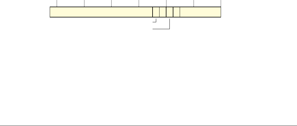
D1 The AArch64 System Level Programmers’ Model
D1.17 Use of the ESR_EL1, ESR_EL2, and ESR_EL3
D1-1524 Copyright © 2013 ARM Limited. All rights reserved. ARM DDI 0487A.a
Non-Confidential - Beta ID090413
ISS[4:1] The CRm value from the issued instruction.
ISS[0] Indicates the direction of the instruction that caused the exception. The possible values of this bit
are:
0 Write access, including
MSR
instructions.
1 Read access, including
MRS
instructions.
For exceptions caused by System instructions, see System on page C3-174 for the encoding values returned by an
instruction.
The following sections describe configuration settings for generating the exception that is reported using EC value
0x18
:
•Traps to EL2 of Non-secure EL1 and EL0 reads of ID registers on page D1-1485.
•Traps to EL2 of Non-secure EL1 and EL0 execution of cache maintenance instructions on page D1-1480.
•Traps to EL2 of Non-secure EL1 execution of TLB maintenance instructions on page D1-1479.
•Traps to EL2 of Non-secure EL1 and EL0 accesses to the Auxiliary Control Register on page D1-1482.
•Traps to EL2 of Non-secure EL1 and EL0 accesses to Performance Monitors registers on page D1-1497.
•Trapping to EL2 of Non-secure EL1 accesses to the CPACR_EL1 or CPACR on page D1-1489.
•Traps to EL2 of Non-secure EL1 accesses to virtual memory control registers on page D1-1476.
•Traps to EL2 of Non-secure EL1 and EL0 System register accesses to Debug ROM registers on
page D1-1494.
•Traps to EL2 of Non-secure EL1 System register accesses to OS-related debug registers on page D1-1495.
•Traps to EL2 of Non-secure EL1 and EL0 general System register accesses to debug registers on
page D1-1495.
•Traps to EL2 of EL2, and Non-secure EL1 and EL0, System register accesses to the trace registers on
page D1-1490.
D1.17.13 Exception from an Instruction abort
These are the exception syndromes with the following EC values:
•
0x20
, for an Instruction abort exception taken from a lower Exception level, that could be using AArch64 or
AArch32.
•
0x21
, for an Instruction abort exception taken without a change in Exception level, meaning it is taken from
an Exception level that is using AArch64.
These syndromes are used for MMU faults and synchronous external aborts, including synchronous parity errors,
that are generated by instruction accesses. They are not used for Debug exceptions.
When ESR_ELx.EC returns one of these values, the encoding of the ISS field is:
ISS[24:10] RES0.
ISS[9] EA, External abort type. This bit can provide an IMPLEMENTATION DEFINED classification of
synchronous external aborts.
For any abort other than a synchronous external abort this bit returns a value of 0.
ISS[8] RES0.
EA
24 10 9 8 7 6 5 0
RES
0 (0) (0) IFSC
S1PTW

D1 The AArch64 System Level Programmers’ Model
D1.17 Use of the ESR_EL1, ESR_EL2, and ESR_EL3
ARM DDI 0487A.a Copyright © 2013 ARM Limited. All rights reserved. D1-1525
ID090413 Non-Confidential - Beta
ISS[7] S1PTW. For a stage 2 fault, indicates whether the fault was a fault on the stage 2 translation of an
address accessed during a stage 1 translation table walk:
0 . Fault not on a stage 2 translation for a stage 1 translation table walk.
1 . Fault on the stage 2 translation of an access for a stage 1 translation table walk.
For a stage 1 fault, this bit is RES0.
ISS[6] RES0.
ISS[5:0] IFSC, Instruction fault status code. Indicates the fault that caused the exception, using the codes
shown in Table D1-76.
D1.17.14 Exception from a Data abort
These are the exception syndromes with the following EC values:
•
0x24
, for a Data abort exception taken from a lower Exception level, that could be using AArch64 or
AArch32.
•
0x25
, for a Data abort exception taken without a change in Exception level, meaning it is taken from an
Exception level that is using AArch64.
These syndromes are used for the following exceptions if the exception is generated by a data access:
• MMU faults.
• Alignment faults other than those caused by stack pointer misalignment.
• Synchronous external aborts, including synchronous parity errors.
They are not used for Debug exceptions.
Table D1-76 Fault status codes for Instruction aborts
Fault status Fault that caused the exception
0b0000LL
Address Size fault. The
LL
bits indicate the level at which the fault occurred.
0b0001LL
Translation fault. The
LL
bits indicate the level at which the fault occurred.
0b0010LL
Access Flag fault. The
LL
bits indicate the level at which the fault occurred.
0b0011LL
Permission fault. The
LL
bits indicate the level at which the fault occurred.
0b010000
Synchronous External abort.
0b011000
Synchronous Parity error on a memory access.
0b0101LL
Synchronous External abort on a translation table walk. The
LL
bits indicate the level at which the fault occurred.
0b0111LL
Synchronous Parity error on a memory access on a translation table walk. The
LL
bits indicate the level at which the
fault occurred.
0b100001
Alignment fault.
0b110000
TLB Conflict fault.

D1 The AArch64 System Level Programmers’ Model
D1.17 Use of the ESR_EL1, ESR_EL2, and ESR_EL3
D1-1526 Copyright © 2013 ARM Limited. All rights reserved. ARM DDI 0487A.a
Non-Confidential - Beta ID090413
When ESR_ELx.EC returns one of these values, the encoding of the ISS field is:
ISV, ISS[24] Instruction syndrome valid. Indicates whether ISS[23:14] provide a valid instruction syndrome, as
part of the returned ISS. The possible values of this bit are:
0 No valid instruction syndrome. ISS[23:14] are RES0.
1 ISS[23:14] hold a valid instruction syndrome.
This bit is 1 only for Data aborts on a stage 2 address translation, reported in the ELR_EL2, for
accesses performed:
• In AArch64 state, by a load or store of a single general-purpose register, including a
permitted load or store of a stack pointer or a zero register, including Load-Acquire and
Store-Release instructions, but excluding:
— Any instruction that performs register writeback.
— Any Load-Exclusive or Store-Exclusive instruction.
• In AArch32 state, by an instruction to which all of the following apply:
— The instruction is an
LDA
,
LDAB
,
LDAH
,
LDR
,
LDRT
,
LDRSH
,
LDRSHT
,
LDRH
,
LDRHT
,
LDRSB
,
LDRSBT
,
LDRB
,
LDRBT
,
STL
,
STLB
,
STLH
,
STR
,
STRT
,
STRH
,
STRHT
,
STRB
or
STRBT
— The instruction is not performing register writeback
— The instruction is not using the PC as its destination register.
The value of ISV on a synchronous external abort on a stage 2 translation table walk is
IMPLEMENTATION DEFINED.
This bit is 0 for:
• All other Data aborts reported in ELR_EL2.
• Any Data abort reported in ELR_EL1 or ELR_EL3.
Note
• For ISS reporting, a stage 2 abort on a stage 1 translation table lookup is treated as a stage 1
Translation fault, and does not return a valid instruction syndrome.
• In the A32 instruction set,
LDR*T
and
STR*T
instructions always perform register writeback and
therefore never return a valid instruction syndrome.
• A valid instruction syndrome provides information that can help a hypervisor to emulate the
instruction efficiently. Instruction syndromes are returned for instructions for which such
accelerated emulation is possible.
SAS, ISS[23:22]
Syndrome access size. When the value of ISV is 1, indicates the size of the access attempted by the
faulted operation. The possible values of this field are:
0b00
Byte.
0b01
Halfword.
0b10
Word.
0b11
Doubleword.
When the value of ISV is 0, this field is RES0.
ISV
(0)
24 23 20 19 18 17 16 15 10 9 8 7 6 5 0
SAS SRT RES0 DFSC
22 21
SSE
Instruction syndrome
EA
CM
S1PTW
WnR

D1 The AArch64 System Level Programmers’ Model
D1.17 Use of the ESR_EL1, ESR_EL2, and ESR_EL3
ARM DDI 0487A.a Copyright © 2013 ARM Limited. All rights reserved. D1-1527
ID090413 Non-Confidential - Beta
SSE, ISS[21] Syndrome sign extend. When the value of ISV is 1, for a byte, halfword, or word load operation,
indicates whether the data item must be sign extended. For these cases, the possible values of this
bit are:
0 Sign-extension not required.
1 Data item must be sign-extended.
For all other operations, when the value of ISV is 1,this bit is 0.
When the value of ISV is 0, this bit is RES0.
SRT, ISS[20:16]
Syndrome register transfer. When the value of ISV is 1, the value of the Rt operand of the faulting
instruction. This specifies:
• The destination register for a load operation.
• The source register for a store operation.
Note
For an exception taken from an Exception level using AArch32, usually software emulating an
instruction must consider both the Rt value and the Mode value saved in the SPSR, to determine the
physical register to access.
When the value of ISV is 0, this field is RES0.
SF, ISS[15] Sixty-four. When the value of ISV is 1, indicates whether the instruction accessed a 32-bit or 64-bit
register. For these cases, the possible values of this bit are:
0 Instruction accesses a 32-bit register.
1 Instruction accesses a 64-bit register.
Note
This is not the Execution state, but the width of the registers accessed by the instruction, as indicated
by the instruction syntax.
When the value of ISV is 0, this bit is RES0.
AR, ISS[14] Acquire/release. When the value of ISV is 1, indicates whether the instruction has acquire/release
semantics. For these cases, the possible values of this bit are:
0 Instruction did not have acquire/release semantics.
1 Instruction had acquire/release semantics.
When the value of ISV is 0, this bit is RES0.
ISS[13:10] RES0.
EA, ISS[9] External abort type. This bit can provide an IMPLEMENTATION DEFINED classification of
synchronous external aborts.
For any abort other than a synchronous external abort this bit returns a value of 0.
CM, ISS[8] Cache maintenance. For a synchronous fault, this bit identifies whether the fault came from a cache
maintenance or address translation operation. The possible values of this bit are:
0 Not a synchronous fault generated by a cache maintenance or address translation
operation.
1 Synchronous fault generated by a cache maintenance or address translation operation.
For asynchronous faults, and for faults on a
DC ZVA
instruction, this bit is 0.
S1PTW, ISS[7] For a stage 2 fault, indicates whether the fault was a fault on the stage 2 translation of an address
accessed during a stage 1 translation table walk. The possible values of this bit are:
0 Fault not a fault on a stage 2 translation for a stage 1 translation table walk.
1 Fault on the stage 2 translation of an access for a stage 1 translation table walk.
For all faults other than stage 2 faults, this bit is RES0.

D1 The AArch64 System Level Programmers’ Model
D1.17 Use of the ESR_EL1, ESR_EL2, and ESR_EL3
D1-1528 Copyright © 2013 ARM Limited. All rights reserved. ARM DDI 0487A.a
Non-Confidential - Beta ID090413
WnR, ISS[6] Indicates whether a synchronous abort was caused by a write or a read operation. The possible
values of this bit are:
0 Abort caused by a read operation.
1 Abort caused by a write operation.
For faults on cache maintenance and address translation operations, this bit always returns a value
of 1.
Note
ISS[8] is set to 1 on a fault on a cache maintenance or address translation operation.
For an asynchronous abort exception this bit is UNKNOWN.
DFSC, ISS[5:0]
Data fault status code. Indicates the fault that caused the exception, using the codes shown in
Table D1-77.
Table D1-77 Fault status codes for Data aborts
Fault status Fault that caused the exception
0b0000LL
Address size fault. The
LL
bits indicate the level at which the fault occurred.
0b0001LL
Translation fault. The
LL
bits indicate the level at which the fault occurred.
0b0010LL
Access flag fault. The
LL
bits indicate the level at which the fault occurred.
0b0011LL
Permission fault. The
LL
bits indicate the level at which the fault occurred.
0b010000
Synchronous External abort.
0b011000
Synchronous Parity error on a memory access.
0b0101LL
Synchronous External abort on a translation table walk. The
LL
bits indicate the level at which the fault occurred.
0b0111LL
Synchronous Parity error on a memory access on a translation table walk. The
LL
bits indicate the level at which the
fault occurred.
0b100001
Alignment fault.
0b110000
TLB Conflict fault.
0b110100
IMPLEMENTATION DEFINED fault, Lockdown abort.
0b110101
IMPLEMENTATION DEFINED fault, Unsupported exclusive.
0b111101
First Level Domain faulta, used only for faults reported in the PAR_EL1, see Domain fault, Short-descriptor format
translation tables only on page G3-3656.
0b111110
Second Level Domain faulta, used only for faults reported in the PAR_EL1, see Domain fault, Short-descriptor
format translation tables only on page G3-3656.
a. This fault can occur only for the VMSAv8-32 translation scheme, and only when that scheme is using the Short-descriptor translation table
format.
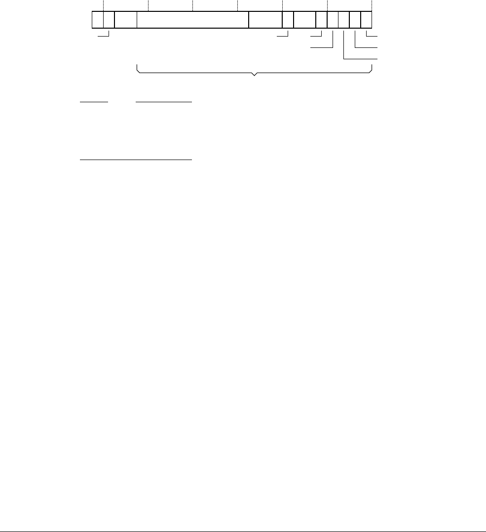
D1 The AArch64 System Level Programmers’ Model
D1.17 Use of the ESR_EL1, ESR_EL2, and ESR_EL3
ARM DDI 0487A.a Copyright © 2013 ARM Limited. All rights reserved. D1-1529
ID090413 Non-Confidential - Beta
D1.17.15 Floating-point exceptions
These are the exception syndromes with the following EC values:
•
0x28
, trapped floating-point exception from AArch32.
•
0x2C
, trapped floating-point exception from AArch64.
These Exception classes are supported only when the SIMD and floating-point implementation supports the
trapping of floating-point exceptions, see Exception from an access to SIMD or floating-point registers, from
AArch32 or AArch64 on page D1-1521. Otherwise, the
0x28
and
0x2C
EC values are reserved. That is, these EC
values are used to report the floating-point exceptions defined by IEE 754, and input denormal.
When ESR_ELx.EC returns one of these values, the encoding of the ISS field is:
Note
Bits[20:0] correspond to bits[20:0] of the extensions to the FPEXC defined by version 3 of the Common VFP
subarchitecture, as defined in the ARM® Architecture Reference Manual, ARMv7-A and ARMv7-R edition. However,
ARMv8 does not support short vector operations for scalar floating-point instructions, and therefore although the
VECITR field retains is subarchitecture name, its meaning is redefined.
ISS[24] RES0.
ISS[23] TFV, Trapped Fault Valid bit. Indicates whether bits[7, 4:0] of the ISS hold valid information about
a trapped fault. The possible values of this bit are:
0 ISS[7, 4:0] do not hold valid information about a trapped fault and are UNKNOWN.
1 ISS[7, 4:0] hold valid information about one or more trapped faults. All floating-point
exceptions indicated by these bits have occurred since the bits were last cleared to 0.
ISS[22:21] RES0.
ISS[20:11] RES0.
ISS[10:8] VECITR. Whether this field is valid depends on the value of the EC field, as follows:
0x28
Floating-point exception from an AArch32 SIMD instruction.
The VECITR field is RES0.
0x2C
Floating-point exception from an AArch64 SIMD instruction.
The VECITR field specifies the source lane number that is being reported in the ESR.
This is the vector element that generated the reported floating-point exception, and:
• If the instruction combines two adjacent elements to creating a single element,
this field specifies the lower-numbered element. The pairwise instructions such
as
FPADD
are examples of instructions that combine elements in this way.
• If the instruction produces a single value from all the elements of the input vector,
the only possible floating-point exceptions are where an input operand causes
either an Invalid operation exception because it is a signalling NaN, or an Input
denormal exception. In this case the field specifies the element number that is
being reported in the ISR. The all-lanes instructions such as FMAXV are
examples of instructions that combine elements in this way.
RES0
24 10 48765 0
RES0(0) RES0VECITR
TFV IDF
23 22 21 20 321
IXF
UFF
IOF
DZF
OFF
11
FPEXC fields, see Note in the text

D1 The AArch64 System Level Programmers’ Model
D1.17 Use of the ESR_EL1, ESR_EL2, and ESR_EL3
D1-1530 Copyright © 2013 ARM Limited. All rights reserved. ARM DDI 0487A.a
Non-Confidential - Beta ID090413
ISS[7, 4:0] Latched floating-point exception bits.
When the TFV bit, ISS[23] on page D1-1529, is 0 these bits are UNKNOWN. Otherwise, the possible
values of each bit are:
0 The corresponding floating-point exception has not occurred.
1 The corresponding floating-point exception has occurred since the bit was last set to 0.
When a bit is set to 1, it must be cleared to 0 by the exception-handling routine.
The latched floating-point exception bits, and corresponding floating-point exceptions, are:
ISS[7] IDF, Input Denormal floating-point exception trapped bit.
ISS[4] IXF, Inexact floating-point exception trapped bit.
ISS[3] UFF, Underflow floating-point exception trapped bit.
ISS[2] OFF, Overflow floating-point exception trapped bit.
ISS[1] DZF, Divide-by-zero floating-point exception trapped bit.
ISS[0] IOF, Invalid operation floating-point exception trapped bit.
ISS[6:5] RES0.
In an implementation where the SIMD and floating-point implementation supports the trapping of floating-point
exceptions:
• From an Exception level using AArch64, the FPCR.{IDE, IXE, UFE, OFE, DZE, IOE} bits enable each of
the floating-point exception traps.
• From an Exception level using AArch32, the FPSCR.{IDE, IXE, UFE, OFE, DZE, IOE} bits enable each of
the floating-point exception traps.
D1.17.16 SError interrupt
This is the exception syndrome with EC value
0x2F
.
It is used to report the exception caused by an SError interrupt.
When ESR_ELx.EC returns this value, the encoding of the ISS field is:
ISS[24] Indicates if the syndrome field is valid. The possible values of this bit are:
0 ISS[23:0] is not valid.
1 ISS[23:0] is valid.
ISS[23:0] The meaning of this field depends on the value of the ISS[24] bit as follows:
ISS[24]==0 RES0.
ISS[24]==1 Provides IMPLEMENTATION SPECIFIC syndrome information.
D1.17.17 Breakpoint exception or Vector Catch exception
These are the exception syndromes with the following EC values:
•
0x30
, Breakpoint exception taken from a lower Exception level.
•
0x31
, Breakpoint exception taken without a change of Exception level.
•
0x3A
, AArch32 Vector Catch exception.
24 23 0
CV IMPLEMENTATION SPECIFIC
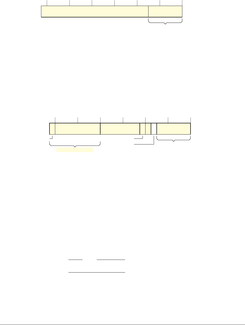
D1 The AArch64 System Level Programmers’ Model
D1.17 Use of the ESR_EL1, ESR_EL2, and ESR_EL3
ARM DDI 0487A.a Copyright © 2013 ARM Limited. All rights reserved. D1-1531
ID090413 Non-Confidential - Beta
When ESR_ELx.EC returns one of these values, the encoding of the ISS field is:
ISS[24:6] RES0.
ISS[5:0] IFSC, Instruction fault status code. Set to
0b100010
, Debug exception.
For more information about generating these exceptions, see:
•Breakpoint exceptions on page D2-1569.
•Vector Catch exceptions on page D2-1627.
D1.17.18 Watchpoint exception
These are the exception syndromes with the following EC values:
•
0x34
, Watchpoint exception taken from a lower Exception level.
•
0x35
, Watchpoint exception taken without a change of Exception level.
When ESR_ELx.EC returns one of these values, the encoding of the ISS field is:
ISS[24] ISV, Instruction syndrome valid. Indicates whether ISS[24:14] provide a valid instruction
syndrome, as part of the returned ISS. This field has the value 0, because watchpoints are not stage 2
aborts. This also indicates that ISS[23:14] are RES0.
ISS[23:9, 7] RES0.
ISS[8] CM, Cache maintenance. This bit identifies whether the watchpoint was on a cache maintenance
operation. The possible values of this bit are:
0 Not a watchpoint generated on cache maintenance operation.
1 Watchpoint generated on a cache maintenance operation.
For a watchpoint on a
DC ZVA
instruction, this bit is 0.
ISS[6] WnR. Indicates whether the watchpointed access was a write or a read operation. The possible
values of this bit are:
0 Watchpoint on a read operation.
1 Watchpoint on a write operation.
For watchpoints on cache maintenance operations, this bit always returns a value of 1.
Note
ISS[8] is set to 1 on a watchpoint on a cache maintenance operation.
ISS[5:0] DFSC, Data Fault Status Code. Set to
0b100010
, Debug exception.
For more information about generating these exceptions, see Watchpoint exceptions on page D2-1606.
11 00 0 0
24 6 5 0
RES0
IFSC
11 00 0 0
ISV
24 23 16 15 9 8 7 6 5 0
0RES0RES0 (0)
Instruction syndrome
CM
WnR DFSC

D1 The AArch64 System Level Programmers’ Model
D1.17 Use of the ESR_EL1, ESR_EL2, and ESR_EL3
D1-1532 Copyright © 2013 ARM Limited. All rights reserved. ARM DDI 0487A.a
Non-Confidential - Beta ID090413
D1.17.19 Software Step exception
These are the exception syndromes with the following EC values:
•
0x32
, Software Step exception taken from a lower Exception level.
•
0x33
, Software Step exception taken without a change of Exception level.
When ESR_ELx.EC returns one of these values, the encoding of the ISS field is:
ISS[24] ISV, Instruction syndrome valid. Indicates whether the EX bit, ISS[6], is valid, as follows:
0 EX bit is RES0.
1 EX bit is valid.
See the ISS[6] description for more information.
ISS[23:7] RES0.
ISS[6] EX. Exclusive operation. Together with the ISV bit, ISS[24], indicates whether the stepped
instruction was a Load-Exclusive, as Table D1-78 shows:
ISS[5:0] IFSC, Instruction fault status code. Set to
0b100010
, Debug exception.
For more information about generating these exceptions, see Software Step exceptions on page D2-1634.
D1.17.20 Software Breakpoint Instruction exception
These are the exception syndromes with the following EC values:
•
0x38
,
BKPT
instruction executed in AArch32 state.
•
0x3C
,
BRK
instruction executed in AArch64 state.
When ESR_ELx.EC returns one of these values, the encoding of the ISS field is:
ISS[24:16] RES0.
ISS[15:0] Comment. Set to the instruction comment field, zero-extended as necessary.
For more information about generating these exceptions, see Software Breakpoint Instruction exceptions on
page D2-1566.
Table D1-78 Possible syndrome information for Software Step exceptions
ISV EX Meaning
0 0 No syndrome data available
1 0 An instruction other than a Load-Exclusive instruction was stepped
1 1 A Load-Exclusive instruction was stepped
11 00 0 0
ISV
24 23 7 6 5 0
RES0
EX
IFSC
24 16 15 0
RES
0 Comment

D1 The AArch64 System Level Programmers’ Model
D1.18 Mechanisms for entering a low-power state
ARM DDI 0487A.a Copyright © 2013 ARM Limited. All rights reserved. D1-1533
ID090413 Non-Confidential - Beta
D1.18 Mechanisms for entering a low-power state
The ARM architecture provides mechanisms that software can use to indicate that the PE can enter a low-power
state, if it supports that state. The following sections describe those mechanisms:
•Wait for Event mechanism and Send event.
•Wait For Interrupt on page D1-1536.
D1.18.1 Wait for Event mechanism and Send event
A PE can use the Wait for Event (WFE) mechanism to enter a low-power state, depending on the value of an Event
Register for that PE. To enter the low-power state, the PE executes a Wait For Event instruction,
WFE
, and if the Event
Register is clear, the PE can enter the low-power state.
If the PE does enter the low-power state, it remains in that low-power state until it receives a WFE wake-up event.
The architecture does not define the exact nature of the low-power state, except that the execution of a
WFE
instruction must not cause a loss of memory coherency.
WFE mechanism behavior depends on the interaction of all of the following, that are described in the subsections
that follow:
• The Event Register for the PE. See subsection The Event Register on page D1-1534.
• The Wait For Event instruction,
WFE
. See subsection The Wait For Event instruction on page D1-1534.
•WFE wake-up events. See subsection WFE wake-up events in AArch64 state on page D1-1535
• The Send Event instructions,
SEV
and
SEVL
that can cause WFE wake-up events. See subsection The Send
Event instructions on page D1-1535.
Note
Because the Wait for Event mechanism is associated with suspending execution on a PE for the purpose of power
saving, ARM recommends that the Event Register is set only infrequently. However, software must only use the
setting of the Event Register as a hint, and must not assume that any particular message is sent as a result of the
setting of the Event Register.
Example D1-2 describes how a spinlock implementation might use the WFE mechanism to save energy.
Example D1-2 Spinlock as an example of using Wait For Event and Send Event
A multiprocessor operating system requires locking mechanisms to protect data structures from being accessed
simultaneously by multiple PEs. These mechanisms prevent the data structures becoming inconsistent or corrupted
if different PEs try to make conflicting changes. If a lock is busy, because a data structure is being used by one PE,
it might not be practical for another PE to do anything except wait for the lock to be released. For example, if a PE
is handling an interrupt from a device, it might need to add data received from the device to a queue. If another PE
is removing data from the same queue, it will have locked the memory area that holds the queue. The first PE cannot
add the new data until the queue is in a consistent state and the second PE has released the lock. The first PE cannot
return from the interrupt handler until the data has been added to the queue, so it must wait.
Typically, a spin-lock mechanism is used in these circumstances:
• A PE requiring access to the protected data attempts to obtain the lock using single-copy atomic
synchronization primitives such as the Load-Exclusive and Store-Exclusive operations described in
Synchronization and semaphores on page B2-100.
• If the PE obtains the lock it performs its memory operation and then releases the lock.
• If the PE cannot obtain the lock, it reads the lock value repeatedly in a tight loop until the lock becomes
available. When the lock becomes available, the PE again attempts to obtain it.

D1 The AArch64 System Level Programmers’ Model
D1.18 Mechanisms for entering a low-power state
D1-1534 Copyright © 2013 ARM Limited. All rights reserved. ARM DDI 0487A.a
Non-Confidential - Beta ID090413
A spin-lock mechanism is not ideal for all situations:
• In a low-power system the tight read loop is undesirable because it uses energy to no effect.
• In a multi-PE implementation the execution of spin-locks by multiple waiting PEs can degrade overall
performance.
Using the Wait For Event and Send Event mechanism can improve the energy efficiency of a spinlock:
• A PE that fails to obtain a lock executes a
WFE
instruction to request entry to a low-power state, at the time
when the exclusive monitor is set holding the address of the location holding the lock.
• When a PE releases a lock, the write to the lock location causes the exclusive monitor of any PE monitoring
the lock location to be cleared. This clearing of the exclusive monitors generates a WFE wake-up event for
each of those PEs. Then, these PEs can attempt to obtain the lock again.
For large systems, more advanced locking systems, such as ticket locks, can avoid unfairness caused by having
multiple PEs simultaneously reading the lock. In such systems, the WFE mechanism can be used in a similar way
to monitor the next ticket value.
The Event Register
The Event Register is a single bit register for each PE. When set, an Event Register indicates that an event has
occurred since the register was last cleared, that might require some action by the PE. Therefore, when the Event
Register is set, the PE must not suspend operation on executing a
WFE
instruction.
The reset value of the Event Register is UNKNOWN.
The Event Register for a PE is set by any of the following:
• A Send Event instruction,
SEV
, executed by any PE in the system.
• A Send Event Local instruction,
SEVL
, executed by the PE.
• The clearing of the global monitor for the PE.
• An exception return.
• An event sent by some IMPLEMENTATION DEFINED mechanism.
The Event Register is cleared only by a Wait For Event instruction.
Note
Software cannot read or write the value of the Event Register directly.
The Wait For Event instruction
The action of the Wait For Event instruction,
WFE
, depends on the state of the Event Register:
• If the Event Register is set, the instruction clears the register and completes immediately.
• If the Event Register is clear the PE can suspend execution and enter a low-power state. It remains in that
state until the PE detects a WFE wake-up event, or earlier if the implementation chooses, or a until a reset.
When the PE detects a WFE wake-up event, or earlier if chosen, the WFE instruction completes. If the
wake-up event sets the Event Register, it is IMPLEMENTATION DEFINED whether on restarting execution, the
Event Register is cleared.
The
WFE
is available at all Exception levels. Attempts to enter a low-power state made by software executing at EL0,
EL1, or EL2 can be trapped to a higher Exception level. See:
•Traps to EL1 of EL0 execution of WFE and WFI instructions on page D1-1465.
•Traps to EL2 of Non-secure EL1 and EL0 execution of WFE and WFI instructions on page D1-1488.
•Traps to EL3 of EL2, EL1, and EL0 execution of WFE and WFI instructions on page D1-1501.

D1 The AArch64 System Level Programmers’ Model
D1.18 Mechanisms for entering a low-power state
ARM DDI 0487A.a Copyright © 2013 ARM Limited. All rights reserved. D1-1535
ID090413 Non-Confidential - Beta
Note
Software using the Wait For Event mechanism must tolerate spurious wake-up events, including multiple wake-ups.
WFE wake-up events in AArch64 state
The following are WFE wake-up events:
• The execution of an
SEV
instruction on any PE in the multiprocessor system.
• The execution of an
SEVL
instruction by the PE.
• An SError interrupt received by the PE, unless masked by PSTATE.A or EDSCR.INTdis.
• A physical IRQ interrupt received by the PE, unless masked by PSTATE.I or EDSCR.INTdis.
• A physical FIQ interrupt received by the PE, unless masked by PSTATE.F or EDSCR.INTdis.
• In Non-secure EL1 or EL1, all of the following:
— When HCR_EL2.FMO is 1, a virtual FIQ interrupt, unless masked by PSTATE.F or EDSCR.INTdis.
— When HCR_EL2.IMO is 1, a virtual IRQ interrupt, unless masked by PSTATE.I or EDSCR.INTdis.
— When HCR_EL2.AMO is 1, a virtual SError interrupt, unless masked by PSTATE.A or
EDSCR.INTdis.
• An asynchronous External Debug Request debug event, if halting is allowed. For the definition of halting is
allowed, see Halting allowed and halting prohibited on page H2-4329. Also see External Debug Request
debug event on page H3-4380.
• An event sent by the timer event stream for the PE. See Event streams on page D7-1859.
• An event caused by the clearing of the global monitor for the PE.
• An event sent by some IMPLEMENTATION DEFINED mechanism.
Not all of these wake-up events set the Event Register.
Note
• EDSCR.INTdis masking applies only when external debug is disabled.
• For more information about the masking of physical and virtual interrupts see Asynchronous exception types,
routing, masking and priorities on page D1-1456. If the configuration of HCR_EL2.{AMO, IMO, FMO} or
HCR.{AMO, IMO, FMO}, or SCR_EL3.{EA, TRQ, FIQ}, means that a PSTATE mask bit cannot mask a
physical or virtual interrupt, then that interrupt is a WFE wake-up event, regardless of the value of the
PSTATE mask bit.
The Send Event instructions
These are:
SEV
Send Event instruction. This causes an event to be signaled to all PEs in the multiprocessor system.
SEVL
Send Event Local instruction. This must set the local Event Register. It might signal an event to
other PEs, but is not required to do so.
The mechanism that signals an event to other PEs is IMPLEMENTATION DEFINED. The PE is not required to guarantee
the ordering of this event with respect to the completion of memory accesses by instructions before the
SEV
instruction. Therefore, ARM recommends that software includes a
DSB
instruction before any
SEV
instruction.
The
SEVL
instruction appears to execute in program order relative to any subsequent
WFE
instruction executed on the
same PE, without the need for any explicit insertion of barrier instructions.

D1 The AArch64 System Level Programmers’ Model
D1.18 Mechanisms for entering a low-power state
D1-1536 Copyright © 2013 ARM Limited. All rights reserved. ARM DDI 0487A.a
Non-Confidential - Beta ID090413
Note
A
DSB
instruction ensures that no instructions, including any
SEV
instructions, that appear in program order after the
DSB
instruction, can execute until the
DSB
instruction has completed. See Data Synchronization Barrier (DSB) on
page B2-86.
The receipt of a signaled
SEV
or
SEVL
event by a PE sets the Event Register on that PE.
The
SEV
and
SEVL
instructions are available at all Exception levels.
Pseudocode details of the Wait For Event mechanism
This section defines pseudocode functions that describe the behavior of the Wait For Event mechanism.
The
ClearEventRegister()
pseudocode procedure clears the Event Register of the current PE.
ClearEventRegister();
The
EventRegistered()
pseudocode function returns TRUE if the Event Register of the current PE is set and FALSE
if it is clear:
boolean EventRegistered();
The
WaitForEvent()
pseudocode procedure optionally suspends execution until a WFE wake-up event or reset
occurs, or until some earlier time if the implementation chooses. It is IMPLEMENTATION DEFINED whether restarting
execution after the period of suspension causes a
ClearEventRegister()
to occur.
WaitForEvent();
The
SendEvent()
pseudocode procedure sets the Event Register of every PE in the multiprocessor system.
SendEvent();
The
EventRegisterSet()
pseudocode procedure sets the event register for this PE.
EventRegisterSet();
D1.18.2 Wait For Interrupt
Software can use the Wait for Interrupt (
WFI
) instruction to cause the PE to enter a low-power state. The PE then
remains in that low-power state until it receives a WFI wake-up event, or until some other IMPLEMENTATION
DEFINED reason causes it to leave the low-power state. The architecture permits a PE to leave the low-power state
for any reason, but requires that it must leave the low-power state on receipt of any architected WFI wake-up event.
Note
Because the architecture permits a PE to leave the low-power state for any reason, it is permissible for a PE to treat
WFI
as a
NOP
, but this is not recommended for lowest power operation.
When the PE leaves a low-power state that was entered as a result of a
WFI
instruction, that
WFI
instruction completes.
The architecture does not define the exact nature of the low-power state, except that the execution of a
WFI
instruction must not cause a loss of memory coherency.
Attempts to enter a low-power state made by software executing at EL0, EL1, or EL2 can be trapped to a higher
Exception level. See:
•Traps to EL1 of EL0 execution of WFE and WFI instructions on page D1-1465.
•Traps to EL2 of Non-secure EL1 and EL0 execution of WFE and WFI instructions on page D1-1488.
•Traps to EL3 of EL2, EL1, and EL0 execution of WFE and WFI instructions on page D1-1501.

D1 The AArch64 System Level Programmers’ Model
D1.18 Mechanisms for entering a low-power state
ARM DDI 0487A.a Copyright © 2013 ARM Limited. All rights reserved. D1-1537
ID090413 Non-Confidential - Beta
WFI wake-up events
The following are WFI wake-up events:
• A SError interrupt, regardless of the value of PSTATE.A or EDSCR.INTdis.
• A physical IRQ interrupt, regardless of the value of PSTATE.I or EDSCR.INTdis.
• A physical FIQ interrupt, regardless of the value of PSTATE.F or EDSCR.INTdis.
• In Non-secure state when executing at EL0 or EL1:
— When HCR_EL2.AMO is 1, a virtual SError interrupt, regardless of the value of PSTATE.A or
EDSCR.INTdis.
— When HCR_EL2.IMO is 1, a virtual IRQ interrupt, regardless of the value of PSTATE.I or
EDSCR.INTdis.
— When HCR_EL2.FMO is 1, a virtual FIQ interrupt, regardless of the value of PSTATE.F or
EDSCR.INTdis.
• An asynchronous External Debug Request debug event, if halting is allowed. For the definition of halting is
allowed, see Halting allowed and halting prohibited on page H2-4329. Also see External Debug Request
debug event on page H3-4380.
• An event sent by some IMPLEMENTATION DEFINED mechanism.
Note
• Because debug events are WFI wake-up events, ARM recommends that Wait For Interrupt is used as part of
an idle loop rather than waiting for a single specific interrupt event to occur and then moving forward. This
ensures that the intervention of debug while waiting does not significantly change the function of the program
being debugged.
• The WFI mechanism can be used while interrupts are masked. If it is, then an interrupt is still a WFI wake-up
event, but the interrupt is not taken.
• Some implementations of the WFI mechanism drain down any pending memory activity before suspending
execution. This increases power saving, by increasing the area over which clocks can be stopped. The
architecture does not require this operation, therefore software must not rely on the WFI mechanism
operating in this way.
Using WFI to indicate an idle state on bus interfaces
Software can use the WFI mechanism to force quiescence on a PE, and, combined with preventing any possible WFI
wakeup events, this can be used to complete an entry into a powerdown state.
Because mechanisms for entering powerdown states are inherently IMPLEMENTATION DEFINED, whether an
implementation uses the WFI mechanism is IMPLEMENTATION DEFINED. If it does, the
WFI
instruction forces the
suspension of execution, and of all associated bus activity.
The control logic that does this also tracks the activity on the bus interfaces of the PE, so that when the PE has
completed all current operations and any associated bus activity has completed, it can signal to an external power
controller that there is no ongoing bus activity.
However, the PE must continue to process memory-mapped and external debug interface accesses to debug registers
when in the WFI state. The indication of idle state to the system normally only applies to the non-debug functional
interfaces used by the PE, not the debug interfaces.
When the OS Double Lock control, OSDLR_EL1.DLK, is 1, the PE must not signal this idle state to the control
logic unless it can also guarantee that the debug interface is idle. For more information about the OS Double Lock,
see Debug behavior when the OS Double Lock is locked on page H6-4432.

D1 The AArch64 System Level Programmers’ Model
D1.18 Mechanisms for entering a low-power state
D1-1538 Copyright © 2013 ARM Limited. All rights reserved. ARM DDI 0487A.a
Non-Confidential - Beta ID090413
Note
In a PE that implements separate core and debug power domains, the debug interface referred to in this section is
the interface between the core and debug power domains, since the signal to the power controller indicates that the
core power domain is idle. For more information about the power domains see Power domains and debug on
page H6-4425.
The exact nature of this interface is IMPLEMENTATION DEFINED, but the use of Wait For Interrupt as the only
architecturally-defined mechanism that completely suspends execution makes it very suitable as the preferred
powerdown entry mechanism.
Pseudocode details of Wait For Interrupt
The
WaitForInterrupt()
pseudocode procedure optionally suspends execution until a WFI wake-up event or reset
occurs, or until some earlier time if the implementation chooses.

D1 The AArch64 System Level Programmers’ Model
D1.19 Self-hosted debug
ARM DDI 0487A.a Copyright © 2013 ARM Limited. All rights reserved. D1-1539
ID090413 Non-Confidential - Beta
D1.19 Self-hosted debug
The ARMv8-A architecture supports both of the following:
Self-hosted debug
The PE itself hosts a debugger. The debugger programs the PE to generate debug exceptions. Debug
exceptions are accommodated in the ARMv8-A Exception model.
External debug
The PE is controlled by an external debugger. The debugger programs the PE to generate Halting
debug events, that cause the PE to enter Debug state. In Debug state, the PE is halted.
This section describes self-hosted debug. It includes:
•Debug exceptions.
•The PSTATE debug mask bit, D.
For external debug, see part E.
D1.19.1 Debug exceptions
Debug exceptions occur during normal program flow, if a debugger has programmed the PE to generate them.
For example, a software developer might use a debugger contained in an operating system to debug an application.
To do this, the debugger might enable one or more debug exceptions.
The possible debug exceptions are:
• Software Breakpoint Instruction exceptions.
• Breakpoint exceptions.
• Watchpoint exceptions.
• Vector Catch exceptions.
• Software Step exceptions.
Chapter D2 Debug Exceptions describes these in detail.
For the PE to generate a debug exception requires that:
• The debug exception is enabled. The debug exceptions enable controls on page D3-1651 gives the controls
for the different debug exceptions.
• Debug exceptions are enabled from the current Exception level and Security state. See Enabling debug
exceptions from current Exception level and Security state on page D3-1656.
Debug exceptions are synchronous exceptions, and are accommodated in the ARMv8 Exception model.
Note
Breakpoints and Watchpoints can cause entry to Debug state instead of causing debug exceptions. See Chapter H1
Introduction to External Debug.
D1.19.2 The PSTATE debug mask bit, D
As with all other exceptions, when a debug exception is taken, software must take care to avoid generating another
instance of an exception within the exception handler, to avoid recursive entry into the exception handler and loss
of return state.
To help avoid this, the ARMv8 architecture provides a debug exception mask bit, PSTATE.D, that can mask
Watchpoint, Breakpoint, and Software Step exceptions when the target Exception level is the current Exception
level.

D1 The AArch64 System Level Programmers’ Model
D1.19 Self-hosted debug
D1-1540 Copyright © 2013 ARM Limited. All rights reserved. ARM DDI 0487A.a
Non-Confidential - Beta ID090413
PSTATE.D is set to 1 on taking an exception. This means that while handling an exception in AArch64 state,
Watchpoint, Breakpoint, and Software Step exceptions are masked. This prevents recursive entry at the Exception
level that debug exceptions are targeted to.
When execution is in AArch64 state, debug exceptions are also masked implicitly when the target Exception level
is lower than the current Exception level.
When the target Exception level is higher than the current Exception level, debug exceptions cannot be masked by
PSTATE.D.
Because debug exceptions are synchronous, the architecture requires that debug exceptions are not generated when
PSTATE.D is 1. By preventing debug exception generation, debug exceptions cannot be taken at a subsequent time
when the Process state D mask bit is cleared to 0.
Note
This differs from the behavior for interrupts, where the PSTATE.{A, I, F} mask has the effect of preventing the
interrupt from being taken, but instead the interrupt remains pending.

D1 The AArch64 System Level Programmers’ Model
D1.20 Performance Monitors extension
ARM DDI 0487A.a Copyright © 2013 ARM Limited. All rights reserved. D1-1541
ID090413 Non-Confidential - Beta
D1.20 Performance Monitors extension
The System registers provide access to a Performance Monitors Unit (PMU), a non-invasive debug resource that
provides information about the operation of the PE. The PMU provides:
• A 64-bit cycle counter.
•An
IMPLEMENTATION DEFINED number of 32-bit event counters. Each event counter can be configured to
count occurrences of a specified event. The events that can be counted are:
— Architectural and microarchitectural events that are likely to be consistent across many
microarchitectures. The PMU architecture uses event numbers to identify an event, and the PMU
specification defines which event number must be used for each of these architectural and
microarchitectural events.
— Implementation-specific events. The PMU specification reserves event numbers for
implementation-specific events. See Appendix C Recommendations for Performance Monitors Event
Numbers for IMPLEMENTATION DEFINED Events.
For more information, see Chapter D6 The Performance Monitors Extension.

D1 The AArch64 System Level Programmers’ Model
D1.21 Interprocessing
D1-1542 Copyright © 2013 ARM Limited. All rights reserved. ARM DDI 0487A.a
Non-Confidential - Beta ID090413
D1.21 Interprocessing
Interprocessing is the term used to describe moving between the AArch64 and AArch32 Execution states.
The Execution state can change only on a change of Exception level. This means that the Execution state can change
only on taking an exception to a higher Exception level, or returning from an exception to a lower Exception level.
On taking an exception to a higher Exception level, the Execution state either:
• Remains unchanged.
• Changes from AArch32 state to AArch64 state.
On returning from an exception to a lower Exception level, the Execution state either:
• Remains unchanged.
• Changes from AArch64 state to AArch32 state.
Note
If, on taking or returning from an exception, the Exception level remains the same, the Execution state cannot
change.
For the description of:
• Exception entry to an Exception level using AArch64, see Exception entry on page D1-1429.
• Exception return from an Exception level using AArch64 state, see Exception return on page D1-1439.
• Exception return to AArch32 state, see Exception return to an Exception level using AArch32 on
page G1-3454.
Note
The description in Handling exceptions that are taken to an Exception level using AArch32 on page G1-3431
is outside the scope of interprocessing, because such exceptions must have been taken from an Exception
level that is using AArch32, and therefore there is no change of Execution state.
The following sections describe the behavior associated with interprocessing.
•Register mappings between AArch32 state and AArch64 state.
•State of the general-purpose registers on taking an exception to AArch64 state on page D1-1551.
•SPSR, ELR, and AArch64 SP relationships on changing Execution state on page D1-1552.
D1.21.1 Register mappings between AArch32 state and AArch64 state
This section defines the architectural mappings between AArch32 state registers and AArch64 state registers.
The mappings describe:
• For exceptions taken from AArch32 state to AArch64 state, where the AArch32 register content is found.
• For exception returns from AArch64 state to AArch32 state, how the AArch32 register content is derived.
The general model is:
• The AArch32 register contents are situated in the bottom 32 bits of the AArch64 registers.
• In AArch32 state, the upper 32 bits of AArch64 registers are inaccessible and are ignored.
Note
System software that executes in AArch64 state, such as an OS or Hypervisor, can use these mappings for context
save and restore, or to interpret and modify the AArch32 registers of an application or virtual machine.

D1 The AArch64 System Level Programmers’ Model
D1.21 Interprocessing
ARM DDI 0487A.a Copyright © 2013 ARM Limited. All rights reserved. D1-1543
ID090413 Non-Confidential - Beta
For more information see the following subsections:
•Mapping of the general-purpose registers between the Execution states.
•Mapping of the SIMD and floating-point registers between the Execution states on page D1-1544.
•Mapping of the System registers between the Execution states on page D1-1545.
Mapping of the general-purpose registers between the Execution states
Table D1-79 shows how each of the AArch32 general-purpose registers, R0-R12, SP, and LR, including the banked
copies of these registers, maps to an AArch64 general-purpose register.
Table D1-79 Base instruction set register mapping between AArch32 state and AArch64 state
AArch32 register AArch64 register
R0 X0
R1 X1
R2 X2
R3 X3
R4 X4
R5 X5
R6 X6
R7 X7
R8_usr X8
R9_usr X9
R10_usr X10
R11_usr X11
R12_usr X12
SP_usr X13
LR_usr X14
SP_hyp X15
LR_irq X16
SP_irq X17
LR_svc X18
SP_svc X19
LR_abt X20
SP_abt X21
LR_und X22
SP_und X23
R8_fiq X24
R9_fiq X25

D1 The AArch64 System Level Programmers’ Model
D1.21 Interprocessing
D1-1544 Copyright © 2013 ARM Limited. All rights reserved. ARM DDI 0487A.a
Non-Confidential - Beta ID090413
Note
For a description of the banking of AArch32 general-purpose registers R8-R12, SP, and LR, see AArch32
general-purpose registers, and the PC on page G1-3418.
Mapping of the SIMD and floating-point registers between the Execution states
Table D1-80 shows the mapping between the AArch64 V registers and the AArch32 Q registers.
The AArch64 registers V16-V31 are not accessible from AArch32 state.
The mapping between the V, D, and S registers in AArch64 state is not the same as the mapping between the Q, D,
and S registers in AArch32 state:
• In AArch64 state, there are:
— 32 128-bit V registers, V0-V31.
— 32 64-bit D registers, D0-D31.
— 32 32-bit S registers, S0-S31.
A smaller register occupies the least-significant bytes of the corresponding larger register. For example, S5
is the least-significant word of D5 and V5. Figure D1-3 shows this mapping.
Figure D1-3 AArch64 state SIMD and floating-point register mappings
R10_fiq X26
R11_fiq X27
R12_fiq X28
SP_fiq X29
LR_fiq X30
Table D1-80 SIMD and floating-point register mapping between AArch64 state and AArch32 state
AArch64 register AArch32 register
V0 Q0
V1 Q1
V2 Q2
.
.
.
.
.
.
V15 Q15
Table D1-79 Base instruction set register mapping between AArch32 state and AArch64 state
AArch32 register AArch64 register
127 64 63 32 31 0
Vn
Sn
Dn

D1 The AArch64 System Level Programmers’ Model
D1.21 Interprocessing
ARM DDI 0487A.a Copyright © 2013 ARM Limited. All rights reserved. D1-1545
ID090413 Non-Confidential - Beta
• In AArch 32 state, there are:
— 16 128-bit Q registers, Q0-Q15.
— 32 64-bit D registers, D0-D31.
— 32 32-bit S registers, S0-S31.
Smaller registers are packed into larger registers. Figure D1-4 shows this mapping.
Figure D1-4 AArch32 state SIMD and floating-point register mappings
In AArch32 state:
• There are no S registers that correspond to Q8-Q15.
• D16-D31 pack into Q8-Q15. For example, D16 and D17 pack into Q8.
Note
A consequence of this mapping is that if software executing in AArch64 state interprets D or S registers from
AArch32 state, it must unpack the D or S registers from the V registers before it uses them.
Mapping of the System registers between the Execution states
ARMv8 architecturally defines the relationship between the AArch64 System registers and the AArch32 System
registers, to allow supervisory code such as a hypervisor, that is executing in AArch64 state, to save, restore, and
interpret the System registers belonging to a lower Exception level that is using AArch32.
Any modifications made to AArch32 System registers affects only those parts of those AArch64 registers that are
mapped to the AArch32 System registers. Bits[63:32] of AArch64 registers, where they are not mapped to AArch32
registers, are unchanged by AArch32 state execution.
Note
This model is different to the model for the general-purpose registers described in Mapping of the general-purpose
registers between the Execution states on page D1-1543. In this model, there are several cases where two AArch32
System registers are packed into a single AArch64 System register.
When EL3 is using AArch32, some System registers are banked between the two Security states. When a register
is banked in this way, there is an instance of the register in Secure state, and another instance of the register in
Non-secure state. This banking is not supported when EL3 is using AArch64. For the registers that are banked in
this way when EL3 is using AArch32, the architected mapping is between the Non-secure AArch32 register and the
AArch64 register. This use of the Non-secure instance of the AArch32 register applies in all cases where EL3 is
using AArch64 state. This includes execution at EL1 or EL0, using AArch32, in Secure state.
Note
Although the architecture does not require this, because it is not architecturally visible, ARM expects that
implementations will map many of the AArch64 registers for use by EL3 to the Secure instances of banked
AArch32 registers. However, if EL2 and EL3 are implemented and both support use of AArch32, this is not possible
for the following registers:
IFAR This is because when EL3 is using AArch32, HIFAR is an alias of the Secure IFAR.
DFAR This is because when EL3 is using AArch32, HDFAR is an alias of the Secure DFAR.
127 64 63 32 31 0
Qn
S(4n)
D(2n)D(2n+1)
S(4n+1)S(4n+2)S(4n+3)

D1 The AArch64 System Level Programmers’ Model
D1.21 Interprocessing
D1-1546 Copyright © 2013 ARM Limited. All rights reserved. ARM DDI 0487A.a
Non-Confidential - Beta ID090413
Table D1-81 shows the mappings between the writable AArch64 System registers and the AArch32 System
registers.
Table D1-81 Mapping of writable AArch64 System registers to the AArch32 System registers
AArch64 register AArch32 register
ACTLR_EL1 ACTLRa, Non-secure
AFSR0_EL1 ADFSRa, Non-secure
AFSR1_EL1 AIFSRa, Non-secure
AMAIR_EL1[31:0] AMAIR0a, Non-secure
AMAIR_EL1[63:32] AMAIR1a, Non-secure
CONTEXTIDR_EL1 CONTEXTIDRa, Non-secure
CPACR_EL1 CPACR
CSSELR_EL1 CSSELRa, Non-secure
DACR32_EL2 DACRa, Non-secure
FAR_EL1[31:0] DFARa, Non-secure
ESR_EL1 DFSRa, Non-secure
HACR_EL2 HACR
ACTLR_EL2 HACTLR
AFSR0_EL2 HADFSR
AFSR1_EL2 HAIFSR
AMAIR_EL2[31:0] HAMAIR0
AMAIR_EL2[63:32] HAMAIR1
CPTR_EL2 HCPTR
HCR_EL2[31:0] HCR
HCR_EL2[63:32] HCR2
MDCR_EL2 HDCR
FAR_EL2[31:0] HDFAR
FAR_EL2[63:32] HIFAR
MAIR_EL2[31:0] HMAIR0
MAIR_EL2[63:32] HMAIR1
HPFAR_EL2[31:0] HPFAR
SCTLR_EL2 HSCTLR
ESR_EL2 HSR
HSTR_EL2 HSTR
TCR_EL2 HTCR

D1 The AArch64 System Level Programmers’ Model
D1.21 Interprocessing
ARM DDI 0487A.a Copyright © 2013 ARM Limited. All rights reserved. D1-1547
ID090413 Non-Confidential - Beta
TPIDR_EL2[31:0] HTPIDR
TTBR0_EL2 HTTBR
VBAR_EL2[31:0] HVBAR
FAR_EL1[63:32] IFARa, Non-secure
IFSR32_EL2 IFSRa, Non-secure
MAIR_EL1[63:32] NMRR or MAIR1a, Non-secure
PAR_EL1 PAR a, Non-secure
MAIR_EL1[31:0] PRRR or MAIR0a, Non-secure
RMR_EL1 RMR (at EL1)
RMR_EL2 HRMR
RMR_EL3 RMR (at EL3)
SCTLR_EL1 SCTLRa, Non-secure
SDER32_EL3 SDER
TEECR32_EL1 TEECR
TEEHBR32_EL1 TEEHBR
TPIDR_EL1[31:0] TPIDRPRWa, Non-secure
TPIDRRO_EL0[31:0] TPIDRUROa, Non-secure
TPIDR_EL0[31:0] TPIDRURWa, Non-secure
TCR_EL1[31:0] TTBCRa, Non-secure
TTBR0_EL1 TTBR0a, Non-secure
TTBR1_EL1 TTBR1a, Non-secure
VBAR_EL1[31:0] VBARa, Non-secure
VMPIDR_EL2[31:0] VMPIDR
VPIDR_EL2 VPIDR
VTCR_EL2 VTCR
VTTBR_EL2 VTTBR
Timer registers
CNTFRQ_EL0 CNTFRQ
CNTHCTL_EL2 CNTHCTL
CNTHP_CTL_EL2 CNTHP_CTL
CNTHP_CVAL_EL2[63:0] CNTHP_CVAL
CNTHP_TVAL_EL2 CNTHP_TVAL
Table D1-81 Mapping of writable AArch64 System registers to the AArch32 System registers
AArch64 register AArch32 register

D1 The AArch64 System Level Programmers’ Model
D1.21 Interprocessing
D1-1548 Copyright © 2013 ARM Limited. All rights reserved. ARM DDI 0487A.a
Non-Confidential - Beta ID090413
CNTKCTL_EL1 CNTKCTL
CNTP_CTL_EL0 CNTP_CTLa, Non-secure
CNTP_CVAL_EL0[63:0] CNTP_CVALa, Non-secure
CNTP_TVAL_EL0 CNTP_TVALa, Non-secure
CNTPCT_EL0[63:0] CNTPCT
CNTV_CTL_EL0 CNTV_CTL
CNTV_CVAL_EL0[63:0] CNTV_CVAL
CNTV_TVAL_EL0 CNTV_TVAL
CNTVCT_EL0[63:0] CNTVCT
CNTVOFF_EL2[63:0] CNTVOFF
Debug System registers
DBGAUTHSTATUS_EL1 DBGAUTHSTATUS
DBGBCR<n>_EL1 DBGBCR<n>
DBGBVR<n>_EL1[31:0] DBGBVR<n>
DBGBVR<n>_EL1[63:32] DBGBXVR<n>
DBGCLAIMCLR_EL1 DBGCLAIMCLR
DBGCLAIMSET_EL1 DBGCLAIMSET
DBGDTR_EL0 DBGDTRRXint or the DBGDTRTXint
DBGDTRRX_EL0 DBGDTRRXint
DBGDTRTX_EL0 DBGDTRRXint
DBGPRCR_EL1 DBGPRCR
DBGVCR32_EL2 DBGVCR
DBGWCR<n>_EL1 DBGWCR<n>
DBGWVR<n>_EL1[31:0] DBGWVR<n>
ID_DFR0_EL1 ID_DFR0
MDCCSR_EL0bDBGDSCRintb
MDCR_EL2 HDCR
MDRAR_EL1 DBGDRAR
MDSCR_EL1bDBGDSCRextb
OSDLR_EL1 DBGOSDLR
OSDTRRX_EL1bDBGDTRRXextb
OSDTRTX_EL1bDBGDTRTXextb
Table D1-81 Mapping of writable AArch64 System registers to the AArch32 System registers
AArch64 register AArch32 register

D1 The AArch64 System Level Programmers’ Model
D1.21 Interprocessing
ARM DDI 0487A.a Copyright © 2013 ARM Limited. All rights reserved. D1-1549
ID090413 Non-Confidential - Beta
There are a small number of AArch32 System registers that are not mapped to any AArch64 System registers. The
AArch64 registers listed in Table D1-82 on page D1-1550 can be used to access these from a higher Exception level
that is using AArch64. Of the registers shown in the table:
•TEECR, TEEHBR, TEECR32_EL1, and TEEHBR32_EL1 are UNDEFINED if either:
— The implementation does not include support for T32EE.
— Use of T32EE is disabled either because the value of SCTLR.THEE is 1 or because the value of
SCTLR_EL1.THEE is 1.
•TEECR32_EL1 and TEEHBR32_EL1 are UNDEFINED if EL0 cannot use AArch32.
• The other registers are UNDEFINED if EL1 cannot use AArch32.
OSECCR_EL1 DBGOSECCR
OSLAR_EL1 DBGOSLAR
OSLSR_EL1 DBGOSLSR
SDER32_EL3 SDER
Performance Monitors System registers
PMCCNTR_EL0[31:0] PMCCNTR (MRC/MCR)
PMCEID0_EL0 PMCEID0
PMCEID1_EL0 PMCEID1
PMCNTENCLR_EL0 PMCNTENCLR
PMCNTENSET_EL0 PMCNTENSET
PMCR_EL0 PMCR
PMEVCNTR<n>_EL0 PMEVCNTR<n>
PMEVTYPER<n>_EL0 PMEVTYPER<n>
PMINTENCLR_EL1 PMINTENCLR
PMINTENSET_EL1 PMINTENSET
PMOVSCLR_EL0 PMOVSR
PMOVSSET_EL0 PMOVSSET
PMSELR_EL0 PMSELR
PMSWINC_EL0 PMSWINC
PMUSERENR_EL0 PMUSERENR
PMXEVCNTR_EL0 PMXEVCNTR
PMXEVTYPER_EL0 PMXEVTYPER
a. As described in this section, AArch32 System register banking between
Non-secure and Secure states is supported only when EL3 is using AArch32.
b. These registers have overlapping register content. One or more bits of one
register appear in the other register.
Table D1-81 Mapping of writable AArch64 System registers to the AArch32 System registers
AArch64 register AArch32 register

D1 The AArch64 System Level Programmers’ Model
D1.21 Interprocessing
D1-1550 Copyright © 2013 ARM Limited. All rights reserved. ARM DDI 0487A.a
Non-Confidential - Beta ID090413
Table D1-83 shows the AArch64 System registers that allow access from AArch64 state to the AArch32
ID registers. These registers are RAZ if no Exception level can use AArch32.
Table D1-82 AArch64 registers for accessing registers that are only used in AArch32 state
AArch32 register AArch64 register provided for
accessing the AArch32 register Short description
DACR DACR32_EL2 Domain Access Control Register
FPEXC FPEXC32_EL2 Floating-Point Exception Control Register
IFSR IFSR32_EL2 Instruction Fault Status Register
SDER SDER32_EL3 AArch32 Secure Debug Enable Register
TEECR TEECR32_EL1 ThumbEE Configuration Register
TEEHBR TEEHBR32_EL1 ThumbEE Handler Base Register
Table D1-83 AArch64 registers that access the AArch32 ID registers
AArch32 register AArch64 register for access
to the AArch32 register Short description
ID_AFR0 ID_AFR0_EL1 AArch32 Auxiliary Feature Register 0
ID_DFR0 ID_DFR0_EL1 AArch32 Debug Feature Register 0
ID_ISAR0 ID_ISAR0_EL1 EL1, AArch32 Instruction Set Attribute Register 0
ID_ISAR1 ID_ISAR1_EL1 EL1, AArch32 Instruction Set Attribute Register 1
ID_ISAR2 ID_ISAR2_EL1 EL1, AArch32 Instruction Set Attribute Register 2
ID_ISAR3 ID_ISAR3_EL1 EL1, AArch32 Instruction Set Attribute Register 3
ID_ISAR4 ID_ISAR4_EL1 EL1, AArch32 Instruction Set Attribute Register 4
ID_ISAR5 ID_ISAR5_EL1 EL1, AArch32 Instruction Set Attribute Register 5
ID_MMFR0 ID_MMFR0_EL1 AArch32 Memory Model Feature Register 0
ID_MMFR1 ID_MMFR1_EL1 AArch32 Memory Model Feature Register 1
ID_MMFR2 ID_MMFR2_EL1 AArch32 Memory Model Feature Register 2
ID_MMFR3 ID_MMFR3_EL1 AArch32 Memory Model Feature Register 3
ID_PFR0 ID_PFR0_EL1 AArch32 PE Feature Register 0
ID_PFR1 ID_PFR1_EL1 AArch32 PE Feature Register 1

D1 The AArch64 System Level Programmers’ Model
D1.21 Interprocessing
ARM DDI 0487A.a Copyright © 2013 ARM Limited. All rights reserved. D1-1551
ID090413 Non-Confidential - Beta
D1.21.2 State of the general-purpose registers on taking an exception to AArch64 state
When an exception is taken from AArch32 state to AArch64 state, the state of a general-purpose register depends
on whether, immediately before the exception, the register was accessible from AArch32 state, as follows:
If the general-purpose register was accessible from AArch32 state
The upper 32 bits either become zero, or hold the value that the same architectural register held
before any AArch32 execution. The choice between these two options is IMPLEMENTATION
DEFINED, and might vary dynamically within an implementation. Correspondingly, software must
regard the value as being a CONSTRAINED UNPREDICTABLE choice between these two values.
This behavior applies regardless of whether any execution occurred at the Exception level that was
using AArch32. That is, this behavior applies even if AArch32 state was entered by an exception
return from AArch64 state, and another exception was immediately taken to AArch64 state without
any instruction execution in AArch32 state.
Which general-purpose registers have their upper 32 bits affected in this way depends on both:
• The AArch64 state target Exception level.
• The values of both:
—SCR_EL3.RW.
—HCR_EL2.RW or HCR.RW, where HCR.RW is a notional bit that is RES0.
Table D1-84 shows which general-purpose registers can have their upper 32 bits set to zero.
Note
If EL2 is not implemented, or the SCR_EL3.NS or SCR.NS bit prevents its use, then as described
in The effects of supporting fewer than four Exception levels on page D1-1556, the behavior is
consistent with HCR_EL2.RW taking the value of SCR_EL3.RW.
If the general-purpose register was not accessible from AArch32 state
The general rule is that the register retains the state it had before any AArch32 execution.
There is one exception to this rule, that is when taking an exception to EL3 using AArch64 when
either EL2 is not implemented or EL1 is in Secure state. In these cases, the X15 register must be
treated as if it is accessible when the value of SCR_EL3.RW is 0, and therefore the upper bits of
X15 might either be set to zero or retain their previous value.
Which general-purpose registers retain their state depends on both:
• The AArch64 state target Exception level.
Table D1-84 General-purpose registers that can have their upper 32 bits set to zero on taking an
exception to AArch64 state from AArch32 state
SCR_EL3.RW HCR_EL2.RW or HCR.RWa
a. HCR.RW is a notional bit that is RES0.
Registers when the target Exception level is:
EL3 EL2 EL1
00 X0-X30
-b
b. The RW bit values are not valid for the targeted EL.
-b
01 -c
c. Not valid because the RW bit values would imply that EL2 is AArch32 and EL1 is AArch64.
-c-c
1 0 X0-X14, X16-X30 X0-X14, X16-X30 -b
1 1 X0-X14 X0-X14 X0-X14

D1 The AArch64 System Level Programmers’ Model
D1.21 Interprocessing
D1-1552 Copyright © 2013 ARM Limited. All rights reserved. ARM DDI 0487A.a
Non-Confidential - Beta ID090413
• The values of both:
—SCR_EL3.RW.
—HCR_EL2.RW or HCR.RW, where HCR.RW is a notional bit that is RES0.
Table D1-85 shows which general-purpose registers can retain their state.
Note
If EL2 is not implemented, or the SCR_EL3.NS bit prevents its use, then as described in The effects
of supporting fewer than four Exception levels on page D1-1556, the behavior is consistent with
HCR_EL2.RW taking the value of SCR_EL3.RW.
D1.21.3 SPSR, ELR, and AArch64 SP relationships on changing Execution state
Table D1-86 shows the SPSR and ELR registers that are architecturally mapped between AArch32 state and
AArch64 state.
On exception entry to EL3 using AArch64 state from an Exception level using AArch32 state, when EL2 has been
using AArch32 state, the upper 32-bits of ELR_EL2 are either set to zero or they retain the value before the
AArch32 state execution. The implementation determines the choice between these two options, and the choice
might vary dynamically within an implementation. Therefore, software must regard the upper 32-bits as being
UNKNOWN.
On exception entry to an Exception level using AArch64 state from an Exception level using AArch32 state, the
AArch64 Stack Pointers and Exception Link Registers associated with an Exception level that are not accessible
during execution in AArch32 state at that Exception level, retain the state that they had before the execution in
AArch32 state.
Table D1-85 General-purpose registers that can retain their state on taking an exception to
AArch64 from AArch32
SCR_EL3.RW HCR_EL2.RW or HCR.RWa
a. HCR.RW is a notional bit that is RES0.
Registers when the target Exception level is:
EL3 EL2 EL1
0 0 None -b
b. The RW bit values are not valid for the targeted EL.
-b
01 -c
c. Not valid because the RW bit values would imply that EL2 is AArch32 and EL1 is AArch64.
-c-c
10 X15X15
-b
1 1 X15-X30 X15-X30 X15-X30
Table D1-86 SPSR and ELR mappings between AArch32 state and AArch64 state
AArch32 register AArch64 register
SPSR_svc SPSR_EL1
SPSR_hyp SPSR_EL2
ELR_hyp ELR_EL2

D1 The AArch64 System Level Programmers’ Model
D1.21 Interprocessing
ARM DDI 0487A.a Copyright © 2013 ARM Limited. All rights reserved. D1-1553
ID090413 Non-Confidential - Beta
The following AArch32 registers are used only during execution in AArch32 state. However, they retain their state
when there is execution at EL1 with EL1 using AArch64 state:
•SPSR_abt
•SPSR_und
•SPSR_irq
•SPSR_fiq.
Note
• These registers are accessible during execution in AArch64 state at Exception levels higher than EL1, for
context switching.
• If EL1 does not support execution in AArch32 state then these registers are RES0.

D1 The AArch64 System Level Programmers’ Model
D1.22 Supported configurations
D1-1554 Copyright © 2013 ARM Limited. All rights reserved. ARM DDI 0487A.a
Non-Confidential - Beta ID090413
D1.22 Supported configurations
ARMv8 supports three configuration choices:
• The number of Exception levels implemented.
• Which Exception levels support AArch32 and which Exception levels support AArch64.
• Whether SIMD and floating-point support is implemented.
The following subsections provide further information:
•Implication of Exception levels implemented.
•Support for Exception levels and Execution states on page D1-1555.
•Implementations not including Advanced SIMD and floating-point instructions on page D1-1556.
•The effects of supporting fewer than four Exception levels on page D1-1556.
D1.22.1 Implication of Exception levels implemented
All implementations must include EL0 and EL1.
EL2 and EL3 are optional. The architecture permits all combinations of EL2 and EL3.
See also Implementations not including Advanced SIMD and floating-point instructions on page D1-1556 and The
effects of supporting fewer than four Exception levels on page D1-1556.
For an implementation that includes all of the Exception levels Figure D1-5 shows the implemented Exception
levels and the possible Execution states at lower Exception levels when EL3 is using AArch64. Figure D1-5 applies
regardless of whether EL3 also supports use of AArch32.
Figure D1-5 ARMv8-A security model when EL3 is using AArch64
Secure App2Secure App1App2App1App2App1
AArch32 or
AArch64†
Guest OS1
AArch32 or AArch64‡
AArch32 or
AArch64†
AArch32 or
AArch64†
AArch32 or
AArch64†
AArch32 or
AArch64†
AArch32 or
AArch64†
Guest OS2
AArch32 or AArch64‡
Secure OS
AArch32 or AArch64
Hypervisor
AArch32 or AArch64
Secure monitor
AArch64
EL0
† AArch64 permitted only if EL1 is using AArch64
‡ AArch64 permitted only if EL2 is using AArch64
EL1
EL2
EL3
Non-secure state Secure state

D1 The AArch64 System Level Programmers’ Model
D1.22 Supported configurations
ARM DDI 0487A.a Copyright © 2013 ARM Limited. All rights reserved. D1-1555
ID090413 Non-Confidential - Beta
The possible combinations of Exception levels are as follows:
• EL0, EL1, and EL2. The implementation supports only Non-secure state.
• EL0, EL1, and EL3. The implementation does not support Virtualization. The Exception levels and
Execution states depend on whether EL3 is using AArch64 state or AArch32 state, as follows:
— If EL3 is using AArch64, the Exception levels and Execution states are as shown in Figure D1-5 on
page D1-1554 with EL2 removed and no Non-secure state virtualization of EL1 and EL0.
— If EL3 is using AArch32, the Exception levels and Execution states are as shown in Figure G1-1 on
page G1-3408 with EL2 removed and no Non-secure state virtualization of EL1 and EL0.
• EL0 and EL1 only. The implementation supports only a single Security state. This might be either Secure
state or Non-secure state, see Behavior when only EL1 and EL0 are implemented on page D1-1557.
• EL0, EL1, EL2, and EL3, as described in this section.
For more information, see The effects of supporting fewer than four Exception levels on page D1-1556.
D1.22.2 Support for Exception levels and Execution states
Subject to the interprocessing rules defined in Interprocessing on page D1-1542, an implementation of the ARM
architecture could support:
• AArch64 state only.
• AArch64 and AArch32 states.
• AArch32 state only.
This means the ARMv8-A architecture can, potentially, support implementations with very large number of
combinations of Execution state and Exception level. ARM intends to license only a subset of the possible
combinations Table D1-87 shows the combinations of Exception levels and Execution states that are currently
licensed.
Table D1-87 Supported combinations of Exception levels and Execution state
Number of
Exception levels Supported
Security states
Exception levels, AArch64 state Exception levels, AArch32 state
EL3 EL2 EL1 EL0 EL3 EL2 EL1 EL0
Four Both YesYesYesYesYesYesYesYes
YesYesYesYesNo No YesYes
Yes Yes Yes Yes No No No Yes
Yes Yes Yes Yes No No No No
Three Both Yes No Yes Yes No No No Yes
Yes No Yes Yes No No Yes Yes
Yes No Yes Yes No No No No
Non-secure only No Yes Yes Yes No No Yes Yes
No Yes Yes Yes No No No No
Two Either No No Yes Yes No No No Yes
No No Yes Yes No No No No

D1 The AArch64 System Level Programmers’ Model
D1.22 Supported configurations
D1-1556 Copyright © 2013 ARM Limited. All rights reserved. ARM DDI 0487A.a
Non-Confidential - Beta ID090413
D1.22.3 Implementations not including Advanced SIMD and floating-point instructions
In general, ARMv8-A requires the inclusion of the Floating-point and Advanced SIMD instructions in all
instruction sets. Exceptionally, for implementations targeting specialized markets, ARM might produce or license
an ARMv8-A implementation that does not provide any support for Floating-point and Advanced SIMD
instructions. In such an implementation:
In AArch64 state
• The CPACR_EL1.FPEN field is RES0.
• The CPTR_EL2.TFP bit is RES1.
• The CPTR_EL3.TFP bit is RES1.
• Each of the ID_AA64PFR0_EL1.{AdvSIMD, FP} fields is
0b1111
.
D1.22.4 The effects of supporting fewer than four Exception levels
Supported configurations on page D1-1554 defines the permitted combinations of Exception levels in an ARMv8-A
implementation.
In every implementation that supports the highest Exception level using either AArch64 state or AArch32 state, an
IMPLEMENTATION DEFINED mechanism determines whether the highest implemented Exception level uses AArch64
state or AArch32 state from a Cold reset. Typically, this mechanism is a configuration input. When the highest level
is configured to be AArch64 state, then after a Cold reset execution starts at the reset vector in that Exception level.
The unimplemented Exception levels have no effect on execution:
• No interrupts are routed to these Exception levels, and no virtual interrupts defined by these Exception levels
are active.
• No traps that target these Exception levels are active
• All systems calls to unimplemented Exception levels from lower Exception levels are treated as UNDEFINED.
• There is no support for address translation from these Exception levels.
• Any exception return that targets an unimplemented Exception level is treated as an illegal exception return
as described in Illegal return events on page D1-1441.
• Every accessible register associated with an unimplemented Exception level is RES0 unless the register is
associated with the Exception level only to provide the ability to transfer execution to a lower Exception
level.
Note
If, for example, EL3 is not implemented and EL2 is the highest implemented Exception level, then because
none of the EL3 registers are accessible from EL2, the content of those registers is not architecturally visible.
The following subsections give more information about each of the permitted combinations of Exception levels that
do not include all Exception levels.
Behavior when EL2 is not implemented
If EL2 is not implemented and EL3 is implemented:
• If EL1 can use AArch32 then the following registers are not RES0:
—DACR32_EL2.
—IFSR32_EL2.
—FPEXC32_EL2.
—DBGVCR32_EL2.

D1 The AArch64 System Level Programmers’ Model
D1.22 Supported configurations
ARM DDI 0487A.a Copyright © 2013 ARM Limited. All rights reserved. D1-1557
ID090413 Non-Confidential - Beta
• The VMPIDR_EL2 and VPIDR_EL2 are RO and:
—VMPIDR_EL2 takes the value of MPIDR_EL1.
—VPIDR_EL2 takes the value of MIDR_EL1.
• Behavior is consistent with the HCR_EL2.RW bit taking the value of the SCR_EL3.RW bit for all purposes
other than reading the HCR_EL2.
• The following address translation and TLB invalidation instructions are UNDEFINED:
—AT S1E2R and AT S1E2W.
—TLBI VAE2, TLBI VALE2, TLBI VAE2IS, TLBI VALE2IS, TLBI ALLE2, TLBI ALLE2IS.
Note
No other TLB or address translation instructions become UNDEFINED with this combination of
Exception levels.
• The SCR_EL3.HCE bit is RES0.
• The CNTHCTL_EL2[1:0] bits are treated as if they have the value
0b11
for all purposes other than reading
the CNTHCTL_EL2 register.
Behavior when EL3 is not implemented
If EL3 is not implemented and EL2 is implemented, then:
• All memory transactions can only access a single physical memory address space.
• The PE behaves as if the value of the SCR_EL3.NS bit is 1, even though the SCR_EL3 is not accessible.
This means that if the PE is part of a system that supports two Security states, it behaves as if it is in Non-secure
state, and can only access Non-secure memory.
Behavior when only EL1 and EL0 are implemented
If EL3 and EL2 are not implemented, it is IMPLEMENTATION DEFINED whether the PE behaves as if the value of the
SCR_EL3.NS bit is 1 or the PE behaves as if the value of the SCR_EL3.NS bit is 0.
This means that if the PE is part of a system that supports two Security states:
• If it behaves as if the value of the SCR_EL3.NS bit is 1, it can only access Non-secure memory.
• If it behaves as if the value of the SCR_EL3.NS bit is 0, it can access both Secure memory and Non-secure
memory.
Note
• The behavior described in this subsection still applies if EL1 is configured to use AArch32.
• The implementation can provide a configuration input that determines, from reset, whether the it behaves as
if the value of the SCR_EL3.NS bit is 1, or as if the value of the SCR_EL3.NS bit is 0.

D1 The AArch64 System Level Programmers’ Model
D1.22 Supported configurations
D1-1558 Copyright © 2013 ARM Limited. All rights reserved. ARM DDI 0487A.a
Non-Confidential - Beta ID090413

ARM DDI 0487A.a Copyright © 2013 ARM Limited. All rights reserved. D2-1559
ID090413 Non-Confidential - Beta
Chapter D2
Debug Exceptions
The PE generates debug exceptions when it is using self-hosted debug. This chapter describes the different debug
exceptions that the PE can generate. It covers behavior in both Execution states, and is organized as follows:
• Introductory information:
—Introduction to debug exceptions on page D2-1560.
—Legacy debug exceptions on page D2-1564.
—Understanding the descriptions for AArch64 state and AArch32 state on page D2-1565.
• The debug exceptions:
—Software Breakpoint Instruction exceptions on page D2-1566.
—Breakpoint exceptions on page D2-1569.
—Watchpoint exceptions on page D2-1606.
—Vector Catch exceptions on page D2-1627.
—Software Step exceptions on page D2-1634.
• The behavior of self-hosted debug after changes to system registers, or after changes to the authentication
interface, but before a context synchronization operation (CSO) guarantees the effects of the changes:
—Synchronization and debug exceptions on page D2-1647.

D2 Debug Exceptions
D2.1 Introduction to debug exceptions
D2-1560 Copyright © 2013 ARM Limited. All rights reserved. ARM DDI 0487A.a
Non-Confidential - Beta ID090413
D2.1 Introduction to debug exceptions
Debug exceptions occur during normal program flow, if a debugger has programmed the PE to generate them. For
example, a software developer might use a debugger contained in an operating system to debug an application. To
do this, the debugger might enable one or more debug exceptions. The debug exceptions are:
• Software Breakpoint Instruction exceptions.
• Breakpoint exceptions, generated by hardware breakpoints.
• Watchpoint exceptions, generated by hardware watchpoints.
• Vector Catch exceptions.
• Software Step exceptions.
The PE can only generate a particular debug exception if both:
• A debugger has enabled that particular debug exception.
• Debug exceptions are enabled from the current Exception level and Security state.
The debug exceptions enable controls on page D3-1651 give the enable controls for the different debug exceptions.
For a description of when debug exceptions are enabled from the current Exception level and Security state, see
Enabling debug exceptions from current Exception level and Security state on page D3-1656.
Debug exceptions are accommodated in the ARMv8-A Exception model. This is the basis of self-hosted debug.
If halting is allowed and EDSCR.HDE is 1, hardware breakpoints and watchpoints cause entry to Debug state
instead of causing debug exceptions. In Debug state, the PE is halted. Only breakpoints and watchpoints can cause
entry to Debug state. No other self-hosted debug resource can cause entry to Debug state.
Note
For the definition of halting is allowed, see Halting allowed and halting prohibited on page H2-4329.
The following list summarizes each of the debug exceptions:
Software Breakpoint Instruction exceptions
Breakpoint instructions generate these. Breakpoint instructions are instructions that software
developers can use to cause exceptions at particular points in the program flow.
The breakpoint instructions are:
• In the A64 instruction set:
BRK #<immediate>
• In the A32 and T32 instruction sets:
BKPT #<immediate>
Whenever one of these instructions is committed for execution, a Software Breakpoint Instruction
exception is generated.
Execution states
Software Breakpoint Instruction exceptions can be generated in both Execution states.
Enable control
None. Software Breakpoint Instruction exceptions are always enabled.
PE behavior
Software Breakpoint Instruction exceptions cannot be masked. The PE takes Software
Breakpoint Instruction exceptions regardless of both of the following:
• The current Exception level.
• The current Security state.
For more information, see Software Breakpoint Instruction exceptions on page D2-1566.
Breakpoint exceptions
The ARMv8-A architecture provides 2-16 hardware breakpoints. These are resources that software
developers can program to generate Breakpoint exceptions based on particular instruction
addresses, or based on particular PE contexts, or both.

D2 Debug Exceptions
D2.1 Introduction to debug exceptions
ARM DDI 0487A.a Copyright © 2013 ARM Limited. All rights reserved. D2-1561
ID090413 Non-Confidential - Beta
For example, a software developer might program a hardware breakpoint to generate a Breakpoint
exception whenever the instruction with address
0x1000
is committed for execution.
Note
A hardware breakpoint can cause entry to Debug state instead of generating a Breakpoint exception.
See PE behavior later in this section.
The ARMv8-A architecture supports the following types of hardware breakpoint:
• Address:
— Address Match.
— Address Mismatch. This type is only supported in an AArch32 stage 1 translation
regime.
Comparisons are made with the virtual address of each instruction in the program flow.
• Context:
— Context ID Match. Matches with the Context ID held in the CONTEXTIDR_EL1.
— VMID Match. Matches with the VMID value held in the VTTBR_EL2.
— Context ID and VMID Match. Matches with both the Context ID and the VMID value.
An Address breakpoint can link to a Context breakpoint, so that the Address breakpoint only
generates a Breakpoint exception if the PE is in a particular context when the address match or
mismatch occurs.
In an AArch64 stage 1 translation regime, the smallest address size that an Address breakpoint can
match on is a word. In an AArch32 stage 1 translation regime, the smallest address size that an
Address breakpoint can match on is a halfword.
A breakpoint generates a Breakpoint exception whenever an instruction that causes a match is
committed for execution.
Execution states
Breakpoint exceptions can be generated in both Execution states.
Enable control
MDSCR_EL1.MDE in AArch64 state, or DBGDSCRext.MDBGen in AArch32 state,
plus an enable control for each breakpoint, DBGBCR<n>_EL1.E.
PE behavior
If halting is allowed and EDSCR.HDE is 1, hardware breakpoints cause entry to Debug
state. That is, they halt the PE. See Chapter H2 Debug State.
Otherwise:
• If debug exceptions are enabled, hardware breakpoints cause Breakpoint
exceptions.
• If debug exceptions are disabled, hardware breakpoints are ignored.
For more information, see Breakpoint exceptions on page D2-1569.
Watchpoint exceptions
The ARMv8-A architecture provides 2-16 hardware watchpoints. These are resources that software
developers can program to generate Watchpoint exceptions based on accesses to particular data
addresses, or based on accesses to any address in a data address range.
For example, a software developer might program a hardware watchpoint to generate a Watchpoint
exception on an access to any address in the data address range
0x1000
-
0x101F
.
Note
A hardware watchpoint can cause entry to Debug state instead of generating a Watchpoint
exception. See PE behavior on page D2-1562 later in this section.

D2 Debug Exceptions
D2.1 Introduction to debug exceptions
D2-1562 Copyright © 2013 ARM Limited. All rights reserved. ARM DDI 0487A.a
Non-Confidential - Beta ID090413
A hardware watchpoint can link to a hardware breakpoint, if the hardware breakpoint is a Linked
Context type. In this case, the watchpoint only generates a Watchpoint exception if the PE is in a
particular context when the address match occurs.
The smallest address size that a watchpoint can be programmed to match on is a byte. A single
watchpoint can be programmed to match on one or more bytes.
A watchpoint generates a Watchpoint exception whenever an instruction that initiates an access that
causes a match is committed for execution.
Execution states
Watchpoint exceptions can be generated in both Execution states.
Enable control
MDSCR_EL1.MDE in AArch64 state, or DBGDSCRext.MDBGen in AArch32 state,
plus an enable control for each watchpoint, DBGWCR<n>_EL1.E.
PE behavior
If halting is allowed and EDSCR.HDE is 1, hardware watchpoints cause entry to Debug
state. That is, they halt the PE. See Chapter H2 Debug State.
Otherwise:
• If debug exceptions are enabled, hardware watchpoints cause Watchpoint
exceptions.
• If debug exceptions are disabled, hardware watchpoints are ignored.
For more information, see Watchpoint exceptions on page D2-1606.
Vector Catch exceptions
These are used to trap exceptions. The ARMv8-A architecture provides two forms of vector catch,
address-matching and exception-trapping. Only one form can be implemented.
To use either form, a debugger must first enable Vector Catch exceptions for one or more exception
vectors. The set of vectors that Vector Catch exceptions are enabled for is called the vector address
set. Generation of Vector Catch exceptions is then as follows:
• For the address-matching form, a Vector Catch exception is generated whenever the virtual
address of an instruction matches a vector in the vector address set.
• For the Exception-trapping form, a Vector Catch exception is generated as part of exception
entry for exception types that correspond to vectors in the vector address set.
Execution states
Vector Catch exceptions can only be generated in an AArch32 stage 1 translation
regime, regardless of which form is implemented. See Legacy debug exceptions on
page D2-1564.
Enable control
MDSCR_EL1.MDE or DBGDSCRext.MDBGen.
PE behavior
If debug exceptions are enabled, Vector Catch exceptions can be generated.
If debug exceptions are disabled, vector catch is ignored.
For more information, see Vector Catch exceptions on page D2-1627.
Software Step exceptions
Software step is a resource that a debugger can use to make the PE single-step instructions.
For example, by using software step, debugger software executing at a higher Exception level can
debug software executing at a lower Exception level, by making it single-step instructions.
After the software being debugged has single-stepped an instruction, it takes a Software Step
exception.
Execution states
Software Step exceptions can be generated in both Execution states. However, software
step is inactive if the debugger is executing in an Exception level that is using AArch32.

D2 Debug Exceptions
D2.1 Introduction to debug exceptions
ARM DDI 0487A.a Copyright © 2013 ARM Limited. All rights reserved. D2-1563
ID090413 Non-Confidential - Beta
Enable control
MDSCR_EL1.SS.
PE behavior
If debug exceptions are enabled, Software Step exceptions can be generated.
If debug exceptions are disabled, software step is inactive.
For more information, see Software Step exceptions on page D2-1634.
Table D2-1 summarizes PE behavior and shows where the pseudocode is for each of the debug exceptions.
Table D2-1 PE behavior and pseudocode for each type of debug exception
Debug exception PE behavior Pseudocode
If debug exceptions are enabled If debug exceptions are disabled
Software Breakpoint
Instruction exceptions Takes the exception Takes the exception page D2-1568
Breakpoint exceptions Takes the exceptionaIgnored page D2-1600
Watchpoint exceptions Takes the exceptionaIgnored page D2-1621
Vector Catch exceptions Takes the exception Ignored page D2-1633
Software Step exceptions Takes the exception Not applicablebpage D2-1645
a. If halting is allowed and EDSCR.HDE is 1, hardware breakpoints and watchpoints cause the PE to enter Debug state instead of causing
debug exceptions. See Chapter H2 Debug State.
b. Software step is inactive when debug exceptions are disabled.

D2 Debug Exceptions
D2.2 Legacy debug exceptions
D2-1564 Copyright © 2013 ARM Limited. All rights reserved. ARM DDI 0487A.a
Non-Confidential - Beta ID090413
D2.2 Legacy debug exceptions
Legacy debug exceptions are those debug exceptions that can only be generated in an AArch32 translation regime.
They are:
• Vector Catch exceptions, regardless of which form is implemented.
• Breakpoint exceptions generated by Address Mismatch breakpoints.
• Breakpoint exceptions generated by any breakpoint type that is programmed to match in AArch32 User,
Supervisor, or System modes. See Execution conditions that a breakpoint generates Breakpoint exceptions
for on page D2-1573.
Because legacy debug exceptions can only be generated in an AArch32 translation regime, they are only supported
if at least EL1 using AArch32 is supported.
Table D2-2 shows which Exception levels legacy debug exceptions are enabled from.
For Exception levels that are using an AArch64 stage 1 translation regime, behavior of legacy debug exceptions is
as follows:
• Vector Catch exceptions are not generated.
• Address Mismatch breakpoints are evaluated as Address Match breakpoints.
• Breakpoints that are programmed to match only in AArch32 User, Supervisor, and System modes do not
generate Breakpoint exceptions.
Table D2-2 Exception levels that legacy debug exceptions are enabled from
Exception levels using AArch32 EL0 EL1 EL2 EL3
None. The configuration is an AArch64 configuration. Disabled Disabled Disabled Disabled
EL0 only. Disabled Disabled Disabled Disabled
EL1 and EL0. Enabled Enabled Disabled Disabled
EL2, EL1, and EL0. Enabled Enabled Disabled Disabled
EL3, EL2, EL1, and EL0. Enabled Enabled Disabled Enabled

D2 Debug Exceptions
D2.3 Understanding the descriptions for AArch64 state and AArch32 state
ARM DDI 0487A.a Copyright © 2013 ARM Limited. All rights reserved. D2-1565
ID090413 Non-Confidential - Beta
D2.3 Understanding the descriptions for AArch64 state and AArch32 state
In the sections that follow, including all subsections:
• Where a description is true for PE operation in both Execution states, the description refers to the AArch64
register first, followed by the AArch32 register.
For example:
—“The DBGBCR<n>_EL1.{BT, LBN, E} or DBGBCR<n>.{BT, LBN, E} fields for a breakpoint
define the general properties of that breakpoint.”
In this example, the DBGBCR<n>_EL1 is the AArch64 register and the DBGBCR<n> is the AArch32
register.
• Where a description is true for only AArch64 state, it begins with “In AArch64 state”.
• Where a description is true for only AArch32 state, it begins with “In AArch32 state”.
Each section begins with a list of AArch64 and AArch32 registers referred to in that section.

D2 Debug Exceptions
D2.4 Software Breakpoint Instruction exceptions
D2-1566 Copyright © 2013 ARM Limited. All rights reserved. ARM DDI 0487A.a
Non-Confidential - Beta ID090413
D2.4 Software Breakpoint Instruction exceptions
The following subsections describe Software Breakpoint Instruction exceptions:
•About Software Breakpoint Instruction exceptions.
•Breakpoint instructions in the ARMv8-A architecture.
•Exception syndrome information provided by the PE on page D2-1567.
•Breakpoint instructions as the first instruction in an IT block on page D2-1568.
•Pseudocode description of Software Breakpoint Instruction exceptions on page D2-1568.
D2.4.1 About Software Breakpoint Instruction exceptions
A breakpoint is a debug event that results from the execution of an instruction, based on either:
• The instruction address, the PE context, or both. This type of breakpoint is called a hardware breakpoint.
• The instruction itself. That is, the instruction is a breakpoint instruction. These can be included in the
program that the PE executes. This type of breakpoint is called a software breakpoint.
Software Breakpoint Instruction exceptions, that this section describes, are software breakpoints. Breakpoint
exceptions on page D2-1569 describes hardware breakpoints.
There is no enable control for Software Breakpoint Instruction exceptions. They are always enabled, and cannot be
masked.
A Software Breakpoint Instruction exception is generated whenever a breakpoint instruction is committed for
execution, regardless of all of the following:
• The current Exception level.
• The current Security state.
•Whether the debug target Exception level, ELD, is using AArch64 or AArch32.
Note
•EL
D is the Exception level that debug exceptions are targeting. Routing debug exceptions on page D3-1652
describes how ELD is derived.
• Debuggers using breakpoint instructions must be aware of the ARMv8 rules for concurrent modification and
execution of instructions. See Concurrent modification and execution of instructions on page B2-91.
D2.4.2 Breakpoint instructions in the ARMv8-A architecture
In the ARMv8-A architecture, the breakpoint instructions are:
• In the A64 instruction set:
BRK #<immediate>
• In the A32 and T32 instruction sets:
BKPT #<immediate>
For details of the A64
BRK
instruction encoding, see BRK on page C5-433.
For details of the A32
BKPT
and T32
BKPT
instruction encodings, see BKPT on page F7-2575.

D2 Debug Exceptions
D2.4 Software Breakpoint Instruction exceptions
ARM DDI 0487A.a Copyright © 2013 ARM Limited. All rights reserved. D2-1567
ID090413 Non-Confidential - Beta
About whether breakpoint instructions are conditional
A64
BRK
and T32
BKPT
instructions
Are unconditional. This applies even for T32
BKPT
instructions included inside an
IT
block.
A32
BKPT
instructions
If the condition code field is AL, the instruction is unconditional.
If the condition code field is anything other than AL, behavior is CONSTRAINED UNPREDICTABLE,
and is one of the following:
• The instruction is UNDEFINED.
• The instruction is treated as a
NOP
instruction.
• The instruction is executed unconditionally.
• The instruction is executed conditionally.
D2.4.3 Exception syndrome information provided by the PE
If a Software Breakpoint Instruction exception is taken to:
AArch64 state
The PE records the following in the Exception Syndrome Register (ESR) at the Exception level the
exception is taken to, ESR_ELx:
• The value contained in the immediate field of the breakpoint instruction, in
ESR_ELx.ISS[15:0].
• Whether the breakpoint instruction was executed in AArch64 state or AArch32 state, in the
Exception Class field, ESR_ELx.EC:
—
0x3C
, if the instruction is an A64
BRK
instruction.
—
0x38
, if the instruction is an A32 or T32
BKPT
instruction.
Note
If debug exceptions are routed to EL2, it is the exception that is routed, not the instruction
that is trapped. Therefore, the value that ESR_EL2.EC is set to is the same as it would have
been if it the exception was taken to EL1.
See Software Breakpoint Instruction exception on page D1-1532.
EL2 when EL2 is using AArch32
The PE records the exception as a Prefetch Abort exception that has been routed to Hyp mode, by
setting HSR.EC to
0x20
. The HSR is the Hypervisor Syndrome Register.
See Reporting exceptions taken to Hyp mode on page G3-3668.
EL1 when EL1 is using AArch32, or EL3 when EL3 is using AArch64
The PE records the exception as a Prefetch Abort exception, by using the Instruction Fault Status
Register (IFSR). The PE sets IFSR.FS to
0b0010
, to indicate a debug event.
See Reporting exceptions taken to PL1 modes on page G3-3660.
Note
For information about how debug exceptions can be routed to EL2, see Routing debug exceptions on page D3-1652.

D2 Debug Exceptions
D2.4 Software Breakpoint Instruction exceptions
D2-1568 Copyright © 2013 ARM Limited. All rights reserved. ARM DDI 0487A.a
Non-Confidential - Beta ID090413
D2.4.4 Breakpoint instructions as the first instruction in an IT block
If the first instruction in an IT block is a T32
BKPT
instruction, then if the IT Disable bit (ITD) associated with the
current Exception level is:
0 The
BKPT
instruction generates a Software Breakpoint Instruction exception.
1 The combination of
IT
instruction and
BKPT
instruction is UNDEFINED. Either the
IT
instruction or the
BKPT
instruction generates an Undefined Instruction exception.
To ensure consistent behavior when making the first instruction in one or more IT blocks a
BKPT
instruction, the
debugger must replace the
IT
instruction.
Note
T32
BKPT
instructions are always unconditional, even when they are inside an IT block.
D2.4.5 Pseudocode description of Software Breakpoint Instruction exceptions
AArch64.SoftwareBreakpoint()
generates a Software Breakpoint Instruction exception that is taken to AArch64
state.
// AArch64.SoftwareBreakpoint()
// ============================
AArch64.SoftwareBreakpoint(bits(16) immediate)
route_to_el2 = (AArch64.GeneralExceptionsToEL2() ||
(HaveEL(EL2) && !IsSecure() && MDCR_EL2.TDE == ‘1’));
exception = ExceptionSyndrome(Exception_SoftwareBreakpoint);
exception.syndrome<15:0> = immediate;
bits(64) preferred_exception_return = ThisInstrAddr();
vect_offset = 0x0;
if UInt(PSTATE.EL) > UInt(EL1) then
AArch64.TakeException(PSTATE.EL, exception, preferred_exception_return, vect_offset);
elsif route_to_el2 then
AArch64.TakeException(EL2, exception, preferred_exception_return, vect_offset);
else
AArch64.TakeException(EL1, exception, preferred_exception_return, vect_offset);
AArch32.BKPTInstrDebugEvent()
generates a Prefetch Abort exception that is taken from AArch32 state.
// AArch32.BKPTInstrDebugEvent()
// =============================
AArch32.BKPTInstrDebugEvent(bits(16) immediate)
route_to_hyp = (AArch32.GeneralExceptionsToHyp() ||
(HaveEL(EL2) && !IsSecure() && HDCR.TDE == ‘1’));
if route_to_hyp && !ELUsingAArch32(EL2) then
AArch64.SoftwareBreakpoint(immediate);
vaddress = bits(32) UNKNOWN;
acctype = AccType_IFETCH; // Take as a Prefetch Abort
iswrite = FALSE;
entry = DebugException_BKPT;
fault = AArch32.DebugFault(acctype, iswrite, entry);
AArch32.Abort(vaddress, fault);

D2 Debug Exceptions
D2.5 Breakpoint exceptions
ARM DDI 0487A.a Copyright © 2013 ARM Limited. All rights reserved. D2-1569
ID090413 Non-Confidential - Beta
D2.5 Breakpoint exceptions
The following subsections describe Breakpoint exceptions:
•About Breakpoint exceptions.
•Enable controls for Breakpoint exceptions on page D2-1571.
•Conditions for generating a Breakpoint exception on page D2-1572.
•About Breakpoint Control Registers on page D2-1573.
•Breakpoint types and linking of breakpoints on page D2-1576.
•Instruction address comparisons for Breakpoint exception generation on page D2-1582.
•Specifying the halfword-aligned address that an address comparison is successful on on page D2-1583.
•Context comparisons for Breakpoint exception generation on page D2-1587.
•Linked comparisons for Breakpoint exception generation on page D2-1588.
•Using breakpoints on page D2-1590.
•Summary of breakpoint matching for different breakpoint types on page D2-1595.
•Pseudocode descriptions of Breakpoint exceptions taken from AArch64 state on page D2-1600.
•Pseudocode descriptions of Breakpoint exceptions taken from AArch32 state on page D2-1603.
D2.5.1 About Breakpoint exceptions
A breakpoint is a debug event that results from the execution of an instruction, based on either:
• The instruction address, the PE context, or both. This type of breakpoint is called a Hardware Breakpoint.
• The instruction itself. That is, the instruction is a breakpoint instruction. These can be included in the
program that the PE executes. This type of breakpoint is called a Software Breakpoint.
Breakpoint exceptions, that this section describes, are Hardware Breakpoints. Software Breakpoints are described
in Software Breakpoint Instruction exceptions on page D2-1566.
An implementation can include between 2-16 hardware breakpoints. In an implementation,
ID_AA64DFR0_EL1.BRPs or DBGDIDR.BRPs shows how many are implemented.
To use an implemented hardware breakpoint, a debugger programs one of the following sets of registers, depending
on the Execution state:
In AArch64 state:
•A 32-bit Breakpoint Control Register, DBGBCR<n>_EL1, that holds control information for
the breakpoint, for example whether the breakpoint is enabled.
• A 64-bit Breakpoint Value Register, DBGBVR<n>_EL1, that holds the value used for
breakpoint matching. This value is one of:
— An instruction address.
— A Context ID.
—A VMID value.
— A concatenation of both a Context ID value and a VMID value.
In AArch32 state:
• A 32-bit Breakpoint Control Register, DBGBCR<n>, that holds control information for the
breakpoint, for example whether the breakpoint is enabled.
• A 32-bit Breakpoint Value Register, DBGBVR<n>, that, depending on the breakpoint type,
holds a value used for breakpoint matching. This value is one of:
— An instruction address.
— A Context ID.
• A 32-bit Breakpoint Extended Value Register, DBGBXVR<n>, that, depending on the
breakpoint type and whether EL2 is implemented, holds a VMID value used for breakpoint
matching.

D2 Debug Exceptions
D2.5 Breakpoint exceptions
D2-1570 Copyright © 2013 ARM Limited. All rights reserved. ARM DDI 0487A.a
Non-Confidential - Beta ID090413
The registers are numbered, so for example in AArch64 state:
• DBGBCR1_EL1 and DBGBVR1_EL1 are for breakpoint number one.
• DBGBCR1_EL2 and DBGBVR2_EL1 are for breakpoint number two.
•…
•…
• DBGBCRn_EL1 and DBGBVRn_EL1 are for breakpoint number n.
Each implemented breakpoint is one of the following types:
•A context-aware breakpoint. This is a breakpoint that can be programmed to generate a Breakpoint exception
on any one of the following:
— An instruction address match.
— An instruction address mismatch.
— A Context ID match.
—A VMID match.
— Both a Context ID match and a VMID match.
• A breakpoint that is not context-aware. These can only be programmed to generate a Breakpoint exception
on an instruction address match or an instruction address mismatch.
ID_AA64DFR0_EL1.CTX_CMPs or DBGDIDR.CTX_CMPs shows how many of the implemented breakpoints
are context-aware breakpoints.
Any breakpoint that is programmed to generate a Breakpoint exception on an instruction address match or mismatch
is categorized as an Address breakpoint. If a context-aware breakpoint is programmed to generate a Breakpoint
exception on a Context ID match, a VMID match, or a Context ID and VMID match, it is categorized as a Context
breakpoint. Figure D2-1 shows this.
Figure D2-1 Categorization of breakpoints into Address breakpoints and Context breakpoints
An Address breakpoint must either:
• Be used in isolation, so that for example if it is an Address Match breakpoint, it generates a Breakpoint
exception whenever the instruction address it is programmed with occurs in the program flow.
• Link to a Context breakpoint, so that it only generates a Breakpoint exception if the PE is in a particular
context when the instruction address match or mismatch occurs.
A Context breakpoint must either:
• Be used in isolation, so that it generates a Breakpoint exception whenever the PE enters a particular context.
• Be linked to, by either or both:
— One or more Address breakpoints.
— One or more watchpoints.
Address breakpoints
Address Match
breakpoints
Address Mismatch
breakpoints
Context ID Match
breakpoints
VMID Match
breakpoints
Context ID and VMID Match
breakpoints
A breakpoint that is not context-aware
can only be programmed as
an Address breakpoint
A Context-aware breakpoint can be
programmed as an Address breakpoint
or a Context breakpoint
Context breakpoints

D2 Debug Exceptions
D2.5 Breakpoint exceptions
ARM DDI 0487A.a Copyright © 2013 ARM Limited. All rights reserved. D2-1571
ID090413 Non-Confidential - Beta
The Address Mismatch breakpoint type is only supported in an AArch32 stage 1 translation regime. It is a reserved
type in an AArch64 stage 1 translation regime. The behavior of a breakpoint that is programmed as an Address
Mismatch breakpoint is as follows:
• In an AArch32 stage 1 translation regime, the breakpoint generates a Breakpoint exception on an address
mismatch.
• In an AArch64 stage 1 translation regime, the breakpoint is evaluated as an Address Match breakpoint, so
generates a Breakpoint exception on an address match.
Context breakpoints cannot be programmed to generate Breakpoint exceptions on context mismatches. They can
only be programmed to generate Breakpoint exceptions on context matches.
Breakpoint types and linking of breakpoints on page D2-1576 describes the different breakpoint types and their
behaviors in more detail.
In an implementation supports AArch32 in at least one Exception level, Address breakpoints can be programmed
to generate Breakpoint exceptions on addresses that are halfword-aligned but not word-aligned. This provides a
debugger with a method of breakpointing on T32 instructions. This feature works as follows:
• The debugger programs the DBGBVR<n>_EL1 or DBGBVR<n> for the Address breakpoint with an
address. That address must be word-aligned.
• The debugger programs the Byte Address Selection field for the breakpoint, DBGBCR<n>_EL1.BAS or
DBGBCR<n>.BAS, to select either:
— The whole word starting at the address that the DBGBVR<n>_EL1 or DBGBVR<n> is programmed
with.
— Either of the two halfwords that comprise the word.
For more information about programming the BAS field, see Specifying the halfword-aligned address that an
address comparison is successful on on page D2-1583.
D2.5.2 Enable controls for Breakpoint exceptions
To enable Breakpoint exceptions, a debugger must set MDSCR_EL1.MDE or DBGDSCRext.MDBGen to 1. The
debug exceptions enable controls on page D3-1651 describes this.
In addition:
• Each implemented hardware breakpoint also has its own enable control, DBGBCR<n>_EL1.E or
DBGBCR<n>.E.
• A Breakpoint exception can only be generated if debug exceptions are enabled from the current Exception
level and Security state. See Enabling debug exceptions from current Exception level and Security state on
page D3-1656.

D2 Debug Exceptions
D2.5 Breakpoint exceptions
D2-1572 Copyright © 2013 ARM Limited. All rights reserved. ARM DDI 0487A.a
Non-Confidential - Beta ID090413
D2.5.3 Conditions for generating a Breakpoint exception
For each instruction in the program flow, the debug logic tests all of the breakpoints.
When a breakpoint is tested, it generates a Breakpoint debug event if all of the following are true:
• The conditions specified in the DBGBCR<n>_EL1 or DBGBCR<n> for the breakpoint are met. See About
Breakpoint Control Registers on page D2-1573.
• The comparison with the value held in the DBGBVR<n>_EL1 is successful, or the comparisons with the
values held in one or both of the DBGBVR<n> and DBGBXVR<n> are successful.
• If the breakpoint is linked to another breakpoint, the comparisons made by the other breakpoint are also
successful. Figure D2-3 on page D2-1578 shows this.
• The instruction is committed for execution.
If all of these conditions are met, the breakpoint generates the Breakpoint debug event regardless of both of the
following:
• Whether the instruction passes its condition code check.
• The instruction type.
Note
The debug logic tests all breakpoints before the PE executes each instruction. The debug logic might test all
breakpoints when an instruction is fetched speculatively. However, a breakpoint does not generate a Breakpoint
debug event until the instruction is committed for execution.
A Breakpoint debug event generates a Breakpoint exception if both of the following are true:
• Breakpoint exceptions are enabled, that is, MDSCR_EL1.MDE or DBGDSCRext.MDBGen is 1.
• Debug exceptions are enabled from the current Exception level and Security state. See Enabling debug
exceptions from current Exception level and Security state on page D3-1656.

D2 Debug Exceptions
D2.5 Breakpoint exceptions
ARM DDI 0487A.a Copyright © 2013 ARM Limited. All rights reserved. D2-1573
ID090413 Non-Confidential - Beta
D2.5.4 About Breakpoint Control Registers
For each breakpoint, the Breakpoint Control Register, DBGBCR<n>_EL1 or DBGBCR<n>, defines all of the
following:
• General properties of the breakpoint. For example whether the breakpoint is enabled.
See General properties of a breakpoint, defined by its control register.
• Execution conditions for generating a Breakpoint exception. For example, the breakpoint might be
programmed to only generate Breakpoint exceptions when the PE is executing at EL0 in Secure state.
See Execution conditions that a breakpoint generates Breakpoint exceptions for.
• For Address breakpoints, if the implementation supports AArch32 in any Exception level, whether the
breakpoint matches on the whole word starting at the word-aligned address held in the DBGBVR<n>_EL1
or DBGBVR<n>, or on one of the halfwords that comprise the word.
Specifying the halfword-aligned address that an address comparison is successful on on page D2-1583
describes this.
General properties of a breakpoint, defined by its control register
The DBGBCR<n>_EL1.{BT, LBN, E} or DBGBCR<n>.{BT, LBN, E} fields define the general properties of a
breakpoint, as follows:
Breakpoint Type, BT
Controls the breakpoint type and whether the breakpoint is linked, as follows:
BT[3,1] Breakpoint type control. Controls the breakpoint type, for example a VMID Match
breakpoint.
BT[2] Address mismatch control. An Address breakpoint is an Address Mismatch breakpoint
if this is 1. For Context breakpoints, this is always 0. Context mismatching is not
supported.
BT[0] Linking control. The breakpoint is a Linked breakpoint if this is 1. Breakpoint types and
linking of breakpoints on page D2-1576 describes this.
Note
See Reserved DBGBCR<n>_EL1.BT or DBGBCR<n>.BT values on page D2-1592 for the
behavior of breakpoints programmed with reserved DBGBCR<n>_EL1.BT or DBGBCR<n>.BT
values.
Linked Breakpoint Number, LBN
For Linked Address breakpoints, selects the number of the Linked Context breakpoint that the
Linked Address breakpoint links to.
This field is ignored if the breakpoint is an Unlinked Address breakpoint or a Context breakpoint.
Enable control, E
Controls whether the breakpoint is enabled. A disabled breakpoint never generates any Breakpoint
exceptions.
Execution conditions that a breakpoint generates Breakpoint exceptions for
For each breakpoint, DBGBCR<n>_EL1.{SSC, HMC, PMC} or DBGBCR<n>.{SSC, HMC, PMC} define the
execution conditions that the breakpoint generates Breakpoint exceptions for, as follows:
Security State Control, SSC
Controls whether the breakpoint generates Breakpoint exceptions only in Secure state, only in
Non-secure state, or in both Security states. The comparison is made with the Security state of the
PE, not the NS attribute of the physical instruction fetch address.

D2 Debug Exceptions
D2.5 Breakpoint exceptions
D2-1574 Copyright © 2013 ARM Limited. All rights reserved. ARM DDI 0487A.a
Non-Confidential - Beta ID090413
Higher Mode Control, HMC, and Privileged Mode Control, PMC
HMC and PMC together control which Exception levels the breakpoint generates Breakpoint
exceptions in, and, in AArch32 state, which AArch32 modes the breakpoint generates Breakpoint
exceptions in.
Table D2-3 shows the valid combinations of the values of HMC, SSC, and PMC, and for each combination shows
which Exception levels breakpoints generate Breakpoint exceptions in.
In the table:
Y or - Means that a breakpoint programmed with the values of HMC, SSC and PMC shown in that row:
Y Can generate Breakpoint exceptions in that Exception level.
- Cannot generate Breakpoint exceptions in that Exception level.
Res Means that the combination of HMC, SSC, and PMC is reserved in the implementation. See
Reserved HMC, SSC, and PMC values on page D2-1592.
Note
If EL3 is implemented and is using AArch32, there is no Secure EL1. In this case, ignore the table entries for Secure
EL1.
Table D2-3 Summary of breakpoint HMC, SSC, and PMC encodings
HMC SSC PMC Security state
breakpoint is
programmed
to match in
AArch64 stage 1 regime AArch32 stage 1 regime Implementation
EL3aEL2 EL1 EL0 EL3 EL2aEL1 EL0 No
EL3
No EL2
or EL3
0 0000Both - ---Yb-YbYb--
0 0001 - -Y-Y- Y-- -
0 0010 - --Y-- -Y- -
0 0011 - - YYY- YY- -
0 0100Non-secure - ----- YbYbRes Res
0 0101 - -Y--- Y-ResRes
0 0110 - --Y-- -YResRes
0 0111 - - YY- - YYResRes
0 10 00 Secure - - - - Yb-YbYbRes Res
0 1001 - -Y-Y- Y-ResRes
0 1010 - --Y-- -YResRes
0 1011 - - YYY- YYResRes
1 0001 Both Y YY- YY Y- - Res
1 0011 Y YYYYY YY- Res
1 0101 Non-secure - YY- - Y Y- ResRes
1 0111 - YYY- Y YYResRes

D2 Debug Exceptions
D2.5 Breakpoint exceptions
ARM DDI 0487A.a Copyright © 2013 ARM Limited. All rights reserved. D2-1575
ID090413 Non-Confidential - Beta
Note
For the behavior of breakpoints programmed with HMC, SSC, and PMC combinations that this table does not show,
see Table D2-6 on page D2-1593.
1 1000Secure Y----- --ResRes
1 1001 Y-Y-Y- Y-ResRes
1 1011 Y - YYY- YYResRes
1 1100Non-secure - Y---Y--ResRes
a. Debug exceptions are not generated at EL3 using AArch64 or EL2 using AArch32. This means that these combinations of HMC, SSC, and
PMC are only relevant if breakpoints cause entry to Debug state. See Breakpoint and Watchpoint debug events on page H2-4330.
Self-hosted debuggers must avoid combinations of HMC, SSC, and PMC that generate Breakpoint exceptions at EL3 using AArch64 or at
EL2 using AArch32.
b. Only in User, System and Supervisor modes. If EL1 using AArch32 is not supported, these combinations of HMC, SSC and PMC are
reserved.
Table D2-3 Summary of breakpoint HMC, SSC, and PMC encodings (continued)
HMC SSC PMC Security state
breakpoint is
programmed
to match in
AArch64 stage 1 regime AArch32 stage 1 regime Implementation
EL3aEL2 EL1 EL0 EL3 EL2aEL1 EL0 No
EL3
No EL2
or EL3

D2 Debug Exceptions
D2.5 Breakpoint exceptions
D2-1576 Copyright © 2013 ARM Limited. All rights reserved. ARM DDI 0487A.a
Non-Confidential - Beta ID090413
D2.5.5 Breakpoint types and linking of breakpoints
Breakpoints are categorized into Address breakpoints and Context breakpoints. The possible breakpoint types in
these categories are:
• Address breakpoints:
— Address Match.
— Address Mismatch. This type of breakpoint is only supported in an AArch32 stage 1 translation
regime.
• Context breakpoints:
— Context ID Match. Matches with the Context ID value held in the CONTEXTIDR_EL1.
— VMID Match. Matches with the VMID value held in the VTTBR_EL2.
— Context ID and VMID Match. Matches with both the Context ID value and the VMID value.
Each breakpoint must either be:
• Used in isolation. In this case the breakpoint is called an Unlinked breakpoint.
•Linked.
By linking two breakpoints together, a debugger can create a breakpoint pair that only generates a Breakpoint
exception if the PE is in a particular context when an instruction address match or mismatch occurs.
For example, a debugger might:
1. Program breakpoint number one to be a Linked Address Match breakpoint.
2. Program breakpoint number five to be a Linked Context ID Match breakpoint.
3. Link these two breakpoints together. A Breakpoint exception is only generated if both the instruction address
matches and the Context ID matches.
The Breakpoint Type field for a breakpoint, DBGBCR<n>_EL1.BT or DBGBCR<n>.BT, controls the breakpoint
type and whether the breakpoint is linked. See General properties of a breakpoint, defined by its control register on
page D2-1573. If BT[0] is 1, the breakpoint is enabled for linking and is called a Linked breakpoint.
Figure D2-2 on page D2-1577 shows all of the possible breakpoint types the associated BT field values.

D2 Debug Exceptions
D2.5 Breakpoint exceptions
ARM DDI 0487A.a Copyright © 2013 ARM Limited. All rights reserved. D2-1577
ID090413 Non-Confidential - Beta
Figure D2-2 Breakpoint types and associated BT field values
The rules for breakpoint linking are as follows:
• Only Linked breakpoint types can be linked.
• Any type of Linked Address breakpoint can link to any type of Linked Context breakpoint. The Linked
Breakpoint Number field, DBGBCR<n>_EL1.LBN or DBGBCR<n>.LBN, for the Linked Address
breakpoint specifies the particular Linked Context breakpoint that the Linked Address breakpoint links to.
• A Linked Context breakpoint cannot link to another Linked Context breakpoint.
• A Linked Address breakpoint cannot link to any of the following:
— Another Address breakpoint.
— An Unlinked Context breakpoint.
— A watchpoint.
• Multiple Linked Address breakpoints can link to a single Linked Context breakpoint.
Note
—DBGBCR<n>_EL1.LBN or DBGBCR<n>.LBN for Context breakpoints is ignored, regardless of
whether they are Linked or Unlinked.
— Multiple Linked watchpoints can also link to a single Linked Context breakpoint.
— For a full description of the BT and LBN fields, see General properties of a breakpoint, defined by its
control register on page D2-1573.
This means that a single Linked Context breakpoint might be linked to by all, or any combination of, the following:
• Multiple Linked Address Match breakpoints.
BT == 0b0000
Unlinked Address Match
BT == 0b0001
Linked Address Match
BT == 0b0100
Unlinked Address Mismatch
BT == 0b0101
Linked Address Mismatch
BT == 0b1000
Unlinked VMID Match
BT == 0b1001
Linked VMID Match
BT == 0b0010
Unlinked Context ID Match
BT == 0b0011
Linked Context ID Match
BT == 0b1010
Unlinked VMID and Context
ID Match
BT == 0b1011
Linked VMID and Context ID
Match
Unlinked Linked
Address breakpoints
Context breakpoints
Address
Match
Address
Mismatch
Context ID
Match
VMID
Match
VMID and
context ID
Match
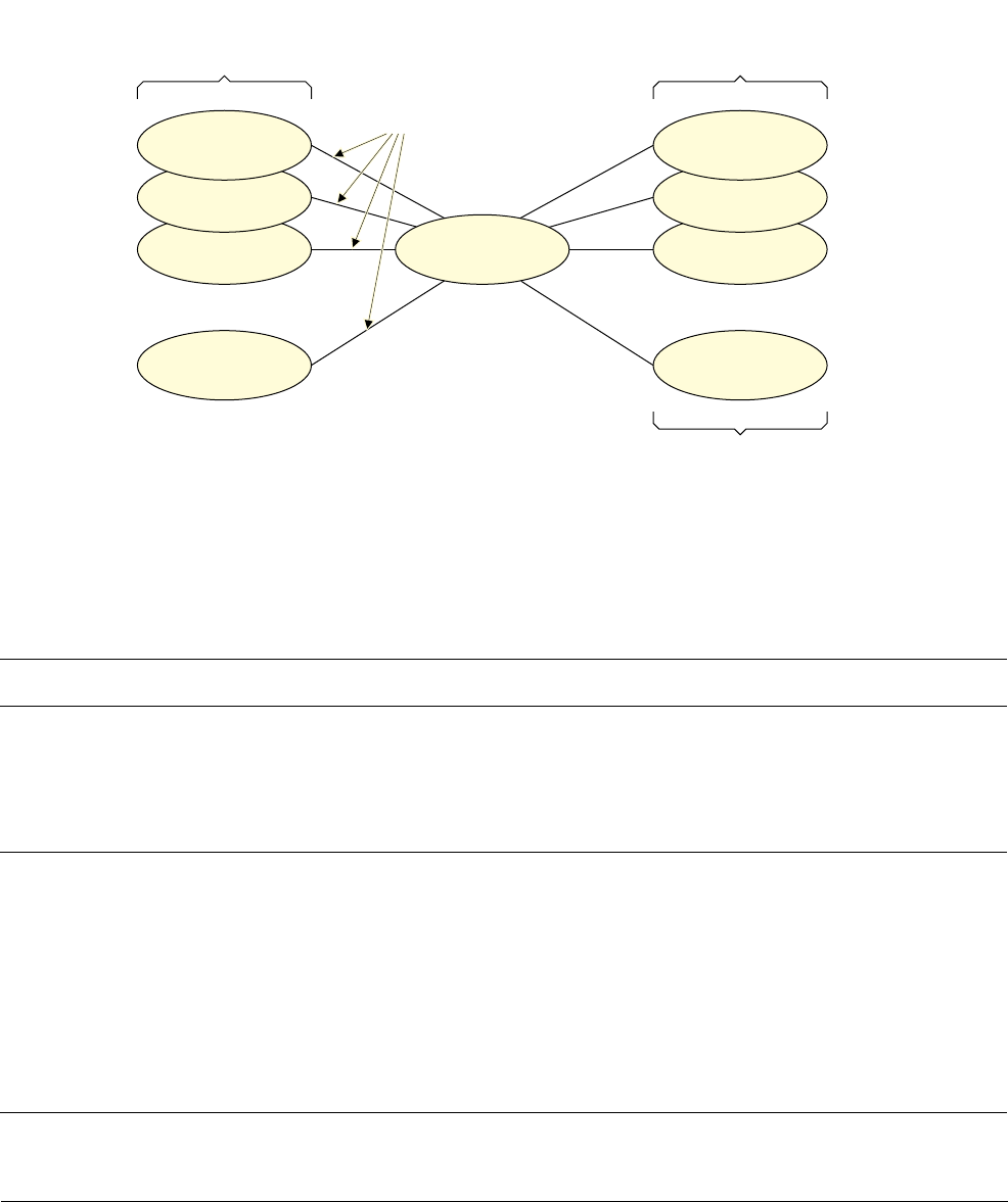
D2 Debug Exceptions
D2.5 Breakpoint exceptions
D2-1578 Copyright © 2013 ARM Limited. All rights reserved. ARM DDI 0487A.a
Non-Confidential - Beta ID090413
• Multiple Linked Address Mismatch breakpoints.
• Multiple Linked watchpoints.
It is also possible that a Linked Context breakpoint might have no breakpoints or watchpoints linked to it.
Figure D2-3 shows a single Linked Context breakpoint that is linked to by a number of Linked Address breakpoints
and a number of Linked watchpoints.
Figure D2-3 The role of linking in Breakpoint and Watchpoint exception generation
Table D2-4 shows a summary of the basic properties of Address and Context breakpoints.
Linked
Address breakpoint 3
Linked
Address breakpoint 2
Linked
Address breakpoint n
Linked Context
breakpoint
Linked
Address breakpoint 1
Linked Watchpoint 3
Linked Watchpoint 2
Linked Watchpoint n
•
•
•
Linked Watchpoint 1
Links
Each Linked Address breakpoint can only generate a
Breakpoint exception if the comparisons made by both it, and
the Linked Context breakpoint, are successful.
Each Linked watchpoint can only generate a Watchpoint
exception if the comparisons made by both it, and the
Linked Context breakpoint, are successful.
•
•
•
These might be:
• All Linked Address match breakpoints.
• All Linked Address mismatch breakpoints.
• A combination of both.
Table D2-4 Summary of the basic properties of Address and Context breakpoints
Breakpoint Linking Programming for a mismatch
Address Can be used in isolation.
If BT[0] is 1, is called a Linked Address breakpoint.
A Linked Address breakpoint:
• Can link to one Linked Context breakpoint.
• Cannot link to any Address breakpoints or watchpoints.
Can be programmed for an address
mismatch. However, address
mismatching is only supported in an
AArch32 stage 1 translation regime.
Context Can be used in isolation.
If BT[0] is 1, is called a Linked Context breakpoint.
A Linked Context breakpoint can be linked to by nothing, or by either or
both of the following:
• One or more Linked Address breakpoints. These might be Linked
Address Match breakpoints, or Linked Address Mismatch
breakpoints, or a combination of both.
• One or more Linked watchpoints.
A Linked Context breakpoint cannot be linked to by another Context
breakpoint.
Cannot be programmed for a context
mismatch.

D2 Debug Exceptions
D2.5 Breakpoint exceptions
ARM DDI 0487A.a Copyright © 2013 ARM Limited. All rights reserved. D2-1579
ID090413 Non-Confidential - Beta
Breakpoint types defined by DBGBCRn_EL1.BT or DBGBCRn.BT
The following list provides more detail about each breakpoint type shown in Figure D2-2 on page D2-1577:
0b0000
, Unlinked Address Match breakpoint
Generation of a Breakpoint exception depends on both:
• The DBGBCR<n>_EL1.{SSC, HMC, PMC} or DBGBCR<n>.{SSC, HMC, PMC}
controls. These define the PE conditions that the breakpoint generates a Breakpoint exception
for. See Execution conditions that a breakpoint generates Breakpoint exceptions for on
page D2-1573.
• A successful address match, as described in Instruction address comparisons for Breakpoint
exception generation on page D2-1582.
DBGBCR<n>_EL1.LBN or DBGBCR<n>.LBN for this breakpoint is ignored.
0b0001
, Linked Address Match breakpoint
Generation of a Breakpoint exception depends on all of the following:
• The DBGBCR<n>_EL1.{SSC, HMC, PMC} or DBGBCR<n>.{SSC, HMC, PMC} controls
for this breakpoint. These define the PE conditions that the breakpoint generates a Breakpoint
exception for. See Execution conditions that a breakpoint generates Breakpoint exceptions
for on page D2-1573.
• A successful address match defined by this breakpoint, as described in Instruction address
comparisons for Breakpoint exception generation on page D2-1582.
• A successful context match defined by the Linked Context breakpoint that this breakpoint
links to.
DBGBCR<n>_EL1.LBN or DBGBCR<n>.LBN for this breakpoint identifies the Linked Context
breakpoint that this breakpoint links to.
0b0010
, Unlinked Context ID Match breakpoint
BT ==
0b0010
is a reserved value if the breakpoint is not a context-aware breakpoint.
For context-aware breakpoints, generation of a Breakpoint exception depends on both:
• The DBGBCR<n>_EL1.{SSC, HMC, PMC} or DBGBCR<n>.{SSC, HMC, PMC}
controls. These define the PE conditions that the breakpoint generates a Breakpoint exception
for. See Execution conditions that a breakpoint generates Breakpoint exceptions for on
page D2-1573.
• A successful Context ID match, as described in Context comparisons for Breakpoint
exception generation on page D2-1587.
DBGBCR<n>_EL1.{LBN, BAS} or DBGBCR<n>.{LBN, BAS} for this breakpoint are ignored
0b0011
, Linked Context ID Match breakpoint
BT ==
0b0011
is a reserved value if the breakpoint is not a context-aware breakpoint.
For context-aware breakpoints, either:
• This breakpoint does not generate any Breakpoint exceptions, if no Linked breakpoints or
Linked watchpoints link to it.
• Generation of a Breakpoint exception depends on both:
— A successful instruction address match, defined by a Linked Address breakpoint that
links to this breakpoint, see Instruction address comparisons for Breakpoint exception
generation on page D2-1582.
— A successful Context ID match defined by this breakpoint, as described in Context
comparisons for Breakpoint exception generation on page D2-1587.
• Generation of a Watchpoint exception depends on both:
— A successful data address match, defined by a Linked watchpoint that links to this
breakpoint, see Data address comparisons for Watchpoint exception generation on
page D2-1612.

D2 Debug Exceptions
D2.5 Breakpoint exceptions
D2-1580 Copyright © 2013 ARM Limited. All rights reserved. ARM DDI 0487A.a
Non-Confidential - Beta ID090413
— A successful Context ID match defined by this breakpoint, as described in Context
comparisons for Breakpoint exception generation on page D2-1587.
DBGBCR<n>_EL1.{LBN, SSC, HMC, BAS, PMC} or DBGBCR<n>.{LBN, SSC, HMC, BAS
PMC} for this breakpoint are ignored.
0b0100
, Unlinked Address Mismatch breakpoint
AArch64 state does not support Address Mismatch breakpoints. BT ==
0b0100
is a reserved value.
In an AArch64 stage 1 translation regime, if a breakpoint is programmed to be this type, it is
evaluated as an Unlinked Address Match breakpoint, described in 0b0000, Unlinked Address Match
breakpoint on page D2-1579.
In an AArch32 stage 1 translation regime:
• Generation of a Breakpoint exception depends on both:
— The DBGBCR<n>.{SSC, HMC, PMC} controls. These define the PE conditions that
the breakpoint generates a Breakpoint exception for. See Execution conditions that a
breakpoint generates Breakpoint exceptions for on page D2-1573.
— A successful address mismatch, as described in Instruction address comparisons for
Breakpoint exception generation on page D2-1582.
•DBGBCR<n>.LBN is for this breakpoint is ignored.
0b0101
, Linked Address Mismatch breakpoint
AArch64 state does not support Address Mismatch breakpoints. BT ==
0b0101
is a reserved value.
In an AArch64 stage 1 translation regime, if a breakpoint is programmed to be this type, it is
evaluated as a Linked Address Match breakpoint, described in 0b0001, Linked Address Match on
page D2-1579.
In an AArch32 stage 1 translation regime, generation of a Breakpoint exception depends on all of
the following:
— The DBGBCR<n>.{SSC, HMC, PMC} controls. These define the PE conditions that
the breakpoint generates a Breakpoint exception for. See Execution conditions that a
breakpoint generates Breakpoint exceptions for on page D2-1573.
— A successful address mismatch defined by this breakpoint, as described in Instruction
address comparisons for Breakpoint exception generation on page D2-1582.
— A successful context match defined by the Linked Context breakpoint that this
breakpoint links to.
DBGBCR<n>_EL1.LBN or DBGBCR<n>.LBN for this breakpoint identifies the Linked Context
breakpoint that this breakpoint links to.
0b1000
, Unlinked VMID Match breakpoint
BT ==
0b1000
is a reserved value if either:
• The breakpoint is not a context-aware breakpoint.
• EL2 is not implemented.
For context-aware breakpoints, generation of a Breakpoint exception depends on both:
• The DBGBCR<n>_EL1.{SSC, HMC, PMC} or DBGBCR<n>.{SSC, HMC, PMC}
controls. These define the PE conditions that the breakpoint generates a Breakpoint exception
for. See Execution conditions that a breakpoint generates Breakpoint exceptions for on
page D2-1573.
• A successful VMID match, as described in Context comparisons for Breakpoint exception
generation on page D2-1587.
DBGBCR<n>_EL1.{LBN, BAS} or DBGBCR<n>.{LBN, BAS} for this breakpoint are ignored.
0b1001
, Linked VMID Match breakpoint
BT ==
0b1000
is a reserved value if either:
• The breakpoint is not a context-matching breakpoint.
• EL2 is not implemented.

D2 Debug Exceptions
D2.5 Breakpoint exceptions
ARM DDI 0487A.a Copyright © 2013 ARM Limited. All rights reserved. D2-1581
ID090413 Non-Confidential - Beta
For context-aware breakpoints, either:
• This breakpoint does not generate any Breakpoint exceptions, if no Linked breakpoints or
Linked watchpoints link to it.
• Generation of a Breakpoint exception depends on both:
— A successful instruction address match, defined by a Linked Address Match
breakpoint that links to this breakpoint. See Instruction address comparisons for
Breakpoint exception generation on page D2-1582.
— A successful VMID match defined by this breakpoint, as described in Context
comparisons for Breakpoint exception generation on page D2-1587.
• Generation of a Watchpoint exception depends on both:
— A successful data address match, defined by a Linked watchpoint that links to this
breakpoint, see Data address comparisons for Watchpoint exception generation on
page D2-1612.
— A successful VMID match defined by this breakpoint, as described in Context
comparisons for Breakpoint exception generation on page D2-1587.
DBGBCR<n>_EL1.{LBN, SSC, HMC, BAS, PMC} or DBGBCR<n>.{LBN, SSC, HMC, BAS,
PMC} for this breakpoint are ignored.
0b1010
, Unlinked Context ID and VMID Match breakpoint
BT ==
0b1010
is a reserved value if either:
• The breakpoint is not a context-matching breakpoint.
• EL2 is not implemented.
For context-matching breakpoints, generation of a Breakpoint exception depends on all of the
following:
• The DBGBCR<n>_EL1.{SSC, HMC, PMC} or DBGBCR<n>.{SSC, HMC, PMC}
controls. These define the PE conditions that the breakpoint generates a Breakpoint exception
for. See Execution conditions that a breakpoint generates Breakpoint exceptions for on
page D2-1573.
• A successful Context ID match.
• A successful VMID match.
Context comparisons for Breakpoint exception generation on page D2-1587 describes the
requirements for a successful Context ID match and a successful VMID match.
DBGBCR<n>_EL1.{LBN, BAS} or DBGBCR<n>.{LBN, BAS} for this breakpoint are ignored.
0b1011
, Linked Context ID and VMID Match breakpoint
BT ==
0b1011
is a reserved value if either:
• The breakpoint is not a context-matching breakpoint.
• EL2 is not implemented.
For context-matching breakpoints, either:
• This breakpoint does not generate any Breakpoint exceptions, if no Linked breakpoints or
Linked watchpoints link to it.
• Generation of a Breakpoint exception depends on all of the following:
— A successful instruction address match, defined by a Linked Address breakpoint that
links to this breakpoint, see Instruction address comparisons for Breakpoint exception
generation on page D2-1582.
— A successful Context ID match defined by this breakpoint.
— A successful VMID match defined by this breakpoint.
• Generation of a Watchpoint exception depends on all of the following:
— A successful data address match, defined by a Linked watchpoint that links to this
breakpoint, see Data address comparisons for Watchpoint exception generation on
page D2-1612.

D2 Debug Exceptions
D2.5 Breakpoint exceptions
D2-1582 Copyright © 2013 ARM Limited. All rights reserved. ARM DDI 0487A.a
Non-Confidential - Beta ID090413
— A successful Context ID match defined by this breakpoint.
— A successful VMID match defined by this breakpoint.
Context comparisons for Breakpoint exception generation on page D2-1587 describes the
requirements for a successful Context ID match and a successful VMID match by this breakpoint.
DBGBCR<n>_EL1.{LBN, SSC, HMC, BAS, PMC} or DBGBCR<n>.{LBN, SSC, HMC, BAS,
PMC} for this breakpoint are ignored.
D2.5.6 Instruction address comparisons for Breakpoint exception generation
The following subsections describe the address comparisons that are made for each instruction in the program flow,
for:
•Address Match breakpoints.
•Address Mismatch breakpoints in an AArch32 stage 1 translation regime.
Address Match breakpoints
For Unlinked and Linked Address Match breakpoints:
In an AArch64 stage 1 translation regime:
An address comparison is successful if both:
• Bits [48:2] of the current instruction address are equal to DBGBVR<n>_EL1[48:2].
•DBGBCR<n>_EL1.BAS is programmed with either
0b0011
or
0b1111
. See Specifying the
halfword-aligned address that an address comparison is successful on on page D2-1583.
Note
•DBGBVR<n>_EL1 is a 64-bit register. The most significant bits of this register are
sign-extension bits.
• If the implementation is an AArch64-only implementation, DBGBCR<n>_EL1.BAS is
programmed by default with
0b1111
, because it is RES1.
In an AArch32 stage 1 translation regime:
An address comparison is successful if both:
• Bits [31:2] of the current instruction address are equal to DBGBVR<n>[31:2].
•Either:
—DBGBCR<n>.BAS is programmed with
0b0011
or
0b1111
, and the instruction is at a
word-aligned address.
—DBGBCR<n>.BAS is programmed with
0b1100
, and the instruction is not at a
word-aligned address.
See Specifying the halfword-aligned address that an address comparison is successful on on
page D2-1583.
Address Mismatch breakpoints in an AArch32 stage 1 translation regime
For Unlinked and Linked Address Mismatch breakpoints in an AArch32 stage 1 translation regime, an address
comparison is successful if both:
• Bits [31:2] of the current instruction address value are not equal to DBGBVR<n>[31:2].
•Either:
—DBGBCR<n>.BAS is programmed with
0b0011
or
0b1111
, and the instruction is at a word-aligned
address.
—DBGBCR<n>.BAS is programmed with
0b1100
, and the instruction is not at a word-aligned address.

D2 Debug Exceptions
D2.5 Breakpoint exceptions
ARM DDI 0487A.a Copyright © 2013 ARM Limited. All rights reserved. D2-1583
ID090413 Non-Confidential - Beta
See Using the BAS field in Address Mismatch breakpoints, in an AArch32 stage 1 translation regime on
page D2-1586.
Note
Address Mismatch breakpoints can be used to single-step through code. See Using an Address Mismatch breakpoint
to single-step an instruction on page D2-1590.
D2.5.7 Specifying the halfword-aligned address that an address comparison is successful on
If the implementation supports AArch32 state in any Exception level, then for an Address breakpoint, a debugger
can use the Byte Address Selection field, DBGBCR<n>_EL1.BAS or DBGBCR<n>.BAS, so that the address
comparison is successful on either:
• The instruction starting at the address held in the DBGBVR<n>_EL1 or DBGBVR<n>.
• The instruction starting at the halfword-aligned address immediately after the address held in the
DBGBVR<n>_EL1 or DBGBVR<n>.
Note
The address programmed into the DBGBVR<n>_EL1 or DBGBVR<n> must be word-aligned.
This provides a debugger with a method of programming breakpoints on T32 instructions.
In AArch64-only implementations this feature is not supported. In this case, DBGBCR<n>_EL1.BAS is RES1 and
the smallest instruction size a debugger can program a breakpoint to match on is a word, that starts at the address
held in the DBGBVR<n>_EL1.
For Context breakpoints, DBGBCR<n>_EL1.BAS or DBGBCR<n>.BAS is RES1 and is ignored.
Where DBGBCR<n>_EL1.BAS or DBGBCR<n>.BAS is supported, it can be used in both Address Match
breakpoints and Address Mismatch breakpoints, as follows:
• For an Address Match breakpoint, that can be Linked or Unlinked, the BAS field selects which
halfword-aligned address the breakpoint must generate a Breakpoint exception for. This means that an
address comparison is successful only if both of the following match:
— The instruction address held in bits [48:2] of the DBGBVR<n>_EL1, or bits [31:2] of the
DBGBVR<n>.
— The halfword defined by the BAS field.
Table D2-9 on page D2-1597 also shows the set of conditions required. The conditions for a successful
address match comparison are:
Equals[address] AND selected[BAS]
• For an Address Mismatch breakpoint, that can be Linked or Unlinked, the BAS field selects which
halfword-aligned address the breakpoint must not generate a Breakpoint exception for. This means that an
address comparison is successful if either or both of the following do not match:
— The instruction address held in bits [48:2] of the DBGBVR<n>_EL1, or bits [31:2] of the
DBGBVR<n>.
— The halfword defined by the BAS field.
Table D2-9 on page D2-1597 also shows the set of conditions required. The conditions for a successful
address mismatch comparison are:
Not (equals[address] AND selected[BAS])
Note
Address Mismatch breakpoints are not supported in an AArch64 stage 1 translation regime. See Breakpoint
types defined by DBGBCRn_EL1.BT or DBGBCRn.BT on page D2-1579.

D2 Debug Exceptions
D2.5 Breakpoint exceptions
D2-1584 Copyright © 2013 ARM Limited. All rights reserved. ARM DDI 0487A.a
Non-Confidential - Beta ID090413
The following two subsections show the supported BAS values:
•Using the BAS field in Address Match breakpoints.
•Using the BAS field in Address Mismatch breakpoints, in an AArch32 stage 1 translation regime on
page D2-1586.
Using the BAS field in Address Match breakpoints
The supported BAS values are:
0b0000
This value is reserved. Behavior is a CONSTRAINED UNPREDICTABLE choice of:
• The breakpoint is disabled.
• The breakpoint behaves as if BAS is
0b0011
,
0b1100
, or
0b1111
.
0b0011
Generates a Breakpoint exception if an instruction with an address described as follows is
committed for execution:
• Bits [48:2] of the address equals DBGBVR<n>_EL1[48:2], or bits [31:2] of the address
equals DBGBVR<n>[31:2].
• Bits [1:0] of the address are
0b00
.
This means that breakpoints programmed with this BAS value generate Breakpoint exceptions for
all of the following:
• 32-bit T32 instructions at word-aligned addresses.
• 16-bit T32 instructions at word-aligned addresses.
• A64 or A32 instructions. These are always at word-aligned addresses.
However, ARM recommends that a debugger uses this BAS value only for T32 instructions.
It is CONSTRAINED UNPREDICTABLE whether a breakpoint programmed with this BAS value
generates a Breakpoint exception on the second halfword of a 32-bit T32 instruction starting at the
halfword-aligned address ((DBGBVR<n>[31:2]:00) - 2).
0b1100
Generates a Breakpoint exception if an instruction with an address described as follows is
committed for execution:
• Bits [48:2] of the address equals DBGBVR<n>_EL1[48:2], or bits [31:2] of the address
equals DBGBVR<n>[31:2].
• Bits [1:0] of the address are
0b10
.
This means that breakpoints programmed with this BAS value generate Breakpoint exceptions for
both of the following:
• 32-bit T32 instructions at addresses that are halfword-aligned but not word-aligned.
• 16-bit T32 instructions at addresses that are halfword-aligned but not word-aligned.
It is CONSTRAINED UNPREDICTABLE whether a breakpoint programmed with this BAS value
generates a Breakpoint exception on the second halfword of a 32-bit T32, A32, or A64 instruction
starting at a word-aligned address.
0b1111
Generates a Breakpoint exception if an instruction with an address described as follows is
committed for execution:
• Bits [48:2] of the address equals DBGBVR<n>_EL1[48:2], or bits [31:2] of the address
equals DBGBVR<n>[31:2].
• Bits [1:0] of the address are
0b00
.
This means that breakpoints programmed with this BAS value generate Breakpoint exceptions for
all of the following:
• 32-bit T32 instructions at word-aligned addresses.
• 16-bit T32 instructions at word-aligned addresses.
• A64 or A32 instructions. These are always at word-aligned addresses.
However, ARM recommends that a debugger uses this BAS value only for A64 and A32
instructions.
D2 Debug Exceptions
D2.5 Breakpoint exceptions
ARM DDI 0487A.a Copyright © 2013 ARM Limited. All rights reserved. D2-1585
ID090413 Non-Confidential - Beta
It is CONSTRAINED UNPREDICTABLE whether a breakpoint programmed with this BAS value
generates a Breakpoint exception on the second halfword of a 32-bit T32 instruction starting at the
halfword-aligned address ((DBGBVR<n>[31:2]:00) - 2).
It is CONSTRAINED UNPREDICTABLE whether a breakpoint programmed with this BAS value
generates a Breakpoint exception on a 32-bit T32 instruction or a 16-bit T32 instruction at the
halfword-aligned address DBGBVR<n>[31:2]:10.
All other BAS values are reserved. For these reserved other BAS values, DBGBCR<n>_EL1.BAS[3,1] or
DBGBCR<n>.BAS[3,1] ignore writes and read the same values as DBGBCR<n>_EL1[2,0] or DBGBCR<n>[2,0]
respectively. This means that the smallest instruction size a debugger can program a breakpoint to match on is a
halfword.
Figure D2-4 shows a summary of when breakpoints programmed with particular BAS values generate Breakpoint
exceptions.
The figure contains four parts:
• A column showing the row number, on the left.
• An instruction set and instruction size table.
• A location of instruction figure.
• A BAS field values table, on the right.
To use the figure, read across the rows. For example:
• Row 2 shows that a breakpoint with a BAS value of
0b1100
generates Breakpoint exceptions for 16-bit T32
instructions starting at the halfword-aligned address immediately after the word aligned address held in the
DBGBVR<n>_EL1 or DBGBVR<n>.
• Row 7 shows that a breakpoint with a BAS value of either
0b0011
or
0b1111
generates Breakpoint exceptions
for A64 instructions. A64 instructions are always at word-aligned addresses.
In the figure:
Ye s Means that the breakpoint generates a Breakpoint exception.
No Means that the breakpoint does not generate a Breakpoint exception.
UNP Means that is it CONSTRAINED UNPREDICTABLE whether the breakpoint generates a Breakpoint
exception.
Figure D2-4 Summary of BAS field meanings for Address Match breakpoints
-2 -1 +2+10+3+4Size
16-bit
16-bit
32-bit
32-bit
32-bit
32-bit
32-bit
+5Instruction set
T32
T32
A32
A64
Yes
UNP
UNP
Yes
UNP
Yes
Yes
0b0011
Yes
UNP
Yes
Yes
BAS[3:0]
0b1100 0b1111
No
Yes
No
No
No
UNP
UNP
Yes
UNP
Yes
Location of instruction
a
a.
0 means the word-aligned address held in the DBGBVRn_EL1 or DBGBVRn.
The other locations are as follows:
•
+1 means DBGBVRn_EL1[48:2]:01 or DBGBVRn[31:2]:01.
•
+2 means DBGBVRn_EL1[48:2]:10 or DBGBVRn[31:2]:10.
•
+3 means DBGBVRn_EL1[48:2]:11 or DBGBVRn[31:2]:11.
•
...
The solid areas show the location of the instruction.
Row 1
R
OW
2
R
OW
3
Row 4
R
OW
5
Row 6
Row 7

D2 Debug Exceptions
D2.5 Breakpoint exceptions
D2-1586 Copyright © 2013 ARM Limited. All rights reserved. ARM DDI 0487A.a
Non-Confidential - Beta ID090413
Using the BAS field in Address Mismatch breakpoints, in an AArch32 stage 1 translation
regime
An Address Mismatch breakpoint generates Breakpoint exceptions for all instructions committed for execution,
apart from the instruction whose address matches the address held in the DBGBVR<n>. The following list shows
when an Address Mismatch breakpoint does not generate Breakpoint exceptions.
The supported BAS values are:
0b0000
The breakpoint ignores the address held in the DBGBVR<n> and generates Breakpoint exceptions
for all instruction addresses.
0b0011
Does not generate a Breakpoint exception if an instruction with an address described as follows is
committed for execution:
• Bits [31:2] of the address equals DBGBVR<n>[31:2].
• Bits [1:0] of the address are
0b00
.
This means that breakpoints programmed with this BAS value do not generate Breakpoint
exceptions for any of the following:
• 32-bit T32 instructions at word-aligned addresses.
• 16-bit T32 instructions at word-aligned addresses.
• A32 instructions. These are always at word-aligned addresses.
However, ARM recommends that a debugger uses this BAS value only for T32 instructions.
It is CONSTRAINED UNPREDICTABLE whether a breakpoint programmed with this BAS value does
not generate a Breakpoint exception on the second halfword of a 32-bit T32 instruction starting at
the halfword-aligned address (DBGBVR<n>[31:2]:00) - 2)).
0b1100
Does not generates a Breakpoint exception if an instruction with an address described as follows is
committed for execution:
• Bits [31:2] equals DBGBVR<n>[31:2].
• Bits [1:0] of the address are
0b10
.
This means that breakpoints programmed with this BAS value do not generate Breakpoint
exceptions for either of the following:
• 32-bit T32 instructions at addresses that are halfword-aligned but not word-aligned.
• 16-bit T32 instructions at addresses that are halfword-aligned but not word-aligned.
It is CONSTRAINED UNPREDICTABLE whether a breakpoint programmed with this BAS value does
not generate a Breakpoint exception on the second halfword of a 32-bit T32, A32, or A64 instruction
at a word-aligned address.
0b1111
Does not generate a Breakpoint exception if an instruction with an address described as follows is
committed for execution:
• Bits [31:2] os the address equals DBGBVR<n>[31:2].
• Bits [1:0] of the address are
0b00
.
This means that breakpoints programmed with this BAS value do not generate Breakpoint
exceptions for any of the following:
• 32-bit T32 instructions at a word-aligned addresses.
• 16-bit T32 instructions at a word-aligned addresses.
• A32 instructions. These are always at word-aligned addresses.
However, ARM recommends that a debugger uses this BAS value only for A32 instructions.
It is CONSTRAINED UNPREDICTABLE whether a breakpoint programmed with this BAS value does
not generate a Breakpoint exception on the second halfword of a 32-bit T32 instruction starting at
the halfword-aligned address (DBGBVR<n>[31:2]:00) - 2)).
It is CONSTRAINED UNPREDICTABLE whether a breakpoint programmed with this BAS value does
not generate a Breakpoint exception on a 32-bit T32 instruction or a 16-bit T32 instruction at the
halfword-aligned address DBGBVR<n>[31:2]:10.
D2 Debug Exceptions
D2.5 Breakpoint exceptions
ARM DDI 0487A.a Copyright © 2013 ARM Limited. All rights reserved. D2-1587
ID090413 Non-Confidential - Beta
All other BAS values are reserved. For any of these reserved other BAS values, DBGBCR<n>.BAS[3,1] ignore
writes and read the same values as DBGBCR<n>[2,0] respectively. This means that the smallest instruction size
that a breakpoint can never generate a Breakpoint exception for is a halfword.
Figure D2-4 on page D2-1585 shows a summary of when breakpoints programmed with particular BAS values
generate Breakpoint exceptions.
The figure contains four parts:
• A column showing the row number, on the left.
• An instruction set and instruction size table.
• A location of instruction figure.
• A BAS field values table, on the right.
To use the figure, read across the rows. For example:
• Row 1 shows that a breakpoint with a BAS value of
0b1100
generates Breakpoint exceptions for 16-bit T32
instructions starting at the word-aligned address held in the DBGBVR<n>.
• Row 5 shows that a breakpoint with a BAS value of
0b0011
generates Breakpoint exceptions for 32-bit T32
instructions starting at the halfword-aligned address immediately after the word aligned address held in the
DBGBVR<n>.
In the figure:
Ye s Means that the breakpoint does generate a Breakpoint exception.
No Means that the breakpoint does not generate a Breakpoint exception.
UNP Means that is it CONSTRAINED UNPREDICTABLE whether the breakpoint generates a Breakpoint
exception.
Figure D2-5 Summary of BAS field meanings for Address Mismatch breakpoints
D2.5.8 Context comparisons for Breakpoint exception generation
This section describes the context comparisons that are made for each instruction in the program flow, for Context
breakpoints.
In an AArch64 stage 1 translation regime:
A context comparison is successful if, depending on the breakpoint type set by
DBGBCR<n>_EL1.BT[3,1], one of the following is true:
• The current Context ID value is equal to DBGBVR<n>_EL1[31:0].
• The current VMID value is equal to DBGBVR<n>_EL1[39:32].
-2 -1 +2+10+3+4Size
16-bit
16-bit
32-bit
32-bit
32-bit
32-bit
+5Instruction set
T32
T32
A32
No
UNP
UNP
No
UNP
No
0b0011
No
UNP
No
BAS[3:0]
0b1100 0b1111
Yes
No
Yes
Yes
Yes
UNP
No
UNP
No
Location of instructiona
a.
0 means the word-aligned address held in the DBGBVRn. The other locations are as follows:
•
+1 means DBGBVRn[31:2]:01.
•
+2 means DBGBVRn[31:2]:10.
•
+3 means DBGBVRn[31:2]:11.
•
...
The solid areas show the location of the instruction.
Row 1
ROW 2
ROW 3
Row 4
ROW 5
Row 6
0b0000
Yes
Yes
Yes
Yes
Yes
Yes

D2 Debug Exceptions
D2.5 Breakpoint exceptions
D2-1588 Copyright © 2013 ARM Limited. All rights reserved. ARM DDI 0487A.a
Non-Confidential - Beta ID090413
• The current Context ID value is equal to DBGBVR<n>_EL1[31:0], and the current VMID
value is equal to DBGBVR<n>_EL1[39:32].
In an AArch32 stage 1 translation regime:
A context comparison is successful if, depending on the breakpoint type set by
DBGBCR<n>.BT[3,1], one of the following is true:
• The current Context ID value is equal to DBGBVR<n>[31:0].
• The current VMID value is equal to DBGBXVR<n>[7:0].
• The current Context ID value is equal to DBGBVR<n>[31:0], and the current VMID value
is equal to DBGBXVR<n>[7:0].
For Context breakpoints, DBGBCR<n>_EL1.BAS or DBGBCR<n>.BAS is RES1 and ignored. If the Context
breakpoint is a Linked Context breakpoint, then DBGBCR<n>_EL1.{LBN, SSC, HMC, PMC} or
DBGBCR<n>.{LBN, SSC, HMC, PMC} are RES0 and ignored.
D2.5.9 Linked comparisons for Breakpoint exception generation
In the following description:
• Breakpoint n is a Linked Address Match or a Linked Address Mismatch breakpoint.
•Watchpoint n is a Linked watchpoint.
• Breakpoint m is a Linked Context breakpoint, that is one of the following:
— A Linked Context ID Match breakpoint.
— A Linked VMID Match breakpoint.
— A Linked VMID and Context ID Match breakpoint.
For a linked comparison, either:
• A breakpoint n links to a breakpoint m. In this case, if breakpoint n matches, it only generates a Breakpoint
exception if breakpoint m also matches.
• A watchpoint n links to a breakpoint m. In this case, if watchpoint n matches, it only generates a Watchpoint
exception if breakpoint m also matches.
If no breakpoints or watchpoints link to breakpoint m, breakpoint m cannot generate any Breakpoint exceptions.
The following subsections describe linked comparisons for Breakpoint exception generation:
•A linked comparison for an address match and a context match.
•A linked comparison for an address mismatch and a context match, in an AArch32 stage 1 translation regime
on page D2-1589.
Note
• A Linked Context breakpoint m might be linked to by more than one Linked Address breakpoint, and might
also be linked to one or more Linked watchpoint. See Breakpoint types and linking of breakpoints on
page D2-1576.
• For more information about linked comparisons for Watchpoint exception generation, see Linked
comparisons for Watchpoint exception generation on page D2-1616.
A linked comparison for an address match and a context match
This comparison is made for a Linked Address Match breakpoint and a Linked Context breakpoint, that are linked
together by using DBGBCR<n>_EL1.BT[0] and DBGBCR<n>_EL1.LBN, or DBGBCR<n>.BT[0] and
DBGBCR<n>.LBN, for the Linked Address Match breakpoint.
A Breakpoint exception is generated only if both:
• The instruction address comparison is successful.

D2 Debug Exceptions
D2.5 Breakpoint exceptions
ARM DDI 0487A.a Copyright © 2013 ARM Limited. All rights reserved. D2-1589
ID090413 Non-Confidential - Beta
• The context comparison is successful.
In an AArch64 stage 1 translation regime:
The address comparison is successful if the conditions described for an AArch64 stage 1 translation
regime in Address Match breakpoints on page D2-1582 are met.
The context comparison is successful if the conditions described for an AArch64 stage 1 translation
regime in Context comparisons for Breakpoint exception generation on page D2-1587 are met.
In an AArch32 stage 1 translation regime:
The address comparison is successful if the conditions described for an AArch32 stage 1 translation
regime in Address Match breakpoints on page D2-1582 are met.
The context comparison is successful if the conditions described for an AArch32 stage 1 translation
regime in Context comparisons for Breakpoint exception generation on page D2-1587 are met.
Note
For the Linked Context breakpoint, DBGBCR<n>_EL1.{LBN, SSC, HMC, BAS, PMC} or DBGBCR<n>.{LBN,
SSC, HMC, BAS, PMC} are ignored.
A linked comparison for an address mismatch and a context match, in an AArch32 stage
1 translation regime
The comparison described is made for a Linked Address Mismatch breakpoint and a Linked Context breakpoint,
that are linked together by using DBGBCR<n>.BT[0] and DBGBCR<n>.LBN for the Linked Address Mismatch
breakpoint.
A Breakpoint exception is generated only if both:
• The instruction address comparison is successful.
• The context comparison is successful.
The address comparison is successful if the conditions described for an AArch32 stage 1 translation regime in
Address Mismatch breakpoints in an AArch32 stage 1 translation regime on page D2-1582 are met.
The context comparison is successful if the conditions described for an AArch32 stage 1 translation regime in
Context comparisons for Breakpoint exception generation on page D2-1587 are met.
Note
For the Linked Context breakpoint, DBGBCR<n>_EL1.{LBN, SSC, HMC, BAS, PMC} or DBGBCR<n>.{LBN,
SSC, HMC, BAS, PMC} are ignored.

D2 Debug Exceptions
D2.5 Breakpoint exceptions
D2-1590 Copyright © 2013 ARM Limited. All rights reserved. ARM DDI 0487A.a
Non-Confidential - Beta ID090413
D2.5.10 Using breakpoints
This section contains the following:
•Using an Address Mismatch breakpoint to single-step an instruction.
•Address breakpoints on the first instruction in an IT block on page D2-1591.
•Constraints on programming hardware breakpoints on page D2-1591.
Using an Address Mismatch breakpoint to single-step an instruction
The following description applies only for an AArch32 stage 1 translation regime.
In execution conditions that an Address Mismatch breakpoint matches, the breakpoint generates Breakpoint
exceptions for all instructions committed for execution, except the instruction whose address the breakpoint is
programmed with. See Figure D2-6 for an example of Address Mismatch breakpoint operation, for an Address
Mismatch breakpoint programmed with address
0x1014
.
Note
When a debugger programs an Address Mismatch breakpoint, it programs the breakpoint to match only in certain
execution conditions. For example, a debugger might program an Address Mismatch breakpoint to generate
Breakpoint exceptions only when execution is in Secure EL0. For more information, see Execution conditions that
a breakpoint generates Breakpoint exceptions for on page D2-1573.
Figure D2-6 Operation of an Address Mismatch breakpoint
This means that an Address Mismatch breakpoint can be used to single-step an instruction.
In the example shown in Figure D2-6:
• If the target of a branch is any instruction other than the instruction at address
0x1014
, the breakpoint generates
a Breakpoint exception when the target is committed for execution.
• If the target of a branch is the instruction at address
0x1014
, the PE executes the instruction at
0x1014
and the
breakpoint does not generate a Breakpoint exception until the instruction at address
0x1018
is committed for
execution. The instruction at address
0x1014
is therefore single-stepped.
However, if the instruction at address
0x1014
is single-stepped and causes a synchronous exception, or if an
asynchronous exception occurs while the instruction is being stepped, the breakpoint is evaluated again after
taking the exception. This means that behavior is as follows:
— If the exception handler executes in execution conditions that the breakpoint matches, the breakpoint
generates a Breakpoint exception for the exception vector, because the exception vector is not address
0x1014
. This means that software execution on the PE steps into the exception.
0x1000
0x1004
0x1008
0x100C
0x1010
0x1014
0x1018
0x101C
0x1020
The breakpoint does not generate a Breakpoint debug event
Instruction
addresses
Program
flow
The breakpoint generates a Breakpoint debug event for all of these instructions
The breakpoint generates a Breakpoint debug event for all of these instructions
All executed in execution conditions that the breakpoint matches

D2 Debug Exceptions
D2.5 Breakpoint exceptions
ARM DDI 0487A.a Copyright © 2013 ARM Limited. All rights reserved. D2-1591
ID090413 Non-Confidential - Beta
— If the exception handler executes in execution conditions that the breakpoint does not match, the
breakpoint does not generate any Breakpoint exceptions after the PE has taken the exception, until the
PE returns from the exception. The effect is to step over the exception. Whether the instruction is
stepped again depends on whether the preferred exception return for the exception, and hence the
target of the exception return instruction, is the instruction at
0x1014
or the instruction at
0x1018
.
If the instruction at address
0x1014
is single-stepped and branches to itself, it is CONSTRAINED
UNPREDICTABLE whether the breakpoint generates a Breakpoint exception after the PE has executed the
branch.
This means that an instruction is only single-stepped if it is the target of a branch instruction and its address matches
the address the breakpoint is programmed for. In the example shown in Figure D2-6 on page D2-1590, this is
0x1014
.
Because Address Mismatch breakpoints can single-step instructions, the behavior of an address mismatch
Breakpoint exception is similar to the behavior of a Software Step exception.
Note
• The example shown in Figure D2-6 on page D2-1590 assumes an A32 instruction. The same behavior applies
for both 32-bit and 16-bit T32 instructions.
• Software Step exceptions are the highest priority exception. Breakpoint exceptions are lower priority. See
Synchronous exception prioritization on page D1-1451.
• In AArch64 state, if EDSCR.HDE is 1 and halting is allowed, the Address Mismatch breakpoint type is
reserved. In these cases, Address Mismatch breakpoints are evaluated as Address Match breakpoints. This
behavior might change in future revisions of the architecture. For this reason, software must not rely on this
behavior.
Address breakpoints on the first instruction in an IT block
This section applies to AArch32 state only.
The ARMv8-A architecture permits a combination of an
IT
instruction and another 16-bit T32 instruction to
comprise one 32-bit instruction, if the ITD bit associated with the current Exception level is 1.
It is IMPLEMENTATION DEFINED whether:
• The debug logic considers one of these 32-bit instructions to be one instruction.
• The debug logic considers one of these 32-bit instructions to be two instructions.
Because an Address breakpoint might not generate a Breakpoint exception if an address match occurs only on the
second halfword of a 32-bit instruction, a debugger that wants to program a breakpoint to match on the first
instruction in an IT block must instead program the breakpoint to match on the
IT
instruction itself, even if ITD is
zero.
Note
• The ITD bit is the IT Disable bit. See Trapped instructions when SCTLR_EL1.ITD is 1 on page D1-1468.
•Constraints on programming hardware breakpoints describes that Address breakpoints might not generate
Breakpoint exceptions for address matches that occur on the second halfword of an instruction.
Constraints on programming hardware breakpoints
For the conditions described in the following subsections, breakpoint behavior is one of the following:
• The breakpoint does not generate any Breakpoint exceptions.
• The breakpoint is evaluated as a different breakpoint type, or to match in different PE execution conditions.
• It is CONSTRAINED UNPREDICTABLE whether the breakpoint generates a Breakpoint exception.
The subsections are:
•Reserved DBGBCR<n>_EL1.BT or DBGBCR<n>.BT values on page D2-1592.

D2 Debug Exceptions
D2.5 Breakpoint exceptions
D2-1592 Copyright © 2013 ARM Limited. All rights reserved. ARM DDI 0487A.a
Non-Confidential - Beta ID090413
•Reserved HMC, SSC, and PMC values.
•Constraints that apply to all breakpoint types on page D2-1593.
•Constraints that apply only to Address breakpoints on page D2-1593.
•Constraints that apply only to Context breakpoints on page D2-1594.
Reserved DBGBCR<n>_EL1.BT or DBGBCR<n>.BT values
Table D2-5 shows when particular DBGBCR<n>_EL1.BT or DBGBCR<n>.BT values are reserved, and for the
corresponding breakpoint types, shows behavior when the value is reserved.
The behavior of breakpoints with reserved BT values might change in future revisions of the architecture. For this
reason, software must not rely on the behavior described here.
Reserved HMC, SSC, and PMC values
Table D2-6 on page D2-1593 shows when particular combinations of DBGBCR<n>_EL1.{HMC, SSC, PMC} or
DBGBCR<n>.{HMC, SSC, PMC} are reserved, and shows behavior when the combination is reserved, for all
breakpoint types except Linked Context breakpoints.
Table D2-5 Behaviors of breakpoints programmed with reserved BT values
BT value Breakpoint type Reserved Breakpoint behavior when the BT
value is reserved
0b011x
- Always. The breakpoint behaves as if it is disabled.
0b11xx
-
0b001x
Context ID Match For non context-aware breakpoints. BT[3, 1] are RES0, therefore the breakpoint
behaves as an Address Match breakpoint.
0b100x
VMID Match
0b101x
Context ID and VMID Match
0b100x
VMID Match If EL2 is not implemented. BT[3] is RES0, therefore the breakpoint
behaves as an Address Match breakpoint.
0b101x
Context ID and VMID Match
0b010x
Address Mismatch In an AArch64 stage 1 translation
regime, or if EL1 using AArch32 is
not supported, or if EDSCR.HDE is 1
and halting is allowed.
BT[2] is RES0, therefore the breakpoint
behaves as an Address Match breakpoint.

D2 Debug Exceptions
D2.5 Breakpoint exceptions
ARM DDI 0487A.a Copyright © 2013 ARM Limited. All rights reserved. D2-1593
ID090413 Non-Confidential - Beta
Linked Context breakpoints ignore the HMC, SSC, and PMC fields.
The behavior of breakpoints with reserved combinations of HMC, SSC, and PMC might change in future revisions
of the architecture. For this reason, software must not rely on the behavior described here.
Constraints that apply to all breakpoint types
Constraints that apply to all breakpoint types are as follows:
• Address masking and Context ID masking are not supported.
• If the implementation is an AArch64-only implementation, DBGBCR<n>_EL1.BAS for all breakpoints is
RES1.
• For all Unlinked breakpoint types, DBGBCR<n>_EL1.LBN or DBGBCR<n>.LBN reads UNKNOWN and is
ignored.
Constraints that apply only to Address breakpoints
As follows:
For Address Match breakpoints
For enabled Address Match breakpoints:
•DBGBVR<n>_EL1[1:0] or DBGBVR<n>[1:0] are RES0 and are ignored.
• In AArch32 state, the DBGBXVR<n> is ignored.
• For 32-bit instructions, if a breakpoint matches on the address of the second halfword but not
the address of the first halfword, it is CONSTRAINED UNPREDICTABLE whether the breakpoint
generates a Breakpoint exception.
• If DBGBCR<n>_EL1.BAS or DBGBCR<n>.BAS is
0b1111
, it is CONSTRAINED
UNPREDICTABLE whether the breakpoint generates a Breakpoint exception for a T32
instruction starting at address DBGBVR<n>_EL1[48:2]:10 or DBGBVR<n>[31:2]:10. For
T32 instructions, ARM recommends that the debugger programs the BAS field with either
0b0011
or
0b1100
.
Table D2-6 Behaviors for reserved HMC, SSC, and PMC combinations
HMC SSC PMC Reserved Behavior when reserved
0
0
0
00
01
10
00
00
00
In an AArch64 stage 1
translation regime, or if EL1
using AArch32 is not
supported.
The breakpoint never generates any Breakpoint exceptions.
All combinations with SSC set to
0b01
or
0b10
.When EL3 is not implemented
and EL2 is implemented. SSC[1] is RO and returns the same value as SSC[0]. If the
combination with SSC ==
0b00
or SSC ==
0b11
is then a
combination that Table D2-3 on page D2-1574:
• Includes, the breakpoint matches for those execution
conditions.
• Does not include, the breakpoint never generates any
Breakpoint exceptions.
Any combination where HMC or
SSC is nonzero. When both of EL2 and EL3 are
not implemented. SSC and HMC are RES0.
This means that the breakpoint matches for different
execution conditions. See Table D2-3 on page D2-1574.
Combinations not included in
Table D2-3 on page D2-1574.Always The breakpoint never generates any Breakpoint exceptionsa
a. A breakpoint programmed with a combination that Table D2-3 on page D2-1574 does not include might be affected by a behavior listed this
table, so that it then has a combination that Table D2-3 on page D2-1574 does include.

D2 Debug Exceptions
D2.5 Breakpoint exceptions
D2-1594 Copyright © 2013 ARM Limited. All rights reserved. ARM DDI 0487A.a
Non-Confidential - Beta ID090413
• The BAS value
0b0000
is reserved. A breakpoint programmed with this BAS value behaves
either as if the breakpoint is disabled, or as if the BAS field is programmed as
0b0011
,
0b1100
,
or
0b1111
.
If the Address Match breakpoint is a Linked Address Match breakpoint, the following conditions
also apply:
• If it links to a breakpoint that is not implemented, or a breakpoint that is not context-aware,
then behavior is CONSTRAINED UNPREDICTABLE. Either:
— The Linked Address Match breakpoint never generates any Breakpoint exceptions,
and DBGBCR<n>_EL1.LBN or DBGBCR<n>.LBN for the breakpoint reads
UNKNOWN.
— The breakpoint behaves as if it is linked to an UNKNOWN context-aware breakpoint. In
this case, the breakpoint generates Breakpoint exceptions, and
DBGBCR<n>_EL1.LBN or DBGBCR<n>.LBN indicates the context-matching
breakpoint.
• If it links to any of the following, it never generates any Breakpoint exceptions:
— A breakpoint that is implemented and that is context-aware, but that is not
programmed as a Linked Context breakpoint.
— A breakpoint that is implemented but that is not enabled.
See also Constraints that apply to all breakpoint types on page D2-1593.
For Address Mismatch breakpoints
The constraints are the same as those described in For Address Match breakpoints on
page D2-1593, except that:
• If DBGBCR<n>_EL1.BAS or DBGBCR<n>.BAS is programmed with
0b0000
, the
breakpoint matches on all addresses, even for the address held in the DBGBVR<n>_EL1 or
DBGBVR<n>.
That is, if DBGBCR<n>_EL1.BAS or DBGBCR<n>.BAS is programmed with
0b0000
, the
Address Mismatch breakpoint ignores the address held in the DBGBVR<n>_EL1 or
DBGBVR<n>.
See also Constraints that apply to all breakpoint types on page D2-1593.
Constraints that apply only to Context breakpoints
For enabled Context breakpoints:
•DBGBCR<n>_EL1.BAS or DBGBCR<n>.BAS is RES1 and is ignored.
• Any bits of DBGBVR<n>_EL1 or DBGBVR<n> that are not used to specify Context ID or VMID are RES0
and are ignored.
• In AArch32 state:
— Context ID Match breakpoints ignore the DBGBXVR<n>.
— VMID Match breakpoints ignore the DBGBVR<n>.
If the Context breakpoint is a Linked Context breakpoint, the following condition also applies:
•DBGBCR<n>_EL1.{LBN, SSC, HMC, PMC} or DBGBCR<n>.{LBN, SSC, HMC PMC} are ignored.
See also Constraints that apply to all breakpoint types on page D2-1593.

D2 Debug Exceptions
D2.5 Breakpoint exceptions
ARM DDI 0487A.a Copyright © 2013 ARM Limited. All rights reserved. D2-1595
ID090413 Non-Confidential - Beta
D2.5.11 Summary of breakpoint matching for different breakpoint types
The tables in this section each show a summary of breakpoint matching. See:
•Table D2-7 for an AArch64-only implementation.
•Table D2-8 on page D2-1596 for breakpoint matching in an AArch64 stage 1 translation regime, in an
implementation that supports AArch32 in at least one Exception level.
•Table D2-9 on page D2-1597 for breakpoint matching in an AArch32 stage 1 translation regime.
For the meanings of the conditions given in bold in the tables, see Condition definitions on page D2-1598. Also see
Using the tables on page D2-1597.
Table D2-7 Summary of breakpoint matching for an AArch64-only implementation
Breakpoint type Comparisons made Linking
Address BAS Context ID VMID PE state
0b0000
Unlinked Address Match
Equals - --AND match -
0b0001
Linked Address Match
Equals - --AND match AND linka
0b0010
Unlinked Context ID Match
-- Equals -AND match -
0b0011
Linked Context ID Match
- - AND equals --AND linkb
0b0100
Unlinked Address Mismatch
Equals - --AND match -
0b0101
Linked Address Mismatch
Equals - --AND match AND linka
0b1000
Unlinked VMID Match
-- - Equals AND match -
0b1001
Linked VMID Match
-- - AND equals -AND linkb
0b1010
Unlinked Context ID and VMID
Match
-- Equals AND equals AND match -
0b1011
Linked Context ID and VMID
Match
- - AND equals AND equals -AND linkb
a. Links to one of:
Breakpoint type
0b0011
.
Breakpoint type
0b1001
.
Breakpoint type
0b1011.
See Breakpoint types and linking of breakpoints on page D2-1576.

D2 Debug Exceptions
D2.5 Breakpoint exceptions
D2-1596 Copyright © 2013 ARM Limited. All rights reserved. ARM DDI 0487A.a
Non-Confidential - Beta ID090413
b. One of the following is true:
No breakpoints or watchpoints link to it.
Either or both:
One or more of breakpoint type
0b0001
links to it.
One or more of breakpoint type
0b0101
links to it.
Might also be linked to one or more watchpoints. See Breakpoint types and linking of breakpoints on page D2-1576.
Table D2-8 Summary of breakpoint matching in an AArch64 stage 1 translation regime, for an implementation that
supports AArch32 in at least one Exception level
Breakpoint type Comparisons made Linking
Address BAS Context ID VMID PE state
0b0000
Unlinked Address Match
Equals AND selected --AND match -
0b0001
Linked Address Match
Equals AND selected --AND match AND linka
0b0010
Unlinked Context ID Match
-- Equals -AND match -
0b0011
Linked Context ID Match
- - AND equals --AND linkb
0b0100
Unlinked Address Mismatch
Equals AND selected --AND match -
0b0101
Linked Address Mismatch
Equals AND selected --AND match AND linka
0b1000
Unlinked VMID Match
-- - Equals AND match -
0b1001
Linked VMID Match
-- - AND equals -AND linkb
0b1010
Unlinked Context ID and VMID
Match
-- Equals AND equals AND match -
0b1011
Linked Context ID and VMID
Match
- - AND equals AND equals -AND linkb
a. Links to one of:
Breakpoint type
0b0011
.
Breakpoint type
0b1001
.
Breakpoint type
0b1011.
See Breakpoint types and linking of breakpoints on page D2-1576.
b. One of the following is true:
No breakpoints or watchpoints link to it.
Either or both:
One or more of breakpoint type
0b0001
links to it.
One or more of breakpoint type
0b0101
links to it.
Might also be linked to one or more watchpoints. See Breakpoint types and linking of breakpoints on page D2-1576.

D2 Debug Exceptions
D2.5 Breakpoint exceptions
ARM DDI 0487A.a Copyright © 2013 ARM Limited. All rights reserved. D2-1597
ID090413 Non-Confidential - Beta
Using the tables
Reading across the columns gives the comparisons that are made for each breakpoint type. For example, in
Table D2-9:
• For a Linked Address Mismatch breakpoint,
0b0101
, that links to a Linked VMID Match breakpoint,
0b1001
,
the comparisons made are:
— A comparison of the instruction address, by the Linked Address Mismatch breakpoint. This
comparison considers the BAS field.
Table D2-9 Summary of breakpoint matching in an AArch32 stage 1 translation regime
Breakpoint type Comparisons made Linking
Address BAS Context ID VMID PE state
0b0000
Unlinked Address Match
Equals AND selected --AND match -
0b0001
Linked Address Match
Equals AND selected --AND match AND linka
0b0010
Unlinked Context ID Match
-- Equals -AND match -
0b0011
Linked Context ID Match
- - AND equals --AND linkb
0b0100
Unlinked Address Mismatch
Not (equals AND selected)--AND match -
0b0101
Linked Address Mismatch
Not (equals AND selected)--AND match AND linka
0b1000
Unlinked VMID Match
-- - Equals AND match -
0b1001
Linked VMID Match
-- - AND equals -AND linkb
0b1010
Unlinked Context ID and VMID
Match
-- Equals AND equals AND match -
0b1011
Linked Context ID and VMID
Match
- - AND equals AND equals -AND linkb
a. Links to one of:
Breakpoint type
0b0011
.
Breakpoint type
0b1001
.
Breakpoint type
0b1011.
See Breakpoint types and linking of breakpoints on page D2-1576.
b. One of the following is true:
No breakpoints or watchpoints link to it.
Either or both:
One or more of breakpoint type
0b0001
links to it.
One or more of breakpoint type
0b0101
links to it.
Might also be linked to one or more watchpoints. See Breakpoint types and linking of breakpoints on page D2-1576.

D2 Debug Exceptions
D2.5 Breakpoint exceptions
D2-1598 Copyright © 2013 ARM Limited. All rights reserved. ARM DDI 0487A.a
Non-Confidential - Beta ID090413
— A comparison of the PE state, by the Linked Address Mismatch breakpoint.
— A comparison of the VMID, by the Linked VMID Match breakpoint.
Therefore, in this example, the conditions that are required are:
Not (equals[address] AND selected[BAS]) AND match[PE state] AND equals[VMID]
• For an Unlinked Context ID and VMID Match breakpoint type,
0b1010
, the comparisons that are made are:
— A comparison of the Context ID.
— A comparison of the VMID.
— A comparison of the PE state.
By reading across the columns, the conditions required are:
Equals[Context ID] AND equals[VMID] AND match[PE state].
For the meanings of the Equals, selected, match and link conditions, see Condition definitions.
Condition definitions
For each breakpoint type, the tables show all of the following:
• Whether the breakpoint compares an instruction address value, or a context value or context values.
• Whether the breakpoint takes the BAS field into account.
• Whether the breakpoint makes a PE state comparison.
• Whether the breakpoint is linked to a watchpoint or another breakpoint.
For each of these items, see the subsections that follow.
Whether the breakpoint compares an instruction address value, or a context value or context
values
For this comparison, the table entry shows the condition required for the breakpoint to generate a Breakpoint
exception. The possible conditions are:
Equals The value compared must be equal.
If the comparison is an instruction address comparison:
• In AArch64 state, bits [48:2] of the current instruction address value must equal
DBGBVR<n>_EL1[48:2].
• In AArch32 state, bits [31:2] of the current instruction address value must equal
DBGBVR<n>[31:2].
If the comparison is a Context ID comparison:
• In AArch64 state, bits [31:0] of the current Context ID value must equal
DBGBVR<n>_EL1[31:0].
• In AArch32 state, bits [31:0] of the current Context ID value must equal
DBGBVR<n>[31:0].
If the comparison is a VMID comparison:
• In AArch64 state, bits [39:32] of the current VMID value must equal
DBGBVR<n>_EL1[39:32].
• In AArch32 state, bits [7:0] of the current VMID value must equal DBGBXVR<n>[7:0].
Not equals
The value compared must not be equal.
This condition applies only to instruction address mismatch comparisons:
• In AArch64 state, bits [48:2] of the current instruction address value must not equal
DBGBVR<n>_EL1 [48:2].
• In AArch32 state, bits [31:2] of the current instruction address value must not equal
DBGBVR<n>[31:2].

D2 Debug Exceptions
D2.5 Breakpoint exceptions
ARM DDI 0487A.a Copyright © 2013 ARM Limited. All rights reserved. D2-1599
ID090413 Non-Confidential - Beta
Not (equals
This is the beginning of a Boolean function that continues in the BAS column of the table. It applies
only to Address Mismatch breakpoints. See AND selected).
Whether the breakpoint takes the BAS field into account
The BAS field is only used for Address comparisons, and is only supported if the implementation supports AArch32
state in at least one Exception level. If the implementation is an AArch64-only implementation, the BAS field for
all breakpoints is RES1.
The BAS field selects a particular halfword-aligned address, that is either:
• The word-aligned address held in the DBGBVR<n>_EL1 or DBGBVR<n>.
• The halfword-aligned address at DBGBVR<n>_EL1[48:2]:10 or DBGBVR<n>[31:2]:10.
For breakpoint types that take the BAS field into account, the table entry shows either:
AND selected
This means that the halfword-aligned address specified by the BAS field must match.
This means that:
• In AArch64 state, an address comparison is successful only if both:
— Bits [48:2] of the current instruction address value equals DBGBVR<n>_EL1[48:2].
— Bits [1:0] of the current instruction address value matches the halfword-aligned
address defined by the BAS field.
• in AArch32 state, an address comparison is successful only if both:
— Bits [31:2] of the current instruction address value equals DBGBVR<n>[31:2].
— Bits [1:0] of the current instruction address value matches the halfword-aligned
address defined by the BAS field.
See Using the BAS field in Address Match breakpoints on page D2-1584.
AND selected)
This is the end of a Boolean function that started in the Address column. The Boolean function
applies only to Address Mismatch breakpoints in an AArch32 stage 1 translation regime. This
condition means that the halfword-aligned address specified by the BAS field must not match.
An address comparison is successful if either or both:
• Bits [31:2] of the current instruction address value do not equal DBGBVR<n>[31:2].
• Bits [1:0] of the current instruction address value do not match the halfword-aligned address
defined by the BAS field.
See Using the BAS field in Address Mismatch breakpoints, in an AArch32 stage 1 translation regime
on page D2-1586.
Whether the breakpoint makes a PE state comparison
If it does, the table entry shows:
AND Match
This means that the PE state must match for the breakpoint to generate a Breakpoint exception:
• In AArch64 state, the current PE state must match the conditions defined by the
DBGBCR<n>_EL1.{SSC, HMC, PMC} fields.
• In AArch32 state, the current PE state must match the conditions defined by the
DBGBCR<n>.{SSC, HMC, PMC} fields.
See Execution conditions that a breakpoint generates Breakpoint exceptions for on page D2-1573.

D2 Debug Exceptions
D2.5 Breakpoint exceptions
D2-1600 Copyright © 2013 ARM Limited. All rights reserved. ARM DDI 0487A.a
Non-Confidential - Beta ID090413
This condition is in addition to other successful comparisons, for example either or both of the
following:
• A successful address match, that might or might not take the BAS field into account,
depending on whether the implementation is AArch64 only or supports AArch32 in any state.
• A successful context match, that might be a Context ID match, a VMID match, or both.
Whether the breakpoint is linked to a watchpoint or another breakpoint
If it is linked, the footnote in the table entry shows what it might be linked to.
D2.5.12 Pseudocode descriptions of Breakpoint exceptions taken from AArch64 state
AArch64.BreakpointValueMatch()
tests the value in DBGBVR<n>_EL1.
// AArch64.BreakpointValueMatch()
// ==============================
boolean AArch64.BreakpointValueMatch(integer n, bits(64) vaddress, boolean linked_to)
// “n” is the identity of the breakpoint unit to match against
// “vaddress” is the current instruction address, ignored if linked_to is TRUE and Context
// matching breakpoints.
// “linked_to” is TRUE if this is a call from StateMatch for linking.
// If a non-existant breakpoint then it is CONSTRAINED UNPREDICTABLE whether this gives
// no match or the breakpoint is mapped to another UNKNOWN implemented breakpoint.
if n > UInt(ID_AA64DFR0_EL1.BRPs) then
(c, n) = ConstrainUnpredictableInteger(0, UInt(ID_AA64DFR0_EL1.BRPs));
assert c IN {Constraint_NONE, Constraint_UNKNOWN};
if c == Constraint_NONE then return FALSE;
// If this breakpoint is not enabled, it cannot generate a match. (This could also happen on a
// call from StateMatch for linking.)
if DBGBCR_EL1[n].E == ‘0’ then return FALSE;
// Return FALSE if BT is set to a reserved type.
if DBGBCR_EL1[n].BT IN {‘011x’,’11xx’} then return FALSE;
// Determine what to compare against.
match_addr = DBGBCR_EL1[n].BT<3,1> == ‘00’;
match_vmid = DBGBCR_EL1[n].BT<3> == ‘1’;
match_cid = DBGBCR_EL1[n].BT<1> == ‘1’;
linked = DBGBCR_EL1[n].BT<0> == ‘1’;
// Assertions based on the definition of DBGBCR_EL1[n].BT.
// Unless this breakpoint is context-aware, BT<3,1> are RAZ, and
// doesn’t match VMID or CONTEXTIDR
assert (n >= UInt(ID_AA64DFR0_EL1.BRPs) - UInt(ID_AA64DFR0_EL1.CTX_CMPs) ||
(IsZero(DBGBCR_EL1[n].BT<3,1>) && !match_vmid && !match_cid));
// Must be matching either address, or one or both of CONTEXTIDR and VMID. This assertion is
// obviously true given the definition of these variables.
assert ((match_addr && !match_cid && !match_vmid) ||
(!match_addr && match_cid) || (!match_addr && match_vmid));
// VMID matching is not possible/allowable if no EL2 support.
assert HaveEL(EL2) || !match_vmid;
// If this is a call from StateMatch, return FALSE if the breakpoint is not programmed for a
// VMID and/or context ID match, of if not context-aware. The above assertions mean that the
// code can just test for match_addr == TRUE to confirm all these things.
if linked_to && (!linked || match_addr) then return FALSE;
// If this is a call from BreakpointMatch return FALSE for Linked context ID and/or
// VMID matches.
if !linked_to && linked && !match_addr then return FALSE;

D2 Debug Exceptions
D2.5 Breakpoint exceptions
ARM DDI 0487A.a Copyright © 2013 ARM Limited. All rights reserved. D2-1601
ID090413 Non-Confidential - Beta
// Do the comparison.
if match_addr then
top = AddrTop(vaddress);
byte_select_match = (DBGBCR_EL1[n].BAS<0> != ‘0’);
BVR_match = vaddress<top:2> == DBGBVR_EL1[n]<top:2> && byte_select_match;
elsif match_cid then
BVR_match = (PSTATE.EL IN {EL0,EL1} && CONTEXTIDR_EL1 == DBGBVR_EL1[n]<31:0>);
if match_vmid then
BXVR_match = (CurrentStateHasEL2() && PSTATE.EL IN {EL1,EL0} &&
VTTBR_EL2.VMID == DBGBVR_EL1[n]<39:32>);
match = (!match_vmid || BXVR_match) && (!(match_addr || match_cid) || BVR_match);
return match;
AArch64.StateMatch()
tests the values in DBGBCR<n>_EL1.{SSC, HMC, PMC}, and if the breakpoint is Linked,
also tests the Linked Context breakpoint that it links to.
For a watchpoint,
AArch64.StateMatch()
tests the values in DBGWCR<n>_EL1.{SSC, HMC, PAC}, and if the
watchpoint is Linked, also tests the Linked Context breakpoint that it links to.
// AArch64.StateMatch()
// ====================
boolean AArch64.StateMatch(bits(2) SSC, bit HMC, bits(2) PxC, boolean linked, bits(4) LBN,
boolean ispriv)
// Function used in both Breakpoint and Watchpoint matching to determine whether the point is
// enabled in the current mode and state.
// “SSC”, “HMC”, “PxC” and “LBN” are the control fields from the DBGBCRn_EL1 or DBGWCRn_EL1
// register.
// “ispriv” is only valid for watchpoints, and selects between privileged and unprivileged
// accesses.
// “linked” is TRUE if this is a linked breakpoint/watchpoint address type.
// Return FALSE if parameters are set to a reserved type.
if (HMC:SSC:PxC) IN {‘100x0’,’101x0’,’11010’,’011xx’,’111x1’,’11110’} then return FALSE;
EL3_match = HaveEL(EL3) && HMC == ‘1’ && SSC<0> == ‘0’;
EL2_match = HaveEL(EL2) && HMC == ‘1’;
EL1_match = PxC<0> == ‘1’;
EL0_match = PxC<1> == ‘1’;
case PSTATE.EL of
when EL3 priv_match = EL3_match;
when EL2 priv_match = EL2_match;
when EL1 priv_match = if ispriv then EL1_match else EL0_match;
when EL0 priv_match = EL0_match;
// The determination of security_state_match relies on these assertions to avoid reserved cases.
if !HaveEL(EL3) then assert SSC<0> == SSC<1>;
if SSC == ‘11’ then assert HMC == ‘1’;
case SSC of
when ‘00’ security_state_match = TRUE; // Both
when ‘01’ security_state_match = !IsSecure(); // Non-secure only
when ‘10’ security_state_match = IsSecure(); // Secure only
when ‘11’ security_state_match = TRUE; // Both
if linked then
// “LBN” must be an enabled context-aware breakpoint unit. If it is not context-aware
// then it is CONSTRAINED UNPREDICTABLE whether this gives no match, or LBN is mapped to
// some UNKNOWN breakpoint that is context-aware.
lbn = UInt(LBN);
first_ctx_cmp = (UInt(ID_AA64DFR0_EL1.BRPs) - UInt(ID_AA64DFR0_EL1.CTX_CMPs));
last_ctx_cmp = UInt(ID_AA64DFR0_EL1.BRPs);
if (lbn < first_ctx_cmp || lbn > last_ctx_cmp) then
(c, lbn) = ConstrainUnpredictableInteger(first_ctx_cmp, last_ctx_cmp);
assert c IN {Constraint_NONE, Constraint_UNKNOWN};
if c == Constraint_NONE then return FALSE;

D2 Debug Exceptions
D2.5 Breakpoint exceptions
D2-1602 Copyright © 2013 ARM Limited. All rights reserved. ARM DDI 0487A.a
Non-Confidential - Beta ID090413
vaddress = bits(64) UNKNOWN;
linked_to = TRUE;
linked_match = AArch64.BreakpointValueMatch(lbn, vaddress, linked_to);
return priv_match && security_state_match && (!linked || linked_match);
AArch64.CheckBreakpoint()
tests a committed instruction against all breakpoints. If all of the following are true, a
Breakpoint exception is generated:
•MDSCR_EL1.MDE is 1.
• Debug exceptions are enabled from the current Exception level and Security state. See Enabling debug
exceptions from current Exception level and Security state on page D3-1656.
• All of the conditions required for Breakpoint exception generation are met. See Conditions for generating a
Breakpoint exception on page D2-1572.
AArch64.CheckBreakpoint()
might halt the PE and cause it to enter Debug state. External debug uses Debug state.
// AArch64.CheckBreakpoint()
// =========================
// Called before executing the instruction of length “size” bytes at “vaddress” in an AArch64
// translation regime.
// The breakpoint can in fact be evaluated well ahead of execution, for example, at instruction
// fetch. This is the simple sequential execution of the program.
FaultRecord AArch64.CheckBreakpoint(bits(64) vaddress, integer size)
assert !ELUsingAArch32(TranslationRegime());
assert (UsingAArch32() && size IN {2,4}) || size == 4;
match = FALSE;
for i = 0 to UInt(ID_AA64DFR0_EL1.BRPs)
match_i = AArch64.BreakpointMatch(i, vaddress, size);
match = match || match_i;
if match && HaltOnBreakpointOrWatchpoint() then
reason = DebugHalt_Breakpoint;
Halt(reason);
elsif match && MDSCR_EL1.MDE == ‘1’ && AArch64.GenerateDebugExceptions() then
acctype = AccType_IFETCH;
iswrite = FALSE;
return AArch64.DebugFault(acctype, iswrite);
else
return AArch64.NoFault();
AArch64.BreakpointException()
is called to generate a Breakpoint exception.
// AArch64.BreakpointException()
// =============================
AArch64.BreakpointException(FaultRecord fault)
assert PSTATE.EL != EL3;
route_to_el2 = (AArch64.GeneralExceptionsToEL2() ||
(HaveEL(EL2) && !IsSecure() && MDCR_EL2.TDE == ‘1’));
vaddress = bits(64) UNKNOWN;
exception = AArch64.AbortSyndrome(Exception_Breakpoint, fault, vaddress);
bits(64) preferred_exception_return = ThisInstrAddr();
vect_offset = 0x0;
if PSTATE.EL == EL2 || route_to_el2 then
AArch64.TakeException(EL2, exception, preferred_exception_return, vect_offset);
else
AArch64.TakeException(EL1, exception, preferred_exception_return, vect_offset);

D2 Debug Exceptions
D2.5 Breakpoint exceptions
ARM DDI 0487A.a Copyright © 2013 ARM Limited. All rights reserved. D2-1603
ID090413 Non-Confidential - Beta
D2.5.13 Pseudocode descriptions of Breakpoint exceptions taken from AArch32 state
AArch32.BreakpointValueMatch()
returns a pair of results:
• A result for Address Match and Context breakpoints.
• A result for Address Mismatch breakpoints.
// AArch32.BreakpointValueMatch()
// ==============================
// The first result is whether an Address Match or Context breakpoint is programmed
// on the instruction at “address”.
// The second result is whether an Address Mismatch breakpoint is programmed on the instruction,
// that is, whether the instruction is one which has a “mismatch” step pending on it. This only
// applies in an AArch32 code translation regime, for v7-A compatibility.
(boolean,boolean) AArch32.BreakpointValueMatch(integer n, bits(32) vaddress, boolean linked_to)
// “n” is the identity of the breakpoint unit to match against
// “vaddress” is the current instruction address, ignored if linked_to is TRUE and Context
// matching breakpoints.
// “linked_to” is TRUE if this is a call from StateMatch for linking.
// If a non-existant breakpoint then it is CONSTRAINED UNPREDICTABLE whether this gives
// no match or the breakpoint is mapped to another UNKNOWN implemented breakpoint.
if n > UInt(DBGDIDR.BRPs) then
(c, n) = ConstrainUnpredictableInteger(0, UInt(DBGDIDR.BRPs));
assert c IN {Constraint_NONE, Constraint_UNKNOWN};
if c == Constraint_NONE then return (FALSE,FALSE);
// If this breakpoint is not enabled, it cannot generate a match. (This could also happen on a
// call from StateMatch for linking.)
if DBGBCR[n].E == ‘0’ then return (FALSE,FALSE);
// Return FALSE if BT is set to a reserved type.
if DBGBCR[n].BT IN {‘011x’,’11xx’} then return (FALSE,FALSE);
// Determine what to compare against.
match_addr = DBGBCR[n].BT<3,1> == ‘00’;
match_vmid = DBGBCR[n].BT<3> == ‘1’;
mismatch = DBGBCR[n].BT<2> == ‘1’ && !HaltOnBreakpointOrWatchpoint();
match_cid = DBGBCR[n].BT<1> == ‘1’;
linked = DBGBCR[n].BT<0> == ‘1’;
// Assertions based on the definition of DBGBCR[n].BT.
// Unless this breakpoint is context-aware, BT<3,1> are RAZ, and
// doesn’t match VMID or CONTEXTIDR
assert (n >= UInt(DBGDIDR.BRPs) - UInt(DBGDIDR.CTX_CMPs) ||
(IsZero(DBGBCR[n].BT<3,1>) && !match_vmid && !match_cid));
// Unless EL1 using AArch32 is supported, BT<2> is RAZ, and doesn’t support mismatch
assert HaveAArch32EL(EL1) || (IsZero(DBGBCR[n].BT<2>) && !mismatch);
// Must be matching either address, or one or both of CONTEXTIDR and VMID. This assertion is
// obviously true given the definition of these variables.
assert ((match_addr && !match_cid && !match_vmid) ||
(!match_addr && match_cid) || (!match_addr && match_vmid));
// VMID matching is not possible/allowable if no EL2 support.
assert HaveEL(EL2) || !match_vmid;
// If this is a call from StateMatch, return FALSE if the breakpoint is not programmed for a
// VMID and/or context ID match, of if not context-aware. The above assertions mean that the
// code can just test for match_addr == TRUE to confirm all these things.
if linked_to && (!linked || match_addr) then return (FALSE,FALSE);
// If this is a call from BreakpointMatch return FALSE for Linked context ID and/or
// VMID matches.
if !linked_to && linked && !match_addr then return (FALSE,FALSE);

D2 Debug Exceptions
D2.5 Breakpoint exceptions
D2-1604 Copyright © 2013 ARM Limited. All rights reserved. ARM DDI 0487A.a
Non-Confidential - Beta ID090413
// Do the comparison.
if match_addr then
assert vaddress<0> == ‘0’; // Direct execution of Java bytecodes not supported in v8-A.
byte = UInt(vaddress<1:0>); assert byte IN {2,0};
assert DBGBCR[n].BAS<byte+1> == DBGBCR[n].BAS<byte>;
byte_select_match = (DBGBCR[n].BAS<byte> != ‘0’);
BVR_match = vaddress<31:2> == DBGBVR[n]<31:2> && byte_select_match;
elsif match_cid then
BVR_match = ((PSTATE.EL != EL3 || ELUsingAArch32(EL3)) && PSTATE.EL != EL2 &&
CONTEXTIDR_GEN[] == DBGBVR[n]<31:0>);
if match_vmid then
BXVR_match = (CurrentStateHasEL2() && PSTATE.EL IN {EL1,EL0} &&
VTTBR_EL2.VMID == DBGBXVR[n]<7:0>);
match = (!match_vmid || BXVR_match) && (!(match_addr || match_cid) || BVR_match);
return (match && !mismatch, !match && mismatch);
AArch32.StateMatch()
tests the values in DBGBCR<n>.{SSC, HMC, PMC}, and if the breakpoint is Linked, also
tests the Linked Context breakpoint that it links to.
For a watchpoint,
AArch32.StateMatch()
tests the values in DBGWCR<n>.{SSC, HMC, PAC}, and if the
watchpoint is Linked, also tests the Linked Context breakpoint that it links to.
// AArch32.StateMatch()
// ====================
boolean AArch32.StateMatch(bits(2) SSC, bit HMC, bits(2) PxC, boolean linked, bits(4) LBN,
boolean isbreakpnt, boolean ispriv)
// Function used in both Breakpoint and Watchpoint matching to determine whether the point is
// enabled in the current mode and state.
// “SSC”, “HMC”, “PxC” and “LBN” are the control fields from the DBGBCRn_EL1 or DBGWCRn_EL1
// register.
// “ispriv” is only valid for watchpoints, and selects between privileged and unprivileged
// accesses.
// “linked” is TRUE if this is a linked breakpoint/watchpoint address type.
// “isbreakpnt” is TRUE for breakpoints if any of EL3, EL2 or EL1 is using AArch32, FALSE for
// watchpoints. It allows selection of the “Svs/Sys/User” match in AArch32 modes.
// Return FALSE if parameters are set to a reserved type.
if (HMC:SSC:PxC) IN {‘100x0’,’101x0’,’11010’,’011xx’,’111x1’,’11110’} then return FALSE;
PL3_match = HaveEL(EL3) && HMC == ‘1’ && SSC<0> == ‘0’;
PL2_match = HaveEL(EL2) && HMC == ‘1’;
PL1_match = PxC<0> == ‘1’;
PL0_match = PxC<1> == ‘1’;
SSU_match = HMC == ‘0’ && PxC == ‘00’ && SSC != ‘11’;
// no Sys/Svc/Usr matching for watchpoints or for breakpoints when EL1 is using AArch64.
if !isbreakpnt && SSU_match then return FALSE;
if SSU_match then
priv_match = PSTATE.M IN {M32_User,M32_Svc,M32_System};
else
case PSTATE.EL of
when EL3, EL1 priv_match = if ispriv then PL1_match else PL0_match;
when EL2 priv_match = PL2_match;
when EL0 priv_match = PL0_match;
// The determination of security_state_match relies on these assertions to avoid reserved cases.
if !HaveEL(EL3) then assert SSC<0> == SSC<1>;
if SSC == ‘11’ then assert HMC == ‘1’;
case SSC of
when ‘00’ security_state_match = TRUE; // Both
when ‘01’ security_state_match = !IsSecure(); // Non-secure only
when ‘10’ security_state_match = IsSecure(); // Secure only
when ‘11’ security_state_match = TRUE; // Both

D2 Debug Exceptions
D2.5 Breakpoint exceptions
ARM DDI 0487A.a Copyright © 2013 ARM Limited. All rights reserved. D2-1605
ID090413 Non-Confidential - Beta
if linked then
// “LBN” must be an enabled context-aware breakpoint unit. If it is not context-aware
// then it is CONSTRAINED UNPREDICTABLE whether this gives no match, or LBN is mapped to
// some UNKNOWN breakpoint that is context-aware.
lbn = UInt(LBN);
first_ctx_cmp = (UInt(DBGDIDR.BRPs) - UInt(DBGDIDR.CTX_CMPs));
last_ctx_cmp = UInt(DBGDIDR.BRPs);
if (lbn < first_ctx_cmp || lbn > last_ctx_cmp) then
(c, lbn) = ConstrainUnpredictableInteger(first_ctx_cmp, last_ctx_cmp);
assert c IN {Constraint_NONE, Constraint_UNKNOWN};
if c == Constraint_NONE then return FALSE;
vaddress = bits(32) UNKNOWN;
linked_to = TRUE;
(linked_match,-) = AArch32.BreakpointValueMatch(lbn, vaddress, linked_to);
return priv_match && security_state_match && (!linked || linked_match);
AArch32.CheckBreakpoint()
tests a committed instruction against all breakpoints. If all of the following are true, a
Breakpoint exception is generated:
•DBGDSCRext.MDBGen is 1.
• Debug exceptions are enabled from the current Exception level and Security state. See Enabling debug
exceptions from current Exception level and Security state on page D3-1656.
• All of the conditions required for Breakpoint exception generation are met. See Conditions for generating a
Breakpoint exception on page D2-1572.
AArch64.CheckBreakpoint()
might halt the PE and cause it to enter Debug state. External debug uses Debug state.
// AArch32.CheckBreakpoint()
// =========================
// Called before executing the instruction of length “size” bytes at “vaddress” in an AArch32
// translation regime.
// The breakpoint can in fact be evaluated well ahead of execution, for example, at instruction
// fetch. This is the simple sequential execution of the program.
FaultRecord AArch32.CheckBreakpoint(bits(32) vaddress, integer size)
assert ELUsingAArch32(TranslationRegime());
assert size IN {2,4};
match = FALSE;
mismatch = FALSE;
for i = 0 to UInt(DBGDIDR.BRPs)
(match_i, mismatch_i) = AArch32.BreakpointMatch(i, vaddress, size);
match = match || match_i;
mismatch = mismatch || mismatch_i;
if match && HaltOnBreakpointOrWatchpoint() then
reason = DebugHalt_Breakpoint;
Halt(reason);
elsif (match || mismatch) && DBGDSCRext.MDBGen == ‘1’ && AArch32.GenerateDebugExceptions() then
acctype = AccType_IFETCH;
iswrite = FALSE;
debugmoe = DebugException_Breakpoint;
return AArch32.DebugFault(acctype, iswrite, debugmoe);
else
return AArch32.NoFault();
There is no
AArch32.BreakpointException()
because Breakpoint exceptions are handled by
AArch32.TakePrefetchAbortException()
. See Pseudocode description of taking the Prefetch Abort exception on
page G1-3482.

D2 Debug Exceptions
D2.6 Watchpoint exceptions
D2-1606 Copyright © 2013 ARM Limited. All rights reserved. ARM DDI 0487A.a
Non-Confidential - Beta ID090413
D2.6 Watchpoint exceptions
The following subsections describe Watchpoint exceptions:
•About Watchpoint exceptions.
•Enable controls for Watchpoint exceptions on page D2-1607.
•Conditions for generating a Watchpoint exception on page D2-1608.
•About Watchpoint Control Registers on page D2-1609.
•Linking of watchpoints on page D2-1611.
•Data address comparisons for Watchpoint exception generation on page D2-1612.
•Taking into account the size of the data access on page D2-1612.
•Programming a watchpoint with eight bytes or fewer on page D2-1613.
•Programming a watchpoint with eight or more bytes on page D2-1615.
•Programming dependencies of the BAS and MASK fields on page D2-1616.
•Linked comparisons for Watchpoint exception generation on page D2-1616.
•Determining the memory location that caused a Watchpoint debug event on page D2-1617.
•Using watchpoints on page D2-1618.
•Summary of watchpoint matching on page D2-1620.
•Pseudocode description of Watchpoint exceptions taken from AArch64 state on page D2-1621.
•Pseudocode description of Watchpoint exceptions taken from AArch32 state on page D2-1624.
D2.6.1 About Watchpoint exceptions
A watchpoint is a debug event that results from the execution of an instruction, based on a data address. Watchpoints
are also known as data breakpoints.
A watchpoint operates as follows:
1. A debugger programs the watchpoint with a data address, or a data address range.
2. The watchpoint generates a Watchpoint exception whenever an instruction that initiates an access to the
address, or any address in the programmed range, is committed for execution.
A watchpoint never generates a Watchpoint exception on an instruction fetch.
An implementation can include between 2-16 watchpoints. In an implementation, ID_AA64DFR0_EL1.WRPs or
DBGDIDR.WRPs shows how many are implemented.
To use an implemented watchpoint, a debugger programs one of the following pairs of registers, depending on the
Execution state:
In AArch64 state:
• A 32-bit Watchpoint Control Register, DBGWCR<n>_EL1, that holds control information
for the watchpoint, for example whether the watchpoint is enabled.
• A 64-bit Watchpoint Value Register, DBGWVR<n>_EL1, that holds the data address value
used for watchpoint matching.
In AArch32 state:
• A 32-bit Watchpoint Control Register, DBGWCR<n>, that holds control information for the
watchpoint, for example whether the watchpoint is enabled.
• A 32-bit Watchpoint Value Register, DBGWVR<n>, that holds the data address value used
for watchpoint matching.
The registers are numbered, so for example in AArch64 state:
• DBGWCR1_EL1 and DBGWVR1_EL1 are for watchpoint number one.
• DBGWCR1_EL2 and DBGWVR2_EL1 are for watchpoint number two.
•…
•…

D2 Debug Exceptions
D2.6 Watchpoint exceptions
ARM DDI 0487A.a Copyright © 2013 ARM Limited. All rights reserved. D2-1607
ID090413 Non-Confidential - Beta
• DBGWCRn_EL1 and DBGWVRn_EL1 are for watchpoint number n.
Each watchpoint must either:
• Be used in isolation, so that it generates a Watchpoint exception whenever an instruction accesses any data
address it is programmed with.
• Link to a Linked Context breakpoint, so that it only generates a Watchpoint exception if the PE is in a
particular context when a data address match occurs. See Linking of watchpoints on page D2-1611.
A single watchpoint can be programmed to match on one or more data address bytes, and generates a Watchpoint
exception if an instruction accesses any byte that it is watching. The number of bytes a single watchpoint is watching
is either:
• One to eight bytes, provided that these bytes are contiguous, and that they are all in the same naturally-aligned
doubleword. A debugger uses DBGWCR<n>_EL1.BAS or DBGWCR<n>.BAS to select the one to eight
bytes. See Programming a watchpoint with eight bytes or fewer on page D2-1613.
• Eight bytes to 2GB, provided that both of the following are true:
— The number of bytes is a power-of-two.
— The range starts at an address that is aligned to the range size.
A debugger uses DBGWCR<n>_EL1.MASK or DBGWCR<n>.MASK to program a watchpoint with eight
bytes to 2GB. See Programming a watchpoint with eight or more bytes on page D2-1615.
A debugger must use either the BAS field or the MASK field. If it uses both, whether the watchpoint generates
Watchpoint exceptions is CONSTRAINED UNPREDICTABLE. See Programming dependencies of the BAS and MASK
fields on page D2-1616.
For each watchpoint, Watchpoint exception generation can be made conditional on whether the memory access is
a load or a store. Each watchpoint can be programmed to match on any one of the following:
• Only data store accesses to the programmed address, or any address in the programmed range.
• Only data load accesses to the programmed address, or any address in the programmed range.
• Data load and data store accesses to the programmed address, or any address in the programmed range.
D2.6.2 Enable controls for Watchpoint exceptions
To enable Watchpoint exceptions, a debugger must set MDSCR_EL1.MDE or DBGDSCRext.MDBGen to 1. The
debug exceptions enable controls on page D3-1651 describes this.
In addition:
• Each implemented watchpoint also has its own enable control, DBGWCR<n>_EL1.E or DBGWCR<n>.E.
• A Watchpoint exception can only be generated if debug exceptions are enabled from the current Exception
level and Security state. See Enabling debug exceptions from current Exception level and Security state on
page D3-1656.

D2 Debug Exceptions
D2.6 Watchpoint exceptions
D2-1608 Copyright © 2013 ARM Limited. All rights reserved. ARM DDI 0487A.a
Non-Confidential - Beta ID090413
D2.6.3 Conditions for generating a Watchpoint exception
For each memory access, the debug logic tests all of the watchpoints.
When a watchpoint is tested, it generates a Watchpoint debug event if all of the following are true:
• The conditions specified in the DBGWCR<n>_EL1 or DBGWCR<n> for the watchpoint are met. See About
Watchpoint Control Registers on page D2-1609.
• The comparison with the address held in the DBGWVR<n>_EL1 or DBGWVR<n> is successful.
• If the watchpoint links to a Linked Context breakpoint, the comparison or comparisons made by the Linked
Context breakpoint are successful. Figure D2-3 on page D2-1578 shows this. See also Context comparisons
for Breakpoint exception generation on page D2-1587.
• The instruction that initiates the memory access is committed for execution.
• The instruction that initiates the memory access passes its condition code check.
Note
The debug logic tests all watchpoints before the execution of each instruction that initiates a memory access. The
debug logic might test all watchpoints when data is fetched speculatively. However, a watchpoint does not generate
a Watchpoint debug event unless the instruction that initiates the memory access passes its condition code check
and is committed for execution.
A Watchpoint debug event generates a Watchpoint exception if both of the following are true:
• Watchpoint exceptions are enabled, that is, MDSCR_EL1.MDE or DBGDSCRext.MDBGen is 1.
• Debug exceptions are enabled from the current Exception level and Security state. See Enabling debug
exceptions from current Exception level and Security state on page D3-1656.

D2 Debug Exceptions
D2.6 Watchpoint exceptions
ARM DDI 0487A.a Copyright © 2013 ARM Limited. All rights reserved. D2-1609
ID090413 Non-Confidential - Beta
D2.6.4 About Watchpoint Control Registers
For each watchpoint, the Watchpoint Control Register, DBGWCR<n>_EL1 or DBGWCR<n>, defines all of the
following:
• General properties of the watchpoint. For example whether the watchpoint is enabled.
See General properties of a watchpoint, defined by its control register.
• Execution conditions for generating a Watchpoint exception. For example, the watchpoint might be
programmed to only generate Watchpoint exceptions for unprivileged accesses made in the Secure EL1&0
translation regime.
See Execution conditions a watchpoint generates Watchpoint exceptions for.
• How many bytes the watchpoint is programmed to generate Watchpoint exceptions for.
See both:
—Programming a watchpoint with eight bytes or fewer on page D2-1613.
—Programming a watchpoint with eight or more bytes on page D2-1615.
General properties of a watchpoint, defined by its control register
The DBGWCR<n>_EL1.{WT, LBN, LSC, E} or DBGWCR<n>.{WT, LBN, LSC, E} fields define the general
properties of a watchpoint, as follows:
Watchpoint type, WT
Controls whether the watchpoint is linked:
0 Unlinked. The watchpoint is called an Unlinked watchpoint.
1 Linked. The watchpoint is called a Linked watchpoint, and it links to a Linked Context
breakpoint.
Linked breakpoint number, LBN
For Linked watchpoints, selects the number of the Linked Context breakpoint that the Linked
watchpoint links to.
For Unlinked watchpoints, this field is ignored.
Load/store control, LSC
Controls whether the watchpoint generates a Watchpoint exception based on a data load, a data
store, or both.
Enable control, E
Controls whether the watchpoint is enabled. A disabled watchpoint never generates any Watchpoint
exceptions.
Execution conditions a watchpoint generates Watchpoint exceptions for
For each watchpoint, DBGWCR<n>_EL1.{SSC, HMC, PAC} or DBGWCR<n>.{SSC, HMC, PAC} define the
execution conditions that the watchpoint generates Watchpoint exceptions for. These fields are:
Security State Control, SSC
Controls whether the watchpoint generates Watchpoint exceptions only in Secure state, only in
Non-secure state, or in both Security states. The comparison is made with the Security state of the
PE, not the NS attribute of the physical instruction fetch address.
Higher Mode Control, HMC, and Privileged Access Control, PAC
HMC and PMC together control which Exception levels the watchpoint generates Watchpoint
exceptions in, and, in AArch32 state, which AArch32 modes the watchpoint generates Watchpoint
exceptions in.

D2 Debug Exceptions
D2.6 Watchpoint exceptions
D2-1610 Copyright © 2013 ARM Limited. All rights reserved. ARM DDI 0487A.a
Non-Confidential - Beta ID090413
Table D2-10 shows the valid combinations of HMC, SSC, and PAC, and for each combination shows which
Exception levels watchpoints generate Watchpoint exceptions in.
In the table:
Y or - Means that a watchpoint programmed with the values of HMC, SSC, and PAC shown in that row:
Y Can generate Watchpoint exceptions in that Exception level.
- Cannot generate Watchpoint exceptions in that Exception level.
Res Means that the combination of HMC, SSC, and PAC is reserved in the implementation. See
Table D2-13 on page D2-1619.
Note
If EL3 is implemented and is using AArch32, there is no Secure EL1. In this case, ignore the table entries for Secure
EL1.
Table D2-10 Summary of watchpoint HMC, SSC, and PAC encodings
HMC SSC PAC Security state
watchpoint is
programmed
to match in
AArch64 stage 1 regime AArch32 stage 1 regime Implementation
EL3aEL2 EL1 EL0 EL3 EL2aEL1 EL0 No
EL3
No EL2
or EL3
0 0001Both - -Y-Y- Y-- -
0 0010 - --Y-- -Y- -
0 0011 - - YYY- YY- -
0 0101 Non-secure - - Y- - - Y- ResRes
0 0110 - --Y-- -YResRes
0 0111 - - YY- - YYResRes
0 1001 Secure - - Y- Y- Y- ResRes
0 1010 - --Y-- -YResRes
0 1011 - - YYY- YYResRes
1 0001 Both Y YY- YY Y- - Res
1 0011 Y YYYYY YY- Res
1 0101 Non-secure - YY- - Y Y- ResRes
1 0111 - YYY- Y YYResRes
1 1000Secure Y----- --ResRes
1 1001 Y-Y-Y- Y-ResRes
1 1011 Y - YYY- YYResRes
1 1100Non-secure - Y---Y--- Res
a. Debug exceptions are not generated in EL3 using AArch64 or EL2 using AArch32. This means that these combinations of HMC, SSC, and
PAC are only relevant if watchpoints cause entry to Debug state. See Breakpoint and Watchpoint debug events on page H2-4330.
Self-hosted debuggers must avoid combinations of HMC, SSC, and PMC that generate Breakpoint exceptions at EL3 using AArch64 or
EL2 using AArch32.

D2 Debug Exceptions
D2.6 Watchpoint exceptions
ARM DDI 0487A.a Copyright © 2013 ARM Limited. All rights reserved. D2-1611
ID090413 Non-Confidential - Beta
Note
For the behavior of watchpoints programmed with HMC, SSC, and PAC combinations that this table does not show,
see Table D2-13 on page D2-1619.
D2.6.5 Linking of watchpoints
By linking a Linked watchpoint to a Linked Context breakpoint, a debugger can create a watchpoint-breakpoint pair
that only generates a Watchpoint exception if the PE is in a particular context when the data address match occurs.
For example, a debugger might:
1. Program watchpoint number one with a data address.
2. Program breakpoint number five to be a Linked VMID Match breakpoint.
3. Link the watchpoint and the breakpoint together. A Watchpoint exception is only generated if both the data
address matches and the VMID matches.
The rules for watchpoint linking are as follows:
• Only Linked watchpoints can be linked.
• A Linked watchpoint can link to any type of Linked Context breakpoint. The Linked Breakpoint Number field
DBGWCR<n>_EL1.LBN or DBGWCR<n>.LBN, for the Linked watchpoint specifies the particular Linked
Context breakpoint that the Linked watchpoint links to.
• A Linked watchpoint cannot link to any of the following:
— Another watchpoint.
— An UnLinked Context breakpoint.
— An Address breakpoint.
• Multiple Linked watchpoints can link to a single Linked Context breakpoint.
Note
— Multiple Address breakpoints can also link to a single Linked Context breakpoint.
— For a full description of the WT and LBN fields, see General properties of a watchpoint, defined by
its control register on page D2-1609.

D2 Debug Exceptions
D2.6 Watchpoint exceptions
D2-1612 Copyright © 2013 ARM Limited. All rights reserved. ARM DDI 0487A.a
Non-Confidential - Beta ID090413
D2.6.6 Data address comparisons for Watchpoint exception generation
For each data address comparison, a watchpoint generates a Watchpoint exception only if the address comparison
is successful, and all of the other conditions defined in the DBGWCR<n>_EL1 or DBGWCR<n> are met.
In an AArch64 stage 1 translation regime:
An address comparison is successful if bits [48:2] of the current data address are equal to
DBGWVR<n>_EL1[48:2], taking into account any byte masking indicated by
DBGWVR<n>_EL1.BAS and any address ranges indicated by DBGWVR<n>_EL1.MASK.
Note
DBGWVR<n>_EL1 is a 64-bit register. The most significant bits of this register are sign-extension
bits.
In an AArch32 stage 1 translation regime:
An address comparison is successful if bits [31:2] of the current data address are equal to
DBGWVR<n>[31:2], taking into account any byte masking indicated by DBGWVR<n>.BAS and
any address ranges indicated by DBGWVR<n>.MASK.
D2.6.7 Taking into account the size of the data access
The debug logic must take into account the size of each data access that the PE performs.
This is because watchpoints can be programmed to only generate Watchpoint exceptions on accesses to particular
bytes.
For example:
1. A debugger programs a watchpoint to only generate Watchpoint exceptions when the byte at address
0x1004
is accessed.
2. The PE accesses the doubleword starting at address
0x1000
.
In this scenario, the watchpoint must generate a Watchpoint exception.
Note
• The size of data accesses initiated by data cache maintenance instructions is IMPLEMENTATION DEFINED, and
some cache maintenance instructions can generate Watchpoint exceptions. See Watchpoint behavior on
accesses caused by cache maintenance instructions on page D2-1618.
• Also see both:
—Programming a watchpoint with eight bytes or fewer on page D2-1613.
—Programming a watchpoint with eight or more bytes on page D2-1615

D2 Debug Exceptions
D2.6 Watchpoint exceptions
ARM DDI 0487A.a Copyright © 2013 ARM Limited. All rights reserved. D2-1613
ID090413 Non-Confidential - Beta
D2.6.8 Programming a watchpoint with eight bytes or fewer
The Byte Address Select field, DBGWCR<n>_EL1.BAS or DBGWCR<n>.BAS, selects which bytes in the
doubleword starting at the address contained in the DBGWVR<n>_EL1 or DBGWVR<n> the watchpoint generates
exceptions for.
If the address programmed into the DBGWVR<n>_EL1 or DBGWVR<n> is:
• Doubleword-aligned:
— All eight bits of DBGWCR<n>_EL1.BAS or DBGWCR<n>.BAS are used, and the descriptions given
in Table D2-11 apply.
• Word-aligned but not doubleword-aligned:
— Only DBGWCR<n>_EL1.BAS[3:0] or DBGWCR<n>.BAS[3:0] are used, and the descriptions given
in Table D2-12 apply. In this case, DBGWCR<n>_EL1.BAS[7:4] or DBGWCR<n>.BAS[7:4] are
RES0.
Table D2-11 Supported BAS values when the DBGWVRn_EL1 or DBGWVRn address alignment is doubleword
BAS value Description
0b00000000
Watchpoint never generates a Watchpoint exception
BAS[0] == 1 Generates a Watchpoint exception if byte at address DBGWVR<n>_EL1[48:3]:000 or
DBGWVR<n>[31:3]:000 is accessed
BAS[1] == 1 Generates a Watchpoint exception if byte at address DBGWVR<n>_EL1[48:3]:001 or
DBGWVR<n>[31:3]:001 is accessed
BAS[2] == 1 Generates a Watchpoint exception if byte at address DBGWVR<n>_EL1[48:3]:010 or
DBGWVR<n>[31:3]:010 is accessed
BAS[3] == 1 Generates a Watchpoint exception if byte at address DBGWVR<n>_EL1[48:3]:011 or
DBGWVR<n>[31:3]:011 is accessed
BAS[4] == 1 Generates a Watchpoint exception if byte at address DBGWVR<n>_EL1[48:3]:100 or
DBGWVR<n>[31:3]:100 is accessed
BAS[5] == 1 Generates a Watchpoint exception if byte at address DBGWVR<n>_EL1[48:3]:101 or
DBGWVR<n>[31:3]:101 is accessed
BAS[6] == 1 Generates a Watchpoint exception if byte at address DBGWVR<n>_EL1[48:3]:110 or
DBGWVR<n>[31:3]:110 is accessed
BAS[7] == 1 Generates a Watchpoint exception if byte at address DBGWVR<n>_EL1[48:3]:111 or
DBGWVR<n>[31:3]:111 is accessed
Table D2-12 Supported BAS values when the DBGWVRn_EL1 or DBGWVRn address alignment is word
BAS valueaDescription
0b00000000
Watchpoint never generates a Watchpoint exception
BAS[0] == 1 Generates a Watchpoint exception if byte at address DBGWVR<n>_EL1[48:2]:00 or DBGWVR<n>[31:2]:00
is accessed

D2 Debug Exceptions
D2.6 Watchpoint exceptions
D2-1614 Copyright © 2013 ARM Limited. All rights reserved. ARM DDI 0487A.a
Non-Confidential - Beta ID090413
If the BAS field is programmed with more than one byte, the bytes that it is programmed with must be contiguous.
For watchpoint behavior when its BAS field is programmed with non-contiguous bytes, see Constraints that apply
to all watchpoints on page D2-1619.
When programming the BAS field with anything other than
0b11111111
, a debugger must also program
DBGWCR<n>_EL1.MASK or DBGWCR<n>.MASK to be
0b00000
. See Programming dependencies of the BAS
and MASK fields on page D2-1616.
In cases where the BAS field is programmed with a single byte or a set of contiguous bytes, the watchpoint generates
a Watchpoint exception whenever a watched byte is accessed, even if:
• The access size is smaller or larger than the address region being watched.
• The access is misaligned, and the base address of the access is not in the doubleword or word of memory
addressed by the DBGWVR<n>_EL1[48:3] or DBGWVR<n>[31:3].
This means that, for example, if a debugger programs a watchpoint to generate a Watchpoint exception when any
byte in the doubleword starting at
0x1000
is accessed, the watchpoint generates a Watchpoint exception on a
doubleword access at the misaligned address
0x0FF9
, because both the doubleword being watched and the
doubleword accessed contain the watched byte at
0x1000
.
The following are some example configurations of the BAS field:
• To program a watchpoint to generate a Watchpoint exception on the byte at address
0x1003
, program:
—DBGWVR<n>_EL1 or DBGWVR<n> to hold
0x1000
.
—DBGWCR<n>_EL1.BAS or DBGWCR<n>_EL1.BAS to be
0b00001000
.
• To program a watchpoint to generate a Watchpoint exception on the bytes at addresses
0x2003
,
0x2004
and
0x2005
, program:
—DBGWVR<n>_EL1 or DBGWVR<n> to hold
0x2000
.
—DBGWCR<n>_EL1.BAS or DBGWCR<n>_EL1.BAS to be
0b00111000
.
• If the address programmed into the DBGWVR<n>_EL1 or DBGWVR<n> is doubleword-aligned:
— To program the watchpoint to generate a Watchpoint exception when any byte in the word starting at
the doubleword-aligned address is accessed, program DBGWCR<n>_EL1.BAS or
DBGWCR<n>.BAS to be
0b00001111
.
— To program the watchpoint to generate a Watchpoint exception when any byte in the word starting at
address DBGWVR<n>_EL1[31:3]:100 or DBGWVR<n>[31:3]:100 is accessed, program
DBGWCR<n>_EL1.BAS or DBGWCR<n>.BAS to be
0b11110000
.
Note
ARM deprecates programming a DBGWVR<n>_EL1 or DBGWVR<n> with an address that is not
doubleword-aligned.
BAS[1] == 1 Generates a Watchpoint exception if byte at address DBGWVR<n>_EL1[48:2]:01 or DBGWVR<n>[31:2]:01
is accessed
BAS[2] == 1 Generates a Watchpoint exception if byte at address DBGWVR<n>_EL1[48:2]:10 or DBGWVR<n>[31:2]:10
is accessed
BAS[3] == 1 Generates a Watchpoint exception if byte at address DBGWVR<n>_EL1[48:2]:11 or DBGWVR<n>[31:2]:11
is accessed
a. DBGWCR<n>_EL1.BAS[7:4] or DBGWCR<n>.BAS[7:4] are RES0.
Table D2-12 Supported BAS values when the DBGWVRn_EL1 or DBGWVRn address alignment is word (continued)
BAS valueaDescription

D2 Debug Exceptions
D2.6 Watchpoint exceptions
ARM DDI 0487A.a Copyright © 2013 ARM Limited. All rights reserved. D2-1615
ID090413 Non-Confidential - Beta
D2.6.9 Programming a watchpoint with eight or more bytes
A single watchpoint can be programmed with a data address range that meets all of the following criteria:
• It is a size that is both:
— A power-of-two.
— Eight bytes to 2GB.
• It starts at an address that is aligned to the size.
To do this, a debugger programs the MASK field, DBGWCR<n>_EL1.MASK or DBGWCR<n>.MASK.The
MASK field specifies the number of least significant bits of the address held in the DBGWVR<n>_EL1 or
DBGWVR<n> that must be masked whenever an address comparison takes place.
Up to 31 least significant bits can be masked. A minimum of three must be masked:
MASK Selects how many bits, if any, are masked.
0b00000
No bits are masked.
0b00001
Reserved.
0b00010
Reserved.
0b00011
Three least significant bits are masked.
0b00100
Four least significant bits are masked.
0b00101
Five least significant bits are masked.
… …
0b11111
31 least significant bits are masked.
If n least significant bits of DBGWVR<n>_EL1 or DBGWVR<n> are masked, the watchpoint generates a
Watchpoint exception on all of the following:
• Address DBGWVR<n>_EL1[48:n]:000… or DBGWVR<n>[31:n]:000…
• Address DBGWVR<n>_EL1[48:n]:111… or DBGWVR<n>[31:n]:111…
• Any address between these two addresses.
For example, if the four least significant bits of an address held in DBGWVR<n>_EL1 or DBGWVR<n> are
masked, then:
• In AArch64 state, Watchpoint exceptions are generated for all addresses between
DBGWVR<n>_EL1[48:4]:0000 and DBGWVR<n>_EL1[48:4]:1111, including these addresses.
• In AArch32 state, Watchpoint exceptions are generated for all addresses between DBGWVR<n>[31:4]:0000
and DBGWVR<n>[31:4]:1111, including these addresses.
Note
• The full address cannot be masked in either Execution state:
— In AArch64 state, the 17 most significant bits cannot be masked.
— In AArch32 state, the most significant bit cannot be masked.
•If DBGWCR<n>_EL1.MASK or DBGWCR<n>.MASK is programmed with a reserved value, no address
bits are masked, therefore no address range is specified.
When masking address bits, a debugger must both:
• Set the masked address bits to 0. If any of the masked address bits are not 0, the watchpoint never generates
any Watchpoint exceptions.
•Program the Byte Address Select field for the watchpoint, DBGWCR<n>_EL1.BAS or DBGWCR<n>.BAS,
to be
0b11111111
. See Programming dependencies of the BAS and MASK fields on page D2-1616.

D2 Debug Exceptions
D2.6 Watchpoint exceptions
D2-1616 Copyright © 2013 ARM Limited. All rights reserved. ARM DDI 0487A.a
Non-Confidential - Beta ID090413
D2.6.10 Programming dependencies of the BAS and MASK fields
When programming a watchpoint, a debugger must use either:
• The MASK field, to program the watchpoint with an address range that can be eight bytes to 2GB.
• The BAS field, to select which bytes in the doubleword or word starting at the address contained in the
DBGWVR<n>_EL1 or DBGWVR<n> the watchpoint must generate Watchpoint exceptions for.
If the debugger uses the:
• MASK field, it must program the BAS field to be
0b11111111
, so that all bytes in the doubleword or word are
selected.
• BAS field, it must program the MASK field to be
0b00000
, so that the MASK field does not indicate any
address ranges.
If the debugger uses both of these fields, then behavior of the watchpoint is CONSTRAINED UNPREDICTABLE. The
watchpoint must do one of the following:
• Treat the MASK field as if it is programmed with
0b00000
. In this case, the watchpoint is programmed with
a single address and it generates Watchpoint exceptions only for those bytes that the BAS field indicates.
• Treat the BAS field as if it is programmed with
0b11111111
. In this case, the watchpoint generates Watchpoint
exceptions for all bytes included in the range that the MASK field indicates.
• Apply BAS[7:0] to every doubleword in the address range that the MASK field indicates.
D2.6.11 Linked comparisons for Watchpoint exception generation
This comparison is made for a Linked watchpoint and a Linked Context breakpoint, that are linked together by using
DBGWCR<n>_EL1.WT and DBGWCR<n>_EL1.LBN, or DBGWCR<n>.WT and DBGWCR<n>.LBN, for the
Linked watchpoint.
A Watchpoint exception is only generated if both:
• The data address comparison is successful.
• The context comparison is successful.
In an AArch64 stage 1 translation regime:
The address comparison is successful if the conditions described for an AArch64 stage 1 translation
regime in Data address comparisons for Watchpoint exception generation on page D2-1612 are
met.
The context comparison is successful if the conditions described for an AArch64 stage 1 translation
regime in Context comparisons for Breakpoint exception generation on page D2-1587 are met.
In an AArch32 stage 1 translation regime:
The address comparison is successful if the conditions described for an AArch32 stage 1 translation
regime in Data address comparisons for Watchpoint exception generation on page D2-1612 are
met.
The context comparison is successful if the conditions described for an AArch32 stage 1 translation
regime in Context comparisons for Breakpoint exception generation on page D2-1587 are met.

D2 Debug Exceptions
D2.6 Watchpoint exceptions
ARM DDI 0487A.a Copyright © 2013 ARM Limited. All rights reserved. D2-1617
ID090413 Non-Confidential - Beta
D2.6.12 Determining the memory location that caused a Watchpoint debug event
On a Watchpoint debug event, the PE records an address that the debugger can use to determine the memory
location that triggered the watchpoint.
If the debug event:
• Generates a Watchpoint exception, the PE records the address in one of the following Fault Address
Registers:
—FAR_EL1 or DFAR, if the exception is taken to EL1.
—FAR_EL2 or HDFAR, if the exception is taken to EL2.
• Causes entry to Debug state, the PE records the address in the External Debug Watchpoint Address Register,
EDWAR.
In cases where multiple watchpoints each generate a separate Watchpoint debug event for one memory access, only
one address is recorded.
Address recorded for Watchpoint debug events generated by instructions other than
Data Cache instructions
The address recorded must be both:
• From the inclusive range between:
— The lowest address accessed by the memory access that triggered the watchpoint.
— The highest watchpointed address accessed by the memory access. A watchpointed address is an
address that the watchpoint is watching.
• Within a naturally-aligned block of memory that is all of the following:
— A power-of-two size.
— No larger than the
DC ZVA
block size.
— Contains a watchpointed address accessed by the memory access.
This means that the address recorded is guaranteed to be the same as or lower than the address of the location that
triggered the watchpoint.
Example D2-1
A debugger programs a watchpoint to generate a Watchpoint debug event on any access to the byte
0x8019
.
An A32 load multiple instruction then loads nine registers starting from address
0x8004
upwards. This triggers the
watchpoint.
If the
DC ZVA
block size is:
• 32 bytes, the address that the PE records must be between
0x8004
and
0x8019
inclusive.
• 16 bytes, the address that the PE records must be between
0x8010
and
0x8019
inclusive.
Address recorded for Watchpoint debug events generated by Data Cache instructions
The address recorded is the address passed to the instruction. This means that the address recorded might be higher
than the address of the location that triggered the watchpoint.

D2 Debug Exceptions
D2.6 Watchpoint exceptions
D2-1618 Copyright © 2013 ARM Limited. All rights reserved. ARM DDI 0487A.a
Non-Confidential - Beta ID090413
D2.6.13 Using watchpoints
This section contains the following:
•Watchpoint behavior on accesses caused by prefetch instructions.
•Watchpoint behavior on accesses caused by Store-Exclusive instructions.
•Watchpoint behavior on accesses caused by cache maintenance instructions.
•Constraints on programming watchpoints.
Watchpoint behavior on accesses caused by prefetch instructions
Memory prefetch instructions never cause Watchpoint exceptions.
Watchpoint behavior on accesses caused by Store-Exclusive instructions
If a watchpoint matches on a data access caused by a Store-Exclusive instruction, then:
• If the write to memory is successful, the watchpoint generates a Watchpoint exception.
• If the write to memory fails because the Store-Exclusive instruction does not have possession of the exclusive
monitors, it is IMPLEMENTATION DEFINED whether the watchpoint generates a Watchpoint exception.
Watchpoint behavior on accesses caused by cache maintenance instructions
In AArch64 state:
DC IVAC
and
DC ZVA
operations are treated as data stores. This means that for a watchpoint to match
on an access caused by one of these instructions, the debugger must program
DBGWCR<n>_EL1.LSC or DBGWCR<n>.LSC to be one of the following:
10 Match on data stores only.
11 Match on data stores and data loads.
No other data cache maintenance operations can generate Watchpoint exceptions.
Instruction cache maintenance operations never generate Watchpoint exceptions.
Note
The size of accesses performed by cache maintenance instructions is IMPLEMENTATION DEFINED.
See Taking into account the size of the data access on page D2-1612
In AArch32 state:
It is IMPLEMENTATION DEFINED whether
DCIMVAC
operations can generate Watchpoint exceptions. If
they can, they are treated as data stores. This means that for a watchpoint to match on an access
caused by a
DCIMVAC
instruction, the debugger must program DBGWCR<n>_EL1.LSC or
DBGWCR<n>.LSC to be one of the following:
10 Match on data stores only.
11 Match on data stores and data loads.
No other data cache operations can generate Watchpoint exceptions.
Instruction cache maintenance operations never generate Watchpoint exceptions.
Note
The size of accesses performed by cache maintenance instructions is IMPLEMENTATION DEFINED.
See Taking into account the size of the data access on page D2-1612.
Constraints on programming watchpoints
For the conditions described in the following subsections, watchpoint behavior is one of the following:
• The watchpoint does not generate a Watchpoint exception.

D2 Debug Exceptions
D2.6 Watchpoint exceptions
ARM DDI 0487A.a Copyright © 2013 ARM Limited. All rights reserved. D2-1619
ID090413 Non-Confidential - Beta
• The watchpoint is evaluated to match for different PE execution conditions.
• It is CONSTRAINED UNPREDICTABLE whether the watchpoint generates a Watchpoint exception.
The subsections are:
•Reserved HMC, SSC, and PAC values.
•Constraints that apply to all watchpoints.
•Constraints that apply to only Linked watchpoints on page D2-1620.
Reserved HMC, SSC, and PAC values
Table D2-13 shows when particular combinations of DBGWCR<n>_EL1.{HMC, SSC, PAC} or
DBGWCR<n>.{HMC, SSC, PAC} are reserved, and shows behavior when the combination is reserved.
The behavior of breakpoints with reserved combinations of HMC, SSC, and PAC might change in future revisions
of the architecture. For this reason, software must not rely on the behavior described here.
Constraints that apply to all watchpoints
As follows:
•DBGWVR<n>_EL1[1:0] or DBGWVR<n>[1:0] are RES0 and are ignored.
•If DBGWVR<n>_EL1[2] or DBGWVR<n>[2] is 1, DBGWCR<n>_EL1.BAS[7:4] or
DBGWCR<n>.BAS[7:4] is RES0 and is ignored.
•If DBGWCR<n>_EL1.LSC or DBGWCR<n>.LSC is
0b00
, the watchpoint never generates any Watchpoint
exceptions.
•If DBGWCR<n>_EL1.BAS or DBGWCR<n>.BAS is programmed with non-contiguous bytes of memory,
then it is CONSTRAINED UNPREDICTABLE whether the Watchpoint generates a Watchpoint exception for each
byte in the doubleword or word of memory addressed by the DBGWCR<n>_EL1 or DBGWCR<n>. See
Programming a watchpoint with eight bytes or fewer on page D2-1613.
• If a debugger programs DBGWCR<n>_EL1.MASK or DBGWCR<n>.MASK so that a number of least
significant bits of DBGWVR<n>_EL1 or DBGWVR<n> are masked, and DBGWCR<n>_EL1.BAS or
DBGWCR<n>.BAS is not
0b11111111
, it is CONSTRAINED UNPREDICTABLE whether the watchpoint generates
any Watchpoint exceptions. See Programming dependencies of the BAS and MASK fields on page D2-1616.
• If any masked bits of DBGWVR<n>_EL1 or DBGWVR<n> are not 0, the watchpoint never generates any
Watchpoint exceptions.
Table D2-13 Behaviors for reserved HMC, SSC, and PAC combinations
HMC SSC PAC Reserved Behavior when reserved
All combinations with SSC set to
0b01
or
0b10
.When EL3 is not implemented
and EL2 is implemented. SSC[1] is RO and returns the same value as SSC[0]. If the
combination with SSC ==
0b00
or
0b11
is then a combination
that Table D2-10 on page D2-1610:
• Includes, the watchpoint matches for those execution
conditions.
• Does not include, the watchpoint never generates any
Watchpoint exceptions.
All combinations where HMC or
SSC is nonzero. When both of EL2 and EL3 are
not implemented. SSC and HMC are RES0.
This means that the watchpoint matches for different
execution conditions. See Table D2-10 on page D2-1610.
Combinations not included in
Table D2-10 on page D2-1610.Always The watchpoint never generates any Watchpoint
exceptionsa.
a. A watchpoint programmed with a combination that Table D2-10 on page D2-1610 does not include might be affected by a behavior listed
in this table, so that it then has a combination that Table D2-10 on page D2-1610 does include.

D2 Debug Exceptions
D2.6 Watchpoint exceptions
D2-1620 Copyright © 2013 ARM Limited. All rights reserved. ARM DDI 0487A.a
Non-Confidential - Beta ID090413
•If DBGWCR<n>_EL1.MASK or DBGWCR<n>.MASK is programmed with a reserved value, the
watchpoint never generates any Watchpoint exceptions.
• If the watchpoint is an Unlinked watchpoint, DBGBCR<n>_EL1.LBN or DBGBCR<n>.LBN reads
UNKNOWN and is ignored.
Constraints that apply to only Linked watchpoints
As follows:
• If a Linked watchpoint links to a breakpoint that is not implemented, or a breakpoint that is not context-aware,
then behavior is CONSTRAINED UNPREDICTABLE. Either:
— The watchpoint never generates any Watchpoint exceptions, and DBGWCR<n>_EL1.LBN or
DBGWCR<n>.LBN for the watchpoint reads UNKNOWN.
— The watchpoint behaves as if it is linked to an UNKNOWN context-aware breakpoint. In this case, the
watchpoint generates Watchpoint exceptions, and DBGWCR<n>_EL1.LBN or DBGWCR<n>.LBN
indicates the context-matching breakpoint.
• If a Linked watchpoint links to any of the following, it never generates any Watchpoint exceptions:
— A breakpoint that is implemented and that is context-aware, but that is not programmed as a Linked
Context breakpoint.
— A breakpoint that is implemented but that is not enabled.
See also Constraints that apply to all watchpoints on page D2-1619.
D2.6.14 Summary of watchpoint matching
Table D2-14 shows a summary of watchpoint matching. For the meanings of the conditions given in bold in the
table, see Condition definitions on page D2-1621.
Using the table
Reading across the columns gives the comparisons that are made. For example:
• For a Linked watchpoint that links to a Linked Context ID Match breakpoint type,
0b0011
, the comparisons
that are made are:
— A comparison of the data address, taking into account the BAS field, by the Linked watchpoint.
— A comparison of the PE state, by the Linked watchpoint.
— A comparison of the Context ID, by the Linked Context ID Match breakpoint. Table D2-9 on
page D2-1597 shows this comparison.
Therefore, the conditions that are required are:
Equals[address] AND selected[BAS] AND match[state] AND equals[Context ID]
Table D2-14 Summary of watchpoint matching
Watchpoint Comparisons made Linking
Address BAS PE state
Unlinked watchpoint Equals AND selected AND match -
Linked watchpoint Equals AND selected AND match AND linka
a. Links to a Linked Context breakpoint.

D2 Debug Exceptions
D2.6 Watchpoint exceptions
ARM DDI 0487A.a Copyright © 2013 ARM Limited. All rights reserved. D2-1621
ID090413 Non-Confidential - Beta
Condition definitions
Table D2-14 on page D2-1620 shows, for watchpoints:
• In the Address column:
Equals This means that the value compared must be equal:
• In AArch64 state, bits [48:2] of the data address access must equal
DBGWVR<n>_EL1[48:2].
• In AArch32 state, bits [31:2] of the data address access must equal DBGWVR<n>[31:2].
• In the BAS column:
AND selected
This means that the memory access must match what DBGWCR<n>_EL1.BAS or
DBGWCR<n>.BAS indicates. See Programming a watchpoint with eight bytes or fewer on
page D2-1613. This condition is in addition to a successful address match.
• In the PE state column:
AND Match
This means that the PE state must match for the watchpoint to generate a Watchpoint exception:
• In AArch64 state, the current PE state must match the conditions defined by the
DBGWCR<n>_EL1.{SSC, HMC, PAC} fields.
• In AArch32 state, the current PE state must match the conditions defined by the
DBGWCR<n>.{SSC, HMC, PAC} fields.
See Execution conditions a watchpoint generates Watchpoint exceptions for on page D2-1609.
This condition is in addition to other successful comparisons, as follows:
• A successful data address match, that takes the BAS field into account.
• If the watchpoint links to a Linked Context breakpoint, a successful context match, that
might be a Context ID match, a VMID match, or both.
• In the Linking column, whether the watchpoint links to a Linked Context breakpoint.
D2.6.15 Pseudocode description of Watchpoint exceptions taken from AArch64 state
AArch64.WatchpointMatch()
tests the value in DBGWVR<n>_EL1.
// AArch64.WatchpointMatch()
// =========================
// Watchpoint matching in an AArch64 translation regime.
boolean AArch64.WatchpointMatch(integer n, bits(64) vaddress, integer size, boolean ispriv,
boolean iswrite)
assert !ELUsingAArch32(TranslationRegime());
assert n <= UInt(ID_AA64DFR0_EL1.WRPs);
// “ispriv” is FALSE for LDTR/STTR instructions executed at EL1 and all
// load/stores at EL0, TRUE for all other load/stores. “iswrite” is TRUE for stores, FALSE for
// loads.
enabled = DBGWCR_EL1[n].E == ‘1’;
linked = DBGWCR_EL1[n].WT == ‘1’;
state_match = AArch64.StateMatch(DBGWCR_EL1[n].SSC, DBGWCR_EL1[n].HMC, DBGWCR_EL1[n].PAC,
linked, DBGWCR_EL1[n].LBN, ispriv);
ls_match = (DBGWCR_EL1[n].LSC<(if iswrite then 1 else 0)> == ‘1’);
value_match = FALSE;
for byte = 0 to size - 1
value_match = value_match || AArch64.WatchpointByteMatch(n, vaddress + byte);
return value_match && state_match && ls_match && enabled;

D2 Debug Exceptions
D2.6 Watchpoint exceptions
D2-1622 Copyright © 2013 ARM Limited. All rights reserved. ARM DDI 0487A.a
Non-Confidential - Beta ID090413
AArch64.StateMatch()
tests the values in DBGWCR<n>_EL1.{HMC, SSC, PAC}, and if the watchpoint is Linked,
also tests the Linked Context breakpoint that the watchpoint links to.
For a breakpoint,
AArch64.StateMatch()
tests the values in DBGBCR<n>_EL1.{HMC, SSC, PMC}, and if the
breakpoint is Linked, also tests the Linked Context breakpoint that it links to.
// AArch64.StateMatch()
// ====================
boolean AArch64.StateMatch(bits(2) SSC, bit HMC, bits(2) PxC, boolean linked, bits(4) LBN,
boolean ispriv)
// Function used in both Breakpoint and Watchpoint matching to determine whether the point is
// enabled in the current mode and state.
// “SSC”, “HMC”, “PxC” and “LBN” are the control fields from the DBGBCRn_EL1 or DBGWCRn_EL1
// register.
// “ispriv” is only valid for watchpoints, and selects between privileged and unprivileged
// accesses.
// “linked” is TRUE if this is a linked breakpoint/watchpoint address type.
// Return FALSE if parameters are set to a reserved type.
if (HMC:SSC:PxC) IN {‘100x0’,’101x0’,’11010’,’011xx’,’111x1’,’11110’} then return FALSE;
EL3_match = HaveEL(EL3) && HMC == ‘1’ && SSC<0> == ‘0’;
EL2_match = HaveEL(EL2) && HMC == ‘1’;
EL1_match = PxC<0> == ‘1’;
EL0_match = PxC<1> == ‘1’;
case PSTATE.EL of
when EL3 priv_match = EL3_match;
when EL2 priv_match = EL2_match;
when EL1 priv_match = if ispriv then EL1_match else EL0_match;
when EL0 priv_match = EL0_match;
// The determination of security_state_match relies on these assertions to avoid reserved cases.
if !HaveEL(EL3) then assert SSC<0> == SSC<1>;
if SSC == ‘11’ then assert HMC == ‘1’;
case SSC of
when ‘00’ security_state_match = TRUE; // Both
when ‘01’ security_state_match = !IsSecure(); // Non-secure only
when ‘10’ security_state_match = IsSecure(); // Secure only
when ‘11’ security_state_match = TRUE; // Both
if linked then
// “LBN” must be an enabled context-aware breakpoint unit. If it is not context-aware
// then it is CONSTRAINED UNPREDICTABLE whether this gives no match, or LBN is mapped to
// some UNKNOWN breakpoint that is context-aware.
lbn = UInt(LBN);
first_ctx_cmp = (UInt(ID_AA64DFR0_EL1.BRPs) - UInt(ID_AA64DFR0_EL1.CTX_CMPs));
last_ctx_cmp = UInt(ID_AA64DFR0_EL1.BRPs);
if (lbn < first_ctx_cmp || lbn > last_ctx_cmp) then
(c, lbn) = ConstrainUnpredictableInteger(first_ctx_cmp, last_ctx_cmp);
assert c IN {Constraint_NONE, Constraint_UNKNOWN};
if c == Constraint_NONE then return FALSE;
vaddress = bits(64) UNKNOWN;
linked_to = TRUE;
linked_match = AArch64.BreakpointValueMatch(lbn, vaddress, linked_to);
return priv_match && security_state_match && (!linked || linked_match);
AArch64.WatchpointByteMatch()
tests an individual byte accessed by an operation.
// AArch64.WatchpointByteMatch()
// =============================
boolean AArch64.WatchpointByteMatch(integer n, bits(64) vaddress)
top = AddrTop(vaddress);
bottom = if DBGWVR_EL1[n]<2> == ‘1’ then 2 else 3;

D2 Debug Exceptions
D2.6 Watchpoint exceptions
ARM DDI 0487A.a Copyright © 2013 ARM Limited. All rights reserved. D2-1623
ID090413 Non-Confidential - Beta
byte_select_match = (DBGWCR_EL1[n].BAS<UInt(vaddress<bottom-1:0>)> != ‘0’);
mask = UInt(DBGWCR_EL1[n].MASK);
// If the address mask is set to a reserved value, no address masking is performed.
if mask <= 2 then mask = bottom;
// If masked bits of DBGWVR_EL1[n] are not zero, no Watchpoint debug event is generated.
if mask > bottom then
WVR_match = vaddress<top:mask>:Zeros(mask - bottom) == DBGWVR_EL1[n]<top:bottom>;
else
WVR_match = vaddress<top:bottom> == DBGWVR_EL1[n]<top:bottom>;
// If DBGWCR_EL1[n].MASK is set to a non-zero (not reserved) value, DBGWCR_EL1[n].BAS is not set
// to ‘11111111’, the generation of Watchpoint debug events by that watchpoint is CONSTRAINED
// UNPREDICTABLE.
if UInt(DBGWCR_EL1[n].MASK) > 2 && !IsOnes(DBGWCR_EL1[n].BAS) then
// See Constraints on programming Watchpoint debug events.
c = ConstrainUnpredictable();
case c of
when Constraint_IGNOREMASK
WVR_match = vaddress<top:bottom> == DBGWVR_EL1[n]<top:bottom>;
when Constraint_IGNOREBAS
byte_select_match = TRUE;
when Constraint_REPEATBAS
/*do nothing*/
otherwise Unreachable();
else
// If DBGWCR_EL1[n].BAS specifies a non-contiguous set of bytes, the generation of
// Watchpoint debug events for the doubleword is CONSTRAINED UNPREDICTABLE.
LSB = (DBGWCR_EL1[n].BAS AND NOT(DBGWCR_EL1[n].BAS - 1)); MSB = (DBGWCR_EL1[n].BAS + LSB);
if !IsZero(MSB AND (MSB - 1)) && vaddress<top:3> == DBGWVR_EL1[n]<top:3> then
byte_select_match = ConstrainUnpredictableBool();
return WVR_match && byte_select_match;
AArch64.CheckWatchpoint()
tests a committed instruction against all watchpoints. If all of the following are true, a
Watchpoint exception is generated:
•MDSCR_EL1.MDE is 1.
• Debug exceptions are enabled from the current Exception level and Security state. See Enabling debug
exceptions from current Exception level and Security state on page D3-1656.
• All of the conditions required for Watchpoint exception generation are met. See Conditions for generating a
Watchpoint exception on page D2-1608.
AArch64.CheckWatchpoint()
might halt the PE and cause it to enter Debug state. External debug uses Debug state.
// AArch64.CheckWatchpoint()
// =========================
// Called before accessing the memory location of “size” bytes at “address”.
FaultRecord AArch64.CheckWatchpoint(bits(64) vaddress, AccType acctype,
boolean iswrite, integer size)
assert !ELUsingAArch32(TranslationRegime());
match = FALSE;
ispriv = PSTATE.EL != EL0 && !(PSTATE.EL == EL1 && acctype == AccType_UNPRIV);
for i = 0 to UInt(ID_AA64DFR0_EL1.WRPs)
match = match || AArch64.WatchpointMatch(i, vaddress, size, ispriv, iswrite);
if match && HaltOnBreakpointOrWatchpoint() then
reason = DebugHalt_Watchpoint;
Halt(reason);
elsif match && MDSCR_EL1.MDE == ‘1’ && AArch64.GenerateDebugExceptions() then
return AArch64.DebugFault(acctype, iswrite);
else

D2 Debug Exceptions
D2.6 Watchpoint exceptions
D2-1624 Copyright © 2013 ARM Limited. All rights reserved. ARM DDI 0487A.a
Non-Confidential - Beta ID090413
return AArch64.NoFault();
AArch32.WatchpointExeption()
is called to generate a Watchpoint exception.
// AArch64.WatchpointException()
// =============================
AArch64.WatchpointException(bits(64) vaddress, FaultRecord fault)
assert PSTATE.EL != EL3;
route_to_el2 = (AArch64.GeneralExceptionsToEL2() ||
(HaveEL(EL2) && !IsSecure() && MDCR_EL2.TDE == ‘1’));
exception = AArch64.AbortSyndrome(Exception_Watchpoint, fault, vaddress);
bits(64) preferred_exception_return = ThisInstrAddr();
vect_offset = 0x0;
if PSTATE.EL == EL2 || route_to_el2 then
AArch64.TakeException(EL2, exception, preferred_exception_return, vect_offset);
else
AArch64.TakeException(EL1, exception, preferred_exception_return, vect_offset);
D2.6.16 Pseudocode description of Watchpoint exceptions taken from AArch32 state
AArch32.WatchpointMatch()
tests the value in DBGWVR<n>_EL1.
// AArch32.WatchpointMatch()
// =========================
// Watchpoint matching in an AArch32 translation regime.
boolean AArch32.WatchpointMatch(integer n, bits(32) vaddress, integer size, boolean ispriv,
boolean iswrite)
assert ELUsingAArch32(TranslationRegime());
assert n <= UInt(DBGDIDR.WRPs);
// “ispriv” is FALSE for LDRT/STRT instructions executed at EL1 and all
// load/stores at EL0, TRUE for all other load/stores. “iswrite” is TRUE for stores, FALSE for
// loads.
enabled = DBGWCR[n].E == ‘1’;
linked = DBGWCR[n].WT == ‘1’;
isbreakpnt = FALSE;
state_match = AArch32.StateMatch(DBGWCR[n].SSC, DBGWCR[n].HMC, DBGWCR[n].PAC,
linked, DBGWCR[n].LBN, isbreakpnt, ispriv);
ls_match = (DBGWCR[n].LSC<(if iswrite then 1 else 0)> == ‘1’);
value_match = FALSE;
for byte = 0 to size - 1
value_match = value_match || AArch32.WatchpointByteMatch(n, vaddress + byte);
return value_match && state_match && ls_match && enabled;
AArch32.StateMatch()
tests the values in DBGWCR<n>.{HMC, SSC, PAC}, and if the watchpoint is Linked, also
tests the Linked Context breakpoint that the watchpoint links to.
For a breakpoint,
AArch32.StateMatch()
tests the values in DBGBCR<n>.{HMC, SSC, PMC}, and if the breakpoint
is Linked, also tests the Linked Context breakpoint that it links to.
// AArch32.StateMatch()
// ====================
boolean AArch32.StateMatch(bits(2) SSC, bit HMC, bits(2) PxC, boolean linked, bits(4) LBN,
boolean isbreakpnt, boolean ispriv)
// Function used in both Breakpoint and Watchpoint matching to determine whether the point is
// enabled in the current mode and state.
// “SSC”, “HMC”, “PxC” and “LBN” are the control fields from the DBGBCRn_EL1 or DBGWCRn_EL1

D2 Debug Exceptions
D2.6 Watchpoint exceptions
ARM DDI 0487A.a Copyright © 2013 ARM Limited. All rights reserved. D2-1625
ID090413 Non-Confidential - Beta
// register.
// “ispriv” is only valid for watchpoints, and selects between privileged and unprivileged
// accesses.
// “linked” is TRUE if this is a linked breakpoint/watchpoint address type.
// “isbreakpnt” is TRUE for breakpoints if any of EL3, EL2 or EL1 is using AArch32, FALSE for
// watchpoints. It allows selection of the “Svs/Sys/User” match in AArch32 modes.
// Return FALSE if parameters are set to a reserved type.
if (HMC:SSC:PxC) IN {‘100x0’,’101x0’,’11010’,’011xx’,’111x1’,’11110’} then return FALSE;
PL3_match = HaveEL(EL3) && HMC == ‘1’ && SSC<0> == ‘0’;
PL2_match = HaveEL(EL2) && HMC == ‘1’;
PL1_match = PxC<0> == ‘1’;
PL0_match = PxC<1> == ‘1’;
SSU_match = HMC == ‘0’ && PxC == ‘00’ && SSC != ‘11’;
// no Sys/Svc/Usr matching for watchpoints or for breakpoints when EL1 is using AArch64.
if !isbreakpnt && SSU_match then return FALSE;
if SSU_match then
priv_match = PSTATE.M IN {M32_User,M32_Svc,M32_System};
else
case PSTATE.EL of
when EL3, EL1 priv_match = if ispriv then PL1_match else PL0_match;
when EL2 priv_match = PL2_match;
when EL0 priv_match = PL0_match;
// The determination of security_state_match relies on these assertions to avoid reserved cases.
if !HaveEL(EL3) then assert SSC<0> == SSC<1>;
if SSC == ‘11’ then assert HMC == ‘1’;
case SSC of
when ‘00’ security_state_match = TRUE; // Both
when ‘01’ security_state_match = !IsSecure(); // Non-secure only
when ‘10’ security_state_match = IsSecure(); // Secure only
when ‘11’ security_state_match = TRUE; // Both
if linked then
// “LBN” must be an enabled context-aware breakpoint unit. If it is not context-aware
// then it is CONSTRAINED UNPREDICTABLE whether this gives no match, or LBN is mapped to
// some UNKNOWN breakpoint that is context-aware.
lbn = UInt(LBN);
first_ctx_cmp = (UInt(DBGDIDR.BRPs) - UInt(DBGDIDR.CTX_CMPs));
last_ctx_cmp = UInt(DBGDIDR.BRPs);
if (lbn < first_ctx_cmp || lbn > last_ctx_cmp) then
(c, lbn) = ConstrainUnpredictableInteger(first_ctx_cmp, last_ctx_cmp);
assert c IN {Constraint_NONE, Constraint_UNKNOWN};
if c == Constraint_NONE then return FALSE;
vaddress = bits(32) UNKNOWN;
linked_to = TRUE;
(linked_match,-) = AArch32.BreakpointValueMatch(lbn, vaddress, linked_to);
return priv_match && security_state_match && (!linked || linked_match);
AArch32.WatchpointByteMatch()
tests an individual byte accessed by an operation.
// AArch32.WatchpointByteMatch()
// =============================
boolean AArch32.WatchpointByteMatch(integer n, bits(32) vaddress)
bottom = if DBGWVR[n]<2> == ‘1’ then 2 else 3;
byte_select_match = (DBGWCR[n].BAS<UInt(vaddress<bottom-1:0>)> != ‘0’);
mask = UInt(DBGWCR[n].MASK);
// If the address mask is set to a reserved value, no address masking is performed.
if mask <= 2 then mask = bottom;
// If masked bits of DBGWVR[n] are not zero, no Watchpoint debug event is generated.

D2 Debug Exceptions
D2.6 Watchpoint exceptions
D2-1626 Copyright © 2013 ARM Limited. All rights reserved. ARM DDI 0487A.a
Non-Confidential - Beta ID090413
if mask > bottom then
WVR_match = vaddress<31:mask>:Zeros(mask - bottom) == DBGWVR[n]<31:bottom>;
else
WVR_match = vaddress<31:bottom> == DBGWVR[n]<31:bottom>;
// If DBGWCR[n].MASK is set to a non-zero (not reserved) value, DBGWCR[n].BAS is not set
// to ‘11111111’, the generation of Watchpoint debug events by that watchpoint is CONSTRAINED
// UNPREDICTABLE.
if UInt(DBGWCR[n].MASK) > 2 && !IsOnes(DBGWCR[n].BAS) then
// See Constraints on programming Watchpoint debug events.
c = ConstrainUnpredictable();
case c of
when Constraint_IGNOREMASK
WVR_match = vaddress<31:bottom> == DBGWVR[n]<31:bottom>;
when Constraint_IGNOREBAS
byte_select_match = TRUE;
when Constraint_REPEATBAS
/*do nothing*/
otherwise Unreachable();
else
// If DBGWCR[n].BAS specifies a non-contiguous set of bytes, the generation of
// Watchpoint debug events for the doubleword is CONSTRAINED UNPREDICTABLE.
LSB = (DBGWCR[n].BAS AND NOT(DBGWCR[n].BAS - 1)); MSB = (DBGWCR[n].BAS + LSB);
if !IsZero(MSB AND (MSB - 1)) && vaddress<31:3> == DBGWVR[n]<31:3> then
byte_select_match = ConstrainUnpredictableBool();
return WVR_match && byte_select_match;
AArch32.CheckWatchpoint()
tests a committed instruction against all watchpoints. If all of the following are true, a
Watchpoint exception is generated:
•DBGDSCRext.MDBGen is 1.
• Debug exceptions are enabled from the current Exception level and Security state. See Enabling debug
exceptions from current Exception level and Security state on page D3-1656.
• All of the conditions required for Watchpoint exception generation are met. See Conditions for generating a
Watchpoint exception on page D2-1608.
AArch32.CheckWatchpoint()
might halt the PE and cause it to enter Debug state. External debug uses Debug state.
// AArch32.CheckWatchpoint()
// =========================
// Called before accessing the memory location of “size” bytes at “address”.
FaultRecord AArch32.CheckWatchpoint(bits(32) vaddress, AccType acctype,
boolean iswrite, integer size)
assert ELUsingAArch32(TranslationRegime());
match = FALSE;
ispriv = PSTATE.EL != EL0 && !(PSTATE.EL == EL1 && acctype == AccType_UNPRIV);
for i = 0 to UInt(DBGDIDR.WRPs)
match = match || AArch32.WatchpointMatch(i, vaddress, size, ispriv, iswrite);
if match && HaltOnBreakpointOrWatchpoint() then
reason = DebugHalt_Watchpoint;
Halt(reason);
elsif match && DBGDSCRext.MDBGen == ‘1’ && AArch32.GenerateDebugExceptions() then
debugmoe = DebugException_Watchpoint;
return AArch32.DebugFault(acctype, iswrite, debugmoe);
else
return AArch32.NoFault();
There is no
AArch32.WatchpointException()
because Watchpoint exceptions are handled by
AArch32.TakeDataAbortException()
. See Pseudocode description of taking the Data Abort exception on
page G1-3484.

D2 Debug Exceptions
D2.7 Vector Catch exceptions
ARM DDI 0487A.a Copyright © 2013 ARM Limited. All rights reserved. D2-1627
ID090413 Non-Confidential - Beta
D2.7 Vector Catch exceptions
The following subsections describe Vector Catch exceptions:
•About Vector Catch exceptions.
•Enable controls for Vector Catch exceptions on page D2-1629.
•Exception vectors that Vector Catch exceptions can be enabled for on page D2-1629.
•Generation of Vector Catch exceptions on page D2-1631.
•Constraints to consider when programming vector catch on page D2-1632.
•Pseudocode description of Vector Catch exceptions on page D2-1633.
D2.7.1 About Vector Catch exceptions
Vector Catch exceptions are only supported in an AArch32 stage 1 translation regime. This means that they are only
supported if at least EL1 using AArch32 is supported.
Whenever the PE takes an exception to an Exception level that is using AArch32, execution is forced to an address
that is the exception vector for that type of exception. A unique exception vector exists for each exception type. A
debugger can enable Vector Catch exceptions for one or more exception vectors, so that whenever an exception is
taken that uses one of those vectors, a Vector Catch exception is generated.
Note
For more information on exception handling, see Chapter G1 The AArch32 System Level Programmers’ Model.
The ARMv8-A architecture supports two forms of vector catch, address-matching and exception-trapping. For the
address-matching form, the execution of an instruction that is fetched from an exception vector generates a Vector
Catch exception. For the exception-trapping form, an exception entry generates a Vector Catch exception.
Address-matching
For vectors that Vector Catch exceptions are enabled for, a Vector Catch exception is generated
whenever the virtual address of an instruction matches the vector. That is:
1. The debugger enables Vector Catch exceptions for one or more exception vectors.
2. The vectors that Vector Catch exceptions are enabled for are the vector address set.
3. For each instruction in the program flow, the virtual address of the instruction is compared
with some or all of the addresses in the vector address set. The comparisons that are made
depend on whether EL3 is implemented. Generation of Vector Catch exceptions on
page D2-1631 describes this.
4. If a match occurs, a Vector Catch exception is generated. The exception is generated when
the instruction that caused the match is committed for execution.
Because Vector Catch exceptions are only supported in an AArch32 stage 1 translation regime, they
can only be generated as a result of instructions executed in AArch32 state.
Exception-trapping
For exception types that correspond to the vectors that Vector Catch exceptions are enabled for, a
Vector Catch exception is generated as part exception entry. That is:
1. The debugger enables Vector Catch exceptions for one or more exception vectors.
2. The vectors that Vector Catch exceptions are enabled for are the vector address set.
3. Whenever the PE takes an exception, if the exception type is handled by branching to a vector
in the vector address set, a Vector Catch exception is generated. The Vector Catch exception
is generated as part of the entry to the exception, before the exception handler either executes
any instructions or takes any further exceptions.
Because Vector Catch exceptions are only generated in an AArch32 stage 1 translation regime, they
can only be generated as a result of exceptions taken to AArch32 state.
When Vector Catch exceptions are enabled for an exception vector, this is called an enabled vector catch.

D2 Debug Exceptions
D2.7 Vector Catch exceptions
D2-1628 Copyright © 2013 ARM Limited. All rights reserved. ARM DDI 0487A.a
Non-Confidential - Beta ID090413
Note
In this section, including in all subsections, “Vector Catch”, where the initial letters are capitalized, means a Vector
Catch exception, and “vector catch”, where the initial letters are not capitalized, means the ARMv8-A vector catch
resource.
Table D2-15 summarizes the differences between the address-matching and exception-trapping forms.
Only one form of vector catch can be implemented. Which form is implemented is IMPLEMENTATION DEFINED. The
DBGDEVID indicates which form is implemented.
For both forms, a debugger enables Vector Catch exceptions for exception vectors by programming the DBGVCR.
The DBGVCR contains vector catch enable bits. Each vector catch enable bit corresponds to a different exception
vector. When a debugger sets a vector catch enable bit to 1, Vector Catch exceptions are enabled for that vector.
Note
EL2 using AArch64 or EL3 using AArch64 can enable Vector Catch exceptions for exception vectors by
programming the DBGVCR32_EL2. The DBGVCR32_EL2 is architecturally mapped to the DBGVCR.
Depending on the implementation, some vector catch enable bits might not exist in the DBGVCR. For example, if
EL3 is not implemented, or is implemented and is using AArch64, Monitor mode does not exist, and so the enable
bits for exception vectors for exceptions taken to Monitor mode are RES0. See the register description for the vector
catch enable bits that exist for different implementation options. Also see Exception vectors that Vector Catch
exceptions can be enabled for on page D2-1629.
Note
• The ARMv8-A architecture does not provide vector catch enable bits for exceptions taken to EL2.
Table D2-15 Differences in behavior of the address-matching and exception-trapping forms of vector catch
Address-matching Exception-trapping
An enabled vector catch generates a Vector Catch exception when
an instruction that is fetched from the exception vector is
committed for execution.
This means that spurious Vector Catch exceptions might occur,
where the Vector Catch exception does not result from an
exception entry, but is instead caused by a branch to the exception
vector.
A branch to the exception vector might occur, for example, on a
return from a nested exception or when simulating an exception
entry.
An enabled vector catch generates a Vector Catch exception
immediately after the PE takes the exception that is associated
with the exception vector.
This means that Vector Catch exceptions always result from
exception entry, and not from branches to vector addresses.
A Vector Catch exception is generated as a result of an instruction
fetch. This means that the Vector Catch exception has a priority
relative to the other synchronous exceptions that result from an
instruction fetch.
Synchronous exception prioritization on page D1-1451 describes
this prioritization.
A Vector Catch exception is generated as a result of an exception
entry. This means that the Vector Catch exception is considered to
be part of the exception that caused the Vector Catch exception.
Therefore, the Vector Catch exception has no priority associated
with it.
For this reason, Vector Catch exceptions are outside the scope of
the prioritization that Synchronous exception prioritization on
page D1-1451 describes.
A Vector Catch exception can be preempted by another exception.
If this happens, the Vector Catch exception is generated again
when the exception handler branches back to the vector address.
Vector Catch exceptions must be taken before other exceptions.
A Vector Catch exception can be taken as a result of a fetch
instruction executed in any AArch32 mode. Because a Vector Catch exception is generated as the result of an
exception entry, the Vector Catch exception is only generated
when the PE is in the exception handling mode.

D2 Debug Exceptions
D2.7 Vector Catch exceptions
ARM DDI 0487A.a Copyright © 2013 ARM Limited. All rights reserved. D2-1629
ID090413 Non-Confidential - Beta
• A warm PE reset resets the DBGVCR.
D2.7.2 Enable controls for Vector Catch exceptions
To enable Vector Catch exceptions, a debugger must set DBGDSCRext.MDBGen to 1. The debug exceptions
enable controls on page D3-1651 describes this.
In addition, a Vector Catch exception can only be generated if debug exceptions are enabled from the current
Exception level and Security state. See Enabling debug exceptions from current Exception level and Security state
on page D3-1656.
D2.7.3 Exception vectors that Vector Catch exceptions can be enabled for
When the PE takes an exception to EL1 using AArch32 or EL3 using AArch32:
If the implementation does not include EL3
The PE uses a single vector table, that contains Local vector addresses.
If the implementation includes EL3
The PE uses one of three vector tables:
• The table for exceptions taken to Monitor mode, if EL3 is using AArch32. This table contains
Monitor vector addresses.
• The table for exceptions taken to one of:
— Secure EL1 modes, if EL3 is using AArch64.
— Secure PL1 modes other than Monitor mode, if EL3 is using AArch32.
This table contains Secure Local vector addresses.
• The table for exceptions taken to Non-secure EL1 modes, regardless of whether EL3 is using
AArch64 or AArch32. This table contains Non-secure Local vector addresses.
Table D2-16 shows which vector table is used.
The following tables show all of the exception vectors that Vector Catch exceptions can be enabled for, and their
corresponding vector catch enable bits in the DBGVCR:
•Table D2-17 on page D2-1630 shows the Local vector addresses.
•Table D2-18 on page D2-1630 shows the Monitor vector addresses.
•Table D2-19 on page D2-1630 shows the Secure Local vector addresses.
Table D2-16 Vector tables used for different target AArch32 modes
Implementation Target AArch32 mode Vector table used
EL3 is not implemented Any EL1 mode Local vector addresses
EL3 is implemented,
and is using AArch64 Any Secure EL1 mode Secure Local vector addresses
Any Non-secure EL1 mode Non-secure Local vector addresses
EL3 is implemented,
and is using AArch32 Monitor mode Monitor vector addresses
Any Secure PL1 mode other than Monitor mode Secure Local vector addresses
Any Non-secure EL1 mode Non-secure Local vector addresses

D2 Debug Exceptions
D2.7 Vector Catch exceptions
D2-1630 Copyright © 2013 ARM Limited. All rights reserved. ARM DDI 0487A.a
Non-Confidential - Beta ID090413
•Table D2-20 on page D2-1631 shows the Non-secure Local vector addresses.
Table D2-17 Local vector addresses, for if EL3 is not implemented
Vector catch enable bit Exception type Local vector addresses
Normal. SCTLR.V is 0. High. SCTLR.V is 1.
SF FIQ interrupt
0x0000001C 0xFFFF001C
SI IRQ interrupt
0x00000018 0xFFFF0018
SD Data Abort
0x00000010 0xFFFF0010
SA Prefetch Abort
0x0000000C 0xFFFF000C
SS Supervisor Call
0x00000008 0xFFFF0008
SU Undefined Instruction
0x00000004 0xFFFF0004
Table D2-18 Monitor vector addresses, for if EL3 is implemented and is using AArch32
Vector catch enable bit Exception type Monitor vector addresses
MF FIQ interrupt MVBAR +
0x0000001C
MI IRQ interrupt MVBAR +
0x00000018
MD Data Abort MVBAR +
0x00000010
MP Prefetch Abort MVBAR +
0x0000000C
MS Secure Monitor Call MVBAR +
0x00000008
Table D2-19 Secure Local vector addresses, for Secure EL1 modes if EL3 is implemented and is
using AArch64, or for Secure PL1 modes other than Monitor mode if EL3 is implemented and is
using AArch32
Vector catch enable bit Exception type Secure Local vector addresses
Normal. SCTLRS.V is 0. High. SCTLRS.V is 1.
SF FIQ interrupt VBARS +
0x0000001C 0xFFFF001C
SI IRQ interrupt VBARS +
0x00000018 0xFFFF0018
SD Data Abort VBARS +
0x00000010 0xFFFF0010
SA Prefetch Abort VBARS +
0x0000000C 0xFFFF000C
SS Supervisor Call VBARS +
0x00000008 0xFFFF0008
SU Undefined Instruction VBARS +
0x00000004 0xFFFF0004

D2 Debug Exceptions
D2.7 Vector Catch exceptions
ARM DDI 0487A.a Copyright © 2013 ARM Limited. All rights reserved. D2-1631
ID090413 Non-Confidential - Beta
Note
If EL3 is implemented and is using AArch64, VBAR is not banked, therefore VBARS and VBARNS are the same
register, VBAR_EL1.
D2.7.4 Generation of Vector Catch exceptions
How Vector Catch exceptions are generated depends on which form is implemented:
•Address-matching.
•Exception-trapping on page D2-1632.
Address-matching
The virtual address of each instruction in the program flow is compared with some or all of the addresses in the
vector address set, as follows:
• If EL3 is not implemented, the vector address set contains only Local vector addresses. The virtual address
of each instruction in the program flow, including those executed at EL0, is compared with all addresses in
the vector address set.
• If EL3 is implemented, the vector address set might contain addresses of one or more of the following types:
— Monitor vector addresses, if EL3 is using AArch32.
— Secure Local vector addresses.
— Non-secure Local vector addresses.
In this case, Table D2-21 shows which addresses, in the vector address set, the virtual address of each
instruction in the program flow is compared with.
Table D2-20 Non-secure Local vector addresses, for if EL3 is implemented, regardless of which Exception level it is
using
Vector catch enable bit Exception type Non-secure Local vector addresses
Normal. SCTLRNS.V is 0. High. SCTLRNS.V is 1.
NSF FIQ interrupt VBARNS +
0x0000001C 0xFFFF001C
NSI IRQ interrupt VBARNS +
0x00000018 0xFFFF0018
NSD Data Abort VBARNS +
0x00000010 0xFFFF0010
NSA Prefetch Abort VBARNS +
0x0000000C 0xFFFF000C
NSS Supervisor Call VBARNS +
0x00000008 0xFFFF0008
NSU Undefined Instruction VBARNS +
0x00000004 0xFFFF0004
Table D2-21 Comparisons made if the implementation includes EL3
EL3 is using For exceptions taken to:
Secure privileged modes Non-secure EL1 modes
AArch64 Secure Local vector addresses Non-secure Local vector addresses
AArch32 Secure Local vector addresses
and Monitor vector addresses

D2 Debug Exceptions
D2.7 Vector Catch exceptions
D2-1632 Copyright © 2013 ARM Limited. All rights reserved. ARM DDI 0487A.a
Non-Confidential - Beta ID090413
For example, for exceptions taken to a Secure PL1 mode when EL3 is using AArch64, the virtual address of each
instruction in the program flow is compared with each Secure Local vector address in the vector address set.
For each instruction in the program flow, the PE tests for any possible Vector Catch exceptions before executing the
instruction. If a match occurs, a Vector Catch exception is generated when the instruction is committed for
execution, regardless of all of the following:
• Whether the instruction passes its condition code check.
• Whether the instruction is executed as part of exception entry.
• If EL2 is implemented, what HCR_EL2.{IMO, FMO, AMO} or HCR.{IMO, FMO, AMO} are set to.
• If EL3 is implemented, what SCR_EL3.{IRQ, FIQ, EA} or SCR.{IRQ, FIQ, EA} are set to.
Exception-trapping
When the PE takes an exception, if the exception is by branching to an exception vector that is included in the vector
address set, a Vector Catch exception is generated as part of exception entry. That is, a Vector Catch exception is
generated instead of the exception handler executing its first instruction.
D2.7.5 Constraints to consider when programming vector catch
See the following subsections:
•Conditions that apply to both forms of vector catch.
•Conditions that apply only to the address-matching form.
Conditions that apply to both forms of vector catch
For Vector Catch exceptions enabled for either the Prefetch Abort exception vector or the Data Abort exception
vector, if one of these exception types is taken to the Exception level that debug exceptions target, behavior is
CONSTRAINED UNPREDICTABLE. Either:
• Vector catch is ignored, therefore a Vector Catch exception is not generated.
• Vector catch generates a Prefetch Abort debug exception. For Vector Catch exceptions enabled for the
Prefetch Abort exception vector, the PE might enter a recursive loop of Prefetch Abort exceptions causing
Vector Catch exceptions and Vector Catch exceptions causing Prefetch Abort exceptions.
Note
The Exception level that debug exceptions target is called the debug target Exception level. Routing debug
exceptions on page D3-1652 describes the derivation of this.
Conditions that apply only to the address-matching form
Exception vectors are at word-aligned addresses, and:
•It is CONSTRAINED UNPREDICTABLE whether an enabled vector catch generates a Vector Catch exception for
a T32 instruction starting at the halfword-aligned address immediately prior to the vector address.
• T32 instructions that start at the halfword-aligned address immediately after the exception vector do not
generate Vector Catch exceptions.
For the address-matching form, Vector Catch exceptions have the same priority as Breakpoint exceptions. If a single
instruction causes both a Vector Catch exception and a Breakpoint exception, it is CONSTRAINED UNPREDICTABLE
which of these debug exceptions the PE takes.
See also Conditions that apply to both forms of vector catch.

D2 Debug Exceptions
D2.7 Vector Catch exceptions
ARM DDI 0487A.a Copyright © 2013 ARM Limited. All rights reserved. D2-1633
ID090413 Non-Confidential - Beta
D2.7.6 Pseudocode description of Vector Catch exceptions
The
AArch32.VCRMatch()
pseudocode function checks whether the instruction at
address
generates a Vector Catch
exception.
// AArch32.VCRMatch()
// ==================
boolean AArch32.VCRMatch(bits(32) vaddress)
if UsingAArch32() && ELUsingAArch32(EL1) && IsZero(vaddress<1:0>) && PSTATE.EL != EL2 then
// Each bit position in this string corresponds to a bit in DBGVCR and an exception vector.
match_word = Zeros(32);
if vaddress<31:5> == ExcVectorBase()<31:5> then
if HaveEL(EL3) && !IsSecure() then
match_word<UInt(vaddress<4:2>) + 24> = ‘1’; // Non-secure vectors
else
match_word<UInt(vaddress<4:2>) + 0> = ‘1’; // Secure vectors (or no EL3)
if HaveEL(EL3) && ELUsingAArch32(EL3) && IsSecure() && vaddress<31:5> == MVBAR<31:5> then
match_word<UInt(vaddress<4:2>) + 8> = ‘1’; // Monitor vectors
// Mask out bits not corresponding to vectors.
if !HaveEL(EL3) then
mask = ‘00000000’:’00000000’:’00000000’:’11011110’; // DBGVCR[31:8] are RES0
elsif !ELUsingAArch32(EL3) then
mask = ‘11011110’:’00000000’:’00000000’:’11011110’; // DBGVCR[15:8] are RES0
else
mask = ‘11011110’:’00000000’:’11011100’:’11011110’;
match_word = match_word AND DBGVCR AND mask;
match = !IsZero(match_word);
// Check for UNPREDICTABLE case - match on Prefetch Abort and Data Abort vectors
if !IsZero(match_word<28:27,12:11,4:3>) && DebugTarget() == PSTATE.EL then
match = ConstrainUnpredictableBool();
else
match = FALSE;
return match;
The
AArch32.CheckVectorCatch()
pseudocode function uses
VCRMatch()
to test whether the instruction generates a
Vector Catch exception, and if
VCRMatch()
returns TRUE it generates that event.
// AArch32.CheckVectorCatch()
// ==========================
// Called before executing the instruction of length “size” bytes at “vaddress” in an AArch32
// translation regime.
// Vector Catch can in fact be evaluated well ahead of execution, for example, at instruction
// fetch. This is the simple sequential execution of the program.
FaultRecord AArch32.CheckVectorCatch(bits(32) vaddress, integer size)
assert ELUsingAArch32(TranslationRegime());
match = AArch32.VCRMatch(vaddress);
if size == 4 && !match && AArch32.VCRMatch(vaddress + 2) then
match = ConstrainUnpredictableBool();
if match && DBGDSCRext.MDBGen == ‘1’ && AArch32.GenerateDebugExceptions() then
acctype = AccType_IFETCH;
iswrite = FALSE;
debugmoe = DebugException_VectorCatch;
return AArch32.DebugFault(acctype, iswrite, debugmoe);
else
return AArch32.NoFault();

D2 Debug Exceptions
D2.8 Software Step exceptions
D2-1634 Copyright © 2013 ARM Limited. All rights reserved. ARM DDI 0487A.a
Non-Confidential - Beta ID090413
D2.8 Software Step exceptions
The following subsections describe Software Step exceptions:
•About Software Step exceptions.
•Enable controls for software step.
•The software step state machine on page D2-1635.
•Rules for enabling software step on page D2-1636.
•Entering the active-not-pending state on page D2-1637.
•Behavior in the active-not-pending state on page D2-1640.
•Entering the active-pending state on page D2-1641.
•Behavior in the active-pending state on page D2-1642.
•Stepping T32 IT instructions on page D2-1642.
•Syndrome information that the PE provides on page D2-1643.
•Additional considerations on page D2-1644.
•Pseudocode description of Software Step exceptions on page D2-1645.
D2.8.1 About Software Step exceptions
Software step is an ARMv8-A resource that a debugger can use to make the PE single-step instructions.
For example, by using software step, debugger software executing at a higher Exception level can single-step
instructions at a lower Exception level.
Operation is as follows:
1. The debugger software:
a. Enables software step.
b. Executes an exception return instruction,
ERET
, to branch to the instruction to be single-stepped in the
software being debugged.
2. The software being debugged then:
a. Executes the instruction to be single-stepped.
b. Takes a Software Step exception on the next instruction, returning control to the debugger software.
A state machine describes the behavior of software step, shown in The software step state machine on
page D2-1635.
In the following subsections, ELD is used to mean the Exception level that Software Step exceptions target. ELD is
the debug target Exception level. See Routing debug exceptions on page D3-1652.
D2.8.2 Enable controls for software step
To enable software step, a debugger must set MDSCR_EL1.SS to 1. The debug exceptions enable controls on
page D3-1651 describes this.
In addition, a Software Step exception can only be generated if debug exceptions are enabled from the current
Exception level and Security state. See Enabling debug exceptions from current Exception level and Security state
on page D3-1656.
D2 Debug Exceptions
D2.8 Software Step exceptions
ARM DDI 0487A.a Copyright © 2013 ARM Limited. All rights reserved. D2-1635
ID090413 Non-Confidential - Beta
D2.8.3 The software step state machine
Figure D2-7 shows the software step state machine.
Figure D2-7 Software step state machine
For a description of when debug exceptions are enabled or disabled from an Exception level, see Enabling debug
exceptions from current Exception level and Security state on page D3-1656.
For more information about how a step is completed, see Behavior in the active-not-pending state on page D2-1640.
MDSCR_EL1.SS = 1
Inactive
Inactive
PSTATE.SS=0
Active-not-
pending
PSTATE.SS=1
By ERET copying
SPSR_ELx.SS == 1 to PSTATE.SS
By ERET setting PSTATE.SS to 0
Step completedb
Active-pending
PSTATE.SS=0
Execution in a
debugger or above
Step completed
a
Software step is disabled
Software step is enabled
Execution in a
debugger or above
Execution is in the software being debugged.
Inactive
PSTATE.SS=0
Debug exception
Execution has returned to the debugger.
Execution is in the software being debugged.
A Software Step exception is pending.
Execution is at the same Exception level as
the debugger, or higher.
This is termed execution in a debugger or
above.
Software step is disabled.
a. The step is the software being debugged taking an exception to an Exception level that debug exceptions are disabled from. Software step is
inactive when debug exceptions are disabled from the current Exception level.
b. The step is the software being debugged either:
• Executing the instruction to be stepped without taking an exception.
• Taking an exception to an Exception level that debug exceptions are enabled from. The Exception level might be using AArch64 or AArch32.
Asynchronous exceptions taken to an Exception
level that debug exceptions are disabled from
Exceptions taken to an Exception level that
debug exceptions are enabled from
1. Sets SPSR_ELx.SS to 1.
2. Programs the ELR_ELx to point to
the instruction to be stepped.
3. Executes an ERET instruction.
Software step is enabled.
To make the software being debugged single-
step an instruction, a debugger:

D2 Debug Exceptions
D2.8 Software Step exceptions
D2-1636 Copyright © 2013 ARM Limited. All rights reserved. ARM DDI 0487A.a
Non-Confidential - Beta ID090413
The software step states are:
Inactive Software step is inactive. It cannot generate any Software Step exceptions or affect PE execution.
Software step is inactive whenever any of the following are true:
• It is disabled. That is, MDSCR_EL1.SS is 0.
•EL
D is using AArch32.
• Debug exceptions are disabled from the current Exception level or Security state.
Active-not-pending
None of the conditions mentioned in Inactive are true, therefore software step is active.
The current instruction is the instruction to be stepped.
Active-pending
None of the conditions mentioned in Inactive are true, therefore software step is active.
A Software Step exception is pending on the current instruction.
Whenever software step is active, whether the state machine is in the active-not pending state or the active-pending
state depends on PSTATE.SS. Table D2-22 shows this.
D2.8.4 Rules for enabling software step
Debugger software must be executing in an Exception level and Security state that debug exceptions are disabled
from when it enables software step.
The Exception level that hosts the debugger software must be using AArch64.
Table D2-22 State machine states
MDSCR_EL1.SS ELD is using: Debug exceptions enabled or disabled from
the current Exception level and Security
state PSTATE.SS State
0XX XInactive
1 AArch32 X X Inactive
1 AArch64 Disabled X Inactive
1 AArch64 Enabled 1 Active-not-pending
1 AArch64 Enabled 0 Active-pending

D2 Debug Exceptions
D2.8 Software Step exceptions
ARM DDI 0487A.a Copyright © 2013 ARM Limited. All rights reserved. D2-1637
ID090413 Non-Confidential - Beta
D2.8.5 Entering the active-not-pending state
Software step can only enter the active-not-pending state on an
ERET
instruction that copies 1 from SPSR_ELx.SS
to PSTATE.SS, and:
•If SPSR_ELx.SS is 1, an
ERET
only copies it to PSTATE.SS if all of the following are true:
— Software step is enabled.
—EL
D is using AArch64.
— Debug exceptions are disabled from the current Exception level
— Debug exceptions are enabled from the Exception level that the
ERET
instruction targets.
Otherwise,
ERET
instructions set PSTATE.SS to 0, regardless of the value of SPSR_ELx.SS.
Table D2-23 shows this. In the table:
Lock Means the value of (OSLSR_EL1.OSLK OR EDPRSR.DLK).
NS Is SCR_EL3.NS.
SDD Is MDCR_EL3.SDD. See Enabling debug exceptions from the current Security state on
page D3-1657.
TDE Is MDCR_EL2.TDE. See Routing debug exceptions on page D3-1652.
For:
•SCR_EL3.NS == 0 or MDCR_EL3.TDE == 0, and EL1 using AArch64, so that ELD is EL1 using AArch64,
Table D2-24 on page D2-1638 shows the value an
ERET
writes to PSTATE.SS.
•SCR_EL3.NS == 1 and MDCR_EL3.TDE == 1 and EL2 using AArch64, so that ELD is EL2 using AArch64,
Table D2-25 on page D2-1639 shows the value an
ERET
writes to PSTATE.SS.
In both tables:
From EL Means the Exception level that the PE executes the
ERET
at.
Target EL Is the target Exception level of the
ERET
.
Note
If the
ERET
is an illegal exception return, the target Exception level of the
ERET
is the current
Exception level. See Illegal return events on page D1-1441.
Table D2-23 Value an
ERET
writes to PSTATE.SS
MDSCR_EL1.SS Lock NS SDD TDE EL1 is using EL2 is using Value an
ERET
writes to PSTATE.SS
0 XXXXXX0
1 1XXXXX0
001XX n/a 0
0 X AArch32 n/a 0
AArch64 n/a See Table D2-24 on page D2-1638
1 X 0 AArch32 X 0
AArch64 AArch64 See Table D2-24 on page D2-1638
1 AArch32 AArch32 0
X AArch64 See Table D2-25 on page D2-1639

D2 Debug Exceptions
D2.8 Software Step exceptions
D2-1638 Copyright © 2013 ARM Limited. All rights reserved. ARM DDI 0487A.a
Non-Confidential - Beta ID090413
KDE Is MDSCR_EL1.KDE. See Enabling debug exceptions from the current Exception level on
page D3-1656.
Table D2-24 Value an
ERET
writes to PSTATE.SS if ELD is EL1 using AArch64
From EL Target EL KDE PSTATE.D SPSR_ELx.D
Software Step exceptions
are enabled or disabled Value an
ERET
writes to
PSTATE.SS
From EL Target EL
EL3 EL3 X X X Disabled Disabled 0
EL2 X X X Disabled Disabled 0
EL1 0 X X Disabled Disabled 0
1 X 1 Disabled Disabled 0
0 Disabled Enabled SPSR_EL3.SS
EL0 X X X Disabled Enabled SPSR_EL3.SS
EL2 EL2 X X X Disabled Disabled 0
EL1 0 X X Disabled Disabled 0
1 X 1 Disabled Disabled 0
0 Disabled Enabled SPSR_EL2.SS
EL0 X X X Disabled Enabled SPSR_EL2.SS
EL1 EL1 0 X X Disabled Disabled 0
10 X Enableda- b0
1 1 Disabled Disabled 0
0 Disabled Enabled SPSR_EL1.SS
EL0 0 X X Disabled Enabled SPSR_EL1.SS
10 X EnabledaEnabled 0
1X DisabledEnabledSPSR_EL1.SS
a. Because MDSCR_EL1.SS == 1, it means that the
ERET
is itself being stepped.
b. Depends on SPSR_EL1.D.

D2 Debug Exceptions
D2.8 Software Step exceptions
ARM DDI 0487A.a Copyright © 2013 ARM Limited. All rights reserved. D2-1639
ID090413 Non-Confidential - Beta
Note
No AArch32 instruction that can update the CPSR can set PSTATE.SS to 1.
Table D2-25 Value an
ERET
writes to PSTATE.SS if ELD is EL2 using AArch64
From EL Target EL KDE PSTATE.D SPSR_ELx.D Software Step exceptions
are enabled or disabled
Value an
ERET
writes to
PSTATE.SS
From EL Target EL
EL3 EL3 X X X Disabled Disabled 0
EL2 0 X X Disabled Disabled 0
1 X 1 Disabled Disabled 0
0 Disabled Enabled SPSR_EL3.SS
EL1 X X X Disabled Enabled SPSR_EL3.SS
EL0 X X X Disabled Enabled SPSR_EL3.SS
EL2 EL2 0 X X Disabled Disabled 0
10 X Enableda-b0
1 1 Disabled Disabled 0
0 Disabled Enabled SPSR_EL2.SS
EL1 0 X X Disabled Enabled SPSR_EL2.SS
10 X EnabledaEnabled 0
1X DisabledEnabledSPSR_EL2.SS
EL0 0 X X Disabled Enabled SPSR_EL2.SS
10 X EnabledaEnabled 0
1X DisabledEnabledSPSR_EL2.SS
EL1 EL1 X X X EnabledaEnabled 0
EL0 X X X EnabledaEnabled 0
a. Because MDSCR_EL1.SS == 1, it means that the
ERET
is itself being stepped.
b. Depends on SPSR_EL1.D.

D2 Debug Exceptions
D2.8 Software Step exceptions
D2-1640 Copyright © 2013 ARM Limited. All rights reserved. ARM DDI 0487A.a
Non-Confidential - Beta ID090413
D2.8.6 Behavior in the active-not-pending state
In this state, the software being debugged either:
• Executes the instruction to be stepped and either:
— Completes it without taking a synchronous exception.
— Takes a synchronous exception if the instruction generates one.
• Takes an asynchronous exception without executing any instructions.
If the software being debugged takes either a synchronous or an asynchronous exception, behavior is as described
in one of the following:
•If an exception is taken to an Exception level that is using AArch64.
•If the exception is taken to an Exception level that is using AArch32.
If the software being debugged executes the instruction without taking any exceptions, then after executing the
instruction, it sets PSTATE.SS to 0 and software step advances to the active-pending state. See Behavior in the
active-pending state on page D2-1642.
If an exception is taken to an Exception level that is using AArch64
As part of exception entry, the software being debugged does both of the following:
•Sets SPSR_ELx.SS to 0 or 1, depending on the exception. See Table D2-26.
•Sets PSTATE.SS to 0. This causes software step to enter either the active-pending state or the inactive state.
Which state software step enters depends on whether debug exceptions are enabled or disabled from the
Exception level that the exception is taken to:
Enabled Software step enters the active-pending state.
Disabled Software step enters the inactive state.
In either case, on taking the exception, a step is complete.
If the exception is taken to an Exception level that is using AArch32
This can only happen when both of the following are true:
• EL2 is implemented and is using AArch64, the PE is in Non-secure state, and MDCR_EL2.TDE is 1.
Because MDCR_EL2.TDE is 1, ELD is EL2.
• The exception is taken to Non-secure EL1 using AArch32.
As part of exception entry, if the exception is a Supervisor Call (
SVC
) exception, the software being debugged sets
SPSR_svc[21] to 0.
Note
• SPSR_svc[21] is a RES0 bit that is architecturally mapped to SPSR_EL1.SS.
Table D2-26 Categorization of exceptions, for setting SPSR_ELx.SS to 0 or 1
Exception description Exceptions SPSR_ELx.SS
Exceptions whose preferred return address is for
the instruction that follows the instruction to be
stepped.
Supervisor Call (
SVC
) exceptions.
Hypervisor Call (
HVC
) exceptions.
Secure Monitor Call (
SMC
) exceptions.
0
Exceptions whose preferred return address is the
address of the instruction to be stepped. All other synchronous exceptions, and
asynchronous exceptions that occur
before the instruction to be stepped.
1

D2 Debug Exceptions
D2.8 Software Step exceptions
ARM DDI 0487A.a Copyright © 2013 ARM Limited. All rights reserved. D2-1641
ID090413 Non-Confidential - Beta
• For exception types other than the
SVC
exception, SPSR_<mode>[21] is a RES0 bit, and because it is not
architecturally mapped to any AArch64 register, it is hardwired to 0.
Also as part of exception entry, the software being debugged sets PSTATE.SS to 0, regardless of the exception type.
This causes software step to enter the active-pending state rather than the inactive state because the exception is
taken to an Exception level that debug exceptions are enabled from, EL1.
Note
Debug exceptions are enabled from EL1 because ELD is EL2. Debug exceptions are always enabled from Exception
levels that are lower than ELD.
Summary of behavior in the active-not-pending state
Table D2-27 summarizes behavior in the active-not-pending state.
D2.8.7 Entering the active-pending state
Software step enters the active-pending state after any of the following operations, provided that both:
• It is enabled. That is, MDSCR_EL1.SS is 1.
• Debug exceptions are enabled from the Exception level and Security state that execution is in after the
operation.
The operations are:
While software step is in the active-not-pending state
The software being debugged either:
• Executing the instruction to be stepped without taking any exceptions.
• Taking an exception.
Note
If entry to the active-pending state is because of the software being debugged taking an exception,
it means that the exception is one that is taken to Non-secure EL1 when MDCR_EL2.TDE is 1.
Otherwise, debug exceptions are masked by PSTATE.D, therefore they would be disabled from the
target Exception level of the exception.
Table D2-27 Summary of behavior in the active-not-pending state
Event Value written to
PSTATE.SS
Execution state of
the target
Exception level Exception type Value written to
SPSR_ELx.SS Next state
No exception 0 n/a n/a n/a Active-pending
Exception 0 AArch64 Supervisor Call (
SVC
)
Hypervisor Call (
HVC
)
Secure Monitor Call (
SMC
)
0 Active-pending
or inactivea
Other 1
AArch32 All 0bActive-pending
a. Which state software step enters depends on whether debug exceptions are enabled or disabled from the target Exception level. See
Figure D2-7 on page D2-1635.
b. SPSR_<mode>[21] is RES0. For SPSR_svc, it is architecturally mapped to SPSR_EL1.SS so is implemented as read/write. For all other
AArch32 EL1 modes, it is implemented as RAZ/WI.

D2 Debug Exceptions
D2.8 Software Step exceptions
D2-1642 Copyright © 2013 ARM Limited. All rights reserved. ARM DDI 0487A.a
Non-Confidential - Beta ID090413
While software step is in the inactive state
Any of:
• Executing an
ERET
instruction when SPSR_ELx.SS is 0.
• Exiting Debug state when DSPSR_EL0.SS or DSPSR.SS is 0.
• If MDSCR_EL1.KDE is 1, executing an
MSR DAIF
or
MSR DAIFClr
instruction that clears
PSTATE.D to 0.
In addition, software step might enter the active-pending state following a direct write to a system register, for
example a write to MDSCR_EL1.KDE or MDSCR_EL1.SS. These writes require explicit synchronization to
guarantee their effect. See Synchronization and the software step state machine on page D2-1645.
D2.8.8 Behavior in the active-pending state
In this state, a Software Step exception is pending, and the software being debugged takes it on the current
instruction.
Software Step exceptions have priority over all other exceptions except asynchronous exceptions taken to an
Exception level or Security state that debug exceptions are disabled from. This means that there are some
asynchronous exceptions that Software Step exceptions have priority over.
Note
• This is the only case where a synchronous exception explicitly has a higher priority than asynchronous
exceptions.
• For a description of when debug exceptions are enabled or disabled from an Exception level, see Enabling
debug exceptions from current Exception level and Security state on page D3-1656.
In cases where both a Software Step exception, and an asynchronous exception taken to an Exception level or
Security state that debug exceptions are disabled from, are pending, the architecture does not define which exception
the PE takes first.
Note
If, in the active-pending state, the current instruction is in an exception handler, it is the responsibility of the software
step exception handler to set SPSR_ELx.SS or SPSR_svc[21] for the original exception handler to 0, so that
software step returns to the active-pending state when the original exception returns.
D2.8.9 Stepping T32 IT instructions
The ARMv8-A architecture permits a combination of an
IT
instruction and another 16-bit T32 instruction to
comprise one 32-bit instruction.
For the purpose of stepping an item, it is IMPLEMENTATION DEFINED whether:
• The PE considers this combination to be one instruction.
• The PE considers this combination to be two instructions.
It is then IMPLEMENTATION DEFINED whether this behavior depends on the value of the applicable IT Disable bit,
ITD. For example:
• The PE might consider this combination to be one instruction, regardless of the state of the applicable ITD bit.
• The PE might consider this combination to be two instructions, regardless of the state of the applicable ITD
bit.
• The PE might consider this combination to be one instruction when the applicable ITD bit is 1, and two
instructions when it is 0.
The applicable ITD bit is either:
•SCTLR_EL1.ITD if execution is in EL0 using AArch32 when EL1 is using AArch64.

D2 Debug Exceptions
D2.8 Software Step exceptions
ARM DDI 0487A.a Copyright © 2013 ARM Limited. All rights reserved. D2-1643
ID090413 Non-Confidential - Beta
•SCTLR.ITD if execution is in EL1 using AArch32.
•HSCTLR.ITD if execution is in EL2 using AArch32.
D2.8.10 Syndrome information that the PE provides
On taking a Software Step exception, the PE records syndrome information about the cause of the exception in the
applicable Exception Syndrome Register (ESR), ESR_EL1 or ESR_EL2. In this section, the applicable ESR is
referred to as ESR_ELx. The syndrome information that the PE records is as follows:
• The Exception Class, in ESR_ELx.EC. The Exception Class is either:
—
0x32
, if exception entry is from a lower Exception level.
—
0x33
, if exception entry is from the current Exception level.
• The PE might record whether the instruction that was stepped was a Load-Exclusive class of instruction. If
it does, debugger software can use this information when stepping code that uses exclusive monitors. See
Stepping code that uses exclusive monitors on page D2-1645.
The PE records this as follows:
— The Instruction Syndrome Valid bit, ESR_ELx.ISV, indicates whether ESR_ELx.EX is valid:
0 Not valid.
1 Valid.
—ESR_ELx.EX, if valid, indicates whether the instruction stepped was a Load-Exclusive class of
instruction:
0 The stepped instruction was not a Load-Exclusive instruction.
1 The stepped instruction was a Load-Exclusive instruction.
The PE only sets ESR_ELx.ISV to 1 if an instruction was stepped. If the PE sets ESR_ELx.ISV to 1, it must
also set ESR_ELx.EX to indicate whether the instruction stepped was a Load-Exclusive class of instruction.
If no instruction was stepped because software step entered the active-pending state from the inactive state
without passing through the active-not-pending state, the PE sets both ESR_ELx.{ISV, EX} to 0.
Note
An implementation that always sets ESR_ELx.ISV to 0 and never sets ESR_ELx.EX is not compliant.
Table D2-28 shows the permitted scenarios.
Note
• A Load-Exclusive class of instruction is any one of the following:
— In the A64 instruction set, any instruction that has a mnemonic starting with either
LDX
or
LDAX
.
— In the A32 and T32 instruction sets, any instruction that has a mnemonic starting with either
LDREX
or
LDRAEX
.
•ESR_ELx.EX is UNKNOWN if the stepped instruction was a conditional Load-Exclusive instruction that failed
its condition code test.
Table D2-28 Values that the PE can record in ESR_ELx.{ISV, EX}
Description ESR_ELx.ISV ESR_ELx.EX
Syndrome data is not available because no instruction was stepped. 0 0
Syndrome data is available because an instruction was stepped. The instruction stepped
was an instruction other than a Load-Exclusive class of instruction. 10
Syndrome data is available because an instruction was stepped. The instruction stepped
was a Load-Exclusive class of instruction. 11

D2 Debug Exceptions
D2.8 Software Step exceptions
D2-1644 Copyright © 2013 ARM Limited. All rights reserved. ARM DDI 0487A.a
Non-Confidential - Beta ID090413
• For debug exceptions, ESR_ELx.ISV is a bit in the Instruction Specific Syndrome (ISS) field of the ESR,
ESR_ELx.ISS[24]. For all other exception types, ESR_ELx.ISS[24] has a different meaning.
D2.8.11 Additional considerations
This section contains the following:
•Behavior when an ERET instruction is an illegal exception return.
•Behavior when the instruction stepped writes a misaligned PC value.
•Stepping code that uses exclusive monitors on page D2-1645.
•Synchronization and the software step state machine on page D2-1645.
Behavior when an
ERET
instruction is an illegal exception return
If the conditions for entering the active-not-pending state in Entering the active-not-pending state on page D2-1637
are met, but the PE executes an
ERET
instruction that is an illegal exception return, the exception return must be taken
to the same Exception level that it was taken from. In this scenario, even though the Exception level remains the
same before and after the
ERET
, software step can advance from the inactive state to one of the active states. Consider
the following case:
1. Software step is enabled and inactive. The current Exception level is EL1 using AArch64, the OS Lock and
OS Double Lock are unlocked, and MDCR_EL2.TDE is 0, MDSCR_EL1.KDE is 1,and PSTATE.D is 1.
PSTATE.D == 1 is the reason why software step is inactive, because PSTATE.D == 1 means that debug
exceptions are disabled from the current Exception level.
2. The PE executes an
ERET
instruction.
3. The target of the
ERET
is EL2. This means that the
ERET
is an illegal exception return because the target of the
ERET
is higher than the Exception level it is executed at. In this case, the
ERET
must target EL1 instead of EL2.
If SPSR_EL1.D is 0, then on the
ERET
PSTATE.D becomes 0 and debug exceptions become enabled from the
current Exception level. Software step therefore advances from the inactive state to one of the active states.
The case described gives a scenario where debug exceptions are disabled from the Exception level that an
ERET
is
executed at and enabled from the Exception level that the
ERET
is targeting, even though both Exception levels are
EL1. This means that software step advances from the inactive state to one of the active states on executing the
ERET
.
Which active state software step advances to depends on whether SPSR_ELx.SS is 1 or 0:
•If SPSR_ELx.SS is 1, software step advances to the active-not-pending state.
In this case, an Illegal State exception is pending on the instruction to be stepped, and the software being
debugged takes the Illegal State exception instead of executing the instruction to be stepped.
•If SPSR_ELx.SS is 0, software step advances to the active-pending state.
In this case, a Software Step exception and an Illegal State exception are both pending. The Software Step
exception has higher priority. On taking the Software Step exception, the software being debugged sets
SPSR_ELx.IL to 1.
Note
Synchronous exception prioritization on page D1-1451 shows the relative priorities of synchronous exceptions.
Behavior when the instruction stepped writes a misaligned PC value
An indirect branch that writes a misaligned PC value might generate a Misaligned PC exception at the target of the
branch. However, if the indirect branch is stepped using software step, the software being debugged takes a Software
Step exception instead, because the Software Step exception has higher priority. Behavior on returning from the
Software Step exception depends on which Execution state the Exception level being returned to is using:
AArch64 A Misaligned PC exception is generated.

D2 Debug Exceptions
D2.8 Software Step exceptions
ARM DDI 0487A.a Copyright © 2013 ARM Limited. All rights reserved. D2-1645
ID090413 Non-Confidential - Beta
AArch32 The return from the Software Step exception forces the PC to the correct alignment, and no
Misaligned PC exception is generated.
Debugger software must therefore take care when using software step to single-step an indirect branch instruction
executed in AArch32 state, that it does not hide a Misaligned PC exception.
Stepping code that uses exclusive monitors
The ARMv8-A architecture provides no mechanism for preserving the state of the exclusive monitors when a
Load-Exclusive or a Store-Exclusive instruction is stepped.
However, for certain progressions through the software step state machine, on taking a Software Step exception, the
PE provides an indication of whether the instruction stepped was a Load-Exclusive class of instruction.
Debugger software can use this to detect the state of the exclusive monitors. For example, if the PE reports that the
instruction stepped was a Load-Exclusive class of instruction, the debugger is aware that the next Store-Exclusive
operation will fail, because all exclusive monitors are cleared on returning from the Software Step exception. The
debugger must then take action to ensure that the code being stepped makes forwards progress.
For more information on how the PE reports whether the instruction stepped was a Load-Exclusive instruction, see
Syndrome information that the PE provides on page D2-1643.
Synchronization and the software step state machine
Any of the following can cause transitions between software step states:
• A direct write to a system register.
• A write to an external debug register that affects the routing of debug exceptions.
Because the software step state machine indirectly reads these registers, it is not guaranteed to observe any new
values until after a Context Synchronization Operation (CSO) has occurred.
In the time between a write to one of these registers and the next CSO, state machine behavior is CONSTRAINED
UNPREDICTABLE. Either:
• It uses the state of the PE before the write.
• It uses the state of the PE after the write.
After a CSO, the state machine must use the state of the PE after the write.
For example:
1. Software changes MDSCR_EL1.SS from 0 to 1 when debug exceptions are enabled.
2. The PE executes some instructions.
3. A CSO occurs.
During step 2, it is CONSTRAINED UNPREDICTABLE whether software step remains in the inactive state, as if
MDSCR_EL1.SS is 0, or has entered the active-pending state because MDSCR_EL1.SS is 1. If it is in the:
• Inactive state, then after the CSO, it must enter the active-pending state.
• Active-pending state, the PE might take a Software Step exception before the CSO.
D2.8.12 Pseudocode description of Software Step exceptions
SSAdvance()
advances software step from the active-not-pending state to the active-pending state, by setting
PSTATE.SS to 0. It is called on completing execution of each instruction.
// SSAdvance()
// ===========
// Advance the Software Step state machine.
SSAdvance()
// A simpler implementation of this function just clears PSTATE.SS to zero regardless of the
// current Software Step state machine. However, this check is made to illustrate that the
// processor only needs to consider advancing the state machine from the active-not-pending

D2 Debug Exceptions
D2.8 Software Step exceptions
D2-1646 Copyright © 2013 ARM Limited. All rights reserved. ARM DDI 0487A.a
Non-Confidential - Beta ID090413
// state.
target = DebugTarget();
step_enabled = !ELUsingAArch32(target) && MDSCR_EL1.SS == ‘1’;
active_not_pending = step_enabled && PSTATE.SS == ‘1’;
if active_not_pending then PSTATE.SS = ‘0’;
return;
CheckSoftwareStep()
checks whether software step is in the active-pending state, and if it is, generates a Software
Step exception. It is called before each instruction executed, before checking for any other synchronous exceptions.
// CheckSoftwareStep()
// ===================
// Take a Software Step exception if in the active-pending state
CheckSoftwareStep()
if (!ELUsingAArch32(DebugTarget()) && AArch64.GenerateDebugExceptions() &&
MDSCR_EL1.SS == ‘1’ && PSTATE.SS == ‘0’) then
AArch64.SoftwareStepException();
DebugExceptionReturnSS()
returns the value to write to PSTATE.SS on an exception return or a return from Debug
state. See Entering the active-not-pending state on page D2-1637.
// DebugExceptionReturnSS()
// ========================
// Returns value to write to PSTATE.SS on an exception return or Debug state exit.
bit DebugExceptionReturnSS(bits(32) spsr)
assert Halted() || Restarting() || PSTATE.EL != EL0;
SS_bit = ‘0’;
if MDSCR_EL1.SS == ‘1’ then
if Restarting() then
enabled_at_source = FALSE;
elsif UsingAArch32() then
enabled_at_source = AArch32.GenerateDebugExceptions();
else
enabled_at_source = AArch64.GenerateDebugExceptions();
if IllegalExceptionReturn(spsr) then
dest = PSTATE.EL;
else
(valid, dest) = ELFromSPSR(spsr); assert valid;
secure = IsSecureBelowEL3() || dest == EL3;
if ELUsingAArch32(dest) then
enabled_at_dest = AArch32.GenerateDebugExceptionsFrom(dest, secure);
else
mask = spsr<9>;
enabled_at_dest = AArch64.GenerateDebugExceptionsFrom(dest, secure, mask);
ELd = DebugTargetFrom(secure);
if !ELUsingAArch32(ELd) && !enabled_at_source && enabled_at_dest then
SS_bit = spsr<21>;
return SS_bit;

D2 Debug Exceptions
D2.9 Synchronization and debug exceptions
ARM DDI 0487A.a Copyright © 2013 ARM Limited. All rights reserved. D2-1647
ID090413 Non-Confidential - Beta
D2.9 Synchronization and debug exceptions
The behavior of debug depends on all of the following:
• The state of the external debug authentication interface.
• Indirect reads of:
— External debug registers.
— System registers, including system debug registers.
— Special purpose registers.
If a change is made to any of these, the effect of that change on debug exception generation cannot be relied on until
after a Context Synchronization Operation (CSO) has occurred. Similarly, the effect of the change on the software
step state machine cannot be relied on until after a CSO has occurred.
For any instructions executed between the time when the change is made and the time when the next CSO occurs,
it is CONSTRAINED UNPREDICTABLE whether debug uses the state of the PE before the change, or the state of the PE
after the change.
The following gives examples:
• Example one:
1. Software changes MDSCR_EL1.MDE from 0 to 1.
2. An instruction occurs, that would cause a Breakpoint exception if self-hosted debug uses the state of
the PE after the change.
3. A CSO occurs.
In this case, it is CONSTRAINED UNPREDICTABLE whether the instruction causes a Breakpoint exception.
• Example two:
1. Software unlocks the OS lock.
2. The PE executes some instructions.
3. A CSO occurs.
During the time when the PE is executing some instructions, step 2, it is CONSTRAINED UNPREDICTABLE
whether debug exceptions other than Software Breakpoint Instruction exceptions can be generated.
Note
•See Context synchronization operation for the definition of this term.
• Some register updates are self synchronizing. Others require an explicit CSO. For more information, see
both:
—Synchronization requirements for system registers on page D8-1866.
—Synchronization of changes to the external debug registers on page H8-4445.
D2.9.1 State and mode changes without explicit context synchronization operations
Most changes to the Execution state, the AArch32 mode in AArch32 state, and the Security state if EL3 is
implemented, happen as a result of operations that are an explicit CSO. This is because taking an exception and
returning from an exception are both CSOs, and:
• The Execution state can only change as a result of taking or returning from an exception.
However, in AArch32 state, some state and mode changes can happen because of operations that are not an explicit
CSO. These are:
• Execution state and AArch32 mode changes caused by
MSR
and
CPS
instructions.
• If EL3 is using AArch32, a Security state change caused by a direct write to the SCR in a privileged mode
other than Monitor mode, to set SCR.NS to 1.

D2 Debug Exceptions
D2.9 Synchronization and debug exceptions
D2-1648 Copyright © 2013 ARM Limited. All rights reserved. ARM DDI 0487A.a
Non-Confidential - Beta ID090413

ARM DDI 0487A.a Copyright © 2013 ARM Limited. All rights reserved. D3-1649
ID090413 Non-Confidential - Beta
Chapter D3
The Debug Exception Model
When the PE is using self-hosted debug, it generates debug exceptions. This chapter describes the behavior of debug
exceptions. It is organized as follows:
•About debug exceptions on page D3-1650.
•The debug exceptions enable controls on page D3-1651.
•Routing debug exceptions on page D3-1652.
•Enabling debug exceptions from current Exception level and Security state on page D3-1656.
•The effect of powerdown on debug exceptions on page D3-1661.
•Summary of permitted routing and enabling of debug exceptions on page D3-1662.
•Debug exception behavior on page D3-1665.
•Pseudocode descriptions of debug exceptions on page D3-1669.

D3 The Debug Exception Model
D3.1 About debug exceptions
D3-1650 Copyright © 2013 ARM Limited. All rights reserved. ARM DDI 0487A.a
Non-Confidential - Beta ID090413
D3.1 About debug exceptions
The following description is true for both AArch64 state and AArch32 state.
The debug exceptions are:
•Software Breakpoint Instruction exceptions on page D2-1566.
•Breakpoint exceptions on page D2-1569.
•Watchpoint exceptions on page D2-1606.
•Vector Catch exceptions on page D2-1627.
•Software Step exceptions on page D2-1634.
The PE can only generate a particular debug exception when both:
1. Debug exceptions are enabled from the current Exception level and Security state.
2. That particular debug exception is enabled. All of the software debug exceptions except for Software
Breakpoint Instruction exceptions have an enable control contained in the MDSCR_EL1 or DBGDSCRext.
This chapter comprises:
•The debug exceptions enable controls on page D3-1651.
•Routing debug exceptions on page D3-1652.
•Enabling debug exceptions from current Exception level and Security state on page D3-1656.
•The effect of powerdown on debug exceptions on page D3-1661.
•Summary of permitted routing and enabling of debug exceptions on page D3-1662.
•Debug exception behavior on page D3-1665.
•Pseudocode descriptions of debug exceptions on page D3-1669.

D3 The Debug Exception Model
D3.2 The debug exceptions enable controls
ARM DDI 0487A.a Copyright © 2013 ARM Limited. All rights reserved. D3-1651
ID090413 Non-Confidential - Beta
D3.2 The debug exceptions enable controls
Software Breakpoint Instruction exceptions are always enabled. The enable controls for the other debug exceptions
are as follows:
Monitor debug exceptions enable control, MDSCR_EL1.MDE
Enables all of the following:
• Breakpoint exceptions.
• Watchpoint exceptions.
• Vector Catch exceptions.
Breakpoint exceptions and Watchpoint exceptions can be taken from both Execution states. Vector
Catch exceptions can only be taken from AArch32 state.
Software step exceptions enable control, MDSCR_EL1.SS
Enables Software Step exceptions.
Software step is an ARMv8-A resource that a debugger can use to make the PE single-step
instructions. A Software Step exception is generated after the PE has single-stepped an instruction.
Software step can only be used by a debugger executing in an Exception level that is using
AArch64. However, the instruction stepped might be executed in either Execution state, and
therefore Software Step exceptions can be taken from either Execution state.

D3 The Debug Exception Model
D3.3 Routing debug exceptions
D3-1652 Copyright © 2013 ARM Limited. All rights reserved. ARM DDI 0487A.a
Non-Confidential - Beta ID090413
D3.3 Routing debug exceptions
The following description is true for both AArch64 state and AArch32 state.
The Exception level that debug exceptions target is called the debug target Exception level, ELD. ELD is usually
EL1. However:
• If EL3 is implemented and is using AArch32, all debug exceptions taken from Secure state are taken to EL3.
Note
This is because in this case there is no Secure EL1. Secure Abort mode exists only in EL3.
• If EL3 is implemented and is using AArch64, Software Breakpoint Instruction exceptions taken from EL3
are taken to EL3.
The ARMv8-A architecture does not support taking any other debug exceptions to EL3 using AArch64. Only
Software Breakpoint Instruction exceptions taken from EL3 using AArch64 can be taken to EL3 using
AArch64.
• If EL2 is implemented:
— Debug exceptions taken from EL2 are taken to EL2.
— A hypervisor can choose to route all debug exceptions taken from Non-secure EL1 and EL0 to EL2,
by using MDCR_EL2.TDE or HDCR.TDE. Figure D3-1 shows this. In the figure, TGE is
HCR_EL2.TGE or HCR.TGE.
Figure D3-1 The effect of the TGE and TDE control bits on debug exception routing
Note
• If TGE is 1, TDE is treated as being 1 except for the purpose of a direct read.
• If EL2 is not implemented, all of the following apply:
— The PE behaves as if both TDE and TGE are 0.
— The HCR_EL2 or HCR, that contains the TGE bit, is RES0.
— The MDCR_EL2 or HDCR, that contains the TDE bit, is RES0.
Debug exceptions that are taken to an Exception level using AArch32 are taken to either Abort mode or Hyp mode.
TGE
01
0
TDE
1
Do not route general
exceptions to EL2
Route debug exceptions
taken from Non-secure EL1
and EL0 to Non-secure EL1
Do not route general
exceptions to EL2
Route debug exceptions
taken from Non-secure EL1
and EL0 to EL2
Route general exceptions to
EL2
Route debug exceptions
taken from Non-secure EL1
and EL0 to EL2

D3 The Debug Exception Model
D3.3 Routing debug exceptions
ARM DDI 0487A.a Copyright © 2013 ARM Limited. All rights reserved. D3-1653
ID090413 Non-Confidential - Beta
The following tables show the routing of debug exceptions when the highest implemented Exception level is using
AArch64:
Table D3-1 Routing when both EL3 and EL2 are implemented
MDCR_EL2.TDE or HDCR.TDEa
a. If HCR_EL2.TGE or HCR.TGE is 1, this bit is treated as being 1 other than for the purpose of a
direct read. See Figure D3-1 on page D3-1652.
ELD when executing in:
Non-secure Secure
EL0 EL1 EL2 EL0 EL1 EL3
0 EL1 EL1 EL2 EL1 EL1 EL3b
b. Only Software Breakpoint Instruction exceptions can be taken to EL3 if EL3 is using AArch64, and
only if they are taken from EL3.
1 EL2 EL2 EL2 EL1 EL1 EL3b
Table D3-2 Routing when EL3 is implemented and EL2 is not implemented
ELD when executing in:
Non-secure Secure
EL0 EL1 EL0 EL1 EL3
EL1 EL1 EL1 EL1 EL3a
a. Only Software Breakpoint Instruction exceptions can
be taken to EL3 if EL3 is using AArch64, and only if
they are taken from EL3.
Table D3-3 Routing when EL3 is not implemented and EL2 is implemented
MDCR_EL2.TDEa
a. If HCR_EL2.TGE is 1, this bit is treated as being 1 other than for the purpose of
a direct read. See Figure D3-1 on page D3-1652.
ELD when executing in:
Non-secure
EL0 EL1 EL2
0 EL1 EL1 EL2
1 EL2 EL2 EL2

D3 The Debug Exception Model
D3.3 Routing debug exceptions
D3-1654 Copyright © 2013 ARM Limited. All rights reserved. ARM DDI 0487A.a
Non-Confidential - Beta ID090413
The following tables show the routing of debug exceptions when the highest implemented Exception level is using
AArch32:
D3.3.1 Pseudocode description of routing debug exceptions
DebugTarget()
returns the current debug target Exception level.
// DebugTarget()
// =============
bits(2) DebugTarget()
secure = IsSecure();
return DebugTargetFrom(secure);
DebugTargetFrom()
returns the debug target Exception level for the specified Security state.
// DebugTargetFrom()
// =================
bits(2) DebugTargetFrom(boolean secure)
// Returns the debug exception target EL
route_to_el2 = HaveEL(EL2) && !secure && (MDCR_EL2.TDE == ‘1’ || HCR_EL2.TGE == ‘1’);
Table D3-4 Routing when both EL3 and EL2 are implemented
HDCR.TDEa
a. If HCR.TGE is 1, this bit is treated as being 1 other than for the purpose
of a direct read. See Figure D3-1 on page D3-1652.
ELD when executing in:
Non-secure Secure
EL0 EL1 EL2 EL0 EL3
0 EL1 EL1 EL2 EL3 EL3
1 EL2 EL2 EL2 EL3 EL3
Table D3-5 Routing when EL3 is implemented and EL2 is not implemented
ELD when executing in:
Non-secure Secure
EL0 EL1 EL0 EL3
EL1 EL1 EL3 EL3
Table D3-6 Routing when EL3 is not implemented and EL2 is implemented
HDCR.TDEa
a. If HCR.TGE is 1, this bit is treated as being 1 other than for the purpose
of a direct read. See Figure D3-1 on page D3-1652.
ELD when executing in:
Non-secure
EL0 EL1 EL2
0 EL1 EL1 EL2
1 EL2 EL2 EL2

D3 The Debug Exception Model
D3.3 Routing debug exceptions
ARM DDI 0487A.a Copyright © 2013 ARM Limited. All rights reserved. D3-1655
ID090413 Non-Confidential - Beta
if route_to_el2 then
target = EL2;
elsif HaveEL(EL3) && HighestELUsingAArch32() && secure then
target = EL3;
else
target = EL1;
return target;

D3 The Debug Exception Model
D3.4 Enabling debug exceptions from current Exception level and Security state
D3-1656 Copyright © 2013 ARM Limited. All rights reserved. ARM DDI 0487A.a
Non-Confidential - Beta ID090413
D3.4 Enabling debug exceptions from current Exception level and Security state
This section is organized as follows:
•Enabling debug exceptions from the current Exception level.
•Enabling debug exceptions from the current Security state on page D3-1657.
•Pseudocode descriptions of enabling debug exceptions on page D3-1659.
D3.4.1 Enabling debug exceptions from the current Exception level
Whether debug exceptions are enabled from the current Exception level depends on the position of the current
Exception level relative to ELD:
• Debug exceptions are enabled from all Exception levels that are lower than ELD. Therefore, if the current
Exception level is lower than ELD, debug exceptions are enabled from the current Exception level.
• Debug exceptions are disabled from all Exception levels that are higher than ELD. Therefore, if the current
Exception level is higher than ELD, debug exceptions are disabled from the current Exception level.
• If the current Exception level is ELD, behavior depends on whether ELD is using AArch64 or AArch32:
—If EL
D is using AArch64, software must explicitly enable all debug exceptions other than Software
Breakpoint Instruction debug exceptions. See If the current Exception level is ELD using AArch64.
—If EL
D is using AArch32, all debug exceptions are enabled. See If the current Exception level is ELD
is using AArch32 on page D3-1657.
If the current Exception level is ELD using AArch64
Software Breakpoint Instruction exceptions are enabled from ELD.
All other debug exceptions are disabled from ELD by default.
To explicitly enable all debug exceptions other than Software Breakpoint exceptions, a debugger must set both:
• The Kernel Debug Enable bit, MDSCR_EL1.KDE, to 1.
• The Debug exception mask bit, PSTATE.D, to 0.
Note
• PSTATE.D is set to 1 on exception entry.
• If EL3 is implemented and is using AArch64, there is an additional control, MDCR_EL3.SDD, that must be
0 to enable debug exceptions from Secure state. See Enabling debug exceptions from the current Security
state on page D3-1657.

D3 The Debug Exception Model
D3.4 Enabling debug exceptions from current Exception level and Security state
ARM DDI 0487A.a Copyright © 2013 ARM Limited. All rights reserved. D3-1657
ID090413 Non-Confidential - Beta
If the current Exception level is ELD is using AArch32
All debug exceptions are enabled from ELD by default.
Both MDSCR_EL1.KDE and PSTATE.D are ignored. The PE behaves as if:
•MDSCR_EL1.KDE is 0, if ELD is EL2.
•MDSCR_EL1.KDE is 1, otherwise.
•PSTATE.D is 0.
Note
If EL3 is implemented, there are two additional controls, MDCR_EL3.SPD32 or SDCR.SPD, and
SDER32_EL3.SUIDEN or SDER.SUIDEN, that affect whether debug exceptions are enabled from Secure EL1 and
EL0. See Figure D3-2 on page D3-1658 and accompanying text.
D3.4.2 Enabling debug exceptions from the current Security state
Whether debug exceptions are enabled from the current Security state depends on whether ELD is using AArch64
or AArch32. Table D3-7 shows this. In the table, Y means that debug exceptions are enabled.
The ARMv8-A architecture does not support disabling debug in Non-secure state.
The secure debug disable bit
The Secure Debug Disable bit is MDCR_EL3.SDD.
If EL3 is implemented and ELD is using AArch64, a Secure monitor can use MDCR_EL3.SDD to disable all debug
exceptions taken from Secure state, other than Software Breakpoint Instruction exceptions:
0 All debug exceptions enabled from Secure state.
1 Debug exceptions other than Software Breakpoint Instruction exceptions disabled from Secure
state.
The debug exceptions that MDCR_EL3.SDD applies to are those taken from:
• Secure EL0 using AArch32 to Secure EL1 using AArch64.
• Secure EL0 using AArch64 to Secure EL1 using AArch64.
• Secure EL1 using AArch64 to Secure EL1 using AArch64.
If EL3 and EL2 are not implemented, and the implementation is a Secure state only implementation, the PE behaves
as if MDCR_EL3.SDD is 0.
Table D3-7 Whether debug exceptions are enabled from the current Security state
ELD is using: Software Breakpoint
instruction exceptions All other debug exceptions
AArch64 Non-secure Y Y
Secure Y Enabled if MDCR_EL3.SDD is 0.
See The secure debug disable bit.
AArch32 Non-secure Y Enabled from EL1 and EL0 only.
Secure Y Whether all other debug exceptions are enabled depends on
MDCR_EL3.SPD32 or SDCR.SPD, and SDER32_EL3.SUIDEN or
SDER.SUIDEN.
See The Secure Privileged Debug and Secure User Invasive Debug Enable
fields on page D3-1658.

D3 The Debug Exception Model
D3.4 Enabling debug exceptions from current Exception level and Security state
D3-1658 Copyright © 2013 ARM Limited. All rights reserved. ARM DDI 0487A.a
Non-Confidential - Beta ID090413
Note
• If the Reset exception handler sets MDCR_EL3.SDD to 1, software operating at EL3 never has to switch the
debug registers between Secure state and Non-secure state.
•SDER32_EL3.SUIDEN or SDER.SUIDEN, and MDCR_EL3.SPD32 or SDCR.SPD, are ignored if ELD is
using AArch64.
The Secure Privileged Debug and Secure User Invasive Debug Enable fields
If EL3 is implemented and ELD is using AArch32, whether debug exceptions other than Software Breakpoint
Instruction exceptions are enabled from Secure state depends on both of the following controls:
The Secure Privileged Debug field, MDCR_EL3.SPD32 or SDCR.SPD
This enables debug exceptions from either:
• Secure EL1 using AArch32, if EL3 is using AArch64. In this case, ELD is EL1.
• Secure EL3 using AArch32. In this case, ELD is EL3.
The Secure User Invasive Debug Enable bit, SDER32_EL3.SUIDEN or SDER.SUIDEN
This enables debug exceptions from Secure EL0 if ELD is either EL1 using AArch32 or EL3 using
AArch32.
Figure D3-2 shows the permitted values of these controls. In the figure:
•SPIDEN is the Secure Privileged Invasive Debug Enable signal, that is an external input signal to the
recommended external debug interface.
• Y means that debug exceptions are enabled, and N means that debug exceptions are disabled. For example,
when SPD32 or SPD is
0b10
and SUIDEN is 1, debug exceptions are disabled from Secure EL1 and EL3, and
enabled from Secure EL0.
Figure D3-2 Using SPD and SUIDEN to enable debug exceptions taken from Secure state when ELD is using AArch32
Figure D3-2 shows that if debug exceptions are enabled from Secure EL1, debug exceptions are also enabled from
Secure EL0. If debug exceptions are disabled from Secure EL1, whether debug exceptions are enabled from EL0
depends on SUIDEN.
SPD32 or SPD ==
0b01
is reserved, but must have the same behavior as SPD32 or SPD ==
0b00
.
SPD32 or SPD
0b00 0b10 0b11
0
SUIDEN
1
If
SPIDEN
is high:
• Secure EL1 or EL3: Y
• Secure EL0: Y
If
SPIDEN
is low:
• Secure EL1 or EL3: N
• Secure EL0: N
Secure EL1 and EL3: N
Secure EL0: N
Secure EL1 and EL3: Y
Secure EL0: Y
If
SPIDEN
is high:
• Secure EL1 or EL3: Y
Regardless of
SPIDEN
:
• Secure EL0: Y
Secure EL1 and EL3: N
Secure EL0: Y
Secure EL1 and EL3: Y
Secure EL0: Y

D3 The Debug Exception Model
D3.4 Enabling debug exceptions from current Exception level and Security state
ARM DDI 0487A.a Copyright © 2013 ARM Limited. All rights reserved. D3-1659
ID090413 Non-Confidential - Beta
Note
Software must not use SPD32 or SPD ==
0b01
, because in future revisions of the architecture
0b01
might not have
the same behavior as
0b00
.
The possible debug exceptions that these controls apply to are as follows:
If EL3 is using AArch32
• Those taken from Secure EL0 to EL3.
• Those taken from Secure EL1 to EL3.
• Those taken from EL3 to EL3.
In this case, ELD is EL3.
If EL3 is using AArch64
• Those taken from Secure EL0 using AArch32 to Secure EL1 using AArch32.
• Those taken and handled in Secure EL1 using AArch32.
In this case, ELD is EL1.
If EL3 and EL2 are not implemented, and the implementation is a Secure state only implementation:
• The SDER is implemented.
• The SDCR is not implemented. The PE behaves as if SPD32 or SPD is
0b11
.
Note
• If the Reset exception handler configures SUIDEN, and SPD32 or SPD, so that all debug exceptions are
disabled from Secure state, software operating at EL3 never has to switch any of the debug registers between
Secure state and Non-secure state.
•MDCR_EL3.SDD is ignored if ELD is using AArch32.
D3.4.3 Pseudocode descriptions of enabling debug exceptions
See:
•From AArch64 state.
•From AArch32 state on page D3-1660.
From AArch64 state
AArch64.GenerateDebugExceptions()
determines whether debug exceptions are enabled from the current Exception
level and Security state.
// AArch64.GenerateDebugExceptions()
// =================================
boolean AArch64.GenerateDebugExceptions()
return AArch64.GenerateDebugExceptionsFrom(PSTATE.EL, IsSecure(), PSTATE.D);
AArch64.GenerateDebugExceptionsFrom()
determines whether debug exceptions are enabled from the specified
Exception level and Security state.
// AArch64.GenerateDebugExceptionsFrom()
// =====================================
boolean AArch64.GenerateDebugExceptionsFrom(bits(2) from, boolean secure, bit mask)
if OSLSR_EL1.OSLK == ‘1’ || DoubleLockStatus() || Halted() then
return FALSE;
route_to_el2 = HaveEL(EL2) && !secure && (HCR_EL2.TGE == ‘1’ || MDCR_EL2.TDE == ‘1’);

D3 The Debug Exception Model
D3.4 Enabling debug exceptions from current Exception level and Security state
D3-1660 Copyright © 2013 ARM Limited. All rights reserved. ARM DDI 0487A.a
Non-Confidential - Beta ID090413
if HaveEL(EL3) && secure then
enabled = MDCR_EL3.SDD == ‘0’ && from != EL3;
else
enabled = TRUE;
if (route_to_el2 && from == EL2) || (!route_to_el2 && from == EL1) then
enabled = enabled && (MDSCR_EL1.KDE == ‘1’ && mask == ‘0’);
return enabled;
From AArch32 state
AArch32.GenerateDebugExceptions()
determines whether debug exceptions are enabled from the current Exception
level and Security state.
// AArch32.GenerateDebugExceptions()
// =================================
boolean AArch32.GenerateDebugExceptions()
return AArch32.GenerateDebugExceptionsFrom(PSTATE.EL, IsSecure());
AArch32.GenerateDebugExceptionsFrom()
determines whether debug exceptions are enabled from the specified
Exception level and Security state.
// AArch32.GenerateDebugExceptionsFrom()
// =====================================
boolean AArch32.GenerateDebugExceptionsFrom(bits(2) from, boolean secure)
if OSLSR_EL1.OSLK == ‘1’ || DoubleLockStatus() || Halted() then
return FALSE;
if from == EL0 && !ELStateUsingAArch32(EL1, secure) then
mask = bit UNKNOWN; // PSTATE.D mask, unused for EL0 case
return AArch64.GenerateDebugExceptionsFrom(from, secure, mask);
route_to_hyp = HaveEL(EL2) && !secure && (HCR.TGE == ‘1’ || HDCR.TDE == ‘1’);
if HaveEL(EL3) && secure then
spd = (if ELUsingAArch32(EL3) then SDCR.SPD else MDCR_EL3.SPD32);
if spd<1> == ‘1’ then
enabled = spd<0> == ‘1’;
else
// SPD == 0b01 is reserved, but behaves the same as 0b00.
enabled = AArch32SelfHostedSecurePrivilegedInvasiveDebugEnabled();
if from == EL0 then enabled = enabled || SDER.SUIDEN == ‘1’;
else
enabled = from != EL2;
return enabled;

D3 The Debug Exception Model
D3.5 The effect of powerdown on debug exceptions
ARM DDI 0487A.a Copyright © 2013 ARM Limited. All rights reserved. D3-1661
ID090413 Non-Confidential - Beta
D3.5 The effect of powerdown on debug exceptions
The following description is true for both AArch64 state and AArch32 state.
Debug OS Save and Restore sequences on page H6-4430 describes the powerdown save routine and the restore
routine.
When executing either of these routines, software must use the OS Lock and OS Double Lock to disable all of the
following:
• Breakpoint exceptions.
• Watchpoint exceptions.
• Vector Catch exceptions.
• Software Step exceptions.
Software Breakpoint Instruction exceptions are enabled regardless of the state of the OS Lock and the OS Double
Lock.
Debug exceptions other than Software Breakpoint Instruction exceptions must be disabled because the generation
of them depends on the state of the debug registers, and the state of the debug registers might be lost over the
powerdown save routine or the restore routine.
Debug exceptions other than Software Breakpoint Instruction exceptions are enabled only if both the OS Lock and
OS Double Lock are unlocked.
The masking of debug exceptions when the OS Lock is locked depends on the OS Lock status bit,
OSLSR_EL1.OSLK or DBGOSLSR.OSLK.
The masking of debug exceptions when the OS Double Lock is locked depends on the OS Double Lock status bit,
EDPRSR.DLK. The EDPRSR is an external register.

D3 The Debug Exception Model
D3.6 Summary of permitted routing and enabling of debug exceptions
D3-1662 Copyright © 2013 ARM Limited. All rights reserved. ARM DDI 0487A.a
Non-Confidential - Beta ID090413
D3.6 Summary of permitted routing and enabling of debug exceptions
Software Breakpoint Instruction debug exceptions are always enabled, regardless of all of the following:
• The current Exception level.
• The current Security state.
•Whether EL
D is using AArch64 or AArch32.
Table D3-8 and Table D3-9 show the routing of Software Breakpoint Instruction exceptions. In the tables, n/a
means not applicable.
For all other debug exceptions, behavior depends on whether ELD is using AArch64 or AArch32:
•If ELD is using AArch64.
•If ELD is using AArch32 on page D3-1663.
D3.6.1 If ELD is using AArch64
For all debug exceptions except Software Breakpoint Instruction exceptions, Table D3-10 on page D3-1663 shows
the valid combinations of MDCR_EL3.SDD, MDSCR_EL1.KDE and PSTATE.D, and for each combination shows
where debug exceptions are enabled from and where they are taken to.
Table D3-8 Routing of Software Breakpoint Instruction exceptions taken to AArch64 state
Current
Security state ELD isa
a. The tables in Routing debug exceptions on page D3-1652 show how ELD is defined.
ELD when enabled from:
EL0 EL1 EL2 EL3
Secure X Secure EL1 Secure EL1 n/a EL3
Non-secure EL1 Non-secure EL1 Non-secure EL1 EL2 n/a
EL2 EL2 EL2 EL2 n/a
Table D3-9 Routing of Software Breakpoint Instruction exceptions taken to AArch32 state
Current
Security state ELD isa
a. The tables in Routing debug exceptions on page D3-1652 show how ELD is defined.
ELD when enabled from:
EL0 EL1 EL2 EL3
Secure X Secure Abort
modeb
b. If EL3 is implemented and is using AArch32, Secure Abort mode is at EL3. Otherwise, Secure Abort mode is at
EL1.
Secure Abort
mode n/a Secure Abort
mode
Non-secure EL1 Non-secure
Abort mode Non-secure
Abort mode Hyp mode n/a
EL2 Hyp mode Hyp mode Hyp mode n/a

D3 The Debug Exception Model
D3.6 Summary of permitted routing and enabling of debug exceptions
ARM DDI 0487A.a Copyright © 2013 ARM Limited. All rights reserved. D3-1663
ID090413 Non-Confidential - Beta
In the table, n/a means not applicable and a dash, -, means that debug exceptions are disabled from that Exception
level.
D3.6.2 If ELD is using AArch32
For all debug exceptions except Software Breakpoint Instruction exceptions, the enabling of debug exceptions, and
the permitted routing, is controlled by all of the following:
•MDCR_EL3.SPD32 or SDCR.SPD.
•SPIDEN.
•SDER32_EL3.SUIDEN or SDER.SUIDEN.
Table D3-11 on page D3-1664 shows the valid combinations of the values of SPD32 or SPD, SPIDEN, and
SUIDEN, and for each combination shows where debug exceptions are enabled from and where they are taken to.
In the table, n/a means not applicable and a dash, -, means that debug exceptions are disabled from that Exception
level.
Table D3-10 Breakpoint, Watchpoint, Software Step, and Vector Catch exceptions, taken to AArch64state
Debug
state LockaCurrent
Security
state ELD isbSDD KDE D ELD when enabled from:
EL0 EL1 EL2 EL3
Yes X X X X X X - - - -
No1XXXXX----
No 0 Secure EL1 1 X X - - n/a -
No 0 Secure EL1 0 0 X Secure EL1 - n/a -
No 0 Secure EL1 0 1 1 Secure EL1 - n/a -
No 0 Secure EL1 0 1 0 Secure EL1 Secure EL1 n/a -
No 0 Non-secure EL1 X 0 X Non-secure
EL1 - - n/a
No 0 Non-secure EL1 X 1 1 Non-secure
EL1 - - n/a
No 0 Non-secure EL1 X 1 0 Non-secure
EL1 Non-secure
EL1 -n/a
No 0 Non-secure EL2 X 0 X EL2 EL2 - n/a
No 0 Non-secure EL2 X 1 1 EL2 EL2 - n/a
No 0 Non-secure EL2 X 1 0 EL2 EL2 EL2 n/a
a. The value of (OSLSR_EL1.OSLK OR EDPRSR.DLK).
b. The tables in Routing debug exceptions on page D3-1652 show how ELD is defined.

D3 The Debug Exception Model
D3.6 Summary of permitted routing and enabling of debug exceptions
D3-1664 Copyright © 2013 ARM Limited. All rights reserved. ARM DDI 0487A.a
Non-Confidential - Beta ID090413
Table D3-11 Breakpoint, Watchpoint, Software Step, and Vector Catch exceptions, taken to AArch32 state
Debug
state LockaSecurity
state ELDbSPD32
or
SPDcSPIDEN SUIDEN ELD when enabled from:
EL0 EL1 EL2 EL3
Yes X X X
0bXX
XX- - --
No 1 X X
0bXX
XX- - --
No 0 Secure X
0b0X
LOW 0 - - n/a -
No 0 Secure X
0b0X
LOW 1 Secure
Abort moded
-n/a-
No 0 Secure X
0b0X
HIGH X Secure
Abort moded
Secure
Abort mode n/a Secure
Abort mode
No 0 Secure X
0b10
X0 - - n/a-
No 0 Secure X
0b10
X1 Secure
Abort moded
-n/a-
No 0 Secure X
0b11
XXSecure
Abort moded
Secure
Abort mode n/a Secure
Abort mode
No 0 Non-secure EL1
0bXX
X X Non-secure
Abort mode Non-secure
Abort mode -n/a
No 0 Non-secure EL2
0bXX
X X Hyp mode Hyp mode - n/a
a. The value of (OSLSR_EL1.OSLK OR EDPRSR.DLK).
b. The tables in Routing debug exceptions on page D3-1652 show how ELD is defined.
c. If EL3 is not implemented, behavior is as if the Secure Privileged Disable field is
0b11
.
d. If EL3 is implemented and is using AArch32, Secure Abort mode is at EL3. Otherwise, Secure Abort mode is at EL1

D3 The Debug Exception Model
D3.7 Debug exception behavior
ARM DDI 0487A.a Copyright © 2013 ARM Limited. All rights reserved. D3-1665
ID090413 Non-Confidential - Beta
D3.7 Debug exception behavior
Breakpoint exceptions, Watchpoint exceptions, and Software Step exceptions are never taken from EL3.Vector
Catch exceptions can be taken from EL3 only if EL3 is using AArch32. Software Breakpoint Instruction exceptions
can be taken from any Exception level, and from either Security state.
This section contains the following subsections:
•The effect of taking debug exceptions to AArch64 on system registers.
•Preferred return addresses on page D3-1667.
D3.7.1 The effect of taking debug exceptions to AArch64 on system registers
On taking a debug exception to an Exception level that is using AArch64, the PE records information about the
exception in the Exception Syndrome Register (ESR) at that Exception level. For example, if a debug exception is
taken to EL1 using AArch64, the PE records information about the exception in ESR_EL1.
The information recorded:
• Includes the type of debug exception. The PE records this in the Exception Class field, ESR_ELx.EC. See
Table D3-12.
• Might include other syndrome information, for example:
— An indication of the length of instruction that caused the debug exception, recorded in the Instruction
Length field, ESR_ELx.IL.
— Other information specific to the type of debug exception, recorded in the Instruction Specific
Syndrome field, ESR_ELx.ISS.
See Table D3-13 on page D3-1666.
For Watchpoint exceptions, the PE also records an address in a Fault Address Register (FAR), that the debugger can
use to determine the memory location that caused the Watchpoint exception. The FAR register used is either:
•FAR_EL1, if the exception is taken to EL1.
•FAR_EL2, if the exception is taken to EL2.
FARs are only updated for Watchpoint exceptions. They are UNKNOWN for all other debug exceptions.
Note
For information on how a debugger can use the address recorded in the FAR, see Determining the memory location
that caused a Watchpoint debug event on page D2-1617.
Table D3-12 shows, for each type of debug exception:
• The ESR_ELx.EC encoding.
• Which ESRs the ESR_ELx.EC encoding can be encoded in.
• Whether a FAR is updated.
Table D3-12 ESR_ELx.EC encodings for debug exceptions
ESR_ELx.EC
encoding
Description Can be Encoded in: Update
FAR
Debug exception Taken
fromaESR_EL3 ESR_EL2 ESR_EL1
0x30
Breakpoint A lower EL - Y Y -
0x31
Breakpoint The same EL - Y Y -
0x32
Software Step A lower EL - Y Y -

D3 The Debug Exception Model
D3.7 Debug exception behavior
D3-1666 Copyright © 2013 ARM Limited. All rights reserved. ARM DDI 0487A.a
Non-Confidential - Beta ID090413
Table D3-13 shows, for each debug exception, the ESR_ELx.{IL, ISS} encodings that the PE uses to record
information about a debug exception.
0x33
Software Step The same EL - Y Y -
0x34
Watchpoint A lower EL - Y Y Y
0x35
Watchpoint The same EL - Y Y Y
0x38
Software Breakpoint Instruction, caused
by a BKPT instruction executed in
AArch32 state
Any EL - Y Y -
0x3A
Vector catch exceptionbAny EL - Y -c-
0x3C
Software Breakpoint Instruction, caused
by a BRK instruction executed in AArch64
state
Any EL YdYY-
a. EL means Exception level.
b. Vector Catch exception can only be taken from AArch32 state.
c. Cannot occur because Vector Catch exceptions are never generated under EL1 using AArch64. However, Vector Catch exceptions can be
routed to EL2 using AArch64.
d. The only debug exceptions that can be taken to EL3 using AArch64 are those caused by Software Breakpoint Instruction exceptions, that are
taken from EL3.
Table D3-12 ESR_ELx.EC encodings for debug exceptions (continued)
ESR_ELx.EC
encoding
Description Can be Encoded in: Update
FAR
Debug exception Taken
fromaESR_EL3 ESR_EL2 ESR_EL1
Table D3-13 ESR_ELx.{IL, ISS} encodings for debug exceptions
Debug exception ESR_ELx.IL encoding ESR_ELx.ISS encodings
Software Breakpoint
Instruction 0, if the instruction is a T32
BKPT
instruction.
1, if the instruction is an A64
BRK
or an A32
BKPT
instruction.
ISS[15:0] The Comment field. The PE copies the
instruction Comment field value into here, zero
extended as necessary.
Breakpoint 1 ISS[5:0] IFSC, The Instruction Fault Status Code (IFSC)
field. The PE sets this to
0b100010
, to indicate a
debug exception.

D3 The Debug Exception Model
D3.7 Debug exception behavior
ARM DDI 0487A.a Copyright © 2013 ARM Limited. All rights reserved. D3-1667
ID090413 Non-Confidential - Beta
D3.7.2 Preferred return addresses
The following description is true for both AArch64 state and AArch32 state.
The preferred return address of all debug exceptions is the address of the instruction that was not executed because
the PE took the debug exception instead.
This means that for:
Software Breakpoint Instruction exceptions
The preferred return address is the address of the breakpoint instruction itself, not the next
instruction. This is different to the behavior of other exception-generating instructions, like
SVC
.
Breakpoint exceptions
The preferred return address is the address of the instruction that caused the Breakpoint exception.
Watchpoint exceptions
The preferred return address is the address of the instruction that caused Watchpoint exception.
Vector Catch exceptions
The preferred return address is the exception vector. This is true regardless of whether the
address-matching form or the exception trapping form is implemented.
Software Step exceptions
When it is using software step, the PE progresses through states that are defined by the software step
state machine shown in Figure D2-7 on page D2-1635. The PE takes Software Step exceptions from
the active-pending state.
Watchpoint 1 ISS[24] The Instruction Syndrome Valid (ISV) bit. The
PE does not set this. It is 0, because Watchpoint
exceptions are not stage two aborts.
ISS[8] The Cache Maintenance (CM) bit. The PE
configures this to indicate whether the exception
was caused by a cache maintenance instruction
other than a DC ZVA instruction.
ISS[6] The write-not-read (WnR) bit. The PE
configures this to indicate whether the access
was a read or a write.
ISS[5:0] The Data Fault Status Code (DFSC) field. The
PE sets this to
0b100010
, to indicate a debug
exception.
Vector Catch The same as for Breakpoint exceptions. The same as for Breakpoint exceptions.
Software Step 1 ISS[24] The Instruction Syndrome Valid (ISV) bit. The
PE configures this to indicate whether ISS[6],
the EX bit, is valid.
ISS[6] The Exclusive Access (EX) bit. The PE
configures this to indicate whether it was a
load-exclusive class of instruction that was
stepped.
ISS[5:0] The Instruction Fault Status Code (IFSC) field.
The PE sets this to
0b100010
, to indicate a debug
exception.
Table D3-13 ESR_ELx.{IL, ISS} encodings for debug exceptions (continued)
Debug exception ESR_ELx.IL encoding ESR_ELx.ISS encodings

D3 The Debug Exception Model
D3.7 Debug exception behavior
D3-1668 Copyright © 2013 ARM Limited. All rights reserved. ARM DDI 0487A.a
Non-Confidential - Beta ID090413
Usually, this means that the PE takes the Software Step exception instead of executing the
instruction that occurs in the program flow after the instruction to be single-stepped. This means that
the preferred return address is the address of the instruction after the instruction to be stepped.
However, because the software step state machine permits non-debug exceptions caused by the
instruction to be stepped to be taken, the instruction that occurs in the program flow after the
instruction to be stepped is not necessarily the instruction intended in the original program flow.
Instead, it might be the address that a non-debug exception handler returns to.
In addition:
• It is possible for the PE to take a Software Step exception from the active-pending state even
though the instruction to be stepped has not been stepped.
• The PE might take a Software Step exception from the active-pending state following a
transition from the inactive state that occurred because software set PSTATE.D to 0 while an
exception was being handled.
Table D3-14 describes some example scenarios.
Table D3-14 Preferred return addresses for Software Step exceptions
Example scenario Progression thorough the software step
state machine states, from the
active-not-pending state
The preferred return
address is:
The PE executes the instruction to be stepped
and no exception occurs. 1. Active-not-pending state.This is where the
PE executes the instruction to be stepped.
2. Active-pending state. This is where the PE
takes the Software Step exception.
The address of the instruction
after the instruction to be
stepped, as intended in the
original program flow.
The PE executes the instruction to be stepped,
and the instruction to be stepped causes an
SVC
exception that is handled in an Exception level
that debug exceptions are disabled from.
1. Active-not-pending state. This is where the
PE executes the instruction to be stepped.
2. Inactive state. The PE enters this state on
taking the
SVC
exception.
3. Active-pending state. The PE enters this
state on returning from the
SVC
exception.
This is where the PE takes the Software
Step exception.
The address that the
SVC
exception handler returns to.
An asynchronous exception occurs before the
PE can execute the instruction to be stepped. The
asynchronous exception is handled in an
Exception level that debug exceptions are
enabled from.
The PE takes a Software step exception on the
first instruction executed by the asynchronous
exception handler.
In this scenario, the instruction to be stepped has
not been stepped.
1. Active-not-pending state. This is where the
PE takes the asynchronous exception.
2. Active-pending state. The PE enters this
state on taking the asynchronous
exception. This is where the PE takes the
Software step exception.
The address of the first
instruction executed by the
handler handling the
asynchronous exception.
The PE executes the instruction to be stepped,
and the instruction to be stepped causes a
synchronous exceptiona that is handled in ELD
using AArch64 when MDSCR_EL1.KDE is 1.
While the exception is being handled, software
sets PSTATE.D to 0.
1. Active-not-pending state. This is where the
PE executes the instruction to be stepped.
2. Inactive state. The PE enters this state on
taking the type 1 exception.
3. Active-pending state. The PE enters this
state on executing the instruction that sets
PSTATE.D to 0.
The address of the instruction
after the instruction that set
PSTATE.D to 0.
a. Whose preferred return address is the address of the instruction to be stepped.

D3 The Debug Exception Model
D3.8 Pseudocode descriptions of debug exceptions
ARM DDI 0487A.a Copyright © 2013 ARM Limited. All rights reserved. D3-1669
ID090413 Non-Confidential - Beta
D3.8 Pseudocode descriptions of debug exceptions
DebugFault()
returns a
FaultRecord()
that indicates that a memory access has generated a debug exception:
// AArch64.DebugFault()
// ====================
FaultRecord AArch64.DebugFault(AccType acctype, boolean iswrite)
ipaddress = bits(48) UNKNOWN;
level = integer UNKNOWN;
extflag = bit UNKNOWN;
secondstage = FALSE;
s2fs1walk = FALSE;
return AArch64.CreateFaultRecord(Fault_Debug, ipaddress, level, acctype, iswrite,
extflag, secondstage, s2fs1walk);
// AArch32.DebugFault()
// ====================
FaultRecord AArch32.DebugFault(AccType acctype, boolean iswrite, bits(4) debugmoe)
ipaddress = bits(40) UNKNOWN;
domain = bits(4) UNKNOWN;
level = integer UNKNOWN;
extflag = bit UNKNOWN;
secondstage = FALSE;
s2fs1walk = FALSE;
return AArch32.CreateFaultRecord(Fault_Debug, ipaddress, domain, level, acctype, iswrite,
extflag, debugmoe, secondstage, s2fs1walk);
The
Abort()
function processes
FaultRecord()
, as described in:
•Abort exceptions on page D4-1703 for AArch64 state.
•Abort exceptions on page G2-3555 for AArch32 state.
For debug exceptions taken to AArch32 state, the
Abort()
function generates:
• Data Abort exceptions for watchpoints.
• Prefetch Abort exceptions for all other debug exceptions.
For debug exceptions taken to AArch64 state,
Abort()
calls one of the following:
// AArch64.BreakpointException()
// =============================
AArch64.BreakpointException(FaultRecord fault)
assert PSTATE.EL != EL3;
route_to_el2 = (AArch64.GeneralExceptionsToEL2() ||
(HaveEL(EL2) && !IsSecure() && MDCR_EL2.TDE == ‘1’));
vaddress = bits(64) UNKNOWN;
exception = AArch64.AbortSyndrome(Exception_Breakpoint, fault, vaddress);
bits(64) preferred_exception_return = ThisInstrAddr();
vect_offset = 0x0;
if PSTATE.EL == EL2 || route_to_el2 then
AArch64.TakeException(EL2, exception, preferred_exception_return, vect_offset);
else
AArch64.TakeException(EL1, exception, preferred_exception_return, vect_offset);
// AArch64.WatchpointException()
// =============================
AArch64.WatchpointException(bits(64) vaddress, FaultRecord fault)

D3 The Debug Exception Model
D3.8 Pseudocode descriptions of debug exceptions
D3-1670 Copyright © 2013 ARM Limited. All rights reserved. ARM DDI 0487A.a
Non-Confidential - Beta ID090413
assert PSTATE.EL != EL3;
route_to_el2 = (AArch64.GeneralExceptionsToEL2() ||
(HaveEL(EL2) && !IsSecure() && MDCR_EL2.TDE == ‘1’));
exception = AArch64.AbortSyndrome(Exception_Watchpoint, fault, vaddress);
bits(64) preferred_exception_return = ThisInstrAddr();
vect_offset = 0x0;
if PSTATE.EL == EL2 || route_to_el2 then
AArch64.TakeException(EL2, exception, preferred_exception_return, vect_offset);
else
AArch64.TakeException(EL1, exception, preferred_exception_return, vect_offset);
// AArch64.VectorCatchException()
// ==============================
// Vector Catch taken from EL0 or EL1 to EL2. This can only be called when debug exceptions are
// being routed to EL2, as Vector Catch is a legacy debug event.
AArch64.VectorCatchException(FaultRecord fault)
assert PSTATE.EL != EL2;
assert AArch64.GeneralExceptionsToEL2() || (HaveEL(EL2) && !IsSecure() && MDCR_EL2.TDE == ‘1’);
vaddress = bits(64) UNKNOWN;
exception = AArch64.AbortSyndrome(Exception_VectorCatch, fault, vaddress);
bits(64) preferred_exception_return = ThisInstrAddr();
vect_offset = 0x0;
AArch64.TakeException(EL2, exception, preferred_exception_return, vect_offset);
Software Step exceptions can only be taken to AArch64 state. The pseudocode for Software Step exceptions is:
// AArch64.SoftwareStepException()
// ===============================
AArch64.SoftwareStepException()
assert PSTATE.EL != EL3;
route_to_el2 = (AArch64.GeneralExceptionsToEL2() ||
(HaveEL(EL2) && !IsSecure() && MDCR_EL2.TDE == ‘1’));
ExceptionRecord exception;
exception = ExceptionSyndrome(Exception_SoftwareStep);
if SoftwareStep_DidNotStep() then
exception.syndrome<24> = ‘0’;
else
exception.syndrome<24> = ‘1’;
exception.syndrome<6> = if SoftwareStep_SteppedEX() then ‘1’ else ‘0’;
bits(64) preferred_exception_return = ThisInstrAddr();
vect_offset = 0x0;
if PSTATE.EL == EL2 || route_to_el2 then
AArch64.TakeException(EL2, exception, preferred_exception_return, vect_offset);
else
AArch64.TakeException(EL1, exception, preferred_exception_return, vect_offset);

ARM DDI 0487A.a Copyright © 2013 ARM Limited. All rights reserved. D4-1671
ID090413 Non-Confidential - Beta
Chapter D4
The AArch64 System Level Memory Model
This chapter provides a system level view of the general features of the memory system. It contains the following
sections:
•About the memory system architecture on page D4-1672.
•Address space on page D4-1673.
•Mixed-endian support on page D4-1674.
•Cache support on page D4-1675.
•External aborts on page D4-1694.
•Memory barrier instructions on page D4-1696.
•Pseudocode details of general memory system instructions on page D4-1697.

D4 The AArch64 System Level Memory Model
D4.1 About the memory system architecture
D4-1672 Copyright © 2013 ARM Limited. All rights reserved. ARM DDI 0487A.a
Non-Confidential - Beta ID090413
D4.1 About the memory system architecture
The ARM architecture supports different implementation choices for the memory system microarchitecture and
memory hierarchy, depending on the requirements of the system being implemented. In this respect, the memory
system architecture describes a design space in which an implementation is made. The architecture does not
prescribe a particular form for the memory systems. Key concepts are abstracted in a way that permits
implementation choices to be made while enabling the development of common software routines that do not have
to be specific to a particular microarchitectural form of the memory system. For more information about the concept
of a hierarchical memory system see Memory hierarchy on page B2-70.
D4.1.1 Form of the memory system architecture
The ARMv8 A-profile architecture includes a Virtual Memory System Architecture (VMSA), described in
Chapter D5 The AArch64 Virtual Memory System Architecture.
D4.1.2 Memory attributes
Memory types and attributes on page B2-89 describes the memory attributes, including how different memory types
have different attributes. Each location in memory has a set of memory attributes, and the translation tables define
the virtual memory locations, and the attributes for each location.
Table D4-1 shows the memory attributes that are visible at the system level.
For more information on cacheability and shareability see Shareable Normal memory on page B2-90,
Non-shareable Normal memory on page B2-91, and Caches and memory hierarchy on page B2-70.
Table D4-1 Memory attribute summary
Memory type Shareability Cacheability
Devicea
a. Takes additional attributes, see Device memory on page B2-92.
Outer Shareable Non-cacheable.
Normal One of:
• Non-shareable.
• Inner Shareable.
• Outer Shareable.
One of:
• Non-cacheableb.
• Write-Through Cacheable.
• Write-Back Cacheable.
b. See also Cacheability, cache allocation hints, and cache transient hints on page D4-1677.

D4 The AArch64 System Level Memory Model
D4.2 Address space
ARM DDI 0487A.a Copyright © 2013 ARM Limited. All rights reserved. D4-1673
ID090413 Non-Confidential - Beta
D4.2 Address space
The ARMv8 architecture is designed to support a wide range of applications with different memory requirements.
It supports a range of physical address (PA) sizes, and provides associated control and identification mechanisms.
For more information, see Address size configuration on page D5-1715.
D4.2.1 Address space overflow or underflow
When a PE performs a normal, sequential execution of instructions, it calculates:
(address_of_current_instruction) + (size_of_executed_instruction)
This calculation is performed after each instruction to determine which instruction to execute next.
Instruction address space overflow
If the address calculation performed after executing an instruction overflows
0xFFFF FFFF FFFF FFFF
, the program
counter becomes UNKNOWN.
Note
Address tags are not propagated to the program counter, so the tag does not affect the address calculation.
Where an instruction accesses a sequential set of bytes that crosses the
0xFFFF_FFFF_FFFF_FFFF
boundary when
tagged addresses are not used, or the
0xxxFF_FFFF_FFFF_FFFF
boundary when tagged addresses are used, then the
virtual address accessed for the bytes above this boundary is UNKNOWN. When tagged addresses are used, the value
of the tag associated with the address also becomes UNKNOWN.

D4 The AArch64 System Level Memory Model
D4.3 Mixed-endian support
D4-1674 Copyright © 2013 ARM Limited. All rights reserved. ARM DDI 0487A.a
Non-Confidential - Beta ID090413
D4.3 Mixed-endian support
A control bit, SCTLR_EL1.E0E is provided to allow the endianness of explicit data accesses made while executing
at EL0 to be controlled independently of those made while executing at EL1. Table D4-2 shows the endianness of
explicit data accesses and translation table walks.
Note
SCTLR_EL1.E0E has no effect on the endianness of the LDTR, LDTRH, LDTRSH, and LDTRSW instructions, or
on the endianness of the STTR and STTRH instructions, when these are executed at EL1.
ARMv8 provides the following options for endianness support:
• All Exception levels support mixed-endianness:
—SCTLR_ELx.EE is R/W and SCTLR_EL1 is R/W.
• Only EL0 supports mixed-endianness and EL1, EL2, and EL3 support only little-endianness:
—SCTLR_ELx is RES0 and SCTLR_EL1.E0E is R/W.
• Only EL0 supports mixed-endianness and EL1, EL2, and EL3 support only big-endianness:
—SCTLR_ELx is RES1 and SCTLR_EL1.E0E is R/W.
• All Exception levels support only little-endianness:
—SCTLR_ELx is RES0 and SCTLR_EL1.E0E is RES0.
• All Exception levels support only big-endianness:
—SCTLR_ELx is RES1 and SCTLR_EL1.E0E is RES1.
If mixed endian support is implemented for an Exception level using AArch32, endianness is controlled by
PSTATE.E. For exception returns to AArch32 state, PSTATE.E is copied from SPSR_ELx.E. If the target Exception
level supports only little-endian accesses, SPSR_ELx.E is RES0. If the target Exception level supports only
big-endian accesses, SPSR_ELx.E is RES1. PSTATE.E is ignored in AArch64 state.
The
BigEndian()
function determines whether the current Exception level and Execution state is using big-endian
data:
// BigEndian()
// ===========
boolean BigEndian()
boolean bigend;
if UsingAArch32() then
bigend = (PSTATE.E != ‘0’);
elsif PSTATE.EL == EL0 then
bigend = (SCTLR_EL1.E0E != ‘0’);
else
bigend = (SCTLR[].EE != ‘0’);
return bigend;
Table D4-2 Endianness support
Exception level Explicit data accesses Stage 1 translation table walks Stage 2 translation table walks
EL0 SCTLR_EL1.E0E SCTLR_EL1.EE SCTLR_EL2.EE
EL1 SCTLR_EL1.EE SCTLR_EL1.EE SCTLR_EL2.EE
EL2 SCTLR_EL2.EE SCTLR_EL2.EE N/A
EL3 SCTLR_EL3.EE SCTLR_EL3.EE N/A

D4 The AArch64 System Level Memory Model
D4.4 Cache support
ARM DDI 0487A.a Copyright © 2013 ARM Limited. All rights reserved. D4-1675
ID090413 Non-Confidential - Beta
D4.4 Cache support
This section describes the ARMv8 cache identification and control mechanisms, and the cache maintenance
instructions, in the following sections:
•General behavior of the caches
•Cache identification on page D4-1676.
•Cacheability, cache allocation hints, and cache transient hints on page D4-1677.
•Behavior of caches at reset on page D4-1677
•Cache enabling and disabling on page D4-1678.
•Non-cacheable accesses and instruction caches on page D4-1679.
•Cache maintenance operations on page D4-1680.
•Cache maintenance instructions on page D4-1684
•Data cache zero instruction on page D4-1690.
•Cache lockdown on page D4-1691.
•System level caches on page D4-1692.
•Branch prediction on page D4-1693.
See also Caches in a VMSA implementation on page D5-1818.
D4.4.1 General behavior of the caches
When a memory location is marked with a Normal Cacheable memory attribute, determining whether a copy of the
memory location is held in a cache still depends on many aspects of the implementation. The following
non-exhaustive list of factors might be involved:
• The size, line length, and associativity of the cache.
• The cache allocation algorithm.
• Activity by other elements of the system that can access the memory.
• Speculative instruction fetching algorithms.
• Speculative data fetching algorithms.
• Interrupt behaviors.
Given this range of factors, and the large variety of cache systems that might be implemented, the architecture
cannot guarantee whether:
• A memory location present in the cache remains in the cache.
• A memory location not present in the cache is brought into the cache.
Instead, the following principles apply to the behavior of caches:
• The architecture has a concept of an entry locked down in the cache. How lockdown is achieved is
IMPLEMENTATION DEFINED, and lockdown might not be supported by:
— A particular implementation.
— Some memory attributes.
• An unlocked entry in a cache might not remain in that cache. The architecture does not guarantee that an
unlocked cache entry remains in the cache or remains incoherent with the rest of memory. Software must not
assume that an unlocked item that remains in the cache remains dirty.
• A locked entry in a cache is guaranteed to remain in that cache. The architecture does not guarantee that a
locked cache entry remains incoherent with the rest of memory, that is, it might not remain dirty.
Note
For more information, see The interaction of cache lockdown with cache maintenance instructions on
page D4-1691.

D4 The AArch64 System Level Memory Model
D4.4 Cache support
D4-1676 Copyright © 2013 ARM Limited. All rights reserved. ARM DDI 0487A.a
Non-Confidential - Beta ID090413
• If a memory location both has permissions that mean it can be accessed, either by reads or by writes, for the
translation regime at either the current Exception level or at a higher Exception level, and is marked as
Cacheable for that translation regime, then there is no mechanism that can guarantee that the memory
location cannot be allocated to an enabled cache at any time.
Any application must assume that any memory location with such access permissions and cacheability
attributes can be allocated to any enabled cache at any time.
• It is guaranteed that no memory location that does not have a Cacheable attribute is allocated into the cache.
• It is guaranteed that no memory location is allocated to the cache if the access permissions for that location
are such that the location cannot be accessed by reads and cannot be accessed by writes in both:
— The translation regime at the current Exception level.
— The translation regime at a higher Exception level.
• For data accesses, any memory location that is marked as Normal Shareable is guaranteed to be coherent with
all masters in that shareability domain.
• Any memory location is not guaranteed to remain incoherent with the rest of memory.
• The eviction of a cache entry from a cache level can overwrite memory that has been written by another
observer only if the entry contains a memory location that has been written to by an observer in the
shareability domain of that memory location. The maximum size of the memory that can be overwritten is
called the Cache Write-back Granule. In some implementations the CTR_EL0 identifies the Cache
Write-back Granule.
• The allocation of a memory location into a cache cannot cause the most recent value of that memory location
to become invisible to an observer, if it was previously visible to that observer.
For the purpose of these principles, a cache entry covers at least 16 bytes and no more than 2KB of contiguous
address space, aligned to its size.
In the following situations it is UNPREDICTABLE whether the location is returned from cache or from memory:
• The location is not marked as Cacheable but is contained in the cache. This situation can occur if a location
is marked as Non-cacheable after it has been allocated into the cache.
• The location is marked as Cacheable and might be contained in the cache, but the cache is disabled.
D4.4.2 Cache identification
The ARMv8 cache identification registers describe the implemented caches that are under the control of the PE:
• The Cache Type Register, CTR_EL0, defines:
— The minimum line length of any of the instruction caches affected by the instruction cache
maintenance instructions.
— The minimum line length of any of the data or unified caches, affected by the data cache maintenance
instructions.
— The cache indexing and tagging policy of the Level 1 instruction cache.
• A single Cache Level ID Register defines:
— The type of cache implemented at each cache level, up to the maximum of seven levels.
— The Level of Coherence for the caches. See Terms used in describing the maintenance instructions on
page D4-1680 for a definition of these terms.
— The Level of Unification for the caches. See Terms used in describing the maintenance instructions
on page D4-1680 for a definition of these terms.
For more information, see CLIDR_EL1, Cache Level ID Register on page D8-1885.
• A single Cache Size Selection Register selects the cache level and cache type of the current Cache Size
Identification Register, see CSSELR_EL1, Cache Size Selection Register on page D8-1894.
• For each implemented cache, across all the levels of caching, a Cache Size Identification Register defines:
— Whether the cache supports Write-Through, Write-Back, Read-Allocate and Write-Allocate.

D4 The AArch64 System Level Memory Model
D4.4 Cache support
ARM DDI 0487A.a Copyright © 2013 ARM Limited. All rights reserved. D4-1677
ID090413 Non-Confidential - Beta
— The number of sets, associativity and line length of the cache. See Terms used in describing the
maintenance instructions on page D4-1680 for a definition of these terms.
For more information, see CCSIDR_EL1, Current Cache Size ID Register on page D8-1883.
D4.4.3 Cacheability, cache allocation hints, and cache transient hints
Cacheability only applies to Normal memory, and can be defined independently for Inner and Outer cache locations.
As described in Memory types and attributes on page B2-89, the memory attributes include a cacheability attribute
that is one of:
• Non-cacheable.
• Write-Through cacheable.
• Write-Back cacheable.
Cacheability attributes other than Non-cacheable can be complemented by a cache allocation hint. This is an
indication to the memory system of whether allocating a value to a cache is likely to improve performance. A cache
transient hint provides a hint to the memory system that an access is non-temporal or streaming, and unlikely to be
repeated in the near future.
The following cache allocation hints can be used in ARMv8:
• Read-Allocate, Transient Read-Allocate, or No Read-Allocate.
• Write-Allocate, Transient Write-Allocate, or No Write-Allocate.
Note
A Cacheable location with both no Read-Allocate and no Write-Allocate hints is not the same as a Non-cacheable
location. A Non-cacheable location has coherency guarantees for all observers within the system that do not apply
for a location that is Cacheable, no Read-Allocate, no Write-Allocate.
The architecture does not require an implementation to make any use of cache allocation hints. This means an
implementation might not make any distinction between memory locations with attributes that differ only in their
cache allocation hint.
D4.4.4 Behavior of caches at reset
In ARMv8:
• All caches are disabled at reset.
• An implementation can require the use of a specific cache initialization routine to invalidate its storage array
before it is enabled. The exact form of any required initialization routine is IMPLEMENTATION DEFINED, and
the routine must be documented clearly as part of the documentation of the device.
• If an implementation permits cache hits when the cache is disabled the cache initialization routine must:
— Provide a mechanism to ensure the correct initialization of the caches.
— Be documented clearly as part of the documentation of the device.
In particular, if an implementation permits cache hits when the cache is disabled and the cache contents are
not invalidated at reset, the initialization routine must avoid any possibility of running from an uninitialized
cache. It is acceptable for an initialization routine to require a fixed instruction sequence to be placed in a
restricted range of memory.
• ARM recommends that whenever an invalidation routine is required, it is based on the ARMv8 cache
maintenance instructions.
When it is enabled, the state of a cache is UNPREDICTABLE if the appropriate initialization routine has not been
performed.

D4 The AArch64 System Level Memory Model
D4.4 Cache support
D4-1678 Copyright © 2013 ARM Limited. All rights reserved. ARM DDI 0487A.a
Non-Confidential - Beta ID090413
D4.4.5 Cache enabling and disabling
When a data cache or unified cache is disabled for a translation regime, data accesses and translation table walks
from that translation regime to all Normal memory types behave as Non-cacheable for all levels of data caches and
unified caches.
For the EL1&0 translation regime:
• When SCTLR_EL1.C == 0, this makes all stage 1 translations for data accesses to Normal memory
Non-cacheable. It also makes all accesses to the EL1&0 stage 1 translation tables Non-cacheable.
• When HCR_EL2.CD == 1, this makes all stage 2 translations for data accesses to Normal memory
Non-cacheable. It also makes all accesses to the EL1&0 stage 2 translation tables Non-cacheable.
Note
— In Non-secure state, the stage 1 and stage 2 cacheability attributes are combined as described in
Combining the stage 1 and stage 2 cacheability attributes for Normal memory on page D5-1794.
— The SCTLR_EL1.C bit has no effect on the EL2 and EL3 translation regimes.
— The HCR_EL2.CD bit affects only stage 2 of the Non-secure EL1&0 translation regime.
• When HCR_EL2.DC == 1, this makes all stage 1 translations for data accesses and all accesses to the EL1&0
stage 1 translation tables Normal Non-shareable Inner Write-Back Cacheable Read Allocate Write Allocate,
Outer Write-Back Cacheable Read Allocate Write Allocate.
For the EL2 translation regime:
• When SCTLR_EL2.C == 0, all data accesses to Normal memory using the EL2 translation regime are
Non-cacheable. This means all accesses made by the EL2 translation table walks are Non-cacheable.
Note
The SCTLR_EL2.C bit has no effect on the EL1&0 and EL3 translation regimes.
For the EL3 translation regime:
• When SCTLR_EL3.C == 0, all data accesses to Normal memory using the EL3 translation regime are
Non-cacheable. It also makes all accesses made by the EL3 translation table walks are Non-cacheable.
Note
The SCTLR_EL3.C bit has no effect on the EL1&0 and EL2 translation regimes.
The effect of SCTLR_ELx.C, HCR_EL2.DC and HCR_EL2.CD is reflected in the result of the address translation
operations in the PAR when these bits have an effect on the stages of translation being reported in the PAR.
When an instruction cache is disabled for a translation regime, data accesses and translation table walks from that
translation regime to all Normal memory types behave as Non-cacheable for all levels of data caches and unified
caches
For the EL1&0 translation regime:
• When SCTLR_EL1.I == 0, this makes all stage 1 translations for instruction accesses to Normal memory
Non-cacheable. It also makes all accesses to the EL1&0 stage 1 translation tables Non-cacheable.
• When HCR_EL2.CD == 1, this makes all stage 2 translations for instruction accesses to Normal memory
Non-cacheable. It also makes all accesses to the EL1&0 stage 2 translation tables Non-cacheable.
Note
— In Non-secure state, the stage 1 and stage 2 cacheability attributes are combined as described in
Combining the stage 1 and stage 2 cacheability attributes for Normal memory on page D5-1794.
— The SCTLR_EL1.C bit has no effect on the EL2 and EL3 translation regimes.

D4 The AArch64 System Level Memory Model
D4.4 Cache support
ARM DDI 0487A.a Copyright © 2013 ARM Limited. All rights reserved. D4-1679
ID090413 Non-Confidential - Beta
— The HCR_EL2.CD bit affects only stage 2 of the Non-secure EL1&0 translation regime.
•If HCR_EL2.DC == 1, then the Non-secure stage 1 EL1&0 translation regime is cacheable regardless of the
value of SCTLR_EL1.I.
For the EL2 translation regime:
• When SCTLR_EL2.I == 0, all instruction accesses to Normal memory using the EL2 translation regime are
Non-cacheable.
Note
The SCTLR_EL2.I bit has no effect on the EL1&0 and EL3 translation regimes.
For the EL3 translation regime:
• When SCTLR_EL3.I == 0, all instruction accesses to Normal memory using the EL3 translation regime are
Non-cacheable.
Note
The SCTLR_EL3.I bit has no effect on the EL1&0 and EL2 translation regimes
In addition, when SCTLR_ELx.M == 0, indicating that the stage 1 translations are disabled for that translation
regime, the SCTLR_ELx.I bit has the following effect:
•If SCTLR_ELx.I == 0, instruction accesses to Normal memory from stage 1 of that translation regime are
Outer Shareable, Inner Non-cacheable, Outer Non-cacheable.
•If SCTLR_ELx.I == 1, instruction accesses to Normal memory from stage 1 of that translation regime are
Outer Shareable, Inner Write-Through, Outer Write-Through.
When the MMU is off, all instruction accesses are to Normal memory and:
•If SCTLR_ELx.I == 0, the behavior is Normal Non-cacheable.
•If SCTLR_ELx.I == 1, the behavior is Normal Outer Shareable, Inner Write-Through Cacheable, Outer
Write-Through Cacheable.
For the Non-secure EL1 translation regime, when the MMU is off and SCTLR_EL1.M == 0 and HCR_EL2.DC ==
0, all instruction accesses are to Normal memory and:
•If SCTLR_ELx.I == 0, the behavior is Normal Non-cacheable.
•If SCTLR_ELx.I == 1, the behavior is Normal Outer Shareable, Inner Write-Through Cacheable, Outer
Write-Through Cacheable.
Note
In conjunction with the requirements in Non-cacheable accesses and instruction caches, this means that the
architecturally required effect of SCTLR_ELx.I is limited to its effect on caching instruction accesses in unified
caches.
D4.4.6 Non-cacheable accesses and instruction caches
Instruction accesses to Non-cacheable Normal memory can be held in instruction caches.
Correspondingly, the sequence for ensuring that modifications to instructions are available for execution must
include invalidation of the modified locations from the instruction cache, even if the instructions are held in Normal
Non-cacheable memory. This includes cases where the instruction cache is disabled.
Therefore when using self-modified code in non-cacheable space in a uniprocessor system, the following sequence
is required:

D4 The AArch64 System Level Memory Model
D4.4 Cache support
D4-1680 Copyright © 2013 ARM Limited. All rights reserved. ARM DDI 0487A.a
Non-Confidential - Beta ID090413
; Enter this code with <Wt> containing the new 32-bit instruction
; to be held at a location pointed to by <Xn> in Normal Non-cacheable memory.
STR <Wt>, [Xn]
DSB ; Ensure visibility of the data stored
IC IVAU, Xn] ; Invalidate instruction cache by VA to PoU
DSB ; Ensure completion of the invalidations
ISB ;
In a multiprocessor system, the IC IVAU is broadcast to all PEs within the Inner Shareable domain of the PE running
this sequence, but additional software steps might be required to synchronize the threads with other PEs. This might
be necessary so that the PEs executing the modified instructions can execute an
ISB
after completing the
invalidation, and to avoid issues associated with concurrent modification and execution of instruction sequences.
Larger blocks of instructions can be modified using the IC IALLU instruction for a uniprocessor system, or a IC
IALLUIS for a multiprocessor system.
Note
This section applies even when the instruction cache is disabled in AArch64, as described in Cache enabling and
disabling on page D4-1678.
D4.4.7 Cache maintenance operations
The following sections give general information about cache maintenance:
•Terms used in describing the maintenance instructions.
•The ARMv8 abstraction of the cache hierarchy on page D4-1683.
The following sections describe cache maintenance instruction:
•Instruction cache maintenance instructions (IC*) on page D4-1684.
•Data cache maintenance instructions (DC*) on page D4-1685.
Terms used in describing the maintenance instructions
Cache maintenance instructions are defined to act on particular memory locations. Instructions can be defined:
• By the address of the memory location to be maintained, referred to as operating by VA.
• By a mechanism that describes the location in the hardware of the cache, referred to as operating by set/way.
In addition, for instruction caches, there are instructions that invalidate all entries.
The following subsections define the terms used in the descriptions of the cache maintenance instructions:
•Terminology for cache maintenance instruction operating by virtual address, VA.
•Terminology for cache maintenance instructions operating by set/way on page D4-1681.
•Terminology for Clean, Invalidate, and Clean and Invalidate instructions on page D4-1681.
Terminology for cache maintenance instruction operating by virtual address, VA
The addresses used by the PE are VAs. When all applicable stages of translation are disabled, the virtual address is
identical to the physical address.
Note
For more information about memory system behavior when MMUs are disabled, see The effects of disabling a stage
of address translation on page D5-1743.
For the cache maintenance instruction, any instruction described as operating by VA includes as part of any required
VA to PA translation:
• For an instruction executed at EL1, the current system Address Space IDentifier (ASID).
• The current Security state.
• Whether the instruction was performed from Hyp mode, or from Non-secure EL1 state.

D4 The AArch64 System Level Memory Model
D4.4 Cache support
ARM DDI 0487A.a Copyright © 2013 ARM Limited. All rights reserved. D4-1681
ID090413 Non-Confidential - Beta
• For an instruction executed from a Non-secure EL1 state, the Virtual Machine IDentifier, VMID.
For a data or unified cache operation by VA, the operation cannot generate a Data Abort exception for a Permission
fault, except for the Permission fault cases described in:
•Effects of virtualization and security on the cache maintenance instructions on page D4-1687.
•Stage 2 fault on a stage 1 translation table walk on page D5-1801.
For an instruction cache operation by VA:
• It is IMPLEMENTATION DEFINED whether the operation can generate a Data Abort exception for a Translation
fault or an Access flag fault.
• The operation cannot generate a Data Abort exception for a Permission fault, except for the Permission fault
case described in Stage 2 fault on a stage 1 translation table walk on page D5-1801.
For more information about these faults, see MMU faults on page D5-1796.
Terminology for cache maintenance instructions operating by set/way
Cache maintenance instruction that operate by set/way refer to the particular structures in a cache. Three parameters
describe the location in a cache hierarchy that an instruction works on. These parameters are:
Level The cache level of the hierarchy. The number of levels of cache is IMPLEMENTATION DEFINED and
can be determined from the Cache Level ID register. See CLIDR_EL1, Cache Level ID Register on
page D8-1885.
In the ARM architecture, the lower numbered levels are those closest to the PE. See Memory
hierarchy on page B2-70.
Set Each level of a cache is split up into a number of sets. Each set is a set of locations in a cache level
to which an address can be assigned. Usually, the set number is an IMPLEMENTATION DEFINED
function of an address.
In the ARM architecture, sets are numbered from 0.
Way The associativity of a cache is the number of locations in a set to which a specific address can be
assigned. The way number specifies one of these locations.
In the ARM architecture, ways are numbered from 0.
Note
Because the allocation of a memory address to a cache location is entirely IMPLEMENTATION DEFINED, ARM expects
that most portable software will use only the cache maintenance instructions by set/way as single steps in a routine
to perform maintenance on the entire cache.
Terminology for Clean, Invalidate, and Clean and Invalidate instructions
Caches introduce coherency problems in two possible directions:
1. An update to a memory location by a PE that accesses a cache might not be visible to other observers that
can access memory. This can occur because new updates are still in the cache and are not visible yet to the
other observers that do not access that cache.
2. Updates to memory locations by other observers that can access memory might not be visible to a PE that
accesses a cache. This can occur when the cache contains an old, or stale, copy of the memory location that
has been updated.
The Clean and Invalidate instructions address these two issues. The definitions of these instructions are:
Clean A cache clean instruction ensures that updates made by an observer that controls the cache are made
visible to other observers that can access memory at the point to which the instruction is performed.
Once the Clean has completed, the new memory values are guaranteed to be visible to the point to
which the instruction is performed, for example to the point of unification.

D4 The AArch64 System Level Memory Model
D4.4 Cache support
D4-1682 Copyright © 2013 ARM Limited. All rights reserved. ARM DDI 0487A.a
Non-Confidential - Beta ID090413
The cleaning of a cache entry from a cache can overwrite memory that has been written by another
observer only if the entry contains a location that has been written to by an observer in the
shareability domain of that memory location.
Invalidate A cache invalidate instruction ensures that updates made visible by observers that access memory
at the point to which the invalidate is defined, are made visible to an observer that controls the cache.
This might result in the loss of updates to the locations affected by the invalidate instruction that
have been written by observers that access the cache, if those updates have not been cleaned from
the cache since they were made.
If the address of an entry on which the invalidate instruction operates does not have a Normal
Cacheable attribute, or if the cache is disabled, then an invalidate instruction also ensures that this
address is not present in the cache.
Note
Entries for addresses with a Normal Cacheable attribute can be allocated to an enabled cache at any
time, and so the cache invalidate instruction cannot ensure that the address is not present in an
enabled cache.
Clean and Invalidate
A cache clean and invalidate instruction behaves as the execution of a clean instruction followed
immediately by an invalidate instruction. Both instructions are performed to the same location.
The points to which a cache maintenance instruction can be defined differ depending on whether the instruction
operates by VA or by set/way:
• For instructions operating by set/way, the point is defined to be to the next level of caching. For the All
operations, the point is defined as the point of unification for each location held in the cache.
• For instruction operating by VA, two conceptual points are defined:
Point of coherency (PoC)
For a particular VA, the PoC is the point at which all agents that can access memory are
guaranteed to see the same copy of a memory location. In many cases, this is effectively the main
system memory, although the architecture does not prohibit the implementation of caches beyond
the PoC that have no effect on the coherence between memory system agents.
Point of unification (PoU)
The PoU for a PE is the point by which the instruction and data caches and the translation table
walks of that PE are guaranteed to see the same copy of a memory location. In many cases, the
point of unification is the point in a uniprocessor memory system by which the instruction and
data caches and the translation table walks have merged.
The PoU for an Inner Shareable shareability domain is the point by which the instruction and data
caches and the translation table walks of all the PEs in that Inner Shareable shareability domain
are guaranteed to see the same copy of a memory location. Defining this point permits
self-modifying software to ensure future instruction fetches are associated with the modified
version of the software by using the standard correctness policy of:
1. Clean data cache entry by address.
2. Invalidate instruction cache entry by address.
The following fields in the CLIDR_EL1 relate to these conceptual points:
LoC, Level of coherence
This field defines the last level of cache that must be cleaned or invalidated when cleaning or
invalidating to the point of coherency. The LoC value is a cache level, so, for example, if LoC
contains the value 3:
• A clean to the point of coherency operation requires the level 1, level 2 and level 3 caches
to be cleaned.
• Level 4 cache is the first level that does not have to be maintained.
If the LoC field value is
0x0
, this means that no levels of cache need to cleaned or invalidated
when cleaning or invalidating to the point of coherency.

D4 The AArch64 System Level Memory Model
D4.4 Cache support
ARM DDI 0487A.a Copyright © 2013 ARM Limited. All rights reserved. D4-1683
ID090413 Non-Confidential - Beta
If the LoC field value is a nonzero value that corresponds to a level that is not implemented, this
indicates that all implemented caches are before the point of coherency.
LoUU, Level of unification, uniprocessor
This field defines the last level of cache that must be cleaned or invalidated when cleaning or
invalidating to the point of unification for the PE. As with LoC, the LoUU value is a cache level.
If the LoUU field value is
0x0
, this means that no levels of cache need to cleaned or invalidated
when cleaning or invalidating to the point of unification.
If the LoUU field value is a nonzero value that corresponds to a level that is not implemented,
this indicates that all implemented caches are before the point of unification.
LoUIS, Level of unification, Inner Shareable
In any implementation:
• This field defines the last level of cache that must be cleaned or invalidated when cleaning
or invalidating to the point of unification for the Inner Shareable shareability domain. As
with LoC, the LoUIS value is a cache level.
• If the LoUIS field value is
0x0
, this means that no levels of cache need to cleaned or
invalidated when cleaning or invalidating to the point of unification for the Inner
Shareable shareability domain.
• If the LoUIS field value is a nonzero value that corresponds to a level that is not
implemented, this indicates that all implemented caches are before the point of unification.
For more information, see CLIDR_EL1, Cache Level ID Register on page D8-1885.
The ARMv8 abstraction of the cache hierarchy
The following subsections describe the ARMv8 abstraction of the cache hierarchy:
•Cache maintenance instructions that operate by address.
•Cache maintenance instructions that operate by set/way.
Cache maintenance instructions that operate by address
The address-based cache maintenance instructions are described as operating by VA. Each of these instructions is
always qualified as being either:
• Performed to the point of coherency.
• Performed to the point of unification.
See Terms used in describing the maintenance instructions on page D4-1680 for definitions of point of coherency
and point of unification, and more information about possible meanings of VA.
Cache maintenance instructions on page D4-1684 lists the address-based maintenance instructions.
The CTR_EL0 holds minimum line length values for:
• The instruction caches.
• The data and unified caches.
These values support efficient invalidation of a range of addresses, because this value is the most efficient address
stride to use to apply a sequence of address-based maintenance instructions to a range of addresses.
For the Invalidate data or unified cache line by VA instruction, the Cache Write-back Granule field of the CTR_EL0
defines the maximum granule that a single invalidate instruction can invalidate. This meaning of the Cache
Write-back Granule is in addition to its defining the maximum size that can be written back.
Cache maintenance instructions that operate by set/way
Cache maintenance instructions on page D4-1684 lists the set/way-based maintenance instructions. Some
encodings of these instructions include a required field that specifies the cache level for the instruction:
• A clean instruction cleans from the level of cache specified through to at least the next level of cache, moving
further from the PE.

D4 The AArch64 System Level Memory Model
D4.4 Cache support
D4-1684 Copyright © 2013 ARM Limited. All rights reserved. ARM DDI 0487A.a
Non-Confidential - Beta ID090413
• An invalidate instruction invalidates only at the level specified.
D4.4.8 Cache maintenance instructions
Cache maintenance instructions that are performed using the A64 instruction set are a part of the system instruction
class in the register encoding space. For encoding details and other general information on system instructions, see
System instructions on page C2-126, SYS on page C5-752 and Cache maintenance instructions, and data cache zero
on page C4-237.
The instruction and data cache maintenance instructions have the same functionality in AArch32 state and in
AArch64 state. Table D4-3 shows these system instructions. Instructions that take an argument include Xt in the
instruction description.
Note
In Table D4-3 the point of unification is the point of unification of the PE executing the cache maintenance
instruction.
Instruction cache maintenance instructions (IC*)
The A64 assembly syntax for these instructions is described in System instructions on page C2-126.
Where an address argument for these instructions is required, it takes the form of a 64-bit register that holds the
virtual address argument. No restrictions apply for this address.
All instruction cache maintenance instructions can execute in any order relative to other instruction cache
maintenance instructions, data cache maintenance instructions, and loads and stores, unless a
DSB
is executed
between the instructions.
Table D4-3 System instructions for cache maintenance
Register Instruction Notes
Instruction cache maintenance instructions, see System instructions on page C2-126
IC IALLUIS Invalidate all to point of unification, Inner Shareable EL1 or higher access.
IC IALLU Invalidate all to point of unification EL1 or higher access.
IC IVAU, Xt Invalidate by virtual address to point of unification When SCTLR_EL1.UCI == 1, EL0 access.
Otherwise, EL1 or higher access.
Data cache maintenance instructions, see System instructions on page C2-126
DC IVAC, Xt Invalidate by virtual address to point of coherency EL1 or higher access.
DC ISW, Xt Invalidate by set/way EL1 or higher access.
DC CVAC, Xt Clean by virtual address to point of coherency When SCTLR_EL1.UCI == 1, EL0 access.
Otherwise EL1 or higher access.
DC CSW, Xt Clean by set/way EL1 or higher access.
DC CVAU, Xt Clean by virtual address to point of unification When SCTLR_EL1.UCI == 1, EL0 access.
Otherwise EL1 or higher access.
DC CIVAC, Xt Clean and invalidate by virtual address to point of
coherency When SCTLR_EL1.UCI == 1, EL0 access.
Otherwise EL1 or higher access.
DC CISW, Xt Clean and invalidate by set/way EL1 or higher access.

D4 The AArch64 System Level Memory Model
D4.4 Cache support
ARM DDI 0487A.a Copyright © 2013 ARM Limited. All rights reserved. D4-1685
ID090413 Non-Confidential - Beta
An instruction cache maintenance instruction can complete at any time after it is executed, but is only guaranteed
to be complete, and its effects visible to other observers, following a
DSB
instruction executed by the PE that executed
the cache maintenance instruction.
Data cache maintenance instructions (DC*)
The A64 assembly syntax for these instructions is described in System instructions on page C2-126.
Where an address argument for these instructions is required, it takes the form of a 64-bit register that holds the
virtual address argument. No alignment restrictions apply for this address.
Data cache maintenance instructions that take a set/way/level argument take a 64-bit register, the upper 32 bits of
which are RES0.
DC IVAC requires write permission or else a Permission fault is generated.
DC IVAC and DC ISW at EL1 is performed by the PE as clean and invalidate, that is DC CIVAC or DC CISW, if
all of the following apply:
• EL2 is implemented.
•HCR_EL2.VM is set to 1 to enable the second stage of address translation, meaning that execution is in
Non-secure state.
•SCR_EL3.NS is set to 1 or EL3 is not implemented.
Note
This also applies to the AArch32 cache maintenance instructions DCIMVAC and DCISW. see Data cache
maintenance instructions (DC*) on page G2-3535.
If a memory fault that sets the FAR for the translation regime applicable for the cache maintenance instruction is
generated from a data cache maintenance instruction, the FAR holds the address specified in the register argument
of the instruction.
Note
Despite its mnemonic, DC ZVA is not a cache maintenance instruction. For more information, see DC ZVA, Data
Cache Zero by VA on page C4-317
EL0 accessibility to cache maintenance instructions
The SCTLR_EL1.UCI bit enables EL0 access for the DC CVAU, DC CVAC, DC CIVAC, and IC IVAU
instructions.
For these instructions read access permission is required. If the address specified in the argument cannot be read at
EL0, executing the instruction at EL0 generates a Permission fault. When disabled, SCTLR_EL1.UCI == 0, these
instructions generate a trap to EL1, that is reported using EC =
0x18
.
In addition, SCTLR_EL1.UCT bit enables EL0 access to the Cache Type register, CTR_EL0. When software
accesses the CTR_EL0 it can discover the stride necessary for cache maintenance instructions. When EL0 access
to the Cache Type register is disabled, the instruction is trapped to EL1 using EC =
0x18
.
General requirements for the scope of maintenance instructions
The ARMv8 specification of the cache maintenance instructions describes what each instruction is guaranteed to do
in a system. It does not limit other behaviors that might occur, provided they are consistent with the requirements
described in General behavior of the caches on page D4-1675, Behavior of caches at reset on page D4-1677, and
Preloading caches on page B2-73.
This means that as a side-effect of a cache maintenance instruction:
• Any location in the cache might be cleaned.
• Any unlocked location in the cache might be cleaned and invalidated.

D4 The AArch64 System Level Memory Model
D4.4 Cache support
D4-1686 Copyright © 2013 ARM Limited. All rights reserved. ARM DDI 0487A.a
Non-Confidential - Beta ID090413
Note
ARM recommends that, for best performance, such side-effects are kept to a minimum. ARM strongly recommends
that the side-effects of operations performed in Non-secure state do not have a significant performance impact on
execution in Secure state.
Effects of instructions that operate to the point of coherency
For Normal memory that is not Inner Non-cacheable, Outer Non-cacheable, these instructions must affect the caches
of other PEs in the shareability domain described by the shareability attributes of the VA supplied with the
instruction.
For Device memory and Normal memory that is Inner Non-cacheable, Outer Non-cacheable, these instructions must
affect the caches of all PEs in the Outer Shareable shareability domain of the PE on which the instruction is
operating.
In all cases, for any affected PE, these instructions affect all data and unified caches to the point of coherency.
Table D4-4shows the scope of the Data and unified cache operations.
Effects of instructions that do not operate to the point of coherency
For these instructions,Table D4-5 shows how, for a VA in a Normal or Device memory location, the shareability
attribute of the VA determines the minimum set of PEs affected, and the point to which the instruction must be
effective.
Note
The set of PEs guaranteed to be affected is never greater than the PEs in the Inner Shareable shareability domain
containing the PE executing the instruction.
Table D4-4 PEs affected by Data and unified cache operations
Shareability PEs affected Effective to
Non-shareable The PE performing the operation The point of coherency of the entire
system
Inner Shareable All PEs in the same Inner Shareable shareability domain as the PE
performing the operation The point of coherency of the entire
system
Outer Shareable All PEs in the same Outer Shareable shareability domain as the PE
performing the operation The point of coherency of the entire
system
Table D4-5 PEs affected by address-based cache maintenance instructions
Shareability PEs affected Effective to
Non-shareable The PE executing the
instruction The point of unification of instruction cache fills, data cache fills and
write-backs, and translation table walks, on the PE executing the instruction
Inner Shareable or
Outer Shareable All PEs in the same Inner
Shareable shareability domain
as the PE executing the
instruction
The point of unification of instruction cache fills, data cache fills and
write-backs, and translation table walks, of all PEs in the same Inner
Shareable shareability domain as the PE executing the instruction

D4 The AArch64 System Level Memory Model
D4.4 Cache support
ARM DDI 0487A.a Copyright © 2013 ARM Limited. All rights reserved. D4-1687
ID090413 Non-Confidential - Beta
Effects of virtualization and security on the cache maintenance instructions
Each Security state has its own physical address space, and therefore cache entries are associated with physical
address space. In addition, cache maintenance instructions performed in Non-secure state have to take account of:
• Whether the instruction was performed at EL1 or at EL2.
• For instructions that operate by VA, the current VMID.
Table D4-6 shows the effects of virtualization and security on these maintenance instructions.
Table D4-6 Effects of virtualization and security on the maintenance instructions
Cache maintenance
instructions Security
state Targeted entry
Data or unified cache maintenance instructions
Invalidate, Clean, or Clean
and Invalidate by VA:
IVAC, CVAC, CVAU,
CIVAC
Either All lines that hold the PA that, in the current Security state, is mapped to by the
combination of all of:
• The specified VA.
• For an instruction executed at EL1 or EL0, the current ASID.
• For an instruction executed at Non-secure EL1 or Non-secure EL0, the
current VMIDb.
Invalidate, Clean, or Clean
and Invalidate by set/way:
ISW, CSW, CISW
Non- secure Line specified by set/way provided that the entry comes from the Non-secure PA
space.
Secure Line specified by set/way regardless of the PA space that the entry has come from.
Instruction cache maintenance instructions
Invalidate by VA: IVAU Either Implementation without the IVIPT Extensiona:
All Lines that match the specified VA and, for an instruction executed at EL1 or
EL0, the current ASID, and come from the same VA space as the current Security
state. For an instruction executed in Non-secure state, lines are invalidated only if
they also match the current VMIDb and security level, EL1 or EL2.
Implementation with the IVIPT extensiona:
All lines that hold the PA that, in the current Security state, is mapped to by the
combination of all of:
• The specified VA.
• For an instruction executed at EL1 or EL0, the current ASID.
• For an instruction executed in Non-secure EL1 or Non-secure EL0, the
current VMIDb
Invalidate All: IALLU,
IALLUIS • Can invalidate any unlocked entry in the instruction cache.
• Are required to invalidate any entries relevant to the software component
that executed it. The Non-secure and Secure descriptions give more
information:
Non-secure
An instruction executed at EL1 must operate on all instruction
cache lines that contain entries associated with the current
virtual machine, meaning any entry with the current VMIDb.
An instruction executed at EL2 must operate on all instruction
cache lines that contain entries that can be accessed from
Non-secure state.
Secure The instruction must invalidate all instruction cache lines.

D4 The AArch64 System Level Memory Model
D4.4 Cache support
D4-1688 Copyright © 2013 ARM Limited. All rights reserved. ARM DDI 0487A.a
Non-Confidential - Beta ID090413
For locked entries and entries that might be locked, the behavior of cache maintenance instructions described in The
interaction of cache lockdown with cache maintenance instructions on page D4-1691 applies.
With an implementation that generates aborts if entries are locked or might be locked in the cache, when the use of
lockdown aborts is enabled, these aborts can occur on any cache maintenance instructions.
In an implementation that includes EL2:
• The architecture does not require cache cleaning when switching between virtual machines. Cache
invalidation by set/way must not present an opportunity for one virtual machine to corrupt state associated
with a second virtual machine. To ensure this requirement is met, Non-secure clean by set/way operations
can be upgraded to clean and invalidate by set/way.
• The AArch64 Data Cache Invalidate instructions, DC IVAC and DC ISW, at EL1 and EL0, and the AArch32
Data Cache Invalidate instructions DCIMVAC and DCISW, perform a cache clean as well as a cache
invalidation if all of the following apply:
— EL2 is implemented.
—HCR.VM is set.
—SCR.NS is set or EL3 is not implemented.
• When the value of HCR_EL2.FB is 1, TLB and instruction cache invalidate instructions executed in the
Non-secure EL1 Exception level are broadcast across the Inner Shareable domain. When Non-secure EL1 is
using AArch64, this applies to the TLBI VMALLE1, TLBI VAE1, TLBI ASIDE1, TLBI VAAE1, TLBI
VALE1, TLBI VAALE1, and IC IALLU instructions. This means the instruction is upgraded to the
corresponding Inner Shareable instruction, for example IC IALLU is upgraded to IC IALLUIS.
• When the value of HCR_EL2.SWIO is 1, a cache invalidate by set/way instructions executed in the
Non-secure EL1 Exception level is upgraded to a clean and invalidate by set/way. When Non-secure EL1 is
using AArch64, this means the DC ISW instruction is upgraded to DC CISW.
For more information about the cache maintenance instructions, see Cache maintenance operations on
page D4-1680, Cache maintenance instructions on page D4-1684, and Chapter D5 The AArch64 Virtual Memory
System Architecture.
Boundary conditions for cache maintenance instructions
Cache maintenance instructions operate on the caches when the caches are enabled or when they are disabled.
For address-based cache maintenance instructions, the instructions operate on the caches regardless of the memory
type and cacheability attributes marked for the memory address in the VMSA translation table entries. This means
that the effects of the cache maintenance instructions can apply regardless of:
• Whether the address accessed:
— Is Normal memory or Device memory.
— Has the Cacheable attribute or the Non-cacheable attribute.
• Any applicable domain control of the address accessed.
• The access permissions for the address accessed, other than the effect of the stage two write permission on
data or unified cache invalidation instructions.
a. See The IVIPT Extension on page D5-1820.
b. Dependencies on the VMID apply even when HCR_EL2.VM is set to 0. However, VTTBR_EL2.VMID resets to zero, meaning there is a
valid VMID from reset.

D4 The AArch64 System Level Memory Model
D4.4 Cache support
ARM DDI 0487A.a Copyright © 2013 ARM Limited. All rights reserved. D4-1689
ID090413 Non-Confidential - Beta
Ordering and completion of data and instruction cache instructions
All data cache instructions, other than DC ZVA, that specify an address:
• Execute in program order relative to loads or stores that access an address in Normal memory with either
Inner Write Through or Inner Write Back attributes within the same cache line of minimum size, as indicated
by CTR_EL0.DMinLine.
• Can execute in any order relative to loads or stores that access any address with the Device memory attribute,
or with Normal memory with Inner Non-cacheable attribute unless a
DMB
or
DSB
is executed between the
instructions.
• Execute in program order relative to other data cache maintenance instructions, other than
DC ZVA
, that specify
an address within the same cache line of minimum size, as indicated by CTR_EL0.DMinLine.
• Can execute in any order relative to loads or stores that access an address in a different cache line of minimum
size, as indicated by CTR_EL0.DMinLine, unless a
DMB
or
DSB
is executed between the instructions.
• Can execute in any order relative to other data cache maintenance instructions, other than
DC ZVA
, that specify
an address in a different cache line of minimum size, as indicated by CTR_EL0.DMinLine, unless a
DMB
or
DSB
is executed between the instructions.
• Can execute in any order relative to data cache maintenance instructions that do not specify an address unless
a
DMB
or
DSB
is executed between the instructions.
• Can execute in any order relative to instruction cache maintenance instructions unless a
DSB
is executed
between the instructions.
Note
Data cache zero instruction on page D4-1690 describes the ordering and completion rules for Data Cache Zero.
All data cache maintenance instructions that do not specify an address:
• Can execute in any order relative to data cache maintenance instructions that do not specify an address unless
a
DMB
or
DSB
is executed between the instructions.
• Can execute in any order relative to data cache maintenance instructions that specify an address, other than
Data Cache Zero, unless a
DMB
or
DSB
is executed between the instructions.
• Can execute in any order relative to loads or stores unless a
DMB
or
DSB
is executed between the instructions.
A cache maintenance instruction can complete at any time after it is executed, but is only guaranteed to be complete,
and its effects visible to other observers, following a
DSB
instruction executed by the PE that executed the cache
maintenance instruction.
Note
In all cases, where the text in this section refers to a
DMB
or a
DSB
, this means a
DMB
or
DSB
whose required access type
is both loads and stores.
Performing cache maintenance instructions
To ensure all cache lines in a block of address space are maintained through all levels of cache ARM strongly
recommends that software:
• For data or unified cache maintenance, uses the CTR_EL0.DMinLine value to determine the loop increment
size for a loop of data cache maintenance by VA instructions.
• For instruction cache maintenance, uses the CTR_EL0.IMinLine value to determine the loop increment size
for a loop of instruction cache maintenance by VA instructions.

D4 The AArch64 System Level Memory Model
D4.4 Cache support
D4-1690 Copyright © 2013 ARM Limited. All rights reserved. ARM DDI 0487A.a
Non-Confidential - Beta ID090413
Example code for cache maintenance instructions
The cache maintenance instructions by set/way can clean or invalidate, or both, the entirety of one or more levels
of cache attached to a processing element. However, unless all processing elements attached to the caches regard
all memory locations as Non-cacheable, it is not possible to prevent locations being allocated into the cache during
such a sequence of the cache maintenance instructions.
Note
In multi-processing environments, the cache maintenance instructions that operate by set/way are not broadcast
within the shareability domains, and so allocations can occur from other, unmaintained, locations, in caches in other
locations. For this reason, the use of cache maintenance instructions that operate by set/way for the maintenance of
large buffers of memory is not recommended in the architectural sequence. The expected usage of the cache
maintenance instructions that operate by set/way is associated with the cache maintenance instructions associated
with the powerdown and powerup of caches, if this is required by the implementation.
The following example code for cleaning a data or unified cache to the point of coherency illustrates a generic
mechanism for cleaning the entire data or unified cache to the point of coherency.
MRS X0, CLIDR_EL1
AND W3, W0, #0x07000000 // get 2 x level of coherency
LSR W3, W3, #23
CBZ W3, Finished
MOV W10, #0 // W10 = 2 x cache level
MOV W8, #1 // W8 = constant 0b1
Loop1: ADD W2, W10, W10, LSR #1 // calculate 3 x cache level
LSR W1, W0, W2 // extract 3-bit cache type for this level
AND W1, W1, #0x7
CMP W1, #2
B.LT Skip // no data or unified cache at this level
MSR CSSELR_EL1, X10 // select this cache level
ISB // sync change of CSSELR
MRS X1, CCSIDR_EL1 // read CCSIDR
AND W2, W1, #7 // W2 = log2(linelen)-4
ADD W2, W2, #4 // W2 = log2(linelen)
UBFX W4, W1, #3, #10 // W4 = max way number, right aligned
CLZ W5, W4 // W5 = 32-log2(ways), bit position of way in DC operand
LSL W9, W4, W5 // W9 = max way number, aligned to position in DC operand
LSL W16, W8, W5 // W16 = amount to decrement way number per iteration
Loop2: UBFX W7, W1, #13, #15 // W7 = max set number, right aligned
LSL W7, W7, W2 // W7 = max set number, aligned to position in DC operand
LSL W17, W8, W2 // W17 = amount to decrement set number per iteration
Loop3: ORR W11, W10, W9 // W11 = combine way number and cache number ...
ORR W11, W11, W7 // ... and set number for DC operand
DC CSW, X11 // do data cache clean by set and way
SUBS W7, W7, W17 // decrement set number
B.GE Loop3
SUBS X9, X9, X16 // decrement way number
B.GE Loop2
Skip: ADD W10, W10, #2 // increment 2 x cache level
CMP W3, W10
B.GT Loop1
DSB
Finished:
Similar approaches can be used for all cache maintenance instructions.
D4.4.9 Data cache zero instruction
The Data Cache Zero by Address instruction, DC ZVA, writes
0b00
to each of a block of N bytes, aligned in memory
to N bytes in size, where the block in memory is identified by the address passed. There are no alignment restrictions
on the address supplied. The DCZID_EL0 register indicates the block size that is written with byte values of zero.

D4 The AArch64 System Level Memory Model
D4.4 Cache support
ARM DDI 0487A.a Copyright © 2013 ARM Limited. All rights reserved. D4-1691
ID090413 Non-Confidential - Beta
Software can restrict access to this operation. See Trapping functionality to higher Exception levels on
page D1-1462.
If disabled, the operation at EL0 is trapped to EL1.
The
DC ZVA
instruction behaves as a set of stores to the location being accessed, and:
• Generates a Permission fault if the translation regime being used when the instruction is executed does not
permit writes to the locations.
• Requires the same considerations for ordering and the management of coherency as any other store
instruction.
In addition:
• When the instruction is executed, it can generate memory faults or watchpoints that are prioritized in the same
way as other memory related faults or watchpoints. Where a synchronous Data Abort fault or a watchpoint
is generated, the CM bit in the syndrome field is not set to 1, which would be the case for all other cache
maintenance instructions. See Exception from a Data abort on page D1-1525 for more information about the
encoding of ESR_ELx and the associated ISS field.
• If the memory region being zeroed is any type of Device memory, then
DC ZVA
generates an Alignment fault
which is prioritized in the same way as other alignment faults that are determined by the memory type.
Note
The architecture makes no statements about whether or not a DC ZVA instruction causes allocation to any particular
level of the cache, for addresses that have a cacheable attribute for those levels of cache.
D4.4.10 Cache lockdown
The concept of an entry locked in a cache is allowed, but not architecturally defined. How lockdown is achieved is
IMPLEMENTATION DEFINED and might not be supported by:
• An implementation.
• Some memory attributes.
An unlocked entry in a cache might not remain in that cache. The architecture does not guarantee that an unlocked
cache entry remains in the cache or remains incoherent with the rest of memory. Software must not assume that an
unlocked item that remains in the cache remains dirty.
A locked entry in a cache is guaranteed to remain in that cache. The architecture does not guarantee that a locked
cache entry remains incoherent with the rest of memory, that is, it might not remain dirty.
The interaction of cache lockdown with cache maintenance instructions
The interaction of cache lockdown and cache maintenance instructions is IMPLEMENTATION DEFINED. However, an
architecturally-defined cache maintenance instruction on a locked cache line must comply with the following
general rules:
• The effect of the following instructions on locked cache entries is IMPLEMENTATION DEFINED:
— Cache clean by set/way, DC CSW.
— Cache invalidate by set/way, DC ISW.
— Cache clean and invalidate by set/way, DC CISW.
— Instruction cache invalidate all, IC IALLU and IC IALLUIS.
However, one of the following approaches must be adopted in all these cases:
1. If the instruction specified an invalidation, a locked entry is not invalidated from the cache.
2. If the instruction specified a clean it is IMPLEMENTATION DEFINED whether locked entries are cleaned.
3. If an entry is locked down, or could be locked down, an IMPLEMENTATION DEFINED Data Abort
exception is generated, using the fault status code defined for this purpose. See Exception from a Data
abort on page D1-1525.

D4 The AArch64 System Level Memory Model
D4.4 Cache support
D4-1692 Copyright © 2013 ARM Limited. All rights reserved. ARM DDI 0487A.a
Non-Confidential - Beta ID090413
This permits a usage model for cache invalidate routines to operate on a large range of addresses by
performing the required operation on the entire cache, without having to consider whether any cache entries
are locked.
The effect of the following instructions is IMPLEMENTATION DEFINED:
• Cache clean by virtual address, DC CVAC and DC CVAU.
• Cache invalidate by virtual address, DC IVAC.
• Cache clean and invalidate by virtual address, DC CIVAC.
However, one of the following approaches must be adopted in all these cases:
1. If the instruction specified an invalidation, a locked entry is invalidated from the cache. For the clean and
invalidate instructions, the entry must be cleaned before it is invalidated.
2. If the instruction specified an invalidation, a locked entry is not invalidated from the cache. If the instruction
specified a clean it is IMPLEMENTATION DEFINED whether locked entries are cleaned.
3. If an entry is locked down, or could be locked down, an IMPLEMENTATION DEFINED Data Abort exception is
generated, using the fault status code defined for this purpose. See ESR_ELx on page AppxJ-5091.
In an implementation that includes EL2, if HCR_EL2.TIDCP is set to 1, any exception relating to lockdown of an
entry associated with Non-secure memory is routed to EL2.
Note
An implementation that uses an abort mechanisms for entries that can be locked down but are not actually locked
down must:
• Document the IMPLEMENTATION DEFINED instruction sequences that perform the required operations on
entries that are not locked down.
• Implement one of the other permitted alternatives for the locked entries.
ARM recommends that, when possible, such IMPLEMENTATION DEFINED instruction sequences use
architecturally-defined instructions. This minimizes the number of customized instructions required.
In addition, an implementation that uses an abort to handle cache maintenance instructions for entries that might be
locked must provide a mechanism that ensures that no entries are locked in the cache.
The reset setting of the cache must be that no cache entries are locked.
Additional cache functions for the implementation of lockdown
An implementation can add additional cache maintenance functions for the handling of lockdown in the
IMPLEMENTATION DEFINED spaces reserved for Cache Lockdown, see Reserved control space for
IMPLEMENTATION DEFINED functionality on page C4-250.
D4.4.11 System level caches
The system level architecture might define further aspects of the software view of caches and the memory model
that are not defined by the ARMv8 architecture. These aspects of the system level architecture can affect the
requirements for software management of caches and coherency. For example, a system design might introduce
additional levels of caching that cannot be managed using the architecturally-defined maintenance instructions.
Such caches are referred to as system caches and are managed through the use of memory-mapped operations. The
ARMv8 architecture does not forbid the presence of system caches that are outside the scope of the architecture, but
ARM strongly recommends that such caches are always placed after the point of coherency for all memory locations
that might be held in a cache. Placing such system caches after the point of coherency means that coherency
management does not require maintenance of these system caches.
ARM also strongly recommends:
• For the maintenance of any such system cache:
— Physical, rather than virtual, addresses are used for address-based cache maintenance instructions.

D4 The AArch64 System Level Memory Model
D4.4 Cache support
ARM DDI 0487A.a Copyright © 2013 ARM Limited. All rights reserved. D4-1693
ID090413 Non-Confidential - Beta
— Any IMPLEMENTATION DEFINED system cache maintenance instruction includes at least the set of
maintenance options defined by Cache maintenance instructions on page D4-1684, with the number
of levels of system cache operated on by the cache maintenance instructions being IMPLEMENTATION
DEFINED.
• Wherever possible, all caches that require maintenance to ensure coherency are included in the caches
affected by the architecturally-defined cache maintenance instructions, so that the architecturally-defined
software sequences for managing the memory model and coherency are sufficient for managing all caches in
the system.
D4.4.12 Branch prediction
ARMv8 does not define any branch predictor maintenance instructions for AArch64 state.
If branch prediction is architecturally visible, cache maintenance must also apply to branch prediction.

D4 The AArch64 System Level Memory Model
D4.5 External aborts
D4-1694 Copyright © 2013 ARM Limited. All rights reserved. ARM DDI 0487A.a
Non-Confidential - Beta ID090413
D4.5 External aborts
The ARM architecture defines external aborts as errors that occur in the memory system, other than those that are
detected by the MMU or debug logic. External aborts include parity errors detected by the caches or other parts of
the memory system. For example, an uncorrectable parity or ECC failure on a Level 2 Memory structure might
generate an external abort.
An external abort is one of the following:
• Synchronous.
• Precise asynchronous.
• Imprecise asynchronous.
For more information, see Exception terminology on page D1-1409.
The ARM architecture does not provide any method to distinguish between precise asynchronous and imprecise
asynchronous aborts.
In AArch64 state, asynchronous aborts are reported using the SError interrupt exception. See Asynchronous
exception types, routing, masking and priorities on page D1-1456.
Synchronous external aborts are reported using the Instruction Abort and Data Abort exceptions. See Synchronous
exception types, routing and priorities on page D1-1450.
VMSAv8-64 permits external aborts on data accesses, translation table walks, and instruction fetches to be either
synchronous or asynchronous.
It is IMPLEMENTATION DEFINED which external aborts, if any, are supported.
Normally, external aborts are rare. An imprecise asynchronous external abort is likely to be fatal to the process that
is running, ARM recommends that implementations make external aborts precise wherever possible.
The following subsections give more information about possible external aborts:
•External abort on an instruction fetch.
•External abort on data read or write.
•Provision for the classification of external aborts.
•Parity error reporting on page D4-1695.
D4.5.1 External abort on an instruction fetch
An external abort on an instruction fetch can be either synchronous or asynchronous.
A synchronous external abort on an instruction fetch is taken precisely using the Instruction Abort exception.
An implementation can report the external abort asynchronously from the instruction that it applies to. In such an
implementation the abort is taken using the SError interrupt exception.
D4.5.2 External abort on data read or write
Externally-generated errors that occur during a data read or write can be either synchronous or asynchronous.
A synchronous external abort on a data read or write is taken precisely using the Data Abort exception.
An implementation can report the external abort asynchronously from the instruction that generated the access. In
such an implementation the abort is taken using the SError interrupt exception.
D4.5.3 Provision for the classification of external aborts
In AArch64 state, an implementation can use ESR_ELx.EA, ISS[9], to provide more information about
synchronous external aborts. For more information, see Exception from an Instruction abort on page D1-1524 and
Exception from a Data abort on page D1-1525.
For all aborts other than synchronous external aborts reported using the EC values
0x20
,
0x21
,
0x24
, and
0x25
,
ESR_ELx.EA, ISS[9], returns a value of 0.

D4 The AArch64 System Level Memory Model
D4.5 External aborts
ARM DDI 0487A.a Copyright © 2013 ARM Limited. All rights reserved. D4-1695
ID090413 Non-Confidential - Beta
D4.5.4 Parity error reporting
The ARM architecture supports the reporting of both synchronous and asynchronous parity errors from the cache
system. It is IMPLEMENTATION DEFINED what parity errors in the cache systems, if any, result in synchronous or
asynchronous parity errors.
A fault code is defined for reporting parity errors, see Use of the ESR_EL1, ESR_EL2, and ESR_EL3 on
page D1-1512. However, when parity error reporting is implemented, it is IMPLEMENTATION DEFINED whether a
parity error is reported using the assigned fault code or using another appropriate encoding.
For all purposes other than the fault status encoding, parity errors are treated as external aborts.

D4 The AArch64 System Level Memory Model
D4.6 Memory barrier instructions
D4-1696 Copyright © 2013 ARM Limited. All rights reserved. ARM DDI 0487A.a
Non-Confidential - Beta ID090413
D4.6 Memory barrier instructions
Memory barriers on page B2-85 describes the memory barrier instructions. This section describes the system level
controls of those instructions.
D4.6.1 EL2 control of the shareability of data barrier instructions executed at Non-secure EL0 or EL1
In an implementation that includes EL2 and supports shareability limitations on the data barrier instructions, the
HCR_EL2.BSU field can upgrade the required shareability of an instruction that is executed at EL0 or EL1 in
Non-secure state. Table D4-7 shows the encoding of this field:
For an instruction executed at EL0 or EL1 in Non-secure state, Table D4-8 shows how the HCR_EL2.BSU is
combined with the shareability specified by the argument of the
DMB
or
DSB
instruction to give the scope of the
instruction:
Table D4-7 EL2 control of shareability of barrier instructions executed at Non-secure EL0 or EL1
HCR_EL2.BSU Minimum shareability of barrier instructions
00 No effect, shareability is as specified by the instruction
01 Inner Shareable
10 Outer Shareable
11 Full system
Table D4-8 Effect of HCR_EL2.BSU on barrier instructions executed at Non-secure EL1 or EL0
Shareability specified by the
DMB
or
DSB
argument HCR_EL2.BSU Resultant shareability
Full system Any Full system
Outer Shareable
00
,
01
, or
10
Outer Shareable
11
, Full system Full system
Inner Shareable
00
or
01
Inner Shareable
10
, Outer Shareable Outer Shareable
11
, Full system Full system
Non-shareable
00
, No effect Non-shareable
01
, Inner Shareable Inner Shareable
10
, Outer Shareable Outer Shareable
11
, Full system Full system

D4 The AArch64 System Level Memory Model
D4.7 Pseudocode details of general memory system instructions
ARM DDI 0487A.a Copyright © 2013 ARM Limited. All rights reserved. D4-1697
ID090413 Non-Confidential - Beta
D4.7 Pseudocode details of general memory system instructions
This section contains the following pseudocode describing general memory operations:
•Memory data type definitions.
•Basic memory access on page D4-1698.
•Aligned memory access on page D4-1698.
•Unaligned memory access on page D4-1699.
•Exclusive monitors operations on page D4-1700.
•Access permission checking on page D4-1702.
•Abort exceptions on page D4-1703.
•Memory barriers on page D4-1705.
D4.7.1 Memory data type definitions
This section describes the memory data type definitions.
The address descriptor type is defined as follows:
type AddressDescriptor is (
FaultRecord fault, // fault.type indicates whether the address is valid
MemoryAttributes memattrs,
FullAddress paddress
)
The full address type is defined as follows:
type FullAddress is (
bits(48) physicaladdress,
bit NS // ‘0’ = Secure, ‘1’ = Non-secure
)
The memory attributes types are defined is as follows:
type MemoryAttributes is (
MemType type,
DeviceType device, // For Device memory types
MemAttrHints inner, // Inner hints and attributes
MemAttrHints outer, // Outer hints and attributes
boolean shareable,
boolean outershareable
)
The memory type is defined as follows.
enumeration MemType {MemType_Normal, MemType_Device};
The Device memory types are defined as follows:
enumeration DeviceType {DeviceType_GRE, DeviceType_nGRE, DeviceType_nGnRE, DeviceType_nGnRnE};
For Normal memory, the inner and outer attributes are defined is as follows:
type MemAttrHints is (
bits(2) attrs, // The possible encodings for each attributes field are as below
bits(2) hints, // The possible encodings for the hints are below
boolean transient
)
The cacheability attributes are defined as follows:
constant bits(2) MemAttr_NC = ‘00’; // Non-cacheable
constant bits(2) MemAttr_WT = ‘10’; // Write-through

D4 The AArch64 System Level Memory Model
D4.7 Pseudocode details of general memory system instructions
D4-1698 Copyright © 2013 ARM Limited. All rights reserved. ARM DDI 0487A.a
Non-Confidential - Beta ID090413
constant bits(2) MemAttr_WB = ‘11’; // Write-back
The allocation hints are defined as follows:
constant bits(2) MemHint_No = ‘00’; // No allocate
constant bits(2) MemHint_WA = ‘01’; // Write-allocate, Read-no-allocate
constant bits(2) MemHint_RA = ‘10’; // Read-allocate, Write-no-allocate
constant bits(2) MemHint_RWA = ‘11’; // Read-allocate and Write-allocate
The access permissions type is defined as follows:
type Permissions is (
bits(3) ap, // Access permission bits
bit xn, // Execute-never bit
bit pxn // Privileged execute-never bit
)
D4.7.2 Basic memory access
The two
_Mem[]
accessors, Non-assignment (memory read) and Assignment (memory write), are the operations that
perform single-copy atomic, aligned, little-endian memory accesses of
size
bytes to or from the underlying physical
memory array of bytes.
bits(8*size) _Mem[AddressDescriptor desc, integer size, AccType acctype];
_Mem[AddressDescriptor desc, integer size, AccType acctype] = bits(8*size) value;
The functions address the array using
desc.paddress
which supplies:
• A 48-bit physical address.
• A single NS bit to select between Secure and Non-secure parts of the array.
The
AccType
parameter describes the access type, such as normal, exclusive, ordered, and streaming. For a definition
of
AccType
, see Address space on page B2-68.
The actual implemented array of memory might be smaller than the 248 bytes implied. In this case the scheme for
aliasing is IMPLEMENTATION DEFINED, or some parts of the address space might give rise to external aborts or a
System Error.
The attributes in
memaddrdesc.memattrs
are used by the memory system to determine caching and ordering behaviors
as described in Memory types and attributes on page B2-89, Memory ordering on page B2-82, and Atomicity in the
ARM architecture on page B2-79.
PAMax(
) returns the IMPLEMENTATION DEFINED size of the physical address.
integer PAMax();
D4.7.3 Aligned memory access
The
MemSingle[]
function makes an atomic, little-endian accesses of
size
bytes.
// MemSingle[] - non-assignment (read) form
// ========================================
bits(size*8) MemSingle[bits(64) address, integer size, AccType acctype, boolean wasaligned]
assert size IN {1, 2, 4, 8, 16};
assert address == Align(address, size);
AddressDescriptor memaddrdesc;
bits(size*8) value;
iswrite = FALSE;
// MMU or MPU

D4 The AArch64 System Level Memory Model
D4.7 Pseudocode details of general memory system instructions
ARM DDI 0487A.a Copyright © 2013 ARM Limited. All rights reserved. D4-1699
ID090413 Non-Confidential - Beta
memaddrdesc = AArch64.TranslateAddress(address, acctype, iswrite, wasaligned, size);
// Check for aborts or debug exceptions
if IsFault(memaddrdesc) then
AArch64.Abort(address, memaddrdesc.fault);
// Memory array access
value = _Mem[memaddrdesc, size, acctype];
return value;
// MemSingle[] - assignment (write) form
// =====================================
MemSingle[bits(64) address, integer size, AccType acctype, boolean wasaligned] = bits(size*8) value
assert size IN {1, 2, 4, 8, 16};
assert address == Align(address, size);
AddressDescriptor memaddrdesc;
iswrite = TRUE;
// MMU or MPU
memaddrdesc = AArch64.TranslateAddress(address, acctype, iswrite, wasaligned, size);
// Check for aborts or debug exceptions
if IsFault(memaddrdesc) then
AArch64.Abort(address, memaddrdesc.fault);
// Effect on exclusives
if memaddrdesc.memattrs.shareable then
ClearExclusiveByAddress(memaddrdesc.paddress, ProcessorID(), size);
// Memory array access
_Mem[memaddrdesc, size, acctype] = value;
return;
D4.7.4 Unaligned memory access
The
Mem[]
function makes an access of the required type. If that access is not architecturally defined to be atomic,
it synthesizes accesses from multiple calls to
MemSingle[]
. It also reverses the byte order if the access is big-endian.
// Mem[] - non-assignment (read) form
// ==================================
bits(size*8) Mem[bits(64) address, integer size, AccType acctype]
assert size IN {1, 2, 4, 8, 16};
bits(size*8) value;
integer i;
boolean iswrite = FALSE;
aligned = AArch64.CheckAlignment(address, size, acctype, iswrite);
atomic = (aligned && !(acctype IN {AccType_VEC, AccType_VECSTREAM})) || size == 1;
if !atomic then
assert size > 1;
value<7:0> = MemSingle[address, 1, acctype, aligned];
// For subsequent bytes it is CONSTRAINED UNPREDICTABLE whether an unaligned Device memory
// access will generate an Alignment Fault, as to get this far means the first byte did
// not, so we must be changing to a new translation page.
if !aligned then
c = ConstrainUnpredictable();
assert c IN {Constraint_FAULT, Constraint_NONE};
if c == Constraint_NONE then aligned = TRUE;
for i = 1 to size-1
value<8*i+7:8*i> = MemSingle[address+i, 1, acctype, aligned];
else

D4 The AArch64 System Level Memory Model
D4.7 Pseudocode details of general memory system instructions
D4-1700 Copyright © 2013 ARM Limited. All rights reserved. ARM DDI 0487A.a
Non-Confidential - Beta ID090413
value = MemSingle[address, size, acctype, aligned];
if BigEndian() then
value = BigEndianReverse(value);
return value;
// Mem[] - assignment (write) form
// ===============================
Mem[bits(64) address, integer size, AccType acctype] = bits(size*8) value
integer i;
boolean iswrite = TRUE;
if BigEndian() then
value = BigEndianReverse(value);
aligned = AArch64.CheckAlignment(address, size, acctype, iswrite);
atomic = (aligned && !(acctype IN {AccType_VEC, AccType_VECSTREAM})) || size == 1;
if !atomic then
assert size > 1;
MemSingle[address, 1, acctype, aligned] = value<7:0>;
// For subsequent bytes it is CONSTRAINED UNPREDICTABLE whether an unaligned Device memory
// access will generate an Alignment Fault, as to get this far means the first byte did
// not, so we must be changing to a new translation page.
if !aligned then
c = ConstrainUnpredictable();
assert c IN {Constraint_FAULT, Constraint_NONE};
if c == Constraint_NONE then aligned = TRUE;
for i = 1 to size-1
MemSingle[address+i, 1, acctype, aligned] = value<8*i+7:8*i>;
else
MemSingle[address, size, acctype, aligned] = value;
return;
The
CheckAlignment()
function is:
// AArch64.CheckAlignment()
// ========================
boolean AArch64.CheckAlignment(bits(64) address, integer size, AccType acctype, boolean iswrite)
aligned = (address == Align(address, size));
A = SCTLR[].A;
if !aligned && (acctype == AccType_ATOMIC || acctype == AccType_ORDERED || A == ‘1’) then
secondstage = FALSE;
AArch64.Abort(address, AArch64.AlignmentFault(acctype, iswrite, secondstage));
return aligned;
D4.7.5 Exclusive monitors operations
The
SetExclusiveMonitors()
function sets the exclusive monitors for a block of bytes, the size of which is
determined by
size
, at the virtual address defined by
address
.
// AArch64.SetExclusiveMonitors()
// ==============================
// Sets the Exclusive Monitors for the current PE to record the addresses associated
// with the virtual address region of size bytes starting at address.
AArch64.SetExclusiveMonitors(bits(64) address, integer size)
acctype = AccType_ATOMIC;

D4 The AArch64 System Level Memory Model
D4.7 Pseudocode details of general memory system instructions
ARM DDI 0487A.a Copyright © 2013 ARM Limited. All rights reserved. D4-1701
ID090413 Non-Confidential - Beta
iswrite = FALSE;
aligned = (address != Align(address, size));
memaddrdesc = AArch64.TranslateAddress(address, acctype, iswrite, aligned, size);
// Check for aborts or debug exceptions
if IsFault(memaddrdesc) then
return;
if memaddrdesc.memattrs.shareable then
MarkExclusiveGlobal(memaddrdesc.paddress, ProcessorID(), size);
MarkExclusiveLocal(memaddrdesc.paddress, ProcessorID(), size);
AArch64.MarkExclusiveVA(address, ProcessorID(), size);
The
ExclusiveMonitorsPass()
function checks whether the exclusive monitors are set to include the location of a
number of bytes specified by
size
, at the virtual address defined by
address
. The atomic write that follows after the
exclusive monitors have been set must be to the same physical address. It is permitted, but not required, for this
function to return FALSE if the virtual address is not the same as that used in the previous call to
SetExclusiveMonitors()
.
// AArch64.ExclusiveMonitorsPass()
// ===============================
// Return TRUE if the Exclusive Monitors for the current PE include all of the addresses
// associated with the virtual address region of size bytes starting at address.
// The immediately following memory write must be to the same addresses.
boolean AArch64.ExclusiveMonitorsPass(bits(64) address, integer size)
// It is IMPLEMENTATION DEFINED whether the detection of memory aborts happens
// before or after the check on the local Exclusive Monitor. As a result a failure
// of the local monitor can occur on some implementations even if the memory
// access would give an memory abort.
acctype = AccType_ATOMIC;
iswrite = TRUE;
aligned = (address == Align(address, size));
if !aligned then
secondstage = FALSE;
AArch64.Abort(address, AArch64.AlignmentFault(acctype, iswrite, secondstage));
passed = AArch64.IsExclusiveVA(address, ProcessorID(), size);
if !passed then
return FALSE;
memaddrdesc = AArch64.TranslateAddress(address, acctype, iswrite, aligned, size);
// Check for aborts or debug exceptions
if IsFault(memaddrdesc) then
AArch64.Abort(address, memaddrdesc.fault);
passed = IsExclusiveLocal(memaddrdesc.paddress, ProcessorID(), size);
if passed && memaddrdesc.memattrs.shareable then
passed = IsExclusiveGlobal(memaddrdesc.paddress, ProcessorID(), size);
if passed then
ClearExclusiveLocal(ProcessorID());
return passed;
The
ExclusiveMonitorsStatus()
function returns 0 if the previous atomic write was to the same physical memory
locations selected by
ExclusiveMonitorsPass()
and therefore succeeded. Otherwise the function returns 1, indicating
that the address translation delivered a different physical address.

D4 The AArch64 System Level Memory Model
D4.7 Pseudocode details of general memory system instructions
D4-1702 Copyright © 2013 ARM Limited. All rights reserved. ARM DDI 0487A.a
Non-Confidential - Beta ID090413
bit ExclusiveMonitorsStatus();
The
MarkExclusiveGlobal()
procedure takes as arguments a
FullAddress paddress
, the PE identifier
processorid
and
the size of the transfer. The procedure records that the PE
processorid
has requested exclusive access covering at
least
size
bytes from address
paddress
. The size of the location marked as exclusive is IMPLEMENTATION DEFINED,
up to a limit of 2KB and no smaller than two words, and aligned in the address space to the size of the location. It
is UNPREDICTABLE whether this causes any previous request for exclusive access to any other address by the same
PE to be cleared.
MarkExclusiveGlobal(FullAddress paddress, integer processorid, integer size);
The
MarkExclusiveLocal()
procedure takes as arguments a
FullAddress
paddress
, the PE identifier
processorid
and
the size of the transfer. The procedure records in a local record that PE
processorid
has requested exclusive access
to an address covering at least
size
bytes from address paddress. The size of the location marked as exclusive is
IMPLEMENTATION DEFINED, and can at its largest cover the whole of memory but is no smaller than two words, and
is aligned in the address space to the size of the location. It is IMPLEMENTATION DEFINED whether this procedure
also performs a
MarkExclusiveGlobal()
using the same parameters.
MarkExclusiveLocal(FullAddress paddress, integer processorid, integer size);
The
IsExclusiveGlobal()
function takes as arguments a
FullAddress
paddress
, the PE identifier
processorid
and the
size of the transfer. The function returns TRUE if the PE
processorid
has marked in a global record an address range
as exclusive access requested that covers at least
size
bytes from address
paddress
. It is IMPLEMENTATION DEFINED
whether it returns TRUE or FALSE if a global record has marked a different address as exclusive access requested.
If no address is marked in a global record as exclusive access,
IsExclusiveGlobal()
returns FALSE.
boolean IsExclusiveGlobal(FullAddress paddress, integer processorid, integer size);
The
IsExclusiveLocal()
function takes as arguments a
FullAddress
paddress
, the PE identifier
processorid
and the
size of the transfer. The function returns TRUE if the PE
processorid
has marked an address range as exclusive
access requested that covers at least the
size
bytes from address
paddress
. It is IMPLEMENTATION DEFINED whether
this function returns TRUE or FALSE if the address marked as exclusive access requested does not cover all of
size
bytes from address
paddress
. If no address is marked as exclusive access requested, then this function returns
FALSE. It is IMPLEMENTATION DEFINED whether this result is ANDed with the result of
IsExclusiveGlobal()
with
the same parameters.
boolean IsExclusiveLocal(FullAddress paddress, integer processorid, integer size);
The
ClearExclusiveByAddress()
procedure takes as arguments a
FullAddress
paddress
, the PE identifier
processorid
and the size of the transfer. The procedure clears the global records of all PEs, other than
processorid
, for which an
address region including any of
size
bytes starting from
paddress
has had a request for an exclusive access. It is
IMPLEMENTATION DEFINED whether the equivalent global record of the PE
processorid
is also cleared if any of
size
bytes starting from
paddress
has had a request for an exclusive access, or if any other address has had a request for
an exclusive access.
ClearExclusiveByAddress(FullAddress paddress, integer processorid, integer size);
The
ClearExclusiveLocal()
procedure takes as arguments the PE identifier
processorid
. The procedure clears the
local record of PE
processorid
for which an address has had a request for an exclusive access. It is
IMPLEMENTATION DEFINED whether this operation also clears the global record of PE
processorid
that an address
has had a request for an exclusive access.
ClearExclusiveLocal(integer processorid);
D4.7.6 Access permission checking
The function
CheckPermission()
is used by the architecture to perform access permission checking based on
attributes derived from the translation tables or location descriptors. It returns the result of the call to
AArch64.NoFault()
.

D4 The AArch64 System Level Memory Model
D4.7 Pseudocode details of general memory system instructions
ARM DDI 0487A.a Copyright © 2013 ARM Limited. All rights reserved. D4-1703
ID090413 Non-Confidential - Beta
The interpretation of access permission is shown in Memory access control on page D5-1781.
The pseudocode function for checking access permissions is as follows:
// AArch64.CheckPermission()
// =========================
// Function used for permission checking from AArch64 stage 1 translations
FaultRecord AArch64.CheckPermission(Permissions perms, bits(64) vaddress, integer level,
bit NS, AccType acctype, boolean iswrite)
assert !ELUsingAArch32(TranslationRegime());
wxn = SCTLR[].WXN == ‘1’;
if PSTATE.EL IN {EL0,EL1} then
priv_r = TRUE;
priv_w = perms.ap<2> == ‘0’;
user_r = perms.ap<1> == ‘1’;
user_w = perms.ap<2:1> == ‘01’;
user_x = perms.xn == ‘0’ && !(user_w && wxn);
priv_x = perms.pxn == ‘0’ && !(priv_w && wxn) && !user_w;
ispriv = PSTATE.EL == EL1 && acctype != AccType_UNPRIV;
if ispriv then
(r, w, x) = (priv_r, priv_w, priv_x);
else
(r, w, x) = (user_r, user_w, user_x);
else
// Access from EL2 or EL3
r = TRUE;
w = perms.ap<2> == ‘0’;
x = perms.xn == ‘0’ && !(w && wxn);
secure_instr_fetch = SCR_EL3.SIF; // Restriction on Secure instruction fetch
if HaveEL(EL3) && IsSecure() && NS == ‘1’ && secure_instr_fetch == ‘1’ then
x = FALSE;
if acctype == AccType_IFETCH then
fail = !x;
elsif iswrite then
fail = !w;
else
fail = !r;
if fail then
secondstage = FALSE;
s2fs1walk = FALSE;
ipaddress = bits(48) UNKNOWN;
return AArch64.PermissionFault(ipaddress, level, acctype, iswrite, secondstage,
s2fs1walk);
else
return AArch64.NoFault();
D4.7.7 Abort exceptions
The
Abort()
function generates either a Data Abort or an Instruction Abort exception by calling
AArch64.DataAbort()
or
AArch64.InstructionAbort()
. It also can generate a debug exception for debug related faults, see Chapter D3 The
Debug Exception Model.
// AArch64.Abort()
// ===============
// Abort and Debug exception handling in an AArch64 translation regime.
AArch64.Abort(bits(64) vaddress, FaultRecord fault)
if IsDebugException(fault) then
if fault.acctype == AccType_IFETCH then

D4 The AArch64 System Level Memory Model
D4.7 Pseudocode details of general memory system instructions
D4-1704 Copyright © 2013 ARM Limited. All rights reserved. ARM DDI 0487A.a
Non-Confidential - Beta ID090413
if UsingAArch32() && fault.debugmoe == DebugException_VectorCatch then
AArch64.VectorCatchException(fault);
else
AArch64.BreakpointException(fault);
else
AArch64.WatchpointException(vaddress, fault);
elsif fault.acctype == AccType_IFETCH then
AArch64.InstructionAbort(vaddress, fault);
else
AArch64.DataAbort(vaddress, fault);
The
DataAbort()
function generates a Data Abort exception, routes the exception to EL2 or EL3, and records the
information required for the Exception Syndrome registers, ESR_ELx. See Exception from a Data abort on
page D1-1525. A second stage abort might also record the intermediate physical address, IPA, but this depends on
the type of the abort.
For a synchronous abort,
DataAbort()
also sets the FAR to the VA of the abort.
The pseudocode for the
DataAbort()
function is as follows:
// AArch64.DataAbort()
// ===================
AArch64.DataAbort(bits(64) vaddress, FaultRecord fault)
route_to_el3 = HaveEL(EL3) && SCR_EL3.EA == ‘1’ && IsExternalAbort(fault);
route_to_el2 = AArch64.GeneralExceptionsToEL2() || IsSecondStage(fault);
bits(64) preferred_exception_return = ThisInstrAddr();
exception = AArch64.AbortSyndrome(Exception_DataAbort, fault, vaddress);
vect_offset = 0x0;
if PSTATE.EL == EL3 || route_to_el3 then
AArch64.TakeException(EL3, exception, preferred_exception_return, vect_offset);
elsif PSTATE.EL == EL2 || route_to_el2 then
AArch64.TakeException(EL2, exception, preferred_exception_return, vect_offset);
else
AArch64.TakeException(EL1, exception, preferred_exception_return, vect_offset);
The
InstructionAbort()
function generates an Instruction Abort exception, routes the exception to EL2 or EL3, and
records the information required for the Exception Syndrome registers, ESR_ELx. See Exception from an
Instruction abort on page D1-1524. A second stage abort might also record the intermediate physical address, IPA,
but this depends on the type of the abort.
For a synchronous abort,
InstructionAbort()
also sets the FAR to the VA of the abort.
The pseudocode for the
InstructionAbort()
function is as follows:
// AArch64.InstructionAbort()
// ==========================
AArch64.InstructionAbort(bits(64) vaddress, FaultRecord fault)
route_to_el3 = HaveEL(EL3) && SCR_EL3.EA == ‘1’ && IsExternalAbort(fault);
route_to_el2 = AArch64.GeneralExceptionsToEL2() || IsSecondStage(fault);
bits(64) preferred_exception_return = ThisInstrAddr();
exception = AArch64.AbortSyndrome(Exception_InstructionAbort, fault, vaddress);
vect_offset = 0x0;
if PSTATE.EL == EL3 || route_to_el3 then
AArch64.TakeException(EL3, exception, preferred_exception_return, vect_offset);
elsif PSTATE.EL == EL2 || route_to_el2 then
AArch64.TakeException(EL2, exception, preferred_exception_return, vect_offset);
else
AArch64.TakeException(EL1, exception, preferred_exception_return, vect_offset);

D4 The AArch64 System Level Memory Model
D4.7 Pseudocode details of general memory system instructions
ARM DDI 0487A.a Copyright © 2013 ARM Limited. All rights reserved. D4-1705
ID090413 Non-Confidential - Beta
The
FaultRecord
type describes a fault. Functions that check for faults return a record of this type appropriate to the
type of fault. Pseudocode details of the MMU faults on page D5-1803 provides a number of wrappers to generate
FaultRecord
s.
The
NoFault()
function returns a null record that indicates no fault. The
IsFault()
function tests whether a
FaultRecord
contains a fault.
enumeration Fault {Fault_None,
Fault_AccessFlag,
Fault_Alignment,
Fault_Background,
Fault_Domain,
Fault_Permission,
Fault_Translation,
Fault_AddressSize,
Fault_SyncExternal,
Fault_SyncExternalOnWalk,
Fault_SyncParity,
Fault_SyncParityOnWalk,
Fault_AsyncParity,
Fault_AsyncExternal,
Fault_Debug,
Fault_TLBConflict,
Fault_Lockdown,
Fault_Coproc,
Fault_ICacheMaint};
type FaultRecord is (Fault type, // Fault Status
AccType acctype, // Type of access that faulted
bits(48) ipaddress, // Intermediate physical address
boolean s2fs1walk, // Is on a Stage 1 page table walk
boolean write, // TRUE for a read, FALSE for a write
integer level, // For translation, access flag and permission faults
bit extflag, // IMPLEMENTATION DEFINED syndrome for external aborts
boolean secondstage, // Is a Stage 2 abort
bits(4) domain, // Domain number, AArch32 only
bits(4) debugmoe) // Debug method of entry, from AArch32 only
// AArch64.NoFault()
// =================
FaultRecord AArch64.NoFault()
ipaddress = bits(48) UNKNOWN;
level = integer UNKNOWN;
acctype = AccType_NORMAL;
iswrite = boolean UNKNOWN;
extflag = bit UNKNOWN;
secondstage = FALSE;
s2fs1walk = FALSE;
return AArch64.CreateFaultRecord(Fault_None, ipaddress, level, acctype, iswrite,
extflag, secondstage, s2fs1walk);
// IsFault()
// =========
// Return true if a fault is associated with an address descriptor
boolean IsFault(AddressDescriptor addrdesc)
return addrdesc.fault.type != Fault_None;
D4.7.8 Memory barriers
The definition for the memory barrier functions is:
enumeration MBReqDomain {MBReqDomain_Nonshareable, MBReqDomain_InnerShareable,
MBReqDomain_OuterShareable, MBReqDomain_FullSystem};
enumeration MBReqTypes {MBReqTypes_Reads, MBReqTypes_Writes, MBReqTypes_All};

D4 The AArch64 System Level Memory Model
D4.7 Pseudocode details of general memory system instructions
D4-1706 Copyright © 2013 ARM Limited. All rights reserved. ARM DDI 0487A.a
Non-Confidential - Beta ID090413
These functions define the required shareability domains and required access types used as arguments for
DMB
and
DSB
instructions.
The following procedures perform the memory barriers:
DataMemoryBarrier(MBReqDomain domain, MBReqTypes types);
DataSynchronizationBarrier(MBReqDomain domain, MBReqTypes types);
InstructionSynchronizationBarrier();

ARM DDI 0487A.a Copyright © 2013 ARM Limited. All rights reserved. D5-1707
ID090413 Non-Confidential - Beta
Chapter D5
The AArch64 Virtual Memory System Architecture
This chapter provides a system level view of the AArch64 Virtual Memory System Architecture (VMSA), the
memory system architecture of an ARMv8 implementation that is executing in AArch64 state. It contains the
following sections:
•About the Virtual Memory System Architecture (VMSA) on page D5-1708.
•The VMSAv8-64 address translation system on page D5-1710.
•Translation table walk examples on page D5-1760.
•VMSAv8-64 translation table format descriptors on page D5-1772.
•Access controls and memory region attributes on page D5-1781.
•MMU faults on page D5-1796.
•Translation Lookaside Buffers (TLBs) on page D5-1804.
•Caches in a VMSA implementation on page D5-1818.

D5 The AArch64 Virtual Memory System Architecture
D5.1 About the Virtual Memory System Architecture (VMSA)
D5-1708 Copyright © 2013 ARM Limited. All rights reserved. ARM DDI 0487A.a
Non-Confidential - Beta ID090413
D5.1 About the Virtual Memory System Architecture (VMSA)
This chapter describes the Virtual Memory System Architecture (VMSA) that applies to a PE executing in AArch64
state. This is VMSAv8-64, as defined in ARMv8 VMSA naming on page D5-1712.
A VMSA provides a Memory Management Unit (MMU), that controls address translation, access permissions, and
memory attribute determination and checking, for memory accesses made by the PE.
The process of address translation maps the virtual addresses (VAs) used by the PE onto the physical addresses
(PAs) of the physical memory system. These translations are defined independently for different Exception levels
and Security states, and Figure D5-1 shows:
Figure D5-1 Address translations for different Exception levels and Security states
VMSAv8-64 supports tagging of VAs, as described in Address tagging in AArch64 state. As that section describes,
this address tagging has no effect on the address translation process.
The remainder of this chapter gives a full description of VMSAv8-64 for an implementation that includes all of the
Exception levels. The implemented Exception levels and the resulting translation stages and regimes on
page D5-1745 describes the differences in the VMSA if some Exception levels are not implemented.
D5.1.1 Address tagging in AArch64 state
In AArch64 state, the ARMv8 architecture supports tagged addresses for data values. In these cases the top eight
bits of the virtual address are ignored when determining:
• Whether the address causes a Translation fault from being out of range if the translation system is enabled.
• Whether the address causes an Address size fault from being out of range if the translation system is not
enabled.
• Whether the address requires invalidation when performing a TLB invalidation instruction by address.
The use of address tags is controlled as follows:
For addresses using the VMSAv8-64 EL1&0 translation regime
By TCR_EL1.TBI0 when TTBR0_EL1 holds the base address of the translation tables used to
translate the address.
By TCR_EL1.TBI1 when TTBR1_EL1 holds the base address of the translation tables used to
translate the address.
For addresses using the VMSAv8-64 EL2 translation regime
By TCR_EL2.TBI. In this case, TTBR0_EL2 holds the base address of the translation tables used
to translate the address.
For addresses using the VMSAv8-64 EL3 translation regime
By TCR_EL3.TBI. In this case, TTBR0_EL3 holds the base address of the translation tables used
to translate the address.
Secure EL1&0 PA, Secure or Non-secure
Non-secure EL1&0 Non-secure EL1&0 stage 1 IPA
Non-secure EL2 stage 1 PA, Non-secure onlyNon-secure EL2
Secure EL1&0 stage 1
Non-secure EL1&0 stage 2 PA, Non-secure only
Secure EL3 PA, Secure or Non-secure
Secure EL3 stage 1
Address translations when EL3 is using AArch64
VA
VA
VA
VA

D5 The AArch64 Virtual Memory System Architecture
D5.1 About the Virtual Memory System Architecture (VMSA)
ARM DDI 0487A.a Copyright © 2013 ARM Limited. All rights reserved. D5-1709
ID090413 Non-Confidential - Beta
An address tag enable bit also has an effect on the PC value in the following cases:
• Any branch or procedure return within the controlled Exception level.
• On taking an exception to the controlled Exception level, regardless of whether this is also the Exception
level from which the exception was taken.
• On performing an exception return to the controlled Exception level, regardless of whether this is also the
Exception level from which the exception return was performed.
• Exiting from debug state to the controlled Exception level.
Note
As an example of what is mean by the controlled Exception level, TCR_EL2.TBI controls this effect for:
• A branch or procedure return within EL2
• Taking an exception to EL2.
• Performing an exception return or a debug state exit to EL2.
The effect of the controlling TBI{n} bit is:
For EL0 or EL1 If the controlling TBIn bit for the address being loaded into the PC is set to 1, then
bits[63:56] of the PC are forced to be a sign extension of bit[55] of that address.
For EL2 or EL3 If the controlling TBI bit for the address being loaded into the PC is set to 1, then bits[63:56]
of the PC are forced to be
0x00
.
The
AddrTop()
pseudocode function shows the algorithm determining the most significant bit of the VA, and
therefore whether the virtual address is using tagging. For the EL1&0 translation regime, this pseudocode included
the selection between TTBR0_EL1 and TTBR1_EL1 described in Selection between TTBR0 and TTBR1 on
page D5-1736.
// AddrTop()
// =========
integer AddrTop(bits(64) address)
// Return the MSB number of a virtual address in the current stage 1 translation
// regime. If EL1 is using AArch64 then addresses from EL0 using AArch32
// are zero-extended to 64 bits.
if UsingAArch32() && !(PSTATE.EL == EL0 && !ELUsingAArch32(EL1)) then
// AArch32 translation regime.
return 31;
else
// AArch64 translation regime.
case PSTATE.EL of
when EL0, EL1
tbi = if address<55> == ‘1’ then TCR_EL1.TBI1 else TCR_EL1.TBI0;
when EL2
tbi = TCR_EL2.TBI;
when EL3
tbi = TCR_EL3.TBI;
return (if tbi == ‘1’ then 55 else 63);
Note
• The required behavior prevents a tagged address being propagated to the program counter.
• The TCR_ELx.TBIn bits have an effect whether that translation regime is enabled or not.

D5 The AArch64 Virtual Memory System Architecture
D5.2 The VMSAv8-64 address translation system
D5-1710 Copyright © 2013 ARM Limited. All rights reserved. ARM DDI 0487A.a
Non-Confidential - Beta ID090413
D5.2 The VMSAv8-64 address translation system
This section describes the VMSAv8-64 address translation system, that maps VAs to PAs. Related to this:
•Translation table walk examples on page D5-1760 gives detailed descriptions of typical examples of
translating a VA to a final PA, and obtaining the memory attributes of that PA.
•VMSAv8-64 translation table format descriptors on page D5-1772 describes the translation table entries.
•Access controls and memory region attributes on page D5-1781 describes the attributes that are held in the
translation table entries, including how different attributes can interact.
•Translation Lookaside Buffers (TLBs) on page D5-1804 describes the caching of translation table lookups in
TLBs, and the architected instructions for maintaining TLBs.
In this section, the following subsections describe the VMSAv8-64 address translation system:
•About the VMSAv8-64 address translation system.
•Controlling address translation stages on page D5-1714.
•Memory translation granule size on page D5-1716.
•Translation tables and the translation process on page D5-1721.
•Overview of the VMSAv8-64 address translation stages on page D5-1724.
•The VMSAv8-64 translation table format on page D5-1733.
•The algorithm for finding the translation table entries on page D5-1739.
•The effects of disabling a stage of address translation on page D5-1743.
•The implemented Exception levels and the resulting translation stages and regimes on page D5-1745.
•Pseudocode details of VMSAv8-64 address translation on page D5-1745.
•Address translation operations on page D5-1756.
D5.2.1 About the VMSAv8-64 address translation system
The Memory Management Unit (MMU) controls address translation, memory access permissions, and memory
attribute determination and checking, for memory accesses made by the PE.
The general model of MMU operation is that the MMU takes information about a required memory access,
including an input address (IA), and either:
• Returns an associated output address (OA), and the memory attributes for that address.
• Is unable to perform the translation for one of a number of reasons, and therefore causes an exception to be
generated. This exception is called an MMU fault. An MMU fault is generated by a particular stage of
translation, and can be described as either a stage 1 MMU fault or a stage 2 MMU fault.
The process of mapping an IA to an OA is an address translation, or more precisely a single stage of address
translation.
The architecture defines a number of translation regimes, where a translation regime comprises either:
• A single stage of address translation.
This maps an input Virtual Address (VA) to an output Physical Address (PA).
• Two, sequential, stages of address translation, where:
— Stage 1 maps an input VA to an output Intermediate Physical Address (IPA).
— Stage 2 maps an input IPA to an output PA.
The translation granule specifies the granularity of the mapping from IA to OA. That is, it defines both:
• The page size for a stage of address translation, where a page is the smallest block of memory for which an
IA to OA mapping can be specified.
• The size of a complete translation table for that stage of address translation.

D5 The AArch64 Virtual Memory System Architecture
D5.2 The VMSAv8-64 address translation system
ARM DDI 0487A.a Copyright © 2013 ARM Limited. All rights reserved. D5-1711
ID090413 Non-Confidential - Beta
The MMU is controlled by System registers, that provide independent control of each address translation stage,
including a control to disable the stage of address translation. The effects of disabling a stage of address translation
on page D5-1743 defines how the MMU handles an access for which a required address translation stage is disabled.
Note
• In the ARM architecture, a software agent, such as an operating system, that uses or defines stage 1 memory
translations, might be unaware of the second stage of translation, and of the distinction between IPA and PA.
• A more generalized description of the translation regimes is that a regime always comprises two sequential
stages of translation, but in some regimes the stage 2 translation both:
— Returns an OA that equals the IA. This is called a flat mapping of the IA to the OA.
— Does not change the memory attributes returned by the stage 1 address translation.
For an access to a stage of address translation that does not generate an MMU fault, the MMU translates the IA to
the corresponding OA.System control registers are used to report any faults that occur on a memory access.
This section describes the address translation system for an implementation that includes all of the Exception levels,
and gives a complete description of translations that are controlled by an Exception level that is using AArch64.
Figure D5-2 shows these translation stages and translation regimes when EL3 is using AArch64.
Figure D5-2 VMSAv8 AArch64 translation regimes, translation stages, and associated controls
ARMv8 VMSA naming on page D5-1712 gives more information about the options for the different stages of address
translation shown in Figure D5-2, and:
•Chapter G3 The AArch32 Virtual Memory System Architecture describes:
— The translation stages and translation regimes when EL3 is using AArch32.
— Any stages of address translation that are using VMSAv8-32 when EL3 is using AArch64.
•The implemented Exception levels and the resulting translation stages and regimes on page D5-1745
describes the effect on the address translation model when some Exception levels are not implemented.
Each enabled stage of address translation uses a set of address translations and associated memory properties held
in memory mapped tables called translation tables. A single translation table lookup can resolve only a limited
number of bits of the IA, and therefore a single address translation can require multiple lookups. These are described
as different levels of lookup.
Translation table entries can be cached in a Translation Lookaside Buffer (TLB).
As well as defining the OA that corresponds to the IA, the translation table entries define the following properties:
• Access to the Secure or Non-secure address map, for accesses made from Secure state.
• Memory access permission control.
• Memory region attributes.
For more information, see Memory attribute fields in the VMSAv8-64 translation table format descriptors on
page D5-1776.
Secure EL1&0 VA PA, Secure or Non-secure
VANon-secure EL1&0 Controlled from EL1†IPA
PA, Non-secure onlyNon-secure EL2 VA
Secure EL1&0 stage 1
Non-secure EL2 stage 1
PA, Non-secure only
Secure EL3 VA PA, Secure or Non-secure
Secure EL3 stage 1
Non-secure EL1&0 stage 1 Non-secure EL1&0 stage 2
Controlled from EL2†
Controlled from EL2†
Controlled from Secure EL1†
Controlled from Secure EL3
Translation regimes, when EL3 is using AArch64
† Typically controlled from this Exception level, but also accessible from higer Exception levels

D5 The AArch64 Virtual Memory System Architecture
D5.2 The VMSAv8-64 address translation system
D5-1712 Copyright © 2013 ARM Limited. All rights reserved. ARM DDI 0487A.a
Non-Confidential - Beta ID090413
The following subsections give more information:
•ARMv8 VMSA naming.
•VMSA address types and address spaces.
•About address translation on page D5-1713.
•The VMSAv8-64 translation table format on page D5-1713.
ARMv8 VMSA naming
The ARMv8 VMSA naming model reflects the possible stages of address translation, as follows:
VMSAv8 The overall translation scheme, within which an address translation has one or two stages.
VMSAv8-32 The translation scheme for a single stage of address translation that is managed from an Exception
level that is using AArch32.
VMSAv8-64 The translation scheme for a single stage of address translation that is managed from an Exception
level that is using AArch64.
VMSA address types and address spaces
A description of the VMSA refers to the following address types.
Note
These descriptions relate to the VMSAv8 description and therefore give more detail than the generic definitions
given in the glossary.
Virtual Address (VA)
An address used in an instruction, as a data or instruction address, is a Virtual Address (VA).
Note
This means that an address held in the PC, LR, an ELR, or SP, is a VA.
In AArch64 state, the VA address space has a maximum address width of 48 bits. With a single VA
range this gives a maximum VA space of 256TB, with VA range of
0x0000_0000_0000_0000
to
0x0000_FFFF_FFFF_FFFF
.
However, for the EL1&0 translation stage the VA range is split into two subranges, one at the
bottom of the full 64-bit address range of the PC, and one at the top, as follows:
• The bottom VA range runs up from address
0x0000_0000_0000_0000
. With the maximum
address width of 48 bits this gives a VA range of
0x0000_0000_0000_0000
to
0x0000_FFFF_FFFF_FFFF
.
• The top VA subrange runs up to address
0xFFFF_FFFF_FFFF_FFFF
. With the maximum address
width of 48 bits this gives a VA range of
0xFFFF_0000_0000_0000
to
0xFFFF_FFFF_FFFF_FFFF
.
Reducing the address width for this subrange increases the bottom address of the range.
This means that there are two VA subranges, each of up to 256TB.
Each translation regime, that takes a VA as an input address, can be configured to support fewer
than 48 bits of virtual address space, see Address size configuration on page D5-1715.
Intermediate Physical Address (IPA)
In a translation regime that provides two stages of address translation, the IPA is:
• The OA from the stage 1 translation.
• The IA for the stage 2 translation.
In a translation regime that provides only one stage of address translation, the IPA is identical to the
PA. Alternatively, the translation regime can be considered as having no concept of IPAs.
The IPA address space has a maximum address width of 48 bits, see Address size configuration on
page D5-1715.

D5 The AArch64 Virtual Memory System Architecture
D5.2 The VMSAv8-64 address translation system
ARM DDI 0487A.a Copyright © 2013 ARM Limited. All rights reserved. D5-1713
ID090413 Non-Confidential - Beta
Physical Address (PA)
The address of a location in a physical memory map. That is, an output address from the PE to the
memory system.
The EL3 and Secure EL1 Exception levels provide independent definition of physical address
spaces for Secure and Non-secure operation. This means they provide two independent address
spaces, where:
• A VA accessed in Secure state can be translated to either the Secure or the Non-secure
physical address space.
• When in Non-secure state, a virtual address is always mapped to the Non-secure physical
address space.
Each PA address space has a maximum address width of 48 bits, but an implementation can
implement fewer than 48 bits of physical address. See Address size configuration on page D5-1715.
About address translation
For a single stage of address translation, a Translation table base register (TTBR) indicates the start of the first
translation table required for that mapping. Each implemented translation stage shown in VMSAv8 AArch64
translation regimes, translation stages, and associated controls on page D5-1711 requires its own set of translation
tables.
For the EL1&0 stage 1 translation, the split of the VA mapping into two subranges requires two tables, one for the
lower part of the VA space, and the other for the upper part of the VA space. Example use of the split VA range, and
the TTBR0_EL1 and TTBR1_EL1 controls on page D5-1736 shows how these ranges might be used.
Controlling address translation stages on page D5-1714 summarizes the system control registers that control
address translation by the MMU.
A full translation table lookup is called a translation table walk. It is performed automatically by hardware, and can
have a significant cost in execution time. To support fine granularity of the VA to PA mapping, a single IA to OA
translation can require multiple accesses to the translation tables, with each access giving finer granularity. Each
access is described as a level of address lookup. The final level of the lookup defines:
• The high bits of the required output address.
• The attributes and access permissions of the addressed memory.
Translation table entries can be cached in a Translation Lookaside Buffer, see Translation Lookaside Buffers (TLBs)
on page D5-1804.
The VMSAv8-64 translation table format
Stages of address translation that are controlled by an Exception level that is using AArch64 use the VMSAv8-64
translation table format. This format uses 64-bit descriptor entries in the translation tables.
Note
This format is an extension of the VMSAv8-32 Long-descriptor translation table format originally defined by the
ARMv7 Large Physical Address Extension, and extended slightly by ARMv8. VMSAv8-32 also supports a
Short-descriptor translation table format. Chapter G3 The AArch32 Virtual Memory System Architecture describes
both of these formats.
The VMSAv8-64 translation table format provides:
• Up to four levels of address lookup.
• Input addresses of up to 48 bits.
• Output addresses of up to 48 bits.
• A translation granule size of 4KB, 16KB, or 64KB.

D5 The AArch64 Virtual Memory System Architecture
D5.2 The VMSAv8-64 address translation system
D5-1714 Copyright © 2013 ARM Limited. All rights reserved. ARM DDI 0487A.a
Non-Confidential - Beta ID090413
D5.2.2 Controlling address translation stages
The implemented Exception levels and the resulting translation stages and regimes on page D5-1745 defines the
translation regimes and stages. For each supported address translation stage:
• A system control register bit enables the stage of address translation.
• A system control register bit determines the endianness of the translation table lookups.
•A Translation Control Register (TCR) controls the stage of address translation.
• If a stage of address translation supports splitting the VA range into two subranges then that stage of
translation provides a Translation Table Base Register (TTBR) for each VA subrange, and the stage of
address translation has:
— A single TCR.
—A TTBR for each VA subrange.
Otherwise, a single TTBR holds the address of the translation table that must be used for the first lookup for
the stage of address translation.
For address translation stages controlled from AArch64:
•Table D5-1 shows the endianness bit and the enable bit for each stage of address translation. Each register
entry in the table gives the endianness bit followed by the enable bit. Except for the Non-secure EL1&0
stage 2 translation, these two bits are in the same register.
Note
If the PA of the software that enables or disables a particular stage of address translation differs from its VA,
speculative instruction fetching can cause complications. ARM strongly recommends that the PA and VA of
any software that enables or disables a stage of address translation are identical if that stage of translation
controls translations that apply to the software currently being executed.
•Table D5-2 shows the TCR and TTBR, or TTBRs, for each stage of address translation. In the table, each
Controlling registers entry gives the TCR followed by the TTBR or TTBRs.
Table D5-1 Enable and endianness bits for the AArch64 translation stages
Translation stage Controlled from Controlling register
Secure EL3 stage 1 EL3 SCTLR_EL3.{EE, M}
Secure EL1&0 stage 1 Secure EL1 SCTLR_EL1.{EE, M}
Non-secure EL2 stage 1 EL2 SCTLR_EL2.{EE, M}
Non-secure EL1&0 stage 2 EL2 SCTLR_EL2.EE, HCR_EL2.VM
Non-secure EL1&0 stage 1 Non-secure EL1 SCTLR_EL1.{EE, M}
Table D5-2 TCRs and TTBRs for the AArch64 translation stages
Translation stage Controlled from Controlling registers
Secure EL3 stage 1 EL3 TCR_EL3, TTBR0_EL3
Secure EL1&0 stage 1 Secure EL1 TCR_EL1, TTBR0_EL1, TTBR1_EL1
Non-secure EL2 stage 1 EL2 TCR_EL2, TTBR0_EL2
Non-secure EL1&0 stage 2 EL2 VTCR_EL2, VTTBR_EL2
Non-secure EL1&0 stage 1 Non-secure EL1 TCR_EL1, TTBR0_EL1, TTBR1_EL1

D5 The AArch64 Virtual Memory System Architecture
D5.2 The VMSAv8-64 address translation system
ARM DDI 0487A.a Copyright © 2013 ARM Limited. All rights reserved. D5-1715
ID090413 Non-Confidential - Beta
System control registers relevant to MMU operation
In AArch64 state, system control registers have a suffix, that indicates the lowest Exception level from which they
can be accessed. In some general descriptions of MMU control and address translation, this chapter uses a Common
abbreviation for each of the system control registers that affects MMU operation, as Table D5-3 shows. The
common abbreviation is used when describing features that apply to all the translation regimes.
Note
The only translation regime that supports a stage 2 translation is the Non-secure EL1&0 translation regime.
Address size configuration
The following subsubsections specify the configuration of the physical address size and of the input and output
address sizes for each of the stages of address translation.
Physical address size
The ID_AA64MMFR0_EL1.PARange field indicates the implemented physical address size, as Table D5-4 shows:
Output address size
For each enabled stage of address translation, TCR.{I}PS must be programmed to maximum output address size for
that stage of translation, using the same encodings as shown in Table D5-4.
Table D5-3 Abbreviations for system control registers used in this chapter
Common
abbreviation Translation
stage
Exception level
EL1 EL2 EL3
HCR - - HCR_EL2 -
SCTLR - SCTLR_EL1 SCTLR_EL2 SCTLR_EL3
TCR Stage 1 TCR_EL1 TCR_EL2 TCR_EL3
Stage 2 - VTCR_EL2 -
TTBR Stage 1 TTBR0_EL1, TTBR1_EL1 TTBR0_EL2 TTBR0_EL3
Stage 2 - VTTBR_EL2 -
Table D5-4 Physical address size implementation options
ID_AA64MMFR0_EL1.PARange Total PA size PA address size
0000
4 GB 32 bits, PA[31:0]
0001
64 GB 36 bits, PA[35:0]
0010
1 TB 40 bits, PA[39:0]
0011
4 TB 42 bits, PA[41:0]
0100
16 TB 44 bits, PA[43:0]
0101
256 TB 48 bits. PA[47:0]

D5 The AArch64 Virtual Memory System Architecture
D5.2 The VMSAv8-64 address translation system
D5-1716 Copyright © 2013 ARM Limited. All rights reserved. ARM DDI 0487A.a
Non-Confidential - Beta ID090413
Note
• This field is called IPS in the TCR_EL1, and PS in the other TCRs.
• The {I}PS fields are 3-bit fields, corresponding to the least-significant PARange bits shown in Table D5-4
on page D5-1715.
This field is used to check that translation table entries and the TTBR for the stage of address translation have the
address bits above the specified PA size set to zero. If this is not the case, an Address size fault is generated for the
level of translation that caused the fault. An Address size fault from the TTBR is reported as a Level 0 fault.
If the specified output address size is larger than the implemented physical address size then an Address size fault
is generated for the translation stage and level that generates the output address. When stage 2 translation is disabled,
if the output address from the stage 1 translation is larger than the implemented physical address size this is reported
as a Stage 1 Address size fault.
If stage 1 translation is disabled, if the input address is larger than the implemented physical address size then an
Address size fault is generated and reported as a Stage 1 level 0 fault.
Input address size
For each enabled stage of address translation, the TCR.TxSZ fields specify the input address size:
•TCR_EL1 has two TxSZ fields, corresponding to the two VA subranges:
—TCR_EL1.T0SZ specifies the size for the lower VA range, translated using TTBR0_EL1.
—TCR_EL1.T1SZ specifies the size for the upper VA range, translated using TTBR1_EL1.
• Each of the other TCRs has a single T0SZ field.
For the Non-secure EL1&0 translation regime, when both stages of translation are enabled, if the output address
from the stage 1 translation does not generate a stage 1 address size fault, and is larger than the input address
specified by VTCR_EL2.T0SZ, then the input address size check for the stage 2 translation generates a Translation
fault. This check is not affected by the implemented physical address size.
D5.2.3 Memory translation granule size
The memory translation granule size defines both:
• The maximum size of a single translation table.
• The memory page size. That is, the granularity of a translation table lookup.
VMSAv8-64 supports translation granule sizes of 4KB, 16KB, and 64KB, and each translation stage is configured
to use one of these granule sizes.
Note
Using a larger granule size can reduce the maximum required number of levels of address lookup because:
• The increased translation table size means the translation table holds more entries. This means a single
lookup can resolve more bits of the input address.
• The increased page size means more of the least-significant address bits are required to address a page. These
address bits are flat mapped from the input address to the output address, and therefore do not require
translation.

D5 The AArch64 Virtual Memory System Architecture
D5.2 The VMSAv8-64 address translation system
ARM DDI 0487A.a Copyright © 2013 ARM Limited. All rights reserved. D5-1717
ID090413 Non-Confidential - Beta
Table D5-5 summarizes the effects of the different granule sizes.
How the granule size affects the address translation process
As Table D5-5 shows, the translation granule determines the number of address bits:
• Required to address a memory page.
• That can be resolved in a single translation table lookup.
This means the translation granule determines how the input address (IA) is resolved to an output address (OA) by
the translation process.
Because a single translation table lookup can resolve only a limited number of address bits, the IA to OA resolution
requires multiple levels of lookup.
Considering the resolution of the maximum IA range of 48 bits, with a translation granule size of 2n bytes:
•The least-significant n bits of the IA address the memory page. This means OA[(n-1):0]=IA[(n-1):0].
• The remaining (48-n) bits of the IA, IA[47:n], must be resolved by the address translation.
• A translation table descriptor is 8 bytes. Therefore:
— A complete translation table holds 2(n-3) descriptors.
— A single level of translation can resolve a maximum of (n-3) bits of address.
Consider the translation process, working back from the final level of lookup, that resolves the least
significant of the address bits that require translation. Because a level of lookup can resolve (n-3) bits of
address:
— The final level of lookup resolves IA[(2n-4):n].
— The previous level of lookup resolves IA[(3n-7):(2n-3)].
However, the level of lookup that resolves the most significant bits of the IA might not require a full-sized
translation table. Therefore, in general, the address bits resolved in a level of lookup are:
IA[Min(47, ((x-3)(n-3)+2n-4)):(n+(x-3)(n-3))], where:
Min(a, b) Is a function that returns the minimum of a and b.
x Indicates the level of lookup. This is defined so that the level that resolves the least significant of
the translated IA bits is the third level.
The following diagrams show this model, for each of the permitted granule sizes.
Figure D5-3 on page D5-1718 shows how a 48-bit IA is resolved when using the 4KB translation granule.
Table D5-5 Effect of granule size on a stage of address translation
Property 4KB granule 16KB granule 64KB granule Notes
Maximum number of entries in a translation
table 512 2048 (2K) 8192 (8K) -
Address bits resolved in one level of lookup 9 11 13 29=512, 211=2K, 213=8K
Page size 4KB 16KB 64KB -
Page address range VA[11:0]=
PA[11:0] VA[13:0]=
PA[13:0] VA[15:0]=
PA[15:0] 212=4K, 214=16K,
216=64K
D5 The AArch64 Virtual Memory System Architecture
D5.2 The VMSAv8-64 address translation system
D5-1718 Copyright © 2013 ARM Limited. All rights reserved. ARM DDI 0487A.a
Non-Confidential - Beta ID090413
Figure D5-3 How the IA is resolved when using the 4KB translation granule
Figure D5-4 shows how a 48-bit IA is resolved when using the 16KB translation granule.
Figure D5-4 How the IA is resolved when using the 16KB translation granule
Figure D5-5 on page D5-1719 shows how a 48-bit IA is resolved when using the 64KB translation granule.
Input address (IA)
47 30 29 021 20 12 1139 38
Using the 4KB translation granule
IA[11:0]
IA[20:12]
Index the third level translation table†
or
OA[20:12]‡
OA[11:0]
Index the second level translation table†
or
OA[29:21]‡
IA[29:21]
Index the first level translation table†
or
OA[38:30]‡
IA[38:30]
Index the zero level translation tableIA[47:39]
OA Output address
†Table entry at previous lookup level
‡Block entry at previous lookup level
Input address (IA)
47 36 35 025 24 14 13
46
Using the 16KB translation granule
IA[13:0]
IA[24:14]
Index the third level translation table†
or
OA[24:14]‡
OA[13:0]
Index the second level translation table†
or
OA[35:25]‡
IA[35:25]
Index the first level translation tableIA[46:36]
Indexes the zero level translation tableIA[47]
OA Output address
†Table entry at previous lookup level
‡Block entry at previous lookup level

D5 The AArch64 Virtual Memory System Architecture
D5.2 The VMSAv8-64 address translation system
ARM DDI 0487A.a Copyright © 2013 ARM Limited. All rights reserved. D5-1719
ID090413 Non-Confidential - Beta
Figure D5-5 How the IA is resolved when using the 64KB translation granule
Later sections of this chapter give more information about the translation process, and explain the terminology used
in these figures.
Effect of granule size on translation table addressing and indexing
Table D5-6 shows the effect of the translation granule size on the addressing and indexing of the TTBR, and on the
input address range that must be resolved:
Table D5-7 shows the IA bits resolved at each level of lookup, and how these correspond to the possible values of
x in Table D5-6.
Input address (IA)
47 29 28 016 1542 41
Using the 64KB translation granule
IA[15:0] OA[15:0]
IA[28:16]
Index the third level translation table†
or
OA[28:16]‡
Index the second level translation table†
or
OA[41:29]‡
IA[41:29]
Index the first level translation tableIA[47:42]
OA Output address
†Table entry at previous lookup level
‡Block entry at previous lookup level
Table D5-6 The effect of translation granule size on the translation tables
Granule
size
Translation table Translation
resolvesaNotes
Addressed by Indexed byb
4KB TTBR[47:12] IA[(x+8):x] IA[47:12] One level of lookup resolves up toc 9 bits of IA
16KB TTBR[47:14] IA[(x+ 10):x] IA[47:14] One level of lookup resolves up toc 11 bits of IA
64KB TTBR[47:16] IA[(x+ 12):x] IA[47:16] One level of lookup resolves up toc 13 bits of IA
a. When translating a maximum-sized input address of 48 bits, and accessing a page of memory.
b. Where the value of x depends on the lookup level, see Table D5-7.
c. Depending on the IA size, the initial lookup might resolve fewer bits of the IA.
Table D5-7 IA bits resolved at different levels of lookup
Lookup level 4KB granule size 16KB granule size 64KB granule size
Zero IA[47:39], x = 39 IA[47a], x = 47
a. Smaller value than indicated in Table D5-6, as explained in this section.
-b
First IA[38:30], x = 30 IA[46:36], x = 36 IA[47a:42], x = 42
Second IA[29:21], x = 21 IA[35:25], x = 25 IA[41:29], x = 29
Third IA[20:12], x = 12 IA[24:14], x = 14 IA[28:16], x = 16

D5 The AArch64 Virtual Memory System Architecture
D5.2 The VMSAv8-64 address translation system
D5-1720 Copyright © 2013 ARM Limited. All rights reserved. ARM DDI 0487A.a
Non-Confidential - Beta ID090413
Table D5-6 on page D5-1719 refers to accessing a complete translation table, of 4KB, 16KB, or 64KB. However,
the ARMv8 translation system supports the following possible variations from the information in Table D5-6 on
page D5-1719:
Reduced IA width
Depending on the configuration and implementation choices, the required input address width for
the initial level of lookup might be smaller than the number of address bits that can be resolved at
that level. This means that, for this initial level of lookup:
• The translation table size is reduced. For each 1 bit reduction in the input address size the size
of the translation table is halved.
Note
— This has no effect on the translation table size for subsequent levels of lookup, for
which the lookups always use full-sized translation tables.
— For a stage 2 translation, it might be possible to start the translation at a lower level,
see Concatenated translation tables.
• More low-order TTBR bits are needed to hold the translation table base address.
Example D5-1 shows how this applies to translating a 35-bit input address range using the 4KB
granule.
Example D5-1 Effect of an IA width of 35 bits when using the 4KB granule size
With a 4KB granule size, a single level of lookup can resolve up to 9 bits of IA. If an implementation has a 35-bit
input address range, IA[34:0], Table D5-7 on page D5-1719 shows that lookup must start at the first level, and that
the initial lookup must resolve IA[34:30], meaning it resolves 5 bits of address: This 4-bit reduction in the required
resolution means:
• The translation table size is divided by 24, giving a size of 256B.
• The TTBR requires 4 more bits for the translation table base address, which becomes TTBR[47:8].
When using the 64KB translation granule to translate the maximum IA size of 48 bits, Table D5-7
on page D5-1719 shows that a first level lookup must resolve only IA[47:42]. This is 6 bits of
address, compared to the 13 bits that can be resolved at a single level of lookup. This 7-bit reduction
in the required resolution means:
• The translation table size is divided by 27, giving a size of 512B.
• The TTBR requires 7 more bits for the translation table base address, which becomes
TTBR[47:9].
Concatenated translation tables
For stage 2 address translations, for the initial lookup, up to 16 translation tables can be
concatenated. This means additional IA bits can be resolved at that lookup level. Each additional IA
bit resolved:
• Doubles the number of translation tables required. Resolving an additional n bits requires 2n
concatenated translation tables at the initial lookup level.
• Reduces by 1 bit the width of the translation table base address held in the TTBR.
This means that, for the initial lookup of a stage 2 translation table, the IA ranges shown in
Table D5-7 on page D5-1719 can be extended by up to 4 bits. Example D5-2 on page D5-1721
shows how concatenation can be used to resolve a 40-bit IA when using the 4KB translation granule.
b. Zero-level lookup not possible with 64KB granule size

D5 The AArch64 Virtual Memory System Architecture
D5.2 The VMSAv8-64 address translation system
ARM DDI 0487A.a Copyright © 2013 ARM Limited. All rights reserved. D5-1721
ID090413 Non-Confidential - Beta
Example D5-2 Concatenating translation tables to resolve a 40-bit IA range, with the 4K granule
Table D5-7 on page D5-1719 shows that, when using the 4KB translation granule, a first-level lookup can resolve
a 39-bit IA, with the first lookup resolving IA[38:30]. For a stage 2 translation, to extend the IA width to 40 bits and
resolve IA[39:30] with the first lookup:
• Two translation tables are concatenated, giving a total size of 8KB.
• The TTBR requires 1 fewer bit for the translation table base address, which becomes TTBR[47:13].
For more information, see Concatenated translation tables for the initial stage 2 lookup on
page D5-1737.
In all cases, the translation table, or block of concatenated translation tables, must be aligned to the actual size of
the table or block of concatenated tables.
The translation table base address held in the TTBR is defined in the OA map for that stage of address translation.
The information given in this section assumes this stage of translation has an OA size of 48 bits, meaning the
translation table base address is:
•TTBR[47:12] if using the 4KB translation granule.
•TTBR[47:14] if using the 16KB translation granule.
•TTBR[47:16] if using the 64KB translation granule.
If the OA address is smaller than 48 bits then the upper bits of this field must be written as zero. For example, for a
40-bit OA range:
• If using the 4KB translation granule:
—TTBR[39:12] holds the translation table base address.
—TTBR[47:40] must be set to zero.
• If using the 16KB translation granule:
—TTBR[39:14] holds the translation table base address.
—TTBR[47:40] must be set to zero.
• If using the 64KB translation granule:
—TTBR[39:16] holds the translation table base address.
—TTBR[47:40] must be set to zero.
In all cases, if TTBR[47:40] is not zero, any attempt to access the translation table generates an Address size fault.
D5.2.4 Translation tables and the translation process
The following subsections describe general properties of the translation tables and translation table walks, that are
largely independent of the translation table format:
•Translation table walks.
•Security state of translation table lookups on page D5-1723.
•Control of translation table walks on page D5-1724.
•Security state of translation table lookups on page D5-1723.
See also Selection between TTBR0 and TTBR1 on page D5-1736.
Translation table walks
A translation table walk comprises one or more translation table lookups. The translation table walk is the set of
lookups that are required to translate the virtual address to the physical address. For the Non-secure EL1&0
translation regime, this set includes lookups for both the stage1 translation and the stage 2 translation. The
information returned by a successful translation table walk is:
• The required physical address. If the access is from Secure state this includes identifying whether the access
is to the Secure physical address space or the Non-secure physical address space, see Security state of
translation table lookups on page D5-1723.
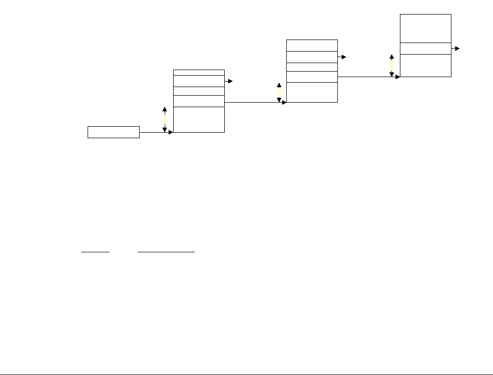
D5 The AArch64 Virtual Memory System Architecture
D5.2 The VMSAv8-64 address translation system
D5-1722 Copyright © 2013 ARM Limited. All rights reserved. ARM DDI 0487A.a
Non-Confidential - Beta ID090413
• The memory attributes for the target memory region, as described in Memory types and attributes on
page B2-89. For more information about how the translation table descriptors specify these attributes see
Memory region attributes on page D5-1788.
• The access permissions for the target memory regions. For more information about how the translation table
descriptors specify these permissions see Memory access control on page D5-1781.
The translation table walk starts with a read of the translation table for the initial lookup. The TTBR for the stage
of translation holds the base address of this table. Each translation table lookup returns a descriptor, that indicates
one of the following:
• The entry is the final entry of the walk. In this case, the entry contains the OA, and the permissions and
attributes for the access.
• An additional level of lookup is required. In this case, the entry contains the translation table base address for
that lookup. In addition:
— The descriptor provides hierarchical attributes that are applied to the final translation, see Hierarchical
control of Secure or Non-secure memory accesses on page D5-1780 and Hierarchical control of data
access permissions on page D5-1783.
— If the translation is in a Secure translation regime, the descriptor indicates whether that base address
is in the Secure or Non-secure address space, unless a hierarchical control at a previous level of lookup
has indicated that it must be in the Non-secure address space.
• The descriptor is invalid. In this case, the memory access generates a Translation fault.
Figure D5-6 gives a generalized view of a single stage of address translation, where three levels of lookup are
required.
Figure D5-6 Generalized view of a stage of address translation
A translation table lookup from VMSAv8-64 performs a single-copy atomic 64-bit access to the translation table
entry. This means the translation table entry is treated as a 64-bit object for the purpose of endianness. SCTLR.EE
determines the endianness of the translation table lookups.
Note
Dynamically changing translation table endianness
Because any change to an SCTLR.EE, bit requires synchronization before it is visible to subsequent
operations, ARM strongly recommends that any EE bit is changed only when either:
• Executing at an Exception level that does not use the translation tables affected by the EE bit
being changed.
• Executing with address translation disabled for any stage of translation affected by the EE bit
being changed.
TTBR
First-level table
Memory
page
D_Block Memory
region
D_Table
Third-level table
D_Page
Second-level table
D_Block Memory
region
D_Table
a
a
a
a Indexed by bits from the input address.
Each lookup level resolves additional bits.
D_Block is a Block descriptor
D_Page is a Page descriptor
D_Table is a Table descriptor

D5 The AArch64 Virtual Memory System Architecture
D5.2 The VMSAv8-64 address translation system
ARM DDI 0487A.a Copyright © 2013 ARM Limited. All rights reserved. D5-1723
ID090413 Non-Confidential - Beta
Address translation stages are disabled by setting an SCTLR.M bit to 0. See the appropriate register
description for more information.
The appropriate TTBR holds the output address of the base of the translation table used for the initial lookup, and:
• For all address translation stages other than Non-secure EL1&0 stage 1 translations, the output address held
in the TTBR, and any translation table base address returned by a translation table descriptor, is the PA of the
base of the translation table.
• For Non-secure EL1&0 stage 1 translations, the output address held in the TTBR, and any translation table
base address returned by a translation table descriptor, is the IPA of the base of the translation table. This
means that if stage 2 address translation is enabled, each of these OAs is subject to second stage translation.
Note
TLB caching can be used to minimise the number of translation table lookups that must be performed.
Because each stage 1 OA generated during a translation table walk is subject to a stage 2 translation, if the
caching of translation table entries is ineffective, a VA to PA address translation with two stages of translation
can give rise to multiple translation table lookups. The number of lookups required is given by the following
equation:
(S1+1)*(S2+1) - 1
Where, for the Non-secure EL1&0 translation regime, S1 is the number of levels of lookup required for at
stage 1translation, and S2 is the number of levels of lookup required for a stage 2 translation.
The TTBR also determines the memory cacheability and shareability attributes that apply, for that stage of
translation, to all translation table lookups generated by that stage of translation.
The Normal memory type is the memory type defined for a translation table lookup for a stage of translation.
Note
• In a two stage translation system, a translation table lookup from stage 1, that has the Normal memory type
defined at stage 1 by this rule, can still be given the Device memory type as part of the stage 2 translation of
that address. ARM strongly recommends against such a remapping of the memory type, and the architecture
includes a trap of this behavior to EL2. For more information, see Stage 2 fault on a stage 1 translation table
walk on page D5-1801.
• The rules about mismatched attributes given in Mismatched memory attributes on page B2-98 apply to the
relationship between translation table walks and explicit memory accesses to the translation tables in the
same way that they apply to the relationship between different explicit memory accesses to the same location.
For this reason, ARM strongly recommends that the attributes that the TTBR applies to the translation tables
are the same as the attributes that are applied for explicit accesses to the memory that holds the translation
tables.
For more information see Overview of the VMSAv8-64 address translation stages on page D5-1724.
See alsoSelection between TTBR0 and TTBR1 on page D5-1736.
Security state of translation table lookups
For a Non-secure translation regime, all translation table lookups are performed to Non-secure output addresses.
For a Secure translation regimes, the initial translation table lookup is performed to a Secure output address.
If the translation table descriptor returned as a result of that initial lookup points to a second translation table, then
the NSTable bit in that descriptor determines whether that translation table lookup is made to Secure or to
Non-secure output addresses.
This applies for all subsequent translation table lookups as part of that translation table walk, with the additional
rule that any translation table descriptor that is returned from Non-secure memory is treated as if the NSTable bit in
that descriptor indicates that the subsequent translation table lookup is to Non-secure memory.

D5 The AArch64 Virtual Memory System Architecture
D5.2 The VMSAv8-64 address translation system
D5-1724 Copyright © 2013 ARM Limited. All rights reserved. ARM DDI 0487A.a
Non-Confidential - Beta ID090413
Control of translation table walks
For the first stage of the EL1&0 translation regime, the TCR_EL1.{EPD0, EPD1} bits determine whether the
translation tables for that regime are valid. EPD0 indicates whether the table that TTBR0_EL1 points to is valid,
and EPD1 indicates whether the table that TTBR1_EL1 points to is valid. The effect of these bits is:
EPDn== 0 The translation table is valid, and can be used for a translation table lookup.
EPDn== 1 If a TLB miss occurs based on TTBRn, a Translation fault is returned, and no translation table walk
is performed. The fault is reported at the level of the initial lookup, for example:
• If translation starts with a zero-level lookup then the fault is a Zero level fault.
• If translation starts with a first-level lookup then the fault is a First level fault.
D5.2.5 Overview of the VMSAv8-64 address translation stages
As shown in Memory translation granule size on page D5-1716, the granule size determines significant aspects of
the address translation process. Effect of granule size on translation table addressing and indexing on page D5-1719
shows, for each granule size:
• How the required input address range determines the required initial lookup levels.
• For stage 2 translations, the possible effect described in Concatenated translation tables on page D5-1720.
• The TTBR addressing and indexing for the initial lookup.
The following subsections summarize the multiple levels of lookup that can be required for a single stage of address
translation that might require the maximum number of lookups:
•Overview of VMSAv8-64 address translation using the 4KB translation granule.
•Overview of VMSAv8-64 address translation using the 16KB translation granule on page D5-1727.
•Overview of VMSAv8-64 address translation using the 64KB translation granule on page D5-1731.
Overview of VMSAv8-64 address translation using the 4KB translation granule
The requirements for the level of the initial lookup are different for stage 1 and stage 2 translations.
Overview of stage 1 translations, 4KB granule
For a stage 1 translation, the required initial lookup level is determined only by the required input address range
specified by the corresponding TCR.TxSZ field. When using the 4KB translation granule, Table D5-8 shows this
requirement.
These configuration options are also permitted for stage 2 translations.
Note
• When using the 4KB translation granule, the initial lookup cannot be at the third level.
• Some bits of the IA do not require resolution by the translation table lookup, because they always map
directly to the OA, When using the 4KB translation granule, IA[11:0] = OA[11:0] for all translations.
Table D5-8 TCR.TnSZ values and IA ranges when there is no concatenation of translation tables
Initial lookup level TnSZ values for and input address rangesa for starting at this level
a. The IAs show the address bits to be resolved when addressing a page of memory, see the Note that follows.
TnSZmin IAmax TnSZmax IAmin
Zero 16 IA[47:12] 24 IA[39:12]
First 25 IA[38:12] 33 IA[30:12]
Second 34 IA[29:12] 39 IA[24:12]

D5 The AArch64 Virtual Memory System Architecture
D5.2 The VMSAv8-64 address translation system
ARM DDI 0487A.a Copyright © 2013 ARM Limited. All rights reserved. D5-1725
ID090413 Non-Confidential - Beta
Figure D5-7 shows the stage 1 address translation, for an address translation using the 4KB granule with an input
address size greater than 39 bits.
Figure D5-7 General view of VMSAv8-64 stage 1 address translation, 4KB granule
Overview of stage 2 translations, 4KB granule
For a stage 2 translation, up to 16 translation tables can be concatenated at the initial lookup level. For certain input
address sizes, concatenating tables in this way means that the lookup starts at a lower level than would otherwise be
the case. For more information see Concatenated translation tables for the initial stage 2 lookup on page D5-1737.
When using the 4KB translation granule, Table D5-9 shows all possibilities for the initial lookup for a stage 2
translation.
TTBR
Zero-level table
D_Table
First-level table
4KB
memory
page
D_Block 1GB
region
D_Table
Third-level table
D_Page
Second-level table
D_Block 2MB
region
D_Table
a
b
c
d
a Indexed by IA[n:39], where IA width is (n+1) bits
b Indexed by IA[38:30]
c Indexed by IA[29:21]
d Indexed by IA[20:12]
D_Block is a Block descriptor
D_Page is a Page descriptor
D_Table is a Table descriptor
Table D5-9 VTCR_EL2.T0SZ values and IA ranges, including cases where translation tables are concatenated
Tablesa124816
Initial
lookup
level
T0SZ values and input address rangesb for starting at this level
T0SZ IA T0SZ IA T0SZ IA T0SZ IA T0SZ IA
Zero 16-
24 IA[47:12]-
IA[39:12] -- -- -- ---
First 25-
33 IA[38:12]-
IA[30:12] 24 IA[39:12] 23 IA[40:12] 22 IA[41:12] 20 IA[42:12]
Second 34-
39 IA[29:12]-
IA[24:12] 33 IA[30:12] 32 IA[31:12] 31 IA[32:12] 30 IA[33:12]
a. Number of concatenated translation tables at the initial lookup level. 1 table corresponds to no concatenation, see Table D5-8 on
page D5-1724.
b. The IAs shown in the table indicate the address bits to be resolved by an address translation addressing a page of memory, see the Note
that follows.

D5 The AArch64 Virtual Memory System Architecture
D5.2 The VMSAv8-64 address translation system
D5-1726 Copyright © 2013 ARM Limited. All rights reserved. ARM DDI 0487A.a
Non-Confidential - Beta ID090413
Note
• When using the 4KB translation granule, the initial lookup cannot be at the third level.
• Because concatenating translation tables reduces the number of levels of lookup required, when using the
4KB translation granule, tables cannot be concatenated at the zero level.
• Some bits of the IA do not require resolution by the translation table lookup, because they always map
directly to the OA. When using the 4KB translation granule, IA[11:0] = OA[11:0] for all translations.
In addition, VTCR_EL2.SL0 indicates the required initial lookup level, as Table D5-10 shows.
Because the maximum number of concatenated translation tables is 16, there is a relationship between the permitted
VTCR_EL2.{T0SZ, SL0} values. If, when a translation table walk is started, the T0SZ value is not consistent with
the SL0 value, a stage 2 level zero translation fault is generated.
Figure D5-8 on page D5-1727 shows the stage 2 address translation, for an input address size of between 40 and 43
bits. This means the lookup can start at either the zero-level or the first-level.
Table D5-10 VTCR_EL2.SL0 values, 4KB granule
Initial lookup level VTCR_EL2.SL0
Zero
0b10
First
0b01
Second
0b00
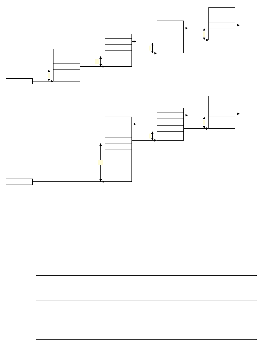
D5 The AArch64 Virtual Memory System Architecture
D5.2 The VMSAv8-64 address translation system
ARM DDI 0487A.a Copyright © 2013 ARM Limited. All rights reserved. D5-1727
ID090413 Non-Confidential - Beta
Figure D5-8 General view of VMSAv8-64 stage 2 address translation, 4KB granule
Overview of VMSAv8-64 address translation using the 16KB translation granule
The requirements for the level of the initial lookup are different for stage 1 and stage 2 translations.
Overview of stage 1 translations, 16KB granule
For a stage 1 translation, the required initial lookup level is determined only by the required input address range
specified by the corresponding TCR.TxSZ field. When using the 4KB translation granule, Table D5-8 on
page D5-1724 shows this requirement.
VTTBR_EL2
Zero-level table
D_Table
First-level table
Second-level table
VTCR_EL2.SL0 defines the start level.
D_Table
D_Block 1GB
region
D_Block 2MB
region
D_Table
Starting at zero level
Third-level table
4KB
memory
page
D_Page
a
b1
c
d
Up to 16 concatenated
tables at the initial level
D_Table
First-level table
Third-level table
D_Table
D_Block 1GB
region
4KB
memory
page
D_Page
VTTBR_EL2
Starting at first level
Second-level table
D_Block 2MB
region
D_Table
a Indexed by IA[n:39], where IA width is (n+1) bits
b1 Indexed by IA[38:30]
c Indexed by IA[29:21]
d Indexed by IA[20:12]
b2 Indexed by IA[n:30], where IA width is (n+1) bits
b2
c
d
D_Block is a Block descriptor
D_Page is a Page descriptor
D_Table is a Table descriptor
Table D5-11 TCR.TnSZ values and IA ranges when there is no concatenation of translation tables
Initial lookup level TnSZ values for and input address rangesa for starting at this level
TnSZmin IAmax TnSZmax IAmin
Zero 16 IA[47:14] - -
First 17 IA[46:14] 27 IA[36:14]
Second 28 IA[35:14] 38 IA[25:14]
Third 39 IA[24:14] - -
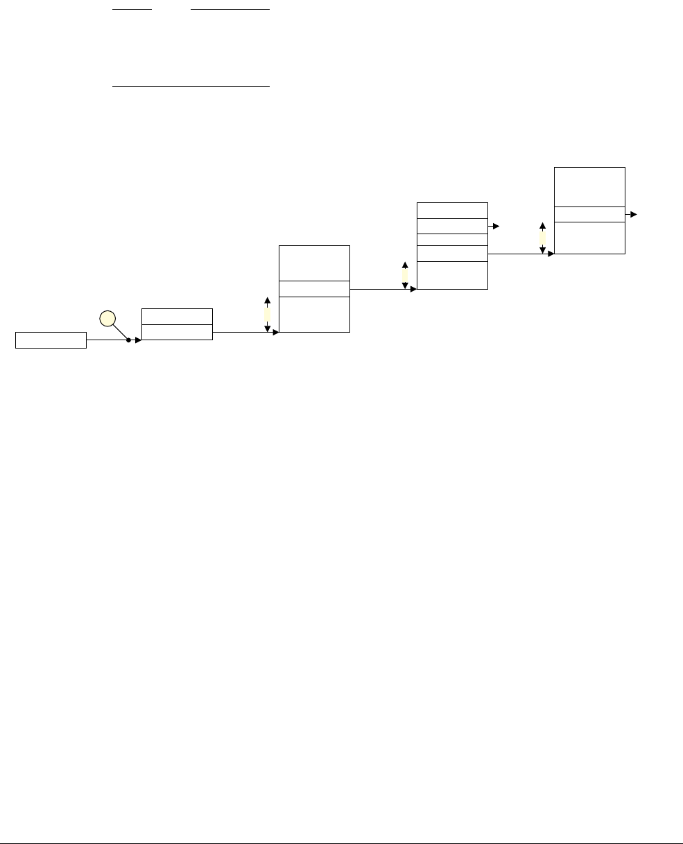
D5 The AArch64 Virtual Memory System Architecture
D5.2 The VMSAv8-64 address translation system
D5-1728 Copyright © 2013 ARM Limited. All rights reserved. ARM DDI 0487A.a
Non-Confidential - Beta ID090413
The configuration options for an initial lookup at the first, second, or third level are also permitted for stage 2
translations, but stage 2 translation does not permit an initial lookup at level zero.
Note
• When using the 16KB translation granule, a maximum of 1 bit of IA is resolved by a level 0 lookup.
• Some bits of the IA do not require resolution by the translation table lookup, because they always map
directly to the OA, When using the 16KB translation granule, IA[13:0] = OA[13:0] for all translations.
Figure D5-9 shows the stage 1 address translation, for an address translation using the 16KB granule with an input
address size of 48 bits.
Figure D5-9 General view of VMSAv8-64 stage 1 address translation, 16KB granule
Overview of stage 2 translations, 16KB granule
For a stage 2 translation, up to 16 translation tables can be concatenated at the initial lookup level. For certain input
address sizes, concatenating tables in this way means that the lookup starts at a lower level than would otherwise be
the case. For more information see Concatenated translation tables for the initial stage 2 lookup on page D5-1737.
When using the 16KB granule, for a stage 2 translation with an input address sized of 48 bits, the initial lookup must
be at level 1, with two concatenated translation tables at this level.
a. The IAs show the address bits to be resolved when addressing a page of memory, see the Note that follows.
TTBR
Zero-level table
D_Table
First-level table
16KB
memory
page
D_Table
Third-level table
D_Page
Second-level table
D_Block 32MB
region
D_Table
b
c
d
a Indexed by IA[47]
b Indexed by IA[46:36]
c Indexed by IA[35:25]
d Indexed by IA[24:14]
D_Block is a Block descriptor
D_Page is a Page descriptor
D_Table is a Table descriptor
a
Table has
only 2 entries

D5 The AArch64 Virtual Memory System Architecture
D5.2 The VMSAv8-64 address translation system
ARM DDI 0487A.a Copyright © 2013 ARM Limited. All rights reserved. D5-1729
ID090413 Non-Confidential - Beta
When using the 4KB translation granule, Table D5-9 on page D5-1725 shows all possibilities for the initial lookup
for a stage 2 translation.
Note
• When using the 16KB translation granule for a stage 2 translation, the initial lookup cannot be at the zero
level. When a 48-bit input address is required, translation must start with first level lookup using two
concatenated translation tables.
• Some bits of the IA do not require resolution by the translation table lookup, because they always map
directly to the OA. When using the 16KB translation granule, IA[13:0] = OA[13:0] for all translations.
In addition, VTCR_EL2.SL0 indicates the required initial lookup level, as Table D5-10 on page D5-1726 shows.
Because the maximum number of concatenated translation tables is 16, there is a relationship between the permitted
VTCR_EL2.{T0SZ, SL0} values. If, when a translation table walk is started, the T0SZ value is not consistent with
the SL0 value, a stage 2 level zero translation fault is generated.
Table D5-12 VTCR_EL2.T0SZ values and IA ranges, including cases where translation tables are concatenated
Tablesa124816
Initial
lookup
level
T0SZ values and input address rangesb for starting at this level
T0SZ IA T0SZ IA T0SZ IA T0SZ IA T0SZ IA
First 17-
27 IA[46:14]-
IA[36:14] 16 IA[47:14] - - - - - -
Second 28-
38 IA[35:14]-
IA[25:14] 27 IA[36:14] 26 IA[37:14] 25 IA[38:14] 24 IA[39:14]
Third 39 IA[24:14] 38 IA[25:14] 37 IA[26:14] 36 IA[27:14] 35 IA[28:14]
a. Number of concatenated translation tables at the initial lookup level. 1 table corresponds to no concatenation, see Table D5-8 on
page D5-1724.
b. The IAs shown in the table indicate the address bits to be resolved by an address translation addressing a page of memory, see the Note
that follows.
Table D5-13 VTCR_EL2.SL0 values, 16KB granule
Initial lookup level VTCR_EL2.SL0
First
0b10
Second
0b01
Third
0b00
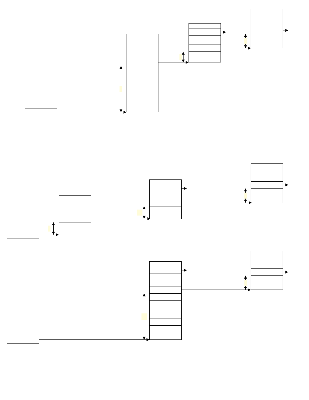
D5 The AArch64 Virtual Memory System Architecture
D5.2 The VMSAv8-64 address translation system
D5-1730 Copyright © 2013 ARM Limited. All rights reserved. ARM DDI 0487A.a
Non-Confidential - Beta ID090413
When stage 2 translation supports a 48-bit input address range, translation must start with a first level lookup using
two concatenated translation tables. Figure D5-10 shows the translation for this case.
Figure D5-10 VMSAv8-64 stage 2 address translation, 16KB granule, 48 bit input address
However, for an input address size of between 37 and 40 bits, Table D5-12 on page D5-1729 shows that translation
can start with either a first level lookup or a second level lookup, and Figure D5-11 shows these options.
Figure D5-11 General view of VMSAv8-64 stage 2 address translation, 16KB granule
Two concatenated
tables at the initial level
D_Table
First-level table
Third-level table
D_Table
16KB
memory
page
D_Page
VTTBR_EL2
Starting at first level
Second-level table
D_Block 32MB
region
D_Table
b Indexed by IA[47:36]
c Indexed by IA[35:25]
d Indexed by IA[24:14]
b
c
d
D_Block is a Block descriptor
D_Page is a Page descriptor
D_Table is a Table descriptor
VTTBR_EL2
First-level table
Second-level table
VTCR_EL2.SL0 defines the start level.
D_Table
D_Block 32MB
region
D_Table
Starting at first level
Third-level table
16KB
memory
page
D_Page
a
b1
c
Up to 16 concatenated
tables at the initial level
D_Table
Third-level table
D_Table
D_Block 16KB
memory
page
D_Page
VTTBR_EL2
Starting at second level 32MB
region
a Indexed by IA[n:36], where IA width is (n+1) bits
b1 Indexed by IA[35:25]
c Indexed by IA[24:14]
b2 Indexed by IA[n:25], where IA width is (n+1) bits
b2
c
D_Block is a Block descriptor
D_Page is a Page descriptor
D_Table is a Table descriptor
Second-level table
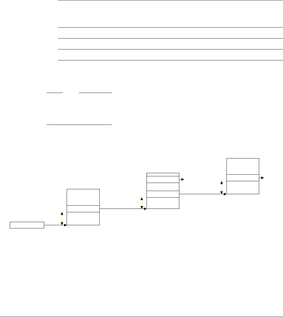
D5 The AArch64 Virtual Memory System Architecture
D5.2 The VMSAv8-64 address translation system
ARM DDI 0487A.a Copyright © 2013 ARM Limited. All rights reserved. D5-1731
ID090413 Non-Confidential - Beta
Overview of VMSAv8-64 address translation using the 64KB translation granule
The requirements for the level of the initial lookup are different for stage 1 and stage 2 translations.
Overview of stage 1 translations, 64KB granule
For a stage 1 translation, the required initial lookup level is determined only by the required input address range
specified by the corresponding TCR.TxSZ field. When using the 64KB translation granule, Table D5-14 shows this
requirement.
These configuration options are also permitted for stage 2 translations.
Note
• When using the 64KB translation granule, there are no zero-level lookups.
• Some bits of the IA do not require resolution by the translation table lookup, because they always map
directly to the OA. When using the 64KB translation granule, IA[15:0] = OA[15:0] for all translations.
Figure D5-12 shows the stage 1 address translation, for an address translation using the 64KB granule with a an
input address size greater than 42 bits.
Figure D5-12 General view of VMSAv8-64 stage 1 address translation, 64KB granule
Table D5-14 TCR.TnSZ values and IA ranges when there is no concatenation of translation tables
Lookup level TnSZ values for and input address rangesa for starting at this level
a. The IAs show the address bits to be resolved when addressing a page of memory, see the Note that follows.
TnSZmin IAmax TnSZmax IAmin
First 16 IA[47:16] 21 IA[42:16]
Second 22 IA[41:16] 34 IA[29:16]
Third 35 IA[28:16] 39 IA[24:16]
TTBR
First-level table
D_Table
Second-level table
64KB
page
D_Block 512MB
region
D_Table
Third-level table
D_Page
a
b
c
a Indexed by IA[n:42], where IA width is (n+1) bits
b Indexed by IA[41:29]
c Indexed by IA[28:16]
D_Block is a Block descriptor
D_Page is a Page descriptor
D_Table is a Table descriptor

D5 The AArch64 Virtual Memory System Architecture
D5.2 The VMSAv8-64 address translation system
D5-1732 Copyright © 2013 ARM Limited. All rights reserved. ARM DDI 0487A.a
Non-Confidential - Beta ID090413
Overview of stage 2 translations, 64KB granule
For a stage 2 translation, up to 16 translation tables can be concatenated at the initial lookup level. For certain input
address sizes, concatenating tables in this way means that the lookup starts at a lower level than would otherwise be
the case. For more information see Concatenated translation tables for the initial stage 2 lookup on page D5-1737.
When using the 64KB translation granule, Table D5-15 shows all possibilities for the initial lookup for a stage 2
translation.
Note
• When using the 64KB translation granule, there are no zero-level lookups.
• Because concatenating translation tables reduces the number of levels of lookup required, when using the
64KB translation granule, tables cannot be concatenated at the first level.
• Some bits of the IA do not require resolution by the translation table lookup, because they always map
directly to the OA. When using the 64KB translation granule, IA[15:0] = OA[15:0] for all translations.
VTCR_EL2.SL0 indicates the required initial lookup level, as Table D5-16 shows.
Because the maximum number of concatenated translation tables is 16, there is a relationship between the permitted
VTCR_EL2.{T0SZ, SL0} values. If, when a translation table walk is started, the T0SZ value is not consistent with
the SL0 value, a stage 2 level zero translation fault is generated.
Table D5-15 VTCR_EL2.T0SZ values and IA ranges when translation tables are concatenated
Tables a124816
Initial
lookup
level
T0SZ values and input address rangesb for starting at this level
T0SZ IA T0SZ IA T0SZ IA T0SZ IA T0SZ IA
First 16-
21 IA[47:16]-
IA[42:16] -- -- -- --
Second 22-
34 IA[41:16]-
IA[29:16] 21 IA[42:16] 20 IA[43:16] 19 IA[44:16] 18 IA[45:16]
Third 35-
39 IA[28:16]-
IA[24:16] 34 IA[29:16] 33 IA[30:16] 32 IA[31:16] 31 IA[32:16]
a. Number of concatenated translation tables at the initial lookup level. 1 table corresponds to no concatenation, see Table D5-14 on
page D5-1731.
b. The IAs shown in the table indicate the address bits to be resolved by an address translation addressing a page of memory, see the
Note that follows.
Table D5-16 VTCR_EL2.SL0 values, 64K granule
Initial lookup level VTCR_EL2.SL0
First
0b10
Second
0b01
Third
0b00
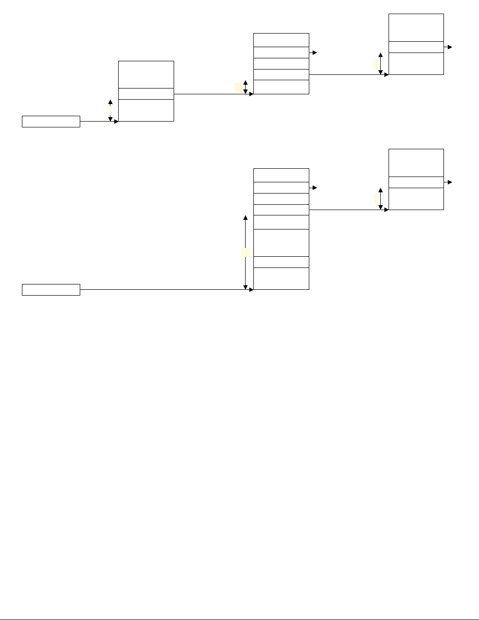
D5 The AArch64 Virtual Memory System Architecture
D5.2 The VMSAv8-64 address translation system
ARM DDI 0487A.a Copyright © 2013 ARM Limited. All rights reserved. D5-1733
ID090413 Non-Confidential - Beta
Figure D5-13 shows the stage 2 address translation, for an input address size of between 43 and 46 bits. This means
the lookup can start at either the first-level or the second-level.
Figure D5-13 General view of VMSAv8-64 stage 2 address translation, 64KB granule
D5.2.6 The VMSAv8-64 translation table format
This section provides the full description of the VMSAv8-64 translation table format, its use for address translations
that are controlled by an Exception level using AArch64.
For the address translations that are controlled by an Exception level that is using AArch64:
• The TCR_EL1.{SH0, ORGN0, IRGN0, SH1, ORGN1, IRGN1} fields define memory region attributes for
the translation table walk, for each of TTBR0_EL1 and TTBR1_EL1.
• For the Secure and Non-secure EL1&0 stage 1 translations, each of TTBR0_EL1 and TTBR1_EL1 contains
an ASID field, and the TCR_EL1.A1 field selects which ASID to use.
For this translation table format, Overview of the VMSAv8-64 address translation stages on page D5-1724
summarizes the lookup levels, and Descriptor encodings, ARMv8 zero-level, first-level, and second-level formats
on page D5-1773 describes the translation table entries.
The following subsections describe the use of this translation table format:
•Translation granule size and associate block and page sizes on page D5-1734.
•Selection between TTBR0 and TTBR1 on page D5-1736.
•Concatenated translation tables for the initial stage 2 lookup on page D5-1737.
•Possible translation table registers programming errors on page D5-1738.
VTTBR_EL2
First-level table
D_Table
Second-level table
VTCR_EL2.SL0 defines the start level.
Starting at first level
D_Block 512MB
region
D_Table
64KB
page
Third-level table
D_Page
D_Table
VTTBR_EL2
Starting at second level
Second-level table
D_Block 512MB
region
D_Table
64KB
page
Third-level table
D_Page
Up to 16 concatenated
tables at the initial level
a
b1
a Indexed by IA[n:42],
where IA width is (n+1) bits
b1 Indexed by IA[41:29]
b2 Indexed by IA[n:29],
where IA width is (n+1) bits
b2
c
c
c Indexed by IA[28:16]
D_Block is a Block descriptor
D_Page is a Page descriptor
D_Table is a Table descriptor

D5 The AArch64 Virtual Memory System Architecture
D5.2 The VMSAv8-64 address translation system
D5-1734 Copyright © 2013 ARM Limited. All rights reserved. ARM DDI 0487A.a
Non-Confidential - Beta ID090413
Translation granule size and associate block and page sizes
Table D5-17 shows the supported granule sizes, block sizes and page sizes, for the different granule sizes. For
completeness, this table includes information for AArch32 state. In the table, the OA bit ranges are the OA bits that
the translation table descriptor specifies to address the block or page of memory, in an implementation that supports
a 48-bit OA range.
Bit[1] of a translation table descriptor identifies whether the descriptor is a block descriptor, and:
• The 4KB granule size supports block descriptors only in first level and second level translation tables.
• The 16KB and 64KB granule sizes support block descriptors only in second level translation tables,
Setting bit[1] of a descriptor to 1 in a translation table that does not support block descriptors gives a Translation
fault.
For translations managed from AArch64 state, the following tables expand the information for each granule size,
showing for each lookup level and when accessing a single translation table:
• The maximum IA size, and the address bits that are resolved for that maximum size.
• The maximum OA range resolved by the translation table descriptors at this level, and the corresponding
memory region size.
• The maximum size of the translation table. This is the size required for the maximum IA size.
Table D5-18 shows this information for the 4KB translation granule size, Table D5-19 on page D5-1735 shows this
information for the 16KB translation granule size, and Table D5-20 on page D5-1735 shows this information for
the 64KB translation granule size.
Table D5-17 Translation table granule sizes, with block and page sizes, and output address
ranges
Granule size Table level Block size and OA bit range Page size and OA bit range
4KB Zero - -
First 1GB, OA[47:30] -
Second 2MB, OA[47:21] -
Third - 4KB, OA[47:12]
16KB Zero - -
First - -
Second 32MB, OA[47:25] -
Third - 16KB, OA[47:14]
64KB First - -
Second 512MB, OA[47:29] -
Third - 64KB, OA[47:16]
Table D5-18 Properties of the address lookup levels, 4KB granule size
Level Maximum input address Maximum output address Number
of entries Block entries
supported?
Size Address range Address range Size of addressed regiona
Zero 256TB Address[47:39] Address[47:39] 512GB Up to 512 No
First 512GB Address[38:30] Address[47:30] 1GB Up to 512 Yes

D5 The AArch64 Virtual Memory System Architecture
D5.2 The VMSAv8-64 address translation system
ARM DDI 0487A.a Copyright © 2013 ARM Limited. All rights reserved. D5-1735
ID090413 Non-Confidential - Beta
For the initial lookup level:
• If the IA range specified by the TCR.TxSZ field is smaller than the maximum size shown in these table then
this reduces the number of addresses in the table and therefore reduces the table size. The smaller translation
table is aligned to its table size.
• For stage 2 translations, multiple translation tables can be concatenated to extend the maximum IA size
beyond that shown in these tables. For more information see the stage 2 translation overviews in Overview
of the VMSAv8-64 address translation stages on page D5-1724 and Concatenated translation tables for the
initial stage 2 lookup on page D5-1737.
If a supplied input address is larger than the configured input address size, a Translation fault is generated.
Note
Larger translation granule sizes typically requires fewer levels of translation tables to translate a particular size of
virtual address.
Second 1GB Address[29:21] Address[47:21] 2MB Up to 512 Yes
Third 2MB Address[20:12] Address[47:12] 4KB 512 Page only
a. That is, the size of the region either addressed by descriptors at this level or to be resolved at this and the subsequent levels of lookup.
Table D5-19 Properties of the address lookup levels, 16KB granule size
Level Maximum input address Maximum output address Number
of entries Block entries
supported?
Size Address range Address range Size of addressed regiona
Zero 256TB Address[47] Address[47] 128TB 2bNo
First 128TB Address[46:36] Address[47:36] 64GB Up to 2048 No
Second 64GB Address[35:25] Address[47:25] 32MB Up to 2048 Yes
Third 32MB Address[24:14] Address[47:14] 16KB 2048 Page only
a. That is, the size of the region either addressed by descriptors at this level or to be resolved at this and the subsequent levels of lookup.
b. The translation table size is less than the maximum for this granule size, and therefore the number of entries is reduced.
Table D5-20 Properties of the address lookup levels, 64KB granule size
Level Maximum input address Maximum output address Number
of entries Block entries
supported?
Size Address range Address range Size of addressed regiona
First 256TB Address[47:42] Address[47:42] 4TB Up to 64bNo
Second 4TB Address[41:29] Address[47:29] 512MB Up to 8192 Yes
Third 512MB Address[28:16] Address[47:16] 64KB 8192 Page only
a. That is, the size of the region either addressed by descriptors at this level or to be resolved at this and the subsequent levels of lookup.
b. The translation table size is less than the maximum for this granule size, and therefore the number of entries is reduced.
Table D5-18 Properties of the address lookup levels, 4KB granule size (continued)
Level Maximum input address Maximum output address Number
of entries Block entries
supported?
Size Address range Address range Size of addressed regiona
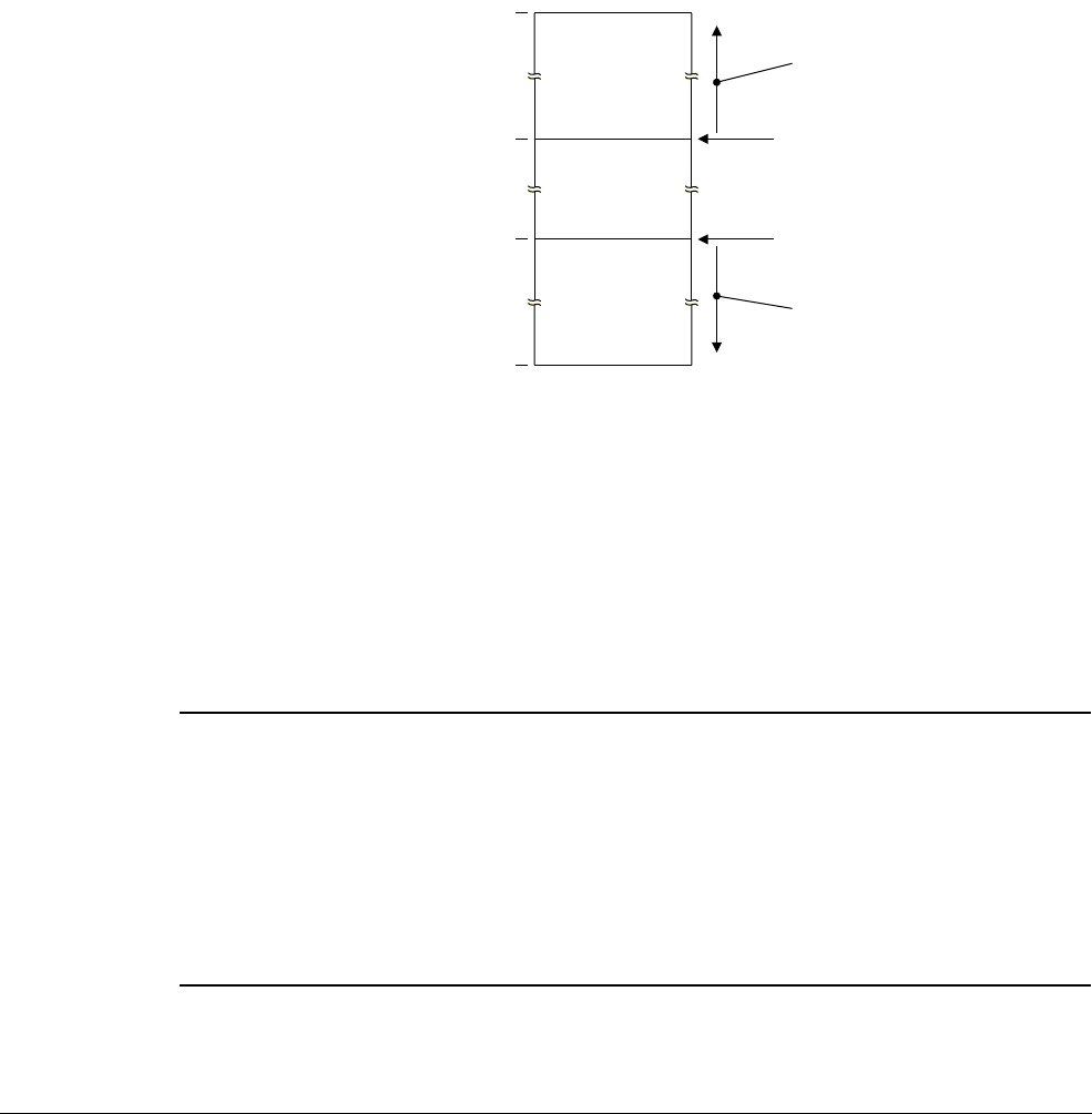
D5 The AArch64 Virtual Memory System Architecture
D5.2 The VMSAv8-64 address translation system
D5-1736 Copyright © 2013 ARM Limited. All rights reserved. ARM DDI 0487A.a
Non-Confidential - Beta ID090413
For the TCR programming requirements for the initial lookup, see Overview of the VMSAv8-64 address translation
stages on page D5-1724.
Selection between TTBR0 and TTBR1
Every translation table walk starts by accessing the translation table addressed by the TTBR for the stage 1
translation for the required translation regime.
For the EL1&0 translation regime, the VA range is split into two subranges as shown in Figure D5-14, and:
•TTBR0_EL1 points to the initial translation table for the lower VA subrange, that starts at address
0x0000_0000_0000_0000
,
•TTBR1_EL1 points to the initial translation table for the upper VA subrange, that runs up to address
0xFFFF_FFFF_FFFF_FFFF
.
Figure D5-14 AArch64 TTBR boundaries and VA ranges
Which TTBR is used depends only on the VA presented for translation:
• If the top bits of the VA are zero, then TTBR0_EL1 is used.
• If the top bits of the VA are one, then TTBR1_EL1 is used.
It is configurable whether this determination depends on the values of VA[63:56] or on the values of VA[63:48],
see Address tagging in AArch64 state on page D5-1708.
Example D5-3 shows a typical application of this VA split.
Example D5-3 Example use of the split VA range, and the TTBR0_EL1 and TTBR1_EL1 controls
An example of using the split VA range is:
TTBR0_EL1 Used for process-specific addresses.
Each process maintains a separate first-level translation table. On a context switch:
•TTBR0_EL1 is updated to point to the first-level translation table for the new context
•TCR_EL1 is updated if this change changes the size of the translation table
•CONTEXTIDR_EL1 is updated.
TTBR1_EL1 Used for operating system and I/O addresses, that do not change on a context switch.
For each VA subrange, the input address size is 2(64-TnSZ), where TnSZ is one of TCR_EL1.{T0SZ, T1SZ},
0x0000_0000_0000_0000
0xFFFF_FFFF_FFFF_FFFF
0xFFFF_0000_0000_0000
0x0000_FFFF_FFFF_FFFF Boundary, when TCR_EL1.T0SZ==16
TTBR1_EL1
region
TTBR0_EL1
region
Accesses
generate a
Translation fault
Boundary, when TCR_EL1.T1SZ==16
Effect of increasing TCR_EL1.T1SZ
Effect of increasing TCR_EL1.T0SZ

D5 The AArch64 Virtual Memory System Architecture
D5.2 The VMSAv8-64 address translation system
ARM DDI 0487A.a Copyright © 2013 ARM Limited. All rights reserved. D5-1737
ID090413 Non-Confidential - Beta
This means the two VA subranges are:
Lower VA subrange
0x0000_0000_0000_0000
to (2(64-T0SZ) - 1).
Upper VA subrange (264 - 2(64-T1SZ)) to
0xFFFF_FFFF_FFFF_FFFF
.
The minimum TnSZ value is 16, corresponding to the maximum input address range of 48 bits. Example D5-4
shows the two VA subranges when T0SZ and T1SZ are both set to this minimum value.
Example D5-4 Maximum VA ranges for EL1&0 stage 1 translations
The maximum VA subranges correspond to T0SZ and T1SZ each having the minimum value of 16. In this case the
subranges are:
Lower VA subrange
0x0000_0000_0000_0000
to
0x0000_FFFF_FFFF_FFFF
.
Upper VA subrange
0xFFFF_0000_0000_0000
to
0xFFFF_FFFF_FFFF_FFFF
.
Figure D5-14 on page D5-1736 indicates the effect of varying the TnSZ values.
As described in Overview of the VMSAv8-64 address translation stages on page D5-1724, the TnSZ values also
determine the initial lookup level for the translation.
Concatenated translation tables for the initial stage 2 lookup
Overview of the VMSAv8-64 address translation stages on page D5-1724 introduced the ability to concatenate
translation tables for the initial stage 2 translation lookup. This section gives more information about that
concatenation.
Where a stage 2 translation would require 16 entries or fewer in its top-level translation table, the system designer
can instead:
• Require the corresponding number of concatenated translation tables at the next translation level, aligned to
the size of the block of concatenated translation tables.
• Start the translation at that next translation level.
In addition, when using the 16KB translation granule and requiring a 48-bit input address size for the stage 2
translations, lookup must start with two concatenated translation tables at the first level.
Note
This translation scheme:
• Avoids the overhead of an additional level of translation.
• Requires the software that is defining the translation to:
— Define the concatenated translation tables with the required overall alignment.
—Program VTTBR_EL2 to hold the address of the first of the concatenated translation tables.
—Program VTCR_EL2 to indicate the required input address range and initial lookup level.
Concatenating additional translation tables at the initial level of look up resolves additional address bits at that level.
To resolve n additional address bits requires 2n concatenated translation tables. Example D5-5 on page D5-1738
shows how, for first level lookups using the 4KB translation granule, translation tables can be concatenated to
resolve three additional address bits.

D5 The AArch64 Virtual Memory System Architecture
D5.2 The VMSAv8-64 address translation system
D5-1738 Copyright © 2013 ARM Limited. All rights reserved. ARM DDI 0487A.a
Non-Confidential - Beta ID090413
Example D5-5 Adding three bits of address resolution at first level lookup, using the 4KB granule
When using the 4KB translation granule, a first level lookup with a single translation table resolves address
bits[38:30]. To add three more address bits requires 23 translation tables, that is, eight translation tables. This means:
• The total size of the concatenated translation tables is 8×4KB=32KB.
• This block of concatenated translation tables must be aligned to 32KB.
• The address range resolved at this lookup level is A[41:30].of which:
— Bits A[41:38] select the 4KB translation table.
— Bits A[38:30] index a descriptor within that translation table.
As an example of the concatenation of translation tables at the initial lookup level, when using the 4KB translation
granule, Table D5-21 shows the possible uses of concatenated translation tables to permit lookup to start at the first
level rather than at the zero level. For completeness, the table starts with the case where the required IPA range
means lookup starts at the first level with a single translation table at that level.
Note
Because concatenation is permitted only for a stage 2 translation, the input addresses in the table are IPAs.
Overview of the VMSAv8-64 address translation stages on page D5-1724 identifies all of the possible uses of
concatenation. In all cases, the block of concatenated translation tables must be aligned to the block size.
Possible translation table registers programming errors
For a stage 2 translation, the programming of the VTCR_EL2.{T0SZ, SL0} fields must be consistent, see Overview
of the VMSAv8-64 address translation stages on page D5-1724.
Where the contiguous bit is used to mark a set of blocks as contiguous, if the address range translated by a set of
blocks marked as contiguous is larger than the size of the input address supported at a stage of translation used to
translate that address at that stage of translation, as defined by the TCR.TxSZ field, then this is a programming error.
An implementation is permitted, but not required, to:
• Treat such a block within a contiguous set of blocks as causing a Translation fault, even though the block is
valid, and the address accessed within that block is within the size of the input address supported at a stage
of translation, as defined by the TCR.TxSZ field.
Table D5-21 Possible uses of concatenated translation tables for first-level lookup, 4KB granule
Configured stage 2
IA size Lookup starts at zero level Lookup starts at first level
IPA range Size Required zero-level entries Number of concatenated tables Required alignmenta
IPA[38:0] 236 bytes - 1 4KB
IPA[39:0] 237 bytes 2 2 8KB
IPA[40:0] 238 bytes 4 4 16KB
IPA[41:0] 239 bytes 8 8 32KB
IPA[42:0] 240 bytes 16 16 64KB
a. Required alignment of the set of concatenated second-level tables.

D5 The AArch64 Virtual Memory System Architecture
D5.2 The VMSAv8-64 address translation system
ARM DDI 0487A.a Copyright © 2013 ARM Limited. All rights reserved. D5-1739
ID090413 Non-Confidential - Beta
• Treat such a block within a contiguous set of blocks as not causing a Translation fault, even though the
address accessed within that block is outside the size of the input address supported at a stage of translation,
as defined by the TCR.TxSZ field, provided that both of the following apply:
— The block is valid.
— At least one address within the block, or contiguous set of blocks, is within the size of the input address
supported at a stage of translation.
The contiguous bit must apply:
• When using the 4KB translation granule, to 16 adjacent translation table entries, aligned so that the upper
five bits of the input address range required to index the table entries are all the same.
• When using the 16KB translation granule, to:
— 128 adjacent translation table entries, aligned so that the upper four bits of the input address range
required to index the table entries are all the same, for entries in a level three translation table.
— 32 adjacent translation table entries, aligned so that the upper six bits of the input address range
required to index the table entries are all the same, for entries in a level two translation table.
• When using the 64KB translation granule, to 32 adjacent translation table entries, aligned so that the upper
eight bits of the input address range required to index the table entries are all the same.
For more information about the contiguous bit see The Contiguous bit on page D5-1792.
D5.2.7 The algorithm for finding the translation table entries
This subsection gives the algorithms for finding the translation table entry that corresponds to a given IA, for each
required level of lookup. The algorithms encode the descriptions of address translation given earlier in this section.
The algorithm details depend on the translation granule size for the stage of address translation, see:
•Finding the translation table entry when using the 4KB translation granule on page D5-1740.
•Finding the translation table entry when using the 16KB translation granule on page D5-1741.
•Finding the translation table descriptor when using the 64KB translation granule on page D5-1742.
Each subsection uses the following terms:
BaseAddress The base address for the level of lookup, as defined by:
• For the initial lookup level, the appropriate TTBR.
• Otherwise, the translation table address returned by the previous level of lookup.
PAMax The supported PA width, in bits.
IA The supplied IA for this stage of translation.
TnSZ The translation table size for this stage of translation:
For EL1&0 stage 1 TCR_EL1.T0SZ or TCR_EL1.T1SZ, as appropriate.
For EL1&0 stage 2 VTCR_EL2.T0SZ.
For EL2 stage 1 TCR_EL2.T0SZ.
For EL3 stage 1 TCR_EL3.T0SZ.
SL0 VTCR_EL2.SL0. Applies to the Non-secure EL1&0 stage 2 translation only.
These subsections show only architecturally-valid programming of the TCR. See also Possible translation table
registers programming errors on page D5-1738.

D5 The AArch64 Virtual Memory System Architecture
D5.2 The VMSAv8-64 address translation system
D5-1740 Copyright © 2013 ARM Limited. All rights reserved. ARM DDI 0487A.a
Non-Confidential - Beta ID090413
Finding the translation table entry when using the 4KB translation granule
Table D5-22 shows the translation table descriptor address, for each level of lookup, when using the 4KB translation
granule. See the start of The algorithm for finding the translation table entries on page D5-1739 for more
information about terms used in the table.
Identifying support for the 4KB granule
The ID_AA64MMFR0_EL1.4Kgranule identifies whether an implementation supports the 4KB translation
granule, as follows:
0b0000 4KB granule size supported.
0b1111 4KB granule size not supported.
Table D5-22 Translation table entry addresses when using the 4KB translation granule
Lookup
level
Entry address and conditions General conditions
Stage 1 translation Stage 2 translation
Zero BaseAddr[PAMax-1:x]:IA[y:39]:
0b000
ifa 16 ≤ TnSZ ≤ 24 then x = (28 - TnSZ)
BaseAddr[PAMax-1:x]:IA[y:39]:
0b000
if SL0b == 2 then
ifa 16 ≤ T0SZ ≤ 24 then x = (28 - T0SZ)
if TnSZ < 16 then x = 12
y = (x + 35)
First BaseAddr[PAMax-1:x]:IA[y:30]:
0b000
ifa 25 ≤ TnSZ ≤ 33 then x = (37 - TnSZ)
elsec x =12
BaseAddr[PAMax-1:x]:IA[y:30]:
0b000
if SL0b == 1 then
ifa 21 ≤ T0SZ ≤ 33 then x = (37 - T0SZ)
elsif SL0b == 2 then x = 12
y = (x + 26)
Second BaseAddr[PAMax-1:x]:IA[y:30]:
0b000
ifa 34 ≤ TnSZ ≤ 39 then x = (46 - TnSZ)
elsif 39 < TnSZ then x = 7
elsec x =12
BaseAddr[PAMax-1:x]:IA[y:30]:
0b000
if SL0b == 0 then
ifa 30 ≤ T0SZ ≤ 39 then x = (46 - T0SZ)
elsif 39 < T0SZ then x = 7
elsif 0 < SL0b then x = 12
y = (x + 17)
Third BaseAddr[PAMax-1:12]:IA[20:30]:
0b000
BaseAddr[PAMax-1:12]:IA[20:30]:
0b000
-
a. This line indicates the range of permitted values for TnSZ, for a lookup that starts at this level.
b. SL0 == 0 if the initial lookup is second level, SL0 == 1 if the initial lookup is first level, and SL0 ==2 if the initial lookup level is zero level.
c. This is the case where this level of lookup is not the initial level of lookup.

D5 The AArch64 Virtual Memory System Architecture
D5.2 The VMSAv8-64 address translation system
ARM DDI 0487A.a Copyright © 2013 ARM Limited. All rights reserved. D5-1741
ID090413 Non-Confidential - Beta
Finding the translation table entry when using the 16KB translation granule
Table D5-22 on page D5-1740 shows the translation table descriptor address, for each level of lookup, when using
the 16KB translation granule. See the start of The algorithm for finding the translation table entries on
page D5-1739 for more information about terms used in the table.
Identifying support for the 16KB granule
The ID_AA64MMFR0_EL1.16Kgranule identifies whether an implementation supports the 4KB translation
granule, as follows:
0b0000 16KB granule size not supported.
0b0001 16KB granule size supported.
Table D5-23 Translation table entry addresses when using the 16KB translation granule
Lookup
level
Entry address and conditions General conditions
Stage 1 translation Stage 2 translation
Zero BaseAddr[PAMax-1:4]:IA[47]:
0b000
a 16 ≤ TnSZ
- Only applies to stage 1
First BaseAddr[PAMax-1:x]:IA[y:36]:
0b000
ifa 17 ≤ TnSZ ≤ 27 then x = (31 - TnSZ)
elseb x =14
BaseAddr[PAMax-1:x]:IA[y:36]:
0b000
if SL0c == 2 then
ifa T0SZ ≤ 27 then x = (31 - T0SZ)
y = (x + 32)
Second BaseAddr[PAMax-1:x]:IA[y:25]:
0b000
ifa 28 ≤ TnSZ ≤ 38 then x = (42 - TnSZ)
elseb x =14
BaseAddr[PAMax-1:x]:IA[y:25]:
0b000
if SL0c == 1 then
ifa 24 ≤ T0SZ ≤ 38 then x = (42 - T0SZ)
elsif 39 < T0SZ then x = 7
elsif SL0c == 2 then x = 14
y = (x + 21)
Third BaseAddr[PAMax-1:14]:IA[24:14]:
0b000
BaseAddr[PAMax-1:14]:IA[y:14]:
0b000
if SL0c == 0 then
ifa 35 ≤ T0SZ ≤ 39 then x = (53 - T0SZ)
elsif SL0c >0 then x = 14
y = (x + 10)
a. This line indicates the range of permitted values for TnSZ, for a lookup that starts at this level.
b. This is the case where this level of lookup is not the initial level of lookup.
c. SL0 == 0 if the initial lookup is third level, SL0 == 1 if the initial lookup is second level, and SL0 ==2 if the initial lookup level is first level.

D5 The AArch64 Virtual Memory System Architecture
D5.2 The VMSAv8-64 address translation system
D5-1742 Copyright © 2013 ARM Limited. All rights reserved. ARM DDI 0487A.a
Non-Confidential - Beta ID090413
Finding the translation table descriptor when using the 64KB translation granule
Table D5-24 shows the translation table descriptor address, for each level of lookup, when using the 64KB
translation granule. See the start of The algorithm for finding the translation table entries on page D5-1739 for more
information about terms used in the table.
Identifying support for the 64KB granule
The ID_AA64MMFR0_EL1.64Kgranule identifies whether an implementation supports the 4KB translation
granule, as follows:
0b0000 64KB granule size supported.
0b1111 64KB granule size not supported.
Table D5-24 Translation table entry addresses when using the 64KB translation granule
Lookup
level
Entry address and conditions General conditions
Stage 1 translation Stage 2 translation
First BaseAddr[PAMax-1:x]:IA[y:42]:
0b000
ifa 16 ≤ TnSZ ≤ 21 then x = (25 - TnSZ)
elsif TnSZ < 16 then x = 9
BaseAddr[PAMax-1:x]:IA[y:42]:
0b000
if SL0b == 2 then
ifa 16 ≤ T0SZ ≤ 21 then x = (25 - T0SZ)
elsif TnSZ < 16 then x = 9
y = (x + 38)
Second BaseAddr[PAMax-1:x]:IA[y:29]:
0b000
ifa 22 ≤ TnSZ ≤ 34 then x = (38 - TnSZ)
elsec x =16
BaseAddr[PAMax-1:x]:IA[y:29]:
0b000
if SL0b == 1 then
ifa 18 ≤ T0SZ ≤ 34 then x = (38 - T0SZ)
elsif SL0b == 2 then x = 16
y = (x + 25)
Third BaseAddr[PAMax-1:x]:IA[y:16]:
0b000
ifa 35 ≤ TnSZ ≤ 39 then x = (51 - TnSZ)
elsif 39 < TnSZ then x = 12
elsec x =16
BaseAddr[PAMax-1:x]:IA[y:16]:
0b000
if SL0b == 0 then
ifa 31 ≤ T0SZ ≤ 39 then x = (51 - T0SZ)
elsif 39 < T0SZ then x = 12
elsif 0 < SL0b then x = 16
y = (x + 12)
a. This line indicates the range of permitted values for TnSZ, for a lookup that starts at this level.
b. SL0 == 0 if the initial lookup is third level, SL0 == 1 if the initial lookup is second level, and SL0 ==2 if the initial lookup level is first level.
c. This is the case where this level of lookup is not the initial level of lookup.

D5 The AArch64 Virtual Memory System Architecture
D5.2 The VMSAv8-64 address translation system
ARM DDI 0487A.a Copyright © 2013 ARM Limited. All rights reserved. D5-1743
ID090413 Non-Confidential - Beta
D5.2.8 The effects of disabling a stage of address translation
The following sections describe the effect on MMU behavior of disabling each stage of translation:
•Behavior when stage 1 address translation is disabled
•Behavior when stage 2 address translation is disabled on page D5-1744
•Behavior of instruction fetches when all associated stages of translation are disabled on page D5-1744.
Behavior when stage 1 address translation is disabled
When a stage 1 address translation is disabled, memory accesses that would otherwise be translated by that stage of
translation are treated as follows:
Non-secure EL1 and EL0 accesses if the HCR_EL2.DC bit is set to 1
For the Non-secure EL1&0 translation regime, when the value of HCR_EL2.DC is 1, the stage 1
translation assigns the Normal Non-shareable, Inner Write-Back Read-Write-Allocate, Outer
Write-Back Read-Write-Allocate memory attributes.
Note
This applies for both instruction and data accesses.
All other accesses
For all other accesses, when stage 1 address translation is disabled, the assigned attributes depend
on whether the access is a data access or an instruction access, as follows:
Data access
The stage 1 translation assigns the Device-nGnRnE memory type.
Instruction access
The stage 1 translation assigns the Normal memory attribute, with the cacheability and
shareability attributes determined by the value of the SCTLR.I bit for the translation
regime, as follows:
When the value of I is 0
The stage 1 translation assigns the Non-cacheable and Outer Shareable
attributes.
When the value of I is 1
The stage 1 translation assigns the Cacheable, Inner Write-Through no
Write-Allocate Read-Allocate, Outer Write-Through no Write-Allocate
Read Allocate Non-shareable attribute.
For this stage of translation, no memory access permission checks are performed, and therefore no MMU faults can
be generated for this stage of address translation.
Note
Alignment checking is performed, and therefore Alignment faults can occur.
For every access, the input address of the stage 1 translation is flat-mapped to the output address.
For a Non-secure EL1 or EL0 access, if EL1&0 stage 2 address translation is enabled, the stage 1 memory attribute
assignments and output address can be modified by the stage 2 translation.
When the value of HCR_EL2.DC is 1, in Non-secure state:
• The SCTLR_EL1.M bit behaves as if it is 0, for all purposes other than reading the value of the bit. This
means Non-secure EL1&0 stage 1 address translation is disabled.
• The HCR_EL2.VM bit behaves as if it is 1, for all purposes other than reading the value of the bit. This means
that Non-secure EL1&0 stage 2 address translation is enabled.
See also Behavior of instruction fetches when all associated stages of translation are disabled on page D5-1744.

D5 The AArch64 Virtual Memory System Architecture
D5.2 The VMSAv8-64 address translation system
D5-1744 Copyright © 2013 ARM Limited. All rights reserved. ARM DDI 0487A.a
Non-Confidential - Beta ID090413
Effect of disabling address translation on maintenance and address translation operations
Cache maintenance instructions act on the target cache regardless of whether any stages of address translation are
disabled, and regardless of the values of the memory attributes. However, if a stage of address translation is disabled,
they use the flat address mapping for that translation stage.
TLB invalidate operations act on the target TLB regardless of whether any stage of address translation is disabled.
The value of HCR_EL2.DC affect some address translation instructions, see Address translation instructions, AT*
on page D5-1757.
Behavior when stage 2 address translation is disabled
When stage 2 address translation is disabled:
• The IPA output from the stage 1 translation maps flat to the PA.
• The memory attributes and permissions from the stage 1 translation apply to the PA.
When both stages of address translation are disabled, see also Behavior of instruction fetches when all associated
stages of translation are disabled.
Behavior of instruction fetches when all associated stages of translation are disabled
When EL3 is using AArch64, this section applies to:
• The Secure EL1&0 translation regime when Secure EL1&0 stage 1 address translation is disabled.
• The Secure EL3 translation regime, when Secure EL3 stage 1 address translation is disabled.
• The Non-secure EL2 translation regime, when Non-secure EL2 stage 1 address translation is disabled
• The Non-secure EL1&0 translation regime, when both stages of address translation are disabled.
Note
• The behaviors in Non-secure state apply regardless of the Execution state that EL3 is using.
• When the value of HCR_EL2.DC is 1, then the behavior of the Non-secure EL1&0 translation regime is as
if stage 1 translation is disabled and stage 2 translation is enabled, as described in Behavior when stage 1
address translation is disabled on page D5-1743.
In these cases, a memory location might be accessed as a result of an instruction fetch if one of the following
conditions is met:
• The memory location is in the same block of memory, of the translation granule size, as an instruction that a
simple sequential execution of the program requires to be fetched, or is in the block of memory of the
translation granule size immediately following such a block.
• The memory location is in the same block of memory of the translation granule size from which a simple
sequential execution of the program with all associated stages of address translation disabled has previously
required an instruction to be fetched, or is in the block of the translation granule size immediately following
such a block.
Each block of memory referred to in this section must be aligned to the translation granule size. These accesses can
be caused by speculative instruction fetches, regardless of whether the prefetched instruction is committed for
execution.

D5 The AArch64 Virtual Memory System Architecture
D5.2 The VMSAv8-64 address translation system
ARM DDI 0487A.a Copyright © 2013 ARM Limited. All rights reserved. D5-1745
ID090413 Non-Confidential - Beta
Note
To ensure architectural compliance, software must ensure that both of the following apply:
• Instructions that will be executed when all associated stages of address translation are disabled are located in
blocks of the address space, of the translation granule size, that contain only memory that is tolerant to
speculative accesses.
• Each block of the address space, of the translation granule size, that immediately follows a similar block that
holds instructions that will be executed when all associated stages address translation are disabled, contains
only memory that is tolerant to speculative accesses.
D5.2.9 The implemented Exception levels and the resulting translation stages and regimes
Elsewhere, this chapter describes an implementation that includes all Exception levels, and describes the control of
address translation by Exception levels that are using AArch64. This subsection describes how the address
translation scheme changes if an implementation does not include all of the Exception levels.
If an implementation does not include EL3, it has only a single Security state, with MMU controls equivalent to the
Secure state MMU controls.
If an implementation does not include EL2 then:
• If it also does not include EL3, the MMU provides only a single EL1&0 stage 1 translation regime.
• If it includes EL3, the MMU provides an EL1&0 stage 1 translation regime in each Security state.
Figure D5-2 on page D5-1711 shows the set of translation regimes for an implementation that implements all of the
Exception levels. Table D5-25 shows how the supported translation stages depend on the implemented Exception
levels, and in some cases on the Execution state being used by the highest implemented Exception level:
D5.2.10 Pseudocode details of VMSAv8-64 address translation
The following subsections gives a pseudocode description of the translation table walk:
•Definitions required for address translation on page D5-1746.
•Performing the full address translation on page D5-1746.
•Stage 1 translation on page D5-1746.
•Stage 2 translation on page D5-1748.
•Translation table walk on page D5-1749.
•Support functions on page D5-1754.
Table D5-25 The relation between the implemented translation stages and Exception levels for AArch64
Translation stage Requires
Secure EL3 stage 1 EL3 implemented and using AArch64.
Secure EL1&0 stage 1 Either:
• EL3 implemented and using AArch64.
• Only EL1 and EL0 implemented, all operation is in Secure state, and EL1 is using AArch64.
Non-secure EL2 stage 1 EL2 implemented.
Non-secure EL1&0 stage 2 EL2 implemented.
Non-secure EL1&0 stage 1 Any implementation except:
• Only EL1 and EL0 implemented, with all operation in the Secure state.

D5 The AArch64 Virtual Memory System Architecture
D5.2 The VMSAv8-64 address translation system
D5-1746 Copyright © 2013 ARM Limited. All rights reserved. ARM DDI 0487A.a
Non-Confidential - Beta ID090413
Definitions required for address translation
In pseudocode, the result of a translation table lookup, in either Execution state, is returned in a
TLBRecord
structure.
type TLBRecord is (
Permissions perms,
bit nG, // ‘0’ = Global, ‘1’ = not Global
bits(4) domain, // AArch32 only
boolean contiguous, // Contiguous bit from page table
integer level, // In AArch32 Short-descriptort format, indicates Section/Page
integer blocksize, // Describes size of memory translated in KBytes
AddressDescriptor addrdesc
)
Memory data type definitions on page D4-1697 includes definitions of the
Permissions
and
AddressDescriptor
parameters.
Performing the full address translation
The function
AArch64.FullTranslate()
performs a full translation table walk. For any translation regime it performs
a stage 1 translation for the supplied virtual address, and for the Non-secure EL1&0 translation regime it then
performs a stage 2 translation of the returned address.
// AArch64.FullTranslate()
// =======================
// This function is called to perform both stage 1 and stage 2 translation walks for the current
// translation regime. The function used by Address Translation operations is similar except it uses
// the translation regime specified for the instruction.
AddressDescriptor AArch64.FullTranslate(bits(64) vaddress, AccType acctype, boolean iswrite,
boolean wasaligned, integer size)
// First Stage Translation
S1 = AArch64.FirstStageTranslate(vaddress, acctype, iswrite, wasaligned, size);
if !IsFault(S1) && HaveEL(EL2) && !IsSecure() && PSTATE.EL != EL2 then
s2fs1walk = FALSE;
result = AArch64.SecondStageTranslate(S1, vaddress, acctype, iswrite, wasaligned, s2fs1walk,
size);
else
result = S1;
return result;
Stage 1 translation
The function
AArch64.FirstStageTranslate()
performs a stage 1 translation, calling the function
AArch64.TranslationTableWalk()
, described in Translation table walk on page D5-1749, to perform the required
translation table walk. However, if stage 1 translation is disabled, it calls the function
AArch64.TranslateAddressS1Off()
, described in this section, to set the memory attributes.
// AArch64.FirstStageTranslate()
// =============================
// This function is called to perform a stage 1 translation walk. If necessary,
// it calls SecondStageTranslate to perform the stage 2 translation walk.
// The function used by Address Translation operations is similar except it uses
// the translation regime specified for the instruction.
AddressDescriptor AArch64.FirstStageTranslate(bits(64) vaddress, AccType acctype, boolean iswrite,
boolean wasaligned, integer size)
s1_enabled = SCTLR[].M == ‘1’;
ipaddress = bits(48) UNKNOWN;
secondstage = FALSE;
s2fs1walk = FALSE;

D5 The AArch64 Virtual Memory System Architecture
D5.2 The VMSAv8-64 address translation system
ARM DDI 0487A.a Copyright © 2013 ARM Limited. All rights reserved. D5-1747
ID090413 Non-Confidential - Beta
boolean permissioncheck = TRUE; // By default, permissions will need to be checked
if s1_enabled then // First stage enabled
S1 = AArch64.TranslationTableWalk(ipaddress, vaddress, acctype, iswrite, secondstage,
s2fs1walk, size);
else
S1 = AArch64.TranslateAddressS1Off(vaddress, acctype, iswrite);
permissioncheck = FALSE;
// Check for unaligned data accesses to Device memory
if (!wasaligned && !IsFault(S1.addrdesc) && S1.addrdesc.memattrs.type == MemType_Device &&
acctype != AccType_IFETCH) then
S1.addrdesc.fault = AArch64.AlignmentFault(acctype, iswrite, secondstage);
if !IsFault(S1.addrdesc) && permissioncheck then
S1.addrdesc.fault = AArch64.CheckPermission(S1.perms, vaddress, S1.level,
S1.addrdesc.paddress.NS,
acctype, iswrite);
// Check for instruction fetches from Device memory not marked as execute-never. If there has
// not been a Permission Fault then the memory is not marked execute-never.
if (!IsFault(S1.addrdesc) && S1.addrdesc.memattrs.type == MemType_Device &&
acctype == AccType_IFETCH) then
S1.addrdesc = AArch64.InstructionDevice(S1.addrdesc, vaddress, ipaddress, S1.level,
acctype, iswrite,
secondstage, s2fs1walk);
return S1.addrdesc;
When stage 1 translation is disabled, the function
AArch64.TranslateAddressS1Off()
sets the memory attributes.
// AArch64.TranslateAddressS1Off()
// ===============================
// Called for stage 1 translations when translation is disabled to supply a default translation.
// Note that there are additional constraints on instruction prefetching that are not described in
// this pseudocode.
TLBRecord AArch64.TranslateAddressS1Off(bits(64) vaddress, AccType acctype, boolean iswrite)
assert !ELUsingAArch32(TranslationRegime());
TLBRecord result;
Top = AddrTop(vaddress);
if !IsZero(vaddress<Top:PAMax()>) then
level = 0;
ipaddress = bits(48) UNKNOWN;
secondstage = FALSE;
s2fs1walk = FALSE;
result.addrdesc.fault = AArch64.AddressSizeFault(ipaddress, level, acctype,
iswrite, secondstage, s2fs1walk);
return result;
if HaveEL(EL2) && !IsSecure() && PSTATE.EL != EL2 && HCR_EL2.DC == ‘1’ then
// Use default cacheable settings
result.addrdesc.memattrs.type = MemType_Normal;
result.addrdesc.memattrs.device = DeviceType UNKNOWN;
result.addrdesc.memattrs.inner.attrs = MemAttr_WB; // Write-back
result.addrdesc.memattrs.inner.hints = MemHint_RWA;
result.addrdesc.memattrs.shareable = FALSE;
result.addrdesc.memattrs.outershareable = FALSE;
if HCR_EL2.VM != ‘1’ then UNPREDICTABLE;
elsif acctype != AccType_IFETCH then
// Treat data as Device
result.addrdesc.memattrs.type = MemType_Device;
result.addrdesc.memattrs.device = DeviceType_nGnRnE;
result.addrdesc.memattrs.inner = MemAttrHints UNKNOWN;
result.addrdesc.memattrs.shareable = TRUE;

D5 The AArch64 Virtual Memory System Architecture
D5.2 The VMSAv8-64 address translation system
D5-1748 Copyright © 2013 ARM Limited. All rights reserved. ARM DDI 0487A.a
Non-Confidential - Beta ID090413
result.addrdesc.memattrs.outershareable = TRUE;
else
// Instruction cacheability controlled by SCTLR_ELx.I
cacheable = SCTLR[].I == ‘1’;
result.addrdesc.memattrs.type = MemType_Normal;
result.addrdesc.memattrs.device = DeviceType UNKNOWN;
if cacheable then
result.addrdesc.memattrs.inner.attrs = MemAttr_WT;
result.addrdesc.memattrs.inner.hints = MemHint_RA;
else
result.addrdesc.memattrs.inner.attrs = MemAttr_NC;
result.addrdesc.memattrs.inner.hints = MemHint_No;
result.addrdesc.memattrs.shareable = TRUE;
result.addrdesc.memattrs.outershareable = TRUE;
result.addrdesc.memattrs.outer = result.addrdesc.memattrs.inner;
result.perms.ap = bits(3) UNKNOWN;
result.perms.xn = ‘0’;
result.perms.pxn = ‘0’;
result.nG = bit UNKNOWN;
result.contiguous = boolean UNKNOWN;
result.domain = bits(4) UNKNOWN;
result.level = integer UNKNOWN;
result.blocksize = integer UNKNOWN;
result.addrdesc.paddress.physicaladdress = vaddress<47:0>;
result.addrdesc.paddress.NS = if IsSecure() then ‘0’ else ‘1’;
result.addrdesc.fault = AArch64.NoFault();
return result;
Stage 2 translation
In the Non-secure EL1&0 translation regime, a descriptor address returned by stage 1 lookup is in the IPA address
space, and must be mapped to a PA by a stage 2 translation. Function
AArch64.SecondStageWalk()
performs this
translation, by calling the
AArch64.SecondStageTranslate()
function.
// AArch64.SecondStageWalk()
// =========================
// This function is called from a stage 1 translation table walk when
// the accesses generated from that requires a second stage of translation
AddressDescriptor AArch64.SecondStageWalk(AddressDescriptor S1, bits(64) vaddress, AccType acctype,
integer size)
assert HaveEL(EL2) && !IsSecure() && PSTATE.EL != EL2;
iswrite = FALSE;
s2fs1walk = TRUE;
wasaligned = TRUE;
return AArch64.SecondStageTranslate(S1, vaddress, acctype, iswrite, wasaligned, s2fs1walk,
size);
The
AArch64.SecondStageTranslate()
function performs the stage 2 address translation.
// AArch64.SecondStageTranslate()
// ==============================
// This function is called to perform a stage 2 translation walk.
AddressDescriptor AArch64.SecondStageTranslate(AddressDescriptor S1, bits(64) vaddress,
AccType acctype, boolean iswrite, boolean wasaligned,
boolean s2fs1walk, integer size)
assert HaveEL(EL2) && !IsSecure() && PSTATE.EL != EL2;
s2_enabled = HCR_EL2.VM == ‘1’;
secondstage = TRUE;

D5 The AArch64 Virtual Memory System Architecture
D5.2 The VMSAv8-64 address translation system
ARM DDI 0487A.a Copyright © 2013 ARM Limited. All rights reserved. D5-1749
ID090413 Non-Confidential - Beta
if s2_enabled then // Second stage enabled
ipaddress = S1.paddress.physicaladdress<47:0>;
S2 = AArch64.TranslationTableWalk(ipaddress, vaddress, acctype, iswrite, secondstage,
s2fs1walk, size);
// Check for unaligned data accesses to Device memory
if (!wasaligned && !IsFault(S2.addrdesc) && S2.addrdesc.memattrs.type == MemType_Device &&
acctype != AccType_IFETCH) then
S2.addrdesc.fault = AArch64.AlignmentFault(acctype, iswrite, secondstage);
if !IsFault(S2.addrdesc) then
S2.addrdesc.fault = AArch64.CheckS2Permission(S2.perms, vaddress, ipaddress, S2.level,
acctype, iswrite, s2fs1walk);
// Check for instruction fetches from Device memory not marked as execute-never. As there
// has not been a Permission Fault then the memory is not marked execute-never.
if (!IsFault(S2.addrdesc) && S2.addrdesc.memattrs.type == MemType_Device &&
acctype == AccType_IFETCH) then
S2.addrdesc = AArch64.InstructionDevice(S2.addrdesc, vaddress, ipaddress, S2.level,
acctype, iswrite,
secondstage, s2fs1walk);
// Check for protected table walk
if (s2fs1walk && !IsFault(S2.addrdesc) && HCR_EL2.PTW == ‘1’ &&
S2.addrdesc.memattrs.type == MemType_Device) then
S2.addrdesc.fault = AArch64.PermissionFault(ipaddress, S2.level, acctype,
iswrite, secondstage, s2fs1walk);
result = CombineS1S2Desc(S1, S2.addrdesc);
else
result = S1;
return result;
Translation table walk
The function
AArch64.TranslationTableWalk()
returns the result, in the form of a
TLBRecord
, of a translation table
walk made for a memory access from an Exception level that is using AArch64.
// AArch64.TranslationTableWalk()
// ==============================
// Returns a result of a translation table walk
//
// Implementations might cache information from memory in any number of non-coherent TLB
// caching structures, and so avoid memory accesses that have been expressed in this
// pseudocode. The use of such TLBs is not expressed in this pseudocode.
TLBRecord AArch64.TranslationTableWalk(bits(48) ipaddress, bits(64) vaddress,
AccType acctype, boolean iswrite, boolean secondstage,
boolean s2fs1walk, integer size)
if !secondstage then
assert !ELUsingAArch32(TranslationRegime());
else
assert HaveEL(EL2) && !IsSecure() && !ELUsingAArch32(EL2) && PSTATE.EL != EL2;
TLBRecord result;
AddressDescriptor descaddr;
domain = bits(4) UNKNOWN;
baseaddress = Zeros(48);
basefound = FALSE;
bits(64) base;
descaddr.memattrs.type = MemType_Normal;
// Determine parameters for the page table walk:
// grainsize = Log2(Size of Table) - one of 4KB, 16KB or 64KB
// stride = Log2(Address per level)

D5 The AArch64 Virtual Memory System Architecture
D5.2 The VMSAv8-64 address translation system
D5-1750 Copyright © 2013 ARM Limited. All rights reserved. ARM DDI 0487A.a
Non-Confidential - Beta ID090413
// firstblocklevel = first level where a block entry is allowed
// psize = Physical Address size as encoded in TCR_EL1.IPS or TCR_ELx/VTCR_EL2.PS
// tablesize = Log2(Address Size)
// level = level to start walk from
// This means that the number of levels after start level = 3-level
if !secondstage then
// First stage translation
bits(64) inputaddr = ZeroExtend(vaddress);
if PSTATE.EL == EL3 then
tablesize = 64 - UInt(TCR_EL3.T0SZ);
if tablesize > 48 then tablesize = 48;
if tablesize < 25 then tablesize = 25;
largegrain = TCR_EL3.TG0 == ‘01’;
midgrain = TCR_EL3.TG0 == ‘10’;
reversedescriptors = SCTLR_EL3.EE == ‘1’;
psize = TCR_EL3.PS;
top = AddrTop(inputaddr);
basefound = tablesize == 48 || IsZero(inputaddr<top:tablesize>);
base = TTBR0_EL3;
descaddr.memattrs = WalkAttrDecode(TCR_EL3.SH0, TCR_EL3.ORGN0, TCR_EL3.IRGN0);
lookupsecure = TRUE;
singlepriv = TRUE;
elsif PSTATE.EL == EL2 then
tablesize = 64 - UInt(TCR_EL2.T0SZ);
if tablesize > 48 then tablesize = 48;
if tablesize < 25 then tablesize = 25;
largegrain = TCR_EL2.TG0 == ‘01’;
midgrain = TCR_EL2.TG0 == ‘10’;
psize = TCR_EL2.PS;
top = AddrTop(inputaddr);
basefound = tablesize == 48 || IsZero(inputaddr<top:tablesize>);
base = TTBR0_EL2;
descaddr.memattrs = WalkAttrDecode(TCR_EL2.SH0, TCR_EL2.ORGN0, TCR_EL2.IRGN0);
reversedescriptors = SCTLR_EL2.EE == ‘1’;
lookupsecure = FALSE;
singlepriv = TRUE;
else
psize = TCR_EL1.IPS;
top = AddrTop(inputaddr);
if inputaddr<top> == ‘0’ then
tablesize = 64 - UInt(TCR_EL1.T0SZ);
if tablesize > 48 then tablesize = 48;
if tablesize < 25 then tablesize = 25;
largegrain = TCR_EL1.TG0 == ‘01’;
midgrain = TCR_EL1.TG0 == ‘10’;
basefound = IsZero(inputaddr<top:tablesize>) && TCR_EL1.EPD0 == ‘0’;
base = TTBR0_EL1;
descaddr.memattrs = WalkAttrDecode(TCR_EL1.SH0, TCR_EL1.ORGN0, TCR_EL1.IRGN0);
else
tablesize = 64 - UInt(TCR_EL1.T1SZ);
if tablesize > 48 then tablesize = 48;
if tablesize < 25 then tablesize = 25;
largegrain = TCR_EL1.TG1 == ‘11’; // TG1 and TG0 encodings differ
midgrain = TCR_EL1.TG1 == ‘01’;
basefound = IsOnes(inputaddr<top:tablesize>) && TCR_EL1.EPD1 == ‘0’;
base = TTBR1_EL1;
descaddr.memattrs = WalkAttrDecode(TCR_EL1.SH1, TCR_EL1.ORGN1, TCR_EL1.IRGN1);
reversedescriptors = SCTLR_EL1.EE == ‘1’;
lookupsecure = IsSecure();
singlepriv = FALSE;
if largegrain then // 64KB pages
grainsize = 16;
stride = grainsize - 3;
if tablesize > (grainsize + 2*stride) then level = 1;
elsif tablesize > (grainsize + stride) then level = 2;
else level = 3;

D5 The AArch64 Virtual Memory System Architecture
D5.2 The VMSAv8-64 address translation system
ARM DDI 0487A.a Copyright © 2013 ARM Limited. All rights reserved. D5-1751
ID090413 Non-Confidential - Beta
firstblocklevel = 2;
elsif midgrain then // 16KB pages
grainsize = 14;
stride = grainsize - 3;
if tablesize > (grainsize + 3*stride) then level = 0;
elsif tablesize > (grainsize + 2*stride) then level = 1;
elsif tablesize > (grainsize + stride) then level = 2;
else level = 3;
firstblocklevel = 2;
else // Small grain, 4KB pages
grainsize = 12;
stride = grainsize - 3;
if tablesize > (grainsize + 3*stride) then level = 0;
elsif tablesize > (grainsize + 2*stride) then level = 1;
else level = 2;
firstblocklevel = 1;
else
// Second stage translation
bits(64) inputaddr = ZeroExtend(ipaddress);
lookupsecure = FALSE;
singlepriv = TRUE;
tablesize = 64 - UInt(VTCR_EL2.T0SZ);
if tablesize > 48 then tablesize = 48;
if tablesize < 25 then tablesize = 25;
largegrain = VTCR_EL2.TG0 == ‘01’;
midgrain = VTCR_EL2.TG0 == ‘10’;
base = VTTBR_EL2;
basefound = IsZero(inputaddr<63:tablesize>);
descaddr.memattrs = WalkAttrDecode(VTCR_EL2.IRGN0, VTCR_EL2.ORGN0, VTCR_EL2.SH0);
reversedescriptors = SCTLR_EL2.EE == ‘1’;
psize = VTCR_EL2.PS;
startlevel = UInt(VTCR_EL2.SL0);
// Limits on IPA controls based on implemented PA size
if startlevel == 3 then basefound = FALSE;
if midgrain then
if PAMax() < 41 && startlevel == 2 then basefound = FALSE;
else
if PAMax() < 43 && startlevel == 2 then basefound = FALSE;
// force the tablesize not to exceed the PAMax value
if tablesize > PAMax() then tablesize = PAMax();
if largegrain then
grainsize = 16;
stride = grainsize - 3;
level = 3 - startlevel;
firstblocklevel = 2;
elsif midgrain then
grainsize = 14;
stride = grainsize - 3;
level = 3 - startlevel;
firstblocklevel = 2;
else
grainsize = 12;
stride = grainsize - 3;
level = 2 - startlevel;
firstblocklevel = 1;
// Check for Translation Table of fewer than 2 entries or more than 16*(2^grainsize/8)
// entries
// Number entries in start table level =
// (Address Size)/((Address per level)^Num of levels after start + Size of Table)
// Upper bound check is
// (tablesize - stride*(3-level) - grainsize > (grainsize - 3) + 4)
// Lower bound check is
// (tablesize - stride*(3-level) - grainsize < 1

D5 The AArch64 Virtual Memory System Architecture
D5.2 The VMSAv8-64 address translation system
D5-1752 Copyright © 2013 ARM Limited. All rights reserved. ARM DDI 0487A.a
Non-Confidential - Beta ID090413
if ((tablesize > stride*(3-level) + 2*grainsize + 1) ||
(tablesize < stride*(3-level) + grainsize + 1)) then
basefound = FALSE;
if !basefound then
result.addrdesc.fault = AArch64.TranslationFault(ipaddress, 0, acctype, iswrite,
secondstage, s2fs1walk);
return result;
case psize of
when ‘000’ cpamax = 32;
when ‘001’ cpamax = 36;
when ‘010’ cpamax = 40;
when ‘011’ cpamax = 42;
when ‘100’ cpamax = 44;
when ‘101’ cpamax = 48;
otherwise cpamax = 48;
if cpamax > PAMax() then cpamax = PAMax();
if cpamax != 48 && !IsZero(base<47:cpamax>) then
result.addrdesc.fault = AArch64.AddressSizeFault(ipaddress, 0, acctype, iswrite,
secondstage, s2fs1walk);
return result;
// Bottom bound of the Base address is:
// log2(8 bytes per entry)+log2(num of entries in start table level)
// Number of entries in start table level =
// (Address Size)/((Address per level)^Num of levels after start level + Size of Table)
baselowerbound = 3 + tablesize - stride*(3-level) - grainsize;
baseaddress = base<47:baselowerbound>:Zeros(baselowerbound);
ns_table = if lookupsecure then ‘0’ else ‘1’;
ap_table = if singlepriv then ‘10’ else ‘11’;
xn_table = ‘0’;
pxn_table = ‘0’;
addrselecttop = tablesize - 1;
repeat
addrselectbottom = (3-level)*stride + grainsize;
bits(48) index = ZeroExtend(inputaddr<addrselecttop:addrselectbottom>:’000’);
descaddr.paddress.physicaladdress = baseaddress OR index;
descaddr.paddress.NS = ns_table;
// If there are two stages of translation, then the first stage table walk addresses
// are themselves subject to translation
if !HaveEL(EL2) || secondstage || IsSecure() || PSTATE.EL == EL2 then
descaddr2 = descaddr;
else
descaddr2 = AArch64.SecondStageWalk(descaddr, vaddress, acctype, 8);
desc = _Mem[descaddr2, 8, AccType_PTW];
if reversedescriptors then
desc = BigEndianReverse(desc);
// Process descriptor
case desc<1:0> of
when ‘x0’ // Fault or reserved
result.addrdesc.fault = AArch64.TranslationFault(ipaddress,
level, acctype, iswrite,
secondstage, s2fs1walk);
return result;
when ‘01’
if level == 3 then // Invalid at level 3
result.addrdesc.fault = AArch64.TranslationFault(ipaddress,

D5 The AArch64 Virtual Memory System Architecture
D5.2 The VMSAv8-64 address translation system
ARM DDI 0487A.a Copyright © 2013 ARM Limited. All rights reserved. D5-1753
ID090413 Non-Confidential - Beta
level, acctype, iswrite,
secondstage, s2fs1walk);
return result;
else // Block
blocktranslate = TRUE;
when ‘11’
if level != 3 then // Table
if cpamax != 48 && !IsZero(desc<47:cpamax>) then
result.addrdesc.fault = AArch64.AddressSizeFault(ipaddress,
level, acctype,
iswrite, secondstage,
s2fs1walk);
return result;
baseaddress = desc<47:grainsize>:Zeros(grainsize);
if !secondstage then
// Unpack the upper and lower table attributes
// pxn_table and ap_table[0] apply only in EL0&1 translation regimes
ns_table = ns_table AND desc<63>;
ap_table<1> = ap_table<1> AND desc<62>;
xn_table = xn_table OR desc<60>;
if !singlepriv then
ap_table<0> = ap_table<0> AND desc<61>;
pxn_table = pxn_table OR desc<59>;
level = level + 1;
addrselecttop = addrselectbottom - 1;
blocktranslate = FALSE;
else // Page
blocktranslate = TRUE;
until blocktranslate;
// Check block size is supported at this level
if level < firstblocklevel then
result.addrdesc.fault = AArch64.TranslationFault(ipaddress, level, acctype,
iswrite, secondstage, s2fs1walk);
return result;
if cpamax != 48 && !IsZero(desc<47:cpamax>) then
result.addrdesc.fault = AArch64.AddressSizeFault(ipaddress, level, acctype,
iswrite, secondstage, s2fs1walk);
return result;
physicaladdress = desc<47:addrselectbottom>:inputaddr<addrselectbottom-1:0>;
// check for misprogramming of the contiguous bit
if largegrain then
contiguousbitcheck = level == 2 && tablesize < 34;
elsif midgrain then
contiguousbitcheck = level == 2 && tablesize < 38;
else
contiguousbitcheck = level == 1 && tablesize < 34;
if contiguousbitcheck && desc<52> == ‘1’ then
if boolean IMPLEMENTATION_DEFINED “Translation fault on misprogrammed contiguous bit” then
result.addrdesc.fault = AArch64.TranslationFault(ipaddress, level,
acctype, iswrite,
secondstage, s2fs1walk);
return result;
// Check the access flag
if desc<10> == ‘0’ then
result.addrdesc.fault = AArch64.AccessFlagFault(ipaddress, level,
acctype, iswrite,
secondstage, s2fs1walk);
return result;

D5 The AArch64 Virtual Memory System Architecture
D5.2 The VMSAv8-64 address translation system
D5-1754 Copyright © 2013 ARM Limited. All rights reserved. ARM DDI 0487A.a
Non-Confidential - Beta ID090413
// Unpack the upper and lower block attributes
xn = desc<54>;
pxn = desc<53>;
contiguousbit = desc<52>;
nG = desc<11>;
sh = desc<9:8>;
ap = desc<7:6>:’1’;
memattr = desc<5:2>; // AttrIndx and NS bit in stage 1
result.domain = bits(4) UNKNOWN; // Domains not used
result.level = level;
result.blocksize = 2^((3-level)*stride + grainsize);
// Stage 1 translation regimes also inherit attributes from the tables
if !secondstage then
result.perms.xn = xn OR xn_table;
result.perms.ap<2> = ap<2> OR ap_table<1>;
// PXN, nG and AP[1] apply only in EL0&1 stage 1 translation regimes
if !singlepriv then
result.perms.ap<1> = ap<1> OR NOT(ap_table<0>);
result.perms.pxn = pxn OR pxn_table;
// Pages from Non-secure tables are marked Global in Secure EL0&1
if IsSecure() then
result.nG = nG OR ns_table;
else
result.nG = nG;
else
result.perms.ap<1> = ‘1’;
result.perms.pxn = ‘0’;
result.nG = ‘0’;
result.perms.ap<0> = ‘1’;
result.addrdesc.memattrs = AArch64.S1AttrDecode(sh, memattr<2:0>, acctype);
result.addrdesc.paddress.NS = if lookupsecure then (memattr<3> OR ns_table) else ‘1’;
else
result.perms.ap<2:1> = ap<2:1>;
result.perms.ap<0> = ‘1’;
result.perms.xn = xn;
result.perms.pxn = ‘0’;
result.nG = ‘0’;
result.addrdesc.memattrs = S2AttrDecode(sh, memattr, acctype);
result.addrdesc.paddress.NS = ‘1’;
result.addrdesc.paddress.physicaladdress = physicaladdress;
result.addrdesc.fault = AArch64.NoFault();
result.contiguous = contiguousbit == ‘1’;
return result;
Support functions
In the translation table walk functions, the
WalkAttrDecode()
function determines the attributes for a translation table
lookup.
// WalkAttrDecode()
// ================
MemoryAttributes WalkAttrDecode(bits(2) SH, bits(2) ORGN, bits(2) IRGN)
MemoryAttributes memattrs;
AccType acctype = AccType_NORMAL;
memattrs.type = MemType_Normal;
memattrs.device = DeviceType UNKNOWN;
memattrs.inner = ShortConvertAttrsHints(IRGN, acctype);

D5 The AArch64 Virtual Memory System Architecture
D5.2 The VMSAv8-64 address translation system
ARM DDI 0487A.a Copyright © 2013 ARM Limited. All rights reserved. D5-1755
ID090413 Non-Confidential - Beta
memattrs.outer = ShortConvertAttrsHints(ORGN, acctype);
memattrs.shareable = SH<1> == ‘1’;
memattrs.outershareable = SH == ‘10’;
return memattrs;
The function
AArch64.S1AttrDecode()
decodes the attributes from a stage 1 translation table lookup.
// AArch64.S1AttrDecode()
// ======================
// Converts the Stage 1 attribute fields, using the MAIR, to orthogonal
// attributes and hints.
MemoryAttributes AArch64.S1AttrDecode(bits(2) SH, bits(3) attr, AccType acctype)
MemoryAttributes memattrs;
mair = MAIR[];
index = 8 * UInt(attr);
attrfield = mair<index+7:index>;
if ((attrfield<7:4> != ‘0000’ && attrfield<3:0> == ‘0000’) ||
(attrfield<7:4> == ‘0000’ && !(attrfield<3:0> IN {‘000x’, ‘1x00’}))) then
// Reserved, maps to an allocated value
(-, attrfield) = ConstrainUnpredictableBits();
if attrfield<7:4> == ‘0000’ then // Device
memattrs.type = MemType_Device;
memattrs.inner = MemAttrHints UNKNOWN;
memattrs.outer = MemAttrHints UNKNOWN;
memattrs.shareable = TRUE;
memattrs.outershareable = TRUE;
case attrfield<3:0> of
when ‘0000’ memattrs.device = DeviceType_nGnRnE;
when ‘0001’ memattrs.device = DeviceType_nGnRE;
when ‘1000’ memattrs.device = DeviceType_nGRE;
when ‘1100’ memattrs.device = DeviceType_GRE;
otherwise Unreachable(); // Reserved, handled above
elsif attrfield<3:0> != ‘0000’ then // Normal
memattrs.type = MemType_Normal;
memattrs.outer = LongConvertAttrsHints(attrfield<7:4>, acctype);
memattrs.inner = LongConvertAttrsHints(attrfield<3:0>, acctype);
memattrs.device = DeviceType UNKNOWN;
memattrs.shareable = SH<1> == ‘1’;
memattrs.outershareable = SH == ‘10’;
else
Unreachable(); // Reserved, handled above
return memattrs;
The function
AArch64.CheckPermission()
checks the access permissions returned by a stage 1 translation table
lookup, see Access permission checking on page D4-1702.
The function
AArch64.CheckS2Permission()
checks the access permissions returned by a stage 2 translation table
lookup.
// AArch64.CheckS2Permission()
// ===========================
// Function used for permission checking from AArch64 stage 2 translations
FaultRecord AArch64.CheckS2Permission(Permissions perms, bits(64) vaddress, bits(48) ipaddress,
integer level, AccType acctype, boolean iswrite,
boolean s2fs1walk)
assert HaveEL(EL2) && !IsSecure() && !ELUsingAArch32(EL2) && PSTATE.EL != EL2;
r = perms.ap<1> == ‘0’;

D5 The AArch64 Virtual Memory System Architecture
D5.2 The VMSAv8-64 address translation system
D5-1756 Copyright © 2013 ARM Limited. All rights reserved. ARM DDI 0487A.a
Non-Confidential - Beta ID090413
w = perms.ap<2> == ‘0’;
x = perms.xn == ‘0’;
// Stage 1 walk is checked as a read, regardless of the original type
if acctype == AccType_IFETCH && !s2fs1walk then
fail = !x;
elsif iswrite && !s2fs1walk then
fail = !w;
else
fail = !r;
if fail then
domain = bits(4) UNKNOWN;
secondstage = TRUE;
return AArch64.PermissionFault(ipaddress, level, acctype, iswrite, secondstage,
s2fs1walk);
else
return AArch64.NoFault();
The
AddrTop()
function returns the bit number of the most significant valid bit of a VA in the current translation
regime. If EL1 is using AArch64 and EL0 is using AArch32 then an address from EL0 is zero-extended to 64 bits.
integer AddrTop(bits(64) address);
D5.2.11 Address translation operations
Each of the ARMv8 instruction sets provides instructions that return the result of translating an input address,
supplied as an argument to the instruction, using a specified translation stage or regime.
The available instructions only perform translations that are accessible from the Security state and Exception level
at which the instruction is executed. That is:
• No instruction executed in Non-secure state can return the result of a Secure address translation stage.
• No instruction can return the result of an address translation stage that is controlled by an Exception level
that is higher than the Exception level at which the instruction is executed.
Address translation instructions, AT* on page D5-1757 summarizes the A64 address translation instructions.
See also A64 system instructions for address translation on page C4-322.

D5 The AArch64 Virtual Memory System Architecture
D5.2 The VMSAv8-64 address translation system
ARM DDI 0487A.a Copyright © 2013 ARM Limited. All rights reserved. D5-1757
ID090413 Non-Confidential - Beta
Address translation instructions, AT*
The A64 assembly language syntax for address translation instructions is:
AT <operation>, <Xt>
Where:
<operation>
. Is one of
S1E1R
,
S1E1W
,
S1E0R
,
S1E0W
,
S12E1R
,
S12E1W
,
S12E0R
,
S12E0W
,
S1E2R
,
S1E2W
,
S1E3R
, or
S1E3W
.
<operation>
has a structure of
<stages><level><read|write>
, where:
<stages>
. Is one of:
S1
. Stage 1 translation.
S12
. Stage 1 translation followed by stage 2 translation.
<level>
. Describes the Exception Level that the translation applies to. Is one of:
E0
. EL0.
E1
. EL1.
E2
. EL2.
E3
. EL3.
If
<level>
is higher than the current Exception Level the instruction is UNDEFINED.
<read|write>
Is one of:
R
. Read.
W
. Write.
<Xt>
. The address to be translated. No alignment restrictions apply for the address.
If EL2 is not implemented, the
AT S1E2R
and
AT S1E2W
instructions are UNDEFINED.
Note
If EL2 is not implemented but EL3 is implemented, the
AT S12E*
instructions are not UNDEFINED, but behave the
same way as the equivalent
AT S1E*
instructions. This is consistent with the behavior if EL2 is implemented but
stage 2 translation is disabled.
In each case, the address being translated is held in the 64-bit address argument register,
Xt
. If the address translation
instruction uses a translation regime that is using AArch32, meaning it requires a VA of only 32 bits, then
VA[63:32] is RES0.
If the address translation is successful, the resulting PA is returned in PAR_EL1.PA, and PAR_EL1.F is set to 0 to
indicate that the translation was successful. Otherwise, see Synchronous faults generated by address translation
instructions on page D5-1758.
Note
The architecture provides a single PAR, PAR_EL1, that is used regardless of:
• The Exception level at which the instruction was executed.
• The Exception level that controls the stage or stages of translation used by the instruction.
For all of these instructions, the current context information determines which entries in TLB caching structures are
used, and how the translation table walk is performed.
When Non-secure EL1&0 stage 1 address translation is disabled, any AT S1E0*, AT S1E1*, AT S12E0*, or
ATS12E1* address translation operation that accesses the Non-secure state translation reflects the effect of the
HCR_EL2.DC bit as described in Behavior when stage 1 address translation is disabled on page D5-1743.
Executing
AT S1E2R
or
AT S1E2W
at EL3 with SCR_EL3.NS==0 is UNDEFINED.
Note
AT S12E*
instructions at EL3 with SCR_EL3.NS==0 are not UNDEFINED but behave the same way as the equivalent
AT S1E*
instructions. This is consistent with the behavior if EL2 is implemented but stage 2 translation is disabled.

D5 The AArch64 Virtual Memory System Architecture
D5.2 The VMSAv8-64 address translation system
D5-1758 Copyright © 2013 ARM Limited. All rights reserved. ARM DDI 0487A.a
Non-Confidential - Beta ID090413
Synchronous faults generated by address translation instructions
The address translation instructions use the translation mechanism, and that mechanism can generate the following
synchronous faults:
• Translation fault.
• Access flag fault.
• Permission fault.
• Domain fault, when translating using the AArch32 translation systems.
• Address size fault.
• TLB conflict fault.
• Synchronous external aborts during a translation table walk.
In addition:
• If the address translation instruction requires two stages of translation then these faults could arise from either
stage 1 or stage 2.
• For a stage 1 translation for the Non-secure EL1&0 translation regime, the fault might be generated on the
stage 2 translation of an address accessed as part of the stage 1 translation table walk, see Stage 2 fault on a
stage 1 translation table walk on page D5-1801.
Except as described in this section, these faults are not taken as an exception for the address translation instructions,
but instead the PAR_EL1.FST field holds the fault status information. In these cases the PAR_EL1.PA field does
not hold the output address of the translation.
The exceptions to this reporting the fault in PAR_EL1 are:
• Synchronous external aborts during a translation table walk are taken as a Data Abort exception.
For an address translation instruction executed at a particular Exception level, if the synchronous external
abort is generated on a stage 1 translation table walk, the Data Abort exception is taken to the Exception level
to which a synchronous external abort on a stage 1 translation table walk for a memory access from that
Exception level would be taken.
If the synchronous external abort is generated on a stage 2 translation table walk then:
— If the address translation instruction was executed at EL3, the synchronous Data Abort exception is
taken to EL3.
— If the address translation instruction was executed at EL2 or EL1, the Data Abort exception is taken
to the Exception level to which a synchronous external abort on a stage 2 translation table walk for a
memory access from that Exception level would be taken.
In any case where the address translation instruction causes a synchronous Data Abort exception to be taken:
— The PAR_EL1 is UNKNOWN.
— The ESR_ELx of the target Exception Level of the exception indicates that the fault was due to a
translation table walk for a cache maintenance instruction.
— The FAR_ELx of the target Exception Level holds the virtual address for the translation request.
•For the
AT S1E0*
and
AT S1E1*
instructions executed from the Non-secure EL1 Exception level, if there is a
stage 2 fault on a memory access made as part of the translation table walk.If SCR_EL3.EA==1 then a
synchronous external abort on a stage 2 translation table walk is taken to EL3. In all other cases, the fault is
taken as an exception to EL2, and:
—PAR_EL1 is UNKNOWN
—ESR_EL2 indicates that the fault occurred on a translation table walk, and that the operation that
faulted was a cache maintenance instruction.
—HPFAR_EL2 holds the IPA that faulted
—FAR_EL2 holds the VA that the executing software supplied to the address translation operation.
— For any exception other than the synchronous external abort on a stage 2 translation table walk, the
HPFAR_EL2 holds the IPA that faulted.

D5 The AArch64 Virtual Memory System Architecture
D5.2 The VMSAv8-64 address translation system
ARM DDI 0487A.a Copyright © 2013 ARM Limited. All rights reserved. D5-1759
ID090413 Non-Confidential - Beta
This fault can occur for any of the following reasons:
— Stage 2 Translation fault.
— Stage 2 Access fault.
— Stage 2 Permission fault.
— Stage 2 Address size fault.
— Synchronous external abort on a stage 2 translation table walk.
Synchronization requirements of the address translation instructions
Where an instruction results in an update to a system register, as is the case with the
AT *
address translation
instructions, explicit synchronization must be performed before the result is guaranteed to be visible to subsequent
direct reads of the PAR_EL1.
Note
This is consistent with the AArch32 requirement, where the VA to PA translation instructions are expressed as CP15
register writes, and the effect of those writes to other registers require explicit synchronization before the result is
guaranteed to be visible to subsequent instructions.

D5 The AArch64 Virtual Memory System Architecture
D5.3 Translation table walk examples
D5-1760 Copyright © 2013 ARM Limited. All rights reserved. ARM DDI 0487A.a
Non-Confidential - Beta ID090413
D5.3 Translation table walk examples
Figure D5-2 on page D5-1711 shows the VMSAv8 address translation stages that are controlled by an Exception
level that is using AArch64. The VMSAv8-64 address translation system on page D5-1710 describes the
VMSAv8-64 address translation scheme. This section gives examples of the use of that scheme, for common
translation requirements.
System control registers relevant to MMU operation on page D5-1715 specifies the relevant registers, including the
TCR and TTBR, or TTBRs, for each stage of address translation.
For any stage of translation, a TCR.TnSZ field indicates the supported input address size. For a stage of address
translation controlled from an Exception level using AArch64, the supported input address size is 2(64-TnSZ).
This section describes:
• Performing the initial lookup, for an address for which the initial lookup is either:
— At the highest lookup level used for the appropriate translation granule size.
— Because of the concatenation of translation tables at the initial lookup level, one level down from the
highest level used for the translation granule size.
These descriptions take account of the following cases:
— The IA size is smaller than the largest size for the translation level, see Reduced IA width on
page D5-1720.
— For a stage 2 translation, translation tables are concatenated, to move the initial lookup level down by
one level, see Concatenated translation tables on page D5-1720.
For examples of performing the initial lookup, see Examples of performing the initial lookup.
• The full translation flow for resolving a page of memory. These examples describe resolving the largest IA
size supported by the initial lookup level. For these examples, see Full translation flows for VMSAv8-64
address translation on page D5-1766.
D5.3.1 Examples of performing the initial lookup
The address ranges used for the initial translation table lookup depend on the translation granule, as described in:
•Performing the initial lookup using the 4KB translation granule.
•Performing the initial lookup using the 16KB granule on page D5-1762.
•Performing the initial lookup using the 64KB translation granule on page D5-1764.
Performing the initial lookup using the 4KB translation granule
This subsection describes examples of the initial lookup when using the 4KB translation granule that Table D5-9
on page D5-1725 shows as starting at the zero level or at the first level. It includes those stage 2 translations where
concatenation of translation tables is required for the lookup to start at the first level. This means that it gives specific
examples of the mechanisms described in The VMSAv8-64 address translation system on page D5-1710.
Note
For stage 2 translations, the same principles apply to an initial lookup that Table D5-9 on page D5-1725 shows as
starting at the first level. In this case, for some IA sizes concatenation of translation tables means the lookup can,
instead, start at the second level.
The following subsections describe these examples of the initial lookup:
•Initial lookup at the zero level, 4KB translation granule on page D5-1761.
•Initial lookup at the first level, 4KB translation granule on page D5-1761.
In all cases, for a stage 2 translation, the VTCR_EL2.SL0 field must indicate the required initial lookup level, and
this level must be consistent with the value of the VTCR_EL2.T0SZ field, see Overview of stage 2 translations,
4KB granule on page D5-1725.
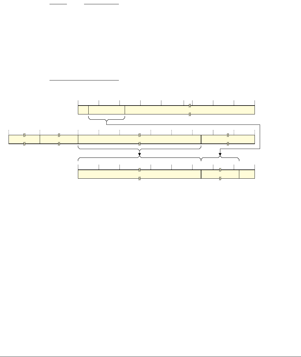
D5 The AArch64 Virtual Memory System Architecture
D5.3 Translation table walk examples
ARM DDI 0487A.a Copyright © 2013 ARM Limited. All rights reserved. D5-1761
ID090413 Non-Confidential - Beta
Initial lookup at the zero level, 4KB translation granule
This subsection describes initial lookups with an input address width of (n+1) bits, meaning the input address is
IA[n:0]. As Table D5-9 on page D5-1725 shows, a stage 1 or stage 2 initial lookup at the zero level is required when
39 ≤ n ≤ 47. For these lookups:
•TTBR[47:(n-35)] specify the translation table base address.
• Bits[n:39] of the input address are bits[(n-36):3] of the descriptor offset in the translation table.
Note
This means that, when the input address width is less than 48 bits
• The size of the translation table is reduced.
• More low-order bits of the TTBR are required to specify the translation table base address.
• Fewer input address bit are used to specify the descriptor offset in the translation table.
For example, if the input address width is 46 bits:
• The translation table size is 1KB,
•TTBR bits[47:10] specify the translation table base address.
• Input address bits[45:39] specify bits[9:3] of the descriptor offset.
Figure D5-15 shows this lookup.
Figure D5-15 Initial lookup for VMSAv8-64 using the 4KB granule, starting at the zero level
Initial lookup at the first level, 4KB translation granule
This subsection describes initial lookups with an input address width of (n+1) bits, meaning the input address is
IA[n:0].
For a stage 1 or stage 2 initial lookup at the first level, without use of concatenated translation tables
As Table D5-9 on page D5-1725 shows, this applies to IA[n:0], where 30 ≤ n ≤ 38. For these
lookups:
• There is a single translation table at this level.
•TTBR[47:(n-26)] specify the translation table base address.
• Bits[n:30] of the input address are bits[(n-27):3] of the descriptor offset in the translation
table.
Figure D5-16 on page D5-1762 shows this lookup.
Translation table base address[47:x]UNK/SBZP
63 56 55 48 47 0
Register-defined UNK/SBZP TTBR
xx-1
Input address‡
47 n39 038
47 xx-1 32 0
000Descriptor address†
Supported input address range is IA[n:0], 4 ≤ x ≤ 12, n = x + 35. When n is 47 the field marked ‡ is absent.
† For a Non-secure EL1&0 stage 1 translation, the IPA of the descriptor. Otherwise, the PA of the descriptor.
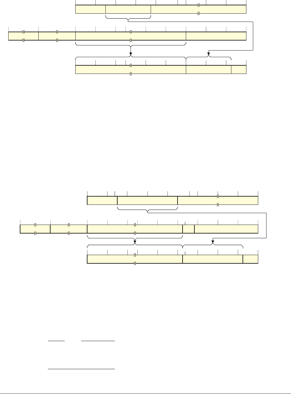
D5 The AArch64 Virtual Memory System Architecture
D5.3 Translation table walk examples
D5-1762 Copyright © 2013 ARM Limited. All rights reserved. ARM DDI 0487A.a
Non-Confidential - Beta ID090413
Figure D5-16 Initial lookup for VMSAv8-64 using the 4KB granule, starting at the first level, without concatenation
For a stage 2 initial lookup at the first level, with concatenated translation tables
As Table D5-9 on page D5-1725 shows, this applies to IA[n:0], where 39 ≤ n ≤ 42. For these
lookups:
• There are 2(n-38) concatenated translation tables at this level.
• These concatenated translation tables must be aligned to 2(n-38)×4KB. This means
TTBR[(n-27):12] must be zero.
•TTBR[47:(n-26)] specify the base address of the block of concatenated translation tables.
• Bits[n:30] of the input address are bits[(n-27):3] of the descriptor offset from the base address
of the block of concatenated translation tables.
Figure D5-17 shows this lookup.
Figure D5-17 Initial lookup for VMSAv8-64 using the 4KB granule, starting at the first level, with concatenation
Performing the initial lookup using the 16KB granule
This subsection describes examples of the initial lookup when using the 16KB translation granule that Table D5-12
on page D5-1729 shows as starting at the zero level or at the first level. It includes those stage 2 translations where
concatenation of translation tables is required for the lookup to start at the first level. This means that it gives specific
examples of the mechanisms described in The VMSAv8-64 address translation system on page D5-1710.
Note
For stage 2 translations, the same principles apply to an initial lookup that Table D5-12 on page D5-1729 shows as
starting at the first level. In this case, for some IA sizes concatenation of translation tables means the lookup can,
instead, start at the second level.
TTBR
Input addressUNK/SBZP
47 029n30
47 32 0
000
Supported input address range is IA[n:0], 4 ≤ x ≤ 12, n = x + 26.
Translation table base address[47:x]
UNK/SBZP
63 56 55 48 47 0
Register-defined UNK/SBZP
xx-1
xx-1
n+1
Descriptor address†
† For a Non-secure EL1&0 stage 1 translation, the IPA of the descriptor. Otherwise, the PA of the descriptor.
‡
Translation table base address[47:x]
UNK/SBZP
63 56 55 48 47 0
Register-defined UNK/SBZP TTBR
Input addressUNK/SBZP
47 02930
n+1
n
47 32 0
0 0 0 Descriptor PA
Supported input address range is IPA[n:0], 13 ≤ x ≤ 16, n = x + 26. The field marked ‡ must be zero.
x
x-1
x
x-1
12 11
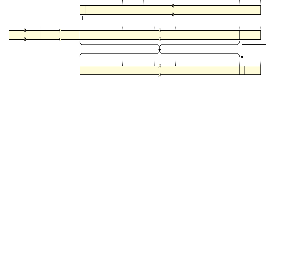
D5 The AArch64 Virtual Memory System Architecture
D5.3 Translation table walk examples
ARM DDI 0487A.a Copyright © 2013 ARM Limited. All rights reserved. D5-1763
ID090413 Non-Confidential - Beta
The following subsections describe these examples of the initial lookup:
•Initial lookup at the zero level, 16KB translation granule.
•Initial lookup at the first level, 16KB translation granule.
In all cases, for a stage 2 translation, the VTCR_EL2.SL0 field must indicate the required initial lookup level, and
this level must be consistent with the value of the VTCR_EL2.T0SZ field, see Overview of stage 2 translations,
16KB granule on page D5-1728.
Initial lookup at the zero level, 16KB translation granule
This subsection describes initial lookups with an input address width of (n+1) bits, meaning the input address is
IA[n:0]. As Table D5-11 on page D5-1727 shows, the only case where an address translation using the 16KB
granule starts at level 0 is a stage 1 translation of a 48-bit input address, IA[47:0]. For this lookup:
• The required translation table has only two entries, meaning its size is 16bytes, and it must be aligned to 16
bytes.
•TTBR[47:4] specify the translation table base address.
• Bit[47] of the input address is bits[3] of the descriptor offset in the translation table.
Figure D5-18 shows this lookup.
Figure D5-18 Initial lookup for VMSAv8-64 using the 16KB granule, starting at the zero level
Initial lookup at the first level, 16KB translation granule
This subsection describes initial lookups with an input address width of (n+1) bits, meaning the input address is
IA[n:0].
For a stage 1 or stage 2 initial lookup at the first level, without use of concatenated translation tables
As Table D5-12 on page D5-1729 shows, this applies to IA[n:0], where 36 ≤ n ≤ 46. For these
lookups:
• There is a single translation table at this level.
•TTBR[47:(n-32)] specify the translation table base address.
• Bits[n:36] of the input address are bits[(n-33):3] of the descriptor offset in the translation
table.
Figure D5-19 on page D5-1764 shows this lookup.
Translation table base address[47:4]UNK/SBZP
63 56 55 48 47 0
Register-defined ‡ TTBR
43
Input address
47 46 0
47 432 0
000Descriptor address†
Supported input address range is IA[47:0]. The field marked ‡ is UNK/SBZP.
† For a Non-secure EL1&0 stage 1 translation, the IPA of the descriptor. Otherwise, the PA of the descriptor.
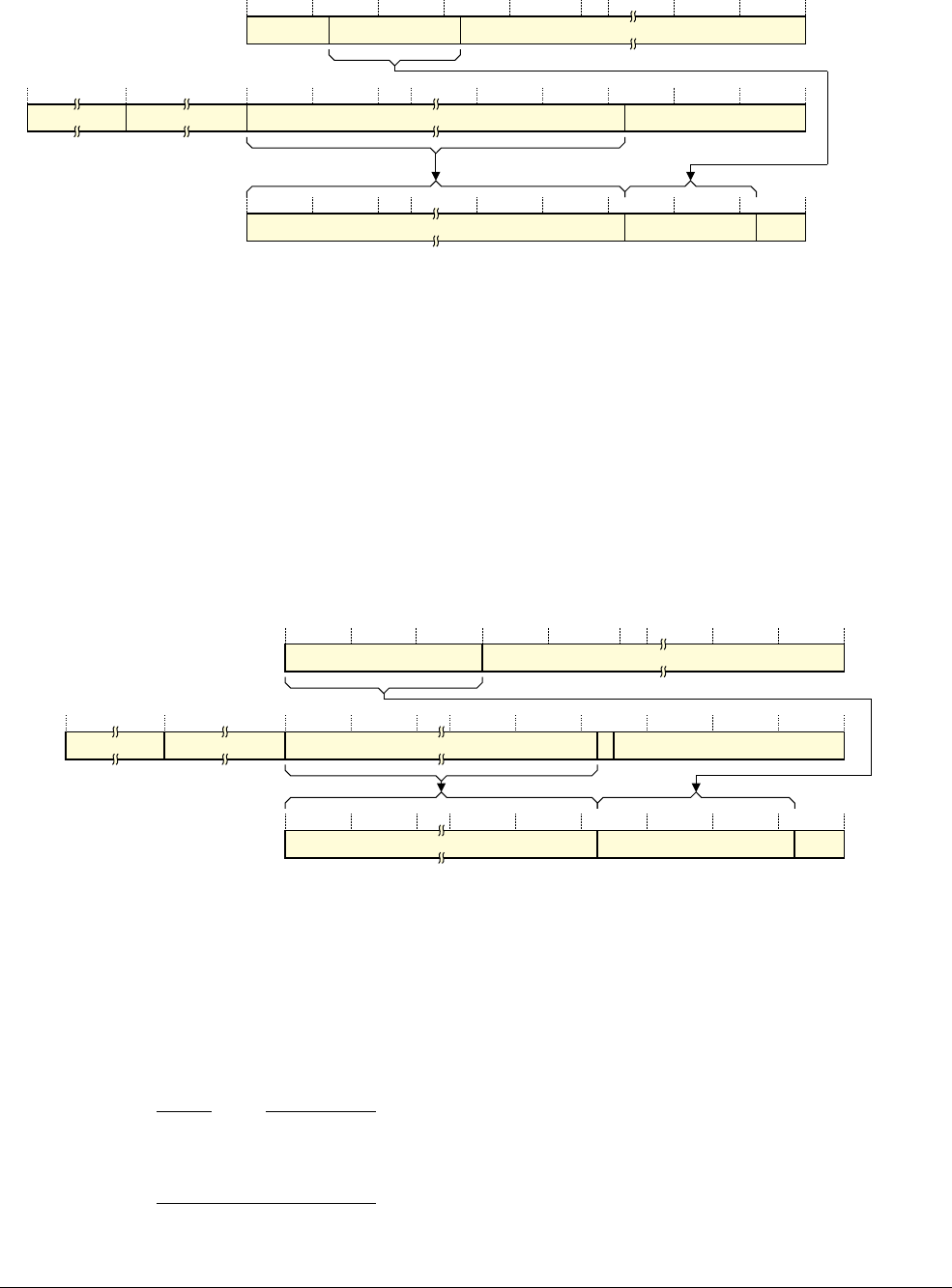
D5 The AArch64 Virtual Memory System Architecture
D5.3 Translation table walk examples
D5-1764 Copyright © 2013 ARM Limited. All rights reserved. ARM DDI 0487A.a
Non-Confidential - Beta ID090413
Figure D5-19 Initial lookup for VMSAv8-64 using the 16KB granule, starting at the first level, without concatenation
For a stage 2 initial lookup at the first level, with concatenated translation tables
As Table D5-12 on page D5-1729 shows, the only case where an address translation using the 16KB
granule starts at the first level because of concatenation of translation tables is a stage 2 translation
of a 48-bit input address, IA[47:0]. For this lookup:
• There are two concatenated translation tables at this level.
• These concatenated translation tables must be aligned to 2×16KB. This means TTBR[14]
must be zero.
•TTBR[47:15] specify the base address of the block of two concatenated translation tables.
• Bits[47:36] of the input address are bits[14:3] of the descriptor offset from the base address
of the block of concatenated translation tables.
Figure D5-20 shows this lookup.
Figure D5-20 Initial lookup for VMSAv8-64 using the 16KB granule, starting at the first level, with concatenation
Performing the initial lookup using the 64KB translation granule
This subsection describes examples of the initial lookup when using the 64KB translation granule that Table D5-15
on page D5-1732 shows as starting at the first level or at the second level. It includes those stage 2 translations where
concatenation of translation tables is required for the lookup to start at the second level. This means that it gives
specific examples of the mechanisms described in The VMSAv8-64 address translation system on page D5-1710.
Note
For stage 2 translations, the same principles apply to an initial lookup that Table D5-15 on page D5-1732 shows as
starting at the second level. In this case, for some IA sizes concatenation of translation tables means the lookup can,
instead, start at the third level.
TTBR
Input addressUNK/SBZP
47 035n36
47 32 0
000
Supported input address range is IA[n:0], 4 ≤ x ≤ 14, n = x + 32.
Translation table base address[47:x]
UNK/SBZP
63 56 55 48 47 0
Register-defined UNK/SBZP
xx-1
xx-1
n+1
Descriptor address†
† For a Non-secure EL1&0 stage 1 translation, the IPA of the descriptor. Otherwise, the PA of the descriptor.
‡Translation table base address[47:15]UNK/SBZP
63 56 55 48 47 0
Register-defined UNK/SBZP TTBR
47 32 0
0 0 0 Descriptor PA
Supported input address range is IPA[47:0]. The bit marked ‡ must be zero.
15 14
15 14 13
Input address
47 03536
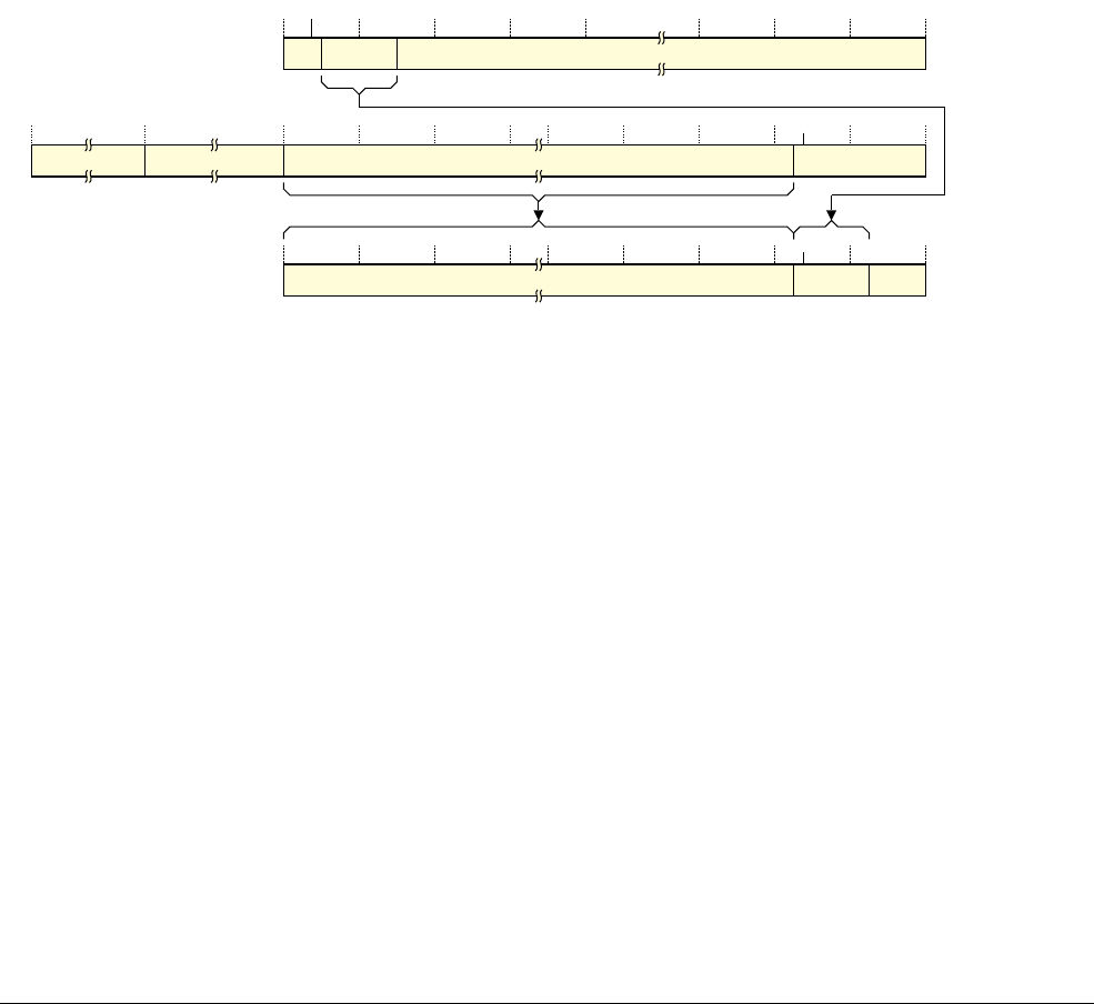
D5 The AArch64 Virtual Memory System Architecture
D5.3 Translation table walk examples
ARM DDI 0487A.a Copyright © 2013 ARM Limited. All rights reserved. D5-1765
ID090413 Non-Confidential - Beta
The following subsections describe these examples of the initial lookup:
•Initial lookup at the first level, 64KB translation granule.
•Initial lookup at the second level, 64KB translation granule.
In all cases, for a stage 2 translation, the VTCR_EL2.SL0 field must indicate the required initial lookup level, and
this level must be consistent with the value of the VTCR_EL2.T0SZ field, see Overview of stage 2 translations,
64KB granule on page D5-1732.
Initial lookup at the first level, 64KB translation granule
This subsection describes initial lookups with an input address width of (n+1) bits, meaning the input address is
IA[n:0]. As Table D5-15 on page D5-1732 shows, a stage 1 or stage 2 initial lookup at the first level is required
when 42 ≤ n ≤ 47. For these lookups:
• The size of the translation table is 2(n-39) bytes. This means the size of the translation table, at this level, is
always less than the granule size. The address of this translation table must align to the size of the table.
• Bits[n:42] of the input address are bits[(n-39):3] of the descriptor offset in the translation table.
• Bits[47:(n-38)] of the TTBR specify the translation table base address.
Figure D5-21 shows this lookup.
Figure D5-21 Initial lookup for VMSAv8-64 using the 64KB granule, starting at the first level
Initial lookup at the second level, 64KB translation granule
This subsection describes initial lookups with an input address width of (n+1) bits, meaning the input address is
IA[n:0].
For a stage 1 or stage 2 initial lookup at the second level, without the use of concatenated translation tables
As Table D5-15 on page D5-1732 shows, this applies to IA[n:0], where 29 ≤ n ≤ 41. For these
lookups:
• There is a single translation table at this level.
•TTBR[47:(n-25)] of the specify the translation table base address.
• Bits[n:29] of the input address are bits[(n-26):3] of the descriptor offset in the translation
table.
Figure D5-22 on page D5-1766 shows this lookup.
Input address‡
47 n0
Translation table base address[47:x]UNK/SBZP
63 56 55 48 47 0
Register-defined UNK/SBZP TTBR
42 41
x-1
x
n+1
Supported input address range is IA[n:0], 42 ≤ n ≤ 47, x = n-38. When n is 47 the field marked ‡ is absent.
† For a Non-secure EL1&0 stage 1 translation, the IPA of the descriptor. Otherwise, the PA of the descriptor.
47 32 0
0 0 0 Descriptor address†
x-1
x
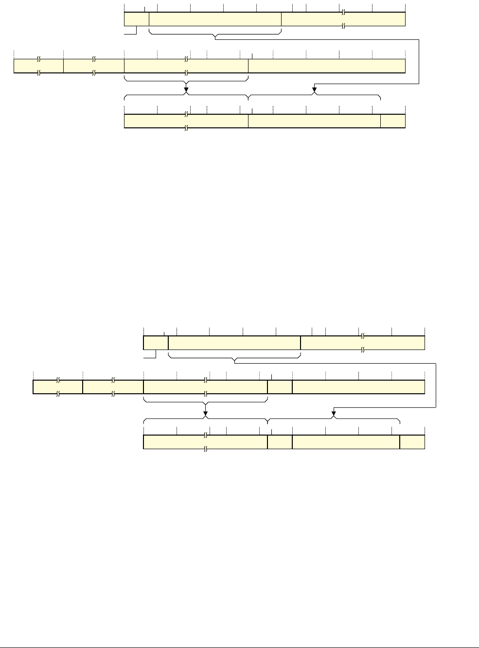
D5 The AArch64 Virtual Memory System Architecture
D5.3 Translation table walk examples
D5-1766 Copyright © 2013 ARM Limited. All rights reserved. ARM DDI 0487A.a
Non-Confidential - Beta ID090413
Figure D5-22 Initial lookup for VMSAv8-64 using the 64KB granule, starting at second level, without concatenation
For a stage 2 initial lookup at the second level, with concatenated translation tables
As Table D5-15 on page D5-1732 shows, this applies to IA[n:0], where 42 ≤ n ≤ 45. For these
lookups:
• There are 2(m-41) concatenated translation tables at this level.
• These concatenated translation tables must be aligned to 2(m-41)×64KB. This means
TTBR[(n-26):16] must be zero.
•TTBR[47:(n-25)] specify the base address of the block of translation tables.
• Bits[n:42] of the input address are bits[(n-26):16] of the descriptor offset from the base
address of the block of translation tables.
Figure D5-23 shows this lookup.
Figure D5-23 Initial lookup for VMSAv8-64 using the 64KB granule, starting at second level, with concatenation
D5.3.2 Full translation flows for VMSAv8-64 address translation
In a translation table walk, only the first lookup uses the translation table base address from the appropriate TTBR.
Subsequent lookups use a combination of address information from:
• The table descriptor read in the previous lookup.
• The input address.
This section describes example full translation flows, from the initial lookup to the address of a memory page. The
described flows:
• Resolve the maximum-sized IA range supported by the initial lookup level.
• Do not have any concatenation of translation tables.
Base address[47:x]UNK/SBZP
63 56 55 48 47 0
Register-defined UNK/SBZP TTBR
47 32 0
0 0 0
Supported input address range is IA[n:0]. 4 ≤ x ≤ 16, n = x + 25.
Input address
47 029 28
n+1 n
x
x-1
UNK/SBZP
† For a Non-secure EL1&0 stage 1 translation, the IPA of the descriptor. Otherwise, the PA of the descriptor.
x
x-1
Descriptor address†
47 32 0
0 0 0 Descriptor PA
Input address
47 029 28
n+1 n
UNK/SBZP
16 15
Supported input address range is IPA[n:0], 17 ≤ x ≤ 20, n = x + 25. The field marked ‡ must be zero.
‡
Base address[47:x]UNK/SBZP
63 56 55 48 47 0
Register-defined UNK/SBZP TTBR
16 15x
x-1
x
x-1

D5 The AArch64 Virtual Memory System Architecture
D5.3 Translation table walk examples
ARM DDI 0487A.a Copyright © 2013 ARM Limited. All rights reserved. D5-1767
ID090413 Non-Confidential - Beta
Examples of performing the initial lookup on page D5-1760 described how either reducing the IA range or
concatenating translation tables affects the initial lookup.
Note
Reducing the IA range or concatenating translation tables affects only the initial lookup.
The following sections describe full VMSAv8-64 translation flows, down to an entry for a memory page:
•The address and properties fields shown in the translation flows.
•Full translation flow using the 4KB granule and starting at the zero level on page D5-1768.
•Full translation flow using the 4KB granule and starting at the first level on page D5-1769.
•Full translation flow using the 64KB granule and starting at the first level on page D5-1770.
•Full translation flow using the 64KB granule and starting at the second level on page D5-1771.
The address and properties fields shown in the translation flows
For the Non-secure EL1&0 stage 1 translation:
• Any descriptor address is the IPA of the required descriptor.
• The final output address is the IPA of the block or page.
In these cases, an EL1&0 stage 2 translation is performed to translate the IPA to the required PA.
For all other translations, the final output address is the PA of the block or page, and any descriptor address is the
PA of the descriptor.
Properties indicates register or translation table fields that return information, other than address information, about
the translation or the targeted memory region. For more information see Memory attribute fields in the VMSAv8-64
translation table format descriptors on page D5-1776.
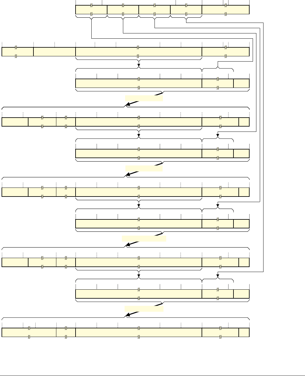
D5 The AArch64 Virtual Memory System Architecture
D5.3 Translation table walk examples
D5-1768 Copyright © 2013 ARM Limited. All rights reserved. ARM DDI 0487A.a
Non-Confidential - Beta ID090413
Full translation flow using the 4KB granule and starting at the zero level
Figure D5-24 shows the complete translation flow for a stage 1 translation table walk for a 48-bit input address. This
lookup must start with a zero-level lookup. For more information about the fields shown in the figure see The
address and properties fields shown in the translation flows on page D5-1767.
Figure D5-24 Complete stage 1 translation of a 48-bit address using the 4KB translation granule
Descriptor
address
Input address
Zero level lookup
Descriptor
address
TTBR
Zero-level
Table descriptor
Second-level
Table descriptor
Third-level
Page descriptor
47 30 29 021 20 12 1139 38
Translation table base address[47:12]UNK/SBZP
63 56 55 48 47 0
Properties UNK/SBZP
12 11
47 32 0
0 0 0
12 11
Ignored 11SBZ
48 47
First-level table address[47:12]Properties
63 59 58 52 51 0
Ignored
2112 11
47 32 0
0 0 0
12 11
Descriptor
address
First level lookup
Ignored 11SBZ
48 47
Properties
63 59 58 52 51 0
Ignored
2112 11
Ignored 11SBZ
48 47
Second-level table address[47:12]Properties
63 59 58 52 51 0
Ignored
2112 11
First-level
Table descriptor
47 32 0
0 0 0
12 11
Descriptor
address
Second level lookup
Ignored 11SBZ
48 47
Second-level table address[47:12]Properties
63 59 58 52 51 0
Ignored
2112 11
47 32 0
0 0 0
12 11
Third level lookup
Properties 11SBZ
48 47
Output address[47:12]Properties
63 52 51 02112 11
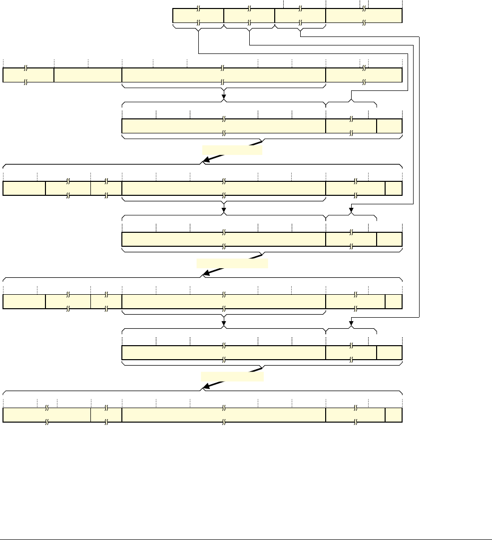
D5 The AArch64 Virtual Memory System Architecture
D5.3 Translation table walk examples
ARM DDI 0487A.a Copyright © 2013 ARM Limited. All rights reserved. D5-1769
ID090413 Non-Confidential - Beta
If the first-level lookup or second-level lookup returns a block descriptor then the translation table walk completes
at that level.
Figure D5-24 on page D5-1768 shows a stage 1 translation. The only difference for a stage 2 translation is that
bits[63:58] of the Table descriptors are SBZ.
Full translation flow using the 4KB granule and starting at the first level
Figure D5-25 shows the complete translation flow for a stage 1 translation table walk for a 39-bit input address. This
lookup must start with a first-level lookup. For more information about the fields shown in the figure see The
address and properties fields shown in the translation flows on page D5-1767.
Figure D5-25 Complete stage 1 translation of a 39-bit address using the 4KB translation granule
If the first-level lookup or the second-level lookup returns a block descriptor then the translation table walk
completes at that level.
Descriptor
address
Input address
First level lookup
For details of Properties fields, see the register or descriptor description.
TTBR
First-level
Table descriptor
Third-level
Page descriptor
Translation table base address[47:12]UNK/SBZP
63 56 55 48 47 0
Properties UNK/SBZP
12 11
47 32 0
0 0 0
12 11
Ignored 11SBZ
48 47
First-level table address[47:12]Properties
63 59 58 52 51 0
Ignored
2112 11
47 32 0
0 0 0
12 11
Descriptor
address
Second level lookup
Ignored 11SBZ
48 47
Second-level table address[47:12]Properties
63 59 58 52 51 0
Ignored
2112 11
Ignored 11SBZ
48 47
Third-level table address[47:12]Properties
63 59 58 52 51 0
Ignored
2112 11
Second-level
Table descriptor
47 32 0
0 0 0
12 11
Descriptor
address
Third level lookup
Properties 11SBZ
48 47
Output address[47:12]Properties
63 52 51 02112 11
30 29 021 20 12 1138
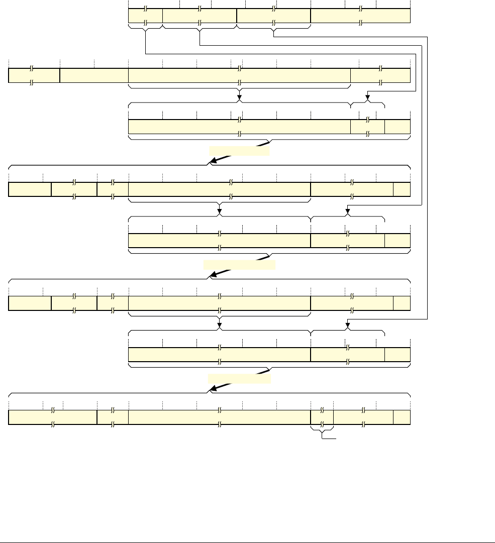
D5 The AArch64 Virtual Memory System Architecture
D5.3 Translation table walk examples
D5-1770 Copyright © 2013 ARM Limited. All rights reserved. ARM DDI 0487A.a
Non-Confidential - Beta ID090413
Figure D5-25 on page D5-1769 shows a stage 1 translation. The only difference for a stage 2 translation is that
bits[63:58] of the Table descriptors are SBZ.
Comparing this translation with the translation for a 48-bit address, shown in Figure D5-24 on page D5-1768, shows
how the translation for the 42-bit address start the same lookup process one stage later.
Full translation flow using the 64KB granule and starting at the first level
Figure D5-24 on page D5-1768 shows the complete translation flow for a stage 1 translation table walk for a 48-bit
input address. This lookup must start with a zero-level lookup. For more information about the fields shown in the
figure see The address and properties fields shown in the translation flows on page D5-1767.
Figure D5-26 Complete stage 1 translation of a 48-bit address using the 64KB translation granule
If the second-level lookup returns a block descriptor then the translation table walk completes at that level.
Figure D5-26 shows a stage 1 translation. The only difference for a stage 2 translation is that bits[63:58] of the Table
descriptors are SBZ.
Descriptor
address
Input address
First level lookup
For details of Properties fields, see the register or descriptor description.
TTBR
First-level
Table descriptor
Third-level
Page descriptor
Translation table base address[47:9]UNK/SBZP
63 56 55 48 47 0
Properties UNK/SBZP
98
47 32 0
0 0 0
98
Ignored 11SBZ
48 47
Properties
63 59 58 52 51 0
Ignored
21
47 32 0
0 0 0
16 15
Descriptor
address
Second level lookup
11SBZ
48 47
Second-level table address[47:16]Properties
63 59 58 52 51 0
Ignored
2116 15
Ignored 11SBZ
48 47
Third-level table address[47:16]Properties
63 59 58 52 51 0
Ignored
2116 15
Second-level
Table descriptor
47 32 0
0 0 0
16 15
Descriptor
address
Third level lookup
Properties 11SBZ
48 47
Output address[47:16]Properties
63 52 51 02112 11
47 29 28 016 1542 41
16 15
UNK/SBZP
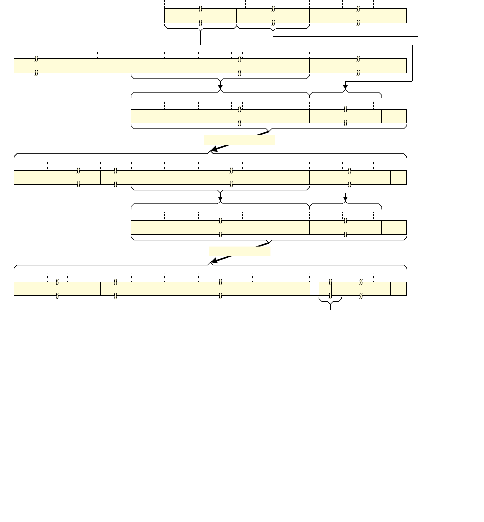
D5 The AArch64 Virtual Memory System Architecture
D5.3 Translation table walk examples
ARM DDI 0487A.a Copyright © 2013 ARM Limited. All rights reserved. D5-1771
ID090413 Non-Confidential - Beta
The first-level lookup resolves only 6 bits of the input address. As described in Performing the initial lookup using
the 64KB translation granule on page D5-1764, this means:
• The translation table size for this level is only 512 bytes.
• The required translation table alignment for this level is 512 bytes.
• The Base address field in the TTBR is extended, at the low-order end, to be bits[47:9].
Full translation flow using the 64KB granule and starting at the second level
Figure D5-25 on page D5-1769 shows the complete translation flow for a stage 1 translation table walk for a 42-bit
input address. This lookup must start with a second-level lookup. For more information about the fields shown in
the figure see The address and properties fields shown in the translation flows on page D5-1767.
Figure D5-27 Complete stage 1 translation of a 42-bit address using the 64KB translation granule
If the second-level lookup returns a block descriptor then the translation table walk completes at that level.
Figure D5-27 shows a stage 1 translation. The only difference for a stage 2 translation is that bits[63:58] of the Table
descriptors are SBZ.
Comparing this translation with the translation for a 48-bit address, shown in Figure D5-26 on page D5-1770,
shows:
• The translation for the 42-bit address starts the same lookup process one stage later.
• Because the initial lookup resolves 13 bits of address:
— The translation table size for this level is 64KB.
— The required translation table alignment for this level is 64KB.
— The Base address field in the TTBR is bits[47:16].
Descriptor
address
Input address
Second level lookup
For details of Properties fields, see the register or descriptor description.
TTBR
Third-level
Page descriptor
Translation table base address[47:16]UNK/SBZP
63 56 55 48 47 0
Properties UNK/SBZP
16 15
47 32 0
0 0 0
16 15
Ignored 11SBZ
48 47
Properties
63 59 58 52 51 0
Ignored
21
47 32 0
0 0 0
16 15
Descriptor
address
Third level lookup
11SBZ
48 47
Third-level table address[47:16]Properties
63 59 58 52 51 0
Ignored
2116 15
Second-level
Table descriptor
Properties 11SBZ
48 47
Output address[47:16]Properties
63 52 51 02112 1116 15
UNK/SBZP
29 28 016 1541

D5 The AArch64 Virtual Memory System Architecture
D5.4 VMSAv8-64 translation table format descriptors
D5-1772 Copyright © 2013 ARM Limited. All rights reserved. ARM DDI 0487A.a
Non-Confidential - Beta ID090413
D5.4 VMSAv8-64 translation table format descriptors
In general, a descriptor is one of:
• An invalid or fault entry.
• A table entry, that points to the next-level translation table.
• A block entry, that defines the memory properties for the access.
• A reserved format.
Bit[1] of the descriptor indicates the descriptor type, and bit[0] indicates whether the descriptor is valid.
The following sections describe the ARMv8 translation table descriptor formats:
•VMSAv8-64 translation table zero-level, first-level, and second-level descriptor formats.
•ARMv8 translation table third-level descriptor formats on page D5-1775.
Memory attribute fields in the VMSAv8-64 translation table format descriptors on page D5-1776 then gives more
information about the descriptor attribute fields, and Control of Secure or Non-secure memory access on
page D5-1779 describe how the NS and NSTable together control whether a memory access from Secure state
accesses the Secure memory map or the Non-secure memory map.
D5.4.1 VMSAv8-64 translation table zero-level, first-level, and second-level descriptor formats
In the VMSAv8-64 translation table format, the difference in the formats of the zero-level, first-level and
second-level descriptors is:
• Whether a block entry is permitted.
• If a block entry is permitted, the size of the memory region described by that entry.
These differences depend on the translation granule, as follows:
4KB granule A zero-level descriptor does not support block translation.
A block entry:
• In a first-level table describes the mapping of the associated 1GB input address range.
• In a second-level table describes the mapping of the associated 2MB input address range.
16KB granule Zero-level and first-level descriptors do not support block translation.
A block entry in a second-level table describes the mapping of the associated 32MB input address
range.
64KB granule Zero-level lookup is not supported.
A first-level descriptor does not support block translation.
A block entry in a second-level table describes the mapping of the associated 512MB input address
range.
Figure D5-28 on page D5-1773 shows the ARMv8 zero-level, first-level and second-level descriptor formats:
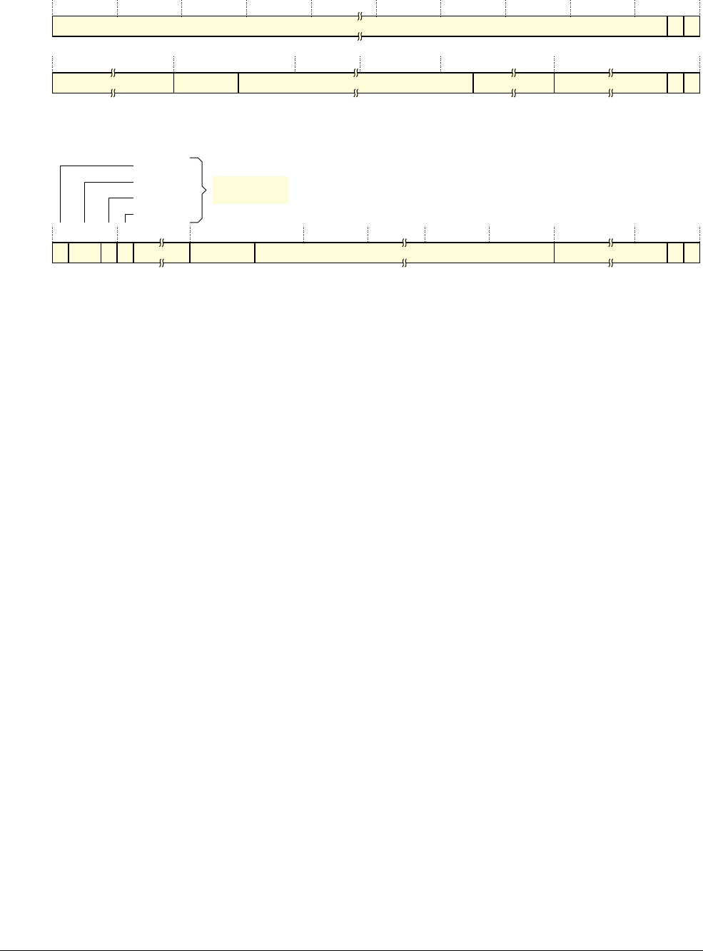
D5 The AArch64 Virtual Memory System Architecture
D5.4 VMSAv8-64 translation table format descriptors
ARM DDI 0487A.a Copyright © 2013 ARM Limited. All rights reserved. D5-1773
ID090413 Non-Confidential - Beta
Figure D5-28 VMSAv8-64 zero-level, first-level, and second-level descriptor formats
Descriptor encodings, ARMv8 zero-level, first-level, and second-level formats
Descriptor bit[0] identifies whether the descriptor is valid, and is 1 for a valid descriptor. If a lookup returns an
invalid descriptor, the associated input address is unmapped, and any attempt to access it generates a Translation
fault.
Descriptor bit[1] identifies the descriptor type, and is encoded as:
0, Block The descriptor gives the base address of a block of memory, and the attributes for that memory
region.
1, Table The descriptor gives the address of the next level of translation table, and for a stage 1 translation,
some attributes for that translation.
The other fields in the valid descriptors are:
Block descriptor
Gives the base address and attributes of a block of memory, as follows:
4KB translation granule
• For a first-level Block descriptor, bits[47:30] are bits[47:30] of the output
address. This output address specifies a 1GB block of memory.
• For a second-level descriptor, bits[47:21] are bits[47:21] of the output
address.This output address specifies a 2MB block of memory.
16KB translation granule
For a second-level Block descriptor, bits[47:25] are bits[47:25] of the output
address.This output address specifies a 32MB block of memory.
64KB translation granule
For a second-level Block descriptor, bits[47:29] are bits[47:29] of the output
address.This output address specifies a 512MB block of memory.
Bits[63:52, 11:2] provide attributes for the target memory block, see Memory attribute fields in the
VMSAv8-64 translation table format descriptors on page D5-1776. The position and contents of
these bits are identical in the second-level block descriptor and in the third-level page descriptor.
UNK/SBZP 1
63 62 61 60 59 58 52 51 48 47 mm-1 2 1 0
Ignored Next-level table address[47:m] Ignored 1Table
PXNTable
XNTable
APTable
NSTable
Stage 1 only,
SBZ at stage 2
A zero-level Table descriptor returns the address of the first-level table.
A first-level Table descriptor returns the address of the second-level table.
A second-level Table descriptor returns the address of the third-level table.
With the 4KB granule size m is 12, with the 16KB granule size m is 14, and with the 64KB granule size, m is 16.
UNK/SBZP 1Upper block attributes
63 52 51 4748 nn-1 12 11 2 1 0
Output address[47:n] UNK/SBZP Lower block attributes 0Block
With the 4KB granule size, for the first-level descriptor n is 30, and for the second-level descriptor, n is 21.
With the 64KB granule size, for the second-level descriptor, n is 29.
With the 16KB granule size, for the second-level descriptor, n is 25.
0Ignore
63 210
xInvalid

D5 The AArch64 Virtual Memory System Architecture
D5.4 VMSAv8-64 translation table format descriptors
D5-1774 Copyright © 2013 ARM Limited. All rights reserved. ARM DDI 0487A.a
Non-Confidential - Beta ID090413
Table descriptor
Gives the translation table address for the next-level lookup, as follows:
4KB translation granule
• Bits[47:12] are bits[47:12] of the address of the required next-level table, which
is:
— For a zero-level Table descriptor, the address of a first-level table.
— For a first-level Table descriptor, the address of a second-level table.
— For a second-level Table descriptor, the address of a third-level table.
• Bits[11:0] of the table address are zero.
16KB translation granule
• Bits[47:14] are bits[47:14] of the address of the required next-level table, which
is:
— For a zero-level Table descriptor, the address of a first-level table.
— For a first-level Table descriptor, the address of a second-level table.
— For a second-level Table descriptor, the address of a third-level table.
• Bits[13:0] of the table address are zero.
64KB translation granule
• Bits[47:16] are bits[47:16] of the address of the required next-level table, which
is:
— For a first-level Table descriptor, the address of a second-level table.
— For a second-level Table descriptor, the address of a third-level table.
• Bits[15:0] of the table address are zero.
For a stage 1 translation only, bits[63:59] provide attributes for the next-level lookup, see Memory
attribute fields in the VMSAv8-64 translation table format descriptors on page D5-1776.
If the translation table defines the Non-secure EL1&0 stage 1 translations, then the output address in the descriptor
is the IPA of the target block or table. Otherwise, it is the PA of the target block or table.
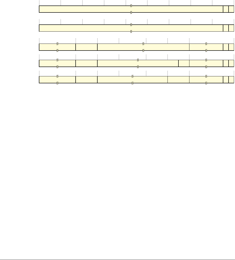
D5 The AArch64 Virtual Memory System Architecture
D5.4 VMSAv8-64 translation table format descriptors
ARM DDI 0487A.a Copyright © 2013 ARM Limited. All rights reserved. D5-1775
ID090413 Non-Confidential - Beta
D5.4.2 ARMv8 translation table third-level descriptor formats
For the 4KB granule size, each entry in a third-level table describes the mapping of the associated 4KB input address
range.
For the 16KB granule size, each entry in a third-level table describes the mapping of the associated 16KB input
address range.
For the 64KB granule size, each entry in a third-level table describes the mapping of the associated 64KB input
address range.
Figure D5-29 shows the ARMv8 third-level descriptor formats.
Figure D5-29 VMSAv8-64 third-level descriptor format
Descriptor bits[1:0] identify whether the descriptor is valid, and the descriptor type of a valid descriptor, encoded as:
0bx0
, Invalid If a lookup returns an invalid descriptor, the associated input address is unmapped, and any attempt
to access it generates a Translation fault.
0b01
, Reserved, invalid
Behaves identically to encodings of
0bx0
.
This encoding must not be used in third-level translation tables.
0b11
, Page Gives the address and attributes of a 4KB, 16KB, or 64KB page of memory.
At this level, the only valid format is the Page descriptor. The other fields in the Page descriptor are:
Page descriptor
Gives the output address of a page of memory, as follows:
4KB translation granule
Bits[47:12] are bits[47:12] of the output address for a page of memory.
16KB translation granule
Bits[47:14] are bits[47:14] of the output address for a page of memory.
64KB translation granule
Bits[47:16] are bits[47:16] of the output address for a page of memory.
Bits[63:52, 11:2] provide attributes for the target memory page, see Memory attribute fields in the
VMSAv8-64 translation table format descriptors on page D5-1776.
1Upper† attributes
63 52 51 4748 12 11 2 1 0
UNK/SBZP Output address[47:12] Lower† attributes 1Page, 4KB granule
Reserved,
invalid 1Reserved
63 210
0
0
Ignore
63 210
x
Invalid
Output address[47:16] UNK/SBZP 1Upper† attributes
63 52 51 4748 12 11 2 1 0
UNK/SBZP Lower† attributes 1
16 15
Page, 64KB granule
Output address[47:14] ‡ 1Upper† attributes
63 52 51 4748 12 11 2 1 0
UNK/SBZP Lower† attributes 1
14 13
Page, 16KB granule
† Upper page attributes and Lower page attributes
‡ Field is UNK/SBZP
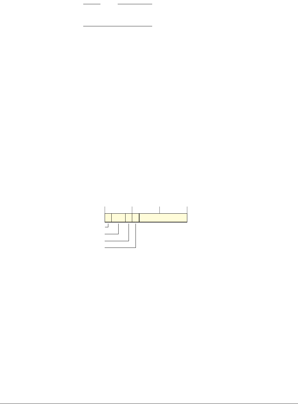
D5 The AArch64 Virtual Memory System Architecture
D5.4 VMSAv8-64 translation table format descriptors
D5-1776 Copyright © 2013 ARM Limited. All rights reserved. ARM DDI 0487A.a
Non-Confidential - Beta ID090413
Note
The position and contents of bits[63:52, 11:2] are identical to bits[63:52, 11:2] in the zero-level,
first-level, and second-level block descriptors.
For the Non-secure EL1&0 stage 1 translations, the output address in the descriptor is the IPA of the target page.
Otherwise, it is the PA of the target page.
D5.4.3 Memory attribute fields in the VMSAv8-64 translation table format descriptors
Memory region attributes on page D5-1788 describes the region attribute fields. The following subsections
summarize the descriptor attributes as follows:
Table descriptor
Table descriptors for stage 2 translations do not include any attribute field. For a summary of the
attribute fields in a stage 1 table descriptor, that define the attributes for the next lookup level, see
Next-level attributes in stage 1 VMSAv8-64 Table descriptors.
Block and page descriptors
These descriptors define memory attributes for the target block or page of memory. Stage 1 and
stage 2 translations have some differences in these attributes, see:
•Attribute fields in stage 1 VMSAv8-64 Block and Page descriptors on page D5-1777
•Attribute fields in stage 2 VMSAv8-64 Block and Page descriptors on page D5-1778.
Next-level attributes in stage 1 VMSAv8-64 Table descriptors
In a Table descriptor for a stage 1 translation, bits[63:59] of the descriptor define the attributes for the next-level
translation table access, and bits[58:52] are ignored:
These attributes are:
NSTable, bit[63]
For memory accesses from Secure state, specifies the security level for subsequent levels of lookup,
see Hierarchical control of Secure or Non-secure memory accesses on page D5-1780.
For memory accesses from Non-secure state, this bit is ignored.
APTable, bits[62:61]
Access permissions limit for subsequent levels of lookup, see Hierarchical control of data access
permissions on page D5-1783.
APTable[0] is reserved, SBZ:
• In the EL2 translation regime.
• In the EL3 translation regime.
† UXNTable for the EL1&0 translation regime, XNTable for the other regimes.
Next-level descriptor attributes, stage 1 only
63 62 61 60 59 58 52
Ignored
NSTable
APTable
UXNTable or XNTable †
PXNTable
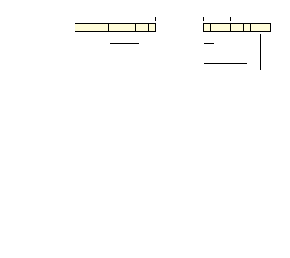
D5 The AArch64 Virtual Memory System Architecture
D5.4 VMSAv8-64 translation table format descriptors
ARM DDI 0487A.a Copyright © 2013 ARM Limited. All rights reserved. D5-1777
ID090413 Non-Confidential - Beta
UXNTable or XNTable, bit[60]
XN limit for subsequent levels of lookup, see Hierarchical control of instruction fetching on
page D5-1786.
This bit is called UXNTable in the EL1&0 translation regime, where it only determines whether
execution at EL0 of instructions fetched from the region identified at a lower level of lookup
permitted. In the other translation regimes the bit is called XNTable.
PXNTable, bit[59]
PXN limit for subsequent levels of lookup, see Hierarchical control of instruction fetching on
page D5-1786.
This bit is reserved, SBZ:
• In the EL2 translation regime.
• In the EL3 translation regime.
Attribute fields in stage 1 VMSAv8-64 Block and Page descriptors
In Block and Page descriptors, the memory attributes are split into an upper block and a lower block, as shown for
a stage 1
translation:
For a stage 1 descriptor, the attributes are:
UXN or XN, bit[54]
The Execute-never bit. Determines whether the region is executable, see Access permissions for
instruction execution on page D5-1784.
This bit is called UXN in the EL1&0 translation regime, where it only determines whether execution
at EL0 of instructions fetched from the region is permitted. In the other translation regimes the bit
is called XN.
PXN, bit[53] The Privileged execute-never bit. Determines whether the region is executable at EL1, see Access
permissions for instruction execution on page D5-1784.
This bit is reserved, SBZ, in the EL2 and EL3 translation regimes.
Contiguous, bit[52]
A hint bit indicating that the translation table entry is one of a contiguous set or entries, that might
be cached in a single TLB entry, see The Contiguous bit on page D5-1792.
nG, bit[11] The not global bit. Determines whether the TLB entry applies to all ASID values, or only to the
current ASID value, see Global and process-specific translation table entries on page D5-1805.
Valid only to the EL1&0 translation regime. This bit is reserved, SBZ, in all other translation
regimes.
AF, bit[10] The Access flag, see The Access flag on page D5-1788.
SH, bits[9:8] Shareability field, see Memory region attributes on page D5-1788.
Upper attributes Lower attributes
Ignored
63 59 58 55 54 53 52
UXN or XN †
PXN
Contiguous
1110987654 2
nG
AF
SH[1:0]
AP[2:1]
NS
AttrIndx[2:0]
Reserved for software use
Attribute fields for VMSAv8-64 stage 1 Block and Page descriptors
† UXN for the EL1&0 translation regime, XN for the other regimes.
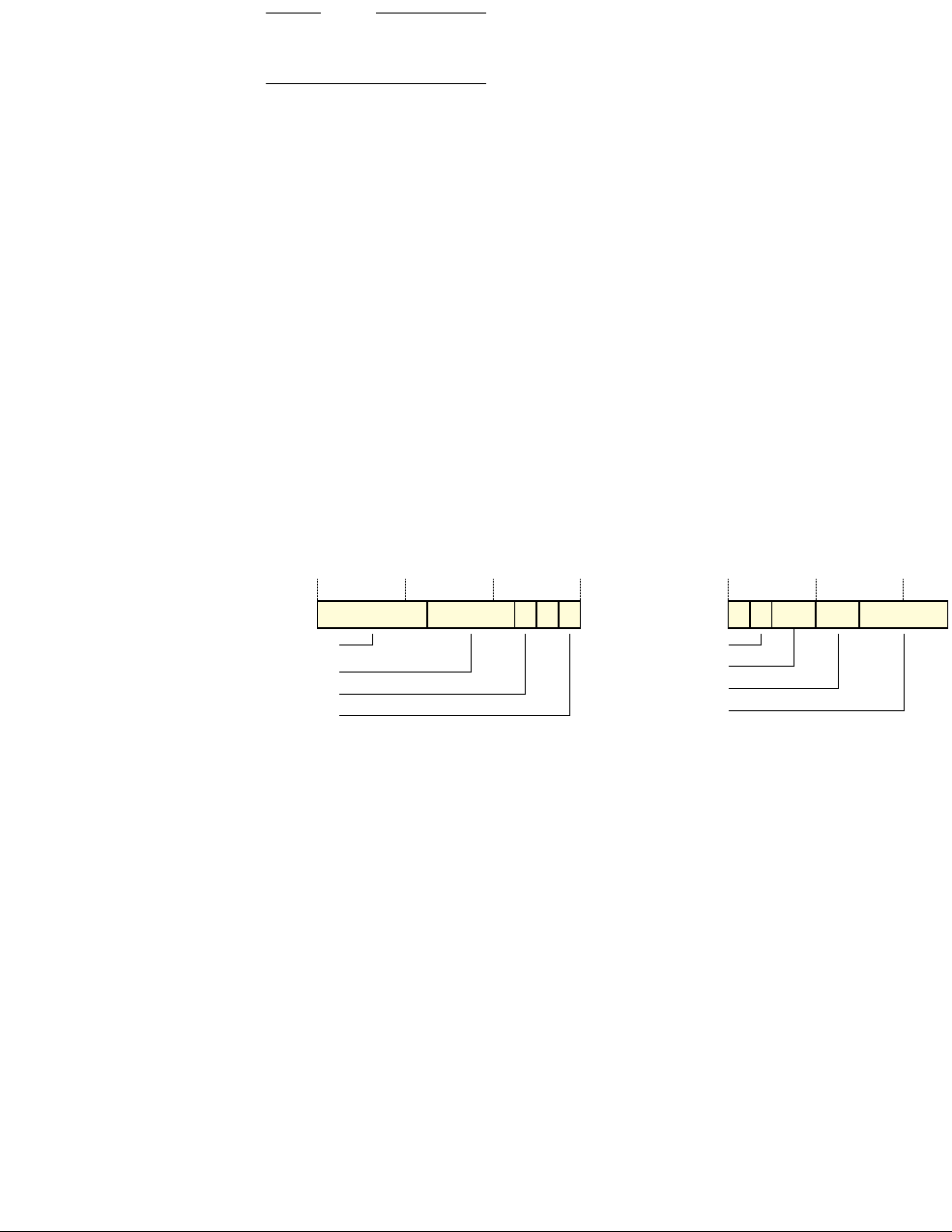
D5 The AArch64 Virtual Memory System Architecture
D5.4 VMSAv8-64 translation table format descriptors
D5-1778 Copyright © 2013 ARM Limited. All rights reserved. ARM DDI 0487A.a
Non-Confidential - Beta ID090413
AP[2:1], bits[7:6]
Data Access Permissions bits, see Memory access control on page D5-1781.
Note
The ARMv8 translation table descriptor format defines AP[2:1] as the Access Permissions bits, and
does not define an AP[0] bit.
AP[1] is reserved, SBO, in the Non-secure EL2 translation regime.
NS, bit[5] Non-secure bit. For memory accesses from Secure state, specifies whether the output address is in
the Secure or Non-secure address map, see Control of Secure or Non-secure memory access on
page D5-1779.
For memory accesses from Non-secure state, this bit is ignored.
AttrIndx[2:0], bits[4:2]
Stage 1 memory attributes index field, for the MAIR_ELx, see Memory region type and attributes,
for stage 1 translations on page D5-1789.
In the upper attributes block, the architecture guarantees that PE makes no use of the fields marked as Ignored and
Reserved for software use. For more information see Other fields in the VMSAv8-64 translation table format
descriptors on page D5-1791.
Attribute fields in stage 2 VMSAv8-64 Block and Page descriptors
In Block and Page descriptors, the memory attributes are split into an upper block and a lower block, as shown for
a stage 2 translation:
For a stage 2 descriptor, the attributes are:
XN, bit[54] The Execute-never bit. Determines whether the region is executable, see Access permissions for
instruction execution on page D5-1784.
Contiguous, bit[52]
A hint bit indicating that the translation table entry is one of a contiguous set or entries, that might
be cached in a single TLB entry, see The Contiguous bit on page D5-1792.
AF, bit[10] The Access flag, see The Access flag on page D5-1788.
SH, bits[9:8] Shareability field, see The memory region attributes for stage 2 translations, EL1&0 translation
regime on page D5-1790.
S2AP, bits[7:6]
Stage 2 data Access Permissions bits, see The S2AP data access permissions, Non-secure EL1&0
translation regime on page D5-1783.
Lower attributes
MemAttr[3:0]
111098765 2
(0)
AF
SH[1:0]
S2AP[1:0]
Upper attributes
63 59 58 55 54 53 52
(0)
XN
Contiguous
Reserved for software use
Reserved for System MMU
Attribute fields for VMSAv8-64 stage 2 Block and Page descriptors

D5 The AArch64 Virtual Memory System Architecture
D5.4 VMSAv8-64 translation table format descriptors
ARM DDI 0487A.a Copyright © 2013 ARM Limited. All rights reserved. D5-1779
ID090413 Non-Confidential - Beta
Note
In the original VMSAv7-32 Long-descriptor attribute definition, this field was called HAP[2:1], for
consistency with the AP[2:1] field in the stage 1 descriptors and despite there being no HAP[0] bit.
ARMv8 renames the field for greater clarity.
MemAttr, bits[5:2]
Stage 2 memory attributes, see The memory region attributes for stage 2 translations, EL1&0
translation regime on page D5-1790.
In the upper attributes block:
• The field marked as Reserved for System MMU use must be ignored by the PE.
• The architecture guarantees that the PE makes no use of the fields marked as Reserved for System MMU and
Reserved for software use.
For more information see Other fields in the VMSAv8-64 translation table format descriptors on page D5-1791.
D5.4.4 Control of Secure or Non-secure memory access
As this section describes, the NS bit in the translation table entries:
• For accesses from Secure state, if the translation table entry was held in secure memory, determines whether
the access is to Secure or Non-secure memory.
• Is ignored by:
— Accesses from Non-secure state.
— Accesses from Secure state if the translation table entry was held in Non-secure memory.
In the VMSAv8-64 translation table format:
• The NS bit relates only to the memory block or page at the output address defined by the descriptor.
• The descriptors also include an NSTable bit, that affects accesses at lower levels of lookup, see Hierarchical
control of Secure or Non-secure memory accesses on page D5-1780.
The NS and NSTable bits are valid only for memory accesses from Secure state described by translation table
descriptors that are fetched from Secure memory, and:
• In the translation table descriptors in a Non-secure translation table, the NS and NSTable bits are SBZ.
• Memory accesses from Non-secure state, including all accesses from EL2, ignore the values of these bits.
In the Secure translation regimes, for translation table descriptors that are fetched from Secure memory, the NS bit
in a descriptor indicates whether the descriptor refers to the Secure or the Non-secure address map, as follows:
NS == 0 Access the Secure physical address space.
NS == 1 Access the Non-secure physical address space.
For Non-secure translation regimes, and for translation table descriptors fetched from Non-secure memory, the
corresponding bit is SBZ and is ignored by the PE. The access is made to Non-secure memory, regardless of the
value of the bit.

D5 The AArch64 Virtual Memory System Architecture
D5.4 VMSAv8-64 translation table format descriptors
D5-1780 Copyright © 2013 ARM Limited. All rights reserved. ARM DDI 0487A.a
Non-Confidential - Beta ID090413
Hierarchical control of Secure or Non-secure memory accesses
For VMSAv8-64 table descriptors for stage 1 translations, the descriptor includes an NSTable bit, that indicates
whether the table identified in the descriptor is in Secure or Non-secure memory. For accesses from Secure state,
the meaning of the NSTable bit is:
NSTable == 0 The defined table address is in the Secure physical address space. In the descriptors in that
translation table, NS bits and NSTable bits have their defined meanings.
NSTable == 1 The defined table address is in the Non-secure physical address space. Because this table is fetched
from the Non-secure address space, the NS and NSTable bits in the descriptors in this table must be
ignored. This means that, for this table:
• The value of the NS bit in any block or page descriptor is ignored. The block or page address
refers to Non-secure memory.
• The value of the NSTable bit in any table descriptor is ignored, and the table address refers
to Non-secure memory. When this table is accessed, the NS bit in any block or page
descriptor is ignored, and all descriptors in the table refer to Non-secure memory.
In addition, an entry fetched in Secure state is treated as non-global if either:
• NSTable is set to 1.
• The fetch ignores the values of NS and NSTable, because of a higher-level fetch with NSTable set to 1.
That is, these entries must be treated as if nG==1, regardless of the value of the nG bit. For more information about
the nG bit, see Global and process-specific translation table entries on page D5-1805.

D5 The AArch64 Virtual Memory System Architecture
D5.5 Access controls and memory region attributes
ARM DDI 0487A.a Copyright © 2013 ARM Limited. All rights reserved. D5-1781
ID090413 Non-Confidential - Beta
D5.5 Access controls and memory region attributes
In addition to an output address, a translation table entry that refers to a page or region of memory includes fields
that define properties of the target memory region. These fields can be classified as address map control, access
control, and region attribute fields. Control of Secure or Non-secure memory access on page D5-1779 describes the
address map control, and the following sections describe the other fields:
•Memory access control.
•Memory region attributes on page D5-1788.
•Combining the stage 1 and stage 2 attributes, Non-secure EL1&0 translation regime on page D5-1793.
Note
This section describes the access controls and memory region attributes for each of the translation regimes, and for
both stages of translation in the Non-secure EL1&0 translation regime. In general, attribute assignment is simpler
in the EL2 and EL3 translation regimes, and in these regimes behavior is consistent fields in the translation tables
being treated as follows:
• APTable[0] is ignored by hardware and is treated as if it is 0.
• AP[1] is ignored by hardware and is treated as if it is 1.
• the PXNTable bit is ignored by hardware and is treated as if it is 0.
• the PXN field is ignored by hardware and is treated as if it is 0.
D5.5.1 Memory access control
The access control fields in the translation table descriptors determine whether the PE, in its current state, is
permitted to perform the required access to the output address given in the translation table descriptor. If a
translation stage does not permit the access then an MMU fault is generated for that translation stage, and no
memory access is performed.
The following sections describe the memory access controls:
•About the access permissions.
•The data access permission controls on page D5-1782.
•Access permissions for instruction execution on page D5-1784.
•The Access flag on page D5-1788.
About the access permissions
Note
This section gives a general description of memory access permissions. In an implementation that includes EL2,
software executing at EL1 in Non-secure state can see only the access permissions defined by the Non-secure
EL1&0 stage 1 translations. However, software executing at EL2 can modify these permissions. This modification
is invisible to the Non-secure software executing at EL1 or EL0.
The access permission bits control access to the corresponding memory region. The VMSAv8-64 translation table
format:
• In stage 1 translations, uses AP[2:1] to define the data access permissions, see The AP[2:1] data access
permissions, for stage 1 translations on page D5-1782.
Note
The description of the access permission field as AP[2:1] is for consistency with the VMSAv8-32
Short-descriptor translation table format, see The VMSAv8-32 Short-descriptor translation table format on
page G3-3578. The VMSAv8-64 translation table format does not define an AP[0] bit.

D5 The AArch64 Virtual Memory System Architecture
D5.5 Access controls and memory region attributes
D5-1782 Copyright © 2013 ARM Limited. All rights reserved. ARM DDI 0487A.a
Non-Confidential - Beta ID090413
• In stage 2 translations, uses S2AP[1:0] to define the data access permissions, see The S2AP data access
permissions, Non-secure EL1&0 translation regime on page D5-1783.
• Uses the UXN, XN and PXN bits to define access controls for instruction fetches, see Access permissions for
instruction execution on page D5-1784.
An attempt to perform a memory access that the translation table access permission bits do not permit generates a
Permission fault, for the corresponding stage of translation.
Note
In an implementation that includes EL2, each stage of the translation of a memory access made from Non-secure
EL1 or EL0 has its own, independent, permission check.
The data access permission controls
The following subsubsections describe the data access permission controls:
•The AP[2:1] data access permissions, for stage 1 translations.
•The S2AP data access permissions, Non-secure EL1&0 translation regime on page D5-1783.
•Hierarchical control of data access permissions on page D5-1783.
The AP[2:1] data access permissions, for stage 1 translations
For the VMSAv8-64 EL1&0 translation regime, the AP[2:1] bits control the stage 1 data access permissions, and:
AP[2] Selects between read-only and read/write access.
AP[1] Selects between Application level (EL0) and System level (EL1) control.
This provides four permission settings for data accesses:
• Read-only at all levels.
• Read/write at all levels.
• Read-only at EL1, no access by software executing at EL0.
• Read/write at EL1, no access by software executing at EL0.
For translation regimes other than the EL1&0 translation regimes, AP[2] determines the stage 1 data access
permissions, and AP[1] is:
•SBO.
• Ignored by hardware and is treated as if it is 1.
Table D5-26 shows the effect of the data access permission bits for stage 1 of the EL1&0 translation regime. In this
table, an entry of None indicates that any access from that Exception level faults.
For the Non-secure EL1&0 translation regime:
• The stage 2 translation also defines data access permissions, see The S2AP data access permissions,
Non-secure EL1&0 translation regime on page D5-1783.
• When both stages of translation are enabled, Combining the stage 1 and stage 2 data access permissions on
page D5-1793 describes how these permissions are combined.
Table D5-26 Data access permissions for stage 1 of the EL1&0 translation regime,
AP[2:1] Access from EL1 Access from EL0
00 Read/write None
01 Read/write Read/write
10 Read-only None
11 Read-only Read-only

D5 The AArch64 Virtual Memory System Architecture
D5.5 Access controls and memory region attributes
ARM DDI 0487A.a Copyright © 2013 ARM Limited. All rights reserved. D5-1783
ID090413 Non-Confidential - Beta
Table D5-27 shows the effect of the AP[2] data access permission bit for the EL2 and EL3 translation regimes:
The S2AP data access permissions, Non-secure EL1&0 translation regime
In the Non-secure EL1&0 translation regime, when stage 2 address translation is enabled, the S2AP field in the stage
2 translation table descriptors define the data access permissions as Table D5-28 shows. In this table, an entry of
None indicates that any access generates a permission fault:
The S2AP access permissions make no distinction between Non-secure accesses from EL1 and Non-secure accesses
from EL0. However, when both stages of address translation are enabled, these permissions are combined with the
stage 1 access permissions defined by AP[2:1], see Combining the stage 1 and stage 2 data access permissions on
page D5-1793.
Combining the stage 1 and stage 2 attributes, Non-secure EL1&0 translation regime on page D5-1793 gives more
information about the use of the stage 1 and stage 2 access permissions in an implementation of virtualization.
Hierarchical control of data access permissions
The VMSAv8-64 translation table format includes mechanisms by which entries at one level of translation table
lookup can set limits on the permitted entries at subsequent levels of lookup. This subsection describes how these
controls apply to the data access permissions.
Note
Similar hierarchical controls apply to instruction fetching, see Hierarchical control of instruction fetching on
page D5-1786.
The restrictions apply only to subsequent levels of lookup for the same stage of translation. The APTable[1:0] field
restricts the access permissions, as Table D5-29 shows.
As stated in the table footnote, for the EL2 translation regime, APTable[0] is reserved, SBZ, and is ignored by the
hardware.
Table D5-27 Data access permissions for the EL2 or EL3 translation regime
AP[2] Access from EL2 or EL3
0Read/write
1 Read-only
Table D5-28 Data access permissions for stage 2 of the Non-secure EL1&0 translation regime,
S2AP Access from Non-secure EL1or Non-secure EL0
00 None
01 Read-only
10 Write-only
11 Read/write
Table D5-29 Effect of APTable[1:0] on subsequent levels of lookup
APTable[1:0] Effect
00 No effect on permissions in subsequent levels of lookup.
01aAccess at EL0 not permitted, regardless of permissions in subsequent levels of lookup.
10 Write access not permitted, at any Exception level, regardless of permissions in subsequent levels of lookup.

D5 The AArch64 Virtual Memory System Architecture
D5.5 Access controls and memory region attributes
D5-1784 Copyright © 2013 ARM Limited. All rights reserved. ARM DDI 0487A.a
Non-Confidential - Beta ID090413
Note
The APTable[1:0] settings are combined with the translation table access permissions in the translation tables
descriptors accessed in subsequent levels of lookup. They do not restrict or change the values entered in those
descriptors.
The VMSAv8-64 provides APTable[1:0] control only for the stage 1 translations. The corresponding bits are SBZ
in the stage 2 translation table descriptors.
When APTable[1:0] is not set to
0b00
, its effects might be held in one or more TLB entries. Therefore, a change to
APTable[1:0] might require coarse-grained invalidation of the TLB to ensure that the effect of the change is visible
to subsequent memory transactions.
Access permissions for instruction execution
Execute-never (XN) controls determine whether an instruction fetched from the memory region can be executed.
These controls are:
UXN, Unprivileged Execute never
Defined only for stage 1 of the EL1&0 translation regime.
PXN, Privileged execute never
Used only for stage 1 of the EL1&0 translation regime:
• For the EL2 and EL3 translation regimes, the descriptors define a PXN bit that is reserved,
SBZ, and is ignored by hardware.
• For stage 2 of the Non-secure EL1&0 translation regime, the corresponding bit position is
reserved, SBZ, and is ignored by hardware.
XN, Unprivileged Execute never
Defined only for stage 1 of the EL2 and EL3 translation regimes.
Each of theses bits is set to 1 to indicate that instructions cannot be executed from the target memory region. In
addition:
• For the EL1&0 translation regime, if the value of the AP[2:1] bits is
0b01
, permitting write access from EL0,
then the PXN bit is treated as if it has the value 1, regardless of its actual value.
• For each translation regime, if the value of the corresponding SCTLR_ELx.WXN bit is 1 then any memory
region that is writable is treated as XN, regardless of the value of the corresponding UXN, XN, or PXN bit.
For more information see Preventing execution from writable locations on page D5-1787.
• The SCR_EL3.SIF bit prevents execution in Secure state of any instruction fetched from Non-secure
memory, see Restriction on Secure instruction fetch on page D5-1788.
The execute-never controls apply to speculative instruction fetching, meaning speculative instruction fetch from a
memory region that is execute-never at the current Exception level is prohibited.
11aRegardless of permissions in subsequent levels of lookup:
• Write access not permitted, at any Exception level.
• Read access not permitted at EL0.
a. Not valid for the EL2 translation regime. In the translation tables for that regime, APTable[0] is SBZ and is ignored by hardware.
Table D5-29 Effect of APTable[1:0] on subsequent levels of lookup (continued)
APTable[1:0] Effect

D5 The AArch64 Virtual Memory System Architecture
D5.5 Access controls and memory region attributes
ARM DDI 0487A.a Copyright © 2013 ARM Limited. All rights reserved. D5-1785
ID090413 Non-Confidential - Beta
Note
• Although the execute-never controls apply to speculative fetching, on a speculative instruction fetch from an
execute-never location, no Permission fault is generated unless the PE attempts to execute the instruction
fetched from that location. This means that, if a speculative fetch from an execute-never location is
attempted, but there is no attempt to execute the corresponding instruction, a Permission fault is not
generated.
• The software that defines a translation table must mark any region of memory that is read-sensitive as
execute-never, to avoid the possibility of a speculative fetch accessing the memory region. This means it must
mark any memory region that corresponds to a read-sensitive peripheral as execute-never.
• When no stage of address translation for the translation regime is enabled, memory regions cannot have
UXN, XN, or PXN attributes assigned. Behavior of instruction fetches when all associated stages of
translation are disabled on page D5-1744 describes how disabling all stages of address translation affects
instruction fetching.
The following subsubsections describe the data access permission controls:
•Instruction execution permissions for stage 1 translations.
•Instruction execution permissions for stage 2 translations on page D5-1786.
•Hierarchical control of instruction fetching on page D5-1786.
•Preventing execution from writable locations on page D5-1787.
•Restriction on Secure instruction fetch on page D5-1788.
Instruction execution permissions for stage 1 translations
Table D5-30 shows the access permissions for instruction execution for stage 1 of the EL1&0 translation regime.
Table D5-30 Access permissions for instruction execution for stage 1 of the EL1&0 translation
regime
UXN PXN AP[2:1]a
a. See Table D5-26 on page D5-1782.
0b00
indicates writable from EL1 only,
0b01
indicates writable from EL1 and
EL0,
0b1x
indicates not writable from EL1 or EL0.
SCTLR_EL1.WXN Access from EL1 Access from EL0
0 0 00 0 Executable Executable
1Not executablebExecutable
01 0 Not executablecExecutable
1 Not executable Not executabled
1x x Executable Executable
0 1 00 x Not executable Executable
01 0 Not executable Executable
1 Not executable Not executabled
1x x Not executable Executable
1 0 00 0 Executable Not executable
1Not executablebNot executable
01 x Not executablecNot executable
1x x Executable Not executable
1 xx x Not executable Not executable

D5 The AArch64 Virtual Memory System Architecture
D5.5 Access controls and memory region attributes
D5-1786 Copyright © 2013 ARM Limited. All rights reserved. ARM DDI 0487A.a
Non-Confidential - Beta ID090413
Table D5-31 shows the access permissions for instruction execution for the EL2 and EL3 translation regimes:
Instruction execution permissions for stage 2 translations
For the Non-secure EL1&0 stage 2 translation, the XN bit in the stage 2 translation table descriptors controls the
execution permission, and this control is completely independent of the S2AP access permissions.
The stage 2 XN access permissions make no distinction between Non-secure accesses from EL1 and Non-secure
accesses from EL0. However, when both stages of address translation are enabled, these permissions are combined
with the stage 1 access permissions defined at stage 1 of the translation, see Combining the stage 1 and stage 2
instruction execution permissions on page D5-1793.
Hierarchical control of instruction fetching
The VMSAv8-64 translation table format includes mechanisms by which entries at one level of table lookup can set
limits on the permitted entries at subsequent levels of lookup. This subsection describes how these controls apply
to the data access permissions.
The VMSAv8-64 translation table format includes mechanisms by which entries at one level of translation table
lookup can set limits on the permitted entries at subsequent levels of lookup. This subsection describes how these
controls apply to the instruction fetching controls.
Note
Similar hierarchical controls apply to data accesses, see Hierarchical control of data access permissions on
page D5-1783.
b. Not executable because of SCTLR_EL1.WXN control, because region is writable at EL1.
c. Not executable, because AArch64 execution treats all regions writable at EL0 as being PXN.
d. Not executable because of SCTLR_EL1.WXN control, because region is writable at EL0.
Table D5-31 Access permissions for instruction execution, EL2 and EL3 translation regimes
XN AP[2]a
a. See Table D5-27 on page D5-1783. 0 indicates writable from this Exception level, and 1 indicates not writable.
SCTLR_EL2.WXN orb
SCTLR_EL3.WXN
b. SCTLR_EL2 for the EL2 translation regime, SCTLR_EL3 for the EL3 translation regime.
Access from EL2 or EL3
0 0 0 Executable
1Not executablec
c. Not executable because of the SCTLR_ELx.WXN control, because region is writable at this Exception level.
10 Executable
1 x x Not executable
Table D5-32 Access permissions for instruction execution for stage 2 of the Non-secure EL1&0
translation regime,
XN Access from Non-secure EL1or Non-secure EL0
0 Executable
1 Not executable

D5 The AArch64 Virtual Memory System Architecture
D5.5 Access controls and memory region attributes
ARM DDI 0487A.a Copyright © 2013 ARM Limited. All rights reserved. D5-1787
ID090413 Non-Confidential - Beta
The restrictions apply only to subsequent levels of lookup at the same stage of translation, and:
• UXNTable or XNTable restricts the XN control:
— When the value of the XNTable bit is 1, the XN bit is treated as 1 in all subsequent levels of lookup,
regardless of its actual value.
— When the value of the UXNtable bit is 1, the UXN bit is treated as 1 in all subsequent levels of lookup,
regardless of its actual value.
— When the value of a UXNtable or XNTable bit is 0 the bit has no effect.
• For the EL1&0 translation regime, PXNTable restricts the PXN control:
— When PXNTable is set to 1, the PXN bit is treated as 1 in all subsequent levels of lookup, regardless
of the actual value of the bit.
— When PXNTable is set to 0 it has no effect.
Note
The UXNtable, XNTable and PXNTable settings are combined with the UXN, XN and PXN bits in the translation
table descriptors accessed at subsequent levels of lookup. They do not restrict or change the values entered in those
descriptors.
The UXNtable, XNTable and PXNTable controls are provided only for stage 1 translations. The corresponding bits
are SBZ in the stage 2 translation table descriptors.
When the value of UXNtable, XNTable, or PXNTable, is 1, its effects might be held in one or more TLB entries.
Therefore, a change to UXNtable, XNTable or PXNTable might require coarse-grained invalidation of the TLB to
ensure that the effect of the change is visible to subsequent memory transactions.
Preventing execution from writable locations
ARMv8 provides control bits that, when corresponding stage 1 address translation is enabled, force writable
memory to be treated as UXN, PXN, or XN, regardless of the value of the UXN, PXN, or XN bit:
• For the EL1&0 translation regime, when the value of SCTLR_EL1.WXN is 1:
— All regions that are writable from EL0 at stage 1 of the address translation are treated as UXN.
— All regions that are writable from EL1 at stage 1 of the address translation are treated as PXN
• For the EL2 translation regime, when the value of SCTLR_EL2.WXN is 1, all regions that are writable at
stage 1 of the address translation are treated as XN.
• For the EL3 translation regime, when the value of SCTLR_EL3.WXN is 1, all regions that are writable at
stage 1 of the address translation are treated as XN.
Note
• The SCTLR_ELx.WXN controls are intended to be used in systems with very high security requirements.
• Setting a WXN bit to 1 changes the interpretation of the translation table entry, overriding a zero value of a
UXN, XN, or PXN field. It does not cause any change to the translation table entry.
For any given virtual machine, ARM expects WXN to remain static in normal operation. In particular, it is
IMPLEMENTATION DEFINED whether TLB entries associated with a particular VMID reflect the effect of the values
of these bits. This means that any change of these bits without a corresponding change of VMID might require
synchronization and TLB invalidation, as described in TLB maintenance requirements and the TLB maintenance
instructions on page D5-1807.

D5 The AArch64 Virtual Memory System Architecture
D5.5 Access controls and memory region attributes
D5-1788 Copyright © 2013 ARM Limited. All rights reserved. ARM DDI 0487A.a
Non-Confidential - Beta ID090413
Restriction on Secure instruction fetch
EL3 provides a Secure instruction fetch bit, SCR_EL3.SIF. When the value of this bit is 1, and execution is using
the EL3 translation regime or the Secure EL1 translation regime, any attempt to execute an instruction fetched from
Non-secure physical memory causes a Permission fault. TLB entries might reflect the value of this bit, and therefore
any change to the value of this bit requires synchronization and TLB invalidation, as described in TLB maintenance
requirements and the TLB maintenance instructions on page D5-1807.
The Access flag
The Access flag indicates when a page or section of memory is accessed for the first time since the Access flag in
the corresponding translation table descriptor was set to 0.
The AF bit in the translation table descriptors is the Access flag.
Software management of the Access flag
ARMv8 requires that software manages the Access flag. This means an Access flag fault is generated whenever an
attempt is made to read into the TLB a translation table descriptor entry for which the value of Access flag is 0.
The Access flag mechanism expects that, when an Access flag fault occurs, software resets the Access flag to 1 in
the translation table entry that caused the fault. This prevents the fault occurring the next time that memory location
is accessed. Entries with the Access flag set to 0 are never held in the TLB, meaning software does not have to flush
the entry from the TLB after setting the flag.
Note
If a system incorporates a System MMU that implements the ARM SMMUv3 architecture and software shares
translation tables between the ARM PE and the SMMUv3, then the software must be aware of the possibility that
the System MMU update the access flag in hardware.
In such a system, system software should perform any changes of translation table entries with an Access flag of 0,
other than changes to the Access flag value, by using an Load-Exclusive/Store-Exclusive loop, to allow for the
possibility of simultaneous updates.
D5.5.2 Memory region attributes
The memory region attribute fields control the memory type, accesses to the caches, and whether the memory region
is Shareable and therefore is coherent. This section also describes some additional translation table fields, that this
manual groups with the memory region attributes.
In the EL1&0 translation regime, each enabled stage of address translation assigns memory region attributes, as
described in this section. When both stages of translation are enabled, Combining the stage 1 and stage 2 attributes,
Non-secure EL1&0 translation regime on page D5-1793 describes how the assignments from the two stages are
combined.
Note
In a virtualization implementation, a hypervisor, executing at EL2, might usefully:
• Reduce the permitted cacheability of a region.
• Increase the required shareability of a region.
The combining of attributes from stage 1 and stage 2 translations supports both of these options.
The following sections describe these attributes:
•The memory region attributes for stage 1 translations on page D5-1789.
•The memory region attributes for stage 2 translations, EL1&0 translation regime on page D5-1790.
•Other fields in the VMSAv8-64 translation table format descriptors on page D5-1791.

D5 The AArch64 Virtual Memory System Architecture
D5.5 Access controls and memory region attributes
ARM DDI 0487A.a Copyright © 2013 ARM Limited. All rights reserved. D5-1789
ID090413 Non-Confidential - Beta
The memory region attributes for stage 1 translations
The description of the memory region attributes in a translation descriptor divides into:
Memory type and attributes
These are described indirectly, by registers referenced by bits in the table descriptor. This is
described as remapping the memory type and attribute description. Memory region type and
attributes, for stage 1 translations describes this encoding.
Shareability The SH[1:0] field in the translation table descriptor encodes shareability information. Shareability
for Normal memory, for stage 1 translations describes this encoding.
Memory region type and attributes, for stage 1 translations
In the VMSAv8-64 translation table format, the AttrIndx[2:0] field in a block or page translation table descriptor
for a stage 1 translation indicates the 8-bit field in the MAIR_ELx that specifies the attributes for the corresponding
memory region. The required field is Attrn, where n = AttrIndx[2:0]. For more information about AttrIndx[2:0] see
Attribute fields in stage 1 VMSAv8-64 Block and Page descriptors on page D5-1777
Note
Each MAIR_ELx is a 64-bit register that is architecturally mapped to a pair of AArch32 registers. See the
MAIR_ELx register descriptions for more information.
Each MAIR_ELx.Attrn field defines, for the corresponding memory region:
• The memory type, Device or Normal.
• For Device memory, the Device memory type, one of:
— Device-nGnRnE.
— Device-nGnRE.
— Device-nGRE.
—Device-GRE.
• For Normal memory:
— The inner and outer cacheability, Non-cacheable, Write-Through, or Write-Back
— For Write-Through Cacheable and Write-Back Cacheable regions, the Read-Allocate and
Write-Allocate policy hints, each of which is Allocate or Do not allocate, and the Transient allocation
hints.
For more information about the memory type and attributes, see Memory types and attributes on page B2-89.
Shareability for Normal memory, for stage 1 translations
When using the VMSAv8-64 translation table format, the SH[1:0] field in a block or page translation table
descriptor specifies the Shareability attributes of the corresponding memory region. Table D5-33 shows the
encoding of this field.
Table D5-33 SH[1:0] field encoding for Normal memory, VMSAv8-64 translation table format
SH[1:0] Normal memory
00 Non-shareable
01 UNPREDICTABLE
10 Outer Shareable
11 Inner Shareable

D5 The AArch64 Virtual Memory System Architecture
D5.5 Access controls and memory region attributes
D5-1790 Copyright © 2013 ARM Limited. All rights reserved. ARM DDI 0487A.a
Non-Confidential - Beta ID090413
Note
The shareability field is only relevant if the memory is a Normal Cacheable memory type. All Device and Normal
Non-cacheable memory regions are always treated as Outer Shareable, regardless of the translation table
shareability attributes
See Combining the stage 1 and stage 2 shareability attributes for Normal memory on page D5-1795 for constraints
on the Shareability attributes of a Normal memory region that is Inner Non-cacheable, Outer Non-cacheable.
The memory region attributes for stage 2 translations, EL1&0 translation regime
In the stage 2 translation table descriptors for memory regions and pages, the MemAttr[3:0] and SH[1:0] fields
describe the stage 2 memory region attributes:
•Memory region type and attributes for stage 2 translations describes how the MemAttr[3:0] field defines
these attributes.
• The SH[1:0] field in the translation table descriptor encodes shareability information. Shareability for
Normal memory, for stage 2 translations on page D5-1791 describes this encoding.
The following sections describe how, when both stages of address translation are enabled, the memory region
attributes assigned at stage 2 of the translation are combined with those assigned at stage 1:
•Combining the stage 1 and stage 2 memory type attributes on page D5-1794
•Combining the stage 1 and stage 2 cacheability attributes for Normal memory on page D5-1794
•Combining the stage 1 and stage 2 shareability attributes for Normal memory on page D5-1795.
Memory region type and attributes for stage 2 translations
Table D5-34 shows how MemAttr[3:2] gives a top-level definition of the memory type, and of the outer cacheability
of a Normal memory region:
The encoding of MemAttr[1:0] depends on the Memory type indicated by MemAttr[3:2]:
• When MemAttr[3:2]==
0b00
, indicating Device memory, Table D5-35 shows the encoding of MemAttr[1:0]:
Table D5-34 VMSAv8-64 MemAttr[3:2] encoding, stage 2 translation
MemAttr[3:2] Memory type Outer cacheability
00 Device. MemAttr[1:0] encodes the Device memory type. Not applicable
01 Normal. MemAttr[1:0] encodes the Inner Cacheability. Outer Non-cacheable
10 Outer Write-Through Cacheable
11 Outer Write-Back Cacheable
Table D5-35 MemAttr[1:0] encoding for Strongly-ordered or Device memory
MemAttr[1:0] Meaning when MemAttr[3:2] ==
0b00
00 Region is Device-nGnRnE memory
01 Region is Device-nGnRE memory
10 Region is Device-nGRE memory
11 Region is Device-GRE memory

D5 The AArch64 Virtual Memory System Architecture
D5.5 Access controls and memory region attributes
ARM DDI 0487A.a Copyright © 2013 ARM Limited. All rights reserved. D5-1791
ID090413 Non-Confidential - Beta
• When MemAttr[3:2]!=
0b00
, indicating Normal memory, Table D5-36 shows the encoding of MemAttr[1:0]:
Note
The stage 2 translation does not assign any allocation hints.
Note
The following stage 2 translation table attribute settings leave the stage 1 settings unchanged:
• MemAttr[3:2] ==
0b11
, Normal memory, Outer Write-Back Cacheable
• MemAttr[1:0] ==
0b11
, Inner Write-Back Cacheable.
Shareability for Normal memory, for stage 2 translations
When using the VMSAv8-64 translation table format, the SH[1:0] field in a block or page translation table
descriptor specifies the Shareability attributes of the corresponding memory region. Table D5-37 shows the
encoding of this field.
Note
• This encoding is the same as the shareability encoding described in Shareability for Normal memory, for
stage 1 translations on page D5-1789.
• The shareability field is only relevant if the memory is a Normal Cacheable memory type. All Device and
Normal Non-cacheable memory regions are always treated as Outer Shareable, regardless of the translation
table shareability attributes
See Combining the stage 1 and stage 2 shareability attributes for Normal memory on page D5-1795 for constraints
on the Shareability attributes of a Normal memory region that is Inner Non-cacheable, Outer Non-cacheable.
Other fields in the VMSAv8-64 translation table format descriptors
The following subsections describe the other fields in the translation table block and page descriptors:
•The Contiguous bit on page D5-1792
•Field reserved for software use on page D5-1792
Table D5-36 MemAttr[1:0] encoding for Normal memory
MemAttr[1:0] Meaning when MemAttr[3:2] !=
0b00
00 UNPREDICTABLE
01 Inner Non-cacheable
10 Inner Write-Through Cacheable
11 Inner Write-Back Cacheable
Table D5-37 SH[1:0] field encoding for Normal memory, VMSAv8-64 translation table format
SH[1:0] Normal memory
00 Non-shareable
01 UNPREDICTABLE
10 Outer Shareable
11 Inner Shareable

D5 The AArch64 Virtual Memory System Architecture
D5.5 Access controls and memory region attributes
D5-1792 Copyright © 2013 ARM Limited. All rights reserved. ARM DDI 0487A.a
Non-Confidential - Beta ID090413
•Ignored fields on page D5-1793.
The Contiguous bit
When the value of the Contiguous bit is 1, it indicates that the entry is one of a number of adjacent translation table
entries that point to a contiguous output address range. The required number of adjacent entries depends on the
current translation granule size, as follows:
4KB granule 16 adjacent translation table entries point to a contiguous output address range that has the same
permissions and attributes. These 16 entries must be aligned in the translation table. If accessing a
full-sized 4KB translation table, this means that the top 5 of the 9 input addresses bits that index the
descriptor positions in the translation table are the same for all of the entries.
The contiguous output address range must be aligned to size of 16 translation table entries at the
same translation table level.
16KB granule This bit indicates that adjacent translation table entries point to contiguous output address range that
has the same permissions and attributes. With the 16KB granule, the number of contiguous entries
indicated by setting this bit to 1 depends on the lookup level of the translation table:
Second level lookup The bit indicates 32 contiguous entries, giving a 1GB block of memory.
These entries must be aligned in the translation table. When accessing a
full-sized 16KB translation table, this means the top 6 of the 11 input
addresses bits that index the descriptor positions in the translation table are
the same for all of the entries.
The contiguous output address range must be aligned to size of 32
translation table entries at the same translation table level.
Third level lookup The bit indicates 128 contiguous entries, giving a 2MB block of memory.
These entries must be aligned in the translation table. When accessing a
full-sized 16KB translation table, this means the top 4 of the 11 input
addresses bits that index the descriptor positions in the translation table are
the same for all of the entries.
The contiguous output address range must be aligned to size of 128
translation table entries at the same translation table level.
64KB granule 32 adjacent translation table entries point to a contiguous output address range that has the same
permissions and attributes. These 32 entries must be aligned in the translation table. If accessing a
full-sized 64KB translation table, this means that the top 8 of the 13 input addresses bits that index
the descriptor positions in the translation table are the same for all of the entries.
The contiguous output address range must be aligned to size of 32 translation table entries at the
same translation table level.
Setting this bit to 1 means that the TLB can cache a single entry to cover the contiguous translation table entries.
This section defines the requirements for programming the contiguous bit. Possible translation table registers
programming errors on page D5-1738 describes the effect of not meeting these requirements.
The architecture does not require a PE to cache TLB entries in this way. To avoid TLB coherency issues, any TLB
maintenance by address must not assume any optimization of the TLB tables that might result from use of the
contiguous bit.
TLB maintenance must be performed based on the size of the underlying translation table entries, to avoid TLB
coherency issues.
Field reserved for software use
The architecture reserves a 4-bit field in the Block and Page table descriptors for software use. The architecture
guarantees that hardware makes no use of this field.
Note
This means there is no need to invalidate the TLB if these bits are changed.

D5 The AArch64 Virtual Memory System Architecture
D5.5 Access controls and memory region attributes
ARM DDI 0487A.a Copyright © 2013 ARM Limited. All rights reserved. D5-1793
ID090413 Non-Confidential - Beta
Ignored fields
For stage 1 translation descriptors, the architecture defines a 4-bit Ignored field in the Block and Page table
descriptors, bit[63:59], and guarantees that hardware makes no use of this field. For stage 2 translation descriptors,
the corresponding field is reserved for use by a System MMU control, and the ARMv8 architecture requires a PE
to ignore this field.
D5.5.3 Combining the stage 1 and stage 2 attributes, Non-secure EL1&0 translation regime
The Non-secure EL1&0 translation regime comprises two stage of translation, each of which can be enabled
independently:
• Stage 1 translation is configured and controlled from EL1. When enabled, stage 1 translation can define
access permissions independently for access from EL0 and for accesses from EL1.
Stage 1 MMU faults are taken to EL1.
• When stage 2 translation is enabled, the stage 2 access controls defined at EL2:
— Affect only the Non-secure stage 1 access permissions settings.
— Take no account of whether the accesses are at EL1 or EL0.
— Permit software executing at EL2 to assign a write-only attribute to a memory region.
Stage 2 MMU faults are taken to EL2.
Note
In an implementation of virtualization, the attributes defined in the stage 2 translation tables mean a hypervisor can
define additional access restrictions to those defined by a Guest OS in the stage 1 translation tables. For a particular
access, the actual access permission is the more restrictive of the permissions defined by:
• The Guest OS, in the stage 1 translation tables.
• The hypervisor, in the stage 2 translation tables.
The effects of the combination of attributes defined by the Hypervisor are functionally transparent to the Guest OS.
Combining the stage 1 and stage 2 data access permissions
When both stages of translation are enabled, the following access permissions are combined:
• The stage 1 permissions described in The AP[2:1] data access permissions, for stage 1 translations on
page D5-1782.
• The stage 2 permissions described in The S2AP data access permissions, Non-secure EL1&0 translation
regime on page D5-1783.
The stage 1 and stage 2 permissions are combined as follows:
1. If an access is not permitted by the stage 1 permissions, then it generates a Stage 1 Permission fault,
regardless of the stage 2 permissions.
2. If an access is permitted by the stage 1 permissions, but is not permitted by the stage 2 Permissions, then it
generates a Stage 2 Permission fault.
3. If an access is permitted by both the stage 1 permissions and the stage 2 permissions, then it does not generate
a Permission fault.
Combining the stage 1 and stage 2 instruction execution permissions
When both stages of translation are enabled, the following access permissions are combined:
• The stage 1 permissions described in Instruction execution permissions for stage 1 translations on
page D5-1785.

D5 The AArch64 Virtual Memory System Architecture
D5.5 Access controls and memory region attributes
D5-1794 Copyright © 2013 ARM Limited. All rights reserved. ARM DDI 0487A.a
Non-Confidential - Beta ID090413
• The stage 2 permissions described in Instruction execution permissions for stage 2 translations on
page D5-1786.
The stage 1 and stage 2 permissions are combined as follows:
1. If an instruction fetch is not permitted by the stage 1 permissions, then it generates a Stage 1 Permission fault,
regardless of the stage 2 permissions.
2. If an instruction fetch is permitted by the stage 1 permissions, but is not permitted by the stage 2 Permissions,
then it generates a Stage 2 Permission fault.
3. If an instruction fetch is permitted by both the stage 1 permissions and the stage 2 permissions, then it does
not generate a Permission fault.
Combining the stage 1 and stage 2 memory type attributes
Table D5-38 shows the rules for combining the stage 1 and stage 2 memory type assignments:
Regardless of any shareability attribute obtained as described in Combining the stage 1 and stage 2 shareability
attributes for Normal memory on page D5-1795:
• Any location for which the resultant memory type is any type of Device memory is always treated as Outer
shareable.
• Any location for which the resultant memory type is Normal Inner Non-cacheable, Outer Non-cacheable is
always treated as Outer shareable.
For information about how the cacheability attribute is obtained from the attributes assigned at each stage of
translation see Combining the stage 1 and stage 2 cacheability attributes for Normal memory.
The combining of the memory type attributes from the two stages of translation means a translation table walk for
a stage 1 translation can be made to Device memory. This is likely to indicate a Guest OS error, and if the value of
HCR_EL2.PTW is 1 such an access is trapped to EL2.
Combining the stage 1 and stage 2 cacheability attributes for Normal memory
For a Normal memory region, Table D5-39 shows how the stage 1 and stage 2 cacheability assignments are
combined. This combination applies, independently, for the Inner cacheability and Outer cacheability attributes:
Table D5-38 Combining the stage 1 and stage 2 memory type assignments
Rule If either stage of translation
assigns: The resultant memory type is:
Device has precedence over Normal Any Device memory type A Device memory type
Non-Gathering has precedence over Gathering A Device-nGxx memory type A Device-nGxx memory type
Non-Reordering has precedence over Reordering A Device-nGnRx memory type A Device-nGnRx memory type
No Early write acknowledge has precedence over
Early write acknowledge The Device-nGnRnE memory type The Device-nGnRnE memory type
Table D5-39 Combining the stage 1 and stage 2 cacheability assignments for Normal memory
Assignment in stage 1 Assignment in stage 2 Resultant cacheability
Non-cacheable Any Non-cacheable
Any Non-cacheable Non-cacheable

D5 The AArch64 Virtual Memory System Architecture
D5.5 Access controls and memory region attributes
ARM DDI 0487A.a Copyright © 2013 ARM Limited. All rights reserved. D5-1795
ID090413 Non-Confidential - Beta
Combining the stage 1 and stage 2 shareability attributes for Normal memory
A memory region is treated as Outer Shareable, regardless of any shareability assignments at either stage of
translation, if either:
• The resultant memory type attribute, described in Combining the stage 1 and stage 2 memory type attributes
on page D5-1794, is any type of Device memory.
• The resultant memory type attribute, described in Combining the stage 1 and stage 2 memory type attributes
on page D5-1794, is Normal memory, and the resultant cacheability, described in Combining the stage 1 and
stage 2 cacheability attributes for Normal memory on page D5-1794, is Inner Non-cacheable, Outer
Non-cacheable.
For a memory region with a resultant memory type attribute of Normal, that is not Inner Non-cacheable, Outer
Non-cacheable, Table D5-40 shows how the stage 1 and stage 2 shareability assignments are combined:
Write-Through Cacheable Write-Through or Write-Back Cacheable Write-Through Cacheable
Write-Through or Write-Back Cacheable Write-Through Cacheable Write-Through Cacheable
Write-Back Cacheable Write-Back Cacheable Write-Back Cacheable
Table D5-39 Combining the stage 1 and stage 2 cacheability assignments for Normal memory (continued)
Assignment in stage 1 Assignment in stage 2 Resultant cacheability
Table D5-40 Combining the stage 1 and stage 2 shareability assignments for Normal memorya
a. Applies only if the Normal memory is not Inner Non-cacheable, Outer Non-cacheable, see text.
Assignment in stage 1 Assignment in stage 2 Resultant shareability
Outer Shareable Any Outer Shareable
Inner Shareable Outer Shareable Outer Shareable
Inner Shareable Inner Shareable Inner Shareable
Inner Shareable Non-shareable Inner Shareable
Non-shareable Outer Shareable Outer Shareable
Non-shareable Inner Shareable Inner Shareable
Non-shareable Non-shareable Non-shareable

D5 The AArch64 Virtual Memory System Architecture
D5.6 MMU faults
D5-1796 Copyright © 2013 ARM Limited. All rights reserved. ARM DDI 0487A.a
Non-Confidential - Beta ID090413
D5.6 MMU faults
In a VMSAv8-64 implementation, the following mechanisms cause a PE to take an exception on a failed memory
access:
Debug exception An exception caused by the debug configuration, see Chapter D3 The Debug Exception
Model.
Alignment fault An Alignment fault is generated if the address used for a memory access does not have the
required alignment for the operation. For more information see Alignment support on
page B2-75.
MMU fault An MMU fault is a fault generated by the fault checking sequence for the current translation
regime. The remainder of this section describes MMU faults.
External abort Any memory system fault other than a Debug exception, an Alignment fault, or an MMU
fault.
Collectively, these mechanisms are called aborts.
MMU faults are synchronous exceptions that fall into two categories in AArch64:
• Data Aborts.
• Instruction Aborts
Note
The Instruction Abort exception applies to any synchronous memory abort on an instruction fetch. It is not restricted
to speculative instruction fetches.
External aborts can be reported synchronously or asynchronously. In AArch64 state, asynchronous external aborts
are reported using the SError interrupt.
An access that causes an abort is said to be aborted, and uses the Fault Address Registers (FARs) and Exception
Syndrome Registers (ESRs) to record context information.
For more information, see Synchronous exception types, routing and priorities on page D1-1450.
The Exception level that the MMU fault is taken to depends on the translation regime that generated the fault. The
fault context saved in the appropriate ESR_ELx register, where ELx is the Exception level that the fault is taken to,
is dependent on whether:
• The MMU fault is due to an Instruction or Data Abort.
• The exception is taken from the same or a lower Exception level.
Software stepping, a debug feature, and a misaligned PC exception are the only exceptions that are higher than an
Instruction Abort. Only watchpoints are at a lower priority than Data Aborts in the exception priority hierarchy. For
details on the exception model priorities, see Synchronous exception prioritization on page D1-1451.
The following sections describe the abort mechanisms:
•Types of MMU faults on page D5-1797.
•The MMU fault-checking sequence on page D5-1799.
•Prioritization of synchronous aborts from a single stage of address translation on page D5-1801.
•Pseudocode details of the MMU faults on page D5-1803.

D5 The AArch64 Virtual Memory System Architecture
D5.6 MMU faults
ARM DDI 0487A.a Copyright © 2013 ARM Limited. All rights reserved. D5-1797
ID090413 Non-Confidential - Beta
D5.6.1 Types of MMU faults
This section describes the faults that might be detected during one of the fault-checking sequences described in The
MMU fault-checking sequence on page D5-1799.
The following list includes all the types of exceptions that can occur:
• Alignment fault.
• Permission fault.
• Translation fault.
• Address size fault.
• Synchronous external abort on a translation table walk.
• Access flag fault.
• TLB conflict abort.
When an MMU fault generates an abort for a region of memory, no memory access is made if that region is or could
be marked as Device.
The following subsections describe the MMU faults:
•Permission fault.
•Translation fault.
•Address size fault on page D5-1798.
•External abort on a translation table walk on page D5-1798.
•Access flag fault on page D5-1798.
Permission fault
A Permission fault can be generated at any level of lookup, and the reported fault code identifies the lookup level.
See About the access permissions on page D5-1781 for information about conditions that cause a Permission fault.
A TLB might hold a translation table entry that cause a Permission fault. Therefore, if the handling of a Permission
fault results in an update to the associated translation tables, the software that updates the translation tables must
invalidate the appropriate TLB entry, to prevent the stale information in the TLB being used on a subsequent
memory access.
This maintenance requirement applies to Permission faults in both stage 1 and stage 2 translations.
Cache maintenance instructions cannot cause a Permission fault, except that:
• A stage 1 translation table walk performed as part of a cache maintenance instruction can generate a stage 2
Permission fault as described in Stage 2 fault on a stage 1 translation table walk on page D5-1801.
•A DC IVAC issued in Non-secure state that attempts to update data in a location for which it does not have
stage 2 write access can generate a stage 2 Permission fault, as described in Effects of virtualization and
security on the cache maintenance instructions on page D4-1687.
Translation fault
A Translation fault can be generated at any level of lookup, and the reported fault code identifies the lookup level.
A Translation fault is generated if bits[1:0] of a translation table descriptor identify the descriptor as either a Fault
encoding or a reserved encoding. For more information see VMSAv8-64 translation table format descriptors on
page D5-1772.
In addition, a Translation fault is generated if the input address for a translation either does not map on to an address
range of a Translation Table Base Register, or the Translation Table Base Register range that it maps on to is
disabled. In these cases the fault is reported as a first level Translation fault on the translation stage at which the
mapping to a region described by a Translation Table Base Register failed.
The architecture guarantees that any translation table entry that causes a Translation fault is not cached, meaning
the TLB never holds such an entry. Therefore, when a Translation fault occurs, the fault handler does not have to
perform any TLB maintenance instructions to remove the faulting entry.

D5 The AArch64 Virtual Memory System Architecture
D5.6 MMU faults
D5-1798 Copyright © 2013 ARM Limited. All rights reserved. ARM DDI 0487A.a
Non-Confidential - Beta ID090413
A data or unified cache maintenance by VA instruction can generate a Translation fault. Whether an instruction
cache invalidate by VA operation can generate a Translation fault is IMPLEMENTATION DEFINED, because it is
IMPLEMENTATION DEFINED whether the operation requires an address translation. If the instruction cache invalidate
by VA operation requires an address translation then the operation can generate a Translation fault, otherwise it
cannot generate a Translation fault.
Address size fault
An Address size fault can be generated at any level of lookup, and the reported fault code identifies the lookup level.
An Address size fault is generated if one of the following applies:
• The translation table entries or the TTBR for the stage of translation have address bits above the most
significant bit of the specified PA size as non zero.
• The specified output address size is larger than the implemented PA.
The architecture guarantees that any translation table entry that causes an Address size fault is not cached, meaning
the TLB never holds such an entry. Therefore, when an Address size fault occurs, the fault handler does not have to
perform any TLB maintenance operations to remove the faulting entry.
For more information on Address size faults, see Output address size on page D5-1715.
External abort on a translation table walk
An external abort on a translation table walk can be either synchronous or asynchronous. An external abort on a
translation table walk is reported:
• If the external abort is synchronous, using:
— A synchronous Instruction Abort exception if the translation table walk is for an instruction fetch.
— A synchronous Data Abort exception if the translation table walk is for a data access.
• If the external abort is asynchronous, using the SError interrupt exception.
Behavior of external aborts on a translation table walk caused by address translation operations
The address translation operations summarized in Address translation operations, functional group on
page G3-3745 require translation table walks. An external abort can occur in the translation table walk. This is
reported as follows:
• If the external abort is synchronous, using a synchronous Data Abort exception.
• If the external abort is asynchronous, using the SError interrupt exception.
For more information, see Synchronous faults generated by address translation instructions on page D5-1758.
Access flag fault
An Access flag fault can be generated at any level of lookup, and the reported fault code identifies the lookup level.
An Access flag fault is generated only if a translation table descriptor with the Access flag bit set to 0 is used.
For more information about the Access flag bit, see VMSAv8-64 translation table format descriptors on
page D5-1772.
The architecture guarantees that any translation table entry that causes an Access flag fault is not cached, meaning
the TLB never holds such an entry. Therefore, when an Access flag fault occurs, the fault handler does not have to
execute any TLB maintenance instructions to remove the faulting entry.
Whether any cache maintenance by VA instructions can generate Access flag faults is IMPLEMENTATION DEFINED.
For more information, see The Access flag on page D5-1788.

D5 The AArch64 Virtual Memory System Architecture
D5.6 MMU faults
ARM DDI 0487A.a Copyright © 2013 ARM Limited. All rights reserved. D5-1799
ID090413 Non-Confidential - Beta
D5.6.2 The MMU fault-checking sequence
This section describes the MMU checks made for the memory accesses required for instruction fetches and for
explicit memory accesses:
• if an instruction fetch faults it generates an Instruction Abort.
• if an data memory access faults it generates a Data Abort.
MMU fault checking is performed for each stage of address translation.
The fault-checking sequence shows a translation from an Input address to an Output address. For more information
about this terminology, see About address translation on page D5-1713.
Note
The descriptions in this section do not include the possibility that the attempted address translation generates a TLB
conflict abort, as described in TLB conflict aborts on page D5-1807.
Types of MMU faults on page D5-1797 describes the faults that an MMU fault-checking sequence can report.
Figure D5-30 shows the process of fetching a descriptor from the translation table. For the top-level fetch for any
translation, the descriptor is fetched only if the input address passes any required alignment check. As the figure
shows, if the translation is stage 1 of the Non-secure EL1&0 translation regime, then the descriptor address is in the
IPA address space, and is subject to a stage 2 translation to obtain the required PA. This stage 2 translation requires
a recursive entry to the fault checking sequence.
Figure D5-30 Fetching the descriptor in a VMSAv8-64 translation table walk
Figure D5-31 on page D5-1800 shows the full VMSA fault checking sequence, including the alignment check on
the initial access.
Descriptor address
Translate address.
Descriptor address is input
address for stage 2
translation A1
Fault checking sequence,
for stage 2 translation
A2
Returns descriptor PA
Fetch descriptor
No
Yes
Synchronous
external
abort ?
Synchronous
external abort
on translation
table walk
Is this address an IPA for a
Non-secure EL0 or EL1 access?
Return descriptor
No
Translation
Required? Yes
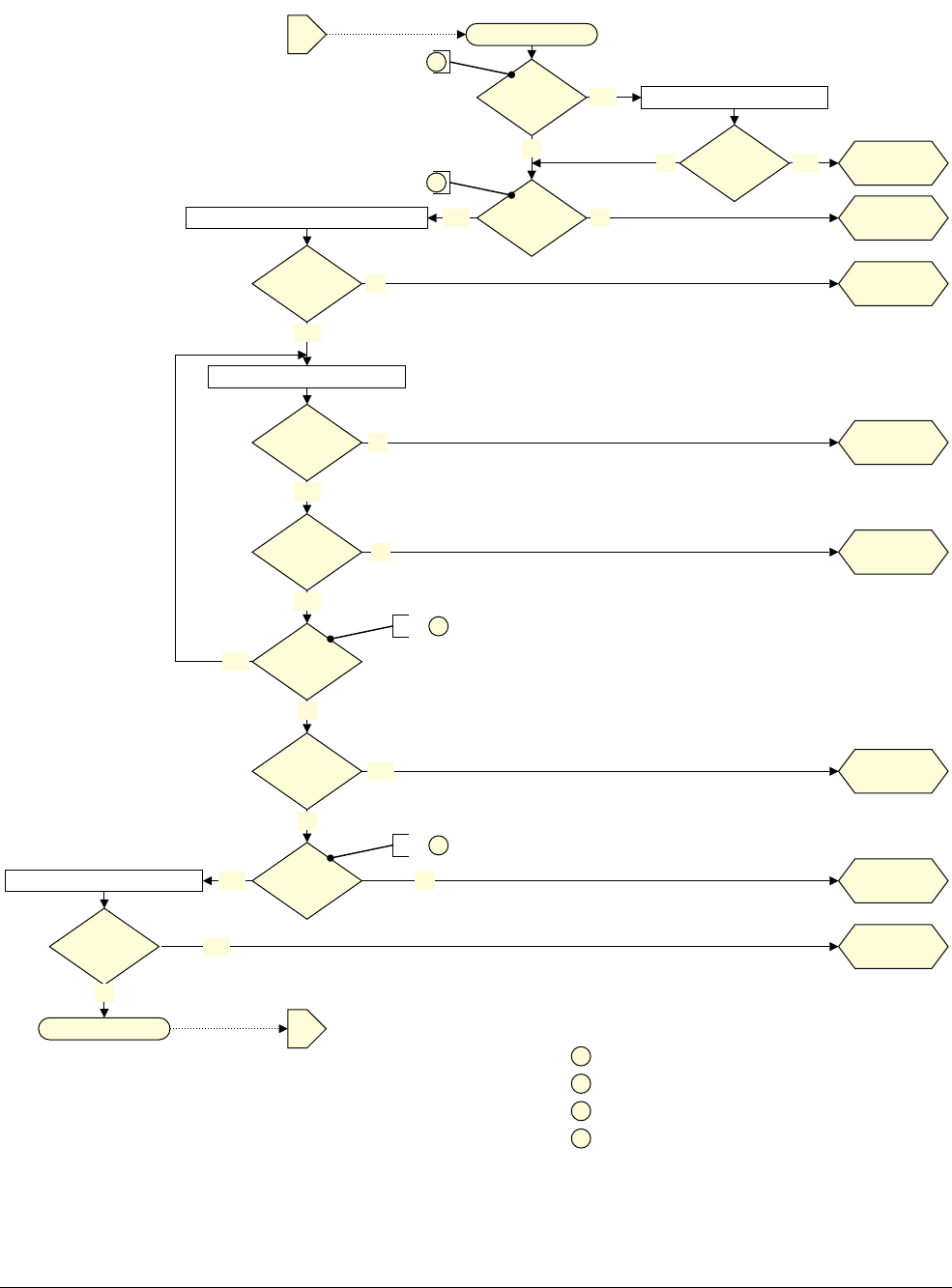
D5 The AArch64 Virtual Memory System Architecture
D5.6 MMU faults
D5-1800 Copyright © 2013 ARM Limited. All rights reserved. ARM DDI 0487A.a
Non-Confidential - Beta ID090413
Figure D5-31 VMSAv8-64 fault checking sequence
Input address
Alignment
check?
Fetch descriptor ‡
No
Table
entry
?
Check address alignment
Misaligned
?
Yes Alignment
fault
Check access permissions
Violation
?
Output address
Yes
Descriptor
valid?
Translation
fault
No
No
Yes Permission
fault
A1†
A2†
No
Alignment
fault
Alignment
valid
?
No
AF bit
== 0
?
Access flag
fault
Yes
Translatable
?
No Translation
fault
Yes
Get translation table base address
Address
size valid
?
Address
size fault
No
Yes
Yes
Address
size valid
?
Address
size fault
No
Yes
No
No
Yes
See 3
See 4
Yes
See
1
See
2
1 Is the access subject to an alignment check?
2 Does the address map to a TTBR?
3 Not permitted at the lowest lookup level
4 Fault any unaligned access to Device memory
‡ See Fetching the descriptor flowchart
† Links to and from Fetching the descriptor flowchart

D5 The AArch64 Virtual Memory System Architecture
D5.6 MMU faults
ARM DDI 0487A.a Copyright © 2013 ARM Limited. All rights reserved. D5-1801
ID090413 Non-Confidential - Beta
Stage 2 fault on a stage 1 translation table walk
On performing a translation table walk for the stage 1 translations, the descriptor addresses must be translated from
IPA to PA, using a stage 2 translation. This means that a memory access made as part of a stage 1 translation table
lookup might generate, on a stage 2 translation:
• A Translation fault, Access flag fault, or Permission fault.
• A synchronous external abort on the memory access.
If SCR_EL3.EA is set to 1, a synchronous external abort is taken to Secure Monitor mode., Otherwise, these faults
are reported as stage 2 memory aborts. ESR_EL2.ISS[7] is set to 1, to indicate a stage 2 fault during a stage 1
translation table walk, and the part of the ISS field that might contain details of the instruction is invalid. For more
information see Use of the ESR_EL1, ESR_EL2, and ESR_EL3 on page D1-1512.
Alternatively, a memory access made as part of a stage 1 translation table lookup might target an area of memory
with the Device or Strongly-ordered attribute assigned on the stage 2 translation of the address accessed. When the
HCR_EL2.PTW bit is set to 1, such an access generates a stage 2 Permission fault.
Note
On most systems, such a mapping to Strongly-ordered or Device memory on the stage 2 translation is likely to
indicate a Guest OS error, where the stage 1 translation table is corrupted. Therefore, it is appropriate to trap this
access to the hypervisor.
A TLB might hold entries that depend on the effect of HCR_EL2.PTW. Therefore, if HCR_EL2.PTW is changed
without changing the current VMID, the TLBs must be invalidated before executing in a Non-secure EL1 or EL0
mode. For more information see Changing HCR_EL2.PTW on page D5-1816.
A cache maintenance instruction executed at Non-secure EL1 can cause a stage 1 translation table walk that might
generate a stage 2 Permission fault, as described in this section. This is an exception to the general rule that a cache
maintenance instruction cannot generate a Permission fault.
D5.6.3 Prioritization of synchronous aborts from a single stage of address translation
For a single stage of translation, the priority of the memory management faults on a memory access is as follows,
ordered from highest priority to lowest priority. For memory accesses that undergo two stages of translation, the
italic entries show where the faults from second stage translations can occur. A second stage fault within a second
stage translation follows the same priority of faults:
1. Alignment fault not caused by memory type, possible for stage 1 translation only.
2. Translation fault due to the input address being out of the address range to be translated or requiring a TTBR
that is disabled. This includes VTCR_EL2.T0SZ being inconsistent with VTCR_EL2.SL0.
3. Address Size fault on a TTBR caused by either:
• The check on TCR_EL1.IPS, TCR_ELx.PS, or VTCR_EL2.PS.
• The physical address being out of the range implemented.
4. Second stage abort on a level zero lookup of a a stage 1 table walk. When stage 2 address translation is
enabled this includes an address size fault caused by the physical address being out of the range
implemented. This is second stage abort during a first stage translation table walk.
5. Synchronous parity fault on a level zero lookup of a translation table walk.
6. Synchronous external abort on a level zero lookup level of a translation table walk.
7. Translation fault on a level zero translation table entry.
8. Address Size fault a level zero lookup translation table entry caused by either:
• The check on TCR_EL1.IPS, TCR_ELx.PS, or VTCR_EL2.PS.
• The output address being out of the range implemented.

D5 The AArch64 Virtual Memory System Architecture
D5.6 MMU faults
D5-1802 Copyright © 2013 ARM Limited. All rights reserved. ARM DDI 0487A.a
Non-Confidential - Beta ID090413
9. Second stage abort on a level one lookup of a a stage 1 table walk. When stage 2 address translation is
enabled this includes an address size fault caused by the physical address being out of the range
implemented. This is second stage abort during a first stage translation table walk.
10. Synchronous parity fault on a level one lookup of a translation table walk.
11. Synchronous external abort on a level one lookup level of a translation table walk.
12. Translation fault on a level one translation table entry.
13. Address Size fault on a level one lookup translation table entry caused by either:
• The check on TCR_EL1.IPS, TCR_ELx.PS, or VTCR_EL2.PS.
• The output address being out of the range implemented.
14. Second stage abort on a level two lookup of a a stage 1 table walk. When stage 2 address translation is
enabled this includes an address size fault caused by the physical address being out of the range
implemented. This is second stage abort during a first stage translation table walk.
15. Synchronous parity fault on a level two lookup of a translation table walk.
16. Synchronous external abort on a level two lookup level of a translation table walk.
17. Translation fault on a level two translation table entry.
18. Address Size fault on a level two lookup translation table entry caused by either:
• The check on TCR_EL1.IPS, TCR_ELx.PS, or VTCR_EL2.PS.
• The output address being out of the range implemented.
19. Second stage abort on a level three lookup of a a stage 1 table walk. When stage 2 address translation is
enabled this includes an address size fault caused by the physical address being out of the range
implemented. This is second stage abort during a first stage translation table walk.
20. Synchronous parity fault on a level three lookup of a translation table walk.
21. Synchronous external abort on a level three lookup level of a translation table walk.
22. Translation fault on a level three translation table entry.
23. Address Size fault on a level three lookup translation table entry caused by either:
• The check on TCR_EL1.IPS, TCR_ELx.PS, or VTCR_EL2.PS.
• The output address being out of the range implemented.
24. Access Flag fault.
25. Alignment fault caused by the memory type.
26. Permission fault.
27. A fault from the state 2 translation of the memory access. When stage 2 address translation is enabled this
includes an address size fault caused by the physical address being out of the range implemented.
28. Synchronous parity fault on the memory access.
29. Synchronous External Abort on the memory access.
Note
The prioritization of TLB Conflict aborts is IMPLEMENTATION DEFINED, as the exact cause of these aborts depends
on the form of TLBs implemented.

D5 The AArch64 Virtual Memory System Architecture
D5.6 MMU faults
ARM DDI 0487A.a Copyright © 2013 ARM Limited. All rights reserved. D5-1803
ID090413 Non-Confidential - Beta
D5.6.4 Pseudocode details of the MMU faults
The following functions generate fault records that describe MMU faults.
FaultRecord AArch64.AlignmentFault(AccType acctype, boolean iswrite, boolean secondstage);
FaultRecord AArch64.TranslationFault(bits(48) ipaddress, integer level,
AccType acctype, boolean iswrite, boolean secondstage,
boolean s2fs1walk);
FaultRecord AArch64.AccessFlagFault(bits(48) ipaddress, integer level,
AccType acctype, boolean iswrite, boolean secondstage,
boolean s2fs1walk);
FaultRecord AArch64.AddressSizeFault(bits(48) ipaddress, integer level,
AccType acctype, boolean iswrite, boolean secondstage,
boolean s2fs1walk);
FaultRecord AArch64.PermissionFault(bits(48) ipaddress, integer level,
AccType acctype, boolean iswrite, boolean secondstage,
boolean s2fs1walk);
Abort exceptions on page D4-1703 describes how fault records are used.

D5 The AArch64 Virtual Memory System Architecture
D5.7 Translation Lookaside Buffers (TLBs)
D5-1804 Copyright © 2013 ARM Limited. All rights reserved. ARM DDI 0487A.a
Non-Confidential - Beta ID090413
D5.7 Translation Lookaside Buffers (TLBs)
Translation Lookaside Buffers (TLBs) reduce the average cost of a memory access by caching the results of
translation table walks. TLBs behave as caches of the translation table information, and the VMSA provides TLB
maintenance instructions for the management of TLB contents.
Note
The ARM architecture permits TLBs to hold any translation table entry that does not directly cause a Translation
fault, an Address Size fault, or an Access flag fault.
To reduce the need for TLB maintenance on context switches, for EL1&0 stage 1 translations the VMSA can
distinguish between Global pages and Process-specific pages. The Address Space Identifier (ASID) identifies pages
associated with a specific process and provides a mechanism for changing process-specific tables without having to
maintain the TLB structures. Similarly, for the Non-secure EL1&0 translation regime, the virtual machine identifier
(VMID) identifies the current virtual machine, with its own independent ASID space. The TLB entries include this
VMID information, meaning TLBs do not require explicit invalidation when changing from one virtual machine to
another, if the virtual machines have different VMIDs.
The following sections describe the architectural requirements for Translation Lookaside Buffers (TLBs) and their
maintenance:
•About ARMv8 Translation Lookaside Buffers (TLBs).
•TLB maintenance requirements and the TLB maintenance instructions on page D5-1807.
In these descriptions, TLB entries for a translation regime for a particular Exception level are out of context when
executing at a higher Exception level.
D5.7.1 About ARMv8 Translation Lookaside Buffers (TLBs)
Translation Lookaside Buffers (TLBs) are an implementation technique that caches translations or translation table
entries. TLBs avoid the requirement for every memory access to perform a translation table walk in memory. The
ARM architecture does not specify the exact form of the TLB structures for any design. In a similar way to the
requirements for caches, the architecture only defines certain principles for TLBs:
• The architecture has a concept of an entry locked down in the TLB. The method by which lockdown is
achieved is IMPLEMENTATION DEFINED, and an implementation might not support lockdown.
• The architecture does not guarantee that an unlocked TLB entry remains in the TLB.
• The architecture guarantees that a locked TLB entry remains in the TLB. However, a locked TLB entry might
be updated by subsequent updates to the translation tables. Therefore, when a change is made to the
translation tables, the architecture does not guarantee that a locked TLB entry remains incoherent with an
entry in the translation table.
• The architecture guarantees that a translation table entry that generates a Translation fault, an Address size
fault, or an Access flag fault is not held in the TLB. However a translation table entry that generates a
Permission fault might be held in the TLB.
• Any translation table entry that does not generate a Translation or Access flag fault and is not out of context
might be allocated to an enabled TLB at any time.
Note
An enabled TLB can hold a translation table entry that does not itself generate a Translation fault but that
points to a subsequent table in the translation table walk. This is referred to as intermediate caching of TLB
entries.
• Software can rely on the fact that between disabling and re-enabling a stage of address translation, entries in
the TLB relating to that stage of translation have not have been corrupted to give incorrect translations.
The following sections give more information about TLB implementation:
•Global and process-specific translation table entries on page D5-1805

D5 The AArch64 Virtual Memory System Architecture
D5.7 Translation Lookaside Buffers (TLBs)
ARM DDI 0487A.a Copyright © 2013 ARM Limited. All rights reserved. D5-1805
ID090413 Non-Confidential - Beta
•TLB matching on page D5-1806
•TLB behavior at reset on page D5-1806
•TLB lockdown on page D5-1806
•TLB conflict aborts on page D5-1807.
See also TLB maintenance requirements and the TLB maintenance instructions on page D5-1807.
Global and process-specific translation table entries
In a VMSA implementation, system software can divide the virtual memory map used by memory accesses at EL1
and EL0 into global and non-global regions, indicated by the nG bit in the translation table descriptors:
nG == 0 The translation is global, meaning the region is available for all processes.
nG == 1 The translation is non-global, or process-specific, meaning it relates to the current ASID, as defined
in either the TTBR0_EL1 or the TTBR1_EL1.
As indicated by the nG field definitions, each non-global region has an associated Address Space Identifier (ASID).
These identifiers mean different translation table mappings can co-exist in a caching structure such as a TLB. This
means that software can create a new mapping of a non-global memory region without removing previous
mappings.
TTBR0_EL1 and TTBR1_EL1 each have an ASID field, and TCR_EL1.A1 determines which of these fields
defines the current ASID. See also ASID size.
Note
The selected ASID applies to the translation of any address for which the value of the nG bit is 1, regardless of
whether the address is translated based on TTBR0_EL1 or on TTBR1_EL1.
For a symmetric multiprocessor cluster where a single operating system is running on the set of processing elements,
the ARM architecture requires all ASID values to be assigned uniquely within any single Inner Shareable domain.
In other words, each ASID value must have the same meaning to all processing elements in the system.
The EL2 translation regime and the EL3 translation regime do not support ASIDs, and all descriptors in these
regimes are treated as global.
When a PE is using the VMSAv8-64 translation table format, and is in Secure state, a translation must be treated as
non-global, regardless of the value of the nG bit, if NSTable is set to 1 at any level of the translation table walk.
For more information see Control of Secure or Non-secure memory access on page D5-1779.
ASID size
In VMSAv8-64, the ASID size is an IMPLEMENTATION DEFINED choice of 8 bits or 16 bits, and
ID_AA64MMFR0_EL1.ASID bits identifies the supported size. When an implementation supports a 16 bit ASID,
TCR_EL1.AS selects whether the top 8 bits of the ASID are used. When the value of TCR_EL1.AS is 0,
ASID[15:8]:
• Are ignored by hardware for every purpose other than reads of ID_AA64MMFR0_EL1.
• Are treated as if they are all zeros when used for allocating and matching entries in the TLB.
Note
ARMv7 and VMSAv8-32 use an 8-bit ASID. For backwards compatibility, when executing using translations
controlled from an Exception level that is using AArch32, the ASID size remains at 8 bits. If the implementation
supports 16-bit ASIDS, the 8-bit ASID used is zero-extended to 16 bits.

D5 The AArch64 Virtual Memory System Architecture
D5.7 Translation Lookaside Buffers (TLBs)
D5-1806 Copyright © 2013 ARM Limited. All rights reserved. ARM DDI 0487A.a
Non-Confidential - Beta ID090413
TLB matching
A TLB is a hardware caching structure for translation table information. Like other hardware caching structures, it
is mostly invisible to software. However, there are some situations where it can become visible. These are associated
with coherency problems caused by an update to the translation table that has not been reflected in the TLB. Use of
the TLB maintenance instructions described in TLB maintenance requirements and the TLB maintenance
instructions on page D5-1807 can prevent any TLB incoherency becoming a problem.
A particular case where the presence of the TLB can become visible is if the translation table entries that are in use
under a particular ASID and VMID are changed without suitable invalidation of the TLB. This is an issue regardless
of whether the translation table entries are global. In some cases, the TLB can hold two mappings for the same
address, and this:
• Might generate a Data abort reported using the TLB Conflict fault code, see TLB conflict aborts on
page D5-1807.
• Might lead to UNPREDICTABLE behavior. In this case, behavior will be consistent with one of the mappings
held in the TLB, or with some amalgamation of the values held in the TLB, but cannot give access to regions
of memory with permissions or attributes that could not be assigned by valid translation table entries in the
translation regime being used for the access. For more information see Appendix A Architectural Constraints
on UNPREDICTABLE behaviors.
TLB behavior at reset
The ARM architecture does not require a reset to invalidate the TLBs. The architecture recognizes that an
implementation might require caches, including TLBs, to maintain their contents over a system reset. Possible
reasons for doing so include power management and debug requirements.
For ARMv8:
• All TLBs are disabled from reset. All stages of address translation are disabled from reset, and the contents
of the TLBs have no effect on address translation. For more information see Controlling address translation
stages on page D5-1714.
• An implementation can require the use of a specific TLB invalidation routine, to invalidate the TLB arrays
before they are enabled after a reset. The exact form of this routine is IMPLEMENTATION DEFINED, but if an
invalidation routine is required it must be documented clearly as part of the documentation of the device.
ARM recommends that if an invalidation routine is required for this purpose, the routine is based on the TLB
maintenance instructions described in TLB maintenance instructions on page D5-1808.
• When TLBs that have not been invalidated by some mechanism since reset are enabled, the state of those
TLBs is UNPREDICTABLE.
Similar rules apply to cache behavior, see Behavior of caches at reset on page D4-1677.
TLB lockdown
The ARM architecture recognizes that any TLB lockdown scheme is heavily dependent on the microarchitecture,
making it inappropriate to define a common mechanism across all implementations. This means that:
• VMSAv8-64 does not require TLB lockdown support.
• If TLB lockdown support is implemented, the lockdown mechanism is IMPLEMENTATION DEFINED. However,
key properties of the interaction of lockdown with the architecture must be documented as part of the
implementation documentation.
This means that a region of the system instruction encoding space is reserved for IMPLEMENTATION DEFINED
functions, see Reserved control space for IMPLEMENTATION DEFINED functionality on page C4-250.An
implementation might use some of these encodings to implement TLB lockdown functions. These functions might
include:
• Unlock all locked TLB entries.
• Preload into a specific level of TLB. This is beyond the scope of the
PLI
and
PLD
hint instructions.

D5 The AArch64 Virtual Memory System Architecture
D5.7 Translation Lookaside Buffers (TLBs)
ARM DDI 0487A.a Copyright © 2013 ARM Limited. All rights reserved. D5-1807
ID090413 Non-Confidential - Beta
In an implementation that includes EL2, exceptions generated by problems related to TLB lockdown in a
Non-secure EL1 mode, can be routed to either:
• Non-secure EL1, as a Data Abort exception.
• Non-secure EL2, as a Hyp Trap exception.
For more information, see Traps to EL2 of Non-secure EL1 and EL0 accesses to lockdown, DMA, and TCM
operations on page D1-1483.
TLB conflict aborts
ARMv8 includes the concept of a TLB conflict abort, and defines fault status encodings for such an abort, see
Exception from an Instruction abort on page D1-1524 and Exception from a Data abort on page D1-1525.
An implementation can generate a TLB conflict abort if it detects that the address being looked up in the TLB hits
multiple entries. This can happen if the TLB has been invalidated inappropriately, for example if TLB invalidation
required by the architecture has not been performed. If it happens, the resulting behavior is UNPREDICTABLE, but
must not permit access to regions of memory with permissions or attributes that mean they cannot be accessed in
the current Security state at the current Exception level.
In some implementations, multiple hits in the TLB can generate a synchronous Data Abort or Prefetch Abort
exception. In any case where this is possible it is IMPLEMENTATION DEFINED whether the abort is a stage 1 abort or
a stage 2 abort.
Note
A stage 2 abort cannot be generated if stage 2 of the Non-secure EL1&0 translation regime is disabled.
The priority of the TLB conflict abort is IMPLEMENTATION DEFINED, because it depends on the form of a TLB that
can generate the abort.
Note
The TLB conflict abort must have higher priority than any abort that depends on a value held in the TLB.
An implementation can generate TLB conflict aborts on either or both instruction fetches and data accesses.
On a TLB conflict abort, the returned syndrome includes the address that generated the fault. That is, it includes the
address that was being looked up in the TLB.
D5.7.2 TLB maintenance requirements and the TLB maintenance instructions
Translation Lookaside Buffers (TLBs) are an implementation mechanism that caches translations or translation
table entries. The ARM architecture does not specify the form of any TLB structures, but defines the mechanisms
by which TLBs can be maintained.The following sections describe the VMSA TLB maintenance instructions:
•General TLB maintenance requirements.
•TLB maintenance instructions on page D5-1808.
•Maintenance requirements on changing System register values on page D5-1816.
•Atomicity of register changes on changing virtual machine on page D5-1816.
General TLB maintenance requirements
TLB maintenance instructions provide a mechanism for invalidating entries from TLB caching structures to ensure
that changes to the translation tables are reflected correctly in those TLB caching structures.
The architecture permits the caching of any translation table entry that has been returned from memory without a
fault, provided that the entry does not, itself, cause a Translation fault, an Address size fault, or an Access Flag fault.
This means that the entries that can be cached include:
• Entries in translation tables that point to subsequent tables to be used in that stage of translation.
• Stage 2 translation table entries used as part of a stage 1 translation table walk

D5 The AArch64 Virtual Memory System Architecture
D5.7 Translation Lookaside Buffers (TLBs)
D5-1808 Copyright © 2013 ARM Limited. All rights reserved. ARM DDI 0487A.a
Non-Confidential - Beta ID090413
• Stage 2 translation table entries used to translate the output address of the stage 1 translation.
Such entries might be held in intermediate TLB caching structures that are used during a translation table walk and
that are distinct from the data caches in that they are not required to be invalidated as the result of writes of the data.
The architecture makes no restriction of the form of these intermediate TLB caching structures.
The architecture does not intend to restrict the form of TLB caching structures used for holding translation table
entries, and in particular for translation regimes that involve two stages of translation, it is recognized that such
caching structures might contain:
• Entries containing information from stage 1 translation table entries, at any level of the translation table walk.
• Entries containing information from stage 2 translation table entries, at any level of the translation table walk.
• Entries that combine information from stage 1 and stage 2 translation table entries, at any level of the
translation table walk.
Where a TLB maintenance instruction is:
• Required to apply to stage 1 entries, then it must apply to any cached entries in caching structures that include
any stage 1 information that are used to translate the address being invalidated.
Note
ARM expects that, in at least some implementations, cached copies of levels of the translation table walk
other than the last level are tagged with their ASID, regardless of whether the final level is global. This means
that TLB invalidations that involve the ASID require the ASID to match such entries to perform the required
invalidation.
• Required to apply to stage 2 entries only, then:
— It is not required to apply to caching structures that combine stage 1 and stage 2 translation table
entries.
— It must apply to caching structures that contain information only from stage 2 translation table entries.
Whenever translation tables entries associated with a particular VMID or ASID are changed, the corresponding
entries must be invalidated from the TLB to ensure that these changes are visible to subsequent execution, including
speculative execution, that uses the changed translation table entries.
Some system register bit descriptions state that the effect of the bit is permitted to be cached in a TLB. This means
that all TLB entries that might be affected by a change in one of these bits must be invalidated whenever that bit is
changed, to ensure that the effect of the change of that control bit is visible to subsequent execution including
speculative execution, that uses those control bits. This invalidation is required in addition to, and after, the normal
synchronization of the system registers described in Synchronization requirements for system registers on
page D8-1866, and applies to any stage of address translation that is implemented for the translation regime, and
VMID if appropriate, that is affected by that control bit.
In addition to any TLB maintenance requirement, when changing the cacheability attributes of an area of memory,
software must ensure that any cached copies of affected locations are removed from the caches. For more
information see Cache maintenance requirement created by changing translation table attributes on page D5-1820.
TLB maintenance instructions
The architecture defines TLB maintenance instructions, that provide the following:
• Invalidate all entries in the TLB.
• Invalidate a single TLB entry by ASID for a non-global entry.
• Invalidate all TLB entries that match a specified ASID.
• Invalidate all TLB entries that match a specified VA, regardless of the ASID.
Each instruction can be specified as applying only to the PE that executes the instruction, or as applying to all PEs
in the same Inner Shareable shareability domain as the PE that executes the instruction.
The following subsubsections describe these instructions:
•TLB maintenance instruction syntax on page D5-1809.
•Operation of the TLB maintenance instructions on page D5-1810.

D5 The AArch64 Virtual Memory System Architecture
D5.7 Translation Lookaside Buffers (TLBs)
ARM DDI 0487A.a Copyright © 2013 ARM Limited. All rights reserved. D5-1809
ID090413 Non-Confidential - Beta
•Scope of the TLB maintenance instructions on page D5-1811.
•Broadcast TLB maintenance between AArch32 and AArch64 on page D5-1813.
•Ordering and completion of TLB maintenance instructions on page D5-1814.
•TLB maintenance in the event of TLB conflict on page D5-1815.
•The interaction of TLB lockdown with TLB maintenance instructions on page D5-1815.
TLB maintenance instructions on page C4-239 describes the encoding of the TLB maintenance instructions.
TLB maintenance instruction syntax
The A64 syntax for TLB maintenance instructions is:
TLBI <operation>{, <Xt>}
Where:
<operation>
Is one of
VMALLE1
,
VA{L}E1
,
ASIDE1
,
VAA{L}E1
,
VMALLE1IS
,
VA{L}E1IS
,
ASIDE1IS
,
VAA{L}E1IS
,
VA{L}E2
,
VA{L}E2IS
,
VA{L}E3
,
VA{L}E3IS
,
ALLE1
,
ALLE1IS
,
ALLE2
,
ALLE2IS
,
ALLE3
,
ALLE3IS
,
VMALLS12E1
,
VMALLS12E1IS
,
IPAS2{L}E1
, or
IPAS2{L}E1IS
.
<operation>
has a structure of
<type>{L}<level>{,IS}
where:
<type>
Is one of:
ALL
All translations used at
<level>
. For
level
== E1, this applies with any
VMID.
VMALL
All stage 1 translations used at <level> with the current VMID.
VMALLS12
All stage 1 and stage 2 translations used at EL1 with the current VMID.
VMALLS12
is only valid when
level
== E1.
ASID
All translations used at EL1 with the current VMID and the supplied ASID.
ASID
is only valid when
level
== E1.
VA{L}
Translations used at
<level>
for the specified address and ASID, if
appropriate, and the current VMID, if appropriate.
VAA{L}
Translations used at
<level>
for the specified address and for all ASID
values, if appropriate, and the current VMID, if appropriate.
IPAS2{L}
Translations used at
<level>
for the specified IPA for the current VMID, if
appropriate, held in stage 2 only caching structures.
L
Indicates that the invalidation only applies to caching of entries returned
from the last level of translation table walk of the stage 1 translation. See
Scope of the TLB maintenance instructions on page D5-1811. As shown in
this list,
L
is an optional additional parameter to some of the
<type>
parameters.
<level>
Describes the Exception level of the translation regime that the invalidation applies to.
Is one of:
E1
EL1.
E2
EL2.
E3
EL3.
Instructions applying to the translation regime of an Exception level other than the
Exception level at which the instruction is executed is UNDEFINED.
TLBI ALLE1{IS}
,
TLBI IPAS2{L}E1{IS}
and
TLBI VMALLS12E1{IS}
are UNDEFINED at EL1.
Note
All TLB maintenance instructions are UNDEFINED at EL0.
IS
When present, it indicates that the function applies to all TLBs in the Inner Shareable
domain.
<Xt>
Passes an address or ASID argument, where required.
<Xt>
is required for the
TLB ASID
,
TLB VA{L}
,
TLB VAA{L}
, and
TLB IPAS2{L}
instructions.

D5 The AArch64 Virtual Memory System Architecture
D5.7 Translation Lookaside Buffers (TLBs)
D5-1810 Copyright © 2013 ARM Limited. All rights reserved. ARM DDI 0487A.a
Non-Confidential - Beta ID090413
If EL2 is not implemented, the
TLBI VA{L}E2
,
TLBI VA{L}E2IS
,
TLBI ALLE2
, and
TLBI ALLE2IS
instructions are
UNDEFINED.
In VMSAv8-64, the TLB instructions that take a register argument that holds a virtual address, an ASID, or both,
use the following register argument format:
Bits[63:48] ASID. However, these bits are RES0 if the instruction does not require an ASID argument.
Bits[47:44] RES0.
Bits[43:0] VA[55:12]. For an instruction that requires a VA argument, the treatment of the low-order bits of
this field depends on the translation granule size, as follows:
4KB granule size All bits are valid and used for the invalidation.
16KB granule size Bits[1:0] RES0 and ignored when the instruction is executed, because
VA[13:12] have no effect on the operation of the instruction.
64KB granule size Bits[3:0] are RES0 and ignored when the instruction is executed, because
VA[15:12] have no effect on the operation of the instruction.
These bits are RES0 if the instruction does not require a VA argument.
For TLB maintenance instructions that take an address, the maintenance of VA[63:56] is interpreted as being the
same as the maintenance of VA[55].
If a TLB maintenance instruction targets a translation regime that is using AArch32, meaning the VA is only 32-bit,
then software must treat VA[55:32] as RES0, and these bits are ignored when the instruction is executed.
If the implementation supports 16 bits of ASID then the upper bits are RES0 when the context being invalidated only
uses 8 bits.
In VMSAv8-64, the TLB instructions that take a register argument that holds an IPA, use the following register
argument format:
Bits[63:36] RES0.
Bits[35:0] IPA[47:12]. For an instruction that requires a VA argument, the treatment of the low-order bits of
this field depends on the translation granule size, as follows:
4KB granule size All bits are valid and used for the invalidation.
16KB granule size Bits[1:0] RES0 and ignored when the instruction is executed, because
IPA[13:12] have no effect on the operation of the instruction.
64KB granule size Bits[3:0] are RES0 and ignored when the instruction is executed, because
IPA[15:12] have no effect on the operation of the instruction.
Operation of the TLB maintenance instructions
Any TLB maintenance instruction can affect any TLB entries that are not locked down.
The TLB maintenance instructions specify the Exception level of the translation regime to which they apply.
Note
Because there is no guarantee that an unlocked TLB entry remains in the cache, architecturally it is not possible to
tell whether a TLB maintenance instruction has affected any TLB entries that were not specified by the instruction.
If a TLB maintenance instruction specifies a VA, and a data or instruction access to that VA would generate an
MMU abort, the TLB maintenance instruction does not generate an abort. VAs for which a TLB maintenance
instruction does not generate an abort include VAs that are not in the range of VAs that can be translated.
When EL3 is implemented:
• The TLB maintenance instructions that apply to the EL1&0 translation regime take account of the current
Security state, as part of the address translation required for the TLB operation.

D5 The AArch64 Virtual Memory System Architecture
D5.7 Translation Lookaside Buffers (TLBs)
ARM DDI 0487A.a Copyright © 2013 ARM Limited. All rights reserved. D5-1811
ID090413 Non-Confidential - Beta
•SCR_EL3.NS modifies the effect of the TLB maintenance instructions as follows:
— For instructions that apply to the EL1&0 translation regime, the SCR_EL3.NS bit identifies whether
the maintenance instructions apply to the Secure or Non-secure EL1&0 translation regime.
Note
If EL3 is not implemented, then there is only a single EL1&0 translation regime.
— For instructions that apply to the EL2 translation regime, the SCR_EL3.NS bit must be 1 or the
instruction is UNDEFINED.
— For instructions that apply to the EL3 translation regime, the SCR_EL3.NS bit has no effect.
Note
• An address-based TLB maintenance instruction that applies to the Inner Shareable domain does so regardless
of the Shareability attributes of the address supplied as an argument to the operation.
• Previous versions of the ARM architecture included TLB maintenance instructions that operated only on
instruction TLBs, or only on data TLBs. From the introduction of ARMv7, ARM deprecated any use of these
instructions. In ARMv8:
— AArch64 state does not include any of these instructions.
— AArch32 state includes some of these instructions, but ARM deprecates their use.
The ARM architecture does not dictate the form in which the TLB stores translation table entries. However, when
a TLB maintenance instruction is executed, the minimum size of the table entry that is invalidated from the TLB
must be at least the size that appears in the translation table entry.
Note
The Contiguous bit does not affect the minimum size of entry that must be invalidated from the TLB
Scope of the TLB maintenance instructions
The TLB invalidation instruction
<type>
affects the different possible levels of caching in the TLB as follows:
VAL, VAAL
The invalidation applies to all cached copies of the final level of translation table walk of stage 1
translation that would be used with the Security state specified by SCR_EL3.NS, current VMID (for
the Non-secure EL1&0 translation regime), and, if appropriate, the specified ASID, during a
translation table walk to translate the address specified in the invalidation instruction at the specified
Exception Level.
VA, VAA
The invalidation applies to all cached copies of the stage 1 translation table entries, at any table level
that would be used with the state specified by SCR_EL3.NS, current VMID (for the Non-secure
EL1&0 translation regime), and, if appropriate, the specified ASID, during a translation table walk
to translate the address specified in the invalidation instruction at the specified Exception Level.
ASID
The invalidation applies to all cached copies of the stage 1 translation table entries, at any table level
that would be used with the state specified by SCR_EL3.NS, current VMID (for the Non-secure
EL1&0 translation regime), and the specified ASID during a translation table walk to translate any
address at the specified Exception Level.
VMALL
The invalidation applies to all cached copies of the stage 1 translation table entries, at any table
level, that would be used with the state specified by SCR_EL3.NS and current VMID (for the
Non-secure EL1&0 translation regime) during a translation table walk to translate any address at the
specified Exception Level.
VMALLS12
The invalidation applies to all cached copies of the stage 1 and stage 2 translation table entries, at
any table level, that would be used with the state specified by SCR_EL3.NS and current VMID (for
the Non-secure EL1&0 translation regime) during a translation table walk to translate any address
at the specified Exception Level.

D5 The AArch64 Virtual Memory System Architecture
D5.7 Translation Lookaside Buffers (TLBs)
D5-1812 Copyright © 2013 ARM Limited. All rights reserved. ARM DDI 0487A.a
Non-Confidential - Beta ID090413
Note
If EL2 is not implemented, or if the
TLBI VMALLS12
instruction is executed with SCR_EL3.NS==0,
the instruction is not UNDEFINED but it has the same effect as
TLBI VMALL
. This is because there are
no stage 2 translations to invalidate.
IPAS2
The invalidation applies to cached copies of the stage 2 translation table entries held in TLB caching
structures holding stage 2 only entries, at any table level, that would be used with the current VMID
during a translation table walk to translate any address at the specified Exception Level. It is not
required that this instruction invalidates TLB caching structures holding stage 1 and stage 2 entries
combined.
The only translation regime to which this instruction can apply is the Non-secure EL1&0 translation
regime.
When executed with the SCR_EL3.NS==0, or in an implementation that does not implement EL2,
this instruction is a
NOP
.
The architectural requirements of this instruction are that:
1. The following code is sufficient to invalidate all cached copies of the stage 2 translation of
the IPA held in
Xt
for the current VMID, with the corresponding requirement for the
broadcast versions of the instructions:
TLBI IPAS2E1, Xt
DSB
TLBI VMALLE1
2. The following code is sufficient to invalidate all cached copies of the stage 2 translations of
the IPA held in
Xt
used to translate the virtual address VA (and ASID when executing
TLBI VAE1
) held in
Xt2
, with the corresponding requirement for the broadcast versions of the
instructions:
TLBI IPAS2E1, Xt
DSB
TLBI VAE1, Xt2 ; or TLBI VAAE1, Xt2
3. The following code is sufficient to invalidate all cached copies of the stage 2 translations of
the IPA held in
Xt
used to translate the IPA produced by the last level of stage 1 translation
table lookup for the virtual address VA (and ASID when executing
TLBI VALE1
) held in
Xt2
,
with the corresponding requirement for the broadcast versions of the instructions:
TLBI IPAS2E1, Xt
DSB
TLBI VALE1, Xt2 ; or TLBI VAALE1, Xt2
IPAS2L
The invalidation applies to cached copies of the stage 2 translation table entries held in TLB caching
structures holding stage 2 only entries, at the final level of the stage 2 translation table walk, that
would be used with the current VMID during a translation table walk to translate any address at the
specified Exception Level. It is not required that this instruction invalidates TLB caching structures
holding combined (stage 1 and stage 2) entries.
The only translation regime to which this instruction can apply is the Non-secure EL1&0 translation
regime.
When executed with the SCR_EL3.NS==0, or in an implementation that does not implement EL2,
this instruction is a
NOP
.
The architecture requirements for
TLBI IPAS2L
instructions correspond to those for the
TLVI IPAS2
instructions, but only for cached copies of the final level of the stage 2 translation.
ALL
The invalidation applies to all cached copies of the stage 1 and stage 2 translation table entries, at
any table level, that would be used with the state specified by SCR_EL3.NS, and any VMID during
a translation table walk to translate any address at the specified Exception Level.

D5 The AArch64 Virtual Memory System Architecture
D5.7 Translation Lookaside Buffers (TLBs)
ARM DDI 0487A.a Copyright © 2013 ARM Limited. All rights reserved. D5-1813
ID090413 Non-Confidential - Beta
The entries that the invalidations apply to are not affected by the state of any other control bits involved in the
translation process. Therefore, the following is a non-exhaustive list of control bits that do not affect how a TLB
maintenance instruction updates the TLB entries:
In AArch64 SCTLR_EL1.M, SCTLR_EL2.M, SCTLR_EL3.{M, RW], HCR_EL2.{VM, RW},
TCR_EL1.{TG1, EPD1, T1SZ, TG0, EPD0, T0SZ, AS, A1}, TCR_EL2.{TG0, T0SZ},
TCR_EL3.{TG0, T0SZ}, VTCR_EL2.{SL0, T0SZ}, TTBR0_EL1.ASID, TTBR1_EL1.ASID.
In AArch32 SCTLR.M, HCR.VM, TTBCR.{EAE, PD1, PD0, N, EPD1, T1SZ, EPD0, T0SZ, A1},
HTCR.T0SZ, VTCR.{SL0, T0SZ}, TTBR0.ASID, TTBR1.ASID, CONTEXTIDR.ASID.
Note
• ARM expects most TLB maintenance performed by an operating system to occur to the last level entries of
the stage 1 translation table walks, and the purpose of the address-based TLB invalidation instructions where
the invalidation need only apply to caching of entries returned from the last level of translation table walk of
stage 1 translation is to avoid unnecessary loss of the intermediate caching of the translation table entries.
Similarly, for stage 2 translations ARM expects that most TLB maintenance performed by a hypervisor for a
given Guest operation system will affect only the last level entries of the stage 2 translations. Therefore,
similar capability is provided for instructions that invalidate single stage 2 entries.
• The architecture permits the invalidation of entries in TLB caching structures at any time, so for each of these
instructions the definition is in terms of the minimum set of entries that must be invalidated from TLB
caching structures, and an implementation might choose to invalidate more entries. In general, for best
performance, ARM recommends not invalidating entries that are not required to be invalidated.
• Dependencies on the VMID for the Non-secure EL1&0 translation regime apply even when HCR_EL2.VM
is set to 0. Because the architecture does not require the VTTBR_EL2.VMID field to be reset in hardware,
the reset routine of each active PE must initialize VTTBR_EL2.VMID[7:0] to a common value such as 0,
even if stage 2 translation is not in use.
Broadcast TLB maintenance between AArch32 and AArch64
In most cases, the TLB maintenance instructions affecting the Inner Shareable domain executed by a PE in an
Exception level that is using AArch64 also affects another PE in the same Inner Shareable domain that is executing
at the same Exception level and is using AArch32, provided that the virtual address, ASID, and VMID match.
Note
The requirement to match means that the invalidation only occurs on the PE that is using AArch32 if, for the PE
that executed the TLB maintenance instruction at an Exception level that is using AArch64, both of the following
apply:
• The VA is in the bottom 4GB.
• If it uses a 16-bit ASID, then the top 8 bits of the ASID are zero.
Except for the cases identified here, the TLB maintenance instructions affecting the Inner Shareable domain
executed by a PE in an Exception level that is using AArch32 also affects another PE in the same Inner Shareable
domain that is executing at the same Exception level and is using AArch64, provided that the virtual address, ASID,
and VMID match. The virtual address from the instruction executed in AArch32 state is zero-extended, and the
ASID is zero-extended if the PE executing in AArch64 state is using a 16-bit ASID. The exceptions to this general
rule are as follows:
1. An ARMv7 PE in the same Inner Shareable domain is treated in the same way as an ARMv8 PE for which
EL3 is using AArch32, except that if an ARMv8 PE issues an instruction that does not exist in ARMv7, then
that instruction is not required to have an effect on the TLBs of the ARMv7 PE. The instructions that do not
exist in ARMv7 include the following TLB maintenance instructions that ARMv8 adds to the T32 and A32
instruction sets:
• The following instructions that operate on TLB entries for the final level of translation table walk for
stage 1 translations:
TLBIMVALIS
,
TLBIMVAALIS
,
TLBIMVALHIS
,
TLBIMVAL
,
TLBIMVAAL
, and
TLBIMVALH
.

D5 The AArch64 Virtual Memory System Architecture
D5.7 Translation Lookaside Buffers (TLBs)
D5-1814 Copyright © 2013 ARM Limited. All rights reserved. ARM DDI 0487A.a
Non-Confidential - Beta ID090413
• The following instructions that operate by IPA on TLB entries for stage 2 translations:
TLBIIPAS2IS
,
TLBIIPAS2LIS
,
TLBIIPAS2
, and
TLBIIPAS2L
.
2. The number of Exception levels in Secure state depends on whether EL3 is using AArch32 or EL3 is using
AArch64. This means that, within the Inner Sharable domain, there might be PEs with different numbers of
Exception levels in Secure state. Therefore, the following exceptions are made to this principle:
• If a PE that has EL3 using AArch32 issues an AArch32 TLB maintenance instruction affecting Secure
entries, and the Inner Shareable domain also contains PEs with EL3 using AArch64, then the
architecture does not require that the AArch32 TLB maintenance instruction has any effect on either:
— The EL3 translation regime of the PEs with EL3 using AArch64.
— The Secure EL1 translation regime of the PEs with EL3 using AArch64, regardless of whether
the Secure EL1 translation regime is using AArch64 or AArch32.
• If a PE that has EL3 using AArch64 issues an AArch64 TLB maintenance instruction affecting EL3
entries, and the Inner Shareable domain also contains PEs with EL3 using AArch32, then the
architecture does not require that the AArch64 TLB maintenance instruction has any effect on the EL3
translation regime of the PEs with EL3 using AArch32.
• If a PE that has EL3 using AArch64 issues an AArch64 TLB maintenance instruction affecting Secure
EL1 entries, and the Inner Shareable domain also contains PEs with EL3 using AArch32 then the
architecture does not require that the AArch64 TLB maintenance instruction has any effect on the EL3
translation regime of the PEs with EL3 using AArch32.
Note
While the architecture does not require such an effect, the architecture also does not require that entries in the TLB
remain in the TLB at any time, and so it is permissible that such instructions affect these translation regimes.
Ordering and completion of TLB maintenance instructions
For AArch64 execution, a TLB maintenance instruction can be executed in any order relative to:
• Loads and stores, unless a
DSB
is executed between the instructions.
Note
In the ARM architecture, a translation table walk is considered to be a separate observer, and a store to
translation tables can be observed by that separate observer at any time after the instruction has been
executed, but is only guaranteed to be observable after the execution of a
DSB
instruction by the PE that
executed the TLB maintenance instruction.
• Another TLB maintenance instruction, unless a
DSB
is executed between the instructions.
• A data or instruction cache maintenance instruction, unless a
DSB
is executed between the instructions.
For AArch64 execution, the completion rules are:
• A TLB maintenance instruction is complete when all memory accesses using the TLB entries that have been
invalidated have been observed by all observers to the extent that those accesses are required to be observed,
as determined by the shareability and cacheability of the memory locations accessed by the accesses. In
addition, after the TLB invalidate instruction is complete, no new memory accesses that can be observed by
those observers using those TLB entries are performed.
Note
For TLB maintenance instructions that affect other PEs, the memory accesses from those PEs that used the
TLB entries that have been invalidated are included in the set of memory accesses that must have been
observed when the TLB maintenance instruction is complete.
• A TLB maintenance instruction can complete at any time after it is issued, but is only guaranteed to be
complete after the execution of
DSB
by the PE that executed the TLB maintenance instruction.

D5 The AArch64 Virtual Memory System Architecture
D5.7 Translation Lookaside Buffers (TLBs)
ARM DDI 0487A.a Copyright © 2013 ARM Limited. All rights reserved. D5-1815
ID090413 Non-Confidential - Beta
• A completed TLB maintenance instruction is only guaranteed to have its effects visible on the PE that
executed the instruction after the execution of an
ISB
instruction by the PE that executed the TLB
maintenance instruction.
Note
In all cases in this section, where a
DMB
or
DSB
is referred to, it refers to a
DMB
or
DSB
whose required access type is
both loads and stores.
TLB maintenance in the event of TLB conflict
In the event of a TLB conflict abort, which indicates that multiple entries in the TLB are being used to translate the
same address, the TLB invalidation of the address (including ASID, VMID and Security state, as appropriate) for
the translation regime that gave rise to the fault is required to clear the conflict.
In some implementations with complex caching structures, to clear the conflict might require more extensive
invalidation of the TLB, by using the
ALL
or
VMALL
types for the affected translation regimes. The need for such
requirements is IMPLEMENTATION DEFINED.
The interaction of TLB lockdown with TLB maintenance instructions
The precise interaction of TLB lockdown with the TLB maintenance instructions is IMPLEMENTATION DEFINED.
However, the architecturally-defined TLB maintenance instructions must comply with these rules:
• The effect on a locked TLB entry of a TLB invalidate all operation that would invalidate that entry if the entry
was not locked is IMPLEMENTATION DEFINED. However, the operation must implement one of the following
options:
— The operation has no effect on entries that are locked down.
— The operation generates an IMPLEMENTATION DEFINED Data Abort exception if an entry is locked
down, or might be locked down.
Any such exceptions taken from Non-secure EL1 can be trapped to EL2, see Traps to EL2 of
Non-secure EL1 and EL0 accesses to lockdown, DMA, and TCM operations on page D1-1483.
This permits a usage model for TLB invalidate routines, where the routine invalidates a large range of
addresses, without considering whether any entries are locked in the TLB.
• The effect on a locked TLB entry of a TLB invalidate by VA or invalidate by ASID match operation that
would invalidate that entry if the entry was not locked is IMPLEMENTATION DEFINED. However, the operation
must implement one of the following options:
— The locked entry is invalidated in the TLB.
— The operation has no effect on any locked entry in the TLB. In the case of an invalidate single entry
by VA, this means the PE treats the operation as a
NOP
.
— The operation generates an IMPLEMENTATION DEFINED Data Abort exception if it operates on an entry
that is locked down, or might be locked down.
The exception syndrome definitions include a fault code for cache and TLB lockdown faults, see Use of the
ESR_EL1, ESR_EL2, and ESR_EL3 on page D1-1512.
Note
Any implementation that uses an abort mechanism for entries that can be locked down but are not actually locked
down must:
• Document the IMPLEMENTATION DEFINED instruction sequences that perform the required operations on
entries that are not locked down.
• Implement one of the other specified alternatives for the locked entries.
ARM recommends that, when possible, such IMPLEMENTATION DEFINED instruction sequences use the
architecturally-defined operations. This minimizes the number of customized operations required.

D5 The AArch64 Virtual Memory System Architecture
D5.7 Translation Lookaside Buffers (TLBs)
D5-1816 Copyright © 2013 ARM Limited. All rights reserved. ARM DDI 0487A.a
Non-Confidential - Beta ID090413
In addition, an implementation that uses an abort mechanism for handling the effect of TLB maintenance
instructions on entries that can be locked down but are not actually locked down must also must provide a
mechanism that ensures that no TLB entries are locked.
Similar rules apply to cache lockdown, see The interaction of cache lockdown with cache maintenance instructions
on page D4-1691.
The architecture does not guarantee that any unlocked entry in the TLB remains in the TLB. This means that, as a
side-effect of any TLB maintenance instruction, any unlocked entry in the TLB might be invalidated.
Maintenance requirements on changing System register values
The TLB contents can be influenced by control bits in a number of system control registers. This means the TLB
must be invalidated after any changes to these bits, unless the changes are accompanied by a change to the VMID
or ASID that defines the context to which the bits apply. The general form of the required invalidation sequence is
as follows:
; Change control bits in system control registers
ISB ; Synchronize changes to the control bits
; Perform TLB invalidation of all entries that might be affected by the changed control bits
The system control register changes that this applies to are:
• Any change to the MAIR_EL1, MAIR_EL2, or MAIR_EL3 registers.
• Any change to the AMAIR_EL1, AMAIR_EL2, or AMAIR_EL3 registers.
• Any change to SCTLR_EL1.EE, SCTLR_EL2.EE, or SCTLR_EL3.EE.
• Any change to SCTLR_EL1.WXN, SCTLR_EL2.WXN, or SCTLR_EL3.WXN.
• Any change to any of the SCR_EL3.{RW, SIF} bits.
• Any change to any of the HCR_EL2.{RW, DC, PTW, VM} bits. See also Changing HCR_EL2.PTW.
• Any changes to the registers that control address translation:
— Any change to any of the TCR_EL1, TCR_EL2, TCR_EL3, or VTCR_EL2 registers.
— Any change to the TTBR0_EL1, TTBR1_EL1, TTBR0_EL2, TTBR0_EL3, or VTTBR_EL2
registers.
Changing HCR_EL2.PTW
When the value of the Protected table walk bit, HCR_EL2.PTW, is 1, a stage 1 translation table access in the
Non-secure EL1&0 translation regime, to an address that is mapped to any type of Device memory by its stage 2
translation, generates a stage 2 Permission fault. A TLB associated with a particular VMID might hold entries that
depend on the effect of HCR_EL2.PTW. Therefore, if the value of HCR_EL2.PTW is changed without a change to
the VMID value, all TLB entries associated with the current VMID must be invalidated before executing software
at Non-secure EL1 or EL0. If this is not done, behavior is UNPREDICTABLE.
Atomicity of register changes on changing virtual machine
From the viewpoint of software executing at Non-secure EL1 or EL0, when there is a switch from one virtual
machine to another, the registers that control or affect address translation must be changed atomically. This applies
to the registers for the Non-secure EL1&0 translation regime. This means that all of the following register must
change atomically:
• The registers associated with the stage 1 translations:
—MAIR_EL1 and AMAIR_EL1.
—TTBR0_EL1, TTBR1_EL1, TCR_EL1, and CONTEXTIDR_EL1.
—SCTLR_EL1.
• The registers associated with the stage 2 translations:
—VTTBR_EL2 and VTCR_EL2.
—MAIR_EL2 and AMAIR_EL2.
—SCTLR_EL2.

D5 The AArch64 Virtual Memory System Architecture
D5.7 Translation Lookaside Buffers (TLBs)
ARM DDI 0487A.a Copyright © 2013 ARM Limited. All rights reserved. D5-1817
ID090413 Non-Confidential - Beta
Note
Only some bits of SCTLR_EL1 affect the stage1 translation, and only some bits of SCTLR_EL2 affect the stage 2
translation. However, in each case, changing these bits requires a write to the register, and that write must be atomic
with the other register updates.
These registers apply to execution using the Non-secure EL1&0 translation regime. However, when updated as part
of a switch of virtual machines they are updated by software executing at EL2. This means the registers are out of
context when they are updated, and no synchronization precautions are required.
The architecture requires that, when executing at EL3, EL2, or Secure EL1, an implementation must not use the
registers associated with the Non-secure EL1&0 translation regime for speculative memory accesses.

D5 The AArch64 Virtual Memory System Architecture
D5.8 Caches in a VMSA implementation
D5-1818 Copyright © 2013 ARM Limited. All rights reserved. ARM DDI 0487A.a
Non-Confidential - Beta ID090413
D5.8 Caches in a VMSA implementation
The ARM architecture describes the required behavior of an implementation of the architecture. As far as possible
it does not restrict the implemented microarchitecture, or the implementation techniques that might achieve the
required behavior.
In particular, maintaining this level of abstraction is difficult when describing the relationship between memory
address translation and caches, especially regarding the indexing and tagging policy of caches. This section:
• Summarizes the architectural requirements for the interaction between caches and address translation.
• Gives some information about the likely implementation impact of the required behavior.
The following sections give this information:
•Data and unified caches
•Instruction caches
In addition, Cache maintenance requirement created by changing translation table attributes on page D5-1820
describes the cache maintenance required after updating the translation tables to change the attributes of an area of
memory.
For more information about cache maintenance see Cache maintenance instructions on page D4-1684, that
describes the cache maintenance instructions in the A64 instruction set.
D5.8.1 Data and unified caches
For data and unified caches, the use of address translation is entirely transparent to any data access that is not
UNPREDICTABLE.
This means that the behavior of accesses from the same observer to different VAs, that are translated to the same
PA with the same memory attributes, is fully coherent. This means these accesses behave as follows, regardless of
which VA is accessed:
• Two writes to the same PA occur in program order.
• A read of a PA returns the value of the last successful write to that PA.
• A write to a PA that occurs, in program order, after a read of that PA, has no effect on the value returned by
that read.
The memory system behaves in this way without any requirement to use barrier or cache maintenance instructions.
In addition, if cache maintenance is performed on a memory location, the effect of that cache maintenance is visible
to all aliases of that physical memory location.
These properties are consistent with implementing all caches that can handle data accesses as Physically-indexed,
physically-tagged (PIPT) caches.
D5.8.2 Instruction caches
In the ARM architecture, an instruction cache is a cache that is accessed only as a result of an instruction fetch.
Therefore, an instruction cache is never written to by any load or store instruction executed by the PE.
The ARM architecture supports three different behaviors for instruction caches. For ease of reference and
description these are identified by descriptions of the associated expected implementation, as follows:
• PIPT instruction caches
•Virtually-indexed, physically-tagged (VIPT) instruction caches
• ASID and VMID tagged Virtually-indexed, virtually-tagged (VIVT) instruction caches.
The CTR_EL0.L1Ip field identifies the form of the instruction caches.

D5 The AArch64 Virtual Memory System Architecture
D5.8 Caches in a VMSA implementation
ARM DDI 0487A.a Copyright © 2013 ARM Limited. All rights reserved. D5-1819
ID090413 Non-Confidential - Beta
The following subsections describe the behavior associated with these cache types, including any occasions where
explicit cache maintenance is required to make the use of address translation transparent to the instruction cache:
•PIPT instruction caches.
•VIPT instruction caches.
•ASID and VMID tagged VIVT instruction caches.
•The IVIPT Extension on page D5-1820.
Note
For software to be portable between implementations that might use any of PIPT instruction caches, VIPT
instruction caches, or ASID and VMID tagged VIVT instruction caches, the software must invalidate the instruction
cache whenever any condition occurs that would require instruction cache maintenance for at least one of the
instruction cache types.
PIPT instruction caches
For PIPT instruction caches, the use of memory address translation is entirely transparent to all instruction fetches
that are not UNPREDICTABLE.
If cache maintenance is performed on a memory location, the effect of that cache maintenance is visible to all aliases
of that physical memory location.
An implementation that provides PIPT instruction caches implements the IVIPT extension, see The IVIPT
Extension on page D5-1820.
VIPT instruction caches
For VIPT instruction caches, the use of memory address translation is transparent to all instruction fetches that are
not UNPREDICTABLE, except for the effect of memory address translation on instruction cache invalidate by address
operations.
Note
Cache invalidation is the only cache maintenance that can be performed on an instruction cache.
If instruction cache invalidation by address is performed on a memory location, the effect of that invalidation is
visible only to the virtual address supplied with the operation. The effect of the invalidation might not be visible to
any other aliases of that physical memory location.
The only architecturally-guaranteed way to invalidate all aliases of a physical address from a VIPT instruction cache
is to invalidate the entire instruction cache.
An implementation that provides VIPT instruction caches implements the IVIPT extension, see The IVIPT
Extension on page D5-1820.
ASID and VMID tagged VIVT instruction caches
For ASID and VMID tagged VIVT instruction caches, if the instructions at any virtual address change, for a given
translation regime and a given ASID and VMID, as appropriate, then instruction cache maintenance is required to
ensure that the change is visible to subsequent execution. This maintenance is required when writing new values to
instruction locations. It can also be required as a result of any of the following situations that change the translation
of a virtual address to a physical address, if, as a result of the change to the translation, the instructions at the virtual
addresses change:
• Enabling or disabling the stage of address translation.
• Writing new mappings to the translation tables.

D5 The AArch64 Virtual Memory System Architecture
D5.8 Caches in a VMSA implementation
D5-1820 Copyright © 2013 ARM Limited. All rights reserved. ARM DDI 0487A.a
Non-Confidential - Beta ID090413
• Any change to the TCR or TTBR for the current translation regime:
— For a change to the Secure EL1&0 translation regime, a change to the ContextID.
— For a change to the stage 1 translations of the Non-secure EL1&0 translation regime, a change to the
ContextID or VMID.
— For a change to the stage 2 translations of the Non-secure EL1&0 translation regime, a change to the
VMID.
Note
For ASID and VMID tagged VIVT instruction caches only, invalidation is not required if the changes to the
translations are such that the instructions associated with the non-faulting translations of a virtual address, for a
given translation regime and a given ASID and VMID, as appropriate, remain unchanged, through the sequence of
changes to the translations. Examples of translation changes to which this applies are:
• Changing a valid translation to a translation that generates a stage of address translation fault.
• Changing a translation that generates a stage of address translation fault to a valid translation.
This does not apply for VIPT or PIPT instruction caches.
If instruction cache invalidation by address is performed on a memory location, the effect of that invalidation is
visible only to the virtual address supplied with the operation. The effect of the invalidation might not be visible to
any other aliases of that physical memory location.
The only architecturally-guaranteed way to invalidate all aliases of a physical address from an ASID and VMID
tagged VIVT instruction cache is to invalidate the entire instruction cache.
The IVIPT Extension
An implementation in which the instruction cache exhibits the behaviors described in PIPT instruction caches on
page D5-1819, or those described in VIPT instruction caches on page D5-1819, is said to implement the IVIPT
Extension to the ARM architecture.
The formal definition of the IVIPT extension to the ARM architecture is that it reduces the instruction cache
maintenance requirement to the following condition:
• Instruction cache maintenance is required only after writing new data to a physical address that holds an
instruction.
D5.8.3 Cache maintenance requirement created by changing translation table attributes
Any change to the translation tables to change the attributes of an area of memory can require maintenance of the
translation tables, as described in General TLB maintenance requirements on page D5-1807. If the change affects
the cacheability attributes of the area of memory, including any change between Write-Through and Write-Back
attributes, software must ensure that any cached copies of affected locations are removed from the caches, typically
by cleaning and invalidating the locations from the levels of cache that might hold copies of the locations affected
by the attribute change. Any of the following changes to the inner cacheability or outer cacheability attribute creates
this maintenance requirement:
• Write-Back to Write-Through
• Write-Back to Non-cacheable
• Write-Through to Non-cacheable
• Write-Through to Write-Back.
The cache clean and invalidate avoids any possible coherency errors caused by mismatched memory attributes.
Similarly, to avoid possible coherency errors caused by mismatched memory attributes, the following sequence
must be followed when changing the shareability attributes of a cacheable memory location:
1. Make the memory location Non-cacheable, Outer Shareable.
2. Clean and invalidate the location from them cache.
3. Change the shareability attributes to the required new values.

ARM DDI 0487A.a Copyright © 2013 ARM Limited. All rights reserved. D6-1821
ID090413 Non-Confidential - Beta
Chapter D6
The Performance Monitors Extension
This chapter describes the ARMv8 implementation of the ARM Performance Monitors, that are an optional
non-invasive debug component. It describes version 3 of the Performance Monitor Unit (PMU) architecture,
PMUv3, and contains the following sections:
•About the Performance Monitors on page D6-1822.
•Accuracy of the Performance Monitors on page D6-1824.
•Behavior on overflow on page D6-1826.
•Attributability on page D6-1828.
•Effect of EL3 and EL2 on page D6-1829.
•Event filtering on page D6-1831
•Performance Monitors and Debug state on page D6-1832.
•Counter enables on page D6-1833.
•Counter access on page D6-1834.
•Event numbers and mnemonics on page D6-1836.
•Performance Monitors Extension registers on page D6-1851.
•Pseudocode details on page D6-1854.
Note
Table J-1 on page AppxJ-5088 disambiguates the general register references used in this chapter.

D6 The Performance Monitors Extension
D6.1 About the Performance Monitors
D6-1822 Copyright © 2013 ARM Limited. All rights reserved. ARM DDI 0487A.a
Non-Confidential - Beta ID090413
D6.1 About the Performance Monitors
In ARMv8-A, the Performance Monitors Extension is an OPTIONAL feature of an implementation, but ARM
strongly recommends that ARMv8-A implementations include version 3 of the Performance Monitors extension,
PMUv3.
Note
No previous versions of the Performance Monitor extension can be implemented in ARMv8.
The basic form of the Performance Monitors is:
• A 64-bit cycle counter.
• A number of 32-bit event counters. The event counted by each counter is programmable. ARMv8 provides
space for up to 31 counters. The actual number of counters is IMPLEMENTATION DEFINED, and the
specification includes an identification mechanism.
Note
ARM recommends that at least two counters are implemented, and that hypervisors provide at least this many
counters to guest operating systems.
• Controls for:
— Enabling and resetting counters.
— Flagging overflows.
— Enabling interrupts on overflow.
Monitoring software can enable the cycle counter independently of the event counters.
The events that can be monitored split into:
• Architectural and microarchitectural events that are likely to be consistent across many microarchitectures.
• Implementation-specific events.
The PMU architecture uses event numbers to identify an event. It:
• Defines event numbers for common events, for use across many architectures and microarchitectures.
Note
Implementations that include PMUv3 must, as a minimum requirement, implement a subset of the common
events. See Common event numbers on page D6-1839.
• Reserves a large event number space for IMPLEMENTATION DEFINED events.
The full set of events for an implementation is IMPLEMENTATION DEFINED. ARM recommends that implementations
include all of the events that are appropriate to the architecture profile and microarchitecture of the implementation.
The event numbers of the common events are reserved for the specified events. Each of these event numbers must
either:
• Be used for its assigned event.
• Not be used.
When a implementation supports monitoring of an event that is assigned a common event number, ARM strongly
recommends that it uses that number for the event. However, software might encounter implementations where an
event assigned a number in this range is monitored using an event number from the IMPLEMENTATION DEFINED
range.
Note
ARM might define other common event numbers. This is one reason why software must not assume that an event
with an assigned common event number is never monitored using an event number from the IMPLEMENTATION
DEFINED range.

D6 The Performance Monitors Extension
D6.1 About the Performance Monitors
ARM DDI 0487A.a Copyright © 2013 ARM Limited. All rights reserved. D6-1823
ID090413 Non-Confidential - Beta
When an implementation includes the Performance Monitors extension, ARMv8 defines the following possible
interfaces to the Performance Monitors registers:
• A system register interface. This interface is mandatory.
• An external debug interface which optionally supports memory-mapped accesses. This interface is
OPTIONAL. See Chapter I3 Recommended Memory-mapped Interfaces to the Performance Monitors
An operating system can use the System registers to access the counters. This supports a number of uses, including:
• Dynamic compilation techniques.
• Energy management.
Also, if required, the operating system can enable application software to access the counters. This enables an
application to monitor its own performance with fine-grain control without requiring operating system support. For
example, an application might implement per-function performance monitoring.
There are many situations where performance monitoring features integrated into the implementation are valuable
for applications and for application development. When an operating system does not use the Performance Monitors
itself, ARM recommends that the operating system enables application software to access the Performance
Monitors.
A hypervisor running on the PE can limit the access of a Non-secure operating system to the Performance Monitors.
To enable interaction with external monitoring, an implementation might consider additional enhancements, such
as providing:
• A set of events, from which a selection can be exported onto a bus for use as external events.
• The ability to count external events. This enhancement requires the implementation to include a set of
external event input signals.
The Performance Monitors extension is common to AArch64 operation and AArch32 operation. This means the
ARMv8 architecture defines both AArch64 and AArch32 system registers to access the Performance Monitors. For
example, the Performance Monitors Cycle Count Register is accessible as:
• When executing in AArch64 state, PMCCNTR_EL0, see PMCCNTR_EL0, Performance Monitors Cycle
Count Register on page D8-2136.
• When executing in AArch32 state, PMCCNTR, see PMCCNTR, Performance Monitors Cycle Count
Register on page G4-4172.
D6.1.1 Interaction with trace
It is IMPLEMENTATION DEFINED whether the implementation exports counter events to a Trace extension, or other
external monitoring agent, to provide triggering information. The form of any exporting is also IMPLEMENTATION
DEFINED. If implemented, this exporting might be enabled as part of the performance monitoring control
functionality.
ARM recommends system designers include a mechanism for importing a set of external events to be counted, but
such a feature is IMPLEMENTATION DEFINED. When implemented, this feature enables the Trace extension to pass in
events to be counted.
D6.1.2 Interaction with power saving operations
All counters are subject to any changes in clock frequency, including clock stopping caused by the
WFI
and
WFE
instructions.

D6 The Performance Monitors Extension
D6.2 Accuracy of the Performance Monitors
D6-1824 Copyright © 2013 ARM Limited. All rights reserved. ARM DDI 0487A.a
Non-Confidential - Beta ID090413
D6.2 Accuracy of the Performance Monitors
The Performance Monitors:
• Are a non-invasive debug component. See Non-invasive behavior.
• Must provide approximately accurate count information.
However, the Performance Monitors allow for:
• A reasonable degree of inaccuracy in the counts to keep the implementation and validation cost low. See A
reasonable degree of inaccuracy.
•A
IMPLEMENTATION DEFINED controls, such as those in ACTLR registers, to put the PE in an operating state
that might do one or both of the following;
— Change the level of non-invasiveness of the Performance Monitors so that enabling an event counter
can impact the performance or behavior of the PE.
— Allow inaccurate counts. This includes, but is not limited to, cycle counts.
D6.2.1 Non-invasive behavior
The performance monitors are a non-invasive debug component. A non-invasive feature permits the observation of
data and program flow.
Enabling an event counter must not severely alter the performance or behavior of the PE. Otherwise, the usefulness
of event counters for performance measurement and profiling is reduced.
Because there is a software overhead to include use of the Performance Monitors, the overall performance is
changed. As such, a small variation in performance from enabling an event counter is permissible. ARM
recommends that such a variation is kept within 5% of normal operating performance, when averaged across a suite
of code representative of the application workload, not including the software overhead.
If an implementation requires more performance-invasive techniques to count an event, ARM recommends that the
implementer defines an IMPLEMENTATION DEFINED event, and documents the impact on behavior accordingly.
D6.2.2 A reasonable degree of inaccuracy
The Performance Monitors provide approximately accurate count information. To keep the implementation and
validation cost low, a reasonable degree of inaccuracy in the counts is acceptable. ARM does not define a reasonable
degree of inaccuracy but recommends the following guidelines:
• Under normal operating conditions, the counters must present an accurate value of the count.
• In exceptional circumstances, such as a change in Security state or other boundary condition, it is acceptable
for the count to be inaccurate.
• Under very unusual non-repeating pathological cases the counts can be inaccurate. These cases are likely to
occur as a result of asynchronous exceptions, such as interrupts, where the chance of a systematic error in the
count is very unlikely.
Note
An implementation must not introduce inaccuracies that can be triggered systematically by the execution of normal
pieces of software. For example, dropping a branch count in a loop due to the structure of the loop gives a systematic
error that makes the count of branch behavior very inaccurate, and this is not reasonable. However, dropping a single
branch count as the result of a rare interaction with an interrupt is acceptable.
The permitted inaccuracy limits the possible uses of the Performance Monitors. In particular, the architecture does
not define the point in a pipeline where the event counter is incremented, relative to the point where a read of the
event counters is made. This means that pipelining effects can cause some imprecision.
A change of Security state can affect the accuracy of the Performance Monitors, see Interaction with EL3 on
page D6-1829.

D6 The Performance Monitors Extension
D6.2 Accuracy of the Performance Monitors
ARM DDI 0487A.a Copyright © 2013 ARM Limited. All rights reserved. D6-1825
ID090413 Non-Confidential - Beta
Entry to and exit from Debug state can also disturb the normal running of the PE, causing additional inaccuracy in
the Performance Monitors. Disabling the counters while in Debug state limits the extent of this inaccuracy. An
implementation can limit this inaccuracy to a greater extent, for example by disabling the counters as soon as
possible during the Debug state entry sequence.
An implementation must document any particular scenarios where significant inaccuracies are expected.

D6 The Performance Monitors Extension
D6.3 Behavior on overflow
D6-1826 Copyright © 2013 ARM Limited. All rights reserved. ARM DDI 0487A.a
Non-Confidential - Beta ID090413
D6.3 Behavior on overflow
All events are counted in 32-bit wrapping counters, that overflow when they wrap. The cycle counter, PMCCNTR,
is a 64-bit wrapping counter, that is configured by PMCR.LC to either:
• Signal an overflow when bit PMCCNTR[63] overflows.
• Signal an overflow when bit PMCCNTR[31] overflows into bit PMCCNTR[32].
On a Performance Monitors counter overflow:
• An overflow status bit is set to 1. See PMOVSCLR.
• An interrupt request is generated if the PE is configured to generate counter overflow interrupts. For more
information, see Generating overflow interrupt requests.
• The counter continues counting events.
D6.3.1 Generating overflow interrupt requests
Software can program the Performance Monitors so that an overflow interrupt request is generated when a counter
overflows. See PMINTENSET on page AppxJ-5090 and PMINTENCLR on page AppxJ-5090.
The overflow interrupt request is a level-sensitive request.
Note
• The mechanism by which an interrupt request from the Performance Monitors generates an FIQ or IRQ
exception is IMPLEMENTATION DEFINED.
• ARM recommends that the overflow interrupt requests:
— Translate on to the PMUIRQ bus, so that they are observable to external devices.
— Connect to inputs on an IMPLEMENTATION DEFINED generic interrupt controller of type, Private
Peripheral Interrupt (PPI). See the ARM Generic Interrupt Controller Architecture Specification for
information about PPIs.
— Connect to a Cross Trigger Interface (CTI), see Chapter H5 The Embedded Cross Trigger Interface.
Counters overflow when counting one or more events generates an unsigned carry out. Software can write to the
counters to control the frequency at which interrupt requests occur. For counters other than the cycle counter, the
counter is always a 32-bit unsigned wrapping value. For example, software might set a counter to
0xFFFF0000
, to
generate another counter overflow after 65536 increments, and reset it to this value every time an overflow interrupt
occurs.
Note
If an event can occur multiple times in a single clock cycle then counter overflow can occur without the counter
registering a value of zero.
For the cycle counter, software can program PMCR.LC to treat the counter as either a 64-bit or a 32-bit unsigned
value.
The PE signals a request for:
• Any given PMNx counter, when the value of PMOVSSET[x] is 1, the value of PMINTENSET[x] is 1, and
one of the following is true:
— EL2 is not implemented and the value of PMCR.E is 1.
— EL2 is implemented, x is less than the value of HDCR.HPMN, and the value of PMCR.E is 1.
— EL2 is implemented, x is greater than or equal to the value of HDCR.HPMN, and the value of
HDCR.HPME is 1.
• The cycle counter, when the values of PMOVSSET[31], PMINTENSET[31], and PMCR.E are all 1.

D6 The Performance Monitors Extension
D6.3 Behavior on overflow
ARM DDI 0487A.a Copyright © 2013 ARM Limited. All rights reserved. D6-1827
ID090413 Non-Confidential - Beta
The overflow interrupt request is active in both Secure and Non-secure states. In particular, if EL3 and EL2 are
implemented, overflow events from PMNx where xis greater than or equal to the value of HDCR.HPMN can be
signaled from all modes and states but only if the value of HDCR.HPME is 1.
The interrupt handler for the counter overflow request must cancel the interrupt request, by writing to
PMOVSCLR_EL0[x] to clear the overflow bit to 0.
D6.3.2 Pseudocode details overflow interrupt requests
The
CheckForPMUOverflow()
pseudocode function signals PMU overflow interrupt requests to an interrupt controller
and PMU overflow trigger events to the cross-trigger interface. The pseudocode function is as follows:
// CheckForPMUOverflow()
// =====================
// Signal Performance Monitors overflow IRQ and CTI overflow events
CheckForPMUOverflow()
pmuirq = (PMCR_EL0.E == ‘1’ && PMINTENSET_EL1<31> == ‘1’ && PMOVSSET_EL0<31> == ‘1’);
for n = 0 to UInt(PMCR_EL0.N) - 1
E = (if !HaveEL(EL2) || n < UInt(MDCR_EL2.HPMN) then PMCR_EL0.E else MDCR_EL2.HPME);
if E == ‘1’ && PMINTENSET_EL1<n> == ‘1’ && PMOVSSET_EL0<n> == ‘1’ then pmuirq = TRUE;
SetInterruptRequestLevel(InterruptID_PMUIRQ, if pmuirq then HIGH else LOW);
CTI_SetEventLevel(CrossTriggerIn_PMUOverflow, if pmuirq then HIGH else LOW);
// The request remains set until the condition is cleared. (For example, an interrupt handler
// or cross-triggered event handler clears the overflow status flag by writing to PMOVSCLR_EL0.)
return;

D6 The Performance Monitors Extension
D6.4 Attributability
D6-1828 Copyright © 2013 ARM Limited. All rights reserved. ARM DDI 0487A.a
Non-Confidential - Beta ID090413
D6.4 Attributability
An event caused by the PE counting the event is Attributable. If an agent other than the PE that is counting the events
causes an event, these events are Unattributable.
An event is defined as being either Attributable or Unattributable. An event can be defined as the combination of
multiple subevents, which can be either Attributable or Unattributable.
All architecturally defined events are Attributable.
Unattributable events might be counted when Attributable events are not counted. See:
•Interaction with EL3 on page D6-1829.
•Event filtering on page D6-1831.
•Performance Monitors and Debug state on page D6-1832.
Table D6-1 Counting events
Event type
Counter and
PMU enabled State Allowed or
prohibited Filtered Attributable Unattributable
Yes Non-debug Allowed Not filtered Count Count
Filtered Do not count IMPLEMENTATION DEFINED
Prohibited X Do not count IMPLEMENTATION DEFINED
Debug X X Do not count IMPLEMENTATION DEFINED
No X X X Do not count Do not count

D6 The Performance Monitors Extension
D6.5 Effect of EL3 and EL2
ARM DDI 0487A.a Copyright © 2013 ARM Limited. All rights reserved. D6-1829
ID090413 Non-Confidential - Beta
D6.5 Effect of EL3 and EL2
This section describes the effects of implementing EL3 and EL2 on the Performance Monitors. It contains the
following subsections:
•Interaction with EL3.
•Interaction with EL2 on page D6-1830.
D6.5.1 Interaction with EL3
Counting events is never prohibited in Non-secure state. From reset, counting Attributable events is prohibited in
Secure state. Software can set SDCR.SPME to 1 to permit event counting in Secure state. This enables a secure
monitor to permit profiling within Secure state without having to configure a debug authentication interface.
The system can use the external authentication interface to override SPME. For example, if SPNIDEN and NIDEN
are HIGH then this permits event counting in Secure state, irrespective of the value in SDCR.SPME.
If EL3 is not implemented, the behavior is as if the value of SDCR.SPME is 1.
In summary, counting Attributable events in Secure state is prohibited unless any one of the following is true:
• EL3 is not implemented.
• EL3 is implemented and SDCR.SPME == 1.
• EL3 is implemented, EL3 or EL1 is using AArch32, executing at EL0, and the value of SDER.SUNIDEN
is 1.
• EL3 is implemented, and counting is permitted by an IMPLEMENTATION DEFINED authentication interface,
ExternalSecureNoninvasiveDebugEnabled()
== TRUE.
Note
Software can read the Authentication Status register, DBGAUTHSTATUS, to determine the state of an
IMPLEMENTATION DEFINED authentication interface.
The cycle counter, PMCCNTR, counts even when event counting is prohibited, unless PMCR.DP is set to 1 or the
PE is in Debug state.
For each Unattributable event it is IMPLEMENTATION DEFINED whether it is counted when counting Attributable
events is prohibited.
Note
• Additional controls in PMCR, HDCR, PMCNTENSET, and PMINTENCLR can also disable the event
counters and the cycle counter.
• Controls in PMEVTYPER<n> and PMCCFILTR can filter out events based on Exception level and Security
state.
This disabling of counters or filtering of events takes precedence over the authentication controls.
See
ProfilingProhibited()
and
CountEvents()
in the Pseudocode details on page D6-1854 for more details.
In AArch32 state, the Performance Monitors registers are Common registers, see Classification of System registers
on page G3-3696.
The Performance Monitors registers are always accessible regardless of the values of the authentication signals and
the SDER.SUNIDEN bit. Authentication controls whether the counters count events, it does not control access to
the Performance Monitors registers.

D6 The Performance Monitors Extension
D6.5 Effect of EL3 and EL2
D6-1830 Copyright © 2013 ARM Limited. All rights reserved. ARM DDI 0487A.a
Non-Confidential - Beta ID090413
The Performance Monitors are not intended to be completely accurate, see Accuracy of the Performance Monitors
on page D6-1824. In particular, some inaccuracy is permitted at the point of changing Security state. However, to
avoid the leaking of information from the Secure state, the permitted inaccuracy is that transactions that are not
prohibited can be uncounted. Where possible, prohibited transactions must not be counted but if they are counted
then that counting must not degrade security.
D6.5.2 Interaction with EL2
In an implementation that includes EL2, Non-secure software executing at EL2 can:
• Trap any attempt by the Guest OS to access the PMU. This means the hypervisor can identify which Guest
OSs are using the PMU and intelligently employ switching of the PMU state.
• Trap accesses to the PMCR, so that it can fully virtualize the PMU identity registers, PMCR.IMP and
PMCR.IDCODE.
• Reserve the highest-numbered counters for its own use by overriding the value of PMCR.N seen by the Guest
OS. The implementation must not permit a Guest OS to access the reserved counters.
HDCR controls Performance Monitors virtualization.
For more information see:
•Counter enables on page D6-1833.
•Counter access on page D6-1834.

D6 The Performance Monitors Extension
D6.6 Event filtering
ARM DDI 0487A.a Copyright © 2013 ARM Limited. All rights reserved. D6-1831
ID090413 Non-Confidential - Beta
D6.6 Event filtering
The PMU can filter events by various combination of Exception level and Security state. This gives software more
flexibility for counting events across multiple processes.
D6.6.1 Filtering by Exception level and state
For each event counter PMEVTYPER<n> specifies the Exception levels in which the counter counts Attributable
events.
PMCCFILTR specifies the Exception levels in which the cycle counter counts.
For each Unattributable event, it is IMPLEMENTATION DEFINED whether the filtering applies.
For more information, see the individual register descriptions.
D6.6.2 Accuracy of event filtering
The PMU architecture does not require event filtering to be accurate.
For most events, it is acceptable that, during a transition between states, events generated by instructions executed
in one state are counted in the other state. The following sections describe the cases where event counts must not be
counted in the wrong state:
•Exception-related events.
•Software increment events.
Exception-related events
The PMU must filter events related to exceptions and exception handling according to the Exception level from
which the exception was taken. These events are:
• Exception taken.
• Instruction architecturally executed, condition code check pass, exception return.
• Instruction architecturally executed, condition code check pass, write to CONTEXTIDR.
• Instruction architecturally executed, condition code check pass, write to translation table base.
The PMU must not count an exception after it has been taken because this could systematically report a result of
zero exceptions at EL0. Similarly, it is not acceptable for the PMU to count exception returns or writes to
CONTEXTIDR after the return from the exception.
Note
Unprivileged software cannot write to CONTEXTIDR.
Software increment events
The PMU must filter software increment events according to the Exception level in which the software increment
occurred. Software increment counting must also be precise, meaning the PMU must count every architecturally
executed software increment event, and must not count any speculatively executed software increment.
Software increment events must also be counted without the need for explicit synchronization. For example, two
software increments executed without an intervening context synchronization operation must increment the event
counter twice.
Pseudocode details of event filtering
The pseudocode for the
CountEvents()
function can be found in Pseudocode details on page D6-1854.

D6 The Performance Monitors Extension
D6.7 Performance Monitors and Debug state
D6-1832 Copyright © 2013 ARM Limited. All rights reserved. ARM DDI 0487A.a
Non-Confidential - Beta ID090413
D6.7 Performance Monitors and Debug state
Attributable events are not counted in Debug state.
For each Unattributable event, it is IMPLEMENTATION DEFINED whether it is counted when the counting processor
is in Debug state. If the event might be counted, then the rules in Filtering by Exception level and state on
page D6-1831 apply for the current Security state in Debug state.

D6 The Performance Monitors Extension
D6.8 Counter enables
ARM DDI 0487A.a Copyright © 2013 ARM Limited. All rights reserved. D6-1833
ID090413 Non-Confidential - Beta
D6.8 Counter enables
Table D6-2 shows an implementation that does not include EL2, and where the PMCR.E bit is a global counter
enable bit, and PMCNTENSET provides an enable bit for each counter.
If the implementation includes EL2, then in addition to the PMCR.E and PMCNTENSET enable bits:
•HDCR.HPME overrides the value of PMCR.E for counters configured for access in Hyp mode.
•HDCR.HPMN specifies the number of performance counters that the Guest OS can access. The minimum
permitted value of HDCR.HPMN is 1, meaning there must be at least one counter that the Guest OS can
access.
Table D6-3 shows the combined effect of all the counter enable controls.
Note
The effect of HDCR.{HPME, HPMN} on the counter enables applies in both Security states. However, in Secure
state the value returned for PMCR.N is not affected by HDCR.HPMN.
EL2 does not affect the enabling of PMCCNTR. Table D6-4 shows the PMCCNTR enables, for all
implementations.
Table D6-2 Event counter enables when an implementation does not include EL2
PMCR.E PMCNTENSET[x] == 0 PMCNTENSET[x] == 1
0PMNx disabled PMNx disabled
1PMNx disabled PMNx enabled
Table D6-3 Event counter enables when an implementation includes EL2
HDCR.HPME PMCR.E PMCNTENSET[x] == 0 PMCNTENSET[x] == 1
x < HDCR.HPMN x ≥ HDCR.HPMN
00PMNx disabled PMNx disabled PMNx disabled
01PMNx disabled PMNx enabled PMNx disabled
10PMNx disabled PMNx disabled PMNx enabled
11PMNx disabled PMNx enabled PMNx enabled
Table D6-4 Cycle counter enables
PMCR.E PMCNTENSET[31] == 0 PMCNTENSET[31] == 1
0PMCCNTR disabled PMCCNTR disabled
1PMCCNTR disabled PMCCNTR enabled

D6 The Performance Monitors Extension
D6.9 Counter access
D6-1834 Copyright © 2013 ARM Limited. All rights reserved. ARM DDI 0487A.a
Non-Confidential - Beta ID090413
D6.9 Counter access
Counters are accessible in EL3, Secure EL1 and EL2. If software executing at EL2 uses HDCR.HPMN to reserve
an event counter, software cannot access that counter from Non-secure EL1 modes or from Non-secure EL0.
Note
This section describes a counter as being accessible from a particular Exception level and state. However, access to
the registers are subject to the access permissions described in Access permissions on page D6-1851. In particular,
accesses from EL0 might be UNDEFINED and accesses from Non-secure EL1 and EL0 might be trapped to EL2.
D6.9.1 Access at EL0
Software can use PMUSERENR.{EN, ER, CR, SW} to enable code executing at EL0 to use the Performance
Monitors. For more information, see Traps to EL1 of EL0 accesses to Performance Monitors registers on
page D1-1473.
D6.9.2 PMNx event counters
For an implementation that includes EL2 and EL3, Table D6-5 shows how the values of the HDCR.HPMN field
control the behavior of accesses to the PMNx event counter registers.
Note
Access to the Performance Monitors registers is also subject to the access permissions described in Access
permissions on page D6-1851. In particular, accesses might be trapped to EL1 or EL2.
Where Table D6-5 shows no access:
•If PMSELR.SEL is x then:
— A direct read of PMXEVTYPER or PMXEVCNTR is CONSTRAINED UNPREDICTABLE.
— A direct write to PMXEVTYPER or PMXEVCNTR is CONSTRAINED UNPREDICTABLE.
• A direct read of PMEVTYPER<n> or PMEVCNTR<n> is CONSTRAINED UNPREDICTABLE.
• A direct write of PMEVTYPER<n> or PMEVCNTR<n> is CONSTRAINED UNPREDICTABLE.
• For direct reads and direct writes, PMOVSCLR[x], PMOVSSET[x], PMCNTENSET[x],
PMCNTENCLR[x], PMINTENSET[x], and PMINTENCLR[x] are RAZ/WI
• Direct writes to PMSWINC[x] are ignored.
• A direct write of 1 to PMCR.P does not reset PMNx.
Note
In Secure state, and in the Non-secure EL2 mode, the value of HDCR2.HPMN does not affect the value returned
for PMCR.N.
Table D6-5 Result of PMNx event counter accesses
Condition Secure state Non-secure state
EL3 EL1 EL0 EL2 EL1 EL0
x < HDCR.HPM Succeeds Succeeds Succeeds Succeeds Succeeds Succeeds
x ≥ HDCR.HPM Succeeds Succeeds Succeeds Succeeds No access No access

D6 The Performance Monitors Extension
D6.9 Counter access
ARM DDI 0487A.a Copyright © 2013 ARM Limited. All rights reserved. D6-1835
ID090413 Non-Confidential - Beta
D6.9.3 CCNT cycle counter
The PMU does not provide any control that a hypervisor can use to reserve the cycle counter for its own use. The
only control over the cycle counter is an access permission control for EL0. See Access permissions on
page D6-1851.

D6 The Performance Monitors Extension
D6.10 Event numbers and mnemonics
D6-1836 Copyright © 2013 ARM Limited. All rights reserved. ARM DDI 0487A.a
Non-Confidential - Beta ID090413
D6.10 Event numbers and mnemonics
The following sections describe the event numbers, and the mnemonics for the events:
•Definition of terms.
•Common event numbers on page D6-1839.
•Common architectural event numbers on page D6-1840.
•Common microarchitectural event numbers on page D6-1843.
•Required events on page D6-1848.
•IMPLEMENTATION DEFINED event numbers on page D6-1849.
D6.10.1 Definition of terms
Speculatively executed
Many events relate to speculatively executed operations. Here, speculatively executed means the PE
did some work associated with one or more instructions but the instructions were not necessarily
architecturally executed.
An instruction might create one or more microarchitectural operations (µ-ops) at any point in the
execution pipeline. For the purpose of event counting, the µ-ops are counted. The definition of a
µ-op is implementation specific. An architecture instruction might create more than one µ-op for
each instruction. µ-ops might also be removed or merged in the execution stream, so an architecture
instruction might create no µ-ops for an instruction. Any arbitrary translation of instructions to an
equivalent sequence of µ-ops is permitted.
This means there is no architecturally guaranteed relationship between a speculatively executed
µ-op and an architecturally executed instruction. The results of such an operation can also be
discarded, if it transpires that the operation was not required, such as a mispredicted branch.
Therefore, ARMv8-A defines these events as operation speculatively executed, where appropriate.
The counting of operations can indicate the workload on the PE. However, there is no requirement
for operations to represent similar amounts of work, and direct comparisons between different
microarchitectures are not meaningful.
For example, an implementation might split an A32 or T32
LDM
instruction of six registers into six
µ-ops, one for each load, and a seventh address-generation operation to determine the base address
or writeback address. Also, for doubleword alignment, the six load µ-ops might combine into four
operations, that is, a word load, two doubleword loads, and a second word load. This single
instruction can then be counted as five, or possibly six, events:
• Four (Operation speculatively executed - Load) events.
• One (Operation speculatively executed - Integer data processing) event.
• One (Operation speculatively executed - Software change of the PC) event, if the PC was one
of the six registers in the
LDM
instruction.
Different groups of events can have different IMPLEMENTATION DEFINED definitions of
speculatively executed. Such groups share a common base type, which the event name denotes.
Each of the events in the previous example are of the base type, operation speculatively executed.
For groups of events with a common base type, speculatively executed operations are all counted
on the same basis, which normally means at the same point in the pipeline. It is possible to compare
the counts and make meaningful observations about the program being profiled.
Within these groups, events are commonly defined with reference to a particular architecture
instruction or group of instructions. In the case of speculatively executed operations this means
operations with semantics that map to that type of instruction.
Instruction memory access
A PE acquires instructions for execution through instruction fetches. Instruction fetches might be
due to:
• Fetching instructions that are architecturally executed.
• The result of the execution of an instruction preload instruction,
PLI
.
• Speculation that a particular instruction might be executed in the future.

D6 The Performance Monitors Extension
D6.10 Event numbers and mnemonics
ARM DDI 0487A.a Copyright © 2013 ARM Limited. All rights reserved. D6-1837
ID090413 Non-Confidential - Beta
The relationship between the fetch of an individual instruction and an instruction memory access is
IMPLEMENTATION DEFINED. For example, an implementation might fetch many instructions
including a non-integer number of instructions in a single instruction memory access.
Memory-read operations
A PE accesses memory through memory-read and memory-write operations. A memory-read
operation might be due to:
• The result of an architecturally executed memory-reading instructions.
• The result of a speculatively executed memory-reading instructions.
• A translation table walk.
For levels of cache hierarchy beyond the Level 1 caches, memory-read operations also include
accesses made as part of a refill of another cache closer to the PE. Such refills might be due to:
• Memory-read operations or memory-write operations that miss in the cache
• The execution of a data preload instruction.
• The execution of an instruction preload instruction on a unified cache.
• The execution of a cache maintenance operation.
Note
A preload instruction or cache maintenance operation is not, in itself, an access to that cache.
However, it might generate cache refills which are then treated as memory-read operations
beyond that cache.
• Speculation that a future instruction might access the memory location.
This list is not exhaustive.
The relationship between memory-read instructions and memory-read operations is
IMPLEMENTATION DEFINED. For example, for some implementations an
LDP
instruction that reads
two 64-bit registers might generate one memory-read operation if the address is quadword-aligned,
but for other addresses it generates two or more memory-read operations.
Memory-write operations
Memory-write operations might be due to:
• The result of an architecturally executed memory-writing instructions.
• The result of a speculatively executed memory-writing instructions.
Note
Speculatively executed memory-writing instructions that do not become architecturally executed
must not alter the architecturally defined view of memory. They can, however, generate a
memory-write operation that is later undone in some implementation specific way.
For levels of cache hierarchy beyond the Level 1 caches, memory-write operations also include
accesses made as part of a write-back from another cache closer to the PE. Such write-backs might
be due to:
• Evicting a dirty line from the cache, to allocate a cache line for a cache refill, see
memory-read operations.
• The execution of a cache maintenance operation.
Note
A cache maintenance operation is not in itself an access to that cache. However, it might
generate write-backs which are then treated as memory-write operations beyond that cache.
• The result of a coherency request from another PE.
This list is not exhaustive.

D6 The Performance Monitors Extension
D6.10 Event numbers and mnemonics
D6-1838 Copyright © 2013 ARM Limited. All rights reserved. ARM DDI 0487A.a
Non-Confidential - Beta ID090413
The relationship between memory-writing instructions and memory-write operations is
IMPLEMENTATION DEFINED. For example, for some implementations an
STP
instruction that writes
two 64-bit registers might generate one memory-write operation if the address is quadword-aligned,
but for other addresses it generates two or more memory-write operations. In some
implementations, the result of two
STR
instructions that write to adjacent memory might be merged
into a single memory-write operation.
Note
The data written back from a cache that is shared with other PEs might not be data that was written
by the PE that performs the operation that leads to the write-back. Nevertheless, the event is counted
as a write-back event for that PE.
Instruction architecturally executed
Instruction architecturally executed is a class of event that counts for each instruction of the
specified type. Architecturally executed means that the program flow is such that the counted
instruction would be executed in a sequential execution of the program. Therefore an instruction that
has been executed and retired is defined to be architecturally executed. When a PE can perform
speculative execution, an instruction is not architecturally executed if the PE discards the results of
the speculative execution.
Each architecturally executed instruction is counted once, even if the implementation splits the
instruction into multiple operations.Instructions that have no visible effect on the architectural state
of the PE are architecturally executed if they form part of the architecturally executed program flow.
The point where such instructions are retired is IMPLEMENTATION DEFINED.
Examples of instructions that have no visible effect are:
•A
NOP
.
• A conditional instruction that fails its condition code check.
• A Compare and Branch on Zero,
CBZ
, instruction that does not branch.
• A Compare and Branch on Nonzero,
CBNZ
, instruction that does not branch.
The point at which an event causes an event counter to be updated is not defined.
Unless otherwise stated, all instructions of the specified type are counted even if they have no visible
effect on the architectural state of the PE. This includes a conditional instruction that fails its
condition code check.
For events that count only the execution of instructions that update context state, such as writes to
the CONTEXTIDR, if such an instruction is executed twice without an intervening context
synchronization operation, it is CONSTRAINED UNPREDICTABLE whether the first instruction is
counted.
Note
See Context synchronization operation for the definition of this term.
Instruction architecturally executed, condition code check pass
Instruction architecturally executed, condition code check pass is a class of events that explicitly do
not occur for:
• A conditional instruction that fails its condition code check.
• A Compare and Branch on Zero,
CBZ
, instruction that does not branch.
• A Compare and Branch on Nonzero,
CBNZ
, instruction that does not branch.
• A Test and Branch on Zero,
TBZ
, instruction that does not branch.
• A Test and Branch on Nonzero,
TBNZ
, instruction that does not branch.
• A Store-Exclusive instruction that does not write to memory.
Otherwise, the definition of architecturally executed is the same as for Instruction architecturally
executed.

D6 The Performance Monitors Extension
D6.10 Event numbers and mnemonics
ARM DDI 0487A.a Copyright © 2013 ARM Limited. All rights reserved. D6-1839
ID090413 Non-Confidential - Beta
D6.10.2 Common event numbers
Table D6-6 lists the PMU architectural and microarchitectural event numbers in event number order.
Table D6-6 PMU event numbers
Event
number Event type Event mnemonic Description
0x00
Architectural SW_INCR Instruction architecturally executed, condition code check
pass, software increment
0x01
Microarchitectural L1I_CACHE_REFILL Level 1 instruction cache refill
0x02
Microarchitectural L1I_TLB_REFILL Level 1 instruction TLB refill
0x03
Microarchitectural L1D_CACHE_REFILL Level 1 data cache refill
0x04
Microarchitectural L1D_CACHE Level 1 data cache access
0x05
Microarchitectural L1D_TLB_REFILL Level 1 data TLB refill
0x06
Architectural LD_RETIRED Instruction architecturally executed, condition code check
pass, load
0x07
Architectural ST_RETIRED Instruction architecturally executed, condition code check
pass, store
0x08
Architectural INST_RETIRED Instruction architecturally executed
0x09
Architectural EXC_TAKEN Exception taken
0x0A
Architectural EXC_RETURN Instruction architecturally executed, condition code check
pass, exception return
0x0B
Architectural CID_WRITE_RETIRED Instruction architecturally executed, condition code check
pass, write to CONTEXTIDR
0x0C
Architectural PC_WRITE_RETIRED Instruction architecturally executed, condition code check
pass, software change of the PC
0x0D
Architectural BR_IMMED_RETIRED Instruction architecturally executed, immediate branch
0x0E
Architectural BR_RETURN_RETIRED Instruction architecturally executed, condition code check
pass, procedure return
0x0F
Architectural UNALIGNED_LDST_RETIRED Instruction architecturally executed, condition code check
pass, unaligned load or store
0x10
Microarchitectural BR_MIS_PRED Mispredicted or not predicted branch speculatively executed
0x11
Microarchitectural CPU_CYCLES Cycle
0x12
Microarchitectural BR_PRED Predictable branch speculatively executed
0x13
Microarchitectural MEM_ACCESS Data memory access
0x14
Microarchitectural L1I_CACHE Level 1 instruction cache access
0x15
Microarchitectural L1D_CACHE_WB Level 1 data cache write-back
0x16
Microarchitectural L2D_CACHE Level 2 data cache access
0x17
Microarchitectural L2D_CACHE_REFILL Level 2 data cache refill
0x18
Microarchitectural L2D_CACHE_WB Level 2 data cache write-back

D6 The Performance Monitors Extension
D6.10 Event numbers and mnemonics
D6-1840 Copyright © 2013 ARM Limited. All rights reserved. ARM DDI 0487A.a
Non-Confidential - Beta ID090413
D6.10.3 Common architectural event numbers
This section describes the defined common architectural event numbers.
For the common features, normally the counters must increment only once for each event. The event descriptions
include any exceptions to this rule.
In these definitions, the term architecturally executed means that the instruction flow is such that the counted
instruction would have been executed in a simple sequential execution model.
The common architectural event numbers are:
0x00
, Instruction architecturally executed, condition code check pass, software increment
The counter increments on writes to the PMSWINC register.
If the PE performs two architecturally executed writes to the PMSWINC register without an
intervening context synchronization operation, then the event is counted twice.
0x06
, Instruction architecturally executed, condition code check pass, load
The counter increments for every executed memory-reading instruction.
Note
Event
0x06
does not count the return status value of a Store-Exclusive instruction.
Whether the preload instructions
PRFM
,
PLD
,
PLDW
,
PLI
, count as memory-reading instructions is
IMPLEMENTATION DEFINED. ARM recommends that if the instruction is not implemented as a
NOP
then it is counted as a memory-reading instruction.
0x07
, Instruction architecturally executed, condition code check pass, store
The counter increments for every executed memory-writing instruction.
DC ZVA
is counted as a store.
The counter does not increment for a Store-Exclusive instruction that fails.
0x08
, Instruction architecturally executed
The counter increments for every architecturally executed instruction.
0x19
Microarchitectural BUS_ACCESS Bus access
0x1A
Microarchitectural MEMORY_ERROR Local memory error
0x1B
Microarchitectural INST_SPEC Operation speculatively executed
0x1C
Architectural TTBR_WRITE_RETIRED Instruction architecturally executed, condition code check
pass, write to TTBR
0x1D
Microarchitectural BUS_CYCLES Bus cycle
0x1E
Architectural CHAIN For odd-numbered counters, increments the count by one for
each overflow of the preceding even-numbered counter. For
even-numbered counters there is no increment.
0x1F
Microarchitectural L1D_CACHE_ALLOCATE Level 1 data cache allocation without refill
0x20
Microarchitectural L2D_CACHE_ALLOCATE Level 2 data cache allocation without refill
Table D6-6 PMU event numbers (continued)
Event
number Event type Event mnemonic Description

D6 The Performance Monitors Extension
D6.10 Event numbers and mnemonics
ARM DDI 0487A.a Copyright © 2013 ARM Limited. All rights reserved. D6-1841
ID090413 Non-Confidential - Beta
0x09
, Exception taken
The counter increments for each exception taken. See Exception-related events on page D6-1831.
Note
The counter counts the PE exceptions described in:
• For exceptions taken to an Exception level using AArch64, Exception entry on
page D1-1429.
• For exceptions taken to an Exception level using AArch32, AArch32 state exception
descriptions on page G1-3475.
It does not count untrapped floating-point exceptions. In an implementation that includes support
for T32EE state, it does not count T32EE null checks and index checks.
0x0A
, Instruction architecturally executed, condition code check pass, exception return
The counter increments for each executed exception return instruction. See also Exception-related
events on page D6-1831.The following sections define the counted instructions:
• For an exception return to an Exception level using AArch64, Exception return on
page D1-1439.
• For an exception return to an Exception level using AArch32, Exception return to an
Exception level using AArch32 on page G1-3454.
0x0B
, Instruction architecturally executed, condition code check pass, write to CONTEXTIDR
The counter increments for every write to CONTEXTIDR. See Exception-related events on
page D6-1831.
In an AArch32 state translation regime, if TTBCR.EAE is 0, every write to CONTEXTIDR updates
the ASID field. Therefore, this event can count the ASID field.
Note
The value of the TTBCR.EAE bit has no effect on this event.
If the PE performs two architecturally-executed writes to CONTEXTIDR without an intervening
context synchronization operation, it is CONSTRAINED UNPREDICTABLE whether the first write is
counted.
0x0C
, Instruction architecturally executed, condition code check pass, software change of the PC
The counter increments for every software change of the PC. This includes all:
• Branch instructions,
B
,
BL
,
BR
, and
BLR
.
• Memory-reading instructions that explicitly write to the PC.
• Data processing instructions that explicitly write to the PC.
• Exception return instructions,
ERET
and
RET
.
• Exception-generating instructions,
SVC
,
HVC
and
SMC
.
It is IMPLEMENTATION DEFINED whether the counter increments for either or both of:
•
BRK
and
BKPT
instructions.
• Undefined Instruction exceptions.
It is IMPLEMENTATION DEFINED whether an
ISB
is counted as a software change of the PC.
The counter does not increment for exceptions other than those explicitly identified in these lists.
Note
Conditional branches are only counted if the branch is taken.
0x0D
, Instruction architecturally executed, immediate branch
The counter counts all immediate branch instructions that are architecturally executed.

D6 The Performance Monitors Extension
D6.10 Event numbers and mnemonics
D6-1842 Copyright © 2013 ARM Limited. All rights reserved. ARM DDI 0487A.a
Non-Confidential - Beta ID090413
In AArch32 state, the counter increments each time the PE executes one of the following
instructions:
•
B <label>
.
•
BL <label>
.
•
BLX <label>
.
•
CBZ <Rn>, <label>
.
•
CBNZ <label>
.
In AArch64 state, the counter increments each time the PE executes an immediate branch
instructions:
•
B <label>
.
•
B.cond <label>
.
•
BL <label>
.
•
CBZ <Rn>, <label>
.
•
CBNZ <Rn>, <label>
.
•
TBZ <Rn>, <label>.
•
TBNZ <Rn>, <label>.
Note
Conditional branches are always counted, regardless of whether the branch is taken.
If an
ISB
is counted as a software change of the PC instruction then it is IMPLEMENTATION DEFINED
whether an
ISB
is counted as an immediate branch instruction.
0x0E
, Instruction architecturally executed, condition code check pass, procedure return
In AArch 32 state, the counter counts the following procedure return instructions:
•
BX R14
.
•
MOV PC, LR
.
•
POP {…, PC}
.
•
LDR PC, [SP], #offset
.
• In an implementation that includes support for T32EE state, in T32EE state only:
—
LDMIA R9!, {…, PC}
.
—
LDR PC, [R9], #offset
.
Note
The counter counts only the listed instructions as procedure returns. For example, it does not count
the following as procedure return instructions:
•
BX R0
, because Rm != R14.
•
MOV PC, R0
, because Rm != R14.
•
LDM SP, {…, PC}
, because writeback is not specified.
•
LDR PC, [SP, #offset]
, because this specifies the wrong addressing mode.
In AArch64 state, the counter counts all architecturally executed
RET
instructions.
0x0F
, Instruction architecturally executed, condition code check pass, unaligned load or store
The counter counts each memory-reading instruction or memory-writing instruction that accesses
an unaligned address. It is IMPLEMENTATION DEFINED whether this event also counts each
Alignment fault Data Abort exception.
See Unaligned data access on page E2-2341 for more information.
0x1C
, Instruction architecturally executed, condition code check pass, write to TTBR
The counter counts writes to TTBR0_EL1 and TTBR1_EL1 in AArch64 state and TTBR0 and
TTBR1 in AArch32 state. See Exception-related events on page D6-1831.

D6 The Performance Monitors Extension
D6.10 Event numbers and mnemonics
ARM DDI 0487A.a Copyright © 2013 ARM Limited. All rights reserved. D6-1843
ID090413 Non-Confidential - Beta
In an AArch32 state translation regime, if the TTBCR.EAE bit is 1, this count includes all updates
to the ASID field in the CONTEXTIDR.
Note
The value of the TTBCR.EAE bit has no effect on this event. If a count of the number of ASID
updates is required, then this event and the Instruction architecturally executed condition code check
pass, write to CONTEXTIDR event must be counted. Software can choose which event to monitor.
If the PE executes two writes to a TTBR, without an intervening context synchronization operation,
it is CONSTRAINED UNPREDICTABLE whether the first write to the TTBR, is counted.
If EL3 is implemented and using AArch64, the counter does not count writes to TTBR0_EL3.
If EL3 is implemented and using AArch32, the counter counts writes to both Banked copies of
TTBR0.
If EL2 is implemented and using AArch64, the counter does not count writes to TTBR0_EL2 and
to VTTBR_EL2.
If EL 2 implemented and using AArch32, the counter does not count writes to HTTBR and to
VTTBR.
0x1E
, Chain
An odd-numbered counter increments when an overflow occurs on the preceding even-numbered
counter. This event no effect on the count of an even-numbered counter.
The CHAIN event enables a system to provide either N 32-bit counters or N/2 64-bit counters. There
is no atomic access to a pair of counters, so if software reads a counter-pair that is enabled, it must
use a high-low-high read sequence or employ reasonable heuristics, to avoid tearing.
D6.10.4 Common microarchitectural event numbers
This section describes the defined common microarchitectural event numbers.
The common microarchitectural events are features that are likely to be implemented across a wide range of
implementations. Unlike the common architectural events, there can be some IMPLEMENTATION DEFINED variation
between definitions on different implementations.
Unless otherwise stated, the common microarchitectural features relate only to events resulting from the operation
of the PE counting the events. Events resulting from the operation of other PEs that might share a resource must not
be counted. Where a resource can be subject to events that do not result from the operation of any of the PEs that
share it, ARM recommends that the resource implements its own event counters. An example of a resource that
might require its own event counters is a shared Level 2 cache that is subject to accesses from a system coherency
port on that cache.
The event definitions relating to Level 2 caches generally assume the Level 2 cache is shared. The event definitions
relating to Level 1 caches generally assume the Level 1 cache is not shared.
The common microarchitectural event numbers are:
0x01
, Level 1 instruction cache refill
The counter counts instruction memory accesses that cause a refill of at least the Level 1 instruction
or unified cache. This includes each instruction memory access that causes a refill from outside the
cache. It excludes accesses that do not cause a new cache refill but are satisfied from refilling data
of a previous miss.
A refill includes any access that causes data to be fetched from outside the cache, even if the data is
ultimately not allocated into the cache. For example, data might be fetched into a buffer but then
discarded, rather than being allocated into a cache. These buffers are treated as part of the cache.
CP15 cache maintenance operations do not count as events.

D6 The Performance Monitors Extension
D6.10 Event numbers and mnemonics
D6-1844 Copyright © 2013 ARM Limited. All rights reserved. ARM DDI 0487A.a
Non-Confidential - Beta ID090413
0x02
, Level 1 instruction TLB refill
The counter counts instruction memory accesses that cause a TLB refill of at least the Level 1
instruction TLB. This includes each instruction memory access that causes an access to a level of
memory system due to a translation table walk or an access to another level of TLB caching. It is
IMPLEMENTATION DEFINED whether the count increments when:
• A refill results in a Translation fault.
• A refill is not allocated in the TLB.
The counter does not count:
• A TLB miss that does not cause a refill but does generate a translation table walk.
• CP15 TLB maintenance operations.
0x03
, Level 1 data cache refill
The counter counts each memory-read operation or memory-write operation that causes a refill of
at least the Level 1 data or unified cache from outside the Level 1 cache. Each access to a cache line
that causes a new linefill is counted, including those from instructions that generate multiple
accesses, such as load or store multiples, and
PUSH
and
POP
instructions. In particular, the counter
counts accesses to the Level 1 cache that cause a refill that is satisfied by another Level 1 data or
unified cache, or a Level 2 cache, or memory.
A refill includes any access that causes data to be fetched from outside the cache, even if the data is
ultimately not allocated into the cache. For example, data might be fetched into a buffer but then
discarded, rather than being allocated into a cache. These buffers are treated as part of the cache.
The counter does not count:
• Accesses that do not cause a new Level 1 cache refill but are satisfied from refilling data of
a previous miss.
• Accesses to a cache line that generate a memory access but not a new linefill, such as
write-through writes that hit in the cache.
• CP15 cache maintenance operations.
• A write that writes an entire line to the cache and does not fetch any data from outside the
Level 1 cache, for example:
— A write of a full cache line from a coalescing buffer.
—A DC ZVA operation.
• A write that misses in the cache, and writes through the cache without allocating a line.
0x04
, Level 1 data cache access
The counter counts each memory-read operation or memory-write operation that causes a cache
access to at least the Level 1 data or unified cache. Each access to a cache line is counted including
the multiple accesses of instructions, such as
LDM
or
STM
. Each access to other Level 1 data or unified
memory structures, for example refill buffers, write buffers, and write-back buffers, is also counted.
CP15 cache maintenance operations do not count as events.
0x05
, Level 1 data TLB refill
The counter counts each memory-read operation or memory-write operation that causes a TLB refill
of at least the Level 1 data or unified TLB. It counts each read or write that causes a refill, in the
form of a translation table walk or an access to another level of TLB caching. It is IMPLEMENTATION
DEFINED whether the count increments when:
• A refill results in a Translation fault.
• A refill is not allocated in the TLB.
The counter does not count:
• A TLB miss that does not cause a refill but does generate a translation table walk.
• CP15 TLB maintenance operations.

D6 The Performance Monitors Extension
D6.10 Event numbers and mnemonics
ARM DDI 0487A.a Copyright © 2013 ARM Limited. All rights reserved. D6-1845
ID090413 Non-Confidential - Beta
0x10
, Mispredicted or not predicted branch speculatively executed
The counter counts each correction to the predicted program flow that occurs because of a
misprediction from, or no prediction from, the branch prediction resources and that relates to
instructions that the branch prediction resources are capable of predicting.
If no program-flow prediction resources are implemented, ARM recommends that the counter
counts all branches that are not taken.
0x11
, Cycle The counter increments on every cycle.
All counters are subject to changes in clock frequency, including when a
WFI
or
WFE
instruction stops
the clock. This means that it is CONSTRAINED UNPREDICTABLE whether or not CPU_CYCLES
continues to increment when the clocks are stopped by
WFI
and
WFE
instructions.
Note
Unlike PMCCNTR, this count is not affected by PMCR.DP, PMCR.D, or PMCR.C:
• The counter is not incremented in prohibited regions, so is not affected by PMCR.DP.
• The counter increments on every cycle, regardless of the setting of PMCR.D.
• The counter is reset when event counters are reset by PMCR.P, never by PMCR.C.
0x12
, Predictable branch speculatively executed
The counter counts every branch or other change in the program flow that the branch prediction
resources are capable of predicting.
If all branches are subject to prediction, for example a BTB or BTAC, then all branches are
predictable branches.
If branches are decoded before the predictor, so that the branch prediction logic dynamically
predicts only some branches, for example conditional and indirect branches, then it is
IMPLEMENTATION DEFINED whether other branches are counted as predictable branches. ARM
recommends that all branches are counted.
An implementation might include other structures that predict branches, such as a loop buffer that
predicts short backwards direct branches as taken. Each execution of such a branch is a predictable
branch. Terminating the loop might generate a misprediction event that is counted by
BR_MIS_PRED.
If no program-flow prediction resources are implemented, ARM recommends that BR_PRED
counts all branches.
0x13
, Data memory access
The counter counts memory-read or memory-write operations that the PE made. The counter
increments whether the access results in an access to a Level 1 data or unified cache, a Level 2 data
or unified cache, or neither of these.
The counter does not increment as a result of:
• Instruction memory accesses, see Definition of terms on page D6-1836.
• Translation table walks.
• CP15 cache maintenance operations.
• Write-back from any cache.
• Refilling of any cache.
0x14
, Level 1 instruction cache access
The counter counts instruction memory accesses that access at least the Level 1 instruction or
unified cache. Each access to other Level 1 instruction memory structures, such as refill buffers, is
also counted.

D6 The Performance Monitors Extension
D6.10 Event numbers and mnemonics
D6-1846 Copyright © 2013 ARM Limited. All rights reserved. ARM DDI 0487A.a
Non-Confidential - Beta ID090413
0x15
, Level 1 data cache write-back
The counter counts every write-back of data from the Level 1 data or unified cache. The counter
counts each write-back that causes data to be written from the Level 1 cache to outside of the
Level 1 cache. For example, the counter counts the following cases:
• A write-back that causes data to be written to a Level 2 cache or memory.
• A write-back of a recently fetched cache line that has not been allocated to the Level 1 cache.
• Transfer of data from the Level 1 cache to outside of this cache made as a result of a
coherency request. The conditions determining which of these are counted for transfers to
other Level 1 caches within the same multiprocessor cluster are IMPLEMENTATION DEFINED.
Each write-back is counted once, even if multiple accesses are required to complete the write-back.
Whether this also includes write-backs made as a result of CP15 cache maintenance operations is
IMPLEMENTATION DEFINED.
The counter does not count:
• The invalidation of a cache line without any write-back to a Level 2 cache or memory.
• Writes from the PE that write through the Level 1 cache to outside of the Level 1 cache.
An Unattributable write-back event occurs when a requestor outside the PE makes a coherency
request that results in write-back.
If the cache is shared, then an Unattributable write-back event is not counted. If the cache is not
shared, then the event is counted. See Attributability on page D6-1828.
It is IMPLEMENTATION DEFINED whether a write of a whole cache line that is not the result of the
eviction of a line from the cache, is counted. For example, this applies when the PE determines
streaming writes to memory and does not allocate lines to the cache, or by a
DC ZVA
operation.
0x16
, Level 2 data cache access
The counter counts memory-read or memory-write operations, that the PE made, that access at least
the Level 2 data or unified cache. Each access to a cache line is counted including refills of and
write-backs from the Level 1 data, instruction, or unified caches. Each access to other Level 2 data
or unified memory structures, such as refill buffers, write buffers, and write-back buffers, is also
counted.
The counter does not count:
• Operations made by other PEs that share this cache.
• CP15 cache maintenance operations.
0x17
, Level 2 data cache refill
The counter counts memory-read or memory-write operations, that the PE made, that access at least
the Level 2 data or unified cache and cause a refill of a Level 1 data, instruction, or unified cache or
of the Level 2 data or unified cache. Each read from or write to the cache that causes a refill from
outside the Level 1 and Level 2 caches is counted.
A refill includes any access that causes data to be fetched from outside the cache, even if the data is
ultimately not allocated into the cache. For example, data might be fetched into a buffer but then
discarded, rather than being allocated into a cache. These buffers are treated as part of the cache.
For example, the counter counts:
• Accesses to the Level 2 cache that cause a refill that is satisfied by another Level 2 cache, a
Level 3 cache, or memory.
• Refills of and write-backs from any Level 1 data, instruction or unified cache that cause a
refill from outside the Level 1 and Level 2 caches.
• Accesses to the Level 2 cache that cause a refill of a Level 1 cache from outside of the
Level 1 and Level 2 caches, even if there is no refill of the Level 2 cache.
The counter does not count:
• Accesses that do not cause a new cache refill but are satisfied from refilling data of a previous
miss.

D6 The Performance Monitors Extension
D6.10 Event numbers and mnemonics
ARM DDI 0487A.a Copyright © 2013 ARM Limited. All rights reserved. D6-1847
ID090413 Non-Confidential - Beta
• Accesses to the Level 2 cache that generate a memory access but not a new linefill, such as
write-through writes that hit in the Level 2 cache.
• Accesses to the Level 2 cache that are part of a Level 1 cache refill or write-back that hit in
the Level 2 cache so do not cause a refill from outside of the Level 1 and Level 2 caches.
• Operations made by other PEs that share this cache, as events on this PE.
• CP15 cache maintenance operations.
• A write that writes an entire line to the cache and does not fetch any data from outside the
Level 1 and Level 2 caches, for example:
— A write-back from a Level 1 cache to a Level 2 cache.
— A write from a coalescing buffer of a full cache line.
—A
DC ZVA
operation.
• A write that misses in the cache, and writes through the cache without allocating a line.
0x18
, Level 2 data cache write-back
The counter counts every write-back of data from the Level 2 data or unified cache that occurs as a
result of an operation by this PE. It counts each write-back that causes data to be written from the
Level 2 cache to outside the Level 1 and Level 2 caches. For example, the counter counts:
• A write-back that causes data to be written to a Level 3 cache or memory.
• A write-back of a recently fetched cache line that has not been allocated to the Level 2 cache.
Each write-back is counted once, even if it requires multiple accesses to complete the write-back.
It is IMPLEMENTATION DEFINED whether the counter counts:
• A transfer of data from the Level 2 cache to outside the Level 1 and Level 2 cache made as a
result of a coherency request, but:
— If the Level 2 cache is shared then the transfer is not counted because it is not caused
by an operation by this PE.
— If the Level 2 cache is not shared then the conditions that determine which of these
transfers are counted, for transfers to other Level 2 caches within the same
multiprocessor cluster, are IMPLEMENTATION DEFINED.
• Write-backs made as a result of CP15 cache maintenance operations.
The counter does not count:
• The invalidation of a cache line without any write-back to a Level 3 cache or memory.
• Writes from the PE or Level 1 data or unified cache that write through the Level 2 cache to
outside the Level 1 and Level 2 caches.
• Transfers of data from the Level 2 cache to a Level 1 cache, to satisfy a Level 1 cache refill.
An Unattributable write-back event occurs when a requestor outside the PE makes a coherency
request that results in write-back.
If the cache is shared, then an Unattributable write-back event is not counted. If the cache is not
shared, then the event is counted. See Attributability on page D6-1828.
It is IMPLEMENTATION DEFINED whether a write of a whole cache line that is not the result of the
eviction of a line from the cache, is counted. For example, this applies when the PE determines
streaming writes to memory and does not allocate lines to the cache, or by a
DC ZVA
operation.
0x19
, Bus access
The counter counts memory-read or memory-write operations that access outside of the boundary
of the PE and its closely-coupled caches. Where this boundary lies with respect to any implemented
caches is IMPLEMENTATION DEFINED. It must count accesses beyond the cache furthest from the PE
for which accesses can be counted.
This means that:
• If Level 2 cache access events are implemented and no IMPLEMENTATION DEFINED events can
count accesses for any caches outside a Level 2 cache, this counter increments for an access
beyond the Level 2 cache.

D6 The Performance Monitors Extension
D6.10 Event numbers and mnemonics
D6-1848 Copyright © 2013 ARM Limited. All rights reserved. ARM DDI 0487A.a
Non-Confidential - Beta ID090413
• If Level 2 cache access events are not implemented and Level 1 cache access events are
implemented, this counter increments for an access beyond the Level 1 cache.
• If neither Level 1 or Level 2 cache access events are implemented, this counter increments
for all data accesses that the PE made.
The definition of a bus access is IMPLEMENTATION DEFINED but physically is a single beat rather
than a burst. That is, for each bus cycle for which the bus is active.
Bus accesses include refills of and write-backs from Level 1 and Level 2 data, instruction, and
unified caches. Whether bus accesses include operations that do use the bus but not explicitly
transfer data, such as barrier operations, is IMPLEMENTATION DEFINED.
Where an implementation has multiple external buses, this event counts the sum of accesses across
all buses.
If a bus supports multiple accesses per cycle, for example through multiple channels, the counter
increments once for each channel that is active on a cycle, and so it might increment by more than
one in any given cycle.
0x1A
, Local memory error
The counter counts every occurrence of a memory error signaled by a memory closely coupled to
this PE. The definition of local memories is IMPLEMENTATION DEFINED but includes caches,
tightly-coupled memories, and TLB arrays.
Memory error refers to a physical error detected by the hardware, such as a parity error. It includes
errors that are correctable and those that are not. It does not include errors as defined in the
architecture, such as MMU faults.
0x1B
, Operation speculatively executed
The counter counts instructions that are speculatively executed by the PE. This includes instructions
that are subsequently not architecturally executed. As a result, this event counts a larger number of
instructions than the number of instructions architecturally executed. The definition of speculatively
executed is IMPLEMENTATION DEFINED.
0x1D
, Bus cycle
The counter increments on every cycle of the external memory interface of the PE.
Note
If the implementation clocks the external memory interface at the same rate as the processor
hardware, the counter counts every cycle.
0x01F
, Level 1 data cache allocation without refill
The counter increments on every writes that writes an entire line into the Level 1 cache without
fetching from outside the cache, for example:
• A write from a coalescing buffer of a full cache line.
•A
DC ZVA
operation.
0x020
, Level 2 data cache allocation without refill
The counter increments on every writes that writes an entire line into the Level 2 cache without
fetching from outside the Level 1 or Level 2 caches, for example:
• A write-back from a Level 1 to Level 2 cache.
• A write from a coalescing buffer of a full cache line.
•A
DC ZVA
operation.
D6.10.5 Required events
A implementation that includes PMUv3 must implement the following common events:
•
0x00
, Instruction architecturally executed, condition code check pass, software increment
•
0x03
, Level 1 data cache refill.

D6 The Performance Monitors Extension
D6.10 Event numbers and mnemonics
ARM DDI 0487A.a Copyright © 2013 ARM Limited. All rights reserved. D6-1849
ID090413 Non-Confidential - Beta
Note
Event
0x03
is only required if the implementation includes a Level 1 data or unified cache.
•
0x04
, Level 1 data cache access.
Note
Event
0x04
is only required if the implementation includes a Level 1 data or unified cache.
•
0x10
, Mispredicted or not predicted branch speculatively executed.
Note
Event
0x10
is only required if the implementation includes program-flow prediction.
•
0x11
, Cycle.
•
0x12
, Predictable branch speculatively executed.
Note
Event
0x12
is only required if the implementation includes program-flow prediction.
• At least one of:
—
0x08
, Instruction architecturally executed.
—
0x1B
, Operation speculatively executed.
Note
ARM recommends that events
0x08
and
0x1B
are implemented.
D6.10.6 IMPLEMENTATION DEFINED event numbers
For IMPLEMENTATION DEFINED event numbers, each counter is defined, independently, to either:
• Increment only once for each event.
• Count the duration for which an event occurs.
ARM recommends that implementers establish a standardized numbering scheme for their IMPLEMENTATION
DEFINED events, with common definitions, and common count numbers, applied to all of their implementations. In
general, the recommended approach is for standardization across implementations with common features. However,
ARM recognizes that attempting to standardize the encoding of microarchitectural features across too wide a range
of implementations is not productive.
ARM strongly recommends that at least the following classes of event are identified in the IMPLEMENTATION
DEFINED events:
• Cumulative duration of stalls resulting from the holes in the instruction availability, separating out counts for
key buffering points that might exist.
• Cumulative duration data-dependent stalls, separating out counts for key dependency classes that might exist.
• Cumulative duration of stalls due to unavailability of execution resources, including, for example, write
buffers, separating out counts for key resources that might exist.
• Missed superscalar issue opportunities, if relevant, separating out counts for key classes of issue that might
exist.
• Miss rates for different levels of caches and TLBs.
• Any external events passed to the PE through an IMPLEMENTATION DEFINED mechanism.
• Cumulative durations:
— For which the CPSR.I and CPSR.F interrupt mask bits are set to 1, in AArch32 state.

D6 The Performance Monitors Extension
D6.10 Event numbers and mnemonics
D6-1850 Copyright © 2013 ARM Limited. All rights reserved. ARM DDI 0487A.a
Non-Confidential - Beta ID090413
— For which the PSTATE.I and PSTATE.F interrupt mask bits are set to 1, in AArch64 state.
• Any other microarchitectural features that the implementer considers are valuable to count.
The IMPLEMENTATION DEFINED event numbers are
0x40
to
0xFF
. Appendix C Recommendations for Performance
Monitors Event Numbers for IMPLEMENTATION DEFINED Events lists the ARM recommended standardized
numbering scheme for these events.

D6 The Performance Monitors Extension
D6.11 Performance Monitors Extension registers
ARM DDI 0487A.a Copyright © 2013 ARM Limited. All rights reserved. D6-1851
ID090413 Non-Confidential - Beta
D6.11 Performance Monitors Extension registers
The following section describes the Performance Monitors Extension registers.
The following subsections give general information about the Performance Monitors Extension registers, that apply
for both Execution states:
•Relationship between AArch32 and AArch64 Performance Monitors registers.
•Access permissions.
Performance Monitors Extension registers, functional group on page G3-3747 summarizes the Performance
Monitors Extension registers in AArch32 state, and shows the CP15 encodings of these registers.
Op0==0b11, Moves to and from non-debug System registers and special-purpose registers on page C4-242
summarized the Performance Monitors Extension in AArch64 state.
D6.11.1 Relationship between AArch32 and AArch64 Performance Monitors registers
Table J-2 on page AppxJ-5090 lists the Performance Monitors register names for AArch32 and AArch64 states.
D6.11.2 Access permissions
Each Exception level is able to control the system register accesses, to the Performance Monitors registers, at lower
Exception levels. The access control flow is:
1. If at EL0:
• Writes to PMUSERENR are UNALLOCATED.
• Reads and writes of PMINTENSET and PMINTENCLR are UNALLOCATED.
•PMUSERENR.EN == 0:
—If PMUSERENR.SW == 0 then writes to PMSWINC are trapped to EL1.
—If PMUSERENR.CR == 0 then reads of PMCCNTR are trapped to EL1.
—If PMUSERENR.ER == 0 then reads of PMEVCNTR<n> and PMXEVCNTR, and reads and
writes of PMSELR, are trapped to EL1.
— Otherwise, for all other Performance Monitors registers, other than reads of PMUSERENR,
reads and writes are trapped to EL1.
Note
If HCR.TGE==1, then all exceptions that would be taken to EL1 are instead taken to EL2.
2. Otherwise, at EL1 and EL0 in Non-secure state, if EL2 is implemented:
•If HDCR.TPMCR == 1 then accesses to PMCR are trapped to EL2.
•If HDCR.TPM == 1 then accesses to all Performance Monitors registers, including PMCR, are trapped
to EL2.
3. Otherwise, at EL2, EL1 and EL0, if EL3 is implemented and using AArch64, and if MDCR_EL3.TPM == 1
then accesses to all Performance Monitors registers are trapped to EL3.
Note
These traps are not possible if EL3 is using AArch32.
4. Otherwise, the access is permitted.
Note
These traps and enables only apply to system register accesses using system register access instructions. For
accesses through the optional memory-mapped or external debug interfaces, see Access permissions for
memory-mapped views of the Performance Monitors on page I3-4695.

D6 The Performance Monitors Extension
D6.11 Performance Monitors Extension registers
D6-1852 Copyright © 2013 ARM Limited. All rights reserved. ARM DDI 0487A.a
Non-Confidential - Beta ID090413
For details of the headings used in Table D6-7, see Trapping functionality to higher Exception levels on
page D1-1462. In addition. the following terms are used:
Instruction This shows the access instruction, read (
MRS
), write (
MSR
), or both (-). In AArch32 state, the
equivalent instructions are
MRC
and
MCR
.
Default access
If the Default access is - then the access is trapped from EL0 to EL1 unless the PMUSERENR
enables are set to 1.
Resultant access permission
This indicates the resulting access permission provided the enables at EL0 are enabled and the traps
to EL2 or EL3 are disabled.
Table D6-7 shows the access permissions for system register accesses to the Performance Monitor registers.
Table D6-7 Access permissions for the Performance Monitors system registers
Register Instruction
At EL0: Traps from below to: Resultant
access
permission
Default
access PMUSERENR
enables EL2 EL3a
PMCR - - EN TPMCR or TPM TPM RW
PMCNTENSET -- EN TPMTPMRW
PMCNTENCLR -- EN TPMTPMRW
PMOVSCLR -- EN TPMTPMRW
PMSWINC - - EN or SW TPM TPM WO
PMSELR - - EN or ER TPM TPM RW
PMCEID0 -- EN TPMTPMRO
PMCEID1 -- EN TPMTPMRO
PMCCNTR Read - EN or CR TPM TPM RW
Write - EN
PMXEVTYPER -- EN TPMTPMRW
PMXEVCNTR Read - EN or ER TPM TPM RW
Write - EN
PMUSERENR Read RO -TPMTPMRW
Write UND
PMINTENSET -UND- TPMTPMRW
PMINTENCLR -UND- TPMTPMRW
PMOVSSET -- EN TPMTPMRW

D6 The Performance Monitors Extension
D6.11 Performance Monitors Extension registers
ARM DDI 0487A.a Copyright © 2013 ARM Limited. All rights reserved. D6-1853
ID090413 Non-Confidential - Beta
PMEVCNTR<n> Read - EN or ER TPM TPM RW
Write - EN
PMEVTYPER<n> -- EN TPMTPMRW
PMCCFILTR -- EN TPMTPMRW
a. Only if EL3 is using AArch64.
Table D6-7 Access permissions for the Performance Monitors system registers (continued)
Register Instruction
At EL0: Traps from below to: Resultant
access
permission
Default
access PMUSERENR
enables EL2 EL3a

D6 The Performance Monitors Extension
D6.12 Pseudocode details
D6-1854 Copyright © 2013 ARM Limited. All rights reserved. ARM DDI 0487A.a
Non-Confidential - Beta ID090413
D6.12 Pseudocode details
The pseudocode function for
ProfilingProhibited()
is as follows:
// ProfilingProhibited()
// =====================
// Determine whether Performance Monitors counting is prohibited in the current state.
boolean ProfilingProhibited(boolean secure, bits(2) el)
// Events are always counted in Non-secure state.
if !secure then return FALSE;
// Counting events in Secure state is prohibited unless any one of:
// * EL3 is not implemented
if !HaveEL(EL3) then return FALSE;
// * EL3 is using AArch64 and MDCR_EL3.SPME == 1
// * EL3 is using AArch32 and SDCR.SPME == 1
spme = (if ELUsingAArch32(EL3) then SDCR.SPME else MDCR_EL3.SPME);
if spme == ‘1’ then return FALSE;
// * Allowed by the IMPLEMENTATION DEFINED authentication interface
if ExternalSecureNoninvasiveDebugEnabled() then return FALSE;
// * EL3 or EL1 is using AArch32, executing at EL0, and SDER32_EL3.SUNIDEN == 1.
if el == EL0 && ELUsingAArch32(EL1) && SDER32_EL3.SUNIDEN == ‘1’ then return FALSE;
return TRUE;
The
CountEvents()
function returns TRUE if PMNx counts events in the current mode and state. The pseudocode
function is as follows:
// CountEvents()
// =============
boolean CountEvents(integer n)
assert(n == 31 || n < UInt(PMCR_EL0.N));
filter = (if n == 31 then PMCCFILTR_EL0<31:26> else PMEVTYPER_EL0[n]<31:26>);
M = if !HaveEL(EL3) then ‘0’ else (filter<5> EOR filter<0>);
H = if !HaveEL(EL2) then ‘0’ else filter<1>;
P = filter<5>; U = filter<4>;
if !IsSecure() && HaveEL(EL3) then
P = P EOR filter<3>; U = U EOR filter<2>;
prohibited = ProfilingProhibited(TRUE, PSTATE.EL);
if prohibited && n == 31 && PMCR_EL0.DP == ‘0’ then prohibited = FALSE;
E = (if !HaveEL(EL2) || n == 31 || n < UInt(MDCR_EL2.HPMN) then PMCR_EL0.E else MDCR_EL2.HPME);
enabled = (E == ‘1’ && PMCNTENSET_EL0<n> == ‘1’);
case PSTATE.EL of
when EL0 filtered = U == ‘1’;
when EL1 filtered = P == ‘1’;
when EL2 filtered = H == ‘0’; // assert kpmuen; assert HaveEL(EL2);
when EL3 filtered = M == ‘1’; // assert HaveEL(EL3);
return !prohibited && !filtered && enabled && !Halted();

ARM DDI 0487A.a Copyright © 2013 ARM Limited. All rights reserved. D7-1855
ID090413 Non-Confidential - Beta
Chapter D7
The Generic Timer
This chapter describes the implementation of the ARM Generic Timer as an extension to an ARMv8
implementation. It includes the definition of the system control register interface to an ARM Generic Timer.
It contains the following sections:
•About the Generic Timer on page D7-1856.
•About the Generic Timer registers on page D7-1864.
Chapter I2 System Level Implementation of the Generic Timer describes the system level implementation of the
Generic Timer.
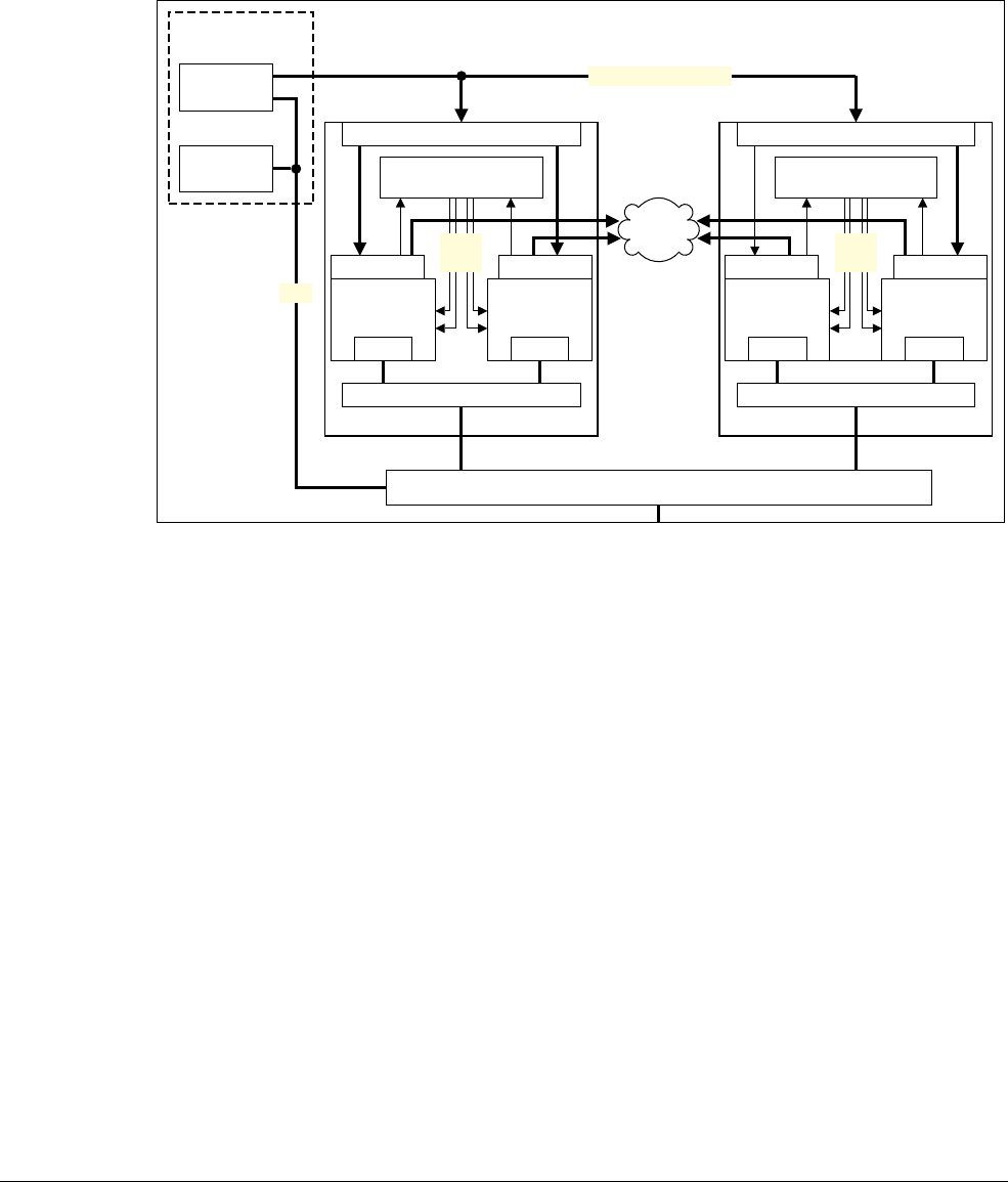
D7 The Generic Timer
D7.1 About the Generic Timer
D7-1856 Copyright © 2013 ARM Limited. All rights reserved. ARM DDI 0487A.a
Non-Confidential - Beta ID090413
D7.1 About the Generic Timer
Figure D7-1 shows an example system-on-chip that uses the Generic Timer as a system timer. In this figure:
• This manual defines the architecture of the individual PEs in the multiprocessor blocks.
• The ARM Generic Interrupt Controller Architecture Specification defines a possible architecture for the
GICs.
• Generic Timer functionality is distributed across multiple components.
Figure D7-1 Generic Timer example
This chapter:
• Gives a general description of the Generic Timer.
• Defines the system control register interface to the Generic Timer. Each PE shown in Figure D7-1 includes
an implementation of this interface.
The Generic Timer:
• Provides a system counter, that measures the passing of time in real-time.
• Supports virtual counters that measure the passing of virtual-time. That is, a virtual counter can measure the
passing of time on a particular virtual machine.
• Timers, that can trigger events after a period of time has passed. The timers:
— Can be used as count-up or as count-down timers.
— Can operate in real-time or in virtual-time.
System
counter
Always-powered
domain
Power
controller
System Timer Bus
APB
Counter interface
GIC
Timer_0
PE_0
Timer_1
PE_1
Shared cache
PPI_0 PPI_1
Memory interconnect and memory controller
Counter interface
GIC
Timer_0
PE_0
Timer_1
PE_1
Shared cache
PPI_0 PPI_1
System
events
System-on-Chip
nFIQ,
nIRQ
nFIQ,
nIRQ
Cache Cache Cache Cache
Multiprocessor A Multiprocessor B

D7 The Generic Timer
D7.1 About the Generic Timer
ARM DDI 0487A.a Copyright © 2013 ARM Limited. All rights reserved. D7-1857
ID090413 Non-Confidential - Beta
D7.1.1 System counter
The Generic Timer provides a system counter with the following specification:
Width At least 56 bits wide.
The value returned by any 64-bit read of the counter is zero-extended to 64 bits.
Frequency Increments at a fixed frequency, typically in the range 1-50MHz.
Can support one or more alternative operating modes in which it increments by larger amounts at a
lower frequency, typically for power-saving.
Roll-over Roll-over time of not less than 40 years.
Accuracy ARM does not specify a required accuracy, but recommends that the counter does not gain or lose
more than ten seconds in a 24-hour period.
Use of lower-frequency modes must not affect the implemented accuracy.
Start-up Starts operating from zero.
The system counter must provide a uniform view of system time. More precisely, it must be impossible for the
following sequence of events to show system time going backwards:
1. Device A reads the time from the system counter.
2. Device A communicates with another agent in the system, Device B.
3. After recognizing the communication from Device A, Device B reads the time from the system counter.
The system counter must be implemented in an always-on power domain.
To support lower-power operating modes, the counter can increment by larger amounts at a lower frequency. For
example, a 10MHz system counter might either increment either:
• By 1 at 10MHz.
• By 500 at 20KHz, when the system lowers the clock frequency, to reduce power consumption.
In this case, the counter must support transitions between high-frequency, high-precision operation, and
lower-frequency, lower-precision operation, without any impact on the required accuracy of the counter.
Software can access the CNTFRQ register to read or modify the clock frequency of the system counter, see
Initializing and reading the system counter frequency.
The mechanism by which the count from the system counter is distributed to system components is
IMPLEMENTATION DEFINED, but each PE with a system control register interface to the system counter must have a
counter input that can capture each increment of the counter.
Note
So that the system counter can be clocked independently from the PE hardware, the count value might be distributed
using a Gray code sequence. Gray-count scheme for timer distribution scheme on page I2-4692 gives more
information about this possibility.
Initializing and reading the system counter frequency
Typically, the system counter frequency is set, using the system control register interface, only during the system
boot process. It is set by writing the system counter frequency to the CNTFRQ register. Only software executing in
a Secure EL1 mode can write to CNTFRQ.
Note
The CNTFRQ register is UNKNOWN at reset, and therefore the counter frequency must be set as part of the system
boot process.
Software can read the CNTFRQ register, to determine the current system counter frequency, in the following states
and modes:
• Non-secure EL2 mode.
• Secure and Non-secure EL1 modes.
• When CNTKCTL.EL0PCTEN is set to 1, Secure and Non-secure EL0 modes.

D7 The Generic Timer
D7.1 About the Generic Timer
D7-1858 Copyright © 2013 ARM Limited. All rights reserved. ARM DDI 0487A.a
Non-Confidential - Beta ID090413
Memory-mapped controls of the system counter
Some system counter controls are accessible only through the memory-mapped interface to the system counter.
These controls are:
• Enabling and disabling the counter.
• Setting the counter value.
• Changing the operating mode, to change the update frequency and increment value.
• Enabling Halt-on-debug, that a debugger can then use to suspend counting.
For descriptions of these controls, see Chapter I2 System Level Implementation of the Generic Timer.
D7.1.2 The physical counter
The PE includes a physical counter that contains the count value of the system counter. The CNTPCT register holds
the current physical counter value.
Accessing the physical counter
Software with sufficient privilege can read CNTPCT using a 64-bit system control register read.
In all implementations, CNTPCT:
• Is always accessible from Secure EL1 modes, and from Non-secure Hyp mode.
• Is accessible from Non-secure EL1 modes only when CNTHCTL.EL1PCTEN is set to 1. When
CNTHCTL.EL1PCTEN is set to 0, any attempt to access CNTPCT from Non-secure EL1generates a Hyp
Trap exception, see Hyp Trap exception on page G1-3478.
In addition, when CNTKCTL.EL0PCTEN is set to 1, if CNTPCT is accessible from EL1 in the current Security
state then it is also accessible from EL0 in that Security state.
When CNTKCTL.EL0PCTEN is set to 0, any attempt to access CNTPCT from EL0is UNDEFINED.
In all implementations:
• The CNTKCTL control has priority over the CNTHCTL control. When both of the following apply, this
means that an attempt to access CNTPCT from Non-secure EL0 is UNDEFINED:
—CNTHCTL.EL1PCTEN is set to 0, to disable accesses from Non-secure EL1.
—CNTKCTL.EL0PCTEN is set to 0, to disable accesses from EL0.
• When EL0 accesses are enabled, the CNTHCTL applies to Non-secure EL0 accesses. When both of the
following apply, this means that an attempt to access CNTPCT from Non-secure EL0 generates a Hyp Trap
exception:
—CNTHCTL.EL1PCTEN is set to 0, to disable accesses from Non-secure EL1.
—CNTKCTL.EL0PCTEN is set to 1, to enable accesses from EL0.
Reads of CNTPCT can occur speculatively and out of order relative to other instructions executed on the same PE.
For example, if a read from memory is used to obtain a signal from another agent that indicates that CNTPCT must
be read, an
ISB
must be used to ensure that the read of CNTPCT occurs after the signal has been read from memory,
as shown in the following code sequence:
loop ; polling for some communication to indicate a requirement to read the timer
LDR R1, [R2]
CMP R1, #1
BNE loop
ISB ; without this, the CNTPCT could be read before the memory location in [R2]
; has had the value 1 written to it
MRS R1, CNTPCT

D7 The Generic Timer
D7.1 About the Generic Timer
ARM DDI 0487A.a Copyright © 2013 ARM Limited. All rights reserved. D7-1859
ID090413 Non-Confidential - Beta
D7.1.3 The virtual counter
An implementation of the Generic Timer always includes a virtual counter, that indicates virtual time:
The virtual counter contains the value of the physical counter minus a 64-bit virtual offset. When executing in a
Non-secure EL1 or EL0 mode, the virtual offset value relates to the current virtual machine.
The CNTVOFF register contains the virtual offset. CNTVOFF is only accessible from EL2, or from EL3 when
SCR.NS is set to 1. See Status of the CNTVOFF register on page D7-1864 for more information.
The CNTVCT register holds the current virtual counter value.
Accessing the virtual counter
Software with sufficient privilege can read CNTVCT using a 64-bit system control register read.
CNTVCT is always accessible from Secure EL3, from Secure EL1 when EL3 is using AArch64, and from
Non-secure EL1 and EL2.
In addition, when CNTKCTL.EL0VCTEN is set to 1, CNTVCT is accessible from EL0.
When CNTKCTL.EL0VCTEN is set to 0, any attempt to access CNTVCT from EL0 is UNDEFINED.
Reads of CNTVCT can occur speculatively and out of order relative to other instructions executed on the same PE.
For example, if a read from memory is used to obtain a signal from another agent that indicates that CNTVCT must
be read, an ISB must be used to ensure that the read of CNTVCT occurs after the signal has been read from memory,
as shown in the following code sequence:
loop ; polling for some communication to indicate a requirement to read the timer
LDR R1, [R2]
CMP R1, #1
BNE loop
ISB ; without this, the CNTVCT could be read before the memory location in [R2]
; has had the value 1 written to it
MRS R1, CNTVCT
D7.1.4 Event streams
An implementation that includes the Generic Timer can use the system counter to generate one or more event
streams, to generate periodic wake-up events as part of the mechanism described in Wait for Event mechanism and
Send event on page D1-1533.
Note
An event stream might be used:
• To impose a time-out on a Wait For Event polling loop.
• To safeguard against any programming error that means an expected event is not generated.
An event stream is configured by:
• Selecting which bit, from the bottom 16 bits of a counter, triggers the event. This determines the frequency
of the events in the stream.
• Selecting whether the event is generated on each 0 to 1 transition, or each 1 to 0 transition, of the selected
counter bit.
The CNTKCTL.{EVNTEN, EVNTDIR, EVNTI} fields define an event stream that is generated from the virtual
counter.
In all implementations the CNTHCTL.{EVNTEN, EVNTDIR, EVNTI} fields define an event stream that is
generated from the physical counter.

D7 The Generic Timer
D7.1 About the Generic Timer
D7-1860 Copyright © 2013 ARM Limited. All rights reserved. ARM DDI 0487A.a
Non-Confidential - Beta ID090413
The operation of an event stream is as follows:
• The pseudocode variables
PreviousCNTVCT
and
PreviousCNTPCT
are initialized as:
// Variables used for generation of the timer event stream.
bits(64) PreviousCNTVCT = bits(64) UNKNOWN;
bits(64) PreviousCNTPCT = bits(64) UNKNOWN;
• The pseudocode functions
TestEventCNTV()
and
TestEventCNTP()
are called on each cycle of the PE clock.
• The
TestEventCNTx()
pseudocode template defines the functions
TestEventCNTV()
and
TestEventCNTP()
:
// TestEventCNTx()
// ===============
// Template for the TestEventCNTV() and TestEventCNTP() functions:
// CNTxCT is CNTVCT or CNTPCT 64-bit count value
// CNTxCTL is CNTVCTL or CNTPCTL Control register
// PreviousCNTxCT is PreviousCNTVCT or PreviousCNTPCT
TestEventCNTx()
if CNTxCTL.EVNTEN == ‘1’ then
n = UInt(CNTxCTL.EVNTI);
SampleBit = CNTxCT<n>;
PreviousBit = PreviousCNTxCT<n>;
if CNTxCTL.EVNTDIR == ‘0’ then
if PreviousBit == ‘0’ && SampleBit == ‘1’ then SendEvent();
else
if PreviousBit == ‘1’ && SampleBit == ‘0’ then SendEvent();
PreviousCNTxCT = CNTxCT;
return;
D7.1.5 Timers
The following timers are provided by an implementation of the Generic Timer Extension:
• A Non-secure EL1 physical timer.
• A Secure EL1 physical timer.
• A Non-secure EL2 physical timer.
• A virtual timer.
The output of each implemented timer:
• Provides an output signal to the system.
• If the PE interfaces to a Generic Interrupt Controller (GIC), signals a Private Peripheral Interrupt (PPI) to
that GIC. In a multiprocessor implementation, each PE must use the same interrupt number for each timer.
Each timer is implemented as three registers:
• A 64-bit CompareValue register, that provides a 64-bit unsigned upcounter.
• A 32-bit TimerValue register, that provides a 32-bit signed downcounter.
• A 32-bit Control register.

D7 The Generic Timer
D7.1 About the Generic Timer
ARM DDI 0487A.a Copyright © 2013 ARM Limited. All rights reserved. D7-1861
ID090413 Non-Confidential - Beta
In all implementations, the registers for the EL1 physical timer are Banked, to provide the Secure and Non-secure
implementations of the timer. Table D7-1 shows the Timer registers.
Table J-3 on page AppxJ-5090 disambiguates these general names to the AArch64 and AArch32 descriptions of
these registers.
The following sections describe:
•Accessing the timer registers
•Operation of the CompareValue views of the timers on page D7-1862
•Operation of the TimerValue views of the timers on page D7-1862.
Accessing the timer registers
For each timer, all timer registers have the same access permissions, as follows:
EL1 physical timer Accessible from EL1 modes, except that Non-secure software executing at EL2 controls
access from Non-secure EL1 modes.
When access from EL1 modes is permitted, CNTKCTL.EL0PTEN determines whether the
registers are accessible from EL0 modes. If an access is not permitted because
CNTKCTL.EL0PTEN is set to 0, an attempted access from EL0 is UNDEFINED.
In all implementations:
• Except for accesses from Monitor mode, accesses are to the registers for the current
Security state.
• For accesses from Monitor mode, the value of SCR_EL3.NS determines whether
accesses are to the Secure or the Non-secure registers.
• The Non-secure registers are accessible from Hyp mode.
•CNTHCTL.NSEL1TPEN determines whether the Non-secure registers are
accessible from Non-secure EL1 modes. If this bit is set to 1, to enable access from
Non-secure EL1 modes, CNTKCTL.EL0PTEN determines whether the registers are
accessible from Non-secure EL0 modes.
If an access is not permitted because CNTHCTL.NSEL1TPEN is set to 0, an
attempted access from a Non-secure EL1 or EL0 mode generates a Hyp Trap
exception. However, if CNTKCTL.EL0PTEN is set to 0, this control takes priority,
and an attempted access from EL0 is UNDEFINED.
Virtual timer Accessible from Secure and Non-secure EL1 modes, and from Hyp mode.
CNTKCTL.EL0VTEN determines whether the registers are accessible from EL0 modes. If
an access is not permitted because CNTKCTL.EL0VTEN is set to 0, an attempted access
from an EL0 is UNDEFINED.
EL2 physical timer Accessible from Non-secure Hyp mode, and from Secure Monitor mode when
SCR_EL3.NS is set to 1.
Table D7-1 Timer registers summary for the Generic Timer
EL1 physical timera
a. In AArch32 state, the registers are Banked.
EL2 physical timer Virtual timer
CompareValue register CNTP_CVAL CNTHP_CVAL CNTV_CVAL
TimerValue register CNTP_TVAL CNTHP_TVAL CNTV_TVAL
Control register CNTP_CTL CNTHP_CTL CNTV_CTL

D7 The Generic Timer
D7.1 About the Generic Timer
D7-1862 Copyright © 2013 ARM Limited. All rights reserved. ARM DDI 0487A.a
Non-Confidential - Beta ID090413
Operation of the CompareValue views of the timers
The CompareValue view of a timer operates as a 64-bit upcounter. The timer triggers when the appropriate counter
reaches the value programmed into a CompareValue register. When the timer triggers, it generates an interrupt if
the interrupt is enabled in the corresponding timer control register, CNTP_CTL, CNTHP_CTL, or CNTV_CTL.
The operation of this view of a timer is:
EventTriggered = (((Counter[63:0] – Offset[63:0])[63:0] - CompareValue[63:0]) >= 0)
Where:
EventTriggered
Is TRUE if the event for this timer must be triggered, and FALSE otherwise.
Counter
The physical counter value, that can be read from the CNTPCT register.
Note
The virtual counter value, that can be read from the CNTVCT register, is the value:
(Counter - Offset)
Offset
For a physical timer it is zero, and for the virtual timer it is the virtual offset, held in the
CNTVOFF register.
CompareValue
The value of the appropriate CompareValue register, CNTP_CVAL, CNTHP_CTL, or
CNTV_CVAL.
In this view of a timer,
Counter
,
Offset
, and
CompareValue
are all 64-bit unsigned values.
Note
This means that a timer with a
CompareValue
of, or close to,
0xFFFF_FFFF_FFFF_FFFF
might never trigger. However,
there is no practical requirement to use values close to the counter wrap value.
Operation of the TimerValue views of the timers
The TimerValue view of a timer operates as a signed 32-bit downcounter. A TimerValue register is programmed
with a count value. This value decrements on each increment of the appropriate counter, and the timer triggers when
the value reaches zero. When the timer triggers, it generates an interrupt if the interrupt is enabled in the
corresponding timer control register, CNTP_CTL, CNTHP_CTL, or CNTV_CTL.
This view of a timer depends on the following behavior of accesses to TimerValue registers:
Reads
TimerValue = (CompareValue – (Counter - Offset))[31:0]
Writes
CompareValue = ((Counter - Offset)[63:0] + SignExtend(TimerValue))[63:0]
Where the arguments have the definitions used in Operation of the CompareValue views of the timers, and in
addition:
TimerValue
The value of a TimerValue register, CNTP_TVAL, CNTHP_TVAL, or CNTV_TVAL.
The operation of this view of a timer is, effectively:
EventTriggered = (TimerValue
≤
0)
In this view of a timer, all values are signed, in standard two’s complement form.
After an event has triggered, a read of a TimerValue register indicates the time since the event triggered.
Note
Programming TimerValue to a negative number with magnitude greater than (Counter–Offset) can lead to an
arithmetic overflow that causes the CompareValue to be an extremely large positive value. This potentially delays
the resultant interrupt for an extremely long period of time.

D7 The Generic Timer
D7.1 About the Generic Timer
ARM DDI 0487A.a Copyright © 2013 ARM Limited. All rights reserved. D7-1863
ID090413 Non-Confidential - Beta

D7 The Generic Timer
D7.2 About the Generic Timer registers
D7-1864 Copyright © 2013 ARM Limited. All rights reserved. ARM DDI 0487A.a
Non-Confidential - Beta ID090413
D7.2 About the Generic Timer registers
This chapter uses general names to refer to the Generic Timers registers. Table J-3 on page AppxJ-5090
disambiguates these general names to either the AArch64 System registers or the AArch32 System registers.
D7.2.1 Status of the CNTVOFF register
All implementations of the Generic Timers Extension include the virtual counter. Therefore, conceptually, all
implementations include the CNTVOFF register that defines the virtual offset between the physical count and the
virtual count. CNTVOFF is defined as an EL2-mode register, see Banked EL2-mode CP15 read/write registers on
page G3-3700. This means:
• In an implementation that includes EL2, CNTVOFF is a RW register, accessible from Non-secure EL2, and
from EL3 when SCR.NS is set to 1. Any access to the CNTVOFF encoding is UNDEFINED if executed at EL3
when SCR.NS is set to 0.
• In an implementation that includes EL3 but does not include EL2, CNTVOFF is RW and RES0.
• Any access to the CNTVOFF encoding other than the accesses from EL2 and EL3 described in this list is
UNDEFINED.
• In an implementation that does not include EL3, although the register is conceptually present, there is no way
of accessing it. The instruction encodings for accessing the register are UNDEFINED.
In all cases where the CNTVOFF register is not defined as a RW register, the virtual counter uses a fixed virtual
offset value of zero.

ARM DDI 0487A.a Copyright © 2013 ARM Limited. All rights reserved. D8-1865
ID090413 Non-Confidential - Beta
Chapter D8
AArch64 System Register Descriptions
This chapter defines the AArch64 System registers. It contains the following sections:
•About the AArch64 System registers on page D8-1866.
•General system control registers on page D8-1870.
•Debug registers on page D8-2077.
•Performance Monitors registers on page D8-2134.
•Generic Timer registers on page D8-2170.
•Generic Interrupt Controller CPU interface registers on page D8-2194.

D8 AArch64 System Register Descriptions
D8.1 About the AArch64 System registers
D8-1866 Copyright © 2013 ARM Limited. All rights reserved. ARM DDI 0487A.a
Non-Confidential - Beta ID090413
D8.1 About the AArch64 System registers
This section describes common features of the AArch64 registers.
D8.1.1 Fixed values in the System register descriptions
See Fixed values in instruction and register descriptions on page C4-230. This section defines the terms RAZ on
page C4-230, RES0, RAO on page C4-230, and RES1, as used in the System register descriptions,
D8.1.2 General behavior of accesses to the System registers
This section gives general information about the behavior of accesses to the System registers.
Synchronization requirements for system registers
Reads of the System registers can occur out of order with respect to earlier instructions executed on the same PE,
provided that any data dependencies between the instructions are respected.
Note
In particular, system registers that hold self-incrementing counts such as the performance counters or the Generic
Timer counter or timers, can be read early. For example, where a memory access is used to communicate a read of
such counters, an
ISB
must be inserted between the read of the memory location and the read of the Generic Timer
counter, where it is necessary that the Generic Timer counter returns a count value after the memory
communication.
Direct writes using the instructions in Table C4-7 on page C4-243 require synchronization before software can rely
on the effects of changes to the system registers to affect instructions appearing in program order after the direct
write to the system register. Direct writes to these registers are not allowed to affect any instructions appearing in
program order before the direct write. The only exceptions are:
• All direct writes to the same register, that use the same encoding for that register, are guaranteed to occur in
program order relative to each other
• All direct writes to a register occur in program order with respect to all direct reads to the same register using
the same encoding.
Explicit synchronization occurs as a result a Context synchronization operation, which is of one of the following
events:
• Execution of an
ISB
instruction.
• Exception entry.
• Exception return.
• Execution of a
DCPS
instruction in Debug state.
• Execution of a
DRPS
instruction in Debug state.
• Exit from Debug state.
Note
The
ISB
, exception entry, or exception return events are applicable either in Debug state or not in Debug state.
Conceptually, explicit synchronization occurs as the first step of each of these events, so that if the event uses state
that has previously been changed but was not synchronized by the time of the event, the event is guaranteed to use
the state as if it had been synchronized.
Note
This explicit synchronization applies as the first step of the execution of the events, and does not apply to any effect
of system registers that apply to the fetch and decode of the instructions that cause these events, such as breakpoints
or changes to the translation table.

D8 AArch64 System Register Descriptions
D8.1 About the AArch64 System registers
ARM DDI 0487A.a Copyright © 2013 ARM Limited. All rights reserved. D8-1867
ID090413 Non-Confidential - Beta
In addition, any system instructions that cause a write to a system register must be synchronized before the result is
guaranteed to be visible to subsequent direct reads of that system register.
Direct reads to any one of the following registers, using the same encoding, occur in program order relative to each
other:
•ISR_EL1
• The Generic Timer registers, that is, CNTPCT_EL0 and CNTVCT_EL0, and the Counter registers
CNTP_TVAL_EL0, CNTV_TVAL_EL0, CNTHP_TVAL_EL2, and CNTPS_TVAL_EL1.
•DBGCLAIMCLR_EL1.
• The PMU Counters, that is, PMCCNTR_EL0, PMEVCNTR<n>_EL0, PMXEVCNTR_EL0,
PMOVSCLR_EL0, and PMOVSSET_EL0.
• The Debug Communications Channel registers, that is, DBGDTRTX_EL0, DBGDTRRX_EL0,
DBGDTR_EL0, MDCCSR_EL0 or EDSCR.
All other direct reads of system registers can occur in any order if synchronization has not been performed.
Table D8-1 describes the synchronization requirements between two successive read/write accesses to the same
register, where the ordering of the read/write is:
1. Program order, in the event that the read or write is caused by an instruction executed on this PE, other than
one caused by a memory access by this PE.
2. The order of arrival of asynchronous reads and writes by the PE relative to the execution of instructions.
Table D8-1 Synchronization requirements
First read-write Second read-write Synchronization requirement
Direct read Direct read None
Direct write None
Indirect read None
Indirect write None, see Notes on page D8-1868
Direct write Direct read None
Direct write None
Indirect read Required
Indirect write None, see Notes on page D8-1868
Indirect read Direct read None
Direct write None
Indirect read None
Indirect write None
Indirect write Direct read Required, see Notes on
page D8-1868
Direct write None, see Notes on page D8-1868
Indirect read Required, see Notes on
page D8-1868
Indirect write None, see Notes on page D8-1868

D8 AArch64 System Register Descriptions
D8.1 About the AArch64 System registers
D8-1868 Copyright © 2013 ARM Limited. All rights reserved. ARM DDI 0487A.a
Non-Confidential - Beta ID090413
Notes
In Table D8-1 on page D8-1867:
Direct read Where software uses a system register access instruction to read the register, see Instructions for
accessing non-debug System registers on page C4-242. Where a direct read of a register has a
side-effect that changes the contents of a register, the effect of a direct read on that register is defined
to be an indirect write. In this case, the indirect write is only guaranteed to have occurred, and be
visible to subsequent direct or indirect reads or writes, if synchronization is performed after the
direct read.
Direct write Where software uses a system register access instruction to write to the register, see Instructions for
accessing non-debug System registers on page C4-242. Where a direct write to a register has an
effect on the register that means that the value in the register is not always the last value that is
written (as is the case with set and clear registers), the effect of a direct write on that register is
defined to be an indirect write. In this case, the indirect write is only guaranteed to be visible to
subsequent direct or indirect reads or writes if synchronization is performed after the direct write
and before the subsequent direct or indirect reads or writes.
Indirect read Where an instruction uses a system register to establish operating conditions, for example,
translation table base register addresses or whether the cache is enabled, for the instruction. This
includes situations where the contents of one system register selects what value is read using a
different register. Indirect reads also include reads of the system register by external agents such as
debuggers. Where an indirect read of a register has a side-effect that changes the contents of that
register, that is defined to be an indirect write.
Indirect write Where a system register is written as the consequence of some other instruction, exception,
operation, or by the asynchronous operation of such some external agent, including the passage of
time as seen in counters, timers, or performance counters, the assertion of interrupts, or writes from
an external debugger.
Note
Since an exception is context synchronizing, registers such as the Exception Syndrome registers that
are indirectly written as part of exception entry do not require additional synchronization.
Where a direct read or write to a register is followed by an indirect write caused by an external agent, autonomous
asynchronous event, or as a result of memory mapped write, synchronization is required to guarantee the order of
those two accesses.
Where an indirect write caused by a direct write is followed by an indirect write caused by an external agent,
autonomous asynchronous event, or as a result of memory mapped write, synchronization is required to guarantee
the order of those two indirect accesses.
Where a direct read to one register causes a bit or field in a different register (or the same register using a different
encoding) to be updated, the change to the different register (or same register using a different encoding) is defined
to be an indirect write. In this case, the indirect write is only guaranteed to be visible to subsequent direct or indirect
reads or writes if synchronization is performed after the direct read and before the subsequent direct or indirect reads
or writes.
Where a direct write to one register causes a bit or field in a different register (or the same register using a different
encoding) to be updated as a side-effect of that direct write (as opposed to simply being a direct write to the different
encoding), the change to the different register (or same register using a different encoding) is defined to be an
indirect write. In this case, the indirect write is only guaranteed to be visible to subsequent direct or indirect reads
or writes if synchronization is performed after the direct write and before the subsequent direct or indirect reads or
writes.
Where indirect writes are caused by the actions of external agents such as debuggers, or by memory-mapped reads
or writes by the PE, then an indirect write by that agent and mechanism to a register, followed by an indirect read
by that agent and mechanism to the same register using the same address, does not require synchronization.

D8 AArch64 System Register Descriptions
D8.1 About the AArch64 System registers
ARM DDI 0487A.a Copyright © 2013 ARM Limited. All rights reserved. D8-1869
ID090413 Non-Confidential - Beta
Indirect writes to the following registers caused by external agents, autonomous asynchronous events, or as a result
of memory-mapped writes, are required to be observable to:
• Direct reads in finite time without explicit synchronization.
• Subsequent indirect reads without explicit synchronization:
—ISR_EL1.
— The Generic Timer registers, that is, CNTPCT_EL0 and CNTVCT_EL0, and the Counter registers
CNTP_TVAL_EL0, CNTV_TVAL_EL0, CNTHP_TVAL_EL2, and CNTPS_TVAL_EL1.
— The debug claim registers, DBGCLAIMCLR_EL1 and DBGCLAIMSET_EL1.
— The PMU Counters, that is, PMCCNTR_EL0, PMEVCNTR<n>_EL0, PMXEVCNTR_EL0,
PMOVSCLR_EL0, and PMOVSSET_EL0.
— The Debug Communications Channel registers, that is, DBGDTRTX_EL0, DBGDTRRX_EL0,
DBGDTR_EL0, MDCCSR_EL0 or EDSCR.
Note
• The provision of explicit synchronization requirements to system registers is provided to allow the direct
access to these registers to be implemented in a small number of cycles, and that updates to multiple registers
can be performed quickly with the synchronization penalty being paid only when the updates have occurred.
• Since toolkits might use registers such as the thread-local storage registers within compiled code, it is
recommended that access to these registers is implemented to take a small number of cycles.
• While no synchronization is required between a direct write and a direct read, or between a direct read and
an indirect write, this does not imply that a direct read causes synchronization of a previous direct write. That
is, the sequence direct write →direct read →indirect read, with no intervening context synchronization,
does not guarantee that the indirect read observes the result of the direct write.

D8 AArch64 System Register Descriptions
D8.2 General system control registers
D8-1870 Copyright © 2013 ARM Limited. All rights reserved. ARM DDI 0487A.a
Non-Confidential - Beta ID090413
D8.2 General system control registers
This section lists the system control registers in AArch64 that are not part of one of the other listed groups.
D8.2.1 ACTLR_EL1, Auxiliary Control Register (EL1)
The ACTLR_EL1 characteristics are:
Purpose
Provides IMPLEMENTATION DEFINED configuration and control options for EL1.
This register is part of:
• the Other system control registers functional group
• the IMPLEMENTATION DEFINED functional group.
Usage constraints
This register is accessible as shown below:
Configurations
ACTLR_EL1 is architecturally mapped to AArch32 register ACTLR (NS).
Attributes
ACTLR_EL1 is a 32-bit register.
The ACTLR_EL1 bit assignments are:
Accessing the ACTLR_EL1:
To access the ACTLR_EL1:
MRS <Xt>, ACTLR_EL1 ; Read ACTLR_EL1 into Xt
MSR ACTLR_EL1, <Xt> ; Write Xt to ACTLR_EL1
Register access is encoded as follows:
EL0 EL1 (NS) EL1 (S) EL2 EL3 (SCR.NS=1) EL3 (SCR.NS=0)
-RW RW RWRW RW
IMPLEMENTATION DEFINED
31 0
op0 op1 CRn CRm op2
11 000 0001 0000 001

D8 AArch64 System Register Descriptions
D8.2 General system control registers
ARM DDI 0487A.a Copyright © 2013 ARM Limited. All rights reserved. D8-1871
ID090413 Non-Confidential - Beta
D8.2.2 ACTLR_EL2, Auxiliary Control Register (EL2)
The ACTLR_EL2 characteristics are:
Purpose
Provides IMPLEMENTATION DEFINED configuration and control options for EL2.
This register is part of:
• the Virtualization registers functional group
• the Other system control registers functional group
• the IMPLEMENTATION DEFINED functional group.
Usage constraints
This register is accessible as shown below:
Configurations
ACTLR_EL2 is architecturally mapped to AArch32 register HACTLR.
If EL2 is not implemented, this register is RES0 from EL3.
Attributes
ACTLR_EL2 is a 32-bit register.
The ACTLR_EL2 bit assignments are:
Accessing the ACTLR_EL2:
To access the ACTLR_EL2:
MRS <Xt>, ACTLR_EL2 ; Read ACTLR_EL2 into Xt
MSR ACTLR_EL2, <Xt> ; Write Xt to ACTLR_EL2
Register access is encoded as follows:
EL0 EL1 (NS) EL1 (S) EL2 EL3 (SCR.NS=1) EL3 (SCR.NS=0)
-- - RWRW RW
IMPLEMENTATION DEFINED
31 0
op0 op1 CRn CRm op2
11 100 0001 0000 001

D8 AArch64 System Register Descriptions
D8.2 General system control registers
D8-1872 Copyright © 2013 ARM Limited. All rights reserved. ARM DDI 0487A.a
Non-Confidential - Beta ID090413
D8.2.3 ACTLR_EL3, Auxiliary Control Register (EL3)
The ACTLR_EL3 characteristics are:
Purpose
Provides IMPLEMENTATION DEFINED configuration and control options for EL3.
This register is part of:
• the Other system control registers functional group
• the Security registers functional group
• the IMPLEMENTATION DEFINED functional group.
Usage constraints
This register is accessible as shown below:
Configurations
ACTLR_EL3 can be mapped to AArch32 register ACTLR (S), but this is not architecturally
mandated.
Attributes
ACTLR_EL3 is a 32-bit register.
The ACTLR_EL3 bit assignments are:
Accessing the ACTLR_EL3:
To access the ACTLR_EL3:
MRS <Xt>, ACTLR_EL3 ; Read ACTLR_EL3 into Xt
MSR ACTLR_EL3, <Xt> ; Write Xt to ACTLR_EL3
Register access is encoded as follows:
EL0 EL1 (NS) EL1 (S) EL2 EL3 (SCR.NS=1) EL3 (SCR.NS=0)
-- - -RW RW
IMPLEMENTATION DEFINED
31 0
op0 op1 CRn CRm op2
11 110 0001 0000 001

D8 AArch64 System Register Descriptions
D8.2 General system control registers
ARM DDI 0487A.a Copyright © 2013 ARM Limited. All rights reserved. D8-1873
ID090413 Non-Confidential - Beta
D8.2.4 AFSR0_EL1, Auxiliary Fault Status Register 0 (EL1)
The AFSR0_EL1 characteristics are:
Purpose
Provides additional IMPLEMENTATION DEFINED fault status information for exceptions taken to EL1.
This register is part of:
• the Exception and fault handling registers functional group
• the IMPLEMENTATION DEFINED functional group.
Usage constraints
This register is accessible as shown below:
Configurations
AFSR0_EL1 is architecturally mapped to AArch32 register ADFSR (NS).
Attributes
AFSR0_EL1 is a 32-bit register.
The AFSR0_EL1 bit assignments are:
Accessing the AFSR0_EL1:
To access the AFSR0_EL1:
MRS <Xt>, AFSR0_EL1 ; Read AFSR0_EL1 into Xt
MSR AFSR0_EL1, <Xt> ; Write Xt to AFSR0_EL1
Register access is encoded as follows:
EL0 EL1 (NS) EL1 (S) EL2 EL3 (SCR.NS=1) EL3 (SCR.NS=0)
-RW RW RWRW RW
IMPLEMENTATION DEFINED
31 0
op0 op1 CRn CRm op2
11 000 0101 0001 000

D8 AArch64 System Register Descriptions
D8.2 General system control registers
D8-1874 Copyright © 2013 ARM Limited. All rights reserved. ARM DDI 0487A.a
Non-Confidential - Beta ID090413
D8.2.5 AFSR0_EL2, Auxiliary Fault Status Register 0 (EL2)
The AFSR0_EL2 characteristics are:
Purpose
Provides additional IMPLEMENTATION DEFINED fault status information for exceptions taken to EL2.
This register is part of:
• the Virtualization registers functional group
• the Exception and fault handling registers functional group
• the IMPLEMENTATION DEFINED functional group.
Usage constraints
This register is accessible as shown below:
Configurations
AFSR0_EL2 is architecturally mapped to AArch32 register HADFSR.
If EL2 is not implemented, this register is RES0 from EL3.
Attributes
AFSR0_EL2 is a 32-bit register.
The AFSR0_EL2 bit assignments are:
Accessing the AFSR0_EL2:
To access the AFSR0_EL2:
MRS <Xt>, AFSR0_EL2 ; Read AFSR0_EL2 into Xt
MSR AFSR0_EL2, <Xt> ; Write Xt to AFSR0_EL2
Register access is encoded as follows:
EL0 EL1 (NS) EL1 (S) EL2 EL3 (SCR.NS=1) EL3 (SCR.NS=0)
-- - RWRW RW
IMPLEMENTATION DEFINED
31 0
op0 op1 CRn CRm op2
11 100 0101 0001 000

D8 AArch64 System Register Descriptions
D8.2 General system control registers
ARM DDI 0487A.a Copyright © 2013 ARM Limited. All rights reserved. D8-1875
ID090413 Non-Confidential - Beta
D8.2.6 AFSR0_EL3, Auxiliary Fault Status Register 0 (EL3)
The AFSR0_EL3 characteristics are:
Purpose
Provides additional IMPLEMENTATION DEFINED fault status information for exceptions taken to EL3.
This register is part of:
• the Exception and fault handling registers functional group
• the Security registers functional group
• the IMPLEMENTATION DEFINED functional group.
Usage constraints
This register is accessible as shown below:
Configurations
AFSR0_EL3 can be mapped to AArch32 register ADFSR (S), but this is not architecturally
mandated.
Attributes
AFSR0_EL3 is a 32-bit register.
The AFSR0_EL3 bit assignments are:
Accessing the AFSR0_EL3:
To access the AFSR0_EL3:
MRS <Xt>, AFSR0_EL3 ; Read AFSR0_EL3 into Xt
MSR AFSR0_EL3, <Xt> ; Write Xt to AFSR0_EL3
Register access is encoded as follows:
EL0 EL1 (NS) EL1 (S) EL2 EL3 (SCR.NS=1) EL3 (SCR.NS=0)
-- - -RW RW
IMPLEMENTATION DEFINED
31 0
op0 op1 CRn CRm op2
11 110 0101 0001 000

D8 AArch64 System Register Descriptions
D8.2 General system control registers
D8-1876 Copyright © 2013 ARM Limited. All rights reserved. ARM DDI 0487A.a
Non-Confidential - Beta ID090413
D8.2.7 AFSR1_EL1, Auxiliary Fault Status Register 1 (EL1)
The AFSR1_EL1 characteristics are:
Purpose
Provides additional IMPLEMENTATION DEFINED fault status information for exceptions taken to EL1.
This register is part of:
• the Exception and fault handling registers functional group
• the IMPLEMENTATION DEFINED functional group.
Usage constraints
This register is accessible as shown below:
Configurations
AFSR1_EL1 is architecturally mapped to AArch32 register AIFSR (NS).
Attributes
AFSR1_EL1 is a 32-bit register.
The AFSR1_EL1 bit assignments are:
Accessing the AFSR1_EL1:
To access the AFSR1_EL1:
MRS <Xt>, AFSR1_EL1 ; Read AFSR1_EL1 into Xt
MSR AFSR1_EL1, <Xt> ; Write Xt to AFSR1_EL1
Register access is encoded as follows:
EL0 EL1 (NS) EL1 (S) EL2 EL3 (SCR.NS=1) EL3 (SCR.NS=0)
-RW RW RWRW RW
IMPLEMENTATION DEFINED
31 0
op0 op1 CRn CRm op2
11 000 0101 0001 001

D8 AArch64 System Register Descriptions
D8.2 General system control registers
ARM DDI 0487A.a Copyright © 2013 ARM Limited. All rights reserved. D8-1877
ID090413 Non-Confidential - Beta
D8.2.8 AFSR1_EL2, Auxiliary Fault Status Register 1 (EL2)
The AFSR1_EL2 characteristics are:
Purpose
Provides additional IMPLEMENTATION DEFINED fault status information for exceptions taken to EL2.
This register is part of:
• the Virtualization registers functional group
• the Exception and fault handling registers functional group
• the IMPLEMENTATION DEFINED functional group.
Usage constraints
This register is accessible as shown below:
Configurations
AFSR1_EL2 is architecturally mapped to AArch32 register HAIFSR.
If EL2 is not implemented, this register is RES0 from EL3.
Attributes
AFSR1_EL2 is a 32-bit register.
The AFSR1_EL2 bit assignments are:
Accessing the AFSR1_EL2:
To access the AFSR1_EL2:
MRS <Xt>, AFSR1_EL2 ; Read AFSR1_EL2 into Xt
MSR AFSR1_EL2, <Xt> ; Write Xt to AFSR1_EL2
Register access is encoded as follows:
EL0 EL1 (NS) EL1 (S) EL2 EL3 (SCR.NS=1) EL3 (SCR.NS=0)
-- - RWRW RW
IMPLEMENTATION DEFINED
31 0
op0 op1 CRn CRm op2
11 100 0101 0001 001

D8 AArch64 System Register Descriptions
D8.2 General system control registers
D8-1878 Copyright © 2013 ARM Limited. All rights reserved. ARM DDI 0487A.a
Non-Confidential - Beta ID090413
D8.2.9 AFSR1_EL3, Auxiliary Fault Status Register 1 (EL3)
The AFSR1_EL3 characteristics are:
Purpose
Provides additional IMPLEMENTATION DEFINED fault status information for exceptions taken to EL3.
This register is part of:
• the Exception and fault handling registers functional group
• the Security registers functional group
• the IMPLEMENTATION DEFINED functional group.
Usage constraints
This register is accessible as shown below:
Configurations
AFSR1_EL3 can be mapped to AArch32 register AIFSR (S), but this is not architecturally
mandated.
Attributes
AFSR1_EL3 is a 32-bit register.
The AFSR1_EL3 bit assignments are:
Accessing the AFSR1_EL3:
To access the AFSR1_EL3:
MRS <Xt>, AFSR1_EL3 ; Read AFSR1_EL3 into Xt
MSR AFSR1_EL3, <Xt> ; Write Xt to AFSR1_EL3
Register access is encoded as follows:
EL0 EL1 (NS) EL1 (S) EL2 EL3 (SCR.NS=1) EL3 (SCR.NS=0)
-- - -RW RW
IMPLEMENTATION DEFINED
31 0
op0 op1 CRn CRm op2
11 110 0101 0001 001

D8 AArch64 System Register Descriptions
D8.2 General system control registers
ARM DDI 0487A.a Copyright © 2013 ARM Limited. All rights reserved. D8-1879
ID090413 Non-Confidential - Beta
D8.2.10 AIDR_EL1, Auxiliary ID Register
The AIDR_EL1 characteristics are:
Purpose
Provides IMPLEMENTATION DEFINED identification information.
This register is part of:
• the Identification registers functional group
• the IMPLEMENTATION DEFINED functional group.
Usage constraints
This register is accessible as shown below:
The value of this register must be interpreted in conjunction with the value of MIDR_EL1.
Configurations
AIDR_EL1 is architecturally mapped to AArch32 register AIDR.
Attributes
AIDR_EL1 is a 32-bit register.
The AIDR_EL1 bit assignments are:
Accessing the AIDR_EL1:
To access the AIDR_EL1:
MRS <Xt>, AIDR_EL1 ; Read AIDR_EL1 into Xt
Register access is encoded as follows:
EL0 EL1 (NS) EL1 (S) EL2 EL3 (SCR.NS=1) EL3 (SCR.NS=0)
-RO RO RORO RO
IMPLEMENTATION DEFINED
31 0
op0 op1 CRn CRm op2
11 001 0000 0000 111
D8 AArch64 System Register Descriptions
D8.2 General system control registers
D8-1880 Copyright © 2013 ARM Limited. All rights reserved. ARM DDI 0487A.a
Non-Confidential - Beta ID090413
D8.2.11 AMAIR_EL1, Auxiliary Memory Attribute Indirection Register (EL1)
The AMAIR_EL1 characteristics are:
Purpose
Provides IMPLEMENTATION DEFINED memory attributes for the memory regions specified by
MAIR_EL1.
This register is part of:
• the Virtual memory control registers functional group
• the IMPLEMENTATION DEFINED functional group.
Usage constraints
This register is accessible as shown below:
AMAIR_EL1 is permitted to be cached in a TLB.
Configurations
AMAIR_EL1[31:0] is architecturally mapped to AArch32 register AMAIR0 (NS).
AMAIR_EL1[63:32] is architecturally mapped to AArch32 register AMAIR1 (NS).
Attributes
AMAIR_EL1 is a 64-bit register.
The AMAIR_EL1 bit assignments are:
Accessing the AMAIR_EL1:
To access the AMAIR_EL1:
MRS <Xt>, AMAIR_EL1 ; Read AMAIR_EL1 into Xt
MSR AMAIR_EL1, <Xt> ; Write Xt to AMAIR_EL1
Register access is encoded as follows:
EL0 EL1 (NS) EL1 (S) EL2 EL3 (SCR.NS=1) EL3 (SCR.NS=0)
-RW RW RWRW RW
IMPLEMENTATION DEFINED
63 0
op0 op1 CRn CRm op2
11 000 1010 0011 000
D8 AArch64 System Register Descriptions
D8.2 General system control registers
ARM DDI 0487A.a Copyright © 2013 ARM Limited. All rights reserved. D8-1881
ID090413 Non-Confidential - Beta
D8.2.12 AMAIR_EL2, Auxiliary Memory Attribute Indirection Register (EL2)
The AMAIR_EL2 characteristics are:
Purpose
Provides IMPLEMENTATION DEFINED memory attributes for the memory regions specified by
MAIR_EL2.
This register is part of:
• the Virtualization registers functional group
• the Virtual memory control registers functional group
• the IMPLEMENTATION DEFINED functional group.
Usage constraints
This register is accessible as shown below:
AMAIR_EL2 is permitted to be cached in a TLB.
Configurations
AMAIR_EL2[31:0] is architecturally mapped to AArch32 register HAMAIR0.
AMAIR_EL2[63:32] is architecturally mapped to AArch32 register HAMAIR1.
If EL2 is not implemented, this register is RES0 from EL3.
Attributes
AMAIR_EL2 is a 64-bit register.
The AMAIR_EL2 bit assignments are:
Accessing the AMAIR_EL2:
To access the AMAIR_EL2:
MRS <Xt>, AMAIR_EL2 ; Read AMAIR_EL2 into Xt
MSR AMAIR_EL2, <Xt> ; Write Xt to AMAIR_EL2
Register access is encoded as follows:
EL0 EL1 (NS) EL1 (S) EL2 EL3 (SCR.NS=1) EL3 (SCR.NS=0)
-- - RWRW RW
IMPLEMENTATION DEFINED
63 0
op0 op1 CRn CRm op2
11 100 1010 0011 000
D8 AArch64 System Register Descriptions
D8.2 General system control registers
D8-1882 Copyright © 2013 ARM Limited. All rights reserved. ARM DDI 0487A.a
Non-Confidential - Beta ID090413
D8.2.13 AMAIR_EL3, Auxiliary Memory Attribute Indirection Register (EL3)
The AMAIR_EL3 characteristics are:
Purpose
Provides IMPLEMENTATION DEFINED memory attributes for the memory regions specified by
MAIR_EL3.
This register is part of:
• the Virtual memory control registers functional group
• the Security registers functional group
• the IMPLEMENTATION DEFINED functional group.
Usage constraints
This register is accessible as shown below:
AMAIR_EL3 is permitted to be cached in a TLB.
Configurations
AMAIR_EL3[31:0] can be mapped to AArch32 register AMAIR0 (S), but this is not architecturally
mandated.
AMAIR_EL3[63:32] can be mapped to AArch32 register AMAIR1 (S), but this is not
architecturally mandated.
Attributes
AMAIR_EL3 is a 64-bit register.
The AMAIR_EL3 bit assignments are:
Accessing the AMAIR_EL3:
To access the AMAIR_EL3:
MRS <Xt>, AMAIR_EL3 ; Read AMAIR_EL3 into Xt
MSR AMAIR_EL3, <Xt> ; Write Xt to AMAIR_EL3
Register access is encoded as follows:
EL0 EL1 (NS) EL1 (S) EL2 EL3 (SCR.NS=1) EL3 (SCR.NS=0)
-- - -RW RW
IMPLEMENTATION DEFINED
63 0
op0 op1 CRn CRm op2
11 110 1010 0011 000
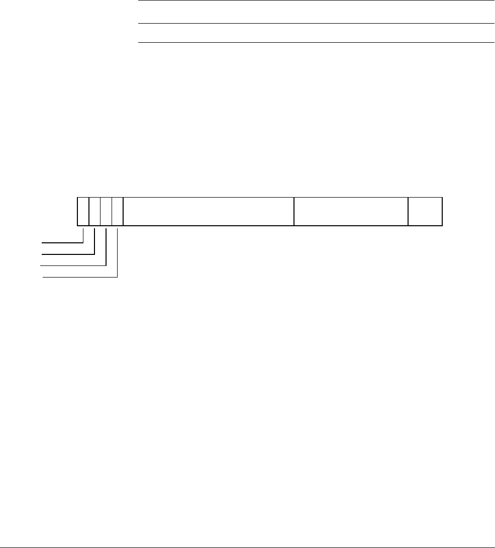
D8 AArch64 System Register Descriptions
D8.2 General system control registers
ARM DDI 0487A.a Copyright © 2013 ARM Limited. All rights reserved. D8-1883
ID090413 Non-Confidential - Beta
D8.2.14 CCSIDR_EL1, Current Cache Size ID Register
The CCSIDR_EL1 characteristics are:
Purpose
Provides information about the architecture of the currently selected cache.
This register is part of the Identification registers functional group.
Usage constraints
This register is accessible as shown below:
Configurations
CCSIDR_EL1 is architecturally mapped to AArch32 register CCSIDR.
The implementation includes one CCSIDR_EL1 for each cache that it can access. CSSELR_EL1
selects which Cache Size ID Register is accessible.
Attributes
CCSIDR_EL1 is a 32-bit register.
The CCSIDR_EL1 bit assignments are:
WT, bit [31]
Indicates whether the selected cache level supports write-through. Permitted values are:
0
Write-through not supported.
1
Write-through supported.
WB, bit [30]
Indicates whether the selected cache level supports write-back. Permitted values are:
0
Write-back not supported.
1
Write-back supported.
RA, bit [29]
Indicates whether the selected cache level supports read-allocation. Permitted values are:
0
Read-allocation not supported.
1
Read-allocation supported.
WA, bit [28]
Indicates whether the selected cache level supports write-allocation. Permitted values are:
0
Write-allocation not supported.
EL0 EL1 (NS) EL1 (S) EL2 EL3 (SCR.NS=1) EL3 (SCR.NS=0)
-RO RO RORO RO
31 30 29 28
NumSets
27 13
Associativity
12 3
LineSize
20
WT
WB
RA
WA

D8 AArch64 System Register Descriptions
D8.2 General system control registers
D8-1884 Copyright © 2013 ARM Limited. All rights reserved. ARM DDI 0487A.a
Non-Confidential - Beta ID090413
1
Write-allocation supported.
NumSets, bits [27:13]
(Number of sets in cache) - 1, therefore a value of 0 indicates 1 set in the cache. The number of sets
does not have to be a power of 2.
Associativity, bits [12:3]
(Associativity of cache) - 1, therefore a value of 0 indicates an associativity of 1. The associativity
does not have to be a power of 2.
LineSize, bits [2:0]
(Log2(Number of bytes in cache line)) - 4. For example:
For a line length of 16 bytes: Log2(16) = 4, LineSize entry = 0. This is the minimum line length.
For a line length of 32 bytes: Log2(32) = 5, LineSize entry = 1.
Accessing the CCSIDR_EL1:
To access the CCSIDR_EL1:
MRS <Xt>, CCSIDR_EL1 ; Read CCSIDR_EL1 into Xt
Register access is encoded as follows:
op0 op1 CRn CRm op2
11 001 0000 0000 000
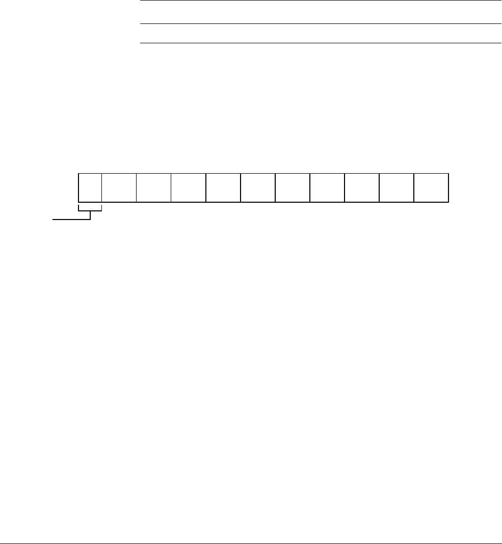
D8 AArch64 System Register Descriptions
D8.2 General system control registers
ARM DDI 0487A.a Copyright © 2013 ARM Limited. All rights reserved. D8-1885
ID090413 Non-Confidential - Beta
D8.2.15 CLIDR_EL1, Cache Level ID Register
The CLIDR_EL1 characteristics are:
Purpose
Identifies the type of cache, or caches, implemented at each level, up to a maximum of seven levels.
Also identifies the Level of Coherency and Level of Unification for the cache hierarchy.
This register is part of the Identification registers functional group.
Usage constraints
This register is accessible as shown below:
Configurations
CLIDR_EL1 is architecturally mapped to AArch32 register CLIDR.
Attributes
CLIDR_EL1 is a 32-bit register.
The CLIDR_EL1 bit assignments are:
Bits [31:30]
Reserved, RES0.
LoUU, bits [29:27]
Level of Unification Uniprocessor for the cache hierarchy.
LoC, bits [26:24]
Level of Coherency for the cache hierarchy.
LoUIS, bits [23:21]
Level of Unification Inner Shareable for the cache hierarchy.
Ctype<n>, bits [3(n-1)+2:3(n-1)], for n = 1 to 7
Cache Type fields. Indicate the type of cache implemented at each level, from Level 1 up to a
maximum of seven levels of cache hierarchy. Possible values of each field are:
000
No cache.
001
Instruction cache only.
010
Data cache only.
011
Separate instruction and data caches.
100
Unified cache.
All other values are reserved.
EL0 EL1 (NS) EL1 (S) EL2 EL3 (SCR.NS=1) EL3 (SCR.NS=0)
-RO RO RORO RO
31 30
LoUU
29 27
LoC
26 24
LoUIS
23 21
Ctype7
20 18
Ctype6
17 15
Ctype5
14 12
Ctype4
11 9
Ctype3
86
Ctype2
53
Ctype1
20
RES0

D8 AArch64 System Register Descriptions
D8.2 General system control registers
D8-1886 Copyright © 2013 ARM Limited. All rights reserved. ARM DDI 0487A.a
Non-Confidential - Beta ID090413
If software reads the Cache Type fields from Ctype1 upwards, once it has seen a value of
0b000
, no
caches exist at further-out levels of the hierarchy. So, for example, if Ctype3 is the first Cache Type
field with a value of
0b000
, the values of Ctype4 to Ctype7 must be ignored.
Accessing the CLIDR_EL1:
To access the CLIDR_EL1:
MRS <Xt>, CLIDR_EL1 ; Read CLIDR_EL1 into Xt
Register access is encoded as follows:
op0 op1 CRn CRm op2
11 001 0000 0000 001

D8 AArch64 System Register Descriptions
D8.2 General system control registers
ARM DDI 0487A.a Copyright © 2013 ARM Limited. All rights reserved. D8-1887
ID090413 Non-Confidential - Beta
D8.2.16 CONTEXTIDR_EL1, Context ID Register
The CONTEXTIDR_EL1 characteristics are:
Purpose
Identifies the current Process Identifier.
This register is part of the Virtual memory control registers functional group.
Usage constraints
This register is accessible as shown below:
The value of the whole of this register is called the Context ID and is used by:
• The debug logic, for Linked and Unlinked Context ID matching.
• The trace logic, to identify the current process.
The significance of this register is for debug and trace use only.
Configurations
CONTEXTIDR_EL1 is architecturally mapped to AArch32 register CONTEXTIDR (NS).
Attributes
CONTEXTIDR_EL1 is a 32-bit register.
The CONTEXTIDR_EL1 bit assignments are:
PROCID, bits [31:0]
Process Identifier. This field must be programmed with a unique value that identifies the current
process. The bottom 8 bits of this register are not used to hold the ASID.
Accessing the CONTEXTIDR_EL1:
To access the CONTEXTIDR_EL1:
MRS <Xt>, CONTEXTIDR_EL1 ; Read CONTEXTIDR_EL1 into Xt
MSR CONTEXTIDR_EL1, <Xt> ; Write Xt to CONTEXTIDR_EL1
Register access is encoded as follows:
EL0 EL1 (NS) EL1 (S) EL2 EL3 (SCR.NS=1) EL3 (SCR.NS=0)
-RW RW RWRW RW
PROCID
31 0
op0 op1 CRn CRm op2
11 000 1101 0000 001

D8 AArch64 System Register Descriptions
D8.2 General system control registers
D8-1888 Copyright © 2013 ARM Limited. All rights reserved. ARM DDI 0487A.a
Non-Confidential - Beta ID090413
D8.2.17 CPACR_EL1, Architectural Feature Access Control Register
The CPACR_EL1 characteristics are:
Purpose
Controls access to Trace, Floating-point, and Advanced SIMD functionality.
This register is part of the Other system control registers functional group.
Usage constraints
This register is accessible as shown below:
Configurations
CPACR_EL1 is architecturally mapped to AArch32 register CPACR.
Attributes
CPACR_EL1 is a 32-bit register.
The CPACR_EL1 bit assignments are:
Bits [31:29]
Reserved, RES0.
TTA, bit [28]
Causes access to the Trace functionality to trap to EL1 when executed from EL0 or EL1.
0
Does not cause System register access to the Trace functionality to be trapped.
1
Causes System register access to the Trace functionality to be trapped.
If system register access to trace functionality is not implemented, this bit is RES0.
Bits [27:22]
Reserved, RES0.
FPEN, bits [21:20]
Causes instructions that access the registers associated with Floating Point and Advanced SIMD
execution to trap to EL1 when executed from EL0 or EL1.
00
Causes any instructions in EL0 or EL1 that use the registers associated with Floating
Point and Advanced SIMD execution to be trapped.
01
Causes any instructions in EL0 that use the registers associated with Floating Point and
Advanced SIMD execution to be trapped, but does not cause any instruction in EL1 to
be trapped.
10
Causes any instructions in EL0 or EL1 that use the registers associated with Floating
Point and Advanced SIMD execution to be trapped.
11
Does not cause any instruction to be trapped.
EL0 EL1 (NS) EL1 (S) EL2 EL3 (SCR.NS=1) EL3 (SCR.NS=0)
-RW RW RWRW RW
RES0
31 29 28
RES0
27 22
FPEN
21 20
RES0
19 0
TTA

D8 AArch64 System Register Descriptions
D8.2 General system control registers
ARM DDI 0487A.a Copyright © 2013 ARM Limited. All rights reserved. D8-1889
ID090413 Non-Confidential - Beta
Bits [19:0]
Reserved, RES0.
Accessing the CPACR_EL1:
To access the CPACR_EL1:
MRS <Xt>, CPACR_EL1 ; Read CPACR_EL1 into Xt
MSR CPACR_EL1, <Xt> ; Write Xt to CPACR_EL1
Register access is encoded as follows:
op0 op1 CRn CRm op2
11 000 0001 0000 010
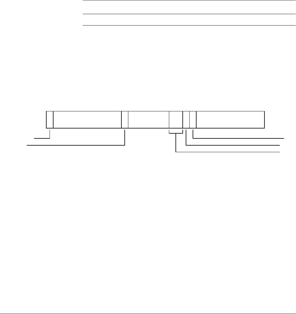
D8 AArch64 System Register Descriptions
D8.2 General system control registers
D8-1890 Copyright © 2013 ARM Limited. All rights reserved. ARM DDI 0487A.a
Non-Confidential - Beta ID090413
D8.2.18 CPTR_EL2, Architectural Feature Trap Register (EL2)
The CPTR_EL2 characteristics are:
Purpose
Controls trapping to EL2 of access to CPACR, CPACR_EL1, Trace functionality and registers
associated with Floating Point and Advanced SIMD execution. Also controls EL2 access to this
functionality.
This register is part of the Virtualization registers functional group.
Usage constraints
This register is accessible as shown below:
Configurations
CPTR_EL2 is architecturally mapped to AArch32 register HCPTR.
If EL2 is not implemented, this register is RES0 from EL3.
Attributes
CPTR_EL2 is a 32-bit register.
The CPTR_EL2 bit assignments are:
TCPAC, bit [31]
This causes a direct access to CPACR or CPACR_EL1 from EL1 to trap to EL2. Possible values of
this bit are:
0
Does not cause access to CPACR or CPACR_EL1 to be trapped.
1
Causes access to CPACR or CPACR_EL1 to be trapped.
Bits [30:21]
Reserved, RES0.
TTA, bit [20]
This causes access to the Trace functionality to trap to EL2 when executed from EL0, EL1, or EL2,
unless already trapped to EL1. Possible values of this bit are:
0
Does not cause System register access to the Trace Functionality to be trapped.
1
Causes System register access to the Trace Functionality to be trapped.
If system register access to trace functionality is not supported, this bit is RES0.
Bits [19:14]
Reserved, RES0.
EL0 EL1 (NS) EL1 (S) EL2 EL3 (SCR.NS=1) EL3 (SCR.NS=0)
-- - RWRW RW
31
RES0
30 21 20
RES0
19 14 13 12 11 10
RES1
90
TCPAC
TTA
TFP
RES0
RES1

D8 AArch64 System Register Descriptions
D8.2 General system control registers
ARM DDI 0487A.a Copyright © 2013 ARM Limited. All rights reserved. D8-1891
ID090413 Non-Confidential - Beta
Bits [13:12]
Reserved, RES1.
Bit [11]
Reserved, RES0.
TFP, bit [10]
This causes instructions that access the registers associated with Floating Point and Advanced
SIMD execution to trap to EL2 when executed from EL0, EL1, or EL2, unless trapped to EL1.
Possible values of this bit are:
0
Does not cause any instruction to be trapped.
1
Causes any instructions that use the registers associated with Floating Point and
Advanced SIMD execution to be trapped.
Bits [9:0]
Reserved, RES1.
Accessing the CPTR_EL2:
To access the CPTR_EL2:
MRS <Xt>, CPTR_EL2 ; Read CPTR_EL2 into Xt
MSR CPTR_EL2, <Xt> ; Write Xt to CPTR_EL2
Register access is encoded as follows:
op0 op1 CRn CRm op2
11 100 0001 0001 010
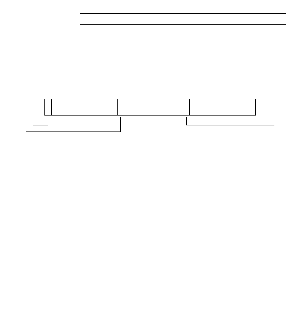
D8 AArch64 System Register Descriptions
D8.2 General system control registers
D8-1892 Copyright © 2013 ARM Limited. All rights reserved. ARM DDI 0487A.a
Non-Confidential - Beta ID090413
D8.2.19 CPTR_EL3, Architectural Feature Trap Register (EL3)
The CPTR_EL3 characteristics are:
Purpose
Controls trapping to EL3 of access to CPACR_EL1, Trace functionality and registers associated
with Floating Point and Advanced SIMD execution. Also controls EL3 access to this functionality.
This register is part of the Security registers functional group.
Usage constraints
This register is accessible as shown below:
Configurations
There are no configuration notes.
Attributes
CPTR_EL3 is a 32-bit register.
The CPTR_EL3 bit assignments are:
TCPAC, bit [31]
This causes a direct access to the CPACR_EL1 from EL1 or the CPTR_EL2 from EL2 to trap to
EL3 unless it is trapped at EL2. Possible values of this bit are:
0
Does not cause access to the CPACR_EL1 or CPTR_EL2 to be trapped.
1
Causes access to the CPACR_EL1 or CPTR_EL2 to be trapped.
Bits [30:21]
Reserved, RES0.
TTA, bit [20]
This causes access to the Trace functionality to trap to EL3 when executed from EL0, EL1, EL2, or
EL3, unless already trapped to EL1 or EL2. Possible values of this bit are:
0
Does not cause System register access to the Trace Functionality to be trapped.
1
Causes System register access to the Trace Functionality to be trapped.
If system register access to trace functionality is not supported, this bit is RES0.
Bits [19:11]
Reserved, RES0.
EL0 EL1 (NS) EL1 (S) EL2 EL3 (SCR.NS=1) EL3 (SCR.NS=0)
-- - -RW RW
31
RES0
30 21 20
RES0
19 11 10
RES0
90
TCPAC
TTA
TFP

D8 AArch64 System Register Descriptions
D8.2 General system control registers
ARM DDI 0487A.a Copyright © 2013 ARM Limited. All rights reserved. D8-1893
ID090413 Non-Confidential - Beta
TFP, bit [10]
This causes instructions that access the registers associated with Floating Point and Advanced
SIMD execution to trap to EL3 when executed from any exception level, unless trapped to EL1 or
EL2. Possible values of this bit are:
0
Does not cause any instruction to be trapped.
1
Causes any instructions that use the registers associated with Floating Point and
Advanced SIMD execution to be trapped.
Bits [9:0]
Reserved, RES0.
Accessing the CPTR_EL3:
To access the CPTR_EL3:
MRS <Xt>, CPTR_EL3 ; Read CPTR_EL3 into Xt
MSR CPTR_EL3, <Xt> ; Write Xt to CPTR_EL3
Register access is encoded as follows:
op0 op1 CRn CRm op2
11 110 0001 0001 010

D8 AArch64 System Register Descriptions
D8.2 General system control registers
D8-1894 Copyright © 2013 ARM Limited. All rights reserved. ARM DDI 0487A.a
Non-Confidential - Beta ID090413
D8.2.20 CSSELR_EL1, Cache Size Selection Register
The CSSELR_EL1 characteristics are:
Purpose
Selects the current Cache Size ID Register, CCSIDR_EL1, by specifying the required cache level
and the cache type (either instruction or data cache).
This register is part of the Identification registers functional group.
Usage constraints
This register is accessible as shown below:
Configurations
CSSELR_EL1 is architecturally mapped to AArch32 register CSSELR (NS).
Attributes
CSSELR_EL1 is a 32-bit register.
The CSSELR_EL1 bit assignments are:
Bits [31:4]
Reserved, RES0.
Level, bits [3:1]
Cache level of required cache. Permitted values are from
0b000
, indicating Level 1 cache, to
0b110
indicating Level 7 cache.
InD, bit [0]
Instruction not Data bit. Permitted values are:
0
Data or unified cache.
1
Instruction cache.
Accessing the CSSELR_EL1:
To access the CSSELR_EL1:
MRS <Xt>, CSSELR_EL1 ; Read CSSELR_EL1 into Xt
MSR CSSELR_EL1, <Xt> ; Write Xt to CSSELR_EL1
Register access is encoded as follows:
EL0 EL1 (NS) EL1 (S) EL2 EL3 (SCR.NS=1) EL3 (SCR.NS=0)
-RW RW RWRW RW
RES0
31 4
Level
31
0
InD
op0 op1 CRn CRm op2
11 010 0000 0000 000

D8 AArch64 System Register Descriptions
D8.2 General system control registers
ARM DDI 0487A.a Copyright © 2013 ARM Limited. All rights reserved. D8-1895
ID090413 Non-Confidential - Beta
D8.2.21 CTR_EL0, Cache Type Register
The CTR_EL0 characteristics are:
Purpose
Provides information about the architecture of the caches.
This register is part of the Identification registers functional group.
Usage constraints
This register is accessible as shown below:
This register is accessible at EL0 when SCTLR_EL1.UCT is set to 1.
Configurations
CTR_EL0 is architecturally mapped to AArch32 register CTR.
Attributes
CTR_EL0 is a 32-bit register.
The CTR_EL0 bit assignments are:
Bit [31]
Reserved, RES1.
Bits [30:28]
Reserved, RES0.
CWG, bits [27:24]
Cache Writeback Granule. Log2 of the number of words of the maximum size of memory that can
be overwritten as a result of the eviction of a cache entry that has had a memory location in it
modified.
A value of
0b0000
indicates that this register does not provide Cache Writeback Granule information
and either:
• The architectural maximum of 512 words (2Kbytes) must be assumed.
• The Cache Writeback Granule can be determined from maximum cache line size encoded in
the Cache Size ID Registers.
Values greater than
0b1001
are reserved.
ERG, bits [23:20]
Exclusives Reservation Granule. Log2 of the number of words of the maximum size of the
reservation granule that has been implemented for the Load-Exclusive and Store-Exclusive
instructions.
A value of
0b0000
indicates that this register does not provide Exclusives Reservation Granule
information and the architectural maximum of 512 words (2Kbytes) must be assumed.
EL0 EL1 (NS) EL1 (S) EL2 EL3 (SCR.NS=1) EL3 (SCR.NS=0)
Config-RO RO RO RO RO RO
31
RES0
30 28
CWG
27 24
ERG
23 20
DminLine
19 16
L1Ip
15 14
RES0
13 4
IminLine
30
RES1

D8 AArch64 System Register Descriptions
D8.2 General system control registers
D8-1896 Copyright © 2013 ARM Limited. All rights reserved. ARM DDI 0487A.a
Non-Confidential - Beta ID090413
Values greater than
0b1001
are reserved.
DminLine, bits [19:16]
Log2 of the number of words in the smallest cache line of all the data caches and unified caches that
are controlled by the processor.
L1Ip, bits [15:14]
Level 1 instruction cache policy. Indicates the indexing and tagging policy for the L1 instruction
cache. Possible values of this field are:
01
ASID-tagged Virtual Index, Virtual Tag (AIVIVT)
10
Virtual Index, Physical Tag (VIPT)
11
Physical Index, Physical Tag (PIPT)
Other values are reserved.
Bits [13:4]
Reserved, RES0.
IminLine, bits [3:0]
Log2 of the number of words in the smallest cache line of all the instruction caches that are
controlled by the processor.
Accessing the CTR_EL0:
To access the CTR_EL0:
MRS <Xt>, CTR_EL0 ; Read CTR_EL0 into Xt
Register access is encoded as follows:
op0 op1 CRn CRm op2
11 011 0000 0000 001

D8 AArch64 System Register Descriptions
D8.2 General system control registers
ARM DDI 0487A.a Copyright © 2013 ARM Limited. All rights reserved. D8-1897
ID090413 Non-Confidential - Beta
D8.2.22 DACR32_EL2, Domain Access Control Register
The DACR32_EL2 characteristics are:
Purpose
Allows access to the AArch32 DACR register from AArch64 state only. Its value has no effect on
execution in AArch64 state.
This register is part of the Virtual memory control registers functional group.
Usage constraints
This register is accessible as shown below:
Configurations
DACR32_EL2 is architecturally mapped to AArch32 register DACR (NS).
If EL1 is AArch64 only, this register is UNDEFINED.
Attributes
DACR32_EL2 is a 32-bit register.
The DACR32_EL2 bit assignments are:
D<n>, bits [2n+1:2n], for n = 0 to 15
Domain n access permission, where n = 0 to 15. Permitted values are:
00
No access. Any access to the domain generates a Domain fault.
01
Client. Accesses are checked against the permission bits in the translation tables.
11
Manager. Accesses are not checked against the permission bits in the translation tables.
The value
0b10
is reserved.
Accessing the DACR32_EL2:
To access the DACR32_EL2:
MRS <Xt>, DACR32_EL2 ; Read DACR32_EL2 into Xt
MSR DACR32_EL2, <Xt> ; Write Xt to DACR32_EL2
Register access is encoded as follows:
EL0 EL1 (NS) EL1 (S) EL2 EL3 (SCR.NS=1) EL3 (SCR.NS=0)
-- - RWRW RW
D15
31 30
D14
29 28
D13
27 26
D12
25 24
D11
23 22
D10
21 20
D9
19 18
D8
17 16
D7
15 14
D6
13 12
D5
11 10
D4
98
D3
76
D2
54
D1
32
D0
10
op0 op1 CRn CRm op2
11 100 0011 0000 000

D8 AArch64 System Register Descriptions
D8.2 General system control registers
D8-1898 Copyright © 2013 ARM Limited. All rights reserved. ARM DDI 0487A.a
Non-Confidential - Beta ID090413
D8.2.23 DCZID_EL0, Data Cache Zero ID register
The DCZID_EL0 characteristics are:
Purpose
Indicates the block size that is written with byte values of 0 by the DC ZVA (Data Cache Zero by
Address) system instruction.
This register is part of the Identification registers functional group.
Usage constraints
This register is accessible as shown below:
Configurations
There are no configuration notes.
Attributes
DCZID_EL0 is a 32-bit register.
The DCZID_EL0 bit assignments are:
Bits [31:5]
Reserved, RES0.
DZP, bit [4]
Data Zero prohibited. Permitted values are:
0
DC ZVA instruction is permitted.
1
DC ZVA instruction is prohibited.
The value read from this field is governed by the access state and the values of the HCR_EL2.TDZ
and SCTLR_EL1.DZE bits.
BS, bits [3:0]
Log2 of the block size in words. The maximum size supported is 2 Kbytes (value == 9).
Accessing the DCZID_EL0:
To access the DCZID_EL0:
MRS <Xt>, DCZID_EL0 ; Read DCZID_EL0 into Xt
Register access is encoded as follows:
EL0 EL1 (NS) EL1 (S) EL2 EL3 (SCR.NS=1) EL3 (SCR.NS=0)
RO RO RO RO RO RO
RES0
31 5 4
BS
30
DZP
op0 op1 CRn CRm op2
11 011 0000 0000 111

D8 AArch64 System Register Descriptions
D8.2 General system control registers
ARM DDI 0487A.a Copyright © 2013 ARM Limited. All rights reserved. D8-1899
ID090413 Non-Confidential - Beta
D8.2.24 ESR_EL1, Exception Syndrome Register (EL1)
The ESR_EL1 characteristics are:
Purpose
Holds syndrome information for an exception taken to EL1.
This register is part of the Exception and fault handling registers functional group.
Usage constraints
This register is accessible as shown below:
When an UNPREDICTABLE instruction is treated as UNDEFINED, and the exception is taken to EL1,
the value of ESR_EL1 is UNKNOWN. The value written to ESR_EL1 must be consistent with a value
that could be created as a result of an exception from the same exception level that generated the
exception as a result of a situation that is not UNPREDICTABLE at that exception level, in order to
avoid the possibility of a privilege violation.
Configurations
ESR_EL1 is architecturally mapped to AArch32 register DFSR (NS).
Attributes
ESR_EL1 is a 32-bit register.
The ESR_EL1 bit assignments are:
EC, bits [31:26]
Exception Class. Indicates the reason for the exception that this register holds information about.
Table D8-2 shows the encoding of this field. For each EC value, the table references a subsection
of the section Use of the ESR_EL1, ESR_EL2, and ESR_EL3 on page D1-1512 that gives
information about:
• The cause of the exception, for example the configuration required to enable the trap.
• The encoding of the associated ISS.
EL0 EL1 (NS) EL1 (S) EL2 EL3 (SCR.NS=1) EL3 (SCR.NS=0)
- RW RW RW RW RW
EC
31 26
IL
25
ISS
24 0
Table D8-2 ESR_ELx.EC field encoding
EC Exception class From, state To, Exception level ISS description, or notes
AArch32 AArch64 EL1 EL2 EL3
0x00
Unknown reason Yes Yes Yes Yes Yes Exceptions with an unknown
reason on page D1-1517.
0x01 WFI
or
WFE
instruction executionaYes Yes Yes Yes Yes Exception from a WFI or WFE
instruction, from AArch32 or
AArch64 state on page D1-1518.

D8 AArch64 System Register Descriptions
D8.2 General system control registers
D8-1900 Copyright © 2013 ARM Limited. All rights reserved. ARM DDI 0487A.a
Non-Confidential - Beta ID090413
0x03 MCR
or
MRC
access to CP15a that is
not reported using EC
0x00
Yes No Yes Yes Yes bException from an MCR or MRC
access from AArch32 state on
page D1-1518.
0x04 MCRR
or
MRRC
access to CP15a that
is not reported using EC
0x00
Yes No Yes Yes YescException from an MCRR or
MRRC access from AArch32 state
on page D1-1519.
0x05 MCR
or
MRC
access to CP14aYes No Yes Yes Yes Exception from an MCR or MRC
access from AArch32 state on
page D1-1518.
0x06 LDC
or
STC
access to CP14aYes No Yes Yes Yes Exception from an LDC or STC
access to CP14 from AArch32
state on page D1-1520.
0x07
Access to SIMD or floating-point
registersa, excluding
(HCR_EL2.TGE==1) traps
Yes Yes Yes Yes Yes Exception from an access to
SIMD or floating-point registers,
from AArch32 or AArch64 on
page D1-1521.
0x08 MCR
or
MRC
access to CP10 that is
not reported using EC
0x07
. This
applies only to ID Group trapsd
Yes No No Yes No Exception from an MCR or MRC
access from AArch32 state on
page D1-1518.
0x0C MRRC
access to CP14aYes No Yes Yes Yes Exception from an MCRR or
MRRC access from AArch32 state
on page D1-1519.
0x0E
Illegal Execution State Yes Yes Yes Yes Yes Exception from an illegal
Execution state, misaligned PC,
or misaligned stack pointer on
page D1-1521.
0x11 SVC
instruction execution Yes No Yes Yes eNo Exception from HVC or SVC
instruction execution on
page D1-1522.
0x12 HVC
instruction execution, when
HVC
is not disabled Yes No No Yes No
0x13 SMC
instruction execution, when
SMC
is not disabled Yes No No Yes fYes Exception from SMC instruction
execution in AArch32 state on
page D1-1522.
0x15 SVC
instruction execution No Yes Yes Yes Yes Exception from HVC or SVC
instruction execution on
page D1-1522.
0x16 HVC
instruction execution, when
HVC
is not disabled No Yes No Yes Yes
0x17 SMC
instruction execution, when
SMC
is not disabled No Yes No YesfYes Exception from SMC instruction
execution in AArch64 state on
page D1-1523.
0x18 MSR
,
MRS
, or System instruction
execution, that is not reported
using EC
0x00
,
0x01
, or
0x07
No Yes Yes Yes Yes Exception from MSR, MRS, or
System instruction execution in
AArch64 state on page D1-1523.
Table D8-2 ESR_ELx.EC field encoding (continued)
EC Exception class From, state To, Exception level ISS description, or notes
AArch32 AArch64 EL1 EL2 EL3

D8 AArch64 System Register Descriptions
D8.2 General system control registers
ARM DDI 0487A.a Copyright © 2013 ARM Limited. All rights reserved. D8-1901
ID090413 Non-Confidential - Beta
0x20
Instruction Abort from a lower
Exception levelg
Yes Yes Yes Yes Yes Exception from an Instruction
abort on page D1-1524.
0x21
Instruction Abort taken without a
change in Exception levelg
Yes Yes Yes Yes Yes
0x22
Misaligned PC exception Yes Yes Yes Yes Yes Exception from an illegal
Execution state, misaligned PC,
or misaligned stack pointer on
page D1-1521.
0x24
Data Abort from a lower
Exception levelh
Yes Yes Yes Yes Yes Exception from a Data abort on
page D1-1525.
0x25
Data Abort taken without a
change in Exception levelh
Yes Yes Yes Yes Yes
0x26
Stack Pointer Alignment
exception Yes Yes Yes Yes Yes Exception from an illegal
Execution state, misaligned PC,
or misaligned stack pointer on
page D1-1521.
0x28
Floating-point exception, if
supported Yes No Yes Yes No Floating-point exceptions on
page D1-1529.
0x2C
Floating-point exception, if
supported No Yes Yes Yes Yes
0x2F
SError interrupt Yes iYes Yes Yes Yes SError interrupt on
page D1-1530.
0x30
Breakpoint exception from a
lower Exception level Yes Yes Yes Yes jNo Breakpoint exception or Vector
Catch exception on
page D1-1530.
0x31
Breakpoint exception taken
without a change in Exception
level
Yes Yes Yes Yes jNo
0x32
Software Step exception from a
lower Exception level Yes Yes Yes YesjNo Software Step exception on
page D1-1532.
0x33
Software Step exception taken
without a change in Exception
level
Yes Yes Yes Yes jNo
0x34
Watchpoint exception from a
lower Exception level Yes Yes Yes YesjNo Watchpoint exception on
page D1-1531.
0x35
Watchpoint exception taken
without a change in Exception
level
Yes Yes Yes YesjNo
0x38 BKPT
instruction execution Yes No Yes YesjNo Software Breakpoint Instruction
exception on page D1-1532.
Table D8-2 ESR_ELx.EC field encoding (continued)
EC Exception class From, state To, Exception level ISS description, or notes
AArch32 AArch64 EL1 EL2 EL3

D8 AArch64 System Register Descriptions
D8.2 General system control registers
D8-1902 Copyright © 2013 ARM Limited. All rights reserved. ARM DDI 0487A.a
Non-Confidential - Beta ID090413
Other EC values are reserved.
IL, bit [25]
Instruction Length for synchronous exceptions. Possible values of this bit are:
0
16-bit instruction trapped.
1
32-bit instruction trapped. This value also applies to the following exceptions:
• An SError interrupt.
• An Instruction Abort exception.
• A Misaligned PC exception.
• A Misaligned Stack Pointer exception.
• A Data Abort for which the value of the ISV bit is 0.
• An Illegal Execution State exception.
• Any debug exception except for Software Breakpoint Instruction exceptions. For
Software Breakpoint Instruction exceptions, this bit has its standard meaning:
0
16-bit T32 BKPT instruction.
1
32-bit A32 BKPT instruction or A64 BRK instruction.
• An exception reported using EC value
0b000000
.
ISS, bits [24:0]
Instruction Specific Syndrome. Architecturally, this field can be defined independently for each
defined Exception class. However, in practice, some ISS encodings are used for more than one
Exception class. See the description of the EC field for more information about the ISS formats.
Table D8-2 on page D8-1899 includes links to the ISS format descriptions.
0x3A
Vector catch exception from
AArch32 state Yes No No YesjNo Breakpoint exception or Vector
Catch exception on
page D1-1530.
0x3C BRK
instruction execution No Yes Yes Yes jYeskSoftware Breakpoint Instruction
exception on page D1-1532.
a. Exceptions caused by configurable traps, enables, or disables.
b. See Traps to EL3 of monitor functionality from Secure EL1 using AArch32 on page D1-1500.
c. Only for
MCRR
or
MRRC
accesses to the PMCCNTR_EL0 or PMCCNTR.
d. Applies only to traps of accesses to MVFR0, MVFR1, MVFR2, or FPSID. Includes traps of
VMRS
accesses. Because the registers are
read-only, there are no
MCR
accesses that can be trapped with this EC value.
e. Only as a result of HCR_EL2.TGE.
f. Only as a result of HCR_EL2.TSC.
g. Used for MMU faults generated by instruction accesses, and for synchronous external aborts, including synchronous parity errors. Not used
for debug-related exceptions.
h. Used for MMU faults generated by data accesses, alignment faults other than stack pointer alignment faults, and for synchronous external
aborts, including synchronous parity errors. Not used for debug-related exceptions.
i. In AArch32 state, these are known as Asynchronous aborts.
j. Only as a result of HCR_EL2.TGE ==1 or MDCR_EL2.TDE ==1.
k. Only if the
BRK
instruction is executed in EL3. This is the only debug exception that can be taken to EL3 when EL3 is using AArch64.
Table D8-2 ESR_ELx.EC field encoding (continued)
EC Exception class From, state To, Exception level ISS description, or notes
AArch32 AArch64 EL1 EL2 EL3

D8 AArch64 System Register Descriptions
D8.2 General system control registers
ARM DDI 0487A.a Copyright © 2013 ARM Limited. All rights reserved. D8-1903
ID090413 Non-Confidential - Beta
Accessing the ESR_EL1:
To access the ESR_EL1:
MRS <Xt>, ESR_EL1 ; Read ESR_EL1 into Xt
MSR ESR_EL1, <Xt> ; Write Xt to ESR_EL1
Register access is encoded as follows:
op0 op1 CRn CRm op2
11 000 0101 0010 000

D8 AArch64 System Register Descriptions
D8.2 General system control registers
D8-1904 Copyright © 2013 ARM Limited. All rights reserved. ARM DDI 0487A.a
Non-Confidential - Beta ID090413
D8.2.25 ESR_EL2, Exception Syndrome Register (EL2)
The ESR_EL2 characteristics are:
Purpose
Holds syndrome information for an exception taken to EL2.
This register is part of:
• the Virtualization registers functional group
• the Exception and fault handling registers functional group.
Usage constraints
This register is accessible as shown below:
When an UNPREDICTABLE instruction is treated as UNDEFINED, and the exception is taken to EL2,
the value of ESR_EL2 is UNKNOWN. The value written to ESR_EL2 must be consistent with a value
that could be created as a result of an exception from the same exception level that generated the
exception as a result of a situation that is not UNPREDICTABLE at that exception level, in order to
avoid the possibility of a privilege violation.
Configurations
ESR_EL2 is architecturally mapped to AArch32 register HSR.
If EL2 is not implemented, this register is RES0 from EL3.
Attributes
ESR_EL2 is a 32-bit register.
The ESR_EL2 bit assignments are:
EC, bits [31:26]
Exception Class. Indicates the reason for the exception that this register holds information about.
Table D8-3 shows the encoding of this field. For each EC value, the table references a subsection
of the section Use of the ESR_EL1, ESR_EL2, and ESR_EL3 on page D1-1512 that gives
information about:
• The cause of the exception, for example the configuration required to enable the trap.
• The encoding of the associated ISS.
EL0 EL1 (NS) EL1 (S) EL2 EL3 (SCR.NS=1) EL3 (SCR.NS=0)
-- - RWRW RW
EC
31 26
IL
25
ISS
24 0
Table D8-3 ESR_ELx.EC field encoding
EC Exception class From, state To, Exception level ISS description, or notes
AArch32 AArch64 EL1 EL2 EL3
0x00
Unknown reason Yes Yes Yes Yes Yes Exceptions with an unknown
reason on page D1-1517.

D8 AArch64 System Register Descriptions
D8.2 General system control registers
ARM DDI 0487A.a Copyright © 2013 ARM Limited. All rights reserved. D8-1905
ID090413 Non-Confidential - Beta
0x01 WFI
or
WFE
instruction executionaYes Yes Yes Yes Yes Exception from a WFI or WFE
instruction, from AArch32 or
AArch64 state on page D1-1518.
0x03 MCR
or
MRC
access to CP15a that is
not reported using EC
0x00
Yes No Yes Yes Yes bException from an MCR or MRC
access from AArch32 state on
page D1-1518.
0x04 MCRR
or
MRRC
access to CP15a that
is not reported using EC
0x00
Yes No Yes Yes YescException from an MCRR or
MRRC access from AArch32 state
on page D1-1519.
0x05 MCR
or
MRC
access to CP14aYes No Yes Yes Yes Exception from an MCR or MRC
access from AArch32 state on
page D1-1518.
0x06 LDC
or
STC
access to CP14aYes No Yes Yes Yes Exception from an LDC or STC
access to CP14 from AArch32
state on page D1-1520.
0x07
Access to SIMD or floating-point
registersa, excluding
(HCR_EL2.TGE==1) traps
Yes Yes Yes Yes Yes Exception from an access to
SIMD or floating-point registers,
from AArch32 or AArch64 on
page D1-1521.
0x08 MCR
or
MRC
access to CP10 that is
not reported using EC
0x07
. This
applies only to ID Group trapsd
Yes No No Yes No Exception from an MCR or MRC
access from AArch32 state on
page D1-1518.
0x0C MRRC
access to CP14aYes No Yes Yes Yes Exception from an MCRR or
MRRC access from AArch32 state
on page D1-1519.
0x0E
Illegal Execution State Yes Yes Yes Yes Yes Exception from an illegal
Execution state, misaligned PC,
or misaligned stack pointer on
page D1-1521.
0x11 SVC
instruction execution Yes No Yes Yes eNo Exception from HVC or SVC
instruction execution on
page D1-1522.
0x12 HVC
instruction execution, when
HVC
is not disabled Yes No No Yes No
0x13 SMC
instruction execution, when
SMC
is not disabled Yes No No Yes fYes Exception from SMC instruction
execution in AArch32 state on
page D1-1522.
0x15 SVC
instruction execution No Yes Yes Yes Yes Exception from HVC or SVC
instruction execution on
page D1-1522.
0x16 HVC
instruction execution, when
HVC
is not disabled No Yes No Yes Yes
0x17 SMC
instruction execution, when
SMC
is not disabled No Yes No YesfYes Exception from SMC instruction
execution in AArch64 state on
page D1-1523.
Table D8-3 ESR_ELx.EC field encoding (continued)
EC Exception class From, state To, Exception level ISS description, or notes
AArch32 AArch64 EL1 EL2 EL3

D8 AArch64 System Register Descriptions
D8.2 General system control registers
D8-1906 Copyright © 2013 ARM Limited. All rights reserved. ARM DDI 0487A.a
Non-Confidential - Beta ID090413
0x18 MSR
,
MRS
, or System instruction
execution, that is not reported
using EC
0x00
,
0x01
, or
0x07
No Yes Yes Yes Yes Exception from MSR, MRS, or
System instruction execution in
AArch64 state on page D1-1523.
0x20
Instruction Abort from a lower
Exception levelg
Yes Yes Yes Yes Yes Exception from an Instruction
abort on page D1-1524.
0x21
Instruction Abort taken without a
change in Exception levelg
Yes Yes Yes Yes Yes
0x22
Misaligned PC exception Yes Yes Yes Yes Yes Exception from an illegal
Execution state, misaligned PC,
or misaligned stack pointer on
page D1-1521.
0x24
Data Abort from a lower
Exception levelh
Yes Yes Yes Yes Yes Exception from a Data abort on
page D1-1525.
0x25
Data Abort taken without a
change in Exception levelh
Yes Yes Yes Yes Yes
0x26
Stack Pointer Alignment
exception Yes Yes Yes Yes Yes Exception from an illegal
Execution state, misaligned PC,
or misaligned stack pointer on
page D1-1521.
0x28
Floating-point exception, if
supported Yes No Yes Yes No Floating-point exceptions on
page D1-1529.
0x2C
Floating-point exception, if
supported No Yes Yes Yes Yes
0x2F
SError interrupt Yes iYes Yes Yes Yes SError interrupt on
page D1-1530.
0x30
Breakpoint exception from a
lower Exception level Yes Yes Yes Yes jNo Breakpoint exception or Vector
Catch exception on
page D1-1530.
0x31
Breakpoint exception taken
without a change in Exception
level
Yes Yes Yes Yes jNo
0x32
Software Step exception from a
lower Exception level Yes Yes Yes YesjNo Software Step exception on
page D1-1532.
0x33
Software Step exception taken
without a change in Exception
level
Yes Yes Yes Yes jNo
0x34
Watchpoint exception from a
lower Exception level Yes Yes Yes YesjNo Watchpoint exception on
page D1-1531.
0x35
Watchpoint exception taken
without a change in Exception
level
Yes Yes Yes YesjNo
Table D8-3 ESR_ELx.EC field encoding (continued)
EC Exception class From, state To, Exception level ISS description, or notes
AArch32 AArch64 EL1 EL2 EL3

D8 AArch64 System Register Descriptions
D8.2 General system control registers
ARM DDI 0487A.a Copyright © 2013 ARM Limited. All rights reserved. D8-1907
ID090413 Non-Confidential - Beta
Other EC values are reserved.
IL, bit [25]
Instruction Length for synchronous exceptions. Possible values of this bit are:
0
16-bit instruction trapped.
1
32-bit instruction trapped. This value also applies to the following exceptions:
• An SError interrupt.
• An Instruction Abort exception.
• A Misaligned PC exception.
• A Misaligned Stack Pointer exception.
• A Data Abort for which the value of the ISV bit is 0.
• An Illegal Execution State exception.
• Any debug exception except for Software Breakpoint Instruction exceptions. For
Software Breakpoint Instruction exceptions, this bit has its standard meaning:
0
16-bit T32 BKPT instruction.
1
32-bit A32 BKPT instruction or A64 BRK instruction.
• An exception reported using EC value
0b000000
.
ISS, bits [24:0]
Instruction Specific Syndrome. Architecturally, this field can be defined independently for each
defined Exception class. However, in practice, some ISS encodings are used for more than one
Exception class. See the description of the EC field for more information about the ISS formats.
Table D8-2 on page D8-1899 includes links to the ISS format descriptions.
0x38 BKPT
instruction execution Yes No Yes YesjNo Software Breakpoint Instruction
exception on page D1-1532.
0x3A
Vector catch exception from
AArch32 state Yes No No YesjNo Breakpoint exception or Vector
Catch exception on
page D1-1530.
0x3C BRK
instruction execution No Yes Yes Yes jYeskSoftware Breakpoint Instruction
exception on page D1-1532.
a. Exceptions caused by configurable traps, enables, or disables.
b. See Traps to EL3 of monitor functionality from Secure EL1 using AArch32 on page D1-1500.
c. Only for
MCRR
or
MRRC
accesses to the PMCCNTR_EL0 or PMCCNTR.
d. Applies only to traps of accesses to MVFR0, MVFR1, MVFR2, or FPSID. Includes traps of
VMRS
accesses. Because the registers are
read-only, there are no
MCR
accesses that can be trapped with this EC value.
e. Only as a result of HCR_EL2.TGE.
f. Only as a result of HCR_EL2.TSC.
g. Used for MMU faults generated by instruction accesses, and for synchronous external aborts, including synchronous parity errors. Not used
for debug-related exceptions.
h. Used for MMU faults generated by data accesses, alignment faults other than stack pointer alignment faults, and for synchronous external
aborts, including synchronous parity errors. Not used for debug-related exceptions.
i. In AArch32 state, these are known as Asynchronous aborts.
j. Only as a result of HCR_EL2.TGE ==1 or MDCR_EL2.TDE ==1.
k. Only if the
BRK
instruction is executed in EL3. This is the only debug exception that can be taken to EL3 when EL3 is using AArch64.
Table D8-3 ESR_ELx.EC field encoding (continued)
EC Exception class From, state To, Exception level ISS description, or notes
AArch32 AArch64 EL1 EL2 EL3

D8 AArch64 System Register Descriptions
D8.2 General system control registers
D8-1908 Copyright © 2013 ARM Limited. All rights reserved. ARM DDI 0487A.a
Non-Confidential - Beta ID090413
Accessing the ESR_EL2:
To access the ESR_EL2:
MRS <Xt>, ESR_EL2 ; Read ESR_EL2 into Xt
MSR ESR_EL2, <Xt> ; Write Xt to ESR_EL2
Register access is encoded as follows:
op0 op1 CRn CRm op2
11 100 0101 0010 000

D8 AArch64 System Register Descriptions
D8.2 General system control registers
ARM DDI 0487A.a Copyright © 2013 ARM Limited. All rights reserved. D8-1909
ID090413 Non-Confidential - Beta
D8.2.26 ESR_EL3, Exception Syndrome Register (EL3)
The ESR_EL3 characteristics are:
Purpose
Holds syndrome information for an exception taken to EL3.
This register is part of the Exception and fault handling registers functional group.
Usage constraints
This register is accessible as shown below:
When an UNPREDICTABLE instruction is treated as UNDEFINED, and the exception is taken to EL3,
the value of ESR_EL3 is UNKNOWN. The value written to ESR_EL3 must be consistent with a value
that could be created as a result of an exception from the same exception level that generated the
exception as a result of a situation that is not UNPREDICTABLE at that exception level, in order to
avoid the possibility of a privilege violation.
Configurations
ESR_EL3 can be mapped to AArch32 register DFSR (S), but this is not architecturally mandated.
Attributes
ESR_EL3 is a 32-bit register.
The ESR_EL3 bit assignments are:
EC, bits [31:26]
Exception Class. Indicates the reason for the exception that this register holds information about.
Table D8-4 shows the encoding of this field. For each EC value, the table references a subsection
of the section Use of the ESR_EL1, ESR_EL2, and ESR_EL3 on page D1-1512 that gives
information about:
• The cause of the exception, for example the configuration required to enable the trap.
• The encoding of the associated ISS.
EL0 EL1 (NS) EL1 (S) EL2 EL3 (SCR.NS=1) EL3 (SCR.NS=0)
-- - -RW RW
EC
31 26
IL
25
ISS
24 0
Table D8-4 ESR_ELx.EC field encoding
EC Exception class From, state To, Exception level ISS description, or notes
AArch32 AArch64 EL1 EL2 EL3
0x00
Unknown reason Yes Yes Yes Yes Yes Exceptions with an unknown
reason on page D1-1517.
0x01 WFI
or
WFE
instruction executionaYes Yes Yes Yes Yes Exception from a WFI or WFE
instruction, from AArch32 or
AArch64 state on page D1-1518.

D8 AArch64 System Register Descriptions
D8.2 General system control registers
D8-1910 Copyright © 2013 ARM Limited. All rights reserved. ARM DDI 0487A.a
Non-Confidential - Beta ID090413
0x03 MCR
or
MRC
access to CP15a that is
not reported using EC
0x00
Yes No Yes Yes Yes bException from an MCR or MRC
access from AArch32 state on
page D1-1518.
0x04 MCRR
or
MRRC
access to CP15a that
is not reported using EC
0x00
Yes No Yes Yes YescException from an MCRR or
MRRC access from AArch32 state
on page D1-1519.
0x05 MCR
or
MRC
access to CP14aYes No Yes Yes Yes Exception from an MCR or MRC
access from AArch32 state on
page D1-1518.
0x06 LDC
or
STC
access to CP14aYes No Yes Yes Yes Exception from an LDC or STC
access to CP14 from AArch32
state on page D1-1520.
0x07
Access to SIMD or floating-point
registersa, excluding
(HCR_EL2.TGE==1) traps
Yes Yes Yes Yes Yes Exception from an access to
SIMD or floating-point registers,
from AArch32 or AArch64 on
page D1-1521.
0x08 MCR
or
MRC
access to CP10 that is
not reported using EC
0x07
. This
applies only to ID Group trapsd
Yes No No Yes No Exception from an MCR or MRC
access from AArch32 state on
page D1-1518.
0x0C MRRC
access to CP14aYes No Yes Yes Yes Exception from an MCRR or
MRRC access from AArch32 state
on page D1-1519.
0x0E
Illegal Execution State Yes Yes Yes Yes Yes Exception from an illegal
Execution state, misaligned PC,
or misaligned stack pointer on
page D1-1521.
0x11 SVC
instruction execution Yes No Yes Yes eNo Exception from HVC or SVC
instruction execution on
page D1-1522.
0x12 HVC
instruction execution, when
HVC
is not disabled Yes No No Yes No
0x13 SMC
instruction execution, when
SMC
is not disabled Yes No No Yes fYes Exception from SMC instruction
execution in AArch32 state on
page D1-1522.
0x15 SVC
instruction execution No Yes Yes Yes Yes Exception from HVC or SVC
instruction execution on
page D1-1522.
0x16 HVC
instruction execution, when
HVC
is not disabled No Yes No Yes Yes
0x17 SMC
instruction execution, when
SMC
is not disabled No Yes No YesfYes Exception from SMC instruction
execution in AArch64 state on
page D1-1523.
0x18 MSR
,
MRS
, or System instruction
execution, that is not reported
using EC
0x00
,
0x01
, or
0x07
No Yes Yes Yes Yes Exception from MSR, MRS, or
System instruction execution in
AArch64 state on page D1-1523.
Table D8-4 ESR_ELx.EC field encoding (continued)
EC Exception class From, state To, Exception level ISS description, or notes
AArch32 AArch64 EL1 EL2 EL3

D8 AArch64 System Register Descriptions
D8.2 General system control registers
ARM DDI 0487A.a Copyright © 2013 ARM Limited. All rights reserved. D8-1911
ID090413 Non-Confidential - Beta
0x20
Instruction Abort from a lower
Exception levelg
Yes Yes Yes Yes Yes Exception from an Instruction
abort on page D1-1524.
0x21
Instruction Abort taken without a
change in Exception levelg
Yes Yes Yes Yes Yes
0x22
Misaligned PC exception Yes Yes Yes Yes Yes Exception from an illegal
Execution state, misaligned PC,
or misaligned stack pointer on
page D1-1521.
0x24
Data Abort from a lower
Exception levelh
Yes Yes Yes Yes Yes Exception from a Data abort on
page D1-1525.
0x25
Data Abort taken without a
change in Exception levelh
Yes Yes Yes Yes Yes
0x26
Stack Pointer Alignment
exception Yes Yes Yes Yes Yes Exception from an illegal
Execution state, misaligned PC,
or misaligned stack pointer on
page D1-1521.
0x28
Floating-point exception, if
supported Yes No Yes Yes No Floating-point exceptions on
page D1-1529.
0x2C
Floating-point exception, if
supported No Yes Yes Yes Yes
0x2F
SError interrupt Yes iYes Yes Yes Yes SError interrupt on
page D1-1530.
0x30
Breakpoint exception from a
lower Exception level Yes Yes Yes Yes jNo Breakpoint exception or Vector
Catch exception on
page D1-1530.
0x31
Breakpoint exception taken
without a change in Exception
level
Yes Yes Yes Yes jNo
0x32
Software Step exception from a
lower Exception level Yes Yes Yes YesjNo Software Step exception on
page D1-1532.
0x33
Software Step exception taken
without a change in Exception
level
Yes Yes Yes Yes jNo
0x34
Watchpoint exception from a
lower Exception level Yes Yes Yes YesjNo Watchpoint exception on
page D1-1531.
0x35
Watchpoint exception taken
without a change in Exception
level
Yes Yes Yes YesjNo
0x38 BKPT
instruction execution Yes No Yes YesjNo Software Breakpoint Instruction
exception on page D1-1532.
Table D8-4 ESR_ELx.EC field encoding (continued)
EC Exception class From, state To, Exception level ISS description, or notes
AArch32 AArch64 EL1 EL2 EL3

D8 AArch64 System Register Descriptions
D8.2 General system control registers
D8-1912 Copyright © 2013 ARM Limited. All rights reserved. ARM DDI 0487A.a
Non-Confidential - Beta ID090413
Other EC values are reserved.
IL, bit [25]
Instruction Length for synchronous exceptions. Possible values of this bit are:
0
16-bit instruction trapped.
1
32-bit instruction trapped. This value also applies to the following exceptions:
• An SError interrupt.
• An Instruction Abort exception.
• A Misaligned PC exception.
• A Misaligned Stack Pointer exception.
• A Data Abort for which the value of the ISV bit is 0.
• An Illegal Execution State exception.
• Any debug exception except for Software Breakpoint Instruction exceptions. For
Software Breakpoint Instruction exceptions, this bit has its standard meaning:
0
16-bit T32 BKPT instruction.
1
32-bit A32 BKPT instruction or A64 BRK instruction.
• An exception reported using EC value
0b000000
.
ISS, bits [24:0]
Instruction Specific Syndrome. Architecturally, this field can be defined independently for each
defined Exception class. However, in practice, some ISS encodings are used for more than one
Exception class. See the description of the EC field for more information about the ISS formats.
Table D8-2 on page D8-1899 includes links to the ISS format descriptions.
0x3A
Vector catch exception from
AArch32 state Yes No No YesjNo Breakpoint exception or Vector
Catch exception on
page D1-1530.
0x3C BRK
instruction execution No Yes Yes Yes jYeskSoftware Breakpoint Instruction
exception on page D1-1532.
a. Exceptions caused by configurable traps, enables, or disables.
b. See Traps to EL3 of monitor functionality from Secure EL1 using AArch32 on page D1-1500.
c. Only for
MCRR
or
MRRC
accesses to the PMCCNTR_EL0 or PMCCNTR.
d. Applies only to traps of accesses to MVFR0, MVFR1, MVFR2, or FPSID. Includes traps of
VMRS
accesses. Because the registers are
read-only, there are no
MCR
accesses that can be trapped with this EC value.
e. Only as a result of HCR_EL2.TGE.
f. Only as a result of HCR_EL2.TSC.
g. Used for MMU faults generated by instruction accesses, and for synchronous external aborts, including synchronous parity errors. Not used
for debug-related exceptions.
h. Used for MMU faults generated by data accesses, alignment faults other than stack pointer alignment faults, and for synchronous external
aborts, including synchronous parity errors. Not used for debug-related exceptions.
i. In AArch32 state, these are known as Asynchronous aborts.
j. Only as a result of HCR_EL2.TGE ==1 or MDCR_EL2.TDE ==1.
k. Only if the
BRK
instruction is executed in EL3. This is the only debug exception that can be taken to EL3 when EL3 is using AArch64.
Table D8-4 ESR_ELx.EC field encoding (continued)
EC Exception class From, state To, Exception level ISS description, or notes
AArch32 AArch64 EL1 EL2 EL3

D8 AArch64 System Register Descriptions
D8.2 General system control registers
ARM DDI 0487A.a Copyright © 2013 ARM Limited. All rights reserved. D8-1913
ID090413 Non-Confidential - Beta
Accessing the ESR_EL3:
To access the ESR_EL3:
MRS <Xt>, ESR_EL3 ; Read ESR_EL3 into Xt
MSR ESR_EL3, <Xt> ; Write Xt to ESR_EL3
Register access is encoded as follows:
op0 op1 CRn CRm op2
11 110 0101 0010 000
D8 AArch64 System Register Descriptions
D8.2 General system control registers
D8-1914 Copyright © 2013 ARM Limited. All rights reserved. ARM DDI 0487A.a
Non-Confidential - Beta ID090413
D8.2.27 FAR_EL1, Fault Address Register (EL1)
The FAR_EL1 characteristics are:
Purpose
Holds the faulting Virtual Address for all synchronous instruction or data aborts, or exceptions from
a misaligned PC or a Watchpoint debug event, taken to EL1.
This register is part of the Exception and fault handling registers functional group.
Usage constraints
This register is accessible as shown below:
Configurations
FAR_EL1[31:0] is architecturally mapped to AArch32 register DFAR (NS).
FAR_EL1[63:32] is architecturally mapped to AArch32 register IFAR (NS).
Attributes
FAR_EL1 is a 64-bit register.
The FAR_EL1 bit assignments are:
Bits [63:0]
Faulting Virtual Address for exceptions taken to EL1. Exceptions that set the FAR_EL1 are all
synchronous instruction aborts or data aborts, an exception from a misaligned PC, or a Watchpoint
debug event.
If a memory fault that sets FAR_EL1 is generated from one of the data cache instructions, this field
holds the address specified in the register argument of the instruction.
Accessing the FAR_EL1:
To access the FAR_EL1:
MRS <Xt>, FAR_EL1 ; Read FAR_EL1 into Xt
MSR FAR_EL1, <Xt> ; Write Xt to FAR_EL1
Register access is encoded as follows:
EL0 EL1 (NS) EL1 (S) EL2 EL3 (SCR.NS=1) EL3 (SCR.NS=0)
-RW RW RWRW RW
Faulting Virtual Address for exceptions taken to EL1
63 0
op0 op1 CRn CRm op2
11 000 0110 0000 000

D8 AArch64 System Register Descriptions
D8.2 General system control registers
ARM DDI 0487A.a Copyright © 2013 ARM Limited. All rights reserved. D8-1915
ID090413 Non-Confidential - Beta
D8.2.28 FAR_EL2, Fault Address Register (EL2)
The FAR_EL2 characteristics are:
Purpose
Holds the faulting Virtual Address for all synchronous instruction or data aborts, or exceptions from
a misaligned PC or a Watchpoint debug event, taken to EL2.
This register is part of:
• the Virtualization registers functional group
• the Exception and fault handling registers functional group.
Usage constraints
This register is accessible as shown below:
Configurations
FAR_EL2[31:0] is architecturally mapped to AArch32 register HDFAR.
FAR_EL2[63:32] is architecturally mapped to AArch32 register HIFAR.
FAR_EL2[31:0] is architecturally mapped to AArch32 register DFAR (S) when EL2 is
implemented.
FAR_EL2[63:32] is architecturally mapped to AArch32 register IFAR (S) when EL2 is
implemented.
If EL2 is not implemented, this register is RES0 from EL3.
Attributes
FAR_EL2 is a 64-bit register.
The FAR_EL2 bit assignments are:
Bits [63:0]
Faulting Virtual Address for exceptions taken to EL2. Exceptions that set the FAR_EL2 are all
synchronous instruction aborts or data aborts, an exception from a misaligned PC, or a Watchpoint
debug event.
If a memory fault that sets FAR_EL2 is generated from one of the data cache instructions, this field
holds the address specified in the register argument of the instruction.
Accessing the FAR_EL2:
To access the FAR_EL2:
MRS <Xt>, FAR_EL2 ; Read FAR_EL2 into Xt
MSR FAR_EL2, <Xt> ; Write Xt to FAR_EL2
EL0 EL1 (NS) EL1 (S) EL2 EL3 (SCR.NS=1) EL3 (SCR.NS=0)
-- - RWRW RW
Faulting Virtual Address for exceptions taken to EL2
63 0

D8 AArch64 System Register Descriptions
D8.2 General system control registers
D8-1916 Copyright © 2013 ARM Limited. All rights reserved. ARM DDI 0487A.a
Non-Confidential - Beta ID090413
Register access is encoded as follows:
op0 op1 CRn CRm op2
11 100 0110 0000 000
D8 AArch64 System Register Descriptions
D8.2 General system control registers
ARM DDI 0487A.a Copyright © 2013 ARM Limited. All rights reserved. D8-1917
ID090413 Non-Confidential - Beta
D8.2.29 FAR_EL3, Fault Address Register (EL3)
The FAR_EL3 characteristics are:
Purpose
Holds the faulting Virtual Address for all synchronous instruction or data aborts, or exceptions from
a misaligned PC, taken to EL3.
This register is part of the Exception and fault handling registers functional group.
Usage constraints
This register is accessible as shown below:
Configurations
FAR_EL3[31:0] can be mapped to AArch32 register DFAR (S) when EL2 is not implemented, but
this is not architecturally mandated.
FAR_EL3[63:32] can be mapped to AArch32 register IFAR (S) when EL2 is not implemented, but
this is not architecturally mandated.
Attributes
FAR_EL3 is a 64-bit register.
The FAR_EL3 bit assignments are:
Bits [63:0]
Faulting Virtual Address for exceptions taken to EL3. Exceptions that set the FAR_EL3 are all
synchronous instruction aborts or data aborts, or an exception from a misaligned PC.
If a memory fault that sets FAR_EL3 is generated from one of the data cache instructions, this field
holds the address specified in the register argument of the instruction.
Accessing the FAR_EL3:
To access the FAR_EL3:
MRS <Xt>, FAR_EL3 ; Read FAR_EL3 into Xt
MSR FAR_EL3, <Xt> ; Write Xt to FAR_EL3
Register access is encoded as follows:
EL0 EL1 (NS) EL1 (S) EL2 EL3 (SCR.NS=1) EL3 (SCR.NS=0)
-- - -RW RW
Faulting Virtual Address for exceptions taken to EL3
63 0
op0 op1 CRn CRm op2
11 110 0110 0000 000
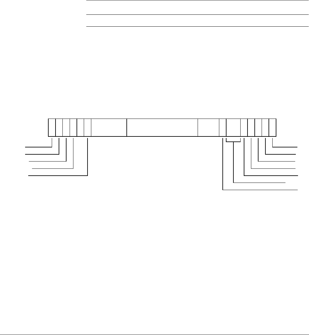
D8 AArch64 System Register Descriptions
D8.2 General system control registers
D8-1918 Copyright © 2013 ARM Limited. All rights reserved. ARM DDI 0487A.a
Non-Confidential - Beta ID090413
D8.2.30 FPEXC32_EL2, Floating-point Exception Control register
The FPEXC32_EL2 characteristics are:
Purpose
Allows access to the AArch32 register FPEXC from AArch64 state only. Its value has no effect on
execution in AArch64 state.
This register is part of the Floating-point registers functional group.
Usage constraints
This register is accessible as shown below:
If EL1 only supports AArch64 execution, this register is UNDEFINED.
Configurations
FPEXC32_EL2 is architecturally mapped to AArch32 register FPEXC.
Attributes
FPEXC32_EL2 is a 32-bit register.
The FPEXC32_EL2 bit assignments are:
EX, bit [31]
Exception bit. A status bit that specifies how much information must be saved to record the state of
the Advanced SIMD and VFP system:
0
The only significant state is the contents of the registers D0 - D31, FPSCR, and FPEXC.
A context switch can be performed by saving and restoring the values of these registers.
1
There is additional state that must be handled by any context switch system.
In ARMv8, this bit must be RES0.
EN, bit [30]
Enable bit. A global enable for the Advanced SIMD and VFP extensions:
0
The Advanced SIMD and VFP extensions are disabled.
1
The Advanced SIMD and VFP extensions are enabled and operate normally.
This bit is made obsolete by the features in the CPACR when executing in AArch64.
When executing in EL0 using AArch32 with EL1 using AArch64, the behavior is as if the
FPEXC.EN bit is set.
EL0 EL1 (NS) EL1 (S) EL2 EL3 (SCR.NS=1) EL3 (SCR.NS=0)
-- - RWRW RW
31 30 29 28
VV
27 26
RES0
25 21
IMPLEMENTATION DEFINED
20 11
VECITR
10 8 7654 3 2 1 0
EX
EN
DEX
FP2V
TFV
IOF
DZF
OFF
UFF
IXF
IMP DEF
IDF

D8 AArch64 System Register Descriptions
D8.2 General system control registers
ARM DDI 0487A.a Copyright © 2013 ARM Limited. All rights reserved. D8-1919
ID090413 Non-Confidential - Beta
DEX, bit [29]
Defined synchronous instruction exception bit.
When a floating-point synchronous exception has occurred, if the exception was caused by an
allocated floating-point instruction that is not implemented in hardware then it is IMPLEMENTATION
DEFINED whether DEX is set to 0 or 1.
Otherwise, the meaning of this bit is:
0
A synchronous exception occurred when processing an unallocated floating-point or
Advanced SIMD instruction.
1
A synchronous exception occurred on an allocated floating-point instruction that
encountered an exceptional condition.
The exception-handling routine must clear DEX to 0.
In an implementation that does not require synchronous exception handling this bit is RES0.
FP2V, bit [28]
FPINST2 instruction valid bit. In ARMv8, this field is always RES0.
VV, bit [27]
VECITR valid bit. In ARMv8, this field is always RES0.
TFV, bit [26]
Trapped Fault Valid bit. Indicates whether FPEXC bits[7, 4:0] indicate trapped exceptions, or have
an IMPLEMENTATION DEFINED meaning:
0
FPEXC bits[7, 4:0] have an IMPLEMENTATION DEFINED meaning
1
FPEXC bits[7, 4:0] indicate the presence of trapped exceptions that have occurred at the
time of the exception. All trapped exceptions that occurred at the time of the exception
have their bits set.
This bit has a fixed value and ignores writes.
Bits [25:21]
Reserved, RES0.
VECITR, bits [10:8]
Vector iteration count. In ARMv8, this field is always RES1.
IDF, bit [7]
Input Denormal trapped exception bit, or IMPLEMENTATION DEFINED. The meaning of this bit
depends on the value of FPEXC.TFV.
If FPEXC.TFV is 0, this bit is IMPLEMENTATION DEFINED and can contain IMPLEMENTATION
DEFINED information about the cause of an exception.
If FPEXC.TFV is 1, this bit is the Input Denormal trapped exception bit, and indicates whether an
Input Denormal exception occurred while FPSCR.IDE was 1:
0
Input denormal exception has not occurred.
1
Input denormal exception has occurred.
Input Denormal exceptions can occur only when FPSCR.FZ is 1.
In both cases this bit must be cleared to 0 by the exception-handling routine.
IXF, bit [4]
Inexact trapped exception bit, or IMPLEMENTATION DEFINED. The meaning of this bit depends on the
value of FPEXC.TFV.
If FPEXC.TFV is 0, this bit is IMPLEMENTATION DEFINED and can contain IMPLEMENTATION
DEFINED information about the cause of an exception.

D8 AArch64 System Register Descriptions
D8.2 General system control registers
D8-1920 Copyright © 2013 ARM Limited. All rights reserved. ARM DDI 0487A.a
Non-Confidential - Beta ID090413
If FPEXC.TFV is 1, this bit is the Inexact trapped exception bit, and indicates whether an Inexact
exception occurred while FPSCR.IXE was 1:
In this case, the meaning of this bit is:
0
Inexact exception has not occurred.
1
Inexact exception has occurred.
In both cases this bit must be cleared to 0 by the exception-handling routine.
UFF, bit [3]
Underflow trapped exception bit, or IMPLEMENTATION DEFINED. The meaning of this bit depends on
the value of FPEXC.TFV.
If FPEXC.TFV is 0, this bit is IMPLEMENTATION DEFINED and can contain IMPLEMENTATION
DEFINED information about the cause of an exception.
If FPEXC.TFV is 1, this bit is the Underflow trapped exception bit, and indicates whether an
Underflow exception occurred while FPSCR.UFE was 1:
0
Underflow exception has not occurred.
1
Underflow exception has occurred.
Underflow trapped exceptions can occur only when FPSCR.FZ is 0.
In both cases this bit must be cleared to 0 by the exception-handling routine.
OFF, bit [2]
Overflow trapped exception bit, or IMPLEMENTATION DEFINED. The meaning of this bit depends on
the value of FPEXC.TFV.
If FPEXC.TFV is 0, this bit is IMPLEMENTATION DEFINED and can contain IMPLEMENTATION
DEFINED information about the cause of an exception.
If FPEXC.TFV is 1, this bit is the Overflow trapped exception bit, and indicates whether an
Overflow exception occurred while FPSCR.OFE was 1:
0
Overflow exception has not occurred.
1
Overflow exception has occurred.
In both cases this bit must be cleared to 0 by the exception-handling routine.
DZF, bit [1]
Divide-by-zero trapped exception bit, or IMPLEMENTATION DEFINED. The meaning of this bit
depends on the value of FPEXC.TFV.
If FPEXC.TFV is 0, this bit is IMPLEMENTATION DEFINED and can contain IMPLEMENTATION
DEFINED information about the cause of an exception.
If FPEXC.TFV is 1, this bit is the Divide-by-zero trapped exception bit, and indicates whether a
Divide-by-zero exception occurred while FPSCR.DZE was 1:
0
Divide-by-zero exception has not occurred.
1
Divide-by-zero exception has occurred.
In both cases this bit must be cleared to 0 by the exception-handling routine.
IOF, bit [0]
Invalid Operation trapped exception bit, or IMPLEMENTATION DEFINED. The meaning of this bit
depends on the value of FPEXC.TFV.
If FPEXC.TFV is 0, this bit is IMPLEMENTATION DEFINED and can contain IMPLEMENTATION
DEFINED information about the cause of an exception.
If FPEXC.TFV is 1, this bit is the Invalid Operation trapped exception bit, and indicates whether an
Invalid Operation exception occurred while FPSCR.IOE was 1:
0
Invalid Operation exception has not occurred.
1
Invalid Operation exception has occurred.

D8 AArch64 System Register Descriptions
D8.2 General system control registers
ARM DDI 0487A.a Copyright © 2013 ARM Limited. All rights reserved. D8-1921
ID090413 Non-Confidential - Beta
In both cases this bit must be cleared to 0 by the exception-handling routine.
Accessing the FPEXC32_EL2:
To access the FPEXC32_EL2:
MRS <Xt>, FPEXC32_EL2 ; Read FPEXC32_EL2 into Xt
MSR FPEXC32_EL2, <Xt> ; Write Xt to FPEXC32_EL2
Register access is encoded as follows:
op0 op1 CRn CRm op2
11 100 0101 0011 000

D8 AArch64 System Register Descriptions
D8.2 General system control registers
D8-1922 Copyright © 2013 ARM Limited. All rights reserved. ARM DDI 0487A.a
Non-Confidential - Beta ID090413
D8.2.31 HACR_EL2, Hypervisor Auxiliary Control Register
The HACR_EL2 characteristics are:
Purpose
Controls trapping to EL2 of IMPLEMENTATION DEFINED aspects of Non-secure EL1 or EL0
operation.
This register is part of the Virtualization registers functional group.
Usage constraints
This register is accessible as shown below:
Configurations
HACR_EL2 is architecturally mapped to AArch32 register HACR.
If EL2 is not implemented, this register is RES0 from EL3.
Attributes
HACR_EL2 is a 32-bit register.
The HACR_EL2 bit assignments are:
Accessing the HACR_EL2:
To access the HACR_EL2:
MRS <Xt>, HACR_EL2 ; Read HACR_EL2 into Xt
MSR HACR_EL2, <Xt> ; Write Xt to HACR_EL2
Register access is encoded as follows:
EL0 EL1 (NS) EL1 (S) EL2 EL3 (SCR.NS=1) EL3 (SCR.NS=0)
-- - RWRW RW
IMPLEMENTATION DEFINED
31 0
op0 op1 CRn CRm op2
11 100 0001 0001 111
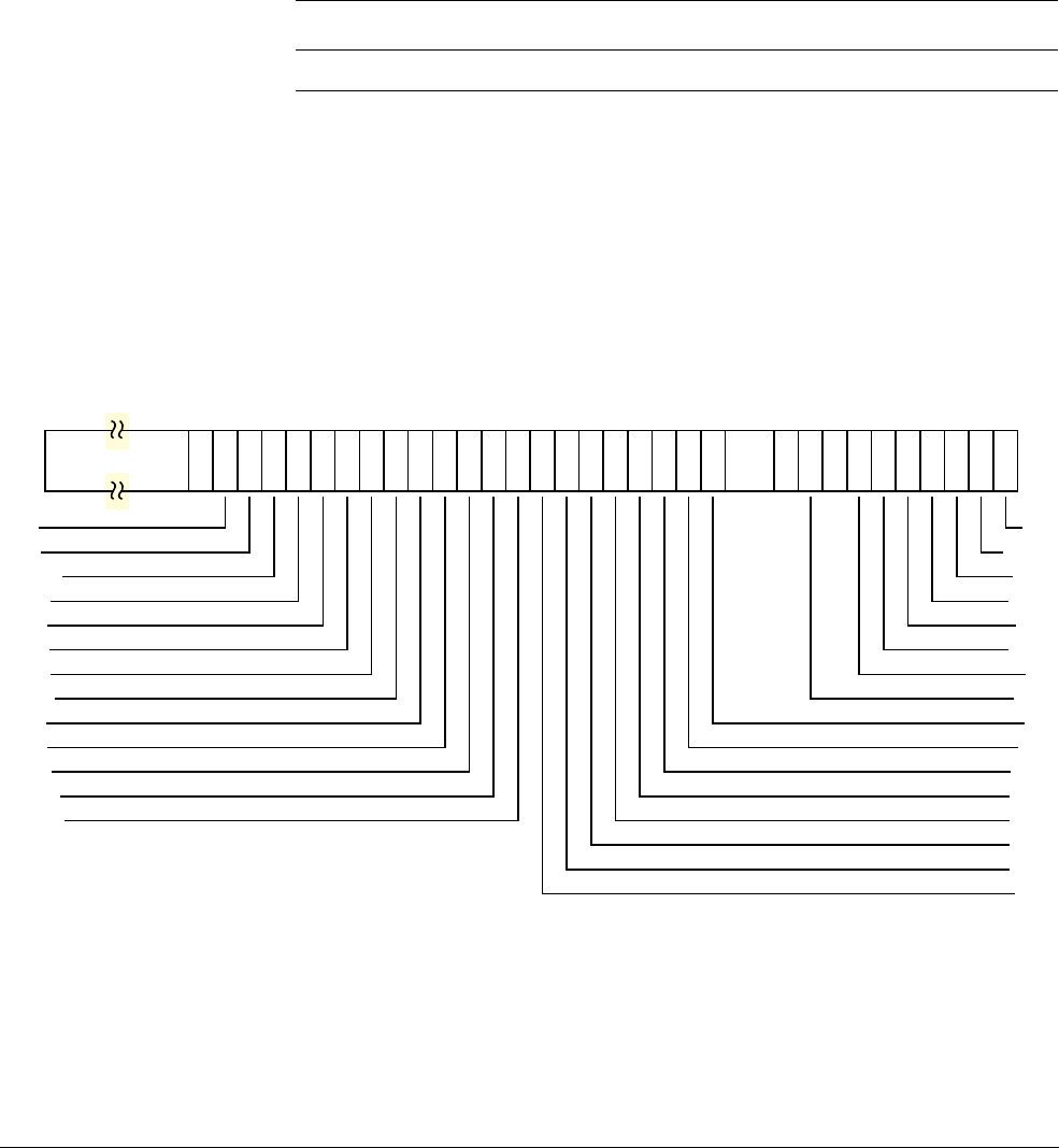
D8 AArch64 System Register Descriptions
D8.2 General system control registers
ARM DDI 0487A.a Copyright © 2013 ARM Limited. All rights reserved. D8-1923
ID090413 Non-Confidential - Beta
D8.2.32 HCR_EL2, Hypervisor Configuration Register
The HCR_EL2 characteristics are:
Purpose
Provides configuration controls for virtualization, including defining whether various Non-secure
operations are trapped to EL2.
This register is part of the Virtualization registers functional group.
Usage constraints
This register is accessible as shown below:
Configurations
HCR_EL2[31:0] is architecturally mapped to AArch32 register HCR.
HCR_EL2[63:32] is architecturally mapped to AArch32 register HCR2.
If EL2 is not implemented, this register is RES0 from EL3.
Attributes
HCR_EL2 is a 64-bit register.
The HCR_EL2 bit assignments are:
Bits [63:34]
Reserved, RES0.
ID, bit [33]
Stage 2 Instruction cache disable. When HCR_EL2.VM==1, this forces all stage 2 translations for
instruction accesses to Normal memory to be Non-cacheable for the EL1&0 translation regime.
0
No effect on the stage 2 of the EL1&0 translation regime for instruction accesses.
EL0 EL1 (NS) EL1 (S) EL2 EL3 (SCR.NS=1) EL3 (SCR.NS=0)
-- - RWRW RW
RES0
63 34
ID
33 32 31 30 29 28 27 26 25 24 23 22 21 20 19 18 17 16 15 14 13 12
BSU
11 10
FB
98
VI
76 5 4 3 2 1 0
CD
RW
TRVM
HCD
TDZ
TGE
TVM
TTLB
TPU
TPC
TSW
TACR
TIDCP
VM
SWIO
PTW
FMO
IMO
AMO
VF
VSE
DC
TWI
TWE
TID0
TID1
TID2
TID3
TSC

D8 AArch64 System Register Descriptions
D8.2 General system control registers
D8-1924 Copyright © 2013 ARM Limited. All rights reserved. ARM DDI 0487A.a
Non-Confidential - Beta ID090413
1
Forces all stage 2 translations for instruction accesses to Normal memory to be
Non-cacheable for the EL1&0 translation regime.
This bit has no effect on the EL2 or EL3 translation regimes.
CD, bit [32]
Stage 2 Data cache disable. When HCR_EL2.VM==1, this forces all stage 2 translations for data
accesses and translation table walks to Normal memory to be Non-cacheable for the EL1&0
translation regime.
0
No effect on the stage 2 of the EL1&0 translation regime for data accesses and
translation table walks.
1
Forces all stage 2 translations for data accesses and translation table walks to Normal
memory to be Non-cacheable for the EL1&0 translation regime.
This bit has no effect on the EL2 or EL3 translation regimes.
RW, bit [31]
Register Width control for lower exception levels:
0
Lower levels are all AArch32.
1
EL1 is AArch64. EL0 is determined by the Register Width described in the current
process state when executing at EL0.
When SCR_EL3.NS==0, this bit behaves as if it has the same value as the SCR_EL3.RW bit except
for the value read back.
The RW bit is permitted to be cached in a TLB.
TRVM, bit [30]
Trap Read of Virtual Memory controls. When this bit is set to 1, this causes Reads to the EL1 virtual
memory control registers from EL1 to be trapped to EL2. This covers the following registers:
AArch32: SCTLR, TTBR0, TTBR1, TTBCR, DACR, DFSR, IFSR, DFAR, IFAR, ADFSR,
AIFSR, PRRR/MAIR0, NMRR/MAIR1, AMAIR0, AMAIR1, CONTEXTIDR.
AArch64: SCTLR_EL1, TTBR0_EL1, TTBR1_EL1, TCR_EL1, ESR_EL1, FAR_EL1,
AFSR0_EL1, AFSR1_EL1, MAIR_EL1, AMAIR_EL1, CONTEXTIDR_EL1.
HCD, bit [29]
Hypervisor Call Disable, if EL3 is not implemented:
0
HVC instruction is enabled at EL1 or EL2.
1
HVC instruction is UNDEFINED at all exception levels.
If EL3 is implemented, this bit is RES0.
TDZ, bit [28]
Trap DC ZVA instruction:
0
The instruction is not trapped.
1
The instruction is trapped to EL2 when executed in Non-secure EL1 or EL0.
This bit also has an effect on the value read from the DCZID_EL0 register. If this bit is 1, then
reading DCZID_EL0.DZP will return 1 to indicate that DC ZVA is prohibited.
TGE, bit [27]
Trap General Exceptions. If this bit is set to 1, and SCR_EL3.NS is set to 1, then:
• All exceptions that would be routed to EL1 are routed to EL2.
• The SCTLR_EL1.M bit is treated as being 0 regardless of its actual state (for EL1 using
AArch32 or AArch64) other than for the purpose of reading the bit.
• The HCR_EL2.FMO, IMO and AMO bits are treated as being 1 regardless of their actual
state other than for the purpose of reading the bits.
• All virtual interrupts are disabled.

D8 AArch64 System Register Descriptions
D8.2 General system control registers
ARM DDI 0487A.a Copyright © 2013 ARM Limited. All rights reserved. D8-1925
ID090413 Non-Confidential - Beta
• Any implementation defined mechanisms for signalling virtual interrupts are disabled.
• An exception return to EL1 is treated as an illegal exception return.
Additionally, if HCR_EL2.TGE == 1, the MDCR_EL2.{TDRA,TDOSA,TDA} bits are ignored
and the processor behaves as if they are set to 1, other than for the value read back from
MDCR_EL2.
TVM, bit [26]
Trap Virtual Memory controls. When this bit is set to 1, this causes Writes to the EL1 virtual
memory control registers from EL1 to be trapped to EL2. This covers the following registers:
AArch32: SCTLR, TTBR0, TTBR1, TTBCR, DACR, DFSR, IFSR, DFAR, IFAR, ADFSR,
AIFSR, PRRR/MAIR0, NMRR/MAIR1, AMAIR0, AMAIR1, CONTEXTIDR.
AArch64: SCTLR_EL1, TTBR0_EL1, TTBR1_EL1, TCR_EL1, ESR_EL1, FAR_EL1,
AFSR0_EL1, AFSR1_EL1, MAIR_EL1, AMAIR_EL1, CONTEXTIDR_EL1
TTLB, bit [25]
Trap TLB maintenance instructions. When this bit is set to 1, this causes TLB maintenance
instructions executed from EL1 which are not UNDEFINED to be trapped to EL2. This covers the
following instructions:
AArch32: TLBIALLIS, TLBIMVAIS, TLBIASIDIS, TLBIMVAAIS, TLBIALL, TLBIMVA,
TLBIASID, DTLBIALL, DTLBIMVA, DTLBIASID, ITLBIALL, ITLBIMVA, ITLBIASID,
TLBIMVAA, TLBIMVALIS, TLBIMVAALIS, TLBIMVAL, TLBIMVAAL
AArch64: TLBI VMALLE1, TLBI VAE1, TLBI ASIDE1, TLBI VAAE1, TLBI VALE1, TLBI
VAALE1, TLBI VMALLE1IS, TLBI VAE1IS, TLBI ASIDE1IS, TLBI VAAE1IS, TLBI
VALE1IS, TLBI VAALE1IS
TPU, bit [24]
Trap Cache maintenance instructions to Point of Unification. When this bit is set to 1, this causes
Cache maintenance instructions to the point of unification executed from EL1 or EL0 which are not
UNDEFINED to be trapped to EL2. This covers the following instructions:
AArch32: ICIMVAU, ICIALLU, ICIALLUIS, DCCMVAU.
AArch64: IC IVAU, IC IALLU, IC IALLUIS, DC CVAU.
TPC, bit [23]
Trap Data/Unified Cache maintenance operations to Point of Coherency. When this bit is set to 1,
this causes Data or Unified Cache maintenance instructions by address to the point of coherency
executed from EL1 or EL0 which are not UNDEFINED to be trapped to EL2. This covers the
following instructions:
AArch32: DCIMVAC, DCCIMVAC, DCCMVAC.
AArch64: DC IVAC, DC CIVAC, DC CVAC.
TSW, bit [22]
Trap Data/Unified Cache maintenance operations by Set/Way. When this bit is set to 1, this causes
Data or Unified Cache maintenance instructions by set/way executed from EL1 which are not
UNDEFINED to be trapped to EL2. This covers the following instructions:
AArch32: DCISW, DCCSW, DCCISW.
AArch64: DC ISW, DC CSW, DC CISW.
TACR, bit [21]
Trap Auxiliary Control Register. When this bit is set to 1, this causes accesses to the following
registers executed from EL1 to be trapped to EL2:
AArch32: ACTLR.
AArch64: ACTLR_EL1.

D8 AArch64 System Register Descriptions
D8.2 General system control registers
D8-1926 Copyright © 2013 ARM Limited. All rights reserved. ARM DDI 0487A.a
Non-Confidential - Beta ID090413
TIDCP, bit [20]
Trap Implementation Dependent functionality. When this bit is set to 1, this causes accesses to the
following instruction set space executed from EL1 to be trapped to EL2.
AArch32: MCR and MRC instructions as follows:
• All CP15, CRn==9, Opcode1 = {0-7}, CRm == {c0-c2, c5-c8}, opcode2 == {0-7}.
• All CP15, CRn==10, Opcode1 =={0-7}, CRm == {c0, c1, c4, c8}, opcode2 == {0-7}.
• All CP15, CRn==11, Opcode1=={0-7}, CRm == {c0-c8, c15}, opcode2 == {0-7}.
AArch64: All encoding space reserved for IMPLEMENTATION DEFINED system operations
(S1_<op1>_<Cn>_<Cm>_<op2>) and system registers (S3_<op1>_<Cn>_<Cm>_<op2>).
It is IMPLEMENTATION DEFINED whether any of this functionality accessed from EL0 is trapped to
EL2 when the HCR_EL2.TIDCP bit is set. If it is not trapped to EL2, it results in an Undefined
exception taken to EL1.
TSC, bit [19]
Trap SMC. When this bit is set to 1, this causes the following instructions executed from EL1 to be
trapped to EL2:
AArch32: SMC.
AArch64: SMC.
If EL3 is not implemented, this bit is RES0.
TID3, bit [18]
Trap ID Group 3. When this bit is set to 1, this causes reads to the following registers executed from
EL1 to be trapped to EL2:
AArch32: ID_PFR0, ID_PFR1, ID_DFR0, ID_AFR0, ID_MMFR0, ID_MMFR1, ID_MMFR2,
ID_MMFR3, ID_ISAR0, ID_ISAR1, ID_ISAR2, ID_ISAR3, ID_ISAR4, ID_ISAR5, MVFR0,
MVFR1, MVFR2. Also MRC to any of the following encodings:
• CP15, CRn == 0, Opc1 == 0, CRm == {3-7}, Opc2 == {0,1}.
• CP15, CRn == 0, Opc1 == 0, CRm == 3, Opc2 == 2.
• CP15, CRn == 0, Opc1 == 0, CRm == 5, Opc2 == {4,5}.
AArch64: ID_PFR0_EL1, ID_PFR1_EL1, ID_DFR0_EL1, ID_AFR0_EL1, ID_MMFR0_EL1,
ID_MMFR1_EL1, ID_MMFR2_EL1, ID_MMFR3_EL1, ID_ISAR0_EL1, ID_ISAR1_EL1,
ID_ISAR2_EL1, ID_ISAR3_EL1, ID_ISAR4_EL1, ID_ISAR5_EL1, MVFR0_EL1,
MVFR1_EL1, MVFR2_EL1, ID_AA64PFR0_EL1, ID_AA64PFR1_EL1, ID_AA64DFR0_EL1,
ID_AA64DFR1_EL1, ID_AA64ISAR0_EL1, ID_AA64ISAR1_EL1, ID_AA64MMFR0_EL1,
ID_AA64MMFR1_EL1, ID_AA64AFR0_EL1, ID_AA64AFR1_EL1.
TID2, bit [17]
Trap ID Group 2. When this bit is set to 1, this causes reads (or writes to CSSELR/CSSELR_EL1)
to the following registers executed from EL1 or EL0 if not UNDEFINED to be trapped to EL2:
AArch32: CTR, CCSIDR, CLIDR, CSSELR.
AArch64: CTR_EL0, CCSIDR_EL1, CLIDR_EL1, CSSELR_EL1.
TID1, bit [16]
Trap ID Group 1. When this bit is set to 1, this causes reads to the following registers executed from
EL1 to be trapped to EL2:
AArch32: TCMTR, TLBTR, AIDR, REVIDR.
AArch64: AIDR_EL1, REVIDR_EL1.
TID0, bit [15]
Trap ID Group 0. When this bit is set to 1, this causes reads to the following registers executed from
EL1 or EL0 if not UNDEFINED to be trapped to EL2:
AArch32: FPSID, JIDR.

D8 AArch64 System Register Descriptions
D8.2 General system control registers
ARM DDI 0487A.a Copyright © 2013 ARM Limited. All rights reserved. D8-1927
ID090413 Non-Confidential - Beta
AArch64: None.
TWE, bit [14]
Trap WFE. When this bit is set to 1, this causes the following instructions executed from EL1 or
EL0 to be trapped to EL2 if the instruction would otherwise cause suspension of execution (i.e. if
the event register is not set):
AArch32: WFE.
AArch64: WFE.
Conditional WFE instructions that fail their condition are not trapped if this bit is set to 1.
TWI, bit [13]
Trap WFI. When this bit is set to 1, this causes the following instructions executed from EL1 or EL0
to be trapped to EL2 if the instruction would otherwise cause suspension of execution (i.e. if there
is not a pending WFI wakeup event):
AArch32: WFI.
AArch64: WFI.
Conditional WFI instructions that fail their condition are not trapped if this bit is set to 1.
DC, bit [12]
Default Cacheable. When this bit is set to 1, this causes:
• The SCTLR_EL1.M bit to behave as 0 for all purposes other than reading the value of the bit.
• The HCR_EL2.VM bit to behave as 1 for all purposes other than reading the value of the bit.
The memory type produced by the first stage of translation used by EL1 and EL0 is Normal
Non-Shareable, Inner WriteBack Read-WriteAllocate, Outer WriteBack Read-WriteAllocate.
When this bit is 0 and the stage 1 MMU is disabled, the default memory attribute for Data accesses
is Device-nGnRnE.
This bit is permitted to be cached in a TLB.
BSU, bits [11:10]
Barrier Shareability upgrade. The value in this field determines the minimum shareability domain
that is applied to any barrier executed from EL1 or EL0:
00
No effect
01
Inner Shareable
10
Outer Shareable
11
Full system
This value is combined with the specified level of the barrier held in its instruction, using the same
principles as combining the shareability attributes from two stages of address translation.
FB, bit [9]
Force broadcast. When this bit is set to 1, this causes the following instructions to be broadcast
within the Inner Shareable domain when executed from Non-secure EL1:
AArch32: BPIALL, TLBIALL, TLBIMVA, TLBIASID, DTLBIALL, DTLBIMVA, DTLBIASID,
ITLBIALL, ITLBIMVA, ITLBIASID, TLBIMVAA, ICIALLU, TLBIMVAL, TLBIMVAAL.
AArch64: TLBI VMALLE1, TLBI VAE1, TLBI ASIDE1, TLBI VAAE1, TLBI VALE1, TLBI
VAALE1, IC IALLU.
VSE, bit [8]
Virtual System Error/Asynchronous Abort.
0
Virtual System Error/Asynchronous Abort is not pending by this mechanism.
1
Virtual System Error/Asynchronous Abort is pending by this mechanism.
The virtual System Error/Asynchronous Abort is only enabled when the HCR_EL2.AMO bit is set.

D8 AArch64 System Register Descriptions
D8.2 General system control registers
D8-1928 Copyright © 2013 ARM Limited. All rights reserved. ARM DDI 0487A.a
Non-Confidential - Beta ID090413
VI, bit [7]
Virtual IRQ Interrupt.
0
Virtual IRQ is not pending by this mechanism.
1
Virtual IRQ is pending by this mechanism.
The virtual IRQ is only enabled when the HCR_EL2.IMO bit is set.
VF, bit [6]
Virtual FIQ Interrupt.
0
Virtual FIQ is not pending by this mechanism.
1
Virtual FIQ is pending by this mechanism.
The virtual FIQ is only enabled when the HCR_EL2.FMO bit is set.
AMO, bit [5]
Asynchronous abort and error interrupt routing.
0
Asynchronous External Aborts and SError Interrupts while executing at exception
levels lower than EL2 are not taken in EL2. Virtual System Error/Asynchronous Abort
is disabled.
1
Asynchronous External Aborts and SError Interrupts while executing at EL2 or lower
are taken in EL2 unless routed by the SCR_EL3.EA bit to EL3. Virtual System
Error/Asynchronous Abort is enabled.
IMO, bit [4]
Physical IRQ Routing.
0
Physical IRQ while executing at exception levels lower than EL2 are not taken in EL2.
Virtual IRQ Interrupt is disabled.
1
Physical IRQ while executing at EL2 or lower are taken in EL2 unless routed by the
SCR_EL3.IRQ bit to EL3. Virtual IRQ Interrupt is enabled.
FMO, bit [3]
Physical FIQ Routing.
0
Physical FIQ while executing at exception levels lower than EL2 are not taken in EL2.
Virtual FIQ Interrupt is disabled.
1
Physical FIQ while executing at EL2 or lower are taken in EL2 unless routed by the
SCR_EL3.FIQ bit to EL3. Virtual FIQ Interrupt is enabled.
PTW, bit [2]
Protected Table Walk. When this bit is set to 1, if the stage 2 translation of a translation table access
made as part of a stage 1 translation table walk at EL0 or EL1 maps that translation table access to
Strongly-ordered or Device memory, the access is faulted as a stage 2 Permission fault.
This bit is permitted to be cached in a TLB.
SWIO, bit [1]
Set/Way Invalidation Override. When this bit is set to 1, this causes EL1 execution of the data cache
invalidate by set/way instruction to be treated as data cache clean and invalidate by set/way. That is:
AArch32: DCISW is executed as DCCISW.
AArch64: DC ISW is executed as DC CISW.
As a result of changes to the behavior of DCISW, this bit is redundant in v8-A. It is permissible that
an implementation makes this bit RES1.

D8 AArch64 System Register Descriptions
D8.2 General system control registers
ARM DDI 0487A.a Copyright © 2013 ARM Limited. All rights reserved. D8-1929
ID090413 Non-Confidential - Beta
VM, bit [0]
Virtualization MMU enable for EL1 and EL0 stage 2 address translation. Possible values of this bit
are:
0
EL1 and EL0 stage 2 address translation disabled.
1
EL1 and EL0 stage 2 address translation enabled.
This bit is permitted to be cached in a TLB.
Accessing the HCR_EL2:
To access the HCR_EL2:
MRS <Xt>, HCR_EL2 ; Read HCR_EL2 into Xt
MSR HCR_EL2, <Xt> ; Write Xt to HCR_EL2
Register access is encoded as follows:
op0 op1 CRn CRm op2
11 100 0001 0001 000
D8 AArch64 System Register Descriptions
D8.2 General system control registers
D8-1930 Copyright © 2013 ARM Limited. All rights reserved. ARM DDI 0487A.a
Non-Confidential - Beta ID090413
D8.2.33 HPFAR_EL2, Hypervisor IPA Fault Address Register
The HPFAR_EL2 characteristics are:
Purpose
Holds the faulting IPA for some aborts on a stage 2 translation taken to EL2.
This register is part of:
• the Exception and fault handling registers functional group
• the Virtualization registers functional group.
Usage constraints
This register is accessible as shown below:
Configurations
HPFAR_EL2[31:0] is architecturally mapped to AArch32 register HPFAR.
If EL2 is not implemented, this register is RES0 from EL3.
Attributes
HPFAR_EL2 is a 64-bit register.
The HPFAR_EL2 bit assignments are:
Bits [63:40]
Reserved, RES0.
FIPA[47:12], bits [39:4]
Bits [47:12] of the faulting intermediate physical address. For implementations with fewer than 48
physical address bits, the equivalent upper bits in this field are RES0.
Bits [3:0]
Reserved, RES0.
Accessing the HPFAR_EL2:
To access the HPFAR_EL2:
MRS <Xt>, HPFAR_EL2 ; Read HPFAR_EL2 into Xt
MSR HPFAR_EL2, <Xt> ; Write Xt to HPFAR_EL2
Register access is encoded as follows:
EL0 EL1 (NS) EL1 (S) EL2 EL3 (SCR.NS=1) EL3 (SCR.NS=0)
-- - RWRW RW
RES0
63 40
FIPA[47:12]
39 4
RES0
30
op0 op1 CRn CRm op2
11 100 0110 0000 100
D8 AArch64 System Register Descriptions
D8.2 General system control registers
ARM DDI 0487A.a Copyright © 2013 ARM Limited. All rights reserved. D8-1931
ID090413 Non-Confidential - Beta
D8.2.34 HSTR_EL2, Hypervisor System Trap Register
The HSTR_EL2 characteristics are:
Purpose
Controls access to T32EE and coprocessor registers at lower exception levels in AArch32.
This register is part of the Virtualization registers functional group.
Usage constraints
This register is accessible as shown below:
Configurations
HSTR_EL2 is architecturally mapped to AArch32 register HSTR.
If EL2 is not implemented, this register is RES0 from EL3.
Attributes
HSTR_EL2 is a 32-bit register.
The HSTR_EL2 bit assignments are:
Bits [31:17]
Reserved, RES0.
TTEE, bit [16]
Trap T32EE. The possible values of this bit are:
0
Has no effect on accesses to the T32EE configuration registers.
1
Trap valid Non-secure accesses to T32EE configuration registers to Hyp mode.
When this bit is set to 1, any valid Non-secure access to the T32EE configuration registers is trapped
to Hyp mode.
If T32EE is not implemented, then this bit is RES0.
T<n>, bit [n], for n = 0 to 15
Trap coprocessor primary register. For each field T<n>, the possible values of this bit are:
0
Has no effect on Non-secure accesses to CP15 coprocessor registers.
1
Trap valid Non-secure accesses to coprocessor primary register c<n> to Hyp mode.
EL0 EL1 (NS) EL1 (S) EL2 EL3 (SCR.NS=1) EL3 (SCR.NS=0)
-- - RWRW RW
RES0
31 17 16 15 14 13 12 11 10
T9
9
T8
8
T7
7
T6
6
T5
5
T4
4
T3
3
T2
2
T1
1
T0
0
TTEE T10
T11
T12
T13
T14
T15

D8 AArch64 System Register Descriptions
D8.2 General system control registers
D8-1932 Copyright © 2013 ARM Limited. All rights reserved. ARM DDI 0487A.a
Non-Confidential - Beta ID090413
When T<n> is set to 1, any valid Non-secure access to CP15 primary coprocessor register c<n> is
trapped to Hyp mode. For example, when T7 is set to 1:
• Any valid Non-secure 32-bit CP15 accesses, using MRC or MCR instructions with
CRn==c7, are trapped to Hyp mode.
• Any valid Non-secure 64-bit CP15 accesses, using MRRC or MCRR instructions with
CRm==c7, are trapped to Hyp mode.
Fields T14 and T4 are RES0.
Accessing the HSTR_EL2:
To access the HSTR_EL2:
MRS <Xt>, HSTR_EL2 ; Read HSTR_EL2 into Xt
MSR HSTR_EL2, <Xt> ; Write Xt to HSTR_EL2
Register access is encoded as follows:
op0 op1 CRn CRm op2
11 100 0001 0001 011
D8 AArch64 System Register Descriptions
D8.2 General system control registers
ARM DDI 0487A.a Copyright © 2013 ARM Limited. All rights reserved. D8-1933
ID090413 Non-Confidential - Beta
D8.2.35 ID_AA64AFR0_EL1, AArch64 Auxiliary Feature Register 0
The ID_AA64AFR0_EL1 characteristics are:
Purpose
Provides information about the IMPLEMENTATION DEFINED features of the processor in AArch64.
This register is part of the Identification registers functional group.
Usage constraints
This register is accessible as shown below:
Configurations
There are no configuration notes.
Attributes
ID_AA64AFR0_EL1 is a 64-bit register.
The ID_AA64AFR0_EL1 bit assignments are:
Bits [63:32]
Reserved, RES0.
Accessing the ID_AA64AFR0_EL1:
To access the ID_AA64AFR0_EL1:
MRS <Xt>, ID_AA64AFR0_EL1 ; Read ID_AA64AFR0_EL1 into Xt
Register access is encoded as follows:
EL0 EL1 (NS) EL1 (S) EL2 EL3 (SCR.NS=1) EL3 (SCR.NS=0)
-RO RO RORO RO
RES0
63 32
IMP DEF
31 28
IMP DEF
27 24
IMP DEF
23 20
IMP DEF
19 16
IMP DEF
15 12
IMP DEF
11 8
IMP DEF
74
IMP DEF
30
op0 op1 CRn CRm op2
11 000 0000 0101 100

D8 AArch64 System Register Descriptions
D8.2 General system control registers
D8-1934 Copyright © 2013 ARM Limited. All rights reserved. ARM DDI 0487A.a
Non-Confidential - Beta ID090413
D8.2.36 ID_AA64AFR1_EL1, AArch64 Auxiliary Feature Register 1
The ID_AA64AFR1_EL1 characteristics are:
Purpose
Reserved for future expansion of information about the IMPLEMENTATION DEFINED features of the
processor in AArch64.
This register is part of the Identification registers functional group.
Usage constraints
This register is accessible as shown below:
Configurations
There are no configuration notes.
Attributes
ID_AA64AFR1_EL1 is a 64-bit register.
The ID_AA64AFR1_EL1 bit assignments are:
Bits [63:0]
Reserved, RES0.
Accessing the ID_AA64AFR1_EL1:
To access the ID_AA64AFR1_EL1:
MRS <Xt>, ID_AA64AFR1_EL1 ; Read ID_AA64AFR1_EL1 into Xt
Register access is encoded as follows:
EL0 EL1 (NS) EL1 (S) EL2 EL3 (SCR.NS=1) EL3 (SCR.NS=0)
-RO RO RORO RO
RES0
63 0
op0 op1 CRn CRm op2
11 000 0000 0101 101

D8 AArch64 System Register Descriptions
D8.2 General system control registers
ARM DDI 0487A.a Copyright © 2013 ARM Limited. All rights reserved. D8-1935
ID090413 Non-Confidential - Beta
D8.2.37 ID_AA64DFR0_EL1, AArch64 Debug Feature Register 0
The ID_AA64DFR0_EL1 characteristics are:
Purpose
Provides top level information about the debug system in AArch64.
This register is part of the Identification registers functional group.
Usage constraints
This register is accessible as shown below:
Configurations
ID_AA64DFR0_EL1 is architecturally mapped to external register ID_AA64DFR0_EL1.
Attributes
ID_AA64DFR0_EL1 is a 64-bit register.
The ID_AA64DFR0_EL1 bit assignments are:
Bits [63:32]
Reserved, RES0.
CTX_CMPs, bits [31:28]
Number of breakpoints that are context-aware, minus 1. These are the highest numbered
breakpoints.
Bits [27:24]
Reserved, RES0.
WRPs, bits [23:20]
Number of watchpoints, minus 1. The value of
0b0000
is reserved.
Bits [19:16]
Reserved, RES0.
BRPs, bits [15:12]
Number of breakpoints, minus 1. The value of
0b0000
is reserved.
PMUVer, bits [11:8]
Performance Monitors extension version. Indicates whether system register interface to
Performance Monitors extension is implemented. Permitted values are:
0000
Performance Monitors extension system registers not implemented.
0001
Performance Monitors extension system registers implemented, PMUv3.
1111
IMPLEMENTATION DEFINED form of performance monitors supported, PMUv3 not
supported.
All other values are reserved.
EL0 EL1 (NS) EL1 (S) EL2 EL3 (SCR.NS=1) EL3 (SCR.NS=0)
-RO RO RORO RO
RES0
63 32
CTX_CMPs
31 28
RES0
27 24
WRPs
23 20
RES0
19 16
BRPs
15 12
PMUVer
11 8
TraceVer
74
DebugVer
30

D8 AArch64 System Register Descriptions
D8.2 General system control registers
D8-1936 Copyright © 2013 ARM Limited. All rights reserved. ARM DDI 0487A.a
Non-Confidential - Beta ID090413
TraceVer, bits [7:4]
Trace extension. Indicates whether system register interface to Trace extension is implemented.
Permitted values are:
0000
Trace extension system registers not implemented.
0001
Trace extension system registers implemented.
All other values are reserved.
A value of
0b0000
only indicates that no system register interface to the trace extension is
implemented. A trace extension may nevertheless be implemented without a system register
interface.
DebugVer, bits [3:0]
Debug architecture version. Indicates presence of v8-A debug architecture.
0110
v8-A debug architecture.
All other values are reserved.
Accessing the ID_AA64DFR0_EL1:
To access the ID_AA64DFR0_EL1:
MRS <Xt>, ID_AA64DFR0_EL1 ; Read ID_AA64DFR0_EL1 into Xt
Register access is encoded as follows:
op0 op1 CRn CRm op2
11 000 0000 0101 000

D8 AArch64 System Register Descriptions
D8.2 General system control registers
ARM DDI 0487A.a Copyright © 2013 ARM Limited. All rights reserved. D8-1937
ID090413 Non-Confidential - Beta
D8.2.38 ID_AA64DFR1_EL1, AArch64 Debug Feature Register 1
The ID_AA64DFR1_EL1 characteristics are:
Purpose
Reserved for future expansion of top level information about the debug system in AArch64.
This register is part of the Identification registers functional group.
Usage constraints
This register is accessible as shown below:
Configurations
ID_AA64DFR1_EL1 is architecturally mapped to external register ID_AA64DFR1_EL1.
Attributes
ID_AA64DFR1_EL1 is a 64-bit register.
The ID_AA64DFR1_EL1 bit assignments are:
Bits [63:0]
Reserved, RES0.
Accessing the ID_AA64DFR1_EL1:
To access the ID_AA64DFR1_EL1:
MRS <Xt>, ID_AA64DFR1_EL1 ; Read ID_AA64DFR1_EL1 into Xt
Register access is encoded as follows:
EL0 EL1 (NS) EL1 (S) EL2 EL3 (SCR.NS=1) EL3 (SCR.NS=0)
-RO RO RORO RO
RES0
63 0
op0 op1 CRn CRm op2
11 000 0000 0101 001
D8 AArch64 System Register Descriptions
D8.2 General system control registers
D8-1938 Copyright © 2013 ARM Limited. All rights reserved. ARM DDI 0487A.a
Non-Confidential - Beta ID090413
D8.2.39 ID_AA64ISAR0_EL1, AArch64 Instruction Set Attribute Register 0
The ID_AA64ISAR0_EL1 characteristics are:
Purpose
Provides information about the instructions implemented by the processor in AArch64.
This register is part of the Identification registers functional group.
Usage constraints
This register is accessible as shown below:
Configurations
ID_AA64ISAR0_EL1 is architecturally mapped to external register ID_AA64ISAR0_EL1.
Attributes
ID_AA64ISAR0_EL1 is a 64-bit register.
The ID_AA64ISAR0_EL1 bit assignments are:
Bits [63:20]
Reserved, RES0.
CRC32, bits [19:16]
CRC32 instructions in AArch64. Possible values of this field are:
0000
No CRC32 instructions implemented.
0001
CRC32B, CRC32H, CRC32W, CRC32X, CRC32CB, CRC32CH, CRC32CW, and
CRC32CX instructions implemented.
All other values are reserved.
This field must have the same value as ID_ISAR5.CRC32. The architecture requires that if CRC32
is supported in one Execution state, it must be supported in both Execution states.
SHA2, bits [15:12]
SHA2 instructions in AArch64. Possible values of this field are:
0000
No SHA2 instructions implemented.
0001
SHA256H, SHA256H2, SHA256SU0, and SHA256SU1 instructions implemented.
All other values are reserved.
SHA1, bits [11:8]
SHA1 instructions in AArch64. Possible values of this field are:
0000
No SHA1 instructions implemented.
0001
SHA1C, SHA1P, SHA1M, SHA1H, SHA1SU0, and SHA1SU1 instructions
implemented.
All other values are reserved.
EL0 EL1 (NS) EL1 (S) EL2 EL3 (SCR.NS=1) EL3 (SCR.NS=0)
-RO RO RORO RO
RES0
63 20
CRC32
19 16
SHA2
15 12
SHA1
11 8
AES
74
RES0
30

D8 AArch64 System Register Descriptions
D8.2 General system control registers
ARM DDI 0487A.a Copyright © 2013 ARM Limited. All rights reserved. D8-1939
ID090413 Non-Confidential - Beta
AES, bits [7:4]
AES instructions in AArch64. Possible values of this field are:
0000
No AES instructions implemented.
0001
AESE, AESD, AESMC, and AESIMC instructions implemented.
0010
As for
0b0001
, plus PMULL/PMULL2 instructions operating on 64-bit data quantities.
Bits [3:0]
Reserved, RES0.
Accessing the ID_AA64ISAR0_EL1:
To access the ID_AA64ISAR0_EL1:
MRS <Xt>, ID_AA64ISAR0_EL1 ; Read ID_AA64ISAR0_EL1 into Xt
Register access is encoded as follows:
op0 op1 CRn CRm op2
11 000 0000 0110 000

D8 AArch64 System Register Descriptions
D8.2 General system control registers
D8-1940 Copyright © 2013 ARM Limited. All rights reserved. ARM DDI 0487A.a
Non-Confidential - Beta ID090413
D8.2.40 ID_AA64ISAR1_EL1, AArch64 Instruction Set Attribute Register 1
The ID_AA64ISAR1_EL1 characteristics are:
Purpose
Reserved for future expansion of the information about the instruction sets implemented by the
processor in AArch64.
This register is part of the Identification registers functional group.
Usage constraints
This register is accessible as shown below:
Configurations
ID_AA64ISAR1_EL1 is architecturally mapped to external register ID_AA64ISAR1_EL1.
Attributes
ID_AA64ISAR1_EL1 is a 64-bit register.
The ID_AA64ISAR1_EL1 bit assignments are:
Bits [63:0]
Reserved, RES0.
Accessing the ID_AA64ISAR1_EL1:
To access the ID_AA64ISAR1_EL1:
MRS <Xt>, ID_AA64ISAR1_EL1 ; Read ID_AA64ISAR1_EL1 into Xt
Register access is encoded as follows:
EL0 EL1 (NS) EL1 (S) EL2 EL3 (SCR.NS=1) EL3 (SCR.NS=0)
-RO RO RORO RO
RES0
63 0
op0 op1 CRn CRm op2
11 000 0000 0110 001

D8 AArch64 System Register Descriptions
D8.2 General system control registers
ARM DDI 0487A.a Copyright © 2013 ARM Limited. All rights reserved. D8-1941
ID090413 Non-Confidential - Beta
D8.2.41 ID_AA64MMFR0_EL1, AArch64 Memory Model Feature Register 0
The ID_AA64MMFR0_EL1 characteristics are:
Purpose
Provides information about the implemented memory model and memory management support in
AArch64.
This register is part of the Identification registers functional group.
Usage constraints
This register is accessible as shown below:
Configurations
ID_AA64MMFR0_EL1 is architecturally mapped to external register ID_AA64MMFR0_EL1.
Attributes
ID_AA64MMFR0_EL1 is a 64-bit register.
The ID_AA64MMFR0_EL1 bit assignments are:
Bits [63:32]
Reserved, RES0.
TGran4, bits [31:28]
Support for 4 Kbyte memory translation granule size. Permitted values are:
0000
4 KB granule supported.
1111
4 KB granule not supported.
All other values are reserved.
TGran64, bits [27:24]
Support for 64 Kbyte memory translation granule size. Permitted values are:
0000
64 KB granule supported.
1111
64 KB granule not supported.
All other values are reserved.
TGran16, bits [23:20]
Support for 16 Kbyte memory translation granule size. Permitted values are:
0000
16 KB granule not supported.
0001
16 KB granule supported.
All other values are reserved.
BigEndEL0, bits [19:16]
Mixed-endian support at EL0 only. Permitted values are:
0000
No mixed-endian support at EL0. The SCTLR_EL1.E0E bit has a fixed value.
EL0 EL1 (NS) EL1 (S) EL2 EL3 (SCR.NS=1) EL3 (SCR.NS=0)
-RO RO RORO RO
RES0
63 32
TGran4
31 28
TGran64
27 24
TGran16
23 20
BigEndEL0
19 16
SNSMem
15 12
BigEnd
11 8
ASIDBits
74
PARange
30

D8 AArch64 System Register Descriptions
D8.2 General system control registers
D8-1942 Copyright © 2013 ARM Limited. All rights reserved. ARM DDI 0487A.a
Non-Confidential - Beta ID090413
0001
Mixed-endian support at EL0. The SCTLR_EL1.E0E bit can be configured.
All other values are reserved.
This field is invalid and is RES0 if the BigEnd field, bits [11:8], is not
0b0000
.
SNSMem, bits [15:12]
Secure versus Non-secure Memory distinction. Permitted values are:
0000
Does not support a distinction between Secure and Non-secure Memory.
0001
Does support a distinction between Secure and Non-secure Memory.
All other values are reserved.
BigEnd, bits [11:8]
Mixed-endian configuration support. Permitted values are:
0000
No mixed-endian support. The SCTLR_ELx.EE bits have a fixed value. See the
BigEndEL0 field, bits[19:16], for whether EL0 supports mixed-endian.
0001
Mixed-endian support. The SCTLR_ELx.EE and SCTLR_EL1.E0E bits can be
configured.
All other values are reserved.
ASIDBits, bits [7:4]
Number of ASID bits. Permitted values are:
0000
8 bits.
0010
16 bits.
All other values are reserved.
PARange, bits [3:0]
Physical Address range supported. Permitted values are:
0000
32 bits, 4 GB.
0001
36 bits, 64 GB.
0010
40 bits, 1 TB.
0011
42 bits, 4 TB.
0100
44 bits, 16 TB.
0101
48 bits, 256 TB.
All other values are reserved.
Accessing the ID_AA64MMFR0_EL1:
To access the ID_AA64MMFR0_EL1:
MRS <Xt>, ID_AA64MMFR0_EL1 ; Read ID_AA64MMFR0_EL1 into Xt
Register access is encoded as follows:
op0 op1 CRn CRm op2
11 000 0000 0111 000
D8 AArch64 System Register Descriptions
D8.2 General system control registers
ARM DDI 0487A.a Copyright © 2013 ARM Limited. All rights reserved. D8-1943
ID090413 Non-Confidential - Beta
D8.2.42 ID_AA64MMFR1_EL1, AArch64 Memory Model Feature Register 1
The ID_AA64MMFR1_EL1 characteristics are:
Purpose
Reserved for future expansion of the information about the implemented memory model and
memory management support in AArch64.
This register is part of the Identification registers functional group.
Usage constraints
This register is accessible as shown below:
Configurations
ID_AA64MMFR1_EL1 is architecturally mapped to external register ID_AA64MMFR1_EL1.
Attributes
ID_AA64MMFR1_EL1 is a 64-bit register.
The ID_AA64MMFR1_EL1 bit assignments are:
Bits [63:0]
Reserved, RES0.
Accessing the ID_AA64MMFR1_EL1:
To access the ID_AA64MMFR1_EL1:
MRS <Xt>, ID_AA64MMFR1_EL1 ; Read ID_AA64MMFR1_EL1 into Xt
Register access is encoded as follows:
EL0 EL1 (NS) EL1 (S) EL2 EL3 (SCR.NS=1) EL3 (SCR.NS=0)
-RO RO RORO RO
RES0
63 0
op0 op1 CRn CRm op2
11 000 0000 0111 001
D8 AArch64 System Register Descriptions
D8.2 General system control registers
D8-1944 Copyright © 2013 ARM Limited. All rights reserved. ARM DDI 0487A.a
Non-Confidential - Beta ID090413
D8.2.43 ID_AA64PFR0_EL1, AArch64 Processor Feature Register 0
The ID_AA64PFR0_EL1 characteristics are:
Purpose
Provides additional information about implemented processor features in AArch64.
This register is part of the Identification registers functional group.
Usage constraints
This register is accessible as shown below:
Configurations
ID_AA64PFR0_EL1 is architecturally mapped to external register ID_AA64PFR0_EL1.
Attributes
ID_AA64PFR0_EL1 is a 64-bit register.
The ID_AA64PFR0_EL1 bit assignments are:
Bits [63:28]
Reserved, RES0.
GIC, bits [27:24]
GIC system register interface. Permitted values are:
0000
No GIC system registers are supported.
0001
GICv3 system registers are supported.
All other values are reserved.
AdvSIMD, bits [23:20]
Advanced SIMD. Permitted values are:
0000
Advanced SIMD is implemented.
1111
Advanced SIMD is not implemented.
All other values are reserved.
FP, bits [19:16]
Floating-point. Permitted values are:
0000
Floating-point is implemented.
1111
Floating-point is not implemented.
All other values are reserved.
EL3, bits [15:12]
EL3 exception level handling. Permitted values are:
0000
EL3 is not implemented.
EL0 EL1 (NS) EL1 (S) EL2 EL3 (SCR.NS=1) EL3 (SCR.NS=0)
-RO RO RORO RO
RES0
63 28
GIC
27 24
AdvSIMD
23 20
FP
19 16
EL3
15 12
EL2
11 8
EL1
74
EL0
30

D8 AArch64 System Register Descriptions
D8.2 General system control registers
ARM DDI 0487A.a Copyright © 2013 ARM Limited. All rights reserved. D8-1945
ID090413 Non-Confidential - Beta
0001
EL3 can be executed in AArch64 state only.
0010
EL3 can be executed in either AArch64 or AArch32 state.
All other values are reserved.
EL2, bits [11:8]
EL2 exception level handling. Permitted values are:
0000
EL2 is not implemented.
0001
EL2 can be executed in AArch64 state only.
0010
EL2 can be executed in either AArch64 or AArch32 state.
All other values are reserved.
EL1, bits [7:4]
EL1 exception level handling. Permitted values are:
0000
EL1 is not implemented.
0001
EL1 can be executed in AArch64 state only.
0010
EL1 can be executed in either AArch64 or AArch32 state.
All other values are reserved.
EL0, bits [3:0]
EL0 exception level handling. Permitted values are:
0000
EL0 is not implemented.
0001
EL0 can be executed in AArch64 state only.
0010
EL0 can be executed in either AArch64 or AArch32 state.
All other values are reserved.
Accessing the ID_AA64PFR0_EL1:
To access the ID_AA64PFR0_EL1:
MRS <Xt>, ID_AA64PFR0_EL1 ; Read ID_AA64PFR0_EL1 into Xt
Register access is encoded as follows:
op0 op1 CRn CRm op2
11 000 0000 0100 000

D8 AArch64 System Register Descriptions
D8.2 General system control registers
D8-1946 Copyright © 2013 ARM Limited. All rights reserved. ARM DDI 0487A.a
Non-Confidential - Beta ID090413
D8.2.44 ID_AA64PFR1_EL1, AArch64 Processor Feature Register 1
The ID_AA64PFR1_EL1 characteristics are:
Purpose
Reserved for future expansion of information about implemented processor features in AArch64.
This register is part of the Identification registers functional group.
Usage constraints
This register is accessible as shown below:
Configurations
ID_AA64PFR1_EL1 is architecturally mapped to external register ID_AA64PFR1_EL1.
Attributes
ID_AA64PFR1_EL1 is a 64-bit register.
The ID_AA64PFR1_EL1 bit assignments are:
Bits [63:0]
Reserved, RES0.
Accessing the ID_AA64PFR1_EL1:
To access the ID_AA64PFR1_EL1:
MRS <Xt>, ID_AA64PFR1_EL1 ; Read ID_AA64PFR1_EL1 into Xt
Register access is encoded as follows:
EL0 EL1 (NS) EL1 (S) EL2 EL3 (SCR.NS=1) EL3 (SCR.NS=0)
-RO RO RORO RO
RES0
63 0
op0 op1 CRn CRm op2
11 000 0000 0100 001
D8 AArch64 System Register Descriptions
D8.2 General system control registers
ARM DDI 0487A.a Copyright © 2013 ARM Limited. All rights reserved. D8-1947
ID090413 Non-Confidential - Beta
D8.2.45 ID_AFR0_EL1, AArch32 Auxiliary Feature Register 0
The ID_AFR0_EL1 characteristics are:
Purpose
Provides information about the IMPLEMENTATION DEFINED features of the processor in AArch32.
This register is part of the Identification registers functional group.
Usage constraints
This register is accessible as shown below:
Configurations
ID_AFR0_EL1 is architecturally mapped to AArch32 register ID_AFR0.
In an AArch64-only implementation, this register is RES0.
Attributes
ID_AFR0_EL1 is a 32-bit register.
The ID_AFR0_EL1 bit assignments are:
Bits [31:16]
Reserved, RES0.
Accessing the ID_AFR0_EL1:
To access the ID_AFR0_EL1:
MRS <Xt>, ID_AFR0_EL1 ; Read ID_AFR0_EL1 into Xt
Register access is encoded as follows:
EL0 EL1 (NS) EL1 (S) EL2 EL3 (SCR.NS=1) EL3 (SCR.NS=0)
-RO RO RORO RO
RES0
31 16 15 12 11 8 7430
IMP DEF
IMP DEF
IMP DEF
IMP DEF
op0 op1 CRn CRm op2
11 000 0000 0001 011

D8 AArch64 System Register Descriptions
D8.2 General system control registers
D8-1948 Copyright © 2013 ARM Limited. All rights reserved. ARM DDI 0487A.a
Non-Confidential - Beta ID090413
D8.2.46 ID_DFR0_EL1, AArch32 Debug Feature Register 0
The ID_DFR0_EL1 characteristics are:
Purpose
Provides top level information about the debug system in AArch32.
This register is part of the Identification registers functional group.
Usage constraints
This register is accessible as shown below:
Configurations
ID_DFR0_EL1 is architecturally mapped to AArch32 register ID_DFR0.
In an AArch64-only implementation, this register is RES0.
Attributes
ID_DFR0_EL1 is a 32-bit register.
The ID_DFR0_EL1 bit assignments are:
Bits [31:28]
Reserved, RES0.
PerfMon, bits [27:24]
Performance Monitors. Support for coprocessor-based ARM Performance Monitors Extension, for
A and R profile processors. Possible values are:
0000
Performance Monitors Extension system registers not implemented.
0001
Support for Performance Monitors Extension version 1 (PMUv1) system registers. Not
permitted in v8-A.
0010
Support for Performance Monitors Extension version 2 (PMUv2) system registers. Not
permitted in v8-A.
0011
Support for Performance Monitors Extension version 3 (PMUv3) system registers.
1111
IMPLEMENTATION DEFINED form of Performance Monitors system registers supported.
PMUv3 not supported.
All other values are reserved.
In v7, the value
0b0000
can mean that PMUv1 is implemented. PMUv1 is not permitted in a v8-A
implementation.
MProfDbg, bits [23:20]
M Profile Debug. Support for memory-mapped debug model for M profile processors. Permitted
values are:
0000
Not supported.
0001
Support for M profile Debug architecture, with memory-mapped access.
EL0 EL1 (NS) EL1 (S) EL2 EL3 (SCR.NS=1) EL3 (SCR.NS=0)
-RO RO RORO RO
RES0
31 28
PerfMon
27 24
MProfDbg
23 20
MMapTrc
19 16
CopTrc
15 12
MMapDbg
11 8
CopSDbg
74
CopDbg
30

D8 AArch64 System Register Descriptions
D8.2 General system control registers
ARM DDI 0487A.a Copyright © 2013 ARM Limited. All rights reserved. D8-1949
ID090413 Non-Confidential - Beta
All other values are reserved. For v8-A, this field is
0b0000
.
MMapTrc, bits [19:16]
Memory Mapped Trace. Support for memory-mapped trace model. Permitted values are:
0000
Not supported.
0001
Support for ARM trace architecture, with memory-mapped access.
All other values are reserved.
In the Trace registers, the ETMIDR gives more information about the implementation.
CopTrc, bits [15:12]
Coprocessor Trace. Support for coprocessor-based trace model. Permitted values are:
0000
Not supported.
0001
Support for ARM trace architecture, with CP14 access.
All other values are reserved.
In the Trace registers, the ETMIDR gives more information about the implementation.
MMapDbg, bits [11:8]
Memory Mapped Debug. Support for v7 memory-mapped debug model, for A and R profile
processors.
In v8-A this field is RES0. The optional memory map defined by v8-A is not compatible with v7-A.
CopSDbg, bits [7:4]
Coprocessor Secure Debug. Support for coprocessor-based Secure debug model, for an A profile
processor that includes the Security Extensions.
If EL3 is not implemented and the processor is Non-secure, this field is RES0. Otherwise, this field
reads the same as bits [3:0].
CopDbg, bits [3:0]
Coprocessor Debug. Support for coprocessor based debug model, for A and R profile processors.
Permitted values are:
0000
Not supported.
0010
Support for v6 Debug architecture, with CP14 access.
0011
Support for v6.1 Debug architecture, with CP14 access.
0100
Support for v7 Debug architecture, with CP14 access.
0101
Support for v7.1 Debug architecture, with CP14 access.
0110
Support for v8-A debug architecture, with CP14 access. This is the value that this field
has in v8-A.
All other values are reserved.
Accessing the ID_DFR0_EL1:
To access the ID_DFR0_EL1:
MRS <Xt>, ID_DFR0_EL1 ; Read ID_DFR0_EL1 into Xt
Register access is encoded as follows:
op0 op1 CRn CRm op2
11 000 0000 0001 010

D8 AArch64 System Register Descriptions
D8.2 General system control registers
D8-1950 Copyright © 2013 ARM Limited. All rights reserved. ARM DDI 0487A.a
Non-Confidential - Beta ID090413
D8.2.47 ID_ISAR0_EL1, AArch32 Instruction Set Attribute Register 0
The ID_ISAR0_EL1 characteristics are:
Purpose
Provides information about the instruction sets implemented by the processor in AArch32.
This register is part of the Identification registers functional group.
Usage constraints
This register is accessible as shown below:
Configurations
ID_ISAR0_EL1 is architecturally mapped to AArch32 register ID_ISAR0.
In an AArch64-only implementation, this register is RES0.
Attributes
ID_ISAR0_EL1 is a 32-bit register.
The ID_ISAR0_EL1 bit assignments are:
Bits [31:28]
Reserved, RES0.
Divide, bits [27:24]
Indicates the implemented Divide instructions. Permitted values are:
0000
None implemented.
0001
Adds SDIV and UDIV in the T32 instruction set.
0010
As for
0b0001
, and adds SDIV and UDIV in the A32 instruction set.
All other values are reserved.
Debug, bits [23:20]
Indicates the implemented Debug instructions. Permitted values are:
0000
None implemented.
0001
Adds BKPT.
All other values are reserved.
Coproc, bits [19:16]
Indicates the implemented Coprocessor instructions. Permitted values are:
0000
None implemented, except for instructions separately attributed by the architecture,
including CP15, CP14, and Advanced SIMD and VFP.
0001
Adds generic CDP, LDC, MCR, MRC, and STC.
0010
As for
0b0001
, and adds generic CDP2, LDC2, MCR2, MRC2, and STC2.
0011
As for
0b0010
, and adds generic MCRR and MRRC.
EL0 EL1 (NS) EL1 (S) EL2 EL3 (SCR.NS=1) EL3 (SCR.NS=0)
-RO RO RORO RO
RES0
31 28
Divide
27 24
Debug
23 20
Coproc
19 16
CmpBranch
15 12
BitField
11 8
BitCount
74
Swap
30

D8 AArch64 System Register Descriptions
D8.2 General system control registers
ARM DDI 0487A.a Copyright © 2013 ARM Limited. All rights reserved. D8-1951
ID090413 Non-Confidential - Beta
0100
As for
0b0011
, and adds generic MCRR2 and MRRC2.
All other values are reserved.
CmpBranch, bits [15:12]
Indicates the implemented combined Compare and Branch instructions in the T32 instruction set.
Permitted values are:
0000
None implemented.
0001
Adds CBNZ and CBZ.
All other values are reserved.
BitField, bits [11:8]
Indicates the implemented BitField instructions. Permitted values are:
0000
None implemented.
0001
Adds BFC, BFI, SBFX, and UBFX.
All other values are reserved.
BitCount, bits [7:4]
Indicates the implemented Bit Counting instructions. Permitted values are:
0000
None implemented.
0001
Adds CLZ.
All other values are reserved.
Swap, bits [3:0]
Indicates the implemented Swap instructions in the A32 instruction set. Permitted values are:
0000
None implemented.
0001
Adds SWP and SWPB.
All other values are reserved.
In v8-A this field is
0b0000
. The SWP and SWPB instructions are not supported in v8-A.
Accessing the ID_ISAR0_EL1:
To access the ID_ISAR0_EL1:
MRS <Xt>, ID_ISAR0_EL1 ; Read ID_ISAR0_EL1 into Xt
Register access is encoded as follows:
op0 op1 CRn CRm op2
11 000 0000 0010 000

D8 AArch64 System Register Descriptions
D8.2 General system control registers
D8-1952 Copyright © 2013 ARM Limited. All rights reserved. ARM DDI 0487A.a
Non-Confidential - Beta ID090413
D8.2.48 ID_ISAR1_EL1, AArch32 Instruction Set Attribute Register 1
The ID_ISAR1_EL1 characteristics are:
Purpose
Provides information about the instruction sets implemented by the processor in AArch32.
This register is part of the Identification registers functional group.
Usage constraints
This register is accessible as shown below:
Configurations
ID_ISAR1_EL1 is architecturally mapped to AArch32 register ID_ISAR1.
In an AArch64-only implementation, this register is RES0.
Attributes
ID_ISAR1_EL1 is a 32-bit register.
The ID_ISAR1_EL1 bit assignments are:
Jazelle, bits [31:28]
Indicates the implemented Jazelle extension instructions. Permitted values are:
0000
No support for Jazelle.
0001
Adds the BXJ instruction, and the J bit in the PSR. This setting might indicate a trivial
implementation of the Jazelle extension.
All other values are reserved.
Interwork, bits [27:24]
Indicates the implemented Interworking instructions. Permitted values are:
0000
None implemented.
0001
Adds the BX instruction, and the T bit in the PSR.
0010
As for
0b0001
, and adds the BLX instruction. PC loads have BX-like behavior.
0011
As for
0b0010
, and guarantees that data-processing instructions in the A32 instruction
set with the PC as the destination and the S bit clear have BX-like behavior.
All other values are reserved.
Immediate, bits [23:20]
Indicates the implemented data-processing instructions with long immediates. Permitted values are:
0000
None implemented.
0001
Adds:
• The MOVT instruction.
• The MOV instruction encodings with zero-extended 16-bit immediates.
EL0 EL1 (NS) EL1 (S) EL2 EL3 (SCR.NS=1) EL3 (SCR.NS=0)
-RO RO RORO RO
Jazelle
31 28
Interwork
27 24
Immediate
23 20
IfThen
19 16
Extend
15 12
Except_AR
11 8
Except
74
Endian
30

D8 AArch64 System Register Descriptions
D8.2 General system control registers
ARM DDI 0487A.a Copyright © 2013 ARM Limited. All rights reserved. D8-1953
ID090413 Non-Confidential - Beta
• The T32 ADD and SUB instruction encodings with zero-extended 12-bit
immediates, and the other ADD, ADR, and SUB encodings cross-referenced by
the pseudocode for those encodings.
All other values are reserved.
IfThen, bits [19:16]
Indicates the implemented If-Then instructions in the T32 instruction set. Permitted values are:
0000
None implemented.
0001
Adds the IT instructions, and the IT bits in the PSRs.
All other values are reserved.
Extend, bits [15:12]
Indicates the implemented Extend instructions. Permitted values are:
0000
No scalar sign-extend or zero-extend instructions are implemented, where scalar
instructions means non-Advanced SIMD instructions.
0001
Adds the SXTB, SXTH, UXTB, and UXTH instructions.
0010
As for
0b0001
, and adds the SXTB16, SXTAB, SXTAB16, SXTAH, UXTB16,
UXTAB, UXTAB16, and UXTAH instructions.
All other values are reserved.
Except_AR, bits [11:8]
Indicates the implemented A and R profile exception-handling instructions. Permitted values are:
0000
None implemented.
0001
Adds the SRS and RFE instructions, and the A and R profile forms of the CPS
instruction.
All other values are reserved.
Except, bits [7:4]
Indicates the implemented exception-handling instructions in the ARM instruction set. Permitted
values are:
0000
Not implemented. This indicates that the User bank and Exception return forms of the
LDM and STM instructions are not implemented.
0001
Adds the LDM (exception return), LDM (user registers), and STM (user registers)
instruction versions.
All other values are reserved.
Endian, bits [3:0]
Indicates the implemented Endian instructions. Permitted values are:
0000
None implemented.
0001
Adds the SETEND instruction, and the E bit in the PSRs.
All other values are reserved.
Accessing the ID_ISAR1_EL1:
To access the ID_ISAR1_EL1:
MRS <Xt>, ID_ISAR1_EL1 ; Read ID_ISAR1_EL1 into Xt

D8 AArch64 System Register Descriptions
D8.2 General system control registers
D8-1954 Copyright © 2013 ARM Limited. All rights reserved. ARM DDI 0487A.a
Non-Confidential - Beta ID090413
Register access is encoded as follows:
op0 op1 CRn CRm op2
11 000 0000 0010 001
D8 AArch64 System Register Descriptions
D8.2 General system control registers
ARM DDI 0487A.a Copyright © 2013 ARM Limited. All rights reserved. D8-1955
ID090413 Non-Confidential - Beta
D8.2.49 ID_ISAR2_EL1, AArch32 Instruction Set Attribute Register 2
The ID_ISAR2_EL1 characteristics are:
Purpose
Provides information about the instruction sets implemented by the processor in AArch32.
This register is part of the Identification registers functional group.
Usage constraints
This register is accessible as shown below:
Configurations
ID_ISAR2_EL1 is architecturally mapped to AArch32 register ID_ISAR2.
In an AArch64-only implementation, this register is RES0.
Attributes
ID_ISAR2_EL1 is a 32-bit register.
The ID_ISAR2_EL1 bit assignments are:
Reversal, bits [31:28]
Indicates the implemented Reversal instructions. Permitted values are:
0000
None implemented.
0001
Adds the REV, REV16, and REVSH instructions.
0010
As for
0b0001
, and adds the RBIT instruction.
All other values are reserved.
PSR_AR, bits [27:24]
Indicates the implemented A and R profile instructions to manipulate the PSR. Permitted values are:
0000
None implemented.
0001
Adds the MRS and MSR instructions, and the exception return forms of data-processing
instructions.
All other values are reserved.
The exception return forms of the data-processing instructions are:
• In the A32 instruction set, data-processing instructions with the PC as the destination and the
S bit set. These instructions might be affected by the WithShifts attribute.
• In the T32 instruction set, the SUBS PC,LR,#N instruction.
MultU, bits [23:20]
Indicates the implemented advanced unsigned Multiply instructions. Permitted values are:
0000
None implemented.
EL0 EL1 (NS) EL1 (S) EL2 EL3 (SCR.NS=1) EL3 (SCR.NS=0)
-RO RO RORO RO
Reversal
31 28
PSR_AR
27 24
MultU
23 20
MultS
19 16
Mult
15 12 11 8
MemHint
74
LoadStore
30
MultiAccessInt

D8 AArch64 System Register Descriptions
D8.2 General system control registers
D8-1956 Copyright © 2013 ARM Limited. All rights reserved. ARM DDI 0487A.a
Non-Confidential - Beta ID090413
0001
Adds the UMULL and UMLAL instructions.
0010
As for
0b0001
, and adds the UMAAL instruction.
All other values are reserved.
MultS, bits [19:16]
Indicates the implemented advanced signed Multiply instructions. Permitted values are:
0000
None implemented.
0001
Adds the SMULL and SMLAL instructions.
0010
As for
0b0001
, and adds the SMLABB, SMLABT, SMLALBB, SMLALBT,
SMLALTB, SMLALTT, SMLATB, SMLATT, SMLAWB, SMLAWT, SMULBB,
SMULBT, SMULTB, SMULTT, SMULWB, and SMULWT instructions. Also adds the
Q bit in the PSRs.
0011
As for
0b0010
, and adds the SMLAD, SMLADX, SMLALD, SMLALDX, SMLSD,
SMLSDX, SMLSLD, SMLSLDX, SMMLA, SMMLAR, SMMLS, SMMLSR,
SMMUL, SMMULR, SMUAD, SMUADX, SMUSD, and SMUSDX instructions.
All other values are reserved.
Mult, bits [15:12]
Indicates the implemented additional Multiply instructions. Permitted values are:
0000
No additional instructions implemented. This means only MUL is implemented.
0001
Adds the MLA instruction.
0010
As for
0b0001
, and adds the MLS instruction.
All other values are reserved.
MultiAccessInt, bits [11:8]
Indicates the support for interruptible multi-access instructions. Permitted values are:
0000
No support. This means the LDM and STM instructions are not interruptible.
0001
LDM and STM instructions are restartable.
0010
LDM and STM instructions are continuable.
All other values are reserved.
MemHint, bits [7:4]
Indicates the implemented Memory Hint instructions. Permitted values are:
0000
None implemented.
0001
Adds the PLD instruction.
0010
Adds the PLD instruction. (
0b0001
and
0b0010
have identical effects.)
0011
As for
0b0001
(or
0b0010
), and adds the PLI instruction.
0100
As for
0b0011
, and adds the PLDW instruction.
All other values are reserved.
LoadStore, bits [3:0]
Indicates the implemented additional load/store instructions. Permitted values are:
0000
No additional load/store instructions implemented.
0001
Adds the LDRD and STRD instructions.
0010
As for
0b0001
, and adds the Load Acquire (LDAB, LDAH, LDA, LDAEXB, LDAEXH,
LDAEX, LDAEXD) and Store Release (STLB, STLH, STL, STLEXB, STLEXH,
STLEX, STLEXD) instructions.
All other values are reserved.

D8 AArch64 System Register Descriptions
D8.2 General system control registers
ARM DDI 0487A.a Copyright © 2013 ARM Limited. All rights reserved. D8-1957
ID090413 Non-Confidential - Beta
Accessing the ID_ISAR2_EL1:
To access the ID_ISAR2_EL1:
MRS <Xt>, ID_ISAR2_EL1 ; Read ID_ISAR2_EL1 into Xt
Register access is encoded as follows:
op0 op1 CRn CRm op2
11 000 0000 0010 010

D8 AArch64 System Register Descriptions
D8.2 General system control registers
D8-1958 Copyright © 2013 ARM Limited. All rights reserved. ARM DDI 0487A.a
Non-Confidential - Beta ID090413
D8.2.50 ID_ISAR3_EL1, AArch32 Instruction Set Attribute Register 3
The ID_ISAR3_EL1 characteristics are:
Purpose
Provides information about the instruction sets implemented by the processor in AArch32.
This register is part of the Identification registers functional group.
Usage constraints
This register is accessible as shown below:
Configurations
ID_ISAR3_EL1 is architecturally mapped to AArch32 register ID_ISAR3.
In an AArch64-only implementation, this register is RES0.
Attributes
ID_ISAR3_EL1 is a 32-bit register.
The ID_ISAR3_EL1 bit assignments are:
T32EE, bits [31:28]
Indicates the implemented TT32EE instructions. Permitted values are:
0000
None implemented.
0001
Adds the ENTERX and LEAVEX instructions, and modifies the load behavior to
include null checking.
All other values are reserved.
This field can only have a value other than
0b0000
when the ID_PFR0.State3 field has a value of
0b0001
.
TrueNOP, bits [27:24]
Indicates the implemented True NOP instructions. Permitted values are:
0000
None implemented. This means there are no NOP instructions that do not have any
register dependencies.
0001
Adds true NOP instructions in both the T32 and A32 instruction sets. This also permits
additional NOP-compatible hints.
All other values are reserved.
ThumbCopy, bits [23:20]
Indicates the support for T32 non flag-setting MOV instructions. Permitted values are:
0000
Not supported. This means that in the T32 instruction set, encoding T1 of the MOV
(register) instruction does not support a copy from a low register to a low register.
0001
Adds support for T32 instruction set encoding T1 of the MOV (register) instruction,
copying from a low register to a low register.
EL0 EL1 (NS) EL1 (S) EL2 EL3 (SCR.NS=1) EL3 (SCR.NS=0)
-RO RO RORO RO
T32EE
31 28
TrueNOP
27 24
ThumbCopy
23 20
TabBranch
19 16
SynchPrim
15 12
SVC
11 8
SIMD
74
Saturate
30

D8 AArch64 System Register Descriptions
D8.2 General system control registers
ARM DDI 0487A.a Copyright © 2013 ARM Limited. All rights reserved. D8-1959
ID090413 Non-Confidential - Beta
All other values are reserved.
TabBranch, bits [19:16]
Indicates the implemented Table Branch instructions in the T32 instruction set. Permitted values
are:
0000
None implemented.
0001
Adds the TBB and TBH instructions.
All other values are reserved.
SynchPrim, bits [15:12]
Used in conjunction with ID_ISAR4.SynchPrim_frac to indicate the implemented Synchronization
Primitive instructions. Permitted values are:
0000
If SynchPrim_frac ==
0b0000
, no Synchronization Primitives implemented.
0001
If SynchPrim_frac ==
0b0000
, adds the LDREX and STREX instructions.
If SynchPrim_frac ==
0b0011
, also adds the CLREX, LDREXB, STREXB, and
STREXH instructions.
0010
If SynchPrim_frac ==
0b0000
, as for [
0b0001
,
0b0011
] and also adds the LDREXD and
STREXD instructions.
All other combinations of SynchPrim and SynchPrim_frac are reserved.
SVC, bits [11:8]
Indicates the implemented SVC instructions. Permitted values are:
0000
Not implemented.
0001
Adds the SVC instruction.
All other values are reserved.
SIMD, bits [7:4]
Indicates the implemented SIMD instructions. Permitted values are:
0000
None implemented.
0001
Adds the SSAT and USAT instructions, and the Q bit in the PSRs.
0011
As for
0b0001
, and adds the PKHBT, PKHTB, QADD16, QADD8, QASX, QSUB16,
QSUB8, QSAX, SADD16, SADD8, SASX, SEL, SHADD16, SHADD8, SHASX,
SHSUB16, SHSUB8, SHSAX, SSAT16, SSUB16, SSUB8, SSAX, SXTAB16,
SXTB16, UADD16, UADD8, UASX, UHADD16, UHADD8, UHASX, UHSUB16,
UHSUB8, UHSAX, UQADD16, UQADD8, UQASX, UQSUB16, UQSUB8, UQSAX,
USAD8, USADA8, USAT16, USUB16, USUB8, USAX, UXTAB16, and UXTB16
instructions. Also adds support for the GE[3:0] bits in the PSRs.
All other values are reserved.
The SIMD field relates only to implemented instructions that perform SIMD operations on the
general-purpose registers. MVFR0 and MVFR1 give information about the SIMD instructions
implemented by the optional Advanced SIMD Extension.
Saturate, bits [3:0]
Indicates the implemented Saturate instructions. Permitted values are:
0000
None implemented. This means no non-Advanced SIMD saturate instructions are
implemented.
0001
Adds the QADD, QDADD, QDSUB, and QSUB instructions, and the Q bit in the PSRs.
All other values are reserved.
Accessing the ID_ISAR3_EL1:
To access the ID_ISAR3_EL1:

D8 AArch64 System Register Descriptions
D8.2 General system control registers
D8-1960 Copyright © 2013 ARM Limited. All rights reserved. ARM DDI 0487A.a
Non-Confidential - Beta ID090413
MRS <Xt>, ID_ISAR3_EL1 ; Read ID_ISAR3_EL1 into Xt
Register access is encoded as follows:
op0 op1 CRn CRm op2
11 000 0000 0010 011
D8 AArch64 System Register Descriptions
D8.2 General system control registers
ARM DDI 0487A.a Copyright © 2013 ARM Limited. All rights reserved. D8-1961
ID090413 Non-Confidential - Beta
D8.2.51 ID_ISAR4_EL1, AArch32 Instruction Set Attribute Register 4
The ID_ISAR4_EL1 characteristics are:
Purpose
Provides information about the instruction sets implemented by the processor in AArch32.
This register is part of the Identification registers functional group.
Usage constraints
This register is accessible as shown below:
Configurations
ID_ISAR4_EL1 is architecturally mapped to AArch32 register ID_ISAR4.
In an AArch64-only implementation, this register is RES0.
Attributes
ID_ISAR4_EL1 is a 32-bit register.
The ID_ISAR4_EL1 bit assignments are:
SWP_frac, bits [31:28]
Indicates support for the memory system locking the bus for SWP or SWPB instructions. Permitted
values are:
0000
SWP or SWPB instructions not implemented.
0001
SWP or SWPB implemented but only in a uniprocessor context. SWP and SWPB do not
guarantee whether memory accesses from other masters can come between the load
memory access and the store memory access of the SWP or SWPB.
All other values are reserved. This field is valid only if the ID_ISAR0.Swap_instrs field is
0b0000
.
In v8-A this field is
0b0000
. The SWP and SWPB instructions are not supported in v8-A.
PSR_M, bits [27:24]
Indicates the implemented M profile instructions to modify the PSRs. Permitted values are:
0000
None implemented.
0001
Adds the M profile forms of the CPS, MRS, and MSR instructions.
All other values are reserved.
EL0 EL1 (NS) EL1 (S) EL2 EL3 (SCR.NS=1) EL3 (SCR.NS=0)
-RO RO RORO RO
SWP_frac
31 28
PSR_M
27 24 23 20
Barrier
19 16
SMC
15 12
Writeback
11 8
WithShifts
74
Unpriv
30
SynchPrim_frac

D8 AArch64 System Register Descriptions
D8.2 General system control registers
D8-1962 Copyright © 2013 ARM Limited. All rights reserved. ARM DDI 0487A.a
Non-Confidential - Beta ID090413
SynchPrim_frac, bits [23:20]
Used in conjunction with ID_ISAR3.SynchPrim to indicate the implemented Synchronization
Primitive instructions. Possible values are:
0000
If SynchPrim ==
0b0000
, no Synchronization Primitives implemented. If SynchPrim ==
0b0001
, adds the LDREX and STREX instructions. If SynchPrim ==
0b0010
, also adds
the CLREX, LDREXB, LDREXH, STREXB, STREXH, LDREXD, and STREXD
instructions.
0011
If SynchPrim ==
0b0001
, adds the LDREX, STREX, CLREX, LDREXB, LDREXH,
STREXB, and STREXH instructions.
All other combinations of SynchPrim and SynchPrim_frac are reserved.
Barrier, bits [19:16]
Indicates the implemented Barrier instructions in the A32 and T32 instruction sets. Permitted values
are:
0000
None implemented. Barrier operations are provided only as CP15 operations.
0001
Adds the DMB, DSB, and ISB barrier instructions.
All other values are reserved.
SMC, bits [15:12]
Indicates the implemented SMC instructions. Permitted values are:
0000
None implemented.
0001
Adds the SMC instruction.
All other values are reserved.
Writeback, bits [11:8]
Indicates the support for Writeback addressing modes. Permitted values are:
0000
Basic support. Only the LDM, STM, PUSH, POP, SRS, and RFE instructions support
writeback addressing modes. These instructions support all of their writeback
addressing modes.
0001
Adds support for all of the writeback addressing modes defined in ARMv7.
All other values are reserved.
WithShifts, bits [7:4]
Indicates the support for instructions with shifts. Permitted values are:
0000
Nonzero shifts supported only in MOV and shift instructions.
0001
Adds support for shifts of loads and stores over the range LSL 0-3.
0011
As for
0b0001
, and adds support for other constant shift options, both on load/store and
other instructions.
0100
As for
0b0011
, and adds support for register-controlled shift options.
All other values are reserved.
Unpriv, bits [3:0]
Indicates the implemented unprivileged instructions. Permitted values are:
0000
None implemented. No T variant instructions are implemented.
0001
Adds the LDRBT, LDRT, STRBT, and STRT instructions.
0010
As for
0b0001
, and adds the LDRHT, LDRSBT, LDRSHT, and STRHT instructions.
All other values are reserved.
Accessing the ID_ISAR4_EL1:
To access the ID_ISAR4_EL1:

D8 AArch64 System Register Descriptions
D8.2 General system control registers
ARM DDI 0487A.a Copyright © 2013 ARM Limited. All rights reserved. D8-1963
ID090413 Non-Confidential - Beta
MRS <Xt>, ID_ISAR4_EL1 ; Read ID_ISAR4_EL1 into Xt
Register access is encoded as follows:
op0 op1 CRn CRm op2
11 000 0000 0010 100

D8 AArch64 System Register Descriptions
D8.2 General system control registers
D8-1964 Copyright © 2013 ARM Limited. All rights reserved. ARM DDI 0487A.a
Non-Confidential - Beta ID090413
D8.2.52 ID_ISAR5_EL1, AArch32 Instruction Set Attribute Register 5
The ID_ISAR5_EL1 characteristics are:
Purpose
Provides information about the instruction sets implemented by the processor in AArch32.
This register is part of the Identification registers functional group.
Usage constraints
This register is accessible as shown below:
Configurations
ID_ISAR5_EL1 is architecturally mapped to AArch32 register ID_ISAR5.
In an AArch64-only implementation, this register is RES0.
Attributes
ID_ISAR5_EL1 is a 32-bit register.
The ID_ISAR5_EL1 bit assignments are:
Bits [31:20]
Reserved, RES0.
CRC32, bits [19:16]
Indicates whether CRC32 instructions are implemented in AArch32.
0000
No CRC32 instructions implemented.
0001
CRC32B, CRC32H, CRC32W, CRC32CB, CRC32CH, and CRC32CW instructions
implemented.
All other values are reserved.
This field must have the same value as ID_AA64ISAR0_EL1.CRC32. The architecture requires
that if CRC32 is supported in one Execution state, it must be supported in both Execution states.
SHA2, bits [15:12]
Indicates whether SHA2 instructions are implemented in AArch32.
0000
No SHA2 instructions implemented.
0001
SHA256H, SHA256H2, SHA256SU0, and SHA256SU1 implemented.
All other values are reserved.
SHA1, bits [11:8]
Indicates whether SHA1 instructions are implemented in AArch32.
0000
No SHA1 instructions implemented.
0001
SHA1C, SHA1P, SHA1M, SHA1H, SHA1SU0, and SHA1SU1 implemented.
All other values are reserved.
EL0 EL1 (NS) EL1 (S) EL2 EL3 (SCR.NS=1) EL3 (SCR.NS=0)
-RO RO RORO RO
RES0
31 20
CRC32
19 16
SHA2
15 12
SHA1
11 8
AES
74
SEVL
30

D8 AArch64 System Register Descriptions
D8.2 General system control registers
ARM DDI 0487A.a Copyright © 2013 ARM Limited. All rights reserved. D8-1965
ID090413 Non-Confidential - Beta
AES, bits [7:4]
Indicates whether AES instructions are implemented in AArch32.
0000
No AES instructions implemented.
0001
AESE, AESD, AESMC, and AESIMC implemented.
0010
As for
0b0001
, plus PMULL/PMULL2 instructions operating on 64-bit data quantities.
All other values are reserved.
SEVL, bits [3:0]
Indicates whether the SEVL instruction is implemented in AArch32.
0000
SEVL is implemented as a NOP.
0001
SEVL is implemented as Send Event Local.
Accessing the ID_ISAR5_EL1:
To access the ID_ISAR5_EL1:
MRS <Xt>, ID_ISAR5_EL1 ; Read ID_ISAR5_EL1 into Xt
Register access is encoded as follows:
op0 op1 CRn CRm op2
11 000 0000 0010 101

D8 AArch64 System Register Descriptions
D8.2 General system control registers
D8-1966 Copyright © 2013 ARM Limited. All rights reserved. ARM DDI 0487A.a
Non-Confidential - Beta ID090413
D8.2.53 ID_MMFR0_EL1, AArch32 Memory Model Feature Register 0
The ID_MMFR0_EL1 characteristics are:
Purpose
Provides information about the implemented memory model and memory management support in
AArch32.
This register is part of the Identification registers functional group.
Usage constraints
This register is accessible as shown below:
Configurations
ID_MMFR0_EL1 is architecturally mapped to AArch32 register ID_MMFR0.
In an AArch64-only implementation, this register is RES0.
Attributes
ID_MMFR0_EL1 is a 32-bit register.
The ID_MMFR0_EL1 bit assignments are:
InnerShr, bits [31:28]
Innermost Shareability. Indicates the innermost shareability domain implemented. Permitted values
are:
0000
Implemented as Non-cacheable.
0001
Implemented with hardware coherency support.
1111
Shareability ignored.
All other values are reserved.
This field is valid only if the implementation distinguishes between Inner Shareable and Outer
Shareable, by implementing two levels of shareability, as indicated by the value of the Shareability
levels field, bits[15:12].
When the Shareability level field is zero, this field is UNK.
FCSE, bits [27:24]
Indicates whether the implementation includes the FCSE. Permitted values are:
0000
Not supported.
0001
Support for FCSE.
All other values are reserved.
The value of
0b0001
is only permitted when the VMSA field has a value greater than
0b0010
.
AuxReg, bits [23:20]
Auxiliary Registers. Indicates support for Auxiliary registers. Permitted values are:
0000
None supported.
EL0 EL1 (NS) EL1 (S) EL2 EL3 (SCR.NS=1) EL3 (SCR.NS=0)
-RO RO RORO RO
InnerShr
31 28
FCSE
27 24
AuxReg
23 20
TCM
19 16
ShareLvl
15 12
OuterShr
11 8
PMSA
74
VMSA
30

D8 AArch64 System Register Descriptions
D8.2 General system control registers
ARM DDI 0487A.a Copyright © 2013 ARM Limited. All rights reserved. D8-1967
ID090413 Non-Confidential - Beta
0001
Support for Auxiliary Control Register only.
0010
Support for Auxiliary Fault Status Registers (AIFSR and ADFSR) and Auxiliary
Control Register.
All other values are reserved.
TCM, bits [19:16]
Indicates support for TCMs and associated DMAs. Permitted values are:
0000
Not supported.
0001
Support is IMPLEMENTATION DEFINED. ARMv7 requires this setting.
0010
Support for TCM only, ARMv6 implementation.
0011
Support for TCM and DMA, ARMv6 implementation.
All other values are reserved.
An ARMv7 implementation might include an ARMv6 model for TCM support. However, in
ARMv7 this is an IMPLEMENTATION DEFINED option, and therefore it must be represented by the
0b0001
encoding in this field.
ShareLvl, bits [15:12]
Shareability Levels. Indicates the number of shareability levels implemented. Permitted values are:
0000
One level of shareability implemented.
0001
Two levels of shareability implemented.
All other values are reserved.
OuterShr, bits [11:8]
Outermost Shareability. Indicates the outermost shareability domain implemented. Permitted values
are:
0000
Implemented as Non-cacheable.
0001
Implemented with hardware coherency support.
1111
Shareability ignored.
All other values are reserved.
PMSA, bits [7:4]
Indicates support for a PMSA. Permitted values are:
0000
Not supported.
0001
Support for IMPLEMENTATION DEFINED PMSA.
0010
Support for PMSAv6, with a Cache Type Register implemented.
0011
Support for PMSAv7, with support for memory subsections. ARMv7-R profile.
All other values are reserved.
When the PMSA field is set to a value other than
0b0000
the VMSA field must be set to
0b0000
.
VMSA, bits [3:0]
Indicates support for a VMSA. Permitted values are:
0000
Not supported.
0001
Support for IMPLEMENTATION DEFINED VMSA.
0010
Support for VMSAv6, with Cache and TLB Type Registers implemented.
0011
Support for VMSAv7, with support for remapping and the Access flag. ARMv7-A
profile.
0100
As for
0b0011
, and adds support for the PXN bit in the Short-descriptor translation table
format descriptors.
0101
As for
0b0100
, and adds support for the Long-descriptor translation table format.

D8 AArch64 System Register Descriptions
D8.2 General system control registers
D8-1968 Copyright © 2013 ARM Limited. All rights reserved. ARM DDI 0487A.a
Non-Confidential - Beta ID090413
All other values are reserved.
When the VMSA field is set to a value other than
0b0000
the PMSA field must be set to
0b0000
.
Accessing the ID_MMFR0_EL1:
To access the ID_MMFR0_EL1:
MRS <Xt>, ID_MMFR0_EL1 ; Read ID_MMFR0_EL1 into Xt
Register access is encoded as follows:
op0 op1 CRn CRm op2
11 000 0000 0001 100

D8 AArch64 System Register Descriptions
D8.2 General system control registers
ARM DDI 0487A.a Copyright © 2013 ARM Limited. All rights reserved. D8-1969
ID090413 Non-Confidential - Beta
D8.2.54 ID_MMFR1_EL1, AArch32 Memory Model Feature Register 1
The ID_MMFR1_EL1 characteristics are:
Purpose
Provides information about the implemented memory model and memory management support in
AArch32.
This register is part of the Identification registers functional group.
Usage constraints
This register is accessible as shown below:
Configurations
ID_MMFR1_EL1 is architecturally mapped to AArch32 register ID_MMFR1.
In an AArch64-only implementation, this register is RES0.
Attributes
ID_MMFR1_EL1 is a 32-bit register.
The ID_MMFR1_EL1 bit assignments are:
BPred, bits [31:28]
Branch Predictor. Indicates branch predictor management requirements. Permitted values are:
0000
No branch predictor, or no MMU present. Implies a fixed MPU configuration.
0001
Branch predictor requires flushing on:
• Enabling or disabling the MMU.
• Writing new data to instruction locations.
• Writing new mappings to the translation tables.
• Any change to the TTBR0, TTBR1, or TTBCR registers.
• Changes of FCSE ProcessID or ContextID.
0010
Branch predictor requires flushing on:
• Enabling or disabling the MMU.
• Writing new data to instruction locations.
• Writing new mappings to the translation tables.
• Any change to the TTBR0, TTBR1, or TTBCR registers without a corresponding
change to the FCSE ProcessID or ContextID.
0011
Branch predictor requires flushing only on writing new data to instruction locations.
0100
For execution correctness, branch predictor requires no flushing at any time.
All other values are reserved.
The branch predictor is described in some documentation as the Branch Target Buffer.
EL0 EL1 (NS) EL1 (S) EL2 EL3 (SCR.NS=1) EL3 (SCR.NS=0)
-RO RO RORO RO
BPred
31 28
L1TstCln
27 24
L1Uni
23 20
L1Hvd
19 16
L1UniSW
15 12
L1HvdSW
11 8
L1UniVA
74
L1HvdVA
30

D8 AArch64 System Register Descriptions
D8.2 General system control registers
D8-1970 Copyright © 2013 ARM Limited. All rights reserved. ARM DDI 0487A.a
Non-Confidential - Beta ID090413
L1TstCln, bits [27:24]
Level 1 cache Test and Clean. Indicates the supported Level 1 data cache test and clean operations,
for Harvard or unified cache implementations. Permitted values are:
0000
None supported. This is the required setting for ARMv7.
0001
Supported Level 1 data cache test and clean operations are:
• Test and clean data cache.
0010
As for
0b0001
, and adds:
• Test, clean, and invalidate data cache.
All other values are reserved.
L1Uni, bits [23:20]
Level 1 Unified cache. Indicates the supported entire Level 1 cache maintenance operations, for a
unified cache implementation. Permitted values are:
0000
None supported. This is the required setting for ARMv7, because ARMv7 requires a
hierarchical cache implementation.
0001
Supported entire Level 1 cache operations are:
• Invalidate cache, including branch predictor if appropriate.
• Invalidate branch predictor, if appropriate.
0010
As for
0b0001
, and adds:
• Clean cache, using a recursive model that uses the cache dirty status bit.
• Clean and invalidate cache, using a recursive model that uses the cache dirty
status bit.
All other values are reserved.
If this field is set to a value other than
0b0000
then the L1 Harvard cache field, bits[19:16], must be
set to
0b0000
.
L1Hvd, bits [19:16]
Level 1 Harvard cache. Indicates the supported entire Level 1 cache maintenance operations, for a
Harvard cache implementation. Permitted values are:
0000
None supported. This is the required setting for ARMv7, because ARMv7 requires a
hierarchical cache implementation.
0001
Supported entire Level 1 cache operations are:
• Invalidate instruction cache, including branch predictor if appropriate.
• Invalidate branch predictor, if appropriate.
0010
As for
0b0001
, and adds:
• Invalidate data cache.
• Invalidate data cache and instruction cache, including branch predictor if
appropriate.
0011
As for
0b0010
, and adds:
• Clean data cache, using a recursive model that uses the cache dirty status bit.
• Clean and invalidate data cache, using a recursive model that uses the cache dirty
status bit.
All other values are reserved.
If this field is set to a value other than
0b0000
then the L1 unified cache field, bits[23:20], must be
set to
0b0000
.

D8 AArch64 System Register Descriptions
D8.2 General system control registers
ARM DDI 0487A.a Copyright © 2013 ARM Limited. All rights reserved. D8-1971
ID090413 Non-Confidential - Beta
L1UniSW, bits [15:12]
Level 1 Unified cache by Set/Way. Indicates the supported Level 1 cache line maintenance
operations by set/way, for a unified cache implementation. Permitted values are:
0000
None supported. This is the required setting for ARMv7, because ARMv7 requires a
hierarchical cache implementation.
0001
Supported Level 1 unified cache line maintenance operations by set/way are:
• Clean cache line by set/way.
0010
As for
0b0001
, and adds:
• Clean and invalidate cache line by set/way.
0011
As for
0b0010
, and adds:
• Invalidate cache line by set/way.
All other values are reserved.
If this field is set to a value other than
0b0000
then the L1 Harvard cache s/w field, bits[11:8], must
be set to
0b0000
.
L1HvdSW, bits [11:8]
Level 1 Harvard cache by Set/Way. Indicates the supported Level 1 cache line maintenance
operations by set/way, for a Harvard cache implementation. Permitted values are:
0000
None supported. This is the required setting for ARMv7, because ARMv7 requires a
hierarchical cache implementation.
0001
Supported Level 1 Harvard cache line maintenance operations by set/way are:
• Clean data cache line by set/way.
• Clean and invalidate data cache line by set/way.
0010
As for
0b0001
, and adds:
• Invalidate data cache line by set/way.
0011
As for
0b0010
, and adds:
• Invalidate instruction cache line by set/way.
All other values are reserved.
If this field is set to a value other than
0b0000
then the L1 unified cache s/w field, bits[15:12], must
be set to
0b0000
.
L1UniVA, bits [7:4]
Level 1 Unified cache by Virtual Address. Indicates the supported Level 1 cache line maintenance
operations by VA, for a unified cache implementation. Permitted values are:
0000
None supported. This is the required setting for ARMv7, because ARMv7 requires a
hierarchical cache implementation.
0001
Supported Level 1 unified cache line maintenance operations by VA are:
• Clean cache line by VA.
• Invalidate cache line by VA.
• Clean and invalidate cache line by VA.
0010
As for
0b0001
, and adds:
• Invalidate branch predictor by VA, if branch predictor is implemented.
All other values are reserved.
If this field is set to a value other than
0b0000
then the L1 Harvard cache VA field, bits[3:0], must
be set to
0b0000
.

D8 AArch64 System Register Descriptions
D8.2 General system control registers
D8-1972 Copyright © 2013 ARM Limited. All rights reserved. ARM DDI 0487A.a
Non-Confidential - Beta ID090413
L1HvdVA, bits [3:0]
Level 1 Harvard cache by Virtual Address. Indicates the supported Level 1 cache line maintenance
operations by VA, for a Harvard cache implementation. Permitted values are:
0000
None supported. This is the required setting for ARMv7, because ARMv7 requires a
hierarchical cache implementation.
0001
Supported Level 1 Harvard cache line maintenance operations by VA are:
• Clean data cache line by VA.
• Invalidate data cache line by VA.
• Clean and invalidate data cache line by VA.
• Clean instruction cache line by VA.
0010
As for
0b0001
, and adds:
• Invalidate branch predictor by VA, if branch predictor is implemented.
All other values are reserved.
If this field is set to a value other than
0b0000
then the L1 unified cache VA field, bits[7:4], must be
set to
0b0000
.
Accessing the ID_MMFR1_EL1:
To access the ID_MMFR1_EL1:
MRS <Xt>, ID_MMFR1_EL1 ; Read ID_MMFR1_EL1 into Xt
Register access is encoded as follows:
op0 op1 CRn CRm op2
11 000 0000 0001 101

D8 AArch64 System Register Descriptions
D8.2 General system control registers
ARM DDI 0487A.a Copyright © 2013 ARM Limited. All rights reserved. D8-1973
ID090413 Non-Confidential - Beta
D8.2.55 ID_MMFR2_EL1, AArch32 Memory Model Feature Register 2
The ID_MMFR2_EL1 characteristics are:
Purpose
Provides information about the implemented memory model and memory management support in
AArch32.
This register is part of the Identification registers functional group.
Usage constraints
This register is accessible as shown below:
Configurations
ID_MMFR2_EL1 is architecturally mapped to AArch32 register ID_MMFR2.
In an AArch64-only implementation, this register is RES0.
Attributes
ID_MMFR2_EL1 is a 32-bit register.
The ID_MMFR2_EL1 bit assignments are:
HWAccFlg, bits [31:28]
Hardware Access Flag. Indicates support for a Hardware Access flag, as part of the VMSAv7
implementation. Permitted values are:
0000
Not supported.
0001
Support for VMSAv7 Access flag, updated in hardware.
All other values are reserved.
On an ARMv7-R implementation this field must be
0b0000
.
WFIStall, bits [27:24]
Wait For Interrupt Stall. Indicates the support for Wait For Interrupt (WFI) stalling. Permitted
values are:
0000
Not supported.
0001
Support for WFI stalling.
All other values are reserved.
MemBarr, bits [23:20]
Memory Barrier. Indicates the supported CP15 memory barrier operations:
0000
None supported.
0001
Supported CP15 Memory barrier operations are:
• Data Synchronization Barrier (DSB), which in previous versions of the ARM
architecture was named Data Write Barrier (DWB).
EL0 EL1 (NS) EL1 (S) EL2 EL3 (SCR.NS=1) EL3 (SCR.NS=0)
-RO RO RORO RO
HWAccFlg
31 28
WFIStall
27 24
MemBarr
23 20
UniTLB
19 16
HvdTLB
15 12
L1HvdRng
11 8
L1HvdBG
74
L1HvdFG
30

D8 AArch64 System Register Descriptions
D8.2 General system control registers
D8-1974 Copyright © 2013 ARM Limited. All rights reserved. ARM DDI 0487A.a
Non-Confidential - Beta ID090413
0010
As for
0b0001
, and adds:
• Instruction Synchronization Barrier (ISB), which in previous versions of the
ARM architecture was called Prefetch Flush.
• Data Memory Barrier (DMB).
All other values are reserved.
From ARMv7, ARM deprecates the use of these operations. ID_ISAR4.Barrier_instrs indicates the
level of support for the preferred barrier instructions.
UniTLB, bits [19:16]
Unified TLB. Indicates the supported TLB maintenance operations, for a unified TLB
implementation. Permitted values are:
0000
Not supported.
0001
Supported unified TLB maintenance operations are:
• Invalidate all entries in the TLB.
• Invalidate TLB entry by VA.
0010
As for
0b0001
, and adds:
• Invalidate TLB entries by ASID match.
0011
As for
0b0010
, and adds:
• Invalidate instruction TLB and data TLB entries by VA All ASID. This is a
shared unified TLB operation.
0100
As for
0b0011
, and adds:
• Invalidate Hyp mode unified TLB entry by VA.
• Invalidate entire Non-secure EL1&0 unified TLB.
• Invalidate entire Hyp mode unified TLB.
0101
As for
0b0100
, and adds the following operations: TLBIMVALIS, TLBIMVAALIS,
TLBIMVALHIS, TLBIMVAL, TLBIMVAAL, TLBIMVALH.
0110
As for
0b0101
, and adds the following operations: TLBIIPAS2IS, TLBIIPAS2LIS,
TLBIIPAS2, TLBIIPAS2L.
All other values are reserved.
If this field is set to a value other than
0b0000
then the Harvard TLB field, bits[15:12], must be set
to
0b0000
.
HvdTLB, bits [15:12]
Harvard TLB. Indicates the supported TLB maintenance operations, for a Harvard TLB
implementation. Permitted values are:
0000
Not supported.
0001
Supported Harvard TLB maintenance operations are:
• Invalidate all entries in the ITLB and the DTLB. This is a shared unified TLB
operation.
• Invalidate all ITLB entries.
• Invalidate all DTLB entries.
• Invalidate ITLB entry by VA.
• Invalidate DTLB entry by VA.
0010
As for
0b0001
, and adds:
• Invalidate ITLB and DTLB entries by ASID match. This is a shared unified TLB
operation.
• Invalidate ITLB entries by ASID match.
• Invalidate DTLB entries by ASID match.

D8 AArch64 System Register Descriptions
D8.2 General system control registers
ARM DDI 0487A.a Copyright © 2013 ARM Limited. All rights reserved. D8-1975
ID090413 Non-Confidential - Beta
All other values are reserved.
If this field is set to a value other than
0b0000
then the Unified TLB field, bits[19:16], must be set to
0b0000
.
L1HvdRng, bits [11:8]
Level 1 Harvard cache Range. Indicates the supported Level 1 cache maintenance range operations,
for a Harvard cache implementation. Permitted values are:
0000
Not supported.
0001
Supported Level 1 Harvard cache maintenance range operations are:
• Invalidate data cache range by VA.
• Invalidate instruction cache range by VA.
• Clean data cache range by VA.
• Clean and invalidate data cache range by VA.
All other values are reserved.
L1HvdBG, bits [7:4]
Level 1 Harvard cache Background fetch. Indicates the supported Level 1 cache background fetch
operations, for a Harvard cache implementation. When supported, background fetch operations are
non-blocking operations. Permitted values are:
0000
Not supported.
0001
Supported Level 1 Harvard cache background fetch operations are:
• Fetch instruction cache range by VA.
• Fetch data cache range by VA.
All other values are reserved.
L1HvdFG, bits [3:0]
Level 1 Harvard cache Foreground fetch. Indicates the supported Level 1 cache foreground fetch
operations, for a Harvard cache implementation. When supported, foreground fetch operations are
blocking operations. Permitted values are:
0000
Not supported.
0001
Supported Level 1 Harvard cache foreground fetch operations are:
• Fetch instruction cache range by VA.
• Fetch data cache range by VA.
All other values are reserved.
Accessing the ID_MMFR2_EL1:
To access the ID_MMFR2_EL1:
MRS <Xt>, ID_MMFR2_EL1 ; Read ID_MMFR2_EL1 into Xt
Register access is encoded as follows:
op0 op1 CRn CRm op2
11 000 0000 0001 110

D8 AArch64 System Register Descriptions
D8.2 General system control registers
D8-1976 Copyright © 2013 ARM Limited. All rights reserved. ARM DDI 0487A.a
Non-Confidential - Beta ID090413
D8.2.56 ID_MMFR3_EL1, AArch32 Memory Model Feature Register 3
The ID_MMFR3_EL1 characteristics are:
Purpose
Provides information about the implemented memory model and memory management support in
AArch32.
This register is part of the Identification registers functional group.
Usage constraints
This register is accessible as shown below:
Configurations
ID_MMFR3_EL1 is architecturally mapped to AArch32 register ID_MMFR3.
In an AArch64-only implementation, this register is RES0.
Attributes
ID_MMFR3_EL1 is a 32-bit register.
The ID_MMFR3_EL1 bit assignments are:
Supersec, bits [31:28]
Supersections. On a VMSA implementation, indicates whether Supersections are supported.
Permitted values are:
0000
Supersections supported.
1111
Supersections not supported.
All other values are reserved.
The sense of this identification is reversed from the normal usage in the CPUID mechanism, with
the value of zero indicating that the feature is supported.
CMemSz, bits [27:24]
Cached Memory Size. Indicates the physical memory size supported by the processor caches.
Permitted values are:
0000
4GBbyte, corresponding to a 32-bit physical address range.
0001
64GBbyte, corresponding to a 36-bit physical address range.
0010
1TBbyte or more, corresponding to a 40-bit or larger physical address range.
All other values are reserved.
CohWalk, bits [23:20]
Coherent Walk. Indicates whether Translation table updates require a clean to the point of
unification. Permitted values are:
0000
Updates to the translation tables require a clean to the point of unification to ensure
visibility by subsequent translation table walks.
EL0 EL1 (NS) EL1 (S) EL2 EL3 (SCR.NS=1) EL3 (SCR.NS=0)
-RO RO RORO RO
Supersec
31 28
CMemSz
27 24
CohWalk
23 20
RES0
19 16
MaintBcst
15 12
BPMaint
11 8
CMaintSW
74
CMaintVA
30

D8 AArch64 System Register Descriptions
D8.2 General system control registers
ARM DDI 0487A.a Copyright © 2013 ARM Limited. All rights reserved. D8-1977
ID090413 Non-Confidential - Beta
0001
Updates to the translation tables do not require a clean to the point of unification to
ensure visibility by subsequent translation table walks.
All other values are reserved.
Bits [19:16]
Reserved, RES0.
MaintBcst, bits [15:12]
Maintenance Broadcast. Indicates whether Cache, TLB, and branch predictor operations are
broadcast. Permitted values are:
0000
Cache, TLB, and branch predictor operations only affect local structures.
0001
Cache and branch predictor operations affect structures according to shareability and
defined behavior of instructions. TLB operations only affect local structures.
0010
Cache, TLB, and branch predictor operations affect structures according to shareability
and defined behavior of instructions.
All other values are reserved.
BPMaint, bits [11:8]
Branch Predictor Maintenance. Indicates the supported branch predictor maintenance operations in
an implementation with hierarchical cache maintenance operations. Permitted values are:
0000
None supported.
0001
Supported branch predictor maintenance operations are:
• Invalidate all branch predictors.
0010
As for
0b0001
, and adds:
• Invalidate branch predictors by VA.
All other values are reserved.
CMaintSW, bits [7:4]
Cache Maintenance by Set/Way. Indicates the supported cache maintenance operations by set/way,
in an implementation with hierarchical caches. Permitted values are:
0000
None supported.
0001
Supported hierarchical cache maintenance operations by set/way are:
• Invalidate data cache by set/way.
• Clean data cache by set/way.
• Clean and invalidate data cache by set/way.
All other values are reserved.
In a unified cache implementation, the data cache operations apply to the unified caches.
CMaintVA, bits [3:0]
Cache Maintenance by Virtual Address. Indicates the supported cache maintenance operations by
VA, in an implementation with hierarchical caches. Permitted values are:
0000
None supported.
0001
Supported hierarchical cache maintenance operations by VA are:
• Invalidate data cache by VA.
• Clean data cache by VA.
• Clean and invalidate data cache by VA.
• Invalidate instruction cache by VA.
• Invalidate all instruction cache entries.
All other values are reserved.

D8 AArch64 System Register Descriptions
D8.2 General system control registers
D8-1978 Copyright © 2013 ARM Limited. All rights reserved. ARM DDI 0487A.a
Non-Confidential - Beta ID090413
In a unified cache implementation, the data cache operations apply to the unified caches, and the
instruction cache operations are not implemented.
Accessing the ID_MMFR3_EL1:
To access the ID_MMFR3_EL1:
MRS <Xt>, ID_MMFR3_EL1 ; Read ID_MMFR3_EL1 into Xt
Register access is encoded as follows:
op0 op1 CRn CRm op2
11 000 0000 0001 111

D8 AArch64 System Register Descriptions
D8.2 General system control registers
ARM DDI 0487A.a Copyright © 2013 ARM Limited. All rights reserved. D8-1979
ID090413 Non-Confidential - Beta
D8.2.57 ID_PFR0_EL1, AArch32 Processor Feature Register 0
The ID_PFR0_EL1 characteristics are:
Purpose
Gives top-level information about the instruction sets supported by the processor in AArch32.
This register is part of the Identification registers functional group.
Usage constraints
This register is accessible as shown below:
Configurations
ID_PFR0_EL1 is architecturally mapped to AArch32 register ID_PFR0.
In an AArch64-only implementation, this register is RES0.
Attributes
ID_PFR0_EL1 is a 32-bit register.
The ID_PFR0_EL1 bit assignments are:
Bits [31:16]
Reserved, RES0.
State3, bits [15:12]
T32EE instruction set support. Permitted values are:
0000
Not implemented.
0001
T32EE instruction set implemented.
All other values are reserved.
The value of
0b0001
is only permitted when State1 ==
0b0011
.
State2, bits [11:8]
Jazelle extension support. Permitted values are:
0000
Not implemented.
0001
Jazelle extension implemented, without clearing of JOSCR.CV on exception entry.
0010
Jazelle extension implemented, with clearing of JOSCR.CV on exception entry.
All other values are reserved.
State1, bits [7:4]
T32 instruction set support. Permitted values are:
0000
T32 instruction set not implemented.
0001
T32 encodings before the introduction of Thumb-2 technology implemented:
• All instructions are 16-bit.
• A BL or BLX is a pair of 16-bit instructions.
EL0 EL1 (NS) EL1 (S) EL2 EL3 (SCR.NS=1) EL3 (SCR.NS=0)
-RO RO RORO RO
RES0
31 16
State3
15 12
State2
11 8
State1
74
State0
30

D8 AArch64 System Register Descriptions
D8.2 General system control registers
D8-1980 Copyright © 2013 ARM Limited. All rights reserved. ARM DDI 0487A.a
Non-Confidential - Beta ID090413
• 32-bit instructions other than BL and BLX cannot be encoded.
0011
T32 encodings after the introduction of Thumb-2 technology implemented, for all
16-bit and 32-bit T32 basic instructions.
All other values are reserved.
State0, bits [3:0]
A32 instruction set support. Permitted values are:
0000
A32 instruction set not implemented.
0001
A32 instruction set implemented.
All other values are reserved.
Accessing the ID_PFR0_EL1:
To access the ID_PFR0_EL1:
MRS <Xt>, ID_PFR0_EL1 ; Read ID_PFR0_EL1 into Xt
Register access is encoded as follows:
op0 op1 CRn CRm op2
11 000 0000 0001 000
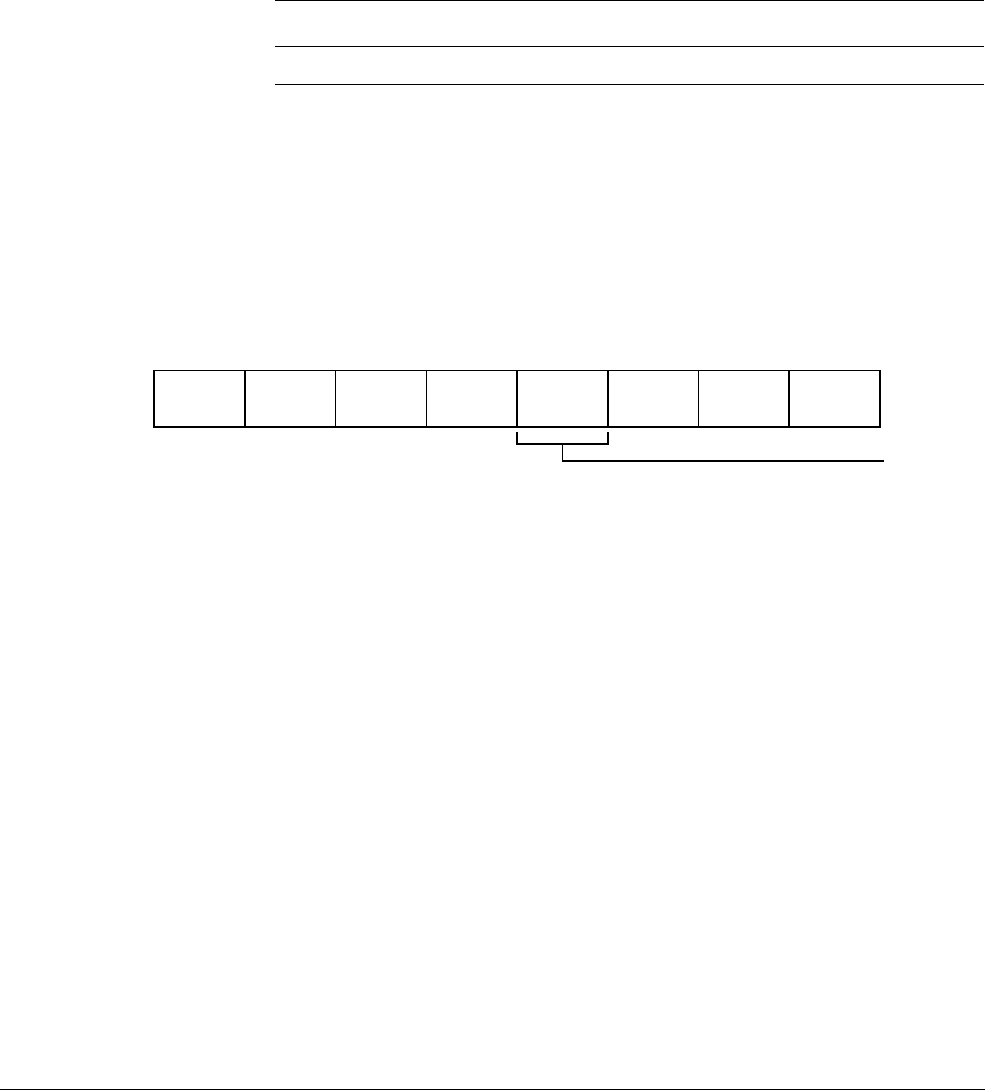
D8 AArch64 System Register Descriptions
D8.2 General system control registers
ARM DDI 0487A.a Copyright © 2013 ARM Limited. All rights reserved. D8-1981
ID090413 Non-Confidential - Beta
D8.2.58 ID_PFR1_EL1, AArch32 Processor Feature Register 1
The ID_PFR1_EL1 characteristics are:
Purpose
Gives information about the programmers' model and extensions support in AArch32.
This register is part of the Identification registers functional group.
Usage constraints
This register is accessible as shown below:
Configurations
ID_PFR1_EL1 is architecturally mapped to AArch32 register ID_PFR1.
In an AArch64-only implementation, this register is RES0.
Attributes
ID_PFR1_EL1 is a 32-bit register.
The ID_PFR1_EL1 bit assignments are:
GIC, bits [31:28]
GIC CP15 interface. Permitted values are:
0000
No GIC CP15 registers are supported.
0001
GICv3 CP15 registers are supported.
All other values are reserved.
Virt_frac, bits [27:24]
Virtualization fractional field. When the Virtualization field is
0b0000
, determines the support for
features from the ARMv7 Virtualization Extensions. Permitted values are:
0000
No features from the ARMv7 Virtualization Extensions are implemented.
0001
The SCR.SIF bit is implemented. The modifications to the SCR.AW and SCR.FW bits
are part of the control of whether the CPSR.A and CPSR.F bits mask the corresponding
aborts. The MSR (Banked register) and MRS (Banked register) instructions are
implemented.
This value is permitted only when ID_PFR1.Security is not
0b0000
.
All other values are reserved.
This field is only valid when ID_PFR1_EL1[15:12] == 0, otherwise it holds the value
0b0000
.
Sec_frac, bits [23:20]
Security fractional field. When the Security field is
0b0000
, determines the support for features from
the ARMv7 Security Extensions. Permitted values are:
0000
No features from the ARMv7 Security Extensions are implemented.
EL0 EL1 (NS) EL1 (S) EL2 EL3 (SCR.NS=1) EL3 (SCR.NS=0)
-RO RO RORO RO
GIC
31 28
Virt_frac
27 24
Sec_frac
23 20
GenTimer
19 16 15 12
MProgMod
11 8
Security
74
ProgMod
30
Virtualization

D8 AArch64 System Register Descriptions
D8.2 General system control registers
D8-1982 Copyright © 2013 ARM Limited. All rights reserved. ARM DDI 0487A.a
Non-Confidential - Beta ID090413
0001
The implementation includes the VBAR, and the TCR.PD0 and TCR.PD1 bits.
0010
As for
0b0001
, plus the ability to access Secure or Non-secure physical memory is
supported.
All other values are reserved.
This field is only valid when ID_PFR1_EL1[7:4] == 0, otherwise it holds the value
0b0000
.
GenTimer, bits [19:16]
Generic Timer Extension support. Permitted values are:
0000
Not implemented.
0001
Generic Timer Extension implemented.
All other values are reserved.
Virtualization, bits [15:12]
Virtualization support. Permitted values are:
0000
EL2 not implemented.
0001
EL2 implemented.
All other values are reserved.
A value of
0b0001
implies implementation of the HVC, ERET, MRS (banked register), and MSR
(banked register) instructions. The ID_ISARs do not identify whether these instructions are
implemented.
MProgMod, bits [11:8]
M profile programmers' model support. Permitted values are:
0000
Not supported.
0010
Support for two-stack programmers' model.
All other values are reserved.
Security, bits [7:4]
Security support. Permitted values are:
0000
EL3 not implemented.
0001
EL3 implemented.
This includes support for Monitor mode and the SMC instruction.
0010
As for
0b0001
, and adds the ability to set the NSACR.RFR bit. Not permitted in v8-A as
the NSACR.RFR bit is RES0.
All other values are reserved.
ProgMod, bits [3:0]
Support for the standard programmers' model for ARMv4 and later. Model must support User, FIQ,
IRQ, Supervisor, Abort, Undefined, and System modes. Permitted values are:
0000
Not supported.
0001
Supported.
All other values are reserved.
Accessing the ID_PFR1_EL1:
To access the ID_PFR1_EL1:
MRS <Xt>, ID_PFR1_EL1 ; Read ID_PFR1_EL1 into Xt

D8 AArch64 System Register Descriptions
D8.2 General system control registers
ARM DDI 0487A.a Copyright © 2013 ARM Limited. All rights reserved. D8-1983
ID090413 Non-Confidential - Beta
Register access is encoded as follows:
op0 op1 CRn CRm op2
11 000 0000 0001 001
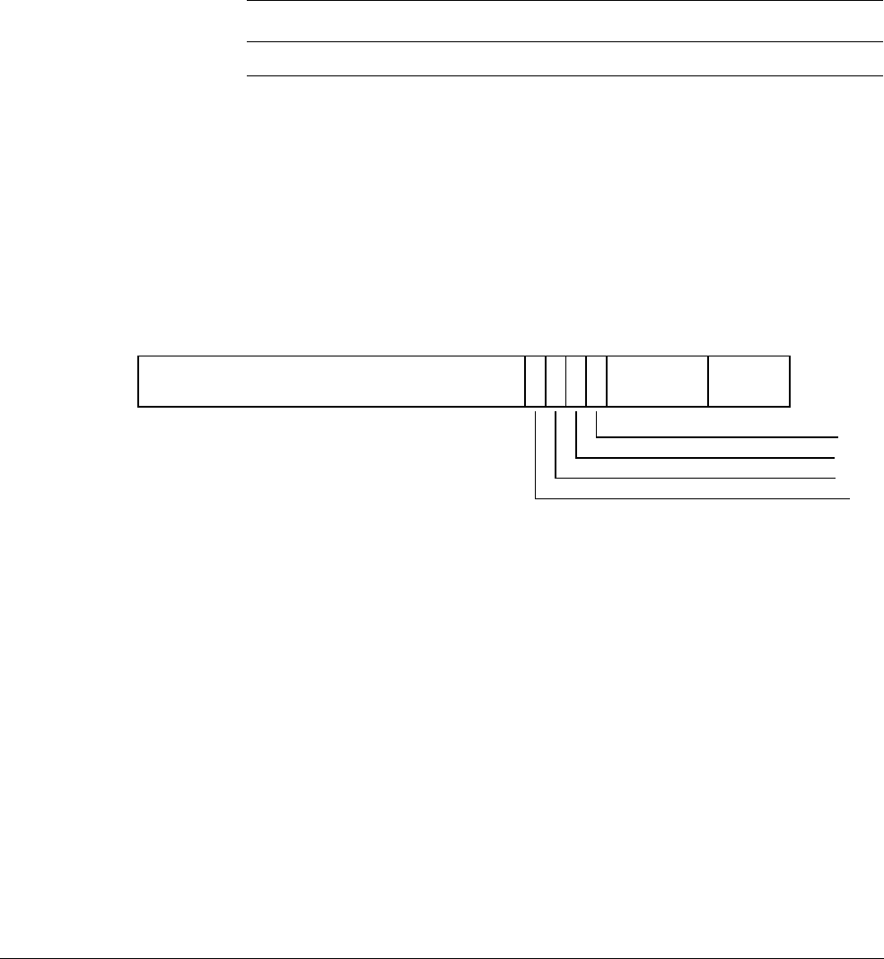
D8 AArch64 System Register Descriptions
D8.2 General system control registers
D8-1984 Copyright © 2013 ARM Limited. All rights reserved. ARM DDI 0487A.a
Non-Confidential - Beta ID090413
D8.2.59 IFSR32_EL2, Instruction Fault Status Register (EL2)
The IFSR32_EL2 characteristics are:
Purpose
Allows access to the AArch32 IFSR register from AArch64 state only. Its value has no effect on
execution in AArch64 state.
This register is part of the Exception and fault handling registers functional group.
Usage constraints
This register is accessible as shown below:
Configurations
IFSR32_EL2 is architecturally mapped to AArch32 register IFSR (NS).
Attributes
IFSR32_EL2 is a 32-bit register.
The IFSR32_EL2 bit assignments are:
When TTBCR.EAE==0:
Bits [31:13]
Reserved, RES0.
ExT, bit [12]
External abort type. This bit can be used to provide an IMPLEMENTATION DEFINED classification of
external aborts.
For aborts other than external aborts this bit always returns 0.
Bit [11]
Reserved, RES0.
FS[4], bit [10]
See below for description of the FS field.
LPAE, bit [9]
On taking a Data Abort exception, this bit is set as follows:
0
Using the Short-descriptor translation table formats.
1
Using the Long-descriptor translation table formats.
EL0 EL1 (NS) EL1 (S) EL2 EL3 (SCR.NS=1) EL3 (SCR.NS=0)
-- - RWRW RW
RES0
31 13 12 11 10 9
RES0
84
FS[3:0]
30
LPAE
FS[4]
RES0
ExT
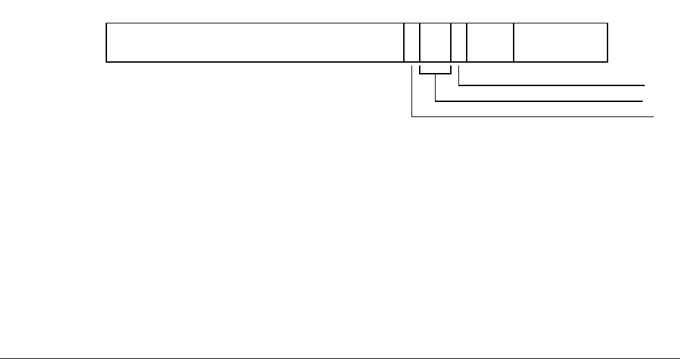
D8 AArch64 System Register Descriptions
D8.2 General system control registers
ARM DDI 0487A.a Copyright © 2013 ARM Limited. All rights reserved. D8-1985
ID090413 Non-Confidential - Beta
Hardware does not interpret this bit to determine the behavior of the memory system, and therefore
software can set this bit to 0 or 1 without affecting operation.
Bits [8:4]
Reserved, RES0.
FS[3:0], bits [3:0]
Fault status bits. Possible values of this field are:
0010
Debug event
0011
Access flag fault, first level
0101
Translation fault, first level
0110
Access flag fault, second level
0111
Translation fault, second level
1000
Synchronous external abort
1001
Domain fault, first level
1011
Domain fault, second level
1100
Synchronous external abort on translation table walk, first level
1101
Permission fault, first level
1110
Synchronous external abort on translation table walk, second level
1111
Permission fault, second level
10000
TLB conflict abort
10100
IMPLEMENTATION DEFINED fault (Lockdown fault)
11001
Synchronous parity error on memory access
11100
Synchronous parity error on translation table walk, first level
11110
Synchronous parity error on translation table walk, second level
All other values are reserved.
When TTBCR.EAE==1:
Bits [31:13]
Reserved, RES0.
ExT, bit [12]
External abort type. This bit can be used to provide an IMPLEMENTATION DEFINED classification of
external aborts.
For aborts other than external aborts this bit always returns 0.
Bits [11:10]
Reserved, RES0.
RES0
31 13 12 11 10 9
RES0
86
STATUS
50
LPAE
RES0
ExT

D8 AArch64 System Register Descriptions
D8.2 General system control registers
D8-1986 Copyright © 2013 ARM Limited. All rights reserved. ARM DDI 0487A.a
Non-Confidential - Beta ID090413
LPAE, bit [9]
On taking a Data Abort exception, this bit is set as follows:
0
Using the Short-descriptor translation table formats.
1
Using the Long-descriptor translation table formats.
Hardware does not interpret this bit to determine the behavior of the memory system, and therefore
software can set this bit to 0 or 1 without affecting operation.
Bits [8:6]
Reserved, RES0.
STATUS, bits [5:0]
Fault status bits. All encodings not shown below are reserved:
000000
Address size fault in TTBR0 or TTBR1
000101
Translation fault, first level
000110
Translation fault, second level
000111
Translation fault, third level
001001
Access flag fault, first level
001010
Access flag fault, second level
001011
Access flag fault, third level
001101
Permission fault, first level
001110
Permission fault, second level
001111
Permission fault, third level
010000
Synchronous external abort
010101
Synchronous external abort on translation table walk, first level
010110
Synchronous external abort on translation table walk, second level
010111
Synchronous external abort on translation table walk, third level
011000
Synchronous parity error on memory access
011101
Synchronous parity error on memory access on translation table walk, first level
011110
Synchronous parity error on memory access on translation table walk, second level
011111
Synchronous parity error on memory access on translation table walk, third level
100001
Alignment fault
100010
Debug event
110000
TLB conflict abort
110100
IMPLEMENTATION DEFINED fault (Lockdown fault)
All other values are reserved.
The lookup level associated with a fault is:
• For a fault generated on a translation table walk, the lookup level of the walk being
performed.
• For a Translation fault, the lookup level of the translation table that gave the fault. If a fault
occurs because an MMU is disabled, or because the input address is outside the range
specified by the appropriate base address register or registers, the fault is reported as a First
level fault.
• For an Access flag fault, the lookup level of the translation table that gave the fault.
• For a Permission fault, including a Permission fault caused by hierarchical permissions, the
lookup level of the final level of translation table accessed for the translation. That is, the
lookup level of the translation table that returned a Block or Page descriptor.

D8 AArch64 System Register Descriptions
D8.2 General system control registers
ARM DDI 0487A.a Copyright © 2013 ARM Limited. All rights reserved. D8-1987
ID090413 Non-Confidential - Beta
Accessing the IFSR32_EL2:
To access the IFSR32_EL2:
MRS <Xt>, IFSR32_EL2 ; Read IFSR32_EL2 into Xt
MSR IFSR32_EL2, <Xt> ; Write Xt to IFSR32_EL2
Register access is encoded as follows:
op0 op1 CRn CRm op2
11 100 0101 0000 001
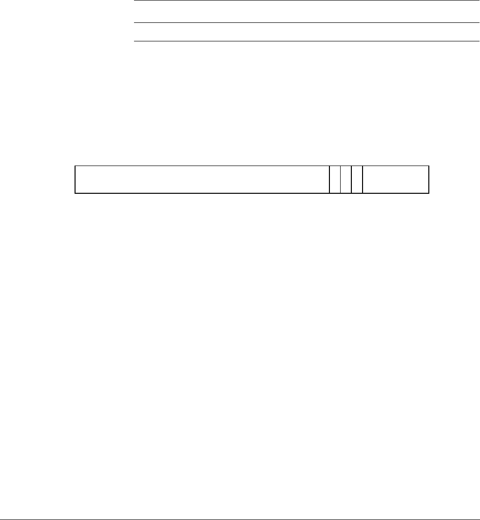
D8 AArch64 System Register Descriptions
D8.2 General system control registers
D8-1988 Copyright © 2013 ARM Limited. All rights reserved. ARM DDI 0487A.a
Non-Confidential - Beta ID090413
D8.2.60 ISR_EL1, Interrupt Status Register
The ISR_EL1 characteristics are:
Purpose
Shows whether an IRQ, FIQ, or SError interrupt is pending. If EL2 is implemented, an indicated
pending interrupt might be a physical interrupt or a virtual interrupt.
This register is part of the Exception and fault handling registers functional group.
Usage constraints
This register is accessible as shown below:
Configurations
ISR_EL1 is architecturally mapped to AArch32 register ISR.
Attributes
ISR_EL1 is a 32-bit register.
The ISR_EL1 bit assignments are:
Bits [31:9]
Reserved, RES0.
A, bit [8]
SError pending bit:
0
No pending SError.
1
An SError interrupt is pending.
I, bit [7]
IRQ pending bit. Indicates whether an IRQ interrupt is pending:
0
No pending IRQ.
1
An IRQ interrupt is pending.
F, bit [6]
FIQ pending bit. Indicates whether an FIQ interrupt is pending.
0
No pending FIQ.
1
An FIQ interrupt is pending.
Bits [5:0]
Reserved, RES0.
Accessing the ISR_EL1:
To access the ISR_EL1:
EL0 EL1 (NS) EL1 (S) EL2 EL3 (SCR.NS=1) EL3 (SCR.NS=0)
-RO RO RORO RO
RES0
31 9
A
8
I
7
F
6
RES0
50

D8 AArch64 System Register Descriptions
D8.2 General system control registers
ARM DDI 0487A.a Copyright © 2013 ARM Limited. All rights reserved. D8-1989
ID090413 Non-Confidential - Beta
MRS <Xt>, ISR_EL1 ; Read ISR_EL1 into Xt
Register access is encoded as follows:
op0 op1 CRn CRm op2
11 000 1100 0001 000
D8 AArch64 System Register Descriptions
D8.2 General system control registers
D8-1990 Copyright © 2013 ARM Limited. All rights reserved. ARM DDI 0487A.a
Non-Confidential - Beta ID090413
D8.2.61 MAIR_EL1, Memory Attribute Indirection Register (EL1)
The MAIR_EL1 characteristics are:
Purpose
Provides the memory attribute encodings corresponding to the possible AttrIndx values in a
Long-descriptor format translation table entry for stage 1 translations at EL1.
This register is part of the Virtual memory control registers functional group.
Usage constraints
This register is accessible as shown below:
MAIR_EL1 is permitted to be cached in a TLB.
Configurations
MAIR_EL1[31:0] is architecturally mapped to AArch32 register PRRR (NS) when
TTBCR.EAE==0.
MAIR_EL1[31:0] is architecturally mapped to AArch32 register MAIR0 (NS) when
TTBCR.EAE==1.
MAIR_EL1[63:32] is architecturally mapped to AArch32 register NMRR (NS) when
TTBCR.EAE==0.
MAIR_EL1[63:32] is architecturally mapped to AArch32 register MAIR1 (NS) when
TTBCR.EAE==1.
Attributes
MAIR_EL1 is a 64-bit register.
The MAIR_EL1 bit assignments are:
Attr<n>, bits [8n+7:8n], for n = 0 to 7
The memory attribute encoding for an AttrIndx[2:0] entry in a Long descriptor format translation
table entry, where AttrIndx[2:0] gives the value of <n> in Attr<n>.
Bits [7:4] are encoded as follows:
EL0 EL1 (NS) EL1 (S) EL2 EL3 (SCR.NS=1) EL3 (SCR.NS=0)
-RW RW RWRW RW
Attr7
63 56
Attr6
55 48
Attr5
47 40
Attr4
39 32
Attr3
31 24
Attr2
23 16
Attr1
15 8
Attr0
70
Attr<n>[7:4] Meaning
0000
Device memory. See encoding of Attr<n>[3:0] for the type of Device memory.
00RW
, RW not
00
Normal Memory, Outer Write-through transient
0100
Normal Memory, Outer Non-Cacheable
01RW
, RW not
00
Normal Memory, Outer Write-back transient
10RW
Normal Memory, Outer Write-through non-transient
11RW
Normal Memory, Outer Write-back non-transient

D8 AArch64 System Register Descriptions
D8.2 General system control registers
ARM DDI 0487A.a Copyright © 2013 ARM Limited. All rights reserved. D8-1991
ID090413 Non-Confidential - Beta
R = Outer Read Allocate Policy, W = Outer Write Allocate Policy.
The meaning of bits [3:0] depends on the value of bits [7:4]:
R = Inner Read Allocate Policy, W = Inner Write Allocate Policy.
ARMv7's Strongly-ordered and Device memory types have been renamed to Device-nGnRnE and
Device-nGnRE in ARMv8.
The R and W bits in some Attr<n> fields have the following meanings:
Accessing the MAIR_EL1:
To access the MAIR_EL1:
MRS <Xt>, MAIR_EL1 ; Read MAIR_EL1 into Xt
MSR MAIR_EL1, <Xt> ; Write Xt to MAIR_EL1
Register access is encoded as follows:
Attr<n>[3:0] Meaning when Attr<n>[7:4] is
0000 Meaning when Attr<n>[7:4] is not 0000
0000
Device-nGnRnE memory UNPREDICTABLE
00RW
, RW not
00
UNPREDICTABLE Normal Memory, Inner Write-through transient
0100
Device-nGnRE memory Normal memory, Inner Non-Cacheable
01RW
, RW not
00
UNPREDICTABLE Normal Memory, Inner Write-back transient
1000
Device-nGRE memory Normal Memory, Inner Write-through
non-transient (RW=00)
10RW
, RW not
00
UNPREDICTABLE Normal Memory, Inner Write-through
non-transient
1100
Device-GRE memory Normal Memory, Inner Write-back non-transient
(RW=00)
11RW
, RW not
00
UNPREDICTABLE Normal Memory, Inner Write-back non-transient
R or W Meaning
0
Do not allocate
1
Allocate
op0 op1 CRn CRm op2
11 000 1010 0010 000
D8 AArch64 System Register Descriptions
D8.2 General system control registers
D8-1992 Copyright © 2013 ARM Limited. All rights reserved. ARM DDI 0487A.a
Non-Confidential - Beta ID090413
D8.2.62 MAIR_EL2, Memory Attribute Indirection Register (EL2)
The MAIR_EL2 characteristics are:
Purpose
Provides the memory attribute encodings corresponding to the possible AttrIndx values in a
Long-descriptor format translation table entry for stage 1 translations at EL2.
This register is part of:
• the Virtualization registers functional group
• the Virtual memory control registers functional group.
Usage constraints
This register is accessible as shown below:
MAIR_EL2 is permitted to be cached in a TLB.
Configurations
MAIR_EL2[31:0] is architecturally mapped to AArch32 register HMAIR0.
MAIR_EL2[63:32] is architecturally mapped to AArch32 register HMAIR1.
If EL2 is not implemented, this register is RES0 from EL3.
Attributes
MAIR_EL2 is a 64-bit register.
The MAIR_EL2 bit assignments are:
Attr<n>, bits [8n+7:8n], for n = 0 to 7
The memory attribute encoding for an AttrIndx[2:0] entry in a Long descriptor format translation
table entry, where AttrIndx[2:0] gives the value of <n> in Attr<n>.
Bits [7:4] are encoded as follows:
R = Outer Read Allocate Policy, W = Outer Write Allocate Policy.
EL0 EL1 (NS) EL1 (S) EL2 EL3 (SCR.NS=1) EL3 (SCR.NS=0)
-- - RWRW RW
Attr7
63 56
Attr6
55 48
Attr5
47 40
Attr4
39 32
Attr3
31 24
Attr2
23 16
Attr1
15 8
Attr0
70
Attr<n>[7:4] Meaning
0000
Device memory. See encoding of Attr<n>[3:0] for the type of Device memory.
00RW
, RW not
00
Normal Memory, Outer Write-through transient
0100
Normal Memory, Outer Non-Cacheable
01RW
, RW not
00
Normal Memory, Outer Write-back transient
10RW
Normal Memory, Outer Write-through non-transient
11RW
Normal Memory, Outer Write-back non-transient

D8 AArch64 System Register Descriptions
D8.2 General system control registers
ARM DDI 0487A.a Copyright © 2013 ARM Limited. All rights reserved. D8-1993
ID090413 Non-Confidential - Beta
The meaning of bits [3:0] depends on the value of bits [7:4]:
R = Inner Read Allocate Policy, W = Inner Write Allocate Policy.
ARMv7's Strongly-ordered and Device memory types have been renamed to Device-nGnRnE and
Device-nGnRE in ARMv8.
The R and W bits in some Attr<n> fields have the following meanings:
Accessing the MAIR_EL2:
To access the MAIR_EL2:
MRS <Xt>, MAIR_EL2 ; Read MAIR_EL2 into Xt
MSR MAIR_EL2, <Xt> ; Write Xt to MAIR_EL2
Register access is encoded as follows:
Attr<n>[3:0] Meaning when Attr<n>[7:4] is
0000 Meaning when Attr<n>[7:4] is not 0000
0000
Device-nGnRnE memory UNPREDICTABLE
00RW
, RW not
00
UNPREDICTABLE Normal Memory, Inner Write-through transient
0100
Device-nGnRE memory Normal memory, Inner Non-Cacheable
01RW
, RW not
00
UNPREDICTABLE Normal Memory, Inner Write-back transient
1000
Device-nGRE memory Normal Memory, Inner Write-through
non-transient (RW=00)
10RW
, RW not
00
UNPREDICTABLE Normal Memory, Inner Write-through
non-transient
1100
Device-GRE memory Normal Memory, Inner Write-back non-transient
(RW=00)
11RW
, RW not
00
UNPREDICTABLE Normal Memory, Inner Write-back non-transient
R or W Meaning
0
Do not allocate
1
Allocate
op0 op1 CRn CRm op2
11 100 1010 0010 000

D8 AArch64 System Register Descriptions
D8.2 General system control registers
D8-1994 Copyright © 2013 ARM Limited. All rights reserved. ARM DDI 0487A.a
Non-Confidential - Beta ID090413
D8.2.63 MAIR_EL3, Memory Attribute Indirection Register (EL3)
The MAIR_EL3 characteristics are:
Purpose
Provides the memory attribute encodings corresponding to the possible AttrIndx values in a
Long-descriptor format translation table entry for stage 1 translations at EL3.
This register is part of the Virtual memory control registers functional group.
Usage constraints
This register is accessible as shown below:
MAIR_EL3 is permitted to be cached in a TLB.
Configurations
MAIR_EL3[31:0] can be mapped to AArch32 register PRRR (S) when TTBCR.EAE==0, but this
is not architecturally mandated.
MAIR_EL3[31:0] can be mapped to AArch32 register MAIR0 (S) when TTBCR.EAE==1, but this
is not architecturally mandated.
MAIR_EL3[63:32] can be mapped to AArch32 register NMRR (S) when TTBCR.EAE==0, but this
is not architecturally mandated.
MAIR_EL3[63:32] can be mapped to AArch32 register MAIR1 (S) when TTBCR.EAE==1, but
this is not architecturally mandated.
Attributes
MAIR_EL3 is a 64-bit register.
The MAIR_EL3 bit assignments are:
Attr<n>, bits [8n+7:8n], for n = 0 to 7
The memory attribute encoding for an AttrIndx[2:0] entry in a Long descriptor format translation
table entry, where AttrIndx[2:0] gives the value of <n> in Attr<n>.
Bits [7:4] are encoded as follows:
EL0 EL1 (NS) EL1 (S) EL2 EL3 (SCR.NS=1) EL3 (SCR.NS=0)
-- - -RW RW
Attr7
63 56
Attr6
55 48
Attr5
47 40
Attr4
39 32
Attr3
31 24
Attr2
23 16
Attr1
15 8
Attr0
70
Attr<n>[7:4] Meaning
0000
Device memory. See encoding of Attr<n>[3:0] for the type of Device memory.
00RW
, RW not
00
Normal Memory, Outer Write-through transient
0100
Normal Memory, Outer Non-Cacheable
01RW
, RW not
00
Normal Memory, Outer Write-back transient
10RW
Normal Memory, Outer Write-through non-transient
11RW
Normal Memory, Outer Write-back non-transient

D8 AArch64 System Register Descriptions
D8.2 General system control registers
ARM DDI 0487A.a Copyright © 2013 ARM Limited. All rights reserved. D8-1995
ID090413 Non-Confidential - Beta
R = Outer Read Allocate Policy, W = Outer Write Allocate Policy.
The meaning of bits [3:0] depends on the value of bits [7:4]:
R = Inner Read Allocate Policy, W = Inner Write Allocate Policy.
ARMv7's Strongly-ordered and Device memory types have been renamed to Device-nGnRnE and
Device-nGnRE in ARMv8.
The R and W bits in some Attr<n> fields have the following meanings:
Accessing the MAIR_EL3:
To access the MAIR_EL3:
MRS <Xt>, MAIR_EL3 ; Read MAIR_EL3 into Xt
MSR MAIR_EL3, <Xt> ; Write Xt to MAIR_EL3
Register access is encoded as follows:
Attr<n>[3:0] Meaning when Attr<n>[7:4] is
0000 Meaning when Attr<n>[7:4] is not 0000
0000
Device-nGnRnE memory UNPREDICTABLE
00RW
, RW not
00
UNPREDICTABLE Normal Memory, Inner Write-through transient
0100
Device-nGnRE memory Normal memory, Inner Non-Cacheable
01RW
, RW not
00
UNPREDICTABLE Normal Memory, Inner Write-back transient
1000
Device-nGRE memory Normal Memory, Inner Write-through
non-transient (RW=00)
10RW
, RW not
00
UNPREDICTABLE Normal Memory, Inner Write-through
non-transient
1100
Device-GRE memory Normal Memory, Inner Write-back non-transient
(RW=00)
11RW
, RW not
00
UNPREDICTABLE Normal Memory, Inner Write-back non-transient
R or W Meaning
0
Do not allocate
1
Allocate
op0 op1 CRn CRm op2
11 110 1010 0010 000

D8 AArch64 System Register Descriptions
D8.2 General system control registers
D8-1996 Copyright © 2013 ARM Limited. All rights reserved. ARM DDI 0487A.a
Non-Confidential - Beta ID090413
D8.2.64 MIDR_EL1, Main ID Register
The MIDR_EL1 characteristics are:
Purpose
Provides identification information for the processor, including an implementer code for the device
and a device ID number.
This register is part of the Identification registers functional group.
Usage constraints
This register is accessible as shown below:
Configurations
MIDR_EL1 is architecturally mapped to AArch32 register MIDR.
MIDR_EL1 is architecturally mapped to external register MIDR_EL1.
Attributes
MIDR_EL1 is a 32-bit register.
The MIDR_EL1 bit assignments are:
Implementer, bits [31:24]
The Implementer code. This field must hold an implementer code that has been assigned by ARM.
Assigned codes include the following:
EL0 EL1 (NS) EL1 (S) EL2 EL3 (SCR.NS=1) EL3 (SCR.NS=0)
-RO RO RORO RO
Implementer
31 24
Variant
23 20 19 16
PartNum
15 4
Revision
30
Architecture
Hex
representation ASCII
representation Implementer
0x41
A ARM Limited
0x42
B Broadcom Corporation
0x43
C Cavium Inc.
0x44
D Digital Equipment Corporation
0x49
I Infineon Technologies AG
0x4D
M Motorola or Freescale Semiconductor Inc.
0x4E
N NVIDIA Corporation
0x50
P Applied Micro Circuits Corporation

D8 AArch64 System Register Descriptions
D8.2 General system control registers
ARM DDI 0487A.a Copyright © 2013 ARM Limited. All rights reserved. D8-1997
ID090413 Non-Confidential - Beta
ARM can assign codes that are not published in this manual. All values not assigned by ARM are
reserved and must not be used.
Variant, bits [23:20]
An IMPLEMENTATION DEFINED variant number. Typically, this field is used to distinguish between
different product variants, or major revisions of a product.
Architecture, bits [19:16]
The permitted values of this field are:
0001
ARMv4
0010
ARMv4T
0011
ARMv5 (obsolete)
0100
ARMv5T
0101
ARMv5TE
0110
ARMv5TEJ
0111
ARMv6
1111
Defined by CPUID scheme
All other values are reserved.
PartNum, bits [15:4]
An IMPLEMENTATION DEFINED primary part number for the device.
On processors implemented by ARM, if the top four bits of the primary part number are
0x0
or
0x7
,
the variant and architecture are encoded differently.
Revision, bits [3:0]
An IMPLEMENTATION DEFINED revision number for the device.
Accessing the MIDR_EL1:
To access the MIDR_EL1:
MRS <Xt>, MIDR_EL1 ; Read MIDR_EL1 into Xt
Register access is encoded as follows:
0x51
Q Qualcomm Inc.
0x56
V Marvell International Ltd.
0x69
i Intel Corporation
op0 op1 CRn CRm op2
11 000 0000 0000 000
Hex
representation ASCII
representation Implementer
D8 AArch64 System Register Descriptions
D8.2 General system control registers
D8-1998 Copyright © 2013 ARM Limited. All rights reserved. ARM DDI 0487A.a
Non-Confidential - Beta ID090413
D8.2.65 MPIDR_EL1, Multiprocessor Affinity Register
The MPIDR_EL1 characteristics are:
Purpose
In a multiprocessor system, provides an additional processor identification mechanism for
scheduling purposes, and indicates whether the implementation includes the Multiprocessing
Extensions.
This register is part of the Identification registers functional group.
Usage constraints
This register is accessible as shown below:
Configurations
MPIDR_EL1 is architecturally mapped to AArch32 register MPIDR.
Attributes
MPIDR_EL1 is a 64-bit register.
The MPIDR_EL1 bit assignments are:
Bits [63:40]
Reserved, RES0.
Aff3, bits [39:32]
Affinity level 3. Highest level affinity field.
Bit [31]
Reserved, RES1.
U, bit [30]
Indicates a Uniprocessor system, as distinct from processor 0 in a multiprocessor system. The
possible values of this bit are:
0
Processor is part of a multiprocessor system.
1
Processor is part of a uniprocessor system.
Bits [29:25]
Reserved, RES0.
MT, bit [24]
Indicates whether the lowest level of affinity consists of logical processors that are implemented
using a multi-threading type approach. The possible values of this bit are:
0
Performance of processors at the lowest affinity level is largely independent.
1
Performance of processors at the lowest affinity level is very interdependent.
EL0 EL1 (NS) EL1 (S) EL2 EL3 (SCR.NS=1) EL3 (SCR.NS=0)
-RO RO RORO RO
RES0
63 40
Aff3
39 32 31
U
30
RES0
29 25 24
Aff2
23 16
Aff1
15 8
Aff0
70
RES1 MT

D8 AArch64 System Register Descriptions
D8.2 General system control registers
ARM DDI 0487A.a Copyright © 2013 ARM Limited. All rights reserved. D8-1999
ID090413 Non-Confidential - Beta
Aff2, bits [23:16]
Affinity level 2. Second highest level affinity field.
Aff1, bits [15:8]
Affinity level 1. Third highest level affinity field.
Aff0, bits [7:0]
Affinity level 0. Lowest level affinity field.
Accessing the MPIDR_EL1:
To access the MPIDR_EL1:
MRS <Xt>, MPIDR_EL1 ; Read MPIDR_EL1 into Xt
Register access is encoded as follows:
op0 op1 CRn CRm op2
11 000 0000 0000 101

D8 AArch64 System Register Descriptions
D8.2 General system control registers
D8-2000 Copyright © 2013 ARM Limited. All rights reserved. ARM DDI 0487A.a
Non-Confidential - Beta ID090413
D8.2.66 MVFR0_EL1, Media and VFP Feature Register 0
The MVFR0_EL1 characteristics are:
Purpose
Describes the features provided by the Advanced SIMD and Floating-point extensions.
This register is part of:
• the Floating-point registers functional group
• the Identification registers functional group.
Usage constraints
This register is accessible as shown below:
Configurations
MVFR0_EL1 is architecturally mapped to AArch32 register MVFR0.
Attributes
MVFR0_EL1 is a 32-bit register.
The MVFR0_EL1 bit assignments are:
FPRound, bits [31:28]
Floating-Point Rounding modes. Indicates the rounding modes supported by the VFP floating-point
hardware. Permitted values are:
0000
Only Round to Nearest mode supported, except that Round towards Zero mode is
supported for VCVT instructions that always use that rounding mode regardless of the
FPSCR setting.
0001
All rounding modes supported.
All other values are reserved.
FPShVec, bits [27:24]
Short Vectors. Indicates the hardware support for VFP short vectors. Permitted values are:
0000
Not supported.
0001
Short vector operation supported.
All other values are reserved.
FPSqrt, bits [23:20]
Square Root. Indicates the hardware support for VFP square root operations. Permitted values are:
0000
Not supported in hardware.
0001
Supported.
All other values are reserved.
The VSQRT.F32 instruction also requires the single-precision VFP attribute, and the VSQRT.F64
instruction also requires the double-precision VFP attribute.
EL0 EL1 (NS) EL1 (S) EL2 EL3 (SCR.NS=1) EL3 (SCR.NS=0)
-RO RO RORO RO
FPRound
31 28
FPShVec
27 24
FPSqrt
23 20
FPDivide
19 16
FPTrap
15 12
FPDP
11 8
FPSP
74
SIMDReg
30

D8 AArch64 System Register Descriptions
D8.2 General system control registers
ARM DDI 0487A.a Copyright © 2013 ARM Limited. All rights reserved. D8-2001
ID090413 Non-Confidential - Beta
FPDivide, bits [19:16]
Indicates the hardware support for VFP divide operations. Permitted values are:
0000
Not supported in hardware.
0001
Supported.
All other values are reserved.
The VDIV.F32 instruction also requires the single-precision VFP attribute, and the VDIV.F64
instruction also requires the double-precision VFP attribute.
FPTrap, bits [15:12]
Floating Point Exception Trapping. Indicates whether the VFP hardware implementation supports
exception trapping. Permitted values are:
0000
Not supported. This is the value for VFPv3 and VFPv4.
0001
Supported by the hardware. This is the value for VFPv3U, VFP4U, and for VFPv2.
When exception trapping is supported, support code is needed to handle the trapped
exceptions.
All other values are reserved.
A value of
0b0001
does not indicate that trapped exception handling is available. Because trapped
exception handling requires support code, only the support code can provide this information.
FPDP, bits [11:8]
Double Precision. Indicates the hardware support for VFP double-precision operations. Permitted
values are:
0000
Not supported in hardware.
0001
Supported, VFPv2.
0010
Supported, VFPv3 or VFPv4. VFPv3 adds an instruction to load a double-precision
floating-point constant, and conversions between double-precision and fixed-point
values.
All other values are reserved.
A value of
0b0001
or
0b0010
indicates support for all VFP double-precision instructions in the
supported version of VFP, except that, in addition to this field being nonzero:
• VSQRT.F64 is only available if the Square root field is
0b0001
.
• VDIV.F64 is only available if the Divide field is
0b0001
.
• Conversion between double-precision and single-precision is only available if the
single-precision field is nonzero.
FPSP, bits [7:4]
Single Precision. Indicates the hardware support for VFP single-precision operations. Permitted
values are:
0000
Not supported in hardware.
0001
Supported, VFPv2.
0010
Supported, VFPv3 or VFPv4. VFPv3 adds an instruction to load a single-precision
floating-point constant, and conversions between single-precision and fixed-point
values.
All other values are reserved.
A value of
0b0001
or
0b0010
indicates support for all VFP single-precision instructions in the
supported version of VFP, except that, in addition to this field being nonzero:
• VSQRT.F32 is only available if the Square root field is
0b0001
.
• VDIV.F32 is only available if the Divide field is
0b0001
.
• Conversion between double-precision and single-precision is only available if the
double-precision field is nonzero.

D8 AArch64 System Register Descriptions
D8.2 General system control registers
D8-2002 Copyright © 2013 ARM Limited. All rights reserved. ARM DDI 0487A.a
Non-Confidential - Beta ID090413
SIMDReg, bits [3:0]
Advanced SIMD registers. Indicates support for the Advanced SIMD register bank. Permitted
values are:
0000
Not supported.
0001
Supported, 16 x 64-bit registers.
0010
Supported, 32 x 64-bit registers.
All other values are reserved.
If this field is nonzero:
• All VFP LDC, STC, MCR, and MRC instructions are supported.
• If the CPUID registers show that the MCRR and MRRC instructions are supported then the
corresponding VFP instructions are supported.
Accessing the MVFR0_EL1:
To access the MVFR0_EL1:
MRS <Xt>, MVFR0_EL1 ; Read MVFR0_EL1 into Xt
Register access is encoded as follows:
op0 op1 CRn CRm op2
11 000 0000 0011 000
D8 AArch64 System Register Descriptions
D8.2 General system control registers
ARM DDI 0487A.a Copyright © 2013 ARM Limited. All rights reserved. D8-2003
ID090413 Non-Confidential - Beta
D8.2.67 MVFR1_EL1, Media and VFP Feature Register 1
The MVFR1_EL1 characteristics are:
Purpose
Describes the features provided by the Advanced SIMD and Floating-point extensions.
This register is part of:
• the Floating-point registers functional group
• the Identification registers functional group.
Usage constraints
This register is accessible as shown below:
Configurations
MVFR1_EL1 is architecturally mapped to AArch32 register MVFR1.
Attributes
MVFR1_EL1 is a 32-bit register.
The MVFR1_EL1 bit assignments are:
SIMDFMAC, bits [31:28]
Advanced SIMD Fused Multiply-Accumulate. Indicates whether any implemented VFP or
Advanced SIMD extension implements the fused multiply accumulate instructions. Permitted
values are:
0000
Not implemented.
0001
Implemented.
All other values are reserved.
If an implementation includes both the VFP extension and the Advanced SIMD extension, both
extensions must provide the same level of support for these instructions.
FPHP, bits [27:24]
Floating Point Half Precision. Indicates whether the VFP extension implements half-precision
floating-point conversion instructions. Permitted values are:
0000
Not implemented.
0001
Instructions to convert between half-precision and single-precision implemented.
0010
As for
0b0001
, and also instructions to convert between half-precision and
double-precision implemented.
All other values are reserved.
EL0 EL1 (NS) EL1 (S) EL2 EL3 (SCR.NS=1) EL3 (SCR.NS=0)
-RO RO RORO RO
31 28
FPHP
27 24
SIMDHP
23 20
SIMDSP
19 16
SIMDInt
15 12
SIMDLS
11 8
FPDNaN
74
FPFtZ
30
SIMDFMAC

D8 AArch64 System Register Descriptions
D8.2 General system control registers
D8-2004 Copyright © 2013 ARM Limited. All rights reserved. ARM DDI 0487A.a
Non-Confidential - Beta ID090413
SIMDHP, bits [23:20]
Advanced SIMD Half Precision. Indicates whether the Advanced SIMD extension implements
half-precision floating-point conversion instructions. Permitted values are:
0000
Not implemented.
0001
Implemented. This value is permitted only if the AdvSIMD SPFP field is
0b0001
.
All other values are reserved.
SIMDSP, bits [19:16]
Advanced SIMD Single Precision. Indicates whether the Advanced SIMD extension implements
single-precision floating-point instructions. Permitted values are:
0000
Not implemented.
0001
Implemented. This value is permitted only if the AdvSIMD integer field is
0b0001
.
All other values are reserved.
SIMDInt, bits [15:12]
Advanced SIMD Integer. Indicates whether the Advanced SIMD extension implements integer
instructions. Permitted values are:
0000
Not implemented.
0001
Implemented.
All other values are reserved.
SIMDLS, bits [11:8]
Advanced SIMD Load/Store. Indicates whether the Advanced SIMD extension implements
load/store instructions. Permitted values are:
0000
Not implemented.
0001
Implemented.
All other values are reserved.
FPDNaN, bits [7:4]
Default NaN mode. Indicates whether the VFP hardware implementation supports only the Default
NaN mode. Permitted values are:
0000
Hardware supports only the Default NaN mode. If a VFP subarchitecture is
implemented its support code might include support for propagation of NaN values.
0001
Hardware supports propagation of NaN values.
All other values are reserved.
FPFtZ, bits [3:0]
Flush to Zero mode. Indicates whether the VFP hardware implementation supports only the
Flush-to-Zero mode of operation. Permitted values are:
0000
Hardware supports only the Flush-to-Zero mode of operation. If a VFP subarchitecture
is implemented its support code might include support for full denormalized number
arithmetic.
0001
Hardware supports full denormalized number arithmetic.
All other values are reserved.
Accessing the MVFR1_EL1:
To access the MVFR1_EL1:
MRS <Xt>, MVFR1_EL1 ; Read MVFR1_EL1 into Xt

D8 AArch64 System Register Descriptions
D8.2 General system control registers
ARM DDI 0487A.a Copyright © 2013 ARM Limited. All rights reserved. D8-2005
ID090413 Non-Confidential - Beta
Register access is encoded as follows:
op0 op1 CRn CRm op2
11 000 0000 0011 001

D8 AArch64 System Register Descriptions
D8.2 General system control registers
D8-2006 Copyright © 2013 ARM Limited. All rights reserved. ARM DDI 0487A.a
Non-Confidential - Beta ID090413
D8.2.68 MVFR2_EL1, Media and VFP Feature Register 2
The MVFR2_EL1 characteristics are:
Purpose
Describes the features provided by the Advanced SIMD and Floating-point extensions.
This register is part of:
• the Floating-point registers functional group
• the Identification registers functional group.
Usage constraints
This register is accessible as shown below:
Configurations
MVFR2_EL1 is architecturally mapped to AArch32 register MVFR2.
Attributes
MVFR2_EL1 is a 32-bit register.
The MVFR2_EL1 bit assignments are:
Bits [31:8]
Reserved, RES0.
FPMisc, bits [7:4]
Indicates support for miscellaneous VFP features.
0000
No support for miscellaneous features.
0001
Support for Floating-point selection.
0010
As
0b0001
, and Floating-point Conversion to Integer with Directed Rounding modes.
0011
As
0b0010
, and Floating-point Round to Integral Floating-point.
0100
As
0b0011
, and Floating-point MaxNum and MinNum.
All other values are reserved.
SIMDMisc, bits [3:0]
Indicates support for miscellaneous Advanced SIMD features.
0000
No support for miscellaneous features.
0001
Floating-point Conversion to Integer with Directed Rounding modes.
0010
As
0b0001
, and Floating-point Round to Integral Floating-point.
0011
As
0b0010
, and Floating-point MaxNum and MinNum.
All other values are reserved.
EL0 EL1 (NS) EL1 (S) EL2 EL3 (SCR.NS=1) EL3 (SCR.NS=0)
-RO RO RORO RO
RES0
31 8
FPMisc
74
SIMDMisc
30

D8 AArch64 System Register Descriptions
D8.2 General system control registers
ARM DDI 0487A.a Copyright © 2013 ARM Limited. All rights reserved. D8-2007
ID090413 Non-Confidential - Beta
Accessing the MVFR2_EL1:
To access the MVFR2_EL1:
MRS <Xt>, MVFR2_EL1 ; Read MVFR2_EL1 into Xt
Register access is encoded as follows:
op0 op1 CRn CRm op2
11 000 0000 0011 010
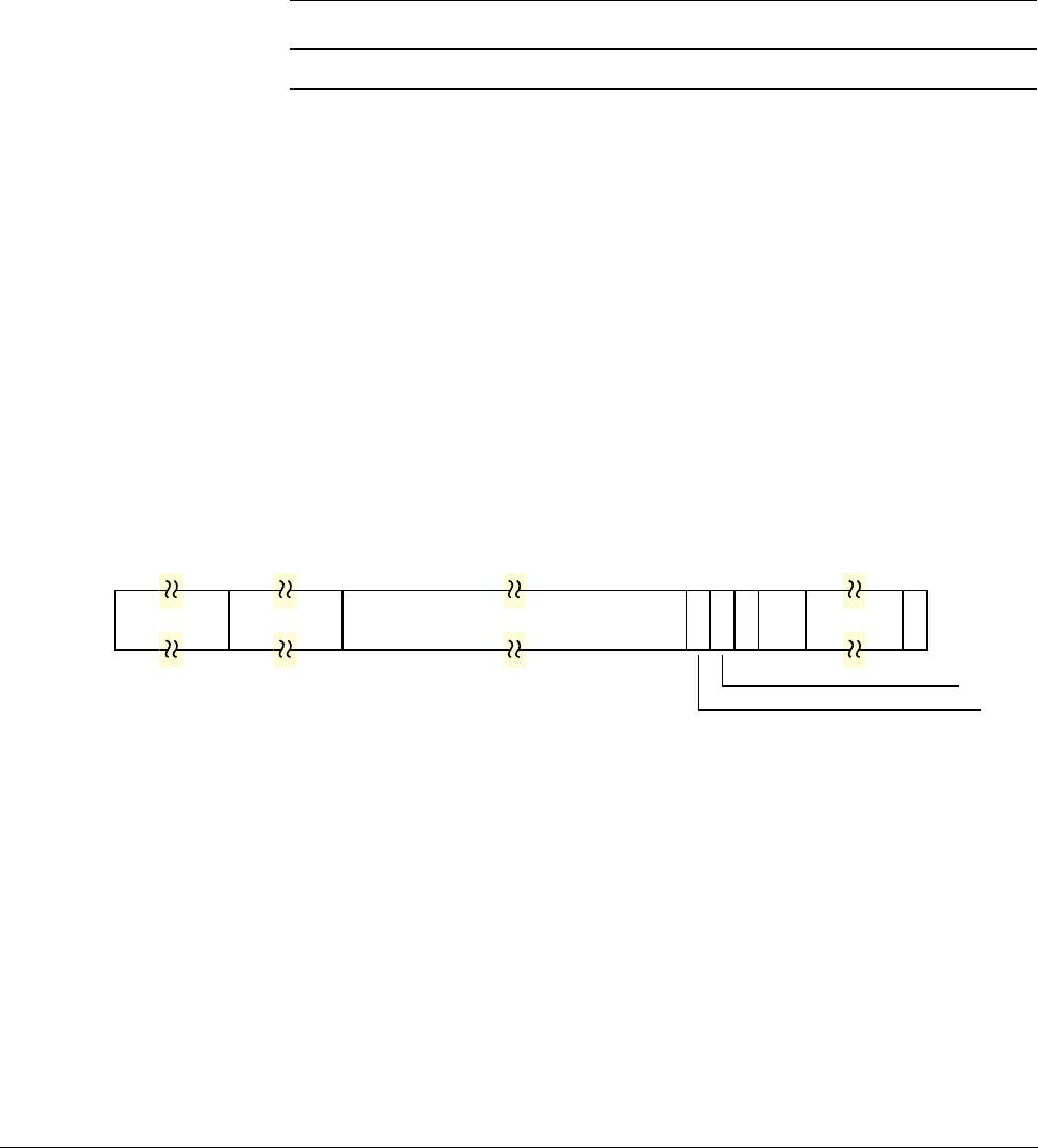
D8 AArch64 System Register Descriptions
D8.2 General system control registers
D8-2008 Copyright © 2013 ARM Limited. All rights reserved. ARM DDI 0487A.a
Non-Confidential - Beta ID090413
D8.2.69 PAR_EL1, Physical Address Register
The PAR_EL1 characteristics are:
Purpose
Receives the PA from any address translation operation.
This register is part of the Address translation operations functional group.
Usage constraints
This register is accessible as shown below:
Configurations
PAR_EL1 is architecturally mapped to AArch32 register PAR (NS).
Attributes
PAR_EL1 is a 64-bit register.
The PAR_EL1 bit assignments are:
For all register layouts:
F, bit [0]
Indicates whether the conversion completed successfully.
0
VA to PA conversion completed successfully.
1
VA to PA conversion aborted.
When PAR_EL1.F==0:
ATTR, bits [63:56]
Memory attributes for the returned PA, as indicated by the translation table entry. This field uses the
same encoding as the Attr<7:0> fields in MAIR_EL1, MAIR_EL2, and MAIR_EL3.
Bits [55:48]
Reserved, RES0.
PA, bits [47:12]
Physical Address. The physical address corresponding to the supplied virtual address. This field
returns address bits[47:12].
Bit [11]
Reserved, RES1.
EL0 EL1 (NS) EL1 (S) EL2 EL3 (SCR.NS=1) EL3 (SCR.NS=0)
-RW RW RWRW RW
ATTR
63 56
RES0
55 48
PA
47 12 11 10
NS
9
SHA
87
RES0
61
F
0
IMP DEF
RES1
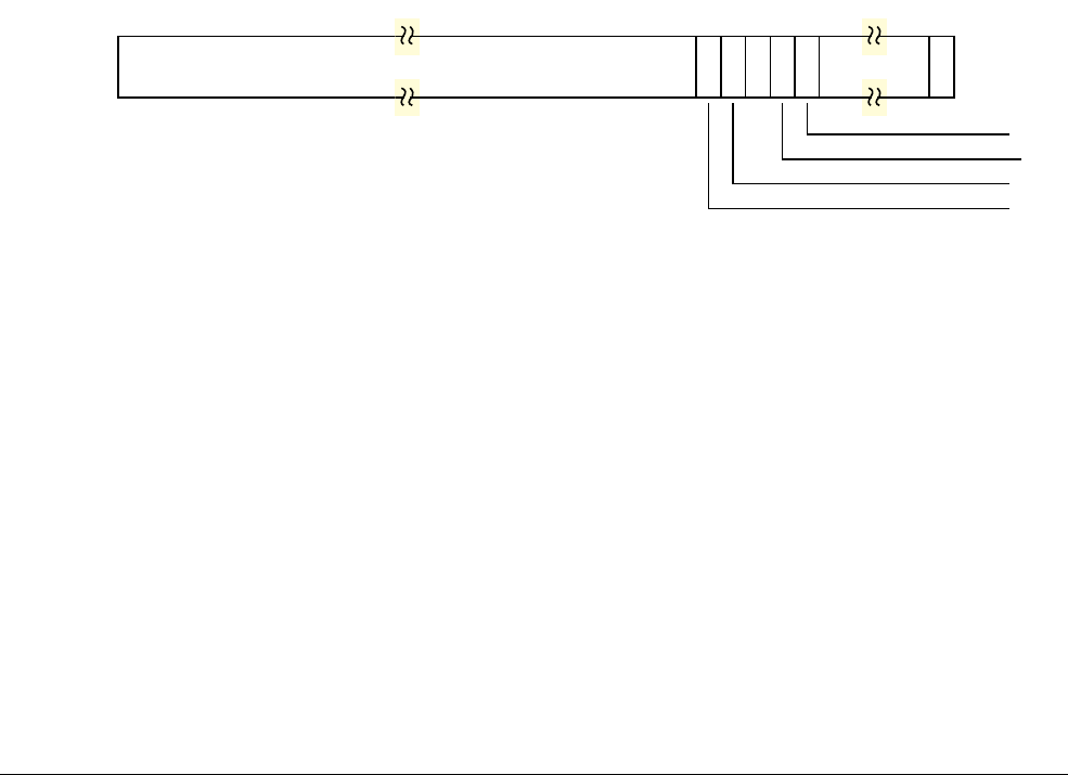
D8 AArch64 System Register Descriptions
D8.2 General system control registers
ARM DDI 0487A.a Copyright © 2013 ARM Limited. All rights reserved. D8-2009
ID090413 Non-Confidential - Beta
NS, bit [9]
Non-secure. The NS attribute for a translation table entry read from Secure state.
This bit is UNKNOWN for a translation table entry read from Non-secure state.
SHA, bits [8:7]
Shareability attribute, from the translation table entry for the returned PA. Permitted values are:
00
Non-shareable.
10
Outer Shareable.
11
Inner Shareable.
The value
0b01
is reserved.
Note: this takes the value
0b10
for:
• Any type of Device memory.
• Normal memory with both Inner Non-cacheable and Outer Non-cacheable attributes.
Bits [6:1]
Reserved, RES0.
F, bit [0]
Indicates whether the conversion completed successfully.
0
VA to PA conversion completed successfully.
When PAR_EL1.F==1:
Bits [63:12]
Reserved, RES0.
Bit [11]
Reserved, RES1.
Bit [10]
Reserved, RES0.
S, bit [9]
Indicates the translation stage at which the translation aborted:
0
Translation aborted because of a fault in the stage 1 translation.
1
Translation aborted because of a fault in the stage 2 translation.
PTW, bit [8]
If this bit is set to 1, it indicates the translation aborted because of a stage 2 fault during a stage 1
translation table walk.
RES0
63 12 11 10
S
98 7
FST
61
F
0
RES0
PTW
RES0
RES1

D8 AArch64 System Register Descriptions
D8.2 General system control registers
D8-2010 Copyright © 2013 ARM Limited. All rights reserved. ARM DDI 0487A.a
Non-Confidential - Beta ID090413
Bit [7]
Reserved, RES0.
FST, bits [6:1]
Fault status code, as shown in the Data Abort ESR encoding.
F, bit [0]
Indicates whether the conversion completed successfully.
1
VA to PA conversion aborted.
Accessing the PAR_EL1:
To access the PAR_EL1:
MRS <Xt>, PAR_EL1 ; Read PAR_EL1 into Xt
MSR PAR_EL1, <Xt> ; Write Xt to PAR_EL1
Register access is encoded as follows:
op0 op1 CRn CRm op2
11 000 0111 0100 000

D8 AArch64 System Register Descriptions
D8.2 General system control registers
ARM DDI 0487A.a Copyright © 2013 ARM Limited. All rights reserved. D8-2011
ID090413 Non-Confidential - Beta
D8.2.70 REVIDR_EL1, Revision ID Register
The REVIDR_EL1 characteristics are:
Purpose
Provides implementation-specific minor revision information that can only be interpreted in
conjunction with the Main ID Register.
This register is part of the Identification registers functional group.
Usage constraints
This register is accessible as shown below:
Configurations
REVIDR_EL1 is architecturally mapped to AArch32 register REVIDR.
Attributes
REVIDR_EL1 is a 32-bit register.
The REVIDR_EL1 bit assignments are:
Accessing the REVIDR_EL1:
To access the REVIDR_EL1:
MRS <Xt>, REVIDR_EL1 ; Read REVIDR_EL1 into Xt
Register access is encoded as follows:
EL0 EL1 (NS) EL1 (S) EL2 EL3 (SCR.NS=1) EL3 (SCR.NS=0)
-RO RO RORO RO
IMPLEMENTATION DEFINED
31 0
op0 op1 CRn CRm op2
11 000 0000 0000 110

D8 AArch64 System Register Descriptions
D8.2 General system control registers
D8-2012 Copyright © 2013 ARM Limited. All rights reserved. ARM DDI 0487A.a
Non-Confidential - Beta ID090413
D8.2.71 RMR_EL1, Reset Management Register (if EL2 and EL3 not implemented)
The RMR_EL1 characteristics are:
Purpose
If EL1 is the highest exception level implemented, and is capable of using both AArch32 and
AArch64, controls the execution state that the processor boots into and allows request of a Warm
reset.
This register is part of the Reset management registers functional group.
Usage constraints
This register is accessible as shown below:
Configurations
RMR_EL1 is architecturally mapped to AArch32 register RMR (at EL1).
Only implemented if the highest exception level implemented is EL1 and supports AArch32 and
AArch64.
If EL1 is not the highest one implemented, then this register is not implemented and its encoding is
UNDEFINED.
Attributes
RMR_EL1 is a 32-bit register.
The RMR_EL1 bit assignments are:
Bits [31:2]
Reserved, RES0.
RR, bit [1]
When set to 1 this bit requests a Warm reset. The bit is strictly a request.
On Warm reset, the field resets to 0.
AA64, bit [0]
Determines which execution state the processor boots into after a Warm reset:
0
AArch32.
1
AArch64.
The reset vector address on reset takes a choice between two IMP DEF values, depending on the
value in the AA64 bit. This ensures that even with reprogramming of the AA64 bit, it is not possible
to change the reset vector to go to a different location.
On Cold reset, the field resets to 1.
EL0 EL1
-RW
RES0
31 2
RR
10
AA64

D8 AArch64 System Register Descriptions
D8.2 General system control registers
ARM DDI 0487A.a Copyright © 2013 ARM Limited. All rights reserved. D8-2013
ID090413 Non-Confidential - Beta
Accessing the RMR_EL1:
To access the RMR_EL1:
MRS <Xt>, RMR_EL1 ; Read RMR_EL1 into Xt
MSR RMR_EL1, <Xt> ; Write Xt to RMR_EL1
Register access is encoded as follows:
op0 op1 CRn CRm op2
11 000 1100 0000 010

D8 AArch64 System Register Descriptions
D8.2 General system control registers
D8-2014 Copyright © 2013 ARM Limited. All rights reserved. ARM DDI 0487A.a
Non-Confidential - Beta ID090413
D8.2.72 RMR_EL2, Reset Management Register (if EL3 not implemented)
The RMR_EL2 characteristics are:
Purpose
If EL2 is the highest exception level implemented, and is capable of using both AArch32 and
AArch64, controls the execution state that the processor boots into and allows request of a Warm
reset.
This register is part of:
• the Virtualization registers functional group
• the Reset management registers functional group.
Usage constraints
This register is accessible as shown below:
Configurations
RMR_EL2 is architecturally mapped to AArch32 register HRMR.
Only implemented if the highest exception level implemented is EL2 and supports AArch32 and
AArch64.
If EL2 is not the highest one implemented, then this register is not implemented and its encoding is
UNDEFINED.
Attributes
RMR_EL2 is a 32-bit register.
The RMR_EL2 bit assignments are:
Bits [31:2]
Reserved, RES0.
RR, bit [1]
When set to 1 this bit requests a Warm reset. The bit is strictly a request.
On Warm reset, the field resets to 0.
AA64, bit [0]
Determines which execution state the processor boots into after a Warm reset:
0
AArch32.
1
AArch64.
The reset vector address on reset takes a choice between two IMP DEF values, depending on the
value in the AA64 bit. This ensures that even with reprogramming of the AA64 bit, it is not possible
to change the reset vector to go to a different location.
On Cold reset, the field resets to 1.
EL0 EL1 EL2
--RW
RES0
31 2
RR
10
AA64

D8 AArch64 System Register Descriptions
D8.2 General system control registers
ARM DDI 0487A.a Copyright © 2013 ARM Limited. All rights reserved. D8-2015
ID090413 Non-Confidential - Beta
Accessing the RMR_EL2:
To access the RMR_EL2:
MRS <Xt>, RMR_EL2 ; Read RMR_EL2 into Xt
MSR RMR_EL2, <Xt> ; Write Xt to RMR_EL2
Register access is encoded as follows:
op0 op1 CRn CRm op2
11 100 1100 0000 010

D8 AArch64 System Register Descriptions
D8.2 General system control registers
D8-2016 Copyright © 2013 ARM Limited. All rights reserved. ARM DDI 0487A.a
Non-Confidential - Beta ID090413
D8.2.73 RMR_EL3, Reset Management Register (if EL3 implemented)
The RMR_EL3 characteristics are:
Purpose
If EL3 is the highest exception level implemented, and is capable of using both AArch32 and
AArch64, controls the execution state that the processor boots into and allows request of a Warm
reset.
This register is part of the Reset management registers functional group.
Usage constraints
This register is accessible as shown below:
Configurations
RMR_EL3 is architecturally mapped to AArch32 register RMR (at EL3).
Only implemented if the highest exception level implemented is EL3 and supports AArch32 and
AArch64.
If EL3 is not the highest one implemented, then this register is not implemented and its encoding is
UNDEFINED.
Attributes
RMR_EL3 is a 32-bit register.
The RMR_EL3 bit assignments are:
Bits [31:2]
Reserved, RES0.
RR, bit [1]
When set to 1 this bit requests a Warm reset. The bit is strictly a request.
On Warm reset, the field resets to 0.
AA64, bit [0]
Determines which execution state the processor boots into after a Warm reset:
0
AArch32.
1
AArch64.
The reset vector address on reset takes a choice between two IMP DEF values, depending on the
value in the AA64 bit. This ensures that even with reprogramming of the AA64 bit, it is not possible
to change the reset vector to go to a different location.
On Cold reset, the field resets to 1.
EL0 EL1 (NS) EL1 (S) EL2 EL3 (SCR.NS=1) EL3 (SCR.NS=0)
-- - -RW RW
RES0
31 2
RR
10
AA64

D8 AArch64 System Register Descriptions
D8.2 General system control registers
ARM DDI 0487A.a Copyright © 2013 ARM Limited. All rights reserved. D8-2017
ID090413 Non-Confidential - Beta
Accessing the RMR_EL3:
To access the RMR_EL3:
MRS <Xt>, RMR_EL3 ; Read RMR_EL3 into Xt
MSR RMR_EL3, <Xt> ; Write Xt to RMR_EL3
Register access is encoded as follows:
op0 op1 CRn CRm op2
11 110 1100 0000 010

D8 AArch64 System Register Descriptions
D8.2 General system control registers
D8-2018 Copyright © 2013 ARM Limited. All rights reserved. ARM DDI 0487A.a
Non-Confidential - Beta ID090413
D8.2.74 RVBAR_EL1, Reset Vector Base Address Register (if EL2 and EL3 not implemented)
The RVBAR_EL1 characteristics are:
Purpose
If EL1 is the highest exception level implemented, contains the IMPLEMENTATION DEFINED address
that execution starts from after reset when executing in AArch64 state.
This register is part of the Reset management registers functional group.
Usage constraints
This register is accessible as shown below:
Configurations
Only implemented if the highest exception level implemented is EL1.
Attributes
RVBAR_EL1 is a 64-bit register.
The RVBAR_EL1 bit assignments are:
Bits [63:0]
Reset Vector Base Address. If this exception level is the highest one implemented, this field
contains the IMPLEMENTATION DEFINED address that execution starts from after reset when
executing in 64-bit state. Bits[1:0] of this register are 00, as this address must be aligned, and the
address must be within the physical address size supported by the processor.
If this exception level is not the highest one implemented, then this register is not implemented and
its encoding is UNDEFINED.
Accessing the RVBAR_EL1:
To access the RVBAR_EL1:
MRS <Xt>, RVBAR_EL1 ; Read RVBAR_EL1 into Xt
Register access is encoded as follows:
EL0 EL1
-RO
Reset Vector Base Address
63 0
op0 op1 CRn CRm op2
11 000 1100 0000 001

D8 AArch64 System Register Descriptions
D8.2 General system control registers
ARM DDI 0487A.a Copyright © 2013 ARM Limited. All rights reserved. D8-2019
ID090413 Non-Confidential - Beta
D8.2.75 RVBAR_EL2, Reset Vector Base Address Register (if EL3 not implemented)
The RVBAR_EL2 characteristics are:
Purpose
If EL2 is the highest exception level implemented, contains the IMPLEMENTATION DEFINED address
that execution starts from after reset when executing in AArch64 state.
This register is part of the Reset management registers functional group.
Usage constraints
This register is accessible as shown below:
Configurations
Only implemented if the highest exception level implemented is EL2.
Attributes
RVBAR_EL2 is a 64-bit register.
The RVBAR_EL2 bit assignments are:
Bits [63:0]
Reset Vector Base Address. If this exception level is the highest one implemented, this field
contains the IMPLEMENTATION DEFINED address that execution starts from after reset when
executing in 64-bit state. Bits[1:0] of this register are 00, as this address must be aligned, and the
address must be within the physical address size supported by the processor.
If this exception level is not the highest one implemented, then this register is not implemented and
its encoding is UNDEFINED.
Accessing the RVBAR_EL2:
To access the RVBAR_EL2:
MRS <Xt>, RVBAR_EL2 ; Read RVBAR_EL2 into Xt
Register access is encoded as follows:
EL0 EL1 EL2
--RO
Reset Vector Base Address
63 0
op0 op1 CRn CRm op2
11 100 1100 0000 001
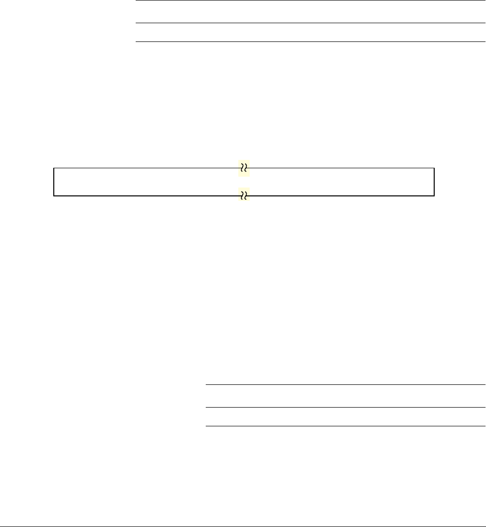
D8 AArch64 System Register Descriptions
D8.2 General system control registers
D8-2020 Copyright © 2013 ARM Limited. All rights reserved. ARM DDI 0487A.a
Non-Confidential - Beta ID090413
D8.2.76 RVBAR_EL3, Reset Vector Base Address Register (if EL3 implemented)
The RVBAR_EL3 characteristics are:
Purpose
If EL3 is the highest exception level implemented, contains the IMPLEMENTATION DEFINED address
that execution starts from after reset when executing in AArch64 state.
This register is part of the Reset management registers functional group.
Usage constraints
This register is accessible as shown below:
Configurations
Only implemented if the highest exception level implemented is EL3.
Attributes
RVBAR_EL3 is a 64-bit register.
The RVBAR_EL3 bit assignments are:
Bits [63:0]
Reset Vector Base Address. If this exception level is the highest one implemented, this field
contains the IMPLEMENTATION DEFINED address that execution starts from after reset when
executing in 64-bit state. Bits[1:0] of this register are 00, as this address must be aligned, and the
address must be within the physical address size supported by the processor.
If this exception level is not the highest one implemented, then this register is not implemented and
its encoding is UNDEFINED.
Accessing the RVBAR_EL3:
To access the RVBAR_EL3:
MRS <Xt>, RVBAR_EL3 ; Read RVBAR_EL3 into Xt
Register access is encoded as follows:
EL0 EL1 (NS) EL1 (S) EL2 EL3 (SCR.NS=1) EL3 (SCR.NS=0)
-- - -RO RO
Reset Vector Base Address
63 0
op0 op1 CRn CRm op2
11 110 1100 0000 001

D8 AArch64 System Register Descriptions
D8.2 General system control registers
ARM DDI 0487A.a Copyright © 2013 ARM Limited. All rights reserved. D8-2021
ID090413 Non-Confidential - Beta
D8.2.77 S3_<op1>_<Cn>_<Cm>_<op2>, IMPLEMENTATION DEFINED registers
The S3_<op1>_<Cn>_<Cm>_<op2> characteristics are:
Purpose
This area of the instruction set space is reserved for IMPLEMENTATION DEFINED registers.
This register is part of the IMPLEMENTATION DEFINED functional group.
Usage constraints
This register is accessible as shown below:
The numbers in these register names are encoded in decimal without leading zeroes, and the Cn and
Cm fields require a literal C before the number. For example, S3_4_C11_C9_7.
Configurations
There are no configuration notes.
Attributes
S3_<op1>_<Cn>_<Cm>_<op2> is a 32-bit register.
The S3_<op1>_<Cn>_<Cm>_<op2> bit assignments are:
Accessing the S3_<op1>_<Cn>_<Cm>_<op2>:
To access the S3_<op1>_<Cn>_<Cm>_<op2>:
MRS <Xt>, S3_<op1>_<Cn>_<Cm>_<op2> ; Read S3_<op1>_<Cn>_<Cm>_<op2> into Xt
MSR S3_<op1>_<Cn>_<Cm>_<op2>, <Xt> ; Write Xt to S3_<op1>_<Cn>_<Cm>_<op2>
Register access is encoded as follows:
EL0 EL1 (NS) EL1 (S) EL2 EL3 (SCR.NS=1) EL3 (SCR.NS=0)
IMP DEF IMP DEF IMP DEF IMP DEF IMP DEF IMP DEF
IMPLEMENTATION DEFINED
31 0
op0 op1 CRn CRm op2
11 xxx 1x11 xxxx xxx
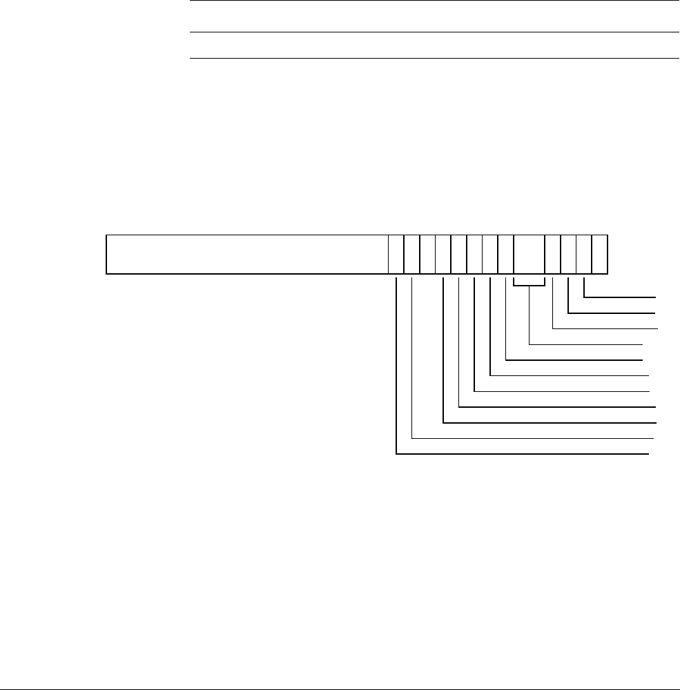
D8 AArch64 System Register Descriptions
D8.2 General system control registers
D8-2022 Copyright © 2013 ARM Limited. All rights reserved. ARM DDI 0487A.a
Non-Confidential - Beta ID090413
D8.2.78 SCR_EL3, Secure Configuration Register
The SCR_EL3 characteristics are:
Purpose
Defines the configuration of the current security state. It specifies:
• The security state of EL0 and EL1, either Secure or Non-secure.
• The register width at lower exception levels.
• Whether IRQ, FIQ, and External Abort interrupts are taken to EL3.
This register is part of the Security registers functional group.
Usage constraints
This register is accessible as shown below:
Configurations
SCR_EL3 can be mapped to AArch32 register SCR, but this is not architecturally mandated.
Attributes
SCR_EL3 is a 32-bit register.
The SCR_EL3 bit assignments are:
Bits [31:14]
Reserved, RES0.
TWE, bit [13]
Trap WFE. The possible values of this bit are:
0
WFE instructions not trapped.
1
WFE instructions executed in AArch32 or AArch64 at EL2, EL1, or EL0 are trapped to
EL3 if the instruction would otherwise cause suspension of execution, i.e. if there is not
a pending WFI wakeup event and the instruction does not cause another exception.
EL0 EL1 (NS) EL1 (S) EL2 EL3 (SCR.NS=1) EL3 (SCR.NS=0)
-- - -RW RW
RES0
31 14 13 12
ST
11 10 9 8 7 6 543 2 1
NS
0
IRQ
FIQ
EA
RES1
RES0
SMD
HCE
SIF
RW
TWI
TWE

D8 AArch64 System Register Descriptions
D8.2 General system control registers
ARM DDI 0487A.a Copyright © 2013 ARM Limited. All rights reserved. D8-2023
ID090413 Non-Confidential - Beta
TWI, bit [12]
Trap WFI. The possible values of this bit are:
0
WFI instructions not trapped.
1
WFI instructions executed in AArch32 or AArch64 at EL2, EL1, or EL0 are trapped to
EL3 if the instruction would otherwise cause suspension of execution.
ST, bit [11]
Enables Secure EL1 access to the CNTPS_TVAL_EL1, CNTPS_CTL_EL1, and
CNTPS_CVAL_EL1 registers. The possible values of this bit are:
0
These registers are only accessible in EL3.
1
These registers are accessible in EL3 and also in EL1 when SCR_EL3.NS==0.
If this bit is 0 and there is a Secure EL1 access to one of the CNTPS registers:
• An exception is taken to EL3.
• The exception class for this exception, as returned in ESR_EL3.EC, is
0x18
.
RW, bit [10]
Register width control for lower exception levels.
0
Lower levels are all AArch32.
1
The next lower level is AArch64.
If EL2 is present:
• EL2 is AArch64.
• EL2 controls EL1 and EL0 behaviors.
If EL2 is not present:
• EL1 is AArch64.
• EL0 is determined by the Register Width described in the current process state
when executing at EL0.
This bit is permitted to be cached in a TLB.
SIF, bit [9]
Secure instruction fetch. When the processor is in Secure state, this bit disables instruction fetch
from Non-secure memory. The possible values for this bit are:
0
Secure state instruction fetches from Non-secure memory are permitted.
1
Secure state instruction fetches from Non-secure memory are not permitted.
This bit is permitted to be cached in a TLB.
HCE, bit [8]
Hypervisor Call enable. This bit enables use of the HVC instruction from Non-secure EL1 modes.
The possible values of this bit are:
0
HVC instruction is UNDEFINED in Non-secure EL1 modes, and either UNDEFINED or a
NOP in Hyp mode, depending on the implementation.
1
HVC instruction is enabled in Non-secure EL1 modes, and performs a Hypervisor Call.
If EL3 is implemented but EL2 is not implemented, this bit is RES0.
SMD, bit [7]
SMC Disable.
0
SMC is enabled at EL1, EL2, or EL3.
1
SMC is UNDEFINED at all exception levels. At EL1 in the Non-secure state, the
HCR_EL2.TSC bit has priority over this control.

D8 AArch64 System Register Descriptions
D8.2 General system control registers
D8-2024 Copyright © 2013 ARM Limited. All rights reserved. ARM DDI 0487A.a
Non-Confidential - Beta ID090413
Bit [6]
Reserved, RES0.
Bits [5:4]
Reserved, RES1.
EA, bit [3]
External Abort and SError Interrupt Routing.
0
External Aborts and SError Interrupts while executing at exception levels other than
EL3 are not taken in EL3.
1
External Aborts and SError Interrupts while executing at all exception levels are taken
in EL3.
FIQ, bit [2]
Physical FIQ Routing.
0
Physical FIQ while executing at exception levels other than EL3 are not taken in EL3.
1
Physical FIQ while executing at all exception levels are taken in EL3.
IRQ, bit [1]
Physical IRQ Routing.
0
Physical IRQ while executing at exception levels other than EL3 are not taken in EL3.
1
Physical IRQ while executing at all exception levels are taken in EL3.
NS, bit [0]
Non-secure bit.
0
Indicates that EL0 and EL1 are in Secure state, and so memory accesses from those
exception levels can access Secure memory.
1
Indicates that EL0 and EL1 are in Non-secure state, and so memory accesses from those
exception levels cannot access Secure memory.
Accessing the SCR_EL3:
To access the SCR_EL3:
MRS <Xt>, SCR_EL3 ; Read SCR_EL3 into Xt
MSR SCR_EL3, <Xt> ; Write Xt to SCR_EL3
Register access is encoded as follows:
op0 op1 CRn CRm op2
11 110 0001 0001 000
D8 AArch64 System Register Descriptions
D8.2 General system control registers
ARM DDI 0487A.a Copyright © 2013 ARM Limited. All rights reserved. D8-2025
ID090413 Non-Confidential - Beta
D8.2.79 SCTLR_EL1, System Control Register (EL1)
The SCTLR_EL1 characteristics are:
Purpose
Provides top level control of the system, including its memory system, at EL1.
This register is part of the Other system control registers functional group.
Usage constraints
This register is accessible as shown below:
Configurations
SCTLR_EL1 is architecturally mapped to AArch32 register SCTLR (NS).
Attributes
SCTLR_EL1 is a 32-bit register.
The SCTLR_EL1 bit assignments are:
Bits [31:30]
Reserved, RES0.
Bits [29:28]
Reserved, RES1.
Bit [27]
Reserved, RES0.
UCI, bit [26]
When set, enables EL0 access in AArch64 for DC CVAU, DC CIVAC, DC CVAC, and IC IVAU
instructions.
Reset value is architecturally UNKNOWN.
EL0 EL1 (NS) EL1 (S) EL2 EL3 (SCR.NS=1) EL3 (SCR.NS=0)
-RW RW RWRW RW
31 30 29 28 27 26 25 24 23 22 21 20 19 18 17 16 15 14 13
I
12 11 10 9 8 7 6 5 4 3
C
2
A
1
M
0
RES0
RES1
RES0
UCI
EE
E0E
RES1
RES0
RES1
WXN
nTWE
RES0
nTWI
SA
SA0
CP15BEN
THEE
ITD
SED
UMA
RES0
RES1
RES0
DZE
UCT

D8 AArch64 System Register Descriptions
D8.2 General system control registers
D8-2026 Copyright © 2013 ARM Limited. All rights reserved. ARM DDI 0487A.a
Non-Confidential - Beta ID090413
EE, bit [25]
Exception Endianness. This bit controls the endianness for:
• Explicit data accesses at EL1.
• Stage 1 translation table walks at EL1 and EL0.
The possible values of this bit are:
0
Little-endian.
1
Big-endian.
If an implementation does not provide Big-endian support, this bit is RES0. If it does not provide
Little-endian support, this bit is RES1.
The EE bit is permitted to be cached in a TLB.
If this register is at the highest exception level implemented, field resets to an IMPLEMENTATION
DEFINED value. Otherwise, its reset value is UNKNOWN.
E0E, bit [24]
Endianness of explicit data accesses at EL0. The possible values of this bit are:
0
Explicit data accesses at EL0 are little-endian.
1
Explicit data accesses at EL0 are big-endian.
If an implementation only supports Little-endian accesses at EL0 then this bit is RES0.
If an implementation only supports Big-endian accesses at EL0 then this bit is RES1.
This bit has no effect on the endianness of LDTR* and STTR* instructions executed at EL1.
Reset value is architecturally UNKNOWN.
Bits [23:22]
Reserved, RES1.
Bit [21]
Reserved, RES0.
Bit [20]
Reserved, RES1.
WXN, bit [19]
Write permission implies XN (Execute Never). This bit can be used to require all memory regions
with write permission to be treated as XN. The possible values of this bit are:
0
Regions with write permission are not forced to XN.
1
Regions with write permission are forced to XN.
The WXN bit is permitted to be cached in a TLB.
Reset value is architecturally UNKNOWN.
nTWE, bit [18]
Not trap WFE. Possible values of this bit are:
0
If a WFE instruction executed at EL0 would cause execution to be suspended, such as
if the event register is not set and there is not a pending WFE wakeup event, it is taken
as an exception to EL1 using the
0x1
ESR code.
1
WFE instructions are executed as normal.
Conditional WFE instructions that fail their condition do not cause an exception if this bit is 0.
Reset value is architecturally UNKNOWN.
Bit [17]
Reserved, RES0.

D8 AArch64 System Register Descriptions
D8.2 General system control registers
ARM DDI 0487A.a Copyright © 2013 ARM Limited. All rights reserved. D8-2027
ID090413 Non-Confidential - Beta
nTWI, bit [16]
Not trap WFI. Possible values of this bit are:
0
If a WFI instruction executed at EL0 would cause execution to be suspended, such as if
there is not a pending WFI wakeup event, it is taken as an exception to EL1 using the
0x1
ESR code.
1
WFI instructions are executed as normal.
Conditional WFI instructions that fail their condition do not cause an exception if this bit is 0.
Reset value is architecturally UNKNOWN.
UCT, bit [15]
When set, enables EL0 access in AArch64 to the CTR_EL0 register.
Reset value is architecturally UNKNOWN.
DZE, bit [14]
Access to DC ZVA instruction at EL0. The possible values of this bit are:
0
Execution of the DC ZVA instruction is prohibited at EL0, and it is treated as
UNDEFINED at EL0.
1
Execution of the DC ZVA instruction is allowed at EL0.
Reset value is architecturally UNKNOWN.
Bit [13]
Reserved, RES0.
I, bit [12]
Instruction cache enable. This is an enable bit for instruction caches at EL0 and EL1:
0
Instruction caches disabled at EL0 and EL1. If SCTLR_EL1.M is set to 0, instruction
accesses from stage 1 of the EL1&0 translation regime are to Normal memory, Outer
Shareable, Inner Non-cacheable, Outer Non-cacheable.
1
Instruction caches enabled at EL0 and EL1. If SCTLR_EL1.M is set to 0, instruction
accesses from stage 1 of the EL1&0 translation regime are to Normal memory, Outer
Shareable, Inner Write-Through, Outer Write-Through.
When this bit is 0, all EL1 and EL0 Normal memory instruction accesses are Non-cacheable.
If the HCR_EL2.DC bit is set to 1, then the Non-secure stage 1 EL1&0 translation regime is
Cacheable regardless of the value of this bit.
If this register is at the highest exception level implemented, field resets to 0. Otherwise, its reset
value is UNKNOWN.
Bit [11]
Reserved, RES1.
Bit [10]
Reserved, RES0.
UMA, bit [9]
User Mask Access. Controls access to interrupt masks from EL0, when EL0 is using AArch64. The
possible values of this bit are:
0
Disable access to the interrupt masks from EL0.
1
Enable access to the interrupt masks from EL0.
Reset value is architecturally UNKNOWN.

D8 AArch64 System Register Descriptions
D8.2 General system control registers
D8-2028 Copyright © 2013 ARM Limited. All rights reserved. ARM DDI 0487A.a
Non-Confidential - Beta ID090413
SED, bit [8]
SETEND Disable. The possible values of this bit are:
0
The SETEND instruction is available.
1
The SETEND instruction is UNALLOCATED.
If an implementation does not support mixed endian operation, this bit is RES1.
Reset value is architecturally UNKNOWN.
ITD, bit [7]
IT Disable. The possible values of this bit are:
0
The IT instruction functionality is available.
1
It is IMPLEMENTATION DEFINED whether the IT instruction is treated as either:
• A 16-bit instruction, which can only be followed by another 16-bit instruction.
• The first half of a 32-bit instruction.
An implementation might vary dynamically as to whether IT is treated as a 16-bit
instruction or the first half of a 32-bit instruction.
All encodings of the IT instruction with hw1[3:0]!=1000 are UNDEFINED and treated as
unallocated.
All encodings of the subsequent instruction with the following values for hw1 are
UNDEFINED (and treated as unallocated):
11xxxxxxxxxxxxxx
All 32-bit instructions, B(2), B(1), Undefined, SVC, Load/Store multiple
1x11xxxxxxxxxxxx
Miscellaneous 16-bit instructions
1x100xxxxxxxxxxx
ADD Rd, PC, #imm
01001xxxxxxxxxxx
LDR Rd, [PC, #imm]
0100x1xxx1111xxx
ADD(4),CMP(3), MOV, BX pc, BLX pc
010001xx1xxxx111
ADD(4),CMP(3), MOV (Note: this pattern also covers UNPREDICTABLE
cases with BLX Rn)
Contrary to the standard treatment of conditional UNDEFINED instructions in the ARM
architecture, in this case these instructions are always treated as UNDEFINED, regardless
of whether the instruction would pass or fail its condition codes as a result of being in
an IT block.
Reset value is architecturally UNKNOWN.
THEE, bit [6]
T32EE enable. The possible values of this bit are:
0
T32EE is disabled.
1
T32EE is enabled.
If T32EE is not implemented, this bit is RES0.
Reset value is architecturally UNKNOWN.
CP15BEN, bit [5]
CP15 barrier enable. If implemented, this is an enable bit for the AArch32 CP15 DMB, DSB, and
ISB barrier operations:
0
AArch32 CP15 barrier operations disabled. Their encodings are UNDEFINED.

D8 AArch64 System Register Descriptions
D8.2 General system control registers
ARM DDI 0487A.a Copyright © 2013 ARM Limited. All rights reserved. D8-2029
ID090413 Non-Confidential - Beta
1
AArch32 CP15 barrier operations enabled.
If an implementation does not support the CP15 barrier operations, this bit is RES0.
Reset value is architecturally UNKNOWN.
SA0, bit [4]
Stack Alignment Check Enable for EL0. When set, use of the stack pointer as the base address in a
load/store instruction at EL0 must be aligned to a 16-byte boundary, or a Stack Alignment Fault
exception will be raised.
Reset value is architecturally UNKNOWN.
SA, bit [3]
Stack Alignment Check Enable. When set, use of the stack pointer as the base address in a load/store
instruction at this register's exception level must be aligned to a 16-byte boundary, or a Stack
Alignment Fault exception will be raised.
Reset value is architecturally UNKNOWN.
C, bit [2]
Cache enable. This is an enable bit for data and unified caches at EL0 and EL1:
0
Data and unified caches disabled.
1
Data and unified caches enabled.
When this bit is 0, all EL0 and EL1 Normal memory data accesses and all accesses to the EL1&0
stage 1 translation tables are Non-cacheable.
If the HCR_EL2.DC bit is set to 1, then the Non-secure stage 1 EL1&0 translation regime is
Cacheable regardless of the value of the SCTLR_EL1.C bit.
If this register is at the highest exception level implemented, field resets to 0. Otherwise, its reset
value is UNKNOWN.
A, bit [1]
Alignment check enable. This is the enable bit for Alignment fault checking:
0
Alignment fault checking disabled.
Instructions that load or store one or more registers, other than load/store exclusive and
load-acquire/store-release, do not check that the address being accessed is aligned to the
size of the data element(s) being accessed.
1
Alignment fault checking enabled.
All instructions that load or store one or more registers have an alignment check that the
address being accessed is aligned to the size of the data element(s) being accessed. If
this check fails it causes an Alignment fault, which is taken as a Data Abort exception.
Load/store exclusive and load-acquire/store-release instructions have an alignment check regardless
of the value of the A bit.
Reset value is architecturally UNKNOWN.
M, bit [0]
MMU enable for EL1 and EL0 stage 1 address translation. Possible values of this bit are:
0
EL1 and EL0 stage 1 address translation disabled.
1
EL1 and EL0 stage 1 address translation enabled.
If this register is at the highest exception level implemented, field resets to 0. Otherwise, its reset
value is UNKNOWN.
Accessing the SCTLR_EL1:
To access the SCTLR_EL1:
MRS <Xt>, SCTLR_EL1 ; Read SCTLR_EL1 into Xt

D8 AArch64 System Register Descriptions
D8.2 General system control registers
D8-2030 Copyright © 2013 ARM Limited. All rights reserved. ARM DDI 0487A.a
Non-Confidential - Beta ID090413
MSR SCTLR_EL1, <Xt> ; Write Xt to SCTLR_EL1
Register access is encoded as follows:
op0 op1 CRn CRm op2
11 000 0001 0000 000
D8 AArch64 System Register Descriptions
D8.2 General system control registers
ARM DDI 0487A.a Copyright © 2013 ARM Limited. All rights reserved. D8-2031
ID090413 Non-Confidential - Beta
D8.2.80 SCTLR_EL2, System Control Register (EL2)
The SCTLR_EL2 characteristics are:
Purpose
Provides top level control of the system, including its memory system, at EL2.
This register is part of:
• the Virtualization registers functional group
• the Other system control registers functional group.
Usage constraints
This register is accessible as shown below:
Configurations
SCTLR_EL2 is architecturally mapped to AArch32 register HSCTLR.
If EL2 is not implemented, this register is RES0 from EL3.
Attributes
SCTLR_EL2 is a 32-bit register.
The SCTLR_EL2 bit assignments are:
Bits [31:30]
Reserved, RES0.
Bits [29:28]
Reserved, RES1.
Bits [27:26]
Reserved, RES0.
EE, bit [25]
Exception Endianness. This bit controls the endianness for:
• Explicit data accesses at EL2.
EL0 EL1 (NS) EL1 (S) EL2 EL3 (SCR.NS=1) EL3 (SCR.NS=0)
-- - RWRW RW
31 30 29 28 27 26 25 24 23 22 21 20 19 18 17 16
RES0
15 13
I
12 11
RES0
10 6 543
C
2
A
1
M
0
RES0
RES1
RES0
EE
RES0
RES1
RES0
WXN
RES1
RES0
RES1
SA
RES1
RES1

D8 AArch64 System Register Descriptions
D8.2 General system control registers
D8-2032 Copyright © 2013 ARM Limited. All rights reserved. ARM DDI 0487A.a
Non-Confidential - Beta ID090413
• Stage 1 translation table walks at EL2.
• Stage 2 translation table walks at EL1 and EL0.
The possible values of this bit are:
0
Little-endian.
1
Big-endian.
If an implementation does not provide Big-endian support, this bit is RES0. If it does not provide
Little-endian support, this bit is RES1.
The EE bit is permitted to be cached in a TLB.
If this register is at the highest exception level implemented, field resets to an IMPLEMENTATION
DEFINED value. Otherwise, its reset value is UNKNOWN.
Bit [24]
Reserved, RES0.
Bits [23:22]
Reserved, RES1.
Bits [21:20]
Reserved, RES0.
WXN, bit [19]
Write permission implies XN (Execute Never). This bit can be used to require all memory regions
with write permission to be treated as XN. The possible values of this bit are:
0
Regions with write permission are not forced to XN.
1
Regions with write permission are forced to XN.
The WXN bit is permitted to be cached in a TLB.
Reset value is architecturally UNKNOWN.
Bit [18]
Reserved, RES1.
Bit [17]
Reserved, RES0.
Bit [16]
Reserved, RES1.
Bits [15:13]
Reserved, RES0.
I, bit [12]
Instruction cache enable. This is an enable bit for instruction caches at EL2:
0
Instruction caches disabled at EL2. If SCTLR_EL2.M is set to 0, instruction accesses
from stage 1 of the EL2 translation regime are to Normal memory, Outer Shareable,
Inner Non-cacheable, Outer Non-cacheable.
1
Instruction caches enabled at EL2. If SCTLR_EL2.M is set to 0, instruction accesses
from stage 1 of the EL2 translation regime are to Normal memory, Outer Shareable,
Inner Write-Through, Outer Write-Through.
When this bit is 0, all EL2 Normal memory instruction accesses are Non-cacheable. This bit has no
effect on the EL1&0 or EL3 translation regimes.
If this register is at the highest exception level implemented, field resets to 0. Otherwise, its reset
value is UNKNOWN.

D8 AArch64 System Register Descriptions
D8.2 General system control registers
ARM DDI 0487A.a Copyright © 2013 ARM Limited. All rights reserved. D8-2033
ID090413 Non-Confidential - Beta
Bit [11]
Reserved, RES1.
Bits [10:6]
Reserved, RES0.
Bits [5:4]
Reserved, RES1.
SA, bit [3]
Stack Alignment Check Enable. When set, use of the stack pointer as the base address in a load/store
instruction at this register's exception level must be aligned to a 16-byte boundary, or a Stack
Alignment Fault exception will be raised.
Reset value is architecturally UNKNOWN.
C, bit [2]
Cache enable. This is an enable bit for data and unified caches at EL2:
0
Data and unified caches disabled at EL2.
1
Data and unified caches enabled at EL2.
When this bit is 0, all EL2 Normal memory data accesses and all accesses to the EL2 translation
tables are Non-cacheable. This bit has no effect on the EL1&0 or EL3 translation regimes.
If this register is at the highest exception level implemented, field resets to 0. Otherwise, its reset
value is UNKNOWN.
A, bit [1]
Alignment check enable. This is the enable bit for Alignment fault checking:
0
Alignment fault checking disabled.
Instructions that load or store one or more registers, other than load/store exclusive and
load-acquire/store-release, do not check that the address being accessed is aligned to the
size of the data element(s) being accessed.
1
Alignment fault checking enabled.
All instructions that load or store one or more registers have an alignment check that the
address being accessed is aligned to the size of the data element(s) being accessed. If
this check fails it causes an Alignment fault, which is taken as a Data Abort exception.
Load/store exclusive and load-acquire/store-release instructions have an alignment check regardless
of the value of the A bit.
Reset value is architecturally UNKNOWN.
M, bit [0]
MMU enable for EL2 stage 1 address translation. Possible values of this bit are:
0
EL2 stage 1 address translation disabled.
1
EL2 stage 1 address translation enabled.
If this register is at the highest exception level implemented, field resets to 0. Otherwise, its reset
value is UNKNOWN.
Accessing the SCTLR_EL2:
To access the SCTLR_EL2:
MRS <Xt>, SCTLR_EL2 ; Read SCTLR_EL2 into Xt
MSR SCTLR_EL2, <Xt> ; Write Xt to SCTLR_EL2

D8 AArch64 System Register Descriptions
D8.2 General system control registers
D8-2034 Copyright © 2013 ARM Limited. All rights reserved. ARM DDI 0487A.a
Non-Confidential - Beta ID090413
Register access is encoded as follows:
op0 op1 CRn CRm op2
11 100 0001 0000 000
D8 AArch64 System Register Descriptions
D8.2 General system control registers
ARM DDI 0487A.a Copyright © 2013 ARM Limited. All rights reserved. D8-2035
ID090413 Non-Confidential - Beta
D8.2.81 SCTLR_EL3, System Control Register (EL3)
The SCTLR_EL3 characteristics are:
Purpose
Provides top level control of the system, including its memory system, at EL3.
This register is part of the Other system control registers functional group.
Usage constraints
This register is accessible as shown below:
Configurations
SCTLR_EL3 can be mapped to AArch32 register SCTLR (S), but this is not architecturally
mandated.
Attributes
SCTLR_EL3 is a 32-bit register.
The SCTLR_EL3 bit assignments are:
Bits [31:30]
Reserved, RES0.
Bits [29:28]
Reserved, RES1.
Bits [27:26]
Reserved, RES0.
EE, bit [25]
Exception Endianness. This bit controls the endianness for:
• Explicit data accesses at EL3.
• Stage 1 translation table walks at EL3.
EL0 EL1 (NS) EL1 (S) EL2 EL3 (SCR.NS=1) EL3 (SCR.NS=0)
-- - -RW RW
31 30 29 28 27 26 25 24 23 22 21 20 19 18 17 16
RES0
15 13
I
12 11
RES0
10 6 543
C
2
A
1
M
0
RES0
RES1
RES0
EE
RES0
RES1
RES0
WXN
RES1
RES0
RES1
SA
RES1
RES1

D8 AArch64 System Register Descriptions
D8.2 General system control registers
D8-2036 Copyright © 2013 ARM Limited. All rights reserved. ARM DDI 0487A.a
Non-Confidential - Beta ID090413
The possible values of this bit are:
0
Little-endian.
1
Big-endian.
If an implementation does not provide Big-endian support, this bit is RES0. If it does not provide
Little-endian support, this bit is RES1.
The EE bit is permitted to be cached in a TLB.
If this register is at the highest exception level implemented, field resets to an IMPLEMENTATION
DEFINED value. Otherwise, its reset value is UNKNOWN.
Bit [24]
Reserved, RES0.
Bits [23:22]
Reserved, RES1.
Bits [21:20]
Reserved, RES0.
WXN, bit [19]
Write permission implies XN (Execute Never). This bit can be used to require all memory regions
with write permission to be treated as XN. The possible values of this bit are:
0
Regions with write permission are not forced to XN.
1
Regions with write permission are forced to XN.
The WXN bit is permitted to be cached in a TLB.
Reset value is architecturally UNKNOWN.
Bit [18]
Reserved, RES1.
Bit [17]
Reserved, RES0.
Bit [16]
Reserved, RES1.
Bits [15:13]
Reserved, RES0.
I, bit [12]
Instruction cache enable. This is an enable bit for instruction caches at EL3:
0
Instruction caches disabled at EL3. If SCTLR_EL3.M is set to 0, instruction accesses
from stage 1 of the EL3 translation regime are to Normal memory, Outer Shareable,
Inner Non-cacheable, Outer Non-cacheable.
1
Instruction caches enabled at EL3. If SCTLR_EL3.M is set to 0, instruction accesses
from stage 1 of the EL3 translation regime are to Normal memory, Outer Shareable,
Inner Write-Through, Outer Write-Through.
When this bit is 0, all EL3 Normal memory instruction accesses are Non-cacheable. This bit has no
effect on the EL1&0 or EL2 translation regimes.
If this register is at the highest exception level implemented, field resets to 0. Otherwise, its reset
value is UNKNOWN.
Bit [11]
Reserved, RES1.

D8 AArch64 System Register Descriptions
D8.2 General system control registers
ARM DDI 0487A.a Copyright © 2013 ARM Limited. All rights reserved. D8-2037
ID090413 Non-Confidential - Beta
Bits [10:6]
Reserved, RES0.
Bits [5:4]
Reserved, RES1.
SA, bit [3]
Stack Alignment Check Enable. When set, use of the stack pointer as the base address in a load/store
instruction at this register's exception level must be aligned to a 16-byte boundary, or a Stack
Alignment Fault exception will be raised.
Reset value is architecturally UNKNOWN.
C, bit [2]
Cache enable. This is an enable bit for data and unified caches at EL3:
0
Data and unified caches disabled at EL3.
1
Data and unified caches enabled at EL3.
When this bit is 0, all EL3 Normal memory data accesses and all accesses to the EL3 translation
tables are Non-cacheable. This bit has no effect on the EL1&0 or EL2 translation regimes.
If this register is at the highest exception level implemented, field resets to 0. Otherwise, its reset
value is UNKNOWN.
A, bit [1]
Alignment check enable. This is the enable bit for Alignment fault checking:
0
Alignment fault checking disabled.
Instructions that load or store one or more registers, other than load/store exclusive and
load-acquire/store-release, do not check that the address being accessed is aligned to the
size of the data element(s) being accessed.
1
Alignment fault checking enabled.
All instructions that load or store one or more registers have an alignment check that the
address being accessed is aligned to the size of the data element(s) being accessed. If
this check fails it causes an Alignment fault, which is taken as a Data Abort exception.
Load/store exclusive and load-acquire/store-release instructions have an alignment check regardless
of the value of the A bit.
Reset value is architecturally UNKNOWN.
M, bit [0]
MMU enable for EL3 stage 1 address translation. Possible values of this bit are:
0
EL3 stage 1 address translation disabled.
1
EL3 stage 1 address translation enabled.
If this register is at the highest exception level implemented, field resets to 0. Otherwise, its reset
value is UNKNOWN.
Accessing the SCTLR_EL3:
To access the SCTLR_EL3:
MRS <Xt>, SCTLR_EL3 ; Read SCTLR_EL3 into Xt
MSR SCTLR_EL3, <Xt> ; Write Xt to SCTLR_EL3
Register access is encoded as follows:
op0 op1 CRn CRm op2
11 110 0001 0000 000
D8 AArch64 System Register Descriptions
D8.2 General system control registers
D8-2038 Copyright © 2013 ARM Limited. All rights reserved. ARM DDI 0487A.a
Non-Confidential - Beta ID090413
D8.2.82 TCR_EL1, Translation Control Register (EL1)
The TCR_EL1 characteristics are:
Purpose
Determines which of the Translation Table Base Registers defined the base address for a translation
table walk required for the stage 1 translation of a memory access from EL0 or EL1. Also controls
the translation table format and holds cacheability and shareability information.
This register is part of the Virtual memory control registers functional group.
Usage constraints
This register is accessible as shown below:
Any of the bits in TCR_EL1 are permitted to be cached in a TLB.
Configurations
TCR_EL1[31:0] is architecturally mapped to AArch32 register TTBCR (NS).
Attributes
TCR_EL1 is a 64-bit register.
The TCR_EL1 bit assignments are:
Bits [63:39]
Reserved, RES0.
TBI1, bit [38]
Top Byte ignored - indicates whether the top byte of an address is used for address match for the
TTBR1_EL1 region, or ignored and used for tagged addresses.
0
Top Byte used in the address calculation.
1
Top Byte ignored in the address calculation.
This affects addresses generated in EL0 and EL1 using AArch64 where the address would be
translated by tables pointed to by TTBR1_EL1. It has an effect whether the EL1&0 translation
regime is enabled or not.
Additionally, this affects changes to the program counter, when TBI1 is 1 and bit [55] of the target
address is 1, caused by:
• A branch or procedure return within EL0 or EL1.
• An exception taken to EL1.
EL0 EL1 (NS) EL1 (S) EL2 EL3 (SCR.NS=1) EL3 (SCR.NS=0)
-RW RW RWRW RW
RES0
63 39 38 37 36 35
IPS
34 32
TG1
31 30
SH1
29 28 27 26 25 24 23 22
T1SZ
21 16
TG0
15 14
SH0
13 12 11 10 987 6
T0SZ
50
TBI1
TBI0
AS
RES0
ORGN1
IRGN1
RES0
EPD0
IRGN0
ORGN0
A1
EPD1

D8 AArch64 System Register Descriptions
D8.2 General system control registers
ARM DDI 0487A.a Copyright © 2013 ARM Limited. All rights reserved. D8-2039
ID090413 Non-Confidential - Beta
• An exception return to EL0 or EL1.
In these cases bits [63:56] of the address are also set to 1 before it is stored in the PC.
TBI0, bit [37]
Top Byte ignored - indicates whether the top byte of an address is used for address match for the
TTBR0_EL1 region, or ignored and used for tagged addresses.
0
Top Byte used in the address calculation.
1
Top Byte ignored in the address calculation.
This affects addresses generated in EL0 and EL1 using AArch64 where the address would be
translated by tables pointed to by TTBR0_EL1. It has an effect whether the EL1&0 translation
regime is enabled or not.
Additionally, this affects changes to the program counter, when TBI0 is 1 and bit [55] of the target
address is 0, caused by:
• A branch or procedure return within EL0 or EL1.
• An exception taken to EL1.
• An exception return to EL0 or EL1.
In these cases bits [63:56] of the address are also set to 0 before it is stored in the PC.
AS, bit [36]
ASID Size.
0
8 bit - the upper 8 bits of TTBR0_EL1 and TTBR1_EL1 are ignored by hardware for
every purpose except reading back the register, and are treated as if they are all zeros for
when used for allocation and matching entries in the TLB.
1
16 bit - the upper 16 bits of TTBR0_EL1 and TTBR1_EL1 are used for allocation and
matching in the TLB.
If the implementation has only 8 bits of ASID, this field is RES0.
Bit [35]
Reserved, RES0.
IPS, bits [34:32]
Intermediate Physical Address Size.
000
32 bits, 4 GB.
001
36 bits, 64 GB.
010
40 bits, 1 TB.
011
42 bits, 4 TB.
100
44 bits, 16 TB.
101
48 bits, 256 TB.
Other values are reserved.
The reserved values behave in the same way as the
101
encoding, but software must not rely on this
property as the behavior of the RESERVED values might change in a future revision of the
architecture.
TG1, bits [31:30]
TTBR1_EL1 Granule size.
01
16KByte
10
4KByte
11
64KByte
Other values are reserved.

D8 AArch64 System Register Descriptions
D8.2 General system control registers
D8-2040 Copyright © 2013 ARM Limited. All rights reserved. ARM DDI 0487A.a
Non-Confidential - Beta ID090413
If the value is programmed to either a reserved value, or a size that has not been implemented, then
the hardware will treat the field as if it has been programmed to an IMPLEMENTATION DEFINED
choice of the sizes that has been implemented for all purposes other than the value read back from
this register.
It is IMPLEMENTATION DEFINED whether the value read back is the value programmed or the value
that corresponds to the size chosen.
SH1, bits [29:28]
Shareability attribute for memory associated with translation table walks using TTBR1_EL1.
00
Non-shareable
10
Outer Shareable
11
Inner Shareable
Other values are reserved.
ORGN1, bits [27:26]
Outer cacheability attribute for memory associated with translation table walks using TTBR1_EL1.
00
Normal memory, Outer Non-cacheable
01
Normal memory, Outer Write-Back Write-Allocate Cacheable
10
Normal memory, Outer Write-Through Cacheable
11
Normal memory, Outer Write-Back no Write-Allocate Cacheable
IRGN1, bits [25:24]
Inner cacheability attribute for memory associated with translation table walks using TTBR1_EL1.
00
Normal memory, Inner Non-cacheable
01
Normal memory, Inner Write-Back Write-Allocate Cacheable
10
Normal memory, Inner Write-Through Cacheable
11
Normal memory, Inner Write-Back no Write-Allocate Cacheable
EPD1, bit [23]
Translation table walk disable for translations using TTBR1_EL1. This bit controls whether a
translation table walk is performed on a TLB miss, for an address that is translated using
TTBR1_EL1. The encoding of this bit is:
0
Perform translation table walks using TTBR1_EL1.
1
A TLB miss on an address that is translated using TTBR1_EL1 generates a Translation
fault. No translation table walk is performed.
A1, bit [22]
Selects whether TTBR0_EL1 or TTBR1_EL1 defines the ASID. The encoding of this bit is:
0
TTBR0_EL1.ASID defines the ASID.
1
TTBR1_EL1.ASID defines the ASID.
T1SZ, bits [21:16]
The size offset of the memory region addressed by TTBR1_EL1. The region size is 264-T1SZ bytes.
The maximum and minimum possible values for T1SZ depend on the level of translation table and
the memory translation granule size, as described in the AArch64 Virtual Memory System
Architecture chapter.
TG0, bits [15:14]
Granule size for the corresponding translation table base address register.
00
4KByte
01
64KByte

D8 AArch64 System Register Descriptions
D8.2 General system control registers
ARM DDI 0487A.a Copyright © 2013 ARM Limited. All rights reserved. D8-2041
ID090413 Non-Confidential - Beta
10
16KByte
Other values are reserved.
If the value is programmed to either a reserved value, or a size that has not been implemented, then
the hardware will treat the field as if it has been programmed to an IMPLEMENTATION DEFINED
choice of the sizes that has been implemented for all purposes other than the value read back from
this register.
It is IMPLEMENTATION DEFINED whether the value read back is the value programmed or the value
that corresponds to the size chosen.
SH0, bits [13:12]
Shareability attribute for memory associated with translation table walks using TTBR0_EL1.
00
Non-shareable
10
Outer Shareable
11
Inner Shareable
Other values are reserved.
ORGN0, bits [11:10]
Outer cacheability attribute for memory associated with translation table walks using TTBR0_EL1.
00
Normal memory, Outer Non-cacheable
01
Normal memory, Outer Write-Back Write-Allocate Cacheable
10
Normal memory, Outer Write-Through Cacheable
11
Normal memory, Outer Write-Back no Write-Allocate Cacheable
IRGN0, bits [9:8]
Inner cacheability attribute for memory associated with translation table walks using TTBR0_EL1.
00
Normal memory, Inner Non-cacheable
01
Normal memory, Inner Write-Back Write-Allocate Cacheable
10
Normal memory, Inner Write-Through Cacheable
11
Normal memory, Inner Write-Back no Write-Allocate Cacheable
EPD0, bit [7]
Translation table walk disable for translations using TTBR0. This bit controls whether a translation
table walk is performed on a TLB miss, for an address that is translated using TTBR0. The encoding
of this bit is:
0
Perform translation table walks using TTBR0.
1
A TLB miss on an address that is translated using TTBR0 generates a Translation fault.
No translation table walk is performed.
Bit [6]
Reserved, RES0.
T0SZ, bits [5:0]
The size offset of the memory region addressed by TTBR0_EL1. The region size is 264-T0SZ bytes.
The maximum and minimum possible values for T0SZ depend on the level of translation table and
the memory translation granule size, as described in the AArch64 Virtual Memory System
Architecture chapter.
Accessing the TCR_EL1:
To access the TCR_EL1:
MRS <Xt>, TCR_EL1 ; Read TCR_EL1 into Xt
MSR TCR_EL1, <Xt> ; Write Xt to TCR_EL1

D8 AArch64 System Register Descriptions
D8.2 General system control registers
D8-2042 Copyright © 2013 ARM Limited. All rights reserved. ARM DDI 0487A.a
Non-Confidential - Beta ID090413
Register access is encoded as follows:
op0 op1 CRn CRm op2
11 000 0010 0000 010

D8 AArch64 System Register Descriptions
D8.2 General system control registers
ARM DDI 0487A.a Copyright © 2013 ARM Limited. All rights reserved. D8-2043
ID090413 Non-Confidential - Beta
D8.2.83 TCR_EL2, Translation Control Register (EL2)
The TCR_EL2 characteristics are:
Purpose
Controls translation table walks required for the stage 1 translation of memory accesses from EL2,
and holds cacheability and shareability information for the accesses.
This register is part of:
• the Virtualization registers functional group
• the Virtual memory control registers functional group.
Usage constraints
This register is accessible as shown below:
Any of the bits in TCR_EL2 are permitted to be cached in a TLB.
Configurations
TCR_EL2 is architecturally mapped to AArch32 register HTCR.
If EL2 is not implemented, this register is RES0 from EL3.
Attributes
TCR_EL2 is a 32-bit register.
The TCR_EL2 bit assignments are:
Bit [31]
Reserved, RES1.
Bits [30:24]
Reserved, RES0.
Bit [23]
Reserved, RES1.
Bits [22:21]
Reserved, RES0.
EL0 EL1 (NS) EL1 (S) EL2 EL3 (SCR.NS=1) EL3 (SCR.NS=0)
-- - RWRW RW
31
RES0
30 24 23 22 21 20 19
PS
18 16
TG0
15 14
SH0
13 12 11 10 9876
T0SZ
50
RES1
RES1
RES0
TBI
RES0
RES0
IRGN0
ORGN0

D8 AArch64 System Register Descriptions
D8.2 General system control registers
D8-2044 Copyright © 2013 ARM Limited. All rights reserved. ARM DDI 0487A.a
Non-Confidential - Beta ID090413
TBI, bit [20]
Top Byte ignored - indicates whether the top byte of an address is used for address match for the
TTBR0_EL2 region, or ignored and used for tagged addresses.
0
Top Byte used in the address calculation.
1
Top Byte ignored in the address calculation.
This affects addresses generated in EL2 using AArch64 where the address would be translated by
tables pointed to by TTBR0_EL2. It has an effect whether the EL2 translation regime is enabled or
not.
Additionally, this affects changes to the program counter, when TBI is 1, caused by:
• A branch or procedure return within EL2.
• An exception taken to EL2.
• An exception return to EL2.
In these cases bits [63:56] of the address are set to 0 before it is stored in the PC.
Bit [19]
Reserved, RES0.
PS, bits [18:16]
Physical Address Size.
000
32 bits, 4 GB.
001
36 bits, 64 GB.
010
40 bits, 1 TB.
011
42 bits, 4 TB.
100
44 bits, 16 TB.
101
48 bits, 256 TB.
Other values are reserved.
The reserved values behave in the same way as the
101
encoding, but software must not rely on this
property as the behavior of the RESERVED values might change in a future revision of the
architecture.
TG0, bits [15:14]
Granule size for the corresponding translation table base address register.
00
4KByte
01
64KByte
10
16KByte
Other values are reserved.
If the value is programmed to either a reserved value, or a size that has not been implemented, then
the hardware will treat the field as if it has been programmed to an IMPLEMENTATION DEFINED
choice of the sizes that has been implemented for all purposes other than the value read back from
this register.
It is IMPLEMENTATION DEFINED whether the value read back is the value programmed or the value
that corresponds to the size chosen.
SH0, bits [13:12]
Shareability attribute for memory associated with translation table walks using TTBR0_EL2.
00
Non-shareable
10
Outer Shareable
11
Inner Shareable
Other values are reserved.

D8 AArch64 System Register Descriptions
D8.2 General system control registers
ARM DDI 0487A.a Copyright © 2013 ARM Limited. All rights reserved. D8-2045
ID090413 Non-Confidential - Beta
ORGN0, bits [11:10]
Outer cacheability attribute for memory associated with translation table walks using TTBR0_EL2.
00
Normal memory, Outer Non-cacheable
01
Normal memory, Outer Write-Back Write-Allocate Cacheable
10
Normal memory, Outer Write-Through Cacheable
11
Normal memory, Outer Write-Back no Write-Allocate Cacheable
IRGN0, bits [9:8]
Inner cacheability attribute for memory associated with translation table walks using TTBR0_EL2.
00
Normal memory, Inner Non-cacheable
01
Normal memory, Inner Write-Back Write-Allocate Cacheable
10
Normal memory, Inner Write-Through Cacheable
11
Normal memory, Inner Write-Back no Write-Allocate Cacheable
Bits [7:6]
Reserved, RES0.
T0SZ, bits [5:0]
The size offset of the memory region addressed by TTBR0_EL2. The region size is 264-T0SZ bytes.
The maximum and minimum possible values for T0SZ depend on the level of translation table and
the memory translation granule size, as described in the AArch64 Virtual Memory System
Architecture chapter.
Accessing the TCR_EL2:
To access the TCR_EL2:
MRS <Xt>, TCR_EL2 ; Read TCR_EL2 into Xt
MSR TCR_EL2, <Xt> ; Write Xt to TCR_EL2
Register access is encoded as follows:
op0 op1 CRn CRm op2
11 100 0010 0000 010
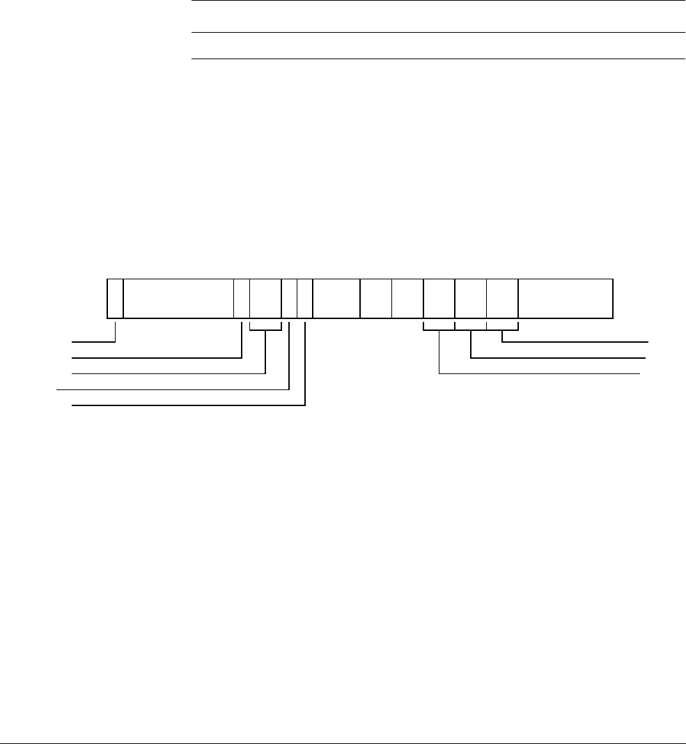
D8 AArch64 System Register Descriptions
D8.2 General system control registers
D8-2046 Copyright © 2013 ARM Limited. All rights reserved. ARM DDI 0487A.a
Non-Confidential - Beta ID090413
D8.2.84 TCR_EL3, Translation Control Register (EL3)
The TCR_EL3 characteristics are:
Purpose
Controls translation table walks required for the stage 1 translation of memory accesses from EL3,
and holds cacheability and shareability information for the accesses.
This register is part of the Virtual memory control registers functional group.
Usage constraints
This register is accessible as shown below:
Any of the bits in TCR_EL3 are permitted to be cached in a TLB.
Configurations
TCR_EL3[31:0] can be mapped to AArch32 register TTBCR (S), but this is not architecturally
mandated.
Attributes
TCR_EL3 is a 32-bit register.
The TCR_EL3 bit assignments are:
Bit [31]
Reserved, RES1.
Bits [30:24]
Reserved, RES0.
Bit [23]
Reserved, RES1.
Bits [22:21]
Reserved, RES0.
TBI, bit [20]
Top Byte ignored - indicates whether the top byte of an address is used for address match for the
TTBR0_EL3 region, or ignored and used for tagged addresses.
0
Top Byte used in the address calculation.
1
Top Byte ignored in the address calculation.
EL0 EL1 (NS) EL1 (S) EL2 EL3 (SCR.NS=1) EL3 (SCR.NS=0)
-- - -RW RW
31
RES0
30 24 23 22 21 20 19
PS
18 16
TG0
15 14
SH0
13 12 11 10 9876
T0SZ
50
RES1
RES1
RES0
TBI
RES0
RES0
IRGN0
ORGN0

D8 AArch64 System Register Descriptions
D8.2 General system control registers
ARM DDI 0487A.a Copyright © 2013 ARM Limited. All rights reserved. D8-2047
ID090413 Non-Confidential - Beta
This affects addresses generated in EL3 using AArch64 where the address would be translated by
tables pointed to by TTBR0_EL3. It has an effect whether the EL3 translation regime is enabled or
not.
Additionally, this affects changes to the program counter, when TBI is 1, caused by:
• A branch or procedure return within EL3.
• A exception taken to EL3.
• An exception return to EL3.
In these cases bits [63:56] of the address are set to 0 before it is stored in the PC.
Bit [19]
Reserved, RES0.
PS, bits [18:16]
Physical Address Size.
000
32 bits, 4 GB.
001
36 bits, 64 GB.
010
40 bits, 1 TB.
011
42 bits, 4 TB.
100
44 bits, 16 TB.
101
48 bits, 256 TB.
Other values are reserved.
The reserved values behave in the same way as the
101
encoding, but software must not rely on this
property as the behavior of the RESERVED values might change in a future revision of the
architecture.
TG0, bits [15:14]
Granule size for the corresponding translation table base address register.
00
4KByte
01
64KByte
10
16KByte
Other values are reserved.
If the value is programmed to either a reserved value, or a size that has not been implemented, then
the hardware will treat the field as if it has been programmed to an IMPLEMENTATION DEFINED
choice of the sizes that has been implemented for all purposes other than the value read back from
this register.
It is IMPLEMENTATION DEFINED whether the value read back is the value programmed or the value
that corresponds to the size chosen.
SH0, bits [13:12]
Shareability attribute for memory associated with translation table walks using TTBR0_EL3.
00
Non-shareable
10
Outer Shareable
11
Inner Shareable
Other values are reserved.
ORGN0, bits [11:10]
Outer cacheability attribute for memory associated with translation table walks using TTBR0_EL3.
00
Normal memory, Outer Non-cacheable
01
Normal memory, Outer Write-Back Write-Allocate Cacheable
10
Normal memory, Outer Write-Through Cacheable

D8 AArch64 System Register Descriptions
D8.2 General system control registers
D8-2048 Copyright © 2013 ARM Limited. All rights reserved. ARM DDI 0487A.a
Non-Confidential - Beta ID090413
11
Normal memory, Outer Write-Back no Write-Allocate Cacheable
IRGN0, bits [9:8]
Inner cacheability attribute for memory associated with translation table walks using TTBR0_EL3.
00
Normal memory, Inner Non-cacheable
01
Normal memory, Inner Write-Back Write-Allocate Cacheable
10
Normal memory, Inner Write-Through Cacheable
11
Normal memory, Inner Write-Back no Write-Allocate Cacheable
Bits [7:6]
Reserved, RES0.
T0SZ, bits [5:0]
The size offset of the memory region addressed by TTBR0_EL3. The region size is 264-T0SZ bytes.
The maximum and minimum possible values for T0SZ depend on the level of translation table and
the memory translation granule size, as described in the AArch64 Virtual Memory System
Architecture chapter.
Accessing the TCR_EL3:
To access the TCR_EL3:
MRS <Xt>, TCR_EL3 ; Read TCR_EL3 into Xt
MSR TCR_EL3, <Xt> ; Write Xt to TCR_EL3
Register access is encoded as follows:
op0 op1 CRn CRm op2
11 110 0010 0000 010
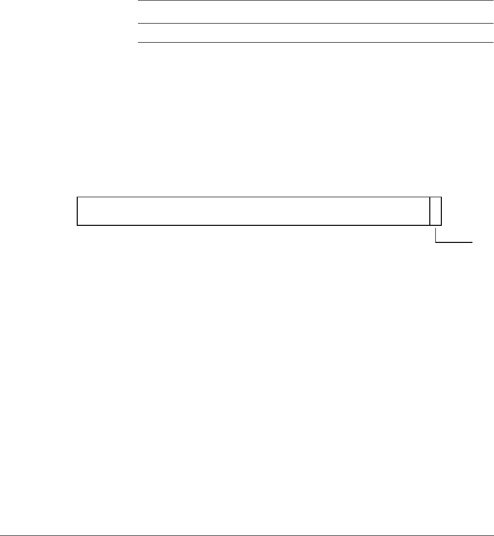
D8 AArch64 System Register Descriptions
D8.2 General system control registers
ARM DDI 0487A.a Copyright © 2013 ARM Limited. All rights reserved. D8-2049
ID090413 Non-Confidential - Beta
D8.2.85 TEECR32_EL1, T32EE Configuration Register
The TEECR32_EL1 characteristics are:
Purpose
Allows access to the AArch32 register TEECR from AArch64 state only. Its value has no effect on
execution in AArch64 state.
This register is part of the Legacy feature registers functional group.
Usage constraints
This register is accessible as shown below:
Configurations
TEECR32_EL1 is architecturally mapped to AArch32 register TEECR.
This register is optional in ARMv8. It is UNDEFINED at all exception levels when T32EE is not
implemented, and UNDEFINED at EL1 when SCTLR_EL1.THEE is 0.
Attributes
TEECR32_EL1 is a 32-bit register.
The TEECR32_EL1 bit assignments are:
Bits [31:1]
Reserved, RES0.
XED, bit [0]
Execution Environment Disable bit. Control unprivileged access to TEEHBR:
0
Unprivileged access permitted.
1
Unprivileged access disabled.
The effects of a write to this register on T32EE configuration are only guaranteed to be visible to
subsequent instructions after the execution of a context synchronization operation. However, a read
of this register always returns the value most recently written to the register.
Accessing the TEECR32_EL1:
To access the TEECR32_EL1:
MRS <Xt>, TEECR32_EL1 ; Read TEECR32_EL1 into Xt
MSR TEECR32_EL1, <Xt> ; Write Xt to TEECR32_EL1
EL0 EL1 (NS) EL1 (S) EL2 EL3 (SCR.NS=1) EL3 (SCR.NS=0)
-RW RW RWRW RW
RES0
31 1 0
XED

D8 AArch64 System Register Descriptions
D8.2 General system control registers
D8-2050 Copyright © 2013 ARM Limited. All rights reserved. ARM DDI 0487A.a
Non-Confidential - Beta ID090413
Register access is encoded as follows:
op0 op1 CRn CRm op2
10 010 0000 0000 000

D8 AArch64 System Register Descriptions
D8.2 General system control registers
ARM DDI 0487A.a Copyright © 2013 ARM Limited. All rights reserved. D8-2051
ID090413 Non-Confidential - Beta
D8.2.86 TEEHBR32_EL1, T32EE Handler Base Register
The TEEHBR32_EL1 characteristics are:
Purpose
Allows access to the AArch32 register TEEHBR from AArch64 state only. Its value has no effect
on execution in AArch64 state.
This register is part of the Legacy feature registers functional group.
Usage constraints
This register is accessible as shown below:
Configurations
TEEHBR32_EL1 is architecturally mapped to AArch32 register TEEHBR.
This register is optional in ARMv8, and is UNDEFINED when not implemented, or when disabled by
SCTLR_EL1.THEE.
Attributes
TEEHBR32_EL1 is a 32-bit register.
The TEEHBR32_EL1 bit assignments are:
HandlerBase, bits [31:2]
The address of the T32EE Handler_00 implementation. This is the address of the first of the T32EE
handlers.
Bits [1:0]
Reserved, RES0.
Accessing the TEEHBR32_EL1:
To access the TEEHBR32_EL1:
MRS <Xt>, TEEHBR32_EL1 ; Read TEEHBR32_EL1 into Xt
MSR TEEHBR32_EL1, <Xt> ; Write Xt to TEEHBR32_EL1
Register access is encoded as follows:
EL0 EL1 (NS) EL1 (S) EL2 EL3 (SCR.NS=1) EL3 (SCR.NS=0)
-RW RW RWRW RW
HandlerBase
31 2 10
RES0
op0 op1 CRn CRm op2
10 010 0001 0000 000

D8 AArch64 System Register Descriptions
D8.2 General system control registers
D8-2052 Copyright © 2013 ARM Limited. All rights reserved. ARM DDI 0487A.a
Non-Confidential - Beta ID090413
D8.2.87 TPIDR_EL0, Thread Pointer / ID Register (EL0)
The TPIDR_EL0 characteristics are:
Purpose
Provides a location where software executing at EL0 can store thread identifying information, for
OS management purposes.
This register is part of the Thread and process ID registers functional group.
Usage constraints
This register is accessible as shown below:
Configurations
TPIDR_EL0[31:0] is architecturally mapped to AArch32 register TPIDRURW (NS).
Attributes
TPIDR_EL0 is a 64-bit register.
The TPIDR_EL0 bit assignments are:
Bits [63:0]
Thread ID. Thread identifying information stored by software running at this exception level.
Accessing the TPIDR_EL0:
To access the TPIDR_EL0:
MRS <Xt>, TPIDR_EL0 ; Read TPIDR_EL0 into Xt
MSR TPIDR_EL0, <Xt> ; Write Xt to TPIDR_EL0
Register access is encoded as follows:
EL0 EL1 (NS) EL1 (S) EL2 EL3 (SCR.NS=1) EL3 (SCR.NS=0)
RW RW RW RW RW RW
Thread ID
63 0
op0 op1 CRn CRm op2
11 011 1101 0000 010
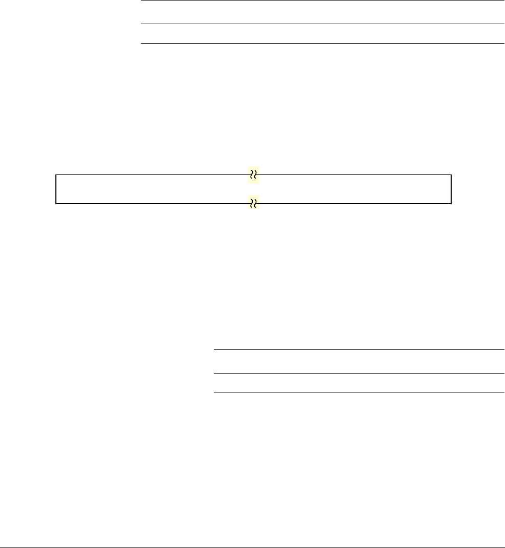
D8 AArch64 System Register Descriptions
D8.2 General system control registers
ARM DDI 0487A.a Copyright © 2013 ARM Limited. All rights reserved. D8-2053
ID090413 Non-Confidential - Beta
D8.2.88 TPIDR_EL1, Thread Pointer / ID Register (EL1)
The TPIDR_EL1 characteristics are:
Purpose
Provides a location where software executing at EL1 can store thread identifying information, for
OS management purposes.
This register is part of the Thread and process ID registers functional group.
Usage constraints
This register is accessible as shown below:
Configurations
TPIDR_EL1[31:0] is architecturally mapped to AArch32 register TPIDRPRW (NS).
Attributes
TPIDR_EL1 is a 64-bit register.
The TPIDR_EL1 bit assignments are:
Bits [63:0]
Thread ID. Thread identifying information stored by software running at this exception level.
Accessing the TPIDR_EL1:
To access the TPIDR_EL1:
MRS <Xt>, TPIDR_EL1 ; Read TPIDR_EL1 into Xt
MSR TPIDR_EL1, <Xt> ; Write Xt to TPIDR_EL1
Register access is encoded as follows:
EL0 EL1 (NS) EL1 (S) EL2 EL3 (SCR.NS=1) EL3 (SCR.NS=0)
-RW RW RWRW RW
Thread ID
63 0
op0 op1 CRn CRm op2
11 000 1101 0000 100
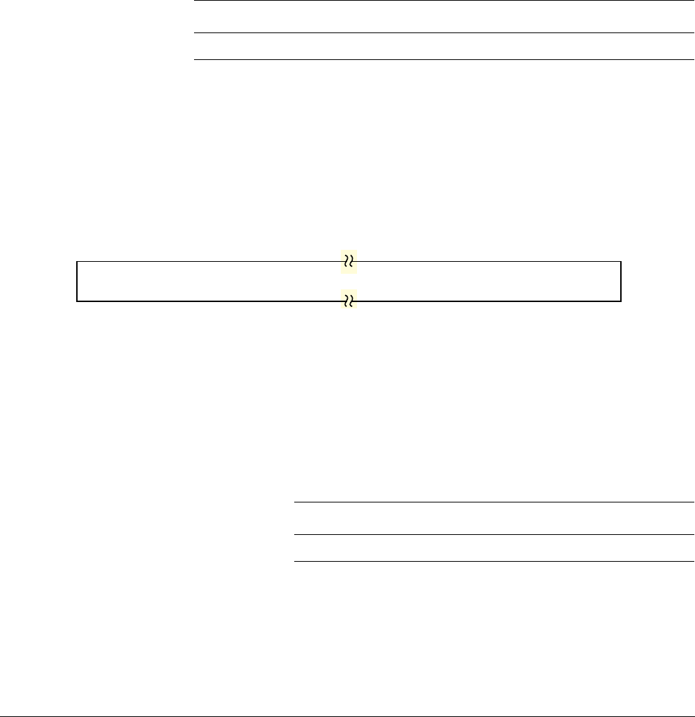
D8 AArch64 System Register Descriptions
D8.2 General system control registers
D8-2054 Copyright © 2013 ARM Limited. All rights reserved. ARM DDI 0487A.a
Non-Confidential - Beta ID090413
D8.2.89 TPIDR_EL2, Thread Pointer / ID Register (EL2)
The TPIDR_EL2 characteristics are:
Purpose
Provides a location where software executing at EL2 can store thread identifying information, for
OS management purposes.
This register is part of:
• the Virtualization registers functional group
• the Thread and process ID registers functional group.
Usage constraints
This register is accessible as shown below:
Configurations
TPIDR_EL2[31:0] is architecturally mapped to AArch32 register HTPIDR.
If EL2 is not implemented, this register is RES0 from EL3.
Attributes
TPIDR_EL2 is a 64-bit register.
The TPIDR_EL2 bit assignments are:
Bits [63:0]
Thread ID. Thread identifying information stored by software running at this exception level.
Accessing the TPIDR_EL2:
To access the TPIDR_EL2:
MRS <Xt>, TPIDR_EL2 ; Read TPIDR_EL2 into Xt
MSR TPIDR_EL2, <Xt> ; Write Xt to TPIDR_EL2
Register access is encoded as follows:
EL0 EL1 (NS) EL1 (S) EL2 EL3 (SCR.NS=1) EL3 (SCR.NS=0)
-- - RWRW RW
Thread ID
63 0
op0 op1 CRn CRm op2
11 100 1101 0000 010

D8 AArch64 System Register Descriptions
D8.2 General system control registers
ARM DDI 0487A.a Copyright © 2013 ARM Limited. All rights reserved. D8-2055
ID090413 Non-Confidential - Beta
D8.2.90 TPIDR_EL3, Thread Pointer / ID Register (EL3)
The TPIDR_EL3 characteristics are:
Purpose
Provides a location where software executing at EL3 can store thread identifying information, for
OS management purposes.
This register is part of the Thread and process ID registers functional group.
Usage constraints
This register is accessible as shown below:
Configurations
There are no configuration notes.
Attributes
TPIDR_EL3 is a 64-bit register.
The TPIDR_EL3 bit assignments are:
Bits [63:0]
Thread ID. Thread identifying information stored by software running at this exception level.
Accessing the TPIDR_EL3:
To access the TPIDR_EL3:
MRS <Xt>, TPIDR_EL3 ; Read TPIDR_EL3 into Xt
MSR TPIDR_EL3, <Xt> ; Write Xt to TPIDR_EL3
Register access is encoded as follows:
EL0 EL1 (NS) EL1 (S) EL2 EL3 (SCR.NS=1) EL3 (SCR.NS=0)
-- - -RW RW
Thread ID
63 0
op0 op1 CRn CRm op2
11 110 1101 0000 010

D8 AArch64 System Register Descriptions
D8.2 General system control registers
D8-2056 Copyright © 2013 ARM Limited. All rights reserved. ARM DDI 0487A.a
Non-Confidential - Beta ID090413
D8.2.91 TPIDRRO_EL0, Thread Pointer / ID Register, Read-Only (EL0)
The TPIDRRO_EL0 characteristics are:
Purpose
Provides a location where software executing at EL1 or higher can store thread identifying
information that is visible to software executing at EL0, for OS management purposes.
This register is part of the Thread and process ID registers functional group.
Usage constraints
This register is accessible as shown below:
Configurations
TPIDRRO_EL0[31:0] is architecturally mapped to AArch32 register TPIDRURO (NS).
Attributes
TPIDRRO_EL0 is a 64-bit register.
The TPIDRRO_EL0 bit assignments are:
Bits [63:0]
Thread ID. Thread identifying information stored by software running at this exception level.
Accessing the TPIDRRO_EL0:
To access the TPIDRRO_EL0:
MRS <Xt>, TPIDRRO_EL0 ; Read TPIDRRO_EL0 into Xt
MSR TPIDRRO_EL0, <Xt> ; Write Xt to TPIDRRO_EL0
Register access is encoded as follows:
EL0 EL1 (NS) EL1 (S) EL2 EL3 (SCR.NS=1) EL3 (SCR.NS=0)
RO RW RW RW RW RW
Thread ID
63 0
op0 op1 CRn CRm op2
11 011 1101 0000 011
D8 AArch64 System Register Descriptions
D8.2 General system control registers
ARM DDI 0487A.a Copyright © 2013 ARM Limited. All rights reserved. D8-2057
ID090413 Non-Confidential - Beta
D8.2.92 TTBR0_EL1, Translation Table Base Register 0 (EL1)
The TTBR0_EL1 characteristics are:
Purpose
Holds the base address of translation table 0, and information about the memory it occupies. This is
one of the translation tables for the stage 1 translation of memory accesses at EL0 and EL1.
This register is part of the Virtual memory control registers functional group.
Usage constraints
This register is accessible as shown below:
Any of the fields in this register are permitted to be cached in a TLB.
Configurations
TTBR0_EL1 is architecturally mapped to AArch32 register TTBR0 (NS).
Attributes
TTBR0_EL1 is a 64-bit register.
The TTBR0_EL1 bit assignments are:
ASID, bits [63:48]
An ASID for the translation table base address. The TCR_EL1.A1 field selects either
TTBR0_EL1.ASID or TTBR1_EL1.ASID.
If the implementation has only 8 bits of ASID, then the upper 8 bits of this field are RES0.
BADDR[47:x], bits [47:0]
Translation table base address, bits[47:x]. Bits [x-1:0] are RES0.
x is based on the value of TCR_EL1.T0SZ, the stage of translation, and the memory translation
granule size.
The AArch64 Virtual Memory System Architecture chapter describes how x is calculated.
The value of x determines the required alignment of the translation table, which must be aligned to
2x bytes.
If bits [x-1:0] are not all zero, this is a misaligned Translation Table Base Address. Its effects are
CONSTRAINED UNPREDICTABLE, and can be one of the following:
• Bits [x-1:0] are treated as if all the bits are zero. The value read back from those bits might
be the value written or might be zero.
• The calculation of an address for a translation table walk using this register can be corrupted
in those bits that are non-zero.
Accessing the TTBR0_EL1:
To access the TTBR0_EL1:
EL0 EL1 (NS) EL1 (S) EL2 EL3 (SCR.NS=1) EL3 (SCR.NS=0)
-RW RW RWRW RW
ASID
63 48
BADDR[47:x]
47 0

D8 AArch64 System Register Descriptions
D8.2 General system control registers
D8-2058 Copyright © 2013 ARM Limited. All rights reserved. ARM DDI 0487A.a
Non-Confidential - Beta ID090413
MRS <Xt>, TTBR0_EL1 ; Read TTBR0_EL1 into Xt
MSR TTBR0_EL1, <Xt> ; Write Xt to TTBR0_EL1
Register access is encoded as follows:
op0 op1 CRn CRm op2
11 000 0010 0000 000
D8 AArch64 System Register Descriptions
D8.2 General system control registers
ARM DDI 0487A.a Copyright © 2013 ARM Limited. All rights reserved. D8-2059
ID090413 Non-Confidential - Beta
D8.2.93 TTBR0_EL2, Translation Table Base Register 0 (EL2)
The TTBR0_EL2 characteristics are:
Purpose
Holds the base address of the translation table for the stage 1 translation of memory accesses from
EL2.
This register is part of:
• the Virtualization registers functional group
• the Virtual memory control registers functional group.
Usage constraints
This register is accessible as shown below:
Any of the fields in this register are permitted to be cached in a TLB.
Configurations
TTBR0_EL2 is architecturally mapped to AArch32 register HTTBR.
If EL2 is not implemented, this register is RES0 from EL3.
Attributes
TTBR0_EL2 is a 64-bit register.
The TTBR0_EL2 bit assignments are:
Bits [63:48]
Reserved, RES0.
BADDR[47:x], bits [47:0]
Translation table base address, bits[47:x]. Bits [x-1:0] are RES0.
x is based on the value of TCR_EL2.T0SZ, the stage of translation, and the memory translation
granule size.
The AArch64 Virtual Memory System Architecture chapter describes how x is calculated.
The value of x determines the required alignment of the translation table, which must be aligned to
2x bytes.
If bits [x-1:0] are not all zero, this is a misaligned Translation Table Base Address. Its effects are
CONSTRAINED UNPREDICTABLE, and can be one of the following:
• Bits [x-1:0] are treated as if all the bits are zero. The value read back from those bits might
be the value written or might be zero.
• The calculation of an address for a translation table walk using this register can be corrupted
in those bits that are non-zero.
Accessing the TTBR0_EL2:
To access the TTBR0_EL2:
EL0 EL1 (NS) EL1 (S) EL2 EL3 (SCR.NS=1) EL3 (SCR.NS=0)
-- - RWRW RW
RES0
63 48
BADDR[47:x]
47 0

D8 AArch64 System Register Descriptions
D8.2 General system control registers
D8-2060 Copyright © 2013 ARM Limited. All rights reserved. ARM DDI 0487A.a
Non-Confidential - Beta ID090413
MRS <Xt>, TTBR0_EL2 ; Read TTBR0_EL2 into Xt
MSR TTBR0_EL2, <Xt> ; Write Xt to TTBR0_EL2
Register access is encoded as follows:
op0 op1 CRn CRm op2
11 100 0010 0000 000
D8 AArch64 System Register Descriptions
D8.2 General system control registers
ARM DDI 0487A.a Copyright © 2013 ARM Limited. All rights reserved. D8-2061
ID090413 Non-Confidential - Beta
D8.2.94 TTBR0_EL3, Translation Table Base Register 0 (EL3)
The TTBR0_EL3 characteristics are:
Purpose
Holds the base address of the translation table for the stage 1 translation of memory accesses from
EL3.
This register is part of the Virtual memory control registers functional group.
Usage constraints
This register is accessible as shown below:
Any of the fields in this register are permitted to be cached in a TLB.
Configurations
TTBR0_EL3 can be mapped to AArch32 register TTBR0 (S), but this is not architecturally
mandated.
Attributes
TTBR0_EL3 is a 64-bit register.
The TTBR0_EL3 bit assignments are:
Bits [63:48]
Reserved, RES0.
BADDR[47:x], bits [47:0]
Translation table base address, bits[47:x]. Bits [x-1:0] are RES0.
x is based on the value of TCR_EL3.T0SZ, the stage of translation, and the memory translation
granule size.
The AArch64 Virtual Memory System Architecture chapter describes how x is calculated.
The value of x determines the required alignment of the translation table, which must be aligned to
2x bytes.
If bits [x-1:0] are not all zero, this is a misaligned Translation Table Base Address. Its effects are
CONSTRAINED UNPREDICTABLE, and can be one of the following:
• Bits [x-1:0] are treated as if all the bits are zero. The value read back from those bits might
be the value written or might be zero.
• The calculation of an address for a translation table walk using this register can be corrupted
in those bits that are non-zero.
Accessing the TTBR0_EL3:
To access the TTBR0_EL3:
MRS <Xt>, TTBR0_EL3 ; Read TTBR0_EL3 into Xt
MSR TTBR0_EL3, <Xt> ; Write Xt to TTBR0_EL3
EL0 EL1 (NS) EL1 (S) EL2 EL3 (SCR.NS=1) EL3 (SCR.NS=0)
-- - -RW RW
RES0
63 48
BADDR[47:x]
47 0

D8 AArch64 System Register Descriptions
D8.2 General system control registers
D8-2062 Copyright © 2013 ARM Limited. All rights reserved. ARM DDI 0487A.a
Non-Confidential - Beta ID090413
Register access is encoded as follows:
op0 op1 CRn CRm op2
11 110 0010 0000 000

D8 AArch64 System Register Descriptions
D8.2 General system control registers
ARM DDI 0487A.a Copyright © 2013 ARM Limited. All rights reserved. D8-2063
ID090413 Non-Confidential - Beta
D8.2.95 TTBR1_EL1, Translation Table Base Register 1
The TTBR1_EL1 characteristics are:
Purpose
Holds the base address of translation table 1, and information about the memory it occupies. This is
one of the translation tables for the stage 1 translation of memory accesses at EL0 and EL1.
This register is part of the Virtual memory control registers functional group.
Usage constraints
This register is accessible as shown below:
Any of the fields in this register are permitted to be cached in a TLB.
Configurations
TTBR1_EL1 is architecturally mapped to AArch32 register TTBR1 (NS).
Attributes
TTBR1_EL1 is a 64-bit register.
The TTBR1_EL1 bit assignments are:
ASID, bits [63:48]
An ASID for the translation table base address. The TCR_EL1.A1 field selects either
TTBR0_EL1.ASID or TTBR1_EL1.ASID.
If the implementation has only 8 bits of ASID, then the upper 8 bits of this field are RES0.
BADDR[47:x], bits [47:0]
Translation table base address, bits[47:x]. Bits [x-1:0] are RES0.
x is based on the value of TCR_EL1.T0SZ, the stage of translation, and the memory translation
granule size.
The AArch64 Virtual Memory System Architecture chapter describes how x is calculated.
The value of x determines the required alignment of the translation table, which must be aligned to
2x bytes.
If bits [x-1:0] are not all zero, this is a misaligned Translation Table Base Address. Its effects are
CONSTRAINED UNPREDICTABLE, and can be one of the following:
• Bits [x-1:0] are treated as if all the bits are zero. The value read back from those bits might
be the value written or might be zero.
• The calculation of an address for a translation table walk using this register can be corrupted
in those bits that are non-zero.
Accessing the TTBR1_EL1:
To access the TTBR1_EL1:
EL0 EL1 (NS) EL1 (S) EL2 EL3 (SCR.NS=1) EL3 (SCR.NS=0)
-RW RW RWRW RW
ASID
63 48
BADDR[47:x]
47 0

D8 AArch64 System Register Descriptions
D8.2 General system control registers
D8-2064 Copyright © 2013 ARM Limited. All rights reserved. ARM DDI 0487A.a
Non-Confidential - Beta ID090413
MRS <Xt>, TTBR1_EL1 ; Read TTBR1_EL1 into Xt
MSR TTBR1_EL1, <Xt> ; Write Xt to TTBR1_EL1
Register access is encoded as follows:
op0 op1 CRn CRm op2
11 000 0010 0000 001

D8 AArch64 System Register Descriptions
D8.2 General system control registers
ARM DDI 0487A.a Copyright © 2013 ARM Limited. All rights reserved. D8-2065
ID090413 Non-Confidential - Beta
D8.2.96 VBAR_EL1, Vector Base Address Register (EL1)
The VBAR_EL1 characteristics are:
Purpose
Holds the exception base address for any exception that is taken to EL1.
This register is part of the Exception and fault handling registers functional group.
Usage constraints
This register is accessible as shown below:
Configurations
VBAR_EL1[31:0] is architecturally mapped to AArch32 register VBAR (NS).
Attributes
VBAR_EL1 is a 64-bit register.
The VBAR_EL1 bit assignments are:
Bits [63:11]
Vector Base Address. Base address of the exception vectors for exceptions taken in EL1.
If tagged addresses are being used, bits [55:48] of VBAR_EL1 must be the same or else the use of
the vector address will result in a recursive exception.
If tagged addresses are not being used, bits [63:48] of VBAR_EL1 must be the same or else the use
of the vector address will result in a recursive exception.
Bits [10:0]
Reserved, RES0.
Accessing the VBAR_EL1:
To access the VBAR_EL1:
MRS <Xt>, VBAR_EL1 ; Read VBAR_EL1 into Xt
MSR VBAR_EL1, <Xt> ; Write Xt to VBAR_EL1
Register access is encoded as follows:
EL0 EL1 (NS) EL1 (S) EL2 EL3 (SCR.NS=1) EL3 (SCR.NS=0)
-RW RW RWRW RW
Vector Base Address
63 11
RES0
10 0
op0 op1 CRn CRm op2
11 000 1100 0000 000
D8 AArch64 System Register Descriptions
D8.2 General system control registers
D8-2066 Copyright © 2013 ARM Limited. All rights reserved. ARM DDI 0487A.a
Non-Confidential - Beta ID090413
D8.2.97 VBAR_EL2, Vector Base Address Register (EL2)
The VBAR_EL2 characteristics are:
Purpose
Holds the exception base address for any exception that is taken to EL2.
This register is part of:
• the Virtualization registers functional group
• the Exception and fault handling registers functional group.
Usage constraints
This register is accessible as shown below:
Configurations
VBAR_EL2[31:0] is architecturally mapped to AArch32 register HVBAR.
If EL2 is not implemented, this register is RES0 from EL3.
Attributes
VBAR_EL2 is a 64-bit register.
The VBAR_EL2 bit assignments are:
Bits [63:11]
Vector Base Address. Base address of the exception vectors for exceptions taken in EL2.
If tagged addresses are being used, bits [55:48] of VBAR_EL2 must be 0 or else the use of the vector
address will result in a recursive exception.
If tagged addresses are not being used, bits [63:48] of VBAR_EL2 must be 0 or else the use of the
vector address will result in a recursive exception.
Bits [10:0]
Reserved, RES0.
Accessing the VBAR_EL2:
To access the VBAR_EL2:
MRS <Xt>, VBAR_EL2 ; Read VBAR_EL2 into Xt
MSR VBAR_EL2, <Xt> ; Write Xt to VBAR_EL2
Register access is encoded as follows:
EL0 EL1 (NS) EL1 (S) EL2 EL3 (SCR.NS=1) EL3 (SCR.NS=0)
-- - RWRW RW
Vector Base Address
63 11
RES0
10 0
op0 op1 CRn CRm op2
11 100 1100 0000 000

D8 AArch64 System Register Descriptions
D8.2 General system control registers
ARM DDI 0487A.a Copyright © 2013 ARM Limited. All rights reserved. D8-2067
ID090413 Non-Confidential - Beta
D8.2.98 VBAR_EL3, Vector Base Address Register (EL3)
The VBAR_EL3 characteristics are:
Purpose
Holds the exception base address for any exception that is taken to EL3.
This register is part of:
• the Exception and fault handling registers functional group
• the Security registers functional group.
Usage constraints
This register is accessible as shown below:
Configurations
VBAR_EL3[31:0] can be mapped to AArch32 register VBAR (S), but this is not architecturally
mandated.
Attributes
VBAR_EL3 is a 64-bit register.
The VBAR_EL3 bit assignments are:
Bits [63:11]
Vector Base Address. Base address of the exception vectors for exceptions taken in EL3.
If tagged addresses are being used, bits [55:48] of VBAR_EL3 must be 0 or else the use of the vector
address will result in a recursive exception.
If tagged addresses are not being used, bits [63:48] of VBAR_EL3 must be 0 or else the use of the
vector address will result in a recursive exception.
Bits [10:0]
Reserved, RES0.
Accessing the VBAR_EL3:
To access the VBAR_EL3:
MRS <Xt>, VBAR_EL3 ; Read VBAR_EL3 into Xt
MSR VBAR_EL3, <Xt> ; Write Xt to VBAR_EL3
Register access is encoded as follows:
EL0 EL1 (NS) EL1 (S) EL2 EL3 (SCR.NS=1) EL3 (SCR.NS=0)
-- - -RW RW
Vector Base Address
63 11
RES0
10 0
op0 op1 CRn CRm op2
11 110 1100 0000 000
D8 AArch64 System Register Descriptions
D8.2 General system control registers
D8-2068 Copyright © 2013 ARM Limited. All rights reserved. ARM DDI 0487A.a
Non-Confidential - Beta ID090413
D8.2.99 VMPIDR_EL2, Virtualization Multiprocessor ID Register
The VMPIDR_EL2 characteristics are:
Purpose
Holds the value of the Virtualization Multiprocessor ID. This is the value returned by Non-secure
EL1 reads of MPIDR_EL1.
This register is part of:
• the Identification registers functional group
• the Virtualization registers functional group.
Usage constraints
This register is accessible as shown below:
Configurations
VMPIDR_EL2[31:0] is architecturally mapped to AArch32 register VMPIDR.
If EL2 is not implemented, this register is RES0 from EL3.
Attributes
VMPIDR_EL2 is a 64-bit register.
The VMPIDR_EL2 bit assignments are:
Bits [63:40]
Reserved, RES0.
Aff3, bits [39:32]
Affinity level 3. Highest level affinity field.
Bit [31]
Reserved, RES1.
U, bit [30]
Indicates a Uniprocessor system, as distinct from processor 0 in a multiprocessor system. The
possible values of this bit are:
0
Processor is part of a multiprocessor system.
1
Processor is part of a uniprocessor system.
Bits [29:25]
Reserved, RES0.
EL0 EL1 (NS) EL1 (S) EL2 EL3 (SCR.NS=1) EL3 (SCR.NS=0)
-- - RWRW RW
RES0
63 40
Aff3
39 32 31
U
30
RES0
29 25 24
Aff2
23 16
Aff1
15 8
Aff0
70
RES1 MT

D8 AArch64 System Register Descriptions
D8.2 General system control registers
ARM DDI 0487A.a Copyright © 2013 ARM Limited. All rights reserved. D8-2069
ID090413 Non-Confidential - Beta
MT, bit [24]
Indicates whether the lowest level of affinity consists of logical processors that are implemented
using a multi-threading type approach. The possible values of this bit are:
0
Performance of processors at the lowest affinity level is largely independent.
1
Performance of processors at the lowest affinity level is very interdependent.
Aff2, bits [23:16]
Affinity level 2. Second highest level affinity field.
Aff1, bits [15:8]
Affinity level 1. Third highest level affinity field.
Aff0, bits [7:0]
Affinity level 0. Lowest level affinity field.
Accessing the VMPIDR_EL2:
To access the VMPIDR_EL2:
MRS <Xt>, VMPIDR_EL2 ; Read VMPIDR_EL2 into Xt
MSR VMPIDR_EL2, <Xt> ; Write Xt to VMPIDR_EL2
Register access is encoded as follows:
op0 op1 CRn CRm op2
11 100 0000 0000 101

D8 AArch64 System Register Descriptions
D8.2 General system control registers
D8-2070 Copyright © 2013 ARM Limited. All rights reserved. ARM DDI 0487A.a
Non-Confidential - Beta ID090413
D8.2.100 VPIDR_EL2, Virtualization Processor ID Register
The VPIDR_EL2 characteristics are:
Purpose
Holds the value of the Virtualization Processor ID. This is the value returned by Non-secure EL1
reads of MIDR_EL1.
This register is part of:
• the Virtualization registers functional group
• the Identification registers functional group.
Usage constraints
This register is accessible as shown below:
Configurations
VPIDR_EL2 is architecturally mapped to AArch32 register VPIDR.
If EL2 is not implemented, this register is RES0 from EL3.
Attributes
VPIDR_EL2 is a 32-bit register.
The VPIDR_EL2 bit assignments are:
Implementer, bits [31:24]
The Implementer code. This field must hold an implementer code that has been assigned by ARM.
Assigned codes include the following:
EL0 EL1 (NS) EL1 (S) EL2 EL3 (SCR.NS=1) EL3 (SCR.NS=0)
-- - RWRW RW
Implementer
31 24
Variant
23 20 19 16
PartNum
15 4
Revision
30
Architecture
Hex
representation ASCII
representation Implementer
0x41
A ARM Limited
0x42
B Broadcom Corporation
0x43
C Cavium Inc.
0x44
D Digital Equipment Corporation
0x49
I Infineon Technologies AG
0x4D
M Motorola or Freescale Semiconductor Inc.
0x4E
N NVIDIA Corporation
0x50
P Applied Micro Circuits Corporation

D8 AArch64 System Register Descriptions
D8.2 General system control registers
ARM DDI 0487A.a Copyright © 2013 ARM Limited. All rights reserved. D8-2071
ID090413 Non-Confidential - Beta
ARM can assign codes that are not published in this manual. All values not assigned by ARM are
reserved and must not be used.
Variant, bits [23:20]
An IMPLEMENTATION DEFINED variant number. Typically, this field is used to distinguish between
different product variants, or major revisions of a product.
Architecture, bits [19:16]
The permitted values of this field are:
0001
ARMv4
0010
ARMv4T
0011
ARMv5 (obsolete)
0100
ARMv5T
0101
ARMv5TE
0110
ARMv5TEJ
0111
ARMv6
1111
Defined by CPUID scheme
All other values are reserved.
PartNum, bits [15:4]
An IMPLEMENTATION DEFINED primary part number for the device.
On processors implemented by ARM, if the top four bits of the primary part number are
0x0
or
0x7
,
the variant and architecture are encoded differently.
Revision, bits [3:0]
An IMPLEMENTATION DEFINED revision number for the device.
Accessing the VPIDR_EL2:
To access the VPIDR_EL2:
MRS <Xt>, VPIDR_EL2 ; Read VPIDR_EL2 into Xt
MSR VPIDR_EL2, <Xt> ; Write Xt to VPIDR_EL2
Register access is encoded as follows:
0x51
Q Qualcomm Inc.
0x56
V Marvell International Ltd.
0x69
i Intel Corporation
op0 op1 CRn CRm op2
11 100 0000 0000 000
Hex
representation ASCII
representation Implementer

D8 AArch64 System Register Descriptions
D8.2 General system control registers
D8-2072 Copyright © 2013 ARM Limited. All rights reserved. ARM DDI 0487A.a
Non-Confidential - Beta ID090413
D8.2.101 VTCR_EL2, Virtualization Translation Control Register
The VTCR_EL2 characteristics are:
Purpose
Controls the translation table walks required for the stage 2 translation of memory accesses from
Non-secure EL0 and EL1, and holds cacheability and shareability information for the accesses.
This register is part of:
• the Virtualization registers functional group
• the Virtual memory control registers functional group.
Usage constraints
This register is accessible as shown below:
Any of the bits in VTCR_EL2 are permitted to be cached in a TLB.
Configurations
VTCR_EL2 is architecturally mapped to AArch32 register VTCR.
If EL2 is not implemented, this register is RES0 from EL3.
Attributes
VTCR_EL2 is a 32-bit register.
The VTCR_EL2 bit assignments are:
Bit [31]
Reserved, RES1.
Bits [30:19]
Reserved, RES0.
PS, bits [18:16]
Physical Address Size.
000
32 bits, 4 GB.
001
36 bits, 64 GB.
010
40 bits, 1 TB.
011
42 bits, 4 TB.
100
44 bits, 16 TB.
101
48 bits, 256 TB.
Other values are reserved.
EL0 EL1 (NS) EL1 (S) EL2 EL3 (SCR.NS=1) EL3 (SCR.NS=0)
-- - RWRW RW
31
RES0
30 19
PS
18 16
TG0
15 14
SH0
13 12 11 10 98
SL0
76
T0SZ
50
RES1 IRGN0
ORGN0

D8 AArch64 System Register Descriptions
D8.2 General system control registers
ARM DDI 0487A.a Copyright © 2013 ARM Limited. All rights reserved. D8-2073
ID090413 Non-Confidential - Beta
The reserved values behave in the same way as the
101
encoding, but software must not rely on this
property as the behavior of the RESERVED values might change in a future revision of the
architecture.
TG0, bits [15:14]
Granule size for the corresponding translation table base address register.
00
4KByte
01
64KByte
10
16KByte
Other values are reserved.
If the value is programmed to either a reserved value, or a size that has not been implemented, then
the hardware will treat the field as if it has been programmed to an IMPLEMENTATION DEFINED
choice of the sizes that has been implemented for all purposes other than the value read back from
this register.
It is IMPLEMENTATION DEFINED whether the value read back is the value programmed or the value
that corresponds to the size chosen.
SH0, bits [13:12]
Shareability attribute for memory associated with translation table walks using VTTBR_EL2.
00
Non-shareable
10
Outer Shareable
11
Inner Shareable
Other values are reserved.
ORGN0, bits [11:10]
Outer cacheability attribute for memory associated with translation table walks using VTTBR_EL2.
00
Normal memory, Outer Non-cacheable
01
Normal memory, Outer Write-Back Write-Allocate Cacheable
10
Normal memory, Outer Write-Through Cacheable
11
Normal memory, Outer Write-Back no Write-Allocate Cacheable
IRGN0, bits [9:8]
Inner cacheability attribute for memory associated with translation table walks using VTTBR_EL2.
00
Normal memory, Inner Non-cacheable
01
Normal memory, Inner Write-Back Write-Allocate Cacheable
10
Normal memory, Inner Write-Through Cacheable
11
Normal memory, Inner Write-Back no Write-Allocate Cacheable
SL0, bits [7:6]
Starting level of the VTCR_EL2 addressed region. The meaning of this field depends on the value
of VTCR_EL2.TG0 (the granule size).
00
If TG0 is
0b00
(4KB granule), start at level 2. If TG0 is
0b10
(16KB granule) or
0b01
(64KB granule), start at level 3.
01
If TG0 is
0b00
(4KB granule), start at level 1. If TG0 is
0b10
(16KB granule) or
0b01
(64KB granule), start at level 2.
10
If TG0 is
0b00
(4KB granule), start at level 0. If TG0 is
0b10
(16KB granule) or
0b01
(64KB granule), start at level 1.
Other values are reserved.
T0SZ, bits [5:0]
The size offset of the memory region addressed by VTTBR_EL2. The region size is 264-T0SZ bytes.

D8 AArch64 System Register Descriptions
D8.2 General system control registers
D8-2074 Copyright © 2013 ARM Limited. All rights reserved. ARM DDI 0487A.a
Non-Confidential - Beta ID090413
The maximum and minimum possible values for T0SZ depend on the level of translation table and
the memory translation granule size, as described in the AArch64 Virtual Memory System
Architecture chapter.
Accessing the VTCR_EL2:
To access the VTCR_EL2:
MRS <Xt>, VTCR_EL2 ; Read VTCR_EL2 into Xt
MSR VTCR_EL2, <Xt> ; Write Xt to VTCR_EL2
Register access is encoded as follows:
op0 op1 CRn CRm op2
11 100 0010 0001 010
D8 AArch64 System Register Descriptions
D8.2 General system control registers
ARM DDI 0487A.a Copyright © 2013 ARM Limited. All rights reserved. D8-2075
ID090413 Non-Confidential - Beta
D8.2.102 VTTBR_EL2, Virtualization Translation Table Base Register
The VTTBR_EL2 characteristics are:
Purpose
Holds the base address of the translation table for the stage 2 translation of memory accesses from
Non-secure EL0 and EL1.
This register is part of:
• the Virtualization registers functional group
• the Virtual memory control registers functional group.
Usage constraints
This register is accessible as shown below:
Any of the fields in this register are permitted to be cached in a TLB.
Configurations
VTTBR_EL2 is architecturally mapped to AArch32 register VTTBR.
If EL2 is not implemented, this register is RES0 from EL3.
Attributes
VTTBR_EL2 is a 64-bit register.
The VTTBR_EL2 bit assignments are:
Bits [63:56]
Reserved, RES0.
VMID, bits [55:48]
The VMID for the translation table.
BADDR[47:x], bits [47:0]
Translation table base address, bits[47:x]. Bits [x-1:0] are RES0.
x is based on the value of VTCR_EL2.T0SZ, the stage of translation, and the memory translation
granule size.
The AArch64 Virtual Memory System Architecture chapter describes how x is calculated.
The value of x determines the required alignment of the translation table, which must be aligned to
2x bytes.
If bits [x-1:0] are not all zero, this is a misaligned Translation Table Base Address. Its effects are
CONSTRAINED UNPREDICTABLE, and can be one of the following:
• Bits [x-1:0] are treated as if all the bits are zero. The value read back from those bits might
be the value written or might be zero.
• The calculation of an address for a translation table walk using this register can be corrupted
in those bits that are non-zero.
EL0 EL1 (NS) EL1 (S) EL2 EL3 (SCR.NS=1) EL3 (SCR.NS=0)
-- - RWRW RW
RES0
63 56
VMID
55 48
BADDR[47:x]
47 0

D8 AArch64 System Register Descriptions
D8.2 General system control registers
D8-2076 Copyright © 2013 ARM Limited. All rights reserved. ARM DDI 0487A.a
Non-Confidential - Beta ID090413
Accessing the VTTBR_EL2:
To access the VTTBR_EL2:
MRS <Xt>, VTTBR_EL2 ; Read VTTBR_EL2 into Xt
MSR VTTBR_EL2, <Xt> ; Write Xt to VTTBR_EL2
Register access is encoded as follows:
op0 op1 CRn CRm op2
11 100 0010 0001 000

D8 AArch64 System Register Descriptions
D8.3 Debug registers
ARM DDI 0487A.a Copyright © 2013 ARM Limited. All rights reserved. D8-2077
ID090413 Non-Confidential - Beta
D8.3 Debug registers
This section lists the Debug registers in AArch64 state.
D8.3.1 DBGAUTHSTATUS_EL1, Debug Authentication Status register
The DBGAUTHSTATUS_EL1 characteristics are:
Purpose
Provides information about the state of the IMPLEMENTATION DEFINED authentication interface for
debug.
This register is part of the Debug registers functional group.
Usage constraints
This register is accessible as shown below:
Configurations
DBGAUTHSTATUS_EL1 is architecturally mapped to AArch32 register DBGAUTHSTATUS.
DBGAUTHSTATUS_EL1 is architecturally mapped to external register
DBGAUTHSTATUS_EL1.
Attributes
DBGAUTHSTATUS_EL1 is a 32-bit register.
The DBGAUTHSTATUS_EL1 bit assignments are:
Bits [31:8]
Reserved, RES0.
SNID, bits [7:6]
Secure non-invasive debug. Possible values of this field are:
00
Not implemented. EL3 is not implemented and the processor is Non-secure.
10
Implemented and disabled. ExternalSecureNoninvasiveDebugEnabled() == FALSE.
11
Implemented and enabled. ExternalSecureNoninvasiveDebugEnabled() == TRUE.
Other values are reserved.
SID, bits [5:4]
Secure invasive debug. Possible values of this field are:
00
Not implemented. EL3 is not implemented and the processor is Non-secure.
10
Implemented and disabled. ExternalSecureInvasiveDebugEnabled() == FALSE.
11
Implemented and enabled. ExternalSecureInvasiveDebugEnabled() == TRUE.
Other values are reserved.
EL0 EL1 (NS) EL1 (S) EL2 EL3 (SCR.NS=1) EL3 (SCR.NS=0)
-RO RO RORO RO
RES0
31 8
SNID
76
SID
5432
NSID
10
NSNID

D8 AArch64 System Register Descriptions
D8.3 Debug registers
D8-2078 Copyright © 2013 ARM Limited. All rights reserved. ARM DDI 0487A.a
Non-Confidential - Beta ID090413
NSNID, bits [3:2]
Non-secure non-invasive debug. Possible values of this field are:
00
Not implemented. EL3 is not implemented and the processor is Secure.
10
Implemented and disabled. ExternalNoninvasiveDebugEnabled() == FALSE.
11
Implemented and enabled. ExternalNoninvasiveDebugEnabled() == TRUE.
Other values are reserved.
NSID, bits [1:0]
Non-secure invasive debug. Possible values of this field are:
00
Not implemented. EL3 is not implemented and the processor is Secure.
10
Implemented and disabled. ExternalInvasiveDebugEnabled() == FALSE.
11
Implemented and enabled. ExternalInvasiveDebugEnabled() == TRUE.
Other values are reserved.
Accessing the DBGAUTHSTATUS_EL1:
To access the DBGAUTHSTATUS_EL1:
MRS <Xt>, DBGAUTHSTATUS_EL1 ; Read DBGAUTHSTATUS_EL1 into Xt
Register access is encoded as follows:
op0 op1 CRn CRm op2
10 000 0111 1110 110
D8 AArch64 System Register Descriptions
D8.3 Debug registers
ARM DDI 0487A.a Copyright © 2013 ARM Limited. All rights reserved. D8-2079
ID090413 Non-Confidential - Beta
D8.3.2 DBGBCR<n>_EL1, Debug Breakpoint Control Registers, n = 0 - 15
The DBGBCR<n>_EL1 characteristics are:
Purpose
Holds control information for a breakpoint. Forms breakpoint n together with value register
DBGBVR<n>_EL1, where n is 0 to 15.
This register is part of the Debug registers functional group.
Usage constraints
This register is accessible as shown below:
When the E field is zero, all the other fields in the register are ignored.
Configurations
DBGBCR<n>_EL1 is architecturally mapped to AArch32 register DBGBCR<n>.
DBGBCR<n>_EL1 is architecturally mapped to external register DBGBCR<n>_EL1.
Attributes
DBGBCR<n>_EL1 is a 32-bit register.
The DBGBCR<n>_EL1 bit assignments are:
Bits [31:24]
Reserved, RES0.
BT, bits [23:20]
Breakpoint Type. Possible values are:
0000
Unlinked address match.
0001
Linked address match.
0010
Unlinked context ID match.
0011
Linked context ID match
0100
Unlinked address mismatch.
0101
Linked address mismatch.
1000
Unlinked VMID match.
1001
Linked VMID match.
1010
Unlinked VMID and context ID match.
1011
Linked VMID and context ID match.
EL0 EL1 (NS) EL1 (S) EL2 EL3 (SCR.NS=1) EL3 (SCR.NS=0)
-RW RW RWRW RW
RES0
31 24
BT
23 20
LBN
19 16
SSC
15 14 13
RES0
12 9
BAS
85
43
PMC
21
E
0
RES0
HMC

D8 AArch64 System Register Descriptions
D8.3 Debug registers
D8-2080 Copyright © 2013 ARM Limited. All rights reserved. ARM DDI 0487A.a
Non-Confidential - Beta ID090413
The field breaks down as follows:
• BT[3:1]: Base type.
000
Match address. DBGBVR<n>_EL1 is the address of an instruction.
010
Mismatch address. Behaves as type
0b000
if in an AArch64 translation, or if
halting debug-mode is enabled and halting is allowed. Otherwise,
DBGBVR<n>_EL1 is the address of an instruction to be stepped.
001
Match context ID. DBGBVR<n>_EL1[31:0] is a context ID.
100
Match VMID. DBGBVR<n>_EL1[39:32] is a VMID.
101
Match VMID and context ID. DBGBVR<n>_EL1[31:0] is a context ID, and
DBGBVR<n>_EL1[39:32] is a VMID.
• BT[0]: Enable linking.
If the breakpoint is not context-aware, BT[3] and BT[1] are RES0. If EL2 is not implemented, BT[3]
is RES0. If EL1 using AArch32 is not implemented, BT[2] is RES0.
The values
011x
and
11xx
are reserved, but must behave as if the breakpoint is disabled. Software
must not rely on this property as the behavior of reserved values might change in a future revision
of the architecture.
On Cold reset, the field reset value is architecturally UNKNOWN.
LBN, bits [19:16]
Linked breakpoint number. For Linked address matching breakpoints, this specifies the index of the
Context-matching breakpoint linked to.
On Cold reset, the field reset value is architecturally UNKNOWN.
SSC, bits [15:14]
Security state control. Determines the security states under which a breakpoint debug event for
breakpoint n is generated. This field must be interpreted along with the HMC and PMC fields.
On Cold reset, the field reset value is architecturally UNKNOWN.
HMC, bit [13]
Higher mode control. Determines the debug perspective for deciding when a breakpoint debug
event for breakpoint n is generated. This field must be interpreted along with the SSC and PMC
fields.
On Cold reset, the field reset value is architecturally UNKNOWN.
Bits [12:9]
Reserved, RES0.
BAS, bits [8:5]
Byte address select. Defines which half-words an address-matching breakpoint matches, regardless
of the instruction set and execution state. In an AArch64-only implementation, this field is reserved,
RES1. Otherwise:
• BAS[2] and BAS[0] are read/write.
• BAS[3] and BAS[1] are read-only copies of BAS[2] and BAS[0] respectively.
The values
0b0011
and
0b1100
are only supported if AArch32 is supported at any exception level.
The permitted values depend on the breakpoint type.

D8 AArch64 System Register Descriptions
D8.3 Debug registers
ARM DDI 0487A.a Copyright © 2013 ARM Limited. All rights reserved. D8-2081
ID090413 Non-Confidential - Beta
For Address match breakpoints in either AArch32 or AArch64 state:
0b0000
is reserved and must behave as if the breakpoint is disabled or map to a permitted value.
For Address mismatch breakpoints in an AArch32 stage 1 translation regime:
For Context matching breakpoints, this field is RES1 and ignored.
On Cold reset, the field reset value is architecturally UNKNOWN.
Bits [4:3]
Reserved, RES0.
PMC, bits [2:1]
Privilege mode control. Determines the exception level or levels at which a breakpoint debug event
for breakpoint n is generated. This field must be interpreted along with the SSC and HMC fields.
On Cold reset, the field reset value is architecturally UNKNOWN.
E, bit [0]
Enable breakpoint DBGBVR<n>_EL1. Possible values are:
0
Breakpoint disabled.
1
Breakpoint enabled.
On Cold reset, the field reset value is architecturally UNKNOWN.
Accessing the DBGBCR<n>_EL1:
To access the DBGBCR<n>_EL1:
MRS <Xt>, DBGBCR<n>_EL1 ; Read DBGBCR<n>_EL1 into Xt, where n is in the range 0 to 15
MSR DBGBCR<n>_EL1, <Xt> ; Write Xt to DBGBCR<n>_EL1, where n is in the range 0 to 15
Register access is encoded as follows:
BAS Match instruction at Constraint for debuggers
0b0011
DBGBVR<n>_EL1 Use for T32 and T32EE instructions.
0b1100
DBGBVR<n>_EL1+2 Use for T32 and T32EE instructions.
0b1111
DBGBVR<n>_EL1 Use for A64 and A32 instructions.
BAS Step instruction at Constraint for debuggers
0b0000
- Use for a match anywhere breakpoint.
0b0011
DBGBVR<n>_EL1 Use for stepping T32 and T32EE instructions.
0b1100
DBGBVR<n>_EL1+2 Use for stepping T32 and T32EE instructions.
0b1111
DBGBVR<n>_EL1 Use for stepping A32 instructions.
op0 op1 CRn CRm op2
10 000 0000 n<3:0> 101
D8 AArch64 System Register Descriptions
D8.3 Debug registers
D8-2082 Copyright © 2013 ARM Limited. All rights reserved. ARM DDI 0487A.a
Non-Confidential - Beta ID090413
D8.3.3 DBGBVR<n>_EL1, Debug Breakpoint Value Registers, n = 0 - 15
The DBGBVR<n>_EL1 characteristics are:
Purpose
Holds a virtual address, or a VMID and/or a context ID, for use in breakpoint matching. Forms
breakpoint n together with control register DBGBCR<n>_EL1, where n is 0 to 15.
This register is part of the Debug registers functional group.
Usage constraints
This register is accessible as shown below:
Configurations
DBGBVR<n>_EL1[31:0] is architecturally mapped to AArch32 register DBGBVR<n>.
DBGBVR<n>_EL1[63:32] is architecturally mapped to AArch32 register DBGBXVR<n>.
DBGBVR<n>_EL1 is architecturally mapped to external register DBGBVR<n>_EL1.
Attributes
DBGBVR<n>_EL1 is a 64-bit register.
The DBGBVR<n>_EL1 bit assignments are:
When DBGBCR<n>_EL1.BT==0b0x0x:
RESS, bits [63:49]
Reserved, Sign extended. Hardwired to the value of the sign bit, bit [48]. Hardware and software
must treat this field as RES0 if bit[48] is 0, and as RES1 if bit[48] is 1.
VA, bits [48:2]
Bits[48:2] of the address value for comparison.
On Cold reset, the field reset value is architecturally UNKNOWN.
Bits [1:0]
Reserved, RES0.
When DBGBCR<n>_EL1.BT==0b0x1x:
EL0 EL1 (NS) EL1 (S) EL2 EL3 (SCR.NS=1) EL3 (SCR.NS=0)
-RW RW RWRW RW
RESS
63 49
VA
48 2 10
RES0
RES0
63 32
ContextID
31 0
D8 AArch64 System Register Descriptions
D8.3 Debug registers
ARM DDI 0487A.a Copyright © 2013 ARM Limited. All rights reserved. D8-2083
ID090413 Non-Confidential - Beta
Bits [63:32]
Reserved, RES0.
ContextID, bits [31:0]
Context ID value for comparison.
On Cold reset, the field reset value is architecturally UNKNOWN.
When DBGBCR<n>_EL1.BT==0b1x0x and EL2 implemented:
Bits [63:40]
Reserved, RES0.
VMID, bits [39:32]
VMID value for comparison.
On Cold reset, the field reset value is architecturally UNKNOWN.
Bits [31:0]
Reserved, RES0.
When DBGBCR<n>_EL1.BT==0x1x1x and EL2 implemented:
Bits [63:40]
Reserved, RES0.
VMID, bits [39:32]
VMID value for comparison.
On Cold reset, the field reset value is architecturally UNKNOWN.
ContextID, bits [31:0]
Context ID value for comparison.
On Cold reset, the field reset value is architecturally UNKNOWN.
Accessing the DBGBVR<n>_EL1:
To access the DBGBVR<n>_EL1:
MRS <Xt>, DBGBVR<n>_EL1 ; Read DBGBVR<n>_EL1 into Xt, where n is in the range 0 to 15
MSR DBGBVR<n>_EL1, <Xt> ; Write Xt to DBGBVR<n>_EL1, where n is in the range 0 to 15
RES0
63 40
VMID
39 32
RES0
31 0
RES0
63 40
VMID
39 32
ContextID
31 0

D8 AArch64 System Register Descriptions
D8.3 Debug registers
D8-2084 Copyright © 2013 ARM Limited. All rights reserved. ARM DDI 0487A.a
Non-Confidential - Beta ID090413
Register access is encoded as follows:
op0 op1 CRn CRm op2
10 000 0000 n<3:0> 100

D8 AArch64 System Register Descriptions
D8.3 Debug registers
ARM DDI 0487A.a Copyright © 2013 ARM Limited. All rights reserved. D8-2085
ID090413 Non-Confidential - Beta
D8.3.4 DBGCLAIMCLR_EL1, Debug Claim Tag Clear register
The DBGCLAIMCLR_EL1 characteristics are:
Purpose
Used by software to read the values of the CLAIM bits, and to clear these bits to 0.
This register is part of the Debug registers functional group.
Usage constraints
This register is accessible as shown below:
Configurations
DBGCLAIMCLR_EL1 is architecturally mapped to AArch32 register DBGCLAIMCLR.
DBGCLAIMCLR_EL1 is architecturally mapped to external register DBGCLAIMCLR_EL1.
Attributes
DBGCLAIMCLR_EL1 is a 32-bit register.
The DBGCLAIMCLR_EL1 bit assignments are:
Bits [31:8]
Reserved, RAZ/SBZ. Software can rely on these bits reading as zero, and must use a should-be-zero
policy on writes. Implementations must ignore writes.
CLAIM, bits [7:0]
Claim clear bits. Reading this field returns the current value of the CLAIM bits.
Writing a 1 to one of these bits clears the corresponding CLAIM bit to 0. This is an indirect write
to the CLAIM bits.
A single write operation can clear multiple bits to 0. Writing 0 to one of these bits has no effect.
On Cold reset, the field resets to 0.
Accessing the DBGCLAIMCLR_EL1:
To access the DBGCLAIMCLR_EL1:
MRS <Xt>, DBGCLAIMCLR_EL1 ; Read DBGCLAIMCLR_EL1 into Xt
MSR DBGCLAIMCLR_EL1, <Xt> ; Write Xt to DBGCLAIMCLR_EL1
Register access is encoded as follows:
EL0 EL1 (NS) EL1 (S) EL2 EL3 (SCR.NS=1) EL3 (SCR.NS=0)
-RW RW RWRW RW
RAZ/SBZ
31 8
CLAIM
70
op0 op1 CRn CRm op2
10 000 0111 1001 110

D8 AArch64 System Register Descriptions
D8.3 Debug registers
D8-2086 Copyright © 2013 ARM Limited. All rights reserved. ARM DDI 0487A.a
Non-Confidential - Beta ID090413
D8.3.5 DBGCLAIMSET_EL1, Debug Claim Tag Set register
The DBGCLAIMSET_EL1 characteristics are:
Purpose
Used by software to set CLAIM bits to 1.
This register is part of the Debug registers functional group.
Usage constraints
This register is accessible as shown below:
Configurations
DBGCLAIMSET_EL1 is architecturally mapped to AArch32 register DBGCLAIMSET.
DBGCLAIMSET_EL1 is architecturally mapped to external register DBGCLAIMSET_EL1.
Attributes
DBGCLAIMSET_EL1 is a 32-bit register.
The DBGCLAIMSET_EL1 bit assignments are:
Bits [31:8]
Reserved, RAZ/SBZ. Software can rely on these bits reading as zero, and must use a should-be-zero
policy on writes. Implementations must ignore writes.
CLAIM, bits [7:0]
Claim set bits. RAO.
Writing a 1 to one of these bits sets the corresponding CLAIM bit to 1. This is an indirect write to
the CLAIM bits.
A single write operation can set multiple bits to 1. Writing 0 to one of these bits has no effect.
On Cold reset, the field resets to 0.
Accessing the DBGCLAIMSET_EL1:
To access the DBGCLAIMSET_EL1:
MRS <Xt>, DBGCLAIMSET_EL1 ; Read DBGCLAIMSET_EL1 into Xt
MSR DBGCLAIMSET_EL1, <Xt> ; Write Xt to DBGCLAIMSET_EL1
Register access is encoded as follows:
EL0 EL1 (NS) EL1 (S) EL2 EL3 (SCR.NS=1) EL3 (SCR.NS=0)
-RW RW RWRW RW
RAZ/SBZ
31 8
CLAIM
70
op0 op1 CRn CRm op2
10 000 0111 1000 110
D8 AArch64 System Register Descriptions
D8.3 Debug registers
ARM DDI 0487A.a Copyright © 2013 ARM Limited. All rights reserved. D8-2087
ID090413 Non-Confidential - Beta
D8.3.6 DBGDTR_EL0, Debug Data Transfer Register, half-duplex
The DBGDTR_EL0 characteristics are:
Purpose
Transfers 64 bits of data between the processor and an external host. Can transfer both ways using
only a single register.
This register is part of the Debug registers functional group.
Usage constraints
This register is accessible as shown below:
This register can be accessed at EL0 when MDSCR_EL1.TDCC is set to 0. When it is set to 1, EL0
access to this register is trapped to EL1.
If EDSCR.ITE == 0 when the processor exits Debug state on receiving a Restart request trigger
event, the behavior of any operation issued by a DTR access in memory access mode that has not
completed execution is CONSTRAINED UNPREDICTABLE, and must do one of the following:
• It must complete execution in Debug state before the processor executes the restart sequence.
• It must complete execution in Non-debug state before the processor executes the restart
sequence.
• It must be abandoned. This means that the instruction does not execute. Any registers or
memory accessed by the instruction are left in an UNKNOWN state.
Configurations
There are no configuration notes.
Attributes
DBGDTR_EL0 is a 64-bit register.
The DBGDTR_EL0 bit assignments are:
HighWord, bits [63:32]
Writes to this register set DTRRX to the value in this field. Reads from this register return the value
of DTRTX.
LowWord, bits [31:0]
Writes to this register set DTRTX to the value in this field. Reads from this register return the value
of DTRRX.
Accessing the DBGDTR_EL0:
To access the DBGDTR_EL0:
MRS <Xt>, DBGDTR_EL0 ; Read DBGDTR_EL0 into Xt
MSR DBGDTR_EL0, <Xt> ; Write Xt to DBGDTR_EL0
EL0 EL1 (NS) EL1 (S) EL2 EL3 (SCR.NS=1) EL3 (SCR.NS=0)
Config-RW RW RW RW RW RW
HighWord
63 32
LowWord
31 0

D8 AArch64 System Register Descriptions
D8.3 Debug registers
D8-2088 Copyright © 2013 ARM Limited. All rights reserved. ARM DDI 0487A.a
Non-Confidential - Beta ID090413
Register access is encoded as follows:
op0 op1 CRn CRm op2
10 011 0000 0100 000

D8 AArch64 System Register Descriptions
D8.3 Debug registers
ARM DDI 0487A.a Copyright © 2013 ARM Limited. All rights reserved. D8-2089
ID090413 Non-Confidential - Beta
D8.3.7 DBGDTRRX_EL0, Debug Data Transfer Register, Receive
The DBGDTRRX_EL0 characteristics are:
Purpose
Transfers 32 bits of data from an external host to the processor.
This register is part of the Debug registers functional group.
Usage constraints
This register is accessible as shown below:
This register can be read at EL0 when MDSCR_EL1.TDCC is set to 0. When it is set to 1, EL0
access to this register is trapped to EL1.
If EDSCR.ITE == 0 when the processor exits Debug state on receiving a Restart request trigger
event, the behavior of any operation issued by a DTR access in memory access mode that has not
completed execution is CONSTRAINED UNPREDICTABLE, and must do one of the following:
• It must complete execution in Debug state before the processor executes the restart sequence.
• It must complete execution in Non-debug state before the processor executes the restart
sequence.
• It must be abandoned. This means that the instruction does not execute. Any registers or
memory accessed by the instruction are left in an UNKNOWN state.
Configurations
DBGDTRRX_EL0 is architecturally mapped to AArch32 register DBGDTRRXint.
DBGDTRRX_EL0 is architecturally mapped to external register DBGDTRRX_EL0.
Attributes
DBGDTRRX_EL0 is a 32-bit register.
The DBGDTRRX_EL0 bit assignments are:
Bits [31:0]
Host to target data. One word of data for transfer from the debug host to the debug target.
For the full behavior of the Debug Communications Channel, see section 9 (The Debug
Communications Channel and Instruction Transfer Register) in document PRD03-PRDC-010486.
On Cold reset, the field reset value is architecturally UNKNOWN.
Accessing the DBGDTRRX_EL0:
To access the DBGDTRRX_EL0:
MRS <Xt>, DBGDTRRX_EL0 ; Read DBGDTRRX_EL0 into Xt
EL0 EL1 (NS) EL1 (S) EL2 EL3 (SCR.NS=1) EL3 (SCR.NS=0)
Config-RO RO RO RO RO RO
Host to target data
31 0

D8 AArch64 System Register Descriptions
D8.3 Debug registers
D8-2090 Copyright © 2013 ARM Limited. All rights reserved. ARM DDI 0487A.a
Non-Confidential - Beta ID090413
Register access is encoded as follows:
op0 op1 CRn CRm op2
10 011 0000 0101 000

D8 AArch64 System Register Descriptions
D8.3 Debug registers
ARM DDI 0487A.a Copyright © 2013 ARM Limited. All rights reserved. D8-2091
ID090413 Non-Confidential - Beta
D8.3.8 DBGDTRTX_EL0, Debug Data Transfer Register, Transmit
The DBGDTRTX_EL0 characteristics are:
Purpose
Transfers 32 bits of data from the processor to an external host.
This register is part of the Debug registers functional group.
Usage constraints
This register is accessible as shown below:
This register can be written at EL0 when MDSCR_EL1.TDCC is set to 0. When it is set to 1, EL0
access to this register is trapped to EL1.
If EDSCR.ITE == 0 when the processor exits Debug state on receiving a Restart request trigger
event, the behavior of any operation issued by a DTR access in memory access mode that has not
completed execution is CONSTRAINED UNPREDICTABLE, and must do one of the following:
• It must complete execution in Debug state before the processor executes the restart sequence.
• It must complete execution in Non-debug state before the processor executes the restart
sequence.
• It must be abandoned. This means that the instruction does not execute. Any registers or
memory accessed by the instruction are left in an UNKNOWN state.
Configurations
DBGDTRTX_EL0 is architecturally mapped to AArch32 register DBGDTRTXint.
DBGDTRTX_EL0 is architecturally mapped to external register DBGDTRTX_EL0.
Attributes
DBGDTRTX_EL0 is a 32-bit register.
The DBGDTRTX_EL0 bit assignments are:
Bits [31:0]
Target to host data. One word of data for transfer from the debug target to the debug host.
For the full behavior of the Debug Communications Channel, see section 9 (The Debug
Communications Channel and Instruction Transfer Register) in document PRD03-PRDC-010486.
On Cold reset, the field reset value is architecturally UNKNOWN.
Accessing the DBGDTRTX_EL0:
To access the DBGDTRTX_EL0:
MSR DBGDTRTX_EL0, <Xt> ; Write Xt to DBGDTRTX_EL0
EL0 EL1 (NS) EL1 (S) EL2 EL3 (SCR.NS=1) EL3 (SCR.NS=0)
Config-WO WO WO WO WO WO
Target to host data
31 0

D8 AArch64 System Register Descriptions
D8.3 Debug registers
D8-2092 Copyright © 2013 ARM Limited. All rights reserved. ARM DDI 0487A.a
Non-Confidential - Beta ID090413
Register access is encoded as follows:
op0 op1 CRn CRm op2
10 011 0000 0101 000

D8 AArch64 System Register Descriptions
D8.3 Debug registers
ARM DDI 0487A.a Copyright © 2013 ARM Limited. All rights reserved. D8-2093
ID090413 Non-Confidential - Beta
D8.3.9 DBGPRCR_EL1, Debug Power Control Register
The DBGPRCR_EL1 characteristics are:
Purpose
Controls behavior of processor on power-down request.
This register is part of the Debug registers functional group.
Usage constraints
This register is accessible as shown below:
Configurations
DBGPRCR_EL1 is architecturally mapped to AArch32 register DBGPRCR.
Bit [0] of this register is mapped to EDPRCR.CORENPDRQ, bit [0] of the external view of this
register. The other bits in these registers are not mapped to each other.
Attributes
DBGPRCR_EL1 is a 32-bit register.
The DBGPRCR_EL1 bit assignments are:
Bits [31:1]
Reserved, RES0.
CORENPDRQ, bit [0]
Core no powerdown request. Requests emulation of powerdown. Possible values of this bit are:
0
On a powerdown request, the system powers down the Core power domain.
1
On a powerdown request, the system emulates powerdown of the Core power domain.
In this emulation mode the Core power domain is not actually powered down.
On Cold reset, the field resets to the value of EDPRCR.COREPURQ.
Accessing the DBGPRCR_EL1:
To access the DBGPRCR_EL1:
MRS <Xt>, DBGPRCR_EL1 ; Read DBGPRCR_EL1 into Xt
MSR DBGPRCR_EL1, <Xt> ; Write Xt to DBGPRCR_EL1
Register access is encoded as follows:
EL0 EL1 (NS) EL1 (S) EL2 EL3 (SCR.NS=1) EL3 (SCR.NS=0)
-RW RW RWRW RW
RES0
31 1 0
CORENPDRQ
op0 op1 CRn CRm op2
10 000 0001 0100 100
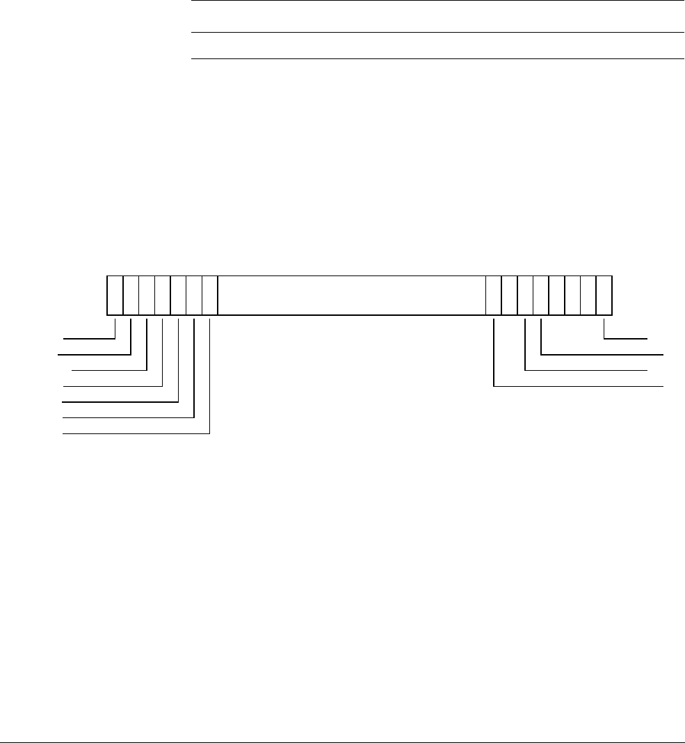
D8 AArch64 System Register Descriptions
D8.3 Debug registers
D8-2094 Copyright © 2013 ARM Limited. All rights reserved. ARM DDI 0487A.a
Non-Confidential - Beta ID090413
D8.3.10 DBGVCR32_EL2, Debug Vector Catch Register
The DBGVCR32_EL2 characteristics are:
Purpose
Allows access to the AArch32 register DBGVCR from AArch64 state only. Its value has no effect
on execution in AArch64 state.
This register is part of the Debug registers functional group.
Usage constraints
This register is accessible as shown below:
Configurations
DBGVCR32_EL2 is architecturally mapped to AArch32 register DBGVCR.
Attributes
DBGVCR32_EL2 is a 32-bit register.
The DBGVCR32_EL2 bit assignments are:
When EL3 implemented and using AArch64:
NSF, bit [31]
FIQ vector catch enable in Non-secure state.
The exception vector offset is
0x1C
.
On Warm reset, the field reset value is architecturally UNKNOWN.
NSI, bit [30]
IRQ vector catch enable in Non-secure state.
The exception vector offset is
0x18
.
On Warm reset, the field reset value is architecturally UNKNOWN.
Bit [29]
Reserved, RES0.
NSD, bit [28]
Data Abort vector catch enable in Non-secure state.
EL0 EL1 (NS) EL1 (S) EL2 EL3 (SCR.NS=1) EL3 (SCR.NS=0)
-- - RWRW RW
31 30 29 28 27 26 25
RES0
24 8 7
SI
65 4
SP
3
SS
2
SU
10
NSF
NSI
RES0
NSD
NSP
NSS
NSU
RES0
SD
RES0
SF

D8 AArch64 System Register Descriptions
D8.3 Debug registers
ARM DDI 0487A.a Copyright © 2013 ARM Limited. All rights reserved. D8-2095
ID090413 Non-Confidential - Beta
The exception vector offset is
0x10
.
On Warm reset, the field reset value is architecturally UNKNOWN.
NSP, bit [27]
Prefetch Abort vector catch enable in Non-secure state.
The exception vector offset is
0x0C
.
On Warm reset, the field reset value is architecturally UNKNOWN.
NSS, bit [26]
Supervisor Call (SVC) vector catch enable in Non-secure state.
The exception vector offset is
0x08
.
On Warm reset, the field reset value is architecturally UNKNOWN.
NSU, bit [25]
Undefined Instruction vector catch enable in Non-secure state.
The exception vector offset is
0x04
.
On Warm reset, the field reset value is architecturally UNKNOWN.
Bits [24:8]
Reserved, RES0.
SF, bit [7]
FIQ vector catch enable in Secure state.
The exception vector offset is
0x1C
.
On Warm reset, the field reset value is architecturally UNKNOWN.
SI, bit [6]
IRQ vector catch enable in Secure state.
The exception vector offset is
0x18
.
On Warm reset, the field reset value is architecturally UNKNOWN.
Bit [5]
Reserved, RES0.
SD, bit [4]
Data Abort vector catch enable in Secure state.
The exception vector offset is
0x10
.
On Warm reset, the field reset value is architecturally UNKNOWN.
SP, bit [3]
Prefetch Abort vector catch enable in Secure state.
The exception vector offset is
0x0C
.
On Warm reset, the field reset value is architecturally UNKNOWN.
SS, bit [2]
Supervisor Call (SVC) vector catch enable in Secure state.
The exception vector offset is
0x08
.
On Warm reset, the field reset value is architecturally UNKNOWN.
SU, bit [1]
Undefined Instruction vector catch enable in Secure state.
The exception vector offset is
0x04
.

D8 AArch64 System Register Descriptions
D8.3 Debug registers
D8-2096 Copyright © 2013 ARM Limited. All rights reserved. ARM DDI 0487A.a
Non-Confidential - Beta ID090413
On Warm reset, the field reset value is architecturally UNKNOWN.
Bit [0]
Reserved, RES0.
When EL3 not implemented:
Bits [31:8]
Reserved, RES0.
F, bit [7]
FIQ vector catch enable.
The exception vector offset is
0x1C
.
On Warm reset, the field reset value is architecturally UNKNOWN.
I, bit [6]
IRQ vector catch enable.
The exception vector offset is
0x18
.
On Warm reset, the field reset value is architecturally UNKNOWN.
Bit [5]
Reserved, RES0.
D, bit [4]
Data Abort vector catch enable.
The exception vector offset is
0x10
.
On Warm reset, the field reset value is architecturally UNKNOWN.
P, bit [3]
Prefetch Abort vector catch enable.
The exception vector offset
0x0C
.
On Warm reset, the field reset value is architecturally UNKNOWN.
S, bit [2]
Supervisor Call (SVC) vector catch enable.
The exception vector offset is
0x08
.
On Warm reset, the field reset value is architecturally UNKNOWN.
U, bit [1]
Undefined Instruction vector catch enable.
The exception vector offset is
0x04
.
On Warm reset, the field reset value is architecturally UNKNOWN.
RES0
31 8
F
7
I
65
D
4
P
3
S
2
U
10
RES0
RES0

D8 AArch64 System Register Descriptions
D8.3 Debug registers
ARM DDI 0487A.a Copyright © 2013 ARM Limited. All rights reserved. D8-2097
ID090413 Non-Confidential - Beta
Bit [0]
Reserved, RES0.
Accessing the DBGVCR32_EL2:
To access the DBGVCR32_EL2:
MRS <Xt>, DBGVCR32_EL2 ; Read DBGVCR32_EL2 into Xt
MSR DBGVCR32_EL2, <Xt> ; Write Xt to DBGVCR32_EL2
Register access is encoded as follows:
op0 op1 CRn CRm op2
10 100 0000 0111 000

D8 AArch64 System Register Descriptions
D8.3 Debug registers
D8-2098 Copyright © 2013 ARM Limited. All rights reserved. ARM DDI 0487A.a
Non-Confidential - Beta ID090413
D8.3.11 DBGWCR<n>_EL1, Debug Watchpoint Control Registers, n = 0 - 15
The DBGWCR<n>_EL1 characteristics are:
Purpose
Holds control information for a watchpoint. Forms watchpoint n together with value register
DBGWVR<n>_EL1, where n is 0 to 15.
This register is part of the Debug registers functional group.
Usage constraints
This register is accessible as shown below:
When the E field is zero, all the other fields in the register are ignored.
Configurations
DBGWCR<n>_EL1 is architecturally mapped to AArch32 register DBGWCR<n>.
DBGWCR<n>_EL1 is architecturally mapped to external register DBGWCR<n>_EL1.
Attributes
DBGWCR<n>_EL1 is a 32-bit register.
The DBGWCR<n>_EL1 bit assignments are:
Bits [31:29]
Reserved, RES0.
MASK, bits [28:24]
Address mask. Only objects up to 2GB can be watched using a single mask.
00000
No mask.
00001
Reserved.
00010
Reserved.
Other values mask the corresponding number of address bits, from
0b00011
masking 3 address bits
(
0x00000007
mask for address) to
0b11111
masking 31 address bits (
0x7FFFFFFF
mask for address).
On Cold reset, the field reset value is architecturally UNKNOWN.
Bits [23:21]
Reserved, RES0.
WT, bit [20]
Watchpoint type. Possible values are:
0
Unlinked data address match.
1
Linked data address match.
EL0 EL1 (NS) EL1 (S) EL2 EL3 (SCR.NS=1) EL3 (SCR.NS=0)
-RW RW RWRW RW
RES0
31 29
MASK
28 24
RES0
23 21 20
LBN
19 16
SSC
15 14 13
BAS
12 5
LSC
43
PAC
21
E
0
WT HMC

D8 AArch64 System Register Descriptions
D8.3 Debug registers
ARM DDI 0487A.a Copyright © 2013 ARM Limited. All rights reserved. D8-2099
ID090413 Non-Confidential - Beta
On Cold reset, the field reset value is architecturally UNKNOWN.
LBN, bits [19:16]
Linked breakpoint number. For Linked data address watchpoints, this specifies the index of the
Context-matching breakpoint linked to.
On Cold reset, the field reset value is architecturally UNKNOWN.
SSC, bits [15:14]
Security state control. Determines the security states under which a watchpoint debug event for
watchpoint n is generated. This field must be interpreted along with the HMC and PAC fields.
On Cold reset, the field reset value is architecturally UNKNOWN.
HMC, bit [13]
Higher mode control. Determines the debug perspective for deciding when a watchpoint debug
event for watchpoint n is generated. This field must be interpreted along with the SSC and PAC
fields.
On Cold reset, the field reset value is architecturally UNKNOWN.
BAS, bits [12:5]
Byte address select. Each bit of this field selects whether a byte from within the word or
double-word addressed by DBGWVR<n>_EL1 is being watched.
In cases where DBGWVR<n>_EL1 addresses a double-word:
If DBGWVR<n>_EL1[2] == 1, only BAS[3:0] is used. ARM deprecates setting
DBGWVR<n>_EL1 == 1.
The valid values for BAS are
0b0000000
, or a binary number all of whose set bits are contiguous. All
other values are reserved and must not be used by software.
If BAS is zero, no bytes are watched by this watchpoint.
Ignored if E is 0.
On Cold reset, the field reset value is architecturally UNKNOWN.
LSC, bits [4:3]
Load/store control. This field enables watchpoint matching on the type of access being made.
Possible values of this field are:
01
Match instructions that load from a watchpointed address.
BAS Description
xxxxxxx1 Match byte at DBGWVR<n>_EL1
xxxxxx1x Match byte at DBGWVR<n>_EL1+1
xxxxx1xx Match byte at DBGWVR<n>_EL1+2
xxxx1xxx Match byte at DBGWVR<n>_EL1+3
BAS Description, if DBGWVR<n>_EL1[2] == 0
xxx1xxxx Match byte at DBGWVR<n>_EL1+4
xx1xxxxx Match byte at DBGWVR<n>_EL1+5
x1xxxxxx Match byte at DBGWVR<n>_EL1+6
1xxxxxxx Match byte at DBGWVR<n>_EL1+7

D8 AArch64 System Register Descriptions
D8.3 Debug registers
D8-2100 Copyright © 2013 ARM Limited. All rights reserved. ARM DDI 0487A.a
Non-Confidential - Beta ID090413
10
Match instructions that store to a watchpointed address.
11
Match instructions that load from or store to a watchpointed address.
All other values are reserved, but must behave as if the watchpoint is disabled. Software must not
rely on this property as the behavior of reserved values might change in a future revision of the
architecture.
Ignored if E is 0.
On Cold reset, the field reset value is architecturally UNKNOWN.
PAC, bits [2:1]
Privilege of access control. Determines the exception level or levels at which a watchpoint debug
event for watchpoint n is generated. This field must be interpreted along with the SSC and HMC
fields.
On Cold reset, the field reset value is architecturally UNKNOWN.
E, bit [0]
Enable watchpoint n. Possible values are:
0
Watchpoint disabled.
1
Watchpoint enabled.
On Cold reset, the field reset value is architecturally UNKNOWN.
Accessing the DBGWCR<n>_EL1:
To access the DBGWCR<n>_EL1:
MRS <Xt>, DBGWCR<n>_EL1 ; Read DBGWCR<n>_EL1 into Xt, where n is in the range 0 to 15
MSR DBGWCR<n>_EL1, <Xt> ; Write Xt to DBGWCR<n>_EL1, where n is in the range 0 to 15
Register access is encoded as follows:
op0 op1 CRn CRm op2
10 000 0000 n<3:0> 111

D8 AArch64 System Register Descriptions
D8.3 Debug registers
ARM DDI 0487A.a Copyright © 2013 ARM Limited. All rights reserved. D8-2101
ID090413 Non-Confidential - Beta
D8.3.12 DBGWVR<n>_EL1, Debug Watchpoint Value Registers, n = 0 - 15
The DBGWVR<n>_EL1 characteristics are:
Purpose
Holds a data address value for use in watchpoint matching. Forms watchpoint n together with
control register DBGWCR<n>_EL1, where n is 0 to 15.
This register is part of the Debug registers functional group.
Usage constraints
This register is accessible as shown below:
Configurations
DBGWVR<n>_EL1[31:0] is architecturally mapped to AArch32 register DBGWVR<n>.
DBGWVR<n>_EL1 is architecturally mapped to external register DBGWVR<n>_EL1.
Attributes
DBGWVR<n>_EL1 is a 64-bit register.
The DBGWVR<n>_EL1 bit assignments are:
RESS, bits [63:49]
Reserved, Sign extended. Hardwired to the value of the sign bit, bit [48]. Hardware and software
must treat this field as RES0 if bit[48] is 0, and as RES1 if bit[48] is 1.
VA, bits [48:2]
Bits[48:2] of the address value for comparison.
ARM deprecates setting DBGWVR<n>_EL1[2] == 1.
On Cold reset, the field reset value is architecturally UNKNOWN.
Bits [1:0]
Reserved, RES0.
Accessing the DBGWVR<n>_EL1:
To access the DBGWVR<n>_EL1:
MRS <Xt>, DBGWVR<n>_EL1 ; Read DBGWVR<n>_EL1 into Xt, where n is in the range 0 to 15
MSR DBGWVR<n>_EL1, <Xt> ; Write Xt to DBGWVR<n>_EL1, where n is in the range 0 to 15
EL0 EL1 (NS) EL1 (S) EL2 EL3 (SCR.NS=1) EL3 (SCR.NS=0)
-RW RW RWRW RW
RESS
63 49
VA
48 2 10
RES0

D8 AArch64 System Register Descriptions
D8.3 Debug registers
D8-2102 Copyright © 2013 ARM Limited. All rights reserved. ARM DDI 0487A.a
Non-Confidential - Beta ID090413
Register access is encoded as follows:
op0 op1 CRn CRm op2
10 000 0000 n<3:0> 110
D8 AArch64 System Register Descriptions
D8.3 Debug registers
ARM DDI 0487A.a Copyright © 2013 ARM Limited. All rights reserved. D8-2103
ID090413 Non-Confidential - Beta
D8.3.13 DLR_EL0, Debug Link Register
The DLR_EL0 characteristics are:
Purpose
In Debug state, holds the address to restart from.
This register is part of:
• the Debug registers functional group
• the Special purpose registers functional group.
Usage constraints
This register is accessible as shown below:
Access to this register is from Debug state only. During normal execution this register is
UNALLOCATED.
Configurations
DLR_EL0[31:0] is architecturally mapped to AArch32 register DLR.
Attributes
DLR_EL0 is a 64-bit register.
The DLR_EL0 bit assignments are:
Bits [63:0]
Restart address.
Accessing the DLR_EL0:
To access the DLR_EL0:
MRS <Xt>, DLR_EL0 ; Read DLR_EL0 into Xt
MSR DLR_EL0, <Xt> ; Write Xt to DLR_EL0
Register access is encoded as follows:
EL0 EL1 (NS) EL1 (S) EL2 EL3 (SCR.NS=1) EL3 (SCR.NS=0)
RW RW RW RW RW RW
Restart address
63 0
op0 op1 CRn CRm op2
11 011 0100 0101 001

D8 AArch64 System Register Descriptions
D8.3 Debug registers
D8-2104 Copyright © 2013 ARM Limited. All rights reserved. ARM DDI 0487A.a
Non-Confidential - Beta ID090413
D8.3.14 DSPSR_EL0, Debug Saved Program Status Register
The DSPSR_EL0 characteristics are:
Purpose
Holds the saved processor state on entry to Debug state.
This register is part of:
• the Debug registers functional group
• the Special purpose registers functional group.
Usage constraints
This register is accessible as shown below:
Access to this register is from Debug state only. During normal execution this register is
UNALLOCATED.
Configurations
DSPSR_EL0 is architecturally mapped to AArch32 register DSPSR.
Attributes
DSPSR_EL0 is a 32-bit register.
The DSPSR_EL0 bit assignments are:
When entering Debug state from AArch32:
N, bit [31]
Set to the value of CPSR.N on entering Debug state, and copied to CPSR.N on exiting Debug state.
Z, bit [30]
Set to the value of CPSR.Z on entering Debug state, and copied to CPSR.Z on exiting Debug state.
C, bit [29]
Set to the value of CPSR.C on entering Debug state, and copied to CPSR.C on exiting Debug state.
V, bit [28]
Set to the value of CPSR.V on entering Debug state, and copied to CPSR.V on exiting Debug state.
Q, bit [27]
Cumulative saturation bit. Set to 1 to indicate that overflow or saturation occurred in some
instructions.
EL0 EL1 (NS) EL1 (S) EL2 EL3 (SCR.NS=1) EL3 (SCR.NS=0)
RW RW RW RW RW RW
N
31
Z
30
C
29
V
28
Q
27 26 25
J
24 23 22
SS
21
IL
20
GE
19 16
IT[7:2]
15 10
E
9
A
8
I
7
F
6
T
54
M[3:0]
30
IT[1:0]
RES0
M[4]

D8 AArch64 System Register Descriptions
D8.3 Debug registers
ARM DDI 0487A.a Copyright © 2013 ARM Limited. All rights reserved. D8-2105
ID090413 Non-Confidential - Beta
IT[1:0], bits [26:25]
If-Then execution state bits for the T32 IT (If-Then) instruction. See IT[7:2] for explanation of this
field.
J, bit [24]
Jazelle bit. Along with the T bit, determines the AArch32 instruction set state that the Debug state
entry was taken from. Possible values of this bit are:
0
Processor in A32 state if T is 0, or T32 state if T is 1.
1
Processor in an invalid state (Jazelle state before ARMv8) if T is 0, or T32EE state if T
is 1.
Since the Jazelle state is obsolete in ARMv8, J==1 and T==0 is an invalid combination, and
attempting to exit Debug state with those values is an illegal exception return.
If T32EE is not implemented, this bit is RES0, so the possible values of the T bit signify either A32
or T32 state.
Bits [23:22]
Reserved, RES0.
SS, bit [21]
Software step. Indicates whether software step was enabled when Debug state was entered.
IL, bit [20]
Illegal Execution State bit. Shows the value of PSTATE.IL immediately before Debug state was
entered.
GE, bits [19:16]
Greater than or Equal flags, for parallel addition and subtraction.
IT[7:2], bits [15:10]
If-Then execution state bits for the T32 IT (If-Then) instruction. This field must be interpreted in
two parts.
• IT[7:5] holds the base condition for the IT block. The base condition is the top 3 bits of the
condition code specified by the first condition field of the IT instruction.
• IT[4:0] encodes the size of the IT block, which is the number of instructions that are to be
conditionally executed, by the position of the least significant 1 in this field. It also encodes
the value of the least significant bit of the condition code for each instruction in the block.
The IT field is
0b00000000
when no IT block is active.
E, bit [9]
Endianness execution state bit. Controls the load and store endianness for data accesses:
0
Little-endian operation
1
Big-endian operation.
Instruction fetches ignore this bit.
When the reset value of the SCTLR.EE bit is defined by a configuration input signal, that value also
applies to the CPSR.E bit on reset, and therefore applies to software execution from reset.
If an implementation does not provide Big-endian support, this bit is RES0. If it does not provide
Little-endian support, this bit is RES1.
If an implementation provides Big-endian support but only at EL0, this bit is RES0 for an exception
return to any exception level other than EL0.
Likewise, if it provides Little-endian support only at EL0, this bit is RES1 for an exception return
to any exception level other than EL0.

D8 AArch64 System Register Descriptions
D8.3 Debug registers
D8-2106 Copyright © 2013 ARM Limited. All rights reserved. ARM DDI 0487A.a
Non-Confidential - Beta ID090413
A, bit [8]
Asynchronous data abort mask bit. The possible values of this bit are:
0
Exception not masked.
1
Exception masked.
I, bit [7]
IRQ mask bit. The possible values of this bit are:
0
Exception not masked.
1
Exception masked.
F, bit [6]
FIQ mask bit. The possible values of this bit are:
0
Exception not masked.
1
Exception masked.
T, bit [5]
Thumb execution state bit. Along with the J bit, determines the AArch32 instruction set state that
the Debug state entry was taken from. Possible values of this bit are:
0
Processor in A32 state if J is 0, or an invalid state (Jazelle state before ARMv8) if J is 1.
1
Processor in T32 state if J is 0, or T32EE state if J is 1.
Since the Jazelle state is obsolete in ARMv8, J==1 and T==0 is an invalid combination, and
attempting to exit Debug state with those values is an illegal exception return.
If T32EE is not implemented, the J bit is RES0, so the possible values of this bit signify either A32
or T32 state.
M[4], bit [4]
Register width that the exception was taken from. Possible values of this bit are:
1
Exception taken from AArch32.
M[3:0], bits [3:0]
Mode that an exception was taken from. For exceptions taken from AArch32, the possible values
are:
Other values are reserved.
M[3:0] Mode
0b0000
User
0b0001
FIQ
0b0010
IRQ
0b0011
Supervisor
0b0110
Monitor
0b0111
Abort
0b1010
Hyp
0b1011
Undefined
0b1111
System

D8 AArch64 System Register Descriptions
D8.3 Debug registers
ARM DDI 0487A.a Copyright © 2013 ARM Limited. All rights reserved. D8-2107
ID090413 Non-Confidential - Beta
When entering Debug state from AArch64:
N, bit [31]
Set to the value of the N condition flag on entering Debug state, and copied to the N condition flag
on exiting Debug state.
Z, bit [30]
Set to the value of the Z condition flag on entering Debug state, and copied to the Z condition flag
on exiting Debug state.
C, bit [29]
Set to the value of the C condition flag on entering Debug state, and copied to the C condition flag
on exiting Debug state.
V, bit [28]
Set to the value of the V condition flag on entering Debug state, and copied to the V condition flag
on exiting Debug state.
Bits [27:22]
Reserved, RES0.
SS, bit [21]
Software step. Indicates whether software step was enabled when Debug state was entered.
IL, bit [20]
Illegal Execution State bit. Shows the value of PSTATE.IL immediately before Debug state was
entered.
Bits [19:10]
Reserved, RES0.
D, bit [9]
Process state D mask. The possible values of this bit are:
0
Debug exceptions from Watchpoint, Breakpoint, and Software step debug events
targeted at the current exception level are not masked.
1
Debug exceptions from Watchpoint, Breakpoint, and Software step debug events
targeted at the current exception level are masked.
When the target exception level of the debug exception is not than the current exception level, the
exception is not masked by this bit.
A, bit [8]
SError (System Error) mask bit. The possible values of this bit are:
0
Exception not masked.
1
Exception masked.
N
31
Z
30
C
29
V
28
RES0
27 22
SS
21
IL
20
RES0
19 10
D
9
A
8
I
7
F
65 4
M[3:0]
30
M[4]
RES0

D8 AArch64 System Register Descriptions
D8.3 Debug registers
D8-2108 Copyright © 2013 ARM Limited. All rights reserved. ARM DDI 0487A.a
Non-Confidential - Beta ID090413
I, bit [7]
IRQ mask bit. The possible values of this bit are:
0
Exception not masked.
1
Exception masked.
F, bit [6]
FIQ mask bit. The possible values of this bit are:
0
Exception not masked.
1
Exception masked.
Bit [5]
Reserved, RES0.
M[4], bit [4]
Register width that the exception was taken from. Possible values of this bit are:
0
Exception taken from AArch64.
M[3:0], bits [3:0]
Mode that an exception was taken from. For exceptions taken from AArch64, the possible values
are:
Other values are reserved.
For exceptions from AArch64:
• M[3:2] holds the Exception Level.
• M[1] is unused, and returning to an exception level that is using AArch64 with this bit set is
treated as an illegal exception return.
• M[0] is used to select the SP:
— 0 means the SP is always SP0.
— 1 means the exception SP is determined by the EL.
Accessing the DSPSR_EL0:
To access the DSPSR_EL0:
MRS <Xt>, DSPSR_EL0 ; Read DSPSR_EL0 into Xt
MSR DSPSR_EL0, <Xt> ; Write Xt to DSPSR_EL0
M[3:0] Mode
0b0000
EL0t
0b0100
EL1t
0b0101
EL1h
0b1000
EL2t
0b1001
EL2h
0b1100
EL3t
0b1101
EL3h

D8 AArch64 System Register Descriptions
D8.3 Debug registers
ARM DDI 0487A.a Copyright © 2013 ARM Limited. All rights reserved. D8-2109
ID090413 Non-Confidential - Beta
Register access is encoded as follows:
op0 op1 CRn CRm op2
11 011 0100 0101 000

D8 AArch64 System Register Descriptions
D8.3 Debug registers
D8-2110 Copyright © 2013 ARM Limited. All rights reserved. ARM DDI 0487A.a
Non-Confidential - Beta ID090413
D8.3.15 MDCCINT_EL1, Monitor DCC Interrupt Enable Register
The MDCCINT_EL1 characteristics are:
Purpose
Enables interrupt requests to be signaled based on the DCC status flags.
This register is part of the Debug registers functional group.
Usage constraints
This register is accessible as shown below:
Configurations
MDCCINT_EL1 is architecturally mapped to AArch32 register DBGDCCINT.
Attributes
MDCCINT_EL1 is a 32-bit register.
The MDCCINT_EL1 bit assignments are:
Bit [31]
Reserved, RES0.
RX, bit [30]
DCC interrupt request enable control for DTRRX. Enables a common COMMIRQ interrupt request
to be signaled based on the DCC status flags.
0
No interrupt request generated by DTRRX.
1
Interrupt request will be generated on RXfull == 1.
If legacy COMMRX and COMMTX signals are implemented, then these are not affected by the
value of this bit.
On Warm reset, the field resets to 0.
TX, bit [29]
DCC interrupt request enable control for DTRTX. Enables a common COMMIRQ interrupt request
to be signaled based on the DCC status flags.
0
No interrupt request generated by DTRTX.
1
Interrupt request will be generated on TXfull == 0.
If legacy COMMRX and COMMTX signals are implemented, then these are not affected by the
value of this bit.
On Warm reset, the field resets to 0.
Bits [28:0]
Reserved, RES0.
EL0 EL1 (NS) EL1 (S) EL2 EL3 (SCR.NS=1) EL3 (SCR.NS=0)
-RW RW RWRW RW
31
RX
30
TX
29
RES0
28 0
RES0

D8 AArch64 System Register Descriptions
D8.3 Debug registers
ARM DDI 0487A.a Copyright © 2013 ARM Limited. All rights reserved. D8-2111
ID090413 Non-Confidential - Beta
Accessing the MDCCINT_EL1:
To access the MDCCINT_EL1:
MRS <Xt>, MDCCINT_EL1 ; Read MDCCINT_EL1 into Xt
MSR MDCCINT_EL1, <Xt> ; Write Xt to MDCCINT_EL1
Register access is encoded as follows:
op0 op1 CRn CRm op2
10 000 0000 0010 000

D8 AArch64 System Register Descriptions
D8.3 Debug registers
D8-2112 Copyright © 2013 ARM Limited. All rights reserved. ARM DDI 0487A.a
Non-Confidential - Beta ID090413
D8.3.16 MDCCSR_EL0, Monitor DCC Status Register
The MDCCSR_EL0 characteristics are:
Purpose
Main control register for the debug implementation, containing flow-control flags for the DCC. This
is an internal, read-only view.
This register is part of the Debug registers functional group.
Usage constraints
This register is accessible as shown below:
This register can be read at EL0 when MDSCR_EL1.TDCC is set to 0. When it is set to 1, EL0
access to this register is trapped to EL1.
Configurations
MDCCSR_EL0 is architecturally mapped to AArch32 register DBGDSCRint.
Attributes
MDCCSR_EL0 is a 32-bit register.
The MDCCSR_EL0 bit assignments are:
Bit [31]
Reserved, RES0.
RXfull, bit [30]
DTRRX full. Read-only view of the equivalent bit in the EDSCR.
TXfull, bit [29]
DTRTX full. Read-only view of the equivalent bit in the EDSCR.
Bits [28:19]
Reserved, RES0.
Bits [18:15]
Reserved, RAZ. Hardware must implement this field as RAZ. Software must not rely on this field
being RAZ.
Bits [14:13]
Reserved, RES0.
EL0 EL1 (NS) EL1 (S) EL2 EL3 (SCR.NS=1) EL3 (SCR.NS=0)
Config-RO RO RO RO RO RO
31 30 29
RES0
28 19
RAZ
18 15 14 13 12
RES0
11 6
RAZ
52
10
RES0
RXfull
TXfull
RES0
RAZ
RES0

D8 AArch64 System Register Descriptions
D8.3 Debug registers
ARM DDI 0487A.a Copyright © 2013 ARM Limited. All rights reserved. D8-2113
ID090413 Non-Confidential - Beta
Bit [12]
Reserved, RAZ. Hardware must implement this field as RAZ. Software must not rely on this field
being RAZ.
Bits [11:6]
Reserved, RES0.
Bits [5:2]
Reserved, RAZ. Hardware must implement this field as RAZ. Software must not rely on this field
being RAZ.
Bits [1:0]
Reserved, RES0.
Accessing the MDCCSR_EL0:
To access the MDCCSR_EL0:
MRS <Xt>, MDCCSR_EL0 ; Read MDCCSR_EL0 into Xt
Register access is encoded as follows:
op0 op1 CRn CRm op2
10 011 0000 0001 000
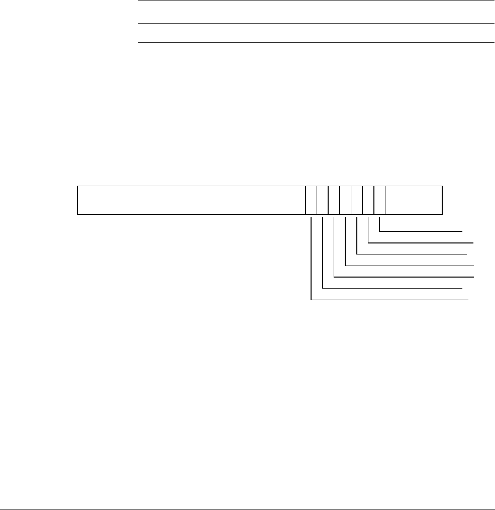
D8 AArch64 System Register Descriptions
D8.3 Debug registers
D8-2114 Copyright © 2013 ARM Limited. All rights reserved. ARM DDI 0487A.a
Non-Confidential - Beta ID090413
D8.3.17 MDCR_EL2, Monitor Debug Configuration Register (EL2)
The MDCR_EL2 characteristics are:
Purpose
Provides configuration options for the Virtualization extensions to self-hosted debug and the
Performance Monitors extension.
This register is part of:
• the Debug registers functional group
• the Virtualization registers functional group.
Usage constraints
This register is accessible as shown below:
Configurations
MDCR_EL2 is architecturally mapped to AArch32 register HDCR.
If EL2 is not implemented, this register is RES0 from EL3.
Attributes
MDCR_EL2 is a 32-bit register.
The MDCR_EL2 bit assignments are:
Bits [31:12]
Reserved, RES0.
TDRA, bit [11]
Trap debug ROM address register access. The possible values of this bit are:
0
Has no effect on accesses to debug ROM address registers from EL1 and EL0.
1
Trap valid EL1 and EL0 access to debug ROM address registers to EL2.
When this bit is set to 1, any access to the following registers from EL1 or EL0 is trapped to EL2:
AArch32: DBGDRAR, DBGDSAR.
AArch64: MDRAR_EL1.
If HCR_EL2.TGE == 1 or MDCR_EL2.TDE == 1, then this bit is ignored and treated as though it
is 1 other than for the value read back from MDCR_EL2.
On Warm reset, the field reset value is architecturally UNKNOWN.
EL0 EL1 (NS) EL1 (S) EL2 EL3 (SCR.NS=1) EL3 (SCR.NS=0)
-- - RWRW RW
RES0
31 12 11 10 9 8 7 6 5
HPMN
40
TPMCR
TPM
HPME
TDE
TDA
TDOSA
TDRA

D8 AArch64 System Register Descriptions
D8.3 Debug registers
ARM DDI 0487A.a Copyright © 2013 ARM Limited. All rights reserved. D8-2115
ID090413 Non-Confidential - Beta
TDOSA, bit [10]
Trap debug OS-related register access. The possible values of this bit are:
0
Has no effect on accesses to OS-related debug registers.
1
Trap valid accesses to OS-related debug registers to EL2.
When this bit is set to 1, any access to the following registers from EL1 or EL0 is trapped to EL2:
AArch32: DBGOSLAR, DBGOSLSR, DBGOSDLR, DBGPRCR.
AArch64: OSLAR_EL1, OSLSR_EL1, OSDLR_EL1, DBGPRCR_EL1.
If HCR_EL2.TGE == 1 or MDCR_EL2.TDE == 1, then this bit is ignored and treated as though it
is 1 other than for the value read back from MDCR_EL2.
On Warm reset, the field reset value is architecturally UNKNOWN.
TDA, bit [9]
Trap debug access. The possible values of this bit are:
0
Has no effect on accesses to Debug registers.
1
Trap valid Non-secure accesses to Debug registers to EL2.
When this bit is set to 1, any valid Non-secure access to the debug registers from EL1 or EL0, other
than the registers trapped by the TDRA and TDOSA bits, is trapped to EL2.
If HCR_EL2.TGE == 1 or MDCR_EL2.TDE == 1, then this bit is ignored and treated as though it
is 1 other than for the value read back from MDCR_EL2.
On Warm reset, the field reset value is architecturally UNKNOWN.
TDE, bit [8]
Route Software debug exceptions from Non-secure EL1 and EL0 to EL2. Also enables traps on all
debug register accesses to EL2.
If HCR_EL2.TGE == 1, then this bit is ignored and treated as though it is 1 other than for the value
read back from MDCR_EL2.
On Warm reset, the field reset value is architecturally UNKNOWN.
HPME, bit [7]
Hypervisor Performance Monitors Enable. The possible values of this bit are:
0
EL2 Performance Monitors disabled.
1
EL2 Performance Monitors enabled.
When this bit is set to 1, the Performance Monitors counters that are reserved for use from EL2 or
Secure state are enabled. For more information see the description of the HPMN field.
If the Performance Monitors extension is not implemented, this field is RES0.
On Warm reset, the field reset value is architecturally UNKNOWN.
TPM, bit [6]
Trap Performance Monitors accesses. The possible values of this bit are:
0
Has no effect on Performance Monitors accesses.
1
Trap Non-secure EL0 and EL1 accesses to Performance Monitors registers that are not
UNALLOCATED to EL2.
If the Performance Monitors extension is not implemented, this field is RES0.
On Warm reset, the field reset value is architecturally UNKNOWN.
TPMCR, bit [5]
Trap PMCR_EL0 accesses. The possible values of this bit are:
0
Has no effect on PMCR_EL0 accesses.
1
Trap Non-secure EL0 and EL1 accesses to PMCR_EL0 to EL2.

D8 AArch64 System Register Descriptions
D8.3 Debug registers
D8-2116 Copyright © 2013 ARM Limited. All rights reserved. ARM DDI 0487A.a
Non-Confidential - Beta ID090413
If the Performance Monitors extension is not implemented, this field is RES0.
On Warm reset, the field reset value is architecturally UNKNOWN.
HPMN, bits [4:0]
Defines the number of Performance Monitors counters that are accessible from Non-secure EL0 and
EL1 modes.
If the Performance Monitors extension is not implemented, this field is RES0.
In Non-secure state, HPMN divides the Performance Monitors counters as follows. For counter n in
Non-secure state:
• If n is in the range 0<=n<HPMN, the counter is accessible from EL1 and EL2, and from EL0
if permitted by PMUSERENR_EL0. PMCR_EL0.E enables the operation of counters in this
range.
• If n is in the range HPMN<=n<PMCR_EL0.N, the counter is accessible only from EL2.
MDCR_EL2.HPME enables the operation of counters in this range.
If this field is set to 0, or to a value larger than PMCR_EL0.N, then the behavior in Non-secure EL0
and EL1 is CONSTRAINED UNPREDICTABLE, and one of the following must happen:
• The number of counters accessible is an UNKNOWN non-zero value less than PMCR_EL0.N.
• There is no access to any counters.
For reads of MDCR_EL2.HPMN by EL2 or higher, if this field is set to 0 or to a value larger than
PMCR_EL0.N, the processor must return a CONSTRAINED UNPREDICTABLE value being one of:
•PMCR_EL0.N.
• The value that was written to MDCR_EL2.HPMN.
• (The value that was written to MDCR_EL2.HPMN) modulo 2h, where h is the smallest
number of bits required for a value in the range 0 to PMCR_EL0.N.
On Warm reset, the field resets to the value of PMCR_EL0.N.
Accessing the MDCR_EL2:
To access the MDCR_EL2:
MRS <Xt>, MDCR_EL2 ; Read MDCR_EL2 into Xt
MSR MDCR_EL2, <Xt> ; Write Xt to MDCR_EL2
Register access is encoded as follows:
op0 op1 CRn CRm op2
11 100 0001 0001 001

D8 AArch64 System Register Descriptions
D8.3 Debug registers
ARM DDI 0487A.a Copyright © 2013 ARM Limited. All rights reserved. D8-2117
ID090413 Non-Confidential - Beta
D8.3.18 MDCR_EL3, Monitor Debug Configuration Register (EL3)
The MDCR_EL3 characteristics are:
Purpose
Provides configuration options for the Security extensions to self-hosted debug.
This register is part of:
• the Debug registers functional group
• the Security registers functional group.
Usage constraints
This register is accessible as shown below:
Configurations
MDCR_EL3 can be mapped to AArch32 register SDCR, but this is not architecturally mandated.
Attributes
MDCR_EL3 is a 32-bit register.
The MDCR_EL3 bit assignments are:
Bits [31:22]
Reserved, RES0.
EPMAD, bit [21]
External debugger access to Performance Monitors registers disabled. This disables access to these
registers by an external debugger:
0
Access to Performance Monitors registers from external debugger is permitted.
1
Access to Performance Monitors registers from external debugger is disabled, unless
overridden by authentication interface.
On Warm reset, the field resets to 0.
EDAD, bit [20]
External debugger access to breakpoint and watchpoint registers disabled. This disables access to
these registers by an external debugger:
0
Access to breakpoint and watchpoint registers from external debugger is permitted.
1
Access to breakpoint and watchpoint registers from external debugger is disabled,
unless overridden by authentication interface.
On Warm reset, the field resets to 0.
EL0 EL1 (NS) EL1 (S) EL2 EL3 (SCR.NS=1) EL3 (SCR.NS=0)
-- - -RW RW
RES0
31 22 21 20 19 18 17 16 15 14
RES0
13 11 10 9 876
RES0
50
EPMAD
EDAD
RES0
SPME
SDD
TPM
RES0
TDA
TDOSA
SPD32

D8 AArch64 System Register Descriptions
D8.3 Debug registers
D8-2118 Copyright © 2013 ARM Limited. All rights reserved. ARM DDI 0487A.a
Non-Confidential - Beta ID090413
Bits [19:18]
Reserved, RES0.
SPME, bit [17]
Secure performance monitors enable. This allows event counting in Secure state:
0
Event counting prohibited in Secure state, unless overridden by the authentication
interface.
1
Event counting allowed in Secure state.
On Warm reset, the field resets to 0.
SDD, bit [16]
AArch64 secure self-hosted invasive debug disable. Disables Software debug exceptions in Secure
state, other than Software breakpoint instruction.
0
Taking Software debug events as debug exceptions is permitted from Secure EL0 and
EL1, if enabled by the relevant MDSCR_EL1 and PSTATE.D flags.
1
Software debug events, other than software breakpoint instruction debug events, are
disabled from all exception levels in Secure state.
SDD only applies when both of the following are true:
• The processor is executing in Secure state.
• Secure EL1 is using AArch64.
On Warm reset, the field reset value is architecturally UNKNOWN.
SPD32, bits [15:14]
AArch32 secure self-hosted privileged invasive debug. Enables or disables debug exceptions from
Secure state if Secure EL1 is using AArch32, other than Software breakpoint instructions. Valid
values for this field are:
00
Legacy mode. Debug exceptions from Secure EL1 are enabled by the authentication
interface.
10
Secure privileged debug disabled. Debug exceptions from Secure EL1 are disabled.
11
Secure privileged debug enabled. Debug exceptions from Secure EL1 are enabled.
Other values are reserved.
If Secure EL1 is using AArch32 then:
• If debug exceptions from Secure EL1 are enabled, then debug exceptions from Secure EL0
are also enabled.
• Otherwise, debug exceptions from Secure EL0 are enabled only if SDER32_EL3.SUIDEN
== 1.
Ignored if Secure EL1 is using AArch64 and in Non-secure state. Debug exceptions from Software
breakpoint instruction debug events are always enabled.
On Warm reset, the field reset value is architecturally UNKNOWN.
Bits [13:11]
Reserved, RES0.
TDOSA, bit [10]
Trap debug OS-related register access. The possible values of this bit are:
0
Has no effect on accesses to OS-related debug registers.
1
Trap valid accesses to OS-related debug registers to EL3.
When this bit is set to 1, any access to the following registers from EL2 or below is trapped to EL3:
AArch32: DBGOSLAR, DBGOSLSR, DBGOSDLR, DBGPRCR.
AArch64: OSLAR_EL1, OSLSR_EL1, OSDLR_EL1, DBGPRCR_EL1.

D8 AArch64 System Register Descriptions
D8.3 Debug registers
ARM DDI 0487A.a Copyright © 2013 ARM Limited. All rights reserved. D8-2119
ID090413 Non-Confidential - Beta
On Warm reset, the field reset value is architecturally UNKNOWN.
TDA, bit [9]
Trap debug access. The possible values of this bit are:
0
Has no effect on accesses to Debug registers.
1
Trap valid Non-secure accesses to Debug registers to EL3.
When this bit is set to 1, any valid Non-secure access to the debug registers from EL2 or below, other
than the registers trapped by the TDRA and TDOSA bits, is trapped to EL3.
On Warm reset, the field reset value is architecturally UNKNOWN.
Bits [8:7]
Reserved, RES0.
TPM, bit [6]
Trap Performance Monitors accesses. The possible values of this bit are:
0
Has no effect on Performance Monitors accesses.
1
Trap Non-secure EL0, EL1 and EL2 accesses to Performance Monitors registers that are
not UNALLOCATED, or trapped to a lower exception level, to EL3.
If the Performance Monitors extension is not implemented, this field is RES0.
On Warm reset, the field reset value is architecturally UNKNOWN.
Bits [5:0]
Reserved, RES0.
Accessing the MDCR_EL3:
To access the MDCR_EL3:
MRS <Xt>, MDCR_EL3 ; Read MDCR_EL3 into Xt
MSR MDCR_EL3, <Xt> ; Write Xt to MDCR_EL3
Register access is encoded as follows:
op0 op1 CRn CRm op2
11 110 0001 0011 001
D8 AArch64 System Register Descriptions
D8.3 Debug registers
D8-2120 Copyright © 2013 ARM Limited. All rights reserved. ARM DDI 0487A.a
Non-Confidential - Beta ID090413
D8.3.19 MDRAR_EL1, Monitor Debug ROM Address Register
The MDRAR_EL1 characteristics are:
Purpose
Defines the base physical address of a 4KB-aligned memory-mapped debug component, usually a
ROM table that locates and describes the memory-mapped debug components in the system.
This register is part of the Debug registers functional group.
Usage constraints
This register is accessible as shown below:
Configurations
MDRAR_EL1 is architecturally mapped to AArch32 register DBGDRAR.
Attributes
MDRAR_EL1 is a 64-bit register.
The MDRAR_EL1 bit assignments are:
Bits [63:48]
Reserved, RES0.
ROMADDR[P-1:12], bits [47:12]
Bits[P-1:12] of the ROM table physical address, where P is the physical address size in bits (up to
48 bits) as stored in ID_AA64MMFR0_EL1. If P is less than 48, bits[47:P] of this register are RES0.
Bits [11:0] of the ROM table physical address are zero.
If EL3 is implemented, ROMADDR is an address in Non-secure memory. Whether the ROM table
is also accessible in Secure memory is IMPLEMENTATION DEFINED.
Bits [11:2]
Reserved, RES0.
Valid, bits [1:0]
This field indicates whether the ROM Table address is valid. The permitted values of this field are:
00
ROM Table address is not valid
11
ROM Table address is valid.
Other values are reserved.
Accessing the MDRAR_EL1:
To access the MDRAR_EL1:
MRS <Xt>, MDRAR_EL1 ; Read MDRAR_EL1 into Xt
EL0 EL1 (NS) EL1 (S) EL2 EL3 (SCR.NS=1) EL3 (SCR.NS=0)
-RO RO RORO RO
RES0
63 48
ROMADDR[P-1:12]
47 12
RES0
11 2
Valid
10

D8 AArch64 System Register Descriptions
D8.3 Debug registers
ARM DDI 0487A.a Copyright © 2013 ARM Limited. All rights reserved. D8-2121
ID090413 Non-Confidential - Beta
Register access is encoded as follows:
op0 op1 CRn CRm op2
10 000 0001 0000 000
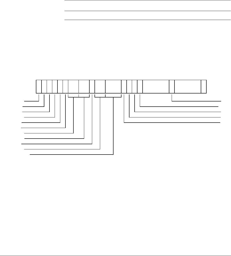
D8 AArch64 System Register Descriptions
D8.3 Debug registers
D8-2122 Copyright © 2013 ARM Limited. All rights reserved. ARM DDI 0487A.a
Non-Confidential - Beta ID090413
D8.3.20 MDSCR_EL1, Monitor Debug System Control Register
The MDSCR_EL1 characteristics are:
Purpose
Main control register for the debug implementation.
This register is part of the Debug registers functional group.
Usage constraints
This register is accessible as shown below:
Configurations
MDSCR_EL1 is architecturally mapped to AArch32 register DBGDSCRext.
Attributes
MDSCR_EL1 is a 32-bit register.
The MDSCR_EL1 bit assignments are:
Bit [31]
Reserved, RES0.
RXfull, bit [30]
Used for save/restore of EDSCR.RXfull.
When OSLSR_EL1.OSLK == 0 (the OS lock is unlocked), this bit is RO, and software must treat
it as UNK/SBZP.
When OSLSR_EL1.OSLK == 1 (the OS lock is locked), this bit is RW.
TXfull, bit [29]
Used for save/restore of EDSCR.TXfull.
When OSLSR_EL1.OSLK == 0 (the OS lock is unlocked), this bit is RO, and software must treat
it as UNK/SBZP.
When OSLSR_EL1.OSLK == 1 (the OS lock is locked), this bit is RW.
EL0 EL1 (NS) EL1 (S) EL2 EL3 (SCR.NS=1) EL3 (SCR.NS=0)
-RW RW RWRW RW
31 30 29 28 27 26 25 24 23 22 21 20 19 18 16 15 14 13 12
RES0
11 7 6
RES0
51
SS
0
RES0
RXfull
TXfull
RES0
RXO
TXU
RES0
INTdis
TDA
RES0
RAZ/WI
ERR
TDCC
KDE
HDE
MDE

D8 AArch64 System Register Descriptions
D8.3 Debug registers
ARM DDI 0487A.a Copyright © 2013 ARM Limited. All rights reserved. D8-2123
ID090413 Non-Confidential - Beta
Bit [28]
Reserved, RES0.
RXO, bit [27]
Used for save/restore of EDSCR.RXO.
When OSLSR_EL1.OSLK == 0 (the OS lock is unlocked), this bit is RO. Software must treat it as
UNKNOWN and use an SBZP policy for writes.
When OSLSR_EL1.OSLK == 1 (the OS lock is locked), this bit is RW.
TXU, bit [26]
Used for save/restore of EDSCR.TXU.
When OSLSR_EL1.OSLK == 0 (the OS lock is unlocked), this bit is RO. Software must treat it as
UNKNOWN and use an SBZP policy for writes.
When OSLSR_EL1.OSLK == 1 (the OS lock is locked), this bit is RW.
Bits [25:24]
Reserved, RES0.
INTdis, bits [23:22]
Used for save/restore of EDSCR.INTdis.
When OSLSR_EL1.OSLK == 0 (the OS lock is unlocked), this field is RO. Software must treat it
as UNKNOWN and use an SBZP policy for writes.
When OSLSR_EL1.OSLK == 1 (the OS lock is locked), this field is RW.
TDA, bit [21]
Used for save/restore of EDSCR.TDA.
When OSLSR_EL1.OSLK == 0 (the OS lock is unlocked), this bit is RO. Software must treat it as
UNKNOWN and use an SBZP policy for writes.
When OSLSR_EL1.OSLK == 1 (the OS lock is locked), this bit is RW.
Bits [20:19]
Reserved, RES0.
Bits [18:16]
Reserved, RAZ/WI. Hardware must implement this as RAZ/WI. Software must not rely on this
property as the behavior of reserved values might change in a future revision of the architecture.
MDE, bit [15]
Monitor debug events. Enable Breakpoint, Watchpoint, and Vector catch debug exceptions.
0
Breakpoint, Watchpoint, and Vector catch debug exceptions disabled.
1
Breakpoint, Watchpoint, and Vector catch debug exceptions enabled.
On Warm reset, the field reset value is architecturally UNKNOWN.
HDE, bit [14]
Used for save/restore of EDSCR.HDE.
When OSLSR_EL1.OSLK == 0 (the OS lock is unlocked), this bit is RO. Software must treat it as
UNKNOWN and use an SBZP policy for writes.
When OSLSR_EL1.OSLK == 1 (the OS lock is locked), this bit is RW.

D8 AArch64 System Register Descriptions
D8.3 Debug registers
D8-2124 Copyright © 2013 ARM Limited. All rights reserved. ARM DDI 0487A.a
Non-Confidential - Beta ID090413
KDE, bit [13]
Local (kernel) debug enable. If ELD is using AArch64, enable Software debug events within ELD.
Permitted values are:
0
Software debug events, other than Software breakpoint instructions, disabled within
ELD.
1
Software debug events enabled within ELD.
RES0 if ELD is using AArch32.
On Warm reset, the field reset value is architecturally UNKNOWN.
TDCC, bit [12]
Trap Debug Communications Channel access. When set, any EL0 access to the following registers
is trapped to EL1:
AArch32: DBGDIDR, DBGDRAR, DBGDSAR, DBGDSCRint, DBGDTRTXint,
DBGDTRRXint.
AArch64: MDCCSR_EL0, DBGDTR_EL0, DBGDTRTX_EL0, DBGDTRRX_EL0.
On Warm reset, the field reset value is architecturally UNKNOWN.
Bits [11:7]
Reserved, RES0.
ERR, bit [6]
Used for save/restore of EDSCR.ERR.
When OSLSR_EL1.OSLK == 0 (the OS lock is unlocked), this bit is RO. Software must treat it as
UNKNOWN and use an SBZP policy for writes.
When OSLSR_EL1.OSLK == 1 (the OS lock is locked), this bit is RW.
Bits [5:1]
Reserved, RES0.
SS, bit [0]
Software step control bit. If ELD is using AArch64, enable Software step. Permitted values are:
0
Software step disabled
1
Software step enabled.
RES0 if ELD is using AArch32.
On Warm reset, the field reset value is architecturally UNKNOWN.
Accessing the MDSCR_EL1:
To access the MDSCR_EL1:
MRS <Xt>, MDSCR_EL1 ; Read MDSCR_EL1 into Xt
MSR MDSCR_EL1, <Xt> ; Write Xt to MDSCR_EL1
Register access is encoded as follows:
op0 op1 CRn CRm op2
10 000 0000 0010 010

D8 AArch64 System Register Descriptions
D8.3 Debug registers
ARM DDI 0487A.a Copyright © 2013 ARM Limited. All rights reserved. D8-2125
ID090413 Non-Confidential - Beta
D8.3.21 OSDLR_EL1, OS Double Lock Register
The OSDLR_EL1 characteristics are:
Purpose
Used to control the OS Double Lock.
This register is part of the Debug registers functional group.
Usage constraints
This register is accessible as shown below:
Configurations
OSDLR_EL1 is architecturally mapped to AArch32 register DBGOSDLR.
Attributes
OSDLR_EL1 is a 32-bit register.
The OSDLR_EL1 bit assignments are:
Bits [31:1]
Reserved, RES0.
DLK, bit [0]
OS Double Lock control bit. Possible values are:
0
OS Double Lock unlocked.
1
OS Double Lock locked, if DBGPRCR_EL1.CORENPDRQ (Core no power-down
request) bit is set to 0 and the processor is in Non-debug state.
On Warm reset, the field resets to 0.
Accessing the OSDLR_EL1:
To access the OSDLR_EL1:
MRS <Xt>, OSDLR_EL1 ; Read OSDLR_EL1 into Xt
MSR OSDLR_EL1, <Xt> ; Write Xt to OSDLR_EL1
Register access is encoded as follows:
EL0 EL1 (NS) EL1 (S) EL2 EL3 (SCR.NS=1) EL3 (SCR.NS=0)
-RW RW RWRW RW
RES0
31 1 0
DLK
op0 op1 CRn CRm op2
10 000 0001 0011 100

D8 AArch64 System Register Descriptions
D8.3 Debug registers
D8-2126 Copyright © 2013 ARM Limited. All rights reserved. ARM DDI 0487A.a
Non-Confidential - Beta ID090413
D8.3.22 OSDTRRX_EL1, OS Lock Data Transfer Register, Receive
The OSDTRRX_EL1 characteristics are:
Purpose
Transfers data from an external host to the ARM processor. Part of the software save/restore
mechanism for external debug. Can be used to access DBGDTRRX_EL0.
This register is part of the Debug registers functional group.
Usage constraints
This register is accessible as shown below:
Configurations
OSDTRRX_EL1 is architecturally mapped to AArch32 register DBGDTRRXext.
Attributes
OSDTRRX_EL1 is a 32-bit register.
The OSDTRRX_EL1 bit assignments are:
Bits [31:0]
Host to target data. One word of data for transfer from the debug host to the debug target.
For the full behavior of the Debug Communications Channel, see section 9 (The Debug
Communications Channel and Instruction Transfer Register) in document PRD03-PRDC-010486.
Accessing the OSDTRRX_EL1:
To access the OSDTRRX_EL1:
MRS <Xt>, OSDTRRX_EL1 ; Read OSDTRRX_EL1 into Xt
MSR OSDTRRX_EL1, <Xt> ; Write Xt to OSDTRRX_EL1
Register access is encoded as follows:
EL0 EL1 (NS) EL1 (S) EL2 EL3 (SCR.NS=1) EL3 (SCR.NS=0)
-RW RW RWRW RW
Host to target data
31 0
op0 op1 CRn CRm op2
10 000 0000 0000 010

D8 AArch64 System Register Descriptions
D8.3 Debug registers
ARM DDI 0487A.a Copyright © 2013 ARM Limited. All rights reserved. D8-2127
ID090413 Non-Confidential - Beta
D8.3.23 OSDTRTX_EL1, OS Lock Data Transfer Register, Transmit
The OSDTRTX_EL1 characteristics are:
Purpose
Transfers data from the ARM processor to an external host. Part of the software save/restore
mechanism for external debug. Can be used to access DBGDTRTX_EL0.
This register is part of the Debug registers functional group.
Usage constraints
This register is accessible as shown below:
Configurations
OSDTRTX_EL1 is architecturally mapped to AArch32 register DBGDTRTXext.
Attributes
OSDTRTX_EL1 is a 32-bit register.
The OSDTRTX_EL1 bit assignments are:
Bits [31:0]
Target to host data. One word of data for transfer from the debug target to the debug host.
For the full behavior of the Debug Communications Channel, see section 9 (The Debug
Communications Channel and Instruction Transfer Register) in document PRD03-PRDC-010486.
Accessing the OSDTRTX_EL1:
To access the OSDTRTX_EL1:
MRS <Xt>, OSDTRTX_EL1 ; Read OSDTRTX_EL1 into Xt
MSR OSDTRTX_EL1, <Xt> ; Write Xt to OSDTRTX_EL1
Register access is encoded as follows:
EL0 EL1 (NS) EL1 (S) EL2 EL3 (SCR.NS=1) EL3 (SCR.NS=0)
-RW RW RWRW RW
Target to host data
31 0
op0 op1 CRn CRm op2
10 000 0000 0011 010

D8 AArch64 System Register Descriptions
D8.3 Debug registers
D8-2128 Copyright © 2013 ARM Limited. All rights reserved. ARM DDI 0487A.a
Non-Confidential - Beta ID090413
D8.3.24 OSECCR_EL1, OS Lock Exception Catch Control Register
The OSECCR_EL1 characteristics are:
Purpose
Provides a mechanism for an operating system to access the contents of EDECCR that are otherwise
invisible to software, so it can save/restore the contents of EDECCR over powerdown on behalf of
the external debugger.
This register is part of the Debug registers functional group.
Usage constraints
This register is accessible as shown below:
Configurations
OSECCR_EL1 is architecturally mapped to AArch32 register DBGOSECCR.
OSECCR_EL1 is architecturally mapped to external register EDECCR.
Attributes
OSECCR_EL1 is a 32-bit register.
The OSECCR_EL1 bit assignments are:
When OSLSR.OSLK==1:
EDECCR, bits [31:0]
Used for save/restore to EDECCR over powerdown.
Accessing the OSECCR_EL1:
To access the OSECCR_EL1:
MRS <Xt>, OSECCR_EL1 ; Read OSECCR_EL1 into Xt
MSR OSECCR_EL1, <Xt> ; Write Xt to OSECCR_EL1
Register access is encoded as follows:
EL0 EL1 (NS) EL1 (S) EL2 EL3 (SCR.NS=1) EL3 (SCR.NS=0)
-RW RW RWRW RW
EDECCR
31 0
op0 op1 CRn CRm op2
10 000 0000 0110 010

D8 AArch64 System Register Descriptions
D8.3 Debug registers
ARM DDI 0487A.a Copyright © 2013 ARM Limited. All rights reserved. D8-2129
ID090413 Non-Confidential - Beta
D8.3.25 OSLAR_EL1, OS Lock Access Register
The OSLAR_EL1 characteristics are:
Purpose
Used to lock or unlock the OS lock.
This register is part of the Debug registers functional group.
Usage constraints
This register is accessible as shown below:
Configurations
OSLAR_EL1 is architecturally mapped to AArch32 register DBGOSLAR.
OSLAR_EL1 is architecturally mapped to external register OSLAR_EL1.
Attributes
OSLAR_EL1 is a 32-bit register.
The OSLAR_EL1 bit assignments are:
Bits [31:1]
Reserved, RES0.
OSLK, bit [0]
On writes to OSLAR_EL1, bit[0] is copied to the OS lock.
Use OSLSR_EL1.OSLK to check the current status of the lock.
Accessing the OSLAR_EL1:
To access the OSLAR_EL1:
MSR OSLAR_EL1, <Xt> ; Write Xt to OSLAR_EL1
Register access is encoded as follows:
EL0 EL1 (NS) EL1 (S) EL2 EL3 (SCR.NS=1) EL3 (SCR.NS=0)
-WO WO WOWO WO
RES0
31 1 0
OSLK
op0 op1 CRn CRm op2
10 000 0001 0000 100
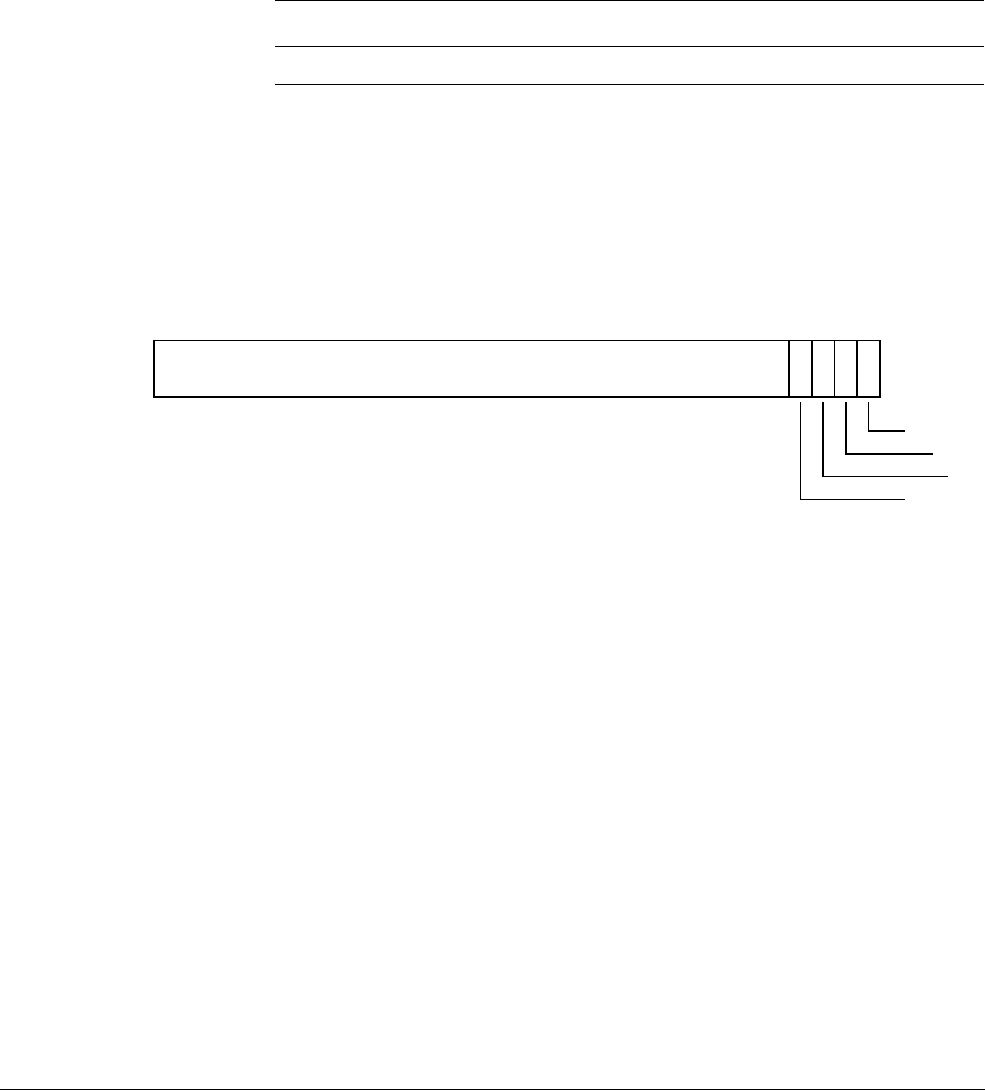
D8 AArch64 System Register Descriptions
D8.3 Debug registers
D8-2130 Copyright © 2013 ARM Limited. All rights reserved. ARM DDI 0487A.a
Non-Confidential - Beta ID090413
D8.3.26 OSLSR_EL1, OS Lock Status Register
The OSLSR_EL1 characteristics are:
Purpose
Provides the status of the OS lock.
This register is part of the Debug registers functional group.
Usage constraints
This register is accessible as shown below:
Configurations
OSLSR_EL1 is architecturally mapped to AArch32 register DBGOSLSR.
Attributes
OSLSR_EL1 is a 32-bit register.
The OSLSR_EL1 bit assignments are:
Bits [31:4]
Reserved, RES0.
OSLM[1], bit [3]
See below for description of the OSLM field.
nTT, bit [2]
Not 32-bit access. This bit is always RAZ. It indicates that a 32-bit access is needed to write the key
to the OS Lock Access Register.
OSLK, bit [1]
OS Lock Status. The possible values are:
0
OS lock unlocked.
1
OS lock locked.
The OS Lock is locked and unlocked by writing to the OS Lock Access Register.
On Cold reset, the field resets to 1.
OSLM[0], bit [0]
OS lock model implemented. Identifies the form of OS save and restore mechanism implemented.
In v8-A these bits are as follows:
10
OS lock implemented. DBGOSSRR not implemented.
EL0 EL1 (NS) EL1 (S) EL2 EL3 (SCR.NS=1) EL3 (SCR.NS=0)
-RO RO RORO RO
RES0
31 4 3 2 1 0
OSLM[0]
OSLK
nTT
OSLM[1]

D8 AArch64 System Register Descriptions
D8.3 Debug registers
ARM DDI 0487A.a Copyright © 2013 ARM Limited. All rights reserved. D8-2131
ID090413 Non-Confidential - Beta
All other values are reserved.
Accessing the OSLSR_EL1:
To access the OSLSR_EL1:
MRS <Xt>, OSLSR_EL1 ; Read OSLSR_EL1 into Xt
Register access is encoded as follows:
op0 op1 CRn CRm op2
10 000 0001 0001 100

D8 AArch64 System Register Descriptions
D8.3 Debug registers
D8-2132 Copyright © 2013 ARM Limited. All rights reserved. ARM DDI 0487A.a
Non-Confidential - Beta ID090413
D8.3.27 SDER32_EL3, AArch32 Secure Debug Enable Register
The SDER32_EL3 characteristics are:
Purpose
Allows access to the AArch32 register SDER from AArch64 state only. Its value has no effect on
execution in AArch64 state.
This register is part of:
• the Debug registers functional group
• the Security registers functional group.
Usage constraints
This register is accessible as shown below:
Configurations
SDER32_EL3 is architecturally mapped to AArch32 register SDER.
If EL1 does not support AArch32, SDER32_EL3 is not implemented.
Attributes
SDER32_EL3 is a 32-bit register.
The SDER32_EL3 bit assignments are:
Bits [31:2]
Reserved, RES0.
SUNIDEN, bit [1]
Secure User Non-Invasive Debug Enable:
0
Non-invasive debug not permitted in Secure EL0 mode.
1
Non-invasive debug permitted in Secure EL0 mode.
SUIDEN, bit [0]
Secure User Invasive Debug Enable:
0
Invasive debug not permitted in Secure EL0 mode.
1
Invasive debug permitted in Secure EL0 mode.
Accessing the SDER32_EL3:
To access the SDER32_EL3:
MRS <Xt>, SDER32_EL3 ; Read SDER32_EL3 into Xt
MSR SDER32_EL3, <Xt> ; Write Xt to SDER32_EL3
EL0 EL1 (NS) EL1 (S) EL2 EL3 (SCR.NS=1) EL3 (SCR.NS=0)
-- - -RW RW
RES0
31 2 1 0
SUIDEN
SUNIDEN

D8 AArch64 System Register Descriptions
D8.3 Debug registers
ARM DDI 0487A.a Copyright © 2013 ARM Limited. All rights reserved. D8-2133
ID090413 Non-Confidential - Beta
Register access is encoded as follows:
op0 op1 CRn CRm op2
11 110 0001 0001 001

D8 AArch64 System Register Descriptions
D8.4 Performance Monitors registers
D8-2134 Copyright © 2013 ARM Limited. All rights reserved. ARM DDI 0487A.a
Non-Confidential - Beta ID090413
D8.4 Performance Monitors registers
This section lists the Performance Monitoring registers in AArch64 state.
D8.4.1 PMCCFILTR_EL0, Performance Monitors Cycle Count Filter Register
The PMCCFILTR_EL0 characteristics are:
Purpose
Determines the modes in which the Cycle Counter, PMCCNTR_EL0, increments.
This register is part of the Performance Monitors registers functional group.
Usage constraints
This register is accessible as shown below:
This register is accessible at EL0 when PMUSERENR_EL0.EN is set to 1.
PMCCFILTR_EL0 can also be accessed by using PMXEVTYPER_EL0 with PMSELR_EL0.SEL
set to
0b11111
.
Configurations
PMCCFILTR_EL0 is architecturally mapped to AArch32 register PMCCFILTR.
PMCCFILTR_EL0 is architecturally mapped to external register PMCCFILTR_EL0.
Attributes
PMCCFILTR_EL0 is a 32-bit register.
The PMCCFILTR_EL0 bit assignments are:
P, bit [31]
EL1 modes filtering bit. Controls counting in EL1. If EL3 is implemented, then counting in
Non-secure EL1 is further controlled by the NSK bit. The possible values of this bit are:
0
Count cycles in EL1.
1
Do not count cycles in EL1.
On Warm reset, the field reset value is architecturally UNKNOWN.
U, bit [30]
EL0 filtering bit. Controls counting in EL0. If EL3 is implemented, then counting in Non-secure
EL0 is further controlled by the NSU bit. The possible values of this bit are:
0
Count cycles in EL0.
1
Do not count cycles in EL0.
On Warm reset, the field reset value is architecturally UNKNOWN.
EL0 EL1 (NS) EL1 (S) EL2 EL3 (SCR.NS=1) EL3 (SCR.NS=0)
Config-RW RW RW RW RW RW
P
31
U
30 29 28 27
M
26
RES0
25 0
NSK
NSU
NSH

D8 AArch64 System Register Descriptions
D8.4 Performance Monitors registers
ARM DDI 0487A.a Copyright © 2013 ARM Limited. All rights reserved. D8-2135
ID090413 Non-Confidential - Beta
NSK, bit [29]
Non-secure kernel modes filtering bit. Controls counting in Non-secure EL1. If EL3 is not
implemented, this bit is RES0.
If the value of this bit is equal to the value of P, cycles in Non-secure EL1 are counted.
Otherwise, cycles in Non-secure EL1 are not counted.
On Warm reset, the field reset value is architecturally UNKNOWN.
NSU, bit [28]
Non-secure user modes filtering bit. Controls counting in Non-secure EL0. If EL3 is not
implemented, this bit is RES0.
If the value of this bit is equal to the value of U, cycles in Non-secure EL0 are counted.
Otherwise, cycles in Non-secure EL0 are not counted.
On Warm reset, the field reset value is architecturally UNKNOWN.
NSH, bit [27]
Non-secure Hyp modes filtering bit. Controls counting in Non-secure EL2. If EL2 is not
implemented, this bit is RES0.
0
Do not count cycles in EL2.
1
Count cycles in EL2.
On Warm reset, the field reset value is architecturally UNKNOWN.
M, bit [26]
Secure EL3 filtering bit. Most applications can ignore this bit and set the value to zero. If EL3 is not
implemented, this bit is RES0.
If the value of this bit is equal to the value of P, cycles in Secure EL3 are counted.
Otherwise, cycles in Secure EL3 are not counted.
On Warm reset, the field reset value is architecturally UNKNOWN.
Bits [25:0]
Reserved, RES0.
Accessing the PMCCFILTR_EL0:
To access the PMCCFILTR_EL0:
MRS <Xt>, PMCCFILTR_EL0 ; Read PMCCFILTR_EL0 into Xt
MSR PMCCFILTR_EL0, <Xt> ; Write Xt to PMCCFILTR_EL0
Register access is encoded as follows:
op0 op1 CRn CRm op2
11 011 1110 1111 111

D8 AArch64 System Register Descriptions
D8.4 Performance Monitors registers
D8-2136 Copyright © 2013 ARM Limited. All rights reserved. ARM DDI 0487A.a
Non-Confidential - Beta ID090413
D8.4.2 PMCCNTR_EL0, Performance Monitors Cycle Count Register
The PMCCNTR_EL0 characteristics are:
Purpose
Holds the value of the processor Cycle Counter, CCNT, that counts processor clock cycles.
This register is part of the Performance Monitors registers functional group.
Usage constraints
This register is accessible as shown below:
This register is accessible at EL0 when PMUSERENR_EL0.EN or PMUSERENR_EL0.CR is set
to 1.
Configurations
PMCCNTR_EL0 is architecturally mapped to AArch32 register PMCCNTR when accessing as a
64-bit register.
PMCCNTR_EL0 is architecturally mapped to external register PMCCNTR_EL0.
PMCCNTR_EL0[31:0] is architecturally mapped to AArch32 register PMCCNTR.
All counters are subject to any changes in clock frequency, including clock stopping caused by the
WFI and WFE instructions. This means that it is CONSTRAINED UNPREDICTABLE whether or not
PMCCNTR_EL0 continues to increment when clocks are stopped by WFI and WFE instructions.
Attributes
PMCCNTR_EL0 is a 64-bit register.
The PMCCNTR_EL0 bit assignments are:
CCNT, bits [63:0]
Cycle count. Depending on the values of PMCR_EL0.{LC,D}, this field increments in one of the
following ways:
• Every processor clock cycle.
• Every 64th processor clock cycle.
This field can be reset to zero by writing 1 to PMCR_EL0.C.
On Warm reset, the field reset value is architecturally UNKNOWN.
Accessing the PMCCNTR_EL0:
To access the PMCCNTR_EL0:
MRS <Xt>, PMCCNTR_EL0 ; Read PMCCNTR_EL0 into Xt
MSR PMCCNTR_EL0, <Xt> ; Write Xt to PMCCNTR_EL0
EL0 EL1 (NS) EL1 (S) EL2 EL3 (SCR.NS=1) EL3 (SCR.NS=0)
Config-RW RW RW RW RW RW
CCNT
63 0

D8 AArch64 System Register Descriptions
D8.4 Performance Monitors registers
ARM DDI 0487A.a Copyright © 2013 ARM Limited. All rights reserved. D8-2137
ID090413 Non-Confidential - Beta
Register access is encoded as follows:
op0 op1 CRn CRm op2
11 011 1001 1101 000

D8 AArch64 System Register Descriptions
D8.4 Performance Monitors registers
D8-2138 Copyright © 2013 ARM Limited. All rights reserved. ARM DDI 0487A.a
Non-Confidential - Beta ID090413
D8.4.3 PMCEID0_EL0, Performance Monitors Common Event Identification register 0
The PMCEID0_EL0 characteristics are:
Purpose
Defines which common architectural and common microarchitectural feature events are
implemented. If a particular bit is set to 1, then the event for that bit is implemented.
This register is part of the Performance Monitors registers functional group.
Usage constraints
This register is accessible as shown below:
This register is accessible at EL0 when PMUSERENR_EL0.EN is set to 1.
Configurations
PMCEID0_EL0 is architecturally mapped to AArch32 register PMCEID0.
PMCEID0_EL0 is architecturally mapped to external register PMCEID0_EL0.
Attributes
PMCEID0_EL0 is a 32-bit register.
The PMCEID0_EL0 bit assignments are:
CE[31:0], bits [31:0]
Common architectural and microarchitectural feature events that can be counted by the PMU event
counters.
For each bit described in the following table, the event is implemented if the bit is set to 1, or not
implemented if the bit is set to 0.
EL0 EL1 (NS) EL1 (S) EL2 EL3 (SCR.NS=1) EL3 (SCR.NS=0)
Config-RO RO RO RO RO RO
CE[31:0]
31 0
Bit Event
number Event mnemonic
31
0x01F
L1D_CACHE_ALLOCATE
30
0x01E
CHAIN
29
0x01D
BUS_CYCLES
28
0x01C
TTBR_WRITE_RETIRED
27
0x01B
INST_SPEC
26
0x01A
MEMORY_ERROR
25
0x019
BUS_ACCESS
24
0x018
L2D_CACHE_WB

D8 AArch64 System Register Descriptions
D8.4 Performance Monitors registers
ARM DDI 0487A.a Copyright © 2013 ARM Limited. All rights reserved. D8-2139
ID090413 Non-Confidential - Beta
Accessing the PMCEID0_EL0:
To access the PMCEID0_EL0:
MRS <Xt>, PMCEID0_EL0 ; Read PMCEID0_EL0 into Xt
Register access is encoded as follows:
23
0x017
L2D_CACHE_REFILL
22
0x016
L2D_CACHE
21
0x015
L1D_CACHE_WB
20
0x014
L1I_CACHE
19
0x013
MEM_ACCESS
18
0x012
BR_PRED
17
0x011
CPU_CYCLES
16
0x010
BR_MIS_PRED
15
0x00F
UNALIGNED_LDST_RETIRED
14
0x00E
BR_RETURN_RETIRED
13
0x00D
BR_IMMED_RETIRED
12
0x00C
PC_WRITE_RETIRED
11
0x00B
CID_WRITE_RETIRED
10
0x00A
EXC_RETURN
9
0x009
EXC_TAKEN
8
0x008
INST_RETIRED
7
0x007
ST_RETIRED
6
0x006
LD_RETIRED
5
0x005
L1D_TLB_REFILL
4
0x004
L1D_CACHE
3
0x003
L1D_CACHE_REFILL
2
0x002
L1I_TLB_REFILL
1
0x001
L1I_CACHE_REFILL
0
0x000
SW_INCR
op0 op1 CRn CRm op2
11 011 1001 1100 110
Bit Event
number Event mnemonic

D8 AArch64 System Register Descriptions
D8.4 Performance Monitors registers
D8-2140 Copyright © 2013 ARM Limited. All rights reserved. ARM DDI 0487A.a
Non-Confidential - Beta ID090413
D8.4.4 PMCEID1_EL0, Performance Monitors Common Event Identification register 1
The PMCEID1_EL0 characteristics are:
Purpose
Reserved for future indication of which common architectural and common microarchitectural
feature events are implemented.
This register is part of the Performance Monitors registers functional group.
Usage constraints
This register is accessible as shown below:
This register is accessible at EL0 when PMUSERENR_EL0.EN is set to 1.
Configurations
PMCEID1_EL0 is architecturally mapped to AArch32 register PMCEID1.
PMCEID1_EL0 is architecturally mapped to external register PMCEID1_EL0.
Attributes
PMCEID1_EL0 is a 32-bit register.
The PMCEID1_EL0 bit assignments are:
Bits [31:1]
Reserved, RES0.
CE[32], bit [0]
Common architectural and microarchitectural feature events that can be counted by the PMU event
counters.
For the bit described in the following table, the event is implemented if the bit is set to 1, or not
implemented if the bit is set to 0.
Accessing the PMCEID1_EL0:
To access the PMCEID1_EL0:
MRS <Xt>, PMCEID1_EL0 ; Read PMCEID1_EL0 into Xt
EL0 EL1 (NS) EL1 (S) EL2 EL3 (SCR.NS=1) EL3 (SCR.NS=0)
Config-RO RO RO RO RO RO
RES0
31 1 0
CE[32]
Bit Event
number Event mnemonic
0
0x020
L2D_CACHE_ALLOCATE

D8 AArch64 System Register Descriptions
D8.4 Performance Monitors registers
ARM DDI 0487A.a Copyright © 2013 ARM Limited. All rights reserved. D8-2141
ID090413 Non-Confidential - Beta
Register access is encoded as follows:
op0 op1 CRn CRm op2
11 011 1001 1100 111

D8 AArch64 System Register Descriptions
D8.4 Performance Monitors registers
D8-2142 Copyright © 2013 ARM Limited. All rights reserved. ARM DDI 0487A.a
Non-Confidential - Beta ID090413
D8.4.5 PMCNTENCLR_EL0, Performance Monitors Count Enable Clear register
The PMCNTENCLR_EL0 characteristics are:
Purpose
Disables the Cycle Count Register, PMCCNTR_EL0, and any implemented event counters
PMEVCNTR<x>. Reading this register shows which counters are enabled.
This register is part of the Performance Monitors registers functional group.
Usage constraints
This register is accessible as shown below:
This register is accessible at EL0 when PMUSERENR_EL0.EN is set to 1.
Configurations
PMCNTENCLR_EL0 is architecturally mapped to AArch32 register PMCNTENCLR.
PMCNTENCLR_EL0 is architecturally mapped to external register PMCNTENCLR_EL0.
Attributes
PMCNTENCLR_EL0 is a 32-bit register.
The PMCNTENCLR_EL0 bit assignments are:
C, bit [31]
PMCCNTR_EL0 disable bit. Disables the cycle counter register. Possible values are:
0
When read, means the cycle counter is disabled. When written, has no effect.
1
When read, means the cycle counter is enabled. When written, disables the cycle
counter.
On Warm reset, the field reset value is architecturally UNKNOWN.
P<x>, bit [x] for x = 0 to (N - 1)
Event counter disable bit for PMEVCNTR<x>.
When EL2 is implemented, in Non-secure EL1 and EL0, N is the value in MDCR_EL2.HPMN.
Otherwise, N is the value in PMCR_EL0.N.
Bits [30:N] are RAZ/WI.
Possible values of each bit are:
0
When read, means that PMEVCNTR<x> is disabled. When written, has no effect.
1
When read, means that PMEVCNTR<x> is enabled. When written, disables
PMEVCNTR<x>.
On Warm reset, the field reset value is architecturally UNKNOWN.
Accessing the PMCNTENCLR_EL0:
To access the PMCNTENCLR_EL0:
EL0 EL1 (NS) EL1 (S) EL2 EL3 (SCR.NS=1) EL3 (SCR.NS=0)
Config-RW RW RW RW RW RW
C
31
P<x>
30 0

D8 AArch64 System Register Descriptions
D8.4 Performance Monitors registers
ARM DDI 0487A.a Copyright © 2013 ARM Limited. All rights reserved. D8-2143
ID090413 Non-Confidential - Beta
MRS <Xt>, PMCNTENCLR_EL0 ; Read PMCNTENCLR_EL0 into Xt
MSR PMCNTENCLR_EL0, <Xt> ; Write Xt to PMCNTENCLR_EL0
Register access is encoded as follows:
op0 op1 CRn CRm op2
11 011 1001 1100 010

D8 AArch64 System Register Descriptions
D8.4 Performance Monitors registers
D8-2144 Copyright © 2013 ARM Limited. All rights reserved. ARM DDI 0487A.a
Non-Confidential - Beta ID090413
D8.4.6 PMCNTENSET_EL0, Performance Monitors Count Enable Set register
The PMCNTENSET_EL0 characteristics are:
Purpose
Enables the Cycle Count Register, PMCCNTR_EL0, and any implemented event counters
PMEVCNTR<x>. Reading this register shows which counters are enabled.
This register is part of the Performance Monitors registers functional group.
Usage constraints
This register is accessible as shown below:
This register is accessible at EL0 when PMUSERENR_EL0.EN is set to 1.
Configurations
PMCNTENSET_EL0 is architecturally mapped to AArch32 register PMCNTENSET.
PMCNTENSET_EL0 is architecturally mapped to external register PMCNTENSET_EL0.
Attributes
PMCNTENSET_EL0 is a 32-bit register.
The PMCNTENSET_EL0 bit assignments are:
C, bit [31]
PMCCNTR_EL0 enable bit. Enables the cycle counter register. Possible values are:
0
When read, means the cycle counter is disabled. When written, has no effect.
1
When read, means the cycle counter is enabled. When written, enables the cycle
counter.
On Warm reset, the field reset value is architecturally UNKNOWN.
P<x>, bit [x] for x = 0 to (N - 1)
Event counter enable bit for PMEVCNTR<x>.
When EL2 is implemented, in Non-secure EL1 and EL0, N is the value in MDCR_EL2.HPMN.
Otherwise, N is the value in PMCR_EL0.N.
Bits [30:N] are RAZ/WI.
Possible values of each bit are:
0
When read, means that PMEVCNTR<x> is disabled. When written, has no effect.
1
When read, means that PMEVCNTR<x> event counter is enabled. When written,
enables PMEVCNTR<x>.
On Warm reset, the field reset value is architecturally UNKNOWN.
Accessing the PMCNTENSET_EL0:
To access the PMCNTENSET_EL0:
EL0 EL1 (NS) EL1 (S) EL2 EL3 (SCR.NS=1) EL3 (SCR.NS=0)
Config-RW RW RW RW RW RW
C
31
P<x>
30 0

D8 AArch64 System Register Descriptions
D8.4 Performance Monitors registers
ARM DDI 0487A.a Copyright © 2013 ARM Limited. All rights reserved. D8-2145
ID090413 Non-Confidential - Beta
MRS <Xt>, PMCNTENSET_EL0 ; Read PMCNTENSET_EL0 into Xt
MSR PMCNTENSET_EL0, <Xt> ; Write Xt to PMCNTENSET_EL0
Register access is encoded as follows:
op0 op1 CRn CRm op2
11 011 1001 1100 001
D8 AArch64 System Register Descriptions
D8.4 Performance Monitors registers
D8-2146 Copyright © 2013 ARM Limited. All rights reserved. ARM DDI 0487A.a
Non-Confidential - Beta ID090413
D8.4.7 PMCR_EL0, Performance Monitors Control Register
The PMCR_EL0 characteristics are:
Purpose
Provides details of the Performance Monitors implementation, including the number of counters
implemented, and configures and controls the counters.
This register is part of the Performance Monitors registers functional group.
Usage constraints
This register is accessible as shown below:
This register is accessible at EL0 when PMUSERENR_EL0.EN is set to 1.
Configurations
PMCR_EL0 is architecturally mapped to AArch32 register PMCR.
PMCR_EL0 is architecturally mapped to external register PMCR_EL0.
Attributes
PMCR_EL0 is a 32-bit register.
The PMCR_EL0 bit assignments are:
IMP, bits [31:24]
Implementer code. This field is RO with an IMPLEMENTATION DEFINED value.
The implementer codes are allocated by ARM. Values have the same interpretation as bits [31:24]
of the MIDR.
IDCODE, bits [23:16]
Identification code. This field is RO with an IMPLEMENTATION DEFINED value.
Each implementer must maintain a list of identification codes that is specific to the implementer. A
specific implementation is identified by the combination of the implementer code and the
identification code.
N, bits [15:11]
Number of event counters. This field is RO with an IMPLEMENTATION DEFINED value that indicates
the number of counters implemented.
The value of this field is the number of counters implemented, from
0b00000
for no counters to
0b11111
for 31 counters.
An implementation can implement only the Cycle Count Register, PMCCNTR_EL0. This is
indicated by a value of
0b00000
for the N field.
Bits [10:7]
Reserved, RES0.
EL0 EL1 (NS) EL1 (S) EL2 EL3 (SCR.NS=1) EL3 (SCR.NS=0)
Config-RW RW RW RW RW RW
IMP
31 24
IDCODE
23 16
N
15 11
RES0
10 7
LC
6
DP
5
X
4
D
3
C
2
P
1
E
0

D8 AArch64 System Register Descriptions
D8.4 Performance Monitors registers
ARM DDI 0487A.a Copyright © 2013 ARM Limited. All rights reserved. D8-2147
ID090413 Non-Confidential - Beta
LC, bit [6]
Long cycle counter enable. Determines which PMCCNTR_EL0 bit generates an overflow recorded
by PMOVSR[31].
0
Cycle counter overflow on increment that changes PMCCNTR_EL0[31] from 1 to 0.
1
Cycle counter overflow on increment that changes PMCCNTR_EL0[63] from 1 to 0.
ARM deprecates use of PMCR_EL0.LC = 0.
On Warm reset, the field reset value is architecturally UNKNOWN.
DP, bit [5]
Disable cycle counter when event counting is prohibited. The possible values of this bit are:
0
PMCCNTR_EL0, if enabled, counts when event counting is prohibited.
1
PMCCNTR_EL0 does not count when event counting is prohibited.
Event counting is prohibited when ProfilingProhibited(IsSecure(),PSTATE.EL) == TRUE.
This bit is RW.
On Warm reset, the field reset value is architecturally UNKNOWN.
X, bit [4]
Enable export of events in an IMPLEMENTATION DEFINED event stream. The possible values of this
bit are:
0
Do not export events.
1
Export events where not prohibited.
This bit is used to permit events to be exported to another debug device, such as an OPTIONAL trace
extension, over an event bus. If the implementation does not include such an event bus, this bit is
RAZ/WI.
This bit does not affect the generation of Performance Monitors overflow interrupt requests or
signaling to a cross-trigger interface (CTI) that can be implemented as signals exported from the
processor.
If the implementation does not include an exported event stream, this bit is RAZ/WI. Otherwise this
bit is RW.
On Warm reset, the field reset value is architecturally UNKNOWN.
D, bit [3]
Clock divider. The possible values of this bit are:
0
When enabled, PMCCNTR_EL0 counts every clock cycle.
1
When enabled, PMCCNTR_EL0 counts once every 64 clock cycles.
This bit is RW.
If PMCR_EL0.LC == 1, this bit is ignored and the cycle counter counts every clock cycle.
ARM deprecates use of PMCR.D = 1.
On Warm reset, the field reset value is architecturally UNKNOWN.
C, bit [2]
Cycle counter reset. This bit is WO. The effects of writing to this bit are:
0
No action.
1
Reset PMCCNTR_EL0 to zero.
This bit is always RAZ.
Resetting PMCCNTR_EL0 does not clear the PMCCNTR_EL0 overflow bit to 0.
On Warm reset, the field reset value is architecturally UNKNOWN.

D8 AArch64 System Register Descriptions
D8.4 Performance Monitors registers
D8-2148 Copyright © 2013 ARM Limited. All rights reserved. ARM DDI 0487A.a
Non-Confidential - Beta ID090413
P, bit [1]
Event counter reset. This bit is WO. The effects of writing to this bit are:
0
No action.
1
Reset all event counters accessible in the current EL, not including PMCCNTR_EL0,
to zero.
This bit is always RAZ.
In Non-secure EL0 and EL1, if EL2 is implemented, a write of 1 to this bit does not reset event
counters that MDCR_EL2.HPMN reserves for EL2 use.
In EL2 and EL3, a write of 1 to this bit resets all the event counters.
Resetting the event counters does not clear any overflow bits to 0.
On Warm reset, the field reset value is architecturally UNKNOWN.
E, bit [0]
Enable. The possible values of this bit are:
0
All counters, including PMCCNTR_EL0, are disabled.
1
All counters are enabled by PMCNTENSET_EL0.
This bit is RW.
In Non-secure EL0 and EL1, if EL2 is implemented, this bit does not affect the operation of event
counters that MDCR_EL2.HPMN reserves for EL2 use.
On Warm reset, the field resets to 0.
Accessing the PMCR_EL0:
To access the PMCR_EL0:
MRS <Xt>, PMCR_EL0 ; Read PMCR_EL0 into Xt
MSR PMCR_EL0, <Xt> ; Write Xt to PMCR_EL0
Register access is encoded as follows:
op0 op1 CRn CRm op2
11 011 1001 1100 000

D8 AArch64 System Register Descriptions
D8.4 Performance Monitors registers
ARM DDI 0487A.a Copyright © 2013 ARM Limited. All rights reserved. D8-2149
ID090413 Non-Confidential - Beta
D8.4.8 PMEVCNTR<n>_EL0, Performance Monitors Event Count Registers, n = 0 - 30
The PMEVCNTR<n>_EL0 characteristics are:
Purpose
Holds event counter n, which counts events, where n is 0 to 30.
This register is part of the Performance Monitors registers functional group.
Usage constraints
This register is accessible as shown below:
This register can be read at EL0 when PMUSERENR_EL0.EN or PMUSERENR_EL0.ER is set to
1, and can be written at EL0 when PMUSERENR_EL0.ER is set to 1.
PMEVCNTR<n>_EL0 can also be accessed by using PMXEVCNTR_EL0 with
PMSELR_EL0.SEL set to n.
If <n> is greater than the number of counters available in the current Exception level and state, reads
and writes of PMEVCNTR<n>_EL0 are CONSTRAINED UNPREDICTABLE, and must behave as one
of the following:
•UNALLOCATED.
•RAZ/WI.
• No-op.
Configurations
PMEVCNTR<n>_EL0 is architecturally mapped to AArch32 register PMEVCNTR<n>.
PMEVCNTR<n>_EL0 is architecturally mapped to external register PMEVCNTR<n>_EL0.
Attributes
PMEVCNTR<n>_EL0 is a 32-bit register.
The PMEVCNTR<n>_EL0 bit assignments are:
Bits [31:0]
Event counter n. Value of event counter n, where n is the number of this register and is a number
from 0 to 30.
On Warm reset, the field reset value is architecturally UNKNOWN.
Accessing the PMEVCNTR<n>_EL0:
To access the PMEVCNTR<n>_EL0:
MRS <Xt>, PMEVCNTR<n>_EL0 ; Read PMEVCNTR<n>_EL0 into Xt, where n is in the range 0 to 30
MSR PMEVCNTR<n>_EL0, <Xt> ; Write Xt to PMEVCNTR<n>_EL0, where n is in the range 0 to 30
EL0 EL1 (NS) EL1 (S) EL2 EL3 (SCR.NS=1) EL3 (SCR.NS=0)
Config-RW RW RW RW RW RW
Event counter n
31 0

D8 AArch64 System Register Descriptions
D8.4 Performance Monitors registers
D8-2150 Copyright © 2013 ARM Limited. All rights reserved. ARM DDI 0487A.a
Non-Confidential - Beta ID090413
Register access is encoded as follows:
op0 op1 CRn CRm op2
11 011 1110 10:n<4:3> n<2:0>
D8 AArch64 System Register Descriptions
D8.4 Performance Monitors registers
ARM DDI 0487A.a Copyright © 2013 ARM Limited. All rights reserved. D8-2151
ID090413 Non-Confidential - Beta
D8.4.9 PMEVTYPER<n>_EL0, Performance Monitors Event Type Registers, n = 0 - 30
The PMEVTYPER<n>_EL0 characteristics are:
Purpose
Configures event counter n, where n is 0 to 30.
This register is part of the Performance Monitors registers functional group.
Usage constraints
This register is accessible as shown below:
This register is accessible at EL0 when PMUSERENR_EL0.EN is set to 1.
PMEVTYPER<n>_EL0 can also be accessed by using PMXEVTYPER_EL0 with
PMSELR_EL0.SEL set to n.
If <n> is greater than the number of counters available in the current Exception level and state, reads
and writes of PMEVTYPER<n>_EL0 are CONSTRAINED UNPREDICTABLE, and must behave as one
of the following:
•UNALLOCATED.
•RAZ/WI.
• No-op.
Configurations
PMEVTYPER<n>_EL0 is architecturally mapped to AArch32 register PMEVTYPER<n>.
PMEVTYPER<n>_EL0 is architecturally mapped to external register PMEVTYPER<n>_EL0.
Attributes
PMEVTYPER<n>_EL0 is a 32-bit register.
The PMEVTYPER<n>_EL0 bit assignments are:
P, bit [31]
EL1 modes filtering bit. Controls counting in EL1. If EL3 is implemented, then counting in
Non-secure EL1 is further controlled by the NSK bit. The possible values of this bit are:
0
Count events in EL1.
1
Do not count events in EL1.
On Warm reset, the field reset value is architecturally UNKNOWN.
EL0 EL1 (NS) EL1 (S) EL2 EL3 (SCR.NS=1) EL3 (SCR.NS=0)
Config-RW RW RW RW RW RW
P
31
U
30 29 28 27
M
26
RES0
25 10
evtCount
90
NSK
NSU
NSH

D8 AArch64 System Register Descriptions
D8.4 Performance Monitors registers
D8-2152 Copyright © 2013 ARM Limited. All rights reserved. ARM DDI 0487A.a
Non-Confidential - Beta ID090413
U, bit [30]
EL0 filtering bit. Controls counting in EL0. If EL3 is implemented, then counting in Non-secure
EL0 is further controlled by the NSU bit. The possible values of this bit are:
0
Count events in EL0.
1
Do not count events in EL0.
On Warm reset, the field reset value is architecturally UNKNOWN.
NSK, bit [29]
Non-secure kernel modes filtering bit. Controls counting in Non-secure EL1. If EL3 is not
implemented, this bit is RES0.
If the value of this bit is equal to the value of P, events in Non-secure EL1 are counted.
Otherwise, events in Non-secure EL1 are not counted.
On Warm reset, the field reset value is architecturally UNKNOWN.
NSU, bit [28]
Non-secure user modes filtering bit. Controls counting in Non-secure EL0. If EL3 is not
implemented, this bit is RES0.
If the value of this bit is equal to the value of U, events in Non-secure EL0 are counted.
Otherwise, events in Non-secure EL0 are not counted.
On Warm reset, the field reset value is architecturally UNKNOWN.
NSH, bit [27]
Non-secure Hyp modes filtering bit. Controls counting in Non-secure EL2. If EL2 is not
implemented, this bit is RES0.
0
Do not count events in EL2.
1
Count events in EL2.
On Warm reset, the field reset value is architecturally UNKNOWN.
M, bit [26]
Secure EL3 filtering bit. Most applications can ignore this bit and set the value to zero. If EL3 is not
implemented, this bit is RES0.
If the value of this bit is equal to the value of P, events in Secure EL3 are counted.
Otherwise, events in Secure EL3 are not counted.
On Warm reset, the field reset value is architecturally UNKNOWN.
Bits [25:10]
Reserved, RES0.
evtCount, bits [9:0]
Event to count. The event number of the event that is counted by event counter
PMEVCNTR<n>_EL0.
Software must program this field with an event defined by the processor or a common event defined
by the architecture.
If evtCount is programmed to an event that is reserved or not implemented, the behavior depends
on the event type.
For common architectural and microarchitectural events:
• No events are counted.
• The value read back on evtCount is the value written.
For IMPLEMENTATION DEFINED events:
• It is UNPREDICTABLE what event, if any, is counted. UNPREDICTABLE in this case means the
event must not expose privileged information.

D8 AArch64 System Register Descriptions
D8.4 Performance Monitors registers
ARM DDI 0487A.a Copyright © 2013 ARM Limited. All rights reserved. D8-2153
ID090413 Non-Confidential - Beta
• The value read back on evtCount is an UNKNOWN value with the same effect.
ARM recommends that the behavior across a family of implementations is defined such that if a
given implementation does not include an event from a set of common IMPLEMENTATION DEFINED
events, then no event is counted and the value read back on evtCount is the value written.
On Warm reset, the field reset value is architecturally UNKNOWN.
Accessing the PMEVTYPER<n>_EL0:
To access the PMEVTYPER<n>_EL0:
MRS <Xt>, PMEVTYPER<n>_EL0 ; Read PMEVTYPER<n>_EL0 into Xt, where n is in the range 0 to 30
MSR PMEVTYPER<n>_EL0, <Xt> ; Write Xt to PMEVTYPER<n>_EL0, where n is in the range 0 to 30
Register access is encoded as follows:
op0 op1 CRn CRm op2
11 011 1110 11:n<4:3> n<2:0>

D8 AArch64 System Register Descriptions
D8.4 Performance Monitors registers
D8-2154 Copyright © 2013 ARM Limited. All rights reserved. ARM DDI 0487A.a
Non-Confidential - Beta ID090413
D8.4.10 PMINTENCLR_EL1, Performance Monitors Interrupt Enable Clear register
The PMINTENCLR_EL1 characteristics are:
Purpose
Disables the generation of interrupt requests on overflows from the Cycle Count Register,
PMCCNTR_EL0, and the event counters PMEVCNTR<n>_EL0. Reading the register shows which
overflow interrupt requests are enabled.
This register is part of the Performance Monitors registers functional group.
Usage constraints
This register is accessible as shown below:
Configurations
PMINTENCLR_EL1 is architecturally mapped to AArch32 register PMINTENCLR.
PMINTENCLR_EL1 is architecturally mapped to external register PMINTENCLR_EL1.
Attributes
PMINTENCLR_EL1 is a 32-bit register.
The PMINTENCLR_EL1 bit assignments are:
C, bit [31]
PMCCNTR_EL0 overflow interrupt request disable bit. Possible values are:
0
When read, means the cycle counter overflow interrupt request is disabled. When
written, has no effect.
1
When read, means the cycle counter overflow interrupt request is enabled. When
written, disables the cycle count overflow interrupt request.
On Warm reset, the field reset value is architecturally UNKNOWN.
P<x>, bit [x] for x = 0 to (N - 1)
Event counter overflow interrupt request disable bit for PMEVCNTR<x>_EL0.
When EL2 is implemented, in Non-secure EL1 and EL0, N is the value in MDCR_EL2.HPMN.
Otherwise, N is the value in PMCR_EL0.N.
Bits [30:N] are RAZ/WI.
Possible values are:
0
When read, means that the PMEVCNTR<x>_EL0 event counter interrupt request is
disabled. When written, has no effect.
1
When read, means that the PMEVCNTR<x>_EL0 event counter interrupt request is
enabled. When written, disables the PMEVCNTR<x>_EL0 interrupt request.
On Warm reset, the field reset value is architecturally UNKNOWN.
EL0 EL1 (NS) EL1 (S) EL2 EL3 (SCR.NS=1) EL3 (SCR.NS=0)
-RW RW RWRW RW
C
31
P<x>
30 0

D8 AArch64 System Register Descriptions
D8.4 Performance Monitors registers
ARM DDI 0487A.a Copyright © 2013 ARM Limited. All rights reserved. D8-2155
ID090413 Non-Confidential - Beta
Accessing the PMINTENCLR_EL1:
To access the PMINTENCLR_EL1:
MRS <Xt>, PMINTENCLR_EL1 ; Read PMINTENCLR_EL1 into Xt
MSR PMINTENCLR_EL1, <Xt> ; Write Xt to PMINTENCLR_EL1
Register access is encoded as follows:
op0 op1 CRn CRm op2
11 000 1001 1110 010

D8 AArch64 System Register Descriptions
D8.4 Performance Monitors registers
D8-2156 Copyright © 2013 ARM Limited. All rights reserved. ARM DDI 0487A.a
Non-Confidential - Beta ID090413
D8.4.11 PMINTENSET_EL1, Performance Monitors Interrupt Enable Set register
The PMINTENSET_EL1 characteristics are:
Purpose
Enables the generation of interrupt requests on overflows from the Cycle Count Register,
PMCCNTR_EL0, and the event counters PMEVCNTR<n>_EL0. Reading the register shows which
overflow interrupt requests are enabled.
This register is part of the Performance Monitors registers functional group.
Usage constraints
This register is accessible as shown below:
Configurations
PMINTENSET_EL1 is architecturally mapped to AArch32 register PMINTENSET.
PMINTENSET_EL1 is architecturally mapped to external register PMINTENSET_EL1.
Attributes
PMINTENSET_EL1 is a 32-bit register.
The PMINTENSET_EL1 bit assignments are:
C, bit [31]
PMCCNTR_EL0 overflow interrupt request enable bit. Possible values are:
0
When read, means the cycle counter overflow interrupt request is disabled. When
written, has no effect.
1
When read, means the cycle counter overflow interrupt request is enabled. When
written, enables the cycle count overflow interrupt request.
On Warm reset, the field reset value is architecturally UNKNOWN.
P<x>, bit [x] for x = 0 to (N - 1)
Event counter overflow interrupt request enable bit for PMEVCNTR<x>_EL0.
When EL2 is implemented, in Non-secure EL1 and EL0, N is the value in MDCR_EL2.HPMN.
Otherwise, N is the value in PMCR_EL0.N.
Bits [30:N] are RAZ/WI.
Possible values are:
0
When read, means that the PMEVCNTR<x>_EL0 event counter interrupt request is
disabled. When written, has no effect.
1
When read, means that the PMEVCNTR<x>_EL0 event counter interrupt request is
enabled. When written, enables the PMEVCNTR<x>_EL0 interrupt request.
On Warm reset, the field reset value is architecturally UNKNOWN.
EL0 EL1 (NS) EL1 (S) EL2 EL3 (SCR.NS=1) EL3 (SCR.NS=0)
-RW RW RWRW RW
C
31
P<x>
30 0

D8 AArch64 System Register Descriptions
D8.4 Performance Monitors registers
ARM DDI 0487A.a Copyright © 2013 ARM Limited. All rights reserved. D8-2157
ID090413 Non-Confidential - Beta
Accessing the PMINTENSET_EL1:
To access the PMINTENSET_EL1:
MRS <Xt>, PMINTENSET_EL1 ; Read PMINTENSET_EL1 into Xt
MSR PMINTENSET_EL1, <Xt> ; Write Xt to PMINTENSET_EL1
Register access is encoded as follows:
op0 op1 CRn CRm op2
11 000 1001 1110 001

D8 AArch64 System Register Descriptions
D8.4 Performance Monitors registers
D8-2158 Copyright © 2013 ARM Limited. All rights reserved. ARM DDI 0487A.a
Non-Confidential - Beta ID090413
D8.4.12 PMOVSCLR_EL0, Performance Monitors Overflow Flag Status Clear Register
The PMOVSCLR_EL0 characteristics are:
Purpose
Contains the state of the overflow bit for the Cycle Count Register, PMCCNTR_EL0, and each of
the implemented event counters PMEVCNTR<x>. Writing to this register clears these bits.
This register is part of the Performance Monitors registers functional group.
Usage constraints
This register is accessible as shown below:
This register is accessible at EL0 when PMUSERENR_EL0.EN is set to 1.
Configurations
PMOVSCLR_EL0 is architecturally mapped to AArch32 register PMOVSR.
PMOVSCLR_EL0 is architecturally mapped to external register PMOVSCLR_EL0.
Attributes
PMOVSCLR_EL0 is a 32-bit register.
The PMOVSCLR_EL0 bit assignments are:
C, bit [31]
PMCCNTR_EL0 overflow bit. Possible values are:
0
When read, means the cycle counter has not overflowed. When written, has no effect.
1
When read, means the cycle counter has overflowed. When written, clears the overflow
bit to 0.
PMCR_EL0.LC is used to control from which bit of PMCCNTR_EL0 (bit 31 or bit 63) an overflow
is detected.
On Warm reset, the field reset value is architecturally UNKNOWN.
P<x>, bit [x] for x = 0 to (N - 1)
Event counter overflow clear bit for PMEVCNTR<x>.
When EL2 is implemented, in Non-secure EL1 and EL0, N is the value in MDCR_EL2.HPMN.
Otherwise, N is the value in PMCR_EL0.N.
Bits [30:N] are RAZ/WI.
Possible values of each bit are:
0
When read, means that PMEVCNTR<x> has not overflowed. When written, has no
effect.
1
When read, means that PMEVCNTR<x> has overflowed. When written, clears the
PMEVCNTR<x> overflow bit to 0.
On Warm reset, the field reset value is architecturally UNKNOWN.
EL0 EL1 (NS) EL1 (S) EL2 EL3 (SCR.NS=1) EL3 (SCR.NS=0)
Config-RW RW RW RW RW RW
C
31
P<x>
30 0

D8 AArch64 System Register Descriptions
D8.4 Performance Monitors registers
ARM DDI 0487A.a Copyright © 2013 ARM Limited. All rights reserved. D8-2159
ID090413 Non-Confidential - Beta
Accessing the PMOVSCLR_EL0:
To access the PMOVSCLR_EL0:
MRS <Xt>, PMOVSCLR_EL0 ; Read PMOVSCLR_EL0 into Xt
MSR PMOVSCLR_EL0, <Xt> ; Write Xt to PMOVSCLR_EL0
Register access is encoded as follows:
op0 op1 CRn CRm op2
11 011 1001 1100 011

D8 AArch64 System Register Descriptions
D8.4 Performance Monitors registers
D8-2160 Copyright © 2013 ARM Limited. All rights reserved. ARM DDI 0487A.a
Non-Confidential - Beta ID090413
D8.4.13 PMOVSSET_EL0, Performance Monitors Overflow Flag Status Set register
The PMOVSSET_EL0 characteristics are:
Purpose
Sets the state of the overflow bit for the Cycle Count Register, PMCCNTR_EL0, and each of the
implemented event counters PMEVCNTR<x>.
This register is part of the Performance Monitors registers functional group.
Usage constraints
This register is accessible as shown below:
This register is accessible at EL0 when PMUSERENR_EL0.EN is set to 1.
Configurations
PMOVSSET_EL0 is architecturally mapped to AArch32 register PMOVSSET.
PMOVSSET_EL0 is architecturally mapped to external register PMOVSSET_EL0.
Attributes
PMOVSSET_EL0 is a 32-bit register.
The PMOVSSET_EL0 bit assignments are:
C, bit [31]
PMCCNTR_EL0 overflow bit. Possible values are:
0
When read, means the cycle counter has not overflowed. When written, has no effect.
1
When read, means the cycle counter has overflowed. When written, sets the overflow
bit to 1.
On Warm reset, the field reset value is architecturally UNKNOWN.
P<x>, bit [x] for x = 0 to (N - 1)
Event counter overflow set bit for PMEVCNTR<x>.
When EL2 is implemented, in Non-secure EL1 and EL0, N is the value in MDCR_EL2.HPMN.
Otherwise, N is the value in PMCR_EL0.N.
Bits [30:N] are RAZ/WI.
Possible values are:
0
When read, means that PMEVCNTR<x> has not overflowed. When written, has no
effect.
1
When read, means that PMEVCNTR<x> has overflowed. When written, sets the
PMEVCNTR<x> overflow bit to 1.
On Warm reset, the field reset value is architecturally UNKNOWN.
EL0 EL1 (NS) EL1 (S) EL2 EL3 (SCR.NS=1) EL3 (SCR.NS=0)
Config-RW RW RW RW RW RW
C
31
P<x>
30 0

D8 AArch64 System Register Descriptions
D8.4 Performance Monitors registers
ARM DDI 0487A.a Copyright © 2013 ARM Limited. All rights reserved. D8-2161
ID090413 Non-Confidential - Beta
Accessing the PMOVSSET_EL0:
To access the PMOVSSET_EL0:
MRS <Xt>, PMOVSSET_EL0 ; Read PMOVSSET_EL0 into Xt
MSR PMOVSSET_EL0, <Xt> ; Write Xt to PMOVSSET_EL0
Register access is encoded as follows:
op0 op1 CRn CRm op2
11 011 1001 1110 011

D8 AArch64 System Register Descriptions
D8.4 Performance Monitors registers
D8-2162 Copyright © 2013 ARM Limited. All rights reserved. ARM DDI 0487A.a
Non-Confidential - Beta ID090413
D8.4.14 PMSELR_EL0, Performance Monitors Event Counter Selection Register
The PMSELR_EL0 characteristics are:
Purpose
Selects the current event counter PMEVCNTR<x> or the cycle counter, CCNT.
This register is part of the Performance Monitors registers functional group.
Usage constraints
This register is accessible as shown below:
This register is accessible at EL0 when PMUSERENR_EL0.EN or PMUSERENR_EL0.ER is set
to 1.
Configurations
PMSELR_EL0 is architecturally mapped to AArch32 register PMSELR.
Attributes
PMSELR_EL0 is a 32-bit register.
The PMSELR_EL0 bit assignments are:
Bits [31:5]
Reserved, RES0.
SEL, bits [4:0]
Selects event counter, PMEVCNTR<x>, where x is the value held in this field. This value identifies
which event counter is accessed when a subsequent access to PMXEVTYPER_EL0 or
PMXEVCNTR_EL0 occurs.
This field can take any value from 0 (
0b00000
) to (PMCR.N)-1, or 31 (
0b11111
).
When PMSELR_EL0.SEL is
0b11111
it selects the cycle counter and:
• A read of the PMXEVTYPER_EL0 returns the value of PMCCFILTR_EL0.
• A write of the PMXEVTYPER_EL0 writes to PMCCFILTR_EL0.
• A read or write of PMXEVCNTR_EL0 has CONSTRAINED UNPREDICTABLE effects, that can
be one of the following:
— Access to PMXEVCNTR_EL0 is UNDEFINED.
— Access to PMXEVCNTR_EL0 behaves as a NOP.
— Access to PMXEVCNTR_EL0 behaves as if the register is RAZ/WI.
— Access to PMXEVCNTR_EL0 behaves as if the PMSELR_EL0.SEL field contains an
UNKNOWN value.
If this field is set to a value greater than or equal to the number of implemented counters, but not
equal to 31, the results of access to PMXEVTYPER_EL0 or PMXEVCNTR_EL0 are CONSTRAINED
UNPREDICTABLE, and can be one of the following:
• Access to PMXEVTYPER_EL0 or PMXEVCNTR_EL0 is UNDEFINED.
EL0 EL1 (NS) EL1 (S) EL2 EL3 (SCR.NS=1) EL3 (SCR.NS=0)
Config-RW RW RW RW RW RW
RES0
31 5
SEL
40

D8 AArch64 System Register Descriptions
D8.4 Performance Monitors registers
ARM DDI 0487A.a Copyright © 2013 ARM Limited. All rights reserved. D8-2163
ID090413 Non-Confidential - Beta
• Access to PMXEVTYPER_EL0 or PMXEVCNTR_EL0 behaves as a NOP.
• Access to PMXEVTYPER_EL0 or PMXEVCNTR_EL0 behaves as if the register is
RAZ/WI.
• Access to PMXEVTYPER_EL0 or PMXEVCNTR_EL0 behaves as if the
PMSELR_EL0.SEL field contains an UNKNOWN value.
• Access to PMXEVTYPER_EL0 or PMXEVCNTR_EL0 behaves as if the
PMSELR_EL0.SEL field contains
0b11111
.
On Warm reset, the field reset value is architecturally UNKNOWN.
Accessing the PMSELR_EL0:
To access the PMSELR_EL0:
MRS <Xt>, PMSELR_EL0 ; Read PMSELR_EL0 into Xt
MSR PMSELR_EL0, <Xt> ; Write Xt to PMSELR_EL0
Register access is encoded as follows:
op0 op1 CRn CRm op2
11 011 1001 1100 101

D8 AArch64 System Register Descriptions
D8.4 Performance Monitors registers
D8-2164 Copyright © 2013 ARM Limited. All rights reserved. ARM DDI 0487A.a
Non-Confidential - Beta ID090413
D8.4.15 PMSWINC_EL0, Performance Monitors Software Increment register
The PMSWINC_EL0 characteristics are:
Purpose
Increments a counter that is configured to count the Software increment event, event
0x00
.
This register is part of the Performance Monitors registers functional group.
Usage constraints
This register is accessible as shown below:
This register is accessible at EL0 when PMUSERENR_EL0.EN or PMUSERENR_EL0.SW is set
to 1.
Configurations
PMSWINC_EL0 is architecturally mapped to AArch32 register PMSWINC.
PMSWINC_EL0 is architecturally mapped to external register PMSWINC_EL0.
Attributes
PMSWINC_EL0 is a 32-bit register.
The PMSWINC_EL0 bit assignments are:
Bit [31]
Reserved, RES0.
P<x>, bit [x] for x = 0 to (N - 1)
Event counter software increment bit for PMEVCNTR<x>.
When EL2 is implemented, in Non-secure EL1 and EL0, N is the value in MDCR_EL2.HPMN.
Otherwise, N is the value in PMCR.N.
Bits [30:N] are RAZ/WI.
The effects of writing to this bit are:
0
No action. The write to this bit is ignored.
1
If PMEVCNTR<x> is enabled and configured to count the software increment event,
increments PMEVCNTR<x> by 1. If PMEVCNTR<x> is disabled, or not configured to
count the software increment event, the write to this bit is ignored.
Accessing the PMSWINC_EL0:
To access the PMSWINC_EL0:
MSR PMSWINC_EL0, <Xt> ; Write Xt to PMSWINC_EL0
EL0 EL1 (NS) EL1 (S) EL2 EL3 (SCR.NS=1) EL3 (SCR.NS=0)
Config-WO WO WO WO WO WO
31
P<x>
30 0
RES0

D8 AArch64 System Register Descriptions
D8.4 Performance Monitors registers
ARM DDI 0487A.a Copyright © 2013 ARM Limited. All rights reserved. D8-2165
ID090413 Non-Confidential - Beta
Register access is encoded as follows:
op0 op1 CRn CRm op2
11 011 1001 1100 100
D8 AArch64 System Register Descriptions
D8.4 Performance Monitors registers
D8-2166 Copyright © 2013 ARM Limited. All rights reserved. ARM DDI 0487A.a
Non-Confidential - Beta ID090413
D8.4.16 PMUSERENR_EL0, Performance Monitors User Enable Register
The PMUSERENR_EL0 characteristics are:
Purpose
Enables or disables EL0 access to the Performance Monitors.
This register is part of the Performance Monitors registers functional group.
Usage constraints
This register is accessible as shown below:
Configurations
PMUSERENR_EL0 is architecturally mapped to AArch32 register PMUSERENR.
Attributes
PMUSERENR_EL0 is a 32-bit register.
The PMUSERENR_EL0 bit assignments are:
Bits [31:4]
Reserved, RES0.
ER, bit [3]
Event counter read enable. The possible values of this bit are:
0
EL0 read access to PMXEVCNTR_EL0 / PMEVCNTR<n>_EL0 and read/write access
to PMSELR_EL0 disabled if PMUSERENR_EL0.EN is also 0.
1
EL0 read access to PMXEVCNTR_EL0 / PMEVCNTR<n>_EL0 and read/write access
to PMSELR_EL0 enabled.
On Warm reset, the field reset value is architecturally UNKNOWN.
CR, bit [2]
Cycle counter read enable. The possible values of this bit are:
0
EL0 read access to PMCCNTR_EL0 disabled if PMUSERENR_EL0.EN is also 0.
1
EL0 read access to PMCCNTR_EL0 enabled.
On Warm reset, the field reset value is architecturally UNKNOWN.
SW, bit [1]
Software Increment write enable. The possible values of this bit are:
0
EL0 write access to PMSWINC_EL0 disabled if PMUSERENR_EL0.EN is also 0.
EL0 EL1 (NS) EL1 (S) EL2 EL3 (SCR.NS=1) EL3 (SCR.NS=0)
RO RW RW RW RW RW
RES0
31 4 3 2 1 0
EN
SW
CR
ER

D8 AArch64 System Register Descriptions
D8.4 Performance Monitors registers
ARM DDI 0487A.a Copyright © 2013 ARM Limited. All rights reserved. D8-2167
ID090413 Non-Confidential - Beta
1
EL0 write access to PMSWINC_EL0 enabled.
On Warm reset, the field reset value is architecturally UNKNOWN.
EN, bit [0]
EL0 access enable bit. The possible values of this bit are:
0
EL0 access to the Performance Monitors disabled.
1
EL0 access to the Performance Monitors enabled. Can access all PMU registers at EL0,
except for writes to PMUSERENR_EL0 and reads/writes of PMINTENSET_EL1 and
PMINTENCLR_EL1.
On Warm reset, the field reset value is architecturally UNKNOWN.
Accessing the PMUSERENR_EL0:
To access the PMUSERENR_EL0:
MRS <Xt>, PMUSERENR_EL0 ; Read PMUSERENR_EL0 into Xt
MSR PMUSERENR_EL0, <Xt> ; Write Xt to PMUSERENR_EL0
Register access is encoded as follows:
op0 op1 CRn CRm op2
11 011 1001 1110 000

D8 AArch64 System Register Descriptions
D8.4 Performance Monitors registers
D8-2168 Copyright © 2013 ARM Limited. All rights reserved. ARM DDI 0487A.a
Non-Confidential - Beta ID090413
D8.4.17 PMXEVCNTR_EL0, Performance Monitors Selected Event Count Register
The PMXEVCNTR_EL0 characteristics are:
Purpose
Reads or writes the value of the selected event counter, PMEVCNTR<x>_EL0.
PMSELR_EL0.SEL determines which event counter is selected.
This register is part of the Performance Monitors registers functional group.
Usage constraints
This register is accessible as shown below:
This register can be read at EL0 when PMUSERENR_EL0.EN or PMUSERENR_EL0.ER is set to
1, and can be written at EL0 when PMUSERENR_EL0.ER is set to 1.
Configurations
PMXEVCNTR_EL0 is architecturally mapped to AArch32 register PMXEVCNTR.
Attributes
PMXEVCNTR_EL0 is a 32-bit register.
The PMXEVCNTR_EL0 bit assignments are:
PMEVCNTR<x>, bits [31:0]
Value of the selected event counter, PMEVCNTR<x>_EL0, where x is the value stored in
PMSELR_EL0.SEL.
Accessing the PMXEVCNTR_EL0:
To access the PMXEVCNTR_EL0:
MRS <Xt>, PMXEVCNTR_EL0 ; Read PMXEVCNTR_EL0 into Xt
MSR PMXEVCNTR_EL0, <Xt> ; Write Xt to PMXEVCNTR_EL0
Register access is encoded as follows:
EL0 EL1 (NS) EL1 (S) EL2 EL3 (SCR.NS=1) EL3 (SCR.NS=0)
Config-RW RW RW RW RW RW
PMEVCNTR<x>
31 0
op0 op1 CRn CRm op2
11 011 1001 1101 010

D8 AArch64 System Register Descriptions
D8.4 Performance Monitors registers
ARM DDI 0487A.a Copyright © 2013 ARM Limited. All rights reserved. D8-2169
ID090413 Non-Confidential - Beta
D8.4.18 PMXEVTYPER_EL0, Performance Monitors Selected Event Type Register
The PMXEVTYPER_EL0 characteristics are:
Purpose
When PMSELR_EL0.SEL selects an event counter, this accesses a PMEVTYPER<n>_EL0
register. When PMSELR_EL0.SEL selects the cycle counter, this accesses PMCCFILTR_EL0.
This register is part of the Performance Monitors registers functional group.
Usage constraints
This register is accessible as shown below:
This register is accessible at EL0 when PMUSERENR_EL0.EN is set to 1.
Configurations
PMXEVTYPER_EL0 is architecturally mapped to AArch32 register PMXEVTYPER.
Attributes
PMXEVTYPER_EL0 is a 32-bit register.
The PMXEVTYPER_EL0 bit assignments are:
Bits [31:0]
Event type register or PMCCFILTR_EL0.
When PMSELR_EL0.SEL == 31, this register accesses PMCCFILTR_EL0.
Otherwise, this register accesses PMEVTYPER<n>_EL0 where n is the value in
PMSELR_EL0.SEL.
Accessing the PMXEVTYPER_EL0:
To access the PMXEVTYPER_EL0:
MRS <Xt>, PMXEVTYPER_EL0 ; Read PMXEVTYPER_EL0 into Xt
MSR PMXEVTYPER_EL0, <Xt> ; Write Xt to PMXEVTYPER_EL0
Register access is encoded as follows:
EL0 EL1 (NS) EL1 (S) EL2 EL3 (SCR.NS=1) EL3 (SCR.NS=0)
Config-RW RW RW RW RW RW
Event type register or PMCCFILTR_EL0
31 0
op0 op1 CRn CRm op2
11 011 1001 1101 001

D8 AArch64 System Register Descriptions
D8.5 Generic Timer registers
D8-2170 Copyright © 2013 ARM Limited. All rights reserved. ARM DDI 0487A.a
Non-Confidential - Beta ID090413
D8.5 Generic Timer registers
This section lists the Generic Timer registers in AArch64 state.
D8.5.1 CNTFRQ_EL0, Counter-timer Frequency register
The CNTFRQ_EL0 characteristics are:
Purpose
Holds the clock frequency of the system counter.
This register is part of the Generic Timer registers functional group.
Usage constraints
This register is accessible as shown below:
Can only be written at the highest exception level implemented. For example, if EL3 is the highest
implemented exception level, CNTFRQ_EL0 can only be written at EL3.
This register is accessible and read-only at EL0 when CNTKCTL_EL1.EL0PCTEN or
CNTKCTL_EL1.EL0VCTEN is set to 1.
Configurations
CNTFRQ_EL0 is architecturally mapped to AArch32 register CNTFRQ.
CNTFRQ_EL0 is architecturally mapped to external register CNTFRQ.
Attributes
CNTFRQ_EL0 is a 32-bit register.
The CNTFRQ_EL0 bit assignments are:
Bits [31:0]
Clock frequency. Indicates the system counter clock frequency, in Hz.
Accessing the CNTFRQ_EL0:
To access the CNTFRQ_EL0:
MRS <Xt>, CNTFRQ_EL0 ; Read CNTFRQ_EL0 into Xt
MSR CNTFRQ_EL0, <Xt> ; Write Xt to CNTFRQ_EL0
Register access is encoded as follows:
EL0 EL1 (NS) EL1 (S) EL2 EL3 (SCR.NS=1) EL3 (SCR.NS=0)
Config-RO RO RO RO RW RW
Clock frequency
31 0
op0 op1 CRn CRm op2
11 011 1110 0000 000
D8 AArch64 System Register Descriptions
D8.5 Generic Timer registers
ARM DDI 0487A.a Copyright © 2013 ARM Limited. All rights reserved. D8-2171
ID090413 Non-Confidential - Beta
D8.5.2 CNTHCTL_EL2, Counter-timer Hypervisor Control register
The CNTHCTL_EL2 characteristics are:
Purpose
Controls the generation of an event stream from the physical counter, and access from Non-secure
EL1 to the physical counter and the Non-secure EL1 physical timer.
This register is part of:
• the Generic Timer registers functional group
• the Virtualization registers functional group.
Usage constraints
This register is accessible as shown below:
Configurations
CNTHCTL_EL2 is architecturally mapped to AArch32 register CNTHCTL.
If EL2 is not implemented, this register is RES0 from EL3.
Attributes
CNTHCTL_EL2 is a 32-bit register.
The CNTHCTL_EL2 bit assignments are:
Bits [31:8]
Reserved, RES0.
EVNTI, bits [7:4]
Selects which bit (0 to 15) of the corresponding counter register (CNTPCT_EL0 or CNTVCT_EL0)
is the trigger for the event stream generated from that counter, when that stream is enabled.
Reset value is architecturally UNKNOWN.
EVNTDIR, bit [3]
Controls which transition of the counter register (CNTPCT_EL0 or CNTVCT_EL0) trigger bit,
defined by EVNTI, generates an event when the event stream is enabled:
0
A 0 to 1 transition of the trigger bit triggers an event.
1
A 1 to 0 transition of the trigger bit triggers an event.
Reset value is architecturally UNKNOWN.
EL0 EL1 (NS) EL1 (S) EL2 EL3 (SCR.NS=1) EL3 (SCR.NS=0)
-- - RWRW RW
RES0
31 8
EVNTI
74
3 2 1 0
EL1PCTEN
EL1PCEN
EVNTEN
EVNTDIR

D8 AArch64 System Register Descriptions
D8.5 Generic Timer registers
D8-2172 Copyright © 2013 ARM Limited. All rights reserved. ARM DDI 0487A.a
Non-Confidential - Beta ID090413
EVNTEN, bit [2]
Enables the generation of an event stream from the corresponding counter:
0
Disables the event stream.
1
Enables the event stream.
Resets to 0.
EL1PCEN, bit [1]
Controls whether the physical timer registers are accessible from Non-secure EL1 and EL0 modes:
0
The CNTP_CVAL_EL0, CNTP_TVAL_EL0, and CNTP_CTL_EL0 registers are not
accessible from Non-secure EL1 and EL0 modes.
1
The CNTP_CVAL_EL0, CNTP_TVAL_EL0, and CNTP_CTL_EL0 registers are
accessible from Non-secure EL1 and EL0 modes.
If EL3 is implemented and EL2 is not implemented, this bit is treated as if it is 1 for all purposes
other than reading the register.
Reset value is architecturally UNKNOWN.
EL1PCTEN, bit [0]
Controls whether the physical counter, CNTPCT_EL0, is accessible from Non-secure EL1 and EL0
modes:
0
The CNTPCT_EL0 register is not accessible from Non-secure EL1 and EL0 modes.
1
The CNTPCT_EL0 register is accessible from Non-secure EL1 and EL0 modes.
If EL3 is implemented and EL2 is not implemented, this bit is treated as if it is 1 for all purposes
other than reading the register.
Reset value is architecturally UNKNOWN.
Accessing the CNTHCTL_EL2:
To access the CNTHCTL_EL2:
MRS <Xt>, CNTHCTL_EL2 ; Read CNTHCTL_EL2 into Xt
MSR CNTHCTL_EL2, <Xt> ; Write Xt to CNTHCTL_EL2
Register access is encoded as follows:
op0 op1 CRn CRm op2
11 100 1110 0001 000
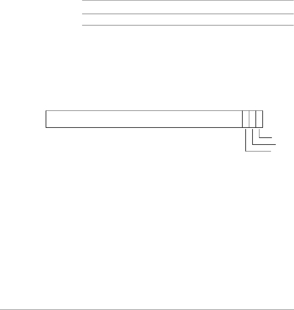
D8 AArch64 System Register Descriptions
D8.5 Generic Timer registers
ARM DDI 0487A.a Copyright © 2013 ARM Limited. All rights reserved. D8-2173
ID090413 Non-Confidential - Beta
D8.5.3 CNTHP_CTL_EL2, Counter-timer Hypervisor Physical Timer Control register
The CNTHP_CTL_EL2 characteristics are:
Purpose
Control register for the EL2 physical timer.
This register is part of:
• the Generic Timer registers functional group
• the Virtualization registers functional group.
Usage constraints
This register is accessible as shown below:
Configurations
CNTHP_CTL_EL2 is architecturally mapped to AArch32 register CNTHP_CTL.
If EL2 is not implemented, this register is RES0 from EL3.
Attributes
CNTHP_CTL_EL2 is a 32-bit register.
The CNTHP_CTL_EL2 bit assignments are:
Bits [31:3]
Reserved, RES0.
ISTATUS, bit [2]
The status of the timer interrupt. This bit is read-only. Permitted values are:
0
Interrupt not asserted.
1
Interrupt asserted.
A register write that sets IMASK to 1 latches this bit to reflect the status of the interrupt immediately
before that write.
Reset value is architecturally UNKNOWN.
IMASK, bit [1]
Timer interrupt mask bit. Permitted values are:
0
Timer interrupt is not masked.
1
Timer interrupt is masked.
Reset value is architecturally UNKNOWN.
EL0 EL1 (NS) EL1 (S) EL2 EL3 (SCR.NS=1) EL3 (SCR.NS=0)
-- - RWRW RW
RES0
31 3 2 1 0
ENABLE
IMASK
ISTATUS

D8 AArch64 System Register Descriptions
D8.5 Generic Timer registers
D8-2174 Copyright © 2013 ARM Limited. All rights reserved. ARM DDI 0487A.a
Non-Confidential - Beta ID090413
ENABLE, bit [0]
Enables the timer. Permitted values are:
0
Timer disabled.
1
Timer enabled.
Disabling the timer masks the timer interrupt, but the timer value continues to count down.
Resets to 0.
Accessing the CNTHP_CTL_EL2:
To access the CNTHP_CTL_EL2:
MRS <Xt>, CNTHP_CTL_EL2 ; Read CNTHP_CTL_EL2 into Xt
MSR CNTHP_CTL_EL2, <Xt> ; Write Xt to CNTHP_CTL_EL2
Register access is encoded as follows:
op0 op1 CRn CRm op2
11 100 1110 0010 001
D8 AArch64 System Register Descriptions
D8.5 Generic Timer registers
ARM DDI 0487A.a Copyright © 2013 ARM Limited. All rights reserved. D8-2175
ID090413 Non-Confidential - Beta
D8.5.4 CNTHP_CVAL_EL2, Counter-timer Hypervisor Physical Timer CompareValue register
The CNTHP_CVAL_EL2 characteristics are:
Purpose
Holds the compare value for the EL2 physical timer.
This register is part of:
• the Generic Timer registers functional group
• the Virtualization registers functional group.
Usage constraints
This register is accessible as shown below:
Configurations
CNTHP_CVAL_EL2 is architecturally mapped to AArch32 register CNTHP_CVAL.
If EL2 is not implemented, this register is RES0 from EL3.
Attributes
CNTHP_CVAL_EL2 is a 64-bit register.
The CNTHP_CVAL_EL2 bit assignments are:
Bits [63:0]
EL2 physical timer compare value.
Accessing the CNTHP_CVAL_EL2:
To access the CNTHP_CVAL_EL2:
MRS <Xt>, CNTHP_CVAL_EL2 ; Read CNTHP_CVAL_EL2 into Xt
MSR CNTHP_CVAL_EL2, <Xt> ; Write Xt to CNTHP_CVAL_EL2
Register access is encoded as follows:
EL0 EL1 (NS) EL1 (S) EL2 EL3 (SCR.NS=1) EL3 (SCR.NS=0)
-- - RWRW RW
EL2 physical timer compare value
63 0
op0 op1 CRn CRm op2
11 100 1110 0010 010

D8 AArch64 System Register Descriptions
D8.5 Generic Timer registers
D8-2176 Copyright © 2013 ARM Limited. All rights reserved. ARM DDI 0487A.a
Non-Confidential - Beta ID090413
D8.5.5 CNTHP_TVAL_EL2, Counter-timer Hypervisor Physical Timer TimerValue register
The CNTHP_TVAL_EL2 characteristics are:
Purpose
Holds the timer value for the EL2 physical timer.
This register is part of:
• the Generic Timer registers functional group
• the Virtualization registers functional group.
Usage constraints
This register is accessible as shown below:
Configurations
CNTHP_TVAL_EL2 is architecturally mapped to AArch32 register CNTHP_TVAL.
If EL2 is not implemented, this register is RES0 from EL3.
Attributes
CNTHP_TVAL_EL2 is a 32-bit register.
The CNTHP_TVAL_EL2 bit assignments are:
Bits [31:0]
EL2 physical timer value.
Accessing the CNTHP_TVAL_EL2:
To access the CNTHP_TVAL_EL2:
MRS <Xt>, CNTHP_TVAL_EL2 ; Read CNTHP_TVAL_EL2 into Xt
MSR CNTHP_TVAL_EL2, <Xt> ; Write Xt to CNTHP_TVAL_EL2
Register access is encoded as follows:
EL0 EL1 (NS) EL1 (S) EL2 EL3 (SCR.NS=1) EL3 (SCR.NS=0)
-- - RWRW RW
EL2 physical timer value
31 0
op0 op1 CRn CRm op2
11 100 1110 0010 000
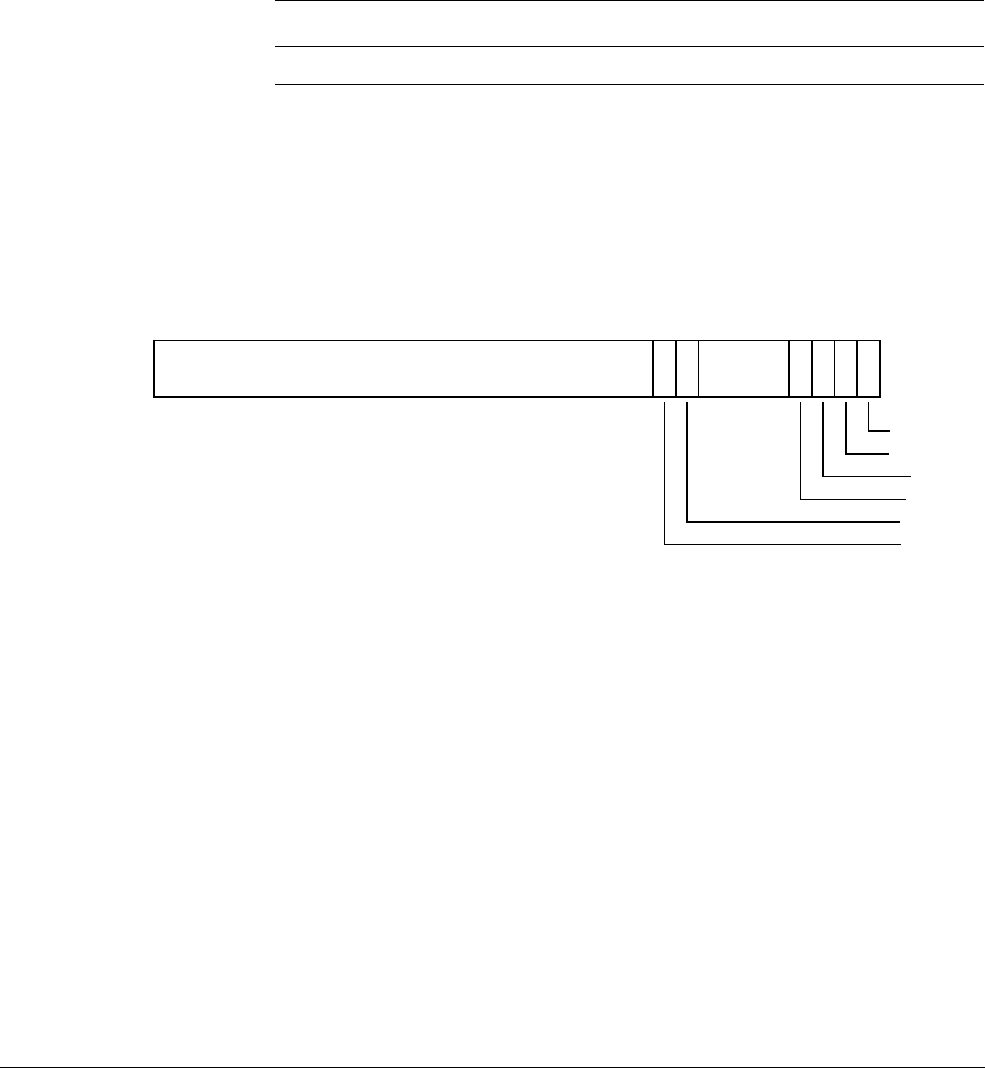
D8 AArch64 System Register Descriptions
D8.5 Generic Timer registers
ARM DDI 0487A.a Copyright © 2013 ARM Limited. All rights reserved. D8-2177
ID090413 Non-Confidential - Beta
D8.5.6 CNTKCTL_EL1, Counter-timer Kernel Control register
The CNTKCTL_EL1 characteristics are:
Purpose
Controls the generation of an event stream from the virtual counter, and access from EL0 to the
physical counter, virtual counter, EL1 physical timers, and the virtual timer.
This register is part of the Generic Timer registers functional group.
Usage constraints
This register is accessible as shown below:
Configurations
CNTKCTL_EL1 is architecturally mapped to AArch32 register CNTKCTL.
Attributes
CNTKCTL_EL1 is a 32-bit register.
The CNTKCTL_EL1 bit assignments are:
Bits [31:10]
Reserved, RES0.
EL0PTEN, bit [9]
Controls whether the physical timer registers are accessible from EL0 modes:
0
The CNTP_CVAL_EL0, CNTP_CTL_EL0, and CNTP_TVAL_EL0 registers are not
accessible from EL0.
1
The CNTP_CVAL_EL0, CNTP_CTL_EL0, and CNTP_TVAL_EL0 registers are
accessible from EL0.
Reset value is architecturally UNKNOWN.
EL0VTEN, bit [8]
Controls whether the virtual timer registers are accessible from EL0 modes:
0
The CNTV_CVAL_EL0, CNTV_CTL_EL0, and CNTV_TVAL_EL0 registers are not
accessible from EL0.
1
The CNTV_CVAL_EL0, CNTV_CTL_EL0, and CNTV_TVAL_EL0 registers are
accessible from EL0.
Reset value is architecturally UNKNOWN.
EL0 EL1 (NS) EL1 (S) EL2 EL3 (SCR.NS=1) EL3 (SCR.NS=0)
-RW RW RWRW RW
RES0
31 10 9 8
EVNTI
74
3 2 1 0
EL0PCTEN
EL0VCTEN
EVNTEN
EVNTDIR
EL0VTEN
EL0PTEN

D8 AArch64 System Register Descriptions
D8.5 Generic Timer registers
D8-2178 Copyright © 2013 ARM Limited. All rights reserved. ARM DDI 0487A.a
Non-Confidential - Beta ID090413
EVNTI, bits [7:4]
Selects which bit (0 to 15) of the corresponding counter register (CNTPCT_EL0 or CNTVCT_EL0)
is the trigger for the event stream generated from that counter, when that stream is enabled.
Reset value is architecturally UNKNOWN.
EVNTDIR, bit [3]
Controls which transition of the counter register (CNTPCT_EL0 or CNTVCT_EL0) trigger bit,
defined by EVNTI, generates an event when the event stream is enabled:
0
A 0 to 1 transition of the trigger bit triggers an event.
1
A 1 to 0 transition of the trigger bit triggers an event.
Reset value is architecturally UNKNOWN.
EVNTEN, bit [2]
Enables the generation of an event stream from the corresponding counter:
0
Disables the event stream.
1
Enables the event stream.
Resets to 0.
EL0VCTEN, bit [1]
Controls whether the virtual counter, CNTVCT_EL0, and the frequency register CNTFRQ_EL0,
are accessible from EL0 modes:
0
CNTVCT_EL0 is not accessible from EL0. If EL0PCTEN is set to 0, CNTFRQ_EL0 is
not accessible from EL0.
1
CNTVCT_EL0 and CNTFRQ_EL0 are accessible from EL0.
Reset value is architecturally UNKNOWN.
EL0PCTEN, bit [0]
Controls whether the physical counter, CNTPCT_EL0, and the frequency register CNTFRQ_EL0,
are accessible from EL0 modes:
0
CNTPCT_EL0 is not accessible from EL0 modes. If EL0VCTEN is set to 0,
CNTFRQ_EL0 is not accessible from EL0.
1
CNTPCT_EL0 and CNTFRQ_EL0 are accessible from EL0.
Reset value is architecturally UNKNOWN.
Accessing the CNTKCTL_EL1:
To access the CNTKCTL_EL1:
MRS <Xt>, CNTKCTL_EL1 ; Read CNTKCTL_EL1 into Xt
MSR CNTKCTL_EL1, <Xt> ; Write Xt to CNTKCTL_EL1
Register access is encoded as follows:
op0 op1 CRn CRm op2
11 000 1110 0001 000

D8 AArch64 System Register Descriptions
D8.5 Generic Timer registers
ARM DDI 0487A.a Copyright © 2013 ARM Limited. All rights reserved. D8-2179
ID090413 Non-Confidential - Beta
D8.5.7 CNTP_CTL_EL0, Counter-timer Physical Timer Control register
The CNTP_CTL_EL0 characteristics are:
Purpose
Control register for the EL1 physical timer.
This register is part of the Generic Timer registers functional group.
Usage constraints
This register is accessible as shown below:
This register is accessible at EL0 when CNTKCTL_EL1.EL0PTEN is set to 1.
If EL2 is implemented, this register is accessible at Non-secure EL1 and EL0 when
CNTHCTL_EL2.EL1PCEN is set to 1.
Configurations
CNTP_CTL_EL0 is architecturally mapped to AArch32 register CNTP_CTL (NS).
CNTP_CTL_EL0 is architecturally mapped to external register CNTP_CTL.
Attributes
CNTP_CTL_EL0 is a 32-bit register.
The CNTP_CTL_EL0 bit assignments are:
Bits [31:3]
Reserved, RES0.
ISTATUS, bit [2]
The status of the timer interrupt. This bit is read-only. Permitted values are:
0
Interrupt not asserted.
1
Interrupt asserted.
A register write that sets IMASK to 1 latches this bit to reflect the status of the interrupt immediately
before that write.
Reset value is architecturally UNKNOWN.
IMASK, bit [1]
Timer interrupt mask bit. Permitted values are:
0
Timer interrupt is not masked.
1
Timer interrupt is masked.
Reset value is architecturally UNKNOWN.
EL0 EL1 (NS) EL1 (S) EL2 EL3 (SCR.NS=1) EL3 (SCR.NS=0)
Config-RW Config-RW RW RW RW RW
RES0
31 3 2 1 0
ENABLE
IMASK
ISTATUS

D8 AArch64 System Register Descriptions
D8.5 Generic Timer registers
D8-2180 Copyright © 2013 ARM Limited. All rights reserved. ARM DDI 0487A.a
Non-Confidential - Beta ID090413
ENABLE, bit [0]
Enables the timer. Permitted values are:
0
Timer disabled.
1
Timer enabled.
Disabling the timer masks the timer interrupt, but the timer value continues to count down.
Resets to 0.
Accessing the CNTP_CTL_EL0:
To access the CNTP_CTL_EL0:
MRS <Xt>, CNTP_CTL_EL0 ; Read CNTP_CTL_EL0 into Xt
MSR CNTP_CTL_EL0, <Xt> ; Write Xt to CNTP_CTL_EL0
Register access is encoded as follows:
op0 op1 CRn CRm op2
11 011 1110 0010 001

D8 AArch64 System Register Descriptions
D8.5 Generic Timer registers
ARM DDI 0487A.a Copyright © 2013 ARM Limited. All rights reserved. D8-2181
ID090413 Non-Confidential - Beta
D8.5.8 CNTP_CVAL_EL0, Counter-timer Physical Timer CompareValue register
The CNTP_CVAL_EL0 characteristics are:
Purpose
Holds the compare value for the EL1 physical timer.
This register is part of the Generic Timer registers functional group.
Usage constraints
This register is accessible as shown below:
This register is accessible at EL0 when CNTKCTL_EL1.EL0PTEN is set to 1.
If EL2 is implemented, this register is accessible at Non-secure EL1 and EL0 when
CNTHCTL_EL2.EL1PCEN is set to 1.
Configurations
CNTP_CVAL_EL0 is architecturally mapped to AArch32 register CNTP_CVAL (NS).
CNTP_CVAL_EL0 is architecturally mapped to external register CNTP_CVAL.
Attributes
CNTP_CVAL_EL0 is a 64-bit register.
The CNTP_CVAL_EL0 bit assignments are:
Bits [63:0]
EL1 physical timer compare value.
Accessing the CNTP_CVAL_EL0:
To access the CNTP_CVAL_EL0:
MRS <Xt>, CNTP_CVAL_EL0 ; Read CNTP_CVAL_EL0 into Xt
MSR CNTP_CVAL_EL0, <Xt> ; Write Xt to CNTP_CVAL_EL0
Register access is encoded as follows:
EL0 EL1 (NS) EL1 (S) EL2 EL3 (SCR.NS=1) EL3 (SCR.NS=0)
Config-RW Config-RW RW RW RW RW
EL1 physical timer compare value
63 0
op0 op1 CRn CRm op2
11 011 1110 0010 010

D8 AArch64 System Register Descriptions
D8.5 Generic Timer registers
D8-2182 Copyright © 2013 ARM Limited. All rights reserved. ARM DDI 0487A.a
Non-Confidential - Beta ID090413
D8.5.9 CNTP_TVAL_EL0, Counter-timer Physical Timer TimerValue register
The CNTP_TVAL_EL0 characteristics are:
Purpose
Holds the timer value for the EL1 physical timer.
This register is part of the Generic Timer registers functional group.
Usage constraints
This register is accessible as shown below:
This register is accessible at EL0 when CNTKCTL_EL1.EL0PTEN is set to 1.
If EL2 is implemented, this register is accessible at Non-secure EL1 and EL0 when
CNTHCTL_EL2.EL1PCEN is set to 1.
Configurations
CNTP_TVAL_EL0 is architecturally mapped to AArch32 register CNTP_TVAL (NS).
CNTP_TVAL_EL0 is architecturally mapped to external register CNTP_TVAL.
Attributes
CNTP_TVAL_EL0 is a 32-bit register.
The CNTP_TVAL_EL0 bit assignments are:
Bits [31:0]
EL1 physical timer value.
Accessing the CNTP_TVAL_EL0:
To access the CNTP_TVAL_EL0:
MRS <Xt>, CNTP_TVAL_EL0 ; Read CNTP_TVAL_EL0 into Xt
MSR CNTP_TVAL_EL0, <Xt> ; Write Xt to CNTP_TVAL_EL0
Register access is encoded as follows:
EL0 EL1 (NS) EL1 (S) EL2 EL3 (SCR.NS=1) EL3 (SCR.NS=0)
Config-RW Config-RW RW RW RW RW
EL1 physical timer value
31 0
op0 op1 CRn CRm op2
11 011 1110 0010 000

D8 AArch64 System Register Descriptions
D8.5 Generic Timer registers
ARM DDI 0487A.a Copyright © 2013 ARM Limited. All rights reserved. D8-2183
ID090413 Non-Confidential - Beta
D8.5.10 CNTPCT_EL0, Counter-timer Physical Count register
The CNTPCT_EL0 characteristics are:
Purpose
Holds the 64-bit physical count value.
This register is part of the Generic Timer registers functional group.
Usage constraints
This register is accessible as shown below:
This register is accessible at EL0 when CNTKCTL_EL1.EL0PCTEN is set to 1.
If EL2 is implemented, this register is accessible at Non-secure EL1 and EL0 when
CNTHCTL_EL2.EL1PCTEN is set to 1.
Configurations
CNTPCT_EL0 is architecturally mapped to AArch32 register CNTPCT.
CNTPCT_EL0 is architecturally mapped to external register CNTPCT.
Attributes
CNTPCT_EL0 is a 64-bit register.
The CNTPCT_EL0 bit assignments are:
Bits [63:0]
Physical count value.
Accessing the CNTPCT_EL0:
To access the CNTPCT_EL0:
MRS <Xt>, CNTPCT_EL0 ; Read CNTPCT_EL0 into Xt
Register access is encoded as follows:
EL0 EL1 (NS) EL1 (S) EL2 EL3 (SCR.NS=1) EL3 (SCR.NS=0)
Config-RO Config-RO RO RO RO RO
Physical count value
63 0
op0 op1 CRn CRm op2
11 011 1110 0000 001

D8 AArch64 System Register Descriptions
D8.5 Generic Timer registers
D8-2184 Copyright © 2013 ARM Limited. All rights reserved. ARM DDI 0487A.a
Non-Confidential - Beta ID090413
D8.5.11 CNTPS_CTL_EL1, Counter-timer Physical Secure Timer Control register
The CNTPS_CTL_EL1 characteristics are:
Purpose
Control register for the secure physical timer, usually accessible at EL3 but configurably accessible
at EL1 in Secure state.
This register is part of the Generic Timer registers functional group.
Usage constraints
This register is accessible as shown below:
This register is accessible at Secure EL1 when SCR_EL3.ST is set to 1.
Configurations
There are no configuration notes.
Attributes
CNTPS_CTL_EL1 is a 32-bit register.
The CNTPS_CTL_EL1 bit assignments are:
Bits [31:3]
Reserved, RES0.
ISTATUS, bit [2]
The status of the timer interrupt. This bit is read-only. Permitted values are:
0
Interrupt not asserted.
1
Interrupt asserted.
A register write that sets IMASK to 1 latches this bit to reflect the status of the interrupt immediately
before that write.
Reset value is architecturally UNKNOWN.
IMASK, bit [1]
Timer interrupt mask bit. Permitted values are:
0
Timer interrupt is not masked.
1
Timer interrupt is masked.
Reset value is architecturally UNKNOWN.
EL0 EL1 (NS) EL1 (S) EL2 EL3 (SCR.NS=1) EL3 (SCR.NS=0)
- - Config-RW - RW RW
RES0
31 3 2 1 0
ENABLE
IMASK
ISTATUS

D8 AArch64 System Register Descriptions
D8.5 Generic Timer registers
ARM DDI 0487A.a Copyright © 2013 ARM Limited. All rights reserved. D8-2185
ID090413 Non-Confidential - Beta
ENABLE, bit [0]
Enables the timer. Permitted values are:
0
Timer disabled.
1
Timer enabled.
Disabling the timer masks the timer interrupt, but the timer value continues to count down.
Resets to 0.
Accessing the CNTPS_CTL_EL1:
To access the CNTPS_CTL_EL1:
MRS <Xt>, CNTPS_CTL_EL1 ; Read CNTPS_CTL_EL1 into Xt
MSR CNTPS_CTL_EL1, <Xt> ; Write Xt to CNTPS_CTL_EL1
Register access is encoded as follows:
op0 op1 CRn CRm op2
11 111 1110 0010 001
D8 AArch64 System Register Descriptions
D8.5 Generic Timer registers
D8-2186 Copyright © 2013 ARM Limited. All rights reserved. ARM DDI 0487A.a
Non-Confidential - Beta ID090413
D8.5.12 CNTPS_CVAL_EL1, Counter-timer Physical Secure Timer CompareValue register
The CNTPS_CVAL_EL1 characteristics are:
Purpose
Holds the compare value for the secure physical timer, usually accessible at EL3 but configurably
accessible at EL1 in Secure state.
This register is part of the Generic Timer registers functional group.
Usage constraints
This register is accessible as shown below:
This register is accessible at Secure EL1 when SCR_EL3.ST is set to 1.
Configurations
There are no configuration notes.
Attributes
CNTPS_CVAL_EL1 is a 64-bit register.
The CNTPS_CVAL_EL1 bit assignments are:
Bits [63:0]
Secure physical timer compare value.
Accessing the CNTPS_CVAL_EL1:
To access the CNTPS_CVAL_EL1:
MRS <Xt>, CNTPS_CVAL_EL1 ; Read CNTPS_CVAL_EL1 into Xt
MSR CNTPS_CVAL_EL1, <Xt> ; Write Xt to CNTPS_CVAL_EL1
Register access is encoded as follows:
EL0 EL1 (NS) EL1 (S) EL2 EL3 (SCR.NS=1) EL3 (SCR.NS=0)
- - Config-RW - RW RW
Secure physical timer compare value
63 0
op0 op1 CRn CRm op2
11 111 1110 0010 010

D8 AArch64 System Register Descriptions
D8.5 Generic Timer registers
ARM DDI 0487A.a Copyright © 2013 ARM Limited. All rights reserved. D8-2187
ID090413 Non-Confidential - Beta
D8.5.13 CNTPS_TVAL_EL1, Counter-timer Physical Secure Timer TimerValue register
The CNTPS_TVAL_EL1 characteristics are:
Purpose
Holds the timer value for the secure physical timer, usually accessible at EL3 but configurably
accessible at EL1 in Secure state.
This register is part of the Generic Timer registers functional group.
Usage constraints
This register is accessible as shown below:
This register is accessible at Secure EL1 when SCR_EL3.ST is set to 1.
Configurations
There are no configuration notes.
Attributes
CNTPS_TVAL_EL1 is a 32-bit register.
The CNTPS_TVAL_EL1 bit assignments are:
Bits [31:0]
Secure physical timer value.
Accessing the CNTPS_TVAL_EL1:
To access the CNTPS_TVAL_EL1:
MRS <Xt>, CNTPS_TVAL_EL1 ; Read CNTPS_TVAL_EL1 into Xt
MSR CNTPS_TVAL_EL1, <Xt> ; Write Xt to CNTPS_TVAL_EL1
Register access is encoded as follows:
EL0 EL1 (NS) EL1 (S) EL2 EL3 (SCR.NS=1) EL3 (SCR.NS=0)
- - Config-RW - RW RW
Secure physical timer value
31 0
op0 op1 CRn CRm op2
11 111 1110 0010 000

D8 AArch64 System Register Descriptions
D8.5 Generic Timer registers
D8-2188 Copyright © 2013 ARM Limited. All rights reserved. ARM DDI 0487A.a
Non-Confidential - Beta ID090413
D8.5.14 CNTV_CTL_EL0, Counter-timer Virtual Timer Control register
The CNTV_CTL_EL0 characteristics are:
Purpose
Control register for the virtual timer.
This register is part of the Generic Timer registers functional group.
Usage constraints
This register is accessible as shown below:
This register is accessible at EL0 when CNTKCTL_EL1.EL0VTEN is set to 1.
Configurations
CNTV_CTL_EL0 is architecturally mapped to AArch32 register CNTV_CTL.
CNTV_CTL_EL0 is architecturally mapped to external register CNTV_CTL.
Attributes
CNTV_CTL_EL0 is a 32-bit register.
The CNTV_CTL_EL0 bit assignments are:
Bits [31:3]
Reserved, RES0.
ISTATUS, bit [2]
The status of the timer interrupt. This bit is read-only. Permitted values are:
0
Interrupt not asserted.
1
Interrupt asserted.
A register write that sets IMASK to 1 latches this bit to reflect the status of the interrupt immediately
before that write.
Reset value is architecturally UNKNOWN.
IMASK, bit [1]
Timer interrupt mask bit. Permitted values are:
0
Timer interrupt is not masked.
1
Timer interrupt is masked.
Reset value is architecturally UNKNOWN.
EL0 EL1 (NS) EL1 (S) EL2 EL3 (SCR.NS=1) EL3 (SCR.NS=0)
Config-RW RW RW RW RW RW
RES0
31 3 2 1 0
ENABLE
IMASK
ISTATUS

D8 AArch64 System Register Descriptions
D8.5 Generic Timer registers
ARM DDI 0487A.a Copyright © 2013 ARM Limited. All rights reserved. D8-2189
ID090413 Non-Confidential - Beta
ENABLE, bit [0]
Enables the timer. Permitted values are:
0
Timer disabled.
1
Timer enabled.
Disabling the timer masks the timer interrupt, but the timer value continues to count down.
Resets to 0.
Accessing the CNTV_CTL_EL0:
To access the CNTV_CTL_EL0:
MRS <Xt>, CNTV_CTL_EL0 ; Read CNTV_CTL_EL0 into Xt
MSR CNTV_CTL_EL0, <Xt> ; Write Xt to CNTV_CTL_EL0
Register access is encoded as follows:
op0 op1 CRn CRm op2
11 011 1110 0011 001

D8 AArch64 System Register Descriptions
D8.5 Generic Timer registers
D8-2190 Copyright © 2013 ARM Limited. All rights reserved. ARM DDI 0487A.a
Non-Confidential - Beta ID090413
D8.5.15 CNTV_CVAL_EL0, Counter-timer Virtual Timer CompareValue register
The CNTV_CVAL_EL0 characteristics are:
Purpose
Holds the compare value for the virtual timer.
This register is part of the Generic Timer registers functional group.
Usage constraints
This register is accessible as shown below:
This register is accessible at EL0 when CNTKCTL_EL1.EL0VTEN is set to 1.
Configurations
CNTV_CVAL_EL0 is architecturally mapped to AArch32 register CNTV_CVAL.
CNTV_CVAL_EL0 is architecturally mapped to external register CNTV_CVAL.
Attributes
CNTV_CVAL_EL0 is a 64-bit register.
The CNTV_CVAL_EL0 bit assignments are:
Bits [63:0]
Virtual timer compare value.
Accessing the CNTV_CVAL_EL0:
To access the CNTV_CVAL_EL0:
MRS <Xt>, CNTV_CVAL_EL0 ; Read CNTV_CVAL_EL0 into Xt
MSR CNTV_CVAL_EL0, <Xt> ; Write Xt to CNTV_CVAL_EL0
Register access is encoded as follows:
EL0 EL1 (NS) EL1 (S) EL2 EL3 (SCR.NS=1) EL3 (SCR.NS=0)
Config-RW RW RW RW RW RW
Virtual timer compare value
63 0
op0 op1 CRn CRm op2
11 011 1110 0011 010

D8 AArch64 System Register Descriptions
D8.5 Generic Timer registers
ARM DDI 0487A.a Copyright © 2013 ARM Limited. All rights reserved. D8-2191
ID090413 Non-Confidential - Beta
D8.5.16 CNTV_TVAL_EL0, Counter-timer Virtual Timer TimerValue register
The CNTV_TVAL_EL0 characteristics are:
Purpose
Holds the timer value for the virtual timer.
This register is part of the Generic Timer registers functional group.
Usage constraints
This register is accessible as shown below:
This register is accessible at EL0 when CNTKCTL_EL1.EL0VTEN is set to 1.
Configurations
CNTV_TVAL_EL0 is architecturally mapped to AArch32 register CNTV_TVAL.
CNTV_TVAL_EL0 is architecturally mapped to external register CNTV_TVAL.
Attributes
CNTV_TVAL_EL0 is a 32-bit register.
The CNTV_TVAL_EL0 bit assignments are:
Bits [31:0]
Virtual timer value.
Accessing the CNTV_TVAL_EL0:
To access the CNTV_TVAL_EL0:
MRS <Xt>, CNTV_TVAL_EL0 ; Read CNTV_TVAL_EL0 into Xt
MSR CNTV_TVAL_EL0, <Xt> ; Write Xt to CNTV_TVAL_EL0
Register access is encoded as follows:
EL0 EL1 (NS) EL1 (S) EL2 EL3 (SCR.NS=1) EL3 (SCR.NS=0)
Config-RW RW RW RW RW RW
Virtual timer value
31 0
op0 op1 CRn CRm op2
11 011 1110 0011 000

D8 AArch64 System Register Descriptions
D8.5 Generic Timer registers
D8-2192 Copyright © 2013 ARM Limited. All rights reserved. ARM DDI 0487A.a
Non-Confidential - Beta ID090413
D8.5.17 CNTVCT_EL0, Counter-timer Virtual Count register
The CNTVCT_EL0 characteristics are:
Purpose
Holds the 64-bit virtual count value.
This register is part of the Generic Timer registers functional group.
Usage constraints
This register is accessible as shown below:
This register is accessible at EL0 when CNTKCTL_EL1.EL0VCTEN is set to 1.
Configurations
CNTVCT_EL0 is architecturally mapped to AArch32 register CNTVCT.
CNTVCT_EL0 is architecturally mapped to external register CNTVCT.
Attributes
CNTVCT_EL0 is a 64-bit register.
The CNTVCT_EL0 bit assignments are:
Bits [63:0]
Virtual count value.
Accessing the CNTVCT_EL0:
To access the CNTVCT_EL0:
MRS <Xt>, CNTVCT_EL0 ; Read CNTVCT_EL0 into Xt
Register access is encoded as follows:
EL0 EL1 (NS) EL1 (S) EL2 EL3 (SCR.NS=1) EL3 (SCR.NS=0)
Config-RO RO RO RO RO RO
Virtual count value
63 0
op0 op1 CRn CRm op2
11 011 1110 0000 010
D8 AArch64 System Register Descriptions
D8.5 Generic Timer registers
ARM DDI 0487A.a Copyright © 2013 ARM Limited. All rights reserved. D8-2193
ID090413 Non-Confidential - Beta
D8.5.18 CNTVOFF_EL2, Counter-timer Virtual Offset register
The CNTVOFF_EL2 characteristics are:
Purpose
Holds the 64-bit virtual offset.
This register is part of:
• the Generic Timer registers functional group
• the Virtualization registers functional group.
Usage constraints
This register is accessible as shown below:
Configurations
CNTVOFF_EL2 is architecturally mapped to AArch32 register CNTVOFF.
CNTVOFF_EL2 is architecturally mapped to external register CNTVOFF.
CNTVOFF_EL2 is architecturally mapped to external register CNTVOFF<n>.
If EL2 is not implemented, this register is RES0 from EL3.
Attributes
CNTVOFF_EL2 is a 64-bit register.
The CNTVOFF_EL2 bit assignments are:
Bits [63:0]
Virtual offset.
Accessing the CNTVOFF_EL2:
To access the CNTVOFF_EL2:
MRS <Xt>, CNTVOFF_EL2 ; Read CNTVOFF_EL2 into Xt
MSR CNTVOFF_EL2, <Xt> ; Write Xt to CNTVOFF_EL2
Register access is encoded as follows:
EL0 EL1 (NS) EL1 (S) EL2 EL3 (SCR.NS=1) EL3 (SCR.NS=0)
-- - RWRW RW
Virtual offset
63 0
op0 op1 CRn CRm op2
11 100 1110 0000 011
D8 AArch64 System Register Descriptions
D8.6 Generic Interrupt Controller CPU interface registers
D8-2194 Copyright © 2013 ARM Limited. All rights reserved. ARM DDI 0487A.a
Non-Confidential - Beta ID090413
D8.6 Generic Interrupt Controller CPU interface registers
This section lists the GIC CPU interface registers in AArch64 state.
D8.6.1 ICC_AP0R0_EL1, Interrupt Controller Active Priorities Register (0,0)
The ICC_AP0R0_EL1 characteristics are:
Purpose
Provides information about the active priorities for the current interrupt regime.
This register is part of the GIC registers functional group.
Usage constraints
This register is accessible as shown below:
In implementations supporting fewer than 8 bits of priority, some of these registers correspond to
unimplemented priority levels. Access to such registers will generate an Undefined exception.
Configurations
ICC_AP0R0_EL1 is architecturally mapped to AArch32 register ICC_AP0R0.
Attributes
ICC_AP0R0_EL1 is a 32-bit register.
The ICC_AP0R0_EL1 bit assignments are:
EL0 EL1 (NS) EL1 (S) EL2 EL3 (SCR.NS=1) EL3 (SCR.NS=0)
-RW RW RWRW RW
31 30 29 28 27 26 25 24 23 22 21 20 19 18 17 16 15 14 13 12 11 10
P9
9
P8
8
P7
7
P6
6
P5
5
P4
4
P3
3
P2
2
P1
1
P0
0
P31
P30
P29
P28
P27
P26
P25
P24
P23
P22
P21
P20
P19
P18
P17
P16
P10
P11
P12
P13
P14
P15

D8 AArch64 System Register Descriptions
D8.6 Generic Interrupt Controller CPU interface registers
ARM DDI 0487A.a Copyright © 2013 ARM Limited. All rights reserved. D8-2195
ID090413 Non-Confidential - Beta
P<n>, bit [n], for n = 0 to 31
Provides information about priority M, according to the following relationship:
Bit P<n> corresponds to priority (M divided by 2U) minus 1, where U is the number of
unimplemented bits of priority and is equal to (7 - ICC_CTLR_EL1.PRIbits).
For example, in a system with ICC_CTLR_EL1.PRIbits ==
0b100
:
• There are 5 bits of implemented priority.
• This means there are 3 bits of unimplemented priority, which are always at the least
significant end (bits [2:0] are RES0).
• Valid priorities are 8, 16, 24, 32, and so on. Dividing these by 23 gives 1, 2, 3, 4, and so on.
• Subtracting 1 from each gives bits 0, 1, 2, 3, and so on that provide information about those
priorities.
Accesses to these registers from an interrupt regime give a view of the active priorities that is
appropriate for that interrupt regime, to allow save and restore of the appropriate state.
Interrupt regime and the number of security states supported by the Distributor affect the view as
follows. Unless otherwise stated, when a bit is successfully set to one, this clears any other active
priorities corresponding to that bit.
A Virtual interrupt in this case means that the interrupt group associated with the register has been
virtualized.
Accessing the ICC_AP0R0_EL1:
To access the ICC_AP0R0_EL1:
MRS <Xt>, ICC_AP0R0_EL1 ; Read ICC_AP0R0_EL1 into Xt
MSR ICC_AP0R0_EL1, <Xt> ; Write Xt to ICC_AP0R0_EL1
Register access is encoded as follows:
Exception level AP0Rn access
(Secure) EL3 Permitted. Accesses Group 0 Secure active
priorities.
Secure EL1 Permitted. Accesses Group 0 Secure active
priorities.
Non-secure EL1 access for a Virtual interrupt ICH_AP0Rn_EL2
Non-secure EL1 or EL2 when GIC Distributor supports two
Security states Permitted. Accesses Group 0 Secure active
priorities.
Non-secure EL1 or EL2 when GIC Distributor supports one
Security state Permitted. Accesses Group 0 active priorities.
op0 op1 CRn CRm op2
11 000 1100 1000 100

D8 AArch64 System Register Descriptions
D8.6 Generic Interrupt Controller CPU interface registers
D8-2196 Copyright © 2013 ARM Limited. All rights reserved. ARM DDI 0487A.a
Non-Confidential - Beta ID090413
D8.6.2 ICC_AP0R1_EL1, Interrupt Controller Active Priorities Register (0,1)
The ICC_AP0R1_EL1 characteristics are:
Purpose
Provides information about the active priorities for the current interrupt regime.
This register is part of the GIC registers functional group.
Usage constraints
This register is accessible as shown below:
In implementations supporting fewer than 8 bits of priority, some of these registers correspond to
unimplemented priority levels. Access to such registers will generate an Undefined exception.
Configurations
ICC_AP0R1_EL1 is architecturally mapped to AArch32 register ICC_AP0R1.
Attributes
ICC_AP0R1_EL1 is a 32-bit register.
The ICC_AP0R1_EL1 bit assignments are:
P<n>, bit [(n-32)], for n = 32 to 63
Provides information about priority M, according to the following relationship:
Bit P<n> corresponds to priority (M divided by 2U) minus 1, where U is the number of
unimplemented bits of priority and is equal to (7 - ICC_CTLR_EL1.PRIbits).
For example, in a system with ICC_CTLR_EL1.PRIbits ==
0b100
:
• There are 5 bits of implemented priority.
EL0 EL1 (NS) EL1 (S) EL2 EL3 (SCR.NS=1) EL3 (SCR.NS=0)
-RW RW RWRW RW
31 30 29 28 27 26 25 24 23 22 21 20 19 18 17 16 15 14 13 12 11 10 9 8 7 6 5 4 3 2 1 0
P63
P62
P61
P60
P59
P58
P57
P56
P55
P54
P53
P52
P51
P50
P49
P48
P32
P33
P34
P35
P36
P37
P38
P39
P40
P41
P42
P43
P44
P45
P46
P47

D8 AArch64 System Register Descriptions
D8.6 Generic Interrupt Controller CPU interface registers
ARM DDI 0487A.a Copyright © 2013 ARM Limited. All rights reserved. D8-2197
ID090413 Non-Confidential - Beta
• This means there are 3 bits of unimplemented priority, which are always at the least
significant end (bits [2:0] are RES0).
• Valid priorities are 8, 16, 24, 32, and so on. Dividing these by 23 gives 1, 2, 3, 4, and so on.
• Subtracting 1 from each gives bits 0, 1, 2, 3, and so on that provide information about those
priorities.
Accesses to these registers from an interrupt regime give a view of the active priorities that is
appropriate for that interrupt regime, to allow save and restore of the appropriate state.
Interrupt regime and the number of security states supported by the Distributor affect the view as
follows. Unless otherwise stated, when a bit is successfully set to one, this clears any other active
priorities corresponding to that bit.
A Virtual interrupt in this case means that the interrupt group associated with the register has been
virtualized.
Accessing the ICC_AP0R1_EL1:
To access the ICC_AP0R1_EL1:
MRS <Xt>, ICC_AP0R1_EL1 ; Read ICC_AP0R1_EL1 into Xt
MSR ICC_AP0R1_EL1, <Xt> ; Write Xt to ICC_AP0R1_EL1
Register access is encoded as follows:
Exception level AP0Rn access
(Secure) EL3 Permitted. Accesses Group 0 Secure active
priorities.
Secure EL1 Permitted. Accesses Group 0 Secure active
priorities.
Non-secure EL1 access for a Virtual interrupt ICH_AP0Rn_EL2
Non-secure EL1 or EL2 when GIC Distributor supports two
Security states Permitted. Accesses Group 0 Secure active
priorities.
Non-secure EL1 or EL2 when GIC Distributor supports one
Security state Permitted. Accesses Group 0 active priorities.
op0 op1 CRn CRm op2
11 000 1100 1000 101

D8 AArch64 System Register Descriptions
D8.6 Generic Interrupt Controller CPU interface registers
D8-2198 Copyright © 2013 ARM Limited. All rights reserved. ARM DDI 0487A.a
Non-Confidential - Beta ID090413
D8.6.3 ICC_AP0R2_EL1, Interrupt Controller Active Priorities Register (0,2)
The ICC_AP0R2_EL1 characteristics are:
Purpose
Provides information about the active priorities for the current interrupt regime.
This register is part of the GIC registers functional group.
Usage constraints
This register is accessible as shown below:
In implementations supporting fewer than 8 bits of priority, some of these registers correspond to
unimplemented priority levels. Access to such registers will generate an Undefined exception.
Configurations
ICC_AP0R2_EL1 is architecturally mapped to AArch32 register ICC_AP0R2.
Attributes
ICC_AP0R2_EL1 is a 32-bit register.
The ICC_AP0R2_EL1 bit assignments are:
P<n>, bit [(n-64)], for n = 64 to 95
Provides information about priority M, according to the following relationship:
Bit P<n> corresponds to priority (M divided by 2U) minus 1, where U is the number of
unimplemented bits of priority and is equal to (7 - ICC_CTLR_EL1.PRIbits).
For example, in a system with ICC_CTLR_EL1.PRIbits ==
0b100
:
• There are 5 bits of implemented priority.
EL0 EL1 (NS) EL1 (S) EL2 EL3 (SCR.NS=1) EL3 (SCR.NS=0)
-RW RW RWRW RW
31 30 29 28 27 26 25 24 23 22 21 20 19 18 17 16 15 14 13 12 11 10 9 8 7 6 5 4 3 2 1 0
P95
P94
P93
P92
P91
P90
P89
P88
P87
P86
P85
P84
P83
P82
P81
P80
P64
P65
P66
P67
P68
P69
P70
P71
P72
P73
P74
P75
P76
P77
P78
P79

D8 AArch64 System Register Descriptions
D8.6 Generic Interrupt Controller CPU interface registers
ARM DDI 0487A.a Copyright © 2013 ARM Limited. All rights reserved. D8-2199
ID090413 Non-Confidential - Beta
• This means there are 3 bits of unimplemented priority, which are always at the least
significant end (bits [2:0] are RES0).
• Valid priorities are 8, 16, 24, 32, and so on. Dividing these by 23 gives 1, 2, 3, 4, and so on.
• Subtracting 1 from each gives bits 0, 1, 2, 3, and so on that provide information about those
priorities.
Accesses to these registers from an interrupt regime give a view of the active priorities that is
appropriate for that interrupt regime, to allow save and restore of the appropriate state.
Interrupt regime and the number of security states supported by the Distributor affect the view as
follows. Unless otherwise stated, when a bit is successfully set to one, this clears any other active
priorities corresponding to that bit.
A Virtual interrupt in this case means that the interrupt group associated with the register has been
virtualized.
Accessing the ICC_AP0R2_EL1:
To access the ICC_AP0R2_EL1:
MRS <Xt>, ICC_AP0R2_EL1 ; Read ICC_AP0R2_EL1 into Xt
MSR ICC_AP0R2_EL1, <Xt> ; Write Xt to ICC_AP0R2_EL1
Register access is encoded as follows:
Exception level AP0Rn access
(Secure) EL3 Permitted. Accesses Group 0 Secure active
priorities.
Secure EL1 Permitted. Accesses Group 0 Secure active
priorities.
Non-secure EL1 access for a Virtual interrupt ICH_AP0Rn_EL2
Non-secure EL1 or EL2 when GIC Distributor supports two
Security states Permitted. Accesses Group 0 Secure active
priorities.
Non-secure EL1 or EL2 when GIC Distributor supports one
Security state Permitted. Accesses Group 0 active priorities.
op0 op1 CRn CRm op2
11 000 1100 1000 110

D8 AArch64 System Register Descriptions
D8.6 Generic Interrupt Controller CPU interface registers
D8-2200 Copyright © 2013 ARM Limited. All rights reserved. ARM DDI 0487A.a
Non-Confidential - Beta ID090413
D8.6.4 ICC_AP0R3_EL1, Interrupt Controller Active Priorities Register (0,3)
The ICC_AP0R3_EL1 characteristics are:
Purpose
Provides information about the active priorities for the current interrupt regime.
This register is part of the GIC registers functional group.
Usage constraints
This register is accessible as shown below:
In implementations supporting fewer than 8 bits of priority, some of these registers correspond to
unimplemented priority levels. Access to such registers will generate an Undefined exception.
Configurations
ICC_AP0R3_EL1 is architecturally mapped to AArch32 register ICC_AP0R3.
Attributes
ICC_AP0R3_EL1 is a 32-bit register.
The ICC_AP0R3_EL1 bit assignments are:
P<n>, bit [(n-96)], for n = 96 to 127
Provides information about priority M, according to the following relationship:
Bit P<n> corresponds to priority (M divided by 2U) minus 1, where U is the number of
unimplemented bits of priority and is equal to (7 - ICC_CTLR_EL1.PRIbits).
For example, in a system with ICC_CTLR_EL1.PRIbits ==
0b100
:
• There are 5 bits of implemented priority.
EL0 EL1 (NS) EL1 (S) EL2 EL3 (SCR.NS=1) EL3 (SCR.NS=0)
-RW RW RWRW RW
31 30 29 28 27 26 25 24 23 22 21 20 19 18 17 16 15 14 13 12 11 10 9 8 7 6 5 4 3 2 1 0
P127
P126
P125
P124
P123
P122
P121
P120
P119
P118
P117
P116
P115
P114
P113
P112
P96
P97
P98
P99
P100
P101
P102
P103
P104
P105
P106
P107
P108
P109
P110
P111

D8 AArch64 System Register Descriptions
D8.6 Generic Interrupt Controller CPU interface registers
ARM DDI 0487A.a Copyright © 2013 ARM Limited. All rights reserved. D8-2201
ID090413 Non-Confidential - Beta
• This means there are 3 bits of unimplemented priority, which are always at the least
significant end (bits [2:0] are RES0).
• Valid priorities are 8, 16, 24, 32, and so on. Dividing these by 23 gives 1, 2, 3, 4, and so on.
• Subtracting 1 from each gives bits 0, 1, 2, 3, and so on that provide information about those
priorities.
Accesses to these registers from an interrupt regime give a view of the active priorities that is
appropriate for that interrupt regime, to allow save and restore of the appropriate state.
Interrupt regime and the number of security states supported by the Distributor affect the view as
follows. Unless otherwise stated, when a bit is successfully set to one, this clears any other active
priorities corresponding to that bit.
A Virtual interrupt in this case means that the interrupt group associated with the register has been
virtualized.
Accessing the ICC_AP0R3_EL1:
To access the ICC_AP0R3_EL1:
MRS <Xt>, ICC_AP0R3_EL1 ; Read ICC_AP0R3_EL1 into Xt
MSR ICC_AP0R3_EL1, <Xt> ; Write Xt to ICC_AP0R3_EL1
Register access is encoded as follows:
Exception level AP0Rn access
(Secure) EL3 Permitted. Accesses Group 0 Secure active
priorities.
Secure EL1 Permitted. Accesses Group 0 Secure active
priorities.
Non-secure EL1 access for a Virtual interrupt ICH_AP0Rn_EL2
Non-secure EL1 or EL2 when GIC Distributor supports two
Security states Permitted. Accesses Group 0 Secure active
priorities.
Non-secure EL1 or EL2 when GIC Distributor supports one
Security state Permitted. Accesses Group 0 active priorities.
op0 op1 CRn CRm op2
11 000 1100 1000 111
D8 AArch64 System Register Descriptions
D8.6 Generic Interrupt Controller CPU interface registers
D8-2202 Copyright © 2013 ARM Limited. All rights reserved. ARM DDI 0487A.a
Non-Confidential - Beta ID090413
D8.6.5 ICC_AP1R0_EL1, Interrupt Controller Active Priorities Register (1,0)
The ICC_AP1R0_EL1 characteristics are:
Purpose
Provides information about the active priorities for the current interrupt regime.
This register is part of the GIC registers functional group.
Usage constraints
This register is accessible as shown below:
In implementations supporting fewer than 8 bits of priority, some of these registers correspond to
unimplemented priority levels. Access to such registers will generate an Undefined exception.
Configurations
ICC_AP1R0_EL1 is architecturally mapped to AArch32 register ICC_AP1R0.
Attributes
ICC_AP1R0_EL1 is a 32-bit register.
The ICC_AP1R0_EL1 bit assignments are:
P<n>, bit [n], for n = 0 to 31
Provides information about priority M, according to the following relationship:
Bit P<n> corresponds to priority (M divided by 2U) minus 1, where U is the number of
unimplemented bits of priority and is equal to (7 - ICC_CTLR_EL1.PRIbits).
For example, in a system with ICC_CTLR_EL1.PRIbits ==
0b100
:
• There are 5 bits of implemented priority.
EL0 EL1 (NS) EL1 (S) EL2 EL3 (SCR.NS=1) EL3 (SCR.NS=0)
-RW RW RWRW RW
31 30 29 28 27 26 25 24 23 22 21 20 19 18 17 16 15 14 13 12 11 10
P9
9
P8
8
P7
7
P6
6
P5
5
P4
4
P3
3
P2
2
P1
1
P0
0
P31
P30
P29
P28
P27
P26
P25
P24
P23
P22
P21
P20
P19
P18
P17
P16
P10
P11
P12
P13
P14
P15

D8 AArch64 System Register Descriptions
D8.6 Generic Interrupt Controller CPU interface registers
ARM DDI 0487A.a Copyright © 2013 ARM Limited. All rights reserved. D8-2203
ID090413 Non-Confidential - Beta
• This means there are 3 bits of unimplemented priority, which are always at the least
significant end (bits [2:0] are RES0).
• Valid priorities are 8, 16, 24, 32, and so on. Dividing these by 23 gives 1, 2, 3, 4, and so on.
• Subtracting 1 from each gives bits 0, 1, 2, 3, and so on that provide information about those
priorities.
Accesses to these registers from an interrupt regime give a view of the active priorities that is
appropriate for that interrupt regime, to allow save and restore of the appropriate state.
Interrupt regime and the number of security states supported by the Distributor affect the view as
follows. Unless otherwise stated, when a bit is successfully set to one, this clears any other active
priorities corresponding to that bit.
A Virtual interrupt in this case means that the interrupt group associated with the register has been
virtualized.
Accessing the ICC_AP1R0_EL1:
To access the ICC_AP1R0_EL1:
MRS <Xt>, ICC_AP1R0_EL1 ; Read ICC_AP1R0_EL1 into Xt
MSR ICC_AP1R0_EL1, <Xt> ; Write Xt to ICC_AP1R0_EL1
Register access is encoded as follows:
Current
exception level
and security
state
AP1Rn access
(Secure) EL3 Permitted. When SCR_EL3.NS is 0, accesses Group 1 Secure active priorities. When
SCR_EL3.NS is 1, accesses Group 1 Non-secure active priorities (unshifted). When a bit
is written, the bit is only updated if the corresponding Group 0 and Group 1 Secure active
priority is zero.
Secure EL1 Permitted. Accesses Group 1 Secure active priorities (unshifted). When a bit is written, the
bit is only updated if the corresponding Group 0 Secure active priority is zero.
Non-secure EL1
access for a
Virtual interrupt
ICH_AP1Rn_EL2
Non-secure EL1
or EL2 when GIC
Distributor
supports two
Security states
Permitted. Accesses Group 1 Non-secure active priorities (shifted). When a bit is written,
the bit is only updated if the corresponding Group 0 and Group 1 Secure active priority is
zero.
Non-secure EL1
or EL2 when GIC
Distributor
supports one
Security state
Permitted. Accesses Group 1 Non-secure active priorities (unshifted). When a bit is
written, the bit is only updated if the Group 0 active priority is zero.
op0 op1 CRn CRm op2
11 000 1100 1001 000
D8 AArch64 System Register Descriptions
D8.6 Generic Interrupt Controller CPU interface registers
D8-2204 Copyright © 2013 ARM Limited. All rights reserved. ARM DDI 0487A.a
Non-Confidential - Beta ID090413
D8.6.6 ICC_AP1R1_EL1, Interrupt Controller Active Priorities Register (1,1)
The ICC_AP1R1_EL1 characteristics are:
Purpose
Provides information about the active priorities for the current interrupt regime.
This register is part of the GIC registers functional group.
Usage constraints
This register is accessible as shown below:
In implementations supporting fewer than 8 bits of priority, some of these registers correspond to
unimplemented priority levels. Access to such registers will generate an Undefined exception.
Configurations
ICC_AP1R1_EL1 is architecturally mapped to AArch32 register ICC_AP1R1.
Attributes
ICC_AP1R1_EL1 is a 32-bit register.
The ICC_AP1R1_EL1 bit assignments are:
P<n>, bit [(n-32)], for n = 32 to 63
Provides information about priority M, according to the following relationship:
Bit P<n> corresponds to priority (M divided by 2U) minus 1, where U is the number of
unimplemented bits of priority and is equal to (7 - ICC_CTLR_EL1.PRIbits).
For example, in a system with ICC_CTLR_EL1.PRIbits ==
0b100
:
• There are 5 bits of implemented priority.
EL0 EL1 (NS) EL1 (S) EL2 EL3 (SCR.NS=1) EL3 (SCR.NS=0)
-RW RW RWRW RW
31 30 29 28 27 26 25 24 23 22 21 20 19 18 17 16 15 14 13 12 11 10 9 8 7 6 5 4 3 2 1 0
P63
P62
P61
P60
P59
P58
P57
P56
P55
P54
P53
P52
P51
P50
P49
P48
P32
P33
P34
P35
P36
P37
P38
P39
P40
P41
P42
P43
P44
P45
P46
P47

D8 AArch64 System Register Descriptions
D8.6 Generic Interrupt Controller CPU interface registers
ARM DDI 0487A.a Copyright © 2013 ARM Limited. All rights reserved. D8-2205
ID090413 Non-Confidential - Beta
• This means there are 3 bits of unimplemented priority, which are always at the least
significant end (bits [2:0] are RES0).
• Valid priorities are 8, 16, 24, 32, and so on. Dividing these by 23 gives 1, 2, 3, 4, and so on.
• Subtracting 1 from each gives bits 0, 1, 2, 3, and so on that provide information about those
priorities.
Accesses to these registers from an interrupt regime give a view of the active priorities that is
appropriate for that interrupt regime, to allow save and restore of the appropriate state.
Interrupt regime and the number of security states supported by the Distributor affect the view as
follows. Unless otherwise stated, when a bit is successfully set to one, this clears any other active
priorities corresponding to that bit.
A Virtual interrupt in this case means that the interrupt group associated with the register has been
virtualized.
Accessing the ICC_AP1R1_EL1:
To access the ICC_AP1R1_EL1:
MRS <Xt>, ICC_AP1R1_EL1 ; Read ICC_AP1R1_EL1 into Xt
MSR ICC_AP1R1_EL1, <Xt> ; Write Xt to ICC_AP1R1_EL1
Register access is encoded as follows:
Current
exception level
and security
state
AP1Rn access
(Secure) EL3 Permitted. When SCR_EL3.NS is 0, accesses Group 1 Secure active priorities. When
SCR_EL3.NS is 1, accesses Group 1 Non-secure active priorities (unshifted). When a bit
is written, the bit is only updated if the corresponding Group 0 and Group 1 Secure active
priority is zero.
Secure EL1 Permitted. Accesses Group 1 Secure active priorities (unshifted). When a bit is written, the
bit is only updated if the corresponding Group 0 Secure active priority is zero.
Non-secure EL1
access for a
Virtual interrupt
ICH_AP1Rn_EL2
Non-secure EL1
or EL2 when GIC
Distributor
supports two
Security states
Permitted. Accesses Group 1 Non-secure active priorities (shifted). When a bit is written,
the bit is only updated if the corresponding Group 0 and Group 1 Secure active priority is
zero.
Non-secure EL1
or EL2 when GIC
Distributor
supports one
Security state
Permitted. Accesses Group 1 Non-secure active priorities (unshifted). When a bit is
written, the bit is only updated if the Group 0 active priority is zero.
op0 op1 CRn CRm op2
11 000 1100 1001 001

D8 AArch64 System Register Descriptions
D8.6 Generic Interrupt Controller CPU interface registers
D8-2206 Copyright © 2013 ARM Limited. All rights reserved. ARM DDI 0487A.a
Non-Confidential - Beta ID090413
D8.6.7 ICC_AP1R2_EL1, Interrupt Controller Active Priorities Register (1,2)
The ICC_AP1R2_EL1 characteristics are:
Purpose
Provides information about the active priorities for the current interrupt regime.
This register is part of the GIC registers functional group.
Usage constraints
This register is accessible as shown below:
In implementations supporting fewer than 8 bits of priority, some of these registers correspond to
unimplemented priority levels. Access to such registers will generate an Undefined exception.
Configurations
ICC_AP1R2_EL1 is architecturally mapped to AArch32 register ICC_AP1R2.
Attributes
ICC_AP1R2_EL1 is a 32-bit register.
The ICC_AP1R2_EL1 bit assignments are:
P<n>, bit [(n-64)], for n = 64 to 95
Provides information about priority M, according to the following relationship:
Bit P<n> corresponds to priority (M divided by 2U) minus 1, where U is the number of
unimplemented bits of priority and is equal to (7 - ICC_CTLR_EL1.PRIbits).
For example, in a system with ICC_CTLR_EL1.PRIbits ==
0b100
:
• There are 5 bits of implemented priority.
EL0 EL1 (NS) EL1 (S) EL2 EL3 (SCR.NS=1) EL3 (SCR.NS=0)
-RW RW RWRW RW
31 30 29 28 27 26 25 24 23 22 21 20 19 18 17 16 15 14 13 12 11 10 9 8 7 6 5 4 3 2 1 0
P95
P94
P93
P92
P91
P90
P89
P88
P87
P86
P85
P84
P83
P82
P81
P80
P64
P65
P66
P67
P68
P69
P70
P71
P72
P73
P74
P75
P76
P77
P78
P79

D8 AArch64 System Register Descriptions
D8.6 Generic Interrupt Controller CPU interface registers
ARM DDI 0487A.a Copyright © 2013 ARM Limited. All rights reserved. D8-2207
ID090413 Non-Confidential - Beta
• This means there are 3 bits of unimplemented priority, which are always at the least
significant end (bits [2:0] are RES0).
• Valid priorities are 8, 16, 24, 32, and so on. Dividing these by 23 gives 1, 2, 3, 4, and so on.
• Subtracting 1 from each gives bits 0, 1, 2, 3, and so on that provide information about those
priorities.
Accesses to these registers from an interrupt regime give a view of the active priorities that is
appropriate for that interrupt regime, to allow save and restore of the appropriate state.
Interrupt regime and the number of security states supported by the Distributor affect the view as
follows. Unless otherwise stated, when a bit is successfully set to one, this clears any other active
priorities corresponding to that bit.
A Virtual interrupt in this case means that the interrupt group associated with the register has been
virtualized.
Accessing the ICC_AP1R2_EL1:
To access the ICC_AP1R2_EL1:
MRS <Xt>, ICC_AP1R2_EL1 ; Read ICC_AP1R2_EL1 into Xt
MSR ICC_AP1R2_EL1, <Xt> ; Write Xt to ICC_AP1R2_EL1
Register access is encoded as follows:
Current
exception level
and security
state
AP1Rn access
(Secure) EL3 Permitted. When SCR_EL3.NS is 0, accesses Group 1 Secure active priorities. When
SCR_EL3.NS is 1, accesses Group 1 Non-secure active priorities (unshifted). When a bit
is written, the bit is only updated if the corresponding Group 0 and Group 1 Secure active
priority is zero.
Secure EL1 Permitted. Accesses Group 1 Secure active priorities (unshifted). When a bit is written, the
bit is only updated if the corresponding Group 0 Secure active priority is zero.
Non-secure EL1
access for a
Virtual interrupt
ICH_AP1Rn_EL2
Non-secure EL1
or EL2 when GIC
Distributor
supports two
Security states
Permitted. Accesses Group 1 Non-secure active priorities (shifted). When a bit is written,
the bit is only updated if the corresponding Group 0 and Group 1 Secure active priority is
zero.
Non-secure EL1
or EL2 when GIC
Distributor
supports one
Security state
Permitted. Accesses Group 1 Non-secure active priorities (unshifted). When a bit is
written, the bit is only updated if the Group 0 active priority is zero.
op0 op1 CRn CRm op2
11 000 1100 1001 010
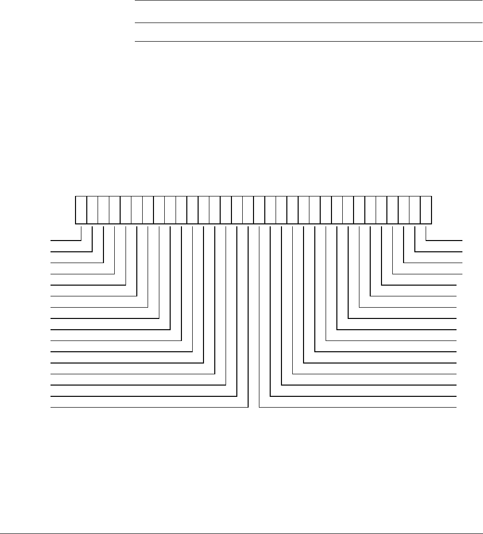
D8 AArch64 System Register Descriptions
D8.6 Generic Interrupt Controller CPU interface registers
D8-2208 Copyright © 2013 ARM Limited. All rights reserved. ARM DDI 0487A.a
Non-Confidential - Beta ID090413
D8.6.8 ICC_AP1R3_EL1, Interrupt Controller Active Priorities Register (1,3)
The ICC_AP1R3_EL1 characteristics are:
Purpose
Provides information about the active priorities for the current interrupt regime.
This register is part of the GIC registers functional group.
Usage constraints
This register is accessible as shown below:
In implementations supporting fewer than 8 bits of priority, some of these registers correspond to
unimplemented priority levels. Access to such registers will generate an Undefined exception.
Configurations
ICC_AP1R3_EL1 is architecturally mapped to AArch32 register ICC_AP1R3.
Attributes
ICC_AP1R3_EL1 is a 32-bit register.
The ICC_AP1R3_EL1 bit assignments are:
P<n>, bit [(n-96)], for n = 96 to 127
Provides information about priority M, according to the following relationship:
Bit P<n> corresponds to priority (M divided by 2U) minus 1, where U is the number of
unimplemented bits of priority and is equal to (7 - ICC_CTLR_EL1.PRIbits).
For example, in a system with ICC_CTLR_EL1.PRIbits ==
0b100
:
• There are 5 bits of implemented priority.
EL0 EL1 (NS) EL1 (S) EL2 EL3 (SCR.NS=1) EL3 (SCR.NS=0)
-RW RW RWRW RW
31 30 29 28 27 26 25 24 23 22 21 20 19 18 17 16 15 14 13 12 11 10 9 8 7 6 5 4 3 2 1 0
P127
P126
P125
P124
P123
P122
P121
P120
P119
P118
P117
P116
P115
P114
P113
P112
P96
P97
P98
P99
P100
P101
P102
P103
P104
P105
P106
P107
P108
P109
P110
P111

D8 AArch64 System Register Descriptions
D8.6 Generic Interrupt Controller CPU interface registers
ARM DDI 0487A.a Copyright © 2013 ARM Limited. All rights reserved. D8-2209
ID090413 Non-Confidential - Beta
• This means there are 3 bits of unimplemented priority, which are always at the least
significant end (bits [2:0] are RES0).
• Valid priorities are 8, 16, 24, 32, and so on. Dividing these by 23 gives 1, 2, 3, 4, and so on.
• Subtracting 1 from each gives bits 0, 1, 2, 3, and so on that provide information about those
priorities.
Accesses to these registers from an interrupt regime give a view of the active priorities that is
appropriate for that interrupt regime, to allow save and restore of the appropriate state.
Interrupt regime and the number of security states supported by the Distributor affect the view as
follows. Unless otherwise stated, when a bit is successfully set to one, this clears any other active
priorities corresponding to that bit.
A Virtual interrupt in this case means that the interrupt group associated with the register has been
virtualized.
Accessing the ICC_AP1R3_EL1:
To access the ICC_AP1R3_EL1:
MRS <Xt>, ICC_AP1R3_EL1 ; Read ICC_AP1R3_EL1 into Xt
MSR ICC_AP1R3_EL1, <Xt> ; Write Xt to ICC_AP1R3_EL1
Register access is encoded as follows:
Current
exception level
and security
state
AP1Rn access
(Secure) EL3 Permitted. When SCR_EL3.NS is 0, accesses Group 1 Secure active priorities. When
SCR_EL3.NS is 1, accesses Group 1 Non-secure active priorities (unshifted). When a bit
is written, the bit is only updated if the corresponding Group 0 and Group 1 Secure active
priority is zero.
Secure EL1 Permitted. Accesses Group 1 Secure active priorities (unshifted). When a bit is written, the
bit is only updated if the corresponding Group 0 Secure active priority is zero.
Non-secure EL1
access for a
Virtual interrupt
ICH_AP1Rn_EL2
Non-secure EL1
or EL2 when GIC
Distributor
supports two
Security states
Permitted. Accesses Group 1 Non-secure active priorities (shifted). When a bit is written,
the bit is only updated if the corresponding Group 0 and Group 1 Secure active priority is
zero.
Non-secure EL1
or EL2 when GIC
Distributor
supports one
Security state
Permitted. Accesses Group 1 Non-secure active priorities (unshifted). When a bit is
written, the bit is only updated if the Group 0 active priority is zero.
op0 op1 CRn CRm op2
11 000 1100 1001 011

D8 AArch64 System Register Descriptions
D8.6 Generic Interrupt Controller CPU interface registers
D8-2210 Copyright © 2013 ARM Limited. All rights reserved. ARM DDI 0487A.a
Non-Confidential - Beta ID090413
D8.6.9 ICC_ASGI1R_EL1, Interrupt Controller Alias Software Generated Interrupt group 1 Register
The ICC_ASGI1R_EL1 characteristics are:
Purpose
Provides software the ability to generate group 1 SGIs for the other security state.
This register is part of the GIC registers functional group.
Usage constraints
This register is accessible as shown below:
When accessed as ICC_ASGI1R_EL1(S):
When accessed as ICC_ASGI1R_EL1(NS):
Configurations
ICC_ASGI1R_EL1(S) is architecturally mapped to AArch32 register ICC_ASGI1R (S).
ICC_ASGI1R_EL1(NS) is architecturally mapped to AArch32 register ICC_ASGI1R (NS).
There are separate Secure and Non-secure instances of this register.
Attributes
ICC_ASGI1R_EL1 is a 64-bit register.
The ICC_ASGI1R_EL1 bit assignments are:
Bits [63:56]
Reserved, RES0.
Aff3, bits [55:48]
The affinity 3 value of the affinity path of the cluster for which SGI interrupts will be generated.
Bits [47:41]
Reserved, RES0.
IRM, bit [40]
Interrupt Routing Mode. Determines how the generated interrupts should be distributed to
processors. Possible values are:
0
Interrupts routed to the processors specified by a.b.c.{target list}. In this routing, a, b,
and c are the values of fields Aff3, Aff2, and Aff1 respectively.
EL1 (NS) EL1 (S) EL2 EL3 (SCR.NS=1) EL3 (SCR.NS=0)
-WO-- WO
EL1 (NS) EL1 (S) EL2 EL3 (SCR.NS=1) EL3 (SCR.NS=0)
WO - WO WO -
RES0
63 56
Aff3
55 48
RES0
47 41 40
Aff2
39 32
RES0
31 28
SGIID
27 24
Aff1
23 16
TargetList
15 0
IRM

D8 AArch64 System Register Descriptions
D8.6 Generic Interrupt Controller CPU interface registers
ARM DDI 0487A.a Copyright © 2013 ARM Limited. All rights reserved. D8-2211
ID090413 Non-Confidential - Beta
1
Interrupts routed to all processors in the system, excluding "self".
Aff2, bits [39:32]
The affinity 2 value of the affinity path of the cluster for which SGI interrupts will be generated.
Bits [31:28]
Reserved, RES0.
SGIID, bits [27:24]
SGI Interrupt ID.
Aff1, bits [23:16]
The affinity 1 value of the affinity path of the cluster for which SGI interrupts will be generated.
TargetList, bits [15:0]
Target List. The set of processors for which SGI interrupts will be generated. Each bit corresponds
to the processor within a cluster with an Affinity 0 value equal to the bit number.
If a bit is 1 and the bit does not correspond to a valid target processor, the bit must be ignored by the
Distributor. In such cases, a Distributor may optionally generate an SGI.
This restricts distribution of SGIs to the first 16 processors of an affinity 1 cluster.
Accessing the ICC_ASGI1R_EL1:
To access the ICC_ASGI1R_EL1:
MSR ICC_ASGI1R_EL1, <Xt> ; Write Xt to ICC_ASGI1R_EL1
Register access is encoded as follows:
op0 op1 CRn CRm op2
11 000 1100 1011 110

D8 AArch64 System Register Descriptions
D8.6 Generic Interrupt Controller CPU interface registers
D8-2212 Copyright © 2013 ARM Limited. All rights reserved. ARM DDI 0487A.a
Non-Confidential - Beta ID090413
D8.6.10 ICC_BPR0_EL1, Interrupt Controller Binary Point Register 0
The ICC_BPR0_EL1 characteristics are:
Purpose
Defines the point at which the priority value fields split into two parts, the group priority field and
the subpriority field. The group priority field is used to determine interrupt preemption.
This register is part of the GIC registers functional group.
Usage constraints
This register is accessible as shown below:
When accessed as ICC_BPR0_EL1(S):
When accessed as ICC_BPR0_EL1(NS):
In Secure state, this register is the binary point register for Group 0 interrupts. In Non-secure state,
this is the BPR for Group 1 interrupts.
The minimum binary point value is IMPLEMENTATION DEFINED in the range:
• 0-3 if the implementation supports one security state, and for the Secure copy of the register
if the implementation supports two security states.
• 1-4 for the Non-secure copy of the register.
An attempt to program the binary point field to a value less than the minimum value sets the field
to the minimum value. On a reset, the binary point field is set to the minimum supported value.
Configurations
ICC_BPR0_EL1(S) is architecturally mapped to AArch32 register ICC_BPR0 (S).
ICC_BPR0_EL1(NS) is architecturally mapped to AArch32 register ICC_BPR0 (NS).
There are separate Secure and Non-secure instances of this register.
Attributes
ICC_BPR0_EL1 is a 32-bit register.
The ICC_BPR0_EL1 bit assignments are:
Bits [31:3]
Reserved, RES0.
EL1 (NS) EL1 (S) EL2 EL3 (SCR.NS=1) EL3 (SCR.NS=0)
-RW-- RW
EL1 (NS) EL1 (S) EL2 EL3 (SCR.NS=1) EL3 (SCR.NS=0)
RW - RW RW -
RES0
31 3 20
BinaryPoint

D8 AArch64 System Register Descriptions
D8.6 Generic Interrupt Controller CPU interface registers
ARM DDI 0487A.a Copyright © 2013 ARM Limited. All rights reserved. D8-2213
ID090413 Non-Confidential - Beta
BinaryPoint, bits [2:0]
The value of this field controls how the 8-bit interrupt priority field is split into a group priority field,
used to determine interrupt preemption, and a subpriority field. This is done as follows:
Accessing the ICC_BPR0_EL1:
To access the ICC_BPR0_EL1:
MRS <Xt>, ICC_BPR0_EL1 ; Read ICC_BPR0_EL1 into Xt
MSR ICC_BPR0_EL1, <Xt> ; Write Xt to ICC_BPR0_EL1
Register access is encoded as follows:
Binary point value Group priority
field Subpriority
field Field with binary point
0 [7:1] [0] ggggggg.s
1 [7:2] [1:0] gggggg.ss
2 [7:3] [2:0] ggggg.sss
3 [7:4] [3:0] gggg.ssss
4 [7:5] [4:0] ggg.sssss
5 [7:6] [5:0] gg.ssssss
6 [7] [6:0] g.sssssss
7 No preemption [7:0] .ssssssss
op0 op1 CRn CRm op2
11 000 1100 1000 011

D8 AArch64 System Register Descriptions
D8.6 Generic Interrupt Controller CPU interface registers
D8-2214 Copyright © 2013 ARM Limited. All rights reserved. ARM DDI 0487A.a
Non-Confidential - Beta ID090413
D8.6.11 ICC_BPR1_EL1, Interrupt Controller Binary Point Register 1
The ICC_BPR1_EL1 characteristics are:
Purpose
Defines the point at which the priority value fields split into two parts, the group priority field and
the subpriority field. The group priority field is used to determine Group 1 interrupt preemption.
This register is part of the GIC registers functional group.
Usage constraints
This register is accessible as shown below:
This register is an alias of the Non-secure view of ICC_BPR0_EL1, and a Secure access to this
register is identical to a Non-secure access to ICC_BPR0_EL1.
The minimum binary point value is IMPLEMENTATION DEFINED in the range 1-4.
An attempt to program the binary point field to a value less than the minimum value sets the field
to the minimum value. On a reset, the binary point field is set to the minimum supported value.
Configurations
ICC_BPR1_EL1 is architecturally mapped to AArch32 register ICC_BPR1.
Attributes
ICC_BPR1_EL1 is a 32-bit register.
The ICC_BPR1_EL1 bit assignments are:
Bits [31:3]
Reserved, RES0.
BinaryPoint, bits [2:0]
The value of this field controls how the 8-bit interrupt priority field is split into a group priority field,
used to determine interrupt preemption, and a subpriority field. This is done as follows:
EL0 EL1 (NS) EL1 (S) EL2 EL3 (SCR.NS=1) EL3 (SCR.NS=0)
-RW RW RWRW RW
RES0
31 3 20
BinaryPoint
Binary point value Group priority
field Subpriority
field Field with binary point
0 [7:1] [0] ggggggg.s
1 [7:2] [1:0] gggggg.ss
2 [7:3] [2:0] ggggg.sss
3 [7:4] [3:0] gggg.ssss
4 [7:5] [4:0] ggg.sssss

D8 AArch64 System Register Descriptions
D8.6 Generic Interrupt Controller CPU interface registers
ARM DDI 0487A.a Copyright © 2013 ARM Limited. All rights reserved. D8-2215
ID090413 Non-Confidential - Beta
Accessing the ICC_BPR1_EL1:
To access the ICC_BPR1_EL1:
MRS <Xt>, ICC_BPR1_EL1 ; Read ICC_BPR1_EL1 into Xt
MSR ICC_BPR1_EL1, <Xt> ; Write Xt to ICC_BPR1_EL1
Register access is encoded as follows:
5 [7:6] [5:0] gg.ssssss
6 [7] [6:0] g.sssssss
7 No preemption [7:0] .ssssssss
op0 op1 CRn CRm op2
11 000 1100 1100 011
Binary point value Group priority
field Subpriority
field Field with binary point
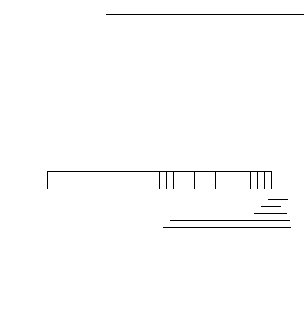
D8 AArch64 System Register Descriptions
D8.6 Generic Interrupt Controller CPU interface registers
D8-2216 Copyright © 2013 ARM Limited. All rights reserved. ARM DDI 0487A.a
Non-Confidential - Beta ID090413
D8.6.12 ICC_CTLR_EL1, Interrupt Controller Control Register (EL1)
The ICC_CTLR_EL1 characteristics are:
Purpose
Controls aspects of the behavior of the GIC CPU interface and provides information about the
features implemented.
This register is part of the GIC registers functional group.
Usage constraints
This register is accessible as shown below:
When accessed as ICC_CTLR_EL1(S):
When accessed as ICC_CTLR_EL1(NS):
Configurations
ICC_CTLR_EL1(S) is architecturally mapped to AArch32 register ICC_CTLR (S).
ICC_CTLR_EL1(NS) is architecturally mapped to AArch32 register ICC_CTLR (NS).
There are separate Secure and Non-secure instances of this register.
Attributes
ICC_CTLR_EL1 is a 32-bit register.
The ICC_CTLR_EL1 bit assignments are:
Bits [31:16]
Reserved, RES0.
A3V, bit [15]
Affinity 3 Valid. Read-only. Possible values are:
0
The CPU interface logic only supports zero values of Affinity 3 in SGI generation
system registers.
1
The CPU interface logic supports non-zero values of Affinity 3 in SGI generation
system registers.
EL1 (NS) EL1 (S) EL2 EL3 (SCR.NS=1) EL3 (SCR.NS=0)
-RW-- RW
EL1 (NS) EL1 (S) EL2 EL3 (SCR.NS=1) EL3 (SCR.NS=0)
RW - RW RW -
RES0
31 16 15 14
IDbits
13 11
PRIbits
10 8
RES0
73
2 1 0
CBPR
EOImode
PMHE
SEIS
A3V

D8 AArch64 System Register Descriptions
D8.6 Generic Interrupt Controller CPU interface registers
ARM DDI 0487A.a Copyright © 2013 ARM Limited. All rights reserved. D8-2217
ID090413 Non-Confidential - Beta
Virtual accesses return the value from ICH_VTR_EL2.A3V.
SEIS, bit [14]
SEI Support. Read-only. Indicates whether the CPU interface supports local generation of SEIs:
0
The CPU interface logic does not support local generation of SEIs by the CPU interface.
1
The CPU interface logic supports local generation of SEIs by the CPU interface.
Virtual accesses return the value from ICH_VTR_EL2.SEIS.
IDbits, bits [13:11]
The number of physical interrupt identifier bits supported:
000
16 bits.
001
24 bits.
All other values are reserved.
Virtual accesses return the value from ICH_VTR_EL2.IDbits.
Reset value is architecturally UNKNOWN.
PRIbits, bits [10:8]
The number of priority bits implemented, minus one. Read-only.
Virtual accesses return the value from ICH_VTR_EL2.PRIbits.
Bits [7:3]
Reserved, RES0.
PMHE, bit [2]
Priority Mask Hint Enable.
If EL3 is present and GICD_CTLR.DS == 0, this bit is a read-only alias of
ICC_CTLR_EL3.PMHE.
If EL3 is present and GICD_CTLR.DS == 1, this bit is writeable at EL1 and EL2.
Resets to 0.
EOImode, bit [1]
Alias of ICC_CTLR_EL3.EOImode_EL1{S,NS} as appropriate to the current security state.
Virtual accesses modify ICH_VMCR_EL2.VEOIM.
Reset value is architecturally UNKNOWN.
CBPR, bit [0]
Common Binary Point Register.
If EL3 is present and GICD_CTLR.DS == 0, this bit is a read-only alias of
ICC_CTLR_EL3.CBPR_EL1{S,NS} as appropriate.
If EL3 is not present, this field resets to zero.
If EL3 is present and GICD_CTLR.DS == 1, this bit is writeable at EL1 and EL2.
Virtual accesses modify ICH_VMCR_EL2.VCBPR. An access is virtual when accessed at
non-secure EL1 and either of FIQ or IRQ has been virtualized. That is, when (SCR_EL3.NS == '1'
&& (HCR_EL2.FMO == '1' || HCR_EL2.IMO == '1')).
Accessing the ICC_CTLR_EL1:
To access the ICC_CTLR_EL1:
MRS <Xt>, ICC_CTLR_EL1 ; Read ICC_CTLR_EL1 into Xt
MSR ICC_CTLR_EL1, <Xt> ; Write Xt to ICC_CTLR_EL1

D8 AArch64 System Register Descriptions
D8.6 Generic Interrupt Controller CPU interface registers
D8-2218 Copyright © 2013 ARM Limited. All rights reserved. ARM DDI 0487A.a
Non-Confidential - Beta ID090413
Register access is encoded as follows:
op0 op1 CRn CRm op2
11 000 1100 1100 100
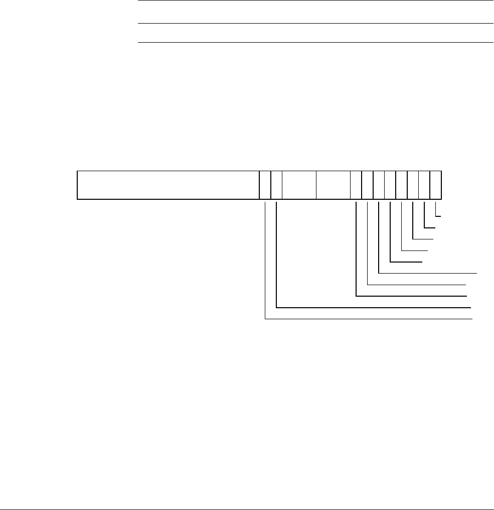
D8 AArch64 System Register Descriptions
D8.6 Generic Interrupt Controller CPU interface registers
ARM DDI 0487A.a Copyright © 2013 ARM Limited. All rights reserved. D8-2219
ID090413 Non-Confidential - Beta
D8.6.13 ICC_CTLR_EL3, Interrupt Controller Control Register (EL3)
The ICC_CTLR_EL3 characteristics are:
Purpose
Controls aspects of the behavior of the GIC CPU interface and provides information about the
features implemented.
This register is part of:
• the GIC registers functional group
• the Security registers functional group.
Usage constraints
This register is accessible as shown below:
Configurations
ICC_CTLR_EL3 is architecturally mapped to AArch32 register ICC_MCTLR.
Attributes
ICC_CTLR_EL3 is a 32-bit register.
The ICC_CTLR_EL3 bit assignments are:
Bits [31:16]
Reserved, RES0.
A3V, bit [15]
Affinity 3 Valid. Read-only. Possible values are:
0
The CPU interface logic only supports zero values of Affinity 3 in SGI generation
system registers.
1
The CPU interface logic supports non-zero values of Affinity 3 in SGI generation
system registers.
Virtual accesses return the value from ICH_VTR_EL2.A3V.
EL0 EL1 (NS) EL1 (S) EL2 EL3 (SCR.NS=1) EL3 (SCR.NS=0)
-- - -RW RW
RES0
31 16 15 14
IDbits
13 11
PRIbits
10 8 7 6 5 4 3 2 1 0
CBPR_EL1S
CBPR_EL1NS
EOImode_EL3
EOImode_EL1S
EOImode_EL1NS
RM
PMHE
RES0
SEIS
A3V

D8 AArch64 System Register Descriptions
D8.6 Generic Interrupt Controller CPU interface registers
D8-2220 Copyright © 2013 ARM Limited. All rights reserved. ARM DDI 0487A.a
Non-Confidential - Beta ID090413
SEIS, bit [14]
SEI Support. Read-only. Indicates whether the CPU interface supports generation of SEIs:
0
The CPU interface logic does not support generation of SEIs.
1
The CPU interface logic supports generation of SEIs.
Virtual accesses return the value from ICH_VTR_EL2.SEIS.
IDbits, bits [13:11]
The number of physical interrupt identifier bits supported:
000
16 bits.
001
24 bits.
All other values are reserved.
Reset value is architecturally UNKNOWN.
PRIbits, bits [10:8]
The number of priority bits implemented, minus one. Read-only.
Bit [7]
Reserved, RES0.
PMHE, bit [6]
Priority Mask Hint Enable.
When set, enables use of the PMR as a hint for interrupt distribution.
Resets to 0.
RM, bit [5]
Routing Modifier. This bit is used to modify the behavior of ICC_IAR0_EL1 and ICC_IAR1_EL1
such that systems with legacy secure software may be supported correctly.
0
Reading ICC_IAR0_EL1 and ICC_IAR1_EL1 at EL3 acknowledges interrupts
normally.
1
Reading ICC_IAR0_EL1 and ICC_IAR1_EL1 at EL3 returns special values:
• Reading ICC_IAR0_EL1 at EL3 returns ID 1020, indicating the interrupt should
be handled at Secure EL1.
• Reading ICC_IAR1_EL1 at EL3 returns ID 1021, indicating the interrupt should
be handled at Non-secure EL1 or EL2.
Reset value is architecturally UNKNOWN.
EOImode_EL1NS, bit [4]
EOI mode for interrupts handled at non-secure EL1 and EL2.
Reset value is architecturally UNKNOWN.
EOImode_EL1S, bit [3]
EOI mode for interrupts handled at secure EL1.
Reset value is architecturally UNKNOWN.
EOImode_EL3, bit [2]
EOI mode for interrupts handled at EL3.
Reset value is architecturally UNKNOWN.
CBPR_EL1NS, bit [1]
When set, non-secure accesses to GICC_BPR and ICC_BPR1_EL1 access the state of
ICC_BPR0_EL1. ICC_BPR0_EL1 is used to determine the preemption group for Non-secure
Group 1 interrupts.

D8 AArch64 System Register Descriptions
D8.6 Generic Interrupt Controller CPU interface registers
ARM DDI 0487A.a Copyright © 2013 ARM Limited. All rights reserved. D8-2221
ID090413 Non-Confidential - Beta
Reset value is architecturally UNKNOWN.
CBPR_EL1S, bit [0]
When set, secure EL1 accesses to ICC_BPR1_EL1 access the state of ICC_BPR0_EL1.
ICC_BPR0_EL1 is used to determine the preemption group for Secure Group 1 interrupts.
Reset value is architecturally UNKNOWN.
Accessing the ICC_CTLR_EL3:
To access the ICC_CTLR_EL3:
MRS <Xt>, ICC_CTLR_EL3 ; Read ICC_CTLR_EL3 into Xt
MSR ICC_CTLR_EL3, <Xt> ; Write Xt to ICC_CTLR_EL3
Register access is encoded as follows:
op0 op1 CRn CRm op2
11 110 1100 1100 100

D8 AArch64 System Register Descriptions
D8.6 Generic Interrupt Controller CPU interface registers
D8-2222 Copyright © 2013 ARM Limited. All rights reserved. ARM DDI 0487A.a
Non-Confidential - Beta ID090413
D8.6.14 ICC_DIR_EL1, Interrupt Controller Deactivate Interrupt Register
The ICC_DIR_EL1 characteristics are:
Purpose
When interrupt priority drop is separated from interrupt deactivation, a write to this register
deactivates the specified interrupt.
This register is part of the GIC registers functional group.
Usage constraints
This register is accessible as shown below:
Configurations
ICC_DIR_EL1 is architecturally mapped to AArch32 register ICC_DIR.
Attributes
ICC_DIR_EL1 is a 32-bit register.
The ICC_DIR_EL1 bit assignments are:
Bits [31:24]
Reserved, RES0.
InterruptID, bits [23:0]
The interrupt ID.
This field has either 16 or 24 bits implemented. The number of implemented bits can be found in
ICC_CTLR_EL1.IDbits and ICC_CTLR_EL3.IDbits. If only 16 bits are implemented, bits [23:16]
of this register are RES0.
Accessing the ICC_DIR_EL1:
To access the ICC_DIR_EL1:
MSR ICC_DIR_EL1, <Xt> ; Write Xt to ICC_DIR_EL1
Register access is encoded as follows:
EL0 EL1 (NS) EL1 (S) EL2 EL3 (SCR.NS=1) EL3 (SCR.NS=0)
-WO WO WOWO WO
RES0
31 24
InterruptID
23 0
op0 op1 CRn CRm op2
11 000 1100 1011 001

D8 AArch64 System Register Descriptions
D8.6 Generic Interrupt Controller CPU interface registers
ARM DDI 0487A.a Copyright © 2013 ARM Limited. All rights reserved. D8-2223
ID090413 Non-Confidential - Beta
D8.6.15 ICC_EOIR0_EL1, Interrupt Controller End Of Interrupt Register 0
The ICC_EOIR0_EL1 characteristics are:
Purpose
A processor writes to this register to inform the CPU interface that it has completed the processing
of the specified interrupt.
This register is part of the GIC registers functional group.
Usage constraints
This register is accessible as shown below:
When accessed as ICC_EOIR0_EL1(S):
When accessed as ICC_EOIR0_EL1(NS):
A write to this register must correspond to the most recent valid read from an Interrupt
Acknowledge Register. A valid read is a read that returns a valid interrupt ID, that is not a spurious
interrupt ID.
Configurations
ICC_EOIR0_EL1(S) is architecturally mapped to AArch32 register ICC_EOIR0 (S).
ICC_EOIR0_EL1(NS) is architecturally mapped to AArch32 register ICC_EOIR0 (NS).
There are separate Secure and Non-secure instances of this register.
In Secure state, this register is the end of interrupt register for Group 0 interrupts. In Non-secure
state, this is the EOIR for Group 1 interrupts.
Attributes
ICC_EOIR0_EL1 is a 32-bit register.
The ICC_EOIR0_EL1 bit assignments are:
Bits [31:24]
Reserved, RES0.
EOIINTID, bits [23:0]
The InterruptID value from the corresponding GICC_IAR access.
This field has either 16 or 24 bits implemented. The number of implemented bits can be found in
ICC_CTLR_EL1.IDbits and ICC_CTLR_EL3.IDbits. If only 16 bits are implemented, bits [23:16]
of this register are RES0.
EL1 (NS) EL1 (S) EL2 EL3 (SCR.NS=1) EL3 (SCR.NS=0)
-WO-- WO
EL1 (NS) EL1 (S) EL2 EL3 (SCR.NS=1) EL3 (SCR.NS=0)
WO - WO WO -
RES0
31 24
EOIINTID
23 0

D8 AArch64 System Register Descriptions
D8.6 Generic Interrupt Controller CPU interface registers
D8-2224 Copyright © 2013 ARM Limited. All rights reserved. ARM DDI 0487A.a
Non-Confidential - Beta ID090413
Accessing the ICC_EOIR0_EL1:
To access the ICC_EOIR0_EL1:
MSR ICC_EOIR0_EL1, <Xt> ; Write Xt to ICC_EOIR0_EL1
Register access is encoded as follows:
op0 op1 CRn CRm op2
11 000 1100 1000 001

D8 AArch64 System Register Descriptions
D8.6 Generic Interrupt Controller CPU interface registers
ARM DDI 0487A.a Copyright © 2013 ARM Limited. All rights reserved. D8-2225
ID090413 Non-Confidential - Beta
D8.6.16 ICC_EOIR1_EL1, Interrupt Controller End Of Interrupt Register 1
The ICC_EOIR1_EL1 characteristics are:
Purpose
A processor writes to this register to inform the CPU interface that it has completed the processing
of the specified Group 1 interrupt.
This register is part of the GIC registers functional group.
Usage constraints
This register is accessible as shown below:
A write to this register must correspond to the most recent valid read from an Interrupt
Acknowledge Register. A valid read is a read that returns a valid interrupt ID, that is not a spurious
interrupt ID.
Configurations
ICC_EOIR1_EL1 is architecturally mapped to AArch32 register ICC_EOIR1.
This register is an alias of the Non-secure view of ICC_EOIR0_EL1, and a Secure access to this
register is identical to a Non-secure access to ICC_EOIR0_EL1.
Attributes
ICC_EOIR1_EL1 is a 32-bit register.
The ICC_EOIR1_EL1 bit assignments are:
Bits [31:24]
Reserved, RES0.
EOIINTID, bits [23:0]
The InterruptID value from the corresponding GICC_IAR access.
This field has either 16 or 24 bits implemented. The number of implemented bits can be found in
ICC_CTLR_EL1.IDbits and ICC_CTLR_EL3.IDbits. If only 16 bits are implemented, bits [23:16]
of this register are RES0.
Accessing the ICC_EOIR1_EL1:
To access the ICC_EOIR1_EL1:
MSR ICC_EOIR1_EL1, <Xt> ; Write Xt to ICC_EOIR1_EL1
Register access is encoded as follows:
EL0 EL1 (NS) EL1 (S) EL2 EL3 (SCR.NS=1) EL3 (SCR.NS=0)
-WO WO WOWO WO
RES0
31 24
EOIINTID
23 0
op0 op1 CRn CRm op2
11 000 1100 1100 001

D8 AArch64 System Register Descriptions
D8.6 Generic Interrupt Controller CPU interface registers
D8-2226 Copyright © 2013 ARM Limited. All rights reserved. ARM DDI 0487A.a
Non-Confidential - Beta ID090413
D8.6.17 ICC_HPPIR0_EL1, Interrupt Controller Highest Priority Pending Interrupt Register 0
The ICC_HPPIR0_EL1 characteristics are:
Purpose
Indicates the Interrupt ID, and processor ID if appropriate, of the highest priority pending interrupt
on the CPU interface.
This register is part of the GIC registers functional group.
Usage constraints
This register is accessible as shown below:
When accessed as ICC_HPPIR0_EL1(S):
When accessed as ICC_HPPIR0_EL1(NS):
Configurations
ICC_HPPIR0_EL1(S) is architecturally mapped to AArch32 register ICC_HPPIR0 (S).
ICC_HPPIR0_EL1(NS) is architecturally mapped to AArch32 register ICC_HPPIR0 (NS).
There are separate Secure and Non-secure instances of this register.
In Secure state, this register is the highest priority pending interrupt register for Group 0 interrupts.
In Non-secure state, this is the HPPIR for Group 1 interrupts.
Attributes
ICC_HPPIR0_EL1 is a 32-bit register.
The ICC_HPPIR0_EL1 bit assignments are:
Bits [31:24]
Reserved, RES0.
PENDINTID, bits [23:0]
The interrupt ID of the highest priority pending interrupt.
This field has either 16 or 24 bits implemented. The number of implemented bits can be found in
ICC_CTLR_EL1.IDbits and ICC_CTLR_EL3.IDbits. If only 16 bits are implemented, bits [23:16]
of this register are RES0.
Accessing the ICC_HPPIR0_EL1:
To access the ICC_HPPIR0_EL1:
MRS <Xt>, ICC_HPPIR0_EL1 ; Read ICC_HPPIR0_EL1 into Xt
EL1 (NS) EL1 (S) EL2 EL3 (SCR.NS=1) EL3 (SCR.NS=0)
-RO-- RO
EL1 (NS) EL1 (S) EL2 EL3 (SCR.NS=1) EL3 (SCR.NS=0)
RO - RO RO -
RES0
31 24
PENDINTID
23 0

D8 AArch64 System Register Descriptions
D8.6 Generic Interrupt Controller CPU interface registers
ARM DDI 0487A.a Copyright © 2013 ARM Limited. All rights reserved. D8-2227
ID090413 Non-Confidential - Beta
Register access is encoded as follows:
op0 op1 CRn CRm op2
11 000 1100 1000 010

D8 AArch64 System Register Descriptions
D8.6 Generic Interrupt Controller CPU interface registers
D8-2228 Copyright © 2013 ARM Limited. All rights reserved. ARM DDI 0487A.a
Non-Confidential - Beta ID090413
D8.6.18 ICC_HPPIR1_EL1, Interrupt Controller Highest Priority Pending Interrupt Register 1
The ICC_HPPIR1_EL1 characteristics are:
Purpose
If the highest priority pending interrupt on the CPU interface is a Group 1 interrupt, returns the
interrupt ID of that interrupt. Otherwise, returns a spurious interrupt ID of 1023.
This register is part of the GIC registers functional group.
Usage constraints
This register is accessible as shown below:
Configurations
ICC_HPPIR1_EL1 is architecturally mapped to AArch32 register ICC_HPPIR1.
This register is an alias of the Non-secure view of ICC_HPPIR0_EL1, and a Secure access to this
register is identical to a Non-secure access to ICC_HPPIR0_EL1.
Attributes
ICC_HPPIR1_EL1 is a 32-bit register.
The ICC_HPPIR1_EL1 bit assignments are:
Bits [31:24]
Reserved, RES0.
PENDINTID, bits [23:0]
The interrupt ID of the highest priority pending interrupt.
This field has either 16 or 24 bits implemented. The number of implemented bits can be found in
ICC_CTLR_EL1.IDbits and ICC_CTLR_EL3.IDbits. If only 16 bits are implemented, bits [23:16]
of this register are RES0.
Accessing the ICC_HPPIR1_EL1:
To access the ICC_HPPIR1_EL1:
MRS <Xt>, ICC_HPPIR1_EL1 ; Read ICC_HPPIR1_EL1 into Xt
Register access is encoded as follows:
EL0 EL1 (NS) EL1 (S) EL2 EL3 (SCR.NS=1) EL3 (SCR.NS=0)
-RO RO RORO RO
RES0
31 24
PENDINTID
23 0
op0 op1 CRn CRm op2
11 000 1100 1100 010

D8 AArch64 System Register Descriptions
D8.6 Generic Interrupt Controller CPU interface registers
ARM DDI 0487A.a Copyright © 2013 ARM Limited. All rights reserved. D8-2229
ID090413 Non-Confidential - Beta
D8.6.19 ICC_IAR0_EL1, Interrupt Controller Interrupt Acknowledge Register 0
The ICC_IAR0_EL1 characteristics are:
Purpose
The processor reads this register to obtain the interrupt ID of the signaled interrupt. This read acts
as an acknowledge for the interrupt.
This register is part of the GIC registers functional group.
Usage constraints
This register is accessible as shown below:
When accessed as ICC_IAR0_EL1(S):
When accessed as ICC_IAR0_EL1(NS):
Configurations
ICC_IAR0_EL1(S) is architecturally mapped to AArch32 register ICC_IAR0 (S).
ICC_IAR0_EL1(NS) is architecturally mapped to AArch32 register ICC_IAR0 (NS).
There are separate Secure and Non-secure instances of this register.
In Secure state, this register is the interrupt acknowledge register for Group 0 interrupts. In
Non-secure state, this is the IAR for Group 1 interrupts.
Attributes
ICC_IAR0_EL1 is a 32-bit register.
The ICC_IAR0_EL1 bit assignments are:
Bits [31:24]
Reserved, RES0.
InterruptID, bits [23:0]
The ID of the signaled interrupt. IDs 1020 to 1023 are reserved and convey additional information
such as spurious interrupts.
This field has either 16 or 24 bits implemented. The number of implemented bits can be found in
ICC_CTLR_EL1.IDbits and ICC_CTLR_EL3.IDbits. If only 16 bits are implemented, bits [23:16]
of this register are RES0.
Accessing the ICC_IAR0_EL1:
To access the ICC_IAR0_EL1:
EL1 (NS) EL1 (S) EL2 EL3 (SCR.NS=1) EL3 (SCR.NS=0)
-RO-- RO
EL1 (NS) EL1 (S) EL2 EL3 (SCR.NS=1) EL3 (SCR.NS=0)
RO - RO RO -
RES0
31 24
InterruptID
23 0

D8 AArch64 System Register Descriptions
D8.6 Generic Interrupt Controller CPU interface registers
D8-2230 Copyright © 2013 ARM Limited. All rights reserved. ARM DDI 0487A.a
Non-Confidential - Beta ID090413
MRS <Xt>, ICC_IAR0_EL1 ; Read ICC_IAR0_EL1 into Xt
Register access is encoded as follows:
op0 op1 CRn CRm op2
11 000 1100 1000 000

D8 AArch64 System Register Descriptions
D8.6 Generic Interrupt Controller CPU interface registers
ARM DDI 0487A.a Copyright © 2013 ARM Limited. All rights reserved. D8-2231
ID090413 Non-Confidential - Beta
D8.6.20 ICC_IAR1_EL1, Interrupt Controller Interrupt Acknowledge Register 1
The ICC_IAR1_EL1 characteristics are:
Purpose
The processor reads this register to obtain the interrupt ID of the signaled Group 1 interrupt. This
read acts as an acknowledge for the interrupt.
This register is part of the GIC registers functional group.
Usage constraints
This register is accessible as shown below:
Configurations
ICC_IAR1_EL1 is architecturally mapped to AArch32 register ICC_IAR1.
This register is an alias of the Non-secure view of ICC_IAR0_EL1, and a Secure access to this
register is identical to a Non-secure access to ICC_IAR0_EL1.
Attributes
ICC_IAR1_EL1 is a 32-bit register.
The ICC_IAR1_EL1 bit assignments are:
Bits [31:24]
Reserved, RES0.
InterruptID, bits [23:0]
The ID of the signaled interrupt. IDs 1020 to 1023 are reserved and convey additional information
such as spurious interrupts.
This field has either 16 or 24 bits implemented. The number of implemented bits can be found in
ICC_CTLR_EL1.IDbits and ICC_CTLR_EL3.IDbits. If only 16 bits are implemented, bits [23:16]
of this register are RES0.
Accessing the ICC_IAR1_EL1:
To access the ICC_IAR1_EL1:
MRS <Xt>, ICC_IAR1_EL1 ; Read ICC_IAR1_EL1 into Xt
Register access is encoded as follows:
EL0 EL1 (NS) EL1 (S) EL2 EL3 (SCR.NS=1) EL3 (SCR.NS=0)
-RO RO RORO RO
RES0
31 24
InterruptID
23 0
op0 op1 CRn CRm op2
11 000 1100 1100 000

D8 AArch64 System Register Descriptions
D8.6 Generic Interrupt Controller CPU interface registers
D8-2232 Copyright © 2013 ARM Limited. All rights reserved. ARM DDI 0487A.a
Non-Confidential - Beta ID090413
D8.6.21 ICC_IGRPEN0_EL1, Interrupt Controller Interrupt Group 0 Enable register
The ICC_IGRPEN0_EL1 characteristics are:
Purpose
Controls whether Group 0 interrupts are enabled or not.
This register is part of the GIC registers functional group.
Usage constraints
This register is accessible as shown below:
When accessed as ICC_IGRPEN0_EL1(S):
When accessed as ICC_IGRPEN0_EL1(NS):
The lowest exception level at which this register may be accessed is governed by the exception level
to which FIQ is routed. This routing depends on SCR_EL3.FIQ, SCR_EL3.NS and
HCR_EL2.FMO.
If an interrupt is pending within the CPU interface when Enable becomes 0, the interrupt must be
released to allow the Distributor to forward the interrupt to a different processor.
Configurations
ICC_IGRPEN0_EL1(S) is architecturally mapped to AArch32 register ICC_IGRPEN0 (S).
ICC_IGRPEN0_EL1(NS) is architecturally mapped to AArch32 register ICC_IGRPEN0 (NS).
There are separate Secure and Non-secure instances of this register.
Attributes
ICC_IGRPEN0_EL1 is a 32-bit register.
The ICC_IGRPEN0_EL1 bit assignments are:
Bits [31:1]
Reserved, RES0.
Enable, bit [0]
Enables Group 0 interrupts.
0
Group 0 interrupts are disabled.
1
Group 0 interrupts are enabled.
Virtual accesses to this register update ICH_VMCR_EL2.VENG0.
EL1 (NS) EL1 (S) EL2 EL3 (SCR.NS=1) EL3 (SCR.NS=0)
-RW-- RW
EL1 (NS) EL1 (S) EL2 EL3 (SCR.NS=1) EL3 (SCR.NS=0)
RW - RW RW -
RES0
31 1 0
Enable

D8 AArch64 System Register Descriptions
D8.6 Generic Interrupt Controller CPU interface registers
ARM DDI 0487A.a Copyright © 2013 ARM Limited. All rights reserved. D8-2233
ID090413 Non-Confidential - Beta
Resets to 0.
Accessing the ICC_IGRPEN0_EL1:
To access the ICC_IGRPEN0_EL1:
MRS <Xt>, ICC_IGRPEN0_EL1 ; Read ICC_IGRPEN0_EL1 into Xt
MSR ICC_IGRPEN0_EL1, <Xt> ; Write Xt to ICC_IGRPEN0_EL1
Register access is encoded as follows:
op0 op1 CRn CRm op2
11 000 1100 1100 110

D8 AArch64 System Register Descriptions
D8.6 Generic Interrupt Controller CPU interface registers
D8-2234 Copyright © 2013 ARM Limited. All rights reserved. ARM DDI 0487A.a
Non-Confidential - Beta ID090413
D8.6.22 ICC_IGRPEN1_EL1, Interrupt Controller Interrupt Group 1 Enable register
The ICC_IGRPEN1_EL1 characteristics are:
Purpose
Controls whether Group 1 interrupts are enabled for the current security state.
This register is part of the GIC registers functional group.
Usage constraints
This register is accessible as shown below:
The lowest exception level at which this register may be accessed is governed by the exception level
to which FIQ is routed. This routing depends on SCR_EL3.FIQ, SCR_EL3.NS and
HCR_EL2.FMO.
If an interrupt is pending within the CPU interface when Enable becomes 0, the interrupt must be
released to allow the Distributor to forward the interrupt to a different processor.
Configurations
ICC_IGRPEN1_EL1 is architecturally mapped to AArch32 register ICC_IGRPEN1.
Attributes
ICC_IGRPEN1_EL1 is a 32-bit register.
The ICC_IGRPEN1_EL1 bit assignments are:
Bits [31:1]
Reserved, RES0.
Enable, bit [0]
Enables Group 1 interrupts for the current security state.
0
Group 1 interrupts are disabled for the current security state.
1
Group 1 interrupts are enabled for the current security state.
Virtual accesses to this register update ICH_VMCR_EL2.VENG1.
When this register is accessed at EL3, the copy of this register appropriate to the current setting of
SCR_EL3.NS is accessed.
Resets to 0.
Accessing the ICC_IGRPEN1_EL1:
To access the ICC_IGRPEN1_EL1:
MRS <Xt>, ICC_IGRPEN1_EL1 ; Read ICC_IGRPEN1_EL1 into Xt
MSR ICC_IGRPEN1_EL1, <Xt> ; Write Xt to ICC_IGRPEN1_EL1
EL0 EL1 (NS) EL1 (S) EL2 EL3 (SCR.NS=1) EL3 (SCR.NS=0)
-RW RW RWRW RW
RES0
31 1 0
Enable

D8 AArch64 System Register Descriptions
D8.6 Generic Interrupt Controller CPU interface registers
ARM DDI 0487A.a Copyright © 2013 ARM Limited. All rights reserved. D8-2235
ID090413 Non-Confidential - Beta
Register access is encoded as follows:
op0 op1 CRn CRm op2
11 000 1100 1100 111

D8 AArch64 System Register Descriptions
D8.6 Generic Interrupt Controller CPU interface registers
D8-2236 Copyright © 2013 ARM Limited. All rights reserved. ARM DDI 0487A.a
Non-Confidential - Beta ID090413
D8.6.23 ICC_IGRPEN1_EL3, Interrupt Controller Interrupt Group 1 Enable register (EL3)
The ICC_IGRPEN1_EL3 characteristics are:
Purpose
Controls whether Group 1 interrupts are enabled or not.
This register is part of the GIC registers functional group.
Usage constraints
This register is accessible as shown below:
If an interrupt is pending within the CPU interface when an Enable bit becomes 0, the interrupt must
be released to allow the Distributor to forward the interrupt to a different processor.
Configurations
ICC_IGRPEN1_EL3 is architecturally mapped to AArch32 register ICC_MGRPEN1.
Attributes
ICC_IGRPEN1_EL3 is a 32-bit register.
The ICC_IGRPEN1_EL3 bit assignments are:
Bits [31:2]
Reserved, RES0.
EnableGrp1S, bit [1]
Enables Group 1 interrupts for the Secure state.
0
Group 1 interrupts are disabled for the Secure state.
1
Group 1 interrupts are enabled for the Secure state.
Resets to 0.
EnableGrp1NS, bit [0]
Enables Group 1 interrupts for the Non-secure state.
0
Group 1 interrupts are disabled for the Non-secure state.
1
Group 1 interrupts are enabled for the Non-secure state.
Resets to 0.
Accessing the ICC_IGRPEN1_EL3:
To access the ICC_IGRPEN1_EL3:
MRS <Xt>, ICC_IGRPEN1_EL3 ; Read ICC_IGRPEN1_EL3 into Xt
MSR ICC_IGRPEN1_EL3, <Xt> ; Write Xt to ICC_IGRPEN1_EL3
EL0 EL1 (NS) EL1 (S) EL2 EL3 (SCR.NS=1) EL3 (SCR.NS=0)
-- - -RW RW
RES0
31 2 1 0
EnableGrp1S
EnableGrp1NS

D8 AArch64 System Register Descriptions
D8.6 Generic Interrupt Controller CPU interface registers
ARM DDI 0487A.a Copyright © 2013 ARM Limited. All rights reserved. D8-2237
ID090413 Non-Confidential - Beta
Register access is encoded as follows:
op0 op1 CRn CRm op2
11 110 1100 1100 111

D8 AArch64 System Register Descriptions
D8.6 Generic Interrupt Controller CPU interface registers
D8-2238 Copyright © 2013 ARM Limited. All rights reserved. ARM DDI 0487A.a
Non-Confidential - Beta ID090413
D8.6.24 ICC_PMR_EL1, Interrupt Controller Interrupt Priority Mask Register
The ICC_PMR_EL1 characteristics are:
Purpose
Provides an interrupt priority filter. Only interrupts with higher priority than the value in this register
are signaled to the processor.
This register is part of the GIC registers functional group.
Usage constraints
This register is accessible as shown below:
Configurations
ICC_PMR_EL1 is architecturally mapped to AArch32 register ICC_PMR.
Attributes
ICC_PMR_EL1 is a 32-bit register.
The ICC_PMR_EL1 bit assignments are:
Bits [31:8]
Reserved, RES0.
Priority, bits [7:0]
The priority mask level for the CPU interface. If the priority of an interrupt is higher than the value
indicated by this field, the interface signals the interrupt to the processor.
If the GIC supports fewer than 256 priority levels then some bits are RAZ/WI, as follows:
128 supported levels
Bit [0] = 0.
64 supported levels
Bits [1:0] =
0b00
.
32 supported levels
Bits [2:0] =
0b000
.
16 supported levels
Bits [3:0] =
0b0000
.
The possible priority field values are as follows:
EL0 EL1 (NS) EL1 (S) EL2 EL3 (SCR.NS=1) EL3 (SCR.NS=0)
-RW RW RWRW RW
RES0
31 8
Priority
70
Implemented priority
bits Possible priority field
values Number of priority
levels
[7:0]
0x00
-
0xFF
(0-255), all values 256
[7:1]
0x00
-
0xFE
(0-254), even values
only 128

D8 AArch64 System Register Descriptions
D8.6 Generic Interrupt Controller CPU interface registers
ARM DDI 0487A.a Copyright © 2013 ARM Limited. All rights reserved. D8-2239
ID090413 Non-Confidential - Beta
Accessing the ICC_PMR_EL1:
To access the ICC_PMR_EL1:
MRS <Xt>, ICC_PMR_EL1 ; Read ICC_PMR_EL1 into Xt
MSR ICC_PMR_EL1, <Xt> ; Write Xt to ICC_PMR_EL1
Register access is encoded as follows:
[7:2]
0x00
-
0xFC
(0-252), in steps of 4 64
[7:3]
0x00
-
0xF8
(0-248), in steps of 8 32
[7:4]
0x00
-
0xF0
(0-240), in steps of 16 16
op0 op1 CRn CRm op2
11 000 0100 0110 000
Implemented priority
bits Possible priority field
values Number of priority
levels

D8 AArch64 System Register Descriptions
D8.6 Generic Interrupt Controller CPU interface registers
D8-2240 Copyright © 2013 ARM Limited. All rights reserved. ARM DDI 0487A.a
Non-Confidential - Beta ID090413
D8.6.25 ICC_RPR_EL1, Interrupt Controller Running Priority Register
The ICC_RPR_EL1 characteristics are:
Purpose
Indicates the Running priority of the CPU interface.
This register is part of the GIC registers functional group.
Usage constraints
This register is accessible as shown below:
If there is no active interrupt on the CPU interface, the value returned is the Idle priority.
Software cannot determine the number of implemented priority bits from a read of this register.
Configurations
ICC_RPR_EL1 is architecturally mapped to AArch32 register ICC_RPR.
Attributes
ICC_RPR_EL1 is a 32-bit register.
The ICC_RPR_EL1 bit assignments are:
Bits [31:8]
Reserved, RES0.
Priority, bits [7:0]
The current running priority on the CPU interface. This is the priority of the current active interrupt.
Accessing the ICC_RPR_EL1:
To access the ICC_RPR_EL1:
MRS <Xt>, ICC_RPR_EL1 ; Read ICC_RPR_EL1 into Xt
Register access is encoded as follows:
EL0 EL1 (NS) EL1 (S) EL2 EL3 (SCR.NS=1) EL3 (SCR.NS=0)
-RO RO RORO RO
RES0
31 8
Priority
70
op0 op1 CRn CRm op2
11 000 1100 1011 011

D8 AArch64 System Register Descriptions
D8.6 Generic Interrupt Controller CPU interface registers
ARM DDI 0487A.a Copyright © 2013 ARM Limited. All rights reserved. D8-2241
ID090413 Non-Confidential - Beta
D8.6.26 ICC_SEIEN_EL1, Interrupt Controller System Error Interrupt Enable register
The ICC_SEIEN_EL1 characteristics are:
Purpose
Controls whether System Error Interrupts generated by bus message are enabled.
This register is part of the GIC registers functional group.
Usage constraints
This register is accessible as shown below:
The lowest exception level at which this register may be accessed is governed by the exception level
to which SError is routed. This routing depends on SCR_EL3.EA, SCR_EL3.NS and
HCR_EL2.AMO.
Internally generated SEIs and pin-generated SEIs might still be generated.
Configurations
ICC_SEIEN_EL1 is architecturally mapped to AArch32 register ICC_SEIEN.
Attributes
ICC_SEIEN_EL1 is a 32-bit register.
The ICC_SEIEN_EL1 bit assignments are:
Accessing the ICC_SEIEN_EL1:
To access the ICC_SEIEN_EL1:
MRS <Xt>, ICC_SEIEN_EL1 ; Read ICC_SEIEN_EL1 into Xt
MSR ICC_SEIEN_EL1, <Xt> ; Write Xt to ICC_SEIEN_EL1
Register access is encoded as follows:
EL0 EL1 (NS) EL1 (S) EL2 EL3 (SCR.NS=1) EL3 (SCR.NS=0)
-RW RW RWRW RW
IMPLEMENTATION DEFINED
31 0
op0 op1 CRn CRm op2
11 000 1100 1101 000
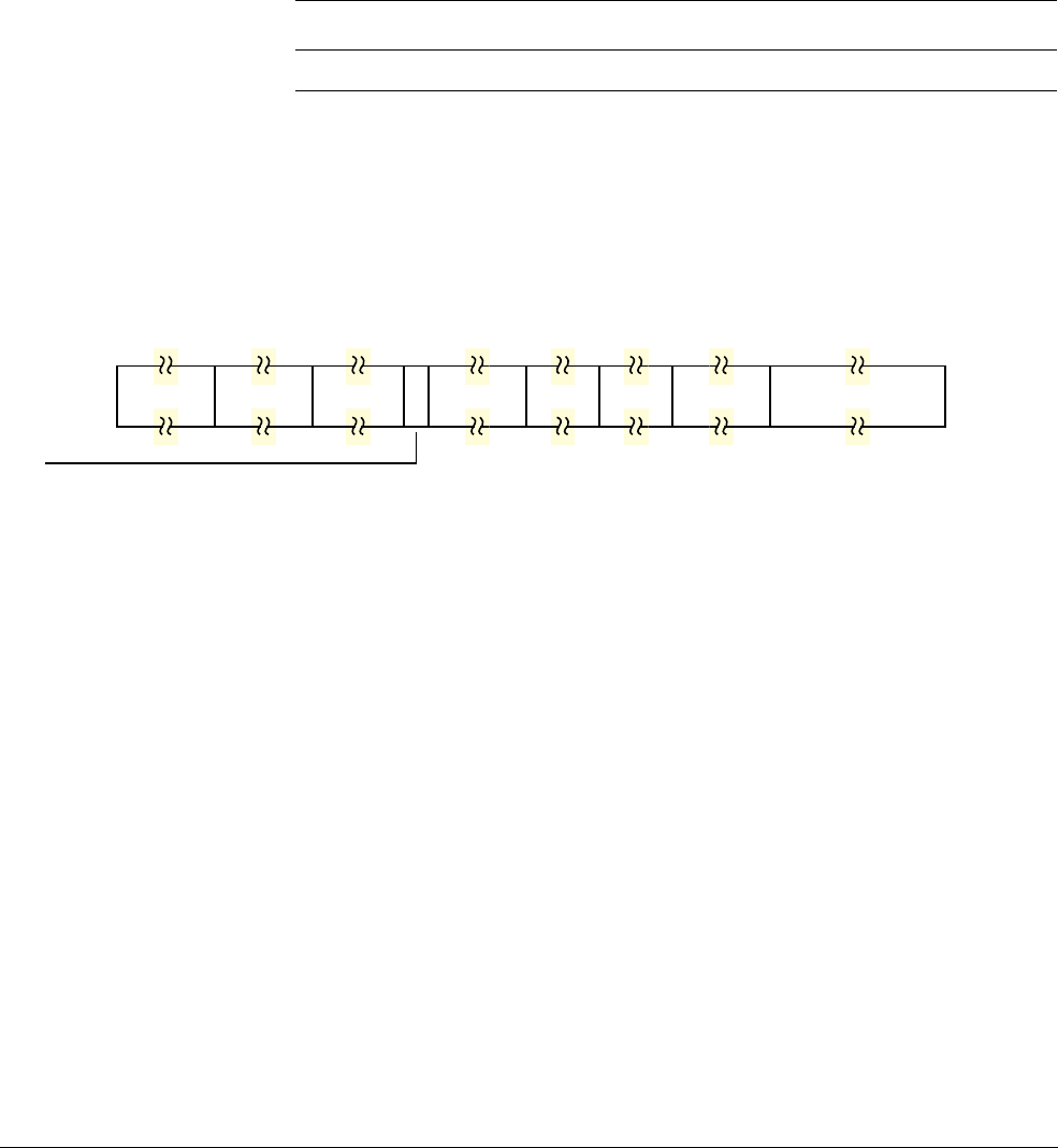
D8 AArch64 System Register Descriptions
D8.6 Generic Interrupt Controller CPU interface registers
D8-2242 Copyright © 2013 ARM Limited. All rights reserved. ARM DDI 0487A.a
Non-Confidential - Beta ID090413
D8.6.27 ICC_SGI0R_EL1, Interrupt Controller Software Generated Interrupt group 0 Register
The ICC_SGI0R_EL1 characteristics are:
Purpose
Provides software the ability to generate secure group 0 SGIs, including from the Non-secure state
when permitted by GICR_NSACR.
This register is part of the GIC registers functional group.
Usage constraints
This register is accessible as shown below:
Configurations
ICC_SGI0R_EL1 is architecturally mapped to AArch32 register ICC_SGI0R.
Attributes
ICC_SGI0R_EL1 is a 64-bit register.
The ICC_SGI0R_EL1 bit assignments are:
Bits [63:56]
Reserved, RES0.
Aff3, bits [55:48]
The affinity 3 value of the affinity path of the cluster for which SGI interrupts will be generated.
Bits [47:41]
Reserved, RES0.
IRM, bit [40]
Interrupt Routing Mode. Determines how the generated interrupts should be distributed to
processors. Possible values are:
0
Interrupts routed to the processors specified by a.b.c.{target list}. In this routing, a, b,
and c are the values of fields Aff3, Aff2, and Aff1 respectively.
1
Interrupts routed to all processors in the system, excluding "self".
Aff2, bits [39:32]
The affinity 2 value of the affinity path of the cluster for which SGI interrupts will be generated.
Bits [31:28]
Reserved, RES0.
SGIID, bits [27:24]
SGI Interrupt ID.
EL0 EL1 (NS) EL1 (S) EL2 EL3 (SCR.NS=1) EL3 (SCR.NS=0)
-WO WO WOWO WO
RES0
63 56
Aff3
55 48
RES0
47 41 40
Aff2
39 32
RES0
31 28
SGIID
27 24
Aff1
23 16
TargetList
15 0
IRM

D8 AArch64 System Register Descriptions
D8.6 Generic Interrupt Controller CPU interface registers
ARM DDI 0487A.a Copyright © 2013 ARM Limited. All rights reserved. D8-2243
ID090413 Non-Confidential - Beta
Aff1, bits [23:16]
The affinity 1 value of the affinity path of the cluster for which SGI interrupts will be generated.
TargetList, bits [15:0]
Target List. The set of processors for which SGI interrupts will be generated. Each bit corresponds
to the processor within a cluster with an Affinity 0 value equal to the bit number.
If a bit is 1 and the bit does not correspond to a valid target processor, the bit must be ignored by the
Distributor. In such cases, a Distributor may optionally generate an SGI.
This restricts distribution of SGIs to the first 16 processors of an affinity 1 cluster.
Accessing the ICC_SGI0R_EL1:
To access the ICC_SGI0R_EL1:
MSR ICC_SGI0R_EL1, <Xt> ; Write Xt to ICC_SGI0R_EL1
Register access is encoded as follows:
op0 op1 CRn CRm op2
11 000 1100 1011 111
D8 AArch64 System Register Descriptions
D8.6 Generic Interrupt Controller CPU interface registers
D8-2244 Copyright © 2013 ARM Limited. All rights reserved. ARM DDI 0487A.a
Non-Confidential - Beta ID090413
D8.6.28 ICC_SGI1R_EL1, Interrupt Controller Software Generated Interrupt group 1 Register
The ICC_SGI1R_EL1 characteristics are:
Purpose
Provides software the ability to generate group 1 SGIs for the current security state.
This register is part of the GIC registers functional group.
Usage constraints
This register is accessible as shown below:
When accessed as ICC_SGI1R_EL1(S):
When accessed as ICC_SGI1R_EL1(NS):
Configurations
ICC_SGI1R_EL1(S) is architecturally mapped to AArch32 register ICC_SGI1R (S).
ICC_SGI1R_EL1(NS) is architecturally mapped to AArch32 register ICC_SGI1R (NS).
There are separate Secure and Non-secure instances of this register.
Attributes
ICC_SGI1R_EL1 is a 64-bit register.
The ICC_SGI1R_EL1 bit assignments are:
Bits [63:56]
Reserved, RES0.
Aff3, bits [55:48]
The affinity 3 value of the affinity path of the cluster for which SGI interrupts will be generated.
Bits [47:41]
Reserved, RES0.
IRM, bit [40]
Interrupt Routing Mode. Determines how the generated interrupts should be distributed to
processors. Possible values are:
0
Interrupts routed to the processors specified by a.b.c.{target list}. In this routing, a, b,
and c are the values of fields Aff3, Aff2, and Aff1 respectively.
EL1 (NS) EL1 (S) EL2 EL3 (SCR.NS=1) EL3 (SCR.NS=0)
-WO-- WO
EL1 (NS) EL1 (S) EL2 EL3 (SCR.NS=1) EL3 (SCR.NS=0)
WO - WO WO -
RES0
63 56
Aff3
55 48
RES0
47 41 40
Aff2
39 32
RES0
31 28
SGIID
27 24
Aff1
23 16
TargetList
15 0
IRM

D8 AArch64 System Register Descriptions
D8.6 Generic Interrupt Controller CPU interface registers
ARM DDI 0487A.a Copyright © 2013 ARM Limited. All rights reserved. D8-2245
ID090413 Non-Confidential - Beta
1
Interrupts routed to all processors in the system, excluding "self".
Aff2, bits [39:32]
The affinity 2 value of the affinity path of the cluster for which SGI interrupts will be generated.
Bits [31:28]
Reserved, RES0.
SGIID, bits [27:24]
SGI Interrupt ID.
Aff1, bits [23:16]
The affinity 1 value of the affinity path of the cluster for which SGI interrupts will be generated.
TargetList, bits [15:0]
Target List. The set of processors for which SGI interrupts will be generated. Each bit corresponds
to the processor within a cluster with an Affinity 0 value equal to the bit number.
If a bit is 1 and the bit does not correspond to a valid target processor, the bit must be ignored by the
Distributor. In such cases, a Distributor may optionally generate an SGI.
This restricts distribution of SGIs to the first 16 processors of an affinity 1 cluster.
Accessing the ICC_SGI1R_EL1:
To access the ICC_SGI1R_EL1:
MSR ICC_SGI1R_EL1, <Xt> ; Write Xt to ICC_SGI1R_EL1
Register access is encoded as follows:
op0 op1 CRn CRm op2
11 000 1100 1011 101

D8 AArch64 System Register Descriptions
D8.6 Generic Interrupt Controller CPU interface registers
D8-2246 Copyright © 2013 ARM Limited. All rights reserved. ARM DDI 0487A.a
Non-Confidential - Beta ID090413
D8.6.29 ICC_SRE_EL1, Interrupt Controller System Register Enable register (EL1)
The ICC_SRE_EL1 characteristics are:
Purpose
Controls whether the system register interface or the memory mapped interface to the GIC CPU
interface is used for EL0 and EL1.
This register is part of the GIC registers functional group.
Usage constraints
This register is accessible as shown below:
When accessed as ICC_SRE_EL1(S):
When accessed as ICC_SRE_EL1(NS):
Configurations
ICC_SRE_EL1(S) is architecturally mapped to AArch32 register ICC_SRE (S).
ICC_SRE_EL1(NS) is architecturally mapped to AArch32 register ICC_SRE (NS).
There are separate Secure and Non-secure instances of this register.
Attributes
ICC_SRE_EL1 is a 32-bit register.
The ICC_SRE_EL1 bit assignments are:
Bits [31:3]
Reserved, RES0.
DIB, bit [2]
Disable IRQ bypass.
If EL3 is present, this field is a read-only alias of ICC_SRE_EL3.DIB.
If EL3 is not present and EL2 is present, this field is a read-only alias of ICC_SRE_EL2.DIB.
Resets to 0.
DFB, bit [1]
Disable FIQ bypass.
EL1 (NS) EL1 (S) EL2 EL3 (SCR.NS=1) EL3 (SCR.NS=0)
-RW-- RW
EL1 (NS) EL1 (S) EL2 EL3 (SCR.NS=1) EL3 (SCR.NS=0)
RW - RW RW -
RES0
31 3 2 1 0
SRE
DFB
DIB

D8 AArch64 System Register Descriptions
D8.6 Generic Interrupt Controller CPU interface registers
ARM DDI 0487A.a Copyright © 2013 ARM Limited. All rights reserved. D8-2247
ID090413 Non-Confidential - Beta
If EL3 is present, this field is a read-only alias of ICC_SRE_EL3.DFB.
If EL3 is not present and EL2 is present, this field is a read-only alias of ICC_SRE_EL2.DFB.
Resets to 0.
SRE, bit [0]
System Register Enable.
0
The memory mapped interface must be used. Access at EL1 to any ICC_* system
register other than ICC_SRE_EL1 results in an Undefined exception.
1
The system register interface for the current security state is enabled.
Virtual accesses modify ICH_VMCR_EL2.VSRE.
Resets to 0.
Accessing the ICC_SRE_EL1:
To access the ICC_SRE_EL1:
MRS <Xt>, ICC_SRE_EL1 ; Read ICC_SRE_EL1 into Xt
MSR ICC_SRE_EL1, <Xt> ; Write Xt to ICC_SRE_EL1
Register access is encoded as follows:
op0 op1 CRn CRm op2
11 000 1100 1100 101
D8 AArch64 System Register Descriptions
D8.6 Generic Interrupt Controller CPU interface registers
D8-2248 Copyright © 2013 ARM Limited. All rights reserved. ARM DDI 0487A.a
Non-Confidential - Beta ID090413
D8.6.30 ICC_SRE_EL2, Interrupt Controller System Register Enable register (EL2)
The ICC_SRE_EL2 characteristics are:
Purpose
Controls whether the system register interface or the memory mapped interface to the GIC CPU
interface is used for EL2.
This register is part of:
• the GIC registers functional group
• the Virtualization registers functional group.
Usage constraints
This register is accessible as shown below:
If EL3 is present and ICC_SRE_EL3.Enable is 0, EL2 accesses to this register will trap to EL3.
Configurations
ICC_SRE_EL2 is architecturally mapped to AArch32 register ICC_HSRE.
Attributes
ICC_SRE_EL2 is a 32-bit register.
The ICC_SRE_EL2 bit assignments are:
Bits [31:4]
Reserved, RES0.
Enable, bit [3]
Enable. Enables lower exception level access to ICC_SRE_EL1.
0
Non-secure EL1 accesses to ICC_SRE_EL1 trap to EL2.
1
Non-secure EL1 accesses to ICC_SRE_EL1 are permitted if EL3 is not present or
ICC_SRE_EL3.Enable is 1, otherwise Non-secure EL1 accesses to ICC_SRE_EL1 trap
to EL3.
Resets to 0.
DIB, bit [2]
Disable IRQ bypass.
If EL3 is present and GICD_CTLR.DS is 0, this field is a read-only alias of ICC_SRE_EL3.DIB.
Resets to 0.
EL0 EL1 (NS) EL1 (S) EL2 EL3 (SCR.NS=1) EL3 (SCR.NS=0)
-- - RWRW -
RES0
31 4 3 2 1 0
SRE
DFB
DIB
Enable

D8 AArch64 System Register Descriptions
D8.6 Generic Interrupt Controller CPU interface registers
ARM DDI 0487A.a Copyright © 2013 ARM Limited. All rights reserved. D8-2249
ID090413 Non-Confidential - Beta
DFB, bit [1]
Disable FIQ bypass.
If EL3 is present and GICD_CTLR.DS is 0, this field is a read-only alias of ICC_SRE_EL3.DFB.
Resets to 0.
Accessing the ICC_SRE_EL2:
To access the ICC_SRE_EL2:
MRS <Xt>, ICC_SRE_EL2 ; Read ICC_SRE_EL2 into Xt
MSR ICC_SRE_EL2, <Xt> ; Write Xt to ICC_SRE_EL2
Register access is encoded as follows:
op0 op1 CRn CRm op2
11 100 1100 1001 101
D8 AArch64 System Register Descriptions
D8.6 Generic Interrupt Controller CPU interface registers
D8-2250 Copyright © 2013 ARM Limited. All rights reserved. ARM DDI 0487A.a
Non-Confidential - Beta ID090413
D8.6.31 ICC_SRE_EL3, Interrupt Controller System Register Enable register (EL3)
The ICC_SRE_EL3 characteristics are:
Purpose
Controls whether the system register interface or the memory mapped interface to the GIC CPU
interface is used for EL2.
This register is part of:
• the GIC registers functional group
• the Security registers functional group.
Usage constraints
This register is accessible as shown below:
Configurations
ICC_SRE_EL3 is architecturally mapped to AArch32 register ICC_MSRE.
Attributes
ICC_SRE_EL3 is a 32-bit register.
The ICC_SRE_EL3 bit assignments are:
Bits [31:4]
Reserved, RES0.
Enable, bit [3]
Enable. Enables lower exception level access to ICC_SRE_EL1 and ICC_SRE_EL2.
0
EL1 and EL2 accesses to ICC_SRE_EL1 or ICC_SRE_EL2 trap to EL3.
1
EL2 accesses to ICC_SRE_EL2 are permitted. If the Enable bit of ICC_SRE_EL2 is 1,
then EL1 accesses to ICC_SRE_EL1 are also permitted.
Resets to 0.
DIB, bit [2]
Disable IRQ bypass.
Resets to 0.
DFB, bit [1]
Disable FIQ bypass.
Resets to 0.
EL0 EL1 (NS) EL1 (S) EL2 EL3 (SCR.NS=1) EL3 (SCR.NS=0)
-- - -RW RW
RES0
31 4 3 2 1 0
SRE
DFB
DIB
Enable

D8 AArch64 System Register Descriptions
D8.6 Generic Interrupt Controller CPU interface registers
ARM DDI 0487A.a Copyright © 2013 ARM Limited. All rights reserved. D8-2251
ID090413 Non-Confidential - Beta
SRE, bit [0]
System Register Enable.
0
The memory mapped interface must be used. Access at EL3 to any ICH_* system
register, or any EL1, EL2, or EL3 ICC_* register other than ICC_SRE_EL1,
ICC_SRE_EL2, or ICC_SRE_EL3, results in an Undefined exception.
1
The system register interface to the ICH_* registers and the EL1, EL2, and EL3 ICC_*
registers is enabled for EL3.
Resets to 0.
Accessing the ICC_SRE_EL3:
To access the ICC_SRE_EL3:
MRS <Xt>, ICC_SRE_EL3 ; Read ICC_SRE_EL3 into Xt
MSR ICC_SRE_EL3, <Xt> ; Write Xt to ICC_SRE_EL3
Register access is encoded as follows:
op0 op1 CRn CRm op2
11 110 1100 1100 101

D8 AArch64 System Register Descriptions
D8.6 Generic Interrupt Controller CPU interface registers
D8-2252 Copyright © 2013 ARM Limited. All rights reserved. ARM DDI 0487A.a
Non-Confidential - Beta ID090413
D8.6.32 ICH_AP0R0_EL2, Interrupt Controller Hyp Active Priorities Register (0,0)
The ICH_AP0R0_EL2 characteristics are:
Purpose
Provides information about the active priorities for the current EL2 interrupt regime.
This register is part of:
• the GIC registers functional group
• the Virtualization registers functional group.
Usage constraints
This register is accessible as shown below:
In implementations supporting fewer than 8 bits of priority, some of these registers correspond to
unimplemented priority levels. Access to such registers will generate an Undefined exception.
Configurations
ICH_AP0R0_EL2 is architecturally mapped to AArch32 register ICH_AP0R0.
Attributes
ICH_AP0R0_EL2 is a 32-bit register.
The ICH_AP0R0_EL2 bit assignments are:
P<n>, bit [n], for n = 0 to 31
Provides information about priority M, according to the following relationship:
Bit P<n> corresponds to priority (M divided by 2U) minus 1, where U is the number of
unimplemented bits of priority and is equal to (7 - ICC_CTLR_EL1.PRIbits).
EL0 EL1 (NS) EL1 (S) EL2 EL3 (SCR.NS=1) EL3 (SCR.NS=0)
-- - RWRW RW
31 30 29 28 27 26 25 24 23 22 21 20 19 18 17 16 15 14 13 12 11 10
P9
9
P8
8
P7
7
P6
6
P5
5
P4
4
P3
3
P2
2
P1
1
P0
0
P31
P30
P29
P28
P27
P26
P25
P24
P23
P22
P21
P20
P19
P18
P17
P16
P10
P11
P12
P13
P14
P15

D8 AArch64 System Register Descriptions
D8.6 Generic Interrupt Controller CPU interface registers
ARM DDI 0487A.a Copyright © 2013 ARM Limited. All rights reserved. D8-2253
ID090413 Non-Confidential - Beta
For example, in a system with ICC_CTLR_EL1.PRIbits ==
0b100
:
• There are 5 bits of implemented priority.
• This means there are 3 bits of unimplemented priority, which are always at the least
significant end (bits [2:0] are RES0).
• Valid priorities are 8, 16, 24, 32, and so on. Dividing these by 23 gives 1, 2, 3, 4, and so on.
• Subtracting 1 from each gives bits 0, 1, 2, 3, and so on that provide information about those
priorities.
Accesses to these registers from an interrupt regime give a view of the active priorities that is
appropriate for that interrupt regime, to allow save and restore of the appropriate state.
Interrupt regime and the number of security states supported by the Distributor affect the view as
follows. Unless otherwise stated, when a bit is successfully set to one, this clears any other active
priorities corresponding to that bit.
A Virtual interrupt in this case means that the interrupt group associated with the register has been
virtualized.
Accessing the ICH_AP0R0_EL2:
To access the ICH_AP0R0_EL2:
MRS <Xt>, ICH_AP0R0_EL2 ; Read ICH_AP0R0_EL2 into Xt
MSR ICH_AP0R0_EL2, <Xt> ; Write Xt to ICH_AP0R0_EL2
Register access is encoded as follows:
Exception level AP0Rn access
(Secure) EL3 Permitted. Accesses Group 0 Secure active
priorities.
Secure EL1 Permitted. Accesses Group 0 Secure active
priorities.
Non-secure EL1 access for a Virtual interrupt ICH_AP0Rn_EL2
Non-secure EL1 or EL2 when GIC Distributor supports two
Security states Permitted. Accesses Group 0 Secure active
priorities.
Non-secure EL1 or EL2 when GIC Distributor supports one
Security state Permitted. Accesses Group 0 active priorities.
op0 op1 CRn CRm op2
11 100 1100 1000 000

D8 AArch64 System Register Descriptions
D8.6 Generic Interrupt Controller CPU interface registers
D8-2254 Copyright © 2013 ARM Limited. All rights reserved. ARM DDI 0487A.a
Non-Confidential - Beta ID090413
D8.6.33 ICH_AP0R1_EL2, Interrupt Controller Hyp Active Priorities Register (0,1)
The ICH_AP0R1_EL2 characteristics are:
Purpose
Provides information about the active priorities for the current EL2 interrupt regime.
This register is part of:
• the GIC registers functional group
• the Virtualization registers functional group.
Usage constraints
This register is accessible as shown below:
In implementations supporting fewer than 8 bits of priority, some of these registers correspond to
unimplemented priority levels. Access to such registers will generate an Undefined exception.
Configurations
ICH_AP0R1_EL2 is architecturally mapped to AArch32 register ICH_AP0R1.
Attributes
ICH_AP0R1_EL2 is a 32-bit register.
The ICH_AP0R1_EL2 bit assignments are:
P<n>, bit [(n-32)], for n = 32 to 63
Provides information about priority M, according to the following relationship:
Bit P<n> corresponds to priority (M divided by 2U) minus 1, where U is the number of
unimplemented bits of priority and is equal to (7 - ICC_CTLR_EL1.PRIbits).
EL0 EL1 (NS) EL1 (S) EL2 EL3 (SCR.NS=1) EL3 (SCR.NS=0)
-- - RWRW RW
31 30 29 28 27 26 25 24 23 22 21 20 19 18 17 16 15 14 13 12 11 10 9 8 7 6 5 4 3 2 1 0
P63
P62
P61
P60
P59
P58
P57
P56
P55
P54
P53
P52
P51
P50
P49
P48
P32
P33
P34
P35
P36
P37
P38
P39
P40
P41
P42
P43
P44
P45
P46
P47

D8 AArch64 System Register Descriptions
D8.6 Generic Interrupt Controller CPU interface registers
ARM DDI 0487A.a Copyright © 2013 ARM Limited. All rights reserved. D8-2255
ID090413 Non-Confidential - Beta
For example, in a system with ICC_CTLR_EL1.PRIbits ==
0b100
:
• There are 5 bits of implemented priority.
• This means there are 3 bits of unimplemented priority, which are always at the least
significant end (bits [2:0] are RES0).
• Valid priorities are 8, 16, 24, 32, and so on. Dividing these by 23 gives 1, 2, 3, 4, and so on.
• Subtracting 1 from each gives bits 0, 1, 2, 3, and so on that provide information about those
priorities.
Accesses to these registers from an interrupt regime give a view of the active priorities that is
appropriate for that interrupt regime, to allow save and restore of the appropriate state.
Interrupt regime and the number of security states supported by the Distributor affect the view as
follows. Unless otherwise stated, when a bit is successfully set to one, this clears any other active
priorities corresponding to that bit.
A Virtual interrupt in this case means that the interrupt group associated with the register has been
virtualized.
Accessing the ICH_AP0R1_EL2:
To access the ICH_AP0R1_EL2:
MRS <Xt>, ICH_AP0R1_EL2 ; Read ICH_AP0R1_EL2 into Xt
MSR ICH_AP0R1_EL2, <Xt> ; Write Xt to ICH_AP0R1_EL2
Register access is encoded as follows:
Exception level AP0Rn access
(Secure) EL3 Permitted. Accesses Group 0 Secure active
priorities.
Secure EL1 Permitted. Accesses Group 0 Secure active
priorities.
Non-secure EL1 access for a Virtual interrupt ICH_AP0Rn_EL2
Non-secure EL1 or EL2 when GIC Distributor supports two
Security states Permitted. Accesses Group 0 Secure active
priorities.
Non-secure EL1 or EL2 when GIC Distributor supports one
Security state Permitted. Accesses Group 0 active priorities.
op0 op1 CRn CRm op2
11 100 1100 1000 001

D8 AArch64 System Register Descriptions
D8.6 Generic Interrupt Controller CPU interface registers
D8-2256 Copyright © 2013 ARM Limited. All rights reserved. ARM DDI 0487A.a
Non-Confidential - Beta ID090413
D8.6.34 ICH_AP0R2_EL2, Interrupt Controller Hyp Active Priorities Register (0,2)
The ICH_AP0R2_EL2 characteristics are:
Purpose
Provides information about the active priorities for the current EL2 interrupt regime.
This register is part of:
• the GIC registers functional group
• the Virtualization registers functional group.
Usage constraints
This register is accessible as shown below:
In implementations supporting fewer than 8 bits of priority, some of these registers correspond to
unimplemented priority levels. Access to such registers will generate an Undefined exception.
Configurations
ICH_AP0R2_EL2 is architecturally mapped to AArch32 register ICH_AP0R2.
Attributes
ICH_AP0R2_EL2 is a 32-bit register.
The ICH_AP0R2_EL2 bit assignments are:
P<n>, bit [(n-64)], for n = 64 to 95
Provides information about priority M, according to the following relationship:
Bit P<n> corresponds to priority (M divided by 2U) minus 1, where U is the number of
unimplemented bits of priority and is equal to (7 - ICC_CTLR_EL1.PRIbits).
EL0 EL1 (NS) EL1 (S) EL2 EL3 (SCR.NS=1) EL3 (SCR.NS=0)
-- - RWRW RW
31 30 29 28 27 26 25 24 23 22 21 20 19 18 17 16 15 14 13 12 11 10 9 8 7 6 5 4 3 2 1 0
P95
P94
P93
P92
P91
P90
P89
P88
P87
P86
P85
P84
P83
P82
P81
P80
P64
P65
P66
P67
P68
P69
P70
P71
P72
P73
P74
P75
P76
P77
P78
P79

D8 AArch64 System Register Descriptions
D8.6 Generic Interrupt Controller CPU interface registers
ARM DDI 0487A.a Copyright © 2013 ARM Limited. All rights reserved. D8-2257
ID090413 Non-Confidential - Beta
For example, in a system with ICC_CTLR_EL1.PRIbits ==
0b100
:
• There are 5 bits of implemented priority.
• This means there are 3 bits of unimplemented priority, which are always at the least
significant end (bits [2:0] are RES0).
• Valid priorities are 8, 16, 24, 32, and so on. Dividing these by 23 gives 1, 2, 3, 4, and so on.
• Subtracting 1 from each gives bits 0, 1, 2, 3, and so on that provide information about those
priorities.
Accesses to these registers from an interrupt regime give a view of the active priorities that is
appropriate for that interrupt regime, to allow save and restore of the appropriate state.
Interrupt regime and the number of security states supported by the Distributor affect the view as
follows. Unless otherwise stated, when a bit is successfully set to one, this clears any other active
priorities corresponding to that bit.
A Virtual interrupt in this case means that the interrupt group associated with the register has been
virtualized.
Accessing the ICH_AP0R2_EL2:
To access the ICH_AP0R2_EL2:
MRS <Xt>, ICH_AP0R2_EL2 ; Read ICH_AP0R2_EL2 into Xt
MSR ICH_AP0R2_EL2, <Xt> ; Write Xt to ICH_AP0R2_EL2
Register access is encoded as follows:
Exception level AP0Rn access
(Secure) EL3 Permitted. Accesses Group 0 Secure active
priorities.
Secure EL1 Permitted. Accesses Group 0 Secure active
priorities.
Non-secure EL1 access for a Virtual interrupt ICH_AP0Rn_EL2
Non-secure EL1 or EL2 when GIC Distributor supports two
Security states Permitted. Accesses Group 0 Secure active
priorities.
Non-secure EL1 or EL2 when GIC Distributor supports one
Security state Permitted. Accesses Group 0 active priorities.
op0 op1 CRn CRm op2
11 100 1100 1000 010
D8 AArch64 System Register Descriptions
D8.6 Generic Interrupt Controller CPU interface registers
D8-2258 Copyright © 2013 ARM Limited. All rights reserved. ARM DDI 0487A.a
Non-Confidential - Beta ID090413
D8.6.35 ICH_AP0R3_EL2, Interrupt Controller Hyp Active Priorities Register (0,3)
The ICH_AP0R3_EL2 characteristics are:
Purpose
Provides information about the active priorities for the current EL2 interrupt regime.
This register is part of:
• the GIC registers functional group
• the Virtualization registers functional group.
Usage constraints
This register is accessible as shown below:
In implementations supporting fewer than 8 bits of priority, some of these registers correspond to
unimplemented priority levels. Access to such registers will generate an Undefined exception.
Configurations
ICH_AP0R3_EL2 is architecturally mapped to AArch32 register ICH_AP0R3.
Attributes
ICH_AP0R3_EL2 is a 32-bit register.
The ICH_AP0R3_EL2 bit assignments are:
P<n>, bit [(n-96)], for n = 96 to 127
Provides information about priority M, according to the following relationship:
Bit P<n> corresponds to priority (M divided by 2U) minus 1, where U is the number of
unimplemented bits of priority and is equal to (7 - ICC_CTLR_EL1.PRIbits).
EL0 EL1 (NS) EL1 (S) EL2 EL3 (SCR.NS=1) EL3 (SCR.NS=0)
-- - RWRW RW
31 30 29 28 27 26 25 24 23 22 21 20 19 18 17 16 15 14 13 12 11 10 9 8 7 6 5 4 3 2 1 0
P127
P126
P125
P124
P123
P122
P121
P120
P119
P118
P117
P116
P115
P114
P113
P112
P96
P97
P98
P99
P100
P101
P102
P103
P104
P105
P106
P107
P108
P109
P110
P111

D8 AArch64 System Register Descriptions
D8.6 Generic Interrupt Controller CPU interface registers
ARM DDI 0487A.a Copyright © 2013 ARM Limited. All rights reserved. D8-2259
ID090413 Non-Confidential - Beta
For example, in a system with ICC_CTLR_EL1.PRIbits ==
0b100
:
• There are 5 bits of implemented priority.
• This means there are 3 bits of unimplemented priority, which are always at the least
significant end (bits [2:0] are RES0).
• Valid priorities are 8, 16, 24, 32, and so on. Dividing these by 23 gives 1, 2, 3, 4, and so on.
• Subtracting 1 from each gives bits 0, 1, 2, 3, and so on that provide information about those
priorities.
Accesses to these registers from an interrupt regime give a view of the active priorities that is
appropriate for that interrupt regime, to allow save and restore of the appropriate state.
Interrupt regime and the number of security states supported by the Distributor affect the view as
follows. Unless otherwise stated, when a bit is successfully set to one, this clears any other active
priorities corresponding to that bit.
A Virtual interrupt in this case means that the interrupt group associated with the register has been
virtualized.
Accessing the ICH_AP0R3_EL2:
To access the ICH_AP0R3_EL2:
MRS <Xt>, ICH_AP0R3_EL2 ; Read ICH_AP0R3_EL2 into Xt
MSR ICH_AP0R3_EL2, <Xt> ; Write Xt to ICH_AP0R3_EL2
Register access is encoded as follows:
Exception level AP0Rn access
(Secure) EL3 Permitted. Accesses Group 0 Secure active
priorities.
Secure EL1 Permitted. Accesses Group 0 Secure active
priorities.
Non-secure EL1 access for a Virtual interrupt ICH_AP0Rn_EL2
Non-secure EL1 or EL2 when GIC Distributor supports two
Security states Permitted. Accesses Group 0 Secure active
priorities.
Non-secure EL1 or EL2 when GIC Distributor supports one
Security state Permitted. Accesses Group 0 active priorities.
op0 op1 CRn CRm op2
11 100 1100 1000 011

D8 AArch64 System Register Descriptions
D8.6 Generic Interrupt Controller CPU interface registers
D8-2260 Copyright © 2013 ARM Limited. All rights reserved. ARM DDI 0487A.a
Non-Confidential - Beta ID090413
D8.6.36 ICH_AP1R0_EL2, Interrupt Controller Hyp Active Priorities Register (1,0)
The ICH_AP1R0_EL2 characteristics are:
Purpose
Provides information about the active priorities for the current EL2 interrupt regime.
This register is part of:
• the GIC registers functional group
• the Virtualization registers functional group.
Usage constraints
This register is accessible as shown below:
In implementations supporting fewer than 8 bits of priority, some of these registers correspond to
unimplemented priority levels. Access to such registers will generate an Undefined exception.
Configurations
ICH_AP1R0_EL2 is architecturally mapped to AArch32 register ICH_AP1R0.
Attributes
ICH_AP1R0_EL2 is a 32-bit register.
The ICH_AP1R0_EL2 bit assignments are:
P<n>, bit [n], for n = 0 to 31
Provides information about priority M, according to the following relationship:
Bit P<n> corresponds to priority (M divided by 2U) minus 1, where U is the number of
unimplemented bits of priority and is equal to (7 - ICC_CTLR_EL1.PRIbits).
EL0 EL1 (NS) EL1 (S) EL2 EL3 (SCR.NS=1) EL3 (SCR.NS=0)
-- - RWRW RW
31 30 29 28 27 26 25 24 23 22 21 20 19 18 17 16 15 14 13 12 11 10
P9
9
P8
8
P7
7
P6
6
P5
5
P4
4
P3
3
P2
2
P1
1
P0
0
P31
P30
P29
P28
P27
P26
P25
P24
P23
P22
P21
P20
P19
P18
P17
P16
P10
P11
P12
P13
P14
P15

D8 AArch64 System Register Descriptions
D8.6 Generic Interrupt Controller CPU interface registers
ARM DDI 0487A.a Copyright © 2013 ARM Limited. All rights reserved. D8-2261
ID090413 Non-Confidential - Beta
For example, in a system with ICC_CTLR_EL1.PRIbits ==
0b100
:
• There are 5 bits of implemented priority.
• This means there are 3 bits of unimplemented priority, which are always at the least
significant end (bits [2:0] are RES0).
• Valid priorities are 8, 16, 24, 32, and so on. Dividing these by 23 gives 1, 2, 3, 4, and so on.
• Subtracting 1 from each gives bits 0, 1, 2, 3, and so on that provide information about those
priorities.
Accesses to these registers from an interrupt regime give a view of the active priorities that is
appropriate for that interrupt regime, to allow save and restore of the appropriate state.
Interrupt regime and the number of security states supported by the Distributor affect the view as
follows. Unless otherwise stated, when a bit is successfully set to one, this clears any other active
priorities corresponding to that bit.
A Virtual interrupt in this case means that the interrupt group associated with the register has been
virtualized.
Accessing the ICH_AP1R0_EL2:
To access the ICH_AP1R0_EL2:
MRS <Xt>, ICH_AP1R0_EL2 ; Read ICH_AP1R0_EL2 into Xt
MSR ICH_AP1R0_EL2, <Xt> ; Write Xt to ICH_AP1R0_EL2
Register access is encoded as follows:
Current
exception level
and security
state
AP1Rn access
(Secure) EL3 Permitted. When SCR_EL3.NS is 0, accesses Group 1 Secure active priorities. When
SCR_EL3.NS is 1, accesses Group 1 Non-secure active priorities (unshifted). When a bit
is written, the bit is only updated if the corresponding Group 0 and Group 1 Secure active
priority is zero.
Secure EL1 Permitted. Accesses Group 1 Secure active priorities (unshifted). When a bit is written, the
bit is only updated if the corresponding Group 0 Secure active priority is zero.
Non-secure EL1
access for a
Virtual interrupt
ICH_AP1Rn_EL2
Non-secure EL1
or EL2 when GIC
Distributor
supports two
Security states
Permitted. Accesses Group 1 Non-secure active priorities (shifted). When a bit is written,
the bit is only updated if the corresponding Group 0 and Group 1 Secure active priority is
zero.
Non-secure EL1
or EL2 when GIC
Distributor
supports one
Security state
Permitted. Accesses Group 1 Non-secure active priorities (unshifted). When a bit is
written, the bit is only updated if the Group 0 active priority is zero.
op0 op1 CRn CRm op2
11 100 1100 1001 000

D8 AArch64 System Register Descriptions
D8.6 Generic Interrupt Controller CPU interface registers
D8-2262 Copyright © 2013 ARM Limited. All rights reserved. ARM DDI 0487A.a
Non-Confidential - Beta ID090413
D8.6.37 ICH_AP1R1_EL2, Interrupt Controller Hyp Active Priorities Register (1,1)
The ICH_AP1R1_EL2 characteristics are:
Purpose
Provides information about the active priorities for the current EL2 interrupt regime.
This register is part of:
• the GIC registers functional group
• the Virtualization registers functional group.
Usage constraints
This register is accessible as shown below:
In implementations supporting fewer than 8 bits of priority, some of these registers correspond to
unimplemented priority levels. Access to such registers will generate an Undefined exception.
Configurations
ICH_AP1R1_EL2 is architecturally mapped to AArch32 register ICH_AP1R1.
Attributes
ICH_AP1R1_EL2 is a 32-bit register.
The ICH_AP1R1_EL2 bit assignments are:
P<n>, bit [(n-32)], for n = 32 to 63
Provides information about priority M, according to the following relationship:
Bit P<n> corresponds to priority (M divided by 2U) minus 1, where U is the number of
unimplemented bits of priority and is equal to (7 - ICC_CTLR_EL1.PRIbits).
EL0 EL1 (NS) EL1 (S) EL2 EL3 (SCR.NS=1) EL3 (SCR.NS=0)
-- - RWRW RW
31 30 29 28 27 26 25 24 23 22 21 20 19 18 17 16 15 14 13 12 11 10 9 8 7 6 5 4 3 2 1 0
P63
P62
P61
P60
P59
P58
P57
P56
P55
P54
P53
P52
P51
P50
P49
P48
P32
P33
P34
P35
P36
P37
P38
P39
P40
P41
P42
P43
P44
P45
P46
P47

D8 AArch64 System Register Descriptions
D8.6 Generic Interrupt Controller CPU interface registers
ARM DDI 0487A.a Copyright © 2013 ARM Limited. All rights reserved. D8-2263
ID090413 Non-Confidential - Beta
For example, in a system with ICC_CTLR_EL1.PRIbits ==
0b100
:
• There are 5 bits of implemented priority.
• This means there are 3 bits of unimplemented priority, which are always at the least
significant end (bits [2:0] are RES0).
• Valid priorities are 8, 16, 24, 32, and so on. Dividing these by 23 gives 1, 2, 3, 4, and so on.
• Subtracting 1 from each gives bits 0, 1, 2, 3, and so on that provide information about those
priorities.
Accesses to these registers from an interrupt regime give a view of the active priorities that is
appropriate for that interrupt regime, to allow save and restore of the appropriate state.
Interrupt regime and the number of security states supported by the Distributor affect the view as
follows. Unless otherwise stated, when a bit is successfully set to one, this clears any other active
priorities corresponding to that bit.
A Virtual interrupt in this case means that the interrupt group associated with the register has been
virtualized.
Accessing the ICH_AP1R1_EL2:
To access the ICH_AP1R1_EL2:
MRS <Xt>, ICH_AP1R1_EL2 ; Read ICH_AP1R1_EL2 into Xt
MSR ICH_AP1R1_EL2, <Xt> ; Write Xt to ICH_AP1R1_EL2
Register access is encoded as follows:
Current
exception level
and security
state
AP1Rn access
(Secure) EL3 Permitted. When SCR_EL3.NS is 0, accesses Group 1 Secure active priorities. When
SCR_EL3.NS is 1, accesses Group 1 Non-secure active priorities (unshifted). When a bit
is written, the bit is only updated if the corresponding Group 0 and Group 1 Secure active
priority is zero.
Secure EL1 Permitted. Accesses Group 1 Secure active priorities (unshifted). When a bit is written, the
bit is only updated if the corresponding Group 0 Secure active priority is zero.
Non-secure EL1
access for a
Virtual interrupt
ICH_AP1Rn_EL2
Non-secure EL1
or EL2 when GIC
Distributor
supports two
Security states
Permitted. Accesses Group 1 Non-secure active priorities (shifted). When a bit is written,
the bit is only updated if the corresponding Group 0 and Group 1 Secure active priority is
zero.
Non-secure EL1
or EL2 when GIC
Distributor
supports one
Security state
Permitted. Accesses Group 1 Non-secure active priorities (unshifted). When a bit is
written, the bit is only updated if the Group 0 active priority is zero.
op0 op1 CRn CRm op2
11 100 1100 1001 001
D8 AArch64 System Register Descriptions
D8.6 Generic Interrupt Controller CPU interface registers
D8-2264 Copyright © 2013 ARM Limited. All rights reserved. ARM DDI 0487A.a
Non-Confidential - Beta ID090413
D8.6.38 ICH_AP1R2_EL2, Interrupt Controller Hyp Active Priorities Register (1,2)
The ICH_AP1R2_EL2 characteristics are:
Purpose
Provides information about the active priorities for the current EL2 interrupt regime.
This register is part of:
• the GIC registers functional group
• the Virtualization registers functional group.
Usage constraints
This register is accessible as shown below:
In implementations supporting fewer than 8 bits of priority, some of these registers correspond to
unimplemented priority levels. Access to such registers will generate an Undefined exception.
Configurations
ICH_AP1R2_EL2 is architecturally mapped to AArch32 register ICH_AP1R2.
Attributes
ICH_AP1R2_EL2 is a 32-bit register.
The ICH_AP1R2_EL2 bit assignments are:
P<n>, bit [(n-64)], for n = 64 to 95
Provides information about priority M, according to the following relationship:
Bit P<n> corresponds to priority (M divided by 2U) minus 1, where U is the number of
unimplemented bits of priority and is equal to (7 - ICC_CTLR_EL1.PRIbits).
EL0 EL1 (NS) EL1 (S) EL2 EL3 (SCR.NS=1) EL3 (SCR.NS=0)
-- - RWRW RW
31 30 29 28 27 26 25 24 23 22 21 20 19 18 17 16 15 14 13 12 11 10 9 8 7 6 5 4 3 2 1 0
P95
P94
P93
P92
P91
P90
P89
P88
P87
P86
P85
P84
P83
P82
P81
P80
P64
P65
P66
P67
P68
P69
P70
P71
P72
P73
P74
P75
P76
P77
P78
P79

D8 AArch64 System Register Descriptions
D8.6 Generic Interrupt Controller CPU interface registers
ARM DDI 0487A.a Copyright © 2013 ARM Limited. All rights reserved. D8-2265
ID090413 Non-Confidential - Beta
For example, in a system with ICC_CTLR_EL1.PRIbits ==
0b100
:
• There are 5 bits of implemented priority.
• This means there are 3 bits of unimplemented priority, which are always at the least
significant end (bits [2:0] are RES0).
• Valid priorities are 8, 16, 24, 32, and so on. Dividing these by 23 gives 1, 2, 3, 4, and so on.
• Subtracting 1 from each gives bits 0, 1, 2, 3, and so on that provide information about those
priorities.
Accesses to these registers from an interrupt regime give a view of the active priorities that is
appropriate for that interrupt regime, to allow save and restore of the appropriate state.
Interrupt regime and the number of security states supported by the Distributor affect the view as
follows. Unless otherwise stated, when a bit is successfully set to one, this clears any other active
priorities corresponding to that bit.
A Virtual interrupt in this case means that the interrupt group associated with the register has been
virtualized.
Accessing the ICH_AP1R2_EL2:
To access the ICH_AP1R2_EL2:
MRS <Xt>, ICH_AP1R2_EL2 ; Read ICH_AP1R2_EL2 into Xt
MSR ICH_AP1R2_EL2, <Xt> ; Write Xt to ICH_AP1R2_EL2
Register access is encoded as follows:
Current
exception level
and security
state
AP1Rn access
(Secure) EL3 Permitted. When SCR_EL3.NS is 0, accesses Group 1 Secure active priorities. When
SCR_EL3.NS is 1, accesses Group 1 Non-secure active priorities (unshifted). When a bit
is written, the bit is only updated if the corresponding Group 0 and Group 1 Secure active
priority is zero.
Secure EL1 Permitted. Accesses Group 1 Secure active priorities (unshifted). When a bit is written, the
bit is only updated if the corresponding Group 0 Secure active priority is zero.
Non-secure EL1
access for a
Virtual interrupt
ICH_AP1Rn_EL2
Non-secure EL1
or EL2 when GIC
Distributor
supports two
Security states
Permitted. Accesses Group 1 Non-secure active priorities (shifted). When a bit is written,
the bit is only updated if the corresponding Group 0 and Group 1 Secure active priority is
zero.
Non-secure EL1
or EL2 when GIC
Distributor
supports one
Security state
Permitted. Accesses Group 1 Non-secure active priorities (unshifted). When a bit is
written, the bit is only updated if the Group 0 active priority is zero.
op0 op1 CRn CRm op2
11 100 1100 1001 010

D8 AArch64 System Register Descriptions
D8.6 Generic Interrupt Controller CPU interface registers
D8-2266 Copyright © 2013 ARM Limited. All rights reserved. ARM DDI 0487A.a
Non-Confidential - Beta ID090413
D8.6.39 ICH_AP1R3_EL2, Interrupt Controller Hyp Active Priorities Register (1,3)
The ICH_AP1R3_EL2 characteristics are:
Purpose
Provides information about the active priorities for the current EL2 interrupt regime.
This register is part of:
• the GIC registers functional group
• the Virtualization registers functional group.
Usage constraints
This register is accessible as shown below:
In implementations supporting fewer than 8 bits of priority, some of these registers correspond to
unimplemented priority levels. Access to such registers will generate an Undefined exception.
Configurations
ICH_AP1R3_EL2 is architecturally mapped to AArch32 register ICH_AP1R3.
Attributes
ICH_AP1R3_EL2 is a 32-bit register.
The ICH_AP1R3_EL2 bit assignments are:
P<n>, bit [(n-96)], for n = 96 to 127
Provides information about priority M, according to the following relationship:
Bit P<n> corresponds to priority (M divided by 2U) minus 1, where U is the number of
unimplemented bits of priority and is equal to (7 - ICC_CTLR_EL1.PRIbits).
EL0 EL1 (NS) EL1 (S) EL2 EL3 (SCR.NS=1) EL3 (SCR.NS=0)
-- - RWRW RW
31 30 29 28 27 26 25 24 23 22 21 20 19 18 17 16 15 14 13 12 11 10 9 8 7 6 5 4 3 2 1 0
P127
P126
P125
P124
P123
P122
P121
P120
P119
P118
P117
P116
P115
P114
P113
P112
P96
P97
P98
P99
P100
P101
P102
P103
P104
P105
P106
P107
P108
P109
P110
P111

D8 AArch64 System Register Descriptions
D8.6 Generic Interrupt Controller CPU interface registers
ARM DDI 0487A.a Copyright © 2013 ARM Limited. All rights reserved. D8-2267
ID090413 Non-Confidential - Beta
For example, in a system with ICC_CTLR_EL1.PRIbits ==
0b100
:
• There are 5 bits of implemented priority.
• This means there are 3 bits of unimplemented priority, which are always at the least
significant end (bits [2:0] are RES0).
• Valid priorities are 8, 16, 24, 32, and so on. Dividing these by 23 gives 1, 2, 3, 4, and so on.
• Subtracting 1 from each gives bits 0, 1, 2, 3, and so on that provide information about those
priorities.
Accesses to these registers from an interrupt regime give a view of the active priorities that is
appropriate for that interrupt regime, to allow save and restore of the appropriate state.
Interrupt regime and the number of security states supported by the Distributor affect the view as
follows. Unless otherwise stated, when a bit is successfully set to one, this clears any other active
priorities corresponding to that bit.
A Virtual interrupt in this case means that the interrupt group associated with the register has been
virtualized.
Accessing the ICH_AP1R3_EL2:
To access the ICH_AP1R3_EL2:
MRS <Xt>, ICH_AP1R3_EL2 ; Read ICH_AP1R3_EL2 into Xt
MSR ICH_AP1R3_EL2, <Xt> ; Write Xt to ICH_AP1R3_EL2
Register access is encoded as follows:
Current
exception level
and security
state
AP1Rn access
(Secure) EL3 Permitted. When SCR_EL3.NS is 0, accesses Group 1 Secure active priorities. When
SCR_EL3.NS is 1, accesses Group 1 Non-secure active priorities (unshifted). When a bit
is written, the bit is only updated if the corresponding Group 0 and Group 1 Secure active
priority is zero.
Secure EL1 Permitted. Accesses Group 1 Secure active priorities (unshifted). When a bit is written, the
bit is only updated if the corresponding Group 0 Secure active priority is zero.
Non-secure EL1
access for a
Virtual interrupt
ICH_AP1Rn_EL2
Non-secure EL1
or EL2 when GIC
Distributor
supports two
Security states
Permitted. Accesses Group 1 Non-secure active priorities (shifted). When a bit is written,
the bit is only updated if the corresponding Group 0 and Group 1 Secure active priority is
zero.
Non-secure EL1
or EL2 when GIC
Distributor
supports one
Security state
Permitted. Accesses Group 1 Non-secure active priorities (unshifted). When a bit is
written, the bit is only updated if the Group 0 active priority is zero.
op0 op1 CRn CRm op2
11 100 1100 1001 011

D8 AArch64 System Register Descriptions
D8.6 Generic Interrupt Controller CPU interface registers
D8-2268 Copyright © 2013 ARM Limited. All rights reserved. ARM DDI 0487A.a
Non-Confidential - Beta ID090413
D8.6.40 ICH_EISR_EL2, Interrupt Controller End of Interrupt Status Register
The ICH_EISR_EL2 characteristics are:
Purpose
When a maintenance interrupt is received, this register helps determine which List registers have
outstanding EOI interrupts that require servicing.
This register is part of:
• the GIC registers functional group
• the Virtualization registers functional group.
Usage constraints
This register is accessible as shown below:
Configurations
ICH_EISR_EL2 is architecturally mapped to AArch32 register ICH_EISR.
Attributes
ICH_EISR_EL2 is a 32-bit register.
The ICH_EISR_EL2 bit assignments are:
Bits [31:16]
Reserved, RES0.
Status<n>, bit [n], for n = 0 to 15
EOI status bit for List register <n>:
0
List register <n>, ICH_LR<n>_EL2, does not have an EOI.
1
List register <n>, ICH_LR<n>_EL2, has an EOI.
EL0 EL1 (NS) EL1 (S) EL2 EL3 (SCR.NS=1) EL3 (SCR.NS=0)
-- - RORO RO
RES0
31 16 15 14 13 12 11 10 9 8 7 6 5 4 3 2 1 0
Status0
Status1
Status2
Status3
Status4
Status5
Status6
Status7
Status8
Status9
Status10
Status11
Status12
Status13
Status14
Status15

D8 AArch64 System Register Descriptions
D8.6 Generic Interrupt Controller CPU interface registers
ARM DDI 0487A.a Copyright © 2013 ARM Limited. All rights reserved. D8-2269
ID090413 Non-Confidential - Beta
For any ICH_LR<n>_EL2, the corresponding status bit is set to 1 if ICH_LR<n>_EL2.State is
0b00
and ICH_LR<n>_EL2.HW is 0 and ICH_LR<n>_EL2.EOI is 1.
Accessing the ICH_EISR_EL2:
To access the ICH_EISR_EL2:
MRS <Xt>, ICH_EISR_EL2 ; Read ICH_EISR_EL2 into Xt
Register access is encoded as follows:
op0 op1 CRn CRm op2
11 100 1100 1011 011
D8 AArch64 System Register Descriptions
D8.6 Generic Interrupt Controller CPU interface registers
D8-2270 Copyright © 2013 ARM Limited. All rights reserved. ARM DDI 0487A.a
Non-Confidential - Beta ID090413
D8.6.41 ICH_ELSR_EL2, Interrupt Controller Empty List Register Status Register
The ICH_ELSR_EL2 characteristics are:
Purpose
This register can be used to locate a usable List register when the hypervisor is delivering an
interrupt to a Guest OS.
This register is part of:
• the GIC registers functional group
• the Virtualization registers functional group.
Usage constraints
This register is accessible as shown below:
Configurations
ICH_ELSR_EL2 is architecturally mapped to AArch32 register ICH_ELSR.
Attributes
ICH_ELSR_EL2 is a 32-bit register.
The ICH_ELSR_EL2 bit assignments are:
Bits [31:16]
Reserved, RES0.
Status<n>, bit [n], for n = 0 to 15
Status bit for List register <n>, ICH_LR<n>_EL2:
0
List register ICH_LR<n>_EL2, if implemented, contains a valid interrupt. Using this
List register can result in overwriting a valid interrupt.
EL0 EL1 (NS) EL1 (S) EL2 EL3 (SCR.NS=1) EL3 (SCR.NS=0)
-- - RORO RO
RES0
31 16 15 14 13 12 11 10 9 8 7 6 5 4 3 2 1 0
Status0
Status1
Status2
Status3
Status4
Status5
Status6
Status7
Status8
Status9
Status10
Status11
Status12
Status13
Status14
Status15

D8 AArch64 System Register Descriptions
D8.6 Generic Interrupt Controller CPU interface registers
ARM DDI 0487A.a Copyright © 2013 ARM Limited. All rights reserved. D8-2271
ID090413 Non-Confidential - Beta
1
List register ICH_LR<n>_EL2 does not contain a valid interrupt. The List register is
empty and can be used without overwriting a valid interrupt or losing an EOI
maintenance interrupt.
For any ICH_LR<n>_EL2, the corresponding status bit is set to 1 if ICH_LR<n>_EL2.State is
0b00
and either ICH_LR<n>_EL2.HW is 1 or ICH_LR<n>_EL2.EOI is 0.
Accessing the ICH_ELSR_EL2:
To access the ICH_ELSR_EL2:
MRS <Xt>, ICH_ELSR_EL2 ; Read ICH_ELSR_EL2 into Xt
Register access is encoded as follows:
op0 op1 CRn CRm op2
11 100 1100 1011 101
D8 AArch64 System Register Descriptions
D8.6 Generic Interrupt Controller CPU interface registers
D8-2272 Copyright © 2013 ARM Limited. All rights reserved. ARM DDI 0487A.a
Non-Confidential - Beta ID090413
D8.6.42 ICH_HCR_EL2, Interrupt Controller Hyp Control Register
The ICH_HCR_EL2 characteristics are:
Purpose
Controls the environment for guest operating systems.
This register is part of:
• the GIC registers functional group
• the Virtualization registers functional group.
Usage constraints
This register is accessible as shown below:
Configurations
ICH_HCR_EL2 is architecturally mapped to AArch32 register ICH_HCR.
Attributes
ICH_HCR_EL2 is a 32-bit register.
The ICH_HCR_EL2 bit assignments are:
EOIcount, bits [31:27]
Counts the number of EOIs received that do not have a corresponding entry in the List registers. The
virtual CPU interface increments this field automatically when a matching EOI is received.
EOIs that do not clear a bit in one of the Active Priorities registers ICH_APmRn_EL2 do not cause
an increment.
Although not possible under correct operation, if an EOI occurs when the value of this field is 31,
this field wraps to 0.
The maintenance interrupt is asserted whenever this field is non-zero and the LRENPIE bit is set to
1.
Bits [26:13]
Reserved, RES0.
EL0 EL1 (NS) EL1 (S) EL2 EL3 (SCR.NS=1) EL3 (SCR.NS=0)
-- - RWRW RW
EOIcount
31 27
RES0
26 13 12 11
TC
10 9 8 7 6 5 4 3 2 1
En
0
UIE
LRENPIE
NPIE
VGrp0EIE
VGrp0DIE
VGrp1EIE
VGrp1DIE
VSEIE
VARE
TALL0
TALL1

D8 AArch64 System Register Descriptions
D8.6 Generic Interrupt Controller CPU interface registers
ARM DDI 0487A.a Copyright © 2013 ARM Limited. All rights reserved. D8-2273
ID090413 Non-Confidential - Beta
TALL1, bit [12]
Trap all Non-secure EL1 accesses to ICC_* system registers for group 1 interrupts to EL2.
0
Non-Secure EL1 accesses to ICC_* registers for group 1 interrupts proceed as normal.
1
Any Non-secure EL1 accesses to ICC_* registers for group 1 interrupts trap to EL2.
TALL0, bit [11]
Trap all Non-secure EL1 accesses to ICC_* system registers for group 0 interrupts to EL2.
0
Non-Secure EL1 accesses to ICC_* registers for group 0 interrupts proceed as normal.
1
Any Non-secure EL1 accesses to ICC_* registers for group 0 interrupts trap to EL2.
TC, bit [10]
Trap all Non-secure El1 accesses to system registers that are common to group 0 and group 1 to
EL2.
0
Non-secure EL1 accesses to common registers proceed as normal.
1
Any Non-secure EL1 accesses to common registers trap to EL2.
This affects ICC_DIR_EL1, ICC_PMR_EL1, and ICC_RPR_EL1.
VARE, bit [9]
Virtual ARE.
0
The guest operating system does not use affinity routing and expects a Source CPU ID
for SGIs.
1
The guest operating system uses affinity routing.
When VARE is 0, the guest operating system does not support LPIs and software must ensure that
no LPIs are presented to the guest either using the List registers or from the Distributor.
VSEIE, bit [8]
Virtual SEI Enable. Enables the signaling of a maintenance interrupt when performing a virtual
access to a system register and a condition that would result in an (optional) SEI for a physical
access is detected.
0
VSEIE maintenance interrupt is disabled.
1
VSEIE maintenance interrupt is enabled.
VGrp1DIE, bit [7]
VM Disable Group 1 Interrupt Enable. Enables the signaling of a maintenance interrupt while
signaling of Group 1 interrupts from the virtual CPU interface to the connected virtual machine is
disabled:
0
Maintenance interrupt disabled.
1
Maintenance interrupt signaled while GICV_CTLR.EnableGrp1 is set to 0.
VGrp1EIE, bit [6]
VM Enable Group 1 Interrupt Enable. Enables the signaling of a maintenance interrupt while
signaling of Group 1 interrupts from the virtual CPU interface to the connected virtual machine is
enabled:
0
Maintenance interrupt disabled.
1
Maintenance interrupt signaled while GICV_CTLR.EnableGrp1 is set to 1.
VGrp0DIE, bit [5]
VM Disable Group 0 Interrupt Enable. Enables the signaling of a maintenance interrupt while
signaling of Group 0 interrupts from the virtual CPU interface to the connected virtual machine is
disabled:
0
Maintenance interrupt disabled.
1
Maintenance interrupt signaled while GICV_CTLR.EnableGrp0 is set to 0.

D8 AArch64 System Register Descriptions
D8.6 Generic Interrupt Controller CPU interface registers
D8-2274 Copyright © 2013 ARM Limited. All rights reserved. ARM DDI 0487A.a
Non-Confidential - Beta ID090413
VGrp0EIE, bit [4]
VM Enable Group 0 Interrupt Enable. Enables the signaling of a maintenance interrupt while
signaling of Group 0 interrupts from the virtual CPU interface to the connected virtual machine is
enabled:
0
Maintenance interrupt disabled.
1
Maintenance interrupt signaled while GICV_CTLR.EnableGrp0 is set to 1.
NPIE, bit [3]
No Pending Interrupt Enable. Enables the signaling of a maintenance interrupt while no pending
interrupts are present in the List registers:
0
Maintenance interrupt disabled.
1
Maintenance interrupt signaled while the List registers contain no interrupts in the
pending state.
LRENPIE, bit [2]
List Register Entry Not Present Interrupt Enable. Enables the signaling of a maintenance interrupt
while the virtual CPU interface does not have a corresponding valid List register entry for an EOI
request:
0
Maintenance interrupt disabled.
1
A maintenance interrupt is asserted while the EOIcount field is not 0.
UIE, bit [1]
Underflow Interrupt Enable. Enables the signaling of a maintenance interrupt when the List
registers are empty, or hold only one valid entry:
0
Maintenance interrupt disabled.
1
A maintenance interrupt is asserted if none, or only one, of the List register entries is
marked as a valid interrupt.
En, bit [0]
Enable. Global enable bit for the virtual CPU interface:
0
Virtual CPU interface operation disabled.
1
Virtual CPU interface operation enabled.
When this field is set to 0:
• The virtual CPU interface does not signal any maintenance interrupts.
• The virtual CPU interface does not signal any virtual interrupts.
• A read of GICV_IAR or GICV_AIAR returns a spurious interrupt ID.
Accessing the ICH_HCR_EL2:
To access the ICH_HCR_EL2:
MRS <Xt>, ICH_HCR_EL2 ; Read ICH_HCR_EL2 into Xt
MSR ICH_HCR_EL2, <Xt> ; Write Xt to ICH_HCR_EL2
Register access is encoded as follows:
op0 op1 CRn CRm op2
11 100 1100 1011 000
D8 AArch64 System Register Descriptions
D8.6 Generic Interrupt Controller CPU interface registers
ARM DDI 0487A.a Copyright © 2013 ARM Limited. All rights reserved. D8-2275
ID090413 Non-Confidential - Beta
D8.6.43 ICH_LR<n>_EL2, Interrupt Controller List Registers, n = 0 - 15
The ICH_LR<n>_EL2 characteristics are:
Purpose
Provides interrupt context information for the virtual CPU interface.
This register is part of:
• the GIC registers functional group
• the Virtualization registers functional group.
Usage constraints
This register is accessible as shown below:
Configurations
ICH_LR<n>_EL2[31:0] is architecturally mapped to AArch32 register ICH_LR<n>.
ICH_LR<n>_EL2[63:32] is architecturally mapped to AArch32 register ICH_LRC<n>.
Attributes
ICH_LR<n>_EL2 is a 64-bit register.
The ICH_LR<n>_EL2 bit assignments are:
State, bits [63:62]
The state of the interrupt:
00
Invalid
01
Pending
10
Active
11
Pending and active.
The GIC updates these state bits as virtual interrupts proceed through the interrupt life cycle. Entries
in the invalid state are ignored, except for the purpose of generating virtual maintenance interrupts.
For hardware interrupts, the pending and active state is held in the physical Distributor rather than
the virtual CPU interface. A hypervisor must only use the pending and active state for software
originated interrupts, which are typically associated with virtual devices, or SGIs.
HW, bit [61]
Indicates whether this virtual interrupt is a hardware interrupt, meaning that it corresponds to a
physical interrupt. Deactivation of the virtual interrupt also causes the deactivation of the physical
interrupt with the ID that the PhysicalID field indicates.
0
The interrupt is triggered entirely in software. No notification is sent to the Distributor
when the virtual interrupt is deactivated.
EL0 EL1 (NS) EL1 (S) EL2 EL3 (SCR.NS=1) EL3 (SCR.NS=0)
-- - RWRW RW
State
63 62 61 60
RES0
59 56
Priority
55 48
RES0
47 42
PhysicalID
41 32
VirtualID
31 0
HW
Group

D8 AArch64 System Register Descriptions
D8.6 Generic Interrupt Controller CPU interface registers
D8-2276 Copyright © 2013 ARM Limited. All rights reserved. ARM DDI 0487A.a
Non-Confidential - Beta ID090413
1
The interrupt is a hardware interrupt. A deactivate interrupt request is sent to the
Distributor when the virtual interrupt is deactivated, using the PhysicalID field from this
register to indicate the physical interrupt ID.
If GICV_CTLR.EOImode is 0, this request corresponds to a write to the GICV_EOIR
or GICV_AEOIR, otherwise it corresponds to a write to the GICV_DIR.
Bits [59:56]
Reserved, RES0.
Priority, bits [55:48]
The priority of this interrupt.
It is IMPLEMENTATION DEFINED how many bits of priority are implemented, though at least five bits
must be implemented. Unimplemented bits are RES0 and start from bit [48] up to bit [50]. The
number of implemented bits can be discovered from ICH_VTR_EL2.PRIbits, and determines how
many GICH_APR<n> registers exist.
Bits [47:42]
Reserved, RES0.
PhysicalID, bits [41:32]
Physical ID, for hardware interrupts.
When HW is 0 (i.e. there is no corresponding physical interrupt), some of these bits have a special
meaning:
Bit [39]
EOI. When this bit is 1, a maintenance interrupt is asserted to signal EOI when the
interrupt state is invalid, which typically occurs when the interrupt is deactivated.
Bits [38:32]
Reserved, RES0.
It is IMPLEMENTATION DEFINED how many bits are implemented, though at least 16 bits must be
implemented. Unimplemented bits are RES0. The number of implemented bits can be discovered
from ICH_VTR_EL2.IDbits.
VirtualID, bits [31:0]
Virtual ID of the interrupt.
When VARE is zero, software must ensure the correct Source CPU ID is provided in bits [12:10].
Software must ensure there is only a single valid entry for a given VirtualID.
It is IMPLEMENTATION DEFINED how many bits are implemented, though at least 16 bits must be
implemented. Unimplemented bits are RES0. The number of implemented bits can be discovered
from ICH_VTR_EL2.IDbits.
Accessing the ICH_LR<n>_EL2:
To access the ICH_LR<n>_EL2:
MRS <Xt>, ICH_LR<n>_EL2 ; Read ICH_LR<n>_EL2 into Xt, where n is in the range 0 to 15
MSR ICH_LR<n>_EL2, <Xt> ; Write Xt to ICH_LR<n>_EL2, where n is in the range 0 to 15
Register access is encoded as follows:
op0 op1 CRn CRm op2
11 100 1100 110:n<3:3> n<2:0>
D8 AArch64 System Register Descriptions
D8.6 Generic Interrupt Controller CPU interface registers
ARM DDI 0487A.a Copyright © 2013 ARM Limited. All rights reserved. D8-2277
ID090413 Non-Confidential - Beta
D8.6.44 ICH_MISR_EL2, Interrupt Controller Maintenance Interrupt State Register
The ICH_MISR_EL2 characteristics are:
Purpose
Indicates which maintenance interrupts are asserted.
This register is part of:
• the GIC registers functional group
• the Virtualization registers functional group.
Usage constraints
This register is accessible as shown below:
Configurations
ICH_MISR_EL2 is architecturally mapped to AArch32 register ICH_MISR.
Attributes
ICH_MISR_EL2 is a 32-bit register.
The ICH_MISR_EL2 bit assignments are:
Bits [31:9]
Reserved, RES0.
VSEI, bit [8]
Virtual SEI. Set to 1 when a condition that would result in generation of an SEI is detected during
a virtual access to an ICC_* system register.
VGrp1D, bit [7]
Disabled Group 1 maintenance interrupt.
Asserted whenever ICH_HCR_EL2.VGrp1DIE is 1 and ICH_VMCR_EL2.VMGrp1En is 0.
VGrp1E, bit [6]
Enabled Group 1 maintenance interrupt.
Asserted whenever ICH_HCR_EL2.VGrp1EIE is 1 and ICH_VMCR_EL2.VMGrp1En is 1.
VGrp0D, bit [5]
Disabled Group 0 maintenance interrupt.
EL0 EL1 (NS) EL1 (S) EL2 EL3 (SCR.NS=1) EL3 (SCR.NS=0)
-- - RORO RO
RES0
31 9 8 7 6 5 4
NP
32
U
10
EOI
LRENP
VGrp0E
VGrp0D
VGrp1E
VGrp1D
VSEI

D8 AArch64 System Register Descriptions
D8.6 Generic Interrupt Controller CPU interface registers
D8-2278 Copyright © 2013 ARM Limited. All rights reserved. ARM DDI 0487A.a
Non-Confidential - Beta ID090413
Asserted whenever ICH_HCR_EL2.VGrp0DIE is 1 and ICH_VMCR_EL2.VMGrp0En is 0.
VGrp0E, bit [4]
Enabled Group 0 maintenance interrupt.
Asserted whenever ICH_HCR_EL2.VGrp0EIE is 1 and ICH_VMCR_EL2.VMGrp0En is 1.
NP, bit [3]
No Pending maintenance interrupt.
Asserted whenever ICH_HCR_EL2.NPIE is 1 and no List register is in pending state.
LRENP, bit [2]
List Register Entry Not Present maintenance interrupt.
Asserted whenever ICH_HCR_EL2.LRENPIE is 1 and ICH_HCR_EL2.EOIcount is non-zero.
U, bit [1]
Underflow maintenance interrupt.
Asserted whenever ICH_HCR_EL2.UIE is 1 and if none, or only one, of the List register entries are
marked as a valid interrupt, that is, if the corresponding ICH_LR<n>_EL2.State bits do not equal
0x0
.
EOI, bit [0]
EOI maintenance interrupt.
Asserted whenever at least one List register is asserting an EOI interrupt. That is, when at least one
bit in ICH_EISR0_EL1 or ICH_EISR1_EL1 is 1.
Accessing the ICH_MISR_EL2:
To access the ICH_MISR_EL2:
MRS <Xt>, ICH_MISR_EL2 ; Read ICH_MISR_EL2 into Xt
Register access is encoded as follows:
op0 op1 CRn CRm op2
11 100 1100 1011 010
D8 AArch64 System Register Descriptions
D8.6 Generic Interrupt Controller CPU interface registers
ARM DDI 0487A.a Copyright © 2013 ARM Limited. All rights reserved. D8-2279
ID090413 Non-Confidential - Beta
D8.6.45 ICH_VMCR_EL2, Interrupt Controller Virtual Machine Control Register
The ICH_VMCR_EL2 characteristics are:
Purpose
Enables the hypervisor to save and restore the virtual machine view of the GIC state.
This register is part of:
• the GIC registers functional group
• the Virtualization registers functional group.
Usage constraints
This register is accessible as shown below:
When EL2 is using system register access, EL1 using either system register or memory-mapped
access must be supported.
Configurations
ICH_VMCR_EL2 is architecturally mapped to AArch32 register ICH_VMCR.
Attributes
ICH_VMCR_EL2 is a 32-bit register.
The ICH_VMCR_EL2 bit assignments are:
VPMR, bits [31:24]
Virtual Priority Mask.
Visible to the guest OS as ICC_PMR_EL1 / GICV_PMR.
VBPR0, bits [23:21]
Virtual BPR0.
Visible to the guest OS as ICC_BPR0_EL1 / GICV_BPR.
VBPR1, bits [20:18]
Virtual BPR1.
Visible to the guest OS as ICC_BPR1_EL1 / GICV_ABPR.
EL0 EL1 (NS) EL1 (S) EL2 EL3 (SCR.NS=1) EL3 (SCR.NS=0)
-- - RWRW RW
VPMR
31 24
VBPR0
23 21
VBPR1
20 18
RES0
17 11 10 9
RES0
86
5 4 3 2 1 0
VENG0
VENG1
VAckCtl
VFIQEn
VCBPR
VENSEI
VEOIM
VSRE

D8 AArch64 System Register Descriptions
D8.6 Generic Interrupt Controller CPU interface registers
D8-2280 Copyright © 2013 ARM Limited. All rights reserved. ARM DDI 0487A.a
Non-Confidential - Beta ID090413
Bits [17:11]
Reserved, RES0.
VSRE, bit [10]
Virtual SRE.
Visible to the guest OS as ICC_SRE_EL1.SRE.
If EL2 is not configured to use system registers, this bit is treated as if it is 0.
VEOIM, bit [9]
Virtual EOImode.
Visible to the guest OS as ICC_CTLR_EL1.EOImode / GICV_CTLR.EOImode.
Bits [8:6]
Reserved, RES0.
VENSEI, bit [5]
This bit is IMP DEF.
If an implementation does not have functionality associated with this bit, ARM recommends that
the bit is RES0.
VCBPR, bit [4]
Virtual CBPR.
Visible to the guest OS as ICC_CTLR_EL1.CBPR / GICV_CTLR.CBPR.
VFIQEn, bit [3]
Virtual FIQ enable.
Visible to the guest OS as GICV_CTLR.FIQEn.
VAckCtl, bit [2]
Virtual AckCtl.
Visible to the guest OS as GICV_CTLR.AckCtl.
VENG1, bit [1]
Virtual group 1 interrupt enable.
Visible to the guest OS as ICC_IGRPEN1_EL1.Enable / GICV_CTLR.EnableGrp1.
VENG0, bit [0]
Virtual group 0 interrupt enable.
Visible to the guest OS as ICC_IGRPEN0_EL1.Enable / GICV_CTLR.EnableGrp0.
Accessing the ICH_VMCR_EL2:
To access the ICH_VMCR_EL2:
MRS <Xt>, ICH_VMCR_EL2 ; Read ICH_VMCR_EL2 into Xt
MSR ICH_VMCR_EL2, <Xt> ; Write Xt to ICH_VMCR_EL2
Register access is encoded as follows:
op0 op1 CRn CRm op2
11 100 1100 1011 111

D8 AArch64 System Register Descriptions
D8.6 Generic Interrupt Controller CPU interface registers
ARM DDI 0487A.a Copyright © 2013 ARM Limited. All rights reserved. D8-2281
ID090413 Non-Confidential - Beta
D8.6.46 ICH_VSEIR_EL2, Interrupt Controller Virtual System Error Interrupt Register
The ICH_VSEIR_EL2 characteristics are:
Purpose
Allows the hypervisor to inject a virtual SEI.
This register is part of:
• the GIC registers functional group
• the Virtualization registers functional group.
Usage constraints
This register is accessible as shown below:
Configurations
ICH_VSEIR_EL2 is architecturally mapped to AArch32 register ICH_VSEIR.
Attributes
ICH_VSEIR_EL2 is a 32-bit register.
The ICH_VSEIR_EL2 bit assignments are:
Accessing the ICH_VSEIR_EL2:
To access the ICH_VSEIR_EL2:
MRS <Xt>, ICH_VSEIR_EL2 ; Read ICH_VSEIR_EL2 into Xt
MSR ICH_VSEIR_EL2, <Xt> ; Write Xt to ICH_VSEIR_EL2
Register access is encoded as follows:
EL0 EL1 (NS) EL1 (S) EL2 EL3 (SCR.NS=1) EL3 (SCR.NS=0)
-- - RWRW RW
IMPLEMENTATION DEFINED
31 0
op0 op1 CRn CRm op2
11 100 1100 1001 100

D8 AArch64 System Register Descriptions
D8.6 Generic Interrupt Controller CPU interface registers
D8-2282 Copyright © 2013 ARM Limited. All rights reserved. ARM DDI 0487A.a
Non-Confidential - Beta ID090413
D8.6.47 ICH_VTR_EL2, Interrupt Controller VGIC Type Register
The ICH_VTR_EL2 characteristics are:
Purpose
Describes the number of implemented virtual priority bits and List registers.
This register is part of:
• the GIC registers functional group
• the Virtualization registers functional group.
Usage constraints
This register is accessible as shown below:
Configurations
ICH_VTR_EL2 is architecturally mapped to AArch32 register ICH_VTR.
Attributes
ICH_VTR_EL2 is a 32-bit register.
The ICH_VTR_EL2 bit assignments are:
PRIbits, bits [31:29]
The number of virtual priority bits implemented, minus one.
PREbits, bits [28:26]
The number of virtual preemption bits implemented, minus one.
IDbits, bits [25:23]
The number of virtual interrupt identifier bits supported:
000
16 bits.
001
24 bits.
All other values are reserved.
SEIS, bit [22]
SEI Support. Indicates whether the virtual CPU interface supports generation of SEIs:
0
The virtual CPU interface logic does not support generation of SEIs.
1
The virtual CPU interface logic supports generation of SEIs.
Virtual system errors may still be generated by writing to ICH_VSEIR_EL2 regardless of the value
of this field.
EL0 EL1 (NS) EL1 (S) EL2 EL3 (SCR.NS=1) EL3 (SCR.NS=0)
-- - RORO RO
PRIbits
31 29
PREbits
28 26
IDbits
25 23 22 21
RES0
20 5
ListRegs
40
SEIS
A3V

D8 AArch64 System Register Descriptions
D8.6 Generic Interrupt Controller CPU interface registers
ARM DDI 0487A.a Copyright © 2013 ARM Limited. All rights reserved. D8-2283
ID090413 Non-Confidential - Beta
A3V, bit [21]
Affinity 3 Valid. Possible values are:
0
The virtual CPU interface logic only supports zero values of Affinity 3 in SGI
generation system registers.
1
The virtual CPU interface logic supports non-zero values of Affinity 3 in SGI generation
system registers.
Bits [20:5]
Reserved, RES0.
ListRegs, bits [4:0]
The number of implemented List registers, minus one. For example, a value of
0b01111
indicates that
the maximum of 16 List registers are implemented.
Accessing the ICH_VTR_EL2:
To access the ICH_VTR_EL2:
MRS <Xt>, ICH_VTR_EL2 ; Read ICH_VTR_EL2 into Xt
Register access is encoded as follows:
op0 op1 CRn CRm op2
11 100 1100 1011 001

D8 AArch64 System Register Descriptions
D8.6 Generic Interrupt Controller CPU interface registers
D8-2284 Copyright © 2013 ARM Limited. All rights reserved. ARM DDI 0487A.a
Non-Confidential - Beta ID090413
Part E
The AArch32 Application Level Architecture

ARM DDI 0487A.a Copyright © 2013 ARM Limited. All rights reserved. E1-2287
ID090413 Non-Confidential - Beta
Chapter E1
The AArch32 Application Level Programmers’ Model
This chapter gives an Application level description of the programmers’ model for software executing in AArch32
state. This means it describes execution in EL0 when EL0 is using AArch32. It contains the following sections:
•About the Application level programmers’ model on page E1-2288.
•Additional information about the programmers’ model in AArch32 state on page E1-2289.
•Advanced SIMD and floating-point instructions on page E1-2303.
•Coprocessor support on page E1-2331.
•Exceptions and debug events on page E1-2332.

E1 The AArch32 Application Level Programmers’ Model
E1.1 About the Application level programmers’ model
E1-2288 Copyright © 2013 ARM Limited. All rights reserved. ARM DDI 0487A.a
Non-Confidential - Beta ID090413
E1.1 About the Application level programmers’ model
This chapter contains the programmers’ model information required for the development of applications that will
execute in AArch32 state.
The information in this chapter is distinct from the system information required to service and support application
execution under an operating system, or higher level of system software. However, some knowledge of that system
information is needed to put the Application level programmers' model into context.
Depending on the implementation, the architecture supports multiple levels of execution privilege. These privilege
levels are indicated by different Exception levels that number upwards from EL0, where EL0 corresponds to the
lowest privilege level and is often described as unprivileged. The Application level programmers’ model is the
programmers’ model for software executing at EL0. For more information see ARMv8 architectural concepts on
page A1-33.
System software determines the Exception level, and therefore the level of privilege, at which application software
runs. When an operating system supports execution at both EL1 and EL0, an application usually runs unprivileged.
This:
• Means the operating system can allocate system resources to an application in a unique or shared manner.
• Provides a degree of protection from other processes, and so helps protect the operating system from
malfunctioning software.
This chapter indicates where some System level understanding is helpful, and if appropriate it gives a reference to
the System level description.
When included in an implementation:
• EL3 provides two Security states, Secure and Non-secure. Secure state provides additional hardware features
that support the development of secure applications.
• EL2 provides virtualization of operation in Non-secure state.
However, application level software is generally unaware of its Security state, and of any virtualization. For more
information, see The ARMv8-A security model on page G1-3407 and The effect of implementing EL2 on the
Exception model on page G1-3410.
Note
• When an implementation includes EL3, application and operating system software normally executes in
Non-secure state.
• EL2, that provides the virtualization features, is implemented only in Non-secure state.
• Older documentation, describing implementations or architecture versions that support only two privilege
levels, often refers to execution at EL1 as privileged execution.
• In this manual, the terms CONSTRAINED UNPREDICTABLE, IMPLEMENTATION DEFINED.
OPTIONAL, RES0, RES1, SUBARCHITECTURE DEFINED, UNDEFINED, UNKNOWN, and
UNPREDICTABLE have special meanings, as defined in the Glossary. In body text, these terms are shown
in small caps, for example IMPLEMENTATION DEFINED.

E1 The AArch32 Application Level Programmers’ Model
E1.2 Additional information about the programmers’ model in AArch32 state
ARM DDI 0487A.a Copyright © 2013 ARM Limited. All rights reserved. E1-2289
ID090413 Non-Confidential - Beta
E1.2 Additional information about the programmers’ model in AArch32 state
The following sections give more information about the Application level programmer’s model in AArch32 state:
•Instruction sets, arithmetic operations, and register files.
•Core data types and arithmetic in AArch32 state.
•The general-purpose registers, and the PC, in AArch32 state on page E1-2294.
•The Application Program Status Register (APSR) on page E1-2297.
•Execution state registers on page E1-2298.
E1.2.1 Instruction sets, arithmetic operations, and register files
The A32 and T32 instruction sets both provide a wide range of integer arithmetic and logical operations, that operate
on a register file of sixteen 32-bit registers, that comprise the AArch32 general-purpose registers and the PC. As
described in The general-purpose registers, and the PC, in AArch32 state on page E1-2294, these registers include
the special registers SP and LR. Core data types and arithmetic in AArch32 state gives more information about these
operations.
In addition, an implementation that implements the T32 and A32 instruction sets includes both:
• Scalar floating-point instructions.
• The Advanced SIMD vector instructions.
Floating-point and vector instructions operate on a separate common register file, described in The Advanced SIMD
and floating-point register file on page E1-2303. Advanced SIMD and floating-point instructions on page E1-2303
gives more information about these instructions.
E1.2.2 Core data types and arithmetic in AArch32 state
When executing in AArch32 state, a PE supports the following data types in memory:
Byte 8 bits
Halfword 16 bits
Word 32 bits
Doubleword 64 bits.
PE registers are 32 bits in size. The instruction sets provide instructions that use the following data types for data
held in registers:
• 32-bit pointers.
• Unsigned or signed 32-bit integers.
• Unsigned 16-bit or 8-bit integers, held in zero-extended form.
• Signed 16-bit or 8-bit integers, held in sign-extended form.
• Two 16-bit integers packed into a register.
• Four 8-bit integers packed into a register.
• Unsigned or signed 64-bit integers held in two registers.
Load and store operations can transfer bytes, halfwords, or words to and from memory. Loads of bytes or halfwords
zero-extend or sign-extend the data as it is loaded, as specified in the appropriate load instruction.
The instruction sets include load and store operations that transfer two or more words to and from memory. Software
can load and store doublewords using these instructions.
Note
For information about the atomicity of memory accesses see Atomicity in the ARM architecture on page E2-2346.
When any of the data types is described as unsigned, the N-bit data value represents a non-negative integer in the
range 0 to 2N-1, using normal binary format.
When any of these types is described as signed, the N-bit data value represents an integer in the range -2(N-1) to
+2(N-1)-1, using two's complement format.

E1 The AArch32 Application Level Programmers’ Model
E1.2 Additional information about the programmers’ model in AArch32 state
E1-2290 Copyright © 2013 ARM Limited. All rights reserved. ARM DDI 0487A.a
Non-Confidential - Beta ID090413
The instructions that operate on packed halfwords or bytes include some multiply instructions that use only one of
two halfwords, and SIMD instructions that perform parallel addition or subtraction on all of the halfwords or bytes.
Direct instruction support for 64-bit integers is limited, and most 64-bit operations require sequences of two or more
instructions to synthesize them.
Integer arithmetic
The instruction set provides a wide range of operations on the values in registers, including bitwise logical
operations, shifts, additions, subtractions, multiplications, and divisions. The pseudocode described in Appendix H
ARM Pseudocode Definition defines these operations, usually in one of three ways:
• By direct use of the pseudocode operators and built-in functions defined in Operators and built-in functions
on page AppxH-5069.
• By use of pseudocode helper functions defined in the main text. See Appendix I Pseudocode Index.
• By a sequence of the form:
1. Use of the
SInt()
,
UInt()
, and
Int()
built-in functions defined in Converting bitstrings to integers on
page AppxH-5071 to convert the bitstring contents of the instruction operands to the unbounded
integers that they represent as two's complement or unsigned integers.
2. Use of mathematical operators, built-in functions and helper functions on those unbounded integers to
calculate other such integers.
3. Use of either the bitstring extraction operator defined in Bitstring extraction on page AppxH-5070 or
of the saturation helper functions described in Pseudocode details of saturation on page E1-2293 to
convert an unbounded integer result into a bitstring result that can be written to a register.
Shift and rotate operations
The following types of shift and rotate operations are used in instructions:
Logical Shift Left
(
LSL
) moves each bit of a bitstring left by a specified number of bits. Zeros are shifted in at the right
end of the bitstring. Bits that are shifted off the left end of the bitstring are discarded, except that the
last such bit can be produced as a carry output.
Logical Shift Right
(
LSR
) moves each bit of a bitstring right by a specified number of bits. Zeros are shifted in at the left
end of the bitstring. Bits that are shifted off the right end of the bitstring are discarded, except that
the last such bit can be produced as a carry output.
Arithmetic Shift Right
(
ASR
) moves each bit of a bitstring right by a specified number of bits. Copies of the leftmost bit are
shifted in at the left end of the bitstring. Bits that are shifted off the right end of the bitstring are
discarded, except that the last such bit can be produced as a carry output.
Rotate Right (
ROR
) moves each bit of a bitstring right by a specified number of bits. Each bit that is shifted off the
right end of the bitstring is re-introduced at the left end. The last bit shifted off the right end of the
bitstring can be produced as a carry output.
Rotate Right with Extend
(
RRX
) moves each bit of a bitstring right by one bit. A carry input is shifted in at the left end of the
bitstring. The bit shifted off the right end of the bitstring can be produced as a carry output.
Pseudocode details of shift and rotate operations
These shift and rotate operations are supported in pseudocode by the following functions:
// LSL_C()
// =======

E1 The AArch32 Application Level Programmers’ Model
E1.2 Additional information about the programmers’ model in AArch32 state
ARM DDI 0487A.a Copyright © 2013 ARM Limited. All rights reserved. E1-2291
ID090413 Non-Confidential - Beta
(bits(N), bit) LSL_C(bits(N) x, integer shift)
assert shift > 0;
extended_x = x : Zeros(shift);
result = extended_x<N-1:0>;
carry_out = extended_x<N>;
return (result, carry_out);
// LSL()
// =====
bits(N) LSL(bits(N) x, integer shift)
assert shift >= 0;
if shift == 0 then
result = x;
else
(result, -) = LSL_C(x, shift);
return result;
// LSR_C()
// =======
(bits(N), bit) LSR_C(bits(N) x, integer shift)
assert shift > 0;
extended_x = ZeroExtend(x, shift+N);
result = extended_x<shift+N-1:shift>;
carry_out = extended_x<shift-1>;
return (result, carry_out);
// LSR()
// =====
bits(N) LSR(bits(N) x, integer shift)
assert shift >= 0;
if shift == 0 then
result = x;
else
(result, -) = LSR_C(x, shift);
return result;
// ASR_C()
// =======
(bits(N), bit) ASR_C(bits(N) x, integer shift)
assert shift > 0;
extended_x = SignExtend(x, shift+N);
result = extended_x<shift+N-1:shift>;
carry_out = extended_x<shift-1>;
return (result, carry_out);
// ASR()
// =====
bits(N) ASR(bits(N) x, integer shift)
assert shift >= 0;
if shift == 0 then
result = x;
else
(result, -) = ASR_C(x, shift);
return result;
// ROR_C()
// =======

E1 The AArch32 Application Level Programmers’ Model
E1.2 Additional information about the programmers’ model in AArch32 state
E1-2292 Copyright © 2013 ARM Limited. All rights reserved. ARM DDI 0487A.a
Non-Confidential - Beta ID090413
(bits(N), bit) ROR_C(bits(N) x, integer shift)
assert shift != 0;
m = shift MOD N;
result = LSR(x,m) OR LSL(x,N-m);
carry_out = result<N-1>;
return (result, carry_out);
// ROR()
// =====
bits(N) ROR(bits(N) x, integer shift)
assert shift >= 0;
if shift == 0 then
result = x;
else
(result, -) = ROR_C(x, shift);
return result;
// RRX_C()
// =======
(bits(N), bit) RRX_C(bits(N) x, bit carry_in)
result = carry_in : x<N-1:1>;
carry_out = x<0>;
return (result, carry_out);
// RRX()
// =====
bits(N) RRX(bits(N) x, bit carry_in)
(result, -) = RRX_C(x, carry_in);
return result;
Pseudocode details of addition and subtraction
In pseudocode, addition and subtraction can be performed on any combination of unbounded integers and bitstrings,
provided that if they are performed on two bitstrings, the bitstrings must be identical in length. The result is another
unbounded integer if both operands are unbounded integers, and a bitstring of the same length as the bitstring
operand or operands otherwise. For the definition of these operations, see Addition and subtraction on
page AppxH-5072.
The main addition and subtraction instructions can produce status information about both unsigned carry and signed
overflow conditions. When necessary, multi-word additions and subtractions can be synthesized from this status
information. In pseudocode the
AddWithCarry()
function provides an addition with a carry input and a set of output
condition flags including carry output and overflow:
// AddWithCarry()
// ==============
// Integer addition with carry input, returning result and NZCV flags
(bits(N), bits(4)) AddWithCarry(bits(N) x, bits(N) y, bit carry_in)
integer unsigned_sum = UInt(x) + UInt(y) + UInt(carry_in);
integer signed_sum = SInt(x) + SInt(y) + UInt(carry_in);
bits(N) result = unsigned_sum<N-1:0>; // same value as signed_sum<N-1:0>
bit n = result<N-1>;
bit z = if IsZero(result) then ‘1’ else ‘0’;
bit c = if UInt(result) == unsigned_sum then ‘0’ else ‘1’;
bit v = if SInt(result) == signed_sum then ‘0’ else ‘1’;
return (result, n:z:c:v);
An important property of the
AddWithCarry()
function is that if:
(result, nzcv) = AddWithCarry(x, NOT(y), carry_in)

E1 The AArch32 Application Level Programmers’ Model
E1.2 Additional information about the programmers’ model in AArch32 state
ARM DDI 0487A.a Copyright © 2013 ARM Limited. All rights reserved. E1-2293
ID090413 Non-Confidential - Beta
Then:
•If
carry_in == ‘1’
, then
result == x-y
with:
—
nzcv<0> == ‘1’
if signed overflow occurred during the subtraction.
—
nzcv<1> == ‘1’
if unsigned borrow did not occur during the subtraction, that is, if
x
≥
y
.
•If
carry_in == ‘0’
, then
result == x-y-1
with:
—
nzcv<0> == ‘1’
if signed overflow occurred during the subtraction.
—
nzcv<1> == ‘1’
if unsigned borrow did not occur during the subtraction, that is, if
x
≥
y
.
Taken together, this means that the
carry_in
and
nzcv<1>
output in
AddWithCarry()
calls can act as NOT borrow flags
for subtractions as well as carry flags for additions.
Pseudocode details of saturation
Some instructions perform saturating arithmetic, that is, if the result of the arithmetic overflows the destination
signed or unsigned N-bit integer range, the result produced is the largest or smallest value in that range, rather than
wrapping around modulo 2N. This is supported in pseudocode by:
• The
SignedSatQ()
and
UnsignedSatQ()
functions when an operation requires, in addition to the saturated
result, a Boolean argument that indicates whether saturation occurred.
• The
SignedSat()
and
UnsignedSat()
functions when only the saturated result is required.
// SignedSatQ()
// ============
(bits(N), boolean) SignedSatQ(integer i, integer N)
if i > 2^(N-1) - 1 then
result = 2^(N-1) - 1; saturated = TRUE;
elsif i < -(2^(N-1)) then
result = -(2^(N-1)); saturated = TRUE;
else
result = i; saturated = FALSE;
return (result<N-1:0>, saturated);
// UnsignedSatQ()
// ==============
(bits(N), boolean) UnsignedSatQ(integer i, integer N)
if i > 2^N - 1 then
result = 2^N - 1; saturated = TRUE;
elsif i < 0 then
result = 0; saturated = TRUE;
else
result = i; saturated = FALSE;
return (result<N-1:0>, saturated);
// SignedSat()
// ===========
bits(N) SignedSat(integer i, integer N)
(result, -) = SignedSatQ(i, N);
return result;
// UnsignedSat()
// =============
bits(N) UnsignedSat(integer i, integer N)
(result, -) = UnsignedSatQ(i, N);
return result;

E1 The AArch32 Application Level Programmers’ Model
E1.2 Additional information about the programmers’ model in AArch32 state
E1-2294 Copyright © 2013 ARM Limited. All rights reserved. ARM DDI 0487A.a
Non-Confidential - Beta ID090413
SatQ(i, N, unsigned)
returns either
UnsignedSatQ(i, N)
or
SignedSatQ(i, N)
depending on the value of its third
argument, and
Sat(i, N, unsigned)
returns either
UnsignedSat(i, N)
or
SignedSat(i, N)
depending on the value of
its third argument:
// SatQ()
// ======
(bits(N), boolean) SatQ(integer i, integer N, boolean unsigned)
(result, sat) = if unsigned then UnsignedSatQ(i, N) else SignedSatQ(i, N);
return (result, sat);
// Sat()
// =====
bits(N) Sat(integer i, integer N, boolean unsigned)
result = if unsigned then UnsignedSat(i, N) else SignedSat(i, N);
return result;
E1.2.3 The general-purpose registers, and the PC, in AArch32 state
In the AArch32 Application level view, a PE has:
• Fifteen general-purpose 32-bit registers, R0 to R14, of which R13 and R14 have alternative names reflecting
how they are, or can be, used:
— R13 is usually identified as SP.
— R14 is usually identified as LR.
• The PC (program counter), that can be described as R15.
The specialized uses of the SP (R13), LR (R14), and PC (R15) are:
SP, the stack pointer
The PE uses SP as a pointer to the active stack.
In the T32 instruction set, some instructions cannot access SP, and for most T32 instructions ARM
deprecates using SP as a general-purpose register. The only T32 instructions for which the use of
SP is not deprecated are those designed to use SP as a stack pointer.
The A32 instruction set provides more general access to the SP, and it can be used as a
general-purpose register. However, ARM deprecates the use of SP for any purpose other than as a
stack pointer.
Note
• Using SP for any purpose other than as a stack pointer is likely to break the requirements of
operating systems, debuggers, and other software systems, causing them to malfunction.
• Before ARMv8, for most T32 instructions, using SP as a general-purpose register was
UNPREDICTABLE. In ARMv8, most of these uses of SP behave predictably, but are deprecated
by ARM. The instruction descriptions give more information.
Software can refer to SP as R13.
LR, the link register
The link register is a special register that can hold return link information. Some cases described in
this manual require this use of the LR. When software does not require the LR for linking, it can use
it for other purposes. Software can refer to LR as R14.
PC, the program counter
• When executing an A32 instruction, PC reads as the address of the current instruction plus 8.
• When executing a T32 instruction, PC reads as the address of the current instruction plus 4.
• Writing an address to PC causes a branch to that address.
Most T32 instructions cannot access PC.

E1 The AArch32 Application Level Programmers’ Model
E1.2 Additional information about the programmers’ model in AArch32 state
ARM DDI 0487A.a Copyright © 2013 ARM Limited. All rights reserved. E1-2295
ID090413 Non-Confidential - Beta
The A32 instruction set provides more general access to the PC, and many A32 instructions can use
the PC as a general-purpose register. However, ARM deprecates the use of PC for any purpose other
than as the program counter. See Writing to the PC for more information.
Software can refer to PC as R15.
See AArch32 general-purpose registers, and the PC on page G1-3418 for the system level view of these registers.
Note
In general, ARM strongly recommends using the names SP, LR and PC instead of R13, R14 and R15. However,
sometimes it is simpler to use the R13-R15 names when referring to a group of registers. For example, it is simpler
to refer to registers R8 to R15, rather than to registers R8 to R12, the SP, LR and PC. These two descriptions of the
group of registers have exactly the same meaning.
Writing to the PC
In the A32 and T32 instruction sets, many data-processing instructions can write to the PC. Writes to the PC are
handled as follows:
• In T32 state, the following 16-bit T32 instruction encodings branch to the value written to the PC:
— Encoding T2 of ADD (register, T32) on page F7-2544.
— Encoding T1 of MOV (register, T32) on page F7-2710.
The value written to the PC is forced to be halfword-aligned by ignoring its least significant bit, treating that
bit as being 0.
• The
B
,
BL
,
CBNZ
,
CBZ
,
CHKA
,
HB
,
HBL
,
HBLP
,
HBP
,
TBB
, and
TBH
instructions remain in the same instruction set state
and branch to the value written to the PC.
The definition of each of these instructions ensures that the value written to the PC is correctly aligned for
the current instruction set state.
• The
BLX
(immediate) instruction switches between A32 and T32 states and branches to the value written to
the PC. Its definition ensures that the value written to the PC is correctly aligned for the new instruction set
state.
• The following instructions write a value to the PC, treating that value as an interworking address to branch
to, with low-order bits that determine the new instruction set state:
—
BLX
(register),
BX
, and
BXJ
.
—
LDR
instructions with
<Rt>
equal to the PC.
—
POP
and all forms of
LDM
except
LDM
(exception return), when the register list includes the PC.
— In A32 state only,
ADC
,
ADD
,
ADR
,
AND
,
ASR
(immediate),
BIC
,
EOR
,
LSL
(immediate),
LSR
(immediate),
MOV
,
MVN
,
ORR
,
ROR
(immediate),
RRX
,
RSB
,
RSC
,
SBC
, and
SUB
instructions with
<Rd>
equal to the PC and without
flag-setting specified.
For details of how an interworking address specifies the new instruction set state and instruction address, see
Pseudocode details of operations on the AArch32 general-purpose registers and the PC on page E1-2296.
Note
The register-shifted register instructions, that are available only in the A32 instruction set and are
summarized in Data-processing (register-shifted register) on page F4-2470, are UNPREDICTABLE if they
attempt to write to the PC.
• Some instructions are treated as exception return instructions, and write both the PC and the CPSR. For more
information, including which instructions are exception return instructions, see Exception return to an
Exception level using AArch32 on page G1-3454.
• Some instructions cause an exception, and the exception handler address is written to the PC as part of the
exception entry.

E1 The AArch32 Application Level Programmers’ Model
E1.2 Additional information about the programmers’ model in AArch32 state
E1-2296 Copyright © 2013 ARM Limited. All rights reserved. ARM DDI 0487A.a
Non-Confidential - Beta ID090413
Pseudocode details of operations on the AArch32 general-purpose registers and the PC
In pseudocode, the uses of the
R[]
function are:
• Reading or writing R0-R12, SP, and LR, using n = 0-12, 13, and 14 respectively.
• Reading the PC, using n = 15.
This function has prototypes:
array bits(64) _R[0..30];
Pseudocode details of general-purpose register and PC operations on page G1-3419 explains the full operation of
this function.
Descriptions of A32 store instructions that store the PC value use the
PCStoreValue()
pseudocode function to specify
the PC value stored by the instruction:
// PCStoreValue()
// ==============
bits(32) PCStoreValue()
// This function returns the PC value. On architecture versions before ARMv7, it
// is permitted to instead return PC+4, provided it does so consistently. It is
// used only to describe ARM instructions, so it returns the address of the current
// instruction plus 8 (normally) or 12 (when the alternative is permitted).
return PC;
Writing an address to the PC causes either a simple branch to that address or an interworking branch that also selects
the instruction set to execute after the branch. A simple branch is performed by the
BranchWritePC()
function:
// BranchWritePC()
// ===============
BranchWritePC(bits(32) address)
if CurrentInstrSet() == InstrSet_A32 then
address<1:0> = ‘00’;
else
address<0> = ‘0’;
BranchTo(address, BranchType_UNKNOWN);
An interworking branch is performed by the
BXWritePC()
function:
// BXWritePC()
// ===========
BXWritePC(bits(32) address)
if CurrentInstrSet() == InstrSet_T32EE then
if address<0> == ‘1’ then
// Remaining in T32EE state
address<0> = ‘0’;
else
// For branches to an unaligned PC counter in T32EE state, the processor takes the
// branch and does one of:
// * take the branch and remain in T32EE state
// * take the branch and enter A32 state
// * take the branch and set PSTATE.IL to 1, meaning the target generates an Illegal
// Execution State exception.
UNPREDICTABLE;
else // T32 or A32 state
if address<0> == ‘1’ then
SelectInstrSet(InstrSet_T32);
address<0> = ‘0’;
else
SelectInstrSet(InstrSet_A32);
// For branches to an unaligned PC counter in A32 state, the processor takes the branch
// and does one of:
// * Forces the address to be aligned

E1 The AArch32 Application Level Programmers’ Model
E1.2 Additional information about the programmers’ model in AArch32 state
ARM DDI 0487A.a Copyright © 2013 ARM Limited. All rights reserved. E1-2297
ID090413 Non-Confidential - Beta
// * Leaves the PC unaligned, meaning the target generates a PC Alignment fault.
if address<1> == ‘1’ && ConstrainUnpredictableBool() then
address<1> = ‘0’;
BranchTo(address, BranchType_UNKNOWN);
The
LoadWritePC()
and
ALUWritePC()
functions are used for two cases where the behavior was systematically
modified between architecture versions:
// LoadWritePC()
// =============
LoadWritePC(bits(32) address)
BXWritePC(address);
// ALUWritePC()
// ============
ALUWritePC(bits(32) address)
if CurrentInstrSet() == InstrSet_A32 then
BXWritePC(address);
else
BranchWritePC(address);
Note
The behavior of the PC writes performed by the
ALUWritePC()
function is different in Debug state, where there are
more UNPREDICTABLE cases. The pseudocode in this section only handles the non-debug cases.
E1.2.4 The Application Program Status Register (APSR)
Program status is reported in the 32-bit Application Program Status Register (APSR). The APSR bit assignments
are:
The APSR bit categories are:
• Reserved bits, that are allocated to system features, or are available for future expansion. Unprivileged
execution ignores writes to fields that are accessible only at EL1 or higher. However, application level
software that writes to the APSR must treat reserved bits as Do-Not-Modify (DNM) bits. For more
information about the reserved bits, see Format of the CPSR and SPSRs on page G1-3423.
• Bits that can be set by many instructions:
— The Condition flags:
N, bit[31] Negative condition flag. Set to bit[31] of the result of the instruction. If the result is
regarded as a two's complement signed integer, then the PE sets N to 1 if the result is
negative, and sets N to 0 if it is positive or zero.
Z, bit[30] Zero condition flag. Set to 1 if the result of the instruction is zero, and to 0 otherwise. A
result of zero often indicates an equal result from a comparison.
C, bit[29] Carry condition flag. Set to 1 if the instruction results in a carry condition, for example an
unsigned overflow on an addition.
V, bit[28] Overflow condition flag. Set to 1 if the instruction results in an overflow condition, for
example a signed overflow on an addition.
— The Overflow or saturation flag:
Q, bit[27] Set to 1 to indicate overflow or saturation occurred in some instructions, normally related
to digital signal processing (DSP). For more information, see Pseudocode details of
saturation on page E1-2293.
Reserved, UNK/SBZPN
31 30 29 28 27 26 24 23 20 19 16 15 0
ZCVQ Reserved,
UNK/SBZP GE[3:0]
RAZ/
SBZP

E1 The AArch32 Application Level Programmers’ Model
E1.2 Additional information about the programmers’ model in AArch32 state
E1-2298 Copyright © 2013 ARM Limited. All rights reserved. ARM DDI 0487A.a
Non-Confidential - Beta ID090413
— The Greater than or Equal flags:
GE[3:0], bits[19:16]
The instructions described in Parallel addition and subtraction instructions on
page F1-2389 update these flags to indicate the results from individual bytes or halfwords
of the operation. These flags can control a later
SEL
instruction. For more information, see
SEL on page F7-2802.
• Bits[26:24] are RAZ/SBZP. Therefore, software can use
MSR
instructions that write the top byte of the APSR
without using a read, modify, write sequence. If it does this, it must write zeros to bits[26:24].
Instructions can test the N, Z, C, and V condition flags, combining these with the condition code for the instruction
to determine whether the instruction must be executed. In this way, execution of the instruction is conditional on the
result of a previous operation. For more information about conditional execution see Conditional execution on
page F2-2416.
In AArch32 state, the APSR is the same register as the CPSR, but the APSR must be used only to access the N, Z,
C, V, Q, and GE[3:0] bits. For more information, see Program Status Registers (PSRs) on page G1-3422.
E1.2.5 Execution state registers
The execution state registers modify the execution of instructions. They control:
• Whether instructions are interpreted as T32 instructions or A32 instructions. For more information, see
Instruction set state register, ISETSTATE.
• In T32 state, the condition codes that apply to the next one to four instructions. For more information, see IT
block state register, ITSTATE on page E1-2300.
• Whether data is interpreted as big-endian or little-endian. For more information, see Endianness mapping
register, ENDIANSTATE on page E1-2302.
In AArch32 state, the execution state registers are part of the Current Program Status Register. For more
information, see Program Status Registers (PSRs) on page G1-3422.
There is no direct access to the execution state registers from application level instructions, but they can be changed
by side-effects of application level instructions.
Instruction set state register, ISETSTATE
The instruction set state register, ISETSTATE, format is:
JT
10

E1 The AArch32 Application Level Programmers’ Model
E1.2 Additional information about the programmers’ model in AArch32 state
ARM DDI 0487A.a Copyright © 2013 ARM Limited. All rights reserved. E1-2299
ID090413 Non-Confidential - Beta
The J bit and the T bit determine the current instruction set state for the PE, as Table E1-1 shows.
A32 state The PE executes the A32 instruction set summarized in Chapter F4 A32 Base Instruction
Set Encoding and Chapter F5 T32 and A32 Instruction Sets Advanced SIMD and
floating-point Encodings.
T32 state The PE executes the T32 instruction set summarized in Chapter F3 T32 Base Instruction Set
Encoding and Chapter F5 T32 and A32 Instruction Sets Advanced SIMD and floating-point
Encodings.
Reserved, Jazelle state before ARMv8
Before ARMv8, an implementation could include Jazelle state, that provided hardware
execution of Java bytecodes. In ARMv8, Java bytecodes must be executed by a software
implementation of a Java Virtual Machine (JVM). This means that, in AArch32 state:
• The implementation includes a Trivial Jazelle implementation, see Trivial
implementation of the Jazelle extension on page G1-3429.
• Setting {J, T} to {1, 0} selects an unimplemented Instruction set state, see
Unimplemented instruction sets on page G1-3429.
Reserved, T32EE state before ARMv8
The T32EE instruction set is a variation of the T32 instruction set specifically targeted for
use with dynamic compilation techniques associated. In ARMv8, support for the T32EE
instruction set and the corresponding Instruction set state is OPTIONAL and deprecated, and
this manual generally describes an implementation that does not include support for T32EE.
In this case, setting {J, T} to {1, 1} selects an unimplemented Instruction set state, see
Unimplemented instruction sets on page G1-3429.
Pseudocode details of ISETSTATE operations
The following pseudocode functions return the current instruction set and select a new instruction set:
enumeration InstrSet {InstrSet_A64, InstrSet_A32, InstrSet_T32, InstrSet_T32EE};
// CurrentInstrSet()
// =================
InstrSet CurrentInstrSet()
if UsingAArch32() then
case PSTATE.<J,T> of
when ‘00’ result = InstrSet_A32;
when ‘01’ result = InstrSet_T32;
when ‘10’ Unreachable(); // Non-trivial implementation of Jazelle not permitted
when ‘11’ result = InstrSet_T32EE;
else
return InstrSet_A64;
return result;
Table E1-1 J and T bit encoding in ISETSTATE
J T Instruction set state
00A32
01T32
1 0 Reserved, Jazelle state before ARMv8
11Reserved, T32EE statea before ARMv8
a. In ARMv8, support for T32EE state is OPTIONAL and deprecated.

E1 The AArch32 Application Level Programmers’ Model
E1.2 Additional information about the programmers’ model in AArch32 state
E1-2300 Copyright © 2013 ARM Limited. All rights reserved. ARM DDI 0487A.a
Non-Confidential - Beta ID090413
// SelectInstrSet()
// ================
SelectInstrSet(InstrSet iset)
assert CurrentInstrSet() != InstrSet_A64;
case iset of
when InstrSet_A32
assert CurrentInstrSet() != InstrSet_T32EE;
ISETSTATE = ‘00’;
when InstrSet_T32
ISETSTATE = ‘01’;
when InstrSet_T32EE
assert CurrentInstrSet() != InstrSet_A32;
ISETSTATE = ‘11’;
otherwise
Unreachable();
return;
IT block state register, ITSTATE
The IT block state register, ITSTATE, format is:
This field holds the If-Then execution state bits for the T32
IT
instruction, that applies to the IT block of one to four
instructions that immediately follow the
IT
instruction. See IT on page F7-2610 for a description of the
IT
instruction
and the associated IT block.
ITSTATE divides into two subfields:
IT[7:5] Holds the base condition for the current IT block. The base condition is the top 3 bits of the
condition code specified by the
<firstcond>
field of the
IT
instruction.
This subfield is
0b000
when no IT block is active.
IT[4:0] Encodes:
• The size of the IT block. This is the number of instructions that are to be conditionally
executed. The size of the block is implied by the position of the least significant 1 in this field,
as shown in Table E1-2 on page E1-2301.
• The value of the least significant bit of the condition code for each instruction in the block.
Note
Changing the value of the least significant bit of a condition code from 0 to 1 has the effect
of inverting the condition code.
This subfield is
0b00000
when no IT block is active.
When an IT instruction is executed, these bits are set according to the
<firstcond>
condition code in the instruction,
and the Then and Else (T and E) parameters in the instruction. For more information, see IT on page F7-2610.
When permitted, an instruction in an IT block is conditional, see Conditional instructions on page F1-2380 and
Conditional execution on page F2-2416. The condition code used is the current value of IT[7:4]. When an
instruction in an IT block completes its execution normally,
ITSTATE
advances to the next line of Table E1-2 on
page E1-2301. A few instructions, for example
BKPT
, cannot be conditional and therefore are always executed,
ignoring the current ITSTATE.
For details of what happens if an instruction in an IT block takes an exception, see Overview of exception entry on
page G1-3436.
IT[7:0]
07

E1 The AArch32 Application Level Programmers’ Model
E1.2 Additional information about the programmers’ model in AArch32 state
ARM DDI 0487A.a Copyright © 2013 ARM Limited. All rights reserved. E1-2301
ID090413 Non-Confidential - Beta
An instruction that might complete its normal execution by branching is only permitted in an IT block as the last
instruction in the block. This means that normal execution of the instruction always results in
ITSTATE
advancing to
normal execution.
On a branch or an exception return, if ITSTATE is set to a value that is not consistent with the instruction stream
being branched to or returned to, then instruction execution is UNPREDICTABLE.
ITSTATE
affects instruction execution only in T32 state. In A32 state,
ITSTATE
must be
'00000000'
, otherwise the
behavior is UNPREDICTABLE.
Pseudocode details of ITSTATE operations
ITSTATE
advances after normal execution of an IT block instruction. This is described by the
ITAdvance()
pseudocode
function:
// AArch32.ITAdvance()
// ===================
AArch32.ITAdvance()
if PSTATE.IT<2:0> == ‘000’ then
PSTATE.IT = ‘00000000’;
else
PSTATE.IT<4:0> = LSL(PSTATE.IT<4:0>, 1);
return;
The following functions test whether the current instruction is in an IT block, and whether it is the last instruction
of an IT block:
// InITBlock()
// ===========
boolean InITBlock()
if CurrentInstrSet() IN {InstrSet_T32, InstrSet_T32EE} then
return ITSTATE.IT<3:0> != ‘0000’;
else
return FALSE;
// LastInITBlock()
// ===============
boolean LastInITBlock()
return (ITSTATE.IT<3:0> == ‘1000’);
Table E1-2 Effect of IT execution state bits
IT bits a
a. Combinations of the IT bits not shown in this table are reserved.
Note
[7:5] [4] [3] [2] [1] [0]
cond_base P1 P2 P3 P4 1 Entry point for 4-instruction IT block
cond_base P1 P2 P3 1 0 Entry point for 3-instruction IT block
cond_base P1 P2 1 0 0 Entry point for 2-instruction IT block
cond_base P1 1 0 0 0 Entry point for 1-instruction IT block
000 0 0 0 0 0 Normal execution, not in an IT block

E1 The AArch32 Application Level Programmers’ Model
E1.2 Additional information about the programmers’ model in AArch32 state
E1-2302 Copyright © 2013 ARM Limited. All rights reserved. ARM DDI 0487A.a
Non-Confidential - Beta ID090413
Endianness mapping register, ENDIANSTATE
ARMv8 supports configuration between little-endian and big-endian interpretations of data memory, as Table E1-3
shows. The endianness is controlled by ENDIANSTATE.
The A32 and T32 instruction sets both include an instruction to manipulate ENDIANSTATE:
SETEND BE
Sets ENDIANSTATE to 1, for big-endian operation.
SETEND LE
Sets ENDIANSTATE to 0, for little-endian operation.
The
SETEND
instruction is unconditional. For more information, see SETEND on page F7-2803.
Pseudocode details of ENDIANSTATE operations
The
BigEndian()
pseudocode function tests whether big-endian memory accesses are currently selected.
// BigEndian()
// ===========
boolean BigEndian()
boolean bigend;
if UsingAArch32() then
bigend = (PSTATE.E != ‘0’);
elsif PSTATE.EL == EL0 then
bigend = (SCTLR_EL1.E0E != ‘0’);
else
bigend = (SCTLR[].EE != ‘0’);
return bigend;
E1.2.6 Jazelle support
ARMv8 requires AArch32 state to include a trivial implementation of the Jazelle extension, as described in Trivial
implementation of the Jazelle extension on page G1-3429. For execution at EL0, this means:
• The JIDR is RO and RAZ.
•A
BXJ
instruction behaves as a
BX
instruction, see BXJ on page F7-2580.
Table E1-3 ENDIANSTATE encoding of endianness
ENDIANSTATE Endian mapping
0 Little-endian
1 Big-endian

E1 The AArch32 Application Level Programmers’ Model
E1.3 Advanced SIMD and floating-point instructions
ARM DDI 0487A.a Copyright © 2013 ARM Limited. All rights reserved. E1-2303
ID090413 Non-Confidential - Beta
E1.3 Advanced SIMD and floating-point instructions
In general, ARMv8 requires implementation of Advanced SIMD and floating-point instructions in the T32 and A32
instruction sets, but see Implications of not including Advanced SIMD and floating-point support on page E1-2310.
The Advanced SIMD instructions perform packed Single Instruction Multiple Data (SIMD) operations, either
integer or single-precision floating-point. The floating-point instructions perform single-precision or
double-precision scalar floating-point operations.
These instructions permit floating-point exceptions, such as overflow or division by zero, to be handled without
trapping. When handled in this way, a floating-point exception causes a cumulative status register bit to be set to 1
and a default result to be produced by the operation.
ARMv8 also optionally supports the trapping of floating-point exceptions, see Trapping of floating-point exception
on page E1-2306.
For more information about floating-point exceptions see Floating-point exceptions on page E1-2307.
The floating-point and Advanced SIMD instructions also provide conversion functions in both directions between
half-precision floating-point and single-precision floating-point.
For system level information about the Advanced SIMD and Floating-point implementation see Advanced SIMD
and floating-point support on page G1-3494.
Some Advanced SIMD instructions support polynomial arithmetic over {0, 1}, as described in Polynomial
arithmetic over {0, 1} on page A1-45.
E1.3.1 Floating-point standards, and terminology
Floating-point standards, and terminology on page A1-48 describes the ARMv8 alignment with the IEEE 754
standard, and the floating-point terminology used throughout this manual.
E1.3.2 The Advanced SIMD and floating-point register file
The Advanced SIMD and floating-point instructions use the same register file, that comprises 32 registers. This is
distinct from the register file that holds the general-purpose registers and the PC.
The Advanced SIMD and floating-point views of the register file are different. The following sections describe these
different views. Figure E1-1 on page E1-2304 shows the views of the register file, and the way the word,
doubleword, and quadword registers overlap.
Advanced SIMD views of the register file
Advanced SIMD can view this register set as:
• Sixteen 128-bit quadword registers,
Q0-Q15
.
• Thirty-two 64-bit doubleword registers,
D0-D31
.
These views can be used simultaneously. For example, a program might hold 64-bit vectors in
D0
and
D1
and a
128-bit vector in
Q1
.
Floating-point views of the register file
The extension register file consists of thirty-two doubleword registers, that can be viewed as:
• Thirty-two 64-bit doubleword registers,
D0-D31
. This view is also available to Advanced SIMD instructions.
• Thirty-two 32-bit single word registers,
S0-S31
. Only half of the set is accessible in this view.
The two views can be used simultaneously.
E1 The AArch32 Application Level Programmers’ Model
E1.3 Advanced SIMD and floating-point instructions
E1-2304 Copyright © 2013 ARM Limited. All rights reserved. ARM DDI 0487A.a
Non-Confidential - Beta ID090413
Advanced SIMD and Floating-point register mapping
Figure E1-1 shows the different views of Advanced SIMD and floating-point register file, and the relationship
between them.
Figure E1-1 Advanced SIMD and floating-point register file, AArch32 operation
The mapping between the registers is as follows:
•
S<2n>
maps to the least significant half of
D<n>.
•
S<2n+1>
maps to the most significant half of
D<n>
.
•
D<2n>
maps to the least significant half of
Q<n>
.
•
D<2n+1>
maps to the most significant half of
Q<n>
.
For example, software can access the least significant half of the elements of a vector in
Q6
by referring to
D12
, and
the most significant half of the elements by referring to
D13
.
Pseudocode details of the Advanced SIMD and Floating-point register file
The pseudocode function boolean VFPSmallRegisterBank(); always returns FALSE in an ARMv8 implementation.
array bits(128) _V[0..31];
Note
AArch32 only uses the first 16 of the registers, V0 - V15.
The following functions provide the
S0
-
S31
,
D0
-
D31
, and
Q0
-
Q15
views of the registers:
array bits(64) _Dclone[0..31];
Floating-point or
Advanced SIMD
D0
D1
D2
D3
D14
D15
D30
D31
D17
D16
Advanced SIMD
only
Q0
Q1
Q7
Q8
Q15
D0-D31 Q0-Q15
S0
S1
S2
S3
S4
S5
S6
S7
S28
S29
S30
S31
Floating-point
only
S0-S31

E1 The AArch32 Application Level Programmers’ Model
E1.3 Advanced SIMD and floating-point instructions
ARM DDI 0487A.a Copyright © 2013 ARM Limited. All rights reserved. E1-2305
ID090413 Non-Confidential - Beta
// S[] - non-assignment form
// =========================
bits(32) S[integer n]
assert n >= 0 && n <= 31;
base = (n MOD 4) * 32;
return _V[n DIV 4]<base+31:base>;
// S[] - assignment form
// =====================
S[integer n] = bits(32) value
assert n >= 0 && n <= 31;
base = (n MOD 4) * 32;
_V[n DIV 4]<base+31:base> = value;
return;
// D[] - non-assignment form
// =========================
bits(64) D[integer n]
assert n >= 0 && n <= 31;
base = (n MOD 2) * 64;
return _V[n DIV 2]<base+63:base>;
// D[] - assignment form
// =====================
D[integer n] = bits(64) value
assert n >= 0 && n <= 31;
base = (n MOD 2) * 64;
_V[n DIV 2]<base+63:base> = value;
return;
The
Din[]
function returns a Doubleword register from the
_Dclone[]
copy of the Advanced SIMD and
Floating-point register bank, and the
Qin[]
function returns a Quadword register from that register bank.
Note
The
CheckAdvancedSIMDEnabled()
function copies the
D[]
register bank to
_Dclone[]
, see Pseudocode details of
enabling the Advanced SIMD and Floating-point Extensions on page G1-3499.
// Din[] - non-assignment form
// ===========================
bits(64) Din[integer n]
assert n >= 0 && n <= 31;
if n >= 16 && VFPSmallRegisterBank() then UNDEFINED;
return _Dclone[n];
// Qin[] - non-assignment form
// ===========================
bits(128) Qin[integer n]
assert n >= 0 && n <= 15;
return Din[2*n+1]:Din[2*n];
E1.3.3 Data types supported by the Advanced SIMD implementation
Advanced SIMD instructions can operate on integer and floating-point data, and the implementation defines a set
of data types that support the required data formats. Vector formats in AArch32 state on page A1-38 describes these
formats.

E1 The AArch32 Application Level Programmers’ Model
E1.3 Advanced SIMD and floating-point instructions
E1-2306 Copyright © 2013 ARM Limited. All rights reserved. ARM DDI 0487A.a
Non-Confidential - Beta ID090413
Advanced SIMD vectors
In an implementation that includes the Advanced SIMD Extension, a register can hold one or more packed elements,
all of the same size and type. The combination of a register and a data type describes a vector of elements. The vector
is considered to be an array of elements of the data type specified in the instruction. The number of elements in the
vector is implied by the size of the data elements and the size of the register.
Vector indices are in the range 0 to (number of elements – 1). An index of 0 refers to the least significant end of the
vector. In Vector formats in AArch32 state on page A1-38, Figure A1-3 on page A1-40 shows the Advanced SIMD
vector formats.
Pseudocode details of Advanced SIMD vectors
The pseudocode function
Elem[]
accesses the element of a specified index and size in a vector:
// Elem[] - non-assignment form
// ============================
bits(size) Elem[bits(N) vector, integer e, integer size]
assert e >= 0 && (e+1)*size <= N;
return vector<e*size+size-1 : e*size>;
// Elem[] - non-assignment form
// ============================
bits(size) Elem[bits(N) vector, integer e]
return Elem[vector, e, size];
// Elem[] - assignment form
// ========================
Elem[bits(N) &vector, integer e, integer size] = bits(size) value
assert e >= 0 && (e+1)*size <= N;
vector<(e+1)*size-1:e*size> = value;
return;
// Elem[] - assignment form
// ========================
Elem[bits(N) &vector, integer e] = bits(size) value
Elem[vector, e, size] = value;
return;
E1.3.4 Advanced SIMD and Floating-point system registers
The Advanced SIMD and floating-point instructions have a shared register space for system registers. Only one
register in this space is accessible at the Application level, see FPSCR, Floating-Point Status and Control Register
on page G4-3845.
Writes to the FPSCR can have side-effects on various aspects of PE operation. All of these side-effects are
synchronous to the FPSCR write. This means they are guaranteed not to be visible to earlier instructions in the
execution stream, and they are guaranteed to be visible to later instructions in the execution stream.
See Advanced SIMD and floating-point system registers on page G1-3500 for the system level view of the registers.
E1.3.5 Trapping of floating-point exception
It is IMPLEMENTATION DEFINED whether the floating-point implementation supports the trapping of floating-point
exceptions:
• If it does, the FPSCR.{IDE, IXE, UFE, OFE, DZE, IOE} bits enable the exception traps.
•Otherwise, the FPSCR trap bits are RES0.

E1 The AArch32 Application Level Programmers’ Model
E1.3 Advanced SIMD and floating-point instructions
ARM DDI 0487A.a Copyright © 2013 ARM Limited. All rights reserved. E1-2307
ID090413 Non-Confidential - Beta
Trapped exception handling never causes the corresponding cumulative exception bit of the FPSCR to be set to 1.
If this behavior is desired, the trap handler routine must use a read, modify, write sequence on the FPSCR to set the
cumulative exception bit.
E1.3.6 Floating-point data types and arithmetic
The T32 and A32 floating-point instructions support single-precision (32-bit) and double-precision (64-bit) data
types and arithmetic as defined by the IEEE 754 floating-point standard. They also support the half-precision
(16-bit) floating-point data type for data storage only, by supporting conversions between single-precision and
half-precision data types.
ARM standard floating-point arithmetic means IEEE 754 floating-point arithmetic with the restrictions described
in Floating-point and Advanced SIMD support on page A1-46, including supporting only the input and output
values described in ARM standard floating-point input and output values on page A1-48.
The AArch32 Advanced SIMD instructions support only single-precision ARM standard floating-point arithmetic.
Note
The floating-point instructions require support code to be installed in the system if trapped floating-point exception
handling is required. See Floating-point exception traps, serialization, and floating-point exception barriers on
page G1-3501.
The following sections describe the Advanced SIMD and floating-point formats:
•Half-precision floating-point formats on page A1-40.
•Single-precision floating-point format on page A1-42.
•Double-precision floating-point format on page A1-43.
The following sections describe features of Advanced SIMD and floating-point processing:
•Flush-to-zero on page A1-49.
•NaN handling and the Default NaN on page A1-50.
E1.3.7 Floating-point exceptions
ARM Advanced SIMD and floating-point instructions record the following floating-point exceptions in the FPSCR
cumulative bits:
FPSCR.IOC Invalid Operation. The bit is set to 1 if the result of an operation has no mathematical value or cannot
be represented. Cases include, for example:
• (infinity) × 0.
• (+infinity) + (–infinity).
These tests are made after flush-to-zero processing. For example, if flush-to-zero mode is selected,
multiplying a denormalized number and an infinity is treated as (0 × infinity), and causes an Invalid
Operation floating-point exception.
IOC is also set on any floating-point operation with one or more signaling NaNs as operands, except
for negation and absolute value, as described in Floating-point negation and absolute value on
page E1-2312.
FPSCR.DZC Division by Zero. The bit is set to 1 if a divide operation has a zero divisor and a dividend that is
not zero, an infinity or a NaN. These tests are made after flush-to-zero processing, so if flush-to-zero
processing is selected, a denormalized dividend is treated as zero and prevents Division by Zero
from occurring, and a denormalized divisor is treated as zero and causes Division by Zero to occur
if the dividend is a normalized number.
For the reciprocal and reciprocal square root estimate functions the dividend is assumed to be +1.0.
This means that a zero or denormalized operand to these functions sets the DZC bit.
FPSCR.OFC Overflow. The bit is set to 1 if the absolute value of the result of an operation, produced after
rounding, is greater than the maximum positive normalized number for the destination precision.

E1 The AArch32 Application Level Programmers’ Model
E1.3 Advanced SIMD and floating-point instructions
E1-2308 Copyright © 2013 ARM Limited. All rights reserved. ARM DDI 0487A.a
Non-Confidential - Beta ID090413
FPSCR.UFC Underflow. The bit is set to 1 if the absolute value of the result of an operation, produced before
rounding, is less than the minimum positive normalized number for the destination precision, and
the rounded result is inexact.
The criteria for the Underflow exception to occur are different in Flush-to-zero mode. For details,
see Flush-to-zero on page A1-49.
FPSCR.IXC Inexact. The bit is set to 1 if the result of an operation is not equivalent to the value that would be
produced if the operation were performed with unbounded precision and exponent range.
The criteria for the Inexact exception to occur are different in Flush-to-zero mode. For details, see
Flush-to-zero on page A1-49.
FPSCR.IDC Input Denormal. The bit is set to 1 if a denormalized input operand is replaced in the computation
by a zero, as described in Flush-to-zero on page A1-49.
For Advanced SIMD instructions, and for floating-point instructions when floating-point exception trapping is not
supported, these are non-trapping exceptions and the data-processing instructions do not generate any trapped
exceptions.
For floating-point instructions when floating-point exception trapping is supported:
• These exceptions can be trapped, by setting trap enable bits in the FPSCR, see Trapping of floating-point
exception on page E1-2306. The way in which trapped floating-point exceptions are delivered to user
software is IMPLEMENTATION DEFINED.
• The definition of the Underflow exception is different in the trapped and cumulative exception cases. In the
trapped case the definition is:
— The trapped Underflow exception occurs if the absolute value of the result of an operation, produced
before rounding, is less than the minimum positive normalized number for the destination precision,
regardless of whether the rounded result is inexact.
• As with cumulative exceptions, higher priority trapped exceptions can prevent lower priority exceptions from
occurring, as described in Combinations of exceptions on page E1-2309.
• For Invalid Operation exceptions, for details of which quiet NaN is produced as the default result see NaN
handling and the Default NaN on page A1-50.
• For Overflow exceptions, the sign bit of the default result is determined normally for the overflowing
operation.
• For Division by Zero exceptions, the sign bit of the default result is determined normally for a division. This
means it is the exclusive OR of the sign bits of the two operands.
Table E1-4 shows the results of untrapped floating-point exceptions:
In Table E1-4:
MaxNorm The maximum normalized number of the destination precision.
RM Round towards Minus Infinity mode, as defined in the IEEE 754 standard.
RN Round to Nearest mode, as defined in the IEEE 754 standard.
RP Round towards Plus Infinity mode, as defined in the IEEE 754 standard.
RZ Round towards Zero mode, as defined in the IEEE 754 standard.
Table E1-4 Results of untrapped floating-point exceptions
Exception type Default result for positive sign Default result for negative sign
IOC, Invalid Operation Quiet NaN Quiet NaN
DZC, Division by Zero +infinity -infinity
OFC, Overflow RN, RP:
RM, RZ:
+infinity
+MaxNorm
RN, RM:
RP, RZ:
-infinity
-MaxNorm

E1 The AArch32 Application Level Programmers’ Model
E1.3 Advanced SIMD and floating-point instructions
ARM DDI 0487A.a Copyright © 2013 ARM Limited. All rights reserved. E1-2309
ID090413 Non-Confidential - Beta
Combinations of exceptions
The following pseudocode functions perform floating-point operations:
FixedToFP()
FPAdd()
FPCompare()
FPCompareEQ()
FPCompareGE()
FPCompareGT()
FPDiv()
FPDoubleToSingle()
FPHalfToSingle()
FPMax()
FPMin()
FPMul()
FPMulAdd()
FPRecipEstimate()
FPRecipStep()
FPRSqrtEstimate()
FPRSqrtStep()
FPSingleToDouble()
FPSingleToHalf()
FPSqrt()
FPSub()
FPToFixed()
All of these operations can generate floating-point exceptions.
Note
FPAbs()
and
FPNeg()
are not classified as floating-point operations because:
• They cannot generate floating-point exceptions.
• The floating-point operation behavior described in the following sections does not apply to them:
—Flush-to-zero on page A1-49.
—NaN handling and the Default NaN on page A1-50.
More than one exception can occur on the same operation. The only combinations of exceptions that can occur are:
• Overflow with Inexact.
• Underflow with Inexact.
• Input Denormal with other exceptions.
When none of the exceptions caused by an operation are trapped, any exception that occurs causes the associated
cumulative bit in the FPSCR to be set.
When one or more exceptions caused by an operation are trapped, the behavior of the instruction depends on the
priority of the exceptions. The Inexact exception is treated as lowest priority, and Input Denormal as highest priority:
• If the higher priority exception is trapped, its trap handler is called. It is IMPLEMENTATION DEFINED whether
the parameters to the trap handler include information about the lower priority exception. Apart from this,
the lower priority exception is ignored in this case.
UFC, Underflow Normal rounded result Normal rounded result
IXC, Inexact Normal rounded result Normal rounded result
IDC, Input Denormal Normal rounded result Normal rounded result
Table E1-4 Results of untrapped floating-point exceptions (continued)
Exception type Default result for positive sign Default result for negative sign

E1 The AArch32 Application Level Programmers’ Model
E1.3 Advanced SIMD and floating-point instructions
E1-2310 Copyright © 2013 ARM Limited. All rights reserved. ARM DDI 0487A.a
Non-Confidential - Beta ID090413
• If the higher priority exception is untrapped, its cumulative bit is set to 1 and its default result is evaluated.
Then the lower priority exception is handled normally, using this default result.
Some floating-point instructions specify more than one floating-point operation, as indicated by the pseudocode
descriptions of the instruction. In such cases, an exception on one operation is treated as higher priority than an
exception on another operation if the occurrence of the second exception depends on the result of the first operation.
Otherwise, it is UNPREDICTABLE which exception is treated as higher priority.
For example, a
VMLA.F32
instruction specifies a floating-point multiplication followed by a floating-point addition.
The addition can generate Overflow, Underflow and Inexact exceptions, all of which depend on both operands to
the addition and so are treated as lower priority than any exception on the multiplication. The same applies to Invalid
Operation exceptions on the addition caused by adding opposite-signed infinities. The addition can also generate an
Input Denormal exception, caused by the addend being a denormalized number while in Flush-to-zero mode. It is
UNPREDICTABLE which of an Input Denormal exception on the addition and an exception on the multiplication is
treated as higher priority, because the occurrence of the Input Denormal exception does not depend on the result of
the multiplication. The same applies to an Invalid Operation exception on the addition caused by the addend being
a signaling NaN.
Note
• The
VFMA
instruction performs a vector addition and a vector multiplication as a single operation. The
VFMS
instruction performs a vector subtraction and a vector multiplication as a single operation.
• Like other details of Floating-point instruction execution, these rules about exception handling apply to the
overall results produced by an instruction when the system uses a combination of hardware and support code
to implement it. See Floating-point exception traps, serialization, and floating-point exception barriers on
page G1-3501 for more information.
E1.3.8 Implications of not including Advanced SIMD and floating-point support
In general, ARMv8 requires the inclusion of the Advanced SIMD and floating-point instructions in all instruction
sets. Exceptionally, for implementation targeting specialized markets, ARM might produce or license an ARMv8-A
implementation that does not provide any support for Advanced SIMD and floating-point instructions. In such an
implementation, in AArch32 state:
• Each of the CPACR.{cp10, cp11} fields is RES0.
• The CPACR.ASEDIS bit is RES1.
• Each of the HCPTR.{TASE, TCP10, TCP11} fields is RES1.
• Each of the NSACR.{NSASEDIS, cp10, cp11} fields is RES0.
• The FPEXC register is UNDEFINED.
E1.3.9 Pseudocode details of floating-point operations
The following subsections contain pseudocode definitions of the floating-point functionality supported by the
ARMv8 architecture:
•Generation of specific floating-point values on page E1-2311.
•Floating-point negation and absolute value on page E1-2312.
•Floating-point value unpacking on page E1-2312.
•Floating-point exception and NaN handling on page E1-2313.
•Floating-point rounding on page E1-2315.
•Selection of ARM standard floating-point arithmetic on page E1-2317.
•Floating-point comparisons on page E1-2317.
•Floating-point maximum and minimum on page E1-2318.
•Floating-point addition and subtraction on page E1-2319.
•Floating-point multiplication and division on page E1-2320.
•Floating-point fused multiply-add on page E1-2321.
•Floating-point reciprocal estimate and step on page E1-2322.
•Floating-point square root on page E1-2324.

E1 The AArch32 Application Level Programmers’ Model
E1.3 Advanced SIMD and floating-point instructions
ARM DDI 0487A.a Copyright © 2013 ARM Limited. All rights reserved. E1-2311
ID090413 Non-Confidential - Beta
•Floating-point reciprocal square root estimate and step on page E1-2325.
•Floating-point conversions on page E1-2328.
Generation of specific floating-point values
The following pseudocode functions generate specific floating-point values. The
sign
argument is
'0'
for the
positive version and
'1'
for the negative version.
// FPInfinity()
// ============
bits(N) FPInfinity(bit sign)
assert N IN {16,32,64};
constant integer E = (if N == 16 then 5 elsif N == 32 then 8 else 11);
constant integer F = N - E - 1;
exp = Ones(E);
frac = Zeros(F);
return sign : exp : frac;
// FPMaxNormal()
// =============
bits(N) FPMaxNormal(bit sign)
assert N IN {16,32,64};
constant integer E = (if N == 16 then 5 elsif N == 32 then 8 else 11);
constant integer F = N - E - 1;
exp = Ones(E-1):’0’;
frac = Ones(F);
return sign : exp : frac;
// FPZero()
// ========
bits(N) FPZero(bit sign)
assert N IN {16,32,64};
constant integer E = (if N == 16 then 5 elsif N == 32 then 8 else 11);
constant integer F = N - E - 1;
exp = Zeros(E);
frac = Zeros(F);
return sign : exp : frac;
// FPTwo()
// =======
bits(N) FPTwo(bit sign)
assert N IN {32,64};
constant integer E = (if N == 32 then 8 else 11);
constant integer F = N - E - 1;
exp = ‘1’:Zeros(E-1);
frac = Zeros(F);
return sign : exp : frac;
// FPThree()
// =========
bits(N) FPThree(bit sign)
assert N IN {32,64};
constant integer E = (if N == 32 then 8 else 11);
constant integer F = N - E - 1;
exp = ‘1’:Zeros(E-1);
frac = ‘1’:Zeros(F-1);
return sign : exp : frac;
// FPDefaultNaN()
// ==============

E1 The AArch32 Application Level Programmers’ Model
E1.3 Advanced SIMD and floating-point instructions
E1-2312 Copyright © 2013 ARM Limited. All rights reserved. ARM DDI 0487A.a
Non-Confidential - Beta ID090413
bits(N) FPDefaultNaN()
assert N IN {16,32,64};
constant integer E = (if N == 16 then 5 elsif N == 32 then 8 else 11);
constant integer F = N - E - 1;
sign = ‘0’;
exp = Ones(E);
frac = ‘1’:Zeros(F-1);
return sign : exp : frac;
Floating-point negation and absolute value
The floating-point negation and absolute value operations only affect the sign bit. They do not treat NaN operands
specially, nor denormalized number operands when flush-to-zero is selected.
// FPNeg()
// =======
bits(N) FPNeg(bits(N) op)
assert N IN {32,64};
return NOT(op<N-1>) : op<N-2:0>;
// FPAbs()
// =======
bits(N) FPAbs(bits(N) op)
assert N IN {32,64};
return ‘0’ : op<N-2:0>;
Floating-point value unpacking
The
FPUnpack()
function determines the type and numerical value of a floating-point number. It also does
flush-to-zero processing on input operands.
enumeration FPType {FPType_Nonzero, FPType_Zero, FPType_Infinity,
FPType_QNaN, FPType_SNaN};
// FPUnpack()
// ==========
//
// Unpack a floating-point number into its type, sign bit and the real number
// that it represents. The real number result has the correct sign for numbers
// and infinities, is very large in magnitude for infinities, and is 0.0 for
// NaNs. (These values are chosen to simplify the description of comparisons
// and conversions.)
//
// The ‘fpcr’ argument supplies FPCR control bits. Status information is
// updated directly in the FPSR where appropriate.
(FPType, bit, real) FPUnpack(bits(N) fpval, FPCRType fpcr)
assert N IN {16,32,64};
if N == 16 then
sign = fpval<15>;
exp16 = fpval<14:10>;
frac16 = fpval<9:0>;
if IsZero(exp16) then
// Produce zero if value is zero
if IsZero(frac16) then
type = FPType_Zero; value = 0.0;
else
type = FPType_Nonzero; value = 2.0^-14 * (UInt(frac16) * 2.0^-10);
elsif IsOnes(exp16) && fpcr.AHP == ‘0’ then // Infinity or NaN in IEEE format
if IsZero(frac16) then
type = FPType_Infinity; value = 2.0^1000000;
else

E1 The AArch32 Application Level Programmers’ Model
E1.3 Advanced SIMD and floating-point instructions
ARM DDI 0487A.a Copyright © 2013 ARM Limited. All rights reserved. E1-2313
ID090413 Non-Confidential - Beta
type = if frac16<9> == ‘1’ then FPType_QNaN else FPType_SNaN;
value = 0.0;
else
type = FPType_Nonzero; value = 2.0^(UInt(exp16)-15) * (1.0 + UInt(frac16) * 2.0^-10);
elsif N == 32 then
sign = fpval<31>;
exp32 = fpval<30:23>;
frac32 = fpval<22:0>;
if IsZero(exp32) then
// Produce zero if value is zero or flush-to-zero is selected.
if IsZero(frac32) || fpcr.FZ == ‘1’ then
type = FPType_Zero; value = 0.0;
if !IsZero(frac32) then // Denormalized input flushed to zero
FPProcessException(FPExc_InputDenorm, fpcr);
else
type = FPType_Nonzero; value = 2.0^-126 * (UInt(frac32) * 2.0^-23);
elsif IsOnes(exp32) then
if IsZero(frac32) then
type = FPType_Infinity; value = 2.0^1000000;
else
type = if frac32<22> == ‘1’ then FPType_QNaN else FPType_SNaN;
value = 0.0;
else
type = FPType_Nonzero; value = 2.0^(UInt(exp32)-127) * (1.0 + UInt(frac32) * 2.0^-23);
else // N == 64
sign = fpval<63>;
exp64 = fpval<62:52>;
frac64 = fpval<51:0>;
if IsZero(exp64) then
// Produce zero if value is zero or flush-to-zero is selected.
if IsZero(frac64) || fpcr.FZ == ‘1’ then
type = FPType_Zero; value = 0.0;
if !IsZero(frac64) then // Denormalized input flushed to zero
FPProcessException(FPExc_InputDenorm, fpcr);
else
type = FPType_Nonzero; value = 2.0^-1022 * (UInt(frac64) * 2.0^-52);
elsif IsOnes(exp64) then
if IsZero(frac64) then
type = FPType_Infinity; value = 2.0^1000000;
else
type = if frac64<51> == ‘1’ then FPType_QNaN else FPType_SNaN;
value = 0.0;
else
type = FPType_Nonzero; value = 2.0^(UInt(exp64)-1023) * (1.0 + UInt(frac64) * 2.0^-52);
if sign == ‘1’ then value = -value;
return (type, sign, value);
Floating-point exception and NaN handling
The
FPProcessException()
procedure checks whether a floating-point exception is trapped, and handles it
accordingly:
enumeration FPExc {FPExc_InvalidOp, FPExc_DivideByZero, FPExc_Overflow,
FPExc_Underflow, FPExc_Inexact, FPExc_InputDenorm};
// FPProcessException()
// ====================
//
// The ‘fpcr’ argument supplies FPCR control bits. Status information is
// updated directly in the FPSR where appropriate.
FPProcessException(FPExc exception, FPCRType fpcr)

E1 The AArch32 Application Level Programmers’ Model
E1.3 Advanced SIMD and floating-point instructions
E1-2314 Copyright © 2013 ARM Limited. All rights reserved. ARM DDI 0487A.a
Non-Confidential - Beta ID090413
// Determine the cumulative exception bit number
case exception of
when FPExc_InvalidOp cumul = 0;
when FPExc_DivideByZero cumul = 1;
when FPExc_Overflow cumul = 2;
when FPExc_Underflow cumul = 3;
when FPExc_Inexact cumul = 4;
when FPExc_InputDenorm cumul = 7;
enable = cumul + 8;
if fpcr<enable> == ‘1’ then
// Trapping of the exception enabled.
// It is IMPLEMENTATION DEFINED whether the enable bit may be set at all, and
// if so then how exceptions may be accumulated before calling FPTrapException()
IMPLEMENTATION_DEFINED “floating-point trap handling”;
else if UsingAArch32() then
// Set the cumulative exception bit
FPSCR<cumul> = ‘1’;
else
// Set the cumulative exception bit
FPSR<cumul> = ‘1’;
return;
The
FPProcessNaN()
function processes a NaN operand, producing the correct result value and generating an Invalid
Operation exception if necessary:
// FPProcessNaN()
// ==============
bits(N) FPProcessNaN(FPType type, bits(N) op, FPCRType fpcr)
assert N IN {32,64};
assert type IN {FPType_QNaN, FPType_SNaN};
topfrac = if N == 32 then 22 else 51;
result = op;
if type == FPType_SNaN then
result<topfrac> = ‘1’;
FPProcessException(FPExc_InvalidOp, fpcr);
if fpcr.DN == ‘1’ then // DefaultNaN requested
result = FPDefaultNaN();
return result;
The
FPProcessNaNs()
function performs the standard NaN processing for a two-operand operation:
// FPProcessNaNs()
// ===============
//
// The boolean part of the return value says whether a NaN has been found and
// processed. The bits(N) part is only relevant if it has and supplies the
// result of the operation.
//
// The ‘fpcr’ argument supplies FPCR control bits. Status information is
// updated directly in the FPSR where appropriate.
(boolean, bits(N)) FPProcessNaNs(FPType type1, FPType type2,
bits(N) op1, bits(N) op2,
FPCRType fpcr)
assert N IN {32,64};
if type1 == FPType_SNaN then
done = TRUE; result = FPProcessNaN(type1, op1, fpcr);
elsif type2 == FPType_SNaN then
done = TRUE; result = FPProcessNaN(type2, op2, fpcr);
elsif type1 == FPType_QNaN then
done = TRUE; result = FPProcessNaN(type1, op1, fpcr);
elsif type2 == FPType_QNaN then
done = TRUE; result = FPProcessNaN(type2, op2, fpcr);
else
done = FALSE; result = Zeros(); // ‘Don’t care’ result
return (done, result);

E1 The AArch32 Application Level Programmers’ Model
E1.3 Advanced SIMD and floating-point instructions
ARM DDI 0487A.a Copyright © 2013 ARM Limited. All rights reserved. E1-2315
ID090413 Non-Confidential - Beta
The
FPProcessNaNs3()
function performs the standard NaN processing for a three-operand operation:
// FPProcessNaNs3()
// ================
//
// The boolean part of the return value says whether a NaN has been found and
// processed. The bits(N) part is only relevant if it has and supplies the
// result of the operation.
//
// The ‘fpcr’ argument supplies FPCR control bits. Status information is
// updated directly in the FPSR where appropriate.
(boolean, bits(N)) FPProcessNaNs3(FPType type1, FPType type2, FPType type3,
bits(N) op1, bits(N) op2, bits(N) op3,
FPCRType fpcr)
assert N IN {32,64};
if type1 == FPType_SNaN then
done = TRUE; result = FPProcessNaN(type1, op1, fpcr);
elsif type2 == FPType_SNaN then
done = TRUE; result = FPProcessNaN(type2, op2, fpcr);
elsif type3 == FPType_SNaN then
done = TRUE; result = FPProcessNaN(type3, op3, fpcr);
elsif type1 == FPType_QNaN then
done = TRUE; result = FPProcessNaN(type1, op1, fpcr);
elsif type2 == FPType_QNaN then
done = TRUE; result = FPProcessNaN(type2, op2, fpcr);
elsif type3 == FPType_QNaN then
done = TRUE; result = FPProcessNaN(type3, op3, fpcr);
else
done = FALSE; result = Zeros(); // ‘Don’t care’ result
return (done, result);
Floating-point rounding
The
FPRound()
function rounds and encodes a floating-point result value to a specified destination format. This
includes processing Overflow, Underflow and Inexact floating-point exceptions and performing flush-to-zero
processing on result values.
// FPRound()
// =========
// Convert a real number OP into an N-bit floating-point value using the
// supplied rounding mode RMODE.
bits(N) FPRound(real op, FPCRType fpcr, FPRounding rounding)
assert N IN {16,32,64};
assert op != 0.0;
assert rounding != FPRounding_TIEAWAY;
bits(N) result;
// Obtain format parameters - minimum exponent, numbers of exponent and fraction bits.
if N == 16 then
minimum_exp = -14; E = 5; F = 10;
elsif N == 32 then
minimum_exp = -126; E = 8; F = 23;
else // N == 64
minimum_exp = -1022; E = 11; F = 52;
// Split value into sign, unrounded mantissa and exponent.
if op < 0.0 then
sign = ‘1’; mantissa = -op;
else
sign = ‘0’; mantissa = op;
exponent = 0;
while mantissa < 1.0 do
mantissa = mantissa * 2.0; exponent = exponent - 1;
while mantissa >= 2.0 do

E1 The AArch32 Application Level Programmers’ Model
E1.3 Advanced SIMD and floating-point instructions
E1-2316 Copyright © 2013 ARM Limited. All rights reserved. ARM DDI 0487A.a
Non-Confidential - Beta ID090413
mantissa = mantissa / 2.0; exponent = exponent + 1;
// Deal with flush-to-zero.
if fpcr.FZ == ‘1’ && N != 16 && exponent < minimum_exp then
// Flush-to-zero never generates a trapped exception
if UsingAArch32() then
FPSCR.UFC = ‘1’;
else
FPSR.UFC = ‘1’;
return FPZero(sign);
// Start creating the exponent value for the result. Start by biasing the actual exponent
// so that the minimum exponent becomes 1, lower values 0 (indicating possible underflow).
biased_exp = Max(exponent - minimum_exp + 1, 0);
if biased_exp == 0 then mantissa = mantissa / 2^(minimum_exp - exponent);
// Get the unrounded mantissa as an integer, and the “units in last place” rounding error.
int_mant = RoundDown(mantissa * 2^F); // < 2^F if biased_exp == 0, >= 2^F if not
error = mantissa * 2^F - int_mant;
// Underflow occurs if exponent is too small before rounding, and result is inexact or
// the Underflow exception is trapped.
if biased_exp == 0 && (error != 0.0 || fpcr.UFE == ‘1’) then
FPProcessException(FPExc_Underflow, fpcr);
// Round result according to rounding mode.
case rounding of
when FPRounding_TIEEVEN
round_up = (error > 0.5 || (error == 0.5 && int_mant<0> == ‘1’));
overflow_to_inf = TRUE;
when FPRounding_POSINF
round_up = (error != 0.0 && sign == ‘0’);
overflow_to_inf = (sign == ‘0’);
when FPRounding_NEGINF
round_up = (error != 0.0 && sign == ‘1’);
overflow_to_inf = (sign == ‘1’);
when FPRounding_ZERO, FPRounding_ODD
round_up = FALSE;
overflow_to_inf = FALSE;
if round_up then
int_mant = int_mant + 1;
if int_mant == 2^F then // Rounded up from denormalized to normalized
biased_exp = 1;
if int_mant == 2^(F+1) then // Rounded up to next exponent
biased_exp = biased_exp + 1; int_mant = int_mant DIV 2;
// Handle rounding to odd aka Von Neumann rounding
if error != 0.0 && rounding == FPRounding_ODD then
int_mant<0> = ‘1’;
// Deal with overflow and generate result.
if N != 16 || fpcr.AHP == ‘0’ then // Single, double or IEEE half precision
if biased_exp >= 2^E - 1 then
result = if overflow_to_inf then FPInfinity(sign) else FPMaxNormal(sign);
FPProcessException(FPExc_Overflow, fpcr);
error = 1.0; // Ensure that an Inexact exception occurs
else
result = sign : biased_exp<N-F-2:0> : int_mant<F-1:0>;
else // Alternative half precision
if biased_exp >= 2^E then
result = sign : Ones(N-1);
FPProcessException(FPExc_InvalidOp, fpcr);
error = 0.0; // Ensure that an Inexact exception does not occur
else
result = sign : biased_exp<N-F-2:0> : int_mant<F-1:0>;
// Deal with Inexact exception.

E1 The AArch32 Application Level Programmers’ Model
E1.3 Advanced SIMD and floating-point instructions
ARM DDI 0487A.a Copyright © 2013 ARM Limited. All rights reserved. E1-2317
ID090413 Non-Confidential - Beta
if error != 0.0 then
FPProcessException(FPExc_Inexact, fpcr);
return result;
// FPRound()
// =========
bits(N) FPRound(real op, FPCRType fpcr)
return FPRound(op, fpcr, FPRoundingMode(fpcr));
Selection of ARM standard floating-point arithmetic
The
StandardFPSCRValue()
function returns the FPSCR value that selects ARM standard floating-point arithmetic.
Most of the arithmetic functions have a Boolean
fpscr_controlled
argument that is
TRUE
for Floating-point
operations and
FALSE
for Advanced SIMD operations, and that selects between using the real FPSCR value and this
value.
// StandardFPSCRValue()
// ====================
FPCRType StandardFPSCRValue()
return ‘00000’ : FPSCR.AHP : ‘11000000000000000000000000’;
Floating-point comparisons
The
FPCompare()
function compares two floating-point numbers, producing a {N, Z, C, V} condition flags result as
shown in Table E1-5:
This result defines the operation of the
VCMP
instruction in the Floating-point Extension. The
VCMP
instruction writes
these flag values in the FPSCR. After using a
VMRS
instruction to transfer them to the APSR, they can control
conditional execution as shown in Table F2-1 on page F2-2416.
// FPCompare()
// ===========
bits(4) FPCompare(bits(N) op1, bits(N) op2, boolean signal_nans, FPCRType fpcr)
assert N IN {32,64};
(type1,sign1,value1) = FPUnpack(op1, fpcr);
(type2,sign2,value2) = FPUnpack(op2, fpcr);
if type1==FPType_SNaN || type1==FPType_QNaN || type2==FPType_SNaN || type2==FPType_QNaN then
result = ‘0011’;
if type1==FPType_SNaN || type2==FPType_SNaN || signal_nans then
FPProcessException(FPExc_InvalidOp, fpcr);
else
// All non-NaN cases can be evaluated on the values produced by FPUnpack()
if value1 == value2 then
result = ‘0110’;
elsif value1 < value2 then
result = ‘1000’;
else // value1 > value2
Table E1-5 Effect of a Floating-point comparison on the condition flags
Comparison result N Z C V
Equal 0 1 1 0
Less than 1 0 0 0
Greater than 0 0 1 0
Unordered 0 0 1 1

E1 The AArch32 Application Level Programmers’ Model
E1.3 Advanced SIMD and floating-point instructions
E1-2318 Copyright © 2013 ARM Limited. All rights reserved. ARM DDI 0487A.a
Non-Confidential - Beta ID090413
result = ‘0010’;
return result;
The
FPCompareEQ()
,
FPCompareGE()
and
FPCompareGT()
functions describe the operation of Advanced SIMD
instructions that perform floating-point comparisons.
// FPCompareEQ()
// =============
boolean FPCompareEQ(bits(N) op1, bits(N) op2, FPCRType fpcr)
assert N IN {32,64};
(type1,sign1,value1) = FPUnpack(op1, fpcr);
(type2,sign2,value2) = FPUnpack(op2, fpcr);
if type1==FPType_SNaN || type1==FPType_QNaN || type2==FPType_SNaN || type2==FPType_QNaN then
result = FALSE;
if type1==FPType_SNaN || type2==FPType_SNaN then
FPProcessException(FPExc_InvalidOp, fpcr);
else
// All non-NaN cases can be evaluated on the values produced by FPUnpack()
result = (value1 == value2);
return result;
// FPCompareGE()
// =============
boolean FPCompareGE(bits(N) op1, bits(N) op2, FPCRType fpcr)
assert N IN {32,64};
(type1,sign1,value1) = FPUnpack(op1, fpcr);
(type2,sign2,value2) = FPUnpack(op2, fpcr);
if type1==FPType_SNaN || type1==FPType_QNaN || type2==FPType_SNaN || type2==FPType_QNaN then
result = FALSE;
FPProcessException(FPExc_InvalidOp, fpcr);
else
// All non-NaN cases can be evaluated on the values produced by FPUnpack()
result = (value1 >= value2);
return result;
// FPCompareGT()
// =============
boolean FPCompareGT(bits(N) op1, bits(N) op2, FPCRType fpcr)
assert N IN {32,64};
(type1,sign1,value1) = FPUnpack(op1, fpcr);
(type2,sign2,value2) = FPUnpack(op2, fpcr);
if type1==FPType_SNaN || type1==FPType_QNaN || type2==FPType_SNaN || type2==FPType_QNaN then
result = FALSE;
FPProcessException(FPExc_InvalidOp, fpcr);
else
// All non-NaN cases can be evaluated on the values produced by FPUnpack()
result = (value1 > value2);
return result;
Floating-point maximum and minimum
// FPMax()
// =======
bits(N) FPMax(bits(N) op1, bits(N) op2, FPCRType fpcr)
assert N IN {32,64};
(type1,sign1,value1) = FPUnpack(op1, fpcr);
(type2,sign2,value2) = FPUnpack(op2, fpcr);
(done,result) = FPProcessNaNs(type1, type2, op1, op2, fpcr);
if !done then
if value1 > value2 then
(type,sign,value) = (type1,sign1,value1);
else

E1 The AArch32 Application Level Programmers’ Model
E1.3 Advanced SIMD and floating-point instructions
ARM DDI 0487A.a Copyright © 2013 ARM Limited. All rights reserved. E1-2319
ID090413 Non-Confidential - Beta
(type,sign,value) = (type2,sign2,value2);
if type == FPType_Infinity then
result = FPInfinity(sign);
elsif type == FPType_Zero then
sign = sign1 AND sign2; // Use most positive sign
result = FPZero(sign);
else
result = FPRound(value, fpcr);
return result;
// FPMin()
// =======
bits(N) FPMin(bits(N) op1, bits(N) op2, FPCRType fpcr)
assert N IN {32,64};
(type1,sign1,value1) = FPUnpack(op1, fpcr);
(type2,sign2,value2) = FPUnpack(op2, fpcr);
(done,result) = FPProcessNaNs(type1, type2, op1, op2, fpcr);
if !done then
if value1 < value2 then
(type,sign,value) = (type1,sign1,value1);
else
(type,sign,value) = (type2,sign2,value2);
if type == FPType_Infinity then
result = FPInfinity(sign);
elsif type == FPType_Zero then
sign = sign1 OR sign2; // Use most negative sign
result = FPZero(sign);
else
result = FPRound(value, fpcr);
return result;
Floating-point addition and subtraction
// FPAdd()
// =======
bits(N) FPAdd(bits(N) op1, bits(N) op2, FPCRType fpcr)
assert N IN {32,64};
rounding = FPRoundingMode(fpcr);
(type1,sign1,value1) = FPUnpack(op1, fpcr);
(type2,sign2,value2) = FPUnpack(op2, fpcr);
(done,result) = FPProcessNaNs(type1, type2, op1, op2, fpcr);
if !done then
inf1 = (type1 == FPType_Infinity); inf2 = (type2 == FPType_Infinity);
zero1 = (type1 == FPType_Zero); zero2 = (type2 == FPType_Zero);
if inf1 && inf2 && sign1 == NOT(sign2) then
result = FPDefaultNaN();
FPProcessException(FPExc_InvalidOp, fpcr);
elsif (inf1 && sign1 == ‘0’) || (inf2 && sign2 == ‘0’) then
result = FPInfinity(‘0’);
elsif (inf1 && sign1 == ‘1’) || (inf2 && sign2 == ‘1’) then
result = FPInfinity(‘1’);
elsif zero1 && zero2 && sign1 == sign2 then
result = FPZero(sign1);
else
result_value = value1 + value2;
if result_value == 0.0 then // Sign of exact zero result depends on rounding mode
result_sign = if rounding == FPRounding_NEGINF then ‘1’ else ‘0’;
result = FPZero(result_sign);
else
result = FPRound(result_value, fpcr, rounding);
return result;
// FPSub()
// =======

E1 The AArch32 Application Level Programmers’ Model
E1.3 Advanced SIMD and floating-point instructions
E1-2320 Copyright © 2013 ARM Limited. All rights reserved. ARM DDI 0487A.a
Non-Confidential - Beta ID090413
bits(N) FPSub(bits(N) op1, bits(N) op2, FPCRType fpcr)
assert N IN {32,64};
rounding = FPRoundingMode(fpcr);
(type1,sign1,value1) = FPUnpack(op1, fpcr);
(type2,sign2,value2) = FPUnpack(op2, fpcr);
(done,result) = FPProcessNaNs(type1, type2, op1, op2, fpcr);
if !done then
inf1 = (type1 == FPType_Infinity);
inf2 = (type2 == FPType_Infinity);
zero1 = (type1 == FPType_Zero);
zero2 = (type2 == FPType_Zero);
if inf1 && inf2 && sign1 == sign2 then
result = FPDefaultNaN();
FPProcessException(FPExc_InvalidOp, fpcr);
elsif (inf1 && sign1 == ‘0’) || (inf2 && sign2 == ‘1’) then
result = FPInfinity(‘0’);
elsif (inf1 && sign1 == ‘1’) || (inf2 && sign2 == ‘0’) then
result = FPInfinity(‘1’);
elsif zero1 && zero2 && sign1 == NOT(sign2) then
result = FPZero(sign1);
else
result_value = value1 - value2;
if result_value == 0.0 then // Sign of exact zero result depends on rounding mode
result_sign = if rounding == FPRounding_NEGINF then ‘1’ else ‘0’;
result = FPZero(result_sign);
else
result = FPRound(result_value, fpcr, rounding);
return result;
Floating-point multiplication and division
// FPMul()
// =======
bits(N) FPMul(bits(N) op1, bits(N) op2, FPCRType fpcr)
assert N IN {32,64};
(type1,sign1,value1) = FPUnpack(op1, fpcr);
(type2,sign2,value2) = FPUnpack(op2, fpcr);
(done,result) = FPProcessNaNs(type1, type2, op1, op2, fpcr);
if !done then
inf1 = (type1 == FPType_Infinity);
inf2 = (type2 == FPType_Infinity);
zero1 = (type1 == FPType_Zero);
zero2 = (type2 == FPType_Zero);
if (inf1 && zero2) || (zero1 && inf2) then
result = FPDefaultNaN();
FPProcessException(FPExc_InvalidOp, fpcr);
elsif inf1 || inf2 then
result = FPInfinity(sign1 EOR sign2);
elsif zero1 || zero2 then
result = FPZero(sign1 EOR sign2);
else
result = FPRound(value1*value2, fpcr);
return result;
// FPDiv()
// =======
bits(N) FPDiv(bits(N) op1, bits(N) op2, FPCRType fpcr)
assert N IN {32,64};
(type1,sign1,value1) = FPUnpack(op1, fpcr);
(type2,sign2,value2) = FPUnpack(op2, fpcr);
(done,result) = FPProcessNaNs(type1, type2, op1, op2, fpcr);
if !done then
inf1 = (type1 == FPType_Infinity);
inf2 = (type2 == FPType_Infinity);
zero1 = (type1 == FPType_Zero);

E1 The AArch32 Application Level Programmers’ Model
E1.3 Advanced SIMD and floating-point instructions
ARM DDI 0487A.a Copyright © 2013 ARM Limited. All rights reserved. E1-2321
ID090413 Non-Confidential - Beta
zero2 = (type2 == FPType_Zero);
if (inf1 && inf2) || (zero1 && zero2) then
result = FPDefaultNaN();
FPProcessException(FPExc_InvalidOp, fpcr);
elsif inf1 || zero2 then
result = FPInfinity(sign1 EOR sign2);
if !inf1 then FPProcessException(FPExc_DivideByZero, fpcr);
elsif zero1 || inf2 then
result = FPZero(sign1 EOR sign2);
else
result = FPRound(value1/value2, fpcr);
return result;
Floating-point fused multiply-add
// FPMulAdd()
// ==========
//
// Calculates addend + op1*op2 with a single rounding.
bits(N) FPMulAdd(bits(N) addend, bits(N) op1, bits(N) op2, FPCRType fpcr)
assert N IN {32,64};
rounding = FPRoundingMode(fpcr);
(typeA,signA,valueA) = FPUnpack(addend, fpcr);
(type1,sign1,value1) = FPUnpack(op1, fpcr);
(type2,sign2,value2) = FPUnpack(op2, fpcr);
inf1 = (type1 == FPType_Infinity); zero1 = (type1 == FPType_Zero);
inf2 = (type2 == FPType_Infinity); zero2 = (type2 == FPType_Zero);
(done,result) = FPProcessNaNs3(typeA, type1, type2, addend, op1, op2, fpcr);
if typeA == FPType_QNaN && ((inf1 && zero2) || (zero1 && inf2)) then
result = FPDefaultNaN();
FPProcessException(FPExc_InvalidOp, fpcr);
if !done then
infA = (typeA == FPType_Infinity); zeroA = (typeA == FPType_Zero);
// Determine sign and type product will have if it does not cause an Invalid
// Operation.
signP = sign1 EOR sign2;
infP = inf1 || inf2;
zeroP = zero1 || zero2;
// Non SNaN-generated Invalid Operation cases are multiplies of zero by infinity and
// additions of opposite-signed infinities.
if (inf1 && zero2) || (zero1 && inf2) || (infA && infP && signA != signP) then
result = FPDefaultNaN();
FPProcessException(FPExc_InvalidOp, fpcr);
// Other cases involving infinities produce an infinity of the same sign.
elsif (infA && signA == ‘0’) || (infP && signP == ‘0’) then
result = FPInfinity(‘0’);
elsif (infA && signA == ‘1’) || (infP && signP == ‘1’) then
result = FPInfinity(‘1’);
// Cases where the result is exactly zero and its sign is not determined by the
// rounding mode are additions of same-signed zeros.
elsif zeroA && zeroP && signA == signP then
result = FPZero(signA);
// Otherwise calculate numerical result and round it.
else
result_value = valueA + (value1 * value2);
if result_value == 0.0 then // Sign of exact zero result depends on rounding mode
result_sign = if rounding == FPRounding_NEGINF then ‘1’ else ‘0’;
result = FPZero(result_sign);
else

E1 The AArch32 Application Level Programmers’ Model
E1.3 Advanced SIMD and floating-point instructions
E1-2322 Copyright © 2013 ARM Limited. All rights reserved. ARM DDI 0487A.a
Non-Confidential - Beta ID090413
result = FPRound(result_value, fpcr);
return result;
Floating-point reciprocal estimate and step
The Advanced SIMD implementation includes instructions that support Newton-Raphson calculation of the
reciprocal of a number.
The
VRECPE
instruction produces the initial estimate of the reciprocal. It uses the following pseudocode functions:
// FPRecipEstimate()
// =================
bits(N) FPRecipEstimate(bits(N) operand, FPCRType fpcr)
assert N IN {32, 64};
(type,sign,value) = FPUnpack(operand, fpcr);
if type == FPType_SNaN || type == FPType_QNaN then
result = FPProcessNaN(type, operand, fpcr);
elsif type == FPType_Infinity then
result = FPZero(sign);
elsif type == FPType_Zero then
result = FPInfinity(sign);
FPProcessException(FPExc_DivideByZero, fpcr);
elsif (N == 32 && Abs(value) < 2.0^-128)
|| (N == 64 && Abs(value) < 2.0^-1024) then
case FPRoundingMode(fpcr) of
when FPRounding_TIEEVEN
overflow_to_inf = TRUE;
when FPRounding_POSINF
overflow_to_inf = (sign == ‘0’);
when FPRounding_NEGINF
overflow_to_inf = (sign == ‘1’);
when FPRounding_ZERO
overflow_to_inf = FALSE;
result = if overflow_to_inf then FPInfinity(sign) else FPMaxNormal(sign);
FPProcessException(FPExc_Overflow, fpcr);
FPProcessException(FPExc_Inexact, fpcr);
elsif fpcr.FZ == ‘1’
&& ((N == 32 && Abs(value) >= 2.0^126)
|| (N == 64 && Abs(value) >= 2.0^1022)) then
// Result flushed to zero of correct sign
result = FPZero(sign);
FPProcessException(FPExc_Underflow, fpcr);
else
// Scale to a double-precision value in the range 0.5 <= x < 1.0, and
// calculate result exponent. Scaled value has copied sign bit,
// exponent = 1022 = double-precision biased version of -1,
// fraction = original fraction extended with zeros.
if N == 32 then
fraction = operand<22:0> : Zeros(29);
exp = UInt(operand<30:23>);
else // N == 64
fraction = operand<51:0>;
exp = UInt(operand<62:52>);
if exp == 0 then
if fraction<51> == 0 then
exp = -1;
fraction = fraction<49:0>:’00’;
else
fraction = fraction<50:0>:’0’;
scaled = ‘0’ : ‘01111111110’ : fraction<51:44> : Zeros(44);
if N == 32 then

E1 The AArch32 Application Level Programmers’ Model
E1.3 Advanced SIMD and floating-point instructions
ARM DDI 0487A.a Copyright © 2013 ARM Limited. All rights reserved. E1-2323
ID090413 Non-Confidential - Beta
result_exp = 253 - exp; // In range 253-254 = -1 to 253+1 = 254
else // N == 64
result_exp = 2045 - exp; // In range 2045-2046 = -1 to 2045+1 = 2046
// Call C function to get reciprocal estimate of scaled value.
// Input is rounded down to a multiple of 1/512.
estimate = recip_estimate(scaled);
// Result is double-precision and a multiple of 1/256 in the range 1 to 511/256.
// Convert to scaled single-precision result with copied sign bit and high-order
// fraction bits, and exponent calculated above.
fraction = estimate<51:0>;
if result_exp == 0 then
fraction = ‘1’ : fraction<51:1>;
elsif result_exp == -1 then
fraction = ‘01’ : fraction<51:2>;
result_exp = 0;
if N == 32 then
result = sign : result_exp<N-25:0> : fraction<51:29>;
else // N == 64
result = sign : result_exp<N-54:0> : fraction<51:0>;
return result;
// UnsignedRecipEstimate()
// =======================
bits(32) UnsignedRecipEstimate(bits(32) operand)
if operand<31> == ‘0’ then // Operands <= 0x7FFFFFFF produce 0xFFFFFFFF
result = Ones(32);
else
// Generate double-precision value = operand * 2^(-32). This has zero sign bit, with:
// exponent = 1022 = double-precision representation of 2^(-1)
// fraction taken from operand, excluding its most significant bit.
dp_operand = ‘0 01111111110’ : operand<30:0> : Zeros(21);
// Call C function to get reciprocal estimate of scaled value.
estimate = recip_estimate(dp_operand);
// Result is double-precision and a multiple of 1/256 in the range 1 to 511/256.
// Multiply by 2^31 and convert to an unsigned integer - this just involves
// concatenating the implicit units bit with the top 31 fraction bits.
result = ‘1’ : estimate<51:21>;
return result;
recip_estimate()
is defined by the following C function:
double recip_estimate(double a)
{
int q, s;
double r;
q = (int)(a * 512.0); /* a in units of 1/512 rounded down */
r = 1.0 / (((double)q + 0.5) / 512.0); /* reciprocal r */
s = (int)(256.0 * r + 0.5); /* r in units of 1/256 rounded to nearest */
return (double)s / 256.0;
}

E1 The AArch32 Application Level Programmers’ Model
E1.3 Advanced SIMD and floating-point instructions
E1-2324 Copyright © 2013 ARM Limited. All rights reserved. ARM DDI 0487A.a
Non-Confidential - Beta ID090413
Table E1-6 shows the results where input values are out of range.
The Newton-Raphson iteration:
x
n+1
= x
n
(2-dx
n
)
converges to (
1/d
) if
x
0 is the result of
VRECPE
applied to
d
.
The
VRECPS
instruction performs a (2 - op1×op2) calculation and can be used with a multiplication to perform a step
of this iteration. The functionality of this instruction is defined by the following pseudocode function:
// FPRecipStep()
// =============
bits(32) FPRecipStep(bits(32) op1, bits(32) op2)
FPCRType fpcr = StandardFPSCRValue();
(type1,sign1,value1) = FPUnpack(op1, fpcr);
(type2,sign2,value2) = FPUnpack(op2, fpcr);
(done,result) = FPProcessNaNs(type1, type2, op1, op2, fpcr);
if !done then
inf1 = (type1 == FPType_Infinity); inf2 = (type2 == FPType_Infinity);
zero1 = (type1 == FPType_Zero); zero2 = (type2 == FPType_Zero);
bits(32) product;
if (inf1 && zero2) || (zero1 && inf2) then
product = FPZero(‘0’);
else
product = FPMul(op1, op2, fpcr);
result = FPSub(FPTwo(‘0’), product, fpcr);
return result;
Table E1-7 shows the results where input values are out of range.
Floating-point square root
// FPSqrt()
// ========
Table E1-6 VRECPE results for out of range inputs
Number type Input Vm[i] Result Vd[i]
Integer <=
0x7FFFFFFF 0xFFFFFFFF
Floating-point NaN Default NaN
Floating-point ±0 or denormalized number ±infinity a
a. FPSCR.DZC is set to 1
Floating-point ±infinity ±0
Floating-point Absolute value >= 2126 ±0
Table E1-7 VRECPS results for out of range inputs
Input Vn[i] Input Vm[i] Result Vd[i]
Any NaN - Default NaN
- Any NaN Default NaN
±0.0 or denormalized number ±infinity 2.0
±infinity ±0.0 or denormalized number 2.0

E1 The AArch32 Application Level Programmers’ Model
E1.3 Advanced SIMD and floating-point instructions
ARM DDI 0487A.a Copyright © 2013 ARM Limited. All rights reserved. E1-2325
ID090413 Non-Confidential - Beta
bits(N) FPSqrt(bits(N) op, FPCRType fpcr)
assert N IN {32,64};
(type,sign,value) = FPUnpack(op, fpcr);
if type == FPType_SNaN || type == FPType_QNaN then
result = FPProcessNaN(type, op, fpcr);
elsif type == FPType_Zero then
result = FPZero(sign);
elsif type == FPType_Infinity && sign == ‘0’ then
result = FPInfinity(sign);
elsif sign == ‘1’ then
result = FPDefaultNaN();
FPProcessException(FPExc_InvalidOp, fpcr);
else
result = FPRound(Sqrt(value), fpcr);
return result;
Floating-point reciprocal square root estimate and step
The Advanced SIMD implementation includes instructions that support Newton-Raphson calculation of the
reciprocal of the square root of a number.
The
VRSQRTE
instruction produces the initial estimate of the reciprocal of the square root. It uses the following
pseudocode functions:
// FPRSqrtEstimate()
// =================
bits(N) FPRSqrtEstimate(bits(N) operand, FPCRType fpcr)
assert N IN {32, 64};
(type,sign,value) = FPUnpack(operand, fpcr);
if type == FPType_SNaN || type == FPType_QNaN then
result = FPProcessNaN(type, operand, fpcr);
elsif type == FPType_Zero then
result = FPInfinity(sign);
FPProcessException(FPExc_DivideByZero, fpcr);
elsif sign == ‘1’ then
result = FPDefaultNaN();
FPProcessException(FPExc_InvalidOp, fpcr);
elsif type == FPType_Infinity then
result = FPZero(‘0’);
else
// Scale to a double-precision value in the range 0.25 <= x < 1.0, with the
// evenness or oddness of the exponent unchanged, and calculate result exponent.
// Scaled value has copied sign bit, exponent = 1022 or 1021 = double-precision
// biased version of -1 or -2, fraction = original fraction extended with zeros.
if N == 32 then
fraction = operand<22:0> : Zeros(29);
exp = UInt(operand<30:23>);
else // N == 64
fraction = operand<51:0>;
exp = UInt(operand<62:52>);
if exp == 0 then
while fraction<51> == 0 do
fraction = fraction<50:0> : ‘0’;
exp = exp - 1;
fraction = fraction<50:0> : ‘0’;
if exp<0> == ‘0’ then
scaled = ‘0’ : ‘01111111110’ : fraction<51:44> : Zeros(44);
else
scaled = ‘0’ : ‘01111111101’ : fraction<51:44> : Zeros(44);
if N == 32 then
result_exp = (380 - exp) DIV 2;

E1 The AArch32 Application Level Programmers’ Model
E1.3 Advanced SIMD and floating-point instructions
E1-2326 Copyright © 2013 ARM Limited. All rights reserved. ARM DDI 0487A.a
Non-Confidential - Beta ID090413
else // N == 64
result_exp = (3068 - exp) DIV 2;
// Call C function to get reciprocal estimate of scaled value.
estimate = recip_sqrt_estimate(scaled);
// Result is double-precision and a multiple of 1/256 in the range 1 to 511/256.
// Convert to scaled single-precision result with copied sign bit and high-order
// fraction bits, and exponent calculated above.
if N == 32 then
result = ‘0’ : result_exp<N-25:0> : estimate<51:29>;
else // N == 64
result = ‘0’ : result_exp<N-54:0> : estimate<51:0>;
return result;
// UnsignedRSqrtEstimate()
// =======================
bits(32) UnsignedRSqrtEstimate(bits(32) operand)
if operand<31:30> == ‘00’ then // Operands <= 0x3FFFFFFF produce 0xFFFFFFFF
result = Ones(32);
else
// Generate double-precision value = operand * 2^(-32). This has zero sign bit, with:
// exponent = 1022 or 1021 = double-precision representation of 2^(-1) or 2^(-2)
// fraction taken from operand, excluding its most significant one or two bits.
if operand<31> == ‘1’ then
dp_operand = ‘0 01111111110’ : operand<30:0> : Zeros(21);
else // operand<31:30> == ‘01’
dp_operand = ‘0 01111111101’ : operand<29:0> : Zeros(22);
// Call C function to get reciprocal estimate of scaled value.
estimate = recip_sqrt_estimate(dp_operand);
// Result is double-precision and a multiple of 1/256 in the range 1 to 511/256.
// Multiply by 2^31 and convert to an unsigned integer - this just involves
// concatenating the implicit units bit with the top 31 fraction bits.
result = ‘1’ : estimate<51:21>;
return result;
recip_sqrt_estimate()
is defined by the following C function:
double recip_sqrt_estimate(double a)
{
int q0, q1, s;
double r;
if (a < 0.5) /* range 0.25 <= a < 0.5 */
{
q0 = (int)(a * 512.0); /* a in units of 1/512 rounded down */
r = 1.0 / sqrt(((double)q0 + 0.5) / 512.0); /* reciprocal root r */
}
else /* range 0.5 <= a < 1.0 */
{
q1 = (int)(a * 256.0); /* a in units of 1/256 rounded down */
r = 1.0 / sqrt(((double)q1 + 0.5) / 256.0); /* reciprocal root r */
}
s = (int)(256.0 * r + 0.5); /* r in units of 1/256 rounded to nearest */
return (double)s / 256.0;
}

E1 The AArch32 Application Level Programmers’ Model
E1.3 Advanced SIMD and floating-point instructions
ARM DDI 0487A.a Copyright © 2013 ARM Limited. All rights reserved. E1-2327
ID090413 Non-Confidential - Beta
Table E1-8 shows the results where input values are out of range.
The Newton-Raphson iteration:
x
n+1
= x
n
(3-dx
n2
)/2
converges to (
1/
√
d
) if
x
0 is the result of
VRSQRTE
applied to
d
.
The
VRSQRTS
instruction performs a (3 – op1×op2)/2 calculation and can be used with two multiplications to perform
a step of this iteration. The
FPRSqrtStep()
pseudocode function defines the functionality of this instruction:
// FPRSqrtStep()
// =============
bits(32) FPRSqrtStep(bits(32) op1, bits(32) op2)
FPCRType fpcr = StandardFPSCRValue();
(type1,sign1,value1) = FPUnpack(op1, fpcr);
(type2,sign2,value2) = FPUnpack(op2, fpcr);
(done,result) = FPProcessNaNs(type1, type2, op1, op2, fpcr);
if !done then
inf1 = (type1 == FPType_Infinity); inf2 = (type2 == FPType_Infinity);
zero1 = (type1 == FPType_Zero); zero2 = (type2 == FPType_Zero);
bits(32) product;
if (inf1 && zero2) || (zero1 && inf2) then
product = FPZero(‘0’);
else
product = FPMul(op1, op2, fpcr);
result = FPHalvedSub(FPThree(‘0’), product, fpcr);
return result;
Table E1-9 shows the results where input values are out of range.
FPRSqrtStep()
calls the
FPHalvedSub()
pseudocode function:
// FPHalvedSub()
// =============
Table E1-8 VRSQRTE results for out of range inputs
Number type Input Vm[i] Result Vd[i]
Integer <=
0x3FFFFFFF 0xFFFFFFFF
Floating-point NaN, –(normalized number), –infinity Default NaN
Floating-point –0 or –(denormalized number) – infinity a
a. FPSCR.DZC is set to 1.
Floating-point +0 or +(denormalized number) +infinity a
Floating-point +infinity +0
Table E1-9 VRSQRTS results for out of range inputs
Input Vn[i] Input Vm[i] Result Vd[i]
Any NaN - Default NaN
- Any NaN Default NaN
±0.0 or denormalized number ±infinity 1.5
±infinity ±0.0 or denormalized number 1.5

E1 The AArch32 Application Level Programmers’ Model
E1.3 Advanced SIMD and floating-point instructions
E1-2328 Copyright © 2013 ARM Limited. All rights reserved. ARM DDI 0487A.a
Non-Confidential - Beta ID090413
bits(N) FPHalvedSub(bits(N) op1, bits(N) op2, FPCRType fpcr)
assert N IN {32,64};
rounding = FPRoundingMode(fpcr);
(type1,sign1,value1) = FPUnpack(op1, fpcr);
(type2,sign2,value2) = FPUnpack(op2, fpcr);
(done,result) = FPProcessNaNs(type1, type2, op1, op2, fpcr);
if !done then
inf1 = (type1 == FPType_Infinity); inf2 = (type2 == FPType_Infinity);
zero1 = (type1 == FPType_Zero); zero2 = (type2 == FPType_Zero);
if inf1 && inf2 && sign1 == sign2 then
result = FPDefaultNaN();
FPProcessException(FPExc_InvalidOp, fpcr);
elsif (inf1 && sign1 == ‘0’) || (inf2 && sign2 == ‘1’) then
result = FPInfinity(‘0’);
elsif (inf1 && sign1 == ‘1’) || (inf2 && sign2 == ‘0’) then
result = FPInfinity(‘1’);
elsif zero1 && zero2 && sign1 != sign2 then
result = FPZero(sign1);
else
result_value = (value1 - value2) / 2.0;
if result_value == 0.0 then // Sign of exact zero result depends on rounding mode
result_sign = if rounding == FPRounding_NEGINF then ‘1’ else ‘0’;
result = FPZero(result_sign);
else
result = FPRound(result_value, fpcr);
return result;
Floating-point conversions
The following function performs conversions between half-precision, single-precision and double-precision
floating-point numbers.
// FPConvert()
// ===========
// Convert floating point OP with N-bit precision to M-bit precision,
// with rounding controlled by ROUNDING.
bits(M) FPConvert(bits(N) op, FPCRType fpcr, FPRounding rounding)
assert M IN {16,32,64};
assert N IN {16,32,64};
bits(M) result;
// Unpack floating-point operand optionally with flush-to-zero.
(type,sign,value) = FPUnpack(op, fpcr);
alt_hp = (M == 16) && (fpcr.AHP == ‘1’);
if type == FPType_SNaN || type == FPType_QNaN then
if alt_hp then
result = FPZero(sign);
elsif fpcr.DN == ‘1’ then
result = FPDefaultNaN();
else
result = FPConvertNaN(op);
if type == FPType_SNaN || alt_hp then
FPProcessException(FPExc_InvalidOp,fpcr);
elsif type == FPType_Infinity then
if alt_hp then
result = sign:Ones(M-1);
FPProcessException(FPExc_InvalidOp, fpcr);
else
result = FPInfinity(sign);
elsif type == FPType_Zero then
result = FPZero(sign);
else

E1 The AArch32 Application Level Programmers’ Model
E1.3 Advanced SIMD and floating-point instructions
ARM DDI 0487A.a Copyright © 2013 ARM Limited. All rights reserved. E1-2329
ID090413 Non-Confidential - Beta
result = FPRound(value, fpcr, rounding);
return result;
// FPConvert()
// ===========
bits(M) FPConvert(bits(N) op, FPCRType fpcr)
return FPConvert(op, fpcr, FPRoundingMode(fpcr));
The following functions perform conversions between floating-point numbers and integers or fixed-point numbers:
// FPToFixed()
// ===========
// Convert N-bit precision floating point OP to M-bit fixed point with
// FBITS fractional bits, controlled by UNSIGNED and ROUNDING.
bits(M) FPToFixed(bits(N) op, integer fbits, boolean unsigned, FPCRType fpcr, FPRounding rounding)
assert N IN {32,64};
assert M IN {32,64};
assert fbits >= 0;
assert rounding != FPRounding_ODD;
// Unpack using fpcr to determine if subnormals are flushed-to-zero
(type,sign,value) = FPUnpack(op, fpcr);
// If NaN, set cumulative flag or take exception
if type == FPType_SNaN || type == FPType_QNaN then
FPProcessException(FPExc_InvalidOp, fpcr);
// Scale by fractional bits and produce integer rounded towards minus-infinity
value = value * 2^fbits;
int_result = RoundDown(value);
error = value - int_result;
// Determine whether supplied rounding mode requires an increment
case rounding of
when FPRounding_TIEEVEN
round_up = (error > 0.5 || (error == 0.5 && int_result<0> == ‘1’));
when FPRounding_POSINF
round_up = (error != 0.0);
when FPRounding_NEGINF
round_up = FALSE;
when FPRounding_ZERO
round_up = (error != 0.0 && int_result < 0);
when FPRounding_TIEAWAY
round_up = (error > 0.5 || (error == 0.5 && int_result >= 0));
if round_up then int_result = int_result + 1;
// Generate saturated result and exceptions
(result, overflow) = SatQ(int_result, M, unsigned);
if overflow then
FPProcessException(FPExc_InvalidOp, fpcr);
elsif error != 0.0 then
FPProcessException(FPExc_Inexact, fpcr);
return result;
// FixedToFP()
// ===========
// Convert M-bit fixed point OP with FBITS fractional bits to
// N-bit precision floating point, controlled by UNSIGNED and ROUNDING.
bits(N) FixedToFP(bits(M) op, integer fbits, boolean unsigned, FPCRType fpcr, FPRounding rounding)
assert N IN {32,64};

E1 The AArch32 Application Level Programmers’ Model
E1.3 Advanced SIMD and floating-point instructions
E1-2330 Copyright © 2013 ARM Limited. All rights reserved. ARM DDI 0487A.a
Non-Confidential - Beta ID090413
assert M IN {32,64};
bits(N) result;
assert fbits >= 0;
assert rounding != FPRounding_ODD;
// Correct signed-ness
int_operand = Int(op, unsigned);
// Scale by fractional bits and generate a real value
real_operand = int_operand / 2^fbits;
if real_operand == 0.0 then
result = FPZero(‘0’);
else
result = FPRound(real_operand, fpcr, rounding);
return result;

E1 The AArch32 Application Level Programmers’ Model
E1.4 Coprocessor support
ARM DDI 0487A.a Copyright © 2013 ARM Limited. All rights reserved. E1-2331
ID090413 Non-Confidential - Beta
E1.4 Coprocessor support
AArch32 state provides a coprocessor interface, that comprises the coprocessor instructions summarized in
Coprocessor instructions on page F1-2397. These can provide access to sixteen coprocessors, described as CP0 to
CP15. The following conceptual coprocessors are reserved by ARM for specific purposes, and from ARMv8 are
the only supported coprocessors:
• Coprocessor 15 (CP15) provides system control functionality, by providing access to System registers. This
includes architecture and feature identification, as well as control, status information and configuration
support.
The following sections give a general description of CP15:
—About the System registers for VMSAv8-32 on page G3-3691.
—Organization of the CP15 registers in VMSAv8-32 on page G3-3716.
—Functional grouping of VMSAv8-32 System registers on page G3-3735.
CP15 also provides performance monitor registers, see Chapter D6 The Performance Monitors Extension.
• Coprocessor 14 (CP14) provides access to additional registers, that support:
— Debug, see Chapter H8 About the External Debug Registers.
— The Jazelle identification registers, see Jazelle support on page E1-2302.
— T32EE registers when implemented.]
• Coprocessors 10 and 11 (CP10 and CP11) together support floating-point and Advanced SIMD vector
operations, and the control and configuration of Advanced SIMD and floating-point operation.
Note
To enable use of the Advanced SIMD and floating-point instructions, software must enable access to both CP10 and
CP11, see Enabling Advanced SIMD and floating-point support on page G1-3494.
UNPREDICTABLE and UNDEFINED behavior for CP14 and CP15 accesses on page G3-3693 gives information
more information about permitted accesses to coprocessors CP14 and CP15.
Most CP14 and CP15 functions cannot be accessed by software executing at EL0. This manual clearly identifies
those functions that can be accessed at EL0. However, software executing at EL1 can enable the unprivileged
execution of all load, store, branch and data operation instructions associated with floating-point, Advanced SIMD
and execution environment support.

E1 The AArch32 Application Level Programmers’ Model
E1.5 Exceptions and debug events
E1-2332 Copyright © 2013 ARM Limited. All rights reserved. ARM DDI 0487A.a
Non-Confidential - Beta ID090413
E1.5 Exceptions and debug events
The ARM architecture uses the following terms to describe various types of exceptional condition:
Exceptions In the ARM architecture, an exception causes entry to EL1, EL2, or EL3. If the Exception level that
is entered is using AArch32, it also cases entry to the PE mode in which the exception must be taken.
A software handler for the exception is then executed.
Note
The term floating-point exception does not use this meaning of exception. This term is described
later in this list.
Exceptions include:
• Reset.
• Interrupts.
• Memory system aborts.
• Undefined instructions.
• Supervisor calls (SVCs), Secure Monitor calls (SMCs), and hypervisor calls (HVCs).
Most details of exception handling are not visible to application level software, and are described in
Handling exceptions that are taken to an Exception level using AArch32 on page G1-3431. In an
ARMv8 implementation that includes all the Exception levels, aspects that are visible to application
level software are:
• The
SVC
instruction causes a Supervisor Call exception. This provides a mechanism for
unprivileged software to make a call to the operating system, or other system component that
is accessible only at EL1.
• The
SMC
instruction causes a Secure Monitor Call exception, but only if software execution is
at EL1 or higher. Unprivileged software can only cause a Secure Monitor Call exception by
methods defined by the operating system, or by another component of the software system
that executes at EL1 or higher.
• The
HVC
instruction causes a Hypervisor Call exception, but only if software execution is at
EL1 or higher. Unprivileged software can only cause a Hypervisor Call exception by methods
defined by the hypervisor, or by another component of the software system that executes at
EL1 or higher.
• The
WFI
(Wait for Interrupt) instruction provides a hint that nothing needs to be done until an
interrupt or another WFI wake-up event occurs, see Wait For Interrupt on page G1-3463.
This means the hardware might enter a low-power state until the wake-up event occurs.
• The
WFE
(Wait for Event) instruction provides a hint that nothing needs to be done until either
an
SEV
instruction generates an event, or another WFE wake-up event occurs, see Wait For
Event and Send Event on page G1-3460. This means the hardware might enter a low-power
state until the wake-up event occurs.
Floating-point exceptions
These relate to exceptional conditions encountered during floating-point arithmetic, such as division
by zero or overflow. For more information see:
•Floating-point exceptions on page E1-2307.
•FPSCR, Floating-Point Status and Control Register on page G4-3845.
• ANSI/IEEE Std. 754, IEEE Standard for Binary Floating-Point Arithmetic.
Debug events These are conditions that cause a debug system to take action. Most aspects of debug events are not
visible to application level software, and are described in Chapter D2 Debug Exceptions. Aspects
that are visible to application level software include:
• The
BKPT
instruction causes a BKPT instruction debug event to occur, see BKPT on
page F7-2575.
• The
DBG
instruction provides a hint to the debug system.

ARM DDI 0487A.a Copyright © 2013 ARM Limited. All rights reserved. E2-2333
ID090413 Non-Confidential - Beta
Chapter E2
The AArch32 Application Level Memory Model
This chapter gives an application level description of the memory model for software executing in AArch32 state.
This means it describes the memory model for execution in EL0 when EL0 is using AArch32 in the following
sections:
•Address space on page E2-2334.
•Memory type overview on page E2-2336.
•Caches and memory hierarchy on page E2-2337.
•Alignment support on page E2-2341.
•Endian support on page E2-2343.
•Atomicity in the ARM architecture on page E2-2346.
•Memory ordering on page E2-2350.
•Memory types and attributes on page E2-2357.
•Mismatched memory attributes on page E2-2366.
•Synchronization and semaphores on page E2-2369
Note
In this chapter, system register names usually link to the description of the register in Chapter G4 AArch32 System
Register Descriptions, for example SCTLR.

E2 The AArch32 Application Level Memory Model
E2.1 Address space
E2-2334 Copyright © 2013 ARM Limited. All rights reserved. ARM DDI 0487A.a
Non-Confidential - Beta ID090413
E2.1 Address space
Address calculations are performed using 32-bit registers. Supervisory software determines the valid address range.
Attempting to access an address that is not valid generates an MMU fault.
Address calculations are performed modulo 232.
The result of an address calculation is UNKNOWN if it overflows or underflows the 32-bit address range A[31:0].
Memory accesses use the
MemA[]
,
MemU[]
, and
MemU_unpriv[]
functions:
• The
MemA[]
function makes an aligned access of the required type.
• The
MemU[]
function makes an unaligned access of the required type
• The
MemU_unpriv[]
function makes an unaligned, unprivileged access of the required type.
// MemA[] - non-assignment form
// ============================
bits(8*size) MemA[bits(32) address, integer size]
acctype = AccType_ATOMIC;
return MemU_with_type[address, size, acctype];
// MemA[] - assignment form
// ========================
MemA[bits(32) address, integer size] = bits(8*size) value
acctype = AccType_ATOMIC;
MemU_with_type[address, size, acctype] = value;
return;
// MemU[] - non-assignment form
// ============================
bits(8*size) MemU[bits(32) address, integer size]
acctype = AccType_NORMAL;
return MemU_with_type[address, size, acctype];
// MemU[] - assignment form
// ========================
MemU[bits(32) address, integer size] = bits(8*size) value
acctype = AccType_NORMAL;
MemU_with_type[address, size, acctype] = value;
return;
// MemU_unpriv[] - non-assignment form
// ===================================
bits(8*size) MemU_unpriv[bits(32) address, integer size]
acctype = AccType_UNPRIV;
return MemU_with_type[address, size, acctype];
// MemU_unpriv[] - assignment form
// ===============================
MemU_unpriv[bits(32) address, integer size] = bits(8*size) value
acctype = AccType_UNPRIV;
MemU_with_type[address, size, acctype] = value;
return;

E2 The AArch32 Application Level Memory Model
E2.1 Address space
ARM DDI 0487A.a Copyright © 2013 ARM Limited. All rights reserved. E2-2335
ID090413 Non-Confidential - Beta
The
AccType
enumeration defines the different access types:
enumeration AccType {AccType_NORMAL, AccType_VEC, // Normal loads and stores
AccType_STREAM, AccType_VECSTREAM, // Streaming loads and stores
AccType_ATOMIC, // Atomic loads and stores
AccType_ORDERED, // Load-Acquire and Store-Release
AccType_UNPRIV, // Load and store unprivileged
AccType_IFETCH, // Instruction fetch
AccType_PTW, // Page table walk
// Other operations
AccType_DC, // Data cache maintenance
AccType_IC, // Instruction cache maintenance
AccType_AT}; // Address translation
Note
• Chapter G2 The AArch32 System Level Memory Model and Chapter G3 The AArch32 Virtual Memory System
Architecture include descriptions of memory system features that are transparent to the application, including
memory access, address translation, memory maintenance instructions, and alignment checking and the
associated fault handling. These chapters also include pseudocode descriptions of these operations.
• For information on the pseudocode that relates to memory accesses, see Basic memory access on
page G2-3550, Unaligned memory access on page G2-3551, and Aligned memory access on page G2-3550.

E2 The AArch32 Application Level Memory Model
E2.2 Memory type overview
E2-2336 Copyright © 2013 ARM Limited. All rights reserved. ARM DDI 0487A.a
Non-Confidential - Beta ID090413
E2.2 Memory type overview
ARMv8 provides the following mutually-exclusive memory types:
Normal This is generally used for bulk memory operations, both read-write and read-only operations.
Device The ARM architecture forbids speculative reads of any type of Device memory. This means Device
memory types are suitable attributes for read-sensitive locations.
Locations of the memory map that are assigned to peripherals are usually assigned the Device
memory attribute.
Device memory has additional attributes that have the following effects:
• They prevent aggregation of reads and writes, maintaining the number and size of the
specified memory accesses. See Gathering on page E2-2362.
• They preserve the access order and synchronization requirements, both for accesses to a
single peripheral and where there is a synchronization requirement on the observability of
one or more memory write and read accesses. See Reordering on page E2-2363
• They indicate whether a write can be acknowledged other than at the end point. See Early
Write Acknowledgement on page E2-2364.
• For more information on Normal memory and Device memory, see Memory types and attributes on
page E2-2357.
Note
Earlier versions of the ARM architecture defined a single Device memory type and a Strongly-Ordered memory
type. A Note in Device memory on page E2-2360 describes how these memory types map onto the ARMv8 memory
types.

E2 The AArch32 Application Level Memory Model
E2.3 Caches and memory hierarchy
ARM DDI 0487A.a Copyright © 2013 ARM Limited. All rights reserved. E2-2337
ID090413 Non-Confidential - Beta
E2.3 Caches and memory hierarchy
The implementation of a memory system depends heavily on the microarchitecture and therefore many details of
the memory system are IMPLEMENTATION DEFINED. ARMv8 defines the application level interface to the memory
system, including a hierarchical memory system with multiple levels of cache. This section describes an application
level view of this system. It contains the subsections:
•Introduction to caches.
•Memory hierarchy.
•Implication of caches for the application programmer on page E2-2339.
•Preloading caches on page E2-2340.
E2.3.1 Introduction to caches
A cache is a block of high-speed memory that contains a number of entries, each consisting of:
• Main memory address information, commonly known as a tag.
• The associated data.
Caches increase the average speed of a memory access and take account of two principles of locality:
Spatial locality
An access to one location is likely to be followed by accesses to adjacent locations. Examples of this
principle are:
• Sequential instruction execution.
• Accessing a data structure.
Temporal locality
An access to an area of memory is likely to be repeated in a short time period. An example of this
principle is the execution of a software loop.
To minimize the quantity of control information stored, the spatial locality property groups several locations
together under the same tag. This logical block is commonly known as a cache line. When data is loaded into a
cache, access times for subsequent loads and stores are reduced, resulting in overall performance benefits. An access
to information already in a cache is known as a cache hit, and other accesses are called cache misses.
Normally, caches are self-managing, with the updates occurring automatically. Whenever the PE accesses a
cacheable memory location, the cache is checked. If the access is a cache hit, the access occurs in the cache.
Otherwise, the access is made to memory. Typically, when making this access, a cache location is allocated and the
cache line loaded from memory. ARMv8 permits different cache topologies and access policies, provided they
comply with the memory coherency model described in this manual.
Caches introduce a number of potential problems, mainly because:
• Memory accesses can occur at times other than when the programmer would expect them.
• A data item can be held in multiple physical locations.
E2.3.2 Memory hierarchy
Typically memory close to a PE has very low latency, but is limited in size and expensive to implement. Further
from the PE it is common to implement larger blocks of memory but these have increased latency. To optimize
overall performance, an ARMv8 memory system can include multiple levels of cache in a hierarchical memory
system that exploits this trade-off between size and latency. Figure E2-1 on page E2-2338 shows an example of such
a system in an ARMv8-A system that supports virtual addressing.
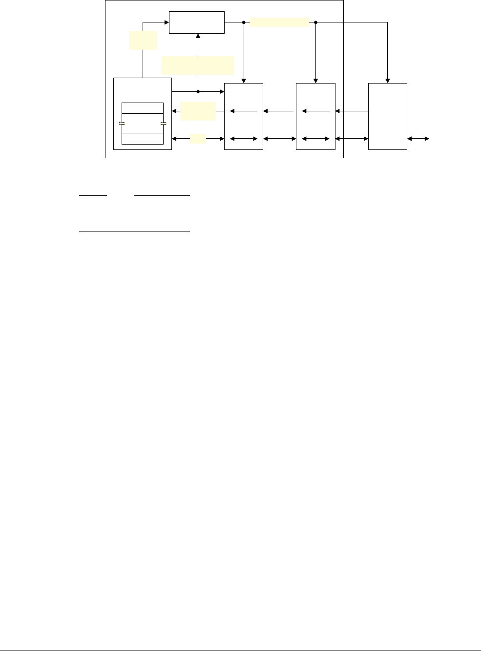
E2 The AArch32 Application Level Memory Model
E2.3 Caches and memory hierarchy
E2-2338 Copyright © 2013 ARM Limited. All rights reserved. ARM DDI 0487A.a
Non-Confidential - Beta ID090413
Figure E2-1 Multiple levels of cache in a memory hierarchy
Note
In this manual, in a hierarchical memory system, Level 1 refers to the level closest to the PE, as shown in
Figure E2-1.
Instructions and data can be held in separate caches or in a unified cache. A cache hierarchy can have one or more
levels of separate instruction and data caches, with one or more unified caches located at the levels closest to the
main memory. Memory coherency for cache topologies can be defined by two conceptual points:
Point of Unification (PoU)
The point at which the instruction cache, data cache, and translation table walks of a particular PE
are guaranteed to see the same copy of a memory location. In many cases, the point of unification
is the point in a uniprocessor memory system by which the instruction and data caches and the
translation table walks have merged. The point of unification might coincide with the point of
coherency.
Point of Coherency (PoC)
The point at which all agents that can access memory are guaranteed to see the same copy of a
memory location. In many cases this is effectively the main system memory, although the
architecture does not prohibit the implementation of caches beyond the PoC that have no effect on
the coherency between memory system agents.
See also The ARMv8 cache maintenance functionality on page G2-3529.
The cacheability and shareability memory attributes
Cacheability and shareability are two attributes that describe the memory hierarchy in a multiprocessing system:
Cacheability This term defines whether memory locations are allowed to be allocated into a cache or not.
Cacheability can be defined independently for Inner and Outer cacheability locations.
Shareability This term defines whether memory locations are shareable between different agents in a system.
Marking a memory location as shareable for a particular domain requires hardware to ensure that
the location is coherent for all agents in that domain. Shareability can be defined independently for
Inner and Outer shareability domains.
• For more information about cacheability and shareability see Memory types and attributes on page E2-2357.
Processing
Element
PE,
AArch32 state
Instruction
fetch
Data
Level 1
Cache
Level 2
Cache
Level 3
DRAM
SRAM
Flash
ROM
Level 4
for example,
memory card,
disk
Address
translation
System configuration
and control
R30
R0
Physical address
Virtual
address

E2 The AArch32 Application Level Memory Model
E2.3 Caches and memory hierarchy
ARM DDI 0487A.a Copyright © 2013 ARM Limited. All rights reserved. E2-2339
ID090413 Non-Confidential - Beta
E2.3.3 Implication of caches for the application programmer
In normal operation, the caches are largely invisible to the application programmer. However they can become
visible when there is a breakdown in the coherency of the caches. Such a breakdown can occur:
• When memory locations are updated by other agents in the system that do not use hardware management of
coherency.
• When memory updates made from the application software must be made visible to other agents in the
system, without the use of hardware management of coherency.
For example:
• In the absence of hardware management of coherency of DMA accesses, in a system with a DMA controller
that reads memory locations that are held in the data cache of a PE, a breakdown of coherency occurs when
the PE has written new data in the data cache, but the DMA controller reads the old data held in memory.
• In a Harvard cache implementation, where there are separate instruction and data caches, a breakdown of
coherency occurs when new instruction data has been written into the data cache, but the instruction cache
still contains the old instruction data.
Data coherency issues
Software can ensure the data coherency of caches in the following ways:
• By not using the caches in situations where coherency issues can arise. This can be achieved by:
— Using Non-cacheable or, in some cases, Write-Through Cacheable memory.
— Not enabling caches in the system.
• By using system calls to functions using cache maintenance instructions that execute at a higher Exception
level.
• By using hardware coherency mechanisms to ensure the coherency of data accesses to memory for cacheable
locations by observers within the different shareability domains, see Non-shareable Normal memory on
page E2-2359 and Shareable, Inner Shareable, and Outer Shareable Normal memory on page E2-2358.
Note
The performance of these hardware coherency mechanisms is highly implementation-specific. In some
implementations the mechanism suppresses the ability to cache shareable locations. In other
implementations, cache coherency hardware can hold data in caches while managing coherency between
observers within the shareability domains.
Synchronization and coherency issues between data and instruction accesses
How far ahead of the current point of execution instructions are fetched from is IMPLEMENTATION DEFINED. Such
prefetching can be either a fixed or a dynamically varying number of instructions, and can follow any or all possible
future execution paths. For all types of memory:
• The PE might have fetched the instructions from memory at any time since the last Context synchronization
operation on that PE.
• Any instructions fetched in this way might be executed multiple times, if this is required by the execution of
the program, without being re-fetched from memory.
The ARM architecture does not require the hardware to ensure coherency between instruction caches and memory,
even for locations of shared memory. This means that for cacheable locations of memory, an instruction cache can
hold instructions that were fetched from memory before any Context synchronization operation.
If software requires coherency between instruction execution and memory, it must manage this coherency using the
ISB
and
DSB
memory barriers and cache maintenance instructions. These can only be accessed from an Exception
level that is higher than EL0, and therefore require a system call, see Exception-generating and exception-handling
instructions on page F1-2396. The following code sequence can then be used:

E2 The AArch32 Application Level Memory Model
E2.3 Caches and memory hierarchy
E2-2340 Copyright © 2013 ARM Limited. All rights reserved. ARM DDI 0487A.a
Non-Confidential - Beta ID090413
; Coherency example for data and instruction accesses within the same Inner Shareable domain.
; Enter this code with <Rt> containing a new 32-bit instruction,
; to be held in non-cacheable space at a location pointed to by Rn.
STR Rt, [Rn]
DC CMVAU Rn ; Clean data cache by MVA to point of unification (PoU)
DSB ; Ensure visibility of the data cleaned from cache
IC IMVAU Rn ; Invalidate instruction cache by MVA to PoU
BPIMVAU Rn ; Invalidate branch predictor by MVA to PoU
DSB ; Ensure completion of the invalidations
ISB ; Synchronize the fetched instruction stream
E2.3.4 Preloading caches
The ARM architecture provides the memory system hints
PLD
(Preload Data),
PLDW
(Preload Data With Intent To
Write) and
PLI
(Preload Instruction) that software can use to communicate the expected use of memory locations to
the hardware. The memory system can respond by taking actions that are expected to speed up the memory accesses
if they occur. The effect of these memory system hints is IMPLEMENTATION DEFINED. Typically, implementations
use this information to bring data or instruction locations into caches.
The Preload instructions are hints, and so implementations can treat them as
NOP
s without affecting the functional
behavior of the device. The instructions cannot generate synchronous Data Abort exceptions, but the resulting
memory system operations might, under exceptional circumstances, generate an asynchronous external abort, which
is taken using an asynchronous Data Abort exception. For more information, see Data Abort exception on
page G1-3483.
A
PLD
or
PLDW
instruction is guaranteed not to cause any effects to the caches, or TLB, or memory, other than the
effects that, for permission or other reasons, can be caused by the equivalent load from the same location with same
context and at the same Exception level.
A
PLD
or
PLDW
instruction is guaranteed not to access Device memory.
A
PLI
instruction is guaranteed not to cause any effect to the caches, or TLB, or memory, other than the effect that,
for permission or other reasons, can be caused by the fetch resulting from changing the PC to the location specified
by the
PLI
instruction with the same context and at the same Exception level.
A
PLI
instruction must not perform any access that might be performed by a speculative instruction fetch by the PE.
Therefore:
•A
PLI
instruction cannot access memory that has a Device attribute.
• If all associated MMUs are disabled, a
PLI
instruction cannot access any memory location that cannot be
accessed by the instruction fetches.
PrefetchHint{}
defines the prefetch hint types:
enumeration PrefetchHint {Prefetch_READ, Prefetch_WRITE, Prefetch_EXEC};
The
Hint_Prefetch()
function signals to the memory system that memory accesses of the type
hint
to or from the
specified
address
are likely to occur in the near future. The memory system might take some action to speed-up the
memory accesses when they do occur, such as preloading the specified address into one or more caches as indicated
by the innermost cache level
target
and non-temporal hint
stream
.
Hint_Prefetch(bits(64) address, PrefetchHint hint, integer target, boolean stream);
For more information on
PLD
,
PLI
, and
PLDW
, see:
•PLD, PLDW (immediate) on page F7-2746.
•PLD (literal) on page F7-2748.
•PLD, PLDW (register) on page F7-2750.
•PLI (immediate, literal) on page F7-2752.
•PLI (register) on page F7-2754.

E2 The AArch32 Application Level Memory Model
E2.4 Alignment support
ARM DDI 0487A.a Copyright © 2013 ARM Limited. All rights reserved. E2-2341
ID090413 Non-Confidential - Beta
E2.4 Alignment support
This section describes alignment support. It contains the following subsections:
•Instruction alignment.
•Unaligned data access.
•Cases where unaligned accesses are UNPREDICTABLE.
•Unaligned data access restrictions on page E2-2342.
E2.4.1 Instruction alignment
A32 instructions are word-aligned.
T32 instruction are halfword-aligned.
E2.4.2 Unaligned data access
An ARMv8 implementation must support unaligned data accesses by some load and store instructions, as
Table E2-1 shows. Software can set SCTLR.A or HSCTLR.A to control whether a misaligned access by one of
these instructions causes an Alignment fault Data Abort exception.
E2.4.3 Cases where unaligned accesses are UNPREDICTABLE
Any load instruction that is not faulted by the alignment restrictions shown in Table E2-1 and that loads the PC has
UNPREDICTABLE behavior if the address it loads from is not word-aligned. This overrules any permitted Load/Store
behavior shown in Table E2-1.
Table E2-1 Alignment requirements of load/store instructions
Instructions Alignment
check
Result if check fails when:
SCTLR.A/
HSCTLR.A is 0 SCTLR.A/
HSCTLR.A is 1
LDRB
,
LDREXB
,
LDRBT
,
LDRSB
,
LDRSBT
,
STRB
,
STREXB
,
STRBT
,
TBB
None - -
LDRH
,
LDRHT
,
LDRSH
,
LDRSHT
,
STRH
,
STRHT
,
TBH
Halfword Unaligned access Alignment fault
LDREXH
,
STREXH
Halfword Alignment fault Alignment fault
LDR
,
LDRT
,
STR
,
STRT
PUSH
, encodings T3 and A2 only
POP
, encodings T3 and A2 only
Word Unaligned access Alignment fault
LDREX
,
STREX
Word Alignment fault Alignment fault
LDREXD
,
STREXD
Doubleword Alignment fault Alignment fault
All forms of
LDM
and
STM
,
LDRD
,
RFE
,
SRS
,
STRD
Word Alignment fault Alignment fault
LDC
,
LDC2
,
STC
,
STC2
Word Alignment fault Alignment fault
VLDM
,
VLDR
,
VPOP
,
VPUSH
,
VSTM
,
VSTR
Word Alignment fault Alignment fault
VLD1
,
VLD2
,
VLD3
,
VLD4
,
VST1
,
VST2
,
VST3
,
VST4
, all with standard alignment Element size Unaligned access Alignment fault
VLD1
,
VLD2
,
VLD3
,
VLD4
,
VST1
,
VST2
,
VST3
,
VST4
, all with
:<align>
specifiedaAs specified
by
:<align>
Alignment fault Alignment fault
a. Previous versions of this document used @<align> to specify alignment. Both forms are supported, see Chapter F8 T32 and A32 Advanced
SIMD and floating-point Instruction Descriptionsfor more information.

E2 The AArch32 Application Level Memory Model
E2.4 Alignment support
E2-2342 Copyright © 2013 ARM Limited. All rights reserved. ARM DDI 0487A.a
Non-Confidential - Beta ID090413
Note
• An unaligned access to Device memory generates an Alignment fault, see Alignment faults on page G3-3654.
•Device memory on page E2-2360 describes the Device memory attributes.
E2.4.4 Unaligned data access restrictions
The following points apply to unaligned data accesses in ARMv8:
• Accesses are not guaranteed to be single-copy atomic except at the byte access level, see Atomicity in the
ARM architecture on page E2-2346.
• Unaligned accesses typically takes a number of additional cycles to complete compared to a naturally-aligned
access.
• An operation that performs an unaligned access can abort on any memory access that it makes, and can abort
on more than one access. This means that an unaligned access that occurs across a page boundary can
generate an abort on either side of the boundary.
E2 The AArch32 Application Level Memory Model
E2.5 Endian support
ARM DDI 0487A.a Copyright © 2013 ARM Limited. All rights reserved. E2-2343
ID090413 Non-Confidential - Beta
E2.5 Endian support
General description of endianness in the ARM architecture describes the relationship between endianness and
memory addressing in the ARM architecture.
The following subsections then describe the endianness schemes supported by the architecture:
•Instruction endianness.
•Data endianness on page E2-2344.
E2.5.1 General description of endianness in the ARM architecture
This section only describes memory addressing and the effects of endianness for data elements up to doubleword
of 64 bits. However, this description can be extended to apply to larger data elements.
For an address A, Figure E2-2 shows, for big-endian and little-endian memory systems, the relationship between:
• The doubleword at address A.
• The words at addresses A and A+4.
• The halfwords at addresses A, A+2, A+4, and A+6.
• The bytes at addresses A, A+1, A+2, A+3, A+4, A+5, A+6, and A+7.
The terms in Figure E2-2 have the following definitions:
MSByte Most-significant byte.
LSByte Least-significant byte.
Figure E2-2 Endianness relationships in AArch32
E2.5.2 Instruction endianness
In ARMv8-A, the mapping of instruction memory is always little-endian.
In this figure, Byte, A+1 is an abbreviation for Byte at address A+1
Byte, A+7 Byte, AByte, A+1Byte, A+2Byte, A+3Byte, A+4Byte, A+5Byte, A+6
Halfword at address AHalfword at address A+2Halfword at address A+4Halfword at address A+6
Word at address AWord at address A+4
Doubleword at address A
Byte, A Byte, A+1 Byte, A+2 Byte, A+3 Byte, A+4 Byte, A+5 Byte, A+6 Byte, A+7
Halfword at address A Halfword at address A+2 Halfword at address A+4 Halfword at address A+6
Word at address A Word at address A+4
Doubleword at address A
Big-endian memory system
Incrementing byte address
MSByte LSByte
Little-endian memory system
Incrementing byte address
MSByte LSByte

E2 The AArch32 Application Level Memory Model
E2.5 Endian support
E2-2344 Copyright © 2013 ARM Limited. All rights reserved. ARM DDI 0487A.a
Non-Confidential - Beta ID090413
E2.5.3 Data endianness
The size of the data value that is loaded or stored is the size that is used for the purpose of endian conversion for
floating-point, Advanced SIMD, and general-purpose register loads and stores.
Table E2-2 shows the element sizes of all the load/store instructions, for all instruction sets.
CPSR.E determines the data endianness.
The data size used for endianness conversions:
• Is the size of the data value that is loaded or stored for SIMD and floating-point register and general-purpose
register loads and stores.
• Is the size of the data element that is loaded or stored for SIMD element and data structure loads and stores.
For more information see Endianness in SIMD on page E2-2345.
Instructions to reverse bytes in a general-purpose register or Advanced SIMD register
An application or device driver might have to interface to memory-mapped peripheral registers or shared memory
structures that are not the same endianness as the internal data structures. Similarly, the endianness of the operating
system might not match that of the peripheral registers or shared memory. In these cases, the PE requires an efficient
method to transform explicitly the endianness of the data.
Table E2-3 shows the instructions that provide this functionality A32, and T32 instruction sets:
Table E2-2 Element size of load/store instructions
Instructions Element size
LDRB
,
LDREXB
,
LDRBT
,
LDRSB
,
LDRSBT
,
STRB
,
STREXB
,
STRBT
,
TBB
Byte
LDRH
,
LDREXH
,
LDRHT
,
LDRSH
,
LDRSHT
,
STRH
,
STREXH
,
STRHT
,
TBH
Halfword
LDR
,
LDRT
,
LDREX
,
STR
,
STRT
,
STREX
Word
LDRD
,
LDREXD
,
STRD
,
STREXD
Word
All forms of
LDM
,
PUSH
,
POP
,
RFE
,
SRS
, all forms of
STM
, Word
LDC
,
LDC2
,
STC
,
STC2
Word
Forms of
VLDM
,
VLDR
,
VPOP
,
VPUSH
,
VSTM
,
VSTR
that transfer 32-bit Si registers Word
Forms of
VLDM
,
VLDR
,
VPOP
,
VPUSH
,
VSTM
,
VSTR
that transfer 64-bit Di registers Doubleword
VLD1
,
VLD2
,
VLD3
,
VLD4
,
VST1
,
VST2
,
VST3
,
VST4
Element size of the Advanced SIMD access
Table E2-3 Byte reversal instructions
Function T32 / A32
Instruction Notes
Reverse bytes in whole register
REV
For use with general purpose registers.
Reverse bytes in 16-bit halfwords
REV16
For use with general purpose registers.
Reverse bytes in halfword and sign-extend
REVSH
For use with general purpose registers.
Reverse elements in doublewords, vector
VREV64
For use with SIMD and floating-point registers
Reverse elements in words, vector
VREV32
For use with SIMD and floating-point registers
Reverse elements in halfwords, vector
VREV16
For use with SIMD and floating-point registers
E2 The AArch32 Application Level Memory Model
E2.5 Endian support
ARM DDI 0487A.a Copyright © 2013 ARM Limited. All rights reserved. E2-2345
ID090413 Non-Confidential - Beta
Endianness in SIMD
Advanced SIMD element Load/Store instructions transfer vectors of elements between memory and the Advanced
SIMD register file. An instruction specifies both the length of the transfer and the size of the data elements being
transferred. This information is used by the PE to load and store data correctly in both big-endian and little-endian
systems.
Consider, for example, the A32 or T32 instruction:
VLD1.16 {D0}, [R1]
This loads a 64-bit register with four 16-bit values. The four elements appear in the register in array order, with the
lowest indexed element fetched from the lowest address. The order of bytes in the elements depends on the
endianness configuration, as shown in Figure E2-3. Therefore, the order of the elements in the registers is the same
regardless of the endianness configuration.
Figure E2-3 Advanced SIMD byte order example for AArch32
For information about the alignment of Advanced SIMD instructions see Alignment support on page E2-2341.
The
BigEndian()
function determines the current endianness of the data:
boolean BigEndian();
The pseudocode function for
BigEndianReverse()
is as follows:
// BigEndianReverse()
// ==================
bits(width) BigEndianReverse (bits(width) value)
assert width IN {8, 16, 32, 64, 128};
integer half = width DIV 2;
if width == 8 then return value;
return BigEndianReverse(value<half-1:0>) : BigEndianReverse(value<width-1:half>);
D[15:8] D[7:0] C[15:8] C[7:0] B[15:8] B[7:0] A[15:8] A[7:0]
64-bit register containing four 16-bit elements
0
1
2
3
4
5
6 D[7:0]
C[15:8]
C[7:0]
B[15:8]
B[7:0]
A[15:8]
A[7:0] 0
1
2
3
4
5
6
D[7:0]
D[15:8]
C[7:0]
C[15:8]
B[7:0]
B[15:8]
A[7:0]
A[15:8]
Memory system with
little-endian addressing (LE)
Memory system with
big-endian addressing (BE)
VLD1.16 {D0}, [R1] VLD1.16 {D0}, [R1]
77 D[15:8]

E2 The AArch32 Application Level Memory Model
E2.6 Atomicity in the ARM architecture
E2-2346 Copyright © 2013 ARM Limited. All rights reserved. ARM DDI 0487A.a
Non-Confidential - Beta ID090413
E2.6 Atomicity in the ARM architecture
Atomicity is a feature of memory accesses, described as atomic accesses. The ARM architecture description refers
to two types of atomicity, defined in:
•Single-copy atomicity.
•Multi-copy atomicity on page E2-2347.
In the ARMv8 architecture, the atomicity requirements for memory accesses depends on the memory type, and
whether the access is explicit or implicit. For more information, see:
•Memory type overview on page E2-2336.
•Requirements for single-copy atomicity.
•Requirements for multi-copy atomicity on page E2-2348.
E2.6.1 Single-copy atomicity
A read or write operation is single-copy atomic if the following conditions are both true:
• After any number of write operations to a memory location, the value of the memory location is the value
written by one of the write operations. It is impossible for part of the value of the memory location to come
from one write operation and another part of the value to come from a different write operation.
• When a read operation and a write operation are made to the same memory location, the value obtained by
the read operation is one of:
— The value of the memory location before the write operation.
— The value of the memory location after the write operation.
It is never the case that the value of the read operation is partly the value of the memory location before the
write operation and partly the value of the memory location after the write operation.
E2.6.2 Requirements for single-copy atomicity
In AArch32 state, the single-copy atomic PE accesses are:
• All byte accesses.
• All halfword accesses to halfword-aligned locations.
• All word accesses to word-aligned locations.
• Memory accesses caused by
LDREXD
and
STREXD
instructions to doubleword-aligned locations.
LDM
,
LDC
,
LDC2
,
LDRD
,
STM
,
STC
,
STC2
,
STRD
,
PUSH
,
POP
,
RFE
,
SRS
,
VLDM
,
VLDR
,
VSTM
, and
VSTR
instructions are executed as a
sequence of word-aligned word accesses. Each 32-bit word access is guaranteed to be single-copy atomic. The
architecture does not require subsequences of two or more word accesses from the sequence to be single-copy
atomic.
LDRD
and
STRD
accesses to 64-bit aligned locations are 64-bit single-copy atomic as seen by translation table walks
and accesses to translation tables.
Note
This requirement has been added to avoid the need for complex measures to avoid atomicity issues when changing
translation table entries, without creating a requirement that all locations in the memory system are 64-bit
single-copy atomic. This addition means:
• The system designer must ensure that all writable memory locations that might be used to hold translations,
such as bulk SDRAM, can be accessed with 64-bit single-copy atomicity.
• Software must ensure that translation tables are not held in memory locations that cannot meet this atomicity
requirement, such as peripherals that are typically accessed using a narrow bus.
This requirement places no burden on read-only memory locations for which reads have no side effects, since it is
impossible to detect the size of memory accesses to such locations.

E2 The AArch32 Application Level Memory Model
E2.6 Atomicity in the ARM architecture
ARM DDI 0487A.a Copyright © 2013 ARM Limited. All rights reserved. E2-2347
ID090413 Non-Confidential - Beta
Advanced SIMD element and structure loads and stores are executed as a sequence of accesses of the element or
structure size. The architecture requires the element accesses to be single-copy atomic if and only if both:
• The element size is 32 bits, or smaller.
• The elements are naturally aligned.
Accesses to 64-bit elements or structures that are at least word-aligned are executed as a sequence of 32-bit accesses,
each of which is single-copy atomic.The architecture does not require subsequences of two or more 32-bit accesses
from the sequence to be single-copy atomic.
When a store that, by the rules given in this section, would be single-copy atomic is made to a memory location at
a time when there is at least one store to the same memory location that has not completed and that would be
single-copy atomic at a different size, then the architecture does not give any assurance of atomicity between
accesses to the bytes of that location.
When an access is not single-copy atomic, it is executed as a sequence of smaller accesses, each of which is
single-copy atomic, at least at the byte level.
Note
In this section, the terms before the write operation and after the write operation mean before or after the write
operation has had its effect on the coherence order of the bytes of the memory location accessed by the write
operation.
If, according to these rules, an instruction is executed as a sequence of accesses, a synchronous Data Abort exception
can be taken during that sequence. This causes execution of the instruction to be abandoned.
If the synchronous Data Abort exception is returned from using the preferred return address, the instruction that
generated the sequence of accesses is re-executed and so any access that was performed before the exception was
taken is repeated.
Note
The exception behavior for these multiple access instructions means they are not suitable for use for writes to
memory for the purpose of software synchronization.
For implicit accesses:
• Cache linefills and evictions have no effect on the single-copy atomicity of explicit transactions or instruction
fetches.
• Instruction fetches are single-copy atomic:
— At 32-bit granularity in A32 state.
— At 16-bit granularity in T32 state.
•Concurrent modification and execution of instructions on page E2-2348 describes additional constraints on
the behavior of instruction fetches.
• Translation table walks are performed using accesses that are single-copy atomic:
— At 32-bit granularity when using Short-descriptor format translation tables.
— At 64-bit granularity when using Long-descriptor format translation tables.
E2.6.3 Multi-copy atomicity
In a multiprocessing system, writes to a memory location are multi-copy atomic if the following conditions are both
true:
• All writes to the same location are serialized, meaning they are observed in the same order by all observers,
although some observers might not observe all of the writes.
• A read of a location does not return the value of a write until all observers observe that write.

E2 The AArch32 Application Level Memory Model
E2.6 Atomicity in the ARM architecture
E2-2348 Copyright © 2013 ARM Limited. All rights reserved. ARM DDI 0487A.a
Non-Confidential - Beta ID090413
Note
Writes that are not coherent are not multi-copy atomic.
E2.6.4 Requirements for multi-copy atomicity
For Normal memory, writes are not required to be multi-copy atomic.
For Device memory with the non-Gathering attribute, writes that are single-copy atomic are also multi-copy atomic.
For Device memory with the Gathering attribute, writes are not required to be multi-copy atomic.
E2.6.5 Concurrent modification and execution of instructions
The ARMv8 architecture limits the set of instructions that can be executed by one thread of execution as they are
being modified by another thread of execution without requiring explicit synchronization.
Concurrent modification and execution of instructions can lead to the resulting instruction performing any behavior
that can be achieved by executing any sequence of instructions that can be executed from the same Exception level,
except where the instruction before modification or the instruction after modification is a:
•
B
,
BL
,
NOP
,
BKPT
,
SVC
,
HVC
, or
SMC
A32 instruction
•
B,BL, BLX, NOP
,
BKPT
, or
SVC
16-bit T32 instruction.
In addition, for the T32 instructions:
• The most-significant halfword of a32-bit
BL
immediate instruction can be concurrently modified to the most
significant halfword of another
BL
immediate instruction:
— This means that the most significant bits of the immediate value can be modified.
• The most-significant halfword of a 32-bit
BLX
immediate instruction can be concurrently modified to the most
significant halfword of another
BLX
immediate instruction:
— This means that the most significant bits of the immediate value can be modified.
• The most-significant halfword of a 32-bit
BL
immediate or
BLX
immediate instruction can be concurrently
modified to a T32 16-bit
B
,
BL
,
BLX
,
BKPT
, or
SVC
instruction. This modification also works in reverse.
• The least-significant halfword of a 32-bit
BL
immediate instruction can be concurrently modified to the least
significant halfword of another
BL
instruction with a different immediate:
— This means that the least significant bits of the immediate value can be modified.
• The least-significant halfword of a 32-bit
BLX
immediate instruction can be concurrently modified to the least
significant halfword of another
BLX
immediate instruction with a different immediate:
— This means that the least significant bits of the immediate value can be modified.
• The least-significant halfword of a 32-bit
B
immediate instruction with a condition field can be concurrently
modified to the least significant halfword of another 32-bit
B
immediate instruction with a condition field with
a different immediate:
— This means that the least significant bits of the immediate value can be modified.
• The least-significant halfword of a 32-bit
B
immediate instruction without a condition field can be
concurrently modified to the least significant halfword of another 32-bit
B
immediate instruction without a
condition field:
— This means that the least significant bits of the immediate value can be modified.
Note
In the T32 instruction set:
• The only encodings of
BKPT
and
SVC
are 16-bit.
• The only encoding of
BL
is 32-bit.

E2 The AArch32 Application Level Memory Model
E2.6 Atomicity in the ARM architecture
ARM DDI 0487A.a Copyright © 2013 ARM Limited. All rights reserved. E2-2349
ID090413 Non-Confidential - Beta
For instructions listed in this section the architecture guarantees that after modification of the instruction, behavior
is consistent with execution of either:
• The instruction originally fetched.
• A fetch of the modified instruction.
If one thread of execution changes a conditional branch instruction, such as
B
or
BL
, to another conditional instruction
and the change affects both the condition field and the branch target, execution of the changed instruction by another
thread of execution before the change is synchronized can lead to either:
• The old condition being associated with the new target address.
• The new condition being associated with the old target address.
For more information about the required synchronization operation, see Synchronization and coherency issues
between data and instruction accesses on page E2-2339.
These possibilities apply regardless of whether the condition, either before or after the change to the branch
instruction, is the always condition.
Note
For information about memory accesses caused by instruction fetches, see Ordering requirements on page E2-2351.

E2 The AArch32 Application Level Memory Model
E2.7 Memory ordering
E2-2350 Copyright © 2013 ARM Limited. All rights reserved. ARM DDI 0487A.a
Non-Confidential - Beta ID090413
E2.7 Memory ordering
This section describes observation ordering. It contains the following subsections:
•Observability and completion.
•Ordering requirements on page E2-2351.
•Memory barriers on page E2-2352.
For information on endpoint ordering of memory accesses, see Reordering on page E2-2363.
In the ARMv8 memory model, the shareability memory attribute indicates whether hardware must ensure memory
coherency.
The ARMv8 memory system architecture defines additional attributes and associated behaviors, defined in the
system level section of this manual. See:
•Chapter G2 The AArch32 System Level Memory Model.
•Chapter G3 The AArch32 Virtual Memory System Architecture.
See also Mismatched memory attributes on page E2-2366.
E2.7.1 Observability and completion
An observer is a master in the system that is capable of observing memory accesses. For a PE, the following
mechanisms must be treated as independent observers:
• The mechanism that performs reads or writes to memory.
• A mechanism that causes an instruction cache to be filled from memory or that fetches instructions to be
executed directly from memory. These are treated as reads.
• A mechanism that performs translation table walks. These are treated as reads.
The set of observers that can observe a memory access is defined by the system.
In the definitions in this subsection, subsequent means whichever of the following is appropriate to the context:
• After the point in time where the location is observed by that observer.
• After the point in time where the location is globally observed.
For all memory:
• A write to a location in memory is said to be observed by an observer when:
— A subsequent read of the location by the same observer returns the value written by the observed write,
or written by a write to that location by any observer that is sequenced in the Coherence order of the
location after the observed write.
— A subsequent write of the location by the same observer is sequenced in the Coherence order of the
location after the observed write.
• A write to a location in memory is said to be globally observed for a shareability domain or set of observers
when:
— A subsequent read of the location by any observer in that shareability domain returns the value written
by the globally observed write, or written by a write to that location by any observer that is sequenced
in the Coherence order of the location after the globally observed write.
— A subsequent write of the location by any observer in that shareability domain is sequenced in the
Coherence order of the location after the globally observed write.
• A read of a location in memory is said to be observed by an observer when a subsequent write to the location
by the same observer has no effect on the value returned by the read.
• A read of a location in memory is said to be globally observed for a shareability domain when a subsequent
write to the location by any observer in that shareability domain has no effect on the value returned by the
read.

E2 The AArch32 Application Level Memory Model
E2.7 Memory ordering
ARM DDI 0487A.a Copyright © 2013 ARM Limited. All rights reserved. E2-2351
ID090413 Non-Confidential - Beta
Additionally, for Device-nGnRnE memory:
• A read or write of a memory-mapped location in a peripheral that exhibits side-effects is said to be observed,
and globally observed, only when the read or write:
— Meets the general conditions listed.
— Can begin to affect the state of the memory-mapped peripheral.
— Can trigger all associated side-effects, whether they affect other peripheral devices, processors, or
memory.
Note
This definition is consistent with the memory access having reached the peripheral.
For all memory, the completion rules are defined as:
• A read or write is complete for a shareability domain when all of the following are true:
— The read or write is globally observed for that shareability domain.
— Any translation table walks associated with the read or write are complete for that shareability domain.
• A translation table walk is complete for a shareability domain when the memory accesses associated with the
translation table walk are globally observed for that shareability domain, and the TLB is updated.
• A cache or TLB maintenance instruction is complete for a shareability domain when the effects of the
instruction are globally observed for that shareability domain, and any translation table walks that arise from
the instruction are complete for that shareability domain.
The completion of any cache or TLB maintenance instruction includes its completion on all processors that
are affected by both the instruction and the
DSB
operation that is required to guarantee visibility of the
maintenance instruction.
Completion of side-effects of accesses to Device memory
The completion of a memory access to Device memory other than Device-nGnRnE is not guaranteed to be sufficient
to determine that the side-effects of the memory access are visible to all observers. The mechanism that ensures the
visibility of side-effects of a memory access is IMPLEMENTATION DEFINED.
E2.7.2 Ordering requirements
• ARMv8 defines restrictions for the permitted ordering of memory accesses. These restrictions depend on the
memory locations that are being accessed. See Memory types and attributes on page E2-2357.
The following additional restrictions apply to the order in which accesses to Normal memory are observed:
• Reads and writes can be observed in any order provided the following constraints are met:
— If an address dependency exists between two reads or between a read and a write, then those memory
accesses are observed in program order by all observers within the shareability domain of the memory
address being accessed.
— Writes that would not occur in a simple sequential execution of the program cannot be observed by
other observers. This implies that where a control, address or data dependency exists between a read
and a write, those memory accesses are observed in program order by all observers within the
shareability domain of the memory addresses being accessed.
— Ordering can be achieved by using a
DMB
or
DSB
barrier. For more information on
DMB
and
DSB
instructions, see Memory barriers on page E2-2352.
• Reads and writes to the same location are coherent within the shareability domain of the memory address
being accessed.
• Two reads of the same location by the same observer are observed in program order by all observers within
the shareability domain of the memory address being accessed.

E2 The AArch32 Application Level Memory Model
E2.7 Memory ordering
E2-2352 Copyright © 2013 ARM Limited. All rights reserved. ARM DDI 0487A.a
Non-Confidential - Beta ID090413
• Writes are not required to be multi-copy atomic. This means that in the absence of barriers, the observation
of a store by one observer does not imply the observation of the store by another observer.
• Instructions that access multiple elements have no defined ordering requirements for the memory accesses
relative to each other.
Memory accesses caused by instruction fetches are not required to be observed in program order, unless they are
separated by an
ISB
or other context synchronization event.
Address dependencies and order
In the ARMv8 architecture, a register data dependency creates order between a load instruction and a subsequent
memory transaction, that is between the data value returned from the load and the address used by the subsequent
memory transaction.
A register data dependency exists between a first data value and a second data value exists when either:
• The register used to hold the first data value is used in the calculation of the second data value, and the
calculation between the first data value and the second data value does not consist of either:
— A conditional branch whose condition is determined by the first data value.
— A conditional selection, move, or computation whose condition is determined by the first data value,
where the input data values for the selection, move, or computation do not have a data dependency on
the first data value.
• There is a register data dependency between the first data value and a third data value, and between the third
data value and the second data value.
Note
A register data dependency can exist even if the value of the first data value is discarded as part of the calculation,
as might be the case if it is ANDed with
0x0
or if arithmetic using the first data value cancels out its contribution.
For example, each of the following code snippets exhibits order between the memory transactions:
1. LDR R1,[R2]
AND R1, R1, #0
LDR R4,[R3, R1]
2. LDR R1, [R2]
ADD R3, R3, R1
SUB R3, R3, R1
STR R4, [R3]
E2.7.3 Memory barriers
The ARM architecture is a weakly ordered memory architecture that supports out of order completion. Memory
barrier is the general term applied to an instruction, or sequence of instructions, that forces synchronization events
by a PE with respect to retiring Load/Store instructions. The memory barriers defined by the ARMv8 architecture
provide a range of functionality, including:
• Ordering of Load/Store instructions.
• Completion of Load/Store instructions.
• Context synchronization.
The following subsections describe the ARMv8 memory barrier instructions:
•Instruction Synchronization Barrier (ISB) on page E2-2353.
•Data Memory Barrier (DMB) on page E2-2353.
•Data Synchronization Barrier (DSB) on page E2-2354.
•Shareability and access limitations on the data barrier operations on page E2-2355.
•Load-Acquire, Store-Release on page E2-2355.

E2 The AArch32 Application Level Memory Model
E2.7 Memory ordering
ARM DDI 0487A.a Copyright © 2013 ARM Limited. All rights reserved. E2-2353
ID090413 Non-Confidential - Beta
Note
Depending on the required synchronization, a program might use memory barriers on their own, or it might use them
in conjunction with cache maintenance and memory management instructions that in general are only available
when software execution is at EL1 or higher.
The
DMB
and
DSB
memory barriers affect reads and writes to the memory system generated by Load/Store instructions
and data or unified cache maintenance instructions being executed by the PE. Instruction fetches or accesses caused
by a hardware translation table access are not explicit accesses.
AArch32 state also supports the legacy CP15 barrier operations CP15DMB, CP15DSB, and CP15ISB. These
operations are accessible from EL0. However, ARM deprecates any use of these operations, and strongly
recommends that software uses the
DMB
,
DSB
, and
ISB
instructions described in this section instead. Supervisory
software can disable use of the CP15 barrier operations, meaning the encodings for these operations are unallocated:
• If EL1 is using AArch32, by setting SCTLR.CP15BEN to 0.
• If EL1 is using AArch64, by setting SCTLR_EL1.CP15BEN to 0.
Instruction Synchronization Barrier (ISB)
An
ISB
instruction flushes the pipeline in the PE, so that all instructions that come after the
ISB
instruction in
program order are fetched from the cache or memory only after the
ISB
instruction has completed. Using an
ISB
ensures that the effects of context-changing operations executed before the
ISB
are visible to the instructions fetched
after the
ISB
instruction. Examples of context-changing operations that require the insertion of an
ISB
instruction to
ensure the effects of the operation are visible to instructions fetched after the
ISB
instruction are:
• Completed cache and TLB maintenance instructions.
• Changes to system control registers.
Any context-changing operations appearing in program order after the
ISB
instruction only take effect after the
ISB
has been executed.
InstructionSynchronizationBarrier();
See also Memory barriers on page G2-3556.
Data Memory Barrier (DMB)
The
DMB
instruction is a data memory barrier. The PE that executes the
DMB
instruction is referred to as the executing
PE, PEe. The
DMB
instruction takes the required shareability domain and required access types as arguments:
DataMemoryBarrier(MBReqDomain domain, MBReqTypes types);
See Shareability and access limitations on the data barrier operations on page E2-2355.
If the required shareability is Full system then the operation applies to all observers within the system.
A
DMB
creates two groups of memory accesses, Group A and Group B:
Group A Contains:
• All explicit memory accesses of the required access types from observers in the same
required shareability domain as PEe that are observed by PEe before the
DMB
instruction.
These accesses include any accesses of the required access types performed by PEe.
• All loads of required access types from an observer PEx in the same required shareability
domain as PEe that have been observed by any given different observer, PEy, in the same
required shareability domain as PEe before PEy has performed a memory access that is a
member of Group A.
Group B Contains:
• All explicit memory accesses of the required access types by PEe that occur in program order
after the
DMB
instruction.

E2 The AArch32 Application Level Memory Model
E2.7 Memory ordering
E2-2354 Copyright © 2013 ARM Limited. All rights reserved. ARM DDI 0487A.a
Non-Confidential - Beta ID090413
• All explicit memory accesses of the required access types by any given observer PEx in the
same required shareability domain as PEe that can only occur after a load by PEx has returned
the result of a store that is a member of Group B.
Any observer with the same required shareability domain as PEe observes all members of Group A before it
observes any member of Group B to the extent that those group members are required to be observed, as determined
by the shareability and cacheability of the memory locations accessed by the group members.
If members of Group A and members of Group B access the same memory-mapped peripheral of arbitrary
system-defined size, then members of Group A that are accessing Device or Normal Non-cacheable memory arrive
at that peripheral before members of Group B that are accessing Device or Normal Non-cacheable memory. Where
the members of Group A and Group B that must be ordered are from the same PE, a
DMB NSH
is sufficient for this
guarantee.
Note
• A memory access might be in neither Group A nor Group B. The
DMB
does not affect the order of observation
of such a memory access.
• The second part of the definition of Group A is recursive. Ultimately, membership of Group A derives from
the observation by PEy of a load before PEy performs an access that is a member of Group A as a result of
the first part of the definition of Group A.
• The second part of the definition of Group B is recursive. Ultimately, membership of Group B derives from
the observation by any observer of an access by PEe that is a member of Group B as a result of the first part
of the definition of Group B.
DMB
only affects memory accesses and the operation of data cache and unified cache maintenance instructions, see
Cache maintenance instructions on page D4-1684. It has no effect on the ordering of any other instructions
executing on the PE.
See also Memory barriers on page D4-1705.
Data Synchronization Barrier (DSB)
The
DSB
instruction is a special memory barrier, that synchronizes the execution stream with memory accesses.
The
DSB
instruction takes the required shareability domain and required access types as arguments:
DataSynchronizationBarrier(MBReqDomain domain, MBReqTypes types);
See Shareability and access limitations on the data barrier operations on page E2-2355.
If the required shareability is Full system then the operation applies to all observers within the system.
A
DSB
behaves as a
DMB
with the same arguments, and also has the additional properties defined in this section. The
PE that executes the
DSB
instruction is referred to as the executing PE, PEe.
A
DSB
completes when all of the following apply:
• All explicit memory accesses that are observed by PEe before the
DSB
is executed and are of the required
access types, and are from observers in the same required shareability domain as PEe, are complete for the
set of observers in the required shareability domain.
• All cache maintenance instructions issued by PEe before the
DSB
are complete for the required shareability
domain.
• If the required access types of the
DSB
is reads and writes, all TLB maintenance instructions issued by PEe
before the
DSB
are complete for the required shareability domain.
In addition, no instruction that appears in program order after the
DSB
instruction can execute until the
DSB
completes.
See also Memory barriers on page G2-3556.

E2 The AArch32 Application Level Memory Model
E2.7 Memory ordering
ARM DDI 0487A.a Copyright © 2013 ARM Limited. All rights reserved. E2-2355
ID090413 Non-Confidential - Beta
Shareability and access limitations on the data barrier operations
The
DMB
and
DSB
instructions can each take an optional limitation argument that specifies:
• The shareability domain over which the instruction must operate. This is one of:
— Full system.
— Outer Shareable.
— Inner Shareable.
— Non-shareable.
• The accesses for which the instruction operates. This is one of:
— Read and write accesses in Group A and Group B.
— Write accesses only in Group A and Group B.
— Read access only in Group A.
Note
This is occasionally referred to as a Load-Load/Store barrier.
— Read and write accesses in Group B.
Note
This is occasionally referred to as a Load-Load/Store barrier.
If no specifiers are used then each instruction operates for read and write accesses, over the full system. See the
instruction descriptions for more information about these arguments.
Note
ISB
also supports an optional limitation argument that can only contain one value that corresponds to full system
operation.
Load-Acquire, Store-Release
ARMv8 provides a set of instructions with Acquire semantics for loads, and Release semantics for stores.
For all memory types, these instructions have the following ordering requirements:
• A Store-Release followed by a Load-Acquire is observed in program order by each observer within the
shareability domain of the memory address being accessed by the Store-Release and the memory address
being accessed by the Load-Acquire.
• A Load-Acquire is a read that must be observed by all observers in the shareability domain of the accessed
memory location before any other read or write that both:
— Is caused by an instruction that appears in program order after the Load-Acquire.
— Accesses memory in the shareability domain accessed by the Load-Acquire.
• A Load-Acquire places no additional ordering constraints on any loads or stores appearing before the
Load-Acquire.
• Store-Release is a write:
— Where the reads and writes generated by loads and stores appearing in program order before the
Store-Release are observed as required by the shareability domains of the memory addresses being
accessed by those loads and stores by each observer within the shareability domain of the memory
address being accessed by the Store-Release, before that observer observes the write generated by the
Store-Release.
— Where any writes that have been observed before the Store-Release by the processing element
executing the Store-Release are observed as required by the shareability domains of the memory
addresses being accessed by those loads and store by each observer within the shareability domain of
the memory address being accessed by the Store-Release, before that observer observes the write
generated by the Store-Release.

E2 The AArch32 Application Level Memory Model
E2.7 Memory ordering
E2-2356 Copyright © 2013 ARM Limited. All rights reserved. ARM DDI 0487A.a
Non-Confidential - Beta ID090413
• The Store-Release places no additional ordering constraints on any loads or stores appearing after the
Store-Release instruction.
• All Store-Release instructions must be multi-copy atomic when they are observed with Load-Acquire
instructions.
Load-Acquire and Store-Release, other than
LDAEXD
and
STLEXD
, access only a single data element. This access is
single-copy atomic. The address of the data object must be aligned to the size of the data element being accessed,
otherwise the access generates an Alignment fault.
LDAEXD
and
STLEXD
access two data elements. The address supplied to the instructions must be doubleword aligned,
otherwise the access generates an Alignment fault.
A Store-Release Exclusive instruction only has the release semantics if the store is successful.
Note
• Each Load-Acquire Exclusive and Store-Release Exclusive instruction is essentially a variant of the
equivalent Load-Exclusive or Store-Exclusive instruction. All usage restrictions and single-copy atomicity
properties that apply to the Load-Exclusive or Store-Exclusive instructions also apply to the Load-Acquire
Exclusive or Store-Release Exclusive instructions.
• The Load-Acquire/Store-Release instructions can remove the requirement to use the explicit
DMB
memory
barrier instruction.

E2 The AArch32 Application Level Memory Model
E2.8 Memory types and attributes
ARM DDI 0487A.a Copyright © 2013 ARM Limited. All rights reserved. E2-2357
ID090413 Non-Confidential - Beta
E2.8 Memory types and attributes
In ARMv8 the ordering of accesses for locations of memory, referred to as the memory order model, is defined by
the memory attributes. The following sections describe this model:
•Normal memory.
•Device memory on page E2-2360.
E2.8.1 Normal memory
The Normal memory type attribute applies to most memory in a system. It indicates that the hardware might perform
speculative data read accesses to these locations.
The Normal memory type has the following properties:
• A write to a memory location with the Normal attribute completes in finite time. This means that it is globally
observed for the shareability domain of the memory location in finite time. For a Non-cacheable location, the
location is observed by all observers in finite time.
• A completed write to a memory location with the Normal attribute is globally observed for the shareability
domain of the memory location in finite time without the need for explicit cache maintenance instructions or
barriers. For a Non-cacheable location, the completed write is globally observed for all observers in finite
time without the need for explicit cache maintenance instructions or barriers.
• Writes to a memory location with the Normal memory attribute that are Non-cacheable must reach the
endpoint for that location in the memory system in finite time.
• Unaligned memory accesses can access Normal memory if the system is configured to generate such
accesses.
• There is no requirement for the memory system beyond the PE to be able to identify the elements accessed
by multi-register Load/Store instructions. See Multi-register loads and stores that access Normal memory on
page E2-2360.
Note
• The Normal memory attribute is appropriate for locations of memory that are idempotent, meaning that they
exhibit all of the following properties:
— Read accesses can be repeated with no side-effects.
— Repeated read accesses return the last value written to the resource being read.
— Read accesses can fetch additional memory locations with no side-effects.
— Write accesses can be repeated with no side-effects if the contents of the location accessed are
unchanged between the repeated writes or as the result of an exception, as described in this section.
— Unaligned accesses can be supported.
— Accesses can be merged before accessing the target memory system.
• An instruction that generates a sequence of accesses as described in Atomicity in the ARM architecture on
page E2-2346 might be abandoned as a result of an exception being taken during the sequence of accesses.
On return from the exception the instruction is restarted, and therefore one or more of the memory locations
might be accessed multiple times. This can result in repeated write accesses to a location that has been
changed between the write accesses.
The following sections describe the other attributes for Normal memory:
•Shareable Normal memory on page E2-2358.
•Non-shareable Normal memory on page E2-2359.

E2 The AArch32 Application Level Memory Model
E2.8 Memory types and attributes
E2-2358 Copyright © 2013 ARM Limited. All rights reserved. ARM DDI 0487A.a
Non-Confidential - Beta ID090413
See also:
•Atomicity in the ARM architecture on page E2-2346.
•Memory barriers on page E2-2352. For accesses to Normal memory, a
DMB
instruction is required to ensure
the required ordering.
•Concurrent modification and execution of instructions on page E2-2348.
Shareable Normal memory
A Normal memory location has a Shareability attribute that is:
• Defined independently for the Inner Shareable and Outer Shareable shareability domains.
• Defined, for each shareability domain, as being either Shareable or Non-shareable.
The shareability attributes define the data coherency requirements of the location, that hardware must enforce. They
do not affect the coherency requirements of instruction fetches, see Synchronization and coherency issues between
data and instruction accesses on page E2-2339.
Note
• System designers can use the shareability attribute to specify the locations in Normal memory for which
coherency must be maintained. However, software developers must not assume that specifying a memory
location as Non-shareable permits software to make assumptions about the incoherency of the location
between different PEs in a shared memory system. Such assumptions are not portable between different
multiprocessing implementations that might use the shareability attribute. Any multiprocessing
implementation might implement caches that are shared, inherently, between different processing elements.
• This architecture assumes that all PEs that use the same operating system or hypervisor are in the same Inner
Shareable shareability domain.
Shareable, Inner Shareable, and Outer Shareable Normal memory
The ARM architecture abstracts the system as a series of Inner and Outer Shareability domains.
Each Inner Shareability domain contains a set of observers that are data coherent for each member of that set for
data accesses with the Inner Shareable attribute made by any member of that set.
Each Outer Shareability domain contains a set of observers that are data coherent for each member of that set for
data accesses with the Outer Shareable attribute made by any member of that set.
The following properties also hold:
• Each observer is only a member of a single Inner Shareability domain.
• Each observer is only a member of a single Outer Shareability domain.
• All observers in an Inner Shareability domain are always members of the same Outer Shareability domain.
This means that an Inner Shareability domain is a subset of an Outer Shareability domain, although it is not
required to be a proper subset.
Note
• Because all data accesses to Non-cacheable locations are data coherent to all observers, Non-cacheable
locations are always treated as Outer Shareable.
• The Inner Shareable domain is expected to be the set of PEs controlled by a single hypervisor or operating
system.

E2 The AArch32 Application Level Memory Model
E2.8 Memory types and attributes
ARM DDI 0487A.a Copyright © 2013 ARM Limited. All rights reserved. E2-2359
ID090413 Non-Confidential - Beta
The details of the use of the shareability attributes are system-specific. Example E2-1 shows how they might be
used.
Example E2-1 Use of shareability attributes
In an implementation, a particular subsystem with two clusters of PEs has the requirement that:
• In each cluster, the data caches or unified caches of the PEs in the cluster are transparent for all data accesses
to memory locations with the Inner Shareable attribute.
• However, between the two clusters, the caches:
— Are not required to be coherent for data accesses that have only the Inner Shareable attribute.
— Are coherent for data accesses that have the Outer Shareable attribute.
In this system, each cluster is in a different shareability domain for the Inner Shareable attribute, but all components
of the subsystem are in the same shareability domain for the Outer Shareable attribute.
A system might implement two such subsystems. If the data caches or unified caches of one subsystem are not
transparent to the accesses from the other subsystem, this system has two Outer Shareable shareability domains.
Having two levels of shareability means system designers can reduce the performance and power overhead for
shared memory locations that do not need to be part of the Outer Shareable shareability domain.
For Shareable Normal memory, the Load-Exclusive and Store-Exclusive synchronization primitives take account
of the possibility of accesses by more than one observer in the same Shareability domain.
Non-shareable Normal memory
For Normal memory locations, the Non-shareable attribute identifies Normal memory that is likely to be accessed
only by a single PE.
A location in Normal memory with the Non-shareable attribute does not require the hardware to make data accesses
by different observers coherent, unless the memory is Non-cacheable. For a Non-shareable location, if other
observers share the memory system, software must use cache maintenance instructions, if the presence of caches
might lead to coherency issues when communicating between the observers. This cache maintenance requirement
is in addition to the barrier operations that are required to ensure memory ordering.
For Non-shareable Normal memory, it is IMPLEMENTATION DEFINED whether the Load-Exclusive and
Store-Exclusive synchronization primitives take account of the possibility of accesses by more than one observer.
Concurrent modification and execution of instructions
The ARMv8 architecture limits the set of instructions that can be executed by one thread of execution as they are
being modified by another thread of execution without requiring explicit synchronization.
Except where the instruction before modification or the instruction after modification is explicitly identified in this
section, concurrent modification and execution of instructions can lead to the resulting instruction performing any
behavior that can be achieved by executing any sequence of instructions that can be executed from the same
Exception level.
For the instructions explicitly identified in this section, the architecture guarantees that, after modification of the
instruction, behavior is consistent with execution of either:
• The instruction originally fetched.
• A fetch of the modified instruction.
The instructions to which this applies are the
B
,
BL
,
NOP
,
BKPT
,
SVC
,
HVC
, and
SMC
instructions.

E2 The AArch32 Application Level Memory Model
E2.8 Memory types and attributes
E2-2360 Copyright © 2013 ARM Limited. All rights reserved. ARM DDI 0487A.a
Non-Confidential - Beta ID090413
For all other instructions, to avoid UNPREDICTABLE behavior, instruction modifications must be explicitly
synchronized before they are executed. The required synchronization is as follows:
1. To ensure that the modified instructions are observable, the thread of execution that is modifying the
instructions must issue the following sequence of instructions and operations:
; Coherency example for self-modifying code
; Enter this code with <Rt> containing a new 32-bit instruction,
; to be held in non-cacheable space at a location pointed to by Rn.Use STRH in the first
; line instead of STR for a 16-bit instruction.
STR <Rt>, [Rn]
DSB ; Ensure visibility of the data stored
IC IMVAU, Rn ; Invalidate instruction cache by VA to PoU
DSB ; Ensure completion of the invalidations
2. Once the modified instructions are observable, the thread of execution that is executing the modified
instructions must issue the following instruction to ensure execution of the modified instructions:
ISB ; Synchronize fetched instruction stream
For both instruction sets, if one thread of execution changes a conditional branch instruction to another conditional
branch instruction, and the change affects both the condition field and the branch target, execution of the changed
instruction by another thread of execution before the change is synchronized can lead to either:
• The old condition being associated with the new target address.
• The new condition being associated with the old target address.
These possibilities apply regardless of whether the condition, either before or after the change to the branch
instruction, is the always condition.
Multi-register loads and stores that access Normal memory
For all instructions that load or store more than one general-purpose register from an Exception level there is no
requirement for the memory system beyond the PE to be able to identify the size of the elements accessed by these
load or store instructions.
For all instructions that load or store more than one general-purpose register from an Exception level the order in
which the registers are accessed is not defined by the architecture.
For all instructions that load or store one or more SIMD and floating-point register from an Exception level there is
no requirement for the memory system beyond the PE to be able to identify the size of the element accessed by these
load or store instructions.
E2.8.2 Device memory
The Device memory type attributes define memory locations where an access to the location can cause side-effects,
or where the value returned for a load can vary depending on the number of loads performed. Typically, the Device
memory attributes are used for memory-mapped peripherals and similar locations.
The attributes for ARMv8 Device memory are:
Gathering Identified as G or nG, see Gathering on page E2-2362.
Reordering Identified as R or nR, see Reordering on page E2-2363.
Early Write Acknowledgement hint
Identified as E or nE, see Early Write Acknowledgement on page E2-2364.
The ARMv8 Device memory types are:
Device-nGnRnE Device non-Gathering, non-Reordering, No Early write acknowledgement.
Equivalent to the Strongly-ordered memory type in earlier versions of the architecture.

E2 The AArch32 Application Level Memory Model
E2.8 Memory types and attributes
ARM DDI 0487A.a Copyright © 2013 ARM Limited. All rights reserved. E2-2361
ID090413 Non-Confidential - Beta
Device-nGnRE Device non-Gathering, non-Reordering, Early Write Acknowledgement.
Equivalent to the Device memory type in earlier versions of the architecture.
Device-nGRE Device non-Gathering, Reordering, Early Write Acknowledgement.
ARMv8 adds this memory type to the translation table formats found in earlier versions of
the architecture. The use of barriers is required to order accesses to Device-nGRE memory.
The Device-nGRE memory type is introduced into the AArch32 translation table formats
when the PE is using the Long Descriptor Translation Table format.
Device-GRE Device Gathering, Reordering, Early Write Acknowledgement.
ARMv8 adds this memory type to the translation table formats found in earlier versions of
the architecture. Device-GRE memory has the fewest constraints. It behaves similar to
Normal memory, with the restriction that speculative accesses to Device-GRE memory is
forbidden.
The Device-GRE memory type is introduced into the AArch32 translation table formats
when the PE is using the Long Descriptor Translation Table format.
Collectively these are referred to as any Device memory type. Going down the list, the memory types are described
as getting weaker; conversely the going up the list the memory types are described as getting stronger.
Note
• As the list of types shows, these additional attributes are hierarchical. For example, a memory location that
permits Gathering must also permit Reordering and Early Write Acknowledgement.
• The architecture does not require an implementation to distinguish between each of these memory types and
ARM recognizes that not all implementations will do so. The subsection that describes each of the attributes,
describes the implementation rules for the attribute.
• Earlier versions of the ARM architecture defined the following memory types:
— Strongly-ordered memory. This is the equivalent of the Device-nGnRnE memory type.
— Device memory. This is the equivalent of the Device-nGnRE memory type.
All of these memory types have the following properties:
• Speculative data accesses are not permitted to any memory location with any Device memory attribute. This
means that each memory access to any Device memory type must be one that would be generated by a simple
sequential execution of the program.
An exception to this applies:
— Reads generated by the SIMD and floating-point instructions can access bytes that are not explicitly
accessed by the instruction if the bytes accessed are in a 16-byte window, aligned to 16-bytes, that
contains at least one byte that is explicitly accessed by the instruction.
Note
• An instruction that generates a sequence of accesses as described in Atomicity in the ARM architecture on
page E2-2346 might be abandoned as a result of an exception being taken during the sequence of accesses.
On return from the exception the instruction is restarted, and therefore one or more of the memory locations
might be accessed multiple times. This can result in repeated accesses to a location where the program only
defines a single access. For this reason, ARM strongly recommends that no accesses to Device memory are
performed from a single instruction that spans the boundary of a translation granule or which in some other
way could lead to some of the accesses being aborted.
— Write speculation that is visible to other observers is prohibited for all memory types.
• A write to a memory location with any Device memory attribute completes in finite time. This means that it
is globally observed for all observers in the system in finite time.

E2 The AArch32 Application Level Memory Model
E2.8 Memory types and attributes
E2-2362 Copyright © 2013 ARM Limited. All rights reserved. ARM DDI 0487A.a
Non-Confidential - Beta ID090413
• If a location with any Device memory attribute changes without an explicit write by an observer, this change
must also be globally observed for all observers in the system in finite time. Such a change might occur in a
peripheral location that holds status information.
• A completed write to a memory location with any Device memory attribute is globally observed for all
observers in finite time without the need for explicit maintenance.
• Data accesses to memory locations are coherent for all observers in the system, and correspondingly are
treated as being Outer Shareable.
• A memory location with any Device memory attribute cannot be allocated into a cache.
• Writes to a memory location with any Device memory attribute must reach the endpoint for that address in
the memory system in finite time. Typically, the endpoint is a peripheral or some physical memory.
• All accesses to memory with any Device memory attribute must be aligned. Any unaligned access generates
an Alignment fault at the first stage of translation that defined the location as being Device.
Note
In the Non-secure EL1 translation regime in systems where HCR.TGE == 1 and HCR.DC == 0, any
Alignment fault that results from the fact that all locations are treated as Device is a fault at the first stage of
translation. This causes the value of HSR.ISS.[24] to be 0.
• Hardware does not prevent speculative instruction fetches from a memory location with any of the Device
memory attributes unless the memory location is also marked as Execute-never for all Exception levels.
Note
This means that to prevent speculative instruction fetches from memory locations with Device memory
attributes, any location that is assigned any Device memory type must also be marked as Execute-never for
all Exception levels. Failure to mark a memory location with any Device memory attribute as Execute-never
for all Exception levels is a programming error.
For instruction fetches, if branches cause the program counter to point to an area of memory with the Device
attribute which is not marked as Execute-never for the current Exception level, an implementation can either:
• Treat the instruction fetch as if it were to a memory location with the Normal Non-cacheable attribute.
• Take a Permission fault.
Gathering
In the Device memory attribute:
G Indicates that the location has the Gathering attribute.
nG Indicates that the location does not have the Gathering attribute, meaning it is non-Gathering.
The Gathering attribute determines whether it is permissible for either:
• Multiple memory accesses of the same type, read or write, to the same memory location to be merged into a
single transaction.
• Multiple memory accesses of the same type, read or write, to different memory locations to be merged into
a single memory transaction on an interconnect.
For memory types with the Gathering attribute, either of these behaviors is permitted, provided that the ordering and
coherency rules of the memory location are followed.
For memory types with the non-Gathering attribute, neither of these behaviors is permitted. As a result:
• The number of memory accesses that are made corresponds to the number that would be generated by a
simple sequential execution of the program.

E2 The AArch32 Application Level Memory Model
E2.8 Memory types and attributes
ARM DDI 0487A.a Copyright © 2013 ARM Limited. All rights reserved. E2-2363
ID090413 Non-Confidential - Beta
• All access occur at their programmed size, except that there is no requirement for the memory system beyond
the PE to be able to identify the elements accessed by multi-register Load/Store instructions. See
Multi-register loads and stores that access Device memory on page E2-2364.
Gathering between memory accesses separated by a memory barrier that affects those memory accesses is not
permitted. This applies if one memory access is in Group A and one memory access is in Group B. That is, gathering
is not permitted between a memory access in Group A and a memory access in Group B if the two accesses are
separated by a barrier that affects at least one of the accesses.
Gathering between two memory accesses generated by a Load-Acquire/Store-Release is not permitted.
A read from a memory location with the non-Gathering attribute cannot come from a cache or a buffer, but must
come from the endpoint for that address in the memory system. Typically this is a peripheral or physical memory.
Note
• A read from a memory location with the Gathering attribute can come from intermediate buffering of a
previous write, provided that:
— The accesses are not separated by a
DMB
or
DSB
barrier that affects both of the accesses, for example if
one access is in Group A and the other is in Group B.
— The accesses are not separated by other ordering constructions that require that the accesses are in
order. Such a construction might be a combination of Load-Acquire and Store-Release.
— The accesses are not generated by a Store-Release instruction.
• The ARM architecture only defines programmer visible behavior. Therefore, gathering can be performed if
a programmer cannot tell whether gathering has occurred.
An implementation is permitted to perform an access with the Gathering attribute in a manner consistent with the
requirements specified by the Non-gathering attribute.
An implementation is not permitted to perform an access with the Non-gathering attribute in a manner consistent
with the relaxations allowed by the Gathering attribute.
Reordering
In the Device memory attribute:
R Indicates that the location has the Reordering attribute.
nR Indicates that the location does not have the Reordering attribute, meaning it is non-Reordering.
For all memory types with the non-Reordering attribute, the order of memory accesses arriving at a single peripheral
of IMPLEMENTATION DEFINED size, as defined by the peripheral, must be the same order that occurs in a simple
sequential execution of the program.That is, the accesses appear in program order. This ordering applies to all
accesses using any of the memory types with the non-Reordering attribute. As a result, if there is a mixture of
Device-nGnRE and Device-nGnRnE accesses to the same peripheral, these occur in program order. If the memory
accesses are not to a peripheral, then this attribute imposes no restrictions.
Note
• The IMPLEMENTATION DEFINED size of the single peripheral is the same as applies for the ordering guarantee
provided by the
DMB
instruction.
• The ARM architecture only defines programmer visible behavior. Therefore, reordering can be performed if
a programmer cannot tell whether reordering has occurred.
An implementation is permitted to perform an access with the Reordering attribute in a manner consistent with the
requirements specified by the non-Reordering attribute.
A additional relaxation is that an implementation is not permitted to perform an access with the non-Reordering
attribute in a manner consistent with the relaxations allowed by the Reordering attribute.

E2 The AArch32 Application Level Memory Model
E2.8 Memory types and attributes
E2-2364 Copyright © 2013 ARM Limited. All rights reserved. ARM DDI 0487A.a
Non-Confidential - Beta ID090413
The non-Reordering attribute does not require any additional ordering, other than that which applies to Normal
memory, between:
• Accesses with the non-Reordering attribute and accesses with the Reordering attribute.
• Accesses with the non-Reordering attribute and accesses to Normal memory.
• Accesses with the non-Reordering attribute and accesses to different peripherals of IMPLEMENTATION
DEFINED size.
Early Write Acknowledgement
In the Device memory attribute:
E Indicates that the location has the Early Write Acknowledgement attribute.
nE Indicates that the location has the No Early Write Acknowledgement attribute.
Early Write Acknowledgement is a hint to the platform memory system. Assigning the No Early Write
Acknowledgement attribute to a Device memory location recommends that only the endpoint of the write access
returns a write acknowledgement of the access, and that no earlier point in the memory system returns a write
acknowledge. This means that a
DSB
barrier, executed by the PE that performed the write to the No Early Write
Acknowledgement location, completes only after the write has reached its endpoint in the memory system.
Typically, this endpoint is a peripheral or physical memory.
When the Early Write Acknowledgement attribute is assigned to a Device memory location, there is no such
recommendation for the handling of accesses to that location.
Note
• The Early Write Acknowledgement hint has no effect on the ordering rules. The purpose of signalling no
Early Write Acknowledgement is to signal to the interconnect that the peripheral requires the ability to signal
the acknowledgement. The No Write Acknowledgement signal also provides an additional semantic that can
be interpreted by the driver that is accessing the peripheral.
• This attribute is treated as a hint, as the exact nature of the interconnects attached to a PE is outside the scope
of the ARM architecture definition, and not all interconnects provide a mechanism to ensure that a write has
reached the physical endpoint of the memory system.
• ARM recommends that writes with the No Early Write Acknowledgement hint are used for PCIe
configuration writes. However, the mechanisms by which PCIe configuration writes are identified are
IMPLEMENTATION DEFINED.
• ARM strongly recommends that the Early Write Acknowledgement hint is not ignored by a PE, but is made
available for use by the system.
Because the No Early Write Acknowledgement attribute is a hint:
• An implementation is permitted to perform an access with the Early Write Acknowledgement attribute in a
manner consistent with the requirements specified by the No Early Write Acknowledgement attribute.
• An implementation is permitted to perform an access with the No Early Write Acknowledgement attribute
in a manner consistent with the relaxations allowed by the Early Write Acknowledgement attribute.
Multi-register loads and stores that access Device memory
For all instructions that load or store more than one general-purpose register from an Exception level there is no
requirement for the memory system beyond the PE to be able to identify the size of the elements accessed by these
load or store instructions.
For an
LDRD,STRD,LDM
instruction with a register list that includes the PC, or an
STM
instruction with a register list that
includes the PC, the order in which the registers are accessed is not defined by the architecture, even for accesses
to any type of Device memory.

E2 The AArch32 Application Level Memory Model
E2.8 Memory types and attributes
ARM DDI 0487A.a Copyright © 2013 ARM Limited. All rights reserved. E2-2365
ID090413 Non-Confidential - Beta
For an
LDM
and
STM
instruction with a register list that doesn’t include the PC, both registers are accessed in ascending
address order.
For all instructions that load or store one or more floating-point and SIMD register from an Exception level there is
no requirement for the memory system beyond the PE to be able to identify the size of the element accessed by these
load or store instructions, even for access to any type of Device memory.

E2 The AArch32 Application Level Memory Model
E2.9 Mismatched memory attributes
E2-2366 Copyright © 2013 ARM Limited. All rights reserved. ARM DDI 0487A.a
Non-Confidential - Beta ID090413
E2.9 Mismatched memory attributes
In the ARMv8 architecture mismatched memory attributes are controlled by privileged software. For more
information, see Chapter G3 The AArch32 Virtual Memory System Architecture.
Physical memory locations are accessed with mismatched attributes if all accesses to the location do not use a
common definition of all of the following attributes of that location:
• Memory type, Device or Normal.
• Shareability.
• Cacheability, for the same level of the inner or outer cache, but excluding any cache allocation hints.
Collectively these are referred to as memory attributes.
Note
The terms location and memory location refer to any byte within the current coherency granule and are used
interchangeably.
The following rules apply when a physical memory location is accessed with mismatched attributes:
1. When a memory location is accessed with mismatched attributes the only software visible effects are one or
more of the following:
• Uniprocessor semantics for reads and writes to that memory location might be lost. This means:
— A read of the memory location by one agent might not return the value most recently written to
that memory location by the same agent.
— Multiple writes to the memory location by one agent with different memory attributes might not
be ordered in program order.
• There might be a loss of coherency when multiple agents attempt to access a memory location.
• There might be a loss of properties derived from the memory type, as described in later bullets in this
section.
• If all Load-Exclusive/Store-Exclusive instructions executed across all threads to access a given
memory location do not use consistent memory attributes, the exclusive monitor state becomes
UNKNOWN.
• Bytes written without the Write-Back cacheable attribute within the same Write-Back granule as bytes
written with the Write-Back cacheable attribute might have their values reverted to the old values as
a result of cache Write-Back.
2. The loss of properties associated with mismatched memory type attributes refers only to the following
properties of Device memory that are additional to the properties of Normal memory:
• Prohibition of speculative read accesses.
• Prohibition on Gathering.
• Prohibition on Re-ordering.
• The Write Acknowledgement guarantee with respect to the endpoint of the access.
If the only memory type mismatch associated with a memory location across all users of the memory location
is between different types of Device memory, then all accesses might take the properties of the weakest
Device memory type.
3. If all aliases of a memory location that permit write access to the location assign the same shareability and
cacheability attributes to that location, and all these aliases use a definition of the shareability attribute that
includes all the threads of execution that can access the location, then any agent that reads the memory
location using these shareability and cacheability attributes accesses it coherently, to the extent required by
that common definition of the memory attributes.
4. The possible loss of software-visible effects caused by mismatched attributes for a memory location are
defined more precisely if all of the mismatched attributes define the memory location as one of:
• Any Device memory type.
• Normal Inner Non-cacheable, Outer Non-cacheable memory.

E2 The AArch32 Application Level Memory Model
E2.9 Mismatched memory attributes
ARM DDI 0487A.a Copyright © 2013 ARM Limited. All rights reserved. E2-2367
ID090413 Non-Confidential - Beta
In these cases, the only permitted software-visible effects of the mismatched attributes are one or more of the
following:
• Possible loss of properties described in point 2 on page E2-2366, derived from the memory type when
multiple agents attempt to access the memory location.
• Possible reordering of memory transactions to the memory location with different memory attributes,
potentially leading to a loss of coherency or uniprocessor semantics. Any possible loss of coherency
or uniprocessor semantics can be avoided by inserting
DMB
barrier instructions between accesses to the
same memory location that might use different attributes.
5. If the mismatched attributes for a memory location all assign the same shareability attribute to the location,
any loss of uniprocessor semantics or coherency within a shareability domain can be avoided by use of
software cache management. To do so, software must use the techniques that are required for the software
management of the coherency of cacheable locations between agents a in different shareability domains. This
means:
• Before writing to a location not using the Write-Back attribute, software must invalidate, or clean, a
location from the caches if any agent might have written to the location with the Write-Back attribute.
This avoids the possibility of overwriting the location with stale data.
• After writing to a location with the Write-Back attribute, software must clean the location from the
caches, to make the write visible to external memory.
• Before reading the location with a cacheable attribute, software must invalidate the location from the
caches, to ensure that any value held in the caches reflects the last value made visible in external
memory.
Note
Cache maintenance instructions can only be accessed from an Exception level that is higher than EL0, and
therefore require a system call. For information on system calls, see Exception-generating and
exception-handling instructions on page F1-2396. For information on cache maintenance instructions, see
Cache support on page G2-3524.
In all cases:
• Location refers to any byte within the current coherency granule.
• A clean and invalidate instruction can be used instead of a clean instruction, or instead of an invalidate
instruction.
• In the sequences outlined in this section, all cache maintenance instructions and memory transactions
must be completed, or ordered by the use of barrier operations, if they are not naturally ordered by the
use of a common address, see Ordering of cache and branch predictor maintenance instructions on
page G2-3539.
Note
With software management of coherency, race conditions can cause loss of data. A race condition occurs
when different agents write simultaneously to bytes that are in the same location, and the invalidate, write,
clean sequence of one agent overlaps with the equivalent sequence of another agent. A race condition also
occurs if the first operation of either sequence is a clean, rather than an invalidate.
6. If the mismatched attributes for a location mean that multiple cacheable accesses to the location might be
made with different shareability attributes, then coherency is guaranteed only if processing elements that
accesses the location with a cacheable attribute performs a clean and invalidate of the location before and
after accessing that location.
Note
The Note in rule 5 on page E2-2367 about possible race conditions also applies to this rule.
In addition, if multiple agents attempt to use Load-Exclusive or Store-Exclusive instructions to access a location,
and the accesses from the different agents have different memory attributes associated with the location, the
exclusive monitor state becomes UNKNOWN.

E2 The AArch32 Application Level Memory Model
E2.9 Mismatched memory attributes
E2-2368 Copyright © 2013 ARM Limited. All rights reserved. ARM DDI 0487A.a
Non-Confidential - Beta ID090413
ARM strongly recommends that software does not use mismatched attributes for aliases of the same location. An
implementation might not optimize the performance of a system that uses mismatched aliases.

E2 The AArch32 Application Level Memory Model
E2.10 Synchronization and semaphores
ARM DDI 0487A.a Copyright © 2013 ARM Limited. All rights reserved. E2-2369
ID090413 Non-Confidential - Beta
E2.10 Synchronization and semaphores
ARMv8 provides non-blocking synchronization of shared memory, using synchronization primitives. The
information in this section about memory accesses by synchronization primitives applies to accesses to both Normal
and Device memory.
Note
Use of the ARMv8 synchronization primitives scales for multiprocessing system designs.
Table E2-4 shows the synchronization primitives and the associated
CLREX
instruction.
The model for the use of a Load-Exclusive/Store-Exclusive instruction pair accessing a non-aborting memory
address x is:
• The Load-Exclusive instruction reads a value from memory address x.
• The corresponding Store-Exclusive instruction succeeds in writing back to memory address x only if no other
observer, process, or thread has performed a more recent store to address x. The Store-Exclusive instruction
returns a status bit that indicates whether the memory write succeeded.
A Load-Exclusive instruction marks a small block of memory for exclusive access. The size of the marked block is
IMPLEMENTATION DEFINED, see Marking and the size of the marked memory block on page E2-2374. A
Store-Exclusive instruction to any address in the marked block clears the marking.
Note
In this section, the term PE includes any observer that can generate a Load-Exclusive or a Store-Exclusive
instruction.
E2.10.1 Exclusive access instructions and Non-shareable memory locations
For memory locations that do not have the Shareable attribute, the exclusive access instructions rely on a local
monitor that marks any address from which the PE executes a Load-Exclusive instruction. Any non-aborted attempt
by the same PE to use a Store-Exclusive instruction to modify any address is guaranteed to clear the marking.
Table E2-4 Synchronization primitives and associated instruction
Function A32/T32 Instruction
Load-Exclusive
Byte
LDREXB
,
LDRAEXB
Halfword
LDREXH, LDRAEXH
Word
LDREX, LDRAEX
Doubleword
LDREXD
.
LDRAEXD
Store-Exclusive
Byte
STREXB
,
STRLEXB
Halfword
STREXH
,
STRLEXH
Word
STREX
,
STRLEX
Doubleword
STREXD
,
STRLEXD
Clear-Exclusive
CLREX
E2 The AArch32 Application Level Memory Model
E2.10 Synchronization and semaphores
E2-2370 Copyright © 2013 ARM Limited. All rights reserved. ARM DDI 0487A.a
Non-Confidential - Beta ID090413
A Load-Exclusive instruction performs a load from memory, and:
• The executing PE marks the physical memory address for exclusive access.
• The local monitor of the executing PE transitions to the Exclusive Access state.
A Store-Exclusive instruction performs a conditional store to memory that depends on the state of the local monitor:
If the local monitor is in the Exclusive Access state
• If the address of the Store-Exclusive instruction is the same as the address that has been
marked in the monitor by an earlier Load-Exclusive instruction, then the store occurs.
Otherwise, it is IMPLEMENTATION DEFINED whether the store occurs.
• A status value is returned to a register:
— If the store took place the status value is 0.
— Otherwise, the status value is 1.
• The local monitor of the executing PE transitions to the Open Access state.
If the local monitor is in the Open Access state
• No store takes place.
• A status value of 1 is returned to a register.
• The local monitor remains in the Open Access state.
The Store-Exclusive instruction defines the register to which the status value is returned.
When a PE writes using any instruction other than a Store-Exclusive instruction:
• If the write is to a physical address that is not tagged by its local monitor it is IMPLEMENTATION DEFINED
whether the write affects the state of the local monitor.
• If the write is to a physical address that is tagged by its local monitor it is IMPLEMENTATION DEFINED whether
the write affects the state of the local monitor.
It is IMPLEMENTATION DEFINED whether a store to a marked physical address causes a mark in the local monitor to
be cleared if that store is by an observer other than the one that caused the physical address to be marked.
Figure E2-4 shows the state machine for the local monitor and the effect of each of the operations shown in the
figure.
Figure E2-4 Local monitor state machine diagram
For more information about marking see Marking and the size of the marked memory block on page E2-2374.
Open
Access
Exclusive
Access
LoadExcl(x) LoadExcl(x)
CLREX
StoreExcl(x)
Store(x)
CLREX Store(!Marked_address)
Store(Marked_address)*
Operations marked * are possible alternative
IMPLEMENTATION
DEFINED
options.
Store(Marked_address)*
StoreExcl(Marked_address)
StoreExcl(!Marked_address)
Store(!Marked_address)*
In the diagram: LoadExcl represents any Load-Exclusive instruction
StoreExcl represents any Store-Exclusive instruction
Store represents any other store instruction.
Any LoadExcl operation updates the marked address to the most significant bits of the address x used for the operation.

E2 The AArch32 Application Level Memory Model
E2.10 Synchronization and semaphores
ARM DDI 0487A.a Copyright © 2013 ARM Limited. All rights reserved. E2-2371
ID090413 Non-Confidential - Beta
Note
For the local monitor state machine, as shown in Figure E2-4 on page E2-2370:
• The IMPLEMENTATION DEFINED options for the local monitor are consistent with the local monitor being
constructed so that it does not hold any physical address, but instead treats any access as matching the address
of the previous Load-Exclusive instruction.
• A local monitor implementation can be unaware of Load-Exclusive and Store-Exclusive instructions from
other PEs.
• The architecture does not require a load instruction, by another PE, that is not a Load-Exclusive instruction,
to have any effect on the local monitor.
• It is IMPLEMENTATION DEFINED whether the transition from Exclusive Access to Open Access state occurs
when the
Store
or
StoreExcl
is from another observer.
Changes to the local monitor state resulting from speculative execution
The architecture permits a local monitor to transition to the Open Access state as a result of speculation, or from
some other cause. This is in addition to the transitions to Open Access state caused by the architectural execution
of an operation shown in Figure E2-4 on page E2-2370.
An implementation must ensure that:
• The local monitor cannot be seen to transition to the Exclusive Access state except as a result of the
architectural execution of one of the operations shown in Figure E2-4 on page E2-2370.
• Any transition of the local monitor to the Open Access state not caused by the architectural execution of an
operation shown in Figure E2-4 on page E2-2370 must not indefinitely delay forward progress of execution.
E2.10.2 Exclusive access instructions and Shareable memory locations
For memory locations that have the Shareable attribute, exclusive access instructions rely on:
•A local monitor for each PE in the system, that marks any address from which the PE executes a
Load-Exclusive. The local monitor operates as described in Exclusive access instructions and Non-shareable
memory locations on page E2-2369, except that for Shareable memory any Store-Exclusive is then subject
to checking by the global monitor if it is described in that section as doing at least one of the following:
— Updating memory.
— Returning a status value of 0.
The local monitor can ignore accesses from other PEs in the system.
•A global monitor that marks a physical address as exclusive access for a particular PE. This marking is used
later to determine whether a Store-Exclusive to that address that has not been failed by the local monitor can
occur. Any successful write to the marked block by any other observer in the shareability domain of the
memory location is guaranteed to clear the marking. For each PE in the system, the global monitor:
— Can hold one marked block.
— Maintains a state machine for each marked block it can hold.
Note
For each PE, the architecture only requires global monitor support for a single marked address. Any situation
that might benefit from the use of multiple marked addresses on a single PE is UNPREDICTABLE, see
Load-Exclusive and Store-Exclusive instruction usage restrictions on page E2-2375.

E2 The AArch32 Application Level Memory Model
E2.10 Synchronization and semaphores
E2-2372 Copyright © 2013 ARM Limited. All rights reserved. ARM DDI 0487A.a
Non-Confidential - Beta ID090413
Note
The global monitor can either reside in a block that is part of the hardware on which the PE executes or exist as a
secondary monitor at the memory interfaces.The IMPLEMENTATION DEFINED aspects of the monitors mean that the
global monitor and local monitor can be combined into a single unit, provided that the unit performs the global
monitor and local monitor functions defined in this manual.
For Shareable locations of memory, in some implementations and for some memory types, the properties of the
global monitor require functionality outside the PE. Some system implementations might not implement this
functionality for all locations of memory. In particular, this can apply to:
• Any type of memory in the system implementation that does not support hardware cache coherency.
• Non-cacheable memory, or memory treated as Non-cacheable, in an implementation that does support
hardware cache coherency.
In such a system, it is defined by the system:
• Whether the global monitor is implemented.
• If the global monitor is implemented, which address ranges or memory types it monitors.
Note
To support the use of the Load-Exclusive/Store-Exclusive mechanism when address translation is disabled, a
system might define at least one location of memory, of at least the size of the translation granule, in the system
memory map to support the global monitor for all PEs within a common Inner Shareable domain. However, this is
not an architectural requirement. Therefore, architecturally-compliant software that requires mutual exclusion must
not rely on using the Load-Exclusive/Store-Exclusive mechanism, and must instead use a software algorithm such
as Lamport’s Bakery algorithm to achieve mutual exclusion.
If the global monitor is not implemented for an address range or memory type, then performing a
Load-Exclusive/Store-Exclusive instruction to such a location has one or more of the following effects:
• The instruction generates an external abort.
• The instruction generates an IMPLEMENTATION DEFINED MMU fault. This is reported using the Fault Status
code of:
—DFSR.STATUS =
0b110101
when using the Long-descriptor translation table format. The fault can also
be reported in the HSR.ISS[5:0] field for exceptions to Hyp mode.
—DFSR.FS =
0b10101
when using the Short-descriptor translation table format.
• The instruction is treated as a
NOP
.
• The Load-Exclusive instruction is treated as if it were accessing a Non-shareable location, but the state of the
local monitor becomes UNKNOWN.
• The Store-Exclusive instruction is treated as if it were accessing a Non-shareable location, but the state of the
local monitor becomes UNKNOWN.
• The value held in the result register of the Store-Exclusive instruction becomes UNKNOWN.
In addition, for write transactions generated by non-PE observers that do not implement exclusive accesses or other
atomic access mechanisms, the effect that writes have on the global and local monitors used by an ARM PE is
IMPLEMENTATION DEFINED. The writes might not clear the global monitors of other PEs for:
• Some address ranges.
• Some memory types.
Operation of the global monitor
A Load-Exclusive instruction from Shareable memory performs a load from memory, and causes the physical
address of the access to be marked as exclusive access for the requesting PE. This access also causes the exclusive
access mark to be removed from any other physical address that has been marked by the requesting PE.
Note
The global monitor only supports a single outstanding exclusive access to Shareable memory for each PE.

E2 The AArch32 Application Level Memory Model
E2.10 Synchronization and semaphores
ARM DDI 0487A.a Copyright © 2013 ARM Limited. All rights reserved. E2-2373
ID090413 Non-Confidential - Beta
A Load-Exclusive instruction by one PE has no effect on the global monitor state for any other PE.
A Store-Exclusive instruction performs a conditional store to memory:
• The store is guaranteed to succeed only if the physical address accessed is marked as exclusive access for the
requesting PE and both the local monitor and the global monitor state machines for the requesting PE are in
the Exclusive Access state. In this case:
— A status value of 0 is returned to a register to acknowledge the successful store.
— The final state of the global monitor state machine for the requesting PE is IMPLEMENTATION DEFINED.
— If the address accessed is marked for exclusive access in the global monitor state machine for any other
PE then that state machine transitions to Open Access state.
• If no address is marked as exclusive access for the requesting PE, the store does not succeed:
— A status value of 1 is returned to a register to indicate that the store failed.
— The global monitor is not affected and remains in Open Access state for the requesting PE.
• If a different physical address is marked as exclusive access for the requesting PE, it is IMPLEMENTATION
DEFINED whether the store succeeds or not:
— If the store succeeds a status value of 0 is returned to a register, otherwise a value of 1 is returned.
— If the global monitor state machine for the PE was in the Exclusive Access state before the
Store-Exclusive instruction it is IMPLEMENTATION DEFINED whether that state machine transitions to
the Open Access state.
The Store-Exclusive instruction defines the register to which the status value is returned.
In a shared memory system, the global monitor implements a separate state machine for each PE in the system. The
state machine for accesses to Shareable memory by PE(n) can respond to all the Shareable memory accesses visible
to it. This means it responds to:
• Accesses generated by PE(n).
• Accesses generated by the other observers in the shareability domain of the memory location. These accesses
are identified as (!n).
In a shared memory system, the global monitor implements a separate state machine for each observer that can
generate a Load-Exclusive or a Store-Exclusive instruction in the system.
Clear global monitor event
Whenever the global monitor state for a PE changes from Exclusive access to Open access, an event is generated
and held in the Event register for that PE. This register is used by the Wait for Event mechanism, see Wait For Event
and Send Event on page G1-3460.
Figure E2-5 on page E2-2374 shows the state machine for PE(n) in a global monitor.
E2 The AArch32 Application Level Memory Model
E2.10 Synchronization and semaphores
E2-2374 Copyright © 2013 ARM Limited. All rights reserved. ARM DDI 0487A.a
Non-Confidential - Beta ID090413
Figure E2-5 Global monitor state machine diagram for PE(n) in a multiprocessor system
For more information about marking see Marking and the size of the marked memory block.
Note
For the global monitor state machine, as shown in Figure E2-5:
• The architecture does not require a load instruction by another PE, that is not a Load-Exclusive instruction,
to have any effect on the global monitor.
• Whether a Store-Exclusive instruction successfully updates memory or not depends on whether the address
accessed matches the marked Shareable memory address for the PE issuing the Store-Exclusive instruction,
and whether the local and global monitors are in the exclusive state. For this reason, Figure E2-5 only shows
how the operations by (!n) cause state transitions of the state machine for PE(n).
• A Load-Exclusive instruction can only update the marked Shareable memory address for the PE issuing the
Load-Exclusive instruction.
• When the global monitor is in the Exclusive Access state, it is IMPLEMENTATION DEFINED whether a
CLREX
instruction causes the global monitor to transition from Exclusive Access to Open Access state.
• It is IMPLEMENTATION DEFINED:
— Whether a modification to a Non-shareable memory location can cause a global monitor to transition
from Exclusive Access to Open Access state.
— Whether a Load-Exclusive instruction to a Non-shareable memory location can cause a global monitor
to transition from Open Access to Exclusive Access state.
E2.10.3 Marking and the size of the marked memory block
When a Load-Exclusive instruction is executed, the resulting marked block ignores the least significant bits of the
64-bit memory address.
Any LoadExcl operation updates the marked address to the most significant bits of the address x used for the operation.
Open
Access
Exclusive
Access
LoadExcl(x,n) LoadExcl(x,n)
CLREX(n)
StoreExcl(x,n)
CLREX(n)*
StoreExcl(Marked_address,!n)‡
Store(Marked_address,!n)
StoreExcl(Marked_address,n)*
Store(!Marked_address,n)
Operations marked * are possible alternative IMPLEMENTATION DEFINED options.
In the diagram: LoadExcl represents any Load-Exclusive instruction
StoreExcl represents any Store-Exclusive instruction
Store represents any other store instruction.
LoadExcl(x,!n)
StoreExcl(x,!n)
Store(x,n)
StoreExcl(!Marked_address,n)*
Store(Marked_address,n)*
StoreExcl(Marked_address,!n)‡
StoreExcl(Marked_address,n)*
StoreExcl(!Marked_address,n)*
Store(Marked_address,n)*
CLREX(n)*
StoreExcl(!Marked_address,!n)
Store(!Marked_address,!n)
CLREX(!n)
‡StoreExcl(Marked_address,!n) clears the monitor only if the StoreExcl updates memory
Store(x,!n)
CLREX(!n)

E2 The AArch32 Application Level Memory Model
E2.10 Synchronization and semaphores
ARM DDI 0487A.a Copyright © 2013 ARM Limited. All rights reserved. E2-2375
ID090413 Non-Confidential - Beta
When a Load-Exclusive instruction is executed, a marked block of size 2a is created by ignoring the least significant
bits of the memory address. A marked address is any address within this marked block. For example, in an
implementation where a is 4, a successful
LDREXB
of address
0x341B4
gives defines a marked block using bits[47:4]
of the address. This means that the four words of memory from
0x341B0
to
0x341BF
are marked for exclusive access.
The size of the marked memory block is called the Exclusives Reservation Granule. The Exclusives Reservation
Granule is IMPLEMENTATION DEFINED in the range 2 - 512 words:
• 3 words in an implementation where a is 4.
• 512 words in an implementation where a is 11.
In some implementations the CTR identifies the Exclusives Reservation Granule, see CTR. Otherwise, software
must assume that the maximum Exclusives Reservation Granule, 512 words, is implemented.
E2.10.4 Context switch support
An exception return clears the local monitor. As a result, performing a
CLREX
instruction as part of a context switch
is not required in most situations.
Note
Context switching is not an application level operation. However, this information is included here to complete the
description of the exclusive operations.
E2.10.5 Load-Exclusive and Store-Exclusive instruction usage restrictions
The Load-Exclusive and Store-Exclusive instructions are intended to work together as a pair, for example a
LDREX/STREX
pair or a
LDREXB/STREXB
pair. To support different implementations of these functions, software must
follow the notes and restrictions given in this subsection.
The following notes describe use of a Load-Exclusive/ Store-Exclusive pair,
LoadExcl
/
StoreExcl
, to indicate the use
of any of the Load-Exclusive/Store-Exclusive instruction pairs shown in Table E2-4 on page E2-2369:
• The exclusives support a single outstanding exclusive access for each software thread that is executed. The
architecture makes use of this by not requiring an address or size check as part of the
IsExclusiveLocal()
function. If the target virtual address of a
StoreExcl
is different from the virtual address of the preceding
LoadExcl
instruction in the same thread of execution, behavior can be UNPREDICTABLE. As a result, a
LoadExcl
/
StoreExcl
pair can only be relied upon to eventually succeed if the
LoadExc
l and the
StoreExcl
are
executed with the same address.
•If two
StoreExcl
instructions are executed without an intervening
LoadExcl
instruction the second
StoreExcl
instruction returns a status value of 1. This means that:
— ARM recommends that, in a given thread of execution, every
StoreExcl
instruction has a preceding
LoadExcl
instruction associated with it.
It is not necessary for every
LoadExcl
instruction to have a subsequent
StoreExcl
instruction.
• An implementation of the Load-Exclusive and Store-Exclusive instructions can require that, in any thread of
execution, the transaction size of a Store-Exclusive instruction is the same as the transaction size of the
preceding Load-Exclusive instruction executed in that thread. If the transaction size of a Store-Exclusive
instruction is different from the preceding Load-Exclusive instruction in the same thread of execution,
behavior can be UNPREDICTABLE. As a result, software can rely on an
LoadExcl
/
StoreExcl
pair to eventually
succeed only if they have the same size.
• An implementation might clear an exclusive monitor between the
LoadExcl
instruction and the
StoreExcl
,
instruction without any application-related cause. For example, this might happen because of cache evictions.
Software must, in any single thread of execution, avoid having any explicit memory accesses or cache
maintenance instructions between the
LoadExcl
instruction and the associated
StoreExcl
instruction.

E2 The AArch32 Application Level Memory Model
E2.10 Synchronization and semaphores
E2-2376 Copyright © 2013 ARM Limited. All rights reserved. ARM DDI 0487A.a
Non-Confidential - Beta ID090413
• Implementations can benefit from keeping the
LoadExcl
and
StoreExcl
operations close together in a single
thread of execution. This minimizes the likelihood of the exclusive monitor state being cleared between the
LoadExcl
instruction and the
StoreExcl
instruction. Therefore, for best performance, ARM strongly
recommends a limit of 128 bytes between
LoadExcl
and
StoreExcl
instructions in a single thread of execution.
• The architecture sets an upper limit of 2048 bytes on the exclusive reservation granule that can be marked as
exclusive. For performance reasons, ARM recommends that objects that are accessed by exclusive accesses
are separated by the size of the exclusive reservations granule. This is a performance guideline rather than a
functional requirement.
• After taking a Data Abort exception, the state of the exclusive monitors is UNKNOWN.
• If the memory attributes for the memory being accessed by a
LoadExcl
/
StoreExcl
pair are changed between
the
LoadExcl
instruction and the
StoreExcl
instruction, behavior is UNPREDICTABLE.
• The effect of a cache invalidation instruction on a local or global exclusive monitor that is in the Exclusive
Access state is UNPREDICTABLE. The instruction might clear the monitor, or it might leave it in the Exclusive
Access state. For address-based invalidation this also applies to the monitors of other PEs in the same
shareability domain as the PE executing the cache invalidation instruction, as determined by the shareability
domain of the address being invalidated.
Note
ARM strongly recommends that implementations ensure that the use of such maintenance instructions by a
PE in the Non-secure state cannot cause a denial of service on a PE in the Secure state.
Note
In the event of repeatedly-contending Load-Exclusive/Store-Exclusive instruction sequences from multiple PEs, an
implementation must ensure that forward progress is made by at least one PE.
E2.10.6 Use of WFE and SEV instructions by spin-locks
ARMv8 provides Wait For Event, Send Event, and Send Event Local instructions,
WFE
,
SEV
,
SEVL
, that can assist with
reducing power consumption and bus contention caused by PEs repeatedly attempting to obtain a spin-lock. These
instructions can be used at the application level, but a complete understanding of what they do depends on a system
level understanding of exceptions. They are described in Wait For Event and Send Event on page G1-3460.
However, in ARMv8, when the global monitor for a PE changes from Exclusive Access state to Open Access state,
an event is generated.
Note
This is equivalent to issuing an
SEV
instruction on the PE for which the monitor state has changed. It removes the
need for spinlock code to include an
SEV
instruction after clearing a spinlock.
Part F
The AArch32 Instruction Sets

ARM DDI 0487A.a Copyright © 2013 ARM Limited. All rights reserved. F1-2379
ID090413 Non-Confidential - Beta
Chapter F1
The AArch32 Instruction Sets Overview
This chapter describes the T32 and A32 instruction sets. It contains the following sections:
•Unified Assembler Language on page F1-2380.
•Branch instructions on page F1-2382.
•Data-processing instructions on page F1-2383.
•Status register access instructions on page F1-2391.
•Load/store instructions on page F1-2392.
•Load/store multiple instructions on page F1-2394.
•Miscellaneous instructions on page F1-2395.
•Exception-generating and exception-handling instructions on page F1-2396.
•Coprocessor instructions on page F1-2397.
•Advanced SIMD and floating-point load/store instructions on page F1-2398.
•Advanced SIMD and floating-point register transfer instructions on page F1-2400.
•Advanced SIMD data-processing instructions on page F1-2401.
•Floating-point data-processing instructions on page F1-2408.

F1 The AArch32 Instruction Sets Overview
F1.1 Unified Assembler Language
F1-2380 Copyright © 2013 ARM Limited. All rights reserved. ARM DDI 0487A.a
Non-Confidential - Beta ID090413
F1.1 Unified Assembler Language
This document uses the ARM Unified Assembler Language (UAL). This assembly language syntax provides a
canonical form for all T32 and A32 instructions.
UAL describes the syntax for the mnemonic and the operands of each instruction. In addition, it assumes that
instructions and data items can be given labels. It does not specify the syntax to be used for labels, nor what
assembler directives and options are available. See your assembler documentation for these details.
Most earlier ARM assembly language mnemonics are still supported as synonyms, as described in the instruction
details.
Note
Most earlier T32 assembly language mnemonics are not supported.
UAL includes instruction selection rules that specify which instruction encoding is selected when more than one
can provide the required functionality. For example, both 16-bit and 32-bit encodings exist for an
ADD R0, R1, R2
instruction. The most common instruction selection rule is that when both a 16-bit encoding and a 32-bit encoding
are available, the 16-bit encoding is selected, to optimize code density.
Syntax options exist to override the normal instruction selection rules and ensure that a particular encoding is
selected. These are useful when disassembling code, to ensure that subsequent assembly produces the original code,
and in some other situations.
F1.1.1 Conditional instructions
For maximum portability of UAL assembly language between the T32 and A32 instruction sets, ARM recommends
that:
•
IT
instructions are written before conditional instructions in the correct way for the T32 instruction set.
• When assembling to the A32 instruction set, assemblers check that any
IT
instructions are correct, but do not
generate any code for them.
Although other T32 instructions are unconditional, all instructions that are made conditional by an
IT
instruction
must be written with a condition. These conditions must match the conditions imposed by the
IT
instruction. For
example, an
ITTEE EQ
instruction imposes the
EQ
condition on the first two following instructions, and the
NE
condition on the next two. Those four instructions must be written with
EQ
,
EQ
,
NE
and
NE
conditions respectively.
Some instructions cannot be made conditional by an
IT
instruction. Some instructions can be conditional if they are
the last instruction in the IT block, but not otherwise.
The branch instruction encodings that include a condition code field cannot be made conditional by an
IT
instruction. If the assembler syntax indicates a conditional branch that correctly matches a preceding
IT
instruction,
it is assembled using a branch instruction encoding that does not include a condition code field.
F1.1.2 Use of labels in UAL instruction syntax
The UAL syntax for some instructions includes the label of an instruction or a literal data item that is at a fixed offset
from the instruction being specified. The assembler must:
1. Calculate the
PC
or
Align(PC, 4)
value of the instruction. The
PC
value of an instruction is its address plus 4
for a T32 instruction, or plus 8 for an A32 instruction. The
Align(PC, 4)
value of an instruction is its
PC
value
ANDed with
0xFFFFFFFC
to force it to be word-aligned. There is no difference between the
PC
and
Align(PC,
4)
values for an A32 instruction, but there can be for a T32 instruction.
2. Calculate the offset from the
PC
or
Align(PC, 4)
value of the instruction to the address of the labelled
instruction or literal data item.
3. Assemble a PC-relative encoding of the instruction, that is, one that reads its
PC
or
Align(PC, 4)
value and
adds the calculated offset to form the required address.

F1 The AArch32 Instruction Sets Overview
F1.1 Unified Assembler Language
ARM DDI 0487A.a Copyright © 2013 ARM Limited. All rights reserved. F1-2381
ID090413 Non-Confidential - Beta
Note
For instructions that can encode a subtraction operation, if the instruction cannot encode the calculated offset
but can encode minus the calculated offset, the instruction encoding specifies a subtraction of minus the
calculated offset.
The syntax of the following instructions includes a label:
•
B
,
BL
, and
BLX
(immediate). The assembler syntax for these instructions always specifies the label of the
instruction that they branch to. Their encodings specify a sign-extended immediate offset that is added to the
PC
value of the instruction to form the target address of the branch.
•
CBNZ
and
CBZ
. The assembler syntax for these instructions always specifies the label of the instruction that they
branch to. Their encodings specify a zero-extended immediate offset that is added to the
PC
value of the
instruction to form the target address of the branch. They do not support backward branches.
•
LDC
,
LDC2
,
LDR
,
LDRB
,
LDRD
,
LDRH
,
LDRSB
,
LDRSH
,
PLD
,
PLDW
,
PLI
, and
VLDR
. The normal assembler syntax of these
load instructions can specify the label of a literal data item that is to be loaded. The encodings of these
instructions specify a zero-extended immediate offset that is either added to or subtracted from the
Align(PC, 4)
value of the instruction to form the address of the data item. A few such encodings perform a
fixed addition or a fixed subtraction and must only be used when that operation is required, but most contain
a bit that specifies whether the offset is to be added or subtracted.
When the assembler calculates an offset of 0 for the normal syntax of these instructions, it must assemble an
encoding that adds 0 to the
Align(PC, 4)
value of the instruction. Encodings that subtract 0 from the
Align(PC,
4)
value cannot be specified by the normal syntax.
There is an alternative syntax for these instructions that specifies the addition or subtraction and the
immediate offset explicitly. In this syntax, the label is replaced by
[PC, #+/-<imm>]
, where:
+/-
Is
+
or omitted to specify that the immediate offset is to be added to the
Align(PC, 4)
value, or
-
if it is to be subtracted.
<imm>
Is the immediate offset.
This alternative syntax makes it possible to assemble the encodings that subtract 0 from the
Align(PC, 4)
value, and to disassemble them to a syntax that can be re-assembled correctly.
•
ADR
. The normal assembler syntax for this instruction can specify the label of an instruction or literal data item
whose address is to be calculated. Its encoding specifies a zero-extended immediate offset that is either added
to or subtracted from the
Align(PC, 4)
value of the instruction to form the address of the data item, and some
opcode bits that determine whether it is an addition or subtraction.
When the assembler calculates an offset of 0 for the normal syntax of this instruction, it must assemble the
encoding that adds 0 to the
Align(PC, 4)
value of the instruction. The encoding that subtracts 0 from the
Align(PC, 4)
value cannot be specified by the normal syntax.
There is an alternative syntax for this instruction that specifies the addition or subtraction and the immediate
value explicitly, by writing them as additions
ADD <Rd>, PC, #<imm>
or subtractions
SUB <Rd>, PC, #<imm>
.
This alternative syntax makes it possible to assemble the encoding that subtracts 0 from the
Align(PC, 4)
value, and to disassemble it to a syntax that can be re-assembled correctly.
Note
ARM recommends that where possible, software avoids using:
• The alternative syntax for the
ADR
,
LDC
,
LDC2
,
LDR
,
LDRB
,
LDRD
,
LDRH
,
LDRSB
,
LDRSH
,
PLD
,
PLI
,
PLDW
, and
VLDR
instructions.
• The encodings of these instructions that subtract 0 from the
Align(PC, 4)
value.

F1 The AArch32 Instruction Sets Overview
F1.2 Branch instructions
F1-2382 Copyright © 2013 ARM Limited. All rights reserved. ARM DDI 0487A.a
Non-Confidential - Beta ID090413
F1.2 Branch instructions
Table F1-1 summarizes the branch instructions in the T32 and A32 instruction sets. In addition to providing for
changes in the flow of execution, some branch instructions can change instruction set.
Branches to loaded and calculated addresses can be performed by
LDR
,
LDM
and data-processing instructions. For
details see Load/store instructions on page F1-2392, Load/store multiple instructions on page F1-2394, Standard
data-processing instructions on page F1-2383, and Shift instructions on page F1-2385.
In addition to the branch instructions shown in Table F1-1:
• In the A32 instruction set, a data-processing instruction that targets the PC behaves as a branch instruction.
For more information, see Data-processing instructions on page F1-2383.
• In the T32 and A32 instruction sets, a load instruction that targets the PC behaves as a branch instruction. For
more information, see Load/store instructions on page F1-2392.
Table F1-1 Branch instructions
Instruction See Range, T32 Range, A32
Branch to target address B on page F7-2566 ±16MB ±32MB
Compare and Branch on Nonzero,
Compare and Branch on Zero CBNZ, CBZ on page F7-2581 0-126 bytes a
Call a subroutine
Call a subroutine, change instruction setb
BL, BLX (immediate) on
page F7-2576 ±16MB
±16MB
±32MB
±32MB
Call a subroutine, optionally change instruction set BLX (register) on
page F7-2578 Any Any
Branch to target address, change instruction set BX on page F7-2579 Any Any
Change to Jazelle state BXJ on page F7-2580 --
Table Branch (byte offsets)
Table Branch (halfword offsets)
TBB, TBH on page F7-2940 0-510 bytes
0-131070 bytes
a
a. These instructions do not exist in the A32 instruction set.
b. The range is determined by the instruction set of the
BLX
instruction, not of the instruction it branches to.

F1 The AArch32 Instruction Sets Overview
F1.3 Data-processing instructions
ARM DDI 0487A.a Copyright © 2013 ARM Limited. All rights reserved. F1-2383
ID090413 Non-Confidential - Beta
F1.3 Data-processing instructions
Core data-processing instructions belong to one of the following groups:
•Standard data-processing instructions.
These instructions perform basic data-processing operations, and share a common format with some
variations.
•Shift instructions on page F1-2385.
•Multiply instructions on page F1-2385.
•Saturating instructions on page F1-2387.
•Saturating addition and subtraction instructions on page F1-2387.
•Packing and unpacking instructions on page F1-2388.
•Parallel addition and subtraction instructions on page F1-2389.
•Divide instructions on page F1-2390.
•Miscellaneous data-processing instructions on page F1-2390.
For extension data-processing instructions, see Advanced SIMD data-processing instructions on page F1-2401 and
Floating-point data-processing instructions on page F1-2408.
F1.3.1 Standard data-processing instructions
These instructions generally have a destination register Rd, a first operand register Rn, and a second operand. The
second operand can be another register Rm, or an immediate constant.
If the second operand is an immediate constant, it can be:
• Encoded directly in the instruction.
•A modified immediate constant that uses 12 bits of the instruction to encode a range of constants. T32 and
A32 instructions have slightly different ranges of modified immediate constants. For more information, see
Modified immediate constants in T32 instructions on page F3-2444 and Modified immediate constants in A32
instructions on page F4-2472.
If the second operand is another register, it can optionally be shifted in any of the following ways:
LSL
Logical Shift Left by 1-31 bits.
LSR
Logical Shift Right by 1-32 bits.
ASR
Arithmetic Shift Right by 1-32 bits.
ROR
Rotate Right by 1-31 bits.
RRX
Rotate Right with Extend. For details see Shift and rotate operations on page E1-2290.
In T32 code, the amount to shift by is always a constant encoded in the instruction. In A32 code, the amount to shift
by is either a constant encoded in the instruction, or the value of a register, Rs.
For instructions other than
CMN
,
CMP
,
TEQ
, and
TST
, the result of the data-processing operation is placed in the
destination register. In the A32 instruction set, the destination register can be the PC, causing the result to be treated
as a branch address. In the T32 instruction set, this is only permitted for some 16-bit forms of the
ADD
and
MOV
instructions.
These instructions can optionally set the condition flags, according to the result of the operation. If they do not set
the flags, existing flag settings from a previous instruction are preserved.
Table F1-2 on page F1-2384 summarizes the main data-processing instructions in the T32 and A32 instruction sets.
Generally, each of these instructions is described in three sections in Chapter F2 About the T32 and A32 Instruction
Descriptions, one section for each of the following:
•
INSTRUCTION
(immediate) where the second operand is a modified immediate constant.
•
INSTRUCTION
(register) where the second operand is a register, or a register shifted by a constant.
•
INSTRUCTION
(register-shifted register) where the second operand is a register shifted by a value obtained from
another register. These are only available in the A32 instruction set.

F1 The AArch32 Instruction Sets Overview
F1.3 Data-processing instructions
F1-2384 Copyright © 2013 ARM Limited. All rights reserved. ARM DDI 0487A.a
Non-Confidential - Beta ID090413
Table F1-2 Standard data-processing instructions
Instruction Mnemonic Notes
Add with Carry
ADC
-
Add
ADD
T32 instruction set permits use of a modified immediate constant or a zero-extended
12-bit immediate constant.
Form PC-relative Address
ADR
First operand is the PC. Second operand is an immediate constant. T32 instruction
set uses a zero-extended 12-bit immediate constant. Operation is an addition or a
subtraction.
Bitwise AND
AND
-
Bitwise Bit Clear
BIC
-
Compare Negative
CMN
Sets flags. Like
ADD
but with no destination register.
Compare
CMP
Sets flags. Like
SUB
but with no destination register.
Bitwise Exclusive OR
EOR
-
Copy operand to destination
MOV
Has only one operand, with the same options as the second operand in most of these
instructions. If the operand is a shifted register, the instruction is an
LSL
,
LSR
,
ASR
, or
ROR
instruction instead. For details see Shift instructions on page F1-2385.
The T32 and A32 instruction sets permit use of a modified immediate constant or a
zero-extended 16-bit immediate constant.
Bitwise NOT
MVN
Has only one operand, with the same options as the second operand in most of these
instructions.
Bitwise OR NOT
ORN
Not available in the A32 instruction set.
Bitwise OR
ORR
-
Reverse Subtract
RSB
Subtracts first operand from second operand. This permits subtraction from constants
and shifted registers.
Reverse Subtract with Carry
RSC
Not available in the T32 instruction set.
Subtract with Carry
SBC
-
Subtract
SUB
T32 instruction set permits use of a modified immediate constant or a zero-extended
12-bit immediate constant.
Test Equivalence
TEQ
Sets flags. Like
EOR
but with no destination register.
Test
TST
Sets flags. Like
AND
but with no destination register.

F1 The AArch32 Instruction Sets Overview
F1.3 Data-processing instructions
ARM DDI 0487A.a Copyright © 2013 ARM Limited. All rights reserved. F1-2385
ID090413 Non-Confidential - Beta
F1.3.2 Shift instructions
Table F1-3 lists the shift instructions in the T32 and A32 instruction sets.
In the A32 instruction set only, the destination register of these instructions can be the PC, causing the result to be
treated as an address to branch to.
F1.3.3 Multiply instructions
These instructions can operate on signed or unsigned quantities. In some types of operation, the results are the same
whether the operands are signed or unsigned.
•Table F1-4 summarizes the multiply instructions where there is no distinction between signed and unsigned
quantities.
The least significant 32 bits of the result are used. More significant bits are discarded.
•Table F1-5 on page F1-2386 summarizes the signed multiply instructions.
•Table F1-6 on page F1-2386 summarizes the unsigned multiply instructions.
Table F1-3 Shift instructions
Instruction See
Arithmetic Shift Right ASR (immediate) on page F7-2562
Arithmetic Shift Right ASR (register) on page F7-2564
Logical Shift Left LSL (immediate) on page F7-2692
Logical Shift Left LSL (register) on page F7-2694
Logical Shift Right LSR (immediate) on page F7-2696
Logical Shift Right LSR (register) on page F7-2698
Rotate Right ROR (immediate) on
page F7-2776
Rotate Right ROR (register) on page F7-2778
Rotate Right with Extend RRX on page F7-2780
Table F1-4 General multiply instructions
Instruction See Operation (number of bits)
Multiply Accumulate MLA on page F7-2704 32 = 32 + 32 × 32
Multiply and Subtract MLS on page F7-2706 32 = 32 – 32 × 32
Multiply MUL on
page F7-2726 32 = 32 × 32

F1 The AArch32 Instruction Sets Overview
F1.3 Data-processing instructions
F1-2386 Copyright © 2013 ARM Limited. All rights reserved. ARM DDI 0487A.a
Non-Confidential - Beta ID090413
Table F1-5 Signed multiply instructions
Instruction See Operation (number of bits)
Signed Multiply Accumulate (halfwords) SMLABB, SMLABT, SMLATB, SMLATT
on page F7-2812 32 = 32 + 16 × 16
Signed Multiply Accumulate Dual SMLAD on page F7-2814 32 = 32 + 16 × 16 + 16 × 16
Signed Multiply Accumulate Long SMLAL on page F7-2816 64 = 64 + 32 × 32
Signed Multiply Accumulate Long (halfwords) SMLALBB, SMLALBT, SMLALTB,
SMLALTT on page F7-2818 64 = 64 + 16 × 16
Signed Multiply Accumulate Long Dual SMLALD on page F7-2820 64 = 64 + 16 × 16 + 16 × 16
Signed Multiply Accumulate (word by halfword) SMLAWB, SMLAWT on page F7-2822 32 = 32 + 32 × 16 a
Signed Multiply Subtract Dual SMLSD on page F7-2824 32 = 32 + 16 × 16 – 16 × 16
Signed Multiply Subtract Long Dual SMLSLD on page F7-2826 64 = 64 + 16 × 16 – 16 × 16
Signed Most Significant Word Multiply Accumulate SMMLA on page F7-2828 32 = 32 + 32 × 32 b
Signed Most Significant Word Multiply Subtract SMMLS on page F7-2830 32 = 32 – 32 × 32 b
Signed Most Significant Word Multiply SMMUL on page F7-2832 32 = 32 × 32 b
Signed Dual Multiply Add SMUAD on page F7-2834 32 = 16 × 16 + 16 × 16
Signed Multiply (halfwords) SMULBB, SMULBT, SMULTB, SMULTT
on page F7-2836 32 = 16 × 16
Signed Multiply Long SMULL on page F7-2838 64 = 32 × 32
Signed Multiply (word by halfword) SMULWB, SMULWT on page F7-2840 32 = 32 × 16 a
Signed Dual Multiply Subtract SMUSD on page F7-2842 32 = 16 × 16 – 16 × 16
a. The most significant 32 bits of the 48-bit product are used. Less significant bits are discarded.
b. The most significant 32 bits of the 64-bit product are used. Less significant bits are discarded.
Table F1-6 Unsigned multiply instructions
Instruction See Operation (number of bits)
Unsigned Multiply Accumulate Accumulate Long UMAAL on page F7-2978 64 = 32 + 32 + 32 × 32
Unsigned Multiply Accumulate Long UMLAL on page F7-2980 64 = 64 + 32 × 32
Unsigned Multiply Long UMULL on page F7-2982 64 = 32 × 32

F1 The AArch32 Instruction Sets Overview
F1.3 Data-processing instructions
ARM DDI 0487A.a Copyright © 2013 ARM Limited. All rights reserved. F1-2387
ID090413 Non-Confidential - Beta
F1.3.4 Saturating instructions
Table F1-7 lists the saturating instructions in the T32 and A32 instruction sets. For more information, see
Pseudocode details of saturation on page E1-2293.
F1.3.5 Saturating addition and subtraction instructions
Table F1-8 lists the saturating addition and subtraction instructions in the T32 and A32 instruction sets. For more
information, see Pseudocode details of saturation on page E1-2293.
Table F1-7 Saturating instructions
Instruction See Operation
Signed Saturate SSAT on page F7-2844 Saturates optionally shifted 32-bit value to selected range
Signed Saturate 16 SSAT16 on page F7-2846 Saturates two 16-bit values to selected range
Unsigned Saturate USAT on page F7-3000 Saturates optionally shifted 32-bit value to selected range
Unsigned Saturate 16 USAT16 on
page F7-3002 Saturates two 16-bit values to selected range
Table F1-8 Saturating addition and subtraction instructions
Instruction See Operation
Saturating Add QADD on page F7-2762 Add, saturating result to the 32-bit signed integer range
Saturating Subtract QSUB on page F7-2769 Subtract, saturating result to the 32-bit signed integer range
Saturating Double and Add QDADD on
page F7-2766 Doubles one value and adds a second value, saturating the doubling and
the addition to the 32-bit signed integer range
Saturating Double and
Subtract QDSUB on page F7-2767 Doubles one value and subtracts the result from a second value, saturating
the doubling and the subtraction to the 32-bit signed integer range

F1 The AArch32 Instruction Sets Overview
F1.3 Data-processing instructions
F1-2388 Copyright © 2013 ARM Limited. All rights reserved. ARM DDI 0487A.a
Non-Confidential - Beta ID090413
F1.3.6 Packing and unpacking instructions
Table F1-9 lists the packing and unpacking instructions in the T32 and A32 instruction sets. These are all available
from ARMv6T2 in the T32 instruction set, and from ARMv6 onwards in the A32 instruction set.
Table F1-9 Packing and unpacking instructions
Instruction See Operation
Pack Halfword PKH on page F7-2744 Combine halfwords
Signed Extend and Add Byte SXTAB on page F7-2928 Extend 8 bits to 32 and add
Signed Extend and Add Byte 16 SXTAB16 on page F7-2930 Dual extend 8 bits to 16 and add
Signed Extend and Add Halfword SXTAH on page F7-2932 Extend 16 bits to 32 and add
Signed Extend Byte SXTB on page F7-2934 Extend 8 bits to 32
Signed Extend Byte 16 SXTB16 on page F7-2936 Dual extend 8 bits to 16
Signed Extend Halfword SXTH on page F7-2938 Extend 16 bits to 32
Unsigned Extend and Add Byte UXTAB on page F7-3010 Extend 8 bits to 32 and add
Unsigned Extend and Add Byte 16 UXTAB16 on page F7-3012 Dual extend 8 bits to 16 and add
Unsigned Extend and Add Halfword UXTAH on page F7-3014 Extend 16 bits to 32 and add
Unsigned Extend Byte UXTB on page F7-3016 Extend 8 bits to 32
Unsigned Extend Byte 16 UXTB16 on page F7-3018 Dual extend 8 bits to 16
Unsigned Extend Halfword UXTH on page F7-3020 Extend 16 bits to 32

F1 The AArch32 Instruction Sets Overview
F1.3 Data-processing instructions
ARM DDI 0487A.a Copyright © 2013 ARM Limited. All rights reserved. F1-2389
ID090413 Non-Confidential - Beta
F1.3.7 Parallel addition and subtraction instructions
These instructions perform additions and subtractions on the values of two registers and write the result to a
destination register, treating the register values as sets of two halfwords or four bytes. That is, they perform SIMD
additions or subtractions on the registers. They are available in ARMv6 and above.
These instructions consist of a prefix followed by a main instruction mnemonic. The prefixes are as follows:
S
Signed arithmetic modulo 28 or 216.
Q
Signed saturating arithmetic.
SH
Signed arithmetic, halving the results.
U
Unsigned arithmetic modulo 28 or 216.
UQ
Unsigned saturating arithmetic.
UH
Unsigned arithmetic, halving the results.
The main instruction mnemonics are as follows:
ADD16
Adds the top halfwords of two operands to form the top halfword of the result, and the bottom
halfwords of the same two operands to form the bottom halfword of the result.
ASX
Exchanges halfwords of the second operand, and then adds top halfwords and subtracts bottom
halfwords.
SAX
Exchanges halfwords of the second operand, and then subtracts top halfwords and adds bottom
halfwords.
SUB16
Subtracts each halfword of the second operand from the corresponding halfword of the first operand
to form the corresponding halfword of the result.
ADD8
Adds each byte of the second operand to the corresponding byte of the first operand to form the
corresponding byte of the result.
SUB8
Subtracts each byte of the second operand from the corresponding byte of the first operand to form
the corresponding byte of the result.
The instruction set permits all 36 combinations of prefix and main instruction operand, as Table F1-10 shows.
See also Advanced SIMD parallel addition and subtraction on page F1-2402.
Table F1-10 Parallel addition and subtraction instructions
Main instruction Signed Saturating Signed
halving Unsigned Unsigned
saturating Unsigned
halving
ADD16
, add, two halfwords
SADD16 QADD16 SHADD16 UADD16 UQADD16 UHADD16
ASX
, add and subtract with exchange
SASX QASX SHASX UASX UQASX UHASX
SAX
, subtract and add with exchange
SSAX QSAX SHSAX USAX UQSAX UHSAX
SUB16
, subtract, two halfwords
SSUB16 QSUB16 SHSUB16 USUB16 UQSUB16 UHSUB16
ADD8
, add, four bytes
SADD8 QADD8 SHADD8 UADD8 UQADD8 UHADD8
SUB8
, subtract, four C.bbytes
SSUB8 QSUB8 SHSUB8 USUB8 UQSUB8 UHSUB8

F1 The AArch32 Instruction Sets Overview
F1.3 Data-processing instructions
F1-2390 Copyright © 2013 ARM Limited. All rights reserved. ARM DDI 0487A.a
Non-Confidential - Beta ID090413
F1.3.8 Divide instructions
In ARMv8, signed and unsigned integer divide instructions are included in both the T32 instruction set and the A32
instruction set. For more information about their implementation in previous versions of the ARM architecture see
the ARM® Architecture Reference Manual, ARMv7-A and ARMv7-R edition.
For descriptions of the instructions see:
•SDIV on page F7-2800.
•UDIV on page F7-2964.
For the
SDIV
and
UDIV
instructions, divide-by-zero always returns a zero result.
The ID_ISAR0.Divide_instrs field indicates the level of support for these instructions. The field value of
0b0010
indicates they are implemented in both the T32 and A32 instruction sets.
F1.3.9 Miscellaneous data-processing instructions
Table F1-11 lists the miscellaneous data-processing instructions in the T32 and A32 instruction sets. Immediate
values in these instructions are simple binary numbers.
Table F1-11 Miscellaneous data-processing instructions
Instruction See Notes
Bit Field Clear BFC on page F7-2568 -
Bit Field Insert BFI on page F7-2569 -
Count Leading Zeros CLZ on page F7-2585 -
Move Top MOVT on page F7-2714 Moves 16-bit immediate value to top
halfword. Bottom halfword unchanged.
Reverse Bits RBIT on page F7-2772 -
Byte-Reverse Word REV on page F7-2773 -
Byte-Reverse Packed Halfword REV16 on page F7-2774 -
Byte-Reverse Signed Halfword REVSH on page F7-2775 -
Signed Bit Field Extract SBFX on page F7-2798 -
Select Bytes using GE flags SEL on page F7-2802 -
Unsigned Bit Field Extract UBFX on page F7-2960 -
Unsigned Sum of Absolute Differences USAD8 on page F7-2996 -
Unsigned Sum of Absolute Differences and Accumulate USADA8 on page F7-2998 -

F1 The AArch32 Instruction Sets Overview
F1.4 Status register access instructions
ARM DDI 0487A.a Copyright © 2013 ARM Limited. All rights reserved. F1-2391
ID090413 Non-Confidential - Beta
F1.4 Status register access instructions
The
MRS
and
MSR
instructions move the contents of the Application Program Status Register (APSR) to or from a
general-purpose register, see:
•MRS on page F7-2720.
•MSR (immediate) on page F7-2722.
•MSR (register) on page F7-2724.
The Application Program Status Register (APSR) on page E1-2297 described the APSR.
The condition flags in the APSR are normally set by executing data-processing instructions, and normally control
the execution of conditional instructions. However, software can set the condition flags explicitly using the
MSR
instruction, and can read the current state of the condition flags explicitly using the
MRS
instruction.
At system level, software can also:
• Use these instructions to access the SPSR of the current mode.
•Use the
CPS
instruction to change the CPSR.M field and the CPSR.{A, I, F} interrupt mask bits.
For details of the system level use of status register access instructions
CPS
,
MRS
, and
MSR
, see:
•CPS (T32) on page F7-3034.
•CPS (A32) on page F7-3036.
•MRS on page F7-3046.
•MSR (immediate) on page F7-3052.
•MSR (register) on page F7-3054.
F1.4.1 Banked register access instructions
In all privileged modes, the
MRS
(Banked register) and
MSR
(Banked register) instructions move the contents of a
Banked general-purpose register, the SPSR, or the ELR_hyp, to or from a general-purpose register. For instruction
descriptions see:
•MRS (Banked register) on page F7-3048.
•MSR (Banked register) on page F7-3050.
Note
These are system level instructions.

F1 The AArch32 Instruction Sets Overview
F1.5 Load/store instructions
F1-2392 Copyright © 2013 ARM Limited. All rights reserved. ARM DDI 0487A.a
Non-Confidential - Beta ID090413
F1.5 Load/store instructions
Table F1-12 summarizes the general-purpose register load/store instructions in the T32 and A32 instruction sets.
Some of these instructions can also operate on the PC. See also:
•Load/store multiple instructions on page F1-2394.
•Advanced SIMD and floating-point load/store instructions on page F1-2398.
Load/store instructions have several options for addressing memory. For more information, see Addressing modes
on page F1-2393.
F1.5.1 Loads to the PC
The
LDR
instruction can load a value into the PC. The value loaded is treated as an interworking address, as described
by the
LoadWritePC()
pseudocode function in Pseudocode details of operations on the AArch32 general-purpose
registers and the PC on page E1-2296.
F1.5.2 Halfword and byte loads and stores
Halfword and byte stores store the least significant halfword or byte from the register, to 16 or 8 bits of memory
respectively. There is no distinction between signed and unsigned stores.
Halfword and byte loads load 16 or 8 bits from memory into the least significant halfword or byte of a register.
Unsigned loads zero-extend the loaded value to 32 bits, and signed loads sign-extend the value to 32 bits.
F1.5.3 Load unprivileged and Store unprivileged
When executing at EL0, a Load unprivileged or Store unprivileged instruction operates in exactly the same way as
the corresponding ordinary load or store instruction. For example, an
LDRT
instruction executes in exactly the same
way as the equivalent
LDR
instruction. When executed at EL1, Load unprivileged and Store unprivileged instructions
behave as they would if they were executed at EL0. For example, an
LDRT
instruction executes in exactly the way
that the equivalent
LDR
instruction would execute at EL0. In particular, the instructions make unprivileged memory
accesses.
The Load unprivileged and Store unprivileged instructions are UNPREDICTABLE if executed at EL2.
For more information, see Access permissions on page G3-3609.
Table F1-12 Load/store instructions
Data type Load Store Load
unprivileged Store
unprivileged Load-
Exclusive Store-
Exclusive
32-bit word
LDR STR LDRT STRT LDREX STREX
16-bit halfword -
STRH
-
STRHT
-
STREXH
16-bit unsigned halfword
LDRH
-
LDRHT - LDREXH
-
16-bit signed halfword
LDRSH
-
LDRSHT
---
8-bit byte -
STRB
-
STRBT
-
STREXB
8-bit unsigned byte
LDRB - LDRBT
-
LDREXB
-
8-bit signed byte
LDRSB
-
LDRSBT
---
Two 32-bit words
LDRD STRD
----
64-bit doubleword - - - -
LDREXD STREXD

F1 The AArch32 Instruction Sets Overview
F1.5 Load/store instructions
ARM DDI 0487A.a Copyright © 2013 ARM Limited. All rights reserved. F1-2393
ID090413 Non-Confidential - Beta
F1.5.4 Exclusive loads and stores
Exclusive loads and stores provide shared memory synchronization. For more information, see Synchronization and
semaphores on page E2-2369.
F1.5.5 Addressing modes
The address for a load or store is formed from two parts: a value from a base register, and an offset.
The base register can be any one of the general-purpose registers R0-R12, SP, or LR.
For loads, the base register can be the PC. This permits PC-relative addressing for position-independent code.
Instructions marked (literal) in their title in Chapter F2 About the T32 and A32 Instruction Descriptions are
PC-relative loads.
The offset takes one of three formats:
Immediate The offset is an unsigned number that can be added to or subtracted from the base register
value. Immediate offset addressing is useful for accessing data elements that are a fixed
distance from the start of the data object, such as structure fields, stack offsets and
input/output registers.
Register The offset is a value from a general-purpose register. The value can be added to, or
subtracted from, the base register value. Register offsets are useful for accessing arrays or
blocks of data.
Scaled register The offset is a general-purpose register, shifted by an immediate value, then added to or
subtracted from the base register. This means an array index can be scaled by the size of each
array element.
The offset and base register can be used in three different ways to form the memory address. The addressing modes
are described as follows:
Offset The offset is added to or subtracted from the base register to form the memory address.
Pre-indexed The offset is added to or subtracted from the base register to form the memory address. The
base register is then updated with this new address, to permit automatic indexing through an
array or memory block.
Post-indexed The value of the base register alone is used as the memory address. The offset is then added
to or subtracted from the base register. The result is stored back in the base register, to permit
automatic indexing through an array or memory block.
Note
Not every variant is available for every instruction, and the range of permitted immediate values and the options for
scaled registers vary from instruction to instruction. See Chapter F2 About the T32 and A32 Instruction Descriptions
for full details for each instruction.

F1 The AArch32 Instruction Sets Overview
F1.6 Load/store multiple instructions
F1-2394 Copyright © 2013 ARM Limited. All rights reserved. ARM DDI 0487A.a
Non-Confidential - Beta ID090413
F1.6 Load/store multiple instructions
Load Multiple instructions load from memory a subset, or possibly all, of the general-purpose registers and the PC.
Store Multiple instructions store to memory a subset, or possibly all, of the general-purpose registers.
The memory locations are consecutive word-aligned words. The addresses used are obtained from a base register,
and can be either above or below the value in the base register. The base register can optionally be updated by the
total size of the data transferred.
Table F1-13 summarizes the load/store multiple instructions in the T32 and A32 instruction sets.
When executing at EL1, variants of the
LDM
and
STM
instructions load and store User mode registers. Another
system level variant of the
LDM
instruction performs an exception return.
F1.6.1 Loads to the PC
The
LDM
,
LDMDA
,
LDMDB
,
LDMIB
, and
POP
instructions can load a value into the PC. The value loaded is treated as an
interworking address, as described by the
LoadWritePC()
pseudocode function in Pseudocode details of operations
on the AArch32 general-purpose registers and the PC on page E1-2296.
Table F1-13 Load/store multiple instructions
Instruction See
Load Multiple, Increment After or Full Descending LDM/LDMIA/LDMFD (T32) on page F7-2624
LDM/LDMIA/LDMFD (A32) on page F7-2626
Load Multiple, Decrement After or Full Ascending aLDMDA/LDMFA on page F7-2628
Load Multiple, Decrement Before or Empty Ascending LDMDB/LDMEA on page F7-2630
Load Multiple, Increment Before or Empty Descending aLDMIB/LDMED on page F7-2632
Pop multiple registers off the stack bPOP (T32) on page F7-2756
POP (A32) on page F7-2758
Push multiple registers onto the stack cPUSH on page F7-2760
Store Multiple, Increment After or Empty Ascending STM (STMIA, STMEA) on page F7-2870
Store Multiple, Decrement After or Empty Descending aSTMDA (STMED) on page F7-2872
Store Multiple, Decrement Before or Full Descending STMDB (STMFD) on page F7-2874
Store Multiple, Increment Before or Full Ascending aSTMIB (STMFA) on page F7-2876
a. Not available in the T32 instruction set.
b. This instruction is equivalent to an
LDM
instruction with the SP as base register, and base register updating.
c. This instruction is equivalent to an
STMDB
instruction with the SP as base register, and base register updating.

F1 The AArch32 Instruction Sets Overview
F1.7 Miscellaneous instructions
ARM DDI 0487A.a Copyright © 2013 ARM Limited. All rights reserved. F1-2395
ID090413 Non-Confidential - Beta
F1.7 Miscellaneous instructions
Table F1-14 summarizes the miscellaneous instructions in the T32 and A32 instruction sets.
F1.7.1 The Yield instruction
In a Symmetric Multi-Threading (SMT) design, a thread can use the
YIELD
instruction to give a hint to the PE that it
is running on. The
YIELD
hint indicates that whatever the thread is currently doing is of low importance, and so could
yield. For example, the thread might be sitting in a spin-lock. A similar use might be in modifying the arbitration
priority of the snoop bus in a multiprocessor (MP) system. Defining such an instruction permits binary compatibility
between SMT and SMP systems.
AArch32 state defines a
YIELD
instruction as a specific NOP (No Operation) hint instruction.
The
YIELD
instruction has no effect in a single-threaded system, but developers of such systems can use the
instruction to flag its intended use on migration to a multiprocessor or multithreading system. Operating systems
can use
YIELD
in places where a yield hint is wanted, knowing that it will be treated as a
NOP
if there is no
implementation benefit.
Table F1-14 Miscellaneous instructions
Instruction See
Clear-Exclusive CLREX on page F7-2584
Debug Hint DBG on page F7-2596
Data Memory Barrier DMB on page F7-2598
Data Synchronization Barrier DSB on page F7-2600
Instruction Synchronization Barrier ISB on page F7-2609
If-Then IT on page F7-2610
No Operation NOP on page F7-2734
Preload Data PLD, PLDW (immediate) on page F7-2746
PLD (literal) on page F7-2748
PLD, PLDW (register) on page F7-2750
Preload Instruction PLI (immediate, literal) on page F7-2752
PLI (register) on page F7-2754
Set Endianness SETEND on page F7-2803
Send Event SEV on page F7-2804
Wait For Event WFE on page F7-3022
Wait For Interrupt WFI on page F7-3024
Yield YIELD on page F7-3026

F1 The AArch32 Instruction Sets Overview
F1.8 Exception-generating and exception-handling instructions
F1-2396 Copyright © 2013 ARM Limited. All rights reserved. ARM DDI 0487A.a
Non-Confidential - Beta ID090413
F1.8 Exception-generating and exception-handling instructions
The following instructions are intended specifically to cause a synchronous exception to occur:
• The
SVC
instruction generates a Supervisor Call exception. For more information, see Supervisor Call (SVC)
exception on page G1-3479.
• The Breakpoint instruction
BKPT
provides software breakpoints. For more information, see About Debug state
on page H2-4328.
• In an implementation that includes EL3, when executing at EL1 or higher, the
SMC
instruction generates a
Secure Monitor Call exception. For more information, see Secure Monitor Call (SMC) exception on
page G1-3480.
• In an implementation that includes EL2, in software executing in a Non-secure EL1 mode, the
HVC
instruction
generates a Hypervisor Call exception. For more information, see Hypervisor Call (HVC) exception on
page G1-3481.
For an exception taken to a EL1 mode:
• The system level variants of the
SUBS
and
LDM
instructions perform a return from an exception.
Note
The variants of
SUBS
include
MOVS
. See the references to
SUBS PC, LR
in Table F1-15 for more information.
• From ARMv6, the
SRS
instruction can be used near the start of the handler, to store return information. The
RFE
instruction can then perform a return from the exception using the stored return information.
In an implementation that includes EL2, the
ERET
instruction performs a return from an exception taken to Hyp
mode.
For more information, see Exception return to an Exception level using AArch32 on page G1-3454.
Table F1-15 summarizes the instructions, in the T32 and A32 instruction sets, for generating or handling an
exception. Except for
BKPT
and
SVC
, these are system level instructions.
Table F1-15 Exception-generating and exception-handling instructions
Instruction See
Supervisor Call SVC (previously SWI) on page F7-2926
Breakpoint BKPT on page F7-2575
Secure Monitor Call SMC (previously SMI) on page F7-3058
Return From Exception RFE on page F7-3056
Subtract (exception return) SUBS PC, LR and related instructions (T32) on page F7-3066
SUBS PC, LR and related instructions (A32) on page F7-3068
Hypervisor Call HVC on page F7-3040
Exception Return ERET on page F7-3038
Load Multiple (exception return) LDM (exception return) on page F7-3042
Store Return State SRS (T32) on page F7-3060
SRS (A32) on page F7-3062

F1 The AArch32 Instruction Sets Overview
F1.9 Coprocessor instructions
ARM DDI 0487A.a Copyright © 2013 ARM Limited. All rights reserved. F1-2397
ID090413 Non-Confidential - Beta
F1.9 Coprocessor instructions
There are three types of instruction for communicating with conceptual coprocessors. These permit the PE to:
• Initiate a coprocessor data-processing operation. For details see CDP, CDP2 on page F7-2582.
• Transfer general-purpose registers to and from coprocessor registers. For details, see:
—MCR, MCR2 on page F7-2700.
—MCRR, MCRR2 on page F7-2702.
—MRC, MRC2 on page F7-2716.
—MRRC, MRRC2 on page F7-2718.
• Load or store the values of coprocessor registers. For details, see:
—LDC, LDC2 (immediate) on page F7-2620.
—LDC, LDC2 (literal) on page F7-2622.
—STC, STC2 on page F7-2854.
The instruction set supports up to 16 coprocessors, CP0 to CP15,with a 4-bit field in each coprocessor instruction
to identify the coprocessor number.
In ARMv8 the only supported coprocessors are CP10, CP11, CP14, and CP15, and these are supported only in
AArch32 state.
Note
Multiple coprocessors can be used together to proved a larger block of coprocessor instructions. CP10 and CP11 are
used in this way.
CP10 and CP11 are used, together, for floating-point and some Advanced SIMD functionality. There are different
instructions for accessing these coprocessors, of similar types to the instructions for the other coprocessors, that is,
to:
• Initiate a coprocessor data-processing operation, see Floating-point data-processing instructions on
page F1-2408.
• Transfer general-purpose registers to and from coprocessor registers, see Advanced SIMD and floating-point
register transfer instructions on page F1-2400.
• Load or store the values of coprocessor registers, see Advanced SIMD and floating-point load/store
instructions on page F1-2398.
Coprocessor instructions are part of the instruction stream executed by the PE. Any coprocessor instruction that
cannot be executed by the implemented conceptual coprocessors causes an Undefined Instruction exception.The
means that, in ARMv8 AArch32 state, all coprocessor access instruction encodings for coprocessors other than
CP10, CP11, CP14, and CP15 are UNALLOCATED.

F1 The AArch32 Instruction Sets Overview
F1.10 Advanced SIMD and floating-point load/store instructions
F1-2398 Copyright © 2013 ARM Limited. All rights reserved. ARM DDI 0487A.a
Non-Confidential - Beta ID090413
F1.10 Advanced SIMD and floating-point load/store instructions
Table F1-16 summarizes the extension register load/store instructions in the Advanced SIMD and floating-point
instruction sets.
Advanced SIMD also provides instructions for loading and storing multiple elements, or structures of elements, see
Element and structure load/store instructions.
F1.10.1 Element and structure load/store instructions
Table F1-17 shows the element and structure load/store instructions available in the Advanced SIMD instruction
set. Loading and storing structures of more than one element automatically de-interleaves or interleaves the
elements, see Figure F1-1 on page F1-2399 for an example of de-interleaving. Interleaving is the inverse process.
Table F1-16 Extension register load/store instructions
Instruction See Operation
Vector Load Multiple VLDM on page F8-3198 Load 1-16 consecutive 64-bit registers, Advanced SIMD and floating-point.
Load 1-16 consecutive 32-bit registers, floating-point only.
Vector Load Register VLDR on page F8-3200 Load one 64-bit register, Advanced SIMD and floating-point.
Load one 32-bit register, floating-point only.
Vector Store Multiple VSTM on page F8-3372 Store 1-16 consecutive 64-bit registers, Advanced SIMD and floating-point.
Store 1-16 consecutive 32-bit registers, floating-point only.
Vector Store Register VSTR on page F8-3374 Store one 64-bit register, Advanced SIMD and floating-point.
Store one 32-bit register, floating-point only.
Table F1-17 Element and structure load/store instructions
Instruction See
Load single element
Multiple elements VLD1 (multiple single elements) on page F8-3174
To one lane VLD1 (single element to one lane) on page F8-3176
To all lanes VLD1 (single element to all lanes) on page F8-3178
Load 2-element structure
Multiple structures VLD2 (multiple 2-element structures) on page F8-3180
To one lane VLD2 (single 2-element structure to one lane) on page F8-3182
To all lanes VLD2 (single 2-element structure to all lanes) on page F8-3184
Load 3-element structure
Multiple structures VLD3 (multiple 3-element structures) on page F8-3186
To one lane VLD3 (single 3-element structure to one lane) on page F8-3188
To all lanes VLD3 (single 3-element structure to all lanes) on page F8-3190
F1 The AArch32 Instruction Sets Overview
F1.10 Advanced SIMD and floating-point load/store instructions
ARM DDI 0487A.a Copyright © 2013 ARM Limited. All rights reserved. F1-2399
ID090413 Non-Confidential - Beta
Figure F1-1 shows the de-interleaving of a
VLD3.16
(multiple 3-element structures) instruction:
Figure F1-1 De-interleaving an array of 3-element structures
Figure F1-1 shows the
VLD3.16
instruction operating to three 64-bit registers that comprise four 16-bit elements:
• Different instructions in this group would produce similar figures, but operate on different numbers of
registers. For example,
VLD4
and
VST4
instructions operate on four registers.
• Different element sizes would produce similar figures but with 8-bit or 32-bit elements.
• These instructions operate only on doubleword (64-bit) registers.
Load 4-element structure
Multiple structures VLD4 (multiple 4-element structures) on page F8-3192
To one lane VLD4 (single 4-element structure to one lane) on page F8-3194
To all lanes VLD4 (single 4-element structure to all lanes) on page F8-3196
Store single element
Multiple elements VST1 (multiple single elements) on page F8-3356
From one lane VST1 (single element from one lane) on page F8-3358
Store 2-element structure
Multiple structures VST2 (multiple 2-element structures) on page F8-3360
From one lane VST2 (single 2-element structure from one lane) on page F8-3362
Store 3-element structure
Multiple structures VST3 (multiple 3-element structures) on page F8-3364
From one lane VST3 (single 3-element structure from one lane) on page F8-3366
Store 4-element structure
Multiple structures VST4 (multiple 4-element structures) on page F8-3368
From one lane VST4 (single 4-element structure from one lane) on page F8-3370
Table F1-17 Element and structure load/store instructions (continued)
Instruction See
A[0].x
A[0].y
A[0].z
A[1].x
A[1].y
A[1].z
A[2].x
A[2].y
A[2].z
A[3].x
A[3].y
A[3].z
Memory
Z3Z2Z1Z0D2
Y3Y1D1
X3X2X1D0
Y2Y0
X0
Registers
A is a packed array of
3-element structures.
Each element is a 16-bit
halfword.

F1 The AArch32 Instruction Sets Overview
F1.11 Advanced SIMD and floating-point register transfer instructions
F1-2400 Copyright © 2013 ARM Limited. All rights reserved. ARM DDI 0487A.a
Non-Confidential - Beta ID090413
F1.11 Advanced SIMD and floating-point register transfer instructions
Table F1-18 summarizes the extension register transfer instructions in the Advanced SIMD and floating-point
instruction sets. These instructions transfer data from general-purpose registers to extension registers, or from
extension registers to general-purpose registers.
Advanced SIMD vectors, and single-precision and double-precision floating-point registers, are all views of the
same extension register set. For details see The Advanced SIMD and floating-point register file on page E1-2303.
Table F1-18 Extension register transfer instructions
Instruction See
Copy element from general-purpose register to every element of Advanced SIMD
vector VDUP (general-purpose register) on
page F8-3162
Copy byte, halfword, or word from general-purpose register to extension register VMOV (general-purpose register to scalar) on
page F8-3218
Copy byte, halfword, or word from extension register to general-purpose register VMOV (scalar to general-purpose register) on
page F8-3220
Copy from single-precision floating-point register to general-purpose register, or
from general-purpose register to single-precision floating-point register VMOV (between general-purpose register and
single-precision register) on page F8-3222
Copy two words from general-purpose registers to consecutive single-precision
floating-point registers, or from consecutive single-precision floating-point
registers to general-purpose registers
VMOV (between two general-purpose registers
and two single-precision registers) on
page F8-3224
Copy two words from general-purpose registers to doubleword extension register,
or from doubleword extension register to general-purpose registers VMOV (between two general-purpose registers
and a doubleword extension register) on
page F8-3226
Copy from Advanced SIMD and floating-point System Register to
general-purpose register VMRS on page F8-3232
VMRS on page F7-3070 (system level view)
Copy from general-purpose register to Advanced SIMD and floating-point
System Register VMSR on page F8-3234
VMSR on page F7-3072 (system level view)
F1 The AArch32 Instruction Sets Overview
F1.12 Advanced SIMD data-processing instructions
ARM DDI 0487A.a Copyright © 2013 ARM Limited. All rights reserved. F1-2401
ID090413 Non-Confidential - Beta
F1.12 Advanced SIMD data-processing instructions
Advanced SIMD data-processing instructions process registers containing vectors of elements of the same type
packed together, enabling the same operation to be performed on multiple items in parallel.
Instructions operate on vectors held in 64-bit or 128-bit registers. Figure F1-2 shows an operation on two 64-bit
operand vectors, generating a 64-bit vector result.
Note
Figure F1-2 and other similar figures show 64-bit vectors that consist of four 16-bit elements, and 128-bit vectors
that consist of four 32-bit elements. Other element sizes produce similar figures, but with one, two, eight, or sixteen
operations performed in parallel instead of four.
Figure F1-2 Advanced SIMD instruction operating on 64-bit registers
Many Advanced SIMD instructions have variants that produce vectors of elements double the size of the inputs. In
this case, the number of elements in the result vector is the same as the number of elements in the operand vectors,
but each element, and the whole vector, is double the size.
Figure F1-3 shows an example of an Advanced SIMD instruction operating on 64-bit registers, and generating a
128-bit result.
Figure F1-3 Advanced SIMD instruction producing wider result
There are also Advanced SIMD instructions that have variants that produce vectors containing elements half the
size of the inputs. Figure F1-4 on page F1-2402 shows an example of an Advanced SIMD instruction operating on
one 128-bit register, and generating a 64-bit result.
Op Op Op Op
Dd
Dm
Dn
Op Op Op Op
Qd
Dm
Dn

F1 The AArch32 Instruction Sets Overview
F1.12 Advanced SIMD data-processing instructions
F1-2402 Copyright © 2013 ARM Limited. All rights reserved. ARM DDI 0487A.a
Non-Confidential - Beta ID090413
Figure F1-4 Advanced SIMD instruction producing narrower result
Some Advanced SIMD instructions do not conform to these standard patterns. Their operation patterns are
described in the individual instruction descriptions.
Advanced SIMD instructions that perform floating-point arithmetic use the ARM standard floating-point arithmetic
defined in Floating-point and Advanced SIMD support on page A1-46.
F1.12.1 Advanced SIMD parallel addition and subtraction
Table F1-19 shows the Advanced SIMD parallel add and subtract instructions.
Op Op Op Op
Qn
Dd
Table F1-19 Advanced SIMD parallel add and subtract instructions
Instruction See
Vector Add VADD (integer) on page F8-3102
VADD (floating-point) on page F8-3104
Vector Add and Narrow, returning High Half VADDHN on page F8-3106
Vector Add Long, Vector Add Wide VADDL, VADDW on page F8-3108
Vector Halving Add, Vector Halving Subtract VHADD, VHSUB on page F8-3172
Vector Pairwise Add and Accumulate Long VPADAL on page F8-3256
Vector Pairwise Add VPADD (integer) on page F8-3258
VPADD (floating-point) on page F8-3260
Vector Pairwise Add Long VPADDL on page F8-3262
Vector Rounding Add and Narrow, returning High Half VRADDHN on page F8-3300
Vector Rounding Halving Add VRHADD on page F8-3308
Vector Rounding Subtract and Narrow, returning High Half VRSUBHN on page F8-3334
Vector Saturating Add VQADD on page F8-3274
Vector Saturating Subtract VQSUB on page F8-3298
Vector Subtract VSUB (integer) on page F8-3376
VSUB (floating-point) on page F8-3378
Vector Subtract and Narrow, returning High Half VSUBHN on page F8-3380
Vector Subtract Long, Vector Subtract Wide VSUBL, VSUBW on page F8-3382

F1 The AArch32 Instruction Sets Overview
F1.12 Advanced SIMD data-processing instructions
ARM DDI 0487A.a Copyright © 2013 ARM Limited. All rights reserved. F1-2403
ID090413 Non-Confidential - Beta
F1.12.2 Bitwise Advanced SIMD data-processing instructions
Table F1-20 shows bitwise Advanced SIMD data-processing instructions. These operate on the doubleword (64-bit)
or quadword (128-bit) extension registers, and there is no division into vector elements.
F1.12.3 Advanced SIMD comparison instructions
Table F1-21 shows Advanced SIMD comparison instructions.
Table F1-20 Bitwise Advanced SIMD data-processing instructions
Instruction See
Vector Bitwise AND VAND (register) on page F8-3110
Vector Bitwise Bit Clear (AND complement) VBIC (immediate) on page F8-3112
VBIC (register) on page F8-3114
Vector Bitwise Exclusive OR VEOR on page F8-3164
Vector Bitwise Insert if False VBIF, VBIT, VBSL on page F8-3116
Vector Bitwise Insert if True
Vector Bitwise Move VMOV (immediate) on page F8-3214
VMOV (register) on page F8-3216
Vector Bitwise NOT VMVN (immediate) on page F8-3242
VMVN (register) on page F8-3244
Vector Bitwise OR VORR (immediate) on page F8-3252
VORR (register) on page F8-3254
Vector Bitwise OR NOT VORN (register) on page F8-3250
Vector Bitwise Select VBIF, VBIT, VBSL on page F8-3116
Table F1-21 Advanced SIMD comparison instructions
Instruction See
Vector Absolute Compare VACGE, VACGT, VACLE, VACLT on page F8-3100
Vector Compare Equal VCEQ (register) on page F8-3118
Vector Compare Equal to Zero VCEQ (immediate #0) on page F8-3120
Vector Compare Greater Than or Equal VCGE (register) on page F8-3122
Vector Compare Greater Than or Equal to Zero VCGE (immediate #0) on page F8-3124
Vector Compare Greater Than VCGT (register) on page F8-3126
Vector Compare Greater Than Zero VCGT (immediate #0) on page F8-3128
Vector Compare Less Than or Equal to Zero VCLE (immediate #0) on page F8-3130
Vector Compare Less Than Zero VCLT (immediate #0) on page F8-3134
Vector Test Bits VTST on page F8-3390

F1 The AArch32 Instruction Sets Overview
F1.12 Advanced SIMD data-processing instructions
F1-2404 Copyright © 2013 ARM Limited. All rights reserved. ARM DDI 0487A.a
Non-Confidential - Beta ID090413
F1.12.4 Advanced SIMD shift instructions
Table F1-22 lists the shift instructions in the Advanced SIMD instruction set.
Table F1-22 Advanced SIMD shift instructions
Instruction See
Vector Saturating Rounding Shift Left VQRSHL on page F8-3288
Vector Saturating Rounding Shift Right and Narrow VQRSHRN, VQRSHRUN on page F8-3290
Vector Saturating Shift Left VQSHL (register) on page F8-3292
VQSHL, VQSHLU (immediate) on page F8-3294
Vector Saturating Shift Right and Narrow VQSHRN, VQSHRUN on page F8-3296
Vector Rounding Shift Left VRSHL on page F8-3322
Vector Rounding Shift Right VRSHR on page F8-3324
Vector Rounding Shift Right and Accumulate VRSRA on page F8-3332
Vector Rounding Shift Right and Narrow VRSHRN on page F8-3326
Vector Shift Left VSHL (immediate) on page F8-3338
VSHL (register) on page F8-3340
Vector Shift Left Long VSHLL on page F8-3342
Vector Shift Right VSHR on page F8-3344
Vector Shift Right and Narrow VSHRN on page F8-3346
Vector Shift Left and Insert VSLI on page F8-3348
Vector Shift Right and Accumulate VSRA on page F8-3352
Vector Shift Right and Insert VSRI on page F8-3354

F1 The AArch32 Instruction Sets Overview
F1.12 Advanced SIMD data-processing instructions
ARM DDI 0487A.a Copyright © 2013 ARM Limited. All rights reserved. F1-2405
ID090413 Non-Confidential - Beta
F1.12.5 Advanced SIMD multiply instructions
Table F1-23 summarizes the Advanced SIMD multiply instructions.
Advanced SIMD multiply instructions can operate on vectors of:
• 8-bit, 16-bit, or 32-bit unsigned integers.
• 8-bit, 16-bit, or 32-bit signed integers.
• 8-bit polynomials over {0, 1}.
VMUL
and
VMULL
are the only instructions that operate on polynomials.
VMULL
produces a 16-bit polynomial over {0, 1}.
• Single-precision (32-bit) floating-point numbers.
They can also act on one vector and one scalar.
Long instructions have doubleword (64-bit) operands, and produce quadword (128-bit) results. Other Advanced
SIMD multiply instructions can have either doubleword or quadword operands, and produce results of the same
size.
Floating-point multiply instructions can operate on:
• Single-precision (32-bit) floating-point numbers.
• Double-precision (64-bit) floating-point numbers.
Some Floating-point Extension implementations do not support double-precision numbers.
Table F1-23 Advanced SIMD multiply instructions
Instruction See
Vector Multiply Accumulate
VMLA, VMLAL, VMLS, VMLSL (integer) on page F8-3208
VMLA, VMLS (floating-point) on page F8-3210
VMLA, VMLAL, VMLS, VMLSL (by scalar) on page F8-3212
Vector Multiply Accumulate Long
Vector Multiply Subtract
Vector Multiply Subtract Long
Vector Multiply VMUL, VMULL (integer and polynomial) on page F8-3236
VMUL (floating-point) on page F8-3238
VMUL, VMULL (by scalar) on page F8-3240
Vector Multiply Long
Vector Fused Multiply Accumulate VFMA, VFMS on page F8-3168
Vector Fused Multiply Subtract
Vector Saturating Doubling Multiply Accumulate Long VQDMLAL, VQDMLSL on page F8-3276
Vector Saturating Doubling Multiply Subtract Long
Vector Saturating Doubling Multiply Returning High Half VQDMULH on page F8-3278
Vector Saturating Rounding Doubling Multiply Returning High Half VQRDMULH on page F8-3286
Vector Saturating Doubling Multiply Long VQDMULL on page F8-3280

F1 The AArch32 Instruction Sets Overview
F1.12 Advanced SIMD data-processing instructions
F1-2406 Copyright © 2013 ARM Limited. All rights reserved. ARM DDI 0487A.a
Non-Confidential - Beta ID090413
F1.12.6 Miscellaneous Advanced SIMD data-processing instructions
Table F1-24 shows miscellaneous Advanced SIMD data-processing instructions.
Table F1-24 Miscellaneous Advanced SIMD data-processing instructions
Instruction See
Vector Absolute Difference and Accumulate VABA, VABAL on page F8-3092
Vector Absolute Difference VABD, VABDL (integer) on page F8-3094
VABD (floating-point) on page F8-3096
Vector Absolute VABS on page F8-3098
Vector Convert between floating-point and fixed
point VCVT (between floating-point and fixed-point, Advanced SIMD) on
page F8-3146
Vector Convert between floating-point and integer VCVT (between floating-point and integer, Advanced SIMD) on page F8-3142
Vector Convert between half-precision and
single-precision VCVT (between half-precision and single-precision, Advanced SIMD) on
page F8-3151
Vector Count Leading Sign Bits VCLS on page F8-3132
Vector Count Leading Zeros VCLZ on page F8-3136
Vector Count Set Bits VCNT on page F8-3140
Vector Duplicate scalar VDUP (scalar) on page F8-3160
Vector Extract VEXT on page F8-3166
Vector Move and Narrow VMOVN on page F8-3230
Vector Move Long VMOVL on page F8-3228
Vector Maximum, Minimum VMAX, VMIN (integer) on page F8-3202
VMAX, VMIN (floating-point) on page F8-3204
Vector Negate VNEG on page F8-3246
Vector Pairwise Maximum, Minimum VPMAX, VPMIN (integer) on page F8-3264
VPMAX, VPMIN (floating-point) on page F8-3266
Vector Reciprocal Estimate VRECPE on page F8-3302
Vector Reciprocal Step VRECPS on page F8-3304
Vector Reciprocal Square Root Estimate VRSQRTE on page F8-3328
Vector Reciprocal Square Root Step VRSQRTS on page F8-3330
Vector Reverse VREV16, VREV32, VREV64 on page F8-3306
Vector Saturating Absolute VQABS on page F8-3272
Vector Saturating Move and Narrow VQMOVN, VQMOVUN on page F8-3282
Vector Saturating Negate VQNEG on page F8-3284
Vector Swap VSWP on page F8-3384
Vector Table Lookup VTBL, VTBX on page F8-3386

F1 The AArch32 Instruction Sets Overview
F1.12 Advanced SIMD data-processing instructions
ARM DDI 0487A.a Copyright © 2013 ARM Limited. All rights reserved. F1-2407
ID090413 Non-Confidential - Beta
Vector Transpose VTRN on page F8-3388
Vector Unzip VUZP on page F8-3392
Vector Zip VZIP on page F8-3394
Table F1-24 Miscellaneous Advanced SIMD data-processing instructions (continued)
Instruction See

F1 The AArch32 Instruction Sets Overview
F1.13 Floating-point data-processing instructions
F1-2408 Copyright © 2013 ARM Limited. All rights reserved. ARM DDI 0487A.a
Non-Confidential - Beta ID090413
F1.13 Floating-point data-processing instructions
Table F1-25 summarizes the data-processing instructions in the floating-point instruction set.
For details of the floating-point arithmetic used by floating-point instructions, see Floating-point and Advanced
SIMD support on page A1-46.
Table F1-25 Floating-point data-processing instructions
Instruction See
Absolute value VABS on page F8-3098
Add VADD (floating-point) on page F8-3104
Compare, optionally with exceptions enabled VCMP, VCMPE on page F8-3138
Convert between floating-point and integer VCVT, VCVTR (between floating-point and integer, floating-point) on
page F8-3144
Convert between floating-point and fixed-point VCVT (between floating-point and fixed-point, floating-point) on
page F8-3148
Convert between double-precision and single-precision VCVT (between double-precision and single-precision) on page F8-3150
Convert between half-precision and single-precision VCVTB, VCVTT on page F8-3156
Divide VDIV on page F8-3158
Multiply Accumulate VMLA, VMLS (floating-point) on page F8-3210
Multiply Subtract
Fused Multiply Accumulate VFMA, VFMS on page F8-3168
Fused Multiply Subtract
Move immediate value to extension register VMOV (immediate) on page F8-3214
Copy from one extension register to another VMOV (register) on page F8-3216
Multiply VMUL (floating-point) on page F8-3238
Negate, by inverting the sign bit VNEG on page F8-3246
Multiply Accumulate and Negate VNMLA, VNMLS, VNMUL on page F8-3248
Multiply Subtract and Negate
Multiply and Negate
Fused Negate Multiply Accumulate VFNMA, VFNMS on page F8-3170
Fused Negate Multiply Subtract
Square Root VSQRT on page F8-3350
Subtract VSUB (floating-point) on page F8-3378

ARM DDI 0487A.a Copyright © 2013 ARM Limited. All rights reserved. F2-2409
ID090413 Non-Confidential - Beta
Chapter F2
About the T32 and A32 Instruction Descriptions
This chapter describes each instruction. It contains the following sections:
•Format of instruction descriptions on page F2-2410.
•Standard assembler syntax fields on page F2-2415.
•Conditional execution on page F2-2416.
•Shifts applied to a register on page F2-2419.
•Memory accesses on page F2-2422.
•Integer arithmetic in the T32 and A32 instruction sets on page F2-2423.
•Encoding of lists of general-purpose registers and the PC on page F2-2426.
•Additional pseudocode support for instruction descriptions on page F2-2427.

F2 About the T32 and A32 Instruction Descriptions
F2.1 Format of instruction descriptions
F2-2410 Copyright © 2013 ARM Limited. All rights reserved. ARM DDI 0487A.a
Non-Confidential - Beta ID090413
F2.1 Format of instruction descriptions
The instruction descriptions in Alphabetical list of T32 and A32 base instruction set instructions on page F7-2534
normally use the following format:
• Instruction section title.
• Introduction to the instruction.
• Instruction encoding(s) with architecture information.
• Assembler syntax.
• Pseudocode describing how the instruction operates.
• Exception information.
• Notes (where applicable).
Each of these items is described in more detail in the following subsections.
A few instruction descriptions describe alternative mnemonics for other instructions and use an abbreviated and
modified version of this format.
F2.1.1 Instruction section title
The instruction section title gives the base mnemonic for the instructions described in the section. When one
mnemonic has multiple forms described in separate instruction sections, this is followed by a short description of
the form in parentheses. The most common use of this is to distinguish between forms of an instruction in which
one of the operands is an immediate value and forms in which it is a register.
Another use of parenthesized text is to indicate the former mnemonic in some cases where a mnemonic has been
replaced entirely by another mnemonic in the new assembler syntax.
F2.1.2 Introduction to the instruction
The instruction section title is followed by text that briefly describes the main features of the instruction. This
description is not necessarily complete and is not definitive. If there is any conflict between it and the more detailed
information that follows, the latter takes priority.
F2.1.3 Instruction encodings
This is a list of one or more instruction encodings. Each instruction encoding is labelled as:
• T1, T2, T3 … for the first, second, third and any additional T32 encodings.
• A1, A2, A3 … for the first, second, third and any additional A32 encodings.
Where T32 and A32 encodings are very closely related, the two encodings are described together, for example as
encoding T1/A1.
Each instruction encoding description consists of:
• Information about which architecture variants include the particular encoding of the instruction. This is
presented in one of two ways:
— For instruction encodings that are in the main instruction set architecture, as a list of the architecture
variants that include the encoding.
— For instruction encodings that are in architecture extensions, as a list of the architecture extensions that
include the encoding.
This architecture variant information is included for completeness. For more information about versions of
AArch32 before ARMv8 see the ARM® Architecture Reference Manual, ARMv7-A and ARMv7-R edition.
In architecture variant lists:
— ARMv7 means ARMv7-A and ARMv7-R profiles. The architecture variant information in this manual
does not cover the ARMv7-M profile.
— * is used as a wildcard. For example, ARMv5T* means ARMv5T, ARMv5TE, and ARMv5TEJ.

F2 About the T32 and A32 Instruction Descriptions
F2.1 Format of instruction descriptions
ARM DDI 0487A.a Copyright © 2013 ARM Limited. All rights reserved. F2-2411
ID090413 Non-Confidential - Beta
—Security Extensions indicates that, before ARMv8, the instruction was implemented as part of the
Security Extensions. Unless qualified by a later architecture version number, this label indicates that
the instruction was first implemented in VMSAv6 implementations of the ARMv6K architecture
version that included the Security Extensions.
• An assembly syntax that ensures that the assembler selects the encoding in preference to any other encoding.
In some cases, multiple syntaxes are given. The correct one to use is sometimes indicated by annotations to
the syntax, such as Inside IT block and Outside IT block. In other cases, the correct one to use can be
determined by looking at the assembler syntax description and using it to determine which syntax
corresponds to the instruction being disassembled.
There is usually more than one syntax that ensures re-assembly to any particular encoding, and the exact set
of syntaxes that do so usually depends on the register numbers, immediate constants and other operands to
the instruction. For example, when assembling to the T32 instruction set, the syntax
AND R0, R0, R8
ensures
selection of a 32-bit encoding but
AND R0, R0, R1
selects a 16-bit encoding.
The assembly syntax documented for the encoding is chosen to be the simplest one that ensures selection of
that encoding for all operand combinations supported by that encoding. This often means that it includes
elements that are only necessary for a small subset of operand combinations. For example, the assembler
syntax documented for the 32-bit T32
AND
(register) encoding includes the
.W
qualifier to ensure that the
32-bit encoding is selected even for the small proportion of operand combinations for which the 16-bit
encoding is also available.
The assembly syntax given for an encoding is therefore a suitable one for a disassembler to disassemble that
encoding to. However, disassemblers might wish to use simpler syntaxes when they are suitable for the
operand combination, in order to produce more readable disassembled code.
• An encoding diagram, or a T32 encoding diagram followed by an A32 encoding diagram when they are being
described together. This is half-width for 16-bit T32 encodings and full-width for 32-bit T32 and A32
encodings. The 32-bit A32 encoding diagrams number the bits from 31 to 0, while the 32-bit T32 encoding
diagrams number the bits from 15 to 0 for each halfword, to distinguish them from A32 encodings and to act
as a reminder that a 32-bit T32 instruction consists of two consecutive halfwords rather than a word.
In particular, if instructions are stored using the standard little-endian instruction endianness, the encoding
diagram for an A32 instruction at address A shows the bytes at addresses A+3, A+2, A+1, A from left to right,
but the encoding diagram for a 32-bit T32 instruction shows them in the order A+1, A for the first halfword,
followed by A+3, A+2 for the second halfword.
• Encoding-specific pseudocode. This is pseudocode that translates the encoding-specific instruction fields
into inputs to the encoding-independent pseudocode in the later Operation subsection, and that picks out any
special cases in the encoding. For a detailed description of the pseudocode used and of the relationship
between the encoding diagram, the encoding-specific pseudocode and the encoding-independent
pseudocode, see Appendix H ARM Pseudocode Definition.
F2.1.4 Assembler syntax
The Assembly syntax subsection describes the standard UAL syntax for the instruction.
Each syntax description consists of the following elements:
• One or more syntax prototype lines written in a
typewriter
font, using the conventions described in
Assembler syntax prototype line conventions on page F2-2412. Each prototype line documents the mnemonic
and (where appropriate) operand parts of a full line of assembler code. When there is more than one such line,
each prototype line is annotated to indicate required results of the encoding-specific pseudocode.
For each instruction encoding belonging to a target instruction set, an assembler can use this information to
determine whether it can use that encoding to encode the instruction requested by the UAL source. If multiple
encodings can encode the instruction then:
— If both a 16-bit encoding and a 32-bit encoding can encode the instruction, the architecture prefers the
16-bit encoding. This means the assembler must use the 16-bit encoding rather than the 32-bit
encoding.
Software can use the
.W
and
.N
qualifiers to specify the required encoding width, see Standard
assembler syntax fields on page F2-2415.

F2 About the T32 and A32 Instruction Descriptions
F2.1 Format of instruction descriptions
F2-2412 Copyright © 2013 ARM Limited. All rights reserved. ARM DDI 0487A.a
Non-Confidential - Beta ID090413
— If multiple encodings of the same length can encode the instruction, the Assembler syntax subsection
says which encoding is preferred, and how software can, instead, select the other encodings.
Each encoding also documents UAL syntax that selects it in preference to any other encoding.
If no encodings of the target instruction set can encode the instruction requested by the UAL source, normally
the assembler generates an error saying that the instruction is not available in that instruction set.
Note
Often, an instruction is available in one instruction set but not in another. The Assembler syntax subsection
identifies many of these cases. For example, the A32 instructions with bits<31:28> ==
0b1111
described in
Unconditional instructions on page F4-2488 cannot have a condition code, but the equivalent T32
instructions often can, and this usually appears in the Assembler syntax subsection as a statement that the A32
instruction cannot be conditional.
However, some such cases are too complex to describe in the available space, so the definitive test of whether
an instruction is available in a given instruction set is whether there is an available encoding for it in that
instruction set.
• The line where: followed by descriptions of all of the variable or optional fields of the prototype syntax line.
Some syntax fields are standardized across all or most instructions. Standard assembler syntax fields on
page F2-2415 describes these fields.
By default, syntax fields that specify registers, such as
<Rd>
,
<Rn>
, or
<Rt>
, can be any of R0-R12 or LR in
T32 instructions, and any of R0-R12, SP or LR in A32 instructions. These require that the encoding-specific
pseudocode set the corresponding integer variable (such as
d
,
n
, or
t
) to the corresponding register number,
using 0-12 for R0-R12, 13 for SP, or 14 for LR:
— Normally, software can do this by setting the corresponding field in the instruction, typically named
Rd, Rn, Rt, to the binary encoding of that number.
— In the case of 16-bit T32 encodings, the field is normally of length 3, and so the encoding is only
available when the assembler syntax specifies one of R0-R7. Such encodings often use a register field
name like Rdn. This indicates that the encoding is only available if
<Rd>
and
<Rn>
specify the same
register, and that the register number of that register is encoded in the field if they do.
The description of a syntax field that specifies a register sometimes extends or restricts the permitted range
of registers or documents other differences from the default rules for such fields. Examples of extensions are
permitting the use of the SP in a T32 instruction, or permitting the use of the PC, identified using register
number 15.
• Where appropriate, text that briefly describes changes from the pre-UAL assembler syntax. Where present,
this usually consists of an alternative pre-UAL form of the assembler mnemonic. The pre-UAL assembler
syntax does not conflict with UAL. ARM recommends that it is supported, as an optional extension to UAL,
so that pre-UAL assembler source files can be assembled.
Assembler syntax prototype line conventions
The following conventions are used in assembler syntax prototype lines and their subfields:
< >
Any item bracketed by
<
and
>
is a short description of a type of value to be supplied by the user in
that position. A longer description of the item is normally supplied by subsequent text. Such items
often correspond to a similarly named field in an encoding diagram for an instruction. When the
correspondence only requires the binary encoding of an integer value or register number to be
substituted into the instruction encoding, it is not described explicitly. For example, if the assembler
syntax for an instruction contains an item
<Rn>
and the instruction encoding diagram contains a 4-bit
field named Rn, the number of the register specified in the assembler syntax is encoded in binary in
the instruction field.
If the correspondence between the assembler syntax item and the instruction encoding is more
complex than simple binary encoding of an integer or register number, the item description indicates
how it is encoded. This is often done by specifying a required output from the encoding-specific
pseudocode, such as
add = TRUE
. The assembler must only use encodings that produce that output.

F2 About the T32 and A32 Instruction Descriptions
F2.1 Format of instruction descriptions
ARM DDI 0487A.a Copyright © 2013 ARM Limited. All rights reserved. F2-2413
ID090413 Non-Confidential - Beta
{}
Any item bracketed by
{
and
}
is optional. A description of the item and of how its presence or
absence is encoded in the instruction is normally supplied by subsequent text.
Many instructions have an optional destination register. Unless otherwise stated, if such a
destination register is omitted, it is the same as the immediately following source register in the
instruction syntax.
#
In the assembler syntax, numeric constants are normally preceded by a
#
. Some UAL instruction
syntax descriptions explicitly show this
#
as optional. Any UAL assembler:
• Must treat the
#
as optional where an instruction syntax description shows it as optional.
• Can treat the
#
either as mandatory or as optional where an instruction syntax description does
not show it as optional.
Note
ARM recommends that UAL assemblers treat all uses of
#
shown in this manual as optional.
spaces Single spaces are used for clarity, to separate items. When a space is obligatory in the assembler
syntax, two or more consecutive spaces are used.
+/-
This indicates an optional
+
or
-
sign. If neither is coded,
+
is assumed.
All other characters must be encoded precisely as they appear in the assembler syntax. Apart from
{
and
}
, the
special characters described above do not appear in the basic forms of assembler instructions documented in this
manual. The
{
and
}
characters need to be encoded in a few places as part of a variable item. When this happens,
the long description of the variable item indicates how they must be used.
F2.1.5 Pseudocode describing how the instruction operates
The Operation subsection contains encoding-independent pseudocode that describes the main operation of the
instruction. For a detailed description of the pseudocode used and of the relationship between the encoding diagram,
the encoding-specific pseudocode and the encoding-independent pseudocode, see Appendix H ARM Pseudocode
Definition.

F2 About the T32 and A32 Instruction Descriptions
F2.1 Format of instruction descriptions
F2-2414 Copyright © 2013 ARM Limited. All rights reserved. ARM DDI 0487A.a
Non-Confidential - Beta ID090413
F2.1.6 Exception information
The Exceptions subsection contains a list of the exceptional conditions that can be caused by execution of the
instruction.
Processor exceptions are listed as follows:
• Resets and interrupts (both IRQs and FIQs) are not listed. They can occur before or after the execution of any
instruction, and in some cases during the execution of an instruction, but they are not in general caused by
the instruction concerned.
• Prefetch Abort exceptions are normally caused by a memory abort when an instruction is fetched, followed
by an attempt to execute that instruction. This can happen for any instruction, but is caused by the aborted
attempt to fetch the instruction rather than by the instruction itself, and so is not listed. A special case is the
BKPT
instruction, that is defined as causing a Prefetch Abort exception in some circumstances.
• Data Abort exceptions are listed for all instructions that perform data memory accesses.
• Undefined Instruction exceptions are listed when they are part of the effects of a defined instruction. For
example, all coprocessor instructions are defined to produce the Undefined Instruction exception if not
accepted by their coprocessor. Undefined Instruction exceptions caused by the execution of an undefined
instruction are not listed, even when the undefined instruction is a special case of one or more of the
encodings of the instruction. Such special cases are instead indicated in the encoding-specific pseudocode for
the encoding.
• Supervisor Call and Secure Monitor Call exceptions are listed for the
SVC
and
SMC
instructions respectively.
Supervisor Call exceptions and the
SVC
instruction were previously called Software Interrupt exceptions and
the
SWI
instruction. Secure Monitor Call exceptions and the
SMC
instruction were previously called Secure
Monitor interrupts and the
SMI
instruction.
Floating-point exceptions are listed for instructions that can produce them. Floating-point exceptions on
page E1-2307 describes these exceptions. They do not normally result in processor exceptions.
F2.1.7 Notes
Where appropriate, other notes about the instruction appear under additional subheadings.
Note
Information that was documented in notes in previous versions of the ARM Architecture Reference Manual and its
supplements has often been moved elsewhere. For example, operand restrictions on the values of fields in an
instruction encoding are now normally documented in the encoding-specific pseudocode for that encoding.

F2 About the T32 and A32 Instruction Descriptions
F2.2 Standard assembler syntax fields
ARM DDI 0487A.a Copyright © 2013 ARM Limited. All rights reserved. F2-2415
ID090413 Non-Confidential - Beta
F2.2 Standard assembler syntax fields
The following assembler syntax fields are standard across all or most instructions:
<c>
Is an optional field. It specifies the condition under which the instruction is executed. See
Conditional execution on page F2-2416 for the range of available conditions and their encoding. If
<c>
is omitted, it defaults to always (
AL
).
<q>
Specifies optional assembler qualifiers on the instruction. The following qualifiers are defined:
.N
Meaning narrow, specifies that the assembler must select a 16-bit encoding for the
instruction. If this is not possible, an assembler error is produced.
.W
Meaning wide, specifies that the assembler must select a 32-bit encoding for the
instruction. If this is not possible, an assembler error is produced.
If neither
.W
nor
.N
is specified, the assembler can select either 16-bit or 32-bit encodings. If both
are available, it must select a 16-bit encoding. In a few cases, more than one encoding of the same
length can be available for an instruction. The rules for selecting between such encodings are
instruction-specific and are part of the instruction description.
Note
When assembling to the A32 instruction set, the
.N
qualifier produces an assembler error and the
.W
qualifier has no effect.

F2 About the T32 and A32 Instruction Descriptions
F2.3 Conditional execution
F2-2416 Copyright © 2013 ARM Limited. All rights reserved. ARM DDI 0487A.a
Non-Confidential - Beta ID090413
F2.3 Conditional execution
Most A32 instructions, and most T32 instructions from ARMv6T2 onwards, can be executed conditionally, based
on the values of the APSR condition flags. Before ARMv6T2, the only conditional T32 instruction was the 16-bit
conditional branch instruction. Table F2-1 lists the available conditions.
In T32 instructions, the condition, if it is not
AL
, is normally encoded in a preceding
IT
instruction. For more
information see Conditional instructions on page F1-2380 and IT on page F7-2610. Some conditional branch
instructions do not require a preceding
IT
instruction, because they include a condition code in their encoding.
In A32 instructions, bits[31:28] of the instruction contain the condition code, or contain
0b1111
for some A32
instructions that can only be executed unconditionally.
ARM deprecates the conditional execution of any instruction encoding provided by Advanced SIMD that is not also
provided by floating-point, and strongly recommends that:
• For A32 instructions, any such Advanced SIMD instruction that can be conditionally executed is executed
with the
<c>
field omitted or set to
AL
.
Note
This applies only to
VDUP
, see VDUP (general-purpose register) on page F8-3162. The other A32 instructions
do not permit conditional execution.
Table F2-1 Condition codes
cond Mnemonic
extension Meaning (integer) Meaning (floating-point) a
a. Unordered means at least one NaN operand.
Condition flags
0000
EQ
Equal Equal Z == 1
0001
NE
Not equal Not equal, or unordered Z == 0
0010
CS
b
b.
HS
(unsigned higher or same) is a synonym for
CS
.
Carry set Greater than, equal, or unordered C == 1
0011
CC
c
c.
LO
(unsigned lower) is a synonym for
CC
.
Carry clear Less than C == 0
0100
MI
Minus, negative Less than N == 1
0101
PL
Plus, positive or zero Greater than, equal, or unordered N == 0
0110
VS
Overflow Unordered V == 1
0111
VC
No overflow Not unordered V == 0
1000
HI
Unsigned higher Greater than, or unordered C == 1 and Z == 0
1001
LS
Unsigned lower or same Less than or equal C == 0 or Z == 1
1010
GE
Signed greater than or equal Greater than or equal N == V
1011
LT
Signed less than Less than, or unordered N != V
1100
GT
Signed greater than Greater than Z == 0 and N == V
1101
LE
Signed less than or equal Less than, equal, or unordered Z == 1 or N != V
1110 None (
AL
) d
d.
AL
is an optional mnemonic extension for always, except in
IT
instructions. For details see IT on page F7-2610.
Always (unconditional) Always (unconditional) Any

F2 About the T32 and A32 Instruction Descriptions
F2.3 Conditional execution
ARM DDI 0487A.a Copyright © 2013 ARM Limited. All rights reserved. F2-2417
ID090413 Non-Confidential - Beta
• For T32 instructions, such Advanced SIMD instructions are never included in an IT block. This means they
must be specified with the
<c>
field omitted or set to
AL
.
This deprecation does not apply to Advanced SIMD instruction encodings that are also available as floating-point
instruction encodings. That is, it does not apply to the Advanced SIMD encodings of the instructions described in
the following sections:
•VLDM on page F8-3198.
•VLDR on page F8-3200.
•VMOV (general-purpose register to scalar) on page F8-3218.
•VMOV (between two general-purpose registers and a doubleword extension register) on page F8-3226.
•VMRS on page F8-3232.
•VMSR on page F8-3234.
•VPOP on page F8-3268.
•VPUSH on page F8-3270.
•VSTM on page F8-3372.
•VSTR on page F8-3374.
See also Conditional execution of undefined instructions on page G1-3478.
F2.3.1 Pseudocode details of conditional execution
The
CurrentCond()
pseudocode function has prototype:
bits(4) AArch32.CurrentCond();
This function returns a 4-bit condition specifier as follows:
• For A32 instructions, it returns bits[31:28] of the instruction.
• For the T1 and T3 encodings of the Branch instruction (see B on page F7-2566), it returns the 4-bit
cond
field
of the encoding.
• For all other T32 instructions:
—If
ITSTATE.IT<3:0> != '0000'
it returns
ITSTATE.IT<7:4>
.
—If
ITSTATE.IT<7:0> == '00000000'
it returns
'1110'
.
— Otherwise, execution of the instruction is UNPREDICTABLE.
For more information, see IT block state register, ITSTATE on page E1-2300.
The
ConditionPassed()
function uses this condition specifier and the condition flags to determine whether the
instruction must be executed:
// ConditionPassed()
// =================
boolean ConditionPassed()
return ConditionHolds(AArch32.CurrentCond());
// ConditionHolds()
// ================
// Return TRUE iff COND currently holds
boolean ConditionHolds(bits(4) cond)
// Evaluate base condition.
case cond<3:1> of
when ‘000’ result = (PSTATE.Z == ‘1’); // EQ or NE
when ‘001’ result = (PSTATE.C == ‘1’); // CS or CC
when ‘010’ result = (PSTATE.N == ‘1’); // MI or PL
when ‘011’ result = (PSTATE.V == ‘1’); // VS or VC
when ‘100’ result = (PSTATE.C == ‘1’ && PSTATE.Z == ‘0’); // HI or LS
when ‘101’ result = (PSTATE.N == PSTATE.V); // GE or LT

F2 About the T32 and A32 Instruction Descriptions
F2.3 Conditional execution
F2-2418 Copyright © 2013 ARM Limited. All rights reserved. ARM DDI 0487A.a
Non-Confidential - Beta ID090413
when ‘110’ result = (PSTATE.N == PSTATE.V && PSTATE.Z == ‘0’); // GT or LE
when ‘111’ result = TRUE; // AL
// Condition flag values in the set ‘111x’ indicate always true
// Otherwise, invert condition if necessary.
if cond<0> == ‘1’ && cond != ‘1111’ then
result = !result;
return result;
Undefined Instruction exception on page G1-3476 describes the handling of conditional instructions that are
UNDEFINED or UNPREDICTABLE. The pseudocode in the manual, as a sequential description of the instructions, has
limitations in this respect. For more information, see Limitations of the instruction pseudocode on
page AppxH-5062.

F2 About the T32 and A32 Instruction Descriptions
F2.4 Shifts applied to a register
ARM DDI 0487A.a Copyright © 2013 ARM Limited. All rights reserved. F2-2419
ID090413 Non-Confidential - Beta
F2.4 Shifts applied to a register
A32 register offset load/store word and unsigned byte instructions can apply a wide range of different constant shifts
to the offset register. Both T32 and A32 data-processing instructions can apply the same range of different constant
shifts to the second operand register. For details see Constant shifts.
A32 data-processing instructions can apply a register-controlled shift to the second operand register.
F2.4.1 Constant shifts
These are the same in T32 and A32 instructions, except that the input bits come from different positions.
<shift>
is an optional shift to be applied to
<Rm>
. It can be any one of:
(omitted) No shift.
LSL #<n>
Logical shift left
<n>
bits. 1 <=
<n>
<= 31.
LSR #<n>
Logical shift right
<n>
bits. 1 <=
<n>
<= 32.
ASR #<n>
Arithmetic shift right
<n>
bits. 1 <=
<n>
<= 32.
ROR #<n>
Rotate right
<n>
bits. 1 <=
<n>
<= 31.
RRX
Rotate right one bit, with extend. Bit[0] is written to
shifter_carry_out
, bits[31:1] are shifted right
one bit, and the Carry flag is shifted into bit[31].
Note
Assemblers can permit the use of some or all of
ASR #0
,
LSL #0
,
LSR #0
, and
ROR #0
to specify that no shift is to be
performed. This is not standard UAL, and the encoding selected for T32 instructions might vary between UAL
assemblers if it is used. To ensure disassembled code assembles to the original instructions, disassemblers must omit
the shift specifier when the instruction specifies no shift.
Similarly, assemblers can permit the use of
#0
in the immediate forms of
ASR
,
LSL
,
LSR
, and
ROR
instructions to specify
that no shift is to be performed, that is, that a
MOV
(register) instruction is wanted. Again, this is not standard UAL,
and the encoding selected for T32 instructions might vary between UAL assemblers if it is used. To ensure
disassembled code assembles to the original instructions, disassemblers must use the
MOV
(register) syntax when the
instruction specifies no shift.
Encoding
The assembler encodes
<shift>
into two type bits and five immediate bits, as follows:
(omitted) type =
0b00
, immediate = 0.
LSL #<n>
type =
0b00
, immediate =
<n>
.
LSR #<n>
type =
0b01
.
If
<n>
< 32, immediate =
<n>
.
If
<n>
== 32, immediate = 0.
ASR #<n>
type =
0b10
.
If
<n>
< 32, immediate =
<n>
.
If
<n>
== 32, immediate = 0.
ROR #<n>
type =
0b11
, immediate =
<n>
.
RRX
type =
0b11
, immediate = 0.

F2 About the T32 and A32 Instruction Descriptions
F2.4 Shifts applied to a register
F2-2420 Copyright © 2013 ARM Limited. All rights reserved. ARM DDI 0487A.a
Non-Confidential - Beta ID090413
F2.4.2 Register controlled shifts
These are only available in A32 instructions.
<type>
is the type of shift to apply to the value read from
<Rm>
. It must be one of:
ASR
Arithmetic shift right, encoded as type =
0b10
.
LSL
Logical shift left, encoded as type =
0b00
.
LSR
Logical shift right, encoded as type =
0b01
.
ROR
Rotate right, encoded as type =
0b11
.
The bottom byte of
<Rs>
contains the shift amount.
F2.4.3 Pseudocode details of instruction-specified shifts and rotates
enumeration SRType {SRType_LSL, SRType_LSR, SRType_ASR, SRType_ROR, SRType_RRX};
// DecodeImmShift()
// ================
(SRType, integer) DecodeImmShift(bits(2) type, bits(5) imm5)
case type of
when ‘00’
shift_t = SRType_LSL; shift_n = UInt(imm5);
when ‘01’
shift_t = SRType_LSR; shift_n = if imm5 == ‘00000’ then 32 else UInt(imm5);
when ‘10’
shift_t = SRType_ASR; shift_n = if imm5 == ‘00000’ then 32 else UInt(imm5);
when ‘11’
if imm5 == ‘00000’ then
shift_t = SRType_RRX; shift_n = 1;
else
shift_t = SRType_ROR; shift_n = UInt(imm5);
return (shift_t, shift_n);
// DecodeRegShift()
// ================
SRType DecodeRegShift(bits(2) type)
case type of
when ‘00’ shift_t = SRType_LSL;
when ‘01’ shift_t = SRType_LSR;
when ‘10’ shift_t = SRType_ASR;
when ‘11’ shift_t = SRType_ROR;
return shift_t;
// Shift()
// =======
bits(N) Shift(bits(N) value, SRType type, integer amount, bit carry_in)
(result, -) = Shift_C(value, type, amount, carry_in);
return result;
// Shift_C()
// =========
(bits(N), bit) Shift_C(bits(N) value, SRType type, integer amount, bit carry_in)
assert !(type == SRType_RRX && amount != 1);
if amount == 0 then
(result, carry_out) = (value, carry_in);
else
case type of
when SRType_LSL
(result, carry_out) = LSL_C(value, amount);

F2 About the T32 and A32 Instruction Descriptions
F2.4 Shifts applied to a register
ARM DDI 0487A.a Copyright © 2013 ARM Limited. All rights reserved. F2-2421
ID090413 Non-Confidential - Beta
when SRType_LSR
(result, carry_out) = LSR_C(value, amount);
when SRType_ASR
(result, carry_out) = ASR_C(value, amount);
when SRType_ROR
(result, carry_out) = ROR_C(value, amount);
when SRType_RRX
(result, carry_out) = RRX_C(value, carry_in);
return (result, carry_out);

F2 About the T32 and A32 Instruction Descriptions
F2.5 Memory accesses
F2-2422 Copyright © 2013 ARM Limited. All rights reserved. ARM DDI 0487A.a
Non-Confidential - Beta ID090413
F2.5 Memory accesses
Commonly, the following addressing modes are permitted for memory access instructions:
Offset addressing
The offset value is applied to an address obtained from the base register. The result is used as the
address for the memory access. The value of the base register is unchanged.
The assembly language syntax for this mode is:
[<Rn>, <offset>]
Pre-indexed addressing
The offset value is applied to an address obtained from the base register. The result is used as the
address for the memory access, and written back into the base register.
The assembly language syntax for this mode is:
[<Rn>, <offset>]!
Post-indexed addressing
The address obtained from the base register is used, unchanged, as the address for the memory
access. The offset value is applied to the address, and written back into the base register
The assembly language syntax for this mode is:
[<Rn>], <offset>
In each case,
<Rn>
is the base register.
<offset>
can be:
• An immediate constant, such as
<imm8>
or
<imm12>
.
• An index register,
<Rm>.
• A shifted index register, such as
<Rm>, LSL #<shift>
.
For information about unaligned access, endianness, and exclusive access, see:
•Alignment support on page E2-2341.
•Endian support on page E2-2343.
•Synchronization and semaphores on page E2-2369.

F2 About the T32 and A32 Instruction Descriptions
F2.6 Integer arithmetic in the T32 and A32 instruction sets
ARM DDI 0487A.a Copyright © 2013 ARM Limited. All rights reserved. F2-2423
ID090413 Non-Confidential - Beta
F2.6 Integer arithmetic in the T32 and A32 instruction sets
The instruction set provides a wide variety of operations on the values in registers, including bitwise logical
operations, shifts, additions, subtractions, multiplications and divisions.
F2.6.1 Shift and rotate operations
The following types of shift and rotate operations are used in instructions:
Logical Shift Left
LSL
moves each bit of a bitstring left by a specified number of bits. Zeros are shifted in at the right
end of the bitstring. Bits that are shifted off the left end of the bitstring are discarded, except that the
last such bit can be produced as a carry output.
Logical Shift Right
LSR
moves each bit of a bitstring right by a specified number of bits. Zeros are shifted in at the left
end of the bitstring. Bits that are shifted off the right end of the bitstring are discarded, except that
the last such bit can be produced as a carry output.
Arithmetic Shift Right
ASR
moves each bit of a bitstring right by a specified number of bits. Copies of the leftmost bit are
shifted in at the left end of the bitstring. Bits that are shifted off the right end of the bitstring are
discarded, except that the last such bit can be produced as a carry output.
Rotate Right
ROR
moves each bit of a bitstring right by a specified number of bits. Each bit that is shifted off the
right end of the bitstring is re-introduced at the left end. The last bit shifted off the right end of the
bitstring can be produced as a carry output.
Rotate Right with Extend
RRX
moves each bit of a bitstring right by one bit. A carry input is shifted in at the left end of the
bitstring. The bit shifted off the right end of the bitstring can be produced as a carry output. This
type applies to AArch32 state only.
F2.6.2 Pseudocode details of addition and subtraction
Addition and subtraction can be performed on any combination of unbounded integers and bitstrings, provided that
if they are performed on two bitstrings, the two bitstrings are of identical length. The result is another unbounded
integer if both operands are unbounded integers. Otherwise it is a bitstring of the same length as the bitstring
operand or operands.
The addition and subtraction instructions can produce status information. If required, software can synthesize
multi-word additions and subtractions from this status information. The
AddWithCarry()
function provides an
addition with a carry input and carry and overflow outputs:
// AddWithCarry()
// ==============
// Integer addition with carry input, returning result and NZCV flags
(bits(N), bits(4)) AddWithCarry(bits(N) x, bits(N) y, bit carry_in)
integer unsigned_sum = UInt(x) + UInt(y) + UInt(carry_in);
integer signed_sum = SInt(x) + SInt(y) + UInt(carry_in);
bits(N) result = unsigned_sum<N-1:0>; // same value as signed_sum<N-1:0>
bit n = result<N-1>;
bit z = if IsZero(result) then ‘1’ else ‘0’;
bit c = if UInt(result) == unsigned_sum then ‘0’ else ‘1’;
bit v = if SInt(result) == signed_sum then ‘0’ else ‘1’;
return (result, n:z:c:v);
An important property of the
AddWithCarry()
function can be illustrated by the following line:
(result, carry_out, overflow) = AddWithCarry(x, NOT(y), carry_in)

F2 About the T32 and A32 Instruction Descriptions
F2.6 Integer arithmetic in the T32 and A32 instruction sets
F2-2424 Copyright © 2013 ARM Limited. All rights reserved. ARM DDI 0487A.a
Non-Confidential - Beta ID090413
In this case:
•If
carry_in == '1'
, then
result == x-y
with:
—
overflow == '1'
if signed overflow occurred during the subtraction.
—
carry_out == '1'
if unsigned borrow did not occur during the subtraction, that is, if
x >= y
•If
carry_in == '0'
, then
result == x-y-1
with:
—
overflow == '1'
if signed overflow occurred during the subtraction.
—
carry_out == '1'
if unsigned borrow did not occur during the subtraction, that is, if
x > y
.
Together, these mean that the
carry_in
and
carry_out
bits in
AddWithCarry()
calls can act as NOT borrow flags for
subtractions as well as carry flags for additions.
F2.6.3 Pseudocode details of saturation
Some instructions perform saturating arithmetic, that is, if the result of the arithmetic overflows the destination
signed or unsigned N-bit integer range, the result produced is the largest or smallest value in that range, rather than
wrapping around modulo 2N. This is supported in pseudocode by:
• The
SignedSatQ()
and
UnsignedSatQ()
functions when an operation requires, in addition to the saturated
result, a Boolean argument that indicates whether saturation occurred.
• The
SignedSat()
and
UnsignedSat()
functions when only the saturated result is required.
// SignedSatQ()
// ============
(bits(N), boolean) SignedSatQ(integer i, integer N)
if i > 2^(N-1) - 1 then
result = 2^(N-1) - 1; saturated = TRUE;
elsif i < -(2^(N-1)) then
result = -(2^(N-1)); saturated = TRUE;
else
result = i; saturated = FALSE;
return (result<N-1:0>, saturated);
// UnsignedSatQ()
// ==============
(bits(N), boolean) UnsignedSatQ(integer i, integer N)
if i > 2^N - 1 then
result = 2^N - 1; saturated = TRUE;
elsif i < 0 then
result = 0; saturated = TRUE;
else
result = i; saturated = FALSE;
return (result<N-1:0>, saturated);
// SignedSat()
// ===========
bits(N) SignedSat(integer i, integer N)
(result, -) = SignedSatQ(i, N);
return result;
// UnsignedSat()
// =============
bits(N) UnsignedSat(integer i, integer N)
(result, -) = UnsignedSatQ(i, N);
return result;

F2 About the T32 and A32 Instruction Descriptions
F2.6 Integer arithmetic in the T32 and A32 instruction sets
ARM DDI 0487A.a Copyright © 2013 ARM Limited. All rights reserved. F2-2425
ID090413 Non-Confidential - Beta
SatQ(i, N, unsigned
) returns either
UnsignedSatQ(i, N)
or
SignedSatQ(i, N)
depending on the value of its third
argument, and
Sat(i, N, unsigned)
returns either
UnsignedSat(i, N)
or
SignedSat(i, N)
depending on the value of
its third argument:
// SatQ()
// ======
(bits(N), boolean) SatQ(integer i, integer N, boolean unsigned)
(result, sat) = if unsigned then UnsignedSatQ(i, N) else SignedSatQ(i, N);
return (result, sat);
// Sat()
// =====
bits(N) Sat(integer i, integer N, boolean unsigned)
result = if unsigned then UnsignedSat(i, N) else SignedSat(i, N);
return result;

F2 About the T32 and A32 Instruction Descriptions
F2.7 Encoding of lists of general-purpose registers and the PC
F2-2426 Copyright © 2013 ARM Limited. All rights reserved. ARM DDI 0487A.a
Non-Confidential - Beta ID090413
F2.7 Encoding of lists of general-purpose registers and the PC
A number of instructions operate on lists of general-purpose registers. For some load instructions, the list of
registers to be loaded can include the PC. For these instructions, the assembler syntax includes a
<registers>
field,
that provides a list of the registers to be operated on, with list entries separated by commas.
The registers list is encoded in the instruction encoding. Most often, this is done using an 8-bit, 13-bit, or 16-bit
register_list
field. This section gives more information about these and other possible register list encodings.
In a
register_list
field, each bit corresponds to a single register, and if the
<registers>
field of the assembler
instruction includes Rt then
register_list<t>
is set to 1, otherwise it is set to 0.
The full rules for the encoding of lists of general-purpose registers, and possibly the PC, are:
• Except for the cases listed here, 16-bit T32 encodings use an 8-bit register list, and can access only registers
R0-R7.
The exceptions to this rule are:
— The T1 encoding of
POP
uses an 8-bit register list, and an additional bit,
P
, that corresponds to the PC.
This means it can access any of R0-R7 and the PC.
— The T1 encoding of
PUSH
uses an 8-bit register list, and an additional bit,
M
, that corresponds to the LR.
This means it can access any of R0-R7 and the LR.
• 32-bit T32 encodings of load operations use a 13-bit register list, and two additional bits,
M
, corresponding to
the LR, and
P
, corresponding to the PC. This means these instructions can access any of R0-R12 and the LR
and PC.
• 32-bit T32 encodings of store operations use a 13-bit register list, and one additional bit,
M
, corresponding to
the LR. This means these instructions can access any of R0-R12 and the LR.
• Except for the case listed here, A32 encodings use a 16-bit register list. This means these instructions can
access any of R0-R12 and the SP, LR, and PC.
The exception to this rule is:
— The system instructions
LDM
(exception return) and
LDM
(User registers) use a 15-bit register list. This
means these instructions can access any of R0-R12 and the SP and LR.
• The T3 and A2 encodings of
POP
, and the T3 and A2 encodings of
PUSH
, access a single register from the set
of registers {R0-R12, LR, PC} and encode the register number in the
Rt
field.
Note
POP
is a load operation, and
PUSH
is a store operation.
In every case, the encoding-specific pseudocode converts the register list into a 32-bit variable,
registers
, with a
bit corresponding to each of the registers R0-R12, SP, LR, and PC.
Note
Some floating-point and Advanced SIMD instructions operate on lists of SIMD and floating-point registers. The
assembler syntax of these instructions includes a
<list>
field that specifies the registers to be operated on, and the
description of the instruction in Alphabetical list of T32 and A32 base instruction set instructions on page F7-2534
defines the use and encoding of this field.

F2 About the T32 and A32 Instruction Descriptions
F2.8 Additional pseudocode support for instruction descriptions
ARM DDI 0487A.a Copyright © 2013 ARM Limited. All rights reserved. F2-2427
ID090413 Non-Confidential - Beta
F2.8 Additional pseudocode support for instruction descriptions
Earlier sections of this chapter include pseudocode that describes features of the execution of A32 and T32
instructions, see:
•Pseudocode details of conditional execution on page F2-2417.
•Pseudocode details of instruction-specified shifts and rotates on page F2-2420
The following subsection gives additional pseudocode support functions for some of the instructions described in
Alphabetical list of T32 and A32 base instruction set instructions on page F7-2534:
F2.8.1 Pseudocode details of coprocessor operations
The
Coproc_Accepted()
pseudocode function determines whether a coprocessor instruction is accepted for
execution.
// Coproc_Accepted()
// =================
// Determines whether the AArch32 CP14 or CP15 coprocessor instruction is accepted.
boolean Coproc_Accepted(integer cp_num, bits(32) instr)
assert UsingAArch32();
assert !(cp_num IN {10,11});
assert cp_num == UInt(instr<11:8>);
if instr<27:24> == ‘1110’ && instr<4> == ‘1’ && instr<31:28> != ‘1111’ then
// MRC/MCR
nreg = 1;
opc1 = UInt(instr<23:21>);
opc2 = UInt(instr<7:5>);
CRn = UInt(instr<19:16>);
CRm = UInt(instr<3:0>);
elsif instr<27:21> == ‘1100010’ && instr<31:28> != ‘1111’ then
// MRRC/MCRR
nreg = 2;
opc1 = UInt(instr<7:4>);
CRm = UInt(instr<3:0>);
elsif instr<27:25> == ‘110’ && instr<31:28> != ‘1111’ then
// LDC/STC
nreg = 0;
CRn = UInt(instr<15:12>);
else
Unreachable();
case cp_num of
when 14
if Coproc_UnallocatedAtEL(PSTATE.EL, instr) then UNDEFINED;
// Coarse-grained decode of CP14 based on opc1 field
case opc1 of
when 0 accepted = CP14DebugInstrDecode(instr);
when 1 accepted = CP14TraceInstrDecode(instr);
when 6 accepted = CP14TEEInstrDecode(instr);
otherwise
Unreachable(); // All other codes are UNDEFINED
when 15
// Check for coarse-grained Hyp traps
if HaveEL(EL2) && !IsSecure() then
// Disabled in HSTR
if CRn != 14 && HSTR<CRn> == ‘1’ then
if (PSTATE.EL == EL0 && Coproc_UnallocatedAtEL(EL0, instr) &&
boolean IMPLEMENTATION_DEFINED “choice to be UNDEFINED”) then
UNDEFINED;
AArch32.CPRegTrap(EL2, instr);
// Check for TIDCP as a coarse-grain check for PL1 accesses
if (HCR.TIDCP == ‘1’ && nreg == 1 &&

F2 About the T32 and A32 Instruction Descriptions
F2.8 Additional pseudocode support for instruction descriptions
F2-2428 Copyright © 2013 ARM Limited. All rights reserved. ARM DDI 0487A.a
Non-Confidential - Beta ID090413
((CRn == 9 && CRm IN {0, 2, 5,6,7,8 }) ||
(CRn == 10 && CRm IN {0,1, 4, 8 }) ||
(CRn == 11 && CRm IN {0,1,2,3,4,5,6,7,8,15}))) then
if (PSTATE.EL == EL0 && Coproc_UnallocatedAtEL(EL0, instr) &&
boolean IMPLEMENTATION_DEFINED “choice to be UNDEFINED”) then
UNDEFINED;
AArch32.CPRegTrap(EL2, instr);
if Coproc_UnallocatedAtEL(PSTATE.EL, instr) then
UNDEFINED;
else
accepted = CP15InstrDecode(instr);
otherwise
// In ARMv8 this case should be Unreachable()
Unreachable();
return accepted;
The
Coproc_DoneLoading()
pseudocode function determines, for an
LDC
instruction, whether enough words have been
loaded:
boolean Coproc_DoneLoading(integer cp_num, bits(32) instr);
The
Coproc_DoneStoring()
function determines for an
STC
instruction whether enough words have been stored:
boolean Coproc_DoneStoring(integer cp_num, bits(32) instr);
The
Coproc_GetOneWord()
function obtains the word for an
MRC
instruction from the coprocessor:
bits(32) Coproc_GetOneWord(integer cp_num, bits(32) instr);
The
Coproc_GetTwoWords()
function obtains the two words for an
MRRC
instruction from the coprocessor:
(bits(32), bits(32)) Coproc_GetTwoWords(integer cp_num, bits(32) instr);
Note
The relative significance of the two words returned is IMPLEMENTATION DEFINED, but all uses within this manual
present the two words in the order (most significant, least significant).
The
Coproc_GetWordToStore()
function obtains the next word to store for an
STC
instruction from the coprocessor:
bits(32) Coproc_GetWordToStore(integer cp_num, bits(32) instr);
The
Coproc_InternalOperation()
procedure instructs a coprocessor to perform the internal operation requested by a
CDP
instruction:
Coproc_InternalOperation(integer cp_num, bits(32) instr);
The
Coproc_SendLoadedWord()
procedure sends a loaded word for an
LDC
instruction to the coprocessor:
Coproc_SendLoadedWord(bits(32) word, integer cp_num, bits(32) instr);
The
Coproc_SendOneWord()
procedure sends the word for an
MCR
instruction to the coprocessor:
Coproc_SendOneWord(bits(32) word, integer cp_num, bits(32) instr);
The
Coproc_SendTwoWords()
procedure sends the two words for an
MCRR
instruction to the coprocessor:

F2 About the T32 and A32 Instruction Descriptions
F2.8 Additional pseudocode support for instruction descriptions
ARM DDI 0487A.a Copyright © 2013 ARM Limited. All rights reserved. F2-2429
ID090413 Non-Confidential - Beta
Coproc_SendTwoWords(bits(32) word2, bits(32) word1, integer cp_num, bits(32) instr);
Note
The relative significance of
word2
and
word1
is IMPLEMENTATION DEFINED, but all uses within this manual treat
word2
as more significant than
word1
.
The CP14DebugInstrDecode() pseudocode function decodes an accepted access to a CP14 debug register:
boolean CP15InstrDecode(bits(32) instr);
The
CP14JazelleInstrDecode()
pseudocode function decodes an accepted access to a CP14 Jazelle register:
boolean CP14JazelleInstrDecode(bits(32) instr);
The
CP14TraceInstrDecode()
pseudocode function decodes an accepted access to a CP14 Trace register:
boolean CP14TraceInstrDecode(bits(32) instr);
The
CP15InstrDecode()
pseudocode function decodes an accepted access to a CP15 register:
boolean CP15InstrDecode(bits(32) instr);
F2.8.2 Calling the supervisor
The
CallSupervisor()
pseudocode function generates a Supervisor Call exception, after setting up the Use of the
HSR on page G3-3672 if the exception must be taken to Hyp mode. Valid execution of the
SVC
instruction calls this
function.
// AArch32.CallSupervisor()
// ========================
// Calls the Supervisor
AArch32.CallSupervisor(bits(16) immediate)
if AArch32.CurrentCond() != ‘1110’ then
immediate = bits(16) UNKNOWN;
if AArch32.GeneralExceptionsToAArch64() then
AArch64.CallSupervisor(immediate);
AArch32.TakeSVCException(immediate);

F2 About the T32 and A32 Instruction Descriptions
F2.8 Additional pseudocode support for instruction descriptions
F2-2430 Copyright © 2013 ARM Limited. All rights reserved. ARM DDI 0487A.a
Non-Confidential - Beta ID090413

ARM DDI 0487A.a Copyright © 2013 ARM Limited. All rights reserved. F3-2431
ID090413 Non-Confidential - Beta
Chapter F3
T32 Base Instruction Set Encoding
This chapter introduces the T32 instruction set and describes how it uses the ARM programmers’ model. It contains
the following sections:
•T32 instruction set encoding on page F3-2432.
•16-bit T32 instruction encoding on page F3-2435.
•32-bit T32 instruction encoding on page F3-2442.
Note
• Architecture variant information in this chapter describes the architecture variant or extension in which the
instruction encoding was introduced into the T32 instruction set.
• In the decode tables in this chapter, an entry of - for a field value means the value of the field does not affect
the decoding.

F3 T32 Base Instruction Set Encoding
F3.1 T32 instruction set encoding
F3-2432 Copyright © 2013 ARM Limited. All rights reserved. ARM DDI 0487A.a
Non-Confidential - Beta ID090413
F3.1 T32 instruction set encoding
The T32 instruction stream is a sequence of halfword-aligned halfwords. Each T32 instruction is either a single
16-bit halfword in that stream, or a 32-bit instruction consisting of two consecutive halfwords in that stream.
If the value of bits[15:11] of the halfword being decoded is one of the following, the halfword is the first halfword
of a 32-bit instruction:
•
0b11101
.
•
0b11110
.
•
0b11111
.
Otherwise, the halfword is a 16-bit instruction.
For details of the encoding of 16-bit T32 instructions see 16-bit T32 instruction encoding on page F3-2435.
For details of the encoding of 32-bit T32 instructions see 32-bit T32 instruction encoding on page F3-2442.
F3.1.1 UNDEFINED and UNPREDICTABLE instruction set space
An attempt to execute an unallocated instruction results in either:
• Unpredictable behavior. The instruction is described as UNPREDICTABLE.
ARMv8-A greatly reduces the architecturally UNPREDICTABLE behavior in AArch32 state. Many cases that
earlier versions of the architecture describe as unpredictable become either:
—CONSTRAINED UNPREDICTABLE, meaning the architecture defines a limited range of permitted
behaviors.
— Fully predictable.
For more information see Appendix A Architectural Constraints on UNPREDICTABLE behaviors.
The AArch32 parts of this manual might sometimes describe as UNPREDICTABLE behavior that ARMv8-A
makes CONSTRAINED UNPREDICTABLE.
• An Undefined Instruction exception. The instruction is described as UNDEFINED.
An instruction is UNDEFINED if it is declared as UNDEFINED in an instruction description, or in this chapter.
An instruction is UNPREDICTABLE if:
• A bit marked (0) in the encoding diagram of an instruction is not 0, and the pseudocode for that encoding
does not indicate that a different special case applies when that bit is not 0.
• A bit marked (1) in the encoding diagram of an instruction is not 1, and the pseudocode for that encoding
does not indicate that a different special case applies when that bit is not 1.
• It is declared as UNPREDICTABLE in an instruction description or in this chapter.
For more information about UNDEFINED and UNPREDICTABLE instruction behavior, see Undefined Instruction
exception on page G1-3476.
Unless otherwise specified:
• T32 instructions introduced in an architecture variant are either UNPREDICTABLE or UNDEFINED in earlier
architecture variants.
• A T32 instruction that is provided by one or more of the architecture extensions is either UNPREDICTABLE or
UNDEFINED in an implementation that does not include any of those extensions.
For more information about the behavior of T32 instructions in earlier versions of the architecture see the ARM®
Architecture Reference Manual, ARMv7-A and ARMv7-R edition.

F3 T32 Base Instruction Set Encoding
F3.1 T32 instruction set encoding
ARM DDI 0487A.a Copyright © 2013 ARM Limited. All rights reserved. F3-2433
ID090413 Non-Confidential - Beta
F3.1.2 Use of the PC, and use of
0b1111
as a register specifier
The use of
0b1111
as a register specifier is not normally permitted in T32 instructions. When a value of
0b1111
is
permitted, a variety of meanings is possible. For register reads, these meanings include:
• Read the PC value, that is, the address of the current instruction + 4. The base register of the table branch
instructions
TBB
and
TBH
can be the PC. This means branch tables can be placed in memory immediately after
the instruction.
Note
In ARMv7, ARM deprecates use of the PC as the base register in the
STC
instruction.
• Read the word-aligned PC value, that is, the address of the current instruction + 4, with bits[1:0] forced to
zero. The base register of
LDC
,
LDR
,
LDRB
,
LDRD
(pre-indexed, no writeback),
LDRH
,
LDRSB
, and
LDRSH
instructions
can be the word-aligned PC. This provides PC-relative data addressing. In addition, some encodings of the
ADD
and
SUB
instructions permit their source registers to be
0b1111
for the same purpose.
• Read zero. This is done in some cases when one instruction is a special case of another, more general
instruction, but with one operand zero. In these cases, the instructions are listed on separate pages, with a
special case in the pseudocode for the more general instruction cross-referencing the other page.
For register writes, these meanings include:
• The PC can be specified as the destination register of an
LDR
instruction. This is done by encoding Rt as
0b1111
. The loaded value is treated as an address, and the effect of execution is a branch to that address. Bit[0]
of the loaded value selects whether to execute A32 or T32 instructions after the branch.
• Some other instructions write the PC in similar ways. An instruction can specify that the PC is written:
— Implicitly, for example, branch instructions.
— Explicitly by a register specifier of
0b1111
, for example 16-bit
MOV
(register) instructions.
— Explicitly by using a register mask, for example
LDM
instructions.
The address to branch to can be:
— A loaded value, for example,
RFE
.
— A register value, for example,
BX
.
— The result of a calculation, for example,
TBB
or
TBH
.
The method of choosing the instruction set used after the branch can be:
— Similar to the
LDR
case, for example,
LDM
or
BX.
— A fixed instruction set other than the one currently being used, for example, the immediate form of
BLX
.
— Unchanged, for example, branch instructions or 16-bit
MOV
(register) instructions.
— Set from the {J, T} bits of the SPSR, for
RFE
and
SUBS PC, LR, #imm8
.
• Discard the result of a calculation. This is done in some cases when one instruction is a special case of
another, more general instruction, but with the result discarded. In these cases, the instructions are listed on
separate pages, with a special case in the pseudocode for the more general instruction cross-referencing the
other page.
• If the destination register specifier of an
LDRB
,
LDRH
,
LDRSB
, or
LDRSH
instruction is
0b1111
, the instruction is a
memory hint instead of a load operation.
• If the destination register specifier of an
MRC
instruction is 0b1111, bits[31:28] of the value transferred from
the coprocessor are written to the N, Z, C, and V condition flags in the APSR, and bits[27:0] are discarded.

F3 T32 Base Instruction Set Encoding
F3.1 T32 instruction set encoding
F3-2434 Copyright © 2013 ARM Limited. All rights reserved. ARM DDI 0487A.a
Non-Confidential - Beta ID090413
F3.1.3 Use of the SP, and use of
0b1101
as a register specifier
In T32 instructions, ARM recommends that the use of
0b1101
as a register specifier specifies the SP.
Note
• The recommendation that register specifier
0b1101
is used only to specify the SP applies to both the T32 and
the A32 instruction sets.
• Despite this recommendation, in ARMv8, most T32uses of R13 as a general-purpose register behave
predictably. This differs from ARMv7, where many uses of R13 are UNPREDICTABLE. For more information,
see the ARM® Architecture Reference Manual, ARMv7-A and ARMv7-R edition.

F3 T32 Base Instruction Set Encoding
F3.2 16-bit T32 instruction encoding
ARM DDI 0487A.a Copyright © 2013 ARM Limited. All rights reserved. F3-2435
ID090413 Non-Confidential - Beta
F3.2 16-bit T32 instruction encoding
The encoding of a 16-bit T32 instruction is:
Table F3-1 shows the allocation of 16-bit instruction encodings.
Table F3-1 16-bit T32 instruction encoding
Opcode Instruction or instruction class Variant
00xxxx Shift (immediate), add, subtract, move, and compare on page F3-2436 -
010000 Data-processing on page F3-2437 -
010001 Special data instructions and branch and exchange on page F3-2438 -
01001x Load from Literal Pool, see LDR (literal) on page F7-2638 v4T
0101xx
011xxx
100xxx
Load/store single data item on page F3-2439 -
10100x Generate PC-relative address, see ADR on page F7-2554 v4T
10101x Generate SP-relative address, see ADD (SP plus register, T32) on page F7-2550 v4T
1011xx Miscellaneous 16-bit instructions on page F3-2440 -
11000x Store multiple registers, see STM (STMIA, STMEA) on page F7-2870 v4T
11001x Load multiple registers, see LDM/LDMIA/LDMFD (T32) on page F7-2624 v4T
1101xx Conditional branch, and Supervisor Call on page F3-2441 -
11100x Unconditional Branch, see B on page F7-2566 v4T
Opcode
15 14 13 12 11 10 9 8 7 6 5 4 3 2 1 0

F3 T32 Base Instruction Set Encoding
F3.2 16-bit T32 instruction encoding
F3-2436 Copyright © 2013 ARM Limited. All rights reserved. ARM DDI 0487A.a
Non-Confidential - Beta ID090413
F3.2.1 Shift (immediate), add, subtract, move, and compare
The encoding of 16-bit T32 shift (immediate), add, subtract, move, and compare instructions is:
Table F3-2 shows the allocation of encodings in this space.
All these instructions are available since the T32 instruction set was introduced in ARMv4T.
Table F3-2 16-bit T32 shift (immediate), add, subtract, move, and compare instructions
Opcode Instruction See
000xx Logical Shift Lefta
a. When
Opcode
is
0b00000
, and bits[8:6] are
0b000
, this is an encoding for
MOV
, see
MOV (register, T32) on page F7-2710.
LSL (immediate) on page F7-2692
001xx Logical Shift Right LSR (immediate) on page F7-2696
010xx Arithmetic Shift Right ASR (immediate) on page F7-2562
01100 Add register ADD (register, T32) on page F7-2544
01101 Subtract register SUB (register) on page F7-2918
01110 Add 3-bit immediate ADD (immediate, T32) on page F7-2540
01111 Subtract 3-bit immediate SUB (immediate, T32) on page F7-2914
100xx Move MOV (immediate) on page F7-2708
101xx Compare CMP (immediate) on page F7-2589
110xx Add 8-bit immediate ADD (immediate, T32) on page F7-2540
111xx Subtract 8-bit immediate SUB (immediate, T32) on page F7-2914
0 0 Opcode
15 14 13 12 11 10 9 8 7 6 5 4 3 2 1 0

F3 T32 Base Instruction Set Encoding
F3.2 16-bit T32 instruction encoding
ARM DDI 0487A.a Copyright © 2013 ARM Limited. All rights reserved. F3-2437
ID090413 Non-Confidential - Beta
F3.2.2 Data-processing
The encoding of 16-bit T32 data-processing instructions is:
Table F3-3 shows the allocation of encodings in this space.
All these instructions are available since the T32 instruction set was introduced in ARMv4T.
Table F3-3 16-bit T32 data-processing instructions
Opcode Instruction See
0000 Bitwise AND AND (register) on page F7-2558
0001 Bitwise Exclusive OR EOR (register) on page F7-2604
0010 Logical Shift Left LSL (register) on page F7-2694
0011 Logical Shift Right LSR (register) on page F7-2698
0100 Arithmetic Shift Right ASR (register) on page F7-2564
0101 Add with Carry ADC (register) on page F7-2536
0110 Subtract with Carry SBC (register) on page F7-2794
0111 Rotate Right ROR (register) on page F7-2778
1000 Test TST (register) on page F7-2950
1001 Reverse Subtract from 0 RSB (immediate) on
page F7-2782
1010 Compare CMP (register) on page F7-2590
1011 Compare Negative CMN (register) on page F7-2587
1100 Bitwise OR ORR (register) on page F7-2740
1101 Multiply MUL on page F7-2726
1110 Bitwise Bit Clear BIC (register) on page F7-2572
1111 Bitwise NOT MVN (register) on page F7-2730
0 1 0 0 0 0 Opcode
15 14 13 12 11 10 9 8 7 6 5 4 3 2 1 0

F3 T32 Base Instruction Set Encoding
F3.2 16-bit T32 instruction encoding
F3-2438 Copyright © 2013 ARM Limited. All rights reserved. ARM DDI 0487A.a
Non-Confidential - Beta ID090413
F3.2.3 Special data instructions and branch and exchange
The encoding of 16-bit T32 special data instructions and branch and exchange instructions is:
Table F3-4 shows the allocation of encodings in this space.
Table F3-4 16-bit T32 special data instructions and branch and exchange
Opcode Instruction See Variant
0000 Add Low Registers ADD (register, T32) on page F7-2544 v6T2 a
a. UNPREDICTABLE in earlier variants.
0001
001x
Add High Registers ADD (register, T32) on page F7-2544 v4T
01xx Compare High Registers CMP (register) on page F7-2590 v4T
1000 Move Low Registers MOV (register, T32) on page F7-2710 v6 a
1001
101x
Move High Registers MOV (register, T32) on page F7-2710 v4T
110x Branch and Exchange BX on page F7-2579 v4T
111x Branch with Link and Exchange BLX (register) on page F7-2578 v5T a
0 1 0 0 0 1 Opcode
15 14 13 12 11 10 9 8 7 6 5 4 3 2 1 0

F3 T32 Base Instruction Set Encoding
F3.2 16-bit T32 instruction encoding
ARM DDI 0487A.a Copyright © 2013 ARM Limited. All rights reserved. F3-2439
ID090413 Non-Confidential - Beta
F3.2.4 Load/store single data item
The encoding of 16-bit T32 instructions that load or store a single data item is:
These instructions have one of the following values of
opA
:
•
0b0101
•
0b011x
•
0b100x
Table F3-5 shows the allocation of encodings in this space.
All these instructions are available since the T32 instruction set was introduced in ARMv4T.
Table F3-5 16-bit T32 Load/store single data item instructions
opA opB Instruction See
0101 000 Store Register STR (register) on page F7-2882
001 Store Register Halfword STRH (register) on page F7-2908
010 Store Register Byte STRB (register) on page F7-2888
011 Load Register Signed Byte LDRSB (register) on page F7-2678
100 Load Register LDR (register, T32) on page F7-2640
101 Load Register Halfword LDRH (register) on page F7-2670
110 Load Register Byte LDRB (register) on page F7-2650
111 Load Register Signed Halfword LDRSH (register) on page F7-2686
0110 0xx Store Register STR (immediate, T32) on page F7-2878
1xx Load Register LDR (immediate, T32) on page F7-2634
0111 0xx Store Register Byte STRB (immediate, T32) on page F7-2884
1xx Load Register Byte LDRB (immediate, T32) on page F7-2644
1000 0xx Store Register Halfword STRH (immediate, T32) on page F7-2904
1xx Load Register Halfword LDRH (immediate, T32) on page F7-2664
1001 0xx Store Register SP relative STR (immediate, T32) on page F7-2878
1xx Load Register SP relative LDR (immediate, T32) on page F7-2634
opA opB
15 14 13 12 11 10 9 8 7 6 5 4 3 2 1 0

F3 T32 Base Instruction Set Encoding
F3.2 16-bit T32 instruction encoding
F3-2440 Copyright © 2013 ARM Limited. All rights reserved. ARM DDI 0487A.a
Non-Confidential - Beta ID090413
F3.2.5 Miscellaneous 16-bit instructions
The encoding of 16-bit T32 miscellaneous instructions is:
Table F3-6 shows the allocation of encodings in this space. Other encodings in this space are UNDEFINED.
Table F3-6 Miscellaneous 16-bit instructions
Opcode Instruction See Variant
00000xx Add Immediate to SP ADD (SP plus immediate) on page F7-2548 v4T
00001xx Subtract Immediate from SP SUB (SP minus immediate) on page F7-2922 v4T
0001xxx Compare and Branch on Zero CBNZ, CBZ on page F7-2581 v6T2
001000x Signed Extend Halfword SXTH on page F7-2938 v6
001001x Signed Extend Byte SXTB on page F7-2934 v6
001010x Unsigned Extend Halfword UXTH on page F7-3020 v6
001011x Unsigned Extend Byte UXTB on page F7-3016 v6
0011xxx Compare and Branch on Zero CBNZ, CBZ on page F7-2581 v6T2
010xxxx Push Multiple Registers PUSH on page F7-2760 v4T
0110010 Set Endianness SETEND on page F7-2803 v6
0110011 Change Processor State CPS (T32) on page F7-3034 v6
1001xxx Compare and Branch on Nonzero CBNZ, CBZ on page F7-2581 v6T2
101000x Byte-Reverse Word REV on page F7-2773 v6
101001x Byte-Reverse Packed Halfword REV16 on page F7-2774 v6
101010x Halting Breakpoint HLT on page F7-2608 v8
101011x Byte-Reverse Signed Halfword REVSH on page F7-2775 v6
1011xxx Compare and Branch on Nonzero CBNZ, CBZ on page F7-2581 v6T2
110xxxx Pop Multiple Registers POP (T32) on page F7-2756 v4T
1110xxx Breakpoint BKPT on page F7-2575 v5
1111xxx If-Then, and hints If-Then, and hints on page F3-2441 -
1 0 1 1 Opcode
15 14 13 12 11 10 9 8 7 6 5 4 3 2 1 0

F3 T32 Base Instruction Set Encoding
F3.2 16-bit T32 instruction encoding
ARM DDI 0487A.a Copyright © 2013 ARM Limited. All rights reserved. F3-2441
ID090413 Non-Confidential - Beta
If-Then, and hints
The encoding of 16-bit T32 If-Then and hint instructions is:
Table F3-7 shows the allocation of encodings in this space.
Other encodings in this space are unallocated hints. They execute as NOPs, but software must not use them.
F3.2.6 Conditional branch, and Supervisor Call
The encoding of 16-bit T32 conditional branch and Supervisor Call instructions is:
Table F3-8 shows the allocation of encodings in this space.
All these instructions are available since the T32 instruction set was introduced in ARMv4T.
Table F3-7 16-bit If-Then and hint instructions
opA opB Instruction See Variant
- not 0000 If-Then IT on page F7-2610 v6T2
0000 0000 No Operation hint NOP on page F7-2734 v6T2
0001 0000 Yield hint YIELD on page F7-3026 v7
0010 0000 Wait For Event hint WFE on page F7-3022 v7
0011 0000 Wait For Interrupt hint WFI on page F7-3024 v7
0100 0000 Send Event hint SEV on page F7-2804 v7
0101 0000 Send Event Local hint SEVL on page F7-2805 v8
1 0 1 1 1 1 1 1 opA opB
15 14 13 12 11 10 9 8 7 6 5 4 3 2 1 0
Table F3-8 Conditional branch and Supervisor Call instructions
Opcode Instruction See
not 111x Conditional branch B on page F7-2566
1110 Permanently UNDEFINED UDF on page F7-2962a
a. Issue C.a of this manual first defines an assembler mnemonic for this encoding.
1111 Supervisor Call SVC (previously SWI) on page F7-2926
1 1 0 1 Opcode
15 14 13 12 11 10 9 8 7 6 5 4 3 2 1 0

F3 T32 Base Instruction Set Encoding
F3.3 32-bit T32 instruction encoding
F3-2442 Copyright © 2013 ARM Limited. All rights reserved. ARM DDI 0487A.a
Non-Confidential - Beta ID090413
F3.3 32-bit T32 instruction encoding
The encoding of a 32-bit T32 instruction is:
If op1 ==
0b00
, a 16-bit instruction is encoded, see 16-bit T32 instruction encoding on page F3-2435.
Otherwise, Table F3-9 shows the allocation of encodings in this space.
Table F3-9 32-bit T32 instruction encoding
op1 op2 op Instruction class, see
01 00xx0xx - Load/store multiple on page F3-2449
00xx1xx - Load/store dual, load/store exclusive, table branch on page F3-2450
01xxxxx - Data-processing (shifted register) on page F3-2456
1xxxxxx - Coprocessor, Advanced SIMD, and floating-point instructions on page F3-2464
10 x0xxxxx 0 Data-processing (modified immediate) on page F3-2443
x1xxxxx 0 Data-processing (plain binary immediate) on page F3-2446
-1Branches and miscellaneous control on page F3-2447
11 000xxx0 - Store single data item on page F3-2455
00xx001 - Load byte, memory hints on page F3-2454
00xx011 - Load halfword, memory hints on page F3-2453
00xx101 - Load word on page F3-2452
00xx111 - UNDEFINED
001xxx0 - Advanced SIMD element or structure load/store instructions on page F5-2515
010xxxx - Data-processing (register) on page F3-2458
0110xxx - Multiply, multiply accumulate, and absolute difference on page F3-2462
0111xxx - Long multiply, long multiply accumulate, and divide on page F3-2463
1xxxxxx - Coprocessor, Advanced SIMD, and floating-point instructions on page F3-2464
1 1 op1 op2 op
15 14 13 12 11 10 9 8 7 6 5 4 3 2 1 0
1
1514131211109876543210

F3 T32 Base Instruction Set Encoding
F3.3 32-bit T32 instruction encoding
ARM DDI 0487A.a Copyright © 2013 ARM Limited. All rights reserved. F3-2443
ID090413 Non-Confidential - Beta
F3.3.1 Data-processing (modified immediate)
The encoding of the 32-bit T32 data-processing (modified immediate) instructions is:
Table F3-10 shows the allocation of encodings in this space. Other encodings in this space are UNDEFINED.
These encodings are all available in ARMv6T2 and above.
These instructions all have modified immediate constants, rather than a simple 12-bit binary number. This provides
a more useful range of values. For details see Modified immediate constants in T32 instructions on page F3-2444.
Table F3-10 32-bit modified immediate data-processing instructions
op Rn Rd:S Instruction See
0000 - not 11111 Bitwise AND AND (immediate) on page F7-2556
11111 Test TST (immediate) on page F7-2948
0001 - - Bitwise Bit Clear BIC (immediate) on page F7-2570
0010 not 1111 - Bitwise OR ORR (immediate) on page F7-2738
1111 - Move MOV (immediate) on page F7-2708
0011 not 1111 - Bitwise OR NOT ORN (immediate) on page F7-2735
1111 - Bitwise NOT MVN (immediate) on page F7-2728
0100 - not 11111 Bitwise Exclusive OR EOR (immediate) on page F7-2602
11111 Test Equivalence TEQ (immediate) on page F7-2942
1000 - not 11111 Add ADD (immediate, T32) on page F7-2540
11111 Compare Negative CMN (immediate) on page F7-2586
1010 - - Add with Carry ADC (immediate) on page F7-2534
1011 - - Subtract with Carry SBC (immediate) on page F7-2793
1101 - not 11111 Subtract SUB (immediate, T32) on page F7-2914
11111 Compare CMP (immediate) on page F7-2589
1110 - - Reverse Subtract RSB (immediate) on page F7-2782
1 1 1 0 0 op S Rn 0 Rd
15 14 13 12 11 10 9 8 7 6 5 4 3 2 1 0
1
1514131211109876543210

F3 T32 Base Instruction Set Encoding
F3.3 32-bit T32 instruction encoding
F3-2444 Copyright © 2013 ARM Limited. All rights reserved. ARM DDI 0487A.a
Non-Confidential - Beta ID090413
F3.3.2 Modified immediate constants in T32 instructions
The encoding of a modified immediate constant in a 32-bit T32 instruction is:
Table F3-11 shows the range of modified immediate constants available in T32 data-processing instructions, and
their encoding in the a, b, c, d, e, f, g, h, and i bits, and the imm3 field, in the instruction.
Note
As the footnotes to Table F3-11 show, the range of values available in T32 modified immediate constants is slightly
different from the range of values available in A32 instructions. See Modified immediate constants in A32
instructions on page F4-2472 for the A32 values.
Carry out
A logical instruction with i:imm3:a == '00xxx' does not affect the Carry flag. Otherwise, a logical flag-setting
instruction sets the Carry flag to the value of bit[31] of the modified immediate constant.
Table F3-11 Encoding of modified immediates in T32 data-processing instructions
i:imm3:a <const> a
a. This table shows the immediate constant value in binary form, to relate
abcdefgh
to the encoding diagram.
In assembly syntax, the immediate value is specified in the usual way (a decimal number by default).
0000x
00000000 00000000 00000000 abcdefgh
0001x
00000000 abcdefgh 00000000 abcdefgh
b
b. ARM deprecates using a modified immediate with abcdefgh == 00000000.
0010x
abcdefgh 00000000 abcdefgh 00000000
b
0011x
abcdefgh abcdefgh abcdefgh abcdefgh
b
01000
1bcdefgh 00000000 00000000 00000000
01001
01bcdefg h0000000 00000000 00000000
c
01010
001bcdef gh000000 00000000 00000000
01011
0001bcde fgh00000 00000000 00000000
c
.
.
.
.
.
.
8-bit values shifted to other positions
11101
00000000 00000000 000001bc defgh000
c
11110
00000000 00000000 0000001b cdefgh00
11111
00000000 00000000 00000001 bcdefgh0
c
c. Not available in A32 instructions if
h
== 1.
i imm3 a b c d e f g h
15 14 13 12 11 10 9 8 7 6 5 4 3 2 1 0
1514131211109876543210

F3 T32 Base Instruction Set Encoding
F3.3 32-bit T32 instruction encoding
ARM DDI 0487A.a Copyright © 2013 ARM Limited. All rights reserved. F3-2445
ID090413 Non-Confidential - Beta
Operation of modified immediate constants, T32 instructions
// ThumbExpandImm()
// ================
bits(32) ThumbExpandImm(bits(12) imm12)
// APSR.C argument to following function call does not affect the imm32 result.
(imm32, -) = ThumbExpandImm_C(imm12, APSR.C);
return imm32;
// ThumbExpandImm_C()
// ==================
(bits(32), bit) ThumbExpandImm_C(bits(12) imm12, bit carry_in)
if imm12<11:10> == ‘00’ then
case imm12<9:8> of
when ‘00’
imm32 = ZeroExtend(imm12<7:0>, 32);
when ‘01’
if imm12<7:0> == ‘00000000’ then UNPREDICTABLE;
imm32 = ‘00000000’ : imm12<7:0> : ‘00000000’ : imm12<7:0>;
when ‘10’
if imm12<7:0> == ‘00000000’ then UNPREDICTABLE;
imm32 = imm12<7:0> : ‘00000000’ : imm12<7:0> : ‘00000000’;
when ‘11’
if imm12<7:0> == ‘00000000’ then UNPREDICTABLE;
imm32 = imm12<7:0> : imm12<7:0> : imm12<7:0> : imm12<7:0>;
carry_out = carry_in;
else
unrotated_value = ZeroExtend(‘1’:imm12<6:0>, 32);
(imm32, carry_out) = ROR_C(unrotated_value, UInt(imm12<11:7>));
return (imm32, carry_out);

F3 T32 Base Instruction Set Encoding
F3.3 32-bit T32 instruction encoding
F3-2446 Copyright © 2013 ARM Limited. All rights reserved. ARM DDI 0487A.a
Non-Confidential - Beta ID090413
F3.3.3 Data-processing (plain binary immediate)
The encoding of the 32-bit T32 data-processing (plain binary immediate) instructions is:
Table F3-12 shows the allocation of encodings in this space. Other encodings in this space are UNDEFINED.
These encodings are all available in ARMv6T2 and above.
Table F3-12 32-bit unmodified immediate data-processing instructions
op Rn Instruction See
00000 not 1111 Add Wide (12-bit) ADD (immediate, T32) on page F7-2540
1111 Form PC-relative Address ADR on page F7-2554
00100 - Move Wide (16-bit) MOV (immediate) on page F7-2708
01010 not 1111 Subtract Wide (12-bit) SUB (immediate, T32) on page F7-2914
1111 Form PC-relative Address ADR on page F7-2554
01100 - Move Top (16-bit) MOVT on page F7-2714
10000
10010 a
a. In the second halfword of the instruction, bits[14:12, 7:6] !=
0b00000
.
- Signed Saturate SSAT on page F7-2844
10010 b
b. In the second halfword of the instruction, bits[14:12, 7:6] ==
0b00000
.
- Signed Saturate, two 16-bit SSAT16 on page F7-2846
10100 - Signed Bit Field Extract SBFX on page F7-2798
10110 not 1111 Bit Field Insert BFI on page F7-2569
1111 Bit Field Clear BFC on page F7-2568
11000
11010 a
- Unsigned Saturate USAT on page F7-3000
11010 b- Unsigned Saturate, two 16-bit USAT16 on page F7-3002
11100 - Unsigned Bit Field Extract UBFX on page F7-2960
1 1 1 0 1 op Rn 0
15 14 13 12 11 10 9 8 7 6 5 4 3 2 1 0
1
1514131211109876543210

F3 T32 Base Instruction Set Encoding
F3.3 32-bit T32 instruction encoding
ARM DDI 0487A.a Copyright © 2013 ARM Limited. All rights reserved. F3-2447
ID090413 Non-Confidential - Beta
F3.3.4 Branches and miscellaneous control
The encoding of the 32-bit T32 branch instructions and miscellaneous control instructions is:
Table F3-13 shows the allocation of encodings in this space. Other encodings in this space are UNDEFINED.
1 1 1 0 op 1 op1 op2 imm8
15 14 13 12 11 10 9 8 7 6 5 4 3 2 1 0
1
1514131211109876543210
Table F3-13 Branches and miscellaneous control instructions
op1 imm8 op op2 Instruction See Variant
0x0 - not
x111xxx - Conditional branch B on page F7-2566 v6T2
xx1xxxxx 011100x - Move to Banked or Special register MSR (Banked register) on
page F7-3050 v7VE
xx0xxxxx 0111000 xx00 Move to Special register, Application
level MSR (register) on page F7-2724 All
xx01
xx1x
Move to Special register,
System level MSR (register) on page F7-3054 All
0111001 - Move to Special register,
System level MSR (register) on page F7-3054 All
- 0111010 - - Change Processor State, and hints on
page F3-2448
- 0111011 - - Miscellaneous control instructions on
page F3-2449
- 0111100 - Branch and Exchange Jazelle BXJ on page F7-2580 v6T2
00000000 0111101 - Exception Return ERET on page F7-3038 v6T2a
not
00000000 0111101 - Exception Return SUBS PC, LR and related
instructions (T32) on page F7-3066 v6T2
xx1xxxxx 011111x - Move from Banked or Special
register MRS (Banked register) on
page F7-3048 v7VE
xx0xxxxx 0111110 - Move from Special register,
Application level MRS on page F7-2720 v6T2
0111111 - Move from Special register, System
level MRS on page F7-3046 v6T2
000 - 1111000 - Debug Change Processor State DCPS1, DCPS2, DCPS3 on
page F7-2597 v8
1111110 - Hypervisor Call HVC on page F7-3040 v7VE
1111111 - Secure Monitor Call SMC (previously SMI) on
page F7-3058 Security
Extensions
0x1 - - - Branch B on page F7-2566 v6T2
010 - 1111111 - Permanently UNDEFINED UDF on page F7-2962 Allb
F3 T32 Base Instruction Set Encoding
F3.3 32-bit T32 instruction encoding
F3-2448 Copyright © 2013 ARM Limited. All rights reserved. ARM DDI 0487A.a
Non-Confidential - Beta ID090413
Change Processor State, and hints
The encoding of 32-bit T32 Change Processor State and hint instructions is:
Table F3-14 shows the allocation of encodings in this space. Encodings with
op1
set to
0b000
and a value of
op2
that
is not shown in the table are unallocated hints, and behave as if
op2
is set to
0b00000000
. These unallocated hint
encodings are reserved and software must not use them.
1x0 - - - Branch with Link and Exchange BL, BLX (immediate) on
page F7-2576 v5T c
1x1 - - - Branch with Link BL, BLX (immediate) on
page F7-2576 v4T
a. v7VE, that is, ARMv7 with the Virtualization Extensions, first defines
ERET
as an assembler mnemonic for this encoding. From ARMv6T2
this is an encoding for SUBS PC, LR and related instructions (T32) on page F7-3066 with an imm8 value of zero. This reuse of this encoding
for
ERET
does not change the behavior of the encoded instruction when executing at EL1.
b. Issue C.a of this manual first defines an assembler mnemonic for this encoding.
c. UNDEFINED in ARMv4T.
Table F3-13 Branches and miscellaneous control instructions (continued)
op1 imm8 op op2 Instruction See Variant
Table F3-14 Change Processor State, and hint instructions
op1 op2 Instruction See Variant
not 000 - Change Processor State CPS (T32) on page F7-3034 v6T2
000 00000000 No Operation hint NOP on page F7-2734 v6T2
00000001 Yield hint YIELD on page F7-3026 v7
00000010 Wait For Event hint WFE on page F7-3022 v7
00000011 Wait For Interrupt hint WFI on page F7-3024 v7
00000100 Send Event hint SEV on page F7-2804 v7
00000101 Send Event Local hint SEVL on page F7-2805 v8
1111xxxx Debug hint DBG on page F7-2596 v7
1 1 1 0 0 1 1 1 0 1 0 1 0 0 op1 op2
15 14 13 12 11 10 9 8 7 6 5 4 3 2 1 0
1
1514131211109876543210

F3 T32 Base Instruction Set Encoding
F3.3 32-bit T32 instruction encoding
ARM DDI 0487A.a Copyright © 2013 ARM Limited. All rights reserved. F3-2449
ID090413 Non-Confidential - Beta
Miscellaneous control instructions
The encoding of some 32-bit T32 miscellaneous control instructions is:
Table F3-15 shows the allocation of encodings in this space. Other encodings in this space are UNDEFINED in
ARMv7. They are UNPREDICTABLE in ARMv6T2.
F3.3.5 Load/store multiple
The encoding of 32-bit T32 load/store multiple instructions is:
Table F3-16 shows the allocation of encodings in this space.
These encodings are all available in ARMv6T2 and above.
Table F3-15 Miscellaneous control instructions
op Instruction See Variant
0010 Clear-Exclusive CLREX on page F7-2584 v7
0100 Data Synchronization Barrier DSB on page F7-2600 v7
0101 Data Memory Barrier DMB on page F7-2598 v7
0110 Instruction Synchronization Barrier ISB on page F7-2609 v7
1 1 1 0 0 1 1 1 0 1 1 1 0 0 op
15 14 13 12 11 10 9 8 7 6 5 4 3 2 1 0
1
1514131211109876543210
1 1 0 1 0 0 op 0 W L Rn
15 14 13 12 11 10 9 8 7 6 5 4 3 2 1 0
1
1514131211109876543210
Table F3-16 Load/store multiple instructions
op L W:Rn Instruction See
00 0 - Store Return State SRS (T32) on page F7-3060
1 - Return From Exception RFE on page F7-3056
01 0 - Store Multiple (Increment After, Empty Ascending) STM (STMIA, STMEA) on page F7-2870
1 not 11101 Load Multiple (Increment After, Full Descending) LDM/LDMIA/LDMFD (T32) on page F7-2624
11101 Pop Multiple Registers from the stack POP (T32) on page F7-2756
10 0 not 11101 Store Multiple (Decrement Before, Full Descending) STMDB (STMFD) on page F7-2874
11101 Push Multiple Registers to the stack. PUSH on page F7-2760
1 - Load Multiple (Decrement Before, Empty Ascending) LDMDB/LDMEA on page F7-2630
11 0 - Store Return State SRS (T32) on page F7-3060
1 - Return From Exception RFE on page F7-3056

F3 T32 Base Instruction Set Encoding
F3.3 32-bit T32 instruction encoding
F3-2450 Copyright © 2013 ARM Limited. All rights reserved. ARM DDI 0487A.a
Non-Confidential - Beta ID090413
F3.3.6 Load/store dual, load/store exclusive, table branch
The encoding of 32-bit T32 load/store dual, load/store exclusive and table branch instructions is:
Table F3-17 shows the allocation of encodings in this space. Other encodings in this space are UNDEFINED.
1 1 0 1 0 0 op1 1 op2 Rn op3
15 14 13 12 11 10 9 8 7 6 5 4 3 2 1 0
1
1514131211109876543210
Table F3-17 Load/store double or exclusive, table branch
op1 op2 op3 Rn Instruction See Variant
00 00 - - Store Register Exclusive STREX on page F7-2896 v6T2
01 - - Load Register Exclusive LDREX on page F7-2660 v6T2
0x 10 - - Store Register Dual STRD (immediate) on page F7-2892 v6T2
1x x0 - -
0x 11 - not 1111 Load Register Dual (immediate) LDRD (immediate) on page F7-2654 v6T2
1x x1 - not 1111
0x 11 - 1111 Load Register Dual (literal) LDRD (literal) on page F7-2656 v6T2
1x x1 - 1111

F3 T32 Base Instruction Set Encoding
F3.3 32-bit T32 instruction encoding
ARM DDI 0487A.a Copyright © 2013 ARM Limited. All rights reserved. F3-2451
ID090413 Non-Confidential - Beta
01 00 0100 - Store Register Exclusive Byte STREXB on page F7-2898 v7
0101 - Store Register Exclusive Halfword STREXH on page F7-2902 v7
0111 - Store Register Exclusive Doubleword STREXD on page F7-2900 v7
1000 - Store Release Byte STLB on page F7-2858 v8
1001 - Store Release Halfword STLH on page F7-2868 v8
1010 - Store Release Word STL on page F7-2856 v8
1100 - Store Release Exclusive Byte STLEXB on page F7-2862 v8
1101 - Store Release Exclusive Halfword STLEXH on page F7-2866 v8
1110 - Store Release Exclusive Word STLEX on page F7-2860 v8
1111 - Store Release Exclusive Dual STLEXD on page F7-2864 v8
01 0000 - Table Branch Byte TBB, TBH on page F7-2940 v6T2
0001 - Table Branch Halfword TBB, TBH on page F7-2940 v6T2
0100 - Load Register Exclusive Byte LDREXB on page F7-2661 v7
0101 - Load Register Exclusive Halfword LDREXH on page F7-2663 v7
0111 - Load Register Exclusive Doubleword LDREXD on page F7-2662 v7
1000 - Load Acquire Byte LDAB on page F7-2613 v8
1001 - Load Acquire Halfword LDAH on page F7-2618 v8
1010 - Load Acquire Word LDA on page F7-2612 v8
1100 - Load Acquire Exclusive Byte LDAEXB on page F7-2615 v8
1101 Load Acquire Exclusive Halfword LDAEXH on page F7-2617 v8
1110 Load Acquire Exclusive Word LDAEX on page F7-2614 v8
1111 Load Acquire Exclusive Dual LDAEXD on page F7-2616 v8
Table F3-17 Load/store double or exclusive, table branch (continued)
op1 op2 op3 Rn Instruction See Variant

F3 T32 Base Instruction Set Encoding
F3.3 32-bit T32 instruction encoding
F3-2452 Copyright © 2013 ARM Limited. All rights reserved. ARM DDI 0487A.a
Non-Confidential - Beta ID090413
F3.3.7 Load word
The encoding of 32-bit T32 load word instructions is:
Table F3-18 shows the allocation of encodings in this space. Other encodings in this space are UNDEFINED.
These encodings are all available in ARMv6T2 and above.
Table F3-18 Load word
op1 op2 Rn Instruction See
00 000000 not 1111 Load Register LDR (register, T32) on page F7-2640
00 1xx1xx not 1111 Load Register LDR (immediate, T32) on page F7-2634
1100xx not 1111
01 - not 1111
00 1110xx not 1111 Load Register Unprivileged LDRT on page F7-2690
0x - 1111 Load Register LDR (literal) on page F7-2638
1 1 1 1 0 0 op1 1 0 1 Rn op2
15 14 13 12 11 10 9 8 7 6 5 4 3 2 1 0
1
1514131211109876543210

F3 T32 Base Instruction Set Encoding
F3.3 32-bit T32 instruction encoding
ARM DDI 0487A.a Copyright © 2013 ARM Limited. All rights reserved. F3-2453
ID090413 Non-Confidential - Beta
F3.3.8 Load halfword, memory hints
The encoding of 32-bit T32 load halfword instructions and some memory hint instructions is:
Table F3-19 shows the allocation of encodings in this space. Other encodings in this space are UNDEFINED.
Except where otherwise noted, these encodings are available in ARMv6T2 and above.
1 1 1 1 0 0 op1 0 1 1 Rn Rt op2
15 14 13 12 11 10 9 8 7 6 5 4 3 2 1 0
1
1514131211109876543210
Table F3-19 Load halfword, preload
op1 op2 Rn Rt Instruction See
0x - 1111 not 1111 Load Register Halfword LDRH (literal) on page F7-2668
1111 Preload Data PLD (literal) on page F7-2748
00 1xx1xx not 1111 - Load Register Halfword LDRH (immediate, T32) on
page F7-2664
1100xx not 1111 not 1111
01 - not 1111 not 1111
00 000000 not 1111 not 1111 Load Register Halfword LDRH (register) on page F7-2670
1110xx not 1111 - Load Register Halfword Unprivileged LDRHT on page F7-2672
000000 not 1111 1111 Preload Data with intent to WriteaPLD, PLDW (register) on page F7-2750
1100xx not 1111 1111 Preload Data with intent to WriteaPLD, PLDW (immediate) on
page F7-2746
01 - not 1111 1111
10 1xx1xx not 1111 - Load Register Signed Halfword LDRSH (immediate) on page F7-2682
1100xx not 1111 not 1111
11 - not 1111 not 1111
1x - 1111 not 1111 Load Register Signed Halfword LDRSH (literal) on page F7-2684
10 000000 not 1111 not 1111 Load Register Signed Halfword LDRSH (register) on page F7-2686
1110xx not 1111 - Load Register Signed Halfword Unprivileged LDRSHT on page F7-2688
10 000000 not 1111 1111 Unallocated memory hint (treat as NOP) -
1100xx not 1111 1111
1x - 1111 1111
11 - not 1111 1111 Unallocated memory hint (treat as NOP) -
a. Available in ARMv7 with the Multiprocessing Extensions. In an ARMv7 implementation that does not include the Multiprocessing
Extensions, and in ARMv6T2, these are unallocated memory hints, that are treated as NOPs.

F3 T32 Base Instruction Set Encoding
F3.3 32-bit T32 instruction encoding
F3-2454 Copyright © 2013 ARM Limited. All rights reserved. ARM DDI 0487A.a
Non-Confidential - Beta ID090413
F3.3.9 Load byte, memory hints
The encoding of 32-bit T32 load byte instructions and some memory hint instructions is:
Table F3-20 shows the allocation of encodings in this space. Other encodings in this space are UNDEFINED.
These encodings are all available in ARMv6T2 and above.
1 1 1 1 0 0 op1 0 0 1 Rn Rt op2
15 14 13 12 11 10 9 8 7 6 5 4 3 2 1 0
1
1514131211109876543210
Table F3-20 Load byte, memory hints
op1 op2 Rn Rt Instruction See
00 000000 not 1111 not 1111 Load Register Byte LDRB (register) on page F7-2650
1111 Preload Data PLD, PLDW (register) on page F7-2750
0x - 1111 not 1111 Load Register Byte LDRB (literal) on page F7-2648
1111 Preload Data PLD (literal) on page F7-2748
00 1xx1xx not 1111 - Load Register Byte LDRB (immediate, T32) on page F7-2644
1100xx not 1111 not 1111 Load Register Byte
1111 Preload Data PLD, PLDW (immediate) on page F7-2746
1110xx not 1111 - Load Register Byte Unprivileged LDRBT on page F7-2652
01 - not 1111 not 1111 Load Register Byte LDRB (immediate, T32) on page F7-2644
1111 Preload Data PLD, PLDW (immediate) on page F7-2746
10 000000 not 1111 not 1111 Load Register Signed Byte LDRSB (register) on page F7-2678
1111 Preload Instruction PLI (register) on page F7-2754
1x - 1111 not 1111 Load Register Signed Byte LDRSB (literal) on page F7-2676
1111 Preload Instruction PLI (immediate, literal) on page F7-2752
10 1xx1xx not 1111 - Load Register Signed Byte LDRSB (immediate) on page F7-2674
1100xx not 1111 not 1111 Load Register Signed Byte LDRSB (immediate) on page F7-2674
1111 Preload Instruction PLI (immediate, literal) on page F7-2752
1110xx not 1111 - Load Register Signed Byte Unprivileged LDRSBT on page F7-2680
11 - not 1111 not 1111 Load Register Signed Byte LDRSB (immediate) on page F7-2674
1111 Preload Instruction PLI (immediate, literal) on page F7-2752

F3 T32 Base Instruction Set Encoding
F3.3 32-bit T32 instruction encoding
ARM DDI 0487A.a Copyright © 2013 ARM Limited. All rights reserved. F3-2455
ID090413 Non-Confidential - Beta
F3.3.10 Store single data item
The encoding of 32-bit T32 store single data item instructions is:
Table F3-21 show the allocation of encodings in this space. Other encodings in this space are UNDEFINED.
These encodings are all available in ARMv6T2 and above.
Table F3-21 Store single data item
op1 op2 Instruction See
000 1xx1xx Store Register Byte STRB (immediate, T32) on page F7-2884
1100xx
100 -
000 000000 Store Register Byte STRB (register) on page F7-2888
1110xx Store Register Byte Unprivileged STRBT on page F7-2890
001 1xx1xx Store Register Halfword STRH (immediate, T32) on page F7-2904
1100xx
101 -
001 000000 Store Register Halfword STRH (register) on page F7-2908
1110xx Store Register Halfword Unprivileged STRHT on page F7-2910
010 1xx1xx Store Register STR (immediate, T32) on page F7-2878
1100xx
110 -
010 000000 Store Register STR (register) on page F7-2882
1110xx Store Register Unprivileged STRT on page F7-2912
1 1 1 1 0 0 0 op1 0 op2
15 14 13 12 11 10 9 8 7 6 5 4 3 2 1 0
1
1514131211109876543210

F3 T32 Base Instruction Set Encoding
F3.3 32-bit T32 instruction encoding
F3-2456 Copyright © 2013 ARM Limited. All rights reserved. ARM DDI 0487A.a
Non-Confidential - Beta ID090413
F3.3.11 Data-processing (shifted register)
The encoding of 32-bit T32 data-processing (shifted register) instructions is:
Table F3-22 shows the allocation of encodings in this space. Other encodings in this space are UNDEFINED.
These encodings are all available in ARMv6T2 and above.
Table F3-22 Data-processing (shifted register)
op Rn Rd:S Instruction See
0000 - not 11111 Bitwise AND AND (register) on page F7-2558
11111 Test TST (register) on page F7-2950
0001 - - Bitwise Bit Clear BIC (register) on page F7-2572
0010 not 1111 - Bitwise OR ORR (register) on page F7-2740
1111 - - Move register and immediate shifts on page F3-2457
0011 not 1111 - Bitwise OR NOT ORN (register) on page F7-2736
1111 - Bitwise NOT MVN (register) on page F7-2730
0100 - not 11111 Bitwise Exclusive OR EOR (register) on page F7-2604
11111 Test Equivalence TEQ (register) on page F7-2944
0110 - - Pack Halfword PKH on page F7-2744
1000 - not 11111 Add ADD (register, T32) on page F7-2544
11111 Compare Negative CMN (register) on page F7-2587
1010 - - Add with Carry ADC (register) on page F7-2536
1011 - - Subtract with Carry SBC (register) on page F7-2794
1101 - not 11111 Subtract SUB (register) on page F7-2918
11111 Compare CMP (register) on page F7-2590
1110 - - Reverse Subtract RSB (register) on page F7-2784
1 1 0 1 0 1 op S Rn Rd
15 14 13 12 11 10 9 8 7 6 5 4 3 2 1 0
1
1514131211109876543210

F3 T32 Base Instruction Set Encoding
F3.3 32-bit T32 instruction encoding
ARM DDI 0487A.a Copyright © 2013 ARM Limited. All rights reserved. F3-2457
ID090413 Non-Confidential - Beta
Move register and immediate shifts
The encoding of the 32-bit T32 move register and immediate shift instructions is:
Table F3-23 shows the allocation of encodings in this space.
These encodings are all available in ARMv6T2 and above.
Table F3-23 Move register and immediate shifts
type imm3:imm2 Instruction See
00 00000 Move MOV (register, T32) on page F7-2710
not 00000 Logical Shift Left LSL (immediate) on page F7-2692
01 - Logical Shift Right LSR (immediate) on page F7-2696
10 - Arithmetic Shift Right ASR (immediate) on page F7-2562
11 00000 Rotate Right with Extend RRX on page F7-2780
not 00000 Rotate Right ROR (immediate) on page F7-2776
1 1 0 1 0 1 0 0 1 0 1 1 1 1 imm3 imm2 type
15 14 13 12 11 10 9 8 7 6 5 4 3 2 1 0
1
1514131211109876543210

F3 T32 Base Instruction Set Encoding
F3.3 32-bit T32 instruction encoding
F3-2458 Copyright © 2013 ARM Limited. All rights reserved. ARM DDI 0487A.a
Non-Confidential - Beta ID090413
F3.3.12 Data-processing (register)
The encoding of 32-bit T32 data-processing (register) instructions is:
If, in the second halfword of the instruction, bits[15:12] !=
0b1111
, the instruction is UNDEFINED.
Table F3-24 shows the allocation of encodings in this space. Other encodings in this space are UNDEFINED.
These encodings are all available in ARMv6T2 and above.
1 1 1 1 0 1 0 op1 Rn 1 1 1 1 op2
15 14 13 12 11 10 9 8 7 6 5 4 3 2 1 0
1
1514131211109876543210
Table F3-24 Data-processing (register)
op1 op2 Rn Instruction See
000x 0000 - Logical Shift Left LSL (register) on page F7-2694
001x 0000 - Logical Shift Right LSR (register) on page F7-2698
010x 0000 - Arithmetic Shift Right ASR (register) on page F7-2564
011x 0000 - Rotate Right ROR (register) on page F7-2778
0000 1xxx not 1111 Signed Extend and Add Halfword SXTAH on page F7-2932
1111 Signed Extend Halfword SXTH on page F7-2938
0001 1xxx not 1111 Unsigned Extend and Add Halfword UXTAH on page F7-3014
1111 Unsigned Extend Halfword UXTH on page F7-3020
0010 1xxx not 1111 Signed Extend and Add Byte 16-bit SXTAB16 on page F7-2930
1111 Signed Extend Byte 16-bit SXTB16 on page F7-2936
0011 1xxx not 1111 Unsigned Extend and Add Byte 16-bit UXTAB16 on page F7-3012
1111 Unsigned Extend Byte 16-bit UXTB16 on page F7-3018
0100 1xxx not 1111 Signed Extend and Add Byte SXTAB on page F7-2928
1111 Signed Extend Byte SXTB on page F7-2934
0101 1xxx not 1111 Unsigned Extend and Add Byte UXTAB on page F7-3010
1111 Unsigned Extend Byte UXTB on page F7-3016
1xxx 00xx - - Parallel addition and subtraction, signed on page F3-2459
01xx - - Parallel addition and subtraction, unsigned on page F3-2460
10xx - - Miscellaneous operations on page F3-2461

F3 T32 Base Instruction Set Encoding
F3.3 32-bit T32 instruction encoding
ARM DDI 0487A.a Copyright © 2013 ARM Limited. All rights reserved. F3-2459
ID090413 Non-Confidential - Beta
F3.3.13 Parallel addition and subtraction, signed
The encoding of 32-bit T32 signed parallel addition and subtraction instructions is:
If, in the second halfword of the instruction, bits[15:12] !=
0b1111
, the instruction is UNDEFINED.
Table F3-25 shows the allocation of encodings in this space. Other encodings in this space are UNDEFINED. These
encodings are all available in ARMv6T2 and above.
Table F3-25 Signed parallel addition and subtraction instructions
op1 op2 Instruction See
001 00 Add 16-bit SADD16 on page F7-2791
010 00 Add and Subtract with Exchange, 16-bit SASX on page F7-2792
110 00 Subtract and Add with Exchange, 16-bit SSAX on page F7-2848
101 00 Subtract 16-bit SSUB16 on page F7-2852
000 00 Add 8-bit SADD8 on page F7-2790
100 00 Subtract 8-bit SSUB8 on page F7-2850
Saturating instructions
001 01 Saturating Add 16-bit QADD16 on page F7-2764
010 01 Saturating Add and Subtract with Exchange, 16-bit QASX on page F7-2765
110 01 Saturating Subtract and Add with Exchange, 16-bit QSAX on page F7-2768
101 01 Saturating Subtract 16-bit QSUB16 on page F7-2771
000 01 Saturating Add 8-bit QADD8 on page F7-2763
100 01 Saturating Subtract 8-bit QSUB8 on page F7-2770
Halving instructions
001 10 Halving Add 16-bit SHADD16 on
page F7-2807
010 10 Halving Add and Subtract with Exchange, 16-bit SHASX on page F7-2808
110 10 Halving Subtract and Add with Exchange, 16-bit SHSAX on page F7-2809
101 10 Halving Subtract 16-bit SHSUB16 on page F7-2811
000 10 Halving Add 8-bit SHADD8 on page F7-2806
100 10 Halving Subtract 8-bit SHSUB8 on page F7-2810
1 1 1 1 0 1 0 1 op1 1 1 1 1 0 0 op2
15 14 13 12 11 10 9 8 7 6 5 4 3 2 1 0
1
1514131211109876543210

F3 T32 Base Instruction Set Encoding
F3.3 32-bit T32 instruction encoding
F3-2460 Copyright © 2013 ARM Limited. All rights reserved. ARM DDI 0487A.a
Non-Confidential - Beta ID090413
F3.3.14 Parallel addition and subtraction, unsigned
The encoding of 32-bit T32 unsigned parallel addition and subtraction instructions is:
If, in the second halfword of the instruction, bits[15:12] !=
0b1111
, the instruction is UNDEFINED.
Table F3-26 shows the allocation of encodings in this space. Other encodings in this space are UNDEFINED. These
encodings are all available in ARMv6T2 and above.
Table F3-26 Unsigned parallel addition and subtraction instructions
op1 op2 Instruction See
001 00 Add 16-bit UADD16 on page F7-2956
010 00 Add and Subtract with Exchange, 16-bit UASX on page F7-2958
110 00 Subtract and Add with Exchange, 16-bit USAX on page F7-3004
101 00 Subtract 16-bit USUB16 on page F7-3008
000 00 Add 8-bit UADD8 on page F7-2954
100 00 Subtract 8-bit USUB8 on page F7-3006
Saturating instructions
001 01 Saturating Add 16-bit UQADD16 on
page F7-2986
010 01 Saturating Add and Subtract with Exchange, 16-bit UQASX on page F7-2988
110 01 Saturating Subtract and Add with Exchange, 16-bit UQSAX on page F7-2990
101 01 Saturating Subtract 16-bit UQSUB16 on page F7-2994
000 01 Saturating Add 8-bit UQADD8 on page F7-2984
100 01 Saturating Subtract 8-bit UQSUB8 on page F7-2992
Halving instructions
001 10 Halving Add 16-bit UHADD16 on
page F7-2968
010 10 Halving Add and Subtract with Exchange, 16-bit UHASX on page F7-2970
110 10 Halving Subtract and Add with Exchange, 16-bit UHSAX on page F7-2972
101 10 Halving Subtract 16-bit UHSUB16 on page F7-2976
000 10 Halving Add 8-bit UHADD8 on page F7-2966
100 10 Halving Subtract 8-bit UHSUB8 on page F7-2974
1 1 1 1 0 1 0 1 op1 1 1 1 1 0 1 op2
15 14 13 12 11 10 9 8 7 6 5 4 3 2 1 0
1
1514131211109876543210

F3 T32 Base Instruction Set Encoding
F3.3 32-bit T32 instruction encoding
ARM DDI 0487A.a Copyright © 2013 ARM Limited. All rights reserved. F3-2461
ID090413 Non-Confidential - Beta
F3.3.15 Miscellaneous operations
The encoding of some 32-bit T32 miscellaneous instructions is:
If, in the second halfword of the instruction, bits[15:12] !=
0b1111
, the instruction is UNDEFINED.
Table F3-27 shows the allocation of encodings in this space. Other encodings in this space are UNDEFINED.
Table F3-27 Miscellaneous operations
op1 op2 Instruction See Variant
000 00 Saturating Add QADD on page F7-2762 v6T
01 Saturating Double and Add QDADD on page F7-2766 v6T
10 Saturating Subtract QSUB on page F7-2769 v6T
11 Saturating Double and Subtract QDSUB on page F7-2767 v6T
001 00 Byte-Reverse Word REV on page F7-2773 v6T
01 Byte-Reverse Packed Halfword REV16 on page F7-2774 v6T
10 Reverse Bits RBIT on page F7-2772 v6T
11 Byte-Reverse Signed Halfword REVSH on page F7-2775 v6T
010 00 Select Bytes SEL on page F7-2802 v6T
011 00 Count Leading Zeros CLZ on page F7-2585 v6T
10x xx CRC32 CRC32, CRC32C on
page F7-2594 v8
1 1 1 1 0 1 0 1 op1 1 1 1 1 1 0 op2
15 14 13 12 11 10 9 8 7 6 5 4 3 2 1 0
1
1514131211109876543210

F3 T32 Base Instruction Set Encoding
F3.3 32-bit T32 instruction encoding
F3-2462 Copyright © 2013 ARM Limited. All rights reserved. ARM DDI 0487A.a
Non-Confidential - Beta ID090413
F3.3.16 Multiply, multiply accumulate, and absolute difference
The encoding of 32-bit T32 multiply, multiply accumulate, and absolute difference instructions is:
If, in the second halfword of the instruction, bits[7:6] !=
0b00
, the instruction is UNDEFINED.
Table F3-28 shows the allocation of encodings in this space. Other encodings in this space are UNDEFINED. These
encodings are all available in ARMv6T2 and above.
1 1 1 1 0 1 1 0 op1 Ra 0 0 op2
15 14 13 12 11 10 9 8 7 6 5 4 3 2 1 0
1
1514131211109876543210
Table F3-28 Multiply, multiply accumulate, and absolute difference operations
op1 op2 Ra Instruction See
000 00 not 1111 Multiply Accumulate MLA on page F7-2704
1111 Multiply MUL on page F7-2726
01 - Multiply and Subtract MLS on page F7-2706
001 - not 1111 Signed Multiply Accumulate (Halfwords) SMLABB, SMLABT, SMLATB, SMLATT on
page F7-2812
1111 Signed Multiply (Halfwords) SMULBB, SMULBT, SMULTB, SMULTT on
page F7-2836
010 0x not 1111 Signed Multiply Accumulate Dual SMLAD on page F7-2814
1111 Signed Dual Multiply Add SMUAD on page F7-2834
011 0x not 1111 Signed Multiply Accumulate (Word by halfword) SMLAWB, SMLAWT on page F7-2822
1111 Signed Multiply (Word by halfword) SMULWB, SMULWT on page F7-2840
100 0x not 1111 Signed Multiply Subtract Dual SMLSD on page F7-2824
1111 Signed Dual Multiply Subtract SMUSD on page F7-2842
101 0x not 1111 Signed Most Significant Word Multiply Accumulate SMMLA on page F7-2828
1111 Signed Most Significant Word Multiply SMMUL on page F7-2832
110 0x - Signed Most Significant Word Multiply Subtract SMMLS on page F7-2830
111 00 not 1111 Unsigned Sum of Absolute Differences, Accumulate USADA8 on page F7-2998
1111 Unsigned Sum of Absolute Differences USAD8 on page F7-2996

F3 T32 Base Instruction Set Encoding
F3.3 32-bit T32 instruction encoding
ARM DDI 0487A.a Copyright © 2013 ARM Limited. All rights reserved. F3-2463
ID090413 Non-Confidential - Beta
F3.3.17 Long multiply, long multiply accumulate, and divide
The encoding of 32-bit T32 long multiply, long multiply accumulate, and divide instructions is:
Table F3-29 shows the allocation of encodings in this space. Other encodings in this space are UNDEFINED.
1 1 1 1 0 1 1 1 op1 op2
15 14 13 12 11 10 9 8 7 6 5 4 3 2 1 0
1
1514131211109876543210
Table F3-29 Multiply, multiply accumulate, and absolute difference operations
op1 op2 Instruction See Variant
000 0000 Signed Multiply Long SMULL on page F7-2838 v6T2
001 1111 Signed Divide SDIV on page F7-2800 v7-Ra
010 0000 Unsigned Multiply Long UMULL on page F7-2982 v6T2
011 1111 Unsigned Divide UDIV on page F7-2964 v7-Ra
100 0000 Signed Multiply Accumulate Long SMLAL on page F7-2816 v6T2
10xx Signed Multiply Accumulate Long (Halfwords) SMLALBB, SMLALBT, SMLALTB, SMLALTT on
page F7-2818 v6T2
110x Signed Multiply Accumulate Long Dual SMLALD on page F7-2820 v6T2
101 110x Signed Multiply Subtract Long Dual SMLSLD on page F7-2826 v6T2
110 0000 Unsigned Multiply Accumulate Long UMLAL on page F7-2980 v6T2
0110 Unsigned Multiply Accumulate Accumulate Long UMAAL on page F7-2978 v6T2
a. Optional in some ARMv7 implementations, see Format of instruction descriptions on page F2-2410.

F3 T32 Base Instruction Set Encoding
F3.3 32-bit T32 instruction encoding
F3-2464 Copyright © 2013 ARM Limited. All rights reserved. ARM DDI 0487A.a
Non-Confidential - Beta ID090413
F3.3.18 Coprocessor, Advanced SIMD, and floating-point instructions
The encoding of 32-bit T32 coprocessor instructions is:
Table F3-30 shows the allocation of encodings in this space. These encodings are all available in ARMv6T2 and
above.
For more information about specific coprocessors see Coprocessor support on page E1-2331.
1 1 1 1 op1 Rn coproc op
15 14 13 12 11 10 9 8 7 6 5 4 3 2 1 0
1
1514131211109876543210
Table F3-30 Coprocessor, Advanced SIMD, and floating-point instructions
coproc op1 op Rn Instructions See
- 00000x - - UNDEFINED -
11xxxx - - Advanced SIMD Advanced SIMD data-processing instructions on
page F1-2401
not 101x 0xxxx0
not 000x0x - - Store Coprocessor STC, STC2 on page F7-2854
0xxxx1
not 000x0x - not 1111 Load Coprocessor (immediate) LDC, LDC2 (immediate) on page F7-2620
1111 Load Coprocessor (literal) LDC, LDC2 (literal) on page F7-2622
000100 - - Move to Coprocessor from two
ARM core registers MCRR, MCRR2 on page F7-2702
000101 - - Move to two general-purpose
registers from Coprocessor MRRC, MRRC2 on page F7-2718
10xxxx 0 - Coprocessor data operations CDP, CDP2 on page F7-2582
10xxx0 1 - Move to Coprocessor from
general-purpose register MCR, MCR2 on page F7-2700
10xxx1 1 - Move to general-purpose
register from Coprocessor MRC, MRC2 on page F7-2716
101x 0xxxxx
not 000x0x - - Advanced SIMD,
floating-point Extension register load/store instructions on
page F5-2514
00010x - - Advanced SIMD,
floating-point 64-bit transfers between general-purpose and
extension registers on page F5-2519
10xxxx 0 - Floating-point data processing Floating-point data-processing instructions on
page F5-2511
10xxxx 1 - Advanced SIMD,
floating-point 8, 16, and 32-bit transfer between general-purpose
and extension registers on page F5-2518

ARM DDI 0487A.a Copyright © 2013 ARM Limited. All rights reserved. F4-2465
ID090413 Non-Confidential - Beta
Chapter F4
A32 Base Instruction Set Encoding
This chapter describes the encoding of the A32 instruction set. It contains the following sections:
•A32 instruction set encoding on page F4-2466.
•Data-processing and miscellaneous instructions on page F4-2468.
•Load/store word and unsigned byte on page F4-2480.
•Media instructions on page F4-2481.
•Branch, branch with link, and block data transfer on page F4-2486.
•Coprocessor instructions, and Supervisor Call on page F4-2487.
•Unconditional instructions on page F4-2488.
Note
• Architecture variant information in this chapter describes the architecture variant or extension in which the
instruction encoding was introduced into the A32 instruction set. All means that the instruction encoding was
introduced in ARMv4 or earlier, and so is in all variants of the A32 instruction set covered by this manual.
• In the decode tables in this chapter, an entry of - for a field value means the value of the field does not affect
the decoding.

F4 A32 Base Instruction Set Encoding
F4.1 A32 instruction set encoding
F4-2466 Copyright © 2013 ARM Limited. All rights reserved. ARM DDI 0487A.a
Non-Confidential - Beta ID090413
F4.1 A32 instruction set encoding
The A32 instruction stream is a sequence of word-aligned words. Each A32 instruction is a single 32-bit word in
that stream. The encoding of an A32 instruction is:
Table F4-1 shows the major subdivisions of the A32 instruction set, determined by bits[31:25, 4].
Most A32 instructions can be conditional, with a condition determined by bits[31:28] of the instruction, the
cond
field. For more information see The condition code field. This applies to all instructions except those with the cond
field equal to
0b1111
.
F4.1.1 The condition code field
Every conditional instruction contains a 4-bit condition code field, the
cond
field, in bits 31 to 28:
This field contains one of the values
0b0000
-
0b1110
, as shown in Table F2-1 on page F2-2416. Most instruction
mnemonics can be extended with the letters defined in the mnemonic extension column of this table.
If the always (
AL
) condition is specified, the instruction is executed irrespective of the value of the condition flags.
The absence of a condition code on an instruction mnemonic implies the
AL
condition code.
op1 op
31 30 29 28 27 26 25 24 23 22 21 20 19 18 17 16 15 14 13 12 11 10 9 8 7 6 5 4 3 2 1 0
cond
Table F4-1 A32 instruction encoding
cond op1 op Instruction classes
not 1111 00x - Data-processing and miscellaneous instructions on page F4-2468.
010 - Load/store word and unsigned byte on page F4-2480.
011 0 Load/store word and unsigned byte on page F4-2480.
1Media instructions on page F4-2481.
10x - Branch, branch with link, and block data transfer on page F4-2486.
11x - Coprocessor instructions, and Supervisor Call on page F4-2487.
Includes floating-point instructions and Advanced SIMD data transfers, see Chapter F5 T32 and A32
Instruction Sets Advanced SIMD and floating-point Encodings.
1111 - - If the cond field is
0b1111
, the instruction can only be executed unconditionally, see Unconditional
instructions on page F4-2488.
Includes Advanced SIMD instructions, see Chapter F5 T32 and A32 Instruction Sets Advanced SIMD and
floating-point Encodings.
31 30 29 28 27 26 25 24 23 22 21 20 19 18 17 16 15 14 13 12 11 10 9 8 7 6 5 4 3 2 1 0
cond

F4 A32 Base Instruction Set Encoding
F4.1 A32 instruction set encoding
ARM DDI 0487A.a Copyright © 2013 ARM Limited. All rights reserved. F4-2467
ID090413 Non-Confidential - Beta
F4.1.2 UNDEFINED and UNPREDICTABLE instruction set space
An attempt to execute an unallocated instruction results in either:
• Unpredictable behavior. The instruction is described as UNPREDICTABLE.
ARMv8-A greatly reduces the architecturally UNPREDICTABLE behavior in AArch32 state. Many cases that
earlier versions of the architecture describe as unpredictable become either:
—CONSTRAINED UNPREDICTABLE, meaning the architecture defines a limited range of permitted
behaviors.
— Fully predictable.
For more information see Appendix A Architectural Constraints on UNPREDICTABLE behaviors.
The AArch32 parts of this manual might sometimes describe as UNPREDICTABLE behavior that ARMv8-A
makes CONSTRAINED UNPREDICTABLE.
• An Undefined Instruction exception. The instruction is described as UNDEFINED.
An instruction is UNDEFINED if it is declared as UNDEFINED in an instruction description, or in this chapter.
An instruction is UNPREDICTABLE if:
• It is declared as UNPREDICTABLE in an instruction description or in this chapter.
• The pseudocode for that encoding does not indicate that a different special case applies, and a bit marked (0)
or (1) in the encoding diagram of an instruction is not 0 or 1 respectively.
For more information about UNDEFINED and UNPREDICTABLE instruction behavior, see Undefined Instruction
exception on page G1-3476.
Unless otherwise specified:
• A32 instructions introduced in an architecture variant are UNDEFINED in earlier architecture variants.
• A32 instructions introduced in one or more architecture extensions are UNDEFINED in an implementation that
does not include any of those extensions.
F4.1.3 The PC and the use of
0b1111
as a register specifier
In A32 instructions, the use of
0b1111
as a register specifier specifies the PC.
Many instructions are UNPREDICTABLE if they use
0b1111
as a register specifier. This is specified by pseudocode in
the instruction description. ARMv8-A constrains the resulting UNPREDICTABLE behavior, see Using R15 on
page AppxA-4760.
Note
In ARMv7, ARM deprecates use of the PC as the base register in any store instruction.
F4.1.4 The SP and the use of
0b1101
as a register specifier
In A32 instructions, the use of
0b1101
as a register specifier specifies the SP.
This applies to both A32 and T32 in AArch32 state. ARM deprecates using SP for any purpose other than as a stack
pointer.

F4 A32 Base Instruction Set Encoding
F4.2 Data-processing and miscellaneous instructions
F4-2468 Copyright © 2013 ARM Limited. All rights reserved. ARM DDI 0487A.a
Non-Confidential - Beta ID090413
F4.2 Data-processing and miscellaneous instructions
The encoding of A32 data-processing instructions, and some miscellaneous, instructions is:
Table F4-2 shows the allocation of encodings in this space.
Table F4-2 Data-processing and miscellaneous instructions
op op1 op2 Instruction or instruction class Variant
0 not 10xx0 xxx0 Data-processing (register) on page F4-2469 -
0xx1 Data-processing (register-shifted register) on page F4-2470 -
10xx0 0xxx Miscellaneous instructions on page F4-2479 -
1xx0 Halfword multiply and multiply accumulate on page F4-2475 -
0xxxx 1001 Multiply and multiply accumulate on page F4-2474 -
1xxxx 1001 Synchronization primitives on page F4-2477 -
not 0xx1x 1011 Extra load/store instructions on page F4-2475 -
11x1 Extra load/store instructions on page F4-2475 -
0xx1x 1011 Extra load/store instructions, unprivileged on page F4-2476 -
11x1 Extra load/store instructions on page F4-2475 -
1 not 10xx0 - Data-processing (immediate) on page F4-2471 -
10000 - 16-bit immediate load, MOV (immediate) on page F7-2708 v6T2
10100 - High halfword 16-bit immediate load, MOVT on page F7-2714 v6T2
10x10 - MSR (immediate), and hints on page F4-2478 -
0 0 op op1 op2
31 30 29 28 27 26 25 24 23 22 21 20 19 18 17 16 15 14 13 12 11 10 9 8 7 6 5 4 3 2 1 0
cond

F4 A32 Base Instruction Set Encoding
F4.2 Data-processing and miscellaneous instructions
ARM DDI 0487A.a Copyright © 2013 ARM Limited. All rights reserved. F4-2469
ID090413 Non-Confidential - Beta
F4.2.1 Data-processing (register)
The encoding of A32 data-processing (register) instructions is:
Table F4-3 shows the allocation of encodings in this space. These encodings are in all architecture variants.
Table F4-3 Data-processing (register) instructions
op op2 imm5 Instruction See
0000x - - Bitwise AND AND (register) on page F7-2558
0001x - - Bitwise Exclusive OR EOR (register) on page F7-2604
0010x - - Subtract SUB (register) on page F7-2918
0011x - - Reverse Subtract RSB (register) on page F7-2784
0100x - - Add ADD (register, A32) on page F7-2546
0101x - - Add with Carry ADC (register) on page F7-2536
0110x - - Subtract with Carry SBC (register) on page F7-2794
0111x - - Reverse Subtract with Carry RSC (register) on page F7-2788
10xx0 - - See Data-processing and miscellaneous instructions on page F4-2468
10001 - - Test TST (register) on page F7-2950
10011 - - Test Equivalence TEQ (register) on page F7-2944
10101 - - Compare CMP (register) on page F7-2590
10111 - - Compare Negative CMN (register) on page F7-2587
1100x - - Bitwise OR ORR (register) on page F7-2740
1101x 00 00000 Move MOV (register, A32) on page F7-2712
not 00000 Logical Shift Left LSL (immediate) on page F7-2692
01 - Logical Shift Right LSR (immediate) on page F7-2696
10 - Arithmetic Shift Right ASR (immediate) on page F7-2562
11 00000 Rotate Right with Extend RRX on page F7-2780
not 00000 Rotate Right ROR (immediate) on page F7-2776
1110x - - Bitwise Bit Clear BIC (register) on page F7-2572
1111x - - Bitwise NOT MVN (register) on page F7-2730
0 0 0 op imm5 op2 0
31 30 29 28 27 26 25 24 23 22 21 20 19 18 17 16 15 14 13 12 11 10 9 8 7 6 5 4 3 2 1 0
cond

F4 A32 Base Instruction Set Encoding
F4.2 Data-processing and miscellaneous instructions
F4-2470 Copyright © 2013 ARM Limited. All rights reserved. ARM DDI 0487A.a
Non-Confidential - Beta ID090413
F4.2.2 Data-processing (register-shifted register)
The encoding of A32 data-processing (register-shifted register) instructions is:
Table F4-4 shows the allocation of encodings in this space. These encodings are in all architecture variants.
Table F4-4 Data-processing (register-shifted register) instructions
op1 op2 Instruction See
0000x - Bitwise AND AND (register-shifted register) on
page F7-2560
0001x - Bitwise Exclusive OR EOR (register-shifted register) on page F7-2606
0010x - Subtract SUB (register-shifted register) on page F7-2920
0011x - Reverse Subtract RSB (register-shifted register) on page F7-2786
0100x - Add ADD (register-shifted register) on
page F7-2547
0101x - Add with Carry ADC (register-shifted register) on
page F7-2538
0110x - Subtract with Carry SBC (register-shifted register) on page F7-2796
0111x - Reverse Subtract with Carry RSC (register-shifted register) on page F7-2789
10xx0 - See Data-processing and miscellaneous instructions on page F4-2468
10001 - Test TST (register-shifted register) on page F7-2952
10011 - Test Equivalence TEQ (register-shifted register) on page F7-2946
10101 - Compare CMP (register-shifted register) on
page F7-2592
10111 - Compare Negative CMN (register-shifted register) on
page F7-2588
1100x - Bitwise OR ORR (register-shifted register) on page F7-2742
1101x 00 Logical Shift Left LSL (register) on page F7-2694
01 Logical Shift Right LSR (register) on page F7-2698
10 Arithmetic Shift Right ASR (register) on page F7-2564
11 Rotate Right ROR (register) on page F7-2778
1110x - Bitwise Bit Clear BIC (register-shifted register) on page F7-2574
1111x - Bitwise NOT MVN (register-shifted register) on
page F7-2732
0 0 0 op1 0 op2 1
31 30 29 28 27 26 25 24 23 22 21 20 19 18 17 16 15 14 13 12 11 10 9 8 7 6 5 4 3 2 1 0
cond

F4 A32 Base Instruction Set Encoding
F4.2 Data-processing and miscellaneous instructions
ARM DDI 0487A.a Copyright © 2013 ARM Limited. All rights reserved. F4-2471
ID090413 Non-Confidential - Beta
F4.2.3 Data-processing (immediate)
The encoding of A32 data-processing (immediate) instructions is:
Table F4-5 shows the allocation of encodings in this space. These encodings are in all architecture variants.
These instructions all have modified immediate constants, rather than a simple 12-bit binary number. This provides
a more useful range of values. For details see Modified immediate constants in A32 instructions on page F4-2472.
Table F4-5 Data-processing (immediate) instructions
op Rn Instruction See
0000x - Bitwise AND AND (immediate) on page F7-2556
0001x - Bitwise Exclusive OR EOR (immediate) on page F7-2602
0010x not 1111 Subtract SUB (immediate, A32) on page F7-2916
1111 Form PC-relative address ADR on page F7-2554
0011x - Reverse Subtract RSB (immediate) on page F7-2782
0100x not 1111 Add ADD (immediate, A32) on page F7-2542
1111 Form PC-relative address ADR on page F7-2554
0101x - Add with Carry ADC (immediate) on page F7-2534
0110x - Subtract with Carry SBC (immediate) on page F7-2793
0111x - Reverse Subtract with Carry RSC (immediate) on page F7-2787
10xx0 - See Data-processing and miscellaneous instructions on page F4-2468
10001 - Test TST (immediate) on page F7-2948
10011 - Test Equivalence TEQ (immediate) on page F7-2942
10101 - Compare CMP (immediate) on page F7-2589
10111 - Compare Negative CMN (immediate) on page F7-2586
1100x - Bitwise OR ORR (immediate) on page F7-2738
1101x - Move MOV (immediate) on page F7-2708
1110x - Bitwise Bit Clear BIC (immediate) on page F7-2570
1111x - Bitwise NOT MVN (immediate) on page F7-2728
0 0 1 op Rn
31 30 29 28 27 26 25 24 23 22 21 20 19 18 17 16 15 14 13 12 11 10 9 8 7 6 5 4 3 2 1 0
cond

F4 A32 Base Instruction Set Encoding
F4.2 Data-processing and miscellaneous instructions
F4-2472 Copyright © 2013 ARM Limited. All rights reserved. ARM DDI 0487A.a
Non-Confidential - Beta ID090413
F4.2.4 Modified immediate constants in A32 instructions
The encoding of a modified immediate constant in an A32 instruction is:
Table F4-6 shows the range of modified immediate constants available in A32 data-processing instructions, and
their encoding in the a, b, c, d, e, f, g, and h bits and the rotation field in the instruction.
Note
The range of values available in A32 modified immediate constants is slightly different from the range of values
available in 32-bit T32 instructions. See Modified immediate constants in T32 instructions on page F3-2444.
Carry out
A logical instruction with the rotation field set to
0b0000
does not affect APSR.C. Otherwise, a logical flag-setting
instruction sets APSR.C to the value of bit[31] of the modified immediate constant.
Constants with multiple encodings
Some constant values have multiple possible encodings. In this case, a UAL assembler must select the encoding
with the lowest unsigned value of the rotation field. This is the encoding that appears first in Table F4-6. For
example, the constant
#3
must be encoded with (rotation, abcdefgh) == (
0b0000
,
0b00000011
), not (
0b0001
,
0b00001100
), (
0b0010
,
0b00110000
), or (
0b0011
,
0b11000000
).
Table F4-6 Encoding of modified immediates in A32 processing instructions
rotation <const> a
a. This table shows the immediate constant value in binary form, to relate
abcdefgh
to the encoding diagram.
In assembly syntax, the immediate value is specified in the usual way (a decimal number by default).
0000
00000000 00000000 00000000 abcdefgh
0001
gh000000 00000000 00000000 00abcdef
0010
efgh0000 00000000 00000000 0000abcd
0011
cdefgh00 00000000 00000000 000000ab
0100
abcdefgh 00000000 00000000 00000000
.
.
.
.
.
.
8-bit values shifted to other even-numbered positions
1001
00000000 00abcdef gh000000 00000000
.
.
.
.
.
.
8-bit values shifted to other even-numbered positions
1110
00000000 00000000 0000abcd efgh0000
1111
00000000 00000000 000000ab cdefgh00
rotation a b c d e f g h
31 30 29 28 27 26 25 24 23 22 21 20 19 18 17 16 15 14 13 12 11 10 9 8 7 6 5 4 3 2 1 0

F4 A32 Base Instruction Set Encoding
F4.2 Data-processing and miscellaneous instructions
ARM DDI 0487A.a Copyright © 2013 ARM Limited. All rights reserved. F4-2473
ID090413 Non-Confidential - Beta
In particular, this means that all constants in the range 0-255 are encoded with rotation ==
0b0000
, and permitted
constants outside that range are encoded with rotation !=
0b0000
. A flag-setting logical instruction with a modified
immediate constant therefore leaves APSR.C unchanged if the constant is in the range 0-255 and sets it to the most
significant bit of the constant otherwise. This matches the behavior of T32 modified immediate constants for all
constants that are permitted in both the A32 and T32 instruction sets.
An alternative syntax is available for a modified immediate constant that permits the programmer to specify the
encoding directly. In this syntax,
#<const>
is instead written as
#<byte>, #<rot>
, where:
<byte>
Is the numeric value of abcdefgh, in the range 0-255.
<rot>
Is twice the numeric value of rotation, an even number in the range 0-30.
This syntax permits all A32 data-processing instructions with modified immediate constants to be disassembled to
assembler syntax that assembles to the original instruction.
This syntax also makes it possible to write variants of some flag-setting logical instructions that have different
effects on APSR.C to those obtained with the normal
#<const>
syntax. For example,
ANDS R1, R2, #12, #2
has the
same behavior as
ANDS R1, R2, #3
except that it sets APSR.C to 0 instead of leaving it unchanged. Such variants of
flag-setting logical instructions do not have equivalents in the T32 instruction set, and ARM deprecates their use.
Operation of modified immediate constants, A32 instructions
// ARMExpandImm()
// ==============
bits(32) ARMExpandImm(bits(12) imm12)
// APSR.C argument to following function call does not affect the imm32 result.
(imm32, -) = ARMExpandImm_C(imm12, APSR.C);
return imm32;
// ARMExpandImm_C()
// ================
(bits(32), bit) ARMExpandImm_C(bits(12) imm12, bit carry_in)
unrotated_value = ZeroExtend(imm12<7:0>, 32);
(imm32, carry_out) = Shift_C(unrotated_value, SRType_ROR, 2*UInt(imm12<11:8>), carry_in);
return (imm32, carry_out);

F4 A32 Base Instruction Set Encoding
F4.2 Data-processing and miscellaneous instructions
F4-2474 Copyright © 2013 ARM Limited. All rights reserved. ARM DDI 0487A.a
Non-Confidential - Beta ID090413
F4.2.5 Multiply and multiply accumulate
The encoding of A32 multiply and multiply accumulate instructions is:
Table F4-7 shows the allocation of encodings in this space.
F4.2.6 Saturating addition and subtraction
The encoding of A32 saturating addition and subtraction instructions is:
Table F4-8 shows the allocation of encodings in this space. These encodings are all available in ARMv5TE and
above, and are UNDEFINED in earlier variants of the architecture.
Table F4-7 Multiply and multiply accumulate instructions
op Instruction See Variant
000x Multiply MUL on page F7-2726 All
001x Multiply Accumulate MLA on page F7-2704 All
0100 Unsigned Multiply Accumulate Accumulate Long UMAAL on page F7-2978 v6
0101 UNDEFINED --
0110 Multiply and Subtract MLS on page F7-2706 v6T2
0111 UNDEFINED --
100x Unsigned Multiply Long UMULL on page F7-2982 All
101x Unsigned Multiply Accumulate Long UMLAL on page F7-2980 All
110x Signed Multiply Long SMULL on page F7-2838 All
111x Signed Multiply Accumulate Long SMLAL on page F7-2816 All
0 0 0 0 op 1 0 0 1
31 30 29 28 27 26 25 24 23 22 21 20 19 18 17 16 15 14 13 12 11 10 9 8 7 6 5 4 3 2 1 0
cond
Table F4-8 Saturating addition and subtraction instructions
op Instruction See
00 Saturating Add QADD on page F7-2762
01 Saturating Subtract QSUB on page F7-2769
10 Saturating Double and Add QDADD on
page F7-2766
11 Saturating Double and Subtract QDSUB on page F7-2767
0 0 0 1 0 op 0 0 1 0 1
31 30 29 28 27 26 25 24 23 22 21 20 19 18 17 16 15 14 13 12 11 10 9 8 7 6 5 4 3 2 1 0
cond
F4 A32 Base Instruction Set Encoding
F4.2 Data-processing and miscellaneous instructions
ARM DDI 0487A.a Copyright © 2013 ARM Limited. All rights reserved. F4-2475
ID090413 Non-Confidential - Beta
F4.2.7 Halfword multiply and multiply accumulate
The encoding of A32 halfword multiply and multiply accumulate instructions is:
Table F4-9 shows the allocation of encodings in this space.
These encodings are signed multiply (
SMUL
) and signed multiply accumulate (
SMLA
) instructions, operating on 16-bit
values, or mixed 16-bit and 32-bit values. The results and accumulators are 32-bit or 64-bit.
These encodings are all available in ARMv5TE and above, and are UNDEFINED in earlier variants of the architecture.
F4.2.8 Extra load/store instructions
The encoding of extra A32 load/store instructions is:
If (op2 ==
0b00
) or (op1 ==
0b0xx11
) or (op1 ==
0b0xx10
AND op2 ==
0b0x
) then see Data-processing and
miscellaneous instructions on page F4-2468.
Otherwise, Table F4-10 shows the allocation of encodings in this space.
0 0 0 1 0 op1 0 1 op 0
31 30 29 28 27 26 25 24 23 22 21 20 19 18 17 16 15 14 13 12 11 10 9 8 7 6 5 4 3 2 1 0
cond
Table F4-9 Halfword multiply and multiply accumulate instructions
op1 op Instruction See
00 - Signed 16-bit multiply, 32-bit accumulate SMLABB, SMLABT, SMLATB, SMLATT on page F7-2812
01 0 Signed 16-bit × 32-bit multiply, 32-bit accumulate SMLAWB, SMLAWT on page F7-2822
1 Signed 16-bit × 32-bit multiply, 32-bit result SMULWB, SMULWT on page F7-2840
10 - Signed 16-bit multiply, 64-bit accumulate SMLALBB, SMLALBT, SMLALTB, SMLALTT on page F7-2818
11 - Signed 16-bit multiply, 32-bit result SMULBB, SMULBT, SMULTB, SMULTT on page F7-2836
0 0 0 op1 Rn 1 op2 1
31 30 29 28 27 26 25 24 23 22 21 20 19 18 17 16 15 14 13 12 11 10 9 8 7 6 5 4 3 2 1 0
cond
Table F4-10 Extra load/store instructions
op2 op1 Rn Instruction See Variant
01 xx0x0 - Store Halfword STRH (register) on page F7-2908 All
xx0x1 - Load Halfword LDRH (register) on page F7-2670 All
xx1x0 - Store Halfword STRH (immediate, A32) on page F7-2906 All
xx1x1 not 1111 Load Halfword LDRH (immediate, A32) on page F7-2666 All
1111 Load Halfword LDRH (literal) on page F7-2668 All
10 xx0x0 - Load Dual LDRD (register) on page F7-2658 v5TE
xx0x1 - Load Signed Byte LDRSB (register) on page F7-2678 All
xx1x0 not 1111 Load Dual LDRD (immediate) on page F7-2654 v5TE
1111 Load Dual LDRD (literal) on page F7-2656 v5TE
xx1x1 not 1111 Load Signed Byte LDRSB (immediate) on page F7-2674 All
1111 Load Signed Byte LDRSB (literal) on page F7-2676 All
F4 A32 Base Instruction Set Encoding
F4.2 Data-processing and miscellaneous instructions
F4-2476 Copyright © 2013 ARM Limited. All rights reserved. ARM DDI 0487A.a
Non-Confidential - Beta ID090413
F4.2.9 Extra load/store instructions, unprivileged
The encoding of unprivileged extra A32 load/store instructions is:
If op2 ==
0b00
then see Data-processing and miscellaneous instructions on page F4-2468.
If (op ==
0b0
AND op2 ==
0b1x
) then see Extra load/store instructions on page F4-2475.
Otherwise, Table F4-11 shows the allocation of encodings in this space.
11 xx0x0 - Store Dual STRD (register) on page F7-2894 All
xx0x1 - Load Signed Halfword LDRSH (register) on page F7-2686 All
xx1x0 - Store Dual STRD (immediate) on page F7-2892 All
xx1x1 not 1111 Load Signed Halfword LDRSH (immediate) on page F7-2682 All
1111 Load Signed Halfword LDRSH (literal) on page F7-2684 All
Table F4-10 Extra load/store instructions (continued)
op2 op1 Rn Instruction See Variant
0 0 0 0 1 op 1 op2 1
31 30 29 28 27 26 25 24 23 22 21 20 19 18 17 16 15 14 13 12 11 10 9 8 7 6 5 4 3 2 1 0
cond
Table F4-11 Extra load/store instructions, unprivileged
op2 op Instruction See Variant
01 0 Store Halfword Unprivileged STRHT on page F7-2910 v6T2
1 Load Halfword Unprivileged LDRHT on page F7-2672 v6T2
10 1 Load Signed Byte Unprivileged LDRSBT on page F7-2680 v6T2
11 1 Load Signed Halfword Unprivileged LDRSHT on page F7-2688 v6T2

F4 A32 Base Instruction Set Encoding
F4.2 Data-processing and miscellaneous instructions
ARM DDI 0487A.a Copyright © 2013 ARM Limited. All rights reserved. F4-2477
ID090413 Non-Confidential - Beta
F4.2.10 Synchronization primitives
The encoding of A32 synchronization primitive instructions is:
Table F4-12 shows the allocation of encodings in this space.
Other encodings in this space are UNDEFINED.
Table F4-12
op op1 Instruction See Variant
1000 00 Store Release Word STL on page F7-2856 v8
10 Store Release Exclusive Word STLEX on page F7-2860 v8
11 Store Register Exclusive STREX on page F7-2896
1001 00 Load Acquire Word LDA on page F7-2612 v8
10 Load Acquire Exclusive Word LDAEX on page F7-2614 v8
11 Load Register Exclusive LDREX on page F7-2660
1010 10 Store Release Exclusive Dual STLEXD on page F7-2864 v8
11 Store Register Exclusive Doubleword STREXD on page F7-2900
1011 10 Load Acquire Exclusive Dual LDAEXD on page F7-2616 v8
11 Load Register Exclusive Doubleword LDREXD on page F7-2662
1100 00 Store Release Byte STLB on page F7-2858 v8
10 Store Release Exclusive Byte STLEXB on page F7-2862 v8
11 Store Register Exclusive Byte STREXB on page F7-2898
1101 00 Load Acquire Byte LDAB on page F7-2613 v8
10 Load Acquire Exclusive Byte LDAEXB on page F7-2615 v8
11 Load Register Exclusive Byte LDREXB on page F7-2661
1110 00 Store Release Halfword STLH on page F7-2868 v8
10 Store Release Exclusive Halfword STLEXH on page F7-2866 v8
11 Store Register Exclusive Halfword STREXH on page F7-2902
1111 00 Load Acquire Halfword LDAH on page F7-2618 v8
10 Load Acquire Exclusive Halfword LDAEXH on page F7-2617 v8
11 Load Register Exclusive Halfword LDREXH on page F7-2663
op10 0 0 1 op 1 0 0 1
31 30 29 28 27 26 25 24 23 22 21 20 19 18 17 16 15 14 13 12 11 10 9 8 7 6 5 4 3 2 1 0
cond

F4 A32 Base Instruction Set Encoding
F4.2 Data-processing and miscellaneous instructions
F4-2478 Copyright © 2013 ARM Limited. All rights reserved. ARM DDI 0487A.a
Non-Confidential - Beta ID090413
F4.2.11 MSR (immediate), and hints
The encoding of A32
MSR
(immediate) and hint instructions is:
Table F4-13 shows the allocation of encodings in this space. Encodings with
op
set to 0,
op1
set to
0b000
, and a value
of
op2
that is not shown in the table, are unallocated hints and behave as if
op2
is set to
0b00000000
. These unallocated
hint encodings are reserved and software must not use them.
0 0 1 1 0 op 1 0 op1 op2
31 30 29 28 27 26 25 24 23 22 21 20 19 18 17 16 15 14 13 12 11 10 9 8 7 6 5 4 3 2 1 0
cond
Table F4-13 MSR (immediate), and hints
op op1 op2 Instruction See Variant
0 0000 00000000 No Operation hint NOP on page F7-2734 v6K, v6T2
00000001 Yield hint YIELD on page F7-3026 v6K
00000010 Wait For Event hint WFE on page F7-3022 v6K
00000011 Wait For Interrupt hint WFI on page F7-3024 v6K
00000100 Send Event hint SEV on page F7-2804 v6K
00000101 Send Event Local hint SEVL on page F7-2805 v8
1111xxxx Debug hint DBG on page F7-2596 v7
0100
1x00
- Move to Special register, Application level MSR (immediate) on page F7-2722 All
xx01
xx1x
- Move to Special register, System level MSR (immediate) on page F7-3052 All
1 - - Move to Special register, System level MSR (immediate) on page F7-3052 All

F4 A32 Base Instruction Set Encoding
F4.2 Data-processing and miscellaneous instructions
ARM DDI 0487A.a Copyright © 2013 ARM Limited. All rights reserved. F4-2479
ID090413 Non-Confidential - Beta
F4.2.12 Miscellaneous instructions
The encoding of some miscellaneous A32 instructions is:
Table F4-14 shows the allocation of encodings in this space. Other encodings in this space are UNDEFINED.
0 0 0 1 0 op 0 op1 B 0 op2
31 30 29 28 27 26 25 24 23 22 21 20 19 18 17 16 15 14 13 12 11 10 9 8 7 6 5 4 3 2 1 0
cond
Table F4-14 Miscellaneous instructions
op2 B op op1 Instruction or instruction class See Variant
000 1 x0 xxxx Move from Banked or Special register MRS (Banked register) on page F7-3048 v7VE
x1 xxxx Move to Banked or Special register MSR (Banked register) on page F7-3050 v7VE
0 x0 xxxx Move from Special register MRS on page F7-2720
MRS on page F7-3046
All
01 xx00 Move to Special register, Application level MSR (register) on page F7-2724 All
xx01
xx1x
Move to Special register, System level MSR (register) on page F7-3054 All
11 - Move to Special register, System level MSR (register) on page F7-3054 All
001 - 01 - Branch and Exchange BX on page F7-2579 v4T
11 - Count Leading Zeros CLZ on page F7-2585 v5T
010 - 01 - Branch and Exchange Jazelle BXJ on page F7-2580 v5TEJ
011 - 01 - Branch with Link and Exchange BLX (register) on page F7-2578 v5T
100 - - - CRC32 CRC32, CRC32C on page F7-2594 v8
101 - - - Saturating addition and subtraction Saturating addition and subtraction on
page F4-2474 -
110 - 11 - Exception Return ERET on page F7-3038 v7VE
111 - 00 - Halting Breakpoint HLT on page F7-2608 v8
01 - Breakpoint BKPT on page F7-2575 v5T
10 - Hypervisor Call HVC on page F7-3040 v7VE
11 - Secure Monitor Call SMC (previously SMI) on page F7-3058 Security
Extensions

F4 A32 Base Instruction Set Encoding
F4.3 Load/store word and unsigned byte
F4-2480 Copyright © 2013 ARM Limited. All rights reserved. ARM DDI 0487A.a
Non-Confidential - Beta ID090413
F4.3 Load/store word and unsigned byte
The encoding of A32 load/store word and unsigned byte instructions is:
These instructions have either A == 0 or B == 0. For instructions with A == 1 and B == 1, see Media instructions
on page F4-2481.
Otherwise, Table F4-15 shows the allocation of encodings in this space. These encodings are in all architecture
variants.
0 1 A op1 Rn B
31 30 29 28 27 26 25 24 23 22 21 20 19 18 17 16 15 14 13 12 11 10 9 8 7 6 5 4 3 2 1 0
cond
Table F4-15 Single data transfer instructions
A op1 B Rn Instruction See
0 xx0x0 not 0x010 - - Store Register STR (immediate, A32) on page F7-2880
1 xx0x0 not 0x010 0 - Store Register STR (register) on page F7-2882
0 0x010 - - Store Register Unprivileged STRT on page F7-2912
1 0x010 0 -
0 xx0x1 not 0x011 - not 1111 Load Register (immediate) LDR (immediate, A32) on page F7-2636
1111 Load Register (literal) LDR (literal) on page F7-2638
1 xx0x1 not 0x011 0 - Load Register LDR (register, A32) on page F7-2642
0 0x011 - - Load Register Unprivileged LDRT on page F7-2690
1 0x011 0 -
0 xx1x0 not 0x110 - - Store Register Byte (immediate) STRB (immediate, A32) on page F7-2886
1 xx1x0 not 0x110 0 - Store Register Byte (register) STRB (register) on page F7-2888
0 0x110 - - Store Register Byte Unprivileged STRBT on page F7-2890
1 0x110 0 -
0 xx1x1 not 0x111 - not 1111 Load Register Byte (immediate) LDRB (immediate, A32) on page F7-2646
1111 Load Register Byte (literal) LDRB (literal) on page F7-2648
1 xx1x1 not 0x111 0 - Load Register Byte (register) LDRB (register) on page F7-2650
0 0x111 - - Load Register Byte Unprivileged LDRBT on page F7-2652
1 0x111 0 -

F4 A32 Base Instruction Set Encoding
F4.4 Media instructions
ARM DDI 0487A.a Copyright © 2013 ARM Limited. All rights reserved. F4-2481
ID090413 Non-Confidential - Beta
F4.4 Media instructions
The encoding of A32 media instructions is:
Table F4-16 shows the allocation of encodings in this space.
Other encodings in this space are UNDEFINED.
0 1 1 op1 Rd op2 1 Rn
31 30 29 28 27 26 25 24 23 22 21 20 19 18 17 16 15 14 13 12 11 10 9 8 7 6 5 4 3 2 1 0
cond
Table F4-16 Media instructions
op1 op2 Rd Rn cond Instructions See Variant
000xx - - - - - Parallel addition and subtraction, signed on
page F4-2482
001xx - - - - - Parallel addition and subtraction, unsigned on
page F4-2483
01xxx - - - - - Packing, unpacking, saturation, and reversal
on page F4-2484
10xxx - - - - - Signed multiply, signed and unsigned divide on
page F4-2485
11000 000 1111 - - Unsigned Sum of Absolute Differences USAD8 on page F7-2996 v6
000 not
1111 - - Unsigned Sum of Absolute Differences
and Accumulate USADA8 on page F7-2998 v6
1101x x10 - - - Signed Bit Field Extract SBFX on page F7-2798 v6T2
1110x x00 - 1111 - Bit Field Clear BFC on page F7-2568 v6T2
not
1111 - Bit Field Insert BFI on page F7-2569 v6T2
1111x x10 - - - Unsigned Bit Field Extract UBFX on page F7-2960 v6T2
11111 111 - - 1110 Permanently UNDEFINED UDF on page F7-2962 Alla
not
1110 -aAll
a. Issue C.a of this manual first defines an assembler mnemonic for this encoding. This mnemonic applies only to the unconditional encoding,
with cond set to
0b1110
.

F4 A32 Base Instruction Set Encoding
F4.4 Media instructions
F4-2482 Copyright © 2013 ARM Limited. All rights reserved. ARM DDI 0487A.a
Non-Confidential - Beta ID090413
F4.4.1 Parallel addition and subtraction, signed
The encoding of A32 signed parallel addition and subtraction instructions is:
Table F4-17 shows the allocation of encodings in this space. These encodings are all available in ARMv6 and
above, and are UNDEFINED in earlier variants of the architecture.
Other encodings in this space are UNDEFINED.
Table F4-17 Signed parallel addition and subtraction instructions
op1 op2 Instruction See
01 000 Add 16-bit SADD16 on page F7-2791
001 Add and Subtract with Exchange, 16-bit SASX on page F7-2792
010 Subtract and Add with Exchange, 16-bit SSAX on page F7-2848
011 Subtract 16-bit SSUB16 on page F7-2852
100 Add 8-bit SADD8 on page F7-2790
111 Subtract 8-bit SSUB8 on page F7-2850
Saturating instructions
10 000 Saturating Add 16-bit QADD16 on page F7-2764
001 Saturating Add and Subtract with Exchange, 16-bit QASX on page F7-2765
010 Saturating Subtract and Add with Exchange, 16-bit QSAX on page F7-2768
011 Saturating Subtract 16-bit QSUB16 on page F7-2771
100 Saturating Add 8-bit QADD8 on page F7-2763
111 Saturating Subtract 8-bit QSUB8 on page F7-2770
Halving instructions
11 000 Halving Add 16-bit SHADD16 on
page F7-2807
001 Halving Add and Subtract with Exchange, 16-bit SHASX on page F7-2808
010 Halving Subtract and Add with Exchange, 16-bit SHSAX on page F7-2809
011 Halving Subtract 16-bit SHSUB16 on page F7-2811
100 Halving Add 8-bit SHADD8 on page F7-2806
111 Halving Subtract 8-bit SHSUB8 on page F7-2810
0 1 1 0 0 0 op1 op2 1
31 30 29 28 27 26 25 24 23 22 21 20 19 18 17 16 15 14 13 12 11 10 9 8 7 6 5 4 3 2 1 0
cond

F4 A32 Base Instruction Set Encoding
F4.4 Media instructions
ARM DDI 0487A.a Copyright © 2013 ARM Limited. All rights reserved. F4-2483
ID090413 Non-Confidential - Beta
F4.4.2 Parallel addition and subtraction, unsigned
The encoding of A32 unsigned parallel addition and subtraction instructions is:
Table F4-18 shows the allocation of encodings in this space. These encodings are all available in ARMv6 and
above, and are UNDEFINED in earlier variants of the architecture.
Other encodings in this space are UNDEFINED.
Table F4-18 Unsigned parallel addition and subtractions instructions
op1 op2 Instruction See
01 000 Add 16-bit UADD16 on page F7-2956
001 Add and Subtract with Exchange, 16-bit UASX on page F7-2958
010 Subtract and Add with Exchange, 16-bit USAX on page F7-3004
011 Subtract 16-bit USUB16 on page F7-3008
100 Add 8-bit UADD8 on page F7-2954
111 Subtract 8-bit USUB8 on page F7-3006
Saturating instructions
10 000 Saturating Add 16-bit UQADD16 on
page F7-2986
001 Saturating Add and Subtract with Exchange, 16-bit UQASX on page F7-2988
010 Saturating Subtract and Add with Exchange, 16-bit UQSAX on page F7-2990
011 Saturating Subtract 16-bit UQSUB16 on page F7-2994
100 Saturating Add 8-bit UQADD8 on page F7-2984
111 Saturating Subtract 8-bit UQSUB8 on page F7-2992
Halving instructions
11 000 Halving Add 16-bit UHADD16 on
page F7-2968
001 Halving Add and Subtract with Exchange, 16-bit UHASX on page F7-2970
010 Halving Subtract and Add with Exchange, 16-bit UHSAX on page F7-2972
011 Halving Subtract 16-bit UHSUB16 on page F7-2976
100 Halving Add 8-bit UHADD8 on page F7-2966
111 Halving Subtract 8-bit UHSUB8 on page F7-2974
0 1 1 0 0 1 op1 op2 1
31 30 29 28 27 26 25 24 23 22 21 20 19 18 17 16 15 14 13 12 11 10 9 8 7 6 5 4 3 2 1 0
cond

F4 A32 Base Instruction Set Encoding
F4.4 Media instructions
F4-2484 Copyright © 2013 ARM Limited. All rights reserved. ARM DDI 0487A.a
Non-Confidential - Beta ID090413
F4.4.3 Packing, unpacking, saturation, and reversal
The encoding of A32 packing, unpacking, saturation, and reversal instructions is:
Table F4-19 shows the allocation of encodings in this space.
Other encodings in this space are UNDEFINED.
Table F4-19 Packing, unpacking, saturation, and reversal instructions
op1 op2 A Instructions See Variant
000 xx0 - Pack Halfword PKH on page F7-2744 v6
011 not 1111 Signed Extend and Add Byte 16-bit SXTAB16 on page F7-2930 v6
1111 Signed Extend Byte 16-bit SXTB16 on page F7-2936 v6
101 - Select Bytes SEL on page F7-2802 v6
01x xx0 - Signed Saturate SSAT on page F7-2844 v6
010 001 - Signed Saturate, two 16-bit SSAT16 on page F7-2846 v6
011 not 1111 Signed Extend and Add Byte SXTAB on page F7-2928 v6
1111 Signed Extend Byte SXTB on page F7-2934 v6
011 001 - Byte-Reverse Word REV on page F7-2773 v6
011 not 1111 Signed Extend and Add Halfword SXTAH on page F7-2932 v6
1111 Signed Extend Halfword SXTH on page F7-2938 v6
101 - Byte-Reverse Packed Halfword REV16 on page F7-2774 v6
100 011 not 1111 Unsigned Extend and Add Byte 16-bit UXTAB16 on
page F7-3012 v6
1111 Unsigned Extend Byte 16-bit UXTB16 on page F7-3018 v6
11x xx0 - Unsigned Saturate USAT on page F7-3000 v6
110 001 - Unsigned Saturate, two 16-bit USAT16 on page F7-3002 v6
011 not 1111 Unsigned Extend and Add Byte UXTAB on page F7-3010 v6
1111 Unsigned Extend Byte UXTB on page F7-3016 v6
111 001 - Reverse Bits RBIT on page F7-2772 v6T2
011 not 1111 Unsigned Extend and Add Halfword UXTAH on page F7-3014 v6
1111 Unsigned Extend Halfword UXTH on page F7-3020 v6
101 - Byte-Reverse Signed Halfword REVSH on page F7-2775 v6
0 1 1 0 1 op1 A op2 1
31 30 29 28 27 26 25 24 23 22 21 20 19 18 17 16 15 14 13 12 11 10 9 8 7 6 5 4 3 2 1 0
cond

F4 A32 Base Instruction Set Encoding
F4.4 Media instructions
ARM DDI 0487A.a Copyright © 2013 ARM Limited. All rights reserved. F4-2485
ID090413 Non-Confidential - Beta
F4.4.4 Signed multiply, signed and unsigned divide
The encoding of A32 signed multiply and divide instructions is:
Table F4-20 shows the allocation of encodings in this space.
Other encodings in this space are UNDEFINED.
0 1 1 1 0 op1 A op2 1
31 30 29 28 27 26 25 24 23 22 21 20 19 18 17 16 15 14 13 12 11 10 9 8 7 6 5 4 3 2 1 0
cond
Table F4-20 Signed multiply instructions
op1 op2 A Instruction See Variant
000 00x not 1111 Signed Multiply Accumulate Dual SMLAD on page F7-2814 v6
1111 Signed Dual Multiply Add SMUAD on page F7-2834 v6
01x not 1111 Signed Multiply Subtract Dual SMLSD on page F7-2824 v6
1111 Signed Dual Multiply Subtract SMUSD on page F7-2842 v6
001 000 - Signed Divide SDIV on page F7-2800 v7a
011 000 - Unsigned Divide UDIV on page F7-2964 v7a
100 00x - Signed Multiply Accumulate Long Dual SMLALD on
page F7-2820 v6
01x - Signed Multiply Subtract Long Dual SMLSLD on page F7-2826 v6
101 00x not 1111 Signed Most Significant Word Multiply Accumulate SMMLA on page F7-2828 v6
1111 Signed Most Significant Word Multiply SMMUL on page F7-2832 v6
11x - Signed Most Significant Word Multiply Subtract SMMLS on page F7-2830 v6
a. Optional in some ARMv7 implementations, see the ARM® Architecture Reference Manual, ARMv7-A and ARMv7-R edition.

F4 A32 Base Instruction Set Encoding
F4.5 Branch, branch with link, and block data transfer
F4-2486 Copyright © 2013 ARM Limited. All rights reserved. ARM DDI 0487A.a
Non-Confidential - Beta ID090413
F4.5 Branch, branch with link, and block data transfer
The encoding of A32 branch, branch with link, and block data transfer instructions is:
Table F4-21 shows the allocation of encodings in this space. These encodings are in all architecture variants.
1 0 op Rn R
31 30 29 28 27 26 25 24 23 22 21 20 19 18 17 16 15 14 13 12 11 10 9 8 7 6 5 4 3 2 1 0
cond
Table F4-21 Branch, branch with link, and block data transfer instructions
op R Rn Instructions See
0000x0 - - Store Multiple Decrement After STMDA (STMED) on page F7-2872
0000x1 - - Load Multiple Decrement After LDMDA/LDMFA on page F7-2628
0010x0 - - Store Multiple Increment After STM (STMIA, STMEA) on page F7-2870
001001 - - Load Multiple Increment After LDM/LDMIA/LDMFD (A32) on page F7-2626
001011 - not 1101 Load Multiple Increment After LDM/LDMIA/LDMFD (A32) on page F7-2626
1101 Pop multiple registers POP (A32) on page F7-2758
010000 - - Store Multiple Decrement Before STMDB (STMFD) on page F7-2874
010010 - not 1101 Store Multiple Decrement Before STMDB (STMFD) on page F7-2874
- 1101 Push multiple registers PUSH on page F7-2760
0100x1 - - Load Multiple Decrement Before LDMDB/LDMEA on page F7-2630
0110x0 - - Store Multiple Increment Before STMIB (STMFA) on page F7-2876
0110x1 - - Load Multiple Increment Before LDMIB/LDMED on page F7-2632
0xx1x0 - - Store Multiple (user registers) STM (User registers) on page F7-3064
0xx1x1 0 - Load Multiple (user registers) LDM (User registers) on page F7-3044
1 - Load Multiple (exception return) LDM (exception return) on page F7-3042
10xxxx - - Branch B on page F7-2566
11xxxx - - Branch with Link BL, BLX (immediate) on page F7-2576

F4 A32 Base Instruction Set Encoding
F4.6 Coprocessor instructions, and Supervisor Call
ARM DDI 0487A.a Copyright © 2013 ARM Limited. All rights reserved. F4-2487
ID090413 Non-Confidential - Beta
F4.6 Coprocessor instructions, and Supervisor Call
The encoding of A32 coprocessor instructions and the Supervisor Call instruction is:
Table F4-22 shows the allocation of encodings in this space:
For more information about specific coprocessors see Coprocessor support on page E1-2331.
1 1 op1 Rn coproc op
31 30 29 28 27 26 25 24 23 22 21 20 19 18 17 16 15 14 13 12 11 10 9 8 7 6 5 4 3 2 1 0
cond
Table F4-22 Coprocessor instructions, and Supervisor Call
coproc op1 op Rn Instructions See Variant
- 00000x - - UNDEFINED --
11xxxx - - Supervisor Call SVC (previously SWI) on page F7-2926 All
not
101x 0xxxx0
not 000x00 - - Store Coprocessor STC, STC2 on page F7-2854 All
0xxxx1
not 000x01 - not 1111 Load Coprocessor (immediate) LDC, LDC2 (immediate) on
page F7-2620 All
1111 Load Coprocessor (literal) LDC, LDC2 (literal) on page F7-2622 All
000100 - - Move to Coprocessor from two
general-purpose registers MCRR, MCRR2 on page F7-2702 v5TE
000101 - - Move to two general-purpose
registers from Coprocessor MRRC, MRRC2 on page F7-2718 v5TE
10xxxx 0 - Coprocessor data operations CDP, CDP2 on page F7-2582 All
10xxx0 1 - Move to Coprocessor from
general-purpose register MCR, MCR2 on page F7-2700 All
10xxx1 1 - Move to general-purpose
register from Coprocessor MRC, MRC2 on page F7-2716 All
101x 0xxxxx
not 000x0x - - Advanced SIMD,
floating-point Extension register load/store instructions on
page F5-2514
00010x - - Advanced SIMD,
floating-point 64-bit transfers between general-purpose and
extension registers on page F5-2519
10xxxx 0 - Floating-point data processing Floating-point data-processing instructions on
page F5-2511
10xxxx 1 - Advanced SIMD,
floating-point 8, 16, and 32-bit transfer between general-purpose
and extension registers on page F5-2518

F4 A32 Base Instruction Set Encoding
F4.7 Unconditional instructions
F4-2488 Copyright © 2013 ARM Limited. All rights reserved. ARM DDI 0487A.a
Non-Confidential - Beta ID090413
F4.7 Unconditional instructions
The encoding of A32 unconditional instructions is:
Table F4-23 shows the allocation of encodings in this space.
Other encodings in this space are UNDEFINED in ARMv5 and above.
All encodings in this space are UNPREDICTABLE in ARMv4 and ARMv4T.
1 1 1 op1 Rn op
31 30 29 28 27 26 25 24 23 22 21 20 19 18 17 16 15 14 13 12 11 10 9 8 7 6 5 4 3 2 1 0
1
Table F4-23 Unconditional instructions
op1 op Rn Instruction See Variant
0xxxxxxx - - - Memory hints, Advanced SIMD instructions, and
miscellaneous instructions on page F4-2489
100xx1x0 - - Store Return State SRS (A32) on page F7-3062 v6
100xx0x1 - - Return From Exception RFE on page F7-3056 v6
101xxxxx - - Branch with Link and Exchange BL, BLX (immediate) on page F7-2576 v5
110xxxx0
not 11000x00 - - Store Coprocessor STC, STC2 on page F7-2854 v5
110xxxx1
not 11000x01 - not 1111 Load Coprocessor (immediate) LDC, LDC2 (immediate) on page F7-2620 v5
1111 Load Coprocessor (literal) LDC, LDC2 (literal) on page F7-2622 v5
11000100 - - Move to Coprocessor from two
general-purpose registers MCRR, MCRR2 on page F7-2702 v6
11000101 - - Move to two general-purpose
registers from Coprocessor MRRC, MRRC2 on page F7-2718 v6
1110xxxx 0 - Coprocessor data operations CDP, CDP2 on page F7-2582 v5
1110xxx0 1 - Move to Coprocessor from
general-purpose register MCR, MCR2 on page F7-2700 v5
1110xxx1 1 - Move to general-purpose register
from Coprocessor MRC, MRC2 on page F7-2716 v5

F4 A32 Base Instruction Set Encoding
F4.7 Unconditional instructions
ARM DDI 0487A.a Copyright © 2013 ARM Limited. All rights reserved. F4-2489
ID090413 Non-Confidential - Beta
F4.7.1 Memory hints, Advanced SIMD instructions, and miscellaneous instructions
The encoding of A32 memory hint and Advanced SIMD instructions, and some miscellaneous instruction is:
Table F4-24 shows the allocation of encodings in this space.
Other encodings in this space are UNDEFINED in ARMv5 and above. All these encodings are UNPREDICTABLE in
ARMv4 and ARMv4T.
1 1 1 0 op1 Rn op2
31 30 29 28 27 26 25 24 23 22 21 20 19 18 17 16 15 14 13 12 11 10 9 8 7 6 5 4 3 2 1 0
1
Table F4-24 Hints, and Advanced SIMD instructions
op1 op2 Rn Instruction See Variant
0010000 xx0x xxx0 Change Processor State CPS (A32) on page F7-3036 v6
0010000 0000 xxx1 Set Endianness SETEND on page F7-2803 v6
01xxxxx - - See Advanced SIMD data-processing instructions on page F5-2499 v7
100xxx0 - - See Advanced SIMD element or structure load/store instructions on page F5-2515 v7
100x001 - - Unallocated memory hint (treat as NOP) MP Exta
100x101 - - Preload Instruction PLI (immediate, literal) on page F7-2752 v7
100xx11 - - UNPREDICTABLE --
101x001 - not 1111 Preload Data with intent to Write PLD, PLDW (immediate) on page F7-2746 MP Exta
1111 UNPREDICTABLE --
101x101 - not 1111 Preload Data PLD, PLDW (immediate) on page F7-2746 v5TE
1111 Preload Data PLD (literal) on page F7-2748 v5TE
1010011 - - UNPREDICTABLE --
1010111 0000 - UNPREDICTABLE --
0001 - Clear-Exclusive CLREX on page F7-2584 v6K
001x - UNPREDICTABLE --
0100 - Data Synchronization Barrier DSB on page F7-2600 v6T2
0101 - Data Memory Barrier DMB on page F7-2598 v7
0110 - Instruction Synchronization Barrier ISB on page F7-2609 v6T2
0111 - UNPREDICTABLE --
1xxx - UNPREDICTABLE --
1011x11 - - UNPREDICTABLE -
110x001 xxx0 - Unallocated memory hint (treat as NOP) MP Exta
110x101 xxx0 - Preload Instruction PLI (register) on page F7-2754 v7
111x001 xxx0 - Preload Data with intent to Write PLD, PLDW (register) on page F7-2750 MP Exta

F4 A32 Base Instruction Set Encoding
F4.7 Unconditional instructions
F4-2490 Copyright © 2013 ARM Limited. All rights reserved. ARM DDI 0487A.a
Non-Confidential - Beta ID090413
111x101 xxx0 - Preload Data PLD, PLDW (register) on page F7-2750 v5TE
11xxx11 xxx0 - UNPREDICTABLE --
1111111 1111 Permanently UNDEFINEDb-v5
a. Multiprocessing Extensions.
b. See Table F4-16 on page F4-2481 for the full range of encodings in this permanently UNDEFINED group.
Table F4-24 Hints, and Advanced SIMD instructions (continued)
op1 op2 Rn Instruction See Variant

ARM DDI 0487A.a Copyright © 2013 ARM Limited. All rights reserved. F5-2491
ID090413 Non-Confidential - Beta
Chapter F5
T32 and A32 Instruction Sets Advanced SIMD and
floating-point Encodings
This chapter gives an overview of the Advanced SIMD and floating-point instruction sets. It contains the following
sections:
•Overview on page F5-2492.
•Advanced SIMD and floating-point instruction syntax on page F5-2493.
•Register encoding on page F5-2497.
•Advanced SIMD data-processing instructions on page F5-2499.
•Floating-point data-processing instructions on page F5-2511.
•Extension register load/store instructions on page F5-2514.
•Advanced SIMD element or structure load/store instructions on page F5-2515.
•8, 16, and 32-bit transfer between general-purpose and extension registers on page F5-2518.
•64-bit transfers between general-purpose and extension registers on page F5-2519.
Note
• The Advanced SIMD architecture, its associated implementations, and supporting software, are commonly
referred to as NEON™ technology.
• In the decode tables in this chapter, an entry of - for a field value means the value of the field does not affect
the decoding.

F5 T32 and A32 Instruction Sets Advanced SIMD and floating-point Encodings
F5.1 Overview
F5-2492 Copyright © 2013 ARM Limited. All rights reserved. ARM DDI 0487A.a
Non-Confidential - Beta ID090413
F5.1 Overview
All Advanced SIMD and floating-point instructions are available in both A32 and T32 instruction sets.
F5.1.1 Advanced SIMD
The following sections describe the classes of Advanced SIMD instructions:
•Advanced SIMD data-processing instructions on page F5-2499.
•Advanced SIMD element or structure load/store instructions on page F5-2515.
•Extension register load/store instructions on page F5-2514.
•8, 16, and 32-bit transfer between general-purpose and extension registers on page F5-2518.
•64-bit transfers between general-purpose and extension registers on page F5-2519.
F5.1.2 Floating-point
The following sections describe the classes of floating-point instructions:
•Extension register load/store instructions on page F5-2514.
•8, 16, and 32-bit transfer between general-purpose and extension registers on page F5-2518.
•64-bit transfers between general-purpose and extension registers on page F5-2519.
•Floating-point data-processing instructions on page F5-2511.

F5 T32 and A32 Instruction Sets Advanced SIMD and floating-point Encodings
F5.2 Advanced SIMD and floating-point instruction syntax
ARM DDI 0487A.a Copyright © 2013 ARM Limited. All rights reserved. F5-2493
ID090413 Non-Confidential - Beta
F5.2 Advanced SIMD and floating-point instruction syntax
Advanced SIMD and floating-point instructions use the general conventions of the T32 and A32 instruction sets.
Advanced SIMD and floating-point data-processing instructions use the following general format:
V{<modifier>}<operation>{<shape>}{<c>}{<q>}{.<dt>} {<dest>,} <src1>, <src2>
All Advanced SIMD and floating-point instructions begin with a
V
. This distinguishes Advanced SIMD vector and
floating-point instructions from scalar instructions.
The main operation is specified in the
<operation>
field. It is usually a three letter mnemonic the same as or similar
to the corresponding scalar integer instruction.
The
<c>
and
<q>
fields are standard assembler syntax fields. For details see Standard assembler syntax fields on
page F2-2415.
F5.2.1 Advanced SIMD instruction modifiers
The
<modifier>
field provides additional variants of some instructions. Table F5-1 provides definitions of the
modifiers. Modifiers are not available for every instruction.
F5.2.2 Advanced SIMD operand shapes
The
<shape>
field provides additional variants of some instructions. Table F5-2 provides definitions of the shapes.
Operand shapes are not available for every instruction.
Note
• Some assemblers support a Q shape specifier, that requires all operands to be Q registers. An example of
using this specifier is
VADDQ.S32 q0, q1, q2
. This is not standard UAL, and ARM recommends that
programmers do not use a Q shape specifier.
• A disassembler must not generate any shape specifier not shown in Table F5-2.
Table F5-1 Advanced SIMD instruction modifiers
<modifier> Meaning
Q The operation uses saturating arithmetic.
R The operation performs rounding.
D The operation doubles the result (before accumulation, if any).
H The operation halves the result.
Table F5-2 Advanced SIMD operand shapes
<shape> Meaning Typical register shape
(none) The operands and result are all the same width. Dd, Dn, Dm Qd, Qn, Qm
L Long operation - result is twice the width of both operands Qd, Dn, Dm
N Narrow operation - result is half the width of both operands Dd, Qn, Qm
W Wide operation - result and first operand are twice the width of the second operand Qd, Qn, Dm

F5 T32 and A32 Instruction Sets Advanced SIMD and floating-point Encodings
F5.2 Advanced SIMD and floating-point instruction syntax
F5-2494 Copyright © 2013 ARM Limited. All rights reserved. ARM DDI 0487A.a
Non-Confidential - Beta ID090413
F5.2.3 Data type specifiers
The
<dt>
field normally contains one data type specifier. Unless the assembler syntax description for the instruction
indicates otherwise, this indicates the data type contained in:
• The second operand, if any.
• The operand, if there is no second operand.
• The result, if there are no operand registers.
The data types of the other operand and result are implied by the
<dt>
field combined with the instruction shape. For
information about data type formats see Data types supported by the Advanced SIMD implementation on
page E1-2305.
In the instruction syntax descriptions in Chapter F2 About the T32 and A32 Instruction Descriptions, the
<dt>
field
is usually specified as a single field. However, where more convenient, it is sometimes specified as a concatenation
of two fields,
<type><size>
.
Syntax flexibility
There is some flexibility in the data type specifier syntax:
• Software can specify three data types, specifying the result and both operand data types. For example:
VSUBW.I16.I16.S8 Q3, Q5, D0
instead of
VSUBW.S8 Q3, Q5, D0
• Software can specify two data types, specifying the data types of the two operands. The data type of the result
is implied by the instruction shape. For example:
VSUBW.I16.S8 Q3, Q5, D0
instead of
VSUBW.S8 Q3, Q5, D0
• Software can specify two data types, specifying the data types of the single operand and the result. For
example:
VMOVN.I16.I32 D0, Q1
instead of
VMOVN.I32 D0, Q1
• Where an instruction requires a less specific data type, software can instead specify a more specific type, as
shown in Table F5-3.
• Where an instruction does not require a data type, software can provide one.
• The
F32
data type can be abbreviated to
F
.
• The
F64
data type can be abbreviated to
D
.
In all cases, if software provides additional information, the additional information must match the instruction
shape. Disassembly does not regenerate this additional information.
Table F5-3 Data type specification flexibility
Specified data type Permitted more specific data types
None Any
.I<size>
-
.S<size> .U<size>
--
.8 .I8 .S8 .U8 .P8
-
.16 .I16 .S16 .U16 .P16 .F16
.32 .I32 .S32 .U32
-
.F32
or
.F
.64 .I64 .S64 .U64
-
.F64
or
.D

F5 T32 and A32 Instruction Sets Advanced SIMD and floating-point Encodings
F5.2 Advanced SIMD and floating-point instruction syntax
ARM DDI 0487A.a Copyright © 2013 ARM Limited. All rights reserved. F5-2495
ID090413 Non-Confidential - Beta
F5.2.4 Register specifiers
The
<dest>
,
<src1>
, and
<src2>
fields contain register specifiers, or in some cases scalar specifiers or register lists.
Table F5-4 shows the register and scalar specifier formats that appear in the instruction descriptions.
If
<dest>
is omitted, it is the same as
<src1>
.
Table F5-4 Advanced SIMD and floating-point register specifier formats
<specifier> Usual meaning a
a. In some instructions the roles of registers are different.
Used in
<Qd>
A quadword destination register for the result vector. Advanced SIMD
<Qn>
A quadword source register for the first operand vector. Advanced SIMD
<Qm>
A quadword source register for the second operand vector. Advanced SIMD
<Dd>
A doubleword destination register for the result vector. Both
<Dn>
A doubleword source register for the first operand vector. Both
<Dm>
A doubleword source register for the second operand vector. Both
<Sd>
A singleword destination register for the result vector. Floating-point
<Sn>
A singleword source register for the first operand vector. Floating-point
<Sm>
A singleword source register for the second operand vector. Floating-point
<Dd[x]>
A destination scalar for the result. Element x of vector
<Dd>
. Advanced SIMD
<Dn[x]>
A source scalar for the first operand. Element x of vector
<Dn>
.Bothb
b. In the floating-point instructions,
<Dn[x]>
is used only in
VMOV
(scalar to general-purpose register), see VMOV
(scalar to general-purpose register) on page F8-3220.
<Dm[x]>
A source scalar for the second operand. Element x of vector
<Dm>
. Advanced SIMD
<Rt>
A general-purpose register, used for a source or destination address. Both
<Rt2>
A general-purpose register, used for a source or destination address. Both
<Rn>
A general-purpose register, used as a load or store base address. Both
<Rm>
A general-purpose register, used as a post-indexed address source. Both

F5 T32 and A32 Instruction Sets Advanced SIMD and floating-point Encodings
F5.2 Advanced SIMD and floating-point instruction syntax
F5-2496 Copyright © 2013 ARM Limited. All rights reserved. ARM DDI 0487A.a
Non-Confidential - Beta ID090413
F5.2.5 Register lists
A register list is a list of register specifiers separated by commas and enclosed in brackets { and }. There are
restrictions on what registers can appear in a register list. These restrictions are described in the individual
instruction descriptions. Table F5-5 shows some register list formats, with examples of actual register lists
corresponding to those formats.
Note
Register lists must not wrap around the end of the register bank.
Syntax flexibility
There is some flexibility in the register list syntax:
• Where a register list contains consecutive registers, they can be specified as a range, instead of listing every
register, for example
{D0-D3}
instead of
{D0, D1, D2, D3}
.
• Where a register list contains an even number of consecutive doubleword registers starting with an even
numbered register, it can be written as a list of quadword registers instead, for example
{Q1, Q2}
instead of
{D2-D5}
.
• Where a register list contains only one register, the enclosing braces can be omitted, for example
VLD1.8 D0, [R0]
instead of
VLD1.8 {D0}, [R0]
.
Table F5-5 Example register lists
Format Example Alternative
{<Dd>} {D3} D3
{<Dd>, <Dd+1>, <Dd+2>} {D3, D4, D5} {D3-D5}
{<Dd[x]>, <Dd+2[x]} {D0[3], D2[3]}
-
{<Dd[]>} {D7[]} D7[]
F5 T32 and A32 Instruction Sets Advanced SIMD and floating-point Encodings
F5.3 Register encoding
ARM DDI 0487A.a Copyright © 2013 ARM Limited. All rights reserved. F5-2497
ID090413 Non-Confidential - Beta
F5.3 Register encoding
An Advanced SIMD register is either:
•quadword, meaning it is 128 bits wide.
•doubleword, meaning it is 64 bits wide.
Some instructions have options for either doubleword or quadword registers. This is normally encoded in Q, bit[6],
as Q = 0 for doubleword operations, or Q = 1 for quadword operations.
A floating-point register is either:
• Double-precision, meaning it is 64 bits wide.
• Single-precision, meaning it is 32 bits wide.
This is encoded in the
sz
field, bit[8], as sz = 1 for double-precision operations, or sz = 0 for single-precision
operations.
The T32 instruction encoding of Advanced SIMD or floating-point registers is:
The A32 instruction encoding of Advanced SIMD or floating-point registers is:
Some instructions use only one or two registers, and use the unused register fields as additional opcode bits.
Table F5-6 shows the encodings for the registers.
D Vn Vd sz N Q M Vm
15 14 13 12 11 10 9 8 7 6 5 4 3 2 1 0
1514131211109876543210
D Vn Vd sz N Q M Vm
31 30 29 28 27 26 25 24 23 22 21 20 19 18 17 16 15 14 13 12 11 10 9 8 7 6 5 4 3 2 1 0
Table F5-6 Encoding of register numbers
Register
mnemonic Usual usage Register number
encoded inaNotesaUsed in
<Qd>
Destination (quadword) D, Vd (bits[22, 15:13]) bit[12] == 0bAdvanced SIMD
<Qn>
First operand (quadword) N, Vn (bits[7, 19:17]) bit[16] == 0bAdvanced SIMD
<Qm>
Second operand (quadword) M, Vm (bits[5, 3:1]) bit[0] == 0bAdvanced SIMD
<Dd>
Destination (doubleword) D, Vd (bits[22, 15:12]) - Both
<Dn>
First operand (doubleword) N, Vn (bits[7, 19:16]) - Both
<Dm>
Second operand (doubleword) M, Vm (bits[5, 3:0]) - Both
<Sd>
Destination (single-precision) Vd, D (bits[15:12, 22]) - Floating-point
<Sn>
First operand (single-precision) Vn, N (bits[19:16, 7]) - Floating-point
<Sm>
Second operand (single-precision) Vm, M (bits[3:0, 5]) - Floating-point
a. Bit numbers given for the A32 instruction encoding. See the figures in this section for the equivalent bits in the T32
encoding.
b. If this bit is 1, the instruction is UNDEFINED.

F5 T32 and A32 Instruction Sets Advanced SIMD and floating-point Encodings
F5.3 Register encoding
F5-2498 Copyright © 2013 ARM Limited. All rights reserved. ARM DDI 0487A.a
Non-Confidential - Beta ID090413
F5.3.1 Advanced SIMD scalars
Advanced SIMD scalars can be 8-bit, 16-bit, 32-bit, or 64-bit. Instructions other than multiply instructions can
access any element in the register set. The instruction syntax refers to the scalars using an index into a doubleword
vector. The descriptions of the individual instructions contain details of the encodings.
Table F5-7 shows the form of encoding for scalars used in multiply instructions. These instructions cannot access
scalars in some registers. The descriptions of the individual instructions contain cross references to this section
where appropriate.
32-bit Advanced SIMD scalars, when used as single-precision floating-point numbers, are equivalent to
Floating-point single-precision registers. That is,
Dm[x]
in a 32-bit context (0 <=
m
<= 15, 0 <=
x
<=1) is equivalent
to
S[2m + x]
.
Table F5-7 Encoding of scalars in multiply instructions
Scalar
mnemonic Usual usage Scalar
size Register
specifier Index
specifier Accessible
registers
<Dm[x]>
Second operand 16-bit Vm[2:0] M, Vm[3] D0-D7
32-bit Vm[3:0] M D0-D15

F5 T32 and A32 Instruction Sets Advanced SIMD and floating-point Encodings
F5.4 Advanced SIMD data-processing instructions
ARM DDI 0487A.a Copyright © 2013 ARM Limited. All rights reserved. F5-2499
ID090413 Non-Confidential - Beta
F5.4 Advanced SIMD data-processing instructions
The T32 encoding of Advanced SIMD data processing instructions is:
The A32 encoding of Advanced SIMD data processing instructions is:
Table F5-8 shows the encoding for Advanced SIMD data-processing instructions. Other encodings in this space are
UNDEFINED.
In these instructions, the U bit is in a different location in A32 and T32 instructions. This is bit[12] of the first
halfword in the T32 encoding, and bit[24] in the A32 encoding. Other variable bits are in identical locations in the
two encodings, after adjusting for the fact that the A32 encoding is held in memory as a single word and the T32
encoding is held as two consecutive halfwords.
The A32 instructions can only be executed unconditionally. The T32 instructions can be executed conditionally by
using the
IT
instruction. For details see IT on page F7-2610.
Table F5-8 Data-processing instructions
UA B C See
- 0xxxx - - Three registers of the same length on page F5-2500
1x000 - 0xx1 One register and a modified immediate value on page F5-2508
1x001 - 0xx1 Two registers and a shift amount on page F5-2505
1x01x - 0xx1
1x1xx - 0xx1
1xxxx - 1xx1
1x0xx - x0x0 Three registers of different lengths on page F5-2503
1x10x - x0x0
1x0xx - x1x0 Two registers and a scalar on page F5-2504
1x10x - x1x0
0 1x11x - xxx0 Vector Extract, VEXT on page F8-3166
1 1x11x 0xxx xxx0 Two registers, miscellaneous on page F5-2506
10xx xxx0 Vector Table Lookup, VTBL, VTBX on page F8-3386
1100 0xx0 Vector Duplicate, VDUP (scalar) on page F8-3160
1 1 U 1 1 1 1 A B C
15 14 13 12 11 10 9 8 7 6 5 4 3 2 1 0
1
1514131211109876543210
1 1 1 0 0 1 U A B C
31 30 29 28 27 26 25 24 23 22 21 20 19 18 17 16 15 14 13 12 11 10 9 8 7 6 5 4 3 2 1 0
1

F5 T32 and A32 Instruction Sets Advanced SIMD and floating-point Encodings
F5.4 Advanced SIMD data-processing instructions
F5-2500 Copyright © 2013 ARM Limited. All rights reserved. ARM DDI 0487A.a
Non-Confidential - Beta ID090413
F5.4.1 Three registers of the same length
The T32 encoding of these instructions is:
The A32 encoding of these instructions is:
Table F5-9 shows the allocation of encodings in this space. Other encodings in this space are UNDEFINED.
1 1 U 1 1 1 1 0 C A B
15 14 13 12 11 10 9 8 7 6 5 4 3 2 1 0
1
1514131211109876543210
1 1 1 0 0 1 U 0 C A B
31 30 29 28 27 26 25 24 23 22 21 20 19 18 17 16 15 14 13 12 11 10 9 8 7 6 5 4 3 2 1 0
1
Table F5-9 Three registers of the same length
A B U C Instruction See Varianta
0000 0 - - Vector Halving Add VHADD, VHSUB on page F8-3172 ASIMD
1 - - Vector Saturating Add VQADD on page F8-3274 ASIMD
0001 0 - - Vector Rounding Halving Add VRHADD on page F8-3308 ASIMD
1 0 00 Vector Bitwise AND VAND (register) on page F8-3110 ASIMD
01 Vector Bitwise Bit Clear, AND complement VBIC (register) on page F8-3114 ASIMD
10 Vector Bitwise OR, if source registers differ VORR (register) on page F8-3254 ASIMD
Vector Move, if source registers identical VMOV (register) on page F8-3216 ASIMD
11 Vector Bitwise OR NOT VORN (register) on page F8-3250 ASIMD
0001 1 1 00 Vector Bitwise Exclusive OR VEOR on page F8-3164 ASIMD
01 Vector Bitwise Select VBIF, VBIT, VBSL on page F8-3116 ASIMD
10 Vector Bitwise Insert if True VBIF, VBIT, VBSL on page F8-3116 ASIMD
11 Vector Bitwise Insert if False VBIF, VBIT, VBSL on page F8-3116 ASIMD
0010 0 - - Vector Halving Subtract VHADD, VHSUB on page F8-3172 ASIMD
1 - - Vector Saturating Subtract VQSUB on page F8-3298 ASIMD
0011 0 - - Vector Compare Greater Than VCGT (register) on page F8-3126 ASIMD
1 - - Vector Compare Greater Than or Equal VCGE (register) on page F8-3122 ASIMD
0100 0 - - Vector Shift Left VSHL (register) on page F8-3340 ASIMD
1 - - Vector Saturating Shift Left VQSHL (register) on page F8-3292 ASIMD
0101 0 - - Vector Rounding Shift Left VRSHL on page F8-3322 ASIMD
1 - - Vector Saturating Rounding Shift Left VQRSHL on page F8-3288 ASIMD
0110 - - - Vector Maximum or Minimum VMAX, VMIN (integer) on page F8-3202 ASIMD
0111 0 - - Vector Absolute Difference VABD, VABDL (integer) on page F8-3094 ASIMD
1 - - Vector Absolute Difference and Accumulate VABA, VABAL on page F8-3092 ASIMD

F5 T32 and A32 Instruction Sets Advanced SIMD and floating-point Encodings
F5.4 Advanced SIMD data-processing instructions
ARM DDI 0487A.a Copyright © 2013 ARM Limited. All rights reserved. F5-2501
ID090413 Non-Confidential - Beta
1000 0 0 - Vector Add VADD (integer) on page F8-3102 ASIMD
1 - Vector Subtract VSUB (integer) on page F8-3376 ASIMD
1 0 - Vector Test Bits VTST on page F8-3390 ASIMD
1 - Vector Compare Equal VCEQ (register) on page F8-3118 ASIMD
1001 0 - - Vector Multiply Accumulate or Subtract VMLA, VMLAL, VMLS, VMLSL (integer)
on page F8-3208 ASIMD
1 - - Vector Multiply VMUL, VMULL (integer and polynomial)
on page F8-3236 ASIMD
1010 - - - Vector Pairwise Maximum or Minimum VPMAX, VPMIN (integer) on
page F8-3264 ASIMD
1011 0 0 - Vector Saturating Doubling Multiply Returning
High Half VQDMULH on page F8-3278 ASIMD
1 - Vector Saturating Rounding Doubling Multiply
Returning High Half VQRDMULH on page F8-3286 ASIMD
1 0 - Vector Pairwise Add VPADD (integer) on page F8-3258 ASIMD
1100 0 0 00 SHA1 Hash Update (Choose) SHA1C on page F8-3081 ARMv8
ASIMD
01 SHA1 Hash Update (Parity) SHA1P on page F8-3084 ARMv8
ASIMD
10 SHA1 Hash Update (Majority) SHA1M on page F8-3083 ARMv8
ASIMD
11 SHA1 Schedule Update 0 SHA1SU0 on page F8-3085 ARMv8
ASIMD
1 00 SHA256 Hash Update (part 1) SHA256H on page F8-3087 ARMv8
ASIMD
01 SHA256 Hash Update (part 2) SHA256H2 on page F8-3088 ARMv8
ASIMD
10 SHA256 Schedule Update 1 SHA256SU1 on page F8-3090 ARMv8
ASIMD
1 0 - Vector Fused Multiply Accumulate or Subtract VFMA, VFMS on page F8-3168 ASIMDv2
1101 0 0 0x Vector Add VADD (floating-point) on page F8-3104 ASIMD
1x Vector Subtract VSUB (floating-point) on page F8-3378 ASIMD
1 0x Vector Pairwise Add VPADD (floating-point) on page F8-3260 ASIMD
1x Vector Absolute Difference VABD (floating-point) on page F8-3096 ASIMD
10 - Vector Multiply Accumulate or Subtract VMLA, VMLS (floating-point) on
page F8-3210 ASIMD
1 0x Vector Multiply VMUL (floating-point) on page F8-3238 ASIMD
Table F5-9 Three registers of the same length (continued)
A B U C Instruction See Varianta

F5 T32 and A32 Instruction Sets Advanced SIMD and floating-point Encodings
F5.4 Advanced SIMD data-processing instructions
F5-2502 Copyright © 2013 ARM Limited. All rights reserved. ARM DDI 0487A.a
Non-Confidential - Beta ID090413
1110 0 0 0x Vector Compare Equal VCEQ (register) on page F8-3118 ASIMD
1 0x Vector Compare Greater Than or Equal VCGE (register) on page F8-3122 ASIMD
1x Vector Compare Greater Than VCGT (register) on page F8-3126 ASIMD
1 1 - Vector Absolute Compare Greater or Less Than
(or Equal) VACGE, VACGT, VACLE, VACLT on
page F8-3100 ASIMD
1111 0 0 - Vector Maximum or Minimum VMAX, VMIN (floating-point) on
page F8-3204 ASIMD
1- Vector Pairwise Maximum or Minimum VPMAX, VPMIN (floating-point) on
page F8-3266 ASIMD
1 0 0x Vector Reciprocal Step VRECPS on page F8-3304 ASIMD
0 1x Vector Reciprocal Square Root Step VRSQRTS on page F8-3330 ASIMD
1 xx Floating-point Maximum or Minimum Number VMAXNM, VMINNM on page F8-3206 ARMv8
ASIMD
a. In this column, ASIMD indicates Advanced SIMD, and ASIMDv2 indicates Advanced SIMDv2.
Table F5-9 Three registers of the same length (continued)
A B U C Instruction See Varianta
F5 T32 and A32 Instruction Sets Advanced SIMD and floating-point Encodings
F5.4 Advanced SIMD data-processing instructions
ARM DDI 0487A.a Copyright © 2013 ARM Limited. All rights reserved. F5-2503
ID090413 Non-Confidential - Beta
F5.4.2 Three registers of different lengths
The T32 encoding of these instructions is:
The A32 encoding of these instructions is:
If B ==
0b11
, see Advanced SIMD data-processing instructions on page F5-2499.
Otherwise, Table F5-10 shows the allocation of encodings in this space. Other encodings in this space are
UNDEFINED.
1 1 U 1 1 1 1 1 B A 0 0
15 14 13 12 11 10 9 8 7 6 5 4 3 2 1 0
1
1514131211109876543210
1 1 1 0 0 1 U 1 B A 0 0
31 30 29 28 27 26 25 24 23 22 21 20 19 18 17 16 15 14 13 12 11 10 9 8 7 6 5 4 3 2 1 0
1
Table F5-10 Data-processing instructions with three registers of different lengths
A U Instruction See
000x - Vector Add Long or Wide VADDL, VADDW on page F8-3108
001x - Vector Subtract Long or Wide VSUBL, VSUBW on page F8-3382
0100 0 Vector Add and Narrow, returning High Half VADDHN on page F8-3106
1 Vector Rounding Add and Narrow, returning High Half VRADDHN on page F8-3300
0101 - Vector Absolute Difference and Accumulate VABA, VABAL on page F8-3092
0110 0 Vector Subtract and Narrow, returning High Half VSUBHN on page F8-3380
1 Vector Rounding Subtract and Narrow, returning High Half VRSUBHN on page F8-3334
0111 - Vector Absolute Difference VABD, VABDL (integer) on page F8-3094
10x0 - Vector Multiply Accumulate or Subtract VMLA, VMLAL, VMLS, VMLSL (integer) on
page F8-3208
10x1 0 Vector Saturating Doubling Multiply Accumulate or
Subtract Long VQDMLAL, VQDMLSL on page F8-3276
1100 - Vector Multiply
(integer) VMUL, VMULL (integer and polynomial) on
page F8-3236
1101 0 Vector Saturating Doubling Multiply Long VQDMULL on page F8-3280
1110 - Vector Multiply (polynomial) VMUL, VMULL (integer and polynomial) on
page F8-3236
F5 T32 and A32 Instruction Sets Advanced SIMD and floating-point Encodings
F5.4 Advanced SIMD data-processing instructions
F5-2504 Copyright © 2013 ARM Limited. All rights reserved. ARM DDI 0487A.a
Non-Confidential - Beta ID090413
F5.4.3 Two registers and a scalar
The T32 encoding of these instructions is:
The A32 encoding of these instructions is:
If B ==
0b11
, see Advanced SIMD data-processing instructions on page F5-2499.
Otherwise, Table F5-11 shows the allocation of encodings in this space. Other encodings in this space are
UNDEFINED.
1 1 U 1 1 1 1 1 B A 1 0
15 14 13 12 11 10 9 8 7 6 5 4 3 2 1 0
1
1514131211109876543210
1 1 1 0 0 1 U 1 B A 1 0
31 30 29 28 27 26 25 24 23 22 21 20 19 18 17 16 15 14 13 12 11 10 9 8 7 6 5 4 3 2 1 0
1
Table F5-11 Data-processing instructions with two registers and a scalar
A U Instruction See
0x0x - Vector Multiply Accumulate or Subtract VMLA, VMLAL, VMLS, VMLSL (by scalar) on page F8-3212
0x10 - Vector Multiply Accumulate or Subtract Long VMLA, VMLAL, VMLS, VMLSL (by scalar) on page F8-3212
0x11 0 Vector Saturating Doubling Multiply Accumulate or
Subtract Long VQDMLAL, VQDMLSL on page F8-3276
100x - Vector Multiply VMUL, VMULL (by scalar) on page F8-3240
1010 - Vector Multiply Long VMUL, VMULL (by scalar) on page F8-3240
1011 0 Vector Saturating Doubling Multiply Long VQDMULL on page F8-3280
1100 - Vector Saturating Doubling Multiply returning High
Half VQDMULH on page F8-3278
1101 - Vector Saturating Rounding Doubling Multiply
returning High Half VQRDMULH on page F8-3286

F5 T32 and A32 Instruction Sets Advanced SIMD and floating-point Encodings
F5.4 Advanced SIMD data-processing instructions
ARM DDI 0487A.a Copyright © 2013 ARM Limited. All rights reserved. F5-2505
ID090413 Non-Confidential - Beta
F5.4.4 Two registers and a shift amount
The T32 encoding of these instructions is:
The A32 encoding of these instructions is:
If [L, imm3] ==
0b0000
, see One register and a modified immediate value on page F5-2508.
Otherwise, Table F5-12 shows the allocation of encodings in this space. Other encodings in this space are
UNDEFINED.
1 1 U 1 1 1 1 1 imm3 A L B 1
15 14 13 12 11 10 9 8 7 6 5 4 3 2 1 0
1
1514131211109876543210
1 1 1 0 0 1 U 1 imm3 A L B 1
31 30 29 28 27 26 25 24 23 22 21 20 19 18 17 16 15 14 13 12 11 10 9 8 7 6 5 4 3 2 1 0
1
Table F5-12 Data-processing instructions with two registers and a shift amount
A U B L Instruction See
0000 - - - Vector Shift Right VSHR on page F8-3344
0001 - - - Vector Shift Right and Accumulate VSRA on page F8-3352
0010 - - - Vector Rounding Shift Right VRSHR on page F8-3324
0011 - - - Vector Rounding Shift Right and Accumulate VRSRA on page F8-3332
0100 1 - - Vector Shift Right and Insert VSRI on page F8-3354
0101 0 - - Vector Shift Left VSHL (immediate) on page F8-3338
1 - - Vector Shift Left and Insert VSLI on page F8-3348
011x - - - Vector Saturating Shift Left VQSHL, VQSHLU (immediate) on page F8-3294
1000 0 0 0 Vector Shift Right Narrow VSHRN on page F8-3346
1 0 Vector Rounding Shift Right Narrow VRSHRN on page F8-3326
1 0 0 Vector Saturating Shift Right, Unsigned Narrow VQSHRN, VQSHRUN on page F8-3296
1 0 Vector Saturating Shift Right, Rounded Unsigned
Narrow VQRSHRN, VQRSHRUN on page F8-3290
1001 - 0 0 Vector Saturating Shift Right, Narrow VQSHRN, VQSHRUN on page F8-3296
1 0 Vector Saturating Shift Right, Rounded Narrow VQRSHRN, VQRSHRUN on page F8-3290
1010 - 0 0 Vector Shift Left Long VSHLL on page F8-3342
Vector Move Long VMOVL on page F8-3228
111x - - 0 Vector Convert VCVT (between floating-point and fixed-point,
Advanced SIMD) on page F8-3146

F5 T32 and A32 Instruction Sets Advanced SIMD and floating-point Encodings
F5.4 Advanced SIMD data-processing instructions
F5-2506 Copyright © 2013 ARM Limited. All rights reserved. ARM DDI 0487A.a
Non-Confidential - Beta ID090413
F5.4.5 Two registers, miscellaneous
The T32 encoding of these instructions is:
The A32 encoding of these instructions is:
The allocation of encodings in this space is shown in Table F5-13. Other encodings in this space are UNDEFINED.
1 1 1 1 1 1 1 1 1 1 A 0 B 0
15 14 13 12 11 10 9 8 7 6 5 4 3 2 1 0
1
1514131211109876543210
1 1 1 0 0 1 1 1 1 1 A 0 B 0
31 30 29 28 27 26 25 24 23 22 21 20 19 18 17 16 15 14 13 12 11 10 9 8 7 6 5 4 3 2 1 0
1
Table F5-13 Instructions with two registers, miscellaneous
A B Instruction See
00 0000x Vector Reverse in doublewords VREV16, VREV32, VREV64 on page F8-3306
0001x Vector Reverse in words VREV16, VREV32, VREV64 on page F8-3306
0010x Vector Reverse in halfwords VREV16, VREV32, VREV64 on page F8-3306
010xx Vector Pairwise Add Long VPADDL on page F8-3262
01100 AES Single Round Encryption AESE on page F8-3077
01101 AES Single Round Decryption AESD on page F8-3076
01110 AES Inverse Mix Columns AESIMC on page F8-3078
01111 AES Mix Columns AESMC on page F8-3079
1000x Vector Count Leading Sign Bits VCLS on page F8-3132
1001x Vector Count Leading Zeros VCLZ on page F8-3136
1010x Vector Count VCNT on page F8-3140
1011x Vector Bitwise NOT VMVN (register) on page F8-3244
110xx Vector Pairwise Add and Accumulate Long VPADAL on page F8-3256
00 1110x Vector Saturating Absolute VQABS on page F8-3272
1111x Vector Saturating Negate VQNEG on page F8-3284
01 x000x Vector Compare Greater Than Zero VCGT (immediate #0) on page F8-3128
x001x Vector Compare Greater Than or Equal to Zero VCGE (immediate #0) on page F8-3124
x010x Vector Compare Equal to zero VCEQ (immediate #0) on page F8-3120
x011x Vector Compare Less Than or Equal to Zero VCLE (immediate #0) on page F8-3130
x100x Vector Compare Less Than Zero VCLT (immediate #0) on page F8-3134
x110x Vector Absolute VABS on page F8-3098
x111x Vector Negate VNEG on page F8-3246
01011 SHA1 Fixed Rotate SHA1H on page F8-3082

F5 T32 and A32 Instruction Sets Advanced SIMD and floating-point Encodings
F5.4 Advanced SIMD data-processing instructions
ARM DDI 0487A.a Copyright © 2013 ARM Limited. All rights reserved. F5-2507
ID090413 Non-Confidential - Beta
10 0000x Vector Swap VSWP on page F8-3384
0001x Vector Transpose VTRN on page F8-3388
0010x Vector Unzip VUZP on page F8-3392
0011x Vector Zip VZIP on page F8-3394
01000 Vector Move and Narrow VMOVN on page F8-3230
01001 Vector Saturating Move and Unsigned Narrow VQMOVN, VQMOVUN on page F8-3282
0101x Vector Saturating Move and Narrow VQMOVN, VQMOVUN on page F8-3282
01100 Vector Shift Left Long (maximum shift) VSHLL on page F8-3342
01110 SHA1 Schedule Update 1 SHA1SU1 on page F8-3086
01111 SHA256 Schedule Update 0 SHA256SU0 on page F8-3089
1xxxx Vector Round to Integer VRINTA, VRINTN, VRINTP, VRINTM (Advanced SIMD) on
page F8-3310
1001x Vector Round to Integer VRINTX (Advanced SIMD) on page F8-3314
1011x Vector Round to Integer VRINTZ (Advanced SIMD) on page F8-3318
11x00 Vector Convert VCVT (between half-precision and single-precision, Advanced
SIMD) on page F8-3151
11 0xxxx Vector Convert VCVTA, VCVTN, VCVTP, VCVTM (between floating-point and
integer, Advanced SIMD) on page F8-3152
10x0x Vector Reciprocal Estimate VRECPE on page F8-3302
10x1x Vector Reciprocal Square Root Estimate VRSQRTE on page F8-3328
11xxx Vector Convert VCVT (between floating-point and integer, Advanced SIMD) on
page F8-3142
Table F5-13 Instructions with two registers, miscellaneous (continued)
A B Instruction See

F5 T32 and A32 Instruction Sets Advanced SIMD and floating-point Encodings
F5.4 Advanced SIMD data-processing instructions
F5-2508 Copyright © 2013 ARM Limited. All rights reserved. ARM DDI 0487A.a
Non-Confidential - Beta ID090413
F5.4.6 One register and a modified immediate value
The T32 encoding of these instructions is:
The A32 encoding of these instructions is:
Table F5-14 shows the allocation of encodings in this space.
Table F5-15 shows the modified immediate constants available with these instructions, and how they are encoded.
Table F5-14 Data-processing instructions with one register and a modified immediate value
op cmode Instruction See
0 0xx0 Vector Move VMOV (immediate) on page F8-3214
0xx1 Vector Bitwise OR VORR (immediate) on page F8-3252
10x0 Vector Move VMOV (immediate) on page F8-3214
10x1 Vector Bitwise OR VORR (immediate) on page F8-3252
11xx Vector Move VMOV (immediate) on page F8-3214
1 0xx0 Vector Bitwise NOT VMVN (immediate) on page F8-3242
0xx1 Vector Bit Clear VBIC (immediate) on page F8-3112
10x0 Vector Bitwise NOT VMVN (immediate) on page F8-3242
10x1 Vector Bit Clear VBIC (immediate) on page F8-3112
110x Vector Bitwise NOT VMVN (immediate) on page F8-3242
1110 Vector Move VMOV (immediate) on page F8-3214
1111 UNDEFINED -
1 1 a 1 1 1 1 1 0 0 0 b c d cmode 0 op 1 e f g h
15 14 13 12 11 10 9 8 7 6 5 4 3 2 1 0
1
1514131211109876543210
1 1 1 0 0 1 a 1 0 0 0 b c d cmode 0 op 1 e f g h
31 30 29 28 27 26 25 24 23 22 21 20 19 18 17 16 15 14 13 12 11 10 9 8 7 6 5 4 3 2 1 0
1
Table F5-15 Modified immediate values for Advanced SIMD instructions
op cmode Constanta<dt>bNotes
- 000x
00000000 00000000 00000000 abcdefgh 00000000 00000000 00000000 abcdefgh I32
c
001x
00000000 00000000 abcdefgh 00000000 00000000 00000000 abcdefgh 00000000 I32
c, d
010x
00000000 abcdefgh 00000000 00000000 00000000 abcdefgh 00000000 00000000 I32
c, d
011x
abcdefgh 00000000 00000000 00000000 abcdefgh 00000000 00000000 00000000 I32
c, d
100x
00000000 abcdefgh 00000000 abcdefgh 00000000 abcdefgh 00000000 abcdefgh I16
c
101x
abcdefgh 00000000 abcdefgh 00000000 abcdefgh 00000000 abcdefgh 00000000 I16
c, d
1100
00000000 00000000 abcdefgh 11111111 00000000 00000000 abcdefgh 11111111 I32
d, e
1101
00000000 abcdefgh 11111111 11111111 00000000 abcdefgh 11111111 11111111 I32
d, e

F5 T32 and A32 Instruction Sets Advanced SIMD and floating-point Encodings
F5.4 Advanced SIMD data-processing instructions
ARM DDI 0487A.a Copyright © 2013 ARM Limited. All rights reserved. F5-2509
ID090413 Non-Confidential - Beta
01110
abcdefgh abcdefgh abcdefgh abcdefgh abcdefgh abcdefgh abcdefgh abcdefgh I8
f
1111
aBbbbbbc defgh000 00000000 00000000 aBbbbbbc defgh000 00000000 00000000 F32
f, g
11110
aaaaaaaa bbbbbbbb cccccccc dddddddd eeeeeeee ffffffff gggggggg hhhhhhhh I64
f
1111 UNDEFINED --
a. In this table, the immediate value is shown in binary form, to relate abcdefgh to the encoding diagram. In assembler
syntax, the constant is specified by a data type and a value of that type. That value is specified in the normal way (a
decimal number by default) and is replicated enough times to fill the 64-bit immediate. For example, a data type of
I32
and a value of 10 specify the 64-bit constant
0x0000000A0000000A
.
b. This specifies the data type used when the instruction is disassembled. On assembly, the data type must be matched in
the table if possible. Other data types are permitted as pseudo-instructions when a program is assembled, provided the
64-bit constant specified by the data type and value is available for the instruction. If a constant is available in more than
one way, the first entry in this table that can produce it is used. For example,
VMOV.I64 D0, #0x8000000080000000
does
not specify a 64-bit constant that is available from the I64 line of the table, but does specify one that is available from
the fourth I32 line or the F32 line. It is assembled to the first of these, and therefore is disassembled as
VMOV.I32 D0,
#0x80000000
.
c. This constant is available for the
VBIC
,
VMOV
,
VMVN
, and
VORR
instructions.
d. UNPREDICTABLE if
abcdefgh
== 00000000.
e. This constant is available for the
VMOV
and
VMVN
instructions only.
f. This constant is available for the
VMOV
instruction only.
g. In this entry,
B
=NOT(
b
). The bit pattern represents the floating-point number (–1)S × 2exp × mantissa, where
S=
UInt(a)
, exp =
UInt(NOT(b):c:d)-3
and mantissa =
(16+UInt(e:f:g:h))/16
.
Table F5-15 Modified immediate values for Advanced SIMD instructions (continued)
op cmode Constanta<dt>bNotes

F5 T32 and A32 Instruction Sets Advanced SIMD and floating-point Encodings
F5.4 Advanced SIMD data-processing instructions
F5-2510 Copyright © 2013 ARM Limited. All rights reserved. ARM DDI 0487A.a
Non-Confidential - Beta ID090413
Advanced SIMD expand immediate pseudocode
// AdvSIMDExpandImm()
// ==================
bits(64) AdvSIMDExpandImm(bit op, bits(4) cmode, bits(8) imm8)
case cmode<3:1> of
when ‘000’
imm64 = Replicate(Zeros(24):imm8, 2);
when ‘001’
imm64 = Replicate(Zeros(16):imm8:Zeros(8), 2);
when ‘010’
imm64 = Replicate(Zeros(8):imm8:Zeros(16), 2);
when ‘011’
imm64 = Replicate(imm8:Zeros(24), 2);
when ‘100’
imm64 = Replicate(Zeros(8):imm8, 4);
when ‘101’
imm64 = Replicate(imm8:Zeros(8), 4);
when ‘110’
if cmode<0> == ‘0’ then
imm64 = Replicate(Zeros(16):imm8:Ones(8), 2);
else
imm64 = Replicate(Zeros(8):imm8:Ones(16), 2);
when ‘111’
if cmode<0> == ‘0’ && op == ‘0’ then
imm64 = Replicate(imm8, 8);
if cmode<0> == ‘0’ && op == ‘1’ then
imm8a = Replicate(imm8<7>, 8); imm8b = Replicate(imm8<6>, 8);
imm8c = Replicate(imm8<5>, 8); imm8d = Replicate(imm8<4>, 8);
imm8e = Replicate(imm8<3>, 8); imm8f = Replicate(imm8<2>, 8);
imm8g = Replicate(imm8<1>, 8); imm8h = Replicate(imm8<0>, 8);
imm64 = imm8a:imm8b:imm8c:imm8d:imm8e:imm8f:imm8g:imm8h;
if cmode<0> == ‘1’ && op == ‘0’ then
imm32 = imm8<7>:NOT(imm8<6>):Replicate(imm8<6>,5):imm8<5:0>:Zeros(19);
imm64 = Replicate(imm32, 2);
if cmode<0> == ‘1’ && op == ‘1’ then
if UsingAArch32() then ReservedEncoding();
imm64 = imm8<7>:NOT(imm8<6>):Replicate(imm8<6>,8):imm8<5:0>:Zeros(48);
return imm64;

F5 T32 and A32 Instruction Sets Advanced SIMD and floating-point Encodings
F5.5 Floating-point data-processing instructions
ARM DDI 0487A.a Copyright © 2013 ARM Limited. All rights reserved. F5-2511
ID090413 Non-Confidential - Beta
F5.5 Floating-point data-processing instructions
The T32 encoding of floating-point data processing instructions is:
The A32 encoding of floating-point data processing instructions is:
•Table F5-16 shows the encodings for three-register floating-point data-processing instructions. Other
encodings in this space are UNDEFINED.
•Table F5-17 applies only if Table F5-16 indicates that it does. It shows the encodings for floating-point
data-processing instructions with two registers or a register and an immediate. Other encodings in this space
are UNDEFINED.
•Table F5-18 on page F5-2512 shows the immediate constants available in the
VMOV
(immediate) instruction.
These instructions are
CDP
instructions for coprocessors 10 and 11.
1 1 T 1 1 1 0 opc1 opc2 1 0 1 opc3 0 opc4
15 14 13 12 11 10 9 8 7 6 5 4 3 2 1 0
1
1514131211109876543210
1 1 1 0 opc1 opc2 1 0 1 opc3 0 opc4
31 30 29 28 27 26 25 24 23 22 21 20 19 18 17 16 15 14 13 12 11 10 9 8 7 6 5 4 3 2 1 0
cond
Table F5-16 Three-register floating-point data-processing instructions
opc1 opc3 Instruction See Variant
0xxx x0 Floating-point Selection VSEL on page F8-3336 ARMv8 FP
0x00 - Vector Multiply Accumulate or Subtract VMLA, VMLS (floating-point) on
page F8-3210 VFPv2
0x01 - Vector Negate Multiply Accumulate or Subtract VNMLA, VNMLS, VNMUL on page F8-3248 VFPv2
0x10 x1
x0 Vector Multiply VMUL (floating-point) on page F8-3238 VFPv2
0x11 x0 Vector Add VADD (floating-point) on page F8-3104 VFPv2
x1 Vector Subtract VSUB (floating-point) on page F8-3378 VFPv2
1x00 xx Floating-point Maximum or Minimum Number VMAXNM, VMINNM on page F8-3206 ARMv8 FP
x0 Vector Divide VDIV on page F8-3158
1x01 - Vector Fused Negate Multiply Accumulate or
Subtract VFNMA, VFNMS on page F8-3170 VFPv4
1x10 - Vector Fused Multiply Accumulate or Subtract VFMA, VFMS on page F8-3168 VFPv4
1x11 - Other floating-point data-processing instructions Table F5-17 -
Table F5-17 Other floating-point data-processing instructions
opc2 opc3 Instruction See Variant
-x0Vector Move VMOV (immediate) on page F8-3214 VFPv3
0000 01 Vector Move VMOV (register) on page F8-3216 VFPv2
11 Vector Absolute VABS on page F8-3098 VFPv2

F5 T32 and A32 Instruction Sets Advanced SIMD and floating-point Encodings
F5.5 Floating-point data-processing instructions
F5-2512 Copyright © 2013 ARM Limited. All rights reserved. ARM DDI 0487A.a
Non-Confidential - Beta ID090413
0001 01 Vector Negate VNEG on page F8-3246 VFPv2
11 Vector Square Root VSQRT on page F8-3350 VFPv2
001x x1 Vector Convert VCVTB, VCVTT on page F8-3156 VFPv3HPa
010x x1 Vector Compare VCMP, VCMPE on page F8-3138 VFPv2
0110 x1 Floating-point
Round to Integer VRINTZ, VRINTR (floating-point) on page F8-3320 ARMv8 FP
0111 01 Floating-point
Round to Integer VRINTX (floating-point) on page F8-3316 ARMv8 FP
11 Vector Convert VCVT (between double-precision and single-precision) on page F8-3150 VFPv2
10xx 01 Floating-point
Round to Integer VRINTA, VRINTN, VRINTP, VRINTM (floating-point) on page F8-3312 ARMv8 FP
1000 x1 Vector Convert VCVT, VCVTR (between floating-point and integer, floating-point) on
page F8-3144 VFPv2
101x x1 Vector Convert VCVT (between floating-point and fixed-point, floating-point) on
page F8-3148 VFPv3
11xx x1 Vector Convert VCVTA, VCVTN, VCVTP, VCVTM (between floating-point and integer,
floating-point) on page F8-3154 ARMv8 FP
110x x1 Vector Convert VCVT, VCVTR (between floating-point and integer, floating-point) on
page F8-3144 VFPv2
111x x1 Vector Convert VCVT (between floating-point and fixed-point, floating-point) on
page F8-3148 VFPv3
a. VFPv3 Half-precision Extension.
Table F5-17 Other floating-point data-processing instructions (continued)
opc2 opc3 Instruction See Variant
Table F5-18 Floating-point modified immediate constants
Data type opc2 opc4 Constant a
F32
abcd efgh
aBbbbbbc defgh000 00000000 00000000
F64
abcd efgh
aBbbbbbb bbcdefgh 00000000 00000000 00000000 00000000 00000000 00000000
a. In this column,
B
=NOT(
b
). The bit pattern represents the floating-point number (–1)S × 2exp × mantissa, where
S=
UInt(a)
, exp =
UInt(NOT(b):c:d)-3
and mantissa =
(16+UInt(e:f:g:h))/16
.

F5 T32 and A32 Instruction Sets Advanced SIMD and floating-point Encodings
F5.5 Floating-point data-processing instructions
ARM DDI 0487A.a Copyright © 2013 ARM Limited. All rights reserved. F5-2513
ID090413 Non-Confidential - Beta
F5.5.1 Operation of modified immediate constants, floating-point
The
VFPExpandImm()
pseudocode function describes the operation of an immediate constant in a floating-point
instruction.
// VFPExpandImm()
// ==============
bits(N) VFPExpandImm(bits(8) imm8)
assert N IN {32,64};
constant integer E = (if N == 32 then 8 else 11);
constant integer F = N - E - 1;
sign = imm8<7>;
exp = NOT(imm8<6>):Replicate(imm8<6>,E-3):imm8<5:4>;
frac = imm8<3:0>:Zeros(F-4);
return sign : exp : frac;
F5 T32 and A32 Instruction Sets Advanced SIMD and floating-point Encodings
F5.6 Extension register load/store instructions
F5-2514 Copyright © 2013 ARM Limited. All rights reserved. ARM DDI 0487A.a
Non-Confidential - Beta ID090413
F5.6 Extension register load/store instructions
The T32 encoding of Advanced SIMD and floating-point register load and store instructions is:
The A32 encoding of Advanced SIMD and floating-point register load and store instructions is:
If
T
== 1 in the T32 encoding or
cond
==
0b1111
in the A32 encoding, the instruction is UNDEFINED.
Otherwise, the allocation of encodings in this space is shown in Table F5-19. Other encodings in this space are
UNDEFINED.
These instructions are
LDC
and
STC
instructions for coprocessors 10 and 11.
1 1 T 1 1 0 Opcode Rn 1 0 1
15 14 13 12 11 10 9 8 7 6 5 4 3 2 1 0
1
1514131211109876543210
1 1 0 Opcode Rn 1 0 1
31 30 29 28 27 26 25 24 23 22 21 20 19 18 17 16 15 14 13 12 11 10 9 8 7 6 5 4 3 2 1 0
cond
Table F5-19 Extension register load/store instructions
Opcode Rn Instruction See
0010x - - 64-bit transfers between general-purpose and
extension registers on page F5-2519
01x00 - Vector Store Multiple (Increment After, no writeback) VSTM on page F8-3372
01x10 - Vector Store Multiple (Increment After, writeback) VSTM on page F8-3372
1xx00 - Vector Store Register VSTR on page F8-3374
10x10 not 1101 Vector Store Multiple (Decrement Before, writeback) VSTM on page F8-3372
1101 Vector Push Registers VPUSH on page F8-3270
01x01 - Vector Load Multiple (Increment After, no writeback) VLDM on page F8-3198
01x11 not 1101 Vector Load Multiple (Increment After, writeback) VLDM on page F8-3198
1101 Vector Pop Registers VPOP on page F8-3268
1xx01 - Vector Load Register VLDR on page F8-3200
10x11 - Vector Load Multiple (Decrement Before, writeback) VLDM on page F8-3198

F5 T32 and A32 Instruction Sets Advanced SIMD and floating-point Encodings
F5.7 Advanced SIMD element or structure load/store instructions
ARM DDI 0487A.a Copyright © 2013 ARM Limited. All rights reserved. F5-2515
ID090413 Non-Confidential - Beta
F5.7 Advanced SIMD element or structure load/store instructions
The T32 encoding of Advanced SIMD element load and store instructions is:
The A32 encoding of Advanced SIMD element load and store instructions is:
The allocation of encodings in this space is shown in:
•Table F5-20 if L == 0. These are the encodings for store instructions.
•Table F5-21 on page F5-2516 if L == 1. These are the encodings for load instructions.
Other encodings in this space are UNDEFINED.
The variable bits are in identical locations in the two encodings, after adjusting for the fact that the A32 encoding
is held in memory as a single word and the T32 encoding is held as two consecutive halfwords.
The A32 instructions can only be executed unconditionally. The T32 instructions can be executed conditionally by
using the
IT
instruction. For details see IT on page F7-2610.
Table F5-20 Element and structure store instructions (L == 0)
A B Instruction See
0 0010
011x
1010
Vector Store VST1 (multiple single elements) on page F8-3356
0011
100x
Vector Store VST2 (multiple 2-element structures) on page F8-3360
010x Vector Store VST3 (multiple 3-element structures) on page F8-3364
000x Vector Store VST4 (multiple 4-element structures) on page F8-3368
1 0x00
1000
Vector Store VST1 (single element from one lane) on page F8-3358
0x01
1001
Vector Store VST2 (single 2-element structure from one lane) on page F8-3362
0x10
1010
Vector Store VST3 (single 3-element structure from one lane) on page F8-3366
0x11
1011
Vector Store VST4 (single 4-element structure from one lane) on page F8-3370
1 1 1 1 0 0 1 A L 0 B
15 14 13 12 11 10 9 8 7 6 5 4 3 2 1 0
1
1514131211109876543210
1 1 1 0 1 0 0 A L 0 B
31 30 29 28 27 26 25 24 23 22 21 20 19 18 17 16 15 14 13 12 11 10 9 8 7 6 5 4 3 2 1 0
1

F5 T32 and A32 Instruction Sets Advanced SIMD and floating-point Encodings
F5.7 Advanced SIMD element or structure load/store instructions
F5-2516 Copyright © 2013 ARM Limited. All rights reserved. ARM DDI 0487A.a
Non-Confidential - Beta ID090413
Table F5-21 Element and structure load instructions (L == 1)
A B Instruction See
0 0010
011x
1010
Vector Load VLD1 (multiple single elements) on page F8-3174
0011
100x
Vector Load VLD2 (multiple 2-element structures) on page F8-3180
010x Vector Load VLD3 (multiple 3-element structures) on page F8-3186
000x Vector Load VLD4 (multiple 4-element structures) on page F8-3192
1 0x00
1000
Vector Load VLD1 (single element to one lane) on page F8-3176
1100 Vector Load VLD1 (single element to all lanes) on page F8-3178
0x01
1001
Vector Load VLD2 (single 2-element structure to one lane) on page F8-3182
1101 Vector Load VLD2 (single 2-element structure to all lanes) on page F8-3184
0x10
1010
Vector Load VLD3 (single 3-element structure to one lane) on page F8-3188
1110 Vector Load VLD3 (single 3-element structure to all lanes) on page F8-3190
0x11
1011
Vector Load VLD4 (single 4-element structure to one lane) on page F8-3194
1111 Vector Load VLD4 (single 4-element structure to all lanes) on page F8-3196

F5 T32 and A32 Instruction Sets Advanced SIMD and floating-point Encodings
F5.7 Advanced SIMD element or structure load/store instructions
ARM DDI 0487A.a Copyright © 2013 ARM Limited. All rights reserved. F5-2517
ID090413 Non-Confidential - Beta
F5.7.1 Advanced SIMD addressing mode
All the element and structure load/store instructions use this addressing mode. There is a choice of three formats:
[<Rn>{:<align>}]
The address is contained in general-purpose register Rn.
Rn is not updated by this instruction.
Encoded as Rm =
0b1111
.
If Rn is encoded as
0b1111
, the instruction is UNPREDICTABLE.
[<Rn>{:<align>}]!
The address is contained in general-purpose register Rn.
Rn is updated by this instruction:
Rn = Rn + transfer_size
Encoded as Rm =
0b1101
.
transfer_size
is the number of bytes transferred by the instruction. This means that, after
the instruction is executed, Rn points to the address in memory immediately following the
last address loaded from or stored to.
If Rn is encoded as
0b1111
, the instruction is UNPREDICTABLE.
This addressing mode can also be written as:
[<Rn>{:align}], #<transfer_size>
However, disassembly produces the
[<Rn>{:align}]!
form.
[<Rn>{:<align>}], <Rm>
The address is contained in general-purpose register
<Rn>
.
Rn is updated by this instruction:
Rn = Rn + Rm
Encoded as Rm = Rm. Rm must not be encoded as
0b1111
or
0b1101
, the PC or the SP.
If Rn is encoded as
0b1111
, the instruction is UNPREDICTABLE.
In all cases,
<align>
specifies an alignment. Details are given in the individual instruction descriptions.
Previous versions of the document used the
@
character for alignment. So, for example, the first format in this section
was shown as
[<Rn>{@<align>}]
. Both
@
and
:
are supported. However, to ensure portability of code to assemblers
that treat
@
as a comment character,
:
is preferred.

F5 T32 and A32 Instruction Sets Advanced SIMD and floating-point Encodings
F5.8 8, 16, and 32-bit transfer between general-purpose and extension registers
F5-2518 Copyright © 2013 ARM Limited. All rights reserved. ARM DDI 0487A.a
Non-Confidential - Beta ID090413
F5.8 8, 16, and 32-bit transfer between general-purpose and extension registers
The T32 encoding of Advanced SIMD and floating-point 8-bit, 16-bit, and 32-bit register data transfer instructions
is:
The A32 encoding of Advanced SIMD and floating-point 8-bit, 16-bit, and 32-bit register data transfer instructions
is:
If
T
== 1 in the T32 encoding or
cond
==
0b1111
in the A32 encoding, the instruction is UNDEFINED.
Otherwise, the allocation of encodings in this space is shown in Table F5-22. Other encodings in this space are
UNDEFINED.
These instructions are
MRC
and
MCR
instructions for coprocessors 10 and 11.
1 1 T 1 1 1 0 A L 1 0 1 C B 1
15 14 13 12 11 10 9 8 7 6 5 4 3 2 1 0
1
1514131211109876543210
1 1 1 0 A L 1 0 1 C B 1
31 30 29 28 27 26 25 24 23 22 21 20 19 18 17 16 15 14 13 12 11 10 9 8 7 6 5 4 3 2 1 0
cond
Table F5-22 8-bit, 16-bit and 32-bit data transfer instructions
L C A B Instruction See
0 0 000 - Vector Move VMOV (between general-purpose register and single-precision
register) on page F8-3222
111 - Move to floating-point Special
register from general-purpose register VMSR on page F8-3234
VMSR on page F7-3072, System level view
0 1 0xx - Vector Move VMOV (general-purpose register to scalar) on page F8-3218
1xx 0x Vector Duplicate VDUP (general-purpose register) on page F8-3162
1 0 000 - Vector Move VMOV (between general-purpose register and single-precision
register) on page F8-3222
111 - Move to general-purpose register
from floating-point Special register VMRS on page F8-3232
VMRS on page F7-3070, System level view
1 xxx - Vector Move VMOV (scalar to general-purpose register) on page F8-3220

F5 T32 and A32 Instruction Sets Advanced SIMD and floating-point Encodings
F5.9 64-bit transfers between general-purpose and extension registers
ARM DDI 0487A.a Copyright © 2013 ARM Limited. All rights reserved. F5-2519
ID090413 Non-Confidential - Beta
F5.9 64-bit transfers between general-purpose and extension registers
The T32 encoding of Advanced SIMD and floating-point 64-bit register data transfer instructions is:
The A32 encoding of Advanced SIMD and floating-point 64-bit register data transfer instructions is:
If
T
== 1 in the T32 encoding or
cond
==
0b1111
in the A32 encoding, the instruction is UNDEFINED.
Otherwise, the allocation of encodings in this space is shown in Table F5-23. Other encodings in this space are
UNDEFINED.
These instructions are
MRRC
and
MCRR
instructions for coprocessors 10 and 11.
Table F5-23 64-bit data transfer instructions
C op Instruction
0 00x1 VMOV (between two general-purpose registers and two single-precision registers) on
page F8-3224
1 00x1 VMOV (between two general-purpose registers and a doubleword extension register) on
page F8-3226
1 1 T 1 1 0 0 0 1 0 1 0 1 C op
15 14 13 12 11 10 9 8 7 6 5 4 3 2 1 0
1
1514131211109876543210
1 1 0 0 0 1 0 1 0 1 C op
31 30 29 28 27 26 25 24 23 22 21 20 19 18 17 16 15 14 13 12 11 10 9 8 7 6 5 4 3 2 1 0
cond

F5 T32 and A32 Instruction Sets Advanced SIMD and floating-point Encodings
F5.9 64-bit transfers between general-purpose and extension registers
F5-2520 Copyright © 2013 ARM Limited. All rights reserved. ARM DDI 0487A.a
Non-Confidential - Beta ID090413

ARM DDI 0487A.a Copyright © 2013 ARM Limited. All rights reserved. F6-2521
ID090413 Non-Confidential - Beta
Chapter F6
ARMv8 Changes to the T32 and A32 Instruction Sets
This chapter summarizes the changes that ARMv8 makes to the T32 and A32 instruction sets. It contains the
following section:
•The A32 and T32 instruction sets on page F6-2522.
•Partial Deprecation of IT on page F6-2523.
•New A32 and T32 Load-Acquire/Store-Release instructions on page F6-2524.
•New A32 and T32 scalar floating-point instructions on page F6-2525.
•New A32 and T32 Advanced SIMD floating-point instructions on page F6-2528.
•New A32 and T32 cryptography instructions on page F6-2530.
•New A32 and T32 System instructions on page F6-2531.

F6 ARMv8 Changes to the T32 and A32 Instruction Sets
F6.1 The A32 and T32 instruction sets
F6-2522 Copyright © 2013 ARM Limited. All rights reserved. ARM DDI 0487A.a
Non-Confidential - Beta ID090413
F6.1 The A32 and T32 instruction sets
This chapter describes the changes that ARMv8-A makes to the T32 and A32 instruction sets, compared to an
ARMv7-A implementation that includes all of the following extensions:
• Multiprocessing Extensions.
• Large Physical Address Extension.
• Virtualization Extensions.
• Security Extensions.
• VFPv4.
• Advanced SIMDv2.
The implemented instructions are not affected by whether the ARMv8-A implementation includes either or both of
EL2 and EL3.
ARMv8-A obsoletes the A32
SWP
and
SWPB
instructions.
ARM deprecates any use of the following instructions. In ARMv8-A, privileged software can disable these
instructions:
• A32 and T32 CP15 barriers CP15DSB, CP15ISB, and CP15DMB.
• A32 and T32
SETEND
instruction.
• A subset of T32 IT instruction functionality, as described in Partial Deprecation of IT on page F6-2523.
ARMv8-A adds new A32 and T32 instructions to align with some of the features introduced in the A64 instruction
set. These are described in:
•Partial Deprecation of IT on page F6-2523.
•New A32 and T32 Load-Acquire/Store-Release instructions on page F6-2524.
•New A32 and T32 scalar floating-point instructions on page F6-2525.
•New A32 and T32 Advanced SIMD floating-point instructions on page F6-2528.
•New A32 and T32 cryptography instructions on page F6-2530.
•New A32 and T32 System instructions on page F6-2531.
Note
The existing A32 and T32 assembler syntax is unchanged from ARMv7 UAL. Where the syntax term <c> is used
in this chapter, it represents a standard ARM condition code. Mnemonics that do not include <c> can not be
conditionally executed.

F6 ARMv8 Changes to the T32 and A32 Instruction Sets
F6.2 Partial Deprecation of IT
ARM DDI 0487A.a Copyright © 2013 ARM Limited. All rights reserved. F6-2523
ID090413 Non-Confidential - Beta
F6.2 Partial Deprecation of IT
ARMv8-A deprecates some uses of the T32
IT
instruction. All uses of
IT
that apply to instructions other than a single
subsequent 16-bit instruction from a restricted set are deprecated, as are explicit references to the PC within that
single 16-bit instruction. This permits the non-deprecated forms of
IT
and subsequent instructions to be treated as a
single 32-bit conditional instruction. The restricted set of 16-bit instructions which are not deprecated when used in
conjunction with
IT
are listed in Table F6-1.
Note
The ARMv7
IT
instruction functionality remains available in order to execute ARMv7 T32 code. However, to verify
conformance with the deprecation, a new control bit permits privileged software to disable the deprecated forms of
the IT instruction, so that their use generates an Undefined Instruction exception. See HSCTLR.ITD.
Table F6-1 Non-deprecated IT 16-bit conditional instructions
Permitted 16-bit instructions Class Notes
MOV
,
MVN
Move Deprecated when
Rm
or
Rd
is the PC.
LDR
,
LDRB
,
LDRH
,
LDRSB
,
LDRSH
Load Deprecated for PC-relative load literal forms
STR
,
STRB
,
STRH
Store -
ADD, ADC, RSB, SBC, SUB
Add/Subtract Deprecated for
ADD SP,SP,#imm
,
SUB SP,SP,#imm
, and when
Rm
,
Rdn
, or
Rdm
is the PC
CMP
,
CMN
Compare Deprecated when
Rm
or
Rn
is the PC
MUL
Multiply -
ASR
,
LSL
,
LSR
,
ROR
Shift -
AND
,
BIC
,
EOR
,
ORR
,
TST
Logical -
BX
,
BLX
Branch to register Deprecated when
Rm
is the PC

F6 ARMv8 Changes to the T32 and A32 Instruction Sets
F6.3 New A32 and T32 Load-Acquire/Store-Release instructions
F6-2524 Copyright © 2013 ARM Limited. All rights reserved. ARM DDI 0487A.a
Non-Confidential - Beta ID090413
F6.3 New A32 and T32 Load-Acquire/Store-Release instructions
The new Load-Acquire/Store-Release instructions must be naturally aligned.
LDRAEXD
and
STRLEXD
must be aligned
to 8 bytes. An unaligned address causes an alignment fault. For more information about the ordering of
Load-Acquire/Store-Release, see Load-Acquire, Store-Release on page E2-2355.
F6.3.1 A32 and T32 Load-Acquire/Store-Release (non-exclusive) instructions
Table F6-2 lists the new A32 and T32 Load-Acquire/Store-Release (non-exclusive) instructions.
F6.3.2 A32 and T32 Load-Acquire/Store-Release Exclusive instructions
Table F6-3 lists the new A32 and T32 Load-Acquire/Store-Release Exclusive instructions.
Table F6-2 A32 and T32 Load-Acquire/Store-Release (non-exclusive) instructions
Mnemonic Instruction See
LDA
Load-Acquire Word LDA on page F7-2612
LDAB
Load-Acquire Byte LDAB on page F7-2613
LDAH
Load-Acquire Halfword LDAH on page F7-2618
STL
Store-Release Word STL on page F7-2856
STLB
Store-Release Byte STLB on page F7-2858
STLH
Store-Release Halfword STLH on page F7-2868
Table F6-3 A32 and T32Load-Acquire/Store-Release Exclusive instructions
Mnemonic Instruction See
LDAEX
Load-Acquire Exclusive Word LDAEX on page F7-2614
LDAEXB
Load-Acquire Exclusive Byte LDAEXB on page F7-2615
LDAEXD
Load-Acquire Exclusive Double LDAEXD on page F7-2616
LDAEXH
Load-Acquire Exclusive Halfword LDAEXH on page F7-2617
STLEX
Store-Release Exclusive STLEX on page F7-2860
STLEXB
Store-Release Exclusive Byte STLEXB on page F7-2862
STLEXD
Store-Release Exclusive Double STLEXD on page F7-2864
STLEXH
Store-Release Exclusive Halfword STLEXH on page F7-2866

F6 ARMv8 Changes to the T32 and A32 Instruction Sets
F6.4 New A32 and T32 scalar floating-point instructions
ARM DDI 0487A.a Copyright © 2013 ARM Limited. All rights reserved. F6-2525
ID090413 Non-Confidential - Beta
F6.4 New A32 and T32 scalar floating-point instructions
This section describes the new A32 and T32 scalar floating-point instructions. It contains the following subsections:
•A32 and T32 floating-point conditional select.
•A32 and T32 floating-point minimum and maximum numeric.
•A32 and T32 floating-point to integer conversion.
•A32 and T32 floating-point conversion between half-precision and double-precision on page F6-2526.
•A32 and T32 floating-point round to integral on page F6-2526.
F6.4.1 A32 and T32 floating-point conditional select
The new
VSEL
instruction conditionally copies one of its two source registers to the destination register. For A32 it
provides an alternative to a pair of conditional
VMOV
instructions, while for T32 it compensates for the partial
deprecation of
IT
instruction described in Partial Deprecation of IT on page F6-2523, since it does not require an
IT
prefix.
Table F6-4 lists the A32 and T32 floating-point conditional select instructions
F6.4.2 A32 and T32 floating-point minimum and maximum numeric
The new
VMAXNM
and
VMINNM
instructions implement the
minNum(x,y)
and
maxNum(x,y)
operations defined by the
IEEE754-2008 standard. They return the numerical operand when one operand is numerical and the other is a quiet
NaN, but otherwise the result is identical to
VFP
VMAX
and
VMIN
. These instructions cannot be conditionally executed.
Table F6-5 lists the A32 and T32 floating-point minNum and maxNum instructions.
F6.4.3 A32 and T32 floating-point to integer conversion
These new instructions extend the ARMv7 VFP
VCVT
instructions by providing four additional explicit rounding
modes. The syntax term
<r>
selects the rounding direction as follows:
N Round to nearest, with ties to even.
A Round to nearest, with ties to away.
P Round towards positive infinity.
M Round towards minus infinity.
These instructions cannot be conditionally executed.
Table F6-4 A32 and T32 Conditional select
Mnemonic Instruction See
VSEL
Conditional select VSEL on page F8-3336
Table F6-5 A32 and T32 floating-point minNum and maxNum instructions
Mnemonic Instruction See
VMAXNM
Single-precision maxNum (scalar) on page F8-3204VMAXNM,
VMINNM on page F8-3206
VMINNM
Double-precision minNum (scalar)

F6 ARMv8 Changes to the T32 and A32 Instruction Sets
F6.4 New A32 and T32 scalar floating-point instructions
F6-2526 Copyright © 2013 ARM Limited. All rights reserved. ARM DDI 0487A.a
Non-Confidential - Beta ID090413
Table F6-6 lists the A32 and T32 FP to integer conversion instructions.
F6.4.4 A32 and T32 floating-point conversion between half-precision and double-precision
The VFP
VCVTT
and
VCVTB
instructions are extended to permit direct conversion between half-precision and
double-precision floating-point as a single operation, preventing double rounding errors. The syntax term <y> in
Table F6-7 is either
T
, top half, and
B
, bottom half.
Table F6-7 lists the A32 and T32 instructions to convert between half-precision and double-precision floating-point
values.
F6.4.5 A32 and T32 floating-point round to integral
The new round to integral instructions round a floating-point value to the nearest integral floating-point value of the
same size. The floating-point exceptions that can be raised by these instructions are the Invalid operation, for a
signaling NaN input, or Input Denormal, for a denormal input when flush-to-zero mode is enabled. For
VRINTX
only
an Inexact exception can be raised if the result is numeric and does not have the same numerical value as the source.
A zero input gives a zero result with the same sign, an infinite input gives an infinite result with the same sign, and
a NaN is propagated as for normal floating-point arithmetic.
A subset of the rounding instructions can be conditionally executed when the syntax term
<x>
selects the rounding
direction as follows:
Z Round towards zero.
R
FPSCR
rounding mode.
X
FPSCR
rounding mode and signaling inexactness.
Table F6-9 on page F6-2527 lists the A32 and T32 round to integral instructions that can be conditionally executed.
The remaining rounding instructions cannot be conditionally executed when the syntax term
<r>
selects the
rounding directions as follows:
N Round to nearest, with ties to even.
A Round to nearest, with ties to away.
P Round towards positive infinity.
Table F6-6 A32 and T32 floating-point to integer conversion instructions
Mnemonic Instruction See
VCVT
Floating-point convert to integer VCVTA, VCVTN, VCVTP, VCVTM (between floating-point and integer,
floating-point) on page F8-3154
Table F6-7 A32 and T32 floating-point precision conversion
Mnemonic Instruction See
VCVTB
Floating-point convert single-precision to
double-precision VCVTB, VCVTT on page F8-3156
VCVTT
Floating-point convert double-precision
to single-precision
Table F6-8 A32 and T32 floating-point round to integral instruction (unconditional)
Mnemonic Instruction See
VRINT
Floating-point round to integral • VRINTX (floating-point) on page F8-3316
•VRINTZ, VRINTR (floating-point) on page F8-3320

F6 ARMv8 Changes to the T32 and A32 Instruction Sets
F6.4 New A32 and T32 scalar floating-point instructions
ARM DDI 0487A.a Copyright © 2013 ARM Limited. All rights reserved. F6-2527
ID090413 Non-Confidential - Beta
M Round towards minus infinity.
Table F6-8 on page F6-2526 lists the A32 and T32 round to integral instructions that cannot be conditionally
executed.
Table F6-9 A32 and T32 floating-point round to integral instruction (conditional)
Mnemonic Instruction See
VRINT
on
page F8-3310 Floating-point round to integral VRINTA, VRINTN, VRINTP, VRINTM (floating-point) on page F8-3312

F6 ARMv8 Changes to the T32 and A32 Instruction Sets
F6.5 New A32 and T32 Advanced SIMD floating-point instructions
F6-2528 Copyright © 2013 ARM Limited. All rights reserved. ARM DDI 0487A.a
Non-Confidential - Beta ID090413
F6.5 New A32 and T32 Advanced SIMD floating-point instructions
The AArch32 Advanced SIMD extension continues to support only single-precision, 32-bit, floating-point data
types, with fixed operating modes of Round to Nearest, Default NaN, and Flush-to-Zero. However, it is extended
with the addition of the instructions in the following subsections:
•A32 and T32 floating-point minimum and maximum numeric.
•A32 and T32 floating-point conversion.
•A32 and T32 floating-point round to integral.
F6.5.1 A32 and T32 floating-point minimum and maximum numeric
Vector forms of the new
VMAXNM
and
VMINNM
instructions are described in A32 and T32 floating-point minimum and
maximum numeric on page F6-2525.
Table F6-10 lists the A32 and T32 floating-point minNum/maxNum instructions.
F6.5.2 A32 and T32 floating-point conversion
Vector forms of the floating-point to integer conversion instructions are described in A32 and T32 floating-point to
integer conversion on page F6-2525. The syntax term <r> selects the rounding direction as follows:
N Round to nearest, with ties to even.
A Round to nearest, with ties to away.
P Round towards positive infinity.
M Round towards minus infinity.
Table F6-11 lists the A32 and T32 floating-point conversion instructions.
F6.5.3 A32 and T32 floating-point round to integral
Vector forms of the floating-point rounding instructions are described in A32 and T32 floating-point round to
integral on page F6-2526. The syntax term <rx> selects the rounding direction as follows:
N Round to the nearest, with ties to even.
A Round to the nearest, with ties to away.
P Round towards positive infinity.
M Round towards minus infinity.
Z Round towards zero.
X Round to the nearest, with ties to even, signaling inexactness.
Table F6-12 on page F6-2529 lists the A32 and T32 floating-point round to integral instructions.
Table F6-10 A32 and T32 floating-point minNum/maxNum instructions
Mnemonic Instruction See
VMAXNM
Single-precision maxNum (vector) VMAXNM, VMINNM on page F8-3206
VMINNM
Double-precision minNum (vector)
Table F6-11 A32 and T32 floating-point conversion instructions
Mnemonic Instruction See
VCVT
Floating-point convert to integer VCVTA, VCVTN, VCVTP, VCVTM (between floating-point and integer,
Advanced SIMD) on page F8-3152

F6 ARMv8 Changes to the T32 and A32 Instruction Sets
F6.5 New A32 and T32 Advanced SIMD floating-point instructions
ARM DDI 0487A.a Copyright © 2013 ARM Limited. All rights reserved. F6-2529
ID090413 Non-Confidential - Beta
Table F6-12 A32 and T32 SIMD floating-point round to integral instructions
Mnemonic Instruction See
VRINT
Floating-point round to integral • VRINTX (Advanced SIMD) on page F8-3314
•VRINTZ (Advanced SIMD) on page F8-3318
•VRINTA, VRINTN, VRINTP, VRINTM (Advanced SIMD) on page F8-3310

F6 ARMv8 Changes to the T32 and A32 Instruction Sets
F6.6 New A32 and T32 cryptography instructions
F6-2530 Copyright © 2013 ARM Limited. All rights reserved. ARM DDI 0487A.a
Non-Confidential - Beta ID090413
F6.6 New A32 and T32 cryptography instructions
The optional Cryptography extension instructions share the SIMD and floating-point register file. For more
information see:
•Announcing the Advanced Encryption Standard.
•The Galois/Counter Mode of Operation.
•Announcing the Secure Hash Standard.
Table F6-13 lists the A32 and T32 cryptography instructions.
Table F6-13 A32 and T32 Cryptography instructions
Mnemonic Instruction See
AESD
AES single round decryption AESD on page F8-3076
AESE
AED single round encryption AESE on page F8-3077
AESIMC
AES inverse mix columns AESIMC on page F8-3078
AESMC
AES mix columns AESMC on page F8-3079
SHA1C
SHA1 hash update accelerator, choose SHA1C on page F8-3081
SHA1M
SHA1 hash update accelerator, majority SHA1M on page F8-3083
SHA1P
SHA1 hash update accelerator, parity SHA1P on page F8-3084
SHA1H
SHA1 hash update accelerator, rotate left by 30 SHA1H on page F8-3082
SHA1SU0
SHA1 schedule update accelerator, first part SHA1SU0 on page F8-3085
SHA1SU1
SHA1 schedule update accelerator, second part SHA1SU1 on page F8-3086
SHA256H
SHA256 hash update accelerator SHA256H on page F8-3087
SHA256H2
SHA256 hash update accelerator upper part SHA256H2 on page F8-3088
SHA256SU0
SHA256 schedule update accelerator, first part SHA256SU0 on page F8-3089
SHA256SU1
SHA256 schedule update accelerator, second part SHA256SU1 on page F8-3090
VMULL
Polynomial multiply long, 64×64 to 128-bit VMUL, VMULL (integer and polynomial) on page F8-3236

F6 ARMv8 Changes to the T32 and A32 Instruction Sets
F6.7 New A32 and T32 System instructions
ARM DDI 0487A.a Copyright © 2013 ARM Limited. All rights reserved. F6-2531
ID090413 Non-Confidential - Beta
F6.7 New A32 and T32 System instructions
The section describes the system instructions. It contains the following subsections:
•External Debug.
•Barriers and hints.
•TLB Maintenance.
F6.7.1 External Debug
Table F6-14 lists the new External Debug support instructions.
F6.7.2 Barriers and hints
There are new A32 and T32 barrier options and hint instructions.
Table F6-15 lists the new A32 and T32 barrier instructions.
F6.7.3 TLB Maintenance
TLB maintenance operations that are only required to apply to the last level translation table walk of the first stage
of translation are added to A32 and T32 as shown in Table F6-16. See Translation Lookaside Buffers (TLBs) on
page G3-3630 and TLB maintenance requirements on page G3-3633
Table F6-14 External Debug support instructions
Mnemonic Instructions Note
DCPS1
Debug switch to EL1, valid in External Debug state only -
DCPS2
Debug switch to EL2, valid in External Debug state only -
DCPS3
Debug switch to EL3, valid in External Debug state only -
HLT #uimm6
Halting mode software breakpoint Enters External Debug state if enabled, else treated
as UNALLOCATED, with a 6-bit payload in
uimm6
Table F6-15 Additional barrier instructions
Mnemonic Notes
DMB {ISHLD, OSHLD, NSHLD, LD}
Data Memory Barrier is extended to support the new Load-Load/Store options
DSB {ISHLD, OSHLD, NSHLD, LD}
Data Synchronization Barrier is extended to support the new Load-Load/Store options
SEVL
Send Event Locally without the requirement to affect other processors, for example to prime a
wait-loop which starts with a
WFE
instructions
Table F6-16 Additional A32 and T32 TLB maintenance instructions
Mnemonic Relation to existing A32/T32 operation
TLBIMVALIS
Related to
the TLBIMVAIS
operation
TLBIMVAALIS
Related to the
TLBIMVAAIS
operation
TLBIMVALHIS
Related to the
TLBIMVAHIS
operation
TLBIMVAL
Related to the
TLBIMVA
operation

F6 ARMv8 Changes to the T32 and A32 Instruction Sets
F6.7 New A32 and T32 System instructions
F6-2532 Copyright © 2013 ARM Limited. All rights reserved. ARM DDI 0487A.a
Non-Confidential - Beta ID090413
A32 and T32 instructions contain TLB maintenance operations that must apply to individual entries from stage2
TLB structures, which hold IPA to PA translations. These are consistent with the A64
TLBI
system instructions
described in New A32 and T32 System instructions on page F6-2531. The relation between the A32 and T32
instructions and the A64 instructions is shown in Table F6-17
Note
These new system operations are accessed using the
MCR
instruction or, if implemented, by an assembler using the
SYS
mnemonic followed by the
TLBI
operation name.
TLBIMVAAL
Related to the
TLBIMVAA
operation
TLBIMVALH
Related to the
TLBIMVAH
operation
Table F6-17 Relation of A32 TLB maintenance instructions to A64 instructions
Instruction Relation to A64 operation
TLBIIPAS2IS
Equivalent to
IPAS2E1IS
TLBIIPAS2LIS
Equivalent to
IPAS2LE1IS
Related to existing A32/T32
TLBIIPAS2IS
operation
TLBIIPAS2
Equivalent to the A64
IPAS2E1
operation
TLBIIPAS2L
Equivalent to
IPAS2LE1
operation
Related to existing A32/T32
TLBIIPAS2
operation
Table F6-16 Additional A32 and T32 TLB maintenance instructions (continued)
Mnemonic Relation to existing A32/T32 operation

ARM DDI 0487A.a Copyright © 2013 ARM Limited. All rights reserved. F7-2533
ID090413 Non-Confidential - Beta
Chapter F7
T32 and A32 Base Instruction Set Instruction
Descriptions
This chapter describes each instruction. It contains the following sections:
•Alphabetical list of T32 and A32 base instruction set instructions on page F7-2534.
•General restrictions on system instructions on page F7-3028.
•Encoding and use of Banked register transfer instructions on page F7-3029.
•Alphabetical list of system instructions on page F7-3033.
F7 T32 and A32 Base Instruction Set Instruction Descriptions
F7.1 Alphabetical list of T32 and A32 base instruction set instructions
F7-2534 Copyright © 2013 ARM Limited. All rights reserved. ARM DDI 0487A.a
Non-Confidential - Beta ID090413
F7.1 Alphabetical list of T32 and A32 base instruction set instructions
This section lists every instruction in the T32 and A32 base instruction sets. For details of the format used see
Format of instruction descriptions on page F2-2410.
This section is formatted so that a full description of an instruction uses a double page.
F7.1.1 ADC (immediate)
Add with Carry (immediate) adds an immediate value and the Carry flag value to a register value, and writes the
result to the destination register. It can optionally update the condition flags based on the result.
d = UInt(Rd); n = UInt(Rn); setflags = (S == ‘1’); imm32 = ThumbExpandImm(i:imm3:imm8);
if d == 15 || n == 15 then UNPREDICTABLE; // ARMv8-A removes UNPREDICTABLE for R13
if Rd == ‘1111’ && S == ‘1’ then SEE SUBS PC, LR and related instructions;
d = UInt(Rd); n = UInt(Rn); setflags = (S == ‘1’); imm32 = ARMExpandImm(imm12);
For information about the CONSTRAINED UNPREDICTABLE behavior, see Appendix A Architectural Constraints on
UNPREDICTABLE behaviors.
Encoding T1 ARMv6T2, ARMv7
ADC{S}<c> <Rd>, <Rn>, #<const>
Encoding A1 ARMv4*, ARMv5T*, ARMv6*, ARMv7
ADC{S}<c> <Rd>, <Rn>, #<const>
1 1 1 0 i 0 1 0 1 0 S Rn 0 imm3 Rd imm8
15 14 13 12 11 10 9 8 7 6 5 4 3 2 1 0
1
1514131211109876543210
0 0 1 0 1 0 1 S Rn Rd imm12
31 30 29 28 27 26 25 24 23 22 21 20 19 18 17 16 15 14 13 12 11 10 9 8 7 6 5 4 3 2 1 0
cond

F7 T32 and A32 Base Instruction Set Instruction Descriptions
F7.1 Alphabetical list of T32 and A32 base instruction set instructions
ARM DDI 0487A.a Copyright © 2013 ARM Limited. All rights reserved. F7-2535
ID090413 Non-Confidential - Beta
Assembler syntax
ADC{S}{<c>}{<q>} {<Rd>,} <Rn>, #<const>
where:
S
If
S
is present, the instruction updates the flags. Otherwise, the flags are not updated.
<c>, <q>
See Standard assembler syntax fields on page F2-2415.
<Rd>
The destination register. If
S
is specified and <Rd> is the PC, see SUBS PC, LR and related
instructions (T32) on page F7-3066 or SUBS PC, LR and related instructions (A32) on
page F7-3068.
In A32 instructions, if
S
is not specified and <Rd> is the PC, the instruction is a branch to the address
calculated by the operation. This is an interworking branch, see Pseudocode details of operations
on the AArch32 general-purpose registers and the PC on page E1-2296.
<Rn>
The first operand register. The PC can be used in A32 instructions.
<const>
The immediate value to be added to the value obtained from
<Rn>
. See Modified immediate constants
in T32 instructions on page F3-2444 or Modified immediate constants in A32 instructions on
page F4-2472 for the range of values.
The pre-UAL syntax
ADC<c>S
is equivalent to
ADCS<c>
.
Operation
if ConditionPassed() then
EncodingSpecificOperations();
(result, nzcv) = AddWithCarry(R[n], imm32, APSR.C);
if d == 15 then // Can only occur for ARM encoding
ALUWritePC(result); // setflags is always FALSE here
else
R[d] = result;
if setflags then
APSR.<N,Z,C,V> = nzcv;

F7 T32 and A32 Base Instruction Set Instruction Descriptions
F7.1 Alphabetical list of T32 and A32 base instruction set instructions
F7-2536 Copyright © 2013 ARM Limited. All rights reserved. ARM DDI 0487A.a
Non-Confidential - Beta ID090413
F7.1.2 ADC (register)
Add with Carry (register) adds a register value, the Carry flag value, and an optionally-shifted register value, and
writes the result to the destination register. It can optionally update the condition flags based on the result.
d = UInt(Rdn); n = UInt(Rdn); m = UInt(Rm); setflags = !InITBlock();
(shift_t, shift_n) = (SRType_LSL, 0);
d = UInt(Rd); n = UInt(Rn); m = UInt(Rm); setflags = (S == ‘1’);
(shift_t, shift_n) = DecodeImmShift(type, imm3:imm2);
if d == 15 || n == 15 || m == 15 then UNPREDICTABLE; // ARMv8-A removes UNPREDICTABLE for R13
if Rd == ‘1111’ && S == ‘1’ then SEE SUBS PC, LR and related instructions;
d = UInt(Rd); n = UInt(Rn); m = UInt(Rm); setflags = (S == ‘1’);
(shift_t, shift_n) = DecodeImmShift(type, imm5);
For information about the CONSTRAINED UNPREDICTABLE behavior, see Appendix A Architectural Constraints on
UNPREDICTABLE behaviors.
Encoding T1 ARMv4T, ARMv5T*, ARMv6*, ARMv7
ADCS <Rdn>, <Rm>
Outside IT block.
ADC<c> <Rdn>, <Rm>
Inside IT block.
Encoding T2 ARMv6T2, ARMv7
ADC{S}<c>.W <Rd>, <Rn>, <Rm>{, <shift>}
Encoding A1 ARMv4*, ARMv5T*, ARMv6*, ARMv7
ADC{S}<c> <Rd>, <Rn>, <Rm>{, <shift>}
0 1 0 0 0 0 0 1 0 1 Rm Rdn
15 14 13 12 11 10 9 8 7 6 5 4 3 2 1 0
1 1 0 1 0 1 1 0 1 0 S Rn (0) imm3 Rd imm2 type Rm
15 14 13 12 11 10 9 8 7 6 5 4 3 2 1 0
1
1514131211109876543210
0 0 0 0 1 0 1 S Rn Rd imm5 type 0 Rm
31 30 29 28 27 26 25 24 23 22 21 20 19 18 17 16 15 14 13 12 11 10 9 8 7 6 5 4 3 2 1 0
cond

F7 T32 and A32 Base Instruction Set Instruction Descriptions
F7.1 Alphabetical list of T32 and A32 base instruction set instructions
ARM DDI 0487A.a Copyright © 2013 ARM Limited. All rights reserved. F7-2537
ID090413 Non-Confidential - Beta
Assembler syntax
ADC{S}{<c>}{<q>} {<Rd>,} <Rn>, <Rm> {, <shift>}
where:
S
If
S
is present, the instruction updates the flags. Otherwise, the flags are not updated.
<c>, <q>
See Standard assembler syntax fields on page F2-2415.
<Rd>
The destination register. If
S
is specified and
<Rd>
is the PC, see SUBS PC, LR and related
instructions (T32) on page F7-3066 or SUBS PC, LR and related instructions (A32) on
page F7-3068.
In A32 instructions, if
S
is not specified and
<Rd>
is the PC, the instruction is a branch to the address
calculated by the operation. This is an interworking branch, see Pseudocode details of operations
on the AArch32 general-purpose registers and the PC on page E1-2296.
<Rn>
The first operand register. The PC can be used in A32 instructions.
<Rm>
The optionally shifted second operand register. The PC can be used in A32 instructions.
<shift>
The shift to apply to the value read from
<Rm>
. If present, encoding T1 is not permitted. If absent, no
shift is applied and any encoding is permitted. Shifts applied to a register on page F2-2419 describes
the shifts and how they are encoded.
In T32 assembly:
• Outside an IT block, if
ADCS <Rd>, <Rn>, <Rd>
has
<Rd>
and
<Rn>
both in the range R0-R7, it is assembled
using encoding T1 as though
ADCS <Rd>, <Rn>
had been written.
• Inside an IT block, if
ADC<c> <Rd>, <Rn>, <Rd>
has
<Rd>
and
<Rn>
both in the range R0-R7, it is assembled
using encoding T1 as though
ADC<c> <Rd>, <Rn>
had been written.
To prevent either of these happening, use the .W qualifier.
The pre-UAL syntax
ADC<c>S
is equivalent to
ADCS<c>
.
Operation
if ConditionPassed() then
EncodingSpecificOperations();
shifted = Shift(R[m], shift_t, shift_n, APSR.C);
(result, nzcv) = AddWithCarry(R[n], shifted, APSR.C);
if d == 15 then // Can only occur for ARM encoding
ALUWritePC(result); // setflags is always FALSE here
else
R[d] = result;
if setflags then
APSR.<N,Z,C,V> = nzcv;

F7 T32 and A32 Base Instruction Set Instruction Descriptions
F7.1 Alphabetical list of T32 and A32 base instruction set instructions
F7-2538 Copyright © 2013 ARM Limited. All rights reserved. ARM DDI 0487A.a
Non-Confidential - Beta ID090413
F7.1.3 ADC (register-shifted register)
Add with Carry (register-shifted register) adds a register value, the Carry flag value, and a register-shifted register
value. It writes the result to the destination register, and can optionally update the condition flags based on the result.
d = UInt(Rd); n = UInt(Rn); m = UInt(Rm); s = UInt(Rs);
setflags = (S == ‘1’); shift_t = DecodeRegShift(type);
if d == 15 || n == 15 || m == 15 || s == 15 then UNPREDICTABLE;
For information about the CONSTRAINED UNPREDICTABLE behavior, see Appendix A Architectural Constraints on
UNPREDICTABLE behaviors.
Encoding A1 ARMv4*, ARMv5T*, ARMv6*, ARMv7
ADC{S}<c> <Rd>, <Rn>, <Rm>, <type> <Rs>
0 0 0 0 1 0 1 S Rn Rd Rs 0 type 1 Rm
31 30 29 28 27 26 25 24 23 22 21 20 19 18 17 16 15 14 13 12 11 10 9 8 7 6 5 4 3 2 1 0
cond

F7 T32 and A32 Base Instruction Set Instruction Descriptions
F7.1 Alphabetical list of T32 and A32 base instruction set instructions
ARM DDI 0487A.a Copyright © 2013 ARM Limited. All rights reserved. F7-2539
ID090413 Non-Confidential - Beta
Assembler syntax
ADC{S}{<c>}{<q>} {<Rd>,} <Rn>, <Rm>, <type> <Rs>
where:
S
If
S
is present, the instruction updates the flags. Otherwise, the flags are not updated.
<c>, <q>
See Standard assembler syntax fields on page F2-2415.
<Rd>
The destination register.
<Rn>
The first operand register.
<Rm>
The register that is shifted and used as the second operand.
<type>
The type of shift to apply to the value read from
<Rm>
. It must be one of:
ASR
Arithmetic shift right, encoded as type =
0b10
.
LSL
Logical shift left, encoded as type =
0b00
.
LSR
Logical shift right, encoded as type =
0b01
.
ROR
Rotate right, encoded as type =
0b11
.
<Rs>
The register whose bottom byte contains the amount to shift by.
The pre-UAL syntax
ADC<c>S
is equivalent to
ADCS<c>
.
Operation
if ConditionPassed() then
EncodingSpecificOperations();
shift_n = UInt(R[s]<7:0>);
shifted = Shift(R[m], shift_t, shift_n, APSR.C);
(result, nzcv) = AddWithCarry(R[n], shifted, APSR.C);
R[d] = result;
if setflags then
APSR.<N,Z,C,V> = nzcv;

F7 T32 and A32 Base Instruction Set Instruction Descriptions
F7.1 Alphabetical list of T32 and A32 base instruction set instructions
F7-2540 Copyright © 2013 ARM Limited. All rights reserved. ARM DDI 0487A.a
Non-Confidential - Beta ID090413
F7.1.4 ADD (immediate, T32)
This instruction adds an immediate value to a register value, and writes the result to the destination register. It can
optionally update the condition flags based on the result.
d = UInt(Rd); n = UInt(Rn); setflags = !InITBlock(); imm32 = ZeroExtend(imm3, 32);
d = UInt(Rdn); n = UInt(Rdn); setflags = !InITBlock(); imm32 = ZeroExtend(imm8, 32);
if Rd == ‘1111’ && S == ‘1’ then SEE CMN (immediate);
if Rn == ‘1101’ then SEE ADD (SP plus immediate);
d = UInt(Rd); n = UInt(Rn); setflags = (S == ‘1’); imm32 = ThumbExpandImm(i:imm3:imm8);
if (d == 15 && S == ‘0’) || n == 15 then UNPREDICTABLE; // ARMv8-A removes UNPREDICTABLE for R13
if Rn == ‘1111’ then SEE ADR;
if Rn == ‘1101’ then SEE ADD (SP plus immediate);
d = UInt(Rd); n = UInt(Rn); setflags = FALSE; imm32 = ZeroExtend(i:imm3:imm8, 32);
if d == 15 then UNPREDICTABLE; // ARMv8-A removes UNPREDICTABLE for R13
For information about the CONSTRAINED UNPREDICTABLE behavior, see Appendix A Architectural Constraints on
UNPREDICTABLE behaviors.
Encoding T1 ARMv4T, ARMv5T*, ARMv6*, ARMv7
ADDS <Rd>, <Rn>, #<imm3>
Outside IT block.
ADD<c> <Rd>, <Rn>, #<imm3>
Inside IT block.
Encoding T2 ARMv4T, ARMv5T*, ARMv6*, ARMv7
ADDS <Rdn>, #<imm8>
Outside IT block.
ADD<c> <Rdn>, #<imm8>
Inside IT block.
Encoding T3 ARMv6T2, ARMv7
ADD{S}<c>.W <Rd>, <Rn>, #<const>
Encoding T4 ARMv6T2, ARMv7
ADDW<c> <Rd>, <Rn>, #<imm12>
0 0 0 1 1 1 0 imm3 Rn Rd
15 14 13 12 11 10 9 8 7 6 5 4 3 2 1 0
0 0 1 1 0 Rdn imm8
15 14 13 12 11 10 9 8 7 6 5 4 3 2 1 0
1 1 1 0 i 0 1 0 0 0 S Rn 0 imm3 Rd imm8
15 14 13 12 11 10 9 8 7 6 5 4 3 2 1 0
1
1514131211109876543210
1 1 1 0 i 1 0 0 0 0 0 Rn 0 imm3 Rd imm8
15 14 13 12 11 10 9 8 7 6 5 4 3 2 1 0
1
1514131211109876543210

F7 T32 and A32 Base Instruction Set Instruction Descriptions
F7.1 Alphabetical list of T32 and A32 base instruction set instructions
ARM DDI 0487A.a Copyright © 2013 ARM Limited. All rights reserved. F7-2541
ID090413 Non-Confidential - Beta
Assembler syntax
where:
S
If
S
is present, the instruction updates the flags. Otherwise, the flags are not updated.
<c>, <q>
See Standard assembler syntax fields on page F2-2415.
<Rd>
The destination register.
<Rn>
The first operand register. If
<Rn>
is SP, see ADD (SP plus immediate) on page F7-2548. If
<Rn>
is
PC, see ADR on page F7-2554.
<const>
The immediate value to be added to the value obtained from
<Rn>
. The range of values is 0-7 for
encoding T1, 0-255 for encoding T2 and 0-4095 for encoding T4. See Modified immediate constants
in T32 instructions on page F3-2444 for the range of values for encoding T3.
When multiple encodings of the same length are available for an instruction, encoding T3 is preferred to encoding
T4 (if encoding T4 is required, use the
ADDW
syntax). Encoding T1 is preferred to encoding T2 if
<Rd>
is specified
and encoding T2 is preferred to encoding T1 if
<Rd>
is omitted.
The pre-UAL syntax
ADD<c>S
is equivalent to
ADDS<c>
.
Operation
if ConditionPassed() then
EncodingSpecificOperations();
(result, nzcv) = AddWithCarry(R[n], imm32, ‘0’);
R[d] = result;
if setflags then
APSR.<N,Z,C,V> = nzcv;
ADD{S}{<c>}{<q>} {<Rd>,} <Rn>, #<const>
All encodings permitted
ADDW{<c>}{<q>} {<Rd>,} <Rn>, #<const>
Only encoding T4 permitted

F7 T32 and A32 Base Instruction Set Instruction Descriptions
F7.1 Alphabetical list of T32 and A32 base instruction set instructions
F7-2542 Copyright © 2013 ARM Limited. All rights reserved. ARM DDI 0487A.a
Non-Confidential - Beta ID090413
F7.1.5 ADD (immediate, A32)
This instruction adds an immediate value to a register value, and writes the result to the destination register. It can
optionally update the condition flags based on the result.
if Rn == ‘1111’ && S == ‘0’ then SEE ADR;
if Rn == ‘1101’ then SEE ADD (SP plus immediate);
if Rd == ‘1111’ && S == ‘1’ then SEE SUBS PC, LR and related instructions;
d = UInt(Rd); n = UInt(Rn); setflags = (S == ‘1’); imm32 = ARMExpandImm(imm12);
Encoding A1 ARMv4*, ARMv5T*, ARMv6*, ARMv7
ADD{S}<c> <Rd>, <Rn>, #<const>
0 0 1 0 1 0 0 S Rn Rd imm12
31 30 29 28 27 26 25 24 23 22 21 20 19 18 17 16 15 14 13 12 11 10 9 8 7 6 5 4 3 2 1 0
cond

F7 T32 and A32 Base Instruction Set Instruction Descriptions
F7.1 Alphabetical list of T32 and A32 base instruction set instructions
ARM DDI 0487A.a Copyright © 2013 ARM Limited. All rights reserved. F7-2543
ID090413 Non-Confidential - Beta
Assembler syntax
where:
S
If
S
is present, the instruction updates the flags. Otherwise, the flags are not updated.
<c>, <q>
See Standard assembler syntax fields on page F2-2415.
<Rd>
The destination register. If
S
is specified and
<Rd>
is the PC, see SUBS PC, LR and related
instructions (T32) on page F7-3066 or SUBS PC, LR and related instructions (A32) on
page F7-3068.
If
S
is not specified and
<Rd>
is the PC, the instruction is a branch to the address calculated by the
operation. This is an interworking branch, see Pseudocode details of operations on the AArch32
general-purpose registers and the PC on page E1-2296.
<Rn>
The first operand register. If the SP is specified for
<Rn>
, see ADD (SP plus immediate) on
page F7-2548. If the PC is specified for
<Rn>
, see ADR on page F7-2554.
<const>
The immediate value to be added to the value obtained from
<Rn>
. See Modified immediate constants
in A32 instructions on page F4-2472 for the range of values.
The pre-UAL syntax
ADD<c>S
is equivalent to
ADDS<c>
.
Operation
if ConditionPassed() then
EncodingSpecificOperations();
(result, nzcv) = AddWithCarry(R[n], imm32, ‘0’);
if d == 15 then
ALUWritePC(result); // setflags is always FALSE here
else
R[d] = result;
if setflags then
APSR.<N,Z,C,V> = nzcv;
ADD{S}{<c>}{<q>} {<Rd>,} <Rn>, #<const>
F7 T32 and A32 Base Instruction Set Instruction Descriptions
F7.1 Alphabetical list of T32 and A32 base instruction set instructions
F7-2544 Copyright © 2013 ARM Limited. All rights reserved. ARM DDI 0487A.a
Non-Confidential - Beta ID090413
F7.1.6 ADD (register, T32)
This instruction adds a register value and an optionally-shifted register value, and writes the result to the destination
register. It can optionally update the condition flags based on the result.
d = UInt(Rd); n = UInt(Rn); m = UInt(Rm); setflags = !InITBlock();
(shift_t, shift_n) = (SRType_LSL, 0);
if (DN:Rdn) == ‘1101’ || Rm == ‘1101’ then SEE ADD (SP plus register);
d = UInt(DN:Rdn); n = d; m = UInt(Rm); setflags = FALSE; (shift_t, shift_n) = (SRType_LSL, 0);
if n == 15 && m == 15 then UNPREDICTABLE;
if d == 15 && InITBlock() && !LastInITBlock() then UNPREDICTABLE;
if Rd == ‘1111’ && S == ‘1’ then SEE CMN (register);
if Rn == ‘1101’ then SEE ADD (SP plus register);
d = UInt(Rd); n = UInt(Rn); m = UInt(Rm); setflags = (S == ‘1’);
(shift_t, shift_n) = DecodeImmShift(type, imm3:imm2);
if (d == 15 && S == ‘0’) || n == 15 || m == 15 then UNPREDICTABLE;
// ARMv8-A removes UNPREDICTABLE for R13
For information about the CONSTRAINED UNPREDICTABLE behavior, see Appendix A Architectural Constraints on
UNPREDICTABLE behaviors.
Encoding T1 ARMv4T, ARMv5T*, ARMv6*, ARMv7
ADDS <Rd>, <Rn>, <Rm>
Outside IT block.
ADD<c> <Rd>, <Rn>, <Rm>
Inside IT block.
Encoding T2 ARMv6T2, ARMv7 if
<Rdn>
and
<Rm>
are both from R0-R7
ARMv4T, ARMv5T*, ARMv6*, ARMv7 otherwise
ADD<c> <Rdn>, <Rm>
If
<Rdn>
is the PC, must be outside or last in IT block.
Encoding T3 ARMv6T2, ARMv7
ADD{S}<c>.W <Rd>, <Rn>, <Rm>{, <shift>}
0 0 0 1 1 0 0 Rm Rn Rd
15 14 13 12 11 10 9 8 7 6 5 4 3 2 1 0
0 1 0 0 0 1 0 0
DN
Rm Rdn
15 14 13 12 11 10 9 8 7 6 5 4 3 2 1 0
1 1 0 1 0 1 1 0 0 0 S Rn (0) imm3 Rd imm2 type Rm
15 14 13 12 11 10 9 8 7 6 5 4 3 2 1 0
1
1514131211109876543210

F7 T32 and A32 Base Instruction Set Instruction Descriptions
F7.1 Alphabetical list of T32 and A32 base instruction set instructions
ARM DDI 0487A.a Copyright © 2013 ARM Limited. All rights reserved. F7-2545
ID090413 Non-Confidential - Beta
Assembler syntax
ADD{S}{<c>}{<q>} {<Rd>,} <Rn>, <Rm> {, <shift>}
where:
S
If
S
is present, the instruction updates the flags. Otherwise, the flags are not updated.
<c>, <q>
See Standard assembler syntax fields on page F2-2415.
<Rd>
The destination register. If
S
is specified and
<Rd>
is the PC, see CMN (register) on page F7-2587.
If omitted,
<Rd>
is the same as
<Rn>
and encoding T2 is preferred to encoding T1 inside an IT block.
If
<Rd>
is present, encoding T1 is preferred to encoding T2.
If
<Rd>
is the PC and
S
is not specified, encoding T2 is used and the instruction is a branch to the
address calculated by the operation. This is a simple branch, see Pseudocode details of operations
on the AArch32 general-purpose registers and the PC on page E1-2296.
<Rn>
The first operand register. The PC can be used in encoding T2. If
<Rn>
is SP, see ADD (SP plus
register, T32) on page F7-2550.
<Rm>
The register that is optionally shifted and used as the second operand. The PC can be used in
encoding T2.
<shift>
The shift to apply to the value read from
<Rm>
. If present, only encoding T3 is permitted. If omitted,
no shift is applied and any encoding is permitted. Shifts applied to a register on page F2-2419
describes the shifts and how they are encoded.
Inside an IT block, if
ADD<c> <Rd>, <Rn>, <Rd>
cannot be assembled using encoding T1, it is assembled using
encoding T2 as though
ADD<c> <Rd>, <Rn>
had been written. To prevent this happening, use the
.W
qualifier.
The pre-UAL syntax
ADD<c>S
is equivalent to
ADDS<c>
.
Operation
if ConditionPassed() then
EncodingSpecificOperations();
shifted = Shift(R[m], shift_t, shift_n, APSR.C);
(result, nzcv) = AddWithCarry(R[n], shifted, ‘0’);
if d == 15 then
ALUWritePC(result); // setflags is always FALSE here
else
R[d] = result;
if setflags then
APSR.<N,Z,C,V> = nzcv;

F7 T32 and A32 Base Instruction Set Instruction Descriptions
F7.1 Alphabetical list of T32 and A32 base instruction set instructions
F7-2546 Copyright © 2013 ARM Limited. All rights reserved. ARM DDI 0487A.a
Non-Confidential - Beta ID090413
F7.1.7 ADD (register, A32)
This instruction adds a register value and an optionally-shifted register value, and writes the result to the destination
register. It can optionally update the condition flags based on the result.
if Rd == ‘1111’ && S == ‘1’ then SEE SUBS PC, LR and related instructions;
if Rn == ‘1101’ then SEE ADD (SP plus register);
d = UInt(Rd); n = UInt(Rn); m = UInt(Rm); setflags = (S == ‘1’);
(shift_t, shift_n) = DecodeImmShift(type, imm5);
Assembler syntax
ADD{S}{<c>}{<q>} {<Rd>,} <Rn>, <Rm> {, <shift>}
where:
S
If
S
is present, the instruction updates the flags. Otherwise, the flags are not updated.
<c>, <q>
See Standard assembler syntax fields on page F2-2415.
<Rd>
The destination register. If
S
is specified and
<Rd>
is the PC, see SUBS PC, LR and related
instructions (A32) on page F7-3068. If omitted,
<Rd>
is the same as
<Rn>
.
If
<Rd>
is the PC and
S
is not specified, the instruction is a branch to the address calculated by the
operation. This is an interworking branch, see Pseudocode details of operations on the AArch32
general-purpose registers and the PC on page E1-2296.
<Rn>
The first operand register. The PC can be used. If
<Rn>
is SP, see ADD (SP plus register, T32) on
page F7-2550.
<Rm>
The register that is optionally shifted and used as the second operand. The PC can be used.
<shift>
The shift to apply to the value read from
<Rm>
. If present, only encoding T3 or A1 is permitted. If
omitted, no shift is applied and any encoding is permitted. Shifts applied to a register on
page F2-2419 describes the shifts and how they are encoded.
The pre-UAL syntax
ADD<c>S
is equivalent to
ADDS<c>
.
Operation
if ConditionPassed() then
EncodingSpecificOperations();
shifted = Shift(R[m], shift_t, shift_n, APSR.C);
(result, nzcv) = AddWithCarry(R[n], shifted, ‘0’);
if d == 15 then
ALUWritePC(result); // setflags is always FALSE here
else
R[d] = result;
if setflags then
APSR.<N,Z,C,V> = nzcv;
Encoding A1 ARMv4*, ARMv5T*, ARMv6*, ARMv7
ADD{S}<c> <Rd>, <Rn>, <Rm>{, <shift>}
cond 0 0 0 0 1 0 0 S Rn Rd imm5 type 0 Rm
31 30 29 28 27 26 25 24 23 22 21 20 19 18 17 16 15 14 13 12 11 10 9 8 7 6 5 4 3 2 1 0

F7 T32 and A32 Base Instruction Set Instruction Descriptions
F7.1 Alphabetical list of T32 and A32 base instruction set instructions
ARM DDI 0487A.a Copyright © 2013 ARM Limited. All rights reserved. F7-2547
ID090413 Non-Confidential - Beta
F7.1.8 ADD (register-shifted register)
Add (register-shifted register) adds a register value and a register-shifted register value. It writes the result to the
destination register, and can optionally update the condition flags based on the result.
d = UInt(Rd); n = UInt(Rn); m = UInt(Rm); s = UInt(Rs);
setflags = (S == ‘1’); shift_t = DecodeRegShift(type);
if d == 15 || n == 15 || m == 15 || s == 15 then UNPREDICTABLE;
For information about the CONSTRAINED UNPREDICTABLE behavior, see Appendix A Architectural Constraints on
UNPREDICTABLE behaviors.
Assembler syntax
ADD{S}{<c>}{<q>} {<Rd>,} <Rn>, <Rm>, <type> <Rs>
where:
S
If
S
is present, the instruction updates the flags. Otherwise, the flags are not updated.
<c>, <q>
See Standard assembler syntax fields on page F2-2415.
<Rd>
The destination register.
<Rn>
The first operand register.
<Rm>
The register that is shifted and used as the second operand.
<type>
The type of shift to apply to the value read from
<Rm>
. It must be one of:
ASR
Arithmetic shift right, encoded as type =
0b10
.
LSL
Logical shift left, encoded as type =
0b00
.
LSR
Logical shift right, encoded as type =
0b01
.
ROR
Rotate right, encoded as type =
0b11
.
<Rs>
The register whose bottom byte contains the amount to shift by.
The pre-UAL syntax
ADD<c>S
is equivalent to
ADDS<c>
.
Operation
if ConditionPassed() then
EncodingSpecificOperations();
shift_n = UInt(R[s]<7:0>);
shifted = Shift(R[m], shift_t, shift_n, APSR.C);
(result, nzcv) = AddWithCarry(R[n], shifted, ‘0’);
R[d] = result;
if setflags then
APSR.<N,Z,C,V> = nzcv;
Encoding A1 ARMv4*, ARMv5T*, ARMv6*, ARMv7
ADD{S}<c> <Rd>, <Rn>, <Rm>, <type> <Rs>
cond 0 0 0 0 1 0 0 S Rn Rd Rs 0 type 1 Rm
31 30 29 28 27 26 25 24 23 22 21 20 19 18 17 16 15 14 13 12 11 10 9 8 7 6 5 4 3 2 1 0
F7 T32 and A32 Base Instruction Set Instruction Descriptions
F7.1 Alphabetical list of T32 and A32 base instruction set instructions
F7-2548 Copyright © 2013 ARM Limited. All rights reserved. ARM DDI 0487A.a
Non-Confidential - Beta ID090413
F7.1.9 ADD (SP plus immediate)
This instruction adds an immediate value to the SP value, and writes the result to the destination register.
d = UInt(Rd); setflags = FALSE; imm32 = ZeroExtend(imm8:’00’, 32);
d = 13; setflags = FALSE; imm32 = ZeroExtend(imm7:’00’, 32);
if Rd == ‘1111’ && S == ‘1’ then SEE CMN (immediate);
d = UInt(Rd); setflags = (S == ‘1’); imm32 = ThumbExpandImm(i:imm3:imm8);
if d == 15 && S == ‘0’ then UNPREDICTABLE;
d = UInt(Rd); setflags = FALSE; imm32 = ZeroExtend(i:imm3:imm8, 32);
if d == 15 then UNPREDICTABLE;
if Rd == ‘1111’ && S == ‘1’ then SEE SUBS PC, LR and related instructions;
d = UInt(Rd); setflags = (S == ‘1’); imm32 = ARMExpandImm(imm12);
For information about the CONSTRAINED UNPREDICTABLE behavior, see Appendix A Architectural Constraints on
UNPREDICTABLE behaviors.
Encoding T1 ARMv4T, ARMv5T*, ARMv6*, ARMv7
ADD<c> <Rd>, SP, #<imm>
Encoding T2 ARMv4T, ARMv5T*, ARMv6*, ARMv7
ADD<c> SP, SP, #<imm>
Encoding T3 ARMv6T2, ARMv7
ADD{S}<c>.W <Rd>, SP, #<const>
Encoding T4 ARMv6T2, ARMv7
ADDW<c> <Rd>, SP, #<imm12>
Encoding A1 ARMv4*, ARMv5T*, ARMv6*, ARMv7
ADD{S}<c> <Rd>, SP, #<const>
1 0 1 0 1 Rd imm8
15 14 13 12 11 10 9 8 7 6 5 4 3 2 1 0
1 0 1 1 0 0 0 0 0 imm7
15 14 13 12 11 10 9 8 7 6 5 4 3 2 1 0
1 1 1 0 i 0 1 0 0 0 S 1 1 0 1 0 imm3 Rd imm8
15 14 13 12 11 10 9 8 7 6 5 4 3 2 1 0
1
1514131211109876543210
1 1 1 0 i 1 0 0 0 0 0 1 1 0 1 0 imm3 Rd imm8
15 14 13 12 11 10 9 8 7 6 5 4 3 2 1 0
1
1514131211109876543210
cond 0 0 1 0 1 0 0 S 1 1 0 1 Rd imm12
31 30 29 28 27 26 25 24 23 22 21 20 19 18 17 16 15 14 13 12 11 10 9 8 7 6 5 4 3 2 1 0

F7 T32 and A32 Base Instruction Set Instruction Descriptions
F7.1 Alphabetical list of T32 and A32 base instruction set instructions
ARM DDI 0487A.a Copyright © 2013 ARM Limited. All rights reserved. F7-2549
ID090413 Non-Confidential - Beta
Assembler syntax
where:
S
If
S
is present, the instruction updates the flags. Otherwise, the flags are not updated.
<c>, <q>
See Standard assembler syntax fields on page F2-2415.
<Rd>
The destination register. If
S
is specified and
<Rd>
is the PC, see SUBS PC, LR and related
instructions (T32) on page F7-3066 or SUBS PC, LR and related instructions (A32) on
page F7-3068. If omitted,
<Rd>
is SP.
In A32 instructions, if
S
is not specified and
<Rd>
is the PC, the instruction is a branch to the address
calculated by the operation. This is an interworking branch, see Pseudocode details of operations
on the AArch32 general-purpose registers and the PC on page E1-2296.
<const>
The immediate value to be added to the value obtained from SP. Values are multiples of 4 in the
range 0-1020 for encoding T1, multiples of 4 in the range 0-508 for encoding T2 and any value in
the range 0-4095 for encoding T4. See Modified immediate constants in T32 instructions on
page F3-2444 or Modified immediate constants in A32 instructions on page F4-2472 for the range
of values for encodings T3 and A1.
When both 32-bit encodings are available for an instruction, encoding T3 is preferred to encoding
T4.
Note
If encoding T4 is required, use the
ADDW
syntax.
The pre-UAL syntax
ADD<c>S
is equivalent to
ADDS<c>
.
Operation
if ConditionPassed() then
EncodingSpecificOperations();
(result, nzcv) = AddWithCarry(SP, imm32, ‘0’);
if d == 15 then // Can only occur for ARM encoding
ALUWritePC(result); // setflags is always FALSE here
else
R[d] = result;
if setflags then
APSR.<N,Z,C,V> = nzcv;
ADD{S}{<c>}{<q>} {<Rd>,} SP, #<const>
All encodings permitted
ADDW{<c>}{<q>} {<Rd>,} SP, #<const>
Only encoding T4 is permitted
F7 T32 and A32 Base Instruction Set Instruction Descriptions
F7.1 Alphabetical list of T32 and A32 base instruction set instructions
F7-2550 Copyright © 2013 ARM Limited. All rights reserved. ARM DDI 0487A.a
Non-Confidential - Beta ID090413
F7.1.10 ADD (SP plus register, T32)
This instruction adds an optionally-shifted register value to the SP value, and writes the result to the destination
register.
d = UInt(DM:Rdm); m = UInt(DM:Rdm); setflags = FALSE;
(shift_t, shift_n) = (SRType_LSL, 0);
if d == 15 && InITBlock() && !LastInITBlock() then UNPREDICTABLE;
if Rm == ‘1101’ then SEE encoding T1;
d = 13; m = UInt(Rm); setflags = FALSE;
(shift_t, shift_n) = (SRType_LSL, 0);
if Rd == ‘1111’ && S == ‘1’ then SEE CMN (register);
d = UInt(Rd); m = UInt(Rm); setflags = (S == ‘1’);
(shift_t, shift_n) = DecodeImmShift(type, imm3:imm2);
if (d == 15 && S == ‘0’) || m == 15 then UNPREDICTABLE; // ARMv8-A removes UNPREDICTABLE for R13
For information about the CONSTRAINED UNPREDICTABLE behavior, see Appendix A Architectural Constraints on
UNPREDICTABLE behaviors.
Encoding T1 ARMv4T, ARMv5T*, ARMv6*, ARMv7
ADD<c> <Rdm>, SP, <Rdm>
Encoding T2 ARMv4T, ARMv5T*, ARMv6*, ARMv7
ADD<c> SP, <Rm>
Encoding T3 ARMv6T2, ARMv7
ADD{S}<c>.W <Rd>, SP, <Rm>{, <shift>}
0 1 0 0 0 1 0 0
DM
1 1 0 1 Rdm
1514131211109876543210
0 1 0 0 0 1 0 0 1 Rm 1 0 1
15 14 13 12 11 10 9 8 7 6 5 4 3 2 1 0
1 1 0 1 0 1 1 0 0 0 S 1 1 0 1 (0) imm3 Rd imm2 type Rm
15 14 13 12 11 10 9 8 7 6 5 4 3 2 1 0
1
1514131211109876543210

F7 T32 and A32 Base Instruction Set Instruction Descriptions
F7.1 Alphabetical list of T32 and A32 base instruction set instructions
ARM DDI 0487A.a Copyright © 2013 ARM Limited. All rights reserved. F7-2551
ID090413 Non-Confidential - Beta
Assembler syntax
ADD{S}{<c>}{<q>} {<Rd>,} SP, <Rm>{, <shift>}
where:
S
If
S
is present, the instruction updates the flags. Otherwise, the flags are not updated.
<c>, <q>
See Standard assembler syntax fields on page F2-2415.
<Rd>
The destination register. If
S
is specified and
<Rd>
is the PC, see CMN (register) on page F7-2587.
This register can be SP. If omitted,
<Rd>
is SP. This register can be the PC, but if it is, encoding T3
is not permitted. ARM deprecates using the PC.
If
<Rd>
is the PC and
S
is not specified, encoding T1 is used and the instruction is a branch to the
address calculated by the operation. This is a simple branch, see Pseudocode details of operations
on the AArch32 general-purpose registers and the PC on page E1-2296.
<Rm>
The register that is optionally shifted and used as the second operand. This register can be the PC,
but if it is, encoding T3 is not permitted. ARM deprecates using the PC. This register can be the SP,
but:
• ARM deprecates using the SP.
• Only encoding T1 is available and so the instruction can only be
ADD SP, SP, SP
.
<shift>
The shift to apply to the value read from
<Rm>
. If omitted, no shift is applied and any encoding is
permitted. If present, only encoding T3 is permitted. Shifts applied to a register on page F2-2419
describes the shifts and how they are encoded.
If
<Rd>
is SP or omitted,
<shift>
is only permitted to be omitted,
LSL #1
,
LSL #2
, or
LSL #3
.
The pre-UAL syntax
ADD<c>S
is equivalent to
ADDS<c>
.
Operation
if ConditionPassed() then
EncodingSpecificOperations();
shifted = Shift(R[m], shift_t, shift_n, APSR.C);
(result, nzcv) = AddWithCarry(SP, shifted, ‘0’);
if d == 15 then
ALUWritePC(result); // setflags is always FALSE here
else
R[d] = result;
if setflags then
APSR.<N,Z,C,V> = nzcv;

F7 T32 and A32 Base Instruction Set Instruction Descriptions
F7.1 Alphabetical list of T32 and A32 base instruction set instructions
F7-2552 Copyright © 2013 ARM Limited. All rights reserved. ARM DDI 0487A.a
Non-Confidential - Beta ID090413
F7.1.11 ADD (SP plus register, A32)
This instruction adds an optionally-shifted register value to the SP value, and writes the result to the destination
register.
if Rd == ‘1111’ && S == ‘1’ then SEE SUBS PC, LR and related instructions;
d = UInt(Rd); m = UInt(Rm); setflags = (S == ‘1’);
(shift_t, shift_n) = DecodeImmShift(type, imm5);
Encoding A1 ARMv4*, ARMv5T*, ARMv6*, ARMv7
ADD{S}<c> <Rd>, SP, <Rm>{, <shift>}
cond 0 0 0 0 1 0 0 S 1 1 0 1 Rd imm5 type 0 Rm
31 30 29 28 27 26 25 24 23 22 21 20 19 18 17 16 15 14 13 12 11 10 9 8 7 6 5 4 3 2 1 0

F7 T32 and A32 Base Instruction Set Instruction Descriptions
F7.1 Alphabetical list of T32 and A32 base instruction set instructions
ARM DDI 0487A.a Copyright © 2013 ARM Limited. All rights reserved. F7-2553
ID090413 Non-Confidential - Beta
Assembler syntax
ADD{S}{<c>}{<q>} {<Rd>,} SP, <Rm>{, <shift>}
where:
S
If
S
is present, the instruction updates the flags. Otherwise, the flags are not updated.
<c>, <q>
See Standard assembler syntax fields on page F2-2415.
<Rd>
The destination register. If
S
is specified and
<Rd>
is the PC, see SUBS PC, LR and related
instructions (A32) on page F7-3068. This register can be SP. If omitted,
<Rd>
is SP. This register can
be the PC, but ARM deprecates using the PC.
If
S
is not specified and
<Rd>
is the PC, the instruction is a branch to the address calculated by the
operation. This is an interworking branch, see Pseudocode details of operations on the AArch32
general-purpose registers and the PC on page E1-2296.
<Rm>
The register that is optionally shifted and used as the second operand. This register can be the PC,
but ARM deprecates using the PC. This register can be the SP, but ARM deprecates using the SP.
<shift>
The shift to apply to the value read from
<Rm>
. If omitted, no shift is applied and any encoding is
permitted. Shifts applied to a register on page F2-2419 describes the shifts and how they are
encoded.
The pre-UAL syntax
ADD<c>S
is equivalent to
ADDS<c>
.
Operation
if ConditionPassed() then
EncodingSpecificOperations();
shifted = Shift(R[m], shift_t, shift_n, APSR.C);
(result, nzcv) = AddWithCarry(SP, shifted, ‘0’);
if d == 15 then
ALUWritePC(result); // setflags is always FALSE here
else
R[d] = result;
if setflags then
APSR.<N,Z,C,V> = nzcv;
F7 T32 and A32 Base Instruction Set Instruction Descriptions
F7.1 Alphabetical list of T32 and A32 base instruction set instructions
F7-2554 Copyright © 2013 ARM Limited. All rights reserved. ARM DDI 0487A.a
Non-Confidential - Beta ID090413
F7.1.12 ADR
This instruction adds an immediate value to the PC value to form a PC-relative address, and writes the result to the
destination register.
d = UInt(Rd); imm32 = ZeroExtend(imm8:’00’, 32); add = TRUE;
d = UInt(Rd); imm32 = ZeroExtend(i:imm3:imm8, 32); add = FALSE;
if d == 15 then UNPREDICTABLE; // ARMv8-A removes UNPREDICTABLE for R13
d = UInt(Rd); imm32 = ZeroExtend(i:imm3:imm8, 32); add = TRUE;
if d == 15 then UNPREDICTABLE; // ARMv8-A removes UNPREDICTABLE for R13
d = UInt(Rd); imm32 = ARMExpandImm(imm12); add = TRUE;
d = UInt(Rd); imm32 = ARMExpandImm(imm12); add = FALSE;
For information about the CONSTRAINED UNPREDICTABLE behavior, see Appendix A Architectural Constraints on
UNPREDICTABLE behaviors.
Encoding T1 ARMv4T, ARMv5T*, ARMv6*, ARMv7
ADR<c> <Rd>, <label>
Encoding T2 ARMv6T2, ARMv7
ADR<c>.W <Rd>, <label> <label>
before current instruction
SUB <Rd>, PC, #0
Special case for subtraction of zero
Encoding T3 ARMv6T2, ARMv7
ADR<c>.W <Rd>, <label> <label>
after current instruction
Encoding A1 ARMv4*, ARMv5T*, ARMv6*, ARMv7
ADR<c> <Rd>, <label> <label>
after current instruction
Encoding A2 ARMv4*, ARMv5T*, ARMv6*, ARMv7
ADR<c> <Rd>, <label> <label>
before current instruction
SUB <Rd>, PC, #0
Special case for subtraction of zero
1 0 1 0 0 Rd imm8
15 14 13 12 11 10 9 8 7 6 5 4 3 2 1 0
1 1 1 0 i 1 0 1 0 1 0 1 1 1 1 0 imm3 Rd imm8
15 14 13 12 11 10 9 8 7 6 5 4 3 2 1 0
1
1514131211109876543210
1 1 1 0 i 1 0 0 0 0 0 1 1 1 1 0 imm3 Rd imm8
15 14 13 12 11 10 9 8 7 6 5 4 3 2 1 0
1
1514131211109876543210
cond 0 0 1 0 1 0 0 0 1 1 1 1 Rd imm12
31 30 29 28 27 26 25 24 23 22 21 20 19 18 17 16 15 14 13 12 11 10 9 8 7 6 5 4 3 2 1 0
cond 0 0 1 0 0 1 0 0 1 1 1 1 Rd imm12
31 30 29 28 27 26 25 24 23 22 21 20 19 18 17 16 15 14 13 12 11 10 9 8 7 6 5 4 3 2 1 0

F7 T32 and A32 Base Instruction Set Instruction Descriptions
F7.1 Alphabetical list of T32 and A32 base instruction set instructions
ARM DDI 0487A.a Copyright © 2013 ARM Limited. All rights reserved. F7-2555
ID090413 Non-Confidential - Beta
Assembler syntax
where:
<c>, <q>
See Standard assembler syntax fields on page F2-2415.
<Rd>
The destination register. In A32 instructions, if
<Rd>
is the PC, the instruction is a branch to the
address calculated by the operation. This is an interworking branch, see Pseudocode details of
operations on the AArch32 general-purpose registers and the PC on page E1-2296.
<label>
The label of an instruction or literal data item whose address is to be loaded into
<Rd>
. The assembler
calculates the required value of the offset from the
Align(PC, 4)
value of the
ADR
instruction to this
label.
If the offset is zero or positive, encodings T1, T3, and A1 are permitted, with
imm32
equal to the
offset.
If the offset is negative, encodings T2 and A2 are permitted, with
imm32
equal to the size of the offset.
That is, the use of encoding T2 or A2 indicates that the required offset is minus the value of
imm32
.
Permitted values of the size of the offset are:
Encoding T1 Multiples of 4 in the range 0 to 1020.
Encodings T2, T3 Any value in the range 0 to 4095.
Encodings A1, A2 Any of the constants described in Modified immediate constants in A32
instructions on page F4-2472.
The alternative syntax permits the addition or subtraction of the offset and the immediate offset to be specified
separately, including permitting a subtraction of 0 that cannot be specified using the normal syntax. For more
information, see Use of labels in UAL instruction syntax on page F1-2380.
Operation
if ConditionPassed() then
EncodingSpecificOperations();
result = if add then (Align(PC,4) + imm32) else (Align(PC,4) - imm32);
if d == 15 then // Can only occur for ARM encodings
ALUWritePC(result);
else
R[d] = result;
ADR{<c>}{<q>} <Rd>, <label>
Normal syntax
ADD{<c>}{<q>} <Rd>, PC, #<const>
Alternative for encodings T1, T3, A1
SUB{<c>}{<q>} <Rd>, PC, #<const>
Alternative for encoding T2, A2

F7 T32 and A32 Base Instruction Set Instruction Descriptions
F7.1 Alphabetical list of T32 and A32 base instruction set instructions
F7-2556 Copyright © 2013 ARM Limited. All rights reserved. ARM DDI 0487A.a
Non-Confidential - Beta ID090413
F7.1.13 AND (immediate)
This instruction performs a bitwise AND of a register value and an immediate value, and writes the result to the
destination register.
if Rd == ‘1111’ && S == ‘1’ then SEE TST (immediate);
d = UInt(Rd); n = UInt(Rn); setflags = (S == ‘1’);
(imm32, carry) = ThumbExpandImm_C(i:imm3:imm8, APSR.C);
if (d == 15 && S == ‘0’) || n == 15 then UNPREDICTABLE; // ARMv8-A removes UNPREDICTABLE for R13
if Rd == ‘1111’ && S == ‘1’ then SEE SUBS PC, LR and related instructions;
d = UInt(Rd); n = UInt(Rn); setflags = (S == ‘1’);
(imm32, carry) = ARMExpandImm_C(imm12, APSR.C);
For information about the CONSTRAINED UNPREDICTABLE behavior, see Appendix A Architectural Constraints on
UNPREDICTABLE behaviors.
Encoding T1 ARMv6T2, ARMv7
AND{S}<c> <Rd>, <Rn>, #<const>
Encoding A1 ARMv4*, ARMv5T*, ARMv6*, ARMv7
AND{S}<c> <Rd>, <Rn>, #<const>
1 1 1 0 i 0 0 0 0 0 S Rn 0 imm3 Rd imm8
15 14 13 12 11 10 9 8 7 6 5 4 3 2 1 0
1
1514131211109876543210
cond 0 0 1 0 0 0 0 S Rn Rd imm12
31 30 29 28 27 26 25 24 23 22 21 20 19 18 17 16 15 14 13 12 11 10 9 8 7 6 5 4 3 2 1 0

F7 T32 and A32 Base Instruction Set Instruction Descriptions
F7.1 Alphabetical list of T32 and A32 base instruction set instructions
ARM DDI 0487A.a Copyright © 2013 ARM Limited. All rights reserved. F7-2557
ID090413 Non-Confidential - Beta
Assembler syntax
AND{S}{<c>}{<q>} {<Rd>,} <Rn>, #<const>
where:
S
If
S
is present, the instruction updates the flags. Otherwise, the flags are not updated.
<c>, <q>
See Standard assembler syntax fields on page F2-2415.
<Rd>
The destination register. If
S
is specified and
<Rd>
is the PC, see SUBS PC, LR and related
instructions (T32) on page F7-3066 or SUBS PC, LR and related instructions (A32) on
page F7-3068.
In A32 instructions, if
S
is not specified and
<Rd>
is the PC, the instruction is a branch to the address
calculated by the operation. This is an interworking branch, see Pseudocode details of operations
on the AArch32 general-purpose registers and the PC on page E1-2296.
<Rn>
The first operand register. The PC can be used in A32 instructions.
<const>
The immediate value to be ANDed with the value obtained from
<Rn>
. See Modified immediate
constants in T32 instructions on page F3-2444 or Modified immediate constants in A32 instructions
on page F4-2472 for the range of values.
The pre-UAL syntax
AND<c>S
is equivalent to
ANDS<c>
.
Operation
if ConditionPassed() then
EncodingSpecificOperations();
result = R[n] AND imm32;
if d == 15 then // Can only occur for ARM encoding
ALUWritePC(result); // setflags is always FALSE here
else
R[d] = result;
if setflags then
APSR.N = result<31>;
APSR.Z = IsZeroBit(result);
APSR.C = carry;
// APSR.V unchanged
F7 T32 and A32 Base Instruction Set Instruction Descriptions
F7.1 Alphabetical list of T32 and A32 base instruction set instructions
F7-2558 Copyright © 2013 ARM Limited. All rights reserved. ARM DDI 0487A.a
Non-Confidential - Beta ID090413
F7.1.14 AND (register)
This instruction performs a bitwise AND of a register value and an optionally-shifted register value, and writes the
result to the destination register. It can optionally update the condition flags based on the result.
d = UInt(Rdn); n = UInt(Rdn); m = UInt(Rm); setflags = !InITBlock();
(shift_t, shift_n) = (SRType_LSL, 0);
if Rd == ‘1111’ && S == ‘1’ then SEE TST (register);
d = UInt(Rd); n = UInt(Rn); m = UInt(Rm); setflags = (S == ‘1’);
(shift_t, shift_n) = DecodeImmShift(type, imm3:imm2);
if (d == 15 && S == ‘0’) || n == 15 || m == 15 then UNPREDICTABLE;
// ARMv8-A removes UNPREDICTABLE for R13
if Rd == ‘1111’ && S == ‘1’ then SEE SUBS PC, LR and related instructions;
d = UInt(Rd); n = UInt(Rn); m = UInt(Rm); setflags = (S == ‘1’);
(shift_t, shift_n) = DecodeImmShift(type, imm5);
For information about the CONSTRAINED UNPREDICTABLE behavior, see Appendix A Architectural Constraints on
UNPREDICTABLE behaviors.
Encoding T1 ARMv4T, ARMv5T*, ARMv6*, ARMv7
ANDS <Rdn>, <Rm>
Outside IT block.
AND<c> <Rdn>, <Rm>
Inside IT block.
Encoding T2 ARMv6T2, ARMv7
AND{S}<c>.W <Rd>, <Rn>, <Rm>{, <shift>}
Encoding A1 ARMv4*, ARMv5T*, ARMv6*, ARMv7
AND{S}<c> <Rd>, <Rn>, <Rm>{, <shift>}
0 1 0 0 0 0 0 0 0 0 Rm Rdn
15 14 13 12 11 10 9 8 7 6 5 4 3 2 1 0
1 1 0 1 0 1 0 0 0 0 S Rn (0) imm3 Rd imm2 type Rm
15 14 13 12 11 10 9 8 7 6 5 4 3 2 1 0
1
1514131211109876543210
cond 0 0 0 0 0 0 0 S Rn Rd imm5 type 0 Rm
31 30 29 28 27 26 25 24 23 22 21 20 19 18 17 16 15 14 13 12 11 10 9 8 7 6 5 4 3 2 1 0

F7 T32 and A32 Base Instruction Set Instruction Descriptions
F7.1 Alphabetical list of T32 and A32 base instruction set instructions
ARM DDI 0487A.a Copyright © 2013 ARM Limited. All rights reserved. F7-2559
ID090413 Non-Confidential - Beta
Assembler syntax
AND{S}{<c>}{<q>} {<Rd>,} <Rn>, <Rm> {, <shift>}
where:
S
If
S
is present, the instruction updates the flags. Otherwise, the flags are not updated.
<c>, <q>
See Standard assembler syntax fields on page F2-2415.
<Rd>
The destination register. If
S
is specified and
<Rd>
is the PC, see SUBS PC, LR and related
instructions (T32) on page F7-3066 or SUBS PC, LR and related instructions (A32) on
page F7-3068.
In A32 instructions, if
S
is not specified and
<Rd>
is the PC, the instruction is a branch to the address
calculated by the operation. This is an interworking branch, see Pseudocode details of operations
on the AArch32 general-purpose registers and the PC on page E1-2296.
<Rn>
The first operand register. The PC can be used in A32 instructions.
<Rm>
The register that is optionally shifted and used as the second operand. The PC can be used in A32
instructions.
<shift>
The shift to apply to the value read from
<Rm>
. If present, encoding T1 is not permitted. If absent, no
shift is applied and all encodings are permitted. Shifts applied to a register on page F2-2419
describes the shifts and how they are encoded.
In T32 assembly:
• Outside an IT block, if
ANDS <Rd>, <Rn>, <Rd>
has
<Rd>
and
<Rn>
both in the range R0-R7, it is assembled
using encoding T1 as though
ANDS <Rd>, <Rn>
had been written.
• Inside an IT block, if
AND<c> <Rd>, <Rn>, <Rd>
has
<Rd>
and
<Rn>
both in the range R0-R7, it is assembled
using encoding T1 as though
AND<c> <Rd>, <Rn>
had been written.
To prevent either of these happening, use the .W qualifier.
The pre-UAL syntax
AND<c>S
is equivalent to
ANDS<c>
.
Operation
if ConditionPassed() then
EncodingSpecificOperations();
(shifted, carry) = Shift_C(R[m], shift_t, shift_n, APSR.C);
result = R[n] AND shifted;
if d == 15 then // Can only occur for ARM encoding
ALUWritePC(result); // setflags is always FALSE here
else
R[d] = result;
if setflags then
APSR.N = result<31>;
APSR.Z = IsZeroBit(result);
APSR.C = carry;
// APSR.V unchanged

F7 T32 and A32 Base Instruction Set Instruction Descriptions
F7.1 Alphabetical list of T32 and A32 base instruction set instructions
F7-2560 Copyright © 2013 ARM Limited. All rights reserved. ARM DDI 0487A.a
Non-Confidential - Beta ID090413
F7.1.15 AND (register-shifted register)
This instruction performs a bitwise AND of a register value and a register-shifted register value. It writes the result
to the destination register, and can optionally update the condition flags based on the result.
d = UInt(Rd); n = UInt(Rn); m = UInt(Rm); s = UInt(Rs);
setflags = (S == ‘1’); shift_t = DecodeRegShift(type);
if d == 15 || n == 15 || m == 15 || s == 15 then UNPREDICTABLE;
For information about the CONSTRAINED UNPREDICTABLE behavior, see Appendix A Architectural Constraints on
UNPREDICTABLE behaviors.
Encoding A1 ARMv4*, ARMv5T*, ARMv6*, ARMv7
AND{S}<c> <Rd>, <Rn>, <Rm>, <type> <Rs>
cond 0 0 0 0 0 0 0 S Rn Rd Rs 0 type 1 Rm
31 30 29 28 27 26 25 24 23 22 21 20 19 18 17 16 15 14 13 12 11 10 9 8 7 6 5 4 3 2 1 0

F7 T32 and A32 Base Instruction Set Instruction Descriptions
F7.1 Alphabetical list of T32 and A32 base instruction set instructions
ARM DDI 0487A.a Copyright © 2013 ARM Limited. All rights reserved. F7-2561
ID090413 Non-Confidential - Beta
Assembler syntax
AND{S}{<c>}{<q>} {<Rd>,} <Rn>, <Rm>, <type> <Rs>
where:
S
If
S
is present, the instruction updates the flags. Otherwise, the flags are not updated.
<c>, <q>
See Standard assembler syntax fields on page F2-2415.
<Rd>
The destination register.
<Rn>
The first operand register.
<Rm>
The register that is shifted and used as the second operand.
<type>
The type of shift to apply to the value read from
<Rm>
. It must be one of:
ASR
Arithmetic shift right, encoded as type =
0b10
.
LSL
Logical shift left, encoded as type =
0b00
.
LSR
Logical shift right, encoded as type =
0b01
.
ROR
Rotate right, encoded as type =
0b11
.
<Rs>
The register whose bottom byte contains the amount to shift by.
The pre-UAL syntax
AND<c>S
is equivalent to
ANDS<c>
.
Operation
if ConditionPassed() then
EncodingSpecificOperations();
shift_n = UInt(R[s]<7:0>);
(shifted, carry) = Shift_C(R[m], shift_t, shift_n, APSR.C);
result = R[n] AND shifted;
R[d] = result;
if setflags then
APSR.N = result<31>;
APSR.Z = IsZeroBit(result);
APSR.C = carry;
// APSR.V unchanged
F7 T32 and A32 Base Instruction Set Instruction Descriptions
F7.1 Alphabetical list of T32 and A32 base instruction set instructions
F7-2562 Copyright © 2013 ARM Limited. All rights reserved. ARM DDI 0487A.a
Non-Confidential - Beta ID090413
F7.1.16 ASR (immediate)
Arithmetic Shift Right (immediate) shifts a register value right by an immediate number of bits, shifting in copies
of its sign bit, and writes the result to the destination register. It can optionally update the condition flags based on
the result.
d = UInt(Rd); m = UInt(Rm); setflags = !InITBlock();
(-, shift_n) = DecodeImmShift(‘10’, imm5);
d = UInt(Rd); m = UInt(Rm); setflags = (S == ‘1’);
(-, shift_n) = DecodeImmShift(‘10’, imm3:imm2);
if d == 15 || m == 15 then UNPREDICTABLE; // ARMv8-A removes UNPREDICTABLE for R13
if Rd == ‘1111’ && S == ‘1’ then SEE SUBS PC, LR and related instructions;
d = UInt(Rd); m = UInt(Rm); setflags = (S == ‘1’);
(-, shift_n) = DecodeImmShift(‘10’, imm5);
For information about the CONSTRAINED UNPREDICTABLE behavior, see Appendix A Architectural Constraints on
UNPREDICTABLE behaviors.
Encoding T1 ARMv4T, ARMv5T*, ARMv6*, ARMv7
ASRS <Rd>, <Rm>, #<imm>
Outside IT block.
ASR<c> <Rd>, <Rm>, #<imm>
Inside IT block.
Encoding T2 ARMv6T2, ARMv7
ASR{S}<c>.W <Rd>, <Rm>, #<imm>
Encoding A1 ARMv4*, ARMv5T*, ARMv6*, ARMv7
ASR{S}<c> <Rd>, <Rm>, #<imm>
0 0 0 1 0 imm5 Rm Rd
15 14 13 12 11 10 9 8 7 6 5 4 3 2 1 0
1 1 0 1 0 1 0 0 1 0 S 1 1 1 1 (0) imm3 Rd imm2 1 0 Rm
15 14 13 12 11 10 9 8 7 6 5 4 3 2 1 0
1
1514131211109876543210
cond 0 0 0 1 1 0 1 S (0) (0) (0) (0) Rd imm5 1 0 0 Rm
31 30 29 28 27 26 25 24 23 22 21 20 19 18 17 16 15 14 13 12 11 10 9 8 7 6 5 4 3 2 1 0

F7 T32 and A32 Base Instruction Set Instruction Descriptions
F7.1 Alphabetical list of T32 and A32 base instruction set instructions
ARM DDI 0487A.a Copyright © 2013 ARM Limited. All rights reserved. F7-2563
ID090413 Non-Confidential - Beta
Assembler syntax
ASR{S}{<c>}{<q>} {<Rd>,} <Rm>, #<imm>
where:
S
If
S
is present, the instruction updates the flags. Otherwise, the flags are not updated.
<c>, <q>
See Standard assembler syntax fields on page F2-2415.
<Rd>
The destination register.
In A32 instructions, if
S
is not specified and
<Rd>
is the PC, the instruction is a branch to the address
calculated by the operation. This is an interworking branch, see Pseudocode details of operations
on the AArch32 general-purpose registers and the PC on page E1-2296.
<Rm>
The first operand register. The PC can be used in A32 instructions.
<imm>
The shift amount, in the range 1 to 32. See Shifts applied to a register on page F2-2419.
Operation
if ConditionPassed() then
EncodingSpecificOperations();
(result, carry) = Shift_C(R[m], SRType_ASR, shift_n, APSR.C);
if d == 15 then // Can only occur for ARM encoding
ALUWritePC(result); // setflags is always FALSE here
else
R[d] = result;
if setflags then
APSR.N = result<31>;
APSR.Z = IsZeroBit(result);
APSR.C = carry;
// APSR.V unchanged

F7 T32 and A32 Base Instruction Set Instruction Descriptions
F7.1 Alphabetical list of T32 and A32 base instruction set instructions
F7-2564 Copyright © 2013 ARM Limited. All rights reserved. ARM DDI 0487A.a
Non-Confidential - Beta ID090413
F7.1.17 ASR (register)
Arithmetic Shift Right (register) shifts a register value right by a variable number of bits, shifting in copies of its
sign bit, and writes the result to the destination register. The variable number of bits is read from the bottom byte of
a register. It can optionally update the condition flags based on the result.
d = UInt(Rdn); n = UInt(Rdn); m = UInt(Rm); setflags = !InITBlock();
d = UInt(Rd); n = UInt(Rn); m = UInt(Rm); setflags = (S == ‘1’);
if d == 15 || n == 15 || m == 15 then UNPREDICTABLE; // ARMv8-A removes UNPREDICTABLE for R13
d = UInt(Rd); n = UInt(Rn); m = UInt(Rm); setflags = (S == ‘1’);
if d == 15 || n == 15 || m == 15 then UNPREDICTABLE;
For information about the CONSTRAINED UNPREDICTABLE behavior, see Appendix A Architectural Constraints on
UNPREDICTABLE behaviors.
Encoding T1 ARMv4T, ARMv5T*, ARMv6*, ARMv7
ASRS <Rdn>, <Rm>
Outside IT block.
ASR<c> <Rdn>, <Rm>
Inside IT block.
Encoding T2 ARMv6T2, ARMv7
ASR{S}<c>.W <Rd>, <Rn>, <Rm>
Encoding A1 ARMv4*, ARMv5T*, ARMv6*, ARMv7
ASR{S}<c> <Rd>, <Rn>, <Rm>
0 1 0 0 0 0 0 1 0 0 Rm Rdn
15 14 13 12 11 10 9 8 7 6 5 4 3 2 1 0
1 1 1 1 0 1 0 0 1 0 S Rn 1 1 1 1 Rd 0 0 0 0 Rm
15 14 13 12 11 10 9 8 7 6 5 4 3 2 1 0
1
1514131211109876543210
cond 0 0 0 1 1 0 1 (S) (0) (0) (0) (0) Rd Rm 0 1 0 1 Rn
31 30 29 28 27 26 25 24 23 22 21 20 19 18 17 16 15 14 13 12 11 10 9 8 7 6 5 4 3 2 1 0

F7 T32 and A32 Base Instruction Set Instruction Descriptions
F7.1 Alphabetical list of T32 and A32 base instruction set instructions
ARM DDI 0487A.a Copyright © 2013 ARM Limited. All rights reserved. F7-2565
ID090413 Non-Confidential - Beta
Assembler syntax
ASR{S}{<c>}{<q>} {<Rd>,} <Rn>, <Rm>
where:
S
If
S
is present, the instruction updates the flags. Otherwise, the flags are not updated.
<c>, <q>
See Standard assembler syntax fields on page F2-2415.
<Rd>
The destination register.
<Rn>
The first operand register.
<Rm>
The register whose bottom byte contains the amount to shift by.
Operation
if ConditionPassed() then
EncodingSpecificOperations();
shift_n = UInt(R[m]<7:0>);
(result, carry) = Shift_C(R[n], SRType_ASR, shift_n, APSR.C);
R[d] = result;
if setflags then
APSR.N = result<31>;
APSR.Z = IsZeroBit(result);
APSR.C = carry;
// APSR.V unchanged
F7 T32 and A32 Base Instruction Set Instruction Descriptions
F7.1 Alphabetical list of T32 and A32 base instruction set instructions
F7-2566 Copyright © 2013 ARM Limited. All rights reserved. ARM DDI 0487A.a
Non-Confidential - Beta ID090413
F7.1.18 B
Branch causes a branch to a target address.
if cond == ‘1110’ then SEE UDF;
if cond == ‘1111’ then SEE SVC;
imm32 = SignExtend(imm8:’0’, 32);
if InITBlock() then UNPREDICTABLE;
imm32 = SignExtend(imm11:’0’, 32);
if InITBlock() && !LastInITBlock() then UNPREDICTABLE;
if cond<3:1> == ‘111’ then SEE “Related encodings”;
imm32 = SignExtend(S:J2:J1:imm6:imm11:’0’, 32);
if InITBlock() then UNPREDICTABLE;
I1 = NOT(J1 EOR S); I2 = NOT(J2 EOR S); imm32 = SignExtend(S:I1:I2:imm10:imm11:’0’, 32);
if InITBlock() && !LastInITBlock() then UNPREDICTABLE;
imm32 = SignExtend(imm24:’00’, 32);
For information about the CONSTRAINED UNPREDICTABLE behavior, see Appendix A Architectural Constraints on
UNPREDICTABLE behaviors.
Encoding T1 ARMv4T, ARMv5T*, ARMv6*, ARMv7
B<c> <label>
Not permitted in IT block.
Encoding T2 ARMv4T, ARMv5T*, ARMv6*, ARMv7
B<c> <label>
Outside or last in IT block
Encoding T3 ARMv6T2, ARMv7
B<c>.W <label>
Not permitted in IT block.
Encoding T4 ARMv6T2, ARMv7
B<c>.W <label>
Outside or last in IT block
Encoding A1 ARMv4*, ARMv5T*, ARMv6*, ARMv7
B<c> <label>
Related encodings See Branches and miscellaneous control on page F3-2447.
1 1 0 1 cond imm8
15 14 13 12 11 10 9 8 7 6 5 4 3 2 1 0
1 1 1 0 0 imm11
15 14 13 12 11 10 9 8 7 6 5 4 3 2 1 0
1 1 1 0 S cond imm6 1 0 J1 0 J2 imm11
15 14 13 12 11 10 9 8 7 6 5 4 3 2 1 0
1
1514131211109876543210
1 1 1 0 S imm10 1 0 J1 1 J2 imm11
15 14 13 12 11 10 9 8 7 6 5 4 3 2 1 0
1
1514131211109876543210
cond 1 0 1 0 imm24
31 30 29 28 27 26 25 24 23 22 21 20 19 18 17 16 15 14 13 12 11 10 9 8 7 6 5 4 3 2 1 0

F7 T32 and A32 Base Instruction Set Instruction Descriptions
F7.1 Alphabetical list of T32 and A32 base instruction set instructions
ARM DDI 0487A.a Copyright © 2013 ARM Limited. All rights reserved. F7-2567
ID090413 Non-Confidential - Beta
Assembler syntax
B{<c>}{<q>} <label>
where:
<c>, <q>
See Standard assembler syntax fields on page F2-2415.
Note
Encodings T1 and T3 are conditional in their own right, and do not require an
IT
instruction to make
them conditional.
For encodings T1 and T3,
<c>
must not be
AL
or omitted. The 4-bit encoding of the condition is
placed in the instruction and not in a preceding
IT
instruction, and the instruction must not be in an
IT block. As a result, encodings T1 and T2 are never both available to the assembler, nor are
encodings T3 and T4.
<label>
The label of the instruction that is to be branched to. The assembler calculates the required value of
the offset from the PC value of the
B
instruction to this label, then selects an encoding that sets
imm32
to that offset.
Permitted offsets are:
Encoding T1 Even numbers in the range –256 to 254.
Encoding T2 Even numbers in the range –2048 to 2046.
Encoding T3 Even numbers in the range –1048576 to 1048574.
Encoding T4 Even numbers in the range –16777216 to 16777214.
Encoding A1 Multiples of 4 in the range –33554432 to 33554428.
Operation
if ConditionPassed() then
EncodingSpecificOperations();
BranchWritePC(PC + imm32);
F7 T32 and A32 Base Instruction Set Instruction Descriptions
F7.1 Alphabetical list of T32 and A32 base instruction set instructions
F7-2568 Copyright © 2013 ARM Limited. All rights reserved. ARM DDI 0487A.a
Non-Confidential - Beta ID090413
F7.1.19 BFC
Bit Field Clear clears any number of adjacent bits at any position in a register, without affecting the other bits in the
register.
d = UInt(Rd); msbit = UInt(msb); lsbit = UInt(imm3:imm2);
if d == 15 then UNPREDICTABLE; // ARMv8-A removes UNPREDICTABLE for R13
d = UInt(Rd); msbit = UInt(msb); lsbit = UInt(lsb);
if d == 15 then UNPREDICTABLE;
For information about the CONSTRAINED UNPREDICTABLE behavior of this instruction, see Appendix A
Architectural Constraints on UNPREDICTABLE behaviors, and particularly BFC on page AppxA-4702.
Assembler syntax
BFC{<c>}{<q>} <Rd>, #<lsb>, #<width>
where:
<c>, <q>
See Standard assembler syntax fields on page F2-2415.
<Rd>
The destination register.
<lsb>
The least significant bit that is to be cleared, in the range 0 to 31. This determines the required value
of
lsbit
.
<width>
The number of bits to be cleared, in the range 1 to 32-
<lsb>
. The required value of
msbit
is
<lsb>+<width>-1
.
Operation
if ConditionPassed() then
EncodingSpecificOperations();
if msbit >= lsbit then
R[d]<msbit:lsbit> = Replicate(‘0’, msbit-lsbit+1);
// Other bits of R[d] are unchanged
else
UNPREDICTABLE;
Encoding T1 ARMv6T2, ARMv7
BFC<c> <Rd>, #<lsb>, #<width>
Encoding A1 ARMv6T2, ARMv7
BFC<c> <Rd>, #<lsb>, #<width>
1 1 1 0 (0) 1 1 0 1 1 0 1 1 1 1 0 imm3 Rd imm2 (0) msb
15 14 13 12 11 10 9 8 7 6 5 4 3 2 1 0
1
1514131211109876543210
cond 0 1 1 1 1 1 0 msb Rd lsb 0 0 1 1 1 1 1
31 30 29 28 27 26 25 24 23 22 21 20 19 18 17 16 15 14 13 12 11 10 9 8 7 6 5 4 3 2 1 0

F7 T32 and A32 Base Instruction Set Instruction Descriptions
F7.1 Alphabetical list of T32 and A32 base instruction set instructions
ARM DDI 0487A.a Copyright © 2013 ARM Limited. All rights reserved. F7-2569
ID090413 Non-Confidential - Beta
F7.1.20 BFI
Bit Field Insert copies any number of low order bits from a register into the same number of adjacent bits at any
position in the destination register.
if Rn == ‘1111’ then SEE BFC;
d = UInt(Rd); n = UInt(Rn); msbit = UInt(msb); lsbit = UInt(imm3:imm2);
if d == 15 then UNPREDICTABLE; // ARMv8-A removes UNPREDICTABLE for R13
if Rn == ‘1111’ then SEE BFC;
d = UInt(Rd); n = UInt(Rn); msbit = UInt(msb); lsbit = UInt(lsb);
if d == 15 then UNPREDICTABLE;
For information about the CONSTRAINED UNPREDICTABLE behavior of this instruction, see Appendix A
Architectural Constraints on UNPREDICTABLE behaviors, and particularly BFI on page AppxA-4703.
Assembler syntax
BFI{<c>}{<q>} <Rd>, <Rn>, #<lsb>, #<width>
where:
<c>, <q>
See Standard assembler syntax fields on page F2-2415.
<Rd>
The destination register.
<Rn>
The source register.
<lsb>
The least significant destination bit, in the range 0 to 31. This determines the required value of
lsbit
.
<width>
The number of bits to be copied, in the range 1 to 32-
<lsb>
. The required value of
msbit
is
<lsb>+<width>-1
.
Operation
if ConditionPassed() then
EncodingSpecificOperations();
if msbit >= lsbit then
R[d]<msbit:lsbit> = R[n]<(msbit-lsbit):0>;
// Other bits of R[d] are unchanged
else
UNPREDICTABLE;
Encoding T1 ARMv6T2, ARMv7
BFI<c> <Rd>, <Rn>, #<lsb>, #<width>
Encoding A1 ARMv6T2, ARMv7
BFI<c> <Rd>, <Rn>, #<lsb>, #<width>
1 1 1 0 (0) 1 1 0 1 1 0 Rn 0 imm3 Rd imm2 (0) msb
15 14 13 12 11 10 9 8 7 6 5 4 3 2 1 0
1
1514131211109876543210
cond 0 1 1 1 1 1 0 msb Rd lsb 0 0 1 Rn
31 30 29 28 27 26 25 24 23 22 21 20 19 18 17 16 15 14 13 12 11 10 9 8 7 6 5 4 3 2 1 0

F7 T32 and A32 Base Instruction Set Instruction Descriptions
F7.1 Alphabetical list of T32 and A32 base instruction set instructions
F7-2570 Copyright © 2013 ARM Limited. All rights reserved. ARM DDI 0487A.a
Non-Confidential - Beta ID090413
F7.1.21 BIC (immediate)
Bitwise Bit Clear (immediate) performs a bitwise AND of a register value and the complement of an immediate
value, and writes the result to the destination register. It can optionally update the condition flags based on the result.
d = UInt(Rd); n = UInt(Rn); setflags = (S == ‘1’);
(imm32, carry) = ThumbExpandImm_C(i:imm3:imm8, APSR.C);
if d == 15 || n == 15 then UNPREDICTABLE; // ARMv8-A removes UNPREDICTABLE for R13
if Rd == ‘1111’ && S == ‘1’ then SEE SUBS PC, LR and related instructions;
d = UInt(Rd); n = UInt(Rn); setflags = (S == ‘1’);
(imm32, carry) = ARMExpandImm_C(imm12, APSR.C);
For information about the CONSTRAINED UNPREDICTABLE behavior, see Appendix A Architectural Constraints on
UNPREDICTABLE behaviors.
Encoding T1 ARMv6T2, ARMv7
BIC{S}<c> <Rd>, <Rn>, #<const>
Encoding A1 ARMv4*, ARMv5T*, ARMv6*, ARMv7
BIC{S}<c> <Rd>, <Rn>, #<const>
1 1 1 0 i 0 0 0 0 1 S Rn 0 imm3 Rd imm8
15 14 13 12 11 10 9 8 7 6 5 4 3 2 1 0
1
1514131211109876543210
cond 0 0 1 1 1 1 0 S Rn Rd imm12
31 30 29 28 27 26 25 24 23 22 21 20 19 18 17 16 15 14 13 12 11 10 9 8 7 6 5 4 3 2 1 0

F7 T32 and A32 Base Instruction Set Instruction Descriptions
F7.1 Alphabetical list of T32 and A32 base instruction set instructions
ARM DDI 0487A.a Copyright © 2013 ARM Limited. All rights reserved. F7-2571
ID090413 Non-Confidential - Beta
Assembler syntax
BIC{S}{<c>}{<q>} {<Rd>,} <Rn>, #<const>
where:
S
If
S
is present, the instruction updates the flags. Otherwise, the flags are not updated.
<c>, <q>
See Standard assembler syntax fields on page F2-2415.
<Rd>
The destination register. If
S
is specified and
<Rd>
is the PC, see SUBS PC, LR and related
instructions (T32) on page F7-3066 or SUBS PC, LR and related instructions (A32) on
page F7-3068.
In A32 instructions, if
S
is not specified and
<Rd>
is the PC, the instruction is a branch to the address
calculated by the operation. This is an interworking branch, see Pseudocode details of operations
on the AArch32 general-purpose registers and the PC on page E1-2296.
<Rn>
The register that contains the operand. The PC can be used in A32 instructions.
<const>
The immediate value to be bitwise inverted and ANDed with the value obtained from
<Rn>
. See
Modified immediate constants in T32 instructions on page F3-2444 or Modified immediate
constants in A32 instructions on page F4-2472 for the range of values.
The pre-UAL syntax
BIC<c>S
is equivalent to
BICS<c>
.
Operation
if ConditionPassed() then
EncodingSpecificOperations();
result = R[n] AND NOT(imm32);
if d == 15 then // Can only occur for ARM encoding
ALUWritePC(result); // setflags is always FALSE here
else
R[d] = result;
if setflags then
APSR.N = result<31>;
APSR.Z = IsZeroBit(result);
APSR.C = carry;
// APSR.V unchanged
F7 T32 and A32 Base Instruction Set Instruction Descriptions
F7.1 Alphabetical list of T32 and A32 base instruction set instructions
F7-2572 Copyright © 2013 ARM Limited. All rights reserved. ARM DDI 0487A.a
Non-Confidential - Beta ID090413
F7.1.22 BIC (register)
Bitwise Bit Clear (register) performs a bitwise AND of a register value and the complement of an optionally-shifted
register value, and writes the result to the destination register. It can optionally update the condition flags based on
the result.
d = UInt(Rdn); n = UInt(Rdn); m = UInt(Rm); setflags = !InITBlock();
(shift_t, shift_n) = (SRType_LSL, 0);
d = UInt(Rd); n = UInt(Rn); m = UInt(Rm); setflags = (S == ‘1’);
(shift_t, shift_n) = DecodeImmShift(type, imm3:imm2);
if d == 15 || n == 15 || m == 15 then UNPREDICTABLE; // ARMv8-A removes UNPREDICTABLE for R13
if Rd == ‘1111’ && S == ‘1’ then SEE SUBS PC, LR and related instructions;
d = UInt(Rd); n = UInt(Rn); m = UInt(Rm); setflags = (S == ‘1’);
(shift_t, shift_n) = DecodeImmShift(type, imm5);
For information about the CONSTRAINED UNPREDICTABLE behavior, see Appendix A Architectural Constraints on
UNPREDICTABLE behaviors.
Encoding T1 ARMv4T, ARMv5T*, ARMv6*, ARMv7
BICS <Rdn>, <Rm>
Outside IT block.
BIC<c> <Rdn>, <Rm>
Inside IT block.
Encoding T2 ARMv6T2, ARMv7
BIC{S}<c>.W <Rd>, <Rn>, <Rm>{, <shift>}
Encoding A1 ARMv4*, ARMv5T*, ARMv6*, ARMv7
BIC{S}<c> <Rd>, <Rn>, <Rm>{, <shift>}
0 1 0 0 0 0 1 1 1 0 Rm Rdn
15 14 13 12 11 10 9 8 7 6 5 4 3 2 1 0
1 1 0 1 0 1 0 0 0 1 S Rn (0) imm3 Rd imm2 type Rm
15 14 13 12 11 10 9 8 7 6 5 4 3 2 1 0
1
1514131211109876543210
cond 0 0 0 1 1 1 0 S Rn Rd imm5 type 0 Rm
31 30 29 28 27 26 25 24 23 22 21 20 19 18 17 16 15 14 13 12 11 10 9 8 7 6 5 4 3 2 1 0

F7 T32 and A32 Base Instruction Set Instruction Descriptions
F7.1 Alphabetical list of T32 and A32 base instruction set instructions
ARM DDI 0487A.a Copyright © 2013 ARM Limited. All rights reserved. F7-2573
ID090413 Non-Confidential - Beta
Assembler syntax
BIC{S}{<c>}{<q>} {<Rd>,} <Rn>, <Rm> {, <shift>}
where:
S
If
S
is present, the instruction updates the flags. Otherwise, the flags are not updated.
<c>, <q>
See Standard assembler syntax fields on page F2-2415.
<Rd>
The destination register. If
S
is specified and
<Rd>
is the PC, see SUBS PC, LR and related
instructions (T32) on page F7-3066 or SUBS PC, LR and related instructions (A32) on
page F7-3068.
In A32 instructions, if
S
is not specified and
<Rd>
is the PC, the instruction is a branch to the address
calculated by the operation. This is an interworking branch, see Pseudocode details of operations
on the AArch32 general-purpose registers and the PC on page E1-2296.
<Rn>
The first operand register. The PC can be used in A32 instructions.
<Rm>
The register that is optionally shifted and used as the second operand. The PC can be used in A32
instructions.
<shift>
The shift to apply to the value read from
<Rm>
. If present, encoding T1 is not permitted. If absent, no
shift is applied and all encodings are permitted. Shifts applied to a register on page F2-2419
describes the shifts and how they are encoded.
The pre-UAL syntax
BIC<c>S
is equivalent to
BICS<c>
.
Operation
if ConditionPassed() then
EncodingSpecificOperations();
(shifted, carry) = Shift_C(R[m], shift_t, shift_n, APSR.C);
result = R[n] AND NOT(shifted);
if d == 15 then // Can only occur for ARM encoding
ALUWritePC(result); // setflags is always FALSE here
else
R[d] = result;
if setflags then
APSR.N = result<31>;
APSR.Z = IsZeroBit(result);
APSR.C = carry;
// APSR.V unchanged

F7 T32 and A32 Base Instruction Set Instruction Descriptions
F7.1 Alphabetical list of T32 and A32 base instruction set instructions
F7-2574 Copyright © 2013 ARM Limited. All rights reserved. ARM DDI 0487A.a
Non-Confidential - Beta ID090413
F7.1.23 BIC (register-shifted register)
Bitwise Bit Clear (register-shifted register) performs a bitwise AND of a register value and the complement of a
register-shifted register value. It writes the result to the destination register, and can optionally update the condition
flags based on the result.
d = UInt(Rd); n = UInt(Rn); m = UInt(Rm); s = UInt(Rs);
setflags = (S == ‘1’); shift_t = DecodeRegShift(type);
if d == 15 || n == 15 || m == 15 || s == 15 then UNPREDICTABLE;
For information about the CONSTRAINED UNPREDICTABLE behavior, see Appendix A Architectural Constraints on
UNPREDICTABLE behaviors.
Assembler syntax
BIC{S}{<c>}{<q>} {<Rd>,} <Rn>, <Rm>, <type> <Rs>
where:
S
If
S
is present, the instruction updates the flags. Otherwise, the flags are not updated.
<c>, <q>
See Standard assembler syntax fields on page F2-2415.
<Rd>
The destination register.
<Rn>
The first operand register.
<Rm>
The register that is shifted and used as the second operand.
<type>
The type of shift to apply to the value read from
<Rm>
. It must be one of:
ASR
Arithmetic shift right, encoded as type =
0b10
.
LSL
Logical shift left, encoded as type =
0b00
.
LSR
Logical shift right, encoded as type =
0b01
.
ROR
Rotate right, encoded as type =
0b11
.
<Rs>
The register whose bottom byte contains the amount to shift by.
The pre-UAL syntax
BIC<c>S
is equivalent to
BICS<c>
.
Operation
if ConditionPassed() then
EncodingSpecificOperations();
shift_n = UInt(R[s]<7:0>);
(shifted, carry) = Shift_C(R[m], shift_t, shift_n, APSR.C);
result = R[n] AND NOT(shifted);
R[d] = result;
if setflags then
APSR.N = result<31>;
APSR.Z = IsZeroBit(result);
APSR.C = carry;
// APSR.V unchanged
Encoding A1 ARMv4*, ARMv5T*, ARMv6*, ARMv7
BIC{S}<c> <Rd>, <Rn>, <Rm>, <type> <Rs>
cond 0 0 0 1 1 1 0 S Rn Rd Rs 0 type 1 Rm
31 30 29 28 27 26 25 24 23 22 21 20 19 18 17 16 15 14 13 12 11 10 9 8 7 6 5 4 3 2 1 0
F7 T32 and A32 Base Instruction Set Instruction Descriptions
F7.1 Alphabetical list of T32 and A32 base instruction set instructions
ARM DDI 0487A.a Copyright © 2013 ARM Limited. All rights reserved. F7-2575
ID090413 Non-Confidential - Beta
F7.1.24 BKPT
Breakpoint causes a software breakpoint to occur.
Breakpoint is always unconditional, even when inside an IT block.
imm16 = ZeroExtend(imm8, 16);
imm16 = imm12:imm4;
if cond != ‘1110’ then UNPREDICTABLE; // BKPT must be encoded with AL condition
For information about the CONSTRAINED UNPREDICTABLE behavior of this instruction, see Appendix A
Architectural Constraints on UNPREDICTABLE behaviors, and particularly BKPT on page AppxA-4703.
Assembler syntax
BKPT{<q>} {#}<imm>
where:
<q>
See Standard assembler syntax fields on page F2-2415. A
BKPT
instruction must be unconditional.
<imm>
Specifies a value that is stored in the instruction, in the range 0-255 for a T32 instruction or 0-65535
for an A32 instruction. This value is ignored by the PE, but can be used by a debugger to store more
information about the breakpoint.
Operation
EncodingSpecificOperations();
AArch32.BKPTInstrDebugEvent(imm16);
Encoding T1 ARMv5T*, ARMv6*, ARMv7
BKPT #<imm8>
Encoding A1 ARMv5T*, ARMv6*, ARMv7
BKPT #<imm16>
1 0 1 1 1 1 1 0 imm8
15 14 13 12 11 10 9 8 7 6 5 4 3 2 1 0
cond 0 0 0 1 0 0 1 0 imm12 0 1 1 1 imm4
31 30 29 28 27 26 25 24 23 22 21 20 19 18 17 16 15 14 13 12 11 10 9 8 7 6 5 4 3 2 1 0
F7 T32 and A32 Base Instruction Set Instruction Descriptions
F7.1 Alphabetical list of T32 and A32 base instruction set instructions
F7-2576 Copyright © 2013 ARM Limited. All rights reserved. ARM DDI 0487A.a
Non-Confidential - Beta ID090413
F7.1.25 BL, BLX (immediate)
Branch with Link calls a subroutine at a PC-relative address.
Branch with Link and Exchange Instruction Sets (immediate) calls a subroutine at a PC-relative address, and
changes instruction set from A32 to T32, or from T32 to A32.
I1 = NOT(J1 EOR S); I2 = NOT(J2 EOR S); imm32 = SignExtend(S:I1:I2:imm10:imm11:’0’, 32);
targetInstrSet = CurrentInstrSet();
if InITBlock() && !LastInITBlock() then UNPREDICTABLE;
if CurrentInstrSet() == InstrSet_T32EE || H == ‘1’ then UNDEFINED;
I1 = NOT(J1 EOR S); I2 = NOT(J2 EOR S); imm32 = SignExtend(S:I1:I2:imm10H:imm10L:’00’, 32);
targetInstrSet = InstrSet_A32;
if InITBlock() && !LastInITBlock() then UNPREDICTABLE;
imm32 = SignExtend(imm24:’00’, 32); targetInstrSet = InstrSet_A32;
imm32 = SignExtend(imm24:H:’0’, 32); targetInstrSet = InstrSet_T32;
For information about the CONSTRAINED UNPREDICTABLE behavior, see Appendix A Architectural Constraints on
UNPREDICTABLE behaviors.
Encoding T1 ARMv4T, ARMv5T*, ARMv6*, ARMv7 if J1 == J2 == 1
ARMv6T2, ARMv7 otherwise
BL<c> <label>
Outside or last in IT block
Encoding T2 ARMv5T*, ARMv6*, ARMv7 if J1 == J2 == 1
ARMv6T2, ARMv7 otherwise
BLX<c> <label>
Outside or last in IT block
Encoding A1 ARMv4*, ARMv5T*, ARMv6*, ARMv7
BL<c> <label>
Encoding A2 ARMv5T*, ARMv6*, ARMv7
BLX <label>
1 1 1 0 S imm10 1 1 J1 1 J2 imm11
15 14 13 12 11 10 9 8 7 6 5 4 3 2 1 0
1
1514131211109876543210
1 1 1 0 S imm10H 1 1 J1 0 J2 imm10L H
15 14 13 12 11 10 9 8 7 6 5 4 3 2 1 0
1
1514131211109876543210
cond 1 0 1 1 imm24
31 30 29 28 27 26 25 24 23 22 21 20 19 18 17 16 15 14 13 12 11 10 9 8 7 6 5 4 3 2 1 0
1 1 1 1 0 1 H imm24
31 30 29 28 27 26 25 24 23 22 21 20 19 18 17 16 15 14 13 12 11 10 9 8 7 6 5 4 3 2 1 0
1

F7 T32 and A32 Base Instruction Set Instruction Descriptions
F7.1 Alphabetical list of T32 and A32 base instruction set instructions
ARM DDI 0487A.a Copyright © 2013 ARM Limited. All rights reserved. F7-2577
ID090413 Non-Confidential - Beta
Assembler syntax
BL{X}{<c>}{<q>} <label>
where:
<c>, <q>
See Standard assembler syntax fields on page F2-2415. An A32
BLX
(immediate) instruction must
be unconditional.
X
If present, specifies a change of instruction set (from A32 to T32 or from T32 to A32). If X is
omitted, the PE remains in the same state.
<label>
The label of the instruction that is to be branched to.
BL
uses encoding T1 or A1. The assembler calculates the required value of the offset from the PC
value of the
BL
instruction to this label, then selects an encoding with
imm32
set to that offset.
BLX
uses encoding T2 or A2. The assembler calculates the required value of the offset from the
Align(PC, 4)
value of the
BLX
instruction to this label, then selects an encoding with
imm32
set to that
offset.
Permitted offsets are:
Encoding T1 Even numbers in the range –16777216 to 16777214.
Encoding T2 Multiples of 4 in the range –16777216 to 16777212.
Encoding A1 Multiples of 4 in the range –33554432 to 33554428.
Encoding A2 Even numbers in the range –33554432 to 33554430.
Operation
if ConditionPassed() then
EncodingSpecificOperations();
if CurrentInstrSet() == InstrSet_A32 then
LR = PC - 4;
else
LR = PC<31:1> : ‘1’;
if targetInstrSet == InstrSet_A32 then
targetAddress = Align(PC,4) + imm32;
else
targetAddress = PC + imm32;
SelectInstrSet(targetInstrSet);
BranchWritePC(targetAddress);

F7 T32 and A32 Base Instruction Set Instruction Descriptions
F7.1 Alphabetical list of T32 and A32 base instruction set instructions
F7-2578 Copyright © 2013 ARM Limited. All rights reserved. ARM DDI 0487A.a
Non-Confidential - Beta ID090413
F7.1.26 BLX (register)
Branch with Link and Exchange (register) calls a subroutine at an address and instruction set specified by a register.
m = UInt(Rm);
if m == 15 then UNPREDICTABLE;
if InITBlock() && !LastInITBlock() then UNPREDICTABLE;
m = UInt(Rm);
if m == 15 then UNPREDICTABLE;
For information about the CONSTRAINED UNPREDICTABLE behavior, see Appendix A Architectural Constraints on
UNPREDICTABLE behaviors.
Assembler syntax
BLX{<c>}{<q>} <Rm>
where:
<c>, <q>
See Standard assembler syntax fields on page F2-2415.
<Rm>
The register that contains the branch target address and instruction set selection bit. This register can
be the SP in both A32 and T32 instructions, but ARM deprecates this use of the SP.
Operation
if ConditionPassed() then
EncodingSpecificOperations();
target = R[m];
if CurrentInstrSet() == InstrSet_A32 then
next_instr_addr = PC - 4;
LR = next_instr_addr;
else
next_instr_addr = PC - 2;
LR = next_instr_addr<31:1> : ‘1’;
BXWritePC(target);
Encoding T1 ARMv5T*, ARMv6*, ARMv7
BLX<c> <Rm>
Outside or last in IT block
Encoding A1 ARMv5T*, ARMv6*, ARMv7
BLX<c> <Rm>
0 1 0 0 0 1 1 1 1 Rm (0) (0) (0)
15 14 13 12 11 10 9 8 7 6 5 4 3 2 1 0
cond 0 0 0 1 0 0 1 0 (1) (1) (1) (1) (1) (1) (1) (1) (1) (1) (1) (1) 0 0 1 1 Rm
31 30 29 28 27 26 25 24 23 22 21 20 19 18 17 16 15 14 13 12 11 10 9 8 7 6 5 4 3 2 1 0
F7 T32 and A32 Base Instruction Set Instruction Descriptions
F7.1 Alphabetical list of T32 and A32 base instruction set instructions
ARM DDI 0487A.a Copyright © 2013 ARM Limited. All rights reserved. F7-2579
ID090413 Non-Confidential - Beta
F7.1.27 BX
Branch and Exchange causes a branch to an address and instruction set specified by a register.
m = UInt(Rm);
if InITBlock() && !LastInITBlock() then UNPREDICTABLE;
m = UInt(Rm);
For information about the CONSTRAINED UNPREDICTABLE behavior, see Appendix A Architectural Constraints on
UNPREDICTABLE behaviors.
Assembler syntax
BX{<c>}{<q>} <Rm>
where:
<c>, <q>
See Standard assembler syntax fields on page F2-2415.
<Rm>
The register that contains the branch target address and instruction set selection bit.This can be the
PC. This register can be the SP in both A32 and T32 instructions, but ARM deprecates this use of
the SP.
Note
If
<Rm>
is the PC in a T32 instruction at a non word-aligned address, it results in UNPREDICTABLE
behavior because the address passed to the
BXWritePC()
pseudocode function has bits<1:0> = '10'.
Operation
if ConditionPassed() then
EncodingSpecificOperations();
BXWritePC(R[m]);
Encoding T1 ARMv4T, ARMv5T*, ARMv6*, ARMv7
BX<c> <Rm>
Outside or last in IT block
Encoding A1 ARMv4T, ARMv5T*, ARMv6*, ARMv7
BX<c> <Rm>
0 1 0 0 0 1 1 1 0 Rm (0) (0) (0)
15 14 13 12 11 10 9 8 7 6 5 4 3 2 1 0
cond 0 0 0 1 0 0 1 0 (1) (1) (1) (1) (1) (1) (1) (1) (1) (1) (1) (1) 0 0 0 1 Rm
31 30 29 28 27 26 25 24 23 22 21 20 19 18 17 16 15 14 13 12 11 10 9 8 7 6 5 4 3 2 1 0

F7 T32 and A32 Base Instruction Set Instruction Descriptions
F7.1 Alphabetical list of T32 and A32 base instruction set instructions
F7-2580 Copyright © 2013 ARM Limited. All rights reserved. ARM DDI 0487A.a
Non-Confidential - Beta ID090413
F7.1.28 BXJ
In ARMv8,
BXJ
behaves as a
BX
instruction, see BX on page F7-2579. This means it causes a branch to an address
and instruction set specified by a register.
m = UInt(Rm);
if m == 15 then UNPREDICTABLE; // ARMv8-A removes UNPREDICTABLE for R13
if InITBlock() && !LastInITBlock() then UNPREDICTABLE;
m = UInt(Rm);
if m == 15 then UNPREDICTABLE;
For information about the CONSTRAINED UNPREDICTABLE behavior, see Appendix A Architectural Constraints on
UNPREDICTABLE behaviors.
Assembler syntax
BXJ{<c>}{<q>} <Rm>
where:
<c>, <q>
See Standard assembler syntax fields on page F2-2415.
<Rm>
The register that specifies the branch target address and instruction set selection bit.
Operation
if ConditionPassed() then
EncodingSpecificOperations();
BXWritePC(R[m]);
Encoding T1 ARMv6T2, ARMv7
BXJ<c> <Rm>
Outside or last in IT block
Encoding A1 ARMv5TEJ, ARMv6*, ARMv7
BXJ<c> <Rm>
1 1 1 0 0 1 1 1 1 0 0 Rm 1 0 (0) 0 (1) (1) (1) (1) (0) (0) (0) (0) (0) (0) (0) (0)
15 14 13 12 11 10 9 8 7 6 5 4 3 2 1 0
1
1514131211109876543210
cond 0 0 0 1 0 0 1 0 (1) (1) (1) (1) (1) (1) (1) (1) (1) (1) (1) (1) 0 0 1 0 Rm
31 30 29 28 27 26 25 24 23 22 21 20 19 18 17 16 15 14 13 12 11 10 9 8 7 6 5 4 3 2 1 0

F7 T32 and A32 Base Instruction Set Instruction Descriptions
F7.1 Alphabetical list of T32 and A32 base instruction set instructions
ARM DDI 0487A.a Copyright © 2013 ARM Limited. All rights reserved. F7-2581
ID090413 Non-Confidential - Beta
F7.1.29 CBNZ, CBZ
Compare and Branch on Nonzero and Compare and Branch on Zero compare the value in a register with zero, and
conditionally branch forward a constant value. They do not affect the condition flags.
n = UInt(Rn); imm32 = ZeroExtend(i:imm5:’0’, 32); nonzero = (op == ‘1’);
if InITBlock() then UNPREDICTABLE;
For information about the CONSTRAINED UNPREDICTABLE behavior, see Appendix A Architectural Constraints on
UNPREDICTABLE behaviors.
Assembler syntax
CB{N}Z{<q>} <Rn>, <label>
where:
N
If specified, causes the branch to occur when the contents of
<Rn>
are nonzero (encoded as op = 1).
If omitted, causes the branch to occur when the contents of
<Rn>
are zero (encoded as op = 0).
<q>
See Standard assembler syntax fields on page F2-2415. A
CBZ
or
CBNZ
instruction must be
unconditional.
<Rn>
The operand register.
<label>
The label of the instruction that is to be branched to. The assembler calculates the required value of
the offset from the PC value of the
CBZ
or
CBNZ
instruction to this label, then selects an encoding that
sets
imm32
to that offset. Permitted offsets are even numbers in the range 0 to 126.
Operation
EncodingSpecificOperations();
if nonzero != IsZero(R[n]) then
BranchWritePC(PC + imm32);
Encoding T1 ARMv6T2, ARMv7
CB{N}Z <Rn>, <label>
Not permitted in IT block.
1 0 1 1 op 0 i 1 imm5 Rn
15 14 13 12 11 10 9 8 7 6 5 4 3 2 1 0
F7 T32 and A32 Base Instruction Set Instruction Descriptions
F7.1 Alphabetical list of T32 and A32 base instruction set instructions
F7-2582 Copyright © 2013 ARM Limited. All rights reserved. ARM DDI 0487A.a
Non-Confidential - Beta ID090413
F7.1.30 CDP, CDP2
Coprocessor Data Processing is a generic coprocessor instruction. None of the fields have any functionality defined
by the architecture and are free for use by the coprocessor instruction set designer. These are the
opc1
,
opc2
,
CRd
,
CRn
,
and
CRm
fields. However, coprocessors CP8-CP15 are reserved for use by A32, and this manual defines the valid
CDP
and
CDP2
instructions when
coproc
is in the range
p8
-
p15
. For more information see Coprocessor support on
page E1-2331.
if coproc == ‘101x’ then SEE “Floating-point instructions”;
cp = UInt(coproc);
if coproc == ‘101x’ then SEE “Floating-point instructions”;
cp = UInt(coproc);
Encoding T1/A1 ARMv6T2, ARMv7 for encoding T1
ARMv4*, ARMv5T*, ARMv6*, ARMv7 for encoding A1
CDP<c> <coproc>, <opc1>, <CRd>, <CRn>, <CRm>, <opc2>
Encoding T2/A2 ARMv6T2, ARMv7 for encoding T2
ARMv5T*, ARMv6*, ARMv7 for encoding A2
CDP2<c> <coproc>, <opc1>, <CRd>, <CRn>, <CRm>, <opc2>
Floating-point instructions See Floating-point data-processing instructions on page F5-2511
1 1 0 1 1 1 0 opc1 CRn CRd coproc opc2 0 CRm
15 14 13 12 11 10 9 8 7 6 5 4 3 2 1 0
1
1514131211109876543210
cond 1 1 1 0 opc1 CRn CRd coproc opc2 0 CRm
31 30 29 28 27 26 25 24 23 22 21 20 19 18 17 16 15 14 13 12 11 10 9 8 7 6 5 4 3 2 1 0
1 1 1 1 1 1 0 opc1 CRn CRd coproc opc2 0 CRm
15 14 13 12 11 10 9 8 7 6 5 4 3 2 1 0
1
1514131211109876543210
1 1 1 1 1 1 0 opc1 CRn CRd coproc opc2 0 CRm
31 30 29 28 27 26 25 24 23 22 21 20 19 18 17 16 15 14 13 12 11 10 9 8 7 6 5 4 3 2 1 0
1

F7 T32 and A32 Base Instruction Set Instruction Descriptions
F7.1 Alphabetical list of T32 and A32 base instruction set instructions
ARM DDI 0487A.a Copyright © 2013 ARM Limited. All rights reserved. F7-2583
ID090413 Non-Confidential - Beta
Assembler syntax
CDP{2}{<c>}{<q>} <coproc>, {#}<opc1>, <CRd>, <CRn>, <CRm> {, {#}<opc2>}
where:
2
If specified, selects encoding T2/A2. If omitted, selects encoding T1/A1.
<c>, <q>
See Standard assembler syntax fields on page F2-2415. An A32
CDP2
instruction must be
unconditional.
<coproc>
The name of the coprocessor, and causes the corresponding coprocessor number to be placed in the
cp_num field of the instruction. The generic coprocessor names are p0-p15.
<opc1>
Is a coprocessor-specific opcode, in the range 0 to 15.
<CRd>
The destination coprocessor register for the instruction.
<CRn>
The coprocessor register that contains the first operand.
<CRm>
The coprocessor register that contains the second operand.
<opc2>
Is a coprocessor-specific opcode in the range 0 to 7. If it is omitted,
<opc2>
is 0.
Operation
if ConditionPassed() then
EncodingSpecificOperations();
if !Coproc_Accepted(cp, ThisInstr()) then
GenerateCoprocessorException();
else
Coproc_InternalOperation(cp, ThisInstr());
F7 T32 and A32 Base Instruction Set Instruction Descriptions
F7.1 Alphabetical list of T32 and A32 base instruction set instructions
F7-2584 Copyright © 2013 ARM Limited. All rights reserved. ARM DDI 0487A.a
Non-Confidential - Beta ID090413
F7.1.31 CLREX
Clear-Exclusive clears the local monitor of the executing PE.
// No additional decoding required
// No additional decoding required
For information about the CONSTRAINED UNPREDICTABLE behavior, see Appendix A Architectural Constraints on
UNPREDICTABLE behaviors.
Assembler syntax
CLREX{<c>}{<q>}
where:
<c>, <q>
See Standard assembler syntax fields on page F2-2415. An A32
CLREX
instruction must be
unconditional.
Operation
if ConditionPassed() then
EncodingSpecificOperations();
ClearExclusiveLocal(ProcessorID());
Encoding T1 ARMv7
CLREX<c>
Encoding A1 ARMv6K, ARMv7
CLREX
1 1 1 0 0 1 1 1 0 1 1 (1) (1) (1) (1) 1 0 (0) 0 (1) (1) (1) (1) 0 0 1 0 (1) (1) (1) (1)
15 14 13 12 11 10 9 8 7 6 5 4 3 2 1 0
1
1514131211109876543210
(1)1 1 1 0 1 0 1 0 1 1 1 (1) (1) (1) (1) (1) (1) (1) (0) (0) (0) (0) 0 0 0 1 (1) (1) (1) (1)
31 30 29 28 27 26 25 24 23 22 21 20 19 18 17 16 15 14 13 12 11 10 9 8 7 6 5 4 3 2 1 0
1
F7 T32 and A32 Base Instruction Set Instruction Descriptions
F7.1 Alphabetical list of T32 and A32 base instruction set instructions
ARM DDI 0487A.a Copyright © 2013 ARM Limited. All rights reserved. F7-2585
ID090413 Non-Confidential - Beta
F7.1.32 CLZ
Count Leading Zeros returns the number of binary zero bits before the first binary one bit in a value.
if !Consistent(Rm) then UNPREDICTABLE;
d = UInt(Rd); m = UInt(Rm);
if d == 15 || m == 15 then UNPREDICTABLE; // ARMv8-A removes UNPREDICTABLE for R13
d = UInt(Rd); m = UInt(Rm);
if d == 15 || m == 15 then UNPREDICTABLE;
For information about the CONSTRAINED UNPREDICTABLE behavior of this instruction, see Appendix A
Architectural Constraints on UNPREDICTABLE behaviors, and particularly CLZ on page AppxA-4703.
Assembler syntax
CLZ{<c>}{<q>} <Rd>, <Rm>
where:
<c>, <q>
See Standard assembler syntax fields on page F2-2415.
<Rd>
The destination register.
<Rm>
The register that contains the operand. Its number must be encoded twice in encoding T1.
Operation
if ConditionPassed() then
EncodingSpecificOperations();
result = CountLeadingZeroBits(R[m]);
R[d] = result<31:0>;
Encoding T1 ARMv6T2, ARMv7
CLZ<c> <Rd>, <Rm>
Encoding A1 ARMv5T*, ARMv6*, ARMv7
CLZ<c> <Rd>, <Rm>
1 1 1 1 0 1 0 1 0 1 1 Rm 1 1 1 1 Rd 1 0 0 0 Rm
15 14 13 12 11 10 9 8 7 6 5 4 3 2 1 0
1
1514131211109876543210
cond 0 0 0 1 0 1 1 0 (1) (1) (1) (1) Rd (1) (1) (1) (1) 0 0 0 1 Rm
31 30 29 28 27 26 25 24 23 22 21 20 19 18 17 16 15 14 13 12 11 10 9 8 7 6 5 4 3 2 1 0
F7 T32 and A32 Base Instruction Set Instruction Descriptions
F7.1 Alphabetical list of T32 and A32 base instruction set instructions
F7-2586 Copyright © 2013 ARM Limited. All rights reserved. ARM DDI 0487A.a
Non-Confidential - Beta ID090413
F7.1.33 CMN (immediate)
Compare Negative (immediate) adds a register value and an immediate value. It updates the condition flags based
on the result, and discards the result.
n = UInt(Rn); imm32 = ThumbExpandImm(i:imm3:imm8);
if n == 15 then UNPREDICTABLE;
n = UInt(Rn); imm32 = ARMExpandImm(imm12);
For information about the CONSTRAINED UNPREDICTABLE behavior, see Appendix A Architectural Constraints on
UNPREDICTABLE behaviors.
Assembler syntax
CMN{<c>}{<q>} <Rn>, #<const>
where:
<c>, <q>
See Standard assembler syntax fields on page F2-2415.
<Rn>
The register that contains the operand. SP can be used in T32 and A32 instructions. The PC can be
used in A32 instructions.
<const>
The immediate value to be added to the value obtained from
<Rn>
. See Modified immediate constants
in T32 instructions on page F3-2444 or Modified immediate constants in A32 instructions on
page F4-2472 for the range of values.
Operation
if ConditionPassed() then
EncodingSpecificOperations();
(result, nzcv) = AddWithCarry(R[n], imm32, ‘0’);
APSR.<N,Z,C,V> = nzcv;
Encoding T1 ARMv6T2, ARMv7
CMN<c> <Rn>, #<const>
Encoding A1 ARMv4*, ARMv5T*, ARMv6*, ARMv7
CMN<c> <Rn>, #<const>
1 1 1 0 i 0 1 0 0 0 1 Rn 0 imm3 1 1 1 1 imm8
15 14 13 12 11 10 9 8 7 6 5 4 3 2 1 0
1
1514131211109876543210
cond 0 0 1 1 0 1 1 1 Rn (0) (0) (0) (0) imm12
31 30 29 28 27 26 25 24 23 22 21 20 19 18 17 16 15 14 13 12 11 10 9 8 7 6 5 4 3 2 1 0
F7 T32 and A32 Base Instruction Set Instruction Descriptions
F7.1 Alphabetical list of T32 and A32 base instruction set instructions
ARM DDI 0487A.a Copyright © 2013 ARM Limited. All rights reserved. F7-2587
ID090413 Non-Confidential - Beta
F7.1.34 CMN (register)
Compare Negative (register) adds a register value and an optionally-shifted register value. It updates the condition
flags based on the result, and discards the result.
n = UInt(Rn); m = UInt(Rm);
(shift_t, shift_n) = (SRType_LSL, 0);
n = UInt(Rn); m = UInt(Rm);
(shift_t, shift_n) = DecodeImmShift(type, imm3:imm2);
if n == 15 || m == 15 then UNPREDICTABLE; // ARMv8-A removes UNPREDICTABLE for R13
n = UInt(Rn); m = UInt(Rm);
(shift_t, shift_n) = DecodeImmShift(type, imm5);
For information about the CONSTRAINED UNPREDICTABLE behavior, see Appendix A Architectural Constraints on
UNPREDICTABLE behaviors.
Assembler syntax
CMN{<c>}{<q>} <Rn>, <Rm> {, <shift>}
where:
<c>, <q>
See Standard assembler syntax fields on page F2-2415.
<Rn>
The first operand register. SP can be used in T32 instructions (encoding T2) and in A32 instructions.
The PC can be used in A32 instructions.
<Rm>
The register that is optionally shifted and used as the second operand. The PC can be used in A32
instructions.
<shift>
The shift to apply to the value read from
<Rm>
. If present, encoding T1 is not permitted. If absent, no
shift is applied and all encodings are permitted. Shifts applied to a register on page F2-2419
describes the shifts and how they are encoded.
Operation
if ConditionPassed() then
EncodingSpecificOperations();
shifted = Shift(R[m], shift_t, shift_n, APSR.C);
(result, nzcv) = AddWithCarry(R[n], shifted, ‘0’);
APSR.<N,Z,C,V> = nzcv;
Encoding T1 ARMv4T, ARMv5T*, ARMv6*, ARMv7
CMN<c> <Rn>, <Rm>
Encoding T2 ARMv6T2, ARMv7
CMN<c>.W <Rn>, <Rm>{, <shift>}
Encoding A1 ARMv4*, ARMv5T*, ARMv6*, ARMv7
CMN<c> <Rn>, <Rm>{, <shift>}
0 1 0 0 0 0 1 0 1 1 Rm Rn
15 14 13 12 11 10 9 8 7 6 5 4 3 2 1 0
1 1 0 1 0 1 1 0 0 0 1 Rn (0) imm3 1 1 1 1 imm2 type Rm
15 14 13 12 11 10 9 8 7 6 5 4 3 2 1 0
1
1514131211109876543210
cond 0 0 0 1 0 1 1 1 Rn (0) (0) (0) (0) imm5 type 0 Rm
31 30 29 28 27 26 25 24 23 22 21 20 19 18 17 16 15 14 13 12 11 10 9 8 7 6 5 4 3 2 1 0

F7 T32 and A32 Base Instruction Set Instruction Descriptions
F7.1 Alphabetical list of T32 and A32 base instruction set instructions
F7-2588 Copyright © 2013 ARM Limited. All rights reserved. ARM DDI 0487A.a
Non-Confidential - Beta ID090413
F7.1.35 CMN (register-shifted register)
Compare Negative (register-shifted register) adds a register value and a register-shifted register value. It updates the
condition flags based on the result, and discards the result.
n = UInt(Rn); m = UInt(Rm); s = UInt(Rs);
shift_t = DecodeRegShift(type);
if n == 15 || m == 15 || s == 15 then UNPREDICTABLE;
For information about the CONSTRAINED UNPREDICTABLE behavior, see Appendix A Architectural Constraints on
UNPREDICTABLE behaviors.
Assembler syntax
CMN{<c>}{<q>} <Rn>, <Rm>, <type> <Rs>
where:
<c>, <q>
See Standard assembler syntax fields on page F2-2415.
<Rn>
The first operand register.
<Rm>
The register that is shifted and used as the second operand.
<type>
The type of shift to apply to the value read from
<Rm>
. It must be one of:
ASR
Arithmetic shift right, encoded as type =
0b10
.
LSL
Logical shift left, encoded as type =
0b00
.
LSR
Logical shift right, encoded as type =
0b01
.
ROR
Rotate right, encoded as type =
0b11
.
<Rs>
The register whose bottom byte contains the amount to shift by.
Operation
if ConditionPassed() then
EncodingSpecificOperations();
shift_n = UInt(R[s]<7:0>);
shifted = Shift(R[m], shift_t, shift_n, APSR.C);
(result, nzcv) = AddWithCarry(R[n], shifted, ‘0’);
APSR.<N,Z,C,V> = nzcv;
Encoding A1 ARMv4*, ARMv5T*, ARMv6*, ARMv7
CMN<c> <Rn>, <Rm>, <type> <Rs>
cond 0 0 0 1 0 1 1 1 Rn (0) (0) (0) (0) Rs 0 type 1 Rm
31 30 29 28 27 26 25 24 23 22 21 20 19 18 17 16 15 14 13 12 11 10 9 8 7 6 5 4 3 2 1 0
F7 T32 and A32 Base Instruction Set Instruction Descriptions
F7.1 Alphabetical list of T32 and A32 base instruction set instructions
ARM DDI 0487A.a Copyright © 2013 ARM Limited. All rights reserved. F7-2589
ID090413 Non-Confidential - Beta
F7.1.36 CMP (immediate)
Compare (immediate) subtracts an immediate value from a register value. It updates the condition flags based on
the result, and discards the result.
n = UInt(Rn); imm32 = ZeroExtend(imm8, 32);
n = UInt(Rn); imm32 = ThumbExpandImm(i:imm3:imm8);
if n == 15 then UNPREDICTABLE;
n = UInt(Rn); imm32 = ARMExpandImm(imm12);
For information about the CONSTRAINED UNPREDICTABLE behavior, see Appendix A Architectural Constraints on
UNPREDICTABLE behaviors.
Assembler syntax
CMP{<c>}{<q>} <Rn>, #<const>
where:
<c>, <q>
See Standard assembler syntax fields on page F2-2415.
<Rn>
The first operand register. SP can be used in T32 instructions (encoding T2) and in A32 instructions.
The PC can be used in A32 instructions.
<const>
The immediate value to be compared with the value obtained from
<Rn>
. The range of values is
0-255 for encoding T1. See Modified immediate constants in T32 instructions on page F3-2444 or
Modified immediate constants in A32 instructions on page F4-2472 for the range of values for
encoding T2 and A1.
Operation
if ConditionPassed() then
EncodingSpecificOperations();
(result, nzcv) = AddWithCarry(R[n], NOT(imm32), ‘1’);
APSR.<N,Z,C,V> = nzcv;
Encoding T1 ARMv4T, ARMv5T*, ARMv6*, ARMv7
CMP<c> <Rn>, #<imm8>
Encoding T2 ARMv6T2, ARMv7
CMP<c>.W <Rn>, #<const>
Encoding A1 ARMv4*, ARMv5T*, ARMv6*, ARMv7
CMP<c> <Rn>, #<const>
0 0 1 0 1 Rn imm8
15 14 13 12 11 10 9 8 7 6 5 4 3 2 1 0
1 1 1 0 i 0 1 1 0 1 1 Rn 0 imm3 1 1 1 1 imm8
15 14 13 12 11 10 9 8 7 6 5 4 3 2 1 0
1
1514131211109876543210
cond 0 0 1 1 0 1 0 1 Rn (0) (0) (0) (0) imm12
31 30 29 28 27 26 25 24 23 22 21 20 19 18 17 16 15 14 13 12 11 10 9 8 7 6 5 4 3 2 1 0
F7 T32 and A32 Base Instruction Set Instruction Descriptions
F7.1 Alphabetical list of T32 and A32 base instruction set instructions
F7-2590 Copyright © 2013 ARM Limited. All rights reserved. ARM DDI 0487A.a
Non-Confidential - Beta ID090413
F7.1.37 CMP (register)
Compare (register) subtracts an optionally-shifted register value from a register value. It updates the condition flags
based on the result, and discards the result.
n = UInt(Rn); m = UInt(Rm);
(shift_t, shift_n) = (SRType_LSL, 0);
n = UInt(N:Rn); m = UInt(Rm);
(shift_t, shift_n) = (SRType_LSL, 0);
if n < 8 && m < 8 then UNPREDICTABLE;
if n == 15 || m == 15 then UNPREDICTABLE;
n = UInt(Rn); m = UInt(Rm);
(shift_t, shift_n) = DecodeImmShift(type, imm3:imm2);
if n == 15 || m == 15 then UNPREDICTABLE; // ARMv8-A removes UNPREDICTABLE for R13
n = UInt(Rn); m = UInt(Rm);
(shift_t, shift_n) = DecodeImmShift(type, imm5);
For information about the CONSTRAINED UNPREDICTABLE behavior of this instruction, see Appendix A
Architectural Constraints on UNPREDICTABLE behaviors, and particularly CMP (register) on page AppxA-4703.
Encoding T1 ARMv4T, ARMv5T*, ARMv6*, ARMv7
CMP<c> <Rn>, <Rm> <Rn>
and
<Rm>
both from R0-R7
Encoding T2 ARMv4T, ARMv5T*, ARMv6*, ARMv7
CMP<c> <Rn>, <Rm> <Rn>
and
<Rm>
not both from R0-R7
Encoding T3 ARMv6T2, ARMv7
CMP<c>.W <Rn>, <Rm> {, <shift>}
Encoding A1 ARMv4*, ARMv5T*, ARMv6*, ARMv7
CMP<c> <Rn>, <Rm>{, <shift>}
0 1 0 0 0 0 1 0 1 0 Rm Rn
15 14 13 12 11 10 9 8 7 6 5 4 3 2 1 0
0 1 0 0 0 1 0 1 N Rm Rn
15 14 13 12 11 10 9 8 7 6 5 4 3 2 1 0
1 1 0 1 0 1 1 1 0 1 1 Rn (0) imm3 1 1 1 1 imm2 type Rm
15 14 13 12 11 10 9 8 7 6 5 4 3 2 1 0
1
1514131211109876543210
cond 0 0 0 1 0 1 0 1 Rn (0) (0) (0) (0) imm5 type 0 Rm
31 30 29 28 27 26 25 24 23 22 21 20 19 18 17 16 15 14 13 12 11 10 9 8 7 6 5 4 3 2 1 0

F7 T32 and A32 Base Instruction Set Instruction Descriptions
F7.1 Alphabetical list of T32 and A32 base instruction set instructions
ARM DDI 0487A.a Copyright © 2013 ARM Limited. All rights reserved. F7-2591
ID090413 Non-Confidential - Beta
Assembler syntax
CMP{<c>}{<q>} <Rn>, <Rm> {, <shift>}
where:
<c>, <q>
See Standard assembler syntax fields on page F2-2415.
<Rn>
The first operand register. The SP can be used. The PC can be used in A32 instructions.
<Rm>
The register that is optionally shifted and used as the second operand. The PC can be used in A32
instructions.The SP can be used in both A32 and T32 instructions, but:
• ARM deprecates the use of SP.
• When assembling for the T32 instruction set, only encoding T2 is available.
<shift>
The shift to apply to the value read from
<Rm>
. If present, encodings T1 and T2 are not permitted. If
absent, no shift is applied and all encodings are permitted. Shifts applied to a register on
page F2-2419 describes the shifts and how they are encoded.
Operation
if ConditionPassed() then
EncodingSpecificOperations();
shifted = Shift(R[m], shift_t, shift_n, APSR.C);
(result, nzcv) = AddWithCarry(R[n], NOT(shifted), ‘1’);
APSR.<N,Z,C,V> = nzcv;

F7 T32 and A32 Base Instruction Set Instruction Descriptions
F7.1 Alphabetical list of T32 and A32 base instruction set instructions
F7-2592 Copyright © 2013 ARM Limited. All rights reserved. ARM DDI 0487A.a
Non-Confidential - Beta ID090413
F7.1.38 CMP (register-shifted register)
Compare (register-shifted register) subtracts a register-shifted register value from a register value. It updates the
condition flags based on the result, and discards the result.
n = UInt(Rn); m = UInt(Rm); s = UInt(Rs);
shift_t = DecodeRegShift(type);
if n == 15 || m == 15 || s == 15 then UNPREDICTABLE;
For information about the CONSTRAINED UNPREDICTABLE behavior, see Appendix A Architectural Constraints on
UNPREDICTABLE behaviors.
Assembler syntax
CMP{<c>}{<q>} <Rn>, <Rm>, <type> <Rs>
where:
<c>, <q>
See Standard assembler syntax fields on page F2-2415.
<Rn>
The first operand register.
<Rm>
The register that is shifted and used as the second operand.
<type>
The type of shift to apply to the value read from
<Rm>
. It must be one of:
ASR
Arithmetic shift right, encoded as type =
0b10
.
LSL
Logical shift left, encoded as type =
0b00
.
LSR
Logical shift right, encoded as type =
0b01
.
ROR
Rotate right, encoded as type =
0b11
.
<Rs>
The register whose bottom byte contains the amount to shift by.
Operation
if ConditionPassed() then
EncodingSpecificOperations();
shift_n = UInt(R[s]<7:0>);
shifted = Shift(R[m], shift_t, shift_n, APSR.C);
(result, nzcv) = AddWithCarry(R[n], NOT(shifted), ‘1’);
APSR.<N,Z,C,V> = nzcv;
Encoding A1 ARMv4*, ARMv5T*, ARMv6*, ARMv7
CMP<c> <Rn>, <Rm>, <type> <Rs>
cond 0 0 0 1 0 1 0 1 Rn (0) (0) (0) (0) Rs 0 type 1 Rm
31 30 29 28 27 26 25 24 23 22 21 20 19 18 17 16 15 14 13 12 11 10 9 8 7 6 5 4 3 2 1 0

F7 T32 and A32 Base Instruction Set Instruction Descriptions
F7.1 Alphabetical list of T32 and A32 base instruction set instructions
ARM DDI 0487A.a Copyright © 2013 ARM Limited. All rights reserved. F7-2593
ID090413 Non-Confidential - Beta
F7.1.39 CPS
Change PE State is a system instruction, see CPS (T32) on page F7-3034 and CPS (A32) on page F7-3036.
F7.1.40 CPY
Copy is a pre-UAL synonym for
MOV
(register). See MOV (register, T32) on page F7-2710 and MOV (register, A32)
on page F7-2712.
Assembler syntax
CPY <Rd>, <Rn>
This is equivalent to:
MOV <Rd>, <Rn>
F7 T32 and A32 Base Instruction Set Instruction Descriptions
F7.1 Alphabetical list of T32 and A32 base instruction set instructions
F7-2594 Copyright © 2013 ARM Limited. All rights reserved. ARM DDI 0487A.a
Non-Confidential - Beta ID090413
F7.1.41 CRC32, CRC32C
CRC32
performs a cyclic redundancy check (CRC) calculation on a value held in a general-purpose register. It is an
OPTIONAL instruction, introduced in ARMv8. It performs a CRC on an input value that can be 8, 16, or 32 bits,
taking an input CRC value from a second register, and returning the output CRC value to the that supplied the input
CRC. To align with common usage, the bit order of the values is reversed as part of the operation, and:
• The
CRC32
form of the instruction uses the polynomial
0x04C11DB7
for the CRC calculation.
• The
CRC32C
form of the instruction uses the polynomial
0x1EDC6F41
for the CRC calculation.
Note
ID_ISAR5.CRC32 indicates whether this instruction is supported in the T32 and A32 instruction sets.
d = UInt(Rd); n = UInt(Rn); m = UInt(Rm);
size = 8 << UInt(sz);
crc32c = (C == ‘1’);
if d == 15 || n == 15 || m == 15 then UNPREDICTABLE;
if size == 64 then UNPREDICTABLE;
if InITBlock() then UNPREDICTABLE;
d = UInt(Rd); n = UInt(Rn); m = UInt(Rm);
size = 8 << UInt(sz);
crc32c = (C == ‘1’);
if d == 15 || n == 15 || m == 15 then UNPREDICTABLE;
if size == 64 then UNPREDICTABLE;
if cond != ‘1110’ then UNPREDICTABLE;
For information about the CONSTRAINED UNPREDICTABLE behavior, see Appendix A Architectural Constraints on
UNPREDICTABLE behaviors, and particularly CRC32, CRC32C on page AppxA-4704.
Encoding T1 ARMv8
CRC32{C}<y> Rd, Rn, Rm
Encoding A1 ARMv8
CRC32{C}<y><c> Rd, Rn, Rm
1 1 1 1 0 1 0 1 1 0 C Rn 1 1 1 1 Rd 1 0 sz Rm
15 14 13 12 11 10 9 8 7 6 5 4 3 2 1 0
1
1514131211109876543210
0 0 0 1 0 sz 0 Rn Rd (0) (0) C (0) 0 1 0 0 Rm
31 30 29 28 27 26 25 24 23 22 21 20 19 18 17 16 15 14 13 12 11 10 9 8 7 6 5 4 3 2 1 0
cond

F7 T32 and A32 Base Instruction Set Instruction Descriptions
F7.1 Alphabetical list of T32 and A32 base instruction set instructions
ARM DDI 0487A.a Copyright © 2013 ARM Limited. All rights reserved. F7-2595
ID090413 Non-Confidential - Beta
Assembler syntax
CRC32{C}<y><c> Rd, Rn, Rm
where:
C
Specified the polynomial to be used for the CRC calculation:
• If
C
is omitted, the calculation uses the polynomial
0x04C11DB7
.
• If
C
is included, the calculation uses the polynomial
0x1EDC6F41
.
<y>
Is one of:
B
Specifies that the instruction takes a byte of new data, encoded as
sz = '00'
.
H
Specifies that the instruction takes a halfword of new data, encoded as
sz = '01'
.
H
Specifies that the instruction takes a word of new data, encoded as
sz = '10'
.
<c>
See Standard assembler syntax fields on page F2-2415.
<Rd>
The destination register for the output CRC value.
<Rn>
The first operand register, that holds the input CRC value.
<Rm>
The second operand register, that holds the data that the CRC is to be performed on.
Operation
if ConditionPassed() then
EncodingSpecificOperations();
acc = R[n]; // accumulator
val = R[m]<size-1:0>; // input value
poly = (if crc32c then 0x1EDC6F41 else 0x04C11DB7)<31:0>;
tempacc = BitReverse(acc):Zeros(size);
tempval = BitReverse(val):Zeros(32);
// Poly32Mod2 on a bitstring does a polynomial Modulus over {0,1} operation
R[d] = BitReverse(Poly32Mod2(tempacc EOR tempval, poly));
F7 T32 and A32 Base Instruction Set Instruction Descriptions
F7.1 Alphabetical list of T32 and A32 base instruction set instructions
F7-2596 Copyright © 2013 ARM Limited. All rights reserved. ARM DDI 0487A.a
Non-Confidential - Beta ID090413
F7.1.42 DBG
Debug Hint provides a hint to debug and related systems. See their documentation for what use (if any) they make
of this instruction.
// Any decoding of ‘option’ is specified by the debug system
// Any decoding of ‘option’ is specified by the debug system
For information about the CONSTRAINED UNPREDICTABLE behavior, see Appendix A Architectural Constraints on
UNPREDICTABLE behaviors.
Assembler syntax
DBG{<c>}{<q>} #<option>
where:
<c>, <q>
See Standard assembler syntax fields on page F2-2415.
<option>
Provides extra information about the hint, and is in the range 0 to 15.
Operation
if ConditionPassed() then
EncodingSpecificOperations();
Hint_Debug(option);
Encoding T1 ARMv7 (executes as NOP in ARMv6T2)
DBG<c> #<option>
Encoding A1 ARMv7 (executes as NOP in ARMv6Kand ARMv6T2)
DBG<c> #<option>
1 1 1 0 0 1 1 1 0 1 0 (1) (1) (1) (1) 1 0 (0) 0 (0) 0 0 0 1 1 1 1 option
15 14 13 12 11 10 9 8 7 6 5 4 3 2 1 0
1
1514131211109876543210
cond 0 0 1 1 0 0 1 0 0 0 0 0 (1) (1) (1) (1) (0) (0) (0) (0) 1 1 1 1 option
31 30 29 28 27 26 25 24 23 22 21 20 19 18 17 16 15 14 13 12 11 10 9 8 7 6 5 4 3 2 1 0

F7 T32 and A32 Base Instruction Set Instruction Descriptions
F7.1 Alphabetical list of T32 and A32 base instruction set instructions
ARM DDI 0487A.a Copyright © 2013 ARM Limited. All rights reserved. F7-2597
ID090413 Non-Confidential - Beta
F7.1.43 DCPS1, DCPS2, DCPS3
DCPSx allows the debugger to move the PE into a higher Exception Level or to a specific mode at the current
Exception Level.
DCPSx is always UNDEFINED in Non-debug state.
For more information see DCPS on page H2-4351.
if !Halted() || opt == ‘00’ then UNDEFINED;
Assembler syntax
DCPS<opt>
where:
<opt>
Specifies the target Exception Level and the mode the PE enters.
Is one of:
1
The target Exception Level is EL1 and:
• If EL1 is using AArch32, the PE enters SVC mode.
Note
If EL3 is using AArch32, Secure SVC mode is an EL3 mode. This means
DCPS1
causes the PE to enter EL3.
• If EL1 is using AArch64, the PE enters EL1h, and executes future instructions as
A64 instructions.
Encoded as
opt = 01
.
2
The target Exception Level is EL2 and:
• If EL2 is using AArch32, the PE enters Hyp mode.
• If EL2 is using AArch64, the PE enters EL2h, and executes future instructions as
A64 instructions.
Encoded as
opt = 10
.
3
The target Exception Level is EL3 and:
• If EL3 is using AArch32, the PE enters Monitor mode.
• If EL3 is using AArch64, the PE enters EL3h, and executes future instructions as
A64 instructions.
Encoded as
opt = 11
.
Operation
DCPSInstruction(opt);
Encoding T1 ARMv8
DCPS<opt>
0 01 1 1 0 1 1 1 1 0 0 0 1 1 0 0 0 0 0 0 0 0 0 0 opt
15 14 13 12 11 10 9 8 7 6 5 4 3 2 1 0
1 1 1 1 0
1514131211109876543210

F7 T32 and A32 Base Instruction Set Instruction Descriptions
F7.1 Alphabetical list of T32 and A32 base instruction set instructions
F7-2598 Copyright © 2013 ARM Limited. All rights reserved. ARM DDI 0487A.a
Non-Confidential - Beta ID090413
F7.1.44 DMB
Data Memory Barrier is a memory barrier that ensures the ordering of observations of memory accesses, see Data
Memory Barrier (DMB) on page E2-2353.
// No additional decoding required
// No additional decoding required
For information about the CONSTRAINED UNPREDICTABLE behavior, see Appendix A Architectural Constraints on
UNPREDICTABLE behaviors.
Assembler syntax
DMB{<c>}{<q>} {<option>}
where:
<c>, <q>
See Standard assembler syntax fields on page F2-2415. An A32
DMB
instruction must be
unconditional.
<option>
Specifies an optional limitation on the DMB operation. Values are:
SY
Full system is the required shareability domain, reads and writes are the required access
types. Can be omitted.
This option is referred to as the full system DMB. Encoded as option =
0b1111
.
ST
Full system is the required shareability domain, writes are the required access type.
SYST
is a synonym for
ST
. Encoded as option =
0b1110
.
LD
Full system is the required shareability domain, reads are the required access type.
Encoded as option =
0b1101
.
ISH
Inner Shareable is the required shareability domain, reads and writes are the required
access types. Encoded as option =
0b1011
.
ISHST
Inner Shareable is the required shareability domain, writes are the required access type.
Encoded as option =
0b1010
.
ISHLD
Inner Shareable is the required shareability domain, reads are the required access type.
Encoded as option =
0b1001
.
NSH
Non-shareable is the required shareability domain, reads and writes are the required
access types. Encoded as option =
0b0111
.
NSHST
Non-shareable is the required shareability domain, writes are the required access type.
Encoded as option =
0b0110
.
NSHLD
Non-shareable is the required shareability domain, reads are the required access type.
Encoded as option =
0b0101
.
OSH
Outer Shareable is the required shareability domain, reads and writes are the required
access types. Encoded as option =
0b0011
.
Encoding T1 ARMv7
DMB<c> <option>
Encoding A1 ARMv7
DMB <option>
1 1 1 0 0 1 1 1 0 1 1 (1) (1) (1) (1) 1 0 (0) 0 (1) (1) (1) (1) 0 1 0 1 option
15 14 13 12 11 10 9 8 7 6 5 4 3 2 1 0
1
1514131211109876543210
1 1 1 0 1 0 1 0 1 1 1 (1) (1) (1) (1) (1) (1) (1) (1) (0) (0) (0) (0) 0 1 0 1 option
31 30 29 28 27 26 25 24 23 22 21 20 19 18 17 16 15 14 13 12 11 10 9 8 7 6 5 4 3 2 1 0
1

F7 T32 and A32 Base Instruction Set Instruction Descriptions
F7.1 Alphabetical list of T32 and A32 base instruction set instructions
ARM DDI 0487A.a Copyright © 2013 ARM Limited. All rights reserved. F7-2599
ID090413 Non-Confidential - Beta
OSHST
Outer Shareable is the required shareability domain, writes are the required access type.
Encoded as option =
0b0010
.
OSHLD
Outer Shareable is the required shareability domain, reads are the required access type.
Encoded as option =
0b0001
.
All other encodings of option are reserved. It is IMPLEMENTATION DEFINED whether options other
than
SY
are implemented. All unsupported and reserved options must execute as a full system DMB
operation, but software must not rely on this behavior.
Note
The instruction supports the following alternative
<option>
values, but ARM recommends that
software does not use these alternative values:
•
SH
as an alias for
ISH
.
•
SHST
as an alias for
ISHST.
•
UN
as an alias for
NSH
.
•
UNST
is an alias for
NSHST
.
Operation
if ConditionPassed() then
EncodingSpecificOperations();
case option of
when ‘0001’ domain = MBReqDomain_OuterShareable; types = MBReqTypes_Reads;
when ‘0010’ domain = MBReqDomain_OuterShareable; types = MBReqTypes_Writes;
when ‘0011’ domain = MBReqDomain_OuterShareable; types = MBReqTypes_All;
when ‘0101’ domain = MBReqDomain_Nonshareable; types = MBReqTypes_Reads;
when ‘0110’ domain = MBReqDomain_Nonshareable; types = MBReqTypes_Writes;
when ‘0111’ domain = MBReqDomain_Nonshareable; types = MBReqTypes_All;
when ‘1001’ domain = MBReqDomain_InnerShareable; types = MBReqTypes_Reads;
when ‘1010’ domain = MBReqDomain_InnerShareable; types = MBReqTypes_Writes;
when ‘1011’ domain = MBReqDomain_InnerShareable; types = MBReqTypes_All;
when ‘1101’ domain = MBReqDomain_FullSystem; types = MBReqTypes_Reads;
when ‘1110’ domain = MBReqDomain_FullSystem; types = MBReqTypes_Writes;
otherwise domain = MBReqDomain_FullSystem; types = MBReqTypes_All;
if HaveEL(EL2) && !IsSecure() && !CurrentModeIsHyp() then
if HCR.BSU == ‘11’ then
domain = MBReqDomain_FullSystem;
if HCR.BSU == ‘10’ && domain != MBReqDomain_FullSystem then
domain = MBReqDomain_OuterShareable;
if HCR.BSU == ‘01’ && domain == MBReqDomain_Nonshareable then
domain = MBReqDomain_InnerShareable;
DataMemoryBarrier(domain, types);
F7 T32 and A32 Base Instruction Set Instruction Descriptions
F7.1 Alphabetical list of T32 and A32 base instruction set instructions
F7-2600 Copyright © 2013 ARM Limited. All rights reserved. ARM DDI 0487A.a
Non-Confidential - Beta ID090413
F7.1.45 DSB
Data Synchronization Barrier is a memory barrier that ensures the completion of memory accesses, see Data
Synchronization Barrier (DSB) on page E2-2354.
// No additional decoding required
// No additional decoding required
For information about the CONSTRAINED UNPREDICTABLE behavior, see Appendix A Architectural Constraints on
UNPREDICTABLE behaviors.
Assembler syntax
DSB{<c>}{<q>} {<option>}
where:
<c>, <q>
See Standard assembler syntax fields on page F2-2415. An A32
DSB
instruction must be
unconditional.
<option>
Specifies an optional limitation on the DSB operation. Values are:
SY
Full system is the required shareability domain, reads and writes are the required access
types. Can be omitted.
This option is referred to as the full system DSB. Encoded as option =
0b1111
.
ST
Full system is the required shareability domain, writes are the required access type.
SYST
is a synonym for
ST
. Encoded as option =
0b1110
.
LD
Full system is the required shareability domain, reads are the required access type.
Encoded as option =
0b1101
.
ISH
Inner Shareable is the required shareability domain, reads and writes are the required
access types. Encoded as option =
0b1011
.
ISHST
Inner Shareable is the required shareability domain, writes are the required access type.
Encoded as option =
0b1010
.
ISHLD
Inner Shareable is the required shareability domain, reads are the required access type.
Encoded as option =
0b1001
.
NSH
Non-shareable is the required shareability domain, reads and writes are the required
access types. Encoded as option =
0b0111
.
NSHST
Non-shareable is the required shareability domain, writes are the required access type.
Encoded as option =
0b0110
.
NSHLD
Non-shareable is the required shareability domain, reads are the required access type.
Encoded as option =
0b0101
.
OSH
Outer Shareable is the required shareability domain, reads and writes are the required
access types. Encoded as option =
0b0011
.
Encoding T1 ARMv7
DSB<c> <option>
Encoding A1 ARMv7
DSB <option>
1 1 1 0 0 1 1 1 0 1 1 (1) (1) (1) (1) 1 0 (0) 0 (1) (1) (1) (1) 0 1 0 0 option
15 14 13 12 11 10 9 8 7 6 5 4 3 2 1 0
1
1514131211109876543210
1 1 1 0 1 0 1 0 1 1 1 (1) (1) (1) (1) (1) (1) (1) (1) (0) (0) (0) (0) 0 1 0 0 option
31 30 29 28 27 26 25 24 23 22 21 20 19 18 17 16 15 14 13 12 11 10 9 8 7 6 5 4 3 2 1 0
1

F7 T32 and A32 Base Instruction Set Instruction Descriptions
F7.1 Alphabetical list of T32 and A32 base instruction set instructions
ARM DDI 0487A.a Copyright © 2013 ARM Limited. All rights reserved. F7-2601
ID090413 Non-Confidential - Beta
OSHST
Outer Shareable is the required shareability domain, writes are the required access type.
Encoded as option =
0b0010
.
OSHLD
Outer Shareable is the required shareability domain, reads are the required access type.
Encoded as option =
0b0001
.
All other encodings of option are reserved. It is IMPLEMENTATION DEFINED whether options other
than
SY
are implemented. All unsupported and reserved options must execute as a full system DSB
operation, but software must not rely on this behavior.
Note
The instruction supports the following alternative
<option>
values, but ARM recommends that
software does not use these alternative values:
•
SH
as an alias for
ISH
.
•
SHST
as an alias for
ISHST
.
•
UN
as an alias for
NSH
.
•
UNST
is an alias for
NSHST
.
Operation
if ConditionPassed() then
EncodingSpecificOperations();
case option of
when ‘0001’ domain = MBReqDomain_OuterShareable; types = MBReqTypes_Reads;
when ‘0010’ domain = MBReqDomain_OuterShareable; types = MBReqTypes_Writes;
when ‘0011’ domain = MBReqDomain_OuterShareable; types = MBReqTypes_All;
when ‘0101’ domain = MBReqDomain_Nonshareable; types = MBReqTypes_Reads;
when ‘0110’ domain = MBReqDomain_Nonshareable; types = MBReqTypes_Writes;
when ‘0111’ domain = MBReqDomain_Nonshareable; types = MBReqTypes_All;
when ‘1001’ domain = MBReqDomain_InnerShareable; types = MBReqTypes_Reads;
when ‘1010’ domain = MBReqDomain_InnerShareable; types = MBReqTypes_Writes;
when ‘1011’ domain = MBReqDomain_InnerShareable; types = MBReqTypes_All;
when ‘1101’ domain = MBReqDomain_FullSystem; types = MBReqTypes_Reads;
when ‘1110’ domain = MBReqDomain_FullSystem; types = MBReqTypes_Writes;
otherwise domain = MBReqDomain_FullSystem; types = MBReqTypes_All;
if HaveEL(EL2) && !IsSecure() && !CurrentModeIsHyp() then
if HCR.BSU == ‘11’ then
domain = MBReqDomain_FullSystem;
if HCR.BSU == ‘10’ && domain != MBReqDomain_FullSystem then
domain = MBReqDomain_OuterShareable;
if HCR.BSU == ‘01’ && domain == MBReqDomain_Nonshareable then
domain = MBReqDomain_InnerShareable;
DataSynchronizationBarrier(domain, types);
F7 T32 and A32 Base Instruction Set Instruction Descriptions
F7.1 Alphabetical list of T32 and A32 base instruction set instructions
F7-2602 Copyright © 2013 ARM Limited. All rights reserved. ARM DDI 0487A.a
Non-Confidential - Beta ID090413
F7.1.46 EOR (immediate)
Bitwise Exclusive OR (immediate) performs a bitwise Exclusive OR of a register value and an immediate value,
and writes the result to the destination register. It can optionally update the condition flags based on the result.
if Rd == ‘1111’ && S == ‘1’ then SEE TEQ (immediate);
d = UInt(Rd); n = UInt(Rn); setflags = (S == ‘1’);
(imm32, carry) = ThumbExpandImm_C(i:imm3:imm8, APSR.C);
if (d == 15 && S == ‘0’) || n == 15 then UNPREDICTABLE;
// ARMv8-A removes UNPREDICTABLE for R13
if Rd == ‘1111’ && S == ‘1’ then SEE SUBS PC, LR and related instructions;
d = UInt(Rd); n = UInt(Rn); setflags = (S == ‘1’);
(imm32, carry) = ARMExpandImm_C(imm12, APSR.C);
For information about the CONSTRAINED UNPREDICTABLE behavior, see Appendix A Architectural Constraints on
UNPREDICTABLE behaviors.
Encoding T1 ARMv6T2, ARMv7
EOR{S}<c> <Rd>, <Rn>, #<const>
Encoding A1 ARMv4*, ARMv5T*, ARMv6*, ARMv7
EOR{S}<c> <Rd>, <Rn>, #<const>
1 1 1 0 i 0 0 1 0 0 S Rn 0 imm3 Rd imm8
15 14 13 12 11 10 9 8 7 6 5 4 3 2 1 0
1
1514131211109876543210
cond 0 0 1 0 0 0 1 S Rn Rd imm12
31 30 29 28 27 26 25 24 23 22 21 20 19 18 17 16 15 14 13 12 11 10 9 8 7 6 5 4 3 2 1 0

F7 T32 and A32 Base Instruction Set Instruction Descriptions
F7.1 Alphabetical list of T32 and A32 base instruction set instructions
ARM DDI 0487A.a Copyright © 2013 ARM Limited. All rights reserved. F7-2603
ID090413 Non-Confidential - Beta
Assembler syntax
EOR{S}{<c>}{<q>} {<Rd>,} <Rn>, #<const>
where:
S
If
S
is present, the instruction updates the flags. Otherwise, the flags are not updated.
<c>, <q>
See Standard assembler syntax fields on page F2-2415.
<Rd>
The destination register. If
S
is specified and
<Rd>
is the PC, see SUBS PC, LR and related
instructions (T32) on page F7-3066 or SUBS PC, LR and related instructions (A32) on
page F7-3068.
In A32 instructions, if
S
is not specified and
<Rd>
is the PC, the instruction is a branch to the address
calculated by the operation. This is an interworking branch, see Pseudocode details of operations
on the AArch32 general-purpose registers and the PC on page E1-2296.
<Rn>
The register that contains the operand. The PC can be used in A32 instructions.
<const>
The immediate value to be exclusive ORed with the value obtained from
<Rn>
. See Modified
immediate constants in T32 instructions on page F3-2444 or Modified immediate constants in A32
instructions on page F4-2472 for the range of values.
The pre-UAL syntax
EOR<c>S
is equivalent to
EORS<c>
.
Operation
if ConditionPassed() then
EncodingSpecificOperations();
result = R[n] EOR imm32;
if d == 15 then // Can only occur for ARM encoding
ALUWritePC(result); // setflags is always FALSE here
else
R[d] = result;
if setflags then
APSR.N = result<31>;
APSR.Z = IsZeroBit(result);
APSR.C = carry;
// APSR.V unchanged
F7 T32 and A32 Base Instruction Set Instruction Descriptions
F7.1 Alphabetical list of T32 and A32 base instruction set instructions
F7-2604 Copyright © 2013 ARM Limited. All rights reserved. ARM DDI 0487A.a
Non-Confidential - Beta ID090413
F7.1.47 EOR (register)
Bitwise Exclusive OR (register) performs a bitwise Exclusive OR of a register value and an optionally-shifted
register value, and writes the result to the destination register. It can optionally update the condition flags based on
the result.
d = UInt(Rdn); n = UInt(Rdn); m = UInt(Rm); setflags = !InITBlock();
(shift_t, shift_n) = (SRType_LSL, 0);
if Rd == ‘1111’ && S == ‘1’ then SEE TEQ (register);
d = UInt(Rd); n = UInt(Rn); m = UInt(Rm); setflags = (S == ‘1’);
(shift_t, shift_n) = DecodeImmShift(type, imm3:imm2);
if (d == 15 && S == ‘0’) || n == 15 || m == 15 then UNPREDICTABLE;
// ARMv8-A removes UNPREDICTABLE for R13
if Rd == ‘1111’ && S == ‘1’ then SEE SUBS PC, LR and related instructions;
d = UInt(Rd); n = UInt(Rn); m = UInt(Rm); setflags = (S == ‘1’);
(shift_t, shift_n) = DecodeImmShift(type, imm5);
For information about the CONSTRAINED UNPREDICTABLE behavior, see Appendix A Architectural Constraints on
UNPREDICTABLE behaviors.
Encoding T1 ARMv4T, ARMv5T*, ARMv6*, ARMv7
EORS <Rdn>, <Rm>
Outside IT block.
EOR<c> <Rdn>, <Rm>
Inside IT block.
Encoding T2 ARMv6T2, ARMv7
EOR{S}<c>.W <Rd>, <Rn>, <Rm>{, <shift>}
Encoding A1 ARMv4*, ARMv5T*, ARMv6*, ARMv7
EOR{S}<c> <Rd>, <Rn>, <Rm>{, <shift>}
0 1 0 0 0 0 0 0 0 1 Rm Rdn
15 14 13 12 11 10 9 8 7 6 5 4 3 2 1 0
1 1 0 1 0 1 0 1 0 0 S Rn (0) imm3 Rd imm2 type Rm
15 14 13 12 11 10 9 8 7 6 5 4 3 2 1 0
1
1514131211109876543210
cond 0 0 0 0 0 0 1 S Rn Rd imm5 type 0 Rm
31 30 29 28 27 26 25 24 23 22 21 20 19 18 17 16 15 14 13 12 11 10 9 8 7 6 5 4 3 2 1 0

F7 T32 and A32 Base Instruction Set Instruction Descriptions
F7.1 Alphabetical list of T32 and A32 base instruction set instructions
ARM DDI 0487A.a Copyright © 2013 ARM Limited. All rights reserved. F7-2605
ID090413 Non-Confidential - Beta
Assembler syntax
EOR{S}{<c>}{<q>} {<Rd>,} <Rn>, <Rm> {, <shift>}
where:
S
If
S
is present, the instruction updates the flags. Otherwise, the flags are not updated.
<c>, <q>
See Standard assembler syntax fields on page F2-2415.
<Rd>
The destination register. If
S
is specified and
<Rd>
is the PC, see SUBS PC, LR and related
instructions (T32) on page F7-3066 or SUBS PC, LR and related instructions (A32) on
page F7-3068.
In A32 instructions, if
S
is not specified and
<Rd>
is the PC, the instruction is a branch to the address
calculated by the operation. This is an interworking branch, see Pseudocode details of operations
on the AArch32 general-purpose registers and the PC on page E1-2296.
<Rn>
The first operand register. The PC can be used in A32 instructions.
<Rm>
The register that is optionally shifted and used as the second operand. The PC can be used in A32
instructions.
<shift>
The shift to apply to the value read from
<Rm>
. If present, encoding T1 is not permitted. If absent, no
shift is applied and all encodings are permitted.Shifts applied to a register on page F2-2419
describes the shifts and how they are encoded.
In T32 assembly:
• Outside an IT block, if
EORS <Rd>, <Rn>, <Rd>
has
<Rd>
and
<Rn>
both in the range R0-R7, it is assembled
using encoding T1 as though
EORS <Rd>, <Rn>
had been written
• Inside an IT block, if
EOR<c> <Rd>, <Rn>, <Rd>
has
<Rd>
and
<Rn>
both in the range R0-R7, it is assembled
using encoding T1 as though
EOR<c> <Rd>, <Rn>
had been written.
To prevent either of these happening, use the .W qualifier.
The pre-UAL syntax
EOR<c>S
is equivalent to
EORS<c>
.
Operation
if ConditionPassed() then
EncodingSpecificOperations();
(shifted, carry) = Shift_C(R[m], shift_t, shift_n, APSR.C);
result = R[n] EOR shifted;
if d == 15 then // Can only occur for ARM encoding
ALUWritePC(result); // setflags is always FALSE here
else
R[d] = result;
if setflags then
APSR.N = result<31>;
APSR.Z = IsZeroBit(result);
APSR.C = carry;
// APSR.V unchanged

F7 T32 and A32 Base Instruction Set Instruction Descriptions
F7.1 Alphabetical list of T32 and A32 base instruction set instructions
F7-2606 Copyright © 2013 ARM Limited. All rights reserved. ARM DDI 0487A.a
Non-Confidential - Beta ID090413
F7.1.48 EOR (register-shifted register)
Bitwise Exclusive OR (register-shifted register) performs a bitwise Exclusive OR of a register value and a
register-shifted register value. It writes the result to the destination register, and can optionally update the condition
flags based on the result.
d = UInt(Rd); n = UInt(Rn); m = UInt(Rm); s = UInt(Rs);
setflags = (S == ‘1’); shift_t = DecodeRegShift(type);
if d == 15 || n == 15 || m == 15 || s == 15 then UNPREDICTABLE;
For information about the CONSTRAINED UNPREDICTABLE behavior, see Appendix A Architectural Constraints on
UNPREDICTABLE behaviors.
Assembler syntax
EOR{S}{<c>}{<q>} {<Rd>,} <Rn>, <Rm>, <type> <Rs>
where:
S
If
S
is present, the instruction updates the flags. Otherwise, the flags are not updated.
<c>, <q>
See Standard assembler syntax fields on page F2-2415.
<Rd>
The destination register.
<Rn>
The first operand register.
<Rm>
The register that is shifted and used as the second operand.
<type>
The type of shift to apply to the value read from
<Rm>
. It must be one of:
ASR
Arithmetic shift right, encoded as type =
0b10
.
LSL
Logical shift left, encoded as type =
0b00
.
LSR
Logical shift right, encoded as type =
0b01
.
ROR
Rotate right, encoded as type =
0b11
.
<Rs>
The register whose bottom byte contains the amount to shift by.
The pre-UAL syntax
EOR<c>S
is equivalent to
EORS<c>
.
Operation
if ConditionPassed() then
EncodingSpecificOperations();
shift_n = UInt(R[s]<7:0>);
(shifted, carry) = Shift_C(R[m], shift_t, shift_n, APSR.C);
result = R[n] EOR shifted;
R[d] = result;
if setflags then
APSR.N = result<31>;
APSR.Z = IsZeroBit(result);
APSR.C = carry;
// APSR.V unchanged
Encoding A1 ARMv4*, ARMv5T*, ARMv6*, ARMv7
EOR{S}<c> <Rd>, <Rn>, <Rm>, <type> <Rs>
cond 0 0 0 0 0 0 1 S Rn Rd Rs 0 type 1 Rm
31 30 29 28 27 26 25 24 23 22 21 20 19 18 17 16 15 14 13 12 11 10 9 8 7 6 5 4 3 2 1 0

F7 T32 and A32 Base Instruction Set Instruction Descriptions
F7.1 Alphabetical list of T32 and A32 base instruction set instructions
ARM DDI 0487A.a Copyright © 2013 ARM Limited. All rights reserved. F7-2607
ID090413 Non-Confidential - Beta
F7.1.49 ERET
Exception Return is a system instruction, see ERET on page F7-3038.

F7 T32 and A32 Base Instruction Set Instruction Descriptions
F7.1 Alphabetical list of T32 and A32 base instruction set instructions
F7-2608 Copyright © 2013 ARM Limited. All rights reserved. ARM DDI 0487A.a
Non-Confidential - Beta ID090413
F7.1.50 HLT
Halting breakpoint causes a software breakpoint to occur.
Halting breakpoint is always unconditional, even inside an IT block.
if EDSCR.HDE == ‘0’ || !HaltingAllowed() then UNDEFINED;
// imm8 is for assembly/disassembly only and ignored by hardware
if EDSCR.HDE == ‘0’ || !HaltingAllowed() then UNDEFINED;
if cond != ‘1110’ then UNPREDICTABLE; // HLT must be encoded with AL condition
// imm12:imm4 are for assembly/disassembly only and ignored by hardware
For information about the CONSTRAINED UNPREDICTABLE behavior of this instruction, see Appendix A
Architectural Constraints on UNPREDICTABLE behaviors, and particularly HLT on page AppxA-4704.
Assembler syntax
HLT{<q>} {#}<imm>
where:
<q>
See Standard assembler syntax fields on page F2-2415. An
HLT
instruction must be unconditional.
<imm>
Specifies a value that is stored in the instruction, in the range 0-63 for a T32 instruction or 0-65535
for an A32 instruction. This value is ignored by the PE, but can be used by a debugger to store more
information about the halting breakpoint.
Operation
EncodingSpecificOperations();
Halt(DebugHalt_HaltInstruction);
Encoding T1 ARMv8
HLT #<imm8>
Encoding A1 ARMv8
HLT #<imm16>
1 01 0 1 1 1 0 1 0 imm6
15 14 13 12 11 10 9 8 7 6 5 4 3 2 1 0
cond 0 0 0 1 0 0 0 0 imm12 0 1 1 1 imm4
31 30 29 28 27 26 25 24 23 22 21 20 19 18 17 16 15 14 13 12 11 10 9 8 7 6 5 4 3 2 1 0
F7 T32 and A32 Base Instruction Set Instruction Descriptions
F7.1 Alphabetical list of T32 and A32 base instruction set instructions
ARM DDI 0487A.a Copyright © 2013 ARM Limited. All rights reserved. F7-2609
ID090413 Non-Confidential - Beta
F7.1.51 HVC
Hypervisor Call is a system instruction, see HVC on page F7-3040.
F7.1.52 ISB
Instruction Synchronization Barrier flushes the pipeline in the PE, so that all instructions following the
ISB
are
fetched from cache or memory, after the instruction has been completed. It ensures that the effects of context
changing operations executed before the
ISB
instruction are visible to the instructions fetched after the
ISB
. Context
changing operations include changing the Address Space Identifier (ASID), TLB maintenance operations, branch
predictor maintenance operations, and all changes to the System registers. In addition, any branches that appear in
program order after the
ISB
instruction are written into the branch prediction logic with the context that is visible
after the
ISB
instruction. This is needed to ensure correct execution of the instruction stream.
// No additional decoding required
// No additional decoding required
For information about the CONSTRAINED UNPREDICTABLE behavior, see Appendix A Architectural Constraints on
UNPREDICTABLE behaviors.
Assembler syntax
ISB{<c>}{<q>} {<option>}
where:
<c>, <q>
See Standard assembler syntax fields on page F2-2415. An A32
ISB
instruction must be
unconditional.
<option>
Specifies an optional limitation on the ISB operation. Values are:
SY
Full system ISB operation, encoded as option =
0b1111
. Can be omitted.
All other encodings of option are reserved. The corresponding instructions execute as full system
ISB operations, but must not be relied upon by software.
Operation
if ConditionPassed() then
EncodingSpecificOperations();
InstructionSynchronizationBarrier();
Encoding T1 ARMv7
ISB<c> <option>
Encoding A1 ARMv7
ISB <option>
1 1 1 0 0 1 1 1 0 1 1 (1) (1) (1) (1) 1 0 (0) 0 (1) (1) (1) (1) 0 1 1 0 option
15 14 13 12 11 10 9 8 7 6 5 4 3 2 1 0
1
1514131211109876543210
1 1 1 0 1 0 1 0 1 1 1 (1) (1) (1) (1) (1) (1) (1) (1) (0) (0) (0) (0) 0 1 1 0 option
31 30 29 28 27 26 25 24 23 22 21 20 19 18 17 16 15 14 13 12 11 10 9 8 7 6 5 4 3 2 1 0
1

F7 T32 and A32 Base Instruction Set Instruction Descriptions
F7.1 Alphabetical list of T32 and A32 base instruction set instructions
F7-2610 Copyright © 2013 ARM Limited. All rights reserved. ARM DDI 0487A.a
Non-Confidential - Beta ID090413
F7.1.53 IT
If-Then makes up to four following instructions (the IT block) conditional. The conditions for the instructions in the
IT block are the same as, or the inverse of, the condition the
IT
instruction specifies for the first instruction in the
block.
The
IT
instruction itself does not affect the condition flags, but the execution of the instructions in the IT block can
change the condition flags.
16-bit instructions in the IT block, other than
CMP
,
CMN
and
TST
, do not set the condition flags. An
IT
instruction with
the
AL
condition can change the behavior without conditional execution.
The architecture permits exception return to an instruction in the IT block only if the restoration of the CPSR
restores ITSTATE to a state consistent with the conditions specified by the
IT
instruction. Any other exception
return to an instruction in an IT block is UNPREDICTABLE. Any branch to a target instruction in an IT block is not
permitted, and if such a branch is made it is UNPREDICTABLE what condition is used when executing that target
instruction and any subsequent instruction in the IT block.
See also Conditional instructions on page F1-2380 and Conditional execution on page F2-2416.
if mask == ‘0000’ then SEE “Related encodings”;
if firstcond == ‘1111’ || (firstcond == ‘1110’ && BitCount(mask) != 1) then UNPREDICTABLE;
if InITBlock() then UNPREDICTABLE;
For information about the CONSTRAINED UNPREDICTABLE behavior of this instruction, see Appendix A
Architectural Constraints on UNPREDICTABLE behaviors, and particularly IT on page AppxA-4704.
Assembler syntax
IT{<x>{<y>{<z>}}}{<q>} <firstcond>
where:
<x>
The condition for the second instruction in the IT block.
<y>
The condition for the third instruction in the IT block.
<z>
The condition for the fourth instruction in the IT block.
<q>
See Standard assembler syntax fields on page F2-2415. An
IT
instruction must be unconditional.
<firstcond>
The condition for the first instruction in the IT block. See Table F2-1 on page F2-2416 for the range
of conditions available, and the encodings.
Each of
<x>
,
<y>
, and
<z>
can be either:
T
Then. The condition for the instruction is
<firstcond>
.
E
Else. The condition for the instruction is the inverse of
<firstcond>
. The condition code is the same
as
<firstcond>
, except that the least significant bit is inverted.
E
must not be specified if
<firstcond>
is
AL
.
Table F7-1 on page F7-2611 shows how the values of
<x>
,
<y>
, and
<z>
determine the value of the
mask
field.
Encoding T1 ARMv6T2, ARMv7
IT{<x>{<y>{<z>}}} <firstcond>
Not permitted in IT block
Related encodings See If-Then, and hints on page F3-2441.
1 0 1 1 1 1 1 1 firstcond mask
15 14 13 12 11 10 9 8 7 6 5 4 3 2 1 0

F7 T32 and A32 Base Instruction Set Instruction Descriptions
F7.1 Alphabetical list of T32 and A32 base instruction set instructions
ARM DDI 0487A.a Copyright © 2013 ARM Limited. All rights reserved. F7-2611
ID090413 Non-Confidential - Beta
The conditions specified in an
IT
instruction must match those specified in the syntax of the instructions in its IT
block. When assembling to A32 code, assemblers check
IT
instruction syntax for validity but do not generate
assembled instructions for them. See Conditional instructions on page F1-2380.
Operation
EncodingSpecificOperations();
ITSTATE.IT<7:0> = firstcond:mask;
Table F7-1 Determination of mask field
<x> <y> <z> mask[3] mask[2] mask[1] mask[0]
Omitted Omitted Omitted 1 0 0 0
T
Omitted Omitted firstcond[0] 1 0 0
E
Omitted Omitted NOT firstcond[0] 1 0 0
TT
Omitted firstcond[0] firstcond[0] 1 0
ET
Omitted NOT firstcond[0] firstcond[0] 1 0
TE
Omitted firstcond[0] NOT firstcond[0] 1 0
EE
Omitted NOT firstcond[0] NOT firstcond[0] 1 0
TTT
firstcond[0] firstcond[0] firstcond[0] 1
ETT
NOT firstcond[0] firstcond[0] firstcond[0] 1
TET
firstcond[0] NOT firstcond[0] firstcond[0] 1
EET
NOT firstcond[0] NOT firstcond[0] firstcond[0] 1
TTE
firstcond[0] firstcond[0] NOT firstcond[0] 1
ETE
NOT firstcond[0] firstcond[0] NOT firstcond[0] 1
TEE
firstcond[0] NOT firstcond[0] NOT firstcond[0] 1
EEE
NOT firstcond[0] NOT firstcond[0] NOT firstcond[0] 1

F7 T32 and A32 Base Instruction Set Instruction Descriptions
F7.1 Alphabetical list of T32 and A32 base instruction set instructions
F7-2612 Copyright © 2013 ARM Limited. All rights reserved. ARM DDI 0487A.a
Non-Confidential - Beta ID090413
F7.1.54 LDA
Load Acquire Word loads a word from memory and writes it to a register. The instruction also has memory ordering
semantics as described in Load-Acquire, Store-Release on page E2-2355
For more information about support for shared memory see Synchronization and semaphores on page E2-2369. For
information about memory accesses see Memory accesses on page F2-2422.
t = UInt(Rt); n = UInt(Rn);
if t == 15 || n == 15 then UNPREDICTABLE;
t = UInt(Rt); n = UInt(Rn);
if t == 15 || n == 15 then UNPREDICTABLE;
For information about the CONSTRAINED UNPREDICTABLE behavior, see Appendix A Architectural Constraints on
UNPREDICTABLE behaviors.
Assembler syntax
LDA{<c>}{<q>} <Rt>, [<Rn>]
where:
<c>, <q>
See Standard assembler syntax fields on page F2-2415.
<Rt>
The destination register.
<Rn>
The base register. The SP can be used.
Operation
if ConditionPassed() then
EncodingSpecificOperations(); NullCheckIfThumbEE(n);
address = R[n];
acctype = AccType_ORDERED;
aligned = (address == Align(address, 4));
R[t] = MemA_with_type[address, 4, acctype, aligned];
Encoding T1 ARMv8
LDA<c> <Rt>, [<Rn>]
Encoding A1 ARMv8
LDA <Rt>, [<Rn>]
(1) (1) (1)(1)(1) (1) (1)(1)1 1 0 1 0 0 0 1 1 0 1 Rn Rt
15 14 13 12 11 10 9 8 7 6 5 4 3 2 1 0
1 1 01 0
1514131211109876543210
(1) (1) (1) (1)cond 0 0 0 1 1 0 0 1 Rn Rt (1) (1) 0 0 1 0 0 1
31 30 29 28 27 26 25 24 23 22 21 20 19 18 17 16 15 14 13 12 11 10 9 8 7 6 5 4 3 2 1 0

F7 T32 and A32 Base Instruction Set Instruction Descriptions
F7.1 Alphabetical list of T32 and A32 base instruction set instructions
ARM DDI 0487A.a Copyright © 2013 ARM Limited. All rights reserved. F7-2613
ID090413 Non-Confidential - Beta
F7.1.55 LDAB
Load-Acquire Byte loads a byte from memory, zero-extends it to form a 32-bit word and writes it to a register. The
instruction also has memory ordering semantics as described in Load-Acquire, Store-Release on page E2-2355.
For more information about support for shared memory see Synchronization and semaphores on page E2-2369. For
information about memory accesses see Memory accesses on page F2-2422.
t = UInt(Rt); n = UInt(Rn);
if t == 15 || n == 15 then UNPREDICTABLE;
t = UInt(Rt); n = UInt(Rn);
if t == 15 || n == 15 then UNPREDICTABLE;
For information about the CONSTRAINED UNPREDICTABLE behavior, see Appendix A Architectural Constraints on
UNPREDICTABLE behaviors.
Assembler syntax
LDAB{<c>}{<q>} <Rt>, [<Rn>]
where:
<c>, <q>
See Standard assembler syntax fields on page F2-2415.
<Rt>
The destination register.
<Rn>
The base register. The SP can be used.
Operation
if ConditionPassed() then
EncodingSpecificOperations(); NullCheckIfThumbEE(n);
address = R[n];
acctype = AccType_ORDERED;
aligned = TRUE;
R[t] = ZeroExtend(MemA_with_type[address, 4, acctype, aligned], 32);
Encoding T1 ARMv8
LDAB<c> <Rt>, [<Rn>]
Encoding A1 ARMv8
LDAB <Rt>, [<Rn>]
(1) (1) (1)(1)(1) (1) (1)(1)1 1 0 1 0 0 0 1 1 0 1 Rn Rt
15 14 13 12 11 10 9 8 7 6 5 4 3 2 1 0
1 0 01 0
1514131211109876543210
(1) (1) (1) (1)cond 0 0 0 1 1 1 0 1 Rn Rt (1) (1) 0 0 1 0 0 1
31 30 29 28 27 26 25 24 23 22 21 20 19 18 17 16 15 14 13 12 11 10 9 8 7 6 5 4 3 2 1 0

F7 T32 and A32 Base Instruction Set Instruction Descriptions
F7.1 Alphabetical list of T32 and A32 base instruction set instructions
F7-2614 Copyright © 2013 ARM Limited. All rights reserved. ARM DDI 0487A.a
Non-Confidential - Beta ID090413
F7.1.56 LDAEX
Load-Acquire Exclusive Word loads a word from memory, writes it to a register and:
• If the address has the Shared Memory attribute, marks the physical address as exclusive access for the
executing PE in a global monitor.
• Causes the executing PE to indicate an active exclusive access in the local monitor.
The instruction also has memory ordering semantics as described in Load-Acquire, Store-Release on page E2-2355.
For more information about support for shared memory see Synchronization and semaphores on page E2-2369. For
information about memory accesses see Memory accesses on page F2-2422.
t = UInt(Rt); n = UInt(Rn);
if t == 15 || n == 15 then UNPREDICTABLE;
t = UInt(Rt); n = UInt(Rn);
if t == 15 || n == 15 then UNPREDICTABLE;
For information about the CONSTRAINED UNPREDICTABLE behavior of this instruction, see Appendix A
Architectural Constraints on UNPREDICTABLE behaviors, and particularly LDAEX on page AppxA-4718.
Assembler syntax
LDAEX{<c>}{<q>} <Rt>, [<Rn>]
where:
<c>, <q>
See Standard assembler syntax fields on page F2-2415.
<Rt>
The destination register.
<Rn>
The base register. The SP can be used.
Operation
if ConditionPassed() then
EncodingSpecificOperations(); NullCheckIfThumbEE(n);
address = R[n];
acctype = AccType_ORDERED;
aligned = (address == Align(address, 4));
AArch32.SetExclusiveMonitors(address, 4);
R[t] = MemA_with_type[address, 4, acctype, aligned];
Encoding T1 ARMv8
LDAEX<c> <Rt>, [<Rn>]
Encoding A1 ARMv8
LDAEX <Rt>, [<Rn>]
(1) (1) (1)(1)(1) (1) (1)(1)1 1 0 1 0 0 0 1 1 0 1 Rn Rt
15 14 13 12 11 10 9 8 7 6 5 4 3 2 1 0
1 1 01 1
1514131211109876543210
(1) (1) (1) (1)cond 0 0 0 1 1 0 0 1 Rn Rt (1) (1) 1 0 1 0 0 1
31 30 29 28 27 26 25 24 23 22 21 20 19 18 17 16 15 14 13 12 11 10 9 8 7 6 5 4 3 2 1 0

F7 T32 and A32 Base Instruction Set Instruction Descriptions
F7.1 Alphabetical list of T32 and A32 base instruction set instructions
ARM DDI 0487A.a Copyright © 2013 ARM Limited. All rights reserved. F7-2615
ID090413 Non-Confidential - Beta
F7.1.57 LDAEXB
Load-Acquire Exclusive Byte loads a byte from memory, zero-extends it to form a 32-bit word, writes it to a register
and:
• If the address has the Shared Memory attribute, marks the physical address as exclusive access for the
executing PE in a global monitor.
• Causes the executing PE to indicate an active exclusive access in the local monitor.
The instruction also has memory ordering semantics as described in Load-Acquire, Store-Release on page E2-2355.
For more information about support for shared memory see Synchronization and semaphores on page E2-2369. For
information about memory accesses see Memory accesses on page F2-2422.
t = UInt(Rt); n = UInt(Rn);
if t == 15 || n == 15 then UNPREDICTABLE;
t = UInt(Rt); n = UInt(Rn);
if t == 15 || n == 15 then UNPREDICTABLE;
For information about the CONSTRAINED UNPREDICTABLE behavior of this instruction, see Appendix A
Architectural Constraints on UNPREDICTABLE behaviors, and particularly LDAEXB on page AppxA-4718.
Assembler syntax
LDAEXB{<c>}{<q>} <Rt>, [<Rn>]
where:
<c>, <q>
See Standard assembler syntax fields on page F2-2415.
<Rt>
The destination register.
<Rn>
The base register. The SP can be used.
Operation
if ConditionPassed() then
EncodingSpecificOperations(); NullCheckIfThumbEE(n);
address = R[n];
acctype = AccType_ORDERED;
aligned = TRUE;
AArch32.SetExclusiveMonitors(address, 1);
R[t] = ZeroExtend(MemA_with_type[address, 1, acctype, aligned], 32);
Encoding T1 ARMv8
LDAEXB<c> <Rt>, [<Rn>]
Encoding A1 ARMv8
LDAEXB <Rt>, [<Rn>]
(1) (1) (1)(1)(1) (1) (1)(1)1 1 0 1 0 0 0 1 1 0 1 Rn Rt
15 14 13 12 11 10 9 8 7 6 5 4 3 2 1 0
1 0 01 1
1514131211109876543210
(1) (1) (1) (1)cond 0 0 0 1 1 1 0 1 Rn Rt (1) (1) 1 0 1 0 0 1
31 30 29 28 27 26 25 24 23 22 21 20 19 18 17 16 15 14 13 12 11 10 9 8 7 6 5 4 3 2 1 0

F7 T32 and A32 Base Instruction Set Instruction Descriptions
F7.1 Alphabetical list of T32 and A32 base instruction set instructions
F7-2616 Copyright © 2013 ARM Limited. All rights reserved. ARM DDI 0487A.a
Non-Confidential - Beta ID090413
F7.1.58 LDAEXD
Load-Acquire Exclusive Dual loads a doubleword from memory, writes it to two registers and:
• If the address has the Shared Memory attribute, marks the physical address as exclusive access for the
executing PE in a global monitor
• Causes the executing PE to indicate an active exclusive access in the local monitor.
The instruction also acts as a barrier instruction with the ordering requirements described in Load-Acquire,
Store-Release on page E2-2355.
For more information about support for shared memory see Synchronization and semaphores on page E2-2369. For
information about memory accesses see Memory accesses on page F2-2422.
t = UInt(Rt); t2 = UInt(Rt2); n = UInt(Rn);
if t == 15 || t2 == 15 || t == t2 || n == 15 then UNPREDICTABLE;
t = UInt(Rt); t2 = t + 1; n = UInt(Rn);
if Rt<0> == ‘1’ || t2 == 15 || n == 15 then UNPREDICTABLE;
For information about the CONSTRAINED UNPREDICTABLE behavior of this instruction, see Appendix A
Architectural Constraints on UNPREDICTABLE behaviors, and particularly LDAEXD on page AppxA-4719.
Assembler syntax
LDAEXD{<c>}{<q>} <Rt>, <Rt2>, [<Rn>]
where:
<c>, <q>
See Standard assembler syntax fields on page F2-2415.
<Rt>
The first destination register. For an A32 instruction,
<Rt>
must be even-numbered and not R14.
<Rt2>
The second destination register. For an A32 instruction,
<Rt2>
must be
<R(t+1)>
.
<Rn>
The base register. The SP can be used.
Operation
if ConditionPassed() then
EncodingSpecificOperations(); NullCheckIfThumbEE(n);
address = R[n];
AArch32.SetExclusiveMonitors(address, 8);
acctype = AccType_ORDERED;
aligned = (address == Align(address, 8));
value = MemA_with_type[address, 8, acctype, aligned];
// Extract words from 64-bit loaded value such that R[t] is
// loaded from address and R[t2] from address+4.
R[t] = if BigEndian() then value<63:32> else value<31:0>;
R[t2] = if BigEndian() then value<31:0> else value<63:32>;
Encoding T1 ARMv8
LDAEXD<c> <Rt>, <Rt2>, [<Rn>]
Encoding A1 ARMv8
LDAEXD <Rt>, <Rt2>, [<Rn>]
Rt2 (1) (1) (1)(1)1 1 0 1 0 0 0 1 1 0 1 Rn Rt
15 14 13 12 11 10 9 8 7 6 5 4 3 2 1 0
1 1 11 1
1514131211109876543210
(1) (1) (1) (1)cond 0 0 0 1 1 0 1 1 Rn Rt (1) (1) 1 0 1 0 0 1
31 30 29 28 27 26 25 24 23 22 21 20 19 18 17 16 15 14 13 12 11 10 9 8 7 6 5 4 3 2 1 0

F7 T32 and A32 Base Instruction Set Instruction Descriptions
F7.1 Alphabetical list of T32 and A32 base instruction set instructions
ARM DDI 0487A.a Copyright © 2013 ARM Limited. All rights reserved. F7-2617
ID090413 Non-Confidential - Beta
F7.1.59 LDAEXH
Load-Acquire Exclusive Halfword loads a halfword from memory, zero-extends it to form a 32-bit word, writes it
to a register and:
• If the address has the Shared Memory attribute, marks the physical address as exclusive access for the
executing PE in a global monitor.
• Causes the executing PE to indicate an active exclusive access in the local monitor.
The instruction also has memory ordering semantics as described in Load-Acquire, Store-Release on page E2-2355.
For more information about support for shared memory see Synchronization and semaphores on page E2-2369. For
information about memory accesses see Memory accesses on page F2-2422.
t = UInt(Rt); n = UInt(Rn);
if t == 15 || n == 15 then UNPREDICTABLE;
t = UInt(Rt); n = UInt(Rn);
if t == 15 || n == 15 then UNPREDICTABLE;
For information about the CONSTRAINED UNPREDICTABLE behavior of this instruction, see Appendix A
Architectural Constraints on UNPREDICTABLE behaviors, and particularly LDAEXH on page AppxA-4718.
Assembler syntax
LDAEXH{<c>}{<q>} <Rt>, [<Rn>]
where:
<c>, <q>
See Standard assembler syntax fields on page F2-2415.
<Rt>
The destination register.
<Rn>
The base register. The SP can be used.
Operation
if ConditionPassed() then
EncodingSpecificOperations(); NullCheckIfThumbEE(n);
address = R[n];
acctype = AccType_ORDERED;
aligned = (address == Align(address, 2));
AArch32.SetExclusiveMonitors(address, 2);
R[t] = ZeroExtend(MemA_with_type[address, 2, acctype, aligned], 32);
Encoding T1 ARMv8
LDAEXH<c> <Rt>, [<Rn>]
Encoding A1 ARMv8
LDAEXH <Rt>, [<Rn>]
(1) (1) (1)(1)(1) (1) (1)(1)1 1 0 1 0 0 0 1 1 0 1 Rn Rt
15 14 13 12 11 10 9 8 7 6 5 4 3 2 1 0
1 0 11 1
1514131211109876543210
(1) (1) (1) (1)cond 0 0 0 1 1 1 1 1 Rn Rt (1) (1) 1 0 1 0 0 1
31 30 29 28 27 26 25 24 23 22 21 20 19 18 17 16 15 14 13 12 11 10 9 8 7 6 5 4 3 2 1 0

F7 T32 and A32 Base Instruction Set Instruction Descriptions
F7.1 Alphabetical list of T32 and A32 base instruction set instructions
F7-2618 Copyright © 2013 ARM Limited. All rights reserved. ARM DDI 0487A.a
Non-Confidential - Beta ID090413
F7.1.60 LDAH
Load-Acquire Halfword loads a halfword from memory, zero-extends it to form a 32-bit word and writes it to a
register. The instruction also has memory ordering semantics as described in Load-Acquire, Store-Release on
page E2-2355.
For more information about support for shared memory see Synchronization and semaphores on page E2-2369. For
information about memory accesses see Memory accesses on page F2-2422.
t = UInt(Rt); n = UInt(Rn);
if t == 15 || n == 15 then UNPREDICTABLE;
t = UInt(Rt); n = UInt(Rn);
if t == 15 || n == 15 then UNPREDICTABLE;
For information about the CONSTRAINED UNPREDICTABLE behavior, see Appendix A Architectural Constraints on
UNPREDICTABLE behaviors.
Encoding T1 ARMv8
LDAH<c> <Rt>, [<Rn>]
Encoding A1 ARMv8
LDAH <Rt>, [<Rn>]
(1) (1) (1)(1)(1) (1) (1)(1)1 1 0 1 0 0 0 1 1 0 1 Rn Rt
15 14 13 12 11 10 9 8 7 6 5 4 3 2 1 0
1 0 11 0
1514131211109876543210
(1) (1) (1) (1)cond 0 0 0 1 1 1 1 1 Rn Rt (1) (1) 0 0 1 0 0 1
31 30 29 28 27 26 25 24 23 22 21 20 19 18 17 16 15 14 13 12 11 10 9 8 7 6 5 4 3 2 1 0

F7 T32 and A32 Base Instruction Set Instruction Descriptions
F7.1 Alphabetical list of T32 and A32 base instruction set instructions
ARM DDI 0487A.a Copyright © 2013 ARM Limited. All rights reserved. F7-2619
ID090413 Non-Confidential - Beta
Assembler syntax
LDAH{<c>}{<q>} <Rt>, [<Rn>]
where:
<c>, <q>
See Standard assembler syntax fields on page F2-2415.
<Rt>
The destination register.
<Rn>
The base register. The SP can be used.
Operation
if ConditionPassed() then
EncodingSpecificOperations(); NullCheckIfThumbEE(n);
address = R[n];
acctype = AccType_ORDERED;
aligned = (address == Align(address, 2));
R[t] = ZeroExtend(MemA_with_type[address, 2, acctype, aligned], 32);
F7 T32 and A32 Base Instruction Set Instruction Descriptions
F7.1 Alphabetical list of T32 and A32 base instruction set instructions
F7-2620 Copyright © 2013 ARM Limited. All rights reserved. ARM DDI 0487A.a
Non-Confidential - Beta ID090413
F7.1.61 LDC, LDC2 (immediate)
Load Coprocessor loads memory data from a sequence of consecutive memory addresses to a conceptual
coprocessor. If no coprocessor can execute the instruction, an Undefined Instruction exception is generated.
This is a generic coprocessor instruction. Some of the fields have no functionality defined by the architecture and
are free for use by the coprocessor instruction set designer. These are the
D
bit, the
CRd
field, and in the Unindexed
addressing mode only, the
imm8
field. However, coprocessors CP8-CP15 are reserved for use by A32, and this
manual defines the valid
LDC
and
LDC2
instructions when
coproc
is in the range
p8
-
p15
. For more information see
Coprocessor support on page E1-2331.
In an implementation that includes EL2, the permitted
LDC
access to a system control register can be trapped to Hyp
mode, meaning that an attempt to execute an
LDC
instruction in a Non-secure mode other than Hyp mode, that would
be permitted in the absence of the Hyp trap controls, generates a Hyp Trap exception. For more information, see
Trapping general CP14 accesses to debug registers on page G1-3515.
Note
For simplicity, the
LDC
pseudocode does not show this possible trap to Hyp mode.
if Rn == ‘1111’ then SEE LDC (literal);
if P == ‘0’ && U == ‘0’ && D == ‘0’ && W == ‘0’ then UNDEFINED;
if P == ‘0’ && U == ‘0’ && D == ‘1’ && W == ‘0’ then SEE MRRC, MRRC2;
if coproc == ‘101x’ then SEE “Advanced SIMD and Floating-point”;
n = UInt(Rn); cp = UInt(coproc);
imm32 = ZeroExtend(imm8:’00’, 32); index = (P == ‘1’); add = (U == ‘1’); wback = (W == ‘1’);
if Rn == ‘1111’ then SEE LDC (literal);
if P == ‘0’ && U == ‘0’ && D == ‘0’ && W == ‘0’ then UNDEFINED;
if P == ‘0’ && U == ‘0’ && D == ‘1’ && W == ‘0’ then SEE MRRC, MRRC2;
if coproc == ‘101x’ then UNDEFINED;
n = UInt(Rn); cp = UInt(coproc);
imm32 = ZeroExtend(imm8:’00’, 32); index = (P == ‘1’); add = (U == ‘1’); wback = (W == ‘1’);
Encoding T1/A1 ARMv6T2, ARMv7 for encoding T1
ARMv4*, ARMv5T*, ARMv6*, ARMv7 for encoding A1
LDC{L}<c> <coproc>, <CRd>, [<Rn>, #+/-<imm>]{!}
LDC{L}<c> <coproc>, <CRd>, [<Rn>], #+/-<imm>
LDC{L}<c> <coproc>, <CRd>, [<Rn>], <option>
Encoding T2/A2 ARMv6T2, ARMv7 for encoding T2
ARMv5T*, ARMv6*, ARMv7 for encoding A2
LDC2{L}<c> <coproc>, <CRd>, [<Rn>, #+/-<imm>]{!}
LDC2{L}<c> <coproc>, <CRd>, [<Rn>], #+/-<imm>
LDC2{L}<c> <coproc>, <CRd>, [<Rn>], <option>
Advanced SIMD and floating-point See Extension register load/store instructions on page F5-2514
1 1 0 1 1 0 P U D W 1 Rn CRd coproc imm8
15 14 13 12 11 10 9 8 7 6 5 4 3 2 1 0
1
1514131211109876543210
cond 1 1 0 P U D W 1 Rn CRd coproc imm8
31 30 29 28 27 26 25 24 23 22 21 20 19 18 17 16 15 14 13 12 11 10 9 8 7 6 5 4 3 2 1 0
1 1 1 1 1 0 P U D W 1 Rn CRd coproc imm8
15 14 13 12 11 10 9 8 7 6 5 4 3 2 1 0
1
1514131211109876543210
1 1 1 1 1 0 P U D W 1 Rn CRd coproc imm8
31 30 29 28 27 26 25 24 23 22 21 20 19 18 17 16 15 14 13 12 11 10 9 8 7 6 5 4 3 2 1 0
1

F7 T32 and A32 Base Instruction Set Instruction Descriptions
F7.1 Alphabetical list of T32 and A32 base instruction set instructions
ARM DDI 0487A.a Copyright © 2013 ARM Limited. All rights reserved. F7-2621
ID090413 Non-Confidential - Beta
Assembler syntax
where:
2
If specified, selects encoding T2/A2. If omitted, selects encoding T1/A1.
L
If specified, selects the D == 1 form of the encoding. If omitted, selects the D == 0 form.
<c>, <q>
See Standard assembler syntax fields on page F2-2415. An A32
LDC2
instruction must be
unconditional.
<coproc>
The name of the coprocessor. The generic coprocessor names are p0-p15.
<CRd>
The coprocessor destination register.
<Rn>
The base register. The SP can be used. For PC use see LDC, LDC2 (literal) on page F7-2622.
+/-
Is + or omitted if the immediate offset is to be added to the base register value (
add == TRUE
, encoded
as U ==1), or – if it is to be subtracted (
add == FALSE
, encoded as U==0).
#0
and
#-0
generate
different instructions.
<imm>
The immediate offset used for forming the address. Values are multiples of 4 in the range 0-1020.
For the offset addressing syntax,
<imm>
can be omitted, meaning an offset of +0.
<option>
A coprocessor option. An integer in the range 0-255 enclosed in { }. Encoded in imm8.
The pre-UAL syntax
LDC<c>L
is equivalent to
LDCL<c>
.
Operation
if ConditionPassed() then
EncodingSpecificOperations();
if !Coproc_Accepted(cp, ThisInstr()) then
GenerateCoprocessorException();
else
NullCheckIfThumbEE(n);
offset_addr = if add then (R[n] + imm32) else (R[n] - imm32);
address = if index then offset_addr else R[n];
repeat
Coproc_SendLoadedWord(MemA[address,4], cp, ThisInstr());
address = address + 4;
until Coproc_DoneLoading(cp, ThisInstr());
if wback then R[n] = offset_addr;
LDC{2}{L}{<c>}{<q>} <coproc>, <CRd>, [<Rn>{, #+/-<imm>}]
Offset. P = 1, W = 0.
LDC{2}{L}{<c>}{<q>} <coproc>, <CRd>, [<Rn>, #+/-<imm>]!
Pre-indexed. P = 1, W = 1.
LDC{2}{L}{<c>}{<q>} <coproc>, <CRd>, [<Rn>], #+/-<imm>
Post-indexed. P = 0, W = 1.
LDC{2}{L}{<c>}{<q>} <coproc>, <CRd>, [<Rn>], <option>
Unindexed. P = 0, W = 0, U = 1.
F7 T32 and A32 Base Instruction Set Instruction Descriptions
F7.1 Alphabetical list of T32 and A32 base instruction set instructions
F7-2622 Copyright © 2013 ARM Limited. All rights reserved. ARM DDI 0487A.a
Non-Confidential - Beta ID090413
F7.1.62 LDC, LDC2 (literal)
Load Coprocessor loads memory data from a sequence of consecutive memory addresses to a conceptual
coprocessor. If no coprocessor can execute the instruction, an Undefined Instruction exception is generated.
This is a generic coprocessor instruction. Some of the fields have no functionality defined by the architecture and
are free for use by the coprocessor instruction set designer. These are the
D
bit, the
CRd
field, and in the Unindexed
addressing mode only, the
imm8
field. However, coprocessors CP8-CP15 are reserved for use by A32, and this
manual defines the valid
LDC
and
LDC2
instructions when
coproc
is in the range
p8
-
p15
. For more information see
Coprocessor support on page E1-2331.
In an implementation that includes EL2, the permitted
LDC
access to a system control register can be trapped to Hyp
mode, meaning that an attempt to execute an
LDC
instruction in a Non-secure mode other than Hyp mode, that would
be permitted in the absence of the Hyp trap controls, generates a Hyp Trap exception. For more information, see
Trapping general CP14 accesses to debug registers on page G1-3515.
Note
For simplicity, the
LDC
pseudocode does not show this possible trap to Hyp mode.
if P == ‘0’ && U == ‘0’ && D == ‘0’ && W == ‘0’ then UNDEFINED;
if P == ‘0’ && U == ‘0’ && D == ‘1’ && W == ‘0’ then SEE MRRC, MRRC2;
if coproc == ‘101x’ then SEE “Advanced SIMD and Floating-point”;
index = (P == ‘1’); add = (U == ‘1’); cp = UInt(coproc); imm32 = ZeroExtend(imm8:’00’, 32);
if W == ‘1’ || (P == ‘0’ && CurrentInstrSet() != InstrSet_A32) then UNPREDICTABLE;
if P == ‘0’ && U == ‘0’ && D == ‘0’ && W == ‘0’ then UNDEFINED;
if P == ‘0’ && U == ‘0’ && D == ‘1’ && W == ‘0’ then SEE MRRC, MRRC2;
if coproc == ‘101x’ then UNDEFINED;
index = (P == ‘1’); add = (U == ‘1’); cp = UInt(coproc); imm32 = ZeroExtend(imm8:’00’, 32);
if W == ‘1’ || (P == ‘0’ && CurrentInstrSet() != InstrSet_A32) then UNPREDICTABLE;
For information about the CONSTRAINED UNPREDICTABLE behavior of this instruction, see Appendix A
Architectural Constraints on UNPREDICTABLE behaviors, and particularly LDC/LDC2 (literal) on
page AppxA-4704.
Encoding T1/A1 ARMv6T2, ARMv7 for encoding T1
ARMv4*, ARMv5T*, ARMv6*, ARMv7 for encoding A1
LDC{L}<c> <coproc>, <CRd>, <label>
LDC{L}<c> <coproc>, <CRd>, [PC, #-0]
Special case
LDC{L}<c> <coproc>, <CRd>, [PC], <option>
Encoding T2/A2 ARMv6T2, ARMv7 for encoding T2
ARMv5T*, ARMv6*, ARMv7 for encoding A2
LDC2{L}<c> <coproc>, <CRd>, <label>
LDC2{L}<c> <coproc>, <CRd>, [PC, #-0]
Special case
LDC2{L}<c> <coproc>, <CRd>, [PC], <option>
1 1 0 1 1 0 P U D W 1 1 1 1 1 CRd coproc imm8
15 14 13 12 11 10 9 8 7 6 5 4 3 2 1 0
1
1514131211109876543210
cond 1 1 0 P U D W 1 1 1 1 1 CRd coproc imm8
31 30 29 28 27 26 25 24 23 22 21 20 19 18 17 16 15 14 13 12 11 10 9 8 7 6 5 4 3 2 1 0
1 1 1 1 1 0 P U D W 1 1 1 1 1 CRd coproc imm8
15 14 13 12 11 10 9 8 7 6 5 4 3 2 1 0
1
1514131211109876543210
1 1 1 1 1 0 P U D W 1 1 1 1 1 CRd coproc imm8
31 30 29 28 27 26 25 24 23 22 21 20 19 18 17 16 15 14 13 12 11 10 9 8 7 6 5 4 3 2 1 0
1

F7 T32 and A32 Base Instruction Set Instruction Descriptions
F7.1 Alphabetical list of T32 and A32 base instruction set instructions
ARM DDI 0487A.a Copyright © 2013 ARM Limited. All rights reserved. F7-2623
ID090413 Non-Confidential - Beta
Assembler syntax
where:
2
If specified, selects encoding T2/A2. If omitted, selects encoding T1/A1.
L
If specified, selects the D == 1 form of the encoding. If omitted, selects the D == 0 form.
<c>, <q>
See Standard assembler syntax fields on page F2-2415. An A32
LDC2
instruction must be
unconditional.
<coproc>
The name of the coprocessor. The generic coprocessor names are p0-p15.
<CRd>
The coprocessor destination register.
<label>
The label of the literal data item that is to be loaded into
<Rt>
. The assembler calculates the required
value of the offset from the
Align(PC, 4)
value of the instruction to this label. Permitted values of
the offset are multiples of 4 in the range -1020 to 1020.
If the offset is zero or positive,
imm32
is equal to the offset and
add == TRUE
(encoded as U == 1).
If the offset is negative,
imm32
is equal to minus the offset and
add == FALSE (encoded as U == 0)
.
The alternative syntax permits the addition or subtraction of the offset and the immediate offset to be specified
separately, including permitting a subtraction of 0 that cannot be specified using the normal syntax. For more
information, see Use of labels in UAL instruction syntax on page F1-2380.
The unindexed form is permitted for the A32 instruction set only. In it,
<option>
is a coprocessor option, written as
an integer 0-255 enclosed in { } and encoded in
imm8
.
The pre-UAL syntax
LDC<c>L
is equivalent to
LDCL<c>
.
Operation
if ConditionPassed() then
EncodingSpecificOperations();
if !Coproc_Accepted(cp, ThisInstr()) then
GenerateCoprocessorException();
else
NullCheckIfThumbEE(15);
offset_addr = if add then (Align(PC,4) + imm32) else (Align(PC,4) - imm32);
address = if index then offset_addr else Align(PC,4);
repeat
Coproc_SendLoadedWord(MemA[address,4], cp, ThisInstr());
address = address + 4;
until Coproc_DoneLoading(cp, ThisInstr());
Advanced SIMD and floating-point See Extension register load/store instructions on page F5-2514
LDC{2}{L}{<c>}{<q>} <coproc>, <CRd>, <label>
Normal form with P = 1, W = 0
LDC{2}{L}{<c>}{<q>} <coproc>, <CRd>, [PC, #+/-<imm>]
Alternative form with P = 1, W = 0
LDC{2}{L}{<c>}{<q>} <coproc>, <CRd>, [PC], <option>
Unindexed form with P = 0, U = 1, W = 0, encoding
A1/A2 only
F7 T32 and A32 Base Instruction Set Instruction Descriptions
F7.1 Alphabetical list of T32 and A32 base instruction set instructions
F7-2624 Copyright © 2013 ARM Limited. All rights reserved. ARM DDI 0487A.a
Non-Confidential - Beta ID090413
F7.1.63 LDM/LDMIA/LDMFD (T32)
Load Multiple Increment After (Load Multiple Full Descending) loads multiple registers from consecutive memory
locations using an address from a base register. The consecutive memory locations start at this address, and the
address just above the highest of those locations can optionally be written back to the base register. The registers
loaded can include the PC, causing a branch to a loaded address. Related system instructions are LDM (User
registers) on page F7-3044 and LDM (exception return) on page F7-3042.
if CurrentInstrSet() == InstrSet_T32EE then SEE “ThumbEE instructions”;
n = UInt(Rn); registers = ‘00000000’:register_list; wback = (registers<n> == ‘0’);
if BitCount(registers) < 1 then UNPREDICTABLE;
if W == ‘1’ && Rn == ‘1101’ then SEE POP (Thumb);
n = UInt(Rn); registers = P:M:’0’:register_list; wback = (W == ‘1’);
if n == 15 || BitCount(registers) < 2 || (P == ‘1’ && M == ‘1’) then UNPREDICTABLE;
if wback && registers<n> == ‘1’ then UNPREDICTABLE;
if registers<15> == ‘1’ && InITBlock() && !LastInITBlock() then UNPREDICTABLE;
For information about the CONSTRAINED UNPREDICTABLE behavior of this instruction, see Appendix A
Architectural Constraints on UNPREDICTABLE behaviors, and particularly LDM/LDMIA/LDMFD (T32) on
page AppxA-4705.
Encoding T1 ARMv4T, ARMv5T*, ARMv6*, ARMv7 (not in ThumbEE)
LDM<c> <Rn>!, <registers> <Rn>
not included in
<registers>
LDM<c> <Rn>, <registers> <Rn>
included in
<registers>
Encoding T2 ARMv6T2, ARMv7
LDM<c>.W <Rn>{!}, <registers>
ThumbEE instructions ARM deprecates any use of ThumbEE instructions and they are not documented
in this manual.
1 1 0 0 1 Rn register_list
15 14 13 12 11 10 9 8 7 6 5 4 3 2 1 0
1 1 0 1 0 0 0 1 0 W 1 Rn P M (0) register_list
15 14 13 12 11 10 9 8 7 6 5 4 3 2 1 0
1
1514131211109876543210

F7 T32 and A32 Base Instruction Set Instruction Descriptions
F7.1 Alphabetical list of T32 and A32 base instruction set instructions
ARM DDI 0487A.a Copyright © 2013 ARM Limited. All rights reserved. F7-2625
ID090413 Non-Confidential - Beta
Assembler syntax
LDM{<c>}{<q>} <Rn>{!}, <registers>
where:
<c>, <q>
See Standard assembler syntax fields on page F2-2415.
<Rn>
The base register. SP can be used. If it is the SP and ! is specified, the instruction is treated as
described in POP (T32) on page F7-2756.
!
Causes the instruction to write a modified value back to
<Rn>
. Encoded as W = 1. If
!
is omitted, the
instruction does not change
<Rn>
in this way. Encoded as W = 0.
<registers>
Is a list of one or more registers to be loaded, separated by commas and surrounded by
{
and
}
. The
lowest-numbered register is loaded from the lowest memory address, through to the
highest-numbered register from the highest memory address. See also Encoding of lists of
general-purpose registers and the PC on page F2-2426.
Encoding T2 does not support a list containing only one register. If an
LDMIA
instruction with just
one register
<Rt>
in the list is assembled to T32 and encoding T1 is not available, it is assembled to
the equivalent
LDR{<c>}{<q>} <Rt>, [<Rn>]{, #4}
instruction.
The SP cannot be in the list.
The PC can be in the list. If it is, the instruction branches to the address loaded to the PC. In
ARMv5T and above, this is an interworking branch, see Pseudocode details of operations on the
AArch32 general-purpose registers and the PC on page E1-2296. If the PC is in the list:
• The LR must not be in the list.
• The instruction must be either outside any IT block, or the last instruction in an IT block.
If
!
is specified,
<registers>
cannot include the base register.
LDMIA
and
LDMFD
are pseudo-instructions for
LDM
.
LDMFD
refers to its use for popping data from Full Descending stacks.
The pre-UAL syntaxes
LDM<c>IA
and
LDM<c>FD
are equivalent to
LDM<c>
.
Operation
if ConditionPassed() then
EncodingSpecificOperations(); NullCheckIfThumbEE(n);
address = R[n];
for i = 0 to 14
if registers<i> == ‘1’ then
R[i] = MemA[address,4]; address = address + 4;
if registers<15> == ‘1’ then
LoadWritePC(MemA[address,4]);
if wback && registers<n> == ‘0’ then R[n] = R[n] + 4*BitCount(registers);
if wback && registers<n> == ‘1’ then R[n] = bits(32) UNKNOWN;

F7 T32 and A32 Base Instruction Set Instruction Descriptions
F7.1 Alphabetical list of T32 and A32 base instruction set instructions
F7-2626 Copyright © 2013 ARM Limited. All rights reserved. ARM DDI 0487A.a
Non-Confidential - Beta ID090413
F7.1.64 LDM/LDMIA/LDMFD (A32)
Load Multiple Increment After (Load Multiple Full Descending) loads multiple registers from consecutive memory
locations using an address from a base register. The consecutive memory locations start at this address, and the
address just above the highest of those locations can optionally be written back to the base register. The registers
loaded can include the PC, causing a branch to a loaded address. Related system instructions are LDM (User
registers) on page F7-3044 and LDM (exception return) on page F7-3042.
if W == ‘1’ && Rn == ‘1101’ && BitCount(register_list) > 1 then SEE POP (ARM);
n = UInt(Rn); registers = register_list; wback = (W == ‘1’);
if n == 15 || BitCount(registers) < 1 then UNPREDICTABLE;
if wback && registers<n> == ‘1’ then UNPREDICTABLE;
For information about the CONSTRAINED UNPREDICTABLE behavior of this instruction, see Appendix A
Architectural Constraints on UNPREDICTABLE behaviors, and particularly LDM/LDMIA/LDMFD (A32) on
page AppxA-4705.
Encoding A1 ARMv4*, ARMv5T*, ARMv6*, ARMv7
LDM<c> <Rn>{!}, <registers>
1 0 0 0 1 0 W 1 Rn register_list
31 30 29 28 27 26 25 24 23 22 21 20 19 18 17 16 15 14 13 12 11 10 9 8 7 6 5 4 3 2 1 0
cond

F7 T32 and A32 Base Instruction Set Instruction Descriptions
F7.1 Alphabetical list of T32 and A32 base instruction set instructions
ARM DDI 0487A.a Copyright © 2013 ARM Limited. All rights reserved. F7-2627
ID090413 Non-Confidential - Beta
Assembler syntax
LDM{<c>}{<q>} <Rn>{!}, <registers>
where:
<c>, <q>
See Standard assembler syntax fields on page F2-2415.
<Rn>
The base register. SP can be used. If the SP is used, ! is specified, and there is more than one register
in the
<registers>
list, the instruction is treated as described in POP (A32) on page F7-2758.
!
Causes the instruction to write a modified value back to
<Rn>
. Encoded as W = 1. If
!
is omitted, the
instruction does not change
<Rn>
in this way. Encoded as W = 0.
<registers>
Is a list of one or more registers to be loaded, separated by commas and surrounded by
{
and
}
. The
lowest-numbered register is loaded from the lowest memory address, through to the
highest-numbered register from the highest memory address. See also Encoding of lists of
general-purpose registers and the PC on page F2-2426.
The SP can be in the list. However, ARM deprecates using these instructions with SP in the list.
The PC can be in the list. If it is, the instruction branches to the address loaded to the PC. In
ARMv5T and above, this is an interworking branch, see Pseudocode details of operations on the
AArch32 general-purpose registers and the PC on page E1-2296.
ARM deprecates using these instructions with both the LR and the PC in the list.
LDMIA
and
LDMFD
are pseudo-instructions for
LDM
.
LDMFD
refers to its use for popping data from Full Descending stacks.
The pre-UAL syntaxes
LDM<c>IA
and
LDM<c>FD
are equivalent to
LDM<c>
.
Operation
if ConditionPassed() then
EncodingSpecificOperations(); NullCheckIfThumbEE(n);
address = R[n];
for i = 0 to 14
if registers<i> == ‘1’ then
R[i] = MemA[address,4]; address = address + 4;
if registers<15> == ‘1’ then
LoadWritePC(MemA[address,4]);
if wback && registers<n> == ‘0’ then R[n] = R[n] + 4*BitCount(registers);
if wback && registers<n> == ‘1’ then R[n] = bits(32) UNKNOWN;

F7 T32 and A32 Base Instruction Set Instruction Descriptions
F7.1 Alphabetical list of T32 and A32 base instruction set instructions
F7-2628 Copyright © 2013 ARM Limited. All rights reserved. ARM DDI 0487A.a
Non-Confidential - Beta ID090413
F7.1.65 LDMDA/LDMFA
Load Multiple Decrement After (Load Multiple Full Ascending) loads multiple registers from consecutive memory
locations using an address from a base register. The consecutive memory locations end at this address, and the
address just below the lowest of those locations can optionally be written back to the base register. The registers
loaded can include the PC, causing a branch to a loaded address.
Related system instructions are LDM (User registers) on page F7-3044 and LDM (exception return) on
page F7-3042.
n = UInt(Rn); registers = register_list; wback = (W == ‘1’);
if n == 15 || BitCount(registers) < 1 then UNPREDICTABLE;
if wback && registers<n> == ‘1’ then UNPREDICTABLE;
For information about the CONSTRAINED UNPREDICTABLE behavior of this instruction, see Appendix A
Architectural Constraints on UNPREDICTABLE behaviors, and particularly LDMDA/LDMFA on
page AppxA-4706.
Encoding A1 ARMv4*, ARMv5T*, ARMv6*, ARMv7
LDMDA<c> <Rn>{!}, <registers>
cond 1 0 0 0 0 0 W 1 Rn register_list
31 30 29 28 27 26 25 24 23 22 21 20 19 18 17 16 15 14 13 12 11 10 9 8 7 6 5 4 3 2 1 0

F7 T32 and A32 Base Instruction Set Instruction Descriptions
F7.1 Alphabetical list of T32 and A32 base instruction set instructions
ARM DDI 0487A.a Copyright © 2013 ARM Limited. All rights reserved. F7-2629
ID090413 Non-Confidential - Beta
Assembler syntax
LDMDA{<c>}{<q>} <Rn>{!}, <registers>
where:
<c>, <q>
See Standard assembler syntax fields on page F2-2415.
<Rn>
The base register. SP can be used.
!
Causes the instruction to write a modified value back to
<Rn>
. Encoded as W = 1.
If
!
is omitted, the instruction does not change
<Rn>
in this way. Encoded as W = 0.
<registers>
Is a list of one or more registers to be loaded, separated by commas and surrounded by
{
and
}
. The
lowest-numbered register is loaded from the lowest memory address, through to the
highest-numbered register from the highest memory address. See also Encoding of lists of
general-purpose registers and the PC on page F2-2426.
The SP can be in the list. However, instructions that include the SP in the list are deprecated.
The PC can be in the list. If it is, the instruction branches to the address (data) loaded to the PC. In
ARMv5T and above, this branch is an interworking branch, see Pseudocode details of operations
on the AArch32 general-purpose registers and the PC on page E1-2296.
Instructions that include both the LR and the PC in the list are deprecated.
LDMFA
is a pseudo-instruction for
LDMDA
, referring to its use for popping data from Full Ascending stacks.
The pre-UAL syntaxes
LDM<c>DA
and
LDM<c>FA
are equivalent to
LDMDA<c>
.
Operation
if ConditionPassed() then
EncodingSpecificOperations();
address = R[n] - 4*BitCount(registers) + 4;
for i = 0 to 14
if registers<i> == ‘1’ then
R[i] = MemA[address,4]; address = address + 4;
if registers<15> == ‘1’ then
LoadWritePC(MemA[address,4]);
if wback && registers<n> == ‘0’ then R[n] = R[n] - 4*BitCount(registers);
if wback && registers<n> == ‘1’ then R[n] = bits(32) UNKNOWN;
F7 T32 and A32 Base Instruction Set Instruction Descriptions
F7.1 Alphabetical list of T32 and A32 base instruction set instructions
F7-2630 Copyright © 2013 ARM Limited. All rights reserved. ARM DDI 0487A.a
Non-Confidential - Beta ID090413
F7.1.66 LDMDB/LDMEA
Load Multiple Decrement Before (Load Multiple Empty Ascending) loads multiple registers from consecutive
memory locations using an address from a base register. The consecutive memory locations end just below this
address, and the address of the lowest of those locations can optionally be written back to the base register. The
registers loaded can include the PC, causing a branch to a loaded address.
Related system instructions are LDM (User registers) on page F7-3044 and LDM (exception return) on
page F7-3042.
n = UInt(Rn); registers = P:M:’0’:register_list; wback = (W == ‘1’);
if n == 15 || BitCount(registers) < 2 || (P == ‘1’ && M == ‘1’) then UNPREDICTABLE;
if wback && registers<n> == ‘1’ then UNPREDICTABLE;
if registers<15> == ‘1’ && InITBlock() && !LastInITBlock() then UNPREDICTABLE;
n = UInt(Rn); registers = register_list; wback = (W == ‘1’);
if n == 15 || BitCount(registers) < 1 then UNPREDICTABLE;
if wback && registers<n> == ‘1’ then UNPREDICTABLE;
For information about the CONSTRAINED UNPREDICTABLE behavior of this instruction, see Appendix A
Architectural Constraints on UNPREDICTABLE behaviors, and particularly LDMDB/LDMEA on
page AppxA-4707.
Encoding T1 ARMv6T2, ARMv7
LDMDB<c> <Rn>{!}, <registers>
Encoding A1 ARMv4*, ARMv5T*, ARMv6*, ARMv7
LDMDB<c> <Rn>{!}, <registers>
1 1 0 1 0 0 1 0 0 W 1 Rn P M (0) register_list
15 14 13 12 11 10 9 8 7 6 5 4 3 2 1 0
1
1514131211109876543210
cond 1 0 0 1 0 0 W 1 Rn register_list
31 30 29 28 27 26 25 24 23 22 21 20 19 18 17 16 15 14 13 12 11 10 9 8 7 6 5 4 3 2 1 0

F7 T32 and A32 Base Instruction Set Instruction Descriptions
F7.1 Alphabetical list of T32 and A32 base instruction set instructions
ARM DDI 0487A.a Copyright © 2013 ARM Limited. All rights reserved. F7-2631
ID090413 Non-Confidential - Beta
Assembler syntax
LDMDB{<c>}{<q>} <Rn>{!}, <registers>
where:
<c>, <q>
See Standard assembler syntax fields on page F2-2415.
<Rn>
The base register. The SP can be used.
!
Causes the instruction to write a modified value back to
<Rn>
. Encoded as W = 1.
If
!
is omitted, the instruction does not change
<Rn>
in this way. Encoded as W = 0.
<registers>
Is a list of one or more registers to be loaded, separated by commas and surrounded by
{
and
}
. The
lowest-numbered register is loaded from the lowest memory address, through to the
highest-numbered register from the highest memory address. See also Encoding of lists of
general-purpose registers and the PC on page F2-2426.
Encoding T1 does not support a list containing only one register. If an
LDMDB
instruction with just
one register
<Rt>
in the list is assembled to T32, it is assembled to the equivalent
LDR{<c>}{<q>}
<Rt>, [<Rn>, #-4]{!}
instruction.
The SP can be in the list in A32 instructions, but not in T32 instructions. However, A32 instructions
that include the SP in the list are deprecated.
The PC can be in the list. If it is, the instruction branches to the address loaded to the PC. In
ARMv5T and above, this is an interworking branch, see Pseudocode details of operations on the
AArch32 general-purpose registers and the PC on page E1-2296. In T32 instructions, if the PC is
in the list:
• The LR must not be in the list.
• The instruction must be either outside any IT block, or the last instruction in an IT block.
A32 instructions that include both the LR and the PC in the list are deprecated.
LDMEA
is a pseudo-instruction for
LDMDB
, referring to its use for popping data from Empty Ascending stacks.
The pre-UAL syntaxes
LDM<c>DB
and
LDM<c>EA
are equivalent to
LDMDB<c>
.
Operation
if ConditionPassed() then
EncodingSpecificOperations(); NullCheckIfThumbEE(n);
address = R[n] - 4*BitCount(registers);
for i = 0 to 14
if registers<i> == ‘1’ then
R[i] = MemA[address,4]; address = address + 4;
if registers<15> == ‘1’ then
LoadWritePC(MemA[address,4]);
if wback && registers<n> == ‘0’ then R[n] = R[n] - 4*BitCount(registers);
if wback && registers<n> == ‘1’ then R[n] = bits(32) UNKNOWN;

F7 T32 and A32 Base Instruction Set Instruction Descriptions
F7.1 Alphabetical list of T32 and A32 base instruction set instructions
F7-2632 Copyright © 2013 ARM Limited. All rights reserved. ARM DDI 0487A.a
Non-Confidential - Beta ID090413
F7.1.67 LDMIB/LDMED
Load Multiple Increment Before (Load Multiple Empty Descending) loads multiple registers from consecutive
memory locations using an address from a base register. The consecutive memory locations start just above this
address, and the address of the last of those locations can optionally be written back to the base register. The registers
loaded can include the PC, causing a branch to a loaded address.
Related system instructions are LDM (User registers) on page F7-3044 and LDM (exception return) on
page F7-3042.
n = UInt(Rn); registers = register_list; wback = (W == ‘1’);
if n == 15 || BitCount(registers) < 1 then UNPREDICTABLE;
if wback && registers<n> == ‘1’ then UNPREDICTABLE;
For information about the CONSTRAINED UNPREDICTABLE behavior of this instruction, see Appendix A
Architectural Constraints on UNPREDICTABLE behaviors, and particularly LDMIB/LDMED on
page AppxA-4706.
Encoding A1 ARMv4*, ARMv5T*, ARMv6*, ARMv7
LDMIB<c> <Rn>{!}, <registers>
cond 1 0 0 1 1 0 W 1 Rn register_list
31 30 29 28 27 26 25 24 23 22 21 20 19 18 17 16 15 14 13 12 11 10 9 8 7 6 5 4 3 2 1 0

F7 T32 and A32 Base Instruction Set Instruction Descriptions
F7.1 Alphabetical list of T32 and A32 base instruction set instructions
ARM DDI 0487A.a Copyright © 2013 ARM Limited. All rights reserved. F7-2633
ID090413 Non-Confidential - Beta
Assembler syntax
LDMIB{<c>}{<q>} <Rn>{!}, <registers>
where:
<c>, <q>
See Standard assembler syntax fields on page F2-2415.
<Rn>
The base register. The SP can be used.
!
Causes the instruction to write a modified value back to
<Rn>
. Encoded as W = 1.
If
!
is omitted, the instruction does not change
<Rn>
in this way. Encoded as W = 0.
<registers>
Is a list of one or more registers to be loaded, separated by commas and surrounded by
{
and
}
. The
lowest-numbered register is loaded from the lowest memory address, through to the
highest-numbered register from the highest memory address. See also Encoding of lists of
general-purpose registers and the PC on page F2-2426.
The SP can be in the list. However, instructions that include the SP in the list are deprecated.
The PC can be in the list. If it is, the instruction branches to the address (data) loaded to the PC. In
ARMv5T and above, this branch is an interworking branch, see Pseudocode details of operations
on the AArch32 general-purpose registers and the PC on page E1-2296.
Instructions that include both the LR and the PC in the list are deprecated.
LDMED
is a pseudo-instruction for
LDMIB
, referring to its use for popping data from Empty Descending stacks.
The pre-UAL syntaxes
LDM<c>IB
and
LDM<c>ED
are equivalent to
LDMIB<c>
.
Operation
if ConditionPassed() then
EncodingSpecificOperations();
address = R[n] + 4;
for i = 0 to 14
if registers<i> == ‘1’ then
R[i] = MemA[address,4]; address = address + 4;
if registers<15> == ‘1’ then
LoadWritePC(MemA[address,4]);
if wback && registers<n> == ‘0’ then R[n] = R[n] + 4*BitCount(registers);
if wback && registers<n> == ‘1’ then R[n] = bits(32) UNKNOWN;
F7 T32 and A32 Base Instruction Set Instruction Descriptions
F7.1 Alphabetical list of T32 and A32 base instruction set instructions
F7-2634 Copyright © 2013 ARM Limited. All rights reserved. ARM DDI 0487A.a
Non-Confidential - Beta ID090413
F7.1.68 LDR (immediate, T32)
Load Register (immediate) calculates an address from a base register value and an immediate offset, loads a word
from memory, and writes it to a register. It can use offset, post-indexed, or pre-indexed addressing. For information
about memory accesses see Memory accesses on page F2-2422.
t = UInt(Rt); n = UInt(Rn); imm32 = ZeroExtend(imm5:’00’, 32);
index = TRUE; add = TRUE; wback = FALSE;
t = UInt(Rt); n = 13; imm32 = ZeroExtend(imm8:’00’, 32);
index = TRUE; add = TRUE; wback = FALSE;
if Rn == ‘1111’ then SEE LDR (literal);
t = UInt(Rt); n = UInt(Rn); imm32 = ZeroExtend(imm12, 32); index = TRUE; add = TRUE;
wback = FALSE; if t == 15 && InITBlock() && !LastInITBlock() then UNPREDICTABLE;
if Rn == ‘1111’ then SEE LDR (literal);
if P == ‘1’ && U == ‘1’ && W == ‘0’ then SEE LDRT;
if Rn == ‘1101’ && P == ‘0’ && U == ‘1’ && W == ‘1’ && imm8 == ‘00000100’ then SEE POP;
if P == ‘0’ && W == ‘0’ then UNDEFINED;
t = UInt(Rt); n = UInt(Rn);
imm32 = ZeroExtend(imm8, 32); index = (P == ‘1’); add = (U == ‘1’); wback = (W == ‘1’);
if (wback && n == t) || (t == 15 && InITBlock() && !LastInITBlock()) then UNPREDICTABLE;
For information about the CONSTRAINED UNPREDICTABLE behavior of this instruction, see Appendix A
Architectural Constraints on UNPREDICTABLE behaviors, and particularly LDR (immediate, T32) on
page AppxA-4707.
Encoding T1 ARMv4T, ARMv5T*, ARMv6*, ARMv7
LDR<c> <Rt>, [<Rn>{, #<imm>}]
Encoding T2 ARMv4T, ARMv5T*, ARMv6*, ARMv7
LDR<c> <Rt>, [SP{, #<imm>}]
Encoding T3 ARMv6T2, ARMv7
LDR<c>.W <Rt>, [<Rn>{, #<imm12>}]
Encoding T4 ARMv6T2, ARMv7
LDR<c> <Rt>, [<Rn>, #-<imm8>]
LDR<c> <Rt>, [<Rn>], #+/-<imm8>
LDR<c> <Rt>, [<Rn>, #+/-<imm8>]!
0 1 1 0 1 imm5 Rn Rt
15 14 13 12 11 10 9 8 7 6 5 4 3 2 1 0
1 0 0 1 1 Rt imm8
15 14 13 12 11 10 9 8 7 6 5 4 3 2 1 0
1 1 1 1 0 0 0 1 1 0 1 Rn Rt imm12
15 14 13 12 11 10 9 8 7 6 5 4 3 2 1 0
1
1514131211109876543210
1 1 1 1 0 0 0 0 1 0 1 Rn Rt 1 P U W imm8
15 14 13 12 11 10 9 8 7 6 5 4 3 2 1 0
1
1514131211109876543210

F7 T32 and A32 Base Instruction Set Instruction Descriptions
F7.1 Alphabetical list of T32 and A32 base instruction set instructions
ARM DDI 0487A.a Copyright © 2013 ARM Limited. All rights reserved. F7-2635
ID090413 Non-Confidential - Beta
Assembler syntax
where:
<c>, <q>
See Standard assembler syntax fields on page F2-2415.
<Rt>
The destination register. The SP can be used. The PC can be used, provided the instruction is either
outside an IT block or the last instruction of an IT block. If the PC is used, the instruction branches
to the address (data) loaded to the PC. In ARMv5T and above, this branch is an interworking branch,
see Pseudocode details of operations on the AArch32 general-purpose registers and the PC on
page E1-2296.
<Rn>
The base register. The SP can be used. For PC use see LDR (literal) on page F7-2638.
+/- +
or omitted The immediate offset is to be added to the base register value (
add == TRUE
,
encoded as U == 1 in encoding T4).
–
The immediate offset is to be subtracted from the base register value.
Encoding T4 must be used, with
add == FALSE
, encoded as U == 0.
#0
and
#-0
generate different instructions.
<imm>
The immediate offset used for forming the address. For the offset addressing syntax,
<imm>
can be
omitted, meaning an offset of 0. Values are:
Encoding T1 Multiples of 4 in the range 0-124.
Encoding T2 Multiples of 4 in the range 0-1020.
Encoding T3 Any value in the range 0-4095.
Encoding T4 Any value in the range 0-255.
Operation
if ConditionPassed() then
EncodingSpecificOperations(); NullCheckIfThumbEE(n);
offset_addr = if add then (R[n] + imm32) else (R[n] - imm32);
address = if index then offset_addr else R[n];
data = MemU[address,4];
if wback then R[n] = offset_addr;
if t == 15 then
if address<1:0> == ‘00’ then
LoadWritePC(data);
else
UNPREDICTABLE;
else
R[t] = data;
LDR{<c>}{<q>} <Rt>, [<Rn> {, #+/-<imm>}]
Offset:
index==TRUE
,
wback==FALSE
LDR{<c>}{<q>} <Rt>, [<Rn>, #+/-<imm>]!
Pre-indexed:
index==TRUE
,
wback==TRUE
LDR{<c>}{<q>} <Rt>, [<Rn>], #+/-<imm>
Post-indexed:
index==FALSE
,
wback==TRUE

F7 T32 and A32 Base Instruction Set Instruction Descriptions
F7.1 Alphabetical list of T32 and A32 base instruction set instructions
F7-2636 Copyright © 2013 ARM Limited. All rights reserved. ARM DDI 0487A.a
Non-Confidential - Beta ID090413
F7.1.69 LDR (immediate, A32)
Load Register (immediate) calculates an address from a base register value and an immediate offset, loads a word
from memory, and writes it to a register. It can use offset, post-indexed, or pre-indexed addressing. For information
about memory accesses see Memory accesses on page F2-2422.
if Rn == ‘1111’ then SEE LDR (literal);
if P == ‘0’ && W == ‘1’ then SEE LDRT;
if Rn == ‘1101’ && P == ‘0’ && U == ‘1’ && W == ‘0’ && imm12 == ‘000000000100’ then SEE POP;
t = UInt(Rt); n = UInt(Rn); imm32 = ZeroExtend(imm12, 32);
index = (P == ‘1’); add = (U == ‘1’); wback = (P == ‘0’) || (W == ‘1’);
if wback && n == t then UNPREDICTABLE;
For information about the CONSTRAINED UNPREDICTABLE behavior of this instruction, see Appendix A
Architectural Constraints on UNPREDICTABLE behaviors, and particularly LDR (immediate, A32) on
page AppxA-4708.
Encoding A1 ARMv4*, ARMv5T*, ARMv6*, ARMv7
LDR<c> <Rt>, [<Rn>{, #+/-<imm12>}]
LDR<c> <Rt>, [<Rn>], #+/-<imm12>
LDR<c> <Rt>, [<Rn>, #+/-<imm12>]!
0 1 0 P U 0 W 1 Rn Rt imm12
31 30 29 28 27 26 25 24 23 22 21 20 19 18 17 16 15 14 13 12 11 10 9 8 7 6 5 4 3 2 1 0
cond

F7 T32 and A32 Base Instruction Set Instruction Descriptions
F7.1 Alphabetical list of T32 and A32 base instruction set instructions
ARM DDI 0487A.a Copyright © 2013 ARM Limited. All rights reserved. F7-2637
ID090413 Non-Confidential - Beta
Assembler syntax
where:
<c>, <q>
See Standard assembler syntax fields on page F2-2415.
<Rt>
The destination register. The SP or the PC can be used. If the PC is used, the instruction branches
to the address (data) loaded to the PC. In ARMv5T and above, this branch is an interworking branch,
see Pseudocode details of operations on the AArch32 general-purpose registers and the PC on
page E1-2296.
<Rn>
The base register. The SP can be used. For PC use see LDR (literal) on page F7-2638.
+/-
Is + or omitted if the immediate offset is to be added to the base register value (
add == TRUE
, encoded
as U ==1), or – if it is to be subtracted (
add == FALSE
, encoded as U ==0).
#0
and
#-0
generate
different instructions.
<imm>
The immediate offset used for forming the address. For the offset addressing syntax,
<imm>
can be
omitted, meaning an offset of 0. Any value in the range 0-4095 is permitted.
Operation
if ConditionPassed() then
EncodingSpecificOperations();
offset_addr = if add then (R[n] + imm32) else (R[n] - imm32);
address = if index then offset_addr else R[n];
data = MemU[address,4];
if wback then R[n] = offset_addr;
if t == 15 then
if address<1:0> == ‘00’ then
LoadWritePC(data);
else
UNPREDICTABLE;
else
R[t] = data;
LDR{<c>}{<q>} <Rt>, [<Rn> {, #+/-<imm>}]
Offset:
index==TRUE
,
wback==FALSE
LDR{<c>}{<q>} <Rt>, [<Rn>, #+/-<imm>]!
Pre-indexed:
index==TRUE
,
wback==TRUE
LDR{<c>}{<q>} <Rt>, [<Rn>], #+/-<imm>
Post-indexed:
index==FALSE
,
wback==TRUE
F7 T32 and A32 Base Instruction Set Instruction Descriptions
F7.1 Alphabetical list of T32 and A32 base instruction set instructions
F7-2638 Copyright © 2013 ARM Limited. All rights reserved. ARM DDI 0487A.a
Non-Confidential - Beta ID090413
F7.1.70 LDR (literal)
Load Register (literal) calculates an address from the PC value and an immediate offset, loads a word from memory,
and writes it to a register. For information about memory accesses see Memory accesses on page F2-2422.
t = UInt(Rt); imm32 = ZeroExtend(imm8:’00’, 32); add = TRUE;
t = UInt(Rt); imm32 = ZeroExtend(imm12, 32); add = (U == ‘1’);
if t == 15 && InITBlock() && !LastInITBlock() then UNPREDICTABLE;
t = UInt(Rt); imm32 = ZeroExtend(imm12, 32); add = (U == ‘1’);
For information about the CONSTRAINED UNPREDICTABLE behavior of this instruction, see Appendix A
Architectural Constraints on UNPREDICTABLE behaviors, and particularly LDR (literal) on page AppxA-4713.
Encoding T1 ARMv4T, ARMv5T*, ARMv6*, ARMv7
LDR<c> <Rt>, <label>
Encoding T2 ARMv6T2, ARMv7
LDR<c>.W <Rt>, <label>
LDR<c>.W <Rt>, [PC, #-0]
Special case
Encoding A1 ARMv4*, ARMv5T*, ARMv6*, ARMv7
LDR<c> <Rt>, <label>
LDR<c> <Rt>, [PC, #-0]
Special case
0 1 0 0 1 Rt imm8
15 14 13 12 11 10 9 8 7 6 5 4 3 2 1 0
1 1 1 1 0 0 0 U 1 0 1 1 1 1 1 Rt imm12
15 14 13 12 11 10 9 8 7 6 5 4 3 2 1 0
1
1514131211109876543210
cond 0 1 0 (1) U 0 (0) 1 1 1 1 1 Rt imm12
31 30 29 28 27 26 25 24 23 22 21 20 19 18 17 16 15 14 13 12 11 10 9 8 7 6 5 4 3 2 1 0

F7 T32 and A32 Base Instruction Set Instruction Descriptions
F7.1 Alphabetical list of T32 and A32 base instruction set instructions
ARM DDI 0487A.a Copyright © 2013 ARM Limited. All rights reserved. F7-2639
ID090413 Non-Confidential - Beta
Assembler syntax
where:
<c>, <q>
See Standard assembler syntax fields on page F2-2415.
<Rt>
The destination register. The SP can be used. The PC can be used, provided the instruction is either
outside an IT block or the last instruction of an IT block. If the PC is used, the instruction branches
to the address (data) loaded to the PC. In ARMv5T and above, this branch is an interworking branch,
see Pseudocode details of operations on the AArch32 general-purpose registers and the PC on
page E1-2296.
<label>
The label of the literal data item that is to be loaded into
<Rt>
. The assembler calculates the required
value of the offset from the
Align(PC, 4)
value of the instruction to this label. Permitted values of
the offset are:
Encoding T1 Multiples of four in the range 0 to 1020.
Encoding T2 or A1 Any value in the range -4095 to 4095.
If the offset is zero or positive,
imm32
is equal to the offset and
add == TRUE
, encoded as U == 1 in
encoding T2.
If the offset is negative,
imm32
is equal to minus the offset and
add == FALSE
, encoded as U == 0.
Negative offset is not available in encoding T1.
Note
In examples in this manual, the syntax
=<value>
is used for the label of a memory word whose
contents is constant and equal to
<value>
. The actual syntax for such a label is assembler-dependent.
The alternative syntax permits the addition or subtraction of the offset and the immediate offset to be specified
separately, including permitting a subtraction of 0 that cannot be specified using the normal syntax. For more
information, see Use of labels in UAL instruction syntax on page F1-2380.
Operation
if ConditionPassed() then
EncodingSpecificOperations(); NullCheckIfThumbEE(15);
base = Align(PC,4);
address = if add then (base + imm32) else (base - imm32);
data = MemU[address,4];
if t == 15 then
if address<1:0> == ‘00’ then
LoadWritePC(data);
else
UNPREDICTABLE;
else
R[t] = data;
LDR{<c>}{<q>} <Rt>, <label>
Normal form
LDR{<c>}{<q>} <Rt>, [PC, #+/-<imm>]
Alternative form

F7 T32 and A32 Base Instruction Set Instruction Descriptions
F7.1 Alphabetical list of T32 and A32 base instruction set instructions
F7-2640 Copyright © 2013 ARM Limited. All rights reserved. ARM DDI 0487A.a
Non-Confidential - Beta ID090413
F7.1.71 LDR (register, T32)
Load Register (register) calculates an address from a base register value and an offset register value, loads a word
from memory, and writes it to a register. The offset register value can optionally be shifted. For information about
memory accesses, see Memory accesses on page F2-2422.
The T32 form of
LDR
(register) does not support register writeback.
if CurrentInstrSet() == InstrSet_T32EE then SEE “Modified operation in ThumbEE”;
t = UInt(Rt); n = UInt(Rn); m = UInt(Rm);
(shift_t, shift_n) = (SRType_LSL, 0);
if Rn == ‘1111’ then SEE LDR (literal);
t = UInt(Rt); n = UInt(Rn); m = UInt(Rm);
(shift_t, shift_n) = (SRType_LSL, UInt(imm2));
if m == 15 then UNPREDICTABLE; // ARMv8-A removes UNPREDICTABLE for R13
if t == 15 && InITBlock() && !LastInITBlock() then UNPREDICTABLE;
For information about the CONSTRAINED UNPREDICTABLE behavior of this instruction, see Appendix A
Architectural Constraints on UNPREDICTABLE behaviors.
Encoding T1 ARMv4T, ARMv5T*, ARMv6*, ARMv7
LDR<c> <Rt>, [<Rn>, <Rm>]
Encoding T2 ARMv6T2, ARMv7
LDR<c>.W <Rt>, [<Rn>, <Rm>{, LSL #<imm2>}]
Modified operation in ThumbEE ARM deprecates any use of ThumbEE instructions and they are not
documented in this manual.
0 1 0 1 1 0 0 Rm Rn Rt
15 14 13 12 11 10 9 8 7 6 5 4 3 2 1 0
1 1 1 1 0 0 0 0 1 0 1 Rn Rt 0 0 0 0 0 0 imm2 Rm
15 14 13 12 11 10 9 8 7 6 5 4 3 2 1 0
1
1514131211109876543210

F7 T32 and A32 Base Instruction Set Instruction Descriptions
F7.1 Alphabetical list of T32 and A32 base instruction set instructions
ARM DDI 0487A.a Copyright © 2013 ARM Limited. All rights reserved. F7-2641
ID090413 Non-Confidential - Beta
Assembler syntax
where:
<c>, <q>
See Standard assembler syntax fields on page F2-2415.
<Rt>
The destination register. The SP can be used. The PC can be used, provided the instruction is either
outside an IT block or the last instruction of an IT block. If the PC is used, the instruction branches
to the address (data) loaded to the PC. In ARMv5T and above, this branch is an interworking branch,
see Pseudocode details of operations on the AArch32 general-purpose registers and the PC on
page E1-2296.
<Rn>
The base register. The SP can be used. In the T32 instruction set, the PC cannot be used with this
form of the
LDR
instruction.
+
In T32 instructions, the optionally shifted value of
<Rm>
is added to the base register value. T32
instructions cannot subtract
<Rm>
from the base register value.
<Rm>
The offset that is optionally shifted and applied to the value of
<Rn>
to form the address.
<shift>
The shift to apply to the value read from
<Rm>
. If present, encoding T1 is not permitted. If absent, no
shift is applied and all encodings are permitted. For encoding T2,
<shift>
can only be omitted,
encoded as imm2 =
0b00
, or
LSL #<imm>
with
<imm>
= 1, 2, or 3, and
<imm>
encoded in imm2.
Operation
if ConditionPassed() then
EncodingSpecificOperations(); NullCheckIfThumbEE(n);
offset = Shift(R[m], shift_t, shift_n, APSR.C);
offset_addr = (R[n] + offset);
address = offset_addr;
data = MemU[address,4];
if t == 15 then
if address<1:0> == ‘00’ then
LoadWritePC(data);
else
UNPREDICTABLE;
else
R[t] = data;
LDR{<c>}{<q>} <Rt>, [<Rn>, {+}<Rm>{, <shift>}]
Offset addressing

F7 T32 and A32 Base Instruction Set Instruction Descriptions
F7.1 Alphabetical list of T32 and A32 base instruction set instructions
F7-2642 Copyright © 2013 ARM Limited. All rights reserved. ARM DDI 0487A.a
Non-Confidential - Beta ID090413
F7.1.72 LDR (register, A32)
Load Register (register) calculates an address from a base register value and an offset register value, loads a word
from memory, and writes it to a register. The offset register value can optionally be shifted. For information about
memory accesses, see Memory accesses on page F2-2422.
if P == ‘0’ && W == ‘1’ then SEE LDRT;
t = UInt(Rt); n = UInt(Rn); m = UInt(Rm);
index = (P == ‘1’); add = (U == ‘1’); wback = (P == ‘0’) || (W == ‘1’);
(shift_t, shift_n) = DecodeImmShift(type, imm5);
if m == 15 then UNPREDICTABLE;
if wback && (n == 15 || n == t) then UNPREDICTABLE;
For information about the CONSTRAINED UNPREDICTABLE behavior of this instruction, see Appendix A
Architectural Constraints on UNPREDICTABLE behaviors, and particularly LDR (register, A32) on
page AppxA-4708.
Encoding A1 ARMv4*, ARMv5T*, ARMv6*, ARMv7
LDR<c> <Rt>, [<Rn>,+/-<Rm>{, <shift>}]{!}
LDR<c> <Rt>, [<Rn>],+/-<Rm>{, <shift>}
cond 0 1 1 P U 0 W 1 Rn Rt imm5 type 0 Rm
31 30 29 28 27 26 25 24 23 22 21 20 19 18 17 16 15 14 13 12 11 10 9 8 7 6 5 4 3 2 1 0

F7 T32 and A32 Base Instruction Set Instruction Descriptions
F7.1 Alphabetical list of T32 and A32 base instruction set instructions
ARM DDI 0487A.a Copyright © 2013 ARM Limited. All rights reserved. F7-2643
ID090413 Non-Confidential - Beta
Assembler syntax
where:
<c>, <q>
See Standard assembler syntax fields on page F2-2415.
<Rt>
The destination register. The SP can be used. The PC can be used. If the PC is used, the instruction
branches to the address (data) loaded to the PC. In ARMv5T and above, this branch is an
interworking branch, see Pseudocode details of operations on the AArch32 general-purpose
registers and the PC on page E1-2296.
<Rn>
The base register. The SP can be used. The PC can be used for offset addressing only.
+/-
If + or omitted, the optionally shifted value of
<Rm>
is added to the base register value (
add == TRUE
encoded as U == 1).
If –, the optionally shifted value of
<Rm>
is subtracted from the base register value (
add==FALSE
encoded as U == 0).
<Rm>
The offset that is optionally shifted and applied to the value of
<Rn>
to form the address.
<shift>
The shift to apply to the value read from
<Rm>
. If absent, no shift is applied. Otherwise, see Shifts
applied to a register on page F2-2419.
Operation
if ConditionPassed() then
EncodingSpecificOperations();
offset = Shift(R[m], shift_t, shift_n, APSR.C);
offset_addr = if add then (R[n] + offset) else (R[n] - offset);
address = if index then offset_addr else R[n];
data = MemU[address,4];
if wback then R[n] = offset_addr;
if t == 15 then
if address<1:0> == ‘00’ then
LoadWritePC(data);
else
UNPREDICTABLE;
else
R[t] = data;
LDR{<c>}{<q>} <Rt>, [<Rn>, {+/-}<Rm>{, <shift>}]
Offset:
index==TRUE
,
wback==FALSE
LDR{<c>}{<q>} <Rt>, [<Rn>, {+/-}<Rm>{, <shift>}]!
Pre-indexed:
index==TRUE
,
wback==TRUE
LDR{<c>}{<q>} <Rt>, [<Rn>], {+/-}<Rm>{, <shift>}
Post-indexed:
index==FALSE
,
wback==TRUE
F7 T32 and A32 Base Instruction Set Instruction Descriptions
F7.1 Alphabetical list of T32 and A32 base instruction set instructions
F7-2644 Copyright © 2013 ARM Limited. All rights reserved. ARM DDI 0487A.a
Non-Confidential - Beta ID090413
F7.1.73 LDRB (immediate, T32)
Load Register Byte (immediate) calculates an address from a base register value and an immediate offset, loads a
byte from memory, zero-extends it to form a 32-bit word, and writes it to a register. It can use offset, post-indexed,
or pre-indexed addressing. For information about memory accesses see Memory accesses on page F2-2422.
t = UInt(Rt); n = UInt(Rn); imm32 = ZeroExtend(imm5, 32);
index = TRUE; add = TRUE; wback = FALSE;
if Rt == ‘1111’ then SEE PLD;
if Rn == ‘1111’ then SEE LDRB (literal);
t = UInt(Rt); n = UInt(Rn); imm32 = ZeroExtend(imm12, 32);
index = TRUE; add = TRUE; wback = FALSE;
// ARMv8-A removes UNPREDICTABLE for R13
if Rt == ‘1111’ && P == ‘1’ && U == ‘0’ && W == ‘0’ then SEE PLD, PLDW (immediate);
if Rn == ‘1111’ then SEE LDRB (literal);
if P == ‘1’ && U == ‘1’ && W == ‘0’ then SEE LDRBT;
if P == ‘0’ && W == ‘0’ then UNDEFINED;
t = UInt(Rt); n = UInt(Rn); imm32 = ZeroExtend(imm8, 32);
index = (P == ‘1’); add = (U == ‘1’); wback = (W == ‘1’);
if (t == 15 && W == ‘1’) || (wback && n == t) then UNPREDICTABLE;
// ARMv8-A removes UNPREDICTABLE for R13
For information about the CONSTRAINED UNPREDICTABLE behavior of this instruction, see Appendix A
Architectural Constraints on UNPREDICTABLE behaviors, and particularly LDRB (immediate, T32) on
page AppxA-4708.
Encoding T1 ARMv4T, ARMv5T*, ARMv6*, ARMv7
LDRB<c> <Rt>, [<Rn>{, #<imm5>}]
Encoding T2 ARMv6T2, ARMv7
LDRB<c>.W <Rt>, [<Rn>{, #<imm12>}]
Encoding T3 ARMv6T2, ARMv7
LDRB<c> <Rt>, [<Rn>, #-<imm8>]
LDRB<c> <Rt>, [<Rn>], #+/-<imm8>
LDRB<c> <Rt>, [<Rn>, #+/-<imm8>]!
0 1 1 1 1 imm5 Rn Rt
15 14 13 12 11 10 9 8 7 6 5 4 3 2 1 0
1 1 1 1 0 0 0 1 0 0 1 Rn Rt imm12
15 14 13 12 11 10 9 8 7 6 5 4 3 2 1 0
1
1514131211109876543210
1 1 1 1 0 0 0 0 0 0 1 Rn Rt 1 P U W imm8
15 14 13 12 11 10 9 8 7 6 5 4 3 2 1 0
1
1514131211109876543210

F7 T32 and A32 Base Instruction Set Instruction Descriptions
F7.1 Alphabetical list of T32 and A32 base instruction set instructions
ARM DDI 0487A.a Copyright © 2013 ARM Limited. All rights reserved. F7-2645
ID090413 Non-Confidential - Beta
Assembler syntax
where:
<c>, <q>
See Standard assembler syntax fields on page F2-2415.
<Rt>
The destination register.
<Rn>
The base register. The SP can be used. For PC use see LDRB (literal) on page F7-2648.
+/-
Is + or omitted if the immediate offset is to be added to the base register value (
add == TRUE
, encoded
as U == 1), or – if it is to be subtracted (
add == FALSE
, encoded as U == 0).
#0
and
#-0
generate
different instructions.
<imm>
The immediate offset used for forming the address. For the offset addressing syntax,
<imm>
can be
omitted, meaning an offset of 0. Values are:
Encoding T1 Any value in the range 0-31.
Encoding T2 Any value in the range 0-4095.
Encoding T3 Any value in the range 0-255.
The pre-UAL syntax
LDR<c>B
is equivalent to
LDRB<c>
.
Operation
if ConditionPassed() then
EncodingSpecificOperations(); NullCheckIfThumbEE(n);
offset_addr = if add then (R[n] + imm32) else (R[n] - imm32);
address = if index then offset_addr else R[n];
R[t] = ZeroExtend(MemU[address,1], 32);
if wback then R[n] = offset_addr;
LDRB{<c>}{<q>} <Rt>, [<Rn> {, #+/-<imm>}]
Offset:
index==TRUE
,
wback==FALSE
LDRB{<c>}{<q>} <Rt>, [<Rn>, #+/-<imm>]!
Pre-indexed:
index==TRUE
,
wback==TRUE
LDRB{<c>}{<q>} <Rt>, [<Rn>], #+/-<imm>
Post-indexed:
index==FALSE
,
wback==TRUE

F7 T32 and A32 Base Instruction Set Instruction Descriptions
F7.1 Alphabetical list of T32 and A32 base instruction set instructions
F7-2646 Copyright © 2013 ARM Limited. All rights reserved. ARM DDI 0487A.a
Non-Confidential - Beta ID090413
F7.1.74 LDRB (immediate, A32)
Load Register Byte (immediate) calculates an address from a base register value and an immediate offset, loads a
byte from memory, zero-extends it to form a 32-bit word, and writes it to a register. It can use offset, post-indexed,
or pre-indexed addressing. For information about memory accesses see Memory accesses on page F2-2422.
if Rn == ‘1111’ then SEE LDRB (literal);
if P == ‘0’ && W == ‘1’ then SEE LDRBT;
t = UInt(Rt); n = UInt(Rn); imm32 = ZeroExtend(imm12, 32);
index = (P == ‘1’); add = (U == ‘1’); wback = (P == ‘0’) || (W == ‘1’);
if t == 15 || (wback && n == t) then UNPREDICTABLE;
For information about the CONSTRAINED UNPREDICTABLE behavior of this instruction, see Appendix A
Architectural Constraints on UNPREDICTABLE behaviors, and particularly LDRB (immediate, A32) on
page AppxA-4709.
Encoding A1 ARMv4*, ARMv5T*, ARMv6*, ARMv7
LDRB<c> <Rt>, [<Rn>{, #+/-<imm12>}]
LDRB<c> <Rt>, [<Rn>], #+/-<imm12>
LDRB<c> <Rt>, [<Rn>, #+/-<imm12>]!
0 1 0 P U 1 W 1 Rn Rt imm12
31 30 29 28 27 26 25 24 23 22 21 20 19 18 17 16 15 14 13 12 11 10 9 8 7 6 5 4 3 2 1 0
cond

F7 T32 and A32 Base Instruction Set Instruction Descriptions
F7.1 Alphabetical list of T32 and A32 base instruction set instructions
ARM DDI 0487A.a Copyright © 2013 ARM Limited. All rights reserved. F7-2647
ID090413 Non-Confidential - Beta
Assembler syntax
where:
<c>, <q>
See Standard assembler syntax fields on page F2-2415.
<Rt>
The destination register.
<Rn>
The base register. The SP can be used. For PC use see LDRB (literal) on page F7-2648.
+/-
Is + or omitted if the immediate offset is to be added to the base register value (
add == TRUE
, encoded
as U == 1), or – if it is to be subtracted (
add == FALSE
, encoded as U == 0).
#0
and
#-0
generate
different instructions.
<imm>
The immediate offset used for forming the address. For the offset addressing syntax,
<imm>
can be
omitted, meaning an offset of 0. Any value in the range 0-4095 is permitted.
The pre-UAL syntax
LDR<c>B
is equivalent to
LDRB<c>
.
Operation
if ConditionPassed() then
EncodingSpecificOperations();
offset_addr = if add then (R[n] + imm32) else (R[n] - imm32);
address = if index then offset_addr else R[n];
R[t] = ZeroExtend(MemU[address,1], 32);
if wback then R[n] = offset_addr;
LDRB{<c>}{<q>} <Rt>, [<Rn> {, #+/-<imm>}]
Offset:
index==TRUE
,
wback==FALSE
LDRB{<c>}{<q>} <Rt>, [<Rn>, #+/-<imm>]!
Pre-indexed:
index==TRUE
,
wback==TRUE
LDRB{<c>}{<q>} <Rt>, [<Rn>], #+/-<imm>
Post-indexed:
index==FALSE
,
wback==TRUE
F7 T32 and A32 Base Instruction Set Instruction Descriptions
F7.1 Alphabetical list of T32 and A32 base instruction set instructions
F7-2648 Copyright © 2013 ARM Limited. All rights reserved. ARM DDI 0487A.a
Non-Confidential - Beta ID090413
F7.1.75 LDRB (literal)
Load Register Byte (literal) calculates an address from the PC value and an immediate offset, loads a byte from
memory, zero-extends it to form a 32-bit word, and writes it to a register. For information about memory accesses
see Memory accesses on page F2-2422.
if Rt == ‘1111’ then SEE PLD;
t = UInt(Rt); imm32 = ZeroExtend(imm12, 32); add = (U == ‘1’);
// ARMv8-A removes UNPREDICTABLE for R13
t = UInt(Rt); imm32 = ZeroExtend(imm12, 32); add = (U == ‘1’);
if t == 15 then UNPREDICTABLE;
For information about the CONSTRAINED UNPREDICTABLE behavior of this instruction, see Appendix A
Architectural Constraints on UNPREDICTABLE behaviors, and particularly LDRB (literal) on page AppxA-4713.
Encoding T1 ARMv6T2, ARMv7
LDRB<c> <Rt>, <label>
LDRB<c> <Rt>, [PC, #-0]
Special case
Encoding A1 ARMv4*, ARMv5T*, ARMv6*, ARMv7
LDRB<c> <Rt>, <label>
LDRB<c> <Rt>, [PC, #-0]
Special case
1 1 1 1 0 0 0 U 0 0 1 1 1 1 1 Rt imm12
15 14 13 12 11 10 9 8 7 6 5 4 3 2 1 0
1
1514131211109876543210
cond 0 1 0 (1) U 1 (0) 1 1 1 1 1 Rt imm12
31 30 29 28 27 26 25 24 23 22 21 20 19 18 17 16 15 14 13 12 11 10 9 8 7 6 5 4 3 2 1 0

F7 T32 and A32 Base Instruction Set Instruction Descriptions
F7.1 Alphabetical list of T32 and A32 base instruction set instructions
ARM DDI 0487A.a Copyright © 2013 ARM Limited. All rights reserved. F7-2649
ID090413 Non-Confidential - Beta
Assembler syntax
where:
<c>, <q>
See Standard assembler syntax fields on page F2-2415.
<Rt>
The destination register.
<label>
The label of the literal data item that is to be loaded into
<Rt>
. The assembler calculates the required
value of the offset from the
Align(PC, 4)
value of the instruction to this label. Permitted values of
the offset are -4095 to 4095.
If the offset is zero or positive,
imm32
is equal to the offset and
add == TRUE
, encoded as U == 1.
If the offset is negative,
imm32
is equal to minus the offset and
add == FALSE
, encoded as U == 0.
The alternative syntax permits the addition or subtraction of the offset and the immediate offset to be specified
separately, including permitting a subtraction of 0 that cannot be specified using the normal syntax. For more
information, see Use of labels in UAL instruction syntax on page F1-2380.
The pre-UAL syntax
LDR<c>B
is equivalent to
LDRB<c>
.
Operation
if ConditionPassed() then
EncodingSpecificOperations(); NullCheckIfThumbEE(15);
base = Align(PC,4);
address = if add then (base + imm32) else (base - imm32);
R[t] = ZeroExtend(MemU[address,1], 32);
LDRB{<c>}{<q>} <Rt>, <label>
Normal form
LDRB{<c>}{<q>} <Rt>, [PC, #+/-<imm>]
Alternative form
F7 T32 and A32 Base Instruction Set Instruction Descriptions
F7.1 Alphabetical list of T32 and A32 base instruction set instructions
F7-2650 Copyright © 2013 ARM Limited. All rights reserved. ARM DDI 0487A.a
Non-Confidential - Beta ID090413
F7.1.76 LDRB (register)
Load Register Byte (register) calculates an address from a base register value and an offset register value, loads a
byte from memory, zero-extends it to form a 32-bit word, and writes it to a register. The offset register value can
optionally be shifted. For information about memory accesses see Memory accesses on page F2-2422.
t = UInt(Rt); n = UInt(Rn); m = UInt(Rm);
index = TRUE; add = TRUE; wback = FALSE;
(shift_t, shift_n) = (SRType_LSL, 0);
if Rt == ‘1111’ then SEE PLD;
if Rn == ‘1111’ then SEE LDRB (literal);
t = UInt(Rt); n = UInt(Rn); m = UInt(Rm);
index = TRUE; add = TRUE; wback = FALSE;
(shift_t, shift_n) = (SRType_LSL, UInt(imm2));
if m == 15 then UNPREDICTABLE; // ARMv8-A removes UNPREDICTABLE for R13
if P == ‘0’ && W == ‘1’ then SEE LDRBT;
t = UInt(Rt); n = UInt(Rn); m = UInt(Rm);
index = (P == ‘1’); add = (U == ‘1’); wback = (P == ‘0’) || (W == ‘1’);
(shift_t, shift_n) = DecodeImmShift(type, imm5);
if t == 15 || m == 15 then UNPREDICTABLE;
if wback && (n == 15 || n == t) then UNPREDICTABLE;
For information about the CONSTRAINED UNPREDICTABLE behavior of this instruction, see Appendix A
Architectural Constraints on UNPREDICTABLE behaviors, and particularly LDRB (register) on
page AppxA-4709.
Encoding T1 ARMv4T, ARMv5T*, ARMv6*, ARMv7
LDRB<c> <Rt>, [<Rn>, <Rm>]
Encoding T2 ARMv6T2, ARMv7
LDRB<c>.W <Rt>, [<Rn>, <Rm>{, LSL #<imm2>}]
Encoding A1 ARMv4*, ARMv5T*, ARMv6*, ARMv7
LDRB<c> <Rt>, [<Rn>,+/-<Rm>{, <shift>}]{!}
LDRB<c> <Rt>, [<Rn>],+/-<Rm>{, <shift>}
0 1 0 1 1 1 0 Rm Rn Rt
15 14 13 12 11 10 9 8 7 6 5 4 3 2 1 0
1 1 1 1 0 0 0 0 0 0 1 Rn Rt 0 0 0 0 0 0 imm2 Rm
15 14 13 12 11 10 9 8 7 6 5 4 3 2 1 0
1
1514131211109876543210
cond 0 1 1 P U 1 W 1 Rn Rt imm5 type 0 Rm
31 30 29 28 27 26 25 24 23 22 21 20 19 18 17 16 15 14 13 12 11 10 9 8 7 6 5 4 3 2 1 0

F7 T32 and A32 Base Instruction Set Instruction Descriptions
F7.1 Alphabetical list of T32 and A32 base instruction set instructions
ARM DDI 0487A.a Copyright © 2013 ARM Limited. All rights reserved. F7-2651
ID090413 Non-Confidential - Beta
Assembler syntax
where:
<c>, <q>
See Standard assembler syntax fields on page F2-2415.
<Rt>
The destination register.
<Rn>
The base register. The SP can be used. In the A32 instruction set the PC can be used, for the offset
addressing form of the instruction only. In the T32 instruction set, the PC cannot be used with any
of these forms of the
LDRB
instruction.
+/-
Is + or omitted if the optionally shifted value of
<Rm>
is to be added to the base register value
(
add == TRUE
, encoded as U == 1 in encoding A1), or – if it is to be subtracted (permitted in A32
instructions only,
add == FALSE, encoded as U == 0
).
<Rm>
Contains the offset that is optionally shifted and applied to the value of
<Rn>
to form the address.
<shift>
The shift to apply to the value read from
<Rm>
. If present, encoding T1 is not permitted. If absent, no
shift is applied and all encodings are permitted. For encoding T2,
<shift>
can only be omitted,
encoded as imm2 =
0b00
, or
LSL #<imm>
with
<imm>
= 1, 2, or 3, and
<imm>
encoded in imm2. For
encoding A1, see Shifts applied to a register on page F2-2419.
The pre-UAL syntax
LDR<c>B
is equivalent to
LDRB<c>
.
Operation
if ConditionPassed() then
EncodingSpecificOperations(); NullCheckIfThumbEE(n);
offset = Shift(R[m], shift_t, shift_n, APSR.C);
offset_addr = if add then (R[n] + offset) else (R[n] - offset);
address = if index then offset_addr else R[n];
R[t] = ZeroExtend(MemU[address,1],32);
if wback then R[n] = offset_addr;
LDRB{<c>}{<q>} <Rt>, [<Rn>, +/-<Rm>{, <shift>}]
Offset:
index==TRUE
,
wback==FALSE
LDRB{<c>}{<q>} <Rt>, [<Rn>, +/-<Rm>{, <shift>}]!
Pre-indexed:
index==TRUE
,
wback==TRUE
LDRB{<c>}{<q>} <Rt>, [<Rn>], +/-<Rm>{, <shift>}
Post-indexed:
index==FALSE
,
wback==TRUE

F7 T32 and A32 Base Instruction Set Instruction Descriptions
F7.1 Alphabetical list of T32 and A32 base instruction set instructions
F7-2652 Copyright © 2013 ARM Limited. All rights reserved. ARM DDI 0487A.a
Non-Confidential - Beta ID090413
F7.1.77 LDRBT
Load Register Byte Unprivileged loads a byte from memory, zero-extends it to form a 32-bit word, and writes it to
a register. For information about memory accesses see Memory accesses on page F2-2422.
The memory access is restricted as if the PE were running in User mode. This makes no difference if the PE is
actually running in User mode.
LDRBT
is UNPREDICTABLE in Hyp mode.
The T32 instruction uses an offset addressing mode, that calculates the address used for the memory access from a
base register value and an immediate offset, and leaves the base register unchanged.
The A32 instruction uses a post-indexed addressing mode, that uses a base register value as the address for the
memory access, and calculates a new address from a base register value and an offset and writes it back to the base
register. The offset can be an immediate value or an optionally-shifted register value.
if Rn == ‘1111’ then SEE LDRB (literal);
t = UInt(Rt); n = UInt(Rn); postindex = FALSE; add = TRUE;
register_form = FALSE; imm32 = ZeroExtend(imm8, 32);
if t == 15 then UNPREDICTABLE; // ARMv8-A removes UNPREDICTABLE for R13
t = UInt(Rt); n = UInt(Rn); postindex = TRUE; add = (U == ‘1’);
register_form = FALSE; imm32 = ZeroExtend(imm12, 32);
if t == 15 || n == 15 || n == t then UNPREDICTABLE;
t = UInt(Rt); n = UInt(Rn); m = UInt(Rm); postindex = TRUE; add = (U == ‘1’);
register_form = TRUE; (shift_t, shift_n) = DecodeImmShift(type, imm5);
if t == 15 || n == 15 || n == t || m == 15 then UNPREDICTABLE;
For information about the CONSTRAINED UNPREDICTABLE behavior of this instruction, see Appendix A
Architectural Constraints on UNPREDICTABLE behaviors, and particularly LDRBT on page AppxA-4709.
Encoding T1 ARMv6T2, ARMv7
LDRBT<c> <Rt>, [<Rn>, #<imm8>]
Encoding A1 ARMv4*, ARMv5T*, ARMv6*, ARMv7
LDRBT<c> <Rt>, [<Rn>], #+/-<imm12>
Encoding A2 ARMv4*, ARMv5T*, ARMv6*, ARMv7
LDRBT<c> <Rt>, [<Rn>],+/-<Rm>{, <shift>}
1 1 1 1 0 0 0 0 0 0 1 Rn Rt 1 1 1 0 imm8
15 14 13 12 11 10 9 8 7 6 5 4 3 2 1 0
1
1514131211109876543210
cond 0 1 0 0 U 1 1 1 Rn Rt imm12
31 30 29 28 27 26 25 24 23 22 21 20 19 18 17 16 15 14 13 12 11 10 9 8 7 6 5 4 3 2 1 0
cond 0 1 1 0 U 1 1 1 Rn Rt imm5 type 0 Rm
31 30 29 28 27 26 25 24 23 22 21 20 19 18 17 16 15 14 13 12 11 10 9 8 7 6 5 4 3 2 1 0

F7 T32 and A32 Base Instruction Set Instruction Descriptions
F7.1 Alphabetical list of T32 and A32 base instruction set instructions
ARM DDI 0487A.a Copyright © 2013 ARM Limited. All rights reserved. F7-2653
ID090413 Non-Confidential - Beta
Assembler syntax
where:
<c>, <q>
See Standard assembler syntax fields on page F2-2415.
<Rt>
The destination register.
<Rn>
The base register. The SP can be used.
+/-
Is + or omitted if
<imm>
or the optionally shifted value of
<Rm>
is to be added to the base register value
(
add == TRUE
, encoded as U == 1 in encodings A1 and A2), or – if it is to be subtracted (permitted
in A32 instructions only,
add == FALSE
, encoded as U == 0).
<imm>
The immediate offset applied to the value of
<Rn>
. Values are 0-255 for encoding T1, and 0-4095
for encoding A1.
<imm>
can be omitted, meaning an offset of 0.
<Rm>
Contains the offset that is optionally shifted and applied to the value of
<Rn>
to form the address.
<shift>
The shift to apply to the value read from
<Rm>
. If omitted, no shift is applied. Shifts applied to a
register on page F2-2419 describes the shifts and how they are encoded.
The pre-UAL syntax
LDR<c>BT
is equivalent to
LDRBT<c>
.
Operation
if ConditionPassed() then
if CurrentModeIsHyp() then UNPREDICTABLE; // Hyp mode
EncodingSpecificOperations(); NullCheckIfThumbEE(n);
offset = if register_form then Shift(R[m], shift_t, shift_n, APSR.C) else imm32;
offset_addr = if add then (R[n] + offset) else (R[n] - offset);
address = if postindex then R[n] else offset_addr;
R[t] = ZeroExtend(MemU_unpriv[address,1],32);
if postindex then R[n] = offset_addr;
LDRBT{<c>}{<q>} <Rt>, [<Rn> {, #<imm>}]
Offset: T32 only
LDRBT{<c>}{<q>} <Rt>, [<Rn>] {, #+/-<imm>}
Post-indexed: A32 only
LDRBT{<c>}{<q>} <Rt>, [<Rn>], +/-<Rm> {, <shift>}
Post-indexed: A32 only
F7 T32 and A32 Base Instruction Set Instruction Descriptions
F7.1 Alphabetical list of T32 and A32 base instruction set instructions
F7-2654 Copyright © 2013 ARM Limited. All rights reserved. ARM DDI 0487A.a
Non-Confidential - Beta ID090413
F7.1.78 LDRD (immediate)
Load Register Dual (immediate) calculates an address from a base register value and an immediate offset, loads two
words from memory, and writes them to two registers. It can use offset, post-indexed, or pre-indexed addressing.
For information about memory accesses see Memory accesses on page F2-2422.
if P == ‘0’ && W == ‘0’ then SEE “Related encodings”;
if Rn == ‘1111’ then SEE LDRD (literal);
t = UInt(Rt); t2 = UInt(Rt2); n = UInt(Rn); imm32 = ZeroExtend(imm8:’00’, 32);
index = (P == ‘1’); add = (U == ‘1’); wback = (W == ‘1’);
if wback && (n == t || n == t2) then UNPREDICTABLE;
if t == 15 || t2 == 15 || t == t2 then UNPREDICTABLE; // ARMv8-A removes UNPREDICTABLE for R13
if Rn == ‘1111’ then SEE LDRD (literal);
if Rt<0> == ‘1’ then UNPREDICTABLE;
t = UInt(Rt); t2 = t+1; n = UInt(Rn); imm32 = ZeroExtend(imm4H:imm4L, 32);
index = (P == ‘1’); add = (U == ‘1’); wback = (P == ‘0’) || (W == ‘1’);
if P == ‘0’ && W == ‘1’ then UNPREDICTABLE;
if wback && (n == t || n == t2) then UNPREDICTABLE;
if t2 == 15 then UNPREDICTABLE;
For information about the CONSTRAINED UNPREDICTABLE behavior of this instruction, see Appendix A
Architectural Constraints on UNPREDICTABLE behaviors, and particularly LDRD (immediate) on
page AppxA-4715.
Encoding T1 ARMv6T2, ARMv7
LDRD<c> <Rt>, <Rt2>, [<Rn>{, #+/-<imm>}]
LDRD<c> <Rt>, <Rt2>, [<Rn>], #+/-<imm>
LDRD<c> <Rt>, <Rt2>, [<Rn>, #+/-<imm>]!
Encoding A1 ARMv5TE*, ARMv6*, ARMv7
LDRD<c> <Rt>, <Rt2>, [<Rn>{, #+/-<imm8>}]
LDRD<c> <Rt>, <Rt2>, [<Rn>], #+/-<imm8>
LDRD<c> <Rt>, <Rt2>, [<Rn>, #+/-<imm8>]!
Related encodings See Load/store dual, load/store exclusive, table branch on page F3-2450.
1 1 0 1 0 0 P U 1 W 1 Rn Rt Rt2 imm8
15 14 13 12 11 10 9 8 7 6 5 4 3 2 1 0
1
1514131211109876543210
cond 0 0 0 P U 1 W 0 Rn Rt imm4H 1 1 0 1 imm4L
31 30 29 28 27 26 25 24 23 22 21 20 19 18 17 16 15 14 13 12 11 10 9 8 7 6 5 4 3 2 1 0

F7 T32 and A32 Base Instruction Set Instruction Descriptions
F7.1 Alphabetical list of T32 and A32 base instruction set instructions
ARM DDI 0487A.a Copyright © 2013 ARM Limited. All rights reserved. F7-2655
ID090413 Non-Confidential - Beta
Assembler syntax
where:
<c>, <q>
See Standard assembler syntax fields on page F2-2415.
<Rt>
The first destination register. For an A32 instruction,
<Rt>
must be even-numbered and not R14.
<Rt2>
The second destination register. For an A32 instruction,
<Rt2>
must be
<R(t+1)>
.
<Rn>
The base register. The SP can be used. For PC use see LDRD (literal) on page F7-2656.
+/-
Is + or omitted if the immediate offset is to be added to the base register value (
add == TRUE
, encoded
as U == 1), or – if it is to be subtracted (
add == FALSE
, encoded as U == 0).
#0
and
#-0
generate
different instructions.
<imm>
The immediate offset used for forming the address. For the offset addressing syntax,
<imm>
can be
omitted, meaning an offset of 0. Values are:
Encoding T1 Multiples of 4 in the range 0-1020.
Encoding A1 Any value in the range 0-255.
The pre-UAL syntax
LDR<c>D
is equivalent to
LDRD<c>
.
Operation
if ConditionPassed() then
EncodingSpecificOperations(); NullCheckIfThumbEE(n);
offset_addr = if add then (R[n] + imm32) else (R[n] - imm32);
address = if index then offset_addr else R[n];
if address == Align(address, 8) then
data = MemA[address,8];
if BigEndian() then
R[t] = data<63:32>;
R[t2] = data<31:0>;
else
R[t] = data<31:0>;
R[t2] = data<63:32>;
else
R[t] = MemA[address,4];
R[t2] = MemA[address+4,4];
if wback then R[n] = offset_addr;
LDRD{<c>}{<q>} <Rt>, <Rt2>, [<Rn> {, #+/-<imm>}]
Offset:
index==TRUE
,
wback==FALSE
LDRD{<c>}{<q>} <Rt>, <Rt2>, [<Rn>, #+/-<imm>]!
Pre-indexed:
index==TRUE
,
wback==TRUE
LDRD{<c>}{<q>} <Rt>, <Rt2>, [<Rn>], #+/-<imm>
Post-indexed:
index==FALSE
,
wback==TRUE
F7 T32 and A32 Base Instruction Set Instruction Descriptions
F7.1 Alphabetical list of T32 and A32 base instruction set instructions
F7-2656 Copyright © 2013 ARM Limited. All rights reserved. ARM DDI 0487A.a
Non-Confidential - Beta ID090413
F7.1.79 LDRD (literal)
Load Register Dual (literal) calculates an address from the PC value and an immediate offset, loads two words from
memory, and writes them to two registers. For information about memory accesses see Memory accesses on
page F2-2422.
if P == ‘0’ && W == ‘0’ then SEE “Related encodings”;
t = UInt(Rt); t2 = UInt(Rt2);
imm32 = ZeroExtend(imm8:’00’, 32); add = (U == ‘1’);
if t == 15 || t2 == 15 || t == t2 then UNPREDICTABLE; // ARMv8-A removes UNPREDICTABLE for R13
if W == ‘1’ then UNPREDICTABLE;
if Rt<0> == ‘1’ then UNPREDICTABLE;
t = UInt(Rt); t2 = t+1; imm32 = ZeroExtend(imm4H:imm4L, 32); add = (U == ‘1’);
if t2 == 15 then UNPREDICTABLE;
For information about the CONSTRAINED UNPREDICTABLE behavior of this instruction, see Appendix A
Architectural Constraints on UNPREDICTABLE behaviors, and particularly LDRD (literal) on page AppxA-4717.
Encoding T1 ARMv6T2, ARMv7
LDRD<c> <Rt>, <Rt2>, <label>
LDRD<c> <Rt>, <Rt2>, [PC, #-0]
Special case
Encoding A1 ARMv5TE*, ARMv6*, ARMv7
LDRD<c> <Rt>, <Rt2>, <label>
LDRD<c> <Rt>, <Rt2>, [PC, #-0]
Special case
Related encodings See Load/store dual, load/store exclusive, table branch on page F3-2450.
1 1 0 1 0 0 P U 1 W 1 1 1 1 1 Rt Rt2 imm8
15 14 13 12 11 10 9 8 7 6 5 4 3 2 1 0
1
1514131211109876543210
cond 0 0 0 (1) U 1 (0) 0 1 1 1 1 Rt imm4H 1 1 0 1 imm4L
31 30 29 28 27 26 25 24 23 22 21 20 19 18 17 16 15 14 13 12 11 10 9 8 7 6 5 4 3 2 1 0

F7 T32 and A32 Base Instruction Set Instruction Descriptions
F7.1 Alphabetical list of T32 and A32 base instruction set instructions
ARM DDI 0487A.a Copyright © 2013 ARM Limited. All rights reserved. F7-2657
ID090413 Non-Confidential - Beta
Assembler syntax
where:
<c>, <q>
See Standard assembler syntax fields on page F2-2415.
<Rt>
The first destination register. For an A32 instruction,
<Rt>
must be even-numbered and not R14.
<Rt2>
The second destination register. For an A32 instruction,
<Rt2>
must be
<R(t+1)>
.
<label>
The label of the literal data item that is to be loaded into
<Rt>
. The assembler calculates the required
value of the offset from the
Align(PC, 4)
value of the instruction to this label. Permitted values of
the offset are:
Encoding T1 Multiples of 4 in the range -1020 to 1020.
Encoding A1 Any value in the range -255 to 255.
If the offset is zero or positive,
imm32
is equal to the offset and
add == TRUE
, encoded as U == 1.
If the offset is negative,
imm32
is equal to minus the offset and
add == FALSE
, encoded as U == 0.
The alternative syntax permits the addition or subtraction of the offset and the immediate offset to be specified
separately, including permitting a subtraction of 0 that cannot be specified using the normal syntax. For more
information, see Use of labels in UAL instruction syntax on page F1-2380.
The pre-UAL syntax
LDR<c>D
is equivalent to
LDRD<c>
.
Operation
if ConditionPassed() then
EncodingSpecificOperations(); NullCheckIfThumbEE(15);
address = if add then (Align(PC,4) + imm32) else (Align(PC,4) - imm32);
if address == Align(address, 8) then
data = MemA[address,8];
if BigEndian() then
R[t] = data<63:32>;
R[t2] = data<31:0>;
else
R[t] = data<31:0>;
R[t2] = data<63:32>;
else
R[t] = MemA[address,4];
R[t2] = MemA[address+4,4];
LDRD{<c>}{<q>} <Rt>, <Rt2>, <label>
Normal form
LDRD{<c>}{<q>} <Rt>, <Rt2>, [PC, #+/-<imm>]
Alternative form

F7 T32 and A32 Base Instruction Set Instruction Descriptions
F7.1 Alphabetical list of T32 and A32 base instruction set instructions
F7-2658 Copyright © 2013 ARM Limited. All rights reserved. ARM DDI 0487A.a
Non-Confidential - Beta ID090413
F7.1.80 LDRD (register)
Load Register Dual (register) calculates an address from a base register value and a register offset, loads two words
from memory, and writes them to two registers. It can use offset, post-indexed, or pre-indexed addressing. For
information about memory accesses see Memory accesses on page F2-2422.
if Rt<0> == ‘1’ then UNPREDICTABLE;
t = UInt(Rt); t2 = t+1; n = UInt(Rn); m = UInt(Rm);
index = (P == ‘1’); add = (U == ‘1’); wback = (P == ‘0’) || (W == ‘1’);
if P == ‘0’ && W == ‘1’ then UNPREDICTABLE;
if t2 == 15 || m == 15 || m == t || m == t2 then UNPREDICTABLE;
if wback && (n == 15 || n == t || n == t2) then UNPREDICTABLE;
For information about the CONSTRAINED UNPREDICTABLE behavior of this instruction, see Appendix A
Architectural Constraints on UNPREDICTABLE behaviors, and particularly LDRD (register) on
page AppxA-4716.
Encoding A1 ARMv5TE*, ARMv6*, ARMv7
LDRD<c> <Rt>, <Rt2>, [<Rn>,+/-<Rm>]{!}
LDRD<c> <Rt>, <Rt2>, [<Rn>],+/-<Rm>
cond 0 0 0 P U 0 W 0 Rn Rt (0) (0) (0) (0) 1 1 0 1 Rm
31 30 29 28 27 26 25 24 23 22 21 20 19 18 17 16 15 14 13 12 11 10 9 8 7 6 5 4 3 2 1 0

F7 T32 and A32 Base Instruction Set Instruction Descriptions
F7.1 Alphabetical list of T32 and A32 base instruction set instructions
ARM DDI 0487A.a Copyright © 2013 ARM Limited. All rights reserved. F7-2659
ID090413 Non-Confidential - Beta
Assembler syntax
where:
<c>, <q>
See Standard assembler syntax fields on page F2-2415.
<Rt>
The first destination register. This register must be even-numbered and not R14.
<Rt2>
The second destination register. This register must be
<R(t+1)>
.
<Rn>
The base register. The SP can be used. The PC can be used, for offset addressing only.
+/-
Is + or omitted if the value of
<Rm>
is to be added to the base register value (
add == TRUE
, encoded as
U == 1), or – if it is to be subtracted (
add == FALSE
, encoded as U == 0).
<Rm>
Contains the offset that is applied to the value of
<Rn>
to form the address.
The pre-UAL syntax
LDR<c>D
is equivalent to
LDRD<c>
.
Operation
if ConditionPassed() then
EncodingSpecificOperations();
offset_addr = if add then (R[n] + R[m]) else (R[n] - R[m]);
address = if index then offset_addr else R[n];
if address == Align(address, 8) then
data = MemA[address,8];
if BigEndian() then
R[t] = data<63:32>;
R[t2] = data<31:0>;
else
R[t] = data<31:0>;
R[t2] = data<63:32>;
else
R[t] = MemA[address,4];
R[t2] = MemA[address+4,4];
if wback then R[n] = offset_addr;
LDRD{<c>}{<q>} <Rt>, <Rt2>, [<Rn>, +/-<Rm>]
Offset:
index==TRUE
,
wback==FALSE
LDRD{<c>}{<q>} <Rt>, <Rt2>, [<Rn>, +/-<Rm>]!
Pre-indexed:
index==TRUE
,
wback==TRUE
LDRD{<c>}{<q>} <Rt>, <Rt2>, [<Rn>], +/-<Rm>
Post-indexed:
index==FALSE
,
wback==TRUE
F7 T32 and A32 Base Instruction Set Instruction Descriptions
F7.1 Alphabetical list of T32 and A32 base instruction set instructions
F7-2660 Copyright © 2013 ARM Limited. All rights reserved. ARM DDI 0487A.a
Non-Confidential - Beta ID090413
F7.1.81 LDREX
Load Register Exclusive calculates an address from a base register value and an immediate offset, loads a word from
memory, writes it to a register and:
• If the address has the Shared Memory attribute, marks the physical address as exclusive access for the
executing PE in a global monitor.
• Causes the executing PE to indicate an active exclusive access in the local monitor.
For more information about support for shared memory see Synchronization and semaphores on page E2-2369. For
information about memory accesses see Memory accesses on page F2-2422.
t = UInt(Rt); n = UInt(Rn); imm32 = ZeroExtend(imm8:’00’, 32);
if t == 15 || n == 15 then UNPREDICTABLE; // ARMv8-A removes UNPREDICTABLE for R13
t = UInt(Rt); n = UInt(Rn); imm32 = Zeros(32); // Zero offset
if t == 15 || n == 15 then UNPREDICTABLE;
For information about the CONSTRAINED UNPREDICTABLE behavior of this instruction, see Appendix A
Architectural Constraints on UNPREDICTABLE behaviors, and particularly LDREX on page AppxA-4717.
Assembler syntax
LDREX{<c>}{<q>} <Rt>, [<Rn> {, #<imm>}]
where:
<c>, <q>
See Standard assembler syntax fields on page F2-2415.
<Rt>
The destination register.
<Rn>
The base register. The SP can be used.
<imm>
The immediate offset added to the value of
<Rn>
to form the address.
<imm>
can be omitted, meaning
an offset of 0. Values are:
Encoding T1 Multiples of 4 in the range 0-1020.
Encoding A1 Omitted or 0.
Operation
if ConditionPassed() then
EncodingSpecificOperations(); NullCheckIfThumbEE(n);
address = R[n] + imm32;
AArch32.SetExclusiveMonitors(address,4);
R[t] = MemA[address,4];
Encoding T1 ARMv6T2, ARMv7
LDREX<c> <Rt>, [<Rn>{, #<imm>}]
Encoding A1 ARMv8
LDREX <Rt>, [<Rn>]
1 1 0 1 0 0 0 0 1 0 1 Rn Rt (1) (1) (1) (1) imm8
15 14 13 12 11 10 9 8 7 6 5 4 3 2 1 0
1
1514131211109876543210
cond 0 0 0 1 1 0 0 1 Rn Rt (1) (1) 1 1 1 0 0 1 (1) (1) (1) (1)
31 30 29 28 27 26 25 24 23 22 21 20 19 18 17 16 15 14 13 12 11 10 9 8 7 6 5 4 3 2 1 0

F7 T32 and A32 Base Instruction Set Instruction Descriptions
F7.1 Alphabetical list of T32 and A32 base instruction set instructions
ARM DDI 0487A.a Copyright © 2013 ARM Limited. All rights reserved. F7-2661
ID090413 Non-Confidential - Beta
F7.1.82 LDREXB
Load Register Exclusive Byte derives an address from a base register value, loads a byte from memory, zero-extends
it to form a 32-bit word, writes it to a register and:
• If the address has the Shared Memory attribute, marks the physical address as exclusive access for the
executing PE in a global monitor.
• Causes the executing PE to indicate an active exclusive access in the local monitor.
For more information about support for shared memory see Synchronization and semaphores on page E2-2369. For
information about memory accesses see Memory accesses on page F2-2422.
t = UInt(Rt); n = UInt(Rn);
if t == 15 || n == 15 then UNPREDICTABLE; // ARMv8-A removes UNPREDICTABLE for R13
t = UInt(Rt); n = UInt(Rn);
if t == 15 || n == 15 then UNPREDICTABLE;
For information about the CONSTRAINED UNPREDICTABLE behavior of this instruction, see Appendix A
Architectural Constraints on UNPREDICTABLE behaviors, and particularly LDREXB on page AppxA-4718.
Assembler syntax
LDREXB{<c>}{<q>} <Rt>, [<Rn>]
where:
<c>, <q>
See Standard assembler syntax fields on page F2-2415.
<Rt>
The destination register.
<Rn>
The base register. The SP can be used.
Operation
if ConditionPassed() then
EncodingSpecificOperations(); NullCheckIfThumbEE(n);
address = R[n];
AArch32.SetExclusiveMonitors(address,1);
R[t] = ZeroExtend(MemA[address,1], 32);
Encoding T1 ARMv7
LDREXB<c> <Rt>, [<Rn>]
Encoding A1 ARMVv8
LDREXB <Rt>, [<Rn>]
1 1 0 1 0 0 0 1 1 0 1 Rn Rt (1) (1) (1) (1) 0 1 0 0 (1) (1) (1) (1)
15 14 13 12 11 10 9 8 7 6 5 4 3 2 1 0
1
1514131211109876543210
cond 0 0 0 1 1 1 0 1 Rn Rt (1) (1) 1 1 1 0 0 1 (1) (1) (1) (1)
31 30 29 28 27 26 25 24 23 22 21 20 19 18 17 16 15 14 13 12 11 10 9 8 7 6 5 4 3 2 1 0
F7 T32 and A32 Base Instruction Set Instruction Descriptions
F7.1 Alphabetical list of T32 and A32 base instruction set instructions
F7-2662 Copyright © 2013 ARM Limited. All rights reserved. ARM DDI 0487A.a
Non-Confidential - Beta ID090413
F7.1.83 LDREXD
Load Register Exclusive Doubleword derives an address from a base register value, loads a 64-bit doubleword from
memory, writes it to two registers and:
• If the address has the Shared Memory attribute, marks the physical address as exclusive access for the
executing PE in a global monitor.
• Causes the executing PE to indicate an active exclusive access in the local monitor.
For more information about support for shared memory see Synchronization and semaphores on page E2-2369. For
information about memory accesses see Memory accesses on page F2-2422.
t = UInt(Rt); t2 = UInt(Rt2); n = UInt(Rn);
if t == 15 || t2 == 15 || t == t2 || n == 15 then UNPREDICTABLE;
// ARMv8-A removes UNPREDICTABLE for R13
t = UInt(Rt); t2 = t + 1; n = UInt(Rn);
if Rt<0> == ‘1’ || t2 == 15 || n == 15 then UNPREDICTABLE;
For information about the CONSTRAINED UNPREDICTABLE behavior of this instruction, see Appendix A
Architectural Constraints on UNPREDICTABLE behaviors, and particularly LDREXD on page AppxA-4718.
Assembler syntax
LDREXD{<c>}{<q>} <Rt>, <Rt2>, [<Rn>]
where:
<c>, <q>
See Standard assembler syntax fields on page F2-2415.
<Rt>
The first destination register. For an A32 instruction,
<Rt>
must be even-numbered and not R14.
<Rt2>
The second destination register. For an A32 instruction,
<Rt2>
must be
<R(t+1)>
.
<Rn>
The base register. The SP can be used.
Operation
if ConditionPassed() then
EncodingSpecificOperations(); NullCheckIfThumbEE(n);
address = R[n];
AArch32.SetExclusiveMonitors(address,8);
value = MemA[address,8];
// Extract words from 64-bit loaded value such that R[t] is
// loaded from address and R[t2] from address+4.
R[t] = if BigEndian() then value<63:32> else value<31:0>;
R[t2] = if BigEndian() then value<31:0> else value<63:32>;
Encoding T1 ARMv7
LDREXD<c> <Rt>, <Rt2>, [<Rn>]
Encoding A1 ARMv8
LDREXD <Rt>, <Rt2>, [<Rn>]
1 1 0 1 0 0 0 1 1 0 1 Rn Rt Rt2 0 1 1 1 (1) (1) (1) (1)
15 14 13 12 11 10 9 8 7 6 5 4 3 2 1 0
1
1514131211109876543210
cond 0 0 0 1 1 0 1 1 Rn Rt (1) (1) 1 1 1 0 0 1 (1) (1) (1) (1)
31 30 29 28 27 26 25 24 23 22 21 20 19 18 17 16 15 14 13 12 11 10 9 8 7 6 5 4 3 2 1 0

F7 T32 and A32 Base Instruction Set Instruction Descriptions
F7.1 Alphabetical list of T32 and A32 base instruction set instructions
ARM DDI 0487A.a Copyright © 2013 ARM Limited. All rights reserved. F7-2663
ID090413 Non-Confidential - Beta
F7.1.84 LDREXH
Load Register Exclusive Halfword derives an address from a base register value, loads a halfword from memory,
zero-extends it to form a 32-bit word, writes it to a register and:
• If the address has the Shared Memory attribute, marks the physical address as exclusive access for the
executing PE in a global monitor.
• Causes the executing PE to indicate an active exclusive access in the local monitor.
For more information about support for shared memory see Synchronization and semaphores on page E2-2369. For
information about memory accesses see Memory accesses on page F2-2422.
t = UInt(Rt); n = UInt(Rn);
if t == 15 || n == 15 then UNPREDICTABLE; // ARMv8-A removes UNPREDICTABLE for R13
t = UInt(Rt); n = UInt(Rn);
if t == 15 || n == 15 then UNPREDICTABLE;
For information about the CONSTRAINED UNPREDICTABLE behavior of this instruction, see Appendix A
Architectural Constraints on UNPREDICTABLE behaviors, and particularly LDREXH on page AppxA-4717.
Assembler syntax
LDREXH{<c>}{<q>} <Rt>, [<Rn>]
where:
<c>, <q>
See Standard assembler syntax fields on page F2-2415.
<Rt>
The destination register.
<Rn>
The base register. The SP can be used.
Operation
if ConditionPassed() then
EncodingSpecificOperations(); NullCheckIfThumbEE(n);
address = R[n];
AArch32.SetExclusiveMonitors(address,2);
R[t] = ZeroExtend(MemA[address,2], 32);
Encoding T1 ARMv7
LDREXH<c> <Rt>, [<Rn>]
Encoding A1 ARMv8
LDREXH <Rt>, [<Rn>]
1 1 0 1 0 0 0 1 1 0 1 Rn Rt (1) (1) (1) (1) 0 1 0 1 (1) (1) (1) (1)
15 14 13 12 11 10 9 8 7 6 5 4 3 2 1 0
1
1514131211109876543210
cond 0 0 0 1 1 1 1 1 Rn Rt (1) (1) (1) (1) 1 0 0 1 (1) (1) (1) (1)
31 30 29 28 27 26 25 24 23 22 21 20 19 18 17 16 15 14 13 12 11 10 9 8 7 6 5 4 3 2 1 0
F7 T32 and A32 Base Instruction Set Instruction Descriptions
F7.1 Alphabetical list of T32 and A32 base instruction set instructions
F7-2664 Copyright © 2013 ARM Limited. All rights reserved. ARM DDI 0487A.a
Non-Confidential - Beta ID090413
F7.1.85 LDRH (immediate, T32)
Load Register Halfword (immediate) calculates an address from a base register value and an immediate offset, loads
a halfword from memory, zero-extends it to form a 32-bit word, and writes it to a register. It can use offset,
post-indexed, or pre-indexed addressing. For information about memory accesses see Memory accesses on
page F2-2422.
t = UInt(Rt); n = UInt(Rn); imm32 = ZeroExtend(imm5:’0’, 32);
index = TRUE; add = TRUE; wback = FALSE;
if Rt == ‘1111’ then SEE PLD (immediate);
if Rn == ‘1111’ then SEE LDRH (literal);
t = UInt(Rt); n = UInt(Rn); imm32 = ZeroExtend(imm12, 32);
index = TRUE; add = TRUE; wback = FALSE;
// ARMv8-A removes UNPREDICTABLE for R13
if Rn == ‘1111’ then SEE LDRH (literal);
if P == ‘1’ && U == ‘0’ && W == ‘0’ then SEE PLDW (immediate);
if P == ‘1’ && U == ‘1’ && W == ‘0’ then SEE LDRHT;
if P == ‘0’ && W == ‘0’ then UNDEFINED;
t = UInt(Rt); n = UInt(Rn); imm32 = ZeroExtend(imm8, 32);
index = (P == ‘1’); add = (U == ‘1’); wback = (W == ‘1’);
if (t == 15 && W == ‘1’) || (wback && n == t) then UNPREDICTABLE;
// ARMv8-A removes UNPREDICTABLE for R13
For information about the CONSTRAINED UNPREDICTABLE behavior of this instruction, see Appendix A
Architectural Constraints on UNPREDICTABLE behaviors, and particularly LDRH (immediate, T32) on
page AppxA-4709.
Encoding T1 ARMv4T, ARMv5T*, ARMv6*, ARMv7
LDRH<c> <Rt>, [<Rn>{, #<imm>}]
Encoding T2 ARMv6T2, ARMv7
LDRH<c>.W <Rt>, [<Rn>{, #<imm12>}]
Encoding T3 ARMv6T2, ARMv7
LDRH<c> <Rt>, [<Rn>, #-<imm8>]
LDRH<c> <Rt>, [<Rn>], #+/-<imm8>
LDRH<c> <Rt>, [<Rn>, #+/-<imm8>]!
1 0 0 0 1 imm5 Rn Rt
15 14 13 12 11 10 9 8 7 6 5 4 3 2 1 0
1 1 1 1 0 0 0 1 0 1 1 Rn Rt imm12
15 14 13 12 11 10 9 8 7 6 5 4 3 2 1 0
1
1514131211109876543210
1 1 1 1 0 0 0 0 0 1 1 Rn Rt 1 P U W imm8
15 14 13 12 11 10 9 8 7 6 5 4 3 2 1 0
1
1514131211109876543210

F7 T32 and A32 Base Instruction Set Instruction Descriptions
F7.1 Alphabetical list of T32 and A32 base instruction set instructions
ARM DDI 0487A.a Copyright © 2013 ARM Limited. All rights reserved. F7-2665
ID090413 Non-Confidential - Beta
Assembler syntax
where:
<c>, <q>
See Standard assembler syntax fields on page F2-2415.
<Rt>
The destination register.
<Rn>
The base register. The SP can be used. For PC use see LDRH (literal) on page F7-2668.
+/-
Is + or omitted to indicate that the immediate offset is added to the base register value (
add == TRUE
),
or – to indicate that the offset is to be subtracted (
add == FALSE
). Different instructions are generated
for
#0
and
#-0
.
<imm>
The immediate offset used for forming the address. For the offset addressing syntax,
<imm>
can be
omitted, meaning an offset of 0. Values are:
Encoding T1 Multiples of 2 in the range 0-62.
Encoding T2 Any value in the range 0-4095.
Encoding T3 Any value in the range 0-255.
The pre-UAL syntax
LDR<c>H
is equivalent to
LDRH<c>
.
Operation
if ConditionPassed() then
EncodingSpecificOperations(); NullCheckIfThumbEE(n);
offset_addr = if add then (R[n] + imm32) else (R[n] - imm32);
address = if index then offset_addr else R[n];
data = MemU[address,2];
if wback then R[n] = offset_addr;
R[t] = ZeroExtend(data, 32);
LDRH{<c>}{<q>} <Rt>, [<Rn> {, #+/-<imm>}]
Offset:
index==TRUE
,
wback==FALSE
LDRH{<c>}{<q>} <Rt>, [<Rn>, #+/-<imm>]!
Pre-indexed:
index==TRUE
,
wback==TRUE
LDRH{<c>}{<q>} <Rt>, [<Rn>], #+/-<imm>
Post-indexed:
index==FALSE
,
wback==TRUE

F7 T32 and A32 Base Instruction Set Instruction Descriptions
F7.1 Alphabetical list of T32 and A32 base instruction set instructions
F7-2666 Copyright © 2013 ARM Limited. All rights reserved. ARM DDI 0487A.a
Non-Confidential - Beta ID090413
F7.1.86 LDRH (immediate, A32)
Load Register Halfword (immediate) calculates an address from a base register value and an immediate offset, loads
a halfword from memory, zero-extends it to form a 32-bit word, and writes it to a register. It can use offset,
post-indexed, or pre-indexed addressing. For information about memory accesses see Memory accesses on
page F2-2422.
if Rn == ‘1111’ then SEE LDRH (literal);
if P == ‘0’ && W == ‘1’ then SEE LDRHT;
t = UInt(Rt); n = UInt(Rn); imm32 = ZeroExtend(imm4H:imm4L, 32);
index = (P == ‘1’); add = (U == ‘1’); wback = (P == ‘0’) || (W == ‘1’);
if t == 15 || (wback && n == t) then UNPREDICTABLE;
For information about the CONSTRAINED UNPREDICTABLE behavior of this instruction, see Appendix A
Architectural Constraints on UNPREDICTABLE behaviors, and particularly LDRH (immediate, A32) on
page AppxA-4710.
Encoding A1 ARMv4*, ARMv5T*, ARMv6*, ARMv7
LDRH<c> <Rt>, [<Rn>{, #+/-<imm8>}]
LDRH<c> <Rt>, [<Rn>], #+/-<imm8>
LDRH<c> <Rt>, [<Rn>, #+/-<imm8>]!
0 0 0 P U 1 W 1 Rn Rt imm4H 1 0 1 1 imm4L
31 30 29 28 27 26 25 24 23 22 21 20 19 18 17 16 15 14 13 12 11 10 9 8 7 6 5 4 3 2 1 0
cond

F7 T32 and A32 Base Instruction Set Instruction Descriptions
F7.1 Alphabetical list of T32 and A32 base instruction set instructions
ARM DDI 0487A.a Copyright © 2013 ARM Limited. All rights reserved. F7-2667
ID090413 Non-Confidential - Beta
Assembler syntax
where:
<c>, <q>
See Standard assembler syntax fields on page F2-2415.
<Rt>
The destination register.
<Rn>
The base register. The SP can be used. For PC use see LDRH (literal) on page F7-2668.
+/-
Is + or omitted to indicate that the immediate offset is added to the base register value (
add == TRUE
),
or – to indicate that the offset is to be subtracted (
add == FALSE
). Different instructions are generated
for
#0
and
#-0
.
<imm>
The immediate offset used for forming the address. For the offset addressing syntax,
<imm>
can be
omitted, meaning an offset of 0. Any value in the range 0-255 is permitted.
The pre-UAL syntax
LDR<c>H
is equivalent to
LDRH<c>
.
Operation
if ConditionPassed() then
EncodingSpecificOperations();
offset_addr = if add then (R[n] + imm32) else (R[n] - imm32);
address = if index then offset_addr else R[n];
data = MemU[address,2];
if wback then R[n] = offset_addr;
R[t] = ZeroExtend(data, 32);
LDRH{<c>}{<q>} <Rt>, [<Rn> {, #+/-<imm>}]
Offset:
index==TRUE
,
wback==FALSE
LDRH{<c>}{<q>} <Rt>, [<Rn>, #+/-<imm>]!
Pre-indexed:
index==TRUE
,
wback==TRUE
LDRH{<c>}{<q>} <Rt>, [<Rn>], #+/-<imm>
Post-indexed:
index==FALSE
,
wback==TRUE

F7 T32 and A32 Base Instruction Set Instruction Descriptions
F7.1 Alphabetical list of T32 and A32 base instruction set instructions
F7-2668 Copyright © 2013 ARM Limited. All rights reserved. ARM DDI 0487A.a
Non-Confidential - Beta ID090413
F7.1.87 LDRH (literal)
Load Register Halfword (literal) calculates an address from the PC value and an immediate offset, loads a halfword
from memory, zero-extends it to form a 32-bit word, and writes it to a register. For information about memory
accesses see Memory accesses on page F2-2422.
if Rt == ‘1111’ then SEE PLD (literal);
t = UInt(Rt); imm32 = ZeroExtend(imm12, 32); add = (U == ‘1’);
// ARMv8-A removes UNPREDICTABLE for R13
t = UInt(Rt); imm32 = ZeroExtend(imm4H:imm4L, 32); add = (U == ‘1’);
if P == ‘0’ && W == ‘1’ then SEE LDRHT;
if P == W then UNPREDICTABLE;
if t == 15 then UNPREDICTABLE;
For information about the CONSTRAINED UNPREDICTABLE behavior of this instruction, see Appendix A
Architectural Constraints on UNPREDICTABLE behaviors, and particularly LDRH (literal) on page AppxA-4714.
Encoding T1 ARMv6T2, ARMv7
LDRH<c> <Rt>, <label>
LDRH<c> <Rt>, [PC, #-0]
Special case
Encoding A1 ARMv4*, ARMv5T*, ARMv6*, ARMv7
LDRH<c> <Rt>, <label>
LDRH<c> <Rt>, [PC, #-0]
Special case
1 1 1 1 0 0 0 U 0 1 1 1 1 1 1 Rt imm12
15 14 13 12 11 10 9 8 7 6 5 4 3 2 1 0
1
1514131211109876543210
cond 0 0 0 P U 1 W 1 1 1 1 1 Rt imm4H 1 0 1 1 imm4L
31 30 29 28 27 26 25 24 23 22 21 20 19 18 17 16 15 14 13 12 11 10 9 8 7 6 5 4 3 2 1 0

F7 T32 and A32 Base Instruction Set Instruction Descriptions
F7.1 Alphabetical list of T32 and A32 base instruction set instructions
ARM DDI 0487A.a Copyright © 2013 ARM Limited. All rights reserved. F7-2669
ID090413 Non-Confidential - Beta
Assembler syntax
where:
<c>, <q>
See Standard assembler syntax fields on page F2-2415.
<Rt>
The destination register.
<label>
The label of the literal data item that is to be loaded into
<Rt>
. The assembler calculates the required
value of the offset from the
Align(PC, 4)
value of the instruction to this label. Permitted values of
the offset are:
Encoding T1 Any value in the range -4095 to 4095.
Encoding A1 Any value in the range -255 to 255.
If the offset is zero or positive,
imm32
is equal to the offset and
add == TRUE
.
If the offset is negative,
imm32
is equal to minus the offset and
add == FALSE
.
The alternative syntax permits the addition or subtraction of the offset and the immediate offset to be specified
separately, including permitting a subtraction of 0 that cannot be specified using the normal syntax. For more
information, see Use of labels in UAL instruction syntax on page F1-2380.
The pre-UAL syntax
LDR<c>H
is equivalent to
LDRH<c>
.
Operation
if ConditionPassed() then
EncodingSpecificOperations(); NullCheckIfThumbEE(15);
base = Align(PC,4);
address = if add then (base + imm32) else (base - imm32);
data = MemU[address,2];
R[t] = ZeroExtend(data, 32);
LDRH{<c>}{<q>} <Rt>, <label>
Normal form
LDRH{<c>}{<q>} <Rt>, [PC, #+/-<imm>]
Alternative form

F7 T32 and A32 Base Instruction Set Instruction Descriptions
F7.1 Alphabetical list of T32 and A32 base instruction set instructions
F7-2670 Copyright © 2013 ARM Limited. All rights reserved. ARM DDI 0487A.a
Non-Confidential - Beta ID090413
F7.1.88 LDRH (register)
Load Register Halfword (register) calculates an address from a base register value and an offset register value, loads
a halfword from memory, zero-extends it to form a 32-bit word, and writes it to a register. The offset register value
can be shifted left by 0, 1, 2, or 3 bits. For information about memory accesses see Memory accesses on
page F2-2422.
if CurrentInstrSet() == InstrSet_T32EE then SEE “Modified operation in ThumbEE”;
t = UInt(Rt); n = UInt(Rn); m = UInt(Rm);
index = TRUE; add = TRUE; wback = FALSE;
(shift_t, shift_n) = (SRType_LSL, 0);
if Rn == ‘1111’ then SEE LDRH (literal);
if Rt == ‘1111’ then SEE PLDW (register);
t = UInt(Rt); n = UInt(Rn); m = UInt(Rm);
index = TRUE; add = TRUE; wback = FALSE;
(shift_t, shift_n) = (SRType_LSL, UInt(imm2));
if m == 15 then UNPREDICTABLE; // ARMv8-A removes UNPREDICTABLE for R13
if P == ‘0’ && W == ‘1’ then SEE LDRHT;
t = UInt(Rt); n = UInt(Rn); m = UInt(Rm);
index = (P == ‘1’); add = (U == ‘1’); wback = (P == ‘0’) || (W == ‘1’);
(shift_t, shift_n) = (SRType_LSL, 0);
if t == 15 || m == 15 then UNPREDICTABLE;
if wback && (n == 15 || n == t) then UNPREDICTABLE;
For information about the CONSTRAINED UNPREDICTABLE behavior of this instruction, see Appendix A
Architectural Constraints on UNPREDICTABLE behaviors, and particularly LDRH (register) on
page AppxA-4710.
Encoding T1 ARMv4T, ARMv5T*, ARMv6*, ARMv7
LDRH<c> <Rt>, [<Rn>, <Rm>]
Encoding T2 ARMv6T2, ARMv7
LDRH<c>.W <Rt>, [<Rn>, <Rm>{, LSL #<imm2>}]
Encoding A1 ARMv4*, ARMv5T*, ARMv6*, ARMv7
LDRH<c> <Rt>, [<Rn>,+/-<Rm>]{!}
LDRH<c> <Rt>, [<Rn>],+/-<Rm>
Modified operation in ThumbEE ARM deprecates any use of ThumbEE instructions and they
are not documented in this manual.
0 1 0 1 1 0 1 Rm Rn Rt
15 14 13 12 11 10 9 8 7 6 5 4 3 2 1 0
1 1 1 1 0 0 0 0 0 1 1 Rn Rt 0 0 0 0 0 0 imm2 Rm
15 14 13 12 11 10 9 8 7 6 5 4 3 2 1 0
1
1514131211109876543210
cond 0 0 0 P U 0 W 1 Rn Rt (0) (0) (0) (0) 1 0 1 1 Rm
31 30 29 28 27 26 25 24 23 22 21 20 19 18 17 16 15 14 13 12 11 10 9 8 7 6 5 4 3 2 1 0

F7 T32 and A32 Base Instruction Set Instruction Descriptions
F7.1 Alphabetical list of T32 and A32 base instruction set instructions
ARM DDI 0487A.a Copyright © 2013 ARM Limited. All rights reserved. F7-2671
ID090413 Non-Confidential - Beta
Assembler syntax
where:
<c>, <q>
See Standard assembler syntax fields on page F2-2415.
<Rt>
The destination register.
<Rn>
The base register. The SP can be used. In the A32 instruction set the PC can be used, for offset
addressing forms of the instruction only. In the T32 instruction set, the PC cannot be used for any
of these forms of the
LDRH
instruction.
+/-
Is + or omitted if the optionally shifted value of
<Rm>
is to be added to the base register value
(
add == TRUE
), or – if it is to be subtracted (permitted in A32 instructions only,
add == FALSE
).
<Rm>
Contains the offset that is optionally left shifted and added to the value of
<Rn>
to form the address.
<imm>
If present, the size of the left shift to apply to the value from
<Rm>
, in the range 1-3. Only encoding
T2 is permitted, and
<imm>
is encoded in imm2.
If absent, no shift is specified and all encodings are permitted. In encoding T2, imm2 is encoded as
0b00
.
The pre-UAL syntax
LDR<c>H
is equivalent to
LDRH<c>
.
Operation
if ConditionPassed() then
EncodingSpecificOperations(); NullCheckIfThumbEE(n);
offset = Shift(R[m], shift_t, shift_n, APSR.C);
offset_addr = if add then (R[n] + offset) else (R[n] - offset);
address = if index then offset_addr else R[n];
data = MemU[address,2];
if wback then R[n] = offset_addr;
R[t] = ZeroExtend(data, 32);
LDRH{<c>}{<q>} <Rt>, [<Rn>, <Rm>{, LSL #<imm>}]
Offset:
index==TRUE
,
wback==FALSE
LDRH{<c>}{<q>} <Rt>, [<Rn>, +/-<Rm>]
Offset:
index==TRUE
,
wback==FALSE
LDRH{<c>}{<q>} <Rt>, [<Rn>, +/-<Rm>]!
Pre-indexed:
index==TRUE
,
wback==TRUE
LDRH{<c>}{<q>} <Rt>, [<Rn>], +/-<Rm>
Post-indexed:
index==FALSE
,
wback==TRUE

F7 T32 and A32 Base Instruction Set Instruction Descriptions
F7.1 Alphabetical list of T32 and A32 base instruction set instructions
F7-2672 Copyright © 2013 ARM Limited. All rights reserved. ARM DDI 0487A.a
Non-Confidential - Beta ID090413
F7.1.89 LDRHT
Load Register Halfword Unprivileged loads a halfword from memory, zero-extends it to form a 32-bit word, and
writes it to a register. For information about memory accesses see Memory accesses on page F2-2422.
The memory access is restricted as if the PE were running in User mode. This makes no difference if the PE is
actually running in User mode.
LDRHT
is UNPREDICTABLE in Hyp mode.
The T32 instruction uses an offset addressing mode, that calculates the address used for the memory access from a
base register value and an immediate offset, and leaves the base register unchanged.
The A32 instruction uses a post-indexed addressing mode, that uses a base register value as the address for the
memory access, and calculates a new address from a base register value and an offset and writes it back to the base
register. The offset can be an immediate value or a register value.
if Rn == ‘1111’ then SEE LDRH (literal);
t = UInt(Rt); n = UInt(Rn); postindex = FALSE; add = TRUE;
register_form = FALSE; imm32 = ZeroExtend(imm8, 32);
if t == 15 then UNPREDICTABLE; // ARMv8-A removes UNPREDICTABLE for R13
t = UInt(Rt); n = UInt(Rn); postindex = TRUE; add = (U == ‘1’);
register_form = FALSE; imm32 = ZeroExtend(imm4H:imm4L, 32);
if t == 15 || n == 15 || n == t then UNPREDICTABLE;
t = UInt(Rt); n = UInt(Rn); m = UInt(Rm); postindex = TRUE; add = (U == ‘1’);
register_form = TRUE;
if t == 15 || n == 15 || n == t || m == 15 then UNPREDICTABLE;
For information about the CONSTRAINED UNPREDICTABLE behavior of this instruction, see Appendix A
Architectural Constraints on UNPREDICTABLE behaviors, and particularly LDRHT on page AppxA-4710.
Encoding T1 ARMv6T2, ARMv7
LDRHT<c> <Rt>, [<Rn>, #<imm8>]
Encoding A1 ARMv6T2, ARMv7
LDRHT<c> <Rt>, [<Rn>] {, #+/-<imm8>}
Encoding A2 ARMv6T2, ARMv7
LDRHT<c> <Rt>, [<Rn>], +/-<Rm>
1 1 1 1 0 0 0 0 0 1 1 Rn Rt 1 1 1 0 imm8
15 14 13 12 11 10 9 8 7 6 5 4 3 2 1 0
1
1514131211109876543210
cond 0 0 0 0 U 1 1 1 Rn Rt imm4H 1 0 1 1 imm4L
31 30 29 28 27 26 25 24 23 22 21 20 19 18 17 16 15 14 13 12 11 10 9 8 7 6 5 4 3 2 1 0
cond 0 0 0 0 U 0 1 1 Rn Rt (0) (0) (0) (0) 1 0 1 1 Rm
31 30 29 28 27 26 25 24 23 22 21 20 19 18 17 16 15 14 13 12 11 10 9 8 7 6 5 4 3 2 1 0

F7 T32 and A32 Base Instruction Set Instruction Descriptions
F7.1 Alphabetical list of T32 and A32 base instruction set instructions
ARM DDI 0487A.a Copyright © 2013 ARM Limited. All rights reserved. F7-2673
ID090413 Non-Confidential - Beta
Assembler syntax
where:
<c>, <q>
See Standard assembler syntax fields on page F2-2415.
<Rt>
The destination register.
<Rn>
The base register. The SP can be used.
+/-
Is + or omitted if
<imm>
or the optionally shifted value of
<Rm>
is to be added to the base register
value.Encoded as
add = TRUE
.
Is – if
<imm>
or the optionally shifted value of
<Rm>
is to be subtracted from the base register value.
This is permitted in A32 instructions only, and is encoded as
add = FALSE
.
<imm>
The immediate offset applied to the value of
<Rn>
. Any value in the range 0-255 is permitted.
<imm>
can be omitted, meaning an offset of 0.
<Rm>
Contains the offset that is applied to the value of
<Rn>
to form the address.
Operation
if ConditionPassed() then
if CurrentModeIsHyp() then UNPREDICTABLE; // Hyp mode
EncodingSpecificOperations(); NullCheckIfThumbEE(n);
offset = if register_form then R[m] else imm32;
offset_addr = if add then (R[n] + offset) else (R[n] - offset);
address = if postindex then R[n] else offset_addr;
data = MemU_unpriv[address,2];
if postindex then R[n] = offset_addr;
R[t] = ZeroExtend(data, 32);
LDRHT{<c>}{<q>} <Rt>, [<Rn> {, #<imm>}]
Offset: T32 only
LDRHT{<c>}{<q>} <Rt>, [<Rn>] {, #+/-<imm>}
Post-indexed: A32 only
LDRHT{<c>}{<q>} <Rt>, [<Rn>], +/-<Rm>
Post-indexed: A32 only

F7 T32 and A32 Base Instruction Set Instruction Descriptions
F7.1 Alphabetical list of T32 and A32 base instruction set instructions
F7-2674 Copyright © 2013 ARM Limited. All rights reserved. ARM DDI 0487A.a
Non-Confidential - Beta ID090413
F7.1.90 LDRSB (immediate)
Load Register Signed Byte (immediate) calculates an address from a base register value and an immediate offset,
loads a byte from memory, sign-extends it to form a 32-bit word, and writes it to a register. It can use offset,
post-indexed, or pre-indexed addressing. For information about memory accesses see Memory accesses on
page F2-2422.
if Rt == ‘1111’ then SEE PLI;
if Rn == ‘1111’ then SEE LDRSB (literal);
t = UInt(Rt); n = UInt(Rn); imm32 = ZeroExtend(imm12, 32);
index = TRUE; add = TRUE; wback = FALSE;
// ARMv8-A removes UNPREDICTABLE for R13
if Rt == ‘1111’ && P == ‘1’ && U == ‘0’ && W == ‘0’ then SEE PLI;
if Rn == ‘1111’ then SEE LDRSB (literal);
if P == ‘1’ && U == ‘1’ && W == ‘0’ then SEE LDRSBT;
if P == ‘0’ && W == ‘0’ then UNDEFINED;
t = UInt(Rt); n = UInt(Rn); imm32 = ZeroExtend(imm8, 32);
index = (P == ‘1’); add = (U == ‘1’); wback = (W == ‘1’);
if (t == 15 && W == ‘1’) || (wback && n == t) then UNPREDICTABLE;
// ARMv8-A removes UNPREDICTABLE for R13
if Rn == ‘1111’ then SEE LDRSB (literal);
if P == ‘0’ && W == ‘1’ then SEE LDRSBT;
t = UInt(Rt); n = UInt(Rn); imm32 = ZeroExtend(imm4H:imm4L, 32);
index = (P == ‘1’); add = (U == ‘1’); wback = (P == ‘0’) || (W == ‘1’);
if t == 15 || (wback && n == t) then UNPREDICTABLE;
For information about the CONSTRAINED UNPREDICTABLE behavior of this instruction, see Appendix A
Architectural Constraints on UNPREDICTABLE behaviors, and particularly LDRSB (immediate) on
page AppxA-4711.
Encoding T1 ARMv6T2, ARMv7
LDRSB<c> <Rt>, [<Rn>, #<imm12>]
Encoding T2 ARMv6T2, ARMv7
LDRSB<c> <Rt>, [<Rn>, #-<imm8>]
LDRSB<c> <Rt>, [<Rn>], #+/-<imm8>
LDRSB<c> <Rt>, [<Rn>, #+/-<imm8>]!
Encoding A1 ARMv4*, ARMv5T*, ARMv6*, ARMv7
LDRSB<c> <Rt>, [<Rn>{, #+/-<imm8>}]
LDRSB<c> <Rt>, [<Rn>], #+/-<imm8>
LDRSB<c> <Rt>, [<Rn>, #+/-<imm8>]!
1 1 1 1 0 0 1 1 0 0 1 Rn Rt imm12
15 14 13 12 11 10 9 8 7 6 5 4 3 2 1 0
1
1514131211109876543210
1 1 1 1 0 0 1 0 0 0 1 Rn Rt 1 P U W imm8
15 14 13 12 11 10 9 8 7 6 5 4 3 2 1 0
1
1514131211109876543210
0 0 0 P U 1 W 1 Rn Rt imm4H 1 1 0 1 imm4L
31 30 29 28 27 26 25 24 23 22 21 20 19 18 17 16 15 14 13 12 11 10 9 8 7 6 5 4 3 2 1 0
cond

F7 T32 and A32 Base Instruction Set Instruction Descriptions
F7.1 Alphabetical list of T32 and A32 base instruction set instructions
ARM DDI 0487A.a Copyright © 2013 ARM Limited. All rights reserved. F7-2675
ID090413 Non-Confidential - Beta
Assembler syntax
where:
<c>, <q>
See Standard assembler syntax fields on page F2-2415.
<Rt>
The destination register.
<Rn>
The base register. The SP can be used. For PC use see LDRSB (literal) on page F7-2676.
+/-
Is + or omitted to indicate that the immediate offset is added to the base register value (
add == TRUE
),
or – to indicate that the offset is to be subtracted (
add == FALSE
). Different instructions are generated
for
#0
and
#-0
.
<imm>
The immediate offset used for forming the address. For the offset addressing syntax,
<imm>
can be
omitted, meaning an offset of 0. Values are:
Encoding T1 Any value in the range 0-4095.
Encoding T2 or A1 Any value in the range0-255.
The pre-UAL syntax
LDR<c>SB
is equivalent to
LDRSB<c>
.
Operation
if ConditionPassed() then
EncodingSpecificOperations(); NullCheckIfThumbEE(n);
offset_addr = if add then (R[n] + imm32) else (R[n] - imm32);
address = if index then offset_addr else R[n];
R[t] = SignExtend(MemU[address,1], 32);
if wback then R[n] = offset_addr;
LDRSB{<c>}{<q>} <Rt>, [<Rn> {, #+/-<imm>}]
Offset:
index==TRUE
,
wback==FALSE
LDRSB{<c>}{<q>} <Rt>, [<Rn>, #+/-<imm>]!
Pre-indexed:
index==TRUE
,
wback==TRUE
LDRSB{<c>}{<q>} <Rt>, [<Rn>], #+/-<imm>
Post-indexed:
index==FALSE
,
wback==TRUE
F7 T32 and A32 Base Instruction Set Instruction Descriptions
F7.1 Alphabetical list of T32 and A32 base instruction set instructions
F7-2676 Copyright © 2013 ARM Limited. All rights reserved. ARM DDI 0487A.a
Non-Confidential - Beta ID090413
F7.1.91 LDRSB (literal)
Load Register Signed Byte (literal) calculates an address from the PC value and an immediate offset, loads a byte
from memory, sign-extends it to form a 32-bit word, and writes it to a register. For information about memory
accesses see Memory accesses on page F2-2422.
if Rt == ‘1111’ then SEE PLI;
t = UInt(Rt); imm32 = ZeroExtend(imm12, 32); add = (U == ‘1’);
// ARMv8-A removes UNPREDICTABLE for R13
t = UInt(Rt); imm32 = ZeroExtend(imm4H:imm4L, 32); add = (U == ‘1’);
if t == 15 then UNPREDICTABLE;
For information about the CONSTRAINED UNPREDICTABLE behavior of this instruction, see Appendix A
Architectural Constraints on UNPREDICTABLE behaviors, and particularly LDRSB (literal) on
page AppxA-4714.
Encoding T1 ARMv6T2, ARMv7
LDRSB<c> <Rt>, <label>
LDRSB<c> <Rt>, [PC, #-0]
Special case
Encoding A1 ARMv4*, ARMv5T*, ARMv6*, ARMv7
LDRSB<c> <Rt>, <label>
LDRSB<c> <Rt>, [PC, #-0]
Special case
1 1 1 1 0 0 1 U 0 0 1 1 1 1 1 Rt imm12
15 14 13 12 11 10 9 8 7 6 5 4 3 2 1 0
1
1514131211109876543210
cond 0 0 0 (1) U 1 (0) 1 1 1 1 1 Rt imm4H 1 1 0 1 imm4L
31 30 29 28 27 26 25 24 23 22 21 20 19 18 17 16 15 14 13 12 11 10 9 8 7 6 5 4 3 2 1 0

F7 T32 and A32 Base Instruction Set Instruction Descriptions
F7.1 Alphabetical list of T32 and A32 base instruction set instructions
ARM DDI 0487A.a Copyright © 2013 ARM Limited. All rights reserved. F7-2677
ID090413 Non-Confidential - Beta
Assembler syntax
where:
<c>, <q>
See Standard assembler syntax fields on page F2-2415.
<Rt>
The destination register.
<label>
The label of the literal data item that is to be loaded into
<Rt>
. The assembler calculates the required
value of the offset from the
Align(PC, 4)
value of the instruction to this label. Permitted values of
the offset are:
Encoding T1 Any value in the range -4095 to 4095.
Encoding A1 Any value in the range -255 to 255.
If the offset is zero or positive,
imm32
is equal to the offset and
add == TRUE
.
If the offset is negative,
imm32
is equal to minus the offset and
add == FALSE
.
The alternative syntax permits the addition or subtraction of the offset and the immediate offset to be specified
separately, including permitting a subtraction of 0 that cannot be specified using the normal syntax. For more
information, see Use of labels in UAL instruction syntax on page F1-2380.
The pre-UAL syntax
LDR<c>SB
is equivalent to
LDRSB<c>
.
Operation
if ConditionPassed() then
EncodingSpecificOperations(); NullCheckIfThumbEE(15);
base = Align(PC,4);
address = if add then (base + imm32) else (base - imm32);
R[t] = SignExtend(MemU[address,1], 32);
LDRSB{<c>}{<q>} <Rt>, <label>
Normal form
LDRSB{<c>}{<q>} <Rt>, [PC, #+/-<imm>]
Alternative form
F7 T32 and A32 Base Instruction Set Instruction Descriptions
F7.1 Alphabetical list of T32 and A32 base instruction set instructions
F7-2678 Copyright © 2013 ARM Limited. All rights reserved. ARM DDI 0487A.a
Non-Confidential - Beta ID090413
F7.1.92 LDRSB (register)
Load Register Signed Byte (register) calculates an address from a base register value and an offset register value,
loads a byte from memory, sign-extends it to form a 32-bit word, and writes it to a register. The offset register value
can be shifted left by 0, 1, 2, or 3 bits. For information about memory accesses see Memory accesses on
page F2-2422.
t = UInt(Rt); n = UInt(Rn); m = UInt(Rm);
index = TRUE; add = TRUE; wback = FALSE;
(shift_t, shift_n) = (SRType_LSL, 0);
if Rt == ‘1111’ then SEE PLI;
if Rn == ‘1111’ then SEE LDRSB (literal);
t = UInt(Rt); n = UInt(Rn); m = UInt(Rm);
index = TRUE; add = TRUE; wback = FALSE;
(shift_t, shift_n) = (SRType_LSL, UInt(imm2));
if m == 15 then UNPREDICTABLE; // ARMv8-A removes UNPREDICTABLE for R13
if P == ‘0’ && W == ‘1’ then SEE LDRSBT;
t = UInt(Rt); n = UInt(Rn); m = UInt(Rm);
index = (P == ‘1’); add = (U == ‘1’); wback = (P == ‘0’) || (W == ‘1’);
(shift_t, shift_n) = (SRType_LSL, 0);
if t == 15 || m == 15 then UNPREDICTABLE;
if wback && (n == 15 || n == t) then UNPREDICTABLE;
For information about the CONSTRAINED UNPREDICTABLE behavior of this instruction, see Appendix A
Architectural Constraints on UNPREDICTABLE behaviors, and particularly LDRSB (register) on
page AppxA-4711.
Encoding T1 ARMv4T, ARMv5T*, ARMv6*, ARMv7
LDRSB<c> <Rt>, [<Rn>, <Rm>]
Encoding T2 ARMv6T2, ARMv7
LDRSB<c>.W <Rt>, [<Rn>, <Rm>{, LSL #<imm2>}]
Encoding A1 ARMv4*, ARMv5T*, ARMv6*, ARMv7
LDRSB<c> <Rt>, [<Rn>,+/-<Rm>]{!}
LDRSB<c> <Rt>, [<Rn>],+/-<Rm>
0 1 0 1 0 1 1 Rm Rn Rt
15 14 13 12 11 10 9 8 7 6 5 4 3 2 1 0
1 1 1 1 0 0 1 0 0 0 1 Rn Rt 0 0 0 0 0 0 imm2 Rm
15 14 13 12 11 10 9 8 7 6 5 4 3 2 1 0
1
1514131211109876543210
cond 0 0 0 P U 0 W 1 Rn Rt (0) (0) (0) (0) 1 1 0 1 Rm
31 30 29 28 27 26 25 24 23 22 21 20 19 18 17 16 15 14 13 12 11 10 9 8 7 6 5 4 3 2 1 0

F7 T32 and A32 Base Instruction Set Instruction Descriptions
F7.1 Alphabetical list of T32 and A32 base instruction set instructions
ARM DDI 0487A.a Copyright © 2013 ARM Limited. All rights reserved. F7-2679
ID090413 Non-Confidential - Beta
Assembler syntax
where:
<c>, <q>
See Standard assembler syntax fields on page F2-2415.
<Rt>
The destination register.
<Rn>
The base register. The SP can be used. In the A32 instruction set the PC can be used, for the offset
addressing forms of the instruction only. In the T32 instruction set, the PC cannot be used for any
of these forms of the
LDRSB
instruction.
+/-
Is + or omitted if the optionally shifted value of
<Rm>
is to be added to the base register value
(
add == TRUE
), or – if it is to be subtracted (permitted in A32 instructions only,
add == FALSE
).
<Rm>
Contains the offset that is optionally left shifted and added to the value of
<Rn>
to form the address.
<imm>
If present, the size of the left shift to apply to the value from
<Rm>
, in the range 1-3. Only encoding
T2 is permitted, and
<imm>
is encoded in imm2.
If absent, no shift is specified and all encodings are permitted. In encoding T2, imm2 is encoded as
0b00
.
The pre-UAL syntax
LDR<c>SB
is equivalent to
LDRSB<c>
.
Operation
if ConditionPassed() then
EncodingSpecificOperations(); NullCheckIfThumbEE(n);
offset = Shift(R[m], shift_t, shift_n, APSR.C);
offset_addr = if add then (R[n] + offset) else (R[n] - offset);
address = if index then offset_addr else R[n];
R[t] = SignExtend(MemU[address,1], 32);
if wback then R[n] = offset_addr;
LDRSB{<c>}{<q>} <Rt>, [<Rn>, <Rm>{, LSL #<imm>}]
Offset:
index==TRUE
,
wback==FALSE
LDRSB{<c>}{<q>} <Rt>, [<Rn>, +/-<Rm>]
Offset:
index==TRUE
,
wback==FALSE
LDRSB{<c>}{<q>} <Rt>, [<Rn>, +/-<Rm>]!
Pre-indexed:
index==TRUE
,
wback==TRUE
LDRSB{<c>}{<q>} <Rt>, [<Rn>], +/-<Rm>
Post-indexed:
index==FALSE
,
wback==TRUE
F7 T32 and A32 Base Instruction Set Instruction Descriptions
F7.1 Alphabetical list of T32 and A32 base instruction set instructions
F7-2680 Copyright © 2013 ARM Limited. All rights reserved. ARM DDI 0487A.a
Non-Confidential - Beta ID090413
F7.1.93 LDRSBT
Load Register Signed Byte Unprivileged loads a byte from memory, sign-extends it to form a 32-bit word, and
writes it to a register. For information about memory accesses see Memory accesses on page F2-2422.
The memory access is restricted as if the PE were running in User mode. This makes no difference if the PE is
actually running in User mode.
LDRSBT
is UNPREDICTABLE in Hyp mode.
The T32 instruction uses an offset addressing mode, that calculates the address used for the memory access from a
base register value and an immediate offset, and leaves the base register unchanged.
The A32 instruction uses a post-indexed addressing mode, that uses a base register value as the address for the
memory access, and calculates a new address from a base register value and an offset and writes it back to the base
register. The offset can be an immediate value or a register value.
if Rn == ‘1111’ then SEE LDRSB (literal);
t = UInt(Rt); n = UInt(Rn); postindex = FALSE; add = TRUE;
register_form = FALSE; imm32 = ZeroExtend(imm8, 32);
if t == 15 then UNPREDICTABLE; // ARMv8-A removes UNPREDICTABLE for R13
t = UInt(Rt); n = UInt(Rn); postindex = TRUE; add = (U == ‘1’);
register_form = FALSE; imm32 = ZeroExtend(imm4H:imm4L, 32);
if t == 15 || n == 15 || n == t then UNPREDICTABLE;
t = UInt(Rt); n = UInt(Rn); m = UInt(Rm); postindex = TRUE; add = (U == ‘1’);
register_form = TRUE;
if t == 15 || n == 15 || n == t || m == 15 then UNPREDICTABLE;
For information about the CONSTRAINED UNPREDICTABLE behavior of this instruction, see Appendix A
Architectural Constraints on UNPREDICTABLE behaviors, and particularly LDRSBT on page AppxA-4711.
Encoding T1 ARMv6T2, ARMv7
LDRSBT<c> <Rt>, [<Rn>, #<imm8>]
Encoding A1 ARMv6T2, ARMv7
LDRSBT<c> <Rt>, [<Rn>] {, #+/-<imm8>}
Encoding A2 ARMv6T2, ARMv7
LDRSBT<c> <Rt>, [<Rn>], +/-<Rm>
1 1 1 1 0 0 1 0 0 0 1 Rn Rt 1 1 1 0 imm8
15 14 13 12 11 10 9 8 7 6 5 4 3 2 1 0
1
1514131211109876543210
cond 0 0 0 0 U 1 1 1 Rn Rt imm4H 1 1 0 1 imm4L
31 30 29 28 27 26 25 24 23 22 21 20 19 18 17 16 15 14 13 12 11 10 9 8 7 6 5 4 3 2 1 0
cond 0 0 0 0 U 0 1 1 Rn Rt (0) (0) (0) (0) 1 1 0 1 Rm
31 30 29 28 27 26 25 24 23 22 21 20 19 18 17 16 15 14 13 12 11 10 9 8 7 6 5 4 3 2 1 0

F7 T32 and A32 Base Instruction Set Instruction Descriptions
F7.1 Alphabetical list of T32 and A32 base instruction set instructions
ARM DDI 0487A.a Copyright © 2013 ARM Limited. All rights reserved. F7-2681
ID090413 Non-Confidential - Beta
Assembler syntax
where:
<c>, <q>
See Standard assembler syntax fields on page F2-2415.
<Rt>
The destination register.
<Rn>
The base register. The SP can be used.
+/-
Is + or omitted if
<imm>
or the optionally shifted value of
<Rm>
is to be added to the base register value
(
add == TRUE
), or – if it is to be subtracted (permitted in A32 instructions only,
add == FALSE
).
<imm>
The immediate offset applied to the value of
<Rn>
. Any value in the range 0-255 is permitted.
<imm>
can be omitted, meaning an offset of 0.
<Rm>
Contains the offset that is applied to the value of
<Rn>
to form the address.
Operation
if ConditionPassed() then
if CurrentModeIsHyp() then UNPREDICTABLE; // Hyp mode
EncodingSpecificOperations(); NullCheckIfThumbEE(n);
offset = if register_form then R[m] else imm32;
offset_addr = if add then (R[n] + offset) else (R[n] - offset);
address = if postindex then R[n] else offset_addr;
R[t] = SignExtend(MemU_unpriv[address,1], 32);
if postindex then R[n] = offset_addr;
LDRSBT{<c>}{<q>} <Rt>, [<Rn> {, #<imm>}]
Offset: T32 only
LDRSBT{<c>}{<q>} <Rt>, [<Rn>] {, #+/-<imm>}
Post-indexed: A32 only
LDRSBT{<c>}{<q>} <Rt>, [<Rn>], +/-<Rm>
Post-indexed: A32 only
F7 T32 and A32 Base Instruction Set Instruction Descriptions
F7.1 Alphabetical list of T32 and A32 base instruction set instructions
F7-2682 Copyright © 2013 ARM Limited. All rights reserved. ARM DDI 0487A.a
Non-Confidential - Beta ID090413
F7.1.94 LDRSH (immediate)
Load Register Signed Halfword (immediate) calculates an address from a base register value and an immediate
offset, loads a halfword from memory, sign-extends it to form a 32-bit word, and writes it to a register. It can use
offset, post-indexed, or pre-indexed addressing. For information about memory accesses see Memory accesses on
page F2-2422.
if Rn == ‘1111’ then SEE LDRSH (literal);
if Rt == ‘1111’ then SEE “Related instructions”;
t = UInt(Rt); n = UInt(Rn); imm32 = ZeroExtend(imm12, 32);
index = TRUE; add = TRUE; wback = FALSE;
// ARMv8-A removes UNPREDICTABLE for R13
if Rn == ‘1111’ then SEE LDRSH (literal);
if Rt == ‘1111’ && P == ‘1’ && U == ‘0’ && W == ‘0’ then SEE “Related instructions”;
if P == ‘1’ && U == ‘1’ && W == ‘0’ then SEE LDRSHT;
if P == ‘0’ && W == ‘0’ then UNDEFINED;
t = UInt(Rt); n = UInt(Rn); imm32 = ZeroExtend(imm8, 32);
index = (P == ‘1’); add = (U == ‘1’); wback = (W == ‘1’);
if (t == 15 && W == ‘1’) || (wback && n == t) then UNPREDICTABLE;
// ARMv8-A removes UNPREDICTABLE for R13
if Rn == ‘1111’ then SEE LDRSH (literal);
if P == ‘0’ && W == ‘1’ then SEE LDRSHT;
t = UInt(Rt); n = UInt(Rn); imm32 = ZeroExtend(imm4H:imm4L, 32);
index = (P == ‘1’); add = (U == ‘1’); wback = (P == ‘0’) || (W == ‘1’);
if t == 15 || (wback && n == t) then UNPREDICTABLE;
For information about the CONSTRAINED UNPREDICTABLE behavior of this instruction, see Appendix A
Architectural Constraints on UNPREDICTABLE behaviors, and particularly LDRSH (immediate) on
page AppxA-4712.
Encoding T1 ARMv6T2, ARMv7
LDRSH<c> <Rt>, [<Rn>, #<imm12>]
Encoding T2 ARMv6T2, ARMv7
LDRSH<c> <Rt>, [<Rn>, #-<imm8>]
LDRSH<c> <Rt>, [<Rn>], #+/-<imm8>
LDRSH<c> <Rt>, [<Rn>, #+/-<imm8>]!
Encoding A1 ARMv4*, ARMv5T*, ARMv6*, ARMv7
LDRSH<c> <Rt>, [<Rn>{, #+/-<imm8>}]
LDRSH<c> <Rt>, [<Rn>], #+/-<imm8>
LDRSH<c> <Rt>, [<Rn>, #+/-<imm8>]!
Related instructions See Load halfword, memory hints on page F3-2453
1 1 1 1 0 0 1 1 0 1 1 Rn Rt imm12
15 14 13 12 11 10 9 8 7 6 5 4 3 2 1 0
1
1514131211109876543210
1 1 1 1 0 0 1 0 0 1 1 Rn Rt 1 P U W imm8
15 14 13 12 11 10 9 8 7 6 5 4 3 2 1 0
1
1514131211109876543210
0 0 0 P U 1 W 1 Rn Rt imm4H 1 1 1 1 imm4L
31 30 29 28 27 26 25 24 23 22 21 20 19 18 17 16 15 14 13 12 11 10 9 8 7 6 5 4 3 2 1 0
cond

F7 T32 and A32 Base Instruction Set Instruction Descriptions
F7.1 Alphabetical list of T32 and A32 base instruction set instructions
ARM DDI 0487A.a Copyright © 2013 ARM Limited. All rights reserved. F7-2683
ID090413 Non-Confidential - Beta
Assembler syntax
where:
<c>, <q>
See Standard assembler syntax fields on page F2-2415.
<Rt>
The destination register.
<Rn>
The base register. The SP can be used. For PC use see LDRSH (literal) on page F7-2684.
+/-
Is + or omitted to indicate that the immediate offset is added to the base register value (
add == TRUE
),
or – to indicate that the offset is to be subtracted (
add == FALSE
). Different instructions are generated
for
#0
and
#-0
.
<imm>
The immediate offset used for forming the address, Values are 0-4095 for encoding T1, and 0-255
for encoding T2 or A1. For the offset syntax,
<imm>
can be omitted, meaning an offset of 0.
The pre-UAL syntax
LDR<c>SH
is equivalent to
LDRSH<c>
.
Operation
if ConditionPassed() then
EncodingSpecificOperations(); NullCheckIfThumbEE(n);
offset_addr = if add then (R[n] + imm32) else (R[n] - imm32);
address = if index then offset_addr else R[n];
data = MemU[address,2];
if wback then R[n] = offset_addr;
R[t] = SignExtend(data, 32);
LDRSH{<c>}{<q>} <Rt>, [<Rn> {, #+/-<imm>}]
Offset:
index==TRUE
,
wback==FALSE
LDRSH{<c>}{<q>} <Rt>, [<Rn>, #+/-<imm>]!
Pre-indexed:
index==TRUE
,
wback==TRUE
LDRSH{<c>}{<q>} <Rt>, [<Rn>], #+/-<imm>
Post-indexed:
index==FALSE
,
wback==TRUE

F7 T32 and A32 Base Instruction Set Instruction Descriptions
F7.1 Alphabetical list of T32 and A32 base instruction set instructions
F7-2684 Copyright © 2013 ARM Limited. All rights reserved. ARM DDI 0487A.a
Non-Confidential - Beta ID090413
F7.1.95 LDRSH (literal)
Load Register Signed Halfword (literal) calculates an address from the PC value and an immediate offset, loads a
halfword from memory, sign-extends it to form a 32-bit word, and writes it to a register. For information about
memory accesses see Memory accesses on page F2-2422.
if Rt == ‘1111’ then SEE “Related instructions”;
t = UInt(Rt); imm32 = ZeroExtend(imm12, 32); add = (U == ‘1’);
// ARMv8-A removes UNPREDICTABLE for R13
t = UInt(Rt); imm32 = ZeroExtend(imm4H:imm4L, 32); add = (U == ‘1’);
if t == 15 then UNPREDICTABLE;
For information about the CONSTRAINED UNPREDICTABLE behavior of this instruction, see Appendix A
Architectural Constraints on UNPREDICTABLE behaviors, and particularly LDRSH (literal) on page AppxA-4715
on page AppxA-4760.
Encoding T1 ARMv6T2, ARMv7
LDRSH<c> <Rt>, <label>
LDRSH<c> <Rt>, [PC, #-0]
Special case
Encoding A1 ARMv4*, ARMv5T*, ARMv6*, ARMv7
LDRSH<c> <Rt>, <label>
LDRSH<c> <Rt>, [PC, #-0]
Special case
Related instructions See Load halfword, memory hints on page F3-2453
1 1 1 1 0 0 1 U 0 1 1 1 1 1 1 Rt imm12
15 14 13 12 11 10 9 8 7 6 5 4 3 2 1 0
1
1514131211109876543210
cond 0 0 0 (1) U 1 (0) 1 1 1 1 1 Rt imm4H 1 1 1 1 imm4L
31 30 29 28 27 26 25 24 23 22 21 20 19 18 17 16 15 14 13 12 11 10 9 8 7 6 5 4 3 2 1 0

F7 T32 and A32 Base Instruction Set Instruction Descriptions
F7.1 Alphabetical list of T32 and A32 base instruction set instructions
ARM DDI 0487A.a Copyright © 2013 ARM Limited. All rights reserved. F7-2685
ID090413 Non-Confidential - Beta
Assembler syntax
where:
<c>, <q>
See Standard assembler syntax fields on page F2-2415.
<Rt>
The destination register.
<label>
The label of the literal data item that is to be loaded into
<Rt>
. The assembler calculates the required
value of the offset from the
Align(PC, 4)
value of the instruction to this label. Permitted values of
the offset are:
Encoding T1 Any value in the range -4095 to 4095.
Encoding A1 Any value in the range -255 to 255.
If the offset is zero or positive,
imm32
is equal to the offset and
add == TRUE
.
If the offset is negative,
imm32
is equal to minus the offset and
add == FALSE
.
The alternative syntax permits the addition or subtraction of the offset and the immediate offset to be specified
separately, including permitting a subtraction of 0 that cannot be specified using the normal syntax. For more
information, see Use of labels in UAL instruction syntax on page F1-2380.
The pre-UAL syntax
LDR<c>SH
is equivalent to
LDRSH<c>
.
Operation
if ConditionPassed() then
EncodingSpecificOperations(); NullCheckIfThumbEE(15);
base = Align(PC,4);
address = if add then (base + imm32) else (base - imm32);
data = MemU[address,2];
R[t] = SignExtend(data, 32);
LDRSH{<c>}{<q>} <Rt>, <label>
Normal form
LDRSH{<c>}{<q>} <Rt>, [PC, #+/-<imm>]
Alternative form
F7 T32 and A32 Base Instruction Set Instruction Descriptions
F7.1 Alphabetical list of T32 and A32 base instruction set instructions
F7-2686 Copyright © 2013 ARM Limited. All rights reserved. ARM DDI 0487A.a
Non-Confidential - Beta ID090413
F7.1.96 LDRSH (register)
Load Register Signed Halfword (register) calculates an address from a base register value and an offset register
value, loads a halfword from memory, sign-extends it to form a 32-bit word, and writes it to a register. The offset
register value can be shifted left by 0, 1, 2, or 3 bits. For information about memory accesses see Memory accesses
on page F2-2422.
if CurrentInstrSet() == InstrSet_T32EE then SEE “Modified operation in ThumbEE”;
t = UInt(Rt); n = UInt(Rn); m = UInt(Rm);
index = TRUE; add = TRUE; wback = FALSE;
(shift_t, shift_n) = (SRType_LSL, 0);
if Rn == ‘1111’ then SEE LDRSH (literal);
if Rt == ‘1111’ then SEE “Related instructions”;
t = UInt(Rt); n = UInt(Rn); m = UInt(Rm);
index = TRUE; add = TRUE; wback = FALSE;
(shift_t, shift_n) = (SRType_LSL, UInt(imm2));
if m == 15 then UNPREDICTABLE; // ARMv8-A removes UNPREDICTABLE for R13
if P == ‘0’ && W == ‘1’ then SEE LDRSHT;
t = UInt(Rt); n = UInt(Rn); m = UInt(Rm);
index = (P == ‘1’); add = (U == ‘1’); wback = (P == ‘0’) || (W == ‘1’);
(shift_t, shift_n) = (SRType_LSL, 0);
if t == 15 || m == 15 then UNPREDICTABLE;
if wback && (n == 15 || n == t) then UNPREDICTABLE;
For information about the CONSTRAINED UNPREDICTABLE behavior of this instruction, see Appendix A
Architectural Constraints on UNPREDICTABLE behaviors, and particularly LDRSH (register) on
page AppxA-4712.
Encoding T1 ARMv4T, ARMv5T*, ARMv6*, ARMv7
LDRSH<c> <Rt>, [<Rn>, <Rm>]
Encoding T2 ARMv6T2, ARMv7
LDRSH<c>.W <Rt>, [<Rn>, <Rm>{, LSL #<imm2>}]
Encoding A1 ARMv4*, ARMv5T*, ARMv6*, ARMv7
LDRSH<c> <Rt>, [<Rn>,+/-<Rm>]{!}
LDRSH<c> <Rt>, [<Rn>],+/-<Rm>
Related instructions See Load halfword, memory hints on page F3-2453
Modified operation in ThumbEE ARM deprecates any use of ThumbEE instructions and they
are not documented in this manual.
0 1 0 1 1 1 1 Rm Rn Rt
15 14 13 12 11 10 9 8 7 6 5 4 3 2 1 0
1 1 1 1 0 0 1 0 0 1 1 Rn Rt 0 0 0 0 0 0 imm2 Rm
15 14 13 12 11 10 9 8 7 6 5 4 3 2 1 0
1
1514131211109876543210
cond 0 0 0 P U 0 W 1 Rn Rt (0) (0) (0) (0) 1 1 1 1 Rm
31 30 29 28 27 26 25 24 23 22 21 20 19 18 17 16 15 14 13 12 11 10 9 8 7 6 5 4 3 2 1 0

F7 T32 and A32 Base Instruction Set Instruction Descriptions
F7.1 Alphabetical list of T32 and A32 base instruction set instructions
ARM DDI 0487A.a Copyright © 2013 ARM Limited. All rights reserved. F7-2687
ID090413 Non-Confidential - Beta
Assembler syntax
where:
<c>, <q>
See Standard assembler syntax fields on page F2-2415.
<Rt>
The destination register.
<Rn>
The base register. The SP can be used. In the A32 instruction set the PC can be used, for the offset
addressing forms of the instruction only. In the T32 instruction set, the PC cannot be used for any
of these forms of the
LDRSH
instruction.
+/-
Is + or omitted if the optionally shifted value of
<Rm>
is to be added to the base register value
(
add == TRUE
), or – if it is to be subtracted (permitted in A32 instructions only,
add == FALSE
).
<Rm>
Contains the offset that is optionally left shifted and added to the value of
<Rn>
to form the address.
<imm>
If present, the size of the left shift to apply to the value from
<Rm>
, in the range 1-3. Only encoding
T2 is permitted, and
<imm>
is encoded in imm2.
If absent, no shift is specified and all encodings are permitted. In encoding T2, imm2 is encoded as
0b00
.
The pre-UAL syntax
LDR<c>SH
is equivalent to
LDRSH<c>
.
Operation
if ConditionPassed() then
EncodingSpecificOperations(); NullCheckIfThumbEE(n);
offset = Shift(R[m], shift_t, shift_n, APSR.C);
offset_addr = if add then (R[n] + offset) else (R[n] - offset);
address = if index then offset_addr else R[n];
data = MemU[address,2];
if wback then R[n] = offset_addr;
R[t] = SignExtend(data, 32);
LDRSH{<c>}{<q>} <Rt>, [<Rn>, <Rm>{, LSL #<imm>}]
Offset:
index==TRUE
,
wback==FALSE
LDRSH{<c>}{<q>} <Rt>, [<Rn>, +/-<Rm>]
Offset:
index==TRUE
,
wback==FALSE
LDRSH{<c>}{<q>} <Rt>, [<Rn>, +/-<Rm>]!
Pre-indexed:
index==TRUE
,
wback==TRUE
LDRSH{<c>}{<q>} <Rt>, [<Rn>], +/-<Rm>
Post-indexed:
index==FALSE
,
wback==TRUE

F7 T32 and A32 Base Instruction Set Instruction Descriptions
F7.1 Alphabetical list of T32 and A32 base instruction set instructions
F7-2688 Copyright © 2013 ARM Limited. All rights reserved. ARM DDI 0487A.a
Non-Confidential - Beta ID090413
F7.1.97 LDRSHT
Load Register Signed Halfword Unprivileged loads a halfword from memory, sign-extends it to form a 32-bit word,
and writes it to a register. For information about memory accesses see Memory accesses on page F2-2422.
The memory access is restricted as if the PE were running in User mode. This makes no difference if the PE is
actually running in User mode.
LDRSHT
is UNPREDICTABLE in Hyp mode.
The T32 instruction uses an offset addressing mode, that calculates the address used for the memory access from a
base register value and an immediate offset, and leaves the base register unchanged.
The A32 instruction uses a post-indexed addressing mode, that uses a base register value as the address for the
memory access, and calculates a new address from a base register value and an offset and writes it back to the base
register. The offset can be an immediate value or a register value.
if Rn == ‘1111’ then SEE LDRSH (literal);
t = UInt(Rt); n = UInt(Rn); postindex = FALSE; add = TRUE;
register_form = FALSE; imm32 = ZeroExtend(imm8, 32);
if t == 15 then UNPREDICTABLE; // ARMv8-A removes UNPREDICTABLE for R13
t = UInt(Rt); n = UInt(Rn); postindex = TRUE; add = (U == ‘1’);
register_form = FALSE; imm32 = ZeroExtend(imm4H:imm4L, 32);
if t == 15 || n == 15 || n == t then UNPREDICTABLE;
t = UInt(Rt); n = UInt(Rn); m = UInt(Rm); postindex = TRUE; add = (U == ‘1’);
register_form = TRUE;
if t == 15 || n == 15 || n == t || m == 15 then UNPREDICTABLE;
For information about the CONSTRAINED UNPREDICTABLE behavior of this instruction, see Appendix A
Architectural Constraints on UNPREDICTABLE behaviors, and particularly LDRSHT on page AppxA-4712.
Encoding T1 ARMv6T2, ARMv7
LDRSHT<c> <Rt>, [<Rn>, #<imm8>]
Encoding A1 ARMv6T2, ARMv7
LDRSHT<c> <Rt>, [<Rn>] {, #+/-<imm8>}
Encoding A2 ARMv6T2, ARMv7
LDRSHT<c> <Rt>, [<Rn>], +/-<Rm>
1 1 1 1 0 0 1 0 0 1 1 Rn Rt 1 1 1 0 imm8
15 14 13 12 11 10 9 8 7 6 5 4 3 2 1 0
1
1514131211109876543210
cond 0 0 0 0 U 1 1 1 Rn Rt imm4H 1 1 1 1 imm4L
31 30 29 28 27 26 25 24 23 22 21 20 19 18 17 16 15 14 13 12 11 10 9 8 7 6 5 4 3 2 1 0
cond 0 0 0 0 U 0 1 1 Rn Rt (0) (0) (0) (0) 1 1 1 1 Rm
31 30 29 28 27 26 25 24 23 22 21 20 19 18 17 16 15 14 13 12 11 10 9 8 7 6 5 4 3 2 1 0

F7 T32 and A32 Base Instruction Set Instruction Descriptions
F7.1 Alphabetical list of T32 and A32 base instruction set instructions
ARM DDI 0487A.a Copyright © 2013 ARM Limited. All rights reserved. F7-2689
ID090413 Non-Confidential - Beta
Assembler syntax
where:
<c>, <q>
See Standard assembler syntax fields on page F2-2415.
<Rt>
The destination register.
<Rn>
The base register. The SP can be used.
+/-
Is + or omitted if
<imm>
or the optionally shifted value of
<Rm>
is to be added to the base register value
(
add == TRUE
), or – if it is to be subtracted (permitted in A32 instructions only,
add == FALSE
).
<imm>
The immediate offset applied to the value of
<Rn>
. Any value in the range 0-255 is permitted.
<imm>
can be omitted, meaning an offset of 0.
<Rm>
Contains the offset that is applied to the value of
<Rn>
to form the address.
Operation
if ConditionPassed() then
if CurrentModeIsHyp() then UNPREDICTABLE; // Hyp mode
EncodingSpecificOperations(); NullCheckIfThumbEE(n);
offset = if register_form then R[m] else imm32;
offset_addr = if add then (R[n] + offset) else (R[n] - offset);
address = if postindex then R[n] else offset_addr;
data = MemU_unpriv[address,2];
if postindex then R[n] = offset_addr;
R[t] = SignExtend(data, 32);
LDRSHT{<c>}{<q>} <Rt>, [<Rn> {, #<imm>}]
Offset: T32 only
LDRSHT{<c>}{<q>} <Rt>, [<Rn>] {, #+/-<imm>}
Post-indexed: A32 only
LDRSHT{<c>}{<q>} <Rt>, [<Rn>], +/-<Rm>
Post-indexed: A32 only
F7 T32 and A32 Base Instruction Set Instruction Descriptions
F7.1 Alphabetical list of T32 and A32 base instruction set instructions
F7-2690 Copyright © 2013 ARM Limited. All rights reserved. ARM DDI 0487A.a
Non-Confidential - Beta ID090413
F7.1.98 LDRT
Load Register Unprivileged loads a word from memory, and writes it to a register. For information about memory
accesses see Memory accesses on page F2-2422.
The memory access is restricted as if the PE were running in User mode. This makes no difference if the PE is
actually running in User mode.
LDRT
is UNPREDICTABLE in Hyp mode.
The T32 instruction uses an offset addressing mode, that calculates the address used for the memory access from a
base register value and an immediate offset, and leaves the base register unchanged.
The A32 instruction uses a post-indexed addressing mode, that uses a base register value as the address for the
memory access, and calculates a new address from a base register value and an offset and writes it back to the base
register. The offset can be an immediate value or an optionally-shifted register value.
if Rn == ‘1111’ then SEE LDR (literal);
t = UInt(Rt); n = UInt(Rn); postindex = FALSE; add = TRUE;
register_form = FALSE; imm32 = ZeroExtend(imm8, 32);
if t == 15 then UNPREDICTABLE; // ARMv8-A removes UNPREDICTABLE for R13
t = UInt(Rt); n = UInt(Rn); postindex = TRUE; add = (U == ‘1’);
register_form = FALSE; imm32 = ZeroExtend(imm12, 32);
if t == 15 || n == 15 || n == t then UNPREDICTABLE;
t = UInt(Rt); n = UInt(Rn); m = UInt(Rm); postindex = TRUE; add = (U == ‘1’);
register_form = TRUE; (shift_t, shift_n) = DecodeImmShift(type, imm5);
if t == 15 || n == 15 || n == t || m == 15 then UNPREDICTABLE;
For information about the CONSTRAINED UNPREDICTABLE behavior of this instruction, see Appendix A
Architectural Constraints on UNPREDICTABLE behaviors, and particularly LDRT on page AppxA-4713.
Encoding T1 ARMv6T2, ARMv7
LDRT<c> <Rt>, [<Rn>, #<imm8>]
Encoding A1 ARMv4*, ARMv5T*, ARMv6*, ARMv7
LDRT<c> <Rt>, [<Rn>] {, #+/-<imm12>}
Encoding A2 ARMv4*, ARMv5T*, ARMv6*, ARMv7
LDRT<c> <Rt>, [<Rn>],+/-<Rm>{, <shift>}
1 1 1 1 0 0 0 0 1 0 1 Rn Rt 1 1 1 0 imm8
15 14 13 12 11 10 9 8 7 6 5 4 3 2 1 0
1
1514131211109876543210
cond 0 1 0 0 U 0 1 1 Rn Rt imm12
31 30 29 28 27 26 25 24 23 22 21 20 19 18 17 16 15 14 13 12 11 10 9 8 7 6 5 4 3 2 1 0
cond 0 1 1 0 U 0 1 1 Rn Rt imm5 type 0 Rm
31 30 29 28 27 26 25 24 23 22 21 20 19 18 17 16 15 14 13 12 11 10 9 8 7 6 5 4 3 2 1 0

F7 T32 and A32 Base Instruction Set Instruction Descriptions
F7.1 Alphabetical list of T32 and A32 base instruction set instructions
ARM DDI 0487A.a Copyright © 2013 ARM Limited. All rights reserved. F7-2691
ID090413 Non-Confidential - Beta
Assembler syntax
where:
<c>, <q>
See Standard assembler syntax fields on page F2-2415.
<Rt>
The destination register.
<Rn>
The base register. The SP can be used.
+/-
Is + or omitted if
<imm>
or the optionally shifted value of
<Rm>
is to be added to the base register value
(
add == TRUE
), or – if it is to be subtracted (permitted in A32 instructions only,
add == FALSE
).
<imm>
The immediate offset applied to the value of
<Rn>
. Values are 0-255 for encoding T1, and 0-4095
for encoding A1.
<imm>
can be omitted, meaning an offset of 0.
<Rm>
Contains the offset that is optionally shifted and applied to the value of
<Rn>
to form the address.
<shift>
The shift to apply to the value read from
<Rm>
. If omitted, no shift is applied. Shifts applied to a
register on page F2-2419 describes the shifts and how they are encoded.
The pre-UAL syntax
LDR<c>T
is equivalent to
LDRT<c>
.
Operation
if ConditionPassed() then
if CurrentModeIsHyp() then UNPREDICTABLE; // Hyp mode
EncodingSpecificOperations(); NullCheckIfThumbEE(n);
offset = if register_form then Shift(R[m], shift_t, shift_n, APSR.C) else imm32;
offset_addr = if add then (R[n] + offset) else (R[n] - offset);
address = if postindex then R[n] else offset_addr;
data = MemU_unpriv[address,4];
if postindex then R[n] = offset_addr;
R[t] = data;
LDRT{<c>}{<q>} <Rt>, [<Rn> {, #<imm>}]
Offset: T32 only
LDRT{<c>}{<q>} <Rt>, [<Rn>] {, #+/-<imm>}
Post-indexed: A32 only
LDRT{<c>}{<q>} <Rt>, [<Rn>], +/-<Rm> {, <shift>}
Post-indexed: A32 only
F7 T32 and A32 Base Instruction Set Instruction Descriptions
F7.1 Alphabetical list of T32 and A32 base instruction set instructions
F7-2692 Copyright © 2013 ARM Limited. All rights reserved. ARM DDI 0487A.a
Non-Confidential - Beta ID090413
F7.1.99 LSL (immediate)
Logical Shift Left (immediate) shifts a register value left by an immediate number of bits, shifting in zeros, and
writes the result to the destination register. It can optionally update the condition flags based on the result.
if imm5 == ‘00000’ then SEE MOV (register);
d = UInt(Rd); m = UInt(Rm); setflags = !InITBlock();
(-, shift_n) = DecodeImmShift(‘00’, imm5);
if (imm3:imm2) == ‘00000’ then SEE MOV (register);
d = UInt(Rd); m = UInt(Rm); setflags = (S == ‘1’);
(-, shift_n) = DecodeImmShift(‘00’, imm3:imm2);
if d == 15 || m == 15 then UNPREDICTABLE; // ARMv8-A removes UNPREDICTABLE for R13
if Rd == ‘1111’ && S == ‘1’ then SEE SUBS PC, LR and related instructions;
if imm5 == ‘00000’ then SEE MOV (register);
d = UInt(Rd); m = UInt(Rm); setflags = (S == ‘1’);
(-, shift_n) = DecodeImmShift(‘00’, imm5);
For information about the CONSTRAINED UNPREDICTABLE behavior of this instruction, see Appendix A
Architectural Constraints on UNPREDICTABLE behaviors.
Encoding T1 ARMv4T, ARMv5T*, ARMv6*, ARMv7
LSLS <Rd>, <Rm>, #<imm5>
Outside IT block.
LSL<c> <Rd>, <Rm>, #<imm5>
Inside IT block.
Encoding T2 ARMv6T2, ARMv7
LSL{S}<c>.W <Rd>, <Rm>, #<imm5>
Encoding A1 ARMv4*, ARMv5T*, ARMv6*, ARMv7
LSL{S}<c> <Rd>, <Rm>, #<imm5>
0 0 0 0 0 imm5 Rm Rd
15 14 13 12 11 10 9 8 7 6 5 4 3 2 1 0
1 1 0 1 0 1 0 0 1 0 S 1 1 1 1 (0) imm3 Rd imm2 0 0 Rm
15 14 13 12 11 10 9 8 7 6 5 4 3 2 1 0
1
1514131211109876543210
cond 0 0 0 1 1 0 1 S (0) (0) (0) (0) Rd imm5 0 0 0 Rm
31 30 29 28 27 26 25 24 23 22 21 20 19 18 17 16 15 14 13 12 11 10 9 8 7 6 5 4 3 2 1 0

F7 T32 and A32 Base Instruction Set Instruction Descriptions
F7.1 Alphabetical list of T32 and A32 base instruction set instructions
ARM DDI 0487A.a Copyright © 2013 ARM Limited. All rights reserved. F7-2693
ID090413 Non-Confidential - Beta
Assembler syntax
LSL{S}{<c>}{<q>} {<Rd>,} <Rm>, #<imm5>
where:
S
If
S
is present, the instruction updates the flags. Otherwise, the flags are not updated.
<c>, <q>
See Standard assembler syntax fields on page F2-2415.
<Rd>
The destination register.
In A32 instructions, if
S
is not specified and
<Rd>
is the PC, the instruction is a branch to the address
calculated by the operation. This is an interworking branch, see Pseudocode details of operations
on the AArch32 general-purpose registers and the PC on page E1-2296.
<Rm>
The first operand register. The PC can be used in A32 instructions.
<imm5>
The shift amount, in the range 1 to 31. See Shifts applied to a register on page F2-2419.
Operation
if ConditionPassed() then
EncodingSpecificOperations();
(result, carry) = Shift_C(R[m], SRType_LSL, shift_n, APSR.C);
if d == 15 then // Can only occur for ARM encoding
ALUWritePC(result); // setflags is always FALSE here
else
R[d] = result;
if setflags then
APSR.N = result<31>;
APSR.Z = IsZeroBit(result);
APSR.C = carry;
// APSR.V unchanged
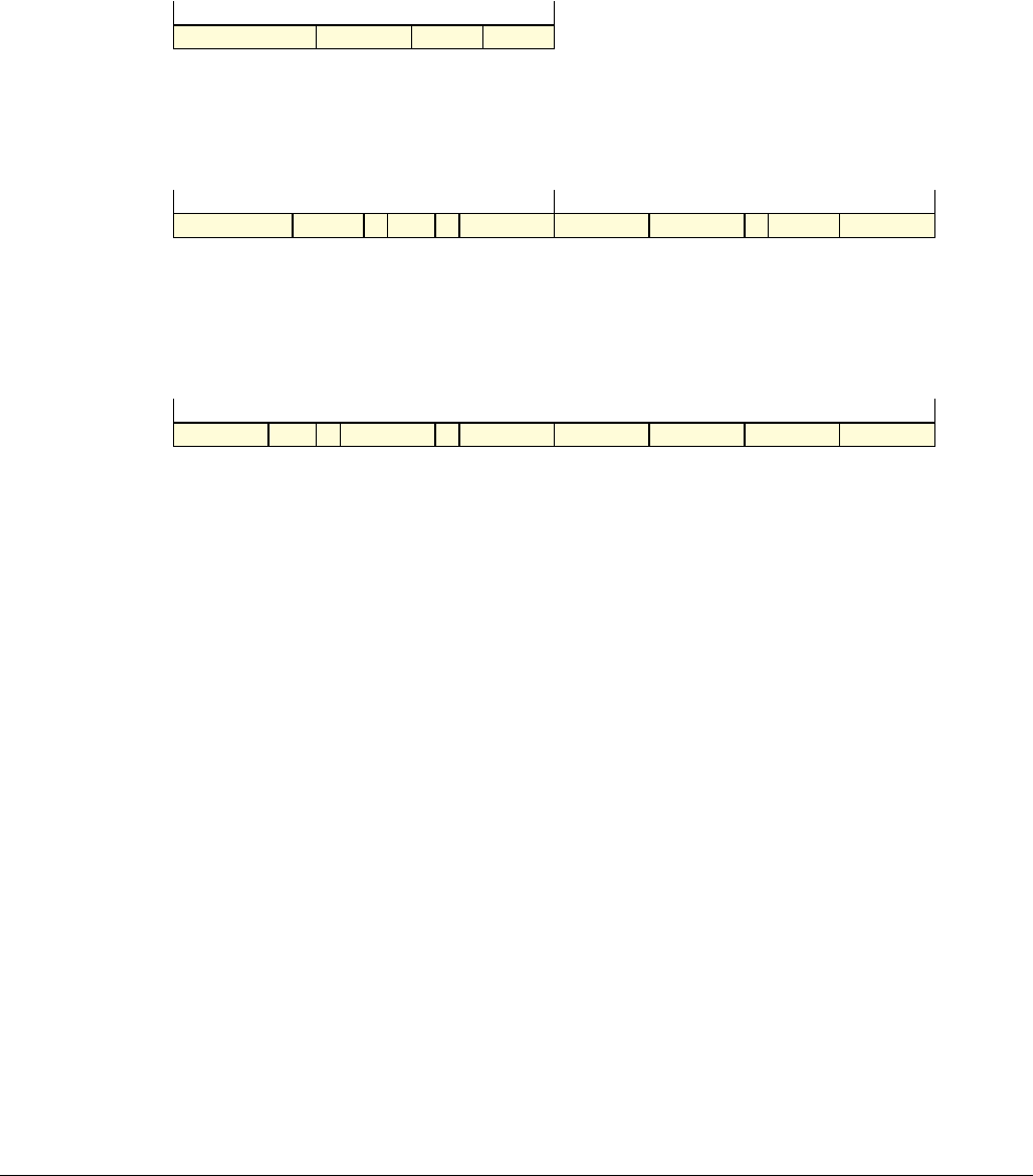
F7 T32 and A32 Base Instruction Set Instruction Descriptions
F7.1 Alphabetical list of T32 and A32 base instruction set instructions
F7-2694 Copyright © 2013 ARM Limited. All rights reserved. ARM DDI 0487A.a
Non-Confidential - Beta ID090413
F7.1.100 LSL (register)
Logical Shift Left (register) shifts a register value left by a variable number of bits, shifting in zeros, and writes the
result to the destination register. The variable number of bits is read from the bottom byte of a register. It can
optionally update the condition flags based on the result.
d = UInt(Rdn); n = UInt(Rdn); m = UInt(Rm); setflags = !InITBlock();
d = UInt(Rd); n = UInt(Rn); m = UInt(Rm); setflags = (S == ‘1’);
if d == 15 || n == 15 || m == 15 then UNPREDICTABLE; // ARMv8-A removes UNPREDICTABLE for R13
d = UInt(Rd); n = UInt(Rn); m = UInt(Rm); setflags = (S == ‘1’);
if d == 15 || n == 15 || m == 15 then UNPREDICTABLE;
For information about the CONSTRAINED UNPREDICTABLE behavior of this instruction, see Appendix A
Architectural Constraints on UNPREDICTABLE behaviors.
Encoding T1 ARMv4T, ARMv5T*, ARMv6*, ARMv7
LSLS <Rdn>, <Rm>
Outside IT block.
LSL<c> <Rdn>, <Rm>
Inside IT block.
Encoding T2 ARMv6T2, ARMv7
LSL{S}<c>.W <Rd>, <Rn>, <Rm>
Encoding A1 ARMv4*, ARMv5T*, ARMv6*, ARMv7
LSL{S}<c> <Rd>, <Rn>, <Rm>
0 1 0 0 0 0 0 0 1 0 Rm Rdn
15 14 13 12 11 10 9 8 7 6 5 4 3 2 1 0
1 1 1 1 0 1 0 0 0 0 S Rn 1 1 1 1 Rd 0 0 0 0 Rm
15 14 13 12 11 10 9 8 7 6 5 4 3 2 1 0
1
1514131211109876543210
cond 0 0 0 1 1 0 1 S (0) (0) (0) (0) Rd Rm 0 0 0 1 Rn
31 30 29 28 27 26 25 24 23 22 21 20 19 18 17 16 15 14 13 12 11 10 9 8 7 6 5 4 3 2 1 0

F7 T32 and A32 Base Instruction Set Instruction Descriptions
F7.1 Alphabetical list of T32 and A32 base instruction set instructions
ARM DDI 0487A.a Copyright © 2013 ARM Limited. All rights reserved. F7-2695
ID090413 Non-Confidential - Beta
Assembler syntax
LSL{S}{<c>}{<q>} {<Rd>,} <Rn>, <Rm>
where:
S
If
S
is present, the instruction updates the flags. Otherwise, the flags are not updated.
<c>, <q>
See Standard assembler syntax fields on page F2-2415.
<Rd>
The destination register.
<Rn>
The first operand register.
<Rm>
The register whose bottom byte contains the amount to shift by.
Operation
if ConditionPassed() then
EncodingSpecificOperations();
shift_n = UInt(R[m]<7:0>);
(result, carry) = Shift_C(R[n], SRType_LSL, shift_n, APSR.C);
R[d] = result;
if setflags then
APSR.N = result<31>;
APSR.Z = IsZeroBit(result);
APSR.C = carry;
// APSR.V unchanged

F7 T32 and A32 Base Instruction Set Instruction Descriptions
F7.1 Alphabetical list of T32 and A32 base instruction set instructions
F7-2696 Copyright © 2013 ARM Limited. All rights reserved. ARM DDI 0487A.a
Non-Confidential - Beta ID090413
F7.1.101 LSR (immediate)
Logical Shift Right (immediate) shifts a register value right by an immediate number of bits, shifting in zeros, and
writes the result to the destination register. It can optionally update the condition flags based on the result.
d = UInt(Rd); m = UInt(Rm); setflags = !InITBlock();
(-, shift_n) = DecodeImmShift(‘01’, imm5);
d = UInt(Rd); m = UInt(Rm); setflags = (S == ‘1’);
(-, shift_n) = DecodeImmShift(‘01’, imm3:imm2);
if d == 15 || m == 15 then UNPREDICTABLE; // ARMv8-A removes UNPREDICTABLE for R13
if Rd == ‘1111’ && S == ‘1’ then SEE SUBS PC, LR and related instructions;
d = UInt(Rd); m = UInt(Rm); setflags = (S == ‘1’);
(-, shift_n) = DecodeImmShift(‘01’, imm5);
For information about the CONSTRAINED UNPREDICTABLE behavior of this instruction, see Appendix A
Architectural Constraints on UNPREDICTABLE behaviors.
Encoding T1 ARMv4T, ARMv5T*, ARMv6*, ARMv7
LSRS <Rd>, <Rm>, #<imm>
Outside IT block.
LSR<c> <Rd>, <Rm>, #<imm>
Inside IT block.
Encoding T2 ARMv6T2, ARMv7
LSR{S}<c>.W <Rd>, <Rm>, #<imm>
Encoding A1 ARMv4*, ARMv5T*, ARMv6*, ARMv7
LSR{S}<c> <Rd>, <Rm>, #<imm>
0 0 0 0 1 imm5 Rm Rd
15 14 13 12 11 10 9 8 7 6 5 4 3 2 1 0
1 1 0 1 0 1 0 0 1 0 S 1 1 1 1 (0) imm3 Rd imm2 0 1 Rm
15 14 13 12 11 10 9 8 7 6 5 4 3 2 1 0
1
1514131211109876543210
cond 0 0 0 1 1 0 1 S (0) (0) (0) (0) Rd imm5 0 1 0 Rm
31 30 29 28 27 26 25 24 23 22 21 20 19 18 17 16 15 14 13 12 11 10 9 8 7 6 5 4 3 2 1 0

F7 T32 and A32 Base Instruction Set Instruction Descriptions
F7.1 Alphabetical list of T32 and A32 base instruction set instructions
ARM DDI 0487A.a Copyright © 2013 ARM Limited. All rights reserved. F7-2697
ID090413 Non-Confidential - Beta
Assembler syntax
LSR{S}{<c>}{<q>} {<Rd>,} <Rm>, #<imm>
where:
S
If
S
is present, the instruction updates the flags. Otherwise, the flags are not updated.
<c>, <q>
See Standard assembler syntax fields on page F2-2415.
<Rd>
The destination register.
In A32 instructions, if
S
is not specified and
<Rd>
is the PC, the instruction is a branch to the address
calculated by the operation. This is an interworking branch, see Pseudocode details of operations
on the AArch32 general-purpose registers and the PC on page E1-2296.
<Rm>
The first operand register. The PC can be used in A32 instructions.
<imm>
The shift amount, in the range 1 to 32. See Shifts applied to a register on page F2-2419.
Operation
if ConditionPassed() then
EncodingSpecificOperations();
(result, carry) = Shift_C(R[m], SRType_LSR, shift_n, APSR.C);
if d == 15 then // Can only occur for ARM encoding
ALUWritePC(result); // setflags is always FALSE here
else
R[d] = result;
if setflags then
APSR.N = result<31>;
APSR.Z = IsZeroBit(result);
APSR.C = carry;
// APSR.V unchanged

F7 T32 and A32 Base Instruction Set Instruction Descriptions
F7.1 Alphabetical list of T32 and A32 base instruction set instructions
F7-2698 Copyright © 2013 ARM Limited. All rights reserved. ARM DDI 0487A.a
Non-Confidential - Beta ID090413
F7.1.102 LSR (register)
Logical Shift Right (register) shifts a register value right by a variable number of bits, shifting in zeros, and writes
the result to the destination register. The variable number of bits is read from the bottom byte of a register. It can
optionally update the condition flags based on the result.
d = UInt(Rdn); n = UInt(Rdn); m = UInt(Rm); setflags = !InITBlock();
d = UInt(Rd); n = UInt(Rn); m = UInt(Rm); setflags = (S == ‘1’);
if d == 15 || n == 15 || m == 15 then UNPREDICTABLE; // ARMv8-A removes UNPREDICTABLE for R13
d = UInt(Rd); n = UInt(Rn); m = UInt(Rm); setflags = (S == ‘1’);
if d == 15 || n == 15 || m == 15 then UNPREDICTABLE;
For information about the CONSTRAINED UNPREDICTABLE behavior of this instruction, see Appendix A
Architectural Constraints on UNPREDICTABLE behaviors.
Encoding T1 ARMv4T, ARMv5T*, ARMv6*, ARMv7
LSRS <Rdn>, <Rm>
Outside IT block.
LSR<c> <Rdn>, <Rm>
Inside IT block.
Encoding T2 ARMv6T2, ARMv7
LSR{S}<c>.W <Rd>, <Rn>, <Rm>
Encoding A1 ARMv4*, ARMv5T*, ARMv6*, ARMv7
LSR{S}<c> <Rd>, <Rn>, <Rm>
0 1 0 0 0 0 0 0 1 1 Rm Rdn
15 14 13 12 11 10 9 8 7 6 5 4 3 2 1 0
1 1 1 1 0 1 0 0 0 1 S Rn 1 1 1 1 Rd 0 0 0 0 Rm
15 14 13 12 11 10 9 8 7 6 5 4 3 2 1 0
1
1514131211109876543210
(0)cond 0 0 0 1 1 0 1 S (0) (0) (0) Rd Rm 0 0 1 1 Rn
31 30 29 28 27 26 25 24 23 22 21 20 19 18 17 16 15 14 13 12 11 10 9 8 7 6 5 4 3 2 1 0

F7 T32 and A32 Base Instruction Set Instruction Descriptions
F7.1 Alphabetical list of T32 and A32 base instruction set instructions
ARM DDI 0487A.a Copyright © 2013 ARM Limited. All rights reserved. F7-2699
ID090413 Non-Confidential - Beta
Assembler syntax
LSR{S}{<c>}{<q>} {<Rd>,} <Rn>, <Rm>
where:
S
If
S
is present, the instruction updates the flags. Otherwise, the flags are not updated.
<c>, <q>
See Standard assembler syntax fields on page F2-2415.
<Rd>
The destination register.
<Rn>
The first operand register.
<Rm>
The register whose bottom byte contains the amount to shift by.
Operation
if ConditionPassed() then
EncodingSpecificOperations();
shift_n = UInt(R[m]<7:0>);
(result, carry) = Shift_C(R[n], SRType_LSR, shift_n, APSR.C);
R[d] = result;
if setflags then
APSR.N = result<31>;
APSR.Z = IsZeroBit(result);
APSR.C = carry;
// APSR.V unchanged
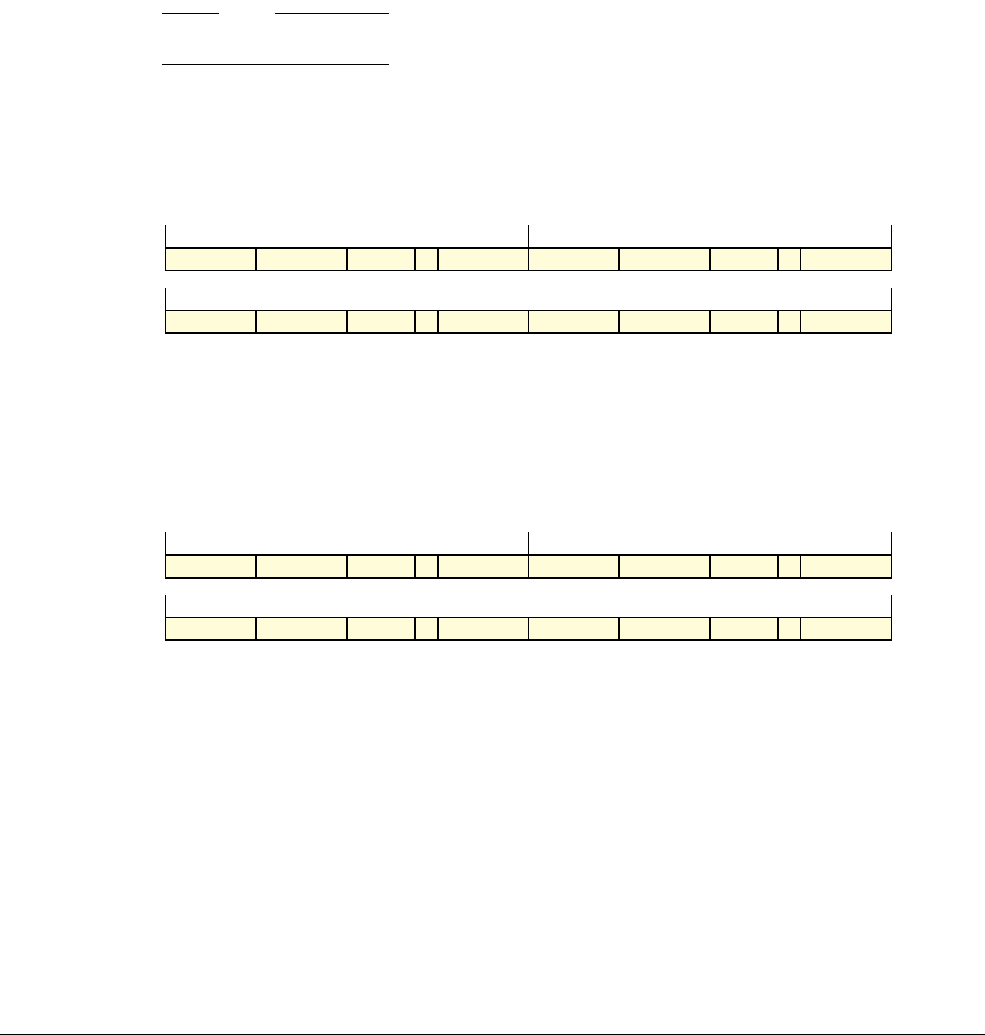
F7 T32 and A32 Base Instruction Set Instruction Descriptions
F7.1 Alphabetical list of T32 and A32 base instruction set instructions
F7-2700 Copyright © 2013 ARM Limited. All rights reserved. ARM DDI 0487A.a
Non-Confidential - Beta ID090413
F7.1.103 MCR, MCR2
Move to Coprocessor from general-purpose register passes the value of a general-purpose register to a coprocessor.
If no coprocessor can execute the instruction, an Undefined Instruction exception is generated.
This is a generic coprocessor instruction. Some of the fields have no functionality defined by the architecture and
are free for use by the coprocessor instruction set designer. These are the
opc1
,
opc2
,
CRn
, and
CRm
fields. However,
coprocessors CP8-CP15 are reserved for use by A32, and this manual defines the valid
MCR
and
MCR2
instructions
when
coproc
is in the range
p8
-
p15
. For more information see Coprocessor support on page E1-2331.
In an implementation that includes EL2,
MCR
accesses to system control registers can be trapped to Hyp mode,
meaning that an attempt to execute an
MCR
instruction in a Non-secure mode other than Hyp mode, that would be
permitted in the absence of the Hyp trap controls, generates a Hyp Trap exception. For more information, see
AArch32 control of traps to the hypervisor on page G1-3503.
Note
Because of the range of possible traps to Hyp mode, the
MCR
pseudocode does not show these possible traps.
if coproc == ‘101x’ then SEE “Advanced SIMD and Floating-point”;
t = UInt(Rt); cp = UInt(coproc);
if t == 15 then UNPREDICTABLE; // ARMv8-A removes UNPREDICTABLE for R13
if coproc == ‘101x’ then UNDEFINED;
t = UInt(Rt); cp = UInt(coproc);
if t == 15 then UNPREDICTABLE; // ARMv8-A removes UNPREDICTABLE for R13
For information about the CONSTRAINED UNPREDICTABLE behavior of this instruction, see Appendix A
Architectural Constraints on UNPREDICTABLE behaviors.
Encoding T1/A1 ARMv6T2, ARMv7 for encoding T1
ARMv4*, ARMv5T*, ARMv6*, ARMv7 for encoding A1
MCR<c> <coproc>, <opc1>, <Rt>, <CRn>, <CRm>{, <opc2>}
Encoding T2/A2 ARMv6T2, ARMv7 for encoding T2
ARMv5T*, ARMv6*, ARMv7 for encoding A2
MCR2<c> <coproc>, <opc1>, <Rt>, <CRn>, <CRm>{, <opc2>}
Advanced SIMD and
floating-point See 8, 16, and 32-bit transfer between general-purpose and extension registers
on page F5-2518
1 1 0 1 1 1 0 opc1 0 CRn Rt coproc opc2 1 CRm
15 14 13 12 11 10 9 8 7 6 5 4 3 2 1 0
1
1514131211109876543210
1 1 1 0 opc1 0 CRn Rt coproc opc2 1 CRmcond
31 30 29 28 27 26 25 24 23 22 21 20 19 18 17 16 15 14 13 12 11 10 9 8 7 6 5 4 3 2 1 0
1 1 1 1 1 1 0 opc1 0 CRn Rt coproc opc2 1 CRm
15 14 13 12 11 10 9 8 7 6 5 4 3 2 1 0
1
1514131211109876543210
1 1 1 1 1 1 1 0 opc1 0 CRn Rt coproc opc2 1 CRm
31 30 29 28 27 26 25 24 23 22 21 20 19 18 17 16 15 14 13 12 11 10 9 8 7 6 5 4 3 2 1 0

F7 T32 and A32 Base Instruction Set Instruction Descriptions
F7.1 Alphabetical list of T32 and A32 base instruction set instructions
ARM DDI 0487A.a Copyright © 2013 ARM Limited. All rights reserved. F7-2701
ID090413 Non-Confidential - Beta
Assembler syntax
MCR{2}{<c>}{<q>} <coproc>, {#}<opc1>, <Rt>, <CRn>, <CRm>{, {#}<opc2>}
where:
2
If specified, selects encoding T2/A2. If omitted, selects encoding T1/A1.
<c>, <q>
See Standard assembler syntax fields on page F2-2415. An A32
MCR2
instruction must be
unconditional.
<coproc>
The name of the coprocessor. The generic coprocessor names are p0-p15.
<opc1>
Is a coprocessor-specific opcode in the range 0 to 7.
<Rt>
Is the general-purpose register whose value is transferred to the coprocessor.
<CRn>
Is the destination coprocessor register.
<CRm>
Is an additional destination coprocessor register.
<opc2>
Is a coprocessor-specific opcode in the range 0-7. If omitted,
<opc2>
is assumed to be 0.
Operation
if ConditionPassed() then
EncodingSpecificOperations();
if !Coproc_Accepted(cp, ThisInstr()) then
GenerateCoprocessorException();
else
Coproc_SendOneWord(R[t], cp, ThisInstr());
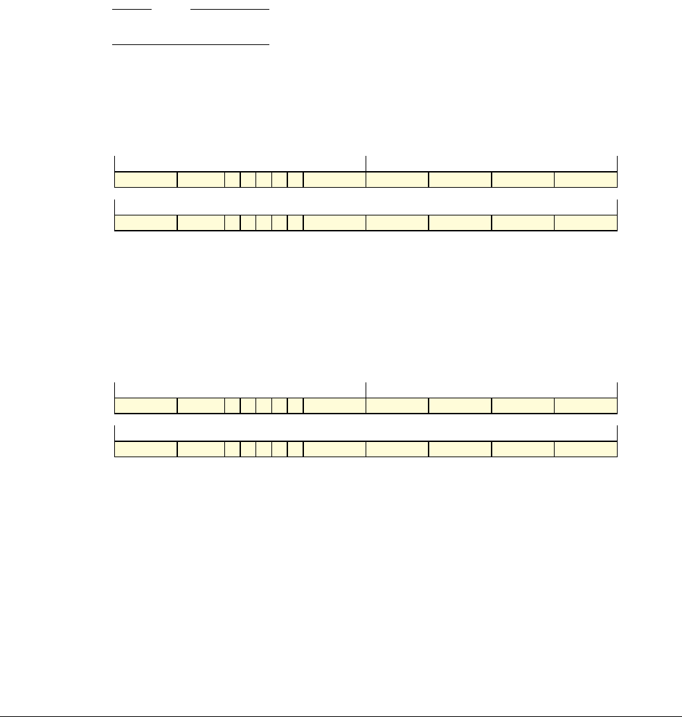
F7 T32 and A32 Base Instruction Set Instruction Descriptions
F7.1 Alphabetical list of T32 and A32 base instruction set instructions
F7-2702 Copyright © 2013 ARM Limited. All rights reserved. ARM DDI 0487A.a
Non-Confidential - Beta ID090413
F7.1.104 MCRR, MCRR2
Move to Coprocessor from two general-purpose registers passes the values of two general-purpose registers to a
coprocessor. If no coprocessor can execute the instruction, an Undefined Instruction exception is generated.
This is a generic coprocessor instruction. Some of the fields have no functionality defined by the architecture and
are free for use by the coprocessor instruction set designer. These are the
opc1
and
CRm
fields. However, coprocessors
CP8-CP15 are reserved for use by A32, and this manual defines the valid
MCRR
and
MCRR2
instructions when
coproc
is in the range
p8
-
p15
. For more information see Coprocessor support on page E1-2331.
In an implementation that includes EL2,
MCRR
accesses to system control registers can be trapped to Hyp mode,
meaning that an attempt to execute an
MCRR
instruction in a Non-secure mode other than Hyp mode, that would be
permitted in the absence of the Hyp trap controls, generates a Hyp Trap exception. For more information, see
AArch32 control of traps to the hypervisor on page G1-3503.
Note
Because of the range of possible traps to Hyp mode, the
MCRR
pseudocode does not show these possible traps.
if coproc == ‘101x’ then SEE “Advanced SIMD and Floating-point”;
t = UInt(Rt); t2 = UInt(Rt2); cp = UInt(coproc);
if t == 15 || t2 == 15 then UNPREDICTABLE;
// ARMv8-A removes UNPREDICTABLE for R13
if coproc == ‘101x’ then UNDEFINED;
t = UInt(Rt); t2 = UInt(Rt2); cp = UInt(coproc);
if t == 15 || t2 == 15 then UNPREDICTABLE;
// ARMv8-A removes UNPREDICTABLE for R13
For information about the CONSTRAINED UNPREDICTABLE behavior of this instruction, see Appendix A
Architectural Constraints on UNPREDICTABLE behaviors, and particularly MRRC, MRRC2 on
page AppxA-4720.
Encoding T1/A1 ARMv6T2, ARMv7 for encoding T1
ARMv5TE*, ARMv6*, ARMv7 for encoding A1
MCRR<c> <coproc>, <opc1>, <Rt>, <Rt2>, <CRm>
Encoding T2/A2 ARMv6T2, ARMv7 for encoding T2
ARMv6*, ARMv7 for encoding A2
MCRR2<c> <coproc>, <opc1>, <Rt>, <Rt2>, <CRm>
Advanced SIMD and
floating-point See 64-bit transfers between general-purpose and extension registers on
page F5-2519
1 1 0 1 1 0 0 0 1 0 0 Rt2 Rt coproc opc1 CRm
15 14 13 12 11 10 9 8 7 6 5 4 3 2 1 0
1
1514131211109876543210
1 1 0 0 0 1 0 0 Rt2 Rt coproc opc1 CRmcond
31 30 29 28 27 26 25 24 23 22 21 20 19 18 17 16 15 14 13 12 11 10 9 8 7 6 5 4 3 2 1 0
1 1 1 1 1 0 0 0 1 0 0 Rt2 Rt coproc opc1 CRm
15 14 13 12 11 10 9 8 7 6 5 4 3 2 1 0
1
1514131211109876543210
1 1 1 1 1 1 0 0 0 1 0 0 Rt2 Rt coproc opc1 CRm
31 30 29 28 27 26 25 24 23 22 21 20 19 18 17 16 15 14 13 12 11 10 9 8 7 6 5 4 3 2 1 0

F7 T32 and A32 Base Instruction Set Instruction Descriptions
F7.1 Alphabetical list of T32 and A32 base instruction set instructions
ARM DDI 0487A.a Copyright © 2013 ARM Limited. All rights reserved. F7-2703
ID090413 Non-Confidential - Beta
Assembler syntax
MCRR{2}{<c>}{<q>} <coproc>, {#}<opc1>, <Rt>, <Rt2>, <CRm>
where:
2
If specified, selects encoding T2/A2. If omitted, selects encoding T1/A1.
<c>, <q>
See Standard assembler syntax fields on page F2-2415. An A32
MCRR2
instruction must be
unconditional.
<coproc>
The name of the coprocessor.
The generic coprocessor names are p0-p15.
<opc1>
Is a coprocessor-specific opcode in the range 0 to 15.
<Rt>
Is the first general-purpose register whose value is transferred to the coprocessor.
<Rt2>
Is the second general-purpose register whose value is transferred to the coprocessor.
<CRm>
Is the destination coprocessor register.
Note
The relative significance of
Rt2
and
Rt
is IMPLEMENTATION DEFINED, but all uses within this manual treat
Rt2
as
more significant than
Rt
Operation
if ConditionPassed() then
EncodingSpecificOperations();
if !Coproc_Accepted(cp, ThisInstr()) then
GenerateCoprocessorException();
else
Coproc_SendTwoWords(R[t2], R[t], cp, ThisInstr());
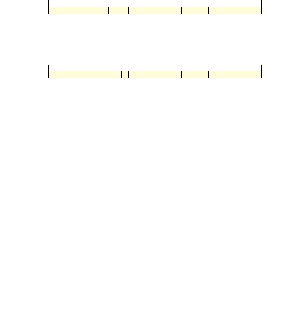
F7 T32 and A32 Base Instruction Set Instruction Descriptions
F7.1 Alphabetical list of T32 and A32 base instruction set instructions
F7-2704 Copyright © 2013 ARM Limited. All rights reserved. ARM DDI 0487A.a
Non-Confidential - Beta ID090413
F7.1.105 MLA
Multiply Accumulate multiplies two register values, and adds a third register value. The least significant 32 bits of
the result are written to the destination register. These 32 bits do not depend on whether the source register values
are considered to be signed values or unsigned values.
In an A32 instruction, the condition flags can optionally be updated based on the result. Use of this option adversely
affects performance on many implementations.
if Ra == ‘1111’ then SEE MUL;
d = UInt(Rd); n = UInt(Rn); m = UInt(Rm); a = UInt(Ra); setflags = FALSE;
if d == 15 || n == 15 || m == 15 then UNPREDICTABLE; // ARMv8-A removes UNPREDICTABLE for R13
d = UInt(Rd); n = UInt(Rn); m = UInt(Rm); a = UInt(Ra); setflags = (S == ‘1’);
if d == 15 || n == 15 || m == 15 || a == 15 then UNPREDICTABLE;
For information about the CONSTRAINED UNPREDICTABLE behavior of this instruction, see Appendix A
Architectural Constraints on UNPREDICTABLE behaviors.
Encoding T1 ARMv6T2, ARMv7
MLA<c> <Rd>, <Rn>, <Rm>, <Ra>
Encoding A1 ARMv4*, ARMv5T*, ARMv6*, ARMv7
MLA{S}<c> <Rd>, <Rn>, <Rm>, <Ra>
1 1 1 1 0 1 1 0 0 0 0 Rn Ra Rd 0 0 0 0 Rm
15 14 13 12 11 10 9 8 7 6 5 4 3 2 1 0
1
1514131211109876543210
cond 0 0 0 0 0 0 1 S Rd Ra Rm 1 0 0 1 Rn
31 30 29 28 27 26 25 24 23 22 21 20 19 18 17 16 15 14 13 12 11 10 9 8 7 6 5 4 3 2 1 0

F7 T32 and A32 Base Instruction Set Instruction Descriptions
F7.1 Alphabetical list of T32 and A32 base instruction set instructions
ARM DDI 0487A.a Copyright © 2013 ARM Limited. All rights reserved. F7-2705
ID090413 Non-Confidential - Beta
Assembler syntax
MLA{S}{<c>}{<q>} <Rd>, <Rn>, <Rm>, <Ra>
where:
S
If
S
is present, the instruction updates the flags. Otherwise, the flags are not updated.
S
can be specified only for the A32 instruction set.
<c>, <q>
See Standard assembler syntax fields on page F2-2415.
<Rd>
The destination register.
<Rn>
The first operand register.
<Rm>
The second operand register.
<Ra>
The register containing the accumulate value.
The pre-UAL syntax
MLA<c>S
is equivalent to
MLAS<c>
.
Operation
if ConditionPassed() then
EncodingSpecificOperations();
operand1 = SInt(R[n]); // operand1 = UInt(R[n]) produces the same final results
operand2 = SInt(R[m]); // operand2 = UInt(R[m]) produces the same final results
addend = SInt(R[a]); // addend = UInt(R[a]) produces the same final results
result = operand1 * operand2 + addend;
R[d] = result<31:0>;
if setflags then
APSR.N = result<31>;
APSR.Z = IsZeroBit(result<31:0>);
// APSR.C, APSR.V unchanged

F7 T32 and A32 Base Instruction Set Instruction Descriptions
F7.1 Alphabetical list of T32 and A32 base instruction set instructions
F7-2706 Copyright © 2013 ARM Limited. All rights reserved. ARM DDI 0487A.a
Non-Confidential - Beta ID090413
F7.1.106 MLS
Multiply and Subtract multiplies two register values, and subtracts the product from a third register value. The least
significant 32 bits of the result are written to the destination register. These 32 bits do not depend on whether the
source register values are considered to be signed values or unsigned values.
d = UInt(Rd); n = UInt(Rn); m = UInt(Rm); a = UInt(Ra);
if d == 15 || n == 15 || m == 15 || a == 15 then UNPREDICTABLE;
// ARMv8-A removes UNPREDICTABLE for R13
d = UInt(Rd); n = UInt(Rn); m = UInt(Rm); a = UInt(Ra);
if d == 15 || n == 15 || m == 15 || a == 15 then UNPREDICTABLE;
For information about the CONSTRAINED UNPREDICTABLE behavior of this instruction, see Appendix A
Architectural Constraints on UNPREDICTABLE behaviors.
Encoding T1 ARMv6T2, ARMv7
MLS<c> <Rd>, <Rn>, <Rm>, <Ra>
Encoding A1 ARMv6T2, ARMv7
MLS<c> <Rd>, <Rn>, <Rm>, <Ra>
1 1 1 1 0 1 1 0 0 0 0 Rn Ra Rd 0 0 0 1 Rm
15 14 13 12 11 10 9 8 7 6 5 4 3 2 1 0
1
1514131211109876543210
cond 0 0 0 0 0 1 1 0 Rd Ra Rm 1 0 0 1 Rn
31 30 29 28 27 26 25 24 23 22 21 20 19 18 17 16 15 14 13 12 11 10 9 8 7 6 5 4 3 2 1 0

F7 T32 and A32 Base Instruction Set Instruction Descriptions
F7.1 Alphabetical list of T32 and A32 base instruction set instructions
ARM DDI 0487A.a Copyright © 2013 ARM Limited. All rights reserved. F7-2707
ID090413 Non-Confidential - Beta
Assembler syntax
MLS{<c>}{<q>} <Rd>, <Rn>, <Rm>, <Ra>
where:
<c>, <q>
See Standard assembler syntax fields on page F2-2415.
<Rd>
The destination register.
<Rn>
The first operand register.
<Rm>
The second operand register.
<Ra>
The register containing the accumulate value.
Operation
if ConditionPassed() then
EncodingSpecificOperations();
operand1 = SInt(R[n]); // operand1 = UInt(R[n]) produces the same final results
operand2 = SInt(R[m]); // operand2 = UInt(R[m]) produces the same final results
addend = SInt(R[a]); // addend = UInt(R[a]) produces the same final results
result = addend - operand1 * operand2;
R[d] = result<31:0>;
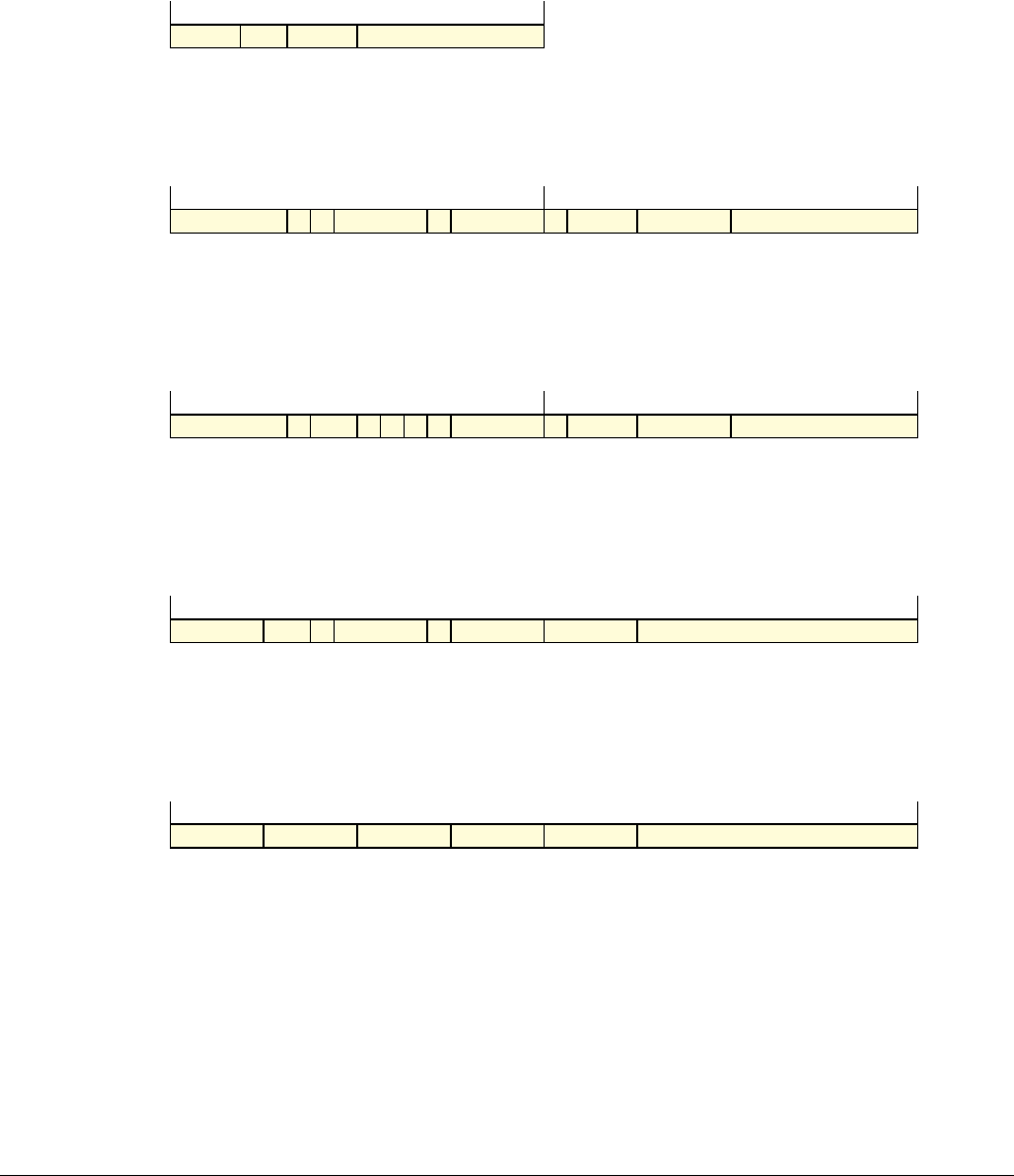
F7 T32 and A32 Base Instruction Set Instruction Descriptions
F7.1 Alphabetical list of T32 and A32 base instruction set instructions
F7-2708 Copyright © 2013 ARM Limited. All rights reserved. ARM DDI 0487A.a
Non-Confidential - Beta ID090413
F7.1.107 MOV (immediate)
Move (immediate) writes an immediate value to the destination register. It can optionally update the condition flags
based on the value.
d = UInt(Rd); setflags = !InITBlock(); imm32 = ZeroExtend(imm8, 32); carry = APSR.C;
d = UInt(Rd); setflags = (S == ‘1’); (imm32, carry) = ThumbExpandImm_C(i:imm3:imm8, APSR.C);
if d == 15 then UNPREDICTABLE; // ARMv8-A removes UNPREDICTABLE for R13
d = UInt(Rd); setflags = FALSE; imm32 = ZeroExtend(imm4:i:imm3:imm8, 32);
if d == 15 then UNPREDICTABLE; // ARMv8-A removes UNPREDICTABLE for R13
if Rd == ‘1111’ && S == ‘1’ then SEE SUBS PC, LR and related instructions;
d = UInt(Rd); setflags = (S == ‘1’); (imm32, carry) = ARMExpandImm_C(imm12, APSR.C);
d = UInt(Rd); setflags = FALSE; imm32 = ZeroExtend(imm4:imm12, 32);
if d == 15 then UNPREDICTABLE;
For information about the CONSTRAINED UNPREDICTABLE behavior of this instruction, see Appendix A
Architectural Constraints on UNPREDICTABLE behaviors.
Encoding T1 ARMv4T, ARMv5T*, ARMv6*, ARMv7
MOVS <Rd>, #<imm8>
Outside IT block.
MOV<c> <Rd>, #<imm8>
Inside IT block.
Encoding T2 ARMv6T2, ARMv7
MOV{S}<c>.W <Rd>, #<const>
Encoding T3 ARMv6T2, ARMv7
MOVW<c> <Rd>, #<imm16>
Encoding A1 ARMv4*, ARMv5T*, ARMv6*, ARMv7
MOV{S}<c> <Rd>, #<const>
Encoding A2 ARMv6T2, ARMv7
MOVW<c> <Rd>, #<imm16>
0 0 1 0 0 Rd imm8
15 14 13 12 11 10 9 8 7 6 5 4 3 2 1 0
1 1 1 0 i 0 0 0 1 0 S 1 1 1 1 0 imm3 Rd imm8
15 14 13 12 11 10 9 8 7 6 5 4 3 2 1 0
1
1514131211109876543210
1 1 1 0 i 1 0 0 1 0 0 imm4 0 imm3 Rd imm8
15 14 13 12 11 10 9 8 7 6 5 4 3 2 1 0
1
1514131211109876543210
cond 0 0 1 1 1 0 1 S (0) (0) (0) (0) Rd imm12
31 30 29 28 27 26 25 24 23 22 21 20 19 18 17 16 15 14 13 12 11 10 9 8 7 6 5 4 3 2 1 0
cond 0 0 1 1 0 0 0 0 imm4 Rd imm12
31 30 29 28 27 26 25 24 23 22 21 20 19 18 17 16 15 14 13 12 11 10 9 8 7 6 5 4 3 2 1 0

F7 T32 and A32 Base Instruction Set Instruction Descriptions
F7.1 Alphabetical list of T32 and A32 base instruction set instructions
ARM DDI 0487A.a Copyright © 2013 ARM Limited. All rights reserved. F7-2709
ID090413 Non-Confidential - Beta
Assembler syntax
where:
S
If
S
is present, the instruction updates the flags. Otherwise, the flags are not updated.
<c>, <q>
See Standard assembler syntax fields on page F2-2415.
<Rd>
The destination register. If
S
is specified and
<Rd>
is the PC, see SUBS PC, LR and related
instructions (T32) on page F7-3066 or SUBS PC, LR and related instructions (A32) on
page F7-3068.
In A32 instructions, if
S
is not specified and
<Rd>
is the PC, encoding A2 is not permitted, and for
encoding A1 the instruction is a branch to the address calculated by the operation. This is an
interworking branch, see Pseudocode details of operations on the AArch32 general-purpose
registers and the PC on page E1-2296.
<const>
The immediate value to be placed in
<Rd>
. The range of values is 0-255 for encoding T1 and 0-65535
for encoding T3 or A2. See Modified immediate constants in T32 instructions on page F3-2444 or
Modified immediate constants in A32 instructions on page F4-2472 for the range of values for
encoding T2 or A1.
When both 32-bit encodings are available for an instruction, encoding T2 or A1 is preferred to
encoding T3 or A2 (if encoding T3 or A2 is required, use the
MOVW
syntax).
The pre-UAL syntax
MOV<c>S
is equivalent to
MOVS<c>
.
Operation
if ConditionPassed() then
EncodingSpecificOperations();
result = imm32;
if d == 15 then // Can only occur for encoding A1
ALUWritePC(result); // setflags is always FALSE here
else
R[d] = result;
if setflags then
APSR.N = result<31>;
APSR.Z = IsZeroBit(result);
APSR.C = carry;
// APSR.V unchanged
MOV{S}{<c>}{<q>} <Rd>, #<const>
All encodings permitted
MOVW{<c>}{<q>} <Rd>, #<const>
Only encoding T3 or A2 permitted
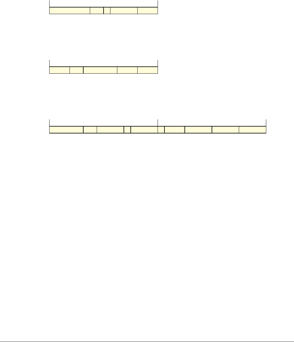
F7 T32 and A32 Base Instruction Set Instruction Descriptions
F7.1 Alphabetical list of T32 and A32 base instruction set instructions
F7-2710 Copyright © 2013 ARM Limited. All rights reserved. ARM DDI 0487A.a
Non-Confidential - Beta ID090413
F7.1.108 MOV (register, T32)
Move (register) copies a value from a register to the destination register. It can optionally update the condition flags
based on the value.
d = UInt(D:Rd); m = UInt(Rm); setflags = FALSE;
if d == 15 && InITBlock() && !LastInITBlock() then UNPREDICTABLE;
d = UInt(Rd); m = UInt(Rm); setflags = TRUE;
if InITBlock() then UNPREDICTABLE;
d = UInt(Rd); m = UInt(Rm); setflags = (S == ‘1’);
if d == 15 || m == 15 then UNPREDICTABLE; // ARMv8-A removes UNPREDICTABLE for R13
For information about the CONSTRAINED UNPREDICTABLE behavior of this instruction, see Appendix A
Architectural Constraints on UNPREDICTABLE behaviors, and particularly MOV (register, T32) on
page AppxA-4719.
Encoding T1 ARMv6*, ARMv7 if
<Rd>
and
<Rm>
both from R0-R7
ARMv4T, ARMv5T*, ARMv6*, ARMv7 otherwise
MOV<c> <Rd>, <Rm>
If
<Rd>
is the PC, must be outside or last in IT block.
Encoding T2 ARMv4T, ARMv5T*, ARMv6*, ARMv7
MOVS <Rd>, <Rm>
Not permitted in IT block
Encoding T3 ARMv6T2, ARMv7
MOV{S}<c>.W <Rd>, <Rm>
0 1 0 0 0 1 1 0 D Rm Rd
15 14 13 12 11 10 9 8 7 6 5 4 3 2 1 0
0 0 0 0 0 0 0 0 0 0 Rm Rd
15 14 13 12 11 10 9 8 7 6 5 4 3 2 1 0
1 1 0 1 0 1 0 0 1 0 S 1 1 1 1 (0) 0 0 0 Rd 0 0 0 0 Rm
15 14 13 12 11 10 9 8 7 6 5 4 3 2 1 0
1
1514131211109876543210

F7 T32 and A32 Base Instruction Set Instruction Descriptions
F7.1 Alphabetical list of T32 and A32 base instruction set instructions
ARM DDI 0487A.a Copyright © 2013 ARM Limited. All rights reserved. F7-2711
ID090413 Non-Confidential - Beta
Assembler syntax
MOV{S}{<c>}{<q>} <Rd>, <Rm>
where:
S
If
S
is present, the instruction updates the flags. Otherwise, the flags are not updated.
<c>, <q>
See Standard assembler syntax fields on page F2-2415.
<Rd>
The destination register. This register can be the SP or PC.
S
must not be specified if
<Rd>
is the SP.
If
<Rd>
is the PC and
S
is not specified:
• The instruction causes a branch to the address moved to the PC. This is a simple branch, see
Pseudocode details of operations on the AArch32 general-purpose registers and the PC on
page E1-2296.
• The instruction must either be outside an IT block or the last instruction of an IT block.
<Rm>
The source register. This register can be the SP or PC.
S
must not be specified if
<Rm>
is the SP or PC.
Encoding T3 is not permitted if
<Rd>
or
<Rm>
is the PC.
Note
• ARM deprecates the use of the following
MOV
(register) instructions:
— Ones in which
<Rd>
is the SP or PC and
<Rm>
is also the SP or PC.
— Ones in which
S
is specified and
<Rm>
is the SP, or
<Rm>
is the PC.
•See also Branch instructions on page F1-2382 about the use of the
MOV PC, LR
instruction.
The pre-UAL syntax
MOV<c>S
is equivalent to
MOVS<c>
.
Operation
if ConditionPassed() then
EncodingSpecificOperations();
result = R[m];
if d == 15 then
ALUWritePC(result); // setflags is always FALSE here
else
R[d] = result;
if setflags then
APSR.N = result<31>;
APSR.Z = IsZeroBit(result);
// APSR.C unchanged
// APSR.V unchanged

F7 T32 and A32 Base Instruction Set Instruction Descriptions
F7.1 Alphabetical list of T32 and A32 base instruction set instructions
F7-2712 Copyright © 2013 ARM Limited. All rights reserved. ARM DDI 0487A.a
Non-Confidential - Beta ID090413
F7.1.109 MOV (register, A32)
Move (register) copies a value from a register to the destination register. It can optionally update the condition flags
based on the value.
if Rd == ‘1111’ && S == ‘1’ then SEE SUBS PC, LR and related instructions;
d = UInt(Rd); m = UInt(Rm); setflags = (S == ‘1’);
For information about the CONSTRAINED UNPREDICTABLE behavior of this instruction, see Appendix A
Architectural Constraints on UNPREDICTABLE behaviors.
Assembler syntax
MOV{S}{<c>}{<q>} <Rd>, <Rm>
where:
S
If
S
is present, the instruction updates the flags. Otherwise, the flags are not updated.
<c>, <q>
See Standard assembler syntax fields on page F2-2415.
<Rd>
The destination register. If
S
is specified and
<Rd>
is the PC, see SUBS PC, LR and related
instructions (A32) on page F7-3068. This register can be the SP or PC.
If
<Rd>
is the PC and
S
is not specified, the instruction causes a branch to the address moved to the
PC. This is an interworking branch, see Pseudocode details of operations on the AArch32
general-purpose registers and the PC on page E1-2296.
<Rm>
The source register. This register can be the SP or PC.
Note
• ARM deprecates the use of the following
MOV
(register) instructions:
— Ones in which
<Rd>
is the SP or PC and
<Rm>
is also the SP or PC.
— Ones in which
S
is specified and
<Rd>
is the SP,
<Rm>
is the SP, or
<Rm>
is the PC.
•See also Branch instructions on page F1-2382 about the use of the
MOV PC, LR
instruction.
The pre-UAL syntax
MOV<c>S
is equivalent to
MOVS<c>
.
Operation
if ConditionPassed() then
EncodingSpecificOperations();
result = R[m];
if d == 15 then
ALUWritePC(result); // setflags is always FALSE here
else
R[d] = result;
if setflags then
APSR.N = result<31>;
APSR.Z = IsZeroBit(result);
// APSR.C unchanged
// APSR.V unchanged
Encoding A1 ARMv4*, ARMv5T*, ARMv6*, ARMv7
MOV{S}<c> <Rd>, <Rm>
cond 0 0 0 1 1 0 1 S (0) (0) (0) (0) Rd 0 0 0 0 0 0 0 0 Rm
31 30 29 28 27 26 25 24 23 22 21 20 19 18 17 16 15 14 13 12 11 10 9 8 7 6 5 4 3 2 1 0

F7 T32 and A32 Base Instruction Set Instruction Descriptions
F7.1 Alphabetical list of T32 and A32 base instruction set instructions
ARM DDI 0487A.a Copyright © 2013 ARM Limited. All rights reserved. F7-2713
ID090413 Non-Confidential - Beta
F7.1.110 MOV (shifted register)
For the special case of
MOVS
where
<Rd>
is the PC, see SUBS PC, LR and related instructions (T32) on page F7-3066
and SUBS PC, LR and related instructions (A32) on page F7-3068. Otherwise,
MOV
(shifted register) is a
pseudo-instruction for
ASR
,
LSL
,
LSR
,
ROR
, and
RRX
. For more information see the following sections:
•ASR (immediate) on page F7-2562.
•ASR (register) on page F7-2564.
•LSL (immediate) on page F7-2692.
•LSL (register) on page F7-2694.
•LSR (immediate) on page F7-2696.
•LSR (register) on page F7-2698.
•ROR (immediate) on page F7-2776.
•ROR (register) on page F7-2778.
•RRX on page F7-2780.
Assembler syntax
Table F7-2 shows the equivalences between
MOV
(shifted register) and other instructions.
Disassembly produces the canonical form of the instruction.
Table F7-2 MOV (shifted register) equivalences
MOV instruction Canonical form
MOV{S} <Rd>, <Rm>, ASR #<n> ASR{S} <Rd>, <Rm>, #<n>
MOV{S} <Rd>, <Rm>, LSL #<n> LSL{S} <Rd>, <Rm>, #<n>
MOV{S} <Rd>, <Rm>, LSR #<n> LSR{S} <Rd>, <Rm>, #<n>
MOV{S} <Rd>, <Rm>, ROR #<n> ROR{S} <Rd>, <Rm>, #<n>
MOV{S} <Rd>, <Rm>, ASR <Rs> ASR{S} <Rd>, <Rm>, <Rs>
MOV{S} <Rd>, <Rm>, LSL <Rs> LSL{S} <Rd>, <Rm>, <Rs>
MOV{S} <Rd>, <Rm>, LSR <Rs> LSR{S} <Rd>, <Rm>, <Rs>
MOV{S} <Rd>, <Rm>, ROR <Rs> ROR{S} <Rd>, <Rm>, <Rs>
MOV{S} <Rd>, <Rm>, RRX RRX{S} <Rd>, <Rm>

F7 T32 and A32 Base Instruction Set Instruction Descriptions
F7.1 Alphabetical list of T32 and A32 base instruction set instructions
F7-2714 Copyright © 2013 ARM Limited. All rights reserved. ARM DDI 0487A.a
Non-Confidential - Beta ID090413
F7.1.111 MOVT
Move Top writes an immediate value to the top halfword of the destination register. It does not affect the contents
of the bottom halfword.
d = UInt(Rd); imm16 = imm4:i:imm3:imm8;
if d == 15 then UNPREDICTABLE; // ARMv8-A removes UNPREDICTABLE for R13
d = UInt(Rd); imm16 = imm4:imm12;
if d == 15 then UNPREDICTABLE;
For information about the CONSTRAINED UNPREDICTABLE behavior of this instruction, see Appendix A
Architectural Constraints on UNPREDICTABLE behaviors.
Encoding T1 ARMv6T2, ARMv7
MOVT<c> <Rd>, #<imm16>
Encoding A1 ARMv6T2, ARMv7
MOVT<c> <Rd>, #<imm16>
1 1 1 0 i 1 0 1 1 0 0 imm4 0 imm3 Rd imm8
15 14 13 12 11 10 9 8 7 6 5 4 3 2 1 0
1
1514131211109876543210
cond 0 0 1 1 0 1 0 0 imm4 Rd imm12
31 30 29 28 27 26 25 24 23 22 21 20 19 18 17 16 15 14 13 12 11 10 9 8 7 6 5 4 3 2 1 0

F7 T32 and A32 Base Instruction Set Instruction Descriptions
F7.1 Alphabetical list of T32 and A32 base instruction set instructions
ARM DDI 0487A.a Copyright © 2013 ARM Limited. All rights reserved. F7-2715
ID090413 Non-Confidential - Beta
Assembler syntax
MOVT{<c>}{<q>} <Rd>, #<imm16>
where:
<c>, <q>
See Standard assembler syntax fields on page F2-2415.
<Rd>
The destination register.
<imm16>
The immediate value to be written to
<Rd>
. It must be in the range 0-65535.
Operation
if ConditionPassed() then
EncodingSpecificOperations();
R[d]<31:16> = imm16;
// R[d]<15:0> unchanged
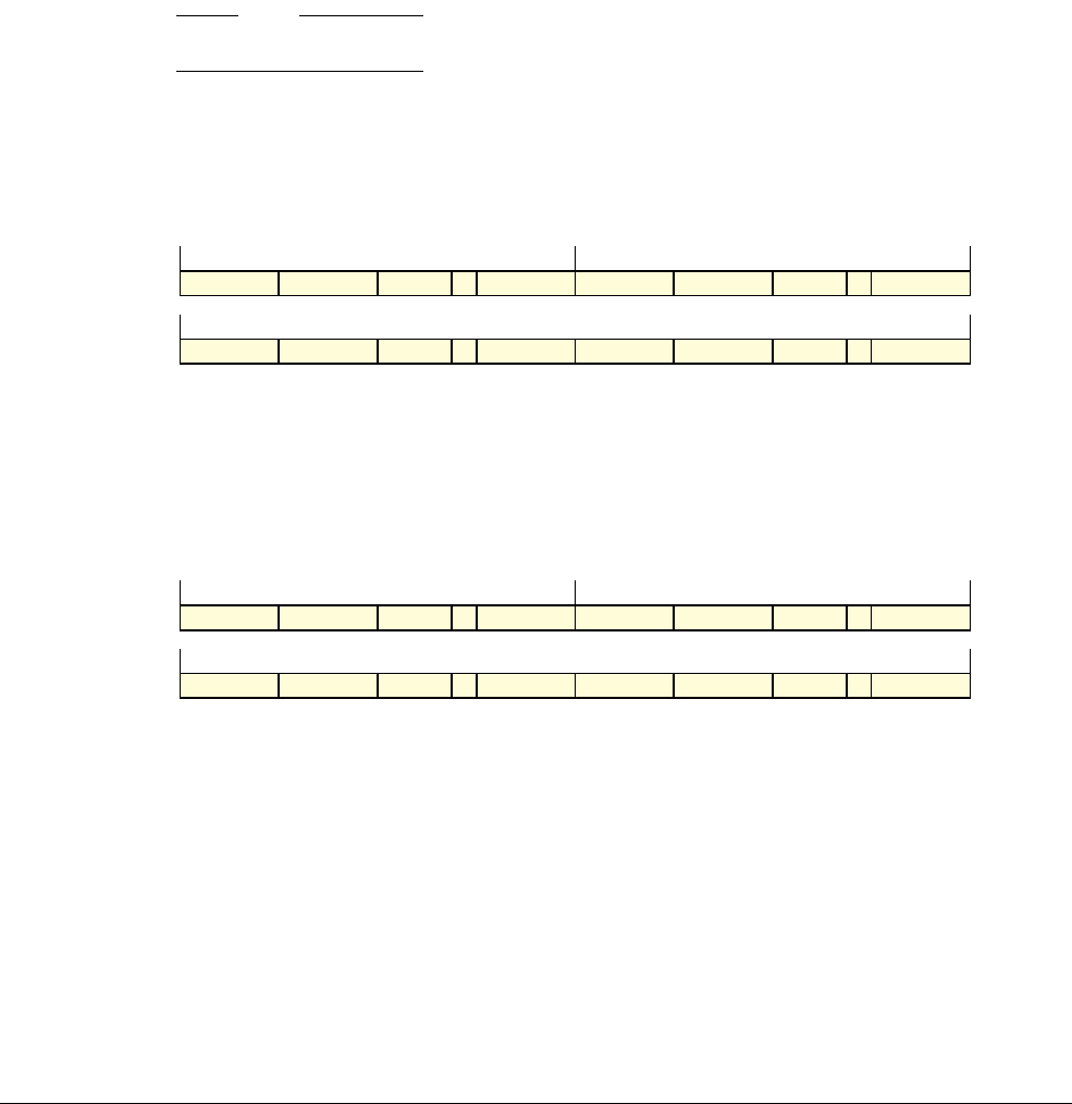
F7 T32 and A32 Base Instruction Set Instruction Descriptions
F7.1 Alphabetical list of T32 and A32 base instruction set instructions
F7-2716 Copyright © 2013 ARM Limited. All rights reserved. ARM DDI 0487A.a
Non-Confidential - Beta ID090413
F7.1.112 MRC, MRC2
Move to general-purpose register from Coprocessor causes a coprocessor to transfer a value to a general-purpose
register or to the condition flags. If no coprocessor can execute the instruction, an Undefined Instruction exception
is generated.
This is a generic coprocessor instruction. Some of the fields have no functionality defined by the architecture and
are free for use by the coprocessor instruction set designer. These are the
opc1
,
opc2
,
CRn
, and
CRm
fields. However,
coprocessors CP8-CP15 are reserved for use by A32, and this manual defines the valid
MRC
and
MRC2
instructions
when
coproc
is in the range
p8
-
p15
. For more information see Coprocessor support on page E1-2331.
In an implementation that includes EL2,
MRC
accesses to system control registers can be trapped to Hyp mode,
meaning that an attempt to execute an
MRC
instruction in a Non-secure mode other than Hyp mode, that would be
permitted in the absence of the Hyp trap controls, generates a Hyp Trap exception. For more information, see
AArch32 control of traps to the hypervisor on page G1-3503.
Note
Because of the range of possible traps to Hyp mode, the
MRC
pseudocode does not show these possible traps.
if coproc == ‘101x’ then SEE “Advanced SIMD and Floating-point”;
t = UInt(Rt); cp = UInt(coproc);
// ARMv8-A removes UNPREDICTABLE for R13
if coproc == ‘101x’ then UNDEFINED;
t = UInt(Rt); cp = UInt(coproc);
// ARMv8-A removes UNPREDICTABLE for R13
For information about the CONSTRAINED UNPREDICTABLE behavior of this instruction, see Appendix A
Architectural Constraints on UNPREDICTABLE behaviors.
Encoding T1/A1 ARMv6T2, ARMv7 for encoding T1
ARMv4*, ARMv5T*, ARMv6*, ARMv7 for encoding A1
MRC<c> <coproc>, <opc1>, <Rt>, <CRn>, <CRm>{, <opc2>}
Encoding T2/A2 ARMv6T2, ARMv7 for encoding T2
ARMv5T*, ARMv6*, ARMv7 for encoding A2
MRC2<c> <coproc>, <opc1>, <Rt>, <CRn>, <CRm>{, <opc2>}
Advanced SIMD and
floating-point See 8, 16, and 32-bit transfer between general-purpose and extension registers
on page F5-2518
1 1 0 1 1 1 0 opc1 1 CRn Rt coproc opc2 1 CRm
15 14 13 12 11 10 9 8 7 6 5 4 3 2 1 0
1
1514131211109876543210
cond 1 1 1 0 opc1 1 CRn Rt coproc opc2 1 CRm
31 30 29 28 27 26 25 24 23 22 21 20 19 18 17 16 15 14 13 12 11 10 9 8 7 6 5 4 3 2 1 0
1 1 1 1 1 1 0 opc1 1 CRn Rt coproc opc2 1 CRm
15 14 13 12 11 10 9 8 7 6 5 4 3 2 1 0
1
1514131211109876543210
1 1 1 1 1 1 0 opc1 1 CRn Rt coproc opc2 1 CRm
31 30 29 28 27 26 25 24 23 22 21 20 19 18 17 16 15 14 13 12 11 10 9 8 7 6 5 4 3 2 1 0
1

F7 T32 and A32 Base Instruction Set Instruction Descriptions
F7.1 Alphabetical list of T32 and A32 base instruction set instructions
ARM DDI 0487A.a Copyright © 2013 ARM Limited. All rights reserved. F7-2717
ID090413 Non-Confidential - Beta
Assembler syntax
MRC{2}{<c>}{<q>} <coproc>, {#}<opc1>, <Rt>, <CRn>, <CRm>{, {#}<opc2>}
where:
2
If specified, selects encoding T2/A2. If omitted, selects encoding T1/A1.
<c>, <q>
See Standard assembler syntax fields on page F2-2415. An A32
MRC2
instruction must be
unconditional.
<coproc>
The name of the coprocessor. The generic coprocessor names are p0-p15.
<opc1>
Is a coprocessor-specific opcode in the range 0 to 7.
<Rt>
Is the destination general-purpose register. This register can be R0-R14 or APSR_nzcv. The last
form writes bits[31:28] of the transferred value to the N, Z, C and V condition flags and is specified
by setting the Rt field of the encoding to
0b1111
. In pre-UAL assembler syntax, PC was written
instead of APSR_nzcv to select this form.
<CRn>
Is the coprocessor register that contains the first operand.
<CRm>
Is an additional source or destination coprocessor register.
<opc2>
Is a coprocessor-specific opcode in the range 0 to 7. If omitted,
<opc2>
is assumed to be 0.
Operation
if ConditionPassed() then
EncodingSpecificOperations();
if !Coproc_Accepted(cp, ThisInstr()) then
GenerateCoprocessorException();
else
value = Coproc_GetOneWord(cp, ThisInstr());
if t != 15 then
R[t] = value;
else
APSR.N = value<31>;
APSR.Z = value<30>;
APSR.C = value<29>;
APSR.V = value<28>;
// value<27:0> are not used.
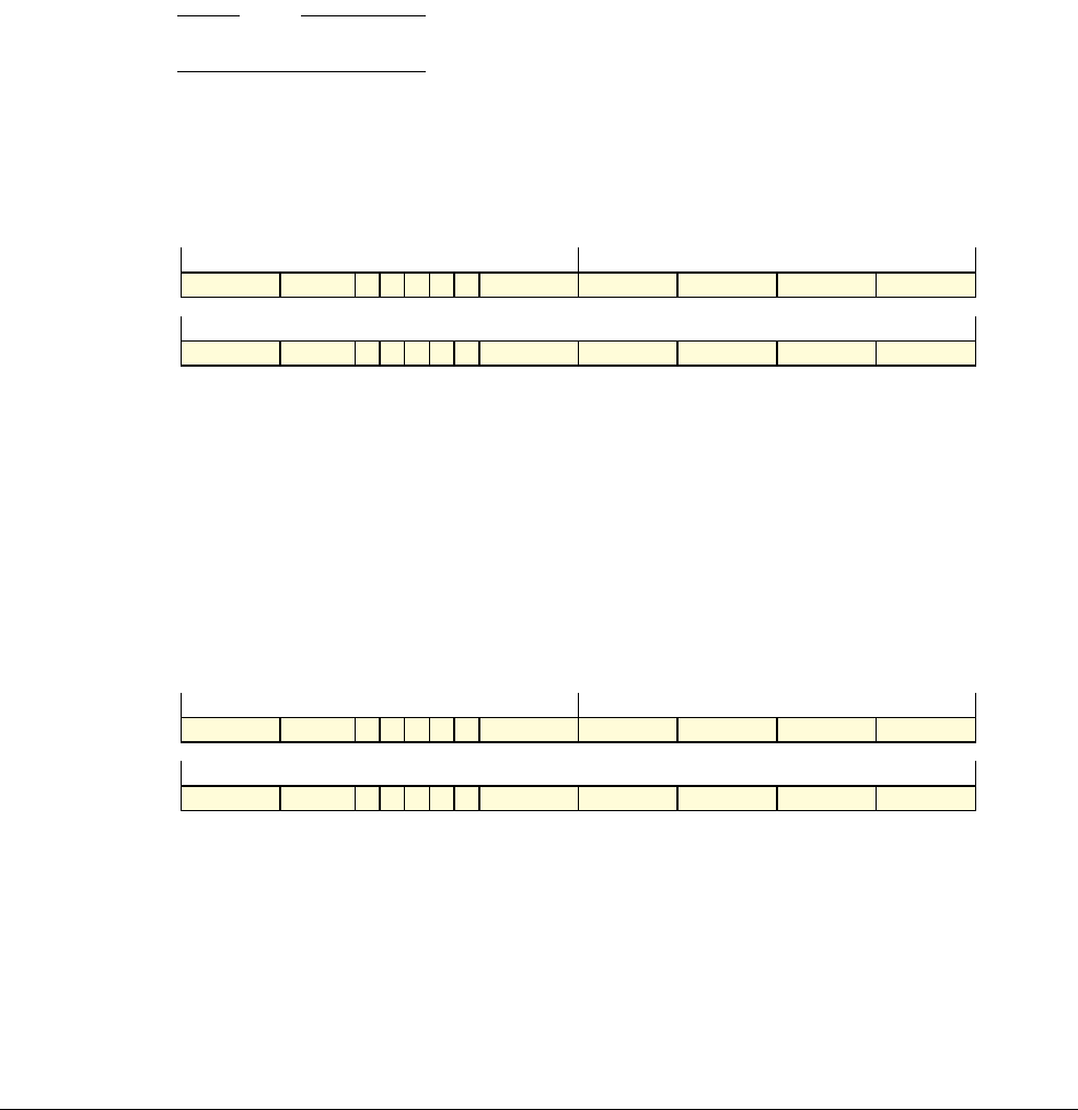
F7 T32 and A32 Base Instruction Set Instruction Descriptions
F7.1 Alphabetical list of T32 and A32 base instruction set instructions
F7-2718 Copyright © 2013 ARM Limited. All rights reserved. ARM DDI 0487A.a
Non-Confidential - Beta ID090413
F7.1.113 MRRC, MRRC2
Move to two general-purpose registers from Coprocessor causes a coprocessor to transfer values to two
general-purpose registers. If no coprocessor can execute the instruction, an Undefined Instruction exception is
generated.
This is a generic coprocessor instruction. Some of the fields have no functionality defined by the architecture and
are free for use by the coprocessor instruction set designer. These are the
opc1
and
CRm
fields. However, coprocessors
CP8-CP15 are reserved for use by A32, and this manual defines the valid
MRRC
and
MRRC2
instructions when
coproc
is in the range
p8
-
p15
. For more information see Coprocessor support on page E1-2331.
In an implementation that includes EL2,
MRRC
accesses to system control registers can be trapped to Hyp mode,
meaning that an attempt to execute an
MRRC
instruction in a Non-secure mode other than Hyp mode, that would be
permitted in the absence of the Hyp trap controls, generates a Hyp Trap exception. For more information, see
AArch32 control of traps to the hypervisor on page G1-3503.
Note
Because of the range of possible traps to Hyp mode, the
MRRC
pseudocode does not show these possible traps.
if coproc == ‘101x’ then SEE “Advanced SIMD and Floating-point”;
t = UInt(Rt); t2 = UInt(Rt2); cp = UInt(coproc);
if t == 15 || t2 == 15 || t == t2 then UNPREDICTABLE; // ARMv8-A removes UNPREDICTABLE for R13
For information about the CONSTRAINED UNPREDICTABLE behavior of this instruction, see Appendix A
Architectural Constraints on UNPREDICTABLE behaviors, and particularly MRRC, MRRC2 on
page AppxA-4720.
if coproc == ‘101x’ then UNDEFINED;
t = UInt(Rt); t2 = UInt(Rt2); cp = UInt(coproc);
if t == 15 || t2 == 15 || t == t2 then UNPREDICTABLE;
// ARMv8-A removes UNPREDICTABLE for R13
Encoding T1/A1 ARMv6T2, ARMv7 for encoding T1
ARMv5TE*, ARMv6*, ARMv7 for encoding A1
MRRC<c> <coproc>, <opc>, <Rt>, <Rt2>, <CRm>
Encoding T2/A2 ARMv6T2, ARMv7 for encoding T2
ARMv6*, ARMv7 for encoding A2
MRRC2<c> <coproc>, <opc>, <Rt>, <Rt2>, <CRm>
Advanced SIMD and
floating-point See 64-bit transfers between general-purpose and extension registers on
page F5-2519
1 1 0 1 1 0 0 0 1 0 1 Rt2 Rt coproc opc1 CRm
15 14 13 12 11 10 9 8 7 6 5 4 3 2 1 0
1
1514131211109876543210
cond 1 1 0 0 0 1 0 1 Rt2 Rt coproc opc1 CRm
31 30 29 28 27 26 25 24 23 22 21 20 19 18 17 16 15 14 13 12 11 10 9 8 7 6 5 4 3 2 1 0
1 1 1 1 1 0 0 0 1 0 1 Rt2 Rt coproc opc1 CRm
15 14 13 12 11 10 9 8 7 6 5 4 3 2 1 0
1
1514131211109876543210
1 1 1 1 1 0 0 0 1 0 1 Rt2 Rt coproc opc1 CRm
31 30 29 28 27 26 25 24 23 22 21 20 19 18 17 16 15 14 13 12 11 10 9 8 7 6 5 4 3 2 1 0
1

F7 T32 and A32 Base Instruction Set Instruction Descriptions
F7.1 Alphabetical list of T32 and A32 base instruction set instructions
ARM DDI 0487A.a Copyright © 2013 ARM Limited. All rights reserved. F7-2719
ID090413 Non-Confidential - Beta
Assembler syntax
MRRC{2}{<c>}{<q>} <coproc>, {#}<opc1>, <Rt>, <Rt2>, <CRm>
where:
2
If specified, selects encoding T2/A2. If omitted, selects encoding T1/A1.
<c>, <q>
See Standard assembler syntax fields on page F2-2415. An A32
MRRC2
instruction must be
unconditional.
<coproc>
The name of the coprocessor. The generic coprocessor names are p0-p15.
<opc1>
Is a coprocessor-specific opcode in the range 0 to 15.
<Rt>
Is the first destination general-purpose register.
<Rt2>
Is the second destination general-purpose register.
<CRm>
Is the coprocessor register that supplies the data to be transferred.
Note
The relative significance of
Rt2
and
Rt
is IMPLEMENTATION DEFINED, but all uses within this manual treat
Rt2
as
more significant than
Rt
Operation
if ConditionPassed() then
EncodingSpecificOperations();
if !Coproc_Accepted(cp, ThisInstr()) then
GenerateCoprocessorException();
else
(R[t2], R[t]) = Coproc_GetTwoWords(cp, ThisInstr());
F7 T32 and A32 Base Instruction Set Instruction Descriptions
F7.1 Alphabetical list of T32 and A32 base instruction set instructions
F7-2720 Copyright © 2013 ARM Limited. All rights reserved. ARM DDI 0487A.a
Non-Confidential - Beta ID090413
F7.1.114 MRS
Move to Register from Special register moves the value from the APSR into a general-purpose register.
For details of system level use of this instruction, see MRS on page F7-3046.
d = UInt(Rd);
if d == 15 then UNPREDICTABLE; // ARMv8-A removes UNPREDICTABLE for R13
d = UInt(Rd);
if d == 15 then UNPREDICTABLE;
For information about the CONSTRAINED UNPREDICTABLE behavior of this instruction, see Appendix A
Architectural Constraints on UNPREDICTABLE behaviors.
Assembler syntax
MRS{<c>}{<q>} <Rd>, <spec_reg>
where:
<c>, <q>
See Standard assembler syntax fields on page F2-2415.
<Rd>
The destination register.
<spec_reg>
Is one of:
•
APSR
.
•
CPSR
.
When the
MRS
instruction is executed in User mode,
CPSR
is treated as a synonym of
APSR
.
ARM recommends that application level software uses the
APSR
form. For more information, see The
Application Program Status Register (APSR) on page E1-2297.
Operation
if ConditionPassed() then
EncodingSpecificOperations();
R[d] = APSR;
Encoding T1 ARMv6T2, ARMv7
MRS<c> <Rd>, <spec_reg>
Encoding A1 ARMv4*, ARMv5T*, ARMv6*, ARMv7
MRS<c> <Rd>, <spec_reg>
1 1 1 0 0 1 1 1 1 1 0 (1) (1) (1) (1) 1 0 (0) 0 Rd (0) (0) 0 (0) (0) (0) (0) (0)
15 14 13 12 11 10 9 8 7 6 5 4 3 2 1 0
1
1514131211109876543210
cond 0 0 0 1 0 0 0 0 (1) (1) (1) (1) Rd (0) (0) 0 (0) 0 0 0 0 (0) (0) (0) (0)
31 30 29 28 27 26 25 24 23 22 21 20 19 18 17 16 15 14 13 12 11 10 9 8 7 6 5 4 3 2 1 0

F7 T32 and A32 Base Instruction Set Instruction Descriptions
F7.1 Alphabetical list of T32 and A32 base instruction set instructions
ARM DDI 0487A.a Copyright © 2013 ARM Limited. All rights reserved. F7-2721
ID090413 Non-Confidential - Beta
F7.1.115 MRS (Banked register)
Move to Register from Banked or Special register is a system instruction, see MRS (Banked register) on
page F7-3048.

F7 T32 and A32 Base Instruction Set Instruction Descriptions
F7.1 Alphabetical list of T32 and A32 base instruction set instructions
F7-2722 Copyright © 2013 ARM Limited. All rights reserved. ARM DDI 0487A.a
Non-Confidential - Beta ID090413
F7.1.116 MSR (immediate)
Move immediate value to Special register moves selected bits of an immediate value to the corresponding bits in
the APSR.
For details of system level use of this instruction, see MSR (immediate) on page F7-3052.
if mask == ‘00’ then SEE “Related encodings”;
imm32 = ARMExpandImm(imm12); write_nzcvq = (mask<1> == ‘1’); write_g = (mask<0> == ‘1’);
For information about the CONSTRAINED UNPREDICTABLE behavior of this instruction, see Appendix A
Architectural Constraints on UNPREDICTABLE behaviors.
Encoding A1 ARMv4*, ARMv5T*, ARMv6*, ARMv7
MSR<c> <spec_reg>, #<const>
Related encodings See MSR (immediate), and hints on page F4-2478.
cond 0 0 1 1 0 0 1 0 mask 0 0 (1) (1) (1) (1) imm12
31 30 29 28 27 26 25 24 23 22 21 20 19 18 17 16 15 14 13 12 11 10 9 8 7 6 5 4 3 2 1 0

F7 T32 and A32 Base Instruction Set Instruction Descriptions
F7.1 Alphabetical list of T32 and A32 base instruction set instructions
ARM DDI 0487A.a Copyright © 2013 ARM Limited. All rights reserved. F7-2723
ID090413 Non-Confidential - Beta
Assembler syntax
MSR{<c>}{<q>} <spec_reg>, #<imm>
where:
<c>, <q>
See Standard assembler syntax fields on page F2-2415.
<spec_reg>
Is one of:
•
APSR_<bits>
.
•
CPSR_<fields>
.
ARM recommends that application level software uses the
APSR
forms. For more
information, see The Application Program Status Register (APSR) on page E1-2297.
<imm>
Is the immediate value to be transferred to
<spec_reg>
. See Modified immediate constants in
A32 instructions on page F4-2472 for the range of values.
<bits>
Is one of
nzcvq
,
g
, or
nzcvqg
.
In the A and R profiles:
•
APSR_nzcvq
is the same as
CPSR_f
.
•
APSR_g
is the same as
CPSR_s
.
•
APSR_nzcvqg
is the same as
CPSR_fs
.
<fields>
Is a sequence of one or more of the following:
s
,
f
.
Operation
if ConditionPassed() then
EncodingSpecificOperations();
if write_nzcvq then
APSR.N = imm32<31>;
APSR.Z = imm32<30>;
APSR.C = imm32<29>;
APSR.V = imm32<28>;
APSR.Q = imm32<27>;
if write_g then
APSR.GE = imm32<19:16>;
Usage
For details of the APSR see The Application Program Status Register (APSR) on page E1-2297. Because of the
Do-Not-Modify nature of its reserved bits, the immediate form of
MSR
is normally only useful at the Application
level for writing to
APSR_nzcvq
(
CPSR_f
).
For the A and R profiles, MSR (immediate) on page F7-3052 describes additional functionality that is available
using the reserved bits. This includes some deprecated functionality that is also available to unprivileged software
and therefore can be used at the Application level.
F7 T32 and A32 Base Instruction Set Instruction Descriptions
F7.1 Alphabetical list of T32 and A32 base instruction set instructions
F7-2724 Copyright © 2013 ARM Limited. All rights reserved. ARM DDI 0487A.a
Non-Confidential - Beta ID090413
F7.1.117 MSR (register)
Move to Special register from general-purpose register moves selected bits of a general-purpose register to the
APSR.
For details of system level use of this instruction, see MSR (register) on page F7-3054.
n = UInt(Rn); write_nzcvq = (mask<1> == ‘1’); write_g = (mask<0> == ‘1’);
if mask == ‘00’ then UNPREDICTABLE;
if n == 15 then UNPREDICTABLE; // ARMv8-A removes UNPREDICTABLE for R13
n = UInt(Rn); write_nzcvq = (mask<1> == ‘1’); write_g = (mask<0> == ‘1’);
if mask == ‘00’ then UNPREDICTABLE;
if n == 15 then UNPREDICTABLE;
For information about the CONSTRAINED UNPREDICTABLE behavior of this instruction, see Appendix A
Architectural Constraints on UNPREDICTABLE behaviors, and particularly MSR (register) on page AppxA-4720.
Encoding T1 ARMv6T2, ARMv7
MSR<c> <spec_reg>, <Rn>
Encoding A1 ARMv4*, ARMv5T*, ARMv6*, ARMv7
MSR<c> <spec_reg>, <Rn>
0 01 1 1 0 0 1 1 1 0 0 0 Rn 1 0 (0) 0 mask (0) (0) 0 (0) (0) (0) (0) (0)
15 14 13 12 11 10 9 8 7 6 5 4 3 2 1 0
1
1514131211109876543210
0 0cond 0 0 0 1 0 0 1 0 mask (1) (1) (1) (1) (0) (0) 0 (0) 0 0 0 0 Rn
31 30 29 28 27 26 25 24 23 22 21 20 19 18 17 16 15 14 13 12 11 10 9 8 7 6 5 4 3 2 1 0

F7 T32 and A32 Base Instruction Set Instruction Descriptions
F7.1 Alphabetical list of T32 and A32 base instruction set instructions
ARM DDI 0487A.a Copyright © 2013 ARM Limited. All rights reserved. F7-2725
ID090413 Non-Confidential - Beta
Assembler syntax
MSR{<c>}{<q>} <spec_reg>, <Rn>
where:
<c>, <q>
See Standard assembler syntax fields on page F2-2415.
<spec_reg>
Is one of:
•
APSR_<bits>
.
•
CPSR_<fields>
.
ARM recommends that application level software uses the
APSR
form. For more information, see The
Application Program Status Register (APSR) on page E1-2297.
<Rn>
Is the general-purpose register to be transferred to
<spec_reg>
.
<bits>
Is one of
nzcvq
,
g
, or
nzcvqg
.
In the A and R profiles:
•
APSR_nzcvq
is the same as
CPSR_f
.
•
APSR_g
is the same as
CPSR_s
.
•
APSR_nzcvqg
is the same as
CPSR_fs
.
<fields>
Is a sequence of one or more of the following:
s
,
f
.
Operation
if ConditionPassed() then
EncodingSpecificOperations();
if write_nzcvq then
APSR.N = R[n]<31>;
APSR.Z = R[n]<30>;
APSR.C = R[n]<29>;
APSR.V = R[n]<28>;
APSR.Q = R[n]<27>;
if write_g then
APSR.GE = R[n]<19:16>;
Usage
For details of the APSR see The Application Program Status Register (APSR) on page E1-2297. Because of the
Do-Not-Modify nature of its reserved bits, a read-modify-write sequence is normally needed when the
MSR
instruction is being used at Application level and its destination is not
APSR_nzcvq
(
CPSR_f
).
For the A and R profiles, MSR (register) on page F7-3054 describes additional functionality that is available using
the reserved bits. This includes some deprecated functionality that is also available to unprivileged software and
therefore can be used at the Application level.
F7 T32 and A32 Base Instruction Set Instruction Descriptions
F7.1 Alphabetical list of T32 and A32 base instruction set instructions
F7-2726 Copyright © 2013 ARM Limited. All rights reserved. ARM DDI 0487A.a
Non-Confidential - Beta ID090413
F7.1.118 MSR (Banked register)
Move to Banked or Special register from general-purpose register is a system instruction, see MSR (Banked register)
on page F7-3050.
F7.1.119 MUL
Multiply multiplies two register values. The least significant 32 bits of the result are written to the destination
register. These 32 bits do not depend on whether the source register values are considered to be signed values or
unsigned values.
Optionally, it can update the condition flags based on the result. In the T32 instruction set, this option is limited to
only a few forms of the instruction. Use of this option adversely affects performance on many implementations.
d = UInt(Rdm); n = UInt(Rn); m = UInt(Rdm); setflags = !InITBlock();
d = UInt(Rd); n = UInt(Rn); m = UInt(Rm); setflags = FALSE;
if d == 15 || n == 15 || m == 15 then UNPREDICTABLE; // ARMv8-A removes UNPREDICTABLE for R13
d = UInt(Rd); n = UInt(Rn); m = UInt(Rm); setflags = (S == ‘1’);
if d == 15 || n == 15 || m == 15 then UNPREDICTABLE;
For information about the CONSTRAINED UNPREDICTABLE behavior of this instruction, see Appendix A
Architectural Constraints on UNPREDICTABLE behaviors.
Encoding T1 ARMv4T, ARMv5T*, ARMv6*, ARMv7
MULS <Rdm>, <Rn>, <Rdm>
Outside IT block.
MUL<c> <Rdm>, <Rn>, <Rdm>
Inside IT block.
Encoding T2 ARMv6T2, ARMv7
MUL<c> <Rd>, <Rn>, <Rm>
Encoding A1 ARMv4*, ARMv5T*, ARMv6*, ARMv7
MUL{S}<c> <Rd>, <Rn>, <Rm>
0 1 0 0 0 0 1 1 0 1 Rn Rdm
15 14 13 12 11 10 9 8 7 6 5 4 3 2 1 0
1 1 1 1 0 1 1 0 0 0 0 Rn 1 1 1 1 Rd 0 0 0 0 Rm
15 14 13 12 11 10 9 8 7 6 5 4 3 2 1 0
1
1514131211109876543210
cond 0 0 0 0 0 0 0 S Rd (0) (0) (0) (0) Rm 1 0 0 1 Rn
31 30 29 28 27 26 25 24 23 22 21 20 19 18 17 16 15 14 13 12 11 10 9 8 7 6 5 4 3 2 1 0

F7 T32 and A32 Base Instruction Set Instruction Descriptions
F7.1 Alphabetical list of T32 and A32 base instruction set instructions
ARM DDI 0487A.a Copyright © 2013 ARM Limited. All rights reserved. F7-2727
ID090413 Non-Confidential - Beta
Assembler syntax
MUL{S}{<c>}{<q>} <Rd>, <Rn>{, <Rm>}
where:
S
If
S
is present, the instruction updates the flags. Otherwise, the flags are not updated.
In the T32 instruction set,
S
can be specified only if both
<Rn>
and
<Rm>
are R0-R7 and the instruction
is outside an IT block.
<c>, <q>
See Standard assembler syntax fields on page F2-2415.
<Rd>
The destination register.
<Rn>
The first operand register.
<Rm>
The second operand register. If omitted,
<Rd>
is used.
The pre-UAL syntax
MUL<c>S
is equivalent to
MULS<c>
.
Operation
if ConditionPassed() then
EncodingSpecificOperations();
operand1 = SInt(R[n]); // operand1 = UInt(R[n]) produces the same final results
operand2 = SInt(R[m]); // operand2 = UInt(R[m]) produces the same final results
result = operand1 * operand2;
R[d] = result<31:0>;
if setflags then
APSR.N = result<31>;
APSR.Z = IsZeroBit(result<31:0>);
// APSR.C, APSR.V unchanged
F7 T32 and A32 Base Instruction Set Instruction Descriptions
F7.1 Alphabetical list of T32 and A32 base instruction set instructions
F7-2728 Copyright © 2013 ARM Limited. All rights reserved. ARM DDI 0487A.a
Non-Confidential - Beta ID090413
F7.1.120 MVN (immediate)
Bitwise NOT (immediate) writes the bitwise inverse of an immediate value to the destination register. It can
optionally update the condition flags based on the value.
d = UInt(Rd); setflags = (S == ‘1’);
(imm32, carry) = ThumbExpandImm_C(i:imm3:imm8, APSR.C);
if d == 15 then UNPREDICTABLE; // ARMv8-A removes UNPREDICTABLE for R13
if Rd == ‘1111’ && S == ‘1’ then SEE SUBS PC, LR and related instructions;
d = UInt(Rd); setflags = (S == ‘1’);
(imm32, carry) = ARMExpandImm_C(imm12, APSR.C);
For information about the CONSTRAINED UNPREDICTABLE behavior of this instruction, see Appendix A
Architectural Constraints on UNPREDICTABLE behaviors.
Encoding T1 ARMv6T2, ARMv7
MVN{S}<c> <Rd>, #<const>
Encoding A1 ARMv4*, ARMv5T*, ARMv6*, ARMv7
MVN{S}<c> <Rd>, #<const>
1 1 1 0 i 0 0 0 1 1 S 1 1 1 1 0 imm3 Rd imm8
15 14 13 12 11 10 9 8 7 6 5 4 3 2 1 0
1
1514131211109876543210
cond 0 0 1 1 1 1 1 S (0) (0) (0) (0) Rd imm12
31 30 29 28 27 26 25 24 23 22 21 20 19 18 17 16 15 14 13 12 11 10 9 8 7 6 5 4 3 2 1 0

F7 T32 and A32 Base Instruction Set Instruction Descriptions
F7.1 Alphabetical list of T32 and A32 base instruction set instructions
ARM DDI 0487A.a Copyright © 2013 ARM Limited. All rights reserved. F7-2729
ID090413 Non-Confidential - Beta
Assembler syntax
MVN{S}{<c>}{<q>} <Rd>, #<const>
where:
S
If
S
is present, the instruction updates the flags. Otherwise, the flags are not updated.
<c>, <q>
See Standard assembler syntax fields on page F2-2415.
<Rd>
The destination register. If
S
is specified and
<Rd>
is the PC, see SUBS PC, LR and related
instructions (T32) on page F7-3066 or SUBS PC, LR and related instructions (A32) on
page F7-3068.
In A32 instructions, if
S
is not specified and
<Rd>
is the PC, the instruction is a branch to the address
calculated by the operation. This is an interworking branch, see Pseudocode details of operations
on the AArch32 general-purpose registers and the PC on page E1-2296.
<const>
The immediate value to be bitwise inverted. See Modified immediate constants in T32 instructions
on page F3-2444 or Modified immediate constants in A32 instructions on page F4-2472 for the
range of values.
The pre-UAL syntax
MVN<c>S
is equivalent to
MVNS<c>
.
Operation
if ConditionPassed() then
EncodingSpecificOperations();
result = NOT(imm32);
if d == 15 then // Can only occur for ARM encoding
ALUWritePC(result); // setflags is always FALSE here
else
R[d] = result;
if setflags then
APSR.N = result<31>;
APSR.Z = IsZeroBit(result);
APSR.C = carry;
// APSR.V unchanged
F7 T32 and A32 Base Instruction Set Instruction Descriptions
F7.1 Alphabetical list of T32 and A32 base instruction set instructions
F7-2730 Copyright © 2013 ARM Limited. All rights reserved. ARM DDI 0487A.a
Non-Confidential - Beta ID090413
F7.1.121 MVN (register)
Bitwise NOT (register) writes the bitwise inverse of a register value to the destination register. It can optionally
update the condition flags based on the result.
d = UInt(Rd); m = UInt(Rm); setflags = !InITBlock();
(shift_t, shift_n) = (SRType_LSL, 0);
d = UInt(Rd); m = UInt(Rm); setflags = (S == ‘1’);
(shift_t, shift_n) = DecodeImmShift(type, imm3:imm2);
if d == 15 || m == 15 then UNPREDICTABLE; // ARMv8-A removes UNPREDICTABLE for R13
if Rd == ‘1111’ && S == ‘1’ then SEE SUBS PC, LR and related instructions;
d = UInt(Rd); m = UInt(Rm); setflags = (S == ‘1’);
(shift_t, shift_n) = DecodeImmShift(type, imm5);
For information about the CONSTRAINED UNPREDICTABLE behavior of this instruction, see Appendix A
Architectural Constraints on UNPREDICTABLE behaviors.
Encoding T1 ARMv4T, ARMv5T*, ARMv6*, ARMv7
MVNS <Rd>, <Rm>
Outside IT block.
MVN<c> <Rd>, <Rm>
Inside IT block.
Encoding T2 ARMv6T2, ARMv7
MVN{S}<c>.W <Rd>, <Rm>{, <shift>}
Encoding A1 ARMv4*, ARMv5T*, ARMv6*, ARMv7
MVN{S}<c> <Rd>, <Rm>{, <shift>}
0 1 0 0 0 0 1 1 1 1 Rm Rd
15 14 13 12 11 10 9 8 7 6 5 4 3 2 1 0
1 1 0 1 0 1 0 0 1 1 S 1 1 1 1 (0) imm3 Rd imm2 type Rm
15 14 13 12 11 10 9 8 7 6 5 4 3 2 1 0
1
1514131211109876543210
cond 0 0 0 1 1 1 1 S (0) (0) (0) (0) Rd imm5 type 0 Rm
31 30 29 28 27 26 25 24 23 22 21 20 19 18 17 16 15 14 13 12 11 10 9 8 7 6 5 4 3 2 1 0

F7 T32 and A32 Base Instruction Set Instruction Descriptions
F7.1 Alphabetical list of T32 and A32 base instruction set instructions
ARM DDI 0487A.a Copyright © 2013 ARM Limited. All rights reserved. F7-2731
ID090413 Non-Confidential - Beta
Assembler syntax
MVN{S}{<c>}{<q>} <Rd>, <Rm> {, <shift>}
where:
S
If
S
is present, the instruction updates the flags. Otherwise, the flags are not updated.
<c>, <q>
See Standard assembler syntax fields on page F2-2415.
<Rd>
The destination register. If
S
is specified and
<Rd>
is the PC, see SUBS PC, LR and related
instructions (T32) on page F7-3066 or SUBS PC, LR and related instructions (A32) on
page F7-3068.
In A32 instructions, if
S
is not specified and
<Rd>
is the PC, the instruction is a branch to the address
calculated by the operation. This is an interworking branch, see Pseudocode details of operations
on the AArch32 general-purpose registers and the PC on page E1-2296.
<Rm>
The register that is optionally shifted and used as the source register. The PC can be used in A32
instructions.
<shift>
The shift to apply to the value read from
<Rm>
. If present, encoding T1 is not permitted. If absent, no
shift is applied and all encodings are permitted. Shifts applied to a register on page F2-2419
describes the shifts and how they are encoded.
The pre-UAL syntax
MVN<c>S
is equivalent to
MVNS<c>
.
Operation
if ConditionPassed() then
EncodingSpecificOperations();
(shifted, carry) = Shift_C(R[m], shift_t, shift_n, APSR.C);
result = NOT(shifted);
if d == 15 then // Can only occur for ARM encoding
ALUWritePC(result); // setflags is always FALSE here
else
R[d] = result;
if setflags then
APSR.N = result<31>;
APSR.Z = IsZeroBit(result);
APSR.C = carry;
// APSR.V unchanged

F7 T32 and A32 Base Instruction Set Instruction Descriptions
F7.1 Alphabetical list of T32 and A32 base instruction set instructions
F7-2732 Copyright © 2013 ARM Limited. All rights reserved. ARM DDI 0487A.a
Non-Confidential - Beta ID090413
F7.1.122 MVN (register-shifted register)
Bitwise NOT (register-shifted register) writes the bitwise inverse of a register-shifted register value to the
destination register. It can optionally update the condition flags based on the result.
d = UInt(Rd); m = UInt(Rm); s = UInt(Rs);
setflags = (S == ‘1’); shift_t = DecodeRegShift(type);
if d == 15 || m == 15 || s == 15 then UNPREDICTABLE;
For information about the CONSTRAINED UNPREDICTABLE behavior of this instruction, see Appendix A
Architectural Constraints on UNPREDICTABLE behaviors.
Assembler syntax
MVN{S}{<c>}{<q>} <Rd>, <Rm>, <type> <Rs>
where:
S
If
S
is present, the instruction updates the flags. Otherwise, the flags are not updated.
<c>, <q>
See Standard assembler syntax fields on page F2-2415.
<Rd>
The destination register.
<Rm>
The register that is shifted and used as the operand.
<type>
The type of shift to apply to the value read from
<Rm>
. It must be one of:
ASR
Arithmetic shift right, encoded as type =
0b10
.
LSL
Logical shift left, encoded as type =
0b00
.
LSR
Logical shift right, encoded as type =
0b01
.
ROR
Rotate right, encoded as type =
0b11
.
<Rs>
The register whose bottom byte contains the amount to shift by.
The pre-UAL syntax
MVN<c>S
is equivalent to
MVNS<c>
.
Operation
if ConditionPassed() then
EncodingSpecificOperations();
shift_n = UInt(R[s]<7:0>);
(shifted, carry) = Shift_C(R[m], shift_t, shift_n, APSR.C);
result = NOT(shifted);
R[d] = result;
if setflags then
APSR.N = result<31>;
APSR.Z = IsZeroBit(result);
APSR.C = carry;
// APSR.V unchanged
Encoding A1 ARMv4*, ARMv5T*, ARMv6*, ARMv7
MVN{S}<c> <Rd>, <Rm>, <type> <Rs>
cond 0 0 0 1 1 1 1 S (0) (0) (0) (0) Rd Rs 0 type 1 Rm
31 30 29 28 27 26 25 24 23 22 21 20 19 18 17 16 15 14 13 12 11 10 9 8 7 6 5 4 3 2 1 0

F7 T32 and A32 Base Instruction Set Instruction Descriptions
F7.1 Alphabetical list of T32 and A32 base instruction set instructions
ARM DDI 0487A.a Copyright © 2013 ARM Limited. All rights reserved. F7-2733
ID090413 Non-Confidential - Beta
F7.1.123 NEG
Negate is a pre-UAL synonym for
RSB
(immediate) with an immediate value of 0. For details see RSB (immediate)
on page F7-2782.
Assembler syntax
NEG{<c>}{<q>} <Rd>, <Rm>
This is equivalent to:
RSBS{<c>}{<q>} <Rd>, <Rm>, #0
F7 T32 and A32 Base Instruction Set Instruction Descriptions
F7.1 Alphabetical list of T32 and A32 base instruction set instructions
F7-2734 Copyright © 2013 ARM Limited. All rights reserved. ARM DDI 0487A.a
Non-Confidential - Beta ID090413
F7.1.124 NOP
No Operation does nothing. This instruction can be used for instruction alignment purposes.
Note
The timing effects of including a
NOP
instruction in a program are not guaranteed. It can increase execution time,
leave it unchanged, or even reduce it. Therefore,
NOP
instructions are not suitable for timing loops.
// No additional decoding required
// No additional decoding required
// No additional decoding required
For information about the CONSTRAINED UNPREDICTABLE behavior of this instruction, see Appendix A
Architectural Constraints on UNPREDICTABLE behaviors.
Assembler syntax
NOP{<c>}{<q>}
where:
{<c>}{<q>}
See Standard assembler syntax fields on page F2-2415.
Operation
if ConditionPassed() then
EncodingSpecificOperations();
// Do nothing
Encoding T1 ARMv6T2, ARMv7
NOP<c>
Encoding T2 ARMv6T2, ARMv7
NOP<c>.W
Encoding A1 ARMv6K, ARMv6T2, ARMv7
NOP<c>
1 0 1 1 1 1 1 1 0 0 0 0 0 0 0 0
15 14 13 12 11 10 9 8 7 6 5 4 3 2 1 0
1 1 1 0 0 1 1 1 0 1 0 (1) (1) (1) (1) 1 0 (0) 0 (0) 0 0 0 0 0 0 0 0 0 0 0
15 14 13 12 11 10 9 8 7 6 5 4 3 2 1 0
1
1514131211109876543210
cond 0 0 1 1 0 0 1 0 0 0 0 0 (1) (1) (1) (1) (0) (0) (0) (0) 0 0 0 0 0 0 0 0
31 30 29 28 27 26 25 24 23 22 21 20 19 18 17 16 15 14 13 12 11 10 9 8 7 6 5 4 3 2 1 0

F7 T32 and A32 Base Instruction Set Instruction Descriptions
F7.1 Alphabetical list of T32 and A32 base instruction set instructions
ARM DDI 0487A.a Copyright © 2013 ARM Limited. All rights reserved. F7-2735
ID090413 Non-Confidential - Beta
F7.1.125 ORN (immediate)
Bitwise OR NOT (immediate) performs a bitwise (inclusive) OR of a register value and the complement of an
immediate value, and writes the result to the destination register. It can optionally update the condition flags based
on the result.
if Rn == ‘1111’ then SEE MVN (immediate);
d = UInt(Rd); n = UInt(Rn); setflags = (S == ‘1’);
(imm32, carry) = ThumbExpandImm_C(i:imm3:imm8, APSR.C);
if d == 15 then UNPREDICTABLE; // ARMv8-A removes UNPREDICTABLE for R13
For information about the CONSTRAINED UNPREDICTABLE behavior of this instruction, see Appendix A
Architectural Constraints on UNPREDICTABLE behaviors.
Assembler syntax
ORN{S}{<c>}{<q>} {<Rd>,} <Rn>, #<const>
where:
S
If
S
is present, the instruction updates the flags. Otherwise, the flags are not updated.
<c>, <q>
See Standard assembler syntax fields on page F2-2415.
<Rd>
The destination register.
<Rn>
The register that contains the operand.
<const>
The immediate value to be bitwise inverted and ORed with the value obtained from
<Rn>
. See
Modified immediate constants in T32 instructions on page F3-2444 for the range of values.
Operation
if ConditionPassed() then
EncodingSpecificOperations();
result = R[n] OR NOT(imm32);
R[d] = result;
if setflags then
APSR.N = result<31>;
APSR.Z = IsZeroBit(result);
APSR.C = carry;
// APSR.V unchanged
Encoding T1 ARMv6T2, ARMv7
ORN{S}<c> <Rd>, <Rn>, #<const>
1 1 1 0 i 0 0 0 1 1 S Rn 0 imm3 Rd imm8
15 14 13 12 11 10 9 8 7 6 5 4 3 2 1 0
1
1514131211109876543210

F7 T32 and A32 Base Instruction Set Instruction Descriptions
F7.1 Alphabetical list of T32 and A32 base instruction set instructions
F7-2736 Copyright © 2013 ARM Limited. All rights reserved. ARM DDI 0487A.a
Non-Confidential - Beta ID090413
F7.1.126 ORN (register)
Bitwise OR NOT (register) performs a bitwise (inclusive) OR of a register value and the complement of an
optionally-shifted register value, and writes the result to the destination register. It can optionally update the
condition flags based on the result.
if Rn == ‘1111’ then SEE MVN (register);
d = UInt(Rd); n = UInt(Rn); m = UInt(Rm); setflags = (S == ‘1’);
(shift_t, shift_n) = DecodeImmShift(type, imm3:imm2);
if d == 15 || m == 15 then UNPREDICTABLE; // ARMv8-A removes UNPREDICTABLE for R13
For information about the CONSTRAINED UNPREDICTABLE behavior of this instruction, see Appendix A
Architectural Constraints on UNPREDICTABLE behaviors.
Encoding T1 ARMv6T2, ARMv7
ORN{S}<c> <Rd>, <Rn>, <Rm>{, <shift>}
1 1 0 1 0 1 0 0 1 1 S Rn (0) imm3 Rd imm2 type Rm
15 14 13 12 11 10 9 8 7 6 5 4 3 2 1 0
1
1514131211109876543210

F7 T32 and A32 Base Instruction Set Instruction Descriptions
F7.1 Alphabetical list of T32 and A32 base instruction set instructions
ARM DDI 0487A.a Copyright © 2013 ARM Limited. All rights reserved. F7-2737
ID090413 Non-Confidential - Beta
Assembler syntax
ORN{S}{<c>}{<q>} {<Rd>,} <Rn>, <Rm> {, <shift>}
where:
S
If
S
is present, the instruction updates the flags. Otherwise, the flags are not updated.
<c>, <q>
See Standard assembler syntax fields on page F2-2415.
<Rd>
The destination register.
<Rn>
The first operand register.
<Rm>
The register that is optionally shifted and used as the second operand.
<shift>
The shift to apply to the value read from
<Rm>
. If omitted, no shift is applied. Shifts applied to a
register on page F2-2419 describes the shifts and how they are encoded.
Operation
if ConditionPassed() then
EncodingSpecificOperations();
(shifted, carry) = Shift_C(R[m], shift_t, shift_n, APSR.C);
result = R[n] OR NOT(shifted);
R[d] = result;
if setflags then
APSR.N = result<31>;
APSR.Z = IsZeroBit(result);
APSR.C = carry;
// APSR.V unchanged

F7 T32 and A32 Base Instruction Set Instruction Descriptions
F7.1 Alphabetical list of T32 and A32 base instruction set instructions
F7-2738 Copyright © 2013 ARM Limited. All rights reserved. ARM DDI 0487A.a
Non-Confidential - Beta ID090413
F7.1.127 ORR (immediate)
Bitwise OR (immediate) performs a bitwise (inclusive) OR of a register value and an immediate value, and writes
the result to the destination register. It can optionally update the condition flags based on the result.
if Rn == ‘1111’ then SEE MOV (immediate);
d = UInt(Rd); n = UInt(Rn); setflags = (S == ‘1’);
(imm32, carry) = ThumbExpandImm_C(i:imm3:imm8, APSR.C);
if d == 15 then UNPREDICTABLE; // ARMv8-A removes UNPREDICTABLE for R13
if Rd == ‘1111’ && S == ‘1’ then SEE SUBS PC, LR and related instructions;
d = UInt(Rd); n = UInt(Rn); setflags = (S == ‘1’);
(imm32, carry) = ARMExpandImm_C(imm12, APSR.C);
For information about the CONSTRAINED UNPREDICTABLE behavior of this instruction, see Appendix A
Architectural Constraints on UNPREDICTABLE behaviors.
Encoding T1 ARMv6T2, ARMv7
ORR{S}<c> <Rd>, <Rn>, #<const>
Encoding A1 ARMv4*, ARMv5T*, ARMv6*, ARMv7
ORR{S}<c> <Rd>, <Rn>, #<const>
1 1 1 0 i 0 0 0 1 0 S Rn 0 imm3 Rd imm8
15 14 13 12 11 10 9 8 7 6 5 4 3 2 1 0
1
1514131211109876543210
cond 0 0 1 1 1 0 0 S Rn Rd imm12
31 30 29 28 27 26 25 24 23 22 21 20 19 18 17 16 15 14 13 12 11 10 9 8 7 6 5 4 3 2 1 0

F7 T32 and A32 Base Instruction Set Instruction Descriptions
F7.1 Alphabetical list of T32 and A32 base instruction set instructions
ARM DDI 0487A.a Copyright © 2013 ARM Limited. All rights reserved. F7-2739
ID090413 Non-Confidential - Beta
Assembler syntax
ORR{S}{<c>}{<q>} {<Rd>,} <Rn>, #<const>
where:
S
If
S
is present, the instruction updates the flags. Otherwise, the flags are not updated.
<c>, <q>
See Standard assembler syntax fields on page F2-2415.
<Rd>
The destination register. If
S
is specified and
<Rd>
is the PC, see SUBS PC, LR and related
instructions (T32) on page F7-3066 or SUBS PC, LR and related instructions (A32) on
page F7-3068.
In A32 instructions, if
S
is not specified and
<Rd>
is the PC, the instruction is a branch to the address
calculated by the operation. This is an interworking branch, see Pseudocode details of operations
on the AArch32 general-purpose registers and the PC on page E1-2296.
<Rn>
The register that contains the operand. The PC can be used in A32 instructions.
<const>
The immediate value to be bitwise ORed with the value obtained from
<Rn>
. See Modified
immediate constants in T32 instructions on page F3-2444 or Modified immediate constants in A32
instructions on page F4-2472 for the range of values.
The pre-UAL syntax
ORR<c>S
is equivalent to
ORRS<c>
.
Operation
if ConditionPassed() then
EncodingSpecificOperations();
result = R[n] OR imm32;
if d == 15 then // Can only occur for ARM encoding
ALUWritePC(result); // setflags is always FALSE here
else
R[d] = result;
if setflags then
APSR.N = result<31>;
APSR.Z = IsZeroBit(result);
APSR.C = carry;
// APSR.V unchanged
F7 T32 and A32 Base Instruction Set Instruction Descriptions
F7.1 Alphabetical list of T32 and A32 base instruction set instructions
F7-2740 Copyright © 2013 ARM Limited. All rights reserved. ARM DDI 0487A.a
Non-Confidential - Beta ID090413
F7.1.128 ORR (register)
Bitwise OR (register) performs a bitwise (inclusive) OR of a register value and an optionally-shifted register value,
and writes the result to the destination register. It can optionally update the condition flags based on the result.
d = UInt(Rdn); n = UInt(Rdn); m = UInt(Rm); setflags = !InITBlock();
(shift_t, shift_n) = (SRType_LSL, 0);
if Rn == ‘1111’ then SEE “Related encodings”;
d = UInt(Rd); n = UInt(Rn); m = UInt(Rm); setflags = (S == ‘1’);
(shift_t, shift_n) = DecodeImmShift(type, imm3:imm2);
if d == 15 || m == 15 then UNPREDICTABLE; // ARMv8-A removes UNPREDICTABLE for R13
if Rd == ‘1111’ && S == ‘1’ then SEE SUBS PC, LR and related instructions;
d = UInt(Rd); n = UInt(Rn); m = UInt(Rm); setflags = (S == ‘1’);
(shift_t, shift_n) = DecodeImmShift(type, imm5);
For information about the CONSTRAINED UNPREDICTABLE behavior of this instruction, see Appendix A
Architectural Constraints on UNPREDICTABLE behaviors.
Encoding T1 ARMv4T, ARMv5T*, ARMv6*, ARMv7
ORRS <Rdn>, <Rm>
Outside IT block.
ORR<c> <Rdn>, <Rm>
Inside IT block.
Encoding T2 ARMv6T2, ARMv7
ORR{S}<c>.W <Rd>, <Rn>, <Rm>{, <shift>}
Encoding A1 ARMv4*, ARMv5T*, ARMv6*, ARMv7
ORR{S}<c> <Rd>, <Rn>, <Rm>{, <shift>}
Related encodings See Move register and immediate shifts on page F3-2457.
0 1 0 0 0 0 1 1 0 0 Rm Rdn
15 14 13 12 11 10 9 8 7 6 5 4 3 2 1 0
1 1 0 1 0 1 0 0 1 0 S Rn (0) imm3 Rd imm2 type Rm
15 14 13 12 11 10 9 8 7 6 5 4 3 2 1 0
1
1514131211109876543210
cond 0 0 0 1 1 0 0 S Rn Rd imm5 type 0 Rm
31 30 29 28 27 26 25 24 23 22 21 20 19 18 17 16 15 14 13 12 11 10 9 8 7 6 5 4 3 2 1 0

F7 T32 and A32 Base Instruction Set Instruction Descriptions
F7.1 Alphabetical list of T32 and A32 base instruction set instructions
ARM DDI 0487A.a Copyright © 2013 ARM Limited. All rights reserved. F7-2741
ID090413 Non-Confidential - Beta
Assembler syntax
ORR{S}{<c>}{<q>} {<Rd>,} <Rn>, <Rm> {, <shift>}
where:
S
If
S
is present, the instruction updates the flags. Otherwise, the flags are not updated.
<c>, <q>
See Standard assembler syntax fields on page F2-2415.
<Rd>
The destination register. If
S
is specified and
<Rd>
is the PC, see SUBS PC, LR and related
instructions (T32) on page F7-3066 or SUBS PC, LR and related instructions (A32) on
page F7-3068.
In A32 instructions, if
S
is not specified and
<Rd>
is the PC, the instruction is a branch to the address
calculated by the operation. This is an interworking branch, see Pseudocode details of operations
on the AArch32 general-purpose registers and the PC on page E1-2296.
<Rn>
The first operand register. The PC can be used in A32 instructions.
<Rm>
The register that is optionally shifted and used as the second operand. The PC can be used in A32
instructions.
<shift>
The shift to apply to the value read from
<Rm>
. If present, encoding T1 is not permitted. If absent, no
shift is applied and all encodings are permitted. Shifts applied to a register on page F2-2419
describes the shifts and how they are encoded.
In T32 assembly:
• Outside an IT block, if
ORRS <Rd>, <Rn>, <Rd>
is written with
<Rd>
and
<Rn>
both in the range R0-R7, it is
assembled using encoding T1 as though
ORRS <Rd>, <Rn>
had been written.
• Inside an IT block, if
ORR<c> <Rd>, <Rn>, <Rd>
is written with
<Rd>
and
<Rn>
both in the range R0-R7, it is
assembled using encoding T1 as though
ORR<c> <Rd>, <Rn>
had been written.
To prevent either of these happening, use the .W qualifier.
The pre-UAL syntax
ORR<c>S
is equivalent to
ORRS<c>
.
Operation
if ConditionPassed() then
EncodingSpecificOperations();
(shifted, carry) = Shift_C(R[m], shift_t, shift_n, APSR.C);
result = R[n] OR shifted;
if d == 15 then // Can only occur for ARM encoding
ALUWritePC(result); // setflags is always FALSE here
else
R[d] = result;
if setflags then
APSR.N = result<31>;
APSR.Z = IsZeroBit(result);
APSR.C = carry;
// APSR.V unchanged

F7 T32 and A32 Base Instruction Set Instruction Descriptions
F7.1 Alphabetical list of T32 and A32 base instruction set instructions
F7-2742 Copyright © 2013 ARM Limited. All rights reserved. ARM DDI 0487A.a
Non-Confidential - Beta ID090413
F7.1.129 ORR (register-shifted register)
Bitwise OR (register-shifted register) performs a bitwise (inclusive) OR of a register value and a register-shifted
register value, and writes the result to the destination register. It can optionally update the condition flags based on
the result.
d = UInt(Rd); n = UInt(Rn); m = UInt(Rm); s = UInt(Rs);
setflags = (S == ‘1’); shift_t = DecodeRegShift(type);
if d == 15 || n == 15 || m == 15 || s == 15 then UNPREDICTABLE;
For information about the CONSTRAINED UNPREDICTABLE behavior of this instruction, see Appendix A
Architectural Constraints on UNPREDICTABLE behaviors.
Encoding A1 ARMv4*, ARMv5T*, ARMv6*, ARMv7
ORR{S}<c> <Rd>, <Rn>, <Rm>, <type> <Rs>
cond 0 0 0 1 1 0 0 S Rn Rd Rs 0 type 1 Rm
31 30 29 28 27 26 25 24 23 22 21 20 19 18 17 16 15 14 13 12 11 10 9 8 7 6 5 4 3 2 1 0

F7 T32 and A32 Base Instruction Set Instruction Descriptions
F7.1 Alphabetical list of T32 and A32 base instruction set instructions
ARM DDI 0487A.a Copyright © 2013 ARM Limited. All rights reserved. F7-2743
ID090413 Non-Confidential - Beta
Assembler syntax
ORR{S}{<c>}{<q>} {<Rd>,} <Rn>, <Rm>, <type> <Rs>
where:
S
If
S
is present, the instruction updates the flags. Otherwise, the flags are not updated.
<c>, <q>
See Standard assembler syntax fields on page F2-2415.
<Rd>
The destination register.
<Rn>
The first operand register.
<Rm>
The register that is shifted and used as the second operand.
<type>
The type of shift to apply to the value read from
<Rm>
. It must be one of:
ASR
Arithmetic shift right, encoded as type =
0b10
.
LSL
Logical shift left, encoded as type =
0b00
.
LSR
Logical shift right, encoded as type =
0b01
.
ROR
Rotate right, encoded as type =
0b11
.
<Rs>
The register whose bottom byte contains the amount to shift by.
The pre-UAL syntax
ORR<c>S
is equivalent to
ORRS<c>
.
Operation
if ConditionPassed() then
EncodingSpecificOperations();
shift_n = UInt(R[s]<7:0>);
(shifted, carry) = Shift_C(R[m], shift_t, shift_n, APSR.C);
result = R[n] OR shifted;
R[d] = result;
if setflags then
APSR.N = result<31>;
APSR.Z = IsZeroBit(result);
APSR.C = carry;
// APSR.V unchanged
F7 T32 and A32 Base Instruction Set Instruction Descriptions
F7.1 Alphabetical list of T32 and A32 base instruction set instructions
F7-2744 Copyright © 2013 ARM Limited. All rights reserved. ARM DDI 0487A.a
Non-Confidential - Beta ID090413
F7.1.130 PKH
Pack Halfword combines one halfword of its first operand with the other halfword of its shifted second operand.
if S == ‘1’ || T == ‘1’ then UNDEFINED;
d = UInt(Rd); n = UInt(Rn); m = UInt(Rm); tbform = (tb == ‘1’);
(shift_t, shift_n) = DecodeImmShift(tb:’0’, imm3:imm2);
if d == 15 || n == 15 || m == 15 then UNPREDICTABLE; // ARMv8-A removes UNPREDICTABLE for R13
d = UInt(Rd); n = UInt(Rn); m = UInt(Rm); tbform = (tb == ‘1’);
(shift_t, shift_n) = DecodeImmShift(tb:’0’, imm5);
if d == 15 || n == 15 || m == 15 then UNPREDICTABLE;
For information about the CONSTRAINED UNPREDICTABLE behavior of this instruction, see Appendix A
Architectural Constraints on UNPREDICTABLE behaviors.
Encoding T1 ARMv6T2, ARMv7
PKHBT<c> <Rd>, <Rn>, <Rm>{, LSL #<imm>}
PKHTB<c> <Rd>, <Rn>, <Rm>{, ASR #<imm>}
Encoding A1 ARMv6*, ARMv7
PKHBT<c> <Rd>, <Rn>, <Rm>{, LSL #<imm>}
PKHTB<c> <Rd>, <Rn>, <Rm>{, ASR #<imm>}
1 1 0 1 0 1 0 1 1 0 S Rn (0) imm3 Rd imm2 tb T Rm
15 14 13 12 11 10 9 8 7 6 5 4 3 2 1 0
1
1514131211109876543210
0 1 1 0 1 0 0 0 Rn Rd imm5 tb 0 1 Rm
31 30 29 28 27 26 25 24 23 22 21 20 19 18 17 16 15 14 13 12 11 10 9 8 7 6 5 4 3 2 1 0
cond

F7 T32 and A32 Base Instruction Set Instruction Descriptions
F7.1 Alphabetical list of T32 and A32 base instruction set instructions
ARM DDI 0487A.a Copyright © 2013 ARM Limited. All rights reserved. F7-2745
ID090413 Non-Confidential - Beta
Assembler syntax
where:
<c>, <q>
See Standard assembler syntax fields on page F2-2415.
<Rd>
The destination register.
<Rn>
The first operand register.
<Rm>
The register that is optionally shifted and used as the second operand.
<imm>
The shift to apply to the value read from
<Rm>
, encoded in imm3:imm2 for encoding T1 and imm5
for encoding A1.
For
PKHBT
, it is one of:
omitted No shift, encoded as
0b00000
.
1-31 Left shift by specified number of bits, encoded as a binary number.
For
PKHTB
, it is one of:
omitted Instruction is a pseudo-instruction and is assembled as though
PKHBT{<c>}{<q>} <Rd>,
<Rm>, <Rn>
had been written.
1-32 Arithmetic right shift by specified number of bits. A shift by 32 bits is encoded as
0b00000
. Other shift amounts are encoded as binary numbers.
Note
An assembler can permit
<imm>
= 0 to mean the same thing as omitting the shift, but this is not
standard UAL and must not be used for disassembly.
Operation
if ConditionPassed() then
EncodingSpecificOperations();
operand2 = Shift(R[m], shift_t, shift_n, APSR.C); // APSR.C ignored
R[d]<15:0> = if tbform then operand2<15:0> else R[n]<15:0>;
R[d]<31:16> = if tbform then R[n]<31:16> else operand2<31:16>;
PKHBT{<c>}{<q>} {<Rd>,} <Rn>, <Rm> {, LSL #<imm>}
tbform == FALSE
PKHTB{<c>}{<q>} {<Rd>,} <Rn>, <Rm> {, ASR #<imm>}
tbform == TRUE
F7 T32 and A32 Base Instruction Set Instruction Descriptions
F7.1 Alphabetical list of T32 and A32 base instruction set instructions
F7-2746 Copyright © 2013 ARM Limited. All rights reserved. ARM DDI 0487A.a
Non-Confidential - Beta ID090413
F7.1.131 PLD, PLDW (immediate)
Preload Data signals the memory system that data memory accesses from a specified address are likely in the near
future. The memory system can respond by taking actions that are expected to speed up the memory accesses when
they do occur, such as pre-loading the cache line containing the specified address into the data cache.
On an architecture variant that includes both the
PLD
and
PLDW
instructions, the
PLD
instruction signals that the likely
memory access is a read, and the
PLDW
instruction signals that it is a write.
The effect of a
PLD
or
PLDW
instruction is IMPLEMENTATION DEFINED. For more information, see Preloading caches
on page E2-2340.
if Rn == ‘1111’ then SEE PLD (literal);
n = UInt(Rn); imm32 = ZeroExtend(imm12, 32); add = TRUE; is_pldw = (W == ‘1’);
if Rn == ‘1111’ then SEE PLD (literal);
n = UInt(Rn); imm32 = ZeroExtend(imm8, 32); add = FALSE; is_pldw = (W == ‘1’);
if Rn == ‘1111’ then SEE PLD (literal);
n = UInt(Rn); imm32 = ZeroExtend(imm12, 32); add = (U == ‘1’); is_pldw = (R == ‘0’);
For information about the CONSTRAINED UNPREDICTABLE behavior of this instruction, see Appendix A
Architectural Constraints on UNPREDICTABLE behaviors.
Encoding T1 ARMv6T2, ARMv7 for PLD
ARMv7 with MP Extensions for PLDW
PLD{W}<c> [<Rn>, #<imm12>]
Encoding T2 ARMv6T2, ARMv7 for PLD
ARMv7 with MP Extensions for PLDW
PLD{W}<c> [<Rn>, #-<imm8>]
Encoding A1 ARMv5TE*, ARMv6*, ARMv7 for PLD
ARMv7 with MP Extensions for PLDW
PLD{W} [<Rn>, #+/-<imm12>]
1 1 1 1 0 0 0 1 0 W 1 Rn 1 1 1 1 imm12
15 14 13 12 11 10 9 8 7 6 5 4 3 2 1 0
1
1514131211109876543210
1 1 1 1 0 0 0 0 0 W 1 Rn 1 1 1 1 1 1 0 0 imm8
15 14 13 12 11 10 9 8 7 6 5 4 3 2 1 0
1
1514131211109876543210
1 1 1 0 1 0 1 U R 0 1 Rn (1) (1) (1) (1) imm12
31 30 29 28 27 26 25 24 23 22 21 20 19 18 17 16 15 14 13 12 11 10 9 8 7 6 5 4 3 2 1 0
1

F7 T32 and A32 Base Instruction Set Instruction Descriptions
F7.1 Alphabetical list of T32 and A32 base instruction set instructions
ARM DDI 0487A.a Copyright © 2013 ARM Limited. All rights reserved. F7-2747
ID090413 Non-Confidential - Beta
Assembler syntax
where:
W
If specified, selects PLDW, encoded as W = 1 in T32 encodings and R = 0 in A32 encodings. If
omitted, selects PLD, encoded as W = 0 in T32 encodings and R = 1 in A32 encodings.
<c>, <q>
See Standard assembler syntax fields on page F2-2415. An A32
PLD
or
PLDW
instruction must be
unconditional.
<Rn>
The base register. The SP can be used. For PC use in the
PLD
instruction, see PLD (literal) on
page F7-2748.
+/-
Is + or omitted to indicate that the immediate offset is added to the base register value (
add == TRUE
),
or – to indicate that the offset is to be subtracted (
add == FALSE
). Different instructions are generated
for
#0
and
#-0
.
<imm>
The immediate offset used for forming the address. This offset can be omitted, meaning an offset of
0. Values are:
Encoding T1, A1 Any value in the range 0-4095.
Encoding T2 Any value in the range 0-255.
Operation
if ConditionPassed() then
EncodingSpecificOperations();
address = if add then (R[n] + imm32) else (R[n] - imm32);
if is_pldw then
Hint_PreloadDataForWrite(address);
else
Hint_PreloadData(address);
PLD{W}{<c>}{<q>} [<Rn> {, #+/-<imm>}]
F7 T32 and A32 Base Instruction Set Instruction Descriptions
F7.1 Alphabetical list of T32 and A32 base instruction set instructions
F7-2748 Copyright © 2013 ARM Limited. All rights reserved. ARM DDI 0487A.a
Non-Confidential - Beta ID090413
F7.1.132 PLD (literal)
Preload Data signals the memory system that data memory accesses from a specified address are likely in the near
future. The memory system can respond by taking actions that are expected to speed up the memory accesses when
they do occur, such as pre-loading the cache line containing the specified address into the data cache.
The effect of a
PLD
instruction is IMPLEMENTATION DEFINED. For more information, see Preloading caches on
page E2-2340.
imm32 = ZeroExtend(imm12, 32); add = (U == ‘1’);
imm32 = ZeroExtend(imm12, 32); add = (U == ‘1’);
For information about the CONSTRAINED UNPREDICTABLE behavior of this instruction, see Appendix A
Architectural Constraints on UNPREDICTABLE behaviors.
Encoding T1 ARMv6T2, ARMv7
PLD<c> <label>
PLD<c> [PC, #-0]
Special case
Encoding A1 ARMv5TE*, ARMv6*, ARMv7
PLD <label>
PLD [PC, #-0]
Special case
1 1 1 1 0 0 0 U 0 (0) 1 1 1 1 1 1 1 1 1 imm12
15 14 13 12 11 10 9 8 7 6 5 4 3 2 1 0
1
1514131211109876543210
1 1 1 0 1 0 1 U (1) 0 1 1 1 1 1 (1) (1) (1) (1) imm12
31 30 29 28 27 26 25 24 23 22 21 20 19 18 17 16 15 14 13 12 11 10 9 8 7 6 5 4 3 2 1 0
1

F7 T32 and A32 Base Instruction Set Instruction Descriptions
F7.1 Alphabetical list of T32 and A32 base instruction set instructions
ARM DDI 0487A.a Copyright © 2013 ARM Limited. All rights reserved. F7-2749
ID090413 Non-Confidential - Beta
Assembler syntax
where:
<c>, <q>
See Standard assembler syntax fields on page F2-2415. An A32
PLD
instruction must be
unconditional.
<label>
The label of the literal data item that is likely to be accessed in the near future. The assembler
calculates the required value of the offset from the
Align(PC, 4)
value of the instruction to this label.
The offset must be in the range –4095 to 4095.
If the offset is zero or positive,
imm32
is equal to the offset and
add == TRUE
.
If the offset is negative,
imm32
is equal to minus the offset and
add == FALSE
.
+/-
Is + or omitted to indicate that the immediate offset is added to the
Align(PC, 4)
value (
add == TRUE
),
or – to indicate that the offset is to be subtracted (
add == FALSE
). Different instructions are generated
for
#0
and
#-0
.
<imm>
The immediate offset used for forming the address. Values are in the range 0-4095.
The alternative syntax permits the addition or subtraction of the offset and the immediate offset to be specified
separately, including permitting a subtraction of 0 that cannot be specified using the normal syntax. For more
information, see Use of labels in UAL instruction syntax on page F1-2380.
Operation
if ConditionPassed() then
EncodingSpecificOperations();
address = if add then (Align(PC,4) + imm32) else (Align(PC,4) - imm32);
Hint_PreloadData(address);
PLD{<c>}{<q>} <label>
Normal form
PLD{<c>}{<q>} [PC, #+/-<imm>]
Alternative form

F7 T32 and A32 Base Instruction Set Instruction Descriptions
F7.1 Alphabetical list of T32 and A32 base instruction set instructions
F7-2750 Copyright © 2013 ARM Limited. All rights reserved. ARM DDI 0487A.a
Non-Confidential - Beta ID090413
F7.1.133 PLD, PLDW (register)
Preload Data signals the memory system that data memory accesses from a specified address are likely in the near
future. The memory system can respond by taking actions that are expected to speed up the memory accesses when
they do occur, such as pre-loading the cache line containing the specified address into the data cache.
On an architecture variant that includes both the
PLD
and
PLDW
instructions, the
PLD
instruction signals that the likely
memory access is a read, and the
PLDW
instruction signals that it is a write.
The effect of a
PLD
or
PLDW
instruction is IMPLEMENTATION DEFINED. For more information, see Preloading caches
on page E2-2340.
if Rn == ‘1111’ then SEE PLD (literal);
n = UInt(Rn); m = UInt(Rm); add = TRUE; is_pldw = (W == ‘1’);
(shift_t, shift_n) = (SRType_LSL, UInt(imm2));
if m == 15 then UNPREDICTABLE; // ARMv8-A removes UNPREDICTABLE for R13
n = UInt(Rn); m = UInt(Rm); add = (U == ‘1’); is_pldw = (R == ‘0’);
(shift_t, shift_n) = DecodeImmShift(type, imm5);
if m == 15 || (n == 15 && is_pldw) then UNPREDICTABLE;
For information about the CONSTRAINED UNPREDICTABLE behavior of this instruction, see Appendix A
Architectural Constraints on UNPREDICTABLE behaviors.
Encoding T1 ARMv6T2, ARMv7 for PLD
ARMv7 with MP Extensions for PLDW
PLD{W}<c> [<Rn>, <Rm>{, LSL #<imm2>}]
Encoding A1 ARMv5TE*, ARMv6*, ARMv7 for PLD
ARMv7 with MP Extensions for PLDW
PLD{W} [<Rn>,+/-<Rm>{, <shift>}]
1 1 1 1 0 0 0 0 0 W 1 Rn 1 1 1 1 0 0 0 0 0 0 imm2 Rm
15 14 13 12 11 10 9 8 7 6 5 4 3 2 1 0
1
1514131211109876543210
1 1 1 0 1 1 1 U R 0 1 Rn (1) (1) (1) (1) imm5 type 0 Rm
31 30 29 28 27 26 25 24 23 22 21 20 19 18 17 16 15 14 13 12 11 10 9 8 7 6 5 4 3 2 1 0
1

F7 T32 and A32 Base Instruction Set Instruction Descriptions
F7.1 Alphabetical list of T32 and A32 base instruction set instructions
ARM DDI 0487A.a Copyright © 2013 ARM Limited. All rights reserved. F7-2751
ID090413 Non-Confidential - Beta
Assembler syntax
PLD[W]{<c>}{<q>} [<Rn>, +/-<Rm> {, <shift>}]
where:
W
If specified, selects PLDW, encoded as W = 1 in T32 encodings and R = 0 in A32 encodings. If
omitted, selects PLD, encoded as W = 0 in T32 encodings and R = 1 in A32 encodings.
<c>, <q>
See Standard assembler syntax fields on page F2-2415. An A32
PLD
or
PLDW
instruction must be
unconditional.
<Rn>
Is the base register. The SP can be used. The PC can be used in A32
PLD
instructions, but not in T32
PLD
instructions or in any
PLDW
instructions.
+/-
Is + or omitted if the optionally shifted value of
<Rm>
is to be added to the base register value
(
add == TRUE
), or – if it is to be subtracted (permitted in A32 instructions only,
add == FALSE
).
<Rm>
Contains the offset that is optionally shifted and applied to the value of
<Rn>
to form the address.
<shift>
The shift to apply to the value read from
<Rm>
. If absent, no shift is applied. For encoding T1,
<shift>
can only be omitted, encoded as imm2 =
0b00
, or
LSL #<imm>
with
<imm>
= 1, 2, or 3, with
<imm>
encoded in imm2. For encoding A1, see Shifts applied to a register on page F2-2419.
Operation
if ConditionPassed() then
EncodingSpecificOperations();
offset = Shift(R[m], shift_t, shift_n, APSR.C);
address = if add then (R[n] + offset) else (R[n] - offset);
if is_pldw then
Hint_PreloadDataForWrite(address);
else
Hint_PreloadData(address);
F7 T32 and A32 Base Instruction Set Instruction Descriptions
F7.1 Alphabetical list of T32 and A32 base instruction set instructions
F7-2752 Copyright © 2013 ARM Limited. All rights reserved. ARM DDI 0487A.a
Non-Confidential - Beta ID090413
F7.1.134 PLI (immediate, literal)
Preload Instruction signals the memory system that instruction memory accesses from a specified address are likely
in the near future. The memory system can respond by taking actions that are expected to speed up the memory
accesses when they do occur, such as pre-loading the cache line containing the specified address into the instruction
cache.
The effect of a
PLI
instruction is IMPLEMENTATION DEFINED. For more information, see Preloading caches on
page E2-2340.
if Rn == ‘1111’ then SEE encoding T3;
n = UInt(Rn); imm32 = ZeroExtend(imm12, 32); add = TRUE;
if Rn == ‘1111’ then SEE encoding T3;
n = UInt(Rn); imm32 = ZeroExtend(imm8, 32); add = FALSE;
n = 15; imm32 = ZeroExtend(imm12, 32); add = (U == ‘1’);
n = UInt(Rn); imm32 = ZeroExtend(imm12, 32); add = (U == ‘1’);
For information about the CONSTRAINED UNPREDICTABLE behavior of this instruction, see Appendix A
Architectural Constraints on UNPREDICTABLE behaviors.
Encoding T1 ARMv7
PLI<c> [<Rn>, #<imm12>]
Encoding T2 ARMv7
PLI<c> [<Rn>, #-<imm8>]
Encoding T3 ARMv7
PLI<c> <label>
PLI<c> [PC, #-0]
Special case
Encoding A1 ARMv7
PLI [<Rn>, #+/-<imm12>]
PLI <label>
PLI [PC, #-0]
Special case
1 1 1 1 0 0 1 1 0 0 1 Rn 1 1 1 1 imm12
15 14 13 12 11 10 9 8 7 6 5 4 3 2 1 0
1
1514131211109876543210
1 1 1 1 0 0 1 0 0 0 1 Rn 1 1 1 1 1 1 0 0 imm8
15 14 13 12 11 10 9 8 7 6 5 4 3 2 1 0
1
1514131211109876543210
1 1 1 1 0 0 1 U 0 0 1 1 1 1 1 1 1 1 1 imm12
15 14 13 12 11 10 9 8 7 6 5 4 3 2 1 0
1
1514131211109876543210
1 1 1 0 1 0 0 U 1 0 1 Rn (1) (1) (1) (1) imm12
31 30 29 28 27 26 25 24 23 22 21 20 19 18 17 16 15 14 13 12 11 10 9 8 7 6 5 4 3 2 1 0
1

F7 T32 and A32 Base Instruction Set Instruction Descriptions
F7.1 Alphabetical list of T32 and A32 base instruction set instructions
ARM DDI 0487A.a Copyright © 2013 ARM Limited. All rights reserved. F7-2753
ID090413 Non-Confidential - Beta
Assembler syntax
where:
<c>, <q>
See Standard assembler syntax fields on page F2-2415. An A32
PLI
instruction must be
unconditional.
<Rn>
Is the base register. The SP can be used.
+/-
Is + or omitted to indicate that the immediate offset is added to the base register value (
add == TRUE
),
or – to indicate that the offset is to be subtracted (
add == FALSE
). Different instructions are generated
for
#0
and
#-0
.
<imm>
The immediate offset used for forming the address. For the immediate form of the syntax,
<imm>
can
be omitted, in which case the
#0
form of the instruction is assembled. Values are:
Encoding T1, T3, A1 Any value in the range 0 to 4095.
Encoding T2 Any value in the range 0 to 255.
<label>
The label of the instruction that is likely to be accessed in the near future. The assembler calculates
the required value of the offset from the
Align(PC, 4)
value of the instruction to this label. The offset
must be in the range –4095 to 4095.
If the offset is zero or positive,
imm32
is equal to the offset and
add == TRUE
.
If the offset is negative,
imm32
is equal to minus the offset and
add == FALSE
.
For the literal forms of the instruction, encoding T3 is used, or Rn is encoded as
0b1111
in encoding A1, to indicate
that the PC is the base register.
The alternative literal syntax permits the addition or subtraction of the offset and the immediate offset to be specified
separately, including permitting a subtraction of 0 that cannot be specified using the normal syntax. For more
information, see Use of labels in UAL instruction syntax on page F1-2380.
Operation
if ConditionPassed() then
EncodingSpecificOperations();
base = if n == 15 then Align(PC,4) else R[n];
address = if add then (base + imm32) else (base - imm32);
Hint_PreloadInstr(address);
PLI{<c>}{<q>} [<Rn> {, #+/-<imm>}]
Immediate form
PLI{<c>}{<q>} <label>
Normal literal form
PLI{<c>}{<q>} [PC, #+/-<imm>]
Alternative literal form
F7 T32 and A32 Base Instruction Set Instruction Descriptions
F7.1 Alphabetical list of T32 and A32 base instruction set instructions
F7-2754 Copyright © 2013 ARM Limited. All rights reserved. ARM DDI 0487A.a
Non-Confidential - Beta ID090413
F7.1.135 PLI (register)
Preload Instruction signals the memory system that instruction memory accesses from a specified address are likely
in the near future. The memory system can respond by taking actions that are expected to speed up the memory
accesses when they do occur, such as pre-loading the cache line containing the specified address into the instruction
cache.
The effect of a
PLI
instruction is IMPLEMENTATION DEFINED. For more information, see Preloading caches on
page E2-2340.
if Rn == ‘1111’ then SEE PLI (immediate, literal);
n = UInt(Rn); m = UInt(Rm); add = TRUE;
(shift_t, shift_n) = (SRType_LSL, UInt(imm2));
if m == 15 then UNPREDICTABLE; // ARMv8-A removes UNPREDICTABLE for R13
n = UInt(Rn); m = UInt(Rm); add = (U == ‘1’);
(shift_t, shift_n) = DecodeImmShift(type, imm5);
if m == 15 then UNPREDICTABLE;
For information about the CONSTRAINED UNPREDICTABLE behavior of this instruction, see Appendix A
Architectural Constraints on UNPREDICTABLE behaviors.
Encoding T1 ARMv7
PLI<c> [<Rn>, <Rm>{, LSL #<imm2>}]
Encoding A1 ARMv7
PLI [<Rn>,+/-<Rm>{, <shift>}]
1 1 1 1 0 0 1 0 0 0 1 Rn 1 1 1 1 0 0 0 0 0 0 imm2 Rm
15 14 13 12 11 10 9 8 7 6 5 4 3 2 1 0
1
1514131211109876543210
1 1 1 0 1 1 0 U 1 0 1 Rn (1) (1) (1) (1) imm5 type 0 Rm
31 30 29 28 27 26 25 24 23 22 21 20 19 18 17 16 15 14 13 12 11 10 9 8 7 6 5 4 3 2 1 0
1

F7 T32 and A32 Base Instruction Set Instruction Descriptions
F7.1 Alphabetical list of T32 and A32 base instruction set instructions
ARM DDI 0487A.a Copyright © 2013 ARM Limited. All rights reserved. F7-2755
ID090413 Non-Confidential - Beta
Assembler syntax
PLI{<c>}{<q>} [<Rn>, +/-<Rm> {, <shift>}]
where:
<c>, <q>
See Standard assembler syntax fields on page F2-2415. An A32
PLI
instruction must be
unconditional.
<Rn>
Is the base register. The SP can be used.
+/-
Is + or omitted if the optionally shifted value of
<Rm>
is to be added to the base register value
(
add == TRUE
), or – if it is to be subtracted (permitted in A32 instructions only,
add == FALSE
).
<Rm>
Contains the offset that is optionally shifted and applied to the value of
<Rn>
to form the address.
<shift>
The shift to apply to the value read from
<Rm>
. If absent, no shift is applied. For encoding T1,
<shift>
can only be omitted, encoded as imm2 =
0b00
, or
LSL #<imm>
with
<imm>
= 1, 2, or 3, with
<imm>
encoded in imm2. For encoding A1, see Shifts applied to a register on page F2-2419.
Operation
if ConditionPassed() then
EncodingSpecificOperations();
offset = Shift(R[m], shift_t, shift_n, APSR.C);
address = if add then (R[n] + offset) else (R[n] - offset);
Hint_PreloadInstr(address);
F7 T32 and A32 Base Instruction Set Instruction Descriptions
F7.1 Alphabetical list of T32 and A32 base instruction set instructions
F7-2756 Copyright © 2013 ARM Limited. All rights reserved. ARM DDI 0487A.a
Non-Confidential - Beta ID090413
F7.1.136 POP (T32)
Pop Multiple Registers loads multiple registers from the stack, loading from consecutive memory locations starting
at the address in SP, and updates SP to point just above the loaded data.
registers = P:’0000000’:register_list; UnalignedAllowed = FALSE;
if BitCount(registers) < 1 then UNPREDICTABLE;
if registers<15> == ‘1’ && InITBlock() && !LastInITBlock() then UNPREDICTABLE;
registers = P:M:’0’:register_list; UnalignedAllowed = FALSE;
if BitCount(registers) < 2 || (P == ‘1’ && M == ‘1’) then UNPREDICTABLE;
if registers<15> == ‘1’ && InITBlock() && !LastInITBlock() then UNPREDICTABLE;
t = UInt(Rt); registers = Zeros(16); registers<t> = ‘1’; UnalignedAllowed = TRUE;
if t == 13 || (t == 15 && InITBlock() && !LastInITBlock()) then UNPREDICTABLE;
For information about the CONSTRAINED UNPREDICTABLE behavior of this instruction, see Appendix A
Architectural Constraints on UNPREDICTABLE behaviors, and particularly POP (T32) on page AppxA-4720.
Encoding T1 ARMv4T, ARMv5T*, ARMv6*, ARMv7
POP<c> <registers>
Encoding T2 ARMv6T2, ARMv7
POP<c>.W <registers> <registers>
contains more than one register
Encoding T3 ARMv6T2, ARMv7
POP<c>.W <registers> <registers>
contains one register,
<Rt>
1 0 1 1 1 1 0 P register_list
15 14 13 12 11 10 9 8 7 6 5 4 3 2 1 0
1 1 0 1 0 0 0 1 0 1 1 1 1 0 1 P M (0) register_list
15 14 13 12 11 10 9 8 7 6 5 4 3 2 1 0
1
1514131211109876543210
1 1 1 1 0 0 0 0 1 0 1 1 1 0 1 Rt 1 0 1 1 0 0 0 0 0 1 0 0
15 14 13 12 11 10 9 8 7 6 5 4 3 2 1 0
1
1514131211109876543210

F7 T32 and A32 Base Instruction Set Instruction Descriptions
F7.1 Alphabetical list of T32 and A32 base instruction set instructions
ARM DDI 0487A.a Copyright © 2013 ARM Limited. All rights reserved. F7-2757
ID090413 Non-Confidential - Beta
Assembler syntax
where:
<c>, <q>
See Standard assembler syntax fields on page F2-2415.
<registers>
Is a list of one or more registers to be loaded, separated by commas and surrounded by
{
and
}
. The
lowest-numbered register is loaded from the lowest memory address, through to the
highest-numbered register from the highest memory address. See also Encoding of lists of
general-purpose registers and the PC on page F2-2426.
If the list contains more than one register, the instruction is assembled to encoding T1 or T2. If the
list contains exactly one register, the instruction is assembled to encoding T1 or T3.
The PC can be in the list. If it is, the instruction branches to the address loaded to the PC. In
ARMv5T and above, this is an interworking branch, see Pseudocode details of operations on the
AArch32 general-purpose registers and the PC on page E1-2296. If the PC is in the list:
• The LR must not be in the list.
• The instruction must be either outside any IT block, or the last instruction in an IT block.
Operation
if ConditionPassed() then
EncodingSpecificOperations(); NullCheckIfThumbEE(13);
address = SP;
for i = 0 to 14
if registers<i> == ‘1’ then
R[i] = if UnalignedAllowed then MemU[address,4] else MemA[address,4];
address = address + 4;
if registers<15> == ‘1’ then
if UnalignedAllowed then
if address<1:0> == ‘00’ then
LoadWritePC(MemU[address,4]);
else
UNPREDICTABLE;
else
LoadWritePC(MemA[address,4]);
if registers<13> == ‘0’ then SP = SP + 4*BitCount(registers);
if registers<13> == ‘1’ then SP = bits(32) UNKNOWN;
POP{<c>}{<q>} <registers>
Standard syntax
LDM{<c>}{<q>} SP!, <registers>
Equivalent
LDM
syntax
F7 T32 and A32 Base Instruction Set Instruction Descriptions
F7.1 Alphabetical list of T32 and A32 base instruction set instructions
F7-2758 Copyright © 2013 ARM Limited. All rights reserved. ARM DDI 0487A.a
Non-Confidential - Beta ID090413
F7.1.137 POP (A32)
Pop Multiple Registers loads multiple registers from the stack, loading from consecutive memory locations starting
at the address in SP, and updates SP to point just above the loaded data.
if BitCount(register_list) < 2 then SEE LDM / LDMIA / LDMFD;
registers = register_list; UnalignedAllowed = FALSE;
if registers<13> == ‘1’ then UNPREDICTABLE;
t = UInt(Rt); registers = Zeros(16); registers<t> = ‘1’; UnalignedAllowed = TRUE;
// ARMv8-A removes UNPREDICTABLE for R13
For information about the CONSTRAINED UNPREDICTABLE behavior of this instruction, see Appendix A
Architectural Constraints on UNPREDICTABLE behaviors, and particularly POP (A32) on page AppxA-4721.
Encoding A1 ARMv4*, ARMv5T*, ARMv6*, ARMv7
POP<c> <registers> <registers>
contains more than one register
Encoding A2 ARMv4*, ARMv5T*, ARMv6*, ARMv7
POP<c> <registers> <registers>
contains one register,
<Rt>
cond 1 0 0 0 1 0 1 1 1 1 0 1 register_list
31 30 29 28 27 26 25 24 23 22 21 20 19 18 17 16 15 14 13 12 11 10 9 8 7 6 5 4 3 2 1 0
cond 0 1 0 0 1 0 0 1 1 1 0 1 Rt 0 0 0 0 0 0 0 0 0 1 0 0
31 30 29 28 27 26 25 24 23 22 21 20 19 18 17 16 15 14 13 12 11 10 9 8 7 6 5 4 3 2 1 0

F7 T32 and A32 Base Instruction Set Instruction Descriptions
F7.1 Alphabetical list of T32 and A32 base instruction set instructions
ARM DDI 0487A.a Copyright © 2013 ARM Limited. All rights reserved. F7-2759
ID090413 Non-Confidential - Beta
Assembler syntax
where:
<c>, <q>
See Standard assembler syntax fields on page F2-2415.
<registers>
Is a list of one or more registers to be loaded, separated by commas and surrounded by
{
and
}
. The
lowest-numbered register is loaded from the lowest memory address, through to the
highest-numbered register from the highest memory address. See also Encoding of lists of
general-purpose registers and the PC on page F2-2426.
If the list contains more than one register, the instruction is assembled to encoding A1. If the list
contains exactly one register, the instruction is assembled to encoding A2.
ARM deprecates any use of A32 instructions that include the SP, and the value of the SP after such
an instruction is UNKNOWN.
The PC can be in the list. If it is, the instruction branches to the address loaded to the PC. In
ARMv5T and above, this is an interworking branch, see Pseudocode details of operations on the
AArch32 general-purpose registers and the PC on page E1-2296.
ARM deprecates the use of this instruction with both the LR and the PC in the list.
Operation
if ConditionPassed() then
EncodingSpecificOperations(); NullCheckIfThumbEE(13);
address = SP;
for i = 0 to 14
if registers<i> == ‘1’ then
R[i] = if UnalignedAllowed then MemU[address,4] else MemA[address,4];
address = address + 4;
if registers<15> == ‘1’ then
if UnalignedAllowed then
if address<1:0> == ‘00’ then
LoadWritePC(MemU[address,4]);
else
UNPREDICTABLE;
else
LoadWritePC(MemA[address,4]);
if registers<13> == ‘0’ then SP = SP + 4*BitCount(registers);
if registers<13> == ‘1’ then SP = bits(32) UNKNOWN;
POP{<c>}{<q>} <registers>
Standard syntax
LDM{<c>}{<q>} SP!, <registers>
Equivalent
LDM
syntax
F7 T32 and A32 Base Instruction Set Instruction Descriptions
F7.1 Alphabetical list of T32 and A32 base instruction set instructions
F7-2760 Copyright © 2013 ARM Limited. All rights reserved. ARM DDI 0487A.a
Non-Confidential - Beta ID090413
F7.1.138 PUSH
Push Multiple Registers stores multiple registers to the stack, storing to consecutive memory locations ending just
below the address in SP, and updates SP to point to the start of the stored data.
registers = ‘0’:M:’000000’:register_list; UnalignedAllowed = FALSE;
if BitCount(registers) < 1 then UNPREDICTABLE;
registers = ‘0’:M:’0’:register_list; UnalignedAllowed = FALSE;
if BitCount(registers) < 2 then UNPREDICTABLE;
t = UInt(Rt); registers = Zeros(16); registers<t> = ‘1’; UnalignedAllowed = TRUE;
if t == 15 then UNPREDICTABLE; // ARMv8-A removes UNPREDICTABLE for R13
if BitCount(register_list) < 2 then SEE STMDB / STMFD;
registers = register_list; UnalignedAllowed = FALSE;
t = UInt(Rt); registers = Zeros(16); registers<t> = ‘1’; UnalignedAllowed = TRUE;
// ARMv8-A removes UNPREDICTABLE for R13
For information about the CONSTRAINED UNPREDICTABLE behavior of this instruction, see Appendix A
Architectural Constraints on UNPREDICTABLE behaviors, and particularly PUSH on page AppxA-4721.
Encoding T1 ARMv4T, ARMv5T*, ARMv6*, ARMv7
PUSH<c> <registers>
Encoding T2 ARMv6T2, ARMv7
PUSH<c>.W <registers> <registers>
contains more than one register
Encoding T3 ARMv6T2, ARMv7
PUSH<c>.W <registers> <registers>
contains one register,
<Rt>
Encoding A1 ARMv4*, ARMv5T*, ARMv6*, ARMv7
PUSH<c> <registers> <registers>
contains more than one register
Encoding A2 ARMv4*, ARMv5T*, ARMv6*, ARMv7
PUSH<c> <registers> <registers>
contains one register,
<Rt>
1 0 1 1 0 1 0 M register_list
15 14 13 12 11 10 9 8 7 6 5 4 3 2 1 0
1 1 0 1 0 0 1 0 0 1 0 1 1 0 1 (0) M (0) register_list
15 14 13 12 11 10 9 8 7 6 5 4 3 2 1 0
1
1514131211109876543210
1 1 1 1 0 0 0 0 1 0 0 1 1 0 1 Rt 1 1 0 1 0 0 0 0 0 1 0 0
15 14 13 12 11 10 9 8 7 6 5 4 3 2 1 0
1
1514131211109876543210
cond 1 0 0 1 0 0 1 0 1 1 0 1 register_list
31 30 29 28 27 26 25 24 23 22 21 20 19 18 17 16 15 14 13 12 11 10 9 8 7 6 5 4 3 2 1 0
cond 0 1 0 1 0 0 1 0 1 1 0 1 Rt 0 0 0 0 0 0 0 0 0 1 0 0
31 30 29 28 27 26 25 24 23 22 21 20 19 18 17 16 15 14 13 12 11 10 9 8 7 6 5 4 3 2 1 0

F7 T32 and A32 Base Instruction Set Instruction Descriptions
F7.1 Alphabetical list of T32 and A32 base instruction set instructions
ARM DDI 0487A.a Copyright © 2013 ARM Limited. All rights reserved. F7-2761
ID090413 Non-Confidential - Beta
Assembler syntax
where:
<c>, <q>
See Standard assembler syntax fields on page F2-2415.
<registers>
Is a list of one or more registers to be stored, separated by commas and surrounded by
{
and
}
. The
lowest-numbered register is stored to the lowest memory address, through to the highest-numbered
register to the highest memory address. See also Encoding of lists of general-purpose registers and
the PC on page F2-2426.
If the list contains more than one register, the instruction is assembled to encoding T1, T2, or A1. If
the list contains exactly one register, the instruction is assembled to encoding T1, T3, or A2.
The SP and PC can be in the list in A32 instructions, but not in T32 instructions. However:
• ARM deprecates the use of A32 instructions that include the PC in the list.
• If the SP is in the list, and it is not the lowest-numbered register in the list, the instruction
stores an UNKNOWN value for the SP.
Operation
if ConditionPassed() then
EncodingSpecificOperations(); NullCheckIfThumbEE(13);
address = SP - 4*BitCount(registers);
for i = 0 to 14
if registers<i> == ‘1’ then
if i == 13 && i != LowestSetBit(registers) then // Only possible for encoding A1
MemA[address,4] = bits(32) UNKNOWN;
else
if UnalignedAllowed then
MemU[address,4] = R[i];
else
MemA[address,4] = R[i];
address = address + 4;
if registers<15> == ‘1’ then // Only possible for encoding A1 or A2
if UnalignedAllowed then
MemU[address,4] = PCStoreValue();
else
MemA[address,4] = PCStoreValue();
SP = SP - 4*BitCount(registers);
PUSH{<c>}{<q>} <registers>
Standard syntax
STMDB{<c>}{<q>} SP!, <registers>
Equivalent
STM
syntax

F7 T32 and A32 Base Instruction Set Instruction Descriptions
F7.1 Alphabetical list of T32 and A32 base instruction set instructions
F7-2762 Copyright © 2013 ARM Limited. All rights reserved. ARM DDI 0487A.a
Non-Confidential - Beta ID090413
F7.1.139 QADD
Saturating Add adds two register values, saturates the result to the 32-bit signed integer range –231 to (231 – 1), and
writes the result to the destination register. If saturation occurs, it sets the Q flag in the APSR.
d = UInt(Rd); n = UInt(Rn); m = UInt(Rm);
if d == 15 || n == 15 || m == 15 then UNPREDICTABLE; // ARMv8-A removes UNPREDICTABLE for R13
d = UInt(Rd); n = UInt(Rn); m = UInt(Rm);
if d == 15 || n == 15 || m == 15 then UNPREDICTABLE;
For information about the CONSTRAINED UNPREDICTABLE behavior of this instruction, see Appendix A
Architectural Constraints on UNPREDICTABLE behaviors.
Assembler syntax
QADD{<c>}{<q>} {<Rd>,} <Rm>, <Rn>
where:
<c>, <q>
See Standard assembler syntax fields on page F2-2415.
<Rd>
The destination register.
<Rm>
The first operand register.
<Rn>
The second operand register.
Operation
if ConditionPassed() then
EncodingSpecificOperations();
(R[d], sat) = SignedSatQ(SInt(R[m]) + SInt(R[n]), 32);
if sat then
APSR.Q = ‘1’;
Encoding T1 ARMv6T2, ARMv7
QADD<c> <Rd>, <Rm>, <Rn>
Encoding A1 ARMv5TE*, ARMv6*, ARMv7
QADD<c> <Rd>, <Rm>, <Rn>
1 1 1 1 0 1 0 1 0 0 0 Rn 1 1 1 1 Rd 1 0 0 0 Rm
15 14 13 12 11 10 9 8 7 6 5 4 3 2 1 0
1
1514131211109876543210
cond 0 0 0 1 0 0 0 0 Rn Rd (0) (0) (0) (0) 0 1 0 1 Rm
31 30 29 28 27 26 25 24 23 22 21 20 19 18 17 16 15 14 13 12 11 10 9 8 7 6 5 4 3 2 1 0

F7 T32 and A32 Base Instruction Set Instruction Descriptions
F7.1 Alphabetical list of T32 and A32 base instruction set instructions
ARM DDI 0487A.a Copyright © 2013 ARM Limited. All rights reserved. F7-2763
ID090413 Non-Confidential - Beta
F7.1.140 QADD8
Saturating Add 8 performs four 8-bit integer additions, saturates the results to the 8-bit signed integer range
–27≤x≤27– 1, and writes the results to the destination register.
d = UInt(Rd); n = UInt(Rn); m = UInt(Rm);
if d == 15 || n == 15 || m == 15 then UNPREDICTABLE; // ARMv8-A removes UNPREDICTABLE for R13
d = UInt(Rd); n = UInt(Rn); m = UInt(Rm);
if d == 15 || n == 15 || m == 15 then UNPREDICTABLE;
For information about the CONSTRAINED UNPREDICTABLE behavior of this instruction, see Appendix A
Architectural Constraints on UNPREDICTABLE behaviors.
Assembler syntax
QADD8{<c>}{<q>} {<Rd>,} <Rn>, <Rm>
where:
<c>, <q>
See Standard assembler syntax fields on page F2-2415.
<Rd>
The destination register.
<Rn>
The first operand register.
<Rm>
The second operand register.
Operation
if ConditionPassed() then
EncodingSpecificOperations();
sum1 = SInt(R[n]<7:0>) + SInt(R[m]<7:0>);
sum2 = SInt(R[n]<15:8>) + SInt(R[m]<15:8>);
sum3 = SInt(R[n]<23:16>) + SInt(R[m]<23:16>);
sum4 = SInt(R[n]<31:24>) + SInt(R[m]<31:24>);
R[d]<7:0> = SignedSat(sum1, 8);
R[d]<15:8> = SignedSat(sum2, 8);
R[d]<23:16> = SignedSat(sum3, 8);
R[d]<31:24> = SignedSat(sum4, 8);
Encoding T1 ARMv6T2, ARMv7
QADD8<c> <Rd>, <Rn>, <Rm>
Encoding A1 ARMv6*, ARMv7
QADD8<c> <Rd>, <Rn>, <Rm>
1 1 1 1 0 1 0 1 0 0 0 Rn 1 1 1 1 Rd 0 0 0 1 Rm
15 14 13 12 11 10 9 8 7 6 5 4 3 2 1 0
1
1514131211109876543210
cond
31 30 29 28 27 26 25 24 23 22 21 20 19 18 17 16 15 14 13 12 11 10 9 8 7 6 5 4 3 2 1 0
0 1 1 0 0 0 1 0 Rn Rd (1) (1) (1) (1) 1 0 0 1 Rm

F7 T32 and A32 Base Instruction Set Instruction Descriptions
F7.1 Alphabetical list of T32 and A32 base instruction set instructions
F7-2764 Copyright © 2013 ARM Limited. All rights reserved. ARM DDI 0487A.a
Non-Confidential - Beta ID090413
F7.1.141 QADD16
Saturating Add 16 performs two 16-bit integer additions, saturates the results to the 16-bit signed integer range
–215 ≤x≤215 – 1, and writes the results to the destination register.
d = UInt(Rd); n = UInt(Rn); m = UInt(Rm);
if d == 15 || n == 15 || m == 15 then UNPREDICTABLE; // ARMv8-A removes UNPREDICTABLE for R13
d = UInt(Rd); n = UInt(Rn); m = UInt(Rm);
if d == 15 || n == 15 || m == 15 then UNPREDICTABLE;
For information about the CONSTRAINED UNPREDICTABLE behavior of this instruction, see Appendix A
Architectural Constraints on UNPREDICTABLE behaviors.
Assembler syntax
QADD16{<c>}{<q>} {<Rd>,} <Rn>, <Rm>
where:
<c>, <q>
See Standard assembler syntax fields on page F2-2415.
<Rd>
The destination register.
<Rn>
The first operand register.
<Rm>
The second operand register.
Operation
if ConditionPassed() then
EncodingSpecificOperations();
sum1 = SInt(R[n]<15:0>) + SInt(R[m]<15:0>);
sum2 = SInt(R[n]<31:16>) + SInt(R[m]<31:16>);
R[d]<15:0> = SignedSat(sum1, 16);
R[d]<31:16> = SignedSat(sum2, 16);
Encoding T1 ARMv6T2, ARMv7
QADD16<c> <Rd>, <Rn>, <Rm>
Encoding A1 ARMv6*, ARMv7
QADD16<c> <Rd>, <Rn>, <Rm>
1 1 1 1 0 1 0 1 0 0 1 Rn 1 1 1 1 Rd 0 0 0 1 Rm
15 14 13 12 11 10 9 8 7 6 5 4 3 2 1 0
1
1514131211109876543210
cond
31 30 29 28 27 26 25 24 23 22 21 20 19 18 17 16 15 14 13 12 11 10 9 8 7 6 5 4 3 2 1 0
0 1 1 0 0 0 1 0 Rn Rd (1) (1) (1) (1) 0 0 0 1 Rm

F7 T32 and A32 Base Instruction Set Instruction Descriptions
F7.1 Alphabetical list of T32 and A32 base instruction set instructions
ARM DDI 0487A.a Copyright © 2013 ARM Limited. All rights reserved. F7-2765
ID090413 Non-Confidential - Beta
F7.1.142 QASX
Saturating Add and Subtract with Exchange exchanges the two halfwords of the second operand, performs one
16-bit integer addition and one 16-bit subtraction, saturates the results to the 16-bit signed integer range
–215 ≤x≤215 – 1, and writes the results to the destination register.
d = UInt(Rd); n = UInt(Rn); m = UInt(Rm);
if d == 15 || n == 15 || m == 15 then UNPREDICTABLE; // ARMv8-A removes UNPREDICTABLE for R13
d = UInt(Rd); n = UInt(Rn); m = UInt(Rm);
if d == 15 || n == 15 || m == 15 then UNPREDICTABLE;
For information about the CONSTRAINED UNPREDICTABLE behavior of this instruction, see Appendix A
Architectural Constraints on UNPREDICTABLE behaviors.
Assembler syntax
QASX{<c>}{<q>} {<Rd>,} <Rn>, <Rm>
where:
<c>, <q>
See Standard assembler syntax fields on page F2-2415.
<Rd>
The destination register.
<Rn>
The first operand register.
<Rm>
The second operand register.
The pre-UAL syntax
QADDSUBX<c>
is equivalent to
QASX<c>
.
Operation
if ConditionPassed() then
EncodingSpecificOperations();
diff = SInt(R[n]<15:0>) - SInt(R[m]<31:16>);
sum = SInt(R[n]<31:16>) + SInt(R[m]<15:0>);
R[d]<15:0> = SignedSat(diff, 16);
R[d]<31:16> = SignedSat(sum, 16);
Encoding T1 ARMv6T2, ARMv7
QASX<c> <Rd>, <Rn>, <Rm>
Encoding A1 ARMv6*, ARMv7
QASX<c> <Rd>, <Rn>, <Rm>
1 1 1 1 0 1 0 1 0 1 0 Rn 1 1 1 1 Rd 0 0 0 1 Rm
15 14 13 12 11 10 9 8 7 6 5 4 3 2 1 0
1
1514131211109876543210
cond 0 1 1 0 0 0 1 0 Rn Rd (1) (1) (1) (1) 0 0 1 1 Rm
31 30 29 28 27 26 25 24 23 22 21 20 19 18 17 16 15 14 13 12 11 10 9 8 7 6 5 4 3 2 1 0

F7 T32 and A32 Base Instruction Set Instruction Descriptions
F7.1 Alphabetical list of T32 and A32 base instruction set instructions
F7-2766 Copyright © 2013 ARM Limited. All rights reserved. ARM DDI 0487A.a
Non-Confidential - Beta ID090413
F7.1.143 QDADD
Saturating Double and Add adds a doubled register value to another register value, and writes the result to the
destination register. Both the doubling and the addition have their results saturated to the 32-bit signed integer range
–231 ≤x≤231 – 1. If saturation occurs in either operation, it sets the Q flag in the APSR.
d = UInt(Rd); n = UInt(Rn); m = UInt(Rm);
if d == 15 || n == 15 || m == 15 then UNPREDICTABLE; // ARMv8-A removes UNPREDICTABLE for R13
d = UInt(Rd); n = UInt(Rn); m = UInt(Rm);
if d == 15 || n == 15 || m == 15 then UNPREDICTABLE;
For information about the CONSTRAINED UNPREDICTABLE behavior of this instruction, see Appendix A
Architectural Constraints on UNPREDICTABLE behaviors.
Assembler syntax
QDADD{<c>}{<q>} {<Rd>,} <Rm>, <Rn>
where:
<c>, <q>
See Standard assembler syntax fields on page F2-2415.
<Rd>
The destination register.
<Rm>
The first operand register.
<Rn>
The second operand register.
Operation
if ConditionPassed() then
EncodingSpecificOperations();
(doubled, sat1) = SignedSatQ(2 * SInt(R[n]), 32);
(R[d], sat2) = SignedSatQ(SInt(R[m]) + SInt(doubled), 32);
if sat1 || sat2 then
APSR.Q = ‘1’;
Encoding T1 ARMv6T2, ARMv7
QDADD<c> <Rd>, <Rm>, <Rn>
Encoding A1 ARMv5TE*, ARMv6*, ARMv7
QDADD<c> <Rd>, <Rm>, <Rn>
1 1 1 1 0 1 0 1 0 0 0 Rn 1 1 1 1 Rd 1 0 0 1 Rm
15 14 13 12 11 10 9 8 7 6 5 4 3 2 1 0
1
1514131211109876543210
cond
31 30 29 28 27 26 25 24 23 22 21 20 19 18 17 16 15 14 13 12 11 10 9 8 7 6 5 4 3 2 1 0
0 0 0 1 0 1 0 0 Rn Rd (0) (0) (0) (0) 0 1 0 1 Rm

F7 T32 and A32 Base Instruction Set Instruction Descriptions
F7.1 Alphabetical list of T32 and A32 base instruction set instructions
ARM DDI 0487A.a Copyright © 2013 ARM Limited. All rights reserved. F7-2767
ID090413 Non-Confidential - Beta
F7.1.144 QDSUB
Saturating Double and Subtract subtracts a doubled register value from another register value, and writes the result
to the destination register. Both the doubling and the subtraction have their results saturated to the 32-bit signed
integer range –231 ≤x≤231 – 1. If saturation occurs in either operation, it sets the Q flag in the APSR.
d = UInt(Rd); n = UInt(Rn); m = UInt(Rm);
if d == 15 || n == 15 || m == 15 then UNPREDICTABLE; // ARMv8-A removes UNPREDICTABLE for R13
d = UInt(Rd); n = UInt(Rn); m = UInt(Rm);
if d == 15 || n == 15 || m == 15 then UNPREDICTABLE;
For information about the CONSTRAINED UNPREDICTABLE behavior of this instruction, see Appendix A
Architectural Constraints on UNPREDICTABLE behaviors.
Assembler syntax
QDSUB{<c>}{<q>} {<Rd>,} <Rm>, <Rn>
where:
<c>, <q>
See Standard assembler syntax fields on page F2-2415.
<Rd>
The destination register.
<Rm>
The first operand register.
<Rn>
The second operand register.
Operation
if ConditionPassed() then
EncodingSpecificOperations();
(doubled, sat1) = SignedSatQ(2 * SInt(R[n]), 32);
(R[d], sat2) = SignedSatQ(SInt(R[m]) - SInt(doubled), 32);
if sat1 || sat2 then
APSR.Q = ‘1’;
Encoding T1 ARMv6T2, ARMv7
QDSUB<c> <Rd>, <Rm>, <Rn>
Encoding A1 ARMv5TE*, ARMv6*, ARMv7
QDSUB<c> <Rd>, <Rm>, <Rn>
1 1 1 1 0 1 0 1 0 0 0 Rn 1 1 1 1 Rd 1 0 1 1 Rm
15 14 13 12 11 10 9 8 7 6 5 4 3 2 1 0
1
1514131211109876543210
cond 0 0 0 1 0 1 1 0 Rn Rd (0) (0) (0) (0) 0 1 0 1 Rm
31 30 29 28 27 26 25 24 23 22 21 20 19 18 17 16 15 14 13 12 11 10 9 8 7 6 5 4 3 2 1 0

F7 T32 and A32 Base Instruction Set Instruction Descriptions
F7.1 Alphabetical list of T32 and A32 base instruction set instructions
F7-2768 Copyright © 2013 ARM Limited. All rights reserved. ARM DDI 0487A.a
Non-Confidential - Beta ID090413
F7.1.145 QSAX
Saturating Subtract and Add with Exchange exchanges the two halfwords of the second operand, performs one
16-bit integer subtraction and one 16-bit addition, saturates the results to the 16-bit signed integer range
–215 ≤x≤215 – 1, and writes the results to the destination register.
d = UInt(Rd); n = UInt(Rn); m = UInt(Rm);
if d == 15 || n == 15 || m == 15 then UNPREDICTABLE; // ARMv8-A removes UNPREDICTABLE for R13
d = UInt(Rd); n = UInt(Rn); m = UInt(Rm);
if d == 15 || n == 15 || m == 15 then UNPREDICTABLE;
For information about the CONSTRAINED UNPREDICTABLE behavior of this instruction, see Appendix A
Architectural Constraints on UNPREDICTABLE behaviors.
Assembler syntax
QSAX{<c>}{<q>} {<Rd>,} <Rn>, <Rm>
where:
<c>, <q>
See Standard assembler syntax fields on page F2-2415.
<Rd>
The destination register.
<Rn>
The first operand register.
<Rm>
The second operand register.
The pre-UAL syntax
QSUBADDX<c>
is equivalent to
QSAX<c>
.
Operation
if ConditionPassed() then
EncodingSpecificOperations();
sum = SInt(R[n]<15:0>) + SInt(R[m]<31:16>);
diff = SInt(R[n]<31:16>) - SInt(R[m]<15:0>);
R[d]<15:0> = SignedSat(sum, 16);
R[d]<31:16> = SignedSat(diff, 16);
Encoding T1 ARMv6T2, ARMv7
QSAX<c> <Rd>, <Rn>, <Rm>
Encoding A1 ARMv6*, ARMv7
QSAX<c> <Rd>, <Rn>, <Rm>
1 1 1 1 0 1 0 1 1 1 0 Rn 1 1 1 1 Rd 0 0 0 1 Rm
15 14 13 12 11 10 9 8 7 6 5 4 3 2 1 0
1
1514131211109876543210
cond 0 1 1 0 0 0 1 0 Rn Rd (1) (1) (1) (1) 0 1 0 1 Rm
31 30 29 28 27 26 25 24 23 22 21 20 19 18 17 16 15 14 13 12 11 10 9 8 7 6 5 4 3 2 1 0

F7 T32 and A32 Base Instruction Set Instruction Descriptions
F7.1 Alphabetical list of T32 and A32 base instruction set instructions
ARM DDI 0487A.a Copyright © 2013 ARM Limited. All rights reserved. F7-2769
ID090413 Non-Confidential - Beta
F7.1.146 QSUB
Saturating Subtract subtracts one register value from another register value, saturates the result to the 32-bit signed
integer range –231 ≤x≤231 – 1, and writes the result to the destination register. If saturation occurs, it sets the Q
flag in the APSR.
d = UInt(Rd); n = UInt(Rn); m = UInt(Rm);
if d == 15 || n == 15 || m == 15 then UNPREDICTABLE; // ARMv8-A removes UNPREDICTABLE for R13
d = UInt(Rd); n = UInt(Rn); m = UInt(Rm);
if d == 15 || n == 15 || m == 15 then UNPREDICTABLE;
For information about the CONSTRAINED UNPREDICTABLE behavior of this instruction, see Appendix A
Architectural Constraints on UNPREDICTABLE behaviors.
Assembler syntax
QSUB{<c>}{<q>} {<Rd>,} <Rm>, <Rn>
where:
<c>, <q>
See Standard assembler syntax fields on page F2-2415.
<Rd>
The destination register.
<Rm>
The first operand register.
<Rn>
The second operand register.
Operation
if ConditionPassed() then
EncodingSpecificOperations();
(R[d], sat) = SignedSatQ(SInt(R[m]) - SInt(R[n]), 32);
if sat then
APSR.Q = ‘1’;
Encoding T1 ARMv6T2, ARMv7
QSUB<c> <Rd>, <Rm>, <Rn>
Encoding A1 ARMv5TE*, ARMv6*, ARMv7
QSUB<c> <Rd>, <Rm>, <Rn>
1 1 1 1 0 1 0 1 0 0 0 Rn 1 1 1 1 Rd 1 0 1 0 Rm
15 14 13 12 11 10 9 8 7 6 5 4 3 2 1 0
1
1514131211109876543210
cond 0 0 0 1 0 0 1 0 Rn Rd (0) (0) (0) (0) 0 1 0 1 Rm
31 30 29 28 27 26 25 24 23 22 21 20 19 18 17 16 15 14 13 12 11 10 9 8 7 6 5 4 3 2 1 0

F7 T32 and A32 Base Instruction Set Instruction Descriptions
F7.1 Alphabetical list of T32 and A32 base instruction set instructions
F7-2770 Copyright © 2013 ARM Limited. All rights reserved. ARM DDI 0487A.a
Non-Confidential - Beta ID090413
F7.1.147 QSUB8
Saturating Subtract 8 performs four 8-bit integer subtractions, saturates the results to the 8-bit signed integer range
–27≤x≤27– 1, and writes the results to the destination register.
d = UInt(Rd); n = UInt(Rn); m = UInt(Rm);
if d == 15 || n == 15 || m == 15 then UNPREDICTABLE; // ARMv8-A removes UNPREDICTABLE for R13
d = UInt(Rd); n = UInt(Rn); m = UInt(Rm);
if d == 15 || n == 15 || m == 15 then UNPREDICTABLE;
For information about the CONSTRAINED UNPREDICTABLE behavior of this instruction, see Appendix A
Architectural Constraints on UNPREDICTABLE behaviors.
Assembler syntax
QSUB8{<c>}{<q>} {<Rd>,} <Rn>, <Rm>
where:
<c>, <q>
See Standard assembler syntax fields on page F2-2415.
<Rd>
The destination register.
<Rn>
The first operand register.
<Rm>
The second operand register.
Operation
if ConditionPassed() then
EncodingSpecificOperations();
diff1 = SInt(R[n]<7:0>) - SInt(R[m]<7:0>);
diff2 = SInt(R[n]<15:8>) - SInt(R[m]<15:8>);
diff3 = SInt(R[n]<23:16>) - SInt(R[m]<23:16>);
diff4 = SInt(R[n]<31:24>) - SInt(R[m]<31:24>);
R[d]<7:0> = SignedSat(diff1, 8);
R[d]<15:8> = SignedSat(diff2, 8);
R[d]<23:16> = SignedSat(diff3, 8);
R[d]<31:24> = SignedSat(diff4, 8);
Encoding T1 ARMv6T2, ARMv7
QSUB8<c> <Rd>, <Rn>, <Rm>
Encoding A1 ARMv6*, ARMv7
QSUB8<c> <Rd>, <Rn>, <Rm>
1 1 1 1 0 1 0 1 1 0 0 Rn 1 1 1 1 Rd 0 0 0 1 Rm
15 14 13 12 11 10 9 8 7 6 5 4 3 2 1 0
1
1514131211109876543210
cond 0 1 1 0 0 0 1 0 Rn Rd (1) (1) (1) (1) 1 1 1 1 Rm
31 30 29 28 27 26 25 24 23 22 21 20 19 18 17 16 15 14 13 12 11 10 9 8 7 6 5 4 3 2 1 0

F7 T32 and A32 Base Instruction Set Instruction Descriptions
F7.1 Alphabetical list of T32 and A32 base instruction set instructions
ARM DDI 0487A.a Copyright © 2013 ARM Limited. All rights reserved. F7-2771
ID090413 Non-Confidential - Beta
F7.1.148 QSUB16
Saturating Subtract 16 performs two 16-bit integer subtractions, saturates the results to the 16-bit signed integer
range –215 ≤x≤215 – 1, and writes the results to the destination register.
d = UInt(Rd); n = UInt(Rn); m = UInt(Rm);
if d == 15 || n == 15 || m == 15 then UNPREDICTABLE; // ARMv8-A removes UNPREDICTABLE for R13
d = UInt(Rd); n = UInt(Rn); m = UInt(Rm);
if d == 15 || n == 15 || m == 15 then UNPREDICTABLE;
For information about the CONSTRAINED UNPREDICTABLE behavior of this instruction, see Appendix A
Architectural Constraints on UNPREDICTABLE behaviors.
Assembler syntax
QSUB16{<c>}{<q>} {<Rd>,} <Rn>, <Rm>
where:
<c>, <q>
See Standard assembler syntax fields on page F2-2415.
<Rd>
The destination register.
<Rn>
The first operand register.
<Rm>
The second operand register.
Operation
if ConditionPassed() then
EncodingSpecificOperations();
diff1 = SInt(R[n]<15:0>) - SInt(R[m]<15:0>);
diff2 = SInt(R[n]<31:16>) - SInt(R[m]<31:16>);
R[d]<15:0> = SignedSat(diff1, 16);
R[d]<31:16> = SignedSat(diff2, 16);
Encoding T1 ARMv6T2, ARMv7
QSUB16<c> <Rd>, <Rn>, <Rm>
Encoding A1 ARMv6*, ARMv7
QSUB16<c> <Rd>, <Rn>, <Rm>
1 1 1 1 0 1 0 1 1 0 1 Rn 1 1 1 1 Rd 0 0 0 1 Rm
15 14 13 12 11 10 9 8 7 6 5 4 3 2 1 0
1
1514131211109876543210
cond 0 1 1 0 0 0 1 0 Rn Rd (1) (1) (1) (1) 0 1 1 1 Rm
31 30 29 28 27 26 25 24 23 22 21 20 19 18 17 16 15 14 13 12 11 10 9 8 7 6 5 4 3 2 1 0

F7 T32 and A32 Base Instruction Set Instruction Descriptions
F7.1 Alphabetical list of T32 and A32 base instruction set instructions
F7-2772 Copyright © 2013 ARM Limited. All rights reserved. ARM DDI 0487A.a
Non-Confidential - Beta ID090413
F7.1.149 RBIT
Reverse Bits reverses the bit order in a 32-bit register.
if !Consistent(Rm) then UNPREDICTABLE;
d = UInt(Rd); m = UInt(Rm);
if d == 15 || m == 15 then UNPREDICTABLE; // ARMv8-A removes UNPREDICTABLE for R13
d = UInt(Rd); m = UInt(Rm);
if d == 15 || m == 15 then UNPREDICTABLE;
For information about the CONSTRAINED UNPREDICTABLE behavior of this instruction, see Appendix A
Architectural Constraints on UNPREDICTABLE behaviors, and particularly RBIT on page AppxA-4722.
Assembler syntax
RBIT{<c>}{<q>} <Rd>, <Rm>
where:
<c>, <q>
See Standard assembler syntax fields on page F2-2415.
<Rd>
The destination register.
<Rm>
The register that contains the operand. In encoding T1, its number must be encoded twice.
Operation
if ConditionPassed() then
EncodingSpecificOperations();
bits(32) result;
for i = 0 to 31
result<31-i> = R[m]<i>;
R[d] = result;
Encoding T1 ARMv6T2, ARMv7
RBIT<c> <Rd>, <Rm>
Encoding A1 ARMv6T2, ARMv7
RBIT<c> <Rd>, <Rm>
1 1 1 1 0 1 0 1 0 0 1 Rm 1 1 1 1 Rd 1 0 1 0 Rm
15 14 13 12 11 10 9 8 7 6 5 4 3 2 1 0
1
1514131211109876543210
cond 0 1 1 0 1 1 1 1 (1) (1) (1) (1) Rd (1) (1) (1) (1) 0 0 1 1 Rm
31 30 29 28 27 26 25 24 23 22 21 20 19 18 17 16 15 14 13 12 11 10 9 8 7 6 5 4 3 2 1 0
F7 T32 and A32 Base Instruction Set Instruction Descriptions
F7.1 Alphabetical list of T32 and A32 base instruction set instructions
ARM DDI 0487A.a Copyright © 2013 ARM Limited. All rights reserved. F7-2773
ID090413 Non-Confidential - Beta
F7.1.150 REV
Byte-Reverse Word reverses the byte order in a 32-bit register.
d = UInt(Rd); m = UInt(Rm);
if !Consistent(Rm) then UNPREDICTABLE;
d = UInt(Rd); m = UInt(Rm);
if d == 15 || m == 15 then UNPREDICTABLE; // ARMv8-A removes UNPREDICTABLE for R13
d = UInt(Rd); m = UInt(Rm);
if d == 15 || m == 15 then UNPREDICTABLE;
For information about the CONSTRAINED UNPREDICTABLE behavior of this instruction, see Appendix A
Architectural Constraints on UNPREDICTABLE behaviors, and particularly REV on page AppxA-4722.
Assembler syntax
REV{<c>}{<q>} <Rd>, <Rm>
where:
<c>, <q>
See Standard assembler syntax fields on page F2-2415.
<Rd>
The destination register.
<Rm>
The register that contains the operand. Its number must be encoded twice in encoding T2.
Operation
if ConditionPassed() then
EncodingSpecificOperations();
bits(32) result;
result<31:24> = R[m]<7:0>;
result<23:16> = R[m]<15:8>;
result<15:8> = R[m]<23:16>;
result<7:0> = R[m]<31:24>;
R[d] = result;
Encoding T1 ARMv6*, ARMv7
REV<c> <Rd>, <Rm>
Encoding T2 ARMv6T2, ARMv7
REV<c>.W <Rd>, <Rm>
Encoding A1 ARMv6*, ARMv7
REV<c> <Rd>, <Rm>
1 0 1 1 1 0 1 0 0 0 Rm Rd
15 14 13 12 11 10 9 8 7 6 5 4 3 2 1 0
1 1 1 1 0 1 0 1 0 0 1 Rm 1 1 1 1 Rd 1 0 0 0 Rm
15 14 13 12 11 10 9 8 7 6 5 4 3 2 1 0
1
1514131211109876543210
cond 0 1 1 0 1 0 1 1 (1) (1) (1) (1) Rd (1) (1) (1) (1) 0 0 1 1 Rm
31 30 29 28 27 26 25 24 23 22 21 20 19 18 17 16 15 14 13 12 11 10 9 8 7 6 5 4 3 2 1 0

F7 T32 and A32 Base Instruction Set Instruction Descriptions
F7.1 Alphabetical list of T32 and A32 base instruction set instructions
F7-2774 Copyright © 2013 ARM Limited. All rights reserved. ARM DDI 0487A.a
Non-Confidential - Beta ID090413
F7.1.151 REV16
Byte-Reverse Packed Halfword reverses the byte order in each16-bit halfword of a 32-bit register.
d = UInt(Rd); m = UInt(Rm);
if !Consistent(Rm) then UNPREDICTABLE;
d = UInt(Rd); m = UInt(Rm);
if d == 15 || m == 15 then UNPREDICTABLE; // ARMv8-A removes UNPREDICTABLE for R13
d = UInt(Rd); m = UInt(Rm);
if d == 15 || m == 15 then UNPREDICTABLE;
For information about the CONSTRAINED UNPREDICTABLE behavior of this instruction, see Appendix A
Architectural Constraints on UNPREDICTABLE behaviors, and particularly REV16 on page AppxA-4723.
Assembler syntax
REV16{<c>}{<q>} <Rd>, <Rm>
where:
<c>, <q>
See Standard assembler syntax fields on page F2-2415.
<Rd>
The destination register.
<Rm>
The register that contains the operand. Its number must be encoded twice in encoding T2.
Operation
if ConditionPassed() then
EncodingSpecificOperations();
bits(32) result;
result<31:24> = R[m]<23:16>;
result<23:16> = R[m]<31:24>;
result<15:8> = R[m]<7:0>;
result<7:0> = R[m]<15:8>;
R[d] = result;
Encoding T1 ARMv6*, ARMv7
REV16<c> <Rd>, <Rm>
Encoding T2 ARMv6T2, ARMv7
REV16<c>.W <Rd>, <Rm>
Encoding A1 ARMv6*, ARMv7
REV16<c> <Rd>, <Rm>
1 0 1 1 1 0 1 0 0 1 Rm Rd
15 14 13 12 11 10 9 8 7 6 5 4 3 2 1 0
1 1 1 1 0 1 0 1 0 0 1 Rm 1 1 1 1 Rd 1 0 0 1 Rm
15 14 13 12 11 10 9 8 7 6 5 4 3 2 1 0
1
1514131211109876543210
cond 0 1 1 0 1 0 1 1 (1) (1) (1) (1) Rd (1) (1) (1) (1) 1 0 1 1 Rm
31 30 29 28 27 26 25 24 23 22 21 20 19 18 17 16 15 14 13 12 11 10 9 8 7 6 5 4 3 2 1 0
F7 T32 and A32 Base Instruction Set Instruction Descriptions
F7.1 Alphabetical list of T32 and A32 base instruction set instructions
ARM DDI 0487A.a Copyright © 2013 ARM Limited. All rights reserved. F7-2775
ID090413 Non-Confidential - Beta
F7.1.152 REVSH
Byte-Reverse Signed Halfword reverses the byte order in the lower 16-bit halfword of a 32-bit register, and
sign-extends the result to 32 bits.
d = UInt(Rd); m = UInt(Rm);
if !Consistent(Rm) then UNPREDICTABLE;
d = UInt(Rd); m = UInt(Rm);
if d == 15 || m == 15 then UNPREDICTABLE; // ARMv8-A removes UNPREDICTABLE for R13
d = UInt(Rd); m = UInt(Rm);
if d == 15 || m == 15 then UNPREDICTABLE;
For information about the CONSTRAINED UNPREDICTABLE behavior of this instruction, see Appendix A
Architectural Constraints on UNPREDICTABLE behaviors, and particularly REVSH on page AppxA-4723.
Assembler syntax
REVSH{<c>}{<q>} <Rd>, <Rm>
where:
<c>, <q>
See Standard assembler syntax fields on page F2-2415.
<Rd>
The destination register.
<Rm>
The register that contains the operand. Its number must be encoded twice in encoding T2.
Operation
if ConditionPassed() then
EncodingSpecificOperations();
bits(32) result;
result<31:8> = SignExtend(R[m]<7:0>, 24);
result<7:0> = R[m]<15:8>;
R[d] = result;
Encoding T1 ARMv6*, ARMv7
REVSH<c> <Rd>, <Rm>
Encoding T2 ARMv6T2, ARMv7
REVSH<c>.W <Rd>, <Rm>
Encoding A1 ARMv6*, ARMv7
REVSH<c> <Rd>, <Rm>
1 0 1 1 1 0 1 0 1 1 Rm Rd
15 14 13 12 11 10 9 8 7 6 5 4 3 2 1 0
1 1 1 1 0 1 0 1 0 0 1 Rm 1 1 1 1 Rd 1 0 1 1 Rm
15 14 13 12 11 10 9 8 7 6 5 4 3 2 1 0
1
1514131211109876543210
cond 0 1 1 0 1 1 1 1 (1) (1) (1) (1) Rd (1) (1) (1) (1) 1 0 1 1 Rm
31 30 29 28 27 26 25 24 23 22 21 20 19 18 17 16 15 14 13 12 11 10 9 8 7 6 5 4 3 2 1 0
F7 T32 and A32 Base Instruction Set Instruction Descriptions
F7.1 Alphabetical list of T32 and A32 base instruction set instructions
F7-2776 Copyright © 2013 ARM Limited. All rights reserved. ARM DDI 0487A.a
Non-Confidential - Beta ID090413
F7.1.153 RFE
Return From Exception is a system instruction. For details see RFE on page F7-3056.
F7.1.154 ROR (immediate)
Rotate Right (immediate) provides the value of the contents of a register rotated by a constant value. The bits that
are rotated off the right end are inserted into the vacated bit positions on the left. It can optionally update the
condition flags based on the result.
if (imm3:imm2) == ‘00000’ then SEE RRX;
d = UInt(Rd); m = UInt(Rm); setflags = (S == ‘1’);
(-, shift_n) = DecodeImmShift(‘11’, imm3:imm2);
if d == 15 || m == 15 then UNPREDICTABLE; // ARMv8-A removes UNPREDICTABLE for R13
if Rd == ‘1111’ && S == ‘1’ then SEE SUBS PC, LR and related instructions;
if imm5 == ‘00000’ then SEE RRX;
d = UInt(Rd); m = UInt(Rm); setflags = (S == ‘1’);
(-, shift_n) = DecodeImmShift(‘11’, imm5);
For information about the CONSTRAINED UNPREDICTABLE behavior of this instruction, see Appendix A
Architectural Constraints on UNPREDICTABLE behaviors.
Encoding T1 ARMv6T2, ARMv7
ROR{S}<c> <Rd>, <Rm>, #<imm>
Encoding A1 ARMv4*, ARMv5T*, ARMv6*, ARMv7
ROR{S}<c> <Rd>, <Rm>, #<imm>
1 1 0 1 0 1 0 0 1 0 S 1 1 1 1 (0) imm3 Rd imm2 1 1 Rm
15 14 13 12 11 10 9 8 7 6 5 4 3 2 1 0
1
1514131211109876543210
cond 0 0 0 1 1 0 1 S (0) (0) (0) (0) Rd imm5 1 1 0 Rm
31 30 29 28 27 26 25 24 23 22 21 20 19 18 17 16 15 14 13 12 11 10 9 8 7 6 5 4 3 2 1 0

F7 T32 and A32 Base Instruction Set Instruction Descriptions
F7.1 Alphabetical list of T32 and A32 base instruction set instructions
ARM DDI 0487A.a Copyright © 2013 ARM Limited. All rights reserved. F7-2777
ID090413 Non-Confidential - Beta
Assembler syntax
ROR{S}{<c>}{<q>} {<Rd>,} <Rm>, #<imm>
where:
S
If
S
is present, the instruction updates the flags. Otherwise, the flags are not updated.
<c>, <q>
See Standard assembler syntax fields on page F2-2415.
<Rd>
The destination register.
In A32 instructions, if
S
is not specified and
<Rd>
is the PC, the instruction is a branch to the address
calculated by the operation. This is an interworking branch, see Pseudocode details of operations
on the AArch32 general-purpose registers and the PC on page E1-2296.
<Rm>
The first operand register. The PC can be used in A32 instructions.
<imm>
The shift amount, in the range 1 to 31. See Shifts applied to a register on page F2-2419.
Operation
if ConditionPassed() then
EncodingSpecificOperations();
(result, carry) = Shift_C(R[m], SRType_ROR, shift_n, APSR.C);
if d == 15 then // Can only occur for ARM encoding
ALUWritePC(result); // setflags is always FALSE here
else
R[d] = result;
if setflags then
APSR.N = result<31>;
APSR.Z = IsZeroBit(result);
APSR.C = carry;
// APSR.V unchanged

F7 T32 and A32 Base Instruction Set Instruction Descriptions
F7.1 Alphabetical list of T32 and A32 base instruction set instructions
F7-2778 Copyright © 2013 ARM Limited. All rights reserved. ARM DDI 0487A.a
Non-Confidential - Beta ID090413
F7.1.155 ROR (register)
Rotate Right (register) provides the value of the contents of a register rotated by a variable number of bits. The bits
that are rotated off the right end are inserted into the vacated bit positions on the left. The variable number of bits is
read from the bottom byte of a register. It can optionally update the condition flags based on the result.
d = UInt(Rdn); n = UInt(Rdn); m = UInt(Rm); setflags = !InITBlock();
d = UInt(Rd); n = UInt(Rn); m = UInt(Rm); setflags = (S == ‘1’);
if d == 15 || n == 15 || m == 15 then UNPREDICTABLE; // ARMv8-A removes UNPREDICTABLE for R13
d = UInt(Rd); n = UInt(Rn); m = UInt(Rm); setflags = (S == ‘1’);
if d == 15 || n == 15 || m == 15 then UNPREDICTABLE;
For information about the CONSTRAINED UNPREDICTABLE behavior of this instruction, see Appendix A
Architectural Constraints on UNPREDICTABLE behaviors.
Encoding T1 ARMv4T, ARMv5T*, ARMv6*, ARMv7
RORS <Rdn>, <Rm>
Outside IT block.
ROR<c> <Rdn>, <Rm>
Inside IT block.
Encoding T2 ARMv6T2, ARMv7
ROR{S}<c>.W <Rd>, <Rn>, <Rm>
Encoding A1 ARMv4*, ARMv5T*, ARMv6*, ARMv7
ROR{S}<c> <Rd>, <Rn>, <Rm>
0 1 0 0 0 0 0 1 1 1 Rm Rdn
15 14 13 12 11 10 9 8 7 6 5 4 3 2 1 0
1 1 1 1 0 1 0 0 1 1 S Rn 1 1 1 1 Rd 0 0 0 0 Rm
15 14 13 12 11 10 9 8 7 6 5 4 3 2 1 0
1
1514131211109876543210
cond 0 0 0 1 1 0 1 S (0) (0) (0) (0) Rd Rm 0 1 1 1 Rn
31 30 29 28 27 26 25 24 23 22 21 20 19 18 17 16 15 14 13 12 11 10 9 8 7 6 5 4 3 2 1 0

F7 T32 and A32 Base Instruction Set Instruction Descriptions
F7.1 Alphabetical list of T32 and A32 base instruction set instructions
ARM DDI 0487A.a Copyright © 2013 ARM Limited. All rights reserved. F7-2779
ID090413 Non-Confidential - Beta
Assembler syntax
ROR{S}{<c>}{<q>} {<Rd>,} <Rn>, <Rm>
where:
S
If
S
is present, the instruction updates the flags. Otherwise, the flags are not updated.
<c>, <q>
See Standard assembler syntax fields on page F2-2415.
<Rd>
The destination register.
<Rn>
The first operand register.
<Rm>
The register whose bottom byte contains the amount to rotate by.
Operation
if ConditionPassed() then
EncodingSpecificOperations();
shift_n = UInt(R[m]<7:0>);
(result, carry) = Shift_C(R[n], SRType_ROR, shift_n, APSR.C);
R[d] = result;
if setflags then
APSR.N = result<31>;
APSR.Z = IsZeroBit(result);
APSR.C = carry;
// APSR.V unchanged

F7 T32 and A32 Base Instruction Set Instruction Descriptions
F7.1 Alphabetical list of T32 and A32 base instruction set instructions
F7-2780 Copyright © 2013 ARM Limited. All rights reserved. ARM DDI 0487A.a
Non-Confidential - Beta ID090413
F7.1.156 RRX
Rotate Right with Extend provides the value of the contents of a register shifted right by one place, with the Carry
flag shifted into bit[31].
RRX
can optionally update the condition flags based on the result. In that case, bit[0] is shifted into the Carry flag.
d = UInt(Rd); m = UInt(Rm); setflags = (S == ‘1’);
if d == 15 || m == 15 then UNPREDICTABLE; // ARMv8-A removes UNPREDICTABLE for R13
if Rd == ‘1111’ && S == ‘1’ then SEE SUBS PC, LR and related instructions;
d = UInt(Rd); m = UInt(Rm); setflags = (S == ‘1’);
For information about the CONSTRAINED UNPREDICTABLE behavior of this instruction, see Appendix A
Architectural Constraints on UNPREDICTABLE behaviors.
Encoding T1 ARMv6T2, ARMv7
RRX{S}<c> <Rd>, <Rm>
Encoding A1 ARMv4*, ARMv5T*, ARMv6*, ARMv7
RRX{S}<c> <Rd>, <Rm>
1 1 0 1 0 1 0 0 1 0 S 1 1 1 1 (0) 0 0 0 Rd 0 0 1 1 Rm
15 14 13 12 11 10 9 8 7 6 5 4 3 2 1 0
1
1514131211109876543210
cond 0 0 0 1 1 0 1 S (0) (0) (0) (0) Rd 0 0 0 0 0 1 1 0 Rm
31 30 29 28 27 26 25 24 23 22 21 20 19 18 17 16 15 14 13 12 11 10 9 8 7 6 5 4 3 2 1 0

F7 T32 and A32 Base Instruction Set Instruction Descriptions
F7.1 Alphabetical list of T32 and A32 base instruction set instructions
ARM DDI 0487A.a Copyright © 2013 ARM Limited. All rights reserved. F7-2781
ID090413 Non-Confidential - Beta
Assembler syntax
RRX{S}{<c>}{<q>} {<Rd>,} <Rm>
where:
S
If
S
is present, the instruction updates the flags. Otherwise, the flags are not updated.
<c>, <q>
See Standard assembler syntax fields on page F2-2415.
<Rd>
The destination register.
In A32 instructions, if
S
is not specified and
<Rd>
is the PC, the instruction is a branch to the address
calculated by the operation. This is an interworking branch, see Pseudocode details of operations
on the AArch32 general-purpose registers and the PC on page E1-2296.
<Rm>
The register that contains the operand. The PC can be used in A32 instructions.
Operation
if ConditionPassed() then
EncodingSpecificOperations();
(result, carry) = Shift_C(R[m], SRType_RRX, 1, APSR.C);
if d == 15 then // Can only occur for ARM encoding
ALUWritePC(result); // setflags is always FALSE here
else
R[d] = result;
if setflags then
APSR.N = result<31>;
APSR.Z = IsZeroBit(result);
APSR.C = carry;
// APSR.V unchanged

F7 T32 and A32 Base Instruction Set Instruction Descriptions
F7.1 Alphabetical list of T32 and A32 base instruction set instructions
F7-2782 Copyright © 2013 ARM Limited. All rights reserved. ARM DDI 0487A.a
Non-Confidential - Beta ID090413
F7.1.157 RSB (immediate)
Reverse Subtract (immediate) subtracts a register value from an immediate value, and writes the result to the
destination register. It can optionally update the condition flags based on the result.
d = UInt(Rd); n = UInt(Rn); setflags = !InITBlock(); imm32 = Zeros(32); // immediate = #0
d = UInt(Rd); n = UInt(Rn); setflags = (S == ‘1’); imm32 = ThumbExpandImm(i:imm3:imm8);
if d == 15 || n == 15 then UNPREDICTABLE; // ARMv8-A removes UNPREDICTABLE for R13
if Rd == ‘1111’ && S == ‘1’ then SEE SUBS PC, LR and related instructions;
d = UInt(Rd); n = UInt(Rn); setflags = (S == ‘1’); imm32 = ARMExpandImm(imm12);
For information about the CONSTRAINED UNPREDICTABLE behavior of this instruction, see Appendix A
Architectural Constraints on UNPREDICTABLE behaviors.
Encoding T1 ARMv4T, ARMv5T*, ARMv6*, ARMv7
RSBS <Rd>, <Rn>, #0
Outside IT block.
RSB<c> <Rd>, <Rn>, #0
Inside IT block.
Encoding T2 ARMv6T2, ARMv7
RSB{S}<c>.W <Rd>, <Rn>, #<const>
Encoding A1 ARMv4*, ARMv5T*, ARMv6*, ARMv7
RSB{S}<c> <Rd>, <Rn>, #<const>
0 1 0 0 0 0 1 0 0 1 Rn Rd
15 14 13 12 11 10 9 8 7 6 5 4 3 2 1 0
1 1 1 0 i 0 1 1 1 0 S Rn 0 imm3 Rd imm8
15 14 13 12 11 10 9 8 7 6 5 4 3 2 1 0
1
1514131211109876543210
cond 0 0 1 0 0 1 1 S Rn Rd imm12
31 30 29 28 27 26 25 24 23 22 21 20 19 18 17 16 15 14 13 12 11 10 9 8 7 6 5 4 3 2 1 0

F7 T32 and A32 Base Instruction Set Instruction Descriptions
F7.1 Alphabetical list of T32 and A32 base instruction set instructions
ARM DDI 0487A.a Copyright © 2013 ARM Limited. All rights reserved. F7-2783
ID090413 Non-Confidential - Beta
Assembler syntax
RSB{S}{<c>}{<q>} {<Rd>,} <Rn>, #<const>
where:
S
If
S
is present, the instruction updates the flags. Otherwise, the flags are not updated.
<c>, <q>
See Standard assembler syntax fields on page F2-2415.
<Rd>
The destination register. If
S
is specified and
<Rd>
is the PC, see SUBS PC, LR and related
instructions (T32) on page F7-3066 or SUBS PC, LR and related instructions (A32) on
page F7-3068.
In A32 instructions, if
S
is not specified and
<Rd>
is the PC, the instruction is a branch to the address
calculated by the operation. This is an interworking branch, see Pseudocode details of operations
on the AArch32 general-purpose registers and the PC on page E1-2296.
<Rn>
The first operand register. The PC can be used in A32 instructions.
<const>
The immediate value to be added to the value obtained from
<Rn>
. The only permitted value for
encoding T1 is 0. See Modified immediate constants in T32 instructions on page F3-2444 or
Modified immediate constants in A32 instructions on page F4-2472 for the range of values for
encoding T2 or A1.
The pre-UAL syntax
RSB<c>S
is equivalent to
RSBS<c>
.
Operation
if ConditionPassed() then
EncodingSpecificOperations();
(result, nzcv) = AddWithCarry(NOT(R[n]), imm32, ‘1’);
if d == 15 then // Can only occur for ARM encoding
ALUWritePC(result); // setflags is always FALSE here
else
R[d] = result;
if setflags then
APSR.<N,Z,C,V> = nzcv;

F7 T32 and A32 Base Instruction Set Instruction Descriptions
F7.1 Alphabetical list of T32 and A32 base instruction set instructions
F7-2784 Copyright © 2013 ARM Limited. All rights reserved. ARM DDI 0487A.a
Non-Confidential - Beta ID090413
F7.1.158 RSB (register)
Reverse Subtract (register) subtracts a register value from an optionally-shifted register value, and writes the result
to the destination register. It can optionally update the condition flags based on the result.
d = UInt(Rd); n = UInt(Rn); m = UInt(Rm); setflags = (S == ‘1’);
(shift_t, shift_n) = DecodeImmShift(type, imm3:imm2);
if d == 15 || n == 15 || m == 15 then UNPREDICTABLE; // ARMv8-A removes UNPREDICTABLE for R13
if Rd == ‘1111’ && S == ‘1’ then SEE SUBS PC, LR and related instructions;
d = UInt(Rd); n = UInt(Rn); m = UInt(Rm); setflags = (S == ‘1’);
(shift_t, shift_n) = DecodeImmShift(type, imm5);
For information about the CONSTRAINED UNPREDICTABLE behavior of this instruction, see Appendix A
Architectural Constraints on UNPREDICTABLE behaviors.
Encoding T1 ARMv6T2, ARMv7
RSB{S}<c> <Rd>, <Rn>, <Rm>{, <shift>}
Encoding A1 ARMv4*, ARMv5T*, ARMv6*, ARMv7
RSB{S}<c> <Rd>, <Rn>, <Rm>{, <shift>}
1 1 0 1 0 1 1 1 1 0 S Rn (0) imm3 Rd imm2 type Rm
15 14 13 12 11 10 9 8 7 6 5 4 3 2 1 0
1
1514131211109876543210
cond 0 0 0 0 0 1 1 S Rn Rd imm5 type 0 Rm
31 30 29 28 27 26 25 24 23 22 21 20 19 18 17 16 15 14 13 12 11 10 9 8 7 6 5 4 3 2 1 0

F7 T32 and A32 Base Instruction Set Instruction Descriptions
F7.1 Alphabetical list of T32 and A32 base instruction set instructions
ARM DDI 0487A.a Copyright © 2013 ARM Limited. All rights reserved. F7-2785
ID090413 Non-Confidential - Beta
Assembler syntax
RSB{S}{<c>}{<q>} {<Rd>,} <Rn>, <Rm> {, <shift>}
where:
S
If
S
is present, the instruction updates the flags. Otherwise, the flags are not updated.
<c>, <q>
See Standard assembler syntax fields on page F2-2415.
<Rd>
The destination register. If
S
is specified and
<Rd>
is the PC, see SUBS PC, LR and related
instructions (T32) on page F7-3066 or SUBS PC, LR and related instructions (A32) on
page F7-3068.
In A32 instructions, if
S
is not specified and
<Rd>
is the PC, the instruction is a branch to the address
calculated by the operation. This is an interworking branch, see Pseudocode details of operations
on the AArch32 general-purpose registers and the PC on page E1-2296.
<Rn>
The first operand register. The PC can be used in A32 instructions.
<Rm>
The register that is optionally shifted and used as the second operand. The PC can be used in A32
instructions.
<shift>
The shift to apply to the value read from
<Rm>
. If omitted, no shift is applied. Shifts applied to a
register on page F2-2419 describes the shifts and how they are encoded.
The pre-UAL syntax
RSB<c>S
is equivalent to
RSBS<c>
.
Operation
if ConditionPassed() then
EncodingSpecificOperations();
shifted = Shift(R[m], shift_t, shift_n, APSR.C);
(result, nzcv) = AddWithCarry(NOT(R[n]), shifted, ‘1’);
if d == 15 then // Can only occur for ARM encoding
ALUWritePC(result); // setflags is always FALSE here
else
R[d] = result;
if setflags then
APSR.<N,Z,C,V> = nzcv;

F7 T32 and A32 Base Instruction Set Instruction Descriptions
F7.1 Alphabetical list of T32 and A32 base instruction set instructions
F7-2786 Copyright © 2013 ARM Limited. All rights reserved. ARM DDI 0487A.a
Non-Confidential - Beta ID090413
F7.1.159 RSB (register-shifted register)
Reverse Subtract (register-shifted register) subtracts a register value from a register-shifted register value, and
writes the result to the destination register. It can optionally update the condition flags based on the result.
d = UInt(Rd); n = UInt(Rn); m = UInt(Rm); s = UInt(Rs);
setflags = (S == ‘1’); shift_t = DecodeRegShift(type);
if d == 15 || n == 15 || m == 15 || s == 15 then UNPREDICTABLE;
For information about the CONSTRAINED UNPREDICTABLE behavior of this instruction, see Appendix A
Architectural Constraints on UNPREDICTABLE behaviors.
Assembler syntax
RSB{S}{<c>}{<q>} {<Rd>,} <Rn>, <Rm>, <type> <Rs>
where:
S
If
S
is present, the instruction updates the flags. Otherwise, the flags are not updated.
<c>, <q>
See Standard assembler syntax fields on page F2-2415.
<Rd>
The destination register.
<Rn>
The first operand register.
<Rm>
The register that is shifted and used as the second operand.
<type>
The type of shift to apply to the value read from
<Rm>
. It must be one of:
ASR
Arithmetic shift right, encoded as type =
0b10
.
LSL
Logical shift left, encoded as type =
0b00
.
LSR
Logical shift right, encoded as type =
0b01
.
ROR
Rotate right, encoded as type =
0b11
.
<Rs>
The register whose bottom byte contains the amount to shift by.
The pre-UAL syntax
RSB<c>S
is equivalent to
RSBS<c>
.
Operation
if ConditionPassed() then
EncodingSpecificOperations();
shift_n = UInt(R[s]<7:0>);
shifted = Shift(R[m], shift_t, shift_n, APSR.C);
(result, nzcv) = AddWithCarry(NOT(R[n]), shifted, ‘1’);
R[d] = result;
if setflags then
APSR.<N,Z,C,V> = nzcv;
Encoding A1 ARMv4*, ARMv5T*, ARMv6*, ARMv7
RSB{S}<c> <Rd>, <Rn>, <Rm>, <type> <Rs>
cond 0 0 0 0 0 1 1 S Rn Rd Rs 0 type 1 Rm
31 30 29 28 27 26 25 24 23 22 21 20 19 18 17 16 15 14 13 12 11 10 9 8 7 6 5 4 3 2 1 0

F7 T32 and A32 Base Instruction Set Instruction Descriptions
F7.1 Alphabetical list of T32 and A32 base instruction set instructions
ARM DDI 0487A.a Copyright © 2013 ARM Limited. All rights reserved. F7-2787
ID090413 Non-Confidential - Beta
F7.1.160 RSC (immediate)
Reverse Subtract with Carry (immediate) subtracts a register value and the value of NOT (Carry flag) from an
immediate value, and writes the result to the destination register. It can optionally update the condition flags based
on the result.
if Rd == ‘1111’ && S == ‘1’ then SEE SUBS PC, LR and related instructions;
d = UInt(Rd); n = UInt(Rn); setflags = (S == ‘1’); imm32 = ARMExpandImm(imm12);
Assembler syntax
RSC{S}{<c>}{<q>} {<Rd>,} <Rn>, #<const>
where:
S
If
S
is present, the instruction updates the flags. Otherwise, the flags are not updated.
<c>, <q>
See Standard assembler syntax fields on page F2-2415.
<Rd>
The destination register. If
S
is specified and
<Rd>
is the PC, see SUBS PC, LR and related
instructions (T32) on page F7-3066 or SUBS PC, LR and related instructions (A32) on
page F7-3068.
<Rn>
The first operand register. The PC can be used.
<const>
The immediate value that the value obtained from
<Rn>
is to be subtracted from. See Modified
immediate constants in A32 instructions on page F4-2472 for the range of values.
The pre-UAL syntax
RSC<c>S
is equivalent to
RSCS<c>
.
Operation
if ConditionPassed() then
EncodingSpecificOperations();
(result, nzcv) = AddWithCarry(NOT(R[n]), imm32, APSR.C);
if d == 15 then
ALUWritePC(result); // setflags is always FALSE here
else
R[d] = result;
if setflags then
APSR.<N,Z,C,V> = nzcv;
Encoding A1 ARMv4*, ARMv5T*, ARMv6*, ARMv7
RSC{S}<c> <Rd>, <Rn>, #<const>
cond 0 0 1 0 1 1 1 S Rn Rd imm12
31 30 29 28 27 26 25 24 23 22 21 20 19 18 17 16 15 14 13 12 11 10 9 8 7 6 5 4 3 2 1 0

F7 T32 and A32 Base Instruction Set Instruction Descriptions
F7.1 Alphabetical list of T32 and A32 base instruction set instructions
F7-2788 Copyright © 2013 ARM Limited. All rights reserved. ARM DDI 0487A.a
Non-Confidential - Beta ID090413
F7.1.161 RSC (register)
Reverse Subtract with Carry (register) subtracts a register value and the value of NOT (Carry flag) from an
optionally-shifted register value, and writes the result to the destination register. It can optionally update the
condition flags based on the result.
if Rd == ‘1111’ && S == ‘1’ then SEE SUBS PC, LR and related instructions;
d = UInt(Rd); n = UInt(Rn); m = UInt(Rm); setflags = (S == ‘1’);
(shift_t, shift_n) = DecodeImmShift(type, imm5);
Assembler syntax
RSC{S}{<c>}{<q>} {<Rd>,} <Rn>, <Rm> {, <shift>}
where:
S
If
S
is present, the instruction updates the flags. Otherwise, the flags are not updated.
<c>, <q>
See Standard assembler syntax fields on page F2-2415.
<Rd>
The destination register. If
S
is specified and
<Rd>
is the PC, see SUBS PC, LR and related
instructions (T32) on page F7-3066 or SUBS PC, LR and related instructions (A32) on
page F7-3068.
In A32 instructions, if
S
is not specified and
<Rd>
is the PC, the instruction is a branch to the address
calculated by the operation. This is an interworking branch, see Pseudocode details of operations
on the AArch32 general-purpose registers and the PC on page E1-2296.
<Rn>
The first operand register. The PC can be used.
<Rm>
The register that is optionally shifted and used as the second operand. The PC can be used.
<shift>
The shift to apply to the value read from
<Rm>
. If omitted, no shift is applied. Shifts applied to a
register on page F2-2419 describes the shifts and how they are encoded.
The pre-UAL syntax
RSC<c>S
is equivalent to
RSCS<c>
.
Operation
if ConditionPassed() then
EncodingSpecificOperations();
shifted = Shift(R[m], shift_t, shift_n, APSR.C);
(result, nzcv) = AddWithCarry(NOT(R[n]), shifted, APSR.C);
if d == 15 then
ALUWritePC(result); // setflags is always FALSE here
else
R[d] = result;
if setflags then
APSR.<N,Z,C,V> = nzcv;
Encoding A1 ARMv4*, ARMv5T*, ARMv6*, ARMv7
RSC{S}<c> <Rd>, <Rn>, <Rm>{, <shift>}
cond 0 0 0 0 1 1 1 S Rn Rd imm5 type 0 Rm
31 30 29 28 27 26 25 24 23 22 21 20 19 18 17 16 15 14 13 12 11 10 9 8 7 6 5 4 3 2 1 0

F7 T32 and A32 Base Instruction Set Instruction Descriptions
F7.1 Alphabetical list of T32 and A32 base instruction set instructions
ARM DDI 0487A.a Copyright © 2013 ARM Limited. All rights reserved. F7-2789
ID090413 Non-Confidential - Beta
F7.1.162 RSC (register-shifted register)
Reverse Subtract (register-shifted register) subtracts a register value and the value of NOT (Carry flag) from a
register-shifted register value, and writes the result to the destination register. It can optionally update the condition
flags based on the result.
d = UInt(Rd); n = UInt(Rn); m = UInt(Rm); s = UInt(Rs);
setflags = (S == ‘1’); shift_t = DecodeRegShift(type);
if d == 15 || n == 15 || m == 15 || s == 15 then UNPREDICTABLE;
For information about the CONSTRAINED UNPREDICTABLE behavior of this instruction, see Appendix A
Architectural Constraints on UNPREDICTABLE behaviors.
Assembler syntax
RSC{S}{<c>}{<q>} {<Rd>,} <Rn>, <Rm>, <type> <Rs>
where:
S
If
S
is present, the instruction updates the flags. Otherwise, the flags are not updated.
<c>, <q>
See Standard assembler syntax fields on page F2-2415.
<Rd>
The destination register.
<Rn>
The first operand register.
<Rm>
The register that is shifted and used as the second operand.
<type>
The type of shift to apply to the value read from
<Rm>
. It must be one of:
ASR
Arithmetic shift right, encoded as type =
0b10
.
LSL
Logical shift left, encoded as type =
0b00
.
LSR
Logical shift right, encoded as type =
0b01
.
ROR
Rotate right, encoded as type =
0b11
.
<Rs>
The register whose bottom byte contains the amount to shift by.
The pre-UAL syntax
RSC<c>S
is equivalent to
RSCS<c>
.
Operation
if ConditionPassed() then
EncodingSpecificOperations();
shift_n = UInt(R[s]<7:0>);
shifted = Shift(R[m], shift_t, shift_n, APSR.C);
(result, nzcv) = AddWithCarry(NOT(R[n]), shifted, APSR.C);
R[d] = result;
if setflags then
APSR.<N,Z,C,V> = nzcv;
Encoding A1 ARMv4*, ARMv5T*, ARMv6*, ARMv7
RSC{S}<c> <Rd>, <Rn>, <Rm>, <type> <Rs>
cond 0 0 0 0 1 1 1 S Rn Rd Rs 0 type 1 Rm
31 30 29 28 27 26 25 24 23 22 21 20 19 18 17 16 15 14 13 12 11 10 9 8 7 6 5 4 3 2 1 0

F7 T32 and A32 Base Instruction Set Instruction Descriptions
F7.1 Alphabetical list of T32 and A32 base instruction set instructions
F7-2790 Copyright © 2013 ARM Limited. All rights reserved. ARM DDI 0487A.a
Non-Confidential - Beta ID090413
F7.1.163 SADD8
Signed Add 8 performs four 8-bit signed integer additions, and writes the results to the destination register. It sets
the APSR.GE bits according to the results of the additions.
d = UInt(Rd); n = UInt(Rn); m = UInt(Rm);
if d == 15 || n == 15 || m == 15 then UNPREDICTABLE; // ARMv8-A removes UNPREDICTABLE for R13
d = UInt(Rd); n = UInt(Rn); m = UInt(Rm);
if d == 15 || n == 15 || m == 15 then UNPREDICTABLE;
For information about the CONSTRAINED UNPREDICTABLE behavior of this instruction, see Appendix A
Architectural Constraints on UNPREDICTABLE behaviors.
Assembler syntax
SADD8{<c>}{<q>} {<Rd>,} <Rn>, <Rm>
where:
<c>, <q>
See Standard assembler syntax fields on page F2-2415.
<Rd>
The destination register.
<Rn>
The first operand register.
<Rm>
The second operand register.
Operation
if ConditionPassed() then
EncodingSpecificOperations();
sum1 = SInt(R[n]<7:0>) + SInt(R[m]<7:0>);
sum2 = SInt(R[n]<15:8>) + SInt(R[m]<15:8>);
sum3 = SInt(R[n]<23:16>) + SInt(R[m]<23:16>);
sum4 = SInt(R[n]<31:24>) + SInt(R[m]<31:24>);
R[d]<7:0> = sum1<7:0>;
R[d]<15:8> = sum2<7:0>;
R[d]<23:16> = sum3<7:0>;
R[d]<31:24> = sum4<7:0>;
APSR.GE<0> = if sum1 >= 0 then ‘1’ else ‘0’;
APSR.GE<1> = if sum2 >= 0 then ‘1’ else ‘0’;
APSR.GE<2> = if sum3 >= 0 then ‘1’ else ‘0’;
APSR.GE<3> = if sum4 >= 0 then ‘1’ else ‘0’;
Encoding T1 ARMv6T2, ARMv7
SADD8<c> <Rd>, <Rn>, <Rm>
Encoding A1 ARMv6*, ARMv7
SADD8<c> <Rd>, <Rn>, <Rm>
1 1 1 1 0 1 0 1 0 0 0 Rn 1 1 1 1 Rd 0 0 0 0 Rm
15 14 13 12 11 10 9 8 7 6 5 4 3 2 1 0
1
1514131211109876543210
cond 0 1 1 0 0 0 0 1 Rn Rd (1) (1) (1) (1) 1 0 0 1 Rm
31 30 29 28 27 26 25 24 23 22 21 20 19 18 17 16 15 14 13 12 11 10 9 8 7 6 5 4 3 2 1 0

F7 T32 and A32 Base Instruction Set Instruction Descriptions
F7.1 Alphabetical list of T32 and A32 base instruction set instructions
ARM DDI 0487A.a Copyright © 2013 ARM Limited. All rights reserved. F7-2791
ID090413 Non-Confidential - Beta
F7.1.164 SADD16
Signed Add 16 performs two 16-bit signed integer additions, and writes the results to the destination register. It sets
the APSR.GE bits according to the results of the additions.
d = UInt(Rd); n = UInt(Rn); m = UInt(Rm);
if d == 15 || n == 15 || m == 15 then UNPREDICTABLE; // ARMv8-A removes UNPREDICTABLE for R13
d = UInt(Rd); n = UInt(Rn); m = UInt(Rm);
if d == 15 || n == 15 || m == 15 then UNPREDICTABLE;
For information about the CONSTRAINED UNPREDICTABLE behavior of this instruction, see Appendix A
Architectural Constraints on UNPREDICTABLE behaviors.
Assembler syntax
SADD16{<c>}{<q>} {<Rd>,} <Rn>, <Rm>
where:
<c>, <q>
See Standard assembler syntax fields on page F2-2415.
<Rd>
The destination register.
<Rn>
The first operand register.
<Rm>
The second operand register.
Operation
if ConditionPassed() then
EncodingSpecificOperations();
sum1 = SInt(R[n]<15:0>) + SInt(R[m]<15:0>);
sum2 = SInt(R[n]<31:16>) + SInt(R[m]<31:16>);
R[d]<15:0> = sum1<15:0>;
R[d]<31:16> = sum2<15:0>;
APSR.GE<1:0> = if sum1 >= 0 then ‘11’ else ‘00’;
APSR.GE<3:2> = if sum2 >= 0 then ‘11’ else ‘00’;
Encoding T1 ARMv6T2, ARMv7
SADD16<c> <Rd>, <Rn>, <Rm>
Encoding A1 ARMv6*, ARMv7
SADD16<c> <Rd>, <Rn>, <Rm>
1 1 1 1 0 1 0 1 0 0 1 Rn 1 1 1 1 Rd 0 0 0 0 Rm
15 14 13 12 11 10 9 8 7 6 5 4 3 2 1 0
1
1514131211109876543210
cond 0 1 1 0 0 0 0 1 Rn Rd (1) (1) (1) (1) 0 0 0 1 Rm
31 30 29 28 27 26 25 24 23 22 21 20 19 18 17 16 15 14 13 12 11 10 9 8 7 6 5 4 3 2 1 0

F7 T32 and A32 Base Instruction Set Instruction Descriptions
F7.1 Alphabetical list of T32 and A32 base instruction set instructions
F7-2792 Copyright © 2013 ARM Limited. All rights reserved. ARM DDI 0487A.a
Non-Confidential - Beta ID090413
F7.1.165 SASX
Signed Add and Subtract with Exchange exchanges the two halfwords of the second operand, performs one 16-bit
integer addition and one 16-bit subtraction, and writes the results to the destination register. It sets the APSR.GE
bits according to the results.
d = UInt(Rd); n = UInt(Rn); m = UInt(Rm);
if d == 15 || n == 15 || m == 15 then UNPREDICTABLE; // ARMv8-A removes UNPREDICTABLE for R13
d = UInt(Rd); n = UInt(Rn); m = UInt(Rm);
if d == 15 || n == 15 || m == 15 then UNPREDICTABLE;
For information about the CONSTRAINED UNPREDICTABLE behavior of this instruction, see Appendix A
Architectural Constraints on UNPREDICTABLE behaviors.
Assembler syntax
SASX{<c>}{<q>} {<Rd>,} <Rn>, <Rm>
where:
<c>, <q>
See Standard assembler syntax fields on page F2-2415.
<Rd>
The destination register.
<Rn>
The first operand register.
<Rm>
The second operand register.
The pre-UAL syntax
SADDSUBX<c>
is equivalent to
SASX<c>
.
Operation
if ConditionPassed() then
EncodingSpecificOperations();
diff = SInt(R[n]<15:0>) - SInt(R[m]<31:16>);
sum = SInt(R[n]<31:16>) + SInt(R[m]<15:0>);
R[d]<15:0> = diff<15:0>;
R[d]<31:16> = sum<15:0>;
APSR.GE<1:0> = if diff >= 0 then ‘11’ else ‘00’;
APSR.GE<3:2> = if sum >= 0 then ‘11’ else ‘00’;
Encoding T1 ARMv6T2, ARMv7
SASX<c> <Rd>, <Rn>, <Rm>
Encoding A1 ARMv6*, ARMv7
SASX<c> <Rd>, <Rn>, <Rm>
1 1 1 1 0 1 0 1 0 1 0 Rn 1 1 1 1 Rd 0 0 0 0 Rm
15 14 13 12 11 10 9 8 7 6 5 4 3 2 1 0
1
1514131211109876543210
cond 0 1 1 0 0 0 0 1 Rn Rd (1) (1) (1) (1) 0 0 1 1 Rm
31 30 29 28 27 26 25 24 23 22 21 20 19 18 17 16 15 14 13 12 11 10 9 8 7 6 5 4 3 2 1 0

F7 T32 and A32 Base Instruction Set Instruction Descriptions
F7.1 Alphabetical list of T32 and A32 base instruction set instructions
ARM DDI 0487A.a Copyright © 2013 ARM Limited. All rights reserved. F7-2793
ID090413 Non-Confidential - Beta
F7.1.166 SBC (immediate)
Subtract with Carry (immediate) subtracts an immediate value and the value of NOT (Carry flag) from a register
value, and writes the result to the destination register. It can optionally update the condition flags based on the result.
d = UInt(Rd); n = UInt(Rn); setflags = (S == ‘1’); imm32 = ThumbExpandImm(i:imm3:imm8);
if d == 15 || n == 15 then UNPREDICTABLE; // ARMv8-A removes UNPREDICTABLE for R13
if Rd == ‘1111’ && S == ‘1’ then SEE SUBS PC, LR and related instructions;
d = UInt(Rd); n = UInt(Rn); setflags = (S == ‘1’); imm32 = ARMExpandImm(imm12);
For information about the CONSTRAINED UNPREDICTABLE behavior of this instruction, see Appendix A
Architectural Constraints on UNPREDICTABLE behaviors.
Assembler syntax
SBC{S}{<c>}{<q>} {<Rd>,} <Rn>, #<const>
where:
S
If
S
is present, the instruction updates the flags. Otherwise, the flags are not updated.
<c>, <q>
See Standard assembler syntax fields on page F2-2415.
<Rd>
The destination register. If
S
is specified and
<Rd>
is the PC, see SUBS PC, LR and related
instructions (T32) on page F7-3066 or SUBS PC, LR and related instructions (A32) on
page F7-3068.
In A32 instructions, if
S
is not specified and
<Rd>
is the PC, the instruction is a branch to the address
calculated by the operation. This is an interworking branch, see Pseudocode details of operations
on the AArch32 general-purpose registers and the PC on page E1-2296.
<Rn>
The first operand register. The PC can be used in A32 instructions.
<const>
The immediate value to be subtracted from the value obtained from
<Rn>
. See Modified immediate
constants in T32 instructions on page F3-2444 or Modified immediate constants in A32 instructions
on page F4-2472 for the range of values.
The pre-UAL syntax
SBC<c>S
is equivalent to
SBCS<c>
.
Operation
if ConditionPassed() then
EncodingSpecificOperations();
(result, nzcv) = AddWithCarry(R[n], NOT(imm32), APSR.C);
if d == 15 then // Can only occur for ARM encoding
ALUWritePC(result); // setflags is always FALSE here
else
R[d] = result;
if setflags then
APSR.<N,Z,C,V> = nzcv;
Encoding T1 ARMv6T2, ARMv7
SBC{S}<c> <Rd>, <Rn>, #<const>
Encoding A1 ARMv4*, ARMv5T*, ARMv6*, ARMv7
SBC{S}<c> <Rd>, <Rn>, #<const>
1 1 1 0 i 0 1 0 1 1 S Rn 0 imm3 Rd imm8
15 14 13 12 11 10 9 8 7 6 5 4 3 2 1 0
1
1514131211109876543210
cond 0 0 1 0 1 1 0 S Rn Rd imm12
31 30 29 28 27 26 25 24 23 22 21 20 19 18 17 16 15 14 13 12 11 10 9 8 7 6 5 4 3 2 1 0

F7 T32 and A32 Base Instruction Set Instruction Descriptions
F7.1 Alphabetical list of T32 and A32 base instruction set instructions
F7-2794 Copyright © 2013 ARM Limited. All rights reserved. ARM DDI 0487A.a
Non-Confidential - Beta ID090413
F7.1.167 SBC (register)
Subtract with Carry (register) subtracts an optionally-shifted register value and the value of NOT (Carry flag) from
a register value, and writes the result to the destination register. It can optionally update the condition flags based
on the result.
d = UInt(Rdn); n = UInt(Rdn); m = UInt(Rm); setflags = !InITBlock();
(shift_t, shift_n) = (SRType_LSL, 0);
d = UInt(Rd); n = UInt(Rn); m = UInt(Rm); setflags = (S == ‘1’);
(shift_t, shift_n) = DecodeImmShift(type, imm3:imm2);
if d == 15 || n == 15 || m == 15 then UNPREDICTABLE; // ARMv8-A removes UNPREDICTABLE for R13
if Rd == ‘1111’ && S == ‘1’ then SEE SUBS PC, LR and related instructions;
d = UInt(Rd); n = UInt(Rn); m = UInt(Rm); setflags = (S == ‘1’);
(shift_t, shift_n) = DecodeImmShift(type, imm5);
For information about the CONSTRAINED UNPREDICTABLE behavior of this instruction, see Appendix A
Architectural Constraints on UNPREDICTABLE behaviors.
Encoding T1 ARMv4T, ARMv5T*, ARMv6*, ARMv7
SBCS <Rdn>, <Rm>
Outside IT block.
SBC<c> <Rdn>, <Rm>
Inside IT block.
Encoding T2 ARMv6T2, ARMv7
SBC{S}<c>.W <Rd>, <Rn>, <Rm>{, <shift>}
Encoding A1 ARMv4*, ARMv5T*, ARMv6*, ARMv7
SBC{S}<c> <Rd>, <Rn>, <Rm>{, <shift>}
0 1 0 0 0 0 0 1 1 0 Rm Rdn
15 14 13 12 11 10 9 8 7 6 5 4 3 2 1 0
1 1 0 1 0 1 1 0 1 1 S Rn (0) imm3 Rd imm2 type Rm
15 14 13 12 11 10 9 8 7 6 5 4 3 2 1 0
1
1514131211109876543210
cond 0 0 0 0 1 1 0 S Rn Rd imm5 type 0 Rm
31 30 29 28 27 26 25 24 23 22 21 20 19 18 17 16 15 14 13 12 11 10 9 8 7 6 5 4 3 2 1 0

F7 T32 and A32 Base Instruction Set Instruction Descriptions
F7.1 Alphabetical list of T32 and A32 base instruction set instructions
ARM DDI 0487A.a Copyright © 2013 ARM Limited. All rights reserved. F7-2795
ID090413 Non-Confidential - Beta
Assembler syntax
SBC{S}{<c>}{<q>} {<Rd>,} <Rn>, <Rm> {, <shift>}
where:
S
If
S
is present, the instruction updates the flags. Otherwise, the flags are not updated.
<c>, <q>
See Standard assembler syntax fields on page F2-2415.
<Rd>
The destination register. If
S
is specified and
<Rd>
is the PC, see SUBS PC, LR and related
instructions (T32) on page F7-3066 or SUBS PC, LR and related instructions (A32) on
page F7-3068.
In A32 instructions, if
S
is not specified and
<Rd>
is the PC, the instruction is a branch to the address
calculated by the operation. This is an interworking branch, see Pseudocode details of operations
on the AArch32 general-purpose registers and the PC on page E1-2296.
<Rn>
The first operand register. The PC can be used in A32 instructions.
<Rm>
The register that is optionally shifted and used as the second operand. The PC can be used in A32
instructions.
<shift>
The shift to apply to the value read from
<Rm>
. If present, encoding T1 is not permitted. If absent, no
shift is applied and all encodings are permitted. Shifts applied to a register on page F2-2419
describes the shifts and how they are encoded.
The pre-UAL syntax
SBC<c>S
is equivalent to
SBCS<c>
.
Operation
if ConditionPassed() then
EncodingSpecificOperations();
shifted = Shift(R[m], shift_t, shift_n, APSR.C);
(result, nzcv) = AddWithCarry(R[n], NOT(shifted), APSR.C);
if d == 15 then // Can only occur for ARM encoding
ALUWritePC(result); // setflags is always FALSE here
else
R[d] = result;
if setflags then
APSR.<N,Z,C,V> = nzcv;

F7 T32 and A32 Base Instruction Set Instruction Descriptions
F7.1 Alphabetical list of T32 and A32 base instruction set instructions
F7-2796 Copyright © 2013 ARM Limited. All rights reserved. ARM DDI 0487A.a
Non-Confidential - Beta ID090413
F7.1.168 SBC (register-shifted register)
Subtract with Carry (register-shifted register) subtracts a register-shifted register value and the value of NOT (Carry
flag) from a register value, and writes the result to the destination register. It can optionally update the condition
flags based on the result.
d = UInt(Rd); n = UInt(Rn); m = UInt(Rm); s = UInt(Rs);
setflags = (S == ‘1’); shift_t = DecodeRegShift(type);
if d == 15 || n == 15 || m == 15 || s == 15 then UNPREDICTABLE;
For information about the CONSTRAINED UNPREDICTABLE behavior of this instruction, see Appendix A
Architectural Constraints on UNPREDICTABLE behaviors.
Encoding A1 ARMv4*, ARMv5T*, ARMv6*, ARMv7
SBC{S}<c> <Rd>, <Rn>, <Rm>, <type> <Rs>
cond 0 0 0 0 1 1 0 S Rn Rd Rs 0 type 1 Rm
31 30 29 28 27 26 25 24 23 22 21 20 19 18 17 16 15 14 13 12 11 10 9 8 7 6 5 4 3 2 1 0

F7 T32 and A32 Base Instruction Set Instruction Descriptions
F7.1 Alphabetical list of T32 and A32 base instruction set instructions
ARM DDI 0487A.a Copyright © 2013 ARM Limited. All rights reserved. F7-2797
ID090413 Non-Confidential - Beta
Assembler syntax
SBC{S}{<c>}{<q>} {<Rd>,} <Rn>, <Rm>, <type> <Rs>
where:
S
If
S
is present, the instruction updates the flags. Otherwise, the flags are not updated.
<c>, <q>
See Standard assembler syntax fields on page F2-2415.
<Rd>
The destination register.
<Rn>
The first operand register.
<Rm>
The register that is shifted and used as the second operand.
<type>
The type of shift to apply to the value read from
<Rm>
. It must be one of:
ASR
Arithmetic shift right, encoded as type =
0b10
.
LSL
Logical shift left, encoded as type =
0b00
.
LSR
Logical shift right, encoded as type =
0b01
.
ROR
Rotate right, encoded as type =
0b11
.
<Rs>
The register whose bottom byte contains the amount to shift by.
The pre-UAL syntax
SBC<c>S
is equivalent to
SBCS<c>
.
Operation
if ConditionPassed() then
EncodingSpecificOperations();
shift_n = UInt(R[s]<7:0>);
shifted = Shift(R[m], shift_t, shift_n, APSR.C);
(result, nzcv) = AddWithCarry(R[n], NOT(shifted), APSR.C);
R[d] = result;
if setflags then
APSR.<N,Z,C,V> = nzcv;

F7 T32 and A32 Base Instruction Set Instruction Descriptions
F7.1 Alphabetical list of T32 and A32 base instruction set instructions
F7-2798 Copyright © 2013 ARM Limited. All rights reserved. ARM DDI 0487A.a
Non-Confidential - Beta ID090413
F7.1.169 SBFX
Signed Bit Field Extract extracts any number of adjacent bits at any position from a register, sign-extends them to
32 bits, and writes the result to the destination register.
d = UInt(Rd); n = UInt(Rn);
lsbit = UInt(imm3:imm2); widthminus1 = UInt(widthm1);
if d == 15 || n == 15 then UNPREDICTABLE; // ARMv8-A removes UNPREDICTABLE for R13
d = UInt(Rd); n = UInt(Rn);
lsbit = UInt(lsb); widthminus1 = UInt(widthm1);
if d == 15 || n == 15 then UNPREDICTABLE;
For information about the CONSTRAINED UNPREDICTABLE behavior of this instruction, see Appendix A
Architectural Constraints on UNPREDICTABLE behaviors, and particularly SBFX on page AppxA-4723.
Encoding T1 ARMv6T2, ARMv7
SBFX<c> <Rd>, <Rn>, #<lsb>, #<width>
Encoding A1 ARMv6T2, ARMv7
SBFX<c> <Rd>, <Rn>, #<lsb>, #<width>
1 1 1 0 (0) 1 1 0 1 0 0 Rn 0 imm3 Rd imm2 (0) widthm1
15 14 13 12 11 10 9 8 7 6 5 4 3 2 1 0
1
1514131211109876543210
cond 0 1 1 1 1 0 1 widthm1 Rd lsb 1 0 1 Rn
31 30 29 28 27 26 25 24 23 22 21 20 19 18 17 16 15 14 13 12 11 10 9 8 7 6 5 4 3 2 1 0

F7 T32 and A32 Base Instruction Set Instruction Descriptions
F7.1 Alphabetical list of T32 and A32 base instruction set instructions
ARM DDI 0487A.a Copyright © 2013 ARM Limited. All rights reserved. F7-2799
ID090413 Non-Confidential - Beta
Assembler syntax
SBFX{<c>}{<q>} <Rd>, <Rn>, #<lsb>, #<width>
where:
<c>, <q>
See Standard assembler syntax fields on page F2-2415.
<Rd>
The destination register.
<Rn>
The first operand register.
<lsb>
Is the bit number of the least significant bit in the field, in the range 0-31. This determines the
required value of
lsbit
.
<width>
Is the width of the field, in the range 1 to 32-
<lsb>
. The required value of
widthminus1
is
<width>-1
.
Operation
if ConditionPassed() then
EncodingSpecificOperations();
msbit = lsbit + widthminus1;
if msbit <= 31 then
R[d] = SignExtend(R[n]<msbit:lsbit>, 32);
else
UNPREDICTABLE;
F7 T32 and A32 Base Instruction Set Instruction Descriptions
F7.1 Alphabetical list of T32 and A32 base instruction set instructions
F7-2800 Copyright © 2013 ARM Limited. All rights reserved. ARM DDI 0487A.a
Non-Confidential - Beta ID090413
F7.1.170 SDIV
Signed Divide divides a 32-bit signed integer register value by a 32-bit signed integer register value, and writes the
result to the destination register. The condition flags are not affected.
d = UInt(Rd); n = UInt(Rn); m = UInt(Rm);
if d == 15 || n == 15 || m == 15 then UNPREDICTABLE; // ARMv8-A removes UNPREDICTABLE for R13
d = UInt(Rd); n = UInt(Rn); m = UInt(Rm);
if d == 15 || n == 15 || m == 15 then UNPREDICTABLE;
For information about the CONSTRAINED UNPREDICTABLE behavior of this instruction, see SDIV on
page AppxA-4724.
Encoding T1 ARMv7-R, ARMv7VE, otherwise OPTIONAL in ARMv7-A
SDIV<c> <Rd>, <Rn>, <Rm>
Encoding A1 ARMv7VE, otherwise OPTIONAL in ARMv7-A and ARMv7-R
SDIV<c> <Rd>, <Rn>, <Rm>
01 1 1 1 0 1 1 1 0 1 Rn (1) (1) (1) (1) Rd 1 1 1 1 Rm
15 14 13 12 11 10 9 8 7 6 5 4 3 2 1 0
1
1514131211109876543210
0 1 1 1 0 0 0 1 Rd (1) (1) (1) (1) Rm 0 0 0 1 Rn
31 30 29 28 27 26 25 24 23 22 21 20 19 18 17 16 15 14 13 12 11 10 9 8 7 6 5 4 3 2 1 0
cond

F7 T32 and A32 Base Instruction Set Instruction Descriptions
F7.1 Alphabetical list of T32 and A32 base instruction set instructions
ARM DDI 0487A.a Copyright © 2013 ARM Limited. All rights reserved. F7-2801
ID090413 Non-Confidential - Beta
Assembler syntax
SDIV{<c>}{<q>} {<Rd>,} <Rn>, <Rm>
where:
<c>, <q>
See Standard assembler syntax fields on page F2-2415.
<Rd>
The destination register.
<Rn>
The register that contains the dividend.
<Rm>
The register that contains the divisor.
Operation
if ConditionPassed() then
EncodingSpecificOperations();
if SInt(R[m]) == 0 then
if IntegerZeroDivideTrappingEnabled() then
GenerateIntegerZeroDivide();
else
result = 0;
else
result = RoundTowardsZero(SInt(R[n]) / SInt(R[m]));
R[d] = result<31:0>;
Overflow
If the signed integer division
0x80000000 / 0xFFFFFFFF
is performed, the pseudocode produces the intermediate
integer result +231, that overflows the 32-bit signed integer range. No indication of this overflow case is produced,
and the 32-bit result written to
R[d]
must be the bottom 32 bits of the binary representation of +231. So the result of
the division is
0x80000000
.

F7 T32 and A32 Base Instruction Set Instruction Descriptions
F7.1 Alphabetical list of T32 and A32 base instruction set instructions
F7-2802 Copyright © 2013 ARM Limited. All rights reserved. ARM DDI 0487A.a
Non-Confidential - Beta ID090413
F7.1.171 SEL
Select Bytes selects each byte of its result from either its first operand or its second operand, according to the values
of the GE flags.
d = UInt(Rd); n = UInt(Rn); m = UInt(Rm);
if d == 15 || n == 15 || m == 15 then UNPREDICTABLE; // ARMv8-A removes UNPREDICTABLE for R13
d = UInt(Rd); n = UInt(Rn); m = UInt(Rm);
if d == 15 || n == 15 || m == 15 then UNPREDICTABLE;
For information about the CONSTRAINED UNPREDICTABLE behavior of this instruction, see Appendix A
Architectural Constraints on UNPREDICTABLE behaviors.
Assembler syntax
SEL{<c>}{<q>} {<Rd>,} <Rn>, <Rm>
where:
<c>, <q>
See Standard assembler syntax fields on page F2-2415.
<Rd>
The destination register.
<Rn>
The first operand register.
<Rm>
The second operand register.
Operation
if ConditionPassed() then
EncodingSpecificOperations();
R[d]<7:0> = if APSR.GE<0> == ‘1’ then R[n]<7:0> else R[m]<7:0>;
R[d]<15:8> = if APSR.GE<1> == ‘1’ then R[n]<15:8> else R[m]<15:8>;
R[d]<23:16> = if APSR.GE<2> == ‘1’ then R[n]<23:16> else R[m]<23:16>;
R[d]<31:24> = if APSR.GE<3> == ‘1’ then R[n]<31:24> else R[m]<31:24>;
Encoding T1 ARMv6T2, ARMv7
SEL<c> <Rd>, <Rn>, <Rm>
Encoding A1 ARMv6*, ARMv7
SEL<c> <Rd>, <Rn>, <Rm>
1 1 1 1 0 1 0 1 0 1 0 Rn 1 1 1 1 Rd 1 0 0 0 Rm
15 14 13 12 11 10 9 8 7 6 5 4 3 2 1 0
1
1514131211109876543210
cond 0 1 1 0 1 0 0 0 Rn Rd (1) (1) (1) (1) 1 0 1 1 Rm
31 30 29 28 27 26 25 24 23 22 21 20 19 18 17 16 15 14 13 12 11 10 9 8 7 6 5 4 3 2 1 0
F7 T32 and A32 Base Instruction Set Instruction Descriptions
F7.1 Alphabetical list of T32 and A32 base instruction set instructions
ARM DDI 0487A.a Copyright © 2013 ARM Limited. All rights reserved. F7-2803
ID090413 Non-Confidential - Beta
F7.1.172 SETEND
Set Endianness writes a new value to ENDIANSTATE.
set_bigend = (E == ‘1’);
if InITBlock() then UNPREDICTABLE;
set_bigend = (E == ‘1’);
For information about the CONSTRAINED UNPREDICTABLE behavior of this instruction, see Appendix A
Architectural Constraints on UNPREDICTABLE behaviors.
Assembler syntax
SETEND{<q>} <endian_specifier>
where:
<q>
See Standard assembler syntax fields on page F2-2415. A
SETEND
instruction must be unconditional.
<endian_specifier>
Is one of:
BE
Sets the E bit in the instruction. This sets ENDIANSTATE.
LE
Clears the E bit in the instruction. This clears ENDIANSTATE.
Operation
EncodingSpecificOperations();
ENDIANSTATE = if set_bigend then ‘1’ else ‘0’;
Encoding T1 ARMv6*, ARMv7
SETEND <endian_specifier>
Not permitted in IT block
Encoding A1 ARMv6*, ARMv7
SETEND <endian_specifier>
Cannot be conditional
1 0 1 1 0 1 1 0 0 1 0 (1) E (0) (0) (0)
15 14 13 12 11 10 9 8 7 6 5 4 3 2 1 0
1 1 1 0 0 0 1 0 0 0 0 (0) (0) (0) 1 (0) (0) (0) (0) (0) (0) E (0) 0 0 0 0 (0) (0) (0) (0)
31 30 29 28 27 26 25 24 23 22 21 20 19 18 17 16 15 14 13 12 11 10 9 8 7 6 5 4 3 2 1 0
1
F7 T32 and A32 Base Instruction Set Instruction Descriptions
F7.1 Alphabetical list of T32 and A32 base instruction set instructions
F7-2804 Copyright © 2013 ARM Limited. All rights reserved. ARM DDI 0487A.a
Non-Confidential - Beta ID090413
F7.1.173 SEV
Send Event is a hint instruction. It causes an event to be signaled to all PEs in the multiprocessor system. For more
information, see Wait For Event and Send Event on page G1-3460.
// No additional decoding required
// No additional decoding required
// No additional decoding required
For information about the CONSTRAINED UNPREDICTABLE behavior of this instruction, see Appendix A
Architectural Constraints on UNPREDICTABLE behaviors.
Assembler syntax
SEV{<c>}{<q>}
where:
<c>, <q>
See Standard assembler syntax fields on page F2-2415.
Operation
if ConditionPassed() then
EncodingSpecificOperations();
SendEvent();
Encoding T1 ARMv7 (executes as NOP in ARMv6T2)
SEV<c>
Encoding T2 ARMv7 (executes as NOP in ARMv6T2)
SEV<c>.W
Encoding A1 ARMv6K, ARMv7 (executes as NOP in ARMv6T2)
SEV<c>
1 0 1 1 1 1 1 1 0 1 0 0 0 0 0 0
15 14 13 12 11 10 9 8 7 6 5 4 3 2 1 0
1 1 1 0 0 1 1 1 0 1 0 (1) (1) (1) (1) 1 0 (0) 0 (0) 0 0 0 0 0 0 0 0 1 0 0
15 14 13 12 11 10 9 8 7 6 5 4 3 2 1 0
1
1514131211109876543210
cond 0 0 1 1 0 0 1 0 0 0 0 0 (1) (1) (1) (1) (0) (0) (0) (0) 0 0 0 0 0 1 0 0
31 30 29 28 27 26 25 24 23 22 21 20 19 18 17 16 15 14 13 12 11 10 9 8 7 6 5 4 3 2 1 0

F7 T32 and A32 Base Instruction Set Instruction Descriptions
F7.1 Alphabetical list of T32 and A32 base instruction set instructions
ARM DDI 0487A.a Copyright © 2013 ARM Limited. All rights reserved. F7-2805
ID090413 Non-Confidential - Beta
F7.1.174 SEVL
Send Event Local is a hint instruction. It causes an event to be signaled locally without the requirement to affect
other PEs in the multiprocessor system. It can prime a wait-loop which starts with a
WFE
instruction.
// No additional decoding required
// No additional decoding required
// No additional decoding required
For information about the CONSTRAINED UNPREDICTABLE behavior of this instruction, see Appendix A
Architectural Constraints on UNPREDICTABLE behaviors.
Assembler syntax
SEV{<c>}{<q>}
where:
<c>, <q>
See Standard assembler syntax fields on page F2-2415.
Operation
if ConditionPassed() then
EncodingSpecificOperations();
SendEvent();
Encoding T1 ARMv8
SEVL<c>
Encoding T2 ARMv8
SEVL<c>.W
Encoding A1 ARMv8
SEVL<c>
1 0 1 1 1 1 1 1 0 1 0 1 0 0 0 0
15 14 13 12 11 10 9 8 7 6 5 4 3 2 1 0
1 1 1 0 0 1 1 1 0 1 0 (1) (1) (1) (1) 1 0 (0) 0 (0) 0 0 0 0 0 0 0 0 1 0 1
15 14 13 12 11 10 9 8 7 6 5 4 3 2 1 0
1
1514131211109876543210
cond 0 0 1 1 0 0 1 0 0 0 0 0 (1) (1) (1) (1) (0) (0) (0) (0) 0 0 0 0 0 1 0 1
31 30 29 28 27 26 25 24 23 22 21 20 19 18 17 16 15 14 13 12 11 10 9 8 7 6 5 4 3 2 1 0

F7 T32 and A32 Base Instruction Set Instruction Descriptions
F7.1 Alphabetical list of T32 and A32 base instruction set instructions
F7-2806 Copyright © 2013 ARM Limited. All rights reserved. ARM DDI 0487A.a
Non-Confidential - Beta ID090413
F7.1.175 SHADD8
Signed Halving Add 8 performs four signed 8-bit integer additions, halves the results, and writes the results to the
destination register.
d = UInt(Rd); n = UInt(Rn); m = UInt(Rm);
if d == 15 || n == 15 || m == 15 then UNPREDICTABLE; // ARMv8-A removes UNPREDICTABLE for R13
d = UInt(Rd); n = UInt(Rn); m = UInt(Rm);
if d == 15 || n == 15 || m == 15 then UNPREDICTABLE;
For information about the CONSTRAINED UNPREDICTABLE behavior of this instruction, see Appendix A
Architectural Constraints on UNPREDICTABLE behaviors.
Assembler syntax
SHADD8{<c>}{<q>} {<Rd>,} <Rn>, <Rm>
where:
<c>, <q>
See Standard assembler syntax fields on page F2-2415.
<Rd>
The destination register.
<Rn>
The first operand register.
<Rm>
The second operand register.
Operation
if ConditionPassed() then
EncodingSpecificOperations();
sum1 = SInt(R[n]<7:0>) + SInt(R[m]<7:0>);
sum2 = SInt(R[n]<15:8>) + SInt(R[m]<15:8>);
sum3 = SInt(R[n]<23:16>) + SInt(R[m]<23:16>);
sum4 = SInt(R[n]<31:24>) + SInt(R[m]<31:24>);
R[d]<7:0> = sum1<8:1>;
R[d]<15:8> = sum2<8:1>;
R[d]<23:16> = sum3<8:1>;
R[d]<31:24> = sum4<8:1>;
Encoding T1 ARMv6T2, ARMv7
SHADD8<c> <Rd>, <Rn>, <Rm>
Encoding A1 ARMv6*, ARMv7
SHADD8<c> <Rd>, <Rn>, <Rm>
1 1 1 1 0 1 0 1 0 0 0 Rn 1 1 1 1 Rd 0 0 1 0 Rm
15 14 13 12 11 10 9 8 7 6 5 4 3 2 1 0
1
1514131211109876543210
cond 0 1 1 0 0 0 1 1 Rn Rd (1) (1) (1) (1) 1 0 0 1 Rm
31 30 29 28 27 26 25 24 23 22 21 20 19 18 17 16 15 14 13 12 11 10 9 8 7 6 5 4 3 2 1 0

F7 T32 and A32 Base Instruction Set Instruction Descriptions
F7.1 Alphabetical list of T32 and A32 base instruction set instructions
ARM DDI 0487A.a Copyright © 2013 ARM Limited. All rights reserved. F7-2807
ID090413 Non-Confidential - Beta
F7.1.176 SHADD16
Signed Halving Add 16 performs two signed 16-bit integer additions, halves the results, and writes the results to the
destination register.
d = UInt(Rd); n = UInt(Rn); m = UInt(Rm);
if d == 15 || n == 15 || m == 15 then UNPREDICTABLE; // ARMv8-A removes UNPREDICTABLE for R13
d = UInt(Rd); n = UInt(Rn); m = UInt(Rm);
if d == 15 || n == 15 || m == 15 then UNPREDICTABLE;
For information about the CONSTRAINED UNPREDICTABLE behavior of this instruction, see Appendix A
Architectural Constraints on UNPREDICTABLE behaviors.
Assembler syntax
SHADD16{<c>}{<q>} {<Rd>,} <Rn>, <Rm>
where:
<c>, <q>
See Standard assembler syntax fields on page F2-2415.
<Rd>
The destination register.
<Rn>
The first operand register.
<Rm>
The second operand register.
Operation
if ConditionPassed() then
EncodingSpecificOperations();
sum1 = SInt(R[n]<15:0>) + SInt(R[m]<15:0>);
sum2 = SInt(R[n]<31:16>) + SInt(R[m]<31:16>);
R[d]<15:0> = sum1<16:1>;
R[d]<31:16> = sum2<16:1>;
Encoding T1 ARMv6T2, ARMv7
SHADD16<c> <Rd>, <Rn>, <Rm>
Encoding A1 ARMv6*, ARMv7
SHADD16<c> <Rd>, <Rn>, <Rm>
1 1 1 1 0 1 0 1 0 0 1 Rn 1 1 1 1 Rd 0 0 1 0 Rm
15 14 13 12 11 10 9 8 7 6 5 4 3 2 1 0
1
1514131211109876543210
cond 0 1 1 0 0 0 1 1 Rn Rd (1) (1) (1) (1) 0 0 0 1 Rm
31 30 29 28 27 26 25 24 23 22 21 20 19 18 17 16 15 14 13 12 11 10 9 8 7 6 5 4 3 2 1 0

F7 T32 and A32 Base Instruction Set Instruction Descriptions
F7.1 Alphabetical list of T32 and A32 base instruction set instructions
F7-2808 Copyright © 2013 ARM Limited. All rights reserved. ARM DDI 0487A.a
Non-Confidential - Beta ID090413
F7.1.177 SHASX
Signed Halving Add and Subtract with Exchange exchanges the two halfwords of the second operand, performs one
signed 16-bit integer addition and one signed 16-bit subtraction, halves the results, and writes the results to the
destination register.
d = UInt(Rd); n = UInt(Rn); m = UInt(Rm);
if d == 15 || n == 15 || m == 15 then UNPREDICTABLE; // ARMv8-A removes UNPREDICTABLE for R13
d = UInt(Rd); n = UInt(Rn); m = UInt(Rm);
if d == 15 || n == 15 || m == 15 then UNPREDICTABLE;
For information about the CONSTRAINED UNPREDICTABLE behavior of this instruction, see Appendix A
Architectural Constraints on UNPREDICTABLE behaviors.
Assembler syntax
SHASX{<c>}{<q>} {<Rd>,} <Rn>, <Rm>
where:
<c>, <q>
See Standard assembler syntax fields on page F2-2415.
<Rd>
The destination register.
<Rn>
The first operand register.
<Rm>
The second operand register.
The pre-UAL syntax
SHADDSUBX<c>
is equivalent to
SHASX<c>
.
Operation
if ConditionPassed() then
EncodingSpecificOperations();
diff = SInt(R[n]<15:0>) - SInt(R[m]<31:16>);
sum = SInt(R[n]<31:16>) + SInt(R[m]<15:0>);
R[d]<15:0> = diff<16:1>;
R[d]<31:16> = sum<16:1>;
Encoding T1 ARMv6T2, ARMv7
SHASX<c> <Rd>, <Rn>, <Rm>
Encoding A1 ARMv6*, ARMv7
SHASX<c> <Rd>, <Rn>, <Rm>
1 1 1 1 0 1 0 1 0 1 0 Rn 1 1 1 1 Rd 0 0 1 0 Rm
15 14 13 12 11 10 9 8 7 6 5 4 3 2 1 0
1
1514131211109876543210
0cond 0 1 1 0 0 1 1 Rn Rd (1) (1) (1) (1) 0 0 1 1 Rm
31 30 29 28 27 26 25 24 23 22 21 20 19 18 17 16 15 14 13 12 11 10 9 8 7 6 5 4 3 2 1 0

F7 T32 and A32 Base Instruction Set Instruction Descriptions
F7.1 Alphabetical list of T32 and A32 base instruction set instructions
ARM DDI 0487A.a Copyright © 2013 ARM Limited. All rights reserved. F7-2809
ID090413 Non-Confidential - Beta
F7.1.178 SHSAX
Signed Halving Subtract and Add with Exchange exchanges the two halfwords of the second operand, performs one
signed 16-bit integer subtraction and one signed 16-bit addition, halves the results, and writes the results to the
destination register.
d = UInt(Rd); n = UInt(Rn); m = UInt(Rm);
if d == 15 || n == 15 || m == 15 then UNPREDICTABLE; // ARMv8-A removes UNPREDICTABLE for R13
d = UInt(Rd); n = UInt(Rn); m = UInt(Rm);
if d == 15 || n == 15 || m == 15 then UNPREDICTABLE;
For information about the CONSTRAINED UNPREDICTABLE behavior of this instruction, see Appendix A
Architectural Constraints on UNPREDICTABLE behaviors.
Assembler syntax
SHSAX{<c>}{<q>} {<Rd>,} <Rn>, <Rm>
where:
<c>, <q>
See Standard assembler syntax fields on page F2-2415.
<Rd>
The destination register.
<Rn>
The first operand register.
<Rm>
The second operand register.
The pre-UAL syntax
SHSUBADDX<c>
is equivalent to
SHSAX<c>
.
Operation
if ConditionPassed() then
EncodingSpecificOperations();
sum = SInt(R[n]<15:0>) + SInt(R[m]<31:16>);
diff = SInt(R[n]<31:16>) - SInt(R[m]<15:0>);
R[d]<15:0> = sum<16:1>;
R[d]<31:16> = diff<16:1>;
Encoding T1 ARMv6T2, ARMv7
SHSAX<c> <Rd>, <Rn>, <Rm>
Encoding A1 ARMv6*, ARMv7
SHSAX<c> <Rd>, <Rn>, <Rm>
1 1 1 1 0 1 0 1 1 1 0 Rn 1 1 1 1 Rd 0 0 1 0 Rm
15 14 13 12 11 10 9 8 7 6 5 4 3 2 1 0
1
1514131211109876543210
cond 0 1 1 0 0 0 1 1 Rn Rd (1) (1) (1) (1) 0 1 0 1 Rm
31 30 29 28 27 26 25 24 23 22 21 20 19 18 17 16 15 14 13 12 11 10 9 8 7 6 5 4 3 2 1 0

F7 T32 and A32 Base Instruction Set Instruction Descriptions
F7.1 Alphabetical list of T32 and A32 base instruction set instructions
F7-2810 Copyright © 2013 ARM Limited. All rights reserved. ARM DDI 0487A.a
Non-Confidential - Beta ID090413
F7.1.179 SHSUB8
Signed Halving Subtract 8 performs four signed 8-bit integer subtractions, halves the results, and writes the results
to the destination register.
d = UInt(Rd); n = UInt(Rn); m = UInt(Rm);
if d == 15 || n == 15 || m == 15 then UNPREDICTABLE; // ARMv8-A removes UNPREDICTABLE for R13
d = UInt(Rd); n = UInt(Rn); m = UInt(Rm);
if d == 15 || n == 15 || m == 15 then UNPREDICTABLE;
For information about the CONSTRAINED UNPREDICTABLE behavior of this instruction, see Appendix A
Architectural Constraints on UNPREDICTABLE behaviors.
Assembler syntax
SHSUB8{<c>}{<q>} {<Rd>,} <Rn>, <Rm>
where:
<c>, <q>
See Standard assembler syntax fields on page F2-2415.
<Rd>
The destination register.
<Rn>
The first operand register.
<Rm>
The second operand register.
Operation
if ConditionPassed() then
EncodingSpecificOperations();
diff1 = SInt(R[n]<7:0>) - SInt(R[m]<7:0>);
diff2 = SInt(R[n]<15:8>) - SInt(R[m]<15:8>);
diff3 = SInt(R[n]<23:16>) - SInt(R[m]<23:16>);
diff4 = SInt(R[n]<31:24>) - SInt(R[m]<31:24>);
R[d]<7:0> = diff1<8:1>;
R[d]<15:8> = diff2<8:1>;
R[d]<23:16> = diff3<8:1>;
R[d]<31:24> = diff4<8:1>;
Encoding T1 ARMv6T2, ARMv7
SHSUB8<c> <Rd>, <Rn>, <Rm>
Encoding A1 ARMv6*, ARMv7
SHSUB8<c> <Rd>, <Rn>, <Rm>
1 1 1 1 0 1 0 1 1 0 0 Rn 1 1 1 1 Rd 0 0 1 0 Rm
15 14 13 12 11 10 9 8 7 6 5 4 3 2 1 0
1
1514131211109876543210
cond 0 1 1 0 0 0 1 1 Rn Rd (1) (1) (1) (1) 1 1 1 1 Rm
31 30 29 28 27 26 25 24 23 22 21 20 19 18 17 16 15 14 13 12 11 10 9 8 7 6 5 4 3 2 1 0

F7 T32 and A32 Base Instruction Set Instruction Descriptions
F7.1 Alphabetical list of T32 and A32 base instruction set instructions
ARM DDI 0487A.a Copyright © 2013 ARM Limited. All rights reserved. F7-2811
ID090413 Non-Confidential - Beta
F7.1.180 SHSUB16
Signed Halving Subtract 16 performs two signed 16-bit integer subtractions, halves the results, and writes the results
to the destination register.
d = UInt(Rd); n = UInt(Rn); m = UInt(Rm);
if d == 15 || n == 15 || m == 15 then UNPREDICTABLE; // ARMv8-A removes UNPREDICTABLE for R13
d = UInt(Rd); n = UInt(Rn); m = UInt(Rm);
if d == 15 || n == 15 || m == 15 then UNPREDICTABLE;
For information about the CONSTRAINED UNPREDICTABLE behavior of this instruction, see Appendix A
Architectural Constraints on UNPREDICTABLE behaviors.
Assembler syntax
SHSUB16{<c>}{<q>} {<Rd>,} <Rn>, <Rm>
where:
<c>, <q>
See Standard assembler syntax fields on page F2-2415.
<Rd>
The destination register.
<Rn>
The first operand register.
<Rm>
The second operand register.
Operation
if ConditionPassed() then
EncodingSpecificOperations();
diff1 = SInt(R[n]<15:0>) - SInt(R[m]<15:0>);
diff2 = SInt(R[n]<31:16>) - SInt(R[m]<31:16>);
R[d]<15:0> = diff1<16:1>;
R[d]<31:16> = diff2<16:1>;
Encoding T1 ARMv6T2, ARMv7
SHSUB16<c> <Rd>, <Rn>, <Rm>
Encoding A1 ARMv6*, ARMv7
SHSUB16<c> <Rd>, <Rn>, <Rm>
1 1 1 1 0 1 0 1 1 0 1 Rn 1 1 1 1 Rd 0 0 1 0 Rm
15 14 13 12 11 10 9 8 7 6 5 4 3 2 1 0
1
1514131211109876543210
cond 0 1 1 0 0 0 1 1 Rn Rd (1) (1) (1) (1) 0 1 1 1 Rm
31 30 29 28 27 26 25 24 23 22 21 20 19 18 17 16 15 14 13 12 11 10 9 8 7 6 5 4 3 2 1 0
F7 T32 and A32 Base Instruction Set Instruction Descriptions
F7.1 Alphabetical list of T32 and A32 base instruction set instructions
F7-2812 Copyright © 2013 ARM Limited. All rights reserved. ARM DDI 0487A.a
Non-Confidential - Beta ID090413
F7.1.181 SMC (previously SMI)
Secure Monitor Call is a system instruction. For details see SMC (previously SMI) on page F7-3058.
F7.1.182 SMLABB, SMLABT, SMLATB, SMLATT
Signed Multiply Accumulate (halfwords) performs a signed multiply accumulate operation. The multiply acts on
two signed 16-bit quantities, taken from either the bottom or the top half of their respective source registers. The
other halves of these source registers are ignored. The 32-bit product is added to a 32-bit accumulate value and the
result is written to the destination register.
If overflow occurs during the addition of the accumulate value, the instruction sets the Q flag in the APSR. It is not
possible for overflow to occur during the multiplication.
if Ra == ‘1111’ then SEE SMULBB, SMULBT, SMULTB, SMULTT;
d = UInt(Rd); n = UInt(Rn); m = UInt(Rm); a = UInt(Ra);
n_high = (N == ‘1’); m_high = (M == ‘1’);
if d == 15 || n == 15 || m == 15 then UNPREDICTABLE; // ARMv8-A removes UNPREDICTABLE for R13
d = UInt(Rd); n = UInt(Rn); m = UInt(Rm); a = UInt(Ra);
n_high = (N == ‘1’); m_high = (M == ‘1’);
if d == 15 || n == 15 || m == 15 || a == 15 then UNPREDICTABLE;
For information about the CONSTRAINED UNPREDICTABLE behavior of this instruction, see Appendix A
Architectural Constraints on UNPREDICTABLE behaviors.
Encoding T1 ARMv6T2, ARMv7
SMLA<x><y><c> <Rd>, <Rn>, <Rm>, <Ra>
Encoding A1 ARMv5TE*, ARMv6*, ARMv7
SMLA<x><y><c> <Rd>, <Rn>, <Rm>, <Ra>
1 1 1 1 0 1 1 0 0 0 1 Rn Ra Rd 0 0 N M Rm
15 14 13 12 11 10 9 8 7 6 5 4 3 2 1 0
1
1514131211109876543210
cond 0 0 0 1 0 0 0 0 Rd Ra Rm 1 M N 0 Rn
31 30 29 28 27 26 25 24 23 22 21 20 19 18 17 16 15 14 13 12 11 10 9 8 7 6 5 4 3 2 1 0

F7 T32 and A32 Base Instruction Set Instruction Descriptions
F7.1 Alphabetical list of T32 and A32 base instruction set instructions
ARM DDI 0487A.a Copyright © 2013 ARM Limited. All rights reserved. F7-2813
ID090413 Non-Confidential - Beta
Assembler syntax
SMLA<x><y>{<c>}{<q>} <Rd>, <Rn>, <Rm>, <Ra>
where:
<x>
Specifies which half of the source register
<Rn>
is used as the first multiply operand. If
<x>
is
B
, then
the bottom half (bits[15:0]) of
<Rn>
is used. If
<x>
is
T
, then the top half (bits[31:16]) of
<Rn>
is used.
<y>
Specifies which half of the source register
<Rm>
is used as the second multiply operand. If
<y>
is
B
,
then the bottom half (bits[15:0]) of
<Rm>
is used. If
<y>
is
T
, then the top half (bits[31:16]) of
<Rm>
is
used.
<c>, <q>
See Standard assembler syntax fields on page F2-2415.
<Rd>
The destination register.
<Rn>
The source register whose bottom or top half (selected by
<x>
) is the first multiply operand.
<Rm>
The source register whose bottom or top half (selected by
<y>
) is the second multiply operand.
<Ra>
The register that contains the accumulate value.
Operation
if ConditionPassed() then
EncodingSpecificOperations();
operand1 = if n_high then R[n]<31:16> else R[n]<15:0>;
operand2 = if m_high then R[m]<31:16> else R[m]<15:0>;
result = SInt(operand1) * SInt(operand2) + SInt(R[a]);
R[d] = result<31:0>;
if result != SInt(result<31:0>) then // Signed overflow
APSR.Q = ‘1’;

F7 T32 and A32 Base Instruction Set Instruction Descriptions
F7.1 Alphabetical list of T32 and A32 base instruction set instructions
F7-2814 Copyright © 2013 ARM Limited. All rights reserved. ARM DDI 0487A.a
Non-Confidential - Beta ID090413
F7.1.183 SMLAD
Signed Multiply Accumulate Dual performs two signed 16 × 16-bit multiplications. It adds the products to a 32-bit
accumulate operand.
Optionally, the instruction can exchange the halfwords of the second operand before performing the arithmetic. This
produces top × bottom and bottom × top multiplication.
This instruction sets the Q flag if the accumulate operation overflows. Overflow cannot occur during the
multiplications.
if Ra == ‘1111’ then SEE SMUAD;
d = UInt(Rd); n = UInt(Rn); m = UInt(Rm); a = UInt(Ra);
m_swap = (M == ‘1’);
if d == 15 || n == 15 || m == 15 then UNPREDICTABLE; // ARMv8-A removes UNPREDICTABLE for R13
if Ra == ‘1111’ then SEE SMUAD;
d = UInt(Rd); n = UInt(Rn); m = UInt(Rm); a = UInt(Ra);
m_swap = (M == ‘1’);
if d == 15 || n == 15 || m == 15 then UNPREDICTABLE;
For information about the CONSTRAINED UNPREDICTABLE behavior of this instruction, see Appendix A
Architectural Constraints on UNPREDICTABLE behaviors.
Encoding T1 ARMv6T2, ARMv7
SMLAD{X}<c> <Rd>, <Rn>, <Rm>, <Ra>
Encoding A1 ARMv6*, ARMv7
SMLAD{X}<c> <Rd>, <Rn>, <Rm>, <Ra>
1 1 1 1 0 1 1 0 0 1 0 Rn Ra Rd 0 0 0 M Rm
15 14 13 12 11 10 9 8 7 6 5 4 3 2 1 0
1
1514131211109876543210
cond 0 1 1 1 0 0 0 0 Rd Ra Rm 0 0 M 1 Rn
31 30 29 28 27 26 25 24 23 22 21 20 19 18 17 16 15 14 13 12 11 10 9 8 7 6 5 4 3 2 1 0

F7 T32 and A32 Base Instruction Set Instruction Descriptions
F7.1 Alphabetical list of T32 and A32 base instruction set instructions
ARM DDI 0487A.a Copyright © 2013 ARM Limited. All rights reserved. F7-2815
ID090413 Non-Confidential - Beta
Assembler syntax
SMLAD{X}{<c>}{<q>} <Rd>, <Rn>, <Rm>, <Ra>
where:
X
If X is present (encoded as M = 1), the multiplications are bottom × top and top × bottom.
If the X is omitted (encoded as M = 0), the multiplications are bottom × bottom and top × top.
<c>, <q>
See Standard assembler syntax fields on page F2-2415.
<Rd>
The destination register.
<Rn>
The first operand register.
<Rm>
The second operand register.
<Ra>
The register that contains the accumulate value.
Operation
if ConditionPassed() then
EncodingSpecificOperations();
operand2 = if m_swap then ROR(R[m],16) else R[m];
product1 = SInt(R[n]<15:0>) * SInt(operand2<15:0>);
product2 = SInt(R[n]<31:16>) * SInt(operand2<31:16>);
result = product1 + product2 + SInt(R[a]);
R[d] = result<31:0>;
if result != SInt(result<31:0>) then // Signed overflow
APSR.Q = ‘1’;

F7 T32 and A32 Base Instruction Set Instruction Descriptions
F7.1 Alphabetical list of T32 and A32 base instruction set instructions
F7-2816 Copyright © 2013 ARM Limited. All rights reserved. ARM DDI 0487A.a
Non-Confidential - Beta ID090413
F7.1.184 SMLAL
Signed Multiply Accumulate Long multiplies two signed 32-bit values to produce a 64-bit value, and accumulates
this with a 64-bit value.
In A32 instructions, the condition flags can optionally be updated based on the result. Use of this option adversely
affects performance on many implementations.
dLo = UInt(RdLo); dHi = UInt(RdHi); n = UInt(Rn); m = UInt(Rm); setflags = FALSE;
if dLo == 15 || dHi == 15 || n == 15 || m == 15 then UNPREDICTABLE;
// ARMv8-A removes UNPREDICTABLE for R13
if dHi == dLo then UNPREDICTABLE;
dLo = UInt(RdLo); dHi = UInt(RdHi); n = UInt(Rn); m = UInt(Rm); setflags = (S == ‘1’);
if dLo == 15 || dHi == 15 || n == 15 || m == 15 then UNPREDICTABLE;
if dHi == dLo then UNPREDICTABLE;
For information about the CONSTRAINED UNPREDICTABLE behavior of this instruction, see Appendix A
Architectural Constraints on UNPREDICTABLE behaviors, and particularly SMLAL on page AppxA-4725.
Encoding T1 ARMv6T2, ARMv7
SMLAL<c> <RdLo>, <RdHi>, <Rn>, <Rm>
Encoding A1 ARMv4*, ARMv5T*, ARMv6*, ARMv7
SMLAL{S}<c> <RdLo>, <RdHi>, <Rn>, <Rm>
1 1 1 1 0 1 1 1 1 0 0 Rn RdLo RdHi 0 0 0 0 Rm
15 14 13 12 11 10 9 8 7 6 5 4 3 2 1 0
1
1514131211109876543210
cond 0 0 0 0 1 1 1 S RdHi RdLo Rm 1 0 0 1 Rn
31 30 29 28 27 26 25 24 23 22 21 20 19 18 17 16 15 14 13 12 11 10 9 8 7 6 5 4 3 2 1 0

F7 T32 and A32 Base Instruction Set Instruction Descriptions
F7.1 Alphabetical list of T32 and A32 base instruction set instructions
ARM DDI 0487A.a Copyright © 2013 ARM Limited. All rights reserved. F7-2817
ID090413 Non-Confidential - Beta
Assembler syntax
SMLAL{S}{<c>}{<q>} <RdLo>, <RdHi>, <Rn>, <Rm>
where:
S
If
S
is present, the instruction updates the flags. Otherwise, the flags are not updated.
S
can be specified only for the A32 instruction set.
<c>, <q>
See Standard assembler syntax fields on page F2-2415.
<RdLo>
Supplies the lower 32 bits of the accumulate value, and is the destination register for the lower 32
bits of the result.
<RdHi>
Supplies the upper 32 bits of the accumulate value, and is the destination register for the upper 32
bits of the result.
<Rn>
The first operand register.
<Rm>
The second operand register.
The pre-UAL syntax
SMLAL<c>S
is equivalent to
SMLALS<c>
.
Operation
if ConditionPassed() then
EncodingSpecificOperations();
result = SInt(R[n]) * SInt(R[m]) + SInt(R[dHi]:R[dLo]);
R[dHi] = result<63:32>;
R[dLo] = result<31:0>;
if setflags then
APSR.N = result<63>;
APSR.Z = IsZeroBit(result<63:0>);
// APSR.C, APSR.V unchanged
F7 T32 and A32 Base Instruction Set Instruction Descriptions
F7.1 Alphabetical list of T32 and A32 base instruction set instructions
F7-2818 Copyright © 2013 ARM Limited. All rights reserved. ARM DDI 0487A.a
Non-Confidential - Beta ID090413
F7.1.185 SMLALBB, SMLALBT, SMLALTB, SMLALTT
Signed Multiply Accumulate Long (halfwords) multiplies two signed 16-bit values to produce a 32-bit value, and
accumulates this with a 64-bit value. The multiply acts on two signed 16-bit quantities, taken from either the bottom
or the top half of their respective source registers. The other halves of these source registers are ignored. The 32-bit
product is sign-extended and accumulated with a 64-bit accumulate value.
Overflow is possible during this instruction, but only as a result of the 64-bit addition. This overflow is not detected
if it occurs. Instead, the result wraps around modulo 264.
dLo = UInt(RdLo); dHi = UInt(RdHi); n = UInt(Rn); m = UInt(Rm);
n_high = (N == ‘1’); m_high = (M == ‘1’);
if dLo == 15 || dHi == 15 || n == 15 || m == 15 then UNPREDICTABLE;
// ARMv8-A removes UNPREDICTABLE for R13
if dHi == dLo then UNPREDICTABLE;
dLo = UInt(RdLo); dHi = UInt(RdHi); n = UInt(Rn); m = UInt(Rm);
n_high = (N == ‘1’); m_high = (M == ‘1’);
if dLo == 15 || dHi == 15 || n == 15 || m == 15 then UNPREDICTABLE;
if dHi == dLo then UNPREDICTABLE;
For information about the CONSTRAINED UNPREDICTABLE behavior of this instruction, see Appendix A
Architectural Constraints on UNPREDICTABLE behaviors, and particularly SMLALBB, SMLALBT, SMLALTB,
SMLALTT on page AppxA-4725.
Encoding T1 ARMv6T2, ARMv7
SMLAL<x><y><c> <RdLo>, <RdHi>, <Rn>, <Rm>
Encoding A1 ARMv5TE*, ARMv6*, ARMv7
SMLAL<x><y><c> <RdLo>, <RdHi>, <Rn>, <Rm>
1 1 1 1 0 1 1 1 1 0 0 Rn RdLo RdHi 1 0 N M Rm
15 14 13 12 11 10 9 8 7 6 5 4 3 2 1 0
1
1514131211109876543210
cond 0 0 0 1 0 1 0 0 RdHi RdLo Rm 1 M N 0 Rn
31 30 29 28 27 26 25 24 23 22 21 20 19 18 17 16 15 14 13 12 11 10 9 8 7 6 5 4 3 2 1 0

F7 T32 and A32 Base Instruction Set Instruction Descriptions
F7.1 Alphabetical list of T32 and A32 base instruction set instructions
ARM DDI 0487A.a Copyright © 2013 ARM Limited. All rights reserved. F7-2819
ID090413 Non-Confidential - Beta
Assembler syntax
SMLAL<x><y>{<c>}{<q>} <RdLo>, <RdHi>, <Rn>, <Rm>
where:
<x>
Specifies which half of the source register
<Rn>
is used as the first multiply operand. If
<x>
is
B
, then
the bottom half (bits[15:0]) of
<Rn>
is used. If
<x>
is
T
, then the top half (bits[31:16]) of
<Rn>
is used.
<y>
Specifies which half of the source register
<Rm>
is used as the second multiply operand. If
<y>
is
B
,
then the bottom half (bits[15:0]) of
<Rm>
is used. If
<y>
is
T
, then the top half (bits[31:16]) of
<Rm>
is
used.
<c>, <q>
See Standard assembler syntax fields on page F2-2415.
<RdLo>
Supplies the lower 32 bits of the accumulate value, and is the destination register for the lower 32
bits of the result.
<RdHi>
Supplies the upper 32 bits of the accumulate value, and is the destination register for the upper 32
bits of the result.
<Rn>
The source register whose bottom or top half (selected by
<x>
) is the first multiply operand.
<Rm>
The source register whose bottom or top half (selected by
<y>
) is the second multiply operand.
Operation
if ConditionPassed() then
EncodingSpecificOperations();
operand1 = if n_high then R[n]<31:16> else R[n]<15:0>;
operand2 = if m_high then R[m]<31:16> else R[m]<15:0>;
result = SInt(operand1) * SInt(operand2) + SInt(R[dHi]:R[dLo]);
R[dHi] = result<63:32>;
R[dLo] = result<31:0>;
F7 T32 and A32 Base Instruction Set Instruction Descriptions
F7.1 Alphabetical list of T32 and A32 base instruction set instructions
F7-2820 Copyright © 2013 ARM Limited. All rights reserved. ARM DDI 0487A.a
Non-Confidential - Beta ID090413
F7.1.186 SMLALD
Signed Multiply Accumulate Long Dual performs two signed 16 × 16-bit multiplications. It adds the products to a
64-bit accumulate operand.
Optionally, the instruction can exchange the halfwords of the second operand before performing the arithmetic. This
produces top × bottom and bottom × top multiplication.
Overflow is possible during this instruction, but only as a result of the 64-bit addition. This overflow is not detected
if it occurs. Instead, the result wraps around modulo 264.
dLo = UInt(RdLo); dHi = UInt(RdHi); n = UInt(Rn); m = UInt(Rm); m_swap = (M == ‘1’);
if dLo == 15 || dHi == 15 || n == 15 || m == 15 then UNPREDICTABLE;
// ARMv8-A removes UNPREDICTABLE for R13
if dHi == dLo then UNPREDICTABLE;
dLo = UInt(RdLo); dHi = UInt(RdHi); n = UInt(Rn); m = UInt(Rm); m_swap = (M == ‘1’);
if dLo == 15 || dHi == 15 || n == 15 || m == 15 then UNPREDICTABLE;
if dHi == dLo then UNPREDICTABLE;
For information about the CONSTRAINED UNPREDICTABLE behavior of this instruction, see Appendix A
Architectural Constraints on UNPREDICTABLE behaviors, and particularly SMLALD on page AppxA-4725.
Encoding T1 ARMv6T2, ARMv7
SMLALD{X}<c> <RdLo>, <RdHi>, <Rn>, <Rm>
Encoding A1 ARMv6*, ARMv7
SMLALD{X}<c> <RdLo>, <RdHi>, <Rn>, <Rm>
1 1 1 1 0 1 1 1 1 0 0 Rn RdLo RdHi 1 1 0 M Rm
15 14 13 12 11 10 9 8 7 6 5 4 3 2 1 0
1
1514131211109876543210
cond 0 1 1 1 0 1 0 0 RdHi RdLo Rm 0 0 M 1 Rn
31 30 29 28 27 26 25 24 23 22 21 20 19 18 17 16 15 14 13 12 11 10 9 8 7 6 5 4 3 2 1 0

F7 T32 and A32 Base Instruction Set Instruction Descriptions
F7.1 Alphabetical list of T32 and A32 base instruction set instructions
ARM DDI 0487A.a Copyright © 2013 ARM Limited. All rights reserved. F7-2821
ID090413 Non-Confidential - Beta
Assembler syntax
SMLALD{X}{<c>}{<q>} <RdLo>, <RdHi>, <Rn>, <Rm>
where:
X
If X is present, the multiplications are bottom × top and top × bottom.
If the X is omitted, the multiplications are bottom × bottom and top × top.
<c>, <q>
See Standard assembler syntax fields on page F2-2415.
<RdLo>
Supplies the lower 32 bits of the accumulate value, and is the destination register for the lower 32
bits of the result.
<RdHi>
Supplies the upper 32 bits of the accumulate value, and is the destination register for the upper 32
bits of the result.
<Rn>
The first operand register.
<Rm>
The second operand register.
Operation
if ConditionPassed() then
EncodingSpecificOperations();
operand2 = if m_swap then ROR(R[m],16) else R[m];
product1 = SInt(R[n]<15:0>) * SInt(operand2<15:0>);
product2 = SInt(R[n]<31:16>) * SInt(operand2<31:16>);
result = product1 + product2 + SInt(R[dHi]:R[dLo]);
R[dHi] = result<63:32>;
R[dLo] = result<31:0>;
F7 T32 and A32 Base Instruction Set Instruction Descriptions
F7.1 Alphabetical list of T32 and A32 base instruction set instructions
F7-2822 Copyright © 2013 ARM Limited. All rights reserved. ARM DDI 0487A.a
Non-Confidential - Beta ID090413
F7.1.187 SMLAWB, SMLAWT
Signed Multiply Accumulate (word by halfword) performs a signed multiply accumulate operation. The multiply
acts on a signed 32-bit quantity and a signed 16-bit quantity. The signed 16-bit quantity is taken from either the
bottom or the top half of its source register. The other half of the second source register is ignored. The top 32 bits
of the 48-bit product are added to a 32-bit accumulate value and the result is written to the destination register. The
bottom 16 bits of the 48-bit product are ignored.
If overflow occurs during the addition of the accumulate value, the instruction sets the Q flag in the APSR. No
overflow can occur during the multiplication.
if Ra == ‘1111’ then SEE SMULWB, SMULWT;
d = UInt(Rd); n = UInt(Rn); m = UInt(Rm); a = UInt(Ra); m_high = (M == ‘1’);
if d == 15 || n == 15 || m == 15 then UNPREDICTABLE; // ARMv8-A removes UNPREDICTABLE for R13
d = UInt(Rd); n = UInt(Rn); m = UInt(Rm); a = UInt(Ra); m_high = (M == ‘1’);
if d == 15 || n == 15 || m == 15 || a == 15 then UNPREDICTABLE;
For information about the CONSTRAINED UNPREDICTABLE behavior of this instruction, see Appendix A
Architectural Constraints on UNPREDICTABLE behaviors.
Encoding T1 ARMv6T2, ARMv7
SMLAW<y><c> <Rd>, <Rn>, <Rm>, <Ra>
Encoding A1 ARMv5TE*, ARMv6*, ARMv7
SMLAW<y><c> <Rd>, <Rn>, <Rm>, <Ra>
1 1 1 1 0 1 1 0 0 1 1 Rn Ra Rd 0 0 0 M Rm
15 14 13 12 11 10 9 8 7 6 5 4 3 2 1 0
1
1514131211109876543210
cond 0 0 0 1 0 0 1 0 Rd Ra Rm 1 M 0 0 Rn
31 30 29 28 27 26 25 24 23 22 21 20 19 18 17 16 15 14 13 12 11 10 9 8 7 6 5 4 3 2 1 0

F7 T32 and A32 Base Instruction Set Instruction Descriptions
F7.1 Alphabetical list of T32 and A32 base instruction set instructions
ARM DDI 0487A.a Copyright © 2013 ARM Limited. All rights reserved. F7-2823
ID090413 Non-Confidential - Beta
Assembler syntax
SMLAW<y>{<c>}{<q>} <Rd>, <Rn>, <Rm>, <Ra>
where:
<y>
Specifies which half of the source register
<Rm>
is used as the second multiply operand. If
<y>
is
B
,
then the bottom half (bits[15:0]) of
<Rm>
is used. If
<y>
is
T
, then the top half (bits[31:16]) of
<Rm>
is
used.
<c>, <q>
See Standard assembler syntax fields on page F2-2415.
<Rd>
The destination register.
<Rn>
The first operand register.
<Rm>
The source register whose bottom or top half (selected by
<y>
) is the second multiply operand.
<Ra>
The register that contains the accumulate value.
Operation
if ConditionPassed() then
EncodingSpecificOperations();
operand2 = if m_high then R[m]<31:16> else R[m]<15:0>;
result = SInt(R[n]) * SInt(operand2) + (SInt(R[a]) << 16);
R[d] = result<47:16>;
if (result >> 16) != SInt(R[d]) then // Signed overflow
APSR.Q = ‘1’;
F7 T32 and A32 Base Instruction Set Instruction Descriptions
F7.1 Alphabetical list of T32 and A32 base instruction set instructions
F7-2824 Copyright © 2013 ARM Limited. All rights reserved. ARM DDI 0487A.a
Non-Confidential - Beta ID090413
F7.1.188 SMLSD
Signed Multiply Subtract Dual performs two signed 16 × 16-bit multiplications. It adds the difference of the
products to a 32-bit accumulate operand.
Optionally, the instruction can exchange the halfwords of the second operand before performing the arithmetic. This
produces top × bottom and bottom × top multiplication.
This instruction sets the Q flag if the accumulate operation overflows. Overflow cannot occur during the
multiplications or subtraction.
if Ra == ‘1111’ then SEE SMUSD;
d = UInt(Rd); n = UInt(Rn); m = UInt(Rm); a = UInt(Ra); m_swap = (M == ‘1’);
if d == 15 || n == 15 || m == 15 then UNPREDICTABLE; // ARMv8-A removes UNPREDICTABLE for R13
if Ra == ‘1111’ then SEE SMUSD;
d = UInt(Rd); n = UInt(Rn); m = UInt(Rm); a = UInt(Ra); m_swap = (M == ‘1’);
if d == 15 || n == 15 || m == 15 then UNPREDICTABLE;
For information about the CONSTRAINED UNPREDICTABLE behavior of this instruction, see Appendix A
Architectural Constraints on UNPREDICTABLE behaviors.
Encoding T1 ARMv6T2, ARMv7
SMLSD{X}<c> <Rd>, <Rn>, <Rm>, <Ra>
Encoding A1 ARMv6*, ARMv7
SMLSD{X}<c> <Rd>, <Rn>, <Rm>, <Ra>
1 1 1 1 0 1 1 0 1 0 0 Rn Ra Rd 0 0 0 M Rm
15 14 13 12 11 10 9 8 7 6 5 4 3 2 1 0
1
1514131211109876543210
cond 0 1 1 1 0 0 0 0 Rd Ra Rm 0 1 M 1 Rn
31 30 29 28 27 26 25 24 23 22 21 20 19 18 17 16 15 14 13 12 11 10 9 8 7 6 5 4 3 2 1 0

F7 T32 and A32 Base Instruction Set Instruction Descriptions
F7.1 Alphabetical list of T32 and A32 base instruction set instructions
ARM DDI 0487A.a Copyright © 2013 ARM Limited. All rights reserved. F7-2825
ID090413 Non-Confidential - Beta
Assembler syntax
SMLSD{X}{<c>}{<q>} <Rd>, <Rn>, <Rm>, <Ra>
where:
X
If X is present, the multiplications are bottom × top and top × bottom.
If the X is omitted, the multiplications are bottom × bottom and top × top.
<c>, <q>
See Standard assembler syntax fields on page F2-2415.
<Rd>
The destination register.
<Rn>
The first operand register.
<Rm>
The second operand register.
<Ra>
The register that contains the accumulate value.
Operation
if ConditionPassed() then
EncodingSpecificOperations();
operand2 = if m_swap then ROR(R[m],16) else R[m];
product1 = SInt(R[n]<15:0>) * SInt(operand2<15:0>);
product2 = SInt(R[n]<31:16>) * SInt(operand2<31:16>);
result = product1 - product2 + SInt(R[a]);
R[d] = result<31:0>;
if result != SInt(result<31:0>) then // Signed overflow
APSR.Q = ‘1’;
F7 T32 and A32 Base Instruction Set Instruction Descriptions
F7.1 Alphabetical list of T32 and A32 base instruction set instructions
F7-2826 Copyright © 2013 ARM Limited. All rights reserved. ARM DDI 0487A.a
Non-Confidential - Beta ID090413
F7.1.189 SMLSLD
Signed Multiply Subtract Long Dual performs two signed 16 × 16-bit multiplications. It adds the difference of the
products to a 64-bit accumulate operand.
Optionally, the instruction can exchange the halfwords of the second operand before performing the arithmetic. This
produces top × bottom and bottom × top multiplication.
Overflow is possible during this instruction, but only as a result of the 64-bit addition. This overflow is not detected
if it occurs. Instead, the result wraps around modulo 264.
dLo = UInt(RdLo); dHi = UInt(RdHi); n = UInt(Rn); m = UInt(Rm); m_swap = (M == ‘1’);
if dLo == 15 || dHi == 15 || n == 15 || m == 15 then UNPREDICTABLE;
// ARMv8-A removes UPREDICTABLE for R13
if dHi == dLo then UNPREDICTABLE;
dLo = UInt(RdLo); dHi = UInt(RdHi); n = UInt(Rn); m = UInt(Rm); m_swap = (M == ‘1’);
if dLo == 15 || dHi == 15 || n == 15 || m == 15 then UNPREDICTABLE;
if dHi == dLo then UNPREDICTABLE;
For information about the CONSTRAINED UNPREDICTABLE behavior of this instruction, see Appendix A
Architectural Constraints on UNPREDICTABLE behaviors, and particularly SMLSLD on page AppxA-4725.
Encoding T1 ARMv6T2, ARMv7
SMLSLD{X}<c> <RdLo>, <RdHi>, <Rn>, <Rm>
Encoding A1 ARMv6*, ARMv7
SMLSLD{X}<c> <RdLo>, <RdHi>, <Rn>, <Rm>
1 1 1 1 0 1 1 1 1 0 1 Rn RdLo RdHi 1 1 0 M Rm
15 14 13 12 11 10 9 8 7 6 5 4 3 2 1 0
1
1514131211109876543210
cond 0 1 1 1 0 1 0 0 RdHi RdLo Rm 0 1 M 1 Rn
31 30 29 28 27 26 25 24 23 22 21 20 19 18 17 16 15 14 13 12 11 10 9 8 7 6 5 4 3 2 1 0

F7 T32 and A32 Base Instruction Set Instruction Descriptions
F7.1 Alphabetical list of T32 and A32 base instruction set instructions
ARM DDI 0487A.a Copyright © 2013 ARM Limited. All rights reserved. F7-2827
ID090413 Non-Confidential - Beta
Assembler syntax
SMLSLD{X}{<c>}{<q>} <RdLo>, <RdHi>, <Rn>, <Rm>
where:
X
If X is present, the multiplications are bottom × top and top × bottom.
If the X is omitted, the multiplications are bottom × bottom and top × top.
<c>, <q>
See Standard assembler syntax fields on page F2-2415.
<RdLo>
Supplies the lower 32 bits of the accumulate value, and is the destination register for the lower 32
bits of the result.
<RdHi>
Supplies the upper 32 bits of the accumulate value, and is the destination register for the upper 32
bits of the result.
<Rn>
The first operand register.
<Rm>
The second operand register.
Operation
if ConditionPassed() then
EncodingSpecificOperations();
operand2 = if m_swap then ROR(R[m],16) else R[m];
product1 = SInt(R[n]<15:0>) * SInt(operand2<15:0>);
product2 = SInt(R[n]<31:16>) * SInt(operand2<31:16>);
result = product1 - product2 + SInt(R[dHi]:R[dLo]);
R[dHi] = result<63:32>;
R[dLo] = result<31:0>;

F7 T32 and A32 Base Instruction Set Instruction Descriptions
F7.1 Alphabetical list of T32 and A32 base instruction set instructions
F7-2828 Copyright © 2013 ARM Limited. All rights reserved. ARM DDI 0487A.a
Non-Confidential - Beta ID090413
F7.1.190 SMMLA
Signed Most Significant Word Multiply Accumulate multiplies two signed 32-bit values, extracts the most
significant 32 bits of the result, and adds an accumulate value.
Optionally, the instruction can specify that the result is rounded instead of being truncated. In this case, the constant
0x80000000
is added to the product before the high word is extracted.
if Ra == ‘1111’ then SEE SMMUL;
d = UInt(Rd); n = UInt(Rn); m = UInt(Rm); a = UInt(Ra); round = (R == ‘1’);
if d == 15 || n == 15 || m == 15 then UNPREDICTABLE; // ARMv8-A removes UNPREDICTABLE for R13
if Ra == ‘1111’ then SEE SMMUL;
d = UInt(Rd); n = UInt(Rn); m = UInt(Rm); a = UInt(Ra); round = (R == ‘1’);
if d == 15 || n == 15 || m == 15 then UNPREDICTABLE;
For information about the CONSTRAINED UNPREDICTABLE behavior of this instruction, see Appendix A
Architectural Constraints on UNPREDICTABLE behaviors.
Encoding T1 ARMv6T2, ARMv7
SMMLA{R}<c> <Rd>, <Rn>, <Rm>, <Ra>
Encoding A1 ARMv6*, ARMv7
SMMLA{R}<c> <Rd>, <Rn>, <Rm>, <Ra>
1 1 1 1 0 1 1 0 1 0 1 Rn Ra Rd 0 0 0 R Rm
15 14 13 12 11 10 9 8 7 6 5 4 3 2 1 0
1
1514131211109876543210
cond 0 1 1 1 0 1 0 1 Rd Ra Rm 0 0 R 1 Rn
31 30 29 28 27 26 25 24 23 22 21 20 19 18 17 16 15 14 13 12 11 10 9 8 7 6 5 4 3 2 1 0

F7 T32 and A32 Base Instruction Set Instruction Descriptions
F7.1 Alphabetical list of T32 and A32 base instruction set instructions
ARM DDI 0487A.a Copyright © 2013 ARM Limited. All rights reserved. F7-2829
ID090413 Non-Confidential - Beta
Assembler syntax
SMMLA{R}{<c>}{<q>} <Rd>, <Rn>, <Rm>, <Ra>
where:
R
If R is present, the multiplication is rounded.
If the R is omitted, the multiplication is truncated.
<c>, <q>
See Standard assembler syntax fields on page F2-2415.
<Rd>
The destination register.
<Rn>
The register that contains the first multiply operand.
<Rm>
The register that contains the second multiply operand.
<Ra>
The register that contains the accumulate value.
Operation
if ConditionPassed() then
EncodingSpecificOperations();
result = (SInt(R[a]) << 32) + SInt(R[n]) * SInt(R[m]);
if round then result = result + 0x80000000;
R[d] = result<63:32>;

F7 T32 and A32 Base Instruction Set Instruction Descriptions
F7.1 Alphabetical list of T32 and A32 base instruction set instructions
F7-2830 Copyright © 2013 ARM Limited. All rights reserved. ARM DDI 0487A.a
Non-Confidential - Beta ID090413
F7.1.191 SMMLS
Signed Most Significant Word Multiply Subtract multiplies two signed 32-bit values, subtracts the result from a
32-bit accumulate value that is shifted left by 32 bits, and extracts the most significant 32 bits of the result of that
subtraction.
Optionally, the instruction can specify that the result of the instruction is rounded instead of being truncated. In this
case, the constant
0x80000000
is added to the result of the subtraction before the high word is extracted.
d = UInt(Rd); n = UInt(Rn); m = UInt(Rm); a = UInt(Ra); round = (R == ‘1’);
if d == 15 || n == 15 || m == 15 || a == 15 then UNPREDICTABLE;
// ARMv8-A removes UNPREDICTABLE for R13
d = UInt(Rd); n = UInt(Rn); m = UInt(Rm); a = UInt(Ra); round = (R == ‘1’);
if d == 15 || n == 15 || m == 15 || a == 15 then UNPREDICTABLE;
For information about the CONSTRAINED UNPREDICTABLE behavior of this instruction, see Appendix A
Architectural Constraints on UNPREDICTABLE behaviors.
Encoding T1 ARMv6T2, ARMv7
SMMLS{R}<c> <Rd>, <Rn>, <Rm>, <Ra>
Encoding A1 ARMv6*, ARMv7
SMMLS{R}<c> <Rd>, <Rn>, <Rm>, <Ra>
1 1 1 1 0 1 1 0 1 1 0 Rn Ra Rd 0 0 0 R Rm
15 14 13 12 11 10 9 8 7 6 5 4 3 2 1 0
1
1514131211109876543210
cond 0 1 1 1 0 1 0 1 Rd Ra Rm 1 1 R 1 Rn
31 30 29 28 27 26 25 24 23 22 21 20 19 18 17 16 15 14 13 12 11 10 9 8 7 6 5 4 3 2 1 0

F7 T32 and A32 Base Instruction Set Instruction Descriptions
F7.1 Alphabetical list of T32 and A32 base instruction set instructions
ARM DDI 0487A.a Copyright © 2013 ARM Limited. All rights reserved. F7-2831
ID090413 Non-Confidential - Beta
Assembler syntax
SMMLS{R}{<c>}{<q>} <Rd>, <Rn>, <Rm>, <Ra>
where:
R
If R is present, the multiplication is rounded.
If the R is omitted, the multiplication is truncated.
<c>, <q>
See Standard assembler syntax fields on page F2-2415.
<Rd>
The destination register.
<Rn>
The register that contains the first multiply operand.
<Rm>
The register that contains the second multiply operand.
<Ra>
The register that contains the accumulate value.
Operation
if ConditionPassed() then
EncodingSpecificOperations();
result = (SInt(R[a]) << 32) - SInt(R[n]) * SInt(R[m]);
if round then result = result + 0x80000000;
R[d] = result<63:32>;
F7 T32 and A32 Base Instruction Set Instruction Descriptions
F7.1 Alphabetical list of T32 and A32 base instruction set instructions
F7-2832 Copyright © 2013 ARM Limited. All rights reserved. ARM DDI 0487A.a
Non-Confidential - Beta ID090413
F7.1.192 SMMUL
Signed Most Significant Word Multiply multiplies two signed 32-bit values, extracts the most significant 32 bits of
the result, and writes those bits to the destination register.
Optionally, the instruction can specify that the result is rounded instead of being truncated. In this case, the constant
0x80000000
is added to the product before the high word is extracted.
d = UInt(Rd); n = UInt(Rn); m = UInt(Rm); round = (R == ‘1’);
if d == 15 || n == 15 || m == 15 then UNPREDICTABLE; // ARMv8-A removes UNPREDICTABLE for R13
d = UInt(Rd); n = UInt(Rn); m = UInt(Rm); round = (R == ‘1’);
if d == 15 || n == 15 || m == 15 then UNPREDICTABLE;
For information about the CONSTRAINED UNPREDICTABLE behavior of this instruction, see Appendix A
Architectural Constraints on UNPREDICTABLE behaviors.
Encoding T1 ARMv6T2, ARMv7
SMMUL{R}<c> <Rd>, <Rn>, <Rm>
Encoding A1 ARMv6*, ARMv7
SMMUL{R}<c> <Rd>, <Rn>, <Rm>
1 1 1 1 0 1 1 0 1 0 1 Rn 1 1 1 1 Rd 0 0 0 R Rm
15 14 13 12 11 10 9 8 7 6 5 4 3 2 1 0
1
1514131211109876543210
cond 0 1 1 1 0 1 0 1 Rd 1 1 1 1 Rm 0 0 R 1 Rn
31 30 29 28 27 26 25 24 23 22 21 20 19 18 17 16 15 14 13 12 11 10 9 8 7 6 5 4 3 2 1 0

F7 T32 and A32 Base Instruction Set Instruction Descriptions
F7.1 Alphabetical list of T32 and A32 base instruction set instructions
ARM DDI 0487A.a Copyright © 2013 ARM Limited. All rights reserved. F7-2833
ID090413 Non-Confidential - Beta
Assembler syntax
SMMUL{R}{<c>}{<q>} {<Rd>,} <Rn>, <Rm>
where:
R
If R is present, the multiplication is rounded.
If the R is omitted, the multiplication is truncated.
<c>, <q>
See Standard assembler syntax fields on page F2-2415.
<Rd>
The destination register.
<Rn>
The first operand register.
<Rm>
The second operand register.
Operation
if ConditionPassed() then
EncodingSpecificOperations();
result = SInt(R[n]) * SInt(R[m]);
if round then result = result + 0x80000000;
R[d] = result<63:32>;

F7 T32 and A32 Base Instruction Set Instruction Descriptions
F7.1 Alphabetical list of T32 and A32 base instruction set instructions
F7-2834 Copyright © 2013 ARM Limited. All rights reserved. ARM DDI 0487A.a
Non-Confidential - Beta ID090413
F7.1.193 SMUAD
Signed Dual Multiply Add performs two signed 16 × 16-bit multiplications. It adds the products together, and writes
the result to the destination register.
Optionally, the instruction can exchange the halfwords of the second operand before performing the arithmetic. This
produces top × bottom and bottom × top multiplication.
This instruction sets the Q flag if the addition overflows. The multiplications cannot overflow.
d = UInt(Rd); n = UInt(Rn); m = UInt(Rm); m_swap = (M == ‘1’);
if d == 15 || n == 15 || m == 15 then UNPREDICTABLE; // ARMv8-A removes UNPREDICTABLE for R13
d = UInt(Rd); n = UInt(Rn); m = UInt(Rm); m_swap = (M == ‘1’);
if d == 15 || n == 15 || m == 15 then UNPREDICTABLE;
For information about the CONSTRAINED UNPREDICTABLE behavior of this instruction, see Appendix A
Architectural Constraints on UNPREDICTABLE behaviors.
Encoding T1 ARMv6T2, ARMv7
SMUAD{X}<c> <Rd>, <Rn>, <Rm>
Encoding A1 ARMv6*, ARMv7
SMUAD{X}<c> <Rd>, <Rn>, <Rm>
1 1 1 1 0 1 1 0 0 1 0 Rn 1 1 1 1 Rd 0 0 0 M Rm
15 14 13 12 11 10 9 8 7 6 5 4 3 2 1 0
1
1514131211109876543210
cond 0 1 1 1 0 0 0 0 Rd 1 1 1 1 Rm 0 0 M 1 Rn
31 30 29 28 27 26 25 24 23 22 21 20 19 18 17 16 15 14 13 12 11 10 9 8 7 6 5 4 3 2 1 0

F7 T32 and A32 Base Instruction Set Instruction Descriptions
F7.1 Alphabetical list of T32 and A32 base instruction set instructions
ARM DDI 0487A.a Copyright © 2013 ARM Limited. All rights reserved. F7-2835
ID090413 Non-Confidential - Beta
Assembler syntax
SMUAD{X}{<c>}{<q>} {<Rd>,} <Rn>, <Rm>
where:
X
If X is present, the multiplications are bottom × top and top × bottom.
If the X is omitted, the multiplications are bottom × bottom and top × top.
<c>, <q>
See Standard assembler syntax fields on page F2-2415.
<Rd>
The destination register.
<Rn>
The first operand register.
<Rm>
The second operand register.
Operation
if ConditionPassed() then
EncodingSpecificOperations();
operand2 = if m_swap then ROR(R[m],16) else R[m];
product1 = SInt(R[n]<15:0>) * SInt(operand2<15:0>);
product2 = SInt(R[n]<31:16>) * SInt(operand2<31:16>);
result = product1 + product2;
R[d] = result<31:0>;
if result != SInt(result<31:0>) then // Signed overflow
APSR.Q = ‘1’;
F7 T32 and A32 Base Instruction Set Instruction Descriptions
F7.1 Alphabetical list of T32 and A32 base instruction set instructions
F7-2836 Copyright © 2013 ARM Limited. All rights reserved. ARM DDI 0487A.a
Non-Confidential - Beta ID090413
F7.1.194 SMULBB, SMULBT, SMULTB, SMULTT
Signed Multiply (halfwords) multiplies two signed 16-bit quantities, taken from either the bottom or the top half of
their respective source registers. The other halves of these source registers are ignored. The 32-bit product is written
to the destination register. No overflow is possible during this instruction.
d = UInt(Rd); n = UInt(Rn); m = UInt(Rm);
n_high = (N == ‘1’); m_high = (M == ‘1’);
if d == 15 || n == 15 || m == 15 then UNPREDICTABLE; // ARMv8-A removes UNPREDICTABLE for R13
d = UInt(Rd); n = UInt(Rn); m = UInt(Rm);
n_high = (N == ‘1’); m_high = (M == ‘1’);
if d == 15 || n == 15 || m == 15 then UNPREDICTABLE;
For information about the CONSTRAINED UNPREDICTABLE behavior of this instruction, see Appendix A
Architectural Constraints on UNPREDICTABLE behaviors.
Encoding T1 ARMv6T2, ARMv7
SMUL<x><y><c> <Rd>, <Rn>, <Rm>
Encoding A1 ARMv5TE*, ARMv6*, ARMv7
SMUL<x><y><c> <Rd>, <Rn>, <Rm>
1 1 1 1 0 1 1 0 0 0 1 Rn 1 1 1 1 Rd 0 0 N M Rm
15 14 13 12 11 10 9 8 7 6 5 4 3 2 1 0
1
1514131211109876543210
(0) (0) (0) (0)cond 0 0 0 1 0 1 1 0 Rd Rm 1 M N 0 Rn
31 30 29 28 27 26 25 24 23 22 21 20 19 18 17 16 15 14 13 12 11 10 9 8 7 6 5 4 3 2 1 0

F7 T32 and A32 Base Instruction Set Instruction Descriptions
F7.1 Alphabetical list of T32 and A32 base instruction set instructions
ARM DDI 0487A.a Copyright © 2013 ARM Limited. All rights reserved. F7-2837
ID090413 Non-Confidential - Beta
Assembler syntax
SMUL<x><y>{<c>}{<q>} {<Rd>,} <Rn>, <Rm>
where:
<x>
Specifies which half of the source register
<Rn>
is used as the first multiply operand. If
<x>
is
B
, then
the bottom half (bits[15:0]) of
<Rn>
is used. If
<x>
is
T
, then the top half (bits[31:16]) of
<Rn>
is used.
<y>
Specifies which half of the source register
<Rm>
is used as the second multiply operand. If
<y>
is
B
,
then the bottom half (bits[15:0]) of
<Rm>
is used. If
<y>
is
T
, then the top half (bits[31:16]) of
<Rm>
is
used.
<c>, <q>
See Standard assembler syntax fields on page F2-2415.
<Rd>
The destination register.
<Rn>
The source register whose bottom or top half (selected by
<x>
) is the first multiply operand.
<Rm>
The source register whose bottom or top half (selected by
<y>
) is the second multiply operand.
Operation
if ConditionPassed() then
EncodingSpecificOperations();
operand1 = if n_high then R[n]<31:16> else R[n]<15:0>;
operand2 = if m_high then R[m]<31:16> else R[m]<15:0>;
result = SInt(operand1) * SInt(operand2);
R[d] = result<31:0>;
// Signed overflow cannot occur

F7 T32 and A32 Base Instruction Set Instruction Descriptions
F7.1 Alphabetical list of T32 and A32 base instruction set instructions
F7-2838 Copyright © 2013 ARM Limited. All rights reserved. ARM DDI 0487A.a
Non-Confidential - Beta ID090413
F7.1.195 SMULL
Signed Multiply Long multiplies two 32-bit signed values to produce a 64-bit result.
In A32 instructions, the condition flags can optionally be updated based on the result. Use of this option adversely
affects performance on many implementations.
dLo = UInt(RdLo); dHi = UInt(RdHi); n = UInt(Rn); m = UInt(Rm); setflags = FALSE;
if dLo == 15 || dHi == 15 || n == 15 || m == 15 then UNPREDICTABLE;
// ARMv8-A removes UNPREDICTABLE for R13
if dHi == dLo then UNPREDICTABLE;
dLo = UInt(RdLo); dHi = UInt(RdHi); n = UInt(Rn); m = UInt(Rm); setflags = (S == ‘1’);
if dLo == 15 || dHi == 15 || n == 15 || m == 15 then UNPREDICTABLE;
if dHi == dLo then UNPREDICTABLE;
For information about the CONSTRAINED UNPREDICTABLE behavior of this instruction, see Appendix A
Architectural Constraints on UNPREDICTABLE behaviors, and particularly SMULL on page AppxA-4724.
Encoding T1 ARMv6T2, ARMv7
SMULL<c> <RdLo>, <RdHi>, <Rn>, <Rm>
Encoding A1 ARMv4*, ARMv5T*, ARMv6*, ARMv7
SMULL{S}<c> <RdLo>, <RdHi>, <Rn>, <Rm>
1 1 1 1 0 1 1 1 0 0 0 Rn RdLo RdHi 0 0 0 0 Rm
15 14 13 12 11 10 9 8 7 6 5 4 3 2 1 0
1
1514131211109876543210
cond 0 0 0 0 1 1 0 S RdHi RdLo Rm 1 0 0 1 Rn
31 30 29 28 27 26 25 24 23 22 21 20 19 18 17 16 15 14 13 12 11 10 9 8 7 6 5 4 3 2 1 0

F7 T32 and A32 Base Instruction Set Instruction Descriptions
F7.1 Alphabetical list of T32 and A32 base instruction set instructions
ARM DDI 0487A.a Copyright © 2013 ARM Limited. All rights reserved. F7-2839
ID090413 Non-Confidential - Beta
Assembler syntax
SMULL{S}{<c>}{<q>} <RdLo>, <RdHi>, <Rn>, <Rm>
where:
S
If
S
is present, the instruction updates the flags. Otherwise, the flags are not updated.
S
can be specified only for the A32 instruction set.
<c>, <q>
See Standard assembler syntax fields on page F2-2415.
<RdLo>
Stores the lower 32 bits of the result.
<RdHi>
Stores the upper 32 bits of the result.
<Rn>
The first operand register.
<Rm>
The second operand register.
The pre-UAL syntax
SMULL<c>S
is equivalent to
SMULLS<c>
.
Operation
if ConditionPassed() then
EncodingSpecificOperations();
result = SInt(R[n]) * SInt(R[m]);
R[dHi] = result<63:32>;
R[dLo] = result<31:0>;
if setflags then
APSR.N = result<63>;
APSR.Z = IsZeroBit(result<63:0>);
// APSR.C, APSR.V unchanged
F7 T32 and A32 Base Instruction Set Instruction Descriptions
F7.1 Alphabetical list of T32 and A32 base instruction set instructions
F7-2840 Copyright © 2013 ARM Limited. All rights reserved. ARM DDI 0487A.a
Non-Confidential - Beta ID090413
F7.1.196 SMULWB, SMULWT
Signed Multiply (word by halfword) multiplies a signed 32-bit quantity and a signed 16-bit quantity. The signed
16-bit quantity is taken from either the bottom or the top half of its source register. The other half of the second
source register is ignored. The top 32 bits of the 48-bit product are written to the destination register. The bottom
16 bits of the 48-bit product are ignored. No overflow is possible during this instruction.
d = UInt(Rd); n = UInt(Rn); m = UInt(Rm); m_high = (M == ‘1’);
if d == 15 || n == 15 || m == 15 then UNPREDICTABLE; // ARMv8-A removes UNPREDICTABLE for R13
d = UInt(Rd); n = UInt(Rn); m = UInt(Rm); m_high = (M == ‘1’);
if d == 15 || n == 15 || m == 15 then UNPREDICTABLE;
For information about the CONSTRAINED UNPREDICTABLE behavior of this instruction, see Appendix A
Architectural Constraints on UNPREDICTABLE behaviors.
Encoding T1 ARMv6T2, ARMv7
SMULW<y><c> <Rd>, <Rn>, <Rm>
Encoding A1 ARMv5TE*, ARMv6*, ARMv7
SMULW<y><c> <Rd>, <Rn>, <Rm>
1 1 1 1 0 1 1 0 0 1 1 Rn 1 1 1 1 Rd 0 0 0 M Rm
15 14 13 12 11 10 9 8 7 6 5 4 3 2 1 0
1
1514131211109876543210
(0) (0) (0)cond 0 0 0 1 0 0 1 0 Rd (0) Rm 1 M 1 0 Rn
31 30 29 28 27 26 25 24 23 22 21 20 19 18 17 16 15 14 13 12 11 10 9 8 7 6 5 4 3 2 1 0

F7 T32 and A32 Base Instruction Set Instruction Descriptions
F7.1 Alphabetical list of T32 and A32 base instruction set instructions
ARM DDI 0487A.a Copyright © 2013 ARM Limited. All rights reserved. F7-2841
ID090413 Non-Confidential - Beta
Assembler syntax
SMULW<y>{<c>}{<q>} {<Rd>,} <Rn>, <Rm>
where:
<y>
Specifies which half of the source register
<Rm>
is used as the second multiply operand. If
<y>
is
B
,
then the bottom half (bits[15:0]) of
<Rm>
is used. If
<y>
is
T
, then the top half (bits[31:16]) of
<Rm>
is
used.
<c>, <q>
See Standard assembler syntax fields on page F2-2415.
<Rd>
The destination register.
<Rn>
The first operand register.
<Rm>
The source register whose bottom or top half (selected by
<y>
) is the second multiply operand.
Operation
if ConditionPassed() then
EncodingSpecificOperations();
operand2 = if m_high then R[m]<31:16> else R[m]<15:0>;
product = SInt(R[n]) * SInt(operand2);
R[d] = product<47:16>;
// Signed overflow cannot occur
F7 T32 and A32 Base Instruction Set Instruction Descriptions
F7.1 Alphabetical list of T32 and A32 base instruction set instructions
F7-2842 Copyright © 2013 ARM Limited. All rights reserved. ARM DDI 0487A.a
Non-Confidential - Beta ID090413
F7.1.197 SMUSD
Signed Multiply Subtract Dual performs two signed 16 × 16-bit multiplications. It subtracts one of the products from
the other, and writes the result to the destination register.
Optionally, the instruction can exchange the halfwords of the second operand before performing the arithmetic. This
produces top × bottom and bottom × top multiplication.
Overflow cannot occur.
d = UInt(Rd); n = UInt(Rn); m = UInt(Rm); m_swap = (M == ‘1’);
if d == 15 || n == 15 || m == 15 then UNPREDICTABLE; // ARMv8-A removes UNPREDICTABLE for R13
d = UInt(Rd); n = UInt(Rn); m = UInt(Rm); m_swap = (M == ‘1’);
if d == 15 || n == 15 || m == 15 then UNPREDICTABLE;
For information about the CONSTRAINED UNPREDICTABLE behavior of this instruction, see Appendix A
Architectural Constraints on UNPREDICTABLE behaviors.
Encoding T1 ARMv6T2, ARMv7
SMUSD{X}<c> <Rd>, <Rn>, <Rm>
Encoding A1 ARMv6*, ARMv7
SMUSD{X}<c> <Rd>, <Rn>, <Rm>
1 1 1 1 0 1 1 0 1 0 0 Rn 1 1 1 1 Rd 0 0 0 M Rm
15 14 13 12 11 10 9 8 7 6 5 4 3 2 1 0
1
1514131211109876543210
cond 0 1 1 1 0 0 0 0 Rd 1 1 1 1 Rm 0 1 M 1 Rn
31 30 29 28 27 26 25 24 23 22 21 20 19 18 17 16 15 14 13 12 11 10 9 8 7 6 5 4 3 2 1 0

F7 T32 and A32 Base Instruction Set Instruction Descriptions
F7.1 Alphabetical list of T32 and A32 base instruction set instructions
ARM DDI 0487A.a Copyright © 2013 ARM Limited. All rights reserved. F7-2843
ID090413 Non-Confidential - Beta
Assembler syntax
SMUSD{X}{<c>}{<q>} {<Rd>,} <Rn>, <Rm>
where:
X
If X is present, the multiplications are bottom × top and top × bottom.
If the X is omitted, the multiplications are bottom × bottom and top × top.
<c>, <q>
See Standard assembler syntax fields on page F2-2415.
<Rd>
The destination register.
<Rn>
The first operand register.
<Rm>
The second operand register.
Operation
if ConditionPassed() then
EncodingSpecificOperations();
operand2 = if m_swap then ROR(R[m],16) else R[m];
product1 = SInt(R[n]<15:0>) * SInt(operand2<15:0>);
product2 = SInt(R[n]<31:16>) * SInt(operand2<31:16>);
result = product1 - product2;
R[d] = result<31:0>;
// Signed overflow cannot occur
F7 T32 and A32 Base Instruction Set Instruction Descriptions
F7.1 Alphabetical list of T32 and A32 base instruction set instructions
F7-2844 Copyright © 2013 ARM Limited. All rights reserved. ARM DDI 0487A.a
Non-Confidential - Beta ID090413
F7.1.198 SRS
Store Return State is a system instruction. For details see SRS (T32) on page F7-3060 and SRS (A32) on
page F7-3062.
F7.1.199 SSAT
Signed Saturate saturates an optionally-shifted signed value to a selectable signed range.
The Q flag is set if the operation saturates.
if sh == ‘1’ && (imm3:imm2) == ‘00000’ then SEE SSAT16;
d = UInt(Rd); n = UInt(Rn); saturate_to = UInt(sat_imm)+1;
(shift_t, shift_n) = DecodeImmShift(sh:’0’, imm3:imm2);
if d == 15 || n == 15 then UNPREDICTABLE; // ARMv8-A removes UNPREDICTABLE for R13
d = UInt(Rd); n = UInt(Rn); saturate_to = UInt(sat_imm)+1;
(shift_t, shift_n) = DecodeImmShift(sh:’0’, imm5);
if d == 15 || n == 15 then UNPREDICTABLE;
For information about the CONSTRAINED UNPREDICTABLE behavior of this instruction, see Appendix A
Architectural Constraints on UNPREDICTABLE behaviors.
Encoding T1 ARMv6T2, ARMv7
SSAT<c> <Rd>, #<imm>, <Rn>{, <shift>}
Encoding A1 ARMv6*, ARMv7
SSAT<c> <Rd>, #<imm>, <Rn>{, <shift>}
1 1 1 0 (0) 1 1 0 0 sh 0 Rn 0 imm3 Rd imm2 (0) sat_imm
15 14 13 12 11 10 9 8 7 6 5 4 3 2 1 0
1
1514131211109876543210
cond 0 1 1 0 1 0 1 sat_imm Rd imm5 sh 0 1 Rn
31 30 29 28 27 26 25 24 23 22 21 20 19 18 17 16 15 14 13 12 11 10 9 8 7 6 5 4 3 2 1 0

F7 T32 and A32 Base Instruction Set Instruction Descriptions
F7.1 Alphabetical list of T32 and A32 base instruction set instructions
ARM DDI 0487A.a Copyright © 2013 ARM Limited. All rights reserved. F7-2845
ID090413 Non-Confidential - Beta
Assembler syntax
SSAT{<c>}{<q>} <Rd>, #<imm>, <Rn> {, <shift>}
where:
<c>, <q>
See Standard assembler syntax fields on page F2-2415.
<Rd>
The destination register.
<imm>
The bit position for saturation, in the range 1 to 32. The
sat_imm
field of the instruction encodes this
bit position, by taking the value (
<imm>
-1).
<Rn>
The register that contains the value to be saturated.
<shift>
The optional shift, encoded in the
sh
bit and the
immsh
field, where
immsh
is:
•
imm3:imm2
for encoding T1.
•
imm5
for encoding A1.
<shift>
must be one of:
omitted No shift. Encoded as
sh
= 0,
immsh
=
0b00000
.
LSL #<n>
Left shift by
<n>
bits, with
<n>
in the range 1-31.
Encoded as
sh
= 0,
immsh
=
<n>
.
ASR #<n>
Arithmetic right shift by
<n>
bits, with
<n>
in the range 1-31.
Encoded as
sh
= 1,
immsh
=
<n>
.
ASR #32
Arithmetic right shift by 32 bits, permitted only for encoding A1.
Encoded as
sh
= 1,
immsh
=
0b00000
.
Note
An assembler can permit
ASR #0
or
LSL #0
to mean the same thing as omitting the shift, but this is
not standard UAL and must not be used for disassembly.
Operation
if ConditionPassed() then
EncodingSpecificOperations();
operand = Shift(R[n], shift_t, shift_n, APSR.C); // APSR.C ignored
(result, sat) = SignedSatQ(SInt(operand), saturate_to);
R[d] = SignExtend(result, 32);
if sat then
APSR.Q = ‘1’;

F7 T32 and A32 Base Instruction Set Instruction Descriptions
F7.1 Alphabetical list of T32 and A32 base instruction set instructions
F7-2846 Copyright © 2013 ARM Limited. All rights reserved. ARM DDI 0487A.a
Non-Confidential - Beta ID090413
F7.1.200 SSAT16
Signed Saturate 16 saturates two signed 16-bit values to a selected signed range.
The Q flag is set if the operation saturates.
d = UInt(Rd); n = UInt(Rn); saturate_to = UInt(sat_imm)+1;
if d == 15 || n == 15 then UNPREDICTABLE; // ARMv8-A removes UNPREDICTABLE for R13
d = UInt(Rd); n = UInt(Rn); saturate_to = UInt(sat_imm)+1;
if d == 15 || n == 15 then UNPREDICTABLE;
For information about the CONSTRAINED UNPREDICTABLE behavior of this instruction, see Appendix A
Architectural Constraints on UNPREDICTABLE behaviors.
Encoding T1 ARMv6T2, ARMv7
SSAT16<c> <Rd>, #<imm>, <Rn>
Encoding A1 ARMv6*, ARMv7
SSAT16<c> <Rd>, #<imm>, <Rn>
1 1 1 0 (0) 1 1 0 0 1 0 Rn 0 0 0 0 Rd 0 0 (0) (0) sat_imm
15 14 13 12 11 10 9 8 7 6 5 4 3 2 1 0
1
1514131211109876543210
cond 0 1 1 0 1 0 1 0 sat_imm Rd (1) (1) (1) (1) 0 0 1 1 Rn
31 30 29 28 27 26 25 24 23 22 21 20 19 18 17 16 15 14 13 12 11 10 9 8 7 6 5 4 3 2 1 0

F7 T32 and A32 Base Instruction Set Instruction Descriptions
F7.1 Alphabetical list of T32 and A32 base instruction set instructions
ARM DDI 0487A.a Copyright © 2013 ARM Limited. All rights reserved. F7-2847
ID090413 Non-Confidential - Beta
Assembler syntax
SSAT16{<c>}{<q>} <Rd>, #<imm>, <Rn>
where:
<c>, <q>
See Standard assembler syntax fields on page F2-2415.
<Rd>
The destination register.
<imm>
The bit position for saturation, in the range 1 to 16. The
sat_imm
field of the instruction encodes this
bit position, by taking the value (
<imm>
-1).
<Rn>
The register that contains the values to be saturated.
Operation
if ConditionPassed() then
EncodingSpecificOperations();
(result1, sat1) = SignedSatQ(SInt(R[n]<15:0>), saturate_to);
(result2, sat2) = SignedSatQ(SInt(R[n]<31:16>), saturate_to);
R[d]<15:0> = SignExtend(result1, 16);
R[d]<31:16> = SignExtend(result2, 16);
if sat1 || sat2 then
APSR.Q = ‘1’;

F7 T32 and A32 Base Instruction Set Instruction Descriptions
F7.1 Alphabetical list of T32 and A32 base instruction set instructions
F7-2848 Copyright © 2013 ARM Limited. All rights reserved. ARM DDI 0487A.a
Non-Confidential - Beta ID090413
F7.1.201 SSAX
Signed Subtract and Add with Exchange exchanges the two halfwords of the second operand, performs one 16-bit
integer subtraction and one 16-bit addition, and writes the results to the destination register. It sets the APSR.GE
bits according to the results.
d = UInt(Rd); n = UInt(Rn); m = UInt(Rm);
if d == 15 || n == 15 || m == 15 then UNPREDICTABLE; // ARMv8-A removes UNPREDICTABLE for R13
d = UInt(Rd); n = UInt(Rn); m = UInt(Rm);
if d == 15 || n == 15 || m == 15 then UNPREDICTABLE;
For information about the CONSTRAINED UNPREDICTABLE behavior of this instruction, see Appendix A
Architectural Constraints on UNPREDICTABLE behaviors.
Encoding T1 ARMv6T2, ARMv7
SSAX<c> <Rd>, <Rn>, <Rm>
Encoding A1 ARMv6*, ARMv7
SSAX<c> <Rd>, <Rn>, <Rm>
01 1 1 1 1 0 1 1 1 0 Rn 1 1 1 1 Rd 0 0 0 0 Rm
15 14 13 12 11 10 9 8 7 6 5 4 3 2 1 0
1
1514131211109876543210
cond 0 1 1 0 0 0 0 1 Rn Rd (1) (1) (1) (1) 0 1 0 1 Rm
31 30 29 28 27 26 25 24 23 22 21 20 19 18 17 16 15 14 13 12 11 10 9 8 7 6 5 4 3 2 1 0

F7 T32 and A32 Base Instruction Set Instruction Descriptions
F7.1 Alphabetical list of T32 and A32 base instruction set instructions
ARM DDI 0487A.a Copyright © 2013 ARM Limited. All rights reserved. F7-2849
ID090413 Non-Confidential - Beta
Assembler syntax
SSAX{<c>}{<q>} {<Rd>,} <Rn>, <Rm>
where:
<c>, <q>
See Standard assembler syntax fields on page F2-2415.
<Rd>
The destination register.
<Rn>
The first operand register.
<Rm>
The second operand register.
The pre-UAL syntax
SSUBADDX<c>
is equivalent to
SSAX<c>
.
Operation
if ConditionPassed() then
EncodingSpecificOperations();
sum = SInt(R[n]<15:0>) + SInt(R[m]<31:16>);
diff = SInt(R[n]<31:16>) - SInt(R[m]<15:0>);
R[d]<15:0> = sum<15:0>;
R[d]<31:16> = diff<15:0>;
APSR.GE<1:0> = if sum >= 0 then ‘11’ else ‘00’;
APSR.GE<3:2> = if diff >= 0 then ‘11’ else ‘00’;

F7 T32 and A32 Base Instruction Set Instruction Descriptions
F7.1 Alphabetical list of T32 and A32 base instruction set instructions
F7-2850 Copyright © 2013 ARM Limited. All rights reserved. ARM DDI 0487A.a
Non-Confidential - Beta ID090413
F7.1.202 SSUB8
Signed Subtract 8 performs four 8-bit signed integer subtractions, and writes the results to the destination register.
It sets the APSR.GE bits according to the results of the subtractions.
d = UInt(Rd); n = UInt(Rn); m = UInt(Rm);
if d == 15 || n == 15 || m == 15 then UNPREDICTABLE; // ARMv8-A removes UNPREDICTABLE for R13
d = UInt(Rd); n = UInt(Rn); m = UInt(Rm);
if d == 15 || n == 15 || m == 15 then UNPREDICTABLE;
For information about the CONSTRAINED UNPREDICTABLE behavior of this instruction, see Appendix A
Architectural Constraints on UNPREDICTABLE behaviors.
Encoding T1 ARMv6T2, ARMv7
SSUB8<c> <Rd>, <Rn>, <Rm>
Encoding A1 ARMv6*, ARMv7
SSUB8<c> <Rd>, <Rn>, <Rm>
1 1 1 1 0 1 0 1 1 0 0 Rn 1 1 1 1 Rd 0 0 0 0 Rm
15 14 13 12 11 10 9 8 7 6 5 4 3 2 1 0
1
1514131211109876543210
cond 0 1 1 0 0 0 0 1 Rn Rd (1) (1) (1) (1) 1 1 1 1 Rm
31 30 29 28 27 26 25 24 23 22 21 20 19 18 17 16 15 14 13 12 11 10 9 8 7 6 5 4 3 2 1 0

F7 T32 and A32 Base Instruction Set Instruction Descriptions
F7.1 Alphabetical list of T32 and A32 base instruction set instructions
ARM DDI 0487A.a Copyright © 2013 ARM Limited. All rights reserved. F7-2851
ID090413 Non-Confidential - Beta
Assembler syntax
SSUB8{<c>}{<q>} {<Rd>,} <Rn>, <Rm>
where:
<c>, <q>
See Standard assembler syntax fields on page F2-2415.
<Rd>
The destination register.
<Rn>
The first operand register.
<Rm>
The second operand register.
Operation
if ConditionPassed() then
EncodingSpecificOperations();
diff1 = SInt(R[n]<7:0>) - SInt(R[m]<7:0>);
diff2 = SInt(R[n]<15:8>) - SInt(R[m]<15:8>);
diff3 = SInt(R[n]<23:16>) - SInt(R[m]<23:16>);
diff4 = SInt(R[n]<31:24>) - SInt(R[m]<31:24>);
R[d]<7:0> = diff1<7:0>;
R[d]<15:8> = diff2<7:0>;
R[d]<23:16> = diff3<7:0>;
R[d]<31:24> = diff4<7:0>;
APSR.GE<0> = if diff1 >= 0 then ‘1’ else ‘0’;
APSR.GE<1> = if diff2 >= 0 then ‘1’ else ‘0’;
APSR.GE<2> = if diff3 >= 0 then ‘1’ else ‘0’;
APSR.GE<3> = if diff4 >= 0 then ‘1’ else ‘0’;

F7 T32 and A32 Base Instruction Set Instruction Descriptions
F7.1 Alphabetical list of T32 and A32 base instruction set instructions
F7-2852 Copyright © 2013 ARM Limited. All rights reserved. ARM DDI 0487A.a
Non-Confidential - Beta ID090413
F7.1.203 SSUB16
Signed Subtract 16 performs two 16-bit signed integer subtractions, and writes the results to the destination register.
It sets the APSR.GE bits according to the results of the subtractions.
d = UInt(Rd); n = UInt(Rn); m = UInt(Rm);
if d == 15 || n == 15 || m == 15 then UNPREDICTABLE; // ARMv8-A removes UNPREDICTABLE for R13
d = UInt(Rd); n = UInt(Rn); m = UInt(Rm);
if d == 15 || n == 15 || m == 15 then UNPREDICTABLE;
For information about the CONSTRAINED UNPREDICTABLE behavior of this instruction, see Appendix A
Architectural Constraints on UNPREDICTABLE behaviors.
Encoding T1 ARMv6T2, ARMv7
SSUB16<c> <Rd>, <Rn>, <Rm>
Encoding A1 ARMv6*, ARMv7
SSUB16<c> <Rd>, <Rn>, <Rm>
1 1 1 1 0 1 0 1 1 0 1 Rn 1 1 1 1 Rd 0 0 0 0 Rm
15 14 13 12 11 10 9 8 7 6 5 4 3 2 1 0
1
1514131211109876543210
cond 0 1 1 0 0 0 0 1 Rn Rd (1) (1) (1) (1) 0 1 1 1 Rm
31 30 29 28 27 26 25 24 23 22 21 20 19 18 17 16 15 14 13 12 11 10 9 8 7 6 5 4 3 2 1 0

F7 T32 and A32 Base Instruction Set Instruction Descriptions
F7.1 Alphabetical list of T32 and A32 base instruction set instructions
ARM DDI 0487A.a Copyright © 2013 ARM Limited. All rights reserved. F7-2853
ID090413 Non-Confidential - Beta
Assembler syntax
SSUB16{<c>}{<q>} {<Rd>,} <Rn>, <Rm>
where:
<c>, <q>
See Standard assembler syntax fields on page F2-2415.
<Rd>
The destination register.
<Rn>
The first operand register.
<Rm>
The second operand register.
Operation
if ConditionPassed() then
EncodingSpecificOperations();
diff1 = SInt(R[n]<15:0>) - SInt(R[m]<15:0>);
diff2 = SInt(R[n]<31:16>) - SInt(R[m]<31:16>);
R[d]<15:0> = diff1<15:0>;
R[d]<31:16> = diff2<15:0>;
APSR.GE<1:0> = if diff1 >= 0 then ‘11’ else ‘00’;
APSR.GE<3:2> = if diff2 >= 0 then ‘11’ else ‘00’;
F7 T32 and A32 Base Instruction Set Instruction Descriptions
F7.1 Alphabetical list of T32 and A32 base instruction set instructions
F7-2854 Copyright © 2013 ARM Limited. All rights reserved. ARM DDI 0487A.a
Non-Confidential - Beta ID090413
F7.1.204 STC, STC2
Store Coprocessor stores data from a coprocessor to a sequence of consecutive memory addresses. If no coprocessor
can execute the instruction, an Undefined Instruction exception is generated.
This is a generic coprocessor instruction. Some of the fields have no functionality defined by the architecture and
are free for use by the coprocessor instruction set designer. These are the
D
bit, the
CRd
field, and in the Unindexed
addressing mode only, the
imm8
field. However, coprocessors CP8-CP15 are reserved for use by A32, and this
manual defines the valid
STC
and
STC2
instructions when
coproc
is in the range
p8
-
p15
. For more information see
Coprocessor support on page E1-2331.
In an implementation that includes EL2, the permitted
STC
access to a system control register can be trapped to Hyp
mode, meaning that an attempt to execute an
STC
instruction in a Non-secure mode other than Hyp mode, that would
be permitted in the absence of the Hyp trap controls, generates a Hyp Trap exception. For more information, see
Trapping general CP14 accesses to debug registers on page G1-3515.
Note
For simplicity, the
STC
pseudocode does not show this possible trap to Hyp mode.
if P == ‘0’ && U == ‘0’ && D == ‘0’ && W == ‘0’ then UNDEFINED;
if P == ‘0’ && U == ‘0’ && D == ‘1’ && W == ‘0’ then SEE MCRR, MCRR2;
if coproc == ‘101x’ then SEE “Advanced SIMD and Floating-point”;
n = UInt(Rn); cp = UInt(coproc);
imm32 = ZeroExtend(imm8:’00’, 32); index = (P == ‘1’); add = (U == ‘1’); wback = (W == ‘1’);
if n == 15 && (wback || CurrentInstrSet() != InstrSet_A32) then UNPREDICTABLE;
if P == ‘0’ && U == ‘0’ && D == ‘0’ && W == ‘0’ then UNDEFINED;
if P == ‘0’ && U == ‘0’ && D == ‘1’ && W == ‘0’ then SEE MCRR, MCRR2;
if coproc == ‘101x’ then UNDEFINED;
n = UInt(Rn); cp = UInt(coproc);
imm32 = ZeroExtend(imm8:’00’, 32); index = (P == ‘1’); add = (U == ‘1’); wback = (W == ‘1’);
if n == 15 && (wback || CurrentInstrSet() != InstrSet_A32) then UNPREDICTABLE;
Encoding T1/A1 ARMv6T2, ARMv7 for encoding T1
ARMv4*, ARMv5T*, ARMv6*, ARMv7 for encoding A1
STC{L}<c> <coproc>, <CRd>, [<Rn>, #+/-<imm>]{!}
STC{L}<c> <coproc>, <CRd>, [<Rn>], #+/-<imm>
STC{L}<c> <coproc>, <CRd>, [<Rn>], <option>
Encoding T2/A2 ARMv6T2, ARMv7 for encoding T2
ARMv5T*, ARMv6*, ARMv7 for encoding A2
STC2{L}<c> <coproc>, <CRd>, [<Rn>, #+/-<imm>]{!}
STC2{L}<c> <coproc>, <CRd>, [<Rn>], #+/-<imm>
STC2{L}<c> <coproc>, <CRd>, [<Rn>], <option>
1 1 0 1 1 0 P U D W 0 Rn CRd coproc imm8
15 14 13 12 11 10 9 8 7 6 5 4 3 2 1 0
1
1514131211109876543210
cond 1 1 0 P U D W 0 Rn CRd coproc imm8
31 30 29 28 27 26 25 24 23 22 21 20 19 18 17 16 15 14 13 12 11 10 9 8 7 6 5 4 3 2 1 0
1 1 1 1 1 0 P U D W 0 Rn CRd coproc imm8
15 14 13 12 11 10 9 8 7 6 5 4 3 2 1 0
1
1514131211109876543210
1 1 1 1 1 0 P U D W 0 Rn CRd coproc imm8
31 30 29 28 27 26 25 24 23 22 21 20 19 18 17 16 15 14 13 12 11 10 9 8 7 6 5 4 3 2 1 0
1

F7 T32 and A32 Base Instruction Set Instruction Descriptions
F7.1 Alphabetical list of T32 and A32 base instruction set instructions
ARM DDI 0487A.a Copyright © 2013 ARM Limited. All rights reserved. F7-2855
ID090413 Non-Confidential - Beta
For information about the CONSTRAINED UNPREDICTABLE behavior of this instruction, see Appendix A
Architectural Constraints on UNPREDICTABLE behaviors, and particularly STC, STC2 on page AppxA-4726.
Assembler syntax
where:
2
If specified, selects encoding T2/A2. If omitted, selects encoding T1/A1.
L
If specified, selects the D == 1 form of the encoding. If omitted, selects the D == 0 form.
<c>, <q>
See Standard assembler syntax fields on page F2-2415. An A32
STC2
instruction must be
unconditional.
<coproc>
The name of the coprocessor. The generic coprocessor names are p0-p15.
<CRd>
The coprocessor source register.
<Rn>
The base register. The SP can be used. In the A32 instruction set, for offset and unindexed
addressing only, the PC can be used. However, ARM deprecates use of the PC.
+/-
Is + or omitted if the immediate offset is to be added to the base register value (
add == TRUE
), or – if
it is to be subtracted (
add == FALSE
).
#0
and
#-0
generate different instructions.
<imm>
The immediate offset used for forming the address. Values are multiples of 4 in the range 0-1020.
For the offset addressing syntax,
<imm>
can be omitted, meaning an offset of +0.
<option>
A coprocessor option. An integer in the range 0-255 enclosed in { }. Encoded in imm8.
The pre-UAL syntax
STC<c>L
is equivalent to
STCL<c>
.
Operation
if ConditionPassed() then
EncodingSpecificOperations();
if !Coproc_Accepted(cp, ThisInstr()) then
GenerateCoprocessorException();
else
NullCheckIfThumbEE(n);
offset_addr = if add then (R[n] + imm32) else (R[n] - imm32);
address = if index then offset_addr else R[n];
repeat
MemA[address,4] = Coproc_GetWordToStore(cp, ThisInstr());
address = address + 4;
until Coproc_DoneStoring(cp, ThisInstr());
if wback then R[n] = offset_addr;
Advanced SIMD and floating-point See Extension register load/store instructions on page F5-2514
STC{2}{L}{<c>}{<q>} <coproc>, <CRd>, [<Rn>{, #+/-<imm>}]
Offset. P = 1, W = 0.
STC{2}{L}{<c>}{<q>} <coproc>, <CRd>, [<Rn>, #+/-<imm>]!
Pre-indexed. P = 1, W = 1.
STC{2}{L}{<c>}{<q>} <coproc>, <CRd>, [<Rn>], #+/-<imm>
Post-indexed. P = 0, W = 1.
STC{2}{L}{<c>}{<q>} <coproc>, <CRd>, [<Rn>], <option>
Unindexed. P = 0, W = 0, U = 1.

F7 T32 and A32 Base Instruction Set Instruction Descriptions
F7.1 Alphabetical list of T32 and A32 base instruction set instructions
F7-2856 Copyright © 2013 ARM Limited. All rights reserved. ARM DDI 0487A.a
Non-Confidential - Beta ID090413
F7.1.205 STL
Store Release Word stores a word from a register to memory. The instruction also has memory ordering semantics
as described in Load-Acquire, Store-Release on page E2-2355.
For more information about support for shared memory see Synchronization and semaphores on page E2-2369. For
information about memory accesses see Memory accesses on page F2-2422.
t = UInt(Rt); n = UInt(Rn);
if t == 15 || n == 15 then UNPREDICTABLE;
t = UInt(Rt); n = UInt(Rn);
if t == 15 || n == 15 then UNPREDICTABLE;
For information about the CONSTRAINED UNPREDICTABLE behavior of this instruction, see Appendix A
Architectural Constraints on UNPREDICTABLE behaviors.
Encoding T1 ARMv8
STL<c> <Rt>, [<Rn>]
Encoding A1 ARMv8
STL <Rt>, [<Rn>]
(1) (1) (1)(1)(1) (1) (1)(1)1 1 0 1 0 0 0 1 1 0 0 Rn Rt
15 14 13 12 11 10 9 8 7 6 5 4 3 2 1 0
1 1 01 0
1514131211109876543210
(1) (1) (1) (1)cond 0 0 0 1 1 0 0 0 Rn (1) (1) 0 0 1 0 0 1 Rt
31 30 29 28 27 26 25 24 23 22 21 20 19 18 17 16 15 14 13 12 11 10 9 8 7 6 5 4 3 2 1 0

F7 T32 and A32 Base Instruction Set Instruction Descriptions
F7.1 Alphabetical list of T32 and A32 base instruction set instructions
ARM DDI 0487A.a Copyright © 2013 ARM Limited. All rights reserved. F7-2857
ID090413 Non-Confidential - Beta
Assembler syntax
STL{<c>}{<q>} <Rt>, [<Rn>]
where:
<c>, <q>
See Standard assembler syntax fields on page F2-2415.
<Rt>
The source register.
<Rn>
The base register. The SP can be used.
Operation
if ConditionPassed() then
EncodingSpecificOperations(); NullCheckIfThumbEE(n);
address = R[n];
acctype = AccType_ORDERED;
aligned = (address == Align(address, 4));
MemA_with_type[address, 4, acctype, aligned] = R[t];

F7 T32 and A32 Base Instruction Set Instruction Descriptions
F7.1 Alphabetical list of T32 and A32 base instruction set instructions
F7-2858 Copyright © 2013 ARM Limited. All rights reserved. ARM DDI 0487A.a
Non-Confidential - Beta ID090413
F7.1.206 STLB
Store Release Byte stores a byte from a register to memory. The instruction also has memory ordering semantics as
described in Load-Acquire, Store-Release on page E2-2355.
For more information about support for shared memory see Synchronization and semaphores on page E2-2369. For
information about memory accesses see Memory accesses on page F2-2422.
t = UInt(Rt); n = UInt(Rn);
if t == 15 || n == 15 then UNPREDICTABLE;
t = UInt(Rt); n = UInt(Rn);
if t == 15 || n == 15 then UNPREDICTABLE;
For information about the CONSTRAINED UNPREDICTABLE behavior of this instruction, see Appendix A
Architectural Constraints on UNPREDICTABLE behaviors.
Encoding T1 ARMv8
STLB<c> <Rt>, [<Rn>]
Encoding A1 ARMv8
STLB <Rt>, [<Rn>]
(1) (1) (1)(1)(1) (1) (1)(1)1 1 0 1 0 0 0 1 1 0 0 Rn Rt
15 14 13 12 11 10 9 8 7 6 5 4 3 2 1 0
1 0 01 0
1514131211109876543210
(1) (1) (1) (1)cond 0 0 0 1 1 1 0 0 Rn (1) (1) 0 0 1 0 0 1 Rt
31 30 29 28 27 26 25 24 23 22 21 20 19 18 17 16 15 14 13 12 11 10 9 8 7 6 5 4 3 2 1 0

F7 T32 and A32 Base Instruction Set Instruction Descriptions
F7.1 Alphabetical list of T32 and A32 base instruction set instructions
ARM DDI 0487A.a Copyright © 2013 ARM Limited. All rights reserved. F7-2859
ID090413 Non-Confidential - Beta
Assembler syntax
STLB{<c>}{<q>} <Rt>, [<Rn>]
where:
<c>, <q>
See Standard assembler syntax fields on page F2-2415.
<Rt>
The source register.
<Rn>
The base register. The SP can be used.
Operation
if ConditionPassed() then
EncodingSpecificOperations(); NullCheckIfThumbEE(n);
address = R[n];
acctype = AccType_ORDERED;
aligned = TRUE;
MemA_with_type[address, 1, acctype, aligned] = R[t]<7:0>;

F7 T32 and A32 Base Instruction Set Instruction Descriptions
F7.1 Alphabetical list of T32 and A32 base instruction set instructions
F7-2860 Copyright © 2013 ARM Limited. All rights reserved. ARM DDI 0487A.a
Non-Confidential - Beta ID090413
F7.1.207 STLEX
Store Release Exclusive Word stores a word from a register to memory if the executing PE has exclusive access to
the memory addressed. The instruction also has memory ordering semantics as described in Load-Acquire,
Store-Release on page E2-2355.
For more information about support for shared memory see Synchronization and semaphores on page E2-2369. For
information about memory accesses see Memory accesses on page F2-2422.
d = UInt(Rd); t = UInt(Rt); n = UInt(Rn);
if d == 15 || t == 15 || n == 15 then UNPREDICTABLE;
if d == n || d == t then UNPREDICTABLE;
d = UInt(Rd); t = UInt(Rt); n = UInt(Rn);
if d == 15 || t == 15 || n == 15 then UNPREDICTABLE;
if d == n || d == t then UNPREDICTABLE;
For information about the CONSTRAINED UNPREDICTABLE behavior of this instruction, see Appendix A
Architectural Constraints on UNPREDICTABLE behaviors.
Encoding T1 ARMv8
STLEX<c> <Rd>, <Rt>, [<Rn>]
Encoding A1 ARMv8
STLEX <Rd>, <Rt>, [<Rn>]
(1) (1) (1)(1)1 1 0 1 0 0 0 1 1 0 0 Rn Rt Rd
15 14 13 12 11 10 9 8 7 6 5 4 3 2 1 0
1 1 01 1
1514131211109876543210
cond 0 0 0 1 1 0 0 0 Rn Rd (1) (1) 1 0 1 0 0 1 Rt
31 30 29 28 27 26 25 24 23 22 21 20 19 18 17 16 15 14 13 12 11 10 9 8 7 6 5 4 3 2 1 0

F7 T32 and A32 Base Instruction Set Instruction Descriptions
F7.1 Alphabetical list of T32 and A32 base instruction set instructions
ARM DDI 0487A.a Copyright © 2013 ARM Limited. All rights reserved. F7-2861
ID090413 Non-Confidential - Beta
Assembler syntax
STLEX{<c>}{<q>} <Rd>, <Rt>, [<Rn>]
where:
<c>, <q>
See Standard assembler syntax fields on page F2-2415.
<Rd>
The destination register for the returned status value. The value returned is:
0
If the operation updates memory.
1
If the operation fails to update memory.
<Rt>
The source register.
<Rn>
The base register. The SP can be used.
Operation
if ConditionPassed() then
EncodingSpecificOperations(); NullCheckIfThumbEE(n);
address = R[n];
if AArch32.ExclusiveMonitorsPass(address,4) then
acctype = AccType_ORDERED;
aligned = (address == Align(address, 4));
MemA_with_type[address, 4, acctype, aligned] = R[t];
R[d] = ZeroExtend(‘0’);
else
R[d] = ZeroExtend(‘1’);
Aborts and alignment
If a synchronous Data Abort exception is generated by the execution of this instruction:
• Memory is not updated.
•
<Rd>
is not updated.
If SCTLR.A and SCTLR.U are both 0, a non word-aligned memory address causes UNPREDICTABLE behavior.
Otherwise, a non word-aligned memory address causes an Alignment fault Data Abort exception to be generated,
subject to the following rules:
•If
ExclusiveMonitorsPass()
returns
TRUE
, the exception is generated.
• Otherwise, it is IMPLEMENTATION DEFINED whether the exception is generated.
If
ExclusiveMonitorsPass()
returns
FALSE
and the memory address, if accessed, would generate a synchronous Data
Abort exception, it is IMPLEMENTATION DEFINED whether the exception is generated.

F7 T32 and A32 Base Instruction Set Instruction Descriptions
F7.1 Alphabetical list of T32 and A32 base instruction set instructions
F7-2862 Copyright © 2013 ARM Limited. All rights reserved. ARM DDI 0487A.a
Non-Confidential - Beta ID090413
F7.1.208 STLEXB
Store Release Exclusive Byte stores a byte from a register to memory if the executing PE has exclusive access to
the memory addressed. The instruction also has memory ordering semantics as described in Load-Acquire,
Store-Release on page E2-2355.
For more information about support for shared memory see Synchronization and semaphores on page E2-2369. For
information about memory accesses see Memory accesses on page F2-2422.
d = UInt(Rd); t = UInt(Rt); n = UInt(Rn);
if d == 15 || t == 15 || n == 15 then UNPREDICTABLE;
if d == n || d == t then UNPREDICTABLE;
d = UInt(Rd); t = UInt(Rt); n = UInt(Rn);
if d == 15 || t == 15 || n == 15 then UNPREDICTABLE;
if d == n || d == t then UNPREDICTABLE;
For information about the CONSTRAINED UNPREDICTABLE behavior of this instruction, see Appendix A
Architectural Constraints on UNPREDICTABLE behaviors.
Encoding T1 ARMv8
STLEXB<c> <Rd>, <Rt>, [<Rn>]
Encoding A1 ARMv8
STLEXB <Rd>, <Rt>, [<Rn>]
(1) (1) (1)(1)1 1 0 1 0 0 0 1 1 0 0 Rn Rt Rd
15 14 13 12 11 10 9 8 7 6 5 4 3 2 1 0
1 0 01 1
1514131211109876543210
cond 0 0 0 1 1 1 0 0 Rn Rd (1) (1) 1 0 1 0 0 1 Rt
31 30 29 28 27 26 25 24 23 22 21 20 19 18 17 16 15 14 13 12 11 10 9 8 7 6 5 4 3 2 1 0

F7 T32 and A32 Base Instruction Set Instruction Descriptions
F7.1 Alphabetical list of T32 and A32 base instruction set instructions
ARM DDI 0487A.a Copyright © 2013 ARM Limited. All rights reserved. F7-2863
ID090413 Non-Confidential - Beta
Assembler syntax
STLEXB{<c>}{<q>} <Rd>, <Rt>, [<Rn>]
where:
<c>, <q>
See Standard assembler syntax fields on page F2-2415.
<Rd>
The destination register for the returned status value. The value returned is:
0
If the operation updates memory.
1
If the operation fails to update memory.
<Rt>
The source register.
<Rn>
The base register. The SP can be used.
Operation
if ConditionPassed() then
EncodingSpecificOperations(); NullCheckIfThumbEE(n);
address = R[n];
if AArch32.ExclusiveMonitorsPass(address,1) then
acctype = AccType_ORDERED;
aligned = TRUE;
MemA_with_type[address, 1, acctype, aligned] = R[t]<7:0>;
R[d] = ZeroExtend(‘0’);
else
R[d] = ZeroExtend(‘1’);
Aborts
If a synchronous Data Abort exception is generated by the execution of this instruction:
• Memory is not updated.
•
<Rd>
is not updated.
If
ExclusiveMonitorsPass()
returns
FALSE
and the memory address, if accessed, would generate a synchronous Data
Abort exception, it is IMPLEMENTATION DEFINED whether the exception is generated.

F7 T32 and A32 Base Instruction Set Instruction Descriptions
F7.1 Alphabetical list of T32 and A32 base instruction set instructions
F7-2864 Copyright © 2013 ARM Limited. All rights reserved. ARM DDI 0487A.a
Non-Confidential - Beta ID090413
F7.1.209 STLEXD
Store Release Exclusive Dual stores a doubleword from two registers to memory if the executing PE has exclusive
access to the memory addressed. The instruction also has memory ordering semantics as described in Load-Acquire,
Store-Release on page E2-2355.
For more information about support for shared memory see Synchronization and semaphores on page E2-2369. For
information about memory accesses see Memory accesses on page F2-2422.
d = UInt(Rd); t = UInt(Rt); t2 = UInt(Rt2); n = UInt(Rn);
if d == 15 || t == 15 || t2 == 15 || n == 15 then UNPREDICTABLE;
if d == n || d == t || d == t2 then UNPREDICTABLE;
d = UInt(Rd); t = UInt(Rt); t2 = t+1; n = UInt(Rn);
if d == 15 || Rt<0> == ‘1’ || t2 == 15 || n == 15 then UNPREDICTABLE;
if d == n || d == t || d == t2 then UNPREDICTABLE;
For information about the CONSTRAINED UNPREDICTABLE behavior of this instruction, see Appendix A
Architectural Constraints on UNPREDICTABLE behaviors, and particularly STLEXD on page AppxA-4742.
Encoding T1 ARMv8
STLEXD<c> <Rd>, <Rt>, <Rt2>, [<Rn>]
Encoding A1 ARMv8
STLEXD <Rd>, <Rt>, <Rt2>, [<Rn>]
Rt21 1 0 1 0 0 0 1 1 0 0 Rn Rt Rd
15 14 13 12 11 10 9 8 7 6 5 4 3 2 1 0
1 1 11 1
1514131211109876543210
cond 0 0 0 1 1 0 1 0 Rn Rd (1) (1) 1 0 1 0 0 1 Rt
31 30 29 28 27 26 25 24 23 22 21 20 19 18 17 16 15 14 13 12 11 10 9 8 7 6 5 4 3 2 1 0

F7 T32 and A32 Base Instruction Set Instruction Descriptions
F7.1 Alphabetical list of T32 and A32 base instruction set instructions
ARM DDI 0487A.a Copyright © 2013 ARM Limited. All rights reserved. F7-2865
ID090413 Non-Confidential - Beta
Assembler syntax
STLEXD{<c>}{<q>} <Rd>, <Rt>, <Rt2>, [<Rn>]
where:
<c>, <q>
See Standard assembler syntax fields on page F2-2415.
<Rd>
The destination register for the returned status value. The value returned is:
0
If the operation updates memory.
1
If the operation fails to update memory.
<Rt>
The first source register. For an A32 instruction,
<Rt>
must be even-numbered and not R14.
<Rt2>
The second source register. For an A32 instruction,
<Rt2>
must be
<R(t+1)>
.
<Rn>
The base register. The SP can be used.
Operation
if ConditionPassed() then
EncodingSpecificOperations(); NullCheckIfThumbEE(n);
address = R[n];
// Create doubleword to store such that R[t] will be stored at address and R[t2] at address+4.
value = if BigEndian() then R[t]:R[t2] else R[t2]:R[t];
if AArch32.ExclusiveMonitorsPass(address, 8) then
acctype = AccType_ORDERED;
aligned = (address == Align(address, 8));
MemA_with_type[address, 8, acctype, aligned] = value;
R[d] = ZeroExtend(‘0’);
else
R[d] = ZeroExtend(‘1’);
Aborts and alignment
If a synchronous Data Abort exception is generated by the execution of this instruction:
• Memory is not updated.
•
<Rd>
is not updated.
If SCTLR.A and SCTLR.U are both 0, a non word-aligned memory address causes UNPREDICTABLE behavior.
Otherwise, a non word-aligned memory address causes an Alignment fault Data Abort exception to be generated,
subject to the following rules:
•If
ExclusiveMonitorsPass()
returns
TRUE
, the exception is generated.
• Otherwise, it is IMPLEMENTATION DEFINED whether the exception is generated.
If
ExclusiveMonitorsPass()
returns
FALSE
and the memory address, if accessed, would generate a synchronous Data
Abort exception, it is IMPLEMENTATION DEFINED whether the exception is generated.

F7 T32 and A32 Base Instruction Set Instruction Descriptions
F7.1 Alphabetical list of T32 and A32 base instruction set instructions
F7-2866 Copyright © 2013 ARM Limited. All rights reserved. ARM DDI 0487A.a
Non-Confidential - Beta ID090413
F7.1.210 STLEXH
Store Release Exclusive Halfword stores a halfword from a register to memory if the executing PE has exclusive
access to the memory addressed. The instruction also has memory ordering semantics as described in Load-Acquire,
Store-Release on page E2-2355.
For more information about support for shared memory see Synchronization and semaphores on page E2-2369. For
information about memory accesses see Memory accesses on page F2-2422.
d = UInt(Rd); t = UInt(Rt); n = UInt(Rn);
if d == 15 || t == 15 || n == 15 then UNPREDICTABLE;
if d == n || d == t then UNPREDICTABLE;
d = UInt(Rd); t = UInt(Rt); n = UInt(Rn);
if d == 15 || t == 15 || n == 15 then UNPREDICTABLE;
if d == n || d == t then UNPREDICTABLE;
For information about the CONSTRAINED UNPREDICTABLE behavior of this instruction, see Appendix A
Architectural Constraints on UNPREDICTABLE behaviors.
Encoding T1 ARMv8
STLEXH<c> <Rd>, <Rt>, [<Rn>]
Encoding A1 ARMv8
STLEXH <Rd>, <Rt>, [<Rn>]
(1) (1) (1)(1)1 1 0 1 0 0 0 1 1 0 0 Rn Rt Rd
15 14 13 12 11 10 9 8 7 6 5 4 3 2 1 0
1 0 11 1
1514131211109876543210
cond 0 0 0 1 1 1 1 0 Rn Rd (1) (1) 1 0 1 0 0 1 Rt
31 30 29 28 27 26 25 24 23 22 21 20 19 18 17 16 15 14 13 12 11 10 9 8 7 6 5 4 3 2 1 0

F7 T32 and A32 Base Instruction Set Instruction Descriptions
F7.1 Alphabetical list of T32 and A32 base instruction set instructions
ARM DDI 0487A.a Copyright © 2013 ARM Limited. All rights reserved. F7-2867
ID090413 Non-Confidential - Beta
Assembler syntax
STLEXH{<c>}{<q>} <Rd>, <Rt>, [<Rn>]
where:
<c>, <q>
See Standard assembler syntax fields on page F2-2415.
<Rd>
The destination register for the returned status value. The value returned is:
0
If the operation updates memory.
1
If the operation fails to update memory.
<Rt>
The source register.
<Rn>
The base register. The SP can be used.
Operation
if ConditionPassed() then
EncodingSpecificOperations(); NullCheckIfThumbEE(n);
address = R[n];
if AArch32.ExclusiveMonitorsPass(address,2) then
acctype = AccType_ORDERED;
aligned = (address == Align(address, 2));
MemA_with_type[address, 2, acctype, aligned] = R[t]<15:0>;
R[d] = ZeroExtend(‘0’);
else
R[d] = ZeroExtend(‘1’);
Aborts and alignment
If a synchronous Data Abort exception is generated by the execution of this instruction:
• memory is not updated
•
<Rd>
is not updated.
If SCTLR.A and SCTLR.U are both 0, a non word-aligned memory address causes UNPREDICTABLE behavior.
Otherwise, a non word-aligned memory address causes an Alignment fault Data Abort exception to be generated,
subject to the following rules:
•If
ExclusiveMonitorsPass()
returns
TRUE
, the exception is generated.
• Otherwise, it is IMPLEMENTATION DEFINED whether the exception is generated.
If
ExclusiveMonitorsPass()
returns
FALSE
and the memory address, if accessed, would generate a synchronous Data
Abort exception, it is IMPLEMENTATION DEFINED whether the exception is generated.

F7 T32 and A32 Base Instruction Set Instruction Descriptions
F7.1 Alphabetical list of T32 and A32 base instruction set instructions
F7-2868 Copyright © 2013 ARM Limited. All rights reserved. ARM DDI 0487A.a
Non-Confidential - Beta ID090413
F7.1.211 STLH
Store Release Halfword stores a halfword from a register to memory. The instruction also has memory ordering
semantics as described in Load-Acquire, Store-Release on page E2-2355.
For more information about support for shared memory see Synchronization and semaphores on page E2-2369. For
information about memory accesses see Memory accesses on page F2-2422.
t = UInt(Rt); n = UInt(Rn);
if t == 15 || n == 15 then UNPREDICTABLE;
t = UInt(Rt); n = UInt(Rn);
if t == 15 || n == 15 then UNPREDICTABLE;
For information about the CONSTRAINED UNPREDICTABLE behavior of this instruction, see Appendix A
Architectural Constraints on UNPREDICTABLE behaviors.
Encoding T1 ARMv8
STLH<c> <Rt>, [<Rn>]
Encoding A1 ARMv8
STLH <Rt>, [<Rn>]
(1) (1) (1)(1)(1) (1) (1)(1)1 1 0 1 0 0 0 1 1 0 0 Rn Rt
15 14 13 12 11 10 9 8 7 6 5 4 3 2 1 0
1 0 11 0
1514131211109876543210
(1) (1) (1) (1)cond 0 0 0 1 1 1 1 0 Rn (1) (1) 0 0 1 0 0 1 Rt
31 30 29 28 27 26 25 24 23 22 21 20 19 18 17 16 15 14 13 12 11 10 9 8 7 6 5 4 3 2 1 0

F7 T32 and A32 Base Instruction Set Instruction Descriptions
F7.1 Alphabetical list of T32 and A32 base instruction set instructions
ARM DDI 0487A.a Copyright © 2013 ARM Limited. All rights reserved. F7-2869
ID090413 Non-Confidential - Beta
Assembler syntax
STLH{<c>}{<q>} <Rt>, [<Rn>]
where:
<c>, <q>
See Standard assembler syntax fields on page F2-2415.
<Rt>
The source register.
<Rn>
The base register. The SP can be used.
Operation
if ConditionPassed() then
EncodingSpecificOperations(); NullCheckIfThumbEE(n);
address = R[n];
acctype = AccType_ORDERED;
aligned = (address == Align(address, 2));
MemA_with_type[address, 2, acctype, aligned] = R[t]<15:0>;
F7 T32 and A32 Base Instruction Set Instruction Descriptions
F7.1 Alphabetical list of T32 and A32 base instruction set instructions
F7-2870 Copyright © 2013 ARM Limited. All rights reserved. ARM DDI 0487A.a
Non-Confidential - Beta ID090413
F7.1.212 STM (STMIA, STMEA)
Store Multiple Increment After (Store Multiple Empty Ascending) stores multiple registers to consecutive memory
locations using an address from a base register. The consecutive memory locations start at this address, and the
address just above the last of those locations can optionally be written back to the base register.
For details of related system instructions see STM (User registers) on page F7-3064.
if CurrentInstrSet() == InstrSet_T32EE then SEE “ThumbEE instructions”;
n = UInt(Rn); registers = ‘00000000’:register_list; wback = TRUE;
if BitCount(registers) < 1 then UNPREDICTABLE;
n = UInt(Rn); registers = ‘0’:M:’0’:register_list; wback = (W == ‘1’);
if n == 15 || BitCount(registers) < 2 then UNPREDICTABLE;
if wback && registers<n> == ‘1’ then UNPREDICTABLE;
n = UInt(Rn); registers = register_list; wback = (W == ‘1’);
if n == 15 || BitCount(registers) < 1 then UNPREDICTABLE;
For information about the CONSTRAINED UNPREDICTABLE behavior of this instruction, see Appendix A
Architectural Constraints on UNPREDICTABLE behaviors, and particularly STM (STMIA, STMEA) on
page AppxA-4727.
Encoding T1 ARMv4T, ARMv5T*, ARMv6*, ARMv7 (not in ThumbEE)
STM<c> <Rn>!, <registers>
Encoding T2 ARMv6T2, ARMv7
STM<c>.W <Rn>{!}, <registers>
Encoding A1 ARMv4*, ARMv5T*, ARMv6*, ARMv7
STM<c> <Rn>{!}, <registers>
ThumbEE instructions ARM deprecates any use of ThumbEE instructions and they are not
documented in this manual.
1 1 0 0 0 Rn register_list
15 14 13 12 11 10 9 8 7 6 5 4 3 2 1 0
1 1 0 1 0 0 0 1 0 W 0 Rn (0) M (0) register_list
15 14 13 12 11 10 9 8 7 6 5 4 3 2 1 0
1
1514131211109876543210
cond 1 0 0 0 1 0 W 0 Rn register_list
31 30 29 28 27 26 25 24 23 22 21 20 19 18 17 16 15 14 13 12 11 10 9 8 7 6 5 4 3 2 1 0

F7 T32 and A32 Base Instruction Set Instruction Descriptions
F7.1 Alphabetical list of T32 and A32 base instruction set instructions
ARM DDI 0487A.a Copyright © 2013 ARM Limited. All rights reserved. F7-2871
ID090413 Non-Confidential - Beta
Assembler syntax
STM{<c>}{<q>} <Rn>{!}, <registers>
where:
<c>, <q>
See Standard assembler syntax fields on page F2-2415.
<Rn>
The base register. The SP can be used.
!
Causes the instruction to write a modified value back to
<Rn>
. Encoded as W = 1.
If
!
is omitted, the instruction does not change
<Rn>
in this way. Encoded as W = 0.
<registers>
Is a list of one or more registers to be stored, separated by commas and surrounded by
{
and
}
. The
lowest-numbered register is stored to the lowest memory address, through to the highest-numbered
register to the highest memory address. See also Encoding of lists of general-purpose registers and
the PC on page F2-2426.
Encoding T2 does not support a list containing only one register. If an
STM
instruction with just one
register
<Rt>
in the list is assembled to T32 and encoding T1 is not available, it is assembled to the
equivalent
STR{<c>}{<q>} <Rt>, [<Rn>]{, #4}
instruction.
The SP and PC can be in the list in A32 instructions, but not in T32 instructions. However, ARM
deprecates the use of A32 instructions that include the SP or the PC in the list.
ARM deprecates the use of instructions with the base register in the list and ! specified. If the base
register is not the lowest-numbered register in the list, such an instruction stores an UNKNOWN value
for the base register.
An instruction with the base register in the list and ! specified cannot use encoding T2.
STMEA
and
STMIA
are pseudo-instructions for
STM
.
STMEA
refers to its use for pushing data onto Empty Ascending
stacks.
The pre-UAL syntaxes
STM<c>IA
and
STM<c>EA
are equivalent to
STM<c>
.
Operation
if ConditionPassed() then
EncodingSpecificOperations(); NullCheckIfThumbEE(n);
address = R[n];
for i = 0 to 14
if registers<i> == ‘1’ then
if i == n && wback && i != LowestSetBit(registers) then
MemA[address,4] = bits(32) UNKNOWN; // Only possible for encodings T1 and A1
else
MemA[address,4] = R[i];
address = address + 4;
if registers<15> == ‘1’ then // Only possible for encoding A1
MemA[address,4] = PCStoreValue();
if wback then R[n] = R[n] + 4*BitCount(registers);

F7 T32 and A32 Base Instruction Set Instruction Descriptions
F7.1 Alphabetical list of T32 and A32 base instruction set instructions
F7-2872 Copyright © 2013 ARM Limited. All rights reserved. ARM DDI 0487A.a
Non-Confidential - Beta ID090413
F7.1.213 STMDA (STMED)
Store Multiple Decrement After (Store Multiple Empty Descending) stores multiple registers to consecutive
memory locations using an address from a base register. The consecutive memory locations end at this address, and
the address just below the lowest of those locations can optionally be written back to the base register.
For details of related system instructions see STM (User registers) on page F7-3064.
n = UInt(Rn); registers = register_list; wback = (W == ‘1’);
if n == 15 || BitCount(registers) < 1 then UNPREDICTABLE;
For information about the CONSTRAINED UNPREDICTABLE behavior of this instruction, see Appendix A
Architectural Constraints on UNPREDICTABLE behaviors, and particularly STMDA (STMED) on
page AppxA-4727.
Encoding A1 ARMv4*, ARMv5T*, ARMv6*, ARMv7
STMDA<c> <Rn>{!}, <registers>
cond 1 0 0 0 0 0 W 0 Rn register_list
31 30 29 28 27 26 25 24 23 22 21 20 19 18 17 16 15 14 13 12 11 10 9 8 7 6 5 4 3 2 1 0

F7 T32 and A32 Base Instruction Set Instruction Descriptions
F7.1 Alphabetical list of T32 and A32 base instruction set instructions
ARM DDI 0487A.a Copyright © 2013 ARM Limited. All rights reserved. F7-2873
ID090413 Non-Confidential - Beta
Assembler syntax
STMDA{<c>}{<q>} <Rn>{!}, <registers>
where:
<c>, <q>
See Standard assembler syntax fields on page F2-2415.
<Rn>
The base register. The SP can be used.
!
Causes the instruction to write a modified value back to
<Rn>
. Encoded as W = 1.
If
!
is omitted, the instruction does not change
<Rn>
in this way. Encoded as W = 0.
<registers>
Is a list of one or more registers to be stored, separated by commas and surrounded by
{
and
}
. The
lowest-numbered register is stored to the lowest memory address, through to the highest-numbered
register to the highest memory address. See also Encoding of lists of general-purpose registers and
the PC on page F2-2426.
The SP and PC can be in the list. However, instructions that include the SP or the PC in the list are
deprecated.
ARM deprecates the use of instructions with the base register in the list and ! specified. If the base
register is not the lowest-numbered register in the list, such an instruction stores an UNKNOWN value
for the base register.
STMED
is s pseudo-instruction for
STMDA
, referring to its use for pushing data onto Empty Descending stacks.
The pre-UAL syntaxes
STM<c>DA
and
STM<c>ED
are equivalent to
STMDA<c>
.
Operation
if ConditionPassed() then
EncodingSpecificOperations();
address = R[n] - 4*BitCount(registers) + 4;
for i = 0 to 14
if registers<i> == ‘1’ then
if i == n && wback && i != LowestSetBit(registers) then
MemA[address,4] = bits(32) UNKNOWN;
else
MemA[address,4] = R[i];
address = address + 4;
if registers<15> == ‘1’ then
MemA[address,4] = PCStoreValue();
if wback then R[n] = R[n] - 4*BitCount(registers);
F7 T32 and A32 Base Instruction Set Instruction Descriptions
F7.1 Alphabetical list of T32 and A32 base instruction set instructions
F7-2874 Copyright © 2013 ARM Limited. All rights reserved. ARM DDI 0487A.a
Non-Confidential - Beta ID090413
F7.1.214 STMDB (STMFD)
Store Multiple Decrement Before (Store Multiple Full Descending) stores multiple registers to consecutive memory
locations using an address from a base register. The consecutive memory locations end just below this address, and
the address of the first of those locations can optionally be written back to the base register.
For details of related system instructions see STM (User registers) on page F7-3064.
if W == ‘1’ && Rn == ‘1101’ then SEE PUSH;
n = UInt(Rn); registers = ‘0’:M:’0’:register_list; wback = (W == ‘1’);
if n == 15 || BitCount(registers) < 2 then UNPREDICTABLE;
if wback && registers<n> == ‘1’ then UNPREDICTABLE;
if W == ‘1’ && Rn == ‘1101’ && BitCount(register_list) >= 2 then SEE PUSH;
n = UInt(Rn); registers = register_list; wback = (W == ‘1’);
if n == 15 || BitCount(registers) < 1 then UNPREDICTABLE;
For information about the CONSTRAINED UNPREDICTABLE behavior of this instruction, see Appendix A
Architectural Constraints on UNPREDICTABLE behaviors, and particularly STMDB (STMFD) on
page AppxA-4728.
Encoding T1 ARMv6T2, ARMv7
STMDB<c> <Rn>{!}, <registers>
Encoding A1 ARMv4*, ARMv5T*, ARMv6*, ARMv7
STMDB<c> <Rn>{!}, <registers>
1 1 0 1 0 0 1 0 0 W 0 Rn (0) M (0) register_list
15 14 13 12 11 10 9 8 7 6 5 4 3 2 1 0
1
1514131211109876543210
cond 1 0 0 1 0 0 W 0 Rn register_list
31 30 29 28 27 26 25 24 23 22 21 20 19 18 17 16 15 14 13 12 11 10 9 8 7 6 5 4 3 2 1 0

F7 T32 and A32 Base Instruction Set Instruction Descriptions
F7.1 Alphabetical list of T32 and A32 base instruction set instructions
ARM DDI 0487A.a Copyright © 2013 ARM Limited. All rights reserved. F7-2875
ID090413 Non-Confidential - Beta
Assembler syntax
STMDB{<c>}{<q>} <Rn>{!}, <registers>
where:
<c>, <q>
See Standard assembler syntax fields on page F2-2415.
<Rn>
The base register. The SP can be used. If the SP is used, and ! is specified:
• For encoding T1, it is treated as described in PUSH on page F7-2760.
• For encoding A1, if there is more than one register in the
<registers>
list, it is treated as
described in PUSH on page F7-2760.
!
Causes the instruction to write a modified value back to
<Rn>
. Encoded as W = 1.
If
!
is omitted, the instruction does not change
<Rn>
in this way. Encoded as W = 0.
<registers>
Is a list of one or more registers to be stored, separated by commas and surrounded by
{
and
}
. The
lowest-numbered register is stored to the lowest memory address, through to the highest-numbered
register to the highest memory address. See also Encoding of lists of general-purpose registers and
the PC on page F2-2426.
Encoding T1 does not support a list containing only one register. If an
STMDB
instruction with just
one register
<Rt>
in the list is assembled to T32, it is assembled to the equivalent
STR{<c>}{<q>}
<Rt>, [<Rn>, #-4]{!}
instruction.
The SP and PC can be in the list in A32 instructions, but not in T32 instructions. However, ARM
deprecates the use of A32 instructions that include the SP or the PC in the list.
Instructions with the base register in the list and ! specified are only available in the A32 instruction
set, and ARM deprecates the use of such instructions. If the base register is not the lowest-numbered
register in the list, such an instruction stores an UNKNOWN value for the base register.
STMFD
is a pseudo-instruction for
STMDB
, referring to its use for pushing data onto Full Descending stacks.
The pre-UAL syntaxes
STM<c>DB
and
STM<c>FD
are equivalent to
STMDB<c>
.
Operation
if ConditionPassed() then
EncodingSpecificOperations(); NullCheckIfThumbEE(n);
address = R[n] - 4*BitCount(registers);
for i = 0 to 14
if registers<i> == ‘1’ then
if i == n && wback && i != LowestSetBit(registers) then
MemA[address,4] = bits(32) UNKNOWN; // Only possible for encoding A1
else
MemA[address,4] = R[i];
address = address + 4;
if registers<15> == ‘1’ then // Only possible for encoding A1
MemA[address,4] = PCStoreValue();
if wback then R[n] = R[n] - 4*BitCount(registers);

F7 T32 and A32 Base Instruction Set Instruction Descriptions
F7.1 Alphabetical list of T32 and A32 base instruction set instructions
F7-2876 Copyright © 2013 ARM Limited. All rights reserved. ARM DDI 0487A.a
Non-Confidential - Beta ID090413
F7.1.215 STMIB (STMFA)
Store Multiple Increment Before (Store Multiple Full Ascending) stores multiple registers to consecutive memory
locations using an address from a base register. The consecutive memory locations start just above this address, and
the address of the last of those locations can optionally be written back to the base register.
For details of related system instructions see STM (User registers) on page F7-3064.
n = UInt(Rn); registers = register_list; wback = (W == ‘1’);
if n == 15 || BitCount(registers) < 1 then UNPREDICTABLE;
For information about the CONSTRAINED UNPREDICTABLE behavior of this instruction, see Appendix A
Architectural Constraints on UNPREDICTABLE behaviors, and particularly STMIB (STMFA) on
page AppxA-4728.
Encoding A1 ARMv4*, ARMv5T*, ARMv6*, ARMv7
STMIB<c> <Rn>{!}, <registers>
cond 1 0 0 1 1 0 W 0 Rn register_list
31 30 29 28 27 26 25 24 23 22 21 20 19 18 17 16 15 14 13 12 11 10 9 8 7 6 5 4 3 2 1 0

F7 T32 and A32 Base Instruction Set Instruction Descriptions
F7.1 Alphabetical list of T32 and A32 base instruction set instructions
ARM DDI 0487A.a Copyright © 2013 ARM Limited. All rights reserved. F7-2877
ID090413 Non-Confidential - Beta
Assembler syntax
STMIB{<c>}{<q>} <Rn>{!}, <registers>
where:
<c>, <q>
See Standard assembler syntax fields on page F2-2415.
<Rn>
The base register. The SP can be used.
!
Causes the instruction to write a modified value back to
<Rn>
. Encoded as W = 1.
If
!
is omitted, the instruction does not change
<Rn>
in this way. Encoded as W = 0.
<registers>
Is a list of one or more registers to be stored, separated by commas and surrounded by
{
and
}
. The
lowest-numbered register is stored to the lowest memory address, through to the highest-numbered
register to the highest memory address. See also Encoding of lists of general-purpose registers and
the PC on page F2-2426.
The SP and PC can be in the list. However, instructions that include the SP or the PC in the list are
deprecated.
ARM deprecates the use of instructions with the base register in the list and ! specified. If the base
register is not the lowest-numbered register in the list, such an instruction stores an UNKNOWN value
for the base register.
STMFA
is a pseudo-instruction for
STMIB
, referring to its use for pushing data onto Full Ascending stacks.
The pre-UAL syntax
STM<c>IB
and
STM<c>FA
are equivalent to
STMIB<c>
.
Operation
if ConditionPassed() then
EncodingSpecificOperations();
address = R[n] + 4;
for i = 0 to 14
if registers<i> == ‘1’ then
if i == n && wback && i != LowestSetBit(registers) then
MemA[address,4] = bits(32) UNKNOWN;
else
MemA[address,4] = R[i];
address = address + 4;
if registers<15> == ‘1’ then
MemA[address,4] = PCStoreValue();
if wback then R[n] = R[n] + 4*BitCount(registers);
F7 T32 and A32 Base Instruction Set Instruction Descriptions
F7.1 Alphabetical list of T32 and A32 base instruction set instructions
F7-2878 Copyright © 2013 ARM Limited. All rights reserved. ARM DDI 0487A.a
Non-Confidential - Beta ID090413
F7.1.216 STR (immediate, T32)
Store Register (immediate) calculates an address from a base register value and an immediate offset, and stores a
word from a register to memory. It can use offset, post-indexed, or pre-indexed addressing. For information about
memory accesses see Memory accesses on page F2-2422.
t = UInt(Rt); n = UInt(Rn); imm32 = ZeroExtend(imm5:’00’, 32);
index = TRUE; add = TRUE; wback = FALSE;
t = UInt(Rt); n = 13; imm32 = ZeroExtend(imm8:’00’, 32);
index = TRUE; add = TRUE; wback = FALSE;
if Rn == ‘1111’ then UNDEFINED;
t = UInt(Rt); n = UInt(Rn); imm32 = ZeroExtend(imm12, 32);
index = TRUE; add = TRUE; wback = FALSE;
if t == 15 then UNPREDICTABLE;
if P == ‘1’ && U == ‘1’ && W == ‘0’ then SEE STRT;
if Rn == ‘1101’ && P == ‘1’ && U == ‘0’ && W == ‘1’ && imm8 == ‘00000100’ then SEE PUSH;
if Rn == ‘1111’ || (P == ‘0’ && W == ‘0’) then UNDEFINED;
t = UInt(Rt); n = UInt(Rn); imm32 = ZeroExtend(imm8, 32);
index = (P == ‘1’); add = (U == ‘1’); wback = (W == ‘1’);
if t == 15 || (wback && n == t) then UNPREDICTABLE;
For information about the CONSTRAINED UNPREDICTABLE behavior of this instruction, see Appendix A
Architectural Constraints on UNPREDICTABLE behaviors, and particularly STR (immediate, T32) on
page AppxA-4729.
Encoding T1 ARMv4T, ARMv5T*, ARMv6*, ARMv7
STR<c> <Rt>, [<Rn>{, #<imm>}]
Encoding T2 ARMv4T, ARMv5T*, ARMv6*, ARMv7
STR<c> <Rt>, [SP, #<imm>]
Encoding T3 ARMv6T2, ARMv7
STR<c>.W <Rt>, [<Rn>, #<imm12>]
Encoding T4 ARMv6T2, ARMv7
STR<c> <Rt>, [<Rn>, #-<imm8>]
STR<c> <Rt>, [<Rn>], #+/-<imm8>
STR<c> <Rt>, [<Rn>, #+/-<imm8>]!
0 1 1 0 0 imm5 Rn Rt
15 14 13 12 11 10 9 8 7 6 5 4 3 2 1 0
1 0 0 1 0 Rt imm8
15 14 13 12 11 10 9 8 7 6 5 4 3 2 1 0
1 1 1 1 0 0 0 1 1 0 0 Rn Rt imm12
15 14 13 12 11 10 9 8 7 6 5 4 3 2 1 0
1
1514131211109876543210
1 1 1 1 0 0 0 0 1 0 0 Rn Rt 1 P U W imm8
15 14 13 12 11 10 9 8 7 6 5 4 3 2 1 0
1
1514131211109876543210

F7 T32 and A32 Base Instruction Set Instruction Descriptions
F7.1 Alphabetical list of T32 and A32 base instruction set instructions
ARM DDI 0487A.a Copyright © 2013 ARM Limited. All rights reserved. F7-2879
ID090413 Non-Confidential - Beta
Assembler syntax
where:
<c>, <q>
See Standard assembler syntax fields on page F2-2415.
<Rt>
The source register. The SP can be used.
<Rn>
The base register. The SP can be used.
+/-
Is + or omitted if the immediate offset is to be added to the base register value (
add == TRUE
), or – if
it is to be subtracted (
add == FALSE
).
#0
and
#-0
generate different instructions.
<imm>
The immediate offset used for forming the address. Values are:
Encoding T1 Multiples of 4 in the range 0-124.
Encoding T2 Multiples of 4 in the range 0-1020.
Encoding T3 Any value in the range 0-4095.
Encoding T4 Any value in the range 0-255.
For the offset addressing syntax,
<imm>
can be omitted, meaning an offset of 0.
Operation
if ConditionPassed() then
EncodingSpecificOperations(); NullCheckIfThumbEE(n);
offset_addr = if add then (R[n] + imm32) else (R[n] - imm32);
address = if index then offset_addr else R[n];
MemU[address,4] = R[t];
if wback then R[n] = offset_addr;
STR{<c>}{<q>} <Rt>, [<Rn> {, #+/-<imm>}]
Offset:
index==TRUE
,
wback==FALSE
STR{<c>}{<q>} <Rt>, [<Rn>, #+/-<imm>]!
Pre-indexed:
index==TRUE
,
wback==TRUE
STR{<c>}{<q>} <Rt>, [<Rn>], #+/-<imm>
Post-indexed:
index==FALSE
,
wback==TRUE

F7 T32 and A32 Base Instruction Set Instruction Descriptions
F7.1 Alphabetical list of T32 and A32 base instruction set instructions
F7-2880 Copyright © 2013 ARM Limited. All rights reserved. ARM DDI 0487A.a
Non-Confidential - Beta ID090413
F7.1.217 STR (immediate, A32)
Store Register (immediate) calculates an address from a base register value and an immediate offset, and stores a
word from a register to memory. It can use offset, post-indexed, or pre-indexed addressing. For information about
memory accesses see Memory accesses on page F2-2422.
if P == ‘0’ && W == ‘1’ then SEE STRT;
if Rn == ‘1101’ && P == ‘1’ && U == ‘0’ && W == ‘1’ && imm12 == ‘000000000100’ then SEE PUSH;
t = UInt(Rt); n = UInt(Rn); imm32 = ZeroExtend(imm12, 32);
index = (P == ‘1’); add = (U == ‘1’); wback = (P == ‘0’) || (W == ‘1’);
if wback && (n == 15 || n == t) then UNPREDICTABLE;
For information about the CONSTRAINED UNPREDICTABLE behavior of this instruction, see Appendix A
Architectural Constraints on UNPREDICTABLE behaviors, and particularly STR (immediate, A32) on
page AppxA-4730.
Encoding A1 ARMv4*, ARMv5T*, ARMv6*, ARMv7
STR<c> <Rt>, [<Rn>{, #+/-<imm12>}]
STR<c> <Rt>, [<Rn>], #+/-<imm12>
STR<c> <Rt>, [<Rn>, #+/-<imm12>]!
cond 0 1 0 P U 0 W 0 Rn Rt imm12
31 30 29 28 27 26 25 24 23 22 21 20 19 18 17 16 15 14 13 12 11 10 9 8 7 6 5 4 3 2 1 0

F7 T32 and A32 Base Instruction Set Instruction Descriptions
F7.1 Alphabetical list of T32 and A32 base instruction set instructions
ARM DDI 0487A.a Copyright © 2013 ARM Limited. All rights reserved. F7-2881
ID090413 Non-Confidential - Beta
Assembler syntax
where:
<c>, <q>
See Standard assembler syntax fields on page F2-2415.
<Rt>
The source register. The SP or the PC can be used. However, ARM deprecates use of the PC.
<Rn>
The base register. The SP can be used. For offset addressing only, the PC can be used. However,
ARM deprecates use of the PC.
+/-
Is + or omitted if the immediate offset is to be added to the base register value (
add == TRUE
), or – if
it is to be subtracted (
add == FALSE
).
#0
and
#-0
generate different instructions.
<imm>
The immediate offset used for forming the address. Any value in the range 0-4095 is permitted. For
the offset addressing syntax,
<imm>
can be omitted, meaning an offset of 0.
Operation
if ConditionPassed() then
EncodingSpecificOperations();
offset_addr = if add then (R[n] + imm32) else (R[n] - imm32);
address = if index then offset_addr else R[n];
MemU[address,4] = if t == 15 then PCStoreValue() else R[t];
if wback then R[n] = offset_addr;
STR{<c>}{<q>} <Rt>, [<Rn> {, #+/-<imm>}]
Offset:
index==TRUE
,
wback==FALSE
STR{<c>}{<q>} <Rt>, [<Rn>, #+/-<imm>]!
Pre-indexed:
index==TRUE
,
wback==TRUE
STR{<c>}{<q>} <Rt>, [<Rn>], #+/-<imm>
Post-indexed:
index==FALSE
,
wback==TRUE
F7 T32 and A32 Base Instruction Set Instruction Descriptions
F7.1 Alphabetical list of T32 and A32 base instruction set instructions
F7-2882 Copyright © 2013 ARM Limited. All rights reserved. ARM DDI 0487A.a
Non-Confidential - Beta ID090413
F7.1.218 STR (register)
Store Register (register) calculates an address from a base register value and an offset register value, stores a word
from a register to memory. The offset register value can optionally be shifted. For information about memory
accesses see Memory accesses on page F2-2422.
if CurrentInstrSet() == InstrSet_T32EE then SEE “Modified operation in ThumbEE”;
t = UInt(Rt); n = UInt(Rn); m = UInt(Rm);
index = TRUE; add = TRUE; wback = FALSE;
(shift_t, shift_n) = (SRType_LSL, 0);
if Rn == ‘1111’ then UNDEFINED;
t = UInt(Rt); n = UInt(Rn); m = UInt(Rm);
index = TRUE; add = TRUE; wback = FALSE;
(shift_t, shift_n) = (SRType_LSL, UInt(imm2));
if t == 15 || m == 15 then UNPREDICTABLE; // ARMv8-A removes UNPREDICTABLE for R13
if P == ‘0’ && W == ‘1’ then SEE STRT;
t = UInt(Rt); n = UInt(Rn); m = UInt(Rm);
index = (P == ‘1’); add = (U == ‘1’); wback = (P == ‘0’) || (W == ‘1’);
(shift_t, shift_n) = DecodeImmShift(type, imm5);
if m == 15 then UNPREDICTABLE;
if wback && (n == 15 || n == t) then UNPREDICTABLE;
For information about the CONSTRAINED UNPREDICTABLE behavior of this instruction, see Appendix A
Architectural Constraints on UNPREDICTABLE behaviors, and particularly STR (register) on page AppxA-4731.
Encoding T1 ARMv4T, ARMv5T*, ARMv6*, ARMv7
STR<c> <Rt>, [<Rn>, <Rm>]
Encoding T2 ARMv6T2, ARMv7
STR<c>.W <Rt>, [<Rn>, <Rm>{, LSL #<imm2>}]
Encoding A1 ARMv4*, ARMv5T*, ARMv6*, ARMv7
STR<c> <Rt>, [<Rn>,+/-<Rm>{, <shift>}]{!}
STR<c> <Rt>, [<Rn>],+/-<Rm>{, <shift>}
Modified operation in ThumbEE ARM deprecates any use of ThumbEE
instructions and they are not documented in this
manual.
0 1 0 1 0 0 0 Rm Rn Rt
15 14 13 12 11 10 9 8 7 6 5 4 3 2 1 0
0 00 0 01 1 1 1 0 0 0 0 1 0 0 Rn Rt 0 imm2 Rm
15 14 13 12 11 10 9 8 7 6 5 4 3 2 1 0
1
1514131211109876543210
cond 0 1 1 P U 0 W 0 Rn Rt imm5 type 0 Rm
31 30 29 28 27 26 25 24 23 22 21 20 19 18 17 16 15 14 13 12 11 10 9 8 7 6 5 4 3 2 1 0

F7 T32 and A32 Base Instruction Set Instruction Descriptions
F7.1 Alphabetical list of T32 and A32 base instruction set instructions
ARM DDI 0487A.a Copyright © 2013 ARM Limited. All rights reserved. F7-2883
ID090413 Non-Confidential - Beta
Assembler syntax
where:
<c>, <q>
See Standard assembler syntax fields on page F2-2415.
<Rt>
The source register. The SP can be used. In the A32 instruction set, the PC can be used. However,
ARM deprecates use of the PC.
<Rn>
The base register. The SP can be used. In the A32 instruction set, for offset addressing only, the PC
can be used. However, ARM deprecates use of the PC.
+/-
Is + or omitted if the optionally shifted value of
<Rm>
is to be added to the base register value
(
add == TRUE
), or – if it is to be subtracted (permitted in A32 instructions only,
add == FALSE
).
<Rm>
Contains the offset that is optionally shifted and added to the value of
<Rn>
to form the address.
<shift>
The shift to apply to the value read from
<Rm>
. If present, encoding T1 is not permitted. If absent, no
shift is applied and all encodings are permitted. For encoding T2,
<shift>
can only be omitted,
encoded as imm2 =
0b00
, or
LSL #<imm>
with
<imm>
= 1, 2, or 3, and
<imm>
encoded in imm2. For
encoding A1, see Shifts applied to a register on page F2-2419.
Operation
if ConditionPassed() then
EncodingSpecificOperations(); NullCheckIfThumbEE(n);
offset = Shift(R[m], shift_t, shift_n, APSR.C);
offset_addr = if add then (R[n] + offset) else (R[n] - offset);
address = if index then offset_addr else R[n];
if t == 15 then // Only possible for encoding A1
data = PCStoreValue();
else
data = R[t];
MemU[address,4] = data;
if wback then R[n] = offset_addr;
STR{<c>}{<q>} <Rt>, [<Rn>, <Rm>{, <shift>}]
Offset:
index==TRUE
,
wback==FALSE
STR{<c>}{<q>} <Rt>, [<Rn>, <Rm>{, <shift>}]!
Pre-indexed:
index==TRUE
,
wback==TRUE
STR{<c>}{<q>} <Rt>, [<Rn>], <Rm>{, <shift>}
Post-indexed:
index==FALSE
,
wback==TRUE
F7 T32 and A32 Base Instruction Set Instruction Descriptions
F7.1 Alphabetical list of T32 and A32 base instruction set instructions
F7-2884 Copyright © 2013 ARM Limited. All rights reserved. ARM DDI 0487A.a
Non-Confidential - Beta ID090413
F7.1.219 STRB (immediate, T32)
Store Register Byte (immediate) calculates an address from a base register value and an immediate offset, and stores
a byte from a register to memory. It can use offset, post-indexed, or pre-indexed addressing. For information about
memory accesses see Memory accesses on page F2-2422.
t = UInt(Rt); n = UInt(Rn); imm32 = ZeroExtend(imm5, 32);
index = TRUE; add = TRUE; wback = FALSE;
if Rn == ‘1111’ then UNDEFINED;
t = UInt(Rt); n = UInt(Rn); imm32 = ZeroExtend(imm12, 32);
index = TRUE; add = TRUE; wback = FALSE;
if t == 15 then UNPREDICTABLE; // ARMv8-A removes UNPREDICTABLE for R13
if P == ‘1’ && U == ‘1’ && W == ‘0’ then SEE STRBT;
if Rn == ‘1111’ || (P == ‘0’ && W == ‘0’) then UNDEFINED;
t = UInt(Rt); n = UInt(Rn); imm32 = ZeroExtend(imm8, 32);
index = (P == ‘1’); add = (U == ‘1’); wback = (W == ‘1’);
if t == 15 || (wback && n == t) then UNPREDICTABLE; // ARMv8-A removes UNPREDICTABLE for R13
For information about the CONSTRAINED UNPREDICTABLE behavior of this instruction, see Appendix A
Architectural Constraints on UNPREDICTABLE behaviors, and particularly STRB (immediate, T32) on
page AppxA-4731.
Encoding T1 ARMv4T, ARMv5T*, ARMv6*, ARMv7
STRB<c> <Rt>, [<Rn>, #<imm5>]
Encoding T2 ARMv6T2, ARMv7
STRB<c>.W <Rt>, [<Rn>, #<imm12>]
Encoding T3 ARMv6T2, ARMv7
STRB<c> <Rt>, [<Rn>, #-<imm8>]
STRB<c> <Rt>, [<Rn>], #+/-<imm8>
STRB<c> <Rt>, [<Rn>, #+/-<imm8>]!
0 1 1 1 0 imm5 Rn Rt
15 14 13 12 11 10 9 8 7 6 5 4 3 2 1 0
1 1 1 1 0 0 0 1 0 0 0 Rn Rt imm12
15 14 13 12 11 10 9 8 7 6 5 4 3 2 1 0
1
1514131211109876543210
1 1 1 1 0 0 0 0 0 0 0 Rn Rt 1 P U W imm8
15 14 13 12 11 10 9 8 7 6 5 4 3 2 1 0
1
1514131211109876543210

F7 T32 and A32 Base Instruction Set Instruction Descriptions
F7.1 Alphabetical list of T32 and A32 base instruction set instructions
ARM DDI 0487A.a Copyright © 2013 ARM Limited. All rights reserved. F7-2885
ID090413 Non-Confidential - Beta
Assembler syntax
where:
<c>, <q>
See Standard assembler syntax fields on page F2-2415.
<Rt>
The source register.
<Rn>
The base register. The SP can be used.
+/-
Is + or omitted if the immediate offset is to be added to the base register value (
add == TRUE
), or – if
it is to be subtracted (
add == FALSE
).
#0
and
#-0
generate different instructions.
<imm>
The immediate offset used for forming the address. Values are:
Encoding T1 Any value in the range 0-31.
Encoding T2 Any value in the range 0-4095.
Encoding T3 Any value in the range 0-255.
For the offset addressing syntax,
<imm>
can be omitted, meaning an offset of 0.
The pre-UAL syntax
STR<c>B
is equivalent to
STRB<c>
.
Operation
if ConditionPassed() then
EncodingSpecificOperations(); NullCheckIfThumbEE(n);
offset_addr = if add then (R[n] + imm32) else (R[n] - imm32);
address = if index then offset_addr else R[n];
MemU[address,1] = R[t]<7:0>;
if wback then R[n] = offset_addr;
STRB{<c>}{<q>} <Rt>, [<Rn> {, #+/-<imm>}]
Offset:
index==TRUE
,
wback==FALSE
STRB{<c>}{<q>} <Rt>, [<Rn>, #+/-<imm>]!
Pre-indexed:
index==TRUE
,
wback==TRUE
STRB{<c>}{<q>} <Rt>, [<Rn>], #+/-<imm>
Post-indexed:
index==FALSE
,
wback==TRUE

F7 T32 and A32 Base Instruction Set Instruction Descriptions
F7.1 Alphabetical list of T32 and A32 base instruction set instructions
F7-2886 Copyright © 2013 ARM Limited. All rights reserved. ARM DDI 0487A.a
Non-Confidential - Beta ID090413
F7.1.220 STRB (immediate, A32)
Store Register Byte (immediate) calculates an address from a base register value and an immediate offset, and stores
a byte from a register to memory. It can use offset, post-indexed, or pre-indexed addressing. For information about
memory accesses see Memory accesses on page F2-2422.
if P == ‘0’ && W == ‘1’ then SEE STRBT;
t = UInt(Rt); n = UInt(Rn); imm32 = ZeroExtend(imm12, 32);
index = (P == ‘1’); add = (U == ‘1’); wback = (P == ‘0’) || (W == ‘1’);
if t == 15 then UNPREDICTABLE;
if wback && (n == 15 || n == t) then UNPREDICTABLE;
For information about the CONSTRAINED UNPREDICTABLE behavior of this instruction, see Appendix A
Architectural Constraints on UNPREDICTABLE behaviors, and particularly STRB (immediate, A32) on
page AppxA-4732.
Encoding A1 ARMv4*, ARMv5T*, ARMv6*, ARMv7
STRB<c> <Rt>, [<Rn>{, #+/-<imm12>}]
STRB<c> <Rt>, [<Rn>], #+/-<imm12>
STRB<c> <Rt>, [<Rn>, #+/-<imm12>]!
cond 0 1 0 P U 1 W 0 Rn Rt imm12
31 30 29 28 27 26 25 24 23 22 21 20 19 18 17 16 15 14 13 12 11 10 9 8 7 6 5 4 3 2 1 0

F7 T32 and A32 Base Instruction Set Instruction Descriptions
F7.1 Alphabetical list of T32 and A32 base instruction set instructions
ARM DDI 0487A.a Copyright © 2013 ARM Limited. All rights reserved. F7-2887
ID090413 Non-Confidential - Beta
Assembler syntax
where:
<c>, <q>
See Standard assembler syntax fields on page F2-2415.
<Rt>
The source register.
<Rn>
The base register. The SP can be used. For offset addressing only, the PC can be used. However,
ARM deprecates use of the PC.
+/-
Is + or omitted if the immediate offset is to be added to the base register value (
add == TRUE
), or – if
it is to be subtracted (
add == FALSE
).
#0
and
#-0
generate different instructions.
<imm>
The immediate offset used for forming the address. Values are 0-4095. For the offset addressing
syntax,
<imm>
can be omitted, meaning an offset of 0.
The pre-UAL syntax
STR<c>B
is equivalent to
STRB<c>
.
Operation
if ConditionPassed() then
EncodingSpecificOperations();
offset_addr = if add then (R[n] + imm32) else (R[n] - imm32);
address = if index then offset_addr else R[n];
MemU[address,1] = R[t]<7:0>;
if wback then R[n] = offset_addr;
STRB{<c>}{<q>} <Rt>, [<Rn> {, #+/-<imm>}]
Offset:
index==TRUE
,
wback==FALSE
STRB{<c>}{<q>} <Rt>, [<Rn>, #+/-<imm>]!
Pre-indexed:
index==TRUE
,
wback==TRUE
STRB{<c>}{<q>} <Rt>, [<Rn>], #+/-<imm>
Post-indexed:
index==FALSE
,
wback==TRUE
F7 T32 and A32 Base Instruction Set Instruction Descriptions
F7.1 Alphabetical list of T32 and A32 base instruction set instructions
F7-2888 Copyright © 2013 ARM Limited. All rights reserved. ARM DDI 0487A.a
Non-Confidential - Beta ID090413
F7.1.221 STRB (register)
Store Register Byte (register) calculates an address from a base register value and an offset register value, and stores
a byte from a register to memory. The offset register value can optionally be shifted. For information about memory
accesses see Memory accesses on page F2-2422.
t = UInt(Rt); n = UInt(Rn); m = UInt(Rm);
index = TRUE; add = TRUE; wback = FALSE;
(shift_t, shift_n) = (SRType_LSL, 0);
if Rn == ‘1111’ then UNDEFINED;
t = UInt(Rt); n = UInt(Rn); m = UInt(Rm);
index = TRUE; add = TRUE; wback = FALSE;
(shift_t, shift_n) = (SRType_LSL, UInt(imm2));
if t == 15 || m == 15 then UNPREDICTABLE; // ARMv8-A removes UNPREDICTABLE for R13
if P == ‘0’ && W == ‘1’ then SEE STRBT;
t = UInt(Rt); n = UInt(Rn); m = UInt(Rm);
index = (P == ‘1’); add = (U == ‘1’); wback = (P == ‘0’) || (W == ‘1’);
(shift_t, shift_n) = DecodeImmShift(type, imm5);
if t == 15 || m == 15 then UNPREDICTABLE;
if wback && (n == 15 || n == t) then UNPREDICTABLE;
For information about the CONSTRAINED UNPREDICTABLE behavior of this instruction, see Appendix A
Architectural Constraints on UNPREDICTABLE behaviors, and particularly STRB (register) on page AppxA-4733.
Encoding T1 ARMv4T, ARMv5T*, ARMv6*, ARMv7
STRB<c> <Rt>, [<Rn>, <Rm>]
Encoding T2 ARMv6T2, ARMv7
STRB<c>.W <Rt>, [<Rn>, <Rm>{, LSL #<imm2>}]
Encoding A1 ARMv4*, ARMv5T*, ARMv6*, ARMv7
STRB<c> <Rt>, [<Rn>,+/-<Rm>{, <shift>}]{!}
STRB<c> <Rt>, [<Rn>],+/-<Rm>{, <shift>}
0 1 0 1 0 1 0 Rm Rn Rt
15 14 13 12 11 10 9 8 7 6 5 4 3 2 1 0
1 1 1 1 0 0 0 0 0 0 0 Rn Rt 0 0 0 0 0 0 imm2 Rm
15 14 13 12 11 10 9 8 7 6 5 4 3 2 1 0
1
1514131211109876543210
cond 0 1 1 P U 1 W 0 Rn Rt imm5 type 0 Rm
31 30 29 28 27 26 25 24 23 22 21 20 19 18 17 16 15 14 13 12 11 10 9 8 7 6 5 4 3 2 1 0

F7 T32 and A32 Base Instruction Set Instruction Descriptions
F7.1 Alphabetical list of T32 and A32 base instruction set instructions
ARM DDI 0487A.a Copyright © 2013 ARM Limited. All rights reserved. F7-2889
ID090413 Non-Confidential - Beta
Assembler syntax
where:
<c>, <q>
See Standard assembler syntax fields on page F2-2415.
<Rt>
The source register.
<Rn>
The base register. The SP can be used. In the A32 instruction set, for offset addressing only, the PC
can be used. However, ARM deprecates use of the PC.
+/-
Is + or omitted if the optionally shifted value of
<Rm>
is to be added to the base register value
(
add == TRUE
), or – if it is to be subtracted (permitted in A32 instructions only,
add == FALSE
).
<Rm>
Contains the offset that is optionally shifted and added to the value of
<Rn>
to form the address.
<shift>
The shift to apply to the value read from
<Rm>
. If present, encoding T1 is not permitted. If absent, no
shift is applied and all encodings are permitted. For encoding T2,
<shift>
can only be omitted,
encoded as imm2 =
0b00
, or
LSL #<imm>
with
<imm>
= 1, 2, or 3, and
<imm>
encoded in imm2. For
encoding A1, see Shifts applied to a register on page F2-2419.
The pre-UAL syntax
STR<c>B
is equivalent to
STRB<c>
.
Operation
if ConditionPassed() then
EncodingSpecificOperations(); NullCheckIfThumbEE(n);
offset = Shift(R[m], shift_t, shift_n, APSR.C);
offset_addr = if add then (R[n] + offset) else (R[n] - offset);
address = if index then offset_addr else R[n];
MemU[address,1] = R[t]<7:0>;
if wback then R[n] = offset_addr;
STRB{<c>}{<q>} <Rt>, [<Rn>, <Rm>{, <shift>}]
Offset:
index==TRUE
,
wback==FALSE
STRB{<c>}{<q>} <Rt>, [<Rn>, <Rm>{, <shift>}]!
Pre-indexed:
index==TRUE
,
wback==TRUE
STRB{<c>}{<q>} <Rt>, [<Rn>], <Rm>{, <shift>}
Post-indexed:
index==FALSE
,
wback==TRUE

F7 T32 and A32 Base Instruction Set Instruction Descriptions
F7.1 Alphabetical list of T32 and A32 base instruction set instructions
F7-2890 Copyright © 2013 ARM Limited. All rights reserved. ARM DDI 0487A.a
Non-Confidential - Beta ID090413
F7.1.222 STRBT
Store Register Byte Unprivileged stores a byte from a register to memory. For information about memory accesses
see Memory accesses on page F2-2422.
The memory access is restricted as if the PE were running in User mode. This makes no difference if the PE is
actually running in User mode.
STRBT
is UNPREDICTABLE in Hyp mode.
The T32 instruction uses an offset addressing mode, that calculates the address used for the memory access from a
base register value and an immediate offset, and leaves the base register unchanged.
The A32 instruction uses a post-indexed addressing mode, that uses a base register value as the address for the
memory access, and calculates a new address from a base register value and an offset and writes it back to the base
register. The offset can be an immediate value or an optionally-shifted register value.
if Rn == ‘1111’ then UNDEFINED;
t = UInt(Rt); n = UInt(Rn); postindex = FALSE; add = TRUE;
register_form = FALSE; imm32 = ZeroExtend(imm8, 32);
if t == 15 then UNPREDICTABLE; // ARMv8-A removes UNPREDICTABLE for R13
t = UInt(Rt); n = UInt(Rn); postindex = TRUE; add = (U == ‘1’);
register_form = FALSE; imm32 = ZeroExtend(imm12, 32);
if t == 15 || n == 15 || n == t then UNPREDICTABLE;
t = UInt(Rt); n = UInt(Rn); m = UInt(Rm); postindex = TRUE; add = (U == ‘1’);
register_form = TRUE; (shift_t, shift_n) = DecodeImmShift(type, imm5);
if t == 15 || n == 15 || n == t || m == 15 then UNPREDICTABLE;
For information about the CONSTRAINED UNPREDICTABLE behavior of this instruction, see Appendix A
Architectural Constraints on UNPREDICTABLE behaviors, and particularly STRBT on page AppxA-4733.
Encoding T1 ARMv6T2, ARMv7
STRBT<c> <Rt>, [<Rn>, #<imm8>]
Encoding A1 ARMv4*, ARMv5T*, ARMv6*, ARMv7
STRBT<c> <Rt>, [<Rn>], #+/-<imm12>
Encoding A2 ARMv4*, ARMv5T*, ARMv6*, ARMv7
STRBT<c> <Rt>, [<Rn>],+/-<Rm>{, <shift>}
1 1 1 1 0 0 0 0 0 0 0 Rn Rt 1 1 1 0 imm8
15 14 13 12 11 10 9 8 7 6 5 4 3 2 1 0
1
1514131211109876543210
cond 0 1 0 0 U 1 1 0 Rn Rt imm12
31 30 29 28 27 26 25 24 23 22 21 20 19 18 17 16 15 14 13 12 11 10 9 8 7 6 5 4 3 2 1 0
cond 0 1 1 0 U 1 1 0 Rn Rt imm5 type 0 Rm
31 30 29 28 27 26 25 24 23 22 21 20 19 18 17 16 15 14 13 12 11 10 9 8 7 6 5 4 3 2 1 0

F7 T32 and A32 Base Instruction Set Instruction Descriptions
F7.1 Alphabetical list of T32 and A32 base instruction set instructions
ARM DDI 0487A.a Copyright © 2013 ARM Limited. All rights reserved. F7-2891
ID090413 Non-Confidential - Beta
Assembler syntax
where:
<c>, <q>
See Standard assembler syntax fields on page F2-2415.
<Rt>
The source register.
<Rn>
The base register. The SP can be used.
+/-
Is + or omitted if
<imm>
or the optionally shifted value of
<Rm>
is to be added to the base register value
(
add == TRUE
), or – if it is to be subtracted (permitted in A32 instructions only,
add == FALSE
).
<imm>
The immediate offset applied to the value of
<Rn>
. Values are 0-255 for encoding T1, and 0-4095
for encoding A1.
<imm>
can be omitted, meaning an offset of 0.
<Rm>
Contains the offset that is optionally shifted and added to the value of
<Rn>
to form the address.
<shift>
The shift to apply to the value read from
<Rm>
. If omitted, no shift is applied. Shifts applied to a
register on page F2-2419 describes the shifts and how they are encoded.
The pre-UAL syntax
STR<c>BT
is equivalent to
STRBT<c>
.
Operation
if ConditionPassed() then
if CurrentModeIsHyp() then UNPREDICTABLE; // Hyp mode
EncodingSpecificOperations(); NullCheckIfThumbEE(n);
offset = if register_form then Shift(R[m], shift_t, shift_n, APSR.C) else imm32;
offset_addr = if add then (R[n] + offset) else (R[n] - offset);
address = if postindex then R[n] else offset_addr;
MemU_unpriv[address,1] = R[t]<7:0>;
if postindex then R[n] = offset_addr;
STRBT{<c>}{<q>} <Rt>, [<Rn> {, #<imm>}]
Offset: T32 only
STRBT{<c>}{<q>} <Rt>, [<Rn>] {, #<imm>}
Post-indexed: A32 only
STRBT{<c>}{<q>} <Rt>, [<Rn>], +/-<Rm> {, <shift>}
Post-indexed: A32 only
F7 T32 and A32 Base Instruction Set Instruction Descriptions
F7.1 Alphabetical list of T32 and A32 base instruction set instructions
F7-2892 Copyright © 2013 ARM Limited. All rights reserved. ARM DDI 0487A.a
Non-Confidential - Beta ID090413
F7.1.223 STRD (immediate)
Store Register Dual (immediate) calculates an address from a base register value and an immediate offset, and stores
two words from two registers to memory. It can use offset, post-indexed, or pre-indexed addressing. For information
about memory accesses see Memory accesses on page F2-2422.
if P == ‘0’ && W == ‘0’ then SEE “Related encodings”;
t = UInt(Rt); t2 = UInt(Rt2); n = UInt(Rn); imm32 = ZeroExtend(imm8:’00’, 32);
index = (P == ‘1’); add = (U == ‘1’); wback = (W == ‘1’);
if wback && (n == t || n == t2) then UNPREDICTABLE;
if n == 15 || t == 15 || t2 == 15 then UNPREDICTABLE; // ARMv8-A removes UNPREDICTABLE for R13
if Rt<0> == ‘1’ then UNPREDICTABLE;
t = UInt(Rt); t2 = t+1; n = UInt(Rn); imm32 = ZeroExtend(imm4H:imm4L, 32);
index = (P == ‘1’); add = (U == ‘1’); wback = (P == ‘0’) || (W == ‘1’);
if P == ‘0’ && W == ‘1’ then UNPREDICTABLE;
if wback && (n == 15 || n == t || n == t2) then UNPREDICTABLE;
if t2 == 15 then UNPREDICTABLE;
For information about the CONSTRAINED UNPREDICTABLE behavior of this instruction, see Appendix A
Architectural Constraints on UNPREDICTABLE behaviors, and particularly STRD (immediate) on
page AppxA-4738.
Encoding T1 ARMv6T2, ARMv7
STRD<c> <Rt>, <Rt2>, [<Rn>{, #+/-<imm>}]
STRD<c> <Rt>, <Rt2>, [<Rn>], #+/-<imm>
STRD<c> <Rt>, <Rt2>, [<Rn>, #+/-<imm>]!
Encoding A1 ARMv5TE*, ARMv6*, ARMv7
STRD<c> <Rt>, <Rt2>, [<Rn>{, #+/-<imm8>}]
STRD<c> <Rt>, <Rt2>, [<Rn>], #+/-<imm8>
STRD<c> <Rt>, <Rt2>, [<Rn>, #+/-<imm8>]!
Related encodings See Load/store dual, load/store exclusive, table branch on page F3-2450.
1 1 0 1 0 0 P U 1 W 0 Rn Rt Rt2 imm8
15 14 13 12 11 10 9 8 7 6 5 4 3 2 1 0
1
1514131211109876543210
cond 0 0 0 P U 1 W 0 Rn Rt imm4H 1 1 1 1 imm4L
31 30 29 28 27 26 25 24 23 22 21 20 19 18 17 16 15 14 13 12 11 10 9 8 7 6 5 4 3 2 1 0

F7 T32 and A32 Base Instruction Set Instruction Descriptions
F7.1 Alphabetical list of T32 and A32 base instruction set instructions
ARM DDI 0487A.a Copyright © 2013 ARM Limited. All rights reserved. F7-2893
ID090413 Non-Confidential - Beta
Assembler syntax
where:
<c>, <q>
See Standard assembler syntax fields on page F2-2415.
<Rt>
The first source register. For an A32 instruction,
<Rt>
must be even-numbered and not R14.
<Rt2>
The second source register. For an A32 instruction,
<Rt2>
must be
<R(t+1)>
.
<Rn>
The base register. The SP can be used. In the A32 instruction set, for offset addressing only, the PC
can be used. However, ARM deprecates use of the PC.
+/-
Is + or omitted if the immediate offset is to be added to the base register value (
add == TRUE
), or – if
it is to be subtracted (
add == FALSE
).
#0
and
#-0
generate different instructions.
<imm>
The immediate offset used for forming the address. Values are multiples of 4 in the range 0-1020
for encoding T1, and any value in the range 0-255 for encoding A1. For the offset addressing syntax,
<imm>
can be omitted, meaning an offset of 0.
The pre-UAL syntax
STR<c>D
is equivalent to
STRD<c>
.
Operation
if ConditionPassed() then
EncodingSpecificOperations(); NullCheckIfThumbEE(n);
offset_addr = if add then (R[n] + imm32) else (R[n] - imm32);
address = if index then offset_addr else R[n];
if address == Align(address, 8) then
bits(64) data;
if BigEndian() then
data<63:32> = R[t];
data<31:0> = R[t2];
else
data<31:0> = R[t];
data<63:32> = R[t2];
MemA[address,8] = data;
else
MemA[address,4] = R[t];
MemA[address+4,4] = R[t2];
if wback then R[n] = offset_addr;
STRD{<c>}{<q>} <Rt>, <Rt2>, [<Rn> {, #+/-<imm>}]
Offset:
index==TRUE
,
wback==FALSE
STRD{<c>}{<q>} <Rt>, <Rt2>, [<Rn>, #+/-<imm>]!
Pre-indexed:
index==TRUE
,
wback==TRUE
STRD{<c>}{<q>} <Rt>, <Rt2>, [<Rn>], #+/-<imm>
Post-indexed:
index==FALSE
,
wback==TRUE

F7 T32 and A32 Base Instruction Set Instruction Descriptions
F7.1 Alphabetical list of T32 and A32 base instruction set instructions
F7-2894 Copyright © 2013 ARM Limited. All rights reserved. ARM DDI 0487A.a
Non-Confidential - Beta ID090413
F7.1.224 STRD (register)
Store Register Dual (register) calculates an address from a base register value and a register offset, and stores two
words from two registers to memory. It can use offset, post-indexed, or pre-indexed addressing. For information
about memory accesses see Memory accesses on page F2-2422.
if Rt<0> == ‘1’ then UNPREDICTABLE;
t = UInt(Rt); t2 = t+1; n = UInt(Rn); m = UInt(Rm);
index = (P == ‘1’); add = (U == ‘1’); wback = (P == ‘0’) || (W == ‘1’);
if P == ‘0’ && W == ‘1’ then UNPREDICTABLE;
if t2 == 15 || m == 15 then UNPREDICTABLE;
if wback && (n == 15 || n == t || n == t2) then UNPREDICTABLE;
For information about the CONSTRAINED UNPREDICTABLE behavior of this instruction, see Appendix A
Architectural Constraints on UNPREDICTABLE behaviors, and particularly STRD (register) on
page AppxA-4739.
Encoding A1 ARMv5TE*, ARMv6*, ARMv7
STRD<c> <Rt>, <Rt2>, [<Rn>,+/-<Rm>]{!}
STRD<c> <Rt>, <Rt2>, [<Rn>],+/-<Rm>
cond 0 0 0 P U 0 W 0 Rn Rt (0) (0) (0) (0) 1 1 1 1 Rm
31 30 29 28 27 26 25 24 23 22 21 20 19 18 17 16 15 14 13 12 11 10 9 8 7 6 5 4 3 2 1 0

F7 T32 and A32 Base Instruction Set Instruction Descriptions
F7.1 Alphabetical list of T32 and A32 base instruction set instructions
ARM DDI 0487A.a Copyright © 2013 ARM Limited. All rights reserved. F7-2895
ID090413 Non-Confidential - Beta
Assembler syntax
where:
<c>, <q>
See Standard assembler syntax fields on page F2-2415.
<Rt>
The first source register. This register must be even-numbered and not R14.
<Rt2>
The second source register. This register must be
<R(t+1)>
.
<Rn>
The base register. The SP can be used. For offset addressing only, the PC can be used. However,
ARM deprecates use of the PC.
+/-
Is + or omitted if the immediate offset is to be added to the base register value (
add == TRUE
), or – if
it is to be subtracted (
add == FALSE
).
<Rm>
Contains the offset that is added to the value of
<Rn>
to form the address.
The pre-UAL syntax
STR<c>D
is equivalent to
STRD<c>
.
Operation
if ConditionPassed() then
EncodingSpecificOperations();
offset_addr = if add then (R[n] + R[m]) else (R[n] - R[m]);
address = if index then offset_addr else R[n];
if address == Align(address, 8) then
bits(64) data;
if BigEndian() then
data<63:32> = R[t];
data<31:0> = R[t2];
else
data<31:0> = R[t];
data<63:32> = R[t2];
MemA[address,8] = data;
else
MemA[address,4] = R[t];
MemA[address+4,4] = R[t2];
if wback then R[n] = offset_addr;
STRD{<c>}{<q>} <Rt>, <Rt2>, [<Rn>, +/-<Rm>]
Offset:
index==TRUE
,
wback==FALSE
STRD{<c>}{<q>} <Rt>, <Rt2>, [<Rn>, +/-<Rm>]!
Pre-indexed:
index==TRUE
,
wback==TRUE
STRD{<c>}{<q>} <Rt>, <Rt2>, [<Rn>], +/-<Rm>
Post-indexed:
index==FALSE
,
wback==TRUE

F7 T32 and A32 Base Instruction Set Instruction Descriptions
F7.1 Alphabetical list of T32 and A32 base instruction set instructions
F7-2896 Copyright © 2013 ARM Limited. All rights reserved. ARM DDI 0487A.a
Non-Confidential - Beta ID090413
F7.1.225 STREX
Store Register Exclusive calculates an address from a base register value and an immediate offset, and stores a word
from a register to memory if the executing PE has exclusive access to the memory addressed.
For more information about support for shared memory see Synchronization and semaphores on page E2-2369. For
information about memory accesses see Memory accesses on page F2-2422.
d = UInt(Rd); t = UInt(Rt); n = UInt(Rn); imm32 = ZeroExtend(imm8:’00’, 32);
if d == 15 || t == 15 || n == 15 then UNPREDICTABLE; // ARMv8-A removes UNPREDICTABLE for R13
if d == n || d == t then UNPREDICTABLE;
d = UInt(Rd); t = UInt(Rt); n = UInt(Rn); imm32 = Zeros(32); // Zero offset
if d == 15 || t == 15 || n == 15 then UNPREDICTABLE;
if d == n || d == t then UNPREDICTABLE;
For information about the CONSTRAINED UNPREDICTABLE behavior of this instruction, see Appendix A
Architectural Constraints on UNPREDICTABLE behaviors, and particularly STREX on page AppxA-4740.
Encoding T1 ARMv6T2, ARMv7
STREX<c> <Rd>, <Rt>, [<Rn>{, #<imm>}]
Encoding A1 ARMv8
STREX <Rd>, <Rt>, [<Rn>]
1 1 0 1 0 0 0 0 1 0 0 Rn Rt Rd imm8
15 14 13 12 11 10 9 8 7 6 5 4 3 2 1 0
1
1514131211109876543210
cond 0 0 0 1 1 0 0 0 Rn Rd (1) (1) 1 1 1 0 0 1 Rt
31 30 29 28 27 26 25 24 23 22 21 20 19 18 17 16 15 14 13 12 11 10 9 8 7 6 5 4 3 2 1 0

F7 T32 and A32 Base Instruction Set Instruction Descriptions
F7.1 Alphabetical list of T32 and A32 base instruction set instructions
ARM DDI 0487A.a Copyright © 2013 ARM Limited. All rights reserved. F7-2897
ID090413 Non-Confidential - Beta
Assembler syntax
STREX{<c>}{<q>} <Rd>, <Rt>, [<Rn> {, #<imm>}]
where:
<c>, <q>
See Standard assembler syntax fields on page F2-2415.
<Rd>
The destination register for the returned status value. The value returned is:
0
If the operation updates memory.
1
If the operation fails to update memory.
<Rt>
The source register.
<Rn>
The base register. The SP can be used.
<imm>
The immediate offset added to the value of
<Rn>
to form the address. Values are multiples of 4 in the
range 0-1020 for encoding T1, and 0 for encoding A1.
<imm>
can be omitted, meaning an offset of 0.
Operation
if ConditionPassed() then
EncodingSpecificOperations(); NullCheckIfThumbEE(n);
address = R[n] + imm32;
if AArch32.ExclusiveMonitorsPass(address,4) then
MemA[address,4] = R[t];
R[d] = ZeroExtend(‘0’);
else
R[d] = ZeroExtend(‘1’);
Aborts and alignment
If a synchronous Data Abort exception is generated by the execution of this instruction:
• Memory is not updated.
•
<Rd>
is not updated.
If SCTLR.A and SCTLR.U are both 0, a non word-aligned memory address causes UNPREDICTABLE behavior.
Otherwise, a non word-aligned memory address causes an Alignment fault Data Abort exception to be generated,
subject to the following rules:
•If
ExclusiveMonitorsPass()
returns
TRUE
, the exception is generated.
• Otherwise, it is IMPLEMENTATION DEFINED whether the exception is generated.
If
ExclusiveMonitorsPass()
returns
FALSE
and the memory address, if accessed, would generate a synchronous Data
Abort exception, it is IMPLEMENTATION DEFINED whether the exception is generated.

F7 T32 and A32 Base Instruction Set Instruction Descriptions
F7.1 Alphabetical list of T32 and A32 base instruction set instructions
F7-2898 Copyright © 2013 ARM Limited. All rights reserved. ARM DDI 0487A.a
Non-Confidential - Beta ID090413
F7.1.226 STREXB
Store Register Exclusive Byte derives an address from a base register value, and stores a byte from a register to
memory if the executing PE has exclusive access to the memory addressed.
For more information about support for shared memory see Synchronization and semaphores on page E2-2369. For
information about memory accesses see Memory accesses on page F2-2422.
d = UInt(Rd); t = UInt(Rt); n = UInt(Rn);
if d == 15 || t == 15 || n == 15 then UNPREDICTABLE; // ARMv8-A removes UNPREDICTABLE for R13
if d == n || d == t then UNPREDICTABLE;
d = UInt(Rd); t = UInt(Rt); n = UInt(Rn);
if d == 15 || t == 15 || n == 15 then UNPREDICTABLE;
if d == n || d == t then UNPREDICTABLE;
For information about the CONSTRAINED UNPREDICTABLE behavior of this instruction, see Appendix A
Architectural Constraints on UNPREDICTABLE behaviors, and particularly STREXB on page AppxA-4740.
Encoding T1 ARMv7
STREXB<c> <Rd>, <Rt>, [<Rn>]
Encoding A1 ARMv8
STREXB <Rd>, <Rt>, [<Rn>]
1 1 0 1 0 0 0 1 1 0 0 Rn Rt (1) (1) (1) (1) 0 1 0 0 Rd
15 14 13 12 11 10 9 8 7 6 5 4 3 2 1 0
1
1514131211109876543210
cond 0 0 0 1 1 1 0 0 Rn Rd (1) (1) 1 1 1 0 0 1 Rt
31 30 29 28 27 26 25 24 23 22 21 20 19 18 17 16 15 14 13 12 11 10 9 8 7 6 5 4 3 2 1 0

F7 T32 and A32 Base Instruction Set Instruction Descriptions
F7.1 Alphabetical list of T32 and A32 base instruction set instructions
ARM DDI 0487A.a Copyright © 2013 ARM Limited. All rights reserved. F7-2899
ID090413 Non-Confidential - Beta
Assembler syntax
STREXB{<c>}{<q>} <Rd>, <Rt>, [<Rn>]
where:
<c>, <q>
See Standard assembler syntax fields on page F2-2415.
<Rd>
The destination register for the returned status value. The value returned is:
0
If the operation updates memory.
1
If the operation fails to update memory.
<Rt>
The source register.
<Rn>
The base register. The SP can be used.
Operation
if ConditionPassed() then
EncodingSpecificOperations(); NullCheckIfThumbEE(n);
address = R[n];
if AArch32.ExclusiveMonitorsPass(address,1) then
MemA[address,1] = R[t]<7:0>;
R[d] = ZeroExtend(‘0’);
else
R[d] = ZeroExtend(‘1’);
Aborts
If a synchronous Data Abort exception is generated by the execution of this instruction:
• Memory is not updated.
•
<Rd>
is not updated.
If
ExclusiveMonitorsPass()
returns
FALSE
and the memory address, if accessed, would generate a synchronous Data
Abort exception, it is IMPLEMENTATION DEFINED whether the exception is generated.

F7 T32 and A32 Base Instruction Set Instruction Descriptions
F7.1 Alphabetical list of T32 and A32 base instruction set instructions
F7-2900 Copyright © 2013 ARM Limited. All rights reserved. ARM DDI 0487A.a
Non-Confidential - Beta ID090413
F7.1.227 STREXD
Store Register Exclusive Doubleword derives an address from a base register value, and stores a 64-bit doubleword
from two registers to memory if the executing PE has exclusive access to the memory addressed.
For more information about support for shared memory see Synchronization and semaphores on page E2-2369. For
information about memory accesses see Memory accesses on page F2-2422.
d = UInt(Rd); t = UInt(Rt); t2 = UInt(Rt2); n = UInt(Rn);
if d == 15 || t == 15 || t2 == 15 || n == 15 then UNPREDICTABLE;
// ARMv8-A removes UNPREDICTABLE for R13
if d == n || d == t || d == t2 then UNPREDICTABLE;
d = UInt(Rd); t = UInt(Rt); t2 = t+1; n = UInt(Rn);
if d == 15 || Rt<0> == ‘1’ || t2 == 15 || n == 15 then UNPREDICTABLE;
if d == n || d == t || d == t2 then UNPREDICTABLE;
For information about the CONSTRAINED UNPREDICTABLE behavior of this instruction, see Appendix A
Architectural Constraints on UNPREDICTABLE behaviors, and particularly STREXD on page AppxA-4741.
Encoding T1 ARMv7
STREXD<c> <Rd>, <Rt>, <Rt2>, [<Rn>]
Encoding A1 ARMv8
STREXD <Rd>, <Rt>, <Rt2>, [<Rn>]
1 1 0 1 0 0 0 1 1 0 0 Rn Rt Rt2 0 1 1 1 Rd
15 14 13 12 11 10 9 8 7 6 5 4 3 2 1 0
1
1514131211109876543210
cond 0 0 0 1 1 0 1 0 Rn Rd (1) (1) 1 1 1 0 0 1 Rt
31 30 29 28 27 26 25 24 23 22 21 20 19 18 17 16 15 14 13 12 11 10 9 8 7 6 5 4 3 2 1 0

F7 T32 and A32 Base Instruction Set Instruction Descriptions
F7.1 Alphabetical list of T32 and A32 base instruction set instructions
ARM DDI 0487A.a Copyright © 2013 ARM Limited. All rights reserved. F7-2901
ID090413 Non-Confidential - Beta
Assembler syntax
STREXD{<c>}{<q>} <Rd>, <Rt>, <Rt2>, [<Rn>]
where:
<c>, <q>
See Standard assembler syntax fields on page F2-2415.
<Rd>
The destination register for the returned status value. The value returned is:
0
If the operation updates memory.
1
If the operation fails to update memory.
<Rd>
must not be the same as
<Rn>
,
<Rt>
, or
<Rt2>
.
<Rt>
The first source register. For an A32 instruction,
<Rt>
must be even-numbered and not R14.
<Rt2>
The second source register. For an A32 instruction,
<Rt2>
must be
<R(t+1)>
.
<Rn>
The base register. The SP can be used.
Operation
if ConditionPassed() then
EncodingSpecificOperations(); NullCheckIfThumbEE(n);
address = R[n];
// Create doubleword to store such that R[t] will be stored at address and R[t2] at address+4.
value = if BigEndian() then R[t]:R[t2] else R[t2]:R[t];
if AArch32.ExclusiveMonitorsPass(address,8) then
MemA[address,8] = value; R[d] = ZeroExtend(‘0’);
else
R[d] = ZeroExtend(‘1’);
Aborts and alignment
If a synchronous Data Abort exception is generated by the execution of this instruction:
• Memory is not updated.
•
<Rd>
is not updated.
If SCTLR.A and SCTLR.U are both 0, a non doubleword-aligned memory address causes UNPREDICTABLE
behavior. Otherwise, a non doubleword-aligned memory address causes an Alignment fault Data Abort exception
to be generated, subject to the following rules:
•If
ExclusiveMonitorsPass()
returns
TRUE
, the exception is generated.
• Otherwise, it is IMPLEMENTATION DEFINED whether the exception is generated.
If
ExclusiveMonitorsPass()
returns
FALSE
and the memory address, if accessed, would generate a synchronous Data
Abort exception, it is IMPLEMENTATION DEFINED whether the exception is generated.

F7 T32 and A32 Base Instruction Set Instruction Descriptions
F7.1 Alphabetical list of T32 and A32 base instruction set instructions
F7-2902 Copyright © 2013 ARM Limited. All rights reserved. ARM DDI 0487A.a
Non-Confidential - Beta ID090413
F7.1.228 STREXH
Store Register Exclusive Halfword derives an address from a base register value, and stores a halfword from a
register to memory if the executing PE has exclusive access to the memory addressed.
For more information about support for shared memory see Synchronization and semaphores on page E2-2369. For
information about memory accesses see Memory accesses on page F2-2422.
d = UInt(Rd); t = UInt(Rt); n = UInt(Rn);
if d == 15 || t == 15 || n == 15 then UNPREDICTABLE; // ARMv8-A removes UNPREDICTABLE for R13
if d == n || d == t then UNPREDICTABLE;
d = UInt(Rd); t = UInt(Rt); n = UInt(Rn);
if d == 15 || t == 15 || n == 15 then UNPREDICTABLE;
if d == n || d == t then UNPREDICTABLE;
For information about the CONSTRAINED UNPREDICTABLE behavior of this instruction, see Appendix A
Architectural Constraints on UNPREDICTABLE behaviors, and particularly STREXH on page AppxA-4741.
Encoding T1 ARMv7
STREXH<c> <Rd>, <Rt>, [<Rn>]
Encoding A1 ARMv8
STREXH <Rd>, <Rt>, [<Rn>]
1 1 0 1 0 0 0 1 1 0 0 Rn Rt (1) (1) (1) (1) 0 1 0 1 Rd
15 14 13 12 11 10 9 8 7 6 5 4 3 2 1 0
1
1514131211109876543210
cond 0 0 0 1 1 1 1 0 Rn Rd (1) (1) 1 1 1 0 0 1 Rt
31 30 29 28 27 26 25 24 23 22 21 20 19 18 17 16 15 14 13 12 11 10 9 8 7 6 5 4 3 2 1 0

F7 T32 and A32 Base Instruction Set Instruction Descriptions
F7.1 Alphabetical list of T32 and A32 base instruction set instructions
ARM DDI 0487A.a Copyright © 2013 ARM Limited. All rights reserved. F7-2903
ID090413 Non-Confidential - Beta
Assembler syntax
STREXH{<c>}{<q>} <Rd>, <Rt>, [<Rn>]
where:
<c>, <q>
See Standard assembler syntax fields on page F2-2415.
<Rd>
The destination register for the returned status value. The value returned is:
0
If the operation updates memory.
1
If the operation fails to update memory.
<Rt>
The source register.
<Rn>
The base register. The SP can be used.
Operation
if ConditionPassed() then
EncodingSpecificOperations(); NullCheckIfThumbEE(n);
address = R[n];
if AArch32.ExclusiveMonitorsPass(address,2) then
MemA[address,2] = R[t]<15:0>;
R[d] = ZeroExtend(‘0’);
else
R[d] = ZeroExtend(‘1’);
Aborts and alignment
If a synchronous Data Abort exception is generated by the execution of this instruction:
• Memory is not updated.
•
<Rd>
is not updated.
If SCTLR.A and SCTLR.U are both 0, a non halfword-aligned memory address causes UNPREDICTABLE behavior.
Otherwise, a non halfword-aligned memory address causes an Alignment fault Data Abort exception to be
generated, subject to the following rules:
•If
ExclusiveMonitorsPass()
returns
TRUE
, the exception is generated.
• Otherwise, it is IMPLEMENTATION DEFINED whether the exception is generated.
If
ExclusiveMonitorsPass()
returns
FALSE
and the memory address, if accessed, would generate a synchronous Data
Abort exception, it is IMPLEMENTATION DEFINED whether the exception is generated.
F7 T32 and A32 Base Instruction Set Instruction Descriptions
F7.1 Alphabetical list of T32 and A32 base instruction set instructions
F7-2904 Copyright © 2013 ARM Limited. All rights reserved. ARM DDI 0487A.a
Non-Confidential - Beta ID090413
F7.1.229 STRH (immediate, T32)
Store Register Halfword (immediate) calculates an address from a base register value and an immediate offset, and
stores a halfword from a register to memory. It can use offset, post-indexed, or pre-indexed addressing. For
information about memory accesses see Memory accesses on page F2-2422.
t = UInt(Rt); n = UInt(Rn); imm32 = ZeroExtend(imm5:’0’, 32);
index = TRUE; add = TRUE; wback = FALSE;
if Rn == ‘1111’ then UNDEFINED;
t = UInt(Rt); n = UInt(Rn); imm32 = ZeroExtend(imm12, 32);
index = TRUE; add = TRUE; wback = FALSE;
if t == 15 then UNPREDICTABLE; // ARMv8-A removes UNPREDICTABLE for R13
if P == ‘1’ && U == ‘1’ && W == ‘0’ then SEE STRHT;
if Rn == ‘1111’ || (P == ‘0’ && W == ‘0’) then UNDEFINED;
t = UInt(Rt); n = UInt(Rn); imm32 = ZeroExtend(imm8, 32);
index = (P == ‘1’); add = (U == ‘1’); wback = (W == ‘1’);
if t == 15 || (wback && n == t) then UNPREDICTABLE; // ARMv8-A removes UNPREDICTABLE for R13
For information about the CONSTRAINED UNPREDICTABLE behavior of this instruction, see Appendix A
Architectural Constraints on UNPREDICTABLE behaviors, and particularly STRH (immediate, T32) on
page AppxA-4734.
Encoding T1 ARMv4T, ARMv5T*, ARMv6*, ARMv7
STRH<c> <Rt>, [<Rn>{, #<imm>}]
Encoding T2 ARMv6T2, ARMv7
STRH<c>.W <Rt>, [<Rn>{, #<imm12>}]
Encoding T3 ARMv6T2, ARMv7
STRH<c> <Rt>, [<Rn>, #-<imm8>]
STRH<c> <Rt>, [<Rn>], #+/-<imm8>
STRH<c> <Rt>, [<Rn>, #+/-<imm8>]!
1 0 0 0 0 imm5 Rn Rt
15 14 13 12 11 10 9 8 7 6 5 4 3 2 1 0
1 1 1 1 0 0 0 1 0 1 0 Rn Rt imm12
15 14 13 12 11 10 9 8 7 6 5 4 3 2 1 0
1
1514131211109876543210
1 1 1 1 0 0 0 0 0 1 0 Rn Rt 1 P U W imm8
15 14 13 12 11 10 9 8 7 6 5 4 3 2 1 0
1
1514131211109876543210

F7 T32 and A32 Base Instruction Set Instruction Descriptions
F7.1 Alphabetical list of T32 and A32 base instruction set instructions
ARM DDI 0487A.a Copyright © 2013 ARM Limited. All rights reserved. F7-2905
ID090413 Non-Confidential - Beta
Assembler syntax
where:
<c>, <q>
See Standard assembler syntax fields on page F2-2415.
<Rt>
The source register.
<Rn>
The base register. The SP can be used.
+/-
Is + or omitted if the immediate offset is to be added to the base register value (
add == TRUE
), or – if
it is to be subtracted (
add == FALSE
).
#0
and
#-0
generate different instructions.
<imm>
The immediate offset used for forming the address. Values are:
Encoding T1 Multiples of 2 in the range 0-62.
Encoding T2 Any value in the range 0-4095.
Encoding T3 Any value in the range 0-255.
For the offset addressing syntax,
<imm>
can be omitted, meaning an offset of 0.
The pre-UAL syntax
STR<c>H
is equivalent to
STRH<c>
.
Operation
if ConditionPassed() then
EncodingSpecificOperations(); NullCheckIfThumbEE(n);
offset_addr = if add then (R[n] + imm32) else (R[n] - imm32);
address = if index then offset_addr else R[n];
MemU[address,2] = R[t]<15:0>;
if wback then R[n] = offset_addr;
STRH{<c>}{<q>} <Rt>, [<Rn> {, #+/-<imm>}]
Offset:
index==TRUE
,
wback==FALSE
STRH{<c>}{<q>} <Rt>, [<Rn>, #+/-<imm>]!
Pre-indexed:
index==TRUE
,
wback==TRUE
STRH{<c>}{<q>} <Rt>, [<Rn>], #+/-<imm>
Post-indexed:
index==FALSE
,
wback==TRUE

F7 T32 and A32 Base Instruction Set Instruction Descriptions
F7.1 Alphabetical list of T32 and A32 base instruction set instructions
F7-2906 Copyright © 2013 ARM Limited. All rights reserved. ARM DDI 0487A.a
Non-Confidential - Beta ID090413
F7.1.230 STRH (immediate, A32)
Store Register Halfword (immediate) calculates an address from a base register value and an immediate offset, and
stores a halfword from a register to memory. It can use offset, post-indexed, or pre-indexed addressing. For
information about memory accesses see Memory accesses on page F2-2422.
if P == ‘0’ && W == ‘1’ then SEE STRHT;
t = UInt(Rt); n = UInt(Rn); imm32 = ZeroExtend(imm4H:imm4L, 32);
index = (P == ‘1’); add = (U == ‘1’); wback = (P == ‘0’) || (W == ‘1’);
if t == 15 then UNPREDICTABLE;
if wback && (n == 15 || n == t) then UNPREDICTABLE;
For information about the CONSTRAINED UNPREDICTABLE behavior of this instruction, see Appendix A
Architectural Constraints on UNPREDICTABLE behaviors, and particularly STRH (immediate, A32) on
page AppxA-4735.
Encoding A1 ARMv4*, ARMv5T*, ARMv6*, ARMv7
STRH<c> <Rt>, [<Rn>{, #+/-<imm8>}]
STRH<c> <Rt>, [<Rn>], #+/-<imm8>
STRH<c> <Rt>, [<Rn>, #+/-<imm8>]!
cond 0 0 0 P U 1 W 0 Rn Rt imm4H 1 0 1 1 imm4L
31 30 29 28 27 26 25 24 23 22 21 20 19 18 17 16 15 14 13 12 11 10 9 8 7 6 5 4 3 2 1 0

F7 T32 and A32 Base Instruction Set Instruction Descriptions
F7.1 Alphabetical list of T32 and A32 base instruction set instructions
ARM DDI 0487A.a Copyright © 2013 ARM Limited. All rights reserved. F7-2907
ID090413 Non-Confidential - Beta
Assembler syntax
where:
<c>, <q>
See Standard assembler syntax fields on page F2-2415.
<Rt>
The source register.
<Rn>
The base register. The SP can be used. For offset addressing only, the PC can be used. However,
ARM deprecates use of the PC.
+/-
Is + or omitted if the immediate offset is to be added to the base register value (
add == TRUE
), or – if
it is to be subtracted (
add == FALSE
).
#0
and
#-0
generate different instructions.
<imm>
The immediate offset used for forming the address. Values are 0-255. For the offset addressing
syntax,
<imm>
can be omitted, meaning an offset of 0.
The pre-UAL syntax
STR<c>H
is equivalent to
STRH<c>
.
Operation
if ConditionPassed() then
EncodingSpecificOperations();
offset_addr = if add then (R[n] + imm32) else (R[n] - imm32);
address = if index then offset_addr else R[n];
MemU[address,2] = R[t]<15:0>;
if wback then R[n] = offset_addr;
STRH{<c>}{<q>} <Rt>, [<Rn> {, #+/-<imm>}]
Offset:
index==TRUE
,
wback==FALSE
STRH{<c>}{<q>} <Rt>, [<Rn>, #+/-<imm>]!
Pre-indexed:
index==TRUE
,
wback==TRUE
STRH{<c>}{<q>} <Rt>, [<Rn>], #+/-<imm>
Post-indexed:
index==FALSE
,
wback==TRUE

F7 T32 and A32 Base Instruction Set Instruction Descriptions
F7.1 Alphabetical list of T32 and A32 base instruction set instructions
F7-2908 Copyright © 2013 ARM Limited. All rights reserved. ARM DDI 0487A.a
Non-Confidential - Beta ID090413
F7.1.231 STRH (register)
Store Register Halfword (register) calculates an address from a base register value and an offset register value, and
stores a halfword from a register to memory. The offset register value can be shifted left by 0, 1, 2, or 3 bits. For
information about memory accesses see Memory accesses on page F2-2422.
if CurrentInstrSet() == InstrSet_T32EE then SEE “Modified operation in ThumbEE”;
t = UInt(Rt); n = UInt(Rn); m = UInt(Rm);
index = TRUE; add = TRUE; wback = FALSE;
(shift_t, shift_n) = (SRType_LSL, 0);
if Rn == ‘1111’ then UNDEFINED;
t = UInt(Rt); n = UInt(Rn); m = UInt(Rm);
index = TRUE; add = TRUE; wback = FALSE;
(shift_t, shift_n) = (SRType_LSL, UInt(imm2));
if t == 15 || m == 15 then UNPREDICTABLE; // ARMv8-A removes UNPREDICTABLE for R13
if P == ‘0’ && W == ‘1’ then SEE STRHT;
t = UInt(Rt); n = UInt(Rn); m = UInt(Rm);
index = (P == ‘1’); add = (U == ‘1’); wback = (P == ‘0’) || (W == ‘1’);
(shift_t, shift_n) = (SRType_LSL, 0);
if t == 15 || m == 15 then UNPREDICTABLE;
if wback && (n == 15 || n == t) then UNPREDICTABLE;
For information about the CONSTRAINED UNPREDICTABLE behavior of this instruction, see Appendix A
Architectural Constraints on UNPREDICTABLE behaviors, and particularly STRH (register) on
page AppxA-4736.
Encoding T1 ARMv4T, ARMv5T*, ARMv6*, ARMv7
STRH<c> <Rt>, [<Rn>, <Rm>]
Encoding T2 ARMv6T2, ARMv7
STRH<c>.W <Rt>, [<Rn>, <Rm>{, LSL #<imm2>}]
Encoding A1 ARMv4*, ARMv5T*, ARMv6*, ARMv7
STRH<c> <Rt>, [<Rn>,+/-<Rm>]{!}
STRH<c> <Rt>, [<Rn>],+/-<Rm>
Modified operation in ThumbEE ARM deprecates any use of ThumbEE instructions
and they are not documented in this manual.
0 1 0 1 0 0 1 Rm Rn Rt
15 14 13 12 11 10 9 8 7 6 5 4 3 2 1 0
1 1 1 1 0 0 0 0 0 1 0 Rn Rt 0 0 0 0 0 0 imm2 Rm
15 14 13 12 11 10 9 8 7 6 5 4 3 2 1 0
1
1514131211109876543210
cond 0 0 0 P U 0 W 0 Rn Rt (0) (0) (0) (0) 1 0 1 1 Rm
31 30 29 28 27 26 25 24 23 22 21 20 19 18 17 16 15 14 13 12 11 10 9 8 7 6 5 4 3 2 1 0

F7 T32 and A32 Base Instruction Set Instruction Descriptions
F7.1 Alphabetical list of T32 and A32 base instruction set instructions
ARM DDI 0487A.a Copyright © 2013 ARM Limited. All rights reserved. F7-2909
ID090413 Non-Confidential - Beta
Assembler syntax
where:
<c>, <q>
See Standard assembler syntax fields on page F2-2415.
<Rt>
The source register.
<Rn>
The base register. The SP can be used. In the A32 instruction set, for offset addressing only, the PC
can be used. However, ARM deprecates use of the PC.
+/-
Is + or omitted if the optionally shifted value of
<Rm>
is to be added to the base register value
(
add == TRUE
), or – if it is to be subtracted (permitted in A32 instructions only,
add == FALSE
).
<Rm>
Contains the offset that is optionally left shifted and added to the value of
<Rn>
to form the address.
<imm>
If present, the size of the left shift to apply to the value from
<Rm>
, in the range 1-3. Only encoding
T2 is permitted, and
<imm>
is encoded in imm2.
If absent, no shift is specified and all encodings are permitted. In encoding T2, imm2 is encoded as
0b00
.
The pre-UAL syntax
STR<c>H
is equivalent to
STRH<c>
.
Operation
if ConditionPassed() then
EncodingSpecificOperations(); NullCheckIfThumbEE(n);
offset = Shift(R[m], shift_t, shift_n, APSR.C);
offset_addr = if add then (R[n] + offset) else (R[n] - offset);
address = if index then offset_addr else R[n];
MemU[address,2] = R[t]<15:0>;
if wback then R[n] = offset_addr;
STRH{<c>}{<q>} <Rt>, [<Rn>, +/-<Rm>{, LSL #<imm>}]
Offset:
index==TRUE
,
wback==FALSE
STRH{<c>}{<q>} <Rt>, [<Rn>, +/-<Rm>]!
Pre-indexed:
index==TRUE
,
wback==TRUE
STRH{<c>}{<q>} <Rt>, [<Rn>], +/-<Rm>
Post-indexed:
index==FALSE
,
wback==TRUE

F7 T32 and A32 Base Instruction Set Instruction Descriptions
F7.1 Alphabetical list of T32 and A32 base instruction set instructions
F7-2910 Copyright © 2013 ARM Limited. All rights reserved. ARM DDI 0487A.a
Non-Confidential - Beta ID090413
F7.1.232 STRHT
Store Register Halfword Unprivileged stores a halfword from a register to memory. For information about memory
accesses see Memory accesses on page F2-2422.
The memory access is restricted as if the PE were running in User mode. This makes no difference if the PE is
actually running in User mode.
STRHT
is UNPREDICTABLE in Hyp mode.
The T32 instruction uses an offset addressing mode, that calculates the address used for the memory access from a
base register value and an immediate offset, and leaves the base register unchanged.
The A32 instruction uses a post-indexed addressing mode, that uses a base register value as the address for the
memory access, and calculates a new address from a base register value and an offset and writes it back to the base
register. The offset can be an immediate value or a register value.
if Rn == ‘1111’ then UNDEFINED;
t = UInt(Rt); n = UInt(Rn); postindex = FALSE; add = TRUE;
register_form = FALSE; imm32 = ZeroExtend(imm8, 32);
if t == 15 then UNPREDICTABLE; // ARMv8-A removes UNPREDICTABLE for R13
t = UInt(Rt); n = UInt(Rn); postindex = TRUE; add = (U == ‘1’);
register_form = FALSE; imm32 = ZeroExtend(imm4H:imm4L, 32);
if t == 15 || n == 15 || n == t then UNPREDICTABLE;
t = UInt(Rt); n = UInt(Rn); m = UInt(Rm); postindex = TRUE; add = (U == ‘1’);
register_form = TRUE;
if t == 15 || n == 15 || n == t || m == 15 then UNPREDICTABLE;
For information about the CONSTRAINED UNPREDICTABLE behavior of this instruction, see Appendix A
Architectural Constraints on UNPREDICTABLE behaviors, and particularly STRHT on page AppxA-4736.
Encoding T1 ARMv6T2, ARMv7
STRHT<c> <Rt>, [<Rn>, #<imm8>]
Encoding A1 ARMv6T2, ARMv7
STRHT<c> <Rt>, [<Rn>] {, #+/-<imm8>}
Encoding A2 ARMv6T2, ARMv7
STRHT<c> <Rt>, [<Rn>], +/-<Rm>
1 1 1 1 0 0 0 0 0 1 0 Rn Rt 1 1 1 0 imm8
15 14 13 12 11 10 9 8 7 6 5 4 3 2 1 0
1
1514131211109876543210
cond 0 0 0 0 U 1 1 0 Rn Rt imm4H 1 0 1 1 imm4L
31 30 29 28 27 26 25 24 23 22 21 20 19 18 17 16 15 14 13 12 11 10 9 8 7 6 5 4 3 2 1 0
(0) (0) (0) (0)cond 0 0 0 0 U 0 1 0 Rn Rt 1 0 1 1 Rm
31 30 29 28 27 26 25 24 23 22 21 20 19 18 17 16 15 14 13 12 11 10 9 8 7 6 5 4 3 2 1 0

F7 T32 and A32 Base Instruction Set Instruction Descriptions
F7.1 Alphabetical list of T32 and A32 base instruction set instructions
ARM DDI 0487A.a Copyright © 2013 ARM Limited. All rights reserved. F7-2911
ID090413 Non-Confidential - Beta
Assembler syntax
where:
<c>, <q>
See Standard assembler syntax fields on page F2-2415.
<Rt>
The source register.
<Rn>
The base register. The SP can be used.
+/-
Is + or omitted if
<imm>
or the optionally shifted value of
<Rm>
is to be added to the base register value
(
add == TRUE
), or – if it is to be subtracted (permitted in A32 instructions only,
add == FALSE
).
<imm>
The immediate offset applied to the value of
<Rn>
. Any value in the range 0-255 is permitted.
<imm>
can be omitted, meaning an offset of 0.
<Rm>
Contains the offset that is applied to the value of
<Rn>
to form the address.
Operation
if ConditionPassed() then
if CurrentModeIsHyp() then UNPREDICTABLE; // Hyp mode
EncodingSpecificOperations(); NullCheckIfThumbEE(n);
offset = if register_form then R[m] else imm32;
offset_addr = if add then (R[n] + offset) else (R[n] - offset);
address = if postindex then R[n] else offset_addr;
MemU_unpriv[address,2] = R[t]<15:0>;
if postindex then R[n] = offset_addr;
STRHT{<c>}{<q>} <Rt>, [<Rn> {, #<imm>}]
Offset: T32 only
STRHT{<c>}{<q>} <Rt>, [<Rn>] {, #+/-<imm>}
Post-indexed: A32 only
STRHT{<c>}{<q>} <Rt>, [<Rn>], +/-<Rm>
Post-indexed: A32 only

F7 T32 and A32 Base Instruction Set Instruction Descriptions
F7.1 Alphabetical list of T32 and A32 base instruction set instructions
F7-2912 Copyright © 2013 ARM Limited. All rights reserved. ARM DDI 0487A.a
Non-Confidential - Beta ID090413
F7.1.233 STRT
Store Register Unprivileged stores a word from a register to memory. For information about memory accesses see
Memory accesses on page F2-2422.
The memory access is restricted as if the PE were running in User mode. This makes no difference if the PE is
actually running in User mode.
STRT
is UNPREDICTABLE in Hyp mode.
The T32 instruction uses an offset addressing mode, that calculates the address used for the memory access from a
base register value and an immediate offset, and leaves the base register unchanged.
The A32 instruction uses a post-indexed addressing mode, that uses a base register value as the address for the
memory access, and calculates a new address from a base register value and an offset and writes it back to the base
register. The offset can be an immediate value or an optionally-shifted register value.
if Rn == ‘1111’ then UNDEFINED;
t = UInt(Rt); n = UInt(Rn); postindex = FALSE; add = TRUE;
register_form = FALSE; imm32 = ZeroExtend(imm8, 32);
if t == 15 then UNPREDICTABLE; // ARMv8-A removes UNPREDICTABLE for R13
t = UInt(Rt); n = UInt(Rn); postindex = TRUE; add = (U == ‘1’);
register_form = FALSE; imm32 = ZeroExtend(imm12, 32);
if n == 15 || n == t then UNPREDICTABLE;
t = UInt(Rt); n = UInt(Rn); m = UInt(Rm); postindex = TRUE; add = (U == ‘1’);
register_form = TRUE; (shift_t, shift_n) = DecodeImmShift(type, imm5);
if n == 15 || n == t || m == 15 then UNPREDICTABLE;
For information about the CONSTRAINED UNPREDICTABLE behavior of this instruction, see Appendix A
Architectural Constraints on UNPREDICTABLE behaviors, and particularly STRT on page AppxA-4737.
Encoding T1 ARMv6T2, ARMv7
STRT<c> <Rt>, [<Rn>, #<imm8>]
Encoding A1 ARMv4*, ARMv5T*, ARMv6*, ARMv7
STRT<c> <Rt>, [<Rn>] {, +/-<imm12>}
Encoding A2 ARMv4*, ARMv5T*, ARMv6*, ARMv7
STRT<c> <Rt>, [<Rn>],+/-<Rm>{, <shift>}
1 1 1 1 0 0 0 0 1 0 0 Rn Rt 1 1 1 0 imm8
15 14 13 12 11 10 9 8 7 6 5 4 3 2 1 0
1
1514131211109876543210
cond 0 1 0 0 U 0 1 0 Rn Rt imm12
31 30 29 28 27 26 25 24 23 22 21 20 19 18 17 16 15 14 13 12 11 10 9 8 7 6 5 4 3 2 1 0
cond 0 1 1 0 U 0 1 0 Rn Rt imm5 type 0 Rm
31 30 29 28 27 26 25 24 23 22 21 20 19 18 17 16 15 14 13 12 11 10 9 8 7 6 5 4 3 2 1 0

F7 T32 and A32 Base Instruction Set Instruction Descriptions
F7.1 Alphabetical list of T32 and A32 base instruction set instructions
ARM DDI 0487A.a Copyright © 2013 ARM Limited. All rights reserved. F7-2913
ID090413 Non-Confidential - Beta
Assembler syntax
where:
<c>, <q>
See Standard assembler syntax fields on page F2-2415.
<Rt>
The source register. In the A32 instruction set, the PC can be used. However, ARM deprecates use
of the PC.
<Rn>
The base register. The SP can be used.
+/-
Is + or omitted if
<imm>
or the optionally shifted value of
<Rm>
is to be added to the base register value
(
add == TRUE
), or – if it is to be subtracted (permitted in A32 instructions only,
add == FALSE
).
<imm>
The immediate offset applied to the value of
<Rn>
. Values are 0-255 for encoding T1, and 0-4095
for encoding A1.
<imm>
can be omitted, meaning an offset of 0.
<Rm>
Contains the offset that is optionally shifted and added to the value of
<Rn>
to form the address.
<shift>
The shift to apply to the value read from
<Rm>
. If omitted, no shift is applied. Shifts applied to a
register on page F2-2419 describes the shifts and how they are encoded.
The pre-UAL syntax
STR<c>T
is equivalent to
STRT<c>
.
Operation
if ConditionPassed() then
if CurrentModeIsHyp() then UNPREDICTABLE; // Hyp mode
EncodingSpecificOperations(); NullCheckIfThumbEE(n);
offset = if register_form then Shift(R[m], shift_t, shift_n, APSR.C) else imm32;
offset_addr = if add then (R[n] + offset) else (R[n] - offset);
address = if postindex then R[n] else offset_addr;
if t == 15 then // Only possible for encodings A1 and A2
data = PCStoreValue();
else
data = R[t];
MemU_unpriv[address,4] = data;
if postindex then R[n] = offset_addr;
STRT{<c>}{<q>} <Rt>, [<Rn> {, #<imm>}]
Offset: T32 only
STRT{<c>}{<q>} <Rt>, [<Rn>] {, #+/-<imm>}
Post-indexed: A32 only
STRT{<c>}{<q>} <Rt>, [<Rn>], +/-<Rm> {, <shift>}
Post-indexed: A32 only
F7 T32 and A32 Base Instruction Set Instruction Descriptions
F7.1 Alphabetical list of T32 and A32 base instruction set instructions
F7-2914 Copyright © 2013 ARM Limited. All rights reserved. ARM DDI 0487A.a
Non-Confidential - Beta ID090413
F7.1.234 SUB (immediate, T32)
This instruction subtracts an immediate value from a register value, and writes the result to the destination register.
It can optionally update the condition flags based on the result.
d = UInt(Rd); n = UInt(Rn); setflags = !InITBlock(); imm32 = ZeroExtend(imm3, 32);
d = UInt(Rdn); n = UInt(Rdn); setflags = !InITBlock(); imm32 = ZeroExtend(imm8, 32);
if Rd == ‘1111’ && S == ‘1’ then SEE CMP (immediate);
if Rn == ‘1101’ then SEE SUB (SP minus immediate);
d = UInt(Rd); n = UInt(Rn); setflags = (S == ‘1’); imm32 = ThumbExpandImm(i:imm3:imm8);
if (d == 15 && S == ‘0’) || n == 15 then UNPREDICTABLE; // ARMv8-A removes UNPREDICTABLE for R13
if Rn == ‘1111’ then SEE ADR;
if Rn == ‘1101’ then SEE SUB (SP minus immediate);
d = UInt(Rd); n = UInt(Rn); setflags = FALSE; imm32 = ZeroExtend(i:imm3:imm8, 32);
if d == 15 then UNPREDICTABLE; // ARMv8-A removes UNPREDICTABLE for R13
For information about the CONSTRAINED UNPREDICTABLE behavior of this instruction, see Appendix A
Architectural Constraints on UNPREDICTABLE behaviors.
Encoding T1 ARMv4T, ARMv5T*, ARMv6*, ARMv7
SUBS <Rd>, <Rn>, #<imm3>
Outside IT block.
SUB<c> <Rd>, <Rn>, #<imm3>
Inside IT block.
Encoding T2 ARMv4T, ARMv5T*, ARMv6*, ARMv7
SUBS <Rdn>, #<imm8>
Outside IT block.
SUB<c> <Rdn>, #<imm8>
Inside IT block.
Encoding T3 ARMv6T2, ARMv7
SUB{S}<c>.W <Rd>, <Rn>, #<const>
Encoding T4 ARMv6T2, ARMv7
SUBW<c> <Rd>, <Rn>, #<imm12>
0 0 0 1 1 1 1 imm3 Rn Rd
15 14 13 12 11 10 9 8 7 6 5 4 3 2 1 0
0 0 1 1 1 Rdn imm8
15 14 13 12 11 10 9 8 7 6 5 4 3 2 1 0
1 1 1 0 i 0 1 1 0 1 S Rn 0 imm3 Rd imm8
15 14 13 12 11 10 9 8 7 6 5 4 3 2 1 0
1
1514131211109876543210
1 1 1 0 i 1 0 1 0 1 0 Rn 0 imm3 Rd imm8
15 14 13 12 11 10 9 8 7 6 5 4 3 2 1 0
1
1514131211109876543210

F7 T32 and A32 Base Instruction Set Instruction Descriptions
F7.1 Alphabetical list of T32 and A32 base instruction set instructions
ARM DDI 0487A.a Copyright © 2013 ARM Limited. All rights reserved. F7-2915
ID090413 Non-Confidential - Beta
Assembler syntax
where:
S
If
S
is present, the instruction updates the flags. Otherwise, the flags are not updated.
<c>, <q>
See Standard assembler syntax fields on page F2-2415.
<Rd>
The destination register. If
S
is specified and
<Rd>
is the PC, see SUBS PC, LR and related
instructions (T32) on page F7-3066 or SUBS PC, LR and related instructions (A32) on
page F7-3068.
<Rn>
The first operand register. If the SP is specified for
<Rn>
, see SUB (SP minus immediate) on
page F7-2922. If the PC is specified for
<Rn>
, see ADR on page F7-2554.
<const>
The immediate value to be subtracted from the value obtained from
<Rn>
. The range of values is 0-7
for encoding T1, 0-255 for encoding T2 and 0-4095 for encoding T4. See Modified immediate
constants in T32 instructions on page F3-2444 for the range of values for encoding T3.
When multiple encodings of the same length are available for an instruction, encoding T3 is
preferred to encoding T4. If encoding T4 is required, use the
SUBW
syntax. Encoding T1 is preferred
to encoding T2 if
<Rd>
is specified and encoding T2 is preferred to encoding T1 if
<Rd>
is omitted.
The pre-UAL syntax
SUB<c>S
is equivalent to
SUBS<c>
.
Operation
if ConditionPassed() then
EncodingSpecificOperations();
(result, nzcv) = AddWithCarry(R[n], NOT(imm32), ‘1’);
R[d] = result;
if setflags then
APSR.<N,Z,C,V> = nzcv;
SUB{S}{<c>}{<q>} {<Rd>,} <Rn>, #<const>
All encodings permitted
SUBW{<c>}{<q>} {<Rd>,} <Rn>, #<const>
Only encoding T4 permitted

F7 T32 and A32 Base Instruction Set Instruction Descriptions
F7.1 Alphabetical list of T32 and A32 base instruction set instructions
F7-2916 Copyright © 2013 ARM Limited. All rights reserved. ARM DDI 0487A.a
Non-Confidential - Beta ID090413
F7.1.235 SUB (immediate, A32)
This instruction subtracts an immediate value from a register value, and writes the result to the destination register.
It can optionally update the condition flags based on the result.
if Rn == ‘1111’ && S == ‘0’ then SEE ADR;
if Rn == ‘1101’ then SEE SUB (SP minus immediate);
if Rd == ‘1111’ && S == ‘1’ then SEE SUBS PC, LR and related instructions;
d = UInt(Rd); n = UInt(Rn); setflags = (S == ‘1’); imm32 = ARMExpandImm(imm12);
Encoding A1 ARMv4*, ARMv5T*, ARMv6*, ARMv7
SUB{S}<c> <Rd>, <Rn>, #<const>
cond 0 0 1 0 0 1 0 S Rn Rd imm12
31 30 29 28 27 26 25 24 23 22 21 20 19 18 17 16 15 14 13 12 11 10 9 8 7 6 5 4 3 2 1 0

F7 T32 and A32 Base Instruction Set Instruction Descriptions
F7.1 Alphabetical list of T32 and A32 base instruction set instructions
ARM DDI 0487A.a Copyright © 2013 ARM Limited. All rights reserved. F7-2917
ID090413 Non-Confidential - Beta
Assembler syntax
where:
S
If
S
is present, the instruction updates the flags. Otherwise, the flags are not updated.
<c>, <q>
See Standard assembler syntax fields on page F2-2415.
<Rd>
The destination register. If
S
is specified and
<Rd>
is the PC, see SUBS PC, LR and related
instructions (T32) on page F7-3066 or SUBS PC, LR and related instructions (A32) on
page F7-3068.
If
S
is not specified and
<Rd>
is the PC, the instruction is a branch to the address calculated by the
operation. This is an interworking branch, see Pseudocode details of operations on the AArch32
general-purpose registers and the PC on page E1-2296.
<Rn>
The first operand register. If the SP is specified for
<Rn>
, see SUB (SP minus immediate) on
page F7-2922. If the PC is specified for
<Rn>
, see ADR on page F7-2554.
<const>
The immediate value to be subtracted from the value obtained from
<Rn>
. See Modified immediate
constants in A32 instructions on page F4-2472 for the range of values.
The pre-UAL syntax
SUB<c>S
is equivalent to
SUBS<c>
.
Operation
if ConditionPassed() then
EncodingSpecificOperations();
(result, nzcv) = AddWithCarry(R[n], NOT(imm32), ‘1’);
if d == 15 then
ALUWritePC(result); // setflags is always FALSE here
else
R[d] = result;
if setflags then
APSR.<N,Z,C,V> = nzcv;
SUB{S}{<c>}{<q>} {<Rd>,} <Rn>, #<const>
F7 T32 and A32 Base Instruction Set Instruction Descriptions
F7.1 Alphabetical list of T32 and A32 base instruction set instructions
F7-2918 Copyright © 2013 ARM Limited. All rights reserved. ARM DDI 0487A.a
Non-Confidential - Beta ID090413
F7.1.236 SUB (register)
This instruction subtracts an optionally-shifted register value from a register value, and writes the result to the
destination register. It can optionally update the condition flags based on the result.
d = UInt(Rd); n = UInt(Rn); m = UInt(Rm); setflags = !InITBlock();
(shift_t, shift_n) = (SRType_LSL, 0);
if Rd == ‘1111’ && S == ‘1’ then SEE CMP (register);
if Rn == ‘1101’ then SEE SUB (SP minus register);
d = UInt(Rd); n = UInt(Rn); m = UInt(Rm); setflags = (S == ‘1’);
(shift_t, shift_n) = DecodeImmShift(type, imm3:imm2);
if (d == 15 && S == ‘0’) || n == 15 || m == 15 then UNPREDICTABLE;
// ARMv8-A removes UNPREDICTABLE for R13
if Rd == ‘1111’ && S == ‘1’ then SEE SUBS PC, LR and related instructions;
if Rn == ‘1101’ then SEE SUB (SP minus register);
d = UInt(Rd); n = UInt(Rn); m = UInt(Rm); setflags = (S == ‘1’);
(shift_t, shift_n) = DecodeImmShift(type, imm5);
For information about the CONSTRAINED UNPREDICTABLE behavior of this instruction, see Appendix A
Architectural Constraints on UNPREDICTABLE behaviors.
Encoding T1 ARMv4T, ARMv5T*, ARMv6*, ARMv7
SUBS <Rd>, <Rn>, <Rm>
Outside IT block.
SUB<c> <Rd>, <Rn>, <Rm>
Inside IT block.
Encoding T2 ARMv6T2, ARMv7
SUB{S}<c>.W <Rd>, <Rn>, <Rm>{, <shift>}
Encoding A1 ARMv4*, ARMv5T*, ARMv6*, ARMv7
SUB{S}<c> <Rd>, <Rn>, <Rm>{, <shift>}
0 0 0 1 1 0 1 Rm Rn Rd
15 14 13 12 11 10 9 8 7 6 5 4 3 2 1 0
1 1 0 1 0 1 1 1 0 1 S Rn (0) imm3 Rd imm2 type Rm
15 14 13 12 11 10 9 8 7 6 5 4 3 2 1 0
1
1514131211109876543210
cond 0 0 0 0 0 1 0 S Rn Rd imm5 type 0 Rm
31 30 29 28 27 26 25 24 23 22 21 20 19 18 17 16 15 14 13 12 11 10 9 8 7 6 5 4 3 2 1 0

F7 T32 and A32 Base Instruction Set Instruction Descriptions
F7.1 Alphabetical list of T32 and A32 base instruction set instructions
ARM DDI 0487A.a Copyright © 2013 ARM Limited. All rights reserved. F7-2919
ID090413 Non-Confidential - Beta
Assembler syntax
SUB{S}{<c>}{<q>} {<Rd>,} <Rn>, <Rm> {, <shift>}
where:
S
If
S
is present, the instruction updates the flags. Otherwise, the flags are not updated.
<c>, <q>
See Standard assembler syntax fields on page F2-2415.
<Rd>
The destination register. If
S
is specified and
<Rd>
is the PC, see SUBS PC, LR and related
instructions (T32) on page F7-3066 or SUBS PC, LR and related instructions (A32) on
page F7-3068.
In A32 instructions, if
S
is not specified and
<Rd>
is the PC, the instruction is a branch to the address
calculated by the operation. This is an interworking branch, see Pseudocode details of operations
on the AArch32 general-purpose registers and the PC on page E1-2296.
<Rn>
The first operand register. The PC can be used in A32 instructions. If the SP is specified for
<Rn>
,
see SUB (SP minus register) on page F7-2924.
<Rm>
The register that is optionally shifted and used as the second operand. The PC can be used in A32
instructions.
<shift>
The shift to apply to the value read from
<Rm>
. If present, encoding T1 is not permitted. If absent, no
shift is applied and all encodings are permitted. Shifts applied to a register on page F2-2419
describes the shifts and how they are encoded.
The pre-UAL syntax
SUB<c>S
is equivalent to
SUBS<c>
.
Operation
if ConditionPassed() then
EncodingSpecificOperations();
shifted = Shift(R[m], shift_t, shift_n, APSR.C);
(result, nzcv) = AddWithCarry(R[n], NOT(shifted), ‘1’);
if d == 15 then // Can only occur for ARM encoding
ALUWritePC(result); // setflags is always FALSE here
else
R[d] = result;
if setflags then
APSR.<N,Z,C,V> = nzcv;

F7 T32 and A32 Base Instruction Set Instruction Descriptions
F7.1 Alphabetical list of T32 and A32 base instruction set instructions
F7-2920 Copyright © 2013 ARM Limited. All rights reserved. ARM DDI 0487A.a
Non-Confidential - Beta ID090413
F7.1.237 SUB (register-shifted register)
This instruction subtracts a register-shifted register value from a register value, and writes the result to the
destination register. It can optionally update the condition flags based on the result.
d = UInt(Rd); n = UInt(Rn); m = UInt(Rm); s = UInt(Rs);
setflags = (S == ‘1’); shift_t = DecodeRegShift(type);
if d == 15 || n == 15 || m == 15 || s == 15 then UNPREDICTABLE;
For information about the CONSTRAINED UNPREDICTABLE behavior of this instruction, see Appendix A
Architectural Constraints on UNPREDICTABLE behaviors.
Encoding A1 ARMv4*, ARMv5T*, ARMv6*, ARMv7
SUB{S}<c> <Rd>, <Rn>, <Rm>, <type> <Rs>
cond 0 0 0 0 0 1 0 S Rn Rd Rs 0 type 1 Rm
31 30 29 28 27 26 25 24 23 22 21 20 19 18 17 16 15 14 13 12 11 10 9 8 7 6 5 4 3 2 1 0

F7 T32 and A32 Base Instruction Set Instruction Descriptions
F7.1 Alphabetical list of T32 and A32 base instruction set instructions
ARM DDI 0487A.a Copyright © 2013 ARM Limited. All rights reserved. F7-2921
ID090413 Non-Confidential - Beta
Assembler syntax
SUB{S}{<c>}{<q>} {<Rd>,} <Rn>, <Rm>, <type> <Rs>
where:
S
If
S
is present, the instruction updates the flags. Otherwise, the flags are not updated.
<c>, <q>
See Standard assembler syntax fields on page F2-2415.
<Rd>
The destination register.
<Rn>
The first operand register.
<Rm>
The register that is shifted and used as the second operand.
<type>
The type of shift to apply to the value read from
<Rm>
. It must be one of:
ASR
Arithmetic shift right, encoded as type =
0b10
.
LSL
Logical shift left, encoded as type =
0b00
.
LSR
Logical shift right, encoded as type =
0b01
.
ROR
Rotate right, encoded as type =
0b11
.
<Rs>
The register whose bottom byte contains the amount to shift by.
The pre-UAL syntax
SUB<c>S
is equivalent to
SUBS<c>
.
Operation
if ConditionPassed() then
EncodingSpecificOperations();
shift_n = UInt(R[s]<7:0>);
shifted = Shift(R[m], shift_t, shift_n, APSR.C);
(result, nzcv) = AddWithCarry(R[n], NOT(shifted), ‘1’);
R[d] = result;
if setflags then
APSR.<N,Z,C,V> = nzcv;
F7 T32 and A32 Base Instruction Set Instruction Descriptions
F7.1 Alphabetical list of T32 and A32 base instruction set instructions
F7-2922 Copyright © 2013 ARM Limited. All rights reserved. ARM DDI 0487A.a
Non-Confidential - Beta ID090413
F7.1.238 SUB (SP minus immediate)
This instruction subtracts an immediate value from the SP value, and writes the result to the destination register.
d = 13; setflags = FALSE; imm32 = ZeroExtend(imm7:’00’, 32);
if Rd == ‘1111’ && S == ‘1’ then SEE CMP (immediate);
d = UInt(Rd); setflags = (S == ‘1’); imm32 = ThumbExpandImm(i:imm3:imm8);
if d == 15 && S == ‘0’ then UNPREDICTABLE;
d = UInt(Rd); setflags = FALSE; imm32 = ZeroExtend(i:imm3:imm8, 32);
if d == 15 then UNPREDICTABLE;
if Rd == ‘1111’ && S == ‘1’ then SEE SUBS PC, LR and related instructions;
d = UInt(Rd); setflags = (S == ‘1’); imm32 = ARMExpandImm(imm12);
For information about the CONSTRAINED UNPREDICTABLE behavior of this instruction, see Appendix A
Architectural Constraints on UNPREDICTABLE behaviors.
Encoding T1 ARMv4T, ARMv5T*, ARMv6*, ARMv7
SUB<c> SP, SP, #<imm>
Encoding T2 ARMv6T2, ARMv7
SUB{S}<c>.W <Rd>, SP, #<const>
Encoding T3 ARMv6T2, ARMv7
SUBW<c> <Rd>, SP, #<imm12>
Encoding A1 ARMv4*, ARMv5T*, ARMv6*, ARMv7
SUB{S}<c> <Rd>, SP, #<const>
1 0 1 1 0 0 0 0 1 imm7
15 14 13 12 11 10 9 8 7 6 5 4 3 2 1 0
1 1 1 0 i 0 1 1 0 1 S 1 1 0 1 0 imm3 Rd imm8
15 14 13 12 11 10 9 8 7 6 5 4 3 2 1 0
1
1514131211109876543210
1 1 1 0 i 1 0 1 0 1 0 1 1 0 1 0 imm3 Rd imm8
15 14 13 12 11 10 9 8 7 6 5 4 3 2 1 0
1
1514131211109876543210
1 1 0 1cond 0 0 1 0 0 1 0 S Rd imm12
31 30 29 28 27 26 25 24 23 22 21 20 19 18 17 16 15 14 13 12 11 10 9 8 7 6 5 4 3 2 1 0

F7 T32 and A32 Base Instruction Set Instruction Descriptions
F7.1 Alphabetical list of T32 and A32 base instruction set instructions
ARM DDI 0487A.a Copyright © 2013 ARM Limited. All rights reserved. F7-2923
ID090413 Non-Confidential - Beta
Assembler syntax
where:
S
If
S
is present, the instruction updates the flags. Otherwise, the flags are not updated.
<c>, <q>
See Standard assembler syntax fields on page F2-2415.
<Rd>
The destination register. If
S
is specified and
<Rd>
is the PC, see SUBS PC, LR and related
instructions (T32) on page F7-3066 or SUBS PC, LR and related instructions (A32) on
page F7-3068. If omitted,
<Rd>
is SP.
In A32 instructions, if
S
is not specified and
<Rd>
is the PC, the instruction is a branch to the address
calculated by the operation. This is an interworking branch, see Pseudocode details of operations
on the AArch32 general-purpose registers and the PC on page E1-2296.
<const>
The immediate value to be subtracted from the value obtained from SP. Values are multiples of 4 in
the range 0-508 for encoding T1 and any value in the range 0-4095 for encoding T3. See Modified
immediate constants in T32 instructions on page F3-2444 or Modified immediate constants in A32
instructions on page F4-2472 for the range of values for encodings T2 and A1.
When both 32-bit encodings are available for an instruction, encoding T2 is preferred to encoding
T3 (if encoding T3 is required, use the
SUBW
syntax).
The pre-UAL syntax
SUB<c>S
is equivalent to
SUBS<c>
.
Operation
if ConditionPassed() then
EncodingSpecificOperations();
(result, nzcv) = AddWithCarry(SP, NOT(imm32), ‘1’);
if d == 15 then // Can only occur for ARM encoding
ALUWritePC(result); // setflags is always FALSE here
else
R[d] = result;
if setflags then
APSR.<N,Z,C,V> = nzcv;
SUB{S}{<c>}{<q>} {<Rd>,} SP, #<const>
All encodings permitted
SUBW{<c>}{<q>} {<Rd>,} SP, #<const>
Only encoding T3 permitted

F7 T32 and A32 Base Instruction Set Instruction Descriptions
F7.1 Alphabetical list of T32 and A32 base instruction set instructions
F7-2924 Copyright © 2013 ARM Limited. All rights reserved. ARM DDI 0487A.a
Non-Confidential - Beta ID090413
F7.1.239 SUB (SP minus register)
This instruction subtracts an optionally-shifted register value from the SP value, and writes the result to the
destination register.
if Rd == ‘1111’ && S == ‘1’ then SEE CMP (register);
d = UInt(Rd); m = UInt(Rm); setflags = (S == ‘1’);
(shift_t, shift_n) = DecodeImmShift(type, imm3:imm2);
if (d == 15 && S == ‘0’) || m == 15 then UNPREDICTABLE; // ARMv8-A removes UNPREDICTABLE for R13
if Rd == ‘1111’ && S == ‘1’ then SEE SUBS PC, LR and related instructions;
d = UInt(Rd); m = UInt(Rm); setflags = (S == ‘1’);
(shift_t, shift_n) = DecodeImmShift(type, imm5);
For information about the CONSTRAINED UNPREDICTABLE behavior of this instruction, see Appendix A
Architectural Constraints on UNPREDICTABLE behaviors.
Encoding T1 ARMv6T2, ARMv7
SUB{S}<c> <Rd>, SP, <Rm>{, <shift>}
Encoding A1 ARMv4*, ARMv5T*, ARMv6*, ARMv7
SUB{S}<c> <Rd>, SP, <Rm>{, <shift>}
1 1 0 1 0 1 1 1 0 1 S 1 1 0 1 (0) imm3 Rd imm2 type Rm
15 14 13 12 11 10 9 8 7 6 5 4 3 2 1 0
1
1514131211109876543210
cond 0 0 0 0 0 1 0 S 1 1 0 1 Rd imm5 type 0 Rm
31 30 29 28 27 26 25 24 23 22 21 20 19 18 17 16 15 14 13 12 11 10 9 8 7 6 5 4 3 2 1 0

F7 T32 and A32 Base Instruction Set Instruction Descriptions
F7.1 Alphabetical list of T32 and A32 base instruction set instructions
ARM DDI 0487A.a Copyright © 2013 ARM Limited. All rights reserved. F7-2925
ID090413 Non-Confidential - Beta
Assembler syntax
SUB{S}{<c>}{<q>} {<Rd>,} SP, <Rm> {, <shift>}
where:
S
If
S
is present, the instruction updates the flags. Otherwise, the flags are not updated.
<c><q>
See Standard assembler syntax fields on page F2-2415.
<Rd>
The destination register. If
S
is specified and
<Rd>
is the PC, see SUBS PC, LR and related
instructions (T32) on page F7-3066 or SUBS PC, LR and related instructions (A32) on
page F7-3068. If omitted,
<Rd>
is SP.
In A32 instructions, if
S
is not specified and
<Rd>
is the PC, the instruction is a branch to the address
calculated by the operation. This is an interworking branch, see Pseudocode details of operations
on the AArch32 general-purpose registers and the PC on page E1-2296.
<Rm>
The register that is optionally shifted and used as the second operand. The PC can be used in A32
instructions.
<shift>
The shift to apply to the value read from
<Rm>
. If omitted, no shift is applied. Shifts applied to a
register on page F2-2419 describes the shifts and how they are encoded.
In the T32 instruction set, if
<Rd>
is SP or omitted,
<shift>
is only permitted to be omitted,
LSL #1
,
LSL #2
, or
LSL #3
.
The pre-UAL syntax
SUB<c>S
is equivalent to
SUBS<c>
.
Operation
if ConditionPassed() then
EncodingSpecificOperations();
shifted = Shift(R[m], shift_t, shift_n, APSR.C);
(result, nzcv) = AddWithCarry(SP, NOT(shifted), ‘1’);
if d == 15 then // Can only occur for ARM encoding
ALUWritePC(result); // setflags is always FALSE here
else
R[d] = result;
if setflags then
APSR.<N,Z,C,V> = nzcv;
F7 T32 and A32 Base Instruction Set Instruction Descriptions
F7.1 Alphabetical list of T32 and A32 base instruction set instructions
F7-2926 Copyright © 2013 ARM Limited. All rights reserved. ARM DDI 0487A.a
Non-Confidential - Beta ID090413
F7.1.240 SUBS PC, LR and related instructions
These instructions are for system level use only. See SUBS PC, LR and related instructions (T32) on page F7-3066
and SUBS PC, LR and related instructions (A32) on page F7-3068.
F7.1.241 SVC (previously SWI)
Supervisor Call, previously called Software Interrupt, causes a Supervisor Call exception. For more information,
see Supervisor Call (SVC) exception on page G1-3479.
Software can use this instruction as a call to an operating system to provide a service.
In the following cases, the Supervisor Call exception generated by the
SVC
instruction is taken to Hyp mode:
•If the
SVC
is executed in Hyp mode.
•If HCR.TGE is set to 1, and the
SVC
is executed in Non-secure User mode. For more information, see
Supervisor Call exception, when HCR.TGE is set to 1 on page G1-3452
In these cases, the HSR identifies that the exception entry was caused by a Supervisor Call exception, EC value
0x11
,
see Use of the HSR on page G3-3672. The immediate field in the HSR:
•If the
SVC
is unconditional:
— For the T32 instruction, is the zero-extended value of the
imm8
field.
— For the A32 instruction, is the least-significant 16 bits the
imm24
field.
•If the
SVC
is conditional, is UNKNOWN.
imm32 = ZeroExtend(imm8, 32);
// imm32 is for assembly/disassembly. SVC handlers in some
// systems interpret imm8 in software, for example to determine the required service.
imm32 = ZeroExtend(imm24, 32);
// imm32 is for assembly/disassembly. SVC handlers in some
// systems interpret imm24 in software, for example to determine the required service.
Encoding T1 ARMv4T, ARMv5T*, ARMv6*, ARMv7
SVC<c> #<imm8>
Encoding A1 ARMv4*, ARMv5T*, ARMv6*, ARMv7
SVC<c> #<imm24>
1 1 0 1 1 1 1 1 imm8
15 14 13 12 11 10 9 8 7 6 5 4 3 2 1 0
cond 1 1 1 1 imm24
31 30 29 28 27 26 25 24 23 22 21 20 19 18 17 16 15 14 13 12 11 10 9 8 7 6 5 4 3 2 1 0

F7 T32 and A32 Base Instruction Set Instruction Descriptions
F7.1 Alphabetical list of T32 and A32 base instruction set instructions
ARM DDI 0487A.a Copyright © 2013 ARM Limited. All rights reserved. F7-2927
ID090413 Non-Confidential - Beta
Assembler syntax
SVC{<c>}{<q>} {#}<imm>
where:
<c>, <q>
See Standard assembler syntax fields on page F2-2415.
<imm>
Specifies an immediate constant, 8-bit in T32 instructions, or 24-bit in A32 instructions.
The pre-UAL syntax
SWI<c>
is equivalent to
SVC<c>
.
Operation
if ConditionPassed() then
EncodingSpecificOperations();
AArch32.CallSupervisor(imm32<15:0>);

F7 T32 and A32 Base Instruction Set Instruction Descriptions
F7.1 Alphabetical list of T32 and A32 base instruction set instructions
F7-2928 Copyright © 2013 ARM Limited. All rights reserved. ARM DDI 0487A.a
Non-Confidential - Beta ID090413
F7.1.242 SXTAB
Signed Extend and Add Byte extracts an 8-bit value from a register, sign-extends it to 32 bits, adds the result to the
value in another register, and writes the final result to the destination register. The instruction can specify a rotation
by 0, 8, 16, or 24 bits before extracting the 8-bit value.
if Rn == ‘1111’ then SEE SXTB;
d = UInt(Rd); n = UInt(Rn); m = UInt(Rm); rotation = UInt(rotate:’000’);
if d == 15 || m == 15 then UNPREDICTABLE; // ARMv8-A removes UNPREDICTABLE for R13
if Rn == ‘1111’ then SEE SXTB;
d = UInt(Rd); n = UInt(Rn); m = UInt(Rm); rotation = UInt(rotate:’000’);
if d == 15 || m == 15 then UNPREDICTABLE;
For information about the CONSTRAINED UNPREDICTABLE behavior of this instruction, see Appendix A
Architectural Constraints on UNPREDICTABLE behaviors.
Encoding T1 ARMv6T2, ARMv7
SXTAB<c> <Rd>, <Rn>, <Rm>{, <rotation>}
Encoding A1 ARMv6*, ARMv7
SXTAB<c> <Rd>, <Rn>, <Rm>{, <rotation>}
1 1 1 1 0 1 0 0 1 0 0 Rn 1 1 1 1 Rd 1 (0) rotate Rm
15 14 13 12 11 10 9 8 7 6 5 4 3 2 1 0
1
1514131211109876543210
cond 0 1 1 0 1 0 1 0 Rn Rd rotate (0) (0) 0 1 1 1 Rm
31 30 29 28 27 26 25 24 23 22 21 20 19 18 17 16 15 14 13 12 11 10 9 8 7 6 5 4 3 2 1 0

F7 T32 and A32 Base Instruction Set Instruction Descriptions
F7.1 Alphabetical list of T32 and A32 base instruction set instructions
ARM DDI 0487A.a Copyright © 2013 ARM Limited. All rights reserved. F7-2929
ID090413 Non-Confidential - Beta
Assembler syntax
SXTAB{<c>}{<q>} {<Rd>,} <Rn>, <Rm> {, <rotation>}
where:
<c>, <q>
See Standard assembler syntax fields on page F2-2415.
<Rd>
The destination register.
<Rn>
The first operand register.
<Rm>
The second operand register.
<rotation>
This can be any one of:
omitted Encoded as rotate =
0b00
.
ROR #8
Encoded as rotate =
0b01
.
ROR #16
Encoded as rotate =
0b10
.
ROR #24
Encoded as rotate =
0b11
.
Note
An assembler can permit
ROR #0
to mean the same thing as omitting the rotation, possibly with
restrictions on the permitted encodings, but this is not standard UAL and must not be used for
disassembly.
Operation
if ConditionPassed() then
EncodingSpecificOperations();
rotated = ROR(R[m], rotation);
R[d] = R[n] + SignExtend(rotated<7:0>, 32);

F7 T32 and A32 Base Instruction Set Instruction Descriptions
F7.1 Alphabetical list of T32 and A32 base instruction set instructions
F7-2930 Copyright © 2013 ARM Limited. All rights reserved. ARM DDI 0487A.a
Non-Confidential - Beta ID090413
F7.1.243 SXTAB16
Signed Extend and Add Byte 16 extracts two 8-bit values from a register, sign-extends them to 16 bits each, adds
the results to two 16-bit values from another register, and writes the final results to the destination register. The
instruction can specify a rotation by 0, 8, 16, or 24 bits before extracting the 8-bit values.
if Rn == ‘1111’ then SEE SXTB16;
d = UInt(Rd); n = UInt(Rn); m = UInt(Rm); rotation = UInt(rotate:’000’);
if d == 15 || m == 15 then UNPREDICTABLE; // ARMv8-A removes UNPREDICTABLE for R13
if Rn == ‘1111’ then SEE SXTB16;
d = UInt(Rd); n = UInt(Rn); m = UInt(Rm); rotation = UInt(rotate:’000’);
if d == 15 || m == 15 then UNPREDICTABLE;
For information about the CONSTRAINED UNPREDICTABLE behavior of this instruction, see Appendix A
Architectural Constraints on UNPREDICTABLE behaviors.
Encoding T1 ARMv6T2, ARMv7
SXTAB16<c> <Rd>, <Rn>, <Rm>{, <rotation>}
Encoding A1 ARMv6*, ARMv7
SXTAB16<c> <Rd>, <Rn>, <Rm>{, <rotation>}
1 1 1 1 0 1 0 0 0 1 0 Rn 1 1 1 1 Rd 1 (0) rotate Rm
15 14 13 12 11 10 9 8 7 6 5 4 3 2 1 0
1
1514131211109876543210
cond 0 1 1 0 1 0 0 0 Rn Rd rotate (0) (0) 0 1 1 1 Rm
31 30 29 28 27 26 25 24 23 22 21 20 19 18 17 16 15 14 13 12 11 10 9 8 7 6 5 4 3 2 1 0

F7 T32 and A32 Base Instruction Set Instruction Descriptions
F7.1 Alphabetical list of T32 and A32 base instruction set instructions
ARM DDI 0487A.a Copyright © 2013 ARM Limited. All rights reserved. F7-2931
ID090413 Non-Confidential - Beta
Assembler syntax
SXTAB16{<c>}{<q>} {<Rd>,} <Rn>, <Rm> {, <rotation>}
where:
<c>, <q>
See Standard assembler syntax fields on page F2-2415.
<Rd>
The destination register.
<Rn>
The first operand register.
<Rm>
The second operand register.
<rotation>
This can be any one of:
omitted Encoded as rotate =
0b00
.
ROR #8
Encoded as rotate =
0b01
.
ROR #16
Encoded as rotate =
0b10
.
ROR #24
Encoded as rotate =
0b11
.
Note
An assembler can permit
ROR #0
to mean the same thing as omitting the rotation, possibly with
restrictions on the permitted encodings, but this is not standard UAL and must not be used for
disassembly.
Operation
if ConditionPassed() then
EncodingSpecificOperations();
rotated = ROR(R[m], rotation);
R[d]<15:0> = R[n]<15:0> + SignExtend(rotated<7:0>, 16);
R[d]<31:16> = R[n]<31:16> + SignExtend(rotated<23:16>, 16);

F7 T32 and A32 Base Instruction Set Instruction Descriptions
F7.1 Alphabetical list of T32 and A32 base instruction set instructions
F7-2932 Copyright © 2013 ARM Limited. All rights reserved. ARM DDI 0487A.a
Non-Confidential - Beta ID090413
F7.1.244 SXTAH
Signed Extend and Add Halfword extracts a 16-bit value from a register, sign-extends it to 32 bits, adds the result
to a value from another register, and writes the final result to the destination register. The instruction can specify a
rotation by 0, 8, 16, or 24 bits before extracting the 16-bit value.
if Rn == ‘1111’ then SEE SXTH;
d = UInt(Rd); n = UInt(Rn); m = UInt(Rm); rotation = UInt(rotate:’000’);
if d == 15 || m == 15 then UNPREDICTABLE; // ARMv8-A removes UNPREDICTABLE for R13
if Rn == ‘1111’ then SEE SXTH;
d = UInt(Rd); n = UInt(Rn); m = UInt(Rm); rotation = UInt(rotate:’000’);
if d == 15 || m == 15 then UNPREDICTABLE;
For information about the CONSTRAINED UNPREDICTABLE behavior of this instruction, see Appendix A
Architectural Constraints on UNPREDICTABLE behaviors.
Encoding T1 ARMv6T2, ARMv7
SXTAH<c> <Rd>, <Rn>, <Rm>{, <rotation>}
Encoding A1 ARMv6*, ARMv7
SXTAH<c> <Rd>, <Rn>, <Rm>{, <rotation>}
1 1 1 1 0 1 0 0 0 0 0 Rn 1 1 1 1 Rd 1 (0) rotate Rm
15 14 13 12 11 10 9 8 7 6 5 4 3 2 1 0
1
1514131211109876543210
cond 0 1 1 0 1 0 1 1 Rn Rd rotate (0) (0) 0 1 1 1 Rm
31 30 29 28 27 26 25 24 23 22 21 20 19 18 17 16 15 14 13 12 11 10 9 8 7 6 5 4 3 2 1 0

F7 T32 and A32 Base Instruction Set Instruction Descriptions
F7.1 Alphabetical list of T32 and A32 base instruction set instructions
ARM DDI 0487A.a Copyright © 2013 ARM Limited. All rights reserved. F7-2933
ID090413 Non-Confidential - Beta
Assembler syntax
SXTAH{<c>}{<q>} {<Rd>,} <Rn>, <Rm> {, <rotation>}
where:
<c>, <q>
See Standard assembler syntax fields on page F2-2415.
<Rd>
The destination register.
<Rn>
The first operand register.
<Rm>
The second operand register.
<rotation>
This can be any one of:
omitted Encoded as rotate =
0b00
.
ROR #8
Encoded as rotate =
0b01
.
ROR #16
Encoded as rotate =
0b10.
ROR #24
Encoded as rotate =
0b11
.
Note
An assembler can permit
ROR #0
to mean the same thing as omitting the rotation, possibly with
restrictions on the permitted encodings, but this is not standard UAL and must not be used for
disassembly.
Operation
if ConditionPassed() then
EncodingSpecificOperations();
rotated = ROR(R[m], rotation);
R[d] = R[n] + SignExtend(rotated<15:0>, 32);

F7 T32 and A32 Base Instruction Set Instruction Descriptions
F7.1 Alphabetical list of T32 and A32 base instruction set instructions
F7-2934 Copyright © 2013 ARM Limited. All rights reserved. ARM DDI 0487A.a
Non-Confidential - Beta ID090413
F7.1.245 SXTB
Signed Extend Byte extracts an 8-bit value from a register, sign-extends it to 32 bits, and writes the result to the
destination register. The instruction can specify a rotation by 0, 8, 16, or 24 bits before extracting the 8-bit value.
d = UInt(Rd); m = UInt(Rm); rotation = 0;
d = UInt(Rd); m = UInt(Rm); rotation = UInt(rotate:’000’);
if d == 15 || m == 15 then UNPREDICTABLE; // ARMv8-A removes UNPREDICTABLE for R13
d = UInt(Rd); m = UInt(Rm); rotation = UInt(rotate:’000’);
if d == 15 || m == 15 then UNPREDICTABLE;
For information about the CONSTRAINED UNPREDICTABLE behavior of this instruction, see Appendix A
Architectural Constraints on UNPREDICTABLE behaviors.
Encoding T1 ARMv6*, ARMv7
SXTB<c> <Rd>, <Rm>
Encoding T2 ARMv6T2, ARMv7
SXTB<c>.W <Rd>, <Rm>{, <rotation>}
Encoding A1 ARMv6*, ARMv7
SXTB<c> <Rd>, <Rm>{, <rotation>}
1 0 1 1 0 0 1 0 0 1 Rm Rd
15 14 13 12 11 10 9 8 7 6 5 4 3 2 1 0
1 1 1 1 0 1 0 0 1 0 0 1 1 1 1 1 1 1 1 Rd 1 (0) rotate Rm
15 14 13 12 11 10 9 8 7 6 5 4 3 2 1 0
1
1514131211109876543210
cond 0 1 1 0 1 0 1 0 1 1 1 1 Rd rotate (0) (0) 0 1 1 1 Rm
31 30 29 28 27 26 25 24 23 22 21 20 19 18 17 16 15 14 13 12 11 10 9 8 7 6 5 4 3 2 1 0

F7 T32 and A32 Base Instruction Set Instruction Descriptions
F7.1 Alphabetical list of T32 and A32 base instruction set instructions
ARM DDI 0487A.a Copyright © 2013 ARM Limited. All rights reserved. F7-2935
ID090413 Non-Confidential - Beta
Assembler syntax
SXTB{<c>}{<q>} {<Rd>,} <Rm> {, <rotation>}
where:
<c>, <q>
See Standard assembler syntax fields on page F2-2415.
<Rd>
The destination register.
<Rm>
The register that contains the operand.
<rotation>
This can be any one of:
omitted Any encoding, encoded as rotate =
0b00
in encoding T2 or A1.
ROR #8
Encoding T2 or A1, encoded as rotate =
0b01.
ROR #16
Encoding T2 or A1, encoded as rotate =
0b10.
ROR #24
Encoding T2 or A1, encoded as rotate =
0b11
.
Note
An assembler can permit
ROR #0
to mean the same thing as omitting the rotation, possibly with
restrictions on the permitted encodings, but this is not standard UAL and must not be used for
disassembly.
Operation
if ConditionPassed() then
EncodingSpecificOperations();
rotated = ROR(R[m], rotation);
R[d] = SignExtend(rotated<7:0>, 32);

F7 T32 and A32 Base Instruction Set Instruction Descriptions
F7.1 Alphabetical list of T32 and A32 base instruction set instructions
F7-2936 Copyright © 2013 ARM Limited. All rights reserved. ARM DDI 0487A.a
Non-Confidential - Beta ID090413
F7.1.246 SXTB16
Signed Extend Byte 16 extracts two 8-bit values from a register, sign-extends them to 16 bits each, and writes the
results to the destination register. The instruction can specify a rotation by 0, 8, 16, or 24 bits before extracting the
8-bit values.
d = UInt(Rd); m = UInt(Rm); rotation = UInt(rotate:’000’);
if d == 15 || m == 15 then UNPREDICTABLE; // ARMv8-A removes UNPREDICTABLE for R13
d = UInt(Rd); m = UInt(Rm); rotation = UInt(rotate:’000’);
if d == 15 || m == 15 then UNPREDICTABLE;
For information about the CONSTRAINED UNPREDICTABLE behavior of this instruction, see Appendix A
Architectural Constraints on UNPREDICTABLE behaviors.
Encoding T1 ARMv6T2, ARMv7
SXTB16<c> <Rd>, <Rm>{, <rotation>}
Encoding A1 ARMv6*, ARMv7
SXTB16<c> <Rd>, <Rm>{, <rotation>}
1 1 1 1 0 1 0 0 0 1 0 1 1 1 1 1 1 1 1 Rd 1 (0) rotate Rm
15 14 13 12 11 10 9 8 7 6 5 4 3 2 1 0
1
1514131211109876543210
cond 0 1 1 0 1 0 0 0 1 1 1 1 Rd rotate (0) (0) 0 1 1 1 Rm
31 30 29 28 27 26 25 24 23 22 21 20 19 18 17 16 15 14 13 12 11 10 9 8 7 6 5 4 3 2 1 0

F7 T32 and A32 Base Instruction Set Instruction Descriptions
F7.1 Alphabetical list of T32 and A32 base instruction set instructions
ARM DDI 0487A.a Copyright © 2013 ARM Limited. All rights reserved. F7-2937
ID090413 Non-Confidential - Beta
Assembler syntax
SXTB16{<c>}{<q>} {<Rd>,} <Rm> {, <rotation>}
where:
<c>, <q>
See Standard assembler syntax fields on page F2-2415.
<Rd>
The destination register.
<Rm>
The register that contains the operand.
<rotation>
This can be any one of:
omitted Encoded as rotate =
0b00
.
ROR #8
Encoded as rotate =
0b01
.
ROR #16
Encoded as rotate =
0b10
.
ROR #24
Encoded as rotate =
0b11
.
Note
An assembler can permit
ROR #0
to mean the same thing as omitting the rotation, possibly with
restrictions on the permitted encodings, but this is not standard UAL and must not be used for
disassembly.
Operation
if ConditionPassed() then
EncodingSpecificOperations();
rotated = ROR(R[m], rotation);
R[d]<15:0> = SignExtend(rotated<7:0>, 16);
R[d]<31:16> = SignExtend(rotated<23:16>, 16);

F7 T32 and A32 Base Instruction Set Instruction Descriptions
F7.1 Alphabetical list of T32 and A32 base instruction set instructions
F7-2938 Copyright © 2013 ARM Limited. All rights reserved. ARM DDI 0487A.a
Non-Confidential - Beta ID090413
F7.1.247 SXTH
Signed Extend Halfword extracts a 16-bit value from a register, sign-extends it to 32 bits, and writes the result to
the destination register. The instruction can specify a rotation by 0, 8, 16, or 24 bits before extracting the 16-bit
value.
d = UInt(Rd); m = UInt(Rm); rotation = 0;
d = UInt(Rd); m = UInt(Rm); rotation = UInt(rotate:’000’);
if d == 15 || m == 15 then UNPREDICTABLE; // ARMv8-A removes UNPREDICTABLE for R13
d = UInt(Rd); m = UInt(Rm); rotation = UInt(rotate:’000’);
if d == 15 || m == 15 then UNPREDICTABLE;
For information about the CONSTRAINED UNPREDICTABLE behavior of this instruction, see Appendix A
Architectural Constraints on UNPREDICTABLE behaviors.
Encoding T1 ARMv6*, ARMv7
SXTH<c> <Rd>, <Rm>
Encoding T2 ARMv6T2, ARMv7
SXTH<c>.W <Rd>, <Rm>{, <rotation>}
Encoding A1 ARMv6*, ARMv7
SXTH<c> <Rd>, <Rm>{, <rotation>}
1 0 1 1 0 0 1 0 0 0 Rm Rd
15 14 13 12 11 10 9 8 7 6 5 4 3 2 1 0
1 1 1 1 0 1 0 0 0 0 0 1 1 1 1 1 1 1 1 Rd 1 (0) rotate Rm
15 14 13 12 11 10 9 8 7 6 5 4 3 2 1 0
1
1514131211109876543210
cond 0 1 1 0 1 0 1 1 1 1 1 1 Rd rotate (0) (0) 0 1 1 1 Rm
31 30 29 28 27 26 25 24 23 22 21 20 19 18 17 16 15 14 13 12 11 10 9 8 7 6 5 4 3 2 1 0

F7 T32 and A32 Base Instruction Set Instruction Descriptions
F7.1 Alphabetical list of T32 and A32 base instruction set instructions
ARM DDI 0487A.a Copyright © 2013 ARM Limited. All rights reserved. F7-2939
ID090413 Non-Confidential - Beta
Assembler syntax
SXTH{<c>}{<q>} {<Rd>,} <Rm> {, <rotation>}
where:
<c>, <q>
See Standard assembler syntax fields on page F2-2415.
<Rd>
The destination register.
<Rm>
The register that contains the operand.
<rotation>
This can be any one of:
omitted Any encoding, encoded as rotate =
0b00
in encoding T2 or A1.
ROR #8
Encoding T2 or A1, encoded as rotate =
0b01
.
ROR #16
Encoding T2 or A1, encoded as rotate =
0b10
.
ROR #24
Encoding T2 or A1, encoded as rotate =
0b11
.
Note
An assembler can permit
ROR #0
to mean the same thing as omitting the rotation, possibly with
restrictions on the permitted encodings, but this is not standard UAL and must not be used for
disassembly.
Operation
if ConditionPassed() then
EncodingSpecificOperations();
rotated = ROR(R[m], rotation);
R[d] = SignExtend(rotated<15:0>, 32);
F7 T32 and A32 Base Instruction Set Instruction Descriptions
F7.1 Alphabetical list of T32 and A32 base instruction set instructions
F7-2940 Copyright © 2013 ARM Limited. All rights reserved. ARM DDI 0487A.a
Non-Confidential - Beta ID090413
F7.1.248 TBB, TBH
Table Branch Byte causes a PC-relative forward branch using a table of single byte offsets. A base register provides
a pointer to the table, and a second register supplies an index into the table. The branch length is twice the value of
the byte returned from the table.
Table Branch Halfword causes a PC-relative forward branch using a table of single halfword offsets. A base register
provides a pointer to the table, and a second register supplies an index into the table. The branch length is twice the
value of the halfword returned from the table.
n = UInt(Rn); m = UInt(Rm); is_tbh = (H == ‘1’);
if m == 15 then UNPREDICTABLE; // ARMv8-A removes UNPREDICTABLE for R13
if InITBlock() && !LastInITBlock() then UNPREDICTABLE;
For information about the CONSTRAINED UNPREDICTABLE behavior of this instruction, see Appendix A
Architectural Constraints on UNPREDICTABLE behaviors.
Encoding T1 ARMv6T2, ARMv7
TBB<c> [<Rn>, <Rm>]
Outside or last in IT block
TBH<c> [<Rn>, <Rm>, LSL #1]
Outside or last in IT block
1 1 0 1 0 0 0 1 1 0 1 Rn (1) (1) (1) (1) (0) (0) (0) (0) 0 0 0 H Rm
15 14 13 12 11 10 9 8 7 6 5 4 3 2 1 0
1
1514131211109876543210

F7 T32 and A32 Base Instruction Set Instruction Descriptions
F7.1 Alphabetical list of T32 and A32 base instruction set instructions
ARM DDI 0487A.a Copyright © 2013 ARM Limited. All rights reserved. F7-2941
ID090413 Non-Confidential - Beta
Assembler syntax
TBB{<c>}{<q>} [<Rn>, <Rm>]
TBH{<c>}{<q>} [<Rn>, <Rm>, LSL #1]
where:
<c>, <q>
See Standard assembler syntax fields on page F2-2415.
<Rn>
The base register. This contains the address of the table of branch lengths. The PC can be used. If it
is, the table immediately follows this instruction.
<Rm>
The index register.
For
TBB
, this contains an integer pointing to a single byte in the table. The offset in the table is the
value of the index.
For
TBH
, this contains an integer pointing to a halfword in the table. The offset in the table is twice
the value of the index.
Operation
if ConditionPassed() then
EncodingSpecificOperations(); NullCheckIfThumbEE(n);
if is_tbh then
halfwords = UInt(MemU[R[n]+LSL(R[m],1), 2]);
else
halfwords = UInt(MemU[R[n]+R[m], 1]);
BranchWritePC(PC + 2*halfwords);

F7 T32 and A32 Base Instruction Set Instruction Descriptions
F7.1 Alphabetical list of T32 and A32 base instruction set instructions
F7-2942 Copyright © 2013 ARM Limited. All rights reserved. ARM DDI 0487A.a
Non-Confidential - Beta ID090413
F7.1.249 TEQ (immediate)
Test Equivalence (immediate) performs a bitwise exclusive OR operation on a register value and an immediate
value. It updates the condition flags based on the result, and discards the result.
n = UInt(Rn);
(imm32, carry) = ThumbExpandImm_C(i:imm3:imm8, APSR.C);
if n == 15 then UNPREDICTABLE; // ARMv8-A removes UNPREDICTABLE for R13
n = UInt(Rn);
(imm32, carry) = ARMExpandImm_C(imm12, APSR.C);
For information about the CONSTRAINED UNPREDICTABLE behavior of this instruction, see Appendix A
Architectural Constraints on UNPREDICTABLE behaviors.
Encoding T1 ARMv6T2, ARMv7
TEQ<c> <Rn>, #<const>
Encoding A1 ARMv4*, ARMv5T*, ARMv6*, ARMv7
TEQ<c> <Rn>, #<const>
1 1 1 0 i 0 0 1 0 0 1 Rn 0 imm3 1 1 1 1 imm8
15 14 13 12 11 10 9 8 7 6 5 4 3 2 1 0
1
1514131211109876543210
cond 0 0 1 1 0 0 1 1 Rn (0) (0) (0) (0) imm12
31 30 29 28 27 26 25 24 23 22 21 20 19 18 17 16 15 14 13 12 11 10 9 8 7 6 5 4 3 2 1 0

F7 T32 and A32 Base Instruction Set Instruction Descriptions
F7.1 Alphabetical list of T32 and A32 base instruction set instructions
ARM DDI 0487A.a Copyright © 2013 ARM Limited. All rights reserved. F7-2943
ID090413 Non-Confidential - Beta
Assembler syntax
TEQ{<c>}{<q>} <Rn>, #<const>
where:
<c>, <q>
See Standard assembler syntax fields on page F2-2415.
<Rn>
The operand register. The PC can be used in A32 instructions.
<const>
The immediate value to be tested against the value obtained from
<Rn>
. See Modified immediate
constants in T32 instructions on page F3-2444 or Modified immediate constants in A32 instructions
on page F4-2472 for the range of values.
Operation
if ConditionPassed() then
EncodingSpecificOperations();
result = R[n] EOR imm32;
APSR.N = result<31>;
APSR.Z = IsZeroBit(result);
APSR.C = carry;
// APSR.V unchanged

F7 T32 and A32 Base Instruction Set Instruction Descriptions
F7.1 Alphabetical list of T32 and A32 base instruction set instructions
F7-2944 Copyright © 2013 ARM Limited. All rights reserved. ARM DDI 0487A.a
Non-Confidential - Beta ID090413
F7.1.250 TEQ (register)
Test Equivalence (register) performs a bitwise exclusive OR operation on a register value and an optionally-shifted
register value. It updates the condition flags based on the result, and discards the result.
n = UInt(Rn); m = UInt(Rm);
(shift_t, shift_n) = DecodeImmShift(type, imm3:imm2);
if n == 15 || m == 15 then UNPREDICTABLE; // ARMv8-A removes UNPREDICTABLE for R13
n = UInt(Rn); m = UInt(Rm);
(shift_t, shift_n) = DecodeImmShift(type, imm5);
For information about the CONSTRAINED UNPREDICTABLE behavior of this instruction, see Appendix A
Architectural Constraints on UNPREDICTABLE behaviors.
Encoding T1 ARMv6T2, ARMv7
TEQ<c> <Rn>, <Rm>{, <shift>}
Encoding A1 ARMv4*, ARMv5T*, ARMv6*, ARMv7
TEQ<c> <Rn>, <Rm>{, <shift>}
1 1 0 1 0 1 0 1 0 0 1 Rn (0) imm3 1 1 1 1 imm2 type Rm
15 14 13 12 11 10 9 8 7 6 5 4 3 2 1 0
1
1514131211109876543210
cond 0 0 0 1 0 0 1 1 Rn (0) (0) (0) (0) imm5 type 0 Rm
31 30 29 28 27 26 25 24 23 22 21 20 19 18 17 16 15 14 13 12 11 10 9 8 7 6 5 4 3 2 1 0

F7 T32 and A32 Base Instruction Set Instruction Descriptions
F7.1 Alphabetical list of T32 and A32 base instruction set instructions
ARM DDI 0487A.a Copyright © 2013 ARM Limited. All rights reserved. F7-2945
ID090413 Non-Confidential - Beta
Assembler syntax
TEQ{<c>}{<q>} <Rn>, <Rm> {, <shift>}
where:
<c>, <q>
See Standard assembler syntax fields on page F2-2415.
<Rn>
The first operand register. The PC can be used in A32 instructions.
<Rm>
The register that is optionally shifted and used as the second operand. The PC can be used in A32
instructions.
<shift>
The shift to apply to the value read from
<Rm>
. If omitted, no shift is applied. Shifts applied to a
register on page F2-2419 describes the shifts and how they are encoded.
Operation
if ConditionPassed() then
EncodingSpecificOperations();
(shifted, carry) = Shift_C(R[m], shift_t, shift_n, APSR.C);
result = R[n] EOR shifted;
APSR.N = result<31>;
APSR.Z = IsZeroBit(result);
APSR.C = carry;
// APSR.V unchanged

F7 T32 and A32 Base Instruction Set Instruction Descriptions
F7.1 Alphabetical list of T32 and A32 base instruction set instructions
F7-2946 Copyright © 2013 ARM Limited. All rights reserved. ARM DDI 0487A.a
Non-Confidential - Beta ID090413
F7.1.251 TEQ (register-shifted register)
Test Equivalence (register-shifted register) performs a bitwise exclusive OR operation on a register value and a
register-shifted register value. It updates the condition flags based on the result, and discards the result.
n = UInt(Rn); m = UInt(Rm); s = UInt(Rs);
shift_t = DecodeRegShift(type);
if n == 15 || m == 15 || s == 15 then UNPREDICTABLE;
For information about the CONSTRAINED UNPREDICTABLE behavior of this instruction, see Appendix A
Architectural Constraints on UNPREDICTABLE behaviors.
Encoding A1 ARMv4*, ARMv5T*, ARMv6*, ARMv7
TEQ<c> <Rn>, <Rm>, <type> <Rs>
cond 0 0 0 1 0 0 1 1 Rn (0) (0) (0) (0) Rs 0 type 1 Rm
31 30 29 28 27 26 25 24 23 22 21 20 19 18 17 16 15 14 13 12 11 10 9 8 7 6 5 4 3 2 1 0

F7 T32 and A32 Base Instruction Set Instruction Descriptions
F7.1 Alphabetical list of T32 and A32 base instruction set instructions
ARM DDI 0487A.a Copyright © 2013 ARM Limited. All rights reserved. F7-2947
ID090413 Non-Confidential - Beta
Assembler syntax
TEQ{<c>}{<q>} <Rn>, <Rm>, <type> <Rs>
where:
<c>, <q>
See Standard assembler syntax fields on page F2-2415.
<Rn>
The first operand register.
<Rm>
The register that is shifted and used as the second operand.
<type>
The type of shift to apply to the value read from
<Rm>
. It must be one of:
ASR
Arithmetic shift right, encoded as type =
0b10
.
LSL
Logical shift left, encoded as type =
0b00
.
LSR
Logical shift right, encoded as type =
0b01
.
ROR
Rotate right, encoded as type =
0b11
.
<Rs>
The register whose bottom byte contains the amount to shift by.
Operation
if ConditionPassed() then
EncodingSpecificOperations();
shift_n = UInt(R[s]<7:0>);
(shifted, carry) = Shift_C(R[m], shift_t, shift_n, APSR.C);
result = R[n] EOR shifted;
APSR.N = result<31>;
APSR.Z = IsZeroBit(result);
APSR.C = carry;
// APSR.V unchanged

F7 T32 and A32 Base Instruction Set Instruction Descriptions
F7.1 Alphabetical list of T32 and A32 base instruction set instructions
F7-2948 Copyright © 2013 ARM Limited. All rights reserved. ARM DDI 0487A.a
Non-Confidential - Beta ID090413
F7.1.252 TST (immediate)
Test (immediate) performs a bitwise AND operation on a register value and an immediate value. It updates the
condition flags based on the result, and discards the result.
n = UInt(Rn);
(imm32, carry) = ThumbExpandImm_C(i:imm3:imm8, APSR.C);
if n == 15 then UNPREDICTABLE; // ARMv8-A removes UNPREDICTABLE for R13
n = UInt(Rn);
(imm32, carry) = ARMExpandImm_C(imm12, APSR.C);
For information about the CONSTRAINED UNPREDICTABLE behavior of this instruction, see Appendix A
Architectural Constraints on UNPREDICTABLE behaviors.
Encoding T1 ARMv6T2, ARMv7
TST<c> <Rn>, #<const>
Encoding A1 ARMv4*, ARMv5T*, ARMv6*, ARMv7
TST<c> <Rn>, #<const>
1 1 1 0 i 0 0 0 0 0 1 Rn 0 imm3 1 1 1 1 imm8
15 14 13 12 11 10 9 8 7 6 5 4 3 2 1 0
1
1514131211109876543210
cond 0 0 1 1 0 0 0 1 Rn (0) (0) (0) (0) imm12
31 30 29 28 27 26 25 24 23 22 21 20 19 18 17 16 15 14 13 12 11 10 9 8 7 6 5 4 3 2 1 0

F7 T32 and A32 Base Instruction Set Instruction Descriptions
F7.1 Alphabetical list of T32 and A32 base instruction set instructions
ARM DDI 0487A.a Copyright © 2013 ARM Limited. All rights reserved. F7-2949
ID090413 Non-Confidential - Beta
Assembler syntax
TST{<c>}{<q>} <Rn>, #<const>
where:
<c>, <q>
See Standard assembler syntax fields on page F2-2415.
<Rn>
The operand register. The PC can be used in A32 instructions.
<const>
The immediate value to be tested against the value obtained from
<Rn>
. See Modified immediate
constants in T32 instructions on page F3-2444 or Modified immediate constants in A32 instructions
on page F4-2472 for the range of values.
Operation
if ConditionPassed() then
EncodingSpecificOperations();
result = R[n] AND imm32;
APSR.N = result<31>;
APSR.Z = IsZeroBit(result);
APSR.C = carry;
// APSR.V unchanged

F7 T32 and A32 Base Instruction Set Instruction Descriptions
F7.1 Alphabetical list of T32 and A32 base instruction set instructions
F7-2950 Copyright © 2013 ARM Limited. All rights reserved. ARM DDI 0487A.a
Non-Confidential - Beta ID090413
F7.1.253 TST (register)
Test (register) performs a bitwise AND operation on a register value and an optionally-shifted register value. It
updates the condition flags based on the result, and discards the result.
n = UInt(Rn); m = UInt(Rm);
(shift_t, shift_n) = (SRType_LSL, 0);
n = UInt(Rn); m = UInt(Rm);
(shift_t, shift_n) = DecodeImmShift(type, imm3:imm2);
if n == 15 || m == 15 then UNPREDICTABLE; // ARMv8-A removes UNPREDICTABLE for R13
n = UInt(Rn); m = UInt(Rm);
(shift_t, shift_n) = DecodeImmShift(type, imm5);
For information about the CONSTRAINED UNPREDICTABLE behavior of this instruction, see Appendix A
Architectural Constraints on UNPREDICTABLE behaviors.
Encoding T1 ARMv4T, ARMv5T*, ARMv6*, ARMv7
TST<c> <Rn>, <Rm>
Encoding T2 ARMv6T2, ARMv7
TST<c>.W <Rn>, <Rm>{, <shift>}
Encoding A1 ARMv4*, ARMv5T*, ARMv6*, ARMv7
TST<c> <Rn>, <Rm>{, <shift>}
0 1 0 0 0 0 1 0 0 0 Rm Rn
15 14 13 12 11 10 9 8 7 6 5 4 3 2 1 0
1 1 0 1 0 1 0 0 0 0 1 Rn (0) imm3 1 1 1 1 imm2 type Rm
15 14 13 12 11 10 9 8 7 6 5 4 3 2 1 0
1
1514131211109876543210
cond 0 0 0 1 0 0 0 1 Rn (0) (0) (0) (0) imm5 type 0 Rm
31 30 29 28 27 26 25 24 23 22 21 20 19 18 17 16 15 14 13 12 11 10 9 8 7 6 5 4 3 2 1 0

F7 T32 and A32 Base Instruction Set Instruction Descriptions
F7.1 Alphabetical list of T32 and A32 base instruction set instructions
ARM DDI 0487A.a Copyright © 2013 ARM Limited. All rights reserved. F7-2951
ID090413 Non-Confidential - Beta
Assembler syntax
TST{<c>}{<q>} <Rn>, <Rm> {, <shift>}
where:
<c>, <q>
See Standard assembler syntax fields on page F2-2415.
<Rn>
The first operand register. The PC can be used in A32 instructions.
<Rm>
The register that is optionally shifted and used as the second operand. The PC can be used in A32
instructions.
<shift>
The shift to apply to the value read from
<Rm>
. If present, encoding T1 is not permitted. If absent, no
shift is applied and all encodings are permitted. Shifts applied to a register on page F2-2419
describes the shifts and how they are encoded.
Operation
if ConditionPassed() then
EncodingSpecificOperations();
(shifted, carry) = Shift_C(R[m], shift_t, shift_n, APSR.C);
result = R[n] AND shifted;
APSR.N = result<31>;
APSR.Z = IsZeroBit(result);
APSR.C = carry;
// APSR.V unchanged

F7 T32 and A32 Base Instruction Set Instruction Descriptions
F7.1 Alphabetical list of T32 and A32 base instruction set instructions
F7-2952 Copyright © 2013 ARM Limited. All rights reserved. ARM DDI 0487A.a
Non-Confidential - Beta ID090413
F7.1.254 TST (register-shifted register)
Test (register-shifted register) performs a bitwise AND operation on a register value and a register-shifted register
value. It updates the condition flags based on the result, and discards the result.
n = UInt(Rn); m = UInt(Rm); s = UInt(Rs);
shift_t = DecodeRegShift(type);
if n == 15 || m == 15 || s == 15 then UNPREDICTABLE;
For information about the CONSTRAINED UNPREDICTABLE behavior of this instruction, see Appendix A
Architectural Constraints on UNPREDICTABLE behaviors.
Encoding A1 ARMv4*, ARMv5T*, ARMv6*, ARMv7
TST<c> <Rn>, <Rm>, <type> <Rs>
cond 0 0 0 1 0 0 0 1 Rn (0) (0) (0) (0) Rs 0 type 1 Rm
31 30 29 28 27 26 25 24 23 22 21 20 19 18 17 16 15 14 13 12 11 10 9 8 7 6 5 4 3 2 1 0

F7 T32 and A32 Base Instruction Set Instruction Descriptions
F7.1 Alphabetical list of T32 and A32 base instruction set instructions
ARM DDI 0487A.a Copyright © 2013 ARM Limited. All rights reserved. F7-2953
ID090413 Non-Confidential - Beta
Assembler syntax
TST{<c>}{<q>} <Rn>, <Rm>, <type> <Rs>
where:
<c>, <q>
See Standard assembler syntax fields on page F2-2415.
<Rn>
The first operand register.
<Rm>
The register that is shifted and used as the second operand.
<type>
The type of shift to apply to the value read from
<Rm>
. It must be one of:
ASR
Arithmetic shift right, encoded as type =
0b10
.
LSL
Logical shift left, encoded as type =
0b00
.
LSR
Logical shift right, encoded as type =
0b01
.
ROR
Rotate right, encoded as type =
0b11
.
<Rs>
The register whose bottom byte contains the amount to shift by.
Operation
if ConditionPassed() then
EncodingSpecificOperations();
shift_n = UInt(R[s]<7:0>);
(shifted, carry) = Shift_C(R[m], shift_t, shift_n, APSR.C);
result = R[n] AND shifted;
APSR.N = result<31>;
APSR.Z = IsZeroBit(result);
APSR.C = carry;
// APSR.V unchanged

F7 T32 and A32 Base Instruction Set Instruction Descriptions
F7.1 Alphabetical list of T32 and A32 base instruction set instructions
F7-2954 Copyright © 2013 ARM Limited. All rights reserved. ARM DDI 0487A.a
Non-Confidential - Beta ID090413
F7.1.255 UADD8
Unsigned Add 8 performs four unsigned 8-bit integer additions, and writes the results to the destination register. It
sets the APSR.GE bits according to the results of the additions.
d = UInt(Rd); n = UInt(Rn); m = UInt(Rm);
if d == 15 || n == 15 || m == 15 then UNPREDICTABLE; // ARMv8-A removes UNPREDICTABLE for R13
d = UInt(Rd); n = UInt(Rn); m = UInt(Rm);
if d == 15 || n == 15 || m == 15 then UNPREDICTABLE;
For information about the CONSTRAINED UNPREDICTABLE behavior of this instruction, see Appendix A
Architectural Constraints on UNPREDICTABLE behaviors.
Encoding T1 ARMv6T2, ARMv7
UADD8<c> <Rd>, <Rn>, <Rm>
Encoding A1 ARMv6*, ARMv7
UADD8<c> <Rd>, <Rn>, <Rm>
1 1 1 1 0 1 0 1 0 0 0 Rn 1 1 1 1 Rd 0 1 0 0 Rm
15 14 13 12 11 10 9 8 7 6 5 4 3 2 1 0
1
1514131211109876543210
cond 0 1 1 0 0 1 0 1 Rn Rd (1) (1) (1) (1) 1 0 0 1 Rm
31 30 29 28 27 26 25 24 23 22 21 20 19 18 17 16 15 14 13 12 11 10 9 8 7 6 5 4 3 2 1 0

F7 T32 and A32 Base Instruction Set Instruction Descriptions
F7.1 Alphabetical list of T32 and A32 base instruction set instructions
ARM DDI 0487A.a Copyright © 2013 ARM Limited. All rights reserved. F7-2955
ID090413 Non-Confidential - Beta
Assembler syntax
UADD8{<c>}{<q>} {<Rd>,} <Rn>, <Rm>
where:
<c>, <q>
See Standard assembler syntax fields on page F2-2415.
<Rd>
The destination register.
<Rn>
The first operand register.
<Rm>
The second operand register.
Operation
if ConditionPassed() then
EncodingSpecificOperations();
sum1 = UInt(R[n]<7:0>) + UInt(R[m]<7:0>);
sum2 = UInt(R[n]<15:8>) + UInt(R[m]<15:8>);
sum3 = UInt(R[n]<23:16>) + UInt(R[m]<23:16>);
sum4 = UInt(R[n]<31:24>) + UInt(R[m]<31:24>);
R[d]<7:0> = sum1<7:0>;
R[d]<15:8> = sum2<7:0>;
R[d]<23:16> = sum3<7:0>;
R[d]<31:24> = sum4<7:0>;
APSR.GE<0> = if sum1 >= 0x100 then ‘1’ else ‘0’;
APSR.GE<1> = if sum2 >= 0x100 then ‘1’ else ‘0’;
APSR.GE<2> = if sum3 >= 0x100 then ‘1’ else ‘0’;
APSR.GE<3> = if sum4 >= 0x100 then ‘1’ else ‘0’;

F7 T32 and A32 Base Instruction Set Instruction Descriptions
F7.1 Alphabetical list of T32 and A32 base instruction set instructions
F7-2956 Copyright © 2013 ARM Limited. All rights reserved. ARM DDI 0487A.a
Non-Confidential - Beta ID090413
F7.1.256 UADD16
Unsigned Add 16 performs two 16-bit unsigned integer additions, and writes the results to the destination register.
It sets the APSR.GE bits according to the results of the additions.
d = UInt(Rd); n = UInt(Rn); m = UInt(Rm);
if d == 15 || n == 15 || m == 15 then UNPREDICTABLE; // ARMv8-A removes UNPREDICTABLE for R13
d = UInt(Rd); n = UInt(Rn); m = UInt(Rm);
if d == 15 || n == 15 || m == 15 then UNPREDICTABLE;
For information about the CONSTRAINED UNPREDICTABLE behavior of this instruction, see Appendix A
Architectural Constraints on UNPREDICTABLE behaviors.
Encoding T1 ARMv6T2, ARMv7
UADD16<c> <Rd>, <Rn>, <Rm>
Encoding A1 ARMv6*, ARMv7
UADD16<c> <Rd>, <Rn>, <Rm>
1 1 1 1 0 1 0 1 0 0 1 Rn 1 1 1 1 Rd 0 1 0 0 Rm
15 14 13 12 11 10 9 8 7 6 5 4 3 2 1 0
1
1514131211109876543210
cond 0 1 1 0 0 1 0 1 Rn Rd (1) (1) (1) (1) 0 0 0 1 Rm
31 30 29 28 27 26 25 24 23 22 21 20 19 18 17 16 15 14 13 12 11 10 9 8 7 6 5 4 3 2 1 0

F7 T32 and A32 Base Instruction Set Instruction Descriptions
F7.1 Alphabetical list of T32 and A32 base instruction set instructions
ARM DDI 0487A.a Copyright © 2013 ARM Limited. All rights reserved. F7-2957
ID090413 Non-Confidential - Beta
Assembler syntax
UADD16{<c>}{<q>} {<Rd>,} <Rn>, <Rm>
where:
<c>, <q>
See Standard assembler syntax fields on page F2-2415.
<Rd>
The destination register.
<Rn>
The first operand register.
<Rm>
The second operand register.
Operation
if ConditionPassed() then
EncodingSpecificOperations();
sum1 = UInt(R[n]<15:0>) + UInt(R[m]<15:0>);
sum2 = UInt(R[n]<31:16>) + UInt(R[m]<31:16>);
R[d]<15:0> = sum1<15:0>;
R[d]<31:16> = sum2<15:0>;
APSR.GE<1:0> = if sum1 >= 0x10000 then ‘11’ else ‘00’;
APSR.GE<3:2> = if sum2 >= 0x10000 then ‘11’ else ‘00’;

F7 T32 and A32 Base Instruction Set Instruction Descriptions
F7.1 Alphabetical list of T32 and A32 base instruction set instructions
F7-2958 Copyright © 2013 ARM Limited. All rights reserved. ARM DDI 0487A.a
Non-Confidential - Beta ID090413
F7.1.257 UASX
Unsigned Add and Subtract with Exchange exchanges the two halfwords of the second operand, performs one
unsigned 16-bit integer addition and one unsigned 16-bit subtraction, and writes the results to the destination
register. It sets the APSR.GE bits according to the results.
d = UInt(Rd); n = UInt(Rn); m = UInt(Rm);
if d == 15 || n == 15 || m == 15 then UNPREDICTABLE; // ARMv8-A removes UNPREDICTABLE for R13
d = UInt(Rd); n = UInt(Rn); m = UInt(Rm);
if d == 15 || n == 15 || m == 15 then UNPREDICTABLE;
For information about the CONSTRAINED UNPREDICTABLE behavior of this instruction, see Appendix A
Architectural Constraints on UNPREDICTABLE behaviors.
Encoding T1 ARMv6T2, ARMv7
UASX<c> <Rd>, <Rn>, <Rm>
Encoding A1 ARMv6*, ARMv7
UASX<c> <Rd>, <Rn>, <Rm>
1 1 1 1 0 1 0 1 0 1 0 Rn 1 1 1 1 Rd 0 1 0 0 Rm
15 14 13 12 11 10 9 8 7 6 5 4 3 2 1 0
1
1514131211109876543210
cond 0 1 1 0 0 1 0 1 Rn Rd (1) (1) (1) (1) 0 0 1 1 Rm
31 30 29 28 27 26 25 24 23 22 21 20 19 18 17 16 15 14 13 12 11 10 9 8 7 6 5 4 3 2 1 0

F7 T32 and A32 Base Instruction Set Instruction Descriptions
F7.1 Alphabetical list of T32 and A32 base instruction set instructions
ARM DDI 0487A.a Copyright © 2013 ARM Limited. All rights reserved. F7-2959
ID090413 Non-Confidential - Beta
Assembler syntax
UASX{<c>}{<q>} {<Rd>,} <Rn>, <Rm>
where:
<c>, <q>
See Standard assembler syntax fields on page F2-2415.
<Rd>
The destination register.
<Rn>
The first operand register.
<Rm>
The second operand register.
The pre-UAL syntax
UADDSUBX<c>
is equivalent to
UASX<c>
.
Operation
if ConditionPassed() then
EncodingSpecificOperations();
diff = UInt(R[n]<15:0>) - UInt(R[m]<31:16>);
sum = UInt(R[n]<31:16>) + UInt(R[m]<15:0>);
R[d]<15:0> = diff<15:0>;
R[d]<31:16> = sum<15:0>;
APSR.GE<1:0> = if diff >= 0 then ‘11’ else ‘00’;
APSR.GE<3:2> = if sum >= 0x10000 then ‘11’ else ‘00’;
F7 T32 and A32 Base Instruction Set Instruction Descriptions
F7.1 Alphabetical list of T32 and A32 base instruction set instructions
F7-2960 Copyright © 2013 ARM Limited. All rights reserved. ARM DDI 0487A.a
Non-Confidential - Beta ID090413
F7.1.258 UBFX
Unsigned Bit Field Extract extracts any number of adjacent bits at any position from a register, zero-extends them
to 32 bits, and writes the result to the destination register.
d = UInt(Rd); n = UInt(Rn);
lsbit = UInt(imm3:imm2); widthminus1 = UInt(widthm1);
if d == 15 || n == 15 then UNPREDICTABLE; // ARMv8-A removes UNPREDICTABLE for R13
d = UInt(Rd); n = UInt(Rn);
lsbit = UInt(lsb); widthminus1 = UInt(widthm1);
if d == 15 || n == 15 then UNPREDICTABLE;
For information about the CONSTRAINED UNPREDICTABLE behavior of this instruction, see Appendix A
Architectural Constraints on UNPREDICTABLE behaviors, and particularly UBFX on page AppxA-4723.
Encoding T1 ARMv6T2, ARMv7
UBFX<c> <Rd>, <Rn>, #<lsb>, #<width>
Encoding A1 ARMv6T2, ARMv7
UBFX<c> <Rd>, <Rn>, #<lsb>, #<width>
1 1 1 0 (0) 1 1 1 1 0 0 Rn 0 imm3 Rd imm2 (0) widthm1
15 14 13 12 11 10 9 8 7 6 5 4 3 2 1 0
1
1514131211109876543210
cond 0 1 1 1 1 1 1 widthm1 Rd lsb 1 0 1 Rn
31 30 29 28 27 26 25 24 23 22 21 20 19 18 17 16 15 14 13 12 11 10 9 8 7 6 5 4 3 2 1 0

F7 T32 and A32 Base Instruction Set Instruction Descriptions
F7.1 Alphabetical list of T32 and A32 base instruction set instructions
ARM DDI 0487A.a Copyright © 2013 ARM Limited. All rights reserved. F7-2961
ID090413 Non-Confidential - Beta
Assembler syntax
UBFX{<c>}{<q>} <Rd>, <Rn>, #<lsb>, #<width>
where:
<c>, <q>
See Standard assembler syntax fields on page F2-2415.
<Rd>
The destination register.
<Rn>
The first operand register.
<lsb>
Is the bit number of the least significant bit in the field, in the range 0-31. This determines the
required value of
lsbit
.
<width>
Is the width of the field, in the range 1 to 32-
<lsb>
. The required value of
widthminus1
is
<width>-1
.
Operation
if ConditionPassed() then
EncodingSpecificOperations();
msbit = lsbit + widthminus1;
if msbit <= 31 then
R[d] = ZeroExtend(R[n]<msbit:lsbit>, 32);
else
UNPREDICTABLE;
F7 T32 and A32 Base Instruction Set Instruction Descriptions
F7.1 Alphabetical list of T32 and A32 base instruction set instructions
F7-2962 Copyright © 2013 ARM Limited. All rights reserved. ARM DDI 0487A.a
Non-Confidential - Beta ID090413
F7.1.259 UDF
Permanently Undefined generates an Undefined Instruction exception.
The encodings for
UDF
used in this section are defined as permanently UNDEFINED in the ARMv8-A architecture.
However:
• With the T32 instruction set, ARM deprecates using the
UDF
instruction in an IT block.
• In the A32 instruction set,
UDF
is not conditional.
imm32 = ZeroExtend(imm8, 32);
// imm32 is for assembly and disassembly only, and is ignored by hardware.
imm32 = ZeroExtend(imm4:imm12, 32);
// imm32 is for assembly and disassembly only, and is ignored by hardware.
imm32 = ZeroExtend(imm12:imm4, 32);
// imm32 is for assembly and disassembly only, and is ignored by hardware.
Encoding T1 ARMv4T, ARMv5T*, ARMv6, ARMv7
UDF<c> #<imm8>
Encoding T2 ARMv6T2, ARMv7
UDF<c>.W #<imm16>
Encoding A1 ARMv4T, ARMv5T*, ARMv6, ARMv7
UDF<c> #<imm16>
1 1 0 1 1 1 1 0 imm8
15 14 13 12 11 10 9 8 7 6 5 4 3 2 1 0
1 1 1 0 1 1 1 1 1 1 1 imm4 1 0 1 0 imm12
15 14 13 12 11 10 9 8 7 6 5 4 3 2 1 0
1
1514131211109876543210
01 1 1 0 1 1 1 1 1 1 1 imm12 1 1 1 1 imm4
31 30 29 28 27 26 25 24 23 22 21 20 19 18 17 16 15 14 13 12 11 10 9 8 7 6 5 4 3 2 1 0

F7 T32 and A32 Base Instruction Set Instruction Descriptions
F7.1 Alphabetical list of T32 and A32 base instruction set instructions
ARM DDI 0487A.a Copyright © 2013 ARM Limited. All rights reserved. F7-2963
ID090413 Non-Confidential - Beta
Assembler syntax
UDF{<c>}{<q>} {#}<imm>
where:
<c>, <q>
See Standard assembler syntax fields on page F2-2415.
In the A32 instruction set,
<c>
must be
AL
or omitted.
In the T32 instruction set, ARM deprecates using any
<c>
value other than
AL
.
<imm>
Specifies an immediate constant, that is 8-bit in encoding T1, and 16-bit in encodings T2 and A1.
The PE ignores the value of this constant.
Operation
if ConditionPassed() then
EncodingSpecificOperations();
UNDEFINED;

F7 T32 and A32 Base Instruction Set Instruction Descriptions
F7.1 Alphabetical list of T32 and A32 base instruction set instructions
F7-2964 Copyright © 2013 ARM Limited. All rights reserved. ARM DDI 0487A.a
Non-Confidential - Beta ID090413
F7.1.260 UDIV
Unsigned Divide divides a 32-bit unsigned integer register value by a 32-bit unsigned integer register value, and
writes the result to the destination register. The condition flags are not affected.
See Divide instructions on page F1-2390 for more information about this instruction.
d = UInt(Rd); n = UInt(Rn); m = UInt(Rm);
if d == 15 || n == 15 || m == 15 then UNPREDICTABLE; // ARMv8-A removes UNPREDICTABLE for R13
d = UInt(Rd); n = UInt(Rn); m = UInt(Rm);
if d == 15 || n == 15 || m == 15 then UNPREDICTABLE;
For information about the CONSTRAINED UNPREDICTABLE behavior of this instruction, see Appendix A
Architectural Constraints on UNPREDICTABLE behaviors, and particularly UDIV on page AppxA-4724.
Encoding T1 ARMv7-R, ARMv7VE, otherwise OPTIONAL in ARMv7-A
UDIV<c> <Rd>, <Rn>, <Rm>
Encoding A1 ARMv7VE, otherwise OPTIONAL in ARMv7-A and ARMv7-R
UDIV<c> <Rd>, <Rn>, <Rm>
1 1 1 1 0 1 1 1 0 1 1 Rn (1) (1) (1) (1) Rd 1 1 1 1 Rm
15 14 13 12 11 10 9 8 7 6 5 4 3 2 1 0
1
1514131211109876543210
0 1 1 1 0 0 1 1 Rd (1) (1) (1) (1) Rm 0 0 0 1 Rn
31 30 29 28 27 26 25 24 23 22 21 20 19 18 17 16 15 14 13 12 11 10 9 8 7 6 5 4 3 2 1 0
cond

F7 T32 and A32 Base Instruction Set Instruction Descriptions
F7.1 Alphabetical list of T32 and A32 base instruction set instructions
ARM DDI 0487A.a Copyright © 2013 ARM Limited. All rights reserved. F7-2965
ID090413 Non-Confidential - Beta
Assembler syntax
UDIV{<c>}{<q>} {<Rd>,} <Rn>, <Rm>
where:
<c>, <q>
See Standard assembler syntax fields on page F2-2415.
<Rd>
The destination register.
<Rn>
The register that contains the dividend.
<Rm>
The register that contains the divisor.
Operation
if ConditionPassed() then
EncodingSpecificOperations();
if UInt(R[m]) == 0 then
if IntegerZeroDivideTrappingEnabled() then
GenerateIntegerZeroDivide();
else
result = 0;
else
result = RoundTowardsZero(UInt(R[n]) / UInt(R[m]));
R[d] = result<31:0>;
F7 T32 and A32 Base Instruction Set Instruction Descriptions
F7.1 Alphabetical list of T32 and A32 base instruction set instructions
F7-2966 Copyright © 2013 ARM Limited. All rights reserved. ARM DDI 0487A.a
Non-Confidential - Beta ID090413
F7.1.261 UHADD8
Unsigned Halving Add 8 performs four unsigned 8-bit integer additions, halves the results, and writes the results to
the destination register.
d = UInt(Rd); n = UInt(Rn); m = UInt(Rm);
if d == 15 || n == 15 || m == 15 then UNPREDICTABLE; // ARMv8-A removes UNPREDICTABLE for R13
d = UInt(Rd); n = UInt(Rn); m = UInt(Rm);
if d == 15 || n == 15 || m == 15 then UNPREDICTABLE;
For information about the CONSTRAINED UNPREDICTABLE behavior of this instruction, see Appendix A
Architectural Constraints on UNPREDICTABLE behaviors.
Encoding T1 ARMv6T2, ARMv7
UHADD8<c> <Rd>, <Rn>, <Rm>
Encoding A1 ARMv6*, ARMv7
UHADD8<c> <Rd>, <Rn>, <Rm>
1 1 1 1 0 1 0 1 0 0 0 Rn 1 1 1 1 Rd 0 1 1 0 Rm
15 14 13 12 11 10 9 8 7 6 5 4 3 2 1 0
1
1514131211109876543210
cond 0 1 1 0 0 1 1 1 Rn Rd (1) (1) (1) (1) 1 0 0 1 Rm
31 30 29 28 27 26 25 24 23 22 21 20 19 18 17 16 15 14 13 12 11 10 9 8 7 6 5 4 3 2 1 0

F7 T32 and A32 Base Instruction Set Instruction Descriptions
F7.1 Alphabetical list of T32 and A32 base instruction set instructions
ARM DDI 0487A.a Copyright © 2013 ARM Limited. All rights reserved. F7-2967
ID090413 Non-Confidential - Beta
Assembler syntax
UHADD8{<c>}{<q>} {<Rd>,} <Rn>, <Rm>
where:
<c>, <q>
See Standard assembler syntax fields on page F2-2415.
<Rd>
The destination register.
<Rn>
The first operand register.
<Rm>
The second operand register.
Operation
if ConditionPassed() then
EncodingSpecificOperations();
sum1 = UInt(R[n]<7:0>) + UInt(R[m]<7:0>);
sum2 = UInt(R[n]<15:8>) + UInt(R[m]<15:8>);
sum3 = UInt(R[n]<23:16>) + UInt(R[m]<23:16>);
sum4 = UInt(R[n]<31:24>) + UInt(R[m]<31:24>);
R[d]<7:0> = sum1<8:1>;
R[d]<15:8> = sum2<8:1>;
R[d]<23:16> = sum3<8:1>;
R[d]<31:24> = sum4<8:1>;

F7 T32 and A32 Base Instruction Set Instruction Descriptions
F7.1 Alphabetical list of T32 and A32 base instruction set instructions
F7-2968 Copyright © 2013 ARM Limited. All rights reserved. ARM DDI 0487A.a
Non-Confidential - Beta ID090413
F7.1.262 UHADD16
Unsigned Halving Add 16 performs two unsigned 16-bit integer additions, halves the results, and writes the results
to the destination register.
d = UInt(Rd); n = UInt(Rn); m = UInt(Rm);
if d == 15 || n == 15 || m == 15 then UNPREDICTABLE; // ARMv8-A removes UNPREDICTABLE for R13
d = UInt(Rd); n = UInt(Rn); m = UInt(Rm);
if d == 15 || n == 15 || m == 15 then UNPREDICTABLE;
For information about the CONSTRAINED UNPREDICTABLE behavior of this instruction, see Appendix A
Architectural Constraints on UNPREDICTABLE behaviors.
Encoding T1 ARMv6T2, ARMv7
UHADD16<c> <Rd>, <Rn>, <Rm>
Encoding A1 ARMv6*, ARMv7
UHADD16<c> <Rd>, <Rn>, <Rm>
1 1 1 1 0 1 0 1 0 0 1 Rn 1 1 1 1 Rd 0 1 1 0 Rm
15 14 13 12 11 10 9 8 7 6 5 4 3 2 1 0
1
1514131211109876543210
cond 0 1 1 0 0 1 1 1 Rn Rd (1) (1) (1) (1) 0 0 0 1 Rm
31 30 29 28 27 26 25 24 23 22 21 20 19 18 17 16 15 14 13 12 11 10 9 8 7 6 5 4 3 2 1 0

F7 T32 and A32 Base Instruction Set Instruction Descriptions
F7.1 Alphabetical list of T32 and A32 base instruction set instructions
ARM DDI 0487A.a Copyright © 2013 ARM Limited. All rights reserved. F7-2969
ID090413 Non-Confidential - Beta
Assembler syntax
UHADD16{<c>}{<q>} {<Rd>,} <Rn>, <Rm>
where:
<c>, <q>
See Standard assembler syntax fields on page F2-2415.
<Rd>
The destination register.
<Rn>
The first operand register.
<Rm>
The second operand register.
Operation
if ConditionPassed() then
EncodingSpecificOperations();
sum1 = UInt(R[n]<15:0>) + UInt(R[m]<15:0>);
sum2 = UInt(R[n]<31:16>) + UInt(R[m]<31:16>);
R[d]<15:0> = sum1<16:1>;
R[d]<31:16> = sum2<16:1>;

F7 T32 and A32 Base Instruction Set Instruction Descriptions
F7.1 Alphabetical list of T32 and A32 base instruction set instructions
F7-2970 Copyright © 2013 ARM Limited. All rights reserved. ARM DDI 0487A.a
Non-Confidential - Beta ID090413
F7.1.263 UHASX
Unsigned Halving Add and Subtract with Exchange exchanges the two halfwords of the second operand, performs
one unsigned 16-bit integer addition and one unsigned 16-bit subtraction, halves the results, and writes the results
to the destination register.
d = UInt(Rd); n = UInt(Rn); m = UInt(Rm);
if d == 15 || n == 15 || m == 15 then UNPREDICTABLE; // ARMv8-A removes UNPREDICTABLE for R13
d = UInt(Rd); n = UInt(Rn); m = UInt(Rm);
if d == 15 || n == 15 || m == 15 then UNPREDICTABLE;
For information about the CONSTRAINED UNPREDICTABLE behavior of this instruction, see Appendix A
Architectural Constraints on UNPREDICTABLE behaviors.
Encoding T1 ARMv6T2, ARMv7
UHASX<c> <Rd>, <Rn>, <Rm>
Encoding A1 ARMv6*, ARMv7
UHASX<c> <Rd>, <Rn>, <Rm>
1 1 1 1 0 1 0 1 0 1 0 Rn 1 1 1 1 Rd 0 1 1 0 Rm
15 14 13 12 11 10 9 8 7 6 5 4 3 2 1 0
1
1514131211109876543210
cond 0 1 1 0 0 1 1 1 Rn Rd (1) (1) (1) (1) 0 0 1 1 Rm
31 30 29 28 27 26 25 24 23 22 21 20 19 18 17 16 15 14 13 12 11 10 9 8 7 6 5 4 3 2 1 0

F7 T32 and A32 Base Instruction Set Instruction Descriptions
F7.1 Alphabetical list of T32 and A32 base instruction set instructions
ARM DDI 0487A.a Copyright © 2013 ARM Limited. All rights reserved. F7-2971
ID090413 Non-Confidential - Beta
Assembler syntax
UHASX{<c>}{<q>} {<Rd>,} <Rn>, <Rm>
where:
<c>, <q>
See Standard assembler syntax fields on page F2-2415.
<Rd>
The destination register.
<Rn>
The first operand register.
<Rm>
The second operand register.
The pre-UAL syntax
UHADDSUBX<c>
is equivalent to
UHASX<c>
.
Operation
if ConditionPassed() then
EncodingSpecificOperations();
diff = UInt(R[n]<15:0>) - UInt(R[m]<31:16>);
sum = UInt(R[n]<31:16>) + UInt(R[m]<15:0>);
R[d]<15:0> = diff<16:1>;
R[d]<31:16> = sum<16:1>;
F7 T32 and A32 Base Instruction Set Instruction Descriptions
F7.1 Alphabetical list of T32 and A32 base instruction set instructions
F7-2972 Copyright © 2013 ARM Limited. All rights reserved. ARM DDI 0487A.a
Non-Confidential - Beta ID090413
F7.1.264 UHSAX
Unsigned Halving Subtract and Add with Exchange exchanges the two halfwords of the second operand, performs
one unsigned 16-bit integer subtraction and one unsigned 16-bit addition, halves the results, and writes the results
to the destination register.
d = UInt(Rd); n = UInt(Rn); m = UInt(Rm);
if d == 15 || n == 15 || m == 15 then UNPREDICTABLE; // ARMv8-A removes UNPREDICTABLE for R13
d = UInt(Rd); n = UInt(Rn); m = UInt(Rm);
if d == 15 || n == 15 || m == 15 then UNPREDICTABLE;
For information about the CONSTRAINED UNPREDICTABLE behavior of this instruction, see Appendix A
Architectural Constraints on UNPREDICTABLE behaviors.
Encoding T1 ARMv6T2, ARMv7
UHSAX<c> <Rd>, <Rn>, <Rm>
Encoding A1 ARMv6*, ARMv7
UHSAX<c> <Rd>, <Rn>, <Rm>
1 1 1 1 0 1 0 1 1 1 0 Rn 1 1 1 1 Rd 0 1 1 0 Rm
15 14 13 12 11 10 9 8 7 6 5 4 3 2 1 0
1
1514131211109876543210
cond 0 1 1 0 0 1 1 1 Rn Rd (1) (1) (1) (1) 0 1 0 1 Rm
31 30 29 28 27 26 25 24 23 22 21 20 19 18 17 16 15 14 13 12 11 10 9 8 7 6 5 4 3 2 1 0

F7 T32 and A32 Base Instruction Set Instruction Descriptions
F7.1 Alphabetical list of T32 and A32 base instruction set instructions
ARM DDI 0487A.a Copyright © 2013 ARM Limited. All rights reserved. F7-2973
ID090413 Non-Confidential - Beta
Assembler syntax
UHSAX{<c>}{<q>} {<Rd>,} <Rn>, <Rm>
where:
<c>, <q>
See Standard assembler syntax fields on page F2-2415.
<Rd>
The destination register.
<Rn>
The first operand register.
<Rm>
The second operand register.
The pre-UAL syntax
UHSUBADDX<c>
is equivalent to
UHSAX<c>
.
Operation
if ConditionPassed() then
EncodingSpecificOperations();
sum = UInt(R[n]<15:0>) + UInt(R[m]<31:16>);
diff = UInt(R[n]<31:16>) - UInt(R[m]<15:0>);
R[d]<15:0> = sum<16:1>;
R[d]<31:16> = diff<16:1>;

F7 T32 and A32 Base Instruction Set Instruction Descriptions
F7.1 Alphabetical list of T32 and A32 base instruction set instructions
F7-2974 Copyright © 2013 ARM Limited. All rights reserved. ARM DDI 0487A.a
Non-Confidential - Beta ID090413
F7.1.265 UHSUB8
Unsigned Halving Subtract 8 performs four unsigned 8-bit integer subtractions, halves the results, and writes the
results to the destination register.
d = UInt(Rd); n = UInt(Rn); m = UInt(Rm);
if d == 15 || n == 15 || m == 15 then UNPREDICTABLE; // ARMv8-A removes UNPREDICTABLE for R13
d = UInt(Rd); n = UInt(Rn); m = UInt(Rm);
if d == 15 || n == 15 || m == 15 then UNPREDICTABLE;
For information about the CONSTRAINED UNPREDICTABLE behavior of this instruction, see Appendix A
Architectural Constraints on UNPREDICTABLE behaviors.
Encoding T1 ARMv6T2, ARMv7
UHSUB8<c> <Rd>, <Rn>, <Rm>
Encoding A1 ARMv6*, ARMv7
UHSUB8<c> <Rd>, <Rn>, <Rm>
1 1 1 1 0 1 0 1 1 0 0 Rn 1 1 1 1 Rd 0 1 1 0 Rm
15 14 13 12 11 10 9 8 7 6 5 4 3 2 1 0
1
1514131211109876543210
cond 0 1 1 0 0 1 1 1 Rn Rd (1) (1) (1) (1) 1 1 1 1 Rm
31 30 29 28 27 26 25 24 23 22 21 20 19 18 17 16 15 14 13 12 11 10 9 8 7 6 5 4 3 2 1 0

F7 T32 and A32 Base Instruction Set Instruction Descriptions
F7.1 Alphabetical list of T32 and A32 base instruction set instructions
ARM DDI 0487A.a Copyright © 2013 ARM Limited. All rights reserved. F7-2975
ID090413 Non-Confidential - Beta
Assembler syntax
UHSUB8{<c>}{<q>} {<Rd>,} <Rn>, <Rm>
where:
<c>, <q>
See Standard assembler syntax fields on page F2-2415.
<Rd>
The destination register.
<Rn>
The first operand register.
<Rm>
The second operand register.
Operation
if ConditionPassed() then
EncodingSpecificOperations();
diff1 = UInt(R[n]<7:0>) - UInt(R[m]<7:0>);
diff2 = UInt(R[n]<15:8>) - UInt(R[m]<15:8>);
diff3 = UInt(R[n]<23:16>) - UInt(R[m]<23:16>);
diff4 = UInt(R[n]<31:24>) - UInt(R[m]<31:24>);
R[d]<7:0> = diff1<8:1>;
R[d]<15:8> = diff2<8:1>;
R[d]<23:16> = diff3<8:1>;
R[d]<31:24> = diff4<8:1>;

F7 T32 and A32 Base Instruction Set Instruction Descriptions
F7.1 Alphabetical list of T32 and A32 base instruction set instructions
F7-2976 Copyright © 2013 ARM Limited. All rights reserved. ARM DDI 0487A.a
Non-Confidential - Beta ID090413
F7.1.266 UHSUB16
Unsigned Halving Subtract 16 performs two unsigned 16-bit integer subtractions, halves the results, and writes the
results to the destination register.
d = UInt(Rd); n = UInt(Rn); m = UInt(Rm);
if d == 15 || n == 15 || m == 15 then UNPREDICTABLE; // ARMv8-A removes UNPREDICTABLE for R13
d = UInt(Rd); n = UInt(Rn); m = UInt(Rm);
if d == 15 || n == 15 || m == 15 then UNPREDICTABLE;
For information about the CONSTRAINED UNPREDICTABLE behavior of this instruction, see Appendix A
Architectural Constraints on UNPREDICTABLE behaviors.
Encoding T1 ARMv6T2, ARMv7
UHSUB16<c> <Rd>, <Rn>, <Rm>
Encoding A1 ARMv6*, ARMv7
UHSUB16<c> <Rd>, <Rn>, <Rm>
1 1 1 1 0 1 0 1 1 0 1 Rn 1 1 1 1 Rd 0 1 1 0 Rm
15 14 13 12 11 10 9 8 7 6 5 4 3 2 1 0
1
1514131211109876543210
0 1 1 1cond 0 1 1 0 0 1 1 1 Rn Rd (1) (1) (1) (1) Rm
31 30 29 28 27 26 25 24 23 22 21 20 19 18 17 16 15 14 13 12 11 10 9 8 7 6 5 4 3 2 1 0

F7 T32 and A32 Base Instruction Set Instruction Descriptions
F7.1 Alphabetical list of T32 and A32 base instruction set instructions
ARM DDI 0487A.a Copyright © 2013 ARM Limited. All rights reserved. F7-2977
ID090413 Non-Confidential - Beta
Assembler syntax
UHSUB16{<c>}{<q>} {<Rd>,} <Rn>, <Rm>
where:
<c>, <q>
See Standard assembler syntax fields on page F2-2415.
<Rd>
The destination register.
<Rn>
The first operand register.
<Rm>
The second operand register.
Operation
if ConditionPassed() then
EncodingSpecificOperations();
diff1 = UInt(R[n]<15:0>) - UInt(R[m]<15:0>);
diff2 = UInt(R[n]<31:16>) - UInt(R[m]<31:16>);
R[d]<15:0> = diff1<16:1>;
R[d]<31:16> = diff2<16:1>;

F7 T32 and A32 Base Instruction Set Instruction Descriptions
F7.1 Alphabetical list of T32 and A32 base instruction set instructions
F7-2978 Copyright © 2013 ARM Limited. All rights reserved. ARM DDI 0487A.a
Non-Confidential - Beta ID090413
F7.1.267 UMAAL
Unsigned Multiply Accumulate Accumulate Long multiplies two unsigned 32-bit values to produce a 64-bit value,
adds two unsigned 32-bit values, and writes the 64-bit result to two registers.
dLo = UInt(RdLo); dHi = UInt(RdHi); n = UInt(Rn); m = UInt(Rm);
if dLo == 15 || dHi == 15 || n == 15 || m == 15 then UNPREDICTABLE;
// ARMv8-A removes UNPREDICTABLE for R13
if dHi == dLo then UNPREDICTABLE;
dLo = UInt(RdLo); dHi = UInt(RdHi); n = UInt(Rn); m = UInt(Rm);
if dLo == 15 || dHi == 15 || n == 15 || m == 15 then UNPREDICTABLE;
if dHi == dLo then UNPREDICTABLE;
For information about the CONSTRAINED UNPREDICTABLE behavior of this instruction, see Appendix A
Architectural Constraints on UNPREDICTABLE behaviors, and particularly UMAAL on page AppxA-4726.
Encoding T1 ARMv6T2, ARMv7
UMAAL<c> <RdLo>, <RdHi>, <Rn>, <Rm>
Encoding A1 ARMv6*, ARMv7
UMAAL<c> <RdLo>, <RdHi>, <Rn>, <Rm>
1 1 1 1 0 1 1 1 1 1 0 Rn RdLo RdHi 0 1 1 0 Rm
15 14 13 12 11 10 9 8 7 6 5 4 3 2 1 0
1
1514131211109876543210
cond 0 0 0 0 0 1 0 0 RdHi RdLo Rm 1 0 0 1 Rn
31 30 29 28 27 26 25 24 23 22 21 20 19 18 17 16 15 14 13 12 11 10 9 8 7 6 5 4 3 2 1 0

F7 T32 and A32 Base Instruction Set Instruction Descriptions
F7.1 Alphabetical list of T32 and A32 base instruction set instructions
ARM DDI 0487A.a Copyright © 2013 ARM Limited. All rights reserved. F7-2979
ID090413 Non-Confidential - Beta
Assembler syntax
UMAAL{<c>}{<q>} <RdLo>, <RdHi>, <Rn>, <Rm>
where:
<c>, <q>
See Standard assembler syntax fields on page F2-2415.
<RdLo>
Supplies one of the 32-bit values to be added, and is the destination register for the lower 32 bits of
the result.
<RdHi>
Supplies the other of the 32-bit values to be added, and is the destination register for the upper
32 bits of the result.
<Rn>
The register that contains the first multiply operand.
<Rm>
The register that contains the second multiply operand.
Operation
if ConditionPassed() then
EncodingSpecificOperations();
result = UInt(R[n]) * UInt(R[m]) + UInt(R[dHi]) + UInt(R[dLo]);
R[dHi] = result<63:32>;
R[dLo] = result<31:0>;

F7 T32 and A32 Base Instruction Set Instruction Descriptions
F7.1 Alphabetical list of T32 and A32 base instruction set instructions
F7-2980 Copyright © 2013 ARM Limited. All rights reserved. ARM DDI 0487A.a
Non-Confidential - Beta ID090413
F7.1.268 UMLAL
Unsigned Multiply Accumulate Long multiplies two unsigned 32-bit values to produce a 64-bit value, and
accumulates this with a 64-bit value.
In A32 instructions, the condition flags can optionally be updated based on the result. Use of this option adversely
affects performance on many implementations.
dLo = UInt(RdLo); dHi = UInt(RdHi); n = UInt(Rn); m = UInt(Rm); setflags = FALSE;
if dLo == 15 || dHi == 15 || n == 15 || m == 15 then UNPREDICTABLE;
// ARMv8-A removes UNPREDICTABLE for R13
if dHi == dLo then UNPREDICTABLE;
dLo = UInt(RdLo); dHi = UInt(RdHi); n = UInt(Rn); m = UInt(Rm); setflags = (S == ‘1’);
if dLo == 15 || dHi == 15 || n == 15 || m == 15 then UNPREDICTABLE;
if dHi == dLo then UNPREDICTABLE;
For information about the CONSTRAINED UNPREDICTABLE behavior of this instruction, see Appendix A
Architectural Constraints on UNPREDICTABLE behaviors, and particularly UMLAL on page AppxA-4726.
Encoding T1 ARMv6T2, ARMv7
UMLAL<c> <RdLo>, <RdHi>, <Rn>, <Rm>
Encoding A1 ARMv4*, ARMv5T*, ARMv6*, ARMv7
UMLAL{S}<c> <RdLo>, <RdHi>, <Rn>, <Rm>
1 1 1 1 0 1 1 1 1 1 0 Rn RdLo RdHi 0 0 0 0 Rm
15 14 13 12 11 10 9 8 7 6 5 4 3 2 1 0
1
1514131211109876543210
cond 0 0 0 0 1 0 1 S RdHi RdLo Rm 1 0 0 1 Rn
31 30 29 28 27 26 25 24 23 22 21 20 19 18 17 16 15 14 13 12 11 10 9 8 7 6 5 4 3 2 1 0

F7 T32 and A32 Base Instruction Set Instruction Descriptions
F7.1 Alphabetical list of T32 and A32 base instruction set instructions
ARM DDI 0487A.a Copyright © 2013 ARM Limited. All rights reserved. F7-2981
ID090413 Non-Confidential - Beta
Assembler syntax
UMLAL{S}{<c>}{<q>} <RdLo>, <RdHi>, <Rn>, <Rm>
where:
S
If
S
is present, the instruction updates the flags. Otherwise, the flags are not updated.
S
can be specified only for the A32 instruction set.
<c>, <q>
See Standard assembler syntax fields on page F2-2415.
<RdLo>
Supplies the lower 32 bits of the accumulate value, and is the destination register for the lower 32
bits of the result.
<RdHi>
Supplies the upper 32 bits of the accumulate value, and is the destination register for the upper 32
bits of the result.
<Rn>
The first operand register.
<Rm>
The second operand register.
The pre-UAL syntax
UMLAL<c>S
is equivalent to
UMLALS<c>
.
Operation
if ConditionPassed() then
EncodingSpecificOperations();
result = UInt(R[n]) * UInt(R[m]) + UInt(R[dHi]:R[dLo]);
R[dHi] = result<63:32>;
R[dLo] = result<31:0>;
if setflags then
APSR.N = result<63>;
APSR.Z = IsZeroBit(result<63:0>);
// APSR.C, APSR.V unchanged

F7 T32 and A32 Base Instruction Set Instruction Descriptions
F7.1 Alphabetical list of T32 and A32 base instruction set instructions
F7-2982 Copyright © 2013 ARM Limited. All rights reserved. ARM DDI 0487A.a
Non-Confidential - Beta ID090413
F7.1.269 UMULL
Unsigned Multiply Long multiplies two 32-bit unsigned values to produce a 64-bit result.
In A32 instructions, the condition flags can optionally be updated based on the result. Use of this option adversely
affects performance on many implementations.
dLo = UInt(RdLo); dHi = UInt(RdHi); n = UInt(Rn); m = UInt(Rm); setflags = FALSE;
if dLo == 15 || dHi == 15 || n == 15 || m == 15 then UNPREDICTABLE;
// ARMv8-A removes UNPREDICTABLE for R13
if dHi == dLo then UNPREDICTABLE;
dLo = UInt(RdLo); dHi = UInt(RdHi); n = UInt(Rn); m = UInt(Rm); setflags = (S == ‘1’);
if dLo == 15 || dHi == 15 || n == 15 || m == 15 then UNPREDICTABLE;
if dHi == dLo then UNPREDICTABLE;
For information about the CONSTRAINED UNPREDICTABLE behavior of this instruction, see Appendix A
Architectural Constraints on UNPREDICTABLE behaviors, and particularly UMULL on page AppxA-4725.
Encoding T1 ARMv6T2, ARMv7
UMULL<c> <RdLo>, <RdHi>, <Rn>, <Rm>
Encoding A1 ARMv4*, ARMv5T*, ARMv6*, ARMv7
UMULL{S}<c> <RdLo>, <RdHi>, <Rn>, <Rm>
1 1 1 1 0 1 1 1 0 1 0 Rn RdLo RdHi 0 0 0 0 Rm
15 14 13 12 11 10 9 8 7 6 5 4 3 2 1 0
1
1514131211109876543210
cond 0 0 0 0 1 0 0 S RdHi RdLo Rm 1 0 0 1 Rn
31 30 29 28 27 26 25 24 23 22 21 20 19 18 17 16 15 14 13 12 11 10 9 8 7 6 5 4 3 2 1 0

F7 T32 and A32 Base Instruction Set Instruction Descriptions
F7.1 Alphabetical list of T32 and A32 base instruction set instructions
ARM DDI 0487A.a Copyright © 2013 ARM Limited. All rights reserved. F7-2983
ID090413 Non-Confidential - Beta
Assembler syntax
UMULL{S}{<c>}{<q>} <RdLo>, <RdHi>, <Rn>, <Rm>
where:
S
If
S
is present, the instruction updates the flags. Otherwise, the flags are not updated.
S
can be specified only for the A32 instruction set.
<c>, <q>
See Standard assembler syntax fields on page F2-2415.
<RdLo>
Stores the lower 32 bits of the result.
<RdHi>
Stores the upper 32 bits of the result.
<Rn>
The first operand register.
<Rm>
The second operand register.
The pre-UAL syntax
UMULL<c>S
is equivalent to
UMULLS<c>
.
Operation
if ConditionPassed() then
EncodingSpecificOperations();
result = UInt(R[n]) * UInt(R[m]);
R[dHi] = result<63:32>;
R[dLo] = result<31:0>;
if setflags then
APSR.N = result<63>;
APSR.Z = IsZeroBit(result<63:0>);
// APSR.C, APSR.V unchanged

F7 T32 and A32 Base Instruction Set Instruction Descriptions
F7.1 Alphabetical list of T32 and A32 base instruction set instructions
F7-2984 Copyright © 2013 ARM Limited. All rights reserved. ARM DDI 0487A.a
Non-Confidential - Beta ID090413
F7.1.270 UQADD8
Unsigned Saturating Add 8 performs four unsigned 8-bit integer additions, saturates the results to the 8-bit unsigned
integer range 0 ≤x≤28– 1, and writes the results to the destination register.
d = UInt(Rd); n = UInt(Rn); m = UInt(Rm);
if d == 15 || n == 15 || m == 15 then UNPREDICTABLE; // ARMv8-A removes UNPREDICTABLE for R13
d = UInt(Rd); n = UInt(Rn); m = UInt(Rm);
if d == 15 || n == 15 || m == 15 then UNPREDICTABLE;
For information about the CONSTRAINED UNPREDICTABLE behavior of this instruction, see Appendix A
Architectural Constraints on UNPREDICTABLE behaviors.
Encoding T1 ARMv6T2, ARMv7
UQADD8<c> <Rd>, <Rn>, <Rm>
Encoding A1 ARMv6*, ARMv7
UQADD8<c> <Rd>, <Rn>, <Rm>
1 1 1 1 0 1 0 1 0 0 0 Rn 1 1 1 1 Rd 0 1 0 1 Rm
15 14 13 12 11 10 9 8 7 6 5 4 3 2 1 0
1
1514131211109876543210
cond 0 1 1 0 0 1 1 0 Rn Rd (1) (1) (1) (1) 1 0 0 1 Rm
31 30 29 28 27 26 25 24 23 22 21 20 19 18 17 16 15 14 13 12 11 10 9 8 7 6 5 4 3 2 1 0

F7 T32 and A32 Base Instruction Set Instruction Descriptions
F7.1 Alphabetical list of T32 and A32 base instruction set instructions
ARM DDI 0487A.a Copyright © 2013 ARM Limited. All rights reserved. F7-2985
ID090413 Non-Confidential - Beta
Assembler syntax
UQADD8{<c>}{<q>} {<Rd>,} <Rn>, <Rm>
where:
<c>, <q>
See Standard assembler syntax fields on page F2-2415.
<Rd>
The destination register.
<Rn>
The first operand register.
<Rm>
The second operand register.
Operation
if ConditionPassed() then
EncodingSpecificOperations();
sum1 = UInt(R[n]<7:0>) + UInt(R[m]<7:0>);
sum2 = UInt(R[n]<15:8>) + UInt(R[m]<15:8>);
sum3 = UInt(R[n]<23:16>) + UInt(R[m]<23:16>);
sum4 = UInt(R[n]<31:24>) + UInt(R[m]<31:24>);
R[d]<7:0> = UnsignedSat(sum1, 8);
R[d]<15:8> = UnsignedSat(sum2, 8);
R[d]<23:16> = UnsignedSat(sum3, 8);
R[d]<31:24> = UnsignedSat(sum4, 8);

F7 T32 and A32 Base Instruction Set Instruction Descriptions
F7.1 Alphabetical list of T32 and A32 base instruction set instructions
F7-2986 Copyright © 2013 ARM Limited. All rights reserved. ARM DDI 0487A.a
Non-Confidential - Beta ID090413
F7.1.271 UQADD16
Unsigned Saturating Add 16 performs two unsigned 16-bit integer additions, saturates the results to the 16-bit
unsigned integer range 0 ≤x≤216 – 1, and writes the results to the destination register.
d = UInt(Rd); n = UInt(Rn); m = UInt(Rm);
if d == 15 || n == 15 || m == 15 then UNPREDICTABLE; // ARMv8-A removes UNPREDICTABLE for R13
d = UInt(Rd); n = UInt(Rn); m = UInt(Rm);
if d == 15 || n == 15 || m == 15 then UNPREDICTABLE;
For information about the CONSTRAINED UNPREDICTABLE behavior of this instruction, see Appendix A
Architectural Constraints on UNPREDICTABLE behaviors.
Encoding T1 ARMv6T2, ARMv7
UQADD16<c> <Rd>, <Rn>, <Rm>
Encoding A1 ARMv6*, ARMv7
UQADD16<c> <Rd>, <Rn>, <Rm>
1 1 1 1 0 1 0 1 0 0 1 Rn 1 1 1 1 Rd 0 1 0 1 Rm
15 14 13 12 11 10 9 8 7 6 5 4 3 2 1 0
1
1514131211109876543210
cond 0 1 1 0 0 1 1 0 Rn Rd (1) (1) (1) (1) 0 0 0 1 Rm
31 30 29 28 27 26 25 24 23 22 21 20 19 18 17 16 15 14 13 12 11 10 9 8 7 6 5 4 3 2 1 0

F7 T32 and A32 Base Instruction Set Instruction Descriptions
F7.1 Alphabetical list of T32 and A32 base instruction set instructions
ARM DDI 0487A.a Copyright © 2013 ARM Limited. All rights reserved. F7-2987
ID090413 Non-Confidential - Beta
Assembler syntax
UQADD16{<c>}{<q>} {<Rd>,} <Rn>, <Rm>
where:
<c>, <q>
See Standard assembler syntax fields on page F2-2415.
<Rd>
The destination register.
<Rn>
The first operand register.
<Rm>
The second operand register.
Operation
if ConditionPassed() then
EncodingSpecificOperations();
sum1 = UInt(R[n]<15:0>) + UInt(R[m]<15:0>);
sum2 = UInt(R[n]<31:16>) + UInt(R[m]<31:16>);
R[d]<15:0> = UnsignedSat(sum1, 16);
R[d]<31:16> = UnsignedSat(sum2, 16);

F7 T32 and A32 Base Instruction Set Instruction Descriptions
F7.1 Alphabetical list of T32 and A32 base instruction set instructions
F7-2988 Copyright © 2013 ARM Limited. All rights reserved. ARM DDI 0487A.a
Non-Confidential - Beta ID090413
F7.1.272 UQASX
Unsigned Saturating Add and Subtract with Exchange exchanges the two halfwords of the second operand,
performs one unsigned 16-bit integer addition and one unsigned 16-bit subtraction, saturates the results to the 16-bit
unsigned integer range 0 ≤x≤216 – 1, and writes the results to the destination register.
d = UInt(Rd); n = UInt(Rn); m = UInt(Rm);
if d == 15 || n == 15 || m == 15 then UNPREDICTABLE; // ARMv8-A removes UNPREDICTABLE for R13
d = UInt(Rd); n = UInt(Rn); m = UInt(Rm);
if d == 15 || n == 15 || m == 15 then UNPREDICTABLE;
For information about the CONSTRAINED UNPREDICTABLE behavior of this instruction, see Appendix A
Architectural Constraints on UNPREDICTABLE behaviors.
Encoding T1 ARMv6T2, ARMv7
UQASX<c> <Rd>, <Rn>, <Rm>
Encoding A1 ARMv6*, ARMv7
UQASX<c> <Rd>, <Rn>, <Rm>
1 1 1 1 0 1 0 1 0 1 0 Rn 1 1 1 1 Rd 0 1 0 1 Rm
15 14 13 12 11 10 9 8 7 6 5 4 3 2 1 0
1
1514131211109876543210
cond 0 1 1 0 0 1 1 0 Rn Rd (1) (1) (1) (1) 0 0 1 1 Rm
31 30 29 28 27 26 25 24 23 22 21 20 19 18 17 16 15 14 13 12 11 10 9 8 7 6 5 4 3 2 1 0

F7 T32 and A32 Base Instruction Set Instruction Descriptions
F7.1 Alphabetical list of T32 and A32 base instruction set instructions
ARM DDI 0487A.a Copyright © 2013 ARM Limited. All rights reserved. F7-2989
ID090413 Non-Confidential - Beta
Assembler syntax
UQASX{<c>}{<q>} {<Rd>,} <Rn>, <Rm>
where:
<c>, <q>
See Standard assembler syntax fields on page F2-2415.
<Rd>
The destination register.
<Rn>
The first operand register.
<Rm>
The second operand register.
The pre-UAL syntax
UQADDSUBX<c>
is equivalent to
UQASX<c>
.
Operation
if ConditionPassed() then
EncodingSpecificOperations();
diff = UInt(R[n]<15:0>) - UInt(R[m]<31:16>);
sum = UInt(R[n]<31:16>) + UInt(R[m]<15:0>);
R[d]<15:0> = UnsignedSat(diff, 16);
R[d]<31:16> = UnsignedSat(sum, 16);

F7 T32 and A32 Base Instruction Set Instruction Descriptions
F7.1 Alphabetical list of T32 and A32 base instruction set instructions
F7-2990 Copyright © 2013 ARM Limited. All rights reserved. ARM DDI 0487A.a
Non-Confidential - Beta ID090413
F7.1.273 UQSAX
Unsigned Saturating Subtract and Add with Exchange exchanges the two halfwords of the second operand,
performs one unsigned 16-bit integer subtraction and one unsigned 16-bit addition, saturates the results to the 16-bit
unsigned integer range 0 ≤x≤216 – 1, and writes the results to the destination register.
d = UInt(Rd); n = UInt(Rn); m = UInt(Rm);
if d == 15 || n == 15 || m == 15 then UNPREDICTABLE; // ARMv8-A removes UNPREDICTABLE for R13
d = UInt(Rd); n = UInt(Rn); m = UInt(Rm);
if d == 15 || n == 15 || m == 15 then UNPREDICTABLE;
For information about the CONSTRAINED UNPREDICTABLE behavior of this instruction, see Appendix A
Architectural Constraints on UNPREDICTABLE behaviors.
Encoding T1 ARMv6T2, ARMv7
UQSAX<c> <Rd>, <Rn>, <Rm>
Encoding A1 ARMv6*, ARMv7
UQSAX<c> <Rd>, <Rn>, <Rm>
1 1 1 1 0 1 0 1 1 1 0 Rn 1 1 1 1 Rd 0 1 0 1 Rm
15 14 13 12 11 10 9 8 7 6 5 4 3 2 1 0
1
1514131211109876543210
cond 0 1 1 0 0 1 1 0 Rn Rd (1) (1) (1) (1) 0 1 0 1 Rm
31 30 29 28 27 26 25 24 23 22 21 20 19 18 17 16 15 14 13 12 11 10 9 8 7 6 5 4 3 2 1 0

F7 T32 and A32 Base Instruction Set Instruction Descriptions
F7.1 Alphabetical list of T32 and A32 base instruction set instructions
ARM DDI 0487A.a Copyright © 2013 ARM Limited. All rights reserved. F7-2991
ID090413 Non-Confidential - Beta
Assembler syntax
UQSAX{<c>}{<q>} {<Rd>,} <Rn>, <Rm>
where:
<c>, <q>
See Standard assembler syntax fields on page F2-2415.
<Rd>
The destination register.
<Rn>
The first operand register.
<Rm>
The second operand register.
The pre-UAL syntax
UQSUBADDX<c>
is equivalent to
UQSAX<c>
.
Operation
if ConditionPassed() then
EncodingSpecificOperations();
sum = UInt(R[n]<15:0>) + UInt(R[m]<31:16>);
diff = UInt(R[n]<31:16>) - UInt(R[m]<15:0>);
R[d]<15:0> = UnsignedSat(sum, 16);
R[d]<31:16> = UnsignedSat(diff, 16);

F7 T32 and A32 Base Instruction Set Instruction Descriptions
F7.1 Alphabetical list of T32 and A32 base instruction set instructions
F7-2992 Copyright © 2013 ARM Limited. All rights reserved. ARM DDI 0487A.a
Non-Confidential - Beta ID090413
F7.1.274 UQSUB8
Unsigned Saturating Subtract 8 performs four unsigned 8-bit integer subtractions, saturates the results to the 8-bit
unsigned integer range 0 ≤x≤28– 1, and writes the results to the destination register.
d = UInt(Rd); n = UInt(Rn); m = UInt(Rm);
if d == 15 || n == 15 || m == 15 then UNPREDICTABLE; // ARMv8-A removes UNPREDICTABLE for R13
d = UInt(Rd); n = UInt(Rn); m = UInt(Rm);
if d == 15 || n == 15 || m == 15 then UNPREDICTABLE;
For information about the CONSTRAINED UNPREDICTABLE behavior of this instruction, see Appendix A
Architectural Constraints on UNPREDICTABLE behaviors.
Encoding T1 ARMv6T2, ARMv7
UQSUB8<c> <Rd>, <Rn>, <Rm>
Encoding A1 ARMv6*, ARMv7
UQSUB8<c> <Rd>, <Rn>, <Rm>
1 1 1 1 0 1 0 1 1 0 0 Rn 1 1 1 1 Rd 0 1 0 1 Rm
15 14 13 12 11 10 9 8 7 6 5 4 3 2 1 0
1
1514131211109876543210
cond 0 1 1 0 0 1 1 0 Rn Rd (1) (1) (1) (1) 1 1 1 1 Rm
31 30 29 28 27 26 25 24 23 22 21 20 19 18 17 16 15 14 13 12 11 10 9 8 7 6 5 4 3 2 1 0

F7 T32 and A32 Base Instruction Set Instruction Descriptions
F7.1 Alphabetical list of T32 and A32 base instruction set instructions
ARM DDI 0487A.a Copyright © 2013 ARM Limited. All rights reserved. F7-2993
ID090413 Non-Confidential - Beta
Assembler syntax
UQSUB8{<c>}{<q>} {<Rd>,} <Rn>, <Rm>
where:
<c>, <q>
See Standard assembler syntax fields on page F2-2415.
<Rd>
The destination register.
<Rn>
The first operand register.
<Rm>
The second operand register.
Operation
if ConditionPassed() then
EncodingSpecificOperations();
diff1 = UInt(R[n]<7:0>) - UInt(R[m]<7:0>);
diff2 = UInt(R[n]<15:8>) - UInt(R[m]<15:8>);
diff3 = UInt(R[n]<23:16>) - UInt(R[m]<23:16>);
diff4 = UInt(R[n]<31:24>) - UInt(R[m]<31:24>);
R[d]<7:0> = UnsignedSat(diff1, 8);
R[d]<15:8> = UnsignedSat(diff2, 8);
R[d]<23:16> = UnsignedSat(diff3, 8);
R[d]<31:24> = UnsignedSat(diff4, 8);

F7 T32 and A32 Base Instruction Set Instruction Descriptions
F7.1 Alphabetical list of T32 and A32 base instruction set instructions
F7-2994 Copyright © 2013 ARM Limited. All rights reserved. ARM DDI 0487A.a
Non-Confidential - Beta ID090413
F7.1.275 UQSUB16
Unsigned Saturating Subtract 16 performs two unsigned 16-bit integer subtractions, saturates the results to the
16-bit unsigned integer range 0 ≤x≤216 – 1, and writes the results to the destination register.
d = UInt(Rd); n = UInt(Rn); m = UInt(Rm);
if d == 15 || n == 15 || m == 15 then UNPREDICTABLE; // ARMv8-A removes UNPREDICTABLE for R13
d = UInt(Rd); n = UInt(Rn); m = UInt(Rm);
if d == 15 || n == 15 || m == 15 then UNPREDICTABLE;
For information about the CONSTRAINED UNPREDICTABLE behavior of this instruction, see Appendix A
Architectural Constraints on UNPREDICTABLE behaviors.
Encoding T1 ARMv6T2, ARMv7
UQSUB16<c> <Rd>, <Rn>, <Rm>
Encoding A1 ARMv6*, ARMv7
UQSUB16<c> <Rd>, <Rn>, <Rm>
1 1 1 1 0 1 0 1 1 0 1 Rn 1 1 1 1 Rd 0 1 0 1 Rm
15 14 13 12 11 10 9 8 7 6 5 4 3 2 1 0
1
1514131211109876543210
cond 0 1 1 0 0 1 1 0 Rn Rd (1) (1) (1) (1) 0 1 1 1 Rm
31 30 29 28 27 26 25 24 23 22 21 20 19 18 17 16 15 14 13 12 11 10 9 8 7 6 5 4 3 2 1 0

F7 T32 and A32 Base Instruction Set Instruction Descriptions
F7.1 Alphabetical list of T32 and A32 base instruction set instructions
ARM DDI 0487A.a Copyright © 2013 ARM Limited. All rights reserved. F7-2995
ID090413 Non-Confidential - Beta
Assembler syntax
UQSUB16{<c>}{<q>} {<Rd>,} <Rn>, <Rm>
where:
<c>, <q>
See Standard assembler syntax fields on page F2-2415.
<Rd>
The destination register.
<Rn>
The first operand register.
<Rm>
The second operand register.
Operation
if ConditionPassed() then
EncodingSpecificOperations();
diff1 = UInt(R[n]<15:0>) - UInt(R[m]<15:0>);
diff2 = UInt(R[n]<31:16>) - UInt(R[m]<31:16>);
R[d]<15:0> = UnsignedSat(diff1, 16);
R[d]<31:16> = UnsignedSat(diff2, 16);

F7 T32 and A32 Base Instruction Set Instruction Descriptions
F7.1 Alphabetical list of T32 and A32 base instruction set instructions
F7-2996 Copyright © 2013 ARM Limited. All rights reserved. ARM DDI 0487A.a
Non-Confidential - Beta ID090413
F7.1.276 USAD8
Unsigned Sum of Absolute Differences performs four unsigned 8-bit subtractions, and adds the absolute values of
the differences together.
d = UInt(Rd); n = UInt(Rn); m = UInt(Rm);
if d == 15 || n == 15 || m == 15 then UNPREDICTABLE; // ARMv8-A removes UNPREDICTABLE for R13
d = UInt(Rd); n = UInt(Rn); m = UInt(Rm);
if d == 15 || n == 15 || m == 15 then UNPREDICTABLE;
For information about the CONSTRAINED UNPREDICTABLE behavior of this instruction, see Appendix A
Architectural Constraints on UNPREDICTABLE behaviors.
Encoding T1 ARMv6T2, ARMv7
USAD8<c> <Rd>, <Rn>, <Rm>
Encoding A1 ARMv6*, ARMv7
USAD8<c> <Rd>, <Rn>, <Rm>
1 1 1 1 0 1 1 0 1 1 1 Rn 1 1 1 1 Rd 0 0 0 0 Rm
15 14 13 12 11 10 9 8 7 6 5 4 3 2 1 0
1
1514131211109876543210
cond 0 1 1 1 1 0 0 0 Rd 1 1 1 1 Rm 0 0 0 1 Rn
31 30 29 28 27 26 25 24 23 22 21 20 19 18 17 16 15 14 13 12 11 10 9 8 7 6 5 4 3 2 1 0

F7 T32 and A32 Base Instruction Set Instruction Descriptions
F7.1 Alphabetical list of T32 and A32 base instruction set instructions
ARM DDI 0487A.a Copyright © 2013 ARM Limited. All rights reserved. F7-2997
ID090413 Non-Confidential - Beta
Assembler syntax
USAD8{<c>}{<q>} {<Rd>,} <Rn>, <Rm>
where:
<c>, <q>
See Standard assembler syntax fields on page F2-2415.
<Rd>
The destination register.
<Rn>
The first operand register.
<Rm>
The second operand register.
Operation
if ConditionPassed() then
EncodingSpecificOperations();
absdiff1 = Abs(UInt(R[n]<7:0>) - UInt(R[m]<7:0>));
absdiff2 = Abs(UInt(R[n]<15:8>) - UInt(R[m]<15:8>));
absdiff3 = Abs(UInt(R[n]<23:16>) - UInt(R[m]<23:16>));
absdiff4 = Abs(UInt(R[n]<31:24>) - UInt(R[m]<31:24>));
result = absdiff1 + absdiff2 + absdiff3 + absdiff4;
R[d] = result<31:0>;

F7 T32 and A32 Base Instruction Set Instruction Descriptions
F7.1 Alphabetical list of T32 and A32 base instruction set instructions
F7-2998 Copyright © 2013 ARM Limited. All rights reserved. ARM DDI 0487A.a
Non-Confidential - Beta ID090413
F7.1.277 USADA8
Unsigned Sum of Absolute Differences and Accumulate performs four unsigned 8-bit subtractions, and adds the
absolute values of the differences to a 32-bit accumulate operand.
if Ra == ‘1111’ then SEE USAD8;
d = UInt(Rd); n = UInt(Rn); m = UInt(Rm); a = UInt(Ra);
if d == 15 || n == 15 || m == 15 then UNPREDICTABLE; // ARMv8-A removes UNPREDICTABLE for R13
if Ra == ‘1111’ then SEE USAD8;
d = UInt(Rd); n = UInt(Rn); m = UInt(Rm); a = UInt(Ra);
if d == 15 || n == 15 || m == 15 then UNPREDICTABLE;
For information about the CONSTRAINED UNPREDICTABLE behavior of this instruction, see Appendix A
Architectural Constraints on UNPREDICTABLE behaviors.
Encoding T1 ARMv6T2, ARMv7
USADA8<c> <Rd>, <Rn>, <Rm>, <Ra>
Encoding A1 ARMv6*, ARMv7
USADA8<c> <Rd>, <Rn>, <Rm>, <Ra>
1 1 1 1 0 1 1 0 1 1 1 Rn Ra Rd 0 0 0 0 Rm
15 14 13 12 11 10 9 8 7 6 5 4 3 2 1 0
1
1514131211109876543210
cond 0 1 1 1 1 0 0 0 Rd Ra Rm 0 0 0 1 Rn
31 30 29 28 27 26 25 24 23 22 21 20 19 18 17 16 15 14 13 12 11 10 9 8 7 6 5 4 3 2 1 0

F7 T32 and A32 Base Instruction Set Instruction Descriptions
F7.1 Alphabetical list of T32 and A32 base instruction set instructions
ARM DDI 0487A.a Copyright © 2013 ARM Limited. All rights reserved. F7-2999
ID090413 Non-Confidential - Beta
Assembler syntax
USADA8{<c>}{<q>} <Rd>, <Rn>, <Rm>, <Ra>
where:
<c>, <q>
See Standard assembler syntax fields on page F2-2415.
<Rd>
The destination register.
<Rn>
The first operand register.
<Rm>
The second operand register.
<Ra>
The register that contains the accumulation value.
Operation
if ConditionPassed() then
EncodingSpecificOperations();
absdiff1 = Abs(UInt(R[n]<7:0>) - UInt(R[m]<7:0>));
absdiff2 = Abs(UInt(R[n]<15:8>) - UInt(R[m]<15:8>));
absdiff3 = Abs(UInt(R[n]<23:16>) - UInt(R[m]<23:16>));
absdiff4 = Abs(UInt(R[n]<31:24>) - UInt(R[m]<31:24>));
result = UInt(R[a]) + absdiff1 + absdiff2 + absdiff3 + absdiff4;
R[d] = result<31:0>;
F7 T32 and A32 Base Instruction Set Instruction Descriptions
F7.1 Alphabetical list of T32 and A32 base instruction set instructions
F7-3000 Copyright © 2013 ARM Limited. All rights reserved. ARM DDI 0487A.a
Non-Confidential - Beta ID090413
F7.1.278 USAT
Unsigned Saturate saturates an optionally-shifted signed value to a selected unsigned range.
The Q flag is set if the operation saturates.
if sh == ‘1’ && (imm3:imm2) == ‘00000’ then SEE USAT16;
d = UInt(Rd); n = UInt(Rn); saturate_to = UInt(sat_imm);
(shift_t, shift_n) = DecodeImmShift(sh:’0’, imm3:imm2);
if d == 15 || n == 15 then UNPREDICTABLE; // ARMv8-A removes UNPREDICTABLE for R13
d = UInt(Rd); n = UInt(Rn); saturate_to = UInt(sat_imm);
(shift_t, shift_n) = DecodeImmShift(sh:’0’, imm5);
if d == 15 || n == 15 then UNPREDICTABLE;
For information about the CONSTRAINED UNPREDICTABLE behavior of this instruction, see Appendix A
Architectural Constraints on UNPREDICTABLE behaviors.
Encoding T1 ARMv6T2, ARMv7
USAT<c> <Rd>, #<imm5>, <Rn>{, <shift>}
Encoding A1 ARMv6*, ARMv7
USAT<c> <Rd>, #<imm5>, <Rn>{, <shift>}
1 1 1 0 (0) 1 1 1 0 sh 0 Rn 0 imm3 Rd imm2 (0) sat_imm
15 14 13 12 11 10 9 8 7 6 5 4 3 2 1 0
1
1514131211109876543210
cond 0 1 1 0 1 1 1 sat_imm Rd imm5 sh 0 1 Rn
31 30 29 28 27 26 25 24 23 22 21 20 19 18 17 16 15 14 13 12 11 10 9 8 7 6 5 4 3 2 1 0

F7 T32 and A32 Base Instruction Set Instruction Descriptions
F7.1 Alphabetical list of T32 and A32 base instruction set instructions
ARM DDI 0487A.a Copyright © 2013 ARM Limited. All rights reserved. F7-3001
ID090413 Non-Confidential - Beta
Assembler syntax
USAT{<c>}{<q>} <Rd>, #<imm>, <Rn> {, <shift>}
where:
<c>, <q>
See Standard assembler syntax fields on page F2-2415.
<Rd>
The destination register.
<imm>
The bit position for saturation, in the range 0 to 31. This is encoded directly in the
sat_imm
field of
the instruction, meaning
sat_imm
takes the value of
<imm>
.
<Rn>
The register that contains the value to be saturated.
<shift>
The optional shift, encoded in the sh bit and the
immsh
field, where
immsh
is:
•
imm3:imm2
for encoding T1.
•
imm5
for encoding A1.
<shift>
must be one of:
omitted No shift. Encoded as
sh
= 0,
immsh
=
0b00000
.
LSL #<n>
Left shift by
<n>
bits, with
<n>
in the range 1-31.
Encoded as
sh
= 0,
immsh
=
<n>
.
ASR #<n>
Arithmetic right shift by
<n>
bits, with
<n>
in the range 1-31.
Encoded as
sh
= 1,
immsh
=
<n>
.
ASR #32
Arithmetic right shift by 32 bits, permitted only for encoding A1.
Encoded as
sh
= 1,
immsh
=
0b00000
.
Note
An assembler can permit
ASR #0
or
LSL #0
to mean the same thing as omitting the shift, but this is
not standard UAL and must not be used for disassembly.
Operation
if ConditionPassed() then
EncodingSpecificOperations();
operand = Shift(R[n], shift_t, shift_n, APSR.C); // APSR.C ignored
(result, sat) = UnsignedSatQ(SInt(operand), saturate_to);
R[d] = ZeroExtend(result, 32);
if sat then
APSR.Q = ‘1’;

F7 T32 and A32 Base Instruction Set Instruction Descriptions
F7.1 Alphabetical list of T32 and A32 base instruction set instructions
F7-3002 Copyright © 2013 ARM Limited. All rights reserved. ARM DDI 0487A.a
Non-Confidential - Beta ID090413
F7.1.279 USAT16
Unsigned Saturate 16 saturates two signed 16-bit values to a selected unsigned range.
The Q flag is set if the operation saturates.
d = UInt(Rd); n = UInt(Rn); saturate_to = UInt(sat_imm);
if d == 15 || n == 15 then UNPREDICTABLE; // ARMv8-A removes UNPREDICTABLE for R13
d = UInt(Rd); n = UInt(Rn); saturate_to = UInt(sat_imm);
if d == 15 || n == 15 then UNPREDICTABLE;
For information about the CONSTRAINED UNPREDICTABLE behavior of this instruction, see Appendix A
Architectural Constraints on UNPREDICTABLE behaviors.
Encoding T1 ARMv6T2, ARMv7
USAT16<c> <Rd>, #<imm4>, <Rn>
Encoding A1 ARMv6*, ARMv7
USAT16<c> <Rd>, #<imm4>, <Rn>
1 1 1 0 (0) 1 1 1 0 1 0 Rn 0 0 0 0 Rd 0 0 (0) (0) sat_imm
15 14 13 12 11 10 9 8 7 6 5 4 3 2 1 0
1
1514131211109876543210
cond 0 1 1 0 1 1 1 0 sat_imm Rd (1) (1) (1) (1) 0 0 1 1 Rn
31 30 29 28 27 26 25 24 23 22 21 20 19 18 17 16 15 14 13 12 11 10 9 8 7 6 5 4 3 2 1 0

F7 T32 and A32 Base Instruction Set Instruction Descriptions
F7.1 Alphabetical list of T32 and A32 base instruction set instructions
ARM DDI 0487A.a Copyright © 2013 ARM Limited. All rights reserved. F7-3003
ID090413 Non-Confidential - Beta
Assembler syntax
USAT16{<c>}{<q>} <Rd>, #<imm>, <Rn>
where:
<c>, <q>
See Standard assembler syntax fields on page F2-2415.
<Rd>
The destination register.
<imm>
The bit position for saturation, in the range 0 to 15. This is encoded directly in the
sat_imm
field of
the instruction, meaning
sat_imm
takes the value of
<imm>
.
<Rn>
The register that contains the values to be saturated.
Operation
if ConditionPassed() then
EncodingSpecificOperations();
(result1, sat1) = UnsignedSatQ(SInt(R[n]<15:0>), saturate_to);
(result2, sat2) = UnsignedSatQ(SInt(R[n]<31:16>), saturate_to);
R[d]<15:0> = ZeroExtend(result1, 16);
R[d]<31:16> = ZeroExtend(result2, 16);
if sat1 || sat2 then
APSR.Q = ‘1’;

F7 T32 and A32 Base Instruction Set Instruction Descriptions
F7.1 Alphabetical list of T32 and A32 base instruction set instructions
F7-3004 Copyright © 2013 ARM Limited. All rights reserved. ARM DDI 0487A.a
Non-Confidential - Beta ID090413
F7.1.280 USAX
Unsigned Subtract and Add with Exchange exchanges the two halfwords of the second operand, performs one
unsigned 16-bit integer subtraction and one unsigned 16-bit addition, and writes the results to the destination
register. It sets the APSR.GE bits according to the results.
d = UInt(Rd); n = UInt(Rn); m = UInt(Rm);
if d == 15 || n == 15 || m == 15 then UNPREDICTABLE; // ARMv8-A removes UNPREDICTABLE for R13
d = UInt(Rd); n = UInt(Rn); m = UInt(Rm);
if d == 15 || n == 15 || m == 15 then UNPREDICTABLE;
For information about the CONSTRAINED UNPREDICTABLE behavior of this instruction, see Appendix A
Architectural Constraints on UNPREDICTABLE behaviors.
Encoding T1 ARMv6T2, ARMv7
USAX<c> <Rd>, <Rn>, <Rm>
Encoding A1 ARMv6*, ARMv7
USAX<c> <Rd>, <Rn>, <Rm>
1 1 1 1 0 1 0 1 1 1 0 Rn 1 1 1 1 Rd 0 1 0 0 Rm
15 14 13 12 11 10 9 8 7 6 5 4 3 2 1 0
1
1514131211109876543210
cond 0 1 1 0 0 1 0 1 Rn Rd (1) (1) (1) (1) 0 1 0 1 Rm
31 30 29 28 27 26 25 24 23 22 21 20 19 18 17 16 15 14 13 12 11 10 9 8 7 6 5 4 3 2 1 0

F7 T32 and A32 Base Instruction Set Instruction Descriptions
F7.1 Alphabetical list of T32 and A32 base instruction set instructions
ARM DDI 0487A.a Copyright © 2013 ARM Limited. All rights reserved. F7-3005
ID090413 Non-Confidential - Beta
Assembler syntax
USAX{<c>}{<q>} {<Rd>,} <Rn>, <Rm>
where:
<c>, <q>
See Standard assembler syntax fields on page F2-2415.
<Rd>
The destination register.
<Rn>
The first operand register.
<Rm>
The second operand register.
The pre-UAL syntax
USUBADDX<c>
is equivalent to
USAX<c>
.
Operation
if ConditionPassed() then
EncodingSpecificOperations();
sum = UInt(R[n]<15:0>) + UInt(R[m]<31:16>);
diff = UInt(R[n]<31:16>) - UInt(R[m]<15:0>);
R[d]<15:0> = sum<15:0>;
R[d]<31:16> = diff<15:0>;
APSR.GE<1:0> = if sum >= 0x10000 then ‘11’ else ‘00’;
APSR.GE<3:2> = if diff >= 0 then ‘11’ else ‘00’;

F7 T32 and A32 Base Instruction Set Instruction Descriptions
F7.1 Alphabetical list of T32 and A32 base instruction set instructions
F7-3006 Copyright © 2013 ARM Limited. All rights reserved. ARM DDI 0487A.a
Non-Confidential - Beta ID090413
F7.1.281 USUB8
Unsigned Subtract 8 performs four 8-bit unsigned integer subtractions, and writes the results to the destination
register. It sets the APSR.GE bits according to the results of the subtractions.
d = UInt(Rd); n = UInt(Rn); m = UInt(Rm);
if d == 15 || n == 15 || m == 15 then UNPREDICTABLE; // ARMv8-A removes UNPREDICTABLE for R13
d = UInt(Rd); n = UInt(Rn); m = UInt(Rm);
if d == 15 || n == 15 || m == 15 then UNPREDICTABLE;
For information about the CONSTRAINED UNPREDICTABLE behavior of this instruction, see Appendix A
Architectural Constraints on UNPREDICTABLE behaviors.
Encoding T1 ARMv6T2, ARMv7
USUB8<c> <Rd>, <Rn>, <Rm>
Encoding A1 ARMv6*, ARMv7
USUB8<c> <Rd>, <Rn>, <Rm>
1 1 1 1 0 1 0 1 1 0 0 Rn 1 1 1 1 Rd 0 1 0 0 Rm
15 14 13 12 11 10 9 8 7 6 5 4 3 2 1 0
1
1514131211109876543210
cond 0 1 1 0 0 1 0 1 Rn Rd (1) (1) (1) (1) 1 1 1 1 Rm
31 30 29 28 27 26 25 24 23 22 21 20 19 18 17 16 15 14 13 12 11 10 9 8 7 6 5 4 3 2 1 0

F7 T32 and A32 Base Instruction Set Instruction Descriptions
F7.1 Alphabetical list of T32 and A32 base instruction set instructions
ARM DDI 0487A.a Copyright © 2013 ARM Limited. All rights reserved. F7-3007
ID090413 Non-Confidential - Beta
Assembler syntax
USUB8{<c>}{<q>} {<Rd>,} <Rn>, <Rm>
where:
<c>, <q>
See Standard assembler syntax fields on page F2-2415.
<Rd>
The destination register.
<Rn>
The first operand register.
<Rm>
The second operand register.
Operation
if ConditionPassed() then
EncodingSpecificOperations();
diff1 = UInt(R[n]<7:0>) - UInt(R[m]<7:0>);
diff2 = UInt(R[n]<15:8>) - UInt(R[m]<15:8>);
diff3 = UInt(R[n]<23:16>) - UInt(R[m]<23:16>);
diff4 = UInt(R[n]<31:24>) - UInt(R[m]<31:24>);
R[d]<7:0> = diff1<7:0>;
R[d]<15:8> = diff2<7:0>;
R[d]<23:16> = diff3<7:0>;
R[d]<31:24> = diff4<7:0>;
APSR.GE<0> = if diff1 >= 0 then ‘1’ else ‘0’;
APSR.GE<1> = if diff2 >= 0 then ‘1’ else ‘0’;
APSR.GE<2> = if diff3 >= 0 then ‘1’ else ‘0’;
APSR.GE<3> = if diff4 >= 0 then ‘1’ else ‘0’;

F7 T32 and A32 Base Instruction Set Instruction Descriptions
F7.1 Alphabetical list of T32 and A32 base instruction set instructions
F7-3008 Copyright © 2013 ARM Limited. All rights reserved. ARM DDI 0487A.a
Non-Confidential - Beta ID090413
F7.1.282 USUB16
Unsigned Subtract 16 performs two 16-bit unsigned integer subtractions, and writes the results to the destination
register. It sets the APSR.GE bits according to the results of the subtractions.
d = UInt(Rd); n = UInt(Rn); m = UInt(Rm);
if d == 15 || n == 15 || m == 15 then UNPREDICTABLE; // ARMv8-A removes UNPREDICTABLE for R13
d = UInt(Rd); n = UInt(Rn); m = UInt(Rm);
if d == 15 || n == 15 || m == 15 then UNPREDICTABLE;
For information about the CONSTRAINED UNPREDICTABLE behavior of this instruction, see Appendix A
Architectural Constraints on UNPREDICTABLE behaviors.
Encoding T1 ARMv6T2, ARMv7
USUB16<c> <Rd>, <Rn>, <Rm>
Encoding A1 ARMv6*, ARMv7
USUB16<c> <Rd>, <Rn>, <Rm>
1 1 1 1 0 1 0 1 1 0 1 Rn 1 1 1 1 Rd 0 1 0 0 Rm
15 14 13 12 11 10 9 8 7 6 5 4 3 2 1 0
1
1514131211109876543210
cond 0 1 1 0 0 1 0 1 Rn Rd (1) (1) (1) (1) 0 1 1 1 Rm
31 30 29 28 27 26 25 24 23 22 21 20 19 18 17 16 15 14 13 12 11 10 9 8 7 6 5 4 3 2 1 0

F7 T32 and A32 Base Instruction Set Instruction Descriptions
F7.1 Alphabetical list of T32 and A32 base instruction set instructions
ARM DDI 0487A.a Copyright © 2013 ARM Limited. All rights reserved. F7-3009
ID090413 Non-Confidential - Beta
Assembler syntax
USUB16{<c>}{<q>} {<Rd>,} <Rn>, <Rm>
where:
<c>, <q>
See Standard assembler syntax fields on page F2-2415.
<Rd>
The destination register.
<Rn>
The first operand register.
<Rm>
The second operand register.
Operation
if ConditionPassed() then
EncodingSpecificOperations();
diff1 = UInt(R[n]<15:0>) - UInt(R[m]<15:0>);
diff2 = UInt(R[n]<31:16>) - UInt(R[m]<31:16>);
R[d]<15:0> = diff1<15:0>;
R[d]<31:16> = diff2<15:0>;
APSR.GE<1:0> = if diff1 >= 0 then ‘11’ else ‘00’;
APSR.GE<3:2> = if diff2 >= 0 then ‘11’ else ‘00’;

F7 T32 and A32 Base Instruction Set Instruction Descriptions
F7.1 Alphabetical list of T32 and A32 base instruction set instructions
F7-3010 Copyright © 2013 ARM Limited. All rights reserved. ARM DDI 0487A.a
Non-Confidential - Beta ID090413
F7.1.283 UXTAB
Unsigned Extend and Add Byte extracts an 8-bit value from a register, zero-extends it to 32 bits, adds the result to
the value in another register, and writes the final result to the destination register. The instruction can specify a
rotation by 0, 8, 16, or 24 bits before extracting the 8-bit value.
if Rn == ‘1111’ then SEE UXTB;
d = UInt(Rd); n = UInt(Rn); m = UInt(Rm); rotation = UInt(rotate:’000’);
if d == 15 || m == 15 then UNPREDICTABLE; // ARMv8-A removes UNPREDICTABLE for R13
if Rn == ‘1111’ then SEE UXTB;
d = UInt(Rd); n = UInt(Rn); m = UInt(Rm); rotation = UInt(rotate:’000’);
if d == 15 || m == 15 then UNPREDICTABLE;
For information about the CONSTRAINED UNPREDICTABLE behavior of this instruction, see Appendix A
Architectural Constraints on UNPREDICTABLE behaviors.
Encoding T1 ARMv6T2, ARMv7
UXTAB<c> <Rd>, <Rn>, <Rm>{, <rotation>}
Encoding A1 ARMv6*, ARMv7
UXTAB<c> <Rd>, <Rn>, <Rm>{, <rotation>}
1 1 1 1 0 1 0 0 1 0 1 Rn 1 1 1 1 Rd 1 (0) rotate Rm
15 14 13 12 11 10 9 8 7 6 5 4 3 2 1 0
1
1514131211109876543210
cond 0 1 1 0 1 1 1 0 Rn Rd rotate (0) (0) 0 1 1 1 Rm
31 30 29 28 27 26 25 24 23 22 21 20 19 18 17 16 15 14 13 12 11 10 9 8 7 6 5 4 3 2 1 0

F7 T32 and A32 Base Instruction Set Instruction Descriptions
F7.1 Alphabetical list of T32 and A32 base instruction set instructions
ARM DDI 0487A.a Copyright © 2013 ARM Limited. All rights reserved. F7-3011
ID090413 Non-Confidential - Beta
Assembler syntax
UXTAB{<c>}{<q>} {<Rd>,} <Rn>, <Rm> {, <rotation>}
where:
<c>, <q>
See Standard assembler syntax fields on page F2-2415.
<Rd>
The destination register.
<Rn>
The first operand register.
<Rm>
The second operand register.
<rotation>
This can be any one of:
omitted Encoded as rotate =
0b00
.
ROR #8
Encoded as rotate =
0b01
.
ROR #16
Encoded as rotate =
0b10
.
ROR #24
Encoded as rotate =
0b11
.
Note
An assembler can permit
ROR #0
to mean the same thing as omitting the rotation, possibly with
restrictions on the permitted encodings, but this is not standard UAL and must not be used for
disassembly.
Operation
if ConditionPassed() then
EncodingSpecificOperations();
rotated = ROR(R[m], rotation);
R[d] = R[n] + ZeroExtend(rotated<7:0>, 32);

F7 T32 and A32 Base Instruction Set Instruction Descriptions
F7.1 Alphabetical list of T32 and A32 base instruction set instructions
F7-3012 Copyright © 2013 ARM Limited. All rights reserved. ARM DDI 0487A.a
Non-Confidential - Beta ID090413
F7.1.284 UXTAB16
Unsigned Extend and Add Byte 16 extracts two 8-bit values from a register, zero-extends them to 16 bits each, adds
the results to two 16-bit values from another register, and writes the final results to the destination register. The
instruction can specify a rotation by 0, 8, 16, or 24 bits before extracting the 8-bit values.
if Rn == ‘1111’ then SEE UXTB16;
d = UInt(Rd); n = UInt(Rn); m = UInt(Rm); rotation = UInt(rotate:’000’);
if d == 15 || m == 15 then UNPREDICTABLE; // ARMv8-A removes UNPREDICTABLE for R13
if Rn == ‘1111’ then SEE UXTB16;
d = UInt(Rd); n = UInt(Rn); m = UInt(Rm); rotation = UInt(rotate:’000’);
if d == 15 || m == 15 then UNPREDICTABLE;
For information about the CONSTRAINED UNPREDICTABLE behavior of this instruction, see Appendix A
Architectural Constraints on UNPREDICTABLE behaviors.
Encoding T1 ARMv6T2, ARMv7
UXTAB16<c> <Rd>, <Rn>, <Rm>{, <rotation>}
Encoding A1 ARMv6*, ARMv7
UXTAB16<c> <Rd>, <Rn>, <Rm>{, <rotation>}
1 1 1 1 0 1 0 0 0 1 1 Rd 1 1 1 1 Rd 1 (0) rotate Rm
15 14 13 12 11 10 9 8 7 6 5 4 3 2 1 0
1
1514131211109876543210
cond 0 1 1 0 1 1 0 0 Rn Rd rotate (0) (0) 0 1 1 1 Rm
31 30 29 28 27 26 25 24 23 22 21 20 19 18 17 16 15 14 13 12 11 10 9 8 7 6 5 4 3 2 1 0

F7 T32 and A32 Base Instruction Set Instruction Descriptions
F7.1 Alphabetical list of T32 and A32 base instruction set instructions
ARM DDI 0487A.a Copyright © 2013 ARM Limited. All rights reserved. F7-3013
ID090413 Non-Confidential - Beta
Assembler syntax
UXTAB16{<c>}{<q>} {<Rd>,} <Rn>, <Rm> {, <rotation>}
where:
<c>, <q>
See Standard assembler syntax fields on page F2-2415.
<Rd>
The destination register.
<Rn>
The first operand register.
<Rm>
The second operand register.
<rotation>
This can be any one of:
omitted Encoded as rotate =
0b00.
ROR #8
Encoded as rotate =
0b01
.
ROR #16
Encoded as rotate =
0b10
.
ROR #24
Encoded as rotate =
0b11
.
Note
An assembler can permit
ROR #0
to mean the same thing as omitting the rotation, possibly with
restrictions on the permitted encodings, but this is not standard UAL and must not be used for
disassembly.
Operation
if ConditionPassed() then
EncodingSpecificOperations();
rotated = ROR(R[m], rotation);
R[d]<15:0> = R[n]<15:0> + ZeroExtend(rotated<7:0>, 16);
R[d]<31:16> = R[n]<31:16> + ZeroExtend(rotated<23:16>, 16);

F7 T32 and A32 Base Instruction Set Instruction Descriptions
F7.1 Alphabetical list of T32 and A32 base instruction set instructions
F7-3014 Copyright © 2013 ARM Limited. All rights reserved. ARM DDI 0487A.a
Non-Confidential - Beta ID090413
F7.1.285 UXTAH
Unsigned Extend and Add Halfword extracts a 16-bit value from a register, zero-extends it to 32 bits, adds the result
to a value from another register, and writes the final result to the destination register. The instruction can specify a
rotation by 0, 8, 16, or 24 bits before extracting the 16-bit value.
if Rn == ‘1111’ then SEE UXTH;
d = UInt(Rd); n = UInt(Rn); m = UInt(Rm); rotation = UInt(rotate:’000’);
if d == 15 || m == 15 then UNPREDICTABLE; // ARMv8-A removes UNPREDICTABLE for R13
if Rn == ‘1111’ then SEE UXTH;
d = UInt(Rd); n = UInt(Rn); m = UInt(Rm); rotation = UInt(rotate:’000’);
if d == 15 || m == 15 then UNPREDICTABLE;
For information about the CONSTRAINED UNPREDICTABLE behavior of this instruction, see Appendix A
Architectural Constraints on UNPREDICTABLE behaviors.
Encoding T1 ARMv6T2, ARMv7
UXTAH<c> <Rd>, <Rn>, <Rm>{, <rotation>}
Encoding A1 ARMv6*, ARMv7
UXTAH<c> <Rd>, <Rn>, <Rm>{, <rotation>}
1 1 1 1 0 1 0 0 0 0 1 Rn 1 1 1 1 Rd 1 (0) rotate Rm
15 14 13 12 11 10 9 8 7 6 5 4 3 2 1 0
1
1514131211109876543210
cond 0 1 1 0 1 1 1 1 Rn Rd rotate (0) (0) 0 1 1 1 Rm
31 30 29 28 27 26 25 24 23 22 21 20 19 18 17 16 15 14 13 12 11 10 9 8 7 6 5 4 3 2 1 0

F7 T32 and A32 Base Instruction Set Instruction Descriptions
F7.1 Alphabetical list of T32 and A32 base instruction set instructions
ARM DDI 0487A.a Copyright © 2013 ARM Limited. All rights reserved. F7-3015
ID090413 Non-Confidential - Beta
Assembler syntax
UXTAH{<c>}{<q>} {<Rd>,} <Rn>, <Rm> {, <rotation>}
where:
<c>, <q>
See Standard assembler syntax fields on page F2-2415.
<Rd>
The destination register.
<Rn>
The first operand register.
<Rm>
The second operand register.
<rotation>
This can be any one of:
omitted Encoded as rotate =
0b00
.
ROR #8
Encoded as rotate =
0b01
.
ROR #16
Encoded as rotate =
0b10
.
ROR #24
Encoded as rotate =
0b11
.
Note
An assembler can permit
ROR #0
to mean the same thing as omitting the rotation, possibly with
restrictions on the permitted encodings, but this is not standard UAL and must not be used for
disassembly.
Operation
if ConditionPassed() then
EncodingSpecificOperations();
rotated = ROR(R[m], rotation);
R[d] = R[n] + ZeroExtend(rotated<15:0>, 32);
F7 T32 and A32 Base Instruction Set Instruction Descriptions
F7.1 Alphabetical list of T32 and A32 base instruction set instructions
F7-3016 Copyright © 2013 ARM Limited. All rights reserved. ARM DDI 0487A.a
Non-Confidential - Beta ID090413
F7.1.286 UXTB
Unsigned Extend Byte extracts an 8-bit value from a register, zero-extends it to 32 bits, and writes the result to the
destination register. The instruction can specify a rotation by 0, 8, 16, or 24 bits before extracting the 8-bit value.
d = UInt(Rd); m = UInt(Rm); rotation = 0;
d = UInt(Rd); m = UInt(Rm); rotation = UInt(rotate:’000’);
if d == 15 || m == 15 then UNPREDICTABLE; // ARMv8-A removes UNPREDICTABLE for R13
d = UInt(Rd); m = UInt(Rm); rotation = UInt(rotate:’000’);
if d == 15 || m == 15 then UNPREDICTABLE;
For information about the CONSTRAINED UNPREDICTABLE behavior of this instruction, see Appendix A
Architectural Constraints on UNPREDICTABLE behaviors.
Encoding T1 ARMv6*, ARMv7
UXTB<c> <Rd>, <Rm>
Encoding T2 ARMv6T2, ARMv7
UXTB<c>.W <Rd>, <Rm>{, <rotation>}
Encoding A1 ARMv6*, ARMv7
UXTB<c> <Rd>, <Rm>{, <rotation>}
RdRm1 0 1 1 0 0 1 0 1 1
15 14 13 12 11 10 9 8 7 6 5 4 3 2 1 0
RmRd1 1 1 1 0 1 0 0 1 0 1 1 1 1 1 1 1 1 1 1 (0)
15 14 13 12 11 10 9 8 7 6 5 4 3 2 1 0
1
1514131211109876543210
rotate
cond Rd rotate (0) (0) Rm0 1 1 0 1 1 1 0 1 1 1 1 0 1 1 1
31 30 29 28 27 26 25 24 23 22 21 20 19 18 17 16 15 14 13 12 11 10 9 8 7 6 5 4 3 2 1 0

F7 T32 and A32 Base Instruction Set Instruction Descriptions
F7.1 Alphabetical list of T32 and A32 base instruction set instructions
ARM DDI 0487A.a Copyright © 2013 ARM Limited. All rights reserved. F7-3017
ID090413 Non-Confidential - Beta
Assembler syntax
UXTB{<c>}{<q>} {<Rd>,} <Rm> {, <rotation>}
where:
<c>, <q>
See Standard assembler syntax fields on page F2-2415.
<Rd>
The destination register.
<Rm>
The second operand register.
<rotation>
This can be any one of:
omitted Any encoding, encoded as rotate =
0b00
in encoding T2 or A1.
ROR #8
Encoding T2 or A1, encoded as rotate =
0b01
.
ROR #16
Encoding T2 or A1, encoded as rotate =
0b10
.
ROR #24
Encoding T2 or A1, encoded as rotate =
0b11
.
Note
An assembler can permit
ROR #0
to mean the same thing as omitting the rotation, possibly with
restrictions on the permitted encodings, but this is not standard UAL and must not be used for
disassembly.
The pre-UAL syntax
UEXT8<c>
is equivalent to
UXTB<c>
.
Operation
if ConditionPassed() then
EncodingSpecificOperations();
rotated = ROR(R[m], rotation);
R[d] = ZeroExtend(rotated<7:0>, 32);
F7 T32 and A32 Base Instruction Set Instruction Descriptions
F7.1 Alphabetical list of T32 and A32 base instruction set instructions
F7-3018 Copyright © 2013 ARM Limited. All rights reserved. ARM DDI 0487A.a
Non-Confidential - Beta ID090413
F7.1.287 UXTB16
Unsigned Extend Byte 16 extracts two 8-bit values from a register, zero-extends them to 16 bits each, and writes
the results to the destination register. The instruction can specify a rotation by 0, 8, 16, or 24 bits before extracting
the 8-bit values.
d = UInt(Rd); m = UInt(Rm); rotation = UInt(rotate:’000’);
if d == 15 || m == 15 then UNPREDICTABLE; // ARMv8-A removes UNPREDICTABLE for R13
d = UInt(Rd); m = UInt(Rm); rotation = UInt(rotate:’000’);
if d == 15 || m == 15 then UNPREDICTABLE;
For information about the CONSTRAINED UNPREDICTABLE behavior of this instruction, see Appendix A
Architectural Constraints on UNPREDICTABLE behaviors.
Encoding T1 ARMv6T2, ARMv7
UXTB16<c> <Rd>, <Rm>{, <rotation>}
Encoding A1 ARMv6*, ARMv7
UXTB16<c> <Rd>, <Rm>{, <rotation>}
Rd rotate Rm1 1 1 1 0 1 0 0 0 1 1 1 1 1 1 1 1 1 1 1 (0)
15 14 13 12 11 10 9 8 7 6 5 4 3 2 1 0
1
1514131211109876543210
rotate RmRdcond 0 1 1 0 1 1 0 0 1 1 1 1 (0) (0) 0 1 1 1
31 30 29 28 27 26 25 24 23 22 21 20 19 18 17 16 15 14 13 12 11 10 9 8 7 6 5 4 3 2 1 0

F7 T32 and A32 Base Instruction Set Instruction Descriptions
F7.1 Alphabetical list of T32 and A32 base instruction set instructions
ARM DDI 0487A.a Copyright © 2013 ARM Limited. All rights reserved. F7-3019
ID090413 Non-Confidential - Beta
Assembler syntax
UXTB16{<c>}{<q>} {<Rd>,} <Rm> {, <rotation>}
where:
<c>, <q>
See Standard assembler syntax fields on page F2-2415.
<Rd>
The destination register.
<Rm>
The second operand register.
<rotation>
This can be any one of:
omitted Encoded as rotate =
0b00.
ROR #8
Encoded as rotate =
0b01.
ROR #16
Encoded as rotate =
0b10
.
ROR #24
Encoded as rotate =
0b11
.
Note
An assembler can permit
ROR #0
to mean the same thing as omitting the rotation, possibly with
restrictions on the permitted encodings, but this is not standard UAL and must not be used for
disassembly.
Operation
if ConditionPassed() then
EncodingSpecificOperations();
rotated = ROR(R[m], rotation);
R[d]<15:0> = ZeroExtend(rotated<7:0>, 16);
R[d]<31:16> = ZeroExtend(rotated<23:16>, 16);

F7 T32 and A32 Base Instruction Set Instruction Descriptions
F7.1 Alphabetical list of T32 and A32 base instruction set instructions
F7-3020 Copyright © 2013 ARM Limited. All rights reserved. ARM DDI 0487A.a
Non-Confidential - Beta ID090413
F7.1.288 UXTH
Unsigned Extend Halfword extracts a 16-bit value from a register, zero-extends it to 32 bits, and writes the result to
the destination register. The instruction can specify a rotation by 0, 8, 16, or 24 bits before extracting the 16-bit
value.
d = UInt(Rd); m = UInt(Rm); rotation = 0;
d = UInt(Rd); m = UInt(Rm); rotation = UInt(rotate:’000’);
if d == 15 || m == 15 then UNPREDICTABLE; // ARMv8-A removes UNPREDICTABLE for R13
d = UInt(Rd); m = UInt(Rm); rotation = UInt(rotate:’000’);
if d == 15 || m == 15 then UNPREDICTABLE;
For information about the CONSTRAINED UNPREDICTABLE behavior of this instruction, see Appendix A
Architectural Constraints on UNPREDICTABLE behaviors.
Encoding T1 ARMv6*, ARMv7
UXTH<c> <Rd>, <Rm>
Encoding T2 ARMv6T2, ARMv7
UXTH<c>.W <Rd>, <Rm>{, <rotation>}
Encoding A1 ARMv6*, ARMv7
UXTH<c> <Rd>, <Rm>{, <rotation>}
Rm Rd1 0 1 1 0 0 1 0 1 0
15 14 13 12 11 10 9 8 7 6 5 4 3 2 1 0
Rd rotate Rm1 1 1 1 0 1 0 0 0 0 1 1 1 1 1 1 1 1 1 1 (0)
15 14 13 12 11 10 9 8 7 6 5 4 3 2 1 0
1
1514131211109876543210
rotateRd Rmcond 0 1 1 0 1 1 1 1 1 1 1 1 (0) (0) 0 1 1 1
31 30 29 28 27 26 25 24 23 22 21 20 19 18 17 16 15 14 13 12 11 10 9 8 7 6 5 4 3 2 1 0

F7 T32 and A32 Base Instruction Set Instruction Descriptions
F7.1 Alphabetical list of T32 and A32 base instruction set instructions
ARM DDI 0487A.a Copyright © 2013 ARM Limited. All rights reserved. F7-3021
ID090413 Non-Confidential - Beta
Assembler syntax
UXTH{<c>}{<q>} {<Rd>,} <Rm> {, <rotation>}
where:
<c>, <q>
See Standard assembler syntax fields on page F2-2415.
<Rd>
The destination register.
<Rm>
The second operand register.
<rotation>
This can be any one of:
omitted Any encoding, encoded as
rotate
=
0b00
in encoding T2 or A1.
ROR #8
Encoding T2 or A1, encoded as
rotate
=
0b01
.
ROR #16
Encoding T2 or A1, encoded as
rotate
=
0b10
.
ROR #24
Encoding T2 or A1, encoded as
rotate
=
0b11
.
Note
An assembler can permit
ROR #0
to mean the same thing as omitting the rotation, possibly with
restrictions on the permitted encodings, but this is not standard UAL and must not be used for
disassembly.
The pre-UAL syntax
UEXT16<c>
is equivalent to
UXTH<c>
.
Operation
if ConditionPassed() then
EncodingSpecificOperations();
rotated = ROR(R[m], rotation);
R[d] = ZeroExtend(rotated<15:0>, 32);
F7 T32 and A32 Base Instruction Set Instruction Descriptions
F7.1 Alphabetical list of T32 and A32 base instruction set instructions
F7-3022 Copyright © 2013 ARM Limited. All rights reserved. ARM DDI 0487A.a
Non-Confidential - Beta ID090413
F7.1.289 WFE
Wait For Event is a hint instruction that permits the PE to enter a low-power state until one of a number of events
occurs, including events signaled by executing the
SEV
instruction on any PE in the multiprocessor system. For more
information, see Wait For Event and Send Event on page G1-3460.
In an implementation that includes EL2, if HCR.TWE is set to 1, execution of a
WFE
instruction in a Non-secure
mode other than Hyp mode generates a Hyp Trap exception if, ignoring the value of the HCR.TWE bit, conditions
permit the suspension of execution by the PE. For more information see Trapping use of the WFI and WFE
instructions on page G1-3511.
// No additional decoding required
// No additional decoding required
// No additional decoding required
For information about the CONSTRAINED UNPREDICTABLE behavior of this instruction, see Appendix A
Architectural Constraints on UNPREDICTABLE behaviors.
Encoding T1 ARMv7 (executes as NOP in ARMv6T2)
WFE<c>
Encoding T2 ARMv7 (executes as NOP in ARMv6T2)
WFE<c>.W
Encoding A1 ARMv6K, ARMv7 (executes as NOP in ARMv6T2)
WFE<c>
1 0 1 1 1 1 1 1 0 0 1 0 0 0 0 0
15 14 13 12 11 10 9 8 7 6 5 4 3 2 1 0
1 1 1 0 0 1 1 1 0 1 0 (1) (1) (1) (1) 1 0 (0) 0 (0) 0 0 0 0 0 0 0 0 0 1 0
15 14 13 12 11 10 9 8 7 6 5 4 3 2 1 0
1
1514131211109876543210
cond 0 0 1 1 0 0 1 0 0 0 0 0 (1) (1) (1) (1) (0) (0) (0) (0) 0 0 0 0 0 0 1 0
31 30 29 28 27 26 25 24 23 22 21 20 19 18 17 16 15 14 13 12 11 10 9 8 7 6 5 4 3 2 1 0

F7 T32 and A32 Base Instruction Set Instruction Descriptions
F7.1 Alphabetical list of T32 and A32 base instruction set instructions
ARM DDI 0487A.a Copyright © 2013 ARM Limited. All rights reserved. F7-3023
ID090413 Non-Confidential - Beta
Assembler syntax
WFE{<c>}{<q>}
where:
<c>, <q>
See Standard assembler syntax fields on page F2-2415.
Operation
if ConditionPassed() then
EncodingSpecificOperations();
if EventRegistered() then
ClearEventRegister();
else
if PSTATE.EL == EL0 && SCTLR.nTWE == ‘0’ then
AArch32.WFxTrap(EL1, TRUE);
elsif HaveEL(EL2) && !IsSecure() && PSTATE.EL != EL2 && HCR.TWE == ‘1’ then
AArch32.WFxTrap(EL2, TRUE);
elsif HaveEL(EL3) && !ELUsingAArch32(EL3) && SCR_EL3.TWE == ‘1’ then
AArch64.WFxTrap(EL3, TRUE);
else
WaitForEvent();

F7 T32 and A32 Base Instruction Set Instruction Descriptions
F7.1 Alphabetical list of T32 and A32 base instruction set instructions
F7-3024 Copyright © 2013 ARM Limited. All rights reserved. ARM DDI 0487A.a
Non-Confidential - Beta ID090413
F7.1.290 WFI
Wait For Interrupt is a hint instruction that permits the PE to enter a low-power state until one of a number of
asynchronous events occurs. For more information, see Wait For Interrupt on page G1-3463.
In an implementation that includes EL2, if HCR.TWI is set to 1, execution of a
WFI
instruction in a Non-secure mode
other than Hyp mode generates a Hyp Trap exception if, ignoring the value of the HCR.TWI bit, conditions permit
the suspension of execution by the PE. For more information see Trapping use of the WFI and WFE instructions on
page G1-3511.
// No additional decoding required
// No additional decoding required
// No additional decoding required
For information about the CONSTRAINED UNPREDICTABLE behavior of this instruction, see Appendix A
Architectural Constraints on UNPREDICTABLE behaviors.
Encoding T1 ARMv7 (executes as NOP in ARMv6T2)
WFI<c>
Encoding T2 ARMv7 (executes as NOP in ARMv6T2)
WFI<c>.W
Encoding A1 ARMv6K, ARMv7 (executes as NOP in ARMv6T2)
WFI<c>
1 0 1 1 1 1 1 1 0 0 1 1 0 0 0 0
15 14 13 12 11 10 9 8 7 6 5 4 3 2 1 0
1 1 1 0 0 1 1 1 0 1 0 (1) (1) (1) (1) 1 0 (0) 0 (0) 0 0 0 0 0 0 0 0 0 1 1
15 14 13 12 11 10 9 8 7 6 5 4 3 2 1 0
1
1514131211109876543210
cond 0 0 1 1 0 0 1 0 0 0 0 0 (1) (1) (1) (1) (0) (0) (0) (0) 0 0 0 0 0 0 1 1
31 30 29 28 27 26 25 24 23 22 21 20 19 18 17 16 15 14 13 12 11 10 9 8 7 6 5 4 3 2 1 0

F7 T32 and A32 Base Instruction Set Instruction Descriptions
F7.1 Alphabetical list of T32 and A32 base instruction set instructions
ARM DDI 0487A.a Copyright © 2013 ARM Limited. All rights reserved. F7-3025
ID090413 Non-Confidential - Beta
Assembler syntax
WFI{<c>}{<q>}
where:
<c>, <q>
See Standard assembler syntax fields on page F2-2415.
Operation
if ConditionPassed() then
EncodingSpecificOperations();
if !InterruptPending() then
if PSTATE.EL == EL0 && SCTLR.nTWI == ‘0’ then
AArch32.WFxTrap(EL1, FALSE);
elsif HaveEL(EL2) && !IsSecure() && PSTATE.EL != EL2 && HCR.TWI == ‘1’ then
AArch32.WFxTrap(EL2, FALSE);
elsif HaveEL(EL3) && !ELUsingAArch32(EL3) && SCR_EL3.TWI == ‘1’ then
AArch64.WFxTrap(EL3, FALSE);
else
WaitForInterrupt();
F7 T32 and A32 Base Instruction Set Instruction Descriptions
F7.1 Alphabetical list of T32 and A32 base instruction set instructions
F7-3026 Copyright © 2013 ARM Limited. All rights reserved. ARM DDI 0487A.a
Non-Confidential - Beta ID090413
F7.1.291 YIELD
YIELD
is a hint instruction. Software with a multithreading capability can use a
YIELD
instruction to indicate to the
PE that it is performing a task, for example a spin-lock, that could be swapped out to improve overall system
performance. The PE can use this hint to suspend and resume multiple software threads if it supports the capability.
For more information about the recommended use of this instruction see The Yield instruction on page F1-2395.
// No additional decoding required
// No additional decoding required
// No additional decoding required
For information about the CONSTRAINED UNPREDICTABLE behavior of this instruction, see Appendix A
Architectural Constraints on UNPREDICTABLE behaviors.
Encoding T1 ARMv7 (executes as NOP in ARMv6T2)
YIELD<c>
Encoding T2 ARMv7 (executes as NOP in ARMv6T2)
YIELD<c>.W
Encoding A1 ARMv6K, ARMv7 (executes as NOP in ARMv6T2)
YIELD<c>
1 0 1 1 1 1 1 1 0 0 0 1 0 0 0 0
15 14 13 12 11 10 9 8 7 6 5 4 3 2 1 0
1 1 1 0 0 1 1 1 0 1 0 (1) (1) (1) (1) 1 0 (0) 0 (0) 0 0 0 0 0 0 0 0 0 0 1
15 14 13 12 11 10 9 8 7 6 5 4 3 2 1 0
1
1514131211109876543210
cond 0 0 1 1 0 0 1 0 0 0 0 0 (1) (1) (1) (1) (0) (0) (0) (0) 0 0 0 0 0 0 0 1
31 30 29 28 27 26 25 24 23 22 21 20 19 18 17 16 15 14 13 12 11 10 9 8 7 6 5 4 3 2 1 0

F7 T32 and A32 Base Instruction Set Instruction Descriptions
F7.1 Alphabetical list of T32 and A32 base instruction set instructions
ARM DDI 0487A.a Copyright © 2013 ARM Limited. All rights reserved. F7-3027
ID090413 Non-Confidential - Beta
Assembler syntax
YIELD{<c>}{<q>}
where:
<c>, <q>
See Standard assembler syntax fields on page F2-2415.
Operation
if ConditionPassed() then
EncodingSpecificOperations();
Hint_Yield();

F7 T32 and A32 Base Instruction Set Instruction Descriptions
F7.2 General restrictions on system instructions
F7-3028 Copyright © 2013 ARM Limited. All rights reserved. ARM DDI 0487A.a
Non-Confidential - Beta ID090413
F7.2 General restrictions on system instructions
This section describes some restrictions that apply to a number of System instructions. The descriptions of the
individual instructions refer to the following subsections when they apply:
•Restrictions on exception return instructions
•Restrictions on updates to the CPSR.M field.
F7.2.1 Restrictions on exception return instructions
A System instruction that is an exception return instruction is UNPREDICTABLE if:
• It is executed in User mode.
• For an exception return instruction other than
RFE
, it is executed in System mode.
• It is executed in ThumbEE state.
• It attempts to return to Hyp mode and ThumbEE state.
• The SPSR value it restores to the CPSR is not permitted because of the restrictions described in Restrictions
on updates to the CPSR.M field.
Note
An exception return instruction that is executed in Hyp mode can set CPSR.M to a value other than
'11010'
,
the value for Hyp mode. However, this does not apply to the following exception return instructions, because
the instructions are UNDEFINED in Hyp mode:
—
LDM
(exception return).
—
SUBS PC, LR, #<const>
with a nonzero constant.
F7.2.2 Restrictions on updates to the CPSR.M field
A System instruction that updates the CPSR.M field is UNPREDICTABLE if it attempts to change to a mode that is not
accessible from the context in which the instruction is executed. This means that a System instruction is
UNPREDICTABLE if it:
• Attempts to change CPSR.M to a value that does not correspond to a PE mode. Table G1-2 on page G1-3412
shows the values of M that correspond to a PE mode.
• Is executed in Non-secure state and attempts to set CPSR.M to
'10110'
, the value for Monitor mode.
• Attempts to set CPSR.M to
'11010'
, the value for Hyp mode, when any of the following applies:
— It is executed in a Non-secure mode other than Hyp mode.
— It is executed in a Secure mode other than Monitor mode.
— It is executed in Monitor mode when SCR.NS is set to 0.
— It is executed in Monitor mode and it is not an exception return instruction.
• Is not an exception return instruction, and is executed in Hyp mode, and attempts to set CPSR.M to a value
other than
'11010'
, the value for Hyp mode.

F7 T32 and A32 Base Instruction Set Instruction Descriptions
F7.3 Encoding and use of Banked register transfer instructions
ARM DDI 0487A.a Copyright © 2013 ARM Limited. All rights reserved. F7-3029
ID090413 Non-Confidential - Beta
F7.3 Encoding and use of Banked register transfer instructions
Software executing at EL1 or higher can use the
MRS
(Banked register) and
MSR
(Banked register) instructions to
transfer values between the general-purpose registers and Special registers. One particular use of these instructions
is for a hypervisor to save or restore the register values of a Guest OS. The following sections give more information
about these instructions:
•Register arguments in the Banked register transfer instructions.
•Usage restrictions on the Banked register transfer instructions on page F7-3030.
•Encoding the register argument in the Banked register transfer instructions on page F7-3031.
•Pseudocode support for the Banked register transfer instructions on page F7-3032.
For descriptions of the instructions see MRS (Banked register) on page F7-3048 and MSR (Banked register) on
page F7-3050.
F7.3.1 Register arguments in the Banked register transfer instructions
Figure F7-1 shows the Banked general-purpose registers and Special registers:
Figure F7-1 Banking of general-purpose registers and Special registers
Figure F7-1 is based on Figure G1-2 on page G1-3415, that shows the complete set of general-purpose registers and
Special registers accessible in each mode.
Note
• System mode uses the same set of registers as User mode. Neither of these modes can access an SPSR, except
that System mode can use the
MRS
(Banked register) and
MSR
(Banked register) instructions to access some
SPSRs, as described in Usage restrictions on the Banked register transfer instructions on page F7-3030.
• General-purpose registers R0-R7, that are not Banked, cannot be accessed using the
MRS
(Banked register)
and
MSR
(Banked register) instructions.
User or
System Supervisor Abort Undefined IRQ FIQ
R8_usr
R9_usr
R10_usr
R11_usr
R12_usr
SP_usr
LR_usr
SPSR_svc SPSR_abt SPSR_irq SPSR_fiq
LR_svc LR_abt LR_irq LR_fiq
SP_svc SP_abt SP_irq SP_fiq
R8_fiq
R9_fiq
R10_fiq
R11_fiq
R12_fiq
LR_und
SP_und
SPSR_und
Monitor
SPSR_mon
LR_mon
SP_mon
Associated mode
Hyp
SP_hyp
SPSR_hyp
For the ARM core registers, if no other register is shown, the current mode register is the _usr register.
So, for example, the full set of current mode registers, including the registers that are not banked:
•
For Hyp mode, is {R0_usr - R12_usr, SP_hyp, LR_usr, SPSR_hyp, ELR_hyp}.
•
For Abort mode, is {R0_usr - R12_usr, SP_abt, LR_abt, SPSR_abt}.
ELR_hyp
ARM
core
registers
Special
registers

F7 T32 and A32 Base Instruction Set Instruction Descriptions
F7.3 Encoding and use of Banked register transfer instructions
F7-3030 Copyright © 2013 ARM Limited. All rights reserved. ARM DDI 0487A.a
Non-Confidential - Beta ID090413
Software using an
MRS
(Banked register) or
MSR
(Banked register) instruction specifies one of these registers using a
name shown in Figure F7-1 on page F7-3029, or an alternative name for SP or LR. These registers can be grouped
as follows:
R8-R12 Each of these registers has two Banked copies, _usr and _fiq, for example R8_usr and R8_fiq.
SP There is a Banked copy of SP for every mode except System mode. For example, SP_svc is the SP
for Supervisor mode.
LR There is a Banked copy of LR for every mode except System mode and Hyp mode. For example,
LR_svc is the SP for Supervisor mode.
SPSR There is a Banked copy of SPSR for every mode except System mode and User mode.
ELR_hyp Except for the operations provided by
MRS
(Banked register) and
MSR
(Banked register), ELR_hyp is
accessible only from Hyp mode. It is not Banked.
F7.3.2 Usage restrictions on the Banked register transfer instructions
When software uses an
MRS
(Banked register) or
MSR
(Banked register) instruction, the current mode determines the
permitted values of the register argument. This determination depends on the rules that an
MRS
(Banked register) or
MSR
(Banked register) instruction cannot access:
• A register that is not accessible from the current privilege level and security state. This means that, for
example:
— Non-secure software executing at EL1 or EL2 cannot access any Monitor mode registers.
— Non-secure software executing at EL1 cannot access any Hyp mode registers.
— except in Monitor mode, Secure software cannot access any Hyp mode registers.
• A register that can be accessed, from the current mode, using a different instruction.
This means that, for each mode, the registers that cannot be accessed are as follows:
Hyp mode The current mode registers R8_usr-R12_usr, SP_hyp, LR_usr, and SPSR_hyp.
The Monitor mode registers SP_mon, LR_mon, and SPSR_mon.
Monitor mode The current mode registers R8_usr-R12_usr, SP_mon, LR_mon, and SPSR_mon.
FIQ mode The current mode registers R8_fiq-R12_fiq, SP_fiq, LR_fiq, and SPSR_fiq.
The Hyp mode registers SP_hyp, SPSR_hyp, and ELR_hyp.
In Non-secure state, the Monitor mode registers SP_mon, LR_mon, and SPSR_mon.
System mode The current mode registers R8_usr-R12_usr, SP_usr, and LR_usr.
The Hyp mode registers SP_hyp, SPSR_hyp, and ELR_hyp.
In Non-secure state, the Monitor mode registers SP_mon, LR_mon, and SPSR_mon.
Supervisor mode, Abort mode, Undefined mode, and IRQ mode
The current mode registers R8_usr-R12_usr, SP_<current_mode>, LR_<current_mode>, and
SPSR_<current_mode>.
The Hyp mode registers SP_hyp, SPSR_hyp, and ELR_hyp.
In Non-secure state, the Monitor mode registers SP_mon, LR_mon, and SPSR_mon.
User mode
MRS
(Banked register) and
MSR
(Banked register) instructions are always UNPREDICTABLE.
In Debug state, the behavior of these instructions is identical to their behavior in Non-debug state.

F7 T32 and A32 Base Instruction Set Instruction Descriptions
F7.3 Encoding and use of Banked register transfer instructions
ARM DDI 0487A.a Copyright © 2013 ARM Limited. All rights reserved. F7-3031
ID090413 Non-Confidential - Beta
If software attempts to use an
MRS
(Banked register) or
MSR
(Banked register) instruction to access a register from a
state from which this section states that the register cannot be accessed, the
MRS
or
MSR
instruction is UNPREDICTABLE.
For more information, see:
•Encoding the register argument in the Banked register transfer instructions.
•Pseudocode support for the Banked register transfer instructions on page F7-3032.
•MRS (Banked register) on page F7-3048.
•MSR (Banked register) on page F7-3050.
Note
UNPREDICTABLE behavior must not give access to registers that are associated with a mode that cannot be entered,
from the current mode, using a
CPS
or
MSR
instruction.
F7.3.3 Encoding the register argument in the Banked register transfer instructions
The
MRS
(Banked register) and
MSR
(Banked register) instructions include a 5-bit field, SYSm, and an R bit, that
together encode the register argument for the instruction.
When the R bit is set to 0, the argument is a register other than a Banked copy of the SPSR, and Table F7-3 shows
how the SYSm field defines the required register argument.
Table F7-3 Banked register encodings when R==0
SYSm<4:3>
SYSm<2:0>
0b00 0b01 0b10 0b11
0b000
R8_usr R8_fiq LR_irq UNPREDICTABLE
0b001
R9_usr R9_fiq SP_irq UNPREDICTABLE
0b010
R10_usr R10_fiq LR_svc UNPREDICTABLE
0b011
R11_usr R11_fiq SP_svc UNPREDICTABLE
0b100
R12_usr R12_fiq LR_abt LR_mon
0b101
SP_usr SP_fiq SP_abt SP_mon
0b110
LR_usr LR_fiq LR_und ELR_hyp
0b111
UNPREDICTABLE UNPREDICTABLE SP_und SP_hyp

F7 T32 and A32 Base Instruction Set Instruction Descriptions
F7.3 Encoding and use of Banked register transfer instructions
F7-3032 Copyright © 2013 ARM Limited. All rights reserved. ARM DDI 0487A.a
Non-Confidential - Beta ID090413
When the R bit is set to 1, the argument is a Banked copy of the SPSR, and Table F7-4 shows how the SYSm field
defines the required register argument.
F7.3.4 Pseudocode support for the Banked register transfer instructions
The pseudocode functions
BankedRegisterAccessValid()
and
SPSRaccessValid()
check the validity of
MRS
(Banked
register) and
MSR
(Banked register) accesses. That is, they filter the accesses that are UNPREDICTABLE either because:
• They attempt to access a register that Usage restrictions on the Banked register transfer instructions on
page F7-3030 shows is not accessible.
• They use an
SYSm<4:0>
encoding that Encoding the register argument in the Banked register transfer
instructions on page F7-3031 shows as UNPREDICTABLE.
BankedRegisterAccessValid()
applies to accesses to the banked general-purpose registers, or to ELR_hyp, and
SPSRaccessValid()
applies to accesses to the SPSRs.
Table F7-4 Banked register encodings when R==1
SYSm<4:3>
SYSm<2:0>
0b00 0b01 0b10 0b11
0b000
UNPREDICTABLE UNPREDICTABLE SPSR_irq UNPREDICTABLE
0b001
UNPREDICTABLE UNPREDICTABLE UNPREDICTABLE UNPREDICTABLE
0b010
UNPREDICTABLE UNPREDICTABLE SPSR_svc UNPREDICTABLE
0b011
UNPREDICTABLE UNPREDICTABLE UNPREDICTABLE UNPREDICTABLE
0b100
UNPREDICTABLE UNPREDICTABLE SPSR_abt SPSR_mon
0b101
UNPREDICTABLE UNPREDICTABLE UNPREDICTABLE UNPREDICTABLE
0b110
UNPREDICTABLE SPSR_fiq SPSR_und SPSR_hyp
0b111
UNPREDICTABLE UNPREDICTABLE UNPREDICTABLE UNPREDICTABLE

F7 T32 and A32 Base Instruction Set Instruction Descriptions
F7.4 Alphabetical list of system instructions
ARM DDI 0487A.a Copyright © 2013 ARM Limited. All rights reserved. F7-3033
ID090413 Non-Confidential - Beta
F7.4 Alphabetical list of system instructions
This section lists every instruction that behaves differently when executed at EL1 or higher, or that is only available
at EL1 or higher. For more information see Exception levels on page G1-3401.
F7 T32 and A32 Base Instruction Set Instruction Descriptions
F7.4 Alphabetical list of system instructions
F7-3034 Copyright © 2013 ARM Limited. All rights reserved. ARM DDI 0487A.a
Non-Confidential - Beta ID090413
F7.4.1 CPS (T32)
Change PE State changes one or more of the CPSR.{A, I, F} interrupt mask bits and the CPSR.M mode field,
without changing the other CPSR bits.
CPS
is treated as
NOP
if executed in User mode.
CPS
is UNPREDICTABLE if it is attempting to change to a mode that is not permitted in the context in which it is
executed, see Restrictions on updates to the CPSR.M field on page F7-3028.
if A:I:F == ‘000’ then UNPREDICTABLE;
enable = (im == ‘0’); disable = (im == ‘1’); changemode = FALSE;
affectA = (A == ‘1’); affectI = (I == ‘1’); affectF = (F == ‘1’);
if InITBlock() then UNPREDICTABLE;
if imod == ‘00’ && M == ‘0’ then SEE “Hint instructions”;
if mode != ‘00000’ && M == ‘0’ then UNPREDICTABLE;
if (imod<1> == ‘1’ && A:I:F == ‘000’) || (imod<1> == ‘0’ && A:I:F != ‘000’) then UNPREDICTABLE;
enable = (imod == ‘10’); disable = (imod == ‘11’); changemode = (M == ‘1’);
affectA = (A == ‘1’); affectI = (I == ‘1’); affectF = (F == ‘1’);
if imod == ‘01’ || InITBlock() then UNPREDICTABLE;
For information about the CONSTRAINED UNPREDICTABLE behavior of this instruction, see Appendix A
Architectural Constraints on UNPREDICTABLE behaviors, and particularly CPS (T32) on page AppxA-4754.
Hint instructions
In encoding T2, if the
imod
field is
'00'
and the
M
bit is
'0'
, a hint instruction is encoded. To determine which hint
instruction, see Change Processor State, and hints on page F3-2448.
Encoding T1 ARMv6*, ARMv7
CPS<effect> <iflags>
Not permitted in IT block.
Encoding T2 ARMv6T2, ARMv7
CPS<effect>.W <iflags>{, #<mode>}
Not permitted in IT block.
CPS #<mode>
Not permitted in IT block.
1 0 1 1 0 1 1 0 0 1 1 im (0) A I F
15 14 13 12 11 10 9 8 7 6 5 4 3 2 1 0
1 1 1 0 0 1 1 1 0 1 0 (1) (1) (1) (1) 1 0 (0) 0 (0) imod M A I F mode
15 14 13 12 11 10 9 8 7 6 5 4 3 2 1 0
1
1514131211109876543210

F7 T32 and A32 Base Instruction Set Instruction Descriptions
F7.4 Alphabetical list of system instructions
ARM DDI 0487A.a Copyright © 2013 ARM Limited. All rights reserved. F7-3035
ID090413 Non-Confidential - Beta
Assembler syntax
CPS<effect>{<q>} <iflags> {, #<mode>}
CPS{<q>} #<mode>
where:
<effect>
The effect required on the A, I, and F bits in the CPSR. This is one of:
IE
Interrupt Enable. This sets the specified bits to 0.
ID
Interrupt Disable. This sets the specified bits to 1.
If
<effect>
is specified, the bits to be affected are specified by
<iflags>
. The mode can optionally
be changed by specifying a mode number as
<mode>
.
If
<effect>
is not specified, then:
•
<iflags>
is not specified and interrupt settings are not changed.
•
<mode>
specifies the new mode number.
<q>
See Standard assembler syntax fields on page F2-2415. A
CPS
instruction must be unconditional.
<iflags>
Is a sequence of one or more of the following, specifying which interrupt mask bits are affected:
a
Sets the A bit in the instruction, causing the specified effect on CPSR.A, the
asynchronous abort bit.
i
Sets the I bit in the instruction, causing the specified effect on CPSR.I, the IRQ interrupt
bit.
f
Sets the F bit in the instruction, causing the specified effect on CPSR.F, the FIQ interrupt
bit.
<mode>
The number of the mode to change to. If this option is omitted, no mode change occurs.
Operation
EncodingSpecificOperations();
if CurrentModeIsNotUser() then
cpsr_val = CPSR;
if enable then
if affectA then cpsr_val<8> = ‘0’;
if affectI then cpsr_val<7> = ‘0’;
if affectF then cpsr_val<6> = ‘0’;
if disable then
if affectA then cpsr_val<8> = ‘1’;
if affectI then cpsr_val<7> = ‘1’;
if affectF then cpsr_val<6> = ‘1’;
if changemode then
cpsr_val<4:0> = mode;
// Attempts to change to an illegal mode, or Hyp mode with CPSR.<J,T> = ‘11’
// will invoke the Illegal Execution State mechanism
CPSRWriteByInstr(cpsr_val, ‘1111’, FALSE);

F7 T32 and A32 Base Instruction Set Instruction Descriptions
F7.4 Alphabetical list of system instructions
F7-3036 Copyright © 2013 ARM Limited. All rights reserved. ARM DDI 0487A.a
Non-Confidential - Beta ID090413
F7.4.2 CPS (A32)
Change PE State changes one or more of the CPSR.{A, I, F} interrupt mask bits and the CPSR.M mode field,
without changing the other CPSR bits.
CPS
is treated as
NOP
if executed in User mode.
CPS
is UNPREDICTABLE if it is attempting to change to a mode that is not permitted in the context in which it is
executed, see Restrictions on updates to the CPSR.M field on page F7-3028.
if mode != ‘00000’ && M == ‘0’ then UNPREDICTABLE;
if (imod<1> == ‘1’ && A:I:F == ‘000’) || (imod<1> == ‘0’ && A:I:F != ‘000’) then UNPREDICTABLE;
enable = (imod == ‘10’); disable = (imod == ‘11’); changemode = (M == ‘1’);
affectA = (A == ‘1’); affectI = (I == ‘1’); affectF = (F == ‘1’);
if (imod == ‘00’ && M == ‘0’) || imod == ‘01’ then UNPREDICTABLE;
For information about the CONSTRAINED UNPREDICTABLE behavior of this instruction, see Appendix A
Architectural Constraints on UNPREDICTABLE behaviors, and particularly CPS (A32) on page AppxA-4754.
Encoding A1 ARMv6*, ARMv7
CPS<effect> <iflags>{, #<mode>}
CPS #<mode>
1 1 1 0 0 0 1 0 0 0 0 imod M 0 (0) (0) (0) (0) (0) (0) (0) A I F 0 mode
31 30 29 28 27 26 25 24 23 22 21 20 19 18 17 16 15 14 13 12 11 10 9 8 7 6 5 4 3 2 1 0
1

F7 T32 and A32 Base Instruction Set Instruction Descriptions
F7.4 Alphabetical list of system instructions
ARM DDI 0487A.a Copyright © 2013 ARM Limited. All rights reserved. F7-3037
ID090413 Non-Confidential - Beta
Assembler syntax
CPS<effect>{<q>} <iflags> {, #<mode>}
CPS{<q>} #<mode>
where:
<effect>
The effect required on the A, I, and F bits in the CPSR. This is one of:
IE
Interrupt Enable. This sets the specified bits to 0.
ID
Interrupt Disable. This sets the specified bits to 1.
If
<effect>
is specified, the bits to be affected are specified by
<iflags>
. The mode can optionally
be changed by specifying a mode number as
<mode>
.
If
<effect>
is not specified, then:
•
<iflags>
is not specified and interrupt settings are not changed.
•
<mode>
specifies the new mode number.
<q>
See Standard assembler syntax fields on page F2-2415. A
CPS
instruction must be unconditional.
<iflags>
Is a sequence of one or more of the following, specifying which interrupt mask bits are affected:
a
Sets the A bit in the instruction, causing the specified effect on CPSR.A, the
asynchronous abort bit.
i
Sets the I bit in the instruction, causing the specified effect on CPSR.I, the IRQ interrupt
bit.
f
Sets the F bit in the instruction, causing the specified effect on CPSR.F, the FIQ interrupt
bit.
<mode>
The number of the mode to change to. If this option is omitted, no mode change occurs.
Operation
EncodingSpecificOperations();
if CurrentModeIsNotUser() then
cpsr_val = CPSR;
if enable then
if affectA then cpsr_val<8> = ‘0’;
if affectI then cpsr_val<7> = ‘0’;
if affectF then cpsr_val<6> = ‘0’;
if disable then
if affectA then cpsr_val<8> = ‘1’;
if affectI then cpsr_val<7> = ‘1’;
if affectF then cpsr_val<6> = ‘1’;
if changemode then
cpsr_val<4:0> = mode;
// Attempts to change to an illegal mode, or Hyp mode with CPSR.<J,T> = ‘11’
// will invoke the Illegal Execution State mechanism
CPSRWriteByInstr(cpsr_val, ‘1111’, FALSE);
F7 T32 and A32 Base Instruction Set Instruction Descriptions
F7.4 Alphabetical list of system instructions
F7-3038 Copyright © 2013 ARM Limited. All rights reserved. ARM DDI 0487A.a
Non-Confidential - Beta ID090413
F7.4.3 ERET
When executed in Hyp mode, Exception Return loads the PC from ELR_hyp and loads the CPSR from SPSR_hyp.
When executed in a Secure or Non-secure EL1 mode,
ERET
behaves as:
•
MOVS PC, LR
in the A32 instruction set, see SUBS PC, LR and related instructions (A32) on page F7-3068.
• The equivalent
SUBS PC, LR, #0
in the T32 instruction set, see SUBS PC, LR and related instructions (T32)
on page F7-3066.
In Debug state,
ERET
is decoded as
DRPS
.
ERET
is CONSTRAINED UNPREDICTABLE in the cases described in Restrictions on exception return instructions on
page F7-3028.
Note
In an implementation that includes EL2:
• The T1 encoding of
ERET
is not a new encoding but, is the preferred synonym of
SUBS PC, LR, #0
in the T32
instruction set. See SUBS PC, LR and related instructions (T32) on page F7-3066 for more information.
• Because
ERET
is the preferred encoding, when decoding T32 instructions, a disassembler reports an
ERET
where the original assembler code used
SUBS PC, LR, #0
.
if imm8 != ‘00000000’ then SEE SUBS PC, LR and related instructions;
if InITBlock() && !LastInITBlock() then UNPREDICTABLE;
// No additional decoding required
For information about the CONSTRAINED UNPREDICTABLE behavior of this instruction, see Appendix A
Architectural Constraints on UNPREDICTABLE behaviors.
Encoding T1 ARMv6T2, ARMv7VE, see syntax rows.
SUBS PC, LR, #0
ARMv6T2, ARMv7
ERET<c>
ARMv7VE
Encoding A1 ARMv7VE
ERET<c>
(1)(1) (1)(1)(0)(1) (1)(1)1 1 1 0 0 1 1 1 1 0 1 1 0 (0) 0 imm8
15 14 13 12 11 10 9 8 7 6 5 4 3 2 1 0
1
1514131211109876543210
0 0 0 1 0 1 1 0 (0) (0) (0) (0) (0) (0) (0) (0) (0) (0) (0) (0) 0 1 1 0 (1) (1) (1) (0)
31 30 29 28 27 26 25 24 23 22 21 20 19 18 17 16 15 14 13 12 11 10 9 8 7 6 5 4 3 2 1 0
cond

F7 T32 and A32 Base Instruction Set Instruction Descriptions
F7.4 Alphabetical list of system instructions
ARM DDI 0487A.a Copyright © 2013 ARM Limited. All rights reserved. F7-3039
ID090413 Non-Confidential - Beta
Assembler syntax
ERET{<c>}{<q>}
where:
<c>, <q>
See Standard assembler syntax fields on page F2-2415.
Operation
if ConditionPassed() then
EncodingSpecificOperations();
if CurrentModeIsUserOrSystem() || CurrentInstrSet() == InstrSet_T32EE then
UNPREDICTABLE; // UNDEFINED or NOP
else
new_pc_value = if CurrentModeIsHyp() then ELR_hyp else R[14];
AArch32.ExceptionReturn(new_pc_value, SPSR[]);
F7 T32 and A32 Base Instruction Set Instruction Descriptions
F7.4 Alphabetical list of system instructions
F7-3040 Copyright © 2013 ARM Limited. All rights reserved. ARM DDI 0487A.a
Non-Confidential - Beta ID090413
F7.4.4 HVC
Hypervisor Call causes a Hypervisor Call exception. For more information see Hypervisor Call (HVC) exception
on page G1-3481. Non-secure software executing at EL1 can use this instruction to call the hypervisor to request a
service.
The
HVC
instruction is:
•UNDEFINED in Secure state, and in User mode in Non-secure state.
• When SCR.HCE is set to 0, UNDEFINED in Non-secure EL1 modes and CONSTRAINED UNPREDICTABLE in
Hyp mode.
On executing an
HVC
instruction, the HSR reports the exception as a Hypervisor Call exception, using the EC value
0x12
, and captures the value of the immediate argument, see Use of the HSR on page G3-3672.
// imm16 is for assembly/disassembly. It is reported in the HSR but otherwise is ignored by
// hardware. An HVC handler might interpret imm16, for example to determine the required service.
imm16 = imm4:imm12;
if InITBlock() then UNPREDICTABLE;
if cond != ‘1110’ then UNPREDICTABLE;
imm16 = imm12:imm4;
// imm16 is for assembly/disassembly. It is reported in the HSR but otherwise is ignored by
// hardware. An HVC handler might interpret imm16, for example to determine the required service.
For information about the CONSTRAINED UNPREDICTABLE behavior of this instruction, see Appendix A
Architectural Constraints on UNPREDICTABLE behaviors.
Encoding T1 ARMv7VE
HVC #<imm>
Encoding A1 ARMv7VE
HVC #<imm>
1 1 1 0 1 1 1 1 1 1 0 imm4 1 0 0 0 imm12
15 14 13 12 11 10 9 8 7 6 5 4 3 2 1 0
1
1514131211109876543210
0 0 0 1 0 1 0 0 imm12 0 1 1 1 imm4
31 30 29 28 27 26 25 24 23 22 21 20 19 18 17 16 15 14 13 12 11 10 9 8 7 6 5 4 3 2 1 0
cond

F7 T32 and A32 Base Instruction Set Instruction Descriptions
F7.4 Alphabetical list of system instructions
ARM DDI 0487A.a Copyright © 2013 ARM Limited. All rights reserved. F7-3041
ID090413 Non-Confidential - Beta
Assembler syntax
HVC{<q>} {#}<imm16>
where:
<q>
See Standard assembler syntax fields on page F2-2415. An
HVC
instruction must be unconditional.
<imm16>
Specifies a 16-bit immediate constant.
Operation
EncodingSpecificOperations();
if !HaveEL(EL2) || PSTATE.EL == EL0 || (PSTATE.EL == EL1 && IsSecure()) then
UNDEFINED;
hvc_enable = if HaveEL(EL3) then SCR_GEN[].HCE else NOT(HCR.HCD);
if hvc_enable == ‘0’ then
UNDEFINED;
else
AArch32.CallHypervisor(imm16);
F7 T32 and A32 Base Instruction Set Instruction Descriptions
F7.4 Alphabetical list of system instructions
F7-3042 Copyright © 2013 ARM Limited. All rights reserved. ARM DDI 0487A.a
Non-Confidential - Beta ID090413
F7.4.5 LDM (exception return)
Load Multiple (exception return) loads multiple registers from consecutive memory locations using an address from
a base register. The SPSR of the current mode is copied to the CPSR. An address adjusted by the size of the data
loaded can optionally be written back to the base register.
The registers loaded include the PC. The word loaded for the PC is treated as an address and a branch occurs to that
address.
LDM
(exception return) is:
•UNDEFINED in Hyp mode.
•UNPREDICTABLE in the cases described in Restrictions on exception return instructions on page F7-3028.
n = UInt(Rn); registers = register_list;
wback = (W == ‘1’); increment = (U == ‘1’); wordhigher = (P == U);
if n == 15 then UNPREDICTABLE;
if wback && registers<n> == ‘1’ then UNPREDICTABLE;
For information about the CONSTRAINED UNPREDICTABLE behavior of this instruction, see Appendix A
Architectural Constraints on UNPREDICTABLE behaviors, and particularly LDM (exception return) on
page AppxA-4755.
Assembler syntax
LDM{<amode>}{<c>}{<q>} <Rn>{!}, <registers_with_pc>^
where:
<amode>
is one of:
DA
Decrement After. The consecutive memory addresses end at the address in the base
register. Encoded as P = 0, U = 0.
FA
Full Ascending. For this instruction, a synonym for
DA
.
DB
Decrement Before. The consecutive memory addresses end one word below the address
in the base register. Encoded as P = 1, U = 0.
EA
Empty Ascending. For this instruction, a synonym for
DB
.
IA
Increment After. The consecutive memory addresses start at the address in the base
register. This is the default. Encoded as P = 0, U = 1.
FD
Full Descending. For this instruction, a synonym for
IA
.
IB
Increment Before. The consecutive memory addresses start one word above the address
in the base register. Encoded as P = 1, U = 1.
ED
Empty Descending. For this instruction, a synonym for
IB
.
<c>, <q>
See Standard assembler syntax fields on page F2-2415.
<Rn>
The base register. This register can be the SP.
!
Causes the instruction to write a modified value back to
<Rn>
. Encoded as W = 1.
If
!
is omitted, the instruction does not change
<Rn>
in this way. Encoded as W = 0.
Encoding A1 ARMv4*, ARMv5T*, ARMv6*, ARMv7
LDM{<amode>}<c> <Rn>{!}, <registers_with_pc>^
cond 1 0 0 P U 1 W 1 Rn 1 register_list
31 30 29 28 27 26 25 24 23 22 21 20 19 18 17 16 15 14 13 12 11 10 9 8 7 6 5 4 3 2 1 0

F7 T32 and A32 Base Instruction Set Instruction Descriptions
F7.4 Alphabetical list of system instructions
ARM DDI 0487A.a Copyright © 2013 ARM Limited. All rights reserved. F7-3043
ID090413 Non-Confidential - Beta
<registers_with_pc>
Is a list of one or more registers, separated by commas and surrounded by
{
and
}
. It specifies the
set of registers to be loaded. The registers are loaded with the lowest-numbered register from the
lowest memory address, through to the highest-numbered register from the highest memory address.
The PC must be specified in the register list, and the instruction causes a branch to the address (data)
loaded into the PC. See also Encoding of lists of general-purpose registers and the PC on
page F2-2426.
The pre-UAL syntax
LDM<c>{<amode>}
is equivalent to
LDM{<amode>}<c>
.
Note
Instructions with similar syntax but without the PC included in the registers list are described in LDM (User
registers) on page F7-3044.
Operation
if ConditionPassed() then
EncodingSpecificOperations();
if CurrentModeIsHyp() then
UNDEFINED;
elsif CurrentModeIsUserOrSystem() || CurrentInstrSet() == InstrSet_T32EE then
UNPREDICTABLE; // UNDEFINED or NOP
else
length = 4*BitCount(registers) + 4;
address = if increment then R[n] else R[n]-length;
if wordhigher then address = address+4;
for i = 0 to 14
if registers<i> == ‘1’ then
R[i] = MemA[address,4]; address = address + 4;
new_pc_value = MemA[address,4];
if wback && registers<n> == ‘0’ then R[n] = if increment then R[n]+length else R[n]-length;
if wback && registers<n> == ‘1’ then R[n] = bits(32) UNKNOWN;
AArch32.ExceptionReturn(new_pc_value, SPSR[]);

F7 T32 and A32 Base Instruction Set Instruction Descriptions
F7.4 Alphabetical list of system instructions
F7-3044 Copyright © 2013 ARM Limited. All rights reserved. ARM DDI 0487A.a
Non-Confidential - Beta ID090413
F7.4.6 LDM (User registers)
In an EL1 mode other than System mode, Load Multiple (User registers) loads multiple User mode registers from
consecutive memory locations using an address from a base register. The registers loaded cannot include the PC.
The PE reads the base register value normally, using the current mode to determine the correct Banked version of
the register. This instruction cannot writeback to the base register.
LDM
(user registers) is UNDEFINED in Hyp mode, and UNPREDICTABLE in User and System modes.
n = UInt(Rn); registers = register_list; increment = (U == ‘1’); wordhigher = (P == U);
if n == 15 || BitCount(registers) < 1 then UNPREDICTABLE;
For information about the CONSTRAINED UNPREDICTABLE behavior of this instruction, see Appendix A
Architectural Constraints on UNPREDICTABLE behaviors, and particularly LDM (User registers) on
page AppxA-4755.
Encoding A1 ARMv4*, ARMv5T*, ARMv6*, ARMv7
LDM{<amode>}<c> <Rn>, <registers_without_pc>^
cond 1 0 0 P U 1 (0) 1 Rn 0 register_list
31 30 29 28 27 26 25 24 23 22 21 20 19 18 17 16 15 14 13 12 11 10 9 8 7 6 5 4 3 2 1 0

F7 T32 and A32 Base Instruction Set Instruction Descriptions
F7.4 Alphabetical list of system instructions
ARM DDI 0487A.a Copyright © 2013 ARM Limited. All rights reserved. F7-3045
ID090413 Non-Confidential - Beta
Assembler syntax
LDM{<amode>}{<c>}{<q>} <Rn>, <registers_without_pc>^
where:
<amode>
is one of:
DA
Decrement After. The consecutive memory addresses end at the address in the base
register. Encoded as P = 0, U = 0.
FA
Full Ascending. For this instruction, a synonym for
DA
.
DB
Decrement Before. The consecutive memory addresses end one word below the address
in the base register. Encoded as P = 1, U = 0.
EA
Empty Ascending. For this instruction, a synonym for
DB
.
IA
Increment After. The consecutive memory addresses start at the address in the base
register. This is the default. Encoded as P = 0, U = 1.
FD
Full Descending. For this instruction, a synonym for
IA
.
IB
Increment Before. The consecutive memory addresses start one word above the address
in the base register. Encoded as P = 1, U = 1.
ED
Empty Descending. For this instruction, a synonym for
IB
.
<c>, <q>
See Standard assembler syntax fields on page F2-2415.
<Rn>
The base register. This register can be the SP.
<registers_without_pc>
Is a list of one or more registers, separated by commas and surrounded by
{
and
}
. It specifies the
set of registers to be loaded by the
LDM
instruction. The registers are loaded with the
lowest-numbered register from the lowest memory address, through to the highest-numbered
register from the highest memory address. The PC must not be in the register list. See also Encoding
of lists of general-purpose registers and the PC on page F2-2426.
The pre-UAL syntax
LDM<c>{<amode>}
is equivalent to
LDM{<amode>}<c>
.
Note
Instructions with similar syntax but with the PC included in
<registers_without_pc>
are described in LDM
(exception return) on page F7-3042.
Operation
if ConditionPassed() then
EncodingSpecificOperations();
if CurrentModeIsHyp() then UNDEFINED;
elsif CurrentModeIsUserOrSystem() then UNPREDICTABLE;
else
length = 4*BitCount(registers);
address = if increment then R[n] else R[n]-length;
if wordhigher then address = address+4;
for i = 0 to 14
if registers<i> == ‘1’ then // Load User mode register
Rmode[i, M32_User] = MemA[address,4]; address = address + 4;
F7 T32 and A32 Base Instruction Set Instruction Descriptions
F7.4 Alphabetical list of system instructions
F7-3046 Copyright © 2013 ARM Limited. All rights reserved. ARM DDI 0487A.a
Non-Confidential - Beta ID090413
F7.4.7 LDRBT, LDRHT, LDRSBT, LDRSHT, and LDRT
Even when executed at EL1 or higher, loads from memory by these instructions are restricted in the same way as
unprivileged loads from memory. The
MemA_unpriv[]
and
MemU_unpriv[]
pseudocode functions describe this
restriction. For more information see Alignment support on page E2-2341.
These instructions are UNPREDICTABLE in Hyp mode.
For descriptions of the instructions see:
•LDRBT on page F7-2652.
•LDRHT on page F7-2672.
•LDRSBT on page F7-2680.
•LDRSHT on page F7-2688.
•LDRT on page F7-2690.
F7.4.8 MRS
Move to Register from Special register moves the value from the CPSR or SPSR of the current mode into a
general-purpose register.
An
MRS
that accesses the SPSR is UNPREDICTABLE if executed in User mode or System mode.
An
MRS
that is executed in User mode and accesses the CPSR returns an UNKNOWN value for the
CPSR.{E, A, I, F, M} fields.
Note
MRS on page F7-2720 describes the valid application level uses of the
MRS
instruction.
d = UInt(Rd); read_spsr = (R == ‘1’);
if d == 15 then UNPREDICTABLE; // ARMv8-A removes UNPREDICTABLE for R13
d = UInt(Rd); read_spsr = (R == ‘1’);
if d == 15 then UNPREDICTABLE;
For information about the CONSTRAINED UNPREDICTABLE behavior of this instruction, see Appendix A
Architectural Constraints on UNPREDICTABLE behaviors, and particularly MRS on page AppxA-4756.
Encoding T1 ARMv6T2, ARMv7
MRS<c> <Rd>, <spec_reg>
Encoding A1 ARMv4*, ARMv5T*, ARMv6*, ARMv7
MRS<c> <Rd>, <spec_reg>
1 1 1 0 0 1 1 1 1 1 R (1) (1) (1) (1) 1 0 (0) 0 Rd (0) (0) 0 (0) (0) (0) (0) (0)
15 14 13 12 11 10 9 8 7 6 5 4 3 2 1 0
1
1514131211109876543210
cond 0 0 0 1 0 R 0 0 (1) (1) (1) (1) Rd (0) (0) 0 (0) 0 0 0 0 (0) (0) (0) (0)
31 30 29 28 27 26 25 24 23 22 21 20 19 18 17 16 15 14 13 12 11 10 9 8 7 6 5 4 3 2 1 0

F7 T32 and A32 Base Instruction Set Instruction Descriptions
F7.4 Alphabetical list of system instructions
ARM DDI 0487A.a Copyright © 2013 ARM Limited. All rights reserved. F7-3047
ID090413 Non-Confidential - Beta
Assembler syntax
MRS{<c>}{<q>} <Rd>, <spec_reg>
where:
<c>, <q>
See Standard assembler syntax fields on page F2-2415.
<Rd>
The destination register.
<spec_reg>
Is one of:
•
APSR
•
CPSR
•
SPSR
.
ARM recommends that software uses the
APSR
form when only the N, Z, C, V, Q, or GE[3:0] bits of
the read value are going to be used, see The Application Program Status Register (APSR) on
page E1-2297.
Operation
if ConditionPassed() then
EncodingSpecificOperations();
if read_spsr then
if CurrentModeIsUserOrSystem() then
UNPREDICTABLE;
else
R[d] = SPSR[];
else
// CPSR is read with execution state bits other than E masked out.
R[d] = CPSR AND ‘11111000 11111111 00000011 11011111’;
if !CurrentModeIsNotUser() then
// If accessed from User mode return UNKNOWN values for M, bits<4:0>,
// and for the E, A, I, F bits, bits<9:6>
R[d]<4:0> = bits(5) UNKNOWN;
R[d]<9:6> = bits(4) UNKNOWN;
F7 T32 and A32 Base Instruction Set Instruction Descriptions
F7.4 Alphabetical list of system instructions
F7-3048 Copyright © 2013 ARM Limited. All rights reserved. ARM DDI 0487A.a
Non-Confidential - Beta ID090413
F7.4.9 MRS (Banked register)
Move to Register from Banked or Special register moves the value from the Banked general-purpose register or
SPSR of the specified mode, or the value of ELR_hyp, to a general-purpose register.
MRS
(Banked register) is UNPREDICTABLE if executed in User mode.
The effect of using an
MRS
(Banked register) instruction with a register argument that is not valid for the current mode
is UNPREDICTABLE. For more information see Usage restrictions on the Banked register transfer instructions on
page F7-3030.
d = UInt(Rd); read_spsr = (R == ‘1’);
if d == 15 then UNPREDICTABLE; // ARMv8-A removes UNPREDICTABLE for R13
SYSm = M:M1;
d = UInt(Rd); read_spsr = (R == ‘1’);
if d == 15 then UNPREDICTABLE;
SYSm = M:M1;
For information about the CONSTRAINED UNPREDICTABLE behavior of this instruction, see Appendix A
Architectural Constraints on UNPREDICTABLE behaviors.
Assembler syntax
MRS{<c>}{<q>} <Rd>, <banked_reg>
where:
<c>, <q>
See Standard assembler syntax fields on page F2-2415.
<Rd>
The destination register.
<banked_reg>
Is one of:
•
<Rm>_<mode>
, encoded with R==0.
•
ELR_hyp
, encoded with R==0.
•
SPSR_<mode>
, encoded with R==1.
For a full description of the encoding of this field, see Encoding and use of Banked register transfer
instructions on page F7-3029.
Encoding T1 ARMv7VE
MRS<c> <Rd>, <banked_reg>
Encoding A1 ARMv7VE
MRS<c> <Rd>, <banked_reg>
1(0) (0) (0) (0)RdM11 1 1 0 0 1 1 1 1 1 R 1 0 (0) 0(0) (0) M
15 14 13 12 11 10 9 8 7 6 5 4 3 2 1 0
1
1514131211109876543210
1cond 0 0 0 1 0 R 0 0 M1 Rd (0) (0) M 0 0 0 0 (0) (0) (0) (0)
31 28 27 20 19 18 17 16 15 14 13 12 11 10 9 8 7 6 5 4 3 2 1 0
30 29 26 25 24 23 22 21

F7 T32 and A32 Base Instruction Set Instruction Descriptions
F7.4 Alphabetical list of system instructions
ARM DDI 0487A.a Copyright © 2013 ARM Limited. All rights reserved. F7-3049
ID090413 Non-Confidential - Beta
Operation
if ConditionPassed() then
EncodingSpecificOperations();
if !CurrentModeIsNotUser() then
UNPREDICTABLE;
else
mode = CPSR.M;
if read_spsr then
SPSRaccessValid(SYSm, mode); // Check for UNPREDICTABLE cases
case SYSm of
when ‘01110’ R[d] = SPSR_fiq;
when ‘10000’ R[d] = SPSR_irq;
when ‘10010’ R[d] = SPSR_svc;
when ‘10100’ R[d] = SPSR_abt;
when ‘10110’ R[d] = SPSR_und;
when ‘11100’ R[d] = SPSR_mon;
when ‘11110’ R[d] = SPSR_hyp;
else
BankedRegisterAccessValid(SYSm, mode); // Check for UNPREDICTABLE cases
if SYSm<4:3> == ‘00’ then // Access the User registers
m = UInt(SYSm<2:0>) + 8;
R[d] = Rmode[m,M32_User];
elsif SYSm<4:3> == ‘01’ then // Access the FIQ registers
m = UInt(SYSm<2:0>) + 8;
R[d] = Rmode[m,M32_FIQ];
elsif SYSm<4:3> == ‘11’ then
if SYSm<1> == ‘0’ then // Access Monitor registers
m = 14 - UInt(SYSm<0>); // LR when SYSm<0> == 0, otherwise SP
R[d] = Rmode[m,M32_Monitor];
else // Access Hyp registers
if SYSm<0> == ‘1’ then // ELR_hyp when SYSm<0> == ‘0’, otherwise SP_hyp
R[d] = Rmode[13,M32_Hyp];
else
R[d] = ELR_hyp;
else // Other Banked registers
bits(5) targetmode; // (SYSm<4:3> == ‘10’ case)
targetmode<0> = SYSm<2> OR SYSm<1>;
targetmode<1> = ‘1’;
targetmode<2> = SYSm<2> AND NOT SYSm<1>;
targetmode<3> = SYSm<2> AND SYSm<1>;
targetmode<4> = ‘1’;
if mode == targetmode then
UNPREDICTABLE;
else
m = 14 - UInt(SYSm<0>); // LR when SYSm<0> == 0, otherwise SP
R[d] = Rmode[m,targetmode];
F7 T32 and A32 Base Instruction Set Instruction Descriptions
F7.4 Alphabetical list of system instructions
F7-3050 Copyright © 2013 ARM Limited. All rights reserved. ARM DDI 0487A.a
Non-Confidential - Beta ID090413
F7.4.10 MSR (Banked register)
Move to Banked or Special register from general-purpose register moves the value of a general-purpose register to
the Banked general-purpose register or SPSR of the specified mode, or to ELR_hyp.
MSR
(Banked register) is UNPREDICTABLE if executed in User mode.
The effect of using an
MSR
(Banked register) instruction with a register argument that is not valid for the current mode
is UNPREDICTABLE. For more information see Usage restrictions on the Banked register transfer instructions on
page F7-3030.
n = UInt(Rn); write_spsr = (R == ‘1’);
if n == 15 then UNPREDICTABLE; // ARMv8-A removes UNPREDICTABLE for R13
SYSm = M:M1;
n = UInt(Rn); write_spsr = (R == ‘1’);
if n == 15 then UNPREDICTABLE;
SYSm = M:M1;
For information about the CONSTRAINED UNPREDICTABLE behavior of this instruction, see Appendix A
Architectural Constraints on UNPREDICTABLE behaviors.
Assembler syntax
MSR{<c>}{<q>} <banked_reg>, <Rn>
where:
<c>, <q>
See Standard assembler syntax fields on page F2-2415.
<banked_reg>
Is one of:
•
<Rm>_<mode>
, encoded with R==0.
•
ELR_hyp
, encoded with R==0.
•
SPSR_<mode>
, encoded with R==1.
For a full description of the encoding of this field, see Encoding and use of Banked register transfer
instructions on page F7-3029.
<Rn>
Is the general-purpose register to be transferred to
<banked_reg>
.
Encoding T1 ARMv7VE
MSR<c> <banked_reg>, <Rn>
Encoding A1 ARMv7VE
MSR<c> <banked_reg>, <Rn>
1(0) (0) (0) (0)Rn1 1 1 0 0 1 1 1 0 0 R 1 0 (0) 0(0) (0) M
15 14 13 12 11 10 9 8 7 6 5 4 3 2 1 0
1
1514131211109876543210
M1
1cond 0 0 0 1 0 R 1 0 M1 (0) (0) M 0 0 0 0 Rn
31 28 27 20 19 18 17 16 15 14 13 12 11 10 9 8 7 6 5 4 3 2 1 0
30 29 26 25 24 23 22 21
(1) (1) (1)(1)

F7 T32 and A32 Base Instruction Set Instruction Descriptions
F7.4 Alphabetical list of system instructions
ARM DDI 0487A.a Copyright © 2013 ARM Limited. All rights reserved. F7-3051
ID090413 Non-Confidential - Beta
Operation
if ConditionPassed() then
EncodingSpecificOperations();
if !CurrentModeIsNotUser() then
UNPREDICTABLE;
else
mode = CPSR.M;
if write_spsr then
SPSRaccessValid(SYSm, mode); // Check for UNPREDICTABLE cases
case SYSm of
when ‘01110’ SPSR_fiq = R[n];
when ‘10000’ SPSR_irq = R[n];
when ‘10010’ SPSR_svc = R[n];
when ‘10100’ SPSR_abt = R[n];
when ‘10110’ SPSR_und = R[n];
when ‘11100’ SPSR_mon = R[n];
when ‘11110’ SPSR_hyp = R[n];
else
BankedRegisterAccessValid(SYSm, mode); // Check for UNPREDICTABLE cases
if SYSm<4:3> == ‘00’ then // Access the User registers
m = UInt(SYSm<2:0>) + 8;
Rmode[m,M32_User] = R[n];
elsif SYSm<4:3> == ‘01’ then // Access the FIQ registers
m = UInt(SYSm<2:0>) + 8;
Rmode[m,M32_FIQ] = R[n];
elsif SYSm<4:3> == ‘11’ then
if SYSm<1> == ‘0’ then // Access Monitor registers
m = 14 - UInt(SYSm<0>); // LR when SYSm<0> == 0, otherwise SP
Rmode[m,M32_Monitor] = R[n];
else // Access Hyp registers
if SYSm<0> == ‘1’ then // ELR_hyp when SYSm<0> == 0, otherwise SP_hyp
Rmode[13,M32_Hyp] = R[n];
else
ELR_hyp = R[n];
else // Other Banked registers
bits(5) targetmode; // (SYSm<4:3> == ‘10’ case)
targetmode<0> = SYSm<2> OR SYSm<1>;
targetmode<1> = ‘1’;
targetmode<2> = SYSm<2> AND NOT SYSm<1>;
targetmode<3> = SYSm<2> AND SYSm<1>;
targetmode<4> = ‘1’;
if mode == targetmode then
UNPREDICTABLE;
else
m = 14 - UInt(SYSm<0>); // LR when SYSm<0> == 0, otherwise SP
Rmode[m,targetmode] = R[n];
F7 T32 and A32 Base Instruction Set Instruction Descriptions
F7.4 Alphabetical list of system instructions
F7-3052 Copyright © 2013 ARM Limited. All rights reserved. ARM DDI 0487A.a
Non-Confidential - Beta ID090413
F7.4.11 MSR (immediate)
Move immediate value to Special register moves selected bits of an immediate value to the CPSR or the SPSR of
the current mode.
MSR
(immediate) is UNPREDICTABLE if it is attempting to update the CPSR, and that update would change to a mode
that is not permitted in the context in which the instruction is executed, see Restrictions on updates to the CPSR.M
field on page F7-3028.
An
MSR
(immediate) executed in User mode:
•Is CONSTRAINED UNPREDICTABLE if it attempts to update the SPSR.
• Otherwise, does not update any CPSR field that is accessible only at EL1 or higher,
Note
MSR (immediate) on page F7-2722 describes the valid application level uses of the
MSR
(immediate) instruction.
An
MSR
(immediate) executed in System mode is CONSTRAINED UNPREDICTABLE if it attempts to update the SPSR.
if mask == ‘0000’ && R == ‘0’ then SEE “Related encodings”;
imm32 = ARMExpandImm(imm12); write_spsr = (R == ‘1’);
if mask == ‘0000’ then UNPREDICTABLE;
For information about the CONSTRAINED UNPREDICTABLE behavior of this instruction, see Appendix A
Architectural Constraints on UNPREDICTABLE behaviors, and particularly MSR (immediate) on
page AppxA-4756.
Encoding A1 ARMv4*, ARMv5T*, ARMv6*, ARMv7
MSR<c> <spec_reg>, #<const>
Related encodings See MSR (immediate), and hints on page F4-2478.
cond 0 0 1 1 0 R 1 0 mask (1) (1) (1) (1) imm12
31 30 29 28 27 26 25 24 23 22 21 20 19 18 17 16 15 14 13 12 11 10 9 8 7 6 5 4 3 2 1 0

F7 T32 and A32 Base Instruction Set Instruction Descriptions
F7.4 Alphabetical list of system instructions
ARM DDI 0487A.a Copyright © 2013 ARM Limited. All rights reserved. F7-3053
ID090413 Non-Confidential - Beta
Assembler syntax
MSR{<c>}{<q>} <spec_reg>, #<const>
where:
<c>, <q>
See Standard assembler syntax fields on page F2-2415.
<spec_reg>
Is one of:
•
APSR_<bits>
.
•
CPSR_<fields>
.
•
SPSR_<fields>
.
ARM recommends the
APSR
forms when only the N, Z, C, V, Q, and GE[3:0] bits are being written.
For more information, see The Application Program Status Register (APSR) on page E1-2297.
<const>
The immediate value to be transferred to
<spec_reg>
. See Modified immediate constants in A32
instructions on page F4-2472 for the range of values.
<bits>
Is one of
nzcvq
,
g
, or
nzcvqg
.
In the A and R profiles:
•
APSR_nzcvq
is the same as
CPSR_f
(
mask == '1000'
).
•
APSR_g
is the same as
CPSR_s
(
mask == '0100'
).
•
APSR_nzcvqg
is the same as
CPSR_fs
(
mask == '1100'
).
<fields>
Is a sequence of one or more of the following:
c
mask<0> = '1' to enable writing of bits<7:0> of the destination PSR.
x
mask<1> = '1' to enable writing of bits<15:8> of the destination PSR.
s
mask<2> = '1' to enable writing of bits<23:16> of the destination PSR.
f
mask<3> = '1' to enable writing of bits<31:24> of the destination PSR.
Operation
if ConditionPassed() then
EncodingSpecificOperations();
if write_spsr then
SPSRWriteByInstr(imm32, mask);
else
// Attempts to change to an illegal mode will invoke the Illegal Execution State mechanism
CPSRWriteByInstr(imm32, mask, FALSE); // Does not affect execution state bits other than E
E bit
The CPSR.E bit is writable from any mode using an
MSR
instruction. ARM deprecates using this to change its value.
Use the
SETEND
instruction instead.
F7 T32 and A32 Base Instruction Set Instruction Descriptions
F7.4 Alphabetical list of system instructions
F7-3054 Copyright © 2013 ARM Limited. All rights reserved. ARM DDI 0487A.a
Non-Confidential - Beta ID090413
F7.4.12 MSR (register)
Move to Special register from general-purpose register moves the value of a general-purpose register to the CPSR
or the SPSR of the current mode.
MSR
(register) is UNPREDICTABLE if it is attempting to update the CPSR, and that update would change to a mode that
is not permitted in the context in which the instruction is executed, see Restrictions on updates to the CPSR.M field
on page F7-3028.
An
MSR
(register) executed in User mode:
•Is
UNPREDICTABLE if it attempts to update the SPSR.
• Otherwise, does not update any CPSR field that is accessible only at EL1 or higher,
Note
MSR (register) on page F7-2724 describes the valid application level uses of the
MSR
(register) instruction.
An
MSR
(register) executed in System mode is UNPREDICTABLE if it attempts to update the SPSR.
n = UInt(Rn); write_spsr = (R == ‘1’);
if mask == ‘0000’ then UNPREDICTABLE;
if n == 15 then UNPREDICTABLE; // ARMv8-A removes UNPREDICTABLE for R13
n = UInt(Rn); write_spsr = (R == ‘1’);
if mask == ‘0000’ then UNPREDICTABLE;
if n == 15 then UNPREDICTABLE;
For information about the CONSTRAINED UNPREDICTABLE behavior of this instruction, see Appendix A
Architectural Constraints on UNPREDICTABLE behaviors, and particularly MSR (register) on page AppxA-4756.
Encoding T1 ARMv6T2, ARMv7
MSR<c> <spec_reg>, <Rn>
Encoding A1 ARMv4*, ARMv5T*, ARMv6*, ARMv7
MSR<c> <spec_reg>, <Rn>
1 1 1 0 0 1 1 1 0 0 R Rn 1 0 (0) 0 mask (0) (0) 0 (0) (0) (0) (0) (0)
15 14 13 12 11 10 9 8 7 6 5 4 3 2 1 0
1
1514131211109876543210
cond 0 0 0 1 0 R 1 0 mask (1) (1) (1) (1) (0) (0) 0 (0) 0 0 0 0 Rn
31 30 29 28 27 26 25 24 23 22 21 20 19 18 17 16 15 14 13 12 11 10 9 8 7 6 5 4 3 2 1 0

F7 T32 and A32 Base Instruction Set Instruction Descriptions
F7.4 Alphabetical list of system instructions
ARM DDI 0487A.a Copyright © 2013 ARM Limited. All rights reserved. F7-3055
ID090413 Non-Confidential - Beta
Assembler syntax
MSR{<c>}{<q>} <spec_reg>, <Rn>
where:
<c>, <q>
See Standard assembler syntax fields on page F2-2415.
<spec_reg>
Is one of:
•
APSR_<bits>
.
•
CPSR_<fields>
.
•
SPSR_<fields>
.
ARM recommends the
APSR
forms when only the N, Z, C, V, Q, and GE[3:0] bits are being written.
For more information, see The Application Program Status Register (APSR) on page E1-2297.
<Rn>
Is the general-purpose register to be transferred to
<spec_reg>
.
<bits>
Is one of
nzcvq
,
g
, or
nzcvqg
.
In the A profile:
•
APSR_nzcvq
is the same as
CPSR_f
(mask == '1000').
•
APSR_g
is the same as
CPSR_s
(
mask == '0100'
).
•
APSR_nzcvqg
is the same as
CPSR_fs
(
mask == '1100'
).
<fields>
Is a sequence of one or more of the following:
c
mask<0> = '1' to enable writing of bits<7:0> of the destination PSR.
x
mask<1> = '1' to enable writing of bits<15:8> of the destination PSR.
s
mask<2> = '1' to enable writing of bits<23:16> of the destination PSR.
f
mask<3> = '1' to enable writing of bits<31:24> of the destination PSR.
Operation
if ConditionPassed() then
EncodingSpecificOperations();
if write_spsr then
SPSRWriteByInstr(R[n], mask);
else
// Attempts to change to an illegal mode will invoke the Illegal Execution State mechanism
CPSRWriteByInstr(R[n], mask, FALSE); // Does not affect execution state bits other than E
E bit
The CPSR.E bit is writable from any mode using an
MSR
instruction. ARM deprecates using this to change its value.
Use the
SETEND
instruction instead.
F7 T32 and A32 Base Instruction Set Instruction Descriptions
F7.4 Alphabetical list of system instructions
F7-3056 Copyright © 2013 ARM Limited. All rights reserved. ARM DDI 0487A.a
Non-Confidential - Beta ID090413
F7.4.13 RFE
Return From Exception loads the PC and the CPSR from the word at the specified address and the following word
respectively. For information about memory accesses see Memory accesses on page F2-2422.
RFE
is:
•UNDEFINED in Hyp mode.
•UNPREDICTABLE in the cases described in Restrictions on exception return instructions on page F7-3028.
Note
As identified in Restrictions on exception return instructions on page F7-3028,
RFE
differs from other
exception return instructions in that it can be executed in System mode.
n = UInt(Rn); wback = (W == ‘1’); increment = FALSE; wordhigher = FALSE;
if n == 15 then UNPREDICTABLE;
if CurrentInstrSet() == InstrSet_T32EE then UNPREDICTABLE;
if InITBlock() && !LastInITBlock() then UNPREDICTABLE;
n = UInt(Rn); wback = (W == ‘1’); increment = TRUE; wordhigher = FALSE;
if n == 15 then UNPREDICTABLE;
if CurrentInstrSet() == InstrSet_T32EE then UNPREDICTABLE;
if InITBlock() && !LastInITBlock() then UNPREDICTABLE;
n = UInt(Rn);
wback = (W == ‘1’); inc = (U == ‘1’); wordhigher = (P == U);
if n == 15 then UNPREDICTABLE;
For information about the CONSTRAINED UNPREDICTABLE behavior of this instruction, see Appendix A
Architectural Constraints on UNPREDICTABLE behaviors, and particularly RFE on page AppxA-4757.
Encoding T1 ARMv6T2, ARMv7
RFEDB<c> <Rn>{!}
Outside or last in IT block
Encoding T2 ARMv6T2, ARMv7
RFE{IA}<c> <Rn>{!}
Outside or last in IT block
Encoding A1 ARMv6*, ARMv7
RFE{<amode>} <Rn>{!}
1 1 0 1 0 0 0 0 0 W 1 Rn (1) (1) (0) (0) (0) (0) (0) (0) (0) (0) (0) (0) (0) (0) (0) (0)
15 14 13 12 11 10 9 8 7 6 5 4 3 2 1 0
1
1514131211109876543210
1 1 0 1 0 0 1 1 0 W 1 Rn (1) (1) (0) (0) (0) (0) (0) (0) (0) (0) (0) (0) (0) (0) (0) (0)
15 14 13 12 11 10 9 8 7 6 5 4 3 2 1 0
1
1514131211109876543210
1 1 1 1 0 0 P U 0 W 1 Rn (0) (0) (0) (0) (1) (0) (1) (0) (0) (0) (0) (0) (0) (0) (0) (0)
31 30 29 28 27 26 25 24 23 22 21 20 19 18 17 16 15 14 13 12 11 10 9 8 7 6 5 4 3 2 1 0
1

F7 T32 and A32 Base Instruction Set Instruction Descriptions
F7.4 Alphabetical list of system instructions
ARM DDI 0487A.a Copyright © 2013 ARM Limited. All rights reserved. F7-3057
ID090413 Non-Confidential - Beta
Assembler syntax
RFE{<amode>}{<c>}{<q>} <Rn>{!}
where:
<amode>
is one of:
DA
Decrement After. A32 instructions only. The consecutive memory addresses end at the
address in the base register. Encoded as P = 0, U = 0 in encoding A1.
DB
Decrement Before. The consecutive memory addresses end one word below the address
in the base register. Encoding T1, or encoding A1 with P = 1, U = 0.
IA
Increment After. The consecutive memory addresses start at the address in the base
register. This is the default. Encoding T2, or encoding A1 with P = 0, U = 1.
IB
Increment Before. A32 instructions only. The consecutive memory addresses start one
word above the address in the base register. Encoded as P = 1, U = 1 in encoding A1.
<c>, <q>
See Standard assembler syntax fields on page F2-2415. An A32
RFE
instruction must be
unconditional.
<Rn>
The base register.
!
Causes the instruction to write a modified value back to
<Rn>
. If
!
is omitted, the instruction does
not change
<Rn>
.
RFEFA
,
RFEEA
,
RFEFD
, and
RFEED
are pseudo-instructions for
RFEDA
,
RFEDB
,
RFEIA
, and
RFEIB
respectively, referring to
their use for popping data from Full Ascending, Empty Ascending, Full Descending, and Empty Descending stacks.
Operation
if ConditionPassed() then
EncodingSpecificOperations();
if CurrentModeIsHyp() then
UNDEFINED;
elsif (!CurrentModeIsNotUser() || CurrentInstrSet() == InstrSet_T32EE) then
UNPREDICTABLE; // UNDEFINED or NOP
else
address = if increment then R[n] else R[n]-8;
if wordhigher then address = address+4;
if wback then R[n] = if increment then R[n]+8 else R[n]-8;
new_pc_value = MemA[address,4];
spsr = MemA[address+4,4];
AArch32.ExceptionReturn(new_pc_value, spsr);
F7 T32 and A32 Base Instruction Set Instruction Descriptions
F7.4 Alphabetical list of system instructions
F7-3058 Copyright © 2013 ARM Limited. All rights reserved. ARM DDI 0487A.a
Non-Confidential - Beta ID090413
F7.4.14 SMC (previously SMI)
Secure Monitor Call causes a Secure Monitor Call exception. For more information see Secure Monitor Call (SMC)
exception on page G1-3480.
SMC
is available only from software executing at EL1 or higher. It is UNDEFINED in User mode.
If HCR.TSC is set to 1, execution of an
SMC
instruction in a Non-secure EL1 mode generates a Hyp Trap exception,
regardless of the value of SCR.SCD. For more information see Trapping use of the SMC instruction on
page G1-3510.
Otherwise, when SCR.SCD is set to 1, the
SMC
instruction is:
•UNDEFINED in Non-secure state.
•UNPREDICTABLE if executed:
— When EL3 is using AArch32, in a Secure EL3 mode.
— When EL3 is using AArch32, in a Secure EL1 mode.
// imm4 is for assembly/disassembly only and is ignored by hardware
if InITBlock() && !LastInITBlock() then UNPREDICTABLE;
// imm4 is for assembly/disassembly only and is ignored by hardware
For information about the CONSTRAINED UNPREDICTABLE behavior of this instruction, see Appendix A
Architectural Constraints on UNPREDICTABLE behaviors.
Encoding T1 Security Extensions (not in ARMv6K)
SMC<c> #<imm4>
Encoding A1 Security Extensions
SMC<c> #<imm4>
1 1 1 0 1 1 1 1 1 1 1 imm4 1 0 0 0 (0) (0) (0) (0) (0) (0) (0) (0) (0) (0) (0) (0)
15 14 13 12 11 10 9 8 7 6 5 4 3 2 1 0
1
1514131211109876543210
cond 0 0 0 1 0 1 1 0 (0) (0) (0) (0) (0) (0) (0) (0) (0) (0) (0) (0) 0 1 1 1 imm4
31 30 29 28 27 26 25 24 23 22 21 20 19 18 17 16 15 14 13 12 11 10 9 8 7 6 5 4 3 2 1 0

F7 T32 and A32 Base Instruction Set Instruction Descriptions
F7.4 Alphabetical list of system instructions
ARM DDI 0487A.a Copyright © 2013 ARM Limited. All rights reserved. F7-3059
ID090413 Non-Confidential - Beta
Assembler syntax
SMC{<c>}{<q>} {#}<imm4>
where:
<c>, <q>
See Standard assembler syntax fields on page F2-2415.
<imm4>
Is a 4-bit immediate value. This is ignored by the PE.
The Secure Monitor Call exception handler (Secure Monitor code) can use this value to determine
what service is being requested, but ARM does not recommend this.
The pre-UAL syntax
SMI<c>
is equivalent to
SMC<c>
.
Operation
if ConditionPassed() then
EncodingSpecificOperations();
if !HaveEL(EL3) || PSTATE.EL == EL0 then
UNDEFINED;
route_to_hyp = HaveEL(EL2) && !IsSecure() && HCR.TSC == ‘1’;
if route_to_hyp then
AArch32.SMCTrap();
elsif SCR_GEN[].SCD == ‘1’ then
// SMC disabled
if IsSecure() then
// Executes either as a NOP or UNALLOCATED.
c = ConstrainUnpredictable(Unpredictable_SMD);
assert c IN {Constraint_NOP, Constraint_UNDEF};
if c == Constraint_NOP then EndOfInstruction();
UNDEFINED;
elsif !ELUsingAArch32(EL3) then
AArch64.CallSecureMonitor(Zeros(16));
else
AArch32.TakeSMCException();
F7 T32 and A32 Base Instruction Set Instruction Descriptions
F7.4 Alphabetical list of system instructions
F7-3060 Copyright © 2013 ARM Limited. All rights reserved. ARM DDI 0487A.a
Non-Confidential - Beta ID090413
F7.4.15 SRS (T32)
Store Return State stores the LR and SPSR of the current mode to the stack of a specified mode. For information
about memory accesses see Memory accesses on page F2-2422.
SRS
is:
•UNDEFINED in Hyp mode.
•UNPREDICTABLE if:
— It is executed in ThumbEE state.
— It is executed in User or System mode.
— It attempts to store the Monitor mode SP when in Non-secure state.
— It attempts to store the Hyp mode SP.
if CurrentInstrSet() == InstrSet_T32EE then UNPREDICTABLE;
wback = (W == ‘1’); increment = FALSE; wordhigher = FALSE;
if CurrentInstrSet() == InstrSet_T32EE then UNPREDICTABLE;
wback = (W == ‘1’); increment = TRUE; wordhigher = FALSE;
For information about the CONSTRAINED UNPREDICTABLE behavior of this instruction, see Appendix A
Architectural Constraints on UNPREDICTABLE behaviors, and particularly SRS (T32) on page AppxA-4757.
Encoding T1 ARMv6T2, ARMv7
SRSDB<c> SP{!}, #<mode>
Encoding T2 ARMv6T2, ARMv7
SRS{IA}<c> SP{!}, #<mode>
1 1 0 1 0 0 0 0 0 W 0 (1) (1) (0) (1) (1) (1) (0) (0) (0) (0) (0) (0) (0) (0) (0) mode
15 14 13 12 11 10 9 8 7 6 5 4 3 2 1 0
1
1514131211109876543210
1 1 0 1 0 0 1 1 0 W 0 (1) (1) (0) (1) (1) (1) (0) (0) (0) (0) (0) (0) (0) (0) (0) mode
15 14 13 12 11 10 9 8 7 6 5 4 3 2 1 0
1
1514131211109876543210

F7 T32 and A32 Base Instruction Set Instruction Descriptions
F7.4 Alphabetical list of system instructions
ARM DDI 0487A.a Copyright © 2013 ARM Limited. All rights reserved. F7-3061
ID090413 Non-Confidential - Beta
Assembler syntax
SRS{<amode>}{<c>}{<q>} SP{!}, #<mode>
where:
<amode>
is one of:
DB
Decrement Before. The consecutive memory addresses end one word below the address
in the base register. Encoding T1.
IA
Increment After. The consecutive memory addresses start at the address in the base
register. This is the default. Encoding T2.
<c>, <q>
See Standard assembler syntax fields on page F2-2415.
!
Causes the instruction to write a modified value back to the base register (encoded as W = 1). If
!
is omitted, the instruction does not change the base register (encoded as W = 0).
<mode>
The number of the mode whose Banked SP is used as the base register. For details of PE modes and
their numbers see AArch32 PE mode descriptions on page G1-3412.
SRSEA
is a pseudo-instruction for
SRSIA
, and
SRSFD
is a pseudo-instruction for
SRSDB
, referring to their use for pushing
data onto Empty Ascending and Full Descending stacks.
Operation
if ConditionPassed() then
EncodingSpecificOperations();
if CurrentModeIsHyp() then
UNDEFINED;
elsif CurrentModeIsUserOrSystem() then
UNPREDICTABLE;
elsif mode == M32_Hyp then // Check for attempt to access Hyp mode SP
UNPREDICTABLE;
elsif !IsSecure() && mode == M32_Monitor then
// In Non-secure state, check for attempts to access Monitor mode.
// The definition of UNPREDICTABLE does not permit this to be a security hole.
UNPREDICTABLE;
base = Rmode[13,mode];
address = if increment then base else base-8;
if wordhigher then address = address+4;
MemA[address,4] = LR;
MemA[address+4,4] = SPSR[];
if wback then Rmode[13,mode] = if increment then base+8 else base-8;
F7 T32 and A32 Base Instruction Set Instruction Descriptions
F7.4 Alphabetical list of system instructions
F7-3062 Copyright © 2013 ARM Limited. All rights reserved. ARM DDI 0487A.a
Non-Confidential - Beta ID090413
F7.4.16 SRS (A32)
Store Return State stores the LR and SPSR of the current mode to the stack of a specified mode. For information
about memory accesses see Memory accesses on page F2-2422.
SRS
is:
•UNDEFINED in Hyp mode.
•UNPREDICTABLE if:
— It is executed in User or System mode.
— It attempts to store the Monitor mode SP when in Non-secure state.
— If it attempts to store the Hyp mode SP.
wback = (W == ‘1’); increment = (U == ‘1’); wordhigher = (P == U);
For information about the CONSTRAINED UNPREDICTABLE behavior of this instruction, see Appendix A
Architectural Constraints on UNPREDICTABLE behaviors, and particularly SRS (A32) on page AppxA-4758.
Encoding A1 ARMv6*, ARMv7
SRS{<amode>} SP{!}, #<mode>
1 1 1 1 0 0 P U 1 W 0 (1) (1) (0) (1) (0) (0) (0) (0) (0) (1) (0) (1) (0) (0) (0) mode
31 30 29 28 27 26 25 24 23 22 21 20 19 18 17 16 15 14 13 12 11 10 9 8 7 6 5 4 3 2 1 0
1

F7 T32 and A32 Base Instruction Set Instruction Descriptions
F7.4 Alphabetical list of system instructions
ARM DDI 0487A.a Copyright © 2013 ARM Limited. All rights reserved. F7-3063
ID090413 Non-Confidential - Beta
Assembler syntax
SRS{<amode>}{<c>}{<q>} SP{!}, #<mode>
where:
<amode>
is one of:
DA
Decrement After. The consecutive memory addresses end at the address in the base
register. Encoded as P = 0, U = 0.
DB
Decrement Before. The consecutive memory addresses end one word below the address
in the base register. Encoded as P = 1, U = 0.
IA
Increment After. The consecutive memory addresses start at the address in the base
register. This is the default. Encoded as P = 0, U = 1.
IB
Increment Before. A32 instructions only. The consecutive memory addresses start one
word above the address in the base register. Encoded as P = 1, U = 1.
<c>, <q>
See Standard assembler syntax fields on page F2-2415. In the A32 instruction set, an
SRS
instruction
must be unconditional.
!
Causes the instruction to write a modified value back to the base register (encoded as W = 1). If
!
is omitted, the instruction does not change the base register (encoded as W = 0).
<mode>
The number of the mode whose Banked SP is used as the base register. For details of PE modes and
their numbers see AArch32 PE mode descriptions on page G1-3412.
SRSFA
,
SRSEA
,
SRSFD
, and
SRSED
are pseudo-instructions for
SRSIB
,
SRSIA
,
SRSDB
, and
SRSDA
respectively, referring to
their use for pushing data onto Full Ascending, Empty Ascending, Full Descending, and Empty Descending stacks.
Operation
if ConditionPassed() then
EncodingSpecificOperations();
if CurrentModeIsHyp() then
UNDEFINED;
elsif CurrentModeIsUserOrSystem() then
UNPREDICTABLE;
elsif mode == M32_Hyp then // Check for attempt to access Hyp mode SP
UNPREDICTABLE;
elsif !IsSecure() && mode == M32_Monitor then
// In Non-secure state, check for attempts to access Monitor mode.
// The definition of UNPREDICTABLE does not permit this to be a security hole.
UNPREDICTABLE;
base = Rmode[13,mode];
address = if increment then base else base-8;
if wordhigher then address = address+4;
MemA[address,4] = LR;
MemA[address+4,4] = SPSR[];
if wback then Rmode[13,mode] = if increment then base+8 else base-8;

F7 T32 and A32 Base Instruction Set Instruction Descriptions
F7.4 Alphabetical list of system instructions
F7-3064 Copyright © 2013 ARM Limited. All rights reserved. ARM DDI 0487A.a
Non-Confidential - Beta ID090413
F7.4.17 STM (User registers)
In an EL1 mode other than System mode, Store Multiple (user registers) stores multiple User mode registers to
consecutive memory locations using an address from a base register. The PE reads the base register value normally,
using the current mode to determine the correct Banked version of the register. This instruction cannot writeback to
the base register.
STM
(User registers) is UNDEFINED in Hyp mode, and CONSTRAINED UNPREDICTABLE in User or System modes.
n = UInt(Rn); registers = register_list; increment = (U == ‘1’); wordhigher = (P == U);
if n == 15 || BitCount(registers) < 1 then UNPREDICTABLE;
For information about the CONSTRAINED UNPREDICTABLE behavior of this instruction, see Appendix A
Architectural Constraints on UNPREDICTABLE behaviors, and particularly STM (User registers) on
page AppxA-4758.
Encoding A1 ARMv4*, ARMv5T*, ARMv6*, ARMv7
STM{<amode>}<c> <Rn>, <registers>^
cond 1 0 0 P U 1 (0) 0 Rn register_list
31 30 29 28 27 26 25 24 23 22 21 20 19 18 17 16 15 14 13 12 11 10 9 8 7 6 5 4 3 2 1 0

F7 T32 and A32 Base Instruction Set Instruction Descriptions
F7.4 Alphabetical list of system instructions
ARM DDI 0487A.a Copyright © 2013 ARM Limited. All rights reserved. F7-3065
ID090413 Non-Confidential - Beta
Assembler syntax
STM{<amode>}{<c>}{<q>} <Rn>, <registers>^
where:
<amode>
is one of:
DA
Decrement After. The consecutive memory addresses end at the address in the base
register. Encoded as P = 0, U = 0.
ED
Empty Descending. For this instruction, a synonym for
DA
.
DB
Decrement Before. The consecutive memory addresses end one word below the address
in the base register. Encoded as P = 1, U = 0.
FD
Full Descending. For this instruction, a synonym for
DB
.
IA
Increment After. The consecutive memory addresses start at the address in the base
register. This is the default. Encoded as P = 0, U = 1.
EA
Empty Ascending. For this instruction, a synonym for
IA
.
IB
Increment Before. The consecutive memory addresses start one word above the address
in the base register. Encoded as P = 1, U = 1.
FA
Full Ascending. For this instruction, a synonym for
IB
.
<c>, <q>
See Standard assembler syntax fields on page F2-2415.
<Rn>
The base register. This register can be the SP.
<registers>
Is a list of one or more registers, separated by commas and surrounded by
{
and
}
. It specifies the
set of registers to be stored by the
STM
instruction. The registers are stored with the lowest-numbered
register to the lowest memory address, through to the highest-numbered register to the highest
memory address. See also Encoding of lists of general-purpose registers and the PC on
page F2-2426.
The pre-UAL syntax
STM<c>{<amode>}
is equivalent to
STM{<amode>}<c>
.
Operation
if ConditionPassed() then
EncodingSpecificOperations();
if CurrentModeIsHyp() then
UNDEFINED;
elsif CurrentModeIsUserOrSystem() then
UNPREDICTABLE;
else
length = 4*BitCount(registers);
address = if increment then R[n] else R[n]-length;
if wordhigher then address = address+4;
for i = 0 to 14
if registers<i> == ‘1’ then // Store User mode register
MemA[address,4] = Rmode[i, M32_User];
address = address + 4;
if registers<15> == ‘1’ then
MemA[address,4] = PCStoreValue();
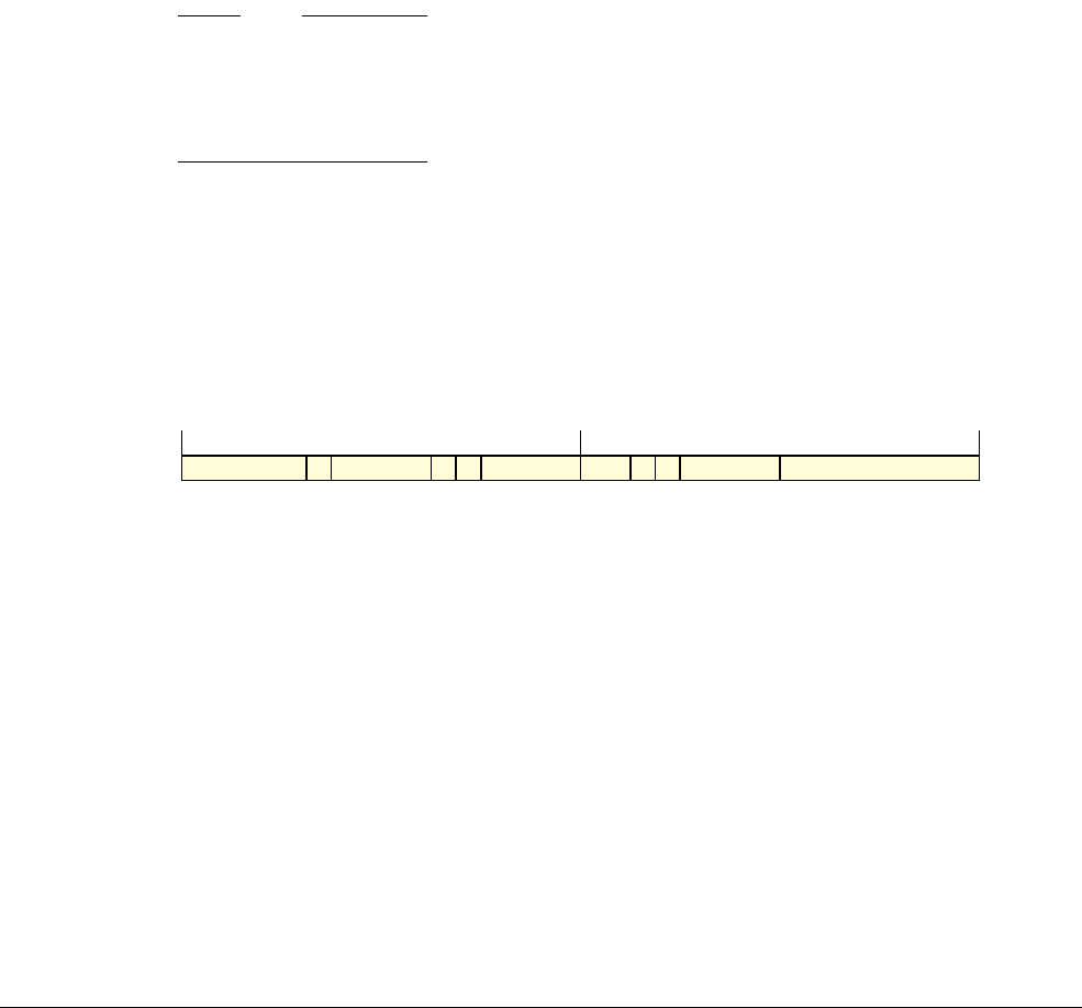
F7 T32 and A32 Base Instruction Set Instruction Descriptions
F7.4 Alphabetical list of system instructions
F7-3066 Copyright © 2013 ARM Limited. All rights reserved. ARM DDI 0487A.a
Non-Confidential - Beta ID090413
F7.4.18 STRBT, STRHT, and STRT
Even in Secure and Non-secure EL1 modes, stores to memory by these instructions are restricted in the same way
as unprivilged stores to memory. The
MemA_unpriv[]
and
MemU_unpriv[]
pseudocode functions describe this
restriction. For more information see Alignment support on page E2-2341.
These instructions are UNPREDICTABLE in Hyp mode.
For descriptions of the instructions see:
•STRBT on page F7-2890.
•STRHT on page F7-2910.
•STRT on page F7-2912.
F7.4.19 SUBS PC, LR and related instructions (T32)
The
SUBS PC, LR, #<const>
instruction provides an exception return without the use of the stack. It subtracts the
immediate constant from LR, branches to the resulting address, and also copies the SPSR to the CPSR.
Note
• The instruction
SUBS PC, LR, #0
is equivalent to
MOVS PC, LR
and
ERET
.
• For an implementation that includes EL2,
ERET
is the preferred disassembly of the T1 encoding defined in this
section. Therefore, a disassembler might report an
ERET
where the original assembler code used
SUBS PC, LR,
#0
.
When executing in Hyp mode:
• The encoding for
SUBS PC, LR, #0
is the encoding of the
ERET
instruction, see ERET on page F7-3038.
•
SUBS PC, LR, #<const>
with a nonzero constant is UNDEFINED.
SUBS PC, LR, #<const>
is CONSTRAINED UNPREDICTABLE in the cases described in Restrictions on exception return
instructions on page F7-3028.
if IsZero(imm8) then SEE ERET;
if CurrentInstrSet() == InstrSet_T32EE then UNPREDICTABLE;
if CurrentModeIsHyp() then UNDEFINED; // UNDEFINED in Hyp mode when not ERET
n = 14; imm32 = ZeroExtend(imm8, 32);
if InITBlock() && !LastInITBlock() then UNPREDICTABLE;
For information about the CONSTRAINED UNPREDICTABLE behavior of this instruction, see Appendix A
Architectural Constraints on UNPREDICTABLE behaviors, and particularly SUBS PC, LR and related instructions
(T32) on page AppxA-4758.
Encoding T1 ARMv6T2, ARMv7
SUBS<c> PC, LR, #<imm8>
Outside or last in IT block
1 1 1 0 0 1 1 1 1 0 1 (1) (1) (1) (0) 1 0 (0) 0 (1) (1) (1) (1) imm8
15 14 13 12 11 10 9 8 7 6 5 4 3 2 1 0
1
1514131211109876543210

F7 T32 and A32 Base Instruction Set Instruction Descriptions
F7.4 Alphabetical list of system instructions
ARM DDI 0487A.a Copyright © 2013 ARM Limited. All rights reserved. F7-3067
ID090413 Non-Confidential - Beta
Assembler syntax
SUBS{<c>}{<q>} PC, LR, #<const>
where:
<c>, <q>
See Standard assembler syntax fields on page F2-2415.
<const>
The immediate constant, in the range 0-255.
In the T32 instruction set,
MOVS{<c>}{<q>} PC, LR
is a pseudo-instruction for
SUBS{<c>}{<q>} PC, LR, #0
.
Operation
if ConditionPassed() then
EncodingSpecificOperations();
if (CurrentModeIsUserOrSystem() || CurrentInstrSet() == InstrSet_T32EE) then
UNPREDICTABLE;
else
operand2 = imm32;
(result, -) = AddWithCarry(R[n], NOT(operand2), ‘1’);
CPSRWriteByInstr(SPSR[], ‘1111’, TRUE);
if CPSR.M == M32_Hyp && CPSR.J == ‘1’ && CPSR.T == ‘1’ then
UNPREDICTABLE;
else
BranchWritePC(result);
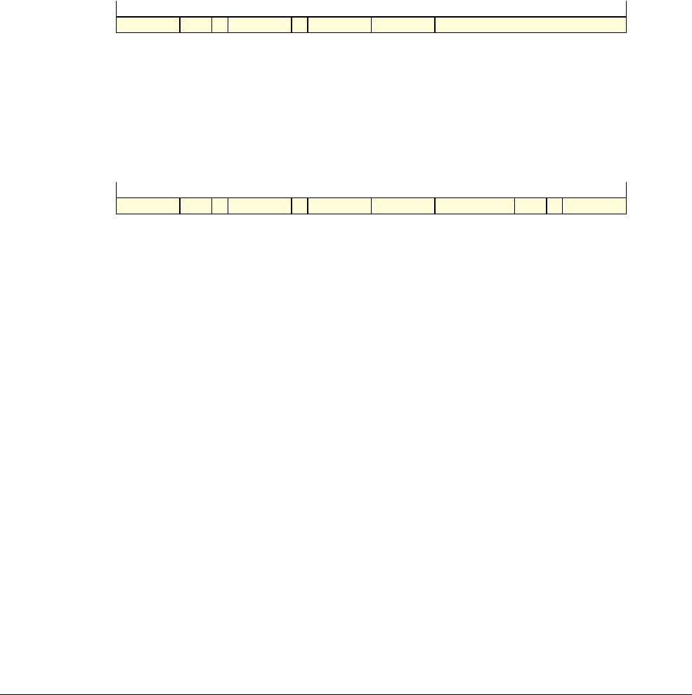
F7 T32 and A32 Base Instruction Set Instruction Descriptions
F7.4 Alphabetical list of system instructions
F7-3068 Copyright © 2013 ARM Limited. All rights reserved. ARM DDI 0487A.a
Non-Confidential - Beta ID090413
F7.4.20 SUBS PC, LR and related instructions (A32)
The
SUBS PC, LR, #<const>
instruction provides an exception return without the use of the stack. It subtracts the
immediate constant from LR, branches to the resulting address, and also copies the SPSR to the CPSR. The A32
instruction set contains similar instructions based on other data-processing operations, or with a wider range of
operands, or both. ARM deprecates using these other instructions, except for
MOVS PC, LR
.
All of these instructions are:
•UNDEFINED in Hyp mode.
•CONSTRAINED UNPREDICTABLE in the cases described in Restrictions on exception return instructions on
page F7-3028.
n = UInt(Rn); imm32 = ARMExpandImm(imm12); register_form = FALSE;
n = UInt(Rn); m = UInt(Rm); register_form = TRUE;
(shift_t, shift_n) = DecodeImmShift(type, imm5);
For information about the CONSTRAINED UNPREDICTABLE behavior of this instruction, see Appendix A
Architectural Constraints on UNPREDICTABLE behaviors, and particularly SUBS PC. LR and related instructions
(A32) on page AppxA-4759.
Assembler syntax
where:
<c>, <q>
See Standard assembler syntax fields on page F2-2415.
<opc1>
The operation.
<opc1>
is one of
ADC
,
ADD
,
AND
,
BIC
,
EOR
,
ORR
,
RSB
,
RSC
,
SBC
, and
SUB
. ARM deprecates
the use of all of these operations except
SUB
.
<opc2>
The operation.
<opc2>
is
MOV
or
MVN
. ARM deprecates the use of
MOV
.
<opc3>
The operation.
<opc3>
is
ASR
,
LSL
,
LSR
, or
ROR
. ARM deprecates the use of all of these operations.
<Rn>
The first operand register. ARM deprecates the use of any register except
LR
.
Encoding A1 ARMv4*, ARMv5T*, ARMv6*, ARMv7
<opc1>S<c> PC, <Rn>, #<const>
<opc2>S<c> PC, #<const>
Encoding A2 ARMv4*, ARMv5T*, ARMv6*, ARMv7
<opc1>S<c> PC, <Rn>, <Rm>{, <shift>}
<opc2>S<c> PC, <Rm>{, <shift>}
<opc3>S<c> PC, <Rn>, #<const>
RRXS<c> PC, <Rn>
SUBS{<c>}{<q>} PC, LR, #<const>
Encoding A1
<opc1>S{<c>}{<q>} PC, <Rn>, #<const>
Encoding A1
<opc1>S{<c>}{<q>} PC, <Rn>, <Rm> {, <shift>}
Encoding A2, deprecated
<opc2>S{<c>}{<q>} PC, #<const>
Encoding A1, deprecated
<opc2>S{<c>}{<q>} PC, <Rm> {, <shift>}
Encoding A2
<opc3>S{<c>}{<q>} PC, <Rn>, #<const>
Encoding A2, deprecated
RRXS{<c>}{<q>} PC, <Rn>
Encoding A2, deprecated
cond 0 0 1 opcode 1 Rn 1 1 1 1 imm12
31 30 29 28 27 26 25 24 23 22 21 20 19 18 17 16 15 14 13 12 11 10 9 8 7 6 5 4 3 2 1 0
cond 0 0 0 opcode 1 Rn 1 1 1 1 imm5 type 0 Rm
31 30 29 28 27 26 25 24 23 22 21 20 19 18 17 16 15 14 13 12 11 10 9 8 7 6 5 4 3 2 1 0

F7 T32 and A32 Base Instruction Set Instruction Descriptions
F7.4 Alphabetical list of system instructions
ARM DDI 0487A.a Copyright © 2013 ARM Limited. All rights reserved. F7-3069
ID090413 Non-Confidential - Beta
<const>
The immediate constant. See Modified immediate constants in A32 instructions on page F4-2472
for the range of available values.
<Rm>
The optionally shifted second or only operand register. ARM deprecates the use of any register
except LR.
<shift>
The shift to apply to the value read from
<Rm>
. If absent, no shift is applied. Constant shifts on
page F2-2419 describes the shifts and how they are encoded. ARM deprecates the use of
<shift>
.
The required operation,
<opc1>
,
<opc2>
,
<opc3>
, or
RRXS
, is encoded in the opcode field of the instruction, and in some
cases in the
imm5
field of encoding T2. For the opcode values for different operations see Operation.
The pre-UAL syntax
<opc1><c>S
is equivalent to
<opc1>S<c>
. The pre-UAL syntax
<opc2><c>S
is equivalent to
<opc2>S<c>
.
Operation
if ConditionPassed() then
EncodingSpecificOperations();
if CurrentModeIsHyp() then
UNDEFINED;
elsif CurrentModeIsUserOrSystem() || CurrentInstrSet() == InstrSet_T32EE then
UNPREDICTABLE; // UNDEFINED or NOP
else
operand2 = if register_form then Shift(R[m], shift_t, shift_n, APSR.C) else imm32;
case opcode of
when ‘0000’ result = R[n] AND operand2; // AND
when ‘0001’ result = R[n] EOR operand2; // EOR
when ‘0010’ (result, -) = AddWithCarry(R[n], NOT(operand2), ‘1’); // SUB
when ‘0011’ (result, -) = AddWithCarry(NOT(R[n]), operand2, ‘1’); // RSB
when ‘0100’ (result, -) = AddWithCarry(R[n], operand2, ‘0’); // ADD
when ‘0101’ (result, -) = AddWithCarry(R[n], operand2, APSR.C); // ADC
when ‘0110’ (result, -) = AddWithCarry(R[n], NOT(operand2), APSR.C); // SBC
when ‘0111’ (result, -) = AddWithCarry(NOT(R[n]), operand2, APSR.C); // RSC
when ‘1100’ result = R[n] OR operand2; // ORR
when ‘1101’ // MOV, if NOT(register_form)
// Otherwise, ASR, LSL, LSR, ROR, or RRX, and
// DecodeImmShift() decodes the different shifts
result = operand2;
when ‘1110’ result = R[n] AND NOT(operand2); // BIC
when ‘1111’ result = NOT(operand2); // MVN
AArch32.ExceptionReturn(result, SPSR[]);
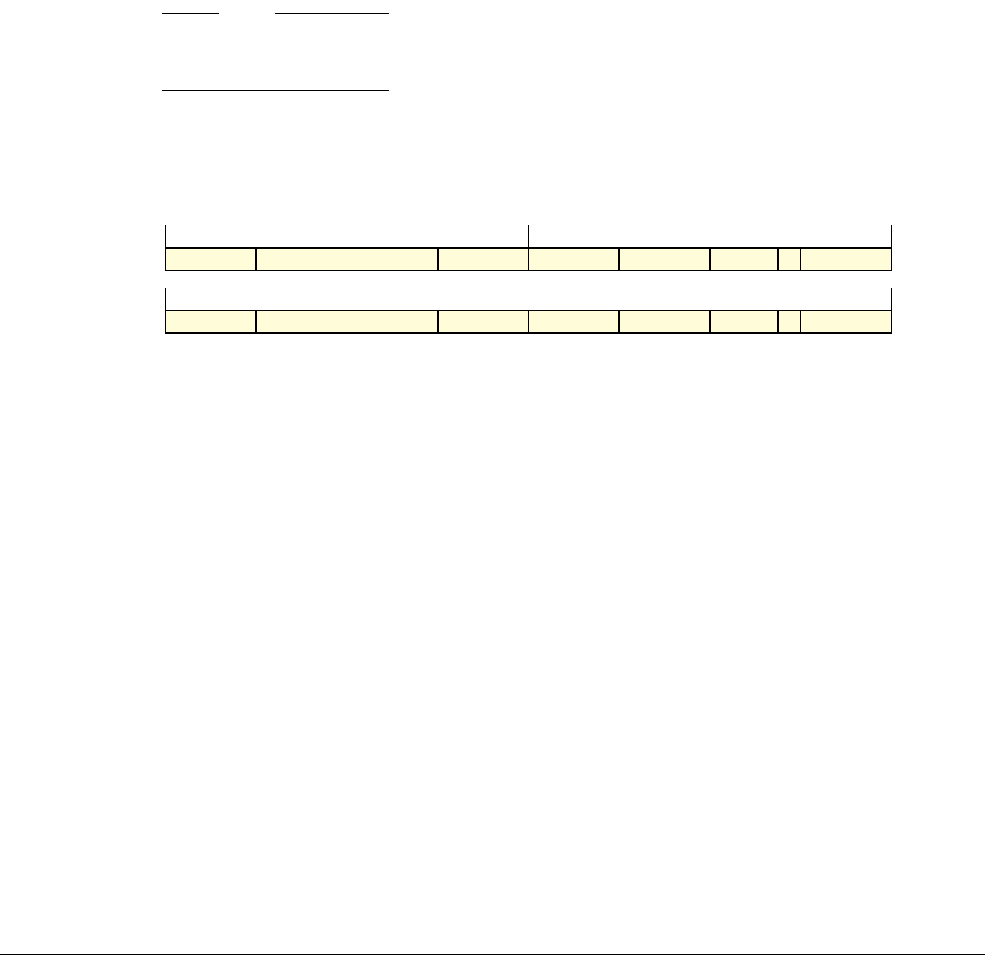
F7 T32 and A32 Base Instruction Set Instruction Descriptions
F7.4 Alphabetical list of system instructions
F7-3070 Copyright © 2013 ARM Limited. All rights reserved. ARM DDI 0487A.a
Non-Confidential - Beta ID090413
F7.4.21 VMRS
Move to general-purpose register from Advanced SIMD and floating-point System register moves the value of an
extension system register to a general-purpose register. When the specified floating-point System register is the
FPSCR, a form of the instruction transfers the FPSCR.{N, Z, C, V} condition flags to the APSR.{N, Z, C, V}
condition flags.
Depending on settings in the CPACR, NSACR, HCPTR, and FPEXC registers, and the security state and mode in
which the instruction is executed, an attempt to execute a
VMRS
instruction might be UNDEFINED, or trapped to Hyp
mode. Summary of general controls of CP10 and CP11 functionality on page G1-3496 and Summary of access
controls for Advanced SIMD functionality on page G1-3498 summarize these controls.
When these settings permit the execution of floating-point and Advanced SIMD instructions, if the specified
floating-point System register is not the FPSCR, the instruction is UNDEFINED if executed in User mode.
In an implementation that includes EL2, when HCR.TID0 is set to 1, any
VMRS
access to FPSID, from a Non-secure
EL1 mode, that would be permitted if HCR.TID0 was set to 0, generates a Hyp Trap exception. For more
information, see ID group 0, Primary device identification registers on page G1-3507.
Note
• VMRS on page F8-3232 describes the valid application level uses of the
VMRS
instruction
• For simplicity, the
VMRS
pseudocode does not show the possible trap to Hyp mode.
t = UInt(Rt);
if t == 15 && reg != ‘0001’ then UNPREDICTABLE; // ARMv8-A removes UNPREDICTABLE for R13
For information about the CONSTRAINED UNPREDICTABLE behavior of this instruction, see Appendix A
Architectural Constraints on UNPREDICTABLE behaviors, and particularly VMRS on page AppxA-4759.
Encoding T1/A1 VFPv2, VFPv3, VFPv4, Advanced SIMD
VMRS<c> <Rt>, <spec_reg>
reg1 1 0 1 1 1 0 1 1 1 1 Rt 1 0 1 0 (0) (0) (0) 1 (0) (0) (0) (0)
15 14 13 12 11 10 9 8 7 6 5 4 3 2 1 0
1
1514131211109876543210
1 1 1 0 1 1 1 1 reg Rt 1 0 1 0 (0) (0) (0) 1 (0) (0) (0) (0)
31 30 29 28 27 26 25 24 23 22 21 20 19 18 17 16 15 14 13 12 11 10 9 8 7 6 5 4 3 2 1 0
cond

F7 T32 and A32 Base Instruction Set Instruction Descriptions
F7.4 Alphabetical list of system instructions
ARM DDI 0487A.a Copyright © 2013 ARM Limited. All rights reserved. F7-3071
ID090413 Non-Confidential - Beta
Assembler syntax
VMRS{<c>}{<q>} <Rt>, <spec_reg>
where:
<c>, <q>
See Standard assembler syntax fields on page F2-2415.
<Rt>
The destination general-purpose register. This register can be R0-R14.
If
<spec_reg>
is
FPSCR
, it is also permitted to be
APSR_nzcv
, encoded as Rt = '1111'. This instruction
transfers the FPSCR.{N, Z, C, V} condition flags to the APSR.{N, Z, C, V} condition flags.
<spec_reg>
Is one of:
FPSID
reg = '0000'.
FPSCR
reg = '0001'.
MVFR1
reg = '0110'.
MVFR0
reg = '0111'.
FPEXC
reg = '1000'.
If the Common VFP subarchitecture is implemented, see Floating-point exception traps,
serialization, and floating-point exception barriers on page G1-3501 for additional values of
<spec_reg>
.
The pre-UAL instruction
FMSTAT
is equivalent to
VMRS APSR_nzcv, FPSCR
.
Operation
if ConditionPassed() then
EncodingSpecificOperations();
if reg == ‘0001’ then // FPSCR
CheckVFPEnabled(TRUE); SerializeVFP(); VFPExcBarrier();
if t == 15 then
APSR.N = FPSR.N; APSR.Z = FPSR.Z; APSR.C = FPSR.C; APSR.V = FPSR.V;
else
R[t] = FPSCR;
else // Non-FPSCR registers are accessible only at PL1 or above and not affected by FPEXC.EN
CheckVFPEnabled(FALSE);
if !CurrentModeIsNotUser() then
UNDEFINED;
else
case reg of
when ‘0000’ SerializeVFP(); R[t] = FPSID;
// Pseudocode does not consider possible trap of Non-secure FPSID access to Hyp mode
// ‘0001’ already handled
when ‘001x’, ‘010x’ UNPREDICTABLE;
when ‘0110’ SerializeVFP(); R[t] = MVFR1;
when ‘0111’ SerializeVFP(); R[t] = MVFR0;
when ‘1000’ SerializeVFP(); R[t] = FPEXC;
otherwise SUBARCHITECTURE_DEFINED register access;
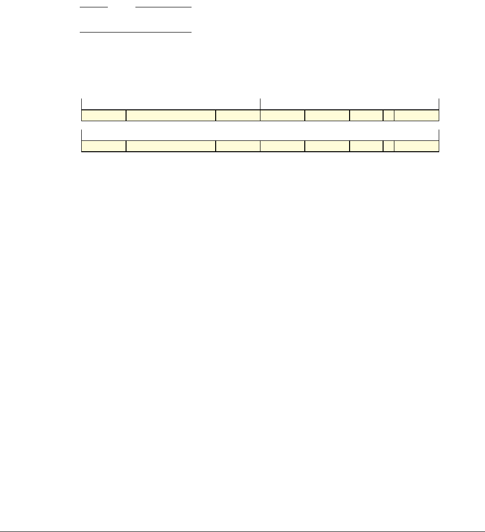
F7 T32 and A32 Base Instruction Set Instruction Descriptions
F7.4 Alphabetical list of system instructions
F7-3072 Copyright © 2013 ARM Limited. All rights reserved. ARM DDI 0487A.a
Non-Confidential - Beta ID090413
F7.4.22 VMSR
Move to Advanced SIMD and floating-point System register from general-purpose register moves the value of a
general-purpose register to a floating-point System register.
Depending on settings in the CPACR, NSACR, HCPTR, and FPEXC registers, and the security state and mode in
which the instruction is executed, an attempt to execute a
VMSR
instruction might be UNDEFINED, or trapped to Hyp
mode. Summary of general controls of CP10 and CP11 functionality on page G1-3496 and Summary of access
controls for Advanced SIMD functionality on page G1-3498 summarize these controls.
When these settings permit the execution of floating-point and Advanced SIMD instructions, if the specified
floating-point System register is not the FPSCR, the instruction is UNDEFINED if executed in User mode.
Note
VMSR on page F8-3234 describes the valid application level uses of the
VMSR
instruction.
t = UInt(Rt);
if reg == ‘001x’ || reg == ‘01xx’ then UNPREDICTABLE;
if t == 15 then UNPREDICTABLE; // ARMv8-A removes UNPREDICTABLE for R13
For information about the CONSTRAINED UNPREDICTABLE behavior of this instruction, see Appendix A
Architectural Constraints on UNPREDICTABLE behaviors, and particularly VMSR on page AppxA-4759.
Encoding T1/A1 VFPv2, VFPv3, VFPv4, Advanced SIMD
VMSR<c> <spec_reg>, <Rt>
1 1 0 1 1 1 0 1 1 1 0 reg Rt 1 0 1 0 (0) (0) (0) 1 (0) (0) (0) (0)
15 14 13 12 11 10 9 8 7 6 5 4 3 2 1 0
1
1514131211109876543210
1 1 1 0 1 1 1 0 reg Rt 1 0 1 0 (0) (0) (0) 1 (0) (0) (0) (0)
31 30 29 28 27 26 25 24 23 22 21 20 19 18 17 16 15 14 13 12 11 10 9 8 7 6 5 4 3 2 1 0
cond

F7 T32 and A32 Base Instruction Set Instruction Descriptions
F7.4 Alphabetical list of system instructions
ARM DDI 0487A.a Copyright © 2013 ARM Limited. All rights reserved. F7-3073
ID090413 Non-Confidential - Beta
Assembler syntax
VMSR{<c>}{<q>} <spec_reg>, <Rt>
where:
<c>, <q>
See Standard assembler syntax fields on page F2-2415.
<spec_reg>
Is one of:
FPSID
reg = '0000'.
FPSCR
reg = '0001'.
FPEXC
reg = '1000'.
If the Common VFP subarchitecture is implemented, see Floating-point exception traps,
serialization, and floating-point exception barriers on page G1-3501 for additional values of
<spec_reg>
.
<Rt>
The general-purpose register to be transferred to
<spec_reg>
.
Operation
if ConditionPassed() then
EncodingSpecificOperations();
if reg == ‘0001’ then // FPSCR
CheckVFPEnabled(TRUE); SerializeVFP(); VFPExcBarrier();
FPSCR = R[t];
else // Non-FPSCR registers are accessible only at PL1 or above and not affected by FPEXC.EN
CheckVFPEnabled(FALSE);
if !CurrentModeIsNotUser() then
UNDEFINED;
else
case reg of
// ‘001x’, ‘01xx’ dealt with in encoding-specific pseudocode
// ‘0001’ already dealt with above
when ‘0000’ SerializeVFP(); // FPSID is read-only
when ‘1000’ SerializeVFP(); FPEXC = R[t];
otherwise SUBARCHITECTURE_DEFINED “register access”;

F7 T32 and A32 Base Instruction Set Instruction Descriptions
F7.4 Alphabetical list of system instructions
F7-3074 Copyright © 2013 ARM Limited. All rights reserved. ARM DDI 0487A.a
Non-Confidential - Beta ID090413

ARM DDI 0487A.a Copyright © 2013 ARM Limited. All rights reserved. F8-3075
ID090413 Non-Confidential - Beta
Chapter F8
T32 and A32 Advanced SIMD and floating-point
Instruction Descriptions
This chapter describes each instruction. It contains the following sections:
•Alphabetical list of floating-point and Advanced SIMD instructions on page F8-3076.
Note
Before ARMv8, the Advanced SIMD and floating-point instructions were added to the T32 and A32 instruction sets
by the Advanced SIMD Extension and the Floating-point Extension, previously called VFP Extension. Instruction
descriptions indicate the first version of the Floating-point extension (VFPv8) or Advanced SIMD Extension that
included the instruction.
F8 T32 and A32 Advanced SIMD and floating-point Instruction Descriptions
F8.1 Alphabetical list of floating-point and Advanced SIMD instructions
F8-3076 Copyright © 2013 ARM Limited. All rights reserved. ARM DDI 0487A.a
Non-Confidential - Beta ID090413
F8.1 Alphabetical list of floating-point and Advanced SIMD instructions
This section lists every floating-point and Advanced SIMD instruction in the T32 and A32 instruction sets. For
details of the format used see Format of instruction descriptions on page F2-2410.
This section is formatted so that a full description of an instruction uses either a single page or two facing pages.
F8.1.1 AESD
AES single round decryption.
if size != ‘00’ then UNDEFINED;
if Vd<0> == ‘1’ || Vm<0> == ‘1’ then UNDEFINED;
d = UInt(D:Vd); m = UInt(M:Vm);
if InITBlock() then UNPREDICTABLE;
if size != ‘00’ then UNDEFINED;
if Vd<0> == ‘1’ || Vm<0> == ‘1’ then UNDEFINED;
d = UInt(D:Vd); m = UInt(M:Vm);
For information about the CONSTRAINED UNPREDICTABLE behavior of this instruction, see Appendix A
Architectural Constraints on UNPREDICTABLE behaviors.
Assembler syntax
where:
<Qd>, <Qm>
The destination vector and the operand vector, for a quadword operation.
Operation
if ConditionPassed() then
EncodingSpecificOperations(); CheckCryptoEnabled32();
op1 = Q[d>>1]; op2 = Q[m>>1];
Q[d>>1] = AESInvSubBytes(AESInvShiftRows(op1 EOR op2));
Encoding T1 ARMv8 Advanced SIMD
AESD.8 <Qd>, <Qm>
Encoding A1 ARMv8 Advanced SIMD
AESD.8 <Qd>, <Qm>
AESD.8 <Qd>, <Qm>
0 11 1 1 1 1 1 1 1 D 1 1 size 0 0 Vd 0 0 1 1 M 0 Vm
15 14 13 12 11 10 9 8 7 6 5 4 3 2 1 0
1
1514131211109876543210
11 1 1 0 0 1 1 1 D 1 1 size 0 0 Vd 0 0 1 1 0 M 0 Vm
31 30 29 28 27 26 25 24 23 22 21 20 19 18 17 16 15 14 13 12 11 10 9 8 7 6 5 4 3 2 1 0
1

F8 T32 and A32 Advanced SIMD and floating-point Instruction Descriptions
F8.1 Alphabetical list of floating-point and Advanced SIMD instructions
ARM DDI 0487A.a Copyright © 2013 ARM Limited. All rights reserved. F8-3077
ID090413 Non-Confidential - Beta
F8.1.2 AESE
AES single round encryption.
if size != ‘00’ then UNDEFINED;
if Vd<0> == ‘1’ || Vm<0> == ‘1’ then UNDEFINED;
d = UInt(D:Vd); m = UInt(M:Vm);
if InITBlock() then UNPREDICTABLE;
if size != ‘00’ then UNDEFINED;
if Vd<0> == ‘1’ || Vm<0> == ‘1’ then UNDEFINED;
d = UInt(D:Vd); m = UInt(M:Vm);
For information about the CONSTRAINED UNPREDICTABLE behavior of this instruction, see Appendix A
Architectural Constraints on UNPREDICTABLE behaviors.
Assembler syntax
where:
<Qd>, <Qm>
The destination vector and the operand vector, for a quadword operation.
Operation
if ConditionPassed() then
EncodingSpecificOperations(); CheckCryptoEnabled32();
op1 = Q[d>>1]; op2 = Q[m>>1];
Q[d>>1] = AESSubBytes(AESShiftRows(op1 EOR op2));
Encoding T1 ARMv8 Advanced SIMD
AESE.8 <Qd>, <Qm>
Encoding A1 ARMv8 Advanced SIMD
AESE.8 <Qd>, <Qm>
AESE.8 <Qd>, <Qm>
0 01 1 1 1 1 1 1 1 D 1 1 size 0 0 Vd 0 0 1 1 M 0 Vm
15 14 13 12 11 10 9 8 7 6 5 4 3 2 1 0
1
1514131211109876543210
01 1 1 0 0 1 1 1 D 1 1 size 0 0 Vd 0 0 1 1 0 M 0 Vm
31 30 29 28 27 26 25 24 23 22 21 20 19 18 17 16 15 14 13 12 11 10 9 8 7 6 5 4 3 2 1 0
1
F8 T32 and A32 Advanced SIMD and floating-point Instruction Descriptions
F8.1 Alphabetical list of floating-point and Advanced SIMD instructions
F8-3078 Copyright © 2013 ARM Limited. All rights reserved. ARM DDI 0487A.a
Non-Confidential - Beta ID090413
F8.1.3 AESIMC
AES inverse mix columns.
if size != ‘00’ then UNDEFINED;
if Vd<0> == ‘1’ || Vm<0> == ‘1’ then UNDEFINED;
d = UInt(D:Vd); m = UInt(M:Vm);
if InITBlock() then UNPREDICTABLE;
if size != ‘00’ then UNDEFINED;
if Vd<0> == ‘1’ || Vm<0> == ‘1’ then UNDEFINED;
d = UInt(D:Vd); m = UInt(M:Vm);
Assembler syntax
where:
<Qd>, <Qm>
The destination vector and the operand vector, for a quadword operation.
Operation
if ConditionPassed() then
EncodingSpecificOperations(); CheckCryptoEnabled32();
op1 = Q[d>>1]; op2 = Q[m>>1];
Q[d>>1] = AESSubBytes(AESShiftRows(op1 EOR op2));
Encoding T1 ARMv8 Advanced SIMD
AESIMC.8 <Qd>, <Qm>
Encoding A1 ARMv8 Advanced SIMD
AESIMC.8 <Qd>, <Qm>
AESIMC.8 <Qd>, <Qm>
1 11 1 1 1 1 1 1 1 D 1 1 size 0 0 Vd 0 0 1 1 M 0 Vm
15 14 13 12 11 10 9 8 7 6 5 4 3 2 1 0
1
1514131211109876543210
11 1 1 0 0 1 1 1 D 1 1 size 0 0 Vd 0 0 1 1 1 M 0 Vm
31 30 29 28 27 26 25 24 23 22 21 20 19 18 17 16 15 14 13 12 11 10 9 8 7 6 5 4 3 2 1 0
1

F8 T32 and A32 Advanced SIMD and floating-point Instruction Descriptions
F8.1 Alphabetical list of floating-point and Advanced SIMD instructions
ARM DDI 0487A.a Copyright © 2013 ARM Limited. All rights reserved. F8-3079
ID090413 Non-Confidential - Beta
F8.1.4 AESMC
AES mix columns.
if size != ‘00’ then UNDEFINED;
if Vd<0> == ‘1’ || Vm<0> == ‘1’ then UNDEFINED;
d = UInt(D:Vd); m = UInt(M:Vm);
if InITBlock() then UNPREDICTABLE;
if size != ‘00’ then UNDEFINED;
if Vd<0> == ‘1’ || Vm<0> == ‘1’ then UNDEFINED;
d = UInt(D:Vd); m = UInt(M:Vm);
For information about the CONSTRAINED UNPREDICTABLE behavior of this instruction, see Appendix A
Architectural Constraints on UNPREDICTABLE behaviors.
Assembler syntax
where:
<Qd>, <Qm>
The destination vector and the operand vector, for a quadword operation.
Operation
if ConditionPassed() then
EncodingSpecificOperations(); CheckCryptoEnabled32();
op1 = Q[d>>1]; op2 = Q[m>>1];
Q[d>>1] = AESSubBytes(AESShiftRows(op1 EOR op2));
Encoding T1 ARMv8 Advanced SIMD
AESMC.8 <Qd>, <Qm>
Encoding A1 ARMv8 Advanced SIMD
AESMC.8 <Qd>, <Qm>
AESMC.8 <Qd>, <Qm>
1 01 1 1 1 1 1 1 1 D 1 1 size 0 0 Vd 0 0 1 1 M 0 Vm
15 14 13 12 11 10 9 8 7 6 5 4 3 2 1 0
1
1514131211109876543210
01 1 1 0 0 1 1 1 D 1 1 size 0 0 Vd 0 0 1 1 1 M 0 Vm
31 30 29 28 27 26 25 24 23 22 21 20 19 18 17 16 15 14 13 12 11 10 9 8 7 6 5 4 3 2 1 0
1

F8 T32 and A32 Advanced SIMD and floating-point Instruction Descriptions
F8.1 Alphabetical list of floating-point and Advanced SIMD instructions
F8-3080 Copyright © 2013 ARM Limited. All rights reserved. ARM DDI 0487A.a
Non-Confidential - Beta ID090413
F8.1.5 F*, former floating-point instruction mnemonics
Before the introduction of UAL, the floating-point instructions had mnemonics starting with
F
. In UAL, most of
these mnemonics are renamed to start with
V
. However, as this section describes, UAL does not define new
mnemonics for the
FLDMX
and
FSTMX
instructions.
FLDMX, FSTMX
Encodings T1/A1 of the
VLDM
,
VPOP
,
VPUSH
, and
VSTM
instructions contain an imm8 field that is set to twice the number
of doubleword registers to be transferred. ARM deprecates use of these encodings with an odd value in imm8, and
there is no UAL syntax for them.
The pre-UAL mnemonics
FLDMX
and
FSTMX
result in the same instructions as
FLDMD
(
VLDM.64
or
VPOP.64
) and
FSTMD
(
VSTM.64
or
VPUSH.64
) respectively, except that imm8 is equal to twice the number of doubleword registers plus one:
• From ARMv6, ARM deprecates use of
FLDMX
and
FSTMX
, except for disassembly purposes, and for reassembly
of disassembled code.
•If an
FLDMX
or
FSTMX
instruction accesses any register in the range D16-D32, the instruction is
UNPREDICTABLE.

F8 T32 and A32 Advanced SIMD and floating-point Instruction Descriptions
F8.1 Alphabetical list of floating-point and Advanced SIMD instructions
ARM DDI 0487A.a Copyright © 2013 ARM Limited. All rights reserved. F8-3081
ID090413 Non-Confidential - Beta
F8.1.6 SHA1C
SHA1 hash update (choose).
if Q != ‘1’ then UNDEFINED;
if Vd<0> == ‘1’ || Vn<0> == ‘1’ || Vm<0> == ‘1’ then UNDEFINED;
d = UInt(D:Vd); n = UInt(N:Vn); m = UInt(M:Vm);
if InITBlock() then UNPREDICTABLE;
if Q != ‘1’ then UNDEFINED;
if Vd<0> == ‘1’ || Vn<0> == ‘1’ || Vm<0> == ‘1’ then UNDEFINED;
d = UInt(D:Vd); n = UInt(N:Vn); m = UInt(M:Vm);
For information about the CONSTRAINED UNPREDICTABLE behavior of this instruction, see Appendix A
Architectural Constraints on UNPREDICTABLE behaviors.
Assembler syntax
where:
<Qd>, <Qn>, <Qm>
The destination vector and the operand vectors, for a quadword operation.
Operation
if ConditionPassed() then
EncodingSpecificOperations(); CheckCryptoEnabled32();
X = Q[d>>1];
Y = Q[n>>1]<31:0>; // Note: 32 bits wide
W = Q[m>>1];
for e = 0 to 3
t = SHAchoose(X<63:32>, X<95:64>, X<127:96>);
Y = Y + ROL(X<31:0>, 5) + t + Elem[W, e, 32];
X<63:32> = ROL(X<63:32>, 30);
<Y, X> = ROL(Y:X, 32);
Q[d>>1] = X;
Encoding T1 ARMv8 Advanced SIMD
SHA1C.32 <Qd>, <Qn>, <Qm>
Encoding A1 ARMv8 Advanced SIMD
SHA1C.32 <Qd>, <Qn>, <Qm>
SHA1C.32 <Qd>, <Qn>, <Qm>
01 1 0 1 1 1 1 0 D 0 Vn Vd 1 1 0 0 N Q M 0 Vm
15 14 13 12 11 10 9 8 7 6 5 4 3 2 1 0
1
1514131211109876543210
01 1 1 0 0 1 0 0 D 0 Vn Vd 1 1 0 0 N Q M 0 Vm
31 30 29 28 27 26 25 24 23 22 21 20 19 18 17 16 15 14 13 12 11 10 9 8 7 6 5 4 3 2 1 0
1

F8 T32 and A32 Advanced SIMD and floating-point Instruction Descriptions
F8.1 Alphabetical list of floating-point and Advanced SIMD instructions
F8-3082 Copyright © 2013 ARM Limited. All rights reserved. ARM DDI 0487A.a
Non-Confidential - Beta ID090413
F8.1.7 SHA1H
SHA1 fixed rotate.
if size != ‘10’ then UNDEFINED;
if Vd<0> == ‘1’ || Vm<0> == ‘1’ then UNDEFINED;
d = UInt(D:Vd); m = UInt(M:Vm);
if InITBlock() then UNPREDICTABLE;
if size != ‘10’ then UNDEFINED;
if Vd<0> == ‘1’ || Vm<0> == ‘1’ then UNDEFINED;
d = UInt(D:Vd); m = UInt(M:Vm);
For information about the CONSTRAINED UNPREDICTABLE behavior of this instruction, see Appendix A
Architectural Constraints on UNPREDICTABLE behaviors.
Assembler syntax
where:
<Qd>, <Qm>
The destination vector and the operand vectors, for a quadword operation.
Operation
if ConditionPassed() then
EncodingSpecificOperations(); CheckCryptoEnabled32();
Q[d>>1] = ZeroExtend(ROL(Q[m>>1]<31:0>, 30), 128);
Encoding T1 ARMv8 Advanced SIMD
SHA1H.32 <Qd>, <Qm>
Encoding A1 ARMv8 Advanced SIMD
SHA1H.32 <Qd>, <Qm>
SHA1H.32 <Qd>, <Qm>
1 1 1 1 1 1 1 1 D 1 1 size 0 1 Vd 0 0 1 0 1 1 M 0 Vm
15 14 13 12 11 10 9 8 7 6 5 4 3 2 1 0
1
1514131211109876543210
1 1 1 0 0 1 1 1 D 1 1 size 0 1 Vd 0 0 1 0 1 1 M 0 Vm
31 30 29 28 27 26 25 24 23 22 21 20 19 18 17 16 15 14 13 12 11 10 9 8 7 6 5 4 3 2 1 0
1

F8 T32 and A32 Advanced SIMD and floating-point Instruction Descriptions
F8.1 Alphabetical list of floating-point and Advanced SIMD instructions
ARM DDI 0487A.a Copyright © 2013 ARM Limited. All rights reserved. F8-3083
ID090413 Non-Confidential - Beta
F8.1.8 SHA1M
SHA1 hash update (majority).
if Q != ‘1’ then UNDEFINED;
if Vd<0> == ‘1’ || Vn<0> == ‘1’ || Vm<0> == ‘1’ then UNDEFINED;
d = UInt(D:Vd); n = UInt(N:Vn); m = UInt(M:Vm);
if InITBlock() then UNPREDICTABLE;
if Q != ‘1’ then UNDEFINED;
if Vd<0> == ‘1’ || Vn<0> == ‘1’ || Vm<0> == ‘1’ then UNDEFINED;
d = UInt(D:Vd); n = UInt(N:Vn); m = UInt(M:Vm);
For information about the CONSTRAINED UNPREDICTABLE behavior of this instruction, see Appendix A
Architectural Constraints on UNPREDICTABLE behaviors.
Assembler syntax
where:
<Qd>, <Qn>, <Qm>
The destination vector and the operand vectors, for a quadword operation.
Operation
if ConditionPassed() then
EncodingSpecificOperations(); CheckCryptoEnabled32();
X = Q[d>>1];
Y = Q[n>>1]<31:0>; // Note: 32 bits wide
W = Q[m>>1];
for e = 0 to 3
t = SHAmajority(X<63:32>, X<95:64>, X<127:96>);
Y = Y + ROL(X<31:0>, 5) + t + Elem[W, e, 32];
X<63:32> = ROL(X<63:32>, 30);
<Y, X> = ROL(Y:X, 32);
Q[d>>1] = X;
Encoding T1 ARMv8 Advanced SIMD
SHA1M.32 <Qd>, <Qn>, <Qm>
Encoding A1 ARMv8 Advanced SIMD
SHA1M.32 <Qd>, <Qn>, <Qm>
SHA1M.32 <Qd>, <Qn>, <Qm>
01 1 0 1 1 1 1 0 D 1 Vn Vd 1 1 0 0 N Q M 0 Vm
15 14 13 12 11 10 9 8 7 6 5 4 3 2 1 0
1
1514131211109876543210
01 1 1 0 0 1 0 0 D 1 Vn Vd 1 1 0 0 N Q M 0 Vm
31 30 29 28 27 26 25 24 23 22 21 20 19 18 17 16 15 14 13 12 11 10 9 8 7 6 5 4 3 2 1 0
1

F8 T32 and A32 Advanced SIMD and floating-point Instruction Descriptions
F8.1 Alphabetical list of floating-point and Advanced SIMD instructions
F8-3084 Copyright © 2013 ARM Limited. All rights reserved. ARM DDI 0487A.a
Non-Confidential - Beta ID090413
F8.1.9 SHA1P
SHA1 hash update (parity).
if Q != ‘1’ then UNDEFINED;
if Vd<0> == ‘1’ || Vn<0> == ‘1’ || Vm<0> == ‘1’ then UNDEFINED;
d = UInt(D:Vd); n = UInt(N:Vn); m = UInt(M:Vm);
if InITBlock() then UNPREDICTABLE;
if Q != ‘1’ then UNDEFINED;
if Vd<0> == ‘1’ || Vn<0> == ‘1’ || Vm<0> == ‘1’ then UNDEFINED;
d = UInt(D:Vd); n = UInt(N:Vn); m = UInt(M:Vm);
For information about the CONSTRAINED UNPREDICTABLE behavior of this instruction, see Appendix A
Architectural Constraints on UNPREDICTABLE behaviors.
Assembler syntax
where:
<Qd>, <Qn>, <Qm>
The destination vector and the operand vectors, for a quadword operation.
Operation
if ConditionPassed() then
EncodingSpecificOperations(); CheckCryptoEnabled32();
X = Q[d>>1];
Y = Q[n>>1]<31:0>; // Note: 32 bits wide
W = Q[m>>1];
for e = 0 to 3
t = SHAparity(X<63:32>, X<95:64>, X<127:96>);
Y = Y + ROL(X<31:0>, 5) + t + Elem[W, e, 32];
X<63:32> = ROL(X<63:32>, 30);
<Y, X> = ROL(Y:X, 32);
Q[d>>1] = X;
Encoding T1 ARMv8 Advanced SIMD
SHA1P.32 <Qd>, <Qn>, <Qm>
Encoding A1 ARMv8 Advanced SIMD
SHA1P.32 <Qd>, <Qn>, <Qm>
SHA1P.32 <Qd>, <Qn>, <Qm>
11 1 0 1 1 1 1 0 D 0 Vn Vd 1 1 0 0 N Q M 0 Vm
15 14 13 12 11 10 9 8 7 6 5 4 3 2 1 0
1
1514131211109876543210
11 1 1 0 0 1 0 0 D 0 Vn Vd 1 1 0 0 N Q M 0 Vm
31 30 29 28 27 26 25 24 23 22 21 20 19 18 17 16 15 14 13 12 11 10 9 8 7 6 5 4 3 2 1 0
1

F8 T32 and A32 Advanced SIMD and floating-point Instruction Descriptions
F8.1 Alphabetical list of floating-point and Advanced SIMD instructions
ARM DDI 0487A.a Copyright © 2013 ARM Limited. All rights reserved. F8-3085
ID090413 Non-Confidential - Beta
F8.1.10 SHA1SU0
SHA1 schedule update 0.
if Q != ‘1’ then UNDEFINED;
if Vd<0> == ‘1’ || Vn<0> == ‘1’ || Vm<0> == ‘1’ then UNDEFINED;
d = UInt(D:Vd); n = UInt(N:Vn); m = UInt(M:Vm);
if InITBlock() then UNPREDICTABLE;
if Q != ‘1’ then UNDEFINED;
if Vd<0> == ‘1’ || Vn<0> == ‘1’ || Vm<0> == ‘1’ then UNDEFINED;
d = UInt(D:Vd); n = UInt(N:Vn); m = UInt(M:Vm);
For information about the CONSTRAINED UNPREDICTABLE behavior of this instruction, see Appendix A
Architectural Constraints on UNPREDICTABLE behaviors.
Assembler syntax
where:
<Qd>, <Qn>, <Qm>
The destination vector and the operand vectors, for a quadword operation.
Operation
if ConditionPassed() then
EncodingSpecificOperations(); CheckCryptoEnabled32();
op1 = Q[d>>1]; op2 = Q[n>>1]; op3 = Q[m>>1];
op2 = op2<63:0> : op1<127:64>;
Q[d>>1] = op1 EOR op2 EOR op3;
Encoding T1 ARMv8 Advanced SIMD
SHA1SU0.32 <Qd>, <Qn>, <Qm>
Encoding A1 ARMv8 Advanced SIMD
SHA1SU0.32 <Qd>, <Qn>, <Qm>
SHA1SU0.32 <Qd>, <Qn>, <Qm>
11 1 0 1 1 1 1 0 D 1 Vn Vd 1 1 0 0 N Q M 0 Vm
15 14 13 12 11 10 9 8 7 6 5 4 3 2 1 0
1
1514131211109876543210
11 1 1 0 0 1 0 0 D 1 Vn Vd 1 1 0 0 N Q M 0 Vm
31 30 29 28 27 26 25 24 23 22 21 20 19 18 17 16 15 14 13 12 11 10 9 8 7 6 5 4 3 2 1 0
1

F8 T32 and A32 Advanced SIMD and floating-point Instruction Descriptions
F8.1 Alphabetical list of floating-point and Advanced SIMD instructions
F8-3086 Copyright © 2013 ARM Limited. All rights reserved. ARM DDI 0487A.a
Non-Confidential - Beta ID090413
F8.1.11 SHA1SU1
SHA1 schedule update 1.
if size != ‘10’ then UNDEFINED;
if Vd<0> == ‘1’ || Vm<0> == ‘1’ then UNDEFINED;
d = UInt(D:Vd); m = UInt(M:Vm);
if InITBlock() then UNPREDICTABLE;
if size != ‘10’ then UNDEFINED;
if Vd<0> == ‘1’ || Vm<0> == ‘1’ then UNDEFINED;
d = UInt(D:Vd); m = UInt(M:Vm);
For information about the CONSTRAINED UNPREDICTABLE behavior of this instruction, see Appendix A
Architectural Constraints on UNPREDICTABLE behaviors.
Assembler syntax
where:
<Qd>, <Qm>
The destination vector and the operand vectors, for a quadword operation.
Operation
if ConditionPassed() then
EncodingSpecificOperations(); CheckCryptoEnabled32();
X = Q[d>>1]; Y = Q[m>>1];
T = X EOR LSR(Y, 32);
W0 = ROL(T<31:0>, 1);
W1 = ROL(T<63:32>, 1);
W2 = ROL(T<95:64>, 1);
W3 = ROL(T<127:96>, 1) EOR ROL(T<31:0>, 2);
Q[d>>1] = W3:W2:W1:W0;
Encoding T1 ARMv8 Advanced SIMD
SHA1SU1.32 <Qd>, <Qm>
Encoding A1 ARMv8 Advanced SIMD
SHA1SU1.32 <Qd>, <Qm>
SHA1SU1.32 <Qd>, <Qm>
1 size 1 01 1 1 1 1 1 1 1 D 1 Vd 0 0 1 1 1 0 M 0 Vm
15 14 13 12 11 10 9 8 7 6 5 4 3 2 1 0
1
1514131211109876543210
1 size 1 01 1 1 0 0 1 1 1 D 1 Vd 0 0 1 1 1 0 M 0 Vm
31 30 29 28 27 26 25 24 23 22 21 20 19 18 17 16 15 14 13 12 11 10 9 8 7 6 5 4 3 2 1 0
1

F8 T32 and A32 Advanced SIMD and floating-point Instruction Descriptions
F8.1 Alphabetical list of floating-point and Advanced SIMD instructions
ARM DDI 0487A.a Copyright © 2013 ARM Limited. All rights reserved. F8-3087
ID090413 Non-Confidential - Beta
F8.1.12 SHA256H
SHA256 hash update part 1.
if Q != ‘1’ then UNDEFINED;
if Vd<0> == ‘1’ || Vn<0> == ‘1’ || Vm<0> == ‘1’ then UNDEFINED;
d = UInt(D:Vd); n = UInt(N:Vn); m = UInt(M:Vm);
if InITBlock() then UNPREDICTABLE;
if Q != ‘1’ then UNDEFINED;
if Vd<0> == ‘1’ || Vn<0> == ‘1’ || Vm<0> == ‘1’ then UNDEFINED;
d = UInt(D:Vd); n = UInt(N:Vn); m = UInt(M:Vm);
For information about the CONSTRAINED UNPREDICTABLE behavior of this instruction, see Appendix A
Architectural Constraints on UNPREDICTABLE behaviors.
Assembler syntax
where:
<Qd>, <Qn>, <Qm>
The destination vector and the operand vectors, for a quadword operation.
Operation
if ConditionPassed() then
EncodingSpecificOperations(); CheckCryptoEnabled32();
X = Q[d>>1]; Y = Q[n>>1]; W = Q[m>>1]; part1 = TRUE;
Q[d>>1] = SHA256hash(X, Y, W, part1);
Encoding T1 ARMv8 Advanced SIMD
SHA256H.32 <Qd>, <Qn>, <Qm>
Encoding A1 ARMv8 Advanced SIMD
SHA256H.32 <Qd>, <Qn>, <Qm>
SHA256H.32 <Qd>, <Qn>, <Qm>
01 1 1 1 1 1 1 0 D 0 Vn Vd 1 1 0 0 N Q M 0 Vm
15 14 13 12 11 10 9 8 7 6 5 4 3 2 1 0
1
1514131211109876543210
01 1 1 0 0 1 1 0 D 0 Vn Vd 1 1 0 0 N Q M 0 Vm
31 30 29 28 27 26 25 24 23 22 21 20 19 18 17 16 15 14 13 12 11 10 9 8 7 6 5 4 3 2 1 0
1

F8 T32 and A32 Advanced SIMD and floating-point Instruction Descriptions
F8.1 Alphabetical list of floating-point and Advanced SIMD instructions
F8-3088 Copyright © 2013 ARM Limited. All rights reserved. ARM DDI 0487A.a
Non-Confidential - Beta ID090413
F8.1.13 SHA256H2
SHA256 hash update part 2.
if Q != ‘1’ then UNDEFINED;
if Vd<0> == ‘1’ || Vn<0> == ‘1’ || Vm<0> == ‘1’ then UNDEFINED;
d = UInt(D:Vd); n = UInt(N:Vn); m = UInt(M:Vm);
if InITBlock() then UNPREDICTABLE;
if Q != ‘1’ then UNDEFINED;
if Vd<0> == ‘1’ || Vn<0> == ‘1’ || Vm<0> == ‘1’ then UNDEFINED;
d = UInt(D:Vd); n = UInt(N:Vn); m = UInt(M:Vm);
For information about the CONSTRAINED UNPREDICTABLE behavior of this instruction, see Appendix A
Architectural Constraints on UNPREDICTABLE behaviors.
Assembler syntax
where:
<Qd>, <Qn>, <Qm>
The destination vector and the operand vectors, for a quadword operation.
Operation
if ConditionPassed() then
EncodingSpecificOperations(); CheckCryptoEnabled32();
X = Q[d>>1]; Y = Q[n>>1]; W = Q[m>>1]; part1 = FALSE;
Q[d>>1] = SHA256hash(X, Y, W, part1);
Encoding T1 ARMv8 Advanced SIMD
SHA256H2.32 <Qd>, <Qn>, <Qm>
Encoding A1 ARMv8 Advanced SIMD
SHA256H2.32 <Qd>, <Qn>, <Qm>
SHA256H2.32 <Qd>, <Qn>, <Qm>
11 1 1 1 1 1 1 0 D 0 Vn Vd 1 1 0 0 N Q M 0 Vm
15 14 13 12 11 10 9 8 7 6 5 4 3 2 1 0
1
1514131211109876543210
11 1 1 0 0 1 1 0 D 0 Vn Vd 1 1 0 0 N Q M 0 Vm
31 30 29 28 27 26 25 24 23 22 21 20 19 18 17 16 15 14 13 12 11 10 9 8 7 6 5 4 3 2 1 0
1

F8 T32 and A32 Advanced SIMD and floating-point Instruction Descriptions
F8.1 Alphabetical list of floating-point and Advanced SIMD instructions
ARM DDI 0487A.a Copyright © 2013 ARM Limited. All rights reserved. F8-3089
ID090413 Non-Confidential - Beta
F8.1.14 SHA256SU0
SHA256 schedule update 0.
if size != ‘10’ then UNDEFINED;
if Vd<0> == ‘1’ || Vm<0> == ‘1’ then UNDEFINED;
d = UInt(D:Vd); m = UInt(M:Vm);
if InITBlock() then UNPREDICTABLE;
if size != ‘10’ then UNDEFINED;
if Vd<0> == ‘1’ || Vm<0> == ‘1’ then UNDEFINED;
d = UInt(D:Vd); m = UInt(M:Vm);
For information about the CONSTRAINED UNPREDICTABLE behavior of this instruction, see Appendix A
Architectural Constraints on UNPREDICTABLE behaviors.
Assembler syntax
where:
<Qd>, <Qm>
The destination vector and the operand vectors, for a quadword operation.
Operation
if ConditionPassed() then
bits(128) result;
EncodingSpecificOperations(); CheckCryptoEnabled32();
X = Q[d>>1]; Y = Q[m>>1];
T = Y<31:0> : X<127:32>;
for e = 0 to 3
elt = Elem[T, e, 32];
elt = ROR(elt, 7) EOR ROR(elt, 18) EOR LSR(elt, 3);
Elem[result, e, 32] = elt + Elem[X, e, 32];
Q[d>>1] = result;
Encoding T1 ARMv8 Advanced SIMD
SHA256SU0.32 <Qd>, <Qm>
Encoding A1 ARMv8 Advanced SIMD
SHA256SU0.32 <Qd>, <Qm>
SHA256SU0.32 <Qd>, <Qm>
1 size 1 01 1 1 1 1 1 1 1 D 1 Vd 0 0 1 1 1 1 M 0 Vm
15 14 13 12 11 10 9 8 7 6 5 4 3 2 1 0
1
1514131211109876543210
1 size 1 01 1 1 0 0 1 1 1 D 1 Vd 0 0 1 1 1 1 M 0 Vm
31 30 29 28 27 26 25 24 23 22 21 20 19 18 17 16 15 14 13 12 11 10 9 8 7 6 5 4 3 2 1 0
1
F8 T32 and A32 Advanced SIMD and floating-point Instruction Descriptions
F8.1 Alphabetical list of floating-point and Advanced SIMD instructions
F8-3090 Copyright © 2013 ARM Limited. All rights reserved. ARM DDI 0487A.a
Non-Confidential - Beta ID090413
F8.1.15 SHA256SU1
SHA256 schedule update 1.
if Q != ‘1’ then UNDEFINED;
if Vd<0> == ‘1’ || Vn<0> == ‘1’ || Vm<0> == ‘1’ then UNDEFINED;
d = UInt(D:Vd); n = UInt(N:Vn); m = UInt(M:Vm);
if InITBlock() then UNPREDICTABLE;
if Q != ‘1’ then UNDEFINED;
if Vd<0> == ‘1’ || Vn<0> == ‘1’ || Vm<0> == ‘1’ then UNDEFINED;
d = UInt(D:Vd); n = UInt(N:Vn); m = UInt(M:Vm);
For information about the CONSTRAINED UNPREDICTABLE behavior of this instruction, see Appendix A
Architectural Constraints on UNPREDICTABLE behaviors.
Encoding T1 ARMv8 Advanced SIMD
SHA256SU1.32 <Qd>, <Qn>, <Qm>
Encoding A1 ARMv8 Advanced SIMD
SHA256SU1.32 <Qd>, <Qn>, <Qm>
01 1 1 1 1 1 1 0 D 1 Vn Vd 1 1 0 0 N Q M 0 Vm
15 14 13 12 11 10 9 8 7 6 5 4 3 2 1 0
1
1514131211109876543210
01 1 1 0 0 1 1 0 D 1 Vn Vd 1 1 0 0 N Q M 0 Vm
31 30 29 28 27 26 25 24 23 22 21 20 19 18 17 16 15 14 13 12 11 10 9 8 7 6 5 4 3 2 1 0
1

F8 T32 and A32 Advanced SIMD and floating-point Instruction Descriptions
F8.1 Alphabetical list of floating-point and Advanced SIMD instructions
ARM DDI 0487A.a Copyright © 2013 ARM Limited. All rights reserved. F8-3091
ID090413 Non-Confidential - Beta
Assembler syntax
where:
<Qd>, <Qn>, <Qm>
The destination vector and the operand vectors, for a quadword operation.
Operation
if ConditionPassed() then
bits(128) result;
EncodingSpecificOperations(); CheckCryptoEnabled32();
X = Q[d>>1]; Y = Q[n>>1]; Z = Q[m>>1];
T0 = Z<31:0> : Y<127:32>;
T1 = Z<127:64>;
for e = 0 to 1
elt = Elem[T1, e, 32];
elt = ROR(elt, 17) EOR ROR(elt, 19) EOR LSR(elt, 10);
elt = elt + Elem[X, e, 32] + Elem[T0, e, 32];
Elem[result, e, 32] = elt;
T1 = result<63:0>;
for e = 2 to 3
elt = Elem[T1, e - 2, 32];
elt = ROR(elt, 17) EOR ROR(elt, 19) EOR LSR(elt, 10);
elt = elt + Elem[X, e, 32] + Elem[T0, e, 32];
Elem[result, e, 32] = elt;
Q[d>>1] = result;
SHA256SU1.32 <Qd>, <Qn>, <Qm>
F8 T32 and A32 Advanced SIMD and floating-point Instruction Descriptions
F8.1 Alphabetical list of floating-point and Advanced SIMD instructions
F8-3092 Copyright © 2013 ARM Limited. All rights reserved. ARM DDI 0487A.a
Non-Confidential - Beta ID090413
F8.1.16 VABA, VABAL
Vector Absolute Difference and Accumulate {Long} subtracts the elements of one vector from the corresponding
elements of another vector, and accumulates the absolute values of the results into the elements of the destination
vector.
Operand and result elements are either all integers of the same length, or optionally the results can be double the
length of the operands.
Depending on settings in the CPACR, NSACR, and HCPTR registers, and the security state and mode in which the
instruction is executed, an attempt to execute the instruction might be UNDEFINED, or trapped to Hyp mode.
Summary of access controls for Advanced SIMD functionality on page G1-3498 summarizes these controls.
ARM deprecates the conditional execution of any Advanced SIMD instruction that is not also available as a VFP
instruction, see Conditional execution on page F2-2416.
if size == ‘11’ then UNDEFINED;
if Q == ‘1’ && (Vd<0> == ‘1’ || Vn<0> == ‘1’ || Vm<0> == ‘1’) then UNDEFINED;
unsigned = (U == ‘1’); long_destination = FALSE;
esize = 8 << UInt(size); elements = 64 DIV esize;
d = UInt(D:Vd); n = UInt(N:Vn); m = UInt(M:Vm); regs = if Q == ‘0’ then 1 else 2;
if size == ‘11’ then SEE “Related encodings”;
if Vd<0> == ‘1’ then UNDEFINED;
unsigned = (U == ‘1’); long_destination = TRUE;
esize = 8 << UInt(size); elements = 64 DIV esize;
d = UInt(D:Vd); n = UInt(N:Vn); m = UInt(M:Vm); regs = 1;
Encoding T1/A1 Advanced SIMDv1
VABA<c>.<dt> <Qd>, <Qn>, <Qm>
VABA<c>.<dt> <Dd>, <Dn>, <Dm>
Encoding T2/A2 Advanced SIMDv1
VABAL<c>.<dt> <Qd>, <Dn>, <Dm>
Related encodings See Advanced SIMD data-processing instructions on page F5-2499.
1 1 U 1 1 1 1 0 D size Vn Vd 0 1 1 1 N Q M 1 Vm
15 14 13 12 11 10 9 8 7 6 5 4 3 2 1 0
1
1514131211109876543210
1 1 1 0 0 1 U 0 D size Vn Vd 0 1 1 1 N Q M 1 Vm
31 30 29 28 27 26 25 24 23 22 21 20 19 18 17 16 15 14 13 12 11 10 9 8 7 6 5 4 3 2 1 0
1
1 1 U 1 1 1 1 1 D size Vn Vd 0 1 0 1 N 0 M 0 Vm
15 14 13 12 11 10 9 8 7 6 5 4 3 2 1 0
1
1514131211109876543210
1 1 1 0 0 1 U 1 D size Vn Vd 0 1 0 1 N 0 M 0 Vm
31 30 29 28 27 26 25 24 23 22 21 20 19 18 17 16 15 14 13 12 11 10 9 8 7 6 5 4 3 2 1 0
1

F8 T32 and A32 Advanced SIMD and floating-point Instruction Descriptions
F8.1 Alphabetical list of floating-point and Advanced SIMD instructions
ARM DDI 0487A.a Copyright © 2013 ARM Limited. All rights reserved. F8-3093
ID090413 Non-Confidential - Beta
Assembler syntax
where:
<c>, <q>
See Standard assembler syntax fields on page F2-2415. An A32
VABA
or
VABAL
instruction
must be unconditional. ARM strongly recommends that a T32
VABA
or
VABAL
instruction is
unconditional, see Conditional execution on page F2-2416.
<dt>
The data type for the elements of the operands. It must be one of:
S8
Encoded as size =
0b00
, U = 0.
S16
Encoded as size =
0b01
, U = 0.
S32
Encoded as size =
0b10
, U = 0.
U8
Encoded as size =
0b00
, U = 1.
U16
Encoded as size =
0b01
, U = 1.
U32
Encoded as size =
0b10
, U = 1.
<Qd>, <Qn>, <Qm>
The destination vector and the operand vectors, for a quadword operation.
<Dd>, <Dn>, <Dm>
The destination vector and the operand vectors, for a doubleword operation.
<Qd>, <Dn>, <Dm>
The destination vector and the operand vectors, for a long operation.
Operation
if ConditionPassed() then
EncodingSpecificOperations(); CheckAdvSIMDEnabled();
for r = 0 to regs-1
for e = 0 to elements-1
op1 = Elem[Din[n+r],e,esize];
op2 = Elem[Din[m+r],e,esize];
absdiff = Abs(Int(op1,unsigned) - Int(op2,unsigned));
if long_destination then
Elem[Q[d>>1],e,2*esize] = Elem[Qin[d>>1],e,2*esize] + absdiff;
else
Elem[D[d+r],e,esize] = Elem[Din[d+r],e,esize] + absdiff;
VABA{<c>}{<q>}.<dt> <Qd>, <Qn>, <Qm>
Encoding T1/A1, Q = 1
VABA{<c>}{<q>}.<dt> <Dd>, <Dn>, <Dm>
Encoding T1/A1, Q = 0
VABAL{<c>}{<q>}.<dt> <Qd>, <Dn>, <Dm>
Encoding T2/A2
F8 T32 and A32 Advanced SIMD and floating-point Instruction Descriptions
F8.1 Alphabetical list of floating-point and Advanced SIMD instructions
F8-3094 Copyright © 2013 ARM Limited. All rights reserved. ARM DDI 0487A.a
Non-Confidential - Beta ID090413
F8.1.17 VABD, VABDL (integer)
Vector Absolute Difference {Long} (integer) subtracts the elements of one vector from the corresponding elements
of another vector, and places the absolute values of the results in the elements of the destination vector.
Operand and result elements are either all integers of the same length, or optionally the results can be double the
length of the operands.
Depending on settings in the CPACR, NSACR, and HCPTR registers, and the security state and mode in which the
instruction is executed, an attempt to execute the instruction might be UNDEFINED, or trapped to Hyp mode.
Summary of access controls for Advanced SIMD functionality on page G1-3498 summarizes these controls.
ARM deprecates the conditional execution of any Advanced SIMD instruction that is not also available as a VFP
instruction, see Conditional execution on page F2-2416.
if size == ‘11’ then UNDEFINED;
if Q == ‘1’ && (Vd<0> == ‘1’ || Vn<0> == ‘1’ || Vm<0> == ‘1’) then UNDEFINED;
unsigned = (U == ‘1’); long_destination = FALSE;
esize = 8 << UInt(size); elements = 64 DIV esize;
d = UInt(D:Vd); n = UInt(N:Vn); m = UInt(M:Vm); regs = if Q == ‘0’ then 1 else 2;
if size == ‘11’ then SEE “Related encodings”;
if Vd<0> == ‘1’ then UNDEFINED;
unsigned = (U == ‘1’); long_destination = TRUE;
esize = 8 << UInt(size); elements = 64 DIV esize;
d = UInt(D:Vd); n = UInt(N:Vn); m = UInt(M:Vm); regs = 1;
Encoding T1/A1 Advanced SIMDv1
VABD<c>.<dt> <Qd>, <Qn>, <Qm>
VABD<c>.<dt> <Dd>, <Dn>, <Dm>
Encoding T2/A2 Advanced SIMDv1
VABDL<c>.<dt> <Qd>, <Dn>, <Dm>
Related encodings See Advanced SIMD data-processing instructions on page F5-2499.
1 1 U 1 1 1 1 0 D size Vn Vd 0 1 1 1 N Q M 0 Vm
15 14 13 12 11 10 9 8 7 6 5 4 3 2 1 0
1
1514131211109876543210
1 1 1 0 0 1 U 0 D size Vn Vd 0 1 1 1 N Q M 0 Vm
31 30 29 28 27 26 25 24 23 22 21 20 19 18 17 16 15 14 13 12 11 10 9 8 7 6 5 4 3 2 1 0
1
1 1 U 1 1 1 1 1 D size Vn Vd 0 1 1 1 N 0 M 0 Vm
15 14 13 12 11 10 9 8 7 6 5 4 3 2 1 0
1
1514131211109876543210
1 1 1 0 0 1 U 1 D size Vn Vd 0 1 1 1 N 0 M 0 Vm
31 30 29 28 27 26 25 24 23 22 21 20 19 18 17 16 15 14 13 12 11 10 9 8 7 6 5 4 3 2 1 0
1

F8 T32 and A32 Advanced SIMD and floating-point Instruction Descriptions
F8.1 Alphabetical list of floating-point and Advanced SIMD instructions
ARM DDI 0487A.a Copyright © 2013 ARM Limited. All rights reserved. F8-3095
ID090413 Non-Confidential - Beta
Assembler syntax
where:
<c>, <q>
See Standard assembler syntax fields on page F2-2415. An A32
VABD
or
VABDL
instruction
must be unconditional. ARM strongly recommends that a T32
VABD
or
VABDL
instruction is
unconditional, see Conditional execution on page F2-2416.
<dt>
The data type for the elements of the operands. It must be one of:
S8
Encoded as size =
0b00
, U = 0.
S16
Encoded as size =
0b01
, U = 0.
S32
Encoded as size =
0b10
, U = 0.
U8
Encoded as size =
0b00
, U = 1.
U16
Encoded as size =
0b01
, U = 1.
U32
Encoded as size =
0b10
, U = 1.
<Qd>, <Qn>, <Qm>
The destination vector and the operand vectors, for a quadword operation.
<Dd>, <Dn>, <Dm>
The destination vector and the operand vectors, for a doubleword operation.
<Qd>, <Dn>, <Dm>
The destination vector and the operand vectors, for a long operation.
Operation
if ConditionPassed() then
EncodingSpecificOperations(); CheckAdvSIMDEnabled();
for r = 0 to regs-1
for e = 0 to elements-1
op1 = Elem[Din[n+r],e,esize];
op2 = Elem[Din[m+r],e,esize];
absdiff = Abs(Int(op1,unsigned) - Int(op2,unsigned));
if long_destination then
Elem[Q[d>>1],e,2*esize] = absdiff<2*esize-1:0>;
else
Elem[D[d+r],e,esize] = absdiff<esize-1:0>;
VABD{<c>}{<q>}.<dt> {<Qd>, }<Qn>, <Qm>
Encoding T1/A1, Q = 1
VABD{<c>}{<q>}.<dt> {<Dd>, }<Dn>, <Dm>
Encoding T1/A1, Q = 0
VABDL{<c>}{<q>}.<dt> <Qd>, <Dn>, <Dm>
Encoding T2/A2

F8 T32 and A32 Advanced SIMD and floating-point Instruction Descriptions
F8.1 Alphabetical list of floating-point and Advanced SIMD instructions
F8-3096 Copyright © 2013 ARM Limited. All rights reserved. ARM DDI 0487A.a
Non-Confidential - Beta ID090413
F8.1.18 VABD (floating-point)
Vector Absolute Difference (floating-point) subtracts the elements of one vector from the corresponding elements
of another vector, and places the absolute values of the results in the elements of the destination vector.
Operand and result elements are all single-precision floating-point numbers.
Depending on settings in the CPACR, NSACR, and HCPTR registers, and the security state and mode in which the
instruction is executed, an attempt to execute the instruction might be UNDEFINED, or trapped to Hyp mode.
Summary of access controls for Advanced SIMD functionality on page G1-3498 summarizes these controls.
ARM deprecates the conditional execution of any Advanced SIMD instruction that is not also available as a VFP
instruction, see Conditional execution on page F2-2416.
if Q == ‘1’ && (Vd<0> == ‘1’ || Vn<0> == ‘1’ || Vm<0> == ‘1’) then UNDEFINED;
if sz == ‘1’ then UNDEFINED;
esize = 32; elements = 2;
d = UInt(D:Vd); n = UInt(N:Vn); m = UInt(M:Vm); regs = if Q == ‘0’ then 1 else 2;
Encoding T1/A1 Advanced SIMDv1 (UNDEFINED in integer-only variant)
VABD<c>.F32 <Qd>, <Qn>, <Qm>
VABD<c>.F32 <Dd>, <Dn>, <Dm>
1 1 1 1 1 1 1 0 D 1 sz Vn Vd 1 1 0 1 N Q M 0 Vm
15 14 13 12 11 10 9 8 7 6 5 4 3 2 1 0
1
1514131211109876543210
1 1 1 0 0 1 1 0 D 1 sz Vn Vd 1 1 0 1 N Q M 0 Vm
31 30 29 28 27 26 25 24 23 22 21 20 19 18 17 16 15 14 13 12 11 10 9 8 7 6 5 4 3 2 1 0
1

F8 T32 and A32 Advanced SIMD and floating-point Instruction Descriptions
F8.1 Alphabetical list of floating-point and Advanced SIMD instructions
ARM DDI 0487A.a Copyright © 2013 ARM Limited. All rights reserved. F8-3097
ID090413 Non-Confidential - Beta
Assembler syntax
where:
<c>, <q>
See Standard assembler syntax fields on page F2-2415. An A32
VABD
instruction must be
unconditional. ARM strongly recommends that a T32
VABD
instruction is unconditional, see
Conditional execution on page F2-2416.
<Qd>, <Qn>, <Qm>
The destination vector and the operand vectors, for a quadword operation.
<Dd>, <Dn>, <Dm>
The destination vector and the operand vectors, for a doubleword operation.
Operation
if ConditionPassed() then
EncodingSpecificOperations(); CheckAdvSIMDEnabled();
for r = 0 to regs-1
for e = 0 to elements-1
op1 = Elem[D[n+r],e,esize]; op2 = Elem[D[m+r],e,esize];
Elem[D[d+r],e,esize] = FPAbs(FPSub(op1,op2,StandardFPSCRValue()));
VABD{<c>}{<q>}.F32 {<Qd>, }<Qn>, <Qm>
Encoded as Q = 1, sz = 0
VABD{<c>}{<q>}.F32 {<Dd>, }<Dn>, <Dm>
Encoded as Q = 0, sz = 0

F8 T32 and A32 Advanced SIMD and floating-point Instruction Descriptions
F8.1 Alphabetical list of floating-point and Advanced SIMD instructions
F8-3098 Copyright © 2013 ARM Limited. All rights reserved. ARM DDI 0487A.a
Non-Confidential - Beta ID090413
F8.1.19 VABS
Vector Absolute takes the absolute value of each element in a vector, and places the results in a second vector. The
floating-point version only clears the sign bit.
Depending on settings in the CPACR, NSACR, and HCPTR, and FPEXC registers, and the security state and mode
in which the instruction is executed, an attempt to execute the instruction might be UNDEFINED, or trapped to Hyp
mode. Summary of general controls of CP10 and CP11 functionality on page G1-3496 and Summary of access
controls for Advanced SIMD functionality on page G1-3498 summarize these controls.
ARM deprecates the conditional execution of any Advanced SIMD instruction that is not also available as a VFP
instruction, see Conditional execution on page F2-2416.
if size == ‘11’ || (F == ‘1’ && size != ‘10’) then UNDEFINED;
if Q == ‘1’ && (Vd<0> == ‘1’ || Vm<0> == ‘1’) then UNDEFINED;
advsimd = TRUE; floating_point = (F == ‘1’);
esize = 8 << UInt(size); elements = 64 DIV esize;
d = UInt(D:Vd); m = UInt(M:Vm); regs = if Q == ‘0’ then 1 else 2;
if FPSCR.Len != ‘000’ || FPSCR.Stride != ‘00’ then UNDEFINED;
advsimd = FALSE; dp_operation = (sz == ‘1’);
d = if dp_operation then UInt(D:Vd) else UInt(Vd:D);
m = if dp_operation then UInt(M:Vm) else UInt(Vm:M);
Encoding T1/A1 Advanced SIMDv1 (F = 1 UNDEFINED in integer-only variants)
VABS<c>.<dt> <Qd>, <Qm>
VABS<c>.<dt> <Dd>, <Dm>
Encoding T2/A2 VFPv2, VFPv3, VFPv4 (sz = 1 UNDEFINED in single-precision only variants)
VABS<c>.F64 <Dd>, <Dm>
VABS<c>.F32 <Sd>, <Sm>
1 1 1 1 1 1 1 1 D 1 1 size 0 1 Vd 0 F 1 1 0 Q M 0 Vm
15 14 13 12 11 10 9 8 7 6 5 4 3 2 1 0
1
1514131211109876543210
1 1 1 0 0 1 1 1 D 1 1 size 0 1 Vd 0 F 1 1 0 Q M 0 Vm
31 30 29 28 27 26 25 24 23 22 21 20 19 18 17 16 15 14 13 12 11 10 9 8 7 6 5 4 3 2 1 0
1
1 1 0 1 1 1 0 1 D 1 1 0 0 0 0 Vd 1 0 1 sz 1 1 M 0 Vm
15 14 13 12 11 10 9 8 7 6 5 4 3 2 1 0
1
1514131211109876543210
1 1 1 0 1 D 1 1 0 0 0 0 Vd 1 0 1 sz 1 1 M 0 Vm
31 30 29 28 27 26 25 24 23 22 21 20 19 18 17 16 15 14 13 12 11 10 9 8 7 6 5 4 3 2 1 0
cond

F8 T32 and A32 Advanced SIMD and floating-point Instruction Descriptions
F8.1 Alphabetical list of floating-point and Advanced SIMD instructions
ARM DDI 0487A.a Copyright © 2013 ARM Limited. All rights reserved. F8-3099
ID090413 Non-Confidential - Beta
Assembler syntax
where:
<c>, <q>
See Standard assembler syntax fields on page F2-2415. An A32 Advanced SIMD
VABS
instruction
must be unconditional. ARM strongly recommends that a T32 Advanced SIMD
VABS
instruction is
unconditional, see Conditional execution on page F2-2416.
<dt>
The data type for the elements of the vectors. It must be one of:
S8
Encoded as
size
=
0b00
,
F
=0.
S16
Encoded as
size
=
0b01
,
F
=0.
S32
Encoded as
size
=
0b10
,
F
=0.
F32
Encoded as
size
=
0b10
,
F
=1.
<Qd>, <Qm>
The destination vector and the operand vector, for a quadword operation.
<Dd>, <Dm>
The destination vector and the operand vector, for a doubleword operation.
<Sd>, <Sm>
The destination vector and the operand vector, for a singleword operation.
Operation
if ConditionPassed() then
EncodingSpecificOperations(); CheckAdvSIMDOrVFPEnabled(TRUE, advsimd);
if advsimd then // Advanced SIMD instruction
for r = 0 to regs-1
for e = 0 to elements-1
if floating_point then
Elem[D[d+r],e,esize] = FPAbs(Elem[D[m+r],e,esize]);
else
result = Abs(SInt(Elem[D[m+r],e,esize]));
Elem[D[d+r],e,esize] = result<esize-1:0>;
else // VFP instruction
if dp_operation then
D[d] = FPAbs(D[m]);
else
S[d] = FPAbs(S[m]);
VABS{<c>}{<q>}.<dt> <Qd>, <Qm>
Encoding T1/A1
VABS{<c>}{<q>}.<dt> <Dd>, <Dm>
Encoding T1/A1
VABS{<c>}{<q>}.F32 <Sd>, <Sm>
Floating-point only, encoding T2/A2, encoded as
sz
=0
VABS{<c>}{<q>}.F64 <Dd>, <Dm>
Encoding T2/A2, encoded as
sz
=1

F8 T32 and A32 Advanced SIMD and floating-point Instruction Descriptions
F8.1 Alphabetical list of floating-point and Advanced SIMD instructions
F8-3100 Copyright © 2013 ARM Limited. All rights reserved. ARM DDI 0487A.a
Non-Confidential - Beta ID090413
F8.1.20 VACGE, VACGT, VACLE, VACLT
VACGE
(Vector Absolute Compare Greater Than or Equal) and
VACGT
(Vector Absolute Compare Greater Than) take
the absolute value of each element in a vector, and compare it with the absolute value of the corresponding element
of a second vector. If the condition is true, the corresponding element in the destination vector is set to all ones.
Otherwise, it is set to all zeros.
VACLE
(Vector Absolute Compare Less Than or Equal) is a pseudo-instruction, equivalent to a
VACGE
instruction with
the operands reversed. Disassembly produces the
VACGE
instruction.
VACLT
(Vector Absolute Compare Less Than) is a pseudo-instruction, equivalent to a
VACGT
instruction with the
operands reversed. Disassembly produces the
VACGT
instruction.
The operands and result can be quadword or doubleword vectors. They must all be the same size.
The operand vector elements must be 32-bit floating-point numbers.
The result vector elements are 32-bit fields.
Depending on settings in the CPACR, NSACR, and HCPTR registers, and the security state and mode in which the
instruction is executed, an attempt to execute the instruction might be UNDEFINED, or trapped to Hyp mode.
Summary of access controls for Advanced SIMD functionality on page G1-3498 summarizes these controls.
ARM deprecates the conditional execution of any Advanced SIMD instruction that is not also available as a VFP
instruction, see Conditional execution on page F2-2416.
if Q == ‘1’ && (Vd<0> == ‘1’ || Vn<0> == ‘1’ || Vm<0> == ‘1’) then UNDEFINED;
if sz == ‘1’ then UNDEFINED;
or_equal = (op == ‘0’); esize = 32; elements = 2;
d = UInt(D:Vd); n = UInt(N:Vn); m = UInt(M:Vm); regs = if Q == ‘0’ then 1 else 2;
Encoding T1/A1 Advanced SIMDv1 (UNDEFINED in integer-only variant)
V<op><c>.F32 <Qd>, <Qn>, <Qm>
V<op><c>.F32 <Dd>, <Dn>, <Dm>
1 1 1 1 1 1 1 0 D op sz Vn Vd 1 1 1 0 N Q M 1 Vm
15 14 13 12 11 10 9 8 7 6 5 4 3 2 1 0
1
1514131211109876543210
1 1 1 0 0 1 1 0 D op sz Vn Vd 1 1 1 0 N Q M 1 Vm
31 30 29 28 27 26 25 24 23 22 21 20 19 18 17 16 15 14 13 12 11 10 9 8 7 6 5 4 3 2 1 0
1

F8 T32 and A32 Advanced SIMD and floating-point Instruction Descriptions
F8.1 Alphabetical list of floating-point and Advanced SIMD instructions
ARM DDI 0487A.a Copyright © 2013 ARM Limited. All rights reserved. F8-3101
ID090413 Non-Confidential - Beta
Assembler syntax
where:
<op>
The operation. It must be one of:
ACGE
Absolute Compare Greater than or Equal, encoded as op = 0.
ACGT
Absolute Compare Greater Than, encoded as op = 1.
<c>, <q>
See Standard assembler syntax fields on page F2-2415. An A32
VACGE
,
VACGT
,
VACLE
, or
VACLT
instruction must be unconditional. ARM strongly recommends that a T32
VACGE
,
VACGT
,
VACLE
, or
VACLT
instruction is unconditional, see Conditional execution on page F2-2416.
<Qd>, <Qn>, <Qm>
The destination vector and the operand vectors, for a quadword operation.
<Dd>, <Dn>, <Dm>
The destination vector and the operand vectors, for a doubleword operation.
Operation
if ConditionPassed() then
EncodingSpecificOperations(); CheckAdvSIMDEnabled();
for r = 0 to regs-1
for e = 0 to elements-1
op1 = FPAbs(Elem[D[n+r],e,esize]); op2 = FPAbs(Elem[D[m+r],e,esize]);
if or_equal then
test_passed = FPCompareGE(op1, op2, StandardFPSCRValue());
else
test_passed = FPCompareGT(op1, op2, StandardFPSCRValue());
Elem[D[d+r],e,esize] = if test_passed then Ones(esize) else Zeros(esize);
V<op>{<c>}{<q>}.F32 {<Qd>,} <Qn>, <Qm>
Encoded as Q = 1
V<op>{<c>}{<q>}.F32 {<Dd>,} <Dn>, <Dm>
Encoded as Q = 0

F8 T32 and A32 Advanced SIMD and floating-point Instruction Descriptions
F8.1 Alphabetical list of floating-point and Advanced SIMD instructions
F8-3102 Copyright © 2013 ARM Limited. All rights reserved. ARM DDI 0487A.a
Non-Confidential - Beta ID090413
F8.1.21 VADD (integer)
Vector Add adds corresponding elements in two vectors, and places the results in the destination vector.
Depending on settings in the CPACR, NSACR, and HCPTR registers, and the security state and mode in which the
instruction is executed, an attempt to execute the instruction might be UNDEFINED, or trapped to Hyp mode.
Summary of access controls for Advanced SIMD functionality on page G1-3498 summarizes these controls.
ARM deprecates the conditional execution of any Advanced SIMD instruction encoding that is not also available
as a VFP instruction encoding, see Conditional execution on page F2-2416.
if Q == ‘1’ && (Vd<0> == ‘1’ || Vn<0> == ‘1’ || Vm<0> == ‘1’) then UNDEFINED;
esize = 8 << UInt(size); elements = 64 DIV esize;
d = UInt(D:Vd); n = UInt(N:Vn); m = UInt(M:Vm); regs = if Q == ‘0’ then 1 else 2;
Encoding T1/A1 Advanced SIMDv1
VADD<c>.<dt> <Qd>, <Qn>, <Qm>
VADD<c>.<dt> <Dd>, <Dn>, <Dm>
1 1 0 1 1 1 1 0 D size Vn Vd 1 0 0 0 N Q M 0 Vm
15 14 13 12 11 10 9 8 7 6 5 4 3 2 1 0
1
1514131211109876543210
1 1 1 0 0 1 0 0 D size Vn Vd 1 0 0 0 N Q M 0 Vm
31 30 29 28 27 26 25 24 23 22 21 20 19 18 17 16 15 14 13 12 11 10 9 8 7 6 5 4 3 2 1 0
1

F8 T32 and A32 Advanced SIMD and floating-point Instruction Descriptions
F8.1 Alphabetical list of floating-point and Advanced SIMD instructions
ARM DDI 0487A.a Copyright © 2013 ARM Limited. All rights reserved. F8-3103
ID090413 Non-Confidential - Beta
Assembler syntax
where:
<c>, <q>
See Standard assembler syntax fields on page F2-2415. An A32 Advanced SIMD
VADD
instruction must be unconditional. ARM strongly recommends that a T32 Advanced SIMD
VADD
instruction is unconditional, see Conditional execution on page F2-2416.
<dt>
The data type for the elements of the vectors. It must be one of:
I8
size =
0b00
.
I16
size =
0b01
.
I32
size =
0b10
.
I64
size =
0b11
.
<Qd>, <Qn>, <Qm>
The destination vector and the operand vectors, for a quadword operation.
<Dd>, <Dn>, <Dm>
The destination vector and the operand vectors, for a doubleword operation.
Operation
if ConditionPassed() then
EncodingSpecificOperations(); CheckAdvSIMDEnabled();
for r = 0 to regs-1
for e = 0 to elements-1
Elem[D[d+r],e,esize] = Elem[D[n+r],e,esize] + Elem[D[m+r],e,esize];
VADD{<c>}{<q>}.<dt> {<Qd>,} <Qn>, <Qm>
VADD{<c>}{<q>}.<dt> {<Dd>,} <Dn>, <Dm>
F8 T32 and A32 Advanced SIMD and floating-point Instruction Descriptions
F8.1 Alphabetical list of floating-point and Advanced SIMD instructions
F8-3104 Copyright © 2013 ARM Limited. All rights reserved. ARM DDI 0487A.a
Non-Confidential - Beta ID090413
F8.1.22 VADD (floating-point)
Vector Add adds corresponding elements in two vectors, and places the results in the destination vector.
Depending on settings in the CPACR, NSACR, and HCPTR, and FPEXC registers, and the security state and mode
in which the instruction is executed, an attempt to execute the instruction might be UNDEFINED, or trapped to Hyp
mode. Summary of general controls of CP10 and CP11 functionality on page G1-3496 and Summary of access
controls for Advanced SIMD functionality on page G1-3498 summarize these controls.
ARM deprecates the conditional execution of any Advanced SIMD instruction encoding that is not also available
as a VFP instruction encoding, see Conditional execution on page F2-2416.
if Q == ‘1’ && (Vd<0> == ‘1’ || Vn<0> == ‘1’ || Vm<0> == ‘1’) then UNDEFINED;
if sz == ‘1’ then UNDEFINED;
advsimd = TRUE; esize = 32; elements = 2;
d = UInt(D:Vd); n = UInt(N:Vn); m = UInt(M:Vm); regs = if Q == ‘0’ then 1 else 2;
if FPSCR.Len != ‘000’ || FPSCR.Stride != ‘00’ then UNDEFINED;
advsimd = FALSE; dp_operation = (sz == ‘1’);
d = if dp_operation then UInt(D:Vd) else UInt(Vd:D);
n = if dp_operation then UInt(N:Vn) else UInt(Vn:N);
m = if dp_operation then UInt(M:Vm) else UInt(Vm:M);
Encoding T1/A1 Advanced SIMDv1 (UNDEFINED in integer-only variant)
VADD<c>.F32 <Qd>, <Qn>, <Qm>
VADD<c>.F32 <Dd>, <Dn>, <Dm>
Encoding T2/A2 VFPv2, VFPv3, VFPv4 (sz = 1 UNDEFINED in single-precision only variants)
VADD<c>.F64 <Dd>, <Dn>, <Dm>
VADD<c>.F32 <Sd>, <Sn>, <Sm>
1 1 0 1 1 1 1 0 D 0 sz Vn Vd 1 1 0 1 N Q M 0 Vm
15 14 13 12 11 10 9 8 7 6 5 4 3 2 1 0
1
1514131211109876543210
1 1 0 11 1 1 0 0 1 0 0 D 0 sz Vn Vd N Q M 0 Vm
31 30 29 28 27 26 25 24 23 22 21 20 19 18 17 16 15 14 13 12 11 10 9 8 7 6 5 4 3 2 1 0
1
1 1 0 1 1 1 0 0 D 1 1 Vn Vd 1 0 1 sz N 0 M 0 Vm
15 14 13 12 11 10 9 8 7 6 5 4 3 2 1 0
1
1514131211109876543210
11 1 1 0 0 D 1 Vn Vd 1 0 1 sz N 0 M 0 Vm
31 30 29 28 27 26 25 24 23 22 21 20 19 18 17 16 15 14 13 12 11 10 9 8 7 6 5 4 3 2 1 0
cond

F8 T32 and A32 Advanced SIMD and floating-point Instruction Descriptions
F8.1 Alphabetical list of floating-point and Advanced SIMD instructions
ARM DDI 0487A.a Copyright © 2013 ARM Limited. All rights reserved. F8-3105
ID090413 Non-Confidential - Beta
Assembler syntax
where:
<c>, <q>
See Standard assembler syntax fields on page F2-2415. An A32 Advanced SIMD
VADD
instruction must be unconditional. ARM strongly recommends that a T32 Advanced SIMD
VADD
instruction is unconditional, see Conditional execution on page F2-2416
<Qd>, <Qn>, <Qm>
The destination vector and the operand vectors, for a quadword operation.
<Dd>, <Dn>, <Dm>
The destination vector and the operand vectors, for a doubleword operation.
<Sd>, <Sn>, <Sm>
The destination vector and the operand vectors, for a singleword operation.
Operation
if ConditionPassed() then
EncodingSpecificOperations(); CheckAdvSIMDOrVFPEnabled(TRUE, advsimd);
if advsimd then // Advanced SIMD instruction
for r = 0 to regs-1
for e = 0 to elements-1
Elem[D[d+r],e,esize] = FPAdd(Elem[D[n+r],e,esize], Elem[D[m+r],e,esize],
StandardFPSCRValue());
else // VFP instruction
if dp_operation then
D[d] = FPAdd(D[n], D[m], FPSCR);
else
S[d] = FPAdd(S[n], S[m], FPSCR);
VADD{<c>}{<q>}.F32 {<Qd>,} <Qn>, <Qm>
Encoding T1/A1, encoded as
Q
= 1,
sz
=0
VADD{<c>}{<q>}.F32 {<Dd>,} <Dn>, <Dm>
Encoding T1/A1, encoded as
Q
= 0,
sz
=0
VADD{<c>}{<q>}.F32 {<Sd>,} <Sn>, <Sm>
Encoding T2/A2, encoded as
sz
=0
VADD{<c>}{<q>}.F64 {<Dd>,} <Dn>, <Dm>
Encoding T2/A2, encoded as
sz
=1

F8 T32 and A32 Advanced SIMD and floating-point Instruction Descriptions
F8.1 Alphabetical list of floating-point and Advanced SIMD instructions
F8-3106 Copyright © 2013 ARM Limited. All rights reserved. ARM DDI 0487A.a
Non-Confidential - Beta ID090413
F8.1.23 VADDHN
Vector Add and Narrow, returning High Half adds corresponding elements in two quadword vectors, and places the
most significant half of each result in a doubleword vector. The results are truncated. (For rounded results, see
VRADDHN on page F8-3300).
The operand elements can be 16-bit, 32-bit, or 64-bit integers. There is no distinction between signed and unsigned
integers.
Depending on settings in the CPACR, NSACR, and HCPTR registers, and the security state and mode in which the
instruction is executed, an attempt to execute the instruction might be UNDEFINED, or trapped to Hyp mode.
Summary of access controls for Advanced SIMD functionality on page G1-3498 summarizes these controls.
ARM deprecates the conditional execution of any Advanced SIMD instruction encoding that is not also available
as a VFP instruction encoding, see Conditional execution on page F2-2416.
if size == ‘11’ then SEE “Related encodings”;
if Vn<0> == ‘1’ || Vm<0> == ‘1’ then UNDEFINED;
esize = 8 << UInt(size); elements = 64 DIV esize;
d = UInt(D:Vd); n = UInt(N:Vn); m = UInt(M:Vm);
Encoding T1/A1 Advanced SIMDv1
VADDHN<c>.<dt> <Dd>, <Qn>, <Qm>
Related encodings See Advanced SIMD data-processing instructions on page F5-2499.
1 1 0 1 1 1 1 1 D size Vn Vd 0 1 0 0 N 0 M 0 Vm
15 14 13 12 11 10 9 8 7 6 5 4 3 2 1 0
1
1514131211109876543210
0 011 1 1 0 0 1 0 1 D size Vn Vd 0 N 0 M 0 Vm
31 30 29 28 27 26 25 24 23 22 21 20 19 18 17 16 15 14 13 12 11 10 9 8 7 6 5 4 3 2 1 0
1

F8 T32 and A32 Advanced SIMD and floating-point Instruction Descriptions
F8.1 Alphabetical list of floating-point and Advanced SIMD instructions
ARM DDI 0487A.a Copyright © 2013 ARM Limited. All rights reserved. F8-3107
ID090413 Non-Confidential - Beta
Assembler syntax
where:
<c>, <q>
See Standard assembler syntax fields on page F2-2415. An A32
VADDHN
instruction must be
unconditional.ARM strongly recommends that a T32
VADDHN
instruction is unconditional,
see Conditional execution on page F2-2416.
<dt>
The data type for the elements of the operands. It must be one of:
I16
size =
0b00
.
I32
size =
0b01
.
I64
size =
0b10
.
<Dd>, <Qn>, <Qm>
The destination vector, the first operand vector, and the second operand vector.
Operation
if ConditionPassed() then
EncodingSpecificOperations(); CheckAdvSIMDEnabled();
for e = 0 to elements-1
result = Elem[Qin[n>>1],e,2*esize] + Elem[Qin[m>>1],e,2*esize];
Elem[D[d],e,esize] = result<2*esize-1:esize>;
VADDHN{<c>}{<q>}.<dt> <Dd>, <Qn>, <Qm>

F8 T32 and A32 Advanced SIMD and floating-point Instruction Descriptions
F8.1 Alphabetical list of floating-point and Advanced SIMD instructions
F8-3108 Copyright © 2013 ARM Limited. All rights reserved. ARM DDI 0487A.a
Non-Confidential - Beta ID090413
F8.1.24 VADDL, VADDW
VADDL
(Vector Add Long) adds corresponding elements in two doubleword vectors, and places the results in a
quadword vector. Before adding, it sign-extends or zero-extends the elements of both operands.
VADDW
(Vector Add Wide) adds corresponding elements in one quadword and one doubleword vector, and places the
results in a quadword vector. Before adding, it sign-extends or zero-extends the elements of the doubleword
operand.
Depending on settings in the CPACR, NSACR, and HCPTR registers, and the security state and mode in which the
instruction is executed, an attempt to execute the instruction might be UNDEFINED, or trapped to Hyp mode.
Summary of access controls for Advanced SIMD functionality on page G1-3498 summarizes these controls.
ARM deprecates the conditional execution of any Advanced SIMD instruction encoding that is not also available
as a VFP instruction encoding, see Conditional execution on page F2-2416.
if size == ‘11’ then SEE “Related encodings”;
if Vd<0> == ‘1’ || (op == ‘1’ && Vn<0> == ‘1’) then UNDEFINED;
unsigned = (U == ‘1’);
esize = 8 << UInt(size); elements = 64 DIV esize; is_vaddw = (op == ‘1’);
d = UInt(D:Vd); n = UInt(N:Vn); m = UInt(M:Vm);
Encoding T1/A1 Advanced SIMDv1
VADDL<c>.<dt> <Qd>, <Dn>, <Dm>
VADDW<c>.<dt> <Qd>, <Qn>, <Dm>
Related encodings See Advanced SIMD data-processing instructions on page F5-2499.
Vn1 1 U 1 1 1 1 1 D size Vd 0 0 0 op N 0 M 0 Vm
15 14 13 12 11 10 9 8 7 6 5 4 3 2 1 0
1
1514131211109876543210
N0 01 1 1 0 0 1 U 1 D size Vn Vd 0 op 0 M 0 Vm
31 30 29 28 27 26 25 24 23 22 21 20 19 18 17 16 15 14 13 12 11 10 9 8 7 6 5 4 3 2 1 0
1

F8 T32 and A32 Advanced SIMD and floating-point Instruction Descriptions
F8.1 Alphabetical list of floating-point and Advanced SIMD instructions
ARM DDI 0487A.a Copyright © 2013 ARM Limited. All rights reserved. F8-3109
ID090413 Non-Confidential - Beta
Assembler syntax
where:
<c>, <q>
See Standard assembler syntax fields on page F2-2415. An A32
VADDL
or
VADDW
instruction must be
unconditional. ARM strongly recommends that a T32
VADDL
or
VADDW
instruction is unconditional,
see Conditional execution on page F2-2416.
<dt>
The data type for the elements of the second operand vector. It must be one of:
S8
Encoded as size =
0b00
, U = 0.
S16
Encoded as size =
0b01
, U = 0.
S32
Encoded as size =
0b10
, U = 0.
U8
Encoded as size =
0b00
, U = 1.
U16
Encoded as size =
0b01
, U = 1.
U32
Encoded as size =
0b10
, U = 1.
<Qd>
The destination register. If this register is omitted in a
VADDW
instruction, it is the same register as
<Qn>
.
<Qn>, <Dm>
The first and second operand registers for a
VADDW
instruction.
<Dn>, <Dm>
The first and second operand registers for a
VADDL
instruction.
Operation
if ConditionPassed() then
EncodingSpecificOperations(); CheckAdvSIMDEnabled();
for e = 0 to elements-1
if is_vaddw then
op1 = Int(Elem[Qin[n>>1],e,2*esize], unsigned);
else
op1 = Int(Elem[Din[n],e,esize], unsigned);
result = op1 + Int(Elem[Din[m],e,esize],unsigned);
Elem[Q[d>>1],e,2*esize] = result<2*esize-1:0>;
VADDL{<c>}{<q>}.<dt> <Qd>, <Dn>, <Dm>
Encoded as op = 0
VADDW{<c>}{<q>}.<dt> {<Qd>,} <Qn>, <Dm>
Encoded as op = 1
F8 T32 and A32 Advanced SIMD and floating-point Instruction Descriptions
F8.1 Alphabetical list of floating-point and Advanced SIMD instructions
F8-3110 Copyright © 2013 ARM Limited. All rights reserved. ARM DDI 0487A.a
Non-Confidential - Beta ID090413
F8.1.25 VAND (immediate)
This is a pseudo-instruction, equivalent to a
VBIC
(immediate) instruction with the immediate value bitwise inverted.
For details see VBIC (immediate) on page F8-3112.
F8.1.26 VAND (register)
This instruction performs a bitwise AND operation between two registers, and places the result in the destination
register.
Depending on settings in the CPACR, NSACR, and HCPTR registers, and the security state and mode in which the
instruction is executed, an attempt to execute the instruction might be UNDEFINED, or trapped to Hyp mode.
Summary of access controls for Advanced SIMD functionality on page G1-3498 summarizes these controls.
ARM deprecates the conditional execution of any Advanced SIMD instruction encoding that is not also available
as a VFP instruction encoding, see Conditional execution on page F2-2416.
if Q == ‘1’ && (Vd<0> == ‘1’ || Vn<0> == ‘1’ || Vm<0> == ‘1’) then UNDEFINED;
d = UInt(D:Vd); n = UInt(N:Vn); m = UInt(M:Vm); regs = if Q == ‘0’ then 1 else 2;
Encoding T1/A1 Advanced SIMDv1
VAND<c> <Qd>, <Qn>, <Qm>
VAND<c> <Dd>, <Dn>, <Dm>
1 1 0 1 1 1 1 0 D 0 0 Vn Vd 0 0 0 1 N Q M 1 Vm
15 14 13 12 11 10 9 8 7 6 5 4 3 2 1 0
1
1514131211109876543210
0 101 1 1 0 0 1 0 0 D 0 0 Vn Vd 0 N Q M 1 Vm
31 30 29 28 27 26 25 24 23 22 21 20 19 18 17 16 15 14 13 12 11 10 9 8 7 6 5 4 3 2 1 0
1

F8 T32 and A32 Advanced SIMD and floating-point Instruction Descriptions
F8.1 Alphabetical list of floating-point and Advanced SIMD instructions
ARM DDI 0487A.a Copyright © 2013 ARM Limited. All rights reserved. F8-3111
ID090413 Non-Confidential - Beta
Assembler syntax
where:
<c>, <q>
See Standard assembler syntax fields on page F2-2415. An A32
VAND
instruction must be
unconditional. ARM strongly recommends that a T32
VAND
instruction is unconditional, see
Conditional execution on page F2-2416.
<dt>
An optional data type. It is ignored by assemblers, and does not affect the encoding.
<Qd>, <Qn>, <Qm>
The destination vector and the operand vectors, for a quadword operation.
<Dd>, <Dn>, <Dm>
The destination vector and the operand vectors, for a doubleword operation.
Operation
if ConditionPassed() then
EncodingSpecificOperations(); CheckAdvSIMDEnabled();
for r = 0 to regs-1
D[d+r] = D[n+r] AND D[m+r];
VAND{<c>}{<q>}{.<dt>} {<Qd>,} <Qn>, <Qm>
Encoded as Q = 1
VAND{<c>}{<q>}{.<dt>} {<Dd>,} <Dn>, <Dm>
Encoded as Q = 0

F8 T32 and A32 Advanced SIMD and floating-point Instruction Descriptions
F8.1 Alphabetical list of floating-point and Advanced SIMD instructions
F8-3112 Copyright © 2013 ARM Limited. All rights reserved. ARM DDI 0487A.a
Non-Confidential - Beta ID090413
F8.1.27 VBIC (immediate)
Vector Bitwise Bit Clear (immediate) performs a bitwise AND between a register value and the complement of an
immediate value, and returns the result into the destination vector. For the range of constants available, see One
register and a modified immediate value on page F5-2508.
Depending on settings in the CPACR, NSACR, and HCPTR registers, and the security state and mode in which the
instruction is executed, an attempt to execute the instruction might be UNDEFINED, or trapped to Hyp mode.
Summary of access controls for Advanced SIMD functionality on page G1-3498 summarizes these controls.
ARM deprecates the conditional execution of any Advanced SIMD instruction encoding that is not also available
as a VFP instruction encoding, see Conditional execution on page F2-2416.
if cmode<0> == ‘0’ || cmode<3:2> == ‘11’ then SEE “Related encodings”;
if Q == ‘1’ && Vd<0> == ‘1’ then UNDEFINED;
imm64 = AdvSIMDExpandImm(‘1’, cmode, i:imm3:imm4);
d = UInt(D:Vd); regs = if Q == ‘0’ then 1 else 2;
Encoding T1/A1 Advanced SIMDv1
VBIC<c>.<dt> <Qd>, #<imm>
VBIC<c>.<dt> <Dd>, #<imm>
Related encodings See One register and a modified immediate value on page F5-2508.
1 1 i 1 1 1 1 1 D 0 0 0 imm3 Vd cmode 0 Q 1 1 imm4
15 14 13 12 11 10 9 8 7 6 5 4 3 2 1 0
1
1514131211109876543210
1 1 1 0 0 1 i 1 D 0 0 0 imm3 Vd cmode 0 Q 1 1 imm4
31 30 29 28 27 26 25 24 23 22 21 20 19 18 17 16 15 14 13 12 11 10 9 8 7 6 5 4 3 2 1 0
1

F8 T32 and A32 Advanced SIMD and floating-point Instruction Descriptions
F8.1 Alphabetical list of floating-point and Advanced SIMD instructions
ARM DDI 0487A.a Copyright © 2013 ARM Limited. All rights reserved. F8-3113
ID090413 Non-Confidential - Beta
Assembler syntax
where:
<c>, <q>
See Standard assembler syntax fields on page F2-2415. An A32
VBIC
instruction must be
unconditional. ARM strongly recommends that a T32
VBIC
instruction is unconditional, see
Conditional execution on page F2-2416.
<dt>
The data type used for
<imm>
. It can be either
I16
or
I32
.
I8
,
I64
, and
F32
are also permitted, but the resulting syntax is a pseudo-instruction.
<Qd>
The destination vector for a quadword operation.
<Dd>
The destination vector for a doubleword operation.
<imm>
A constant of the type specified by
<dt>
. This constant is replicated enough times to fill the
destination register. For example,
VBIC.I32 D0, #10
ANDs the complement of
0x0000000A0000000A
with D0, and puts the result into D0.
For details of the range of constants available and the encoding of
<dt>
and
<imm>
, see One register and a modified
immediate value on page F5-2508.
Operation
if ConditionPassed() then
EncodingSpecificOperations(); CheckAdvSIMDEnabled();
for r = 0 to regs-1
D[d+r] = D[d+r] AND NOT(imm64);
Pseudo-instructions
VAND
can be used with a range of constants that are the bitwise inverse of the available constants for
VBIC
. This is
assembled as the equivalent
VBIC
instruction. Disassembly produces the
VBIC
form.
One register and a modified immediate value on page F5-2508 describes pseudo-instructions with a combination of
<dt>
and
<imm>
that is not supported by hardware, but that generates the same destination register value as a different
combination that is supported by hardware.
VBIC{<c>}{<q>}.<dt> {<Qd>,} <Qd>, #<imm>
Encoded as Q = 1
VBIC{<c>}{<q>}.<dt> {<Dd>,} <Dd>, #<imm>>
Encoded as Q = 0

F8 T32 and A32 Advanced SIMD and floating-point Instruction Descriptions
F8.1 Alphabetical list of floating-point and Advanced SIMD instructions
F8-3114 Copyright © 2013 ARM Limited. All rights reserved. ARM DDI 0487A.a
Non-Confidential - Beta ID090413
F8.1.28 VBIC (register)
Vector Bitwise Bit Clear (register) performs a bitwise AND between a register value and the complement of a
register value, and places the result in the destination register.
Depending on settings in the CPACR, NSACR, and HCPTR registers, and the security state and mode in which the
instruction is executed, an attempt to execute the instruction might be UNDEFINED, or trapped to Hyp mode.
Summary of access controls for Advanced SIMD functionality on page G1-3498 summarizes these controls.
ARM deprecates the conditional execution of any Advanced SIMD instruction encoding that is not also available
as a VFP instruction encoding, see Conditional execution on page F2-2416.
if Q == ‘1’ && (Vd<0> == ‘1’ || Vn<0> == ‘1’ || Vm<0> == ‘1’) then UNDEFINED;
d = UInt(D:Vd); n = UInt(N:Vn); m = UInt(M:Vm); regs = if Q == ‘0’ then 1 else 2;
Encoding T1/A1 Advanced SIMDv1
VBIC<c> <Qd>, <Qn>, <Qm>
VBIC<c> <Dd>, <Dn>, <Dm>
1 1 0 1 1 1 1 0 D 0 1 Vn Vd 0 0 0 1 N Q M 1 Vm
15 14 13 12 11 10 9 8 7 6 5 4 3 2 1 0
1
1514131211109876543210
1 1 1 0 0 1 0 0 D 0 1 Vn Vd 0 0 0 1 N Q M 1 Vm
31 30 29 28 27 26 25 24 23 22 21 20 19 18 17 16 15 14 13 12 11 10 9 8 7 6 5 4 3 2 1 0
1

F8 T32 and A32 Advanced SIMD and floating-point Instruction Descriptions
F8.1 Alphabetical list of floating-point and Advanced SIMD instructions
ARM DDI 0487A.a Copyright © 2013 ARM Limited. All rights reserved. F8-3115
ID090413 Non-Confidential - Beta
Assembler syntax
where:
<c>, <q>
See Standard assembler syntax fields on page F2-2415. An A32
VBIC
instruction must be
unconditional. ARM strongly recommends that a T32
VBIC
instruction is unconditional, see
Conditional execution on page F2-2416.
<dt>
An optional data type. It is ignored by assemblers, and does not affect the encoding.
<Qd>, <Qn>, <Qm>
The destination vector and the operand vectors, for a quadword operation.
<Dd>, <Dn>, <Dm>
The destination vector and the operand vectors, for a doubleword operation.
Operation
if ConditionPassed() then
EncodingSpecificOperations(); CheckAdvSIMDEnabled();
for r = 0 to regs-1
D[d+r] = D[n+r] AND NOT(D[m+r]);
VBIC{<c>}{<q>}{.<dt>} {<Qd>,} <Qn>, <Qm>
Encoded as Q = 1
VBIC{<c>}{<q>}{.<dt>} {<Dd>,} <Dn>, <Dm>
Encoded as Q = 0

F8 T32 and A32 Advanced SIMD and floating-point Instruction Descriptions
F8.1 Alphabetical list of floating-point and Advanced SIMD instructions
F8-3116 Copyright © 2013 ARM Limited. All rights reserved. ARM DDI 0487A.a
Non-Confidential - Beta ID090413
F8.1.29 VBIF, VBIT, VBSL
VBIF
(Vector Bitwise Insert if False),
VBIT
(Vector Bitwise Insert if True), and
VBSL
(Vector Bitwise Select) perform
bitwise selection under the control of a mask, and place the results in the destination register. The registers can be
either quadword or doubleword, and must all be the same size.
Depending on settings in the CPACR, NSACR, and HCPTR registers, and the security state and mode in which the
instruction is executed, an attempt to execute the instruction might be UNDEFINED, or trapped to Hyp mode.
Summary of access controls for Advanced SIMD functionality on page G1-3498 summarizes these controls.
ARM deprecates the conditional execution of any Advanced SIMD instruction encoding that is not also available
as a VFP instruction encoding, see Conditional execution on page F2-2416.
if Q == ‘1’ && (Vd<0> == ‘1’ || Vn<0> == ‘1’ || Vm<0> == ‘1’) then UNDEFINED;
if op == ‘00’ then SEE VEOR;
if op == ‘01’ then operation = VBitOps_VBSL;
if op == ‘10’ then operation = VBitOps_VBIT;
if op == ‘11’ then operation = VBitOps_VBIF;
d = UInt(D:Vd); n = UInt(N:Vn); m = UInt(M:Vm); regs = if Q == ‘0’ then 1 else 2;
Encoding T1/A1 Advanced SIMDv1
V<op><c> <Qd>, <Qn>, <Qm>
V<op><c> <Dd>, <Dn>, <Dm>
1 1 1 1 1 1 1 0 D op Vn Vd 0 0 0 1 N Q M 1 Vm
15 14 13 12 11 10 9 8 7 6 5 4 3 2 1 0
1
1514131211109876543210
1 1 1 0 0 1 1 0 D op Vn Vd 0 0 0 1 N Q M 1 Vm
31 30 29 28 27 26 25 24 23 22 21 20 19 18 17 16 15 14 13 12 11 10 9 8 7 6 5 4 3 2 1 0
1

F8 T32 and A32 Advanced SIMD and floating-point Instruction Descriptions
F8.1 Alphabetical list of floating-point and Advanced SIMD instructions
ARM DDI 0487A.a Copyright © 2013 ARM Limited. All rights reserved. F8-3117
ID090413 Non-Confidential - Beta
Assembler syntax
where:
<op>
The operation. It must be one of:
BIF
Bitwise Insert if False, encoded as op =
0b11
. Inserts each bit from Vn into Vd
if the corresponding bit of Vm is 0, otherwise leaves the Vd bit unchanged.
BIT
Bitwise Insert if True, encoded as op =
0b10
. Inserts each bit from Vn into Vd if
the corresponding bit of Vm is 1, otherwise leaves the Vd bit unchanged.
BSL
Bitwise Select, encoded as op =
0b01
. Selects each bit from Vn into Vd if the
corresponding bit of Vd is 1, otherwise selects the bit from Vm.
<c>, <q>
See Standard assembler syntax fields on page F2-2415. An A32
VBIF
,
VBIT
, or
VBSL
instruction must be unconditional. ARM strongly recommends that a T32
VBIF
,
VBIT
, or
VBSL
instruction is unconditional, see Conditional execution on page F2-2416.
<dt>
An optional data type. It is ignored by assemblers, and does not affect the encoding.
<Qd>, <Qn>, <Qm>
The destination vector and the operand vectors, for a quadword operation.
<Dd>, <Dn>, <Dm>
The destination vector and the operand vectors, for a doubleword operation.
Operation
enumeration VBitOps {VBitOps_VBIF, VBitOps_VBIT, VBitOps_VBSL};
if ConditionPassed() then
EncodingSpecificOperations(); CheckAdvSIMDEnabled();
for r = 0 to regs-1
case operation of
when VBitOps_VBIF D[d+r] = (D[d+r] AND D[m+r]) OR (D[n+r] AND NOT(D[m+r]));
when VBitOps_VBIT D[d+r] = (D[n+r] AND D[m+r]) OR (D[d+r] AND NOT(D[m+r]));
when VBitOps_VBSL D[d+r] = (D[n+r] AND D[d+r]) OR (D[m+r] AND NOT(D[d+r]));
V<op>{<c>}{<q>}{.<dt>} {<Qd>,} <Qn>, <Qm>
Encoded as Q = 1
V<op>{<c>}{<q>}{.<dt>} {<Dd>,} <Dn>, <Dm>
Encoded as Q = 0
F8 T32 and A32 Advanced SIMD and floating-point Instruction Descriptions
F8.1 Alphabetical list of floating-point and Advanced SIMD instructions
F8-3118 Copyright © 2013 ARM Limited. All rights reserved. ARM DDI 0487A.a
Non-Confidential - Beta ID090413
F8.1.30 VCEQ (register)
VCEQ
(Vector Compare Equal) takes each element in a vector, and compares it with the corresponding element of a
second vector. If they are equal, the corresponding element in the destination vector is set to all ones. Otherwise, it
is set to all zeros.
The operand vector elements can be any one of:
• 8-bit, 16-bit, or 32-bit integers. There is no distinction between signed and unsigned integers.
• 32-bit floating-point numbers.
The result vector elements are fields the same size as the operand vector elements.
Depending on settings in the CPACR, NSACR, and HCPTR registers, and the security state and mode in which the
instruction is executed, an attempt to execute the instruction might be UNDEFINED, or trapped to Hyp mode.
Summary of access controls for Advanced SIMD functionality on page G1-3498 summarizes these controls.
ARM deprecates the conditional execution of any Advanced SIMD instruction encoding that is not also available
as a VFP instruction encoding, see Conditional execution on page F2-2416.
if Q == ‘1’ && (Vd<0> == ‘1’ || Vn<0> == ‘1’ || Vm<0> == ‘1’) then UNDEFINED;
if size == ‘11’ then UNDEFINED;
int_operation = TRUE; esize = 8 << UInt(size); elements = 64 DIV esize;
d = UInt(D:Vd); n = UInt(N:Vn); m = UInt(M:Vm); regs = if Q == ‘0’ then 1 else 2;
if Q == ‘1’ && (Vd<0> == ‘1’ || Vn<0> == ‘1’ || Vm<0> == ‘1’) then UNDEFINED;
if sz == ‘1’ then UNDEFINED;
int_operation = FALSE; esize = 32; elements = 2;
d = UInt(D:Vd); n = UInt(N:Vn); m = UInt(M:Vm); regs = if Q == ‘0’ then 1 else 2;
Encoding T1/A1 Advanced SIMDv1
VCEQ<c>.<dt> <Qd>, <Qn>, <Qm> <dt>
an integer type
VCEQ<c>.<dt> <Dd>, <Dn>, <Dm> <dt>
an integer type
Encoding T2/A2 Advanced SIMDv1 (UNDEFINED in integer-only variant)
VCEQ<c>.F32 <Qd>, <Qn>, <Qm>
VCEQ<c>.F32 <Dd>, <Dn>, <Dm>
1 1 1 1 1 1 1 0 D size Vn Vd 1 0 0 0 N Q M 1 Vm
15 14 13 12 11 10 9 8 7 6 5 4 3 2 1 0
1
1514131211109876543210
1 1 1 0 0 1 1 0 D size Vn Vd 1 0 0 0 N Q M 1 Vm
31 30 29 28 27 26 25 24 23 22 21 20 19 18 17 16 15 14 13 12 11 10 9 8 7 6 5 4 3 2 1 0
1
1 1 0 1 1 1 1 0 D 0 sz Vn Vd 1 1 1 0 N Q M 0 Vm
15 14 13 12 11 10 9 8 7 6 5 4 3 2 1 0
1
1514131211109876543210
1 1 1 0 0 1 0 0 D 0 sz Vn Vd 1 1 1 0 N Q M 0 Vm
31 30 29 28 27 26 25 24 23 22 21 20 19 18 17 16 15 14 13 12 11 10 9 8 7 6 5 4 3 2 1 0
1

F8 T32 and A32 Advanced SIMD and floating-point Instruction Descriptions
F8.1 Alphabetical list of floating-point and Advanced SIMD instructions
ARM DDI 0487A.a Copyright © 2013 ARM Limited. All rights reserved. F8-3119
ID090413 Non-Confidential - Beta
Assembler syntax
where:
<c>, <q>
See Standard assembler syntax fields on page F2-2415. An A32
VCEQ
instruction must be
unconditional. ARM strongly recommends that a T32
VCEQ
instruction is unconditional, see
Conditional execution on page F2-2416.
<dt>
The data types for the elements of the operands. It must be one of:
I8
Encoding T1/A1, size =
0b00
.
I16
Encoding T1/A1, size =
0b01
.
I32
Encoding T1/A1, size =
0b10
.
F32
Encoding T2/A2, sz = 0.
<Qd>, <Qn>, <Qm>
The destination vector and the operand vectors, for a quadword operation.
<Dd>, <Dn>, <Dm>
The destination vector and the operand vectors, for a doubleword operation.
Operation
if ConditionPassed() then
EncodingSpecificOperations(); CheckAdvSIMDEnabled();
for r = 0 to regs-1
for e = 0 to elements-1
op1 = Elem[D[n+r],e,esize]; op2 = Elem[D[m+r],e,esize];
if int_operation then
test_passed = (op1 == op2);
else
test_passed = FPCompareEQ(op1, op2, StandardFPSCRValue());
Elem[D[d+r],e,esize] = if test_passed then Ones(esize) else Zeros(esize);
VCEQ{<c>}{<q>}.<dt> {<Qd>,} <Qn>, <Qm>
Encoded as Q = 1
VCEQ{<c>}{<q>}.<dt> {<Dd>,} <Dn>, <Dm>
Encoded as Q = 0

F8 T32 and A32 Advanced SIMD and floating-point Instruction Descriptions
F8.1 Alphabetical list of floating-point and Advanced SIMD instructions
F8-3120 Copyright © 2013 ARM Limited. All rights reserved. ARM DDI 0487A.a
Non-Confidential - Beta ID090413
F8.1.31 VCEQ (immediate #0)
VCEQ #0
(Vector Compare Equal to zero) takes each element in a vector, and compares it with zero. If it is equal to
zero, the corresponding element in the destination vector is set to all ones. Otherwise, it is set to all zeros.
The operand vector elements can be any one of:
• 8-bit, 16-bit, or 32-bit integers. There is no distinction between signed and unsigned integers.
• 32-bit floating-point numbers.
The result vector elements are fields the same size as the operand vector elements.
Depending on settings in the CPACR, NSACR, and HCPTR registers, and the security state and mode in which the
instruction is executed, an attempt to execute the instruction might be UNDEFINED, or trapped to Hyp mode.
Summary of access controls for Advanced SIMD functionality on page G1-3498 summarizes these controls.
ARM deprecates the conditional execution of any Advanced SIMD instruction encoding that is not also available
as a VFP instruction encoding, see Conditional execution on page F2-2416.
if size == ‘11’ || (F == ‘1’ && size != ‘10’) then UNDEFINED;
if Q == ‘1’ && (Vd<0> == ‘1’ || Vm<0> == ‘1’) then UNDEFINED;
floating_point = (F == ‘1’);
esize = 8 << UInt(size); elements = 64 DIV esize;
d = UInt(D:Vd); m = UInt(M:Vm); regs = if Q == ‘0’ then 1 else 2;
Encoding T1/A1 Advanced SIMDv1 (F = 1 UNDEFINED in integer-only variants)
VCEQ<c>.<dt> <Qd>, <Qm>, #0
VCEQ<c>.<dt> <Dd>, <Dm>, #0
1 1 1 1 1 1 1 1 D 1 1 size 0 1 Vd 0 F 0 1 0 Q M 0 Vm
15 14 13 12 11 10 9 8 7 6 5 4 3 2 1 0
1
1514131211109876543210
1 1 1 0 0 1 1 1 D 1 1 size 0 1 Vd 0 F 0 1 0 Q M 0 Vm
31 30 29 28 27 26 25 24 23 22 21 20 19 18 17 16 15 14 13 12 11 10 9 8 7 6 5 4 3 2 1 0
1

F8 T32 and A32 Advanced SIMD and floating-point Instruction Descriptions
F8.1 Alphabetical list of floating-point and Advanced SIMD instructions
ARM DDI 0487A.a Copyright © 2013 ARM Limited. All rights reserved. F8-3121
ID090413 Non-Confidential - Beta
Assembler syntax
where:
<c>, <q>
See Standard assembler syntax fields on page F2-2415. An A32
VCEQ
instruction must be
unconditional. ARM strongly recommends that a T32
VCEQ
instruction is unconditional, see
Conditional execution on page F2-2416.
<dt>
The data types for the elements of the operands. It must be one of:
I8
Encoded as size =
0b00
, F = 0.
I16
Encoded as size =
0b01
, F = 0.
I32
Encoded as size =
0b10
, F = 0.
F32
Encoded as size =
0b10
, F = 1.
<Qd>, <Qm>
The destination vector and the operand vector, for a quadword operation.
<Dd>, <Dm>
The destination vector and the operand vector, for a doubleword operation.
Operation
if ConditionPassed() then
EncodingSpecificOperations(); CheckAdvSIMDEnabled();
for r = 0 to regs-1
for e = 0 to elements-1
if floating_point then
bits(esize) zero = FPZero(‘0’);
test_passed = FPCompareEQ(Elem[D[m+r],e,esize], zero, StandardFPSCRValue());
else
test_passed = (Elem[D[m+r],e,esize] == Zeros(esize));
Elem[D[d+r],e,esize] = if test_passed then Ones(esize) else Zeros(esize);
VCEQ{<c>}{<q>}.<dt> {<Qd>,} <Qm>, #0
Encoded as Q = 1
VCEQ{<c>}{<q>}.<dt> {<Dd>,} <Dm>, #0
Encoded as Q = 0

F8 T32 and A32 Advanced SIMD and floating-point Instruction Descriptions
F8.1 Alphabetical list of floating-point and Advanced SIMD instructions
F8-3122 Copyright © 2013 ARM Limited. All rights reserved. ARM DDI 0487A.a
Non-Confidential - Beta ID090413
F8.1.32 VCGE (register)
VCGE
(Vector Compare Greater Than or Equal) takes each element in a vector, and compares it with the
corresponding element of a second vector. If the first is greater than or equal to the second, the corresponding
element in the destination vector is set to all ones. Otherwise, it is set to all zeros.
The operand vector elements can be any one of:
• 8-bit, 16-bit, or 32-bit signed integers.
• 8-bit, 16-bit, or 32-bit unsigned integers.
• 32-bit floating-point numbers.
The result vector elements are fields the same size as the operand vector elements.
Depending on settings in the CPACR, NSACR, and HCPTR registers, and the security state and mode in which the
instruction is executed, an attempt to execute the instruction might be UNDEFINED, or trapped to Hyp mode.
Summary of access controls for Advanced SIMD functionality on page G1-3498 summarizes these controls.
ARM deprecates the conditional execution of any Advanced SIMD instruction encoding that is not also available
as a VFP instruction encoding, see Conditional execution on page F2-2416.
if Q == ‘1’ && (Vd<0> == ‘1’ || Vn<0> == ‘1’ || Vm<0> == ‘1’) then UNDEFINED;
if size == ‘11’ then UNDEFINED;
type = if U == ‘1’ then VCGEtype_unsigned else VCGEtype_signed;
esize = 8 << UInt(size); elements = 64 DIV esize;
d = UInt(D:Vd); n = UInt(N:Vn); m = UInt(M:Vm); regs = if Q == ‘0’ then 1 else 2;
if Q == ‘1’ && (Vd<0> == ‘1’ || Vn<0> == ‘1’ || Vm<0> == ‘1’) then UNDEFINED;
if sz == ‘1’ then UNDEFINED;
type = VCGEtype_fp; esize = 32; elements = 2;
d = UInt(D:Vd); n = UInt(N:Vn); m = UInt(M:Vm); regs = if Q == ‘0’ then 1 else 2;
Encoding T1/A1 Advanced SIMDv1
VCGE<c>.<dt> <Qd>, <Qn>, <Qm> <dt>
an integer type
VCGE<c>.<dt> <Dd>, <Dn>, <Dm> <dt>
an integer type
Encoding T2/A2 Advanced SIMDv1 (UNDEFINED in integer-only variant)
VCGE<c>.F32 <Qd>, <Qn>, <Qm>
VCGE<c>.F32 <Dd>, <Dn>, <Dm>
Vn 0 1 11 1 U 1 1 1 1 0 D size Vd 0 N Q M 1 Vm
15 14 13 12 11 10 9 8 7 6 5 4 3 2 1 0
1
1514131211109876543210
0 11 1 1 0 0 1 U 0 D size Vn Vd 0 1 N Q M 1 Vm
31 30 29 28 27 26 25 24 23 22 21 20 19 18 17 16 15 14 13 12 11 10 9 8 7 6 5 4 3 2 1 0
1
Vn1 1 1 1 1 1 1 0 D 0 sz Vd 1 1 1 0 N Q M 0 Vm
15 14 13 12 11 10 9 8 7 6 5 4 3 2 1 0
1
1514131211109876543210
1 1 1 0 0 1 1 0 D 0 sz Vn Vd 1 1 1 0 N Q M 0 Vm
31 30 29 28 27 26 25 24 23 22 21 20 19 18 17 16 15 14 13 12 11 10 9 8 7 6 5 4 3 2 1 0
1

F8 T32 and A32 Advanced SIMD and floating-point Instruction Descriptions
F8.1 Alphabetical list of floating-point and Advanced SIMD instructions
ARM DDI 0487A.a Copyright © 2013 ARM Limited. All rights reserved. F8-3123
ID090413 Non-Confidential - Beta
Assembler syntax
where:
<c>, <q>
See Standard assembler syntax fields on page F2-2415. An A32
VCGE
instruction must be
unconditional. ARM strongly recommends that a T32
VCGE
instruction is unconditional, see
Conditional execution on page F2-2416.
<dt>
The data types for the elements of the operands. It must be one of:
S8
Encoding T1/A1, encoded as size =
0b00
, U = 0.
S16
Encoding T1/A1, encoded as size =
0b01
, U = 0.
S32
Encoding T1/A1, encoded as size =
0b10
, U = 0.
U8
Encoding T1/A1, encoded as size =
0b00
, U = 1.
U16
Encoding T1/A1, encoded as size =
0b01
, U = 1.
U32
Encoding T1/A1, encoded as size =
0b10
, U = 1.
F32
Encoding T2/A2, encoded as sz = 0.
<Qd>, <Qn>, <Qm>
The destination vector and the operand vectors, for a quadword operation.
<Dd>, <Dn>, <Dm>
The destination vector and the operand vectors, for a doubleword operation.
Operation
enumeration VCGEtype {VCGEtype_signed, VCGEtype_unsigned, VCGEtype_fp};
if ConditionPassed() then
EncodingSpecificOperations(); CheckAdvSIMDEnabled();
for r = 0 to regs-1
for e = 0 to elements-1
op1 = Elem[D[n+r],e,esize]; op2 = Elem[D[m+r],e,esize];
case type of
when VCGEtype_signed test_passed = (SInt(op1) >= SInt(op2));
when VCGEtype_unsigned test_passed = (UInt(op1) >= UInt(op2));
when VCGEtype_fp test_passed = FPCompareGE(op1, op2, StandardFPSCRValue());
Elem[D[d+r],e,esize] = if test_passed then Ones(esize) else Zeros(esize);
VCGE{<c>}{<q>}.<dt> {<Qd>,} <Qn>, <Qm>
Encoded as Q = 1
VCGE{<c>}{<q>}.<dt> {<Dd>,} <Dn>, <Dm>
Encoded as Q = 0

F8 T32 and A32 Advanced SIMD and floating-point Instruction Descriptions
F8.1 Alphabetical list of floating-point and Advanced SIMD instructions
F8-3124 Copyright © 2013 ARM Limited. All rights reserved. ARM DDI 0487A.a
Non-Confidential - Beta ID090413
F8.1.33 VCGE (immediate #0)
VCGE #0
(Vector Compare Greater Than or Equal to Zero) take each element in a vector, and compares it with zero.
If it is greater than or equal to zero, the corresponding element in the destination vector is set to all ones. Otherwise,
it is set to all zeros.
The operand vector elements can be any one of:
• 8-bit, 16-bit, or 32-bit signed integers.
• 32-bit floating-point numbers.
The result vector elements are fields the same size as the operand vector elements.
Depending on settings in the CPACR, NSACR, and HCPTR registers, and the security state and mode in which the
instruction is executed, an attempt to execute the instruction might be UNDEFINED, or trapped to Hyp mode.
Summary of access controls for Advanced SIMD functionality on page G1-3498 summarizes these controls.
ARM deprecates the conditional execution of any Advanced SIMD instruction encoding that is not also available
as a VFP instruction encoding, see Conditional execution on page F2-2416.
if size == ‘11’ || (F == ‘1’ && size != ‘10’) then UNDEFINED;
if Q == ‘1’ && (Vd<0> == ‘1’ || Vm<0> == ‘1’) then UNDEFINED;
floating_point = (F == ‘1’);
esize = 8 << UInt(size); elements = 64 DIV esize;
d = UInt(D:Vd); m = UInt(M:Vm); regs = if Q == ‘0’ then 1 else 2;
Encoding T1/A1 Advanced SIMDv1 (F = 1 UNDEFINED in integer-only variants)
VCGE<c>.<dt> <Qd>, <Qm>, #0
VCGE<c>.<dt> <Dd>, <Dm>, #0
11 1 1 1 1 1 1 1 D 1 size 0 1 Vd 0 F 0 0 1 Q M 0 Vm
15 14 13 12 11 10 9 8 7 6 5 4 3 2 1 0
1
1514131211109876543210
1 1 1 0 0 1 1 1 D 1 1 size 0 1 Vd 0 F 0 0 1 Q M 0 Vm
31 30 29 28 27 26 25 24 23 22 21 20 19 18 17 16 15 14 13 12 11 10 9 8 7 6 5 4 3 2 1 0
1

F8 T32 and A32 Advanced SIMD and floating-point Instruction Descriptions
F8.1 Alphabetical list of floating-point and Advanced SIMD instructions
ARM DDI 0487A.a Copyright © 2013 ARM Limited. All rights reserved. F8-3125
ID090413 Non-Confidential - Beta
Assembler syntax
where:
<c>, <q>
See Standard assembler syntax fields on page F2-2415. An A32
VCGE
instruction must be
unconditional. ARM strongly recommends that a T32
VCGE
instruction is unconditional, see
Conditional execution on page F2-2416.
<dt>
The data types for the elements of the operands. It must be one of:
S8
Encoded as size =
0b00
, F = 0.
S16
Encoded as size =
0b01
, F = 0.
S32
Encoded as size =
0b10
, F = 0.
F32
Encoded as size =
0b10
, F = 1.
<Qd>, <Qm>
The destination vector and the operand vector, for a quadword operation.
<Dd>, <Dm>
The destination vector and the operand vector, for a doubleword operation.
Operation
if ConditionPassed() then
EncodingSpecificOperations(); CheckAdvSIMDEnabled();
for r = 0 to regs-1
for e = 0 to elements-1
if floating_point then
bits(esize) zero = FPZero(‘0’);
test_passed = FPCompareGE(Elem[D[m+r],e,esize], zero, StandardFPSCRValue());
else
test_passed = (SInt(Elem[D[m+r],e,esize]) >= 0);
Elem[D[d+r],e,esize] = if test_passed then Ones(esize) else Zeros(esize);
VCGE{<c>}{<q>}.<dt> {<Qd>,} <Qm>, #0
Encoded as Q = 1
VCGE{<c>}{<q>}.<dt> {<Dd>,} <Dm>, #0
Encoded as Q = 0
F8 T32 and A32 Advanced SIMD and floating-point Instruction Descriptions
F8.1 Alphabetical list of floating-point and Advanced SIMD instructions
F8-3126 Copyright © 2013 ARM Limited. All rights reserved. ARM DDI 0487A.a
Non-Confidential - Beta ID090413
F8.1.34 VCGT (register)
VCGT
(Vector Compare Greater Than) takes each element in a vector, and compares it with the corresponding element
of a second vector. If the first is greater than the second, the corresponding element in the destination vector is set
to all ones. Otherwise, it is set to all zeros.
The operand vector elements can be any one of:
• 8-bit, 16-bit, or 32-bit signed integers.
• 8-bit, 16-bit, or 32-bit unsigned integers.
• 32-bit floating-point numbers.
The result vector elements are fields the same size as the operand vector elements.
Depending on settings in the CPACR, NSACR, and HCPTR registers, and the security state and mode in which the
instruction is executed, an attempt to execute the instruction might be UNDEFINED, or trapped to Hyp mode.
Summary of access controls for Advanced SIMD functionality on page G1-3498 summarizes these controls.
ARM deprecates the conditional execution of any Advanced SIMD instruction encoding that is not also available
as a VFP instruction encoding, see Conditional execution on page F2-2416.
if Q == ‘1’ && (Vd<0> == ‘1’ || Vn<0> == ‘1’ || Vm<0> == ‘1’) then UNDEFINED;
if size == ‘11’ then UNDEFINED;
type = if U == ‘1’ then VCGTtype_unsigned else VCGTtype_signed;
esize = 8 << UInt(size); elements = 64 DIV esize;
d = UInt(D:Vd); n = UInt(N:Vn); m = UInt(M:Vm); regs = if Q == ‘0’ then 1 else 2;
if Q == ‘1’ && (Vd<0> == ‘1’ || Vn<0> == ‘1’ || Vm<0> == ‘1’) then UNDEFINED;
if sz == ‘1’ then UNDEFINED;
type = VCGTtype_fp; esize = 32; elements = 2;
d = UInt(D:Vd); n = UInt(N:Vn); m = UInt(M:Vm); regs = if Q == ‘0’ then 1 else 2;
Encoding T1/A1 Advanced SIMDv1
VCGT<c>.<dt> <Qd>, <Qn>, <Qm> <dt>
an integer type
VCGT<c>.<dt> <Dd>, <Dn>, <Dm> <dt>
an integer type
Encoding T2/A2 Advanced SIMDv1 (UNDEFINED in integer-only variant)
VCGT<c>.F32 <Qd>, <Qn>, <Qm>
VCGT<c>.F32 <Dd>, <Dn>, <Dm>
1 1 U 1 1 1 1 0 D size Vn Vd 0 0 1 1 N Q M 0 Vm
15 14 13 12 11 10 9 8 7 6 5 4 3 2 1 0
1
1514131211109876543210
1 1 1 0 0 1 U 0 D size Vn Vd 0 0 1 1 N Q M 0 Vm
31 30 29 28 27 26 25 24 23 22 21 20 19 18 17 16 15 14 13 12 11 10 9 8 7 6 5 4 3 2 1 0
1
1 1 1 1 1 1 1 0 D 1 sz Vn Vd 1 1 1 0 N Q M 0 Vm
15 14 13 12 11 10 9 8 7 6 5 4 3 2 1 0
1
1514131211109876543210
1 1 1 0 0 1 1 0 D 1 sz Vn Vd 1 1 1 0 N Q M 0 Vm
31 30 29 28 27 26 25 24 23 22 21 20 19 18 17 16 15 14 13 12 11 10 9 8 7 6 5 4 3 2 1 0
1

F8 T32 and A32 Advanced SIMD and floating-point Instruction Descriptions
F8.1 Alphabetical list of floating-point and Advanced SIMD instructions
ARM DDI 0487A.a Copyright © 2013 ARM Limited. All rights reserved. F8-3127
ID090413 Non-Confidential - Beta
Assembler syntax
where:
<c>, <q>
See Standard assembler syntax fields on page F2-2415. An A32
VCGT
instruction must be
unconditional. ARM strongly recommends that a T32
VCGT
instruction is unconditional, see
Conditional execution on page F2-2416.
<dt>
The data types for the elements of the operands. It must be one of:
S8
Encoding T1/A1, encoded as size =
0b00
, U = 0.
S16
Encoding T1/A1, encoded as size =
0b01
, U = 0.
S32
Encoding T1/A1, encoded as size =
0b10
, U = 0.
U8
Encoding T1/A1, encoded as size =
0b00
, U = 1.
U16
Encoding T1/A1, encoded as size =
0b01
, U = 1.
U32
Encoding T1/A1, encoded as size =
0b10
, U = 1.
F32
Encoding T2/A2, encoded as sz = 0.
<Qd>, <Qn>, <Qm>
The destination vector and the operand vectors, for a quadword operation.
<Dd>, <Dn>, <Dm>
The destination vector and the operand vectors, for a doubleword operation.
Operation
enumeration VCGTtype {VCGTtype_signed, VCGTtype_unsigned, VCGTtype_fp};
if ConditionPassed() then
EncodingSpecificOperations(); CheckAdvSIMDEnabled();
for r = 0 to regs-1
for e = 0 to elements-1
op1 = Elem[D[n+r],e,esize]; op2 = Elem[D[m+r],e,esize];
case type of
when VCGTtype_signed test_passed = (SInt(op1) > SInt(op2));
when VCGTtype_unsigned test_passed = (UInt(op1) > UInt(op2));
when VCGTtype_fp test_passed = FPCompareGT(op1, op2, StandardFPSCRValue());
Elem[D[d+r],e,esize] = if test_passed then Ones(esize) else Zeros(esize);
VCGT{<c>}{<q>}.<dt> {<Qd>,} <Qn>, <Qm>
Encoded as Q = 1
VCGT{<c>}{<q>}.<dt> {<Dd>,} <Dn>, <Dm>
Encoded as Q = 0

F8 T32 and A32 Advanced SIMD and floating-point Instruction Descriptions
F8.1 Alphabetical list of floating-point and Advanced SIMD instructions
F8-3128 Copyright © 2013 ARM Limited. All rights reserved. ARM DDI 0487A.a
Non-Confidential - Beta ID090413
F8.1.35 VCGT (immediate #0)
VCGT #0
(Vector Compare Greater Than Zero) take each element in a vector, and compares it with zero. If it is greater
than zero, the corresponding element in the destination vector is set to all ones. Otherwise, it is set to all zeros.
The operand vector elements can be any one of:
• 8-bit, 16-bit, or 32-bit signed integers.
• 32-bit floating-point numbers.
The result vector elements are fields the same size as the operand vector elements.
Depending on settings in the CPACR, NSACR, and HCPTR registers, and the security state and mode in which the
instruction is executed, an attempt to execute the instruction might be UNDEFINED, or trapped to Hyp mode.
Summary of access controls for Advanced SIMD functionality on page G1-3498 summarizes these controls.
ARM deprecates the conditional execution of any Advanced SIMD instruction encoding that is not also available
as a VFP instruction encoding, see Conditional execution on page F2-2416.
if size == ‘11’ || (F == ‘1’ && size != ‘10’) then UNDEFINED;
if Q == ‘1’ && (Vd<0> == ‘1’ || Vm<0> == ‘1’) then UNDEFINED;
floating_point = (F == ‘1’);
esize = 8 << UInt(size); elements = 64 DIV esize;
d = UInt(D:Vd); m = UInt(M:Vm); regs = if Q == ‘0’ then 1 else 2;
Encoding T1/A1 Advanced SIMDv1 (F = 1 UNDEFINED in integer-only variants)
VCGT<c>.<dt> <Qd>, <Qm>, #0
VCGT<c>.<dt> <Dd>, <Dm>, #0
1 1 1 1 1 1 1 1 D 1 1 size 0 1 Vd 0 F 0 0 0 Q M 0 Vm
15 14 13 12 11 10 9 8 7 6 5 4 3 2 1 0
1
1514131211109876543210
1 1 1 0 0 1 1 1 D 1 1 size 0 1 Vd 0 F 0 0 0 Q M 0 Vm
31 30 29 28 27 26 25 24 23 22 21 20 19 18 17 16 15 14 13 12 11 10 9 8 7 6 5 4 3 2 1 0
1

F8 T32 and A32 Advanced SIMD and floating-point Instruction Descriptions
F8.1 Alphabetical list of floating-point and Advanced SIMD instructions
ARM DDI 0487A.a Copyright © 2013 ARM Limited. All rights reserved. F8-3129
ID090413 Non-Confidential - Beta
Assembler syntax
where:
<c>, <q>
See Standard assembler syntax fields on page F2-2415. An A32
VCGT
instruction must be
unconditional. ARM strongly recommends that a T32
VCGT
instruction is unconditional, see
Conditional execution on page F2-2416.
<dt>
The data types for the elements of the operands. It must be one of:
S8
Encoded as size =
0b00
, F = 0.
S16
Encoded as size =
0b01
, F = 0.
S32
Encoded as size =
0b10
, F = 0.
F32
Encoded as size =
0b10
, F = 1.
<Qd>, <Qm>
The destination vector and the operand vector, for a quadword operation.
<Dd>, <Dm>
The destination vector and the operand vector, for a doubleword operation.
Operation
if ConditionPassed() then
EncodingSpecificOperations(); CheckAdvSIMDEnabled();
for r = 0 to regs-1
for e = 0 to elements-1
if floating_point then
bits(esize) zero = FPZero(‘0’);
test_passed = FPCompareGT(Elem[D[m+r],e,esize], zero, StandardFPSCRValue());
else
test_passed = (SInt(Elem[D[m+r],e,esize]) > 0);
Elem[D[d+r],e,esize] = if test_passed then Ones(esize) else Zeros(esize);
VCGT{<c>}{<q>}.<dt> {<Qd>,} <Qm>, #0
Encoded as Q = 1
VCGT{<c>}{<q>}.<dt> {<Dd>,} <Dm>, #0
Encoded as Q = 0

F8 T32 and A32 Advanced SIMD and floating-point Instruction Descriptions
F8.1 Alphabetical list of floating-point and Advanced SIMD instructions
F8-3130 Copyright © 2013 ARM Limited. All rights reserved. ARM DDI 0487A.a
Non-Confidential - Beta ID090413
F8.1.36 VCLE (register)
VCLE
is a pseudo-instruction, equivalent to a
VCGE
instruction with the operands reversed. For details see VCGE
(register) on page F8-3122.
F8.1.37 VCLE (immediate #0)
VCLE #0
(Vector Compare Less Than or Equal to Zero) take each element in a vector, and compares it with zero. If
it is less than or equal to zero, the corresponding element in the destination vector is set to all ones. Otherwise, it is
set to all zeros.
The operand vector elements can be any one of:
• 8-bit, 16-bit, or 32-bit signed integers.
• 32-bit floating-point numbers.
The result vector elements are fields the same size as the operand vector elements.
Depending on settings in the CPACR, NSACR, and HCPTR registers, and the security state and mode in which the
instruction is executed, an attempt to execute the instruction might be UNDEFINED, or trapped to Hyp mode.
Summary of access controls for Advanced SIMD functionality on page G1-3498 summarizes these controls.
ARM deprecates the conditional execution of any Advanced SIMD instruction encoding that is not also available
as a VFP instruction encoding, see Conditional execution on page F2-2416.
if size == ‘11’ || (F == ‘1’ && size != ‘10’) then UNDEFINED;
if Q == ‘1’ && (Vd<0> == ‘1’ || Vm<0> == ‘1’) then UNDEFINED;
floating_point = (F == ‘1’);
esize = 8 << UInt(size); elements = 64 DIV esize;
d = UInt(D:Vd); m = UInt(M:Vm); regs = if Q == ‘0’ then 1 else 2;
Encoding T1/A1 Advanced SIMDv1 (F = 1 UNDEFINED in integer-only variants)
VCLE<c>.<dt> <Qd>, <Qm>, #0
VCLE<c>.<dt> <Dd>, <Dm>, #0
1 1 1 1 1 1 1 1 D 1 1 size 0 1 Vd 0 F 0 1 1 Q M 0 Vm
15 14 13 12 11 10 9 8 7 6 5 4 3 2 1 0
1
1514131211109876543210
1 1 1 0 0 1 1 1 D 1 1 size 0 1 Vd 0 F 0 1 1 Q M 0 Vm
31 30 29 28 27 26 25 24 23 22 21 20 19 18 17 16 15 14 13 12 11 10 9 8 7 6 5 4 3 2 1 0
1

F8 T32 and A32 Advanced SIMD and floating-point Instruction Descriptions
F8.1 Alphabetical list of floating-point and Advanced SIMD instructions
ARM DDI 0487A.a Copyright © 2013 ARM Limited. All rights reserved. F8-3131
ID090413 Non-Confidential - Beta
Assembler syntax
where:
<c>, <q>
See Standard assembler syntax fields on page F2-2415. An A32
VCLE
instruction must be
unconditional. ARM strongly recommends that a T32
VCLE
instruction is unconditional, see
Conditional execution on page F2-2416.
<dt>
The data types for the elements of the operands. It must be one of:
S8
Encoded as size =
0b00
, F = 0.
S16
Encoded as size =
0b01
, F = 0.
S32
Encoded as size =
0b10
, F = 0.
F32
Encoded as size =
0b10
, F = 1.
<Qd>, <Qm>
The destination vector and the operand vector, for a quadword operation.
<Dd>, <Dm>
The destination vector and the operand vector, for a doubleword operation.
Operation
if ConditionPassed() then
EncodingSpecificOperations(); CheckAdvSIMDEnabled();
for r = 0 to regs-1
for e = 0 to elements-1
if floating_point then
bits(esize) zero = FPZero(‘0’);
test_passed = FPCompareGE(zero, Elem[D[m+r],e,esize], StandardFPSCRValue());
else
test_passed = (SInt(Elem[D[m+r],e,esize]) <= 0);
Elem[D[d+r],e,esize] = if test_passed then Ones(esize) else Zeros(esize);
VCLE{<c>}{<q>}.<dt> {<Qd>,} <Qm>, #0
Encoded as Q = 1
VCLE{<c>}{<q>}.<dt> {<Dd>,} <Dm>, #0
Encoded as Q = 0

F8 T32 and A32 Advanced SIMD and floating-point Instruction Descriptions
F8.1 Alphabetical list of floating-point and Advanced SIMD instructions
F8-3132 Copyright © 2013 ARM Limited. All rights reserved. ARM DDI 0487A.a
Non-Confidential - Beta ID090413
F8.1.38 VCLS
Vector Count Leading Sign Bits counts the number of consecutive bits following the topmost bit, that are the same
as the topmost bit, in each element in a vector, and places the results in a second vector. The count does not include
the topmost bit itself.
The operand vector elements can be any one of 8-bit, 16-bit, or 32-bit signed integers.
The result vector elements are the same data type as the operand vector elements.
Depending on settings in the CPACR, NSACR, and HCPTR registers, and the security state and mode in which the
instruction is executed, an attempt to execute the instruction might be UNDEFINED, or trapped to Hyp mode.
Summary of access controls for Advanced SIMD functionality on page G1-3498 summarizes these controls.
ARM deprecates the conditional execution of any Advanced SIMD instruction encoding that is not also available
as a VFP instruction encoding, see Conditional execution on page F2-2416.
if size == ‘11’ then UNDEFINED;
if Q == ‘1’ && (Vd<0> == ‘1’ || Vm<0> == ‘1’) then UNDEFINED;
esize = 8 << UInt(size); elements = 64 DIV esize;
d = UInt(D:Vd); m = UInt(M:Vm); regs = if Q == ‘0’ then 1 else 2;
Encoding T1/A1 Advanced SIMDv1
VCLS<c>.<dt> <Qd>, <Qm>
VCLS<c>.<dt> <Dd>, <Dm>
1 1 1 1 1 1 1 1 D 1 1 size 0 0 Vd 0 1 0 0 0 Q M 0 Vm
15 14 13 12 11 10 9 8 7 6 5 4 3 2 1 0
1
1514131211109876543210
1 1 1 0 0 1 1 1 D 1 1 size 0 0 Vd 0 1 0 0 0 Q M 0 Vm
31 30 29 28 27 26 25 24 23 22 21 20 19 18 17 16 15 14 13 12 11 10 9 8 7 6 5 4 3 2 1 0
1

F8 T32 and A32 Advanced SIMD and floating-point Instruction Descriptions
F8.1 Alphabetical list of floating-point and Advanced SIMD instructions
ARM DDI 0487A.a Copyright © 2013 ARM Limited. All rights reserved. F8-3133
ID090413 Non-Confidential - Beta
Assembler syntax
where:
<c>, <q>
See Standard assembler syntax fields on page F2-2415. An A32
VCLS
instruction must be
unconditional. ARM strongly recommends that a T32
VCLS
instruction is unconditional, see
Conditional execution on page F2-2416.
<dt>
The data size for the elements of the operands. It must be one of:
S8
Encoded as size =
0b00
.
S16
Encoded as size =
0b01
.
S32
Encoded as size =
0b10
.
<Qd>, <Qm>
The destination vector and the operand vector, for a quadword operation.
<Dd>, <Dm>
The destination vector and the operand vector, for a doubleword operation.
Operation
if ConditionPassed() then
EncodingSpecificOperations(); CheckAdvSIMDEnabled();
for r = 0 to regs-1
for e = 0 to elements-1
Elem[D[d+r],e,esize] = CountLeadingSignBits(Elem[D[m+r],e,esize])<esize-1:0>;
VCLS{<c>}{<q>}.<dt> <Qd>, <Qm>
Encoded as Q = 1
VCLS{<c>}{<q>}.<dt> <Dd>, <Dm>
Encoded as Q = 0

F8 T32 and A32 Advanced SIMD and floating-point Instruction Descriptions
F8.1 Alphabetical list of floating-point and Advanced SIMD instructions
F8-3134 Copyright © 2013 ARM Limited. All rights reserved. ARM DDI 0487A.a
Non-Confidential - Beta ID090413
F8.1.39 VCLT (register)
VCLT
is a pseudo-instruction, equivalent to a
VCGT
instruction with the operands reversed. For details see VCGT
(register) on page F8-3126.
F8.1.40 VCLT (immediate #0)
VCLT #0
(Vector Compare Less Than Zero) take each element in a vector, and compares it with zero. If it is less than
zero, the corresponding element in the destination vector is set to all ones. Otherwise, it is set to all zeros.
The operand vector elements can be any one of:
• 8-bit, 16-bit, or 32-bit signed integers.
• 32-bit floating-point numbers.
The result vector elements are fields the same size as the operand vector elements.
Depending on settings in the CPACR, NSACR, and HCPTR registers, and the security state and mode in which the
instruction is executed, an attempt to execute the instruction might be UNDEFINED, or trapped to Hyp mode.
Summary of access controls for Advanced SIMD functionality on page G1-3498 summarizes these controls.
ARM deprecates the conditional execution of any Advanced SIMD instruction encoding that is not also available
as a VFP instruction encoding, see Conditional execution on page F2-2416.
if size == ‘11’ || (F == ‘1’ && size != ‘10’) then UNDEFINED;
if Q == ‘1’ && (Vd<0> == ‘1’ || Vm<0> == ‘1’) then UNDEFINED;
floating_point = (F == ‘1’);
esize = 8 << UInt(size); elements = 64 DIV esize;
d = UInt(D:Vd); m = UInt(M:Vm); regs = if Q == ‘0’ then 1 else 2;
Encoding T1/A1 Advanced SIMDv1 (F = 1 UNDEFINED in integer-only variants)
VCLT<c>.<dt> <Qd>, <Qm>, #0
VCLT<c>.<dt> <Dd>, <Dm>, #0
1 1 1 1 1 1 1 1 D 1 1 size 0 1 Vd 0 F 1 0 0 Q M 0 Vm
15 14 13 12 11 10 9 8 7 6 5 4 3 2 1 0
1
1514131211109876543210
01 1 1 0 0 1 1 1 D 1 1 size 0 1 Vd 0 F 1 0 Q M 0 Vm
31 30 29 28 27 26 25 24 23 22 21 20 19 18 17 16 15 14 13 12 11 10 9 8 7 6 5 4 3 2 1 0
1

F8 T32 and A32 Advanced SIMD and floating-point Instruction Descriptions
F8.1 Alphabetical list of floating-point and Advanced SIMD instructions
ARM DDI 0487A.a Copyright © 2013 ARM Limited. All rights reserved. F8-3135
ID090413 Non-Confidential - Beta
Assembler syntax
where:
<c>, <q>
See Standard assembler syntax fields on page F2-2415. An A32
VCLT
instruction must be
unconditional. ARM strongly recommends that a T32
VCLT
instruction is unconditional, see
Conditional execution on page F2-2416.
<dt>
The data types for the elements of the operands. It must be one of:
S8
Encoded as size =
0b00
, F = 0.
S16
Encoded as size =
0b01
, F = 0.
S32
Encoded as size =
0b10
, F = 0.
F32
Encoded as size =
0b10
, F = 1.
<Qd>, <Qm>
The destination vector and the operand vector, for a quadword operation.
<Dd>, <Dm>
The destination vector and the operand vector, for a doubleword operation.
Operation
if ConditionPassed() then
EncodingSpecificOperations(); CheckAdvSIMDEnabled();
for r = 0 to regs-1
for e = 0 to elements-1
if floating_point then
bits(esize) zero = FPZero(‘0’);
test_passed = FPCompareGT(zero, Elem[D[m+r],e,esize], StandardFPSCRValue());
else
test_passed = (SInt(Elem[D[m+r],e,esize]) < 0);
Elem[D[d+r],e,esize] = if test_passed then Ones(esize) else Zeros(esize);
VCLT{<c>}{<q>}.<dt> {<Qd>,} <Qm>, #0
Encoded as Q = 1
VCLT{<c>}{<q>}.<dt> {<Dd>,} <Dm>, #0
Encoded as Q = 0

F8 T32 and A32 Advanced SIMD and floating-point Instruction Descriptions
F8.1 Alphabetical list of floating-point and Advanced SIMD instructions
F8-3136 Copyright © 2013 ARM Limited. All rights reserved. ARM DDI 0487A.a
Non-Confidential - Beta ID090413
F8.1.41 VCLZ
Vector Count Leading Zeros counts the number of consecutive zeros, starting from the most significant bit, in each
element in a vector, and places the results in a second vector.
The operand vector elements can be any one of 8-bit, 16-bit, or 32-bit integers. There is no distinction between
signed and unsigned integers.
The result vector elements are the same data type as the operand vector elements.
Depending on settings in the CPACR, NSACR, and HCPTR registers, and the security state and mode in which the
instruction is executed, an attempt to execute the instruction might be UNDEFINED, or trapped to Hyp mode.
Summary of access controls for Advanced SIMD functionality on page G1-3498 summarizes these controls.
ARM deprecates the conditional execution of any Advanced SIMD instruction encoding that is not also available
as a VFP instruction encoding, see Conditional execution on page F2-2416.
if size == ‘11’ then UNDEFINED;
if Q == ‘1’ && (Vd<0> == ‘1’ || Vm<0> == ‘1’) then UNDEFINED;
esize = 8 << UInt(size); elements = 64 DIV esize;
d = UInt(D:Vd); m = UInt(M:Vm); regs = if Q == ‘0’ then 1 else 2;
Encoding T1/A1 Advanced SIMDv1
VCLZ<c>.<dt> <Qd>, <Qm>
VCLZ<c>.<dt> <Dd>, <Dm>
1 1 1 1 1 1 1 1 D 1 1 size 0 0 Vd 0 1 0 0 1 Q M 0 Vm
15 14 13 12 11 10 9 8 7 6 5 4 3 2 1 0
1
1514131211109876543210
1 1 1 0 0 1 1 1 D 1 1 size 0 0 Vd 0 1 0 0 1 Q M 0 Vm
31 30 29 28 27 26 25 24 23 22 21 20 19 18 17 16 15 14 13 12 11 10 9 8 7 6 5 4 3 2 1 0
1

F8 T32 and A32 Advanced SIMD and floating-point Instruction Descriptions
F8.1 Alphabetical list of floating-point and Advanced SIMD instructions
ARM DDI 0487A.a Copyright © 2013 ARM Limited. All rights reserved. F8-3137
ID090413 Non-Confidential - Beta
Assembler syntax
where:
<c>, <q>
See Standard assembler syntax fields on page F2-2415. An A32
VCLZ
instruction must be
unconditional. ARM strongly recommends that a T32
VCLZ
instruction is unconditional, see
Conditional execution on page F2-2416.
<dt>
The data size for the elements of the operands. It must be one of:
I8
Encoded as size =
0b00
.
I16
Encoded as size =
0b01
.
I32
Encoded as size =
0b10
.
<Qd>, <Qm>
The destination vector and the operand vector, for a quadword operation.
<Dd>, <Dm>
The destination vector and the operand vector, for a doubleword operation.
Operation
if ConditionPassed() then
EncodingSpecificOperations(); CheckAdvSIMDEnabled();
for r = 0 to regs-1
for e = 0 to elements-1
Elem[D[d+r],e,esize] = CountLeadingZeroBits(Elem[D[m+r],e,esize])<esize-1:0>;
VCLZ{<c>}{<q>}.<dt> <Qd>, <Qm>
Encoded as Q = 1
VCLZ{<c>}{<q>}.<dt> <Dd>, <Dm>
Encoded as Q = 0
F8 T32 and A32 Advanced SIMD and floating-point Instruction Descriptions
F8.1 Alphabetical list of floating-point and Advanced SIMD instructions
F8-3138 Copyright © 2013 ARM Limited. All rights reserved. ARM DDI 0487A.a
Non-Confidential - Beta ID090413
F8.1.42 VCMP, VCMPE
This instruction compares two floating-point registers, or one floating-point register and zero. It writes the result to
the FPSCR flags. These are normally transferred to the A32 flags by a subsequent
VMRS
instruction.
It can optionally raise an Invalid Operation exception if either operand is any type of NaN. It always raises an Invalid
Operation exception if either operand is a signaling NaN.
Depending on settings in the CPACR, NSACR, and HCPTR registers, and the security state and mode in which the
instruction is executed, an attempt to execute the instruction might be UNDEFINED, or trapped to Hyp mode.
Summary of general controls of CP10 and CP11 functionality on page G1-3496 summarizes these controls.
dp_operation = (sz == ‘1’); quiet_nan_exc = (E == ‘1’); with_zero = FALSE;
d = if dp_operation then UInt(D:Vd) else UInt(Vd:D);
m = if dp_operation then UInt(M:Vm) else UInt(Vm:M);
dp_operation = (sz == ‘1’); quiet_nan_exc = (E == ‘1’); with_zero = TRUE;
d = if dp_operation then UInt(D:Vd) else UInt(Vd:D);
For information about the CONSTRAINED UNPREDICTABLE behavior of this instruction, see Appendix A
Architectural Constraints on UNPREDICTABLE behaviors.
Encoding T1/A1 VFPv2, VFPv3, VFPv4 (sz = 1 UNDEFINED in single-precision only variants)
VCMP{E}<c>.F64 <Dd>, <Dm>
VCMP{E}<c>.F32 <Sd>, <Sm>
Encoding T2/A2 VFPv2, VFPv3, VFPv4 (sz = 1 UNDEFINED in single-precision only variants)
VCMP{E}<c>.F64 <Dd>, #0.0
VCMP{E}<c>.F32 <Sd>, #0.0
1 1 0 1 1 1 0 1 D 1 1 0 1 0 0 Vd 1 0 1 sz E 1 M 0 Vm
15 14 13 12 11 10 9 8 7 6 5 4 3 2 1 0
1
1514131211109876543210
1 1 1 0 1 D 1 1 0 1 0 0 Vd 1 0 1 sz E 1 M 0 Vm
31 30 29 28 27 26 25 24 23 22 21 20 19 18 17 16 15 14 13 12 11 10 9 8 7 6 5 4 3 2 1 0
cond
1 1 0 1 1 1 0 1 D 1 1 0 1 0 1 Vd 1 0 1 sz E 1 (0) 0 (0) (0) (0) (0)
15 14 13 12 11 10 9 8 7 6 5 4 3 2 1 0
1
1514131211109876543210
1 1 1 0 1 D 1 1 0 1 0 1 Vd 1 0 1 sz E 1 (0) 0 (0) (0) (0) (0)
31 30 29 28 27 26 25 24 23 22 21 20 19 18 17 16 15 14 13 12 11 10 9 8 7 6 5 4 3 2 1 0
cond

F8 T32 and A32 Advanced SIMD and floating-point Instruction Descriptions
F8.1 Alphabetical list of floating-point and Advanced SIMD instructions
ARM DDI 0487A.a Copyright © 2013 ARM Limited. All rights reserved. F8-3139
ID090413 Non-Confidential - Beta
Assembler syntax
where:
E
If present, any NaN operand causes an Invalid Operation exception. Encoded as E = 1.
Otherwise, only a signaling NaN causes the exception. Encoded as E = 0.
<c>, <q>
See Standard assembler syntax fields on page F2-2415.
<Dd>, <Dm>
The operand vectors, for a doubleword operation.
<Sd>, <Sm>
The operand vectors, for a singleword operation.
Operation
if ConditionPassed() then
EncodingSpecificOperations(); CheckVFPEnabled(TRUE);
if dp_operation then
bits(64) op64 = if with_zero then FPZero(‘0’) else D[m];
FPSCR.<N,Z,C,V> = FPCompare(D[d], op64, quiet_nan_exc, FPSCR);
else
bits(32) op32 = if with_zero then FPZero(‘0’) else S[m];
FPSCR.<N,Z,C,V> = FPCompare(S[d], op32, quiet_nan_exc, FPSCR);
NaNs
The IEEE 754 standard specifies that the result of a comparison is precisely one of
<, ==
,
>
or unordered. If either
or both of the operands are NaNs, they are unordered, and all three of (Operand1 < Operand2),
(Operand1 == Operand2) and (Operand1 > Operand2) are false. This results in the FPSCR flags being set as N=0,
Z=0, C=1 and V=1.
VCMPE
raises an Invalid Operation exception if either operand is any type of NaN, and is suitable for testing for
<
,
<=
,
>
,
>=
, and other predicates that raise an exception when the operands are unordered.
VCMP{E}{<c>}{<q>}.F64 <Dd>, <Dm>
Encoding T1/A1, encoded as sz = 1
VCMP{E}{<c>}{<q>}.F32 <Sd>, <Sm>
Encoding T1/A1, encoded as sz = 0
VCMP{E}{<c>}{<q>}.F64 <Dd>, #0.0
Encoding T2/A2, encoded as sz = 1
VCMP{E}{<c>}{<q>}.F32 <Sd>, #0.0
Encoding T2/A2, encoded as sz = 0

F8 T32 and A32 Advanced SIMD and floating-point Instruction Descriptions
F8.1 Alphabetical list of floating-point and Advanced SIMD instructions
F8-3140 Copyright © 2013 ARM Limited. All rights reserved. ARM DDI 0487A.a
Non-Confidential - Beta ID090413
F8.1.43 VCNT
This instruction counts the number of bits that are one in each element in a vector, and places the results in a second
vector.
The operand vector elements must be 8-bit fields.
The result vector elements are 8-bit integers.
Depending on settings in the CPACR, NSACR, and HCPTR registers, and the security state and mode in which the
instruction is executed, an attempt to execute the instruction might be UNDEFINED, or trapped to Hyp mode.
Summary of access controls for Advanced SIMD functionality on page G1-3498 summarizes these controls.
ARM deprecates the conditional execution of any Advanced SIMD instruction encoding that is not also available
as a VFP instruction encoding, see Conditional execution on page F2-2416.
if size != ‘00’ then UNDEFINED;
if Q == ‘1’ && (Vd<0> == ‘1’ || Vm<0> == ‘1’) then UNDEFINED;
esize = 8; elements = 8;
d = UInt(D:Vd); m = UInt(M:Vm); regs = if Q == ‘0’ then 1 else 2;
Encoding T1/A1 Advanced SIMDv1
VCNT<c>.8 <Qd>, <Qm>
VCNT<c>.8 <Dd>, <Dm>
1 1 1 1 1 1 1 1 D 1 1 size 0 0 Vd 0 1 0 1 0 Q M 0 Vm
15 14 13 12 11 10 9 8 7 6 5 4 3 2 1 0
1
1514131211109876543210
1 1 1 0 0 1 1 1 D 1 1 size 0 0 Vd 0 1 0 1 0 Q M 0 Vm
31 30 29 28 27 26 25 24 23 22 21 20 19 18 17 16 15 14 13 12 11 10 9 8 7 6 5 4 3 2 1 0
1

F8 T32 and A32 Advanced SIMD and floating-point Instruction Descriptions
F8.1 Alphabetical list of floating-point and Advanced SIMD instructions
ARM DDI 0487A.a Copyright © 2013 ARM Limited. All rights reserved. F8-3141
ID090413 Non-Confidential - Beta
Assembler syntax
where:
<c>, <q>
See Standard assembler syntax fields on page F2-2415. An A32
VCNT
instruction must be
unconditional. ARM strongly recommends that a T32
VCNT
instruction is unconditional, see
Conditional execution on page F2-2416.
<Qd>, <Qm>
The destination vector and the operand vector, for a quadword operation.
<Dd>, <Dm>
The destination vector and the operand vector, for a doubleword operation.
Operation
if ConditionPassed() then
EncodingSpecificOperations(); CheckAdvSIMDEnabled();
for r = 0 to regs-1
for e = 0 to elements-1
Elem[D[d+r],e,esize] = BitCount(Elem[D[m+r],e,esize])<esize-1:0>;
VCNT{<c>}{<q>}.8 <Qd>, <Qm>
Encoded as Q = 1
VCNT{<c>}{<q>}.8 <Dd>, <Dm>
Encoded as Q = 0

F8 T32 and A32 Advanced SIMD and floating-point Instruction Descriptions
F8.1 Alphabetical list of floating-point and Advanced SIMD instructions
F8-3142 Copyright © 2013 ARM Limited. All rights reserved. ARM DDI 0487A.a
Non-Confidential - Beta ID090413
F8.1.44 VCVT (between floating-point and integer, Advanced SIMD)
This instruction converts each element in a vector from floating-point to integer, or from integer to floating-point,
and places the results in a second vector.
The vector elements must be 32-bit floating-point numbers, or 32-bit integers. Signed and unsigned integers are
distinct.
The floating-point to integer operation uses the Round towards Zero rounding mode. The integer to floating-point
operation uses the Round to Nearest rounding mode.
Depending on settings in the CPACR, NSACR, and HCPTR registers, and the security state and mode in which the
instruction is executed, an attempt to execute the instruction might be UNDEFINED, or trapped to Hyp mode.
Summary of access controls for Advanced SIMD functionality on page G1-3498 summarizes these controls.
ARM deprecates the conditional execution of any Advanced SIMD instruction encoding that is not also available
as a VFP instruction encoding, see Conditional execution on page F2-2416.
if Q == ‘1’ && (Vd<0> == ‘1’ || Vm<0> == ‘1’) then UNDEFINED;
if size != ‘10’ then UNDEFINED;
to_integer = (op<1> == ‘1’); unsigned = (op<0> == ‘1’);
esize = 32; elements = 2;
d = UInt(D:Vd); m = UInt(M:Vm); regs = if Q == ‘0’ then 1 else 2;
Encoding T1/A1 Advanced SIMDv1 (UNDEFINED in integer-only variant)
VCVT<c>.<Td>.<Tm> <Qd>, <Qm>
VCVT<c>.<Td>.<Tm> <Dd>, <Dm>
1 1 1 1 1 1 1 1 D 1 1 size 1 1 Vd 0 1 1 op Q M 0 Vm
15 14 13 12 11 10 9 8 7 6 5 4 3 2 1 0
1
1514131211109876543210
1 1 1 0 0 1 1 1 D 1 1 size 1 1 Vd 0 1 1 op Q M 0 Vm
31 30 29 28 27 26 25 24 23 22 21 20 19 18 17 16 15 14 13 12 11 10 9 8 7 6 5 4 3 2 1 0
1

F8 T32 and A32 Advanced SIMD and floating-point Instruction Descriptions
F8.1 Alphabetical list of floating-point and Advanced SIMD instructions
ARM DDI 0487A.a Copyright © 2013 ARM Limited. All rights reserved. F8-3143
ID090413 Non-Confidential - Beta
Assembler syntax
where:
<c>, <q>
See Standard assembler syntax fields on page F2-2415. An A32 Advanced SIMD
VCVT
instruction
must be unconditional. ARM strongly recommends that a T32 Advanced SIMD
VCVT
instruction is
unconditional, see Conditional execution on page F2-2416.
.<Td>.<Tm>
The data types for the elements of the vectors. They must be one of:
.S32.F32
Encoded as op =
0b10
, size =
0b10
.
.U32.F32
Encoded as op =
0b11
, size =
0b10
.
.F32.S32
Encoded as op =
0b00
, size =
0b10
.
.F32.U32
Encoded as op =
0b01
, size =
0b10
.
<Qd>, <Qm>
The destination vector and the operand vector, for a quadword operation.
<Dd>, <Dm>
The destination vector and the operand vector, for a doubleword operation.
Operation
if ConditionPassed() then
EncodingSpecificOperations(); CheckAdvSIMDEnabled();
bits(esize) result;
for r = 0 to regs-1
for e = 0 to elements-1
op1 = Elem[D[m+r],e,esize];
if to_integer then
result = FPToFixed(op1, 0, unsigned, StandardFPSCRValue(), FPRounding_ZERO);
else
result = FixedToFP(op1, 0, unsigned, StandardFPSCRValue(), FPRounding_TIEEVEN);
Elem[D[d+r],e,esize] = result;
VCVT{<c>}{<q>}.<Td>.<Tm> <Qd>, <Qm>
Encoded as Q = 1
VCVT{<c>}{<q>}.<Td>.<Tm> <Dd>, <Dm>
Encoded as Q = 0
F8 T32 and A32 Advanced SIMD and floating-point Instruction Descriptions
F8.1 Alphabetical list of floating-point and Advanced SIMD instructions
F8-3144 Copyright © 2013 ARM Limited. All rights reserved. ARM DDI 0487A.a
Non-Confidential - Beta ID090413
F8.1.45 VCVT, VCVTR (between floating-point and integer, floating-point)
These instructions convert a value in a register from floating-point to a 32-bit integer, or from a 32-bit integer to
floating-point, and place the result in a second register.
The floating-point to integer operation normally uses the Round towards Zero rounding mode, but can optionally
use the rounding mode specified by the FPSCR. The integer to floating-point operation uses the rounding mode
specified by the FPSCR.
VCVT (between floating-point and fixed-point, floating-point) on page F8-3148 describes conversions between
floating-point and 16-bit integers.
Depending on settings in the CPACR, NSACR, and HCPTR, and FPEXC registers, and the security state and mode
in which the instruction is executed, an attempt to execute the instruction might be UNDEFINED, or trapped to Hyp
mode. Summary of general controls of CP10 and CP11 functionality on page G1-3496 summarizes these controls.
if opc2 != ‘000’ && opc2 != ‘10x’ then SEE “Related encodings”;
to_integer = (opc2<2> == ‘1’); dp_operation = (sz == ‘1’);
if to_integer then
unsigned = (opc2<0> == ‘0’);
rounding = if op == ‘1’ then FPRounding_ZERO else FPRoundingMode(FPSCR);
d = UInt(Vd:D); m = if dp_operation then UInt(M:Vm) else UInt(Vm:M);
else
unsigned = (op == ‘0’);
rounding = FPRoundingMode(FPSCR);
m = UInt(Vm:M); d = if dp_operation then UInt(D:Vd) else UInt(Vd:D);
Encoding T1/A1 VFPv2, VFPv3, VFPv4 (sz = 1 UNDEFINED in single-precision only variants)
VCVT{R}<c>.S32.F64 <Sd>, <Dm>
VCVT{R}<c>.S32.F32 <Sd>, <Sm>
VCVT{R}<c>.U32.F64 <Sd>, <Dm>
VCVT{R}<c>.U32.F32 <Sd>, <Sm>
VCVT<c>.F64.<Tm> <Dd>, <Sm>
VCVT<c>.F32.<Tm> <Sd>, <Sm>
Related encodings See Floating-point data-processing instructions on page F5-2511.
1 1 0 1 1 1 0 1 D 1 1 1 opc2 Vd 1 0 1 sz op 1 M 0 Vm
15 14 13 12 11 10 9 8 7 6 5 4 3 2 1 0
1
1514131211109876543210
cond 1 1 1 0 1 D 1 1 1 opc2 Vd 1 0 1 sz op 1 M 0 Vm
31 30 29 28 27 26 25 24 23 22 21 20 19 18 17 16 15 14 13 12 11 10 9 8 7 6 5 4 3 2 1 0

F8 T32 and A32 Advanced SIMD and floating-point Instruction Descriptions
F8.1 Alphabetical list of floating-point and Advanced SIMD instructions
ARM DDI 0487A.a Copyright © 2013 ARM Limited. All rights reserved. F8-3145
ID090413 Non-Confidential - Beta
Assembler syntax
where:
R
If
R
is specified, the operation uses the rounding mode specified by the FPSCR. Encoded as op = 0.
If
R
is omitted. the operation uses the Round towards Zero rounding mode. For syntaxes in which
R
is optional, op is encoded as 1 if
R
is omitted.
<c>, <q>
See Standard assembler syntax fields on page F2-2415.
<Tm>
The data type for the operand. It must be one of:
S32
Encoded as op = 1.
U32
Encoded as op = 0.
<Sd>, <Dm>
The destination register and the operand register, for a double-precision operand.
<Dd>, <Sm>
The destination register and the operand register, for a double-precision result.
<Sd>, <Sm>
The destination register and the operand register, for a single-precision operand or result.
Operation
if ConditionPassed() then
EncodingSpecificOperations(); CheckVFPEnabled(TRUE);
if to_integer then
if dp_operation then
S[d] = FPToFixed(D[m], 0, unsigned, FPSCR, rounding);
else
S[d] = FPToFixed(S[m], 0, unsigned, FPSCR, rounding);
else
if dp_operation then
D[d] = FixedToFP(S[m], 0, unsigned, FPSCR, rounding);
else
S[d] = FixedToFP(S[m], 0, unsigned, FPSCR, rounding);
VCVT{R}{<c>}{<q>}.S32.F64 <Sd>, <Dm>
Encoded as opc2 =
0b101
, sz = 1
VCVT{R}{<c>}{<q>}.S32.F32 <Sd>, <Sm>
Encoded as opc2 =
0b101
, sz = 0
VCVT{R}{<c>}{<q>}.U32.F64 <Sd>, <Dm>
Encoded as opc2 =
0b100
, sz = 1
VCVT{R}{<c>}{<q>}.U32.F32 <Sd>, <Sm>
Encoded as opc2 =
0b100
, sz = 0
VCVT{<c>}{<q>}.F64.<Tm> <Dd>, <Sm>
Encoded as opc2 =
0b000
, sz = 1
VCVT{<c>}{<q>}.F32.<Tm> <Sd>, <Sm>
Encoded as opc2 =
0b000
, sz = 0
F8 T32 and A32 Advanced SIMD and floating-point Instruction Descriptions
F8.1 Alphabetical list of floating-point and Advanced SIMD instructions
F8-3146 Copyright © 2013 ARM Limited. All rights reserved. ARM DDI 0487A.a
Non-Confidential - Beta ID090413
F8.1.46 VCVT (between floating-point and fixed-point, Advanced SIMD)
This instruction converts each element in a vector from floating-point to fixed-point, or from fixed-point to
floating-point, and places the results in a second vector.
The vector elements must be 32-bit floating-point numbers, or 32-bit integers. Signed and unsigned integers are
distinct.
The floating-point to fixed-point operation uses the Round towards Zero rounding mode. The fixed-point to
floating-point operation uses the Round to Nearest rounding mode.
Depending on settings in the CPACR, NSACR, and HCPTR registers, and the security state and mode in which the
instruction is executed, an attempt to execute the instruction might be UNDEFINED, or trapped to Hyp mode.
Summary of access controls for Advanced SIMD functionality on page G1-3498 summarizes these controls.
ARM deprecates the conditional execution of any Advanced SIMD instruction encoding that is not also available
as a VFP instruction encoding, see Conditional execution on page F2-2416.
if imm6 == ‘000xxx’ then SEE “Related encodings”;
if imm6 == ‘0xxxxx’ then UNDEFINED;
if Q == ‘1’ && (Vd<0> == ‘1’ || Vm<0> == ‘1’) then UNDEFINED;
to_fixed = (op == ‘1’); frac_bits = 64 - UInt(imm6);
unsigned = (U == ‘1’); esize = 32; elements = 2;
d = UInt(D:Vd); m = UInt(M:Vm); regs = if Q == ‘0’ then 1 else 2;
Encoding T1/A1 Advanced SIMDv1 (UNDEFINED in integer-only variant)
VCVT<c>.<Td>.<Tm> <Qd>, <Qm>, #<fbits>
VCVT<c>.<Td>.<Tm> <Dd>, <Dm>, #<fbits>
Related encodings See One register and a modified immediate value on page F5-2508.
1 1 U 1 1 1 1 1 D imm6 Vd 1 1 1 op 0 Q M 1 Vm
15 14 13 12 11 10 9 8 7 6 5 4 3 2 1 0
1
1514131211109876543210
1 1 1 0 0 1 U 1 D imm6 Vd 1 1 1 op 0 Q M 1 Vm
31 30 29 28 27 26 25 24 23 22 21 20 19 18 17 16 15 14 13 12 11 10 9 8 7 6 5 4 3 2 1 0
1

F8 T32 and A32 Advanced SIMD and floating-point Instruction Descriptions
F8.1 Alphabetical list of floating-point and Advanced SIMD instructions
ARM DDI 0487A.a Copyright © 2013 ARM Limited. All rights reserved. F8-3147
ID090413 Non-Confidential - Beta
Assembler syntax
where:
<c>, <q>
See Standard assembler syntax fields on page F2-2415. An A32 Advanced SIMD
VCVT
instruction
must be unconditional. ARM strongly recommends that a T32 Advanced SIMD
VCVT
instruction is
unconditional, see Conditional execution on page F2-2416.
.<Td>.<Tm>
The data types for the elements of the vectors. They must be one of:
.S32.F32
Encoded as op = 1, U = 0.
.U32.F32
Encoded as op = 1, U = 1.
.F32.S32
Encoded as op = 0, U = 0.
.F32.U32
Encoded as op = 0, U = 1.
<Qd>, <Qm>
The destination vector and the operand vector, for a quadword operation.
<Dd>, <Dm>
The destination vector and the operand vector, for a doubleword operation.
<fbits>
The number of fraction bits in the fixed point number, in the range 1 to 32:
• (64 -
<fbits>
) is encoded in imm6.
An assembler can permit an
<fbits>
value of 0. This is encoded as floating-point to integer or integer
to floating-point instruction, see VCVT (between floating-point and integer, Advanced SIMD) on
page F8-3142.
Operation
if ConditionPassed() then
EncodingSpecificOperations(); CheckAdvSIMDEnabled();
bits(esize) result;
for r = 0 to regs-1
for e = 0 to elements-1
op1 = Elem[D[m+r],e,esize];
if to_fixed then
result = FPToFixed(op1, frac_bits, unsigned, StandardFPSCRValue(),
FPRounding_ZERO);
else
result = FixedToFP(op1, frac_bits, unsigned, StandardFPSCRValue(),
FPRounding_TIEEVEN);
Elem[D[d+r],e,esize] = result;
VCVT{<c>}{<q>}.<Td>.<Tm> <Qd>, <Qm>, #<fbits>
Encoded as Q = 1
VCVT{<c>}{<q>}.<Td>.<Tm> <Dd>, <Dm>, #<fbits>
Encoded as Q = 0

F8 T32 and A32 Advanced SIMD and floating-point Instruction Descriptions
F8.1 Alphabetical list of floating-point and Advanced SIMD instructions
F8-3148 Copyright © 2013 ARM Limited. All rights reserved. ARM DDI 0487A.a
Non-Confidential - Beta ID090413
F8.1.47 VCVT (between floating-point and fixed-point, floating-point)
This instruction converts a value in a register from floating-point to fixed-point, or from fixed-point to
floating-point. Software can specify the fixed-point value as either signed or unsigned.
The floating-point value can be single-precision or double-precision.
The fixed-point value can be 16-bit or 32-bit. Conversions from fixed-point values take their operand from the
low-order bits of the source register and ignore any remaining bits. Signed conversions to fixed-point values
sign-extend the result value to the destination register width. Unsigned conversions to fixed-point values
zero-extend the result value to the destination register width.
The floating-point to fixed-point operation uses the Round towards Zero rounding mode. The fixed-point to
floating-point operation uses the Round to Nearest rounding mode.
Depending on settings in the CPACR, NSACR, and HCPTR, and FPEXC registers, and the security state and mode
in which the instruction is executed, an attempt to execute the instruction might be UNDEFINED, or trapped to Hyp
mode. Summary of general controls of CP10 and CP11 functionality on page G1-3496 summarizes these controls.
to_fixed = (op == ‘1’); unsigned = (U == ‘1’);
size = if sx == ‘0’ then 16 else 32;
frac_bits = size - UInt(imm4:i);
dp_operation = (sf == ‘1’);
d = if dp_operation then UInt(D:Vd) else UInt(Vd:D);
if frac_bits < 0 then UNPREDICTABLE;
For information about the CONSTRAINED UNPREDICTABLE behavior of this instruction, see Appendix A
Architectural Constraints on UNPREDICTABLE behaviors, and particularly VCVT (between floating-point and
fixed-point) on page AppxA-4743.
Encoding T1/A1 VFPv3, VFPv4 (sf = 1 UNDEFINED in single-precision only variants)
VCVT<c>.<Td>.F64 <Dd>, <Dd>, #<fbits>
VCVT<c>.<Td>.F32 <Sd>, <Sd>, #<fbits>
VCVT<c>.F64.<Td> <Dd>, <Dd>, #<fbits>
VCVT<c>.F32.<Td> <Sd>, <Sd>, #<fbits>
1 1 0 1 1 1 0 1 D 1 1 1 op 1 U Vd 1 0 1 sf sx 1 i 0 imm4
15 14 13 12 11 10 9 8 7 6 5 4 3 2 1 0
1
1514131211109876543210
1 1 1 0 1 D 1 1 1 op 1 U Vd 1 0 1 sf sx 1 i 0 imm4
31 30 29 28 27 26 25 24 23 22 21 20 19 18 17 16 15 14 13 12 11 10 9 8 7 6 5 4 3 2 1 0
cond

F8 T32 and A32 Advanced SIMD and floating-point Instruction Descriptions
F8.1 Alphabetical list of floating-point and Advanced SIMD instructions
ARM DDI 0487A.a Copyright © 2013 ARM Limited. All rights reserved. F8-3149
ID090413 Non-Confidential - Beta
Assembler syntax
where:
<c>, <q>
See Standard assembler syntax fields on page F2-2415.
<Td>
The data type for the fixed-point number. It must be one of:
S16
Encoded as U = 0, sx = 0.
U16
Encoded as U = 1, sx = 0.
S32
Encoded as U = 0, sx = 1.
U32
Encoded as U = 1, sx = 1.
<Dd>
The destination and operand register, for a double-precision operand.
<Sd>
The destination and operand register, for a single-precision operand.
<fbits>
The number of fraction bits in the fixed-point number:
• If
<Td>
is
S16
or
U16
,
<fbits>
must be in the range 0-16. (16 -
<fbits>
) is encoded in
[imm4, i]
•I f
<Td>
is
S32
or
U32
,
<fbits>
must be in the range 1-32. (32 -
<fbits>
) is encoded in
[imm4, i]
.
Operation
if ConditionPassed() then
EncodingSpecificOperations(); CheckVFPEnabled(TRUE);
if to_fixed then
bits(size) result;
if dp_operation then
result = FPToFixed(D[d], frac_bits, unsigned, FPSCR, FPRounding_ZERO);
D[d] = Extend(result, 64, unsigned);
else
result = FPToFixed(S[d], frac_bits, unsigned, FPSCR, FPRounding_ZERO);
S[d] = Extend(result, 32, unsigned);
else
if dp_operation then
D[d] = FixedToFP(D[d]<size-1:0>, frac_bits, unsigned, FPSCR, FPRounding_TIEEVEN);
else
S[d] = FixedToFP(S[d]<size-1:0>, frac_bits, unsigned, FPSCR, FPRounding_TIEEVEN);
VCVT{<c>}{<q>}.<Td>.F64 <Dd>, <Dd>, #<fbits>
Encoded as op = 1, sf = 1
VCVT{<c>}{<q>}.<Td>.F32 <Sd>, <Sd>, #<fbits>
Encoded as op = 1, sf = 0
VCVT{<c>}{<q>}.F64.<Td> <Dd>, <Dd>, #<fbits>
Encoded as op = 0, sf = 1
VCVT{<c>}{<q>}.F32.<Td> <Sd>, <Sd>, #<fbits>
Encoded as op = 0, sf = 0

F8 T32 and A32 Advanced SIMD and floating-point Instruction Descriptions
F8.1 Alphabetical list of floating-point and Advanced SIMD instructions
F8-3150 Copyright © 2013 ARM Limited. All rights reserved. ARM DDI 0487A.a
Non-Confidential - Beta ID090413
F8.1.48 VCVT (between double-precision and single-precision)
This instruction does one of the following:
• Converts the value in a double-precision register to single-precision and writes the result to a single-precision
register.
• Converts the value in a single-precision register to double-precision and writes the result to a
double-precision register.
Depending on settings in the CPACR, NSACR, and HCPTR, and FPEXC registers, and the security state and mode
in which the instruction is executed, an attempt to execute the instruction might be UNDEFINED, or trapped to Hyp
mode. Summary of general controls of CP10 and CP11 functionality on page G1-3496 summarizes these controls.
double_to_single = (sz == ‘1’);
d = if double_to_single then UInt(Vd:D) else UInt(D:Vd);
m = if double_to_single then UInt(M:Vm) else UInt(Vm:M);
Assembler syntax
where:
<c>, <q>
See Standard assembler syntax fields on page F2-2415.
<Dd>, <Sm>
The destination register and the operand register, for a single-precision operand.
<Sd>, <Dm>
The destination register and the operand register, for a double-precision operand.
Operation
if ConditionPassed() then
EncodingSpecificOperations(); CheckVFPEnabled(TRUE);
if double_to_single then
S[d] = FPConvert(D[m], FPSCR);
else
D[d] = FPConvert(S[m], FPSCR);
Encoding T1/A1 VFPv2, VFPv3, VFPv4 (UNDEFINED in single-precision only variants)
VCVT<c>.F64.F32 <Dd>, <Sm>
VCVT<c>.F32.F64 <Sd>, <Dm>
VCVT{<c>}{<q>}.F64.F32 <Dd>, <Sm>
Encoded as sz = 0
VCVT{<c>}{<q>}.F32.F64 <Sd>, <Dm>
Encoded as sz = 1
1 1 0 1 1 1 0 1 D 1 1 0 1 1 1 Vd 1 0 1 sz 1 1 M 0 Vm
15 14 13 12 11 10 9 8 7 6 5 4 3 2 1 0
1
1514131211109876543210
1 1 1 0 1 D 1 1 0 1 1 1 Vd 1 0 1 sz 1 1 M 0 Vm
31 30 29 28 27 26 25 24 23 22 21 20 19 18 17 16 15 14 13 12 11 10 9 8 7 6 5 4 3 2 1 0
cond

F8 T32 and A32 Advanced SIMD and floating-point Instruction Descriptions
F8.1 Alphabetical list of floating-point and Advanced SIMD instructions
ARM DDI 0487A.a Copyright © 2013 ARM Limited. All rights reserved. F8-3151
ID090413 Non-Confidential - Beta
F8.1.49 VCVT (between half-precision and single-precision, Advanced SIMD)
This instruction converts each element in a vector from single-precision to half-precision floating-point or from
half-precision to single-precision, and places the results in a second vector.
The vector elements must be 32-bit floating-point numbers, or 16-bit floating-point numbers.
Depending on settings in the CPACR, NSACR, and HCPTR registers, and the security state and mode in which the
instruction is executed, an attempt to execute the instruction might be UNDEFINED, or trapped to Hyp mode.
Summary of access controls for Advanced SIMD functionality on page G1-3498 summarizes these controls.
ARM deprecates the conditional execution of any Advanced SIMD instruction encoding that is not also available
as a VFP instruction encoding, see Conditional execution on page F2-2416.
if size != ‘01’ then UNDEFINED;
half_to_single = (op == ‘1’);
if half_to_single && Vd<0> == ‘1’ then UNDEFINED;
if !half_to_single && Vm<0> == ‘1’ then UNDEFINED;
esize = 16; elements = 4;
m = UInt(M:Vm); d = UInt(D:Vd);
Assembler syntax
where:
<c>, <q>
See Standard assembler syntax fields on page F2-2415. An A32
VCVT
instruction must be
unconditional. ARM strongly recommends that a T32
VCVT
instruction is unconditional, see
Conditional execution on page F2-2416.
<Qd>, <Dm>
The destination vector and the operand vector for a half-precision to single-precision operation.
<Dd>, <Qm>
The destination vector and the operand vectors for a single-precision to half-precision operation.
Operation
if ConditionPassed() then
EncodingSpecificOperations(); CheckAdvSIMDEnabled();
for e = 0 to elements-1
if half_to_single then
Elem[Q[d>>1],e,32] = FPConvert(Elem[Din[m],e,16], StandardFPSCRValue());
else
Elem[D[d],e,16] = FPConvert(Elem[Qin[m>>1],e,32], StandardFPSCRValue());
Encoding T1/A1 Advanced SIMDv1 with Half-precision Extension (UNDEFINED in integer-only
variant)
VCVT<c>.F32.F16 <Qd>, <Dm>
VCVT<c>.F16.F32 <Dd>, <Qm>
VCVT{<c>}{<q>}.F32.F16 <Qd>, <Dm>
Encoded as op = 1
VCVT{<c>}{<q>}.F16.F32 <Dd>, <Qm>
Encoded as op = 0
1 1 1 1 1 1 1 1 D 1 1 size 1 0 Vd 0 1 1 op 0 0 M 0 Vm
15 14 13 12 11 10 9 8 7 6 5 4 3 2 1 0
1
1514131211109876543210
1 1 1 0 0 1 1 1 D 1 1 size 1 0 Vd 0 1 1 op 0 0 M 0 Vm
31 30 29 28 27 26 25 24 23 22 21 20 19 18 17 16 15 14 13 12 11 10 9 8 7 6 5 4 3 2 1 0
1
F8 T32 and A32 Advanced SIMD and floating-point Instruction Descriptions
F8.1 Alphabetical list of floating-point and Advanced SIMD instructions
F8-3152 Copyright © 2013 ARM Limited. All rights reserved. ARM DDI 0487A.a
Non-Confidential - Beta ID090413
F8.1.50 VCVTA, VCVTN, VCVTP, VCVTM (between floating-point and integer, Advanced SIMD)
These instructions convert each element in a vector from floating-point to integer and places the results in a second
vector.
The vector elements must be 32-bit floating-point numbers, or 32-bit integers. Signed and unsigned integers are
distinct.
These instructions use the following rounding modes:
•
VCVTA
: Round to Nearest with Ties to Away.
•
VCVTN
: Round to Nearest with Ties to Even.
•
VCVTP
: Round toward +Infinity.
•
VCVTM
: Round toward -Infinity.
Depending on settings in the CPACR, NSACR, and HCPTR, and FPEXC registers, and the security state and mode
in which the instruction is executed, an attempt to execute the instruction might be UNDEFINED, or trapped to Hyp
mode. Summary of general controls of CP10 and CP11 functionality on page G1-3496 summarizes these controls.
if Q == ‘1’ && (Vd<0> == ‘1’ || Vm<0> == ‘1’) then UNDEFINED;
if size != ‘10’ then UNDEFINED;
rounding = FPDecodeRM(RM); unsigned = (op == ‘1’);
esize = 32; elements = 2;
d = UInt(D:Vd); m = UInt(M:Vm); regs = if Q == ‘0’ then 1 else 2;
if InITBlock() then UNPREDICTABLE;
Encoding T1/A1 ARMv8 Advanced SIMD
VCVT<r>.S32.F32 <Qd>, <Qm>
VCVT<r>.U32.F32 <Qd>, <Qm>
VCVT<r>.S32.F32 <Dd>, <Dm>
VCVT<r>.U32.F32 <Dd>, <Dm>
1 1 1 1 1 1 1 1 D 1 1 size 1 1 Vd 0 0 opRM Q M 0 Vm
15 14 13 12 11 10 9 8 7 6 5 4 3 2 1 0
1
1514131211109876543210
1 1 1 0 0 1 1 1 D 1 1 size 1 1 Vd 0 0 RM op Q M 0 Vm
31 30 29 28 27 26 25 24 23 22 21 20 19 18 17 16 15 14 13 12 11 10 9 8 7 6 5 4 3 2 1 0
1

F8 T32 and A32 Advanced SIMD and floating-point Instruction Descriptions
F8.1 Alphabetical list of floating-point and Advanced SIMD instructions
ARM DDI 0487A.a Copyright © 2013 ARM Limited. All rights reserved. F8-3153
ID090413 Non-Confidential - Beta
Assembler syntax
where:
r
Selects the rounding mode. It must be one of:
A
Encoded as RM = 00.
N
Encoded as RM = 01.
P
Encoded as RM = 10.
M
Encoded as RM = 11.
<q>
See Standard assembler syntax fields on page F2-2415.
<Tm>
The data type for the operand. It must be one of:
S32
Encoded as op = 0.
U32
Encoded as op = 1.
<Qd>, <Qm>
The destination vector and the operand vector, for a quadword operation.
<Dd>, <Dm>
The destination vector and the operand vector, for a doubleword operation.
Operation
EncodingSpecificOperations(); CheckAdvSIMDEnabled();
bits(esize) result;
for r = 0 to regs-1
for e = 0 to elements-1
Elem[D[d+r],e,esize] = FPToFixed(Elem[D[m+r],e,esize], 0, unsigned,
StandardFPSCRValue(), rounding);
VCVT<r>{<q>}.<Tm>.F32 <Qd>, <Qm>
Encoded as Q= 1
VCVT<r>{<q>}.<Tm>.F32 <Dd>, <Dm>
Encoded as Q= 0

F8 T32 and A32 Advanced SIMD and floating-point Instruction Descriptions
F8.1 Alphabetical list of floating-point and Advanced SIMD instructions
F8-3154 Copyright © 2013 ARM Limited. All rights reserved. ARM DDI 0487A.a
Non-Confidential - Beta ID090413
F8.1.51 VCVTA, VCVTN, VCVTP, VCVTM (between floating-point and integer, floating-point)
These instructions convert a value in a register from floating-point to a 32-bit integer, or from a 32-bit integer to
floating-point, and place the result in a second register.
These instructions use the following rounding modes:
•
VCVTA
: Round to Nearest with Ties to Away.
•
VCVTN
: Round to Nearest with Ties to Even.
•
VCVTP
: Round towards +Infinity.
•
VCVTM
: Round towards -Infinity.
Depending on settings in the CPACR, NSACR, and HCPTR, and FPEXC registers, and the security state and mode
in which the instruction is executed, an attempt to execute the instruction might be UNDEFINED, or trapped to Hyp
mode. Summary of general controls of CP10 and CP11 functionality on page G1-3496 summarizes these controls.
rounding = FPDecodeRM(RM); unsigned = (op == ‘0’); dp_operation = (sz == ‘1’);
d = UInt(Vd:D); m = if dp_operation then UInt(M:Vm) else UInt(Vm:M);
if InITBlock() then UNPREDICTABLE;
Encoding T1/A1 ARMv8 FP
VCVT<r>.S32.F64 <Sd>, <Dm>
VCVT<r>.S32.F32 <Sd>, <Sm>
VCVT<r>.U32.F64 <Sd>, <Dm>
VCVT<r>.U32.F32 <Sd>, <Sm>
Related encodings See Floating-point data-processing instructions on page F5-2511.
11 1 1 1 1 1 0 1 D 1 1 1 RM Vd 1 0 1 sz op 1 M 0 Vm
15 14 13 12 11 10 9 8 7 6 5 4 3 2 1 0
1
1514131211109876543210
11 1 1 1 1 1 1 0 1 D 1 1 1 RM Vd 1 0 1 sz op 1 M 0 Vm
31 30 29 28 27 26 25 24 23 22 21 20 19 18 17 16 15 14 13 12 11 10 9 8 7 6 5 4 3 2 1 0

F8 T32 and A32 Advanced SIMD and floating-point Instruction Descriptions
F8.1 Alphabetical list of floating-point and Advanced SIMD instructions
ARM DDI 0487A.a Copyright © 2013 ARM Limited. All rights reserved. F8-3155
ID090413 Non-Confidential - Beta
Assembler syntax
where:
r
Selects the rounding mode. It must be one of:
A
Encoded as RM = 00.
N
Encoded as RM = 01.
P
Encoded as RM = 10.
M
Encoded as RM = 11.
<c>, <q>
See Standard assembler syntax fields on page F2-2415.
<Tm>
The data type for the operand. It must be one of:
S32
Encoded as op = 1.
U32
Encoded as op = 0.
<Sd>, <Dm>
The destination register and the operand register, for a double-precision operand.
<Sd>, <Sm>
The destination register and the operand register, for a single-precision operand or result.
Operation
EncodingSpecificOperations(); CheckVFPEnabled(TRUE);
if dp_operation then
S[d] = FPToFixed(D[m], 0, unsigned, FPSCR, rounding);
else
S[d] = FPToFixed(S[m], 0, unsigned, FPSCR, rounding);
VCVT<r>{<q>}.<Tm>.F64 <Sd>, <Dm>
Encoded as sz = 1
VCVT<r>{<q>}.<Tm>.F32 <Sd>, <Sm>
Encoded as sz = 0

F8 T32 and A32 Advanced SIMD and floating-point Instruction Descriptions
F8.1 Alphabetical list of floating-point and Advanced SIMD instructions
F8-3156 Copyright © 2013 ARM Limited. All rights reserved. ARM DDI 0487A.a
Non-Confidential - Beta ID090413
F8.1.52 VCVTB, VCVTT
Vector Convert Bottom and Vector Convert Top do one of the following:
• Convert the half-precision value in the top or bottom half of a single-precision register to single-precision
and write the result to a single-precision or double-precision register.
• Convert the value in a single-precision to half-precision and write the result into the top or bottom half of a
single-precision register, preserving the other half of the target register.
Depending on settings in the CPACR, NSACR, and HCPTR, and FPEXC registers, and the security state and mode
in which the instruction is executed, an attempt to execute the instruction might be UNDEFINED, or trapped to Hyp
mode. Summary of general controls of CP10 and CP11 functionality on page G1-3496 summarizes these controls.
uses_double = (sz == ‘1’); convert_from_half = (op == ‘0’);
lowbit = (if T == ‘1’ then 16 else 0);
if uses_double then
if convert_from_half then
d = UInt(D:Vd); m = UInt(Vm:M);
else
d = UInt(Vd:D); m = UInt(M:Vm);
else
d = UInt(Vd:D); m = UInt(Vm:M);
Encoding T1/A1 VFPv3 Half-precision Extension, VFPv4 for operations using single-precision registers
v8FP for operations using double-precision registers
VCVT<y><c>.F32.F16 <Sd>, <Sm>
VCVT<y><c>.F16.F32 <Sd>, <Sm>
VCVT<y><c>.F64.F16 <Dd>, <Sm>
VCVT<y><c>.F16.F64 <Sd>, <Dm>
1 1 0 1 1 1 0 1 D 1 1 0 0 1 op Vd 1 0 1 sz T 1 M 0 Vm
15 14 13 12 11 10 9 8 7 6 5 4 3 2 1 0
1
1514131211109876543210
1 1 1 0 1 D 1 1 0 0 1 op Vd 1 0 1 sz T 1 M 0 Vm
31 30 29 28 27 26 25 24 23 22 21 20 19 18 17 16 15 14 13 12 11 10 9 8 7 6 5 4 3 2 1 0
cond

F8 T32 and A32 Advanced SIMD and floating-point Instruction Descriptions
F8.1 Alphabetical list of floating-point and Advanced SIMD instructions
ARM DDI 0487A.a Copyright © 2013 ARM Limited. All rights reserved. F8-3157
ID090413 Non-Confidential - Beta
Assembler syntax
where:
<y>
Specifies which half of the operand or destination register is used for the operand or destination.
One of:
B
Encoded as T = 0.
Instruction uses the bottom half of the register, bits[15:0].
T
Encoded as T = 1.
Instruction uses the top half of the register, bits[31:16].
<c>, <q>
See Standard assembler syntax fields on page F2-2415.
<Sd>
The single-precision destination register.
<Sm>
The single-precision operand register.
<Dd>
The double-precision destination register.
<Dm>
The double-precision operand register.
Operation
if ConditionPassed() then
EncodingSpecificOperations(); CheckVFPEnabled(TRUE);
bits(16) hp;
if convert_from_half then
hp = S[m]<lowbit+15:lowbit>;
if uses_double then
D[d] = FPConvert(hp, FPSCR);
else
S[d] = FPConvert(hp, FPSCR);
else
if uses_double then
hp = FPConvert(D[m], FPSCR);
else
hp = FPConvert(S[m], FPSCR);
S[d]<lowbit+15:lowbit> = hp;
VCVT<y>{<c>}{<q>}.F32.F16 <Sd>, <Sm>
Encoded as op = 0, sz = 0
VCVT<y>{<c>}{<q>}.F16.F32 <Sd>, <Sm>
Encoded as op = 1, sz = 0
VCVT<y>{<c>}{<q>}.F64.F16 <Dd>, <Sm>
Encoded as op = 0, sz = 1
VCVT<y>{<c>}{<q>}.F16.F64 <Sd>, <Dm>
Encoded as op = 1, sz = 1

F8 T32 and A32 Advanced SIMD and floating-point Instruction Descriptions
F8.1 Alphabetical list of floating-point and Advanced SIMD instructions
F8-3158 Copyright © 2013 ARM Limited. All rights reserved. ARM DDI 0487A.a
Non-Confidential - Beta ID090413
F8.1.53 VDIV
This instruction divides one floating-point value by another floating-point value and writes the result to a third
floating-point register.
Depending on settings in the CPACR, NSACR, and HCPTR, and FPEXC registers, and the security state and mode
in which the instruction is executed, an attempt to execute the instruction might be UNDEFINED, or trapped to Hyp
mode. Summary of general controls of CP10 and CP11 functionality on page G1-3496 summarizes these controls.
if FPSCR.Len != ‘000’ || FPSCR.Stride != ‘00’ then SEE UNDEFINED;
dp_operation = (sz == ‘1’);
d = if dp_operation then UInt(D:Vd) else UInt(Vd:D);
n = if dp_operation then UInt(N:Vn) else UInt(Vn:N);
m = if dp_operation then UInt(M:Vm) else UInt(Vm:M);
Encoding T1/A1 VFPv2, VFPv3, VFPv4 (sz = 1 UNDEFINED in single-precision only variants)
VDIV<c>.F64 <Dd>, <Dn>, <Dm>
VDIV<c>.F32 <Sd>, <Sn>, <Sm>
1 1 0 1 1 1 0 1 D 0 0 Vn Vd 1 0 1 sz N 0 M 0 Vm
15 14 13 12 11 10 9 8 7 6 5 4 3 2 1 0
1
1514131211109876543210
1 1 1 0 1 D 0 0 Vn Vd 1 0 1 sz N 0 M 0 Vm
31 30 29 28 27 26 25 24 23 22 21 20 19 18 17 16 15 14 13 12 11 10 9 8 7 6 5 4 3 2 1 0
cond

F8 T32 and A32 Advanced SIMD and floating-point Instruction Descriptions
F8.1 Alphabetical list of floating-point and Advanced SIMD instructions
ARM DDI 0487A.a Copyright © 2013 ARM Limited. All rights reserved. F8-3159
ID090413 Non-Confidential - Beta
Assembler syntax
where:
<c>, <q>
See Standard assembler syntax fields on page F2-2415.
<Dd>, <Dn>, <Dm>
The destination register and the operand registers, for a double-precision operation.
<Sd>, <Sn>, <Sm>
The destination register and the operand registers, for a single-precision operation.
Operation
if ConditionPassed() then
EncodingSpecificOperations(); CheckVFPEnabled(TRUE);
if dp_operation then
D[d] = FPDiv(D[n], D[m], FPSCR);
else
S[d] = FPDiv(S[n], S[m], FPSCR);
VDIV{<c>}{<q>}.F64 {<Dd>,} <Dn>, <Dm>
Encoded as sz = 1
VDIV{<c>}{<q>}.F32 {<Sd>,} <Sn>, <Sm>
Encoded as sz = 0

F8 T32 and A32 Advanced SIMD and floating-point Instruction Descriptions
F8.1 Alphabetical list of floating-point and Advanced SIMD instructions
F8-3160 Copyright © 2013 ARM Limited. All rights reserved. ARM DDI 0487A.a
Non-Confidential - Beta ID090413
F8.1.54 VDUP (scalar)
Vector Duplicate duplicates a scalar into every element of the destination vector.
The scalar, and the destination vector elements, can be any one of 8-bit, 16-bit, or 32-bit fields. There is no
distinction between data types.
For more information about scalars see Advanced SIMD scalars on page F5-2498.
Depending on settings in the CPACR, NSACR, and HCPTR registers, and the security state and mode in which the
instruction is executed, an attempt to execute the instruction might be UNDEFINED, or trapped to Hyp mode.
Summary of access controls for Advanced SIMD functionality on page G1-3498 summarizes these controls.
ARM deprecates the conditional execution of any Advanced SIMD instruction encoding that is not also available
as a VFP instruction encoding, see Conditional execution on page F2-2416.
if imm4 == ‘x000’ then UNDEFINED;
if Q == ‘1’ && Vd<0> == ‘1’ then UNDEFINED;
case imm4 of
when “xxx1” esize = 8; elements = 8; index = UInt(imm4<3:1>);
when “xx10” esize = 16; elements = 4; index = UInt(imm4<3:2>);
when “x100” esize = 32; elements = 2; index = UInt(imm4<3>);
d = UInt(D:Vd); m = UInt(M:Vm); regs = if Q == ‘0’ then 1 else 2;
Encoding T1/A1 Advanced SIMDv1
VDUP<c>.<size> <Qd>, <Dm[x]>
VDUP<c>.<size> <Dd>, <Dm[x]>
1 1 1 1 1 1 1 1 D 1 1 imm4 Vd 1 1 0 0 0 Q M 0 Vm
15 14 13 12 11 10 9 8 7 6 5 4 3 2 1 0
1
1514131211109876543210
1 1 1 0 0 1 1 1 D 1 1 imm4 Vd 1 1 0 0 0 Q M 0 Vm
31 30 29 28 27 26 25 24 23 22 21 20 19 18 17 16 15 14 13 12 11 10 9 8 7 6 5 4 3 2 1 0
1

F8 T32 and A32 Advanced SIMD and floating-point Instruction Descriptions
F8.1 Alphabetical list of floating-point and Advanced SIMD instructions
ARM DDI 0487A.a Copyright © 2013 ARM Limited. All rights reserved. F8-3161
ID090413 Non-Confidential - Beta
Assembler syntax
where:
<c>, <q>
See Standard assembler syntax fields on page F2-2415. An A32
VDUP
instruction must be
unconditional. ARM strongly recommends that a T32
VDUP
instruction is unconditional, see
Conditional execution on page F2-2416.
<size>
The data size. It must be one of:
8
Encoded as imm4<0> = '1'. imm4<3:1> encodes the index
[x]
of the scalar.
16
Encoded as imm4<1:0> = '10'. imm4<3:2> encodes the index
[x]
of the scalar.
32
Encoded as imm4<2:0> = '100'. imm4<3> encodes the index
[x]
of the scalar.
<Qd>
The destination vector for a quadword operation.
<Dd>
The destination vector for a doubleword operation.
<Dm[x]>
The scalar. For details of how
[x]
is encoded, see the description of
<size>
.
Operation
if ConditionPassed() then
EncodingSpecificOperations(); CheckAdvSIMDEnabled();
scalar = Elem[D[m],index,esize];
for r = 0 to regs-1
for e = 0 to elements-1
Elem[D[d+r],e,esize] = scalar;
VDUP{<c>}{<q>}.<size> <Qd>, <Dm[x]>
Encoded as Q = 1
VDUP{<c>}{<q>}.<size> <Dd>, <Dm[x]>
Encoded as Q = 0

F8 T32 and A32 Advanced SIMD and floating-point Instruction Descriptions
F8.1 Alphabetical list of floating-point and Advanced SIMD instructions
F8-3162 Copyright © 2013 ARM Limited. All rights reserved. ARM DDI 0487A.a
Non-Confidential - Beta ID090413
F8.1.55 VDUP (general-purpose register)
This instruction duplicates an element from a general-purpose register into every element of the destination vector.
The destination vector elements can be 8-bit, 16-bit, or 32-bit fields. The source element is the least significant 8,
16, or 32 bits of the general-purpose register. There is no distinction between data types.
Depending on settings in the CPACR, NSACR, and HCPTR registers, and the security state and mode in which the
instruction is executed, an attempt to execute the instruction might be UNDEFINED, or trapped to Hyp mode.
Summary of access controls for Advanced SIMD functionality on page G1-3498 summarizes these controls.
ARM deprecates the conditional execution of any Advanced SIMD instruction encoding that is not also available
as a VFP instruction encoding, see Conditional execution on page F2-2416.
if Q == ‘1’ && Vd<0> == ‘1’ then UNDEFINED;
d = UInt(D:Vd); t = UInt(Rt); regs = if Q == ‘0’ then 1 else 2;
case B:E of
when ‘00’ esize = 32; elements = 2;
when ‘01’ esize = 16; elements = 4;
when ‘10’ esize = 8; elements = 8;
when ‘11’ UNDEFINED;
if t == 15 then UNPREDICTABLE; // ARMv8-A removes UNPREDICTABLE for R13
For information about the CONSTRAINED UNPREDICTABLE behavior of this instruction, see Appendix A
Architectural Constraints on UNPREDICTABLE behaviors.
Encoding T1/A1 Advanced SIMDv1
VDUP<c>.<size> <Qd>, <Rt>
VDUP<c>.<size> <Dd>, <Rt>
1 1 0 1 1 1 0 1 B Q 0 Vd Rt 1 0 1 1 D 0 E 1 (0) (0) (0) (0)
15 14 13 12 11 10 9 8 7 6 5 4 3 2 1 0
1
1514131211109876543210
1 1 1 0 1 B Q 0 Vd Rt 1 0 1 1 D 0 E 1 (0) (0) (0) (0)
31 30 29 28 27 26 25 24 23 22 21 20 19 18 17 16 15 14 13 12 11 10 9 8 7 6 5 4 3 2 1 0
cond

F8 T32 and A32 Advanced SIMD and floating-point Instruction Descriptions
F8.1 Alphabetical list of floating-point and Advanced SIMD instructions
ARM DDI 0487A.a Copyright © 2013 ARM Limited. All rights reserved. F8-3163
ID090413 Non-Confidential - Beta
Assembler syntax
where:
<c>, <q>
See Standard assembler syntax fields on page F2-2415. ARM strongly recommends that any
VDUP
instruction is unconditional, see Conditional execution on page F2-2416.
<size>
The data size for the elements of the destination vector. It must be one of:
8
Encoded as [b, e] =
0b10
.
16
Encoded as [b, e] =
0b01
.
32
Encoded as [b, e] =
0b00
.
<Qd>
The destination vector for a quadword operation.
<Dd>
The destination vector for a doubleword operation.
<Rt>
The ARM source register.
Operation
if ConditionPassed() then
EncodingSpecificOperations(); CheckAdvSIMDEnabled();
scalar = R[t]<esize-1:0>;
for r = 0 to regs-1
for e = 0 to elements-1
Elem[D[d+r],e,esize] = scalar;
VDUP{<c>}{<q>}.<size> <Qd>, <Rt>
Encoded as Q = 1
VDUP{<c>}{<q>}.<size> <Dd>, <Rt>
Encoded as Q = 0

F8 T32 and A32 Advanced SIMD and floating-point Instruction Descriptions
F8.1 Alphabetical list of floating-point and Advanced SIMD instructions
F8-3164 Copyright © 2013 ARM Limited. All rights reserved. ARM DDI 0487A.a
Non-Confidential - Beta ID090413
F8.1.56 VEOR
Vector Bitwise Exclusive OR performs a bitwise Exclusive OR operation between two registers, and places the
result in the destination register. The operand and result registers can be quadword or doubleword. They must all be
the same size.
Depending on settings in the CPACR, NSACR, and HCPTR registers, and the security state and mode in which the
instruction is executed, an attempt to execute the instruction might be UNDEFINED, or trapped to Hyp mode.
Summary of access controls for Advanced SIMD functionality on page G1-3498 summarizes these controls.
ARM deprecates the conditional execution of any Advanced SIMD instruction encoding that is not also available
as a VFP instruction encoding, see Conditional execution on page F2-2416.
if Q == ‘1’ && (Vd<0> == ‘1’ || Vn<0> == ‘1’ || Vm<0> == ‘1’) then UNDEFINED;
d = UInt(D:Vd); n = UInt(N:Vn); m = UInt(M:Vm); regs = if Q == ‘0’ then 1 else 2;
Encoding T1/A1 Advanced SIMDv1
VEOR<c> <Qd>, <Qn>, <Qm>
VEOR<c> <Dd>, <Dn>, <Dm>
1 1 1 1 1 1 1 0 D 0 0 Vn Vd 0 0 0 1 N Q M 1 Vm
15 14 13 12 11 10 9 8 7 6 5 4 3 2 1 0
1
1514131211109876543210
1 1 1 0 0 1 1 0 D 0 0 Vn Vd 0 0 0 1 N Q M 1 Vm
31 30 29 28 27 26 25 24 23 22 21 20 19 18 17 16 15 14 13 12 11 10 9 8 7 6 5 4 3 2 1 0
1

F8 T32 and A32 Advanced SIMD and floating-point Instruction Descriptions
F8.1 Alphabetical list of floating-point and Advanced SIMD instructions
ARM DDI 0487A.a Copyright © 2013 ARM Limited. All rights reserved. F8-3165
ID090413 Non-Confidential - Beta
Assembler syntax
where:
<c>, <q>
See Standard assembler syntax fields on page F2-2415. An A32
VEOR
instruction must be
unconditional. ARM strongly recommends that a T32
VEOR
instruction is unconditional, see
Conditional execution on page F2-2416.
<dt>
An optional data type. It is ignored by assemblers, and does not affect the encoding.
<Qd>, <Qn>, <Qm>
The destination vector and the operand vectors, for a quadword operation.
<Dd>, <Dn>, <Dm>
The destination vector and the operand vectors, for a doubleword operation.
Operation
if ConditionPassed() then
EncodingSpecificOperations(); CheckAdvSIMDEnabled();
for r = 0 to regs-1
D[d+r] = D[n+r] EOR D[m+r];
VEOR{<c>}{<q>}{.<dt>} {<Qd>,} <Qn>, <Qm>
Encoded as Q = 1
VEOR{<c>}{<q>}{.<dt>} {<Dd>,} <Dn>, <Dm>
Encoded as Q = 0
F8 T32 and A32 Advanced SIMD and floating-point Instruction Descriptions
F8.1 Alphabetical list of floating-point and Advanced SIMD instructions
F8-3166 Copyright © 2013 ARM Limited. All rights reserved. ARM DDI 0487A.a
Non-Confidential - Beta ID090413
F8.1.57 VEXT
Vector Extract extracts elements from the bottom end of the second operand vector and the top end of the first,
concatenates them and places the result in the destination vector. See Figure F8-1 for an example.
The elements of the vectors are treated as being 8-bit fields. There is no distinction between data types.
Figure F8-1 VEXT doubleword operation for imm = 3
Depending on settings in the CPACR, NSACR, and HCPTR registers, and the security state and mode in which the
instruction is executed, an attempt to execute the instruction might be UNDEFINED, or trapped to Hyp mode.
Summary of access controls for Advanced SIMD functionality on page G1-3498 summarizes these controls.
ARM deprecates the conditional execution of any Advanced SIMD instruction encoding that is not also available
as a VFP instruction encoding, see Conditional execution on page F2-2416.
if Q == ‘1’ && (Vd<0> == ‘1’ || Vn<0> == ‘1’ || Vm<0> == ‘1’) then UNDEFINED;
if Q == ‘0’ && imm4<3> == ‘1’ then UNDEFINED;
quadword_operation = (Q == ‘1’); position = 8 * UInt(imm4);
d = UInt(D:Vd); n = UInt(N:Vn); m = UInt(M:Vm);
7654321076543210
Vm Vn
Vd
Encoding T1/A1 Advanced SIMDv1
VEXT<c>.8 <Qd>, <Qn>, <Qm>, #<imm>
VEXT<c>.8 <Dd>, <Dn>, <Dm>, #<imm>
1 1 0 1 1 1 1 1 D 1 1 Vn Vd imm4 N Q M 0 Vm
15 14 13 12 11 10 9 8 7 6 5 4 3 2 1 0
1
1514131211109876543210
1 1 1 0 0 1 0 1 D 1 1 Vn Vd imm4 N Q M 0 Vm
31 30 29 28 27 26 25 24 23 22 21 20 19 18 17 16 15 14 13 12 11 10 9 8 7 6 5 4 3 2 1 0
1

F8 T32 and A32 Advanced SIMD and floating-point Instruction Descriptions
F8.1 Alphabetical list of floating-point and Advanced SIMD instructions
ARM DDI 0487A.a Copyright © 2013 ARM Limited. All rights reserved. F8-3167
ID090413 Non-Confidential - Beta
Assembler syntax
where:
<c>, <q>
See Standard assembler syntax fields on page F2-2415. An A32
VEXT
instruction must be
unconditional. ARM strongly recommends that a T32
VEXT
instruction is unconditional, see
Conditional execution on page F2-2416.
<size>
Size of the operation. The value can be:
• 8, 16, or 32 for doubleword operations.
• 8, 16, 32, or 64 for quadword operations.
If the value is 16, 32, or 64, the syntax is a pseudo-instruction for a
VEXT
instruction
specifying the equivalent number of bytes. The following examples show how an assembler
treats values greater than 8:
VEXT.16 D0, D1, #x
is treated as
VEXT.8 D0, D1, #(x*2).
VEXT.32 D0, D1, #x
is treated as
VEXT.8 D0, D1, #(x*4).
VEXT.64 Q0, Q1, #x
is treated as
VEXT.8 Q0, Q1, #(x*8)
.
<Qd>, <Qn>, <Qm>
The destination vector and the operand vectors, for a quadword operation.
<Dd>, <Dn>, <Dm>
The destination vector and the operand vectors, for a doubleword operation.
<imm>
The location of the extracted result in the concatenation of the operands, as a number of
bytes from the least significant end, in the range 0-7 for a doubleword operation or 0-15 for
a quadword operation.
Operation
if ConditionPassed() then
EncodingSpecificOperations(); CheckAdvSIMDEnabled();
if quadword_operation then
Q[d>>1] = (Q[m>>1]:Q[n>>1])<position+127:position>;
else
D[d] = (D[m]:D[n])<position+63:position>;
VEXT{<c>}{<q>}.<size> {<Qd>,} <Qn>, <Qm>, #<imm>
Encoded as Q = 1
VEXT{<c>}{<q>}.<size> {<Dd>,} <Dn>, <Dm>, #<imm>
Encoded as Q = 0
F8 T32 and A32 Advanced SIMD and floating-point Instruction Descriptions
F8.1 Alphabetical list of floating-point and Advanced SIMD instructions
F8-3168 Copyright © 2013 ARM Limited. All rights reserved. ARM DDI 0487A.a
Non-Confidential - Beta ID090413
F8.1.58 VFMA, VFMS
Vector Fused Multiply Accumulate multiplies corresponding elements of two vectors, and accumulates the results
into the elements of the destination vector. The instruction does not round the result of the multiply before the
accumulation.
Vector Fused Multiply Subtract negates the elements of one vector and multiplies them with the corresponding
elements of another vector, adds the products to the corresponding elements of the destination vector, and places the
results in the destination vector. The instruction does not round the result of the multiply before the addition.
Depending on settings in the CPACR, NSACR, and HCPTR, and FPEXC registers, and the security state and mode
in which the instruction is executed, an attempt to execute the instruction might be UNDEFINED, or trapped to Hyp
mode. Summary of general controls of CP10 and CP11 functionality on page G1-3496 and Summary of access
controls for Advanced SIMD functionality on page G1-3498 summarize these controls.
ARM deprecates the conditional execution of any Advanced SIMD instruction encoding that is not also available
as a VFP instruction encoding, see Conditional execution on page F2-2416.
if Q == ‘1’ && (Vd<0> == ‘1’ || Vn<0> == ‘1’ || Vm<0> == ‘1’) then UNDEFINED;
if sz == ‘1’ then UNDEFINED;
advsimd = TRUE; op1_neg = (op == ‘1’); esize = 32; elements = 2;
d = UInt(D:Vd); n = UInt(N:Vn); m = UInt(M:Vm);
regs = if Q == ‘0’ then 1 else 2;
if FPSCR.Len != ‘000’ || FPSCR.Stride != ‘00’ then UNDEFINED;
advsimd = FALSE; dp_operation = (sz == ‘1’); op1_neg = (op == ‘1’);
d = if dp_operation then UInt(D:Vd) else UInt(Vd:D);
n = if dp_operation then UInt(N:Vn) else UInt(Vn:N);
m = if dp_operation then UInt(M:Vm) else UInt(Vm:M);
Encoding T1/A1 Advanced SIMDv2 (UNDEFINED in integer-only variant)
VFM<y><c>.F32 <Qd>, <Qn>, <Qm>
VFM<y><c>.F32 <Dd>, <Dn>, <Dm>
Encoding T2/A2 VFPv4 (sz = 1 UNDEFINED in single-precision only variants)
VFM<y><c>.F64 <Dd>, <Dn>, <Dm>
VFM<y><c>.F32 <Sd>, <Sn>, <Sm>
1 1 0 1 1 1 1 0 D op sz Vn Vd 1 1 0 0 N Q M 1 Vm
15 14 13 12 11 10 9 8 7 6 5 4 3 2 1 0
1
1514131211109876543210
1 1 1 0 0 1 0 0 D op sz Vn Vd 1 1 0 0 N Q M 1 Vm
31 30 29 28 27 26 25 24 23 22 21 20 19 18 17 16 15 14 13 12 11 10 9 8 7 6 5 4 3 2 1 0
1
1 1 0 1 1 1 0 1 D 1 0 Vn Vd 1 0 1 sz N op M 0 Vm
15 14 13 12 11 10 9 8 7 6 5 4 3 2 1 0
1
1514131211109876543210
1 1 1 0 1 D 1 0 Vn Vd 1 0 1 sz N op M 0 Vm
31 30 29 28 27 26 25 24 23 22 21 20 19 18 17 16 15 14 13 12 11 10 9 8 7 6 5 4 3 2 1 0
cond

F8 T32 and A32 Advanced SIMD and floating-point Instruction Descriptions
F8.1 Alphabetical list of floating-point and Advanced SIMD instructions
ARM DDI 0487A.a Copyright © 2013 ARM Limited. All rights reserved. F8-3169
ID090413 Non-Confidential - Beta
Assembler syntax
where:
<y>
One of:
A
Specifies
VFMA
, encoded as op = 0.
S
Specifies
VFMS
, encoded as op = 1.
<c>, <q>
See Standard assembler syntax fields on page F2-2415. An A32 Advanced SIMD
VFMA
or
VMFS
instruction must be unconditional. ARM strongly recommends that a T32 Advanced
SIMD
VFMA
or
VMFS
instruction is unconditional, see Conditional execution on page F2-2416.
<Qd>, <Qn>, <Qm>
The destination vector and the operand vectors, for a quadword operation.
<Dd>, <Dn>, <Dm>
The destination vector and the operand vectors, for a doubleword operation.
<Sd>, <Sn>, <Sm>
The destination vector and the operand vectors, for a singleword operation.
Operation
if ConditionPassed() then
EncodingSpecificOperations(); CheckAdvSIMDOrVFPEnabled(TRUE, advsimd);
if advsimd then // Advanced SIMD instruction
for r = 0 to regs-1
for e = 0 to elements-1
bits(esize) op1 = Elem[D[n+r],e,esize];
if op1_neg then op1 = FPNeg(op1);
Elem[D[d+r],e,esize] = FPMulAdd(Elem[D[d+r],e,esize],
op1, Elem[D[m+r],e,esize], StandardFPSCRValue());
else // VFP instruction
if dp_operation then
op64 = if op1_neg then FPNeg(D[n]) else D[n];
D[d] = FPMulAdd(D[d], op64, D[m], FPSCR);
else
op32 = if op1_neg then FPNeg(S[n]) else S[n];
S[d] = FPMulAdd(S[d], op32, S[m], FPSCR);
VFM<y><c><q>.F32 <Qd>, <Qn>, <Qm>
Encoding T1/A1, encoded as Q = 1, sz = 0
VFM<y><c><q>.F32 <Dd>, <Dn>, <Dm>
Encoding T1/A1, encoded as Q = 0, sz = 0
VFM<y><c><q>.F64 <Dd>, <Dn>, <Dm>
Encoding T2/A2, encoded as sz = 1
VFM<y><c><q>.F32 <Sd>, <Sn>, <Sm>
Encoding T2/A2, encoded as sz = 0
F8 T32 and A32 Advanced SIMD and floating-point Instruction Descriptions
F8.1 Alphabetical list of floating-point and Advanced SIMD instructions
F8-3170 Copyright © 2013 ARM Limited. All rights reserved. ARM DDI 0487A.a
Non-Confidential - Beta ID090413
F8.1.59 VFNMA, VFNMS
Vector Fused Negate Multiply Accumulate negates one floating-point register value and multiplies it by another
floating-point register value, adds the negation of the floating-point value in the destination register to the product,
and writes the result back to the destination register. The instruction does not round the result of the multiply before
the addition.
Vector Fused Negate Multiply Subtract multiplies together two floating-point register values, adds the negation of
the floating-point value in the destination register to the product, and writes the result back to the destination
register. The instruction does not round the result of the multiply before the addition.
Depending on settings in the CPACR, NSACR, and HCPTR, and FPEXC registers, and the security state and mode
in which the instruction is executed, an attempt to execute the instruction might be UNDEFINED, or trapped to Hyp
mode. Summary of general controls of CP10 and CP11 functionality on page G1-3496 summarizes these controls.
if FPSCR.Len != ‘000’ || FPSCR.Stride != ‘00’ then UNDEFINED;
op1_neg = (op == ‘1’);
dp_operation = (sz == ‘1’);
d = if dp_operation then UInt(D:Vd) else UInt(Vd:D);
n = if dp_operation then UInt(N:Vn) else UInt(Vn:N);
m = if dp_operation then UInt(M:Vm) else UInt(Vm:M);
Encoding T1/A1 VFPv4 (sz = 1 UNDEFINED in single-precision only variants)
VFNM<y><c>.F64 <Dd>, <Dn>, <Dm>
VFNM<y><c>.F32 <Sd>, <Sn>, <Sm>
1 1 0 1 1 1 0 1 D 0 1 Vn Vd 1 0 1 sz N op M 0 Vm
15 14 13 12 11 10 9 8 7 6 5 4 3 2 1 0
1
1514131211109876543210
1 1 1 0 1 D 0 1 Vn Vd 1 0 1 sz N op M 0 Vm
31 30 29 28 27 26 25 24 23 22 21 20 19 18 17 16 15 14 13 12 11 10 9 8 7 6 5 4 3 2 1 0
cond

F8 T32 and A32 Advanced SIMD and floating-point Instruction Descriptions
F8.1 Alphabetical list of floating-point and Advanced SIMD instructions
ARM DDI 0487A.a Copyright © 2013 ARM Limited. All rights reserved. F8-3171
ID090413 Non-Confidential - Beta
Assembler syntax
where:
<y>
One of:
A
Specifies
VFNMA
, encoded as op = 1.
S
Specifies
VFNMS
, encoded as op = 0.
<c>, <q>
See Standard assembler syntax fields on page F2-2415.
<Dd>, <Dn>, <Dm>
The destination vector and the operand vectors, for a doubleword operation.
<Sd>, <Sn>, <Sm>
The destination vector and the operand vectors, for a singleword operation.
Operation
if ConditionPassed() then
EncodingSpecificOperations(); CheckVFPEnabled(TRUE);
if dp_operation then
op64 = if op1_neg then FPNeg(D[n]) else D[n];
D[d] = FPMulAdd(FPNeg(D[d]), op64, D[m], FPSCR);
else
op32 = if op1_neg then FPNeg(S[n]) else S[n];
S[d] = FPMulAdd(FPNeg(S[d]), op32, S[m], FPSCR);
VFNM<y><c><q>.F64 <Dd>, <Dn>, <Dm>
Encoding T1/A1, encoded as sz = 1
VFNM<y><c><q>.F32 <Sd>, <Sn>, <Sm>
Encoding T1/A1, encoded as sz = 0
F8 T32 and A32 Advanced SIMD and floating-point Instruction Descriptions
F8.1 Alphabetical list of floating-point and Advanced SIMD instructions
F8-3172 Copyright © 2013 ARM Limited. All rights reserved. ARM DDI 0487A.a
Non-Confidential - Beta ID090413
F8.1.60 VHADD, VHSUB
Vector Halving Add adds corresponding elements in two vectors of integers, shifts each result right one bit, and
places the final results in the destination vector. The results of the halving operations are truncated (for rounded
results see VRHADD on page F8-3308).
Vector Halving Subtract subtracts the elements of the second operand from the corresponding elements of the first
operand, shifts each result right one bit, and places the final results in the destination vector. The results of the
halving operations are truncated (there is no rounding version).
The operand and result elements are all the same type, and can be any one of:
• 8-bit, 16-bit, or 32-bit signed integers.
• 8-bit, 16-bit, or 32-bit unsigned integers.
Depending on settings in the CPACR, NSACR, and HCPTR registers, and the security state and mode in which the
instruction is executed, an attempt to execute the instruction might be UNDEFINED, or trapped to Hyp mode.
Summary of access controls for Advanced SIMD functionality on page G1-3498 summarizes these controls.
ARM deprecates the conditional execution of any Advanced SIMD instruction encoding that is not also available
as a VFP instruction encoding, see Conditional execution on page F2-2416.
if Q == ‘1’ && (Vd<0> == ‘1’ || Vn<0> == ‘1’ || Vm<0> == ‘1’) then UNDEFINED;
if size == ‘11’ then UNDEFINED;
add = (op == ‘0’); unsigned = (U == ‘1’);
esize = 8 << UInt(size); elements = 64 DIV esize;
d = UInt(D:Vd); n = UInt(N:Vn); m = UInt(M:Vm); regs = if Q == ‘0’ then 1 else 2;
Encoding T1/A1 Advanced SIMDv1
VH<op><c> <Qd>, <Qn>, <Qm>
VH<op><c> <Dd>, <Dn>, <Dm>
1 1 U 1 1 1 1 0 D size Vn Vd 0 0 op 0 N Q M 0 Vm
15 14 13 12 11 10 9 8 7 6 5 4 3 2 1 0
1
1514131211109876543210
1 1 1 0 0 1 U 0 D size Vn Vd 0 0 op 0 N Q M 0 Vm
31 30 29 28 27 26 25 24 23 22 21 20 19 18 17 16 15 14 13 12 11 10 9 8 7 6 5 4 3 2 1 0
1

F8 T32 and A32 Advanced SIMD and floating-point Instruction Descriptions
F8.1 Alphabetical list of floating-point and Advanced SIMD instructions
ARM DDI 0487A.a Copyright © 2013 ARM Limited. All rights reserved. F8-3173
ID090413 Non-Confidential - Beta
Assembler syntax
where:
<op>
The operation, It must be one of:
ADD
Encoded as op = 0.
SUB
Encoded as op = 1.
<c>, <q>
See Standard assembler syntax fields on page F2-2415. An A32
VHADD
or
VHSUB
instruction
must be unconditional. ARM strongly recommends that a T32
VHADD
or
VHSUB
instruction is
unconditional, see Conditional execution on page F2-2416.
<dt>
The data type for the elements of the vectors. It must be one of:
S8
Encoded as size =
0b00
, U = 0.
S16
Encoded as size =
0b01
, U = 0.
S32
Encoded as size =
0b10
, U = 0.
U8
Encoded as size =
0b00
, U = 1.
U16
Encoded as size =
0b01
, U = 1.
U32
Encoded as size =
0b10
, U = 1.
<Qd>, <Qn>, <Qm>
The destination vector and the operand vectors, for a quadword operation.
<Dd>, <Dn>, <Dm>
The destination vector and the operand vectors, for a doubleword operation.
Operation
if ConditionPassed() then
EncodingSpecificOperations(); CheckAdvSIMDEnabled();
for r = 0 to regs-1
for e = 0 to elements-1
op1 = Int(Elem[D[n+r],e,esize], unsigned);
op2 = Int(Elem[D[m+r],e,esize], unsigned);
result = if add then op1+op2 else op1-op2;
Elem[D[d+r],e,esize] = result<esize:1>;
VH<op>{<c>}{<q>}.<dt> {<Qd>,} <Qn>, <Qm>
Encoded as Q = 1
VH<op>{<c>}{<q>}.<dt> {<Dd>,} <Dn>, <Dm>
Encoded as Q = 0

F8 T32 and A32 Advanced SIMD and floating-point Instruction Descriptions
F8.1 Alphabetical list of floating-point and Advanced SIMD instructions
F8-3174 Copyright © 2013 ARM Limited. All rights reserved. ARM DDI 0487A.a
Non-Confidential - Beta ID090413
F8.1.61 VLD1 (multiple single elements)
This instruction loads elements from memory into one, two, three, or four registers, without de-interleaving. Every
element of each register is loaded. For details of the addressing mode see Advanced SIMD addressing mode on
page F5-2517.
Depending on settings in the CPACR, NSACR, and HCPTR registers, and the security state and mode in which the
instruction is executed, an attempt to execute the instruction might be UNDEFINED, or trapped to Hyp mode.
Summary of access controls for Advanced SIMD functionality on page G1-3498 summarizes these controls.
ARM deprecates the conditional execution of any Advanced SIMD instruction encoding that is not also available
as a VFP instruction encoding, see Conditional execution on page F2-2416.
case type of
when ‘0111’
regs = 1; if align<1> == ‘1’ then UNDEFINED;
when ‘1010’
regs = 2; if align == ‘11’ then UNDEFINED;
when ‘0110’
regs = 3; if align<1> == ‘1’ then UNDEFINED;
when ‘0010’
regs = 4;
otherwise
SEE “Related encodings”;
alignment = if align == ‘00’ then 1 else 4 << UInt(align);
ebytes = 1 << UInt(size); elements = 8 DIV ebytes;
d = UInt(D:Vd); n = UInt(Rn); m = UInt(Rm);
wback = (m != 15); register_index = (m != 15 && m != 13);
if n == 15 || d+regs > 32 then UNPREDICTABLE;
For information about the CONSTRAINED UNPREDICTABLE behavior of this instruction, see Appendix A
Architectural Constraints on UNPREDICTABLE behaviors, and particularly VLD1 (multiple single elements) on
page AppxA-4744.
Assembler syntax
where:
<c>, <q>
See Standard assembler syntax fields on page F2-2415. An A32
VLD1
instruction must be
unconditional. ARM strongly recommends that a T32
VLD1
instruction is unconditional, see
Conditional execution on page F2-2416.
<size>
The data size. It must be one of:
8
Encoded as size =
0b00
.
16
Encoded as size =
0b01
.
32
Encoded as size =
0b10
.
Encoding T1/A1 Advanced SIMDv1
VLD1<c>.<size> <list>, [<Rn>{:<align>}]{!}
VLD1<c>.<size> <list>, [<Rn>{:<align>}], <Rm>
Related encodings See Advanced SIMD element or structure load/store instructions on page F5-2515.
VLD1{<c>}{<q>}.<size> <list>, [<Rn>{:<align>}]
Encoded as Rm =
0b1111
VLD1{<c>}{<q>}.<size> <list>, [<Rn>{:<align>}]!
Encoded as Rm =
0b1101
VLD1{<c>}{<q>}.<size> <list>, [<Rn>{:<align>}], <Rm>
Rm cannot be
0b11x1
1 1 1 1 0 0 1 0 D 1 0 Rn Vd type size align Rm
15 14 13 12 11 10 9 8 7 6 5 4 3 2 1 0
1
1514131211109876543210
1 1 1 0 1 0 0 0 D 1 0 Rn Vd type size align Rm
31 30 29 28 27 26 25 24 23 22 21 20 19 18 17 16 15 14 13 12 11 10 9 8 7 6 5 4 3 2 1 0
1

F8 T32 and A32 Advanced SIMD and floating-point Instruction Descriptions
F8.1 Alphabetical list of floating-point and Advanced SIMD instructions
ARM DDI 0487A.a Copyright © 2013 ARM Limited. All rights reserved. F8-3175
ID090413 Non-Confidential - Beta
64
Encoded as size =
0b11
.
<list>
The list of registers to load. It must be one of:
{<Dd>}
Encoded as D:Vd =
<Dd>
, type =
0b0111
.
{<Dd>, <Dd+1>}
Encoded as D:Vd =
<Dd>
, type =
0b1010
.
{<Dd>, <Dd+1>, <Dd+2>}
Encoded as D:Vd =
<Dd>
, type =
0b0110
.
{<Dd>, <Dd+1>, <Dd+2>, <Dd+3>}
encoded as D:Vd =
<Dd>
, type =
0b0010
.
<Rn>
Contains the base address for the access.
<align>
The alignment. It can be one of:
64
8-byte alignment, encoded as align =
0b01
.
128
16-byte alignment, available only if
<list>
contains two or four registers, encoded as
align =
0b10
.
256
32-byte alignment, available only if
<list>
contains four registers, encoded as
align =
0b11
.
omitted Standard alignment, see Unaligned data access on page E2-2341. Encoded as
align =
0b00
.
: is the preferred separator before the
<align>
value, but the alignment can be specified as
@<align>
,
see Advanced SIMD addressing mode on page F5-2517.
!
If present, specifies writeback.
<Rm>
Contains an address offset applied after the access.
For more information about
<Rn>
,
!
, and
<Rm>
, see Advanced SIMD addressing mode on page F5-2517.
Operation
if ConditionPassed() then
EncodingSpecificOperations(); CheckAdvSIMDEnabled(); NullCheckIfThumbEE(n);
address = R[n]; if (address MOD alignment) != 0 then GenerateAlignmentException();
if wback then R[n] = R[n] + (if register_index then R[m] else 8*regs);
for r = 0 to regs-1
for e = 0 to elements-1
bits(ebytes*8) data;
if ebytes != 8 then
data = MemU[address,ebytes];
else
data<31:0> = if BigEndian() then MemU[address+4,4] else MemU[address,4];
data<63:32> = if BigEndian() then MemU[address,4] else MemU[address+4,4];
Elem[D[d+r],e] = data;
address = address + ebytes;

F8 T32 and A32 Advanced SIMD and floating-point Instruction Descriptions
F8.1 Alphabetical list of floating-point and Advanced SIMD instructions
F8-3176 Copyright © 2013 ARM Limited. All rights reserved. ARM DDI 0487A.a
Non-Confidential - Beta ID090413
F8.1.62 VLD1 (single element to one lane)
This instruction loads one element from memory into one element of a register. Elements of the register that are not
loaded are unchanged. For details of the addressing mode see Advanced SIMD addressing mode on page F5-2517.
Depending on settings in the CPACR, NSACR, and HCPTR registers, and the security state and mode in which the
instruction is executed, an attempt to execute the instruction might be UNDEFINED, or trapped to Hyp mode.
Summary of access controls for Advanced SIMD functionality on page G1-3498 summarizes these controls.
ARM deprecates the conditional execution of any Advanced SIMD instruction encoding that is not also available
as a VFP instruction encoding, see Conditional execution on page F2-2416.
if size == ‘11’ then SEE VLD1 (single element to all lanes);
case size of
when ‘00’
if index_align<0> != ‘0’ then UNDEFINED;
ebytes = 1; index = UInt(index_align<3:1>); alignment = 1;
when ‘01’
if index_align<1> != ‘0’ then UNDEFINED;
ebytes = 2; index = UInt(index_align<3:2>);
alignment = if index_align<0> == ‘0’ then 1 else 2;
when ‘10’
if index_align<2> != ‘0’ then UNDEFINED;
if index_align<1:0> != ‘00’ && index_align<1:0> != ‘11’ then UNDEFINED;
ebytes = 4; index = UInt(index_align<3>);
alignment = if index_align<1:0> == ‘00’ then 1 else 4;
d = UInt(D:Vd); n = UInt(Rn); m = UInt(Rm);
wback = (m != 15); register_index = (m != 15 && m != 13);
if n == 15 then UNPREDICTABLE;
For information about the CONSTRAINED UNPREDICTABLE behavior of this instruction, see Appendix A
Architectural Constraints on UNPREDICTABLE behaviors.
Encoding T1/A1 Advanced SIMDv1
VLD1<c>.<size> <list>, [<Rn>{:<align>}]{!}
VLD1<c>.<size> <list>, [<Rn>{:<align>}], <Rm>
1 1 1 1 0 0 1 1 D 1 0 Rn Vd size 0 0 index_align Rm
15 14 13 12 11 10 9 8 7 6 5 4 3 2 1 0
1
1514131211109876543210
1 1 1 0 1 0 0 1 D 1 0 Rn Vd size 0 0 index_align Rm
31 30 29 28 27 26 25 24 23 22 21 20 19 18 17 16 15 14 13 12 11 10 9 8 7 6 5 4 3 2 1 0
1

F8 T32 and A32 Advanced SIMD and floating-point Instruction Descriptions
F8.1 Alphabetical list of floating-point and Advanced SIMD instructions
ARM DDI 0487A.a Copyright © 2013 ARM Limited. All rights reserved. F8-3177
ID090413 Non-Confidential - Beta
Assembler syntax
where:
<c>, <q>
See Standard assembler syntax fields on page F2-2415. An A32
VLD1
instruction must be
unconditional. ARM strongly recommends that a T32
VLD1
instruction is unconditional, see
Conditional execution on page F2-2416.
<size>
The data size. It must be one of:
8
Encoded as size =
0b00
.
16
Encoded as size =
0b01
.
32
Encoded as size =
0b10
.
<list>
The register containing the element to load. It must be
{<Dd[x]>}
. The register
<Dd>
is encoded in
D:Vd
.
<Rn>
Contains the base address for the access.
<align>
The alignment. It can be one of:
16
2-byte alignment, available only if
<size>
is 16.
32
4-byte alignment, available only if
<size>
is 32.
omitted Standard alignment, see Unaligned data access on page E2-2341.
: is the preferred separator before the
<align>
value, but the alignment can be specified as
@<align>
,
see Advanced SIMD addressing mode on page F5-2517.
!
If present, specifies writeback.
<Rm>
Contains an address offset applied after the access.
For more information about
<Rn>
,
!
, and
<Rm>
, see Advanced SIMD addressing mode on page F5-2517.
Table F8-1 shows the encoding of index and alignment for the different
<size>
values.
Operation
if ConditionPassed() then
EncodingSpecificOperations(); CheckAdvSIMDEnabled(); NullCheckIfThumbEE(n);
address = R[n]; if (address MOD alignment) != 0 then GenerateAlignmentException();
if wback then R[n] = R[n] + (if register_index then R[m] else ebytes);
Elem[D[d],index] = MemU[address,ebytes];
VLD1{<c>}{<q>}.<size> <list>, [<Rn>{:<align>}]
Encoded as Rm =
0b1111
VLD1{<c>}{<q>}.<size> <list>, [<Rn>{:<align>}]!
Encoded as Rm =
0b1101
VLD1{<c>}{<q>}.<size> <list>, [<Rn>{:<align>}], <Rm>
Rm cannot be
0b11x1
Table F8-1 Encoding of index and alignment
<size>
== 8
<size>
== 16
<size>
== 32
Index
index_align[3:1]
=x
index_align[3:2]
=x
index_align[3]
=x
<align>
omitted
index_align[0]
=0
index_align[1:0]
=
'00' index_align[2:0]
=
'000'
<align>
== 16 -
index_align[1:0]
=
'01'
-
<align>
== 32 - -
index_align[2:0]
=
'011'

F8 T32 and A32 Advanced SIMD and floating-point Instruction Descriptions
F8.1 Alphabetical list of floating-point and Advanced SIMD instructions
F8-3178 Copyright © 2013 ARM Limited. All rights reserved. ARM DDI 0487A.a
Non-Confidential - Beta ID090413
F8.1.63 VLD1 (single element to all lanes)
This instruction loads one element from memory into every element of one or two vectors. For details of the
addressing mode see Advanced SIMD addressing mode on page F5-2517.
Depending on settings in the CPACR, NSACR, and HCPTR registers, and the security state and mode in which the
instruction is executed, an attempt to execute the instruction might be UNDEFINED, or trapped to Hyp mode.
Summary of access controls for Advanced SIMD functionality on page G1-3498 summarizes these controls.
ARM deprecates the conditional execution of any Advanced SIMD instruction encoding that is not also available
as a VFP instruction encoding, see Conditional execution on page F2-2416.
if size == ‘11’ || (size == ‘00’ && a == ‘1’) then UNDEFINED;
ebytes = 1 << UInt(size); regs = if T == ‘0’ then 1 else 2;
alignment = if a == ‘0’ then 1 else ebytes;
d = UInt(D:Vd); n = UInt(Rn); m = UInt(Rm);
wback = (m != 15); register_index = (m != 15 && m != 13);
if n == 15 || d+regs > 32 then UNPREDICTABLE;
For information about the CONSTRAINED UNPREDICTABLE behavior of this instruction, see Appendix A
Architectural Constraints on UNPREDICTABLE behaviors, and particularly VLD1 (single element to all lanes) on
page AppxA-4744.
Encoding T1/A1 Advanced SIMDv1
VLD1<c>.<size> <list>, [<Rn>{:<align>}]{!}
VLD1<c>.<size> <list>, [<Rn>{:<align>}], <Rm>
1 1 1 1 1 0 0 1 1 D 1 0 Rn Vd 1 1 0 0 size T a Rm
15 14 13 12 11 10 9 8 7 6 5 4 3 2 1 0
1514131211109876543210
1 1 1 0 1 0 0 1 D 1 0 Rn Vd 1 1 0 0 size T a Rm
31 30 29 28 27 26 25 24 23 22 21 20 19 18 17 16 15 14 13 12 11 10 9 8 7 6 5 4 3 2 1 0
1

F8 T32 and A32 Advanced SIMD and floating-point Instruction Descriptions
F8.1 Alphabetical list of floating-point and Advanced SIMD instructions
ARM DDI 0487A.a Copyright © 2013 ARM Limited. All rights reserved. F8-3179
ID090413 Non-Confidential - Beta
Assembler syntax
where:
<c>, <q>
See Standard assembler syntax fields on page F2-2415. An A32
VLD1
instruction must be
unconditional. ARM strongly recommends that a T32
VLD1
instruction is unconditional, see
Conditional execution on page F2-2416.
<size>
The data size. It must be one of:
8
Encoded as size =
0b00
.
16
Encoded as size =
0b01
.
32
Encoded as size =
0b10
.
<list>
The list of registers to load. It must be one of:
{<Dd[]>}
Encoded as D:Vd =
<Dd>
, T = 0.
{<Dd[]>, <Dd+1[]>}
Encoded as D:Vd =
<Dd>
, T = 1.
<Rn>
Contains the base address for the access.
<align>
The alignment. It can be one of:
16
2-byte alignment, available only if
<size>
is 16, encoded as a = 1.
32
4-byte alignment, available only if
<size>
is 32, encoded as a = 1.
omitted Standard alignment, see Unaligned data access on page E2-2341. Encoded as a = 0.
: is the preferred separator before the
<align>
value, but the alignment can be specified as
@<align>
,
see Advanced SIMD addressing mode on page F5-2517.
!
If present, specifies writeback.
<Rm>
Contains an address offset applied after the access.
For more information about
<Rn>
,
!
, and
<Rm>
, see Advanced SIMD addressing mode on page F5-2517.
Operation
if ConditionPassed() then
EncodingSpecificOperations(); CheckAdvSIMDEnabled(); NullCheckIfThumbEE(n);
address = R[n]; if (address MOD alignment) != 0 then GenerateAlignmentException();
if wback then R[n] = R[n] + (if register_index then R[m] else ebytes);
bits(64) replicated_element = Replicate(MemU[address,ebytes]);
for r = 0 to regs-1
D[d+r] = replicated_element;
VLD1{<c>}{<q>}.<size> <list>, [<Rn>{:<align>}]
Encoded as Rm =
0b1111
VLD1{<c>}{<q>}.<size> <list>, [<Rn>{:<align>}]!
Encoded as Rm =
0b1101
VLD1{<c>}{<q>}.<size> <list>, [<Rn>{:<align>}], <Rm>
Rm cannot be
0b11x1

F8 T32 and A32 Advanced SIMD and floating-point Instruction Descriptions
F8.1 Alphabetical list of floating-point and Advanced SIMD instructions
F8-3180 Copyright © 2013 ARM Limited. All rights reserved. ARM DDI 0487A.a
Non-Confidential - Beta ID090413
F8.1.64 VLD2 (multiple 2-element structures)
This instruction loads multiple 2-element structures from memory into two or four registers, with de-interleaving.
For more information, see Element and structure load/store instructions on page F1-2398. Every element of each
register is loaded. For details of the addressing mode see Advanced SIMD addressing mode on page F5-2517.
Depending on settings in the CPACR, NSACR, and HCPTR registers, and the security state and mode in which the
instruction is executed, an attempt to execute the instruction might be UNDEFINED, or trapped to Hyp mode.
Summary of access controls for Advanced SIMD functionality on page G1-3498 summarizes these controls.
ARM deprecates the conditional execution of any Advanced SIMD instruction encoding that is not also available
as a VFP instruction encoding, see Conditional execution on page F2-2416.
if size == ‘11’ then UNDEFINED;
case type of
when ‘1000’
regs = 1; inc = 1; if align == ‘11’ then UNDEFINED;
when ‘1001’
regs = 1; inc = 2; if align == ‘11’ then UNDEFINED;
when ‘0011’
regs = 2; inc = 2;
otherwise
SEE “Related encodings”;
alignment = if align == ‘00’ then 1 else 4 << UInt(align);
ebytes = 1 << UInt(size); elements = 8 DIV ebytes;
d = UInt(D:Vd); d2 = d + inc; n = UInt(Rn); m = UInt(Rm);
wback = (m != 15); register_index = (m != 15 && m != 13);
if n == 15 || d2+regs > 32 then UNPREDICTABLE;
For information about the CONSTRAINED UNPREDICTABLE behavior of this instruction, see Appendix A
Architectural Constraints on UNPREDICTABLE behaviors, and particularly VLD2 (multiple 2-element structures)
on page AppxA-4744.
Encoding T1/A1 Advanced SIMDv1
VLD2<c>.<size> <list>, [<Rn>{:<align>}]{!}
VLD2<c>.<size> <list>, [<Rn>{:<align>}], <Rm>
Related encodings See Advanced SIMD element or structure load/store instructions on page F5-2515.
1 1 1 1 0 0 1 0 D 1 0 Rn Vd type size align Rm
15 14 13 12 11 10 9 8 7 6 5 4 3 2 1 0
1
1514131211109876543210
1 1 1 0 1 0 0 0 D 1 0 Rn Vd type size align Rm
31 30 29 28 27 26 25 24 23 22 21 20 19 18 17 16 15 14 13 12 11 10 9 8 7 6 5 4 3 2 1 0
1

F8 T32 and A32 Advanced SIMD and floating-point Instruction Descriptions
F8.1 Alphabetical list of floating-point and Advanced SIMD instructions
ARM DDI 0487A.a Copyright © 2013 ARM Limited. All rights reserved. F8-3181
ID090413 Non-Confidential - Beta
Assembler syntax
where:
<c>, <q>
See Standard assembler syntax fields on page F2-2415. An A32
VLD2
instruction must be
unconditional. ARM strongly recommends that a T32
VLD2
instruction is unconditional, see
Conditional execution on page F2-2416.
<size>
The data size. It must be one of:
8
Encoded as size =
0b00
.
16
Encoded as size =
0b01
.
32
Encoded as size =
0b10
.
<list>
The list of registers to load. It must be one of:
{<Dd>, <Dd+1>}
Single-spaced registers, encoded as D:Vd =
<Dd>
, type =
0b1000
.
{<Dd>, <Dd+2>}
Double-spaced registers, encoded as D:Vd =
<Dd>
, type =
0b1001
.
{<Dd>, <Dd+1>, <Dd+2>, <Dd+3>}
Single-spaced registers, encoded as D:Vd =
<Dd>
, type =
0b0011
.
<Rn>
Contains the base address for the access.
<align>
The alignment. It can be one of:
64
8-byte alignment, encoded as align =
0b01
.
128
16-byte alignment, encoded as align =
0b10
.
256
32-byte alignment, available only if
<list>
contains four registers. Encoded as align
=
0b11
.
omitted Standard alignment, see Unaligned data access on page E2-2341. Encoded as
align =
0b00
.
: is the preferred separator before the
<align>
value, but the alignment can be specified as
@<align>
,
see Advanced SIMD addressing mode on page F5-2517.
!
If present, specifies writeback.
<Rm>
Contains an address offset applied after the access.
For more information about
<Rn>
,
!
, and
<Rm>
, see Advanced SIMD addressing mode on page F5-2517.
Operation
if ConditionPassed() then
EncodingSpecificOperations(); CheckAdvSIMDEnabled(); NullCheckIfThumbEE(n);
address = R[n]; if (address MOD alignment) != 0 then GenerateAlignmentException();
if wback then R[n] = R[n] + (if register_index then R[m] else 16*regs);
for r = 0 to regs-1
for e = 0 to elements-1
Elem[D[d+r], e] = MemU[address,ebytes];
Elem[D[d2+r],e] = MemU[address+ebytes,ebytes];
address = address + 2*ebytes;
VLD2{<c>}{<q>}.<size> <list>, [<Rn>{:<align>}]
Encoded as Rm =
0b1111
VLD2{<c>}{<q>}.<size> <list>, [<Rn>{:<align>}]!
Encoded as Rm =
0b1101
VLD2{<c>}{<q>}.<size> <list>, [<Rn>{:<align>}], <Rm>
Rm cannot be
0b11x1

F8 T32 and A32 Advanced SIMD and floating-point Instruction Descriptions
F8.1 Alphabetical list of floating-point and Advanced SIMD instructions
F8-3182 Copyright © 2013 ARM Limited. All rights reserved. ARM DDI 0487A.a
Non-Confidential - Beta ID090413
F8.1.65 VLD2 (single 2-element structure to one lane)
This instruction loads one 2-element structure from memory into corresponding elements of two registers. Elements
of the registers that are not loaded are unchanged. For details of the addressing mode see Advanced SIMD
addressing mode on page F5-2517.
Depending on settings in the CPACR, NSACR, and HCPTR registers, and the security state and mode in which the
instruction is executed, an attempt to execute the instruction might be UNDEFINED, or trapped to Hyp mode.
Summary of access controls for Advanced SIMD functionality on page G1-3498 summarizes these controls.
ARM deprecates the conditional execution of any Advanced SIMD instruction encoding that is not also available
as a VFP instruction encoding, see Conditional execution on page F2-2416.
if size == ‘11’ then SEE VLD2 (single 2-element structure to all lanes);
case size of
when ‘00’
ebytes = 1; index = UInt(index_align<3:1>); inc = 1;
alignment = if index_align<0> == ‘0’ then 1 else 2;
when ‘01’
ebytes = 2; index = UInt(index_align<3:2>);
inc = if index_align<1> == ‘0’ then 1 else 2;
alignment = if index_align<0> == ‘0’ then 1 else 4;
when ‘10’
if index_align<1> != ‘0’ then UNDEFINED;
ebytes = 4; index = UInt(index_align<3>);
inc = if index_align<2> == ‘0’ then 1 else 2;
alignment = if index_align<0> == ‘0’ then 1 else 8;
d = UInt(D:Vd); d2 = d + inc; n = UInt(Rn); m = UInt(Rm);
wback = (m != 15); register_index = (m != 15 && m != 13);
if n == 15 || d2 > 31 then UNPREDICTABLE;
For information about the CONSTRAINED UNPREDICTABLE behavior of this instruction, see Appendix A
Architectural Constraints on UNPREDICTABLE behaviors, and particularly VLD2 (single 2-element structure to
one lane) on page AppxA-4745.
Assembler syntax
where:
<c>, <q>
See Standard assembler syntax fields on page F2-2415. An A32
VLD2
instruction must be
unconditional. ARM strongly recommends that a T32
VLD2
instruction is unconditional, see
Conditional execution on page F2-2416.
<size>
The data size. It must be one of:
8
Encoded as size =
0b00
.
16
Encoded as size =
0b01
.
32
Encoded as size =
0b10
.
Encoding T1/A1 Advanced SIMDv1
VLD2<c>.<size> <list>, [<Rn>{:<align>}]{!}
VLD2<c>.<size> <list>, [<Rn>{:<align>}], <Rm>
VLD2{<c>}{<q>}.<size> <list>, [<Rn>{:<align>}]
Encoded as Rm =
0b1111
VLD2{<c>}{<q>}.<size> <list>, [<Rn>{:<align>}]!
Encoded as Rm =
0b1101
VLD2{<c>}{<q>}.<size> <list>, [<Rn>{:<align>}], <Rm>
Rm cannot be
0b11x1
1 1 1 1 0 0 1 1 D 1 0 Rn Vd size 0 1 index_align Rm
15 14 13 12 11 10 9 8 7 6 5 4 3 2 1 0
1
1514131211109876543210
1 1 1 0 1 0 0 1 D 1 0 Rn Vd size 0 1 index_align Rm
31 30 29 28 27 26 25 24 23 22 21 20 19 18 17 16 15 14 13 12 11 10 9 8 7 6 5 4 3 2 1 0
1

F8 T32 and A32 Advanced SIMD and floating-point Instruction Descriptions
F8.1 Alphabetical list of floating-point and Advanced SIMD instructions
ARM DDI 0487A.a Copyright © 2013 ARM Limited. All rights reserved. F8-3183
ID090413 Non-Confidential - Beta
<list>
The registers containing the structure. Encoded with D:Vd =
<Dd>
. It must be one of:
{<Dd[x]>, <Dd+1[x]>}
Single-spaced registers, see Table F8-2.
{<Dd[x]>, <Dd+2[x]>}
Double-spaced registers, see Table F8-2.
This is not available if
<size>
== 8.
<Rn>
Contains the base address for the access.
<align>
The alignment. It can be one of:
16
2-byte alignment, available only if
<size>
is 8.
32
4-byte alignment, available only if
<size>
is 16.
64
8-byte alignment, available only if
<size>
is 32.
omitted Standard alignment, see Unaligned data access on page E2-2341.
: is the preferred separator before the
<align>
value, but the alignment can be specified as
@<align>
,
see Advanced SIMD addressing mode on page F5-2517.
!
If present, specifies writeback.
<Rm>
Contains an address offset applied after the access.
For more information about
<Rn>
,
!
, and
<Rm>
see Advanced SIMD addressing mode on page F5-2517.
Operation
if ConditionPassed() then
EncodingSpecificOperations(); CheckAdvSIMDEnabled(); NullCheckIfThumbEE(n);
address = R[n]; if (address MOD alignment) != 0 then GenerateAlignmentException();
if wback then R[n] = R[n] + (if register_index then R[m] else 2*ebytes);
Elem[D[d], index] = MemU[address,ebytes];
Elem[D[d2],index] = MemU[address+ebytes,ebytes];
Table F8-2 Encoding of index, alignment, and register spacing
<size>
== 8
<size>
== 16
<size>
== 32
Index
index_align[3:1]
=x
index_align[3:2]
=x
index_align[3]
=x
Single-spacing -
index_align[1]
=0
index_align[2]
=0
Double-spacing -
index_align[1]
=1
index_align[2]
=1
<align>
omitted
index_align[0]
=0
index_align[0]
=0
index_align[1:0]
=
'00'
<align>
== 16
index_align[0]
=1 - -
<align>
== 32 -
index_align[0]
=1 -
<align>
== 64 - -
index_align[1:0]
=
'01'

F8 T32 and A32 Advanced SIMD and floating-point Instruction Descriptions
F8.1 Alphabetical list of floating-point and Advanced SIMD instructions
F8-3184 Copyright © 2013 ARM Limited. All rights reserved. ARM DDI 0487A.a
Non-Confidential - Beta ID090413
F8.1.66 VLD2 (single 2-element structure to all lanes)
This instruction loads one 2-element structure from memory into all lanes of two registers. For details of the
addressing mode see Advanced SIMD addressing mode on page F5-2517.
Depending on settings in the CPACR, NSACR, and HCPTR registers, and the security state and mode in which the
instruction is executed, an attempt to execute the instruction might be UNDEFINED, or trapped to Hyp mode.
Summary of access controls for Advanced SIMD functionality on page G1-3498 summarizes these controls.
ARM deprecates the conditional execution of any Advanced SIMD instruction encoding that is not also available
as a VFP instruction encoding, see Conditional execution on page F2-2416.
if size == ‘11’ then UNDEFINED;
ebytes = 1 << UInt(size);
alignment = if a == ‘0’ then 1 else 2*ebytes;
inc = if T == ‘0’ then 1 else 2;
d = UInt(D:Vd); d2 = d + inc; n = UInt(Rn); m = UInt(Rm);
wback = (m != 15); register_index = (m != 15 && m != 13);
if n == 15 || d2 > 31 then UNPREDICTABLE;
For information about the CONSTRAINED UNPREDICTABLE behavior of this instruction, see Appendix A
Architectural Constraints on UNPREDICTABLE behaviors, and particularly VLD2 (single 2-element structure to
all lanes) on page AppxA-4745.
Encoding T1/A1 Advanced SIMDv1
VLD2<c>.<size> <list>, [<Rn>{:<align>}]{!}
VLD2<c>.<size> <list>, [<Rn>{:<align>}], <Rm>
1 1 1 1 0 0 1 1 D 1 0 Rn Vd 1 1 0 1 size T a Rm
15 14 13 12 11 10 9 8 7 6 5 4 3 2 1 0
1
1514131211109876543210
1 1 1 0 1 0 0 1 D 1 0 Rn Vd 1 1 0 1 size T a Rm
31 30 29 28 27 26 25 24 23 22 21 20 19 18 17 16 15 14 13 12 11 10 9 8 7 6 5 4 3 2 1 0
1

F8 T32 and A32 Advanced SIMD and floating-point Instruction Descriptions
F8.1 Alphabetical list of floating-point and Advanced SIMD instructions
ARM DDI 0487A.a Copyright © 2013 ARM Limited. All rights reserved. F8-3185
ID090413 Non-Confidential - Beta
Assembler syntax
where:
<c>, <q>
See Standard assembler syntax fields on page F2-2415. An A32
VLD2
instruction must be
unconditional. ARM strongly recommends that a T32
VLD2
instruction is unconditional, see
Conditional execution on page F2-2416.
<size>
The data size. It must be one of:
8
Encoded as size =
0b00
.
16
Encoded as size =
0b01
.
32
Encoded as size =
0b10
.
<list>
The registers containing the structure. It must be one of:
{<Dd[]>, <Dd+1[]>}
Single-spaced registers, encoded as D:Vd =
<Dd>
, T = 0.
{<Dd[]>, <Dd+2[]>}
Double-spaced registers, encoded as D:Vd =
<Dd>
, T = 1.
<Rn>
Contains the base address for the access.
<align>
The alignment. It can be one of:
16
2-byte alignment, available only if
<size>
is 8, encoded as a = 1.
32
4-byte alignment, available only if
<size>
is 16, encoded as a = 1.
64
8-byte alignment, available only if
<size>
is 32, encoded as a = 1.
omitted Standard alignment, see Unaligned data access on page E2-2341. Encoded as a = 0.
: is the preferred separator before the
<align>
value, but the alignment can be specified as
@<align>
,
see Advanced SIMD addressing mode on page F5-2517.
!
If present, specifies writeback.
<Rm>
Contains an address offset applied after the access.
For more information about
<Rn>
,
!
, and
<Rm>
, see Advanced SIMD addressing mode on page F5-2517.
Operation
if ConditionPassed() then
EncodingSpecificOperations(); CheckAdvSIMDEnabled(); NullCheckIfThumbEE(n);
address = R[n]; if (address MOD alignment) != 0 then GenerateAlignmentException();
if wback then R[n] = R[n] + (if register_index then R[m] else 2*ebytes);
D[d] = Replicate(MemU[address,ebytes]);
D[d2] = Replicate(MemU[address+ebytes,ebytes]);
VLD2{<c>}{<q>}.<size> <list>, [<Rn>{:<align>}]
Encoded as Rm =
0b1111
VLD2{<c>}{<q>}.<size> <list>, [<Rn>{:<align>}]!
Encoded as Rm =
0b1101
VLD2{<c>}{<q>}.<size> <list>, [<Rn>{:<align>}], <Rm>
Rm cannot be
0b11x1

F8 T32 and A32 Advanced SIMD and floating-point Instruction Descriptions
F8.1 Alphabetical list of floating-point and Advanced SIMD instructions
F8-3186 Copyright © 2013 ARM Limited. All rights reserved. ARM DDI 0487A.a
Non-Confidential - Beta ID090413
F8.1.67 VLD3 (multiple 3-element structures)
This instruction loads multiple 3-element structures from memory into three registers, with de-interleaving. For
more information, see Element and structure load/store instructions on page F1-2398. Every element of each
register is loaded. For details of the addressing mode see Advanced SIMD addressing mode on page F5-2517.
Depending on settings in the CPACR, NSACR, and HCPTR registers, and the security state and mode in which the
instruction is executed, an attempt to execute the instruction might be UNDEFINED, or trapped to Hyp mode.
Summary of access controls for Advanced SIMD functionality on page G1-3498 summarizes these controls.
ARM deprecates the conditional execution of any Advanced SIMD instruction encoding that is not also available
as a VFP instruction encoding, see Conditional execution on page F2-2416.
if size == ‘11’ || align<1> == ‘1’ then UNDEFINED;
case type of
when ‘0100’
inc = 1;
when ‘0101’
inc = 2;
otherwise
SEE “Related encodings”;
alignment = if align<0> == ‘0’ then 1 else 8;
ebytes = 1 << UInt(size); elements = 8 DIV ebytes;
d = UInt(D:Vd); d2 = d + inc; d3 = d2 + inc; n = UInt(Rn); m = UInt(Rm);
wback = (m != 15); register_index = (m != 15 && m != 13);
if n == 15 || d3 > 31 then UNPREDICTABLE;
For information about the CONSTRAINED UNPREDICTABLE behavior of this instruction, see Appendix A
Architectural Constraints on UNPREDICTABLE behaviors, and particularly VLD3 (multiple 3-element structures)
on page AppxA-4746.
Encoding T1/A1 Advanced SIMDv1
VLD3<c>.<size> <list>, [<Rn>{:<align>}]{!}
VLD3<c>.<size> <list>, [<Rn>{:<align>}], <Rm>
Related encodings See Advanced SIMD element or structure load/store instructions on page F5-2515.
1 1 1 1 0 0 1 0 D 1 0 Rn Vd type size align Rm
15 14 13 12 11 10 9 8 7 6 5 4 3 2 1 0
1
1514131211109876543210
1 1 1 0 1 0 0 0 D 1 0 Rn Vd type size align Rm
31 30 29 28 27 26 25 24 23 22 21 20 19 18 17 16 15 14 13 12 11 10 9 8 7 6 5 4 3 2 1 0
1

F8 T32 and A32 Advanced SIMD and floating-point Instruction Descriptions
F8.1 Alphabetical list of floating-point and Advanced SIMD instructions
ARM DDI 0487A.a Copyright © 2013 ARM Limited. All rights reserved. F8-3187
ID090413 Non-Confidential - Beta
Assembler syntax
where:
<c>, <q>
See Standard assembler syntax fields on page F2-2415. An A32
VLD3
instruction must be
unconditional. ARM strongly recommends that a T32
VLD3
instruction is unconditional, see
Conditional execution on page F2-2416.
<size>
The data size. It must be one of:
8
Encoded as size =
0b00
.
16
Encoded as size =
0b01
.
32
Encoded as size =
0b10
.
<list>
The list of registers to load. It must be one of:
{<Dd>, <Dd+1>, <Dd+2>}
Single-spaced registers, encoded as D:Vd =
<Dd>
, type =
0b0100
.
{<Dd>, <Dd+2>, <Dd+4>}
Double-spaced registers, encoded as D:Vd =
<Dd>
, type =
0b0101
.
<Rn>
Contains the base address for the access.
<align>
The alignment. It can be:
64
8-byte alignment, encoded as align =
0b01
.
omitted Standard alignment, see Unaligned data access on page E2-2341. Encoded as
align =
0b00
.
: is the preferred separator before the
<align>
value, but the alignment can be specified as
@<align>
,
see Advanced SIMD addressing mode on page F5-2517.
!
If present, specifies writeback.
<Rm>
Contains an address offset applied after the access.
For more information about
<Rn>
,
!
, and
<Rm>
, see Advanced SIMD addressing mode on page F5-2517.
Operation
if ConditionPassed() then
EncodingSpecificOperations(); CheckAdvSIMDEnabled(); NullCheckIfThumbEE(n);
address = R[n]; if (address MOD alignment) != 0 then GenerateAlignmentException();
if wback then R[n] = R[n] + (if register_index then R[m] else 24);
for e = 0 to elements-1
Elem[D[d], e] = MemU[address,ebytes];
Elem[D[d2],e] = MemU[address+ebytes,ebytes];
Elem[D[d3],e] = MemU[address+2*ebytes,ebytes];
address = address + 3*ebytes;
VLD3{<c>}{<q>}.<size> <list>, [<Rn>{:<align>}]
Encoded as Rm =
0b1111
VLD3{<c>}{<q>}.<size> <list>, [<Rn>{:<align>}]!
Encoded as Rm =
0b1101
VLD3{<c>}{<q>}.<size> <list>, [<Rn>{:<align>}], <Rm>
Rm cannot be
0b11x1
F8 T32 and A32 Advanced SIMD and floating-point Instruction Descriptions
F8.1 Alphabetical list of floating-point and Advanced SIMD instructions
F8-3188 Copyright © 2013 ARM Limited. All rights reserved. ARM DDI 0487A.a
Non-Confidential - Beta ID090413
F8.1.68 VLD3 (single 3-element structure to one lane)
This instruction loads one 3-element structure from memory into corresponding elements of three registers.
Elements of the registers that are not loaded are unchanged. For details of the addressing mode see Advanced SIMD
addressing mode on page F5-2517.
Depending on settings in the CPACR, NSACR, and HCPTR registers, and the security state and mode in which the
instruction is executed, an attempt to execute the instruction might be UNDEFINED, or trapped to Hyp mode.
Summary of access controls for Advanced SIMD functionality on page G1-3498 summarizes these controls.
ARM deprecates the conditional execution of any Advanced SIMD instruction encoding that is not also available
as a VFP instruction encoding, see Conditional execution on page F2-2416.
if size == ‘11’ then SEE VLD3 (single 3-element structure to all lanes);
case size of
when ‘00’
if index_align<0> != ‘0’ then UNDEFINED;
ebytes = 1; index = UInt(index_align<3:1>); inc = 1;
when ‘01’
if index_align<0> != ‘0’ then UNDEFINED;
ebytes = 2; index = UInt(index_align<3:2>);
inc = if index_align<1> == ‘0’ then 1 else 2;
when ‘10’
if index_align<1:0> != ‘00’ then UNDEFINED;
ebytes = 4; index = UInt(index_align<3>);
inc = if index_align<2> == ‘0’ then 1 else 2;
d = UInt(D:Vd); d2 = d + inc; d3 = d2 + inc; n = UInt(Rn); m = UInt(Rm);
wback = (m != 15); register_index = (m != 15 && m != 13);
if n == 15 || d3 > 31 then UNPREDICTABLE;
For information about the CONSTRAINED UNPREDICTABLE behavior of this instruction, see Appendix A
Architectural Constraints on UNPREDICTABLE behaviors, and particularly VLD3 (single 3-element structure to
one lane) on page AppxA-4746.
Encoding T1/A1 Advanced SIMDv1
VLD3<c>.<size> <list>, [<Rn>]{!}
VLD3<c>.<size> <list>, [<Rn>], <Rm>
1 1 1 1 0 0 1 1 D 1 0 Rn Vd size 1 0 index_align Rm
15 14 13 12 11 10 9 8 7 6 5 4 3 2 1 0
1
1514131211109876543210
1 1 1 0 1 0 0 1 D 1 0 Rn Vd size 1 0 index_align Rm
31 30 29 28 27 26 25 24 23 22 21 20 19 18 17 16 15 14 13 12 11 10 9 8 7 6 5 4 3 2 1 0
1

F8 T32 and A32 Advanced SIMD and floating-point Instruction Descriptions
F8.1 Alphabetical list of floating-point and Advanced SIMD instructions
ARM DDI 0487A.a Copyright © 2013 ARM Limited. All rights reserved. F8-3189
ID090413 Non-Confidential - Beta
Assembler syntax
where:
<c>, <q>
See Standard assembler syntax fields on page F2-2415. An A32
VLD3
instruction must be
unconditional. ARM strongly recommends that a T32
VLD3
instruction is unconditional, see
Conditional execution on page F2-2416.
<size>
The data size. It must be one of:
8
Encoded as size =
0b00
.
16
Encoded as size =
0b01
.
32
Encoded as size =
0b10
.
<list>
The registers containing the structure. Encoded with D:Vd =
<Dd>
. It must be one of:
{<Dd[x]>, <Dd+1[x]>, <Dd+2[x]>}
Single-spaced registers, see Table F8-3.
{<Dd[x]>, <Dd+2[x]>, <Dd+4[x]>}
Double-spaced registers, see Table F8-3.
This is not available if
<size>
== 8.
<Rn>
Contains the base address for the access.
!
If present, specifies writeback.
<Rm>
Contains an address offset applied after the access.
For more information about
<Rn>
,
!
, and
<Rm>
, see Advanced SIMD addressing mode on page F5-2517.
Alignment
Standard alignment rules apply, see Alignment support on page E2-2341.
Operation
if ConditionPassed() then
EncodingSpecificOperations(); CheckAdvSIMDEnabled(); NullCheckIfThumbEE(n);
address = R[n];
if wback then R[n] = R[n] + (if register_index then R[m] else 3*ebytes);
Elem[D[d], index] = MemU[address,ebytes];
Elem[D[d2],index] = MemU[address+ebytes,ebytes];
Elem[D[d3],index] = MemU[address+2*ebytes,ebytes];
VLD3{<c>}{<q>}.<size> <list>, [<Rn>]
Encoded as Rm =
0b1111
VLD3{<c>}{<q>}.<size> <list>, [<Rn>]!
Encoded as Rm =
0b1101
VLD3{<c>}{<q>}.<size> <list>, [<Rn>], <Rm>
Rm cannot be
0b11x1
Table F8-3 Encoding of index and register spacing
<size>
== 8
<size>
== 16
<size>
== 32
Index
index_align[3:1]
=x
index_align[3:2]
=x
index_align[3]
=x
Single-spacing
index_align[0]
= 0
index_align[1:0]
=
'00' index_align[2:0]
=
'000'
Double-spacing -
index_align[1:0]
=
'10' index_align[2:0]
=
'100'

F8 T32 and A32 Advanced SIMD and floating-point Instruction Descriptions
F8.1 Alphabetical list of floating-point and Advanced SIMD instructions
F8-3190 Copyright © 2013 ARM Limited. All rights reserved. ARM DDI 0487A.a
Non-Confidential - Beta ID090413
F8.1.69 VLD3 (single 3-element structure to all lanes)
This instruction loads one 3-element structure from memory into all lanes of three registers. For details of the
addressing mode see Advanced SIMD addressing mode on page F5-2517.
Depending on settings in the CPACR, NSACR, and HCPTR registers, and the security state and mode in which the
instruction is executed, an attempt to execute the instruction might be UNDEFINED, or trapped to Hyp mode.
Summary of access controls for Advanced SIMD functionality on page G1-3498 summarizes these controls.
ARM deprecates the conditional execution of any Advanced SIMD instruction encoding that is not also available
as a VFP instruction encoding, see Conditional execution on page F2-2416.
if size == ‘11’ || a == ‘1’ then UNDEFINED;
ebytes = 1 << UInt(size);
inc = if T == ‘0’ then 1 else 2;
d = UInt(D:Vd); d2 = d + inc; d3 = d2 + inc; n = UInt(Rn); m = UInt(Rm);
wback = (m != 15); register_index = (m != 15 && m != 13);
if n == 15 || d3 > 31 then UNPREDICTABLE;
For information about the CONSTRAINED UNPREDICTABLE behavior of this instruction, see Appendix A
Architectural Constraints on UNPREDICTABLE behaviors, and particularly VLD3 (single 3-element structure to
all lanes) on page AppxA-4746.
Encoding T1/A1 Advanced SIMDv1
VLD3<c>.<size> <list>, [<Rn>]{!}
VLD3<c>.<size> <list>, [<Rn>], <Rm>
1 01 1 1 1 0 0 1 1 D 1 0 Rn Vd 1 1 size T a Rm
15 14 13 12 11 10 9 8 7 6 5 4 3 2 1 0
1
1514131211109876543210
1 1 1 0 1 0 0 1 D 1 0 Rn Vd 1 1 1 0 size T a Rm
31 30 29 28 27 26 25 24 23 22 21 20 19 18 17 16 15 14 13 12 11 10 9 8 7 6 5 4 3 2 1 0
1

F8 T32 and A32 Advanced SIMD and floating-point Instruction Descriptions
F8.1 Alphabetical list of floating-point and Advanced SIMD instructions
ARM DDI 0487A.a Copyright © 2013 ARM Limited. All rights reserved. F8-3191
ID090413 Non-Confidential - Beta
Assembler syntax
where:
<c>, <q>
See Standard assembler syntax fields on page F2-2415. An A32
VLD3
instruction must be
unconditional. ARM strongly recommends that a T32
VLD3
instruction is unconditional, see
Conditional execution on page F2-2416.
<size>
The data size. It must be one of:
8
Encoded as size =
0b00
.
16
Encoded as size =
0b01
.
32
Encoded as size =
0b10
.
<list>
The registers containing the structures. It must be one of:
{<Dd[]>, <Dd+1[]>, <Dd+2[]>}
Single-spaced registers, encoded as D:Vd =
<Dd>
, T = 0.
{<Dd[]>, <Dd+2[]>, <Dd+4[]>}
Double-spaced registers, encoded as D:Vd =
<Dd>
, T = 1.
<Rn>
Contains the base address for the access.
!
If present, specifies writeback.
<Rm>
Contains an address offset applied after the access.
For more information about
<Rn>
,
!
, and
<Rm>
, see Advanced SIMD addressing mode on page F5-2517.
Alignment
Standard alignment rules apply, see Alignment support on page E2-2341.
The a bit must be encoded as 0.
Operation
if ConditionPassed() then
EncodingSpecificOperations(); CheckAdvSIMDEnabled(); NullCheckIfThumbEE(n);
address = R[n];
if wback then R[n] = R[n] + (if register_index then R[m] else 3*ebytes);
D[d] = Replicate(MemU[address,ebytes]);
D[d2] = Replicate(MemU[address+ebytes,ebytes]);
D[d3] = Replicate(MemU[address+2*ebytes,ebytes]);
VLD3{<c>}{<q>}.<size> <list>, [<Rn>]
Encoded as Rm =
0b1111
VLD3{<c>}{<q>}.<size> <list>, [<Rn>]!
Encoded as Rm =
0b1101
VLD3{<c>}{<q>}.<size> <list>, [<Rn>], <Rm>
Rm cannot be
0b11x1

F8 T32 and A32 Advanced SIMD and floating-point Instruction Descriptions
F8.1 Alphabetical list of floating-point and Advanced SIMD instructions
F8-3192 Copyright © 2013 ARM Limited. All rights reserved. ARM DDI 0487A.a
Non-Confidential - Beta ID090413
F8.1.70 VLD4 (multiple 4-element structures)
This instruction loads multiple 4-element structures from memory into four registers, with de-interleaving. For more
information, see Element and structure load/store instructions on page F1-2398. Every element of each register is
loaded. For details of the addressing mode see Advanced SIMD addressing mode on page F5-2517.
Depending on settings in the CPACR, NSACR, and HCPTR registers, and the security state and mode in which the
instruction is executed, an attempt to execute the instruction might be UNDEFINED, or trapped to Hyp mode.
Summary of access controls for Advanced SIMD functionality on page G1-3498 summarizes these controls.
ARM deprecates the conditional execution of any Advanced SIMD instruction encoding that is not also available
as a VFP instruction encoding, see Conditional execution on page F2-2416.
if size == ‘11’ then UNDEFINED;
case type of
when ‘0000’
inc = 1;
when ‘0001’
inc = 2;
otherwise
SEE “Related encodings”;
alignment = if align == ‘00’ then 1 else 4 << UInt(align);
ebytes = 1 << UInt(size); elements = 8 DIV ebytes;
d = UInt(D:Vd); d2 = d + inc; d3 = d2 + inc; d4 = d3 + inc; n = UInt(Rn); m = UInt(Rm);
wback = (m != 15); register_index = (m != 15 && m != 13);
if n == 15 || d4 > 31 then UNPREDICTABLE;
For information about the CONSTRAINED UNPREDICTABLE behavior of this instruction, see Appendix A
Architectural Constraints on UNPREDICTABLE behaviors, and particularly VLD4 (multiple 4-element structures)
on page AppxA-4747.
Encoding T1/A1 Advanced SIMDv1
VLD4<c>.<size> <list>, [<Rn>{:<align>}]{!}
VLD4<c>.<size> <list>, [<Rn>{:<align>}], <Rm>
Related encodings See Advanced SIMD element or structure load/store instructions on page F5-2515.
1 1 1 1 0 0 1 0 D 1 0 Rn Vd type size align Rm
15 14 13 12 11 10 9 8 7 6 5 4 3 2 1 0
1
1514131211109876543210
1 1 1 0 1 0 0 0 D 1 0 Rn Vd type size align Rm
31 30 29 28 27 26 25 24 23 22 21 20 19 18 17 16 15 14 13 12 11 10 9 8 7 6 5 4 3 2 1 0
1

F8 T32 and A32 Advanced SIMD and floating-point Instruction Descriptions
F8.1 Alphabetical list of floating-point and Advanced SIMD instructions
ARM DDI 0487A.a Copyright © 2013 ARM Limited. All rights reserved. F8-3193
ID090413 Non-Confidential - Beta
Assembler syntax
where:
<c>, <q>
See Standard assembler syntax fields on page F2-2415. An A32
VLD4
instruction must be
unconditional. ARM strongly recommends that a T32
VLD4
instruction is unconditional, see
Conditional execution on page F2-2416.
<size>
The data size. It must be one of:
8
Encoded as size =
0b00
.
16
Encoded as size =
0b01
.
32
Encoded as size =
0b10
.
<list>
The list of registers to load. It must be one of:
{<Dd>, <Dd+1>, <Dd+2>, <Dd+3>}
Single-spaced registers, encoded as D:Vd =
<Dd>
, type =
0b0000
.
{<Dd>, <Dd+2>, <Dd+4>, <Dd+6>}
Double-spaced registers, encoded as D:Vd =
<Dd>
, type =
0b0001
.
<Rn>
Contains the base address for the access.
<align>
The alignment. It can be one of:
64
8-byte alignment, encoded as align =
0b01
.
128
16-byte alignment, encoded as align =
0b10
.
256
32-byte alignment, encoded as align =
0b11
.
omitted Standard alignment, see Unaligned data access on page E2-2341. Encoded as
align =
0b00
.
: is the preferred separator before the
<align>
value, but the alignment can be specified as
@<align>
,
see Advanced SIMD addressing mode on page F5-2517.
!
If present, specifies writeback.
<Rm>
Contains an address offset applied after the access.
For more information about
<Rn>
,
!
, and
<Rm>
, see Advanced SIMD addressing mode on page F5-2517.
Operation
if ConditionPassed() then
EncodingSpecificOperations(); CheckAdvSIMDEnabled(); NullCheckIfThumbEE(n);
address = R[n]; if (address MOD alignment) != 0 then GenerateAlignmentException();
if wback then R[n] = R[n] + (if register_index then R[m] else 32);
for e = 0 to elements-1
Elem[D[d], e] = MemU[address,ebytes];
Elem[D[d2],e] = MemU[address+ebytes,ebytes];
Elem[D[d3],e] = MemU[address+2*ebytes,ebytes];
Elem[D[d4],e] = MemU[address+3*ebytes,ebytes];
address = address + 4*ebytes;
VLD4{<c>}{<q>}.<size> <list>, [<Rn>{:<align>}]
Encoded as Rm =
0b1111
VLD4{<c>}{<q>}.<size> <list>, [<Rn>{:<align>}]!
Encoded as Rm =
0b1101
VLD4{<c>}{<q>}.<size> <list>, [<Rn>{:<align>}], <Rm>
Rm cannot be
0b11x1

F8 T32 and A32 Advanced SIMD and floating-point Instruction Descriptions
F8.1 Alphabetical list of floating-point and Advanced SIMD instructions
F8-3194 Copyright © 2013 ARM Limited. All rights reserved. ARM DDI 0487A.a
Non-Confidential - Beta ID090413
F8.1.71 VLD4 (single 4-element structure to one lane)
This instruction loads one 4-element structure from memory into corresponding elements of four registers. Elements
of the registers that are not loaded are unchanged. For details of the addressing mode see Advanced SIMD
addressing mode on page F5-2517.
Depending on settings in the CPACR, NSACR, and HCPTR registers, and the security state and mode in which the
instruction is executed, an attempt to execute the instruction might be UNDEFINED, or trapped to Hyp mode.
Summary of access controls for Advanced SIMD functionality on page G1-3498 summarizes these controls.
ARM deprecates the conditional execution of any Advanced SIMD instruction encoding that is not also available
as a VFP instruction encoding, see Conditional execution on page F2-2416.
if size == ‘11’ then SEE VLD4 (single 4-element structure to all lanes);
case size of
when ‘00’
ebytes = 1; index = UInt(index_align<3:1>); inc = 1;
alignment = if index_align<0> == ‘0’ then 1 else 4;
when ‘01’
ebytes = 2; index = UInt(index_align<3:2>);
inc = if index_align<1> == ‘0’ then 1 else 2;
alignment = if index_align<0> == ‘0’ then 1 else 8;
when ‘10’
if index_align<1:0> == ‘11’ then UNDEFINED;
ebytes = 4; index = UInt(index_align<3>);
inc = if index_align<2> == ‘0’ then 1 else 2;
alignment = if index_align<1:0> == ‘00’ then 1 else 4 << UInt(index_align<1:0>);
d = UInt(D:Vd); d2 = d + inc; d3 = d2 + inc; d4 = d3 + inc; n = UInt(Rn); m = UInt(Rm);
wback = (m != 15); register_index = (m != 15 && m != 13);
if n == 15 || d4 > 31 then UNPREDICTABLE;
For information about the CONSTRAINED UNPREDICTABLE behavior of this instruction, see Appendix A
Architectural Constraints on UNPREDICTABLE behaviors, and particularly VLD4 (single 4-element structure to
one lane) on page AppxA-4747.
Assembler syntax
where:
<c>, <q>
See Standard assembler syntax fields on page F2-2415. An A32
VLD4
instruction must be
unconditional. ARM strongly recommends that a T32
VLD4
instruction is unconditional, see
Conditional execution on page F2-2416.
<size>
The data size. It must be one of:
8
Encoded as size =
0b00
.
16
Encoded as size =
0b01
.
32
Encoded as size =
0b10
.
Encoding T1/A1 Advanced SIMDv1
VLD4<c>.<size> <list>, [<Rn>{:<align>}]{!}
VLD4<c>.<size> <list>, [<Rn>{:<align>}], <Rm>
VLD4{<c>}{<q>}.<size> <list>, [<Rn>{:<align>}]
Encoded as Rm =
0b1111
VLD4{<c>}{<q>}.<size> <list>, [<Rn>{:<align>}]!
Encoded as Rm =
0b1101
VLD4{<c>}{<q>}.<size> <list>, [<Rn>{:<align>}], <Rm>
Rm cannot be
0b11x1
1 1 1 1 0 0 1 1 D 1 0 Rn Vd size 1 1 index_align Rm
15 14 13 12 11 10 9 8 7 6 5 4 3 2 1 0
1
1514131211109876543210
1 1 1 0 1 0 0 1 D 1 0 Rn Vd size 1 1 index_align Rm
31 30 29 28 27 26 25 24 23 22 21 20 19 18 17 16 15 14 13 12 11 10 9 8 7 6 5 4 3 2 1 0
1

F8 T32 and A32 Advanced SIMD and floating-point Instruction Descriptions
F8.1 Alphabetical list of floating-point and Advanced SIMD instructions
ARM DDI 0487A.a Copyright © 2013 ARM Limited. All rights reserved. F8-3195
ID090413 Non-Confidential - Beta
<list>
The registers containing the structure. Encoded with D:Vd =
<Dd>
. It must be one of:
{<Dd[x]>, <Dd+1[x]>, <Dd+2[x]>, <Dd+3[x]>}
Single-spaced registers, see Table F8-4.
{<Dd[x]>, <Dd+2[x]>, <Dd+4[x]>, <Dd+6[x]>}
Double-spaced registers, see Table F8-4.
Not available if
<size>
== 8.
<Rn>
The base address for the access.
<align>
The alignment. It can be:
32
4-byte alignment, available only if
<size>
is 8.
64
8-byte alignment, available only if
<size>
is 16 or 32.
128
16-byte alignment, available only if
<size>
is 32.
omitted Standard alignment, see Unaligned data access on page E2-2341.
: is the preferred separator before the
<align>
value, but the alignment can be specified as
@<align>
,
see Advanced SIMD addressing mode on page F5-2517.
!
If present, specifies writeback.
<Rm>
Contains an address offset applied after the access.
For more information about
<Rn>
,
!
, and
<Rm>
see Advanced SIMD addressing mode on page F5-2517.
Operation
if ConditionPassed() then
EncodingSpecificOperations(); CheckAdvSIMDEnabled(); NullCheckIfThumbEE(n);
address = R[n]; if (address MOD alignment) != 0 then GenerateAlignmentException();
if wback then R[n] = R[n] + (if register_index then R[m] else 4*ebytes);
Elem[D[d], index] = MemU[address,ebytes];
Elem[D[d2],index] = MemU[address+ebytes,ebytes];
Elem[D[d3],index] = MemU[address+2*ebytes,ebytes];
Elem[D[d4],index] = MemU[address+3*ebytes,ebytes];
Table F8-4 Encoding of index, alignment, and register spacing
<size>
== 8
<size>
== 16
<size>
== 32
Index
index_align[3:1]
=x
index_align[3:2]
=x
index_align[3]
=x
Single-spacing -
index_align[1]
=0
index_align[2]
=0
Double-spacing -
index_align[1]
=1
index_align[2]
=1
<align>
omitted
index_align[0]
=0
index_align[0]
=0
index_align[1:0]
=
'00'
<align>
== 32
index_align[0]
=1 - -
<align>
== 64 -
index_align[0]
=1
index_align[1:0]
=
'01'
<align>
== 128 - -
index_align[1:0]
=
'10'

F8 T32 and A32 Advanced SIMD and floating-point Instruction Descriptions
F8.1 Alphabetical list of floating-point and Advanced SIMD instructions
F8-3196 Copyright © 2013 ARM Limited. All rights reserved. ARM DDI 0487A.a
Non-Confidential - Beta ID090413
F8.1.72 VLD4 (single 4-element structure to all lanes)
This instruction loads one 4-element structure from memory into all lanes of four registers. For details of the
addressing mode see Advanced SIMD addressing mode on page F5-2517.
Depending on settings in the CPACR, NSACR, and HCPTR registers, and the security state and mode in which the
instruction is executed, an attempt to execute the instruction might be UNDEFINED, or trapped to Hyp mode.
Summary of access controls for Advanced SIMD functionality on page G1-3498 summarizes these controls.
ARM deprecates the conditional execution of any Advanced SIMD instruction encoding that is not also available
as a VFP instruction encoding, see Conditional execution on page F2-2416.
if size == ‘11’ && a == ‘0’ then UNDEFINED;
if size == ‘11’ then
ebytes = 4; alignment = 16;
else
ebytes = 1 << UInt(size);
if size == ‘10’ then
alignment = if a == ‘0’ then 1 else 8;
else
alignment = if a == ‘0’ then 1 else 4*ebytes;
inc = if T == ‘0’ then 1 else 2;
d = UInt(D:Vd); d2 = d + inc; d3 = d2 + inc; d4 = d3 + inc; n = UInt(Rn); m = UInt(Rm);
wback = (m != 15); register_index = (m != 15 && m != 13);
if n == 15 || d4 > 31 then UNPREDICTABLE;
For information about the CONSTRAINED UNPREDICTABLE behavior of this instruction, see Appendix A
Architectural Constraints on UNPREDICTABLE behaviors, and particularly VLD4 (single 4-element structure to
all lanes) on page AppxA-4747.
Encoding T1/A1 Advanced SIMDv1
VLD4<c>.<size> <list>, [<Rn>{ :<align>}]{!}
VLD4<c>.<size> <list>, [<Rn>{ :<align>}], <Rm>
1 1 1 1 0 0 1 1 D 1 0 Rn Vd 1 1 1 1 size T a Rm
15 14 13 12 11 10 9 8 7 6 5 4 3 2 1 0
1
1514131211109876543210
1 1 1 0 1 0 0 1 D 1 0 Rn Vd 1 1 1 1 size T a Rm
31 30 29 28 27 26 25 24 23 22 21 20 19 18 17 16 15 14 13 12 11 10 9 8 7 6 5 4 3 2 1 0
1

F8 T32 and A32 Advanced SIMD and floating-point Instruction Descriptions
F8.1 Alphabetical list of floating-point and Advanced SIMD instructions
ARM DDI 0487A.a Copyright © 2013 ARM Limited. All rights reserved. F8-3197
ID090413 Non-Confidential - Beta
Assembler syntax
where:
<c>, <q>
See Standard assembler syntax fields on page F2-2415. An A32
VLD4
instruction must be
unconditional. ARM strongly recommends that a T32
VLD4
instruction is unconditional, see
Conditional execution on page F2-2416.
<size>
The data size. It must be one of:
8
Encoded as size =
0b00
.
16
Encoded as size =
0b01
.
32
Encoded as size =
0b10
, or
0b11
for 16-byte alignment.
<list>
The registers containing the structures. It must be one of:
{<Dd[]>, <Dd+1[]>, <Dd+2[]>, <Dd+3[]>}
Single-spaced registers, encoded as D:Vd =
<Dd>
, T = 0.
{<Dd[]>, <Dd+2[]>, <Dd+4[]>, <Dd+6[]>}
Double-spaced registers, encoded as D:Vd =
<Dd>
, T = 1.
<Rn>
The base address for the access.
<align>
The alignment. It can be one of:
32
4-byte alignment, available only if
<size>
is 8, encoded as a = 1.
64
8-byte alignment, available only if
<size>
is 16 or 32, encoded as a = 1.
128
16-byte alignment, available only if
<size>
is 32, encoded as a = 1, size =
0b11
.
omitted Standard alignment, see Unaligned data access on page E2-2341. Encoded as a = 0.
: is the preferred separator before the
<align>
value, but the alignment can be specified as
@<align>
,
see Advanced SIMD addressing mode on page F5-2517.
!
If present, specifies writeback.
<Rm>
Contains an address offset applied after the access.
For more information about
<Rn>
,
!
, and
<Rm>
, see Advanced SIMD addressing mode on page F5-2517.
Operation
if ConditionPassed() then
EncodingSpecificOperations(); CheckAdvSIMDEnabled(); NullCheckIfThumbEE(n);
address = R[n]; if (address MOD alignment) != 0 then GenerateAlignmentException();
if wback then R[n] = R[n] + (if register_index then R[m] else 4*ebytes);
D[d] = Replicate(MemU[address,ebytes]);
D[d2] = Replicate(MemU[address+ebytes,ebytes]);
D[d3] = Replicate(MemU[address+2*ebytes,ebytes]);
D[d4] = Replicate(MemU[address+3*ebytes,ebytes]);
VLD4{<c>}{<q>}.<size> <list>, [<Rn>{ :<align>}]
Encoded as Rm =
0b1111
VLD4{<c>}{<q>}.<size> <list>, [<Rn>{ :<align>}]!
Encoded as Rm =
0b1101
VLD4{<c>}{<q>}.<size> <list>, [<Rn>{ :<align>}], <Rm>
Rm cannot be
0b11x1
F8 T32 and A32 Advanced SIMD and floating-point Instruction Descriptions
F8.1 Alphabetical list of floating-point and Advanced SIMD instructions
F8-3198 Copyright © 2013 ARM Limited. All rights reserved. ARM DDI 0487A.a
Non-Confidential - Beta ID090413
F8.1.73 VLDM
Vector Load Multiple loads multiple extension registers from consecutive memory locations using an address from
a general-purpose register.
Depending on settings in the CPACR, NSACR, and HCPTR, and FPEXC registers, and the security state and mode
in which the instruction is executed, an attempt to execute the instruction might be UNDEFINED, or trapped to Hyp
mode. Summary of general controls of CP10 and CP11 functionality on page G1-3496 summarizes these controls.
if P == ‘0’ && U == ‘0’ && W == ‘0’ then SEE “Related encodings”;
if P == ‘0’ && U == ‘1’ && W == ‘1’ && Rn == ‘1101’ then SEE VPOP;
if P == ‘1’ && W == ‘0’ then SEE VLDR;
if P == U && W == ‘1’ then UNDEFINED;
// Remaining combinations are PUW = 010 (IA without !), 011 (IA with !), 101 (DB with !)
single_regs = FALSE; add = (U == ‘1’); wback = (W == ‘1’);
d = UInt(D:Vd); n = UInt(Rn); imm32 = ZeroExtend(imm8:’00’, 32);
regs = UInt(imm8) DIV 2; // If UInt(imm8) is odd, see “FLDMX”.
if n == 15 && (wback || CurrentInstrSet() != InstrSet_A32) then UNPREDICTABLE;
if regs == 0 || regs > 16 || (d+regs) > 32 then UNPREDICTABLE;
if VFPSmallRegisterBank() && (d+regs) > 16 then UNPREDICTABLE;
if P == ‘0’ && U == ‘0’ && W == ‘0’ then SEE “Related encodings”;
if P == ‘0’ && U == ‘1’ && W == ‘1’ && Rn == ‘1101’ then SEE VPOP;
if P == ‘1’ && W == ‘0’ then SEE VLDR;
if P == U && W == ‘1’ then UNDEFINED;
// Remaining combinations are PUW = 010 (IA without !), 011 (IA with !), 101 (DB with !)
single_regs = TRUE; add = (U == ‘1’); wback = (W == ‘1’); d = UInt(Vd:D); n = UInt(Rn);
imm32 = ZeroExtend(imm8:’00’, 32); regs = UInt(imm8);
if n == 15 && (wback || CurrentInstrSet() != InstrSet_A32) then UNPREDICTABLE;
if regs == 0 || (d+regs) > 32 then UNPREDICTABLE;
For information about the CONSTRAINED UNPREDICTABLE behavior of this instruction, see Appendix A
Architectural Constraints on UNPREDICTABLE behaviors, and particularly VLDM on page AppxA-4748.
Encoding T1/A1 VFPv2, VFPv3, VFPv4, Advanced SIMDv1
VLDM{mode}<c> <Rn>{!}, <list> <list>
is consecutive 64-bit registers
Encoding T2/A2 VFPv2, VFPv3, VFPv4
VLDM{mode}<c> <Rn>{!}, <list> <list>
is consecutive 32-bit registers
Related encodings See 64-bit transfers between general-purpose and extension registers on page F5-2519.
FLDMX Encoding T1/A1 behaves as described by the pseudocode if imm8 is odd. However,
there is no UAL syntax for such encodings and ARM deprecates their use. For more
information, see FLDMX, FSTMX on page F8-3080.
1 1 0 1 1 0 P U D W 1 Rn Vd 1 0 1 1 imm8
15 14 13 12 11 10 9 8 7 6 5 4 3 2 1 0
1
1514131211109876543210
1 1 0 P U D W 1 Rn Vd 1 0 1 1 imm8
31 30 29 28 27 26 25 24 23 22 21 20 19 18 17 16 15 14 13 12 11 10 9 8 7 6 5 4 3 2 1 0
cond
1 1 0 1 1 0 P U D W 1 Rn Vd 1 0 1 0 imm8
15 14 13 12 11 10 9 8 7 6 5 4 3 2 1 0
1
1514131211109876543210
11 0 P U D W 1 Rn Vd 1 0 1 0 imm8
31 30 29 28 27 26 25 24 23 22 21 20 19 18 17 16 15 14 13 12 11 10 9 8 7 6 5 4 3 2 1 0
cond

F8 T32 and A32 Advanced SIMD and floating-point Instruction Descriptions
F8.1 Alphabetical list of floating-point and Advanced SIMD instructions
ARM DDI 0487A.a Copyright © 2013 ARM Limited. All rights reserved. F8-3199
ID090413 Non-Confidential - Beta
Assembler syntax
VLDM{<mode>}{<c>}{<q>}{.<size>} <Rn>{!}, <list>
where:
<mode>
The addressing mode:
IA
Increment After. The consecutive addresses start at the address specified in
<Rn>
. This
is the default and can be omitted. Encoded as P = 0, U = 1.
DB
Decrement Before. The consecutive addresses end just before the address specified in
<Rn>
. Encoded as P = 1, U = 0.
<c>, <q>
See Standard assembler syntax fields on page F2-2415.
<size>
An optional data size specifier. If present, it must be equal to the size in bits, 32 or 64, of the registers
in
<list>
.
<Rn>
The base register. The SP can be used. In the A32 instruction set, if
!
is not specified the PC can be
used.
!
Causes the instruction to write a modified value back to
<Rn>
. This is required if
<mode>
==
DB
, and
is optional if
<mode>
==
IA
. Encoded as W = 1.
If
!
is omitted, the instruction does not change
<Rn>
in this way. Encoded as W = 0.
<list>
The extension registers to be loaded, as a list of consecutively numbered doubleword (encoding
T1/A1) or singleword (encoding T2/A2) registers, separated by commas and surrounded by
brackets. It is encoded in the instruction by setting D and Vd to specify the first register in the list,
and imm8 to twice the number of registers in the list (encoding T1/A1) or the number of registers
in the list (encoding T2/A2).
<list>
must contain at least one register. If it contains doubleword
registers it must not contain more than 16 registers.
Operation
if ConditionPassed() then
EncodingSpecificOperations(); CheckVFPEnabled(TRUE); NullCheckIfThumbEE(n);
address = if add then R[n] else R[n]-imm32;
if wback then R[n] = if add then R[n]+imm32 else R[n]-imm32;
for r = 0 to regs-1
if single_regs then
S[d+r] = MemA[address,4]; address = address+4;
else
word1 = MemA[address,4]; word2 = MemA[address+4,4]; address = address+8;
// Combine the word-aligned words in the correct order for current endianness.
D[d+r] = if BigEndian() then word1:word2 else word2:word1;
F8 T32 and A32 Advanced SIMD and floating-point Instruction Descriptions
F8.1 Alphabetical list of floating-point and Advanced SIMD instructions
F8-3200 Copyright © 2013 ARM Limited. All rights reserved. ARM DDI 0487A.a
Non-Confidential - Beta ID090413
F8.1.74 VLDR
This instruction loads a single extension register from memory, using an address from a general-purpose register,
with an optional offset.
Depending on settings in the CPACR, NSACR, and HCPTR, and FPEXC registers, and the security state and mode
in which the instruction is executed, an attempt to execute the instruction might be UNDEFINED, or trapped to Hyp
mode. Summary of general controls of CP10 and CP11 functionality on page G1-3496 and Summary of access
controls for Advanced SIMD functionality on page G1-3498 summarize these controls.
single_reg = FALSE; add = (U == ‘1’); imm32 = ZeroExtend(imm8:’00’, 32);
d = UInt(D:Vd); n = UInt(Rn);
single_reg = TRUE; add = (U == ‘1’); imm32 = ZeroExtend(imm8:’00’, 32);
d = UInt(Vd:D); n = UInt(Rn);
Encoding T1/A1 VFPv2, VFPv3, VFPv4, Advanced SIMDv1
VLDR<c> <Dd>, [<Rn>{, #+/-<imm>}]
VLDR<c> <Dd>, <label>
VLDR<c> <Dd>, [PC, #-0]
Special case
Encoding T2/A2 VFPv2, VFPv3, VFPv4
VLDR<c> <Sd>, [<Rn>{, #+/-<imm>}]
VLDR<c> <Sd>, <label>
VLDR<c> <Sd>, [PC, #-0]
Special case
1 1 0 1 1 0 1 U D 0 1 Rn Vd 1 0 1 1 imm8
15 14 13 12 11 10 9 8 7 6 5 4 3 2 1 0
1
1514131211109876543210
1 1 0 1 U D 0 1 Rn Vd 1 0 1 1 imm8
31 30 29 28 27 26 25 24 23 22 21 20 19 18 17 16 15 14 13 12 11 10 9 8 7 6 5 4 3 2 1 0
cond
1 1 0 1 1 0 1 U D 0 1 Rn Vd 1 0 1 0 imm8
15 14 13 12 11 10 9 8 7 6 5 4 3 2 1 0
1
1514131211109876543210
cond 1 1 0 1 U D 0 1 Rn Vd 1 0 1 0 imm8
31 30 29 28 27 26 25 24 23 22 21 20 19 18 17 16 15 14 13 12 11 10 9 8 7 6 5 4 3 2 1 0

F8 T32 and A32 Advanced SIMD and floating-point Instruction Descriptions
F8.1 Alphabetical list of floating-point and Advanced SIMD instructions
ARM DDI 0487A.a Copyright © 2013 ARM Limited. All rights reserved. F8-3201
ID090413 Non-Confidential - Beta
Assembler syntax
where:
<c>, <q>
See Standard assembler syntax fields on page F2-2415.
.32, .64
Optional data size specifiers.
<Dd>
The destination register for a doubleword load.
<Sd>
The destination register for a singleword load.
<Rn>
The base register. The SP can be used.
+/-
Is + or omitted if the immediate offset is to be added to the base register value (
add == TRUE
), or – if
it is to be subtracted (
add == FALSE
).
#0
and
#-0
generate different instructions.
<imm>
The immediate offset used for forming the address. For the immediate forms of the syntax,
<imm>
can be omitted, in which case the #0 form of the instruction is assembled. Permitted values are
multiples of 4 in the range 0 to 1020.
<label>
The label of the literal data item to be loaded. The assembler calculates the required value of the
offset from the
Align(PC, 4)
value of the instruction to this label. Permitted values are multiples of
4 in the range -1020 to 1020.
If the offset is zero or positive,
imm32
is equal to the offset and
add == TRUE
.
If the offset is negative,
imm32
is equal to minus the offset and
add == FALSE
.
For the literal forms of the instruction, the base register is encoded as
0b1111
to indicate that the PC is the base
register.
The alternative syntax permits the addition or subtraction of the offset and the immediate offset to be specified
separately, including permitting a subtraction of 0 that cannot be specified using the normal syntax. For more
information, see Use of labels in UAL instruction syntax on page F1-2380.
Operation
if ConditionPassed() then
EncodingSpecificOperations(); CheckVFPEnabled(TRUE); NullCheckIfThumbEE(n);
base = if n == 15 then Align(PC,4) else R[n];
address = if add then (base + imm32) else (base - imm32);
if single_reg then
S[d] = MemA[address,4];
else
word1 = MemA[address,4]; word2 = MemA[address+4,4];
// Combine the word-aligned words in the correct order for current endianness.
D[d] = if BigEndian() then word1:word2 else word2:word1;
VLDR{<c>}{<q>}{.64} <Dd>, [<Rn> {, #+/-<imm>}]
Encoding T1/A1, immediate form
VLDR{<c>}{<q>}{.64} <Dd>, <label>
Encoding T1/A1, normal literal form
VLDR{<c>}{<q>}{.64} <Dd>, [PC, #+/-<imm>]
Encoding T1/A1, alternative literal form
VLDR{<c>}{<q>}{.32} <Sd>, [<Rn> {, #+/-<imm>}]
Encoding T2/A2, immediate form
VLDR{<c>}{<q>}{.32} <Sd>, <label>
Encoding T2/A2, normal literal form
VLDR{<c>}{<q>}{.32} <Sd>, [PC, #+/-<imm>]
Encoding T2/A2, alternative literal form

F8 T32 and A32 Advanced SIMD and floating-point Instruction Descriptions
F8.1 Alphabetical list of floating-point and Advanced SIMD instructions
F8-3202 Copyright © 2013 ARM Limited. All rights reserved. ARM DDI 0487A.a
Non-Confidential - Beta ID090413
F8.1.75 VMAX, VMIN (integer)
Vector Maximum compares corresponding elements in two vectors, and copies the larger of each pair into the
corresponding element in the destination vector.
Vector Minimum compares corresponding elements in two vectors, and copies the smaller of each pair into the
corresponding element in the destination vector.
The operand vector elements can be any one of:
• 8-bit, 16-bit, or 32-bit signed integers.
• 8-bit, 16-bit, or 32-bit unsigned integers.
The result vector elements are the same size as the operand vector elements.
Depending on settings in the CPACR, NSACR, and HCPTR registers, and the security state and mode in which the
instruction is executed, an attempt to execute the instruction might be UNDEFINED, or trapped to Hyp mode.
Summary of access controls for Advanced SIMD functionality on page G1-3498 summarizes these controls.
ARM deprecates the conditional execution of any Advanced SIMD instruction encoding that is not also available
as a VFP instruction encoding, see Conditional execution on page F2-2416.
if Q == ‘1’ && (Vd<0> == ‘1’ || Vn<0> == ‘1’ || Vm<0> == ‘1’) then UNDEFINED;
if size == ‘11’ then UNDEFINED;
maximum = (op == ‘0’); unsigned = (U == ‘1’);
esize = 8 << UInt(size); elements = 64 DIV esize;
d = UInt(D:Vd); n = UInt(N:Vn); m = UInt(M:Vm); regs = if Q == ‘0’ then 1 else 2;
Encoding T1/A1 Advanced SIMDv1
V<op><c>.<dt> <Qd>, <Qn>, <Qm>
V<op><c>.<dt> <Dd>, <Dn>, <Dm>
1 1 U 1 1 1 1 0 D size Vn Vd 0 1 1 0 N Q M op Vm
15 14 13 12 11 10 9 8 7 6 5 4 3 2 1 0
1
1514131211109876543210
1 1 1 0 0 1 U 0 D size Vn Vd 0 1 1 0 N Q M op Vm
31 30 29 28 27 26 25 24 23 22 21 20 19 18 17 16 15 14 13 12 11 10 9 8 7 6 5 4 3 2 1 0
1

F8 T32 and A32 Advanced SIMD and floating-point Instruction Descriptions
F8.1 Alphabetical list of floating-point and Advanced SIMD instructions
ARM DDI 0487A.a Copyright © 2013 ARM Limited. All rights reserved. F8-3203
ID090413 Non-Confidential - Beta
Assembler syntax
where:
<op>
The operation. It must be one of:
MAX
Encoded as op = 0.
MIN
Encoded as op = 1.
<c>, <q>
See Standard assembler syntax fields on page F2-2415. An A32
VMAX
or
VMIN
instruction
must be unconditional. ARM strongly recommends that a T32
VMAX
or
VMIN
instruction is
unconditional, see Conditional execution on page F2-2416.
<dt>
The data types for the elements of the vectors. It must be one of:
S8
Encoded as size =
0b00
, U = 0.
S16
Encoded as size =
0b01
, U = 0.
S32
Encoded as size =
0b10
, U = 0.
U8
Encoded as size =
0b00
, U = 1.
U16
Encoded as size =
0b01
, U = 1.
U32
Encoded as size =
0b10
, U = 1.
<Qd>, <Qn>, <Qm>
The destination vector and the operand vectors, for a quadword operation.
<Dd>, <Dn>, <Dm>
The destination vector and the operand vectors, for a doubleword operation.
Operation
if ConditionPassed() then
EncodingSpecificOperations(); CheckAdvSIMDEnabled();
for r = 0 to regs-1
for e = 0 to elements-1
op1 = Int(Elem[D[n+r],e,esize], unsigned);
op2 = Int(Elem[D[m+r],e,esize], unsigned);
result = if maximum then Max(op1,op2) else Min(op1,op2);
Elem[D[d+r],e,esize] = result<esize-1:0>;
V<op>{<c>}{<q>}.<dt> {<Qd>,} <Qn>, <Qm>
Encoded as Q = 1
V<op>{<c>}{<q>}.<dt> {<Dd>,} <Dn>, <Dm>
Encoded as Q = 0

F8 T32 and A32 Advanced SIMD and floating-point Instruction Descriptions
F8.1 Alphabetical list of floating-point and Advanced SIMD instructions
F8-3204 Copyright © 2013 ARM Limited. All rights reserved. ARM DDI 0487A.a
Non-Confidential - Beta ID090413
F8.1.76 VMAX, VMIN (floating-point)
Vector Maximum compares corresponding elements in two vectors, and copies the larger of each pair into the
corresponding element in the destination vector.
Vector Minimum compares corresponding elements in two vectors, and copies the smaller of each pair into the
corresponding element in the destination vector.
The operand vector elements are 32-bit floating-point numbers.
Depending on settings in the CPACR, NSACR, and HCPTR registers, and the security state and mode in which the
instruction is executed, an attempt to execute the instruction might be UNDEFINED, or trapped to Hyp mode.
Summary of access controls for Advanced SIMD functionality on page G1-3498 summarizes these controls.
ARM deprecates the conditional execution of any Advanced SIMD instruction encoding that is not also available
as a VFP instruction encoding, see Conditional execution on page F2-2416.
if Q == ‘1’ && (Vd<0> == ‘1’ || Vn<0> == ‘1’ || Vm<0> == ‘1’) then UNDEFINED;
if sz == ‘1’ then UNDEFINED;
maximum = (op == ‘0’); esize = 32; elements = 2;
d = UInt(D:Vd); n = UInt(N:Vn); m = UInt(M:Vm); regs = if Q == ‘0’ then 1 else 2;
Encoding T1/A1 Advanced SIMDv1 (UNDEFINED in integer-only variant)
V<op><c>.F32 <Qd>, <Qn>, <Qm>
V<op><c>.F32 <Dd>, <Dn>, <Dm>
1 1 0 1 1 1 1 0 D op sz Vn Vd 1 1 1 1 N Q M 0 Vm
15 14 13 12 11 10 9 8 7 6 5 4 3 2 1 0
1
1514131211109876543210
1 1 1 0 0 1 0 0 D op sz Vn Vd 1 1 1 1 N Q M 0 Vm
31 30 29 28 27 26 25 24 23 22 21 20 19 18 17 16 15 14 13 12 11 10 9 8 7 6 5 4 3 2 1 0
1

F8 T32 and A32 Advanced SIMD and floating-point Instruction Descriptions
F8.1 Alphabetical list of floating-point and Advanced SIMD instructions
ARM DDI 0487A.a Copyright © 2013 ARM Limited. All rights reserved. F8-3205
ID090413 Non-Confidential - Beta
Assembler syntax
where:
<op>
The operation. It must be one of:
MAX
Encoded as op = 0.
MIN
Encoded as op = 1.
<c>, <q>
See Standard assembler syntax fields on page F2-2415. An A32
VMAX
or
VMIN
instruction
must be unconditional. ARM strongly recommends that a T32
VMAX
or
VMIN
instruction is
unconditional, see Conditional execution on page F2-2416.
<Qd>, <Qn>, <Qm>
The destination vector and the operand vectors, for a quadword operation.
<Dd>, <Dn>, <Dm>
The destination vector and the operand vectors, for a doubleword operation.
Operation
if ConditionPassed() then
EncodingSpecificOperations(); CheckAdvSIMDEnabled();
for r = 0 to regs-1
for e = 0 to elements-1
op1 = Elem[D[n+r],e,esize]; op2 = Elem[D[m+r],e,esize];
if maximum then
Elem[D[d+r],e,esize] = FPMax(op1, op2, StandardFPSCRValue());
else
Elem[D[d+r],e,esize] = FPMin(op1, op2, StandardFPSCRValue());
Floating-point maximum and minimum
• max(+0.0, –0.0) = +0.0
• min(+0.0, –0.0) = –0.0
• If any input is a NaN, the corresponding result element is the default NaN.
V<op>{<c>}{<q>}.F32 {<Qd>,} <Qn>, <Qm>
Encoded as Q = 1
V<op>{<c>}{<q>}.F32 {<Dd>,} <Dn>, <Dm>
Encoded as Q = 0
F8 T32 and A32 Advanced SIMD and floating-point Instruction Descriptions
F8.1 Alphabetical list of floating-point and Advanced SIMD instructions
F8-3206 Copyright © 2013 ARM Limited. All rights reserved. ARM DDI 0487A.a
Non-Confidential - Beta ID090413
F8.1.77 VMAXNM, VMINNM
These instructions determine the floating-point maximum number and floating point minimum number accordingly.
They handle NaNs in consistence with the IEEE754-2008 specification. They return the numerical operand when
one operand is numerical and the other is a quiet NaN, but otherwise the result is identical to
VFP
VMAX
and
VMIN
.
These instructions are not conditional.
if Q == ‘1’ && (Vd<0> == ‘1’ || Vn<0> == ‘1’ || Vm<0> == ‘1’) then UNDEFINED;
if sz == ‘1’ then UNDEFINED;
maximum = (op == ‘0’);
advsimd = TRUE; esize = 32; elements = 2;
d = UInt(D:Vd); n = UInt(N:Vn); m = UInt(M:Vm); regs = if Q == ‘0’ then 1 else 2;
if InITBlock() then UNPREDICTABLE;
advsimd = FALSE;
maximum = (op == ‘0’); dp_operation = (sz == ‘1’);
d = if dp_operation then UInt(D:Vd) else UInt(Vd:D);
n = if dp_operation then UInt(N:Vn) else UInt(Vn:N);
m = if dp_operation then UInt(M:Vm) else UInt(Vm:M);
if InITBlock() then UNPREDICTABLE;
For information about the CONSTRAINED UNPREDICTABLE behavior of this instruction, see Appendix A
Architectural Constraints on UNPREDICTABLE behaviors.
Encoding T1/A1 ARMv8 Advanced SIMD
V<op>.F32 <Qd>, <Qn>, <Qm>
V<op>.F32 <Dd>, <Dn>, <Dm>
Encoding T2/A2 ARMv8 FP
V<op>.F64 <Dd>, <Dn>, <Dm>
V<op>.F32 <Sd>, <Sn>, <Sm>
1 1 1 1 1 1 1 0 D op sz Vn Vd 1 1 1 1 N Q M 1 Vm
15 14 13 12 11 10 9 8 7 6 5 4 3 2 1 0
1
1514131211109876543210
1 1 1 0 0 1 1 0 D op sz Vn Vd 1 1 1 1 N Q M 1 Vm
31 30 29 28 27 26 25 24 23 22 21 20 19 18 17 16 15 14 13 12 11 10 9 8 7 6 5 4 3 2 1 0
1
1 1 1 1 1 1 0 1 D 0 0 Vn Vd 1 0 1 sz N op M 0 Vm
15 14 13 12 11 10 9 8 7 6 5 4 3 2 1 0
1
1514131211109876543210
1 1 1 1 1 1 0 1 D 0 0 Vn Vd 1 0 1 sz N op M 0 Vm
31 30 29 28 27 26 25 24 23 22 21 20 19 18 17 16 15 14 13 12 11 10 9 8 7 6 5 4 3 2 1 0
1

F8 T32 and A32 Advanced SIMD and floating-point Instruction Descriptions
F8.1 Alphabetical list of floating-point and Advanced SIMD instructions
ARM DDI 0487A.a Copyright © 2013 ARM Limited. All rights reserved. F8-3207
ID090413 Non-Confidential - Beta
Assembler syntax
where:
<op>
The operation. It must be one of:
MAXNM
Maximum Number. Encoded as op = 0.
MINNM
Minimum Number. Encoded as op = 1.
<q>
See Standard assembler syntax fields on page F2-2415.
<Qd>, <Qn>, <Qm>
The destination vector and the operand vectors, for a quadword operation.
<Dd>, <Dn>, <Dm>
The destination vector and the operand vectors, for a doubleword operation.
<Sd>, <Sn>, <Sm>
The destination vector and the operand vectors, for a singleword operation.
Operation
EncodingSpecificOperations(); CheckAdvSIMDOrVFPEnabled(TRUE, advsimd);
if advsimd then // Advanced SIMD instruction
for r = 0 to regs-1
for e = 0 to elements-1
op1 = Elem[D[n+r], e, esize]; op2 = Elem[D[m+r], e, esize];
if maximum then
Elem[D[d+r], e, esize] = FPMaxNum(op1, op2, StandardFPSCRValue());
else
Elem[D[d+r], e, esize] = FPMinNum(op1, op2, StandardFPSCRValue());
else // VFP instruction
if dp_operation then
if maximum then
D[d] = FPMaxNum(D[n], D[m], FPSCR);
else
D[d] = FPMinNum(D[n], D[m], FPSCR);
else
if maximum then
S[d] = FPMaxNum(S[n], S[m], FPSCR);
else
S[d] = FPMinNum(S[n], S[m], FPSCR);
V<op>NM{<q>}.F32 <Qd>, <Qn>, <Qm>
Encoding T1/A1, encoded as Q = 1, sz = 0
V<op>NM{<q>}.F32 <Dd>, <Dn>, <Dm>
Encoding T1/A1, encoded as Q = 0, sz = 0
V<op>NM{<q>}.F64 <Dd>, <Dn>, <Dm>
Encoding T2/A2, encoded as sz = 1
V<op>NM{<q>}.F32 <Sd>, <Sn>, <Sm>
Encoding T2/A2, encoded as sz = 0
F8 T32 and A32 Advanced SIMD and floating-point Instruction Descriptions
F8.1 Alphabetical list of floating-point and Advanced SIMD instructions
F8-3208 Copyright © 2013 ARM Limited. All rights reserved. ARM DDI 0487A.a
Non-Confidential - Beta ID090413
F8.1.78 VMLA, VMLAL, VMLS, VMLSL (integer)
Vector Multiply Accumulate and Vector Multiply Subtract multiply corresponding elements in two vectors, and
either add the products to, or subtract them from, the corresponding elements of the destination vector. Vector
Multiply Accumulate Long and Vector Multiply Subtract Long do the same thing, but with destination vector
elements that are twice as long as the elements that are multiplied.
Depending on settings in the CPACR, NSACR, and HCPTR registers, and the security state and mode in which the
instruction is executed, an attempt to execute the instruction might be UNDEFINED, or trapped to Hyp mode.
Summary of access controls for Advanced SIMD functionality on page G1-3498 summarizes these controls.
ARM deprecates the conditional execution of any Advanced SIMD instruction encoding that is not also available
as a VFP instruction encoding, see Conditional execution on page F2-2416.
if size == ‘11’ then UNDEFINED;
if Q == ‘1’ && (Vd<0> == ‘1’ || Vn<0> == ‘1’ || Vm<0> == ‘1’) then UNDEFINED;
add = (op == ‘0’); long_destination = FALSE;
unsigned = FALSE; // “Don’t care” value: TRUE produces same functionality
esize = 8 << UInt(size); elements = 64 DIV esize;
d = UInt(D:Vd); n = UInt(N:Vn); m = UInt(M:Vm); regs = if Q == ‘0’ then 1 else 2;
if size == ‘11’ then SEE “Related encodings”;
if Vd<0> == ‘1’ then UNDEFINED;
add = (op == ‘0’); long_destination = TRUE; unsigned = (U == ‘1’);
esize = 8 << UInt(size); elements = 64 DIV esize;
d = UInt(D:Vd); n = UInt(N:Vn); m = UInt(M:Vm); regs = 1;
Encoding T1/A1 Advanced SIMDv1
V<op><c>.<dt> <Qd>, <Qn>, <Qm>
V<op><c>.<dt> <Dd>, <Dn>, <Dm>
Encoding T2/A2 Advanced SIMDv1
V<op>L<c>.<dt> <Qd>, <Dn>, <Dm>
Related encodings See Advanced SIMD data-processing instructions on page F5-2499.
0 01 1 op 1 1 1 1 0 D size Vn Vd 1 1 N Q M 0 Vm
15 14 13 12 11 10 9 8 7 6 5 4 3 2 1 0
1
1514131211109876543210
1 1 1 0 0 1 op 0 D size Vn Vd 1 0 0 1 N Q M 0 Vm
31 30 29 28 27 26 25 24 23 22 21 20 19 18 17 16 15 14 13 12 11 10 9 8 7 6 5 4 3 2 1 0
1
1 1 U 1 1 1 1 1 D size Vn Vd 1 0 op 0 N 0 M 0 Vm
15 14 13 12 11 10 9 8 7 6 5 4 3 2 1 0
1
1514131211109876543210
1 1 1 0 0 1 U 1 D size Vn Vd 1 0 op 0 N 0 M 0 Vm
31 30 29 28 27 26 25 24 23 22 21 20 19 18 17 16 15 14 13 12 11 10 9 8 7 6 5 4 3 2 1 0
1

F8 T32 and A32 Advanced SIMD and floating-point Instruction Descriptions
F8.1 Alphabetical list of floating-point and Advanced SIMD instructions
ARM DDI 0487A.a Copyright © 2013 ARM Limited. All rights reserved. F8-3209
ID090413 Non-Confidential - Beta
Assembler syntax
where:
<op>
The operation. It must be one of:
MLA
Vector Multiply Accumulate. Encoded as op = 0.
MLS
Vector Multiply Subtract. Encoded as op = 1.
<c>, <q>
See Standard assembler syntax fields on page F2-2415. An A32 Advanced SIMD
VMLA
,
VMLAL
,
VMLS
, or
VMLSL
instruction must be unconditional. ARM strongly recommends that a
T32 Advanced SIMD
VMLA
,
VMLAL
,
VMLS
, or
VMLSL
instruction is unconditional, see
Conditional execution on page F2-2416.
<type>
The data type for the elements of the operands. It must be one of:
S
Optional in encoding T1/A1. Encoded as U = 0 in encoding T2/A2.
U
Optional in encoding T1/A1. Encoded as U = 1 in encoding T2/A2.
I
Available only in encoding T1/A1.
<size>
The data size for the elements of the operands. It must be one of:
8
Encoded as size =
0b00
.
16
Encoded as size =
0b01
.
32
Encoded as size =
0b10
.
<Qd>, <Qn>, <Qm>
The destination vector and the operand vectors, for a quadword operation.
<Dd>, <Dn>, <Dm>
The destination vector and the operand vectors, for a doubleword operation.
<Qd>, <Dn>, <Dm>
The destination vector and the operand vectors, for a long operation.
Operation
if ConditionPassed() then
EncodingSpecificOperations(); CheckAdvSIMDEnabled();
for r = 0 to regs-1
for e = 0 to elements-1
product = Int(Elem[Din[n+r],e,esize],unsigned) * Int(Elem[Din[m+r],e,esize],unsigned);
addend = if add then product else -product;
if long_destination then
Elem[Q[d>>1],e,2*esize] = Elem[Qin[d>>1],e,2*esize] + addend;
else
Elem[D[d+r],e,esize] = Elem[Din[d+r],e,esize] + addend;
V<op>{<c>}{<q>}.<type><size> <Qd>, <Qn>, <Qm>
Encoding T1/A1, encoded as Q = 1
V<op>{<c>}{<q>}.<type><size> <Dd>, <Dn>, <Dm>
Encoding T1/A1, encoded as Q = 0
V<op>L{<c>}{<q>}.<type><size> <Qd>, <Dn>, <Dm>
Encoding T2/A2
F8 T32 and A32 Advanced SIMD and floating-point Instruction Descriptions
F8.1 Alphabetical list of floating-point and Advanced SIMD instructions
F8-3210 Copyright © 2013 ARM Limited. All rights reserved. ARM DDI 0487A.a
Non-Confidential - Beta ID090413
F8.1.79 VMLA, VMLS (floating-point)
Vector Multiply Accumulate multiplies corresponding elements in two vectors, and accumulates the results into the
elements of the destination vector.
Vector Multiply Subtract multiplies corresponding elements in two vectors, subtracts the products from
corresponding elements of the destination vector, and places the results in the destination vector.
Note
ARM recommends that software does not use the
VMLS
instruction in the Round towards Plus Infinity and Round
towards Minus Infinity rounding modes, because the rounding of the product and of the sum can change the result
of the instruction in opposite directions, defeating the purpose of these rounding modes.
Depending on settings in the CPACR, NSACR, and HCPTR, and FPEXC registers, and the security state and mode
in which the instruction is executed, an attempt to execute the instruction might be UNDEFINED, or trapped to Hyp
mode. Summary of general controls of CP10 and CP11 functionality on page G1-3496 and Summary of access
controls for Advanced SIMD functionality on page G1-3498 summarize these controls.
ARM deprecates the conditional execution of any Advanced SIMD instruction encoding that is not also available
as a VFP instruction encoding, see Conditional execution on page F2-2416.
if Q == ‘1’ && (Vd<0> == ‘1’ || Vn<0> == ‘1’ || Vm<0> == ‘1’) then UNDEFINED;
if sz == ‘1’ then UNDEFINED;
advsimd = TRUE; add = (op == ‘0’); esize = 32; elements = 2;
d = UInt(D:Vd); n = UInt(N:Vn); m = UInt(M:Vm); regs = if Q == ‘0’ then 1 else 2;
if FPSCR.Len != ‘000’ || FPSCR.Stride != ‘00’ then UNDEFINED;
advsimd = FALSE; dp_operation = (sz == ‘1’); add = (op == ‘0’);
d = if dp_operation then UInt(D:Vd) else UInt(Vd:D);
n = if dp_operation then UInt(N:Vn) else UInt(Vn:N);
m = if dp_operation then UInt(M:Vm) else UInt(Vm:M);
Encoding T1/A1 Advanced SIMDv1 (UNDEFINED in integer-only variant)
V<op><c>.F32 <Qd>, <Qn>, <Qm>
V<op><c>.F32 <Dd>, <Dn>, <Dm>
Encoding T2/A2 VFPv2, VFPv3, VFPv4 (sz = 1 UNDEFINED in single-precision only variants)
V<op><c>.F64 <Dd>, <Dn>, <Dm>
V<op><c>.F32 <Sd>, <Sn>, <Sm>
1 1 0 1 1 1 1 0 D op sz Vn Vd 1 1 0 1 N Q M 1 Vm
15 14 13 12 11 10 9 8 7 6 5 4 3 2 1 0
1
1514131211109876543210
1 1 1 0 0 1 0 0 D op sz Vn Vd 1 1 0 1 N Q M 1 Vm
31 30 29 28 27 26 25 24 23 22 21 20 19 18 17 16 15 14 13 12 11 10 9 8 7 6 5 4 3 2 1 0
1
1 1 0 1 1 1 0 0 D 0 0 Vn Vd 1 0 1 sz N op M 0 Vm
15 14 13 12 11 10 9 8 7 6 5 4 3 2 1 0
1
1514131211109876543210
1 1 1 0 0 D 0 0 Vn Vd 1 0 1 sz N op M 0 Vm
31 30 29 28 27 26 25 24 23 22 21 20 19 18 17 16 15 14 13 12 11 10 9 8 7 6 5 4 3 2 1 0
cond

F8 T32 and A32 Advanced SIMD and floating-point Instruction Descriptions
F8.1 Alphabetical list of floating-point and Advanced SIMD instructions
ARM DDI 0487A.a Copyright © 2013 ARM Limited. All rights reserved. F8-3211
ID090413 Non-Confidential - Beta
Assembler syntax
where:
<op>
The operation. It must be one of:
MLA
Vector Multiply Accumulate. Encoded as op = 0.
MLS
Vector Multiply Subtract. Encoded as op = 1.
<c>, <q>
See Standard assembler syntax fields on page F2-2415. An A32 Advanced SIMD
VMLA
or
VMLS
instruction must be unconditional. ARM strongly recommends that a T32 Advanced
SIMD
VMLA
or
VMLS
instruction is unconditional, see Conditional execution on page F2-2416.
<Qd>, <Qn>, <Qm>
The destination vector and the operand vectors, for a quadword operation.
<Dd>, <Dn>, <Dm>
The destination vector and the operand vectors, for a doubleword operation.
<Sd>, <Sn>, <Sm>
The destination vector and the operand vectors, for a singleword operation.
Operation
if ConditionPassed() then
EncodingSpecificOperations(); CheckAdvSIMDOrVFPEnabled(TRUE, advsimd);
if advsimd then // Advanced SIMD instruction
for r = 0 to regs-1
for e = 0 to elements-1
product = FPMul(Elem[D[n+r],e,esize], Elem[D[m+r],e,esize], StandardFPSCRValue());
addend = if add then product else FPNeg(product);
Elem[D[d+r],e,esize] = FPAdd(Elem[D[d+r],e,esize], addend, StandardFPSCRValue());
else // VFP instruction
if dp_operation then
addend64 = if add then FPMul(D[n], D[m], FPSCR) else FPNeg(FPMul(D[n], D[m], FPSCR));
D[d] = FPAdd(D[d], addend64, FPSCR);
else
addend32 = if add then FPMul(S[n], S[m], FPSCR) else FPNeg(FPMul(S[n], S[m], FPSCR));
S[d] = FPAdd(S[d], addend32, FPSCR);
V<op>{<c>}{<q>}.F32 <Qd>, <Qn>, <Qm>
Encoding T1/A1, encoded as Q = 1, sz = 0
V<op>{<c>}{<q>}.F32 <Dd>, <Dn>, <Dm>
Encoding T1/A1, encoded as Q = 0, sz = 0
V<op>{<c>}{<q>}.F64 <Dd>, <Dn>, <Dm>
Encoding T2/A2, encoded as sz = 1
V<op>{<c>}{<q>}.F32 <Sd>, <Sn>, <Sm>
Encoding T2/A2, encoded as sz = 0
F8 T32 and A32 Advanced SIMD and floating-point Instruction Descriptions
F8.1 Alphabetical list of floating-point and Advanced SIMD instructions
F8-3212 Copyright © 2013 ARM Limited. All rights reserved. ARM DDI 0487A.a
Non-Confidential - Beta ID090413
F8.1.80 VMLA, VMLAL, VMLS, VMLSL (by scalar)
Vector Multiply Accumulate and Vector Multiply Subtract multiply elements of a vector by a scalar, and either add
the products to, or subtract them from, corresponding elements of the destination vector. Vector Multiply
Accumulate Long and Vector Multiply Subtract Long do the same thing, but with destination vector elements that
are twice as long as the elements that are multiplied.
For more information about scalars see Advanced SIMD scalars on page F5-2498.
Depending on settings in the CPACR, NSACR, and HCPTR registers, and the security state and mode in which the
instruction is executed, an attempt to execute the instruction might be UNDEFINED, or trapped to Hyp mode.
Summary of access controls for Advanced SIMD functionality on page G1-3498 summarizes these controls.
ARM deprecates the conditional execution of any Advanced SIMD instruction encoding that is not also available
as a VFP instruction encoding, see Conditional execution on page F2-2416.
if size == ‘11’ then SEE “Related encodings”;
if size == ‘00’ || (F == ‘1’ && size == ‘01’) then UNDEFINED;
if Q == ‘1’ && (Vd<0> == ‘1’ || Vn<0> == ‘1’) then UNDEFINED;
unsigned = FALSE; // “Don’t care” value: TRUE produces same functionality
add = (op == ‘0’); floating_point = (F == ‘1’); long_destination = FALSE;
d = UInt(D:Vd); n = UInt(N:Vn); regs = if Q == ‘0’ then 1 else 2;
if size == ‘01’ then esize = 16; elements = 4; m = UInt(Vm<2:0>); index = UInt(M:Vm<3>);
if size == ‘10’ then esize = 32; elements = 2; m = UInt(Vm); index = UInt(M);
if size == ‘11’ then SEE “Related encodings”;
if size == ‘00’ || Vd<0> == ‘1’ then UNDEFINED;
unsigned = (U == ‘1’); add = (op == ‘0’); floating_point = FALSE; long_destination = TRUE;
d = UInt(D:Vd); n = UInt(N:Vn); regs = 1;
if size == ‘01’ then esize = 16; elements = 4; m = UInt(Vm<2:0>); index = UInt(M:Vm<3>);
if size == ‘10’ then esize = 32; elements = 2; m = UInt(Vm); index = UInt(M);
Encoding T1/A1 Advanced SIMDv1 (F = 1 UNDEFINED in integer-only variants)
V<op><c>.<dt> <Qd>, <Qn>, <Dm[x]>
V<op><c>.<dt> <Dd>, <Dn>, <Dm[x]>
Encoding T2/A2 Advanced SIMDv1
V<op>L<c>.<dt> <Qd>, <Dn>, <Dm[x]>
Related encodings See Advanced SIMD data-processing instructions on page F5-2499.
1 1 Q 1 1 1 1 1 D size Vn Vd 0 op 0 F N 1 M 0 Vm
15 14 13 12 11 10 9 8 7 6 5 4 3 2 1 0
1
1514131211109876543210
1 1 1 0 0 1 Q 1 D size Vn Vd 0 op 0 F N 1 M 0 Vm
31 30 29 28 27 26 25 24 23 22 21 20 19 18 17 16 15 14 13 12 11 10 9 8 7 6 5 4 3 2 1 0
1
1 1 U 1 1 1 1 1 D size Vn Vd 0 op 1 0 N 1 M 0 Vm
15 14 13 12 11 10 9 8 7 6 5 4 3 2 1 0
1
1514131211109876543210
1 1 1 0 0 1 U 1 D size Vn Vd 0 op 1 0 N 1 M 0 Vm
31 30 29 28 27 26 25 24 23 22 21 20 19 18 17 16 15 14 13 12 11 10 9 8 7 6 5 4 3 2 1 0
1

F8 T32 and A32 Advanced SIMD and floating-point Instruction Descriptions
F8.1 Alphabetical list of floating-point and Advanced SIMD instructions
ARM DDI 0487A.a Copyright © 2013 ARM Limited. All rights reserved. F8-3213
ID090413 Non-Confidential - Beta
Assembler syntax
where:
<op>
The operation. It must be one of:
MLA
Vector Multiply Accumulate. Encoded as op = 0.
MLS
Vector Multiply Subtract. Encoded as op = 1.
<c>, <q>
See Standard assembler syntax fields on page F2-2415. An A32 Advanced SIMD
VMLA
,
VMLAL
,
VMLS
,
or
VMLSL
instruction must be unconditional. ARM strongly recommends that a T32 Advanced SIMD
VMLA
,
VMLAL
,
VMLS
, or
VMLSL
instruction is unconditional, see Conditional execution on page F2-2416.
<type>
The data type for the elements of the operands. It must be one of:
S
Encoding T2/A2, encoded as U = 0.
U
Encoding T2/A2, encoded as U = 1.
I
Encoding T1/A1, encoded as F = 0.
F
Encoding T1/A1, encoded as F = 1.
<size>
must be 32.
<size>
The operand element data size. It can be:
16
Encoded as size = 01.
32
Encoded as size = 10.
<Qd>, <Qn>
The accumulate vector, and the operand vector, for a quadword operation.
<Dd>, <Dn>
The accumulate vector, and the operand vector, for a doubleword operation.
<Qd>, <Dn>
The accumulate vector, and the operand vector, for a long operation.
<Dm[x]>
The scalar.
Dm
is restricted to D0-D7 if
<size>
is 16, or D0-D15 otherwise.
Operation
if ConditionPassed() then
EncodingSpecificOperations(); CheckAdvSIMDEnabled();
op2 = Elem[Din[m],index,esize]; op2val = Int(op2, unsigned);
for r = 0 to regs-1
for e = 0 to elements-1
op1 = Elem[Din[n+r],e,esize]; op1val = Int(op1, unsigned);
if floating_point then
fp_addend = if add then FPMul(op1,op2,StandardFPSCRValue()) else
FPNeg(FPMul(op1,op2,StandardFPSCRValue()));
Elem[D[d+r],e,esize] = FPAdd(Elem[Din[d+r],e,esize], fp_addend, StandardFPSCRValue());
else
addend = if add then op1val*op2val else -op1val*op2val;
if long_destination then
Elem[Q[d>>1],e,2*esize] = Elem[Qin[d>>1],e,2*esize] + addend;
else
Elem[D[d+r],e,esize] = Elem[Din[d+r],e,esize] + addend;
V<op>{<c>}{<q>}.<type><size> <Qd>, <Qn>, <Dm[x]>
Encoding T1/A1, encoded as Q = 1
V<op>{<c>}{<q>}.<type><size> <Dd>, <Dn>, <Dm[x]>
Encoding T1/A1, encoded as Q = 0
V<op>L{<c>}{<q>}.<type><size> <Qd>, <Dn>, <Dm[x]>
Encoding T2/A2
F8 T32 and A32 Advanced SIMD and floating-point Instruction Descriptions
F8.1 Alphabetical list of floating-point and Advanced SIMD instructions
F8-3214 Copyright © 2013 ARM Limited. All rights reserved. ARM DDI 0487A.a
Non-Confidential - Beta ID090413
F8.1.81 VMOV (immediate)
This instruction places an immediate constant into every element of the destination register.
Depending on settings in the CPACR, NSACR, and HCPTR, and FPEXC registers, and the security state and mode
in which the instruction is executed, an attempt to execute the instruction might be UNDEFINED, or trapped to Hyp
mode. Summary of general controls of CP10 and CP11 functionality on page G1-3496 and Summary of access
controls for Advanced SIMD functionality on page G1-3498 summarize these controls.
ARM deprecates the conditional execution of any Advanced SIMD instruction encoding that is not also available
as a VFP instruction encoding, see Conditional execution on page F2-2416.
if op == ‘0’ && cmode<0> == ‘1’ && cmode<3:2> != ‘11’ then SEE VORR (immediate);
if op == ‘1’ && cmode != ‘1110’ then SEE “Related encodings”;
if Q == ‘1’ && Vd<0> == ‘1’ then UNDEFINED;
single_register = FALSE; advsimd = TRUE; imm64 = AdvSIMDExpandImm(op, cmode, i:imm3:imm4);
d = UInt(D:Vd); regs = if Q == ‘0’ then 1 else 2;
if FPSCR.Len != ‘000’ || FPSCR.Stride != ‘00’ then UNDEFINED;
single_register = (sz == ‘0’); advsimd = FALSE;
if single_register then
d = UInt(Vd:D); bits(32) imm32 = VFPExpandImm(imm4H:imm4L);
else
d = UInt(D:Vd); bits(64) imm64 = VFPExpandImm(imm4H:imm4L); regs = 1;
For information about the CONSTRAINED UNPREDICTABLE behavior of this instruction, see Appendix A
Architectural Constraints on UNPREDICTABLE behaviors.
Encoding T1/A1 Advanced SIMDv1
VMOV<c>.<dt> <Qd>, #<imm>
VMOV<c>.<dt> <Dd>, #<imm>
Encoding T2/A2 VFPv3, VFPv4 (sz = 1 UNDEFINED in single-precision only variants)
VMOV<c>.F64 <Dd>, #<imm>
VMOV<c>.F32 <Sd>, #<imm>
Related encodings See One register and a modified immediate value on page F5-2508.
1 1 i 1 1 1 1 1 D 0 0 0 imm3 Vd cmode 0 Q op 1 imm4
15 14 13 12 11 10 9 8 7 6 5 4 3 2 1 0
1
1514131211109876543210
1 1 1 0 0 1 i 1 D 0 0 0 imm3 Vd cmode 0 Q op 1 imm4
31 30 29 28 27 26 25 24 23 22 21 20 19 18 17 16 15 14 13 12 11 10 9 8 7 6 5 4 3 2 1 0
1
1 1 0 1 1 1 0 1 D 1 1 imm4H Vd 1 0 1 sz (0) 0 (0) 0 imm4L
15 14 13 12 11 10 9 8 7 6 5 4 3 2 1 0
1
1514131211109876543210
1 1 1 0 1 D 1 1 imm4H Vd 1 0 1 sz (0) 0 (0) 0 imm4L
31 30 29 28 27 26 25 24 23 22 21 20 19 18 17 16 15 14 13 12 11 10 9 8 7 6 5 4 3 2 1 0
cond

F8 T32 and A32 Advanced SIMD and floating-point Instruction Descriptions
F8.1 Alphabetical list of floating-point and Advanced SIMD instructions
ARM DDI 0487A.a Copyright © 2013 ARM Limited. All rights reserved. F8-3215
ID090413 Non-Confidential - Beta
Assembler syntax
where:
<c>, <q>
See Standard assembler syntax fields on page F2-2415. An A32 Advanced SIMD
VMOV
(immediate)
instruction must be unconditional. ARM strongly recommends that a T32 Advanced SIMD
VMOV
(immediate) instruction is unconditional, see Conditional execution on page F2-2416.
<dt>
The data type. It must be one of
I8
,
I16
,
I32
,
I64
, or
F32
.
<Qd>
The destination register for a quadword operation.
<Dd>
The destination register for a doubleword operation.
<Sd>
The destination register for a singleword operation.
<imm>
A constant of the type specified by
<dt>
. This constant is replicated enough times to fill the
destination register. For example,
VMOV.I32 D0, #10
writes
0x0000000A0000000A
to D0.
For the range of constants available, and the encoding of
<dt>
and
<imm>
, see:
•One register and a modified immediate value on page F5-2508 for encoding T1/A1
•Floating-point data-processing instructions on page F5-2511 for encoding T2/A2.
Operation
if ConditionPassed() then
EncodingSpecificOperations(); CheckAdvSIMDOrVFPEnabled(TRUE, advsimd);
if single_register then
S[d] = imm32;
else
for r = 0 to regs-1
D[d+r] = imm64;
Pseudo-instructions
One register and a modified immediate value on page F5-2508 describes pseudo-instructions with a combination of
<dt>
and
<imm>
that is not supported by hardware, but that generates the same destination register value as a different
combination that is supported by hardware.
VMOV{<c>}{<q>}.<dt> <Qd>, #<imm>
Encoding T1/A1, encoded as Q = 1
VMOV{<c>}{<q>}.<dt> <Dd>, #<imm>
Encoding T1/A1, encoded as Q = 0
VMOV{<c>}{<q>}.F64 <Dd>, #<imm>
Encoding T2/A2, encoded as sz = 1
VMOV{<c>}{<q>}.F32 <Sd>, #<imm>
Encoding T2/A2, encoded as sz = 0
F8 T32 and A32 Advanced SIMD and floating-point Instruction Descriptions
F8.1 Alphabetical list of floating-point and Advanced SIMD instructions
F8-3216 Copyright © 2013 ARM Limited. All rights reserved. ARM DDI 0487A.a
Non-Confidential - Beta ID090413
F8.1.82 VMOV (register)
This instruction copies the contents of one register to another.
Depending on settings in the CPACR, NSACR, and HCPTR, and FPEXC registers, and the security state and mode
in which the instruction is executed, an attempt to execute the instruction might be UNDEFINED, or trapped to Hyp
mode. Summary of general controls of CP10 and CP11 functionality on page G1-3496 and Summary of access
controls for Advanced SIMD functionality on page G1-3498 summarize these controls.
ARM deprecates the conditional execution of any Advanced SIMD instruction encoding that is not also available
as a VFP instruction encoding, see Conditional execution on page F2-2416.
if !Consistent(M) || !Consistent(Vm) then SEE VORR (register);
if Q == ‘1’ && (Vd<0> == ‘1’ || Vm<0> == ‘1’) then UNDEFINED;
single_register = FALSE; advsimd = TRUE;
d = UInt(D:Vd); m = UInt(M:Vm); regs = if Q == ‘0’ then 1 else 2;
if FPSCR.Len != ‘000’ || FPSCR.Stride != ‘00’ then UNDEFINED;
single_register = (sz == ‘0’); advsimd = FALSE;
if single_register then
d = UInt(Vd:D); m = UInt(Vm:M);
else
d = UInt(D:Vd); m = UInt(M:Vm); regs = 1;
Encoding T1/A1 Advanced SIMDv1
VMOV<c> <Qd>, <Qm>
VMOV<c> <Dd>, <Dm>
Encoding T2/A2 VFPv2, VFPv3, VFPv4 (sz = 1 UNDEFINED in single-precision only variants)
VMOV<c>.F64 <Dd>, <Dm>
VMOV<c>.F32 <Sd>, <Sm>
1 1 0 1 1 1 1 0 D 1 0 Vm Vd 0 0 0 1 M Q M 1 Vm
15 14 13 12 11 10 9 8 7 6 5 4 3 2 1 0
1
1514131211109876543210
1 1 1 0 0 1 0 0 D 1 0 Vm Vd 0 0 0 1 M Q M 1 Vm
31 30 29 28 27 26 25 24 23 22 21 20 19 18 17 16 15 14 13 12 11 10 9 8 7 6 5 4 3 2 1 0
1
1 1 0 1 1 1 0 1 D 1 1 0 0 0 0 Vd 1 0 1 sz 0 1 M 0 Vm
15 14 13 12 11 10 9 8 7 6 5 4 3 2 1 0
1
1514131211109876543210
1 1 1 0 1 D 1 1 0 0 0 0 Vd 1 0 1 sz 0 1 M 0 Vm
31 30 29 28 27 26 25 24 23 22 21 20 19 18 17 16 15 14 13 12 11 10 9 8 7 6 5 4 3 2 1 0
cond

F8 T32 and A32 Advanced SIMD and floating-point Instruction Descriptions
F8.1 Alphabetical list of floating-point and Advanced SIMD instructions
ARM DDI 0487A.a Copyright © 2013 ARM Limited. All rights reserved. F8-3217
ID090413 Non-Confidential - Beta
Assembler syntax
where:
<c>, <q>
See Standard assembler syntax fields on page F2-2415. An A32 Advanced SIMD
VMOV
(register) instruction must be unconditional. ARM strongly recommends that a T32
Advanced SIMD
VMOV
(register) instruction is unconditional, see Conditional execution on
page F2-2416.
<dt>
An optional data type.
<dt>
must not be
F64
, but it is otherwise ignored.
<Qd>, <Qm>
The destination register and the source register, for a quadword operation.
<Dd>, <Dm>
The destination register and the source register, for a doubleword operation.
<Sd>, <Sm>
The destination register and the source register, for a singleword operation.
Operation
if ConditionPassed() then
EncodingSpecificOperations(); CheckAdvSIMDOrVFPEnabled(TRUE, advsimd);
if single_register then
S[d] = S[m];
else
for r = 0 to regs-1
D[d+r] = D[m+r];
VMOV{<c>}{<q>}{.<dt>} <Qd>, <Qm>
Encoding T1/A1, encoded as Q = 1
VMOV{<c>}{<q>}{.<dt>} <Dd>, <Dm>
Encoding T1/A1, encoded as Q = 0
VMOV{<c>}{<q>}.F64 <Dd>, <Dm>
Encoding T2/A2, encoded as sz = 1
VMOV{<c>}{<q>}.F32 <Sd>, <Sm>
Encoding T2/A2, encoded as sz = 0
F8 T32 and A32 Advanced SIMD and floating-point Instruction Descriptions
F8.1 Alphabetical list of floating-point and Advanced SIMD instructions
F8-3218 Copyright © 2013 ARM Limited. All rights reserved. ARM DDI 0487A.a
Non-Confidential - Beta ID090413
F8.1.83 VMOV (general-purpose register to scalar)
This instruction copies a byte, halfword, or word from a general-purpose register into an Advanced SIMD scalar.
On a Floating-point-only system, this instruction transfers one word to the upper or lower half of a double-precision
floating-point register from a general-purpose register. This is an identical operation to the Advanced SIMD single
word transfer.
For more information about scalars see Advanced SIMD scalars on page F5-2498.
Depending on settings in the CPACR, NSACR, and HCPTR, and FPEXC registers, and the security state and mode
in which the instruction is executed, an attempt to execute the instruction might be UNDEFINED, or trapped to Hyp
mode. Summary of general controls of CP10 and CP11 functionality on page G1-3496 and Summary of access
controls for Advanced SIMD functionality on page G1-3498 summarize these controls.
case opc1:opc2 of
when “1xxx” advsimd = TRUE; esize = 8; index = UInt(opc1<0>:opc2);
when “0xx1” advsimd = TRUE; esize = 16; index = UInt(opc1<0>:opc2<1>);
when “0x00” advsimd = FALSE; esize = 32; index = UInt(opc1<0>);
when “0x10” UNDEFINED;
d = UInt(D:Vd); t = UInt(Rt);
if t == 15 then UNPREDICTABLE; // ARMv8-A removes UNPREDICTABLE for R13
For information about the CONSTRAINED UNPREDICTABLE behavior of this instruction, see Appendix A
Architectural Constraints on UNPREDICTABLE behaviors.
Encoding T1/A1 Word version (
opc1:opc2 == '0x00'
): VFPv2, VFPv3, VFPv4, Advanced
SIMDv1, other versions Advanced SIMD only
VMOV<c>.<size> <Dd[x]>, <Rt>
1 1 0 1 1 1 0 0 opc1 0 Vd Rt 1 0 1 1 D opc2 1 (0) (0) (0) (0)
15 14 13 12 11 10 9 8 7 6 5 4 3 2 1 0
1
1514131211109876543210
1 1 1 0 0 opc1 0 Vd Rt 1 0 1 1 D opc2 1 (0) (0) (0) (0)
31 30 29 28 27 26 25 24 23 22 21 20 19 18 17 16 15 14 13 12 11 10 9 8 7 6 5 4 3 2 1 0
cond

F8 T32 and A32 Advanced SIMD and floating-point Instruction Descriptions
F8.1 Alphabetical list of floating-point and Advanced SIMD instructions
ARM DDI 0487A.a Copyright © 2013 ARM Limited. All rights reserved. F8-3219
ID090413 Non-Confidential - Beta
Assembler syntax
where:
<c>, <q>
See Standard assembler syntax fields on page F2-2415.
<size>
The data size. It must be one of:
8
Encoded as
opc1<1>
=1.
[x]
is encoded in
opc1<0>
,
opc2
.
16
Encoded as
opc1<1>
= 0,
opc2<0>
=1.
[x]
is encoded in
opc1<0>
,
opc2<1>
.
32
Encoded as
opc1<1>
= 0,
opc2
=
0b00
.
[x]
is encoded in
opc1<0>
.
omitted Equivalent to
32.
<Dd[x]>
The scalar. The register
<Dd>
is encoded in D:Vd. For details of how
[x]
is encoded, see the
description of
<size>
.
<Rt>
The source general-purpose register.
Operation
if ConditionPassed() then
EncodingSpecificOperations(); CheckAdvSIMDOrVFPEnabled(TRUE, advsimd);
Elem[D[d],index,esize] = R[t]<esize-1:0>;
VMOV{<c>}{<q>}{.<size>} <Dd[x]>, <Rt>

F8 T32 and A32 Advanced SIMD and floating-point Instruction Descriptions
F8.1 Alphabetical list of floating-point and Advanced SIMD instructions
F8-3220 Copyright © 2013 ARM Limited. All rights reserved. ARM DDI 0487A.a
Non-Confidential - Beta ID090413
F8.1.84 VMOV (scalar to general-purpose register)
This instruction copies a byte, halfword, or word from an Advanced SIMD scalar to a general-purpose register.
Bytes and halfwords can be either zero-extended or sign-extended.
On a floating-point-only system, this instruction transfers one word from the upper or lower half of a
double-precision floating-point register to a general-purpose register. This is an identical operation to the Advanced
SIMD single word transfer.
For more information about scalars see Advanced SIMD scalars on page F5-2498.
Depending on settings in the CPACR, NSACR, and HCPTR, and FPEXC registers, and the security state and mode
in which the instruction is executed, an attempt to execute the instruction might be UNDEFINED, or trapped to Hyp
mode. Summary of general controls of CP10 and CP11 functionality on page G1-3496 and Summary of access
controls for Advanced SIMD functionality on page G1-3498 summarize these controls.
case U:opc1:opc2 of
when “x1xxx” advsimd = TRUE; esize = 8; index = UInt(opc1<0>:opc2);
when “x0xx1” advsimd = TRUE; esize = 16; index = UInt(opc1<0>:opc2<1>);
when “00x00” advsimd = FALSE; esize = 32; index = UInt(opc1<0>);
when “10x00” UNDEFINED;
when “x0x10” UNDEFINED;
t = UInt(Rt); n = UInt(N:Vn); unsigned = (U == ‘1’);
if t == 15 then UNPREDICTABLE; // ARMv8-A removes UNPREDICTABLE for R13
For information about the CONSTRAINED UNPREDICTABLE behavior of this instruction, see Appendix A
Architectural Constraints on UNPREDICTABLE behaviors.
Encoding T1/A1 Word version (
U:opc1:opc2 == '00x00'
): VFPv2, VFPv3, VFPv4, Advanced
SIMDv1, other versions Advanced SIMD only
VMOV<c>.<dt> <Rt>, <Dn[x]>
1 1 0 1 1 1 0 U opc1 1 Vn Rt 1 0 1 1 N opc2 1 (0) (0) (0) (0)
15 14 13 12 11 10 9 8 7 6 5 4 3 2 1 0
1
1514131211109876543210
1 1 1 0 U opc1 1 Vn Rt 1 0 1 1 N opc2 1 (0) (0) (0) (0)
31 30 29 28 27 26 25 24 23 22 21 20 19 18 17 16 15 14 13 12 11 10 9 8 7 6 5 4 3 2 1 0
cond

F8 T32 and A32 Advanced SIMD and floating-point Instruction Descriptions
F8.1 Alphabetical list of floating-point and Advanced SIMD instructions
ARM DDI 0487A.a Copyright © 2013 ARM Limited. All rights reserved. F8-3221
ID090413 Non-Confidential - Beta
Assembler syntax
where:
<c>, <q>
See Standard assembler syntax fields on page F2-2415.
<dt>
The data type. It must be one of:
S8
Encoded as U = 0,
opc1<1>
= 1.
[x]
is encoded in
opc1<0>
,
opc2
.
S16
Encoded as U = 0,
opc1<1>
= 0,
opc2<0>
= 1.
[x]
is encoded in
opc1<0>
,
opc2<1>
.
U8
Encoded as U = 1,
opc1<1>
= 1.
[x]
is encoded in
opc1<0>
,
opc2
.
U16
Encoded as U = 1,
opc1<1>
= 0,
opc2<0>
= 1.
[x]
is encoded in
opc1<0>
,
opc2<1>
.
32
Encoded as U = 0,
opc1<1>
= 0,
opc2
=
0b00
.
[x]
is encoded in
opc1<0>
.
omitted Equivalent to
32
.
<Dn[x]>
The scalar. For details of how
[x]
is encoded see the description of
<dt>
.
<Rt>
The destination general-purpose register.
Operation
if ConditionPassed() then
EncodingSpecificOperations(); CheckAdvSIMDOrVFPEnabled(TRUE, advsimd);
if unsigned then
R[t] = ZeroExtend(Elem[D[n],index,esize], 32);
else
R[t] = SignExtend(Elem[D[n],index,esize], 32);
VMOV{<c>}{<q>}{.<dt>} <Rt>, <Dn[x]>

F8 T32 and A32 Advanced SIMD and floating-point Instruction Descriptions
F8.1 Alphabetical list of floating-point and Advanced SIMD instructions
F8-3222 Copyright © 2013 ARM Limited. All rights reserved. ARM DDI 0487A.a
Non-Confidential - Beta ID090413
F8.1.85 VMOV (between general-purpose register and single-precision register)
This instruction transfers the contents of a single-precision Floating-point register to a general-purpose register, or
the contents of a general-purpose register to a single-precision Floating-point register.
Depending on settings in the CPACR, NSACR, and HCPTR, and FPEXC registers, and the security state and mode
in which the instruction is executed, an attempt to execute the instruction might be UNDEFINED, or trapped to Hyp
mode. Summary of general controls of CP10 and CP11 functionality on page G1-3496 summarizes these controls.
to_arm_register = (op == ‘1’); t = UInt(Rt); n = UInt(Vn:N);
if t == 15 then UNPREDICTABLE; // ARMv8-A removes UNPREDICTABLE for R13
For information about the CONSTRAINED UNPREDICTABLE behavior of this instruction, see Appendix A
Architectural Constraints on UNPREDICTABLE behaviors.
Encoding T1/A1 VFPv2, VFPv3, VFPv4
VMOV<c> <Sn>, <Rt>
VMOV<c> <Rt>, <Sn>
1 1 0 1 1 1 0 0 0 0 op Vn Rt 1 0 1 0 N (0) (0) 1 (0) (0) (0) (0)
15 14 13 12 11 10 9 8 7 6 5 4 3 2 1 0
1
1514131211109876543210
1 1 1 0 0 0 0 op Vn Rt 1 0 1 0 N (0) (0) 1 (0) (0) (0) (0)
31 30 29 28 27 26 25 24 23 22 21 20 19 18 17 16 15 14 13 12 11 10 9 8 7 6 5 4 3 2 1 0
cond

F8 T32 and A32 Advanced SIMD and floating-point Instruction Descriptions
F8.1 Alphabetical list of floating-point and Advanced SIMD instructions
ARM DDI 0487A.a Copyright © 2013 ARM Limited. All rights reserved. F8-3223
ID090413 Non-Confidential - Beta
Assembler syntax
where:
<c>, <q>
See Standard assembler syntax fields on page F2-2415.
<Sn>
The single-precision VFP register.
<Rt>
The general-purpose register.
Operation
if ConditionPassed() then
EncodingSpecificOperations(); CheckVFPEnabled(TRUE);
if to_arm_register then
R[t] = S[n];
else
S[n] = R[t];
VMOV{<c>}{<q>} <Sn>, <Rt>
Encoded as op = 0
VMOV{<c>}{<q>} <Rt>, <Sn>
Encoded as op = 1

F8 T32 and A32 Advanced SIMD and floating-point Instruction Descriptions
F8.1 Alphabetical list of floating-point and Advanced SIMD instructions
F8-3224 Copyright © 2013 ARM Limited. All rights reserved. ARM DDI 0487A.a
Non-Confidential - Beta ID090413
F8.1.86 VMOV (between two general-purpose registers and two single-precision registers)
This instruction transfers the contents of two consecutively numbered single-precision Floating-point registers to
two general-purpose registers, or the contents of two general-purpose registers to a pair of single-precision
floating-point registers. The general-purpose registers do not have to be contiguous.
Depending on settings in the CPACR, NSACR, and HCPTR, and FPEXC registers, and the security state and mode
in which the instruction is executed, an attempt to execute the instruction might be UNDEFINED, or trapped to Hyp
mode. Summary of general controls of CP10 and CP11 functionality on page G1-3496 summarizes these controls.
to_arm_registers = (op == ‘1’); t = UInt(Rt); t2 = UInt(Rt2); m = UInt(Vm:M);
if t == 15 || t2 == 15 || m == 31 then UNPREDICTABLE;
if CurrentInstrSet() != InstrSet_A32 && (t == 13 || t2 == 13) then UNPREDICTABLE;
if to_arm_registers && t == t2 then UNPREDICTABLE;
For information about the CONSTRAINED UNPREDICTABLE behavior of this instruction, see Appendix A
Architectural Constraints on UNPREDICTABLE behaviors, and particularly VMOV (between two general-purpose
registers and two single-precision registers) on page AppxA-4749.
Encoding T1/A1 VFPv2, VFPv3, VFPv4
VMOV<c> <Sm>, <Sm1>, <Rt>, <Rt2>
VMOV<c> <Rt>, <Rt2>, <Sm>, <Sm1>
1 1 0 1 1 0 0 0 1 0 op Rt2 Rt 1 0 1 0 0 0 M 1 Vm
15 14 13 12 11 10 9 8 7 6 5 4 3 2 1 0
1
1514131211109876543210
1 1 0 0 0 1 0 op Rt2 Rt 1 0 1 0 0 0 M 1 Vm
31 30 29 28 27 26 25 24 23 22 21 20 19 18 17 16 15 14 13 12 11 10 9 8 7 6 5 4 3 2 1 0
cond

F8 T32 and A32 Advanced SIMD and floating-point Instruction Descriptions
F8.1 Alphabetical list of floating-point and Advanced SIMD instructions
ARM DDI 0487A.a Copyright © 2013 ARM Limited. All rights reserved. F8-3225
ID090413 Non-Confidential - Beta
Assembler syntax
where:
<c>, <q>
See Standard assembler syntax fields on page F2-2415.
<Sm>
The first single-precision floating-point register.
<Sm1>
The second single-precision floating-point register. This is the next single-precision floating-point
register after
<Sm>
.
<Rt>
The general-purpose register that
<Sm>
is transferred to or from.
<Rt2>
The general-purpose register that
<Sm1>
is transferred to or from.
Operation
if ConditionPassed() then
EncodingSpecificOperations(); CheckVFPEnabled(TRUE);
if to_arm_registers then
R[t] = S[m];
R[t2] = S[m+1];
else
S[m] = R[t];
S[m+1] = R[t2];
VMOV{<c>}{<q>} <Sm>, <Sm1>, <Rt>, <Rt2>
Encoded as op = 0
VMOV{<c>}{<q>} <Rt>, <Rt2>, <Sm>, <Sm1>
Encoded as op = 1

F8 T32 and A32 Advanced SIMD and floating-point Instruction Descriptions
F8.1 Alphabetical list of floating-point and Advanced SIMD instructions
F8-3226 Copyright © 2013 ARM Limited. All rights reserved. ARM DDI 0487A.a
Non-Confidential - Beta ID090413
F8.1.87 VMOV (between two general-purpose registers and a doubleword extension register)
This instruction copies two words from two general-purpose registers into a doubleword extension register, or from
a doubleword extension register to two general-purpose registers.
Depending on settings in the CPACR, NSACR, and HCPTR, and FPEXC registers, and the security state and mode
in which the instruction is executed, an attempt to execute the instruction might be UNDEFINED, or trapped to Hyp
mode. Summary of general controls of CP10 and CP11 functionality on page G1-3496 and Summary of access
controls for Advanced SIMD functionality on page G1-3498 summarize these controls.
to_arm_registers = (op == ‘1’); t = UInt(Rt); t2 = UInt(Rt2); m = UInt(M:Vm);
if t == 15 || t2 == 15 then UNPREDICTABLE; // ARMv8-A removes UNPREDICTABLE for R13
if to_arm_registers && t == t2 then UNPREDICTABLE;
For information about the CONSTRAINED UNPREDICTABLE behavior of this instruction, see Appendix A
Architectural Constraints on UNPREDICTABLE behaviors, and particularly VMOV (between two general-purpose
registers and a doubleword extension register) on page AppxA-4749.
Encoding T1/A1 VFPv2, VFPv3, VFPv4, Advanced SIMDv1
VMOV<c> <Dm>, <Rt>, <Rt2>
VMOV<c> <Rt>, <Rt2>, <Dm>
1 1 0 1 1 0 0 0 1 0 op Rt2 Rt 1 0 1 1 0 0 M 1 Vm
15 14 13 12 11 10 9 8 7 6 5 4 3 2 1 0
1
1514131211109876543210
1 1 0 0 0 1 0 op Rt2 Rt 1 0 1 1 0 0 M 1 Vm
31 30 29 28 27 26 25 24 23 22 21 20 19 18 17 16 15 14 13 12 11 10 9 8 7 6 5 4 3 2 1 0
cond

F8 T32 and A32 Advanced SIMD and floating-point Instruction Descriptions
F8.1 Alphabetical list of floating-point and Advanced SIMD instructions
ARM DDI 0487A.a Copyright © 2013 ARM Limited. All rights reserved. F8-3227
ID090413 Non-Confidential - Beta
Assembler syntax
where:
<c>, <q>
See Standard assembler syntax fields on page F2-2415.
<Dm>
The doubleword extension register.
<Rt>, <Rt2>
The two general-purpose registers.
Operation
if ConditionPassed() then
EncodingSpecificOperations(); CheckVFPEnabled(TRUE);
if to_arm_registers then
R[t] = D[m]<31:0>;
R[t2] = D[m]<63:32>;
else
D[m]<31:0> = R[t];
D[m]<63:32> = R[t2];
VMOV{<c>}{<q>} <Dm>, <Rt>, <Rt2>
Encoded as op = 0
VMOV{<c>}{<q>} <Rt>, <Rt2>, <Dm>
Encoded as op = 1
F8 T32 and A32 Advanced SIMD and floating-point Instruction Descriptions
F8.1 Alphabetical list of floating-point and Advanced SIMD instructions
F8-3228 Copyright © 2013 ARM Limited. All rights reserved. ARM DDI 0487A.a
Non-Confidential - Beta ID090413
F8.1.88 VMOVL
Vector Move Long takes each element in a doubleword vector, sign or zero-extends them to twice their original
length, and places the results in a quadword vector.
Depending on settings in the CPACR, NSACR, and HCPTR registers, and the security state and mode in which the
instruction is executed, an attempt to execute the instruction might be UNDEFINED, or trapped to Hyp mode.
Summary of access controls for Advanced SIMD functionality on page G1-3498 summarizes these controls.
ARM deprecates the conditional execution of any Advanced SIMD instruction encoding that is not also available
as a VFP instruction encoding, see Conditional execution on page F2-2416.
if imm3 == ‘000’ then SEE “Related encodings”;
if imm3 != ‘001’ && imm3 != ‘010’ && imm3 != ‘100’ then SEE VSHLL;
if Vd<0> == ‘1’ then UNDEFINED;
esize = 8 * UInt(imm3);
unsigned = (U == ‘1’); elements = 64 DIV esize;
d = UInt(D:Vd); m = UInt(M:Vm);
Encoding T1/A1 Advanced SIMDv1
VMOVL<c>.<dt> <Qd>, <Dm>
Related encodings See One register and a modified immediate value on page F5-2508.
1 1 U 1 1 1 1 1 D imm3 0 0 0 Vd 1 0 1 0 0 0 M 1 Vm
15 14 13 12 11 10 9 8 7 6 5 4 3 2 1 0
1
1514131211109876543210
01 1 1 0 0 1 U 1 D imm3 0 0 0 Vd 1 1 0 0 0 M 1 Vm
31 30 29 28 27 26 25 24 23 22 21 20 19 18 17 16 15 14 13 12 11 10 9 8 7 6 5 4 3 2 1 0
1

F8 T32 and A32 Advanced SIMD and floating-point Instruction Descriptions
F8.1 Alphabetical list of floating-point and Advanced SIMD instructions
ARM DDI 0487A.a Copyright © 2013 ARM Limited. All rights reserved. F8-3229
ID090413 Non-Confidential - Beta
Assembler syntax
where:
<c>, <q>
See Standard assembler syntax fields on page F2-2415. An A32
VMOVL
instruction must be
unconditional. ARM strongly recommends that a T32
VMOVL
instruction is unconditional, see
Conditional execution on page F2-2416.
<dt>
The data type for the elements of the operand. It must be one of:
S8
Encoded as U = 0, imm3 =
0b001
.
S16
Encoded as U = 0, imm3 =
0b010
.
S32
Encoded as U = 0, imm3 =
0b100
.
U8
Encoded as U = 1, imm3 =
0b001
.
U16
Encoded as U = 1, imm3 =
0b010
.
U32
Encoded as U = 1, imm3 =
0b100
.
<Qd>, <Dm>
The destination vector and the operand vector.
Operation
if ConditionPassed() then
EncodingSpecificOperations(); CheckAdvSIMDEnabled();
for e = 0 to elements-1
result = Int(Elem[Din[m],e,esize], unsigned);
Elem[Q[d>>1],e,2*esize] = result<2*esize-1:0>;
VMOVL{<c>}{<q>}.dt> <Qd>, <Dm>
F8 T32 and A32 Advanced SIMD and floating-point Instruction Descriptions
F8.1 Alphabetical list of floating-point and Advanced SIMD instructions
F8-3230 Copyright © 2013 ARM Limited. All rights reserved. ARM DDI 0487A.a
Non-Confidential - Beta ID090413
F8.1.89 VMOVN
Vector Move and Narrow copies the least significant half of each element of a quadword vector into the
corresponding elements of a doubleword vector.
The operand vector elements can be any one of 16-bit, 32-bit, or 64-bit integers. There is no distinction between
signed and unsigned integers.
Depending on settings in the CPACR, NSACR, and HCPTR registers, and the security state and mode in which the
instruction is executed, an attempt to execute the instruction might be UNDEFINED, or trapped to Hyp mode.
Summary of access controls for Advanced SIMD functionality on page G1-3498 summarizes these controls.
ARM deprecates the conditional execution of any Advanced SIMD instruction encoding that is not also available
as a VFP instruction encoding, see Conditional execution on page F2-2416.
if size == ‘11’ then UNDEFINED;
if Vm<0> == ‘1’ then UNDEFINED;
esize = 8 << UInt(size); elements = 64 DIV esize;
d = UInt(D:Vd); m = UInt(M:Vm);
Encoding T1/A1 Advanced SIMDv1
VMOVN<c>.<dt> <Dd>, <Qm>
1 1 1 1 1 1 1 1 D 1 1 size 1 0 Vd 0 0 1 0 0 0 M 0 Vm
15 14 13 12 11 10 9 8 7 6 5 4 3 2 1 0
1
1514131211109876543210
1 1 1 0 0 1 1 1 D 1 1 size 1 0 Vd 0 0 1 0 0 0 M 0 Vm
31 30 29 28 27 26 25 24 23 22 21 20 19 18 17 16 15 14 13 12 11 10 9 8 7 6 5 4 3 2 1 0
1

F8 T32 and A32 Advanced SIMD and floating-point Instruction Descriptions
F8.1 Alphabetical list of floating-point and Advanced SIMD instructions
ARM DDI 0487A.a Copyright © 2013 ARM Limited. All rights reserved. F8-3231
ID090413 Non-Confidential - Beta
Assembler syntax
where:
<c>, <q>
See Standard assembler syntax fields on page F2-2415. An A32
VMOVN
instruction must be
unconditional. ARM strongly recommends that a T32
VMOVN
instruction is unconditional, see
Conditional execution on page F2-2416.
<dt>
The data type for the elements of the operand. It must be one of:
I16
Encoded as size =
0b00
.
I32
Encoded as size =
0b01
.
I64
Encoded as size =
0b10
.
<Dd>, <Qm>
The destination vector and the operand vector.
Operation
if ConditionPassed() then
EncodingSpecificOperations(); CheckAdvSIMDEnabled();
for e = 0 to elements-1
Elem[D[d],e,esize] = Elem[Qin[m>>1],e,2*esize]<esize-1:0>;
VMOVN{<c>}{<q>}.<dt> <Dd>, <Qm>

F8 T32 and A32 Advanced SIMD and floating-point Instruction Descriptions
F8.1 Alphabetical list of floating-point and Advanced SIMD instructions
F8-3232 Copyright © 2013 ARM Limited. All rights reserved. ARM DDI 0487A.a
Non-Confidential - Beta ID090413
F8.1.90 VMRS
Move to general-purpose register from Advanced SIMD and floating-point System register moves the value of the
FPSCR to a general-purpose register.
For details of system level use of this instruction, see VMRS on page F7-3070.
Depending on settings in the CPACR, NSACR, and HCPTR, and FPEXC registers, and the security state and mode
in which the instruction is executed, an attempt to execute the instruction might be UNDEFINED, or trapped to Hyp
mode. Summary of general controls of CP10 and CP11 functionality on page G1-3496 and Summary of access
controls for Advanced SIMD functionality on page G1-3498 summarize these controls.
t = UInt(Rt);
// ARMv8-A removes UNPREDICTABLE for R13
For information about the CONSTRAINED UNPREDICTABLE behavior of this instruction, see Appendix A
Architectural Constraints on UNPREDICTABLE behaviors.
Encoding T1/A1 VFPv2, VFPv3, VFPv4, Advanced SIMDv1
VMRS<c> <Rt>, FPSCR
0 0 0 11 1 0 1 1 1 0 1 1 1 1 Rt 1 0 1 0 (0) (0) (0) 1 (0) (0) (0) (0)
15 14 13 12 11 10 9 8 7 6 5 4 3 2 1 0
1
1514131211109876543210
0 0 0 11 1 1 0 1 1 1 1 Rt 1 0 1 0 (0) (0) (0) 1 (0) (0) (0) (0)
31 30 29 28 27 26 25 24 23 22 21 20 19 18 17 16 15 14 13 12 11 10 9 8 7 6 5 4 3 2 1 0
cond

F8 T32 and A32 Advanced SIMD and floating-point Instruction Descriptions
F8.1 Alphabetical list of floating-point and Advanced SIMD instructions
ARM DDI 0487A.a Copyright © 2013 ARM Limited. All rights reserved. F8-3233
ID090413 Non-Confidential - Beta
Assembler syntax
VMRS{<c>}{<q>} <Rt>, FPSCR
where:
<c>, <q>
See Standard assembler syntax fields on page F2-2415.
<Rt>
The destination general-purpose register. This register can be R0-R14 or APSR_nzcv. APSR_nzcv
is encoded as Rt =
0b1111
, and the instruction transfers the FPSCR.{N, Z, C, V} condition flags to
the APSR.{N, Z, C, V} condition flags.
The pre-UAL instruction
FMSTAT
is equivalent to
VMRS APSR_nzcv, FPSCR
.
Operation
if ConditionPassed() then
EncodingSpecificOperations(); CheckVFPEnabled(TRUE);
SerializeVFP(); VFPExcBarrier();
if t != 15 then
R[t] = FPSCR;
else
APSR.N = FPSR.N;
APSR.Z = FPSR.Z;
APSR.C = FPSR.C;
APSR.V = FPSR.V;
F8 T32 and A32 Advanced SIMD and floating-point Instruction Descriptions
F8.1 Alphabetical list of floating-point and Advanced SIMD instructions
F8-3234 Copyright © 2013 ARM Limited. All rights reserved. ARM DDI 0487A.a
Non-Confidential - Beta ID090413
F8.1.91 VMSR
Move to Advanced SIMD and floating-point System register from general-purpose register moves the value of a
general-purpose register to the FPSCR.
For details of system level use of this instruction, see VMSR on page F7-3072.
Depending on settings in the CPACR, NSACR, and HCPTR, and FPEXC registers, and the security state and mode
in which the instruction is executed, an attempt to execute the instruction might be UNDEFINED, or trapped to Hyp
mode. Summary of general controls of CP10 and CP11 functionality on page G1-3496 and Summary of access
controls for Advanced SIMD functionality on page G1-3498 summarize these controls.
t = UInt(Rt);
if t == 15 then UNPREDICTABLE; // ARMv8-A removes UNPREDICTABLE for R13
For information about the CONSTRAINED UNPREDICTABLE behavior of this instruction, see Appendix A
Architectural Constraints on UNPREDICTABLE behaviors.
Encoding T1/A1 VFPv2, VFPv3, VFPv4, Advanced SIMDv1
VMSR<c> FPSCR, <Rt>
0 0 0 11 1 0 1 1 1 0 1 1 1 0 Rt 1 0 1 0 (0) (0) (0) 1 (0) (0) (0) (0)
15 14 13 12 11 10 9 8 7 6 5 4 3 2 1 0
1
1514131211109876543210
0 0 0 11 1 1 0 1 1 1 0 Rt 1 0 1 0 (0) (0) (0) 1 (0) (0) (0) (0)
31 30 29 28 27 26 25 24 23 22 21 20 19 18 17 16 15 14 13 12 11 10 9 8 7 6 5 4 3 2 1 0
cond

F8 T32 and A32 Advanced SIMD and floating-point Instruction Descriptions
F8.1 Alphabetical list of floating-point and Advanced SIMD instructions
ARM DDI 0487A.a Copyright © 2013 ARM Limited. All rights reserved. F8-3235
ID090413 Non-Confidential - Beta
Assembler syntax
VMSR{<c>}{<q>} FPSCR, <Rt>
where:
<c>, <q>
See Standard assembler syntax fields on page F2-2415.
<Rt>
The general-purpose register to be transferred to the FPSCR.
Operation
if ConditionPassed() then
EncodingSpecificOperations(); CheckVFPEnabled(TRUE);
SerializeVFP(); VFPExcBarrier();
FPSCR = R[t];
F8 T32 and A32 Advanced SIMD and floating-point Instruction Descriptions
F8.1 Alphabetical list of floating-point and Advanced SIMD instructions
F8-3236 Copyright © 2013 ARM Limited. All rights reserved. ARM DDI 0487A.a
Non-Confidential - Beta ID090413
F8.1.92 VMUL, VMULL (integer and polynomial)
Vector Multiply multiplies corresponding elements in two vectors. Vector Multiply Long does the same thing, but
with destination vector elements that are twice as long as the elements that are multiplied.
For information about multiplying polynomials see Polynomial arithmetic over {0, 1} on page A1-45.
Depending on settings in the CPACR, NSACR, and HCPTR registers, and the security state and mode in which the
instruction is executed, an attempt to execute the instruction might be UNDEFINED, or trapped to Hyp mode.
Summary of access controls for Advanced SIMD functionality on page G1-3498 summarizes these controls.
ARM deprecates the conditional execution of any Advanced SIMD instruction encoding that is not also available
as a VFP instruction encoding, see Conditional execution on page F2-2416.
if size == ‘11’ || (op == ‘1’ && size != ‘00’) then UNDEFINED;
if Q == ‘1’ && (Vd<0> == ‘1’ || Vn<0> == ‘1’ || Vm<0> == ‘1’) then UNDEFINED;
polynomial = (op == ‘1’); long_destination = FALSE;
unsigned = FALSE; // “Don’t care” value: TRUE produces same functionality
esize = 8 << UInt(size); elements = 64 DIV esize;
d = UInt(D:Vd); n = UInt(N:Vn); m = UInt(M:Vm); regs = if Q == ‘0’ then 1 else 2;
if size == ‘11’ then SEE “Related encodings”;
esize = 8 << UInt(size); elements = 64 DIV esize;
long_destination = TRUE;
unsigned = (U == ‘1’);
polynomial = (op == ‘1’);
if polynomial then
if U == ‘1’ || size<0> == ‘1’ then UNDEFINED;
if size == ‘10’ then
if !HaveCryptoExt() then UNDEFINED;
esize = 64; elements = 1;
if Vd<0> == ‘1’ then UNDEFINED;
d = UInt(D:Vd); n = UInt(N:Vn); m = UInt(M:Vm); regs = 1;
if InITBlock() then UNPREDICTABLE;
For information about the CONSTRAINED UNPREDICTABLE behavior of this instruction, see Appendix A
Architectural Constraints on UNPREDICTABLE behaviors.
Encoding T1/A1 Advanced SIMDv1
VMUL<c>.<dt> <Qd>, <Qn>, <Qm>
VMUL<c>.<dt> <Dd>, <Dn>, <Dm>
Encoding T2/A2 Advanced SIMDv1
VMULL<c>.<dt> <Qd>, <Dn>, <Dm>
Related encodings See Advanced SIMD data-processing instructions on page F5-2499.
1 1 op 1 1 1 1 0 D size Vn Vd 1 0 0 1 N Q M 1 Vm
15 14 13 12 11 10 9 8 7 6 5 4 3 2 1 0
1
1514131211109876543210
1 1 1 0 0 1 op 0 D size Vn Vd 1 0 0 1 N Q M 1 Vm
31 30 29 28 27 26 25 24 23 22 21 20 19 18 17 16 15 14 13 12 11 10 9 8 7 6 5 4 3 2 1 0
1
1 1 U 1 1 1 1 1 D size Vn Vd 1 1 op 0 N 0 M 0 Vm
15 14 13 12 11 10 9 8 7 6 5 4 3 2 1 0
1
1514131211109876543210
1 1 1 0 0 1 U 1 D size Vn Vd 1 1 op 0 N 0 M 0 Vm
31 30 29 28 27 26 25 24 23 22 21 20 19 18 17 16 15 14 13 12 11 10 9 8 7 6 5 4 3 2 1 0
1

F8 T32 and A32 Advanced SIMD and floating-point Instruction Descriptions
F8.1 Alphabetical list of floating-point and Advanced SIMD instructions
ARM DDI 0487A.a Copyright © 2013 ARM Limited. All rights reserved. F8-3237
ID090413 Non-Confidential - Beta
Assembler syntax
where:
<c>, <q>
See Standard assembler syntax fields on page F2-2415. An A32 Advanced SIMD
VMUL
or
VMULL
instruction must be unconditional. ARM strongly recommends that a T32 Advanced
SIMD
VMUL
or
VMULL
instruction is unconditional, see Conditional execution on
page F2-2416.
<type>
The data type for the elements of the operands. It must be one of:
S
Encoded as op = 0 in both encodings, with U = 0 in encoding T2/A2.
U
Encoded as op = 0 in both encodings, with U = 1 in encoding T2/A2.
I
Encoding T1/A1 only, encoded as op = 0.
P
Encoded as op = 1 in both encodings, with U= 0 in encoding T2/A2.
When
<type>
is
P
,
<size>
must be
8
or
64
<size>
The data size for the elements of the operands. For integer types, it must be one of:
8
Encoded as size =
0b00
.
16
Encoded as size =
0b01
.
32
Encoded as size =
0b10
.
For polynomial types, it must be one of:
8
Encoded as size =
0b00
.
32
Encoded as size =
0b10
.
<Qd>, <Qn>, <Qm>
The destination vector and the operand vectors, for a quadword operation.
<Dd>, <Dn>, <Dm>
The destination vector and the operand vectors, for a doubleword operation.
<Qd>, <Dn>, <Dm>
The destination vector and the operand vectors, for a long operation.
Operation
if ConditionPassed() then
EncodingSpecificOperations(); CheckAdvSIMDEnabled();
for r = 0 to regs-1
for e = 0 to elements-1
op1 = Elem[Din[n+r],e,esize]; op1val = Int(op1, unsigned);
op2 = Elem[Din[m+r],e,esize]; op2val = Int(op2, unsigned);
if polynomial then
product = PolynomialMult(op1,op2);
else
product = (op1val*op2val)<2*esize-1:0>;
if long_destination then
Elem[Q[d>>1],e,2*esize] = product;
else
Elem[D[d+r],e,esize] = product<esize-1:0>;
VMUL{<c>}{<q>}.<type><size> {<Qd>,} <Qn>, <Qm>
Encoding T1/A1, encoded as Q = 1
VMUL{<c>}{<q>}.<type><size> {<Dd>,} <Dn>, <Dm>
Encoding T1/A1, encoded as Q = 0
VMULL{<c>}{<q>}.<type><size> <Qd>, <Dn>, <Dm>
Encoding T2/A2

F8 T32 and A32 Advanced SIMD and floating-point Instruction Descriptions
F8.1 Alphabetical list of floating-point and Advanced SIMD instructions
F8-3238 Copyright © 2013 ARM Limited. All rights reserved. ARM DDI 0487A.a
Non-Confidential - Beta ID090413
F8.1.93 VMUL (floating-point)
Vector Multiply multiplies corresponding elements in two vectors, and places the results in the destination vector.
Depending on settings in the CPACR, NSACR, and HCPTR, and FPEXC registers, and the security state and mode
in which the instruction is executed, an attempt to execute the instruction might be UNDEFINED, or trapped to Hyp
mode. Summary of general controls of CP10 and CP11 functionality on page G1-3496 and Summary of access
controls for Advanced SIMD functionality on page G1-3498 summarize these controls.
ARM deprecates the conditional execution of any Advanced SIMD instruction encoding that is not also available
as a VFP instruction encoding, see Conditional execution on page F2-2416.
if Q == ‘1’ && (Vd<0> == ‘1’ || Vn<0> == ‘1’ || Vm<0> == ‘1’) then UNDEFINED;
if sz == ‘1’ then UNDEFINED;
advsimd = TRUE; esize = 32; elements = 2;
d = UInt(D:Vd); n = UInt(N:Vn); m = UInt(M:Vm); regs = if Q == ‘0’ then 1 else 2;
if FPSCR.Len != ‘000’ || FPSCR.Stride != ‘00’ then UNDEFINED;
advsimd = FALSE; dp_operation = (sz == ‘1’);
d = if dp_operation then UInt(D:Vd) else UInt(Vd:D);
n = if dp_operation then UInt(N:Vn) else UInt(Vn:N);
m = if dp_operation then UInt(M:Vm) else UInt(Vm:M);
Encoding T1/A1 Advanced SIMDv1 (UNDEFINED in integer-only variant)
VMUL<c>.F32 <Qd>, <Qn>, <Qm>
VMUL<c>.F32 <Dd>, <Dn>, <Dm>
Encoding T2/A2 VFPv2, VFPv3, VFPv4 (sz = 1 UNDEFINED in single-precision only variants)
VMUL<c>.F64 <Dd>, <Dn>, <Dm>
VMUL<c>.F32 <Sd>, <Sn>, <Sm>
1 1 1 1 1 1 1 0 D 0 sz Vn Vd 1 1 0 1 N Q M 1 Vm
15 14 13 12 11 10 9 8 7 6 5 4 3 2 1 0
1
1514131211109876543210
1 1 1 0 0 1 1 0 D 0 sz Vn Vd 1 1 0 1 N Q M 1 Vm
31 30 29 28 27 26 25 24 23 22 21 20 19 18 17 16 15 14 13 12 11 10 9 8 7 6 5 4 3 2 1 0
1
1 1 0 1 1 1 0 0 D 1 0 Vn Vd 1 0 1 sz N 0 M 0 Vm
15 14 13 12 11 10 9 8 7 6 5 4 3 2 1 0
1
1514131211109876543210
1 1 1 0 0 D 1 0 Vn Vd 1 0 1 sz N 0 M 0 Vm
31 30 29 28 27 26 25 24 23 22 21 20 19 18 17 16 15 14 13 12 11 10 9 8 7 6 5 4 3 2 1 0
cond

F8 T32 and A32 Advanced SIMD and floating-point Instruction Descriptions
F8.1 Alphabetical list of floating-point and Advanced SIMD instructions
ARM DDI 0487A.a Copyright © 2013 ARM Limited. All rights reserved. F8-3239
ID090413 Non-Confidential - Beta
Assembler syntax
where:
<c>, <q>
See Standard assembler syntax fields on page F2-2415. An A32 Advanced SIMD
VMUL
instruction must be unconditional. ARM strongly recommends that a T32 Advanced SIMD
VMUL
instruction is unconditional, see Conditional execution on page F2-2416.
<Qd>, <Qn>, <Qm>
The destination vector and the operand vectors, for a quadword operation.
<Dd>, <Dn>, <Dm>
The destination vector and the operand vectors, for a doubleword operation.
<Sd>, <Sn>, <Sm>
The destination vector and the operand vectors, for a singleword operation.
Operation
if ConditionPassed() then
EncodingSpecificOperations(); CheckAdvSIMDOrVFPEnabled(TRUE, advsimd);
if advsimd then // Advanced SIMD instruction
for r = 0 to regs-1
for e = 0 to elements-1
Elem[D[d+r],e,esize] = FPMul(Elem[D[n+r],e,esize], Elem[D[m+r],e,esize],
StandardFPSCRValue());
else // VFP instruction
if dp_operation then
D[d] = FPMul(D[n], D[m], FPSCR);
else
S[d] = FPMul(S[n], S[m], FPSCR);
VMUL{<c>}{<q>}.F32 {<Qd>,} <Qn>, <Qm>
Encoding T1/A1, encoded as Q = 1, sz = 0
VMUL{<c>}{<q>}.F32 {<Dd>,} <Dn>, <Dm>
Encoding T1/A1, encoded as Q = 0, sz = 0
VMUL{<c>}{<q>}.F64 {<Dd>,} <Dn>, <Dm>
Encoding T2/A2, encoded as sz = 1
VMUL{<c>}{<q>}.F32 {<Sd>,} <Sn>, <Sm>
Encoding T2/A2, encoded as sz = 0
F8 T32 and A32 Advanced SIMD and floating-point Instruction Descriptions
F8.1 Alphabetical list of floating-point and Advanced SIMD instructions
F8-3240 Copyright © 2013 ARM Limited. All rights reserved. ARM DDI 0487A.a
Non-Confidential - Beta ID090413
F8.1.94 VMUL, VMULL (by scalar)
Vector Multiply multiplies each element in a vector by a scalar, and places the results in a second vector. Vector
Multiply Long does the same thing, but with destination vector elements that are twice as long as the elements that
are multiplied.
For more information about scalars see Advanced SIMD scalars on page F5-2498.
Depending on settings in the CPACR, NSACR, and HCPTR registers, and the security state and mode in which the
instruction is executed, an attempt to execute the instruction might be UNDEFINED, or trapped to Hyp mode.
Summary of access controls for Advanced SIMD functionality on page G1-3498 summarizes these controls.
ARM deprecates the conditional execution of any Advanced SIMD instruction encoding that is not also available
as a VFP instruction encoding, see Conditional execution on page F2-2416.
if size == ‘11’ then SEE “Related encodings”;
if size == ‘00’ || (F == ‘1’ && size == ‘01’) then UNDEFINED;
if Q == ‘1’ && (Vd<0> == ‘1’ || Vn<0> == ‘1’) then UNDEFINED;
unsigned = FALSE; // “Don’t care” value: TRUE produces same functionality
floating_point = (F == ‘1’); long_destination = FALSE;
d = UInt(D:Vd); n = UInt(N:Vn); regs = if Q == ‘0’ then 1 else 2;
if size == ‘01’ then esize = 16; elements = 4; m = UInt(Vm<2:0>); index = UInt(M:Vm<3>);
if size == ‘10’ then esize = 32; elements = 2; m = UInt(Vm); index = UInt(M);
if size == ‘11’ then SEE “Related encodings”;
if size == ‘00’ || Vd<0> == ‘1’ then UNDEFINED;
unsigned = (U == ‘1’); long_destination = TRUE; floating_point = FALSE;
d = UInt(D:Vd); n = UInt(N:Vn); regs = 1;
if size == ‘01’ then esize = 16; elements = 4; m = UInt(Vm<2:0>); index = UInt(M:Vm<3>);
if size == ‘10’ then esize = 32; elements = 2; m = UInt(Vm); index = UInt(M);
Encoding T1/A1 Advanced SIMDv1 (F = 1 UNDEFINED in integer-only variants)
VMUL<c>.<dt> <Qd>, <Qn>, <Dm[x]>
VMUL<c>.<dt> <Dd>, <Dn>, <Dm[x]>
Encoding T2/A2 Advanced SIMDv1
VMULL<c>.<dt> <Qd>, <Dn>, <Dm[x]>
Related encodings See Advanced SIMD data-processing instructions on page F5-2499.
1 1 Q 1 1 1 1 1 D size Vn Vd 1 0 0 F N 1 M 0 Vm
15 14 13 12 11 10 9 8 7 6 5 4 3 2 1 0
1
1514131211109876543210
1 1 1 0 0 1 Q 1 D size Vn Vd 1 0 0 F N 1 M 0 Vm
31 30 29 28 27 26 25 24 23 22 21 20 19 18 17 16 15 14 13 12 11 10 9 8 7 6 5 4 3 2 1 0
1
1 1 U 1 1 1 1 1 D size Vn Vd 1 0 1 0 N 1 M 0 Vm
15 14 13 12 11 10 9 8 7 6 5 4 3 2 1 0
1
1514131211109876543210
1 1 1 0 0 1 U 1 D size Vn Vd 1 0 1 0 N 1 M 0 Vm
31 30 29 28 27 26 25 24 23 22 21 20 19 18 17 16 15 14 13 12 11 10 9 8 7 6 5 4 3 2 1 0
1

F8 T32 and A32 Advanced SIMD and floating-point Instruction Descriptions
F8.1 Alphabetical list of floating-point and Advanced SIMD instructions
ARM DDI 0487A.a Copyright © 2013 ARM Limited. All rights reserved. F8-3241
ID090413 Non-Confidential - Beta
Assembler syntax
where:
<c>, <q>
See Standard assembler syntax fields on page F2-2415. An A32 Advanced SIMD
VMUL
or
VMULL
instruction must be unconditional. ARM strongly recommends that a T32 Advanced SIMD
VMUL
or
VMULL
instruction is unconditional, see Conditional execution on page F2-2416.
<dt>
The data type for the scalar, and the elements of the operand vector. It must be one of:
I16
Encoding T1/A1, encoded as size =
0b01
, F = 0.
I32
Encoding T1/A1, encoded as size =
0b10
, F = 0.
F32
Encoding T1/A1, encoded as size =
0b10
, F = 1.
S16
Encoding T2/A2, encoded as size =
0b01
, U = 0.
S32
Encoding T2/A2, encoded as size =
0b10
, U = 0.
U16
Encoding T2/A2, encoded as size =
0b01
, U = 1.
U32
Encoding T2/A2, encoded as size =
0b10
, U = 1.
<Qd>, <Qn>
The destination vector, and the operand vector, for a quadword operation.
<Dd>, <Dn>
The destination vector, and the operand vector, for a doubleword operation.
<Qd>, <Dn>
The destination vector, and the operand vector, for a long operation.
<Dm[x]>
The scalar.
Dm
is restricted to D0-D7 if
<dt>
is
I16
,
S16
, or
U16
, or D0-D15 otherwise.
Operation
if ConditionPassed() then
EncodingSpecificOperations(); CheckAdvSIMDEnabled();
op2 = Elem[Din[m],index,esize]; op2val = Int(op2, unsigned);
for r = 0 to regs-1
for e = 0 to elements-1
op1 = Elem[Din[n+r],e,esize]; op1val = Int(op1, unsigned);
if floating_point then
Elem[D[d+r],e,esize] = FPMul(op1, op2, StandardFPSCRValue());
else
if long_destination then
Elem[Q[d>>1],e,2*esize] = (op1val*op2val)<2*esize-1:0>;
else
Elem[D[d+r],e,esize] = (op1val*op2val)<esize-1:0>;
VMUL{<c>}{<q>}.<dt> {<Qd>,} <Qn>, <Dm[x]>
Encoding T1/A1, encoded as Q = 1
VMUL{<c>}{<q>}.<dt> {<Dd>,} <Dn>, <Dm[x]>
Encoding T1/A1, encoded as Q = 0
VMULL{<c>}{<q>}.<dt> <Qd>, <Dn>, <Dm[x]>
Encoding T2/A2

F8 T32 and A32 Advanced SIMD and floating-point Instruction Descriptions
F8.1 Alphabetical list of floating-point and Advanced SIMD instructions
F8-3242 Copyright © 2013 ARM Limited. All rights reserved. ARM DDI 0487A.a
Non-Confidential - Beta ID090413
F8.1.95 VMVN (immediate)
Vector Bitwise NOT (immediate) places the bitwise inverse of an immediate integer constant into every element of
the destination register. For the range of constants available, see One register and a modified immediate value on
page F5-2508.
Depending on settings in the CPACR, NSACR, and HCPTR registers, and the security state and mode in which the
instruction is executed, an attempt to execute the instruction might be UNDEFINED, or trapped to Hyp mode.
Summary of access controls for Advanced SIMD functionality on page G1-3498 summarizes these controls.
ARM deprecates the conditional execution of any Advanced SIMD instruction encoding that is not also available
as a VFP instruction encoding, see Conditional execution on page F2-2416.
if (cmode<0> == ‘1’ && cmode<3:2> != ‘11’) || cmode<3:1> == ‘111’ then SEE “Related encodings”;
if Q == ‘1’ && Vd<0> == ‘1’ then UNDEFINED;
imm64 = AdvSIMDExpandImm(‘1’, cmode, i:imm3:imm4);
d = UInt(D:Vd); regs = if Q == ‘0’ then 1 else 2;
Encoding T1/A1 Advanced SIMDv1
VMVN<c>.<dt> <Qd>, #<imm>
VMVN<c>.<dt> <Dd>, #<imm>
Related encodings See One register and a modified immediate value on page F5-2508.
1 1 i 1 1 1 1 1 D 0 0 0 imm3 Vd cmode 0 Q 1 1 imm4
15 14 13 12 11 10 9 8 7 6 5 4 3 2 1 0
1
1514131211109876543210
imm3 Vd cmode imm41 1 1 0 0 1 i 1 D 0 0 0 0 Q 1 1
31 30 29 28 27 26 25 24 23 22 21 20 19 18 17 16 15 14 13 12 11 10 9 8 7 6 5 4 3 2 1 0
1

F8 T32 and A32 Advanced SIMD and floating-point Instruction Descriptions
F8.1 Alphabetical list of floating-point and Advanced SIMD instructions
ARM DDI 0487A.a Copyright © 2013 ARM Limited. All rights reserved. F8-3243
ID090413 Non-Confidential - Beta
Assembler syntax
where:
<c>, <q>
See Standard assembler syntax fields on page F2-2415. An A32
VMVN
instruction must be
unconditional. ARM strongly recommends that a T32
VMVN
instruction is unconditional, see
Conditional execution on page F2-2416.
<dt>
The data type. It must be either
I16
or
I32
.
<Qd>
The destination register for a quadword operation.
<Dd>
The destination register for a doubleword operation.
<imm>
A constant of the specified type.
See One register and a modified immediate value on page F5-2508 for the range of constants available, and the
encoding of
<dt>
and
<imm>
.
Operation
if ConditionPassed() then
EncodingSpecificOperations(); CheckAdvSIMDEnabled();
for r = 0 to regs-1
D[d+r] = NOT(imm64);
Pseudo-instructions
One register and a modified immediate value on page F5-2508 describes pseudo-instructions with a combination of
<dt>
and
<imm>
that is not supported by hardware, but that generates the same destination register value as a different
combination that is supported by hardware.
VMVN{<c>}{<q>}.dt> <Qd>, #<imm>
Encoding T1/A1, encoded as Q = 1
VMVN{<c>}{<q>}.dt> <Dd>, #<imm>
Encoding T1/A1, encoded as Q = 0
F8 T32 and A32 Advanced SIMD and floating-point Instruction Descriptions
F8.1 Alphabetical list of floating-point and Advanced SIMD instructions
F8-3244 Copyright © 2013 ARM Limited. All rights reserved. ARM DDI 0487A.a
Non-Confidential - Beta ID090413
F8.1.96 VMVN (register)
Vector Bitwise NOT (register) takes a value from a register, inverts the value of each bit, and places the result in
the destination register. The registers can be either doubleword or quadword.
Depending on settings in the CPACR, NSACR, and HCPTR registers, and the security state and mode in which the
instruction is executed, an attempt to execute the instruction might be UNDEFINED, or trapped to Hyp mode.
Summary of access controls for Advanced SIMD functionality on page G1-3498 summarizes these controls.
ARM deprecates the conditional execution of any Advanced SIMD instruction encoding that is not also available
as a VFP instruction encoding, see Conditional execution on page F2-2416.
if size != ‘00’ then UNDEFINED;
if Q == ‘1’ && (Vd<0> == ‘1’ || Vm<0> == ‘1’) then UNDEFINED;
d = UInt(D:Vd); m = UInt(M:Vm); regs = if Q == ‘0’ then 1 else 2;
Encoding T1/A1 Advanced SIMDv1
VMVN<c> <Qd>, <Qm>
VMVN<c> <Dd>, <Dm>
1 1 1 1 1 1 1 1 D 1 1 size 0 0 Vd 0 1 0 1 1 Q M 0 Vm
15 14 13 12 11 10 9 8 7 6 5 4 3 2 1 0
1
1514131211109876543210
1 1 1 0 0 1 1 1 D 1 1 size 0 0 Vd 0 1 0 1 1 Q M 0 Vm
31 30 29 28 27 26 25 24 23 22 21 20 19 18 17 16 15 14 13 12 11 10 9 8 7 6 5 4 3 2 1 0
1

F8 T32 and A32 Advanced SIMD and floating-point Instruction Descriptions
F8.1 Alphabetical list of floating-point and Advanced SIMD instructions
ARM DDI 0487A.a Copyright © 2013 ARM Limited. All rights reserved. F8-3245
ID090413 Non-Confidential - Beta
Assembler syntax
where:
<c>, <q>
See Standard assembler syntax fields on page F2-2415. An A32
VMVN
instruction must be
unconditional. ARM strongly recommends that a T32
VMVN
instruction is unconditional, see
Conditional execution on page F2-2416.
<dt>
An optional data type. It is ignored by assemblers, and does not affect the encoding.
<Qd>, <Qm>
The destination vector and the operand vector, for a quadword operation.
<Dd>, <Dm>
The destination vector and the operand vector, for a doubleword operation.
Operation
if ConditionPassed() then
EncodingSpecificOperations(); CheckAdvSIMDEnabled();
for r = 0 to regs-1
D[d+r] = NOT(D[m+r]);
VMVN{<c>}{<q>}{.<dt>} <Qd>, <Qm>
VMVN{<c>}{<q>}{.<dt>} <Dd>, <Dm>
F8 T32 and A32 Advanced SIMD and floating-point Instruction Descriptions
F8.1 Alphabetical list of floating-point and Advanced SIMD instructions
F8-3246 Copyright © 2013 ARM Limited. All rights reserved. ARM DDI 0487A.a
Non-Confidential - Beta ID090413
F8.1.97 VNEG
Vector Negate negates each element in a vector, and places the results in a second vector. The floating-point version
only inverts the sign bit.
Depending on settings in the CPACR, NSACR, and HCPTR, and FPEXC registers, and the security state and mode
in which the instruction is executed, an attempt to execute the instruction might be UNDEFINED, or trapped to Hyp
mode. Summary of general controls of CP10 and CP11 functionality on page G1-3496 and Summary of access
controls for Advanced SIMD functionality on page G1-3498 summarize these controls.
ARM deprecates the conditional execution of any Advanced SIMD instruction encoding that is not also available
as a VFP instruction encoding, see Conditional execution on page F2-2416.
if size == ‘11’ || (F == ‘1’ && size != ‘10’) then UNDEFINED;
if Q == ‘1’ && (Vd<0> == ‘1’ || Vm<0> == ‘1’) then UNDEFINED;
advsimd = TRUE; floating_point = (F == ‘1’);
esize = 8 << UInt(size); elements = 64 DIV esize;
d = UInt(D:Vd); m = UInt(M:Vm); regs = if Q == ‘0’ then 1 else 2;
if FPSCR.Len != ‘000’ || FPSCR.Stride != ‘00’ then UNDEFINED;
advsimd = FALSE; dp_operation = (sz == ‘1’);
d = if dp_operation then UInt(D:Vd) else UInt(Vd:D);
m = if dp_operation then UInt(M:Vm) else UInt(Vm:M);
Encoding T1/A1 Advanced SIMDv1 (F = 1 UNDEFINED in integer-only variants)
VNEG<c>.<dt> <Qd>, <Qm>
VNEG<c>.<dt> <Dd>, <Dm>
Encoding T2/A2 VFPv2, VFPv3, VFPv4 (sz = 1 UNDEFINED in single-precision only variants)
VNEG<c>.F64 <Dd>, <Dm>
VNEG<c>.F32 <Sd>, <Sm>
1 1 1 1 1 1 1 1 D 1 1 size 0 1 Vd 0 F 1 1 1 Q M 0 Vm
15 14 13 12 11 10 9 8 7 6 5 4 3 2 1 0
1
1514131211109876543210
1 1 1 0 0 1 1 1 D 1 1 size 0 1 Vd 0 F 1 1 1 Q M 0 Vm
31 30 29 28 27 26 25 24 23 22 21 20 19 18 17 16 15 14 13 12 11 10 9 8 7 6 5 4 3 2 1 0
1
01 1 0 1 1 1 0 1 D 1 1 0 0 1 Vd 1 0 1 sz 0 1 M 0 Vm
15 14 13 12 11 10 9 8 7 6 5 4 3 2 1 0
1
1514131211109876543210
01 1 1 0 1 D 1 1 0 0 1 Vd 1 0 1 sz 0 1 M 0 Vm
31 30 29 28 27 26 25 24 23 22 21 20 19 18 17 16 15 14 13 12 11 10 9 8 7 6 5 4 3 2 1 0
cond

F8 T32 and A32 Advanced SIMD and floating-point Instruction Descriptions
F8.1 Alphabetical list of floating-point and Advanced SIMD instructions
ARM DDI 0487A.a Copyright © 2013 ARM Limited. All rights reserved. F8-3247
ID090413 Non-Confidential - Beta
Assembler syntax
where:
<c>, <q>
See Standard assembler syntax fields on page F2-2415. An A32 Advanced SIMD
VNEG
instruction
must be unconditional. ARM strongly recommends that a T32 Advanced SIMD
VNEG
instruction is
unconditional, see Conditional execution on page F2-2416.
<dt>
The data type for the elements of the vectors. It must be one of:
S8
Encoded as
size
=
0b00
,
F
=0.
S16
Encoded as
size
=
0b01
,
F
=0.
S32
Encoded as
size
=
0b10
,
F
=0.
F32
Encoded as
size
=
0b10
,
F
=1.
<Qd>, <Qm>
The destination vector and the operand vector, for a quadword operation.
<Dd>, <Dm>
The destination vector and the operand vector, for a doubleword operation.
<Sd>, <Sm>
The destination vector and the operand vector, for a singleword operation.
Operation
if ConditionPassed() then
EncodingSpecificOperations(); CheckAdvSIMDOrVFPEnabled(TRUE, advsimd);
if advsimd then // Advanced SIMD instruction
for r = 0 to regs-1
for e = 0 to elements-1
if floating_point then
Elem[D[d+r],e,esize] = FPNeg(Elem[D[m+r],e,esize]);
else
result = -SInt(Elem[D[m+r],e,esize]);
Elem[D[d+r],e,esize] = result<esize-1:0>;
else // VFP instruction
if dp_operation then
D[d] = FPNeg(D[m]);
else
S[d] = FPNeg(S[m]);
VNEG{<c>}{<q>}.<dt> <Qd>, <Qm>
Encoding T1/A1
VNEG{<c>}{<q>}.<dt> <Dd>, <Dm>
Encoding T1/A1
VNEG{<c>}{<q>}.F32 <Sd>, <Sm>
Floating-point only, encoding T2/A2, encoded as
sz
=0
VNEG{<c>}{<q>}.F64 <Dd>, <Dm>
Encoding T2/A2, encoded as
sz
=1
F8 T32 and A32 Advanced SIMD and floating-point Instruction Descriptions
F8.1 Alphabetical list of floating-point and Advanced SIMD instructions
F8-3248 Copyright © 2013 ARM Limited. All rights reserved. ARM DDI 0487A.a
Non-Confidential - Beta ID090413
F8.1.98 VNMLA, VNMLS, VNMUL
VNMLA
multiplies together two floating-point register values, adds the negation of the floating-point value in the
destination register to the negation of the product, and writes the result back to the destination register.
VNMLS
multiplies together two floating-point register values, adds the negation of the floating-point value in the
destination register to the product, and writes the result back to the destination register.
VNMUL
multiplies together two floating-point register values, and writes the negation of the result to the destination
register.
Note
ARM recommends that software does not use the
VNMLA
instruction in the Round towards Plus Infinity and Round
towards Minus Infinity rounding modes, because the rounding of the product and of the sum can change the result
of the instruction in opposite directions, defeating the purpose of these rounding modes.
Depending on settings in the CPACR, NSACR, and HCPTR, and FPEXC registers, and the security state and mode
in which the instruction is executed, an attempt to execute the instruction might be UNDEFINED, or trapped to Hyp
mode. Summary of general controls of CP10 and CP11 functionality on page G1-3496 summarizes these controls.
if FPSCR.Len != ‘000’ || FPSCR.Stride != ‘00’ then UNDEFINED;
type = if op == ‘1’ then VFPNegMul_VNMLA else VFPNegMul_VNMLS;
dp_operation = (sz == ‘1’);
d = if dp_operation then UInt(D:Vd) else UInt(Vd:D);
n = if dp_operation then UInt(N:Vn) else UInt(Vn:N);
m = if dp_operation then UInt(M:Vm) else UInt(Vm:M);
if FPSCR.Len != ‘000’ || FPSCR.Stride != ‘00’ then UNDEFINED;
type = VFPNegMul_VNMUL;
dp_operation = (sz == ‘1’);
d = if dp_operation then UInt(D:Vd) else UInt(Vd:D);
n = if dp_operation then UInt(N:Vn) else UInt(Vn:N);
m = if dp_operation then UInt(M:Vm) else UInt(Vm:M);
Encoding T1/A1 VFPv2, VFPv3, VFPv4 (sz = 1 UNDEFINED in single-precision only variants)
VNMLA<c>.F64 <Dd>, <Dn>, <Dm>
VNMLA<c>.F32 <Sd>, <Sn>, <Sm>
VNMLS<c>.F64 <Dd>, <Dn>, <Dm>
VNMLS<c>.F32 <Sd>, <Sn>, <Sm>
Encoding T2/A2 VFPv2, VFPv3, VFPv4 (sz = 1 UNDEFINED in single-precision only variants)
VNMUL<c>.F64 <Dd>, <Dn>, <Dm>
VNMUL<c>.F32 <Sd>, <Sn>, <Sm>
1 1 0 1 1 1 0 0 D 0 1 Vn Vd 1 0 1 sz N op M 0 Vm
15 14 13 12 11 10 9 8 7 6 5 4 3 2 1 0
1
1514131211109876543210
1 1 1 0 0 D 0 1 Vn Vd 1 0 1 sz N op M 0 Vm
31 30 29 28 27 26 25 24 23 22 21 20 19 18 17 16 15 14 13 12 11 10 9 8 7 6 5 4 3 2 1 0
cond
1 1 0 1 1 1 0 0 D 1 0 Vn Vd 1 0 1 sz N 1 M 0 Vm
15 14 13 12 11 10 9 8 7 6 5 4 3 2 1 0
1
1514131211109876543210
1 1 1 0 0 D 1 0 Vn Vd 1 0 1 sz N 1 M 0 Vm
31 30 29 28 27 26 25 24 23 22 21 20 19 18 17 16 15 14 13 12 11 10 9 8 7 6 5 4 3 2 1 0
cond

F8 T32 and A32 Advanced SIMD and floating-point Instruction Descriptions
F8.1 Alphabetical list of floating-point and Advanced SIMD instructions
ARM DDI 0487A.a Copyright © 2013 ARM Limited. All rights reserved. F8-3249
ID090413 Non-Confidential - Beta
Assembler syntax
where:
<op>
The operation. It must be one of:
MLA
Vector Negate Multiply Accumulate. Encoded as op = 0.
MLS
Vector Negate Multiply Subtract. Encoded as op = 1.
<c>, <q>
See Standard assembler syntax fields on page F2-2415.
<Dd>, <Dn>, <Dm>
The destination register and the operand registers, for a double-precision operation.
<Sd>, <Sn>, <Sm>
The destination register and the operand registers, for a single-precision operation.
Operation
enumeration VFPNegMul {VFPNegMul_VNMLA, VFPNegMul_VNMLS, VFPNegMul_VNMUL};
if ConditionPassed() then
EncodingSpecificOperations(); CheckVFPEnabled(TRUE);
if dp_operation then
product64 = FPMul(D[n], D[m], FPSCR);
case type of
when VFPNegMul_VNMLA D[d] = FPAdd(FPNeg(D[d]), FPNeg(product64), FPSCR);
when VFPNegMul_VNMLS D[d] = FPAdd(FPNeg(D[d]), product64, FPSCR);
when VFPNegMul_VNMUL D[d] = FPNeg(product64);
else
product32 = FPMul(S[n], S[m], FPSCR);
case type of
when VFPNegMul_VNMLA S[d] = FPAdd(FPNeg(S[d]), FPNeg(product32), FPSCR);
when VFPNegMul_VNMLS S[d] = FPAdd(FPNeg(S[d]), product32, FPSCR);
when VFPNegMul_VNMUL S[d] = FPNeg(product32);
VN<op>{<c>}{<q>}.F64 <Dd>, <Dn>, <Dm>
Encoding T1/A1, encoded as sz = 1
VN<op>{<c>}{<q>}.F32 <Sd>, <Sn>, <Sm>
Encoding T1/A1, encoded as sz = 0
VNMUL{<c>}{<q>}.F64 {<Dd>,} <Dn>, <Dm>
Encoding T2/A2, encoded as sz = 1
VNMUL{<c>}{<q>}.F32 {<Sd>,} <Sn>, <Sm>
Encoding T2/A2, encoded as sz = 0

F8 T32 and A32 Advanced SIMD and floating-point Instruction Descriptions
F8.1 Alphabetical list of floating-point and Advanced SIMD instructions
F8-3250 Copyright © 2013 ARM Limited. All rights reserved. ARM DDI 0487A.a
Non-Confidential - Beta ID090413
F8.1.99 VORN (immediate)
VORN
(immediate) is a pseudo-instruction, equivalent to a
VORR
(immediate) instruction with the immediate value
bitwise inverted. For details see VORR (immediate) on page F8-3252.
F8.1.100 VORN (register)
This instruction performs a bitwise OR NOT operation between two registers, and places the result in the destination
register. The operand and result registers can be quadword or doubleword. They must all be the same size.
Depending on settings in the CPACR, NSACR, and HCPTR registers, and the security state and mode in which the
instruction is executed, an attempt to execute the instruction might be UNDEFINED, or trapped to Hyp mode.
Summary of access controls for Advanced SIMD functionality on page G1-3498 summarizes these controls.
ARM deprecates the conditional execution of any Advanced SIMD instruction encoding that is not also available
as a VFP instruction encoding, see Conditional execution on page F2-2416.
if Q == ‘1’ && (Vd<0> == ‘1’ || Vn<0> == ‘1’ || Vm<0> == ‘1’) then UNDEFINED;
d = UInt(D:Vd); n = UInt(N:Vn); m = UInt(M:Vm); regs = if Q == ‘0’ then 1 else 2;
Encoding T1/A1 Advanced SIMDv1
VORN<c> <Qd>, <Qn>, <Qm>
VORN<c> <Dd>, <Dn>, <Dm>
1 1 0 1 1 1 1 0 D 1 1 Vn Vd 0 0 0 1 N Q M 1 Vm
15 14 13 12 11 10 9 8 7 6 5 4 3 2 1 0
1
1514131211109876543210
1 1 1 0 0 1 0 0 D 1 1 Vn Vd 0 0 0 1 N Q M 1 Vm
31 30 29 28 27 26 25 24 23 22 21 20 19 18 17 16 15 14 13 12 11 10 9 8 7 6 5 4 3 2 1 0
1

F8 T32 and A32 Advanced SIMD and floating-point Instruction Descriptions
F8.1 Alphabetical list of floating-point and Advanced SIMD instructions
ARM DDI 0487A.a Copyright © 2013 ARM Limited. All rights reserved. F8-3251
ID090413 Non-Confidential - Beta
Assembler syntax
where:
<c>, <q>
See Standard assembler syntax fields on page F2-2415. An A32
VORN
instruction must be
unconditional. ARM strongly recommends that a T32
VORN
instruction is unconditional, see
Conditional execution on page F2-2416.
<dt>
An optional data type. It is ignored by assemblers, and does not affect the encoding.
<Qd>, <Qn>, <Qm>
The destination vector and the operand vectors, for a quadword operation.
<Dd>, <Dn>, <Dm>
The destination vector and the operand vectors, for a doubleword operation.
Operation
if ConditionPassed() then
EncodingSpecificOperations(); CheckAdvSIMDEnabled();
for r = 0 to regs-1
D[d+r] = D[n+r] OR NOT(D[m+r]);
VORN{<c>}{<q>}{.<dt>} {<Qd>,} <Qn>, <Qm>
Encoded as Q = 1
VORN{<c>}{<q>}{.<dt>} {<Dd>,} <Dn>, <Dm>
Encoded as Q = 0

F8 T32 and A32 Advanced SIMD and floating-point Instruction Descriptions
F8.1 Alphabetical list of floating-point and Advanced SIMD instructions
F8-3252 Copyright © 2013 ARM Limited. All rights reserved. ARM DDI 0487A.a
Non-Confidential - Beta ID090413
F8.1.101 VORR (immediate)
This instruction takes the contents of the destination vector, performs a bitwise OR with an immediate constant, and
returns the result into the destination vector. For the range of constants available, see One register and a modified
immediate value on page F5-2508.
Depending on settings in the CPACR, NSACR, and HCPTR registers, and the security state and mode in which the
instruction is executed, an attempt to execute the instruction might be UNDEFINED, or trapped to Hyp mode.
Summary of access controls for Advanced SIMD functionality on page G1-3498 summarizes these controls.
ARM deprecates the conditional execution of any Advanced SIMD instruction encoding that is not also available
as a VFP instruction encoding, see Conditional execution on page F2-2416.
if cmode<0> == ‘0’ || cmode<3:2> == ‘11’ then SEE VMOV (immediate);
if Q == ‘1’ && Vd<0> == ‘1’ then UNDEFINED;
imm64 = AdvSIMDExpandImm(‘0’, cmode, i:imm3:imm4);
d = UInt(D:Vd); regs = if Q == ‘0’ then 1 else 2;
Encoding T1/A1 Advanced SIMDv1
VORR<c>.<dt> <Qd>, #<imm>
VORR<c>.<dt> <Dd>, #<imm>
01 1 i 1 1 1 1 1 D 0 0 imm3 Vd cmode 0 Q 0 1 imm4
15 14 13 12 11 10 9 8 7 6 5 4 3 2 1 0
1
1514131211109876543210
01 1 1 0 0 1 i 1 D 0 0 imm3 Vd cmode 0 Q 0 1 imm4
31 30 29 28 27 26 25 24 23 22 21 20 19 18 17 16 15 14 13 12 11 10 9 8 7 6 5 4 3 2 1 0
1

F8 T32 and A32 Advanced SIMD and floating-point Instruction Descriptions
F8.1 Alphabetical list of floating-point and Advanced SIMD instructions
ARM DDI 0487A.a Copyright © 2013 ARM Limited. All rights reserved. F8-3253
ID090413 Non-Confidential - Beta
Assembler syntax
where:
<c>, <q>
See Standard assembler syntax fields on page F2-2415. An A32
VORR
instruction must be
unconditional. ARM strongly recommends that a T32
VORR
instruction is unconditional, see
Conditional execution on page F2-2416.
<dt>
The data type used for
<imm>
. It can be either
I16
or
I32
.
I8
,
I64
, and
F32
are also permitted, but the resulting syntax is a pseudo-instruction.
<Qd>
The destination vector for a quadword operation.
<Dd>
The destination vector for a doubleword operation.
<imm>
A constant of the type specified by
<dt>
. This constant is replicated enough times to fill the
destination register. For example,
VORR.I32 D0, #10
ORs
0x0000000A0000000A
into D0.
For details of the range of constants available, and the encoding of
<dt>
and
<imm>
, see One register and a modified
immediate value on page F5-2508.
Operation
if ConditionPassed() then
EncodingSpecificOperations(); CheckAdvSIMDEnabled();
for r = 0 to regs-1
D[d+r] = D[d+r] OR imm64;
Pseudo-instructions
VORN
can be used, with a range of constants that are the bitwise inverse of the available constants for
VORR
. This is
assembled as the equivalent
VORR
instruction. Disassembly produces the
VORR
form.
One register and a modified immediate value on page F5-2508 describes pseudo-instructions with a combination of
<dt>
and
<imm>
that is not supported by hardware, but that generates the same destination register value as a different
combination that is supported by hardware.
VORR{<c>}{<q>}.<dt> {<Qd>,} <Qd>, #<imm>
Encoded as Q = 1
VORR{<c>}{<q>}.<dt> {<Dd>,} <Dd>, #<imm>>
Encoded as Q = 0

F8 T32 and A32 Advanced SIMD and floating-point Instruction Descriptions
F8.1 Alphabetical list of floating-point and Advanced SIMD instructions
F8-3254 Copyright © 2013 ARM Limited. All rights reserved. ARM DDI 0487A.a
Non-Confidential - Beta ID090413
F8.1.102 VORR (register)
This instruction performs a bitwise OR operation between two registers, and places the result in the destination
register. The operand and result registers can be quadword or doubleword. They must all be the same size.
Depending on settings in the CPACR, NSACR, and HCPTR registers, and the security state and mode in which the
instruction is executed, an attempt to execute the instruction might be UNDEFINED, or trapped to Hyp mode.
Summary of access controls for Advanced SIMD functionality on page G1-3498 summarizes these controls.
ARM deprecates the conditional execution of any Advanced SIMD instruction encoding that is not also available
as a VFP instruction encoding, see Conditional execution on page F2-2416.
if N == M && Vn == Vm then SEE VMOV (register);
if Q == ‘1’ && (Vd<0> == ‘1’ || Vn<0> == ‘1’ || Vm<0> == ‘1’) then UNDEFINED;
d = UInt(D:Vd); n = UInt(N:Vn); m = UInt(M:Vm); regs = if Q == ‘0’ then 1 else 2;
Encoding T1/A1 Advanced SIMDv1
VORR<c> <Qd>, <Qn>, <Qm>
VORR<c> <Dd>, <Dn>, <Dm>
0 0 11 1 0 1 1 1 1 0 D 1 0 Vn Vd 0 N Q M 1 Vm
15 14 13 12 11 10 9 8 7 6 5 4 3 2 1 0
1
1514131211109876543210
0 0 11 1 1 0 0 1 0 0 D 1 0 Vn Vd 0 N Q M 1 Vm
31 30 29 28 27 26 25 24 23 22 21 20 19 18 17 16 15 14 13 12 11 10 9 8 7 6 5 4 3 2 1 0
1

F8 T32 and A32 Advanced SIMD and floating-point Instruction Descriptions
F8.1 Alphabetical list of floating-point and Advanced SIMD instructions
ARM DDI 0487A.a Copyright © 2013 ARM Limited. All rights reserved. F8-3255
ID090413 Non-Confidential - Beta
Assembler syntax
where:
<c>, <q>
See Standard assembler syntax fields on page F2-2415. An A32
VORR
instruction must be
unconditional. ARM strongly recommends that a T32
VORR
instruction is unconditional, see
Conditional execution on page F2-2416.
<dt>
An optional data type. It is ignored by assemblers, and does not affect the encoding.
<Qd>, <Qn>, <Qm>
The destination vector and the operand vectors, for a quadword operation.
<Dd>, <Dn>, <Dm>
The destination vector and the operand vectors, for a doubleword operation.
Operation
if ConditionPassed() then
EncodingSpecificOperations(); CheckAdvSIMDEnabled();
for r = 0 to regs-1
D[d+r] = D[n+r] OR D[m+r];
VORR{<c>}{<q>}{.<dt>} {<Qd>,} <Qn>, <Qm>
Encoded as Q = 1
VORR{<c>}{<q>}{.<dt>} {<Dd>,} <Dn>, <Dm>
Encoded as Q = 0
F8 T32 and A32 Advanced SIMD and floating-point Instruction Descriptions
F8.1 Alphabetical list of floating-point and Advanced SIMD instructions
F8-3256 Copyright © 2013 ARM Limited. All rights reserved. ARM DDI 0487A.a
Non-Confidential - Beta ID090413
F8.1.103 VPADAL
Vector Pairwise Add and Accumulate Long adds adjacent pairs of elements of a vector, and accumulates the results
into the elements of the destination vector.
The vectors can be doubleword or quadword. The operand elements can be 8-bit, 16-bit, or 32-bit integers. The
result elements are twice the length of the operand elements.
Figure F8-2 shows an example of the operation of
VPADAL
.
Figure F8-2 VPADAL doubleword operation for data type
S16
Depending on settings in the CPACR, NSACR, and HCPTR registers, and the security state and mode in which the
instruction is executed, an attempt to execute the instruction might be UNDEFINED, or trapped to Hyp mode.
Summary of access controls for Advanced SIMD functionality on page G1-3498 summarizes these controls.
ARM deprecates the conditional execution of any Advanced SIMD instruction encoding that is not also available
as a VFP instruction encoding, see Conditional execution on page F2-2416.
if size == ‘11’ then UNDEFINED;
if Q == ‘1’ && (Vd<0> == ‘1’ || Vm<0> == ‘1’) then UNDEFINED;
unsigned = (op == ‘1’);
esize = 8 << UInt(size); elements = 64 DIV esize;
d = UInt(D:Vd); m = UInt(M:Vm); regs = if Q == ‘0’ then 1 else 2;
Dm
Dd
+ +
Encoding T1/A1 Advanced SIMDv1
VPADAL<c>.<dt> <Qd>, <Qm>
VPADAL<c>.<dt> <Dd>, <Dm>
0size 1 1 01 1 1 1 1 1 1 1 D 1 1 0 Vd 0 op Q M 0 Vm
15 14 13 12 11 10 9 8 7 6 5 4 3 2 1 0
1
1514131211109876543210
00 1 1 01 1 1 0 0 1 1 1 D 1 1 size Vd 0 op Q M 0 Vm
31 30 29 28 27 26 25 24 23 22 21 20 19 18 17 16 15 14 13 12 11 10 9 8 7 6 5 4 3 2 1 0
1

F8 T32 and A32 Advanced SIMD and floating-point Instruction Descriptions
F8.1 Alphabetical list of floating-point and Advanced SIMD instructions
ARM DDI 0487A.a Copyright © 2013 ARM Limited. All rights reserved. F8-3257
ID090413 Non-Confidential - Beta
Assembler syntax
where:
<c>, <q>
See Standard assembler syntax fields on page F2-2415. An A32
VPADAL
instruction must be
unconditional. ARM strongly recommends that a T32
VPADAL
instruction is unconditional, see
Conditional execution on page F2-2416.
<dt>
The data type for the elements of the vectors. It must be one of:
S8
Encoded as size =
0b00
, op = 0.
S16
Encoded as size =
0b01
, op = 0.
S32
Encoded as size =
0b10
, op = 0.
U8
Encoded as size =
0b00
, op = 1.
U16
Encoded as size =
0b01
, op = 1.
U32
Encoded as size =
0b10
, op = 1.
<Qd>, <Qm>
The destination vector and the operand vector, for a quadword operation.
<Dd>, <Dm>
The destination vector and the operand vector, for a doubleword operation.
Operation
if ConditionPassed() then
EncodingSpecificOperations(); CheckAdvSIMDEnabled();
h = elements DIV 2;
for r = 0 to regs-1
for e = 0 to h-1
op1 = Elem[D[m+r],2*e,esize]; op2 = Elem[D[m+r],2*e+1,esize];
result = Int(op1, unsigned) + Int(op2, unsigned);
Elem[D[d+r],e,2*esize] = Elem[D[d+r],e,2*esize] + result;
VPADAL{<c>}{<q>}.<dt> <Qd>, <Qm>
Encoded as Q = 1
VPADAL{<c>}{<q>}.<dt> <Dd>, <Dm>
Encoded as Q = 0
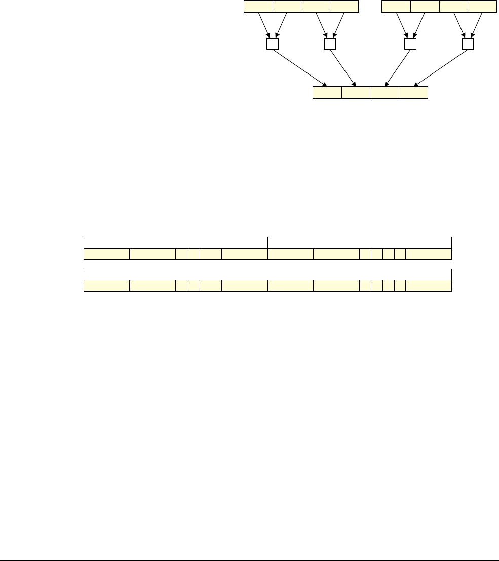
F8 T32 and A32 Advanced SIMD and floating-point Instruction Descriptions
F8.1 Alphabetical list of floating-point and Advanced SIMD instructions
F8-3258 Copyright © 2013 ARM Limited. All rights reserved. ARM DDI 0487A.a
Non-Confidential - Beta ID090413
F8.1.104 VPADD (integer)
Vector Pairwise Add (integer) adds adjacent pairs of elements of two vectors, and places the results in the
destination vector.
The operands and result are doubleword vectors.
The operand and result elements must all be the same type, and can be 8-bit, 16-bit, or 32-bit integers. There is no
distinction between signed and unsigned integers.
Figure F8-3 shows an example of the operation of
VPADD
.
Figure F8-3 VPADD operation for data type
I16
Depending on settings in the CPACR, NSACR, and HCPTR registers, and the security state and mode in which the
instruction is executed, an attempt to execute the instruction might be UNDEFINED, or trapped to Hyp mode.
Summary of access controls for Advanced SIMD functionality on page G1-3498 summarizes these controls.
ARM deprecates the conditional execution of any Advanced SIMD instruction encoding that is not also available
as a VFP instruction encoding, see Conditional execution on page F2-2416.
if size == ‘11’ || Q == ‘1’ then UNDEFINED;
esize = 8 << UInt(size); elements = 64 DIV esize;
d = UInt(D:Vd); n = UInt(N:Vn); m = UInt(M:Vm);
Dm
Dd
+ +
Dn
+ +
Encoding T1/A1 Advanced SIMDv1
VPADD<c>.<dt> <Dd>, <Dn>, <Dm>
1 1 0 1 1 1 1 0 D size Vn Vd 1 0 1 1 N Q M 1 Vm
15 14 13 12 11 10 9 8 7 6 5 4 3 2 1 0
1
1514131211109876543210
1 1 1 0 0 1 0 0 D size Vn Vd 1 0 1 1 N Q M 1 Vm
31 30 29 28 27 26 25 24 23 22 21 20 19 18 17 16 15 14 13 12 11 10 9 8 7 6 5 4 3 2 1 0
1

F8 T32 and A32 Advanced SIMD and floating-point Instruction Descriptions
F8.1 Alphabetical list of floating-point and Advanced SIMD instructions
ARM DDI 0487A.a Copyright © 2013 ARM Limited. All rights reserved. F8-3259
ID090413 Non-Confidential - Beta
Assembler syntax
where:
<c>, <q>
See Standard assembler syntax fields on page F2-2415. An A32
VPADD
instruction must be
unconditional. ARM strongly recommends that a T32
VPADD
instruction is unconditional, see
Conditional execution on page F2-2416.
<dt>
The data type for the elements of the vectors. It must be one of:
I8
Encoding T1/A1, encoded as size =
0b00
.
I16
Encoding T1/A1, encoded as size =
0b01
.
I32
Encoding T1/A1, encoded as size =
0b10
.
<Dd>, <Dn>, <Dm>
The destination vector, the first operand vector, and the second operand vector.
Operation
if ConditionPassed() then
EncodingSpecificOperations(); CheckAdvSIMDEnabled();
bits(64) dest;
h = elements DIV 2;
for e = 0 to h-1
Elem[dest,e,esize] = Elem[D[n],2*e,esize] + Elem[D[n],2*e+1,esize];
Elem[dest,e+h,esize] = Elem[D[m],2*e,esize] + Elem[D[m],2*e+1,esize];
D[d] = dest;
VPADD{<c>}{<q>}.<dt> {<Dd>,} <Dn>, <Dm>
Encoded as Q = 0

F8 T32 and A32 Advanced SIMD and floating-point Instruction Descriptions
F8.1 Alphabetical list of floating-point and Advanced SIMD instructions
F8-3260 Copyright © 2013 ARM Limited. All rights reserved. ARM DDI 0487A.a
Non-Confidential - Beta ID090413
F8.1.105 VPADD (floating-point)
Vector Pairwise Add (floating-point) adds adjacent pairs of elements of two vectors, and places the results in the
destination vector.
The operands and result are doubleword vectors.
The operand and result elements are 32-bit floating-point numbers.
Figure F8-3 on page F8-3258 shows an example of the operation of
VPADD
.
Depending on settings in the CPACR, NSACR, and HCPTR registers, and the security state and mode in which the
instruction is executed, an attempt to execute the instruction might be UNDEFINED, or trapped to Hyp mode.
Summary of access controls for Advanced SIMD functionality on page G1-3498 summarizes these controls.
ARM deprecates the conditional execution of any Advanced SIMD instruction encoding that is not also available
as a VFP instruction encoding, see Conditional execution on page F2-2416.
if sz == ‘1’ || Q == ‘1’ then UNDEFINED;
esize = 32; elements = 2;
d = UInt(D:Vd); n = UInt(N:Vn); m = UInt(M:Vm);
Encoding T1/A1 Advanced SIMDv1 (UNDEFINED in integer-only variant)
VPADD<c>.F32 <Dd>, <Dn>, <Dm>
1 0 11 1 1 1 1 1 1 0 D 0 sz Vn Vd 1 N Q M 0 Vm
15 14 13 12 11 10 9 8 7 6 5 4 3 2 1 0
1
1514131211109876543210
1 1 1 0 0 1 1 0 D 0 sz Vn Vd 1 1 0 1 N Q M 0 Vm
31 30 29 28 27 26 25 24 23 22 21 20 19 18 17 16 15 14 13 12 11 10 9 8 7 6 5 4 3 2 1 0
1

F8 T32 and A32 Advanced SIMD and floating-point Instruction Descriptions
F8.1 Alphabetical list of floating-point and Advanced SIMD instructions
ARM DDI 0487A.a Copyright © 2013 ARM Limited. All rights reserved. F8-3261
ID090413 Non-Confidential - Beta
Assembler syntax
where:
<c>, <q>
See Standard assembler syntax fields on page F2-2415. An A32
VPADD
instruction must be
unconditional. ARM strongly recommends that a T32
VPADD
instruction is unconditional, see
Conditional execution on page F2-2416.
<Dd>, <Dn>, <Dm>
The destination vector, the first operand vector, and the second operand vector.
Operation
if ConditionPassed() then
EncodingSpecificOperations(); CheckAdvSIMDEnabled();
bits(64) dest;
h = elements DIV 2;
for e = 0 to h-1
Elem[dest,e,esize] = FPAdd(Elem[D[n],2*e,esize], Elem[D[n],2*e+1,esize], StandardFPSCRValue());
Elem[dest,e+h,esize] = FPAdd(Elem[D[m],2*e,esize], Elem[D[m],2*e+1,esize], StandardFPSCRValue());
D[d] = dest;
VPADD{<c>}{<q>}.F32 {<Dd>,} <Dn>, <Dm>
Encoded as Q = 0, sz = 0
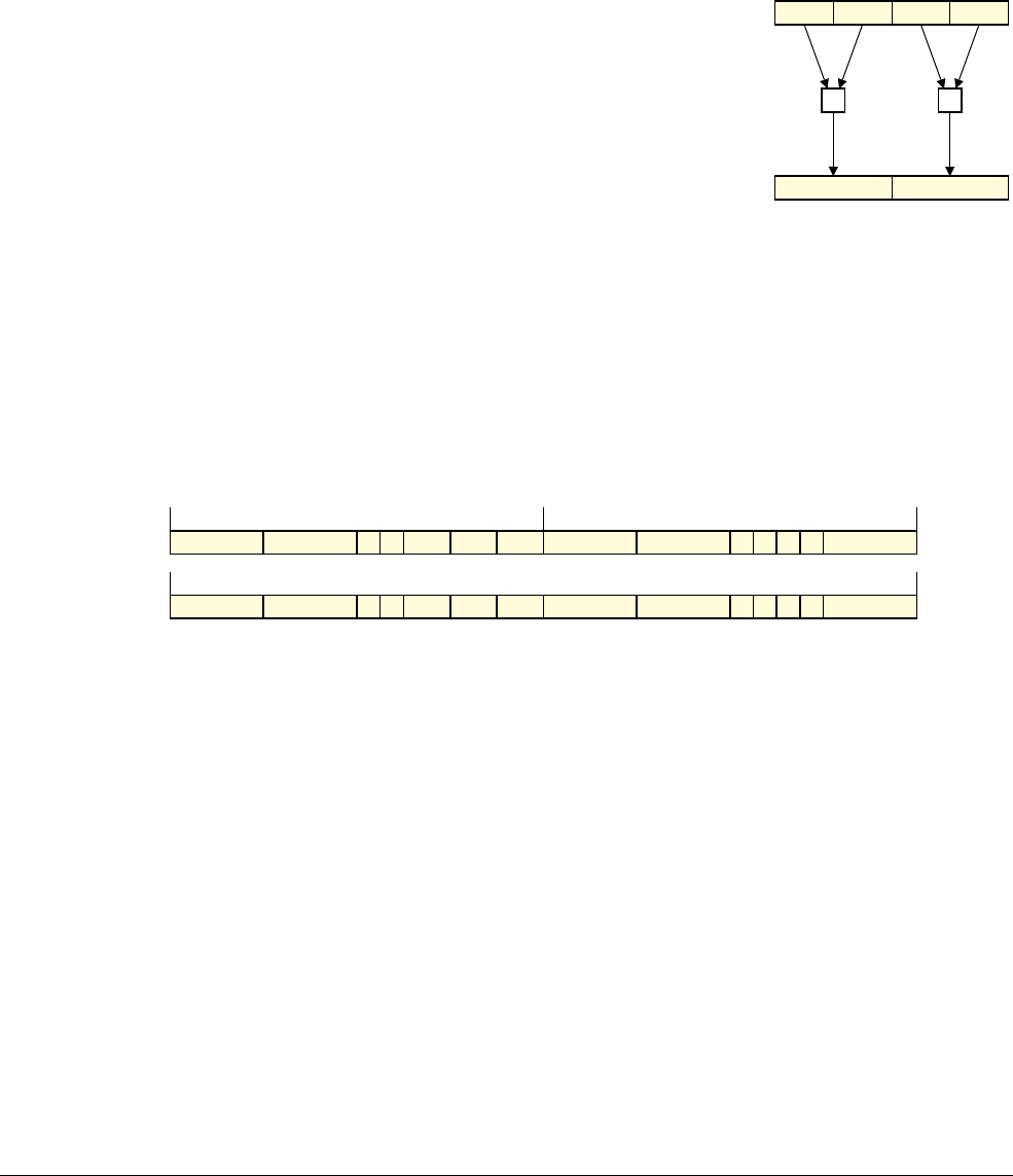
F8 T32 and A32 Advanced SIMD and floating-point Instruction Descriptions
F8.1 Alphabetical list of floating-point and Advanced SIMD instructions
F8-3262 Copyright © 2013 ARM Limited. All rights reserved. ARM DDI 0487A.a
Non-Confidential - Beta ID090413
F8.1.106 VPADDL
Vector Pairwise Add Long adds adjacent pairs of elements of two vectors, and places the results in the destination
vector.
The vectors can be doubleword or quadword. The operand elements can be 8-bit, 16-bit, or 32-bit integers. The
result elements are twice the length of the operand elements.
Figure F8-4 shows an example of the operation of
VPADDL
.
Figure F8-4 VPADDL doubleword operation for data type
S16
Depending on settings in the CPACR, NSACR, and HCPTR registers, and the security state and mode in which the
instruction is executed, an attempt to execute the instruction might be UNDEFINED, or trapped to Hyp mode.
Summary of access controls for Advanced SIMD functionality on page G1-3498 summarizes these controls.
ARM deprecates the conditional execution of any Advanced SIMD instruction encoding that is not also available
as a VFP instruction encoding, see Conditional execution on page F2-2416.
if size == ‘11’ then UNDEFINED;
if Q == ‘1’ && (Vd<0> == ‘1’ || Vm<0> == ‘1’) then UNDEFINED;
unsigned = (op == ‘1’);
esize = 8 << UInt(size); elements = 64 DIV esize;
d = UInt(D:Vd); m = UInt(M:Vm); regs = if Q == ‘0’ then 1 else 2;
Dm
Dd
+ +
Encoding T1/A1 Advanced SIMDv1
VPADDL<c>.<dt> <Qd>, <Qm>
VPADDL<c>.<dt> <Dd>, <Dm>
1 1 1 1 1 1 1 1 D 1 1 size 0 0 Vd 0 0 1 0 op Q M 0 Vm
15 14 13 12 11 10 9 8 7 6 5 4 3 2 1 0
1
1514131211109876543210
1 1 1 0 0 1 1 1 D 1 1 size 0 0 Vd 0 0 1 0 op Q M 0 Vm
31 30 29 28 27 26 25 24 23 22 21 20 19 18 17 16 15 14 13 12 11 10 9 8 7 6 5 4 3 2 1 0
1

F8 T32 and A32 Advanced SIMD and floating-point Instruction Descriptions
F8.1 Alphabetical list of floating-point and Advanced SIMD instructions
ARM DDI 0487A.a Copyright © 2013 ARM Limited. All rights reserved. F8-3263
ID090413 Non-Confidential - Beta
Assembler syntax
where:
<c>, <q>
See Standard assembler syntax fields on page F2-2415. An A32
VPADDL
instruction must be
unconditional. ARM strongly recommends that a T32
VPADDL
instruction is unconditional, see
Conditional execution on page F2-2416.
<dt>
The data type for the elements of the vectors. It must be one of:
S8
Encoded as size =
0b00
, op = 0.
S16
Encoded as size =
0b01
, op = 0.
S32
Encoded as size =
0b10
, op = 0.
U8
Encoded as size =
0b00
, op = 1.
U16
Encoded as size =
0b01
, op = 1.
U32
Encoded as size =
0b10
, op = 1.
<Qd>, <Qm>
The destination vector and the operand vector, for a quadword operation.
<Dd>, <Dm>
The destination vector and the operand vector, for a doubleword operation.
Operation
if ConditionPassed() then
EncodingSpecificOperations(); CheckAdvSIMDEnabled();
h = elements DIV 2;
for r = 0 to regs-1
for e = 0 to h-1
op1 = Elem[D[m+r],2*e,esize]; op2 = Elem[D[m+r],2*e+1,esize];
result = Int(op1, unsigned) + Int(op2, unsigned);
Elem[D[d+r],e,2*esize] = result<2*esize-1:0>;
VPADDL{<c>}{<q>}.<dt> <Qd>, <Qm>
Encoded as Q = 1
VPADDL{<c>}{<q>}.<dt> <Dd>, <Dm>
Encoded as Q = 0
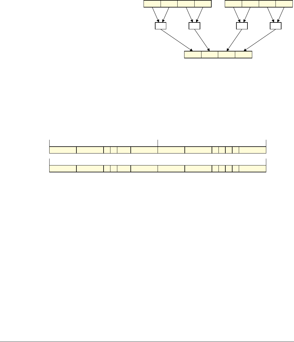
F8 T32 and A32 Advanced SIMD and floating-point Instruction Descriptions
F8.1 Alphabetical list of floating-point and Advanced SIMD instructions
F8-3264 Copyright © 2013 ARM Limited. All rights reserved. ARM DDI 0487A.a
Non-Confidential - Beta ID090413
F8.1.107 VPMAX, VPMIN (integer)
Vector Pairwise Maximum compares adjacent pairs of elements in two doubleword vectors, and copies the larger
of each pair into the corresponding element in the destination doubleword vector.
Vector Pairwise Minimum compares adjacent pairs of elements in two doubleword vectors, and copies the smaller
of each pair into the corresponding element in the destination doubleword vector.
Figure F8-5 shows an example of the operation of
VPMAX
.
Figure F8-5 VPMAX operation for data type
S16
or
U16
Depending on settings in the CPACR, NSACR, and HCPTR registers, and the security state and mode in which the
instruction is executed, an attempt to execute the instruction might be UNDEFINED, or trapped to Hyp mode.
Summary of access controls for Advanced SIMD functionality on page G1-3498 summarizes these controls.
ARM deprecates the conditional execution of any Advanced SIMD instruction encoding that is not also available
as a VFP instruction encoding, see Conditional execution on page F2-2416.
if size == ‘11’ || Q == ‘1’ then UNDEFINED;
maximum = (op == ‘0’); unsigned = (U == ‘1’);
esize = 8 << UInt(size); elements = 64 DIV esize;
d = UInt(D:Vd); n = UInt(N:Vn); m = UInt(M:Vm);
Dm
Dd
max max
Dn
max max
Encoding T1/A1 Advanced SIMDv1
VP<op><c>.<dt> <Dd>, <Dn>, <Dm>
1 1 U 1 1 1 1 0 D size Vn Vd 1 0 1 0 N Q M op Vm
15 14 13 12 11 10 9 8 7 6 5 4 3 2 1 0
1
1514131211109876543210
1 1 1 0 0 1 U 0 D size Vn Vd 1 0 1 0 N Q M op Vm
31 30 29 28 27 26 25 24 23 22 21 20 19 18 17 16 15 14 13 12 11 10 9 8 7 6 5 4 3 2 1 0
1

F8 T32 and A32 Advanced SIMD and floating-point Instruction Descriptions
F8.1 Alphabetical list of floating-point and Advanced SIMD instructions
ARM DDI 0487A.a Copyright © 2013 ARM Limited. All rights reserved. F8-3265
ID090413 Non-Confidential - Beta
Assembler syntax
where:
<op>
The operation. It must be one of:
MAX
Encoded as op = 0.
MIN
Encoded as op = 1.
<c>, <q>
See Standard assembler syntax fields on page F2-2415. An A32
VPMAX
or
VPMIN
instruction
must be unconditional. ARM strongly recommends that a T32
VPMAX
or
VPMIN
instruction is
unconditional, see Conditional execution on page F2-2416.
<dt>
The data type for the elements of the vectors. It must be one of:
S8
Encoding T1/A1, encoded as size =
0b00
, U = 0.
S16
Encoding T1/A1, encoded as size =
0b01
, U = 0.
S32
Encoding T1/A1, encoded as size =
0b10
, U = 0.
U8
Encoding T1/A1, encoded as size =
0b00
, U = 1.
U16
Encoding T1/A1, encoded as size =
0b01
, U = 1.
U32
Encoding T1/A1, encoded as size =
0b10
, U = 1.
<Dd>, <Dn>, <Dm>
The destination vector and the operand vectors.
Operation
if ConditionPassed() then
EncodingSpecificOperations(); CheckAdvSIMDEnabled();
bits(64) dest;
h = elements DIV 2;
for e = 0 to h-1
op1 = Int(Elem[D[n],2*e,esize], unsigned);
op2 = Int(Elem[D[n],2*e+1,esize], unsigned);
result = if maximum then Max(op1,op2) else Min(op1,op2);
Elem[dest,e,esize] = result<esize-1:0>;
op1 = Int(Elem[D[m],2*e,esize], unsigned);
op2 = Int(Elem[D[m],2*e+1,esize], unsigned);
result = if maximum then Max(op1,op2) else Min(op1,op2);
Elem[dest,e+h,esize] = result<esize-1:0>;
D[d] = dest;
VP<op>{<c>}{<q>}.<dt> {<Dd>,} <Dn>, <Dm>
Encoded as Q = 0

F8 T32 and A32 Advanced SIMD and floating-point Instruction Descriptions
F8.1 Alphabetical list of floating-point and Advanced SIMD instructions
F8-3266 Copyright © 2013 ARM Limited. All rights reserved. ARM DDI 0487A.a
Non-Confidential - Beta ID090413
F8.1.108 VPMAX, VPMIN (floating-point)
Vector Pairwise Maximum compares adjacent pairs of elements in two doubleword vectors, and copies the larger
of each pair into the corresponding element in the destination doubleword vector.
Vector Pairwise Minimum compares adjacent pairs of elements in two doubleword vectors, and copies the smaller
of each pair into the corresponding element in the destination doubleword vector.
Figure F8-5 on page F8-3264 shows an example of the operation of
VPMAX
.
Depending on settings in the CPACR, NSACR, and HCPTR registers, and the security state and mode in which the
instruction is executed, an attempt to execute the instruction might be UNDEFINED, or trapped to Hyp mode.
Summary of access controls for Advanced SIMD functionality on page G1-3498 summarizes these controls.
ARM deprecates the conditional execution of any Advanced SIMD instruction encoding that is not also available
as a VFP instruction encoding, see Conditional execution on page F2-2416.
if sz == ‘1’ || Q == ‘1’ then UNDEFINED;
maximum = (op == ‘0’); esize = 32; elements = 2;
d = UInt(D:Vd); n = UInt(N:Vn); m = UInt(M:Vm);
Encoding T1/A1 Advanced SIMDv1 (UNDEFINED in integer-only variant)
VP<op><c>.F32 <Dd>, <Dn>, <Dm>
1 1 1 1 1 1 1 0 D op sz Vn Vd 1 1 1 1 N Q M 0 Vm
15 14 13 12 11 10 9 8 7 6 5 4 3 2 1 0
1
1514131211109876543210
1 1 1 0 0 1 1 0 D op sz Vn Vd 1 1 1 1 N Q M 0 Vm
31 30 29 28 27 26 25 24 23 22 21 20 19 18 17 16 15 14 13 12 11 10 9 8 7 6 5 4 3 2 1 0
1

F8 T32 and A32 Advanced SIMD and floating-point Instruction Descriptions
F8.1 Alphabetical list of floating-point and Advanced SIMD instructions
ARM DDI 0487A.a Copyright © 2013 ARM Limited. All rights reserved. F8-3267
ID090413 Non-Confidential - Beta
Assembler syntax
where:
<op>
The operation. It must be one of:
MAX
Encoded as op = 0.
MIN
Encoded as op = 1.
<c>, <q>
See Standard assembler syntax fields on page F2-2415. An A32
VPMAX
or
VPMIN
instruction
must be unconditional. ARM strongly recommends that a T32
VPMAX
or
VPMIN
instruction is
unconditional, see Conditional execution on page F2-2416.
<Dd>, <Dn>, <Dm>
The destination vector and the operand vectors.
Operation
if ConditionPassed() then
EncodingSpecificOperations(); CheckAdvSIMDEnabled();
bits(64) dest;
h = elements DIV 2;
for e = 0 to h-1
op1 = Elem[D[n],2*e,esize]; op2 = Elem[D[n],2*e+1,esize];
Elem[dest,e,esize] = if maximum then FPMax(op1,op2,StandardFPSCRValue()) else
FPMin(op1,op2,StandardFPSCRValue());
op1 = Elem[D[m],2*e,esize]; op2 = Elem[D[m],2*e+1,esize];
Elem[dest,e+h,esize] = if maximum then FPMax(op1,op2,StandardFPSCRValue()) else
FPMin(op1,op2,StandardFPSCRValue());
D[d] = dest;
VP<op>{<c>}{<q>}.F32 {<Dd>,} <Dn>, <Dm>
Encoded as Q = 0, sz = 0

F8 T32 and A32 Advanced SIMD and floating-point Instruction Descriptions
F8.1 Alphabetical list of floating-point and Advanced SIMD instructions
F8-3268 Copyright © 2013 ARM Limited. All rights reserved. ARM DDI 0487A.a
Non-Confidential - Beta ID090413
F8.1.109 VPOP
Vector Pop loads multiple consecutive extension registers from the stack.
Depending on settings in the CPACR, NSACR, and HCPTR, and FPEXC registers, and the security state and mode
in which the instruction is executed, an attempt to execute the instruction might be UNDEFINED, or trapped to Hyp
mode. Summary of general controls of CP10 and CP11 functionality on page G1-3496 and Summary of access
controls for Advanced SIMD functionality on page G1-3498 summarize these controls.
single_regs = FALSE; d = UInt(D:Vd); imm32 = ZeroExtend(imm8:’00’, 32);
regs = UInt(imm8) DIV 2; // If UInt(imm8) is odd, see “FLDMX”.
if regs == 0 || regs > 16 || (d+regs) > 32 then UNPREDICTABLE;
if VFPSmallRegisterBank() && (d+regs) > 16 then UNPREDICTABLE;
single_regs = TRUE; d = UInt(Vd:D); imm32 = ZeroExtend(imm8:’00’, 32);
regs = UInt(imm8);
if regs == 0 || (d+regs) > 32 then UNPREDICTABLE;
For information about the CONSTRAINED UNPREDICTABLE behavior of this instruction, see Appendix A
Architectural Constraints on UNPREDICTABLE behaviors, and particularly VPOP on page AppxA-4748.
Encoding T1/A1 VFPv2, VFPv3, VFPv4, Advanced SIMDv1
VPOP <list> <list>
is consecutive 64-bit registers
Encoding T2/A2 VFPv2, VFPv3, VFPv4
VPOP <list> <list>
is consecutive 32-bit registers
FLDMX Encoding T1/A1 behaves as described by the pseudocode if imm8 is odd. However,
there is no UAL syntax for such encodings and ARM deprecates their use. For more
information, see FLDMX, FSTMX on page F8-3080.
1 1 0 1 1 0 0 1 D 1 1 1 1 0 1 Vd 1 0 1 1 imm8
15 14 13 12 11 10 9 8 7 6 5 4 3 2 1 0
1
1514131211109876543210
1 1 0 0 1 D 1 1 1 1 0 1 Vd 1 0 1 1 imm8
31 30 29 28 27 26 25 24 23 22 21 20 19 18 17 16 15 14 13 12 11 10 9 8 7 6 5 4 3 2 1 0
cond
1 1 0 1 1 0 0 1 D 1 1 1 1 0 1 Vd 1 0 1 0 imm8
15 14 13 12 11 10 9 8 7 6 5 4 3 2 1 0
1
1514131211109876543210
1 1 0 0 1 D 1 1 1 1 0 1 Vd 1 0 1 0 imm8
31 30 29 28 27 26 25 24 23 22 21 20 19 18 17 16 15 14 13 12 11 10 9 8 7 6 5 4 3 2 1 0
cond

F8 T32 and A32 Advanced SIMD and floating-point Instruction Descriptions
F8.1 Alphabetical list of floating-point and Advanced SIMD instructions
ARM DDI 0487A.a Copyright © 2013 ARM Limited. All rights reserved. F8-3269
ID090413 Non-Confidential - Beta
Assembler syntax
VPOP{<c>}{<q>}{.<size>} <list>
where:
<c>, <q>
See Standard assembler syntax fields on page F2-2415.
<size>
An optional data size specifier. If present, it must be equal to the size in bits, 32 or 64, of the registers
in
<list>
.
<list>
The extension registers to be loaded, as a list of consecutively numbered doubleword (encoding
T1/A1) or singleword (encoding T2/A2) registers, separated by commas and surrounded by
brackets. It is encoded in the instruction by setting D and Vd to specify the first register in the list,
and imm8 to twice the number of registers in the list (encoding T1/A1) or the number of registers
in the list (encoding T2/A2).
<list>
must contain at least one register, and not more than sixteen.
Operation
if ConditionPassed() then
EncodingSpecificOperations(); CheckVFPEnabled(TRUE); NullCheckIfThumbEE(13);
address = SP;
SP = SP + imm32;
if single_regs then
for r = 0 to regs-1
S[d+r] = MemA[address,4]; address = address+4;
else
for r = 0 to regs-1
word1 = MemA[address,4]; word2 = MemA[address+4,4]; address = address+8;
// Combine the word-aligned words in the correct order for current endianness.
D[d+r] = if BigEndian() then word1:word2 else word2:word1;
F8 T32 and A32 Advanced SIMD and floating-point Instruction Descriptions
F8.1 Alphabetical list of floating-point and Advanced SIMD instructions
F8-3270 Copyright © 2013 ARM Limited. All rights reserved. ARM DDI 0487A.a
Non-Confidential - Beta ID090413
F8.1.110 VPUSH
Vector Push stores multiple consecutive extension registers to the stack.
Depending on settings in the CPACR, NSACR, and HCPTR, and FPEXC registers, and the security state and mode
in which the instruction is executed, an attempt to execute the instruction might be UNDEFINED, or trapped to Hyp
mode. Summary of general controls of CP10 and CP11 functionality on page G1-3496 and Summary of access
controls for Advanced SIMD functionality on page G1-3498 summarize these controls.
single_regs = FALSE; d = UInt(D:Vd); imm32 = ZeroExtend(imm8:’00’, 32);
regs = UInt(imm8) DIV 2; // If UInt(imm8) is odd, see “FSTMX”.
if regs == 0 || regs > 16 || (d+regs) > 32 then UNPREDICTABLE;
if VFPSmallRegisterBank() && (d+regs) > 16 then UNPREDICTABLE;
single_regs = TRUE; d = UInt(Vd:D);
imm32 = ZeroExtend(imm8:’00’, 32); regs = UInt(imm8);
if regs == 0 || (d+regs) > 32 then UNPREDICTABLE;
For information about the CONSTRAINED UNPREDICTABLE behavior of this instruction, see Appendix A
Architectural Constraints on UNPREDICTABLE behaviors, and particularly VPUSH on page AppxA-4753.
Encoding T1/A1 VFPv2, VFPv3, VFPv4, Advanced SIMDv1
VPUSH<c> <list> <list>
is consecutive 64-bit registers
Encoding T2/A2 VFPv2, VFPv3, VFPv4
VPUSH<c> <list> <list>
is consecutive 32-bit registers
FSTMX Encoding T1/A1 behaves as described by the pseudocode if imm8 is odd. However,
there is no UAL syntax for such encodings and ARM deprecates their use. For more
information, see FLDMX, FSTMX on page F8-3080.
1 1 0 1 1 0 1 0 D 1 0 1 1 0 1 Vd 1 0 1 1 imm8
15 14 13 12 11 10 9 8 7 6 5 4 3 2 1 0
1
1514131211109876543210
1 1 0 1 0 D 1 0 1 1 0 1 Vd 1 0 1 1 imm8
31 30 29 28 27 26 25 24 23 22 21 20 19 18 17 16 15 14 13 12 11 10 9 8 7 6 5 4 3 2 1 0
cond
1 1 0 1 1 0 1 0 D 1 0 1 1 0 1 Vd 1 0 1 0 imm8
15 14 13 12 11 10 9 8 7 6 5 4 3 2 1 0
1
1514131211109876543210
1 1 0 1 0 D 1 0 1 1 0 1 Vd 1 0 1 0 imm8
31 30 29 28 27 26 25 24 23 22 21 20 19 18 17 16 15 14 13 12 11 10 9 8 7 6 5 4 3 2 1 0
cond

F8 T32 and A32 Advanced SIMD and floating-point Instruction Descriptions
F8.1 Alphabetical list of floating-point and Advanced SIMD instructions
ARM DDI 0487A.a Copyright © 2013 ARM Limited. All rights reserved. F8-3271
ID090413 Non-Confidential - Beta
Assembler syntax
VPUSH{<c>}{<q>}{.<size>} <list>
where:
<c>, <q>
See Standard assembler syntax fields on page F2-2415.
<size>
An optional data size specifier. If present, it must be equal to the size in bits, 32 or 64, of the registers
in
<list>
.
<list>
The extension registers to be stored, as a list of consecutively numbered doubleword (encoding
T1/A1) or singleword (encoding T2/A2) registers, separated by commas and surrounded by
brackets. It is encoded in the instruction by setting D and Vd to specify the first register in the list,
and imm8 to twice the number of registers in the list (encoding T1/A1), or the number of registers
in the list (encoding T2/A2).
<list>
must contain at least one register, and not more than sixteen.
Operation
if ConditionPassed() then
EncodingSpecificOperations(); CheckVFPEnabled(TRUE); NullCheckIfThumbEE(13);
address = SP - imm32;
SP = SP - imm32;
if single_regs then
for r = 0 to regs-1
MemA[address,4] = S[d+r]; address = address+4;
else
for r = 0 to regs-1
// Store as two word-aligned words in the correct order for current endianness.
MemA[address,4] = if BigEndian() then D[d+r]<63:32> else D[d+r]<31:0>;
MemA[address+4,4] = if BigEndian() then D[d+r]<31:0> else D[d+r]<63:32>;
address = address+8;

F8 T32 and A32 Advanced SIMD and floating-point Instruction Descriptions
F8.1 Alphabetical list of floating-point and Advanced SIMD instructions
F8-3272 Copyright © 2013 ARM Limited. All rights reserved. ARM DDI 0487A.a
Non-Confidential - Beta ID090413
F8.1.111 VQABS
Vector Saturating Absolute takes the absolute value of each element in a vector, and places the results in the
destination vector.
If any of the results overflow, they are saturated. The cumulative saturation bit, FPSCR.QC, is set if saturation
occurs. For details see Pseudocode details of saturation on page E1-2293.
Depending on settings in the CPACR, NSACR, and HCPTR registers, and the security state and mode in which the
instruction is executed, an attempt to execute the instruction might be UNDEFINED, or trapped to Hyp mode.
Summary of access controls for Advanced SIMD functionality on page G1-3498 summarizes these controls.
ARM deprecates the conditional execution of any Advanced SIMD instruction encoding that is not also available
as a VFP instruction encoding, see Conditional execution on page F2-2416.
if size == ‘11’ then UNDEFINED;
if Q == ‘1’ && (Vd<0> == ‘1’ || Vm<0> == ‘1’) then UNDEFINED;
esize = 8 << UInt(size); elements = 64 DIV esize;
d = UInt(D:Vd); m = UInt(M:Vm); regs = if Q == ‘0’ then 1 else 2;
Encoding T1/A1 Advanced SIMDv1
VQABS<c>.<dt> <Qd>, <Qm>
VQABS<c>.<dt> <Dd>, <Dm>
1 1 1 1 1 1 1 1 D 1 1 size 0 0 Vd 0 1 1 1 0 Q M 0 Vm
15 14 13 12 11 10 9 8 7 6 5 4 3 2 1 0
1
1514131211109876543210
1 1 1 0 0 1 1 1 D 1 1 size 0 0 Vd 0 1 1 1 0 Q M 0 Vm
31 30 29 28 27 26 25 24 23 22 21 20 19 18 17 16 15 14 13 12 11 10 9 8 7 6 5 4 3 2 1 0
1

F8 T32 and A32 Advanced SIMD and floating-point Instruction Descriptions
F8.1 Alphabetical list of floating-point and Advanced SIMD instructions
ARM DDI 0487A.a Copyright © 2013 ARM Limited. All rights reserved. F8-3273
ID090413 Non-Confidential - Beta
Assembler syntax
where:
<c>, <q>
See Standard assembler syntax fields on page F2-2415. An A32
VQABS
instruction must be
unconditional. ARM strongly recommends that a T32
VQABS
instruction is unconditional, see
Conditional execution on page F2-2416.
<dt>
The data type for the elements of the vectors. It must be one of:
S8
Encoded as size =
0b00
.
S16
Encoded as size =
0b01
.
S32
Encoded as size =
0b10
.
<Qd>, <Qm>
The destination vector and the operand vector, for a quadword operation.
<Dd>, <Dm>
The destination vector and the operand vector, for a doubleword operation.
Operation
if ConditionPassed() then
EncodingSpecificOperations(); CheckAdvSIMDEnabled();
for r = 0 to regs-1
for e = 0 to elements-1
result = Abs(SInt(Elem[D[m+r],e,esize]));
(Elem[D[d+r],e,esize], sat) = SignedSatQ(result, esize);
if sat then FPSR.QC = ‘1’;
VQABS{<c>}{<q>}.<dt> <Qd>, <Qm>
Encoded as Q = 1
VQABS{<c>}{<q>}.<dt> <Dd>, <Dm>
Encoded as Q = 0

F8 T32 and A32 Advanced SIMD and floating-point Instruction Descriptions
F8.1 Alphabetical list of floating-point and Advanced SIMD instructions
F8-3274 Copyright © 2013 ARM Limited. All rights reserved. ARM DDI 0487A.a
Non-Confidential - Beta ID090413
F8.1.112 VQADD
Vector Saturating Add adds the values of corresponding elements of two vectors, and places the results in the
destination vector.
If any of the results overflow, they are saturated. The cumulative saturation bit, FPSCR.QC, is set if saturation
occurs. For details see Pseudocode details of saturation on page E1-2293.
Depending on settings in the CPACR, NSACR, and HCPTR registers, and the security state and mode in which the
instruction is executed, an attempt to execute the instruction might be UNDEFINED, or trapped to Hyp mode.
Summary of access controls for Advanced SIMD functionality on page G1-3498 summarizes these controls.
ARM deprecates the conditional execution of any Advanced SIMD instruction encoding that is not also available
as a VFP instruction encoding, see Conditional execution on page F2-2416.
if Q == ‘1’ && (Vd<0> == ‘1’ || Vn<0> == ‘1’ || Vm<0> == ‘1’) then UNDEFINED;
unsigned = (U == ‘1’);
esize = 8 << UInt(size); elements = 64 DIV esize;
d = UInt(D:Vd); n = UInt(N:Vn); m = UInt(M:Vm); regs = if Q == ‘0’ then 1 else 2;
Encoding T1/A1 Advanced SIMDv1
VQADD<c>.<dt> <Qd>, <Qn>, <Qm>
VQADD<c>.<dt> <Dd>, <Dn>, <Dm>
1 1 U 1 1 1 1 0 D size Vn Vd 0 0 0 0 N Q M 1 Vm
15 14 13 12 11 10 9 8 7 6 5 4 3 2 1 0
1
1514131211109876543210
1 1 1 0 0 1 U 0 D size Vn Vd 0 0 0 0 N Q M 1 Vm
31 30 29 28 27 26 25 24 23 22 21 20 19 18 17 16 15 14 13 12 11 10 9 8 7 6 5 4 3 2 1 0
1

F8 T32 and A32 Advanced SIMD and floating-point Instruction Descriptions
F8.1 Alphabetical list of floating-point and Advanced SIMD instructions
ARM DDI 0487A.a Copyright © 2013 ARM Limited. All rights reserved. F8-3275
ID090413 Non-Confidential - Beta
Assembler syntax
where:
<c>, <q>
See Standard assembler syntax fields on page F2-2415. An A32
VQADD
instruction must be
unconditional. ARM strongly recommends that a T32
VQADD
instruction is unconditional, see
Conditional execution on page F2-2416.
<type>
The data type for the elements of the vectors. It must be one of:
S
Signed, encoded as U = 0.
U
Unsigned, encoded as U = 1.
<size>
The data size for the elements of the vectors. It must be one of:
8
Encoded as size =
0b00
.
16
Encoded as size =
0b01
.
32
Encoded as size =
0b10
.
64
Encoded as size =
0b11
.
<Qd>, <Qn>, <Qm>
The destination vector and the operand vectors, for a quadword operation.
<Dd>, <Dn>, <Dm>
The destination vector and the operand vectors, for a doubleword operation.
Operation
if ConditionPassed() then
EncodingSpecificOperations(); CheckAdvSIMDEnabled();
for r = 0 to regs-1
for e = 0 to elements-1
sum = Int(Elem[D[n+r],e,esize], unsigned) + Int(Elem[D[m+r],e,esize], unsigned);
(Elem[D[d+r],e,esize], sat) = SatQ(sum, esize, unsigned);
if sat then FPSR.QC = ‘1’;
VQADD{<c>}{<q>}.<type><size> {<Qd>,} <Qn>, <Qm>
Encoded as Q = 1
VQADD{<c>}{<q>}.<type><size> {<Dd>,} <Dn>, <Dm>
Encoded as Q = 0
F8 T32 and A32 Advanced SIMD and floating-point Instruction Descriptions
F8.1 Alphabetical list of floating-point and Advanced SIMD instructions
F8-3276 Copyright © 2013 ARM Limited. All rights reserved. ARM DDI 0487A.a
Non-Confidential - Beta ID090413
F8.1.113 VQDMLAL, VQDMLSL
Vector Saturating Doubling Multiply Accumulate Long multiplies corresponding elements in two doubleword
vectors, doubles the products, and accumulates the results into the elements of a quadword vector.
Vector Saturating Doubling Multiply Subtract Long multiplies corresponding elements in two doubleword vectors,
subtracts double the products from corresponding elements of a quadword vector, and places the results in the same
quadword vector.
In both instructions, the second operand can be a scalar instead of a vector. For more information about scalars see
Advanced SIMD scalars on page F5-2498.
If any of the results overflow, they are saturated. The cumulative saturation bit, FPSCR.QC, is set if saturation
occurs. For details see Pseudocode details of saturation on page E1-2293.
Depending on settings in the CPACR, NSACR, and HCPTR registers, and the security state and mode in which the
instruction is executed, an attempt to execute the instruction might be UNDEFINED, or trapped to Hyp mode.
Summary of access controls for Advanced SIMD functionality on page G1-3498 summarizes these controls.
ARM deprecates the conditional execution of any Advanced SIMD instruction encoding that is not also available
as a VFP instruction encoding, see Conditional execution on page F2-2416.
if size == ‘11’ then SEE “Related encodings”;
if size == ‘00’ || Vd<0> == ‘1’ then UNDEFINED;
add = (op == ‘0’);
scalar_form = FALSE; d = UInt(D:Vd); n = UInt(N:Vn); m = UInt(M:Vm);
esize = 8 << UInt(size); elements = 64 DIV esize;
if size == ‘11’ then SEE “Related encodings”;
if size == ‘00’ || Vd<0> == ‘1’ then UNDEFINED;
add = (op == ‘0’);
scalar_form = TRUE; d = UInt(D:Vd); n = UInt(N:Vn);
if size == ‘01’ then esize = 16; elements = 4; m = UInt(Vm<2:0>); index = UInt(M:Vm<3>);
if size == ‘10’ then esize = 32; elements = 2; m = UInt(Vm); index = UInt(M);
Encoding T1/A1 Advanced SIMDv1
VQD<op><c>.<dt> <Qd>, <Dn>, <Dm>
Encoding T2/A2 Advanced SIMDv1
VQD<op><c>.<dt> <Qd>, <Dn>, <Dm[x]>
Related encodings See Advanced SIMD data-processing instructions on page F5-2499.
1 1 0 1 1 1 1 1 D size Vn Vd 1 0 op 1 N 0 M 0 Vm
15 14 13 12 11 10 9 8 7 6 5 4 3 2 1 0
1
1514131211109876543210
1 1 1 0 0 1 0 1 D size Vn Vd 1 0 op 1 N 0 M 0 Vm
31 30 29 28 27 26 25 24 23 22 21 20 19 18 17 16 15 14 13 12 11 10 9 8 7 6 5 4 3 2 1 0
1
1 1 0 1 1 1 1 1 D size Vn Vd 0 op 1 1 N 1 M 0 Vm
15 14 13 12 11 10 9 8 7 6 5 4 3 2 1 0
1
1514131211109876543210
1 1 1 0 0 1 0 1 D size Vn Vd 0 op 1 1 N 1 M 0 Vm
31 30 29 28 27 26 25 24 23 22 21 20 19 18 17 16 15 14 13 12 11 10 9 8 7 6 5 4 3 2 1 0
1

F8 T32 and A32 Advanced SIMD and floating-point Instruction Descriptions
F8.1 Alphabetical list of floating-point and Advanced SIMD instructions
ARM DDI 0487A.a Copyright © 2013 ARM Limited. All rights reserved. F8-3277
ID090413 Non-Confidential - Beta
Assembler syntax
where:
<op>
The operation. It must be one of:
MLAL
Encoded as op = 0.
MLSL
Encoded as op = 1.
<c>, <q>
See Standard assembler syntax fields on page F2-2415. An A32
VQDMLAL
or
VQDMLSL
instruction must
be unconditional. ARM strongly recommends that a T32
VQDMLAL
or
VQDMLSL
instruction is
unconditional, see Conditional execution on page F2-2416.
<dt>
The data type for the elements of the operands. It must be one of:
S16
Encoded as size =
0b01
.
S32
Encoded as size =
0b10
.
<Qd>, <Dn>
The destination vector and the first operand vector.
<Dm>
The second operand vector, for an all vector operation.
<Dm[x]>
The scalar for a scalar operation. If
<dt>
is
S16
,
Dm
is restricted to D0-D7. If
<dt>
is
S32
,
Dm
is restricted
to D0-D15.
Operation
if ConditionPassed() then
EncodingSpecificOperations(); CheckAdvSIMDEnabled();
if scalar_form then op2 = SInt(Elem[Din[m],index,esize]);
for e = 0 to elements-1
if !scalar_form then op2 = SInt(Elem[Din[m],e,esize]);
op1 = SInt(Elem[Din[n],e,esize]);
// The following only saturates if both op1 and op2 equal -(2^(esize-1))
(product, sat1) = SignedSatQ(2*op1*op2, 2*esize);
if add then
result = SInt(Elem[Qin[d>>1],e,2*esize]) + SInt(product);
else
result = SInt(Elem[Qin[d>>1],e,2*esize]) - SInt(product);
(Elem[Q[d>>1],e,2*esize], sat2) = SignedSatQ(result, 2*esize);
if sat1 || sat2 then FPSR.QC = ‘1’;
VQD<op>{<c>}{<q>}.<dt> <Qd>, <Dn>, <Dm>
VQD<op>{<c>}{<q>}.<dt> <Qd>, <Dn>, <Dm[x]>

F8 T32 and A32 Advanced SIMD and floating-point Instruction Descriptions
F8.1 Alphabetical list of floating-point and Advanced SIMD instructions
F8-3278 Copyright © 2013 ARM Limited. All rights reserved. ARM DDI 0487A.a
Non-Confidential - Beta ID090413
F8.1.114 VQDMULH
Vector Saturating Doubling Multiply Returning High Half multiplies corresponding elements in two vectors,
doubles the results, and places the most significant half of the final results in the destination vector. The results are
truncated, for rounded results see VQRDMULH on page F8-3286.
The second operand can be a scalar instead of a vector. For more information about scalars see Advanced SIMD
scalars on page F5-2498.
If any of the results overflow, they are saturated. The cumulative saturation bit, FPSCR.QC, is set if saturation
occurs. For details see Pseudocode details of saturation on page E1-2293.
Depending on settings in the CPACR, NSACR, and HCPTR registers, and the security state and mode in which the
instruction is executed, an attempt to execute the instruction might be UNDEFINED, or trapped to Hyp mode.
Summary of access controls for Advanced SIMD functionality on page G1-3498 summarizes these controls.
ARM deprecates the conditional execution of any Advanced SIMD instruction encoding that is not also available
as a VFP instruction encoding, see Conditional execution on page F2-2416.
if Q == ‘1’ && (Vd<0> == ‘1’ || Vn<0> == ‘1’ || Vm<0> == ‘1’) then UNDEFINED;
if size == ‘00’ || size == ‘11’ then UNDEFINED;
scalar_form = FALSE; esize = 8 << UInt(size); elements = 64 DIV esize;
d = UInt(D:Vd); n = UInt(N:Vn); m = UInt(M:Vm); regs = if Q == ‘0’ then 1 else 2;
if size == ‘11’ then SEE “Related encodings”;
if size == ‘00’ then UNDEFINED;
if Q == ‘1’ && (Vd<0> == ‘1’ || Vn<0> == ‘1’) then UNDEFINED;
scalar_form = TRUE; d = UInt(D:Vd); n = UInt(N:Vn); regs = if Q == ‘0’ then 1 else 2;
if size == ‘01’ then esize = 16; elements = 4; m = UInt(Vm<2:0>); index = UInt(M:Vm<3>);
if size == ‘10’ then esize = 32; elements = 2; m = UInt(Vm); index = UInt(M);
Encoding T1/A1 Advanced SIMDv1
VQDMULH<c>.<dt> <Qd>, <Qn>, <Qm>
VQDMULH<c>.<dt> <Dd>, <Dn>, <Dm>
Encoding T2/A2 Advanced SIMDv1
VQDMULH<c>.<dt> <Qd>, <Qn>, <Dm[x]>
VQDMULH<c>.<dt> <Dd>, <Dn>, <Dm[x]>
Related encodings See Advanced SIMD data-processing instructions on page F5-2499.
1 1 0 1 1 1 1 0 D size Vn Vd 1 0 1 1 N Q M 0 Vm
15 14 13 12 11 10 9 8 7 6 5 4 3 2 1 0
1
1514131211109876543210
1 1 1 0 0 1 0 0 D size Vn Vd 1 0 1 1 N Q M 0 Vm
31 30 29 28 27 26 25 24 23 22 21 20 19 18 17 16 15 14 13 12 11 10 9 8 7 6 5 4 3 2 1 0
1
1 1 Q 1 1 1 1 1 D size Vn Vd 1 1 0 0 N 1 M 0 Vm
15 14 13 12 11 10 9 8 7 6 5 4 3 2 1 0
1
1514131211109876543210
1 1 1 0 0 1 Q 1 D size Vn Vd 1 1 0 0 N 1 M 0 Vm
31 30 29 28 27 26 25 24 23 22 21 20 19 18 17 16 15 14 13 12 11 10 9 8 7 6 5 4 3 2 1 0
1

F8 T32 and A32 Advanced SIMD and floating-point Instruction Descriptions
F8.1 Alphabetical list of floating-point and Advanced SIMD instructions
ARM DDI 0487A.a Copyright © 2013 ARM Limited. All rights reserved. F8-3279
ID090413 Non-Confidential - Beta
Assembler syntax
where:
<c>, <q>
See Standard assembler syntax fields on page F2-2415. An A32
VQDMULH
instruction must be
unconditional. ARM strongly recommends that a T32
VQDMULH
instruction is unconditional,
see Conditional execution on page F2-2416.
<dt>
The data type for the elements of the operands. It must be one of:
S16
Encoded as size =
0b01
.
S32
Encoded as size =
0b10
.
<Qd>, <Qn>
The destination vector and the first operand vector, for a quadword operation.
<Dd>, <Dn>
The destination vector and the first operand vector, for a doubleword operation.
<Qm>
The second operand vector, for a quadword all vector operation.
<Dm>
The second operand vector, for a doubleword all vector operation.
<Dm[x]>
The scalar for either a quadword or a doubleword scalar operation. If
<dt>
is
S16
,
Dm
is
restricted to D0-D7. If
<dt>
is
S32
,
Dm
is restricted to D0-D15.
Operation
if ConditionPassed() then
EncodingSpecificOperations(); CheckAdvSIMDEnabled();
if scalar_form then op2 = SInt(Elem[D[m],index,esize]);
for r = 0 to regs-1
for e = 0 to elements-1
if !scalar_form then op2 = SInt(Elem[D[m+r],e,esize]);
op1 = SInt(Elem[D[n+r],e,esize]);
// The following only saturates if both op1 and op2 equal -(2^(esize-1))
(result, sat) = SignedSatQ((2*op1*op2) >> esize, esize);
Elem[D[d+r],e,esize] = result;
if sat then FPSR.QC = ‘1’;
VQDMULH{<c>}{<q>}.<dt> {<Qd>,} <Qn>, <Qm>
Encoding T1/A1, encoded as Q = 1
VQDMULH{<c>}{<q>}.<dt> {<Dd>,} <Dn>, <Dm>
Encoding T1/A1, encoded as Q = 0
VQDMULH{<c>}{<q>}.<dt> {<Qd>,} <Qn>, <Dm[x]>
Encoding T2/A2, encoded as Q = 1
VQDMULH{<c>}{<q>}.<dt> {<Dd>,} <Dn>, <Dm[x]>
Encoding T2/A2, encoded as Q = 0
F8 T32 and A32 Advanced SIMD and floating-point Instruction Descriptions
F8.1 Alphabetical list of floating-point and Advanced SIMD instructions
F8-3280 Copyright © 2013 ARM Limited. All rights reserved. ARM DDI 0487A.a
Non-Confidential - Beta ID090413
F8.1.115 VQDMULL
Vector Saturating Doubling Multiply Long multiplies corresponding elements in two doubleword vectors, doubles
the products, and places the results in a quadword vector.
The second operand can be a scalar instead of a vector. For more information about scalars see Advanced SIMD
scalars on page F5-2498.
If any of the results overflow, they are saturated. The cumulative saturation bit, FPSCR.QC, is set if saturation
occurs. For details see Pseudocode details of saturation on page E1-2293.
Depending on settings in the CPACR, NSACR, and HCPTR registers, and the security state and mode in which the
instruction is executed, an attempt to execute the instruction might be UNDEFINED, or trapped to Hyp mode.
Summary of access controls for Advanced SIMD functionality on page G1-3498 summarizes these controls.
ARM deprecates the conditional execution of any Advanced SIMD instruction encoding that is not also available
as a VFP instruction encoding, see Conditional execution on page F2-2416.
if size == ‘11’ then SEE “Related encodings”;
if size == ‘00’ || Vd<0> == ‘1’ then UNDEFINED;
scalar_form = FALSE; d = UInt(D:Vd); n = UInt(N:Vn); m = UInt(M:Vm);
esize = 8 << UInt(size); elements = 64 DIV esize;
if size == ‘11’ then SEE “Related encodings”;
if size == ‘00’ || Vd<0> == ‘1’ then UNDEFINED;
scalar_form = TRUE; d = UInt(D:Vd); n = UInt(N:Vn);
if size == ‘01’ then esize = 16; elements = 4; m = UInt(Vm<2:0>); index = UInt(M:Vm<3>);
if size == ‘10’ then esize = 32; elements = 2; m = UInt(Vm); index = UInt(M);
Encoding T1/A1 Advanced SIMDv1
VQDMULL<c>.<dt> <Qd>, <Dn>, <Dm>
Encoding T2/A2 Advanced SIMDv1
VQDMULL<c>.<dt> <Qd>, <Dn>, <Dm[x]>
Related encodings See Advanced SIMD data-processing instructions on page F5-2499.
1 1 0 1 1 1 1 1 D size Vn Vd 1 1 0 1 N 0 M 0 Vm
15 14 13 12 11 10 9 8 7 6 5 4 3 2 1 0
1
1514131211109876543210
1 1 1 0 0 1 0 1 D size Vn Vd 1 1 0 1 N 0 M 0 Vm
31 30 29 28 27 26 25 24 23 22 21 20 19 18 17 16 15 14 13 12 11 10 9 8 7 6 5 4 3 2 1 0
1
1 1 0 1 1 1 1 1 D size Vn Vd 1 0 1 1 N 1 M 0 Vm
15 14 13 12 11 10 9 8 7 6 5 4 3 2 1 0
1
1514131211109876543210
1 1 1 0 0 1 0 1 D size Vn Vd 1 0 1 1 N 1 M 0 Vm
31 30 29 28 27 26 25 24 23 22 21 20 19 18 17 16 15 14 13 12 11 10 9 8 7 6 5 4 3 2 1 0
1

F8 T32 and A32 Advanced SIMD and floating-point Instruction Descriptions
F8.1 Alphabetical list of floating-point and Advanced SIMD instructions
ARM DDI 0487A.a Copyright © 2013 ARM Limited. All rights reserved. F8-3281
ID090413 Non-Confidential - Beta
Assembler syntax
where:
<c>, <q>
See Standard assembler syntax fields on page F2-2415. An A32
VQDMULL
instruction must be
unconditional. ARM strongly recommends that a T32
VQDMULL
instruction is unconditional, see
Conditional execution on page F2-2416.
<dt>
The data type for the elements of the operands. It must be one of:
S16
Encoded as size =
0b01
.
S32
Encoded as size =
0b10
.
<Qd>, <Dn>
The destination vector and the first operand vector.
<Dm>
The second operand vector, for an all vector operation.
<Dm[x]>
The scalar for a scalar operation. If
<dt>
is
S16
,
Dm
is restricted to D0-D7. If
<dt>
is
S32
,
Dm
is restricted
to D0-D15.
Operation
if ConditionPassed() then
EncodingSpecificOperations(); CheckAdvSIMDEnabled();
if scalar_form then op2 = SInt(Elem[Din[m],index,esize]);
for e = 0 to elements-1
if !scalar_form then op2 = SInt(Elem[Din[m],e,esize]);
op1 = SInt(Elem[Din[n],e,esize]);
// The following only saturates if both op1 and op2 equal -(2^(esize-1))
(product, sat) = SignedSatQ(2*op1*op2, 2*esize);
Elem[Q[d>>1],e,2*esize] = product;
if sat then FPSR.QC = ‘1’;
VQDMULL{<c>}{<q>}.<dt> <Qd>, <Dn>, <Dm>
VQDMULL{<c>}{<q>}.<dt> <Qd>, <Dn>, <Dm[x]>

F8 T32 and A32 Advanced SIMD and floating-point Instruction Descriptions
F8.1 Alphabetical list of floating-point and Advanced SIMD instructions
F8-3282 Copyright © 2013 ARM Limited. All rights reserved. ARM DDI 0487A.a
Non-Confidential - Beta ID090413
F8.1.116 VQMOVN, VQMOVUN
Vector Saturating Move and Narrow copies each element of the operand vector to the corresponding element of the
destination vector.
The operand is a quadword vector. The elements can be any one of:
• 16-bit, 32-bit, or 64-bit signed integers.
• 16-bit, 32-bit, or 64-bit unsigned integers.
The result is a doubleword vector. The elements are half the length of the operand vector elements. If the operand
is unsigned, the results are unsigned. If the operand is signed, the results can be signed or unsigned.
If any of the results overflow, they are saturated. The cumulative saturation bit, FPSCR.QC, is set if saturation
occurs. For details see Pseudocode details of saturation on page E1-2293.
Depending on settings in the CPACR, NSACR, and HCPTR registers, and the security state and mode in which the
instruction is executed, an attempt to execute the instruction might be UNDEFINED, or trapped to Hyp mode.
Summary of access controls for Advanced SIMD functionality on page G1-3498 summarizes these controls.
ARM deprecates the conditional execution of any Advanced SIMD instruction encoding that is not also available
as a VFP instruction encoding, see Conditional execution on page F2-2416.
if op == ‘00’ then SEE VMOVN;
if size == ‘11’ || Vm<0> == ‘1’ then UNDEFINED;
src_unsigned = (op == ‘11’); dest_unsigned = (op<0> == ‘1’);
esize = 8 << UInt(size); elements = 64 DIV esize;
d = UInt(D:Vd); m = UInt(M:Vm);
Encoding T1/A1 Advanced SIMDv1
VQMOV{U}N<c>.<type><size> <Dd>, <Qm>
1 1 1 1 1 1 1 1 D 1 1 size 1 0 Vd 0 0 1 0 op M 0 Vm
15 14 13 12 11 10 9 8 7 6 5 4 3 2 1 0
1
1514131211109876543210
1 1 1 0 0 1 1 1 D 1 1 size 1 0 Vd 0 0 1 0 op M 0 Vm
31 30 29 28 27 26 25 24 23 22 21 20 19 18 17 16 15 14 13 12 11 10 9 8 7 6 5 4 3 2 1 0
1

F8 T32 and A32 Advanced SIMD and floating-point Instruction Descriptions
F8.1 Alphabetical list of floating-point and Advanced SIMD instructions
ARM DDI 0487A.a Copyright © 2013 ARM Limited. All rights reserved. F8-3283
ID090413 Non-Confidential - Beta
Assembler syntax
where:
U
If present, specifies that the operation produces unsigned results, even though the operands are
signed. Encoded as op =
0b01
.
<c>, <q>
See Standard assembler syntax fields on page F2-2415. An A32
VQMOVN
or
VQMOVUN
instruction must
be unconditional. ARM strongly recommends that a T32
VQMOVN
or
VQMOVUN
instruction is
unconditional, see Conditional execution on page F2-2416.
<type>
The data type for the elements of the operand. It must be one of:
S
Encoded as:
• op =
0b10
for
VQMOVN
.
• op =
0b01
for
VQMOVUN
.
U
Encoded as op =
0b11
. Not available for
VQMOVUN
.
<size>
The data size for the elements of the operand. It must be one of:
16
Encoded as size =
0b00
.
32
Encoded as size =
0b01
.
64
Encoded as size =
0b10
.
<Dd>, <Qm>
The destination vector and the operand vector.
Operation
if ConditionPassed() then
EncodingSpecificOperations(); CheckAdvSIMDEnabled();
for e = 0 to elements-1
operand = Int(Elem[Qin[m>>1],e,2*esize], src_unsigned);
(Elem[D[d],e,esize], sat) = SatQ(operand, esize, dest_unsigned);
if sat then FPSR.QC = ‘1’;
VQMOV{U}N{<c>}{<q>}.<type><size> <Dd>, <Qm>

F8 T32 and A32 Advanced SIMD and floating-point Instruction Descriptions
F8.1 Alphabetical list of floating-point and Advanced SIMD instructions
F8-3284 Copyright © 2013 ARM Limited. All rights reserved. ARM DDI 0487A.a
Non-Confidential - Beta ID090413
F8.1.117 VQNEG
Vector Saturating Negate negates each element in a vector, and places the results in the destination vector.
If any of the results overflow, they are saturated. The cumulative saturation bit, FPSCR.QC, is set if saturation
occurs. For details see Pseudocode details of saturation on page E1-2293.
Depending on settings in the CPACR, NSACR, and HCPTR registers, and the security state and mode in which the
instruction is executed, an attempt to execute the instruction might be UNDEFINED, or trapped to Hyp mode.
Summary of access controls for Advanced SIMD functionality on page G1-3498 summarizes these controls.
ARM deprecates the conditional execution of any Advanced SIMD instruction encoding that is not also available
as a VFP instruction encoding, see Conditional execution on page F2-2416.
if size == ‘11’ then UNDEFINED;
if Q == ‘1’ && (Vd<0> == ‘1’ || Vm<0> == ‘1’) then UNDEFINED;
esize = 8 << UInt(size); elements = 64 DIV esize;
d = UInt(D:Vd); m = UInt(M:Vm); regs = if Q == ‘0’ then 1 else 2;
Encoding T1/A1 Advanced SIMDv1
VQNEG<c>.<dt> <Qd>, <Qm>
VQNEG<c>.<dt> <Dd>, <Dm>
Q1 1 1 1 1 1 1 1 D 1 1 size 0 0 Vd 0 1 1 1 1 M 0 Vm
15 14 13 12 11 10 9 8 7 6 5 4 3 2 1 0
1
1514131211109876543210
Q1 1 1 0 0 1 1 1 D 1 1 size 0 0 Vd 0 1 1 1 1 M 0 Vm
31 30 29 28 27 26 25 24 23 22 21 20 19 18 17 16 15 14 13 12 11 10 9 8 7 6 5 4 3 2 1 0
1

F8 T32 and A32 Advanced SIMD and floating-point Instruction Descriptions
F8.1 Alphabetical list of floating-point and Advanced SIMD instructions
ARM DDI 0487A.a Copyright © 2013 ARM Limited. All rights reserved. F8-3285
ID090413 Non-Confidential - Beta
Assembler syntax
where:
<c>, <q>
See Standard assembler syntax fields on page F2-2415. An A32
VQNEG
instruction must be
unconditional. ARM strongly recommends that a T32
VQNEG
instruction is unconditional, see
Conditional execution on page F2-2416.
<dt>
The data type for the elements of the vectors. It must be one of:
S8
Encoded as size =
0b00
.
S16
Encoded as size =
0b01
.
S32
Encoded as size =
0b10
.
<Qd>, <Qm>
The destination vector and the operand vector, for a quadword operation.
<Dd>, <Dm>
The destination vector and the operand vector, for a doubleword operation.
Operation
if ConditionPassed() then
EncodingSpecificOperations(); CheckAdvSIMDEnabled();
for r = 0 to regs-1
for e = 0 to elements-1
result = -SInt(Elem[D[m+r],e,esize]);
(Elem[D[d+r],e,esize], sat) = SignedSatQ(result, esize);
if sat then FPSR.QC = ‘1’;
VQNEG{<c>}{<q>}.<dt> <Qd>, <Qm>
Encoded as Q = 1
VQNEG{<c>}{<q>}.<dt> <Dd>, <Dm>
Encoded as Q = 0
F8 T32 and A32 Advanced SIMD and floating-point Instruction Descriptions
F8.1 Alphabetical list of floating-point and Advanced SIMD instructions
F8-3286 Copyright © 2013 ARM Limited. All rights reserved. ARM DDI 0487A.a
Non-Confidential - Beta ID090413
F8.1.118 VQRDMULH
Vector Saturating Rounding Doubling Multiply Returning High Half multiplies corresponding elements in two
vectors, doubles the results, and places the most significant half of the final results in the destination vector. The
results are rounded. For truncated results see VQDMULH on page F8-3278.
The second operand can be a scalar instead of a vector. For more information about scalars see Advanced SIMD
scalars on page F5-2498.
If any of the results overflow, they are saturated. The cumulative saturation bit, FPSCR.QC, is set if saturation
occurs. For details see Pseudocode details of saturation on page E1-2293.
Depending on settings in the CPACR, NSACR, and HCPTR registers, and the security state and mode in which the
instruction is executed, an attempt to execute the instruction might be UNDEFINED, or trapped to Hyp mode.
Summary of access controls for Advanced SIMD functionality on page G1-3498 summarizes these controls.
ARM deprecates the conditional execution of any Advanced SIMD instruction encoding that is not also available
as a VFP instruction encoding, see Conditional execution on page F2-2416.
if Q == ‘1’ && (Vd<0> == ‘1’ || Vn<0> == ‘1’ || Vm<0> == ‘1’) then UNDEFINED;
if size == ‘00’ || size == ‘11’ then UNDEFINED;
scalar_form = FALSE; esize = 8 << UInt(size); elements = 64 DIV esize;
d = UInt(D:Vd); n = UInt(N:Vn); m = UInt(M:Vm); regs = if Q == ‘0’ then 1 else 2;
if size == ‘11’ then SEE “Related encodings”;
if size == ‘00’ then UNDEFINED;
if Q == ‘1’ && (Vd<0> == ‘1’ || Vn<0> == ‘1’) then UNDEFINED;
scalar_form = TRUE; d = UInt(D:Vd); n = UInt(N:Vn); regs = if Q == ‘0’ then 1 else 2;
if size == ‘01’ then esize = 16; elements = 4; m = UInt(Vm<2:0>); index = UInt(M:Vm<3>);
if size == ‘10’ then esize = 32; elements = 2; m = UInt(Vm); index = UInt(M);
Encoding T1/A1 Advanced SIMDv1
VQRDMULH<c>.<dt> <Qd>, <Qn>, <Qm>
VQRDMULH<c>.<dt> <Dd>, <Dn>, <Dm>
Encoding T2/A2 Advanced SIMDv1
VQRDMULH<c>.<dt> <Qd>, <Qn>, <Dm[x]>
VQRDMULH<c>.<dt> <Dd>, <Dn>, <Dm[x]>
Related encodings See Advanced SIMD data-processing instructions on page F5-2499.
1 1 1 1 1 1 1 0 D size Vn Vd 1 0 1 1 N Q M 0 Vm
15 14 13 12 11 10 9 8 7 6 5 4 3 2 1 0
1
1514131211109876543210
1 1 1 0 0 1 1 0 D size Vn Vd 1 0 1 1 N Q M 0 Vm
31 30 29 28 27 26 25 24 23 22 21 20 19 18 17 16 15 14 13 12 11 10 9 8 7 6 5 4 3 2 1 0
1
1 1 Q 1 1 1 1 1 D size Vn Vd 1 1 0 1 N 1 M 0 Vm
15 14 13 12 11 10 9 8 7 6 5 4 3 2 1 0
1
1514131211109876543210
1 1 1 0 0 1 Q 1 D size Vn Vd 1 1 0 1 N 1 M 0 Vm
31 30 29 28 27 26 25 24 23 22 21 20 19 18 17 16 15 14 13 12 11 10 9 8 7 6 5 4 3 2 1 0
1

F8 T32 and A32 Advanced SIMD and floating-point Instruction Descriptions
F8.1 Alphabetical list of floating-point and Advanced SIMD instructions
ARM DDI 0487A.a Copyright © 2013 ARM Limited. All rights reserved. F8-3287
ID090413 Non-Confidential - Beta
Assembler syntax
where:
<c>, <q>
See Standard assembler syntax fields on page F2-2415. An A32
VQRDMULH
instruction must
be unconditional. ARM strongly recommends that a T32
VQRDMULH
instruction is
unconditional, see Conditional execution on page F2-2416.
<dt>
The data type for the elements of the operands. It must be one of:
S16
Encoded as size =
0b01
.
S32
Encoded as size =
0b10
.
<Qd>, <Qn>
The destination vector and the first operand vector, for a quadword operation.
<Dd>, <Dn>
The destination vector and the first operand vector, for a doubleword operation.
<Qm>
The second operand vector, for a quadword all vector operation.
<Dm>
The second operand vector, for a doubleword all vector operation.
<Dm[x]>
The scalar for either a quadword or a doubleword scalar operation. If
<dt>
is
S16
,
Dm
is
restricted to D0-D7. If
<dt>
is
S32
,
Dm
is restricted to D0-D15.
Operation
if ConditionPassed() then
EncodingSpecificOperations(); CheckAdvSIMDEnabled();
round_const = 1 << (esize-1);
if scalar_form then op2 = SInt(Elem[D[m],index,esize]);
for r = 0 to regs-1
for e = 0 to elements-1
op1 = SInt(Elem[D[n+r],e,esize]);
if !scalar_form then op2 = SInt(Elem[D[m+r],e,esize]);
(result, sat) = SignedSatQ((2*op1*op2 + round_const) >> esize, esize);
Elem[D[d+r],e,esize] = result;
if sat then FPSR.QC = ‘1’;
VQRDMULH{<c>}{<q>}.<dt> {<Qd>,} <Qn>, <Qm>
Encoding T1/A1, encoded as Q = 1
VQRDMULH{<c>}{<q>}.<dt> {<Dd>,} <Dn>, <Dm>
Encoding T1/A1, encoded as Q = 0
VQRDMULH{<c>}{<q>}.<dt> {<Qd>,} <Qn>, <Dm[x]>
Encoding T2/A2, encoded as Q = 1
VQRDMULH{<c>}{<q>}.<dt> {<Dd>,} <Dn>, <Dm[x]>
Encoding T2/A2, encoded as Q = 0
F8 T32 and A32 Advanced SIMD and floating-point Instruction Descriptions
F8.1 Alphabetical list of floating-point and Advanced SIMD instructions
F8-3288 Copyright © 2013 ARM Limited. All rights reserved. ARM DDI 0487A.a
Non-Confidential - Beta ID090413
F8.1.119 VQRSHL
Vector Saturating Rounding Shift Left takes each element in a vector, shifts them by a value from the least
significant byte of the corresponding element of a second vector, and places the results in the destination vector. If
the shift value is positive, the operation is a left shift. Otherwise, it is a right shift.
For truncated results see VQSHL (register) on page F8-3292.
The first operand and result elements are the same data type, and can be any one of:
• 8-bit, 16-bit, 32-bit, or 64-bit signed integers.
• 8-bit, 16-bit, 32-bit, or 64-bit unsigned integers.
The second operand is a signed integer of the same size.
If any of the results overflow, they are saturated. The cumulative saturation bit, FPSCR.QC, is set if saturation
occurs. For details see Pseudocode details of saturation on page E1-2293.
Depending on settings in the CPACR, NSACR, and HCPTR registers, and the security state and mode in which the
instruction is executed, an attempt to execute the instruction might be UNDEFINED, or trapped to Hyp mode.
Summary of access controls for Advanced SIMD functionality on page G1-3498 summarizes these controls.
ARM deprecates the conditional execution of any Advanced SIMD instruction encoding that is not also available
as a VFP instruction encoding, see Conditional execution on page F2-2416.
if Q == ‘1’ && (Vd<0> == ‘1’ || Vm<0> == ‘1’ || Vn<0> == ‘1’) then UNDEFINED;
unsigned = (U == ‘1’);
esize = 8 << UInt(size); elements = 64 DIV esize;
d = UInt(D:Vd); m = UInt(M:Vm); n = UInt(N:Vn); regs = if Q == ‘0’ then 1 else 2;
Encoding T1/A1 Advanced SIMDv1
VQRSHL<c>.<type><size> <Qd>, <Qm>, <Qn>
VQRSHL<c>.<type><size> <Dd>, <Dm>, <Dn>
1 1 U 1 1 1 1 0 D size Vn Vd 0 1 0 1 N Q M 1 Vm
15 14 13 12 11 10 9 8 7 6 5 4 3 2 1 0
1
1514131211109876543210
1 1 1 0 0 1 U 0 D size Vn Vd 0 1 0 1 N Q M 1 Vm
31 30 29 28 27 26 25 24 23 22 21 20 19 18 17 16 15 14 13 12 11 10 9 8 7 6 5 4 3 2 1 0
1

F8 T32 and A32 Advanced SIMD and floating-point Instruction Descriptions
F8.1 Alphabetical list of floating-point and Advanced SIMD instructions
ARM DDI 0487A.a Copyright © 2013 ARM Limited. All rights reserved. F8-3289
ID090413 Non-Confidential - Beta
Assembler syntax
where:
<c>, <q>
See Standard assembler syntax fields on page F2-2415. An A32
VQRSHL
instruction must be
unconditional. ARM strongly recommends that a T32
VQRSHL
instruction is unconditional,
see Conditional execution on page F2-2416.
<type>
The data type for the elements of the vectors. It must be one of:
S
Signed, encoded as U = 0.
U
Unsigned, encoded as U = 1.
Together with the
<size>
field, this indicates the data type and size of the first operand and
the result.
<size>
The data size for the elements of the vectors. It must be one of:
8
Encoded as size =
0b00
.
16
Encoded as size =
0b01
.
32
Encoded as size =
0b10
.
64
Encoded as size =
0b11
.
<Qd>, <Qm>, <Qn>
The destination vector and the operand vectors, for a quadword operation.
<Dd>, <Dm>, <Dn>
The destination vector and the operand vectors, for a doubleword operation.
Operation
if ConditionPassed() then
EncodingSpecificOperations(); CheckAdvSIMDEnabled();
for r = 0 to regs-1
for e = 0 to elements-1
shift = SInt(Elem[D[n+r],e,esize]<7:0>);
round_const = 1 << (-1-shift); // 0 for left shift, 2^(n-1) for right shift
operand = Int(Elem[D[m+r],e,esize], unsigned);
(result, sat) = SatQ((operand + round_const) << shift, esize, unsigned);
Elem[D[d+r],e,esize] = result;
if sat then FPSR.QC = ‘1’;
VQRSHL{<c>}{<q>}.<type><size> {<Qd>,} <Qm>, <Qn>
Encoded as Q = 1
VQRSHL{<c>}{<q>}.<type><size> {<Dd>,} <Dm>, <Dn>
Encoded as Q = 0

F8 T32 and A32 Advanced SIMD and floating-point Instruction Descriptions
F8.1 Alphabetical list of floating-point and Advanced SIMD instructions
F8-3290 Copyright © 2013 ARM Limited. All rights reserved. ARM DDI 0487A.a
Non-Confidential - Beta ID090413
F8.1.120 VQRSHRN, VQRSHRUN
Vector Saturating Rounding Shift Right, Narrow takes each element in a quadword vector of integers, right shifts
them by an immediate value, and places the rounded results in a doubleword vector.
For truncated results, see VQSHRN, VQSHRUN on page F8-3296.
The operand elements must all be the same size, and can be any one of:
• 16-bit, 32-bit, or 64-bit signed integers.
• 16-bit, 32-bit, or 64-bit unsigned integers.
The result elements are half the width of the operand elements. If the operand elements are signed, the results can
be either signed or unsigned. If the operand elements are unsigned, the result elements must also be unsigned.
If any of the results overflow, they are saturated. The cumulative saturation bit, FPSCR.QC, is set if saturation
occurs. For details see Pseudocode details of saturation on page E1-2293.
Depending on settings in the CPACR, NSACR, and HCPTR registers, and the security state and mode in which the
instruction is executed, an attempt to execute the instruction might be UNDEFINED, or trapped to Hyp mode.
Summary of access controls for Advanced SIMD functionality on page G1-3498 summarizes these controls.
ARM deprecates the conditional execution of any Advanced SIMD instruction encoding that is not also available
as a VFP instruction encoding, see Conditional execution on page F2-2416.
if imm6 == ‘000xxx’ then SEE “Related encodings”;
if U == ‘0’ && op == ‘0’ then SEE VRSHRN;
if Vm<0> == ‘1’ then UNDEFINED;
case imm6 of
when “001xxx” esize = 8; elements = 8; shift_amount = 16 - UInt(imm6);
when “01xxxx” esize = 16; elements = 4; shift_amount = 32 - UInt(imm6);
when “1xxxxx” esize = 32; elements = 2; shift_amount = 64 - UInt(imm6);
src_unsigned = (U == ‘1’ && op == ‘1’); dest_unsigned = (U == ‘1’);
d = UInt(D:Vd); m = UInt(M:Vm);
Encoding T1/A1 Advanced SIMDv1
VQRSHR{U}N<c>.<type><size> <Dd>, <Qm>, #<imm>
Related encodings See One register and a modified immediate value on page F5-2508.
1 1 U 1 1 1 1 1 D imm6 Vd 1 0 0 op 0 1 M 1 Vm
15 14 13 12 11 10 9 8 7 6 5 4 3 2 1 0
1
1514131211109876543210
1 1 1 0 0 1 U 1 D imm6 Vd 1 0 0 op 0 1 M 1 Vm
31 30 29 28 27 26 25 24 23 22 21 20 19 18 17 16 15 14 13 12 11 10 9 8 7 6 5 4 3 2 1 0
1

F8 T32 and A32 Advanced SIMD and floating-point Instruction Descriptions
F8.1 Alphabetical list of floating-point and Advanced SIMD instructions
ARM DDI 0487A.a Copyright © 2013 ARM Limited. All rights reserved. F8-3291
ID090413 Non-Confidential - Beta
Assembler syntax
where:
U
If present, specifies that the results are unsigned, although the operands are signed.
<c>, <q>
See Standard assembler syntax fields on page F2-2415. An A32
VQRSHRN
or
VQRSHRUN
instruction
must be unconditional. ARM strongly recommends that a T32
VQRSHRN
or
VQRSHRUN
instruction is
unconditional, see Conditional execution on page F2-2416.
<type>
The data type for the elements of the vectors. It must be one of:
S
Signed. Encoded as:
• U =0, op =1, for
VQRSHRN
.
• U =1, op =0, for
VQRSHRUN
.
U
Unsigned:
• Encoded as U = 1, op = 1, for
VQRSHRN
.
• Not available for
VQRSHRUN
.
<size>
The data size for the elements of the vectors. It must be one of:
16
Encoded as imm6<5:3> =
0b001
. (8 –
<imm>
) is encoded in imm6<2:0>.
32
Encoded as imm6<5:4> =
0b01
. (16 –
<imm>
) is encoded in imm6<3:0>.
64
Encoded as imm6<5> =
0b1
. (32 –
<imm>
) is encoded in imm6<4:0>.
<Dd>, <Qm>
The destination vector and the operand vector.
<imm>
The immediate value, in the range 1 to
<size>
/2. See the description of
<size>
for how
<imm>
is
encoded.
Operation
if ConditionPassed() then
EncodingSpecificOperations(); CheckAdvSIMDEnabled();
round_const = 1 << (shift_amount - 1);
for e = 0 to elements-1
operand = Int(Elem[Qin[m>>1],e,2*esize], src_unsigned);
(result, sat) = SatQ((operand + round_const) >> shift_amount, esize, dest_unsigned);
Elem[D[d],e,esize] = result;
if sat then FPSR.QC = ‘1’;
Pseudo-instructions
VQRSHR{U}N{<c>}{<q>}.<type><size> <Dd>, <Qm>, #<imm>
VQRSHRN.I<size> <Dd>, <Qm>, #0
is a synonym for
VQMOVN.I<size> <Dd>, <Qm>
VQRSHRUN.I<size> <Dd>, <Qm>, #0
is a synonym for
VQMOVUN.I<size> <Dd>, <Qm>

F8 T32 and A32 Advanced SIMD and floating-point Instruction Descriptions
F8.1 Alphabetical list of floating-point and Advanced SIMD instructions
F8-3292 Copyright © 2013 ARM Limited. All rights reserved. ARM DDI 0487A.a
Non-Confidential - Beta ID090413
F8.1.121 VQSHL (register)
Vector Saturating Shift Left (register) takes each element in a vector, shifts them by a value from the least significant
byte of the corresponding element of a second vector, and places the results in the destination vector. If the shift
value is positive, the operation is a left shift. Otherwise, it is a right shift.
The results are truncated. For rounded results, see VQRSHL on page F8-3288.
The first operand and result elements are the same data type, and can be any one of:
• 8-bit, 16-bit, 32-bit, or 64-bit signed integers.
• 8-bit, 16-bit, 32-bit, or 64-bit unsigned integers.
The second operand is a signed integer of the same size.
If any of the results overflow, they are saturated. The cumulative saturation bit, FPSCR.QC, is set if saturation
occurs. For details see Pseudocode details of saturation on page E1-2293.
Depending on settings in the CPACR, NSACR, and HCPTR registers, and the security state and mode in which the
instruction is executed, an attempt to execute the instruction might be UNDEFINED, or trapped to Hyp mode.
Summary of access controls for Advanced SIMD functionality on page G1-3498 summarizes these controls.
ARM deprecates the conditional execution of any Advanced SIMD instruction encoding that is not also available
as a VFP instruction encoding, see Conditional execution on page F2-2416.
if Q == ‘1’ && (Vd<0> == ‘1’ || Vm<0> == ‘1’ || Vn<0> == ‘1’) then UNDEFINED;
unsigned = (U == ‘1’);
esize = 8 << UInt(size); elements = 64 DIV esize;
d = UInt(D:Vd); m = UInt(M:Vm); n = UInt(N:Vn); regs = if Q == ‘0’ then 1 else 2;
Encoding T1/A1 Advanced SIMDv1
VQSHL<c>.<type><size> <Qd>, <Qm>, <Qn>
VQSHL<c>.<type><size> <Dd>, <Dm>, <Dn>
1 1 U 1 1 1 1 0 D size Vn Vd 0 1 0 0 N Q M 1 Vm
15 14 13 12 11 10 9 8 7 6 5 4 3 2 1 0
1
1514131211109876543210
1 1 1 0 0 1 U 0 D size Vn Vd 0 1 0 0 N Q M 1 Vm
31 30 29 28 27 26 25 24 23 22 21 20 19 18 17 16 15 14 13 12 11 10 9 8 7 6 5 4 3 2 1 0
1

F8 T32 and A32 Advanced SIMD and floating-point Instruction Descriptions
F8.1 Alphabetical list of floating-point and Advanced SIMD instructions
ARM DDI 0487A.a Copyright © 2013 ARM Limited. All rights reserved. F8-3293
ID090413 Non-Confidential - Beta
Assembler syntax
where:
<c>, <q>
See Standard assembler syntax fields on page F2-2415. An A32
VQSHL
instruction must be
unconditional. ARM strongly recommends that a T32
VQSHL
instruction is unconditional, see
Conditional execution on page F2-2416.
<type>
The data type for the elements of the vectors. It must be one of:
S
Signed, encoded as U = 0.
U
Unsigned, encoded as U = 1.
Together with the
<size>
field, this indicates the data type and size of the first operand and
the result.
<size>
The data size for the elements of the vectors. It must be one of:
8
Encoded as size =
0b00
.
16
Encoded as size =
0b01
.
32
Encoded as size =
0b10
.
64
Encoded as size =
0b11
.
<Qd>, <Qm>, <Qn>
The destination vector and the operand vectors, for a quadword operation.
<Dd>, <Dm>, <Dn>
The destination vector and the operand vectors, for a doubleword operation.
Operation
if ConditionPassed() then
EncodingSpecificOperations(); CheckAdvSIMDEnabled();
for r = 0 to regs-1
for e = 0 to elements-1
shift = SInt(Elem[D[n+r],e,esize]<7:0>);
operand = Int(Elem[D[m+r],e,esize], unsigned);
(result,sat) = SatQ(operand << shift, esize, unsigned);
Elem[D[d+r],e,esize] = result;
if sat then FPSR.QC = ‘1’;
VQSHL{<c>}{<q>}.<type><size> {<Qd>,} <Qm>, <Qn>
Encoded as Q = 1
VQSHL{<c>}{<q>}.<type><size> {<Dd>,} <Dm>, <Dn>
Encoded as Q = 0

F8 T32 and A32 Advanced SIMD and floating-point Instruction Descriptions
F8.1 Alphabetical list of floating-point and Advanced SIMD instructions
F8-3294 Copyright © 2013 ARM Limited. All rights reserved. ARM DDI 0487A.a
Non-Confidential - Beta ID090413
F8.1.122 VQSHL, VQSHLU (immediate)
Vector Saturating Shift Left (immediate) takes each element in a vector of integers, left shifts them by an immediate
value, and places the results in a second vector.
The operand elements must all be the same size, and can be any one of:
• 8-bit, 16-bit, 32-bit, or 64-bit signed integers.
• 8-bit, 16-bit, 32-bit, or 64-bit unsigned integers.
The result elements are the same size as the operand elements. If the operand elements are signed, the results can
be either signed or unsigned. If the operand elements are unsigned, the result elements must also be unsigned.
If any of the results overflow, they are saturated. The cumulative saturation bit, FPSCR.QC, is set if saturation
occurs. For details see Pseudocode details of saturation on page E1-2293.
Depending on settings in the CPACR, NSACR, and HCPTR registers, and the security state and mode in which the
instruction is executed, an attempt to execute the instruction might be UNDEFINED, or trapped to Hyp mode.
Summary of access controls for Advanced SIMD functionality on page G1-3498 summarizes these controls.
ARM deprecates the conditional execution of any Advanced SIMD instruction encoding that is not also available
as a VFP instruction encoding, see Conditional execution on page F2-2416.
if (L:imm6) == ‘0000xxx’ then SEE “Related encodings”;
if U == ‘0’ && op == ‘0’ then UNDEFINED;
if Q == ‘1’ && (Vd<0> == ‘1’ || Vm<0> == ‘1’) then UNDEFINED;
case L:imm6 of
when “0001xxx” esize = 8; elements = 8; shift_amount = UInt(imm6) - 8;
when “001xxxx” esize = 16; elements = 4; shift_amount = UInt(imm6) - 16;
when “01xxxxx” esize = 32; elements = 2; shift_amount = UInt(imm6) - 32;
when “1xxxxxx” esize = 64; elements = 1; shift_amount = UInt(imm6);
src_unsigned = (U == ‘1’ && op == ‘1’); dest_unsigned = (U == ‘1’);
d = UInt(D:Vd); m = UInt(M:Vm); regs = if Q == ‘0’ then 1 else 2;
Encoding T1/A1 Advanced SIMDv1
VQSHL{U}<c>.<type><size> <Qd>, <Qm>, #<imm>
VQSHL{U}<c>.<type><size> <Dd>, <Dm>, #<imm>
Related encodings See One register and a modified immediate value on page F5-2508.
1 1 U 1 1 1 1 1 D imm6 Vd 0 1 1 op L Q M 1 Vm
15 14 13 12 11 10 9 8 7 6 5 4 3 2 1 0
1
1514131211109876543210
1 1 1 0 0 1 U 1 D imm6 Vd 0 1 1 op L Q M 1 Vm
31 30 29 28 27 26 25 24 23 22 21 20 19 18 17 16 15 14 13 12 11 10 9 8 7 6 5 4 3 2 1 0
1

F8 T32 and A32 Advanced SIMD and floating-point Instruction Descriptions
F8.1 Alphabetical list of floating-point and Advanced SIMD instructions
ARM DDI 0487A.a Copyright © 2013 ARM Limited. All rights reserved. F8-3295
ID090413 Non-Confidential - Beta
Assembler syntax
where:
U
If present, specifies that the results are unsigned, although the operands are signed.
<c>, <q>
See Standard assembler syntax fields on page F2-2415. An A32
VQSHL
or
VQSHLU
instruction must be
unconditional. ARM strongly recommends that a T32
VQSHL
or
VQSHLU
instruction is unconditional,
see Conditional execution on page F2-2416.
<type>
The data type for the elements of the vectors. It must be one of:
S
Signed. Encoded as:
• U =0, op =1, for
VQSHL
.
• U =1, op =0, for
VQSHLU
.
U
Unsigned:
• Encoded as U = 1, op = 1, for
VQSHL
.
• Not available for
VQSHLU
.
<size>
The data size for the elements of the vectors. It must be one of:
8
Encoded as L = 0, imm6<5:3> =
0b001
.
<imm>
is encoded in imm6<2:0>.
16
Encoded as L = 0, imm6<5:4> =
0b01
.
<imm>
is encoded in imm6<3:0>.
32
Encoded as L = 0, imm6<5> =
0b1
.
<imm>
is encoded in imm6<4:0>.
64
Encoded as L = 1.
<imm>
is encoded in imm6<5:0>.
<Qd>, <Qm>
The destination vector, and the operand vector, for a quadword operation.
<Dd>, <Dm>
The destination vector, and the operand vector, for a doubleword operation.
<imm>
The immediate value, in the range 0 to
<size>
-1. See the description of
<size>
for how
<imm>
is
encoded.
Operation
if ConditionPassed() then
EncodingSpecificOperations(); CheckAdvSIMDEnabled();
for r = 0 to regs-1
for e = 0 to elements-1
operand = Int(Elem[D[m+r],e,esize], src_unsigned);
(result, sat) = SatQ(operand << shift_amount, esize, dest_unsigned);
Elem[D[d+r],e,esize] = result;
if sat then FPSR.QC = ‘1’;
VQSHL{U}{<c>}{<q>}.<type><size> {<Qd>,} <Qm>, #<imm>
Encoded as Q = 1
VQSHL{U}{<c>}{<q>}.<type><size> {<Dd>,} <Dm>, #<imm>
Encoded as Q = 0

F8 T32 and A32 Advanced SIMD and floating-point Instruction Descriptions
F8.1 Alphabetical list of floating-point and Advanced SIMD instructions
F8-3296 Copyright © 2013 ARM Limited. All rights reserved. ARM DDI 0487A.a
Non-Confidential - Beta ID090413
F8.1.123 VQSHRN, VQSHRUN
Vector Saturating Shift Right, Narrow takes each element in a quadword vector of integers, right shifts them by an
immediate value, and places the truncated results in a doubleword vector.
For rounded results, see VQRSHRN, VQRSHRUN on page F8-3290.
The operand elements must all be the same size, and can be any one of:
• 16-bit, 32-bit, or 64-bit signed integers.
• 16-bit, 32-bit, or 64-bit unsigned integers.
The result elements are half the width of the operand elements. If the operand elements are signed, the results can
be either signed or unsigned. If the operand elements are unsigned, the result elements must also be unsigned.
If any of the results overflow, they are saturated. The cumulative saturation bit, FPSCR.QC, is set if saturation
occurs. For details see Pseudocode details of saturation on page E1-2293.
Depending on settings in the CPACR, NSACR, and HCPTR registers, and the security state and mode in which the
instruction is executed, an attempt to execute the instruction might be UNDEFINED, or trapped to Hyp mode.
Summary of access controls for Advanced SIMD functionality on page G1-3498 summarizes these controls.
ARM deprecates the conditional execution of any Advanced SIMD instruction encoding that is not also available
as a VFP instruction encoding, see Conditional execution on page F2-2416.
if imm6 == ‘000xxx’ then SEE “Related encodings”;
if U == ‘0’ && op == ‘0’ then SEE VSHRN;
if Vm<0> == ‘1’ then UNDEFINED;
case imm6 of
when “001xxx” esize = 8; elements = 8; shift_amount = 16 - UInt(imm6);
when “01xxxx” esize = 16; elements = 4; shift_amount = 32 - UInt(imm6);
when “1xxxxx” esize = 32; elements = 2; shift_amount = 64 - UInt(imm6);
src_unsigned = (U == ‘1’ && op == ‘1’); dest_unsigned = (U == ‘1’);
d = UInt(D:Vd); m = UInt(M:Vm);
Encoding T1/A1 Advanced SIMDv1
VQSHR{U}N<c>.<type><size> <Dd>, <Qm>, #<imm>
Related encodings See One register and a modified immediate value on page F5-2508.
1 1 U 1 1 1 1 1 D imm6 Vd 1 0 0 op 0 0 M 1 Vm
15 14 13 12 11 10 9 8 7 6 5 4 3 2 1 0
1
1514131211109876543210
1 1 1 0 0 1 U 1 D imm6 Vd 1 0 0 op 0 0 M 1 Vm
31 30 29 28 27 26 25 24 23 22 21 20 19 18 17 16 15 14 13 12 11 10 9 8 7 6 5 4 3 2 1 0
1

F8 T32 and A32 Advanced SIMD and floating-point Instruction Descriptions
F8.1 Alphabetical list of floating-point and Advanced SIMD instructions
ARM DDI 0487A.a Copyright © 2013 ARM Limited. All rights reserved. F8-3297
ID090413 Non-Confidential - Beta
Assembler syntax
where:
U
If present, specifies that the results are unsigned, although the operands are signed.
<c>, <q>
See Standard assembler syntax fields on page F2-2415. An A32
VQSHRN
or
VQSHRUN
instruction must
be unconditional. ARM strongly recommends that a T32
VQSHRN
or
VQSHRUN
instruction is
unconditional, see Conditional execution on page F2-2416.
<type>
The data type for the elements of the vectors. It must be one of:
S
Signed. Encoded as:
• U =0, op =1, for
VQSHRN
.
• U =1, op =0, for
VQSHRUN
.
U
Unsigned:
• Encoded as U = 1, op = 1, for
VQSHRN
.
• Not available for
VQSHRUN
.
<size>
The data size for the elements of the vectors. It must be one of:
16
Encoded as imm6<5:3> =
0b001
. (8 –
<imm>
) is encoded in imm6<2:0>.
32
Encoded as imm6<5:4> =
0b01
. (16 –
<imm>
) is encoded in imm6<3:0>.
64
Encoded as imm6<5> =
0b1
. (32 –
<imm>
) is encoded in imm6<4:0>.
<Dd>, <Qm>
The destination vector, and the operand vector.
<imm>
The immediate value, in the range 1 to
<size>
/2. See the description of
<size>
for how
<imm>
is
encoded.
Operation
if ConditionPassed() then
EncodingSpecificOperations(); CheckAdvSIMDEnabled();
for e = 0 to elements-1
operand = Int(Elem[Qin[m>>1],e,2*esize], src_unsigned);
(result, sat) = SatQ(operand >> shift_amount, esize, dest_unsigned);
Elem[D[d],e,esize] = result;
if sat then FPSR.QC = ‘1’;
Pseudo-instructions
VQSHR{U}N{<c>}{<q>}.<type><size> <Dd>, <Qm>, #<imm>
VQSHRN.I<size> <Dd>, <Qm>, #0
is a synonym for
VQMOVN.I<size> <Dd>, <Qm>
VQSHRUN.I<size> <Dd>, <Qm>, #0
is a synonym for
VQMOVUN.I<size> <Dd>, <Qm>
F8 T32 and A32 Advanced SIMD and floating-point Instruction Descriptions
F8.1 Alphabetical list of floating-point and Advanced SIMD instructions
F8-3298 Copyright © 2013 ARM Limited. All rights reserved. ARM DDI 0487A.a
Non-Confidential - Beta ID090413
F8.1.124 VQSUB
Vector Saturating Subtract subtracts the elements of the second operand vector from the corresponding elements of
the first operand vector, and places the results in the destination vector. Signed and unsigned operations are distinct.
The operand and result elements must all be the same type, and can be any one of:
• 8-bit, 16-bit, 32-bit, or 64-bit signed integers.
• 8-bit, 16-bit, 32-bit, or 64-bit unsigned integers.
If any of the results overflow, they are saturated. The cumulative saturation bit, FPSCR.QC, is set if saturation
occurs. For details see Pseudocode details of saturation on page E1-2293.
Depending on settings in the CPACR, NSACR, and HCPTR registers, and the security state and mode in which the
instruction is executed, an attempt to execute the instruction might be UNDEFINED, or trapped to Hyp mode.
Summary of access controls for Advanced SIMD functionality on page G1-3498 summarizes these controls.
ARM deprecates the conditional execution of any Advanced SIMD instruction encoding that is not also available
as a VFP instruction encoding, see Conditional execution on page F2-2416.
if Q == ‘1’ && (Vd<0> == ‘1’ || Vn<0> == ‘1’ || Vm<0> == ‘1’) then UNDEFINED;
unsigned = (U == ‘1’);
esize = 8 << UInt(size); elements = 64 DIV esize;
d = UInt(D:Vd); n = UInt(N:Vn); m = UInt(M:Vm); regs = if Q == ‘0’ then 1 else 2;
Encoding T1/A1 Advanced SIMDv1
VQSUB<c>.<type><size> <Qd>, <Qn>, <Qm>
VQSUB<c>.<type><size> <Dd>, <Dn>, <Dm>
1 1 U 1 1 1 1 0 D size Vn Vd 0 0 1 0 N Q M 1 Vm
15 14 13 12 11 10 9 8 7 6 5 4 3 2 1 0
1
1514131211109876543210
1 1 1 0 0 1 U 0 D size Vn Vd 0 0 1 0 N Q M 1 Vm
31 30 29 28 27 26 25 24 23 22 21 20 19 18 17 16 15 14 13 12 11 10 9 8 7 6 5 4 3 2 1 0
1

F8 T32 and A32 Advanced SIMD and floating-point Instruction Descriptions
F8.1 Alphabetical list of floating-point and Advanced SIMD instructions
ARM DDI 0487A.a Copyright © 2013 ARM Limited. All rights reserved. F8-3299
ID090413 Non-Confidential - Beta
Assembler syntax
where:
<c>, <q>
See Standard assembler syntax fields on page F2-2415. An A32
VQSUB
instruction must be
unconditional. ARM strongly recommends that a T32
VQSUB
instruction is unconditional, see
Conditional execution on page F2-2416.
<type>
The data type for the elements of the vectors. It must be one of:
S
Signed, encoded as U = 0.
U
Unsigned, encoded as U = 1.
<size>
The data size for the elements of the vectors. It must be one of:
8
Encoded as size =
0b00
.
16
Encoded as size =
0b01
.
32
Encoded as size =
0b10
.
64
Encoded as size =
0b11
.
<Qd>, <Qn>, <Qm>
The destination vector and the operand vectors, for a quadword operation.
<Dd>, <Dn>, <Dm>
The destination vector and the operand vectors, for a doubleword operation.
Operation
if ConditionPassed() then
EncodingSpecificOperations(); CheckAdvSIMDEnabled();
for r = 0 to regs-1
for e = 0 to elements-1
diff = Int(Elem[D[n+r],e,esize], unsigned) - Int(Elem[D[m+r],e,esize], unsigned);
(Elem[D[d+r],e,esize], sat) = SatQ(diff, esize, unsigned);
if sat then FPSR.QC = ‘1’;
VQSUB{<c>}{<q>}.<type><size> {<Qd>,} <Qn>, <Qm>
Encoded as Q = 1
VQSUB{<c>}{<q>}.<type><size> {<Dd>,} <Dn>, <Dm>
Encoded as Q = 0

F8 T32 and A32 Advanced SIMD and floating-point Instruction Descriptions
F8.1 Alphabetical list of floating-point and Advanced SIMD instructions
F8-3300 Copyright © 2013 ARM Limited. All rights reserved. ARM DDI 0487A.a
Non-Confidential - Beta ID090413
F8.1.125 VRADDHN
Vector Rounding Add and Narrow, returning High Half adds corresponding elements in two quadword vectors, and
places the most significant half of each result in a doubleword vector. The results are rounded. For truncated results,
see VADDHN on page F8-3106.
The operand elements can be 16-bit, 32-bit, or 64-bit integers. There is no distinction between signed and unsigned
integers.
Depending on settings in the CPACR, NSACR, and HCPTR registers, and the security state and mode in which the
instruction is executed, an attempt to execute the instruction might be UNDEFINED, or trapped to Hyp mode.
Summary of access controls for Advanced SIMD functionality on page G1-3498 summarizes these controls.
ARM deprecates the conditional execution of any Advanced SIMD instruction encoding that is not also available
as a VFP instruction encoding, see Conditional execution on page F2-2416.
if size == ‘11’ then SEE “Related encodings”;
if Vn<0> == ‘1’ || Vm<0> == ‘1’ then UNDEFINED;
esize = 8 << UInt(size); elements = 64 DIV esize;
d = UInt(D:Vd); n = UInt(N:Vn); m = UInt(M:Vm);
Encoding T1/A1 Advanced SIMDv1
VRADDHN<c>.<dt> <Dd>, <Qn>, <Qm>
Related encodings See Advanced SIMD data-processing instructions on page F5-2499.
1 1 1 1 1 1 1 1 D size Vn Vd 0 1 0 0 N 0 M 0 Vm
15 14 13 12 11 10 9 8 7 6 5 4 3 2 1 0
1
1514131211109876543210
1 1 1 0 0 1 1 1 D size Vn Vd 0 1 0 0 N 0 M 0 Vm
31 30 29 28 27 26 25 24 23 22 21 20 19 18 17 16 15 14 13 12 11 10 9 8 7 6 5 4 3 2 1 0
1

F8 T32 and A32 Advanced SIMD and floating-point Instruction Descriptions
F8.1 Alphabetical list of floating-point and Advanced SIMD instructions
ARM DDI 0487A.a Copyright © 2013 ARM Limited. All rights reserved. F8-3301
ID090413 Non-Confidential - Beta
Assembler syntax
where:
<c>, <q>
See Standard assembler syntax fields on page F2-2415. An A32
VRADDHN
instruction must be
unconditional. ARM strongly recommends that a T32
VRADDHN
instruction is unconditional,
see Conditional execution on page F2-2416.
<dt>
The data type for the elements of the operands. It must be one of:
I16
Encoded as size =
0b00
.
I32
Encoded as size =
0b01
.
I64
Encoded as size =
0b10
.
<Dd>, <Qn>, <Qm>
The destination vector and the operand vectors.
Operation
if ConditionPassed() then
EncodingSpecificOperations(); CheckAdvSIMDEnabled();
round_const = 1 << (esize-1);
for e = 0 to elements-1
result = Elem[Qin[n>>1],e,2*esize] + Elem[Qin[m>>1],e,2*esize] + round_const;
Elem[D[d],e,esize] = result<2*esize-1:esize>;
VRADDHN{<c>}{<q>}.<dt> <Dd>, <Qn>, <Qm>

F8 T32 and A32 Advanced SIMD and floating-point Instruction Descriptions
F8.1 Alphabetical list of floating-point and Advanced SIMD instructions
F8-3302 Copyright © 2013 ARM Limited. All rights reserved. ARM DDI 0487A.a
Non-Confidential - Beta ID090413
F8.1.126 VRECPE
Vector Reciprocal Estimate finds an approximate reciprocal of each element in the operand vector, and places the
results in the destination vector.
The operand and result elements are the same type, and can be 32-bit floating-point numbers, or 32-bit unsigned
integers.
For details of the operation performed by this instruction see Floating-point reciprocal square root estimate and
step on page E1-2325.
Depending on settings in the CPACR, NSACR, and HCPTR registers, and the security state and mode in which the
instruction is executed, an attempt to execute the instruction might be UNDEFINED, or trapped to Hyp mode.
Summary of access controls for Advanced SIMD functionality on page G1-3498 summarizes these controls.
ARM deprecates the conditional execution of any Advanced SIMD instruction encoding that is not also available
as a VFP instruction encoding, see Conditional execution on page F2-2416.
if Q == ‘1’ && (Vd<0> == ‘1’ || Vm<0> == ‘1’) then UNDEFINED;
if size != ‘10’ then UNDEFINED;
floating_point = (F == ‘1’); esize = 32; elements = 2;
d = UInt(D:Vd); m = UInt(M:Vm); regs = if Q == ‘0’ then 1 else 2;
Encoding T1/A1 Advanced SIMDv1 (F = 1 UNDEFINED in integer-only variants)
VRECPE<c>.<dt> <Qd>, <Qm>
VRECPE<c>.<dt> <Dd>, <Dm>
Q1 1 1 1 1 1 1 1 D 1 1 size 1 1 Vd 0 1 0 F 0 M 0 Vm
15 14 13 12 11 10 9 8 7 6 5 4 3 2 1 0
1
1514131211109876543210
Q
01 1 1 0 0 1 1 1 D 1 1 size 1 1 Vd 0 1 0 F M 0 Vm
31 30 29 28 27 26 25 24 23 22 21 20 19 18 17 16 15 14 13 12 11 10 9 8 7 6 5 4 3 2 1 0
1

F8 T32 and A32 Advanced SIMD and floating-point Instruction Descriptions
F8.1 Alphabetical list of floating-point and Advanced SIMD instructions
ARM DDI 0487A.a Copyright © 2013 ARM Limited. All rights reserved. F8-3303
ID090413 Non-Confidential - Beta
Assembler syntax
where:
<c>, <q>
See Standard assembler syntax fields on page F2-2415. An A32
VRECPE
instruction must be
unconditional. ARM strongly recommends that a T32
VRECPE
instruction is unconditional, see
Conditional execution on page F2-2416.
<dt>
The data types for the elements of the vectors. It must be one of:
U32
Encoded as F = 0, size =
0b10
.
F32
Encoded as F = 1, size =
0b10
.
<Qd>, <Qm>
The destination vector and the operand vector, for a quadword operation.
<Dd>, <Dm>
The destination vector and the operand vector, for a doubleword operation.
Operation
if ConditionPassed() then
EncodingSpecificOperations(); CheckAdvSIMDEnabled();
for r = 0 to regs-1
for e = 0 to elements-1
if floating_point then
Elem[D[d+r],e,32] = FPRecipEstimate(Elem[D[m+r],e,32], StandardFPSCRValue());
else
Elem[D[d+r],e,32] = UnsignedRecipEstimate(Elem[D[m+r],e,32]);
Newton-Raphson iteration
For details of the operation performed and how it can be used in a Newton-Raphson iteration to calculate the
reciprocal of a number, see Floating-point reciprocal estimate and step on page E1-2322.
VRECPE{<c>}{<q>}.<dt> <Qd>, <Qm>
Encoded as Q = 1
VRECPE{<c>}{<q>}.<dt> <Dd>, <Dm>
Encoded as Q = 0

F8 T32 and A32 Advanced SIMD and floating-point Instruction Descriptions
F8.1 Alphabetical list of floating-point and Advanced SIMD instructions
F8-3304 Copyright © 2013 ARM Limited. All rights reserved. ARM DDI 0487A.a
Non-Confidential - Beta ID090413
F8.1.127 VRECPS
Vector Reciprocal Step multiplies the elements of one vector by the corresponding elements of another vector,
subtracts each of the products from 2.0, and places the results into the elements of the destination vector.
The operand and result elements are 32-bit floating-point numbers.
For details of the operation performed by this instruction see Floating-point reciprocal estimate and step on
page E1-2322.
Depending on settings in the CPACR, NSACR, and HCPTR registers, and the security state and mode in which the
instruction is executed, an attempt to execute the instruction might be UNDEFINED, or trapped to Hyp mode.
Summary of access controls for Advanced SIMD functionality on page G1-3498 summarizes these controls.
ARM deprecates the conditional execution of any Advanced SIMD instruction encoding that is not also available
as a VFP instruction encoding, see Conditional execution on page F2-2416.
if Q == ‘1’ && (Vd<0> == ‘1’ || Vn<0> == ‘1’ || Vm<0> == ‘1’) then UNDEFINED;
if sz == ‘1’ then UNDEFINED;
esize = 32; elements = 2;
d = UInt(D:Vd); n = UInt(N:Vn); m = UInt(M:Vm); regs = if Q == ‘0’ then 1 else 2;
Encoding T1/A1 Advanced SIMDv1 (UNDEFINED in integer-only variant)
VRECPS<c>.F32 <Qd>, <Qn>, <Qm>
VRECPS<c>.F32 <Dd>, <Dn>, <Dm>
sz
01 1 0 1 1 1 1 0 D Vn Vd 1 1 1 1 N Q M 1 Vm
15 14 13 12 11 10 9 8 7 6 5 4 3 2 1 0
1
1514131211109876543210
sz
01 1 1 0 0 1 0 0 D Vn Vd 1 1 1 1 N Q M 1 Vm
31 30 29 28 27 26 25 24 23 22 21 20 19 18 17 16 15 14 13 12 11 10 9 8 7 6 5 4 3 2 1 0
1

F8 T32 and A32 Advanced SIMD and floating-point Instruction Descriptions
F8.1 Alphabetical list of floating-point and Advanced SIMD instructions
ARM DDI 0487A.a Copyright © 2013 ARM Limited. All rights reserved. F8-3305
ID090413 Non-Confidential - Beta
Assembler syntax
where:
<c>, <q>
See Standard assembler syntax fields on page F2-2415. An A32
VRECPS
instruction must be
unconditional. ARM strongly recommends that a T32
VRECPS
instruction is unconditional,
see Conditional execution on page F2-2416.
<Qd>, <Qn>, <Qm>
The destination vector and the operand vectors for a quadword operation.
<Dd>, <Dn>, <Dm>
The destination vector and the operand vectors for a doubleword operation.
Operation
if ConditionPassed() then
EncodingSpecificOperations(); CheckAdvSIMDEnabled();
for r = 0 to regs-1
for e = 0 to elements-1
Elem[D[d+r],e,32] = FPRecipStep(Elem[D[n+r],e,32], Elem[D[m+r],e,32]);
Newton-Raphson iteration
For details of the operation performed and how it can be used in a Newton-Raphson iteration to calculate the
reciprocal of a number, see Floating-point reciprocal estimate and step on page E1-2322.
VRECPS{<c>}{<q>}.F32 {<Qd>,} <Qn>, <Qm>
Encoded as Q = 1
VRECPS{<c>}{<q>}.F32 {<Dd>,} <Dn>, <Dm>
Encoded as Q = 0

F8 T32 and A32 Advanced SIMD and floating-point Instruction Descriptions
F8.1 Alphabetical list of floating-point and Advanced SIMD instructions
F8-3306 Copyright © 2013 ARM Limited. All rights reserved. ARM DDI 0487A.a
Non-Confidential - Beta ID090413
F8.1.128 VREV16, VREV32, VREV64
VREV16
(Vector Reverse in halfwords) reverses the order of 8-bit elements in each halfword of the vector, and places
the result in the corresponding destination vector.
VREV32
(Vector Reverse in words) reverses the order of 8-bit or 16-bit elements in each word of the vector, and places
the result in the corresponding destination vector.
VREV64
(Vector Reverse in doublewords) reverses the order of 8-bit, 16-bit, or 32-bit elements in each doubleword
of the vector, and places the result in the corresponding destination vector.
There is no distinction between data types, other than size.
Figure F8-6 shows two examples of the operation of
VREV
.
Figure F8-6 VREV operation examples
Depending on settings in the CPACR, NSACR, and HCPTR registers, and the security state and mode in which the
instruction is executed, an attempt to execute the instruction might be UNDEFINED, or trapped to Hyp mode.
Summary of access controls for Advanced SIMD functionality on page G1-3498 summarizes these controls.
ARM deprecates the conditional execution of any Advanced SIMD instruction encoding that is not also available
as a VFP instruction encoding, see Conditional execution on page F2-2416.
if UInt(op)+UInt(size) >= 3 then UNDEFINED;
if Q == ‘1’ && (Vd<0> == ‘1’ || Vm<0> == ‘1’) then UNDEFINED;
esize = 8 << UInt(size); elements = 64 DIV esize;
groupsize = (1 << (3-UInt(op)-UInt(size))); // elements per reversing group: 2, 4 or 8
reverse_mask = (groupsize-1)<esize-1:0>; // EORing mask used for index calculations
d = UInt(D:Vd); m = UInt(M:Vm); regs = if Q == ‘0’ then 1 else 2;
Dm Qm
Dd Qm
VREV64.8, doubleword VREV64.32, quadword
Encoding T1/A1 Advanced SIMDv1
VREV<n><c>.<size> <Qd>, <Qm>
VREV<n><c>.<size> <Dd>, <Dm>
1 1 1 1 1 1 1 1 D 1 1 size 0 0 Vd 0 0 0 op Q M 0 Vm
15 14 13 12 11 10 9 8 7 6 5 4 3 2 1 0
1
1514131211109876543210
1 1 1 0 0 1 1 1 D 1 1 size 0 0 Vd 0 0 0 op Q M 0 Vm
31 30 29 28 27 26 25 24 23 22 21 20 19 18 17 16 15 14 13 12 11 10 9 8 7 6 5 4 3 2 1 0
1

F8 T32 and A32 Advanced SIMD and floating-point Instruction Descriptions
F8.1 Alphabetical list of floating-point and Advanced SIMD instructions
ARM DDI 0487A.a Copyright © 2013 ARM Limited. All rights reserved. F8-3307
ID090413 Non-Confidential - Beta
Assembler syntax
where:
<n>
The size of the regions in which the vector elements are reversed. It must be one of:
16
Encoded as op =
0b10
.
32
Encoded as op =
0b01
.
64
Encoded as op =
0b00
.
<c>, <q>
See Standard assembler syntax fields on page F2-2415. An A32
VREV
instruction must be
unconditional. ARM strongly recommends that a T32
VREV
instruction is unconditional, see
Conditional execution on page F2-2416.
<size>
The size of the vector elements. It must be one of:
8
Encoded as size =
0b00
.
16
Encoded as size =
0b01
.
32
Encoded as size =
0b10
.
<size>
must specify a smaller size than
<n>
.
<Qd>, <Qm>
The destination vector and the operand vector, for a quadword operation.
<Dd>, <Dm>
The destination vector and the operand vector, for a doubleword operation.
If op + size >= 3, the instruction is reserved.
Operation
if ConditionPassed() then
EncodingSpecificOperations(); CheckAdvSIMDEnabled();
bits(64) dest;
for r = 0 to regs-1
for e = 0 to elements-1
// Calculate destination element index by bitwise EOR on source element index:
e_bits = e<esize-1:0>; d_bits = e_bits EOR reverse_mask; d = UInt(d_bits);
Elem[dest,d,esize] = Elem[D[m+r],e,esize];
D[d+r] = dest;
VREV<n>{<c>}{<q>}.<size> <Qd>, <Qm>
Encoded as Q = 1
VREV<n>{<c>}{<q>}.<size> <Dd>, <Dm>
Encoded as Q = 0

F8 T32 and A32 Advanced SIMD and floating-point Instruction Descriptions
F8.1 Alphabetical list of floating-point and Advanced SIMD instructions
F8-3308 Copyright © 2013 ARM Limited. All rights reserved. ARM DDI 0487A.a
Non-Confidential - Beta ID090413
F8.1.129 VRHADD
Vector Rounding Halving Add adds corresponding elements in two vectors of integers, shifts each result right one
bit, and places the final results in the destination vector.
The operand and result elements are all the same type, and can be any one of:
• 8-bit, 16-bit, or 32-bit signed integers.
• 8-bit, 16-bit, or 32-bit unsigned integers.
The results of the halving operations are rounded. For truncated results see VHADD, VHSUB on page F8-3172.
Depending on settings in the CPACR, NSACR, and HCPTR registers, and the security state and mode in which the
instruction is executed, an attempt to execute the instruction might be UNDEFINED, or trapped to Hyp mode.
Summary of access controls for Advanced SIMD functionality on page G1-3498 summarizes these controls.
ARM deprecates the conditional execution of any Advanced SIMD instruction encoding that is not also available
as a VFP instruction encoding, see Conditional execution on page F2-2416.
if Q == ‘1’ && (Vd<0> == ‘1’ || Vn<0> == ‘1’ || Vm<0> == ‘1’) then UNDEFINED;
if size == ‘11’ then UNDEFINED;
unsigned = (U == ‘1’);
esize = 8 << UInt(size); elements = 64 DIV esize;
d = UInt(D:Vd); n = UInt(N:Vn); m = UInt(M:Vm); regs = if Q == ‘0’ then 1 else 2;
Encoding T1/A1 Advanced SIMDv1
VRHADD<c> <Qd>, <Qn>, <Qm>
VRHADD<c> <Dd>, <Dn>, <Dm>
1 1 U 1 1 1 1 0 D size Vn Vd 0 0 0 1 N Q M 0 Vm
15 14 13 12 11 10 9 8 7 6 5 4 3 2 1 0
1
1514131211109876543210
1 1 1 0 0 1 U 0 D size Vn Vd 0 0 0 1 N Q M 0 Vm
31 30 29 28 27 26 25 24 23 22 21 20 19 18 17 16 15 14 13 12 11 10 9 8 7 6 5 4 3 2 1 0
1

F8 T32 and A32 Advanced SIMD and floating-point Instruction Descriptions
F8.1 Alphabetical list of floating-point and Advanced SIMD instructions
ARM DDI 0487A.a Copyright © 2013 ARM Limited. All rights reserved. F8-3309
ID090413 Non-Confidential - Beta
Assembler syntax
where:
<c>, <q>
See Standard assembler syntax fields on page F2-2415. An A32
VRHADD
instruction must be
unconditional. ARM strongly recommends that a T32
VRHADD
instruction is unconditional,
see Conditional execution on page F2-2416.
<dt>
The data type for the elements of the vectors. It must be one of:
S8
Encoded as size =
0b00
, U = 0.
S16
Encoded as size =
0b01
, U = 0.
S32
Encoded as size =
0b10
, U = 0.
U8
Encoded as size =
0b00
, U = 1.
U16
Encoded as size =
0b01
, U = 1.
U32
Encoded as size =
0b10
, U = 1.
<Qd>, <Qn>, <Qm>
The destination vector and the operand vectors, for a quadword operation.
<Dd>, <Dn>, <Dm>
The destination vector and the operand vectors, for a doubleword operation.
Operation
if ConditionPassed() then
EncodingSpecificOperations(); CheckAdvSIMDEnabled();
for r = 0 to regs-1
for e = 0 to elements-1
op1 = Int(Elem[D[n+r],e,esize], unsigned);
op2 = Int(Elem[D[m+r],e,esize], unsigned);
result = op1 + op2 + 1;
Elem[D[d+r],e,esize] = result<esize:1>;
VRHADD{<c>}{<q>}.<dt> {<Qd>,} <Qn>, <Qm>
Encoded as Q = 1
VRHADD{<c>}{<q>}.<dt> {<Dd>,} <Dn>, <Dm>
Encoded as Q = 0

F8 T32 and A32 Advanced SIMD and floating-point Instruction Descriptions
F8.1 Alphabetical list of floating-point and Advanced SIMD instructions
F8-3310 Copyright © 2013 ARM Limited. All rights reserved. ARM DDI 0487A.a
Non-Confidential - Beta ID090413
F8.1.130 VRINTA, VRINTN, VRINTP, VRINTM (Advanced SIMD)
These instructions round a floating-point value to an integral floating-point value of the same size. A zero input
gives a zero result with the same sign, an infinite input gives an infinite result with the same sign, and a NaN is
propagated as for normal arithmetic.
These instructions use the following rounding modes:
•
VRINTA
: Round to Nearest with Ties to Away.
•
VRINTN
: Round to Nearest with Ties to Even.
•
VRINTP
: Round Toward +Infinity.
•
VRINTM
: Round towards -Infinity.
if op<2> != op<0> then SEE “Related instructions”;
if Q == ‘1’ && (Vd<0> == ‘1’ || Vm<0> == ‘1’) then UNDEFINED;
if size != ‘10’ then UNDEFINED;
// Rounding encoded differently from other VCVT and VRINT instructions
rounding = FPDecodeRM(op<2>:NOT(op<1>)); exact = FALSE;
esize = 32; elements = 2;
d = UInt(D:Vd); m = UInt(M:Vm); regs = if Q == ‘0’ then 1 else 2;
if InITBlock() then UNPREDICTABLE;
Encoding T1/A1 ARMv8 Advanced SIMD
VRINT<r>.F32.F32 <Qd>, <Qm>
VRINT<r>.F32.F32 <Dd>, <Dm>
Related instructions See Two registers, miscellaneous on page F5-2506
1 1 1 1 1 1 1 1 D 1 1 size 1 0 Vd 0 1 op Q M 0 Vm
15 14 13 12 11 10 9 8 7 6 5 4 3 2 1 0
1
1514131211109876543210
1 1 1 0 0 1 1 1 D 1 1 size 1 0 Vd 0 1 op Q M 0 Vm
31 30 29 28 27 26 25 24 23 22 21 20 19 18 17 16 15 14 13 12 11 10 9 8 7 6 5 4 3 2 1 0
1

F8 T32 and A32 Advanced SIMD and floating-point Instruction Descriptions
F8.1 Alphabetical list of floating-point and Advanced SIMD instructions
ARM DDI 0487A.a Copyright © 2013 ARM Limited. All rights reserved. F8-3311
ID090413 Non-Confidential - Beta
Assembler syntax
where:
r
Selects the rounding direction. It must be one of:
A
Encoded as op = 010.
N
Encoded as op = 000.
P
Encoded as op = 111.
M
Encoded as op = 101.
<q>
See Standard assembler syntax fields on page F2-2415.
<Qd>, <Qm>
The destination vector and the operand vector for a quadword operation.
<Dd>, <Dm>
The destination vector and the operand vector for a doubleword operation.
Operation
EncodingSpecificOperations(); CheckAdvSIMDEnabled();
for r = 0 to regs-1
for e = 0 to elements-1
op1 = Elem[D[m+r],e,esize];
result = FPRoundInt(op1, StandardFPSCRValue(), rounding, exact);
Elem[D[d+r],e,esize] = result;
VRINT<r>{<q>}.F32.F32 <Qd>, <Qm>
Encoded as Q = 1
VRINT<r>{<q>}.F32.F32 <Dd>, <Dm>
Encoded as Q = 0

F8 T32 and A32 Advanced SIMD and floating-point Instruction Descriptions
F8.1 Alphabetical list of floating-point and Advanced SIMD instructions
F8-3312 Copyright © 2013 ARM Limited. All rights reserved. ARM DDI 0487A.a
Non-Confidential - Beta ID090413
F8.1.131 VRINTA, VRINTN, VRINTP, VRINTM (floating-point)
These instructions round a floating-point value to an integral floating-point value of the same size. A zero input
gives a zero result with the same sign, an infinite input gives an infinite result with the same sign, and a NaN is
propagated as for normal arithmetic.
These instructions use the following rounding modes:
•
VRINTA
: Round to Nearest with Ties to Away.
•
VRINTN
: Round to Nearest with Ties to Even.
•
VRINTP
: Round toward +Infinity.
•
VRINTM
: Round toward -Infinity.
rounding = FPDecodeRM(RM); exact = FALSE; dp_operation = (sz == ‘1’);
d = if dp_operation then UInt(D:Vd) else UInt(Vd:D);
m = if dp_operation then UInt(M:Vm) else UInt(Vm:M);
if InITBlock() then UNPREDICTABLE;
For information about the CONSTRAINED UNPREDICTABLE behavior of this instruction, see Appendix A
Architectural Constraints on UNPREDICTABLE behaviors.
Encoding T1/A1 ARMv8 FP
VRINT<r>.F64.F64 <Dd>, <Dm>
VRINT<r>.F32.F32 <Sd>, <Sm>
Related encodings See Floating-point data-processing instructions on page F5-2511.
01 1 1 1 1 1 0 1 D 1 1 1 RM Vd 1 0 1 sz 0 1 M 0 Vm
15 14 13 12 11 10 9 8 7 6 5 4 3 2 1 0
1
1514131211109876543210
01 1 1 1 1 1 1 0 1 D 1 1 1 RM Vd 1 0 1 sz 0 1 M 0 Vm
31 30 29 28 27 26 25 24 23 22 21 20 19 18 17 16 15 14 13 12 11 10 9 8 7 6 5 4 3 2 1 0

F8 T32 and A32 Advanced SIMD and floating-point Instruction Descriptions
F8.1 Alphabetical list of floating-point and Advanced SIMD instructions
ARM DDI 0487A.a Copyright © 2013 ARM Limited. All rights reserved. F8-3313
ID090413 Non-Confidential - Beta
Assembler syntax
where:
r
Selects the rounding mode. It must be one of:
A
Encoded as RM = 00.
N
Encoded as RM = 01.
P
Encoded as RM = 10.
M
Encoded as RM = 11.
<q>
See Standard assembler syntax fields on page F2-2415.
<Dd>, <Dm>
The destination register and the operand register, for a double-precision operation.
<Sd>, <Sm>
The destination register and the operand register, for a single-precision operation.
Operation
EncodingSpecificOperations(); CheckVFPEnabled(TRUE);
if dp_operation then
D[d] = FPRoundInt(D[m], FPSCR, rounding, exact);
else
S[d] = FPRoundInt(S[m], FPSCR, rounding, exact);
VRINT<r>{<q>}.F64.F64 <Dd>, <Dm>
Encoded as sz = 1
VRINT<r>{<q>}.F32.F32 <Sd>, <Sm>
Encoded as sz = 0

F8 T32 and A32 Advanced SIMD and floating-point Instruction Descriptions
F8.1 Alphabetical list of floating-point and Advanced SIMD instructions
F8-3314 Copyright © 2013 ARM Limited. All rights reserved. ARM DDI 0487A.a
Non-Confidential - Beta ID090413
F8.1.132 VRINTX (Advanced SIMD)
This instruction rounds a floating-point value to an integral floating-point value of the same size. A zero input gives
a zero result with the same sign, an infinite input gives an infinite result with the same sign, and a NaN is propagated
as for normal arithmetic.
VRINTX
uses the Round to Nearest with Ties to Even rounding mode, and raises the Inexact exception when the result
value is not numerically equal to the input value.
if Q == ‘1’ && (Vd<0> == ‘1’ || Vm<0> == ‘1’) then UNDEFINED;
if size != ‘10’ then UNDEFINED;
rounding = FPRounding_TIEEVEN; exact = TRUE;
esize = 32; elements = 2;
d = UInt(D:Vd); m = UInt(M:Vm); regs = if Q == ‘0’ then 1 else 2;
if InITBlock() then UNPREDICTABLE;
For information about the CONSTRAINED UNPREDICTABLE behavior of this instruction, see Appendix A
Architectural Constraints on UNPREDICTABLE behaviors.
Encoding T1/A1 ARMv8 Advanced SIMD
VRINTX.F32.F32 <Qd>, <Qm>
VRINTX.F32.F32 <Dd>, <Dm>
1 1 1 1 1 1 1 1 D 1 1 size 1 0 Vd 0 1 0 0 1 Q M 0 Vm
15 14 13 12 11 10 9 8 7 6 5 4 3 2 1 0
1
1514131211109876543210
1 1 1 0 0 1 1 1 D 1 1 size 1 0 Vd 0 1 0 0 1 Q M 0 Vm
31 30 29 28 27 26 25 24 23 22 21 20 19 18 17 16 15 14 13 12 11 10 9 8 7 6 5 4 3 2 1 0
1

F8 T32 and A32 Advanced SIMD and floating-point Instruction Descriptions
F8.1 Alphabetical list of floating-point and Advanced SIMD instructions
ARM DDI 0487A.a Copyright © 2013 ARM Limited. All rights reserved. F8-3315
ID090413 Non-Confidential - Beta
Assembler syntax
where:
<q>
See Standard assembler syntax fields on page F2-2415.
<Qd>, <Qm>
The destination vector and the operand vector for a quadword operation.
<Dd>, <Dm>
The destination vector and the operand vector for a doubleword operation.
Operation
EncodingSpecificOperations(); CheckAdvSIMDEnabled();
for r = 0 to regs-1
for e = 0 to elements-1
op1 = Elem[D[m+r],e,esize];
result = FPRoundInt(op1, StandardFPSCRValue(), rounding, exact);
Elem[D[d+r],e,esize] = result;
VRINTX{<q>}.F32.F32 <Qd>, <Qm>
Encoded as Q = 1
VRINTX{<q>}.F32.F32 <Dd>, <Dm>
Encoded as Q = 0

F8 T32 and A32 Advanced SIMD and floating-point Instruction Descriptions
F8.1 Alphabetical list of floating-point and Advanced SIMD instructions
F8-3316 Copyright © 2013 ARM Limited. All rights reserved. ARM DDI 0487A.a
Non-Confidential - Beta ID090413
F8.1.133 VRINTX (floating-point)
This instruction rounds a floating-point value to an integral floating-point value of the same size. A zero input gives
a zero result with the same sign, an infinite input gives an infinite result with the same sign, and a NaN is propagated
as for normal arithmetic.
VRINTX
uses the rounding mode specified in the FPSCR, and raises an Inexact exception when the result value is not
numerically equal to the input value.
exact = TRUE; dp_operation = (sz == ‘1’);
d = if dp_operation then UInt(D:Vd) else UInt(Vd:D);
m = if dp_operation then UInt(M:Vm) else UInt(Vm:M);
Encoding T1/A1 ARMv8 FP
VRINTX<c>.F64.F64 <Dd>, <Dm>
VRINTX<c>.F32.F32 <Sd>, <Sm>
Related encodings See Floating-point data-processing instructions on page F5-2511.
111 1 0 1 1 1 0 1 D 1 1 0 1 Vd 1 0 1 sz 0 1 M 0 Vm
15 14 13 12 11 10 9 8 7 6 5 4 3 2 1 0
1
1514131211109876543210
11cond 1 1 1 0 1 D 1 1 0 1 Vd 1 0 1 sz 0 1 M 0 Vm
31 30 29 28 27 26 25 24 23 22 21 20 19 18 17 16 15 14 13 12 11 10 9 8 7 6 5 4 3 2 1 0

F8 T32 and A32 Advanced SIMD and floating-point Instruction Descriptions
F8.1 Alphabetical list of floating-point and Advanced SIMD instructions
ARM DDI 0487A.a Copyright © 2013 ARM Limited. All rights reserved. F8-3317
ID090413 Non-Confidential - Beta
Assembler syntax
where:
<c>, <q>
See Standard assembler syntax fields on page F2-2415.
<Dd>, <Dm>
The destination register and the operand register, for a double-precision operation.
<Sd>, <Sm>
The destination register and the operand register, for a single-precision operation.
Operation
if ConditionPassed() then
EncodingSpecificOperations(); CheckVFPEnabled(TRUE);
rounding = FPRoundingMode(FPSCR);
if dp_operation then
D[d] = FPRoundInt(D[m], FPSCR, rounding, exact);
else
S[d] = FPRoundInt(S[m], FPSCR, rounding, exact);
VRINTX<c>{<q>}.F64.F64 <Dd>, <Dm>
Encoded as sz= 1
VRINTX<c>{<q>}.F32.F32 <Sd>, <Sm>
Encoded as sz= 0

F8 T32 and A32 Advanced SIMD and floating-point Instruction Descriptions
F8.1 Alphabetical list of floating-point and Advanced SIMD instructions
F8-3318 Copyright © 2013 ARM Limited. All rights reserved. ARM DDI 0487A.a
Non-Confidential - Beta ID090413
F8.1.134 VRINTZ (Advanced SIMD)
This instruction rounds a floating-point value to an integral floating-point value of the same size. A zero input gives
a zero result with the same sign, an infinite input gives an infinite result with the same sign, and a NaN is propagated
as for normal arithmetic.
VRINTZ
uses the Round toward Zero rounding mode.
if Q == ‘1’ && (Vd<0> == ‘1’ || Vm<0> == ‘1’) then UNDEFINED;
if size != ‘10’ then UNDEFINED;
rounding = FPRounding_ZERO; exact = FALSE;
esize = 32; elements = 2;
d = UInt(D:Vd); m = UInt(M:Vm); regs = if Q == ‘0’ then 1 else 2;
if InITBlock() then UNPREDICTABLE;
For information about the CONSTRAINED UNPREDICTABLE behavior of this instruction, see Appendix A
Architectural Constraints on UNPREDICTABLE behaviors.
Encoding T1/A1 ARMv8 Advanced SIMD
VRINTZ.F32.F32 <Qd>, <Qm>
VRINTZ.F32.F32 <Dd>, <Dm>
1 1 1 1 1 1 1 1 D 1 1 size 1 0 Vd 0 1 0 1 1 Q M 0 Vm
15 14 13 12 11 10 9 8 7 6 5 4 3 2 1 0
1
1514131211109876543210
1 1 1 0 0 1 1 1 D 1 1 size 1 0 Vd 0 1 0 1 1 Q M 0 Vm
31 30 29 28 27 26 25 24 23 22 21 20 19 18 17 16 15 14 13 12 11 10 9 8 7 6 5 4 3 2 1 0
1

F8 T32 and A32 Advanced SIMD and floating-point Instruction Descriptions
F8.1 Alphabetical list of floating-point and Advanced SIMD instructions
ARM DDI 0487A.a Copyright © 2013 ARM Limited. All rights reserved. F8-3319
ID090413 Non-Confidential - Beta
Assembler syntax
where:
<q>
See Standard assembler syntax fields on page F2-2415.
<Qd>, <Qm>
The destination vector and the operand vector for a quadword operation.
<Dd>, <Dm>
The destination vector and the operand vector for a doubleword operation.
Operation
EncodingSpecificOperations(); CheckAdvSIMDEnabled();
for r = 0 to regs-1
for e = 0 to elements-1
op1 = Elem[D[m+r],e,esize];
result = FPRoundInt(op1, StandardFPSCRValue(), rounding, exact);
Elem[D[d+r],e,esize] = result;
VRINTZ{<q>}.F32.F32 <Qd>, <Qm>
Encoded as Q = 1
VRINTZ{<q>}.F32.F32 <Dd>, <Dm>
Encoded as Q = 0

F8 T32 and A32 Advanced SIMD and floating-point Instruction Descriptions
F8.1 Alphabetical list of floating-point and Advanced SIMD instructions
F8-3320 Copyright © 2013 ARM Limited. All rights reserved. ARM DDI 0487A.a
Non-Confidential - Beta ID090413
F8.1.135 VRINTZ, VRINTR (floating-point)
These instructions round a floating-point value to ant integral floating-point value of the same size. A zero input
gives a zero result with the same sign, an infinite input gives an infinite result with the same sign, and a NaN is
propagated as for normal arithmetic.
These instructions use the following rounding modes:
•
VRINTZ
: Round toward Zero.
•
VRINTR
: Round toward the rounding mode specified in the FPSCR.
rounding = if op == ‘1’ then FPRounding_ZERO else FPRoundingMode(FPSCR);
dp_operation = (sz == ‘1’); exact = FALSE;
d = if dp_operation then UInt(D:Vd) else UInt(Vd:D);
m = if dp_operation then UInt(M:Vm) else UInt(Vm:M);
Encoding T1/A1 ARMv8 FP
VRINT<r><c>.F64.F64 <Dd>, <Dm>
VRINT<r><c>.F32.F32 <Sd>, <Sm>
Related encodings See Floating-point data-processing instructions on page F5-2511.
111 1 0 1 1 1 0 1 D 1 1 0 0 Vd 1 0 1 sz op 1 M 0 Vm
15 14 13 12 11 10 9 8 7 6 5 4 3 2 1 0
1
1514131211109876543210
11cond 1 1 1 0 1 D 1 1 0 0 Vd 1 0 1 sz op 1 M 0 Vm
31 30 29 28 27 26 25 24 23 22 21 20 19 18 17 16 15 14 13 12 11 10 9 8 7 6 5 4 3 2 1 0

F8 T32 and A32 Advanced SIMD and floating-point Instruction Descriptions
F8.1 Alphabetical list of floating-point and Advanced SIMD instructions
ARM DDI 0487A.a Copyright © 2013 ARM Limited. All rights reserved. F8-3321
ID090413 Non-Confidential - Beta
Assembler syntax
where:
<r>
Selects the rounding mode. It must be one of:
Z
Encoded as op = 1.
R
Encoded as op = 0.
<c>, <q>
See Standard assembler syntax fields on page F2-2415.
<Dd>, <Dm>
The destination register and the operand register, for a double-precision operation.
<Sd>, <Sm>
The destination register and the operand register, for a single-precision operation.
Operation
if ConditionPassed() then
EncodingSpecificOperations(); CheckVFPEnabled(TRUE);
if dp_operation then
D[d] = FPRoundInt(D[m], FPSCR, rounding, exact);
else
S[d] = FPRoundInt(S[m], FPSCR, rounding, exact);
VRINT<r><c>{<q>}.F64.F64 <Dd>, <Dm>
Encoded as sz= 1
VRINT<r><c>{<q>}.F32.F32 <Sd>, <Sm>
Encoded as sz= 0

F8 T32 and A32 Advanced SIMD and floating-point Instruction Descriptions
F8.1 Alphabetical list of floating-point and Advanced SIMD instructions
F8-3322 Copyright © 2013 ARM Limited. All rights reserved. ARM DDI 0487A.a
Non-Confidential - Beta ID090413
F8.1.136 VRSHL
Vector Rounding Shift Left takes each element in a vector, shifts them by a value from the least significant byte of
the corresponding element of a second vector, and places the results in the destination vector. If the shift value is
positive, the operation is a left shift. If the shift value is negative, it is a rounding right shift. For a truncating shift,
see VSHL (register) on page F8-3340.
The first operand and result elements are the same data type, and can be any one of:
• 8-bit, 16-bit, 32-bit, or 64-bit signed integers.
• 8-bit, 16-bit, 32-bit, or 64-bit unsigned integers.
The second operand is always a signed integer of the same size.
Depending on settings in the CPACR, NSACR, and HCPTR registers, and the security state and mode in which the
instruction is executed, an attempt to execute the instruction might be UNDEFINED, or trapped to Hyp mode.
Summary of access controls for Advanced SIMD functionality on page G1-3498 summarizes these controls.
ARM deprecates the conditional execution of any Advanced SIMD instruction encoding that is not also available
as a VFP instruction encoding, see Conditional execution on page F2-2416.
if Q == ‘1’ && (Vd<0> == ‘1’ || Vm<0> == ‘1’ || Vn<0> == ‘1’) then UNDEFINED;
unsigned = (U == ‘1’);
esize = 8 << UInt(size); elements = 64 DIV esize;
d = UInt(D:Vd); m = UInt(M:Vm); n = UInt(N:Vn); regs = if Q == ‘0’ then 1 else 2;
Encoding T1/A1 Advanced SIMDv1
VRSHL<c>.<type><size> <Qd>, <Qm>, <Qn>
VRSHL<c>.<type><size> <Dd>, <Dm>, <Dn>
1 1 U 1 1 1 1 0 D size Vn Vd 0 1 0 1 N Q M 0 Vm
15 14 13 12 11 10 9 8 7 6 5 4 3 2 1 0
1
1514131211109876543210
1 1 1 0 0 1 U 0 D size Vn Vd 0 1 0 1 N Q M 0 Vm
31 30 29 28 27 26 25 24 23 22 21 20 19 18 17 16 15 14 13 12 11 10 9 8 7 6 5 4 3 2 1 0
1

F8 T32 and A32 Advanced SIMD and floating-point Instruction Descriptions
F8.1 Alphabetical list of floating-point and Advanced SIMD instructions
ARM DDI 0487A.a Copyright © 2013 ARM Limited. All rights reserved. F8-3323
ID090413 Non-Confidential - Beta
Assembler syntax
where:
<c>, <q>
See Standard assembler syntax fields on page F2-2415. An A32
VRSHL
instruction must be
unconditional. ARM strongly recommends that a T32
VRSHL
instruction is unconditional, see
Conditional execution on page F2-2416.
<type>
The data type for the elements of the vectors. It must be one of:
S
Signed, encoded as U = 0.
U
Unsigned, encoded as U = 1.
Together with the
<size>
field, this indicates the data type and size of the first operand and
the result.
<size>
The data size for the elements of the vectors. It must be one of:
8
Encoded as size =
0b00
.
16
Encoded as size =
0b01
.
32
Encoded as size =
0b10
.
64
Encoded as size =
0b11
.
<Qd>, <Qm>, <Qn>
The destination vector and the operand vectors, for a quadword operation.
<Dd>, <Dm>, <Dn>
The destination vector and the operand vectors, for a doubleword operation.
Operation
if ConditionPassed() then
EncodingSpecificOperations(); CheckAdvSIMDEnabled();
for r = 0 to regs-1
for e = 0 to elements-1
shift = SInt(Elem[D[n+r],e,esize]<7:0>);
round_const = 1 << (-shift-1); // 0 for left shift, 2^(n-1) for right shift
result = (Int(Elem[D[m+r],e,esize], unsigned) + round_const) << shift;
Elem[D[d+r],e,esize] = result<esize-1:0>;
VRSHL{<c>}{<q>}.<type><size> {<Qd>,} <Qm>, <Qn>
Encoded as Q = 1
VRSHL{<c>}{<q>}.<type><size> {<Dd>,} <Dm>, <Dn>
Encoded as Q = 0

F8 T32 and A32 Advanced SIMD and floating-point Instruction Descriptions
F8.1 Alphabetical list of floating-point and Advanced SIMD instructions
F8-3324 Copyright © 2013 ARM Limited. All rights reserved. ARM DDI 0487A.a
Non-Confidential - Beta ID090413
F8.1.137 VRSHR
Vector Rounding Shift Right takes each element in a vector, right shifts them by an immediate value, and places the
rounded results in the destination vector. For truncated results, see VSHR on page F8-3344.
The operand and result elements must be the same size, and can be any one of:
• 8-bit, 16-bit, 32-bit, or 64-bit signed integers.
• 8-bit, 16-bit, 32-bit, or 64-bit unsigned integers.
Depending on settings in the CPACR, NSACR, and HCPTR registers, and the security state and mode in which the
instruction is executed, an attempt to execute the instruction might be UNDEFINED, or trapped to Hyp mode.
Summary of access controls for Advanced SIMD functionality on page G1-3498 summarizes these controls.
ARM deprecates the conditional execution of any Advanced SIMD instruction encoding that is not also available
as a VFP instruction encoding, see Conditional execution on page F2-2416.
if (L:imm6) == ‘0000xxx’ then SEE “Related encodings”;
if Q == ‘1’ && (Vd<0> == ‘1’ || Vm<0> == ‘1’) then UNDEFINED;
case L:imm6 of
when “0001xxx” esize = 8; elements = 8; shift_amount = 16 - UInt(imm6);
when “001xxxx” esize = 16; elements = 4; shift_amount = 32 - UInt(imm6);
when “01xxxxx” esize = 32; elements = 2; shift_amount = 64 - UInt(imm6);
when “1xxxxxx” esize = 64; elements = 1; shift_amount = 64 - UInt(imm6);
unsigned = (U == ‘1’); d = UInt(D:Vd); m = UInt(M:Vm); regs = if Q == ‘0’ then 1 else 2;
Encoding T1/A1 Advanced SIMDv1
VRSHR<c>.<type><size> <Qd>, <Qm>, #<imm>
VRSHR<c>.<type><size> <Dd>, <Dm>, #<imm>
Related encodings See One register and a modified immediate value on page F5-2508.
1 1 U 1 1 1 1 1 D imm6 Vd 0 0 1 0 L Q M 1 Vm
15 14 13 12 11 10 9 8 7 6 5 4 3 2 1 0
1
1514131211109876543210
1 1 1 0 0 1 U 1 D imm6 Vd 0 0 1 0 L Q M 1 Vm
31 30 29 28 27 26 25 24 23 22 21 20 19 18 17 16 15 14 13 12 11 10 9 8 7 6 5 4 3 2 1 0
1

F8 T32 and A32 Advanced SIMD and floating-point Instruction Descriptions
F8.1 Alphabetical list of floating-point and Advanced SIMD instructions
ARM DDI 0487A.a Copyright © 2013 ARM Limited. All rights reserved. F8-3325
ID090413 Non-Confidential - Beta
Assembler syntax
where:
<c>, <q>
See Standard assembler syntax fields on page F2-2415. An A32
VRSHR
instruction must be
unconditional. ARM strongly recommends that a T32
VRSHR
instruction is unconditional, see
Conditional execution on page F2-2416.
<type>
The data type for the elements of the vectors. It must be one of:
S
Signed, encoded as U = 0.
U
Unsigned, encoded as U = 1.
<size>
The data size for the elements of the vectors. It must be one of:
8
Encoded as L = 0, imm6<5:3> =
0b001
. (8 –
<imm>
) is encoded in imm6<2:0>.
16
Encoded as L = 0, imm6<5:4> =
0b01
. (16 –
<imm>
) is encoded in imm6<3:0>.
32
Encoded as L = 0, imm6<5> =
0b1
. (32 –
<imm>
) is encoded in imm6<4:0>.
64
Encoded as L = 1. (64 –
<imm>
) is encoded in imm6<5:0>.
<Qd>, <Qm>
The destination vector, and the operand vector, for a quadword operation.
<Dd>, <Dm>
The destination vector, and the operand vector, for a doubleword operation.
<imm>
The immediate value, in the range 1 to
<size>
. See the description of
<size>
for how
<imm>
is
encoded.
Operation
if ConditionPassed() then
EncodingSpecificOperations(); CheckAdvSIMDEnabled();
round_const = 1 << (shift_amount - 1);
for r = 0 to regs-1
for e = 0 to elements-1
result = (Int(Elem[D[m+r],e,esize], unsigned) + round_const) >> shift_amount;
Elem[D[d+r],e,esize] = result<esize-1:0>;
Pseudo-instructions
For details see VMOV (register) on page F8-3216.
VRSHR{<c>}{<q>}.<type><size> {<Qd>,} <Qm>, #<imm>
Encoded as Q = 1
VRSHR{<c>}{<q>}.<type><size> {<Dd>,} <Dm>, #<imm>
Encoded as Q = 0
VRSHR.<type><size> <Qd>, <Qm>, #0
is a synonym for
VMOV <Qd>, <Qm>
VRSHR.<type><size> <Dd>, <Dm>, #0
is a synonym for
VMOV <Dd>, <Dm>

F8 T32 and A32 Advanced SIMD and floating-point Instruction Descriptions
F8.1 Alphabetical list of floating-point and Advanced SIMD instructions
F8-3326 Copyright © 2013 ARM Limited. All rights reserved. ARM DDI 0487A.a
Non-Confidential - Beta ID090413
F8.1.138 VRSHRN
Vector Rounding Shift Right and Narrow takes each element in a vector, right shifts them by an immediate value,
and places the rounded results in the destination vector. For truncated results, see VSHRN on page F8-3346.
The operand elements can be 16-bit, 32-bit, or 64-bit integers. There is no distinction between signed and unsigned
integers. The destination elements are half the size of the source elements.
Depending on settings in the CPACR, NSACR, and HCPTR registers, and the security state and mode in which the
instruction is executed, an attempt to execute the instruction might be UNDEFINED, or trapped to Hyp mode.
Summary of access controls for Advanced SIMD functionality on page G1-3498 summarizes these controls.
ARM deprecates the conditional execution of any Advanced SIMD instruction encoding that is not also available
as a VFP instruction encoding, see Conditional execution on page F2-2416.
if imm6 == ‘000xxx’ then SEE “Related encodings”;
if Vm<0> == ‘1’ then UNDEFINED;
case imm6 of
when “001xxx” esize = 8; elements = 8; shift_amount = 16 - UInt(imm6);
when “01xxxx” esize = 16; elements = 4; shift_amount = 32 - UInt(imm6);
when “1xxxxx” esize = 32; elements = 2; shift_amount = 64 - UInt(imm6);
d = UInt(D:Vd); m = UInt(M:Vm);
Encoding T1/A1 Advanced SIMDv1
VRSHRN<c>.I<size> <Dd>, <Qm>, #<imm>
Related encodings See One register and a modified immediate value on page F5-2508.
1 1 0 1 1 1 1 1 D imm6 Vd 1 0 0 0 0 1 M 1 Vm
15 14 13 12 11 10 9 8 7 6 5 4 3 2 1 0
1
1514131211109876543210
1 1 1 0 0 1 0 1 D imm6 Vd 1 0 0 0 0 1 M 1 Vm
31 30 29 28 27 26 25 24 23 22 21 20 19 18 17 16 15 14 13 12 11 10 9 8 7 6 5 4 3 2 1 0
1

F8 T32 and A32 Advanced SIMD and floating-point Instruction Descriptions
F8.1 Alphabetical list of floating-point and Advanced SIMD instructions
ARM DDI 0487A.a Copyright © 2013 ARM Limited. All rights reserved. F8-3327
ID090413 Non-Confidential - Beta
Assembler syntax
where:
<c>, <q>
See Standard assembler syntax fields on page F2-2415. An A32
VRSHRN
instruction must be
unconditional. ARM strongly recommends that a T32
VRSHRN
instruction is unconditional, see
Conditional execution on page F2-2416.
<size>
The data size for the elements of the vectors. It must be one of:
16
Encoded as imm6<5:3> =
0b001
. (8 –
<imm>
) is encoded in imm6<2:0>.
32
Encoded as imm6<5:4> =
0b01
. (16 –
<imm>
) is encoded in imm6<3:0>.
64
Encoded as imm6<5> =
0b1
. (32 –
<imm>
) is encoded in imm6<4:0>.
<Dd>, <Qm>
The destination vector, and the operand vector.
<imm>
The immediate value, in the range 1 to
<size>
/2. See the description of
<size>
for how
<imm>
is
encoded.
Operation
if ConditionPassed() then
EncodingSpecificOperations(); CheckAdvSIMDEnabled();
round_const = 1 << (shift_amount-1);
for e = 0 to elements-1
result = LSR(Elem[Qin[m>>1],e,2*esize] + round_const, shift_amount);
Elem[D[d],e,esize] = result<esize-1:0>;
Pseudo-instructions
For details see VMOVN on page F8-3230.
VRSHRN{<c>}{<q>}.I<size> <Dd>, <Qm>, #<imm>
VRSHRN.I<size> <Dd>, <Qm>, #0
is a synonym for
VMOVN.I<size> <Dd>, <Qm>

F8 T32 and A32 Advanced SIMD and floating-point Instruction Descriptions
F8.1 Alphabetical list of floating-point and Advanced SIMD instructions
F8-3328 Copyright © 2013 ARM Limited. All rights reserved. ARM DDI 0487A.a
Non-Confidential - Beta ID090413
F8.1.139 VRSQRTE
Vector Reciprocal Square Root Estimate finds an approximate reciprocal square root of each element in a vector,
and places the results in a second vector.
The operand and result elements are the same type, and can be 32-bit floating-point numbers, or 32-bit unsigned
integers.
For details of the operation performed by this instruction see Floating-point reciprocal estimate and step on
page E1-2322.
Depending on settings in the CPACR, NSACR, and HCPTR registers, and the security state and mode in which the
instruction is executed, an attempt to execute the instruction might be UNDEFINED, or trapped to Hyp mode.
Summary of access controls for Advanced SIMD functionality on page G1-3498 summarizes these controls.
ARM deprecates the conditional execution of any Advanced SIMD instruction encoding that is not also available
as a VFP instruction encoding, see Conditional execution on page F2-2416.
if Q == ‘1’ && (Vd<0> == ‘1’ || Vm<0> == ‘1’) then UNDEFINED;
if size != ‘10’ then UNDEFINED;
floating_point = (F == ‘1’); esize = 32; elements = 2;
d = UInt(D:Vd); m = UInt(M:Vm); regs = if Q == ‘0’ then 1 else 2;
Encoding T1/A1 Advanced SIMDv1 (F = 1 UNDEFINED in integer-only variants)
VRSQRTE<c>.<dt> <Qd>, <Qm>
VRSQRTE<c>.<dt> <Dd>, <Dm>
Q1 1 1 1 1 1 1 1 D 1 1 size 1 1 Vd 0 1 0 F 1 M 0 Vm
15 14 13 12 11 10 9 8 7 6 5 4 3 2 1 0
1
1514131211109876543210
Q
11 1 1 0 0 1 1 1 D 1 1 size 1 1 Vd 0 1 0 F M 0 Vm
31 30 29 28 27 26 25 24 23 22 21 20 19 18 17 16 15 14 13 12 11 10 9 8 7 6 5 4 3 2 1 0
1

F8 T32 and A32 Advanced SIMD and floating-point Instruction Descriptions
F8.1 Alphabetical list of floating-point and Advanced SIMD instructions
ARM DDI 0487A.a Copyright © 2013 ARM Limited. All rights reserved. F8-3329
ID090413 Non-Confidential - Beta
Assembler syntax
where:
<c>, <q>
See Standard assembler syntax fields on page F2-2415. An A32
VRSQRTE
instruction must be
unconditional. ARM strongly recommends that a T32
VRSQRTE
instruction is unconditional, see
Conditional execution on page F2-2416.
<dt>
The data types for the elements of the vectors. It must be one of:
U32
Encoded as F = 0, size =
0b10
.
F32
Encoded as F = 1, size =
0b10
.
<Qd>, <Qm>
The destination vector and the operand vector, for a quadword operation.
<Dd>, <Dm>
The destination vector and the operand vector, for a doubleword operation.
Operation
if ConditionPassed() then
EncodingSpecificOperations(); CheckAdvSIMDEnabled();
for r = 0 to regs-1
for e = 0 to elements-1
if floating_point then
Elem[D[d+r],e,32] = FPRSqrtEstimate(Elem[D[m+r],e,32], StandardFPSCRValue());
else
Elem[D[d+r],e,32] = UnsignedRSqrtEstimate(Elem[D[m+r],e,32]);
Newton-Raphson iteration
For details of the operation performed and how it can be used in a Newton-Raphson iteration to calculate the
reciprocal of the square root of a number, see Floating-point reciprocal estimate and step on page E1-2322.
VRSQRTE{<c>}{<q>}.<dt> <Qd>, <Qm>
Encoded as Q = 1
VRSQRTE{<c>}{<q>}.<dt> <Dd>, <Dm>
Encoded as Q = 0

F8 T32 and A32 Advanced SIMD and floating-point Instruction Descriptions
F8.1 Alphabetical list of floating-point and Advanced SIMD instructions
F8-3330 Copyright © 2013 ARM Limited. All rights reserved. ARM DDI 0487A.a
Non-Confidential - Beta ID090413
F8.1.140 VRSQRTS
Vector Reciprocal Square Root Step multiplies the elements of one vector by the corresponding elements of another
vector, subtracts each of the products from 3.0, divides these results by 2.0, and places the results into the elements
of the destination vector.
The operand and result elements are 32-bit floating-point numbers.
For details of the operation performed by this instruction see Floating-point reciprocal estimate and step on
page E1-2322.
Depending on settings in the CPACR, NSACR, and HCPTR registers, and the security state and mode in which the
instruction is executed, an attempt to execute the instruction might be UNDEFINED, or trapped to Hyp mode.
Summary of access controls for Advanced SIMD functionality on page G1-3498 summarizes these controls.
ARM deprecates the conditional execution of any Advanced SIMD instruction encoding that is not also available
as a VFP instruction encoding, see Conditional execution on page F2-2416.
if Q == ‘1’ && (Vd<0> == ‘1’ || Vn<0> == ‘1’ || Vm<0> == ‘1’) then UNDEFINED;
if sz == ‘1’ then UNDEFINED;
esize = 32; elements = 2;
d = UInt(D:Vd); n = UInt(N:Vn); m = UInt(M:Vm); regs = if Q == ‘0’ then 1 else 2;
Encoding T1/A1 Advanced SIMDv1 (UNDEFINED in integer-only variant)
VRSQRTS<c>.F32 <Qd>, <Qn>, <Qm>
VRSQRTS<c>.F32 <Dd>, <Dn>, <Dm>
sz
11 1 0 1 1 1 1 0 D Vn Vd 1 1 1 1 N Q M 1 Vm
15 14 13 12 11 10 9 8 7 6 5 4 3 2 1 0
1
1514131211109876543210
sz
11 1 1 0 0 1 0 0 D Vn Vd 1 1 1 1 N Q M 1 Vm
31 30 29 28 27 26 25 24 23 22 21 20 19 18 17 16 15 14 13 12 11 10 9 8 7 6 5 4 3 2 1 0
1

F8 T32 and A32 Advanced SIMD and floating-point Instruction Descriptions
F8.1 Alphabetical list of floating-point and Advanced SIMD instructions
ARM DDI 0487A.a Copyright © 2013 ARM Limited. All rights reserved. F8-3331
ID090413 Non-Confidential - Beta
Assembler syntax
where:
<c>, <q>
See Standard assembler syntax fields on page F2-2415. An A32
VRSQRTS
instruction must be
unconditional. ARM strongly recommends that a T32
VRSQRTS
instruction is unconditional,
see Conditional execution on page F2-2416.
<Qd>, <Qn>, <Qm>
The destination vector and the operand vectors for a quadword operation.
<Dd>, <Dn>, <Dm>
The destination vector and the operand vectors for a doubleword operation.
Operation
if ConditionPassed() then
EncodingSpecificOperations(); CheckAdvSIMDEnabled();
for r = 0 to regs-1
for e = 0 to elements-1
Elem[D[d+r],e,32] = FPRSqrtStep(Elem[D[n+r],e,32], Elem[D[m+r],e,32]);
Newton-Raphson iteration
For details of the operation performed and how it can be used in a Newton-Raphson iteration to calculate the
reciprocal of the square root of a number, see Floating-point reciprocal estimate and step on page E1-2322.
VRSQRTS{<c>}{<q>}.F32 {<Qd>,} <Qn>, <Qm>
Encoded as Q = 1, sz = 0
VRSQRTS{<c>}{<q>}.F32 {<Dd>,} <Dn>, <Dm>
Encoded as Q = 0, sz = 0

F8 T32 and A32 Advanced SIMD and floating-point Instruction Descriptions
F8.1 Alphabetical list of floating-point and Advanced SIMD instructions
F8-3332 Copyright © 2013 ARM Limited. All rights reserved. ARM DDI 0487A.a
Non-Confidential - Beta ID090413
F8.1.141 VRSRA
Vector Rounding Shift Right and Accumulate takes each element in a vector, right shifts them by an immediate
value, and accumulates the rounded results into the destination vector. (For truncated results, see VSRA on
page F8-3352.)
The operand and result elements must all be the same type, and can be any one of:
• 8-bit, 16-bit, 32-bit, or 64-bit signed integers.
• 8-bit, 16-bit, 32-bit, or 64-bit unsigned integers.
Depending on settings in the CPACR, NSACR, and HCPTR registers, and the security state and mode in which the
instruction is executed, an attempt to execute the instruction might be UNDEFINED, or trapped to Hyp mode.
Summary of access controls for Advanced SIMD functionality on page G1-3498 summarizes these controls.
ARM deprecates the conditional execution of any Advanced SIMD instruction encoding that is not also available
as a VFP instruction encoding, see Conditional execution on page F2-2416.
if (L:imm6) == ‘0000xxx’ then SEE “Related encodings”;
if Q == ‘1’ && (Vd<0> == ‘1’ || Vm<0> == ‘1’) then UNDEFINED;
case L:imm6 of
when “0001xxx” esize = 8; elements = 8; shift_amount = 16 - UInt(imm6);
when “001xxxx” esize = 16; elements = 4; shift_amount = 32 - UInt(imm6);
when “01xxxxx” esize = 32; elements = 2; shift_amount = 64 - UInt(imm6);
when “1xxxxxx” esize = 64; elements = 1; shift_amount = 64 - UInt(imm6);
unsigned = (U == ‘1’); d = UInt(D:Vd); m = UInt(M:Vm); regs = if Q == ‘0’ then 1 else 2;
Encoding T1/A1 Advanced SIMDv1
VRSRA<c>.<type><size> <Qd>, <Qm>, #<imm>
VRSRA<c>.<type><size> <Dd>, <Dm>, #<imm>
Related encodings See One register and a modified immediate value on page F5-2508.
1 1 U 1 1 1 1 1 D imm6 Vd 0 0 1 1 L Q M 1 Vm
15 14 13 12 11 10 9 8 7 6 5 4 3 2 1 0
1
1514131211109876543210
1 1 1 0 0 1 U 1 D imm6 Vd 0 0 1 1 L Q M 1 Vm
31 30 29 28 27 26 25 24 23 22 21 20 19 18 17 16 15 14 13 12 11 10 9 8 7 6 5 4 3 2 1 0
1

F8 T32 and A32 Advanced SIMD and floating-point Instruction Descriptions
F8.1 Alphabetical list of floating-point and Advanced SIMD instructions
ARM DDI 0487A.a Copyright © 2013 ARM Limited. All rights reserved. F8-3333
ID090413 Non-Confidential - Beta
Assembler syntax
where:
<c>, <q>
See Standard assembler syntax fields on page F2-2415. An A32
VRSRA
instruction must be
unconditional. ARM strongly recommends that a T32
VRSRA
instruction is unconditional, see
Conditional execution on page F2-2416.
<type>
The data type for the elements of the vectors. It must be one of:
S
Signed, encoded as U = 0.
U
Unsigned, encoded as U = 1.
<size>
The data size for the elements of the vectors. It must be one of:
8
Encoded as L = 0, imm6<5:3> =
0b001
. (8 –
<imm>
) is encoded in imm6<2:0>.
16
Encoded as L = 0, imm6<5:4> =
0b01
. (16 –
<imm>
) is encoded in imm6<3:0>.
32
Encoded as L = 0, imm6<5> =
0b1
. (32 –
<imm>
) is encoded in imm6<4:0>.
64
Encoded as L = 1. (64 –
<imm>
) is encoded in imm6<5:0>.
<Qd>, <Qm>
The destination vector, and the operand vector, for a quadword operation.
<Dd>, <Dm>
The destination vector, and the operand vector, for a doubleword operation.
<imm>
The immediate value, in the range 1 to
<size>
. See the description of
<size>
for how
<imm>
is
encoded.
Operation
if ConditionPassed() then
EncodingSpecificOperations(); CheckAdvSIMDEnabled();
round_const = 1 << (shift_amount - 1);
for r = 0 to regs-1
for e = 0 to elements-1
result = (Int(Elem[D[m+r],e,esize], unsigned) + round_const) >> shift_amount;
Elem[D[d+r],e,esize] = Elem[D[d+r],e,esize] + result;
VRSRA{<c>}{<q>}.<type><size> {<Qd>,} <Qm>, #<imm>
Encoded as Q = 1
VRSRA{<c>}{<q>}.<type><size> {<Dd>,} <Dm>, #<imm>
Encoded as Q = 0

F8 T32 and A32 Advanced SIMD and floating-point Instruction Descriptions
F8.1 Alphabetical list of floating-point and Advanced SIMD instructions
F8-3334 Copyright © 2013 ARM Limited. All rights reserved. ARM DDI 0487A.a
Non-Confidential - Beta ID090413
F8.1.142 VRSUBHN
Vector Rounding Subtract and Narrow, returning High Half subtracts the elements of one quadword vector from the
corresponding elements of another quadword vector takes the most significant half of each result, and places the
final results in a doubleword vector. The results are rounded. For truncated results, see VSUBHN on page F8-3380.
The operand elements can be 16-bit, 32-bit, or 64-bit integers. There is no distinction between signed and unsigned
integers.
Depending on settings in the CPACR, NSACR, and HCPTR registers, and the security state and mode in which the
instruction is executed, an attempt to execute the instruction might be UNDEFINED, or trapped to Hyp mode.
Summary of access controls for Advanced SIMD functionality on page G1-3498 summarizes these controls.
ARM deprecates the conditional execution of any Advanced SIMD instruction encoding that is not also available
as a VFP instruction encoding, see Conditional execution on page F2-2416.
if size == ‘11’ then SEE “Related encodings”;
if Vn<0> == ‘1’ || Vm<0> == ‘1’ then UNDEFINED;
esize = 8 << UInt(size); elements = 64 DIV esize;
d = UInt(D:Vd); n = UInt(N:Vn); m = UInt(M:Vm);
Encoding T1/A1 Advanced SIMDv1
VRSUBHN<c>.<dt> <Dd>, <Qn>, <Qm>
Related encodings See Advanced SIMD data-processing instructions on page F5-2499.
1 1 1 1 1 1 1 1 D size Vn Vd 0 1 1 0 N 0 M 0 Vm
15 14 13 12 11 10 9 8 7 6 5 4 3 2 1 0
1
1514131211109876543210
1 1 1 0 0 1 1 1 D size Vn Vd 0 1 1 0 N 0 M 0 Vm
31 30 29 28 27 26 25 24 23 22 21 20 19 18 17 16 15 14 13 12 11 10 9 8 7 6 5 4 3 2 1 0
1

F8 T32 and A32 Advanced SIMD and floating-point Instruction Descriptions
F8.1 Alphabetical list of floating-point and Advanced SIMD instructions
ARM DDI 0487A.a Copyright © 2013 ARM Limited. All rights reserved. F8-3335
ID090413 Non-Confidential - Beta
Assembler syntax
where:
<c>, <q>
See Standard assembler syntax fields on page F2-2415. An A32
VRSUBHN
instruction must be
unconditional. ARM strongly recommends that a T32
VRSUBHN
instruction is unconditional,
see Conditional execution on page F2-2416.
<dt>
The data type for the elements of the operands. It must be one of:
I16
Encoded as size =
0b00
.
I32
Encoded as size =
0b01
.
I64
Encoded as size =
0b10
.
<Dd>, <Qn>, <Qm>
The destination vector and the operand vectors.
Operation
if ConditionPassed() then
EncodingSpecificOperations(); CheckAdvSIMDEnabled();
round_const = 1 << (esize-1);
for e = 0 to elements-1
result = Elem[Qin[n>>1],e,2*esize] - Elem[Qin[m>>1],e,2*esize] + round_const;
Elem[D[d],e,esize] = result<2*esize-1:esize>;
VRSUBHN{<c>}{<q>}.<dt> <Dd>, <Qn>, <Qm>

F8 T32 and A32 Advanced SIMD and floating-point Instruction Descriptions
F8.1 Alphabetical list of floating-point and Advanced SIMD instructions
F8-3336 Copyright © 2013 ARM Limited. All rights reserved. ARM DDI 0487A.a
Non-Confidential - Beta ID090413
F8.1.143 VSEL
Floating-point selection allows the destination register to take the value in either one or the other source register
according to the condition codes in the APSR.
If
VSEL
generates an exception, it is regarded as unconditional for the purpose of reporting the condition field in the
Exception Syndrome register.
VSEL
cannot be made conditional using the IT mechanism in T32.
dp_operation = (sz == ‘1’);
d = if dp_operation then UInt(D:Vd) else UInt(Vd:D);
n = if dp_operation then UInt(N:Vn) else UInt(Vn:N);
m = if dp_operation then UInt(M:Vm) else UInt(Vm:M);
cond = cc:(cc<1> EOR cc<0>):’0’;
Encoding T1/A1 ARMv8 FP
VSEL<c>.F64 <Dd>, <Dn>, <Dm>
VSEL<c>.F32 <Sd>, <Sn>, <Sm>
1 1 1 1 1 1 0 0 D cc Vn Vd 1 0 1 sz N 0 M 0 Vm
15 14 13 12 11 10 9 8 7 6 5 4 3 2 1 0
1
1514131211109876543210
1 1 1 1 1 1 1 0 0 D cc Vn Vd 1 0 1 sz N 0 M 0 Vm
31 30 29 28 27 26 25 24 23 22 21 20 19 18 17 16 15 14 13 12 11 10 9 8 7 6 5 4 3 2 1 0

F8 T32 and A32 Advanced SIMD and floating-point Instruction Descriptions
F8.1 Alphabetical list of floating-point and Advanced SIMD instructions
ARM DDI 0487A.a Copyright © 2013 ARM Limited. All rights reserved. F8-3337
ID090413 Non-Confidential - Beta
Assembler syntax
where:
<c>
See Standard assembler syntax fields on page F2-2415. Must be one of
{GE, GT, EQ, VS}
,
see Conditional execution on page F2-2416.
<Dd>, <Dn>, <Dm>
The destination vector and the operand vectors, for a doubleword operation.
<Sd>, <Sn>, <Sm>
The destination vector and the operand vectors, for a singleword operation.
Operation
EncodingSpecificOperations(); CheckVFPEnabled(TRUE);
if dp_operation then
D[d] = if ConditionPassed() then D[n] else D[m];
else
S[d] = if ConditionPassed() then S[n] else S[m];
VSEL<c>.F64 <Dd>, <Dn>, <Dm>
Encoded as sz = 1
VSEL<c>.F32 <Sd>, <Sn>, <Sm>
Encoded as sz = 0

F8 T32 and A32 Advanced SIMD and floating-point Instruction Descriptions
F8.1 Alphabetical list of floating-point and Advanced SIMD instructions
F8-3338 Copyright © 2013 ARM Limited. All rights reserved. ARM DDI 0487A.a
Non-Confidential - Beta ID090413
F8.1.144 VSHL (immediate)
Vector Shift Left (immediate) takes each element in a vector of integers, left shifts them by an immediate value, and
places the results in the destination vector.
Bits shifted out of the left of each element are lost.
The elements must all be the same size, and can be 8-bit, 16-bit, 32-bit, or 64-bit integers. There is no distinction
between signed and unsigned integers.
Depending on settings in the CPACR, NSACR, and HCPTR registers, and the security state and mode in which the
instruction is executed, an attempt to execute the instruction might be UNDEFINED, or trapped to Hyp mode.
Summary of access controls for Advanced SIMD functionality on page G1-3498 summarizes these controls.
ARM deprecates the conditional execution of any Advanced SIMD instruction encoding that is not also available
as a VFP instruction encoding, see Conditional execution on page F2-2416.
if L:imm6 == ‘0000xxx’ then SEE “Related encodings”;
if Q == ‘1’ && (Vd<0> == ‘1’ || Vm<0> == ‘1’) then UNDEFINED;
case L:imm6 of
when “0001xxx” esize = 8; elements = 8; shift_amount = UInt(imm6) - 8;
when “001xxxx” esize = 16; elements = 4; shift_amount = UInt(imm6) - 16;
when “01xxxxx” esize = 32; elements = 2; shift_amount = UInt(imm6) - 32;
when “1xxxxxx” esize = 64; elements = 1; shift_amount = UInt(imm6);
d = UInt(D:Vd); m = UInt(M:Vm); regs = if Q == ‘0’ then 1 else 2;
Encoding T1/A1 Advanced SIMDv1
VSHL<c>.I<size> <Qd>, <Qm>, #<imm>
VSHL<c>.I<size> <Dd>, <Dm>, #<imm>
Related encodings See One register and a modified immediate value on page F5-2508.
1 1 0 1 1 1 1 1 D imm6 Vd 0 1 0 1 L Q M 1 Vm
15 14 13 12 11 10 9 8 7 6 5 4 3 2 1 0
1
1514131211109876543210
1 1 1 0 0 1 0 1 D imm6 Vd 0 1 0 1 L Q M 1 Vm
31 30 29 28 27 26 25 24 23 22 21 20 19 18 17 16 15 14 13 12 11 10 9 8 7 6 5 4 3 2 1 0
1

F8 T32 and A32 Advanced SIMD and floating-point Instruction Descriptions
F8.1 Alphabetical list of floating-point and Advanced SIMD instructions
ARM DDI 0487A.a Copyright © 2013 ARM Limited. All rights reserved. F8-3339
ID090413 Non-Confidential - Beta
Assembler syntax
where:
<c>, <q>
See Standard assembler syntax fields on page F2-2415. An A32
VSHL
instruction must be
unconditional. ARM strongly recommends that a T32
VSHL
instruction is unconditional, see
Conditional execution on page F2-2416.
<size>
The data size for the elements of the vectors. It must be one of:
8
Encoded as L = 0, imm6<5:3> =
0b001
.
<imm>
is encoded in imm6<2:0>.
16
Encoded as L = 0, imm6<5:4> =
0b01
.
<imm>
is encoded in imm6<3:0>.
32
Encoded as L = 0, imm6<5> =
0b1
.
<imm>
is encoded in imm6<4:0>.
64
Encoded as L = 1.
<imm>
is encoded in imm6<5:0>.
<Qd>, <Qm>
The destination vector, and the operand vector, for a quadword operation.
<Dd>, <Dm>
The destination vector, and the operand vector, for a doubleword operation.
<imm>
The immediate value, in the range 0 to
<size>
-1. See the description of
<size>
for how
<imm>
is
encoded.
Operation
if ConditionPassed() then
EncodingSpecificOperations(); CheckAdvSIMDEnabled();
for r = 0 to regs-1
for e = 0 to elements-1
Elem[D[d+r],e,esize] = LSL(Elem[D[m+r],e,esize], shift_amount);
VSHL{<c>}{<q>}.I<size> {<Qd>,} <Qm>, #<imm>
Encoded as Q = 1
VSHL{<c>}{<q>}.I<size> {<Dd>,} <Dm>, #<imm>
Encoded as Q = 0
F8 T32 and A32 Advanced SIMD and floating-point Instruction Descriptions
F8.1 Alphabetical list of floating-point and Advanced SIMD instructions
F8-3340 Copyright © 2013 ARM Limited. All rights reserved. ARM DDI 0487A.a
Non-Confidential - Beta ID090413
F8.1.145 VSHL (register)
Vector Shift Left (register) takes each element in a vector, shifts them by a value from the least significant byte of
the corresponding element of a second vector, and places the results in the destination vector. If the shift value is
positive, the operation is a left shift. If the shift value is negative, it is a truncating right shift.
Note
For a rounding shift, see VRSHL on page F8-3322.
The first operand and result elements are the same data type, and can be any one of:
• 8-bit, 16-bit, 32-bit, or 64-bit signed integers.
• 8-bit, 16-bit, 32-bit, or 64-bit unsigned integers.
The second operand is always a signed integer of the same size.
Depending on settings in the CPACR, NSACR, and HCPTR registers, and the security state and mode in which the
instruction is executed, an attempt to execute the instruction might be UNDEFINED, or trapped to Hyp mode.
Summary of access controls for Advanced SIMD functionality on page G1-3498 summarizes these controls.
ARM deprecates the conditional execution of any Advanced SIMD instruction encoding that is not also available
as a VFP instruction encoding, see Conditional execution on page F2-2416.
if Q == ‘1’ && (Vd<0> == ‘1’ || Vm<0> == ‘1’ || Vn<0> == ‘1’) then UNDEFINED;
unsigned = (U == ‘1’);
esize = 8 << UInt(size); elements = 64 DIV esize;
d = UInt(D:Vd); m = UInt(M:Vm); n = UInt(N:Vn); regs = if Q == ‘0’ then 1 else 2;
Encoding T1/A1 Advanced SIMDv1
VSHL<c>.<type><size> <Qd>, <Qm>, <Qn>
VSHL<c>.<type><size> <Dd>, <Dm>, <Dn>
1 1 U 1 1 1 1 0 D size Vn Vd 0 1 0 0 N Q M 0 Vm
15 14 13 12 11 10 9 8 7 6 5 4 3 2 1 0
1
1514131211109876543210
1 1 1 0 0 1 U 0 D size Vn Vd 0 1 0 0 N Q M 0 Vm
31 30 29 28 27 26 25 24 23 22 21 20 19 18 17 16 15 14 13 12 11 10 9 8 7 6 5 4 3 2 1 0
1

F8 T32 and A32 Advanced SIMD and floating-point Instruction Descriptions
F8.1 Alphabetical list of floating-point and Advanced SIMD instructions
ARM DDI 0487A.a Copyright © 2013 ARM Limited. All rights reserved. F8-3341
ID090413 Non-Confidential - Beta
Assembler syntax
where:
<c>, <q>
See Standard assembler syntax fields on page F2-2415. An A32
VSHL
instruction must be
unconditional. ARM strongly recommends that a T32
VSHL
instruction is unconditional, see
Conditional execution on page F2-2416.
<type>
The data type for the elements of the vectors. It must be one of:
S
Signed, encoded as U = 0.
U
Unsigned, encoded as U = 1.
Together with the
<size>
field, this indicates the data type and size of the first operand and
the result.
<size>
The data size for the elements of the vectors. It must be one of:
8
Encoded as size =
0b00
.
16
Encoded as size =
0b01
.
32
Encoded as size =
0b10
.
64
Encoded as size =
0b11
.
<Qd>, <Qm>, <Qn>
The destination vector and the operand vectors, for a quadword operation.
<Dd>, <Dm>, <Dn>
The destination vector and the operand vectors, for a doubleword operation.
Operation
if ConditionPassed() then
EncodingSpecificOperations(); CheckAdvSIMDEnabled();
for r = 0 to regs-1
for e = 0 to elements-1
shift = SInt(Elem[D[n+r],e,esize]<7:0>);
result = Int(Elem[D[m+r],e,esize], unsigned) << shift;
Elem[D[d+r],e,esize] = result<esize-1:0>;
VSHL{<c>}{<q>}.<type><size> {<Qd>,} <Qm>, <Qn>
Encoded as Q = 1
VSHL{<c>}{<q>}.<type><size> {<Dd>,} <Dm>, <Dn>
Encoded as Q = 0
F8 T32 and A32 Advanced SIMD and floating-point Instruction Descriptions
F8.1 Alphabetical list of floating-point and Advanced SIMD instructions
F8-3342 Copyright © 2013 ARM Limited. All rights reserved. ARM DDI 0487A.a
Non-Confidential - Beta ID090413
F8.1.146 VSHLL
Vector Shift Left Long takes each element in a doubleword vector, left shifts them by an immediate value, and
places the results in a quadword vector.
The operand elements can be:
• 8-bit, 16-bit, or 32-bit signed integers.
• 8-bit, 16-bit, or 32-bit unsigned integers.
• 8-bit, 16-bit, or 32-bit untyped integers, maximum shift only.
The result elements are twice the length of the operand elements.
Depending on settings in the CPACR, NSACR, and HCPTR registers, and the security state and mode in which the
instruction is executed, an attempt to execute the instruction might be UNDEFINED, or trapped to Hyp mode.
Summary of access controls for Advanced SIMD functionality on page G1-3498 summarizes these controls.
ARM deprecates the conditional execution of any Advanced SIMD instruction encoding that is not also available
as a VFP instruction encoding, see Conditional execution on page F2-2416.
if imm6 == ‘000xxx’ then SEE “Related encodings”;
if Vd<0> == ‘1’ then UNDEFINED;
case imm6 of
when “001xxx” esize = 8; elements = 8; shift_amount = UInt(imm6) - 8;
when “01xxxx” esize = 16; elements = 4; shift_amount = UInt(imm6) - 16;
when “1xxxxx” esize = 32; elements = 2; shift_amount = UInt(imm6) - 32;
if shift_amount == 0 then SEE VMOVL;
unsigned = (U == ‘1’); d = UInt(D:Vd); m = UInt(M:Vm);
if size == ‘11’ || Vd<0> == ‘1’ then UNDEFINED;
esize = 8 << UInt(size); elements = 64 DIV esize; shift_amount = esize;
unsigned = FALSE; // Or TRUE without change of functionality
d = UInt(D:Vd); m = UInt(M:Vm);
Encoding T1/A1 Advanced SIMDv1
VSHLL<c>.<type><size> <Qd>, <Dm>, #<imm>
(0 <
<imm>
<
<size>
)
Encoding T2/A2 Advanced SIMDv1
VSHLL<c>.<type><size> <Qd>, <Dm>, #<imm>
(
<imm>
==
<size>
)
Related encodings See One register and a modified immediate value on page F5-2508.
1 1 U 1 1 1 1 1 D imm6 Vd 1 0 1 0 0 0 M 1 Vm
15 14 13 12 11 10 9 8 7 6 5 4 3 2 1 0
1
1514131211109876543210
1 1 1 0 0 1 U 1 D imm6 Vd 1 0 1 0 0 0 M 1 Vm
31 30 29 28 27 26 25 24 23 22 21 20 19 18 17 16 15 14 13 12 11 10 9 8 7 6 5 4 3 2 1 0
1
1 1 1 1 1 1 1 1 D 1 1 size 1 0 Vd 0 0 1 1 0 0 M 0 Vm
15 14 13 12 11 10 9 8 7 6 5 4 3 2 1 0
1
1514131211109876543210
1 1 1 0 0 1 1 1 D 1 1 size 1 0 Vd 0 0 1 1 0 0 M 0 Vm
31 30 29 28 27 26 25 24 23 22 21 20 19 18 17 16 15 14 13 12 11 10 9 8 7 6 5 4 3 2 1 0
1

F8 T32 and A32 Advanced SIMD and floating-point Instruction Descriptions
F8.1 Alphabetical list of floating-point and Advanced SIMD instructions
ARM DDI 0487A.a Copyright © 2013 ARM Limited. All rights reserved. F8-3343
ID090413 Non-Confidential - Beta
Assembler syntax
where:
<c>, <q>
See Standard assembler syntax fields on page F2-2415. An A32
VSHLL
instruction must be
unconditional. ARM strongly recommends that a T32
VSHLL
instruction is unconditional, see
Conditional execution on page F2-2416.
<type>
The data type for the elements of the operand. It must be one of:
S
Signed. In encoding T1/A1, encoded as U = 0.
U
Unsigned. In encoding T1/A1, encoded as U = 1.
I
Untyped integer, Available only in encoding T2/A2.
<size>
The data size for the elements of the operand. Table F8-5 shows the permitted values and their
encodings:
<Qd>, <Dm>
The destination vector and the operand vector.
<imm>
The immediate value.
<imm>
must lie in the range 1 to
<size>
, and:
• If
<size>
==
<imm>
, the encoding is T2/A2.
• Otherwise, the encoding is T1/A1, and:
— If
<size>
== 8,
<imm>
is encoded in imm6<2:0>.
— If
<size>
== 16,
<imm>
is encoded in imm6<3:0>.
— If
<size>
== 32,
<imm>
is encoded in imm6<4:0>.
Operation
if ConditionPassed() then
EncodingSpecificOperations(); CheckAdvSIMDEnabled();
for e = 0 to elements-1
result = Int(Elem[Din[m],e,esize], unsigned) << shift_amount;
Elem[Q[d>>1],e,2*esize] = result<2*esize-1:0>;
VSHLL{<c>}{<q>}.<type><size> <Qd>, <Dm>, #<imm>
Table F8-5 VSHLL <size> field encoding
<size> Encoding T1/A1 Encoding T2/A2
8
Encoded as imm6<5:3> =
0b001
Encoded as size =
0b00
16
Encoded as imm6<5:4> =
0b01
Encoded as size =
0b01
32
Encoded as imm6<5> = 1 Encoded as size =
0b10

F8 T32 and A32 Advanced SIMD and floating-point Instruction Descriptions
F8.1 Alphabetical list of floating-point and Advanced SIMD instructions
F8-3344 Copyright © 2013 ARM Limited. All rights reserved. ARM DDI 0487A.a
Non-Confidential - Beta ID090413
F8.1.147 VSHR
Vector Shift Right takes each element in a vector, right shifts them by an immediate value, and places the truncated
results in the destination vector. For rounded results, see VRSHR on page F8-3324.
The operand and result elements must be the same size, and can be any one of:
• 8-bit, 16-bit, 32-bit, or 64-bit signed integers.
• 8-bit, 16-bit, 32-bit, or 64-bit unsigned integers.
Depending on settings in the CPACR, NSACR, and HCPTR registers, and the security state and mode in which the
instruction is executed, an attempt to execute the instruction might be UNDEFINED, or trapped to Hyp mode.
Summary of access controls for Advanced SIMD functionality on page G1-3498 summarizes these controls.
ARM deprecates the conditional execution of any Advanced SIMD instruction encoding that is not also available
as a VFP instruction encoding, see Conditional execution on page F2-2416.
if (L:imm6) == ‘0000xxx’ then SEE “Related encodings”;
if Q == ‘1’ && (Vd<0> == ‘1’ || Vm<0> == ‘1’) then UNDEFINED;
case L:imm6 of
when “0001xxx” esize = 8; elements = 8; shift_amount = 16 - UInt(imm6);
when “001xxxx” esize = 16; elements = 4; shift_amount = 32 - UInt(imm6);
when “01xxxxx” esize = 32; elements = 2; shift_amount = 64 - UInt(imm6);
when “1xxxxxx” esize = 64; elements = 1; shift_amount = 64 - UInt(imm6);
unsigned = (U == ‘1’); d = UInt(D:Vd); m = UInt(M:Vm); regs = if Q == ‘0’ then 1 else 2;
Encoding T1/A1 Advanced SIMDv1
VSHR<c>.<type><size> <Qd>, <Qm>, #<imm>
VSHR<c>.<type><size> <Dd>, <Dm>, #<imm>
Related encodings See One register and a modified immediate value on page F5-2508.
1 1 U 1 1 1 1 1 D imm6 Vd 0 0 0 0 L Q M 1 Vm
15141312111098765432101514131211109876543210
1
1 1 1 0 0 1 U 1 D imm6 Vd 0 0 0 0 L Q M 1 Vm
31 30 29 28 27 26 25 24 23 22 21 20 19 18 17 16 15 14 13 12 11 10 9 8 7 6 5 4 3 2 1 0
1

F8 T32 and A32 Advanced SIMD and floating-point Instruction Descriptions
F8.1 Alphabetical list of floating-point and Advanced SIMD instructions
ARM DDI 0487A.a Copyright © 2013 ARM Limited. All rights reserved. F8-3345
ID090413 Non-Confidential - Beta
Assembler syntax
where:
<c>, <q>
See Standard assembler syntax fields on page F2-2415. An A32
VSHR
instruction must be
unconditional. ARM strongly recommends that a T32
VSHR
instruction is unconditional, see
Conditional execution on page F2-2416.
<type>
The data type for the elements of the vectors. It must be one of:
S
Signed, encoded as U = 0.
U
Unsigned, encoded as U = 1.
<size>
The data size for the elements of the vectors. It must be one of:
8
Encoded as L = 0, imm6<5:3> =
0b001
. (8 –
<imm>
) is encoded in imm6<2:0>.
16
Encoded as L = 0, imm6<5:4> =
0b01
. (16 –
<imm>
) is encoded in imm6<3:0>.
32
Encoded as L = 0, imm6<5> =
0b1
. (32 –
<imm>
) is encoded in imm6<4:0>.
64
Encoded as L = 1. (64 –
<imm>
) is encoded in imm6<5:0>.
<Qd>, <Qm>
The destination vector, and the operand vector, for a quadword operation.
<Dd>, <Dm>
The destination vector, and the operand vector, for a doubleword operation.
<imm>
The immediate value, in the range 1 to
<size>
. See the description of
<size>
for how
<imm>
is
encoded.
Operation
if ConditionPassed() then
EncodingSpecificOperations(); CheckAdvSIMDEnabled();
for r = 0 to regs-1
for e = 0 to elements-1
result = Int(Elem[D[m+r],e,esize], unsigned) >> shift_amount;
Elem[D[d+r],e,esize] = result<esize-1:0>;
Pseudo-instructions
VSHR{<c>}{<q>}.<type><size> {<Qd>,} <Qm>, #<imm>
Encoded as Q = 1
VSHR{<c>}{<q>}.<type><size> {<Dd>,} <Dm>, #<imm>
Encoded as Q = 0
VSHR.<type><size> <Qd>, <Qm>, #0
is a synonym for
VMOV <Qd>, <Qm>
VSHR.<type><size> <Dd>, <Dm>, #0
is a synonym for
VMOV <Dd>, <Dm>

F8 T32 and A32 Advanced SIMD and floating-point Instruction Descriptions
F8.1 Alphabetical list of floating-point and Advanced SIMD instructions
F8-3346 Copyright © 2013 ARM Limited. All rights reserved. ARM DDI 0487A.a
Non-Confidential - Beta ID090413
F8.1.148 VSHRN
Vector Shift Right Narrow takes each element in a vector, right shifts them by an immediate value, and places the
truncated results in the destination vector. For rounded results, see VRSHRN on page F8-3326.
The operand elements can be 16-bit, 32-bit, or 64-bit integers. There is no distinction between signed and unsigned
integers. The destination elements are half the size of the source elements.
Depending on settings in the CPACR, NSACR, and HCPTR registers, and the security state and mode in which the
instruction is executed, an attempt to execute the instruction might be UNDEFINED, or trapped to Hyp mode.
Summary of access controls for Advanced SIMD functionality on page G1-3498 summarizes these controls.
ARM deprecates the conditional execution of any Advanced SIMD instruction encoding that is not also available
as a VFP instruction encoding, see Conditional execution on page F2-2416.
if imm6 == ‘000xxx’ then SEE “Related encodings”;
if Vm<0> == ‘1’ then UNDEFINED;
case imm6 of
when “001xxx” esize = 8; elements = 8; shift_amount = 16 - UInt(imm6);
when “01xxxx” esize = 16; elements = 4; shift_amount = 32 - UInt(imm6);
when “1xxxxx” esize = 32; elements = 2; shift_amount = 64 - UInt(imm6);
d = UInt(D:Vd); m = UInt(M:Vm);
Encoding T1/A1 Advanced SIMDv1
VSHRN<c>.I<size> <Dd>, <Qm>, #<imm>
Related encodings See One register and a modified immediate value on page F5-2508.
1 1 0 1 1 1 1 1 D imm6 Vd 1 0 0 0 0 0 M 1 Vm
15 14 13 12 11 10 9 8 7 6 5 4 3 2 1 0
1
1514131211109876543210
1 1 1 0 0 1 0 1 D imm6 Vd 1 0 0 0 0 0 M 1 Vm
31 30 29 28 27 26 25 24 23 22 21 20 19 18 17 16 15 14 13 12 11 10 9 8 7 6 5 4 3 2 1 0
1

F8 T32 and A32 Advanced SIMD and floating-point Instruction Descriptions
F8.1 Alphabetical list of floating-point and Advanced SIMD instructions
ARM DDI 0487A.a Copyright © 2013 ARM Limited. All rights reserved. F8-3347
ID090413 Non-Confidential - Beta
Assembler syntax
where:
<c>, <q>
See Standard assembler syntax fields on page F2-2415. An A32
VSHRN
instruction must be
unconditional. ARM strongly recommends that a T32
VSHRN
instruction is unconditional, see
Conditional execution on page F2-2416.
<size>
The data size for the elements of the vectors. It must be one of:
16
Encoded as imm6<5:3> =
0b001
. (8 –
<imm>
) is encoded in imm6<2:0>.
32
Encoded as imm6<5:4> =
0b01
. (16 –
<imm>
) is encoded in imm6<3:0>.
64
Encoded as imm6<5> =
0b1
. (32 –
<imm>
) is encoded in imm6<4:0>.
<Dd>, <Qm>
The destination vector, and the operand vector.
<imm>
The immediate value, in the range 1 to
<size>
/2. See the description of
<size>
for how
<imm>
is
encoded.
Operation
if ConditionPassed() then
EncodingSpecificOperations(); CheckAdvSIMDEnabled();
for e = 0 to elements-1
result = LSR(Elem[Qin[m>>1],e,2*esize], shift_amount);
Elem[D[d],e,esize] = result<esize-1:0>;
Pseudo-instructions
For details see VMOVN on page F8-3230.
VSHRN{<c>}{<q>}.I<size> <Dd>, <Qm>, #<imm>
VSHRN.I<size> <Dd>, <Qm>, #0
is a synonym for
VMOVN.I<size> <Dd>, <Qm>

F8 T32 and A32 Advanced SIMD and floating-point Instruction Descriptions
F8.1 Alphabetical list of floating-point and Advanced SIMD instructions
F8-3348 Copyright © 2013 ARM Limited. All rights reserved. ARM DDI 0487A.a
Non-Confidential - Beta ID090413
F8.1.149 VSLI
Vector Shift Left and Insert takes each element in the operand vector, left shifts them by an immediate value, and
inserts the results in the destination vector. Bits shifted out of the left of each element are lost.
The elements must all be the same size, and can be 8-bit, 16-bit, 32-bit, or 64-bit. There is no distinction between
data types.
Depending on settings in the CPACR, NSACR, and HCPTR registers, and the security state and mode in which the
instruction is executed, an attempt to execute the instruction might be UNDEFINED, or trapped to Hyp mode.
Summary of access controls for Advanced SIMD functionality on page G1-3498 summarizes these controls.
ARM deprecates the conditional execution of any Advanced SIMD instruction encoding that is not also available
as a VFP instruction encoding, see Conditional execution on page F2-2416.
if (L:imm6) == ‘0000xxx’ then SEE “Related encodings”;
if Q == ‘1’ && (Vd<0> == ‘1’ || Vm<0> == ‘1’) then UNDEFINED;
case L:imm6 of
when “0001xxx” esize = 8; elements = 8; shift_amount = UInt(imm6) - 8;
when “001xxxx” esize = 16; elements = 4; shift_amount = UInt(imm6) - 16;
when “01xxxxx” esize = 32; elements = 2; shift_amount = UInt(imm6) - 32;
when “1xxxxxx” esize = 64; elements = 1; shift_amount = UInt(imm6);
d = UInt(D:Vd); m = UInt(M:Vm); regs = if Q == ‘0’ then 1 else 2;
Encoding T1/A1 Advanced SIMDv1
VSLI<c>.<size> <Qd>, <Qm>, #<imm>
VSLI<c>.<size> <Dd>, <Dm>, #<imm>
Related encodings See One register and a modified immediate value on page F5-2508.
1 1 1 1 1 1 1 1 D imm6 Vd 0 1 0 1 L Q M 1 Vm
15 14 13 12 11 10 9 8 7 6 5 4 3 2 1 0
1
1514131211109876543210
1 1 1 0 0 1 1 1 D imm6 Vd 0 1 0 1 L Q M 1 Vm
31 30 29 28 27 26 25 24 23 22 21 20 19 18 17 16 15 14 13 12 11 10 9 8 7 6 5 4 3 2 1 0
1

F8 T32 and A32 Advanced SIMD and floating-point Instruction Descriptions
F8.1 Alphabetical list of floating-point and Advanced SIMD instructions
ARM DDI 0487A.a Copyright © 2013 ARM Limited. All rights reserved. F8-3349
ID090413 Non-Confidential - Beta
Assembler syntax
where:
<c>, <q>
See Standard assembler syntax fields on page F2-2415. An A32
VSLI
instruction must be
unconditional. ARM strongly recommends that a T32
VSLI
instruction is unconditional, see
Conditional execution on page F2-2416.
<size>
The data size for the elements of the vectors. It must be one of:
8
Encoded as L = 0, imm6<5:3> =
0b001
.
<imm>
is encoded in imm6<2:0>.
16
Encoded as L = 0, imm6<5:4> =
0b01
.
<imm>
is encoded in imm6<3:0>.
32
Encoded as L = 0, imm6<5> =
0b1
.
<imm>
is encoded in imm6<4:0>.
64
Encoded as L = 1.
<imm>
is encoded in imm6<5:0>.
<Qd>, <Qm>
The destination vector, and the operand vector, for a quadword operation.
<Dd>, <Dm>
The destination vector, and the operand vector, for a doubleword operation.
<imm>
The immediate value, in the range 0 to
<size>
-1. See the description of
<size>
for how
<imm>
is
encoded.
Operation
if ConditionPassed() then
EncodingSpecificOperations(); CheckAdvSIMDEnabled();
mask = LSL(Ones(esize), shift_amount);
for r = 0 to regs-1
for e = 0 to elements-1
shifted_op = LSL(Elem[D[m+r],e,esize], shift_amount);
Elem[D[d+r],e,esize] = (Elem[D[d+r],e,esize] AND NOT(mask)) OR shifted_op;
VSLI{<c>}{<q>}.<size> {<Qd>,} <Qm>, #<imm>
Encoded as Q = 1
VSLI{<c>}{<q>}.<size> {<Dd>,} <Dm>, #<imm>
Encoded as Q = 0

F8 T32 and A32 Advanced SIMD and floating-point Instruction Descriptions
F8.1 Alphabetical list of floating-point and Advanced SIMD instructions
F8-3350 Copyright © 2013 ARM Limited. All rights reserved. ARM DDI 0487A.a
Non-Confidential - Beta ID090413
F8.1.150 VSQRT
This instruction calculates the square root of the value in a floating-point register and writes the result to another
floating-point register.
Depending on settings in the CPACR, NSACR, and HCPTR, and FPEXC registers, and the security state and mode
in which the instruction is executed, an attempt to execute the instruction might be UNDEFINED, or trapped to Hyp
mode. Summary of general controls of CP10 and CP11 functionality on page G1-3496 summarizes these controls.
if FPSCR.Len != ‘000’ || FPSCR.Stride != ‘00’ then UNDEFINED;
dp_operation = (sz == ‘1’);
d = if dp_operation then UInt(D:Vd) else UInt(Vd:D);
m = if dp_operation then UInt(M:Vm) else UInt(Vm:M);
Encoding T1/A1 VFPv2, VFPv3, VFPv4 (sz = 1 UNDEFINED in single-precision only variants)
VSQRT<c>.F64 <Dd>, <Dm>
VSQRT<c>.F32 <Sd>, <Sm>
1 1 0 1 1 1 0 1 D 1 1 0 0 0 1 Vd 1 0 1 sz 1 1 M 0 Vm
15 14 13 12 11 10 9 8 7 6 5 4 3 2 1 0
1
1514131211109876543210
1 1 1 0 1 D 1 1 0 0 0 1 Vd 1 0 1 sz 1 1 M 0 Vm
31 30 29 28 27 26 25 24 23 22 21 20 19 18 17 16 15 14 13 12 11 10 9 8 7 6 5 4 3 2 1 0
cond

F8 T32 and A32 Advanced SIMD and floating-point Instruction Descriptions
F8.1 Alphabetical list of floating-point and Advanced SIMD instructions
ARM DDI 0487A.a Copyright © 2013 ARM Limited. All rights reserved. F8-3351
ID090413 Non-Confidential - Beta
Assembler syntax
where:
<c>, <q>
See Standard assembler syntax fields on page F2-2415.
<Dd>, <Dm>
The destination vector and the operand vector, for a double-precision operation.
<Sd>, <Sm>
The destination vector and the operand vector, for a single-precision operation.
Operation
if ConditionPassed() then
EncodingSpecificOperations(); CheckVFPEnabled(TRUE);
if dp_operation then
D[d] = FPSqrt(D[m], StandardFPSCRValue());
else
S[d] = FPSqrt(S[m], StandardFPSCRValue());
VSQRT{<c>}{<q>}.F64 <Dd>, <Dm>
Encoded as sz = 1
VSQRT{<c>}{<q>}.F32 <Sd>, <Sm>
Encoded as sz = 0

F8 T32 and A32 Advanced SIMD and floating-point Instruction Descriptions
F8.1 Alphabetical list of floating-point and Advanced SIMD instructions
F8-3352 Copyright © 2013 ARM Limited. All rights reserved. ARM DDI 0487A.a
Non-Confidential - Beta ID090413
F8.1.151 VSRA
Vector Shift Right and Accumulate takes each element in a vector, right shifts them by an immediate value, and
accumulates the truncated results into the destination vector. For rounded results, see VRSRA on page F8-3332.
The operand and result elements must all be the same type, and can be any one of:
• 8-bit, 16-bit, 32-bit, or 64-bit signed integers.
• 8-bit, 16-bit, 32-bit, or 64-bit unsigned integers.
Depending on settings in the CPACR, NSACR, and HCPTR registers, and the security state and mode in which the
instruction is executed, an attempt to execute the instruction might be UNDEFINED, or trapped to Hyp mode.
Summary of access controls for Advanced SIMD functionality on page G1-3498 summarizes these controls.
ARM deprecates the conditional execution of any Advanced SIMD instruction encoding that is not also available
as a VFP instruction encoding, see Conditional execution on page F2-2416.
if (L:imm6) == ‘0000xxx’ then SEE “Related encodings”;
if Q == ‘1’ && (Vd<0> == ‘1’ || Vm<0> == ‘1’) then UNDEFINED;
case L:imm6 of
when “0001xxx” esize = 8; elements = 8; shift_amount = 16 - UInt(imm6);
when “001xxxx” esize = 16; elements = 4; shift_amount = 32 - UInt(imm6);
when “01xxxxx” esize = 32; elements = 2; shift_amount = 64 - UInt(imm6);
when “1xxxxxx” esize = 64; elements = 1; shift_amount = 64 - UInt(imm6);
unsigned = (U == ‘1’); d = UInt(D:Vd); m = UInt(M:Vm); regs = if Q == ‘0’ then 1 else 2;
Encoding T1/A1 Advanced SIMDv1
VSRA<c>.<type><size> <Qd>, <Qm>, #<imm>
VSRA<c>.<type><size> <Dd>, <Dm>, #<imm>
Related encodings See One register and a modified immediate value on page F5-2508.
1 1 U 1 1 1 1 1 D imm6 Vd 0 0 0 1 L Q M 1 Vm
15 14 13 12 11 10 9 8 7 6 5 4 3 2 1 0
1
1514131211109876543210
1 1 1 0 0 1 U 1 D imm6 Vd 0 0 0 1 L Q M 1 Vm
31 30 29 28 27 26 25 24 23 22 21 20 19 18 17 16 15 14 13 12 11 10 9 8 7 6 5 4 3 2 1 0
1

F8 T32 and A32 Advanced SIMD and floating-point Instruction Descriptions
F8.1 Alphabetical list of floating-point and Advanced SIMD instructions
ARM DDI 0487A.a Copyright © 2013 ARM Limited. All rights reserved. F8-3353
ID090413 Non-Confidential - Beta
Assembler syntax
where:
<c>, <q>
See Standard assembler syntax fields on page F2-2415. An A32
VSRA
instruction must be
unconditional. ARM strongly recommends that a T32
VSRA
instruction is unconditional, see
Conditional execution on page F2-2416.
<type>
The data type for the elements of the vectors. It must be one of:
S
Signed, encoded as U = 0.
U
Unsigned, encoded as U = 1.
<size>
The data size for the elements of the vectors. It must be one of:
8
Encoded as L = 0, imm6<5:3> =
0b001
. (8 –
<imm>
) is encoded in imm6<2:0>.
16
Encoded as L = 0, imm6<5:4> =
0b01
. (16 –
<imm>
) is encoded in imm6<3:0>.
32
Encoded as L = 0, imm6<5> =
0b1
. (32 –
<imm>
) is encoded in imm6<4:0>.
64
Encoded as L = 1. (64 –
<imm>
) is encoded in imm6<5:0>.
<Qd>, <Qm>
The destination vector, and the operand vector, for a quadword operation.
<Dd>, <Dm>
The destination vector, and the operand vector, for a doubleword operation.
<imm>
The immediate value, in the range 1 to
<size>
. See the description of
<size>
for how
<imm>
is
encoded.
Operation
if ConditionPassed() then
EncodingSpecificOperations(); CheckAdvSIMDEnabled();
for r = 0 to regs-1
for e = 0 to elements-1
result = Int(Elem[D[m+r],e,esize], unsigned) >> shift_amount;
Elem[D[d+r],e,esize] = Elem[D[d+r],e,esize] + result;
VSRA{<c>}{<q>}.<type><size> {<Qd>,} <Qm>, #<imm>
Encoded as Q = 1
VSRA{<c>}{<q>}.<type><size> {<Dd>,} <Dm>, #<imm>
Encoded as Q = 0

F8 T32 and A32 Advanced SIMD and floating-point Instruction Descriptions
F8.1 Alphabetical list of floating-point and Advanced SIMD instructions
F8-3354 Copyright © 2013 ARM Limited. All rights reserved. ARM DDI 0487A.a
Non-Confidential - Beta ID090413
F8.1.152 VSRI
Vector Shift Right and Insert takes each element in the operand vector, right shifts them by an immediate value, and
inserts the results in the destination vector. Bits shifted out of the right of each element are lost.
The elements must all be the same size, and can be 8-bit, 16-bit, 32-bit, or 64-bit. There is no distinction between
data types.
Depending on settings in the CPACR, NSACR, and HCPTR registers, and the security state and mode in which the
instruction is executed, an attempt to execute the instruction might be UNDEFINED, or trapped to Hyp mode.
Summary of access controls for Advanced SIMD functionality on page G1-3498 summarizes these controls.
ARM deprecates the conditional execution of any Advanced SIMD instruction encoding that is not also available
as a VFP instruction encoding, see Conditional execution on page F2-2416.
if (L:imm6) == ‘0000xxx’ then SEE “Related encodings”;
if Q == ‘1’ && (Vd<0> == ‘1’ || Vm<0> == ‘1’) then UNDEFINED;
case L:imm6 of
when “0001xxx” esize = 8; elements = 8; shift_amount = 16 - UInt(imm6);
when “001xxxx” esize = 16; elements = 4; shift_amount = 32 - UInt(imm6);
when “01xxxxx” esize = 32; elements = 2; shift_amount = 64 - UInt(imm6);
when “1xxxxxx” esize = 64; elements = 1; shift_amount = 64 - UInt(imm6);
d = UInt(D:Vd); m = UInt(M:Vm); regs = if Q == ‘0’ then 1 else 2;
Encoding T1/A1 Advanced SIMDv1
VSRI<c>.<size> <Qd>, <Qm>, #<imm>
VSRI<c>.<size> <Dd>, <Dm>, #<imm>
Related encodings See One register and a modified immediate value on page F5-2508.
1 1 1 1 1 1 1 1 D imm6 Vd 0 1 0 0 L Q M 1 Vm
15 14 13 12 11 10 9 8 7 6 5 4 3 2 1 0
1
1514131211109876543210
1 1 1 0 0 1 1 1 D imm6 Vd 0 1 0 0 L Q M 1 Vm
31 30 29 28 27 26 25 24 23 22 21 20 19 18 17 16 15 14 13 12 11 10 9 8 7 6 5 4 3 2 1 0
1

F8 T32 and A32 Advanced SIMD and floating-point Instruction Descriptions
F8.1 Alphabetical list of floating-point and Advanced SIMD instructions
ARM DDI 0487A.a Copyright © 2013 ARM Limited. All rights reserved. F8-3355
ID090413 Non-Confidential - Beta
Assembler syntax
where:
<c>, <q>
See Standard assembler syntax fields on page F2-2415. An A32
VSRI
instruction must be
unconditional. ARM strongly recommends that a T32
VSRI
instruction is unconditional, see
Conditional execution on page F2-2416.
<size>
The data size for the elements of the vectors. It must be one of:
8
Encoded as L = 0, imm6<5:3> =
0b001
. (8 –
<imm>
) is encoded in imm6<2:0>.
16
Encoded as L = 0, imm6<5:4> =
0b01
. (16 –
<imm>
) is encoded in imm6<3:0>.
32
Encoded as L = 0, imm6<5> =
0b1
. (32 –
<imm>
) is encoded in imm6<4:0>.
64
Encoded as L = 1. (64 –
<imm>
) is encoded in imm6<5:0>.
<Qd>, <Qm>
The destination vector, and the operand vector, for a quadword operation.
<Dd>, <Dm>
The destination vector, and the operand vector, for a doubleword operation.
<imm>
The immediate value, in the range 1 to
<size>
. See the description of
<size>
for how
<imm>
is
encoded.
Operation
if ConditionPassed() then
EncodingSpecificOperations(); CheckAdvSIMDEnabled();
mask = LSR(Ones(esize), shift_amount);
for r = 0 to regs-1
for e = 0 to elements-1
shifted_op = LSR(Elem[D[m+r],e,esize], shift_amount);
Elem[D[d+r],e,esize] = (Elem[D[d+r],e,esize] AND NOT(mask)) OR shifted_op;
VSRI{<c>}{<q>}.<size> {<Qd>,} <Qm>, #<imm>
Encoded as Q = 1
VSRI{<c>}{<q>}.<size> {<Dd>,} <Dm>, #<imm>
Encoded as Q = 0

F8 T32 and A32 Advanced SIMD and floating-point Instruction Descriptions
F8.1 Alphabetical list of floating-point and Advanced SIMD instructions
F8-3356 Copyright © 2013 ARM Limited. All rights reserved. ARM DDI 0487A.a
Non-Confidential - Beta ID090413
F8.1.153 VST1 (multiple single elements)
Vector Store (multiple single elements) stores elements to memory from one, two, three, or four registers, without
interleaving. Every element of each register is stored. For details of the addressing mode see Advanced SIMD
addressing mode on page F5-2517.
Depending on settings in the CPACR, NSACR, and HCPTR registers, and the security state and mode in which the
instruction is executed, an attempt to execute the instruction might be UNDEFINED, or trapped to Hyp mode.
Summary of access controls for Advanced SIMD functionality on page G1-3498 summarizes these controls.
ARM deprecates the conditional execution of any Advanced SIMD instruction encoding that is not also available
as a VFP instruction encoding, see Conditional execution on page F2-2416.
case type of
when ‘0111’
regs = 1; if align<1> == ‘1’ then UNDEFINED;
when ‘1010’
regs = 2; if align == ‘11’ then UNDEFINED;
when ‘0110’
regs = 3; if align<1> == ‘1’ then UNDEFINED;
when ‘0010’
regs = 4;
otherwise
SEE “Related encodings”;
alignment = if align == ‘00’ then 1 else 4 << UInt(align);
ebytes = 1 << UInt(size); elements = 8 DIV ebytes;
d = UInt(D:Vd); n = UInt(Rn); m = UInt(Rm);
wback = (m != 15); register_index = (m != 15 && m != 13);
if n == 15 || d+regs > 32 then UNPREDICTABLE;
For information about the CONSTRAINED UNPREDICTABLE behavior of this instruction, see Appendix A
Architectural Constraints on UNPREDICTABLE behaviors, and particularly VST1 (multiple single elements) on
page AppxA-4749.
Assembler syntax
where:
<c>, <q>
See Standard assembler syntax fields on page F2-2415. An A32
VST1
instruction must be
unconditional. ARM strongly recommends that a T32
VST1
instruction is unconditional, see
Conditional execution on page F2-2416.
Encoding T1/A1 Advanced SIMDv1
VST1<c>.<size> <list>, [<Rn>{:<align>}]{!}
VST1<c>.<size> <list>, [<Rn>{:<align>}], <Rm>
Related encodings See Advanced SIMD element or structure load/store instructions on page F5-2515.
VST1{<c>}{<q>}.<size> <list>, [<Rn>{:<align>}]
Encoded as Rm =
0b1111
VST1{<c>}{<q>}.<size> <list>, [<Rn>{:<align>}]!
Encoded as Rm =
0b1101
VST1{<c>}{<q>}.<size> <list>, [<Rn>{:<align>}], <Rm>
Rm cannot be
0b11x1
1 1 1 1 0 0 1 0 D 0 0 Rn Vd type size align Rm
15 14 13 12 11 10 9 8 7 6 5 4 3 2 1 0
1
1514131211109876543210
1 1 1 0 1 0 0 0 D 0 0 Rn Vd type size align Rm
31 30 29 28 27 26 25 24 23 22 21 20 19 18 17 16 15 14 13 12 11 10 9 8 7 6 5 4 3 2 1 0
1

F8 T32 and A32 Advanced SIMD and floating-point Instruction Descriptions
F8.1 Alphabetical list of floating-point and Advanced SIMD instructions
ARM DDI 0487A.a Copyright © 2013 ARM Limited. All rights reserved. F8-3357
ID090413 Non-Confidential - Beta
<size>
The data size. It must be one of:
8
Encoded as size =
0b00
.
16
Encoded as size =
0b01
.
32
Encoded as size =
0b10
.
64
Encoded as size =
0b11
.
<list>
The list of registers to store. It must be one of:
{<Dd>}
Encoded as D:Vd =
<Dd>
, type =
0b0111
.
{<Dd>, <Dd+1>}
Encoded as D:Vd =
<Dd>
, type =
0b1010
.
{<Dd>, <Dd+1>, <Dd+2>}
Encoded as D:Vd =
<Dd>
, type =
0b0110
.
{<Dd>, <Dd+1>, <Dd+2>, <Dd+3>}
Encoded as D:Vd =
<Dd>
, type =
0b0010
.
<Rn>
Contains the base address for the access.
<align>
The alignment. It can be one of:
64
8-byte alignment, encoded as align =
0b01
.
128
16-byte alignment, available only if
<list>
contains two or four registers, encoded as
align =
0b10
.
256
32-byte alignment, available only if
<list>
contains four registers, encoded as
align =
0b11
.
omitted Standard alignment, see Unaligned data access on page E2-2341. Encoded as
align =
0b00
.
: is the preferred separator before the
<align>
value, but the alignment can be specified as
@<align>
,
see Advanced SIMD addressing mode on page F5-2517.
!
If present, specifies writeback.
<Rm>
Contains an address offset applied after the access.
For more information about
<Rn>
,
!
, and
<Rm>
, see Advanced SIMD addressing mode on page F5-2517.
Operation
if ConditionPassed() then
EncodingSpecificOperations(); CheckAdvSIMDEnabled(); NullCheckIfThumbEE(n);
address = R[n]; if (address MOD alignment) != 0 then GenerateAlignmentException();
if wback then R[n] = R[n] + (if register_index then R[m] else 8*regs);
for r = 0 to regs-1
for e = 0 to elements-1
if ebytes != 8 then
MemU[address,ebytes] = Elem[D[d+r],e];
else
bits(64) data = Elem[D[d+r],e];
MemU[address,4] = if BigEndian() then data<63:32> else data<31:0>;
MemU[address+4,4] = if BigEndian() then data<31:0> else data<63:32>;
address = address + ebytes;

F8 T32 and A32 Advanced SIMD and floating-point Instruction Descriptions
F8.1 Alphabetical list of floating-point and Advanced SIMD instructions
F8-3358 Copyright © 2013 ARM Limited. All rights reserved. ARM DDI 0487A.a
Non-Confidential - Beta ID090413
F8.1.154 VST1 (single element from one lane)
This instruction stores one element to memory from one element of a register. For details of the addressing mode
see Advanced SIMD addressing mode on page F5-2517.
Depending on settings in the CPACR, NSACR, and HCPTR registers, and the security state and mode in which the
instruction is executed, an attempt to execute the instruction might be UNDEFINED, or trapped to Hyp mode.
Summary of access controls for Advanced SIMD functionality on page G1-3498 summarizes these controls.
ARM deprecates the conditional execution of any Advanced SIMD instruction encoding that is not also available
as a VFP instruction encoding, see Conditional execution on page F2-2416.
if size == ‘11’ then UNDEFINED;
case size of
when ‘00’
if index_align<0> != ‘0’ then UNDEFINED;
ebytes = 1; index = UInt(index_align<3:1>); alignment = 1;
when ‘01’
if index_align<1> != ‘0’ then UNDEFINED;
ebytes = 2; index = UInt(index_align<3:2>);
alignment = if index_align<0> == ‘0’ then 1 else 2;
when ‘10’
if index_align<2> != ‘0’ then UNDEFINED;
if index_align<1:0> != ‘00’ && index_align<1:0> != ‘11’ then UNDEFINED;
ebytes = 4; index = UInt(index_align<3>);
alignment = if index_align<1:0> == ‘00’ then 1 else 4;
d = UInt(D:Vd); n = UInt(Rn); m = UInt(Rm);
wback = (m != 15); register_index = (m != 15 && m != 13);
if n == 15 then UNPREDICTABLE;
For information about the CONSTRAINED UNPREDICTABLE behavior of this instruction, see Appendix A
Architectural Constraints on UNPREDICTABLE behaviors.
Encoding T1/A1 Advanced SIMDv1
VST1<c>.<size> <list>, [<Rn>{:<align>}]{!}
VST1<c>.<size> <list>, [<Rn>{:<align>}], <Rm>
1 1 1 1 0 0 1 1 D 0 0 Rn Vd size 0 0 index_align Rm
15 14 13 12 11 10 9 8 7 6 5 4 3 2 1 0
1
1514131211109876543210
1 1 1 0 1 0 0 1 D 0 0 Rn Vd size 0 0 index_align Rm
31 30 29 28 27 26 25 24 23 22 21 20 19 18 17 16 15 14 13 12 11 10 9 8 7 6 5 4 3 2 1 0
1

F8 T32 and A32 Advanced SIMD and floating-point Instruction Descriptions
F8.1 Alphabetical list of floating-point and Advanced SIMD instructions
ARM DDI 0487A.a Copyright © 2013 ARM Limited. All rights reserved. F8-3359
ID090413 Non-Confidential - Beta
Assembler syntax
where:
<c>, <q>
See Standard assembler syntax fields on page F2-2415. An A32
VST1
instruction must be
unconditional. ARM strongly recommends that a T32
VST1
instruction is unconditional, see
Conditional execution on page F2-2416.
<size>
The data size. It must be one of:
8
Encoded as size =
0b00
.
16
Encoded as size =
0b01
.
32
Encoded as size =
0b10
.
<list>
The register containing the element to store. It must be
{<Dd[x]>}
. The register
Dd
is encoded in D:Vd
<Rn>
Contains the base address for the access.
<align>
The alignment. It can be one of:
16
2-byte alignment, available only if
<size>
is 16.
32
4-byte alignment, available only if
<size>
is 32.
omitted Standard alignment, see Unaligned data access on page E2-2341.
: is the preferred separator before the
<align>
value, but the alignment can be specified as
@<align>
,
see Advanced SIMD addressing mode on page F5-2517.
!
If present, specifies writeback.
<Rm>
Contains an address offset applied after the access.
For more information about
<Rn>
,
!
, and
<Rm>
, see Advanced SIMD addressing mode on page F5-2517.
Table F8-6 shows the encoding of index and alignment for different
<size>
values.
Operation
if ConditionPassed() then
EncodingSpecificOperations(); CheckAdvSIMDEnabled(); NullCheckIfThumbEE(n);
address = R[n]; if (address MOD alignment) != 0 then GenerateAlignmentException();
if wback then R[n] = R[n] + (if register_index then R[m] else ebytes);
MemU[address,ebytes] = Elem[D[d],index];
VST1{<c>}{<q>}.<size> <list>, [<Rn>{:<align>}]
Encoded as Rm =
0b1111
VST1{<c>}{<q>}.<size> <list>, [<Rn>{:<align>}]!
Encoded as Rm =
0b1101
VST1{<c>}{<q>}.<size> <list>, [<Rn>{:<align>}], <Rm>
Rm cannot be
0b11x1
Table F8-6 Encoding of index and alignment
<size>
== 8
<size>
== 16
<size>
== 32
Index
index_align[3:1]
=x
index_align[3:2]
=x
index_align[3]
=x
<align>
omitted
index_align[0]
=0
index_align[1:0]
=
'00' index_align[2:0]
=
'000'
<align>
== 16 -
index_align[1:0]
=
'01'
-
<align>
== 32 - -
index_align[2:0]
=
'011'

F8 T32 and A32 Advanced SIMD and floating-point Instruction Descriptions
F8.1 Alphabetical list of floating-point and Advanced SIMD instructions
F8-3360 Copyright © 2013 ARM Limited. All rights reserved. ARM DDI 0487A.a
Non-Confidential - Beta ID090413
F8.1.155 VST2 (multiple 2-element structures)
This instruction stores multiple 2-element structures from two or four registers to memory, with interleaving. For
more information, see Element and structure load/store instructions on page F1-2398. Every element of each
register is saved. For details of the addressing mode see Advanced SIMD addressing mode on page F5-2517.
Depending on settings in the CPACR, NSACR, and HCPTR registers, and the security state and mode in which the
instruction is executed, an attempt to execute the instruction might be UNDEFINED, or trapped to Hyp mode.
Summary of access controls for Advanced SIMD functionality on page G1-3498 summarizes these controls.
ARM deprecates the conditional execution of any Advanced SIMD instruction encoding that is not also available
as a VFP instruction encoding, see Conditional execution on page F2-2416.
if size == ‘11’ then UNDEFINED;
case type of
when ‘1000’
regs = 1; inc = 1; if align == ‘11’ then UNDEFINED;
when ‘1001’
regs = 1; inc = 2; if align == ‘11’ then UNDEFINED;
when ‘0011’
regs = 2; inc = 2;
otherwise
SEE “Related encodings”;
alignment = if align == ‘00’ then 1 else 4 << UInt(align);
ebytes = 1 << UInt(size); elements = 8 DIV ebytes;
d = UInt(D:Vd); d2 = d + inc; n = UInt(Rn); m = UInt(Rm);
wback = (m != 15); register_index = (m != 15 && m != 13);
if n == 15 || d2+regs > 32 then UNPREDICTABLE;
For information about the CONSTRAINED UNPREDICTABLE behavior of this instruction, see Appendix A
Architectural Constraints on UNPREDICTABLE behaviors, and particularly VST2 (multiple 2-element structures)
on page AppxA-4750.
Encoding T1/A1 Advanced SIMDv1
VST2<c>.<size> <list>, [<Rn>{:<align>}]{!}
VST2<c>.<size> <list>, [<Rn>{:<align>}], <Rm>
Related encodings See Advanced SIMD element or structure load/store instructions on page F5-2515.
1 1 1 1 0 0 1 0 D 0 0 Rn Vd type size align Rm
15 14 13 12 11 10 9 8 7 6 5 4 3 2 1 0
1
1514131211109876543210
1 1 1 0 1 0 0 0 D 0 0 Rn Vd type size align Rm
31 30 29 28 27 26 25 24 23 22 21 20 19 18 17 16 15 14 13 12 11 10 9 8 7 6 5 4 3 2 1 0
1

F8 T32 and A32 Advanced SIMD and floating-point Instruction Descriptions
F8.1 Alphabetical list of floating-point and Advanced SIMD instructions
ARM DDI 0487A.a Copyright © 2013 ARM Limited. All rights reserved. F8-3361
ID090413 Non-Confidential - Beta
Assembler syntax
where:
<c>, <q>
See Standard assembler syntax fields on page F2-2415. An A32
VST2
instruction must be
unconditional. ARM strongly recommends that a T32
VST2
instruction is unconditional, see
Conditional execution on page F2-2416.
<size>
The data size. It must be one of:
8
Encoded as size =
0b00
.
16
Encoded as size =
0b01
.
32
Encoded as size =
0b10
.
<list>
The list of registers to store. It must be one of:
{<Dd>, <Dd+1>}
Encoded as D:Vd =
<Dd>
, type =
0b1000
.
{<Dd>, <Dd+2>}
Encoded as D:Vd =
<Dd>
, type =
0b1001
.
{<Dd>, <Dd+1>, <Dd+2>, <Dd+3>}
Encoded as D:Vd =
<Dd>
, type =
0b0011
.
<Rn>
Contains the base address for the access.
<align>
The alignment. It can be one of:
64
8-byte alignment, encoded as align =
0b01
.
128
16-byte alignment, encoded as align =
0b10
.
256
32-byte alignment, available only if
<list>
contains four registers, encoded as
align =
0b11
.
omitted Standard alignment, see Unaligned data access on page E2-2341. Encoded as
align =
0b00
.
: is the preferred separator before the
<align>
value, but the alignment can be specified as
@<align>
,
see Advanced SIMD addressing mode on page F5-2517.
!
If present, specifies writeback.
<Rm>
Contains an address offset applied after the access.
For more information about
<Rn>
,
!
, and
<Rm>
, see Advanced SIMD addressing mode on page F5-2517.
Operation
if ConditionPassed() then
EncodingSpecificOperations(); CheckAdvSIMDEnabled(); NullCheckIfThumbEE(n);
address = R[n]; if (address MOD alignment) != 0 then GenerateAlignmentException();
if wback then R[n] = R[n] + (if register_index then R[m] else 16*regs);
for r = 0 to regs-1
for e = 0 to elements-1
MemU[address, ebytes] = Elem[D[d+r], e];
MemU[address+ebytes,ebytes] = Elem[D[d2+r],e];
address = address + 2*ebytes;
VST2{<c>}{<q>}.<size> <list>, [<Rn>{:<align>}]
Encoded as Rm =
0b1111
VST2{<c>}{<q>}.<size> <list>, [<Rn>{:<align>}]!
Encoded as Rm =
0b1101
VST2{<c>}{<q>}.<size> <list>, [<Rn>{:<align>}], <Rm>
Rm cannot be
0b11x1

F8 T32 and A32 Advanced SIMD and floating-point Instruction Descriptions
F8.1 Alphabetical list of floating-point and Advanced SIMD instructions
F8-3362 Copyright © 2013 ARM Limited. All rights reserved. ARM DDI 0487A.a
Non-Confidential - Beta ID090413
F8.1.156 VST2 (single 2-element structure from one lane)
This instruction stores one 2-element structure to memory from corresponding elements of two registers. For details
of the addressing mode see Advanced SIMD addressing mode on page F5-2517.
Depending on settings in the CPACR, NSACR, and HCPTR registers, and the security state and mode in which the
instruction is executed, an attempt to execute the instruction might be UNDEFINED, or trapped to Hyp mode.
Summary of access controls for Advanced SIMD functionality on page G1-3498 summarizes these controls.
ARM deprecates the conditional execution of any Advanced SIMD instruction encoding that is not also available
as a VFP instruction encoding, see Conditional execution on page F2-2416.
if size == ‘11’ then UNDEFINED;
case size of
when ‘00’
ebytes = 1; index = UInt(index_align<3:1>); inc = 1;
alignment = if index_align<0> == ‘0’ then 1 else 2;
when ‘01’
ebytes = 2; index = UInt(index_align<3:2>);
inc = if index_align<1> == ‘0’ then 1 else 2;
alignment = if index_align<0> == ‘0’ then 1 else 4;
when ‘10’
if index_align<1> != ‘0’ then UNDEFINED;
ebytes = 4; index = UInt(index_align<3>);
inc = if index_align<2> == ‘0’ then 1 else 2;
alignment = if index_align<0> == ‘0’ then 1 else 8;
d = UInt(D:Vd); d2 = d + inc; n = UInt(Rn); m = UInt(Rm);
wback = (m != 15); register_index = (m != 15 && m != 13);
if n == 15 || d2 > 31 then UNPREDICTABLE;
For information about the CONSTRAINED UNPREDICTABLE behavior of this instruction, see Appendix A
Architectural Constraints on UNPREDICTABLE behaviors, and particularly VST2 (single 2-element structure from
one lane) on page AppxA-4750.
Assembler syntax
where:
<c>, <q>
See Standard assembler syntax fields on page F2-2415. An A32
VST2
instruction must be
unconditional. ARM strongly recommends that a T32
VST2
instruction is unconditional, see
Conditional execution on page F2-2416.
<size>
The data size. It must be one of:
8
Encoded as size =
0b00
.
16
Encoded as size =
0b01
.
32
Encoded as size =
0b10
.
Encoding T1/A1 Advanced SIMDv1
VST2<c>.<size> <list>, [<Rn>{:<align>}]{!}
VST2<c>.<size> <list>, [<Rn>{:<align>}], <Rm>
VST2{<c>}{<q>}.<size> <list>, [<Rn>{:<align>}]
Encoded as Rm =
0b1111
VST2{<c>}{<q>}.<size> <list>, [<Rn>{:<align>}]!
Encoded as Rm =
0b1101
VST2{<c>}{<q>}.<size> <list>, [<Rn>{:<align>}], <Rm>
Rm cannot be
0b11x1
1 1 1 1 0 0 1 1 D 0 0 Rn Vd size 0 1 index_align Rm
15 14 13 12 11 10 9 8 7 6 5 4 3 2 1 0
1
1514131211109876543210
1 1 1 0 1 0 0 1 D 0 0 Rn Vd size 0 1 index_align Rm
31 30 29 28 27 26 25 24 23 22 21 20 19 18 17 16 15 14 13 12 11 10 9 8 7 6 5 4 3 2 1 0
1

F8 T32 and A32 Advanced SIMD and floating-point Instruction Descriptions
F8.1 Alphabetical list of floating-point and Advanced SIMD instructions
ARM DDI 0487A.a Copyright © 2013 ARM Limited. All rights reserved. F8-3363
ID090413 Non-Confidential - Beta
<list>
The registers containing the structure. Encoded with D:Vd =
<Dd>
. It must be one of:
{<Dd[x]>, <Dd+1[x]>}
Single-spaced registers, see Table F8-7.
{<Dd[x]>, <Dd+2[x]>}
Double-spaced registers, see Table F8-7. This is not available if
<size>
== 8.
<Rn>
Contains the base address for the access.
<align>
The alignment. It can be one of:
16
2-byte alignment, available only if
<size>
is 8.
32
4-byte alignment, available only if
<size>
is 16.
64
8-byte alignment, available only if
<size>
is 32.
omitted Standard alignment, see Unaligned data access on page E2-2341.
: is the preferred separator before the
<align>
value, but the alignment can be specified as
@<align>
,
see Advanced SIMD addressing mode on page F5-2517.
!
If present, specifies writeback.
<Rm>
Contains an address offset applied after the access.
For more information about
<Rn>
,
!
, and
<Rm>
, see Advanced SIMD addressing mode on page F5-2517.
Operation
if ConditionPassed() then
EncodingSpecificOperations(); CheckAdvSIMDEnabled(); NullCheckIfThumbEE(n);
address = R[n]; if (address MOD alignment) != 0 then GenerateAlignmentException();
if wback then R[n] = R[n] + (if register_index then R[m] else 2*ebytes);
MemU[address, ebytes] = Elem[D[d], index];
MemU[address+ebytes,ebytes] = Elem[D[d2],index];
Table F8-7 Encoding of index, alignment, and register spacing
<size>
== 8
<size>
== 16
<size>
== 32
Index
index_align[3:1]
=x
index_align[3:2]
=x
index_align[3]
=x
Single-spacing -
index_align[1]
=0
index_align[2]
=0
Double-spacing -
index_align[1]
=1
index_align[2]
=1
<align>
omitted
index_align[0]
=0
index_align[0]
=0
index_align[1:0]
=
'00'
<align>
== 16
index_align[0]
=1 - -
<align>
== 32 -
index_align[0]
=1 -
<align>
== 64 - -
index_align[1:0]
=
'01'

F8 T32 and A32 Advanced SIMD and floating-point Instruction Descriptions
F8.1 Alphabetical list of floating-point and Advanced SIMD instructions
F8-3364 Copyright © 2013 ARM Limited. All rights reserved. ARM DDI 0487A.a
Non-Confidential - Beta ID090413
F8.1.157 VST3 (multiple 3-element structures)
This instruction stores multiple 3-element structures to memory from three registers, with interleaving. For more
information, see Element and structure load/store instructions on page F1-2398. Every element of each register is
saved. For details of the addressing mode see Advanced SIMD addressing mode on page F5-2517.
Depending on settings in the CPACR, NSACR, and HCPTR registers, and the security state and mode in which the
instruction is executed, an attempt to execute the instruction might be UNDEFINED, or trapped to Hyp mode.
Summary of access controls for Advanced SIMD functionality on page G1-3498 summarizes these controls.
ARM deprecates the conditional execution of any Advanced SIMD instruction encoding that is not also available
as a VFP instruction encoding, see Conditional execution on page F2-2416.
if size == ‘11’ || align<1> == ‘1’ then UNDEFINED;
case type of
when ‘0100’
inc = 1;
when ‘0101’
inc = 2;
otherwise
SEE “Related encodings”;
alignment = if align<0> == ‘0’ then 1 else 8;
ebytes = 1 << UInt(size); elements = 8 DIV ebytes;
d = UInt(D:Vd); d2 = d + inc; d3 = d2 + inc; n = UInt(Rn); m = UInt(Rm);
wback = (m != 15); register_index = (m != 15 && m != 13);
if n == 15 || d3 > 31 then UNPREDICTABLE;
For information about the CONSTRAINED UNPREDICTABLE behavior of this instruction, see Appendix A
Architectural Constraints on UNPREDICTABLE behaviors, and particularly VST3 (multiple 3-element structures)
on page AppxA-4751.
Encoding T1/A1 Advanced SIMDv1
VST3<c>.<size> <list>, [<Rn>{:<align>}]{!}
VST3<c>.<size> <list>, [<Rn>{:<align>}], <Rm>
Related encodings See Advanced SIMD element or structure load/store instructions on page F5-2515.
1 1 1 1 0 0 1 0 D 0 0 Rn Vd type size align Rm
15 14 13 12 11 10 9 8 7 6 5 4 3 2 1 0
1
1514131211109876543210
1 1 1 0 1 0 0 0 D 0 0 Rn Vd type size align Rm
31 30 29 28 27 26 25 24 23 22 21 20 19 18 17 16 15 14 13 12 11 10 9 8 7 6 5 4 3 2 1 0
1

F8 T32 and A32 Advanced SIMD and floating-point Instruction Descriptions
F8.1 Alphabetical list of floating-point and Advanced SIMD instructions
ARM DDI 0487A.a Copyright © 2013 ARM Limited. All rights reserved. F8-3365
ID090413 Non-Confidential - Beta
Assembler syntax
where:
<c>, <q>
See Standard assembler syntax fields on page F2-2415. An A32
VST3
instruction must be
unconditional. ARM strongly recommends that a T32
VST3
instruction is unconditional, see
Conditional execution on page F2-2416.
<size>
The data size. It must be one of:
8
Encoded as size =
0b00
.
16
Encoded as size =
0b01
.
32
Encoded as size =
0b10
.
<list>
The list of registers to store. It must be one of:
{<Dd>, <Dd+1>, <Dd+2>}
Encoded as D:Vd =
<Dd>
, type =
0b0100
.
{<Dd>, <Dd+2>, <Dd+4>}
Encoded as D:Vd =
<Dd>
, type =
0b0101
.
<Rn>
Contains the base address for the access.
<align>
The alignment. It can be:
64
8-byte alignment, encoded as align =
0b01
.
omitted Standard alignment, see Unaligned data access on page E2-2341. Encoded as
align =
0b00
.
: is the preferred separator before the
<align>
value, but the alignment can be specified as
@<align>
,
see Advanced SIMD addressing mode on page F5-2517.
!
If present, specifies writeback.
<Rm>
Contains an address offset applied after the access.
For more information about
<Rn>
,
!
, and
<Rm>
, see Advanced SIMD addressing mode on page F5-2517.
Operation
if ConditionPassed() then
EncodingSpecificOperations(); CheckAdvSIMDEnabled(); NullCheckIfThumbEE(n);
address = R[n]; if (address MOD alignment) != 0 then GenerateAlignmentException();
if wback then R[n] = R[n] + (if register_index then R[m] else 24);
for e = 0 to elements-1
MemU[address, ebytes] = Elem[D[d], e];
MemU[address+ebytes, ebytes] = Elem[D[d2],e];
MemU[address+2*ebytes,ebytes] = Elem[D[d3],e];
address = address + 3*ebytes;
VST3{<c>}{<q>}.<size> <list>, [<Rn>{:<align>}]
Encoded as Rm =
0b1111
VST3{<c>}{<q>}.<size> <list>, [<Rn>{:<align>}]!
Encoded as Rm =
0b1101
VST3{<c>}{<q>}.<size> <list>, [<Rn>{:<align>}], <Rm>
Rm cannot be
0b11x1

F8 T32 and A32 Advanced SIMD and floating-point Instruction Descriptions
F8.1 Alphabetical list of floating-point and Advanced SIMD instructions
F8-3366 Copyright © 2013 ARM Limited. All rights reserved. ARM DDI 0487A.a
Non-Confidential - Beta ID090413
F8.1.158 VST3 (single 3-element structure from one lane)
This instruction stores one 3-element structure to memory from corresponding elements of three registers. For
details of the addressing mode see Advanced SIMD addressing mode on page F5-2517.
Depending on settings in the CPACR, NSACR, and HCPTR registers, and the security state and mode in which the
instruction is executed, an attempt to execute the instruction might be UNDEFINED, or trapped to Hyp mode.
Summary of access controls for Advanced SIMD functionality on page G1-3498 summarizes these controls.
ARM deprecates the conditional execution of any Advanced SIMD instruction encoding that is not also available
as a VFP instruction encoding, see Conditional execution on page F2-2416.
if size == ‘11’ then UNDEFINED;
case size of
when ‘00’
if index_align<0> != ‘0’ then UNDEFINED;
ebytes = 1; index = UInt(index_align<3:1>); inc = 1;
when ‘01’
if index_align<0> != ‘0’ then UNDEFINED;
ebytes = 2; index = UInt(index_align<3:2>);
inc = if index_align<1> == ‘0’ then 1 else 2;
when ‘10’
if index_align<1:0> != ‘00’ then UNDEFINED;
ebytes = 4; index = UInt(index_align<3>);
inc = if index_align<2> == ‘0’ then 1 else 2;
d = UInt(D:Vd); d2 = d + inc; d3 = d2 + inc; n = UInt(Rn); m = UInt(Rm);
wback = (m != 15); register_index = (m != 15 && m != 13);
if n == 15 || d3 > 31 then UNPREDICTABLE;
For information about the CONSTRAINED UNPREDICTABLE behavior of this instruction, see Appendix A
Architectural Constraints on UNPREDICTABLE behaviors, and particularly VST3 (single 3-element structure from
one lane) on page AppxA-4751.
Encoding T1/A1 Advanced SIMDv1
VST3<c>.<size> <list>, [<Rn>]{!}
VST3<c>.<size> <list>, [<Rn>], <Rm>
1 1 1 1 0 0 1 1 D 0 0 Rn Vd size 1 0 index_align Rm
15 14 13 12 11 10 9 8 7 6 5 4 3 2 1 0
1
1514131211109876543210
1 1 1 0 1 0 0 1 D 0 0 Rn Vd size 1 0 index_align Rm
31 30 29 28 27 26 25 24 23 22 21 20 19 18 17 16 15 14 13 12 11 10 9 8 7 6 5 4 3 2 1 0
1

F8 T32 and A32 Advanced SIMD and floating-point Instruction Descriptions
F8.1 Alphabetical list of floating-point and Advanced SIMD instructions
ARM DDI 0487A.a Copyright © 2013 ARM Limited. All rights reserved. F8-3367
ID090413 Non-Confidential - Beta
Assembler syntax
where:
<c>, <q>
See Standard assembler syntax fields on page F2-2415. An A32
VST3
instruction must be
unconditional. ARM strongly recommends that a T32
VST3
instruction is unconditional, see
Conditional execution on page F2-2416.
<size>
The data size. It must be one of:
8
Encoded as size =
0b00
.
16
Encoded as size =
0b01
.
32
Encoded as size =
0b10
.
<list>
The registers containing the structure. Encoded with D:Vd =
<Dd>
. It must be one of:
{<Dd[x]>, <Dd+1[x]>, <Dd+2[x]>}
Single-spaced registers, see Table F8-8.
{<Dd[x]>, <Dd+2[x]>, <Dd+4[x]>}
Double-spaced registers, see Table F8-8. This is not available if
<size>
== 8.
<Rn>
Contains the base address for the access.
!
If present, specifies writeback.
<Rm>
Contains an address offset applied after the access.
For more information about
<Rn>
,
!
, and
<Rm>
, see Advanced SIMD addressing mode on page F5-2517.
Alignment
Standard alignment rules apply, see Alignment support on page E2-2341.
Operation
if ConditionPassed() then
EncodingSpecificOperations(); CheckAdvSIMDEnabled(); NullCheckIfThumbEE(n);
address = R[n];
if wback then R[n] = R[n] + (if register_index then R[m] else 3*ebytes);
MemU[address, ebytes] = Elem[D[d], index];
MemU[address+ebytes, ebytes] = Elem[D[d2],index];
MemU[address+2*ebytes,ebytes] = Elem[D[d3],index];
VST3{<c>}{<q>}.<size> <list>, [<Rn>]
Encoded as Rm =
0b1111
VST3{<c>}{<q>}.<size> <list>, [<Rn>]!
Encoded as Rm =
0b1101
VST3{<c>}{<q>}.<size> <list>, [<Rn>], <Rm>
Rm cannot be
0b11x1
Table F8-8 Encoding of index and register spacing
<size>
== 8
<size>
== 16
<size>
== 32
Index
index_align[3:1]
=x
index_align[3:2]
=x
index_align[3]
=x
Single-spacing
index_align[0]
=0
index_align[1:0]
=
'00' index_align[2:0]
=
'000'
Double-spacing -
index_align[1:0]
=
'10' index_align[2:0]
=
'100'

F8 T32 and A32 Advanced SIMD and floating-point Instruction Descriptions
F8.1 Alphabetical list of floating-point and Advanced SIMD instructions
F8-3368 Copyright © 2013 ARM Limited. All rights reserved. ARM DDI 0487A.a
Non-Confidential - Beta ID090413
F8.1.159 VST4 (multiple 4-element structures)
This instruction stores multiple 4-element structures to memory from four registers, with interleaving. For more
information, see Element and structure load/store instructions on page F1-2398. Every element of each register is
saved. For details of the addressing mode see Advanced SIMD addressing mode on page F5-2517.
Depending on settings in the CPACR, NSACR, and HCPTR registers, and the security state and mode in which the
instruction is executed, an attempt to execute the instruction might be UNDEFINED, or trapped to Hyp mode.
Summary of access controls for Advanced SIMD functionality on page G1-3498 summarizes these controls.
ARM deprecates the conditional execution of any Advanced SIMD instruction encoding that is not also available
as a VFP instruction encoding, see Conditional execution on page F2-2416.
if size == ‘11’ then UNDEFINED;
case type of
when ‘0000’
inc = 1;
when ‘0001’
inc = 2;
otherwise
SEE “Related encodings”;
alignment = if align == ‘00’ then 1 else 4 << UInt(align);
ebytes = 1 << UInt(size); elements = 8 DIV ebytes;
d = UInt(D:Vd); d2 = d + inc; d3 = d2 + inc; d4 = d3 + inc; n = UInt(Rn); m = UInt(Rm);
wback = (m != 15); register_index = (m != 15 && m != 13);
if n == 15 || d4 > 31 then UNPREDICTABLE;
For information about the CONSTRAINED UNPREDICTABLE behavior of this instruction, see Appendix A
Architectural Constraints on UNPREDICTABLE behaviors, and particularly VST4 (multiple 4-element structures)
on page AppxA-4751.
Encoding T1/A1 Advanced SIMDv1
VST4<c>.<size> <list>, [<Rn>{:<align>}]{!}
VST4<c>.<size> <list>, [<Rn>{:<align>}], <Rm>
Related encodings See Advanced SIMD element or structure load/store instructions on page F5-2515.
1 1 1 1 0 0 1 0 D 0 0 Rn Vd type size align Rm
15 14 13 12 11 10 9 8 7 6 5 4 3 2 1 0
1
1514131211109876543210
1 1 1 0 1 0 0 0 D 0 0 Rn Vd type size align Rm
31 30 29 28 27 26 25 24 23 22 21 20 19 18 17 16 15 14 13 12 11 10 9 8 7 6 5 4 3 2 1 0
1

F8 T32 and A32 Advanced SIMD and floating-point Instruction Descriptions
F8.1 Alphabetical list of floating-point and Advanced SIMD instructions
ARM DDI 0487A.a Copyright © 2013 ARM Limited. All rights reserved. F8-3369
ID090413 Non-Confidential - Beta
Assembler syntax
where:
<c>, <q>
See Standard assembler syntax fields on page F2-2415. An A32
VST4
instruction must be
unconditional. ARM strongly recommends that a T32
VST4
instruction is unconditional, see
Conditional execution on page F2-2416.
<size>
The data size. It must be one of:
8
Encoded as size =
0b00
.
16
Encoded as size =
0b01
.
32
Encoded as size =
0b10
.
<list>
The list of registers to store. It must be one of:
{<Dd>, <Dd+1>, <Dd+2>, <Dd+3>}
Encoded as D:Vd =
<Dd>
, type =
0b0000
.
{<Dd>, <Dd+2>, <Dd+4>, <Dd+6>}
Encoded as D:Vd =
<Dd>
, type =
0b0001
.
<Rn>
Contains the base address for the access.
<align>
The alignment. It can be one of:
64
8-byte alignment, encoded as align =
0b01
.
128
16-byte alignment, encoded as align =
0b10
.
256
32-byte alignment, encoded as align =
0b11
.
omitted Standard alignment, see Unaligned data access on page E2-2341. Encoded as
align =
0b00
.
: is the preferred separator before the
<align>
value, but the alignment can be specified as
@<align>
,
see Advanced SIMD addressing mode on page F5-2517.
!
If present, specifies writeback.
<Rm>
Contains an address offset applied after the access.
For more information about
<Rn>
,
!
, and
<Rm>
, see Advanced SIMD addressing mode on page F5-2517.
Operation
if ConditionPassed() then
EncodingSpecificOperations(); CheckAdvSIMDEnabled(); NullCheckIfThumbEE(n);
address = R[n]; if (address MOD alignment) != 0 then GenerateAlignmentException();
if wback then R[n] = R[n] + (if register_index then R[m] else 32);
for e = 0 to elements-1
MemU[address, ebytes] = Elem[D[d], e];
MemU[address+ebytes, ebytes] = Elem[D[d2],e];
MemU[address+2*ebytes,ebytes] = Elem[D[d3],e];
MemU[address+3*ebytes,ebytes] = Elem[D[d4],e];
address = address + 4*ebytes;
VST4{<c>}{<q>}.<size> <list>, [<Rn>{:<align>}]
Encoded as Rm =
0b1111
VST4{<c>}{<q>}.<size> <list>, [<Rn>{:<align>}]!
Encoded as Rm =
0b1101
VST4{<c>}{<q>}.<size> <list>, [<Rn>{:<align>}], <Rm>
Rm cannot be
0b11x1

F8 T32 and A32 Advanced SIMD and floating-point Instruction Descriptions
F8.1 Alphabetical list of floating-point and Advanced SIMD instructions
F8-3370 Copyright © 2013 ARM Limited. All rights reserved. ARM DDI 0487A.a
Non-Confidential - Beta ID090413
F8.1.160 VST4 (single 4-element structure from one lane)
This instruction stores one 4-element structure to memory from corresponding elements of four registers. For details
of the addressing mode see Advanced SIMD addressing mode on page F5-2517.
Depending on settings in the CPACR, NSACR, and HCPTR registers, and the security state and mode in which the
instruction is executed, an attempt to execute the instruction might be UNDEFINED, or trapped to Hyp mode.
Summary of access controls for Advanced SIMD functionality on page G1-3498 summarizes these controls.
ARM deprecates the conditional execution of any Advanced SIMD instruction encoding that is not also available
as a VFP instruction encoding, see Conditional execution on page F2-2416.
if size == ‘11’ then UNDEFINED;
case size of
when ‘00’
ebytes = 1; index = UInt(index_align<3:1>); inc = 1;
alignment = if index_align<0> == ‘0’ then 1 else 4;
when ‘01’
ebytes = 2; index = UInt(index_align<3:2>);
inc = if index_align<1> == ‘0’ then 1 else 2;
alignment = if index_align<0> == ‘0’ then 1 else 8;
when ‘10’
if index_align<1:0> == ‘11’ then UNDEFINED;
ebytes = 4; index = UInt(index_align<3>);
inc = if index_align<2> == ‘0’ then 1 else 2;
alignment = if index_align<1:0> == ‘00’ then 1 else 4 << UInt(index_align<1:0>);
d = UInt(D:Vd); d2 = d + inc; d3 = d2 + inc; d4 = d3 + inc; n = UInt(Rn); m = UInt(Rm);
wback = (m != 15); register_index = (m != 15 && m != 13);
if n == 15 || d4 > 31 then UNPREDICTABLE;
For information about the CONSTRAINED UNPREDICTABLE behavior of this instruction, see Appendix A
Architectural Constraints on UNPREDICTABLE behaviors, and particularly VST4 (single 4-element structure from
one lane) on page AppxA-4752.
Assembler syntax
where:
<c>, <q>
See Standard assembler syntax fields on page F2-2415. An A32
VST4
instruction must be
unconditional. ARM strongly recommends that a T32
VST4
instruction is unconditional, see
Conditional execution on page F2-2416.
<size>
The data size. It must be one of:
8
Encoded as size =
0b00
.
16
Encoded as size =
0b01
.
32
Encoded as size =
0b10
.
Encoding T1/A1 Advanced SIMDv1
VST4<c>.<size> <list>, [<Rn>{:<align>}]{!}
VST4<c>.<size> <list>, [<Rn>{:<align>}], <Rm>
VST4{<c>}{<q>}.<size> <list>, [<Rn>{:<align>}]
Encoded as Rm =
0b1111
VST4{<c>}{<q>}.<size> <list>, [<Rn>{:<align>}]!
Encoded as Rm =
0b1101
VST4{<c>}{<q>}.<size> <list>, [<Rn>{:<align>}], <Rm>
Rm cannot be
0b11x1
1 1 1 1 0 0 1 1 D 0 0 Rn Vd size 1 1 index_align Rm
15 14 13 12 11 10 9 8 7 6 5 4 3 2 1 0
1
1514131211109876543210
1 1 1 0 1 0 0 1 D 0 0 Rn Vd size 1 1 index_align Rm
31 30 29 28 27 26 25 24 23 22 21 20 19 18 17 16 15 14 13 12 11 10 9 8 7 6 5 4 3 2 1 0
1

F8 T32 and A32 Advanced SIMD and floating-point Instruction Descriptions
F8.1 Alphabetical list of floating-point and Advanced SIMD instructions
ARM DDI 0487A.a Copyright © 2013 ARM Limited. All rights reserved. F8-3371
ID090413 Non-Confidential - Beta
<list>
The registers containing the structure. Encoded with D:Vd =
<Dd>
. It must be one of:
{<Dd[x]>, <Dd+1[x]>, <Dd+2[x]>, <Dd+3[x]>}
Single-spaced registers, see Table F8-9.
{<Dd[x]>, <Dd+2[x]>, <Dd+4[x]>, <Dd+6[x]>}
Double-spaced registers, see Table F8-9. This is not available if
<size>
== 8.
<Rn>
The base address for the access.
<align>
The alignment. It can be:
32
4-byte alignment, available only if
<size>
is 8.
64
8-byte alignment, available only if
<size>
is 16 or 32.
128
16-byte alignment, available only if
<size>
is 32.
omitted Standard alignment, see Unaligned data access on page E2-2341.
: is the preferred separator before the
<align>
value, but the alignment can be specified as
@<align>
,
see Advanced SIMD addressing mode on page F5-2517.
!
If present, specifies writeback.
<Rm>
Contains an address offset applied after the access.
For more information about
<Rn>
,
!
, and
<Rm>
, see Advanced SIMD addressing mode on page F5-2517.
Operation
if ConditionPassed() then
EncodingSpecificOperations(); CheckAdvSIMDEnabled(); NullCheckIfThumbEE(n);
address = R[n]; if (address MOD alignment) != 0 then GenerateAlignmentException();
if wback then R[n] = R[n] + (if register_index then R[m] else 4*ebytes);
MemU[address, ebytes] = Elem[D[d], index];
MemU[address+ebytes, ebytes] = Elem[D[d2],index];
MemU[address+2*ebytes,ebytes] = Elem[D[d3],index];
MemU[address+3*ebytes,ebytes] = Elem[D[d4],index];
Table F8-9 Encoding of index, alignment, and register spacing
<size>
== 8
<size>
== 16
<size>
== 32
Index
index_align[3:1]
=x
index_align[3:2]
=x
index_align[3]
=x
Single-spacing -
index_align[1]
=0
index_align[2]
=0
Double-spacing -
index_align[1]
=1
index_align[2]
=1
<align>
omitted
index_align[0]
=0
index_align[0]
=0
index_align[1:0]
=
'00'
<align>
== 32
index_align[0]
=1 - -
<align>
== 64 -
index_align[0]
=1
index_align[1:0]
=
'01'
<align>
== 128 - -
index_align[1:0]
=
'10'
F8 T32 and A32 Advanced SIMD and floating-point Instruction Descriptions
F8.1 Alphabetical list of floating-point and Advanced SIMD instructions
F8-3372 Copyright © 2013 ARM Limited. All rights reserved. ARM DDI 0487A.a
Non-Confidential - Beta ID090413
F8.1.161 VSTM
Vector Store Multiple stores multiple extension registers to consecutive memory locations using an address from a
general-purpose register.
Depending on settings in the CPACR, NSACR, and HCPTR, and FPEXC registers, and the security state and mode
in which the instruction is executed, an attempt to execute the instruction might be UNDEFINED, or trapped to Hyp
mode. Summary of general controls of CP10 and CP11 functionality on page G1-3496 and Summary of access
controls for Advanced SIMD functionality on page G1-3498 summarize these controls.
if P == ‘0’ && U == ‘0’ && W == ‘0’ then SEE “Related encodings”;
if P == ‘1’ && U == ‘0’ && W == ‘1’ && Rn == ‘1101’ then SEE VPUSH;
if P == ‘1’ && W == ‘0’ then SEE VSTR;
if P == U && W == ‘1’ then UNDEFINED;
// Remaining combinations are PUW = 010 (IA without !), 011 (IA with !), 101 (DB with !)
single_regs = FALSE; add = (U == ‘1’); wback = (W == ‘1’);
d = UInt(D:Vd); n = UInt(Rn); imm32 = ZeroExtend(imm8:’00’, 32);
regs = UInt(imm8) DIV 2; // If UInt(imm8) is odd, see “FSTMX”.
if n == 15 && (wback || CurrentInstrSet() != InstrSet_A32) then UNPREDICTABLE;
if regs == 0 || regs > 16 || (d+regs) > 32 then UNPREDICTABLE;
if VFPSmallRegisterBank() && (d+regs) > 16 then UNPREDICTABLE;
if P == ‘0’ && U == ‘0’ && W == ‘0’ then SEE “Related encodings”;
if P == ‘1’ && U == ‘0’ && W == ‘1’ && Rn == ‘1101’ then SEE VPUSH;
if P == ‘1’ && W == ‘0’ then SEE VSTR;
if P == U && W == ‘1’ then UNDEFINED;
// Remaining combinations are PUW = 010 (IA without !), 011 (IA with !), 101 (DB with !)
single_regs = TRUE; add = (U == ‘1’); wback = (W == ‘1’); d = UInt(Vd:D); n = UInt(Rn);
imm32 = ZeroExtend(imm8:’00’, 32); regs = UInt(imm8);
if n == 15 && (wback || CurrentInstrSet() != InstrSet_A32) then UNPREDICTABLE;
if regs == 0 || (d+regs) > 32 then UNPREDICTABLE;
For information about the CONSTRAINED UNPREDICTABLE behavior of this instruction, see Appendix A
Architectural Constraints on UNPREDICTABLE behaviors, and particularly VSTM on page AppxA-4752.
Encoding T1/A1 VFPv2, VFPv3, VFPv4, Advanced SIMDv1
VSTM{mode}<c> <Rn>{!}, <list> <list>
is consecutive 64-bit registers
Encoding T2/A2 VFPv2, VFPv3, VFPv4
VSTM{mode}<c> <Rn>{!}, <list> <list>
is consecutive 32-bit registers
Related encodings See 64-bit transfers between general-purpose and extension registers on
page F5-2519.
FSTMX Encoding T1/A1 behaves as described by the pseudocode if imm8 is odd. However, there is
no UAL syntax for such encodings and ARM deprecates their use. For more information, see
FLDMX, FSTMX on page F8-3080.
1 1 0 1 1 0 P U D W 0 Rn Vd 1 0 1 1 imm8
15 14 13 12 11 10 9 8 7 6 5 4 3 2 1 0
1
1514131211109876543210
cond 1 1 0 P U D W 0 Rn Vd 1 0 1 1 imm8
31 30 29 28 27 26 25 24 23 22 21 20 19 18 17 16 15 14 13 12 11 10 9 8 7 6 5 4 3 2 1 0
1 1 0 1 1 0 P U D W 0 Rn Vd 1 0 1 0 imm8
15 14 13 12 11 10 9 8 7 6 5 4 3 2 1 0
1
1514131211109876543210
cond 1 1 0 P U D W 0 Rn Vd 1 0 1 0 imm8
31 30 29 28 27 26 25 24 23 22 21 20 19 18 17 16 15 14 13 12 11 10 9 8 7 6 5 4 3 2 1 0

F8 T32 and A32 Advanced SIMD and floating-point Instruction Descriptions
F8.1 Alphabetical list of floating-point and Advanced SIMD instructions
ARM DDI 0487A.a Copyright © 2013 ARM Limited. All rights reserved. F8-3373
ID090413 Non-Confidential - Beta
Assembler syntax
VSTM{<mode>}{<c>}{<q>}{.<size>} <Rn>{!}, <list>
where:
<mode>
The addressing mode:
IA
Increment After. The consecutive addresses start at the address specified in
<Rn>
. This
is the default and can be omitted. Encoded as P = 0, U = 1.
DB
Decrement Before. The consecutive addresses end just before the address specified in
<Rn>
. Encoded as P = 1, U = 0.
<c>, <q>
See Standard assembler syntax fields on page F2-2415.
<size>
An optional data size specifier. If present, it must be equal to the size in bits, 32 or 64, of the registers
in
<list>
.
<Rn>
The base register. The SP can be used. In the A32 instruction set, if
!
is not specified the PC can be
used. However, ARM deprecates use of the PC.
!
Causes the instruction to write a modified value back to
<Rn>
. Required if <mode> ==
DB
. Encoded
as W = 1.
If
!
is omitted, the instruction does not change
<Rn>
in this way. Encoded as W = 0.
<list>
The extension registers to be stored, as a list of consecutively numbered doubleword (encoding
T1/A1) or singleword (encoding T2/A2) registers, separated by commas and surrounded by
brackets. It is encoded in the instruction by setting D and Vd to specify the first register in the list,
and imm8 to twice the number of registers in the list (encoding T1/A1) or the number of registers
(encoding T2/A2).
<list>
must contain at least one register. If it contains doubleword registers it
must not contain more than 16 registers.
Operation
if ConditionPassed() then
EncodingSpecificOperations(); CheckVFPEnabled(TRUE); NullCheckIfThumbEE(n);
address = if add then R[n] else R[n]-imm32;
if wback then R[n] = if add then R[n]+imm32 else R[n]-imm32;
for r = 0 to regs-1
if single_regs then
MemA[address,4] = S[d+r]; address = address+4;
else
// Store as two word-aligned words in the correct order for current endianness.
MemA[address,4] = if BigEndian() then D[d+r]<63:32> else D[d+r]<31:0>;
MemA[address+4,4] = if BigEndian() then D[d+r]<31:0> else D[d+r]<63:32>;
address = address+8;
F8 T32 and A32 Advanced SIMD and floating-point Instruction Descriptions
F8.1 Alphabetical list of floating-point and Advanced SIMD instructions
F8-3374 Copyright © 2013 ARM Limited. All rights reserved. ARM DDI 0487A.a
Non-Confidential - Beta ID090413
F8.1.162 VSTR
This instruction stores a single extension register to memory, using an address from a general-purpose register, with
an optional offset.
Depending on settings in the CPACR, NSACR, and HCPTR, and FPEXC registers, and the security state and mode
in which the instruction is executed, an attempt to execute the instruction might be UNDEFINED, or trapped to Hyp
mode. Summary of general controls of CP10 and CP11 functionality on page G1-3496 and Summary of access
controls for Advanced SIMD functionality on page G1-3498 summarize these controls.
single_reg = FALSE; add = (U == ‘1’); imm32 = ZeroExtend(imm8:’00’, 32);
d = UInt(D:Vd); n = UInt(Rn);
if n == 15 && CurrentInstrSet() != InstrSet_A32 then UNPREDICTABLE;
single_reg = TRUE; add = (U == ‘1’); imm32 = ZeroExtend(imm8:’00’, 32);
d = UInt(Vd:D); n = UInt(Rn);
if n == 15 && CurrentInstrSet() != InstrSet_A32 then UNPREDICTABLE;
For information about the CONSTRAINED UNPREDICTABLE behavior of this instruction, see Appendix A
Architectural Constraints on UNPREDICTABLE behaviors.
Encoding T1/A1 VFPv2, VFPv3, VFPv4, Advanced SIMDv1
VSTR<c> <Dd>, [<Rn>{, #+/-<imm>}]
Encoding T2/A2 VFPv2, VFPv3, VFPv4
VSTR<c> <Sd>, [<Rn>{, #+/-<imm>}]
1 1 0 1 1 0 1 U D 0 0 Rn Vd 1 0 1 1 imm8
15 14 13 12 11 10 9 8 7 6 5 4 3 2 1 0
1
1514131211109876543210
cond 1 1 0 1 U D 0 0 Rn Vd 1 0 1 1 imm8
31 30 29 28 27 26 25 24 23 22 21 20 19 18 17 16 15 14 13 12 11 10 9 8 7 6 5 4 3 2 1 0
1 1 0 1 1 0 1 U D 0 0 Rn Vd 1 0 1 0 imm8
15 14 13 12 11 10 9 8 7 6 5 4 3 2 1 0
1
1514131211109876543210
cond 1 1 0 1 U D 0 0 Rn Vd 1 0 1 0 imm8
31 30 29 28 27 26 25 24 23 22 21 20 19 18 17 16 15 14 13 12 11 10 9 8 7 6 5 4 3 2 1 0

F8 T32 and A32 Advanced SIMD and floating-point Instruction Descriptions
F8.1 Alphabetical list of floating-point and Advanced SIMD instructions
ARM DDI 0487A.a Copyright © 2013 ARM Limited. All rights reserved. F8-3375
ID090413 Non-Confidential - Beta
Assembler syntax
where:
<c>, <q>
See Standard assembler syntax fields on page F2-2415.
.32, .64
Optional data size specifiers.
<Dd>
The source register for a doubleword store.
<Sd>
The source register for a singleword store.
<Rn>
The base register. The SP can be used. In the A32 instruction set the PC can be used. However, ARM
deprecates use of the PC.
+/-
Is + or omitted if the immediate offset is to be added to the base register value (
add == TRUE
), or – if
it is to be subtracted (
add == FALSE
).
#0
and
#-0
generate different instructions.
<imm>
The immediate offset used for forming the address. Values are multiples of 4 in the range 0-1020.
<imm>
can be omitted, meaning an offset of +0.
Operation
if ConditionPassed() then
EncodingSpecificOperations(); CheckVFPEnabled(TRUE); NullCheckIfThumbEE(n);
address = if add then (R[n] + imm32) else (R[n] - imm32);
if single_reg then
MemA[address,4] = S[d];
else
// Store as two word-aligned words in the correct order for current endianness.
MemA[address,4] = if BigEndian() then D[d]<63:32> else D[d]<31:0>;
MemA[address+4,4] = if BigEndian() then D[d]<31:0> else D[d]<63:32>;
VSTR{<c>}{<q>}{.64} <Dd>, [<Rn>{, #+/-<imm>}]
Encoding T1/A1
VSTR{<c>}{<q>}{.32} <Sd>, [<Rn>{, #+/-<imm>}]
Encoding T2/A2

F8 T32 and A32 Advanced SIMD and floating-point Instruction Descriptions
F8.1 Alphabetical list of floating-point and Advanced SIMD instructions
F8-3376 Copyright © 2013 ARM Limited. All rights reserved. ARM DDI 0487A.a
Non-Confidential - Beta ID090413
F8.1.163 VSUB (integer)
Vector Subtract subtracts the elements of one vector from the corresponding elements of another vector, and places
the results in the destination vector.
Depending on settings in the CPACR, NSACR, and HCPTR registers, and the security state and mode in which the
instruction is executed, an attempt to execute the instruction might be UNDEFINED, or trapped to Hyp mode.
Summary of access controls for Advanced SIMD functionality on page G1-3498 summarizes these controls.
ARM deprecates the conditional execution of any Advanced SIMD instruction encoding that is not also available
as a VFP instruction encoding, see Conditional execution on page F2-2416.
if Q == ‘1’ && (Vd<0> == ‘1’ || Vn<0> == ‘1’ || Vm<0> == ‘1’) then UNDEFINED;
esize = 8 << UInt(size); elements = 64 DIV esize;
d = UInt(D:Vd); n = UInt(N:Vn); m = UInt(M:Vm); regs = if Q == ‘0’ then 1 else 2;
Encoding T1/A1 Advanced SIMDv1
VSUB<c>.<dt> <Qd>, <Qn>, <Qm>
VSUB<c>.<dt> <Dd>, <Dn>, <Dm>
1 1 1 1 1 1 1 0 D size Vn Vd 1 0 0 0 N Q M 0 Vm
15 14 13 12 11 10 9 8 7 6 5 4 3 2 1 0
1
1514131211109876543210
1 1 1 0 0 1 1 0 D size Vn Vd 1 0 0 0 N Q M 0 Vm1
31 30 29 28 27 26 25 24 23 22 21 20 19 18 17 16 15 14 13 12 11 10 9 8 7 6 5 4 3 2 1 0

F8 T32 and A32 Advanced SIMD and floating-point Instruction Descriptions
F8.1 Alphabetical list of floating-point and Advanced SIMD instructions
ARM DDI 0487A.a Copyright © 2013 ARM Limited. All rights reserved. F8-3377
ID090413 Non-Confidential - Beta
Assembler syntax
where:
<c>, <q>
See Standard assembler syntax fields on page F2-2415. An A32 Advanced SIMD
VSUB
instruction must be unconditional. ARM strongly recommends that a T32 Advanced SIMD
VSUB
instruction is unconditional, see Conditional execution on page F2-2416.
<dt>
The data type for the elements of the vectors. It must be one of:
I8
Encoded as size =
0b00
.
I16
Encoded as size =
0b01
.
I32
Encoded as size =
0b10
.
I64
Encoded as size =
0b11
.
<Qd>, <Qn>, <Qm>
The destination vector and the operand vectors, for a quadword operation.
<Dd>, <Dn>, <Dm>
The destination vector and the operand vectors, for a doubleword operation.
Operation
if ConditionPassed() then
EncodingSpecificOperations(); CheckAdvSIMDEnabled();
for r = 0 to regs-1
for e = 0 to elements-1
Elem[D[d+r],e,esize] = Elem[D[n+r],e,esize] - Elem[D[m+r],e,esize];
VSUB{<c>}{<q>}.<dt> {<Qd>,} <Qn>, <Qm>
VSUB{<c>}{<q>}.<dt> {<Dd>,} <Dn>, <Dm>

F8 T32 and A32 Advanced SIMD and floating-point Instruction Descriptions
F8.1 Alphabetical list of floating-point and Advanced SIMD instructions
F8-3378 Copyright © 2013 ARM Limited. All rights reserved. ARM DDI 0487A.a
Non-Confidential - Beta ID090413
F8.1.164 VSUB (floating-point)
Vector Subtract subtracts the elements of one vector from the corresponding elements of another vector, and places
the results in the destination vector.
Depending on settings in the CPACR, NSACR, and HCPTR, and FPEXC registers, and the security state and mode
in which the instruction is executed, an attempt to execute the instruction might be UNDEFINED, or trapped to Hyp
mode. Summary of general controls of CP10 and CP11 functionality on page G1-3496 and Summary of access
controls for Advanced SIMD functionality on page G1-3498 summarize these controls.
ARM deprecates the conditional execution of any Advanced SIMD instruction encoding that is not also available
as a VFP instruction encoding, see Conditional execution on page F2-2416.
if Q == ‘1’ && (Vd<0> == ‘1’ || Vn<0> == ‘1’ || Vm<0> == ‘1’) then UNDEFINED;
if sz == ‘1’ then UNDEFINED;
advsimd = TRUE; esize = 32; elements = 2;
d = UInt(D:Vd); n = UInt(N:Vn); m = UInt(M:Vm); regs = if Q == ‘0’ then 1 else 2;
if FPSCR.Len != ‘000’ || FPSCR.Stride != ‘00’ then UNDEFINED;
advsimd = FALSE; dp_operation = (sz == ‘1’);
d = if dp_operation then UInt(D:Vd) else UInt(Vd:D);
n = if dp_operation then UInt(N:Vn) else UInt(Vn:N);
m = if dp_operation then UInt(M:Vm) else UInt(Vm:M);
Encoding T1/A1 Advanced SIMDv1 (UNDEFINED in integer-only variant)
VSUB<c>.F32 <Qd>, <Qn>, <Qm>
VSUB<c>.F32 <Dd>, <Dn>, <Dm>
Encoding T2/A2 VFPv2, VFPv3, VFPv4 (sz = 1 UNDEFINED in single-precision only variants)
VSUB<c>.F64 <Dd>, <Dn>, <Dm>
VSUB<c>.F32 <Sd>, <Sn>, <Sm>
1 1 0 1 1 1 1 0 D 1 sz Vn Vd 1 1 0 1 N Q M 0 Vm
15 14 13 12 11 10 9 8 7 6 5 4 3 2 1 0
1
1514131211109876543210
1 1 1 0 0 1 0 0 D 1 sz Vn Vd 1 1 0 1 N Q M 0 Vm1
31 30 29 28 27 26 25 24 23 22 21 20 19 18 17 16 15 14 13 12 11 10 9 8 7 6 5 4 3 2 1 0
1 1 0 1 1 1 0 0 D 1 1 Vn Vd 1 0 1 sz N 1 M 0 Vm
15 14 13 12 11 10 9 8 7 6 5 4 3 2 1 0
1
1514131211109876543210
cond 1 1 1 0 0 D 1 1 Vn Vd 1 0 1 sz N 1 M 0 Vm
31 30 29 28 27 26 25 24 23 22 21 20 19 18 17 16 15 14 13 12 11 10 9 8 7 6 5 4 3 2 1 0

F8 T32 and A32 Advanced SIMD and floating-point Instruction Descriptions
F8.1 Alphabetical list of floating-point and Advanced SIMD instructions
ARM DDI 0487A.a Copyright © 2013 ARM Limited. All rights reserved. F8-3379
ID090413 Non-Confidential - Beta
Assembler syntax
where:
<c>, <q>
See Standard assembler syntax fields on page F2-2415. An A32 Advanced SIMD
VSUB
instruction must be unconditional. ARM strongly recommends that a T32 Advanced SIMD
VSUB
instruction is unconditional, see Conditional execution on page F2-2416.
<Qd>, <Qn>, <Qm>
The destination vector and the operand vectors, for a quadword operation.
<Dd>, <Dn>, <Dm>
The destination vector and the operand vectors, for a doubleword operation.
<Sd>, <Sn>, <Sm>
The destination vector and the operand vectors, for a singleword operation.
Operation
if ConditionPassed() then
EncodingSpecificOperations(); CheckAdvSIMDOrVFPEnabled(TRUE, advsimd);
if advsimd then // Advanced SIMD instruction
for r = 0 to regs-1
for e = 0 to elements-1
Elem[D[d+r],e,esize] = FPSub(Elem[D[n+r],e,esize], Elem[D[m+r],e,esize],
StandardFPSCRValue());
else // VFP instruction
if dp_operation then
D[d] = FPSub(D[n], D[m], FPSCR);
else
S[d] = FPSub(S[n], S[m], FPSCR);
VSUB{<c>}{<q>}.F32 {<Qd>,} <Qn>, <Qm>
Encoding T1/A1, encoded as Q = 1, sz = 0
VSUB{<c>}{<q>}.F32 {<Dd>,} <Dn>, <Dm>
Encoding T1/A1, encoded as Q = 0, sz = 0
VSUB{<c>}{<q>}.F64 {<Dd>,} <Dn>, <Dm>
Encoding T2/A2, encoded as sz = 1
VSUB{<c>}{<q>}.F32 {<Sd>,} <Sn>, <Sm>
Encoding T2/A2, encoded as sz = 0

F8 T32 and A32 Advanced SIMD and floating-point Instruction Descriptions
F8.1 Alphabetical list of floating-point and Advanced SIMD instructions
F8-3380 Copyright © 2013 ARM Limited. All rights reserved. ARM DDI 0487A.a
Non-Confidential - Beta ID090413
F8.1.165 VSUBHN
Vector Subtract and Narrow, returning High Half subtracts the elements of one quadword vector from the
corresponding elements of another quadword vector, takes the most significant half of each result, and places the
final results in a doubleword vector. The results are truncated. For rounded results, see VRSUBHN on page F8-3334.
There is no distinction between signed and unsigned integers.
Depending on settings in the CPACR, NSACR, and HCPTR registers, and the security state and mode in which the
instruction is executed, an attempt to execute the instruction might be UNDEFINED, or trapped to Hyp mode.
Summary of access controls for Advanced SIMD functionality on page G1-3498 summarizes these controls.
ARM deprecates the conditional execution of any Advanced SIMD instruction encoding that is not also available
as a VFP instruction encoding, see Conditional execution on page F2-2416.
if size == ‘11’ then SEE “Related encodings”;
if Vn<0> == ‘1’ || Vm<0> == ‘1’ then UNDEFINED;
esize = 8 << UInt(size); elements = 64 DIV esize;
d = UInt(D:Vd); n = UInt(N:Vn); m = UInt(M:Vm);
Encoding T1/A1 Advanced SIMDv1
VSUBHN<c>.<dt> <Dd>, <Qn>, <Qm>
Related encodings See Advanced SIMD data-processing instructions on page F5-2499.
1 1 0 1 1 1 1 1 D size Vn Vd 0 1 1 0 N 0 M 0 Vm
15 14 13 12 11 10 9 8 7 6 5 4 3 2 1 0
1
1514131211109876543210
1 1 1 0 0 1 0 1 D size Vn Vd 0 1 1 0 N 0 M 0 Vm1
31 30 29 28 27 26 25 24 23 22 21 20 19 18 17 16 15 14 13 12 11 10 9 8 7 6 5 4 3 2 1 0

F8 T32 and A32 Advanced SIMD and floating-point Instruction Descriptions
F8.1 Alphabetical list of floating-point and Advanced SIMD instructions
ARM DDI 0487A.a Copyright © 2013 ARM Limited. All rights reserved. F8-3381
ID090413 Non-Confidential - Beta
Assembler syntax
where:
<c>, <q>
See Standard assembler syntax fields on page F2-2415. An A32
VSUBHN
instruction must be
unconditional. ARM strongly recommends that a T32
VSUBHN
instruction is unconditional,
see Conditional execution on page F2-2416.
<dt>
The data type for the elements of the operands. It must be one of:
I16
Encoded as size =
0b00
.
I32
Encoded as size =
0b01
.
I64
Encoded as size =
0b10
.
<Dd>, <Qn>, <Qm>
The destination vector, the first operand vector, and the second operand vector.
Operation
if ConditionPassed() then
EncodingSpecificOperations(); CheckAdvSIMDEnabled();
for e = 0 to elements-1
result = Elem[Qin[n>>1],e,2*esize] - Elem[Qin[m>>1],e,2*esize];
Elem[D[d],e,esize] = result<2*esize-1:esize>;
VSUBHN{<c>}{<q>}.<dt> <Dd>, <Qn>, <Qm>
F8 T32 and A32 Advanced SIMD and floating-point Instruction Descriptions
F8.1 Alphabetical list of floating-point and Advanced SIMD instructions
F8-3382 Copyright © 2013 ARM Limited. All rights reserved. ARM DDI 0487A.a
Non-Confidential - Beta ID090413
F8.1.166 VSUBL, VSUBW
Vector Subtract Long subtracts the elements of one doubleword vector from the corresponding elements of another
doubleword vector, and places the results in a quadword vector. Before subtracting, it sign-extends or zero-extends
the elements of both operands.
Vector Subtract Wide subtracts the elements of a doubleword vector from the corresponding elements of a
quadword vector, and places the results in another quadword vector. Before subtracting, it sign-extends or
zero-extends the elements of the doubleword operand.
Depending on settings in the CPACR, NSACR, and HCPTR registers, and the security state and mode in which the
instruction is executed, an attempt to execute the instruction might be UNDEFINED, or trapped to Hyp mode.
Summary of access controls for Advanced SIMD functionality on page G1-3498 summarizes these controls.
ARM deprecates the conditional execution of any Advanced SIMD instruction encoding that is not also available
as a VFP instruction encoding, see Conditional execution on page F2-2416.
if size == ‘11’ then SEE “Related encodings”;
if Vd<0> == ‘1’ || (op == ‘1’ && Vn<0> == ‘1’) then UNDEFINED;
unsigned = (U == ‘1’);
esize = 8 << UInt(size); elements = 64 DIV esize; is_vsubw = (op == ‘1’);
d = UInt(D:Vd); n = UInt(N:Vn); m = UInt(M:Vm);
Encoding T1/A1 Advanced SIMDv1
VSUBL<c>.<dt> <Qd>, <Dn>, <Dm>
VSUBW<c>.<dt> <Qd>, <Qn>, <Dm>
Related encodings See Advanced SIMD data-processing instructions on page F5-2499.
1 1 U 1 1 1 1 1 D size Vn Vd 0 0 1 op N 0 M 0 Vm
15 14 13 12 11 10 9 8 7 6 5 4 3 2 1 0
1
1514131211109876543210
1 1 1 0 0 1 U 1 D size Vn Vd 0 0 1 op N 0 M 0 Vm1
31 30 29 28 27 26 25 24 23 22 21 20 19 18 17 16 15 14 13 12 11 10 9 8 7 6 5 4 3 2 1 0

F8 T32 and A32 Advanced SIMD and floating-point Instruction Descriptions
F8.1 Alphabetical list of floating-point and Advanced SIMD instructions
ARM DDI 0487A.a Copyright © 2013 ARM Limited. All rights reserved. F8-3383
ID090413 Non-Confidential - Beta
Assembler syntax
where:
<c>, <q>
See Standard assembler syntax fields on page F2-2415. An A32
VSUBL
or
VSUBW
instruction must be
unconditional. ARM strongly recommends that a T32
VSUBL
or
VSUBW
instruction is unconditional,
see Conditional execution on page F2-2416.
<dt>
The data type for the elements of the second operand. It must be one of:
S8
Encoded as size =
0b00
, U = 0.
S16
Encoded as size =
0b01
, U = 0.
S32
Encoded as size =
0b10
, U = 0.
U8
Encoded as size =
0b00
, U = 1.
U16
Encoded as size =
0b01
, U = 1.
U32
Encoded as size =
0b10
, U = 1.
<Qd>
The destination register.
<Qn>, <Dm>
The first and second operand registers for a
VSUBW
instruction.
<Dn>, <Dm>
The first and second operand registers for a
VSUBL
instruction.
Operation
if ConditionPassed() then
EncodingSpecificOperations(); CheckAdvSIMDEnabled();
for e = 0 to elements-1
if is_vsubw then
op1 = Int(Elem[Qin[n>>1],e,2*esize], unsigned);
else
op1 = Int(Elem[Din[n],e,esize], unsigned);
result = op1 - Int(Elem[Din[m],e,esize], unsigned);
Elem[Q[d>>1],e,2*esize] = result<2*esize-1:0>;
VSUBL{<c>}{<q>}.<dt> <Qd>, <Dn>, <Dm>
Encoded as op = 0
VSUBW{<c>}{<q>}.<dt> {<Qd>,} <Qn>, <Dm>
Encoded as op = 1

F8 T32 and A32 Advanced SIMD and floating-point Instruction Descriptions
F8.1 Alphabetical list of floating-point and Advanced SIMD instructions
F8-3384 Copyright © 2013 ARM Limited. All rights reserved. ARM DDI 0487A.a
Non-Confidential - Beta ID090413
F8.1.167 VSWP
VSWP
(Vector Swap) exchanges the contents of two vectors. The vectors can be either doubleword or quadword.
There is no distinction between data types.
Depending on settings in the CPACR, NSACR, and HCPTR registers, and the security state and mode in which the
instruction is executed, an attempt to execute the instruction might be UNDEFINED, or trapped to Hyp mode.
Summary of access controls for Advanced SIMD functionality on page G1-3498 summarizes these controls.
ARM deprecates the conditional execution of any Advanced SIMD instruction encoding that is not also available
as a VFP instruction encoding, see Conditional execution on page F2-2416.
if size != ‘00’ then UNDEFINED;
if Q == ‘1’ && (Vd<0> == ‘1’ || Vm<0> == ‘1’) then UNDEFINED;
d = UInt(D:Vd); m = UInt(M:Vm); regs = if Q == ‘0’ then 1 else 2;
Encoding T1/A1 Advanced SIMDv1
VSWP<c> <Qd>, <Qm>
VSWP<c> <Dd>, <Dm>
1 1 1 1 1 1 1 1 D 1 1 size 1 0 Vd 0 0 0 0 0 Q M 0 Vm
15 14 13 12 11 10 9 8 7 6 5 4 3 2 1 0
1
1514131211109876543210
1 1 1 0 0 1 1 1 D 1 1 size 1 0 Vd 0 0 0 0 0 Q M 0 Vm1
31 30 29 28 27 26 25 24 23 22 21 20 19 18 17 16 15 14 13 12 11 10 9 8 7 6 5 4 3 2 1 0

F8 T32 and A32 Advanced SIMD and floating-point Instruction Descriptions
F8.1 Alphabetical list of floating-point and Advanced SIMD instructions
ARM DDI 0487A.a Copyright © 2013 ARM Limited. All rights reserved. F8-3385
ID090413 Non-Confidential - Beta
Assembler syntax
where:
<c>, <q>
See Standard assembler syntax fields on page F2-2415. An A32
VSWP
instruction must be
unconditional. ARM strongly recommends that a T32
VSWP
instruction is unconditional, see
Conditional execution on page F2-2416.
<dt>
An optional data type. It is ignored by assemblers, and does not affect the encoding.
<Qd>, <Qm>
The vectors for a quadword operation.
<Dd>, <Dm>
The vectors for a doubleword operation.
Operation
if ConditionPassed() then
EncodingSpecificOperations(); CheckAdvSIMDEnabled();
for r = 0 to regs-1
if d == m then
D[d+r] = bits(64) UNKNOWN;
else
D[d+r] = Din[m+r];
D[m+r] = Din[d+r];
VSWP{<c>}{<q>}{.<dt>} <Qd>, <Qm>
Encoded as Q = 1, size =
0b00
VSWP{<c>}{<q>}{.<dt>} <Dd>, <Dm>
Encoded as Q = 0, size =
0b00

F8 T32 and A32 Advanced SIMD and floating-point Instruction Descriptions
F8.1 Alphabetical list of floating-point and Advanced SIMD instructions
F8-3386 Copyright © 2013 ARM Limited. All rights reserved. ARM DDI 0487A.a
Non-Confidential - Beta ID090413
F8.1.168 VTBL, VTBX
Vector Table Lookup uses byte indexes in a control vector to look up byte values in a table and generate a new
vector. Indexes out of range return 0.
Vector Table Extension works in the same way, except that indexes out of range leave the destination element
unchanged.
Depending on settings in the CPACR, NSACR, and HCPTR registers, and the security state and mode in which the
instruction is executed, an attempt to execute the instruction might be UNDEFINED, or trapped to Hyp mode.
Summary of access controls for Advanced SIMD functionality on page G1-3498 summarizes these controls.
ARM deprecates the conditional execution of any Advanced SIMD instruction encoding that is not also available
as a VFP instruction encoding, see Conditional execution on page F2-2416.
is_vtbl = (op == ‘0’); length = UInt(len)+1;
d = UInt(D:Vd); n = UInt(N:Vn); m = UInt(M:Vm);
if n+length > 32 then UNPREDICTABLE;
For information about the CONSTRAINED UNPREDICTABLE behavior of this instruction, see Appendix A
Architectural Constraints on UNPREDICTABLE behaviors, and particularly VTBL, VTBX on page AppxA-4753.
Encoding T1/A1 Advanced SIMDv1
V<op><c>.8 <Dd>, <list>, <Dm>
1 1 1 1 1 1 1 1 D 1 1 Vn Vd 1 0 len N op M 0 Vm
15 14 13 12 11 10 9 8 7 6 5 4 3 2 1 0
1
1514131211109876543210
1 1 1 0 0 1 1 1 D 1 1 Vn Vd 1 0 len N op M 0 Vm1
31 30 29 28 27 26 25 24 23 22 21 20 19 18 17 16 15 14 13 12 11 10 9 8 7 6 5 4 3 2 1 0

F8 T32 and A32 Advanced SIMD and floating-point Instruction Descriptions
F8.1 Alphabetical list of floating-point and Advanced SIMD instructions
ARM DDI 0487A.a Copyright © 2013 ARM Limited. All rights reserved. F8-3387
ID090413 Non-Confidential - Beta
Assembler syntax
where:
<op>
The operation. It must be one of:
TBL
Vector Table Lookup. Encoded as op = 0.
TBX
Vector Table Extension. Encoded as op = 1.
<c>, <q>
See Standard assembler syntax fields on page F2-2415. An A32
VTBL
or
VTBX
instruction must be
unconditional. ARM strongly recommends that a T32
VTBL
or
VTBX
instruction is unconditional, see
Conditional execution on page F2-2416.
<Dd>
The destination vector.
<list>
The vectors containing the table. It must be one of:
{<Dn>}
Encoded as len =
0b00
.
{<Dn>, <Dn+1>}
Encoded as len =
0b01
.
{<Dn>, <Dn+1>, <Dn+2>}
Encoded as len =
0b10
.
{<Dn>, <Dn+1>, <Dn+2>, <Dn+3>}
Encoded as len =
0b11
.
<Dm>
The index vector.
Operation
if ConditionPassed() then
EncodingSpecificOperations(); CheckAdvSIMDEnabled();
// Create 256-bit = 32-byte table variable, with zeros in entries that will not be used.
table3 = if length == 4 then D[n+3] else Zeros(64);
table2 = if length >= 3 then D[n+2] else Zeros(64);
table1 = if length >= 2 then D[n+1] else Zeros(64);
table = table3 : table2 : table1 : D[n];
for i = 0 to 7
index = UInt(Elem[D[m],i,8]);
if index < 8*length then
Elem[D[d],i,8] = Elem[table,index,8];
else
if is_vtbl then
Elem[D[d],i,8] = Zeros(8);
// else Elem[D[d],i,8] unchanged
V<op>{<c>}{<q>}.8 <Dd>, <list>, <Dm>
F8 T32 and A32 Advanced SIMD and floating-point Instruction Descriptions
F8.1 Alphabetical list of floating-point and Advanced SIMD instructions
F8-3388 Copyright © 2013 ARM Limited. All rights reserved. ARM DDI 0487A.a
Non-Confidential - Beta ID090413
F8.1.169 VTRN
Vector Transpose treats the elements of its operand vectors as elements of 2 × 2 matrices, and transposes the
matrices.
The elements of the vectors can be 8-bit, 16-bit, or 32-bit. There is no distinction between data types.
Figure F8-7 shows the operation of doubleword
VTRN
. Quadword
VTRN
performs the same operation as doubleword
VTRN
twice, once on the upper halves of the quadword vectors, and once on the lower halves
Figure F8-7 VTRN doubleword operation
Depending on settings in the CPACR, NSACR, and HCPTR registers, and the security state and mode in which the
instruction is executed, an attempt to execute the instruction might be UNDEFINED, or trapped to Hyp mode.
Summary of access controls for Advanced SIMD functionality on page G1-3498 summarizes these controls.
ARM deprecates the conditional execution of any Advanced SIMD instruction encoding that is not also available
as a VFP instruction encoding, see Conditional execution on page F2-2416.
if size == ‘11’ then UNDEFINED;
if Q == ‘1’ && (Vd<0> == ‘1’ || Vm<0> == ‘1’) then UNDEFINED;
esize = 8 << UInt(size); elements = 64 DIV esize;
d = UInt(D:Vd); m = UInt(M:Vm); regs = if Q == ‘0’ then 1 else 2;
Dd
Dm
VTRN.16
0123
Dd
Dm
VTRN.32
01
Dd
Dm
VTRN.8
01234567
Encoding T1/A1 Advanced SIMDv1
VTRN<c>.<size> <Qd>, <Qm>
VTRN<c>.<size> <Dd>, <Dm>
1 1 1 1 1 1 1 1 D 1 1 size 1 0 Vd 0 0 0 0 1 Q M 0 Vm
15 14 13 12 11 10 9 8 7 6 5 4 3 2 1 0
1
1514131211109876543210
1 1 1 0 0 1 1 1 D 1 1 size 1 0 Vd 0 0 0 0 1 Q M 0 Vm1
31 30 29 28 27 26 25 24 23 22 21 20 19 18 17 16 15 14 13 12 11 10 9 8 7 6 5 4 3 2 1 0

F8 T32 and A32 Advanced SIMD and floating-point Instruction Descriptions
F8.1 Alphabetical list of floating-point and Advanced SIMD instructions
ARM DDI 0487A.a Copyright © 2013 ARM Limited. All rights reserved. F8-3389
ID090413 Non-Confidential - Beta
Assembler syntax
where:
<c>, <q>
See Standard assembler syntax fields on page F2-2415. An A32
VTRN
instruction must be
unconditional. ARM strongly recommends that a T32
VTRN
instruction is unconditional, see
Conditional execution on page F2-2416.
<size>
The data size for the elements of the vectors. It must be one of:
8
Encoded as size =
0b00
.
16
Encoded as size =
0b01
.
32
Encoded as size =
0b10
.
<Qd>, <Qm>
The destination vector, and the operand vector, for a quadword operation.
<Dd>, <Dm>
The destination vector, and the operand vector, for a doubleword operation.
Operation
if ConditionPassed() then
EncodingSpecificOperations(); CheckAdvSIMDEnabled();
h = elements DIV 2;
for r = 0 to regs-1
if d == m then
D[d+r] = bits(64) UNKNOWN;
else
for e = 0 to h-1
Elem[D[d+r],2*e+1,esize] = Elem[Din[m+r],2*e,esize];
Elem[D[m+r],2*e,esize] = Elem[Din[d+r],2*e+1,esize];
VTRN{<c>}{<q>}.<size> <Qd>, <Qm>
Encoded as Q = 1
VTRN{<c>}{<q>}.<size> <Dd>, <Dm>
Encoded as Q = 0

F8 T32 and A32 Advanced SIMD and floating-point Instruction Descriptions
F8.1 Alphabetical list of floating-point and Advanced SIMD instructions
F8-3390 Copyright © 2013 ARM Limited. All rights reserved. ARM DDI 0487A.a
Non-Confidential - Beta ID090413
F8.1.170 VTST
Vector Test Bits takes each element in a vector, and bitwise ANDs it with the corresponding element of a second
vector. If the result is not zero, the corresponding element in the destination vector is set to all ones. Otherwise, it is
set to all zeros.
The operand vector elements can be any one of:
• 8-bit, 16-bit, or 32-bit fields.
The result vector elements are fields the same size as the operand vector elements.
Depending on settings in the CPACR, NSACR, and HCPTR registers, and the security state and mode in which the
instruction is executed, an attempt to execute the instruction might be UNDEFINED, or trapped to Hyp mode.
Summary of access controls for Advanced SIMD functionality on page G1-3498 summarizes these controls.
ARM deprecates the conditional execution of any Advanced SIMD instruction encoding that is not also available
as a VFP instruction encoding, see Conditional execution on page F2-2416.
if Q == ‘1’ && (Vd<0> == ‘1’ || Vn<0> == ‘1’ || Vm<0> == ‘1’) then UNDEFINED;
if size == ‘11’ then UNDEFINED;
esize = 8 << UInt(size); elements = 64 DIV esize;
d = UInt(D:Vd); n = UInt(N:Vn); m = UInt(M:Vm); regs = if Q == ‘0’ then 1 else 2;
Encoding T1/A1 Advanced SIMDv1
VTST<c>.<size> <Qd>, <Qn>, <Qm>
VTST<c>.<size> <Dd>, <Dn>, <Dm>
1 1 0 1 1 1 1 0 D size Vn Vd 1 0 0 0 N Q M 1 Vm
15 14 13 12 11 10 9 8 7 6 5 4 3 2 1 0
1
1514131211109876543210
1 1 1 0 0 1 0 0 D size Vn Vd 1 0 0 0 N Q M 1 Vm1
31 30 29 28 27 26 25 24 23 22 21 20 19 18 17 16 15 14 13 12 11 10 9 8 7 6 5 4 3 2 1 0

F8 T32 and A32 Advanced SIMD and floating-point Instruction Descriptions
F8.1 Alphabetical list of floating-point and Advanced SIMD instructions
ARM DDI 0487A.a Copyright © 2013 ARM Limited. All rights reserved. F8-3391
ID090413 Non-Confidential - Beta
Assembler syntax
where:
<c>, <q>
See Standard assembler syntax fields on page F2-2415. An A32
VTST
instruction must be
unconditional. ARM strongly recommends that a T32
VTST
instruction is unconditional, see
Conditional execution on page F2-2416.
<size>
The data size for the elements of the operands. It must be one of:
8
Encoded as size =
0b00
.
16
Encoded as size =
0b01
.
32
Encoded as size =
0b10
.
<Qd>, <Qn>, <Qm>
The destination vector and the operand vectors, for a quadword operation.
<Dd>, <Dn>, <Dm>
The destination vector and the operand vectors, for a doubleword operation.
Operation
if ConditionPassed() then
EncodingSpecificOperations(); CheckAdvSIMDEnabled();
for r = 0 to regs-1
for e = 0 to elements-1
if !IsZero(Elem[D[n+r],e,esize] AND Elem[D[m+r],e,esize]) then
Elem[D[d+r],e,esize] = Ones(esize);
else
Elem[D[d+r],e,esize] = Zeros(esize);
VTST{<c>}{<q>}.<size> {<Qd>,} <Qn>, <Qm>
Encoded as Q = 1
VTST{<c>}{<q>}.<size> {<Dd>,} <Dn>, <Dm>
Encoded as Q = 0
F8 T32 and A32 Advanced SIMD and floating-point Instruction Descriptions
F8.1 Alphabetical list of floating-point and Advanced SIMD instructions
F8-3392 Copyright © 2013 ARM Limited. All rights reserved. ARM DDI 0487A.a
Non-Confidential - Beta ID090413
F8.1.171 VUZP
Vector Unzip de-interleaves the elements of two vectors. See Table F8-10 and Table F8-11 for examples of the
operation.
The elements of the vectors can be 8-bit, 16-bit, or 32-bit. There is no distinction between data types.
Depending on settings in the CPACR, NSACR, and HCPTR registers, and the security state and mode in which the
instruction is executed, an attempt to execute the instruction might be UNDEFINED, or trapped to Hyp mode.
Summary of access controls for Advanced SIMD functionality on page G1-3498 summarizes these controls.
ARM deprecates the conditional execution of any Advanced SIMD instruction encoding that is not also available
as a VFP instruction encoding, see Conditional execution on page F2-2416.
if size == ‘11’ || (Q == ‘0’ && size == ‘10’) then UNDEFINED;
if Q == ‘1’ && (Vd<0> == ‘1’ || Vm<0> == ‘1’) then UNDEFINED;
quadword_operation = (Q == ‘1’); esize = 8 << UInt(size);
d = UInt(D:Vd); m = UInt(M:Vm);
Table F8-10 shows the operation of a doubleword
VUZP.8
instruction, and Table F8-11 shows the operation of a
quadword
VUZP.32
instruction, and
Encoding T1/A1 Advanced SIMDv1
VUZP<c>.<size> <Qd>, <Qm>
VUZP<c>.<size> <Dd>, <Dm>
Table F8-10 Operation of doubleword VUZP.8
Register state before operation Register state after operation
Dd A7A6A5A4A3A2A1A0B6B4B2B0A6A4A2A0
Dm B7B6B5B4B3B2B1B0B7B5B3B1A7A5A3A1
Table F8-11 Operation of quadword VUZP.32
Register state before operation Register state after operation
Qd A3A2A1A0B2B0A2A0
Qm B3B2B1B0B3B1A3A1
1 1 1 1 1 1 1 1 D 1 1 size 1 0 Vd 0 0 0 1 0 Q M 0 Vm
15 14 13 12 11 10 9 8 7 6 5 4 3 2 1 0
1
1514131211109876543210
1 1 1 0 0 1 1 1 D 1 1 size 1 0 Vd 0 0 0 1 0 Q M 0 Vm1
31 30 29 28 27 26 25 24 23 22 21 20 19 18 17 16 15 14 13 12 11 10 9 8 7 6 5 4 3 2 1 0

F8 T32 and A32 Advanced SIMD and floating-point Instruction Descriptions
F8.1 Alphabetical list of floating-point and Advanced SIMD instructions
ARM DDI 0487A.a Copyright © 2013 ARM Limited. All rights reserved. F8-3393
ID090413 Non-Confidential - Beta
Assembler syntax
where:
<c>, <q>
See Standard assembler syntax fields on page F2-2415. An A32
VUZP
instruction must be
unconditional. ARM strongly recommends that a T32
VUZP
instruction is unconditional, see
Conditional execution on page F2-2416.
<size>
The data size for the elements of the vectors. It must be one of:
8
Encoded as size =
0b00
.
16
Encoded as size =
0b01
.
32
Encoded as size =
0b10
for a quadword operation.
Doubleword operation with
<size>
= 32 is a pseudo-instruction.
<Qd>, <Qm>
The vectors for a quadword operation.
<Dd>, <Dm>
The vectors for a doubleword operation.
Operation
if ConditionPassed() then
EncodingSpecificOperations(); CheckAdvSIMDEnabled();
if quadword_operation then
if d == m then
Q[d>>1] = bits(128) UNKNOWN; Q[m>>1] = bits(128) UNKNOWN;
else
zipped_q = Q[m>>1]:Q[d>>1];
for e = 0 to (128 DIV esize) - 1
Elem[Q[d>>1],e,esize] = Elem[zipped_q,2*e,esize];
Elem[Q[m>>1],e,esize] = Elem[zipped_q,2*e+1,esize];
else
if d == m then
D[d] = bits(64) UNKNOWN; D[m] = bits(64) UNKNOWN;
else
zipped_d = D[m]:D[d];
for e = 0 to (64 DIV esize) - 1
Elem[D[d],e,esize] = Elem[zipped_d,2*e,esize];
Elem[D[m],e,esize] = Elem[zipped_d,2*e+1,esize];
Pseudo-instruction
VUZP.32 <Dd>, <Dm>
is a synonym for
VTRN.32 <Dd>, <Dm>
. For details see VTRN on page F8-3388.
VUZP{<c>}{<q>}.<size> <Qd>, <Qm>
Encoded as Q = 1
VUZP{<c>}{<q>}.<size> <Dd>, <Dm>
Encoded as Q = 0
F8 T32 and A32 Advanced SIMD and floating-point Instruction Descriptions
F8.1 Alphabetical list of floating-point and Advanced SIMD instructions
F8-3394 Copyright © 2013 ARM Limited. All rights reserved. ARM DDI 0487A.a
Non-Confidential - Beta ID090413
F8.1.172 VZIP
Vector Zip interleaves the elements of two vectors. See Table F8-12 and Table F8-13 for examples of the operation.
The elements of the vectors can be 8-bit, 16-bit, or 32-bit. There is no distinction between data types.
Depending on settings in the CPACR, NSACR, and HCPTR registers, and the security state and mode in which the
instruction is executed, an attempt to execute the instruction might be UNDEFINED, or trapped to Hyp mode.
Summary of access controls for Advanced SIMD functionality on page G1-3498 summarizes these controls.
ARM deprecates the conditional execution of any Advanced SIMD instruction encoding that is not also available
as a VFP instruction encoding, see Conditional execution on page F2-2416.
if size == ‘11’ || (Q == ‘0’ && size == ‘10’) then UNDEFINED;
if Q == ‘1’ && (Vd<0> == ‘1’ || Vm<0> == ‘1’) then UNDEFINED;
quadword_operation = (Q == ‘1’); esize = 8 << UInt(size);
d = UInt(D:Vd); m = UInt(M:Vm);
Table F8-12 shows the operation of a doubleword
VZIP.8
instruction, and Table F8-13 shows the operation of a
quadword
VZIP.32
instruction.
Encoding T1/A1 Advanced SIMDv1
VZIP<c>.<size> <Qd>, <Qm>
VZIP<c>.<size> <Dd>, <Dm>
Table F8-12 Operation of doubleword VZIP.8
Register state before operation Register state after operation
Dd A7A6A5A4A3A2A1A0B3A3B2A2B1A1B0A0
Dm B7B6B5B4B3B2B1B0B7A7B6A6B5A5B4A4
Table F8-13 Operation of quadword VZIP.32
Register state before operation Register state after operation
Qd A3A2A1A0B1A1B0A0
Qm B3B2B1B0B3A3B2A2
1 1 1 1 1 1 1 1 D 1 1 size 1 0 Vd 0 0 0 1 1 Q M 0 Vm
15 14 13 12 11 10 9 8 7 6 5 4 3 2 1 0
1
1514131211109876543210
1 1 1 0 0 1 1 1 D 1 1 size 1 0 Vd 0 0 0 1 1 Q M 0 Vm1
31 30 29 28 27 26 25 24 23 22 21 20 19 18 17 16 15 14 13 12 11 10 9 8 7 6 5 4 3 2 1 0

F8 T32 and A32 Advanced SIMD and floating-point Instruction Descriptions
F8.1 Alphabetical list of floating-point and Advanced SIMD instructions
ARM DDI 0487A.a Copyright © 2013 ARM Limited. All rights reserved. F8-3395
ID090413 Non-Confidential - Beta
Assembler syntax
where:
<c>, <q>
See Standard assembler syntax fields on page F2-2415. An A32
VZIP
instruction must be
unconditional. ARM strongly recommends that a T32
VZIP
instruction is unconditional, see
Conditional execution on page F2-2416.
<size>
The data size for the elements of the vectors. It must be one of:
8
Encoded as size =
0b00
.
16
Encoded as size =
0b01
.
32
Encoded as size =
0b10
for a quadword operation.
Doubleword operation with
<size>
= 32 is a pseudo-instruction.
<Qd>, <Qm>
The vectors for a quadword operation.
<Dd>, <Dm>
The vectors for a doubleword operation.
Operation
if ConditionPassed() then
EncodingSpecificOperations(); CheckAdvSIMDEnabled();
if quadword_operation then
if d == m then
Q[d>>1] = bits(128) UNKNOWN; Q[m>>1] = bits(128) UNKNOWN;
else
bits(256) zipped_q;
for e = 0 to (128 DIV esize) - 1
Elem[zipped_q,2*e,esize] = Elem[Q[d>>1],e,esize];
Elem[zipped_q,2*e+1,esize] = Elem[Q[m>>1],e,esize];
Q[d>>1] = zipped_q<127:0>; Q[m>>1] = zipped_q<255:128>;
else
if d == m then
D[d] = bits(64) UNKNOWN; D[m] = bits(64) UNKNOWN;
else
bits(128) zipped_d;
for e = 0 to (64 DIV esize) - 1
Elem[zipped_d,2*e,esize] = Elem[D[d],e,esize];
Elem[zipped_d,2*e+1,esize] = Elem[D[m],e,esize];
D[d] = zipped_d<63:0>; D[m] = zipped_d<127:64>;
Pseudo-instructions
VZIP.32 <Dd>, <Dm>
is a synonym for
VTRN.32 <Dd>, <Dm>
. For details see VTRN on page F8-3388.
VZIP{<c>}{<q>}.<size> <Qd>, <Qm>
Encoded as Q = 1
VZIP{<c>}{<q>}.<size> <Dd>, <Dm>
Encoded as Q = 0

F8 T32 and A32 Advanced SIMD and floating-point Instruction Descriptions
F8.1 Alphabetical list of floating-point and Advanced SIMD instructions
F8-3396 Copyright © 2013 ARM Limited. All rights reserved. ARM DDI 0487A.a
Non-Confidential - Beta ID090413
Part G
The AArch32 System Level Architecture

ARM DDI 0487A.a Copyright © 2013 ARM Limited. All rights reserved. G1-3399
ID090413 Non-Confidential - Beta
Chapter G1
The AArch32 System Level Programmers’ Model
This chapter gives a system level description of the programmers’ model for execution in AArch32 state. It contains
the following sections:
•About the AArch32 System level programmers’ model on page G1-3400.
•Exception levels on page G1-3401.
•Exception terminology on page G1-3402.
•Execution state on page G1-3404.
•Instruction Set state on page G1-3406.
•Debug state on page G1-3406.
•Security state on page G1-3407.
•Virtualization on page G1-3410.
•AArch32 PE modes, general-purpose registers, and the PC on page G1-3412.
•Instruction set states on page G1-3429.
•Handling exceptions that are taken to an Exception level using AArch32 on page G1-3431.
•Asynchronous exception behavior for exceptions taken from AArch32 state on page G1-3465.
•AArch32 state exception descriptions on page G1-3475.
•The conceptual coprocessor interface and system control on page G1-3492.
•Advanced SIMD and floating-point support on page G1-3494.
•AArch32 control of traps to the hypervisor on page G1-3503.

G1 The AArch32 System Level Programmers’ Model
G1.1 About the AArch32 System level programmers’ model
G1-3400 Copyright © 2013 ARM Limited. All rights reserved. ARM DDI 0487A.a
Non-Confidential - Beta ID090413
G1.1 About the AArch32 System level programmers’ model
An application programmer has only a restricted view of the system. The System level programmers’ model
supports this application level view of the system, and includes features required for one or both of an operating
system (OS) and a hypervisor to provide the programming environment seen by an application. This chapter
describes the System level programmers’ model when executing at EL1 or higher in an Exception level that is using
AArch32.
The system level programmers’ model includes all of the system features required to support operating systems and
to handle hardware events.
The sections listed below give a system level introduction to the basic concepts of the ARM architecture AArch32
state, and the terminology used for describing the architecture when executing in this state:
•Exception levels on page G1-3401.
•Exception terminology on page G1-3402.
•Execution state on page G1-3404.
•Instruction Set state on page G1-3406.
•Debug state on page G1-3406.
•Security state on page G1-3407.
•Virtualization on page G1-3410.
The rest of this chapter describes the system level programmers’ model when executing in AArch32 state.
The other chapters in this part describe:
• The memory system architecture, as seen when executing in an Exception level that is using AArch32:
—Chapter G2 The AArch32 System Level Memory Model describes the general features of the ARMv8
memory model, when executing in AArch32 state, that are not visible at the application level.
Note
Chapter E2 The AArch32 Application Level Memory Model describes the application level view of the
memory model.
—Chapter G3 The AArch32 Virtual Memory System Architecture describes the Virtual Memory System
Architecture (VMSA) used in AArch32 state.
• The AArch32 System Registers, see Chapter G4 AArch32 System Register Descriptions.
Note
The T32 and A32 instruction sets include instructions that provide system level functionality, such as returning from
an exception. See Alphabetical list of system instructions on page F7-3033.

G1 The AArch32 System Level Programmers’ Model
G1.2 Exception levels
ARM DDI 0487A.a Copyright © 2013 ARM Limited. All rights reserved. G1-3401
ID090413 Non-Confidential - Beta
G1.2 Exception levels
The ARMv8-A architecture defines a set of Exception levels, EL0 to EL3, where:
• If ELn is the Exception level, increased values of n indicate increased software execution privilege.
• Execution at EL0 is called unprivileged execution.
• EL2 provides support for virtualization of Non-secure operation.
• EL3 provides support for switching between two Security states, Secure state and Non-secure state.
An implementation might not include all of the Exception levels. All implementations must include EL0 and EL1.
EL2 and EL3 are optional.
Note
A PE is not required to implement a contiguous set of Exception levels. For example, it is permissible for an
implementation to include only EL0, EL1, and EL3.
Supported configurations on page D1-1554 provides information on implementations.
When executing in AArch32 state, execution can move between Exception levels only on taking an exception or on
returning from an exception:
• On taking an exception, the Exception level can only increase or remain the same.
• On returning from an exception, the Exception level can only decrease or remain the same.
The Exception level that execution changes to or remains in on taking an exception is called the target Exception
level of the exception.
Each exception type has a target Exception level that is either:
• Implicit in the nature of the exception.
• Defined by configuration bits in the system control registers.
An exception cannot target EL0.
Exception levels exist within Security states. The ARMv8-A security model on page G1-3407 describes this. When
executing at an Exception level, the PE can access both of the following:
• The resources that are available for the combination of the current Exception level and the current Security
state.
• The resources that are available at all lower Exception levels, provided that those resources are available to
the current Security state.
This means that if the implementation includes EL3, then because EL3 is only implemented in Secure state,
execution at EL3 can access all resources available at all Exception levels, for both Security states.
Each exception level other than EL0 has its own translation regime and associated control registers. For information
on the translation regimes, see Chapter G3 The AArch32 Virtual Memory System Architecture.
G1.2.1 Typical Exception level usage model
The architecture does not specify what software uses which Exception level. Such choices are outside the scope of
the architecture. However, the following is a common usage model for the Exception levels:
EL0 Applications.
EL1 OS kernel and associated functions that are typically described as privileged.
EL2 Hypervisor.
EL3 Secure monitor.

G1 The AArch32 System Level Programmers’ Model
G1.3 Exception terminology
G1-3402 Copyright © 2013 ARM Limited. All rights reserved. ARM DDI 0487A.a
Non-Confidential - Beta ID090413
G1.3 Exception terminology
The following subsections define the terms used when describing exceptions:
•Terminology for taking an exception.
•Terminology for returning from an exception.
•Exception levels.
•Definition of a precise exception.
•Definitions of synchronous and asynchronous exceptions on page G1-3403.
G1.3.1 Terminology for taking an exception
An exception is generated when the PE first responds to an exceptional condition.The PE state at this time is the
state the exception is taken from. The PE state immediately after taking the exception is the state the exception is
taken to.
G1.3.2 Terminology for returning from an exception
To return from an exception, the PE must execute an exception return instruction.The PE state when an exception
return instruction is committed for execution is the state the exception returns from. The PE state immediately after
the execution of that instruction is the state the exception returns to.
G1.3.3 Exception levels
An Exception level, ELn, with a larger value of n than another Exception level, is described as being a higher
Exception level than the other Exception level. For example, EL3 is a higher Exception level than EL1.
An Exception level with a smaller value of n than another Exception level is described as being a lower Exception
level than the other Exception level. For example, EL0 is a lower Exception level than EL1.
An Exception level is described as:
•Using AArch64 when execution in that Exception level is in the AArch64 Execution state.
•Using AArch32 when execution in that Exception level is in the AArch32 Execution state.
G1.3.4 Definition of a precise exception
An exception is described as precise when the exception handler receives the PE state and memory system state that
is consistent with the PE having executed all of the instructions up to but not including the point in the instruction
stream where the exception was taken, and none afterwards.
Where a synchronous exception is generated as part of an instruction that performs more than one single-copy
atomic memory access, such as the AArch32
LDM
and
STM
instructions, the definition of precise permits that the
values in registers or memory affected by those instructions can be UNKNOWN, provided that:
• The accesses affecting those registers or memory locations do not, themselves, generate exceptions.
• The registers are not involved in the calculation of the memory address used by the instruction.
Other than the Asynchronous Data Abort, sometimes referred to as an external interrupt, all exceptions taken to
AArch32 state are required to be precise.
For each occurrence of an Asynchronous Data Abort, whether the interrupt is precise or imprecise is
IMPLEMENTATION DEFINED.
Note
• For the definition of a single-copy atomic access, see Single-copy atomicity on page E2-2346.
• Asynchronous Data Aborts are known as SError interrupts in AArch64 state.
• By definition, all synchronous aborts are precise.

G1 The AArch32 System Level Programmers’ Model
G1.3 Exception terminology
ARM DDI 0487A.a Copyright © 2013 ARM Limited. All rights reserved. G1-3403
ID090413 Non-Confidential - Beta
G1.3.5 Definitions of synchronous and asynchronous exceptions
An exception is described as synchronous if all of the following apply:
• The exception is generated as a result of direct execution or attempted execution of an instruction.
• The return address presented to the exception handler is guaranteed to indicate the instruction that caused the
exception.
• The exception is precise.
An exception is described as asynchronous if any of the following apply:
• The exception is not generated as a result of direct execution or attempted execution of the instruction stream.
• The return address presented to the exception handler is not guaranteed to indicate the instruction that caused
the exception.
• The exception is imprecise.
For more information about exceptions, see Handling exceptions that are taken to an Exception level using AArch32
on page G1-3431.

G1 The AArch32 System Level Programmers’ Model
G1.4 Execution state
G1-3404 Copyright © 2013 ARM Limited. All rights reserved. ARM DDI 0487A.a
Non-Confidential - Beta ID090413
G1.4 Execution state
The Execution states are:
AArch64 The 64-bit Execution state.
AArch32 The 32-bit Execution state. Operation in this state is compatible with ARMv7-A operation.
Execution state on page A1-33 gives more information about them.
Exception levels use Execution states. For example, EL0, EL1 and EL2 might all be using AArch32, under EL3
using AArch64.
This means that:
• Different software layers, such as an application, an operating system kernel, and a hypervisor, executing at
different Exception levels, can execute in different Execution states.
• The PE can change Execution states only either:
—At reset.
— On a change of Exception level.
Note
• Typical Exception level usage model on page G1-3401 shows which Exception levels different software
layers might typically use.
•Supported configurations on page D1-1554 gives information on supported configurations of Exception
levels and Execution states.
The interaction between the AArch64 and AArch32 Execution states is called interprocessing. Interprocessing on
page D1-1542 describes this.
G1.4.1 About the AArch32 PE modes
AArch32 state provides a set of PE modes that support normal software execution and handle exceptions. The
current mode determines the set of registers that are available, as described in AArch32 general-purpose registers,
and the PC on page G1-3418.
The AArch32 modes are:
• Monitor mode. This mode always executes at Secure EL3.
• Hyp mode. This mode always executes at Non-secure EL2.
• System, Supervisor, Abort, Undefined, IRQ and FIQ modes. The Exception level these modes execute at
depends on the Security state, as described in Security state on page G1-3407.
• User mode. This mode always executes at EL0.
Note
AArch64 state does not support modes. Modes are a concept that is specific to AArch32 state. Modes that execute
at a particular Exception level are only implemented if that Exception level supports using AArch32.
For more information on modes see AArch32 PE mode descriptions on page G1-3412.
The mode in use immediately before an exception is taken is described as the mode the exception is taken from. The
mode that is used on taking the exception is described as the mode the exception is taken to.
All of the following define the mode that an exception is taken to:
• The type of exception.
• The mode the exception is taken from.

G1 The AArch32 System Level Programmers’ Model
G1.4 Execution state
ARM DDI 0487A.a Copyright © 2013 ARM Limited. All rights reserved. G1-3405
ID090413 Non-Confidential - Beta
• Configuration settings defined at EL2 and EL3.
Monitor mode and Hyp mode can create system traps that cause exceptions to EL3 or EL2 respectively. There is an
architected hierarchy where EL2 and EL3 configuration settings affect a common condition, for example interrupt
routing. When no traps are enabled for a particular condition, the AArch32 mode an exception is taken to is called
the default mode for that exception.
In AArch32 state, a number of different modes can exist at the same Privilege level (PL), All modes at a particular
privilege level have the same access rights for accesses to memory and to System registers. The mapping of PE
modes to Exception levels depends on the Security state, as described in Security state on page G1-3407.
Execution privilege, Exception levels, and AArch32 Privilege levels on page G3-3560 gives more information about
the PE modes, their associated Privilege levels, and how these map onto the Exception levels.

G1 The AArch32 System Level Programmers’ Model
G1.5 Instruction Set state
G1-3406 Copyright © 2013 ARM Limited. All rights reserved. ARM DDI 0487A.a
Non-Confidential - Beta ID090413
G1.5 Instruction Set state
In AArch32 state, the Instruction Set state determines the instruction set that the PE is executing. In an
implementation that follows the ARM recommendations, the available Instruction Set states are:
T32 state The PE is executing T32 instructions.
A32 state The PE is executing A32 instructions.
Note
• In previous versions of the ARM architecture:
— The T32 instruction set was called the Thumb instruction set.
— The A32 instruction set was called the ARM instruction set.
• An ARMv8-A implementation can support the T32EE instruction set, previously called the ThumbEE
instruction set. However, any support for T32EE is OPTIONAL and deprecated.
For more information, see Instruction set state register, ISETSTATE on page E1-2298.
G1.6 Debug state
Debug state refers to the PE being halted for debug purposes, because a debug event has occurred when the PE is
configured to Halting debug-mode.
When the PE is not in Debug state it is described as being in Non-debug state.
Except for part H of this manual, or where the context explicitly indicates otherwise, this manual describes PE
behavior and instruction execution in Non-debug state. Chapter H2 Debug State describes the differences in Debug
state.

G1 The AArch32 System Level Programmers’ Model
G1.7 Security state
ARM DDI 0487A.a Copyright © 2013 ARM Limited. All rights reserved. G1-3407
ID090413 Non-Confidential - Beta
G1.7 Security state
The ARMv8-A architecture provides two Security states, each with an associated physical memory address space,
as follows:
Secure state When in this state, the PE can access both the Secure physical address space and the
Non-secure physical address space.
Non-secure state When in this state, the PE:
• Can access only the Non-secure physical address space.
• Cannot access the Secure system control resources.
For information on how virtual addresses translate onto Secure physical and Non-secure addresses, see About
VMSAv8-32 on page G3-3562.
G1.7.1 The ARMv8-A security model
The general principles of the ARMv8-A security model are:
• If the implementation includes EL3 then it has two Security states, Secure and Non-secure, and:
— EL3 exists only in Secure state.
— A change from Non-secure state to Secure state can only occur on taking an exception to EL3.
— A change from Secure state to Non-secure state can only occur on an exception return from EL3.
— If EL2 is implemented, it exists only in Non-secure state.
• If the implementation does not include EL3 it has one Security state, that is:
—IMPLEMENTATION DEFINED, if the implementation does not include EL2.
— Non-secure state if the implementation includes EL2.
The AArch32 security model, and execution privilege
The Exception level hierarchy of four Exception levels, EL0, EL1, EL2, and EL3, applies to execution in both
Execution states. This section describes the mapping between Exception levels, AArch32 modes, and Privilege
levels.
The AArch32 modes Monitor, System, Supervisor, Abort, Undefined, IRQ, and FIQ all have the same privilege. In
the AArch32 Privilege model this is PL1.
In Secure state:
• Monitor mode executes only at EL3, and is accessible only when EL3 is using AArch32.
• System mode, Supervisor mode, Abort mode, Undefined mode, IRQ mode, and FIQ mode all:
— Execute at EL1 when EL3 is using AArch64.
— Execute at EL3 when EL3 is using AArch32.
This means that there is a difference in the Secure state hierarchy that the PE is using, depending on which Execution
state EL3 is using:
• If EL3 is using AArch64:
— There is no support for Monitor mode.
— If EL1 is using AArch32, System mode, Supervisor mode, Abort mode, Undefined mode, IRQ mode,
and FIQ mode execute at Secure EL1.
• If EL3 is using AArch32:
— Monitor mode is supported, and executes at Secure EL3
— System mode, Supervisor mode, Abort mode, Undefined mode, IRQ mode, and FIQ mode execute at
Secure EL3.
— There is no support for a Secure EL1 Exception level.
G1 The AArch32 System Level Programmers’ Model
G1.7 Security state
G1-3408 Copyright © 2013 ARM Limited. All rights reserved. ARM DDI 0487A.a
Non-Confidential - Beta ID090413
See Security behavior in Exception levels using AArch32 when EL3 is using AArch64 on page G1-3441 for more
information about operation in a Secure EL1 mode when EL3 is using AArch64.
In Non-secure state, the PL1 modes System, Supervisor, Abort, Undefined, IRQ, and FIQ always execute at EL1.
User mode always executes at EL0 and has Privilege level PL0. Hyp mode always executes at EL2 and has Privilege
level PL2. See About the AArch32 PE modes on page G1-3404.
Note
For more information about the Privilege level terminology, see Execution privilege, Exception levels, and AArch32
Privilege levels on page G3-3560.
Figure G1-1 shows the security model when EL3 is using AArch32, and shows the expected use of the different
Exception levels, and which modes execute at which Exception levels.
Figure G1-1 ARMv8-A Security model when EL3 is using AArch32
Note
For an overview of the Security models when EL3 is using AArch64:
•See Figure G1-2 on page G1-3415 for the case where EL2, EL1, and EL0 are all using AArch32. This figure
shows the implementation of the PE modes.
•See Figure D1-1 on page D1-1413 for an overview of the set of possible implementations.
Secure App2Secure App1App2App1App2App1
Guest OS1 Guest OS2
Hypervisor
AArch32
EL0
EL1
EL2
EL3
Non-secure state Secure state
Monitor
Modes:
Secure monitor Secure OS
Hyp
Modes:
AArch32
System, FIQ, IRQ,
Supervisor, Abort, Undefined
Modes:
AArch32AArch32
System, FIQ, IRQ,
Supervisor, Abort, Undefined
Modes:
User
Modes:
AArch32
User
Modes:
AArch32
User
Modes:
AArch32
User
Modes:
AArch32
User
Modes:
AArch32
User
Modes:
AArch32
System, FIQ, IRQ,
Supervisor, Abort, Undefined
Modes:

G1 The AArch32 System Level Programmers’ Model
G1.7 Security state
ARM DDI 0487A.a Copyright © 2013 ARM Limited. All rights reserved. G1-3409
ID090413 Non-Confidential - Beta
Figure G1-1 on page G1-3408 shows that when EL3 is using AArch32, the Exception levels and modes available
in each Security state are as follows:
Secure state
EL0 User mode.
EL3 Any mode that is available in Secure state, other than User mode.
Non-secure state
EL0 User mode.
EL1 Any mode that is available in Non-secure state, other than Hyp mode and User mode.
EL2 Hyp mode.
Execution at EL0 is described as unprivileged execution.
A mode associated with a particular Exception level, ELn, is described as an ELn mode.
Note
The Exception level defines the ability to access resources in the current Security state, and does not imply anything
about the ability to access resources in the other Security state.
When EL3 is using AArch32, many AArch32 system registers accessible at PL1 are banked between the Secure and
Non-secure states. This is compatible with the ARMv7-A Security Extensions.
When EL3 is using AArch64 and Secure EL1 is using AArch32, system registers accessible at PL1 are not banked
between the Non-secure and Secure states. Software running at EL3 is expected to switch the content of the PL1
accessible system registers between the Secure and Non-secure context, in a similar manner to switching the
contents of general purpose registers. For information on the relationship between AArch64 and AArch32 system
registers in an interprocessing environment, see Mapping of the System registers between the Execution states on
page D1-1545.
For more information on the system registers, see The conceptual coprocessor interface and system control on
page G1-3492.
The Secure Monitor Call (
SMC
) instruction provides software with a system call to EL3. When executing at a
privileged Exception level,
SMC
instructions generates exceptions. For more information, see Secure Monitor Call
(SMC) exception on page G1-3480 and SMC (previously SMI) on page F7-3058.
Note
For more information about the Privilege level terminology, see Execution privilege, Exception levels, and AArch32
Privilege levels on page G3-3560.
Changing from Secure state to Non-secure state
Monitor mode is provided to support switching between Secure and Non-secure states. When executing in an
Exception level that is using AArch32, except in Monitor mode and Hyp mode, the Security state is controlled:
•By the SCR.NS bit, when EL3 is using AArch32.
•By the SCR_EL3.NS bit, when EL3 is using AArch64.
The mapping of AArch32 privileged modes to the exception hierarchy means that it is possible when EL3 is using
AArch32 to change from EL3 to non-secure EL1 without an exception return. This can occur in one of the following
ways:
•Using an
MSR
or
CPS
instruction to switch from Monitor mode to another privileged mode while SCR.NS is 1.
•Using an
MCR
instruction that writes SCR.NS to change from Secure to Non-secure state when in a privileged
mode other than Monitor mode.
ARM strongly recommends that software executing at EL3 using AArch32 does not use either of these mechanisms
to change from EL3 to non-secure EL1 without an exception return. The use of both of these mechanisms is
deprecated.

G1 The AArch32 System Level Programmers’ Model
G1.8 Virtualization
G1-3410 Copyright © 2013 ARM Limited. All rights reserved. ARM DDI 0487A.a
Non-Confidential - Beta ID090413
G1.8 Virtualization
The support for virtualization described in this section applies only to an implementation that includes EL2. A PE
is in Hyp mode when it is executing at EL2 in the AArch32 state. An exception return from Hyp mode to software
running at EL1 or EL0 is performed using the
ERET
instruction.
EL2 provides a set of features that support virtualizing the Non-secure state of an ARMv8-A implementation. The
basic model of a virtualized system involves:
• A hypervisor, running in EL2, that is responsible for switching between virtual machines. A virtual machine
is comprised of Non-secure EL1 and Non-secure EL0.
• A number of Guest operating systems, that each run in Non-secure EL1, on a virtual machine.
• For each Guest operating system, applications, that usually run in Non-secure EL0, on a virtual machine.
Note
In some systems, a Guest OS is unaware that it is running on a virtual machine, and is unaware of any other Guest
OS. In other systems, a hypervisor makes the Guest OS aware of these facts. The ARMv8-A architecture supports
both of these models.
The hypervisor assigns a virtual machine identifier (VMID) to each virtual machine.
EL2 is implemented only in Non-secure state, to support Guest OS management. EL2 provides controls to:
• Provide virtual values for the contents of a small number of identification registers. A read of one of these
registers by a Guest OS or the applications for a Guest OS returns the virtual value.
•Trap various operations, including memory management operations and accesses to many other registers. A
trapped operation generates an exception that is taken to EL2.
• Route interrupts to the appropriate one of:
— The current Guest OS.
— A Guest OS that is not currently running.
— The hypervisor.
In Non-secure state:
• The implementation provides an independent translation regime for memory accesses from EL2.
• For the EL1&0 translation regime, address translation occurs in two stages:
— Stage 1 maps the Virtual Address (VA) to an Intermediate Physical Address (IPA). This is managed at
EL1, usually by a Guest OS. The Guest OS believes that the IPA is the Physical Address (PA).
— Stage 2 maps the IPA to the PA. This is managed at EL2. The Guest OS might be completely unaware
of this stage.
For more information on the translation regimes, see Chapter G3 The AArch32 Virtual Memory System Architecture.
G1.8.1 The effect of implementing EL2 on the Exception model
An implementation that includes EL2 implements the following exceptions:
• Hypervisor Call (HVC) exception.
• Traps to EL2. AArch32 control of traps to the hypervisor on page G1-3503, describes these.
• All of the virtual interrupts:
— Virtual External interrupt.
—Virtual IRQ.
—Virtual FIQ.
HVC exceptions are always taken to EL2. All virtual interrupts are always taken to EL1, and can only be taken from
Non-secure EL1 or EL0.
Each of the virtual interrupts can be independently enabled using controls at EL2.

G1 The AArch32 System Level Programmers’ Model
G1.8 Virtualization
ARM DDI 0487A.a Copyright © 2013 ARM Limited. All rights reserved. G1-3411
ID090413 Non-Confidential - Beta
Each of the virtual interrupts has a corresponding physical interrupt. See Virtual interrupts.
When a virtual interrupt is enabled, its corresponding physical exception is taken to EL2, unless EL3 has configured
that physical exception to be taken to EL3. For more information, see Asynchronous exception behavior for
exceptions taken from AArch32 state on page G1-3465.
An implementation that includes EL2 also:
• Provides controls that can be used to route some synchronous exceptions, taken from Non-secure state, to
EL2. For more information see:
—Routing general exceptions to EL2 on page G1-3452.
—Routing Debug exceptions to Hyp mode on page G1-3454.
• Provides mechanisms to trap PE operations to EL2. See AArch32 control of traps to the hypervisor on
page G1-3503.
When an operation is trapped to EL2, the hypervisor typically either:
— Emulates the required operation. The application running in the Guest OS is unaware of the trap.
— Returns an error to the Guest OS.
Virtual interrupts
The virtual interrupts have names that correspond to the physical interrupts, as shown in Table G1-1.
Software executing at EL2 can use virtual interrupts to signal physical interrupts to Non-secure EL1 and Non-secure
EL0. Example G1-1 shows a usage model for virtual interrupts.
Example G1-1 Virtual interrupt usage model
A usage model is as follows:
1. Software executing at EL2 routes a physical interrupt to EL2.
2. When a physical interrupt of that type occurs, the exception handler executing in EL2 determines whether
the interrupt can be handled in EL2 or requires routing to a Guest OS in EL1. If the interrupt requires routing
to a Guest OS:
• If the Guest OS is currently running, the hypervisor uses the appropriate virtual interrupt type to signal
the physical interrupt to the Guest OS.
• If the Guest OS is not currently running, the physical interrupt is marked as pending for the guest OS.
When the hypervisor next switches to the virtual machine that is running that Guest OS, the hypervisor
uses the appropriate virtual interrupt type to signal the physical interrupt to the Guest OS.
Non-secure EL1 and Non-secure EL0 modes cannot distinguish a virtual interrupt from the corresponding physical
interrupt.
For more information see Virtual exceptions when an implementation includes EL2 on page G1-3465.
Table G1-1 The virtual interrupts
Physical interrupt Corresponding virtual interrupt
External abort Virtual External Abort
IRQ Virtual IRQ
FIQ Virtual FIQ

G1 The AArch32 System Level Programmers’ Model
G1.9 AArch32 PE modes, general-purpose registers, and the PC
G1-3412 Copyright © 2013 ARM Limited. All rights reserved. ARM DDI 0487A.a
Non-Confidential - Beta ID090413
G1.9 AArch32 PE modes, general-purpose registers, and the PC
The following sections describe the AArch32 PE modes and the general-purpose registers and the PC:
•AArch32 PE mode descriptions.
•AArch32 general-purpose registers, and the PC on page G1-3418.
•Program Status Registers (PSRs) on page G1-3422.
•ELR_hyp on page G1-3428.
Note
The PC is included in the scope of this section because, in AArch32 state, it is defined as being part of the same
register file as the general-purpose registers. That is, the AArch32 register file R0-R15 comprises:
• The general-purpose registers R0-R14.
• The PC, that can be described as R15.
G1.9.1 AArch32 PE mode descriptions
Table G1-2 shows the PE modes defined by the ARM architecture, for execution in AArch32 state. In this table:
• The PE mode column gives the name of each mode and the abbreviation used, for example, in the
general-purpose register name suffixes used in AArch32 general-purpose registers, and the PC on
page G1-3418.
• The Encoding column gives the corresponding CPSR.M field.
• The Exception level column gives the Exception level at which the mode is implemented, including
dependencies on the current Security state and on whether EL3 is using AArch32, see Exception levels on
page G1-3401.
Mode changes can be made under software control, or can be caused by an external or internal exception.
Table G1-2 AArch32 PE modes
PE mode Encoding Security state Exception level Implemented
User usr 10000 Both EL0 Always
FIQ fiq 10001 Non-secure
Secure
EL1
EL1 or EL3a
Always
IRQ irq 10010 Non-secure
Secure
EL1
EL1 or EL3a
Always
Supervisor svc 10011 Non-secure
Secure
EL1
EL1 or EL3a
Always
Monitor mon 10110 Secure EL3 If EL3 implemented and using AArch32
Abort abt 10111 Non-secure
Secure
EL1
EL1 or EL3a
Always
Hyp hyp 11010 Non-secure EL2 If EL2 implemented and using AArch32
Undefined und 11011 Non-secure
Secure
EL1
EL1 or EL3a
Always
System sys 11111 Non-secure
Secure
EL1
EL1 or EL3a
Always
a. EL3 if EL3 is using AArch32. EL1 if EL3 is using AArch64 and EL1 is using AArch32.

G1 The AArch32 System Level Programmers’ Model
G1.9 AArch32 PE modes, general-purpose registers, and the PC
ARM DDI 0487A.a Copyright © 2013 ARM Limited. All rights reserved. G1-3413
ID090413 Non-Confidential - Beta
Notes on the AArch32 PE modes
PE modes are defined only in AArch32. Because each mode is implemented as part of a particular Exception level
that is using AArch32, the set of available modes depends on which Exception levels are implemented and using
AArch32, as described in Effect of the EL3 Execution state on the PE modes and Exception levels on page G1-3415.
This section gives more information about each of the modes, when it is implemented.
User mode Software executing in User mode executes at EL0. Execution in User mode is sometimes described
as unprivileged execution. Application programs normally execute in User mode, and any program
executed in User mode:
• Makes only unprivileged accesses to system resources, meaning it cannot access protected
system resources.
• Makes only unprivileged access to memory.
• Cannot change mode except by causing an exception, see Handling exceptions that are taken
to an Exception level using AArch32 on page G1-3431.
System mode System mode is implemented at EL1 or EL3, see Effect of the EL3 Execution state on the PE modes
and Exception levels on page G1-3415.
System mode has the same registers available as User mode, and is not entered by any exception.
Supervisor mode
Supervisor mode is implemented at EL1 or EL3, see Effect of the EL3 Execution state on the PE
modes and Exception levels on page G1-3415.
Supervisor mode is the default mode to which a Supervisor Call exception is taken. Executing a
SVC
(Supervisor Call) instruction generates an Supervisor Call exception.
In an implementation where the highest implemented Exception level is using AArch32, if that
Exception level is EL3 or EL1, a PE enters Supervisor mode on Reset.
Abort mode Abort mode is implemented at EL1 or EL3, see Effect of the EL3 Execution state on the PE modes
and Exception levels on page G1-3415.
Abort mode is the default mode to which a Data Abort exception or Prefetch Abort exception is
taken.
Undefined mode
Undefined mode is implemented at EL1 or EL3, see Effect of the EL3 Execution state on the PE
modes and Exception levels on page G1-3415.
Undefined mode is the default mode to which an instruction-related exception, including any
attempt to execute an UNDEFINED instruction, is taken.
FIQ mode FIQ mode is implemented at EL1 or EL3, see Effect of the EL3 Execution state on the PE modes
and Exception levels on page G1-3415.
FIQ mode is the default mode to which an FIQ interrupt is taken.
IRQ mode IRQ mode is implemented at EL1 or EL3, see Effect of the EL3 Execution state on the PE modes
and Exception levels on page G1-3415.
IRQ mode is the default mode to which an IRQ interrupt is taken.
Hyp mode Hyp mode is the Non-secure EL2 mode.
Hyp mode is entered on taking an exception from Non-secure state that must be taken to EL2.
In an implementation where the highest implemented Exception level is EL2 and EL2 uses
AArch32 on reset, a PE enters Hyp mode on Reset.
The Hypervisor Call exception and Hyp Trap exception are implemented as part of EL2 and are
always taken to Hyp mode.

G1 The AArch32 System Level Programmers’ Model
G1.9 AArch32 PE modes, general-purpose registers, and the PC
G1-3414 Copyright © 2013 ARM Limited. All rights reserved. ARM DDI 0487A.a
Non-Confidential - Beta ID090413
Note
This means that Hypervisor Call and Hyp Trap exceptions cannot be taken from Secure state.
When the value of the Hypervisor Call enable bit, SCR.HCE, is 1, executing a
HVC
(Hypervisor Call)
instruction in a Non-secure EL1 mode generates a Hypervisor Call exception.
For more information, see Hyp mode on page G1-3416.
Monitor mode
Monitor mode is the Secure EL3 mode. This means it is always in the Secure state, regardless of the
value of the SCR.NS bit.
Monitor mode is the mode to which a Secure Monitor Call exception is taken. In a Non-secure EL1
mode, or a Secure EL3 mode, executing an
SMC
(Secure Monitor Call) instruction generates a Secure
Monitor Call exception.
When EL3 is using AArch32, some exceptions that are taken to a different mode by default can be
configured to be taken to EL3, see PE mode for taking exceptions on page G1-3439.
When EL3 is using AArch32, software executing in Monitor mode:
• Has access to both the Secure and Non-secure copies of System registers.
• Can perform an exception return to Secure state, or to Non-secure state.
This means that, when EL3 is using AArch32, Monitor mode provides the only recommended
method of changing between the Secure and Non-secure Security states.
Secure and Non-secure modes
In an implementation that includes EL3, the names of most implemented modes can be qualified as
Secure or Non-secure, to indicate whether the PE is also in Secure state or Non-secure state. For
example:
• If a PE is in Supervisor mode and Secure state, it is in Secure Supervisor mode.
• If a PE is in User mode and Non-secure state, it is in Non-secure User mode.
Note
As indicated in the appropriate Mode descriptions:
• Monitor mode is a Secure mode, meaning it is always in the Secure state.
• Hyp mode is a Non-secure mode, meaning it is accessible only in Non-secure state.
G1 The AArch32 System Level Programmers’ Model
G1.9 AArch32 PE modes, general-purpose registers, and the PC
ARM DDI 0487A.a Copyright © 2013 ARM Limited. All rights reserved. G1-3415
ID090413 Non-Confidential - Beta
Effect of the EL3 Execution state on the PE modes and Exception levels
Figure G1-1 on page G1-3408 shows the PE modes, Exception levels, and Security states, for an implementation
that includes all of the Exception levels, when EL3 is using AArch32. Figure G1-2 shows how the implemented
modes change when EL3 is using AArch64.
Figure G1-2 ARMv8 Exception levels, and PE modes, when EL3 is using AArch64
Comparing Figure G1-1 on page G1-3408 and Figure G1-2 shows how, in Secure state only, the implementation of
System, FIQ, IRQ, Supervisor, Abort, and Undefined mode depends on the Execution state that EL3 is using. That
is, these modes are implemented as follows:
Non-secure state
If Non-secure EL1 is using AArch32 then System, FIQ, IRQ, Supervisor, Abort, and Undefined
modes are implemented as part of EL1. Otherwise, these modes are not implemented in Non-secure
state.
Secure state The implementation of these modes depends on the Execution state that EL3 is using, as follows:
EL3 using AArch64 If Secure EL1 is using AArch32 then System, FIQ, IRQ, Supervisor, Abort,
and Undefined modes are implemented as part of EL1. Otherwise, these
modes are not implemented in Secure state.
EL3 using AArch32 In Secure state, System, FIQ, IRQ, Supervisor, Abort, and Undefined modes
are implemented as part of EL3, see Figure G1-1 on page G1-3408.
Secure App2Secure App1App2App1App2App1
Guest OS1 Guest OS2
Hypervisor
AArch32‡
EL0
EL1
EL2
EL3
Non-secure state Secure state
Secure monitor
Hyp
Modes:
AArch64
System, FIQ, IRQ,
Supervisor, Abort, Undefined
Modes:
AArch32†
AArch32†
System, FIQ, IRQ,
Supervisor, Abort, Undefined
Modes:
User
Modes:
AArch32
User
Modes:
AArch32
User
Modes:
AArch32
User
Modes:
AArch32
User
Modes:
AArch32
User
Modes:
AArch32
† When EL1 is using AArch64, System, FIQ, IRQ, Supervisor, Abort, and Undefined modes are not implemented
‡ When EL2 is using AArch64, Hyp mode is not implemented
Secure OS
System, FIQ, IRQ,
Supervisor, Abort, Undefined
Modes:
AArch32†

G1 The AArch32 System Level Programmers’ Model
G1.9 AArch32 PE modes, general-purpose registers, and the PC
G1-3416 Copyright © 2013 ARM Limited. All rights reserved. ARM DDI 0487A.a
Non-Confidential - Beta ID090413
Hyp mode
Hyp mode is the Non-secure EL2 mode. When EL2 is using AArch32, it provides the usual method of controlling
the virtualization of Non-secure execution at EL1 and EL0.
Note
The alternative method of controlling this functionality is by accessing the EL2 controls from EL3 with the
SCR_EL3.NS or SCR.NS bit set to 1.
This section summarizes how Hyp mode differs from the other modes, and references where this part of the manual
describes the features of Hyp mode in more detail:
• Software executing in Hyp mode executes at EL2, see Figure G1-1 on page G1-3408.
• Hyp mode is accessible only in Non-secure state. When the PE is in Secure state, setting CPSR.M to
0b11010
,
the encoding for Hyp mode, has no meaning. Therefore, in Secure state, the effect of attempting to set
CPSR.M to
0b11010
is UNPREDICTABLE. For more information see The Current Program Status Register
(CPSR) on page G1-3422.
• In Non-debug state, the only mechanisms for changing to Hyp mode are:
— An exception taken from a Non-secure EL1 or EL0 mode.
— When EL3 is using AArch32, an exception return from Secure Monitor mode.
— When EL3 is using AArch64, an exception return from EL3.
• In Hyp mode, the only exception return is execution of an
ERET
instruction, see ERET on page F7-3038.
• In Hyp mode, the CPACR has no effect on the execution of coprocessor, floating-point, or Advanced SIMD
instructions. The HCPTR controls execution of these instructions in Hyp mode.
• If software running in Hyp mode executes an
SVC
instruction, the Supervisor Call exception generated by the
instruction is taken to Hyp mode, see SVC (previously SWI) on page F7-2926.
• The effect of an exception return with the restored CPSR specifying Hyp mode is UNPREDICTABLE if any of
the following applies:
— EL3 is using AArch64 and the value of SCR_EL3.NS is 0.
— EL3 is using AArch32 and the value of SCR.NS is 0.
— The return is from a Non-secure EL1 mode.
• The instructions described in the following sections are UNDEFINED if executed in Hyp mode:
—SRS (T32) on page F7-3060.
—SRS (A32) on page F7-3062.
—RFE on page F7-3056.
—LDM (exception return) on page F7-3042.
—LDM (User registers) on page F7-3044.
—STM (User registers) on page F7-3064.
—SUBS PC, LR and related instructions (A32) on page F7-3068.
—SUBS PC, LR and related instructions (T32) on page F7-3066, when executed with a nonzero
constant.
Note
In T32 state,
ERET
is encoded as
SUBS PC, LR, #0
, and therefore this is a valid instruction.
• The unprivileged Load unprivileged and Store unprivileged instructions
LDRT
,
LDRSHT
,
LDRHT
,
LDRBT
,
STRT
,
STRHT
, and
STRBT
, are UNPREDICTABLE if executed in Hyp mode.

G1 The AArch32 System Level Programmers’ Model
G1.9 AArch32 PE modes, general-purpose registers, and the PC
ARM DDI 0487A.a Copyright © 2013 ARM Limited. All rights reserved. G1-3417
ID090413 Non-Confidential - Beta
In an implementation that includes EL3. from reset, the
HVC
instruction is UNDEFINED in Non-secure EL1 modes,
meaning entry to Hyp mode is disabled by default. To permit entry to Hyp mode using the Hypervisor Call
exception, Secure software must enable use of the
HVC
instruction:
• By setting the SCR_EL3.HCE bit to1, if EL3 is using AArch64.
• By setting the SCR.HCE bit to 1, if EL3 is using AArch32.
When the
HVC
instruction is UNDEFINED in Non-secure EL1 modes because of the value of the SCR_EL3.HCE or
SCR.HCE bit,
HVC
is UNPREDICTABLE in Hyp mode.
Pseudocode details of mode operations
The
BadMode()
function tests whether a 5-bit mode number corresponds to one of the permitted modes:
// BadMode()
// =========
boolean BadMode(bits(5) mode)
case mode of
when M32_User result = FALSE;
when M32_FIQ result = FALSE;
when M32_IRQ result = FALSE;
when M32_Svc result = FALSE;
when M32_Monitor result = !HaveEL(EL3);
when M32_Abort result = FALSE;
when M32_Hyp result = !HaveEL(EL2);
when M32_Undef result = FALSE;
when M32_System result = FALSE;
otherwise result = TRUE;
return result;
The following pseudocode functions provide information about the current mode:
// CurrentModeIsNotUser()
// ======================
boolean CurrentModeIsNotUser()
if BadMode(CPSR.M) then UNPREDICTABLE;
if CPSR.M == M32_User then return FALSE;
return TRUE; // Other modes
// CurrentModeIsUserOrSystem()
// ===========================
boolean CurrentModeIsUserOrSystem()
if BadMode(CPSR.M) then UNPREDICTABLE;
if CPSR.M == M32_User then return TRUE;
if CPSR.M == M32_System then return TRUE;
return FALSE; // Other modes
// CurrentModeIsHyp()
// ==================
boolean CurrentModeIsHyp()
if BadMode(CPSR.M) then UNPREDICTABLE;
if CPSR.M == M32_Hyp then return TRUE;
return FALSE; // Other modes
G1 The AArch32 System Level Programmers’ Model
G1.9 AArch32 PE modes, general-purpose registers, and the PC
G1-3418 Copyright © 2013 ARM Limited. All rights reserved. ARM DDI 0487A.a
Non-Confidential - Beta ID090413
G1.9.2 AArch32 general-purpose registers, and the PC
The general-purpose registers, and the PC, in AArch32 state on page E1-2294 describes the application level view
of the general-purpose registers, and the PC. This view provides:
• The general-purpose registers R0-R14, of which:
— The preferred name for R13 is SP (stack pointer).
— The preferred name for R14 is LR (link register).
• The PC (program counter), that can be described as R15.
These registers are selected from a larger set of registers, that includes Banked copies of some registers, with the
current register selected by the execution mode. The implementation and banking of the general-purpose registers
depends on whether or not the implementation includes EL2 and EL3, and whether those exception levels are using
AArch32. Figure G1-3 shows the full set of Banked general-purpose registers, the Program Status Registers CPSR
and SPSR, and the ELR_hyp Special register.
Note
The architecture uses system level register names, such as R0_usr, R8_usr, and R8_fiq, when it must identify a
specific register. The application level names refer to the registers for the current mode, and usually are sufficient
to identify a register.
Figure G1-3 AArch32 general-purpose registers, the PC, PSRs, and ELR_hyp, showing register banking
APSR
R12
SP
LR
PC
R11
R10
R9
R8
R7
R6
R5
R4
R3
R2
R1
R0
‡ Part of EL3. Exists only in Secure state, and only when EL3 is using AArch32.
User System Supervisor Abort Undefined IRQ FIQ
R0_usr
R1_usr
R2_usr
R3_usr
R4_usr
R5_usr
R6_usr
R7_usr
R8_usr
R9_usr
R10_usr
R11_usr
R12_usr
SP_usr
LR_usr
PC
CPSR
SPSR_svc SPSR_abt SPSR_irq SPSR_fiq
LR_svc LR_abt LR_irq LR_fiq
SP_svc SP_abt SP_irq SP_fiq
R8_fiq
R9_fiq
R10_fiq
R11_fiq
R12_fiq
LR_und
SP_und
SPSR_und
Monitor ‡
SPSR_mon
LR_mon
SP_mon
Application
level view System level view
Hyp †
SP_hyp
SPSR_hyp
† Part of EL2. Exists only in Non-secure state, and only when EL2 is using AArch32.
ELR_hyp
Cells with no entry indicate that the User mode register is used.

G1 The AArch32 System Level Programmers’ Model
G1.9 AArch32 PE modes, general-purpose registers, and the PC
ARM DDI 0487A.a Copyright © 2013 ARM Limited. All rights reserved. G1-3419
ID090413 Non-Confidential - Beta
As described in PE mode for taking exceptions on page G1-3439, on taking an exception the PE changes mode,
unless it is already in the mode to which it must take the exception. Each mode that the PE might enter in this way
has:
• A Banked copy of the stack pointer, for example SP_irq and SP_hyp.
• A register that holds a preferred return address for the exception. This is:
— For the EL2 mode, Hyp mode, the special register ELR_hyp.
— For the other privileged modes to which exceptions can be taken, a Banked copy of the link register,
for example LR_und and LR_mon.
• A saved copy of the CPSR, made on exception entry, for example SPSR_irq and SPSR_hyp.
In addition FIQ mode has Banked copies of the general-purpose registers R8 to R12.
User mode and System mode share the same general-purpose registers.
User mode, System mode, and Hyp mode share the same LR.
For more information about the application level view of the SP, LR, and PC, and the alternative descriptions of
them as R13, R14 and R15, see The general-purpose registers, and the PC, in AArch32 state on page E1-2294.
Pseudocode details of general-purpose register and PC operations
The following pseudocode gives access to the general-purpose registers and the PC,
_R
is the array of general-purpose registers. This array is common to AArch32 and AArch64 operation and therefore
contains 31 64-bit registers. _PC is the program counter, and its definition is common to AArch32 and AArch64
operation and therefore its size is 64-bit.
array bits(64) _R[0..30];
bits(64) _PC;
LookUpRIndex()
looks up the
_R
entry for the specified register number and PE mode, using
RBankSelect()
to
evaluates the result.
// LookUpRIndex()
// ==============
integer LookUpRIndex(integer n, bits(5) mode)
assert n >= 0 && n <= 14;
case n of // Select index by mode: usr fiq irq svc abt und hyp
when 8 result = RBankSelect(mode, 8, 24, 8, 8, 8, 8, 8);
when 9 result = RBankSelect(mode, 9, 25, 9, 9, 9, 9, 9);
when 10 result = RBankSelect(mode, 10, 26, 10, 10, 10, 10, 10);
when 11 result = RBankSelect(mode, 11, 27, 11, 11, 11, 11, 11);
when 12 result = RBankSelect(mode, 12, 28, 12, 12, 12, 12, 12);
when 13 result = RBankSelect(mode, 13, 29, 17, 19, 21, 23, 15);
when 14 result = RBankSelect(mode, 14, 30, 16, 18, 20, 22, 14);
otherwise result = n;
return result;
// RBankSelect()
// =============
integer RBankSelect(bits(5) mode, integer usr, integer fiq, integer irq,
integer svc, integer abt, integer und, integer hyp)
case mode of
when M32_User result = usr; // User mode
when M32_FIQ result = fiq; // FIQ mode
when M32_IRQ result = irq; // IRQ mode
when M32_Svc result = svc; // Supervisor mode
when M32_Abort result = abt; // Abort mode
when M32_Hyp result = hyp; // Hyp mode

G1 The AArch32 System Level Programmers’ Model
G1.9 AArch32 PE modes, general-purpose registers, and the PC
G1-3420 Copyright © 2013 ARM Limited. All rights reserved. ARM DDI 0487A.a
Non-Confidential - Beta ID090413
when M32_Undef result = und; // Undefined mode
when M32_System result = usr; // System mode uses User mode registers
otherwise Unreachable(); // Monitor mode
return result;
R[]
accesses the specified general-purpose register in the current PE mode, using
Rmode[]
to accesses the register,
accessing
_R
if necessary.
SP
accesses the stack pointer,
LR
accesses the link register, and
PC
accesses the program
counter. Each function has a non-assignment form for register reads and an assignment form for register writes,
other than
PC
, which has only a non-assignment form.
// R[] - assignment form
// =====================
R[integer n] = bits(32) value
Rmode[n, PSTATE.M] = value;
return;
// R[] - non-assignment form
// =========================
bits(32) R[integer n]
if n == 15 then
offset = (if CurrentInstrSet() == InstrSet_A32 then 8 else 4);
return _PC<31:0> + offset;
else
return Rmode[n, PSTATE.M];
// Rmode[] - non-assignment form
// =============================
bits(32) Rmode[integer n, bits(5) mode]
assert n >= 0 && n <= 14;
// Check for attempted use of Monitor mode in Non-secure state.
if !IsSecure() then assert mode != M32_Monitor;
assert !BadMode(mode);
if mode == M32_Monitor && n == 13 then
return SP_mon;
elsif mode == M32_Monitor && n == 14 then
return LR_mon;
else
return _R[LookUpRIndex(n, mode)]<31:0>;
// Rmode[] - assignment form
// =========================
Rmode[integer n, bits(5) mode] = bits(32) value
assert n >= 0 && n <= 14;
// Check for attempted use of Monitor mode in Non-secure state.
if !IsSecure() then assert mode != M32_Monitor;
assert !BadMode(mode);
if mode == M32_Monitor && n == 13 then
SP_mon = value;
elsif mode == M32_Monitor && n == 14 then
LR_mon = value;
else
// It is CONSTRAINED UNPREDICTABLE whether the upper 32 bits of the X
// register are unchanged or set to zero. This is also tested for on
// exception entry, as this applies to all AArch32 registers.
if ConstrainUnpredictableBool() then
_R[LookUpRIndex(n, mode)] = ZeroExtend(value);
else
_R[LookUpRIndex(n, mode)]<31:0> = value;

G1 The AArch32 System Level Programmers’ Model
G1.9 AArch32 PE modes, general-purpose registers, and the PC
ARM DDI 0487A.a Copyright © 2013 ARM Limited. All rights reserved. G1-3421
ID090413 Non-Confidential - Beta
return;
// SP - assignment form
// ====================
SP = bits(32) value
R[13] = value;
return;
// SP - non-assignment form
// ========================
bits(32) SP
return R[13];
// LR - assignment form
// ====================
LR = bits(32) value
R[14] = value;
return;
// LR - non-assignment form
// ========================
bits(32) LR
return R[14];
// PC - non-assignment form
// ========================
bits(32) PC
return R[15]; // This includes the offset from AArch32 state
BranchTo()
performs a branch to the specified address.
// BranchTo()
// ==========
// Set program counter to a new address, with a branch reason hint
// for possible use by hardware fetching the next instruction.
BranchTo(bits(N) target, BranchType branch_type)
HintBranch(branch_type);
if N == 32 then
assert UsingAArch32();
_PC = ZeroExtend(target);
else
assert N == 64 && !UsingAArch32();
// Remove the tag bits from a tagged target
case PSTATE.EL of
when EL0, EL1
if target<55> == ‘1’ && TCR_EL1.TBI1 == ‘1’ then
target<63:56> = ‘11111111’;
if target<55> == ‘0’ && TCR_EL1.TBI0 == ‘1’ then
target<63:56> = ‘00000000’;
when EL2
if TCR_EL2.TBI == ‘1’ then
target<63:56> = ‘00000000’;
when EL3
if TCR_EL3.TBI == ‘1’ then
target<63:56> = ‘00000000’;
_PC = target<63:0>;
return;

G1 The AArch32 System Level Programmers’ Model
G1.9 AArch32 PE modes, general-purpose registers, and the PC
G1-3422 Copyright © 2013 ARM Limited. All rights reserved. ARM DDI 0487A.a
Non-Confidential - Beta ID090413
G1.9.3 Program Status Registers (PSRs)
In AArch32 state, the Application level programmers’ model provides the Application Program Status Register, see
The Application Program Status Register (APSR) on page E1-2297. This is an application level alias for the Current
Program Status Register (CPSR). The system level view of the CPSR extends the register, adding system level
information.
Every mode that an exception can be taken to has its own saved copy of the CPSR, the Saved Program Status
Register (SPSR), as shown in Figure G1-3 on page G1-3418. For example, the SPSR for Monitor mode is called
SPSR_mon.
Note
The information held in the APSR and CPSR is part of the ARMv8 PSTATE information, described in Process state,
PSTATE on page D1-1421. Unlike the AArch32 CPSR, AArch64 state supports instructions that operate on
elements of PSTATE, but its programmers’ model does not include a register that gives access to all of PSTATE.
The Current Program Status Register (CPSR)
In AArch32 state, the Current Program Status Register (CPSR) holds PE status and control information. This means
it holds:
•The APSR, see The Application Program Status Register (APSR) on page E1-2297.
• The current instruction set state, see Instruction set state register, ISETSTATE on page E1-2298.
• The execution state bits for the T32 If-Then instruction, see IT block state register, ITSTATE on
page E1-2300.
• The current endianness, see Endianness mapping register, ENDIANSTATE on page E1-2302.
• The current PE mode.
• Interrupt and asynchronous abort disable bits.
The non-APSR bits of the CPSR have defined reset values. These are shown in the
TakeReset()
pseudocode
function, see Reset on page G1-3475.
Writes to the CPSR have side-effects on various aspects of PE operation. All of these side-effects, except for those
on memory accesses associated with fetching instructions, are synchronous to the CPSR write. This means they are
guaranteed:
• Not to be visible to earlier instructions in the execution stream.
• To be visible to later instructions in the execution stream.
The privilege level and address space of memory accesses associated with fetching instructions depend on the
current Exception level and Security state. Writes to CPSR.M can change one or both of the Exception level and
Security state. The effect, on memory accesses associated with fetching instructions, of a change of Exception level
or Security state is:
• Synchronous to the change of Exception level or Security state, if that change is caused by an exception entry
or exception return.
• Guaranteed not to be visible to any memory access caused by fetching an earlier instruction in the execution
stream.
• Guaranteed to be visible to any memory access caused by fetching any instruction after the next context
synchronization operation in the execution stream.
Note
See Context synchronization operation for the definition of this term.
• Might or might not affect memory accesses caused by fetching instructions between the mode change
instruction and the point where the mode change is guaranteed to be visible.
See Exception return to an Exception level using AArch32 on page G1-3454 for the definition of exception return
instructions.
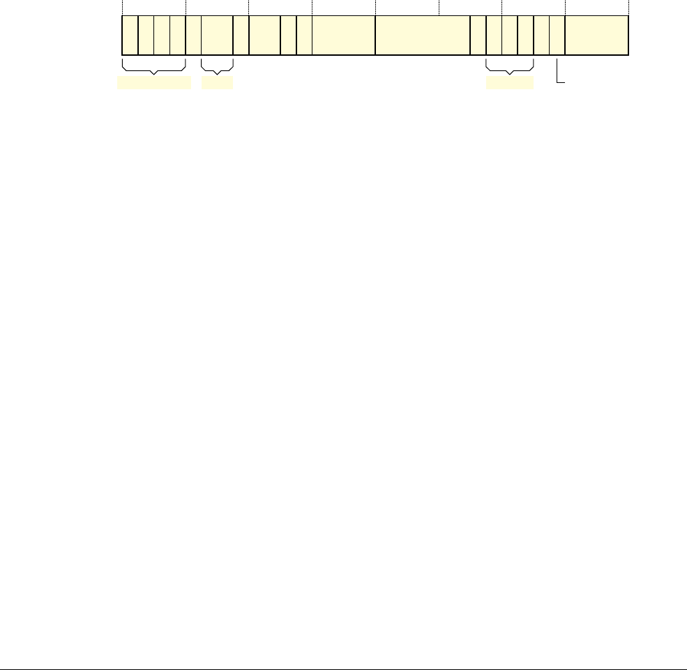
G1 The AArch32 System Level Programmers’ Model
G1.9 AArch32 PE modes, general-purpose registers, and the PC
ARM DDI 0487A.a Copyright © 2013 ARM Limited. All rights reserved. G1-3423
ID090413 Non-Confidential - Beta
The Saved Program Status Registers (SPSRs)
The purpose of an SPSR is to record the pre-exception value of the CPSR. On taking an exception, the CPSR is
copied to the SPSR of the mode to which the exception is taken. Saving this value means the exception handler can:
• On exception return, restore the CPSR to the value it had immediately before the exception was taken.
• Examine the value that the CPSR had when the exception was taken, for example to determine the instruction
set state and privilege level in which the instruction that caused an Undefined Instruction exception was
executed.
Figure G1-3 on page G1-3418 shows the banking of the SPSRs.
The SPSRs are UNKNOWN on reset. Any operation in a Non-secure EL1 or EL0 mode makes SPSR_hyp UNKNOWN.
Format of the CPSR and SPSRs
The CPSR and SPSR bit assignments are:
Condition flags, bits[31:28]
Set on the result of instruction execution. The flags are:
N, bit[31] Negative condition flag.
Z, bit[30] Zero condition flag.
C, bit[29] Carry condition flag.
V, bit[28] Overflow condition flag.
The condition flags can be read or written in any mode, and are described in IT block state register,
ITSTATE on page E1-2300.
Q, bit[27] Cumulative saturation bit. This bit can be read or written in any mode, and is described in IT block
state register, ITSTATE on page E1-2300.
IT[7:0], bits[15:10, 26:25]
If-Then execution state bits for the T32
IT
(If-Then) instruction. IT block state register, ITSTATE on
page E1-2300 describes the encoding of these bits. CPSR.IT[7:0] are the IT[7:0] bits described
there. For more information, see IT on page F7-2610.
For details of how these bits can be accessed see Accessing the execution state bits on
page G1-3425.
J, bit[24] J bit, see the description of the T bit, bit[5].
Bits[23:22] Reserved. RAZ/SBZP.
SS, bit[21] Software step bit, used for tracking the progress of software step debug. SPSR.SS is used by a
debugger to initiate a Software Step debug event. It also indicates which software step state machine
state the PE was in. See Software Step exceptions on page D2-1634.
This bit is RES0 in the CPSR.
IL, bit[20] Illegal state or Mode bit. Holds the value of PSTATE.IL. The IL bit is set to 1 in AArch32 state to
indicate that on exception return or as a result of an explicit change of the CPSR.M field, an illegal
state or mode was indicated. In an SPSR, the IL bit shows the value of PSTATE.IL immediately
before the exception was taken.
This bit is RES0 in the CPSR.
(1)IL
RES
0SS F TN
31 30 29 28 27 26 25 24 23 20 19 16 15 10 9 8 7 6 5 4 3 2 1 0
Z C V Q J GE[3:0] IT[7:2] E A I M[3:0]
IT[1:0]
Condition flags Mask bits
22 21
M[4]

G1 The AArch32 System Level Programmers’ Model
G1.9 AArch32 PE modes, general-purpose registers, and the PC
G1-3424 Copyright © 2013 ARM Limited. All rights reserved. ARM DDI 0487A.a
Non-Confidential - Beta ID090413
Note
Conceptually, CPSR.IL holds the value of PSTATE.IL. However, when PSTATE.IL is set to 1,
execution of any instruction generates an exception, and therefore a CPSR.IL value of 1 could never
be observed, and the observed behavior of this CPSR bit is RES0.
For more information see Illegal exception returns to AArch32 state on page G1-3456.
GE[3:0], bits[19:16]
Greater than or Equal flags, for the parallel addition and subtraction (SIMD) instructions described
in Parallel addition and subtraction instructions on page F1-2389.
The GE[3:0] field can be read or written in any mode, and is described in The Application Program
Status Register (APSR) on page E1-2297.
E, bit[9] Endianness execution state bit. Controls the load and store endianness for data accesses:
0 Little-endian operation.
1 Big-endian operation.
Instruction fetches ignore this bit.
Endianness mapping register, ENDIANSTATE on page E1-2302 describes the encoding of this bit.
CPSR.E is the ENDIANSTATE bit described there.
For details of how this bit can be accessed see Accessing the execution state bits on page G1-3425.
When the reset value of the SCTLR.EE bit is defined by a configuration input signal, that value also
applies to the CPSR.E bit on reset, and therefore applies to software execution from reset.
Mask bits, bits[8:6]
These bits are:
A, bit[8] Asynchronous abort mask bit.
I, bit[7] IRQ mask bit.
F, bit[6] FIQ mask bit.
The possible values of each bit are:
0 Exception not masked.
1 Exception masked.
The A bit has no effect on any Data Abort exception generated by a Watchpoint debug event, even
if that exception is asynchronous. For more information see Breakpoint and Watchpoint debug
events on page H2-4330.
In an implementation that does not include EL3, setting a mask bit masks the corresponding
exception, meaning it cannot be taken. However, the implementation of EL3 and EL2 significantly
alters the behavior and effect of these bits, see Effects of EL3 and EL2 on the CPSR.{A, F} bits on
page G1-3425 and Asynchronous exception masking controls on page G1-3468.
The mask bits can be written only at EL1 or higher. Their values can be read in any mode, but ARM
deprecates any use of their values, or attempt to change them, by software executing at EL0.
T, bit[5] T32 execution state bit. This bit and the J execution state bit, bit[24], determine the instruction set
state of the PE, A32 or T32. Instruction set state register, ISETSTATE on page E1-2298 describes
the encoding of these bits. CPSR.J and CPSR.T are the same bits as ISETSTATE.J and
ISETSTATE.T respectively. For more information, see Instruction set states on page G1-3429.
For details of how these bits can be accessed see Accessing the execution state bits on
page G1-3425.
M[4:0], bits[4:0]
Mode field. This field determines the current mode of the PE. The permitted values of this field are
listed in Table G1-2 on page G1-3412. All other values of M[4:0] are reserved. Illegal changes to
the CPSR.M field on page G1-3458 describes the effect of setting M[4:0] to a reserved value.

G1 The AArch32 System Level Programmers’ Model
G1.9 AArch32 PE modes, general-purpose registers, and the PC
ARM DDI 0487A.a Copyright © 2013 ARM Limited. All rights reserved. G1-3425
ID090413 Non-Confidential - Beta
ARMv8 redefines M[4] as follows:
M[4], Execution state This bit indicates the Execution state of the PE, as follows:
0 AArch64 state.
1 AArch32 state.
Note
This is consistent with the use of the M[4:0] field in previous versions of the architecture. All of the
PE modes have M[4:0] values in which the value of the most significant bit is 1.
For more information about the PE modes see AArch32 PE mode descriptions on page G1-3412.
Figure G1-3 on page G1-3418 shows the registers that can be accessed in each mode.
This field can be written only at EL1 or higher. Its value can be read in any mode, but ARM
deprecates software executing at EL0 making any use of its value, or attempting to change it.
Accessing the execution state bits
The execution state bits are the IT[7:0], J, E, and T bits. If the current mode has an SPSR, software can read or write
these bits in the SPSR.
In the CPSR, unless the PE is in Debug state:
• The execution state bits, other than the E bit, are RAZ when read by an
MRS
instruction.
• Writes to the execution state bits, other than the E bit, by an
MSR
instruction are ignored in all modes.
Instructions other than
MRS
and
MSR
that access the execution state bits can read and write them in any mode.
Unlike the other execution state bits in the CPSR, CPSR.E can be read by an
MRS
instruction and written by an
MSR
instruction. However, ARM deprecates:
•Using the CPSR.E value read by an
MRS
instruction.
•Using an
MSR
instruction to change the value of CPSR.E.
Note
• Software can use the
SETEND
instruction to change the current endianness.
• To determine the current endianness, software can use an
LDR
instruction to load a word of memory with a
known value that differs if the endianness is reversed. For example, using an
LDR
(literal) instruction to load
a word whose four bytes are
0x01
,
0x00
,
0x00
, and
0x00
in ascending order of memory address loads the
destination register with:
—
0x00000001
if the current endianness is little-endian.
—
0x01000000
if the current endianness is big-endian.
For more information about the behavior of these bits in Debug state see Status register access instructions on
page F1-2391.
Effects of EL3 and EL2 on the CPSR.{A, F} bits
In an implementation that includes EL3, the SCR.{AW, FW} bits modify the effect of the CPSR.{A, F} bits on
exceptions taken from Non-secure state.
In an implementation that includes EL2, the HCR.{AMO, IMO, FMO} bits modify the effect of the CPSR.{A, I, F}
bits on exceptions taken from Non-secure state.
For more information see Asynchronous exception masking controls on page G1-3468.

G1 The AArch32 System Level Programmers’ Model
G1.9 AArch32 PE modes, general-purpose registers, and the PC
G1-3426 Copyright © 2013 ARM Limited. All rights reserved. ARM DDI 0487A.a
Non-Confidential - Beta ID090413
Privileged software can change the CPSR.{A, F} and SPSR.{A, F} bits. In an implementation that includes EL3,
this is true regardless of the value of the corresponding SCR.{AW, FW} bits. However, when the SPSR is copied to
the CPSR, a CPSR.{A. F} bit is not updated if the value of the corresponding SCR.{AW, FW} bit is 0.
Note
In ARMv7 implementations before the introduction of the Virtualization Extensions, the SCR.{AW, FW} bits
control whether the CPSR.{A, F} bits are writable in Non-secure state. In ARMv8, the he SCR.{AW, FW} bits
never have this effect.
Pseudocode details of PSR operations
The following pseudocode gives access to the PSRs. The
SPSR[]
function accesses the current SPSR, and is common
to AArch32 and AArch64 operation. The
CPSR[]
function accesses the CPSR. Each of these functions has
non-assignment form for reads and an assignment form for writes.
bits(32) CPSR, SPSR_fiq, SPSR_irq, SPSR_svc, SPSR_mon, SPSR_abt, SPSR_und, SPSR_hyp;
// SPSR[] - non-assignment form
// ============================
bits(32) SPSR[]
bits(32) result;
if UsingAArch32() then
case CPSR.M of
when M32_FIQ result = SPSR_fiq;
when M32_IRQ result = SPSR_irq;
when M32_Svc result = SPSR_svc;
when M32_Monitor result = SPSR_mon;
when M32_Abort result = SPSR_abt;
when M32_Hyp result = SPSR_hyp;
when M32_Undef result = SPSR_und;
otherwise Unreachable();
else
case PSTATE.EL of
when EL1 result = SPSR_EL1;
when EL2 result = SPSR_EL2;
when EL3 result = SPSR_EL3;
otherwise Unreachable();
return result;
// SPSR[] - assignment form
// ========================
SPSR[] = bits(32) value
if UsingAArch32() then
case CPSR.M of
when M32_FIQ SPSR_fiq = value;
when M32_IRQ SPSR_irq = value;
when M32_Svc SPSR_svc = value;
when M32_Monitor SPSR_mon = value;
when M32_Abort SPSR_abt = value;
when M32_Hyp SPSR_hyp = value;
when M32_Undef SPSR_und = value;
otherwise Unreachable();
else
case PSTATE.EL of
when EL1 SPSR_EL1 = value;
when EL2 SPSR_EL2 = value;
when EL3 SPSR_EL3 = value;
otherwise Unreachable();
return;

G1 The AArch32 System Level Programmers’ Model
G1.9 AArch32 PE modes, general-purpose registers, and the PC
ARM DDI 0487A.a Copyright © 2013 ARM Limited. All rights reserved. G1-3427
ID090413 Non-Confidential - Beta
// CPSR - non-assignment form
// ==========================
CPSRType CPSR
bits(32) cpsr = GetSPSRFromPSTATE();
return cpsr;
// CPSR - assignment form
// ======================
CPSR = CPSRType cpsr
bits(32) v = cpsr;
SetPSTATEFromSPSR(v);
// CPSRWriteByInstr()
// ==================
CPSRWriteByInstr(bits(32) value, bits(4) bytemask, boolean is_excpt_return)
privileged = CurrentModeIsNotUser();
new_cpsr = CPSR;
if bytemask<3> == ‘1’ then
new_cpsr<31:27> = value<31:27>; // N,Z,C,V,Q flags
if is_excpt_return then
new_cpsr<26:24> = value<26:24>; // IT<1:0>,J execution state bits
if bytemask<2> == ‘1’ then
// bits <23:20> are RES0
new_cpsr<19:16> = value<19:16>; // GE<3:0> flags
if bytemask<1> == ‘1’ then
if is_excpt_return then
new_cpsr<15:10> = value<15:10>; // IT<7:2> execution state bits
new_cpsr<9> = value<9>; // E bit is user-writable
if privileged then
new_cpsr<8> = value<8>; // A interrupt mask
if bytemask<0> == ‘1’ then
if privileged then
new_cpsr<7> = value<7>; // I interrupt mask
new_cpsr<6> = value<6>; // F interrupt mask
if is_excpt_return then
new_cpsr<5> = value<5>; // T execution state bit
if privileged then
new_cpsr<4:0> = value<4:0>; // mode bits
// Attempts to change to an illegal mode, or return to Hyp mode with CPSR.<J,T> = ‘11’
// will invoke the Illegal Execution State mechanism
CPSR = new_cpsr; // Assign new CPSR value
return;
// SPSRWriteByInstr()
// ==================
SPSRWriteByInstr(bits(32) value, bits(4) bytemask)
if CurrentModeIsUserOrSystem() then UNPREDICTABLE;
if bytemask<3> == ‘1’ then
SPSR[]<31:24> = value<31:24>; // N,Z,C,V,Q flags, IT<1:0>,J execution state bits
if bytemask<2> == ‘1’ then
// bits <23:20> are reserved SBZP bits
SPSR[]<19:16> = value<19:16>; // GE<3:0> flags
if bytemask<1> == ‘1’ then

G1 The AArch32 System Level Programmers’ Model
G1.9 AArch32 PE modes, general-purpose registers, and the PC
G1-3428 Copyright © 2013 ARM Limited. All rights reserved. ARM DDI 0487A.a
Non-Confidential - Beta ID090413
SPSR[]<15:8> = value<15:8>; // IT<7:2> execution state bits, E bit, A interrupt mask
if bytemask<0> == ‘1’ then
SPSR[]<7:5> = value<7:5>; // I,F interrupt masks, T execution state bit
if BadMode(value<4:0>) then // Mode bits
UNPREDICTABLE;
else
SPSR[]<4:0> = value<4:0>;
return;
G1.9.4 ELR_hyp
Hyp mode does not provide its own Banked copy of LR. Instead, on taking an exception to Hyp mode, the preferred
return address is stored in ELR_hyp, a 32-bit Special register implemented for this purpose.
ELR_hyp can be accessed explicitly only by executing:
•An
MRS
or
MSR
instruction that targets ELR_hyp, see:
—MRS (Banked register) on page F7-2721.
—MSR (Banked register) on page F7-2726.
The
ERET
instruction uses the value in ELR_hyp as the return address for the exception. For more information, see
ERET on page F7-2607.
Software execution in any Non-secure EL1 or EL0 mode makes ELR_hyp UNKNOWN.

G1 The AArch32 System Level Programmers’ Model
G1.10 Instruction set states
ARM DDI 0487A.a Copyright © 2013 ARM Limited. All rights reserved. G1-3429
ID090413 Non-Confidential - Beta
G1.10 Instruction set states
The instruction set states are described in Chapter E2 The AArch32 Application Level Memory Model and
application level operations on them are described there. This section supplies more information about how they
interact with system level functionality, in the sections:
•Exceptions and instruction set state.
•Unimplemented instruction sets.
G1.10.1 Exceptions and instruction set state
If an exception is taken to a EL1 mode, the SCTLR.TE bit for the Security state the exception is taken to determines
the instruction set state that handles the exception, and if necessary, the PE changes to this instruction set state on
exception entry.
If the exception is taken to Hyp mode, the HSCTLR.TE bit determines the instruction set state that handles the
exception, and if necessary, the PE changes to this instruction set state on exception entry.
On coming out of reset, if the highest implemented Exception level is using AArch32:
• If the highest implemented Exception level is EL2, the PE starts execution in Hyp mode, in the instruction
set state determined by the reset value of HSCTLR.TE.
• Otherwise, the PE starts execution in Supervisor mode, in the instruction set state determined by the reset
value of SCTLR.TE. If the implementation includes EL3, this execution is in Secure Supervisor mode.
For more information about exception entry see Overview of exception entry on page G1-3436.
G1.10.2 Unimplemented instruction sets
The CPSR.J and CPSR.T bits define the current instruction set state, see Instruction set state register, ISETSTATE
on page E1-2298.
In the ARMv8 architecture:
• There is no support for the hardware acceleration of Java bytecodes, and the Jazelle Instruction set state is
obsolete. Every AArch32 implementation must support the Trivial Jazelle implementation described in
Trivial implementation of the Jazelle extension.
• The T32EE state is OPTIONAL and deprecated in the ARMv8 architecture. ARM strongly recommends that
T23EE state is not supported in any ARMv8 implementation.
Some system instructions permit setting CPSR.{J, T} to values that select an unimplemented instruction set state,
for example setting CPSR.J to 1 and CPSR.T to 0 on an PE that does not implement the Jazelle state. If such values
are written to CPSR.{J, T}, the implementation behaves in one of these ways:
•Sets CPSR.{J, T} to the requested values and causes the next instruction to generate an Undefined Instruction
exception, as described in Exception return to an unimplemented instruction set state on page G1-3458.
• Does not set CPSR.{J, T} to the requested values. The PE might change the value of one or both of the bits
in such a way that the new values correspond to an implemented instruction set state. If this is done then the
instruction set state changes to this new state. The detailed behavior of the attempt to change to an
unimplemented state is IMPLEMENTATION DEFINED.
Trivial implementation of the Jazelle extension
ARMv8 requires that the implementation of AArch32 state includes the trivial Jazelle implementation.
A trivial implementation of the Jazelle extension must:
• Implement the JIDR with the implementer and subarchitecture fields set to zero. The register can be
implemented so that the whole register is RAZ.
• Implement the JMCR as RAZ/WI.

G1 The AArch32 System Level Programmers’ Model
G1.10 Instruction set states
G1-3430 Copyright © 2013 ARM Limited. All rights reserved. ARM DDI 0487A.a
Non-Confidential - Beta ID090413
• Implement the JOSCR either:
— So that it can be read and written, but its effects are ignored.
—As RAZ/WI.
This ensures that operating systems that support an EJVM execute correctly.
• Implement the
BXJ
instruction to behave identically to the
BX
instruction in all circumstances, as required by
the fact that the JMCR.JE bit is always zero. This means that, with a trivial implementation of the Jazelle
extension, Jazelle state can never be entered normally.
• Treat Jazelle state as an unimplemented instruction set state, as described in Exception return to an
unimplemented instruction set state on page G1-3458.
A trivial implementation does not have to extend the PC to 32 bits, that is, it can implement PC[0] as RAZ/WI. This
is because the only way that PC[0] is visible in A32 or T32 state is as a result of an exception occurring during
Jazelle state execution, and Jazelle state execution cannot occur on a trivial implementation.

G1 The AArch32 System Level Programmers’ Model
G1.11 Handling exceptions that are taken to an Exception level using AArch32
ARM DDI 0487A.a Copyright © 2013 ARM Limited. All rights reserved. G1-3431
ID090413 Non-Confidential - Beta
G1.11 Handling exceptions that are taken to an Exception level using AArch32
An exception causes the PE to suspend program execution to handle an event, such as an externally generated
interrupt or an attempt to execute an undefined instruction. Exceptions can be generated by internal and external
sources.
Normally, when an exception is taken the PE state is preserved immediately, before handling the exception. This
means that, when the event has been handled, the original state can be restored and program execution resumed from
the point where the exception was taken.
More than one exception might be generated at the same time, and a new exception can be generated while the PE
is handling an exception.
The following sections describe exception handling:
•Exception vectors and the exception base address.
•Exception priority order on page G1-3435.
•Overview of exception entry on page G1-3436.
•PE mode for taking exceptions on page G1-3439.
•PE state on exception entry on page G1-3450.
•Routing general exceptions to EL2 on page G1-3452.
•Routing Debug exceptions to Hyp mode on page G1-3454.
•Exception return to an Exception level using AArch32 on page G1-3454.
•Wait For Event and Send Event on page G1-3460.
•Wait For Interrupt on page G1-3463.
Asynchronous exception behavior for exceptions taken from AArch32 state on page G1-3465 gives a full description
of asynchronous exception handling, for exceptions taken asynchronously from AArch32 state.
Note
Because of the common model for handling exceptions, the current section requires some understanding of the
asynchronous exception behaviors described in Asynchronous exception behavior for exceptions taken from
AArch32 state on page G1-3465.
AArch32 state exception descriptions on page G1-3475 then describes each exception.
G1.11.1 Exception vectors and the exception base address
When an exception is taken, PE execution is forced to an address that corresponds to the type of exception. This
address is called the exception vector for that exception. The vectors for the different types of exception form a
vector table.
Note
There are significant differences in the sets of exception vectors for exceptions taken to an Exception level that is
using AArch32 and for exceptions taken to an Exception level that is using AArch64. This part of this manual
describes only how exceptions are taken to an Exception level that is using AArch32. So, for example, when
executing at EL1 or EL0, an exception might be generated that must be taken to EL3. In this case:
• If EL3 is using AArch32 then the exception is taken as described in this chapter, using the exception vectors
described in this section.
• If EL3 is using AArch64 then the exception is taken as described in Chapter D1 The AArch64 System Level
Programmers’ Modelusing the exception vectors described in Exception vectors on page D1-1430.
AArch32 state defines exception vector tables for exceptions taken to EL2 and EL3 when those Exception levels
are using AArch32. Those vector tables are not used when the corresponding Exception levels are using AArch64.
A set of exception vectors for an Exception level that is using AArch32 comprises eight consecutive word-aligned
memory addresses, starting at an exception base address. These eight vectors form an AArch32 vector table.

G1 The AArch32 System Level Programmers’ Model
G1.11 Handling exceptions that are taken to an Exception level using AArch32
G1-3432 Copyright © 2013 ARM Limited. All rights reserved. ARM DDI 0487A.a
Non-Confidential - Beta ID090413
The number of possible exception base addresses, and therefore the number of vector tables, depends on the
implemented Exception levels, as follows:
Implementation that does not include EL3
Any implementation that does not include EL3 must include the following AArch32 vector table if
EL1 can use AArch32:
• An exception table for exceptions taken to EL1 modes other than System mode. This is the
EL1 vector table, and is in the address space of the PL1&0 translation regime.
Note
Exceptions cannot be taken to System mode.
For this vector table, the VBAR holds the exception base address.
Implementation that includes EL2
Any implementation that includes EL2 must include the following additional AArch32 vector table
if EL2 can use AArch32:
• An exception table for exceptions taken to Hyp mode. This is the Hyp vector table, and is in
the address space of the Non-secure PL2 translation regime.
For this vector table, HVBAR holds the exception base address.
Implementation that includes EL3
Any implementation that includes EL3 must include the following AArch32 vector tables:
• If EL3 can use AArch32, a vector table for exceptions taken to Secure Monitor mode. This
is the Monitor vector table, and is in the address space of the Secure PL1&0 translation
regime.
For this vector table, MVBAR holds the exception base address.
• If Secure EL1 can use AArch32, a vector table for exceptions taken to Secure privileged
modes other than Monitor mode and System mode. This is the Secure vector table, and is in
the address space of the Secure PL1&0 translation regime.
For this vector table, the Secure VBAR holds the exception base address.
• If Non-secure EL1 can use AArch32, a vector table for exceptions taken to Non-secure PL1
modes. This is the Non-secure vector table, and is in the address space of the Non-secure
PL1&0 translation regime.
For this vector table, the Non-secure VBAR holds the exception base address.
The following subsections give more information:
•The vector tables and exception offsets.
•Pseudocode determination of the exception base address on page G1-3434.
The vector tables and exception offsets
Table G1-3 on page G1-3433 defines the AArch32 vector table entries. In this table:
• The Hyp mode column defines the vector table entries for exceptions taken to Hyp mode.
• The Monitor mode column defines the vector table entries for exceptions taken to Monitor mode.
• The Secure and Non-secure columns define the Secure and Non-secure vector table entries, that are used for
exceptions taken to modes other than Monitor mode, Hyp mode, System mode, and User mode. Table G1-4
on page G1-3433 shows the mode to which each of these exceptions is taken. Each of these modes is
described as the default mode for taking the corresponding exception.
Note
Exceptions cannot be taken to System mode or User mode.

G1 The AArch32 System Level Programmers’ Model
G1.11 Handling exceptions that are taken to an Exception level using AArch32
ARM DDI 0487A.a Copyright © 2013 ARM Limited. All rights reserved. G1-3433
ID090413 Non-Confidential - Beta
For more information about determining the mode to which an exception is taken, see PE mode for taking exceptions
on page G1-3439.
When EL2 is using AArch3, it provides a number of additional exceptions, some of which are not shown explicitly
in the vector tables. For more information, see Offsets of AArch32 exceptions provided by EL2.
For more information about use of the vector tables see Overview of exception entry on page G1-3436.
Offsets of AArch32 exceptions provided by EL2
EL2 provides the following exceptions. When EL2 is using AArch32, these exceptions are taken to Hyp mode, and
the PE enters the handlers for these exceptions using the following vector table entries shown in Table G1-3:
Hypervisor Call
If taken from Hyp mode, shown explicitly in the Hyp mode vector table. Otherwise, see Use of offset
0x14 in the Hyp vector table on page G1-3434.
Table G1-3 The AArch32 vector tables
Offset Vector tables
HypaMonitorbSecurecNon-securec
0x00
Not used Not used Reset Not used
0x04
Undefined Instruction, from Hyp mode Not used Undefined Instruction Undefined Instruction
0x08
Hypervisor Call, from Hyp mode Secure Monitor Call Supervisor Call Supervisor Call
0x0C
Prefetch Abort, from Hyp mode Prefetch Abort Prefetch Abort Prefetch Abort
0x10
Data Abort, from Hyp mode Data Abort Data Abort Data Abort
0x14
Hyp Trap, or Hyp mode entrydNot used Not used Not used
0x18
IRQ interrupt IRQ interrupt IRQ interrupt IRQ interrupt
0x1C
FIQ interrupt FIQ interrupt FIQ interrupt FIQ interrupt
a. Non-secure state only. Implemented only if the implementation includes EL2 and EL2 can use AArch32.
b. Secure state only. Implemented only if the implementation includes EL3 and EL3 can use AArch32.
c. If the implementation does not include EL3 then there is a single vector table for exceptions taken to EL1 when EL1 is using AArch32.
That table holds the vectors shown in the Secure column of this table
d. See Use of offset 0x14 in the Hyp vector table on page G1-3434.
Table G1-4 Modes for taking the exceptions shown in the Secure or Non-secure vector table
Exception Mode taken to
Reset Supervisor
Undefined Instruction Undefined
Supervisor Call Supervisor
Prefetch Abort Abort
Data Abort Abort
IRQ interrupt IRQ
FIQ interrupt FIQ

G1 The AArch32 System Level Programmers’ Model
G1.11 Handling exceptions that are taken to an Exception level using AArch32
G1-3434 Copyright © 2013 ARM Limited. All rights reserved. ARM DDI 0487A.a
Non-Confidential - Beta ID090413
Hyp Trap Shown explicitly in the Hyp mode vector table.
Virtual Abort Entered through the Data Abort vector in the Non-secure vector table.
Virtual IRQ Entered through the IRQ vector in the Non-secure vector table.
Virtual FIQ Entered through the FIQ vector in the Non-secure vector table.
Note
Virtual exceptions when an implementation includes EL2 on page G1-3465 gives more information about the virtual
exceptions.
Use of offset
0x14
in the Hyp vector table
The vector at offset
0x14
in the Hyp vector table is used for exceptions that cause entry to Hyp mode. This means it
is:
• Always used for the Hyp Trap exception.
• Used for any Hypervisor Call exception that is taken from a mode other than Hyp mode.
• Used for any Supervisor Call exception that is taken from Non-secure User mode when the value of
HCR.TGE is 1.
• Used for any Undefined Instruction that is taken from Hyp mode, or is taken from Non-secure User mode
when the value of HCR.TGE is 1.
• Used for any Prefetch Abort exception that is:
— Taken from Non-secure User mode when the value of HCR.TGE is 1.
— Generated by a Debug exception from Non-secure state when the value of HDCR.TGE is 1.
— Generated by a stage 2 abort on an address translation operation.
• Used for any Data Abort exception that is:
— Taken from Non-secure User mode when the value of HCR.TGE is 1.
— Generated by an asynchronous External abort from Non-secure state when the value of HCR.AMO is
1.
— Generated by a Debug exception from Non-secure state when the value of HDCR.TGE is 1.
— Generated by a stage 2 abort on an address translation operation.
Note
Offset
0x14
is never used for IRQ exceptions, Virtual IRQ exceptions, FIQ exceptions, or Virtual FIQ exceptions.
For more information, see PE mode for taking exceptions on page G1-3439.
Pseudocode determination of the exception base address
For an exception taken to a PL1 mode, the
ExcVectorBase()
function determines the exception base address:
// ExcVectorBase()
// ===============
bits(32) ExcVectorBase()
if SCTLR.V == ‘1’ then // Hivecs selected, base = 0xFFFF0000
return Ones(16):Zeros(16);
else
return VBAR;

G1 The AArch32 System Level Programmers’ Model
G1.11 Handling exceptions that are taken to an Exception level using AArch32
ARM DDI 0487A.a Copyright © 2013 ARM Limited. All rights reserved. G1-3435
ID090413 Non-Confidential - Beta
Note
The PL1 modes to which exceptions can be taken are Supervisor mode, Undefined mode, Abort mode, IRQ mode,
and FIQ mode.In Non-secure state, and in Secure state when EL3 is using AArch64, these are EL1 modes. However,
in Secure state when EL3 is using AArch32, these are EL3 modes. For more information see Execution privilege,
Exception levels, and AArch32 Privilege levels on page G3-3560.
G1.11.2 Exception priority order
An instruction is not valid if it generates a synchronous Prefetch Abort exception. Therefore, if an instruction
generates a synchronous Prefetch Abort exception, no other synchronous exception or debug event is generated on
that instruction.
A Breakpoint debug event, or an address matching form of the Vector catch debug event, is associated with the
instruction. This means the corresponding exception is taken before the instruction is executed. Therefore, when a
Breakpoint or address matching Vector catch debug event occurs, no other synchronous exception or debug event,
that might have occurred as a result of executing the instruction, can occur.
Note
An Exception Trapping Vector Catch exception is generated as a result of trapping an exception that has been
prioritized as described in this section. This means it is outside the scope of the description in this section. For more
information see Breakpoint debug events and Vector Catch exception on page H2-4333.
Otherwise:
• An instruction that generates an Undefined Instruction exception or a Hyp Trap exception cannot cause any
memory access, and therefore cannot cause a Data Abort exception.
• If an instruction generates both an Undefined Instruction exception and a Hyp Trap exception then, unless
this manual explicitly states otherwise, the Undefined Instruction exception has priority.
• If a system call is configured to generate an Undefined Instruction exception or a Hyp Trap exception, then
the Undefined Instruction exception or the Hyp Trap exception has priority over the system call.
The system calls are the
SVC
,
HVC
, and
SMC
instructions.
• A memory access that generates fault on a stage of address translation or a synchronous Watchpoint debug
event must not generate an external abort.
• All other synchronous exceptions are mutually exclusive and are derived from a decode of the instruction.
For more information, see:
•Debug state entry and debug event prioritization on page H2-4331 for information about the prioritization of
debug events, including their prioritization relative to a fault on a stage of address translation and
synchronous external aborts
•Prioritization of aborts on page G3-3658, for information about:
— The prioritization of aborts on a single memory access in a VMSA implementation.
— The prioritization of exceptions generated during address translation

G1 The AArch32 System Level Programmers’ Model
G1.11 Handling exceptions that are taken to an Exception level using AArch32
G1-3436 Copyright © 2013 ARM Limited. All rights reserved. ARM DDI 0487A.a
Non-Confidential - Beta ID090413
Architectural requirements for taking asynchronous exceptions
The ARM architecture does not define when asynchronous exceptions are taken, but sets the following limits on
when they are taken:
• An asynchronous exception that is pending before one of the following context synchronizing events is taken
before the first instruction after the context synchronizing event completes its execution, provided that the
pending asynchronous event is not masked after the context synchronizing event. The context synchronizing
events are:
— Execution of an
ISB
instruction.
— Taking an exception.
— Return from an exception.
— Exit from Debug state.
The ISR identifies any pending asynchronous exceptions.
Note
If the first instruction after the context synchronizing event generates a synchronous exception, then the
architecture does not define the order in which that synchronous exception and the asynchronous exception
are taken.
• In the absence of a specific requirement to take an asynchronous exception because of a context
synchronizing event, the only requirement of the architecture is that an unmasked asynchronous exception is
taken in finite time.
Note
The taking of an unmasked asynchronous exception in finite time must occur with all code sequences,
including with a sequence that consists of unconditional loops.
Within these limits, the prioritization of asynchronous exceptions relative to other exceptions, both synchronous and
asynchronous, is IMPLEMENTATION DEFINED.
The CPSR includes a mask bit for each type of asynchronous exception. Setting one of these bits to 1 can prevent
the corresponding asynchronous exception from being taken, although when the PE is in Non-secure state other
controls can modify the effect of these bits. For more information, see Asynchronous exception behavior for
exceptions taken from AArch32 state on page G1-3465.
Taking an exception sets an exception-dependent subset of these mask bits.
Note
In some contexts. the CPSR.{A, I, F} bits mask the taking of asynchronous exceptions. The way these are set on
exception entry, described in CPSR.{A, I, F, M} values on exception entry on page G1-3451, can prevent an
exception handler being interrupted by an asynchronous exception.
G1.11.3 Overview of exception entry
There are some significant differences between the handling of exceptions taken to Hyp mode and exceptions taken
to other modes. Because Hyp mode is the EL2 mode, this means the following descriptions sometimes distinguish
between the EL2 mode and the non-EL2 modes.
On taking an exception to an Exception level that is using AArch32:
1. The hardware determines the mode to which the exception must be taken, see PE mode for taking exceptions
on page G1-3439.

G1 The AArch32 System Level Programmers’ Model
G1.11 Handling exceptions that are taken to an Exception level using AArch32
ARM DDI 0487A.a Copyright © 2013 ARM Limited. All rights reserved. G1-3437
ID090413 Non-Confidential - Beta
2. A link value, indicating the preferred return address for the exception, is saved. This is a possible return
address for the exception handler, and depends on:
• The exception type.
• Whether the exception is taken to the EL2 mode or to a non-EL2 mode.
• For some exceptions taken to non-EL2 modes, the instruction set state when the exception was taken.
Where the link value is saved depends on whether the exception is taken to the EL2 mode.
For more information see Link values saved on exception entry on page G1-3438.
3. The value of the CPSR is saved in the SPSR for the mode to which the exception must be taken. The value
saved in SPSR.IT[7:0] is always correct for the preferred return address.
4. In an implementation that includes EL3, when EL3 is using AArch32:
• If the exception taken from Monitor mode, SCR.NS is cleared to 0.
• Otherwise, taking the exception leaves SCR.NS unchanged.
When EL3 is using AArch64, Monitor mode is not available.
5. The CPSR is updated with new context information for the exception handler. This includes:
• Setting CPSR.M to the PE mode to which the exception is taken.
• Setting the appropriate CPSR mask bits. This can disable the corresponding exceptions, preventing
uncontrolled nesting of exception handlers.
• Setting the instruction set state to the state required for exception entry.
• Setting the endianness to the required value for exception entry.
• Clearing the CPSR.IT[7:0] bits to 0.
For more information, see PE state on exception entry on page G1-3450.
6. The appropriate exception vector is loaded into the PC, see Exception vectors and the exception base address
on page G1-3431.
7. Execution continues from the address held in the PC.
For an exception taken to a non-EL2 mode, on exception entry, the exception handler can use the
SRS
instruction to
store the return state onto the stack of any mode at the same Exception level and in the same Security state, and can
use the CPS instruction to change mode. For more information about the instructions, see SRS (T32) on
page F7-3060, SRS (A32) on page F7-3062, CPS (T32) on page F7-3034, and CPS (A32) on page F7-3036.
Later sections of this chapter describe each of the possible exceptions, and each of these descriptions includes a
pseudocode description of the PE state changes on taking that exception. Table G1-5 gives an index to these
descriptions:
Table G1-5 Pseudocode descriptions of exception entry for exceptions taken to AArch32 state
Exception Description of exception entry
Reset Pseudocode description of taking the Reset exception on page G1-3476
Undefined Instruction Pseudocode description of taking the Undefined Instruction exception on page G1-3477
Supervisor Call Pseudocode description of taking the Supervisor Call exception on page G1-3479
Secure Monitor Call Pseudocode description of taking the Secure Monitor Call exception on page G1-3480
Hypervisor Call Pseudocode description of taking the Hypervisor Call exception on page G1-3481
Prefetch Abort Pseudocode description of taking the Prefetch Abort exception on page G1-3482
Data Abort Pseudocode description of taking the Data Abort exception on page G1-3484
IRQ Pseudocode description of taking the IRQ exception on page G1-3488

G1 The AArch32 System Level Programmers’ Model
G1.11 Handling exceptions that are taken to an Exception level using AArch32
G1-3438 Copyright © 2013 ARM Limited. All rights reserved. ARM DDI 0487A.a
Non-Confidential - Beta ID090413
The following sections give more information about the PE state changes, for different architecture
implementations. However, you must refer to the pseudocode for a full description of the state changes:
•PE mode for taking exceptions on page G1-3439.
•PE state on exception entry on page G1-3450.
Link values saved on exception entry
On exception entry, a link value for use on return from the exception, is saved. This link value is based on the
preferred return address for the exception, as shown in Table G1-6:
Note
• Although Reset is described as an exception, it differs significantly from other exceptions. The architecture
has no concept of a return from a Reset and therefore it is not listed in this section.
• For each exception, the preferred return address is not affected by the Exception level from which the
exception was taken.
FIQ Pseudocode description of taking the FIQ exception on page G1-3489
Hyp Trap Pseudocode description of taking the Hyp Trap exception on page G1-3479
Virtual Abort Pseudocode description of taking the Virtual Asynchronous Abort exception on page G1-3486
Virtual IRQ Pseudocode description of taking the Virtual IRQ exception on page G1-3489
Virtual FIQ Pseudocode description of taking the Virtual FIQ exception on page G1-3490
Table G1-5 Pseudocode descriptions of exception entry for exceptions taken to AArch32 state (continued)
Exception Description of exception entry
Table G1-6 Exception return addresses for exceptions taken to AArch32 state
Exception Preferred return address Taken to a mode at
Undefined Instruction Address of the UNDEFINED instruction Non-EL2a, or EL2c
Supervisor Call Address of the instruction after the
SVC
instruction Non-EL2a or EL2c
Secure Monitor Call Address of the instruction after the
SMC
instruction EL3b, and only in Secure state
Hypervisor Call Address of the instruction after the
HVC
instruction EL2 onlyc
Prefetch Abort Address of aborted instruction fetch Non-EL2a or EL2c
Data Abort Address of instruction that generated the abort Non-EL2a or EL2c
Virtual Abort Address of next instruction to execute EL1, and only in Non-secure state
Hyp Trap Address of the trapped instruction EL2 onlyc
IRQ or FIQ Address of next instruction to execute Non-EL2a or EL2c
Virtual IRQ or Virtual FIQ Address of next instruction to execute EL1, and only in Non-secure state
a. EL1 if the exception is taken to a Non-secure mode, or is taken to a Secure mode when EL3 is using AArch64. EL3 if the exception is taken
to a Secure mode when EL3 is using AArch64.
b. A Secure Monitor Call exception is taken to EL3, and therefore is taken to AArch32 state only if EL3 is using AArch32, in which case it is
taken to Monitor mode.
c. EL2 is implemented only in Non-secure state. Therefore, an exception can be taken to EL2 mode only if it is taken from Non-secure state.

G1 The AArch32 System Level Programmers’ Model
G1.11 Handling exceptions that are taken to an Exception level using AArch32
ARM DDI 0487A.a Copyright © 2013 ARM Limited. All rights reserved. G1-3439
ID090413 Non-Confidential - Beta
The link value saved, and where it is saved, depend on whether the exception is taken to a non-EL2 mode, or to a
EL2 mode, as follows:
Exception taken to a non-EL2 mode
The link value is saved in the LR for the mode to which the exception is taken.
The saved link value is the preferred return address for the exception, plus an offset that depends on
the instruction set state when the exception was taken, as Table G1-7 shows:
Exception taken to a EL2 mode
The link value is saved in the ELR_hyp Special register.
The saved link value is the preferred return address for the exception, as shown in Table G1-6 on
page G1-3438, with no offset.
G1.11.4 PE mode for taking exceptions
The following principles determine the Exception level to which an exception is taken, and if that Exception level
is using AArch32, the PE mode to which the exception is taken:
• An exception cannot be taken to the EL0 mode.
• An exception is taken either:
— To the Exception level at which the PE was executing when it took the exception.
— To a higher Exception level.
This means that, in Secure state:
— When EL3 is using AArch32, an exception is always taken to an EL3 mode.
— When EL3 is using AArch64, an exception that is taken to AArch32 state is taken to an EL1 mode.
• Configuration options and other features provided by EL2 and EL3 can determine the mode to which some
exceptions are taken, as follows:
In an implementation that does not include EL2 or EL3
An exception is always taken to the default mode for that exception.
Table G1-7 Offsets applied to Link value for exceptions taken to EL1 modes
Exception Offset, for PE state of:
A32 T32 or T32EE
Undefined Instruction +4 +2
Supervisor Call None None
Secure Monitor Call None None
Prefetch Abort +4 +4
Data Abort +8 +8
Virtual Abort +8 +8
IRQ or FIQ +4 +4
Virtual IRQ or Virtual FIQ +4 +4

G1 The AArch32 System Level Programmers’ Model
G1.11 Handling exceptions that are taken to an Exception level using AArch32
G1-3440 Copyright © 2013 ARM Limited. All rights reserved. ARM DDI 0487A.a
Non-Confidential - Beta ID090413
In an implementation that includes EL3
A Secure Monitor Call exception is always taken to EL3. This means:
• If EL3 is using AArch32 the exception is taken to Secure Monitor mode.
• If EL3 is using AArch64 then executing the instruction generates an exception that is taken
to EL3, see Execution of an SMC instruction from a privileged Exception level that is using
AArch32 on page G1-3441.
IRQ, FIQ, and External abort exceptions can be configured to be taken to EL3. Therefore, if EL3
is using AArch32 the exceptions are taken to Secure Monitor mode.
Any exception taken from Secure state that is not taken to Secure Monitor mode is taken to
Secure state in the default mode for that exception. As described in Execution privilege,
Exception levels, and AArch32 Privilege levels on page G3-3560, this means it is taken to:
• An EL3 mode other than Monitor mode if EL3 is using AArch32.
• An EL1 mode if EL3 is using AArch64.
If the implementation does not include EL2, any exception taken from Non-secure state that is
not taken to Secure Monitor mode is taken to Non-secure state to the default mode for that
exception. The default mode will be an EL1 mode.
In an implementation that includes EL2
An exception taken from Non-secure state that is not taken to Secure Monitor mode is taken to
Non-secure state and:
• If the exception is taken from Hyp mode then it is taken to Hyp mode.
• Otherwise, the exception is either taken to Hyp mode, as described in Exceptions taken to
Hyp mode on page G1-3441, or taken to the default mode for the exception.
Note
• Hyp mode is the EL2 mode. The other modes to which an exception can be taken in
Non-secure state are EL1 modes.
• EL2 has no effect on the handling of exceptions taken from Secure state.
Table G1-4 on page G1-3433 shows the default mode to which each exception is taken.
Asynchronous exception routing controls on page G1-3467 describes the exception routing controls provided by
EL2 and EL3.
Routing of aborts taken to AArch32 state on page G3-3647 gives more information about the modes to which
memory aborts are taken.
Summary of the possible modes for taking each exception on page G1-3442 shows all modes to which each
exception might be taken, in any implementation. That is, it applies to implementations:
• That include neither EL2 nor EL3.
• That include EL2 but not EL3
• That do not include EL2 but include EL3
• That include both EL2 and EL3.

G1 The AArch32 System Level Programmers’ Model
G1.11 Handling exceptions that are taken to an Exception level using AArch32
ARM DDI 0487A.a Copyright © 2013 ARM Limited. All rights reserved. G1-3441
ID090413 Non-Confidential - Beta
Exceptions taken to Hyp mode
In an implementation that includes EL2 and EL3, when EL2 is using AArch32:
• Any exception taken from Hyp mode, that is not routed to EL3 by the controls described in Asynchronous
exception routing controls on page G1-3467, is taken to Hyp mode.
• The following exceptions, if taken from Non-secure state, are taken to Hyp mode:
— An abort that Routing of aborts taken to AArch32 state on page G3-3647 identifies as taken to Hyp
mode.
— A Hyp Trap exception, see AArch32 control of traps to the hypervisor on page G1-3503.
— A Hypervisor Call exception. This is generated by executing a
HVC
instruction in a Non-secure mode.
— An asynchronous abort, IRQ exception or FIQ exception that is not routed to EL3 but is explicitly
routed to Hyp mode, as described in Asynchronous exception routing controls on page G1-3467.
— A synchronous external abort, Alignment fault, Undefined Instruction exception, or Supervisor Call
exception taken from the Non-secure EL0 mode and explicitly routed to Hyp mode, as described in
Routing general exceptions to EL2 on page G1-3452.
Note
A synchronous external abort can be routed to Hyp mode only if it is not routed to EL3.
— A debug exception that is explicitly routed to Hyp mode as described in Routing Debug exceptions to
Hyp mode on page G1-3454.
Note
The virtual exceptions cannot be taken to Hyp mode. They are always taken to a Non-secure EL1 mode.
Security behavior in Exception levels using AArch32 when EL3 is using AArch64
As described in The ARMv8-A security model on page G1-3407, when EL3 is using AArch64, lower Exception
levels, in either Security state, can be using AArch32. This means software executing in those Exception levels
might try to access AArch32 security features that are not available. The following subsections describe the
associated behaviors:
•Execution of an SMC instruction from a privileged Exception level that is using AArch32
•Non-secure reads of the NSACR
•Secure EL1 operations when Secure EL1 is using AArch32 on page G1-3442
Execution of an SMC instruction from a privileged Exception level that is using AArch32
When EL3 is using AArch64, an
SMC
instruction executed from Secure or Non-secure EL1 using AArch32, or from
Non-secure EL2 using AArch32 when the value of HCR.TSC is 0, generates an exception that is taken to EL3. The
exception syndrome is reported with an EC value of
0x13
,
SMC
instruction executed in AArch32 state, see Exception
from SMC instruction execution in AArch32 state on page D1-1522.
Non-secure reads of the NSACR
The NSACR is defined as being RO from Non-secure PE modes other than User mode. When EL3 is using
AArch64, a read of the NSACR returns a fixed value of
0x00000C00
in the following cases:
• If the read is from a Non-secure EL1 mode when EL1 is using AArch32.
• If the read is from Hyp mode when EL2 is using AArch32.

G1 The AArch32 System Level Programmers’ Model
G1.11 Handling exceptions that are taken to an Exception level using AArch32
G1-3442 Copyright © 2013 ARM Limited. All rights reserved. ARM DDI 0487A.a
Non-Confidential - Beta ID090413
Secure EL1 operations when Secure EL1 is using AArch32
When Secure EL1 is using AArch32 and EL3 is using AArch64:
• Any of the following operations performed in a Secure EL1 mode is trapped to Secure EL3:
— A read or write of any of the SCR, NSACR, MVBAR, and SDCR.
— Performing any of the ATS12NSO** operations described in Address translation stages 1 and 2,
Non-secure state only on page G3-3686.
— Executing an
SRS
instruction that would use SP_mon, see SRS (T32) on page F7-3060 and SRS (T32)
on page F7-3060.
— Executing a
MRS
(Banked register) or
MSR
(Banked register) instruction that would access SPSR_mon,
SP_mon, or LR_mon, see MRS (Banked register) on page F7-3048 and MSR (Banked register) on
page F7-3050.
For more information about these traps, including the associated exception syndromes, see Traps to EL3 of
monitor functionality from Secure EL1 using AArch32 on page D1-1500.
• Writes to the CNTFRQ register are UNDEFINED.
• Any attempt to move into Monitor mode, either by an exception return or by executing a
CPS
or
MSR
instruction, is treated as an illegal operation and is handled as described in Illegal exception returns to
AArch32 state on page G1-3456.
Note
This functionality supports a usage model where:
• EL3 uses AArch64.
• Secure software executed in Secure EL1 using AArch32 and Secure EL0 using AArch32.
• The Non-secure state uses AArch64.
Summary of the possible modes for taking each exception
The following subsections describe the modes to which each exception can be taken:
•Determining the PE mode to which the Undefined Instruction exception is taken on page G1-3443.
•Determining the PE mode to which the Supervisor Call exception is taken on page G1-3444.
•The PE mode to which the Secure Monitor Call exception is taken on page G1-3444.
•The PE mode to which the Hypervisor Call exception is taken on page G1-3445.
•The PE mode to which the Hyp Trap exception is taken on page G1-3445.
•Determining the PE mode to which the Prefetch Abort exception is taken on page G1-3446.
•Determining the PE mode to which the Data Abort exception is taken on page G1-3447.
•The PE mode to which the Virtual Abort exception is taken on page G1-3448.
•Determining the PE mode to which the physical IRQ exception is taken on page G1-3448.
•The PE mode to which the Virtual IRQ exception is taken on page G1-3448.
•Determining the PE mode to which the physical FIQ exception is taken on page G1-3449.
•The PE mode to which the Virtual FIQ exception is taken on page G1-3449.
These descriptions also show the vector offset for the exception entry for each mode. These descriptions assume
that all Exception levels are using AArch32, meaning:
•HCR, rather than HCR_EL2, controls the routing of exceptions to EL2.
•SCR, rather than SCR_EL3, controls the routing of exceptions to EL3.
For more information about:
• Vector offsets, see Exception vectors and the exception base address on page G1-3431.
• The routing of external aborts, IRQ and FIQ exceptions, and the virtual exceptions, see Asynchronous
exception routing controls on page G1-3467.
G1 The AArch32 System Level Programmers’ Model
G1.11 Handling exceptions that are taken to an Exception level using AArch32
ARM DDI 0487A.a Copyright © 2013 ARM Limited. All rights reserved. G1-3443
ID090413 Non-Confidential - Beta
Determining the PE mode to which the Undefined Instruction exception is taken
Figure G1-4 shows how the implementation, state, and configuration options determine the PE mode to which an
Undefined Instruction exception is taken.
Figure G1-4 The PE mode the Undefined Instruction exception is taken to
See also UNPREDICTABLE cases when the value of HCR.TGE is 1 on page G1-3449.
Undefined Instruction exception
State is
Secure
?
Taken from
Hyp mode
?
Yes
HCR.TGE
== 1
?
Non-secure Undefined mode,
vector offset 0x04
Hyp mode,
vector offset 0x04
Hyp mode,
vector offset 0x14
EL1
and EL0
only?
Undefined mode,
vector offset 0x04
Yes
Have
EL2? YesYes
No
Yes
Secure Undefined mode,
vector offset 0x04
No
No
From User mode
only, see text.
No
Have
EL3?
No
Yes
No
G1 The AArch32 System Level Programmers’ Model
G1.11 Handling exceptions that are taken to an Exception level using AArch32
G1-3444 Copyright © 2013 ARM Limited. All rights reserved. ARM DDI 0487A.a
Non-Confidential - Beta ID090413
Determining the PE mode to which the Supervisor Call exception is taken
Figure G1-5 shows how the implementation, state, and configuration options determine the PE mode to which a
Supervisor Call exception is taken.
Figure G1-5 The PE mode the Supervisor Call exception is taken to
See also UNPREDICTABLE cases when the value of HCR.TGE is 1 on page G1-3449.
The PE mode to which the Secure Monitor Call exception is taken
The Secure Monitor Call exception is supported only as part of EL3. When EL3 is using AArch32, a Secure Monitor
Call exception is taken to Monitor mode, using vector offset
0x08
from the Monitor exception base address.
Note
. •An
SMC
instruction that is trapped to Hyp mode because HCR.TSC is set to 1 generates a Hyp Trap exception,
see The PE mode to which the Hyp Trap exception is taken on page G1-3445.
• If EL3 is using AArch64 then Security behavior in Exception levels using AArch32 when EL3 is using
AArch64 on page G1-3441 describes the effect of executing an
SMC
instruction in a mode that is part of an
Exception level that is using EL1.
Supervisor Call exception
State is
Secure
?
Taken from
Hyp mode
?
Yes
HCR.TGE
== 1
?
Non-secure Supervisor mod
vector offset 0x08
Hyp mode,
vector offset 0x08
Hyp mode,
vector offset 0x14
Supervisor mode,
vector offset 0x08
Yes
Have
EL2? Yes
No
Secure Supervisor mode,
vector offset 0x08
No
Yes
Yes
No
No
EL1
and EL0
only?
No
Have
EL3? Yes
No
From User mode
only, see text.
G1 The AArch32 System Level Programmers’ Model
G1.11 Handling exceptions that are taken to an Exception level using AArch32
ARM DDI 0487A.a Copyright © 2013 ARM Limited. All rights reserved. G1-3445
ID090413 Non-Confidential - Beta
The PE mode to which the Hypervisor Call exception is taken
The Hypervisor Call exception is supported only as part of EL2. When EL2 is using AArch32, a Hypervisor Call
exception is taken to Hyp mode, using a vector offset that depends on the mode from which the exception is taken,
as Figure G1-6 shows. This offset is from the Hyp exception base address.
Figure G1-6 The PE mode the Hypervisor Call exception is taken to
The PE mode to which the Hyp Trap exception is taken
The Hyp Trap exception is supported only as part of EL2. When EL2 is using AArch32, a Hyp Trap exception is
taken to Hyp mode, using a vector offset of
0x14
from the Hyp exception base address.
Hypervisor Call exception
Hyp mode,
vector offset 0x14
Taken from
Hyp mode
?
Hyp mode,
vector offset 0x08
Yes
No
G1 The AArch32 System Level Programmers’ Model
G1.11 Handling exceptions that are taken to an Exception level using AArch32
G1-3446 Copyright © 2013 ARM Limited. All rights reserved. ARM DDI 0487A.a
Non-Confidential - Beta ID090413
Determining the PE mode to which the Prefetch Abort exception is taken
Figure G1-7 shows how the implementation, state, and configuration options determine the PE mode to which a
Prefetch Abort exception is taken.
Figure G1-7 The PE mode the Prefetch Abort exception is taken to
See also UNPREDICTABLE cases when the value of HCR.TGE is 1 on page G1-3449.
Prefetch Abort exception
External
abort
?
Yes
Hyp mode, vector
offset 0x0C
Monitor mode,
vector offset 0x0C
SCR.EA
== 1
?
Yes
Debug
exception
?
HDCR.TDE
== 1
?
Stage 2
abort
?
On address
translation
Yes
Abort mode,
vector offset 0x0C
State is
Secure
?
Secure Abort mode,
vector offset 0x0C
1
Taken
from Hyp
mode ?
No
Have
EL2? Yes
No
No
Yes Hyp mode, vector
offset 0x14
Yes
Yes
Non-secure Abort mode,
vector offset 0x0C
No
Yes
1
No
HCR.TGE
== 1
?
No
No
EL1
and EL0
only?
No
Have
EL3? Yes Yes
Yes
No
No
No
From User mode
only, see text.
G1 The AArch32 System Level Programmers’ Model
G1.11 Handling exceptions that are taken to an Exception level using AArch32
ARM DDI 0487A.a Copyright © 2013 ARM Limited. All rights reserved. G1-3447
ID090413 Non-Confidential - Beta
Determining the PE mode to which the Data Abort exception is taken
Figure G1-8 shows the determination of the mode to which a Data Abort exception is taken.
Figure G1-8 The PE mode the Data Abort exception is taken to
Data Abort exception
External
abort
?
Yes
Hyp mode, vector
offset 0x10
Monitor mode,
vector offset 0x10
SCR.EA
== 1
?
Yes
Debug
exception
?
HDCR.TDE
== 1
?
Stage 2
abort
?
On address
translation
Yes Abort mode,
vector offset 0x10
State is
Secure
?
Secure Abort mode,
vector offset 0x10
Have
EL2? Yes
Yes
Yes
Non-secure Abort mode,
vector offset 0x10
Yes
No
No
No
No
Hyp mode, vector
offset 0x14
Yes
1
No
HCR.AMO
== 1
?
Yes
1
1
External
abort
?
Yes Synchronous
?
No
1
HCR.TGE
== 1
?
Yes
No
EL1
and EL0
only?
No
Have
EL3? Yes Yes
No
Yes
No
Taken
from Hyp
mode ?
No
No
No
No
From User mode
only, see text.
G1 The AArch32 System Level Programmers’ Model
G1.11 Handling exceptions that are taken to an Exception level using AArch32
G1-3448 Copyright © 2013 ARM Limited. All rights reserved. ARM DDI 0487A.a
Non-Confidential - Beta ID090413
See also UNPREDICTABLE cases when the value of HCR.TGE is 1 on page G1-3449.
The PE mode to which the Virtual Abort exception is taken
The Virtual Abort exception is supported only as part of EL2. A Virtual Abort exception is taken from a Non-secure
EL1 or EL0 mode, and is taken to Non-secure Abort mode, using a vector offset of
0x10
from the Non-secure
exception base address.
For more information about this exception see Virtual exceptions when an implementation includes EL2 on
page G1-3465.
Determining the PE mode to which the physical IRQ exception is taken
Figure G1-9 shows how the implementation, state, and configuration options determine the mode to which an IRQ
exception is taken.
Figure G1-9 The PE mode the IRQ exception is taken to
The PE mode to which the Virtual IRQ exception is taken
The Virtual IRQ exception is supported only as part of EL2. A Virtual IRQ exception is taken from a Non-secure
EL1 or EL0 mode, and is taken to Non-secure IRQ mode, using a vector offset of
0x18
from the Non-secure
exception base address.
For more information about this exception see Virtual exceptions when an implementation includes EL2 on
page G1-3465.
State is
Secure
?
IRQ exception
Yes IRQ mode,
vector offset 0x18
Secure IRQ mode,
vector offset 0x18
No
SCR.IRQ
== 1
?
Monitor mode,
vector offset 0x18
Yes
No
Yes
Have
EL2? Yes
HCR.IMO
== 1
?
No
Hyp mode,
vector offset 0x18
Yes
Non-secure IRQ mode,
vector offset 0x18
No
No
No
EL1
and EL0
only?
Have
EL3?
Taken
from Hyp
mode ?
Yes
No
Yes
G1 The AArch32 System Level Programmers’ Model
G1.11 Handling exceptions that are taken to an Exception level using AArch32
ARM DDI 0487A.a Copyright © 2013 ARM Limited. All rights reserved. G1-3449
ID090413 Non-Confidential - Beta
Determining the PE mode to which the physical FIQ exception is taken
Figure G1-9 on page G1-3448 shows how the implementation, state, and configuration options determine the PE
mode to which an FIQ exception is taken.
Figure G1-10 The PE mode the FIQ exception is taken to
The PE mode to which the Virtual FIQ exception is taken
The Virtual FIQ exception is supported only as part of EL2. A Virtual FIQ exception is taken from a Non-secure
EL1 or EL0 mode, and is taken to Non-secure FIQ mode, using a vector offset of
0x1C
from the Non-secure
exception base address.
For more information about this exception see Virtual exceptions when an implementation includes EL2 on
page G1-3465.
UNPREDICTABLE cases when the value of HCR.TGE is 1
When the value of HCR.TGE is 1, exceptions that would otherwise be taken to EL1 are, instead, routed to EL2, see
Routing general exceptions to EL2 on page G1-3452. Related to this, when the value of HCR.TGE is 1, execution
in a Non-secure EL1 mode is UNPREDICTABLE. ARMv8 does not constrain this UNPREDICTABLE behavior, but in
ARMv8 software that follows the ARM recommendations cannot get to this state. When following the ARM
recommendations, any attempt to move to a Non-secure EL1 mode when the value of HCR.TGE is 1 is either:
• An illegal exception return, see Illegal exception returns to AArch32 state on page G1-3456.
• An illegal PE mode change, see Illegal changes to the CPSR.M field on page G1-3458.
FIQ exception
FIQ mode,
vector offset 0x1C
Secure FIQ mode,
vector offset 0x1C
Hyp mode,
vector offset 0x1C
Non-secure FIQ mode,
vector offset 0x1C
Monitor mode,
vector offset 0x1C
State is
Secure
?
Yes
No
SCR.FIQ
== 1
?
Yes
No
Yes
Have
EL2? Yes
HCR.FMO
== 1
?
No
Yes
No
No
No
EL1
and EL0
only?
Have
EL3?
Taken
from Hyp
mode ?
Yes
No
Yes

G1 The AArch32 System Level Programmers’ Model
G1.11 Handling exceptions that are taken to an Exception level using AArch32
G1-3450 Copyright © 2013 ARM Limited. All rights reserved. ARM DDI 0487A.a
Non-Confidential - Beta ID090413
G1.11.5 PE state on exception entry
The description of each exception includes a pseudocode description of entry to that exception, as Table G1-5 on
page G1-3437 shows. The following sections describe the PE state changes on entering an exception, for different
implementations and operating states. However, you must always see the exception entry pseudocode for a full
description of the state changes on exception entry:
•Instruction set state on exception entry.
•CPSR.E bit value on exception entry.
•CPSR.{A, I, F, M} values on exception entry on page G1-3451.
Note
The descriptions in these sections assume that EL2 and EL3, that control some aspects of the routing of exceptions
taken from EL1 or EL0, are both using AArch32. If this is not the case:
• If EL2 is using AArch64:
— Controls shown as provided by the HSCTLR are provided by the SCTLR_EL2.
— Controls shown as provided by the HCR are provided by the HCR_EL2.
• If EL3 is using AArch64, controls shown as provided by the SCR are provided by the SCR_EL3.
Instruction set state on exception entry
Exception handlers can execute in either T32 state or A32 state. On exception entry, the CPSR.{T, J} are set to the
required values, with the CPSR.T value determined by SCTLR.TE or HSCTLR.TE, depending on the mode the
exception is taken to. Table G1-8 shows this:
When an implementation includes EL3 and EL3 is using AArch32, SCTLR is Banked for Secure and Non-secure
states, and therefore the TE bit value might be different for Secure and Non-secure states. For an exception taken to
a Secure or Non-secure non-Hyp mode, the SCTLR.TE bit for the Security state to which the exception is taken
determines the instruction set state for the exception handler. This means the non-Hyp mode exception handlers
might run in different instruction set states, depending on the Security state.
CPSR.E bit value on exception entry
The CPSR.E bit controls the load and store endianness for data handling. Table G1-9 show the value to which this
bit is set on exception entry:
Table G1-8 CPSR.{J, T} bit values on exception entry
Exception mode HSCTLR.TE SCTLR.TE CPSR.J CPSR.T Exception handler state
Not Hyp x 0 00A32
1 01T32
Hyp 0 x 00A32
1 x 01T32
Table G1-9 CPSR.E bit value on exception entry
Exception mode HSCTLR.EE SCTLR.EE Endianness for data loads and stores CPSR.E
Secure or Non-secure EL1 x 0 Little-endian 0
1Big-endian 1
Hyp 0 x Little-endian 0
1 x Big-endian 1

G1 The AArch32 System Level Programmers’ Model
G1.11 Handling exceptions that are taken to an Exception level using AArch32
ARM DDI 0487A.a Copyright © 2013 ARM Limited. All rights reserved. G1-3451
ID090413 Non-Confidential - Beta
For more information, see the bit description in Format of the CPSR and SPSRs on page G1-3423.
CPSR.{A, I, F, M} values on exception entry
On exception entry, CPSR.M is set to the value for the mode to which the exception is taken, as described in PE
mode for taking exceptions on page G1-3439.
Table G1-10 shows the cases where CPSR.{A, I, F} bits are set to 1 on an exception entry, and how this depends
on the mode and Security state to which an exception is taken. If the table entry for a particular mode and Security
state does not define a value for a CPSR.{A, I, F} bit then that bit is unchanged by the exception entry. In this table:
• The Exception mode column is the mode to which the exception is taken.
• The Non-secure, EL2 not implemented column applies to exceptions taken to Non-secure state in an
implementation that includes EL3 but does not include EL2.
• The All others column applies to:
— Exceptions taken to Secure state.
— Implementations that do not include the EL3.
— Exceptions taken to Non-secure state in an implementation that includes EL2.
Asynchronous exception behavior for exceptions taken from AArch32 state on page G1-3465 describes how, in some
situations, the CPSR.{A, I, F} bits mask the taking of asynchronous aborts, IRQ interrupts, and FIQ interrupts.
Table G1-10 CPSR.{A, I, F} values on exception entry
PE mode exception
is taken to
Security state
Non-secure Secure
Hyp If SCR.EA==0 then CPSR.A is set to 1
If SCR.IRQ==0 then CPSR.I is set to 1
If SCR.FIQ==0 then CPSR.F is set to 1
-
Monitor - CPSR.A is set to 1
CPSR.I is set to 1
CPSR.F is set to 1
FIQ CPSR.A is set to 1
CPSR.I is set to 1
CPSR.F is set to 1
CPSR.A is set to 1
CPSR.I is set to 1
CPSR.F is set to 1
IRQ, Abort CPSR.A is set to 1
CPSR.I is set to 1
CPSR.A is set to 1
CPSR.I is set to 1
Undefined, Supervisor CPSR.I is set to 1 CPSR.I is set to 1

G1 The AArch32 System Level Programmers’ Model
G1.11 Handling exceptions that are taken to an Exception level using AArch32
G1-3452 Copyright © 2013 ARM Limited. All rights reserved. ARM DDI 0487A.a
Non-Confidential - Beta ID090413
G1.11.6 Routing general exceptions to EL2
Note
The routing provided when the value of HCR.TGE is 1 permits a usage model where applications execute in User
mode under a hypervisor, that executes in Hyp mode, without a Guest OS running in a Non-secure EL1 mode.
When the value of HCR.TGE is 1, and the PE is in Non-secure User mode, any exception that would otherwise be
taken to EL1 is taken to EL2. If EL2 is using AArch32 this means it is taken to Hyp mode, instead of to the default
Non-secure mode for handling the exception. This means that, when the value of HCR.TGE is 1 and EL2 is using
AArch32, the following exceptions are taken from User mode to Hyp mode:
• Undefined Instruction exceptions.
• Supervisor Call exceptions.
• Prefetch Abort exceptions that are not routed to EL3.
• Data Abort exceptions that are not routed to EL3.
Note
The only Prefetch Abort and Data Abort exceptions that might be routed to EL3 are those caused by an external
abort. These are routed to EL3 when the value of SCR.EA is 1.
The following sections give more information about the behavior when each of these exceptions is routed in this
way:
•Undefined Instruction exception, when HCR.TGE is set to 1.
•Supervisor Call exception, when HCR.TGE is set to 1.
•External abort, when HCR.TGE is set to 1 on page G1-3453.
•MMU fault, when HCR.TGE is set to 1 on page G1-3453.
When the value of HCR.TGE 1:
• Each of the HDCR.{TDE, TDA, TDRA, TDOSA} bits is treated as 0 for all purposes other than reading the
HDCR register.
• If the value of the SCR.NS bit is 1, then:
— The SCTLR.M bit is treated as 0 for all purposes other than reading the SCTLR register.
— Each of the HCR.{HCR.FMO, IMO, AMO} bits is treated as 1 for all purposes other than reading the
HCR register
— An exception return to EL1 is treated as an illegal exception return, see Illegal exception returns to
AArch32 state on page G1-3456.
— Any IMPLEMENTATION DEFINED mechanisms for signalling virtual interrupts are disabled.
Undefined Instruction exception, when HCR.TGE is set to 1
When HCR.TGE is set to 1, if the PE is executing in Non-secure User mode and attempts to execute an UNDEFINED
instruction, it takes the Hyp Trap exception, instead of an Undefined Instruction exception. On taking the Hyp Trap
exception, the HSR reports an unknown reason for the exception, using the EC value
0x00
. For more information
see Use of the HSR on page G3-3672.
Supervisor Call exception, when HCR.TGE is set to 1
When HCR.TGE is set to 1, if the PE executes an
SVC
instruction in Non-secure User mode, the Supervisor Call
exception generated by the instruction is taken to Hyp mode.
The HSR reports that entry to Hyp mode was because of a Supervisor Call exception, and:
•If the
SVC
is unconditional, takes for the
imm16
value in the HSR:
— A zero-extended 8-bit immediate value for the T32
SVC
instruction.

G1 The AArch32 System Level Programmers’ Model
G1.11 Handling exceptions that are taken to an Exception level using AArch32
ARM DDI 0487A.a Copyright © 2013 ARM Limited. All rights reserved. G1-3453
ID090413 Non-Confidential - Beta
Note
The only T32 encoding for
SVC
is a 16-bit instruction encoding.
— The bottom16 bits of the immediate value for the A32
SVC
instruction.
•If the
SVC
is conditional, the
imm16
value in the HSR is UNKNOWN.
If the
SVC
is conditional, the PE takes the exception only if the instruction passes its condition code check.
The HSR reports the exception as a Supervisor Call exception taken to Hyp mode, using the EC value
0x11
. For
more information, see Use of the HSR on page G3-3672.
Note
The effect of setting HCR.TGE to 1 is to route the Supervisor Call exception to Hyp mode, not to trap the execution
of the
SVC
instruction. This means that the preferred return address for the exception, when routed to Hyp mode in
this way, is the instruction after the
SVC
instruction.
External abort, when HCR.TGE is set to 1
When the value of HCR.TGE is 1, and SCR.EA is set to 0, if the PE is executing in Non-secure User mode then any
external abort generates an exception that is taken as a Hyp Trap exception. Where an attempt to execute an
instruction causes a synchronous external abort, on taking the Hyp Trap exception, the HSR indicates whether a
Data Abort exception or a Prefetch Abort exception caused the Hyp Trap exception entry, and presents a valid
syndrome in the HSR.
Note
• When SCR.EA is set to 1, external aborts are routed to Secure Monitor mode, and this takes priority over the
HCR.TGE routing. For more information, see Asynchronous exception routing controls on page G1-3467.
The SCR.EA control described in that section applies to both synchronous and asynchronous external aborts.
• Any asynchronous external abort generates a Data Abort exception. Therefore, if an asynchronous external
abort is routed to Hyp mode because the value of HCR.TGE is 1 the exception is reported as a Data Abort
exception routed to Hyp mode.
For an external abort on an instruction fetch, if the instruction that causes this exception is conditional, the PE takes
the exception only if the instruction passes its condition code check.
The HSR reports the exception either:
• As a Prefetch Abort exception routed to Hyp mode, using the EC value
0x20
.
• As a Data Abort exception routed to Hyp mode, using the EC value
0x24
.
For more information about the exception reporting, see Use of the HSR on page G3-3672.
MMU fault, when HCR.TGE is set to 1
When the value of HCR.TGE is 1, if the PE is executing in Non-secure User mode, this control applies to any MMU
fault resulting from any memory access.
In these cases, the attempted access generates a Hyp Trap exception, instead of either:
• A Prefetch Abort exception if the MMU fault was on an instruction fetch.
• A Data Abort exception if the MMU fault was on a data access.
For an MMU fault on an instruction fetch, if the instruction that causes this exception is conditional, the PE takes
the exception only if the instruction passes its condition code check.
The HSR reports the exception either:
• As a Prefetch Abort exception routed to Hyp mode, using the EC value
0x20
.
• As a Data Abort exception routed to Hyp mode, using the EC value
0x24
.

G1 The AArch32 System Level Programmers’ Model
G1.11 Handling exceptions that are taken to an Exception level using AArch32
G1-3454 Copyright © 2013 ARM Limited. All rights reserved. ARM DDI 0487A.a
Non-Confidential - Beta ID090413
For more information about the exception reporting, see Use of the HSR on page G3-3672.
G1.11.7 Routing Debug exceptions to Hyp mode
When the value of HDCR.TDE is 1, if the PE is executing in a Non-secure mode other than Hyp mode, any Debug
exception is routed to Hyp mode. This means it generates a Hyp Trap exception. This applies to:
• Debug exceptions associated with instruction fetch, that would otherwise generate a Prefetch Abort
exception. These are exceptions generated by the Breakpoint, BKPT instruction, and Vector catch debug
events, see Breakpoint debug events and Vector Catch exception on page H2-4333.
• Debug exceptions associated with data accesses, that would otherwise generate a Data Abort exception.
These are exceptions generated by the Watchpoint debug event, see Breakpoint and Watchpoint debug events
on page H2-4330.
When the value of HDCR.TDE is 1, each of the HDCR.{TDRA, TDOSA, TDA} bits is treated as 1 for all purposes
other than reading the HDCR register. See also Permitted combinations of HDCR.{TDRA, TDOSA, TDA, TDE} bits
on page G1-3515.
Note
• A debug event generates a debug exception only when invasive debug is enabled and Monitor debug-mode
is selected, see Exception Catch debug event on page H3-4377. When self-hosted debug is selected, a debug
event causes Debug state entry and cannot be trapped to Hyp mode.
• When HDCR.TDE is set to 1, the Hyp Trap exception is generated instead of the Prefetch Abort exception
or Data Abort exception that is otherwise generated by the Debug exception.
• Debug exceptions, other than the exception on the
BKPT
instruction, are not permitted in Hyp mode.
When a Hyp Trap exception is generated because HDCR.TDE is set to 1, The HSR reports the exception either:
• As a Prefetch Abort exception routed to Hyp mode, using the EC value
0x20
.
• As a Data Abort exception routed to Hyp mode, using the EC value
0x24
.
For more information see Use of the HSR on page G3-3672.
G1.11.8 Exception return to an Exception level using AArch32
In the ARM architecture, exception return to an Exception level that is using AArch32 requires the simultaneous
restoration of the PC and CPSR to values that are consistent with the desired state of execution on returning from
the exception. Typically, exception return involves returning to one of:
• The instruction after the instruction boundary at which an asynchronous exception was taken.
• The instruction following an
SVC
,
SMC
, or
HMC
instruction, for an exception generated by one of those
instructions.
• The instruction that caused the exception, after the reason for the exception has been removed.
• The subsequent instruction, if the instruction that caused the exception has been emulated in the exception
handler.
The ARM architecture defines a preferred return address for each exception other than Reset, see Link values saved
on exception entry on page G1-3438. The values of the SPSR.IT[7:0] bits generated on exception entry are always
correct for this preferred return address, but might require adjustment by the exception handler if returning
elsewhere.
In some cases, to calculate the appropriate preferred return address for a return to an Exception level that is using
AArch32, a subtraction must be performed on the link value saved on taking the exception. The description of each
exception includes any value that must be subtracted from the link value, and other information about the required
exception return.

G1 The AArch32 System Level Programmers’ Model
G1.11 Handling exceptions that are taken to an Exception level using AArch32
ARM DDI 0487A.a Copyright © 2013 ARM Limited. All rights reserved. G1-3455
ID090413 Non-Confidential - Beta
On an exception return, the CPSR takes either:
• The value loaded by the
RFE
instruction.
• If the exception return is not performed by executing an
RFE
instruction, the value of the current SPSR at the
time of the exception return.
Illegal exception returns to AArch32 state on page G1-3456 describes the behavior if the restored PE state would
not be valid for the Exception level, PE mode, and Security state targeted by the exception return.
Exception return instructions
The instructions that an exception handler can use to return from an exception depend on whether the exception was
taken to a EL1 mode, or in a EL2 mode, see:
•Return from an exception taken to a PE mode other than Hyp mode.
•Return from an exception taken to Hyp mode.
Return from an exception taken to a PE mode other than Hyp mode
For an exception taken to a PE mode other than Hyp mode, the ARM AArch32 architecture provides the following
exception return instructions:
• Data-processing instructions with the S bit set and the PC as a destination, see SUBS PC, LR and related
instructions (T32) on page F7-3066 and SUBS PC, LR and related instructions (A32) on page F7-3068.
Typically:
— A return where no subtraction is required uses
SUBS
with an operand of 0, or the equivalent
MOVS
instruction.
— A return requiring subtraction uses
SUBS
with a nonzero operand.
• The
RFE
instruction, see RFE on page F7-3056. If a subtraction is required, typically it is performed before
saving the LR value to memory.
• In A32 state, a form of the
LDM
instruction, see LDM (exception return) on page F7-3042. If a subtraction is
required, typically it is performed before saving the LR value to memory.
Return from an exception taken to Hyp mode
For an exception taken to Hyp mode, the ARM architecture provides the
ERET
instruction, see ERET on
page F7-3038. An exception handler executing in Hyp mode must return using the
ERET
instruction.
Both Hyp mode and the
ERET
instruction are implemented only as part of EL2.
Alignment of exception returns
The {J, T} bits of the value transferred to the CPSR by an exception return control the target instruction set of that
return. The behavior of the hardware for exception returns for different values of the {J, T} bits is as follows:
{J, T} == 00 The target instruction set state is A32 state. Bits[1:0] of the address transferred to the PC are ignored
by the hardware.
{J, T} == 01 The target instruction set state is T32 state:
• Bit[0] of the address transferred to the PC is ignored by the hardware.
• Bit[1] of the address transferred to the PC is part of the instruction address.
{J, T} == 10 Reserved, see Exception return to an unimplemented instruction set state on page G1-3458.

G1 The AArch32 System Level Programmers’ Model
G1.11 Handling exceptions that are taken to an Exception level using AArch32
G1-3456 Copyright © 2013 ARM Limited. All rights reserved. ARM DDI 0487A.a
Non-Confidential - Beta ID090413
Note
Before ARMv8, these values indicated Jazelle state as the target instruction set state. However,
ARMv8 requires a trivial implementation of the Jazelle extension, and therefore Jazelle state is not
implemented. For a description of the trivial Jazelle implementation see Trivial implementation of
the Jazelle extension on page G1-3429.
{J, T} == 11 The target instruction set state is T32EE state. If T32EE state is implemented:
• Bit[0] of the address transferred to the PC is ignored by the hardware.
• Bit[1] of the address transferred to the PC is part of the instruction address.
However, in ARMv8 implementation of T32EE state is OPTIONAL and deprecated See Exception
return to an unimplemented instruction set state on page G1-3458 for a description of the behavior
if T32EE state is not implemented.
ARM deprecates any dependence on the requirements that the hardware ignores bits of the address. ARM
recommends that the address transferred to the PC for an exception return is correctly aligned for the target
instruction set.
After an exception entry other than Reset, the LR value has the correct alignment for the instruction set indicated
by the SPSR.{J, T} bits. This means that if exception return instructions are used with the LR and SPSR values
produced by such an exception entry, the only precaution software needs to take to ensure correct alignment is that
any subtraction is of a multiple of four if returning to A32 state, or a multiple of two if returning to T32 state or to
T32EE state if T32EE state is implemented.
Illegal exception returns to AArch32 state
Throughout this section:
Saved process state
Refers to any of:
• The state held in the SPSR for any exception return other than an exception return made by
executing an
RFE
instruction in AArch32 state.
• The state held in memory that is to be restored to the CPSR by the execution of an
RFE
instruction in AArch32 state.
• The state held in the DSPSR on a debug state exit.
Exception or debug return
Refers to any of:
• An exception return.
• Execution of a
DRPS
instruction in debug state
• Exit from debug state.
Configured from reset
Indicates state determined on powerup or reset by a configuration input signal, or by another
IMPLEMENTATION DEFINED mechanism.
The ARMv8 architecture has a generic mechanism for handling exception returns to a mode or state that is illegal.
This can occur as a result of any of the following situations:
• An exception or debug return where the Exception level being returned to is higher than the current Exception
level.
• An exception or debug return to EL1, EL2 or EL3 where the Execution state specified in the saved process
state is different from the Execution state used in the exception level being returned to, as determined by the
SCR_EL3.RW or HCR_EL2_EL2.RW bits, or as configured from reset.

G1 The AArch32 System Level Programmers’ Model
G1.11 Handling exceptions that are taken to an Exception level using AArch32
ARM DDI 0487A.a Copyright © 2013 ARM Limited. All rights reserved. G1-3457
ID090413 Non-Confidential - Beta
• An exception or debug return to EL0 where the Execution state specified in the saved process state is
AArch64 and the target Execution state for EL1, as determined by the SCR_EL3.RW or HCR_EL2_EL2.RW
bits or as configured from reset, is AArch32.
• An exception or debug return to an Exception level that is not implemented or not accessible, for example:
— A return to EL2 when the value of SCR.NS for the Exception level being returned to is 0.
— Any return to an Exception level that is not implemented.
• An exception or debug return from AArch32 state when the saved process state indicates a return to AArch64
EL0 execution.
• An exception or debug return to Non-secure EL1 when the value of the HCR.TGE bit is 1.
• In an implementation that includes support for T32EE state, an exception or debug return to an exception
level using AArch32 when the values of the saved process state {T, J} bits is {1, 1} and the value of the
SCTLR.THEE bit for the target exception level is 0.
In an implementation that does not support for T32EE state, it is IMPLEMENTATION DEFINED whether:
— An exception or debug return to an exception level using AArch32 when the values of the saved
process state {T, J} bits is {1, 1} is an illegal exception return.
— The saved process state J bit is treated as 0.
See also Exception return to an unimplemented instruction set state on page G1-3458.
• An exception or debug return to an Exception level using AArch64 when the value of the saved process state
M[1] bit is 1.
• An exception or debug return to an Exception level using AArch32 when the value of the saved process state
M field value is not a valid mode. Table G1-2 on page G1-3412 shows the M value for each of the AArch32
PE modes.
• Debug state exit from EL0 using AArch64 to EL0 using AArch32.
In these cases:
•PSTATE.IL is set to 1, to indicate an illegal exception or debug return.
• If the exception or debug return is from an Exception level that is using AArch32, the attempted exception
or debug return does not change the PE mode. This means the CPSR.M field is unchanged.
• If the exception or debug return is from an Exception level that is using AArch64, the attempted exception
or debug return does not change any of the Exception level, the Execution state, and the current stack pointer
selection.
• The SS bit is handled in the same way as any other exception or debug return, see Software Step exceptions
on page D2-1634.
• The CPSR.{GE, N, Z, C, V, Q, A, I, F, E} fields are copied from the saved process state in the SPSR for the
PE mode in which the exception is handled.
• The CPSR.{IT, T, J} bits are each either:
—Set to 0
— Copied from the saved process state in the SPSR for the PE mode in which the exception is handled.
The choice between these two options is determined by an implementation, and might vary dynamically
within an implementation. Correspondingly software must regard the value as being an UNKNOWN choice
between the two values.
Note
An illegal exception return from an Exception level that is using AArch64 is handled in AArch64 state and therefore
is not considered here.

G1 The AArch32 System Level Programmers’ Model
G1.11 Handling exceptions that are taken to an Exception level using AArch32
G1-3458 Copyright © 2013 ARM Limited. All rights reserved. ARM DDI 0487A.a
Non-Confidential - Beta ID090413
All aspects of the illegal exception or debug return, other than the effects described in this section, occur as they do
for a legal exception return.
Exception return to an unimplemented instruction set state
In AArch32 state, the CPSR.{J. T} bits identify the current Instruction set state. In an ARMv8 implementation:
Jazelle state Corresponds to the {J, T} values {1, 0}, and is never implemented, because ARMv8 requires a
trivial Jazelle implementation.
T32EE state Corresponds to the {J, T} values {1, 1}. Support for T32EE state is OPTIONAL and deprecated.
An ARMv8 implementation does not normally attempt to enter an unimplemented instruction set state, because:
• The trivial Jazelle implementation means the
BXJ
instruction acts as a
BX
instruction.
• If the implementation does not include T32EE support, the
ENTERX
instruction is UNDEFINED.
• Normal exception entry and return preserves the instruction set state.
However, an exception return instruction might set CPSR.{J. T} to the values corresponding to an unimplemented
instruction set state, see Unimplemented instruction sets on page G1-3429. This is most likely to happen because a
faulty exception handler restores the wrong value to the CPSR.
If the PE attempts to execute an instruction while the CPSR.{J, T} bits indicate an unimplemented instruction set
state, an Undefined Instruction exception is taken. This happens if either:
• The value of CPSR.{J, T} is {1, 0}, the encoding for Jazelle state in previous versions of the architecture.
• The value of CPSR.{J, T} is {1, 1} and the implementation does not support T32EE state.
The Undefined Instruction exception handler can detect the cause of this exception because on entry to the handler
the SPSR.{J, T} bits indicate the unimplemented instruction set state. If the Undefined Instruction exception handler
wants to return to a valid instruction set state it can change the values its exception return instruction writes to the
CPSR.{J, T} bits.
If an exception return writes CPSR.{J, T} values that correspond to an unimplemented instruction set state, and also
writes the address of an aborting memory location to the PC, it is IMPLEMENTATION DEFINED whether:
• The instruction fetch is attempted, and a Prefetch Abort exception is taken because the memory access aborts.
• An Undefined Instruction exception is taken, without the instruction being fetched.
If an exception return writes CPSR.{J, T} values that correspond to an unimplemented instruction set, the width of
the instruction fetch is an IMPLEMENTATION DEFINED value that is 2 or 4 bytes.
An ARMv8 implementation that does not support the T32EE state can implement the J bits of the PSRs as RAZ/WI.
On such an implementation, a return to an unimplemented instruction set state cannot occur.
Illegal changes to the CPSR.M field
The CPSR.M field can be changed explicitly using an
MSR
or
CPS
instruction. Changing the M field to any of the
following values is an illegal change to the CPSR.M field:
• Changing M to a value that Table G1-2 on page G1-3412 does not show as allocated.
• Changing M to the value that corresponds to a PE mode that is not implemented or not accessible.
This includes:
— When executing in Secure EL1, changing M to the value for Monitor mode when EL3 is using
AArch64.
— In an implementation that includes EL2, writing the value for Hyp mode to the M field from any PE
mode other than Hyp mode.
— In an implementation that includes EL2, when EL2 is using AArch32 and the PE is in Hyp mode,
changing M to the value for any mode other than Hyp mode.
• Changing M to a value that would cause an increase in Exception level.
• When executing in Non-secure state, changing M to the value for Monitor mode.

G1 The AArch32 System Level Programmers’ Model
G1.11 Handling exceptions that are taken to an Exception level using AArch32
ARM DDI 0487A.a Copyright © 2013 ARM Limited. All rights reserved. G1-3459
ID090413 Non-Confidential - Beta
In the ARMv8 Architecture, when in AArch32 state, the IL process state bit is used to catch any illegal explicit
change to the CPSR.M field using an
MSR
or
CPS
instruction. In AArch32 state, the effect of such an illegal change
to the CPSR.M field is that:
1. The current PE mode remains unchanged.
2. The PSTATE.IL bit is set to 1.
3. Any attempt to execute any instruction generates an Illegal Execution state exception.
The Illegal Execution state exception is handled as described in Illegal exception returns to AArch32 state on
page G1-3456.
Note
In ARMv7, the effect of an illegal change to the CPSR.M field is UNPREDICTABLE.
Legal exception returns that set CPSR.IL to 1
When a legal exception return to AArch32 would set the CPSR.IL bit to 1, either by copying this value from an
SPSR, or by loading it from memory if the exception return was performed by executing an
RFE
instruction, then the
CPSR.{IT, T, J} bits are each either:
•Set to 0.
• Copied from the SPSR, or loaded from memory if the exception return was performed by executing an
RFE
instruction.
The choice between these two options is determined by an implementation, and might vary dynamically within the
implementation. This means software must regard each value as being an UNKNOWN choice between the two
permitted values.
The exception return sets the PSTATE.IL bit to 1. This means that any attempt to execute any instruction generates
an Illegal Execution state exception, that is handled as described in Illegal exception returns to AArch32 state on
page G1-3456.
The Illegal Execution state exception
When the value of PSTATE.IL is 1, any attempt to execute any instruction generates an Illegal Execution state
exception. In AArch32 state, the PSTATE.IL bit can be set to 1 by any of:
• An illegal exception return, as described in Illegal exception returns to AArch32 state on page G1-3456.
• An illegal change to CPSR.M, as described in Illegal changes to the CPSR.M field on page G1-3458.
• A legal exception return that would set CPSR.IL to 1, as described in Legal exception returns that set
CPSR.IL to 1.
An Illegal Execution State exception is taken in the same way as an Undefined Instruction exception in the current
Exception level. If the current Exception level is EL2 using AArch32, the HSR provides a syndrome for the
exception, as follows:
•HSR.EC has the value
0xE
.
• The HSR.IL bit is invalid, and is RES1.
• The HSR.ISS field is RES0.
An Illegal Execution State exception has priority over any other Undefined Instruction exception that might arise
from instruction execution.
Note
This section only describes the handling of an Illegal Execution State exception that is taken to an Exception level
that is using AArch32. Illegal return events on page D1-1441 describes the cases where an Illegal Execution State
exception is taken to an Exception level that is using AArch64.

G1 The AArch32 System Level Programmers’ Model
G1.11 Handling exceptions that are taken to an Exception level using AArch32
G1-3460 Copyright © 2013 ARM Limited. All rights reserved. ARM DDI 0487A.a
Non-Confidential - Beta ID090413
On taking an Illegal Execution State exception to an Exception level that is using AArch32:
1. The value of the PSTATE.IL bit, 1, is copied to the SPSR.IL bit for the PE mode to which the exception is
taken.
2. The PSTATE.IL bit is cleared to 0.
G1.11.9 Wait For Event and Send Event
The Wait For Event (WFE) mechanism permits a PE to request entry to a low-power state, and, if the request
succeeds, to remain in that state until an event is generated by a Send Event operation, or another WFE wake-up
event occurs. Example G1-2 describes how a spinlock implementation might use this mechanism to save energy.
Example G1-2 Spinlock as an example of using Wait For Event and Send Event
A multiprocessor operating system requires locking mechanisms to protect data structures from being accessed
simultaneously by multiple PEs. These mechanisms prevent the data structures becoming inconsistent or corrupted
if different PEs try to make conflicting changes. If a lock is busy, because a data structure is being used by one PE,
it might not be practical for another PE to do anything except wait for the lock to be released. For example, if a PE
is handling an interrupt from a device it might need to add data received from the device to a queue. If another PE
is removing data from the queue, it will have locked the memory area that holds the queue. The first PE cannot add
the new data until the queue is in a consistent state and the lock has been released. It cannot return from the interrupt
handler until the data has been added to the queue, so it must wait.
Typically, a spin-lock mechanism is used in these circumstances:
• A PE requiring access to the protected data attempts to obtain the lock using single-copy atomic
synchronization primitives such as the Load-Exclusive and Store-Exclusive operations described in
Synchronization and semaphores on page E2-2369.
• If the PE obtains the lock it performs its memory operation and releases the lock.
• If the PE cannot obtain the lock, it reads the lock value repeatedly in a tight loop until the lock becomes
available. At this point it again attempts to obtain the lock.
A spin-lock mechanism is not ideal for all situations:
• In a low-power system the tight read loop is undesirable because it uses energy to no effect.
• In a multi-threaded implementation the execution of spin-locks by waiting threads can significantly degrade
overall performance.
Using the Wait For Event and Send Event mechanism can improve the energy efficiency of a spinlock. In this
situation, a PE that fails to obtain a lock can execute a Wait For Event instruction,
WFE
, to request entry to a
low-power state. When a PE releases a lock, it must execute a Send Event instruction,
SEV
, causing any waiting PEs
to wake up. Then, these PEs can attempt to gain the lock again.
EL2 provides a bit that traps to Hyp mode any attempt to enter a low-power state from a Non-secure EL1 or EL0
mode. For more information see Trapping use of the WFI and WFE instructions on page G1-3511.
The architecture does not define the exact nature of the low power state, but the execution of a
WFE
instruction must
not cause a loss of memory coherency.
Note
Although a complex operating system can contain thousands of distinct locks, the event sent by this mechanism does
not indicate which lock has been released. If the event relates to a different lock, or if another PE acquires the lock
more quickly, the PE fails to acquire the lock and can re-enter the low-power state waiting for the next event.

G1 The AArch32 System Level Programmers’ Model
G1.11 Handling exceptions that are taken to an Exception level using AArch32
ARM DDI 0487A.a Copyright © 2013 ARM Limited. All rights reserved. G1-3461
ID090413 Non-Confidential - Beta
The Wait For Event system relies on hardware and software working together to achieve energy saving:
• The hardware provides the mechanism to enter the Wait For Event low-power state.
• The operating system software is responsible for issuing:
— A Wait For Event instruction, to request entry to the low-power state, used in the example when
waiting for a spin-lock.
— A Send Event instruction, required in the example when releasing a spin-lock.
The mechanism depends on the interaction of:
• WFE wake-up events, see WFE wake-up events.
• The Event Register, see The Event Register.
• The Send Event instruction, see The Send Event instruction on page G1-3462.
• The Wait For Event instruction, see The Wait For Event instruction on page G1-3462.
WFE wake-up events
The following events are WFE wake-up events:
• The execution of an
SEV
instruction on any PE in the system.
• A physical IRQ interrupt, unless masked by the CPSR.I bit.
• A physical FIQ interrupt, unless masked by the CPSR.F bit.
• A physical asynchronous abort, unless masked by the CPSR.A bit.
• In Non-secure state in any mode other than Hyp mode:
— When HCR.IMO is set to 1, a virtual IRQ interrupt, unless masked by the CPSR.I bit.
— When HCR.FMO is set to 1, a virtual FIQ interrupt, unless masked by the CPSR.F bit.
— When HCR.AMO is set to 1, a virtual asynchronous abort, unless masked by the CPSR.A bit.
• An asynchronous debug event, if invasive debug is enabled and the debug event is permitted.
• An event sent by the timer event stream, see Event streams on page D7-1859.
• An event sent by some IMPLEMENTATION DEFINED mechanism.
In addition to the possible masking of WFE wake-up events shown in this list, when invasive debug is enabled and
DBGDSCRint[15:14] is not set to
0b00
, DBGDSCRint.INTdis can mask interrupts, including masking them acting
as WFE wake-up events. For more information, see DBGDSCRext, Debug Status and Control Register, External
View on page G4-4126 and DBGDSCRint, Debug Status and Control Register, Internal View on page G4-4130.
As shown in the list of wake-up events, an implementation can include IMPLEMENTATION DEFINED hardware
mechanisms to generate wake-up events.
Note
For more information about CPSR masking see Asynchronous exception masking controls on page G1-3468. If the
configuration of the masking controls provided by EL2 and EL3 mean that a CPSR mask bit cannot mask the
corresponding exception, then the physical exception is a WFE wake-up event, regardless of the value of the CPSR
mask bit.
The Event Register
The Event Register is a single bit register for each PE. When set, an event register indicates that an event has
occurred, since the register was last cleared, that might require some action by the PE. Therefore, the PE must not
suspend operation on issuing a
WFE
instruction.
The reset value of the Event Register is UNKNOWN.
The Event Register is set by:
•An
SEV
instruction.
• An event sent by some IMPLEMENTATION DEFINED mechanism.

G1 The AArch32 System Level Programmers’ Model
G1.11 Handling exceptions that are taken to an Exception level using AArch32
G1-3462 Copyright © 2013 ARM Limited. All rights reserved. ARM DDI 0487A.a
Non-Confidential - Beta ID090413
• A debug event that causes entry into Debug state.
• An exception return.
As shown in this list, the Event Register might be set by IMPLEMENTATION DEFINED mechanisms.
The Event Register is cleared only by a Wait For Event instruction.
Software cannot read or write the value of the Event Register directly.
The Send Event instruction
The Send Event instruction,
SEV
, causes an event to be signaled to all PEs in the system. The mechanism that signals
the event to the PEs is IMPLEMENTATION DEFINED. Hardware does not guarantee the ordering of this event with
respect to the completion of memory accesses by instructions before the
SEV
instruction. Therefore, ARM
recommends that software includes a
DSB
instruction before an
SEV
instruction.
Note
A
DSB
instruction ensures that no instruction, including any
SEV
instruction, that appears in program order after the
DSB
instruction, can execute until the
DSB
instruction has completed. For more information, see Data Synchronization
Barrier (DSB) on page E2-2354.
Execution of the Send Event instruction sets the Event Register.
The Send Event instruction is available at all privilege levels, see SEV on page F7-2804.
The Wait For Event instruction
The action of the Wait For Event instruction depends on the state of the Event Register:
• If the Event Register is set, the instruction clears the register and completes immediately. Normally, if this
happens the software makes another attempt to claim the lock.
• If the Event Register is clear the PE can suspend execution, and hardware might enter a low-power state. The
PE can remain suspended until a WFE wake-up event or a reset occurs. When a WFE wake-up event occurs,
or earlier if the implementation chooses, the
WFE
instruction completes.
The Wait For Event instruction,
WFE
, is available at all privilege levels, see WFE on page F7-3022.
Software using the Wait For Event mechanism must tolerate spurious wake-up events, including multiple wake ups.
EL2 provides a bit that traps to EL2 any attempt to enter a low-power state from a Non-secure EL1 or EL0 mode.
For more information see Trapping use of the WFI and WFE instructions on page G1-3511.
Pseudocode details of the Wait For Event lock mechanism
This section defines pseudocode functions that describe the operation of the Wait For Event mechanism.
The
ClearEventRegister()
pseudocode procedure clears the Event Register of the current PE.
The
EventRegistered()
pseudocode function returns TRUE if the Event Register of the current PE is set and FALSE
if it is clear:
boolean EventRegistered();
The
WaitForEvent()
pseudocode procedure optionally suspends execution until a WFE wake-up event or reset
occurs, or until some earlier time if the implementation chooses. It is IMPLEMENTATION DEFINED whether restarting
execution after the period of suspension causes a
ClearEventRegister()
to occur.
The
SendEvent()
pseudocode procedure sets the Event Register of every PE in the system.

G1 The AArch32 System Level Programmers’ Model
G1.11 Handling exceptions that are taken to an Exception level using AArch32
ARM DDI 0487A.a Copyright © 2013 ARM Limited. All rights reserved. G1-3463
ID090413 Non-Confidential - Beta
G1.11.10 Wait For Interrupt
AArch32 state supports Wait For Interrupt through an instruction,
WFI
, that is provided in the A32 and T32
instruction sets. For more information, see WFI on page F7-3024.
When a PE issues a
WFI
instruction, its execution can be suspended, and a low-power state can be entered.
EL2 provides a bit that traps to EL2 any attempt to enter a low-power state from a Non-secure EL1 or EL0 mode.
For more information see Trapping use of the WFI and WFE instructions on page G1-3511.
The PE can remain suspended in its WFI state until it is reset, or one of the following WFI wake-up events occurs:
• A physical IRQ interrupt, regardless of the value of the CPSR.I bit.
• A physical FIQ interrupt, regardless of the value of the CPSR.F bit.
• A physical asynchronous abort, regardless of the value of the CPSR.A bit.
• In Non-secure state in any mode other than Hyp mode:
— When HCR.IMO is set to 1, a virtual IRQ interrupt, regardless of the value of the CPSR.I bit.
— When HCR.FMO is set to 1, a virtual FIQ interrupt, regardless of the value of the CPSR.F bit.
— When HCR.AMO is set to 1, a virtual asynchronous abort, regardless of the value of the CPSR.A bit.
• An asynchronous debug event, when invasive debug is enabled and the debug event is permitted.
An implementation can include other IMPLEMENTATION DEFINED hardware mechanisms to generate WFI wake-up
events.
When a WFI wake-up event is detected, or earlier if the implementation chooses, the
WFI
instruction completes.
WFI wake-up events cannot be masked by the mask bits in the CPSR.
The architecture does not define the exact nature of the low power state, but the execution of a
WFI
instruction must
not cause a loss of memory coherency.
Note
• Because debug events are WFI wake-up events, ARM strongly recommends that Wait For Interrupt is used
as part of an idle loop rather than waiting for a single specific interrupt event to occur and then moving
forward. This ensures the intervention of debug while waiting does not significantly change the function of
the program being debugged.
• In some previous implementations of Wait For Interrupt, the idle loop is followed by exit functions that must
be executed before taking the interrupt. The operation of Wait For Interrupt remains consistent with this
model, and therefore differs from the operation of Wait For Event.
• Some implementations of Wait For Interrupt drain down any pending memory activity before suspending
execution. The ARM architecture does not require this operation, and software must not rely on Wait For
Interrupt operating in this way.
Using WFI to indicate an idle state on bus interfaces
A common implementation practice is to complete any entry into powerdown routines with a
WFI
instruction.
Typically, the
WFI
instruction:
1. Forces the completion of execution of any instructions that are in progress, and of all associated bus activity.
2. Suspends the execution of instructions by the PE.
The control logic required to do this tracks the activity of the bus interfaces used by the PE. This means it can signal
to an external power controller when there is no ongoing bus activity.
However, memory-mapped and external debug interface accesses to debug registers must continue to be processed
while the PE is in the WFI state. The indication of idle state to the system normally only applies to the non-debug
functional interfaces used by the PE, not the debug interfaces.
When the value of DBGOSDLR.DLK, the OS Double Lock status bit, is set to 1, this idle state must not be signaled
to the PE unless the system can guarantee, also, that the debug interface is idle.

G1 The AArch32 System Level Programmers’ Model
G1.11 Handling exceptions that are taken to an Exception level using AArch32
G1-3464 Copyright © 2013 ARM Limited. All rights reserved. ARM DDI 0487A.a
Non-Confidential - Beta ID090413
Note
When separate core and debug power domains are implemented, the debug interface referred to in this section is the
interface between the core and debug power domains, since the signal to the power controller indicates that the core
power domain is idle. For more information about the power domains see Power domains and debug on
page H6-4425.
The exact nature of this interface is IMPLEMENTATION DEFINED, but the use of Wait For Interrupt as the only
architecturally-defined mechanism that completely suspends execution makes it very suitable as the preferred
powerdown entry mechanism.
Pseudocode details of Wait For Interrupt
The
WaitForInterrupt()
pseudocode procedure optionally suspends execution until a WFI wake-up event or reset
occurs, or until some earlier time if the implementation chooses.

G1 The AArch32 System Level Programmers’ Model
G1.12 Asynchronous exception behavior for exceptions taken from AArch32 state
ARM DDI 0487A.a Copyright © 2013 ARM Limited. All rights reserved. G1-3465
ID090413 Non-Confidential - Beta
G1.12 Asynchronous exception behavior for exceptions taken from AArch32 state
In an implementation that does not include EL2 or EL3, the asynchronous exceptions behave as follows when EL1
and EL0 are both using AArch32:
• An asynchronous abort is taken to Abort mode.
• An IRQ exception is taken to IRQ mode.
• An FIQ exception is taken to FIQ mode.
These are the default PE modes for taking these exceptions.
However, the CPSR.{A, I, F} bits mask the asynchronous exceptions, meaning that when the value of one of these
CPSR bits is 1, the corresponding exception is not taken.
If a masked asynchronous exceptions remains signalled, then the exception remains pending unless the value of the
CPSR bit is changed to 0.
EL2 and EL3 provide controls that affect:
• The routing of these exceptions, see Asynchronous exception routing controls on page G1-3467
• Masking of these exceptions in Non-secure state, see Asynchronous exception masking controls on
page G1-3468.
Similar register control bits are provided regardless of whether EL2 and EL3 are using AArch32 or AArch64:
• The EL2 controls are provided by the HCR when EL2 is using AArch32, and by the HCR_EL2 when EL2 is
using AArch64.
• The EL3 controls are provided by the SCR when EL3 is using AArch32, and by the SCR_EL3 when EL3 is
using AArch64.
Therefore, most references to the HCR or SCR in this section are to entries in Table J-1 on page AppxJ-5088, that
disambiguates between AArch32 registers and AArch64 registers. However, the Execution states used by EL2 and
EL3 do affect some aspects of the routing and masking of the asynchronous exceptions, see Asynchronous exception
routing and masking with higher Exception levels using AArch64 on page G1-3470.
G1.12.1 Virtual exceptions when an implementation includes EL2
When implemented, EL2 provides the following virtual exceptions, that correspond to the physical asynchronous
exceptions:
• Virtual Abort, that corresponds to a physical external asynchronous abort.
• Virtual IRQ, that corresponds to a physical IRQ.
• Virtual FIQ, that corresponds to a physical FIQ.
When the value of the corresponding HCR.{AMO, IMO, FMO} bit is 1, a virtual exception is generated either:
• By setting a virtual interrupt pending bit, HCR.{VA, VI, VF}, to 1.
• For a Virtual IRQ or Virtual FIQ, by an IMPLEMENTATION DEFINED mechanism. This might be a signal from
an interrupt controller, for example from a Virtual GIC, as defined by the ARM Generic Interrupt Controller
Architecture Specification.
In AArch32 state, a virtual exception is taken only from a Non-secure EL1 or EL0 mode. In any other mode, if the
exception is generated it is not taken.
A virtual exception is taken in Non-secure state to the default mode for the corresponding physical exception. This
means:
• A Virtual Abort is taken to Non-secure Abort mode.
• A Virtual IRQ is taken to Non-secure IRQ mode.
• A Virtual FIQ is taken to Non-secure FIQ mode.

G1 The AArch32 System Level Programmers’ Model
G1.12 Asynchronous exception behavior for exceptions taken from AArch32 state
G1-3466 Copyright © 2013 ARM Limited. All rights reserved. ARM DDI 0487A.a
Non-Confidential - Beta ID090413
Table G1-11 summarizes the HCR bits that route asynchronous exceptions to EL2, and the bits that generate the
virtual exceptions.
The HCR.{VA, VI, VF} bits generate a virtual exception only if set to 1 when the value of the corresponding
HCR.{AMO, IMO, FMO} is 1.
Similarly, if the implementation also includes EL3, the HCR.{AMO, IMO, FMO} bits route the corresponding
physical exception to Hyp mode only if the physical exception is not routed to Monitor mode by the SCR.{EA, IRQ,
FIQ} bit. For more information, see Asynchronous exception routing controls on page G1-3467.
When the value of an HCR.{AMO, IMO, FMO} control bit is 1, the corresponding mask bit in the CPSR:
• Does not mask the physical exception.
• Masks the virtual exception when the PE is executing in a Non-secure EL1 or EL0 mode.
Taking a Virtual Abort exception clears HCR.VA to zero. Taking a Virtual IRQ exception or a Virtual FIQ
exception does not affect the value of HCR.VI or HCR.VF.
Note
This means that the exception handler for a Virtual IRQ exception or a Virtual FIQ exception must cause software
that is executing at EL2 or EL3 to update the HCR to clear the appropriate virtual exception bit to 0.
See WFE wake-up events on page G1-3461 and Wait For Interrupt on page G1-3463 for information about how
virtual exceptions affect wake up from power-saving states.
Note
A hypervisor can use virtual exceptions to signal exceptions to the current Guest OS. The Guest OS takes a virtual
exception exactly as it would take the corresponding physical exception, and is unaware of any distinction between
virtual exception and the corresponding physical exception.
Effects of the HCR.{AMO, IMO, FMO} bits
As described in this section, the HCR.{AMO, IMO, FMO} bits are part of the mechanism for enabling the virtual
exceptions. In addition, for exceptions generated in Non-secure state:
• As mentioned in this section, affect the routing of the exceptions. See Asynchronous exception routing
controls on page G1-3467.
• Affect the masking of the exceptions. See Asynchronous exception masking controls on page G1-3468.
Table G1-11 HCR bits controlling asynchronous exceptions
Exception Routing the physical exception to EL2 Generating the virtual exception
Asynchronous abort HCR.AMO HCR.VA
IRQ HCR.IMO HCR.VI
FIQ HCR.FMO HCR.VF

G1 The AArch32 System Level Programmers’ Model
G1.12 Asynchronous exception behavior for exceptions taken from AArch32 state
ARM DDI 0487A.a Copyright © 2013 ARM Limited. All rights reserved. G1-3467
ID090413 Non-Confidential - Beta
G1.12.2 Asynchronous exception routing controls
Note
This section describes the behavior when all exception levels are using AArch32. For the differences when this is
not the case see Asynchronous exception routing and masking with higher Exception levels using AArch64 on
page G1-3470
In an implementation that includes EL3 the following bits in the SCR control the routing of asynchronous
exceptions, and also the routing of synchronous external aborts:
SCR.EA When the value of this bit is 1, any external abort is taken to EL3.
Note
• Although this section describes the asynchronous exception routing controls, SCR.EA
controls the routing of both synchronous and asynchronous external aborts.
• The other classes of abort cannot be routed to EL3. For more information about the
classification of aborts, see VMSAv8-32 memory aborts on page G3-3647.
SCR.FIQ When the value of this bit is 1, any FIQ exception is taken to EL3.
SCR.IRQ When the value of this bit is 1, any IRQ exception is taken to EL3.
When EL3 is using AArch32 and the value of one of the SCR.{EA, FIQ, IRQ} bits is 1, the exception is taken to
Monitor mode.
Only Secure software can change the values of these bits.
In an implementation that includes EL2, the following bits in the HCR route asynchronous exceptions to EL2, for
exceptions that are both:
• Taken from a Non-secure EL1 or EL0 mode.
• If the implementation also includes EL3, not configured, by the SCR.{EA, FIQ, IRQ} controls, to be taken
to EL3.
HCR.AMO When the value of this bit is 1, an asynchronous external abort taken from a Non-secure EL1 or EL0
mode is taken to EL2, instead of to Non-secure Abort mode. If the implementation also includes
EL3, this control applies only if the value of SCR.EA is 0. When the value of SCR.EA is 1, the value
of the AMO bit is ignored.
Note
Figure G1-8 on page G1-3447 also shows how synchronous external aborts are handled.
HCR.FMO When the value of this bit is 1, an FIQ exception taken from a Non-secure EL1 or EL0 mode is taken
to EL2, instead of to Non-secure FIQ mode. If the implementation also includes EL3, this control
applies only if the value of SCR.FIQ is 0. When the value of SCR.FIQ is 1, the value of the FMO
bit is ignored.
HCR.IMO When the value of this bit is 1, an IRQ exceptions taken from a Non-secure EL1 or EL0 mode is
taken to EL2, instead of to Non-secure IRQ mode. If the implementation also includes EL3, this
control applies only if the value of SCR.IRQ is 0. When the value of SCR.IRQ is 1, the value of the
IMO bit is ignored.
When EL2 is using AArch32 and the value of one of the HCR.{AMO, FMO, IMO} bits is 1, the exception is taken
to Hyp mode.
Only software executing in Hyp mode, or Secure software executing at EL3 with SCR.NS set to 1, can change the
values of these bits. If EL3 is using AArch32, this requires the Secure software to be executing in Monitor mode.
The HCR.{AMO, FMO, IMO} bits also affect the masking of asynchronous exceptions in Non-secure state, as
described in Asynchronous exception masking controls on page G1-3468.

G1 The AArch32 System Level Programmers’ Model
G1.12 Asynchronous exception behavior for exceptions taken from AArch32 state
G1-3468 Copyright © 2013 ARM Limited. All rights reserved. ARM DDI 0487A.a
Non-Confidential - Beta ID090413
The SCR.{EA, FIQ, IRQ} and HCR.{AMO, FMO, IMO} bits have no effect on the routing of Virtual Abort, Virtual
FIQ, and Virtual IRQ exceptions.
Note
When the PE is in Hyp mode:
• Physical asynchronous exceptions that are not routed to Monitor mode are taken to Hyp mode.
• Virtual exceptions are not signaled to the PE.
See also Asynchronous exception behavior for exceptions taken from AArch32 state on page G1-3465.
G1.12.3 Asynchronous exception masking controls
Note
This section describes the behavior when all exception levels are using AArch32. For the differences when this is
not the case see Asynchronous exception routing and masking with higher Exception levels using AArch64 on
page G1-3470
The CPSR.{A, I, F} bits can mask the taking of the corresponding exceptions from AArch32 state, as follows:
•CPSR.A can mask asynchronous aborts.
•CPSR.I can mask IRQ exceptions.
•CPSR.F can mask FIQ exceptions.
In an implementation that does not include either of EL2 and EL3, setting one of these bits to 1 masks the
corresponding exception, meaning the exception cannot be taken.
In an implementation that includes EL2, the HCR.{AMO, IMO, FMO} bits modify the masking of exceptions taken
from Non-secure state.
Similarly, in an implementation that includes EL3, the SCR.{AW, FW} bits modify the masking of exceptions taken
from Non-secure state by the CPSR.{A, F} bits.
An implementation that includes only EL1 and EL0 does not provide any masking of the CPSR.{A, I, F} bits. The
following subsections describe the masking of these bits in other implementations:
•Asynchronous exception masking in an implementation that includes EL2 but not EL3.
•Asynchronous exception masking in an implementation that includes EL3 but not EL2.
•Asynchronous exception masking in an implementation that includes both EL2 and EL3 on page G1-3469.
•Summary of the asynchronous exception masking controls on page G1-3469.
Asynchronous exception masking in an implementation that includes EL2 but not EL3
The HCR.{AMO, IMO, FMO} bits modify the effect of the CPSR.{A, I, F} bits. When the value of an
HCR.{AMO, IMO, FMO} mask override bit is 1, the value of the corresponding CPSR.{A, I, F} bit is ignored when
the exception is taken from a Non-secure mode other than Hyp mode.
Asynchronous exception masking in an implementation that includes EL3 but not EL2
The SCR.{AW, FW} bits modify the effect of the CPSR.{A, F} bits. When the value of one of the SCR.{AW, FW}
bits is 0, the corresponding CPSR bit is ignored when both of the follow apply:
• The corresponding exception is taken from Non-secure state.
• The value of the corresponding SCR.{EA, FIQ} bit is 1, routing the exception to EL3. This means the
exception is routed to Monitor mode if EL3 is using AArch32.
Note
Whenever the value of CPSR.I is 1, IRQ exceptions are masked and cannot be taken.

G1 The AArch32 System Level Programmers’ Model
G1.12 Asynchronous exception behavior for exceptions taken from AArch32 state
ARM DDI 0487A.a Copyright © 2013 ARM Limited. All rights reserved. G1-3469
ID090413 Non-Confidential - Beta
Asynchronous exception masking in an implementation that includes both EL2 and EL3
When the value of an HCR.{AMO, IMO, FMO} mask override bit is 1, the value of the corresponding CPSR.{A,
I, F} bit is ignored when both of the following apply:
• The exception is taken from Non-secure state.
•Either:
— The corresponding SCR.{EA, IRQ, FIQ} bit routes the exception to Monitor mode.
— The exception is taken from a Non-secure mode other than Hyp mode.
In addition, when the value of an SCR.{AW, FW} bit is 0, the value of the corresponding CPSR.{A, F} bit is ignored
when all of the following apply:
• The exception is taken from Non-secure state.
• The corresponding SCR.{EA, FIQ} bit routes the exception to Monitor mode.
• The corresponding HCR.{AMO, FMO} mask override bit is set to 0.
Summary of the asynchronous exception masking controls
The tables in this section show the masking controls for each of the CPSR.{A, I, F} bits. For an implementation that
does not include all of the exception levels:
If the implementation includes only EL1 and EL0
The CPSR bits cannot be masked. The behavior is as shown in the Secure row of the tables.
If the implementation includes EL2 but not EL3
The behavior is as shown in the Non-secure table rows when the control bits in the SCR are both 0.
If the implementation includes EL3 but not EL2
The behavior is as shown in the table rows where the control bit in the HCR is 0.
Table G1-12 shows the controls of the masking of asynchronous exceptions by CPSR.A.
Table G1-12 Control of masking by CPSR.A
Security state HCR.AMO SCR.EA SCR.AW Mode CPSR.A
Secure x x x x Masks asynchronous aborts, when set to 1
Non-secure 0 0 x x Masks asynchronous aborts, when set to 1
1 0 x Ignored
1 x Masks asynchronous aborts, when set to 1
1 x x Not Hyp Ignored
0 x Hyp Masks asynchronous aborts, when set to 1
1 x x Ignored

G1 The AArch32 System Level Programmers’ Model
G1.12 Asynchronous exception behavior for exceptions taken from AArch32 state
G1-3470 Copyright © 2013 ARM Limited. All rights reserved. ARM DDI 0487A.a
Non-Confidential - Beta ID090413
Table G1-13 shows the controls of the masking of FIQ exceptions by CPSR.F:
Table G1-14 shows the controls of the masking of FIQ exceptions by CPSR.F:
G1.12.4 Asynchronous exception routing and masking with higher Exception levels using AArch64
Asynchronous exception routing controls on page G1-3467 and Asynchronous exception masking controls on
page G1-3468 give full descriptions of the routing and masking of the asynchronous exceptions when all Exception
levels are using AArch32. However, when EL0 and EL1 are using AArch32:
• As already described, the SCR and HCR controls might be from Exception levels that are using AArch64.
• If EL3 is using AArch64, or EL2 is using AArch64, there are some changes to the asynchronous exception
behaviors.
Therefore, the following sections summarize the asynchronous exception behaviors, taking account of the
Execution state being used at EL2 and EL3:
•Summary of physical interrupt routing.
•Summary of physical interrupt masking on page G1-3472.
Summary of physical interrupt routing
The following tables show the routing of physical interrupts. Table G1-15 on page G1-3471 shows the routing of
physical FIQ interrupts, Table G1-16 on page G1-3471 shows the routing of physical IRQ interrupts, and
Table G1-17 on page G1-3472 shows the routing of physical asynchronous aborts.
In these tables, for exceptions that must be taken to an Exception level that is using AArch32, the table shows the
target Exception level and PE mode. In these entries, Mon indicates Monitor mode, and Abt indicates Abort mode.
Table G1-13 Control of masking by CPSR.I
Security state HCR.IMO SCR.IRQ Mode CPSR.I
Secure x x x Masks IRQs, when set to 1
Non-secure 0 x x Masks IRQs, when set to 1
1 x Not Hyp Ignored
0 Hyp Masks IRQs, when set to 1
1 x Ignored
Table G1-14 Control of masking by CPSR.F
Security state HCR.FMO SCR.FIQ SCR.FW Mode CPSR.F
Secure x x x x Masks FIQs, when set to 1
Non-secure 0 0 x x Masks FIQs, when set to 1
1 0 x Ignored
1 x Masks FIQs, when set to 1
1 x x Not Hyp Ignored
0 x Hyp Masks FIQs, when set to 1
1 x x Ignored

G1 The AArch32 System Level Programmers’ Model
G1.12 Asynchronous exception behavior for exceptions taken from AArch32 state
ARM DDI 0487A.a Copyright © 2013 ARM Limited. All rights reserved. G1-3471
ID090413 Non-Confidential - Beta
Table G1-15 Routing of physical FIQ exceptions
EL3
Execution
state
Control bits Target when take from:
SCR HCR Non-secure Secure
FIQ RWaFMObEL0 EL1 EL2 EL0 EL1cEL3
AArch32 0 x 0 EL1 FIQ EL1 FIQ EL2 Hyp EL3 FIQ - EL3 FIQ
1 EL2 Hyp EL2 Hyp EL2 Hyp EL3 FIQ - EL3 FIQ
1 x x EL3 Mon EL3 Mon EL3 Mon EL3 Mon - EL3 Mon
AArch64 0 0 0 EL1 FIQ EL1 FIQ EL2 Hyp EL1 FIQ EL1 FIQ Pd
x1EL2eEL2eEL2eEL1fEL1fPd
10EL1EL1
PdEL1 EL1 Pd
1 x x EL3 EL3 EL3 EL3 EL3 EL3
a. SCR_EL3.RW. When 1, the next lower Exception level is using AArch64. This control is not present when EL3 is using AArch32.
b. When the value of HCR.TGE is 1, the effective value of this bit is 1.
c. When EL3 is using AArch32, the only Secure Exception levels are EL0 and EL3.
d. Interrupt is not taken, but remains pending.
e. If EL2 is using AArch32, taken to Hyp mode.
f. If EL1 is using AArch32.taken to Abort mode.
Table G1-16 Routing of physical IRQ exceptions
EL3
Execution
state
Control bits Target when take from:
SCR HCR Non-secure Secure
IRQ RWaIMObEL0 EL1 EL2 EL0 EL1cEL3
AArch32 0 x 0 EL1 IRQ EL1 IRQ EL2 Hyp EL3 IRQ - EL3 IRQ
1 EL2 Hyp EL2 Hyp EL2 Hyp EL3 IRQ - EL3 IRQ
1 x x EL3 Mon EL3 Mon EL3 Mon EL3 Mon - EL3 Mon
AArch64 0 0 0 EL1 IRQ EL1 IRQ EL2 Hyp EL1 IRQ EL1 IRQ Pd
x1
EL2eEL2eEL2eEL1fEL1fPd
10EL1EL1
PdEL1 EL1 Pd
1 x x EL3 EL3 EL3 EL3 EL3 EL3
a. SCR_EL3.RW. When 1, the next lower Exception level is using AArch64. This control is not present when EL3 is using AArch32.
b. When the value of HCR.TGE is 1, the effective value of this bit is 1.
c. When EL3 is using AArch32, the only Secure Exception levels are EL0 and EL3.
d. Interrupt is not taken, but remains pending.
e. If EL2 is using AArch32, taken to Hyp mode.
f. If EL1 is using AArch32.taken to Abort mode.

G1 The AArch32 System Level Programmers’ Model
G1.12 Asynchronous exception behavior for exceptions taken from AArch32 state
G1-3472 Copyright © 2013 ARM Limited. All rights reserved. ARM DDI 0487A.a
Non-Confidential - Beta ID090413
Summary of physical interrupt masking
The following tables show the masking of physical interrupts. Table G1-18 shows the masking of physical FIQ
interrupts, Table G1-19 on page G1-3473 shows the masking of physical IRQ interrupts, and Table G1-20 on
page G1-3474 shows the masking of physical asynchronous aborts. In these tables:
M Indicates that the exception is masked when the value of the CPSR mask bit is 1.
T Indicates that the exception is taken, regardless of the value of the CPSR mask bit.
P Indicates that the exception is not taken but remains pending. The value of the CPSR mask bit has
no effect on this behavior.
Table G1-17 Routing of physical Asynchronous aborts
EL3
Execution
state
Control bits Target when take from:
SCR HCR Non-secure Secure
EA RWaAMObEL0 EL1 EL2 EL0 EL1cEL3
AArch32 0 x 0 EL1 Abt EL1 Abt EL2 Hyp EL3 Abt - EL3 Abt
1 EL2 Hyp EL2 Hyp EL2 Hyp EL3 Abt - EL3 Abt
1 x x EL3 Mon EL3 Mon EL3 Mon EL3 Mon - EL3 Mon
AArch64 0 0 0 EL1 Abt EL1 Abt EL2 Hyp EL1 Abt EL1Abt Pd
x1 EL2eEL2eEL2eEL1fEL1fPd
10 EL1EL1
PdEL1 EL1 Pd
1 x x EL3 EL3 EL3 EL3 EL3 EL3
a. SCR_EL3.RW. When 1, the next lower Exception level is using AArch64. This control is not present when EL3 is using AArch32.
b. When the value of HCR.TGE is 1, the effective value of this bit is 1.
c. When EL3 is using AArch32, the only Secure Exception levels are EL0 and EL3.
d. Interrupt is not taken, but remains pending.
e. If EL2 is using AArch32, taken to Hyp mode.
f. If EL1 is using AArch32.taken to Abort mode.
Table G1-18 Masking of physical FIQ exceptions
EL3
Execution
state
Control bits Effect of CPSR.Fa mask in Exception level
SCR HCR Non-secure Secure
FIQ FW RWbFMOcEL0 EL1 EL2 EL0 EL1 dEL3
AArch320xx0MMMM- M
1 T T MM- M
10x0TTTM- M
1 x 0 MMMM- M
xx1TTTM- M

G1 The AArch32 System Level Programmers’ Model
G1.12 Asynchronous exception behavior for exceptions taken from AArch32 state
ARM DDI 0487A.a Copyright © 2013 ARM Limited. All rights reserved. G1-3473
ID090413 Non-Confidential - Beta
AArch640x00MMMMMP
1 T T MMMP
1 0 MMP MMP
1 T T MMMP
1xxxTTTTTM
a. Or the PSTATE.F mask in an Exception level that is using AArch64.
b. SCR_EL3 only, this control is not present when EL3 is using AArch32. When the value of RW is 1, the next lower Exception level is
using AArch64.
c. When the value of HCR.TGE is 1, the effective value of this bit is 1.
d. When EL3 is using AArch32, the only Secure Exception levels are EL0 and EL3.
Table G1-19 Masking of physical IRQ exceptions
EL3
Execution
state
Control bits Effect of CPSR.Ia mask in Exception level
SCR HCR Non-secure Secure
IRQ RWbIMOcEL0 EL1 EL2 EL0 EL1 dEL3
AArch320 x 0 MMMM- M
1 T T MM- M
1 x 0 MMMM- M
1TTTM- M
AArch640 0 0 MMMMMP
1 T T MMMP
1 0 MMP MMP
1 T T MMMP
1xxTTTTTM
a. Or the PSTATE.I mask in an Exception level that is using AArch64.
b. SCR_EL3 only, this control is not present when EL3 is using AArch32. When the value of RW is 1, the next lower
Exception level is using AArch64.
c. When the value of HCR.TGE is 1, the effective value of this bit is 1.
d. When EL3 is using AArch32, the only Secure Exception levels are EL0 and EL3.
Table G1-18 Masking of physical FIQ exceptions (continued)
EL3
Execution
state
Control bits Effect of CPSR.Fa mask in Exception level
SCR HCR Non-secure Secure
FIQ FW RWbFMOcEL0 EL1 EL2 EL0 EL1 dEL3

G1 The AArch32 System Level Programmers’ Model
G1.12 Asynchronous exception behavior for exceptions taken from AArch32 state
G1-3474 Copyright © 2013 ARM Limited. All rights reserved. ARM DDI 0487A.a
Non-Confidential - Beta ID090413
Table G1-20 Masking of physical Asynchronous aborts
EL3
Execution
state
Control bits Effect of CPSR.Aa mask in Exception level
SCR HCR Non-secure Secure
EA AW RWbAMOcEL0 EL1 EL2 EL0 EL1 dEL3
AArch320xx0MMMM- M
1 T T MM- M
10x0TTTM- M
1 x 0 MMMM- M
xx1TTTM- M
AArch640x00MMMMMP
1 T T MMMP
1 0 MMP MMP
1 T T MMMP
1xxxTTTTTM
a. Or the PSTATE.A mask in an Exception level that is using AArch64.
b. SCR_EL3 only, this control is not present when EL3 is using AArch32. When the value of RW is 1, the next lower Exception level is
using AArch64.
c. When the value of HCR.TGE is 1, the effective value of this bit is 1.
d. When EL3 is using AArch32, the only Secure Exception levels are EL0 and EL3.

G1 The AArch32 System Level Programmers’ Model
G1.13 AArch32 state exception descriptions
ARM DDI 0487A.a Copyright © 2013 ARM Limited. All rights reserved. G1-3475
ID090413 Non-Confidential - Beta
G1.13 AArch32 state exception descriptions
Handling exceptions that are taken to an Exception level using AArch32 on page G1-3431 gives general information
about exception handling. This section describes each of the exceptions, in the following subsections:
•Reset.
•Undefined Instruction exception on page G1-3476.
•Hyp Trap exception on page G1-3478.
•Supervisor Call (SVC) exception on page G1-3479.
•Secure Monitor Call (SMC) exception on page G1-3480.
•Hypervisor Call (HVC) exception on page G1-3481.
•Prefetch Abort exception on page G1-3481.
•Data Abort exception on page G1-3483.
•Virtual Abort exception on page G1-3485.
•IRQ exception on page G1-3486.
•Virtual IRQ exception on page G1-3488.
•FIQ exception on page G1-3489.
•Virtual FIQ exception on page G1-3490.
Additional pseudocode functions for exception handling on page G1-3491 gives additional pseudocode that is used
in the pseudocode descriptions of a number of the exceptions.
G1.13.1 Reset
On an ARM PE, when the Reset input is asserted the PE stops execution. When Reset is deasserted, the PE then
starts executing instructions in the highest implemented Exception level. If that Exception level is using AArch32,
then it starts execution:
• In Secure state, if the implementation includes EL3.
• With interrupts disabled:
— In Hyp mode, if the highest implemented Exception level is EL2.
— In Supervisor mode, otherwise.
Reset returns some PE state to architecturally-defined or IMPLEMENTATION DEFINED values, and makes other state
UNKNOWN. For more information see:
•Behavior of caches at reset on page G2-3526.
•Enabling stages of address translation on page G3-3572.
•TLB behavior at reset on page G3-3631.
•Reset behavior of CP14 and CP15 registers on page G3-3695.
When reset is deasserted, execution starts either:
•From an IMPLEMENTATION DEFINED address.
Software might be able to identify this address:
— If reset is into EL3, by reading the reset value of MVBAR. That is, after coming out of reset, by reading
MVBAR before the boot software has updated it.
— If reset is into EL2 or EL1, by reading RVBAR.
It is IMPLEMENTATION DEFINED whether this discovery mechanism is supported. RVBAR can only be
implemented at the highest implemented Exception level, and only if that Exception level is not EL3. If
RVBAR is not implemented, and at all Exception levels other than the highest implemented Exception level,
the encoding for RVBAR is UNDEFINED.
• If reset is into EL3 or EL1, from the low or high reset vector address,
0x00000000
or
0xFFFF0000
, as determined
by the reset value of the SCTLR.V bit. This reset value can be determined by an IMPLEMENTATION DEFINED
configuration input signal.

G1 The AArch32 System Level Programmers’ Model
G1.13 AArch32 state exception descriptions
G1-3476 Copyright © 2013 ARM Limited. All rights reserved. ARM DDI 0487A.a
Non-Confidential - Beta ID090413
When executions starts, system behavior depends on the reset value of the CPSR, as defined by the
TakeReset()
pseudocode function that is defined later in this section. See also The Current Program Status Register (CPSR) on
page G1-3422.
The ARM architecture does not define any way of returning to a previous execution state from a reset.
Note
• A Reset exception does not reset the value of all of the debug registers. For more information see Reset and
debug on page H8-4463.
• The ARM architecture does not distinguish between multiple levels of reset. A system can provide multiple
distinct levels of reset that reset different parts of the system. These all correspond to this single reset
exception.
Pseudocode description of taking the Reset exception
The
TakeReset()
pseudocode procedure describes how the PE takes the exception:
// TakeReset()
// ===========
TakeReset()
// Enter Supervisor mode and (if relevant) Secure state, and reset CP15. This affects
// the Banked versions and values of various registers accessed later in the code.
// Also reset other system components.
CPSR.M = ‘10011’; // Supervisor mode
if HaveSecurityExt() then SCR.NS = ‘0’;
ResetControlRegisters();
if HaveAdvSIMDorVFP() then FPEXC.EN = ‘0’; SUBARCHITECTURE_DEFINED further resetting;
if HaveThumbEE() then TEECR.XED = ‘0’;
if HaveJazelle() then JMCR.JE = ‘0’; SUBARCHITECTURE_DEFINED further resetting;
// Further CPSR changes: all interrupts disabled, IT state reset, instruction set
// and endianness according to the SCTLR values produced by the above call to
// ResetControlRegisters().
CPSR.I = ‘1’; CPSR.F = ‘1’; CPSR.A = ‘1’;
CPSR.IT = ‘00000000’;
CPSR.J = ‘0’; CPSR.T = SCTLR.TE; // TE=0: ARM, TE=1: Thumb
CPSR.E = SCTLR.EE; // EE=0: little-endian, EE=1: big-endian
// All registers, bits and fields not reset by the above pseudocode or by the
// BranchTo() call below are UNKNOWN bitstrings after reset. In particular, the
// return information registers R14_svc and SPSR_svc have UNKNOWN values, so that
// it is impossible to return from a reset in an architecturally defined way.
// Branch to Reset vector.
BranchTo(ExcVectorBase() + 0);
G1.13.2 Undefined Instruction exception
An Undefined Instruction exception might be caused by:
• A coprocessor instruction that is not accessible because of the settings in one or more of the CPACR,
NSACR, and the HCPTR.
• A coprocessor instruction that is not implemented.
• A coprocessor instruction that causes an exception during execution, for example a trapped floating-point
exception on a floating-point instruction, see Floating-point exceptions on page E1-2307.
• An instruction that is UNDEFINED.
• An attempt to execute an instruction in an unimplemented instruction set state, see Exception return to an
unimplemented instruction set state on page G1-3458.

G1 The AArch32 System Level Programmers’ Model
G1.13 AArch32 state exception descriptions
ARM DDI 0487A.a Copyright © 2013 ARM Limited. All rights reserved. G1-3477
ID090413 Non-Confidential - Beta
• Division by zero in an
SDIV
or
UDIV
instruction.
By default, an Undefined Instruction exception is taken to Undefined mode, but an Undefined Instruction exception
can be taken EL2, meaning it is taken to Hyp mode if EL2 is using AArch32, see Determining the PE mode to which
the Undefined Instruction exception is taken on page G1-3443.
The Undefined Instruction exception can provide:
• Signaling of an illegal instruction execution.
•Lazy context switching of coprocessor registers.
The preferred return address for an Undefined Instruction exception is the address of the instruction that generated
the exception. This return is performed as follows:
• If returning from Secure or Non-secure Undefined mode, the exception return uses the SPSR and LR_und
values generated by the exception entry, as follows:
—If SPSR.{J, T} are both 0, indicating that the exception occurred in A32 state, the return uses an
exception return instruction with a subtraction of 4.
—If SPSR.T is 1, indicating that the exception occurred in T32 state, the return uses an exception return
instruction with a subtraction of 2.
• If returning from Hyp mode, the exception return is performed by an
ERET
instruction, using the SPSR and
ELR_hyp values generated by the exception entry.
For more information, see Exception return to an Exception level using AArch32 on page G1-3454.
Note
If handling the Undefined Instruction exception requires instruction emulation, followed by return to the next
instruction after the instruction that caused the exception, the instruction emulator must use the instruction length
to calculate the correct return address, and to calculate the updated values of the IT bits if necessary.
Pseudocode description of taking the Undefined Instruction exception
The
TakeUndefInstrException()
pseudocode procedure describes how the PE takes the exception:
// AArch32.TakeUndefInstrException()
// =================================
AArch32.TakeUndefInstrException()
assert !AArch32.GeneralExceptionsToAArch64();
take_to_hyp = PSTATE.EL == EL2;
route_to_hyp = AArch32.GeneralExceptionsToHyp();
bits(32) preferred_exception_return = ThisInstrAddr();
vect_offset = 0x4;
lr_offset = if CurrentInstrSet() == InstrSet_A32 then 8 else 4;
if take_to_hyp || route_to_hyp then
exception = ExceptionSyndrome(Exception_Uncategorized);
if take_to_hyp then
AArch32.EnterHypMode(exception, preferred_exception_return, vect_offset);
else
AArch32.EnterHypMode(exception, preferred_exception_return, 0x14);
else
AArch32.EnterMode(M32_Undef, preferred_exception_return, lr_offset, vect_offset);
Additional pseudocode functions for exception handling on page G1-3491 defines the
EnterHypMode()
pseudocode
procedure.

G1 The AArch32 System Level Programmers’ Model
G1.13 AArch32 state exception descriptions
G1-3478 Copyright © 2013 ARM Limited. All rights reserved. ARM DDI 0487A.a
Non-Confidential - Beta ID090413
Conditional execution of undefined instructions
The conditional execution rules described in Conditional execution on page F2-2416 apply to all instructions. This
includes undefined instructions and other instructions that would cause entry to the Undefined Instruction
exception.
If such an instruction fails its condition check, the behavior depends on the architecture profile and the potential
cause of entry to the Undefined Instruction exception, as follows:
• If the potential cause is the execution of the instruction itself and depends on data values used by the
instruction, the instruction executes as a
NOP
and does not cause an Undefined Instruction exception.
• If the potential cause is the execution of an earlier coprocessor instruction, or the execution of the instruction
itself without dependence on the data values used by the instruction, it is IMPLEMENTATION DEFINED whether
the instruction executes as a
NOP
or causes an Undefined Instruction exception.
An implementation must handle all such cases in the same way.
Note
Before ARMv7, all implementations executed any instruction that failed its condition check as a
NOP
, even if it
would otherwise have caused an Undefined Instruction exception. An Undefined Instruction handler written for
these implementations might assume without checking that the undefined instruction passed its condition check.
Such an Undefined Instruction handler is likely to need rewriting, to check the condition is passed, before it
functions correctly on all AArch32 implementations.
Interaction of UNPREDICTABLE and UNDEFINED instruction behavior
If this manual describes an instruction as both UNPREDICTABLE and UNDEFINED then the instruction is
UNPREDICTABLE.
Note
An example of this is where both:
• An instruction, or instruction class, is made UNDEFINED by some general principle, or by a configuration
field.
• A particular encoding of that instruction or instruction class is specified as UNPREDICTABLE.
G1.13.3 Hyp Trap exception
The Hyp Trap exception is implemented only as part of EL2.
A Hyp Trap exception is generated if the PE is running in a Non-secure mode other than Hyp mode, and commits
for execution an instruction that is trapped to Hyp mode. Instruction traps are enabled by setting bits to 1 in the HCR,
HCPTR, HDCR, or HSTR. For more information see AArch32 control of traps to the hypervisor on page G1-3503.
A Hyp Trap exception is taken to Hyp mode.
The preferred return address for a Hyp Trap exception is the address of the trapped instruction. The exception return
is performed by an
ERET
instruction, using the SPSR and ELR_hyp values generated by the exception entry.
Note
The SPSR and ELR_hyp values generated on exception entry can be used, without modification, for an exception
return to re-execute the trapped instruction. If the exception handler emulates the trapped instruction, and must
return to the following instruction, the emulation of the instruction must include modifying ELR_hyp, and possibly
updating SPSR_hyp.
For related information, see General information about traps to the hypervisor on page G1-3504.

G1 The AArch32 System Level Programmers’ Model
G1.13 AArch32 state exception descriptions
ARM DDI 0487A.a Copyright © 2013 ARM Limited. All rights reserved. G1-3479
ID090413 Non-Confidential - Beta
Pseudocode description of taking the Hyp Trap exception
The
TakeHypTrapException()
pseudocode procedure describes how the PE takes the exception:
// AArch32.TakeHypTrapException()
// ==============================
// Exceptions routed to Hyp mode as a Hyp Trap exception.
AArch32.TakeHypTrapException(ExceptionRecord exception)
assert HaveEL(EL2) && !IsSecure() && ELUsingAArch32(EL2);
bits(32) preferred_exception_return = ThisInstrAddr();
AArch32.EnterHypMode(exception, preferred_exception_return, 0x14);
Additional pseudocode functions for exception handling on page G1-3491 defines the
EnterHypMode()
pseudocode
procedure.
G1.13.4 Supervisor Call (SVC) exception
The Supervisor Call instruction,
SVC
, requests a supervisor function, typically to request an operating system
function. When EL1 is using AArch32, executing an
SVC
instruction causes the PE to enter Supervisor mode. For
more information, see SVC (previously SWI) on page F7-2926.
Note
In an implementation that includes EL2:
• When an
SVC
instruction is executed in Hyp mode, the Supervisor Call exception is taken to Hyp mode. For
more information see SVC (previously SWI) on page F7-2926.
• When the HCR.TGE bit is set to 1, the Supervisor Call exception generated by execution of an
SVC
instruction
in Non-secure User mode is routed to Hyp mode. For more information, see Supervisor Call exception, when
HCR.TGE is set to 1 on page G1-3452.
By default, a Supervisor Call exception is taken to Supervisor mode, but a Supervisor Call exception can be taken
to EL2, meaning it is taken to Hyp mode if EL2 is using AArch32, see Determining the PE mode to which the
Supervisor Call exception is taken on page G1-3444.
The preferred return address for a Supervisor Call exception is the address of the next instruction after the
SVC
instruction. This return is performed as follows:
• If returning from Secure or Non-secure Supervisor mode, the exception return uses the SPSR and LR_svc
values generated by the exception entry, in an exception return instruction without subtraction.
• If returning from Hyp mode, the exception return is performed by an
ERET
instruction, using the SPSR and
ELR_hyp values generated by the exception entry.
For more information, see Exception return to an Exception level using AArch32 on page G1-3454.
Pseudocode description of taking the Supervisor Call exception
The
TakeSVCException()
pseudocode procedure describes how the PE takes the exception:
// AArch32.TakeSVCException()
// ==========================
AArch32.TakeSVCException(bits(16) immediate)
assert !AArch32.GeneralExceptionsToAArch64();
AArch32.ITAdvance();
SSAdvance();
take_to_hyp = PSTATE.EL == EL2;
route_to_hyp = AArch32.GeneralExceptionsToHyp();

G1 The AArch32 System Level Programmers’ Model
G1.13 AArch32 state exception descriptions
G1-3480 Copyright © 2013 ARM Limited. All rights reserved. ARM DDI 0487A.a
Non-Confidential - Beta ID090413
bits(32) preferred_exception_return = NextInstrAddr();
vect_offset = 0x08;
lr_offset = 0;
if take_to_hyp || route_to_hyp then
exception = ExceptionSyndrome(Exception_SupervisorCall);
exception.syndrome<15:0> = immediate;
if take_to_hyp then
AArch32.EnterHypMode(exception, preferred_exception_return, vect_offset);
else
AArch32.EnterHypMode(exception, preferred_exception_return, 0x14);
else
AArch32.EnterMode(M32_Svc, preferred_exception_return, lr_offset, vect_offset);
Additional pseudocode functions for exception handling on page G1-3491 defines the
EnterHypMode()
pseudocode
procedure.
G1.13.5 Secure Monitor Call (SMC) exception
The Secure Monitor Call exception is implemented only as part of EL3. When EL3 is using AArch32, the exception
is taken to Monitor mode.
The Secure Monitor Call instruction,
SMC
, requests a Secure Monitor function. When EL3 is using AArch32,
executing an
SMC
instruction causes the PE to enter Monitor mode. For more information, see SMC (previously SMI)
on page F7-3058.
Note
In an implementation that includes EL2, execution of an
SMC
instruction in a Non-secure EL1 mode can be trapped
to EL2. When EL2 is using AArch32, this means that when the value of the HCR.TSC bit is 1, execution of an
SMC
instruction in a Non-secure EL1 mode generates a Hyp Trap Exception that is taken to Hyp mode. For more
information see Trapping use of the SMC instruction on page G1-3510.
The preferred return address for a Secure Monitor Call exception is the address of the next instruction after the
SMC
instruction. This return is performed using the SPSR and LR_mon values generated by the exception entry, using
an exception return instruction without a subtraction.
For more information, see Exception return to an Exception level using AArch32 on page G1-3454.
Note
The exception handler can return to the
SMC
instruction itself by returning using a subtraction of 4, without any
adjustment to the SPSR.IT[7:0] bits. If it does this, the return occurs, then interrupts or external aborts might occur
and be handled, then the
SMC
instruction is re-executed and another Secure Monitor Call exception occurs.
This relies on:
• The
SMC
instruction being used correctly, either outside an IT block or as the last instruction in an IT block,
so that the SPSR.IT[7:0] bits indicate unconditional execution.
• The Secure Monitor Call handler not changing the result of the original conditional execution test for the
SMC
instruction.
Pseudocode description of taking the Secure Monitor Call exception
The
TakeSMCException()
pseudocode procedure describes how the PE takes the exception:
// AArch32.TakeSMCException()
// ==========================
AArch32.TakeSMCException()
assert HaveEL(EL3) && ELUsingAArch32(EL3);
AArch32.ITAdvance();

G1 The AArch32 System Level Programmers’ Model
G1.13 AArch32 state exception descriptions
ARM DDI 0487A.a Copyright © 2013 ARM Limited. All rights reserved. G1-3481
ID090413 Non-Confidential - Beta
SSAdvance();
bits(32) preferred_exception_return = NextInstrAddr();
vect_offset = 0x08;
lr_offset = 0;
AArch32.EnterMonitorMode(preferred_exception_return, lr_offset, vect_offset);
Additional pseudocode functions for exception handling on page G1-3491 defines the EnterMonitorMode()
pseudocode procedure.
G1.13.6 Hypervisor Call (HVC) exception
The Hypervisor Call exception is implemented only as part of EL2.
The Hypervisor Call instruction,
HVC
, requests a hypervisor function. When EL2 is using AArch32, executing an
HVC instruction generates a Hypervisor Call exception that is taken to Hyp mode. For more information, see HVC
on page F7-3040.
The preferred return address for a Hypervisor Call exception is the address of the next instruction after the
HVC
instruction. The exception return is performed by an
ERET
instruction, using the SPSR and ELR_hyp values
generated by the exception entry.
For more information, see Exception return to an Exception level using AArch32 on page G1-3454.
When EL2 is using AArch32, executing an
HVC
instruction transfers the immediate argument of the instruction to
the HSR. The exception handler retrieves the argument from the HSR, and therefore does not have to access the
original HVC instruction. For more information see Use of the HSR on page G3-3672.
Pseudocode description of taking the Hypervisor Call exception
The
TakeHVCException()
pseudocode procedure describes how the PE takes the exception:
// AArch32.TakeHVCException()
// ==========================
AArch32.TakeHVCException(bits(16) immediate)
assert ELUsingAArch32(EL2);
AArch32.ITAdvance();
SSAdvance();
exception = ExceptionSyndrome(Exception_HypervisorCall);
exception.syndrome<15:0> = immediate;
bits(32) preferred_exception_return = NextInstrAddr();
vect_offset = 0x08;
if PSTATE.EL == EL2 then
AArch32.EnterHypMode(exception, preferred_exception_return, vect_offset);
else
AArch32.EnterHypMode(exception, preferred_exception_return, 0x14);
Additional pseudocode functions for exception handling on page G1-3491 defines the
EnterHypMode()
pseudocode
procedure.
G1.13.7 Prefetch Abort exception
A Prefetch Abort exception can be generated by:
• A synchronous memory abort on an instruction fetch.
Note
Asynchronous aborts on instruction fetches are reported using the Data Abort exception, see Data Abort
exception on page G1-3483.

G1 The AArch32 System Level Programmers’ Model
G1.13 AArch32 state exception descriptions
G1-3482 Copyright © 2013 ARM Limited. All rights reserved. ARM DDI 0487A.a
Non-Confidential - Beta ID090413
A Prefetch Abort exception entry is synchronous to the instruction whose fetch aborted.
For more information about memory aborts see VMSAv8-32 memory aborts on page G3-3647.
• A Breakpoint, Vector catch or BKPT instruction debug event, see Breakpoint debug events and Vector Catch
exception on page H2-4333.
Note
If an implementation fetches instructions speculatively, it must handle a synchronous abort on such an instruction
fetch by:
• Generating a Prefetch Abort exception only if the instruction would be executed in a simple sequential
execution of the program.
• Ignoring the abort if the instruction would not be executed in a simple sequential execution of the program.
By default, when EL1 is using AArch32, a Prefetch Abort exception is taken to Abort mode, but a Prefetch Abort
exception can be taken to:
• EL2, meaning it is taken to Hyp mode if EL2 is using AArch32.
• EL3, meaning it is taken to Monitor mode if EL3 is using AArch32.
For more information, see Determining the PE mode to which the Prefetch Abort exception is taken on
page G1-3446.
The preferred return address for a Prefetch Abort exception is the address of the aborted instruction. This return is
performed as follows:
• If returning from a mode other than Hyp mode, using the SPSR and LR values generated by the exception
entry, using an exception return instruction with a subtraction of 4. This means using:
— SPSR_abt and LR_abt if returning from Abort mode.
— SPSR_mon and LR_mon if returning from Monitor mode.
• If returning from Hyp mode, using the SPSR_hyp and ELR_hyp values generated by the exception entry,
using an
ERET
instruction.
For more information, see Exception return to an Exception level using AArch32 on page G1-3454.
Pseudocode description of taking the Prefetch Abort exception
The
TakePrefetchAbortException()
pseudocode procedure describes how the PE takes the exception:
// AArch32.TakePrefetchAbortException()
// ====================================
AArch32.TakePrefetchAbortException(bits(32) vaddress, FaultRecord fault)
route_to_monitor = HaveEL(EL3) && SCR_GEN[].EA == ‘1’ && IsExternalAbort(fault);
take_to_hyp = PSTATE.EL == EL2;
route_to_hyp = (AArch32.GeneralExceptionsToHyp() || IsSecondStage(fault) ||
(HaveEL(EL2) && !IsSecure() && IsDebugException(fault) && HDCR.TDE == ‘1’));
bits(32) preferred_exception_return = ThisInstrAddr();
vect_offset = 0x0C;
lr_offset = 4;
secure = route_to_monitor || IsSecure();
if IsDebugException(fault) then DBGDSCRext.MOE = fault.debugmoe;
if route_to_monitor then
AArch32.ReportPrefetchAbort(secure, fault, vaddress);
AArch32.EnterMonitorMode(preferred_exception_return, lr_offset, vect_offset);
elsif take_to_hyp || route_to_hyp then
if fault.type == Fault_Alignment then // PC Alignment fault

G1 The AArch32 System Level Programmers’ Model
G1.13 AArch32 state exception descriptions
ARM DDI 0487A.a Copyright © 2013 ARM Limited. All rights reserved. G1-3483
ID090413 Non-Confidential - Beta
exception = ExceptionSyndrome(Exception_PCAlignment);
else
exception = AArch32.AbortSyndrome(Exception_InstructionAbort, fault, vaddress);
if take_to_hyp then
AArch32.EnterHypMode(exception, preferred_exception_return, vect_offset);
else
AArch32.EnterHypMode(exception, preferred_exception_return, 0x14);
else
AArch32.ReportPrefetchAbort(secure, fault, vaddress);
AArch32.EnterMode(M32_Abort, preferred_exception_return, lr_offset, vect_offset);
Additional pseudocode functions for exception handling on page G1-3491 defines the
EnterMonitorMode()
and
EnterHypMode()
pseudocode procedures.
G1.13.8 Data Abort exception
A Data Abort exception can be generated by:
• A synchronous abort on a data read or write memory access. Exception entry is synchronous to the instruction
that generated the memory access.
• An asynchronous abort. The memory access that caused the abort can be any of:
— A data read or write access.
— An instruction fetch.
— In a VMSA memory system, a translation table access.
Exception entry occurs asynchronously, and is similar to an interrupt.
As described in Asynchronous exception masking controls on page G1-3468, asynchronous aborts can be
masked. When this happens, a generated asynchronous abort is not taken until it is not masked.
Note
There are no asynchronous internal aborts in the ARM architecture, so asynchronous aborts are always
asynchronous external aborts.
• A Watchpoint debug event, see Breakpoint and Watchpoint debug events on page H2-4330.
Note
Data Abort exceptions generated by Watchpoint debug events can be either asynchronous or synchronous.
However, the CPSR.A bit has no effect on the taking of such an exception, regardless of whether it is
asynchronous.
By default, when EL1 is using AArch32 a Data Abort exception is taken to Abort mode, but a Data Abort exception
can be taken to:
• EL2, meaning it is taken to Hyp mode if EL2 is using AArch32.
• EL3, meaning it is taken to Monitor mode if EL3 is using AArch32.
For more information see Determining the PE mode to which the Data Abort exception is taken on page G1-3447.
For more information about memory aborts see VMSAv8-32 memory aborts on page G3-3647.
The preferred return address for a Data Abort exception is the address of the instruction that generated the aborting
memory access, or the address of the instruction following the instruction boundary at which an asynchronous Data
Abort exception was taken. This return is performed as follows:
• If returning from a mode other than Hyp mode, using the SPSR and LR values generated by the exception
entry, using an exception return instruction with a subtraction of 8. This means using:
—SPSR_abt and LR_abt if returning from Abort mode.
—SPSR_mon and LR_mon if returning from Monitor mode.
• If returning from Hyp mode, using the SPSR_hyp and ELR_hyp values generated by the exception entry,
using an
ERET
instruction.

G1 The AArch32 System Level Programmers’ Model
G1.13 AArch32 state exception descriptions
G1-3484 Copyright © 2013 ARM Limited. All rights reserved. ARM DDI 0487A.a
Non-Confidential - Beta ID090413
For more information, see Exception return to an Exception level using AArch32 on page G1-3454.
Pseudocode description of taking the Data Abort exception
The
TakeDataAbortException()
pseudocode procedure describes how the PE takes the exception:
// AArch32.TakeDataAbortException()
// ================================
AArch32.TakeDataAbortException(bits(32) vaddress, FaultRecord fault)
route_to_monitor = HaveEL(EL3) && SCR_GEN[].EA == ‘1’ && IsExternalAbort(fault);
take_to_hyp = PSTATE.EL == EL2;
route_to_hyp = (AArch32.GeneralExceptionsToHyp() || IsSecondStage(fault) ||
(HaveEL(EL2) && !IsSecure() && IsDebugException(fault) && HDCR.TDE == ‘1’));
bits(32) preferred_exception_return = ThisInstrAddr();
vect_offset = 0x10;
lr_offset = 8;
secure = route_to_monitor || IsSecure();
if IsDebugException(fault) then DBGDSCRext.MOE = fault.debugmoe;
if route_to_monitor then
AArch32.ReportDataAbort(secure, fault, vaddress);
AArch32.EnterMonitorMode(preferred_exception_return, lr_offset, vect_offset);
elsif take_to_hyp || route_to_hyp then
exception = AArch32.AbortSyndrome(Exception_DataAbort, fault, vaddress);
if take_to_hyp then
AArch32.EnterHypMode(exception, preferred_exception_return, vect_offset);
else
AArch32.EnterHypMode(exception, preferred_exception_return, 0x14);
else
AArch32.ReportDataAbort(secure, fault, vaddress);
AArch32.EnterMode(M32_Abort, preferred_exception_return, lr_offset, vect_offset);
Additional pseudocode functions for exception handling on page G1-3491 defines the
EnterMonitorMode()
and
EnterHypMode()
pseudocode procedures.
Effects of data-aborted instructions
An instruction that accesses data memory can modify memory by storing one or more values. If the execution of
such an instruction generates a Data Abort exception, or causes Debug state entry because of a watchpoint set on
the instruction, the value of each memory location that the instruction stores to is:
• Unchanged for any location for which one of the following applies:
— A stage of address translation fault is generated.
— A Watchpoint is generated.
— An external abort is generated, if that external abort is taken synchronously.
•UNKNOWN for any location for which no exception is generated.
If the access to a memory location generates an external abort that is taken asynchronously, it is outside the scope
of the architecture to define the effect of the store on that memory location, because this depends on the
system-specific nature of the external abort. However, in general, ARM recommends that such locations are
unchanged.
For external aborts and Watchpoints, where in principle faulting could be identified at byte or halfword granularity,
the size of a location in this definition is the size for which a memory access is single-copy atomic.
In AArch32 state, instructions that access data memory can modify registers in the following ways:
• By loading values into one or more of the general-purpose registers. The registers loaded can include the PC.
• By loading values into one or more of the registers in the Advanced SIMD and floating-point register bank.

G1 The AArch32 System Level Programmers’ Model
G1.13 AArch32 state exception descriptions
ARM DDI 0487A.a Copyright © 2013 ARM Limited. All rights reserved. G1-3485
ID090413 Non-Confidential - Beta
• By specifying base register writeback, in which the base register used in the address calculation has a
modified value written to it. All instructions that support base register writeback have UNPREDICTABLE results
if base register writeback is specified with the PC as the base register. Only general-purpose registers can be
modified reliably in this way.
• By a direct or indirect write to one or more coprocessor registers, for example:
—An
LDC
instruction is a direct write to a coprocessor register with a value read from memory.
—An
STC
instruction that reads DBGDTRTXint makes an indirect write to DBGDSCRint.RXfull.
• By modifying the CPSR.
If the execution of such an instruction generates a synchronous Data Abort exception, the following rules determine
the values left in these registers:
• On entry to the Data Abort exception handler:
— The PC value is the Data Abort vector address, see Exception vectors and the exception base address
on page G1-3431.
— The LR_abt value is determined from the address of the aborted instruction.
Neither value is affected by the results of any load specified by the instruction.
• The base register is restored to its original value if either:
— The aborted instruction is a load and the list of registers to be loaded includes the base register.
— The base register is being written back.
• If the instruction only loads one general-purpose register the value in that register is unchanged.
• If the instruction loads more than one general-purpose register, UNKNOWN values are left in destination
registers other than the PC and the base register of the instruction.
• If the instruction affects any registers in the Advanced SIMD and floating-point register bank, UNKNOWN
values are left in the registers that are affected.
•CPSR bits that are not defined as updated on exception entry retain their current value.
• If the instruction is a
STREX
,
STREXB
,
STREXH
, or
STREXD
,
<Rd>
is not updated.
After taking a Data Abort exception, the state of the exclusive monitors is UNKNOWN. Therefore, ARM strongly
recommends that the abort handler performs a
CLREX
instruction, or a dummy
STREX
instruction, to clear the exclusive
monitor state.
The ARM abort model
The abort model used by an ARM PE is described as a Base Restored Abort Model. This means that if a synchronous
Data Abort exception is generated by executing an instruction that specifies base register writeback, the value in the
base register is unchanged.
The abort model applies uniformly across all instructions.
G1.13.9 Virtual Abort exception
The Virtual Abort exception is implemented only as part of EL2.
A Virtual Abort exception is generated if all of the following apply:
• The PE is in a Non-secure mode other than Hyp mode.
• The value of CPSR.A is 0.
•Either:
— EL2 is using AArch32 and the values of the HCR.{AMO, VA} bits are {1, 1}.
— EL2 is using AArch64 and the values of the HCR_EL2.{AMO, VA} bits are {1, 1}.

G1 The AArch32 System Level Programmers’ Model
G1.13 AArch32 state exception descriptions
G1-3486 Copyright © 2013 ARM Limited. All rights reserved. ARM DDI 0487A.a
Non-Confidential - Beta ID090413
The conditions for generating a Virtual Abort exception mean the exception is always:
• Taken from a Non-secure EL1 or EL0 mode.
• Taken to Non-secure Abort mode.
For more information see Virtual exceptions when an implementation includes EL2 on page G1-3465.
Note
Because the Virtual Abort exception is always taken to Non-secure Abort mode, on exception entry the preferred
return address is always saved to LR_abt.
The preferred return address for a Virtual Abort exception is the address of the instruction immediately after the
instruction boundary where the exception was taken. This return is performed using the SPSR and LR_abt values
generated by the exception entry, using an exception return instruction without subtraction.
Pseudocode description of taking the Virtual Asynchronous Abort exception
The
TakeVirtualAsyncAbortException()
pseudocode procedure describes how the PE takes the exception:
// AArch32.TakeVirtualAsynchAbortException()
// =========================================
AArch32.TakeVirtualAsynchAbortException()
assert HaveEL(EL2) && !IsSecure() && PSTATE.EL != EL2 && HCR.TGE == ‘0’;
if !ELUsingAArch32(EL1) then
AArch64.TakeVirtualSystemErrorException();
secure = FALSE;
parity = FALSE;
extflag = bit IMPLEMENTATION_DEFINED “Virtual Asynchronous Abort ExT bit”;
fault = AArch32.AsynchExternalAbort(parity, extflag);
vaddress = bits(32) UNKNOWN;
vect_offset = 0x10;
bits(32) preferred_exception_return = ThisInstrAddr();
lr_offset = 8;
HCR.VA = ‘0’;
AArch32.ReportDataAbort(secure, fault, vaddress);
AArch32.EnterMode(M32_Abort, preferred_exception_return, lr_offset, vect_offset);
G1.13.10 IRQ exception
The IRQ exception is generated by IMPLEMENTATION DEFINED means. Typically this is by asserting an IRQ interrupt
request input to the PE.
When an IRQ exception is taken, exception entry is precise to an instruction boundary.
As described in Asynchronous exception masking controls on page G1-3468, IRQ exceptions can be masked. When
this happens, a generated IRQ exception is not taken until it is not masked.
By default, when EL1 is using AArch32, an IRQ exception is taken to IRQ mode, but an IRQ exception can be taken
to:
• EL2, meaning it is taken to Hyp mode if EL2 is using AArch32.
• EL3, meaning it is taken to Monitor mode if EL3 is using AArch32.
For more information, see Determining the PE mode to which the physical IRQ exception is taken on page G1-3448.

G1 The AArch32 System Level Programmers’ Model
G1.13 AArch32 state exception descriptions
ARM DDI 0487A.a Copyright © 2013 ARM Limited. All rights reserved. G1-3487
ID090413 Non-Confidential - Beta
The preferred return address for an IRQ exception is the address of the instruction following the instruction
boundary at which the exception was taken. This return is performed as follows:
• If returning from a mode other than Hyp mode, using the SPSR and LR values generated by the exception
entry, using an exception return instruction with a subtraction of 4. This means using:
—SPSR_irq and LR_irq if returning from IRQ mode.
—SPSR_mon and LR_mon if returning from Monitor mode.
• If returning from Hyp mode, using the SPSR_hyp and ELR_hyp values generated by the exception entry,
using an
ERET
instruction.
For more information, see Exception return to an Exception level using AArch32 on page G1-3454.

G1 The AArch32 System Level Programmers’ Model
G1.13 AArch32 state exception descriptions
G1-3488 Copyright © 2013 ARM Limited. All rights reserved. ARM DDI 0487A.a
Non-Confidential - Beta ID090413
Pseudocode description of taking the IRQ exception
The
TakePhysicalIRQException()
pseudocode procedure describes how the PE takes the exception:
// AArch32.TakePhysicalIRQException()
// ==================================
// Take an enabled physical IRQ exception.
AArch32.TakePhysicalIRQException()
route_to_monitor = HaveEL(EL3) && SCR_GEN[].IRQ == ‘1’;
take_to_hyp = PSTATE.EL == EL2;
route_to_hyp = (AArch32.GeneralExceptionsToHyp() ||
(HaveEL(EL2) && !IsSecure() && HCR.IMO == ‘1’));
if AArch32.ExceptionToAArch64(route_to_monitor, route_to_hyp) then
AArch64.TakePhysicalIRQException();
vect_offset = 0x18;
bits(32) preferred_exception_return = ThisInstrAddr();
lr_offset = 4;
if route_to_monitor then
AArch32.EnterMonitorMode(preferred_exception_return, lr_offset, vect_offset);
elsif take_to_hyp || route_to_hyp then
exception = ExceptionSyndrome(Exception_IRQ);
AArch32.EnterHypMode(exception, preferred_exception_return, vect_offset);
else
AArch32.EnterMode(M32_IRQ, preferred_exception_return, lr_offset, vect_offset);
Additional pseudocode functions for exception handling on page G1-3491 defines the
EnterMonitorMode()
and
EnterHypMode()
pseudocode procedures.
G1.13.11 Virtual IRQ exception
The Virtual IRQ exception is implemented only as part of EL2.
A Virtual IRQ exception is generated if all of the following apply:
• The PE is in a Non-secure mode other than Hyp mode.
• The value of CPSR.I is 0.
•Either:
— EL2 is using AArch32 and the value of HCR.IMO is 1.
— EL2 is using AArch64 and the value of HCR_EL2.IMO is 1.
•One of the following applies:
— EL2 is using AArch32 and the value of HCR.VI is 1.
— EL2 is using AArch64 and the value of HCR_EL2.VI is 1.
— A Virtual IRQ exception is generated by an IMPLEMENTATION DEFINED mechanism.
The conditions for generating a Virtual IRQ exception mean the exception is always:
• Taken from a Non-secure EL1 or EL0 mode.
• Taken to Non-secure IRQ mode.
For more information see Virtual exceptions when an implementation includes EL2 on page G1-3465
The preferred return address for a Virtual IRQ exception is the address of the instruction immediately after the
instruction boundary where the exception was taken. This return is performed using the SPSR and LR_irq values
generated by the exception entry, using an exception return instruction with a subtraction of 4.

G1 The AArch32 System Level Programmers’ Model
G1.13 AArch32 state exception descriptions
ARM DDI 0487A.a Copyright © 2013 ARM Limited. All rights reserved. G1-3489
ID090413 Non-Confidential - Beta
Pseudocode description of taking the Virtual IRQ exception
The
TakeVirtualIRQException()
pseudocode procedure describes how the PE takes the exception:
// AArch32.TakeVirtualIRQException()
// =================================
AArch32.TakeVirtualIRQException()
assert HaveEL(EL2) && !IsSecure() && PSTATE.EL != EL2 && HCR.TGE == ‘0’;
if !ELUsingAArch32(EL1) then
AArch64.TakeVirtualFIQException();
vect_offset = 0x18;
bits(32) preferred_exception_return = ThisInstrAddr();
lr_offset = 4;
AArch32.EnterMode(M32_IRQ, preferred_exception_return, lr_offset, vect_offset);
G1.13.12 FIQ exception
The FIQ exception is generated by IMPLEMENTATION DEFINED means. Typically this is by asserting an FIQ interrupt
request input to the PE.
When an FIQ exception is taken, exception entry is precise to an instruction boundary.
As described in Asynchronous exception masking controls on page G1-3468, FIQ exceptions can be masked. When
this happens, a generated FIQ exception is not taken until it is not masked.
By default, an FIQ exception is taken to FIQ mode, but an FIQ exception can be taken:
• EL2, meaning it is taken to Hyp mode if EL2 is using AArch32.
• EL3, meaning it is taken to Monitor mode if EL3 is using AArch32.
For more information, see Determining the PE mode to which the physical FIQ exception is taken on page G1-3449.
The preferred return address for an FIQ exception is the address of the instruction following the instruction
boundary at which the exception was taken. This return is performed as follows:
• If returning from a mode other than Hyp mode, using the SPSR and LR values generated by the exception
entry, using an exception return instruction with a subtraction of 4. This means using:
—SPSR_fiq and LR_fiq if returning from FIQ mode.
—SPSR_mon and LR_mon if returning from Monitor mode.
• If returning from Hyp mode, using the SPSR_hyp and ELR_hyp values generated by the exception entry,
using an
ERET
instruction.
For more information, see Exception return to an Exception level using AArch32 on page G1-3454.
Pseudocode description of taking the FIQ exception
The
TakePhysicalFIQException()
pseudocode procedure describes how the PE takes the exception:
// AArch32.TakePhysicalFIQException()
// ==================================
AArch32.TakePhysicalFIQException()
route_to_monitor = HaveEL(EL3) && SCR_GEN[].FIQ == ‘1’;
take_to_hyp = PSTATE.EL == EL2;
route_to_hyp = (AArch32.GeneralExceptionsToHyp() ||
(HaveEL(EL2) && !IsSecure() && HCR.FMO == ‘1’));
if AArch32.ExceptionToAArch64(route_to_monitor, route_to_hyp) then
AArch64.TakePhysicalFIQException();

G1 The AArch32 System Level Programmers’ Model
G1.13 AArch32 state exception descriptions
G1-3490 Copyright © 2013 ARM Limited. All rights reserved. ARM DDI 0487A.a
Non-Confidential - Beta ID090413
vect_offset = 0x1C;
bits(32) preferred_exception_return = ThisInstrAddr();
lr_offset = 4;
if route_to_monitor then
AArch32.EnterMonitorMode(preferred_exception_return, lr_offset, vect_offset);
elsif take_to_hyp || route_to_hyp then
exception = ExceptionSyndrome(Exception_FIQ);
AArch32.EnterHypMode(exception, preferred_exception_return, vect_offset);
else
AArch32.EnterMode(M32_FIQ, preferred_exception_return, lr_offset, vect_offset);
Additional pseudocode functions for exception handling on page G1-3491 defines the
EnterMonitorMode()
and
EnterHypMode()
pseudocode procedures.
G1.13.13 Virtual FIQ exception
The Virtual FIQ exception is implemented only as part of EL2.
A Virtual FIQ exception is generated if all of the following apply:
• The PE is in a Non-secure mode other than Hyp mode.
• The value of CPSR.F is 0.
•Either:
— EL2 is using AArch32 and the value of HCR.FMO is 1.
— EL2 is using AArch64 and the value of HCR_EL2.IMO is 1.
•One of the following applies:
— EL2 is using AArch32 and the value of HCR.VF is 1.
— EL2 is using AArch64 and the value of HCR_EL2.VF is 1.
— A Virtual FIQ exception is generated by an IMPLEMENTATION DEFINED mechanism.
The conditions for generating a Virtual FIQ exception mean the exception is always:
• Taken from a Non-secure EL1 or EL0 mode.
• Taken to Non-secure FIQ mode.
For more information see Virtual exceptions when an implementation includes EL2 on page G1-3465.
The preferred return address for a Virtual FIQ exception is the address of the instruction immediately after the
instruction boundary where the exception was taken. This return is performed using the SPSR and LR_irq values
generated by the exception entry, using an exception return instruction with a subtraction of 4.
Pseudocode description of taking the Virtual FIQ exception
The
TakeVirtualFIQException()
pseudocode procedure describes how the PE takes the exception:
// AArch32.TakeVirtualFIQException()
// =================================
AArch32.TakeVirtualFIQException()
assert HaveEL(EL2) && !IsSecure() && PSTATE.EL != EL2 && HCR.TGE == ‘0’;
if !ELUsingAArch32(EL1) then
AArch64.TakeVirtualFIQException();
vect_offset = 0x1C;
bits(32) preferred_exception_return = ThisInstrAddr();
lr_offset = 4;
AArch32.EnterMode(M32_FIQ, preferred_exception_return, lr_offset, vect_offset);

G1 The AArch32 System Level Programmers’ Model
G1.13 AArch32 state exception descriptions
ARM DDI 0487A.a Copyright © 2013 ARM Limited. All rights reserved. G1-3491
ID090413 Non-Confidential - Beta
G1.13.14 Additional pseudocode functions for exception handling
The
EnterMonitorMode()
pseudocode function changes the PE mode to Monitor mode, with the required state
changes:
// AArch32.EnterMonitorMode()
// ==========================
// Take an exception to Monitor mode.
AArch32.EnterMonitorMode(bits(32) preferred_exception_return, integer lr_offset,
integer vect_offset)
assert HaveEL(EL3) && ELUsingAArch32(EL3);
spsr = GetSPSRFromPSTATE();
if PSTATE.M == M32_Monitor then SCR.NS = ‘0’;
AArch32.WriteMode(M32_Monitor);
SPSR[] = spsr;
R[14] = preferred_exception_return + lr_offset;
PSTATE.J = ‘0’;
PSTATE.T = SCTLR.TE;
PSTATE.E = SCTLR.EE;
PSTATE.<A,I,F> = ‘111’;
PSTATE.IT = ‘00000000’;
BranchTo(MVBAR + vect_offset, BranchType_UNKNOWN);
The
EnterHypMode()
pseudocode function changes the PE mode to Hyp mode, with the required state changes:
// AArch32.EnterHypMode()
// ======================
// Take an exception to Hyp mode.
AArch32.EnterHypMode(ExceptionRecord exception, bits(32) preferred_exception_return,
integer vect_offset)
assert HaveEL(EL2) && !IsSecure() && ELUsingAArch32(EL2);
spsr = GetSPSRFromPSTATE();
AArch32.WriteMode(M32_Hyp);
if !(exception.type IN {Exception_IRQ, Exception_FIQ}) then
AArch32.ReportHypEntry(exception);
SPSR[] = spsr;
R[14] = preferred_exception_return;
PSTATE.J = ‘0’;
PSTATE.T = HSCTLR.TE;
PSTATE.E = HSCTLR.EE;
if !HaveEL(EL3) || SCR_GEN[].EA == ‘0’ then PSTATE.A = ‘1’;
if !HaveEL(EL3) || SCR_GEN[].IRQ == ‘0’ then PSTATE.I = ‘1’;
if !HaveEL(EL3) || SCR_GEN[].FIQ == ‘0’ then PSTATE.F = ‘1’;
PSTATE.IT = ‘00000000’;
BranchTo(HVBAR + vect_offset, BranchType_UNKNOWN);

G1 The AArch32 System Level Programmers’ Model
G1.14 The conceptual coprocessor interface and system control
G1-3492 Copyright © 2013 ARM Limited. All rights reserved. ARM DDI 0487A.a
Non-Confidential - Beta ID090413
G1.14 The conceptual coprocessor interface and system control
AArch32 state includes a coprocessor interface that can access sixteen coprocessors, CP0 to CP15. Coprocessor
support on page E1-2331 introduces this interface. Part of this interface is reserved for conceptual coprocessors, as
follows:
• CP10 and CP11 provide Advanced SIMD and floating-point functionality.
• CP14 and CP15 provide configuration and control related to the architecture:
In ARMv8, AArch32 has no support for coprocessors other than CP10, CP11, CP14, and CP15.
This section gives:
• An introduction to the CP14 and CP15 registers, see CP14 and CP15 system control registers.
• Information about access controls for the other coprocessors, see Access controls on CP10 and CP11.
G1.14.1 CP14 and CP15 system control registers
In AArch32 state:
• CP14 is reserved for the configuration and control of:
— Debug features, see Debug registers on page G4-4101.
— Trace features, see the Embedded Trace Macrocell Architecture Specification and the CoreSight
Program Flow Trace Architecture Specification.
— The T32 Execution Environment, if implemented. In ARMv8, T32EE is OPTIONAL and deprecated.
— Identification registers for the Trivial Jazelle implementation, see Trivial implementation of the Jazelle
extension on page G1-3429.
• CP15 is called the System Control coprocessor, and is reserved for the control and configuration of the PE,
including architecture and feature identification. This means CP15 provides access to the System registers
that control and return status information for PE operation in non-debug state.
See Chapter G4 AArch32 System Register Descriptions.
Access to CP14 and CP15 registers
Most CP14 and CP15 registers are accessible only from EL1 or higher. For possible accesses from EL0:
• The register descriptions in Chapter G4 AArch32 System Register Descriptions indicate whether a register is
accessible from EL0.
Note
These chapters provide all of the CP14 and CP15 register descriptions in this manual, except for the CP14
debug registers, that are described in Debug registers on page G4-4101.
• The descriptions of the CP14 interface in Debug registers on page G4-4101include the permitted accesses to
the debug registers from EL0.
•EL0 views of the CP15 registers on page G3-3732 summarizes the permitted accesses to CP15 registers from
EL0.
G1.14.2 Access controls on CP10 and CP11
The CP10 and CP11 part of the coprocessor interface supports the Advanced SIMD and floating-point instructions,
providing access to System registers relating to the use of these instructions, and some instruction encodings. See
also Advanced SIMD and floating-point support on page G1-3494.
In ARMv8, the CPACR controls access to CP10 and CP11 from software executing at EL1 or EL0 in AArch32 state.
Initially on powerup or reset into AArch32 state, access to coprocessors CP10 and CP11 is disabled.

G1 The AArch32 System Level Programmers’ Model
G1.14 The conceptual coprocessor interface and system control
ARM DDI 0487A.a Copyright © 2013 ARM Limited. All rights reserved. G1-3493
ID090413 Non-Confidential - Beta
Note
The CPACR has no effect on accesses from Hyp mode.
If an implementation includes EL3, the NSACR determines whether CP10 and CP11 can be accessed from the
Non-secure state.
If an implementation includes EL2, the HCPTR provides additional controls on Non-secure accesses to CP10 and
CP11. For accesses that are otherwise permitted by the CPACR and NSACR settings, setting HCPTR bits to 1:
• Traps otherwise-permitted accesses from EL1 or EL0 to EL2. When EL2 is using AArch32, these accesses
are trapped to Hyp mode.
• Makes accesses from EL2 mode UNDEFINED. When EL2 is using AArch32, this makes accesses from Hyp
mode UNDEFINED.
For more information, see Trapping accesses to coprocessors on page G1-3511.
Note
The access settings for CP10 and CP11 must be identical. If these settings are not identical the behavior of the
Advanced SIMD and floating-point functionality is CONSTRAINED UNPREDICTABLE. ARMv8 constrains the
UNPREDICTABLE behavior to be that, for all purposes other than reading the value of the field, behavior is as if the
access control field for CP11 has the same value as the access control field for CP10.

G1 The AArch32 System Level Programmers’ Model
G1.15 Advanced SIMD and floating-point support
G1-3494 Copyright © 2013 ARM Limited. All rights reserved. ARM DDI 0487A.a
Non-Confidential - Beta ID090413
G1.15 Advanced SIMD and floating-point support
Advanced SIMD and floating-point instructions on page E1-2303 introduces:
• The scalar floating-point instructions in the A32 and T32 instruction sets.
• The Advanced SIMD integer and floating-point vector instructions in the A32 and T32 instruction sets.
• The Advanced SIMD and floating-point registers file D0 - D31, and its alternative views as S0 - S31
and Q0 - Q15.
• The Floating-Point Status and Control Register (FPSCR).
For more information about the system registers for the Advanced SIMD and floating-point operation see Advanced
SIMD and floating-point system registers on page G1-3500. Software can interrogate these registers to discover the
implemented Advanced SIMD and floating-point support.
The following subsections give more information about the Advanced SIMD and Floating-point support:
•Enabling Advanced SIMD and floating-point support.
•Advanced SIMD and floating-point system registers on page G1-3500.
•Context switching when using Advanced SIMD and floating-point functionality on page G1-3501.
•Floating-point exception traps, serialization, and floating-point exception barriers on page G1-3501.
G1.15.1 Enabling Advanced SIMD and floating-point support
Software must ensure that the required access to the Advanced SIMD and floating-point features is enabled:
• Any use of Advanced SIMD or floating-point features requires access to CP10 and CP11.
• Additional controls apply to the use of Advanced SIMD features, see Additional controls on Advanced SIMD
functionality on page G1-3498.
Note
This section describes the controls when the controlling Exception levels are using AArch32. Similar controls are
provided when the Exception levels are using AArch64, and then apply to lower Exception levels that are using
AArch32.
The controls of access to CP10 and CP11 are:
•CPACR.{cp10, cp11} control access from PE modes other than Hyp mode. The permitted values of these
fields are:
0b00 No access. Any access to the Advanced SIMD and floating-point features is UNDEFINED.
0b01 Accessible from privileged modes only. Any access to the Advanced SIMD and floating-point
features from User mode is UNDEFINED.
0b11 Accessible from privileged and unprivileged modes.
These fields reset to
0b00
, no access.
These fields have no effect on accesses to CP10 and CP11 from Hyp mode.
• In an implementation that includes EL3, NSACR.{cp10, cp11} control access from Non-secure state. The
permitted values of these bits are:
0 Accessible from Secure state only. Any access to the Advanced SIMD and floating-point features
from Non-secure state is UNDEFINED.
1 Accessible from both Security states, subject to any other access controls that apply. These
include:
• For accesses from any PE mode other than Hyp mode, the CPACR.{cp10, cp11} controls.
• If the implementation includes EL2, the HCPTR.{TCP10, TCP11} control. This applies
to accesses from all PE modes in Non-secure state.

G1 The AArch32 System Level Programmers’ Model
G1.15 Advanced SIMD and floating-point support
ARM DDI 0487A.a Copyright © 2013 ARM Limited. All rights reserved. G1-3495
ID090413 Non-Confidential - Beta
• In an implementation that includes EL2, when NSACR.{cp10, cp11} are set to 1, to permit Non-secure
accesses, HCPTR.{TCP10, TCP11} provide an additional control on those accesses. The permitted values of
these bits are:
0 Advanced SIMD and floating-point features are accessible from Non-secure state, subject to any
other access controls that apply. The CPACR.{cp10, cp11} controls:
• Have no effect on accesses from Hyp mode.
• Apply to accesses from all other PE modes.
1 Trap coprocessor accesses:
• Any access from a Non-secure PE mode other than Hyp mode that is permitted by other
controls, including the CPACR.{cp10, cp11} controls, generates an exception that is taken
to Hyp mode.
• Any access to Advanced SIMD and floating-point features from Hyp mode is UNDEFINED.
When NSACR.{cp10, cp11} are set to 0, all accesses to Advanced SIMD and floating-point features from
Non-secure state are UNDEFINED.
Note
The HCPTR can also trap to Hyp mode otherwise-permitted Non-secure EL1 and EL0 accesses to Advanced
SIMD and floating-point functionality. At reset, those traps are disabled.
Access control bits for CP10 and CP11 must be programmed with the same values, otherwise operation of the
controlled Advanced SIMD and floating-point features is CONSTRAINED UNPREDICTABLE. This means that operation
is CONSTRAINED UNPREDICTABLE:
• In any implementation, if the values of CPACR.cp10 and CPACR.cp11 are different.
• In an implementation that includes EL3, in Non-secure state, if the values of NSACR.cp10 and NSACR.cp11
are different.
• In an implementation that includes EL2, in Non-secure state, if the values of HCPTR.TCP10 and
HCPTR.TCP11 are different.
In ARMv8, the CONSTRAINED UNPREDICTABLE behavior is that, for all purposes other than reading the value of the
register field, behavior is as if the access control field for CP11 has the same value as the access control field for
CP10.
In addition, FPEXC.EN is an enable bit for most Advanced SIMD and floating-point operations. When FPEXC.EN
is 0, all Advanced SIMD and floating-point instructions are treated as UNDEFINED except for:
•A
VMSR
to the FPEXC or FPSID register.
•A
VMRS
from the FPEXC, FPSID, MVFR0, or MVFR1 register.
These instructions can be executed only at EL1 or higher.
Note
• Although FPSID is a read-only register, software can perform a
VMSR
to the FPSID to force Floating-point
serialization, as described in Floating-point exception traps, serialization, and floating-point exception
barriers on page G1-3501.
• When FPEXC.EN is 0, these operations are treated as UNDEFINED:
—A
VMSR
to the FPSCR.
—A
VMRS
from the FPSCR.
These controls, summarized in Summary of general controls of CP10 and CP11 functionality on page G1-3496,
apply to all functionality that depends on access to CP10 and CP11. That is, they apply equally to all implemented
Advanced SIMD and floating-point functionality.
Additional controls apply to any implemented Advanced SIMD functionality, see Additional controls on Advanced
SIMD functionality on page G1-3498.

G1 The AArch32 System Level Programmers’ Model
G1.15 Advanced SIMD and floating-point support
G1-3496 Copyright © 2013 ARM Limited. All rights reserved. ARM DDI 0487A.a
Non-Confidential - Beta ID090413
Pseudocode details of enabling the Advanced SIMD and Floating-point Extensions on page G1-3499 gives a
pseudocode description of both sets of controls.
Summary of general controls of CP10 and CP11 functionality
Table G1-21 summarizes the access controls for the implemented Advanced SIMD and floating-point functionality,
that are based on controlling access to coprocessors CP10 and CP11, and on the FPEXC.EN enable bit. The
following subsections give more information about the entries in this table:
•Information about the general controls of CP10 and CP11 functionality on page G1-3497.
•EL0 access to Advanced SIMD and floating-point functionality on page G1-3497.
In this table, and in Table G1-22 on page G1-3498, an entry of:
•UND indicates that the Advanced SIMD or floating-point access generates an Undefined Instruction
exception. For an access made from Hyp mode this exception is taken to Hyp mode, otherwise it is taken to
Secure or Non-secure Undefined mode.
• Trapped indicates that accesses generate a Hyp Trap exception, that is taken to Hyp mode.
Table G1-21 Summary of access controls for all CP10 and CP11 functionality
Controls Secure Non-secure
CPACR.cpnaNSACR.cpnHCPTR.TCPnFPEXC.EN EL3bEL0 EL2 EL1 EL0
000x
c
x
UND UND UND UND UND
10 0
UND UND UNDdUND UND
1
UND UND Enabled UND UND
1x
UND UND UND UND UND
010x
c
0
UNDdUND UND UND UND
1
Enabled UND UND UND UND
10 0
UNDdUND UNDdUNDdUND
1
Enabled UND Enabled Enabled UND
10
UNDdUND UND UNDeUND
1
Enabled UND UND Trapped UND
110x
c
0
UNDdUND UND UND UND
1
Enabled Enabled UND UND UND
10 0
UNDdUND UNDdUNDdUND
1
Enabled Enabled Enabled Enabled Enabled
10
UNDdUND UND UNDeUND
1
Enabled Enabled UND Trapped Trapped
a. When the corresponding NSACR bit is set to 0, for Non-secure accesses the CPACR field behaves as RAZ/WI. That is, when
NSACR.cp10 is set to 0, for Non-secure accesses CPACR.cp10 ignores writes, and reads as
0b00
, regardless of its actual value.
b. When EL3 is implemented and is using AArch64, Monitor mode is not available, and all Secure modes other than User mode are Secure
EL1 modes.
c. When the NSACR control bits are set to 0, for Non-secure accesses the HCPTR control bits behave as RAO/WI.
d. Except for
VMSR
to the FPEXC or FPSID register, or a
VMRS
from the FPEXC, FPSID, MVFR0, or MVFR1 register.

G1 The AArch32 System Level Programmers’ Model
G1.15 Advanced SIMD and floating-point support
ARM DDI 0487A.a Copyright © 2013 ARM Limited. All rights reserved. G1-3497
ID090413 Non-Confidential - Beta
Note
In Table G1-21 on page G1-3496:
• The behavior of Secure accesses depends only on the CPACR and FPEXC control values.
• The behavior of accesses from Hyp mode depends only on the NSACR, HCPTR, and FPEXC control values.
Information about the general controls of CP10 and CP11 functionality
In Table G1-21 on page G1-3496, the values for each of the registers shown in the Controls columns are:
CPACR The value of the CPACR.{cp10, cp11} fields. These fields must be programmed to the same value,
otherwise behavior is CONSTRAINED UNPREDICTABLE. The table does not show the reserved value
of
0b10
.
NSACR The value of the NSACR.{cp10, cp11} bits. These bits must be programmed to the same value,
otherwise behavior is CONSTRAINED UNPREDICTABLE.
These controls are implemented only as part of EL3 For the access controls for an implementation
that does not include EL3, consider only:
• The Secure EL3 and EL0 columns. When EL3 is not implemented:
— Monitor mode is not available.
— There is only a single Security state, and all AArch32 modes other than User mode and
Hyp mode are always EL1 modes.
• The rows for which NSACR is
0
, and HCPTR is
0
or
x
.
HCPTR The value of the HCPTR.{TCP10, TCP11} bits. These bits must be programmed to the same value,
otherwise behavior is CONSTRAINED UNPREDICTABLE.
These controls are implemented only as part of EL2. For the access controls for an implementation
that does not include EL2:
• Ignore the Non-secure EL2 column.
• Consider only the rows for which HCPTR is
0
or
x
.
FPEXC.EN The value of FPEXC.EN. As indicated in this section, and in the table footnote, when this bit is set
to 0:
• Most Advanced SIMD and floating-point functionality is disabled.
• A limited number of register accesses are permitted at EL1 or higher.
When this bit is set to 1, Advanced SIMD and floating-point functionality is enabled, but subject to:
• The other access controls shown in the table.
• The restrictions described in EL0 access to Advanced SIMD and floating-point functionality.
In ARMv8, the CONSTRAINED UNPREDICTABLE behavior when the access control fields for CP10 and CP11 have
different values is that, for all purposes other than reading the value of the register field, behavior is as if the access
control field for CP11 has the same value as the access control field for CP10.
EL0 access to Advanced SIMD and floating-point functionality
When Table G1-21 on page G1-3496 shows that EL0 access to the Advanced SIMD and floating-point functionality
is enabled, this applies only to the subset of functionality that is available at EL0. In particular, the only Advanced
SIMD and Floating-point system register that is accessible is the FPSCR. However, the Advanced SIMD and
floating-point instructions are available. Execution at EL0 corresponds to the application level view of the
extensions, as described in Advanced SIMD and Floating-point system registers on page E1-2306.
e. Except for
VMSR
to the FPEXC or FPSID register, or a
VMRS
from the FPEXC, FPSID, MVFR0, or MVFR1 register, that are Trapped.

G1 The AArch32 System Level Programmers’ Model
G1.15 Advanced SIMD and floating-point support
G1-3498 Copyright © 2013 ARM Limited. All rights reserved. ARM DDI 0487A.a
Non-Confidential - Beta ID090413
Additional controls on Advanced SIMD functionality
If the general controls summarized in Summary of general controls of CP10 and CP11 functionality on
page G1-3496 permit access to CP10 and CP11 functionality, additional controls apply to any implemented
Advanced SIMD functionality. The following controls apply to all Advanced SIMD instructions, that is, to all
instruction encodings in Alphabetical list of T32 and A32 base instruction set instructions on page F7-2534 that are
identified as Advanced SIMD encodings and are not also floating-point encodings:
• When the value of CPACR.ASEDIS is 1, all Advanced SIMD instructions are UNDEFINED.
• In an implementation that includes EL3, when the value of CPACR.ASEDIS is 0, if the value of
NSACR.NSASEDIS is 1 and the PE is in Non-secure state, CPACR.ASEDIS appears as RAO/WI and all
Advanced SIMD instructions are UNDEFINED.
• In an implementation that includes EL2, when the CPACR and NSACR settings permit Non-secure use of
the Advanced SIMD instructions, if HCPTR.TASE is set to 1 any use of an Advanced SIMD instruction
from:
— A Non-secure EL1 or EL0 mode is trapped to Hyp mode.
— Hyp mode generates an Undefined Instruction exception that is taken to Hyp mode.
Table G1-22 references the descriptions of the registers that control this functionality, and Summary of access
controls for Advanced SIMD functionality shows these controls.
Summary of access controls for Advanced SIMD functionality
Table G1-22 summarizes the additional access controls for the use of Advanced SIMD instructions.
• In this table, entries of UND and Enabled have the meanings defined in Summary of general controls of CP10
and CP11 functionality on page G1-3496
• The entries shown in this table must be combined with the information shown in Table G1-21 on
page G1-3496 as follows:
— If at least one table shows the access as UND then the access is UNDEFINED.
— Otherwise, if at least one table shows the access as Trapped then the access generates a Hyp Trap
exception.
— Otherwise, both tables show the access as Enabled, meaning the access is permitted.
Table G1-22 Summary of additional access controls for Advanced SIMD functionality
Controls Secure Non-secure
CPACR.ASEDIS NSACR.NSASEDIS HCPTR.TASE EL3aEL0 EL2 EL1 EL0
0
b
00
Enabled Enabled Enabled Enabled Enabled
1
Enabled Enabled UND Trapped Trapped
1x
bEnabled Enabled UND UND UND
10 0
UND UND Enabled UND UND
1
UND UND UND UND UND
1x
bUND UND UND UND UND
a. When EL3 is implemented and is using AArch64, Monitor mode is not available, and all Secure modes other than User mode are
Secure EL1 modes.
b. When the value of the NSACR.NSASEDIS is 1, for Non-secure accesses:
– To CPACR, the ASEDIS bit behaves as RAO/WI.
– To HCPTR, the TASE bit behaves as RAO/WI.

G1 The AArch32 System Level Programmers’ Model
G1.15 Advanced SIMD and floating-point support
ARM DDI 0487A.a Copyright © 2013 ARM Limited. All rights reserved. G1-3499
ID090413 Non-Confidential - Beta
When interpreting Table G1-22 on page G1-3498:
• The NSACR is implemented only as part of EL3. For an implementation that does not include EL3, use of
the Advanced SIMD instructions:
— Is enabled when CPACR.ASEDIS is set to 0.
— Is disabled when CPACR.ASEDIS is set to 1.
• The HCPTR is implemented only as part of EL2. For an implementation that does not include EL2, when the
controls shown in Table G1-21 on page G1-3496 permit Non-secure use of the CP10 and CP11 functionality,
use of the Advanced SIMD instructions from Non-secure state:
— Is enabled when CPACR.ASEDIS and NSACR.NSASEDIS are both set to 0.
— Is disabled otherwise.
Pseudocode details of enabling the Advanced SIMD and Floating-point Extensions
The following pseudocode takes appropriate action if an Advanced SIMD or Floating-point instruction is used when
the extensions are not enabled:
// CheckAdvSIMDOrVFPEnabled()
// ==========================
CheckAdvSIMDOrVFPEnabled(boolean include_fpexc_check, boolean advsimd)
instr = ThisInstr();
AArch32.CheckAdvSIMDOrFPEnabled(include_fpexc_check, advsimd, instr);
// Return from CheckAdvSIMDOrFPEnabled() occurs only if VFP access is permitted
return;
// AArch32.CheckAdvSIMDOrFPEnabled()
// =================================
// Check against CPACR, FPEXC, HCPTR, NSACR, and CPTR_EL3.
AArch32.CheckAdvSIMDOrFPEnabled(boolean fpexc_check, boolean advsimd, bits(32) instr)
if !ELUsingAArch32(EL1) then
AArch64.CheckFPAdvSIMDEnabled();
else
cpacr_asedis = CPACR.ASEDIS;
cpacr_cp10 = CPACR.cp10;
if HaveEL(EL2) && !IsSecure() then
hcptr_tase = if ELUsingAArch32(EL2) then HCPTR.TASE else ‘0’;
hcptr_cp10 = HCPTR.TCP10;
if HaveEL(EL3) && ELUsingAArch32(EL3) && !IsSecure() then
// Check if access disabled in NSACR
if NSACR.NSASEDIS == ‘1’ then
cpacr_asedis = ‘1’;
if HaveEL(EL2) then hcptr_tase = ‘1’;
if NSACR.cp10 == ‘0’ then
cpacr_cp10 = ‘00’;
if HaveEL(EL2) then hcptr_cp10 = ‘1’;
if PSTATE.EL != EL2 then
// Check if Advanced SIMD disabled in CPACR
if advsimd && cpacr_asedis == ‘1’ then
AArch32.AdvSIMDFPAccessTrap(EL1, advsimd, instr);
// Check if access disabled in CPACR
if cpacr_cp10<0> == ‘0’ || (cpacr_cp10<1> == ‘0’ && PSTATE.EL == EL0) then
AArch32.AdvSIMDFPAccessTrap(EL1, advsimd, instr);
// If required, check FPEXC enabled bit. If EL1 is using AArch64, then do not
// make this check
if fpexc_check && FPEXC.EN == ‘0’ then UNDEFINED;

G1 The AArch32 System Level Programmers’ Model
G1.15 Advanced SIMD and floating-point support
G1-3500 Copyright © 2013 ARM Limited. All rights reserved. ARM DDI 0487A.a
Non-Confidential - Beta ID090413
if HaveEL(EL2) && !IsSecure() then
// Check if Advanced SIMD access disabled in HCPTR
if advsimd && hcptr_tase == ‘1’ then
AArch32.AdvSIMDFPAccessTrap(EL2, advsimd, instr);
// Check if access disabled in HCPTR
if hcptr_cp10 == ‘1’ then
AArch32.AdvSIMDFPAccessTrap(EL2, advsimd, instr);
if HaveEL(EL3) && !ELUsingAArch32(EL3) then
// Check if access disabled in CPTR_EL3
if CPTR_EL3.TFP == ‘1’ then
AArch64.AdvSIMDFPAccessTrap(EL3);
return;
// CheckAdvSIMDEnabled()
// =====================
CheckAdvSIMDEnabled()
fpexc_check = TRUE;
advsimd = TRUE;
instr = ThisInstr();
AArch32.CheckAdvSIMDOrFPEnabled(fpexc_check, advsimd, instr);
// Return from CheckAdvSIMDOrFPEnabled() occurs only if Advanced SIMD access is permitted
// Make temporary copy of D registers
// _Dclone[] is used as input data for instruction pseudocode
for i = 0 to 31
_Dclone[i] = D[i];
return;
// CheckVFPEnabled()
// =================
CheckVFPEnabled(boolean include_fpexc_check)
advsimd = FALSE;
instr = ThisInstr();
AArch32.CheckAdvSIMDOrFPEnabled(include_fpexc_check, advsimd, instr);
// Return from CheckAdvSIMDOrFPEnabled() occurs only if VFP access is permitted
return;
G1.15.2 Advanced SIMD and floating-point system registers
AArch32 state provides a common set of System registers for the Advanced SIMD and floating-point functionality.
This section gives general information about this set of registers, and indicates where each register is described in
detail. It contains the following subsections:
•Register map of the Advanced SIMD and floating-point System registers.
•Accessing the Advanced SIMD and floating-point System registers on page G1-3501.
Register map of the Advanced SIMD and floating-point System registers
Table G1-24 on page G1-3506 shows the register map of the Advanced SIMD and Floating-point registers. Each
register is 32 bits wide. In an implementation that includes EL3, the Advanced SIMD and Floating-point registers
are common registers, see Common System registers on page G3-3702.

G1 The AArch32 System Level Programmers’ Model
G1.15 Advanced SIMD and floating-point support
ARM DDI 0487A.a Copyright © 2013 ARM Limited. All rights reserved. G1-3501
ID090413 Non-Confidential - Beta
Accessing the Advanced SIMD and floating-point System registers
Software accesses the Advanced SIMD and floating-point System registers using the
VMRS
and
VMSR
instructions, see:
•VMRS on page F7-3070.
•VMSR on page F7-3072.
For example:
VMRS <Rt>, FPSID ; Read Floating-Point System ID Register
VMRS <Rt>, MVFR1 ; Read Media and VFP Feature Register 1
VMSR FPSCR, <Rt> ; Write Floating-Point System Control Register
Software can access the Advanced SIMD and floating-point System registers only if the access controls permit the
access, see Enabling Advanced SIMD and floating-point support on page G1-3494.
Note
All hardware ID information can be accessed only from EL1 or higher. This means:
The FPSID is accessible only from EL1 or higher.
This is a change introduced from VFPv3. Previously, the FPSID register can be accessed in all
modes.
The MVFR registers are accessible only from EL1 or higher.
Unprivileged software must issue a system call to determine what features are supported.
G1.15.3 Context switching when using Advanced SIMD and floating-point functionality
When the Advanced SIMD and floating-point functionality is used by only a subset of processes, the operating
system might implement lazy context switching of the Advanced SIMD and floating-point register file and System
registers.
In the simplest lazy context switch implementation, the primary context switch software disables the Advanced
SIMD and floating-point functionality, by disabling access to coprocessors CP10 and CP11 in the CPACR, see
Enabling Advanced SIMD and floating-point support on page G1-3494. Subsequently, when a process or thread
attempts to use an Advanced SIMD or Floating-point instruction, it triggers an Undefined Instruction exception. The
operating system responds by saving and restoring the Advanced SIMD and floating-point register file and System
registers. Typically, it then re-executes the Advanced SIMD or floating-point instruction that generated the
Undefined Instruction exception.
G1.15.4 Floating-point exception traps, serialization, and floating-point exception barriers
Execution of a floating-point instruction can generate an exceptional condition, called a floating-point exception.
Note
Do not confuse floating-point exceptions with the AArch32 architectural exceptions summarized in AArch32 state
exception descriptions on page G1-3475.
An Advanced SIMD and floating-point implementation can support floating-point exception traps, meaning
floating-point exceptions are passed back to application software to resolve, see Floating-point exceptions on
page E1-2307.
VMRS
and
VMSR
instructions that access the FPSID, FPSCR, or FPEXC registers are serializing instructions. This
means that, before they perform any required register transfer, they ensure that any exceptional condition that
requires support code processing, from any preceding Floating-point instruction, has been detected and reflected in
the extension system registers. A
VMSR
instruction to the read-only FPSID register is a serializing NOP.

G1 The AArch32 System Level Programmers’ Model
G1.15 Advanced SIMD and floating-point support
G1-3502 Copyright © 2013 ARM Limited. All rights reserved. ARM DDI 0487A.a
Non-Confidential - Beta ID090413
In addition, a
VMRS
or
VMSR
instruction that accesses the FPSCR acts as a Floating-point exception barrier. This
means that, before it performs the register transfer, it ensures that any outstanding exceptional conditions in
preceding Floating-point instructions have been detected and processed by the support code. If necessary, the
VMRS
or
VMSR
instruction takes an asynchronous bounce to force the processing of any outstanding exceptional conditions.
In pseudocode, Floating-point serialization and the Floating-point exception barriers are described by the
SerializeVFP()
and
VFPExcBarrier()
functions respectively.

G1 The AArch32 System Level Programmers’ Model
G1.16 AArch32 control of traps to the hypervisor
ARM DDI 0487A.a Copyright © 2013 ARM Limited. All rights reserved. G1-3503
ID090413 Non-Confidential - Beta
G1.16 AArch32 control of traps to the hypervisor
This section describes the traps provided by EL2, that software executing at EL2 can use to trap Non-secure
operations performed at EL1 or EL0. This section describes the control of these traps when EL2 is using AArch32,
meaning the traps must be configured by software executing in Hyp mode. When EL2 is using AArch32:
• The Non-secure EL1 and EL0 exceptions must also be using AArch32,
• The traps to EL2 are taken to Hyp mode.
In addition, software executing in Hyp mode can route a number of exceptions to be taken to Hyp mode, provided
EL3 controls are not routing them to be taken at EL3. Therefore, the trapping and related mechanisms provided by
EL2 include:
• Trapping attempted execution of certain instructions to Hyp mode, so a hypervisor can emulate the
instruction. This section describes these traps.
• Routing certain synchronous exceptions to Hyp mode, see:
—Routing general exceptions to EL2 on page G1-3452.
—Routing Debug exceptions to Hyp mode on page G1-3454.
Note
— These controls for routing synchronous exceptions to Hyp mode are similar to the controls for the traps
described in this section, and Summary of trap controls on page G1-3517 includes these trap controls.
— In addition, a hypervisor can route interrupts and asynchronous external aborts to itself. For more
information see Asynchronous exception routing controls on page G1-3467.
• Providing aliased versions of some system control registers, see Trapping ID mechanisms on page G1-3506.
Because of the wide range of usage models for virtualization, EL2 provides many trapping options, supporting
different levels of granularity of the trapping. The following sections describe these trapping options:
•General information about traps to the hypervisor on page G1-3504.
•Trapping ID mechanisms on page G1-3506.
•Trapping accesses to lockdown, DMA, and TCM operations on page G1-3508.
•Trapping accesses to cache maintenance operations on page G1-3509.
•Trapping accesses to TLB maintenance operations on page G1-3509.
•Trapping accesses to the Auxiliary Control Register on page G1-3509.
•Trapping accesses to the Performance Monitors Extension on page G1-3510.
•Trapping use of the SMC instruction on page G1-3510.
•Trapping use of the WFI and WFE instructions on page G1-3511.
•Trapping accesses to the T32EE configuration registers on page G1-3511.
•Trapping accesses to coprocessors on page G1-3511.
•Trapping writes to virtual memory control registers on page G1-3513.
•Generic trapping of accesses to CP15 system control registers on page G1-3513.
•Trapping CP14 accesses to debug registers on page G1-3514.
•Trapping CP14 accesses to trace registers on page G1-3516.
•Summary of trap controls on page G1-3517.
Note
Many of these sections include a Note that indicates when or why a hypervisor might use the traps described in that
section. This information is not part of the architecture specification.
These sections include descriptions of trapping Debug configuration options that can generate traps when the PE is
in Non-debug state. EL2 does not provide any trapping in Debug state.

G1 The AArch32 System Level Programmers’ Model
G1.16 AArch32 control of traps to the hypervisor
G1-3504 Copyright © 2013 ARM Limited. All rights reserved. ARM DDI 0487A.a
Non-Confidential - Beta ID090413
G1.16.1 General information about traps to the hypervisor
The Hyp Trap exception provides the standard mechanism for trapping Guest OS functions to the hypervisor. When
EL2 is using AArch32, the PE always takes a Hyp Trap exception to Hyp mode, and enters the exception handler
using the vector at offset
0x14
from the Hyp vector base address. For more information see Handling exceptions that
are taken to an Exception level using AArch32 on page G1-3431.
When the PE enters the handler for a Hyp Trap exception, the HSR holds syndrome information for the exception.
For more information see Use of the HSR on page G3-3672.
A Hyp Trap exception can be generated only when all of the following apply:
• The PE is both:
— Not in Debug state.
— In a Non-secure EL1 or EL0 mode.
• The trapped instruction is not UNPREDICTABLE in the mode in which it is executed. UNPREDICTABLE
instructions can generate a Hyp Trap exception, but the architecture does not require them to do so, see
UNPREDICTABLE.
• The trapped instruction is not UNDEFINED in the mode in which it is executed, except for the following cases
in which an UNDEFINED instruction might cause a Hyp Trap exception:
— A trapped conditional UNDEFINED instruction that, if it was not trapped, would generate an Undefined
Instruction exception, see Hyp traps on instructions that fail their condition code check on
page G1-3505.
— A EL0 mode access to IMPLEMENTATION DEFINED CP15 features in primary CP15 register c9-c11, see
Trapping accesses to lockdown, DMA, and TCM operations on page G1-3508.
— A EL0 mode access to an IMPLEMENTATION DEFINED CP15 register for which there is a generic Hyp
trap, see Generic trapping of accesses to CP15 system control registers on page G1-3513.
— When HCR.TGE is set to 1, any instruction executed in Non-secure User mode that generates an
Undefined Instruction exception, see Undefined Instruction exception, when HCR.TGE is set to 1 on
page G1-3452.
Note
• These rules mean that, for traps on system control register accesses, unless the specific trap description states
otherwise:
— If the register description in this manual describes the register as not being accessible from User mode
in Non-secure state, the implementation of EL2 does not change this behavior. User mode accesses to
the register cannot be trapped.
— If the register description in this manual describes the register as being accessible from User mode in
Non-secure state, when accesses to the register are trapped to Hyp mode the trap applies to accesses
from both Non-secure EL1 modes and from the Non-secure EL0 mode.
• Traps to Hyp mode never apply in Secure state, regardless of the value of the SCR.NS bit.
• Although a Hyp Trap exception cannot be generated when the PE is in Hyp mode, the HCPTR restricts
coprocessor accesses in Hyp mode, as well as in the Non-secure EL1 modes. If the HCPTR settings generate
an exception when the PE is in Hyp mode, that exception is taken using the Hyp mode Undefined Instruction
vector, not the Hyp Trap vector.
• EL0 mode is a synonym for User mode.
Many instructions that can be trapped by a Hyp trap are UNDEFINED in User mode. For these instructions, enabling
a Hyp trap on the instruction has no effect on operation in Non-secure User mode. A small number of traps also
apply to operations in Non-secure User mode. This means they trap operations at EL0 and at EL1.

G1 The AArch32 System Level Programmers’ Model
G1.16 AArch32 control of traps to the hypervisor
ARM DDI 0487A.a Copyright © 2013 ARM Limited. All rights reserved. G1-3505
ID090413 Non-Confidential - Beta
Hyp traps on instructions that fail their condition code check
If the PE executes an instruction that has a Hyp trap set, and that instruction fails its condition code check, unless
the specific trap description states otherwise, it is IMPLEMENTATION DEFINED which of the following occurs:
• The instruction generates a Hyp Trap exception.
• The instruction executes as a
NOP
.
Note
The architecture requires that a Hyp trap on a conditional
SMC
instruction generates an exception only if the
instruction passes its condition code check, see Trapping use of the SMC instruction on page G1-3510.
This is consistent with the treatment of conditional undefined instructions, as described in Conditional execution of
undefined instructions on page G1-3478. Any implementation must be consistent in its handling of instructions that
fail their condition code check, meaning that whenever a Hyp trap it set on such an instruction it must either:
• Always generate a Hyp Trap exception.
• Always treat the instruction as a
NOP
.
This requirement that an implementation is consistent in its handling of instructions that fail their condition code
check also means that the IMPLEMENTATION DEFINED part of the requirements of Conditional execution of undefined
instructions on page G1-3478 must be consistent with the handling of Hyp traps on instructions that fail their
condition code check, as Table G1-23 shows:
Hyp traps on instructions that are UNPREDICTABLE
For an instruction that is UNPREDICTABLE, but is in a class that has a Hyp trap, the behavior of the instruction when
the Hyp trap is enabled is UNPREDICTABLE. The architecture permits such an instruction to generate a Hyp Trap
exception, but does not require it to do so.
Note
UNPREDICTABLE behavior must not perform any function that cannot be performed at the current or lower Exception
level using instructions that are not UNPREDICTABLE. This means that setting a Hyp trap on an instruction changes
the set of instructions that might be executed in Non-secure state at EL1 or EL0. This affects, indirectly, the
permitted behavior of UNPREDICTABLE instructions.
If no instructions are configured to generate Hyp traps, then the attempted execution of an UNPREDICTABLE
instruction in a Non-secure EL1 or EL0 mode cannot generate a Hyp Trap exception.
Hyp traps on instructions that are UNDEFINED
Except where explicitly stated in this manual, if an enabled Hyp trap is associated with an instruction that would
otherwise be UNDEFINED, attempting to execute that instruction from a Non-secure EL1 or EL0 mode generates an
Undefined Instruction exception that is taken to EL1, not a Hyp Trap exception.
Table G1-23 Consistent handling of instructions that fail their condition code check
Behavior of conditional UNDEFINED instructionaHyp trap on instruction that fails its condition code checkb
Executes as a
NOP
Executes as a
NOP
Generates an Undefined Instruction exception Generates a Hyp Trap exception
a. As defined in Conditional execution of undefined instructions on page G1-3478. In Non-secure EL1 and EL0 modes, applies only if no
Hyp trap is set for the instruction, otherwise see the behavior in the other column of the table.
b. For a trapped instruction executed in a Non-secure EL1 or EL0 mode.

G1 The AArch32 System Level Programmers’ Model
G1.16 AArch32 control of traps to the hypervisor
G1-3506 Copyright © 2013 ARM Limited. All rights reserved. ARM DDI 0487A.a
Non-Confidential - Beta ID090413
Traps of register access instructions
When an attempt to execute an instruction is trapped to Hyp mode, the trap is taken before execution of the
instruction. This means that, if the trapped instruction is a register access instruction, before taking the Hyp Trap
exception:
• No register access is made.
• No side-effects normally associated with the register access occur.
G1.16.2 Trapping ID mechanisms
Note
The PE ID registers that can be accessed from Non-secure state can present a virtualization hole, since system
software can use them to determine information about the physical hardware that a hypervisor might want to
conceal. However, many uses of virtualization do not require the hypervisor to disguise the identity of the
implemented PE.
For a small number of frequently-accessed ID registers, EL2 provides read/write aliases of the registers, accessible
only from Hyp mode, or from Secure state. A read of the original ID register from a Non-secure EL1 mode actually
returns the value of the read/write alias register. This register substitution is invisible to the software reading the
register.
A reset into AArch32 state sets VPIDR to the MIDR value, and VMPIDR to the MPIDR value.
Reads of MIDR or MPIDR from Hyp mode or from Secure state are unchanged by the implementation of EL2, and
access the physical registers. This also applies to accesses from Monitor mode with SCR.NS set to 1.
Note
A hypervisor often has to virtualize one or both of the MIDR and MPIDR because:
• The MIDR provides information about the implementer, the PE name, and revision information.
• In a multiprocessor implementation, the MPIDR defines the PE position within a cluster.
EL2 divides the remaining ID registers into a number of groups, and provide a bit for each group in the HCR, to
control trapping of accesses to that group of registers. Setting one of these HCR bits to 1 means that any attempt to
read a register in that group from a Non-secure mode other than Hyp mode generates a Hyp Trap exception, unless
the register description indicates that the attempted access is UNDEFINED. These traps have no effect on writes to
these registers.
Note
Most but not all of the ID registers are RO registers, and write accesses to these registers behave as described in
Read-only and write-only register encodings on page G3-3695. Each register description identifies whether the
register is RO.
Table G1-24 ID register substitution by EL2 using AArch32
Physical ID register RW alias register
MIDR VPIDR
MPIDR VMPIDR

G1 The AArch32 System Level Programmers’ Model
G1.16 AArch32 control of traps to the hypervisor
ARM DDI 0487A.a Copyright © 2013 ARM Limited. All rights reserved. G1-3507
ID090413 Non-Confidential - Beta
Table G1-25 shows the HCR trap bits, and references the subsections that define the registers in each group. Each
group description also indicates how the trap is reported to the exception handler.
ID group 0, Primary device identification registers
Note
With MIDR and MPIDR, these registers provide the coarse-grained identification mechanisms that software is
likely to access.
The registers that are in ID group 0 for Hyp traps are the FPSID register and the JIDR.
When an exception is taken because HCR.TID0 is set to 1, the HSR reports the exception:
•Using EC value
0x05
, trapped CP14 access, for a read of JIDR.
•Using EC value
0x08
, trapped CP10 access, for a read of FPSID.
If the HCPTR traps accesses to CP10 and CP11, then for a read of FPSID that trap has priority over the ID group 0
trap. For more information, see Trapping accesses to coprocessors on page G1-3511.
For more information about the exception reporting, see Use of the HSR on page G3-3672.
ID group 1, Implementation identification registers
Note
These registers often provide coarse-grained identification mechanisms for implementation-specific features.
The registers that are in ID group 1 for Hyp traps are the TCMTR, TLBTR, REVIDR, and AIDR.
When an exception is taken because HCR.TID1 is set to 1, the HSR reports the exception as a trapped CP15 access,
using the EC value
0x03
, see Use of the HSR on page G3-3672.
ID group 2, Cache identification registers
Note
These are the registers that describe and control the cache implementation.
The registers that are in ID group 2 for Hyp traps are the CTR, CCSIDR, CLIDR, and CSSELR.
When an exception is taken because HCR.TID2 is set to 1, the HSR reports the exception as a trapped CP15 access,
using the EC value
0x03
, see Use of the HSR on page G3-3672.
Table G1-25 ID register groups for Hyp Trap exceptions
Trap bit Register group definition
HCR.TID0 ID group 0, Primary device identification registers
HCR.TID1 ID group 1, Implementation identification registers
HCR.TID2 ID group 2, Cache identification registers
HCR.TID3 ID group 3, Detailed feature identification registers on page G1-3508

G1 The AArch32 System Level Programmers’ Model
G1.16 AArch32 control of traps to the hypervisor
G1-3508 Copyright © 2013 ARM Limited. All rights reserved. ARM DDI 0487A.a
Non-Confidential - Beta ID090413
ID group 3, Detailed feature identification registers
Note
These are the AArch32 CPUID registers, that provide detailed information about the features of the PE
implementation. In many implementations of virtualization the hypervisor will not trap accesses to registers in this
group. The architecture only requires this trap to apply to the registers listed in this section. There is no requirement
for the trap to apply to the registers that the CPUID identification scheme defines as reserved.
The registers that are in ID group 3 for Hyp traps are the ID_PFR0, ID_PFR1, ID_DFR0, ID_AFR0, ID_MMFR0,
ID_MMFR1, ID_MMFR2, ID_MMFR3, ID_ISAR0, ID_ISAR1, ID_ISAR2, ID_ISAR3, ID_ISAR4, ID_ISAR5,
MVFR0, MVFR1, and MVFR2.
When an exception is taken because HCR.TID3 is set to 1, the HSR reports the exception:
•Using EC value
0x08
, trapped CP10 access, for a read of MVFR0, MVFR1, or MVFR2.
•Using EC value
0x03
, trapped CP15 access, for a read of any other register in the group.
If the HCPTR traps accesses to CP10 and CP11, then for reads of MVFR0, MVFR1, and MVFR2, that trap has
priority over the ID group 3 trap. For more information, see Trapping accesses to coprocessors on page G1-3511.
For more information about the exception reporting, see Use of the HSR on page G3-3672.
G1.16.3 Trapping accesses to lockdown, DMA, and TCM operations
The lockdown, DMA, and TCM features of the ARM architecture are IMPLEMENTATION DEFINED. However, the
architecture reserves the following CP 15 register encodings for control of these features:
• CRn==c9, opc1=={0-7}, CRm=={c0-c2, c5-c8}, opc2=={0-7}, see VMSAv8-32 CP15 c9 register summary
on page G3-3719
• CRn==c10, opc1=={0-7}, CRm=={c0, c1, c4, c8}, opc2=={0-7}, see VMSAv8-32 CP15 c10 register
summary on page G3-3720
• CRn==c11, opc1=={0-7}, CRm=={c0-c8, c15}, opc2=={0-7}, see VMSAv8-32 CP15 c11 register summary
on page G3-3721.
Setting HCR.TIDCP to 1 means:
• Any attempt to use an
MCR
or
MRC
instruction with one of these encodings from a Non-secure EL1 mode
generates a Hyp Trap exception.
• On an attempt to use an
MCR
or
MRC
instruction with one of these encodings from Non-secure EL0 mode, it is
IMPLEMENTATION DEFINED which of the following occurs:
— The PE takes the Hyp Trap exception.
— The PE treats the instruction as UNDEFINED, and takes the Undefined Instruction exception to
Non-secure Undefined mode.
• Any lockdown fault in the memory system caused by the use of these operations in Non-secure state
generates a Data Abort exception that is taken to Hyp mode.
An implementation can include IMPLEMENTATION DEFINED registers that provide additional controls, to give
finer-grained control of the trapping of IMPLEMENTATION DEFINED features.
When an exception is taken because HCR.TIDCP is set to 1, the HSR reports the exception as a trapped CP15
access, using the EC value
0x03
, see Use of the HSR on page G3-3672.
Note
• ARM expects the trapping of Non-secure User mode access to these functions to Hyp mode to be unusual,
and used only when the hypervisor is virtualizing User mode operation. ARM strongly recommends that,
unless the hypervisor must virtualize User mode operation, a Non-secure User mode access to any of these
functions generates an Undefined Instruction exception, as it would if the implementation did not include
EL2. The PE then takes this exception to Non-secure Undefined mode.

G1 The AArch32 System Level Programmers’ Model
G1.16 AArch32 control of traps to the hypervisor
ARM DDI 0487A.a Copyright © 2013 ARM Limited. All rights reserved. G1-3509
ID090413 Non-Confidential - Beta
• The trapping of all attempted accesses to these registers from Non-secure EL1 modes overrides the general
behavior described in Hyp traps on instructions that are UNDEFINED on page G1-3505.
G1.16.4 Trapping accesses to cache maintenance operations
Note
Virtualizing a uniprocessor system within an MP system, permitting a virtual machine to move between different
physical devices, makes cache maintenance by set/way difficult. This is because a set/way operation might be
interrupted part way through its operation, and therefore the hypervisor must reproduce the effect of the
maintenance on both physical devices
Table G1-26 shows the HCR trap bits that trap cache maintenance operations to the hypervisor. When one of these
bits is set to 1, any attempt to access one of the corresponding CP15 c7 operations from a Non-secure EL1 mode
generates a Hyp Trap exception.
For any of these traps, when the exception is taken, the HSR reports the exception as a trapped CP15 access, using
the EC value
0x03
, see Use of the HSR on page G3-3672.
For more information about these operations, see Cache and branch predictor maintenance operations on
page G3-3743.
G1.16.5 Trapping accesses to TLB maintenance operations
Setting HCR.TTLB to 1 means that any attempt to access one of the CP15 c8 maintenance operations from a
Non-secure EL1 mode generates a Hyp Trap exception. The trapped operations are TLBIALLIS, TLBIMVAIS,
TLBIASIDIS, TLBIMVAAIS, DTLBIALL, ITLBIALL, DTLBIMVA, ITLBIMVA, DTLBIASID, ITLBIASID,
TLBIMVAA.
When an exception is taken because HCR.TTLB is set to 1, the HSR reports the exception as a trapped CP15 access,
using the EC value
0x03
, see Use of the HSR on page G3-3672.
For more information about these operations, see The scope of TLB maintenance operations on page G3-3640.
G1.16.6 Trapping accesses to the Auxiliary Control Register
Note
The ACTLR us an IMPLEMENTATION DEFINED register that might implement global control bits for the PE. An
attempt by a Guest OS to access the ACTLR is a potential virtualization problem. Trapping these accesses to the
hypervisor means the hypervisor can react, typically by emulating the required function or signaling a virtualization
error.
Setting HCR.TAC to 1 means that any attempt to access the ACTLR from Non-secure state other than from Hyp
mode generates a Hyp Trap exception, unless the IMPLEMENTATION DEFINED register description indicates that the
attempted access is UNDEFINED.
When an exception is taken because HCR.TAC is set to 1, the HSR reports the exception as a trapped CP15 access,
using the EC value
0x03
, see Use of the HSR on page G3-3672.
Table G1-26 Control of Hyp traps for cache maintenance operations
Trap bit Traps Trapped operations
HCR.TSW Data cache maintenance by set/way DCISW, DCCSW, DCCISW
HCR.TPC Data cache maintenance to point of coherency DCIMVAC, DCCIMVAC, DCCMVAC
HCR.TPU Cache maintenance to point of unification ICIMVAU, ICIALLU, ICIALLUIS, DCCMVAU

G1 The AArch32 System Level Programmers’ Model
G1.16 AArch32 control of traps to the hypervisor
G1-3510 Copyright © 2013 ARM Limited. All rights reserved. ARM DDI 0487A.a
Non-Confidential - Beta ID090413
G1.16.7 Trapping accesses to the Performance Monitors Extension
Note
A hypervisor might assign Performance Monitors functionality to a particular Guest OS, or might virtualize
performance monitoring. EL2 provides a trap bit that, when set to 1, traps all CP15 accesses to the Performance
Monitors to the Hyp Trap exception. A hypervisor might use this as part of a lazy context switch that assigns the
Performance Monitors to a particular Guest OS, or might use it as part of a virtualization approach. A second trap
bit traps accesses to the PMCR. The hypervisor can use this in emulating the Performance Monitors identification
bits.
The Performance Monitors Extension is an OPTIONAL architectural extension. The PE accesses the Performance
Monitors Extension registers through the CP15 c9 registers with opc1 == {0-7}, CRm == {c12-c15},
opc2 == {0-7}.
In an implementation that includes the Performance Monitors Extension:
• Setting HDCR.TPM to 1 traps accesses to the Performance Monitors Extension registers to Hyp mode. When
this bit is set to 1, any attempt to access these registers from a Non-secure EL1 or EL0 mode generates a Hyp
Trap exception, unless the register description in Performance Monitors registers on page G4-4170 indicates
that the attempted access is UNDEFINED.
• Setting HDCR.TPMCR to 1 traps CP15 accesses to the PMCR to Hyp mode. The conditions for this trap are
identical to those for the trap controlled by HDCR.TPM.
For either of these traps, when the exception is taken, the HSR reports the exception as a trapped CP15 access, using
the EC value
0x03
, see Use of the HSR on page G3-3672.
G1.16.8 Trapping use of the
SMC
instruction
Note
Typically, a hypervisor determines whether a Guest OS can access Secure state directly. If the hypervisor does not
permit a particular Guest OS to access Secure state directly, and that Guest OS attempts to change to Secure state,
then the hypervisor must either report a virtualization error or emulate the required Secure state operation. To
support this, the HCR includes a bit that traps use of the
SMC
instruction to the Hyp Trap exception.
When HCR.TSC is set to 1, an attempt to execute an
SMC
instruction from a Non-secure EL1 mode generates a Hyp
Trap exception, regardless of the value of SCR.SCD.
Note
When HCR.TSC is set to 0, SCR.SCD controls whether
SMC
instructions can be executed from Non-secure state:
• When the value of SCR.SCD is 0, the
SMC
instruction executes normally in Non-secure state.
• When the value of SCR.SCD is 1, the
SMC
instruction is UNDEFINED in Non-secure state.
The HCR.TSC trap mechanism traps the attempted execution of a conditional
SMC
instruction only if the instruction
passes its condition code check.
When an exception is taken because HCR.TSC is set to 1, the HSR reports the exception as a trapped
SMC
instruction,
using the EC value
0x13
, see Use of the HSR on page G3-3672.

G1 The AArch32 System Level Programmers’ Model
G1.16 AArch32 control of traps to the hypervisor
ARM DDI 0487A.a Copyright © 2013 ARM Limited. All rights reserved. G1-3511
ID090413 Non-Confidential - Beta
G1.16.9 Trapping use of the WFI and WFE instructions
Note
An operating system can use the WFI mechanism to signal to the PE that it can suspend operation until it receives
an interrupt. In a virtualized system, the hypervisor might use this signal as an indication that it can switch to another
Guest OS. Therefore, the HCR includes a bit that traps attempted execution of a
WFI
instruction to the Hyp Trap
exception.
Software can use the WFE mechanism to signal to the PE that it can suspend execution during polling of a variable,
such as a spinlock. In a virtualized system, WFE might indicate an opportunity for the hypervisor to reschedule.
However, WFE generally requires a shorter wait than WFI, and therefore there might be situations where
rescheduling on WFE is not appropriate.
For this reason, the HCR includes separate bits for trapping WFI and WFE to the Hyp Trap exception.
When HCR.TWI is set to 1, and the PE is in a Non-secure mode other than Hyp mode, execution of a
WFI
instruction
generates a Hyp Trap exception if, ignoring the value of the HCR.TWI bit, conditions permit the PE to suspend
execution. For more information about when a
WFI
instruction can cause the PE to suspend execution, see Wait For
Interrupt on page G1-3463.
When HCR.TWE is set to 1, and the PE is in a Non-secure mode other than Hyp mode, execution of a
WFE
instruction
generates a Hyp Trap exception if, ignoring the value of the HCR.TWE bit, conditions permit the PE to suspend
execution. For more information about when a
WFE
instruction can cause the PE to suspend execution, see Wait For
Event and Send Event on page G1-3460.
For either of these traps, when the exception is taken, the HSR reports the exception as a trapped
WFI
or
WFE
instruction, using the EC value
0x01
, see Use of the HSR on page G3-3672.
G1.16.10 Trapping accesses to the T32EE configuration registers
Setting HSTR.TTEE to 1 means that, when the PE is in a Non-secure mode other than Hyp mode, any access to the
T32EE configuration registers TEECR and TEEHBR that this reference manual does not describe as UNDEFINED,
generates a Hyp Trap exception.
When an exception is taken because HSTR.TTEE is set to 1, the HSR reports the exception as a trapped CP14
access, using the EC value
0x05
, see Use of the HSR on page G3-3672.
G1.16.11 Trapping accesses to coprocessors
Note
• A hypervisor might use the coprocessor access trapping mechanism as part of an implementation of lazy
switching of Guest OSs.
• One function of the CPACR is as an ID register that identifies what coprocessor functionality is implemented.
A hypervisor can trap CPACR accesses, to emulate this ID mechanism.
The HCPTR provides bits that trap CP10 and CP11 coprocessor operations to Hyp mode. The traps controlled by
the HCPTR apply regardless of whether the PE is in Debug state.
As described in Access controls on CP10 and CP11 on page G1-3492, the HCPTR traps are secondary to the
controls provided by the CPACR and NSACR. Only if those controls permit a Non-secure access to a coprocessor
can the HCPTR setting trap that access to Hyp mode.
If the NSACR.cpn control bit is set to 1, prohibiting Non-secure accesses to coprocessor n, then:
• Non-secure accesses to the coprocessor behave as if HCPTR.TCPn is set to1, regardless of the value of that
bit.
• Non-secure writes to the corresponding HCPTR.TCPn bit are ignored.
• Non-secure reads of HCPTR.TCPn return 1, regardless of the actual value of that bit.

G1 The AArch32 System Level Programmers’ Model
G1.16 AArch32 control of traps to the hypervisor
G1-3512 Copyright © 2013 ARM Limited. All rights reserved. ARM DDI 0487A.a
Non-Confidential - Beta ID090413
In addition, for the HCPTR traps on coprocessor accesses, and on the use of Advanced SIMD functionality, if a trap
bit is set to 1, an attempt to access the trapped functionality from Hyp mode generates an Undefined Instruction
exception, that is taken to Hyp mode.
The following subsections give more information about the HCPTR traps:
•Trapping of Advanced SIMD functionality.
•General trapping of coprocessor accesses.
•Trapping CPACR accesses on page G1-3513.
Trapping CP14 accesses to trace registers on page G1-3516 describes an additional HCPTR trap.
Trapping of Advanced SIMD functionality
When the settings in the CPACR and NSACR permit Non-secure accesses to Advanced SIMD functionality, and
the values of HCPTR.{TCP10, TCP11} are {0, 0}, if the value of HCPTR.TASE is 1, execution of any Advanced
SIMD instruction:
• From a Non-secure mode other than Hyp mode generates a Hyp Trap exception.
Note
If the value of CPACR.ASEDIS is 1, the CPACR.ASEDIS setting takes priority. This means any execution
of an Advanced SIMD instruction by Non-secure software executing at EL1 or EL0 generates an Undefined
Instruction exception, taken to Non-secure Undefined mode, and is not trapped to Hyp mode.
• From Hyp mode generates an Undefined Instruction exception, taken to Hyp mode, with the HSR holding a
syndrome for the instruction.
Note
When the value of HCPTR.TASE is 0, if the NSACR settings permit Non-secure use of the Advanced SIMD
functionality then Hyp mode can access that functionality, regardless of any settings in the CPACR.
When an exception is taken because HCPTR.TASE is set to 1, the HSR reports the exception as a HCPTR-trapped
coprocessor access, using the EC value
0x07
, see Use of the HSR on page G3-3672.
General trapping of coprocessor accesses
The HCPTR defines trap bits TCP10 and TCP11, for trapping accesses to coprocessors CP10 and CP11. Setting
HCPTR.TCPn to1 means that an access to coprocessor CPn that is otherwise permitted:
• From a Non-secure mode other than Hyp mode, generates a Hyp Trap exception.
Note
If the CPACR.cpn field does not permit the EL1 or EL0 access, then the CPACR.cpn setting takes priority.
This means the access generates an Undefined Instruction exception, taken to Non-secure Undefined mode,
and is not trapped to Hyp mode.
• From Hyp mode, generates an Undefined Instruction exception, taken to Hyp mode, with the HSR holding a
syndrome for the instruction.
Note
When HCPTR.TCPn is set to 0, if the NSACR settings permit Non-secure use of coprocessor CPn then Hyp
mode can access that coprocessor, regardless of any settings in the CPACR.
When an exception is taken because an HCPTR.TCPn bit is set to 1, the HSR reports the exception as a
HCPTR-trapped coprocessor access, using the EC value
0x07
, see Use of the HSR on page G3-3672.

G1 The AArch32 System Level Programmers’ Model
G1.16 AArch32 control of traps to the hypervisor
ARM DDI 0487A.a Copyright © 2013 ARM Limited. All rights reserved. G1-3513
ID090413 Non-Confidential - Beta
Trapping CPACR accesses
When HCPTR.TCPAC is set to 1, any access to CPACR from a Non-secure EL1 mode generates a Hyp Trap
exception.
When an exception is taken because HCPTR.TCPAC is set to 1, the HSR reports the exception as a trapped CP15
access, using the EC value
0x03
, see Use of the HSR on page G3-3672.
G1.16.12 Trapping writes to virtual memory control registers
Note
EL2 provides a second stage of address translation, that a hypervisor can use to remap the address map defined by
a Guest OS. In addition, a hypervisor can trap attempts by the Guest OS to write to the registers that control the
Non-secure memory system. A hypervisor might use this trap as part of its virtualization of memory management.
When the value of HCR.TVM is 1, any attempt, to write to a Non-secure memory control register from a Non-secure
EL1 or EL0 mode, that this reference manual does not describe as UNDEFINED, generates a Hyp Trap exception. This
trap applies to accesses to the SCTLR, TTBR0, TTBR1, TTBCR, DACR, DFSR, IFSR, DFAR, IFAR, ADFSRs,
PRRR, NMRR, MAIR0, MAIR1, AMAIR0, AMAIR1, and the CONTEXTIDR.
When an exception is taken because HCR.TVM is set to 1, the HSR reports the exception:
• As a trapped
MCR
or
MRC
CP15 access, using the EC value
0x03
, if the access is to a 32-bit register.
• As a trapped
MCRR
or
MRRC
CP15 access, using the EC value
0x04
, if the access is to a 64-bit register.
For more information about the exception reporting, see Use of the HSR on page G3-3672.
G1.16.13 Generic trapping of accesses to CP15 system control registers
Note
• Many of the hypervisor traps described in the section AArch32 control of traps to the hypervisor on
page G1-3503 trap specific CP15 system control register operations to Hyp mode. However, because of the
large number of possible usage models for virtualization, the traps on specific functions might not meet all
possible requirements. Therefore, EL2 also provide a set of generic traps for trapping CP15 accesses to Hyp
mode, as described in this subsection.
• ARM expects that trapping of Non-secure User mode accesses to CP15 to Hyp mode will be unusual, and
used only when the hypervisor must virtualize User mode operation. ARM recommends that, whenever
possible, Non-secure User mode accesses to CP15 behave as they would if the implementation did not
include EL2, generating an Undefined Instruction exception taken to Non-secure Undefined mode if the
architecture does not support the User mode access.
The HSTR provides trap bits {T0-T3, T5-T13, T15}, for trapping accesses to each implemented primary CP15
register, {c0-c3, c5-c13, c15}. When the value of a trap bit is 0, it has no effect on accesses to the CP15 registers.
When the value of a trap bit is 1, the trap applies as follows:
•In
MCR
and
MRC
instructions, CRn specifies the primary CP15 register. The trap applies if the value of CRn
corresponds to the trapped primary CP15 register.
•In
MCRR
and
MRRC
instructions, CRm specifies the primary CP15 register. The trap applies if the value of CRm
corresponds to the trapped primary CP15 register.
For a trapped primary CP15 register:
• Any
MCR
,
MRC
,
MCRR
, or
MRRC
access from a Non-secure EL1 mode, generates a Hyp Trap exception.
• Any
MCR
,
MRC
,
MCRR
, or
MRRC
access from Non-secure User mode:
— Generates a Hyp Trap exception if the access would not be UNDEFINED if the corresponding trap bit
was set to 0.
— Otherwise, generates an Undefined Instruction exception, taken to Non-secure Undefined mode.

G1 The AArch32 System Level Programmers’ Model
G1.16 AArch32 control of traps to the hypervisor
G1-3514 Copyright © 2013 ARM Limited. All rights reserved. ARM DDI 0487A.a
Non-Confidential - Beta ID090413
If it is IMPLEMENTATION DEFINED whether, when the corresponding trap bit is set to 0, an access from
Non-secure User mode is UNDEFINED, then, when the corresponding trap bit is set to 1, it is IMPLEMENTATION
DEFINED whether an access from Non-secure User mode generates:
— A Hyp trap exception.
— An Undefined Instruction exception, taken to Non-secure Undefined mode.
This behavior is an exception to the general trapping behavior described in Hyp traps on instructions that are
UNDEFINED on page G1-3505.
Note
• The definition of this trap means that, when HSTR.Tx is set to 1, the trap applies to accesses from Non-secure
EL1 or EL0 modes:
—Using an
MCR
or
MRC
instruction with CRn set to x.
—Using an
MCRR
or
MRRC
instruction with CRm set to x.
• An implementation might provide additional controls, in IMPLEMENTATION DEFINED registers, to provide
finer-grained control of control of trapping of IMPLEMENTATION DEFINED features.
•HSTR bit[14] is RES0 regardless of whether the implementation includes the Generic Timer, that has its
System registers in CP15 c14. The HSTR does not provide a trap on accesses to the Generic Timer CP15
registers.
For example, when HSTR.T7 is set to 1:
• Any 32-bit CP15 access from a Non-secure EL1 mode, using an
MRC
or
MCR
instruction with CRn set to c7, is
trapped to Hyp mode.
• Any 64-bit CP15 access from a Non-secure EL1 mode, using an
MRRC
or
MCRR
instructions with CRm set to c7,
is trapped to Hyp mode.
When an exception is taken because an HSTR.Tn bit is set to 1, the HSR reports the exception:
• As a trapped
MCR
or
MRC
CP15 access, using the EC value
0x03
, if the access uses an
MCR
or
MRC
instruction.
• As a trapped
MCRR
or
MRRC
CP15 access, using the EC value
0x04
, if the access uses an
MCRR
or
MRRC
instruction.
For more information about the exception reporting, see Use of the HSR on page G3-3672.
G1.16.14 Trapping CP14 accesses to debug registers
Bits in HDCR control the trapping of Non-secure CP14 accesses to Hyp mode. When the value of a HDCR control
bit is 1, and the PE is executing in a Non-secure mode other than Hyp mode and is in Non-debug state, any access
to an associated debug register through the CP14 interface generates a Hyp Trap exception.
CP14 register accesses can have side-effects. When a CP14 register access is trapped to Hyp mode, no side-effects
occur before the exception is taken, see Traps of register access instructions on page G1-3506.
For more information about the reporting of the exceptions see Use of the HSR on page G3-3672.
The following sections summarize the HDCR control bits, the associated debug registers, and the HSR reporting of
the Hyp Trap exception:
•Trapping CP14 accesses to Debug ROM registers.
•Trapping CP14 accesses to OS-related debug registers on page G1-3515.
•Trapping general CP14 accesses to debug registers on page G1-3515.
•Permitted combinations of HDCR.{TDRA, TDOSA, TDA, TDE} bits on page G1-3515.
Trapping CP14 accesses to Debug ROM registers
When the value of HDCR.TDRA is 1, if the PE is executing in a Non-secure mode other than Hyp mode, and is in
Non-debug state, any CP14 access to DBGDRAR or DBGDSAR generates a Hyp Trap exception.

G1 The AArch32 System Level Programmers’ Model
G1.16 AArch32 control of traps to the hypervisor
ARM DDI 0487A.a Copyright © 2013 ARM Limited. All rights reserved. G1-3515
ID090413 Non-Confidential - Beta
If the value of HDCR.TDE is 1, or the value of HDCR.TDA is 1, the value of HDCR.TDRA must be 1, otherwise
behavior is UNPREDICTABLE. For more information about HDCR.TDE, see Routing Debug exceptions to Hyp mode
on page G1-3454.
The HSR reports the exception as a trapped
MCR
or
MRC
access to CP14, using the EC value
0x05
.
Trapping CP14 accesses to OS-related debug registers
When the value of HDCR.TDOSA is 1, if the PE is executing in a Non-secure mode other than Hyp mode, and is
in Non-debug state, any CP14 access to an OS-related debug register generates a Hyp Trap exception.
If the value of HDCR.TDE is 1, or the value of HDCR.TDA is 1, the value of HDCR.TDOSA must be 1, otherwise
behavior is UNPREDICTABLE. For more information about HDCR.TDE, see Routing Debug exceptions to Hyp mode
on page G1-3454.
The OS-related debug registers are:
•DBGOSLSR, DBGOSLAR, DBGOSDLR, and DBGPRCR.
• Any IMPLEMENTATION DEFINED integration registers.
• Any IMPLEMENTATION DEFINED register with similar functionality, that the implementation specifies is
trapped by HDCR.TDOSA.
Depending on the instruction used for the attempted register access, the HSR reports the exception:
• For an access to a 32-bit CP14 register, as a trapped
MCR
or
MRC
access to CP14, using the EC value
0x05
.
• For an access to a 64-bit register, as a trapped
MRRC
access to CP14, using the EC value
0x0C
.
Trapping general CP14 accesses to debug registers
When the value of HDCR.TDA is 1, if the PE is executing in a Non-secure mode other than Hyp mode, and is in
Non-debug state, any CP14 access to a Debug register generates a Hyp Trap exception, except for:
• Any access that this reference manual describes as UNPREDICTABLE or as causing an Undefined Instruction
exception. Accesses described as UNPREDICTABLE can generate a Hyp Trap exception, but the architecture
does not require them to do so, see UNPREDICTABLE.
• Any access to DBGDRAR or DBGDSAR. For more information about trapping accesses to these registers
see Trapping CP14 accesses to Debug ROM registers on page G1-3514.
• Any access to an OS-related debug register. For a list of these registers, and more information about trapping
accesses to them, see Trapping CP14 accesses to OS-related debug registers.
Accesses trapped to Hyp mode when the value of HDCR.TDA is 1 include
STC
accesses to DBGDTRTXint, and
LDC
accesses to DBGDTRTXint.
When the value of HDCR.TDA is 1, the value of HDCR.{TDRA, TDOSA} must be {1, 1}, otherwise behavior is
UNPREDICTABLE.
If the value of HDCR.TDE is the value of 1, the value of HDCR.TDA must be 1, otherwise behavior is
UNPREDICTABLE. For more information about HDCR.TDE, see Routing Debug exceptions to Hyp mode on
page G1-3454.
Depending on the instruction used for the attempted register access, the HSR reports the exception:
• As a trapped
MCR
or
MRC
access to CP14, using the EC value
0x05
.
• As a trapped
LDC
or
STC
access to CP14, using the EC value
0x06
.
Permitted combinations of HDCR.{TDRA, TDOSA, TDA, TDE} bits
The permitted values of the HDCR.{TDRA, TDOSA, TDA, TDE} bits are
0b0000
,
0b0100
,
0b1000
,
0b1100
,
0b1110
,
and
0b1111
. When the value of HDCR.TDE is 1, each of the HDCR.{TDRA, TDOSA, TDA} bits is treated as 1 for
all purposes other than reading the HDCR register.

G1 The AArch32 System Level Programmers’ Model
G1.16 AArch32 control of traps to the hypervisor
G1-3516 Copyright © 2013 ARM Limited. All rights reserved. ARM DDI 0487A.a
Non-Confidential - Beta ID090413
G1.16.15 Trapping CP14 accesses to trace registers
When the value of HCPTR.TTA is 1, any access to a CP14 Trace register through the CP14 interface, except for
accesses that the appropriate Trace Architecture Specification describes as UNPREDICTABLE or as causing an
Undefined Instruction exception:
• If made from a Non-secure EL1 or EL0 mode, generates a Hyp Trap exception.
• If made from Hyp mode, generates an Undefined Instruction exception, taken to Hyp mode, with the HSR
holding a syndrome for the instruction.
Note
Accesses described as UNPREDICTABLE can generate a Hyp Trap or Undefined Instruction exception, but the
architecture does not require them to do so. See UNPREDICTABLE.
CP14 register accesses can have side-effects. When a CP14 register access is trapped to Hyp mode, or generates an
Undefined Instruction exception, because of the value of HCPTR.TTA, no side-effects occur before the exception
is taken, see Traps of register access instructions on page G1-3506.
When the PE is in Debug state, these register accesses do not generate Hyp Trap exceptions, regardless of the value
of HCPTR.TTA.
Trapping accesses to coprocessors on page G1-3511 describes other traps controlled by HCPTR.
When a Hyp Trap exception is generated because the value of HCPTR.TTA is 1, the HSR reports the exception as
a trapped
MCR
or
MRC
access to CP14, using the EC value
0x05
. For more information see Use of the HSR on
page G3-3672.

G1 The AArch32 System Level Programmers’ Model
G1.16 AArch32 control of traps to the hypervisor
ARM DDI 0487A.a Copyright © 2013 ARM Limited. All rights reserved. G1-3517
ID090413 Non-Confidential - Beta
G1.16.16 Summary of trap controls
Table G1-27 summarizes the hypervisor trap controls, and the associated trap bits. To provide a single summary of
all the controls that can cause entry to Hyp mode, it also includes the exception routing controls described in Routing
general exceptions to EL2 on page G1-3452 and Routing Debug exceptions to Hyp mode on page G1-3454.
Table G1-27 Summary of Hyp trap controls
Trap description Controlled by
Trapping ID mechanisms on page G1-3506 HCR.{TID0, TID1, TID2, TID3}
Trapping accesses to lockdown, DMA, and TCM operations on page G1-3508 HCR.TIDCP
Trapping accesses to cache maintenance operations on page G1-3509 HCR.{TSW, TPC, TPU}
Trapping accesses to TLB maintenance operations on page G1-3509 HCR.TTLB
Trapping accesses to the Auxiliary Control Register on page G1-3509 HCR.TAC
Trapping accesses to the Performance Monitors Extension on page G1-3510 HDCR.{TPM, TPMCR}
Trapping use of the SMC instruction on page G1-3510 HCR.TSC
Trapping use of the WFI and WFE instructions on page G1-3511 HCR.{TWI, TWE}
Trapping accesses to the T32EE configuration registers on page G1-3511 HSTR.TTEE
Trapping of Advanced SIMD functionality on page G1-3512 HCPTR.TASE
General trapping of coprocessor accesses on page G1-3512 HCPTR.{TCP0-TCP13}
Trapping CPACR accesses on page G1-3513 HCPTR.TCPAC
Trapping writes to virtual memory control registers on page G1-3513 HCR.TVM
Generic trapping of accesses to CP15 system control registers on page G1-3513 HSTR.{T0-T3, T5-T13, T15}
Trapping CP14 accesses to Debug ROM registers on page G1-3514 HDCR.TDRA
Trapping CP14 accesses to OS-related debug registers on page G1-3515 HDCR.TDOSA
Trapping general CP14 accesses to debug registers on page G1-3515 HDCR.TDA
Trapping CP14 accesses to trace registers on page G1-3516 HCPTR.TTA
Routing general exceptions to EL2 on page G1-3452 HCR.TGE
Routing Debug exceptions to Hyp mode on page G1-3454 HDCR.TDE

G1 The AArch32 System Level Programmers’ Model
G1.16 AArch32 control of traps to the hypervisor
G1-3518 Copyright © 2013 ARM Limited. All rights reserved. ARM DDI 0487A.a
Non-Confidential - Beta ID090413

ARM DDI 0487A.a Copyright © 2013 ARM Limited. All rights reserved. G2-3519
ID090413 Non-Confidential - Beta
Chapter G2
The AArch32 System Level Memory Model
This chapter provides a system level view of the general features of the memory system. It contains the following
sections:
•About the memory system architecture on page G2-3520.
•Address space on page G2-3521.
•Mixed-endian support on page G2-3522.
•Cache support on page G2-3524.
•ARMv8 CP15 register support for IMPLEMENTATION DEFINED features on page G2-3545.
•External aborts on page G2-3546.
•Memory barrier instructions on page G2-3548.
•Pseudocode details of general memory system instructions on page G2-3549.

G2 The AArch32 System Level Memory Model
G2.1 About the memory system architecture
G2-3520 Copyright © 2013 ARM Limited. All rights reserved. ARM DDI 0487A.a
Non-Confidential - Beta ID090413
G2.1 About the memory system architecture
The ARM architecture supports different implementation choices for the memory system microarchitecture and
memory hierarchy, depending on the requirements of the system being implemented. In this respect, the memory
system architecture describes a design space in which an implementation is made. The architecture does not
prescribe a particular form for the memory systems. Key concepts are abstracted in a way that permits
implementation choices to be made while enabling the development of common software routines that do not have
to be specific to a particular microarchitectural form of the memory system. For more information about the concept
of a hierarchical memory system see Memory hierarchy on page E2-2337.
G2.1.1 Form of the memory system architecture
The ARMv8 A-profile architecture includes a Virtual Memory System Architecture (VMSA), described in
Chapter G3 The AArch32 Virtual Memory System Architecture.
G2.1.2 Memory attributes
Memory types and attributes on page E2-2357 describes the memory attributes, including how different memory
types have different attributes. Each location in memory has a set of memory attributes, and the translation tables
define the virtual memory locations, and the attributes for each location.
Table G2-1 shows the memory attributes that are visible at the system level.
For more information on cacheability and shareability see The cacheability and shareability memory attributes on
page E2-2338, Non-shareable Normal memory on page E2-2359, and Caches and memory hierarchy on
page E2-2337.
Table G2-1 Memory attribute summary
Memory type Shareability Cacheability
Devicea
a. Takes additional attributes, see Device memory on page E2-2360.
Outer Shareable Non-cacheable.
Normal One of:
• Non-shareable.
• Inner Shareable.
• Outer Shareable.
One of:
• Non-cacheableb.
• Write-Through Cacheable.
• Write-Back Cacheable.
b. See also Cacheability, cache allocation hints, and cache transient hints on page G2-3526.

G2 The AArch32 System Level Memory Model
G2.2 Address space
ARM DDI 0487A.a Copyright © 2013 ARM Limited. All rights reserved. G2-3521
ID090413 Non-Confidential - Beta
G2.2 Address space
The ARMv8 architecture is designed to support a wide range of applications with different memory requirements.
It supports a range of physical address (PA) sizes, and provides associated control and identification mechanisms.
For more information, see About VMSAv8-32 on page G3-3562.
G2.2.1 Address space overflow or underflow
When a PE performs a normal, sequential execution of instructions, it calculates:
(address_of_current_instruction) + (size_of_executed_instruction)
This calculation is performed after each instruction to determine which instruction to execute next.
Instruction address space overflow
If the address calculation performed after executing an A32 or T32 instruction overflows
0xFFFF FFFF
, the program
counter becomes UNKNOWN.
Note
Address tags are not propagated to the program counter, so the tag does not affect the address calculation.
Where an instruction accesses a sequential set of bytes that crosses the
0xFFFF_FFFF
boundary the virtual address
accessed for the bytes above this boundary is UNKNOWN.
Data address space overflow and underflow
Address calculations associated with data access can cause a data access to be performed at:
• An incremented address that crosses the
0xFFFF FFFF
boundary.
• A decremented address that crosses the
0x0
boundary.
In both cases the computed address in UNKNOWN.

G2 The AArch32 System Level Memory Model
G2.3 Mixed-endian support
G2-3522 Copyright © 2013 ARM Limited. All rights reserved. ARM DDI 0487A.a
Non-Confidential - Beta ID090413
G2.3 Mixed-endian support
Table G2-2 shows the endianness of explicit data accesses and translation table walks.
ARMv8 provides the following options for endianness support:
• All Exception levels support mixed-endianness:
—SCTLR(S/NS).EE, HSCTLR.EE, and CPSR.E are R/W.
• Only EL0 supports mixed-endianness and EL1, EL2, and EL3 support only little-endianness:
—SCTLR(S/NS).EE and HSCTLR.EE are RES0. CPSR.E is R/W when in EL0 and RES0 when in EL1,
EL2, or EL3. SPSR.E is also RES0 when not returning to EL0.
• Only EL0 supports mixed-endianness and EL1, EL2, and EL3 support only big-endianness:
—SCTLR(S/NS).EE and HSCTLR.EE are RES1. CPSR.E is R/W when in EL0 and RES1 when in EL1,
EL2, or EL3. SPSR.E is also RES1 when not returning to EL0.
• All Exception levels support only little-endianness:
—SCTLR(S/NS).EE and HSCTLR.EE are RES0, and CPSR.E is RES0. SPSR.E is RES0.
• All Exception levels support only big-endianness:
—SCTLR(S/NS).EE and HSCTLR.EE are RES1, and CPSR.E is RES1. SPSR.E is RES1.
Note
• When using AArch32, ARM deprecates CPSR.E having a different value from the equivalent System control
register EE bit when in EL1, EL2 or EL3. The use of the
SETEND
instruction is also deprecated.
• If the higher Exception levels are using AArch64, the corresponding registers are:
—SCTLR_EL1 for SCTLR(NS).
—SCTLR_EL2 for HSCTLR.
—SCTLR_EL3 for SCTLR(S).
If mixed endian support is implemented for an Exception level using AArch32, endianness is controlled by CPSR.E.
For exception returns to AArch32 state, CPSR.E is copied from SPSR_ELx.E. If the target Exception level supports
only little-endian accesses, SPSR_ELx.E is RES0. If the target Exception level supports only big-endian accesses,
SPSR_ELx.E is RES1.
The
BigEndian()
function determines whether the current Exception level and execution state is using big-endian
data:
// BigEndian()
// ===========
boolean BigEndian()
boolean bigend;
if UsingAArch32() then
bigend = (PSTATE.E != ‘0’);
elsif PSTATE.EL == EL0 then
Table G2-2 Endianness support
Exception level Explicit data accesses Stage 1 translation table walks Stage 2 translation table walks
EL0 CPSR.E SCTLR(S/NS).EE HSCTLR.EE
EL1 CPSR.E SCTLR(S/NS).EE HSCTLR.EE
EL2 CPSR.E HSCTLR.EE N/A
EL3 CPSR.E SCTLR(S).EE N/A

G2 The AArch32 System Level Memory Model
G2.3 Mixed-endian support
ARM DDI 0487A.a Copyright © 2013 ARM Limited. All rights reserved. G2-3523
ID090413 Non-Confidential - Beta
bigend = (SCTLR_EL1.E0E != ‘0’);
else
bigend = (SCTLR[].EE != ‘0’);
return bigend;

G2 The AArch32 System Level Memory Model
G2.4 Cache support
G2-3524 Copyright © 2013 ARM Limited. All rights reserved. ARM DDI 0487A.a
Non-Confidential - Beta ID090413
G2.4 Cache support
Cache support includes:
• Cache identification. See Cache identification on page G2-3525.
• Write-through and Write-back attributes, and cache allocation hints and cache transient hints. See
Cacheability, cache allocation hints, and cache transient hints on page G2-3526.
• Caches and reset. See Behavior of caches at reset on page G2-3526.
• Enabling and disabling caches. See Cache enabling and disabling on page G2-3527.
• Cache maintenance. See Cache maintenance instructions on page G2-3534.
Additional information relating to caches is provided in the following subsections:
•The ARMv8 cache maintenance functionality on page G2-3529.
•Branch predictors on page G2-3532.
•Cache lockdown on page G2-3542.
•System level caches on page G2-3543.
See also Chapter G3 The AArch32 Virtual Memory System Architecture.
Note
• Branch predictors typically use a form of cache to hold branch target data. Therefore, they are included in
this section.
• In the instruction mnemonics, MVA is a synonym for VA.
G2.4.1 General behavior of the caches
When a memory location is marked with a Normal Cacheable memory attribute, determining whether a copy of the
memory location is held in a cache still depends on many aspects of the implementation. The following
non-exhaustive list of factors might be involved:
• The size, line length, and associativity of the cache.
• The cache allocation algorithm.
• Activity by other elements of the system that can access the memory.
• Speculative instruction fetching algorithms.
• Speculative data fetching algorithms.
• Interrupt behaviors.
Given this range of factors, and the large variety of cache systems that might be implemented, the architecture
cannot guarantee whether:
• A memory location present in the cache remains in the cache.
• A memory location not present in the cache is brought into the cache.
Instead, the following principles apply to the behavior of caches:
• The architecture has a concept of an entry locked down in the cache. How lockdown is achieved is
IMPLEMENTATION DEFINED, and lockdown might not be supported by:
— A particular implementation.
— Some memory attributes.
• An unlocked entry in a cache might not remain in that cache. The architecture does not guarantee that an
unlocked cache entry remains in the cache or remains incoherent with the rest of memory. Software must not
assume that an unlocked item that remains in the cache remains dirty.
• A locked entry in a cache is guaranteed to remain in that cache. The architecture does not guarantee that a
locked cache entry remains incoherent with the rest of memory, that is, it might not remain dirty.

G2 The AArch32 System Level Memory Model
G2.4 Cache support
ARM DDI 0487A.a Copyright © 2013 ARM Limited. All rights reserved. G2-3525
ID090413 Non-Confidential - Beta
Note
For more information, see The interaction of cache lockdown with cache maintenance instructions on
page G2-3542.
• If a memory location both has permissions that mean it can be accessed, either by reads or by writes, for the
translation scheme at either the current Exception level or at a higher Exception level, and is marked as
Cacheable for that translation regime, then there is no mechanism that can guarantee that the memory
location cannot be allocated to an enabled cache at any time.
Any application must assume that any memory location with such access permissions and cacheability
attributes can be allocated to any enabled cache at any time.
• If the cache is disabled, it is guaranteed that no new allocation of memory locations into the cache occurs.
• If the cache is enabled, it is guaranteed that no memory location that does not have a Cacheable attribute is
allocated into the cache.
• If the cache is enabled, it is guaranteed that no memory location is allocated to the cache if the access
permissions for that location are such that the location cannot be accessed by reads and cannot be accessed
by writes in both:
— The translation regime at the current Exception level.
— The translation regime at a higher Exception level.
• For data accesses, any memory location that is marked as Normal Shareable is guaranteed to be coherent with
all masters in that shareability domain.
• Any memory location is not guaranteed to remain incoherent with the rest of memory.
• The eviction of a cache entry from a cache level can overwrite memory that has been written by another
observer only if the entry contains a memory location that has been written to by an observer in the
shareability domain of that memory location. The maximum size of the memory that can be overwritten is
called the Cache Write-back Granule. In some implementations the CTR identifies the Cache Write-back
Granule, see CTR, Cache Type Register on page G4-3815.
• The allocation of a memory location into a cache cannot cause the most recent value of that memory location
to become invisible to an observer, if it was previously visible to that observer.
For the purpose of these principles, a cache entry covers at least 16 bytes and no more than 2KB of contiguous
address space, aligned to its size.
In the following situations it is UNPREDICTABLE whether the location is returned from cache or from memory:
• The location is not marked as Cacheable but is contained in the cache. This situation can occur if a location
is marked as Non-cacheable after it has been allocated into the cache.
• The location is marked as Cacheable and might be contained in the cache, but the cache is disabled.
G2.4.2 Cache identification
The ARMv8 cache identification consists of a set of registers that describe the implemented caches that are under
the control of the PE:
• A single Cache Type Register defines:
— The minimum line length of any of the instruction caches affected by the instruction cache
maintenance instructions.
— The minimum line length of any of the data or unified caches, affected by the data cache maintenance
instructions.
— The cache indexing and tagging policy of the Level 1 instruction cache.
For more information, see CTR, Cache Type Register on page G4-3815.
• A single Cache Level ID Register defines:
— The type of cache implemented at each cache level, up to the maximum of seven levels.

G2 The AArch32 System Level Memory Model
G2.4 Cache support
G2-3526 Copyright © 2013 ARM Limited. All rights reserved. ARM DDI 0487A.a
Non-Confidential - Beta ID090413
— The Level of Coherence and the Level of Unification for the caches. See Terms used in describing the
maintenance instructions on page G2-3529 for a definition of these terms.
For more information, see CLIDR, Cache Level ID Register on page G4-3801.
• A single Cache Size Selection Register selects the cache level and cache type of the current Cache Size
Identification Register, see CSSELR, Cache Size Selection Register on page G4-3813.
• For each implemented cache, across all the levels of caching, a Cache Size Identification Register defines:
— Whether the cache supports Write-Through, Write-Back, Read-Allocate and Write-Allocate.
— The number of sets, associativity and line length of the cache. See Terms used in describing the
maintenance instructions on page G2-3529 for a definition of these terms.
For more information, see CCSIDR, Current Cache Size ID Register on page G4-3799.
G2.4.3 Cacheability, cache allocation hints, and cache transient hints
Cacheability only applies to Normal memory, and can be defined independently for Inner and Outer cache locations.
As described in Memory types and attributes on page E2-2357, the memory attributes include a cacheability
attribute that is one of:
• Non-cacheable.
• Write-Through cacheable.
• Write-Back cacheable.
Cacheability attributes other than Non-cacheable can be complemented by a cache allocation hint. This is an
indication to the memory system of whether allocating a value to a cache is likely to improve performance. A cache
transient hint provides a hint to the memory system that an access is non-temporal or streaming, and unlikely to be
repeated in the near future. These hints are used to limit cache pollution to a part of a cache, such as to a subset of
ways.
The following cache allocation hints can be used in ARMv8:
• Read-Allocate, Transient Read-Allocate, or no Read-Allocate.
• Write-Allocate, Transient Write-Allocate, or no Write-Allocate.
Note
A Cacheable location with both no Read-Allocate and no Write-Allocate hints is not the same as a Non-cacheable
location. A Non-cacheable location has coherency guarantees for all observers within the system that do not apply
for a location that is Cacheable, no Read-Allocate, no Write-Allocate.
The architecture does not require an implementation to make any use of cache allocation hints. This means an
implementation might not make any distinction between memory locations with attributes that differ only in their
cache allocation hint.
G2.4.4 Behavior of caches at reset
In ARMv8:
• All caches are disabled at reset.
• An implementation can require the use of a specific cache initialization routine to invalidate its storage array
before it is enabled. The exact form of any required initialization routine is IMPLEMENTATION DEFINED, and
the routine must be documented clearly as part of the documentation of the device.
• If an implementation permits cache hits when the cache is disabled the cache initialization routine must:
— Provide a mechanism to ensure the correct initialization of the caches.
— Be documented clearly as part of the documentation of the device.

G2 The AArch32 System Level Memory Model
G2.4 Cache support
ARM DDI 0487A.a Copyright © 2013 ARM Limited. All rights reserved. G2-3527
ID090413 Non-Confidential - Beta
In particular, if an implementation permits cache hits when the cache is disabled and the cache contents are
not invalidated at reset, the initialization routine must avoid any possibility of running from an uninitialized
cache. It is acceptable for an initialization routine to require a fixed instruction sequence to be placed in a
restricted range of memory.
• ARM recommends that whenever an invalidation routine is required, it is based on the ARMv8 cache
maintenance instructions.
When it is enabled, the state of a cache is UNPREDICTABLE if the appropriate initialization routine has not been
performed.
Similar rules apply to:
• Branch predictor behavior, see Behavior of the branch predictors at reset on page G2-3534.
• TLB behavior, see TLB behavior at reset on page G3-3631.
G2.4.5 Cache enabling and disabling
When a data cache or unified cache is disabled for a translation regime, as determined by SCTLR.C or HSCTLR.C,
data accesses and translation table walks from that translation regime to all Normal memory types behave as
Non-cacheable for all levels of data caches and unified caches.
For the EL1&0 translation regime:
• When SCTLR.C == 0, this makes all stage 1 translations for data accesses to Normal memory
Non-cacheable. It also makes all accesses to the EL1&0 stage 1 translation tables Non-cacheable.
• When HCR2.CD == 1, this makes all stage 2 translations for data accesses to Normal memory
Non-cacheable. It also makes all accesses to the EL1&0 stage 2 translation tables Non-cacheable.
Note
— The stage 1 and stage 2 cacheability attributes are combined as described in Combining the
cacheability attribute on page G3-3628.
— The SCTLR.C bit has no effect on the EL2 and EL3 translation regimes.
— The HCR2.CD bit affects only stage 2 of the Non-secure EL1&0 translation regime.
•If HCR2.CD is set to 1, then stage 1 EL1&0 translation regime is cacheable regardless of the value of
SCTLR.C.
For the EL2 translation regime:
• When the value of the HSCTLR.C bit is 0, all data accesses to Normal memory using the EL2 translation
regime are Non-cacheable. This means all accesses made by the EL2 translation table walks are
Non-cacheable.
Note
The HSCTLR.C bit has no effect on the EL1&0 and EL3 translation regimes.
For the EL3 translation regime:
• When the value of the SCTLR.C bit is 0, all data accesses to Normal memory using the EL3 translation
regime are Non-cacheable. This means all accessed made by the EL3 translation table walks are
Non-cacheable.
Note
The SCTLR.C bit has no effect on the EL1&0 and EL2 translation regimes.
The effect of the SCTLR.C or HSCTLR.C and HCR2.CD bits is reflected in the result of the address translation
operations in the PAR.

G2 The AArch32 System Level Memory Model
G2.4 Cache support
G2-3528 Copyright © 2013 ARM Limited. All rights reserved. ARM DDI 0487A.a
Non-Confidential - Beta ID090413
Disabling the instruction cache for a translation regime, as determined by the SCTLR.I or HSCTLR.I, makes
instruction accesses to all Normal memory types behave as Non-cacheable for all levels of instruction or unified
cache.
For the EL1&0 translation regime:
• When SCTLR.I == 0, all instruction accesses to Normal memory are made Non-cacheable at the first stage
of translation.
• When HCR2.ID == 1, all instruction accesses to Normal memory are made Non-cacheable at the second
stage of translation.
Note
— The stage 1 and stage 2 cacheability attributes are combined as described in Combining the
cacheability attribute on page G3-3628.
— The SCTLR.I bit has no effect on the EL2 and EL3 translation regimes.
— The HCR2.ID bit affects only stage 2 of the Non-secure EL1&0 translation regime.
•If HCR2.DC is set to 1, then the Non-secure stage 1 EL1&0 translation regime is cacheable regardless of the
value of SCTLR.I.
For the EL2 translation regime:
• When the value of the HSCTLR.I bit is 0, all instruction accesses to Normal memory using the EL2
translation regime are Non-cacheable.
Note
The HSCTLR.I bit has no effect on the EL1&0 and EL3 translation regimes.
For the EL3 translation regime:
• When the value of the SCTLR.I bit is 0, all instruction accesses to Normal memory using the EL3 translation
regime are Non-cacheable.
Note
The SCTLR.I bit has no effect on the EL1&0 and EL2 translation regimes
In addition, for the Secure EL1, EL2, and EL3 translation regimes, when the value of SCTLR.M or HSCTLR.M is
0, indicating that the stage 1 translations are disabled for that translation regime, SCTLR.I or HSCTLR.I has the
following effect:
•If SCTLR.I ==0 or HSCTLR.I == 0, instruction accesses to Normal memory from stage 1 of that translation
regime are Outer Shareable, Inner Non-cacheable, Outer Non-cacheable.
•If SCTLR.I == 1 or HSCTLR.I == 0, instruction accesses to Normal memory from stage 1 of that translation
regime are Outer Shareable, Inner Write-Through, Outer Write-Through.
For the Non-secure EL1 translation regime, when the value of SCTLR.M is 0, indicating that the stage 1 translations
are disabled for that translation regime, and HCR_EL2.DC == 0, the SCTLR.I bit has the following effect:
•If SCTLR.I == 0 or HSCTLR.I == 0, instruction accesses to Normal memory from stage 1 of that translation
regime are Outer Shareable, Inner Non-cacheable, Outer Non-cacheable.
•If SCTLR.I == 1 or HSCTLR.I == 1, instruction accesses to Normal memory from stage 1 of that translation
regime are Outer Shareable, Inner Write-Through, Outer Write-Through.
Note
This means that the architecturally required effect of SCTLR.I or HSCTLR.I is limited to its effect on caching
instruction accesses in unified caches.

G2 The AArch32 System Level Memory Model
G2.4 Cache support
ARM DDI 0487A.a Copyright © 2013 ARM Limited. All rights reserved. G2-3529
ID090413 Non-Confidential - Beta
G2.4.6 The ARMv8 cache maintenance functionality
The following sections give general information about the ARMv8 cache maintenance functionality:
•Terms used in describing the maintenance instructions.
•The ARMv8 abstraction of the cache hierarchy on page G2-3532.
The following sections describe cache maintenance instructions for ARMv8:
•Instruction cache maintenance instructions (IC*) on page G2-3535.
•Data cache maintenance instructions (DC*) on page G2-3535.
Terms used in describing the maintenance instructions
Cache maintenance instructions are defined to act on particular memory locations. Instructions can be defined:
• By the address of the memory location to be maintained, referred to as operating by VA.
• By a mechanism that describes the location in the hardware of the cache, referred to as operating by set/way.
In addition, for instruction caches and branch predictors, there are instructions that invalidate all entries.
The following subsections define the terms used in the descriptions of the cache maintenance instructions:
•Terminology for cache maintenance instruction operating by virtual address, VA.
•Terminology for cache maintenance instructions operating by set/way on page G2-3530.
•Terminology for Clean, Invalidate, and Clean and Invalidate instructions on page G2-3530.
Terminology for cache maintenance instruction operating by virtual address, VA
In a VMSA implementation, the addresses used by the PE are VAs. When all applicable stages of translation are
disabled, the VA is identical to the PA.
Note
For more information about memory system behavior when MMUs are disabled, see The effects of disabling
address translation stages on VMSAv8-32 behavior on page G3-3569.
For the cache maintenance instruction, any instruction described as operating by VA includes as part of any required
VA to PA translation:
• For an instruction executed at EL1, the current system Address Space IDentifier (ASID).
• The current Security state.
• Whether the instruction was performed from Hyp mode, or from Non-secure EL1 state.
• For an instruction executed from a Non-secure EL1 state, the Virtual Machine IDentifier, VMID.
For a data or unified cache operation by VA, the operation cannot generate a Data Abort exception for a Domain
fault or a Permission fault, except for the Permission fault cases described in:
•Effects of virtualization and security on the cache maintenance instructions on page G2-3537.
•Stage 2 fault on a stage 1 translation table walk on page G3-3654.
For an instruction cache operation by VA:
• It is IMPLEMENTATION DEFINED whether the operation can generate a Data Abort exception for a Translation
fault or an Access flag fault.
• The operation cannot generate a Data Abort exception for a Domain fault or a Permission fault, except for
the Permission fault case described in Stage 2 fault on a stage 1 translation table walk on page G3-3654.
For more information about these faults, see MMU faults in AArch32 state on page G3-3655.

G2 The AArch32 System Level Memory Model
G2.4 Cache support
G2-3530 Copyright © 2013 ARM Limited. All rights reserved. ARM DDI 0487A.a
Non-Confidential - Beta ID090413
Terminology for cache maintenance instructions operating by set/way
Cache maintenance instruction that operate by set/way refer to the particular structures in a cache. Three parameters
describe the location in a cache hierarchy that an instruction works on. These parameters are:
Level The cache level of the hierarchy. The number of levels of cache is IMPLEMENTATION DEFINED and
can be determined from the Cache Level ID register. See CLIDR, Cache Level ID Register on
page G4-3801.
In the ARM architecture, the lower numbered levels are those closest to the PE. See Memory
hierarchy on page E2-2337.
Set Each level of a cache is split up into a number of sets. Each set is a set of locations in a cache level
to which an address can be assigned. Usually, the set number is an IMPLEMENTATION DEFINED
function of an address.
In the ARM architecture, sets are numbered from 0.
Way The associativity of a cache is the number of locations in a set to which a specific address can be
assigned. The way number specifies one of these locations.
In the ARM architecture, ways are numbered from 0.
Note
Because the allocation of a memory address to a cache location is entirely IMPLEMENTATION DEFINED, ARM expects
that most portable software will use only the cache maintenance instructions by set/way as single steps in a routine
to perform maintenance on the entire cache.
Terminology for Clean, Invalidate, and Clean and Invalidate instructions
Caches introduce coherency problems in two possible directions:
1. An update to a memory location by a PE that accesses a cache might not be visible to other observers that
can access memory. This can occur because new updates are still in the cache and are not visible yet to the
other observers that do not access that cache.
2. Updates to memory locations by other observers that can access memory might not be visible to a PE that
accesses a cache. This can occur when the cache contains an old, or stale, copy of the memory location that
has been updated.
The Clean and Invalidate instructions address these two issues. The definitions of these instructions are:
Clean A cache clean instruction ensures that updates made by an observer that controls the cache are made
visible to other observers that can access memory at the point to which the instruction is performed.
Once the Clean has completed, the new memory values are guaranteed to be visible to the point to
which the instruction is performed, for example to the point of unification.
The cleaning of a cache entry from a cache can overwrite memory that has been written by another
observer only if the entry contains a location that has been written to by an observer in the
shareability domain of that memory location.
Invalidate A cache invalidate instruction ensures that updates made visible by observers that access memory
at the point to which the invalidate is defined, are made visible to an observer that controls the cache.
This might result in the loss of updates to the locations affected by the invalidate instruction that
have been written by observers that access the cache, if those updates have not been cleaned from
the cache since they were made.
If the address of an entry on which the invalidate instruction operates does not have a Normal
Cacheable attribute, or if the cache is disabled, then an invalidate instruction also ensures that this
address is not present in the cache.

G2 The AArch32 System Level Memory Model
G2.4 Cache support
ARM DDI 0487A.a Copyright © 2013 ARM Limited. All rights reserved. G2-3531
ID090413 Non-Confidential - Beta
Note
Entries for addresses with a Normal Cacheable attribute can be allocated to an enabled cache at any
time, and so the cache invalidate instruction cannot ensure that the address is not present in an
enabled cache.
Clean and Invalidate
A cache clean and invalidate instruction behaves as the execution of a clean instruction followed
immediately by an invalidate instruction. Both instructions are performed to the same location.
The points to which a cache maintenance instruction can be defined differ depending on whether the instruction
operates by VA or by set/way:
• For instructions operating by set/way, the point is defined to be to the next level of caching. For the All
operations, the point is defined as the point of unification for each location held in the cache.
• For instruction operating by VA, two conceptual points are defined:
Point of coherency (PoC)
For a particular VA, the PoC is the point at which all agents that can access memory are
guaranteed to see the same copy of a memory location. In many cases, this is effectively the main
system memory, although the architecture does not prohibit the implementation of caches beyond
the PoC that have no effect on the coherence between memory system agents.
Point of unification (PoU)
The PoU for a PE is the point by which the instruction and data caches and the translation table
walks of that PE are guaranteed to see the same copy of a memory location. In many cases, the
point of unification is the point in a uniprocessor memory system by which the instruction and
data caches and the translation table walks have merged.
The PoU for an Inner Shareable shareability domain is the point by which the instruction and data
caches and the translation table walks of all the PEs in that Inner Shareable shareability domain
are guaranteed to see the same copy of a memory location. Defining this point permits
self-modifying software to ensure future instruction fetches are associated with the modified
version of the software by using the standard correctness policy of:
1. Clean data cache entry by address.
2. Invalidate instruction cache entry by address.
The following fields in the CLIDR relate to these conceptual points:
LoC, Level of coherence
This field defines the last level of cache that must be cleaned or invalidated when cleaning or
invalidating to the point of coherency. The LoC value is a cache level, so, for example, if LoC
contains the value 3:
• A clean to the point of coherency operation requires the level 1, level 2 and level 3 caches
to be cleaned.
• Level 4 cache is the first level that does not have to be maintained.
If the LoC field value is
0x0
, this means that no levels of cache need to cleaned or invalidated
when cleaning or invalidating to the point of coherency.
If the LoC field value is a nonzero value that corresponds to a level that is not implemented, this
indicates that all implemented caches are before the point of coherency.
LoUU, Level of unification, uniprocessor
This field defines the last level of cache that must be cleaned or invalidated when cleaning or
invalidating to the point of unification for the PE. As with LoC, the LoUU value is a cache level.
If the LoUU field value is
0x0
, this means that no levels of cache need to cleaned or invalidated
when cleaning or invalidating to the point of unification.
If the LoUU field value is a nonzero value that corresponds to a level that is not implemented,
this indicates that all implemented caches are before the point of unification.

G2 The AArch32 System Level Memory Model
G2.4 Cache support
G2-3532 Copyright © 2013 ARM Limited. All rights reserved. ARM DDI 0487A.a
Non-Confidential - Beta ID090413
LoUIS, Level of unification, Inner Shareable
In any implementation:
• This field defines the last level of cache that must be cleaned or invalidated when cleaning
or invalidating to the point of unification for the Inner Shareable shareability domain. As
with LoC, the LoUIS value is a cache level.
• If the LoUIS field value is
0x0
, this means that no levels of cache need to cleaned or
invalidated when cleaning or invalidating to the point of unification for the Inner
Shareable shareability domain.
• If the LoUIS field value is a nonzero value that corresponds to a level that is not
implemented, this indicates that all implemented caches are before the point of unification.
For more information, see CLIDR, Cache Level ID Register on page G4-3801.
The ARMv8 abstraction of the cache hierarchy
The following subsections describe the ARMv8 abstraction of the cache hierarchy:
•Cache maintenance instructions that operate by address.
•Cache maintenance instructions that operate by set/way.
Cache maintenance instructions that operate by address
The address-based cache maintenance instructions are described as operating by VA. Each of these instructions is
always qualified as being either:
• Performed to the point of coherency.
• Performed to the point of unification.
See Terms used in describing the maintenance instructions on page G2-3529 for definitions of point of coherency
and point of unification, and more information about possible meanings of VA.
Cache maintenance instructions on page G2-3534 lists the address-based maintenance instructions.
The CTR holds minimum line length values for:
• The instruction caches.
• The data and unified caches.
These values support efficient invalidation of a range of addresses, because this value is the most efficient address
stride to use to apply a sequence of address-based maintenance instructions to a range of addresses.
For the Invalidate data or unified cache line by VA instruction, the Cache Write-back Granule field of the CTR
defines the maximum granule that a single invalidate instruction can invalidate. This meaning of the Cache
Write-back Granule is in addition to its defining the maximum size that can be written back.
Cache maintenance instructions that operate by set/way
Cache maintenance instructions on page G2-3534 lists the set/way-based maintenance instructions. Some
encodings of these instructions include a required field that specifies the cache level for the instruction:
• A clean instruction cleans from the level of cache specified through to at least the next level of cache, moving
further from the PE.
• An invalidate instruction invalidates only at the level specified.
G2.4.7 Branch predictors
In AArch32 state it is IMPLEMENTATION DEFINED whether branch prediction is architecturally visible. This means
that under some circumstances software must perform branch predictor maintenance to avoid incorrect execution
caused by out-of-date entries in the branch predictor. For example, to ensure correct operation it might be necessary
to invalidate branch predictor entries on a change to instruction memory, or a change of instruction address mapping.
For more information, see Requirements for branch predictor maintenance operations on page G2-3533.

G2 The AArch32 System Level Memory Model
G2.4 Cache support
ARM DDI 0487A.a Copyright © 2013 ARM Limited. All rights reserved. G2-3533
ID090413 Non-Confidential - Beta
The following branch predictor instructions are part of the AArch32 architecture:
•BPIMVA:
— This instruction invalidates the branch predictor based on a branch address.
•BPIALLIS:
— This instruction invalidates all branch predictors. It operates on all PEs in the Inner Shareable domain
of the PE that performs the operation.
•BPIALL:
— This instruction invalidates all branch predictors.
An invalidate all operation on the branch predictor ensures that any location held in the branch predictor has no
functional effect on execution. An invalidate branch predictor by VA instruction operates on the address of the
branch instruction, but can affect other branch predictor entries.
Note
The architecture does not make visible the range of addresses in a branch predictor to which the invalidate operation
applies. This means the address used in the invalidate by VA operation must be the address of the branch to be
invalidated.
If branch prediction is architecturally visible, an instruction cache invalidate all operation also invalidates all branch
predictors.
Requirements for branch predictor maintenance operations
If, for a given translation regime and a given ASID and VMID as appropriate, the instructions at any virtual address
change, then branch predictor maintenance operations must be performed to invalidate entries in the branch
predictor, to ensure that the change is visible to subsequent execution. This maintenance is required when writing
new values to instruction locations. It can also be required as a result of any of the following situations that change
the translation of a virtual address to a physical address, if, as a result of the change to the translation, the instructions
at the virtual addresses change:
• Enabling or disabling the MMU.
• Writing new mappings to the translation tables.
• Any change to the TTBR0, TTBR1 or TTBCR registers, unless accompanied by a change to the ContextID,
or a change to the VMID.
• Changes to the VTTBR or VTCR registers, unless accompanied by a change to the VMID.
Note
Invalidation is not required if the changes to the translations are such that the instructions associated with the
non-faulting translations of a virtual address, for a given translation regime and a given ASID and VMID, as
appropriate, remain unchanged throughout the sequence of changes to the translations. Examples of translation
changes to which this applies are:
• Changing a valid translation to a translation that generates a MMU fault.
• Changing a translation that generates a MMU fault to a valid translation.
Failure to invalidate entries might give UNPREDICTABLE results, caused by the execution of old branches. For more
information, see Ordering of cache and branch predictor maintenance instructions on page G2-3539.
Note
• In ARMv8, there is no requirement to use the branch predictor maintenance operations to invalidate the
branch predictor after:
— Changing the ContextID or VMID.
— A cache operation that is identified as also flushing the branch predictors, see Cache maintenance
instructions on page G2-3534.

G2 The AArch32 System Level Memory Model
G2.4 Cache support
G2-3534 Copyright © 2013 ARM Limited. All rights reserved. ARM DDI 0487A.a
Non-Confidential - Beta ID090413
Cache maintenance operations, functional group on page G3-3743 shows the branch predictor maintenance
operations in a VMSA implementation.
Behavior of the branch predictors at reset
In ARMv8:
• If branch predictors are not architecturally invisible the branch prediction logic is disabled at reset.
• An implementation can require the use of a specific branch predictor initialization routine to invalidate the
branch predictor storage array before it is enabled. The exact form of any required initialization routine is
IMPLEMENTATION DEFINED, but the routine must be documented clearly as part of the documentation of the
device.
• ARM recommends that whenever an invalidation routine is required, it is based on the ARMv8 branch
predictor maintenance operations.
When it is enabled, the state of the branch predictor logic is UNPREDICTABLE if the appropriate initialization routine
has not been performed.
Similar rules apply:
• To cache behavior, see Behavior of caches at reset on page G2-3526.
• To TLB behavior, see TLB behavior at reset on page G3-3631.
G2.4.8 Cache maintenance instructions
The instruction and data cache maintenance instructions have the same functionality in AArch32 state and in
AArch64 state. Table G2-3 shows these system instructions. Instructions that take an argument include Rt in the
instruction description.
Note
•In Table G2-3 the point of unification is the point of unification of the PE executing the cache maintenance
instruction.
Table G2-3 System instructions for cache maintenance
Register Instruction Notes
Instruction cache maintenance instructions
ICIALLUIS Invalidate all to point of unification, Inner Shareable EL1 or higher access
ICIALLU Invalidate all to point of unification EL1 or higher access
ICIMVAU, Rt Invalidate by virtual address to point of unification When SCTLR.UCI == 1, EL0 access.
Otherwise, EL1 or higher access
Data cache maintenance instructions
DCIMVAC, Rt Invalidate by virtual address to point of coherency EL1 or higher access
DCISW, Rt Invalidate by set/way EL1 or higher access
DCCMVAC, Rt Clean by virtual address to point of coherency When SCTLR.UCI == 1, EL0 access
Otherwise EL1 or higher access
DCCSW, Rt Clean by set/way EL1 or higher access

G2 The AArch32 System Level Memory Model
G2.4 Cache support
ARM DDI 0487A.a Copyright © 2013 ARM Limited. All rights reserved. G2-3535
ID090413 Non-Confidential - Beta
Instruction cache maintenance instructions (IC*)
Where an address argument for these instructions is required, it takes the form of a 32-bit register that holds the
virtual address argument. No alignment restrictions apply for this address.
All instruction cache maintenance instructions can execute in any order relative to other instruction cache
maintenance instructions, data cache maintenance instructions, and loads and stores, unless a
DSB
is executed
between the instructions.
An instruction cache maintenance instruction can complete at any time after it is executed, but is only guaranteed
to be complete, and its effects visible to other observers, following a
DSB
instruction executed by the PE that executed
the cache maintenance instruction.
Data cache maintenance instructions (DC*)
Where an address argument for these instructions is required, it takes the form of a 32-bit register that holds the
virtual address argument. No alignment restrictions apply for this address.
Data cache maintenance instructions that take a set/way/level argument take a 32-bit register.
A data or unified cache invalidation by MVA operation performed in a Non-secure EL1 mode must change data in
any location for which the stage 2 translation permissions do not permit write access. Where such a permission
violation occurs, it is IMPLEMENTATION DEFINED whether:
• A stage 2 Permission fault is generated for the DCIMVAC operation.
• The DCIMVAC operation is upgraded to DCCIMVAC.
DCIMVAC and DCISW at EL1 is performed by hardware as clean and invalidate, that is DCCIMVAC or DCCISW
if all of the following apply:
• EL2 is implemented.
•HCR.VM is set to 1 to enable the second stage of address translation, meaning that execution is in Non-secure
state.
•SCR.NS is set to 1 or EL3 is not implemented.
Note
Similarly, DCIMVAC and DCISW at EL1 must be performed as clean and invalidate, that is DCCIMVAC and
DCCISW at EL1 when EL1 is using AArch32, if all of the following apply:
• EL2 is implemented.
• EL2 is using AArch32 and HCR.VM is set to the value of 1, or EL2 is using AArch64 and HCR_EL2.VM
is set to the value of 1.
• EL3 is using AArch32 and SCR.NS is set to the value of 1, or EL3 is using AArch64 and SCR.NS is set to
the value of 1, or EL3 is not implemented.
If a memory fault that sets FAR for the translation regime applicable for the cache maintenance instruction is
generated from a data cache maintenance instruction, the FAR holds the address specified in the register argument
of the instruction.
DCCMVAU, Rt Clean by virtual address to point of unification When SCTLR.UCI == 1, EL0 access
Otherwise EL1 or higher access
DCCIMVAC, Rt Clean and invalidate by virtual address to point of
coherency When SCTLR.UCI == 1, EL0 access.
Otherwise EL1 or higher access
DCCISW, Rt Clean and invalidate by set/way EL1 or higher access
Table G2-3 System instructions for cache maintenance (continued)
Register Instruction Notes

G2 The AArch32 System Level Memory Model
G2.4 Cache support
G2-3536 Copyright © 2013 ARM Limited. All rights reserved. ARM DDI 0487A.a
Non-Confidential - Beta ID090413
General requirements for the scope of cache and branch predictor maintenance
instructions
The ARMv8 specification of the cache maintenance and branch predictor instructions describes what each
instruction is guaranteed to do in a system. It does not limit other behaviors that might occur, provided they are
consistent with the requirements described in General behavior of the caches on page G2-3524, Behavior of caches
at reset on page G2-3526, and Preloading caches on page E2-2340.
This means that as a side-effect of a cache maintenance instruction:
• Any location in the cache might be cleaned.
• Any unlocked location in the cache might be cleaned and invalidated.
As a side-effect of a branch predictor maintenance instruction, any entry in the branch predictor might be
invalidated.
Note
ARM recommends that, for best performance, such side-effects are kept to a minimum. ARM strongly recommends
that the side-effects of operations performed in Non-secure state do not have a significant performance impact on
execution in Secure state.
Effects of instructions that operate to the point of coherency
For Normal memory that is not Inner Non-cacheable, Outer Non-cacheable, these instructions must affect the caches
of other PEs in the shareability domain described by the shareability attributes of the VA supplied with the
instruction.
For Device memory and Normal memory that is Inner Non-cacheable, Outer Non-cacheable, these instructions must
affect the caches of all PEs in the Outer Shareable shareability domain of the PE on which the instruction is
operating.
In all cases, for any affected PE, these instructions affect all data and unified caches to the point of coherency.
Table G2-4 PEs affected by Data and Unified cache operations
Shareability PEs affected Effective to
Non-shareable The PE performing the operation The point of coherency of the entire
system
Inner Shareable All PEs in the same Inner Shareable shareability domain as the PE
performing the operation The point of coherency of the entire
system
Outer Shareable All PEs in the same Outer Shareable shareability domain as the PE
performing the operation The point of coherency of the entire
system

G2 The AArch32 System Level Memory Model
G2.4 Cache support
ARM DDI 0487A.a Copyright © 2013 ARM Limited. All rights reserved. G2-3537
ID090413 Non-Confidential - Beta
Effects of instructions that do not operate to the point of coherency
For these instructions, Table G2-5 shows how, for a VA in a Normal or Device memory location, the shareability
attribute of the VA determines the minimum set of PEs affected, and the point to which the instruction must be
effective.
Note
The set of PEs guaranteed to be affected is never greater than the PEs in the Inner Shareable shareability domain
containing the PE executing the instruction.
Effects of virtualization and security on the cache maintenance instructions
Each Security state has its own physical address space, and therefore cache entries are associated with physical
address space. In addition, cache maintenance and branch predictor instructions performed in Non-secure state have
to take account of:
• Whether the instruction was performed at EL1 or at EL2.
• For instructions that operate by VA, the current VMID.
Table G2-6 shows the effects of virtualization and security on these maintenance instructions.
Table G2-5 PEs affected by address-based cache maintenance instructions
Shareability PEs affected Effective to
Non-shareable The PE executing the instruction The point of unification of instruction cache fills, data cache fills and
write-backs, and translation table walks, on the PE executing the instruction
Inner Shareable
or Outer
Shareable
All PEs in the same Inner
Shareable shareability domain as
the PE executing the instruction
The point of unification of instruction cache fills, data cache fills and
write-backs, and translation table walks, of all PEs in the same Inner
Shareable shareability domain as the PE executing the instruction
Table G2-6 Effects of virtualization and security on the maintenance instructions
Cache maintenance
instructions Security
state Targeted entry
Data or unified cache maintenance instructions
Invalidate, Clean, or Clean
and Invalidate by VA:
DCIMVAC, DCCMVAC,
DCCMVAU, DCCIMVAC
Either All lines that hold the PA that, in the current security state, is mapped to by the
combination of all of:
• The specified VA.
• For an instruction executed at EL1, the current ASID.
• For an instruction executed at Non-secure EL1, the current VMIDb.
Invalidate, Clean, or Clean
and Invalidate by set/way:
DCISW, DCCSW,
DCCISW
Non- secure Line specified by set/way provided that the entry comes from the Non-secure PA
space.
Secure Line specified by set/way regardless of the PA space that the entry has come from.
Instruction cache maintenance instructions

G2 The AArch32 System Level Memory Model
G2.4 Cache support
G2-3538 Copyright © 2013 ARM Limited. All rights reserved. ARM DDI 0487A.a
Non-Confidential - Beta ID090413
For locked entries and entries that might be locked, the behavior of cache maintenance instructions described in The
interaction of cache lockdown with cache maintenance instructions on page G2-3542 applies.
With an implementation that generates aborts if entries are locked or might be locked in the cache, when the use of
lockdown aborts is enabled, these aborts can occur on any cache maintenance instructions.
In an implementation that includes EL2:
• The architecture does not require cache cleaning when switching between virtual machines. Cache
invalidation by set/way must not present an opportunity for one virtual machine to corrupt state associated
with a second virtual machine. To ensure this requirement is met, Non-secure clean by set/way operations
can be upgraded to clean and invalidate by set/way.
Invalidate by VA:
ICIMVAU Either Implementation without the IVIPT Extensiona:
All Lines that match the specified VA, and, for an instruction executed at EL1, the
current ASID, and come from the same VA space as the current security state. For
an instruction executed in Non-secure state, lines are invalidated only if they also
match the current VMIDb and security level, EL1 or EL2.
Implementation with the IVIPT Extension:a
All Lines that hold the PA that, in the current security state, is mapped to by the
combination of all of:
• The specified VA.
• For an instruction executed at EL1, the current ASID.
• For an instruction executed in Non-secure EL1, the current VMIDb.
Invalidate All: ICIALLU,
ICIALLUIS • Can invalidate any unlocked entry in the instruction cache.
• Are required to invalidate any entries relevant to the software component
that executed it. The Non-secure and Secure descriptions give more
information:
Non-secure
An instruction executed at EL1 must operate on all instruction
cache lines that contain entries associated with the current
virtual machine, meaning any entry with the current VMIDb.
An instruction executed at EL2 must operate on all instruction
cache lines that contain entries that can be accessed from
Non-secure state.
Secure The instruction must invalidate all instruction cache lines.
Branch predictor operations
Invalidate by VA: BPIMVA Either All entries that match the specified VA and the current ASID, and come from the
same VA space as the current security state. For an operation performed in
Non-secure state, entries are invalidated only if they also match the current VMIDb
and security level, EL1 or EL2.
Invalidate all: BPIALL,
BPIALLIS • Can invalidate any unlocked entry in the instruction cache.
• Are required to invalidate any entries relevant to the software component that executed it. The
Non-secure and Secure descriptions give more information.
a. See IVIPT architecture Extension on page G3-3646.
b. Dependencies on the VMID apply even when HCR_EL2.VM is set to 0. However, VTTBR_EL2.VMID resets to zero, meaning there is a
valid VMID from reset.
Table G2-6 Effects of virtualization and security on the maintenance instructions (continued)
Cache maintenance
instructions Security
state Targeted entry

G2 The AArch32 System Level Memory Model
G2.4 Cache support
ARM DDI 0487A.a Copyright © 2013 ARM Limited. All rights reserved. G2-3539
ID090413 Non-Confidential - Beta
• The AArch64 Data Cache Invalidate instructions, DC IVAC and DC ISW, at EL1 and EL0, and the AArch32
Data Cache Invalidate instructions DCIMVAC and DCISW, perform a cache clean as well as a cache
invalidation if all of the following apply:
— EL2 is implemented.
—HCR.VM is set.
—SCR.NS is set or EL3 is not implemented.
• When the value of HCR.FB is 1, TLB and instruction cache invalidate instructions executed in the
Non-secure EL1 Exception level are broadcast across the Inner Shareable domain. When Non-secure EL1 is
using AArch32, this applies to the TLBIMVA, TLBIASID, TLBIMVAA, TLBIMVAL, TLBIMVAAL, and
ICIALLU instructions. This means the instruction is upgraded to the corresponding Inner Shareable
instruction, for example ICIALLU is upgraded to ICIALLUIS, and BPIALL is upgraded to BPIALLIS.
• When the value of HCR.SWIO is 1, a cache invalidate by set/way instructions executed in the Non-secure
EL1 Exception level is upgraded to a clean and invalidate by set/way. When Non-secure EL1 is using
AArch64, this means the DCISW instruction is upgraded to DCCISW.
For more information about the cache maintenance instructions, see The ARMv8 cache maintenance functionality
on page G2-3529, Cache maintenance instructions on page G2-3534, and Chapter G3 The AArch32 Virtual
Memory System Architecture.
Boundary conditions for cache maintenance instructions
Cache maintenance instructions operate on the caches when the caches are enabled or when they are disabled.
For address-based cache maintenance instructions, the instructions operate on the caches regardless of the memory
type and cacheability attributes marked for the memory address in the VMSA translation table entries. This means
that the effects of the cache maintenance instructions can apply regardless of:
• Whether the address accessed:
— Is Normal memory or Device memory.
— Has the Cacheable attribute or the Non-cacheable attribute.
• Any applicable domain control of the address accessed.
• The access permissions for the address accessed, other than the effect of the stage two write permission on
data or unified cache invalidation instructions.
Ordering of cache and branch predictor maintenance instructions
The following rules describe the effect of the memory order model on the cache and branch predictor maintenance
instructions:
• All cache and branch predictor maintenance instructions that do not specify an address execute, relative to
each other, in program order.
All cache and branch predictor instructions that specify an address:
— Execute in program order relative to all cache and branch predictor operations that do not specify an
address.
— Execute in program order relative to all cache and branch predictor operations that specify the same
address.
— Can execute in any order relative to cache and branch predictor operations that specify a different
address.
• Where a cache maintenance or branch predictor instruction appears in program order before a change to the
translation tables, the architecture guarantees that the cache or branch predictor maintenance instruction uses
the translations that were visible before the change to the translation tables

G2 The AArch32 System Level Memory Model
G2.4 Cache support
G2-3540 Copyright © 2013 ARM Limited. All rights reserved. ARM DDI 0487A.a
Non-Confidential - Beta ID090413
• Where a change of the translation tables appears in program order before a cache maintenance or branch
predictor instruction, software must execute the sequence outlined in TLB maintenance operations and the
memory order model on page G3-3635 before performing the cache or branch predictor maintenance
instruction, to ensure that the maintenance operation uses the new translations.
•A
DMB
instruction causes the effect of all data or unified cache maintenance instructions appearing in program
order before the
DMB
to be visible to all explicit load and store operations appearing in program order after the
DMB
.
Also, a
DMB
instruction ensures that the effects of any data or unified cache maintenance operations appearing
in program order before the
DMB
are observable by any observer in the same required shareability domain
before any data or unified cache maintenance or explicit memory operations appearing in program order after
the
DMB
are observed by the same observer. Completion of the
DMB
does not guarantee the visibility of all data
to other observers. For example, all data might not be visible to a translation table walk, or to instruction
fetches.
•A
DSB
is required to guarantee the completion of all cache maintenance instruction that appear in program
order before the
DSB
instruction.
• A context synchronization operation is required to guarantee the effects of any branch predictor maintenance
operation. This means a context synchronization operation causes the effect of all completed branch predictor
maintenance operations appearing in program order before the context synchronization operation to be
visible to all instructions after the context synchronization operation.
Note
See Context synchronization operation in the Glossaryfor the definition of this term.
This means that, if a branch instruction appears after an invalidate branch predictor operation and before any
context synchronization operation, it is UNPREDICTABLE whether the branch instruction is affected by the
invalidate. Software must avoid this ordering of instructions, because it might cause UNPREDICTABLE
behavior.
• Any data or unified cache maintenance operation by VA must be executed in program order relative to any
explicit load or store on the same PE to an address covered by the VA of the cache instruction if that load or
store is to Normal Cacheable memory. The order of memory accesses that result from the cache maintenance
instruction, relative to any other memory accesses to Normal Cacheable memory, are subject to the memory
ordering rules. For more information, see Memory ordering on page E2-2350.
Any data or unified cache maintenance operation by VA can be executed in any order relative to any explicit
load or store on the same PE to an address covered by the VA of the cache operation if that load or store is
not to Normal Cacheable memory.
• There is no restriction on the ordering of data or unified cache maintenance operations by VA relative to any
explicit load or store on the same PE where the address of the explicit load or store is not covered by the VA
of the cache instruction. Where the ordering must be restricted, a
DMB
instruction must be inserted to enforce
ordering.
• There is no restriction on the ordering of a data or unified cache maintenance operation by set/way relative
to any explicit load or store on the same PE. Where the ordering must be restricted, a
DMB
instruction must be
inserted to enforce ordering.
• Software must execute a context synchronization operation after the completion of an instruction cache
maintenance instruction, to guarantee that the effect of the maintenance instruction is visible to any
instruction fetch.
The scope of instruction cache maintenance depends on the type of the instruction cache. For more information see
Instruction caches on page G3-3644.
Example G2-1 Cache cleaning operations for self-modifying code
The sequence of cache cleaning operations for a line of self-modifying code on a uniprocessor system is:

G2 The AArch32 System Level Memory Model
G2.4 Cache support
ARM DDI 0487A.a Copyright © 2013 ARM Limited. All rights reserved. G2-3541
ID090413 Non-Confidential - Beta
; Enter this code with <Rx> containing the new 32-bit instruction. Use STRH in the first
; line instead of STR for a 16-bit instruction.
STR <Rx>, [instruction location]
DCCMVAU [instruction location] ; Clean data cache by MVA to point of unification
DSB ; Ensure visibility of the data cleaned from the cache
ICIMVAU [instruction location] ; Invalidate instruction cache by MVA to PoU
BPIMVAU [instruction location] ; Invalidate branch predictor by MVA to PoU
DSB ; Ensure completion of the invalidations
ISB ; Synchronize fetched instruction stream
Performing cache maintenance instructions
To ensure all cache lines in a block of address space are maintained through all levels of cache ARM strongly
recommends that software:
• For data or unified cache maintenance, uses the CTR.DMinLine value to determine the loop increment size
for a loop of data cache maintenance by VA instructions.
• For instruction cache maintenance, uses the CTR.IMinLine value to determine the loop increment size for a
loop of instruction cache maintenance by VA instructions.
Example code for cache maintenance instructions
The cache maintenance instructions by set/way can be used to clean or invalidate, or both, the entirety of one or
more levels of cache attached to a processing element. However, unless all processing elements attached to the
caches regard all memory locations as Non-cacheable, it is not possible to prevent locations being allocated into the
cache during such a sequence of the cache maintenance instructions.
Note
In multi-processing environments, the cache maintenance instructions that operate by set/way are not broadcast
within the shareability domains, and so allocations can occur from other, unmaintained, locations, in caches in other
locations. For this reason, the use of cache maintenance instructions that operate by set/way for the maintenance of
large buffers of memory is not recommended in the architectural sequence. The expected usage of the cache
maintenance instructions that operate by set/way is associated with the cache maintenance instructions associated
with the powerdown and powerup of caches, if this is required by the implementation.
The following example code for cleaning a data or unified cache to the point of coherency illustrates a generic
mechanism for cleaning the entire data or unified cache to the point of coherency.
MRC p15, 1, R0, c0, c0, 1 ; Read CLIDR into R0
ANDS R3, R0, #0x07000000
MOV R3, R3, LSR #23 ; Cache level value (naturally aligned)
BEQ Finished
MOV R10, #0
Loop1
ADD R2, R10, R10, LSR #1 ; Work out 3 x cachelevel
MOV R1, R0, LSR R2 ; bottom 3 bits are the Cache type for this level
AND R1, R1, #7 ; get those 3 bits alone
CMP R1, #2
BLT Skip ; no cache or only instruction cache at this level
MCR p15, 2, R10, c0, c0, 0 ; write CSSELR from R10
ISB ; ISB to sync the change to the CCSIDR
MRC p15, 1, R1, c0, c0, 0 ; read current CCSIDR to R1
AND R2, R1, #7 ; extract the line length field
ADD R2, R2, #4 ; add 4 for the line length offset (log2 16 bytes)
LDR R4, =0x3FF
ANDS R4, R4, R1, LSR #3 ; R4 is the max number on the way size (right aligned)
CLZ R5, R4 ; R5 is the bit position of the way size increment
MOV R9, R4 ; R9 working copy of the max way size (right aligned)
Loop2
LDR R7, =0x00007FFF

G2 The AArch32 System Level Memory Model
G2.4 Cache support
G2-3542 Copyright © 2013 ARM Limited. All rights reserved. ARM DDI 0487A.a
Non-Confidential - Beta ID090413
ANDS R7, R7, R1, LSR #13 ; R7 is the max number of the index size (right aligned)
Loop3
ORR R11, R10, R9, LSL R5 ; factor in the way number and cache number into R11
ORR R11, R11, R7, LSL R2 ; factor in the index number
MCR p15, 0, R11, c7, c10, 2 ; DCCSW, clean by set/way
SUBS R7, R7, #1 ; decrement the index
BGE Loop3
SUBS R9, R9, #1 ; decrement the way number
BGE Loop2
Skip
ADD R10, R10, #2 ; increment the cache number
CMP R3, R10
BGT Loop1
DSB
Finished
Similar approaches can be used for all cache maintenance instructions.
G2.4.9 Cache lockdown
The concept of an entry locked in a cache is allowed, but not architecturally defined. How lockdown is achieved is
IMPLEMENTATION DEFINED and might not be supported by:
• An implementation.
• Some memory attributes.
An unlocked entry in a cache might not remain in that cache. The architecture does not guarantee that an unlocked
cache entry remains in the cache or remains incoherent with the rest of memory. Software must not assume that an
unlocked item that remains in the cache remains dirty.
A locked entry in a cache is guaranteed to remain in that cache. The architecture does not guarantee that a locked
cache entry remains incoherent with the rest of memory, that is, it might not remain dirty.
The interaction of cache lockdown with cache maintenance instructions
The interaction of cache lockdown and cache maintenance instructions is IMPLEMENTATION DEFINED. However, an
architecturally-defined cache maintenance instruction on a locked cache line must comply with the following
general rules:
• The effect of the following instructions on locked cache entries is IMPLEMENTATION DEFINED:
— Cache clean by set/way, DCCSW.
— Cache invalidate by set/way, DCISW.
— Cache clean and invalidate by set/way, DCISW.
— Instruction cache invalidate all, ICIALLU and ICIALLUIS.
However, one of the following approaches must be adopted in all these cases:
1. If the instruction specified an invalidation, a locked entry is not invalidated from the cache.
2. If the instruction specified a clean it is IMPLEMENTATION DEFINED whether locked entries are cleaned.
3. If an entry is locked down, or could be locked down, an IMPLEMENTATION DEFINED Data Abort
exception is generated, using the fault status code defined for this purpose. See Data Abort exception
on page G1-3483.
This permits a usage model for cache invalidate routines to operate on a large range of addresses by
performing the required operation on the entire cache, without having to consider whether any cache entries
are locked.
The effect of the following instructions is IMPLEMENTATION DEFINED:
• Cache clean by virtual address, DCCMVAC and DCCMVAU.
• Cache invalidate by virtual address, DCIMVAC.
• Cache clean and invalidate by virtual address, DCCIMVAC.

G2 The AArch32 System Level Memory Model
G2.4 Cache support
ARM DDI 0487A.a Copyright © 2013 ARM Limited. All rights reserved. G2-3543
ID090413 Non-Confidential - Beta
However, one of the following approaches must be adopted in all these cases:
1. If the instruction specified an invalidation, a locked entry is invalidated from the cache. For the clean and
invalidate instructions, the entry must be cleaned before it is invalidated.
2. If the instruction specified an invalidation, a locked entry is not invalidated from the cache. If the instruction
specified a clean it is IMPLEMENTATION DEFINED whether locked entries are cleaned.
3. If an entry is locked down, or could be locked down, an IMPLEMENTATION DEFINED Data Abort exception is
generated, using the fault status code defined for this purpose. See DFSR or HSR.
In an implementation that includes EL2, if HCR.TIDCP is set to 1, any exception relating to lockdown of an entry
associated with Non-secure memory is routed to EL2.
Note
An implementation that uses an abort mechanisms for entries that can be locked down but are not actually locked
down must:
• Document the IMPLEMENTATION DEFINED instruction sequences that perform the required operations on
entries that are not locked down.
• Implement one of the other permitted alternatives for the locked entries.
ARM recommends that, when possible, such IMPLEMENTATION DEFINED instruction sequences use
architecturally-defined instructions. This minimizes the number of customized instructions required.
In addition, an implementation that uses an abort to handle cache maintenance instructions for entries that might be
locked must provide a mechanism that ensures that no entries are locked in the cache.
The reset setting of the cache must be that no cache entries are locked.
Additional cache functions for the implementation of lockdown
An implementation can add additional cache maintenance functions for the handling of lockdown in the
IMPLEMENTATION DEFINED space. See IMPLEMENTATION DEFINED registers, functional group on
page G3-3751.
G2.4.10 System level caches
The system level architecture might define further aspects of the software view of caches and the memory model
that are not defined by the ARMv8 architecture. These aspects of the system level architecture can affect the
requirements for software management of caches and coherency. For example, a system design might introduce
additional levels of caching that cannot be managed using the architecturally-defined maintenance instructions.
Such caches are referred to as system caches and are managed through the use of memory-mapped operations. The
ARMv8 architecture does not forbid the presence of system caches that are outside the scope of the architecture, but
ARM strongly recommends that such caches are always placed after the point of coherency for all memory locations
that might be held in a cache. Placing such system caches after the point of coherency means that coherency
management does not require maintenance of these system caches.
ARM also strongly recommends:
• For the maintenance of any such system cache:
— Physical, rather than virtual, addresses are used for address-based cache maintenance instructions.
— Any IMPLEMENTATION DEFINED system cache maintenance instruction includes at least the set of
maintenance options defined by Cache maintenance instructions on page G2-3534, with the number
of levels of system cache operated on by the cache maintenance instructions being IMPLEMENTATION
DEFINED.

G2 The AArch32 System Level Memory Model
G2.4 Cache support
G2-3544 Copyright © 2013 ARM Limited. All rights reserved. ARM DDI 0487A.a
Non-Confidential - Beta ID090413
• Wherever possible, all caches that require maintenance to ensure coherency are included in the caches
affected by the architecturally-defined cache maintenance instructions, so that the architecturally-defined
software sequences for managing the memory model and coherency are sufficient for managing all caches in
the system.

G2 The AArch32 System Level Memory Model
G2.5 ARMv8 CP15 register support for IMPLEMENTATION DEFINED features
ARM DDI 0487A.a Copyright © 2013 ARM Limited. All rights reserved. G2-3545
ID090413 Non-Confidential - Beta
G2.5 ARMv8 CP15 register support for IMPLEMENTATION DEFINED features
The ARMv8 CP15 registers implementation includes the following support for IMPLEMENTATION DEFINED features
of the memory system:
• The TCM Type Register,TCMTR, in CP15 c0, must be implemented. The following conditions apply to this
register:
— If no TCMs are implemented, the TCMTR indicates zero-size TCMs.
— If bits[31:29] are
0b100
, the format of the rest of the register is IMPLEMENTATION DEFINED. This value
indicates that the implementation includes TCMs that do not follow the legacy usage model. Other
fields in the register might give more information about the TCMs.
• The CP15 c9 encoding space with
<CRm>
= {0-2, 5-7} is IMPLEMENTATION DEFINED for all values of
<opc2>
and
<opc1>
. This space is reserved for branch predictor, cache and TCM functionality, for example
maintenance, override behaviors and lockdown.
For more information, seeVMSAv8-32 CP15 c9 register summary on page G3-3719.
• In a VMSAv8 implementation, part of the CP15 c10 encoding space is IMPLEMENTATION DEFINED and
reserved for TLB functionality, see TLB lockdown on page G3-3631.
• The CP15 c11 encoding space with
<CRm>
= {0-8, 15} is IMPLEMENTATION DEFINED for all values of
<opc2>
and
<opc1>
. This space is reserved for DMA operations to and from the TCMs
For more information, see VMSAv8-32 CP15 c11 register summary on page G3-3721.

G2 The AArch32 System Level Memory Model
G2.6 External aborts
G2-3546 Copyright © 2013 ARM Limited. All rights reserved. ARM DDI 0487A.a
Non-Confidential - Beta ID090413
G2.6 External aborts
The ARM architecture defines external aborts as errors that occur in the memory system, other than those that are
detected by the MMU or Debug hardware. External aborts include parity errors detected by the caches or other parts
of the memory system. For example, an uncorrectable parity or ECC failure on a Level 2 Memory structure might
generate an external abort.
An external abort is one of:
• Synchronous.
• Precise asynchronous.
• Imprecise asynchronous.
For more information, see Exception terminology on page G1-3402.
The ARM architecture does not provide any method to distinguish between precise asynchronous and imprecise
asynchronous aborts.
In AArch32 state, asynchronous aborts are reported using the Data Abort exception.
Synchronous external aborts are reported using the Data Abort exception. See Handling exceptions that are taken
to an Exception level using AArch32 on page G1-3431.
VMSAv8-32 permits external aborts on data accesses, translation table walks, and instruction fetches to be either
synchronous or asynchronous. The reported fault code identifies whether the external abort is synchronous or
asynchronous.
It is IMPLEMENTATION DEFINED which external aborts, if any, are supported.
Normally, external aborts are rare. An imprecise asynchronous external abort is likely to be fatal to the process that
is running. ARM recommends that implementations make external aborts precise wherever possible.
The following subsections give more information about possible external aborts:
•External abort on instruction fetch.
•External abort on data read or write.
•Provision for classification of external aborts on page G2-3547.
•Parity error reporting on page G2-3547.
The section Exception reporting in a VMSAv8-32 implementation on page G3-3659 describes the reporting of
external aborts.
G2.6.1 External abort on instruction fetch
An external abort on an instruction fetch can be either synchronous or asynchronous. A synchronous external abort
on an instruction fetch is taken precisely.
An implementation can report the external abort asynchronously from the instruction that it applies to. In such an
implementation these aborts behave essentially as interrupts. The aborts are masked when CPSR.A is set to 1,
otherwise they are reported using the Data Abort exception.
G2.6.2 External abort on data read or write
Externally-generated errors during a data read or write can be either synchronous or asynchronous.
An implementation can report the external abort asynchronously from the instruction that generated the access. In
such an implementation these aborts behave essentially as interrupts. The aborts are masked when CPSR.A is set
to 1, otherwise they are reported using the Data Abort exception.

G2 The AArch32 System Level Memory Model
G2.6 External aborts
ARM DDI 0487A.a Copyright © 2013 ARM Limited. All rights reserved. G2-3547
ID090413 Non-Confidential - Beta
G2.6.3 Provision for classification of external aborts
For a synchronous external abort taken to a privileged mode other than Hyp mode, an implementation can use the
DFSR.ExT and IFSR.ExT bits to provide more information about synchronous external aborts:
•DFSR.ExT provides an IMPLEMENTATION DEFINED classification of synchronous external aborts on data
accesses.
•IFSR.ExT provides an IMPLEMENTATION DEFINED classification of synchronous external aborts on
instruction accesses.
For a synchronous external abort taken to Hyp mode, the HSR.EA, ISS[9] bit, provides an IMPLEMENTATION
DEFINED classification of external aborts.
For all aborts other than synchronous external aborts these bits return a value of 0.
G2.6.4 Parity error reporting
The ARM architecture supports the reporting of both synchronous and asynchronous parity errors from the cache
systems. It is IMPLEMENTATION DEFINED what parity errors in the cache systems, if any, result in synchronous or
asynchronous parity errors.
A fault code is defined for reporting parity errors, see Exception reporting in a VMSAv8-32 implementation on
page G3-3659. However when parity error reporting is implemented it is IMPLEMENTATION DEFINED whether a
parity error is reported using the assigned fault code, or using another appropriate encoding.
For all purposes other than the fault status encoding, parity errors are treated as external aborts.

G2 The AArch32 System Level Memory Model
G2.7 Memory barrier instructions
G2-3548 Copyright © 2013 ARM Limited. All rights reserved. ARM DDI 0487A.a
Non-Confidential - Beta ID090413
G2.7 Memory barrier instructions
Memory barriers on page E2-2352 describes the memory barrier instructions. This section describes the system
level controls of those instructions.
G2.7.1 EL2 control of the shareability of data barrier instructions executed at EL0 or EL1
In an implementation that includes EL2 and supports shareability limitations on the data barrier instructions, the
HCR.BSU field can upgrade the required shareability of an instruction that is executed at EL0 or EL1 in Non-secure
state. Table G2-7 shows the encoding of this field:
For an instruction executed at EL0 or EL1 in Non-secure state, Table G2-8 shows how the HCR.BSU is combined
with the shareability specified by the argument of the
DMB
or
DSB
instruction to give the scope of the instruction:
Table G2-7 EL2 control of shareability of barrier instructions executed at EL0 or EL1
HCR.BSU Minimum shareability of barrier instructions
00 No effect, shareability is as specified by the instruction
01 Inner Shareable
10 Outer Shareable
11 Full system
Table G2-8 Effect of the HCR_EL2.BSU on barrier instructions executed at Non-secure EL1 or EL1
Shareability specified by the
DMB
or
DSB
argument HCR.BSU Resultant shareability
Full system Any Full system
Outer Shareable
00
,
01
, or
10
Outer Shareable
11
, Full system Full system
Inner Shareable
00
or
01
Inner Shareable
10
, Outer Shareable Outer Shareable
11
, Full system Full system
Non-shareable
00
, No effect Non-shareable
01
, Inner Shareable Inner Shareable
10
, Outer Shareable Outer Shareable
11
, Full system Full system

G2 The AArch32 System Level Memory Model
G2.8 Pseudocode details of general memory system instructions
ARM DDI 0487A.a Copyright © 2013 ARM Limited. All rights reserved. G2-3549
ID090413 Non-Confidential - Beta
G2.8 Pseudocode details of general memory system instructions
This section contains the following pseudocode describing general memory operations:
•Memory data type definitions.
•Basic memory access on page G2-3550.
•Aligned memory access on page G2-3550.
•Unaligned memory access on page G2-3551.
•Exclusive monitors operations on page G2-3552.
•Access permission checking on page G2-3554.
•Abort exceptions on page G2-3555.
•Memory barriers on page G2-3556.
G2.8.1 Memory data type definitions
This section describes the memory data type definitions.
The address descriptor type is defined as follows:
type AddressDescriptor is (
FaultRecord fault, // fault.type indicates whether the address is valid
MemoryAttributes memattrs,
FullAddress paddress
)
The full address type is defined as follows:
type FullAddress is (
bits(48) physicaladdress,
bit NS // ‘0’ = Secure, ‘1’ = Non-secure
)
The memory attributes types are defined is as follows:
type MemoryAttributes is (
MemType type,
DeviceType device, // For Device memory types
MemAttrHints inner, // Inner hints and attributes
MemAttrHints outer, // Outer hints and attributes
boolean shareable,
boolean outershareable
)
The memory type is defined as follows.
enumeration MemType {MemType_Normal, MemType_Device};
The Device memory types are defined as follows:
enumeration DeviceType {DeviceType_GRE, DeviceType_nGRE, DeviceType_nGnRE, DeviceType_nGnRnE};
For Normal memory, the inner and outer attributes are defined is as follows:
type MemAttrHints is (
bits(2) attrs, // The possible encodings for each attributes field are as below
bits(2) hints, // The possible encodings for the hints are below
boolean transient
)
The cacheability attributes are defined as follows:
constant bits(2) MemAttr_NC = ‘00’; // Non-cacheable
constant bits(2) MemAttr_WT = ‘10’; // Write-through

G2 The AArch32 System Level Memory Model
G2.8 Pseudocode details of general memory system instructions
G2-3550 Copyright © 2013 ARM Limited. All rights reserved. ARM DDI 0487A.a
Non-Confidential - Beta ID090413
constant bits(2) MemAttr_WB = ‘11’; // Write-back
The allocation hints are defined as follows:
constant bits(2) MemHint_No = ‘00’; // No allocate
constant bits(2) MemHint_WA = ‘01’; // Write-allocate, Read-no-allocate
constant bits(2) MemHint_RA = ‘10’; // Read-allocate, Write-no-allocate
constant bits(2) MemHint_RWA = ‘11’; // Read-allocate and Write-allocate
The access permissions type is defined as follows:
type Permissions is (
bits(3) ap, // Access permission bits
bit xn, // Execute-never bit
bit pxn // Privileged execute-never bit
)
G2.8.2 Basic memory access
The two
_Mem[]
accessors, Non-assignment (memory read) and Assignment (memory write), are the operations that
perform single-copy atomic, aligned, little-endian memory accesses of
size
bytes to or from the underlying physical
memory array of bytes.
bits(8*size) _Mem[AddressDescriptor desc, integer size, AccType acctype];
_Mem[AddressDescriptor desc, integer size, AccType acctype] = bits(8*size) value;
The functions address the array using
desc.paddress
which supplies:
• A 48-bit physical address.
• A single NS bit to select between Secure and Non-secure parts of the array.
The
AccType
parameter describes the access type, such as normal, exclusive, ordered, and streaming. For a definition
of
AccType
, see Address space on page E2-2334.
The actual implemented array of memory might be smaller than the 248 bytes implied. In this case the scheme for
aliasing is IMPLEMENTATION DEFINED, or some parts of the address space might give rise to external aborts or a
System Error.
The attributes in
memaddrdesc.memattrs
are used by the memory system to determine caching and ordering behaviors
as described in Memory types and attributes on page E2-2357, Memory ordering on page E2-2350, and Atomicity
in the ARM architecture on page E2-2346.
PAMax(
) returns the IMPLEMENTATION DEFINED size of the physical address.
integer PAMax();
Note
In AArch32 a translation regime can never generate more than 40 bits of an address.
G2.8.3 Aligned memory access
The
MemA_with_type[]
function makes an atomic, little-endian accesses of
size
bytes.
// MemA_with_type[] - non-assignment (read) form
// =============================================
bits(size*8) MemA_with_type[bits(32) address, integer size, AccType acctype, boolean wasaligned]
assert size IN {1, 2, 4, 8, 16};
assert address == Align(address, size);
AddressDescriptor memaddrdesc;

G2 The AArch32 System Level Memory Model
G2.8 Pseudocode details of general memory system instructions
ARM DDI 0487A.a Copyright © 2013 ARM Limited. All rights reserved. G2-3551
ID090413 Non-Confidential - Beta
bits(size*8) value;
iswrite = FALSE;
// MMU or MPU
memaddrdesc = AArch32.TranslateAddress(address, acctype, iswrite, wasaligned, size);
// Check for aborts or debug exceptions
if IsFault(memaddrdesc) then
AArch32.Abort(address, memaddrdesc.fault);
// Memory array access
value = _Mem[memaddrdesc, size, acctype];
return value;
// MemA_with_type[] - assignment (write) form
// ==========================================
MemA_with_type[bits(32) address, integer size, AccType acctype, boolean wasaligned] = bits(size*8) value
assert size IN {1, 2, 4, 8, 16};
assert address == Align(address, size);
AddressDescriptor memaddrdesc;
iswrite = TRUE;
// MMU or MPU
memaddrdesc = AArch32.TranslateAddress(address, acctype, iswrite, wasaligned, size);
// Check for aborts or debug exceptions
if IsFault(memaddrdesc) then
AArch32.Abort(address, memaddrdesc.fault);
// Effect on exclusives
if memaddrdesc.memattrs.shareable then
ClearExclusiveByAddress(memaddrdesc.paddress, ProcessorID(), size);
// Memory array access
_Mem[memaddrdesc, size, acctype] = value;
return;
G2.8.4 Unaligned memory access
The
MemU_with_type[]
function makes an access of the required type. If that access is architecturally defined to be
atomic, it synthesizes accesses from multiple calls to
MemA_with_type[]
or multiple accesses, depending on whether
the access is required to be atomic. It also reverses the byte order if the access is big-endian.
// MemU_with_type[] - non-assignment (read) form
// =============================================
bits(size*8) MemU_with_type[bits(32) address, integer size, AccType acctype]
assert size IN {1, 2, 4, 8, 16};
bits(size*8) value;
integer i;
boolean iswrite = FALSE;
aligned = AArch32.CheckAlignment(address, size, acctype, iswrite);
if !aligned then
assert size > 1;
value<7:0> = MemA_with_type[address, 1, acctype, aligned];
// For subsequent bytes it is CONSTRAINED UNPREDICTABLE whether an unaligned Device memory
// access will generate an Alignment Fault, as to get this far means the first byte did
// not, so we must be changing to a new translation page.
c = ConstrainUnpredictable();
assert c IN {Constraint_FAULT, Constraint_NONE};
if c == Constraint_NONE then aligned = TRUE;

G2 The AArch32 System Level Memory Model
G2.8 Pseudocode details of general memory system instructions
G2-3552 Copyright © 2013 ARM Limited. All rights reserved. ARM DDI 0487A.a
Non-Confidential - Beta ID090413
for i = 1 to size-1
value<8*i+7:8*i> = MemA_with_type[address+i, 1, acctype, aligned];
else
value = MemA_with_type[address, size, acctype, aligned];
if BigEndian() then
value = BigEndianReverse(value);
return value;
// MemU_with_type[] - assignment (write) form
// ==========================================
MemU_with_type[bits(32) address, integer size, AccType acctype] = bits(size*8) value
integer i;
boolean iswrite = TRUE;
if BigEndian() then
value = BigEndianReverse(value);
aligned = AArch32.CheckAlignment(address, size, acctype, iswrite);
if !aligned then
assert size > 1;
MemA_with_type[address, 1, acctype, aligned] = value<7:0>;
// For subsequent bytes it is CONSTRAINED UNPREDICTABLE whether an unaligned Device memory
// access will generate an Alignment Fault, as to get this far means the first byte did
// not, so we must be changing to a new translation page.
c = ConstrainUnpredictable();
assert c IN {Constraint_FAULT, Constraint_NONE};
if c == Constraint_NONE then aligned = TRUE;
for i = 1 to size-1
MemA_with_type[address+i, 1, acctype, aligned] = value<8*i+7:8*i>;
else
MemA_with_type[address, size, acctype, aligned] = value;
return;
G2.8.5 Exclusive monitors operations
The
SetExclusiveMonitors()
function sets the exclusive monitors for a Load-Exclusive instruction, for a block of
bytes. The size of the blocks is determined by
size
, at the VA
address
. The
ExclusiveMonitorsPass()
function checks
whether a Store-Exclusive instruction still has possession of the exclusive monitors and therefore completes
successfully.
// AArch32.SetExclusiveMonitors()
// ==============================
// Sets the Exclusive Monitors for the current PE to record the addresses associated
// with the virtual address region of size bytes starting at address.
AArch32.SetExclusiveMonitors(bits(32) address, integer size)
acctype = AccType_ATOMIC;
iswrite = FALSE;
aligned = (address != Align(address, size));
memaddrdesc = AArch32.TranslateAddress(address, acctype, iswrite, aligned, size);
// Check for aborts or debug exceptions
if IsFault(memaddrdesc) then
return;
if memaddrdesc.memattrs.shareable then
MarkExclusiveGlobal(memaddrdesc.paddress, ProcessorID(), size);
MarkExclusiveLocal(memaddrdesc.paddress, ProcessorID(), size);

G2 The AArch32 System Level Memory Model
G2.8 Pseudocode details of general memory system instructions
ARM DDI 0487A.a Copyright © 2013 ARM Limited. All rights reserved. G2-3553
ID090413 Non-Confidential - Beta
AArch32.MarkExclusiveVA(address, ProcessorID(), size);
The
ExclusiveMonitorsPass()
function checks whether a Store-Exclusive instruction still has possession of the
exclusive monitors, by checking whether the exclusive monitors are set to include the location of the memory block
specified by
size
, at the virtual address defined by
address
. The atomic write that follows after the exclusive
monitors have been set must be to the same physical address. It is permitted, but not required, for this function to
return FALSE if the virtual address is not the same as that used in the previous call to
SetExclusiveMonitors()
.
// AArch32.ExclusiveMonitorsPass()
// ===============================
// Return TRUE if the Exclusive Monitors for the current PE include all of the addresses
// associated with the virtual address region of size bytes starting at address.
// The immediately following memory write must be to the same addresses.
boolean AArch32.ExclusiveMonitorsPass(bits(32) address, integer size)
// It is IMPLEMENTATION DEFINED whether the detection of memory aborts happens
// before or after the check on the local Exclusive Monitor. As a result a failure
// of the local monitor can occur on some implementations even if the memory
// access would give an memory abort.
acctype = AccType_ATOMIC;
iswrite = TRUE;
aligned = (address == Align(address, size));
if !aligned then
secondstage = FALSE;
AArch32.Abort(address, AArch32.AlignmentFault(acctype, iswrite, secondstage));
passed = AArch32.IsExclusiveVA(address, ProcessorID(), size);
if !passed then
return FALSE;
memaddrdesc = AArch32.TranslateAddress(address, acctype, iswrite, aligned, size);
// Check for aborts or debug exceptions
if IsFault(memaddrdesc) then
AArch32.Abort(address, memaddrdesc.fault);
passed = IsExclusiveLocal(memaddrdesc.paddress, ProcessorID(), size);
if passed && memaddrdesc.memattrs.shareable then
passed = IsExclusiveGlobal(memaddrdesc.paddress, ProcessorID(), size);
if passed then
ClearExclusiveLocal(ProcessorID());
return passed;
The
ExclusiveMonitorsStatus()
function returns 0 if the previous atomic write was to the same physical memory
locations selected by
ExclusiveMonitorsPass()
and therefore succeeded. Otherwise the function returns 1, indicating
that the address translation delivered a different physical address.
bit ExclusiveMonitorsStatus();
The
MarkExclusiveGlobal()
procedure takes as arguments a
FullAddress.paddress
, the PE identifier
processorid
and
the size of the transfer. The procedure records that the PE
processorid
has requested exclusive access covering at
least
size
bytes from address
paddress
. The size of the location marked as exclusive is IMPLEMENTATION DEFINED,
up to a limit of 2KB and no smaller than two words, and aligned in the address space to the size of the location. It
is UNPREDICTABLE whether this causes any previous request for exclusive access to any other address by the same
PE to be cleared.
MarkExclusiveGlobal(FullAddress paddress, integer processorid, integer size);

G2 The AArch32 System Level Memory Model
G2.8 Pseudocode details of general memory system instructions
G2-3554 Copyright © 2013 ARM Limited. All rights reserved. ARM DDI 0487A.a
Non-Confidential - Beta ID090413
The
MarkExclusiveLocal()
procedure takes as arguments a FullAddress
paddress
, the PE identifier
processorid
and
the size of the transfer. The procedure records in a local record that PE
processorid
has requested exclusive access
to an address covering at least
size
bytes from address paddress. The size of the location marked as exclusive is
IMPLEMENTATION DEFINED, and can at its largest cover the whole of memory but is no smaller than two words, and
is aligned in the address space to the size of the location. It is IMPLEMENTATION DEFINED whether this procedure
also performs a
MarkExclusiveGlobal()
using the same parameters.
MarkExclusiveLocal(FullAddress paddress, integer processorid, integer size);
The
IsExclusiveGlobal()
function takes as arguments a FullAddress
paddress
, the PE identifier
processorid
and the
size of the transfer. The function returns TRUE if the PE
processorid
has marked in a global record an address range
as exclusive access requested that covers at least
size
bytes from address
paddress
. It is IMPLEMENTATION DEFINED
whether it returns TRUE or FALSE if a global record has marked a different address as exclusive access requested.
If no address is marked in a global record as exclusive access,
IsExclusiveGlobal()
returns FALSE.
boolean IsExclusiveGlobal(FullAddress paddress, integer processorid, integer size);
The
IsExclusiveLocal()
function takes as arguments a FullAddress
paddress
, the PE identifier
processorid
and the
size of the transfer. The function returns TRUE if the PE
processorid
has marked an address range as exclusive
access requested that covers at least the
size
bytes from address
paddress
. It is IMPLEMENTATION DEFINED whether
this function returns TRUE or FALSE if the address marked as exclusive access requested does not cover all of
size
bytes from address
paddress
. If no address is marked as exclusive access requested, then this function returns
FALSE. It is IMPLEMENTATION DEFINED whether this result is ANDed with the result of
IsExclusiveGlobal()
with
the same parameters.
boolean IsExclusiveLocal(FullAddress paddress, integer processorid, integer size);
The
ClearExclusiveByAddress()
procedure takes as arguments a
FullAddress
paddress
, the PE identifier
processorid
and the size of the transfer. The procedure clears the global records of all PEs, other than
processorid
, for which an
address region including any of
size
bytes starting from
paddress
has had a request for an exclusive access. It is
IMPLEMENTATION DEFINED whether the equivalent global record of the PE
processorid
is also cleared if any of
size
bytes starting from
paddress
has had a request for an exclusive access, or if any other address has had a request for
an exclusive access.
ClearExclusiveByAddress(FullAddress paddress, integer processorid, integer size);
The
ClearExclusiveLocal()
procedure takes as arguments the PE identifier
processorid
. The procedure clears the
local record of PE
processorid
for which an address has had a request for an exclusive access. It is
IMPLEMENTATION DEFINED whether this operation also clears the global record of PE
processorid
that an address
has had a request for an exclusive access.
ClearExclusiveLocal(integer processorid);
G2.8.6 Access permission checking
The function
CheckPermission()
is used by the architecture to perform access permission checking based on
attributes derived from the translation tables or location descriptors.
The interpretation of access permission is shown in Memory access control on page G3-3609.
The pseudocode function for checking access permissions is as follows:
// AArch32.CheckPermission()
// =========================
// Function used for permission checking from AArch32 stage 1 translations
FaultRecord AArch32.CheckPermission(Permissions perms, bits(32) vaddress, integer level,
bits(4) domain, bit NS, AccType acctype, boolean iswrite)
assert ELUsingAArch32(TranslationRegime());
if PSTATE.EL != EL2 then
wxn = SCTLR.WXN == ‘1’;
if TTBCR.EAE == ‘1’ || SCTLR.AFE == ‘1’ || perms.ap<0> == ‘1’ then
priv_r = TRUE;
priv_w = perms.ap<2> == ‘0’;

G2 The AArch32 System Level Memory Model
G2.8 Pseudocode details of general memory system instructions
ARM DDI 0487A.a Copyright © 2013 ARM Limited. All rights reserved. G2-3555
ID090413 Non-Confidential - Beta
user_r = perms.ap<1> == ‘1’;
user_w = perms.ap<2:1> == ‘01’;
else
priv_r = perms.ap<2:1> != ‘00’;
priv_w = perms.ap<2:1> == ‘01’;
user_r = perms.ap<1> == ‘1’;
user_w = FALSE;
uwxn = SCTLR.UWXN == ‘1’;
user_x = user_r && perms.xn == ‘0’ && !(user_w && wxn);
priv_x = (priv_r && perms.xn == ‘0’ && perms.pxn == ‘0’ &&
!(priv_w && wxn) && !(user_w && uwxn));
ispriv = PSTATE.EL == EL1 && acctype != AccType_UNPRIV;
if ispriv then
(r, w, x) = (priv_r, priv_w, priv_x);
else
(r, w, x) = (user_r, user_w, user_x);
else
// Access from EL2
wxn = HSCTLR.WXN == ‘1’;
r = TRUE;
w = perms.ap<2> == ‘0’;
x = perms.xn == ‘0’ && !(w && wxn);
secure_instr_fetch = SCR_GEN[].SIF; // Restriction on Secure instruction fetch
if HaveEL(EL3) && IsSecure() && NS == ‘1’ && secure_instr_fetch == ‘1’ then
x = FALSE;
if acctype == AccType_IFETCH then
fail = !x;
elsif iswrite then
fail = !w;
else
fail = !r;
if fail then
secondstage = FALSE;
s2fs1walk = FALSE;
ipaddress = bits(40) UNKNOWN;
return AArch32.PermissionFault(ipaddress, domain, level, acctype, iswrite, secondstage,
s2fs1walk);
else
return AArch32.NoFault();
G2.8.7 Abort exceptions
The
Abort()
function generates a Data Abort exception or a Prefetch Abort exception by calling the
TakeDataAbortException()
or
TakePrefetchAbortException()
function.
// AArch32.Abort()
// ===============
// Abort and Debug exception handling in an AArch32 translation regime.
AArch32.Abort(bits(32) vaddress, FaultRecord fault)
route_to_monitor = HaveEL(EL3) && SCR_GEN[].EA == ‘1’ && IsExternalAbort(fault);
route_to_hyp = (AArch32.GeneralExceptionsToHyp() || IsSecondStage(fault) ||
(HaveEL(EL2) && !IsSecure() && IsDebugException(fault) && HDCR.TDE == ‘1’));
if (route_to_monitor && !ELUsingAArch32(EL3)) || (route_to_hyp && !ELUsingAArch32(EL2)) then
AArch64.Abort(ZeroExtend(vaddress), fault);
if fault.acctype == AccType_IFETCH then
AArch32.TakePrefetchAbortException(vaddress, fault);
else
AArch32.TakeDataAbortException(vaddress, fault);

G2 The AArch32 System Level Memory Model
G2.8 Pseudocode details of general memory system instructions
G2-3556 Copyright © 2013 ARM Limited. All rights reserved. ARM DDI 0487A.a
Non-Confidential - Beta ID090413
The
FaultRecord
type describes a fault. Functions that check for faults return a record of this type appropriate to the
type of fault. Pseudocode details of VMSAv8-32 memory system operations on page G3-3755 provides a number of
wrappers to generate a FaultRecord.
The
NoFault()
function returns a null record that indicates no fault. The
IsFault()
function tests whether a
FaultRecord contains a fault.
enumeration Fault {Fault_None,
Fault_AccessFlag,
Fault_Alignment,
Fault_Background,
Fault_Domain,
Fault_Permission,
Fault_Translation,
Fault_AddressSize,
Fault_SyncExternal,
Fault_SyncExternalOnWalk,
Fault_SyncParity,
Fault_SyncParityOnWalk,
Fault_AsyncParity,
Fault_AsyncExternal,
Fault_Debug,
Fault_TLBConflict,
Fault_Lockdown,
Fault_Coproc,
Fault_ICacheMaint};
type FaultRecord is (Fault type, // Fault Status
AccType acctype, // Type of access that faulted
bits(48) ipaddress, // Intermediate physical address
boolean s2fs1walk, // Is on a Stage 1 page table walk
boolean write, // TRUE for a read, FALSE for a write
integer level, // For translation, access flag and permission faults
bit extflag, // IMPLEMENTATION DEFINED syndrome for external aborts
boolean secondstage, // Is a Stage 2 abort
bits(4) domain, // Domain number, AArch32 only
bits(4) debugmoe) // Debug method of entry, from AArch32 only
// AArch32.NoFault()
// =================
FaultRecord AArch32.NoFault()
ipaddress = bits(40) UNKNOWN;
domain = bits(4) UNKNOWN;
level = integer UNKNOWN;
acctype = AccType_NORMAL;
iswrite = boolean UNKNOWN;
extflag = bit UNKNOWN;
debugmoe = bits(4) UNKNOWN;
secondstage = FALSE;
s2fs1walk = FALSE;
return AArch32.CreateFaultRecord(Fault_None, ipaddress, domain, level, acctype, iswrite,
extflag, debugmoe, secondstage, s2fs1walk);
// IsFault()
// =========
// Return true if a fault is associated with an address descriptor
boolean IsFault(AddressDescriptor addrdesc)
return addrdesc.fault.type != Fault_None;
G2.8.8 Memory barriers
The definition for the memory barrier functions is:
enumeration MBReqDomain {MBReqDomain_Nonshareable, MBReqDomain_InnerShareable,
MBReqDomain_OuterShareable, MBReqDomain_FullSystem};

G2 The AArch32 System Level Memory Model
G2.8 Pseudocode details of general memory system instructions
ARM DDI 0487A.a Copyright © 2013 ARM Limited. All rights reserved. G2-3557
ID090413 Non-Confidential - Beta
enumeration MBReqTypes {MBReqTypes_Reads, MBReqTypes_Writes, MBReqTypes_All};
These functions define the required shareability domains and required access types used as arguments for
DMB
and
DSB
instructions.
The following procedures perform the memory barriers:
DataMemoryBarrier(MBReqDomain domain, MBReqTypes types);
DataSynchronizationBarrier(MBReqDomain domain, MBReqTypes types);
InstructionSynchronizationBarrier();

G2 The AArch32 System Level Memory Model
G2.8 Pseudocode details of general memory system instructions
G2-3558 Copyright © 2013 ARM Limited. All rights reserved. ARM DDI 0487A.a
Non-Confidential - Beta ID090413

ARM DDI 0487A.a Copyright © 2013 ARM Limited. All rights reserved. G3-3559
ID090413 Non-Confidential - Beta
Chapter G3
The AArch32 Virtual Memory System Architecture
This chapter describes the ARMv8-A AArch32 Virtual Memory System Architecture (VMSA), that is
backwards-compatible with VMSAv7. It includes the following section.
•Execution privilege, Exception levels, and AArch32 Privilege levels on page G3-3560.
•About VMSAv8-32 on page G3-3562.
•The effects of disabling address translation stages on VMSAv8-32 behavior on page G3-3569.
•Translation tables on page G3-3573.
•The VMSAv8-32 Short-descriptor translation table format on page G3-3578.
•The VMSAv8-32 Long-descriptor translation table format on page G3-3591.
•Memory access control on page G3-3609.
•Memory region attributes on page G3-3618.
•Translation Lookaside Buffers (TLBs) on page G3-3630.
•TLB maintenance requirements on page G3-3633.
•Caches in VMSAv8-32 on page G3-3644.
•VMSAv8-32 memory aborts on page G3-3647.
•Exception reporting in a VMSAv8-32 implementation on page G3-3659.
•Virtual Address to Physical Address translation operations on page G3-3685.
•About the System registers for VMSAv8-32 on page G3-3691.
•Organization of the CP14 registers in VMSAv8-32 on page G3-3713.
•Organization of the CP15 registers in VMSAv8-32 on page G3-3716.
•Functional grouping of VMSAv8-32 System registers on page G3-3735.
•Pseudocode details of VMSAv8-32 memory system operations on page G3-3755.
Note
This chapter must be read with Chapter G2 The AArch32 System Level Memory Model.

G3 The AArch32 Virtual Memory System Architecture
G3.1 Execution privilege, Exception levels, and AArch32 Privilege levels
G3-3560 Copyright © 2013 ARM Limited. All rights reserved. ARM DDI 0487A.a
Non-Confidential - Beta ID090413
G3.1 Execution privilege, Exception levels, and AArch32 Privilege levels
In ARMv8, the hierarchy of software execution privilege, within a particular Security state, is defined by the
Exception levels, with higher Exception level numbers indicating higher privilege. Table G3-1 shows this hierarchy
for each Security state.
When executing in AArch32 state, within a given Security state, the current PE state, including the execution
privilege, is primarily indicated by the current PE mode. In Secure state, how the PE modes map onto the Exception
levels depends on whether EL3 is using AArch32 or is using AArch64, and:
•Figure G1-1 on page G1-3408 shows this mapping when EL3 is using AArch32.
•Figure G1-2 on page G1-3415 shows this mapping when EL3 is using AArch64.
Table G3-2 shows this mapping. In interpreting this table:
• Monitor mode is implemented only in Secure state, and only if EL3 is using AArch32.
• Hyp mode is implemented only in Non-secure state, and only if EL2 is using AArch32.
• System, FIQ, IRQ, Supervisor, Abort, and Undefined modes are implemented:
In Secure state If either:
• EL3 is using AArch32.
• EL3 is using AArch64 and EL1 is using AArch32.
In Non-secure state If EL1 is using AArch32.
• User mode is implemented if EL0 is using AArch32.
Because AArch32 behavior is described in terms of the PE modes, and transitions between PE modes, the Exception
levels are implicit in most of the description of operation in AArch32 state.
However, the translation regimes provided by the VMSA cannot be described only in terms of the PE modes. In
AArch64 state these regimes are defined by the Exception levels that use them. However, in AArch32 state this
would result in descriptions that, for Secure state operation in modes other than User mode, would depend on the
Exception level being used by AArch32.
Table G3-1 Execution privilege and Exception levels, by Security state
Execution privilege Secure state Non-secure state Typical use
Highest EL3 -a
a. EL2 is never implemented in Secure state, and EL3 is never implemented in Non-secure state.
Secure monitor
--aEL2 Hypervisor
- EL1 EL1 Secure or Non-secure OS
Lowest, Unprivileged EL0 EL0 Secure or Non-secure application
Table G3-2 Mapping of AArch32 PE modes to Exception levels
Exception
level
PE modes in the given Security state, and EL3 Execution state
Secure state, EL3 using AArch32 Secure state, EL3 using AArch64 Non-secure state
EL3 Monitor, System, FIQ, IRQ,
Supervisor, Abort, Undefined --
EL2--Hyp
EL1 - System, FIQ, IRQ, Supervisor, Abort,
Undefined System, FIQ, IRQ, Supervisor,
Abort, Undefined
EL0 User User User

G3 The AArch32 Virtual Memory System Architecture
G3.1 Execution privilege, Exception levels, and AArch32 Privilege levels
ARM DDI 0487A.a Copyright © 2013 ARM Limited. All rights reserved. G3-3561
ID090413 Non-Confidential - Beta
To provide a consistent description of address translation as seen from AArch32 state, the translation regimes are
described in terms of the Privilege levels originally defined in the ARMv7 descriptions of AArch32 state.
Table G3-3 shows this.
Comparing Table G3-3 with Table G3-2 on page G3-3560 shows that:
In Non-secure state
Each privilege level maps to the corresponding Exception level. For example PL1 maps to EL1.
In Secure state
PL0 maps to EL0.
The mapping of PL1 depends on the Execution state being used by EL3, as follows:
EL3 using AArch64 Secure PL1 maps to Secure EL1. Monitor mode is not implemented.
EL3 using AArch32 Secure PL1 maps to Secure EL3. Monitor mode is implemented as one of
the Secure PL1 modes.
Table G3-3 Mapping of PE modes to AArch32 Privilege levels
Privilege level Secure state Non-secure state
PL2 - Hypa
PL1 Monitorb, System, FIQ, IRQ, Supervisor, Abort, Undefined System, FIQ, IRQ, Supervisor, Abort, Undefined
PL0 User User
a. Implemented only in Non-secure state, and only if EL2 is using AArch32
b. Implemented only in Secure state, and only if EL3 is using AArch32.

G3 The AArch32 Virtual Memory System Architecture
G3.2 About VMSAv8-32
G3-3562 Copyright © 2013 ARM Limited. All rights reserved. ARM DDI 0487A.a
Non-Confidential - Beta ID090413
G3.2 About VMSAv8-32
Note
• This chapter describes the ARMv8 VMSA for AArch32 state, VMSAv8-32. This is generally equivalent to
VMSAv7 for an implementation that includes all of the Security Extensions, the Multiprocessing Extension,
the Large Physical Address Extension, and the Virtualization Extensions.
• This chapter describes the control of the VMSA by Exception levels that are using AArch32. Execution
privilege, Exception levels, and AArch32 Privilege levels on page G3-3560 summarizes how the AArch32
PE modes map onto the Exception levels.
Chapter D5 The AArch64 Virtual Memory System Architecture describes the control of the VMSA by
exception levels that are using AArch64.
• For details of the VMSA differences in previous versions of the ARM architecture see the ARM® Architecture
Reference Manual, ARMv7-A and ARMv7-R edition.
The main function of the VMSA is to performs address translation, and access permissions and memory attribute
determination and checking, for memory accesses made by the PE. Address translation, and permissions and
attribute determination and checking, is performed by a stage of address translation.
In VMSAv8-32, the Memory Management Unit (MMU) provides a number of stages of address translation. This
chapter describes only the stages that are visible from Exception levels that are using AArch32, which are as
follows:
For operation in Secure state
A single stage of address translation, for use when executing at PL1 or PL0. This is the Secure
PL1&0 stage 1 address translation stage.
For operation in Non-secure state
• A single stage of address translation for use when executing at PL2. This is the Non-secure
PL2 stage 1 address translation stage.
• Two stages of address translation for use when executing at PL1 or PL0. These are:
— The Non-secure PL1&0 stage 1 address translation stage.
— The Non-secure PL1&0 stage 2 address translation stage.
The System registers provide independent control of each supported stage of address translation, including a control
to disable that stage of translation.
These features mean the VMSAv8-32 can support a hierarchy of software supervision, for example an Operating
System and a hypervisor.
Each stage of address translation uses address translations and associated memory properties held in memory
mapped tables called translation tables.
For information about how the MMU features differ if an implementation does not include all of the Exception
levels, see About address translation for VMSAv8-32 on page G3-3565.
The translation tables define the following properties:
Access to the Secure or Non-secure address map
The translation table entries determine whether an access from Secure state accesses the Secure or
the Non-secure address map. Any access from Non-secure state accesses the Non-secure address
map.
Memory access permission control
This controls whether a program is permitted to access a memory region. For instruction and data
access, the possible settings are:
• No access.
• Read-only.

G3 The AArch32 Virtual Memory System Architecture
G3.2 About VMSAv8-32
ARM DDI 0487A.a Copyright © 2013 ARM Limited. All rights reserved. G3-3563
ID090413 Non-Confidential - Beta
• Write-only. This is possible only in a translation regime with two stages of translation.
• Read/write.
For instruction accesses, additional controls determine whether instructions can be fetched and
executed from the memory region.
If a PE attempts an access that is not permitted, a memory fault is signaled to the PE.
Memory region attributes
These describe the properties of a memory region. The top-level attribute, the Memory type, is one
of Normal, or a type of Device memory, as follows:
• Both translation table formats support the following Device memory types:
— Device-nGnRnE
— Device-nGnRE
• The Long-descriptor translation table format supports, in addition, the following Device
memory types:
—Device-nGRE
—Device-GRE
Note
ARMv8 added the Device-nGRE and Device-GRE memory types. Also, in versions of the ARM
architecture before ARMv8:
• Device-nGnRnE memory is described as Strongly-ordered memory.
• Device-nGnRE memory is described as Device memory.
Normal memory regions can have additional attributes.
For more information, see Memory types and attributes on page E2-2357.
Address translation mappings
An address translation maps an input address to an output address.
A stage 1 translation takes the address of an explicit data access or instruction fetch, a virtual
address (VA), as the input address, and translates it to a different output address:
• If only one stage of translation is provided, this output address is the physical address (PA).
• If two stages of address translation are provided, the output address of the stage 1 translation
is an intermediate physical address (IPA).
Note
In the ARMv8-32 architecture, a software agent, such as an Operating System, that uses or defines
stage 1 memory translations, might be unaware of the distinction between IPA and PA.
A stage 2 translation translates the IPA to a PA.
The possible security states and privilege levels of memory accesses define a set of translation
regimes. Figure G3-1 shows the VMSAv8-32 translation regimes, and their associated translation
stages and the Exception levels from which they are controlled.
Figure G3-1 VMSAv8-32 translation regimes, and associated control
Translation regimes, for Exception levels that are using AArch32
Secure PL1&0 VA PA, Secure or Non-secure
VANon-secure PL1&0 IPA
PA, Non-secure onlyNon-secure PL2 VA
Secure PL1&0 stage 1
Non-secure PL2 stage 1
PA, Non-secure only
† Typical control when controlled from an Exception level using AArch32.
Controlled from Non-secure PL1 modes†
Non-secure PL1&0 stage 1 Non-secure PL1&0 stage 2
Controlled from Hyp mode†
Controlled from Hyp mode†
Controlled from Secure PL1 modes†

G3 The AArch32 Virtual Memory System Architecture
G3.2 About VMSAv8-32
G3-3564 Copyright © 2013 ARM Limited. All rights reserved. ARM DDI 0487A.a
Non-Confidential - Beta ID090413
Note
Conceptually, a translation regime that has only a stage 1 address translation is equivalent to a regime with a fixed,
flat stage 2 mapping from IPA to PA.
System registers control VMSAv8-32, including defining the location of the translation tables, and enabling and
configuring the MMU, including enabling and disabling the different address translation stages. Also, they report
any faults that occur on a memory access. For more information, see Functional grouping of VMSAv8-32 System
registers on page G3-3735.
The following sections give an overview of VMSAv8-32, and of the implementation options for VMSAv8-32:
•Address types used in a VMSAv8-32 description.
•Address spaces in VMSAv8-32.
•About address translation for VMSAv8-32 on page G3-3565.
The remainder of the chapter fully describes the VMSA, including the different implementation options, as
summarized in Organization of this chapter on page G3-3567.
G3.2.1 Address types used in a VMSAv8-32 description
A description of VMSAv8-32 refers to the following address types.
Note
These descriptions relate to a VMSAv8-32 description and therefore sometimes differ from the generic definitions
given in the Glossary.
Virtual Address (VA)
An address used in an instruction, as a data or instruction address, is a Virtual Address (VA).
An address held in the PC, LR, or SP, is a VA.
The VA map runs from zero to the size of the VA space. For AArch32 state, the maximum VA space
is 4GB, giving a maximum VA range of
0x00000000
-
0xFFFFFFFF
.
Intermediate Physical Address (IPA)
In a translation regime that provides two stages of address translation, the IPA is the address after
the stage 1 translation, and is the input address for the stage 2 translation.
In a translation regime that provides only one stage of address translation, the IPA is identical to the
PA.
A VMSAv8-32 implementation provides only one stage of address translation:
• If the implementation does not include EL2.
• When executing in Secure state.
• When executing in Hyp mode.
Physical Address (PA)
The address of a location in the Secure or Non-secure memory map. That is, an output address from
the PE to the memory system.
G3.2.2 Address spaces in VMSAv8-32
For execution in AArch32 state, the ARMv8 architecture supports:
• A VA space of up to 32 bits. The actual width is IMPLEMENTATION DEFINED.
• An IPA space of up to 40 bits. The translation tables and associated System registers define the width of the
implemented address space.

G3 The AArch32 Virtual Memory System Architecture
G3.2 About VMSAv8-32
ARM DDI 0487A.a Copyright © 2013 ARM Limited. All rights reserved. G3-3565
ID090413 Non-Confidential - Beta
Note
AArch32 defines two translation table formats. The Long-descriptor format gives access to the full 40-bit IPA or
PA space at a granularity of 4KB. The Short-descriptor format:
• Gives access to a 32-bit PA space at 4KB granularity.
• Gives access to a 40-bit PA space, but only at 16MB granularity, by the use of Supersections.
If an implementation includes EL3, the address maps are defined independently for Secure and Non-secure
operation, providing two independent 40-bit address spaces, where:
• A VA accessed from Non-secure state can only be translated to the Non-secure address map.
• A VA accessed from Secure state can be translated to either the Secure or the Non-secure address map.
G3.2.3 About address translation for VMSAv8-32
Address translation is the process of mapping one address type to another, for example, mapping VAs to IPAs, or
mapping VAs to PAs. A translation table defines the mapping from one address type to another, and a Translation
table base register indicates the start of a translation table. Each implemented stage of address translation shown in
Figure G3-1 on page G3-3563 requires its own translation tables.
For PL1&0 stage 1 translations, the mapping can be split between two tables, one controlling the lower part of the
VA space, and the other controlling the upper part of the VA space. This can be used, for example, so that:
• One table defines the mapping for operating system and I/O addresses, that do not change on a context switch.
• A second table defines the mapping for application-specific addresses, and therefore might require updating
on a context switch.
The VMSAv8-32 implementation options determine the supported address translation stages. The following
descriptions apply when all implemented Exception levels are using AArch32:
VMSAv8-32 without EL2 or EL3
Supports only a single PL1&0 stage 1 address translation. Translation of this stage of address
translation can be split between two sets of translation tables, with base addresses defined by
TTBR0 and TTBR1, and controlled by TTBCR.
VMSAv8-32 with EL3 but without EL2
Supports only the Secure PL1&0 stage 1 address translation and the Non-secure PL1&0 stage 1
address translation. In each security state, this stage of translation can be split between two sets of
translation tables, with base addresses defined by the Secure and Non-secure copies of TTBR0 and
TTBR1, and controlled by the Secure and Non-secure copies of TTBCR.
VMSAv8-32 with EL2 but without EL3
The implementation supports the following stages of address translation:
Non-secure PL2 stage 1 address translation
The HTTBR defines the base address of the translation table for this stage of address
translation, controlled by HTCR.
Non-secure PL1&0 stage 1 address translation
Translation of this stage of address translation can be split between two sets of
translation tables, with base addresses defined by the Non-secure copies of TTBR0 and
TTBR1 and controlled by the Non-secure instance of TTBCR.
Non-secure PL1&0 stage 2 address translation
The VTTBR defines the base address of the translation table for this stage of address
translation, controlled by VTCR.

G3 The AArch32 Virtual Memory System Architecture
G3.2 About VMSAv8-32
G3-3566 Copyright © 2013 ARM Limited. All rights reserved. ARM DDI 0487A.a
Non-Confidential - Beta ID090413
VMSAv8-32 with EL2 and EL3
The implementation supports all of the stages of address translation, as follows:
Secure PL1&0 stage 1 address translation
Translation of this stage of address translation can be split between two sets of
translation tables, with base addresses defined by the Secure copies of TTBR0 and
TTBR1, and controlled by the Secure instance of TTBCR.
Non-secure PL2 stage 1 address translation
The HTTBR defines the base address of the translation table for this stage of address
translation, controlled by HTCR.
Non-secure PL1&0 stage 1 address translation
Translation of this stage of address translation can be split between two sets of
translation tables, with base addresses defined by the Non-secure copies of TTBR0 and
TTBR1 and controlled by the Non-secure instance of TTBCR.
Non-secure PL1&0 stage 2 address translation
The VTTBR defines the base address of the translation table for this stage of address
translation, controlled by VTCR.
Figure G3-2 shows the translation regimes and stages in a VMSAv8-32 implementation that includes all of the
Exception levels, and indicates the PE mode that, typically, defines each set of translation tables, if that stage of
address translation is controlled by a Privilege level that is using AArch32:
Figure G3-2 VMSAv8-32 address translation summary
Note
The term Typically configured is used in Figure G3-2 to indicate the expected software usage. However, stages of
address translation used in AArch32 state can also be configured:
• From an Exception level higher than the Exception level of the configuring PE mode shown in Figure G3-2,
regardless of whether that Exception level is using AArch32 or is using AArch64, except that a Non-secure
Exception level can never configure a stage of address translation that is used in Secure state.
• From an Exception level that is using AArch64 and is higher than the level at which the translation stage is
being used. For example, if Non-secure EL0 is the only Non-secure Exception level that is using AArch32,
then the Non-secure PL1&0 stage of address translation is configured from Non-secure EL1, that is using
AArch64.
In general:
• The translation from VA to PA can require multiple stages of address translation, as Figure G3-2 shows.
• A single stage of address translation takes an input address and translates it to an output address.
† Typically configured from a Non-secure PL1 mode
§ Typically configured from Hyp mode Translation table base address and control registers.
See the Note that follows this figure for other configuration options.
‡ Typically configured from a Secure PL1 mode
VA
Non-secure TTBR0†, TTBR1†, and TTBCR†IPA VTTBR§ and VTCR§
HTTBR§ and HTCR§
VA
Secure PL1&0 stage 1
Secure TTBR0‡, TTBR1‡, and TTBCR‡
Non-secure PL1&0 stage 1
Non-secure PL2 stage 1
VA
PA,
Secure or Non-secure
PA,
Non-secure only
PA,
Non-secure only
Non-secure PL1&0 stage 2
Translation regime
Secure PL1&0
Non-secure PL1&0
Non-secure PL2

G3 The AArch32 Virtual Memory System Architecture
G3.2 About VMSAv8-32
ARM DDI 0487A.a Copyright © 2013 ARM Limited. All rights reserved. G3-3567
ID090413 Non-Confidential - Beta
A full translation table lookup is called a translation table walk. It is performed automatically by hardware, and can
have a significant cost in execution time. To support fine granularity of the VA to PA mapping, a single input
address to output address translation can require multiple accesses to the translation tables, with each access giving
finer granularity. Each access is described as a level of address lookup. The final level of the lookup defines:
• The required output address.
• The attributes and access permissions of the addressed memory.
Translation Lookaside Buffers (TLBs) reduce the average cost of a memory access by caching the results of
translation table walks. TLBs behave as caches of the translation table information, and VMSAv8-32 provides TLB
maintenance operations for the management of TLB contents.
Note
The ARM architecture permits TLBs to hold any translation table entry that does not directly cause a Translation
fault, an Address size fault, or an Access flag fault.
To reduce the software overhead of TLB maintenance, for the PL1&0 translation regimes VMSAv8-32
distinguishes between Global pages and Process-specific pages. The Address Space Identifier (ASID) identifies
pages associated with a specific process and provides a mechanism for changing process-specific tables without
having to maintain the TLB structures.
If an implementation includes EL2, the virtual machine identifier (VMID) identifies the current virtual machine,
with its own independent ASID space. The TLB entries include this VMID information, meaning TLBs do not
require explicit invalidation when changing from one virtual machine to another, if the virtual machines have
different VMIDs. For stage 2 translations, all translations are associated with the current VMID. There is no
mechanism to associate a particular stage 2 translation with multiple virtual machines.
G3.2.4 Organization of this chapter
The remainder of this chapter is organized as follows.
The first part of the chapter describes address translation and the associated memory properties held in the
translation table entries, in the following sections:
•The effects of disabling address translation stages on VMSAv8-32 behavior on page G3-3569.
•Translation tables on page G3-3573.
•Secure and Non-secure address spaces on page G3-3576.
•The VMSAv8-32 Short-descriptor translation table format on page G3-3578.
•The VMSAv8-32 Long-descriptor translation table format on page G3-3591.
•Memory access control on page G3-3609.
•Memory region attributes on page G3-3618.
•Translation Lookaside Buffers (TLBs) on page G3-3630.
•TLB maintenance requirements on page G3-3633.
Caches in VMSAv8-32 on page G3-3644 describes VMSAv8-32-specific cache requirements.
The following sections describe aborts on VMSAv8-32 memory accesses, and how these and other faults are
reported:
•VMSAv8-32 memory aborts on page G3-3647.
•Exception reporting in a VMSAv8-32 implementation on page G3-3659.
Virtual Address to Physical Address translation operations on page G3-3685 describes these operations, and how
they relate to address translation.
A number of sections then describe the System registers for VMSAv8-32. The following sections give general
information about the System registers, and the organization of the registers in the two coprocessor encoding spaces,
CP14 and CP15, that provide the interface to these registers:
•About the System registers for VMSAv8-32 on page G3-3691.
•Organization of the CP14 registers in VMSAv8-32 on page G3-3713.
•Organization of the CP15 registers in VMSAv8-32 on page G3-3716.

G3 The AArch32 Virtual Memory System Architecture
G3.2 About VMSAv8-32
G3-3568 Copyright © 2013 ARM Limited. All rights reserved. ARM DDI 0487A.a
Non-Confidential - Beta ID090413
•Functional grouping of VMSAv8-32 System registers on page G3-3735.
The following sections then describe each of the functional groups of CP15 registers, including a full description of
each register in the group:
•Identification registers, functional group on page G3-3736.
•Virtual memory control registers, functional group on page G3-3737.
•Exception and fault handling registers, functional group on page G3-3741.
•Other system control registers, functional group on page G3-3737.
•Lockdown, DMA, and TCM features, functional group on page G3-3747.
•Cache maintenance operations, functional group on page G3-3743.
•TLB maintenance operations, functional group on page G3-3744.
•Address translation operations, functional group on page G3-3745.
•Legacy feature registers, functional group on page G3-3750.
•Performance Monitors Extension registers, functional group on page G3-3747.
•Security registers, functional group on page G3-3741.
•Virtualization registers, functional group on page G3-3738.
•IMPLEMENTATION DEFINED registers, functional group on page G3-3751.
Pseudocode details of VMSAv8-32 memory system operations on page G3-3755 then describes many feature of
VMSAv8-32 operation.

G3 The AArch32 Virtual Memory System Architecture
G3.3 The effects of disabling address translation stages on VMSAv8-32 behavior
ARM DDI 0487A.a Copyright © 2013 ARM Limited. All rights reserved. G3-3569
ID090413 Non-Confidential - Beta
G3.3 The effects of disabling address translation stages on VMSAv8-32 behavior
About VMSAv8-32 on page G3-3562 defines the translation regimes and the associated stages of address translation,
each of which has its own System registers for control and configuration. VMSAv8-32 includes an enable bit for
each stage of address translation, as follows:
•SCTLR.M, in the Secure instance of the register, controls Secure PL1&0 stage 1 address translation.
•SCTLR.M, in the Non-secure instance of the register, controls Non-secure PL1&0 stage 1 address
translation.
•HCR.VM controls Non-secure PL1&0 stage 2 address translation.
•HSCTLR.M controls Non-secure PL2 stage 1 address translation.
Note
• The descriptions throughout this chapter describe address translation as seen by Exception levels that are
using AArch32. However, for the Non-secure PL1&0 translation regime, the stage 2 translation:
— Is controlled by the HCR if EL2 is using AArch32.
— Is controlled by the HCR_EL2 if EL2 is using AArch64.
For this reason, links to the HCR link to a table that disambiguates between the AArch32 HCR and the
AArch64 HCR_EL2.
• If EL2 is using AArch64, then the equivalent of the Non-secure PL2 translation regime is described in
Chapter D5 The AArch64 Virtual Memory System Architecture, not in this chapter.
The following sections describe the effect on VMSAv8-32 behavior of disabling each stage of translation:
•VMSAv8-32 behavior when stage 1 address translation is disabled.
•VMSAv8-32 behavior when stage 2 address translation is disabled on page G3-3571.
•Behavior of instruction fetches when all associated address translations are disabled on page G3-3571.
Enabling stages of address translation on page G3-3572 gives more information about each stage of address
translation, in particular after a reset on an implementation that includes EL3.
G3.3.1 VMSAv8-32 behavior when stage 1 address translation is disabled
When stage 1 address translation is disabled, memory accesses that would otherwise be translated by that stage of
address translation are treated as follows:
Non-secure PL1 and PL0 accesses when EL2 is implemented and HCR.DC is set to 1
In an implementation that includes EL2, for an access from a Non-secure PL1 or PL0 mode when
HCR.DC is set to 1, the stage 1 translation assigns the Normal Non-shareable, Inner Write-Back
Write-Allocate, Outer Write-Back Write-Allocate memory attributes.
See also Effect of the HCR.DC bit on page G3-3570.
All other accesses
For all other accesses, when a stage 1 address translation is disabled, the assigned attributes depend
on whether the access is a data access or an instruction access, as follows:
Data access
The stage 1 translation assigns the Device-nGnRnE memory type.
Note
This means the access is Non-cacheable. Unexpected data cache hit behavior is
IMPLEMENTATION DEFINED.

G3 The AArch32 Virtual Memory System Architecture
G3.3 The effects of disabling address translation stages on VMSAv8-32 behavior
G3-3570 Copyright © 2013 ARM Limited. All rights reserved. ARM DDI 0487A.a
Non-Confidential - Beta ID090413
Instruction access
The stage 1 translation assigns Normal memory attribute, with the cacheability and
shareability attributes determined by the value of:
• The Secure instance of SCTLR.I for the Secure PL1&0 translation regime.
• The Non-secure instance of SCTLR.I for the Non-secure PL1&0 translation
regime.
•HSCTLR.I for the Non-secure PL2 translation regime.
In these cases, the meaning of the I bit is as follows:
When I is set to 0
The stage 1 translation assigns the attributes Outer Shareable,
Non-cacheable.
When I is set to 1
The stage 1 translation assigns the attributes Inner Write-Through no
Write-Allocate, Outer Write-Through no Write-Allocate Cacheable.
Note
On some implementations, if the SCTLR.TRE bit is set to 0 then this behavior can be
changed by the remap settings in the memory remap registers. The details of TEX remap
when SCTLR.TRE is set to 0 are IMPLEMENTATION DEFINED, see SCTLR.TRE,
SCTLR.M, and the effect of the TEX remap registers on page G3-3623.
For this stage of translation, no memory access permission checks are performed, and therefore no MMU faults
relating to this stage of translation can be generated.
Note
Alignment checking is performed, and therefore Alignment faults can occur.
For every access, when stage 1 translation is disabled, the output address of the stage 1 translation is equal to the
input address. This is called a flat address mapping. If the implementation supports output addresses of more than
32 bits then the output address bits above bit[31] are zero. For example, for a VA to PA translation on an
implementation that supports 40-bit PAs, PA[39:32] is
0x00
.
For a Non-secure PL1 or PL0 access, if the PL1&0 stage 2 address translation is enabled, the stage 1 memory
attribute assignments and output address can be modified by the stage 2 translation.
See also Behavior of instruction fetches when all associated address translations are disabled on page G3-3571.
Effect of the HCR.DC bit
The HCR.DC bit determines the default memory attributes assigned for the first stage of the Non-secure PL1&0
translation regime when that stage of translation is disabled.
When executing in a Non-secure PL1 or PL0 mode with HCR.DC set to 1:
• For all purposes other than reading the value of the SCTLR, the PE behaves as if the value of the SCTLR.M
bit is 0. This means Non-secure PL1&0 stage 1 address translation is disabled.
• For all purposes other than reading the value of the HCR, the PE behaves as if the value of the HCR.VM bit
is 1. This means Non-secure PL1&0 stage 2 address translation is enabled.
The effect of HCR.DC might be held in TLB entries associated with a particular VMID. Therefore, if software
executing at EL2 changes the HCR.DC value without also changing the current VMID, it must also invalidate all
TLB entries associated with the current VMID. Otherwise, the behavior of Non-secure software executing at EL1
or EL0 is UNPREDICTABLE.

G3 The AArch32 Virtual Memory System Architecture
G3.3 The effects of disabling address translation stages on VMSAv8-32 behavior
ARM DDI 0487A.a Copyright © 2013 ARM Limited. All rights reserved. G3-3571
ID090413 Non-Confidential - Beta
Effect of disabling translation on maintenance and address translation operations
Cache maintenance operations act on the target cache whether address translation is enabled or not, and regardless
of the values of the memory attributes. However, if a stage of translation is disabled, they use the flat address
mapping for that stage, and all mappings are considered global.
TLB invalidate operations act on the target TLB whether address translation is enabled or not.
When the Non-secure PL1&0 stage 1 address translation is disabled, any ATS1C** or ATS12NSO** address
translation operation that accesses the Non-secure state translation reflects the effect of the HCR.DC bit. For more
information about these operations see Virtual Address to Physical Address translation operations on
page G3-3685.
G3.3.2 VMSAv8-32 behavior when stage 2 address translation is disabled
When stage 2 address translation is disabled:
• The IPA output from the stage 1 translation maps flat to the PA
• The memory attributes and permissions from the stage 1 translation apply to the PA.
If the stage 1 address translation and the stage 2 address translation are both disabled, see Behavior of instruction
fetches when all associated address translations are disabled.
G3.3.3 Behavior of instruction fetches when all associated address translations are disabled
The information in this section applies to memory accesses:
• From Secure PL1 and PL0 modes, when the Secure PL1&0 stage 1 address translation is disabled
• From Hyp mode, when the Non-secure PL2 stage 1 address translation is disabled
• From Non-secure PL1 and PL0 modes, when all of the following apply:
— The Non-secure PL1&0 stage 1 address translation is disabled.
— The Non-secure PL1&0 stage 2 address translation is disabled.
—HCR.DC is set to 0.
In these cases, a memory location might be accessed as a result of an instruction fetch if one of the following
conditions is met:
• The memory location is in the same 4KB block of memory (aligned to 4KB) as an instruction that a simple
sequential execution of the program requires to be fetched, or is in the 4KB block of memory immediately
following such a block.
• The memory location is in the same 4KB block of memory (aligned to 4KB) from which a simple sequential
execution of the program with all associated stages of address translation disabled has previously required an
instruction to be fetched, or is in the 4KB block immediately following such a block.
These accesses can be caused by speculative instruction fetches, regardless of whether the prefetched instruction is
committed for execution.
Note
To ensure architectural compliance, software must ensure that both of the following apply:
• Instructions that will be executed when address translation is disabled are located in 4KB blocks of the
address space that contain only memory that is tolerant to speculative accesses.
• Each 4KB block of the address space that immediately follows a 4KB block that holds instructions that will
be executed when address translation is disabled also contains only memory that is tolerant to speculative
accesses.

G3 The AArch32 Virtual Memory System Architecture
G3.3 The effects of disabling address translation stages on VMSAv8-32 behavior
G3-3572 Copyright © 2013 ARM Limited. All rights reserved. ARM DDI 0487A.a
Non-Confidential - Beta ID090413
G3.3.4 Enabling stages of address translation
On powerup or reset, only the SCTLR.M bit for the Exception level and Security state entered on reset is reset to 0,
disabling address translation for the initial state of the PE. All other SCTLR.M and HSCTLR.M bits that are
implemented are UNKNOWN after the reset.
This means, on powerup or reset:
• On an implementation that includes EL3, where EL3 is using AArch32:
— The PL1&0 stage 1 address translation enable bit, SCTLR.M, is Banked, meaning there are separate
enables for operation in Secure and Non-secure state.
— If EL3 is using AArch32, only the Secure instance of the SCTLR.M bit resets to 0, disabling the Secure
state PL1&0 stage 1 address translation. The reset value of the Non-secure instance of SCTLR.M is
UNKNOWN.
• On an implementation that includes EL2, where EL2 is using AArch32, the HSCTLR.M bit, that controls the
Non-secure PL2 stage 1 address translation:
— If the implementation does not include EL3, resets to 0.
—Otherwise, is UNKNOWN.
• On an implementation that does not include either EL2 or EL3, there is a single stage of translation. This is
controlled by SCTLR.M, that resets to 0.
Note
If, for the software that enables or disables a stage of address translation, the input address of a stage 1 translation
differs from the output address of that stage 1 translation, and the software is running in translation regime that is
affected by that stage of translation, then the requirement to synchronize changes to the system registers means it is
uncertain where in the instruction stream the change of the translation takes place. For this reason, ARM strongly
recommends that the input address and the output address are identical in this situation.

G3 The AArch32 Virtual Memory System Architecture
G3.4 Translation tables
ARM DDI 0487A.a Copyright © 2013 ARM Limited. All rights reserved. G3-3573
ID090413 Non-Confidential - Beta
G3.4 Translation tables
VMSAv8-32 defines two alternative translation table formats:
Short-descriptor format
It uses 32-bit descriptor entries in the translation tables, and provides:
• Up to two levels of address lookup.
• 32-bit input addresses.
• Output addresses of up to 40 bits.
• Support for PAs of more than 32 bits by use of supersections, with 16MB granularity.
• Support for No access, Client, and Manager domains.
Long-descriptor format
It uses 64-bit descriptor entries in the translation tables, and provides:
• Up to three levels of address lookup.
• Input addresses of up to 40 bits, when used for stage 2 translations.
• Output addresses of up to 40 bits.
• 4KB assignment granularity across the entire PA range.
• No support for domains, all memory regions are treated as in a Client domain.
• Fixed 4KB table size, unless truncated by the size of the input address space.
Note
— Translation with a 40-bit input address range requires two concatenated 4KB top-level
tables, aligned to 8KB.
— The VMASv8-64 Long-descriptor translation table format is generally similar to this
format, but supports input and output addresses of up to 48 bits, and has an assignment
granularity and table size defined by its translation granule. This can be 4KB, 16KB,
or 64KB. See The VMSAv8-64 translation table format on page D5-1733.
In all implementations, of the possible address translations shown in Figure G3-2 on page G3-3566, for stages of
address translation that are using AArch32:
• In a particular Security state, the translation tables for the PL1&0 stage 1 translations can use either
translation table format, and the TTBCR.EAE bit indicates the current translation table format.
• The translation tables for the Non-secure PL2 stage 1 translations, and for the Non-secure PL1&0 stage 2
translations, must use the Long-descriptor translation table format.
Many aspects of performing a translation table walk depend on the current translation table format. Therefore, the
following sections describe the two formats, including how the MMU performs a translation table walk for each
format:
•The VMSAv8-32 Short-descriptor translation table format on page G3-3578.
•The VMSAv8-32 Long-descriptor translation table format on page G3-3591.
The following subsections describe aspects of the translation tables and translation table walks, for memory
accesses from AArch32 state, that are independent of the translation table format:
•Translation table walks for memory accesses using VMSAv8-32 translation regimes on page G3-3574.
•Information returned by a translation table lookup on page G3-3574.
•Determining the translation table base address in the VMSAv8-32 translation regimes on page G3-3575.
•Control of translation table walks on a TLB miss on page G3-3576.
•Access to the Secure or Non-secure physical address map on page G3-3576.
See also TLB maintenance requirements on page G3-3633.

G3 The AArch32 Virtual Memory System Architecture
G3.4 Translation tables
G3-3574 Copyright © 2013 ARM Limited. All rights reserved. ARM DDI 0487A.a
Non-Confidential - Beta ID090413
G3.4.1 Translation table walks for memory accesses using VMSAv8-32 translation regimes
A translation table walk occurs as the result of a TLB miss, and starts with a read of the appropriate starting-level
translation table. The result of that read determines whether additional translation table reads are required, for this
stage of translation, as described in either:
•Translation table walks, when using the VMSAv8-32 Short-descriptor translation table format on
page G3-3584.
•Translation table walks, when using the VMSAv8-32 Long-descriptor translation table format on
page G3-3603.
Note
When using the Short-descriptor translation table format, the starting level for a translation table walk is always a
first-level lookup. However, with the Long-descriptor translation table format, the starting-level can be either a
first-level or a second-level lookup.
For the PL1&0 stage 1 translations, SCTLR.EE determines the endianness of the translation table lookups. SCTLR
is Banked, and therefore the endianness is determined independently for each Security state.
HSCTLR.EE defines the endianness for the Non-secure PL2 stage 1 and Non-secure PL1&0 stage 2 translations.
Note
Dynamically changing translation table endianness
Because any change to SCTLR.EE or HSCTLR.EE requires synchronization before it is visible to
subsequent operations, ARM strongly recommends that:
•SCTLR.EE is changed only when either:
— Executing in a mode that does not use the translation tables affected by SCTLR.EE.
— Executing with SCTLR.M set to 0.
•HSCTLR.EE is changed only when either:
— Executing in a mode that does not use the translation tables affected by HSCTLR.EE.
— Executing with HSCTLR.M set to 0.
The physical address of the base of the starting-level translation table is determined from the appropriate
Translation table base register (TTBR), see Determining the translation table base address in the VMSAv8-32
translation regimes on page G3-3575.
For more information, see TLB maintenance operations and the memory order model on page G3-3635.
Translation table walks must access data or unified caches, or data and unified caches, of other agents participating
in the coherency protocol, according to the shareability attributes described in the TTBR. These shareability
attributes must be consistent with the shareability attributes for the translation tables themselves.
G3.4.2 Information returned by a translation table lookup
When an associated stage of address translation is enabled, a memory access requires one or more translation table
lookups. If the required translation table descriptor is not held in a TLB, a translation table walk is performed to
obtain the descriptor. A lookup, whether from the TLB or as the result of a translation table walk, returns both:
• An output address that corresponds to the input address for the lookup.
• A set of properties that correspond to that output address.
The returned properties are classified as providing address map control, access controls, or region attributes. This
classification determines how the descriptions of the properties are grouped. The classification is based on the
following model:
Address map control
Memory accesses from Secure state can access either the Secure or the Non-secure address map, as
summarized in Access to the Secure or Non-secure physical address map on page G3-3576.
Memory accesses from Non-secure state can only access the Non-secure address map.

G3 The AArch32 Virtual Memory System Architecture
G3.4 Translation tables
ARM DDI 0487A.a Copyright © 2013 ARM Limited. All rights reserved. G3-3575
ID090413 Non-Confidential - Beta
Access controls
Determine whether the PE, in its current state, can access the output address that corresponds to the
given input address. If not, a MMU fault is generated and there is no memory access.
Memory access control on page G3-3609 describes the properties in this group.
Attributes Are valid only for an output address that the PE, in its current state, can access. The attributes define
aspects of the required behavior of accesses to the target memory region.
Memory region attributes on page G3-3618 describes the properties in this group.
G3.4.3 Determining the translation table base address in the VMSAv8-32 translation regimes
On a TLB miss, the VMSA must perform a translation table walk, and therefore must find the base address of the
translation table to use for its lookup. A TTBR holds this address. As Figure G3-2 on page G3-3566 shows:
• For a Non-secure PL2 stage 1 translation, the HTTBR holds the required base address. The HTCR is the
control register for these translations.
• For a Non-secure PL1&0 stage 2 translation, the VTTBR holds the required base address. The VTCR is the
control register for these translations.
• For a PL1&0 stage 1 translation, either TTBR0 or TTBR1 holds the required base address. The TTBCR is
the control register for these translations.
The Non-secure copies of TTBR0, TTBR1, and TTBCR, relate to the Non-secure PL1&0 stage 1 translation.
The Secure copies of TTBR0, TTBR1, and TTBCR, relate to the Secure PL1&0 stage 1 translation.
For the PL1&0 translation table walks:
•TTBR0 can be configured to describe the translation of VAs in the entire address map, or to describe only
the translation of VAs in the lower part of the address map.
•If TTBR0 is configured to describe the translation of VAs in the lower part of the address map, TTBR1 is
configured to describe the translation of VAs in the upper part of the address map.
The contents of the appropriate instance of the TTBCR determine whether the address map is separated into two
parts, and where the separation occurs. The details of the separation depend on the current translation table format,
see:
•Selecting between TTBR0 and TTBR1, VMSAv8-32 Short-descriptor translation table format on
page G3-3583.
•Selecting between TTBR0 and TTBR1, VMSAv8-32 Long-descriptor translation table format on
page G3-3598.
Example G3-1 shows a typical use of the two sets of translation tables:
Example G3-1 Example use of TTBR0 and TTBR1
An example of using the two TTBRs for PL1&0 stage 1 address translations is:
TTBR0 Used for process-specific addresses.
Each process maintains a separate first-level translation table. On a context switch:
•TTBR0 is updated to point to the first-level translation table for the new context.
•TTBCR is updated if this change changes the size of the translation table.
• The CONTEXTIDR is updated.
TTBCR can be programmed so that all translations use TTBR0 in a manner compatible with
architecture versions before ARMv6.
TTBR1 Used for operating system and I/O addresses, that do not change on a context switch.

G3 The AArch32 Virtual Memory System Architecture
G3.4 Translation tables
G3-3576 Copyright © 2013 ARM Limited. All rights reserved. ARM DDI 0487A.a
Non-Confidential - Beta ID090413
G3.4.4 Control of translation table walks on a TLB miss
Two bits in the TCR for the translation stage required by a memory access control whether a translation table walk
is performed on a TLB miss. These two bits are the:
• PD0 and PD1 bits, on a PE using the Short-descriptor translation table format.
• EPD0 and EPD1 bits, on a PE using the Long-descriptor translation table format.
Note
For the VMSAv8-32 translation regimes, the different bit names are because the bits are in different positions in
TTBCR, depending on the translation table format.
The effect of these bits is:
{E}PDx == 0 If a TLB miss occurs based on TTBRx, a translation table walk is performed. The current security
state determines whether the memory access is Secure or Non-secure.
{E}PDx == 1 If a TLB miss occurs based on TTBRx, a First level Translation fault is returned, and no translation
table walk is performed.
G3.4.5 Access to the Secure or Non-secure physical address map
As stated in Address spaces in VMSAv8-32 on page G3-3564, a PE can access independent Secure and Non-secure
address maps. When the PL1 Exception level is using AArch32, these are defined by the translation tables identified
by the Secure TTBR0 and TTBR1. In both translation table formats in the Secure translation tables, the NS bit in a
descriptor indicates whether the descriptor refers to the Secure or the Non-secure address map:
NS == 0 Access the Secure physical address space.
NS == 1 Access the Non-secure physical address space.
Note
In the Non-secure translation tables, the corresponding bit is SBZ. Non-secure accesses always access the
Non-secure physical address space, regardless of the value of this bit.
The Long-descriptor translation table format extends this control, adding an NSTable bit to the Secure translation
tables, as described in Hierarchical control of Secure or Non-secure memory accesses, Long-descriptor format on
page G3-3597. In the Non-secure translation tables, the corresponding bit is SBZ, and Non-secure accesses ignore
the value of this bit.
The following sections describe the address map controls in the two implementations:
•Control of Secure or Non-secure memory access, VMSAv8-32 Short-descriptor format on page G3-3583.
•Control of Secure or Non-secure memory access, VMSAv8-32 Long-descriptor format on page G3-3597.
The following subsection gives more information.
Secure and Non-secure address spaces
EL3 provides two physical address spaces, a Secure physical address space and a Non-secure physical address
space.
As described in Access to the Secure or Non-secure physical address map, for the PL1&0 stage 1 translations when
controlled from an Exception level using AArch32, the translation table base registers, TTBR0, TTBR1, and
TTBCR are Banked between Secure and Non-secure versions, and the Security state of the PE when it performs a
memory access selects the corresponding version of the registers. This means there are independent Secure and
Non-secure versions of these translation tables, and translation table walks are made to the physical address space
corresponding to the security state of the translation tables used.
For a translation table walk caused by a memory access from Non-secure state, all memory accesses are to the
Non-secure address space.

G3 The AArch32 Virtual Memory System Architecture
G3.4 Translation tables
ARM DDI 0487A.a Copyright © 2013 ARM Limited. All rights reserved. G3-3577
ID090413 Non-Confidential - Beta
For a translation table walk caused by a memory access from Secure state:
• When address translation is using the Long-descriptor translation table format:
— The first lookup performed must access the Secure address space.
— If a table descriptor read from the Secure address space has the NSTable bit set to 0, then the next level
of lookup is from the Secure address space.
— If a table descriptor read from the Secure address space has the NSTable bit set to 1, then the next level
of lookup, and any subsequent level of lookup, is from the Non-secure address space.
For more information, see Control of Secure or Non-secure memory access, VMSAv8-32 Long-descriptor
format on page G3-3597.
• Otherwise, all memory accesses are to the Secure address space.
Note
• When executing in Non-secure state, additional translations are supported. For memory accesses from
AArch32 state these are:
— Non-secure PL2 stage 1 translation.
— Non-secure PL1&0 stage 2 translation.
These translations can access only the Non-secure address space.
• A system implementation can alias parts of the Secure physical address space to the Non-secure physical
address space in an implementation-specific way. As with any other aliasing of physical memory, the use of
aliases in this way can require the use of cache maintenance operations to ensure that changes to memory
made using one alias of the physical memory are visible to accesses to the other alias of the physical memory.

G3 The AArch32 Virtual Memory System Architecture
G3.5 The VMSAv8-32 Short-descriptor translation table format
G3-3578 Copyright © 2013 ARM Limited. All rights reserved. ARM DDI 0487A.a
Non-Confidential - Beta ID090413
G3.5 The VMSAv8-32 Short-descriptor translation table format
The Short-descriptor translation table format supports a memory map based on memory sections or pages:
Supersections Consist of 16MB blocks of memory. Support for Supersections is optional, except that an
implementation that supports more than 32 bits of Physical Address must also support
Supersections to provide access to the entire Physical Address space.
Sections Consist of 1MB blocks of memory.
Large pages Consist of 64KB blocks of memory.
Small pages Consist of 4KB blocks of memory.
Supersections, Sections and Large pages map large regions of memory using only a single TLB entry.
Note
Whether a VMSAv8-32 implementation of the Short-descriptor format translation tables supports supersections is
IMPLEMENTATION DEFINED.
When using the Short-descriptor translation table format, two levels of translation tables are held in memory:
First-level table
Holds first-level descriptors that contain the base address and
• Translation properties for a Section and Supersection.
• Translation properties and pointers to a second-level table for a Large page or a Small page.
Second-level tables
Hold second-level descriptors that contain the base address and translation properties for a Small
page or a Large page. With the Short-descriptor format, second-level tables can be referred to as
Page tables.
A second-level table requires 1KByte of memory.
In the translation tables, in general, a descriptor is one of:
• An invalid or fault entry.
• A page table entry, that points to a next-level translation table.
• A page or section entry, that defines the memory properties for the access.
• A reserved format.
Bits[1:0] of the descriptor give the primary indication of the descriptor type.
Figure G3-3 on page G3-3579 gives a general view of address translation when using the Short-descriptor
translation table format.
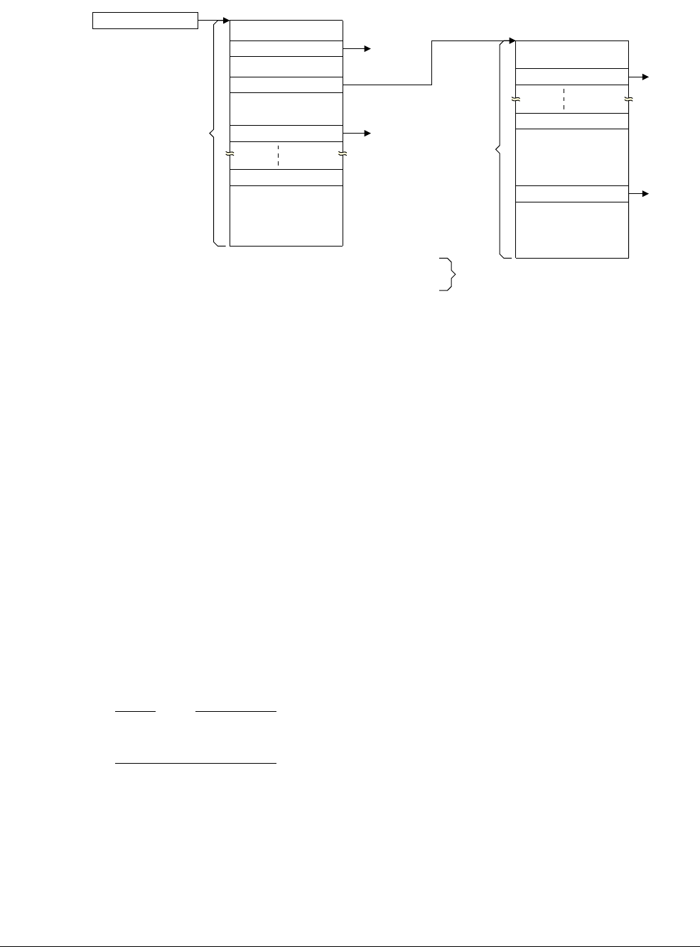
G3 The AArch32 Virtual Memory System Architecture
G3.5 The VMSAv8-32 Short-descriptor translation table format
ARM DDI 0487A.a Copyright © 2013 ARM Limited. All rights reserved. G3-3579
ID090413 Non-Confidential - Beta
Figure G3-3 General view of address translation using Short-descriptor format translation tables
Additional requirements for Short-descriptor format translation tables on page G3-3582 describes why, when using
the Short-descriptor format, Supersection and Large page entries must be repeated 16 times, as shown in
Figure G3-3.
VMSAv8-32 Short-descriptor translation table format descriptors, Memory attributes in the VMSAv8-32
Short-descriptor translation table format descriptors on page G3-3582, and Control of Secure or Non-secure
memory access, VMSAv8-32 Short-descriptor format on page G3-3583 describe the format of the descriptors in the
Short-descriptor format translation tables.
The following sections then describe the use of this translation table format:
•Selecting between TTBR0 and TTBR1, VMSAv8-32 Short-descriptor translation table format on
page G3-3583.
•Translation table walks, when using the VMSAv8-32 Short-descriptor translation table format on
page G3-3584.
G3.5.1 VMSAv8-32 Short-descriptor translation table format descriptors
The following sections describe the formats of the entries in the Short-descriptor translation tables:
•Short-descriptor translation table first-level descriptor formats.
•Short-descriptor translation table second-level descriptor formats on page G3-3581.
For more information about second-level translation tables see Additional requirements for Short-descriptor format
translation tables on page G3-3582.
Note
Previous versions of the ARM Architecture Reference Manual, and some other documentation, describes the AP[2]
bit in the translation table entries as the APX bit.
Information returned by a translation table lookup on page G3-3574 describes the classification of the non-address
fields in the descriptors as address map control, access control, or attribute fields.
Short-descriptor translation table first-level descriptor formats
Each entry in the first-level table describes the mapping of the associated 1MB VA range.
Figure G3-4 on page G3-3580 shows the possible first-level descriptor formats.
TTBR0 or TTBR1
First-level table
Indexed by
VA[19:12]
Section
1MB
memory
region
Page table
Supersection
16MB
memory
region
Second-level table
Indexed by
VA[31-N:20]
‡
Large page
64KB
memory
page
Small page
4KB
memory
page
‡ When using TTBR1, N is 0. When using TTBR0, 0 ≤ N < 8.
† Repeated entries required because of descriptor field overlaps.
Supersection
Repeated
16 times
†
Repeated
16 times
†
Large page
See text for more information.
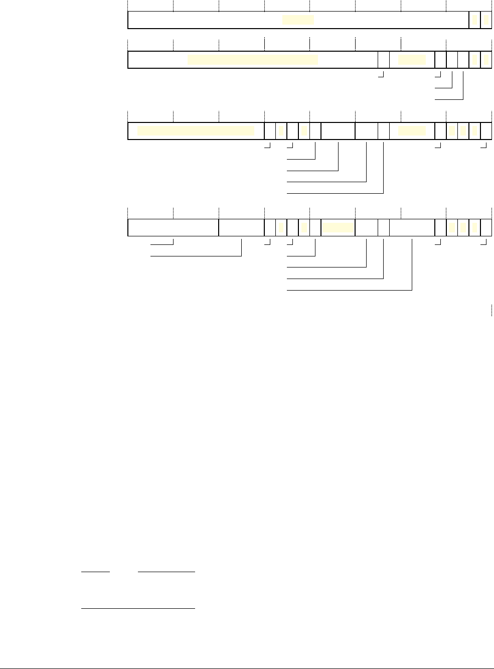
G3 The AArch32 Virtual Memory System Architecture
G3.5 The VMSAv8-32 Short-descriptor translation table format
G3-3580 Copyright © 2013 ARM Limited. All rights reserved. ARM DDI 0487A.a
Non-Confidential - Beta ID090413
Figure G3-4 Short-descriptor first-level descriptor formats
Descriptor bits[1:0] identify the descriptor type. The encoding of these bits is:
0b00
, Invalid or fault entry
The associated VA is unmapped, and any attempt to access it generates a Translation fault.
Software can use bits[31:2] of the descriptor for its own purposes, because the hardware ignores
these bits.
0b01
, Page table
The descriptor gives the address of a second-level translation table, that specifies the mapping of the
associated 1MByte VA range.
0b10
, Section or Supersection
The descriptor gives the base address of the Section or Supersection. Bit[18] determines whether
the entry describes a Section or a Supersection.
This encoding also defines the PXN bit as 0.
0b11
, Section or Supersection, if the implementation supports the PXN attribute
This encoding is identical to
0b10
, except that it defines the PXN bit as 1.
Note
A VMSAv8-32 implementation can use the Short-descriptor translation table format for the Secure EL3&0 or
Non-secure EL1&0 stage 1 translations, by setting TTBCR.EAE to 0.
The address information in the first-level descriptors is:
Page table Bits[31:10] of the descriptor are bits[31:10] of the address of a Page table.
Section Bits[31:20] of the descriptor are bits[31:20] of the address of the Section.
0 0
31 210
IGNOREFault
Page table Domain 0 1
31 10 9 8 5 4 3 2 1 0
Page table base address, bits[31:10]
SBZ
NS
PXN
0 S Domain C B 1
31 20 19 18 17 16 15 14 12 11 10 9 8 5 4 3 2 1 0
Section base address, PA[31:20]Section
NS nG
AP[2]
TEX[2:0]
AP[1:0]
XN
1 S C B 1
31 24 23 20 19 18 17 16 15 14 12 11 10 9 8 5 4 3 2 1 0
Supersection base address, PA[31:24]
Supersection
Extended base address, PA[35:32]
NS nG
AP[2]
IMPLEMENTATION DEFINED
XN
Extended base address, PA[39:36]
TEX[2:0]
AP[1:0]
IMPLEMENTATION DEFINED
IMPLEMENTATION DEFINED
PXN
PXN
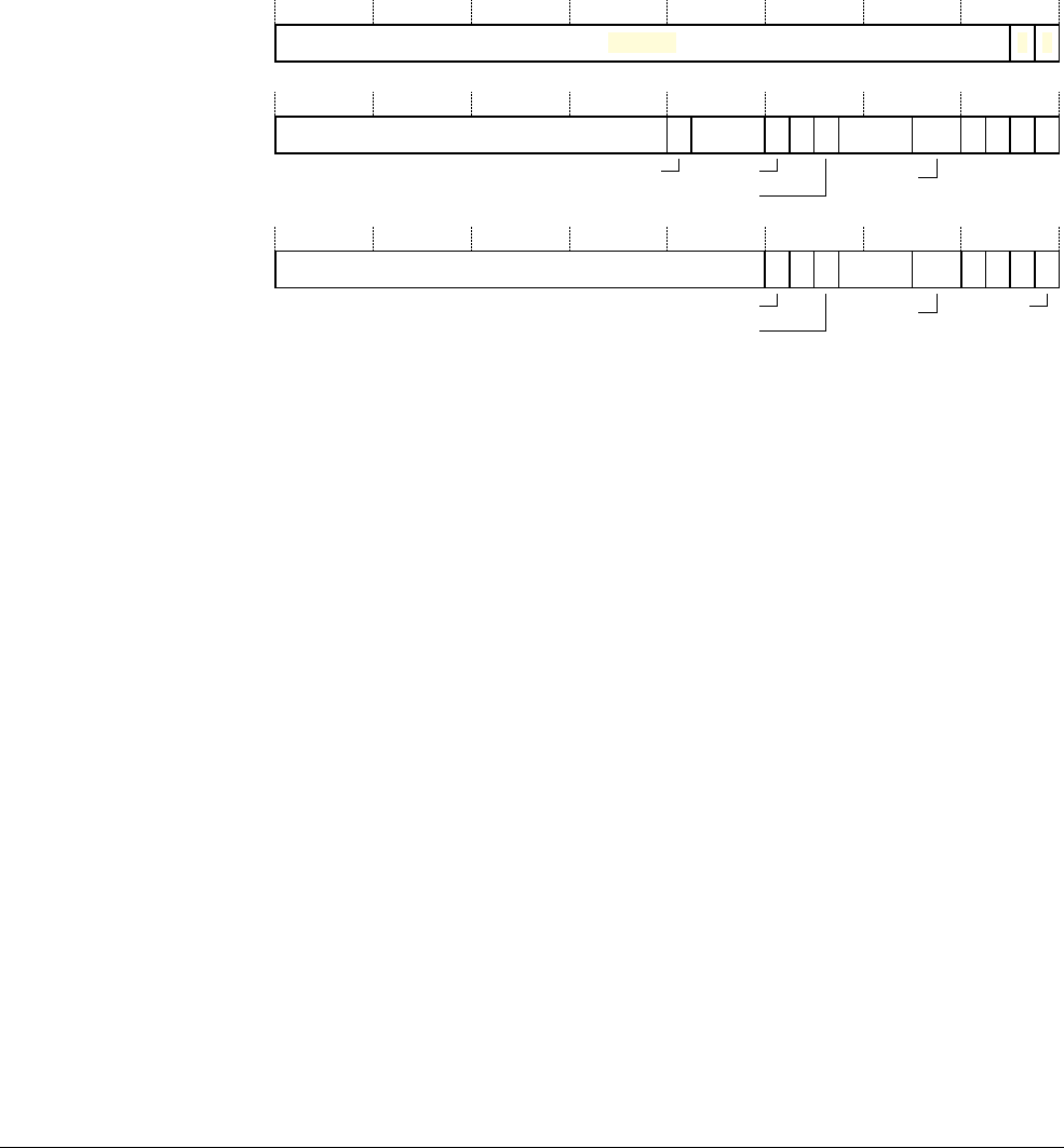
G3 The AArch32 Virtual Memory System Architecture
G3.5 The VMSAv8-32 Short-descriptor translation table format
ARM DDI 0487A.a Copyright © 2013 ARM Limited. All rights reserved. G3-3581
ID090413 Non-Confidential - Beta
Supersection Bits[31:24] of the descriptor are bits[31:24] of the address of the Supersection.
Optionally, bits[8:5, 23:20] of the descriptor are bits[39:32] of the extended Supersection address.
For the Non-secure EL1&0 translation tables, the address in the descriptor is the IPA of the Page table, Section, or
Supersection. Otherwise, the address is the PA of the Page table, Section, or Supersection.
For descriptions of the other fields in the descriptors, see Memory attributes in the VMSAv8-32 Short-descriptor
translation table format descriptors on page G3-3582.
Short-descriptor translation table second-level descriptor formats
Figure G3-5 shows the possible formats of a second-level descriptor.
Figure G3-5 Short-descriptor second-level descriptor formats
Descriptor bits[1:0] identify the descriptor type. The encoding of these bits is:
0b00
, Invalid or fault entry
The associated VA is unmapped, and attempting to access it generates a Translation fault.
Software can use bits[31:2] of the descriptor for its own purposes, because the hardware ignores
these bits.
0b01
, Large page
The descriptor gives the base address and properties of the Large page.
0b1x
, Small page
The descriptor gives the base address and properties of the Small page.
In this descriptor format, bit[0] of the descriptor is the XN bit.
The address information in the second-level descriptors is:
Large page Bits[31:16] of the descriptor are bits[31:16] of the address of the Large page.
Small page Bits[31:12] of the descriptor are bits[31:12] of the address of the Small page.
For the Non-secure EL1&0 translation tables, the address in the descriptor is the IPA of the Page table, Section, or
Supersection. Otherwise, the address is the PA of the Page table, Section, or Supersection.
For descriptions of the other fields in the descriptors, see Memory attributes in the VMSAv8-32 Short-descriptor
translation table format descriptors on page G3-3582.
Large page Large page base address, PA[31:16]
PXN
TEX[2:0]
nG
S
AP[2]
SBZ C B 0 1
0 0
31 210
IGNOREFault
16
31 15
AP[1:0]
14 12111098 6543210
Small page base address, PA[31:12]
31 12111098 6543210
S TEX[2:0] C B 1
nG
AP[2]
AP[1:0] XN
Small page

G3 The AArch32 Virtual Memory System Architecture
G3.5 The VMSAv8-32 Short-descriptor translation table format
G3-3582 Copyright © 2013 ARM Limited. All rights reserved. ARM DDI 0487A.a
Non-Confidential - Beta ID090413
Additional requirements for Short-descriptor format translation tables
When using Supersection or Large page descriptors in the Short-descriptor translation table format, the input
address field that defines the Supersection or Large page descriptor address overlaps the table address field. In each
case, the size of the overlap is 4 bits. The following diagrams show these overlaps:
•Figure G3-8 on page G3-3587 for the first-level translation table Supersection entry.
•Figure G3-10 on page G3-3589 for the second-level translation table Large page table entry.
Considering the case of using Large page table descriptors in a second-level translation table, this overlap means
that for any specific Large page, the bottom four bits of the second-level translation table entry might take any value
from
0b0000
to
0b1111
. Therefore, each of these sixteen index values must point to a separate copy of the same
descriptor.
This means that each Large page or Supersection descriptor must:
• Occur first on a sixteen-word boundary.
• Be repeated in 16 consecutive memory locations.
G3.5.2 Memory attributes in the VMSAv8-32 Short-descriptor translation table format descriptors
This section describes the descriptor fields other than the descriptor type field and the address field:
TEX[2:0], C, B
Memory region attribute bits, see Memory region attributes on page G3-3618.
These bits are not present in a Page table entry.
XN bit The Execute-never bit. Determines whether the PE can execute software from the addressed region,
see Execute-never restrictions on instruction fetching on page G3-3612.
This bit is not present in a Page table entry.
PXN bit The Privileged execute-never bit. Determines whether the PE can execute software from the region
when executing at PL1, see Execute-never restrictions on instruction fetching on page G3-3612.
Note
Memory accesses by software executing at EL2 always use the Long-descriptor translation table
format.
When this bit is set to 1 in the Page table descriptor, it indicates that all memory pages described in
the corresponding page table are Privileged execute-never.
NS bit Non-secure bit. Specifies whether the translated PA is in the Secure or Non-secure address map, see
Control of Secure or Non-secure memory access, VMSAv8-32 Short-descriptor format on
page G3-3583.
This bit is not present in second-level descriptors. The value of the NS bit in the first level Page table
descriptor applies to all entries in the corresponding second-level translation table.
Domain Domain field, see Domains, Short-descriptor format only on page G3-3614.
This field is not present in a Supersection entry. Memory described by Supersections is in domain 0.
This bit is not present in second-level descriptors. The value of the Domain field in the first level
Page table descriptor applies to all entries in the corresponding second-level translation table.
An IMPLEMENTATION DEFINED bit
This bit is not present in second-level descriptors.
AP[2], AP[1:0]
Access Permissions bits, see Memory access control on page G3-3609.
AP[0] can be configured as the Access flag, see The Access flag on page G3-3615.
These bits are not present in a Page table entry.

G3 The AArch32 Virtual Memory System Architecture
G3.5 The VMSAv8-32 Short-descriptor translation table format
ARM DDI 0487A.a Copyright © 2013 ARM Limited. All rights reserved. G3-3583
ID090413 Non-Confidential - Beta
S bit The Shareable bit. Determines whether the addressed region is Shareable memory, see Memory
region attributes on page G3-3618.
This bit is not present in a Page table entry.
nG bit The not global bit. Determines how the translation is marked in the TLB, see Global and
process-specific translation table entries on page G3-3630.
This bit is not present in a Page table entry.
Bit[18], when bits[1:0] indicate a Section or Supersection descriptor
0 Descriptor is for a Section.
1 Descriptor is for a Supersection.
G3.5.3 Control of Secure or Non-secure memory access, VMSAv8-32 Short-descriptor format
Access to the Secure or Non-secure physical address map on page G3-3576 describes how the NS bit in the
translation table entries:
• For accesses from Secure state, determines whether the access is to Secure or Non-secure memory.
• Is ignored by accesses from Non-secure state.
In the Short-descriptor translation table format, the NS bit is defined only in the first-level translation tables. This
means that, in a first-level Page table descriptor, the NS bit defines the physical address space, Secure or
Non-secure, for all of the Large pages and Small pages of memory described by that table.
The NS bit of a first-level Page table descriptor has no effect on the physical address space in which that translation
table is held. As stated in Secure and Non-secure address spaces on page G3-3576, the physical address of that
translation table is in:
• The Secure address space if the translation table walk is in Secure state.
• The Non-secure address space if the translation table walk is in Non-secure state.
This means the granularity of the Secure and Non-secure memory spaces is 1MB. However, in these memory
spaces, table entries can define physical memory regions with a granularity of 4KB.
G3.5.4 Selecting between TTBR0 and TTBR1, VMSAv8-32 Short-descriptor translation table format
As described in Determining the translation table base address in the VMSAv8-32 translation regimes on
page G3-3575, two sets of translation tables can be defined for each of the PL1&0 stage 1 translations, and TTBR0
and TTBR1 hold the base addresses for the two sets of tables. When using the Short-descriptor translation table
format, the value of TTBCR.N indicates the number of most significant bits of the input VA that determine whether
TTBR0 or TTBR1 holds the required translation table base address, as follows:
• If N == 0 then use TTBR0. Setting TTBCR.N to zero disables use of a second set of translation tables.
• if N > 0 then:
— If bits[31:32-N] of the input VA are all zero then use TTBR0.
—Otherwise use TTBR1.
Table G3-4 shows how the value of N determines the lowest address translated using TTBR1, and the size of the
first-level translation table addressed by TTBR0.
Table G3-4 Effect of TTBCR.N on address translation, Short-descriptor format
TTBCR.N First address translated with TTBR1 TTBR0 table
Size Index range
0b000
TTBR1 not used 16KB VA[31:20]
0b001 0x80000000
8KB VA[30:20]
0b010 0x40000000
4KB VA[29:20]
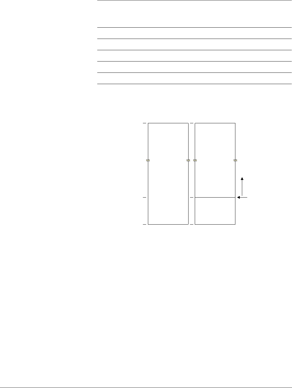
G3 The AArch32 Virtual Memory System Architecture
G3.5 The VMSAv8-32 Short-descriptor translation table format
G3-3584 Copyright © 2013 ARM Limited. All rights reserved. ARM DDI 0487A.a
Non-Confidential - Beta ID090413
Whenever TTBCR.N is nonzero, the size of the translation table addressed by TTBR1 is 16KB.
Figure G3-6 shows how the value of TTBCR.N controls the boundary between VAs that are translated using
TTBR0, and VAs that are translated using TTBR1.
Figure G3-6 How TTBCR.N controls the boundary between the TTBRs, Short-descriptor format
In the selected TTBR, bits RGN, S and IRGN[1:0] define the memory region attributes for the translation table walk.
Translation table walks, when using the VMSAv8-32 Short-descriptor translation table format describes the
translation.
G3.5.5 Translation table walks, when using the VMSAv8-32 Short-descriptor translation table format
When using the Short-descriptor translation table format, and a memory access requires a translation table walk:
• A section-mapped access only requires a read of the first-level translation table.
• A page-mapped access also requires a read of the second-level translation table.
Reading a first-level translation table on page G3-3585 describes how either TTBR1 or TTBR0 is used, with the
accessed VA, to determine the address of the first-level descriptor.
Reading a first-level translation table on page G3-3585 shows the output address as A[39:0]:
• For a Non-secure PL1&0 stage 1 translation, this is the IPA of the required descriptor. A Non-secure PL1&0
stage 2 translation of this address is performed to obtain the PA of the descriptor.
• Otherwise, this address is the PA of the required descriptor.
0b011 0x20000000
2KB VA[28:20]
0b100 0x10000000
1KB VA[27:20]
0b101 0x08000000
512 bytes VA[26:20]
0b110 0x04000000
256 bytes VA[25:20]
0b111 0x02000000
128 bytes VA[24:20]
Table G3-4 Effect of TTBCR.N on address translation, Short-descriptor format (continued)
TTBCR.N First address translated with TTBR1 TTBR0 table
Size Index range
0x00000000
0xFFFFFFFF
0x02000000
TTBR0 region
Boundary, when
TTBCR.N==0b111
Effect of decreasing N
TTBR1 region
TTBR0 region
TTBCR.N==0b000
Use of TTBR1 disabled
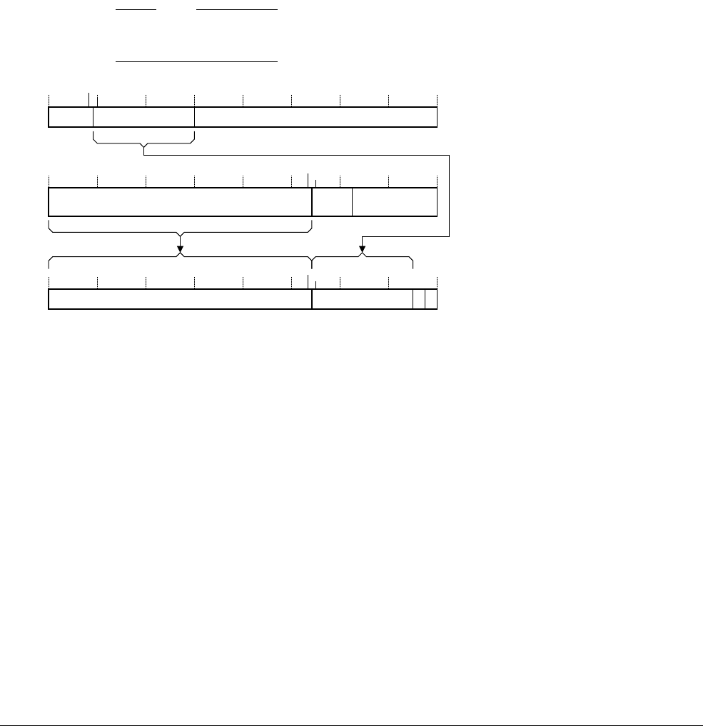
G3 The AArch32 Virtual Memory System Architecture
G3.5 The VMSAv8-32 Short-descriptor translation table format
ARM DDI 0487A.a Copyright © 2013 ARM Limited. All rights reserved. G3-3585
ID090413 Non-Confidential - Beta
The full translation flow for Sections, Supersections, Small pages and Large pages then shows the complete
translation flow for each valid memory access.
Reading a first-level translation table
When performing a fetch based on TTBR0:
• The address bits taken from TTBR0 vary between bits[31:14] and bits[31:7].
• The address bits taken from the VA, that is the input address for the translation, vary between bits[31:20] and
bits[24:20].
The width of the TTBR0 and VA fields depend on the value of TTBCR.N, as Figure G3-7 shows.
When performing a fetch based on TTBR1, Bits TTBR1[31:14] are concatenated with bits[31:20] of the VA. This
makes the fetch equivalent to that shown in Figure G3-7, with N==0.
Note
See The address and Properties fields shown in the translation flows on page G3-3586 for more information about
the Properties label used in this and other figures.
Figure G3-7 Accessing first-level translation table based on TTBR0, Short-descriptor format
Regardless of which register is used as the base for the fetch, the resulting output address selects a four-byte
translation table entry that is one of:
• A first-level descriptor for a Section or Supersection.
•A Page table descriptor that points to a second-level translation table. In this case:
— A second fetch is performed to retrieve a second-level descriptor.
— The descriptor also contains some attributes for the access, see Figure G3-4 on page G3-3580.
• A faulting entry.
The full translation flow for Sections, Supersections, Small pages and Large pages
In a translation table walk, only the first lookup uses the translation table base address from the appropriate
Translation table base register. Subsequent lookups use a combination of address information from:
• The table descriptor read in the previous lookup.
• The input address.
This section summarizes how each of the memory section and page options is described in the translation tables,
and has a subsection summarizing the full translation flow for each of the options.
TTBR0
A[31:0] of first-level descriptor
A[39:32] = 0x00
‡ This field is absent if N is 0
N is the value of TTBCR.N
Input addressTable index
31 20 19 0
32-N 31-N
‡
00Translation base
31 0
Table index
2 1
14-N 13-N
Descriptor address
For details of the Properties field, see the register description
Properties
UNK/
SBZP
Translation base
31
14-N 13-N 0
7 6

G3 The AArch32 Virtual Memory System Architecture
G3.5 The VMSAv8-32 Short-descriptor translation table format
G3-3586 Copyright © 2013 ARM Limited. All rights reserved. ARM DDI 0487A.a
Non-Confidential - Beta ID090413
As described in VMSAv8-32 Short-descriptor translation table format descriptors on page G3-3579, the four
options are:
Supersection A 16MB memory region, see Translation flow for a Supersection.
Section A 1MB memory region, see Translation flow for a Section on page G3-3587.
Large page A 64KB memory region, described by the combination of:
• A first-level translation table entry that indicates a second-level Page table address.
• A second-level descriptor that indicates a Large page.
See Translation flow for a Large page on page G3-3588.
Small page A 4KB memory region, described by the combination of:
• A first-level translation table entry that indicates a second-level Page table address.
• A second-level descriptor that indicates a Small page.
See Translation flow for a Small page on page G3-3590.
The address and Properties fields shown in the translation flows
For the Non-secure PL1&0 stage 1 translation tables:
• Any descriptor address is the IPA of the required descriptor.
• The final output address is the IPA of the Section, Supersection, Large page, or Small page.
In these cases, a PL1&0 stage 2 translation is performed to translate the IPA to the required PA.
Otherwise, the address is the PA of the descriptor, Section, Supersection, Large page, or Small page.
Properties indicates register or translation table fields that return information, other than address information, about
the translation or the targeted memory region. For more information see Information returned by a translation table
lookup on page G3-3574, and the description of the register or translation table descriptor.
For translations using the Short-descriptor translation table format, VMSAv8-32 Short-descriptor translation table
format descriptors on page G3-3579 describes the descriptors formats.
Translation flow for a Supersection
Figure G3-8 on page G3-3587 shows the complete translation flow for a Supersection. For more information about
the fields shown in this figure see The address and Properties fields shown in the translation flows.
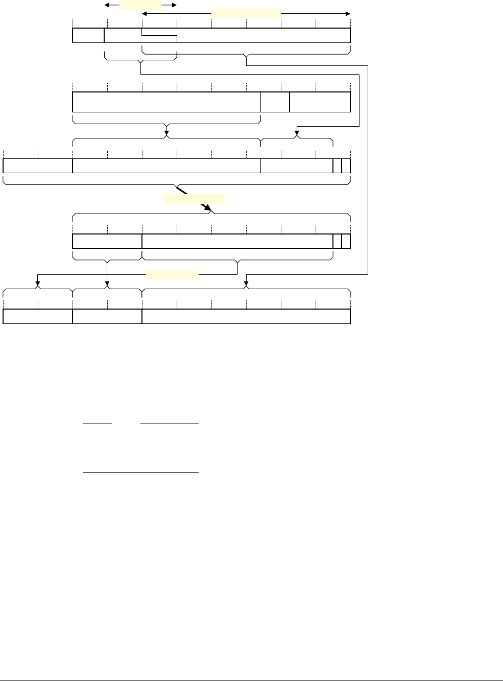
G3 The AArch32 Virtual Memory System Architecture
G3.5 The VMSAv8-32 Short-descriptor translation table format
ARM DDI 0487A.a Copyright © 2013 ARM Limited. All rights reserved. G3-3587
ID090413 Non-Confidential - Beta
Figure G3-8 VMSAv8-32 Short-descriptor Supersection address translation
Note
Figure G3-8 shows how, when the input address, the VA, addresses a Supersection, the top four bits of the
Supersection index bits of the address overlap the bottom four bits of the Table index bits. For more information,
see Additional requirements for Short-descriptor format translation tables on page G3-3582.
Translation flow for a Section
Figure G3-9 on page G3-3588 shows the complete translation flow for a Section. For more information about the
fields shown in this figure see The address and Properties fields shown in the translation flows on page G3-3586.
00000000
For a translation based on TTBR0, N is the value of TTBCR.N
For a translation based on TTBR1, N is 0
UNK/
SBZP
Translation base
31 14-N 13-N 0
First-level
Supersection descriptor
First-level descriptor address
Supersection index
Table index
Bits[8:5,23:20]
Supersection index
31 24 23 0
Supersection BAExtended BA
39 32
Translation Table Base Register
Input address
7 6
Properties
Output address, A[39:0]
‡ This field is absent if N is 0
BA = Base address
For details of Properties fields, see the register or descriptor description
31 210
x
Extended Supersection BA and Properties fields
Supersection BA
24 23
1
First-level lookup
00Translation base
31 0
Table index
2 114-N 13-N39 32
24 2331 20 19 032-N 31-N
‡
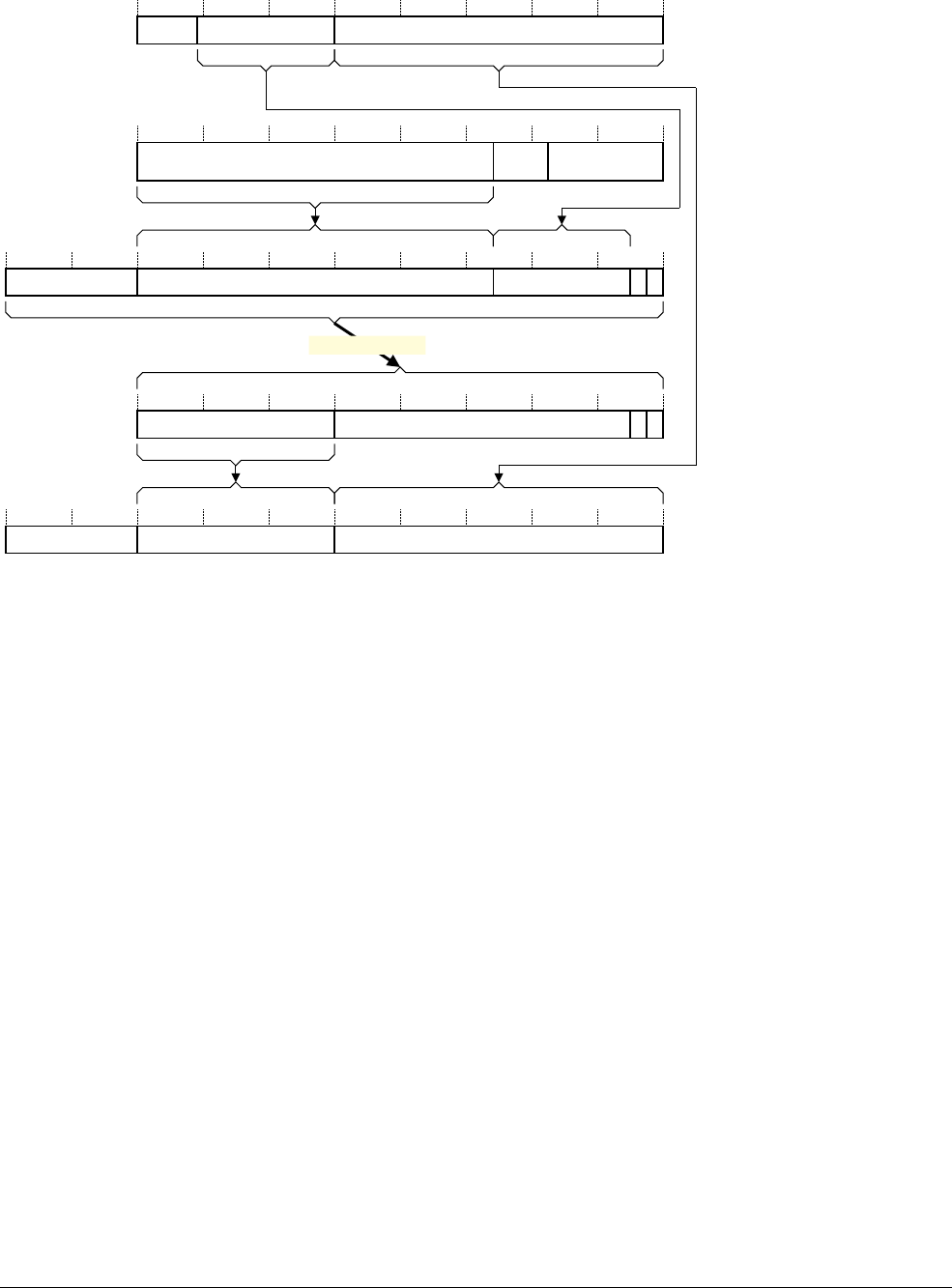
G3 The AArch32 Virtual Memory System Architecture
G3.5 The VMSAv8-32 Short-descriptor translation table format
G3-3588 Copyright © 2013 ARM Limited. All rights reserved. ARM DDI 0487A.a
Non-Confidential - Beta ID090413
Figure G3-9 VMSAv8-32 Short-descriptor Section address translation
Translation flow for a Large page
Figure G3-10 on page G3-3589 shows the complete translation flow for a Large page. For more information about
the fields shown in this figure see The address and Properties fields shown in the translation flows on
page G3-3586.
00000000
39 32
‡ This field is absent if N is 0
For a translation based on TTBR0, N is the value of TTBCR.N
For a translation based on TTBR1, N is 0
31 20 19 0
Section base address Section index
00Translation base
31 0
Table index
2 114-N 13-N
Table index
31 20 19 032-N 31-N
‡ Section index
For details of Properties fields, see the register or descriptor description.
00000000
39 32
Output address, A[39:0]
First-level Section descriptor
Properties
31 20 19 2 1 0
Section base address x1
First-level lookup
First-level descriptor address
Translation Table Base Register
UNK/
SBZP
Translation base
31 14-N 13-N 07 6
Properties
Input address
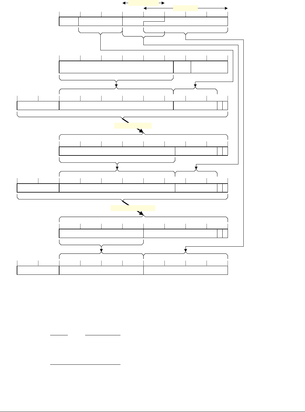
G3 The AArch32 Virtual Memory System Architecture
G3.5 The VMSAv8-32 Short-descriptor translation table format
ARM DDI 0487A.a Copyright © 2013 ARM Limited. All rights reserved. G3-3589
ID090413 Non-Confidential - Beta
Figure G3-10 VMSAv8-32 Short-descriptor Large page address translation
Note
Figure G3-10 shows how, when the input address, the VA, addresses a Large page, the top four bits of the page index
bits of the address overlap the bottom four bits of the First-level table index bits. For more information, see
Additional requirements for Short-descriptor format translation tables on page G3-3582.
00000000
39 32
Page index
For a translation based on TTBR0, N is the value of TTBCR.N
For a translation based on TTBR1, N is 0
Second-level descriptor
L2 table index
Page index
31 16 15 0
Large page base address
00Page table base address
31 0
L2 table index
2 110 9
Properties
31 10 9 2 1 0
Page table base address 10
00Translation base
31 0
L1 table index
2 114-N 13-N
L1 table index
31 20 19 032-N 31-N
‡
12 1116 15
Translation Table
Base Register
L1 = First-level, L2 = Second-level
‡ This field is absent if N is 0
For details of Properties fields, see the register or descriptor description
Output address, A[39:0]
00000000
39 32
1Properties
31 16 15 2 1 0
Large page base address 0
Second-level lookup
Second-level descriptor
address
First-level descriptor
First-level lookup
First-level descriptor
address
00000000
39 32
UNK/
SBZP
Translation base
31 14-N 13-N 07 6
Properties
Input address
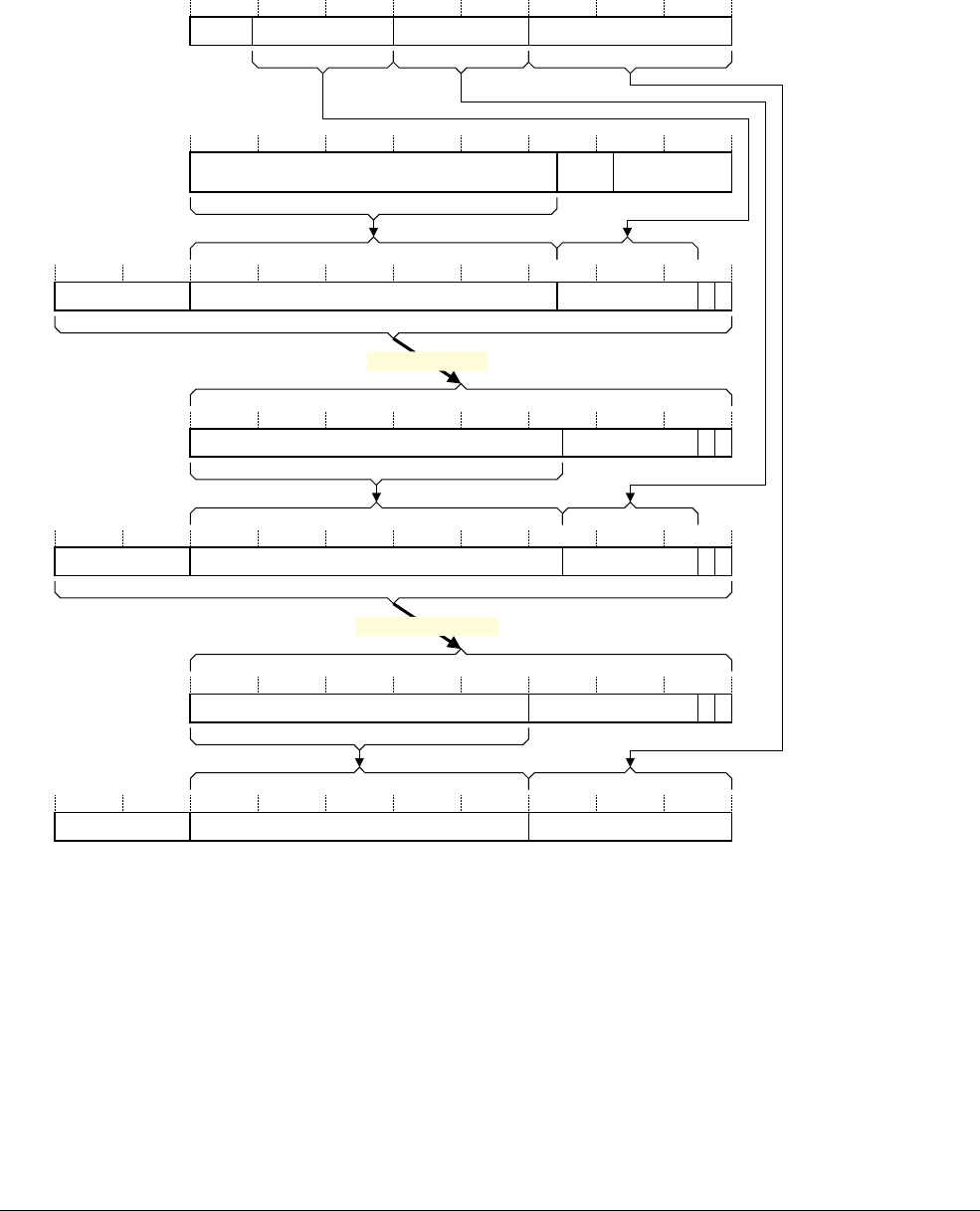
G3 The AArch32 Virtual Memory System Architecture
G3.5 The VMSAv8-32 Short-descriptor translation table format
G3-3590 Copyright © 2013 ARM Limited. All rights reserved. ARM DDI 0487A.a
Non-Confidential - Beta ID090413
Translation flow for a Small page
Figure G3-11 on page G3-3590 shows the complete translation flow for a Small page. For more information about
the fields shown in this figure see The address and Properties fields shown in the translation flows on
page G3-3586.
Figure G3-11 VMSAv8-32 Short-descriptor Small page address translation
Page index
31 12 11 0
Small page base address
00Page table base address
31 0
L2 table index
2 110 9
00Translation base
31 0
L1 table index
2 114-N 13-N
L1 table index
31 20 19 032-N 31-N
‡ Page index
12 11
L2 table index
For a translation based on TTBR0, N is the value of TTBCR.N
For a translation based on TTBR1, N is 0
L1 = First-level, L2 = Second-level
‡ This field is absent if N is 0
For details of Properties fields, see the register or descriptor description.
Output address, A[39:0]00000000
39 32
Properties
31 12 11 2 1 0
Small page base address 1 x Second-level descriptor
Second-level lookup
Second-level descriptor
address
00000000
39 32
First-level descriptorProperties
31 10 9 2 1 0
Page table base address 10
First-level lookup
First-level descriptor
address
00000000
39 32
UNK/
SBZP
Translation base
31 14-N 13-N 07 6
Properties Translation Table
Base Register
Input address

G3 The AArch32 Virtual Memory System Architecture
G3.6 The VMSAv8-32 Long-descriptor translation table format
ARM DDI 0487A.a Copyright © 2013 ARM Limited. All rights reserved. G3-3591
ID090413 Non-Confidential - Beta
G3.6 The VMSAv8-32 Long-descriptor translation table format
The VMSAv8-32 Long-descriptor translation table format supports the assignment of memory attributes to memory
Pages, at a granularity of 4KB, across the complete input address range. It also supports the assignment of memory
attributes to blocks of memory, where a block can be 2MB or 1GB.
Note
• Although the VMSAv8-32 Long-descriptor format is limited to three levels of address lookup, its design and
naming conventions support extension to additional levels, to support a larger input address range.
• Similarly, while the VMSAv8-32 implementation limits the output address range to 40 bits, its design
supports extension to a larger output address range.
Figure G3-2 on page G3-3566 shows the different address translation stages. The Long-descriptor translation table
format:
• Is used for:
— The Non-secure PL2 stage 1 translation.
— The Non-secure PL1&0 stage 2 translation.
• Can be used for the Secure and Non-secure PL1&0 translations.
When used for a stage 1 translation, the translation tables support an input address of up to 32 bits, corresponding
to the VA address range of the PE.
When used for a stage 2 translation, the translation tables support an input address range of up to 40 bits, to support
the translation from IPA to PA. If the input address for the stage 2 translation is a 32-bit address then this address is
zero-extended to 40 bits.
Note
When the Short-descriptor translation table format is used for the Non-secure stage 1 translations, this generates
32-bit IPAs. These are zero-extended to 40 bits to provide the input address for the stage 2 translation.
Overview of VMSAv8-32 address translation using Long-descriptor translation tables summarizes address
translation from AArch32 state when using the Long-descriptor format translation tables.
VMSAv8-32 Long-descriptor translation table format descriptors on page G3-3592, Memory attributes in the
VMSAv8-32 Long-descriptor translation table format descriptors on page G3-3595, and Control of Secure or
Non-secure memory access, VMSAv8-32 Long-descriptor format on page G3-3597 describe the format of the
descriptors in the Long-descriptor format translation tables.
The following sections then describe the use of this translation table format:
•Selecting between TTBR0 and TTBR1, VMSAv8-32 Long-descriptor translation table format on
page G3-3598.
•VMSAv8-32 Long-descriptor translation table format address lookup levels on page G3-3600.
•Translation table walks, when using the VMSAv8-32 Long-descriptor translation table format on
page G3-3603.
G3.6.1 Overview of VMSAv8-32 address translation using Long-descriptor translation tables
Figure G3-12 on page G3-3592 gives a general view of VMSAv8-32 stage 1 address translation when using the
Long-descriptor translation table format.
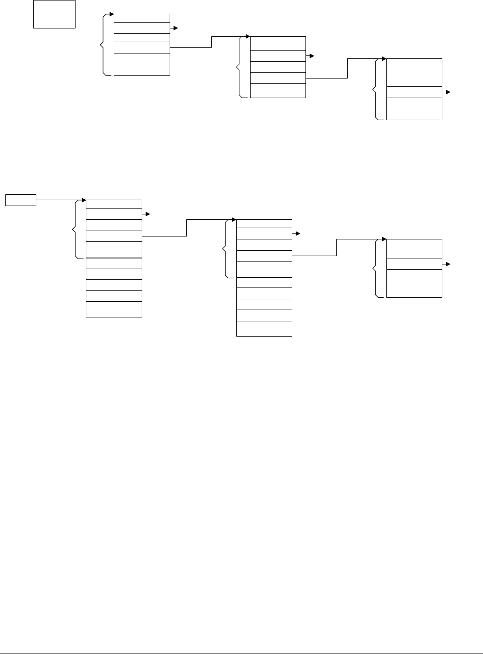
G3 The AArch32 Virtual Memory System Architecture
G3.6 The VMSAv8-32 Long-descriptor translation table format
G3-3592 Copyright © 2013 ARM Limited. All rights reserved. ARM DDI 0487A.a
Non-Confidential - Beta ID090413
Figure G3-12 General view of VMSAv8-32 stage 1 address translation using Long-descriptor format
Figure G3-13 gives a general view of VMSAv8-32 stage 2 address translation. Stage 2 translation always uses the
Long-descriptor translation table format.
Figure G3-13 General view of VMSAv8-32 stage 2 address translation, Long-descriptor translation table format
Use of concatenated translation tables for stage 2 translations on page G3-3601 describes how using concatenated
Second-level tables means lookup can start at the Second level, as referred to in Figure G3-13.
G3.6.2 VMSAv8-32 Long-descriptor translation table format descriptors
As described in VMSAv8-32 Long-descriptor translation table format address lookup levels on page G3-3600, the
Long-descriptor translation table format provides up to three levels of address lookup. A translation table walk starts
either at the first level or the second level of address lookup.
In general, a descriptor is one of:
• An invalid or fault entry.
• A table entry, that points to the next-level translation table.
• A block entry, that defines the memory properties for the access.
• A reserved format.
Bit[1] of the descriptor indicates the descriptor type, and bit[0] indicates whether the descriptor is valid.
The following sections describe the Long-descriptor translation table descriptor formats:
•VMSAv8-32 Long-descriptor first-level and second-level descriptor formats on page G3-3593.
•VMSAv8-32 Long-descriptor translation table third-level descriptor formats on page G3-3594.
TTBR0,
TTBR1, or
HTTBR
First-level table
Indexed by
VA[29:21]
Block
1GB
memory
region
Table
Second-level table
Indexed by
VA[31:30]
4KB
memory
page
If a First-level table would contain only one entry, it is skipped, and the TTBR points
to the Second-level table. This happens if the VA address range is 30 bits or less.
Block
2MB
memory
region
Table
Third-level table
Page
Indexed by
VA[20:12]
VTTBR
First-level tables
Block
1GB
memory
region
Table
Indexed by
IPA[38:30]
4KB
memory
page
If a First-level table would contain 16 entries or fewer, first-level lookup can be omited. If so, VTTBR
points to the start of a block of concatenated Second-level tables. See text for more information.
Third-level table
Page
Block
Table
Indexed by
IPA[20:12]
Up to two concatenated
First-level tables, so that
IPA[39] indexes the table.
Indexed by
IPA[29:21]
Second-level tables
Block
2MB
memory
region
Table
Block
Table
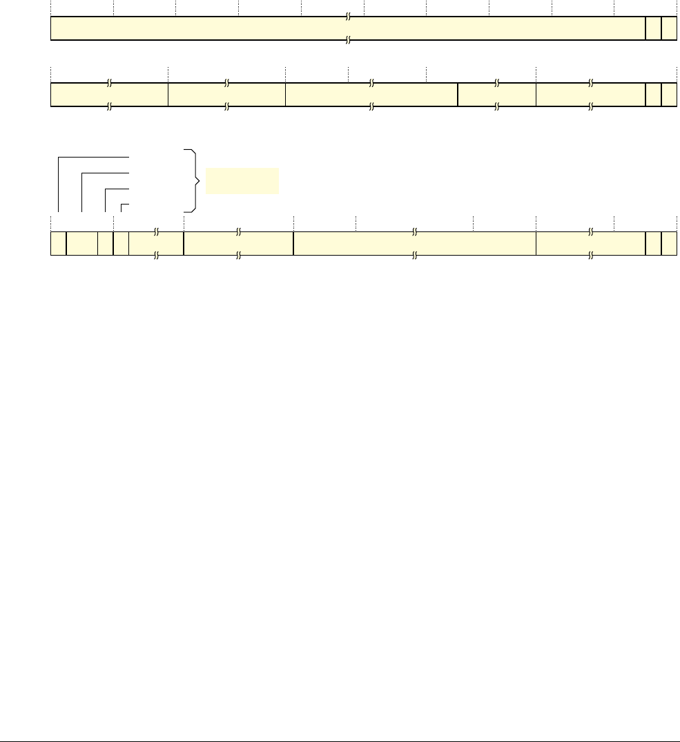
G3 The AArch32 Virtual Memory System Architecture
G3.6 The VMSAv8-32 Long-descriptor translation table format
ARM DDI 0487A.a Copyright © 2013 ARM Limited. All rights reserved. G3-3593
ID090413 Non-Confidential - Beta
Information returned by a translation table lookup on page G3-3574 describes the classification of the non-address
fields in the descriptors between address map control, access controls, and region attributes.
VMSAv8-32 Long-descriptor first-level and second-level descriptor formats
In the Long-descriptor translation tables, the formats of the first-level and second-level descriptors differ only in the
size of the block of memory addressed by the block descriptor. A block entry:
• In a first-level table describes the mapping of the associated 1GB input address range.
• In a second-level table describes the mapping of the associated 2MB input address range.
Figure G3-14 shows the Long-descriptor first-level and second-level descriptor formats:
Figure G3-14 VMSAv8-32 Long-descriptor first-level and second-level descriptor formats
Descriptor encodings, Long-descriptor first-level and second-level formats
Descriptor bit[0] identifies whether the descriptor is valid, and is 1 for a valid descriptor. If a lookup returns an
invalid descriptor, the associated input address is unmapped, and any attempt to access it generates a Translation
fault.
Descriptor bit[1] identifies the descriptor type, and is encoded as:
0, Block The descriptor gives the base address of a block of memory, and the attributes for that memory
region.
1, Table The descriptor gives the address of the next level of translation table, and for a stage 1 translation,
some attributes for that translation.
The other fields in the valid descriptors are:
Block descriptor
Gives the base address and attributes of a block of memory:
• For a first-level Block descriptor, bits[47:30] are bits[47:30] of the output address that
specifies a 1GB block of memory.
• For a second-level Block descriptor, bits[47:21] are bits[47:21] of the output address that
specifies a 2MB block of memory.
0Ignore
63 210
x
Invalid
1Upper block attributes
63 52 51 3940 nn-1 12 11 2 1 0
UNK/SBZP Output address[39:n]UNK/SBZP Lower block attributes 0
Block
For the first-level descriptor, n is 30. For the second-level descriptor, n is 21.
The first-level descriptor returns the address of the second-level table.
The second-level descriptor returns the address of the third-level table.
1
63 62 61 60 59 58 52 51 40 39 12 11 2 1 0
Ignored UNK/SBZP Next-level table address[39:12] Ignored 1
Table
PXNTable
XNTable
APTable
NSTable
Stage 1 only,
SBZ at stage 2
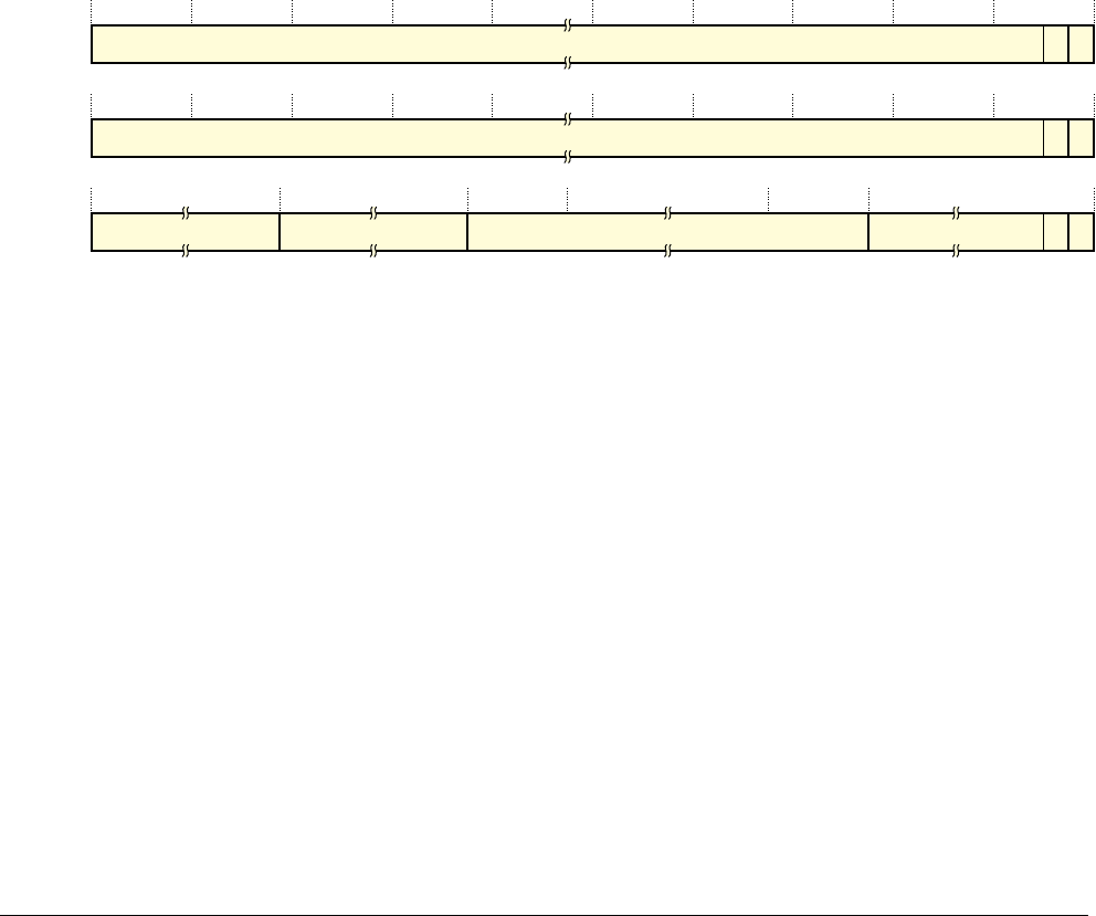
G3 The AArch32 Virtual Memory System Architecture
G3.6 The VMSAv8-32 Long-descriptor translation table format
G3-3594 Copyright © 2013 ARM Limited. All rights reserved. ARM DDI 0487A.a
Non-Confidential - Beta ID090413
Bits[63:52, 11:2] provide attributes for the target memory block, see Memory attributes in the
VMSAv8-32 Long-descriptor translation table format descriptors on page G3-3595. The position
and contents of these bits are identical in the second-level block descriptor and in the third-level
page descriptor.
Table descriptor
Bits[47:m] are bits[47:m] of the address of the required next-level table. Bits[m-1:0] of the table
address are zero:
• For a first-level Table descriptor, this is the address of a second-level table.
• For a second-level Table descriptor, this is the address of a third-level table.
For a stage 1 translation only, bits[63:59] provide attributes for the next-level lookup, see Memory
attributes in the VMSAv8-32 Long-descriptor translation table format descriptors on
page G3-3595.
If the translation table defines the Non-secure PL1&0 stage 1 translations, then the output address in the descriptor
is the IPA of the target block or table. Otherwise, it is the PA of the target block or table.
VMSAv8-32 Long-descriptor translation table third-level descriptor formats
Each entry in a third-level table describes the mapping of the associated 4KB input address range.
Figure G3-15 shows the Long-descriptor third-level descriptor formats.
Figure G3-15 VMSAv8-32 Long-descriptor third-level descriptor formats
Descriptor bit[0] identifies whether the descriptor is valid, and is 1 for a valid descriptor. If a lookup returns an
invalid descriptor, the associated input address is unmapped, and any attempt to access it generates a Translation
fault.
Descriptor bit[1] identifies the descriptor type, and is encoded as:
0, Reserved, invalid
Behaves identically to encodings with bit[0] set to 0.
This encoding must not be used in third-level translation tables.
1, Page Gives the address and attributes of a 4KB page of memory.
At this level, the only valid format is the Page descriptor. The other fields in the Page descriptor are:
Page descriptor
Bits[47:12] are bits[47:12] of the output address for a page of memory.
Bits[63:52, 11:2] provide attributes for the target memory page, see Memory attributes in the
VMSAv8-32 Long-descriptor translation table format descriptors on page G3-3595. The position
and contents of these bits are identical in the first-level block descriptor and in the second-level
block descriptor.
If the translation table defines the Non-secure PL1&0 stage 1 translations, then the output address in the descriptor
is the IPA of the target page. Otherwise, it is the PA of the target page.
0Ignore
63 210
x
Invalid
Reserved,
invalid 1Reserved
63 210
0
Page 1Upper page attributes
63 52 51 3940 12 11 2 1 0
UNK/SBZP Output address[39:12] Lower page attributes 1
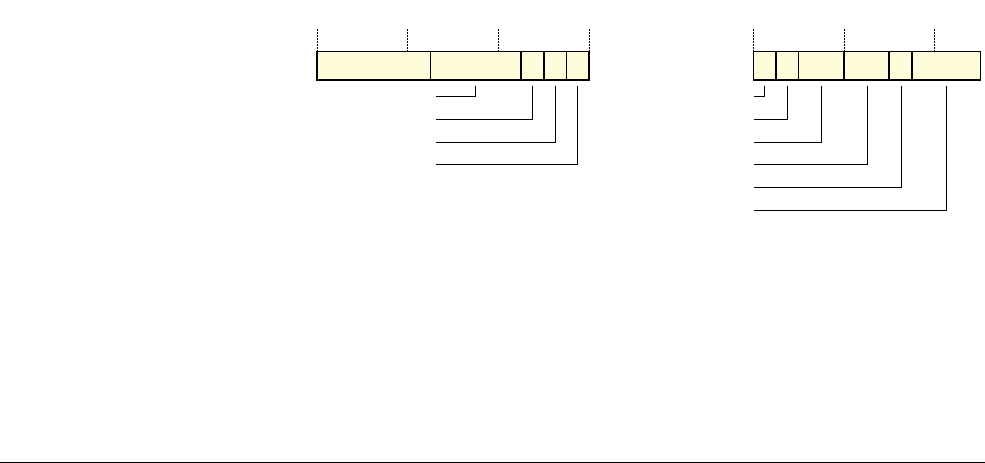
G3 The AArch32 Virtual Memory System Architecture
G3.6 The VMSAv8-32 Long-descriptor translation table format
ARM DDI 0487A.a Copyright © 2013 ARM Limited. All rights reserved. G3-3595
ID090413 Non-Confidential - Beta
G3.6.3 Memory attributes in the VMSAv8-32 Long-descriptor translation table format descriptors
The memory attributes in the VMSAv8-32 Long-descriptor translation tables are based on those in the
Short-descriptor translation table format, with some extensions. Memory region attributes on page G3-3618
describes these attributes. In the Long-descriptor translation table format:
• Table entries for stage 1 translations define attributes for the next level of lookup, see Next-level attributes
in VMSAv8-32 Long-descriptor stage 1 Table descriptors
• Block and Page entries define memory attributes for the target block or page of memory. Stage 1 and stage 2
translations have some differences in these attributes, see:
—Attribute fields in VMSAv8-32 Long-descriptor stage 1 Block and Page descriptors.
—Attribute fields in VMSAv8-32 Long-descriptor stage 2 Block and Page descriptors on page G3-3596.
Next-level attributes in VMSAv8-32 Long-descriptor stage 1 Table descriptors
In a Table descriptor for a stage 1 translation, bits[63:59] of the descriptor define the following attributes for the
next-level translation table access:
NSTable, bit[63] For memory accesses from Secure state, specifies the security level for subsequent levels of
lookup, see Hierarchical control of Secure or Non-secure memory accesses,
Long-descriptor format on page G3-3597.
For memory accesses from Non-secure state, this bit is ignored.
APTable, bits[62:61] Access permissions limit for subsequent levels of lookup, see Hierarchical control of access
permissions, Long-descriptor format on page G3-3610.
APTable[0] is reserved, SBZ, in the Non-secure PL2 stage 1 translation tables.
XNTable, bit[60] XN limit for subsequent levels of lookup, see Hierarchical control of instruction fetching,
Long-descriptor format on page G3-3613.
PXNTable, bit[59] PXN limit for subsequent levels of lookup, see Hierarchical control of instruction fetching,
Long-descriptor format on page G3-3613.
This bit is reserved, SBZ, in the Non-secure PL2 stage 1 translation tables.
Attribute fields in VMSAv8-32 Long-descriptor stage 1 Block and Page descriptors
Block and Page descriptors split the memory attributes into an upper block and a lower block. Figure G3-16 shows
the memory attribute fields in these blocks, for a stage 1 translation:
Figure G3-16 VMSAv8-32 memory attribute fields in Long-descriptor stage 1 Block and Page descriptors
For a stage 1 descriptor, the attributes are:
XN, bit[54] The Execute-never bit. Determines whether the region is executable, see Execute-never restrictions
on instruction fetching on page G3-3612.
PXN, bit[53] The Privileged execute-never bit. Determines whether the region is executable at EL1, see
Execute-never restrictions on instruction fetching on page G3-3612.
Upper attributes Lower attributes
Ignored
63 59 58 55 54 53 52
XN
PXN
Contiguous hint
1110987654 2
nG
AF
SH[1:0]
AP[2:1]
NS
AttrIndx[2:0]
Reserved for software use
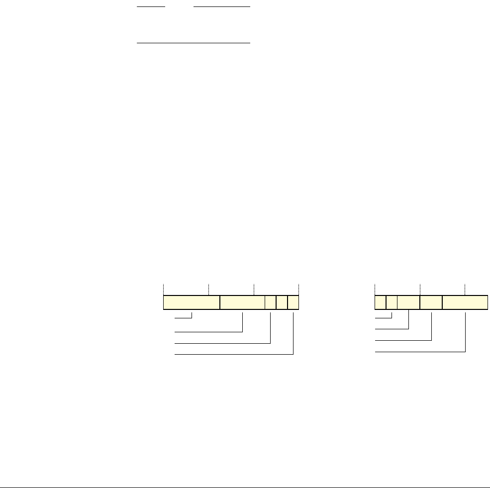
G3 The AArch32 Virtual Memory System Architecture
G3.6 The VMSAv8-32 Long-descriptor translation table format
G3-3596 Copyright © 2013 ARM Limited. All rights reserved. ARM DDI 0487A.a
Non-Confidential - Beta ID090413
This bit is reserved, SBZ, in the Non-secure PL2 stage 1 translation tables.
Contiguous, bit[52]
Indicates that 16 adjacent translation table entries point to contiguous memory regions, see
Contiguous bit on page G3-3625.
nG, bit[11] The not global bit. Determines how the translation is marked in the TLB, see Global and
process-specific translation table entries on page G3-3630.
This bit is reserved, SBZ, in the Non-secure PL2 stage 1 translation tables.
AF, bit[10] The Access flag, see The Access flag on page G3-3615.
SH, bits[9:8] Shareability field, see Memory region attributes on page G3-3618.
AP[2:1], bits[7:6]
Access Permissions bits, see Memory access control on page G3-3609.
Note
For consistency with the Short-descriptor translation table formats, the Long-descriptor format
defines AP[2:1] as the Access Permissions bits, and does not define an AP[0] bit.
AP[1] is reserved, SBO, in the Non-secure PL2 stage 1 translation tables.
NS, bit[5] Non-secure bit. For memory accesses from Secure state, specifies whether the output address is in
Secure or Non-secure memory, see Control of Secure or Non-secure memory access, VMSAv8-32
Long-descriptor format on page G3-3597.
For memory accesses from Non-secure state, this bit is ignored.
AttrIndx[2:0], bits[4:2]
Stage 1 memory attributes index field, for the indicated Memory Attribute Indirection Register, see
VMSAv8-32 Long-descriptor format memory region attributes on page G3-3624.
In the upper attributes block, the architecture guarantees that hardware does not alter the fields marked as Ignored
and Reserved for software use. For more information see Other fields in the Long-descriptor translation table
format descriptors on page G3-3625.
Attribute fields in VMSAv8-32 Long-descriptor stage 2 Block and Page descriptors
Block and Page descriptors split the memory attributes into an upper block and a lower block. Figure G3-17 shows
the memory attribute fields in these blocks, for a stage 2 translation:
Figure G3-17 VMSAv8-32 memory attribute fields in Long-descriptor stage 2 Block and Page descriptors
For a stage 2 descriptor, the attributes are:
XN, bit[54] The Execute-never bit. Determines whether the region is executable, see Execute-never restrictions
on instruction fetching on page G3-3612.
Contiguous, bit[52]
Indicates that 16 adjacent translation table entries point to contiguous memory regions, see
Contiguous bit on page G3-3625.
Lower attributes
MemAttr[3:0]
111098765 2
(0)
AF
SH[1:0]
S2AP[1:0]
Upper attributes
63 59 58 55 54 53 52
(0)
XN
Contiguous hint
Reserved for software use
Reserved for System MMU

G3 The AArch32 Virtual Memory System Architecture
G3.6 The VMSAv8-32 Long-descriptor translation table format
ARM DDI 0487A.a Copyright © 2013 ARM Limited. All rights reserved. G3-3597
ID090413 Non-Confidential - Beta
AF, bit[10] The Access flag, see The Access flag on page G3-3615.
SH, bits[9:8] Shareability field, see EL2 control of Non-secure memory region attributes on page G3-3625.
S2AP, bits[7:6]
Stage 2 Access Permissions bits, see Hyp mode control of Non-secure access permissions on
page G3-3616.
Note
In the original VMSAv7-32 Long-descriptor attribute definition, this field was called HAP[2:1], for
consistency with the AP[2:1] field in the stage 1 descriptors and despite there being no HAP[0] bit.
ARMv8 renames the field for greater clarity.
MemAttr, bits[5:2]
Stage 2 memory attributes, see EL2 control of Non-secure memory region attributes on
page G3-3625.
In the upper attributes block:
• The field marked as Reserved for System MMU use is ignored by the PE. The architecture guarantees that the
PE does not alter this field.
• The architecture guarantees that the PE does not alter the fields marked as Ignored and Reserved for software
use.
For more information see Other fields in the Long-descriptor translation table format descriptors on page G3-3625.
G3.6.4 Control of Secure or Non-secure memory access, VMSAv8-32 Long-descriptor format
Access to the Secure or Non-secure physical address map on page G3-3576 describes how the NS bit in the
translation table entries:
• For accesses from Secure state, determines whether the access is to Secure or Non-secure memory.
• Is ignored by accesses from Non-secure state.
In the Long-descriptor format:
• The NS bit relates only to the memory block or page at the output address defined by the descriptor.
• The descriptors also include an NSTable bit, see Hierarchical control of Secure or Non-secure memory
accesses, Long-descriptor format.
The NS and NSTable bits are valid only for memory accesses from Secure state. Memory accesses from Non-secure
state ignore the values of these bits.
Hierarchical control of Secure or Non-secure memory accesses, Long-descriptor
format
For Long-descriptor format table descriptors for stage 1 translations, the descriptor includes an NSTable bit, that
indicates whether the table identified in the descriptor is in Secure or Non-secure memory. For accesses from Secure
state, the meaning of the NSTable bit is:
NSTable == 0 The defined table address is in the Secure physical address space. In the descriptors in that
translation table, NS bits and NSTable bits have their defined meanings.
NSTable == 1 The defined table address is in the Non-secure physical address space. Because this table is fetched
from the Non-secure address space, the NS and NSTable bits in the descriptors in this table must be
ignored. This means that, for this table:
• The value of the NS bit in any block or page descriptor is ignored. The block or page address
is refers to Non-secure memory.

G3 The AArch32 Virtual Memory System Architecture
G3.6 The VMSAv8-32 Long-descriptor translation table format
G3-3598 Copyright © 2013 ARM Limited. All rights reserved. ARM DDI 0487A.a
Non-Confidential - Beta ID090413
• The value of the NSTable bit in any table descriptor is ignored, and the table address refers
to Non-secure memory. When this table is accessed, the NS bit in any block or page
descriptor is ignored, and all descriptors in the table refer to Non-secure memory.
In addition, an entry fetched in Secure state is treated as non-global if either:
• NSTable is set to 1.
• The fetch ignores the values of NS and NSTable, because of a higher-level fetch with NSTable set to 1.
That is, these entries must be treated as if nG==1, regardless of the value of the nG bit. For more information about
the nG bit, see Global and process-specific translation table entries on page G3-3630.
Note
• When using the Long-descriptor format, table descriptors are defined only for the first level and second level
of lookup.
• Stage 2 translations are performed only for operations in Non-secure state, that can access only the
Non-secure address space. Therefore, the stage 2 descriptors do not include NS or NSTable bits.
G3.6.5 Selecting between TTBR0 and TTBR1, VMSAv8-32 Long-descriptor translation table format
As described in Determining the translation table base address in the VMSAv8-32 translation regimes on
page G3-3575, two sets of translation tables can be defined for each of the PL1&0 stage 1 translations, and TTBR0
and TTBR1 hold the base addresses for the two sets of tables. The Long-descriptor translation table format provides
more flexibility in defining the boundary between using TTBR0 and using TTBR1. When a PL1&0 stage 1 address
translation is enabled, TTBR0 is always used. If TTBR1 is also used then:
•TTBR1 is used for the top part of the input address range.
•TTBR0 is used for the bottom part of the input address range.
The TTBCR.T0SZ and TTBCR.T1SZ size fields control the use of TTBR0 and TTBR1, as Table G3-5 shows.
For stage 1 translations, the input address is always a VA, and the maximum possible VA is (232-1).
When address translation is using the Long-descriptor translation table format:
•Figure G3-18 on page G3-3599 shows how, when TTBCR.T1SZ is zero, the value of TTBCR.T0SZ controls
the boundary between VAs that are translated using TTBR0, and VAs that are translated using TTBR1.
Table G3-5 Use of TTBR0 and TTBR1, Long-descriptor format
TTBCR Input address range using:
T0SZ T1SZ TTBR0 TTBR1
0b000 0b000
All addresses Not used
Ma
a. M, N must be greater than 0.The maximum possible value for each of T0SZ and T1SZ is 7.
0b000
Zero to (2(32-M)-1) 232-M to maximum input address
0b000
NaZero to (232-2(32-N)-1) 232-2(32-N) to maximum input address
MaNaZero to (2(32-M)-1) 232-2(32-N) to maximum input address
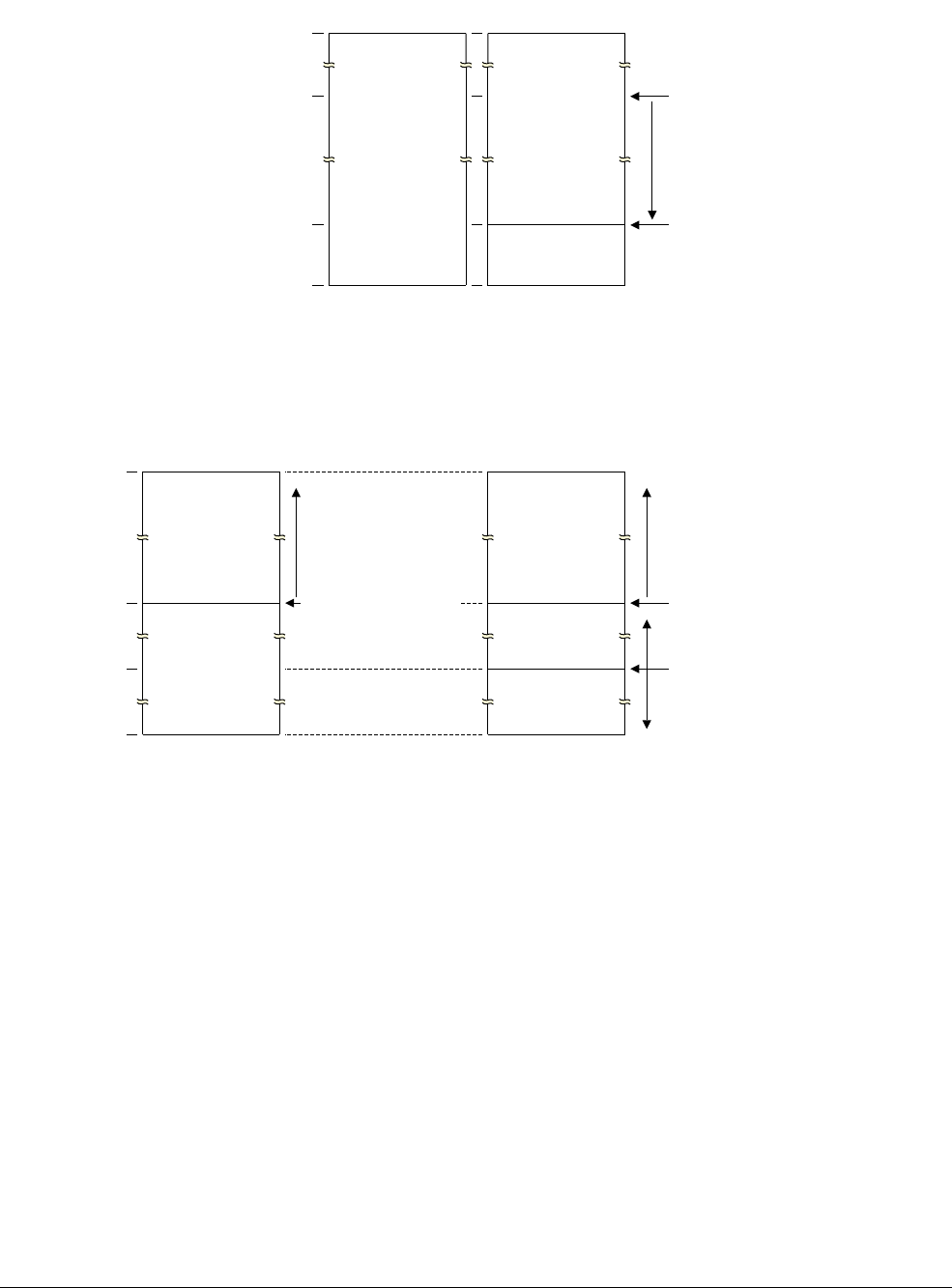
G3 The AArch32 Virtual Memory System Architecture
G3.6 The VMSAv8-32 Long-descriptor translation table format
ARM DDI 0487A.a Copyright © 2013 ARM Limited. All rights reserved. G3-3599
ID090413 Non-Confidential - Beta
Figure G3-18 Control of TTBR boundary, when TTBCR.T1SZ is zero
•Figure G3-19 shows how, when TTBCR.T1SZ is nonzero, the values of TTBCR.T0SZ and TTBCR.T1SZ
control the boundaries between VAs that are translated using TTBR0, and VAs that are translated using
TTBR1.
Figure G3-19 Control of TTBR boundaries, when TTBCR.T1SZ is nonzero
When T0SZ and T1SZ are both nonzero:
— If both fields are set to
0b001
, the boundary between the two regions is
0x80000000
. This is identical to
having T0SZ set to
0b000
and T1SZ set to
0b001
.
— Otherwise, the TTBR0 and TTBR1 regions are non-contiguous. In this case, any attempt to access an
address that is in that gap between the TTBR0 and TTBR1 regions generates a Translation fault.
When using the Long-descriptor translation table format:
• The TTBCR contains fields that define memory region attributes for the translation table walk, for each
TTBR. These are the SH0, ORGN0, IRGN0, SH1, ORGN1, and IRGN1 bits.
•TTBR0 and TTBR1 each contain an ASID field, and the TTBCR.A1 field selects which ASID to use.
For this translation table format, VMSAv8-32 Long-descriptor translation table format address lookup levels on
page G3-3600 summarizes the lookup levels, and Translation table walks, when using the VMSAv8-32
Long-descriptor translation table format on page G3-3603 describes the possible translations.
Possible translation table registers programming errors
In all the descriptions in this subsection, the size of the input address supported for a PL1&0 stage 1 translation
refers to the size specified by a TTBCR.TxSZ field.
0x00000000
0xFFFFFFFF
0x02000000
TTBR0 region Effect of increasing TTBCR.T0SZ
TTBCR.T0SZ==0b000
Use of TTBR1 disabled
TTBR0 region
TTBR1 region
Boundary, when TTBCR.T0SZ==0b111
0x80000000 Boundary, when TTBCR.T0SZ==0b001
TTBCR.T1SZ==0b000
0x00000000
0xFFFFFFFF
TTBR0 region
Effect of increasing TTBCR.T1SZ
TTBR1 region
TTBCR.T0SZ==0b000
0x80000000 Boundary,
TTBCR.T1SZ==0b001
0x40000000
TTBR1 region
TTBR0 region
Boundary, when TTBCR.T0SZ==0b010
Effect of increasing TTBCR.T0SZ
Accesses
generate a
Translation fault
Effect of
increasing
TTBCR.T1SZ
Boundary, when TTBCR.T1SZ==0b001
TTBCR.T0SZ>0b000
Effect of decreasing TTBCR.T0SZ

G3 The AArch32 Virtual Memory System Architecture
G3.6 The VMSAv8-32 Long-descriptor translation table format
G3-3600 Copyright © 2013 ARM Limited. All rights reserved. ARM DDI 0487A.a
Non-Confidential - Beta ID090413
Note
For a PL1&0 stage 1 translation, this section has described how the input address range can be split so that the lower
addresses are translated by TTBR0 and the higher addresses are translated by TTBR1. In this case, each of input
address sizes specified by TTBCR.{T0SZ, T1SZ} is smaller than the total address size supported by the stage of
translation.
The following are possible errors in the programming of TTBR0, TTBR1, and TTBCR. For the translation of a
particular address at a particular stage of translation, either:
• The block size being used to translate the address is larger than the size of the input address supported at a
stage of translation used in performing the required translation. This can occur only for the PL1&0 stage 1
translations, and only when either TTBCR.T0SZ or TTBCR.T1SZ is zero, meaning there is no gap between
the address range translated by TTBR0 and the range translated by TTBR1. In this case, this programming
error occurs if a block translated from the region that has TxSZ set to zero straddles the boundary between
the two address ranges. Example G3-2 shows an example of this mis-programming.
• The address range translated by a set of blocks marked as contiguous, by use of the contiguous bit, is larger
than the size of the input address supported at a stage of translation used in performing the required
translation.
Example G3-2 Translation table programming error
If TTBCR.T0SZ is programmed to 0 and TTBCR.T1SZ is programmed to 7, this means:
•TTBR0 translates addresses in the range
0x00000000
-
0xFDFFFFFF
.
•TTBR1 translates addresses in the range
0xFE000000
-
0xFFFFFFFF
.
The translation table indicated by TTBR0 might be programmed with a block entry for a 1GB region starting at
0xC0000000
. This covers the address range
0xC0000000
-
0xFFFFFFFF
, that overlaps the TTBR1 address range. This
means this block size is larger than the input address size supported for translations using TTBR0, and therefore this
is a programming error.
To understand why this must be a programming error, consider a memory access to address
0xFFFF0000
. According
to the TTBCR.{T0SZ, T1SZ} values, this must be translated using TTBR1. However, the access matches a TLB
entry for the translation, using TTBR0, of the block at
0xC0000000
. Hardware is not required to detect that the access
to
0xFFFF0000
is being translated incorrectly.
In these cases, an implementation might use one of the following approaches:
• Treat such a block, that might be a block within a contiguous set of blocks, as causing a Translation fault,
even though the block is valid, and the address accessed within that block is within the size of the input
address supported at a stage of translation.
• Treat such a block, that might be a block within a contiguous set of blocks, as not causing a Translation fault,
even though the address accessed within that block is outside the size of the input address supported at a stage
of translation, provided that both of the following apply:
— The block is valid.
— At least one address within the block, or contiguous set of blocks, is within the size of the input address
supported at a stage of translation.
G3.6.6 VMSAv8-32 Long-descriptor translation table format address lookup levels
As stated at the start of this section, because the Long-descriptor translation table format is used for the Non-secure
PL1&0 stage 2 translations, the format must support input addresses of up to 40 bits.

G3 The AArch32 Virtual Memory System Architecture
G3.6 The VMSAv8-32 Long-descriptor translation table format
ARM DDI 0487A.a Copyright © 2013 ARM Limited. All rights reserved. G3-3601
ID090413 Non-Confidential - Beta
Table G3-6 summarizes the properties of the different levels of address lookup when using this format.
For first-level and second-level tables, reducing the input address range reduces the number of addresses in the table
and therefore reduces the table size.The appropriate Translation Table Control Register specifies the input address
range.
Stage 1 translations require an input address range of up to 32 bits, corresponding to VA[31:0]. For these
translations:
• For a memory access from a mode other than Hyp mode, the Secure or Non-secure TTBR0 or TTBR1 holds
the translation table base address, and the Secure or Non-secure TTBCR is the control register.
• For a memory access from Hyp mode, HTTBR holds the translation table base address, and HTCR is the
control register.
Note
For translations controlled by TTBR0 and TTBR1, if neither Translation Table Base Register has an input address
range larger than 1GB, then translation starts at the second level. Together, TTBR0 and TTBR1 can still cover the
32-bit VA input address range.
Stage 2 translations require an input address range of up to 40 bits, corresponding to IPA[39:0], and the supported
input address size is configurable in the range 25-40 bits. Table G3-6 indicates a requirement for the translation
mechanism to support a 39-bit input address range, Address[38:0]. Use of concatenated translation tables for stage
2 translations describes how a 40-bit IPA address range is supported. For stage 2 translations:
•VTTBR holds the translation table base address, and VTCR is the control register.
• If a supplied input address is larger than the configured input address size, a Translation fault is generated.
Use of concatenated translation tables for stage 2 translations
If a stage 2 translation requires 16 entries or fewer in its top-level translation table, it can instead:
• Require the corresponding number of concatenated translation tables at the next translation level, aligned to
the size of the block of concatenated translation tables.
• Start the translation at that next translation level.
Note
Stage 2 translations always use the Long-descriptor translation table format.
Table G3-6 Properties of the three levels of address lookup with VMSAv8-32 Long-descriptor translation tables
Level Input address Output addressa
Number of entries
Size Address rangebSize Address range
First Up to 512GB Up to Address[38:0] 1GB Address[39:30] Up to 512
Second Up to 1GB Up to Address[29:0] 2MB Address[39:21] Up to 512
Third 2MB Address[20:0] 4KB Address[47:12] 512
a. Output address when an entry addresses a block of memory or a memory page. If an entry addresses the next level of
address lookup it specifies Address[39:12] for the next-level translation table.
b. Input address range for the translation table. See Use of concatenated first-level translation tables on page G3-3602 for
details of support for additional bits of address at a given level, including possible support of a 40-bit input address
range at the first level.

G3 The AArch32 Virtual Memory System Architecture
G3.6 The VMSAv8-32 Long-descriptor translation table format
G3-3602 Copyright © 2013 ARM Limited. All rights reserved. ARM DDI 0487A.a
Non-Confidential - Beta ID090413
Use of this translation scheme is:
• Required when the stage 2 translation supports a 40-bit input address range, see Use of concatenated
first-level translation tables.
• Supported for a stage 2 translation with an input address range of 31-34 bits, see Use of concatenated
second-level translation tables.
Note
This translation scheme:
• Avoids the overhead of an additional level of translation
• Requires the software that is defining the translation to:
— Define the concatenated translation tables with the required overall alignment.
—Program VTTBR to hold the address of the first of the concatenated translation tables.
—Program VTCR to indicate the required input address range and first lookup level.
Use of concatenated first-level translation tables
The Long-descriptor format translation tables provide 9 bits of address resolution at each level of lookup. However,
a 40-bit input address range with a translation granularity of 4KB requires a total of 28 bits of address resolution.
Therefore, a stage 2 translation that supports a 40-bit input address range requires two concatenated first-level
translation tables, together aligned to 8KB, where:
• The table at the address with PA[12:0]==
0b0_0000_0000_0000
defines the translations for input addresses with
bit[39]==0.
• The table at the address with PA[12:0]==
0b1_0000_0000_0000
defines the translations for input addresses with
bit[39]==1.
• The 8KB alignment requirement means that both table have the same value for PA[39:13].
Use of concatenated second-level translation tables
A stage 2 translation with an input address range of 31-34 bits can start the translation either:
• With a first-level lookup, accessing a first-level translation table with 2-16 entries.
• With a second-level lookup, accessing a set of concatenated second-level translation tables.
Table G3-7 shows these options, for each of the input address ranges that can use this scheme.
Note
Because these are stage 2 translations, the input address range is an IPA range.
Table G3-7 Possible uses of concatenated translation tables for second-level lookup
Input address range Lookup starts at first level Lookup starts at second level
IPA range Size Required first-level entries Number of concatenated tables Required alignmenta
IPA[30:0] 231 bytes 2 2 8KB
IPA[31:0] 232 bytes 4 4 16KB
IPA[32:0] 233 bytes 8 8 32KB
IPA[33:0] 234 bytes 16 16 64KB
a. Required alignment of the set of concatenated second-level tables.

G3 The AArch32 Virtual Memory System Architecture
G3.6 The VMSAv8-32 Long-descriptor translation table format
ARM DDI 0487A.a Copyright © 2013 ARM Limited. All rights reserved. G3-3603
ID090413 Non-Confidential - Beta
See also Determining the required first lookup level for stage 2 translations on page G3-3605.
G3.6.7 Translation table walks, when using the VMSAv8-32 Long-descriptor translation table format
Figure G3-2 on page G3-3566 shows the possible address translations. The following descriptions of the
translations include the registers that control each translation if that translation is controlled from an Exception level
that is using AArch32:
Stage 1 translations
For all stage 1 translations:
• The input address range is up to 32 bits, as determined by either:
—TTBCR.T0SZ or TTBCR.T1SZ, for a PL1&0 stage 1 translation.
—HTCR.T0SZ, for a PL2 stage 1 translation.
• The output address range is 40 bits.
The stage 1 translations are:
Non-secure PL1&0 stage 1 translation
The stage 1 translation for memory accesses from Non-secure modes other than Hyp
mode. This translates a VA to an IPA. For this translation, when Non-secure EL1 is
using AArch32:
• Non-secure TTBR0 or TTBR1 holds the translation table base address.
• Non-secure TTBCR determines which TTBR is used.
Non-secure PL2 stage 1 translation
The stage 1 translation for memory accesses from Hyp mode, translates a VA to a PA.
For this translation, when EL2 is using AArch32, HTTBR holds the translation table
base address.
Secure PL1&0 stage 1 translation
The stage 1 translation for memory accesses from Secure modes, translates a VA to a
PA. For this translation, when the Secure PL1 modes are using AArch32:
• Secure TTBR0 or TTBR1 holds the translation table base address.
• Secure TTBCR determines which TTBR is used.
Stage 2 translation
Non-secure PL1&0 stage 2 translation
The stage 2 translation for memory accesses from Non-secure modes other than Hyp
mode, and translates an IPA to a PA. For this translation, when EL2 is using AArch32:
• The input address range is 40 bits, as determined by VTCR.T0SZ.
• The output address range depends on the implemented memory system, and is up
to 40 bits.
•VTTBR holds the translation table base address.
•VTCR specifies the required input address range, and whether the first lookup is
at the first level or at the second level.
The descriptions of the VMSAv8-32 translation stages state that the maximum output address size is 40 bits.
However, the register and Long-descriptor format descriptor fields that hold these addresses are 48 bits wide. If
bits[47:40] of an output address are not all zero then the address generates an Address size fault.
The Long-descriptor translation table format provides up to three levels of address lookup, as described in
VMSAv8-32 Long-descriptor translation table format address lookup levels on page G3-3600, and the first lookup,
in which the MMU reads the translation table base address, is at either the first level or the second level. The
following determines the level of the first lookup:
• For a stage 1 translation, the required input address range. For more information see Determining the required
first lookup level for stage 1 translations on page G3-3605.
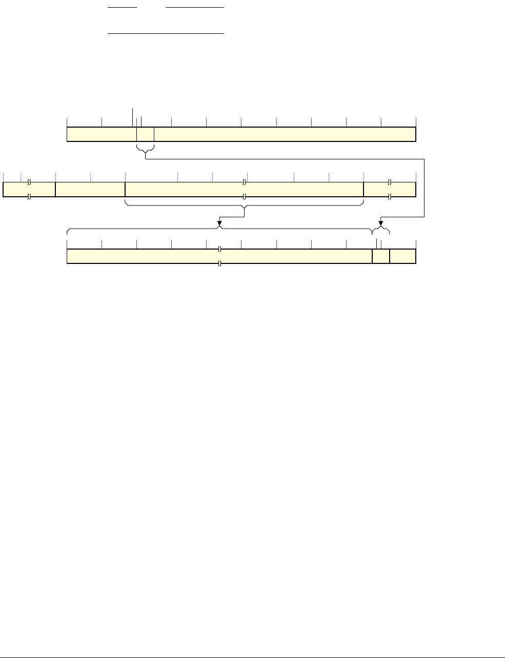
G3 The AArch32 Virtual Memory System Architecture
G3.6 The VMSAv8-32 Long-descriptor translation table format
G3-3604 Copyright © 2013 ARM Limited. All rights reserved. ARM DDI 0487A.a
Non-Confidential - Beta ID090413
• For a stage 2 translation, the level specified by the VTCR.SL0 field. For more information see Determining
the required first lookup level for stage 2 translations on page G3-3605.
Note
For a stage 2 translation, the size of the required input address range constrains the VTCR.SL0 value.
Figure G3-20 shows how the descriptor address for the first lookup for a translation using the Long-descriptor
translation table format is determined from the input address and the translation table base register value. This figure
shows the lookup for a translation that starts with a first-level lookup, that translates bits[39:30] of the input address,
zero extended if necessary.
Figure G3-20 Long-descriptor first lookup, starting at first level
For a translation that starts with a first-level lookup, as shown in Figure G3-20:
For a stage 1 translation
n is in the range 4-5 and:
• For a memory access from Hyp mode:
—HTTBR is the translation table base register.
—n=5-(HTCR.T0SZ).
• For other accesses:
— the Secure or Non-secure instance of TTBR0 or TTBR1 is the translation table base
register.
—n=(5-TTBCR.TxSZ), where x is 0 when using TTBR0, and 1 when using TTBR1.
For a stage 2 translation
n is in the range 4-13 and:
•VTTBR is the translation table base register.
•n=5-(VTCR.T0SZ).
For a translation that starts with a second-level lookup, the descriptor address is obtained in the same way, except
that bits[(n+17):21] of the input address provide bits[(n-1):3] of the descriptor address, where:
For a stage 1 translation
n is in the range 7-12. As Determining the required first lookup level for stage 1 translations on
page G3-3605 shows, for a stage 1 translation to start with a second-level lookup, the corresponding
T0SZ or T1SZ field must be 2 or more. This means:
• For a memory access from Hyp mode, n=14-HTCR.T0SZ.
Input address‡
39
n+27
n+26
30 29 0
47 n
n-1
32 0
000Descriptor address
†
See text for more information about the translation table base register used, and the value of n.
† For a Non-secure PL1&0 stage 1 translation, the IPA of the descriptor. Otherwise, the PA of the descriptor.
‡ This field is absent if n is 13.
Translation table base address[47:n]UNK/SBZP
63 56 55 48 47 nn-1 0
Register-defined UNK/SBZP Translation table
base register

G3 The AArch32 Virtual Memory System Architecture
G3.6 The VMSAv8-32 Long-descriptor translation table format
ARM DDI 0487A.a Copyright © 2013 ARM Limited. All rights reserved. G3-3605
ID090413 Non-Confidential - Beta
• For other memory accesses, n=14-(TTBCR.TxSZ), where x is 0 when using TTBR0, and 1
when using TTBR1.
For a stage 2 translation
n is in the range 7-16. For a stage 2 translation to start with a second-level lookup, VTCR.SL0 is
0b00
, and n=14-(VTCR.T0SZ).
Determining the required first lookup level for stage 1 translations
For a stage 1 translation, the required input address range, indicated by a T0SZ or T1SZ field in a translation table
control register, determines the first lookup level. The size of this input address region is 2(32-TxSZ) bytes, and if this
size is:
• Less than or equal to 230 bytes, the required start is at the second level, and translation requires two levels of
table to map to 4KB pages. This corresponds to a TxSZ value of 2 or more.
• More than 230 bytes, the required start is at the first level, and translation requires three levels of table to map
to 4KB pages. This corresponds to a TxSZ value that is less than 2.
For the PL1&0 stage 1 translations, the TTBCR:
• Splits the 32-bit VA input address range between TTBR0 and TTBR1, see Selecting between TTBR0 and
TTBR1, VMSAv8-32 Long-descriptor translation table format on page G3-3598.
• Holds the input address range sizes for TTBR0 and TTBR1, in the TTBCR.T0SZ and TTBCR.T1SZ fields.
For the PL2 stage 1 translations, HTCR.T0SZ indicates the size of the required input address range. For example,
if this field is
0b000
, it indicates a 32-bit VA input address range, and translation lookup must start at the first level.
Determining the required first lookup level for stage 2 translations
For a PL1&0 stage 2 translation, the output address range from the PL1&0 stage 1 translations determines the
required input address range for the stage 2 translation.
VTCR.SL0 indicates the starting level for the lookup. The permitted SL0 values are:
0b00
Stage 2 translation lookup must start at the second level.
0b01
Stage 2 translation lookup must start at the first level.
In addition, VTCR.T0SZ must indicate the required input address range. The size of the input address region is
2(32-T0SZ) bytes.
Note
VTCR.T0SZ holds a four-bit signed integer value, meaning it supports values from -8 to 7. This is different from
the other translation control registers, where TnSZ holds a three-bit unsigned integer, supporting values from 0 to 7.
The programming of VTCR must follow the constraints shown in Table G3-8, otherwise behavior is
UNPREDICTABLE. The table also shows how the VTCR.SL0 and VTCR.T0SZ values determine the
VTTBR.BADDR field width.
Table G3-8 Input address range constraints on programming VTCR
VTCR.SL0 VTCR.T0SZ Input address range, R First lookup level BADDR[39:x] widtha
0b00
2 to 7 R≤230bytes Second [39:12] to [39:7]
0b00
-2 to 1 230<R≤234bytes Second [39:16] to [39:13]
0b01
-2 to 1 First [39:7] to [39:4]
0b01
-8 to -3 234<R First [39:13] to [39:8]

G3 The AArch32 Virtual Memory System Architecture
G3.6 The VMSAv8-32 Long-descriptor translation table format
G3-3606 Copyright © 2013 ARM Limited. All rights reserved. ARM DDI 0487A.a
Non-Confidential - Beta ID090413
Where necessary, the first lookup level provides multiple concatenated translation tables, as described in Use of
concatenated second-level translation tables on page G3-3602. This section also gives more information about the
alternatives, shown in Table G3-8 on page G3-3605, when R is in the range 231-234.
Full translation flows for VMSAv8-32 Long-descriptor format translation tables
In a translation table walk, only the first lookup uses the translation table base address from the appropriate
Translation table base register. Subsequent lookups use a combination of address information from:
• The table descriptor read in the previous lookup.
• The input address.
The following sections describe full Long-descriptor format translation flows, down to an entry for a 4KB page:
•The address and Properties fields shown in the translation flows on page G3-3586.
•Full translation flow, starting at first-level lookup.
•Full translation flow, starting at second-level lookup on page G3-3608.
The address and Properties fields shown in the translation flows
For the Non-secure PL1&0 stage 1 translation:
• Any descriptor address is the IPA of the required descriptor.
• The final output address is the IPA of the block or page.
In these cases, a PL1&0 stage 2 translation is performed to translate the IPA to the required PA.
For all other translations, the final output address is the PA of the block or page, and any descriptor address is the
PA of the descriptor.
Properties indicates register or translation table fields that return information, other than address information, about
the translation or the targeted memory region. For more information see Information returned by a translation table
lookup on page G3-3574, and the description of the register or translation table descriptor.
For translations using the Long-descriptor translation table format, VMSAv8-32 Long-descriptor translation table
format descriptors on page G3-3592 describes the descriptors formats.
Full translation flow, starting at first-level lookup
Figure G3-21 on page G3-3607 shows the complete translation flow for a VMSAv8-32 Long-descriptor stage 1
translation table walk that starts with a first-level lookup. For more information about the fields shown in the figure
see The address and Properties fields shown in the translation flows on page G3-3586.
a. The first range corresponds to the first T0SZ value, the second range to the second T0SZ value.
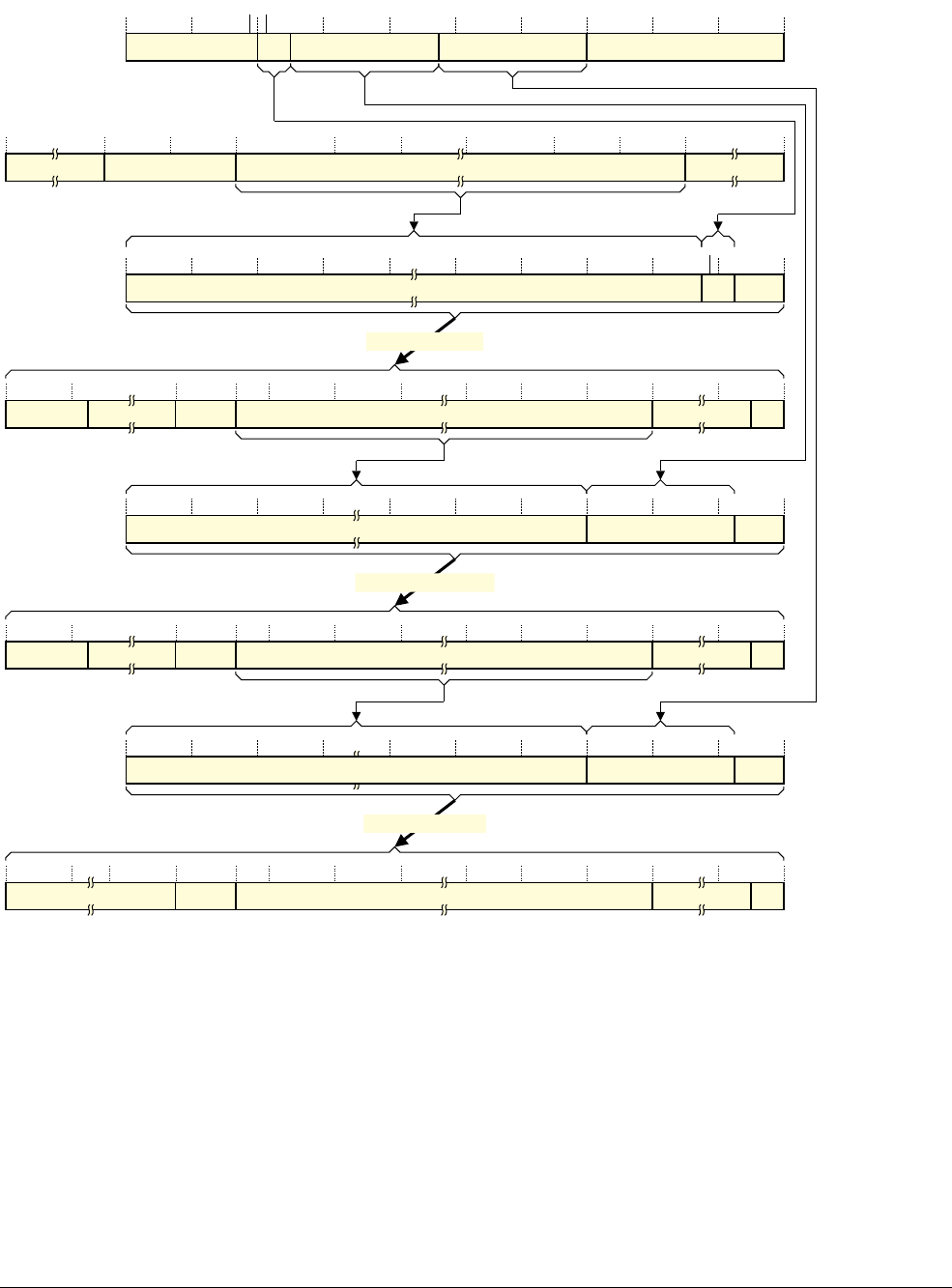
G3 The AArch32 Virtual Memory System Architecture
G3.6 The VMSAv8-32 Long-descriptor translation table format
ARM DDI 0487A.a Copyright © 2013 ARM Limited. All rights reserved. G3-3607
ID090413 Non-Confidential - Beta
Figure G3-21 Complete VMSAv8-32 Long-descriptor format stage 1 translation, starting at first level
If the first-level lookup or the second-level lookup returns a block descriptor then the translation table walk
completes at that level.
A stage 2 translation that starts at a first-level lookup differs from the translation shown in Figure G3-21 only as
follows:
• The possible values of n are 4-13, to support an input address of between 31 and 40 bits.
• A descriptor and output addresses are always PAs.
12 1147 32 0
0 0 0
n-1
47 n32 0
0 0 0 Descriptor
address
Input address
First-level lookup
Descriptor
address
Descriptor
address
For details of Properties fields, see the register or descriptor description.
Translation table base address[47:n]UNK/SBZP
63 56 55 48 47 nn-1 0
Properties UNK/SBZP Translation table
base register
Ignored 11SBZ
48 47
Second-level table address[47:12]Properties
63 59 58 52 51 0
Ignored
2112 11 First-level
table descriptor
Second-level lookup
Ignored 11SBZ
48 47
Third-level table address[47:12]Properties
63 59 58 52 51 0
Ignored
2112 11
Second-level
table descriptor
12 1147 32 0
0 0 0
Third-level lookup
Properties 11SBZ
48 47
Output address[47:12]Properties
63 52 51 02112 11
Third-level
page descriptor
n is {4, 5}
39
n+27 n+26
30 29 0
21 20 12 11
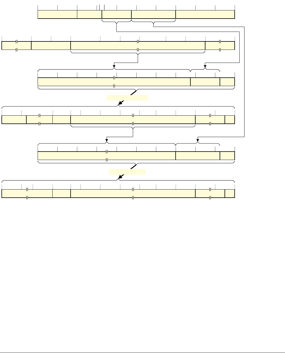
G3 The AArch32 Virtual Memory System Architecture
G3.6 The VMSAv8-32 Long-descriptor translation table format
G3-3608 Copyright © 2013 ARM Limited. All rights reserved. ARM DDI 0487A.a
Non-Confidential - Beta ID090413
Full translation flow, starting at second-level lookup
Figure G3-22 shows the complete translation flow for a stage 1 VMSAv8-32 Long-descriptor translation table walk
that starts at a second-level lookup. For more information about the fields shown in the figure see The address and
Properties fields shown in the translation flows on page G3-3586.
Figure G3-22 Complete VMSAv8-32 Long-descriptor format stage 1 translation, starting at second level
If the second-level lookup returns a block descriptor then the translation table walk completes at that level.
A stage 2 translation that starts at a second-level lookup differs from the translation shown in Figure G3-22 only as
follows:
• The possible values of n are 7-16, to support an input address of up to 34 bits.
• The descriptor and output addresses are always PAs.
12 1147 32 0
0 0 0
47 nn-1 3 2 0
0 0 0 Descriptor
address
Descriptor
address
For details of Properties fields, see the register or descriptor description.
Second-level lookup
Translation table base address[47:n]
UNK/SBZP
63 56 55 48 47 nn-1 0
Properties UNK/SBZP Translation table
base register
Ignored 11SBZ
48 47
Third-level table address[47:12]Properties
63 59 58 52 51 0
Ignored
2112 11
Second-level
table descriptor
Third-level lookup
Properties 11SBZ
48 47
Output address[47:12]Properties
63 52 51 02112 11
Third-level
page descriptor
Input address
n is {7, …, 12}
39
n+18 n+17
0
21 20 12 113132

G3 The AArch32 Virtual Memory System Architecture
G3.7 Memory access control
ARM DDI 0487A.a Copyright © 2013 ARM Limited. All rights reserved. G3-3609
ID090413 Non-Confidential - Beta
G3.7 Memory access control
In addition to an output address, a translation table entry that refers to page or region of memory includes fields that
define properties of the target memory region. Information returned by a translation table lookup on page G3-3574
describes the classification of those fields as address map control, access control, and memory attribute fields. The
access control fields, described in this section, determine whether the PE, in its current state, is permitted to perform
the required access to the output address given in the translation table descriptor. If a translation stage does not
permit the access then a MMU fault is generated for that translation stage, and no memory access is performed.
The following sections describe the memory access controls:
•Access permissions.
•Execute-never restrictions on instruction fetching on page G3-3612.
•Domains, Short-descriptor format only on page G3-3614.
•The Access flag on page G3-3615.
•Hyp mode control of Non-secure access permissions on page G3-3616.
G3.7.1 Access permissions
Note
This section gives a general description of memory access permissions. Software executing at PL1 in Non-secure
state can see only the access permissions defined by the Non-secure PL1&0 stage 1 translations. However, software
executing at PL2 can modify these permissions, as described in Hyp mode control of Non-secure access permissions
on page G3-3616. This modification is invisible to Non-secure software executing at EL1 or EL0.
Access permission bits in a translation table descriptor control access to the corresponding memory region. The
details of this control depend on the translation table format, as follows:
Short-descriptor format
This format supports two options for defining the access permissions:
• Three bits, AP[2:0], define the access permissions.
• Two bits, AP[2:1], define the access permissions, and AP[0] can be used as an Access flag.
SCTLR.AFE selects the access permissions option. Setting this bit to 1, to enable the Access flag,
also selects use of AP[2:1] to define access permissions.
ARM deprecates any use of the AP[2:0] scheme for defining access permissions.
Long-descriptor format
AP[2:1] to control the access permissions, and the descriptors provide an AF bit for use as an Access
flag. This means VMSAv8-32 behaves as if the value of SCTLR.AFE is 1, regardless of the value
that software has written to this bit.
Note
When use of the Long-descriptor format is enabled, SCTLR.AFE is UNK/SBOP.
The Access flag on page G3-3615 describes the Access flag, for both translation table formats.
The XN and PXN bits provide additional access controls for instruction fetches, see Execute-never restrictions on
instruction fetching on page G3-3612.
An attempt to perform a memory access that the translation table access permission bits do not permit generates a
Permission fault, for the corresponding stage of translation. However, when using the Short-descriptor translation
table format, it generates the fault only if the access is to memory in the Client domain, see Domains,
Short-descriptor format only on page G3-3614.

G3 The AArch32 Virtual Memory System Architecture
G3.7 Memory access control
G3-3610 Copyright © 2013 ARM Limited. All rights reserved. ARM DDI 0487A.a
Non-Confidential - Beta ID090413
Note
For the Non-secure PL1&0 translation regime, memory accesses are subject to two stages of translation. Each stage
of translation has its own, independent, fault checking. Fault handling is different for the two stages, see Exception
reporting in a VMSAv8-32 implementation on page G3-3659.
The following sections describe the two access permissions models:
•AP[2:1] access permissions model.
•AP[2:0] access permissions control, Short-descriptor format only on page G3-3611. This section includes
some information on access permission control in earlier versions of the ARM VMSA.
AP[2:1] access permissions model
Note
ARM recommends that this model is always used, even where the AP[2:0] model is permitted. Some documentation
describes the AP[2:1] model as the simplified access permissions model.
This access permissions model is used if the translation is either:
• Using the Long-descriptor translation table format.
• Using Short-descriptor translation table format, and the SCTLR.AFE bit is set to 1.
In this model:
• One bit, AP[2], selects between read-only and read/write access.
• A second bit, AP[1], selects between Application level (PL0) and System level (PL1) control.
For the Non-secure PL2 stage 1 translations, AP[1] is SBO.
This provides four access combinations:
• Read-only at all privilege levels.
• Read/write at all privilege levels.
• Read-only at PL1, no access by software executing at PL0.
• Read/write at PL1, no access by software executing at PL0.
Table G3-9 shows this access control model.
Hierarchical control of access permissions, Long-descriptor format
The Long-descriptor translation table format introduces a mechanism that entries at one level of translation table
lookup can use to set limits on the permitted entries at subsequent levels of lookup. This applies to the access
permissions, and also to the restrictions on instruction fetching described in Hierarchical control of instruction
fetching, Long-descriptor format on page G3-3613.
The restrictions apply only to subsequent levels of lookup at the same stage of translation. The APTable[1:0] field
restricts the access permissions, as Table G3-10 on page G3-3611 shows.
Table G3-9 VMSAv8-32 AP[2:1] access permissions model
AP[2], disable write access AP[1], enable unprivileged access Access
00a
a. Not valid for Non-secure PL2 stage 1 translation tables. AP[1] is SBO in these tables.
Read/write, only at PL1
0 1 Read/write, at any privilege level
10aRead-only, only at PL1
1 1 Read-only, at any privilege level

G3 The AArch32 Virtual Memory System Architecture
G3.7 Memory access control
ARM DDI 0487A.a Copyright © 2013 ARM Limited. All rights reserved. G3-3611
ID090413 Non-Confidential - Beta
As stated in the table footnote, for the Non-secure PL2 stage 1 translation tables, APTable[0] is reserved, SBZ.
Note
The APTable[1:0] settings are combined with the translation table access permissions in the translation tables
descriptors accessed in subsequent levels of lookup. They do not restrict or change the values entered in those
descriptors.
The Long-descriptor format provides APTable[1:0] control only for the stage 1 translations. The corresponding bits
are SBZ in the stage 2 translation table descriptors.
When APTable[1:0] is not set to
0b00
, its effects might be held in one or more TLB entries. Therefore, a change to
APTable[1:0] might require coarse-grained invalidation of the TLB to ensure that the effect of the change is visible
to subsequent memory transactions.
AP[2:0] access permissions control, Short-descriptor format only
This access permissions model applies when using the Short-descriptor translation tables format, and the
SCTLR.AFE bit is set to 0. ARM deprecates any use of this access permissions model.
When SCTLR.AFE is set to 0, ensuring that the AP[0] bit is always set to 1 effectively changes the access model to
the simpler model described in AP[2:1] access permissions model on page G3-3610.
Table G3-11 shows the full AP[2:0] access permissions model:
Table G3-10 Effect of APTable[1:0] on subsequent levels of lookup
APTable[1:0] Effect
00 No effect on permissions in subsequent levels of lookup.
01aAccess at PL0 not permitted, regardless of permissions in subsequent levels of lookup.
10 Write access not permitted, at any exception level, regardless of permissions in subsequent levels of lookup.
11aRegardless of permissions in subsequent levels of lookup:
• Write access not permitted, at any exception level.
• Read access not permitted at PL0.
a. Not valid for the Non-secure PL2 stage 1 translation tables. In those tables, APTable[0] is SBZ.
Table G3-11 VMSAv8-32 MMU access permissions
AP[2] AP[1:0] EL1 and EL2 access Unprivileged access Description
0 00 No access No access All accesses generate Permission faults
01 Read/write No access Access only at PL1 or higher
10 Read/write Read-only Writes at PL0 generate Permission faults
11 Read/write Read/write Full access
1 00 - - Reserved
01 Read-only No access Read-only, only at PL1 or higher
10 Read-only Read-only Read-only at any exception level, deprecateda
11 Read-only Read-only Read-only at any exception levelb
a. From VMSAv7, ARM strongly recommends use of the
0b11
encoding for Read-only at any exception level.
b. This mapping was introduced in VMSAv7, and is reserved in earlier versions of the VMSA.

G3 The AArch32 Virtual Memory System Architecture
G3.7 Memory access control
G3-3612 Copyright © 2013 ARM Limited. All rights reserved. ARM DDI 0487A.a
Non-Confidential - Beta ID090413
Note
• VMSAv8-32 supports the full set of access permissions shown in Table G3-11 on page G3-3611 only when
SCTLR.AFE is set to 0. When SCTLR.AFE is set to 1, the only supported access permissions are those
described in AP[2:1] access permissions model on page G3-3610.
• Some old documentation describes the AP[2] bit in the translation table entries as the APX bit.
G3.7.2 Execute-never restrictions on instruction fetching
Execute-never (XN) controls provide an additional level of control on memory accesses permitted by the access
permissions settings. These controls are:
XN, Execute-never
When the XN bit is 1, a Permission fault is generated if the PE attempts to execute an instruction
fetched from the corresponding memory region. However, when using the Short-descriptor
translation table format, the fault is generated only if the access is to memory in the Client domain,
see Domains, Short-descriptor format only on page G3-3614. A PE can execute instructions from a
memory region only if the access permissions for its current state permit read access, and the XN
bit is set to 0.
PXN, Privileged execute-never
When the PXN bit is 1, a Permission fault is generated if the PE is executing at PL1 and attempts to
execute an instruction fetched from the corresponding memory region. As with the XN bit, when
using the Short-descriptor translation table format, the fault is generated only if the access is to
memory in the Client domain.
In both the Short-descriptor format and the Long-descriptor format translation tables, all descriptors for memory
blocks and pages always include an XN bit.
Support for the PXN bit is as follows:
• The Long-descriptor translation table formats always include the PXN bit.
• All implementations must:
— Support the use of the PXN bit.
— Use the Short-descriptor translation table formats that include the PXN bit.
In the Non-secure PL2 stage 1 translation tables, the PXN bit is reserved, SBZ.
In addition, additional controls can enforce execute-never restrictions, regardless of the settings in the translation
tables, see:
•Restriction on Secure instruction fetch on page G3-3613.
•Preventing execution from writable locations on page G3-3614.
The execute-never controls apply also to speculative instruction fetching. This means a speculative instruction fetch
from a memory region that is execute-never at the current level of privilege is prohibited.
The XN control means that, when the stage of address translation is enabled, the PE can fetch, or speculatively fetch,
an instruction from a memory location only if all of the following apply:
• If using the Short-descriptor translation table format, the translation table descriptor for the location does not
indicate that it is in a No access domain.
• If using the Long-descriptor translation table format, or using the Short descriptor format and the descriptor
indicates that the location is in a Client domain, in the descriptor for the location the following apply:
— XN is set to 0.
— The access permissions permit a read access from the current PE mode.
• No other Prefetch Abort condition exists.

G3 The AArch32 Virtual Memory System Architecture
G3.7 Memory access control
ARM DDI 0487A.a Copyright © 2013 ARM Limited. All rights reserved. G3-3613
ID090413 Non-Confidential - Beta
Note
• The PXN control applies to the PE privilege when it attempts to execute the instruction. In an implementation
that fetches instructions speculatively, this might not be the privilege when the instruction was prefetched.
Therefore, the architecture does not require the PXN control to prevent instruction fetching.
• Although the XN control applies to speculative fetching, on a speculative instruction fetch from an XN
location, no Permission fault is generated unless the PE attempts to execute the instruction fetched from that
location. This means that, if a speculative fetch from an XN location is attempted, but there is no attempt to
execute the corresponding instruction, a Permission fault is not generated.
• The software that defines a translation table must mark any region of memory that is read-sensitive as XN,
to avoid the possibility of a speculative fetch accessing the memory region. For example, it must mark any
memory region that corresponds to a read-sensitive peripheral as XN.
• When using the Short-descriptor translation table format, the XN attribute is not checked for domains marked
as Manager. Therefore, the system must not include read-sensitive memory in domains marked as Manager,
because the XN bit does not prevent speculative fetches from a Manager domain.
When no stage of address translation for the translation regime is enabled, memory regions cannot have XN or PXN
attributes assigned. Behavior of instruction fetches when all associated address translations are disabled on
page G3-3571 describes how disabling all MMUs affects instruction fetching.
Hierarchical control of instruction fetching, Long-descriptor format
The Long-descriptor translation table format introduces a mechanism that means entries at one level of translation
tables lookup can set limits on the permitted entries at subsequent levels of lookup. This applies to the restrictions
on instruction fetching, and also to the access permissions described in Hierarchical control of access permissions,
Long-descriptor format on page G3-3610.
The restrictions apply only to subsequent levels of lookup at the same stage of translation, and:
• XNTable restricts the XN control:
— When XNTable is set to 1, the XN bit is treated as 1 in all subsequent levels of lookup, regardless of
the actual value of the bit.
— When XNTable is set to 0 it has no effect.
• PXNTable restricts the PXN control:
— When PXNTable is set to 1, the PXN bit is treated as 1 in all subsequent levels of lookup, regardless
of the actual value of the bit.
— When PXNTable is set to 0 it has no effect.
Note
The XNTable and PXNTable settings are combined with the XN and PXN bits in the translation table descriptors
accessed at subsequent levels of lookup. They do not restrict or change the values entered in those descriptors.
The XNTable and PXNTable controls are provided only in the Long-descriptor translation table format, and only
for stage 1 translations. The corresponding bits are SBZ in the stage 2 translation table descriptors.
When XNTable, or PXNTable, is set to 1, its effects might be held in one or more TLB entries. Therefore, a change
to XNTable or PXNTable might require coarse-grained invalidation of the TLB to ensure that the effect of the
change is visible to subsequent memory transactions.
Restriction on Secure instruction fetch
EL3 provides a Secure instruction fetch bit, SCR.SIF. When this bit is set to 1, any attempt in Secure state to execute
an instruction fetched from Non-secure physical memory causes a Permission fault. As with all Permission fault
checking, when using the Short-descriptor format translation tables the check applies only to Client domains, see
Access permissions on page G3-3609.

G3 The AArch32 Virtual Memory System Architecture
G3.7 Memory access control
G3-3614 Copyright © 2013 ARM Limited. All rights reserved. ARM DDI 0487A.a
Non-Confidential - Beta ID090413
ARM expects SCR.SIF to be static during normal operation. In particular, whether the TLB holds the effect of the
SIF bit is IMPLEMENTATION DEFINED. The generic sequence to ensure visibility of a change to the SIF bit is:
Change the SCR.SIF bit
ISB ; This ensures synchronization of the change
Invalidate entire TLB
DSB ; This completes the TLB Invalidation
ISB ; This ensures instruction synchronization
Preventing execution from writable locations
The architecture includes control bits that, when the corresponding stage 1 address translation is enabled, force
writable memory to be treated as XN, regardless of the setting of the XN bit. When the translation stages are
controlled by an Exception level that is using AArch32:
• For PL1&0 stage 1 translations, when SCTLR.WXN is set to 1, all regions that are writable at stage 1 of the
address translation are treated as XN.
• For Non-secure PL2 stage 1 translations, when HSCTLR.WXN is set to 1, all regions that are writable at
stage 1 of the address translation are treated as XN.
• For PL1&0 stage 1 translations, when SCTLR.UWXN is set to 1, an instruction fetch is treated as accessing
a PXN region if it accesses a region that software executing at PL0 can write to.
Note
Setting a WXN or UWXN bit to 1 changes the interpretation of the translation table entry, overriding a zero value
of an XN or PXN field. It does not cause any change to the translation table entry.
For any given virtual machine, ARM expects WXN and UWXN to remain static in normal operation. In particular,
it is IMPLEMENTATION DEFINED whether TLB entries associated with a particular VMID reflect the effect of the
values of these bits. A generic sequence to ensure synchronization of a change to these bits, when that change is
made without a corresponding change of VMID, is:
Change the WXN or UWXN bit
ISB ; This ensures synchronization of the change
Invalidate entire TLB of associated entries
DSB ; This completes the TLB Invalidation
ISB ; This ensures instruction synchronization
As with all Permission fault checking, if the stage 1 translation is using the Short-descriptor translation table format,
the permission checks are performed only for Client domains. For more information see Access permissions on
page G3-3609.
For more information about address translation see About address translation for VMSAv8-32 on page G3-3565.
G3.7.3 Domains, Short-descriptor format only
A domain is a collection of memory regions. The Short-descriptor translation table format supports 16 domains, and
requires the software that defines a translation table to assign each VMSAv8-32 memory region to a domain. When
using the Short-descriptor format:
• First-level translation table entries for Page tables and Sections include a domain field.
• Translation table entries for Supersections do not include a domain field. The Short-descriptor format defines
Supersections as being in domain 0.
• Second-level translation table entries inherit a domain setting from the parent first-level Page table entry.
• Each TLB entry includes a domain field.

G3 The AArch32 Virtual Memory System Architecture
G3.7 Memory access control
ARM DDI 0487A.a Copyright © 2013 ARM Limited. All rights reserved. G3-3615
ID090413 Non-Confidential - Beta
The domain field specifies which of the 16 domains the entry is in, and a two-bit field in the DACR defines the
permitted access for each domain. The possible settings for each domain are:
No access Any access using the translation table descriptor generates a Domain fault.
Clients On an access using the translation table descriptor, the access permission attributes are checked.
Therefore, the access might generate a Permission fault.
Managers On an access using the translation table descriptor, the access permission attributes are not checked.
Therefore, the access cannot generate a Permission fault.
See The MMU fault-checking sequence on page G3-3650 for more information about how, when using the
Short-descriptor translation table format, the Domain attribute affects the checking of the other attributes in the
translation table descriptor.
Note
A single program might:
• Be a Client of some domains.
• Be a Manager of some other domains.
• Have no access to the remaining domains.
The Long-descriptor translation table format does not support domains. When a stage of translation is using this
format, all memory is treated as being in a Client domain, and the settings in the DACR are ignored.
G3.7.4 The Access flag
The Access flag indicates when a page or section of memory is accessed for the first time since the Access flag in
the corresponding translation table descriptor was set to 0:
• If address translation is using the Short-descriptor translation table format, it must set SCTLR.AFE to 1 to
enable use of the Access flag, see SCTLR, System Control Register on page G4-4005. Setting this bit to 1
redefines the AP[0] bit in the translation table descriptors as an Access flag, and limits the access permissions
information in the translation table descriptors to AP[2:1], as described in AP[2:1] access permissions model
on page G3-3610.
• The Long-descriptor format always supports an Access flag bit in the translation table descriptors, and
address translation using this format behaves as if SCTLR.AFE is set to 1, regardless of the value of that bit.
In ARMv8 the Access flag is managed by software as described in the following subsection.
Note
Previous version of the ARM architecture optionally supported hardware management of the Access flag. ARMv8
obsoletes this option.
Software management of the Access flag
An implementation that requires software to manage the Access flag generates an Access flag fault whenever a
translation table entry with the Access flag set to 0 is read into the TLB
Note
When using the Short-descriptor translation table format, Access flag faults are generated only if SCTLR.AFE is
set to 1, to enable use of a translation table descriptor bit as an Access flag.
The Access flag mechanism expects that, when an Access flag fault occurs, software resets the Access flag to 1 in
the translation table entry that caused the fault. This prevents the fault occurring the next time that memory location
is accessed. Entries with the Access flag set to 0 are never held in the TLB, meaning software does not have to flush
the entry from the TLB after setting the flag.

G3 The AArch32 Virtual Memory System Architecture
G3.7 Memory access control
G3-3616 Copyright © 2013 ARM Limited. All rights reserved. ARM DDI 0487A.a
Non-Confidential - Beta ID090413
G3.7.5 Hyp mode control of Non-secure access permissions
When EL2 is using AArch32, Non-secure software executing in Hyp mode controls two sets of translation tables,
both of which use the Long-descriptor translation table format:
• The translation tables that control the Non-secure PL2 stage 1 translations. These map VAs to PAs, for
memory accesses made when executing in Non-secure state in Hyp mode, and are indicated and controlled
by the HTTBR and HTCR.
These translations have similar access controls to other Non-secure stage 1 translations using the
Long-descriptor translation table format, as described in:
—AP[2:1] access permissions model on page G3-3610.
—Execute-never restrictions on instruction fetching on page G3-3612.
The differences from the Non-secure stage 1 translations are that:
— The APTable[0], PXNTable, and PXN bits are reserved, SBZ.
— AP[1] is reserved, SBO.
• The translation tables that control the Non-secure PL1&0 stage 2 translations. These map the IPAs from the
stage 1 translation onto PAs, for memory accesses made when executing in Non-secure state at PL1 or PL0,
and are indicated and controlled by the VTTBR and VTCR.
The descriptors in the virtualization translation tables define a second level of access permissions, that are
combined with the permissions defined in the stage 1 translation. This section describes this combining of
access permissions.
Note
The second-level access permissions mean a hypervisor can define additional access restrictions to those defined by
a Guest OS in the stage 1 translation tables. For a particular access, the actual access permission is the more
restrictive of the permissions defined by:
• The Guest OS, in the stage 1 translation tables.
• The hypervisor, in the stage 2 translation tables.
The stage 2 access controls defined from Hyp mode:
• Affect only the Non-secure stage 1 access permissions settings.
• Take no account of whether the accesses are from a Non-secure PL1 mode or a Non-secure PL0 mode.
• Permit software executing in Hyp mode to assign a write-only attribute to a memory region.
The S2AP field in the stage 2 descriptors define the stage 2 access permissions, as Table G3-12 shows:
For more information about the S2AP field see Attribute fields in VMSAv8-32 Long-descriptor stage 2 Block and
Page descriptors on page G3-3596.
If the stage 2 permissions cause a Permission fault, this is a stage 2 address translation fault. Stage 2 address
translation faults are taken to Hyp mode, and reported in the HSR using an EC code of
0x20
or
0x24
. For more
information, see Use of the HSR on page G3-3672.
Table G3-12 Stage 2 control of access permissions
S2AP Access permission
00 No access permitted
01 Read-only. Writes to the region are not permitted, regardless of the stage 1 permissions.
10 Write-only. Reads from the region are not permitted, regardless of the stage 1 permissions.
11 Read/write. The stage 1 permissions determine the access permissions for the region.

G3 The AArch32 Virtual Memory System Architecture
G3.7 Memory access control
ARM DDI 0487A.a Copyright © 2013 ARM Limited. All rights reserved. G3-3617
ID090413 Non-Confidential - Beta
Note
The combination of the EC code and the STATUS value in the HSR indicate that the fault is a stage 2 address
translation fault.
The stage 2 permissions include an XN attribute. If this is set to 1, execution from the region is not permitted,
regardless of the value of the XN attribute in the stage 1 translation. If a Permission fault is generated because the
stage 2 XN bit is set to 1, this is reported as a stage 2 address translation fault.
Prioritization of aborts on page G3-3658 describes the abort prioritization if both stages of a translation generate a
fault.

G3 The AArch32 Virtual Memory System Architecture
G3.8 Memory region attributes
G3-3618 Copyright © 2013 ARM Limited. All rights reserved. ARM DDI 0487A.a
Non-Confidential - Beta ID090413
G3.8 Memory region attributes
In addition to an output address, a translation table entry that refers to a page or region of memory includes fields
that define properties of that target memory region. Information returned by a translation table lookup on
page G3-3574 describes the classification of those fields as address map control, access control, and memory
attribute fields. The memory region attribute fields control the memory type, accesses to the caches, and whether
the memory region is Shareable and therefore is coherent.
The following sections describe the assignment of memory region attributes for stage 1 translations:
•Overview of memory region attributes for stage 1 translations.
•Short-descriptor format memory region attributes, without TEX remap on page G3-3619.
•Short-descriptor format memory region attributes, with TEX remap on page G3-3620.
•VMSAv8-32 Long-descriptor format memory region attributes on page G3-3624.
For an implementation that is operating in Secure state, or in Hyp mode, these assignments define the memory
attributes of the accessed region.
For an implementation that is operating in a Non-secure PL1 or PL0 mode, the Non-secure PL1&0 stage 2
translation can modify the memory attributes assigned by the stage 1 translation. EL2 control of Non-secure memory
region attributes on page G3-3625 describes these stage 2 assignments.
G3.8.1 Overview of memory region attributes for stage 1 translations
The description of the memory region attributes in a translation descriptor divides into:
Memory type and attributes
These are described either:
• Directly, by bits in the translation table descriptor.
• Indirectly, by registers referenced by bits in the table descriptor. This is described as
remapping the memory type and attribute description.
The Short-descriptor translation table format can use either of these approaches, selected by the
SCTLR.TRE bit:
TRE == 0 Remap disabled. The TEX[2:0], C, and B bits in the translation table descriptor define
the memory region attributes. Short-descriptor format memory region attributes,
without TEX remap on page G3-3619 describes this encoding.
Note
With the Short-descriptor format, remapping is called TEX remap, and the SCTLR.TRE
bit is the TEX remap enabled bit.
The description of the TRE == 0 encoding includes information about the encoding in
previous versions of the architecture.
TRE == 1 Remap enabled. The TEX[0], C, and B bits in the translation table descriptor are index
bits to the remap registers, that define the memory region attributes:
• The Primary Region Remap Register, PRRR.
• The Normal Memory Remap Register, NMRR.
Short-descriptor format memory region attributes, with TEX remap on page G3-3620
describes this encoding scheme.
This scheme reassigns translation table descriptor bits TEX[2:1] for use as bits managed
by the operating system.
The Long-descriptor translation table format always uses remapping. This means VMSAv8-32
behaves as if the value of SCTLR.TRE is 1, regardless of the value that software has written to this
bit.
Note
When use of the Long-descriptor format is enabled, SCTLR.TRE is UNK/SBOP.

G3 The AArch32 Virtual Memory System Architecture
G3.8 Memory region attributes
ARM DDI 0487A.a Copyright © 2013 ARM Limited. All rights reserved. G3-3619
ID090413 Non-Confidential - Beta
VMSAv8-32 Long-descriptor format memory region attributes on page G3-3624 describes this
encoding.
Shareability In the Short-descriptor translation table format, the S bit in the translation table descriptor encodes
whether the region is shareable. Enabling TEX remap extends the shareability description. For more
information see:
•Shareability and the S bit, without TEX remap on page G3-3620.
•Shareability and the S bit, with TEX remap on page G3-3622.
In the Long-descriptor translation table format, the SH[1:0] field in the translation table descriptor
encodes shareability information. For more information see Shareability, Long-descriptor format on
page G3-3624.
G3.8.2 Short-descriptor format memory region attributes, without TEX remap
When using the Short-descriptor translation table formats, TEX remap is disabled when SCTLR.TRE is set to 0.
Note
• The Short-descriptor format scheme without TEX remap is the scheme used in VMSAv6.
• The B (Bufferable), C (Cacheable), and TEX (Type extension) bit names are inherited from earlier versions
of the architecture. These names no longer adequately describe the function of the B, C, and TEX bits.
Table G3-13 shows the C, B, and TEX[2:0] encodings when TEX remap is disabled:
Table G3-13 TEX, C, and B encodings when TRE == 0
TEX[2:0] C B Description Memory type Page Shareable
000 0 0 Device-nGnRnE Device-nGnRnE Shareable
1Shareable Device-nGnREaDevice-nGnRE Shareablea
1 0 Outer and Inner Write-Through, no Write-Allocate Normal S bitb
1 Outer and Inner Write-Back, no Write-Allocate Normal S bitb
001 0 0 Outer and Inner Non-cacheable Normal S bitb
1 Reserved - -
10IMPLEMENTATION DEFINED IMPLEMENTATION
DEFINED
IMPLEMENTATION
DEFINED
1 Outer and Inner Write-Back, Write-Allocate Normal S bitb
010 0 0 Non-shareable Device-nGnREaDevice-nGnRE Non-shareablea
1 Reserved - -
1xReserved - -
011 x x Reserved - -
1BB A A Cacheable memory: AA = Inner attributec
BB = Outer attribute
Normal S bitb
a. Some implementations make no distinction between Shareable Device-nGnRE memory and Non-shareable Device-nGnRE memory, and
refer to both memory types as Shareable Device-nGnRE memory.
b. For more information, see Shareability and the S bit, without TEX remap on page G3-3620.
c. For more information, see Cacheable memory attributes, without TEX remap on page G3-3620.

G3 The AArch32 Virtual Memory System Architecture
G3.8 Memory region attributes
G3-3620 Copyright © 2013 ARM Limited. All rights reserved. ARM DDI 0487A.a
Non-Confidential - Beta ID090413
See Memory types and attributes on page E2-2357 for an explanation of Normal memory, and the types of Device
memory, and of the shareability attribute.
Cacheable memory attributes, without TEX remap
When TEX[2] == 1, the memory described by the translation table entry is Cacheable, and the rest of the encoding
defines the Inner and Outer cache attributes:
TEX[1:0] Define the Outer cache attribute.
C, B Define the Inner cache attribute.
The translation table entries use the same encoding for the Outer and Inner cache attributes, as Table G3-14 shows.
Shareability and the S bit, without TEX remap
The translation table entries also include an S bit. This bit:
• Is ignored if the entry refers to any type of Device memory.
• For Normal memory, determines whether the memory region is Shareable or Non-shareable:
S==0 Normal memory region is Non-shareable.
S==1 Normal memory region is Shareable.
G3.8.3 Short-descriptor format memory region attributes, with TEX remap
When using the Short-descriptor translation table formats, TEX remap is enabled when SCTLR.TRE is set to 1. In
this configuration:
• The software that defines the translation tables must program the PRRR and NMRR to define seven possible
memory region attributes.
• The TEX[0], C, and B bits of the translation table descriptors define the memory region attributes, by
indexing PRRR and NMRR.
• Hardware makes no use TEX[2:1], see The OS managed translation table bits on page G3-3623.
When TEX remap is enabled:
• For seven of the eight possible combinations of the TEX[0], C and B bits, fields in the PRRR and NMRR
define the region attributes, as described in this section.
• The meaning of the eighth combination for the TEX[0], C and B bits is IMPLEMENTATION DEFINED.
• Four bits in the PRRR define whether the region is shareable, as described in Shareability and the S bit, with
TEX remap on page G3-3622.
Table G3-14 Inner and Outer cache attribute encoding
Encoding Cache attribute
00 Non-cacheable
01 Write-Back, Write-Allocate
10 Write-Through, no Write-Allocate
11 Write-Back, no Write-Allocate

G3 The AArch32 Virtual Memory System Architecture
G3.8 Memory region attributes
ARM DDI 0487A.a Copyright © 2013 ARM Limited. All rights reserved. G3-3621
ID090413 Non-Confidential - Beta
For each of the possible encodings of the TEX[0], C, and B bits in a translation table entry, Table G3-15 shows
which fields of the PRRR and NMRR registers describe the memory region attributes.
The TEX remap registers and the SCTLR.TRE bit are Banked between the Secure and Non-secure Security states.
For more information, see The effect of EL3 on TEX remap on page G3-3624.
When TEX remap is enabled, the mappings specified by the PRRR and NMRR determine the mapping of the
TEX[0], C and B bits in the translation tables to memory type and cacheability attributes:
1. The primary mapping, indicated by a field in the PRRR as shown in the Memory type column of Table G3-15,
takes precedence.
2. For any region that the PRRR maps as Normal memory, the NMRR determines the Inner cacheability and
Outer cacheability attributes.
3. If it is supported, the Outer Shareable mapping identifies Shareable memory as either Inner Shareable or
Outer Shareable, see Interpretation of the NOSn fields in the PRRR, with TEX remap on page G3-3622.
The TEX remap registers must be static during normal operation. In particular, when the remap registers are
changed:
• It is IMPLEMENTATION DEFINED when the changes take effect.
• It is UNPREDICTABLE whether the TLB caches the effect of the TEX remap on translation tables.
The software sequence to ensure the synchronization of changes to the TEX remap registers is:
1. Execute a
DSB
instruction. This ensures any memory accesses using the old mapping have completed.
2. Write the TEX remap registers or SCTLR.TRE bit.
3. Execute an
ISB
instruction. This ensures synchronization of the register updates.
4. Invalidate the entire TLB.
5. Execute a
DSB
instruction. This ensures completion of the entire TLB operation.
6. Clean and invalidate all caches. This removes any cached information associated with the old mapping.
7. Execute a
DSB
instruction. This ensures completion of the cache maintenance.
8. Execute an
ISB
instruction. This ensures instruction synchronization.
Table G3-15 TEX, C, and B encodings when TRE == 1
Encoding Memory typeaCache attributesa, b:Outer Shareable attributea, c
TEX[0] C B Inner cacheability Outer cacheability
000PRRR[1:0] NMRR[1:0] NMRR[17:16] NOT(PRRR[24])
1PRRR[3:2] NMRR[3:2] NMRR[19:18] NOT(PRRR[25])
10PRRR[5:4] NMRR[5:4] NMRR[21:20] NOT(PRRR[26])
1PRRR[7:6] NMRR[7:6] NMRR[23:22] NOT(PRRR[27])
100PRRR[9:8] NMRR[9:8] NMRR[25:24] NOT(PRRR[28])
1PRRR[11:10] NMRR[11:10] NMRR[27:26] NOT(PRRR[29])
10IMPLEMENTATION DEFINED
1PRRR[15:14] NMRR[15:14] NMRR[31:30] NOT(PRRR[31])
a. For details of the Memory type and Outer Shareable encodings see PRRR, Primary Region Remap Register on page G4-3992. For details
of the Cache attributes encodings see Table G3-14 on page G3-3620.
b. Applies only if the memory type for the region is mapped as Normal memory.
c. Applies only if the memory type for the region is mapped as Normal or Device-nGnRE memory and the region is Shareable.

G3 The AArch32 Virtual Memory System Architecture
G3.8 Memory region attributes
G3-3622 Copyright © 2013 ARM Limited. All rights reserved. ARM DDI 0487A.a
Non-Confidential - Beta ID090413
This extends the standard rules for the synchronization of changes to System registers described in Synchronization
of changes to System registers on page G3-3706, and provides implementation freedom as to whether or not the
effect of the TEX remap is cached.
Shareability and the S bit, with TEX remap
The memory type of a region, as indicated in the Memory type column of Table G3-15 on page G3-3621, provides
the first level of control of whether the region is shareable:
• If using the Long-descriptor translation table format, if the memory is any type of Device memory then the
region is Shareable.
• If using the Short descriptor translation table format then:
— If the memory is Device-nGnRnE memory then the region is Shareable.
— Otherwise, the shareability is determined by using the value of the S bit in the translation table
descriptor to index bits in the PRRR.
Some implementations make no distinction between Shareable Device-nGnRE memory and Non-shareable
Device-nGnRE memory, and refer to both memory types as Shareable Device memory.
• If the memory type is Normal then the shareability is determined by using the value of the S bit in the
translation table descriptor to index bits in the PRRR.
Table G3-16 shows this determination:
In the cases where the shareability is remapped, the appropriate bit of the PRRR indicates whether the region is
Shareable or Non-shareable, as follows:
PRRR[n] == 0 Not shareable.
PRRR[n] == 1 Shareable.
Note
When TEX remap is enabled, a translation table entry with S == 0 can be mapped as Shareable memory.
Interpretation of the NOSn fields in the PRRR, with TEX remap
When all of the following apply, the NOSn fields in the PRRR distinguish between Inner Shareable and Outer
Shareable memory regions:
• The SCTLR.TRE bit is set to 1.
• The region is mapped as Normal memory, or the Short-descriptor translation table format is used and the
region is mapped as Device-nGnRE memory.
• The Normal memory remapping or Device-nGnRE memory remapping of the S bit value for the entry makes
the region Shareable.
• The implementation supports the distinction between Inner Shareable and Outer Shareable.
If the SCTLR.TRE bit is set to 0, an implementation can provide an IMPLEMENTATION DEFINED mechanism to
interpret the NOSn fields in the PRRR, see SCTLR.TRE, SCTLR.M, and the effect of the TEX remap registers on
page G3-3623.
Table G3-16 Determining shareability, with TEX remap
Memory type Remapping when S == 0 Remapping when S == 1
Any type of Device Shareable Shareable
Normal PRRR[18] PRRR[19]

G3 The AArch32 Virtual Memory System Architecture
G3.8 Memory region attributes
ARM DDI 0487A.a Copyright © 2013 ARM Limited. All rights reserved. G3-3623
ID090413 Non-Confidential - Beta
The values of the NOSn fields in the PRRR have no effect.
The NOSn fields in the PRRR are RAZ/WI if the implementation does not support the distinction between Inner
Shareable and Outer Shareable memory regions.
Note
The meaning of shareability attributes for Device-nGnRE memory is IMPLEMENTATION DEFINED when the
Short-descriptor translation table is used, and otherwise has no meaning.
SCTLR.TRE, SCTLR.M, and the effect of the TEX remap registers
When TEX remap is disabled, because the SCTLR.TRE bit is set to 0:
• The effect of the PRRR and NMRR registers can be IMPLEMENTATION DEFINED.
• The interpretation of the fields of the PRRR and NMRR registers can differ from the description given earlier
in this section.
VMSAv8-32 requires that the effect of these registers is limited to remapping the attributes of memory locations.
These registers must not change whether any cache hardware or stages of address translation are enabled. The
mechanism by which the TEX remap registers have an effect when the SCTLR.TRE bit is set to 0 is
IMPLEMENTATION DEFINED. The AArch32 architecture requires that from reset, if the IMPLEMENTATION DEFINED
mechanism has not been invoked:
• If the EL1&0 stage 1 address translation is enabled and is using the Short-descriptor format translation tables,
the architecturally-defined behavior of the TEX[2:0], C, and B bits must apply, without reference to the TEX
remap functionality. In other words, memory attribute assignment must comply with the scheme described
in Short-descriptor format memory region attributes, without TEX remap on page G3-3619.
• If the EL1&0 stage 1 address translation is disabled, then the architecturally-defined behavior of
VMSAv8-32 with address translation disabled must apply, without reference to the TEX remap functionality.
See The effects of disabling address translation stages on VMSAv8-32 behavior on page G3-3569.
Possible mechanisms for enabling the IMPLEMENTATION DEFINED effect of the TEX remap registers when
SCTLR.TRE is set to 0 include:
• A control bit in the ACTLR, or in an IMPLEMENTATION DEFINED System register.
• Changing the behavior when the PRRR and NMRR registers are changed from their IMPLEMENTATION
DEFINED reset values.
In addition, if the stage of address translation is disabled and the SCTLR.TRE bit is set to 1, the
architecturally-defined behavior of the VMSAv8-32 with the stage of address translation disabled must apply
without reference to the TEX remap functionality.
In an implementation that includes EL3, the IMPLEMENTATION DEFINED effect of these registers must only take
effect in the Security state of the registers. See also The effect of EL3 on TEX remap on page G3-3624.
The OS managed translation table bits
When TEX remap is enabled, the TEX[2:1] bits in the translation table descriptors are available as two bits that can
be managed by the operating system. In VMSAv8-32, as long as the SCTLR.TRE bit is set to 1, the values of the
TEX[2:1] bits are ignored by the memory management hardware. Software can write any value to these bits in the
translation tables.

G3 The AArch32 Virtual Memory System Architecture
G3.8 Memory region attributes
G3-3624 Copyright © 2013 ARM Limited. All rights reserved. ARM DDI 0487A.a
Non-Confidential - Beta ID090413
The effect of EL3 on TEX remap
In an implementation that includes EL3, the TEX remap registers are Banked between the Secure and Non-secure
Security states. The register instances for the current security state apply to all PL1&0 stage 1 translation table
lookups in that state. The SCTLR.TRE bit is Banked in the Secure and Non-secure copies of the register, and the
appropriate version of this bit determines whether TEX remap is applied to translation table lookups in the current
security state.
Write accesses to the Secure copies of the TEX remap registers are disabled when the CP15SDISABLE input is
asserted HIGH, meaning the
MCR
operations to access these registers are UNDEFINED. For more information, see The
CP15SDISABLE input on page G3-3704.
G3.8.4 VMSAv8-32 Long-descriptor format memory region attributes
When a PE is using the VMSAv8-32 Long-descriptor translation table format, the AttrIndx[2:0] field in a block or
page translation table descriptor for a stage 1 translation indicates the 8-bit field in the appropriate MAIR register,
that specifies the attributes for the corresponding memory region, as follows:
• AttrIndx[2] indicates the MAIR register to be used:
AttrIndx[2] == 0 Use MAIR0.
AttrIndx[2] == 1 Use MAIR1.
• AttrIndx[2:0] indicates the required Attr field, Attrn, where n = AttrIndx[2:0].
Each AttrIndx field defines, for the corresponding memory region:
• The memory type, Normal or a type of Device memory.
• For Normal memory:
— The inner and outer cacheability, Non-cacheable, Write-Through, or Write-Back.
— For Write-Through Cacheable and Write-Back Cacheable regions, the Read-Allocate and
Write-Allocate policy hints, each of which is Allocate or Do not allocate.
For more information about the AttrIndx[2:0] descriptor field, see Attribute fields in VMSAv8-32 Long-descriptor
stage 1 Block and Page descriptors on page G3-3595.
Shareability, Long-descriptor format
When a PE is using the Long-descriptor translation table format, the SH[1:0] field in a block or page translation
table descriptor specifies the Shareability attributes of the corresponding memory region, if the MAIR entry for that
region identifies it as Normal memory. Table G3-17 shows the encoding of this field.
See Combining the shareability attribute on page G3-3629 for constraints on the Shareability attributes of a Normal
memory region that is Inner Non-cacheable, Outer Non-cacheable.
For any type of Device memory, the value of the SH[1:0] field of the translation table descriptor is ignored.
Table G3-17 SH[1:0] field encoding for Normal memory, Long-descriptor format
SH[1:0] Normal memory
00 Non-shareable
01 UNPREDICTABLE
10 Outer Shareable
11 Inner Shareable

G3 The AArch32 Virtual Memory System Architecture
G3.8 Memory region attributes
ARM DDI 0487A.a Copyright © 2013 ARM Limited. All rights reserved. G3-3625
ID090413 Non-Confidential - Beta
Other fields in the Long-descriptor translation table format descriptors
The following subsections describe the other fields in the translation table block and page descriptors when a PE is
using the Long-descriptor translation table format:
•Contiguous bit
•Field reserved for software use
•Ignored fields.
Contiguous bit
The Long-descriptor translation table format descriptors contain a Contiguous bit. Setting this bit to 1 indicates that
16 adjacent translation table entries point to a contiguous output address range. These 16 entries must be aligned in
the translation table so that the top five bits of their input addresses, that index their position in the translation table,
are the same. For example, referring to Figure G3-21 on page G3-3607, to use this hint for a block of 16 entries in
the third-level translation table, bits[20:16] of the input addresses for the 16 entries must be the same.
The contiguous output address range must be aligned to size of 16 translation table entries at the same translation
table level.
Use of this bit means that the TLB can cache a single entry to cover the 16 translation table entries.
This bit acts as a hint. The architecture does not require a PE to cache TLB entries in this way. To avoid TLB
coherency issues, any TLB maintenance by address must not assume any optimization of the TLB tables that might
result from use of this bit.
Note
The use of the contiguous bit is similar to the approach used, in the Short-descriptor translation table format, for
optimized caching of Large Pages and Supersections in the TLB. However, an important difference in the
contiguous bit capability is that TLB maintenance must be performed based on the size of the underlying translation
table entries, to avoid TLB coherency issues. That is, any use of the contiguous bit has no effect on the minimum
size of entry that must be invalidated from the TLB.
Field reserved for software use
The architecture reserves a 4-bit field in the Block and Page table descriptors for software use. In considering
migration from using the Short-descriptor format to the Long-descriptor format, this field is an extension of the
Short-descriptor field described in The OS managed translation table bits on page G3-3623.
Ignored fields
For stage 1 translation descriptors, the architecture defines a 4-bit Ignored field in the Block and Page table
descriptors, bit[63:59], and guarantees that the PE will not alter the value of this field. For stage 2 translation
descriptors, the corresponding field is reserved for use by a System MMU. In a PE that is using the Long-descriptor
translator table format, this field is an ignored field and the architecture guarantees that the PE does not update the
field.
G3.8.5 EL2 control of Non-secure memory region attributes
Software executing at EL2 controls two sets of translation tables, both of which use the Long-descriptor translation
table format. These are:
• The translation tables that control Non-secure PL2 stage 1 translations. These map VAs to PAs, and when
EL2 is using AArch32 they are indicated and controlled by the HTTBR and HTCR.
These translations have exactly the same memory region attribute controls as any other stage 1 translations,
as described in VMSAv8-32 Long-descriptor format memory region attributes on page G3-3624.
• The translation tables that control Non-secure PL1&0 stage 2 translations. These map the IPAs from the stage
1 translation onto PAs, and are indicated and when EL2 is using AArch32 they are controlled by the VTTBR
and VTCR.

G3 The AArch32 Virtual Memory System Architecture
G3.8 Memory region attributes
G3-3626 Copyright © 2013 ARM Limited. All rights reserved. ARM DDI 0487A.a
Non-Confidential - Beta ID090413
The descriptors in the virtualization translation tables define a second level of memory region attributes, that
are combined with the attributes defined in the stage 1 translation. This section describes this combining of
attributes.
VMSAv8-32 Long-descriptor translation table format descriptors on page G3-3592 describes the format of the
entries in these tables.
Note
In a virtualization implementation, a hypervisor might usefully:
• Reduce the permitted cacheability of a region.
• Increase the required shareability of a region.
The combining of attributes from stage 1 and stage 2 translations supports both of these options.
In the stage 2 translation table descriptors for memory regions and pages, the MemAttr[3:0] and SH[1:0] fields
describe the stage 2 memory region attributes:
• The definition of the stage 2 SH[1:0] field is identical to the same field for a stage 1 translation, see
Shareability, Long-descriptor format on page G3-3624.
• MemAttr[3:2] give a top-level definition of the memory type, and of the cacheability of a Normal memory
region, as Table G3-18 shows:
The encoding of MemAttr[1:0] depends on the Memory type indicated by MemAttr[3:2]:
— When MemAttr[3:2]==
0b00
, indicating a type of Device memory, Table G3-19 shows the encoding
of MemAttr[1:0]:
Table G3-18 Long-descriptor MemAttr[3:2] encoding, stage 2 translation
MemAttr[3:2] Memory type Cacheability
00 Device, of type determined by MemAttr[1:0] Not applicable
01 Normal Outer Non-cacheable
10 Outer Write-Through Cacheable
11 Outer Write-Back Cacheable
Table G3-19 MemAttr[1:0] encoding for the types of Device memory
MemAttr[1:0] Meaning when MemAttr[3:2] ==
0b00
00 Region is Device-nGnRnE memory
01 Region is Device-nGnRE memory
10 Region is Device-nGRE memory
11 Region is Device-GRE memory

G3 The AArch32 Virtual Memory System Architecture
G3.8 Memory region attributes
ARM DDI 0487A.a Copyright © 2013 ARM Limited. All rights reserved. G3-3627
ID090413 Non-Confidential - Beta
— When MemAttr[3:2]!=
0b00
, indicating Normal memory, Table G3-20 shows the encoding of
MemAttr[1:0]:
Note
The stage 2 translation does not assign any allocation hints.
The following sections describe how the memory type attributes assigned at stage 2 of the translation are combined
with those assigned at stage 1:
•Combining the memory type attribute.
•Combining the cacheability attribute on page G3-3628.
•Combining the shareability attribute on page G3-3629.
Note
The following stage 2 translation table attribute settings leave the stage 1 settings unchanged:
• MemAttr[3:2] ==
0b11
, Normal memory, Outer Write-Back Cacheable.
• MemAttr[1:0] ==
0b11
, Inner Write-Back Cacheable.
Combining the memory type attribute
Table G3-21 shows how the stage 1 and stage 2 memory type assignments are combined:
Table G3-20 MemAttr[1:0] encoding for Normal memory
MemAttr[1:0] Meaning when MemAttr[3:2] !=
0b00
00 UNPREDICTABLE
01 Inner Non-cacheable
10 Inner Write-Through Cacheable
11 Inner Write-Back Cacheable
Table G3-21 Combining the stage 1 and stage 2 memory type assignments
Assignment in stage 1 Assignment in stage 2 Resultant type
Device-nGnRnE Any Device-nGnRnE
Device-nGnRE Device-nGnRnE Device-nGnRnE
Not Device-nGnRnE Device-nGnRE
Device-nGRE Device-nGnRnE Device-nGnRnE
Device-nGnRE Device-nGnRE
Not (Device-nGnRnE or Device-nGnRE) Device-nGRE

G3 The AArch32 Virtual Memory System Architecture
G3.8 Memory region attributes
G3-3628 Copyright © 2013 ARM Limited. All rights reserved. ARM DDI 0487A.a
Non-Confidential - Beta ID090413
See Combining the shareability attribute on page G3-3629 for information about:
• The shareability of a region for which the resultant type is any Device type.
• The shareability requirements of a region with a resultant type of Normal for which the resultant cacheability,
described in Combining the cacheability attribute, is Inner Non-cacheable, Outer Non-cacheable.
The combining of the memory type attribute means a translation table walk for a stage 1 translation can be made to
type of Device memory. This is likely to indicate a Guest OS error, and setting the HCR.PTW bit to 1 causes such
an access to generate a Translation fault, see Stage 2 fault on a stage 1 translation table walk on page G3-3654.
Combining the cacheability attribute
For a Normal memory region, Table G3-22 shows how the stage 1 and stage 2 cacheability assignments are
combined. This combination applies, independently, for the Inner cacheability and Outer cacheability attributes:
Note
Only Normal memory has a cacheability attribute.
Device-GRE Device-nGnRnE Device-nGnRnE
Device-nGnRE Device-nGnRE
Device-nGRE Device-nGRE
Device-GRE or Normal Device-GRE
Normal Any type of Device Device type assigned at stage 2
Normal Normal
Table G3-21 Combining the stage 1 and stage 2 memory type assignments (continued)
Assignment in stage 1 Assignment in stage 2 Resultant type
Table G3-22 Combining the stage 1 and stage 2 cacheability assignments
Assignment in stage 1 Assignment in stage 2 Resultant cacheability
Non-cacheable Any Non-cacheable
Any Non-cacheable Non-cacheable
Write-Through Cacheable Write-Through or Write-Back Cacheable Write-Through Cacheable
Write-Through or Write-Back Cacheable Write-Through Cacheable Write-Through Cacheable
Write-Back Cacheable Write-Back Cacheable Write-Back Cacheable

G3 The AArch32 Virtual Memory System Architecture
G3.8 Memory region attributes
ARM DDI 0487A.a Copyright © 2013 ARM Limited. All rights reserved. G3-3629
ID090413 Non-Confidential - Beta
Combining the shareability attribute
A memory region for which the resultant memory type attribute, described in Combining the memory type attribute
on page G3-3627, is any type of Device memory, is treated as Outer Shareable, regardless of any shareability
assignments at either stage of translation.
For a memory region with a resultant memory type attribute of Normal, Table G3-23 shows how the stage 1 and
stage 2 shareability assignments are combined:
A memory region with a resultant memory type attribute of Normal, and a resultant cacheability attribute of Inner
Non-cacheable, Outer Non-cacheable, must have a resultant shareability attribute of Outer Shareable, otherwise
shareability is UNPREDICTABLE.
Table G3-23 Combining the stage 1 and stage 2 shareability assignments
Assignment in stage 1 Assignment in stage 2 Resultant shareability
Outer Shareable Any Outer Shareable
Inner Shareable Outer Shareable Outer Shareable
Inner Shareable Inner Shareable Inner Shareable
Inner Shareable Non-shareable Inner Shareable
Non-shareable Outer Shareable Outer Shareable
Non-shareable Inner Shareable Inner Shareable
Non-shareable Non-shareable Non-shareable

G3 The AArch32 Virtual Memory System Architecture
G3.9 Translation Lookaside Buffers (TLBs)
G3-3630 Copyright © 2013 ARM Limited. All rights reserved. ARM DDI 0487A.a
Non-Confidential - Beta ID090413
G3.9 Translation Lookaside Buffers (TLBs)
Translation Lookaside Buffers (TLBs) are an implementation technique that caches translations or translation table
entries. TLBs avoid the requirement to perform a translation table walk in memory for every memory access. The
ARM architecture does not specify the exact form of the TLB structures for any design. In a similar way to the
requirements for caches, the architecture only defines certain principles for TLBs:
• The architecture has a concept of an entry locked down in the TLB. The method by which lockdown is
achieved is IMPLEMENTATION DEFINED, and an implementation might not support lockdown.
• The architecture does not guarantee that an unlocked TLB entry remains in the TLB.
• The architecture guarantees that a locked TLB entry remains in the TLB. However, a locked TLB entry might
be updated by subsequent updates to the translation tables. Therefore, when a change is made to the
translation tables, the architecture does not guarantee that a locked TLB entry remains incoherent with an
entry in the translation table.
• The architecture guarantees that a translation table entry that generates a Translation fault, an Address size
fault, or an Access flag fault is not held in the TLB. However a translation table entry that generates a Domain
fault or a Permission fault might be held in the TLB.
• Any translation table entry that does not generate a Translation fault, an Address size fault, or an Access flag
fault and is not out of context might be allocated to an enabled TLB at any time. The only translation table
entries guaranteed not to be held in the TLB are those that generate a Translation fault, an Address size fault,
or an Access flag fault.
Note
An enabled TLB can hold translation table entries that do not generate a Translation fault but point to
subsequent tables in the translation table walk. This can be referred to as intermediate caching of TLB
entries.
• Software can rely on the fact that between disabling and re-enabling a stage of address translation, entries in
the TLB relating to that stage of translation have not have been corrupted to give incorrect translations.
The following sections give more information about TLB implementation:
•Global and process-specific translation table entries.
•TLB matching on page G3-3631.
•TLB behavior at reset on page G3-3631.
•TLB lockdown on page G3-3631.
•TLB conflict aborts on page D5-1807.
See also TLB maintenance requirements on page G3-3633.
G3.9.1 Global and process-specific translation table entries
For VMSAv8-32, system software can divide a virtual memory map used by memory accesses at PL1 and PL0 into
global and non-global regions, indicated by the nG bit in the translation table descriptors:
nG == 0 The translation is global, meaning the region is available for all processes.
nG == 1 The translation is non-global, or process-specific, meaning it relates to the current ASID, as defined
by the CONTEXTIDR.
Each non-global region has an associated Address Space Identifier (ASID). These identifiers mean different
translation table mappings can co-exist in a caching structure such as a TLB. This means that software can create a
new mapping of a non-global memory region without removing previous mappings.
For a symmetric multiprocessor cluster where a single operating system is running on the set of PEs, the architecture
requires all ASID values to be assigned uniquely within any single Inner Shareable domain. In other words, each
ASID value must have the same meaning to all PEs in the system.
The translation regime used for accesses made at PL2 does not support ASIDs, and all pages are treated as global.

G3 The AArch32 Virtual Memory System Architecture
G3.9 Translation Lookaside Buffers (TLBs)
ARM DDI 0487A.a Copyright © 2013 ARM Limited. All rights reserved. G3-3631
ID090413 Non-Confidential - Beta
When a PE is using the Long-descriptor translation table format, and is in Secure state, a translation must be treated
as non-global, regardless of the value of the nG bit, if NSTable is set to 1 at any level of the translation table walk.
For more information see Control of Secure or Non-secure memory access, VMSAv8-32 Long-descriptor format on
page G3-3597.
G3.9.2 TLB matching
A TLB is a hardware caching structure for translation table information. Like other hardware caching structures, it
is mostly invisible to software. However, there are some situations where it can become visible. These are associated
with coherency problems caused by an update to the translation table that has not been reflected in the TLB. Use of
the TLB maintenance operations described in TLB maintenance requirements on page G3-3633 can prevent any
TLB incoherency becoming a problem.
A particular case where the presence of the TLB can become visible is if the translation table entries that are in use
under a particular ASID and VMID are changed without suitable invalidation of the TLB. This is an issue regardless
of whether or not the translation table entries are global. In some cases, the TLB can hold two mappings for the same
address, and this might lead to UNPREDICTABLE behavior
G3.9.3 TLB behavior at reset
The architecture does not require a reset to invalidate the TLBs, and recognizes that an implementation might
require caches, including TLBs, to maintain context over a system reset. Possible reasons for doing so include power
management and debug requirements.
The architectural requirements for TLB behavior at reset are:
• All TLBs are disabled from reset. All stages of address translation that are used from the processor state
entered on coming out of reset are disabled from reset, and the contents of the TLBs have no effect on address
translation. For more information see Enabling stages of address translation on page G3-3572.
• An implementation can require the use of a specific TLB invalidation routine, to invalidate the TLB arrays
before they are enabled after a reset. The exact form of this routine is IMPLEMENTATION DEFINED, but if an
invalidation routine is required it must be documented clearly as part of the documentation of the device.
ARM recommends that if an invalidation routine is required for this purpose, and the PE resets into AArch32
state, the routine is based on the AArch32 TLB maintenance operations described in The scope of TLB
maintenance operations on page G3-3640.
• When TLBs that have not been invalidated by some mechanism since reset are enabled, the state of those
TLBs is UNPREDICTABLE.
Similar rules apply:
• To cache behavior, see Behavior of caches at reset on page G2-3526.
• To branch predictor behavior, see Behavior of the branch predictors at reset on page G2-3534.
G3.9.4 TLB lockdown
The ARM architecture recognizes that any TLB lockdown scheme is heavily dependent on the microarchitecture,
making it inappropriate to define a common mechanism across all implementations. This means that:
• The architecture does not require TLB lockdown support.
• If TLB lockdown support is implemented, the lockdown mechanism is IMPLEMENTATION DEFINED. However,
key properties of the interaction of lockdown with the architecture must be documented as part of the
implementation documentation.

G3 The AArch32 Virtual Memory System Architecture
G3.9 Translation Lookaside Buffers (TLBs)
G3-3632 Copyright © 2013 ARM Limited. All rights reserved. ARM DDI 0487A.a
Non-Confidential - Beta ID090413
This means that:
• The TLB Type Register, TLBTR, does not define the lockdown scheme in use.
• In AArch32 state, a region of the CP15 c10 encodings is reserved for IMPLEMENTATION DEFINED TLB
functions, such as TLB lockdown functions. The reserved encodings are those with:
—
<CRm>
== {c0, c1, c4, c8}.
— All values of
<opc2>
and
<opc1>
.
See also VMSAv8-32 CP15 c10 register summary on page G3-3720.
An implementation might use some of the CP15 c10 encodings that are reserved for IMPLEMENTATION DEFINED
TLB functions to implement additional TLB control functions. These functions might include:
• Unlock all locked TLB entries.
• Preload into a specific level of TLB. This is beyond the scope of the
PLI
and
PLD
hint instructions.
The inclusion of EL2 in an implementation does not affect the TLB lockdown requirements. However, in an
implementation that includes EL2, exceptions generated by problems related to TLB lockdown, in a Non-secure
PL1 mode, can be routed to either:
• Non-secure Abort mode, using the Non-secure Data Abort exception vector.
• Hyp mode, using the Hyp Trap exception vector.
For more information, see Trapping accesses to lockdown, DMA, and TCM operations on page G1-3508
G3.9.5 TLB conflict aborts
Fault status encodings for TLB conflict aborts are defined for both the Short-descriptor and Long-descriptor
translation table formats, see:
•PL1 fault reporting with the Short-descriptor translation table format on page G3-3663
•PL1 fault reporting with the Long-descriptor translation table format on page G3-3665.
An implementation can generate a TLB conflict abort if it detects that the address being looked up in the TLB hits
multiple entries. This can happen if the TLB has been invalidated inappropriately, for example if TLB invalidation
required by this manual has not been performed. If it happens, the resulting behavior is UNPREDICTABLE, but must
not permit access to regions of memory with permissions or attributes that mean they cannot be accessed in the
current Security state at the current Privilege level.
In some implementations, multiple hits in the TLB can generate a synchronous Data Abort or Prefetch Abort
exception. In any case where this is possible it is IMPLEMENTATION DEFINED whether the abort is a stage 1 abort or
a stage 2 abort.
Note
A stage 2 abort cannot be generated if the Non-secure PL1&0 stage 2 address translation is disabled.
The priority of the TLB conflict abort is IMPLEMENTATION DEFINED, because it depends on the form of any TLB
that can generate the abort.
Note
The TLB conflict abort must have higher priority than any abort that depends on a value held in the TLB.
An implementation can generate TLB conflict aborts on either or both instruction fetches and data accesses.
On a TLB conflict abort, the fault address register returns the address that generated the fault. That is, it returns the
address that was being looked up in the TLB.

G3 The AArch32 Virtual Memory System Architecture
G3.10 TLB maintenance requirements
ARM DDI 0487A.a Copyright © 2013 ARM Limited. All rights reserved. G3-3633
ID090413 Non-Confidential - Beta
G3.10 TLB maintenance requirements
Translation Lookaside Buffers (TLBs) on page G3-3630 describes the ARM architectural provision for TLBs.
Although the ARM architecture does not specify the form of any TLB structures, it does define the mechanisms by
which TLBs can be maintained.The following sections describe the VMSAv8-32 TLB maintenance operations:
•General TLB maintenance requirements.
•Maintenance requirements on changing System register values on page G3-3636.
•Atomicity of register changes on changing virtual machine on page G3-3637.
•Synchronization of changes of ASID and TTBR on page G3-3637.
•The scope of TLB maintenance operations on page G3-3640.
G3.10.1 General TLB maintenance requirements
TLB maintenance operations provide a mechanism to invalidate entries from a TLB. As stated at the start of
Translation Lookaside Buffers (TLBs) on page G3-3630, any translation table entry that does not generate a
Translation fault, an Address size fault, or an Access flag fault might be allocated to an enabled TLB at any time.
This means that software must perform TLB maintenance between updating translation table entries that apply in a
particular context and accessing memory locations whose translation is determined by those entries in that context.
Note
This requirement applies to any translation table entry at any level of the translation tables, including an entry that
points to further levels of the tables, provided that the entry in that level of the tables does not cause a Translation
fault, an Address size fault, or an Access flag fault.
In addition to any TLB maintenance requirement, when changing the cacheability attributes of an area of memory,
software must ensure that any cached copies of affected locations are removed from the caches. For more
information see Cache maintenance requirement created by changing translation table attributes on page G3-3646.
Because a TLB never holds any translation table entry that generates a Translation fault, an Address size fault, or
an Access flag fault, a change from a translation table entry that causes a Translation, Address size, or Access flag
fault to one that does not fault, does not require any TLB or branch predictor invalidation.
In addition, software must perform TLB maintenance after updating the System registers if the update means that
the TLB might hold information that applies to a current translation context, but is no longer valid for that context.
Maintenance requirements on changing System register values on page G3-3636 gives more information about this
maintenance requirement.
Each of the translation regimes defined in Figure G3-1 on page G3-3563 is a different context, and:
• For the Non-secure PL1&0 regime, a change in the VMID or ASID value changes the context.
• For the Secure PL1&0 regime, a change in the ASID value changes the context.
For operation in Non-secure PL1 or PL0 modes, a change of HCR.VM, unless made at the same time as a change
of VMID, requires the invalidation of all TLB entries for the Non-secure PL1&0 translation regime that apply to
the current VMID. Otherwise, there is no guarantee that the effect of the change of HCR.VM is visible to software
executing in the Non-secure PL1 and PL0 modes.
Any TLB operation can affect any other TLB entries that are not locked down.
AArch32 state defines CP15 c8 functions for TLB maintenance operations, and supports the following operations:
• Invalidate all unlocked entries in the TLB.
• Invalidate a single TLB entry, by VA, or VA and ASID for a non-global entry.
• Invalidate all TLB entries that match a specified ASID.
• Invalidate all TLB entries that match a specified VA, regardless of the ASID.
• Operations that apply across multiprocessors in the same Inner Shareable domain.
Note
An address-based TLB maintenance operation that applies to the Inner Shareable domain does so regardless
of the Shareability attributes of the address supplied as an argument to the operation.

G3 The AArch32 Virtual Memory System Architecture
G3.10 TLB maintenance requirements
G3-3634 Copyright © 2013 ARM Limited. All rights reserved. ARM DDI 0487A.a
Non-Confidential - Beta ID090413
A TLB maintenance operation that specifies a virtual address that would generate any MMU fault, including a
virtual address that is not in the range of virtual addresses that can be translated, does not generate an abort.
EL2 provides additional TLB maintenance operations for use in AArch32 state at PL2, and has some implications
for the effect of the other TLB maintenance operations, see The scope of TLB maintenance operations on
page G3-3640.
In an implementation that includes EL3, the TLB operations take account of the current Security state, as part of the
address translation required for the TLB operation.
Some TLB operations are defined as operating only on instruction TLBs, or only on data TLBs. ARMv8 AArch32
state includes these operations for backwards compatibility. However, more recent TLB operations do not support
this distinction. From the introduction of ARMv7, ARM deprecates any use of Instruction TLB operations, or of
Data TLB operations, and developers must not rely on this distinction being maintained in future revisions of the
ARM architecture.
The ARM architecture does not dictate the form in which the TLB stores translation table entries. However, for TLB
invalidate operations, the minimum size of the table entry that is invalidated from the TLB must be at least the size
that appears in the translation table entry.
The scope of TLB maintenance operations on page G3-3640 describes the TLB operations.
The interaction of TLB lockdown with TLB maintenance operations
The precise interaction of TLB lockdown with the TLB maintenance operations is IMPLEMENTATION DEFINED.
However, the architecturally-defined TLB maintenance operations must comply with these rules:
• The effect on locked entries of a TLB invalidate all unlocked entries operation or a TLB invalidate by VA all
ASID operation is IMPLEMENTATION DEFINED. However, these operations must implement one of the
following options:
— Have no effect on entries that are locked down.
— Generate an IMPLEMENTATION DEFINED Data Abort exception if an entry is locked down, or might be
locked down. For an invalidate operation performed in AArch32 state, the CP15 c5 fault status register
definitions include a fault code for cache and TLB lockdown faults, see Table G3-26 on page G3-3664
for the codes used with the Short-descriptor translation table formats, or Table G3-27 on
page G3-3665 for the codes used with the Long-descriptor translation table formats.
In an implementation that includes EL2, if EL2 is using AArch32 and the value of HCR.TIDCP is 1,
any such exceptions taken from a Non-secure PL1 mode are routed to Hyp mode, see Trapping
accesses to lockdown, DMA, and TCM operations on page G1-3508.
This permits a usage model for TLB invalidate routines, where the routine invalidates a large range of
addresses, without considering whether any entries are locked in the TLB.
• The effect on locked entries of a TLB invalidate by VA operation or a TLB invalidate by ASID match
operation is IMPLEMENTATION DEFINED. However, these operations must implement one of the following
options:
— A locked entry is invalidated in the TLB.
— The operation has no effect on a locked entry in the TLB. In the case of the Invalidate single entry by
VA, this means the PE treats the operation as a NOP.
— The operation generates an IMPLEMENTATION DEFINED Data Abort exception if it operates on an entry
that is locked down, or might be locked down. For an invalidate operation performed in AArch32 state,
the CP15 c5 fault status register definitions include a fault code for cache and TLB lockdown faults,
see Table G3-26 on page G3-3664 and Table G3-27 on page G3-3665.
Note
Any implementation that uses an abort mechanism for entries that can be locked down but are not actually locked
down must:
• Document the IMPLEMENTATION DEFINED instruction sequences that perform the required operations on
entries that are not locked down.

G3 The AArch32 Virtual Memory System Architecture
G3.10 TLB maintenance requirements
ARM DDI 0487A.a Copyright © 2013 ARM Limited. All rights reserved. G3-3635
ID090413 Non-Confidential - Beta
• Implement one of the other specified alternatives for the locked entries.
ARM recommends that, when possible, such IMPLEMENTATION DEFINED instruction sequences use the
architecturally-defined operations. This minimizes the number of customized operations required.
In addition, an implementation that uses an abort mechanism for handling TLB maintenance operations on entries
that can be locked down but are not actually locked down must also must provide a mechanism that ensures that no
TLB entries are locked.
Similar rules apply to cache lockdown, see The interaction of cache lockdown with cache maintenance instructions
on page G2-3542.
The architecture does not guarantee that any unlocked entry in the TLB remains in the TLB. This means that, as a
side-effect of a TLB maintenance operation, any unlocked entry in the TLB might be invalidated.
TLB maintenance operations and the memory order model
The following rules describe the relations between the memory order model and the TLB maintenance operations:
• A TLB invalidate operation is complete when all memory accesses using the invalidated TLB entries have
been observed by all observers, to the extent that those accesses must be observed. The shareability and
cacheability of the accessed memory locations determine the extent to which the accesses must be observed.
In addition, once the TLB invalidate operation is complete, no new memory accesses that can be observed
by those observers will be performed using the invalidated TLB entries.
For a TLB invalidate operation that affects other PEs, the set of memory accesses that have been observed
when the TLB maintenance operation is complete.must include the memory accesses from those processes
that used the invalidated TLB entries.
• A TLB maintenance operation is only guaranteed to be complete after the execution of a
DSB
instruction.
•An
ISB
instruction, or a return from an exception, causes the effect of all completed TLB maintenance
operations that appear in program order before the
ISB
or return from exception to be visible to all subsequent
instructions, including the instruction fetches for those instructions.
• An exception causes all completed TLB maintenance operations, that appear in the instruction stream before
the point where the exception is taken, to be visible to all subsequent instructions, including the instruction
fetches for those instructions.
• All TLB maintenance operations are executed in program order relative to each other.
• The execution of a Data or Unified TLB maintenance operation is only guaranteed to be visible to a
subsequent explicit load or store operation after both:
— The execution of a
DSB
instruction to ensure the completion of the TLB operation.
— Execution of a subsequent Context synchronization operation.
• The execution of an Instruction or Unified TLB maintenance operation is only guaranteed to be visible to a
subsequent instruction fetch after both:
— The execution of a
DSB
instruction to ensure the completion of the TLB operation.
— Execution of a subsequent Context synchronization operation.
The following rules apply when writing translation table entries. They ensure that the updated entries are visible to
subsequent accesses and cache maintenance operations.
For TLB maintenance, the translation table walk is treated as a separate observer. This means:
• A write to the translation tables, after it has been cleaned from the cache if appropriate, is only guaranteed to
be seen by a translation table walk caused by an explicit load or store after the execution of both a
DSB
and an
ISB
.
However, the architecture guarantees that any writes to the translation tables are not seen by any explicit
memory access that occurs in program order before the write to the translation tables.

G3 The AArch32 Virtual Memory System Architecture
G3.10 TLB maintenance requirements
G3-3636 Copyright © 2013 ARM Limited. All rights reserved. ARM DDI 0487A.a
Non-Confidential - Beta ID090413
• A write to the translation tables, after it has been cleaned from the cache if appropriate, is only guaranteed to
be seen by a translation table walk caused by the instruction fetch of an instruction that follows the write to
the translation tables after both a
DSB
and an
ISB
.
Therefore, in a uniprocessor system, an example instruction sequence for writing a translation table entry, covering
changes to the instruction or data mappings is:
STR rx, [Translation table entry] ; write new entry to the translation table
DSB ; ensures visibility of the data cleaned from the D Cache
Invalidate TLB entry by VA (and ASID if non-global) [page address]
Invalidate BTC
DSB ; ensure completion of the Invalidate TLB operation
ISB ; ensure table changes visible to instruction fetch
G3.10.2 Maintenance requirements on changing System register values
The TLB contents can be influenced by control bits in a number of System registers. This means the TLB must be
invalidated after any changes to these bits, unless the changes are accompanied by a change to the VMID or ASID
that defines the context to which the bits apply. The general form of the required invalidation sequence is as follows:
; Change control bits in System registers
ISB ; Synchronize changes to the control bits
; Perform TLB invalidation of all entries that might be affected by the changed control bits
The System register changes that this applies to are:
• Any change to the NMRR, PRRR, MAIR0,MAIR1, HMAIR0 or HMAIR1 registers.
• Any change to the SCTLR.AFE bit, see Changing the Access flag enable.
• Any change to any of the SCTLR.{TRE, WXN, UWXN} bits.
• Changing TTBCR.EAE, see Changing the current Translation table format on page G3-3637.
• In an implementation that includes EL3, any change to the SCR.SIF bit.
• In an implementation that includes EL2:
— Any change to the HCR.VM bit.
— Any change to HCR.PTW bit, see Changing HCR.PTW.
• When using the Short-descriptor translation table format:
— Any change to the RGN, IRGN, S, or NOS fields in TTBR0 or TTBR1.
— Any change to the PD0 or PD1 fields in TTBCR
• When using the Long-descriptor translation table format:
— Any change to the TnSZ, ORGNn, IRGNn, SHn, or EPDn fields in the TTBCR, where n is 0 or 1.
— Any change to the T0SZ, ORGN0, IRGN0, or SH0 fields in the HTCR.
— Any change to the T0SZ, ORGN0, IRGN0, or SH0 fields in the VTCR.
Changing the Access flag enable
In a PE that is using the Short-descriptor translation table format, it is UNPREDICTABLE whether the TLB caches the
effect of the SCTLR.AFE bit on translation tables. This means that, after changing the SCTLR.AFE bit software
must invalidate the TLB before it relies on the effect of the new value of the SCTLR.AFE bit.
Note
There is no enable bit for use of the Access flag when using the Long-descriptor translation table format.
Changing HCR.PTW
When EL2 is using AArch32 and the value of the Protected table walk bit, HCR.PTW, is 1, a stage 1 translation
table access in the Non-secure PL1&0 translation regime, to an address that is mapped to any type of Device
memory by its stage 2 translation, generates a stage 2 Permission fault. A TLB associated with a particular VMID

G3 The AArch32 Virtual Memory System Architecture
G3.10 TLB maintenance requirements
ARM DDI 0487A.a Copyright © 2013 ARM Limited. All rights reserved. G3-3637
ID090413 Non-Confidential - Beta
might hold entries that depend on the effect of HCR.PTW. Therefore, if the value of HCR.PTW is changed without
a change to the VMID value, all TLB entries associated with the current VMID must be invalidated before executing
software in a Non-secure PL1 or PL0 mode. If this is not done, behavior is UNPREDICTABLE.
Changing the current Translation table format
The effect of changing TTBCR.EAE when executing in the translation regime affected by TTBCR.EAE with any
stage of address translation for that translation regime enabled is UNPREDICTABLE. When TTBCR.EAE is changed
for a given context, the TLB must be invalidated before resuming execution in that context, otherwise the effect is
UNPREDICTABLE.
G3.10.3 Atomicity of register changes on changing virtual machine
From the viewpoint of software executing in a Non-secure PL1 or PL0 mode, when there is a switch from one virtual
machine to another, the registers that control or affect address translation must be changed atomically. This applies
to the registers for:
• Non-secure PL1&0 stage 1 address translations. This means that all of the following registers must change
atomically:
—PRRR and NMRR, if using the Short-descriptor translation table format.
—MAIR0 and MAIR1, if using the Long-descriptor translation table format.
—TTBR0, TTBR1, TTBCR, DACR, and CONTEXTIDR.
— The SCTLR.
• Non-secure PL1&0 stage 2 address translations. When EL2 is using AArch32, this means that all of the
following registers and register fields must change atomically:
—VTTBR and VTCR.
—HMAIR0 and HMAIR1.
— The HSCTLR.
Note
Only some bits of SCTLR affect the stage 1 translation, and only some bits of HSCTLR affect the stage 2 translation.
However, in each case, changing these bits requires a write to the register, and that write must be atomic with the
other register updates.
These registers apply to execution in Non-secure PL1&0 modes. However, when updated as part of a switch of
virtual machines they are updated by software executing in Hyp mode. This means the registers are out of context
when they are updated, and no synchronization precautions are required.
Note
By contrast, a translation table change associated with a change of ASID, made by software executing at PL1, can
require changes to registers that are in context. Synchronization of changes of ASID and TTBR describes appropriate
precautions for such a change.
Software executing in Hyp mode, or in Secure state, must not use the registers associated with the Non-secure
PL1&0 translation regime for speculative memory accesses.
G3.10.4 Synchronization of changes of ASID and TTBR
A common virtual memory management requirement is to change the ASID and Translation Table Base Registers
together to associate the new ASID with different translation tables, without any change to the current translation
regime. When using the Short-descriptor translation table format, different registers hold the ASID and the
translation table base address, meaning these two values cannot be updated atomically. Since a PE can perform a
speculative memory access at any time, this lack of atomicity is a problem that software must address. Such a change
is complicated by:
• The depth of speculative fetch being IMPLEMENTATION DEFINED.

G3 The AArch32 Virtual Memory System Architecture
G3.10 TLB maintenance requirements
G3-3638 Copyright © 2013 ARM Limited. All rights reserved. ARM DDI 0487A.a
Non-Confidential - Beta ID090413
• The use of branch prediction.
When using the Short-descriptor translation table format, the virtual memory management operations must ensure
the synchronization of changes of the ContextID and the translation table registers. For example, some or all of the
TLBs, branch predictors, and other caching of ASID and translation information might become corrupt with invalid
translations. Synchronization is required to avoid either:
• The old ASID being associated with translation table walks from the new translation tables.
• The new ASID being associated with translation table walks from the old translation tables.
There are a number of possible solutions to this problem, and the most appropriate approach depends on the system.
Example G3-3, Example G3-4, and Example G3-5 on page G3-3639 describe three possible approaches.
Note
Another instance of the synchronization problem occurs if a branch is encountered between changing the ASID and
performing the synchronization. In this case the value in the branch predictor might be associated with the incorrect
ASID. Software can address this possibility using any of these approaches, but instead software might be written in
a way that avoids such branches.
Example G3-3 Using a reserved ASID to synchronize ASID and TTBR changes
In this approach, a particular ASID value is reserved for use by the operating system, and is used only for the
synchronization of the ASID and Translation Table Base Register. This example uses the value of 0 for this purpose,
but any value could be used.
This approach can be used only when the size of the mapping for any given virtual address is the same in the old
and new translation tables.
The maintenance software uses the following sequence, that must be executed from memory marked as global:
Change ASID to 0
ISB
Change Translation Table Base Register
ISB
Change ASID to new value
This approach ensures that any non-global pages fetched at a time when it is uncertain whether the old or new
translation tables are being accessed are associated with the unused ASID value of 0. Since the ASID value of 0 is
not used for any normal operations these entries cannot cause corruption of execution.
Example G3-4 Using translation tables containing only global mappings when changing the ASID
A second approach involves switching the translation tables to a set of translation tables that only contain global
mappings while switching the ASID.
The maintenance software uses the following sequence, that must be executed from memory marked as global:
Change Translation Table Base Register to the global-only mappings
ISB
Change ASID to new value
ISB
Change Translation Table Base Register to new value
This approach ensures that no non-global pages can be fetched at a time when it is uncertain whether the old or new
ASID value will be used.

G3 The AArch32 Virtual Memory System Architecture
G3.10 TLB maintenance requirements
ARM DDI 0487A.a Copyright © 2013 ARM Limited. All rights reserved. G3-3639
ID090413 Non-Confidential - Beta
This approach works without the need for TLB invalidations in systems that have caching of intermediate levels of
translation tables, as described in General TLB maintenance requirements on page G3-3633, provided that the
translation tables containing only global mappings have only level 1 translation table entries of the following kinds:
• Entries that are global.
• Pointers to level 2 tables that hold only global entries, and that are the same level 2 tables that are used for
accessing global entries by both:
— The set of translation tables that were used under the old ASID value.
— The set of translation tables that will be used with the new ASID value.
• Invalid level 1 entries.
In addition, all sets of translation tables in this example should have the same shareability and cacheability
attributes, as held in the TTBR0.{ORGN, IRGN} or TTBR1.{ORGN, IRGN} fields.
If these rules are not followed, then the implementation might cache level 1 translation table entries that require
explicit invalidation.
Example G3-5 Disabling non-global mappings when changing the ASID
In systems where only the translation tables indexed by TTBR0 hold non-global mappings, maintenance software
can use the TTBCR.PD0 field to disable use of TTBR0 during the change of ASID. This means the system does not
require a set of global-only mappings.
The maintenance software uses the following sequence, that must be executed from a memory region with a
translation that is accessed using the base address in the TTBR1 register, and is marked as global:
Set TTBCR.PD0 = 1
ISB
Change ASID to new value
Change Translation Table Base Register to new value
ISB
Set TTBCR.PD0 = 0
This approach ensures that no non-global pages can be fetched at a time when it is uncertain whether the old or new
ASID value will be used.
When using the Long-descriptor translation table format, TTBCR.A1 holds the number, 0 or 1, of the TTBR that
holds the current ASID. This means the current Translation Table Base Register can also hold the current ASID,
and the current translation table base address and ASID can be updated atomically when:
•TTBR0 is the only Translation Table Base Register being used. TTBCR.A1 must be set to 0.
•TTBR0 points to the only translation tables that hold non-global entries, and TTBCR.A1 is set to 0.
•TTBR1 points to the only translation tables that hold non-global entries, and TTBCR.A1 is set to 1.
In these cases, software can update the current translation table base address and ASID atomically, by updating the
appropriate TTBR, and does not require a specific routine to ensure synchronization of the change of ASID and base
address.
However, in all other cases using the Long-descriptor format, the synchronization requirements are identical to
those when using the Short-descriptor formats, and the examples in this section indicate how synchronization might
be achieved.
Note
When using the Long-descriptor translation table format, CONTEXTIDR.ASID has no significance for address
translation, and is only an extension of the Context ID value.

G3 The AArch32 Virtual Memory System Architecture
G3.10 TLB maintenance requirements
G3-3640 Copyright © 2013 ARM Limited. All rights reserved. ARM DDI 0487A.a
Non-Confidential - Beta ID090413
G3.10.5 The scope of TLB maintenance operations
TLB maintenance operations provide a mechanism for invalidating entries from TLB caching structures, to ensure
that changes to the translation tables are reflected correctly in the TLB caching structures. To support TLB
maintenance in multiprocessor systems, there are maintenance operations that apply to the TLBs of all PEs in the
same Inner Shareable domain.
The architecture permits the caching of any translation table entry that has been returned from memory without a
fault and that does not, itself, cause a Translation Fault, an Address size fault, or an Access Flag fault. This means
the TLB:
• Cannot hold an entry that, when used for a translation table lookup, causes a Translation fault, an Address
size fault, or an Access Flag fault.
• Can hold an entry for a translation table lookup for a translation that causes a Translation Fault, an Address
size fault, or an Access Flag fault at a subsequent level of translation table lookup. For example, it can hold
an entry for the first level lookup of a translation that causes a a Translation fault, an Address size fault, or
an Access Flag fault at the second or third level of lookup.
This means that entries cached in the TLB can include:
• Translation table entries that point to a subsequent table to be used in the current stage of translation.
• In an implementation that includes EL2:
— Stage 2 translation table entries that are used as part of a stage 1 translation table walk.
— Stage 2 translation table entries for translating the output address of a stage 1 translation.
Such entries might be held in intermediate TLB caching structures that are distinct from the data caches, in that they
are not required to be invalidated as the result of writes of the data. The architecture makes no restriction on the form
of these intermediate TLB caching structures.
The architecture does not intend to restrict the form of TLB caching structures used for holding translation table
entries. In particular for translation regimes that involve two stages of translation, it recognizes that such caching
structures might contain:
• At any level of the translation table walk, entries containing information from stage 1 translation table entries.
• In an implementation that includes EL2:
— At any level of the translation table walk, entries containing information from stage 2 translation table
entries.
— At any level of the translation table walk, entries combining information from both stage 1 and stage
2 translation table entries.
Where a TLB maintenance operation is required to apply to stage 1 entries, then it must apply to any cached entry
in the caching structures that includes any stage 1 information that would be used to translate the address being
invalidated, including any entry that combines information from both stage 1 and stage 2 translation table entries.
Where a TLB maintenance operation is required to apply to stage 2 entries it must apply to any cached entry in the
caching structures that includes any information from stage 2 translation table entries, including any entry that
combines information from both stage 1 and stage 2 translation table entries.
Table G3-24 on page G3-3641 summarizes the required effect of the preferred TLB operations, for execution in
AArch32 state, that operate only on TLBs on the PE that executes the instruction. Additional TLB operations:
• Apply across all PEs in the same Inner Shareable domain. Each operation shown in the table has an Inner
Shareable equivalent, identified by an IS suffix. For example, the Inner Shareable equivalent of TLBIALL is
TLBIALLIS. See also EL2 upgrading of TLB maintenance operations on page G3-3643.
• Can apply to separate Instruction or Data TLBs, as indicated by a footnote to the table. ARM deprecates any
use of these operations.
Note
• The architecture permits a TLB invalidation operation to affect any unlocked entry in the TLB. Table G3-24
on page G3-3641 defines only the entries that each operation must invalidate.

G3 The AArch32 Virtual Memory System Architecture
G3.10 TLB maintenance requirements
ARM DDI 0487A.a Copyright © 2013 ARM Limited. All rights reserved. G3-3641
ID090413 Non-Confidential - Beta
• All TLB operations, including those that operate on an VA match, operate regardless of the value of
SCTLR.M.
When interpreting the table:
Related operations Each operation description applies also to any equivalent operation that either:
• Applies to all PEs in the same Inner Shareable domain.
• Applies only to a data TLB, or only to an instruction TLB.
So, for example, the TLBIALL description applies also to TLBIALLIS, ITLBIALL, and
DTLBIALL.
TLB maintenance operations, functional group on page G3-3744 lists all of the TLB
maintenance operations.
Matches the VA Means the VA argument for the operation must match the VA value in the TLB entry.
Matches the ASID Means the ASID argument for the operation must match the ASID in use when the TLB
entry was assigned.
Matches the current VMID
Means the current VMID must match the VMID in use when the TLB entry was assigned.
The dependency on the VMID applies even when the value of HCR.VM is 0, including
situations where there is no use of virtualization. However, VTTBR.VMID resets to zero,
meaning there is a valid VMID from reset.
Execution at PL2 Descriptions of operations at PL2 apply only to implementations that include EL2.
For the definitions of the translation regimes referred to in the table see About VMSAv8-32 on page G3-3562.
Table G3-24 Effect of the TLB maintenance operations
Operation Executed from Effect, must invalidate any entry that matches all stated conditions
State Mode
TLBIALLaSecure PL1 All entries for the Secure PL1&0 translation regime. That is, all entries that were
allocated in Secure state.
Non-secure PL1 All entries for stage 1 of the Non-secure PL1&0 translation regime that match the
current VMID.
Hyp All entries for stage 1 or stage 2 of the Non-secure PL1&0 translation regime that
match the current VMID.
TLBIMVAaSecure PL1 Any entry for the Secure PL1&0 translation regime that both:
• Matches the VA argument.
• Matches the ASID argument, or is global.
Non-secure PL1 or
Hyp Any entry for stage 1 of the Non-secure PL1&0 translation regime for which all of
the following apply. The entry:
• Matches the VA argument.
• Matches the ASID argument, or is global.
• Matches the current VMID.
TLBIASIDaSecure PL1 Any entry for the Secure PL1&0 translation regime that matches the ASID argument.
Non-secure PL1 or
Hyp Any entry for stage 1 of the Non-secure PL1&0 translation regime that both:
• Is not global and matches the ASID argument.
• Matches the current VMID.

G3 The AArch32 Virtual Memory System Architecture
G3.10 TLB maintenance requirements
G3-3642 Copyright © 2013 ARM Limited. All rights reserved. ARM DDI 0487A.a
Non-Confidential - Beta ID090413
TLBIMVAA Secure PL1 Any entry for the Secure PL1&0 translation regime that matches the VA argument.
Non-secure PL1 or
Hyp Any entry for stage 1 of the Non-secure PL1&0 translation regime that both:
• Matches the VA argument.
• Matches the current VMID.
TLBIALLNSNHbSecure Monitor All entries for stage 1 or stage 2 of the Non-secure PL1&0 translation regime,
regardless of the associated VMID.
Non-secure Hyp
TLBIALLHbSecure Monitor All entries for the Non-secure PL2 translation regime. That is, any entry that was
allocated in Non-secure state from Hyp mode.
Non-secure Hyp
TLBIMVAL Secure PL1 Any entry for stage 1 of the Secure PL1&0 translation regime that is the last level of
the translation table walk and matches:
• The VA argument.
• The ASID argument.
Non-secure PL1 or
Hyp Any entry for stage 1 of the Non-secure PL1&0 translation regime that is the last level
of the translation table walk and matches:
• The VA argument.
• The ASID argument.
• The current VMID.
TLBIMVAAL Secure PL1 Any entry for stage 1 of the Secure PL1&0 translation regime that is the last level of
the translation table walk and matches the VA argument.
Non-secure PL1 or
Hyp Any entry for stage 1 of the Non-secure PL1&0 translation regime that is the last level
of the translation table walk and matches:
• The VA argument.
• The current VMID.
TLBIMVAHbSecure Monitor Any entry for the Non-secure PL2 translation regime that matches the VA argument.
Non-secure Hyp
TLBIMVALHbSecure Monitor Any entry for stage 1 of the translation regime that is the last level of the translation
table walk and matches the given VA.
Non-secure Hyp
TLBIIPAS2bSecure Monitor Any entry for an EL1&0 stage 2 of the translation regime holding the IPA to PA
translations and the current VMIDc.
Non-secure Hyp Any entry for an EL1&0 stage 2 of the translation regime holding the IPA to PA
translations and the current VMIDd.
TLBIIPAS2LbSecure Monitor Any entry for an EL1&0 stage 2 of the translation regime for the last level of
translation holding the IPA to PA translations and the current VMIDc.
Non-secure Hyp Any entry for an EL1&0 stage 2 of the translation regime for the last level of
translation holding the IPA to PA translations and the current VMIDd.
a. The architecture defines variants of these operations that apply only to instruction TLBs, and only to data TLBs. ARM deprecates any use
of these variants. For more information, see the referenced description of the operation.
b. Available only in an implementation that includes EL2. See also EL2 upgrading of TLB maintenance operations on page G3-3643.
Table G3-24 Effect of the TLB maintenance operations (continued)
Operation Executed from Effect, must invalidate any entry that matches all stated conditions
State Mode

G3 The AArch32 Virtual Memory System Architecture
G3.10 TLB maintenance requirements
ARM DDI 0487A.a Copyright © 2013 ARM Limited. All rights reserved. G3-3643
ID090413 Non-Confidential - Beta
EL2 upgrading of TLB maintenance operations
In an implementation that includes EL2, when the value of HCR.FB is 1, the TLB maintenance operations that are
not broadcast across the Inner Shareable domain are upgraded to operate across the Inner Shareable domain when
performed in a Non-secure PL1 mode. For example, when the value of HCR.FB is 1, a TLBIMVA operation
performed in a Non-secure PL1 mode operates as a TLBIMVAIS operation,
c. This operation execute as NOPs when SCR.NS == 0.
d. This operation is CONSTRAINED UNPREDICTABLE from any AArch32 Secure privileged mode.

G3 The AArch32 Virtual Memory System Architecture
G3.11 Caches in VMSAv8-32
G3-3644 Copyright © 2013 ARM Limited. All rights reserved. ARM DDI 0487A.a
Non-Confidential - Beta ID090413
G3.11 Caches in VMSAv8-32
The ARM architecture describes the required behavior of an implementation of the architecture. As far as possible
it does not restrict the implemented microarchitecture, or the implementation techniques that might achieve the
required behavior.
Maintaining this level of abstraction is difficult when describing the relationship between memory address
translation and caches, especially regarding the indexing and tagging policy of caches. This section:
• Summarizes the architectural requirements for the interaction between caches and memory translation.
• Gives some information about the likely implementation impact of the required behavior.
The following sections give this information:
•Data and unified caches.
•Instruction caches.
In addition Cache maintenance requirement created by changing translation table attributes on page G3-3646
describes the cache maintenance required after updating the translation tables to change the attributes of an area of
memory.
For more information about cache maintenance see:
•Cache support on page G2-3524. This section describes the ARM cache maintenance operations.
•Cache maintenance operations, functional group on page G3-3743. This section summarizes the System
register encodings used for these operations when executing in AArch32 state.
G3.11.1 Data and unified caches
For data and unified caches, the use of memory address translation is entirely transparent to any data access that is
not UNPREDICTABLE.
This means that the behavior of accesses from the same observer to different VAs, that are translated to the same
PA with the same memory attributes, is fully coherent. This means these accesses behave as follows, regardless of
which VA is accessed:
• Two writes to the same PA occur in program order.
• A read of a PA returns the value of the last successful write to that PA.
• A write to a PA that occurs, in program order, after a read of that PA, has no effect on the value returned by
that read.
The memory system behaves in this way without any requirement to use barrier or cache maintenance operations.
In addition, if cache maintenance is performed on a memory location, the effect of that cache maintenance is visible
to all aliases of that physical memory location.
These properties are consistent with implementing all caches that can handle data accesses as Physically-indexed,
physically-tagged (PIPT) caches.
G3.11.2 Instruction caches
In the ARM architecture, an instruction cache is a cache that is accessed only as a result of an instruction fetch.
Therefore, an instruction cache is never written to by any load or store instruction executed by the PE.
The ARM architecture supports three different behaviors for instruction caches. For ease of reference and
description these are identified by descriptions of the associated expected implementation, as follows:
• PIPT instruction caches.
•Virtually-indexed, physically-tagged (VIPT) instruction caches.
• ASID and VMID tagged Virtually-indexed, virtually-tagged (VIVT) instruction caches.
In AArch32 state, the CTR identifies the form of the instruction caches, see CTR, Cache Type Register on
page G4-3815.

G3 The AArch32 Virtual Memory System Architecture
G3.11 Caches in VMSAv8-32
ARM DDI 0487A.a Copyright © 2013 ARM Limited. All rights reserved. G3-3645
ID090413 Non-Confidential - Beta
The following subsections describe the behavior associated with these cache types, including any occasions where
explicit cache maintenance is required to make the use of memory address translation transparent to the instruction
cache:
•PIPT instruction caches.
•VIPT instruction caches.
•ASID and VMID tagged VIVT instruction caches.
Note
For software to be portable between implementations that might use any of PIPT instruction caches, VIPT
instruction caches, or ASID and VMID tagged VIVT instruction caches, the software must invalidate the instruction
cache whenever any condition occurs that would require instruction cache maintenance for at least one of the
instruction cache types.
PIPT instruction caches
For PIPT instruction caches, the use of memory address translation is entirely transparent to all instruction fetches
that are not UNPREDICTABLE.
If cache maintenance is performed on a memory location, the effect of that cache maintenance is visible to all aliases
of that physical memory location.
An implementation that provides PIPT instruction caches implements the IVIPT Extension, see IVIPT architecture
Extension on page G3-3646.
VIPT instruction caches
For VIPT instruction caches, the use of memory address translation is transparent to all instruction fetches that are
not UNPREDICTABLE, except for the effect of memory address translation on instruction cache invalidate by address
operations.
Note
Cache invalidation is the only cache maintenance operation that can be performed on an instruction cache.
If instruction cache invalidation by address is performed on a memory location, the effect of that invalidation is
visible only to the virtual address supplied with the operation. The effect of the invalidation might not be visible to
any other virtual address aliases of that physical memory location.
The only architecturally-guaranteed way to invalidate all aliases of a physical address from a VIPT instruction cache
is to invalidate the entire instruction cache.
An implementation that provides VIPT instruction caches implements the IVIPT Extension, see IVIPT architecture
Extension on page G3-3646.
ASID and VMID tagged VIVT instruction caches
For ASID and VMID tagged VIVT instruction caches, if the instructions at any virtual address change, for a given
translation regime and a given ASID and VMID, as appropriate, then instruction cache maintenance is required to
ensure that the change is visible to subsequent execution. This maintenance is required when writing new values to
instruction locations. It can also be required as a result of any of the following situations that change the translation
of a virtual address to a physical address, if, as a result of the change to the translation, the instructions at the virtual
addresses change:
• Enabling or disabling the stage of address translation.
• Writing new mappings to the translation tables.

G3 The AArch32 Virtual Memory System Architecture
G3.11 Caches in VMSAv8-32
G3-3646 Copyright © 2013 ARM Limited. All rights reserved. ARM DDI 0487A.a
Non-Confidential - Beta ID090413
• In AArch32 state, any change to the TTBR0, TTBR1, or TTBCR registers, unless accompanied by a change
to the ContextID, or a change to the VMID.
• In AArch32 state, changes to the VTTBR or VTCR registers, unless accompanied by a change to the VMID.
Note
For ASID and VMID tagged VIVT instruction caches only, invalidation is not required if the changes to the
translations are such that the instructions associated with the non-faulting translations of a virtual address, for a
given translation regime and a given ASID and VMID, as appropriate, remain unchanged, through the sequence of
changes to the translations. Examples of translation changes to which this applies are:
• Changing a valid translation to a translation that generates an MMU fault.
• Changing a translation that generates a MMU fault to a valid translation.
This does not apply for VIPT or PIPT instruction caches.
If instruction cache invalidation by address is performed on a memory location, the effect of that invalidation is
visible only to the virtual address supplied with the operation. The effect of the invalidation might not be visible to
any other virtual address aliases of that physical memory location.
The only architecturally-guaranteed way to invalidate all aliases of a physical address from an ASID and VMID
tagged VIVT instruction cache is to invalidate the entire instruction cache.
IVIPT architecture Extension
An implementation in which the instruction cache exhibits the behaviors described in PIPT instruction caches on
page G3-3645, or those described in VIPT instruction caches on page G3-3645, is said to implement the IVIPT
Extension to the ARM architecture.
The formal definition of the IVIPT Extension to the ARM architecture is that it reduces the instruction cache
maintenance requirement to the following condition:
• Instruction cache maintenance is required only after writing new data to a physical address that holds an
instruction.
G3.11.3 Cache maintenance requirement created by changing translation table attributes
Any change to the translation tables to change the attributes of an area of memory can require maintenance of the
translation tables, as described in General TLB maintenance requirements on page G3-3633. If the change affects
the cacheability attributes of the area of memory, including any change between Write-Through and Write-Back
attributes, software must ensure that any cached copies of affected locations are removed from the caches, typically
by cleaning and invalidating the locations from the levels of cache that might hold copies of the locations affected
by the attribute change. Any of the following changes to the inner cacheability or outer cacheability attribute creates
this maintenance requirement:
• Write-Back to Write-Through.
• Write-Back to Non-cacheable.
• Write-Through to Non-cacheable.
• Write-Through to Write-Back.
The cache clean and invalidate avoids any possible coherency errors caused by mismatched memory attributes.
Similarly, to avoid possible coherency errors caused by mismatched memory attributes, the following sequence
must be followed when changing the shareability attributes of a cacheable memory location:
1. Make the memory location Non-cacheable, Outer Shareable.
2. Clean and invalidate the location from them cache.
3. Change the shareability attributes to the required new values.

G3 The AArch32 Virtual Memory System Architecture
G3.12 VMSAv8-32 memory aborts
ARM DDI 0487A.a Copyright © 2013 ARM Limited. All rights reserved. G3-3647
ID090413 Non-Confidential - Beta
G3.12 VMSAv8-32 memory aborts
In a VMSAv8-32 implementation, the following mechanisms cause a PE to take an exception on a failed memory
access:
Debug exception An exception caused by the debug configuration, see Chapter D2 Debug Exceptions and
Exception Catch debug event on page H3-4377.
Alignment fault An Alignment fault is generated if the address used for a memory access does not have the
required alignment for the operation. For more information see Unaligned data access on
page E2-2341 and Alignment faults on page G3-3654.
MMU fault A MMU fault is a fault generated by the fault checking sequence for the current translation
regime.
External abort Any memory system fault other than a Debug exception, an Alignment fault, or a MMU
fault.
Collectively, these mechanisms are called aborts. Chapter D2 Debug Exceptions and Chapter H3 Halting Debug
Events describe Debug exceptions, and the remainder of this section describes Alignment faults, MMU faults, and
External aborts.
The exception generated on a synchronous memory abort:
• On an instruction fetch is called the Prefetch Abort exception.
• On a data access is called the Data Abort exception.
Note
The Prefetch Abort exception applies to any synchronous memory abort on an instruction fetch. It is not restricted
to speculative instruction fetches.
In AArch32 state, asynchronous memory aborts are a type of External abort, and are treated as a special type of Data
Abort exception.
The following sections describe the abort mechanisms:
•Routing of aborts taken to AArch32 state.
•VMSAv8-32 MMU fault terminology on page G3-3650.
•The MMU fault-checking sequence on page G3-3650.
•Alignment faults on page G3-3654.
•MMU faults in AArch32 state on page G3-3655.
•External abort on a translation table walk on page G3-3657.
•Prioritization of aborts on page G3-3658.
An access that causes an abort is said to be aborted, and uses the Fault Address Registers (FARs) and Fault Status
Registers (FSRs) to record context information. For more information about the FARs and FSRs, see Exception
reporting in a VMSAv8-32 implementation on page G3-3659.
G3.12.1 Routing of aborts taken to AArch32 state
A memory abort is either a Data Abort exception or a Prefetch Abort exception. When executing in AArch32 state,
depending on the cause of the abort, and possibly on configuration settings, an abort is taken either:
• To the Exception level of the PE mode from which the abort is taken. In this case the abort is taken to
AArch32 state.
• To a higher Exception level. In this case the Exception level to which the abort is taken is either:
— Using AArch32. In this case, this chapter describes how the abort is handled.
— Using AArch64. In this case, Chapter D5 The AArch64 Virtual Memory System Architecturedescribes
how the abort is handled.

G3 The AArch32 Virtual Memory System Architecture
G3.12 VMSAv8-32 memory aborts
G3-3648 Copyright © 2013 ARM Limited. All rights reserved. ARM DDI 0487A.a
Non-Confidential - Beta ID090413
For an abort taken to an Exception level that is using AArch32, the mode to which a memory abort is taken depends
on the reason for the exception, the mode the PE is in when it takes the exception, and configuration settings, as
follows:
Memory aborts taken to Monitor mode
If an implementation includes EL3, when the value of SCR.EA is 1, all External aborts are taken to
EL3, and if EL3 is using AArch32 they are taken to Monitor mode. This applies to aborts taken from
Secure modes and from Non-secure modes. For more information see Asynchronous exception
routing controls on page G1-3467.
Note
• Although the referenced section mostly describes the routing of asynchronous exceptions, it
includes the SCR.EA control that applies to both synchronous and asynchronous external
aborts.
• The SCR is implemented only as part of EL3.
Memory aborts taken to Secure Abort mode
If an implementation includes EL3, when the PE is executing in Secure state, all memory aborts that
are not routed to EL3 are taken to Secure Abort mode.
Note
The only memory aborts that can be routed to Monitor mode are External aborts.
Memory aborts taken to Hyp mode
If an implementation includes EL2, when the PE is executing in Non-secure state, the following
aborts are taken to EL2. If EL2 is using AArch32 this means they are taken to Hyp mode:
• Alignment faults taken:
— When the PE is in Hyp mode.
— When the PE is in a Non-secure PL1 or EPL0 mode and the exception is generated
because the Non-secure PL1&0 stage 2 translation identifies the target of an unaligned
access as any type of Device memory.
— When the PE is in Non-secure User mode and HCR.TGE is set to 1. For more
information see External abort, when HCR.TGE is set to 1 on page G1-3453.
• When the PE is using the Non-secure PL1&0 translation regime:
— MMU faults from stage 2 translations, for which the stage 1 translation did not cause
an MMU fault.
— Any abort taken during the stage 2 translation of an address accessed in a stage 1
translation table walk that is not routed to Secure Monitor mode, see Stage 2 fault on
a stage 1 translation table walk on page G3-3654.
• When the PE is using the Non-secure PL2 translation regime, MMU faults from stage 1
translations.
Note
The Non-secure PL2 translation regime has only one stage of translation.
• External aborts, if SCR.EA is set to 0 and any of the following applies:
— The PE was executing in Hyp mode when it took the exception.
— The PE was executing in a Non-secure PL0 or PL1 mode when it took the exception,
the abort is asynchronous, and HCR.AMO is set to 1. For more information see
Asynchronous exception routing controls on page G1-3467.
— The PE was executing in the Non-secure User mode when it took the exception, the
abort is synchronous, and HCR.TGE is set to 1. For more information see External
abort, when HCR.TGE is set to 1 on page G1-3453.

G3 The AArch32 Virtual Memory System Architecture
G3.12 VMSAv8-32 memory aborts
ARM DDI 0487A.a Copyright © 2013 ARM Limited. All rights reserved. G3-3649
ID090413 Non-Confidential - Beta
— The abort occurred on a stage 2 translation table walk.
• Debug exceptions, if HDCR.TDE is set to 1. For more information, see Routing Debug
exceptions to Hyp mode on page G1-3454.
Memory aborts taken to Non-secure Abort mode
In an implementation that does not include EL3, all memory aborts that are taken to an Exception
level that is using AArch32 are taken to Abort mode.
Otherwise, when the PE is executing in Non-secure state, the following aborts are taken to
Non-secure Abort mode:
• When the PE is in a Non-secure PL1 or PL0 mode, Alignment faults taken for any of the
following reasons:
—SCTLR.A is set to 1.
— An instruction that does not support unaligned accesses is committed for execution,
and the instruction accesses an unaligned address.
— The PL1&0 stage 1 translation identifies the target of an unaligned access as any type
of Device memory.
Note
In an implementation that does not include EL2, this case results in an
UNPREDICTABLE memory access, see Cases where unaligned accesses are
UNPREDICTABLE on page E2-2341.
If an implementation includes EL2 and the PE is in Non-secure User mode, these exceptions
are taken to Abort mode only if the value of HCR.TGE is 0.
• When the PE is using the Non-secure PL1&0 translation regime, a stage of address
translation faults from stage 1 translations.
• External aborts, if all of the following apply:
— The abort is not on a stage 2 translation table walk.
— The PE is not in Hyp mode.
— The value of SCR.EA is 0.
— The abort is asynchronous, and HCR.AMO is set to 0.
— The abort is synchronous, and HCR.TGE is set to 0.
• Virtual Aborts, see Virtual exceptions when an implementation includes EL2 on
page G1-3465.
• When the value of HDCR.TDE is 0, Debug exceptions. For more information, see Routing
Debug exceptions to Hyp mode on page G1-3454.
Note
If EL0 is using AArch32 and EL1 is using AArch64 then any of these memory aborts taken from
User mode are taken to EL1 as described in Chapter D5 The AArch64 Virtual Memory System
Architecture.
Memory aborts with IMPLEMENTATION DEFINED behavior
In addition, a PE can generate an abort for an IMPLEMENTATION DEFINED reason associated with
lockdown. In an implementation that includes EL2, whether such an abort is taken to Non-secure
Abort mode or is taken to EL2 is IMPLEMENTATION DEFINED, and an implementation might include
a mechanism to select whether the abort is routed to Non-secure Abort mode or to EL2.
When the PE is in a Non-secure mode other than Hyp mode, if multiple factors cause an Alignment fault, the abort
is taken to Non-secure Abort mode if any of the factors require the abort to be taken to Abort mode. For example,
if the SCTLR.A bit is set to 1, and the access is an unaligned access to an address that the stage 2 translation tables
mark as Device-nGnRnE, then the abort is taken to Non-secure Abort mode.
For more information see Handling exceptions that are taken to an Exception level using AArch32 on
page G1-3431.

G3 The AArch32 Virtual Memory System Architecture
G3.12 VMSAv8-32 memory aborts
G3-3650 Copyright © 2013 ARM Limited. All rights reserved. ARM DDI 0487A.a
Non-Confidential - Beta ID090413
G3.12.2 VMSAv8-32 MMU fault terminology
The ARMv7 Large Physical Address Extension introduced new terminology for faults on a stage of address
translation, to provide consistent terminology across all implementations. Table G3-25 shows the terminology used
in this manual for a MMU faults, compared with older ARM documentation. The current terms are the same for
faults that occur with the Short-descriptor translation table format and with the Long-descriptor format, and also
apply to faults in a third-level lookup when using the Long-descriptor translation table format.
In an implementation that includes EL2, MMU faults are also classified by the translation stage at which the fault
is generated. This means that a memory access from a Non-secure PL1 or PL0 mode can generate:
• A stage 1 address translation fault, for example, a stage 1 Translation fault.
• A stage 2 address translation fault, for example, a stage 2 Translation fault.
G3.12.3 The MMU fault-checking sequence
This section describes the MMU checks made for the memory accesses required for instruction fetches and for
explicit memory accesses:
• If an instruction fetch faults it generates a Prefetch Abort exception.
• If an data memory access faults it generates a Data Abort exception.
For more information about Prefetch Abort exceptions and Data Abort exceptions see Handling exceptions that are
taken to an Exception level using AArch32 on page G1-3431.
In VMSAv8-32, all memory accesses require VA to PA translation. Therefore, when a corresponding stage of
address translation is enabled, each access requires a lookup of the translation table descriptor for the accessed VA.
For more information, see Translation tables on page G3-3573 and subsequent sections of this chapter. MMU fault
checking is performed for each level of translation table lookup. If an implementation includes EL2 and is operating
in Non-secure state, MMU fault checking is performed for each stage of address translation.
Table G3-25 Address translation fault terminology
Current term Old term Note
First level Translation fault Section Translation fault -
Second level Translation fault Page Translation fault -
Third level Translation fault - Long-descriptor translation table format only.
First level Access flag fault Section Access flag fault -
Second level Access flag fault Page Access flag fault -
Third level Access flag fault - Long-descriptor translation table format only.
First level Domain fault Section Domain fault Short-descriptor translation table format only, except for reporting faults
on address translation operations in the 64-bit PAR, see Determining the
PAR format on page G3-3688.
Cannot occur at third level.
Second level Domain fault Page Domain fault
First level Permission fault Section Permission fault -
Second level Permission fault Page Permission fault -
Third level Permission fault - Long-descriptor translation table format only.

G3 The AArch32 Virtual Memory System Architecture
G3.12 VMSAv8-32 memory aborts
ARM DDI 0487A.a Copyright © 2013 ARM Limited. All rights reserved. G3-3651
ID090413 Non-Confidential - Beta
Note
In an implementation that includes EL2, if a PE is executing in Non-secure state, the operating system or similar
Non-secure system software defines the stage 1 translation tables in the IPA address space, and typically is unaware
of the stage 2 translation from IPA to PA. However, each Non-secure stage 1 translation table access is subject to
stage 2 address translation, and might be faulted at that stage.
The MMU fault checking sequence is largely independent of the translation table format, as the figures in this
section show. The differences are:
When using the Short-descriptor format
• There are one or two levels of lookup.
• Lookup always starts at the first level.
• The final level of lookup checks the Domain field of the descriptor and:
— Faults if there is no access to the Domain.
— Checks the access permissions only for Client domains.
When using the Long-descriptor format
• There are one, two, or three levels of lookup.
• Lookup starts at either the first level or the second level.
• Domains are not supported. All accesses are treated as Client domain accesses.
The fault-checking sequence shows a translation from an Input address to an Output address. For more information
about this terminology, see About address translation for VMSAv8-32 on page G3-3565.
Note
The descriptions in this section do not include the possibility that the attempted address translation generates a TLB
conflict abort, as described in TLB conflict aborts on page G3-3632.
MMU faults in AArch32 state on page G3-3655 describes the faults that a MMU fault-checking sequence can report.
Figure G3-23 on page G3-3652 shows the process of fetching a descriptor from the translation table. For the
top-level fetch for any translation, the descriptor is fetched only if the input address passes any required alignment
check. As the figure shows, in an implementation that includes EL2, if the translation is stage 1 of the Non-secure
PL1&0 translation regime, then the descriptor address is in the IPA address space, and is subject to a stage 2
translation to obtain the required PA. This stage 2 translation requires a recursive entry to the fault checking
sequence.
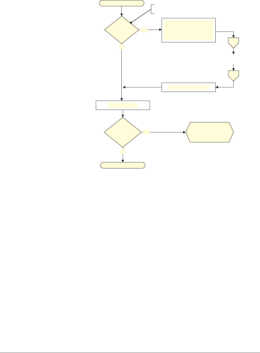
G3 The AArch32 Virtual Memory System Architecture
G3.12 VMSAv8-32 memory aborts
G3-3652 Copyright © 2013 ARM Limited. All rights reserved. ARM DDI 0487A.a
Non-Confidential - Beta ID090413
Figure G3-23 Fetching the descriptor in a VMSAv8-32 translation table walk
Descriptor address
Translation
required? Yes
Translate address.
Descriptor address is input
address for stage 2
translation A1
Fault checking sequence,
for stage 2 translation
A2
Returns descriptor PA
Fetch descriptor
No
Yes
Synchronous
External
Abort?
Synchronous
External Abort on
translation table
walk
Is this address an IPA for a
Non-secure PL0 or PL1 access?
Return descriptor
No
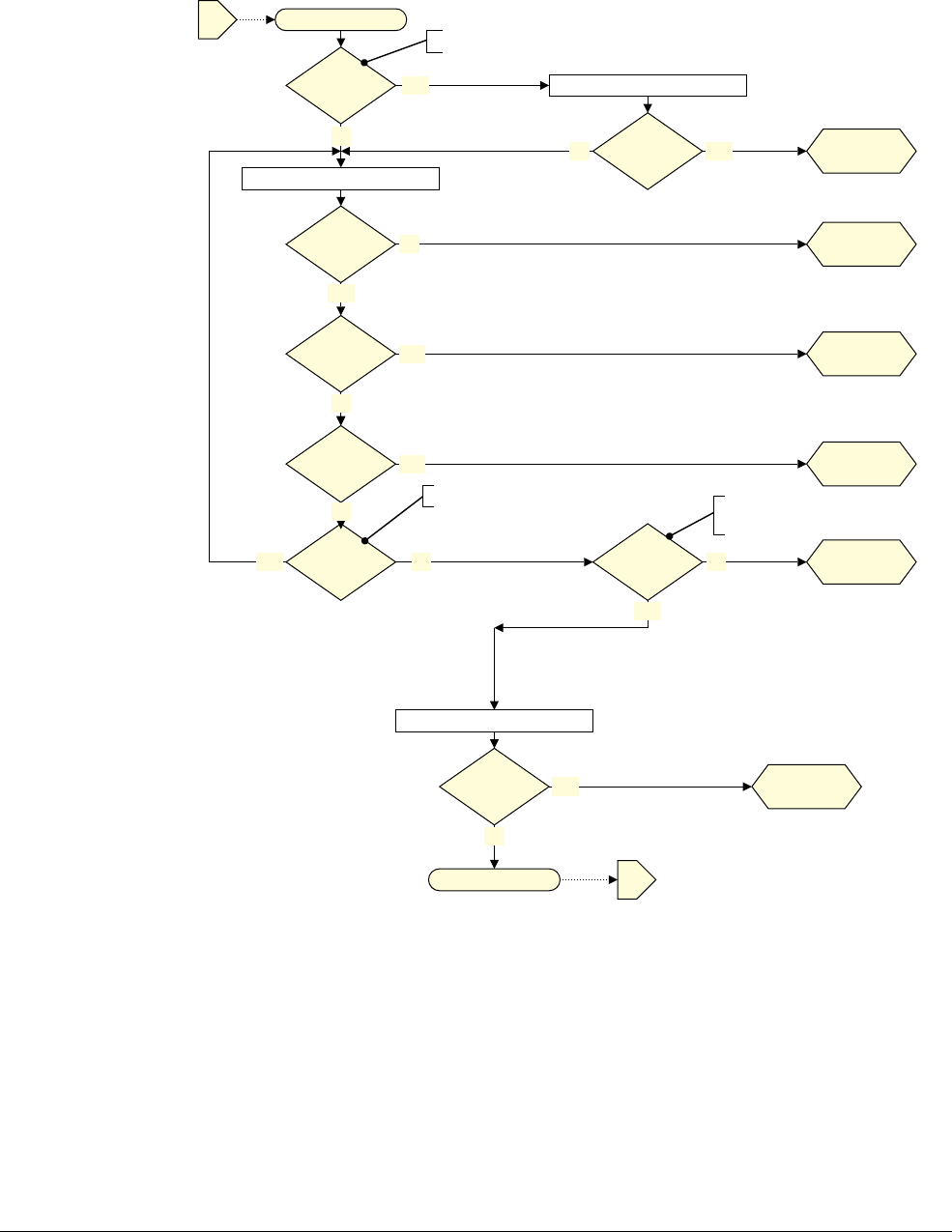
G3 The AArch32 Virtual Memory System Architecture
G3.12 VMSAv8-32 memory aborts
ARM DDI 0487A.a Copyright © 2013 ARM Limited. All rights reserved. G3-3653
ID090413 Non-Confidential - Beta
Figure G3-24 shows the full VMSAv8-32 fault checking sequence, including the alignment check on the initial
access.
Figure G3-24 VMSAv8-32 fault checking sequence
Input address
Alignment
check? Yes
Is the access subject to an alignment check?
Fetch descriptor ‡
No
Table
entry
?
Check address alignment
Misaligned
?
Yes Alignment
fault
Check access permissions
Violation
?
Output address
Table not possible at lowest level
Yes
Address
size fault
?
Descriptor
valid?
Yes
No
Translation
fault
No
Address
size fault
Yes
No
Yes Permission
fault
‡ See Fetching the descriptor
flowchart
† Links to and from Fetching the
descriptor flowchart
A1†
A2†
No
Alignment
fault
Alignment
valid
?
Fault unaligned access to any
Device memory type
No
Yes
No
Access
flag fault
?
No
No
Access flag
fault
Yes

G3 The AArch32 Virtual Memory System Architecture
G3.12 VMSAv8-32 memory aborts
G3-3654 Copyright © 2013 ARM Limited. All rights reserved. ARM DDI 0487A.a
Non-Confidential - Beta ID090413
Stage 2 fault on a stage 1 translation table walk
When an implementation that includes EL2 is operating in a Non-secure PL1 or PL0 mode, any memory access goes
through two stages of translation:
• Stage 1, from VA to IPA.
• Stage 2, from IPA to PA.
Note
In a virtualized system that is using AArch32, typically, a Guest OS operating in a Non-secure PL1 mode defines
the translation tables and translation table register entries controlling the Non-secure PL1&0 stage 1 translations. A
Guest OS has no awareness of the stage 2 address translation, and therefore believes it is specifying translation table
addresses in the physical address space. However, it actually specifies these addresses in its IPA space. Therefore,
to support virtualization, translation table addresses for the Non-secure PL1&0 stage 1 translations are always
defined in the IPA address space.
On performing a translation table walk for the stage 1 translations, the descriptor addresses must be translated from
IPA to PA, using a stage 2 translation. This means that a memory access made as part of a stage 1 translation table
lookup might generate, on a stage 2 translation:
• A Translation fault, Access flag fault, or Permission fault.
• A synchronous external abort on the memory access.
If SCR.EA is set to 1, a synchronous external abort is taken to EL3, and if EL3 is using AArch32 it is taken to Secure
Monitor mode. Otherwise, these faults are reported as stage 2 memory aborts. When EL2 is using AArch32,
HSR.ISS[7] is set to 1, to indicate a stage 2 fault during a stage 1 translation table walk, and the part of the ISS field
that might contain details of the instruction is invalid. For more information see Use of the HSR on page G3-3672.
Alternatively, a memory access made as part of a stage 1 translation table lookup might target an area of memory
with the any type of Device memory attribute assigned on the stage 2 translation of the address accessed. When the
value of the HCR.PTW bit is 1, such an access generates a stage 2 Permission fault.
Note
• On most systems, such a mapping to a Device memory type on the stage 2 translation is likely to indicate a
Guest OS error, where the stage 1 translation table is corrupted. Therefore, it is appropriate to trap this access
to the hypervisor.
A TLB might hold entries that depend on the effect of HCR.PTW. Therefore, if HCR.PTW is changed without
changing the current VMID, the TLBs must be invalidated before executing in a Non-secure PL1 or PL0 mode. For
more information see Changing HCR.PTW on page G3-3636.
A cache maintenance operation performed from a Non-secure PL1 mode can cause a stage 1 translation table walk
that might generate a stage 2 Permission fault, as described in this section. This is an exception to the general rule
that a cache maintenance operation cannot generate a Permission fault.
G3.12.4 Alignment faults
The ARM memory architecture requires support for strict alignment checking. This checking is controlled by
SCTLR.A. In addition, some instructions do not support unaligned accesses, regardless of the value of SCTLR.A.
Unaligned data access on page E2-2341 defines when Alignment faults are generated, for both values of SCTLR.A.
An Alignment fault can occur on an access for which the stage of address translation is disabled.
Any unaligned access to memory region with any Device memory type attribute generates an Alignment fault.
Routing of aborts taken to AArch32 state on page G3-3647 defines the mode to which an Alignment fault is taken.
The prioritization of Alignment faults depends on whether the fault was generated because of an access to a Device
memory type, or for another reason. For more information see Prioritization of aborts on page G3-3658.

G3 The AArch32 Virtual Memory System Architecture
G3.12 VMSAv8-32 memory aborts
ARM DDI 0487A.a Copyright © 2013 ARM Limited. All rights reserved. G3-3655
ID090413 Non-Confidential - Beta
G3.12.5 MMU faults in AArch32 state
This section describes the faults that might be detected during one of the fault-checking sequences described in The
MMU fault-checking sequence on page G3-3650. Unless indicated otherwise, information in this section applies to
the fault checking sequences for both the Short-descriptor translation table format and the Long-descriptor
translation table format.
MMU faults are always synchronous.
When a MMU fault generates an abort for a region of memory, no memory access is made if that region is or could
be marked as any type of Device memory.
The following subsections describe the MMU faults that might be detected during a fault checking sequence:
•Translation fault.
•Address size fault.
•Access flag fault on page G3-3656.
•Domain fault, Short-descriptor format translation tables only on page G3-3656.
•Permission fault on page G3-3657.
See also External abort on a translation table walk on page G3-3657.
Translation fault
A Translation fault can be generated at any level of lookup, and the reported fault code identifies the lookup level.
A Translation fault is generated if bits[1:0] of a translation table descriptor identify the descriptor as either a Fault
encoding or a reserved encoding. For more information see:
•VMSAv8-32 Short-descriptor translation table format descriptors on page G3-3579.
•VMSAv8-32 Long-descriptor translation table format descriptors on page G3-3592.
In addition, a Translation fault is generated if the input address for a translation either does not map on to an address
range of a Translation Table Base Register, or the Translation Table Base Register range that it maps on to is
disabled. In these cases the fault is reported as a first level Translation fault on the translation stage at which the
mapping to a region described by a Translation Table Base Register failed.
The architecture guarantees that any translation table entry that causes a Translation fault is not cached, meaning
the TLB never holds such an entry. Therefore, when a Translation fault occurs, the fault handler does not have to
perform any TLB maintenance operations to remove the faulting entry.
A data or unified cache maintenance operation by VA can generate a Translation fault. Whether an instruction cache
invalidate by VA operation can generate a Translation fault is IMPLEMENTATION DEFINED, because it is
IMPLEMENTATION DEFINED whether the operation requires an address translation. If the instruction cache invalidate
by VA operation requires an address translation then the operation can generate a Translation fault, otherwise it
cannot generate a Translation fault.
Whether branch predictor maintenance operations can generate Translation faults is IMPLEMENTATION DEFINED,
because it is IMPLEMENTATION DEFINED whether the operation requires an address translation. If the branch
predictor maintenance operation requires an address translation then the operation can generate a Translation fault,
otherwise it cannot generate a Translation fault.
Address size fault
An Address size fault can be generated at any level of lookup, and the reported fault code identifies the lookup level.
An Address size fault is generated if one of the following applies:
• The translation table entries or the TTBR for the stage of translation have address bits above the most
significant bit of the specified PA size as non zero.
Since VMSAv8-32 supports a maximum PA and IPA size of 40 bits, this includes any case where a translation
table entry or the TTBR holds an address for which A[47:40] is nonzero.
• The specified output address size is larger than the implemented PA.

G3 The AArch32 Virtual Memory System Architecture
G3.12 VMSAv8-32 memory aborts
G3-3656 Copyright © 2013 ARM Limited. All rights reserved. ARM DDI 0487A.a
Non-Confidential - Beta ID090413
The architecture guarantees that any translation table entry that causes an Address size fault is not cached, meaning
the TLB never holds such an entry. Therefore, when an Address size fault occurs, the fault handler does not have to
perform any TLB maintenance operations to remove the faulting entry.
Access flag fault
An Access flag fault can be generated at any level of lookup, and the reported fault code identifies the lookup level.
An Access flag fault is generated only if all of the following apply:
• The translation tables support an Access flag bit:
— The Short-descriptor format supports an Access flag only when SCTLR.AFE is set to 1.
— The Long-descriptor format always supports an Access flag.
• A translation table descriptor with the Access flag bit set to 0 is loaded.
For more information about the Access flag bit see:
•VMSAv8-32 Short-descriptor translation table format descriptors on page G3-3579
•VMSAv8-32 Long-descriptor translation table format descriptors on page G3-3592.
The architecture guarantees that any translation table entry that causes an Access flag fault is not cached, meaning
the TLB never holds such an entry. Therefore, when an Access flag fault occurs, the fault handler does not have to
perform any TLB maintenance operations to remove the faulting entry.
Whether any cache maintenance operations by VA can generate Access flag faults is IMPLEMENTATION DEFINED.
Whether branch predictor invalidate by VA operations can generate Access flag faults is IMPLEMENTATION
DEFINED.
For more information, see The Access flag on page G3-3615.
Domain fault, Short-descriptor format translation tables only
When using the Short-descriptor translation table format, a Domain fault can be generated at the first level or second
level of lookup. The reported fault code identifies the lookup level. The conditions for generating a Domain fault
are:
First level When a first-level descriptor fetch returns a valid Section first-level descriptor, the domain field of
that descriptor is checked against the DACR. A first-level Domain fault is generated if this check
fails.
Second level When a second-level descriptor fetch returns a valid second-level descriptor, the domain field of the
first-level descriptor that required the second-level fetch is checked against the DACR, and a
second-level Domain fault is generated if this check fails.
For more information, see Domains, Short-descriptor format only on page G3-3614.
Domain faults cannot occur on cache or branch predictor maintenance operations.
A TLB might hold a translation table entry that cause a Domain fault. Therefore, if the handling of a Domain fault
results in an update to the associated translation tables, the software that updates the translation tables must
invalidate the appropriate TLB entry, to prevent the stale information in the TLB being used on a subsequent
memory access. For more information, see the translation table entry update examples in TLB maintenance
operations and the memory order model on page G3-3635.
Any change to the DACR must be synchronized by a context synchronization operation. For more information see
Synchronization of changes to System registers on page G3-3706.

G3 The AArch32 Virtual Memory System Architecture
G3.12 VMSAv8-32 memory aborts
ARM DDI 0487A.a Copyright © 2013 ARM Limited. All rights reserved. G3-3657
ID090413 Non-Confidential - Beta
Permission fault
A Permission fault can be generated at any level of lookup, and the reported fault code identifies the lookup level.
See Access permissions on page G3-3609 for information about conditions that cause a Permission fault.
Note
When using the Short-descriptor translation table format, the translation table descriptors are checked for
Permission faults only for accesses to memory regions in Client domains.
A TLB might hold a translation table entry that cause a Permission fault. Therefore, if the handling of a Permission
fault results in an update to the associated translation tables, the software that updates the translation tables must
invalidate the appropriate TLB entry, to prevent the stale information in the TLB being used on a subsequent
memory access. For more information, see the translation table entry update examples in TLB maintenance
operations and the memory order model on page G3-3635.
Note
In an implementation that includes EL2, this maintenance requirement applies to Permission faults in both stage 1
and stage 2 translations.
Cache or branch predictor maintenance operations cannot cause a Permission fault, except that:
• A stage 1 translation table walk performed as part of a cache or branch predictor maintenance operation can
generate a stage 2 Permission fault as described in Stage 2 fault on a stage 1 translation table walk on
page G3-3654.
•A DCIMVAC issued in Non-secure state that attempts to update a location for which it does not have stage 2
write access can generate a stage 2 Permission fault, as described in Data cache maintenance instructions
(DC*) on page G2-3535.
G3.12.6 External abort on a translation table walk
An external abort on a translation table walk can be either synchronous or asynchronous. For more information on
external aborts, see External aborts on page G2-3546.
An external abort on a translation table walk is reported:
• If the external abort is synchronous, using:
— A synchronous Prefetch Abort exception if the translation table walk is for an instruction fetch.
— A synchronous Data Abort exception if the translation table walk is for a data access.
• If the external abort is asynchronous, using an asynchronous Data Abort exception.
If an implementation reports the error in the translation table walk asynchronously from executing the instruction
whose instruction fetch or memory access caused the translation table walk, these aborts behave essentially as
interrupts. The aborts are masked when CPSR.A is set to 1, otherwise they are reported using the Data Abort
exception.
Behavior of external aborts on a translation table walk caused by address translation
operations
The address translation operations summarized in Address translation operations, functional group on
page G3-3745 require translation table walks. An external abort can occur in the translation table walk. The abort
generates a Data Abort exception, and can be synchronous or asynchronous. For more information, see Handling of
faults and aborts during an address translation operation on page G3-3688.

G3 The AArch32 Virtual Memory System Architecture
G3.12 VMSAv8-32 memory aborts
G3-3658 Copyright © 2013 ARM Limited. All rights reserved. ARM DDI 0487A.a
Non-Confidential - Beta ID090413
G3.12.7 Prioritization of aborts
This section describes the abort prioritization that applies to a single memory access from AArch32 state that might
generate multiple aborts:
On a single memory access from AArch32 state, the following rules apply:
• If a memory access generates an Alignment fault because SCTLR.A is set to 1, or because it is an unaligned
access by an instruction that does not support unaligned accesses, then that access cannot generate any of:
— A MMU fault, on either the stage 1 translation or the stage 2 translation.
— An external abort.
— A Watchpoint debug event.
An Alignment fault generated by an unaligned access to any type of Device memory is prioritized as an
MMU fault. For more information see Alignment faults caused by accessing Device memory types.
• If a memory access generates an MMU fault on its stage 1 translation, and also generates an abort on its stage
2 translation, the fault from the stage 1 translation has priority:
— If a memory access made as part of a stage 1 translation table walk generates an MMU fault on its
stage 2 translation, as described in Stage 2 fault on a stage 1 translation table walk on page G3-3654,
the stage 1 translation table walk does not generate an MMU fault on the stage 1 translation.
— A fault on a particular stage of translation might be a synchronous external abort on a translation table
walk made at that stage of translation.
• If a memory access generates an MMU fault on either its stage 1 translation or on its stage 2 translation, then
the PE cannot generate a Watchpoint debug event on that access.
• If a memory access generates an MMU fault on either its stage 1 translation or on its stage 2 translation, or
generates a synchronous Watchpoint debug event, then the memory access cannot generate an external abort.
• Except as defined in this list, the architecture does not define any prioritization of asynchronous external
aborts relative to any other asynchronous aborts.
If a single instruction generates aborts on more than one memory access, the architecture does not define any
prioritization between those aborts.
In general, the ARM architecture does not define when asynchronous events are taken, and therefore the
prioritization of asynchronous events is IMPLEMENTATION DEFINED.
Note
Debug state entry and debug event prioritization on page H2-4331 describes the relationship between debug events,
MMU faults, and external aborts, for synchronous aborts generated by the same memory access.
Alignment faults caused by accessing Device memory types
Any unaligned access to any type of Device memory generates an Alignment fault. When applying the prioritization
rules, this fault is prioritized at any MMU fault. The priority of this Alignment fault relative to possible MMU faults
is as follows:
• The Alignment fault has lower priority than an Access flag fault.
• If the translation stage that generates the Access flag fault:
— Can generate Domain faults, the Alignment fault has higher priority than a Domain fault.
— Cannot generate Domain faults, the Alignment fault has higher priority than a Permission fault.
The MMU fault checking sequence in Figure G3-24 on page G3-3653 shows this prioritization.

G3 The AArch32 Virtual Memory System Architecture
G3.13 Exception reporting in a VMSAv8-32 implementation
ARM DDI 0487A.a Copyright © 2013 ARM Limited. All rights reserved. G3-3659
ID090413 Non-Confidential - Beta
G3.13 Exception reporting in a VMSAv8-32 implementation
This section describes exception reporting, in AArch32 state, in a VMSAv8-32 implementation. That is, it describes
only the reporting of exceptions that are taken to an Exception level that is using AArch32. EL2 provides an
enhanced reporting mechanism for exceptions taken to the Non-secure EL2 mode, Hyp mode. This means that, for
VMSAv8-32, the exception reporting depends on the mode to which the exception is taken.
Note
The enhanced reporting mechanism for exceptions that are taken to Hyp mode is generally similar to the reporting
of exceptions that are taken to an Exception level that is using AArch64.
About exception reporting introduces the general approach to exception reporting, and the following sections then
describe exception reporting at different privilege levels:
•Reporting exceptions taken to PL1 modes on page G3-3660.
•Fault reporting in PL1 modes on page G3-3663.
•Summary of register updates on faults taken to PL1 modes on page G3-3666.
•Reporting exceptions taken to Hyp mode on page G3-3668.
•Use of the HSR on page G3-3672.
•Summary of register updates on exceptions taken to Hyp mode on page G3-3682.
Note
The registers used for exception reporting also report information about debug exceptions. For more information
see:
•Data Abort exceptions, taken to a PL1 mode on page G3-3661.
•Prefetch Abort exceptions, taken to a PL1 mode on page G3-3662.
•Reporting exceptions taken to Hyp mode on page G3-3668.
G3.13.1 About exception reporting
In an implementation that includes EL2 and EL3, exceptions can be taken to:
• Monitor mode, if EL3 is using AArch32.
• Hyp mode, if EL2 is using AArch32.
• A Secure or Non-secure PL1 mode.
Monitor mode is a PL1 mode, but:
• It is accessible only when EL3 is using AArch32.
• It is present only in Secure state.
• When EL3 is using AArch32, System register controls route some exceptions from Non-secure state to
Monitor mode. These are the only cases where taking an exception to an Exception level that is using
AArch32 changes the Security state of the PE.
Exception reporting in Hyp mode differs significantly from that in the other modes, but in general, exception
reporting returns:
• Information about the exception:
— On taking an exception to Hyp mode, the Hyp Syndrome Register, HSR, returns syndrome
information.
— On taking an exception to any other mode, a Fault Status Register (FSR) returns status information.
• For synchronous exceptions, one or more addresses associated with the exceptions, returned in Fault Address
Registers (FARs).
In all modes, additional IMPLEMENTATION DEFINED registers can provide additional information about exceptions.

G3 The AArch32 Virtual Memory System Architecture
G3.13 Exception reporting in a VMSAv8-32 implementation
G3-3660 Copyright © 2013 ARM Limited. All rights reserved. ARM DDI 0487A.a
Non-Confidential - Beta ID090413
Note
• PE mode for taking exceptions on page G1-3439 describes how the mode to which an exception is taken is
determined.
• EL2 provides:
— Specific exception types, that can only be taken from Non-secure PL1 and PL0 modes, and are always
taken to Hyp mode.
— Routing controls that can route some exceptions from Non-secure PL1 and PL0 modes to Hyp mode.
These exceptions are reported using the same mechanism as the Hyp mode reporting of VMSAv8-32 memory
aborts, as described in this section.
Memory system faults generate either a Data Abort exception or a Prefetch Abort exception, as summarized in:
•Reporting exceptions taken to PL1 modes.
•Memory fault reporting in Hyp mode on page G3-3670.
On an access that might have multiple aborts, the MMU fault checking sequence and the prioritization of aborts
determine which abort occurs. For more information, see The MMU fault-checking sequence on page G3-3650 and
Prioritization of aborts on page G3-3658.
G3.13.2 Reporting exceptions taken to PL1 modes
The following sections give general information about the reporting of exceptions when they are taken to a Secure
or Non-secure PL1 mode:
•Registers used for reporting exceptions taken to PL1 modes.
•Data Abort exceptions, taken to a PL1 mode on page G3-3661.
•Prefetch Abort exceptions, taken to a PL1 mode on page G3-3662.
Fault reporting in PL1 modes on page G3-3663 then describes the fault reporting in these modes, including the
encodings used for reporting the faults.
Note
Execution privilege, Exception levels, and AArch32 Privilege levels on page G3-3560 describes how the Secure and
Non-secure PL1 modes map onto the Exception levels.
Registers used for reporting exceptions taken to PL1 modes
AArch32 state defines the following registers, and register encodings, for exceptions taken to PL1 modes:
• The DFSR holds information about a Data Abort exception.
• The DFAR holds the faulting address for some synchronous Data Abort exceptions.
• The IFSR holds information about a Prefetch Abort exception.
• The IFAR holds the faulting address of a Prefetch Abort exception.
In addition, if implemented, the optional ADFSR and AIFSR can provide additional fault information, see Auxiliary
Fault Status Registers.
Auxiliary Fault Status Registers
AArch32 state defines the following Auxiliary Fault Status Registers:
• The Auxiliary Data Fault Status Register, ADFSR.
• The Auxiliary Instruction Fault Status Register, AIFSR.
The position of these registers is architecturally-defined, but the content and use of the registers is IMPLEMENTATION
DEFINED. An implementation can use these registers to return additional fault status information. An example use
of these registers is to return more information for diagnosing parity errors.

G3 The AArch32 Virtual Memory System Architecture
G3.13 Exception reporting in a VMSAv8-32 implementation
ARM DDI 0487A.a Copyright © 2013 ARM Limited. All rights reserved. G3-3661
ID090413 Non-Confidential - Beta
An implementation that does not need to report additional fault information must implement these registers as
UNK/SBZP. This ensures that an attempt to access these registers from software executing at PL1 does not cause
an Undefined Instruction exception.
Data Abort exceptions, taken to a PL1 mode
On taking a Data Abort exception to a PL1 mode:
• If the exception is on an instruction cache or branch predictor maintenance operation by VA, its reporting
depends on the current translation table format. For more information about the registers used when reporting
the exception, see Data Abort on an instruction cache maintenance operation by VA.
• If the exception is generated by a Watchpoint debug event, then its reporting depends on whether the
Watchpoint debug event is synchronous or asynchronous, and on the Debug architecture version. For more
information, see Data Abort on a Watchpoint exception on page G3-3662.
Otherwise:
• The DFSR is updated with details of the fault, including the appropriate fault status code.
If the Data Abort exception is synchronous, DFSR.WnR is updated to indicate whether the faulted access was
a read or a write. However, if the fault is on a cache maintenance operation, or on an address translation
operation, WnR is set to 1, to indicate a write access fault, and the CM bit is set to 1.
DFSR.WnR is UNKNOWN on an asynchronous Data Abort exception.
See the register description for more information about the returned fault information.
• If the Data Abort exception is
— Synchronous, the DFAR is updated with the VA that caused the exception.
— Asynchronous, the DFAR becomes UNKNOWN.
For all Data Abort exceptions, if the implementation includes EL3, the Security state of the PE in the mode to which
the Data Abort exception is taken determines whether the Secure or Non-secure DFSR and DFAR are updated.
Data Abort on an instruction cache maintenance operation by VA
If an instruction cache or branch predictor invalidation by VA operation generates a Data Abort exception that is
taken to a PL1 mode, the DFAR is updated to hold the faulting VA. However, the reporting of the fault depends on
the current translation table format:
Short-descriptor format
It is IMPLEMENTATION DEFINED which of the following is used when reporting the fault:
• The DFSR indicates an Instruction cache maintenance operation fault, and the IFSR is valid
and indicates the cause of the fault, a Translation fault or Access flag fault.
• The DFSR indicates the cause of the fault, a Translation fault or Access flag fault. The IFSR
is UNKNOWN.
In either case:
•DFSR.WnR is set to 1.
•DFSR.CM is set to 1, to indicate a fault on a cache maintenance operation.
Long-descriptor format
•DFSR.CM is set to 1, to indicates a fault on a cache maintenance operation.
•DFSR.STATUS indicates the cause of the fault, a Translation or Access flag fault.
•DFSR.WnR is set to 1.
• The IFSR is UNKNOWN.

G3 The AArch32 Virtual Memory System Architecture
G3.13 Exception reporting in a VMSAv8-32 implementation
G3-3662 Copyright © 2013 ARM Limited. All rights reserved. ARM DDI 0487A.a
Non-Confidential - Beta ID090413
Data Abort on a Watchpoint exception
On taking a Data Abort exception caused by a watchpoint:
•DFSR.FS is updated to indicate a debug event.
•DFSR.{WnR, Domain} are UNKNOWN.
•DFAR is set to the address that generated the watchpoint
Note
• LR_abt indicates the address of the instruction that triggered the watchpoint.
• In some ARMv7 AArch32 implementations, the DBGWFAR is set to the address of the instruction that
triggered the watchpoint. In ARMv8 this register is RES0.
A watchpointed address can be any byte-aligned address. The address reported in DFAR might not be the
watchpointed address, and, for a watchpoint due to an operation other than a Data Cache maintenance operation,
can be any address between and including:
• The lowest address accessed by the instruction that triggered the watchpoint.
• The highest watchpointed address accessed by that instruction.
If multiple watchpoints are set in this range, there is no guarantee of which watchpoint is generated.
Note
In particular, there is no guarantee of generating the watchpoint with the lowest address in the range.
The address must also be within a naturally-aligned block of memory of an IMPLEMENTATION DEFINED
power-of-two size, containing a watchpoint address accessed by that location.
Note
The implementation defined power-of-two size must be no larger than the block size of the AArch64 DC ZVA
operation.
Prefetch Abort exceptions, taken to a PL1 mode
For a Prefetch Abort exception generated by an instruction fetch, the Prefetch Abort exception is taken
synchronously with the instruction that the abort is reported on. This means:
• If the PE attempts to execute the instruction a Prefetch Abort exception is generated.
• If an instruction fetch is issued but the PE does not attempt to execute the prefetched instruction, no Prefetch
Abort exception is generated for that instruction. For example, if the execution flow branches round a
prefetched instruction, no Prefetch Abort exception is generated.
In addition, debug exceptions caused by a BKPT instruction, Breakpoint, or a Vector catch debug event, generate a
Prefetch Abort exception, see Breakpoint debug events and Vector Catch exception on page H2-4333.
On taking a Prefetch Abort exception to a PL1 mode:
• The IFSR is updated with details of the fault, including the appropriate fault code. If appropriate, the fault
code indicates that the exception was generated by a debug exception.
See the register description for more information about the returned fault information.
• For a Prefetch Abort exception generated by an instruction fetch, the IFAR is updated with the VA that caused
the exception.
• For a Prefetch Abort exception generated by a debug exception, the IFAR is UNKNOWN.
If the implementation includes EL3, the security state of the PE in the mode to which it takes the Prefetch Abort
exception determines whether the exception updates the Secure or Non-secure IFSR and IFAR.

G3 The AArch32 Virtual Memory System Architecture
G3.13 Exception reporting in a VMSAv8-32 implementation
ARM DDI 0487A.a Copyright © 2013 ARM Limited. All rights reserved. G3-3663
ID090413 Non-Confidential - Beta
G3.13.3 Fault reporting in PL1 modes
The FSRs provide fault information, including an indication of the fault that occurred. The following subsections
describe fault reporting in PL1 modes for each of the translation table formats:
•PL1 fault reporting with the Short-descriptor translation table format.
•PL1 fault reporting with the Long-descriptor translation table format on page G3-3665.
Reserved encodings in the IFSR and DFSR encodings tables on page G3-3666 gives some additional information
about the encodings for both formats.
Summary of register updates on faults taken to PL1 modes on page G3-3666 shows which registers are updated on
each of the reported faults.
Reporting of External aborts taken from Non-secure state to Monitor mode describes how the fault status register
format is determined for those aborts. For all other aborts, the current translation table format determines the format
of the fault status registers.
Reporting of External aborts taken from Non-secure state to Monitor mode
When an External abort is taken from Non-secure state to Monitor mode:
• For a Data Abort exception, the Secure DFSR and DFAR hold information about the abort.
• For a Prefetch Abort exception, the Secure IFSR and IFAR hold information about the abort.
• The abort does not affect the contents of the Non-secure copies of the fault reporting registers.
Normally, the current translation table format determines the format of the DFSR and IFSR. However, when
SCR.EA is set to 1, to route external aborts to Monitor mode, and an external abort is taken from Non-secure state,
this section defines the DFSR and IFSR format.
For an External abort taken from Non-secure state to Monitor mode, the DFSR or IFSR uses the format associated
with the Long-descriptor translation table format, as described in PL1 fault reporting with the Long-descriptor
translation table format on page G3-3665, if any of the following applies:
• The Secure TTBCR.EAE bit is set to 1.
• The External abort is synchronous and either:
— It is taken from Hyp mode.
— It is taken from a Non-secure PL1 mode, and the Non-secure TTBCR.EAE bit is set to 1.
Otherwise, the DFSR or IFSR uses the format associated with the Short-descriptor translation table format, as
described in PL1 fault reporting with the Short-descriptor translation table format.
PL1 fault reporting with the Short-descriptor translation table format
This subsection describes the fault reporting for a fault taken to a PL1 when address translation is using the
Short-descriptor translation table format.
On taking an exception, bit[9] of the FSR is RAZ, or set to 0, if the PE is using this FSR format.
An FSR encodes the fault in a 5-bit FS field, that comprises FSR[10, 3:0]. Table G3-26 on page G3-3664 shows the
encoding of that field. Summary of register updates on faults taken to PL1 modes on page G3-3666 shows:
• Whether the corresponding FAR is updated on the fault. That is:
— For a fault reported in the IFSR, whether the IFAR holds a valid address.
— For a fault reported in the DFSR, whether the DFAR holds a valid address.
• For faults that update DFSR, whether DFSR.Domain is valid
When reading Table G3-26 on page G3-3664:
• FS values not shown in the table are reserved.

G3 The AArch32 Virtual Memory System Architecture
G3.13 Exception reporting in a VMSAv8-32 implementation
G3-3664 Copyright © 2013 ARM Limited. All rights reserved. ARM DDI 0487A.a
Non-Confidential - Beta ID090413
• FS values shown as DFSR only are reserved for the IFSR.
The Domain field in the DFSR
The DFSR includes a Domain field. This is inherited from previous versions of the VMSA. The IFSR does not
include a Domain field. Summary of register updates on faults taken to PL1 modes on page G3-3666 describes when
DFSR.Domain is valid.
ARM deprecates any use of the Domain field in the DFSR. The Long-descriptor translation table format does not
support a Domain field, and future versions of the ARM architecture might not support a Domain field in the
Short-descriptor translation table format. ARM strongly recommends that new software does not use this field.
For both Data Abort exceptions and Prefetch Abort exceptions, software can find the domain information by
performing a translation table read for the faulting address and extracting the Domain field from the translation table
entry.
Table G3-26 FSR encodings when using the Short-description translation table format
FS Source Notes
00001 Alignment fault DFSR only. Fault on first lookup
00100 Fault on instruction cache maintenance DFSR only
01100
01110
Synchronous external abort on translation table walk First level
Second level -
11100
11110
Synchronous parity error on translation table walk First level
Second level -
00101
00111
Translation fault First level
Second level
MMU fault
00011a
00110
Access flag fault First level
Second level
MMU fault
01001
01011
Domain fault First level
Second level
MMU fault
01101
01111
Permission fault First level
Second level
MMU fault
00010 Debug event See Chapter D3 The Debug Exception Model
01000 Synchronous external abort -
10000 TLB conflict abort See TLB conflict aborts on page G3-3632
10100 IMPLEMENTATION DEFINED Lockdown
11010 IMPLEMENTATION DEFINED Coprocessor abort
11001 Synchronous parity error on memory access -
10110 Asynchronous external abortbDFSR only
11000 Asynchronous parity error on memory accesscDFSR only
a. Previously, this encoding was a deprecated encoding for Alignment fault. The extensive changes in the memory model in VMSAv8-32
mean there should be no possibility of confusing the new use of this encoding with its previous use
b. Including asynchronous data external abort on translation table walk or instruction fetch.
c. Including asynchronous parity error on translation table walk.

G3 The AArch32 Virtual Memory System Architecture
G3.13 Exception reporting in a VMSAv8-32 implementation
ARM DDI 0487A.a Copyright © 2013 ARM Limited. All rights reserved. G3-3665
ID090413 Non-Confidential - Beta
PL1 fault reporting with the Long-descriptor translation table format
This subsection describes the fault reporting for a fault taken to a PL1mode when address translation is using the
Long-descriptor translation table format.
When the PE takes an exception, bit[9] of the FSR is set to 1 if the PE is using this FSR format.
The FSRs encode the fault in a 6-bit STATUS field, that comprises FSR[5:0]. Table G3-27 shows the encoding of
that field. In addition:
• For a fault taken to a PL1 mode, Summary of register updates on faults taken to PL1 modes on page G3-3666
shows whether the corresponding FAR is updated on the fault. That is:
— For a fault reported in the IFSR, whether the IFAR holds a valid address.
— For a fault reported in the DFSR, whether the DFAR holds a valid address.
• For a fault taken to the Hyp mode, Summary of register updates on exceptions taken to Hyp mode on
page G3-3682 shows what registers are updated on the fault.
Table G3-27 FSR encodings when using the Long-descriptor translation table format
STATUSaSource Notes
0001LL Translation fault. LL bits indicate levelb.MMU fault
0010LL Access flag fault. LL bits indicate levelb.MMU fault
0011LL Permission fault. LL bits indicate levelb.MMU fault
010000 Synchronous external abort. -
011000 Synchronous parity error on memory access. -
010001 Asynchronous external abort. DFSR only
011001 Asynchronous parity error on memory access. DFSR only
0101LL Synchronous external abort on translation table walk.
LL bits indicate levelb.
-
0111LL Synchronous parity error on memory access on translation table walk.
LL bits indicate levelb.
-
100001 Alignment fault. Fault on first lookup
100010 Debug event. See Chapter D3 The Debug Exception Model
110000 TLB conflict abort. See TLB conflict aborts on page G3-3632
110100 IMPLEMENTATION DEFINED. Lockdown, DFSR only
111010 IMPLEMENTATION DEFINED. Coprocessor abort, DFSR only
1111LL Domain fault.
LL bits indicate levelb.
MMU fault. 64-bit PAR only, First or second
level only. Never used in DFSR, IFSR, or
HSRc
a. STATUS values not shown in this table are reserved. STATUS values not supported in the IFSR or DFSR are reserved for the register or
registers in which they are not supported.
b. See The level associated with MMU faults on page G3-3666.
c. A Domain fault can be reported using the Long-descriptor STATUS encodings only as a result of a fault on an address translation operation.
For more information see MMU fault on an address translation operation on page G3-3689.

G3 The AArch32 Virtual Memory System Architecture
G3.13 Exception reporting in a VMSAv8-32 implementation
G3-3666 Copyright © 2013 ARM Limited. All rights reserved. ARM DDI 0487A.a
Non-Confidential - Beta ID090413
The level associated with MMU faults
For MMU faults, Table G3-28 shows how the LL bits in the xFSR.STATUS field encode the lookup level associated
with the fault.
The lookup level associated with a fault is:
• For a fault generated on a translation table walk, the lookup level of the walk being performed.
• For a Translation fault, the lookup level of the translation table that gave the fault. If a fault occurs because
an stage of address translation is disabled, or because the input address is outside the range specified by the
appropriate base address register or registers, the fault is reported as a First level fault.
• For an Access flag fault, the lookup level of the translation table that gave the fault.
• For a Permission fault, including a Permission fault caused by hierarchical permissions, the lookup level of
the final level of translation table accessed for the translation. That is, the lookup level of the translation table
that returned a Block or Page descriptor.
Reserved encodings in the IFSR and DFSR encodings tables
With both the Short-descriptor and the Long-descriptor FSR format, the fault encodings reserve a single encoding
for each of:
• Cache and TLB lockdown faults. The details of these faults and any associated subsidiary registers are
IMPLEMENTATION DEFINED.
• Aborts associated with coprocessors. The details of these faults are IMPLEMENTATION DEFINED.
G3.13.4 Summary of register updates on faults taken to PL1 modes
For faults that generate exceptions that are taken to a PL1 mode, Table G3-29 on page G3-3667 shows the registers
affected by each fault. In this table:
• Yes indicates that the register is updated.
•UNK indicates that the fault makes the register value UNKNOWN.
• A null entry, -, indicates that the fault does not affect the register.
Table G3-28 Use of LL bits to encode the lookup level at which the fault occurred
LL bits Meaning
00 Reserved.
01 First level.
10 Second level.
11 Third level. When xFSR.STATUS indicates a Domain fault, this value is reserved.

G3 The AArch32 Virtual Memory System Architecture
G3.13 Exception reporting in a VMSAv8-32 implementation
ARM DDI 0487A.a Copyright © 2013 ARM Limited. All rights reserved. G3-3667
ID090413 Non-Confidential - Beta
For faults that update the DFSR using the Short-descriptor format FSR encodings, Table G3-30 on page G3-3668
shows whether DFSR.Domain is valid.
Table G3-29 Effect of a fault taken to a PL1 mode on the reporting registers
Fault IFSR IFAR DFSR DFAR
Faults reported as Prefetch Abort exceptions:
MMU fault, always synchronous. Yes Yes - -
Synchronous external abort on translation table walk. Yes Yes - -
Synchronous parity error on translation table walk. Yes Yes - -
Synchronous external abort. Yes Yes - -
Synchronous parity error on memory access. Yes Yes - -
TLB conflict abort. Yes Yes - -
Fault reported as Data Abort exception:
Alignment fault, always synchronous. - - Yes Yes
MMU fault, always synchronous. - - Yes Yes
Fault on instruction cache maintenance, when using Long-descriptor
translation table formata.
UNK -YesYes
Fault on instruction cache maintenance, when using
Short descriptor translation table formatb.
either Yes - Yes Yes
or UNK -YesYes
Synchronous external abort on translation table walk. - - Yes Yes
Synchronous parity error on translation table walk. - - Yes Yes
Synchronous external abort. - - Yes Yes
Synchronous parity error on memory access. - - Yes Yes
Asynchronous external abort. - - Yes UNK
Asynchronous parity error on memory access. - - Yes UNK
TLB conflict abort. - - Yes Yes
Debug exceptions:
Breakpoint, Software Breakpoint Instruction, or Vector Catchc.Yes UNK --
Watchpointd.--YesYes
a. When using the Long-descriptor translation table format, there is not a specific fault code for a fault on an instruction
cache maintenance operation. For more information see Data Abort on an instruction cache maintenance operation by
VA on page G3-3661.
b. The two lines of this entry show the alternative ways of reporting the fault when using the Short-descriptor translation
table format. It is IMPLEMENTATION DEFINED which methods is used, see Data Abort on an instruction cache maintenance
operation by VA on page G3-3661.
c. Generates a Prefetch Abort exception.
d. Generates a Data Abort exception.

G3 The AArch32 Virtual Memory System Architecture
G3.13 Exception reporting in a VMSAv8-32 implementation
G3-3668 Copyright © 2013 ARM Limited. All rights reserved. ARM DDI 0487A.a
Non-Confidential - Beta ID090413
For those faults for which Table G3-29 on page G3-3667 shows that the DFSR is updated, if the fault is reported
using the Short-descriptor FSR encodings, Table G3-30 shows whether DFSR.Domain is valid. In this table, UNK
indicates that the fault makes DFSR.Domain UNKNOWN.
G3.13.5 Reporting exceptions taken to Hyp mode
Hyp mode is the Non-secure EL2 mode. It is entered by taking an exception to Hyp mode.
Note
Software executing in Monitor mode, or at EL3 when EL3 is using AArch64, can perform an exception return to
Hyp mode. This means Hyp mode can be entered either by taking an exception, or by a permitted exception return.
When EL2 is using AArch32, the following exceptions are taken to Hyp mode:
• Asynchronous external aborts, IRQ exceptions, and FIQ exceptions, from Non-secure PL0 and PL1 modes,
if not routed to Secure Monitor mode, and if configured by the AMO, FMO or IMO bits. For more
information see Asynchronous exception routing controls on page G1-3467.
Table G3-30 Validity of Domain field on faults that update the DFSR when using the Short-descriptor encodings
DFSR.FS Source DFSR.Domain Notes
00001 Alignment fault UNK -
00100 Fault on instruction cache maintenance operation UNK -
01100
01110
Synchronous external abort on translation table walk First level
Second level
UNK
Valid -
11100
11110
Synchronous parity error on translation table walk First level
Second level
UNK
Valid -
00101
00111
Translation fault First level
Second level
UNK
Valid
MMU fault
00011a
00110
Access flag fault First level
Second level
UNK
Valid
MMU fault
01001
01011
Domain fault First level
Second level
Valid
Valid
MMU fault
01101
01111
Permission fault First level
Second level
UNK
UNK
MMU fault
01000 Synchronous external abort UNK -
10000 TLB conflict abort UNK -
11001 Synchronous parity error on memory access UNK -
10110 Asynchronous external abortbUNK -
11000 Asynchronous parity error on memory accesscUNK -
00010 Watchpoint UNK
a. Previously, this encoding was a deprecated encoding for Alignment fault. The extensive changes in the memory model in
VMSAv8-32 mean there should be no possibility of confusing the new use of this encoding with its previous use
b. Including asynchronous data external abort on translation table walk or instruction fetch.
c. Including asynchronous parity error on translation table walk.

G3 The AArch32 Virtual Memory System Architecture
G3.13 Exception reporting in a VMSAv8-32 implementation
ARM DDI 0487A.a Copyright © 2013 ARM Limited. All rights reserved. G3-3669
ID090413 Non-Confidential - Beta
• When HCR.TGE is set to 1, all exceptions that would be routed to Non-secure PL1 modes.
For more information, see Routing general exceptions to EL2 on page G1-3452.
• When HCR.TDE is set to 1, any debug exception that would otherwise be taken to a Non-secure PL1 mode,
see Routing Debug exceptions to Hyp mode on page G1-3454.
• The privilege rules for taking exceptions mean that any exception taken from Hyp mode, if not routed to EL3,
must be taken to Hyp mode. This includes a Prefetch Abort exception generated by a Debug exception on a
BKPT
instruction.
Note
Debug exceptions other than the exception on a
BKPT
instruction are not permitted in Hyp mode.
• Hypervisor Call exceptions, and Hyp Trap exceptions, are always taken to Hyp mode. These exceptions are
supported only as part of EL2.
When EL2 is implemented, various operations from Non-secure PL0 and PL1 modes can be trapped to Hyp
mode, using the Hyp Trap exception. For more information, see AArch32 control of traps to the hypervisor
on page G1-3503.
These exceptions include any memory system fault that occurs:
• On a memory access from Hyp mode.
• On memory access from a Non-secure PL0 or PL1 mode:
— On a stage 2 translation, from IPA to PA.
— On the stage 2 translation of an address accessed in performing a stage 1 translation table walk.
Memory fault reporting in Hyp mode on page G3-3670 gives more information about these faults.
The following exceptions provide syndrome information in the HSR:
• Any synchronous exception taken to Hyp mode.
• Some exceptions taken from Debug state that would be taken to Hyp mode if the PE was not in Debug state,
see Exceptions in Debug state on page H2-4355.
Note
— In Debug state, the PE does not change mode on taking an exception.
—As Exceptions in Debug state on page H2-4355 describes, some other exceptions taken from Debug
state make the HSR UNKNOWN.
The syndrome information in the HSR includes the fault status code otherwise provided by the fault status register,
and extends the fault reporting compared to that available for an exception taken to a PL1 mode. For more
information, see Use of the HSR on page G3-3672.
In addition, for a Debug exception taken to Hyp mode, DBGDSCRint.MOE or DBGDTRRXext.MOE shows what
caused the Debug exception. This bit is valid regardless of whether the Debug exception was taken from Hyp mode
or from another Non-secure mode.
Registers used for reporting exceptions taken to Hyp mode lists all of the registers used for exception reporting in
Hyp mode.
Registers used for reporting exceptions taken to Hyp mode
The following registers are used for reporting exceptions taken to Hyp mode:
• The HSR holds syndrome information for the exception.
• The HDFAR holds the VA associated with a Data Abort exception.
• The HIFAR holds the VA associated with a Prefetch Abort exception.
• The HPFAR holds bits[39:12] of the IPA associated with a Prefetch Abort exception.

G3 The AArch32 Virtual Memory System Architecture
G3.13 Exception reporting in a VMSAv8-32 implementation
G3-3670 Copyright © 2013 ARM Limited. All rights reserved. ARM DDI 0487A.a
Non-Confidential - Beta ID090413
In addition, if implemented, the optional HADFSR and HAIFSR can provide additional fault information, see Hyp
Auxiliary Fault Syndrome Registers.
Hyp Auxiliary Fault Syndrome Registers
EL2 also defines encodings for the following Hyp Auxiliary Fault Syndrome Registers:
• The Hyp Auxiliary Data Fault Syndrome Register, HADFSR.
• The Hyp Auxiliary Instruction Fault Syndrome Register, HAIFSR.
An implementation can use these registers to return additional fault status information for aborts taken to Hyp mode.
They are the Hyp mode equivalents of the registers described in Auxiliary Fault Status Registers on page G3-3660.
An example use of these registers is to return more information for diagnosing parity errors.
The architectural requirements for the HADFSR and HAIFSR are:
• The position of these registers is architecturally-defined, but the content and use of the registers is
IMPLEMENTATION DEFINED.
• An implementation with no requirement for additional fault reporting can implement these registers as
UNK/SBZP, but the architecture does not require it to do so.
Memory fault reporting in Hyp mode
Prefetch Abort and Data Abort exceptions taken to Hyp mode report memory faults. For these aborts, the HSR
contains the following fault status information:
• The HSR.EC field indicates the type of abort, as Table G3-31 shows.
• The HSR.ISS field holds more information about the abort. In particular:
— Bits[5:0] of this field hold the STATUS field for the abort, using the encodings defined in PL1 fault
reporting with the Long-descriptor translation table format on page G3-3665.
— Other subfields of the ISS give more information about the exception, equivalent to the information
returned in the FSR for a memory fault reported at PL1.
See the descriptions of the ISS fields for the memory faults, referenced from the Syndrome description
column of Table G3-31, for information about the returned fault information.
For more information, see Use of the HSR on page G3-3672.
A Prefetch Abort exception is taken synchronously with the instruction that the abort is reported on. This means:
• If the PE attempts to execute the instruction a Prefetch Abort exception is generated.
• If an instruction fetch is issued but the PE does not attempt to execute the prefetched instruction, no Prefetch
Abort exception is generated for that instruction. For example, if the execution flow branches round a
prefetched instruction that would abort if the PE attempted to execute it, no Prefetch Abort exception is
generated.
Table G3-31 HSR.EC encodings for aborts taken to Hyp mode
HSR.EC Abort Syndrome description
0x20
Prefetch Abort taken from Non-secure PL0 or PL1 mode ISS encoding for Prefetch Abort exceptions taken to Hyp
mode on page G3-3679
0x21
Prefetch Abort taken from Hyp mode
0x24
Data Abort taken from Non-secure PL0 or PL1 mode ISS encoding for Data Abort exceptions taken to Hyp mode
on page G3-3680
0x25
Data Abort taken from Hyp mode

G3 The AArch32 Virtual Memory System Architecture
G3.13 Exception reporting in a VMSAv8-32 implementation
ARM DDI 0487A.a Copyright © 2013 ARM Limited. All rights reserved. G3-3671
ID090413 Non-Confidential - Beta
Register updates on exception reporting in Hyp mode
The use of the HSR, and of the other registers listed in Registers used for reporting exceptions taken to Hyp mode
on page G3-3669, depends on the cause of the Abort. In reporting these faults, in general:
• If the fault generates a synchronous Data Abort exception, the HDFAR holds the associated VA.
• If the fault generates a Prefetch Abort exception, the HIFAR holds the associated VA.
• In the following cases, the HPFAR holds the faulting IPA:
— A Translation or Access flag fault on a stage 2 translation.
— A fault on the stage 2 translation of an address accessed in a stage 1 translation table walk.
In all other cases, the HPFAR is UNKNOWN.
• On a Data Abort exception that is taken to Hyp mode, the HIFAR is UNKNOWN.
• On a Prefetch Abort exception that is taken to Hyp mode, the HDFAR is UNKNOWN.
In addition, the reporting of particular aborts is as follows:
Abort on the stage 1 translation for a memory access from Hyp mode
The HDFAR or HIFAR holds the VA that caused the fault. The STATUS subfield of HSR.ISS
indicates the type of fault, Translation, Address size, Access flag, or Permission. The HPFAR is
UNKNOWN.
Abort on the stage 2 translation for a memory access from a Non-secure PL1 or PL0 mode
This includes aborts on the stage 2 translation of a memory access made as part of a translation table
walk for a stage 1 translation. The HDFAR or HIFAR holds the VA that caused the fault. The
STATUS subfield of HSR.ISS indicates the type of fault, Translation, Address size, Access flag, or
Permission.
For any Access flag fault or Translation fault, and also for any Permission fault on the stage 2
translation of a memory access made as part of a translation table walk for a stage 1 translation, the
HPFAR holds the IPA that caused the fault. Otherwise, the HPFAR is UNKNOWN.
Abort caused by a synchronous external abort, or synchronous parity error, and taken to Hyp mode
The HDFAR or HIFAR holds the VA that caused the fault. The HPFAR is UNKNOWN.
Data Abort caused by a Watchpoint exception and routed to Hyp mode because HDCR.TDE is set to 1
When HDCR.TDE is set to 1, a Watchpoint exception generated in a Non-secure PL1 or PL0 mode,
that would otherwise generate a Data Abort exception, is routed to Hyp mode and generates a Hyp
Trap exception.
HDFAR is set to the address that generated the watchpoint.
Note
ELR_hyp indicates the address of the instruction that triggered the watchpoint.
A watchpointed address can be any byte-aligned address. The address reported in HDFAR might
not be the watchpointed address, and, for a watchpoint due to an operation other than a Data Cache
maintenance operation, can be any address between and including:
• The lowest address accessed by the instruction that triggered the watchpoint.
• The highest watchpointed address accessed by that instruction.
If multiple watchpoints are set in this range, there is no guarantee of which watchpoint is generated.
Note
In particular, there is no guarantee of generating the watchpoint with the lowest address in the range.
The address must also be within a naturally-aligned block of memory of an IMPLEMENTATION
DEFINED power-of-two size, containing a watchpoint address accessed by that location.

G3 The AArch32 Virtual Memory System Architecture
G3.13 Exception reporting in a VMSAv8-32 implementation
G3-3672 Copyright © 2013 ARM Limited. All rights reserved. ARM DDI 0487A.a
Non-Confidential - Beta ID090413
Note
The IMPLEMENTATION DEFINED power-of-two size must be no larger than the block size of the
AArch64 DC ZVA operation.
See also Watchpoint exceptions on page D2-1606.
In all cases, HPFAR is UNKNOWN.
Prefetch Abort caused by a Software Breakpoint Instruction exception and taken to Hyp mode
This abort is generated if a
BKPT
instruction is executed in Hyp mode. The abort leaves the HIFAR
and HPFAR UNKNOWN.
See also Breakpoint debug events and Vector Catch exception on page H2-4333.
Prefetch Abort caused by a Software Breakpoint Instruction, Breakpoint, or Vector Catch exception, and
routed to Hyp mode because HDCR.TDE is set to 1
When HDCR.TDE is set to 1, a debug exception, generated in a Non-secure PL1 or PL0 mode, that
would otherwise generate a Prefetch Abort exception, is routed to Hyp mode and generates a Hyp
Trap exception.
The abort leaves the HIFAR and HPFAR UNKNOWN. This is identical to the reporting of a Prefetch
Abort exception caused by a Debug exception on a
BKPT
instruction that is executed in Hyp mode.
Note
The difference between these two cases is:
• The Debug exception on a
BKPT
instruction executed in Hyp mode generates a Prefetch Abort
exception, taken to Hyp mode, and reported in the HSR using EC value
0x21
.
• Aborts generated because HDCR.TDE is set to 1 generate a Hyp Trap exception, and are
reported in the HSR using EC value
0x20
.
G3.13.6 Use of the HSR
The HSR holds syndrome information for any synchronous exception taken to Hyp mode. Compared with the
reporting of exceptions taken to PL1 modes, the HSR:
• Always provides details of the fault. The DFSR and IFSR are not used.
• Provides more extensive information, for a wider range of exceptions.
Note
IRQ and FIQ exceptions taken to Hyp mode do not report any syndrome information in the HSR.
The general format of the HSR is that it comprises:
• A 6-bit exception class field, EC, that indicates the cause of the exception.
• An instruction length bit, IL. When an exception is caused by trapping an instruction to Hyp mode, this bit
indicates the length of the trapped instruction, as follows:
0 16-bit instruction trapped.
1 32-bit instruction trapped.
This field is not valid for the following cases:
— When the EC field is
0x00
, indicating an exception with an unknown reason.
— Instruction Aborts.
— Data Aborts that do not have ISS information, or for which the ISS is not valid.
In these cases, the IL field is RES1.
• An instruction specific syndrome field, ISS. Architecturally, this field can be defined independently for each
defined exception class.

G3 The AArch32 Virtual Memory System Architecture
G3.13 Exception reporting in a VMSAv8-32 implementation
ARM DDI 0487A.a Copyright © 2013 ARM Limited. All rights reserved. G3-3673
ID090413 Non-Confidential - Beta
This field is not valid, UNK/SBZP, when the EC field is
0x00
, indicating an exception with an unknown
reason.
Figure G3-25 shows the format of the HSR, with the subdivision of the ISS field that applies to nonzero EC values
with the two most significant bits
0b00
.
Figure G3-25 Format of the HSR, with subdivision of the ISS field for specified EC encodings
HSR exception classes and associated ISS encodings
Table G3-32 shows the encoding of the HSR exception class field, EC. Values of EC not shown in the table are
reserved. The table divides the EC values into three groups, relating to the interpretation of the associated ISS fields.
For each EC value, the table references a subsection that gives information about:
• The cause of the exception, for example the configuration required to enable the trap.
• The encoding of the associated ISS.
ISSEC IL
CV
0
31 30 29 26 25 24 23 20 19 0
0
x x
CONDEC nonzero
xx not 00, or EC zero
Table G3-32 HSR.EC field encoding
EC Exception class ISS description, or notes
0x00
Unknown reason Exceptions with an unknown reason on page G3-3674.
Nonzero EC values with HSR[31:30] zeroa
0x01
Trapped
WFI
or
WFE
instruction ISS encoding for trapped WFI or WFE instruction on page G3-3675.
0x03
Trapped
MCR
or
MRC
access to CP15 ISS encoding for trapped MCR or MRC access on page G3-3675.
0x04
Trapped
MCRR
or
MRRC
access to CP15 ISS encoding for trapped MCRR or MRRC access on page G3-3676.
0x05
Trapped
MCR
or
MRC
access to CP14 ISS encoding for trapped MCR or MRC access on page G3-3675.
0x06
Trapped
LDC
or
STC
access to CP14 ISS encoding for trapped LDC or STC access on page G3-3677.
0x07
HCPTR-trapped access to CP10 or CP11 ISS encoding for HCPTR-trapped access to CP10 or CP11 on
page G3-3678.
Includes trap on use of Advanced SIMD.
0x08
Trapped
MRC
or
VMRS
access to CP10, for ID
group traps ISS encoding for trapped MCR or MRC access on page G3-3675.
This trap is not taken if the HCPTR settings trap the access.
0x0C
Trapped
MRRC
access to CP14 ISS encoding for trapped MCRR or MRRC access on page G3-3676.
0x0E
Illegal exception return to AArch32 state The ISS is RES0

G3 The AArch32 Virtual Memory System Architecture
G3.13 Exception reporting in a VMSAv8-32 implementation
G3-3674 Copyright © 2013 ARM Limited. All rights reserved. ARM DDI 0487A.a
Non-Confidential - Beta ID090413
All EC encodings not shown in Table G3-31 on page G3-3670 are reserved by ARM.
Exceptions with an unknown reason
An HSR.EC value of
0x00
indicates an exception with an unknown reason. Any exception not covered by a nonzero
EC value defined in Table G3-32 on page G3-3673 returns this value. When HSR.EC returns a value of
0x00
, all
other fields of HSR are invalid.
Undefined Instruction exception, when HCR.TGE is set to 1 on page G1-3452 describes the configuration settings
for a trap that returns an HSR.EC value of
0x00
.
Encoding of ISS[24:20] when HSR[31:30] is
0b00
For EC values that are nonzero and have the two most-significant bits
0b00
, ISS[24:20] provides the condition code
field for the trapped instruction, together with a valid flag for this field. The encoding of this part of the ISS field is:
CV, ISS[24] Condition code valid. Possible values of this bit are:
0 The COND field is not valid.
1 The COND field is valid
COND, ISS[23:20]
The condition code for the trapped instruction. This field is valid only when CV is set to 1.
If CV is set to 0, this field is UNK/SBZP.
When an A32 instruction is trapped, CV is set to 1 and:
• If the instruction is conditional, COND is set to the condition code field value from the instruction.
• If the instruction is unconditional, COND is set to
0xE
.
A conditional A32 instruction that is known to pass its condition code check can be presented either:
• With COND set to
0xE
, the value for unconditional.
• With the COND value held in the instruction.
When a T32 instruction is trapped, it is IMPLEMENTATION DEFINED whether:
• CV set to 0 and COND is set to an UNKNOWN value
• CV set to 1 and COND is set to the condition code for the condition that applied to the instruction.
When CV is set to 0, software must examine the SPSR.IT field to determine the conditionality of a T32 instruction.
EC values with HSR[31:30] nonzero
0x11
Supervisor Call exception routed to Hyp
mode ISS encoding for Hypervisor Call exception, or Supervisor Call exception
routed to Hyp mode on page G3-3678.
0x12
Hypervisor Call
0x13
Trapped
SMC
instruction ISS encoding for trapped SMC execution on page G3-3679.
0x20
Prefetch Abort routed to Hyp mode ISS encoding for Prefetch Abort exceptions taken to Hyp mode on
page G3-3679.
0x21
Prefetch Abort taken from Hyp mode
0x22
PC Alignment Exception. The ISS is RES0
0x24
Data Abort routed to Hyp mode ISS encoding for Data Abort exceptions taken to Hyp mode on
page G3-3680.
0x25
Data Abort taken from Hyp mode
a. For more information see Encoding of ISS[24:20] when HSR[31:30] is 0b00.
Table G3-32 HSR.EC field encoding (continued)
EC Exception class ISS description, or notes
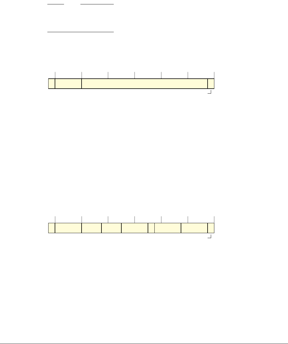
G3 The AArch32 Virtual Memory System Architecture
G3.13 Exception reporting in a VMSAv8-32 implementation
ARM DDI 0487A.a Copyright © 2013 ARM Limited. All rights reserved. G3-3675
ID090413 Non-Confidential - Beta
Except for unconditional T32 instructions reported with CV set to 0, a trapped unconditional instruction is reported
with CV set to 1 and a COND value of
0x0E
, the condition code value for unconditional.
For an implementation that, for both A32 and T32 instructions, takes an exception on a trapped conditional
instruction only if the instruction passes its condition code check, these definitions mean that when CV is set to 1 it
is IMPLEMENTATION DEFINED whether the COND field is set to
0xE
, or to the value of any condition that applied to
the instruction.
Note
In some circumstances, it is IMPLEMENTATION DEFINED whether a conditional instruction that fails its condition
code check generates an Undefined Instruction exception, see Conditional execution of undefined instructions on
page G1-3478.
ISS encoding for trapped
WFI
or
WFE
instruction
This is the exception with EC value
0x01
. When HSR.EC returns this value, the encoding of the ISS field is:
ISS[24:20] See Encoding of ISS[24:20] when HSR[31:30] is 0b00 on page G3-3674.
ISS[19:1] Reserved, UNK/SBZP.
ISS[0] Indicates the trapped instruction. The possible values of this bit are:
0
WFI
trapped.
1
WFE
trapped.
Trapping use of the WFI and WFE instructions on page G1-3511 describes the configuration settings for this trap.
ISS encoding for trapped
MCR
or
MRC
access
These are the exceptions with the following EC values:
•
0x03
, trapped
MRC
or
MCR
access to CP15.
•
0x05
, trapped
MRC
or
MCR
access to CP14.
•
0x08
, trapped
MRC
or
VMRS
access to CP10.
When HSR.EC returns one of these values, the encoding of the ISS field is:
ISS[24:20] See Encoding of ISS[24:20] when HSR[31:30] is 0b00 on page G3-3674.
ISS[19:17] The Opc2 value from the issued instruction.
ISS[16:14] The Opc1 value from the issued instruction.
ISS[13:10] The CRn value from the issued instruction, the coprocessor primary register value.
ISS[9] Reserved, UNK/SBZP.
ISS[8:5] The Rt value from the issued instruction, the general-purpose register used for the transfer.
ISS[4:1] The CRm value from the issued instruction.
ISS[0] Indicates the direction of the trapped instruction. The possible values of this bit are:
0 Write to coprocessor.
MCR
instruction.
1 Read from coprocessor.
MRC
or
VMRS
instruction.
The following sections describe configuration settings for traps that are reported using EC value
0x03
:
•Trapping ID mechanisms on page G1-3506.
24 23 20 19 1 0
CV COND Reserved, UNK/SBZP
Trapped instruction
24 23 20 19 17 16 14 13 10 9 8 5 4 1 0
CV COND Opc2 Opc1 CRn (0) Rt CRm
Direction

G3 The AArch32 Virtual Memory System Architecture
G3.13 Exception reporting in a VMSAv8-32 implementation
G3-3676 Copyright © 2013 ARM Limited. All rights reserved. ARM DDI 0487A.a
Non-Confidential - Beta ID090413
•Trapping accesses to lockdown, DMA, and TCM operations on page G1-3508.
•Trapping accesses to cache maintenance operations on page G1-3509.
•Trapping accesses to TLB maintenance operations on page G1-3509.
•Trapping accesses to the Auxiliary Control Register on page G1-3509.
•Trapping accesses to the Performance Monitors Extension on page G1-3510.
•Trapping CPACR accesses on page G1-3513.
•Generic trapping of accesses to CP15 system control registers on page G1-3513.
The following sections describe configuration settings for traps that are reported using EC value
0x05
:
•ID group 0, Primary device identification registers on page G1-3507.
•Trapping accesses to the T32EE configuration registers on page G1-3511.
•Trapping CP14 accesses to Debug ROM registers on page G1-3514.
•Trapping CP14 accesses to OS-related debug registers on page G1-3515.
•Trapping CP14 accesses to debug registers on page G1-3514.
•Trapping CP14 accesses to trace registers on page G1-3516.
Trapping ID mechanisms on page G1-3506 describes configuration settings for traps that are reported using EC
value
0x08
.
ISS encoding for trapped
MCRR
or
MRRC
access
These are the exceptions with the following EC values:
•
0x04
, trapped
MRRC
or
MCRR
access to CP15.
•
0x0C
, trapped
MRRC
access to CP14.
When HSR.EC returns one of these values, the encoding of the ISS field is:
ISS[24:20] See Encoding of ISS[24:20] when HSR[31:30] is 0b00 on page G3-3674.
ISS[19:16] The Opc1 value from the issued instruction.
ISS[15:14] Reserved, UNK/SBZP.
ISS[13:10] The Rt2 value from the issued instruction, one of the general-purpose registers for the transfer.
ISS[9] Reserved, UNK/SBZP.
ISS[8:5] The Rt value from the issued instruction, one of the general-purpose registers for the transfer.
ISS[4:1] The CRm value from the issued instruction, the coprocessor primary register value.
ISS[0] Indicates the direction of the trapped instruction. The possible values of this bit are:
0 Write to coprocessor.
MCRR
instruction.
1 Read from coprocessor,
MRRC
instruction.
The following sections describe configuration settings for traps that are reported using EC value
0x04
:
•Trapping writes to virtual memory control registers on page G1-3513.
•Generic trapping of accesses to CP15 system control registers on page G1-3513.
The following sections describe configuration settings for traps that are reported using EC value
0x0C
:
•Trapping CP14 accesses to debug registers on page G1-3514.
•Trapping CP14 accesses to Debug ROM registers on page G1-3514.
24 23 20 19 16 15 14 13 10 9 8 5 4 1 0
CV COND Opc1 (0) (0) Rt2 (0) Rt CRm
Direction

G3 The AArch32 Virtual Memory System Architecture
G3.13 Exception reporting in a VMSAv8-32 implementation
ARM DDI 0487A.a Copyright © 2013 ARM Limited. All rights reserved. G3-3677
ID090413 Non-Confidential - Beta
ISS encoding for trapped
LDC
or
STC
access
This is the exception with EC value
0x06
. When HSR.EC returns this value, the encoding of the ISS field is:
ISS[24:20] See Encoding of ISS[24:20] when HSR[31:30] is 0b00 on page G3-3674.
ISS[19:12] imm8. The immediate value from the issued instruction.
ISS[11:9] Reserved, UNK/SBZP.
ISS[8:5] Encoding depends on the instruction form indicated by ISS[3]:
ISS[3]==0 Encodes Rn, the general-purpose register that holds the base address. Applies only to
immediate instruction forms.
ISS[3]==1 UNKNOWN. Applies only to literal instruction forms, that are available only for
LDC
instructions
ISS[4] Indicates whether the offset is added or subtracted:
0 Subtract offset.
1 Add offset.
This bit corresponds to the U bit in the instruction encoding.
ISS[3:1] Addressing mode. The permitted values of this field are:
0b000
Immediate unindexed.
0b001
Immediate post-indexed.
0b010
Immediate offset.
0b011
Immediate pre-indexed.
0b100
Literal unindexed.
LDC
instruction in A32 instruction set only.
For a trapped
STC
instruction or a trapped
LDC
T32 instruction, this encoding is reserved.
0b101
Reserved.
0b110
Literal offset.
LDC
instruction only.
For a trapped
STC
instruction, this encoding is reserved.
0b111
Reserved.
ISS[3] indicates the instruction form, immediate or literal. See the description of ISS[8:5].
ISS[2:1] correspond to the bits {P, W} in the instruction encoding.
ISS[0] Indicates the direction of the trapped instruction. The possible values of this bit are:
0 Write to coprocessor.
STC
instruction.
1 Read from coprocessor,
LDC
instruction.
Note
The only architected uses of these instructions to access CP14 are:
•An
STC
to write to DBGDTRTXint.
•An
LDC
to read DBGDTRTXint.
Offset form
Addressing mode
Direction
xx
24 23 20 19 12 11 9 8 5 4 3 1 0
CV COND imm8 (0) (0) (0) Rn
UNKNOWN
0
1x
Literal instruction, LDC only
Immediate instruction
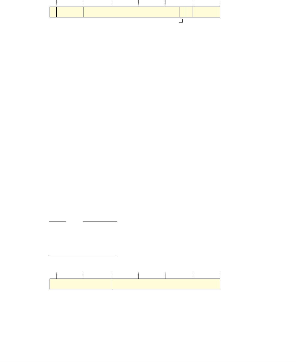
G3 The AArch32 Virtual Memory System Architecture
G3.13 Exception reporting in a VMSAv8-32 implementation
G3-3678 Copyright © 2013 ARM Limited. All rights reserved. ARM DDI 0487A.a
Non-Confidential - Beta ID090413
Trapping general CP14 accesses to debug registers on page G1-3515 describes the configuration settings for the
trap that is reported using EC value
0x06
.
ISS encoding for HCPTR-trapped access to CP10 or CP11
This is the exception with EC value
0x07
. When HSR.EC returns this value, the encoding of the ISS field is:
ISS[24:20] See Encoding of ISS[24:20] when HSR[31:30] is 0b00 on page G3-3674.
ISS[19:6] Reserved, UNK/SBZP.
ISS[5] Indicates trapped use of the Advanced SIMD functionality. The possible values of this bit are:
0 Exception was not caused by trapped use of Advanced SIMD functionality.
1 Exception was caused by trapped use of Advanced SIMD functionality.
Any use of an Advanced SIMD instruction that is trapped to Hyp mode because of a trap configured
in the HCPTR sets this bit to 1.
ISS[4] Reserved, UNK/SBZP.
ISS[3:0] coproc. The number of the coprocessor accessed by the trapped operation, 10 or 11.
This field is valid only when ISS[5] returns 0. Otherwise, it is UNK/SBZP.
Any use of a floating-point instruction or access to a register in the Advanced SIMD and
floating-point register bank that is trapped to Hyp mode because of a trap configured in the HCPTR
sets this field to
0xA
.
The following sections describe the configuration settings for the traps that are reported using EC value
0x07
:
•Trapping of Advanced SIMD functionality on page G1-3512.
•General trapping of coprocessor accesses on page G1-3512
ISS encoding for Hypervisor Call exception, or Supervisor Call exception routed to Hyp mode
These are the exceptions with the following EC values:
•
0x11
, Supervisor Call exception taken to Hyp mode.
•
0x12
, Hypervisor Call exception.
Note
• A Supervisor Call exception is generated by executing an
SVC
instruction, see SVC (previously SWI) on
page F7-2926.
• A Hypervisor Call exception is generated by executing an
HVC
instruction, see HVC on page F7-3040.
When HSR.EC returns one of these values, the encoding of the ISS field is:
ISS[24:16] Reserved, UNK/SBZP.
24 23 20 19 6 5 4 3 0
CV COND Reserved, UNK/SBZP (0) coproc
Trapped Advanced SIMD
24 16 15 0
Reserved, UNK/SBZP imm16
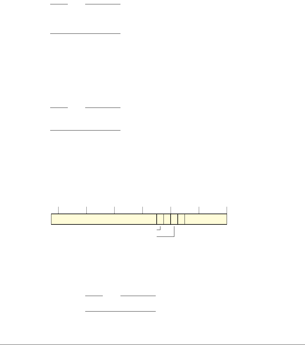
G3 The AArch32 Virtual Memory System Architecture
G3.13 Exception reporting in a VMSAv8-32 implementation
ARM DDI 0487A.a Copyright © 2013 ARM Limited. All rights reserved. G3-3679
ID090413 Non-Confidential - Beta
ISS[15:0] imm16. The value of the immediate field from the issued instruction.
For an
SVC
instruction:
• If the instruction is unconditional:
— For the 16-bit T32 instruction, this field is zero-extended from the imm8 field of the
instruction.
— For the A32 instruction, this field is the bottom 16 bits of the imm24 field of the
instruction.
• If the instruction is conditional, this field is UNKNOWN.
Note
The
HVC
instruction is unconditional, and a conditional
SVC
instruction generates a Supervisor Call exception that is
routed to Hyp mode only if it passes its condition code check. Therefore, the syndrome information for these
exceptions does not include conditionality information.
Supervisor Call exception, when HCR.TGE is set to 1 on page G1-3452 describes the configuration settings for the
trap reported with EC value
0x11
.
ISS encoding for trapped
SMC
execution
This is the exception with EC value
0x13
. When HSR.EC returns this value, the ISS field does not return any
syndrome information, and the encoding of the ISS field is:
ISS[24:0] Reserved, UNK/SBZP.
Note
SMC
instructions cannot be trapped if they fail their condition code check. Therefore, the syndrome information for
this exception does not include conditionality information.
Trapping use of the SMC instruction on page G1-3510 describes the configuration settings for this trap, for
instructions executed in Non-secure PL1 modes.
ISS encoding for Prefetch Abort exceptions taken to Hyp mode
These are the exceptions with the following EC values:
•
0x20
, for a Prefetch Abort exception taken from a mode other than Hyp mode and routed to Hyp mode.
•
0x21
, for a Prefetch Abort exception taken from Hyp mode.
When HSR.EC returns one of these values, the encoding of the ISS field is:
ISS[24:10] Reserved, UNK/SBZP.
ISS[9] EA, External abort type. Can provide an IMPLEMENTATION DEFINED classification of external
aborts. If the implementation does not provide any classification of external aborts, this bit is
UNK/SBZP.
For any abort other than an External abort this bit returns a value of 0.
Note
This bit is equivalent to the IFSR.ExT bit.
ISS[8] Reserved, UNK/SBZP.
EA
24 10 9 8 7 6 5 0
Reserved, UNK/SBZP (0) (0) IFSC
S1PTW
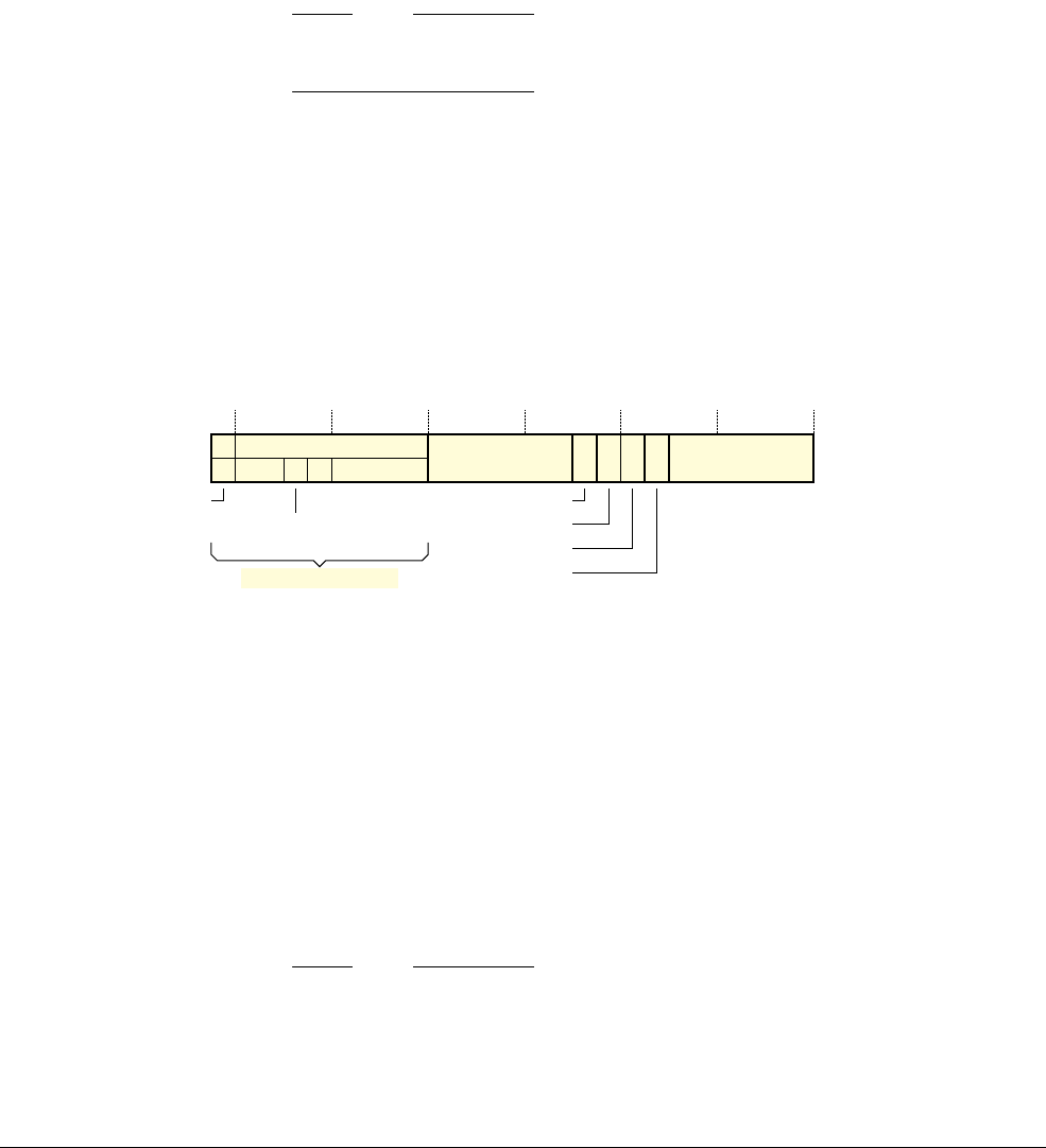
G3 The AArch32 Virtual Memory System Architecture
G3.13 Exception reporting in a VMSAv8-32 implementation
G3-3680 Copyright © 2013 ARM Limited. All rights reserved. ARM DDI 0487A.a
Non-Confidential - Beta ID090413
ISS[7] S1PTW. For a stage 2 fault, indicates whether the fault was a fault on the stage 2 translation of an
address accessed during a stage 1 translation table walk:
0 Fault not on a stage 2 translation for a stage 1 translation table walk.
1 Fault on the stage 2 translation of an access for a stage 1 translation table walk.
For a stage 1 fault, this bit is UNK/SBZP.
ISS[6] Reserved, UNK/SBZP.
ISS[5:0] IFSC, Instruction fault status code. Indicates the fault that caused the exception, using the fault
codes defined for use with the Long-descriptor translation table format, see PL1 fault reporting with
the Long-descriptor translation table format on page G3-3665.
Note
This field is equivalent to the IFSR.STATUS field, and only valid IFSR.STATUS values are valid
for this field.
The following sections describe cases where Prefetch Abort exceptions can be routed to Hyp mode, generating
exceptions that are reported in the HSR with EC value
0x20
:
•External abort, when HCR.TGE is set to 1 on page G1-3453.
•Routing Debug exceptions to Hyp mode on page G1-3454.
ISS encoding for Data Abort exceptions taken to Hyp mode
These are the exceptions with the following EC values:
•
0x24
, for a Data Abort exception taken from a mode other than Hyp mode and routed to Hyp mode.
•
0x25
, for a Data Abort exception taken from Hyp mode.
When HSR.EC returns one of these values, the encoding of the ISS field is:
ISS[24] Instruction syndrome valid. Indicates whether ISS[24:16] provide a valid instruction syndrome, as
part of the returned ISS. The possible values of this bit are:
0 No valid instruction syndrome. ISS[23:16] are UNK/SBZP.
1 ISS[24:16] hold a valid instruction syndrome.
This bit is 0 for all faults except for those generated by a stage 2 translation. For Data Abort
exceptions generated by a stage 2 translation, this bit is 1 and a valid instruction syndrome is
returned only if all of the following are true:
• The instruction that generated the Data Abort exception:
—Is an
LDR
,
LDRT
,
LDRSH
,
LDRSHT
,
LDRH
,
LDRHT
,
LDRSB
,
LDRSBT
,
LDRB
,
LDRBT
,
STR
,
STRT
,
STRH
,
STRHT
,
STRB
, or
STRBT
.
— Is not performing register writeback.
— Is not using the PC as its destination register.
Note
• For ISS reporting, a stage 2 abort on a stage 1 translation table lookup is treated as a stage 1
Translation fault, and does not return a valid instruction syndrome.
• In the A32 instruction set,
LDR*T
and
STR*T
instructions always perform register writeback and
therefore never return a valid instruction syndrome.
ISV
(0)
24 23 20 19 18 17 16 15 10 9 8 7 6 5 0
1 SAS SRT
0 Reserved, UNK/SBZP Reserved,
UNK/SBZP DFSC
22 21
SSE
Instruction syndrome
EA
CM
S1PTW
WnR

G3 The AArch32 Virtual Memory System Architecture
G3.13 Exception reporting in a VMSAv8-32 implementation
ARM DDI 0487A.a Copyright © 2013 ARM Limited. All rights reserved. G3-3681
ID090413 Non-Confidential - Beta
• A valid instruction syndrome provides information that can help a hypervisor to emulate the
instruction efficiently. Instruction syndromes are returned for instructions for which such
accelerated emulation is possible.
ISS[23:16], when ISS[24] is 0
Reserved, UNK/SBZP.
ISS[23:16], when ISS[24] is 1
The remainder of the valid instruction syndrome, defined as follows:
ISS[23:22] SAS, Syndrome access size. Indicate the size of the access attempted by the faulted
operation. The possible values of this field are:
0b00
Byte.
0b01
Halfword.
0b10
Word.
0b11
Reserved.
ISS[21] SSE, Syndrome sign extend. For a byte or halfword load operation, indicates whether
the data item must be sign extended. For these cases, the possible values of this bit are:
0 Sign-extension not required.
1 Data item must be sign-extended.
For all other operations this bit is 0.
ISS[20] Reserved, UNK/SBZP.
ISS[19:16] SRT, Syndrome Register Transfer. The value of the Rt operand of the faulting
instruction. This specifies:
• The destination register for a load operation.
• The source register for a store operation.
Note
Normally, software emulating an instruction must consider both the Rt value and the
Mode value saved in the SPSR, to determine the physical register to access.
ISS[15:10] Reserved, UNK/SBZP.
ISS[9] EA, External abort type. Can provide an IMPLEMENTATION DEFINED classification of external
aborts. If the implementation does not provide any classification of external aborts, this bit is
UNK/SBZP.
For any abort other than an External abort this bit returns a value of 0.
Note
This bit is equivalent to the DFSR.ExT bit.
ISS[8] CM, Cache maintenance. For a synchronous fault, identifies fault that comes from a cache
maintenance or address translation operation. For synchronous faults, the possible values of this bit
are:
0 Fault not generated by a cache maintenance or address translation operation.
1 Fault generated by a cache maintenance or address translation operation.
For asynchronous faults, this bit is 0.
Note
This bit is equivalent to the DFSR.CM bit.

G3 The AArch32 Virtual Memory System Architecture
G3.13 Exception reporting in a VMSAv8-32 implementation
G3-3682 Copyright © 2013 ARM Limited. All rights reserved. ARM DDI 0487A.a
Non-Confidential - Beta ID090413
ISS[7] S1PTW. For a stage 2 fault, indicates whether the fault was a fault on the stage 2 translation of an
address accessed during a stage 1 translation table walk:
0 Fault not on a stage 2 translation for a stage 1 translation table walk.
1 Fault on the stage 2 translation of an access for a stage 1 translation table walk.
For a stage 1 fault, this bit is UNK/SBZP.
ISS[6] WnR. Indicates whether a synchronous abort was caused by a write or a read operation. The possible
values of this bit are:
0 Abort caused by a read operation.
1 Abort caused by a write operation.
For synchronous faults on cache maintenance and address translation operations, this bit always
returns a value of 1.
Note
ISS[8] is set to 1 to identify a fault on a cache maintenance or address translation operation.
For an asynchronous Data Abort exception this bit is UNKNOWN.
Note
This bit is equivalent to the DFSR.WnR bit.
ISS[5:0] DFSC, Data fault status code. Indicates the fault that caused the exception, using the fault codes
defined for use with the Long-descriptor translation table format, see PL1 fault reporting with the
Long-descriptor translation table format on page G3-3665.
Note
This field is equivalent to the DFSR.STATUS field, and all valid DFSR.STATUS values are valid
for this field.
The following describe cases where Data Abort exceptions can be routed to Hyp mode, generating exceptions that
are reported in the HSR with EC value
0x24
:
•MMU fault, when HCR.TGE is set to 1 on page G1-3453.
•External abort, when HCR.TGE is set to 1 on page G1-3453.
•Routing Debug exceptions to Hyp mode on page G1-3454.
G3.13.7 Summary of register updates on exceptions taken to Hyp mode
For memory system faults that generate exceptions that are taken to Hyp mode, Table G3-33 on page G3-3683
shows the registers affected by each fault. In this table:
• Yes indicates that the register is updated.
•UNK indicates that the fault makes the register value UNKNOWN.
• A null entry, -, indicates that the fault does not affect the register.

G3 The AArch32 Virtual Memory System Architecture
G3.13 Exception reporting in a VMSAv8-32 implementation
ARM DDI 0487A.a Copyright © 2013 ARM Limited. All rights reserved. G3-3683
ID090413 Non-Confidential - Beta
Table G3-33 Effect of an exception taken to Hyp mode on the reporting registers
Fault HSR HIFAR HDFAR HPFAR
Faults reported as Prefetch Abort exceptions:
Address translation faulta at stage 1. Yes Yes UNK UNK
Address translation or Access flag faulta at stage 2. Yes Yes UNK Yes
Address translation faulta at stage 2. Yes Yes UNK UNK
Address translation stage 2 faulta on stage 1 translation. Yes Yes UNK Yes
Synchronous external abort on translation table walk. Yes Yes UNK UNK
Synchronous parity error on translation table walk. Yes Yes UNK UNK
Synchronous external abort. Yes Yes UNK UNK
Synchronous parity error on memory access. Yes Yes UNK UNK
TLB conflict abort. Yes Yes UNK UNK
Fault reported as Data Abort exception:
Alignment fault, always synchronous Yes UNK Yes UNK
Address translation faulta at stage 1. Yes UNK Yes UNK
Address translation Translation or Access flag faulta at stage 2. Yes UNK Yes Yes
Address translation Permission faulta at stage 2. Yes UNK Yes UNK
Address translation stage 2 faulta on stage 1 translation. Yes UNK Yes Yes
Synchronous external abort on translation table walk. Yes UNK Yes UNK
Synchronous parity error on translation table walk. Yes UNK Yes UNK
Synchronous external abort. Yes UNK Yes UNK
Synchronous parity error on memory access. Yes UNK Yes UNK
Asynchronous external abort. Yes UNK UNK UNK
Asynchronous parity error on memory access. Yes UNK UNK UNK
TLB conflict abort. Yes UNK Yes UNK
Debug exception:
Software Breakpoint Instructionb, generates a Prefetch Abort
exception.
Yes UNK -UNK
Debug exception routed to Hyp mode because HDCR.TDE is set to 1. Generates a Hyp Trap exception.
Breakpoint Software Breakpoint Instruction or Vector Catch Yes UNK -UNK
Watchpoint Yes - Yes UNK
a. For more information see Classification of MMU faults taken to Hyp mode on page G3-3684
b. All other debug exceptions are not permitted in Hyp mode.

G3 The AArch32 Virtual Memory System Architecture
G3.13 Exception reporting in a VMSAv8-32 implementation
G3-3684 Copyright © 2013 ARM Limited. All rights reserved. ARM DDI 0487A.a
Non-Confidential - Beta ID090413
Note
Unlike Table G3-29 on page G3-3667, the Hyp mode fault reporting table does not include an entry for a fault on
an instruction cache maintenance operation. That is because, when the fault is taken to Hyp mode, the reporting
indicates the cause of the fault, for example a Translation fault, and ISS.CM is set to 1 to indicate that the fault was
on a cache maintenance operation, see ISS encoding for Data Abort exceptions taken to Hyp mode on page G3-3680.
Classification of MMU faults taken to Hyp mode
This subsection gives more information about the MMU faults shown in Table G3-33 on page G3-3683.
Note
All MMU faults are synchronous.
The table uses the following descriptions for MMU faults taken to Hyp mode:
Address translation fault at stage 1
This is an address translation fault generated on a stage 1 translation performed in the Non-secure
PL2 translation regime.
Address translation fault at stage 2
This is an address translation fault generated on a stage 2 translation performed in the Non-secure
PL1&0 translation regime.
As the table shows, for the faults in this group:
• Translation and Access flag faults update the HPFAR
• Permission faults leave the HPFAR UNKNOWN.
Address translation stage 2 fault on a stage 1 translation
This is an address translation fault generated on the stage 2 translation of an address accessed in a
stage 1 translation table walk performed in the Non-secure PL1&0 translation regime. For more
information about these faults see Stage 2 fault on a stage 1 translation table walk on page G3-3654.
Figure G3-1 on page G3-3563 shows the different translation regimes and associated stages of translation.

G3 The AArch32 Virtual Memory System Architecture
G3.14 Virtual Address to Physical Address translation operations
ARM DDI 0487A.a Copyright © 2013 ARM Limited. All rights reserved. G3-3685
ID090413 Non-Confidential - Beta
G3.14 Virtual Address to Physical Address translation operations
The system register space includes operations for Virtual Address (VA) to Physical Address (PA) translation.
Address translation operations, functional group on page G3-3745 summarizes these operations.
When using the Short-descriptor translation table format, all VA to PA translations take account of TEX remap
when this is enabled, see Short-descriptor format memory region attributes, with TEX remap on page G3-3620.
A VA to PA translation operation returns the PA in the PAR. This is a 64-bit register, that can hold PAs of up to 40
bits.
The following sections give more information about these operations:
•Naming of the address translation operations, and operation summary.
•Encoding and availability of the address translation operations on page G3-3687.
•Determining the PAR format on page G3-3688.
•Handling of faults and aborts during an address translation operation on page G3-3688.
G3.14.1 Naming of the address translation operations, and operation summary
Some older documentation uses the original names for the Address translation operations that were included in the
original ARMv7 documentation. Table G3-34 summarizes the operations that are available in AArch32 state, and
relates the old operation names to the current names.
In an implementation that does not include EL2, there is no distinction between stage 1 translations and stage 1 and
2 combined translations.
In the stage 1 current state and stages 1 and 2 Non-secure state only operations, the meanings of the last two letters
of the names are:
PR PL1 mode, read operation.
PW PL1 mode, write operation.
UR User mode, read operation.
UW User mode, write operation.
Note
User mode can be described as an unprivileged mode. It is the only PL0 mode.
In the stage 1 Hyp mode operations, the last letter of the operation name is R for the read operation and W for the
write operation.
The following sections describe the use and availability of these operations:
•Address translation stage 1, current security state on page G3-3686.
•Address translation stages 1 and 2, Non-secure state only on page G3-3686.
•Address translation stage 1, Hyp mode on page G3-3686.
Table G3-34 Naming of address translation operations
Name Old name Description
ATS1CPR, ATS1CPW,
ATS1CUR, ATS1CUW V2PCWPR, V2PCWPW,
V2PCWUR, V2PCWUW See Address translation stage 1, current security state on
page G3-3686
ATS12NSOPR, ATS12NSOPW,
ATS12NSOUR, ATS12NSOUW V2POWPR, V2POWPW,
V2POWUR, V2POWUW See Address translation stages 1 and 2, Non-secure state only on
page G3-3686
ATS1HR, ATS1HW Not applicableaSee Address translation stage 1, Hyp mode on page G3-3686
a. Operations are part of EL2 and have no equivalent in the older descriptions.

G3 The AArch32 Virtual Memory System Architecture
G3.14 Virtual Address to Physical Address translation operations
G3-3686 Copyright © 2013 ARM Limited. All rights reserved. ARM DDI 0487A.a
Non-Confidential - Beta ID090413
Encoding and availability of the address translation operations on page G3-3687 gives the encodings of the
operations.
Address translation stage 1, current security state
These are the ATS1Cxx operations. Any VMSAv8-32 implementation supports these operations. They can be
executed by any software executing at PL1 or higher, in either Security state.
These instructions perform the address translations of the PL1&0 translation regime.
In an implementation that includes EL2, when executed in Non-secure state, these operations return the IPA that is
the output address of the stage 1 translation. Figure G3-1 on page G3-3563 shows the different translation regimes.
Note
The Non-secure PL1 and PL0 modes have no visibility of the stage 2 address translations, that can be defined only
at PL2, and translate IPAs to be PAs.
See Determining the PAR format on page G3-3688 for the format used when returning the result of these operations.
Address translation stages 1 and 2, Non-secure state only
These are the ATS12NSOxx operations. A VMSAv8-32 implementation supports these operations only if it includes
EL2. In an implementation that includes EL2, in AArch32 state, they can be executed:
• If the implementation includes EL3, by any software executing in Secure state at PL1.
• If the implementation includes EL2, by software executing in Non-secure state at PL2. This means by
software executing in Hyp mode.
In an implementation that does not include EL2, but includes EL3, when EL3 is using AArch32 these instructions
are not undefined but each instruction behaves in the same way as the equivalent ATSIC* instruction.
ARM deprecates use of these operations from any Secure PL1 mode other than Monitor mode.
In Secure state and in Non-secure Hyp mode these operations perform the translations made by the Non-secure
PL1&0 translation regime.
These operations always return the PA and final attributes generated by the translation.That is, for an
implementation that includes EL2, they return:
• The result of the two stages of address translation for the specified Non-secure input address.
• The memory attributes obtained by the combination of the stage 1 and stage 2 attributes.
Note
From Hyp mode, the ATS1Cxx and ATS12NSOxx operations both return the results of address translations that
would be performed in the Non-secure modes other than Hyp mode. The difference is:
• The ATS1Cxx operations return the Non-secure PL1 view of these operations. That is, they return the IPA
output address corresponding to the VA input address.
• The ATS12NSOxx operations return the EL2, or Hyp mode, view of these operations. That is, they return the
PA output address corresponding to the VA input address, generated by two stages of translation.
See Determining the PAR format on page G3-3688 for the format used when returning the result of these operations.
Address translation stage 1, Hyp mode
These are the ATS1Hx operations. A VMSAv8-32 implementation supports these operations only if it includes EL2.
They can be executed by:
• Software executing in Non-secure state at PL2. This means by software executing in Hyp mode.
• Software executing in Secure state in Monitor mode.

G3 The AArch32 Virtual Memory System Architecture
G3.14 Virtual Address to Physical Address translation operations
ARM DDI 0487A.a Copyright © 2013 ARM Limited. All rights reserved. G3-3687
ID090413 Non-Confidential - Beta
These operations are UNPREDICTABLE if used in a Secure PL1 mode other than Monitor mode.
These operations perform the translations made by the Non-secure EL2 translation regime. The operation takes a
VA input address and returns a PA output address.
These operations always return a result in a 64-bit format PAR.
G3.14.2 Encoding and availability of the address translation operations
Software executing at PL0 never has any visibility of the address translation operations, but software executing at
PL1 or higher can use the unprivileged address translation operations to find the address translations used for
memory accesses by software executing at PL0 and PL1.
Note
For information about translations when the stage of address translation is disabled see The effects of disabling
address translation stages on VMSAv8-32 behavior on page G3-3569.
Table G3-35 shows the encodings for the address translation operations, and their availability in different
implementations in different PE modes and states.
The result of an operation is always returned in the PAR. The PAR is a RW register and:
• In all implementations, the 32-bit format PAR is accessed using an
MCR
or
MRC
instruction with CRn set to c7,
CRm set to c4, and opc1 and opc2 both set to 0.
• The 64-bit format PAR is accessed using an
MCRR
or
MRRC
instruction with CRm set to c7, and opc1 set to 0.
Table G3-35 Address translation operations in AArch32 state
opc1 CRm opc2 Name Type Description
All VMSAv8-32 implementations, in all modes, at PL1 or higher
0c80ATS1CPR WO PL1 stage 1 read translation, current statea
1ATS1CPW WO PL1 stage 1 write translation, current statea
2ATS1CUR WO Unprivileged stage 1 read translation, current statea
3ATS1CUW WO Unprivileged stage 1 write translation, current statea
Implementations that include EL2, in Non-secure Hyp mode and Secure PL1 modes
0c84ATS12NSOPR WO Non-secure PL1 stage 1 and 2 read translationb
5ATS12NSOPW WO Non-secure PL1 stage 1 and 2 write translationb
6ATS12NSOUR WO Non-secure unprivileged stage 1 and 2 read translationb
7ATS12NSOUW WO Non-secure unprivileged stage 1 and 2 write translationb
Implementations that include EL2, in Non-secure Hyp mode and Secure Monitor mode
4c80ATS1HR WO Hyp mode stage 1 read translation c
1ATS1HW WO Hyp mode stage 1 write translationc
a. For more information about these operations see Address translation stage 1, current security state on page G3-3686.
b. For more information about these operations see Address translation stages 1 and 2, Non-secure state only on page G3-3686.
c. For more information about these operations see Address translation stage 1, Hyp mode on page G3-3686.

G3 The AArch32 Virtual Memory System Architecture
G3.14 Virtual Address to Physical Address translation operations
G3-3688 Copyright © 2013 ARM Limited. All rights reserved. ARM DDI 0487A.a
Non-Confidential - Beta ID090413
Address translation operations that are not available in a particular implementation are reserved and
UNPREDICTABLE. For example, in an implementation that does not include EL3, the encodings with opc2 values of
4-7, and the encodings with an opc1 value of 4, are reserved and UNPREDICTABLE.
G3.14.3 Determining the PAR format
The PAR is a 64-bit register, that supports both 32-bit and 64-bit PAR formats. This section describes how the PAR
format is determined, for returning a result from each of the groups of address translation operations. The returned
result might be the translated address, or might indicate a fault on the translation, see Handling of faults and aborts
during an address translation operation.
ATS1Cxx operations
Address translations for the current state. From modes other than Hyp mode:
•TTBCR.EAE determines whether the result is returned using the 32-bit or the 64-bit PAR
format.
• If the implementation includes EL3, the translation performed is for the current security state
and, depending on that state:
— The Secure or Non-secure TTBCR.EAE determines the PAR format.
— The result is returned to the Secure or Non-secure instance of the PAR
Operations from Hyp mode always return a result to the Non-secure PAR, using the 64-bit format.
ATS12NSOxx operations
Address translations for the Non-secure PL1 and PL0 modes. These operations return a result using
the 64-bit PAR format if at least one of the following is true:
• The Non-secure TTBCR.EAE bit is set to 1.
• The implementation includes EL2, and the value of HCR.VM is 1.
Otherwise, the operation returns a result using the 32-bit PAR format.
Operations from a Secure PL1 mode return a result to the Secure PAR. Operations from Hyp mode
return a result to the Non-secure PAR.
ATS1Hx operations
Address translations from Hyp mode. These operations always return a result using the 64-bit PAR
format.
Operations from Secure Monitor mode return a result to the Secure PAR. Operations from
Non-secure Hyp mode return a result to the Non-secure PAR.
G3.14.4 Handling of faults and aborts during an address translation operation
When a stage of address translation is enabled, any corresponding address translation operation requires a
translation table lookup, and this might require a translation table walk. However, the input address for the
translation might be a faulting address, either because:
• The translation table entries used for the translation indicate a fault.
• A stage 2 fault or an external abort occurs on the required translation table walk.
VMSAv8-32 memory aborts on page G3-3647 describes the faults that might occur on a translation table walk in
AArch32 state.
How the fault is handled, and whether it generates an exception, depends on the cause of the fault, as described in:
•MMU fault on an address translation operation on page G3-3689.
•External abort during an address translation operation on page G3-3689.
•Stage 2 fault on a current state address translation operation on page G3-3690.

G3 The AArch32 Virtual Memory System Architecture
G3.14 Virtual Address to Physical Address translation operations
ARM DDI 0487A.a Copyright © 2013 ARM Limited. All rights reserved. G3-3689
ID090413 Non-Confidential - Beta
MMU fault on an address translation operation
In the following cases, an MMU fault on an address translation is reported in the PAR, and no abort is taken. This
applies:
• For a faulting address translation operation executed in Hyp mode, or in a Secure PL1 mode.
• For a faulting address translation operation executed in a Non-secure PL1 mode, for cases where the fault
would generate a stage 1 abort if it occurred on the on the equivalent load or store operation.
Using the PAR to report a fault on an address translation operation gives more information about how these faults
are reported.
Note
• The Domain fault encodings shown in Table G3-27 on page G3-3665 are used only for reporting a fault on
an address translation operation that uses the 64-bit PAR format. That is, they are used only in an
implementation that includes EL2, and are used for reporting a Domain fault on either:
— An ATS1Cxx operation from Hyp mode.
— An ATS12NSOxx operation when HCR.VM is set to 1.
These encodings are never used for fault reporting in the DFSR, IFSR, or HSR.
• For an address translation operation executed in a Non-secure PL1 mode, for a fault that would generate a
stage 2 abort if it occurred on the equivalent load or store operation, the stage 2 abort is generated as described
in Stage 2 fault on a current state address translation operation on page G3-3690.
Using the PAR to report a fault on an address translation operation
For a fault on an address translation operation for which no abort is taken, the PAR is updated with the following
information, to indicate the fault:
• The fault code, that would normally be written to the Fault status register. The code used depends on the
current translation table format, as described in either:
—PL1 fault reporting with the Short-descriptor translation table format on page G3-3663.
—PL1 fault reporting with the Long-descriptor translation table format on page G3-3665.
See also the Note at the start of Determining the PAR format on page G3-3688 about the Domain fault
encodings shown in Table G3-27 on page G3-3665.
• A status bit, that indicates that the translation operation failed.
The fault does not update any Fault Address Register.
External abort during an address translation operation
As stated in External abort on a translation table walk on page G3-3657, an external abort on a translation table
walk generates a Data Abort exception. The abort can be synchronous or asynchronous, and behaves as follows:
Synchronous external abort on a translation table walk
The fault status and fault address registers of the Security state to which the abort is taken are
updated. The fault status register indicates the appropriate external abort on a Translation fault, and
the fault address register indicates the input address for the translation.
The PAR is UNKNOWN.
Asynchronous external abort on a translation table walk
The fault status register of the Security state to which the abort is taken is updated, to indicate the
asynchronous external abort. No fault address registers are updated.
The PAR is UNKNOWN.

G3 The AArch32 Virtual Memory System Architecture
G3.14 Virtual Address to Physical Address translation operations
G3-3690 Copyright © 2013 ARM Limited. All rights reserved. ARM DDI 0487A.a
Non-Confidential - Beta ID090413
Stage 2 fault on a current state address translation operation
If the PE is in a Non-secure PL1 mode and performs one of the ATS1C** operations, then a fault in the stage 2
translation of an address accessed in a stage 1 translation table lookup generates an exception. This is equivalent to
the case described in Stage 2 fault on a stage 1 translation table walk on page G3-3654. When this fault occurs on
an ATS1C** address translation operation:
• A Hyp Trap exception is taken to Hyp mode.
• The PAR is UNKNOWN.
• The HSR indicates that:
— The fault occurred on a translation table walk.
— The operation that faulted was a cache maintenance operation.
• The HPFAR holds the IPA that faulted.
• The HDFAR holds the VA that the executing software supplied to the address translation operation.

G3 The AArch32 Virtual Memory System Architecture
G3.15 About the System registers for VMSAv8-32
ARM DDI 0487A.a Copyright © 2013 ARM Limited. All rights reserved. G3-3691
ID090413 Non-Confidential - Beta
G3.15 About the System registers for VMSAv8-32
In AArch32 state, the System registers comprise:
• The registers accessed using the System Control Coprocessor interface, CP15.
• Registers accessed using the CP14 coprocessor interface, including:
— Debug registers.
— Trace registers.
— Legacy execution environment registers.
Organization of the CP14 registers in VMSAv8-32 on page G3-3713 summarizes the CP14 registers, and indicates
where the CP14 registers are described, either in this manual or in other architecture specifications.
Organization of the CP15 registers in VMSAv8-32 on page G3-3716 summarizes the CP15 registers, and indicates
where in this manual the CP15 registers are described.
This section gives general information about the control registers, the CP14 and CP15 interfaces to these registers,
and the conventions used in describing these registers.
Note
Many implementations include other interfaces to some functional groups of CP14 and CP15 registers, for example
memory-mapped interfaces to the CP14 Debug registers. These are described in the appropriate sections of this
manual.
This section is organized as follows:
•About System register accesses.
•General behavior of System registers on page G3-3693.
•Classification of System registers on page G3-3696.
•Synchronization of changes to System registers on page G3-3706.
•Meaning of fixed bit values in register diagrams on page G3-3711.
G3.15.1 About System register accesses
Most AArch32 System registers are 32 bits wide. Accessing 32-bit control registers on page G3-3692 describes how
these registers are accessed.
A small number of the AArch32 System registers are 64 bits wide. Accessing 64-bit control registers on
page G3-3692 describes how these registers are accessed.
When using the
MCR
,
MRC
,
MCRR
, and
MRRC
instructions to access these registers, the instruction arguments include:
• A coprocessor identifier, coproc, as a value p0-p15, corresponding to CP0-CP15.
• A coprocessor register, CRn or CRm, as a value c0-c15, to specify a coprocessor register number.
• An opcode, opc1 or opc2, as a value in the range 0-7.
Note
• When accessing CP15, the primary coprocessor register is the top-level indicator of the accessed
functionality, and when:
—Using an
MCR
or
MRC
instruction, CRn specifies the primary coprocessor register.
—Using an
MCRR
or
MRRC
instruction, CRm specifies the primary coprocessor register.
• When accessing CP14 using any of these instructions, opc1 is the top-level indicator of the accessed
functionality.

G3 The AArch32 Virtual Memory System Architecture
G3.15 About the System registers for VMSAv8-32
G3-3692 Copyright © 2013 ARM Limited. All rights reserved. ARM DDI 0487A.a
Non-Confidential - Beta ID090413
Ordering of reads of System registers
Reads of the System registers can occur out of order with respect to earlier instructions executed on the same PE,
provided that the data dependencies between the instructions, specified in Synchronization of changes to System
registers on page G3-3706, are met.
Note
In particular, System registers holding self-incrementing counts, for example the Performance Monitors counters or
the Generic Timer counter or timers, can be read early. This means that, for example, if a memory communication
is used to communicate a read of the Generic Timer counter, an
ISB
must be inserted between the read of the memory
location used for this communication and the read of the Generic Timer counter if it is required that the Generic
Timer counter returns a count value that is later than the memory communication.
Accessing 32-bit control registers
Software accesses a 32-bit control register using the generic
MCR
and
MRC
coprocessor interface, specifying:
• A coprocessor identifier, coproc, identifying a valid coprocessor, CP14 or CP15.
• Two coprocessor registers, CRn and CRm. CRn specifies the primary coprocessor register.
• Two coprocessor-specific opcodes, opc1 and opc2.
• A general-purpose register to hold a 32-bit value to transfer to or from the coprocessor.
CP15 and CP14 provides the control registers. A PE access to a specific 32-bit control register uses:
• p15 to specify CP15, or p14 to specify CP14.
• A unique combination of CRn, opc1, CRm, and opc2, to specify the required control register.
• A general-purpose register for the transferred 32-bit value.
The PE accesses a 32-bit control register using:
•An
MCR
instruction to write to a control register, see MCR, MCR2 on page F7-2700.
•An
MRC
instruction to read a control register, see MCR, MCR2 on page F7-2700.
Accessing 64-bit control registers
Software accesses a 64-bit control register using the generic
MCRR
and
MRRC
coprocessor interface, specifying:
• A coprocessor identifier, coproc, identifying a valid coprocessor, CP14 or CP15.
• A coprocessor register, CRm. In this case, CRm specifies the primary coprocessor register.
• A single coprocessor-specific opcode, opc1.
• Two general-purpose registers to hold two 32-bit values to transfer to or from the coprocessor.
CP15 and CP14 provide the control registers. A PE access to a specific 64-bit System register uses:
• p15 to specify CP15, or p14 to specify CP14.
• A unique combination of CRm and opc1, to specify the required 64-bit System register.
• Two general-purpose registers, each holding 32 bits of the value to transfer.
Therefore, PE accesses a 64-bit control register using:
•An
MCRR
instruction to write to a control register, see MCRR, MCRR2 on page F7-2702.
•An
MRRC
instruction to read a control register, see MCRR, MCRR2 on page F7-2702.
When using a
MCRR
or
MRRC
instruction:
• Rt contains the least-significant 32 bits of the transferred value, and Rt2 contains the most-significant 32 bits
of that value.
• The access is 64-bit atomic.

G3 The AArch32 Virtual Memory System Architecture
G3.15 About the System registers for VMSAv8-32
ARM DDI 0487A.a Copyright © 2013 ARM Limited. All rights reserved. G3-3693
ID090413 Non-Confidential - Beta
Some 64-bit registers also have an
MCR
and
MRC
encoding. The
MCR
and
MRC
encodings for these registers access the
least significant 32 bits of the register. For example, to access the PAR, software can:
• Use the following instructions to access all 64 bits of the register:
MRRC p15, 0, <Rt>, <Rt2>, c7 ; Read 64-bit PAR into Rt (low word) and Rt2 (high word)
MCRR p15, 0, <Rt>, <Rt2>, c7 ; Write Rt (low word) and Rt2 (high word) to 64-bit PAR
• Use the following instructions to access the least-significant 32 bits of the register:
MRC p15, 0, <Rt>, c7, c4, 0 ; Read PAR[31:0] into Rt
MCR p15, 0, <Rt>, c7, c4, 0 ; Write Rt to PAR[31:0]
G3.15.2 General behavior of System registers
Except where indicated, System registers are 32-bits wide. As stated in About System register accesses on
page G3-3691, there are some 64-bit registers, and these include cases where software can access either a 32-bit
view or a 64-bit view of a register. The register summaries, and the individual register descriptions, identify the
64-bit registers and how they can be accessed.
The following sections give information about the general behavior of these registers. Unless otherwise indicated,
information applies to both CP14 and CP15 registers:
•Read-only bits in read/write registers.
•UNPREDICTABLE and UNDEFINED behavior for CP14 and CP15 accesses.
•Read-only and write-only register encodings on page G3-3695.
•Reset behavior of CP14 and CP15 registers on page G3-3695.
See also About System register accesses on page G3-3691 and Meaning of fixed bit values in register diagrams on
page G3-3711.
Read-only bits in read/write registers
Some read/write registers include bits that are read-only. These bits ignore writes.
An example of this is the SCTLR.NMFI bit, SCTLR[27].
UNPREDICTABLE and UNDEFINED behavior for CP14 and CP15 accesses
In AArch32 state the following operations are UNDEFINED:
•All
CDP
,
LDC
and
STC
operations to CP14 and CP15, except for the
LDC
access to DBGDTRTXint and the
STC
access to DBGDTRTXint specified in Table G3-45 on page G3-3714.
•All
MCRR
and
MRRC
operations to CP14 and CP15, except for those explicitly defined as accessing 64-bit CP14
and CP15 registers.
•All
CDP2
,
MCR2
,
MRC2
,
MCRR2
,
MRRC2
,
LDC2
and
STC2
operations to CP14 and CP15.
Unless otherwise indicated in the individual register descriptions:
• Reserved fields in registers are RES0.
• Assigning a reserved value to a field can have an UNPREDICTABLE effect.
The following subsections give more information about UNPREDICTABLE and UNDEFINED behavior for CP14 and
CP15 accesses:
•Accesses to unallocated CP14 and CP15 encodings.
•Additional rules for MCR and MRC accesses to CP14 and CP15 registers on page G3-3694.
•Effects of EL3 and EL2 on CP15 register accesses on page G3-3694.
Accesses to unallocated CP14 and CP15 encodings
In ARMv8-A, accesses to unallocated CP14 and CP15 register encodings are UNDEFINED.

G3 The AArch32 Virtual Memory System Architecture
G3.15 About the System registers for VMSAv8-32
G3-3694 Copyright © 2013 ARM Limited. All rights reserved. ARM DDI 0487A.a
Non-Confidential - Beta ID090413
Additional rules for MCR and MRC accesses to CP14 and CP15 registers
All
MCR
operations from the PC are UNPREDICTABLE for all coprocessors, including for CP14 and CP15.
All
MRC
operations to APSR_nzcv are UNPREDICTABLE for CP14 and CP15, except for the CP14
MRC
operation to
APSR_nzcv from DBGDSCRint.
For registers and operations that are accessible from a particular Privilege level, any attempt to access those registers
from a lower Privilege level is UNDEFINED.
Some individual registers can be made inaccessible by setting configuration bits, possibly including
IMPLEMENTATION DEFINED configuration bits, to disable access to the register. The effects of the
architecturally-defined configuration bits are defined individually in this manual. Unless explicitly stated otherwise
in this manual, setting a configuration bit to disable access to a register results in the register becoming UNDEFINED
for
MRC
and
MCR
accesses.
See also Read-only and write-only register encodings on page G3-3695.
Effects of EL3 and EL2 on CP15 register accesses
EL2 and EL3 introduce classes of System registers, described in Classification of System registers on
page G3-3696. Some of these classes of register are either:
• Accessible only from certain modes or states.
• Accessible from certain modes or states only when configuration settings permit the access.
Accesses to these registers that are not permitted are UNDEFINED, meaning execution of the register access
instruction generates an Undefined Instruction exception.
Note
This section applies only to registers that are accessible from some modes and states. That is, it applies only to
register access instructions using an encoding that, under some circumstances, would perform a valid register
access.
The following register classes restrict access in this way:
Restricted access System registers
This register class is defined in any implementation that includes EL3.
Restricted access registers other than the NSACR are accessible only from Secure EL3 modes. All
other accessed to these registers are UNDEFINED.
The NSACR is a special case of a Restricted access register and:
• The NSACR is:
— Read/write accessible from Secure PL1 modes.
— Is Read-only accessible from Non-secure PL2 and PL1 modes.
• All other accesses to the NSACR are UNDEFINED.
For more information, including behavior when EL3 is using AArch64 or is not implemented, see
Restricted access System registers on page G3-3698.
Configurable access System registers
This register class is defined in any implementation that includes EL3.
Most Configurable access registers are accessible from Non-secure state only if control bits in the
NSACR permit Non-secure access to the register. Otherwise, a Non-secure access to the register is
UNDEFINED.
For other Configurable access registers, control bits in the NSACR control the behavior of bits or
fields in the register when it is accessed from Non-secure state. That is, Non-secure accesses to the
register are permitted, but the NSACR controls how they behave. The only architecturally-defined
register of this type is the CPACR.
For more information, see Configurable access System registers on page G3-3699.

G3 The AArch32 Virtual Memory System Architecture
G3.15 About the System registers for VMSAv8-32
ARM DDI 0487A.a Copyright © 2013 ARM Limited. All rights reserved. G3-3695
ID090413 Non-Confidential - Beta
EL2-mode System registers
This register class is defined only in an implementation that includes EL2.
EL2-mode registers are accessible only from:
• The Non-secure EL2 mode, Hyp mode.
• Secure Monitor mode when SCR.NS is set to 1.
All other accesses to these registers are UNDEFINED.
For more information, see Banked EL2-mode CP15 read/write registers on page G3-3700 and
EL2-mode encodings for shared CP15 registers on page G3-3701.
EL2-mode write-only operations
This register class is defined only in an implementation that includes EL2.
EL2-mode write-only operations are accessible only from:
• The Non-secure EL2 mode, Hyp mode.
• Secure Monitor mode, regardless of the value of SCR.NS.
Write accesses to these operations are:
•UNPREDICTABLE in Secure EL3 modes other than Monitor mode.
•UNDEFINED in Non-secure modes other than Hyp mode.
For more information, see Banked EL2-mode CP15 write-only operations on page G3-3702.
In addition, in any implementation that includes EL3, if write access to a register is disabled by the
CP15SDISABLE signal then any
MCR
access to that register is UNDEFINED.
Read-only and write-only register encodings
Some System registers are read-only (RO) or write-only (WO). For example:
• Most identification registers are read-only.
• Most encodings that perform an operation, such as a cache maintenance operation, are write-only.
If a particular Privilege level defines a register to be:
• RO, then any attempt to write to that register, at that Privilege level, is UNDEFINED. This means that any access
to that register with L == 0 is UNDEFINED.
• WO, then any attempt to read from that register, at that Privilege level, is UNDEFINED. This means that any
access to that register with L== 1 is UNDEFINED.
For IMPLEMENTATION DEFINED encoding spaces, the treatment of the encodings is IMPLEMENTATION DEFINED.
Note
• This section applies only to registers that this manual defines as RO or WO. It does not apply to registers for
which other access permissions are explicitly defined.
• Although the FPSID is a RO register, a write using the FPSID encoding is a valid serializing operation, see
Floating-point exception traps, serialization, and floating-point exception barriers on page G1-3501. Such
a write does not access the register.
Reset behavior of CP14 and CP15 registers
After a reset, only a limited subset of the PE state is guaranteed to be set to defined values. Also, for CP14 debug
and trace registers, reset requirements must take account of different levels of reset. For more information about the
reset behavior of CP14 and CP15 registers, see:
•Reset and debug on page H8-4463, for the Debug CP14 registers.
• the appropriate Trace architecture specification, for the Trace CP14 registers.
•Reset behavior of CP15 registers on page G3-3696.
•Pseudocode details of resetting CP14 and CP15 registers on page G3-3696.

G3 The AArch32 Virtual Memory System Architecture
G3.15 About the System registers for VMSAv8-32
G3-3696 Copyright © 2013 ARM Limited. All rights reserved. ARM DDI 0487A.a
Non-Confidential - Beta ID090413
Reset behavior of CP15 registers
On reset, the VMSAv8-32 architecture defines a required reset value for all or part of each of the following CP15
registers:
• The SCTLR, CPACR, TTBCR, and VBAR. If the implementation includes EL3, unless the register
description says otherwise, the defined reset values apply only to the Secure instances of these registers, and
the reset values of the corresponding bits are UNKNOWN in the Non-secure instances of the registers.
• In an implementation that includes EL3, when EL3 supports AArch32, the SCRand the NSACR.
• In an implementation that includes EL2, when EL2 supports AArch32, the VPIDR, VMPIDR, HCR, HDCR,
HCPTR, HSTR, and VTTBR.
• In an implementation that includes the Performance Monitors Extension, the PMCR, the PMUSERENR, and
the instance of PMXEVTYPER that relates to the cycle counter.
• In an implementation that includes the Generic Timer Extension, the CNTKCTL and CNTHCTL registers.
Note
In an implementation that includes EL3, unless this manual explicitly states otherwise, only the Secure instance of
a Banked register is reset to the defined value, and software must program the Non-secure instance of the register
with the required values. Typically, this programming is part of the PE boot sequence.
For details of the reset values of these registers see the register descriptions. If the description of a register or register
field does not include its reset value then the architecture does not require that register or field to reset to a defined
value, and software must treat the value as UNKNOWN after a reset.
The values of all other registers at reset are architecturally UNKNOWN. An implementation can assign an
IMPLEMENTATION DEFINED reset value to a register whose reset value is architecturally UNKNOWN. After a reset,
software must not rely on the value of any read/write register that does not have either an architecturally-defined
reset value or an IMPLEMENTATION DEFINED reset value.
Pseudocode details of resetting CP14 and CP15 registers
The
ResetControlRegisters()
pseudocode function resets all CP14 and CP15 registers, and register fields, that have
defined reset values, as described in this section.
Note
For CP14 debug and trace registers this function resets registers as defined for the appropriate level of reset.
G3.15.3 Classification of System registers
Features provided by EL3 and EL2 integrate with many features of the architecture. Therefore, the descriptions of
the individual System registers include information about how these Exception levels affect the register. This
section:
• Summarizes how EL3 and EL2 affect the implementation of the System registers, and the classification of
those registers.
• Summarizes how EL3 controls access to the System registers.
• Describes an EL3signal that can control access to some CP15 registers.
It contains the following subsections:
•Banked System registers on page G3-3697.
•Restricted access System registers on page G3-3698.
•Configurable access System registers on page G3-3699.
•EL2-mode System registers on page G3-3699.
•Common System registers on page G3-3702.
•The CP15SDISABLE input on page G3-3704.

G3 The AArch32 Virtual Memory System Architecture
G3.15 About the System registers for VMSAv8-32
ARM DDI 0487A.a Copyright © 2013 ARM Limited. All rights reserved. G3-3697
ID090413 Non-Confidential - Beta
•Access to registers from Monitor mode on page G3-3704.
Note
EL3 defines the register classifications of Banked, Restricted access, Configurable, and Common. EL2 defines the
EL2-mode classification. Some of these classifications can apply to some CP10 and CP11 coprocessor registers, as
well as to the CP14 and CP15 System registers.
It is IMPLEMENTATION DEFINED whether each IMPLEMENTATION DEFINED register is Banked, Restricted access,
Configurable, EL2-mode, or Common.
Banked System registers
In an implementation that includes EL3, some System registers are Banked. Banked System registers have two
copies, one Secure and one Non-secure. The SCR.NS bit selects the Secure or Non-secure instance of the register.
Table G3-36 shows which CP15 registers are Banked in this way, and the permitted access to each register. No CP14
registers are Banked.
Table G3-36 Banked CP15 registers
CRnaBanked register Permitted accessesb
c0 CSSELR, Cache Size Selection Register Read/write only at EL1 or higher
c1 SCTLR, System Control RegistercRead/write only at EL1 or higher
ACTLR, Auxiliary Control RegisterdRead/write only at EL1 or higher
c2 TTBR0, Translation Table Base 0 Read/write only at EL1 or higher
TTBR1, Translation Table Base 1 Read/write only at EL1 or higher
TTBCR, Translation Table Base Control Read/write only at EL1 or higher
c3 DACR, Domain Access Control Register Read/write only at EL1 or higher
c5 DFSR, Data Fault Status Register Read/write only at EL1 or higher
IFSR, Instruction Fault Status Register Read/write only at EL1 or higher
ADFSR, Auxiliary Data Fault Status RegisterdRead/write only at EL1 or higher
AIFSR, Auxiliary Instruction Fault Status RegisterdRead/write only at EL1 or higher
c6 DFAR, Data Fault Address Register Read/write only at EL1 or higher
IFAR, Instruction Fault Address Register Read/write only at EL1 or higher
c7 PAR, Physical Address Register Read/write only at EL1 or higher
c10 PRRR, Primary Region Remap Register Read/write only at EL1 or higher
NMRR, Normal Memory Remap Register Read/write only at EL1 or higher
c12 VBAR, Vector Base Address Register Read/write only at EL1 or higher

G3 The AArch32 Virtual Memory System Architecture
G3.15 About the System registers for VMSAv8-32
G3-3698 Copyright © 2013 ARM Limited. All rights reserved. ARM DDI 0487A.a
Non-Confidential - Beta ID090413
A Banked CP15 register can contain a mixture of:
• Fields that are Banked.
• Fields that are read-only in Non-secure PL1 or PL2 modes but read/write in the Secure state.
The System Control Register SCTLR is an example of a register of that contains this mixture of fields.
The Secure copies of the Banked CP15 registers are sometimes referred to as the Secure Banked CP15 registers.
The Non-secure copies of the Banked CP15 registers are sometimes referred to as the Non-secure Banked CP15
registers.
Restricted access System registers
In an implementation that includes EL3, some System registers are present only in the Secure security state. These
are called Restricted access registers, and their read/write access permissions are:
• In Non-secure state, software cannot modify Restricted access registers.
•For the NSACR, in Non-secure state:
— Software running at PL1 or higher can read the register.
— Unprivileged software, meaning software running at PL0, cannot read the register.
This means that Non-secure software running at PL1 or higher can read the access permissions for System
registers that have Configurable access.
If EL3 is using AArch64d then any read of the NSACR from Non-secure EL2 using AArch32, or Non-secure
EL1 using AArch32, returns the value
0x00000C00
.
If EL3 is not implemented, any read of the NSACR from Non-secure EL2 using AArch32, or Secure or
Non-secure EL1 using AArch32, returns the value
0x00000C00
.
• For all other Restricted access registers, Non-secure software cannot read the register.
c13 FCSEIDR, FCSE PID RegistereRead/write only at EL1 or higher
CONTEXTIDR, Context ID Register Read/write only at EL1 or higher
TPIDRURW, User Read/Write Thread ID Read/write at all privilege levels, including EL0
TPIDRURO, User Read-only Thread ID Read-only at EL0
Read/write at EL1 or higher
TPIDRPRW, EL1 only Thread ID Read/write only at EL1 or higher
a. For accesses to 32-bit registers. More correctly, this is the primary coprocessor register.
b. Any attempt to execute an access that is not permitted results in an Undefined Instruction exception.
c. Some bits are common to the Secure and the Non-secure copies of the register, see SCTLR, System Control Register on
page G4-4005.
d. Register is IMPLEMENTATION DEFINED.
e. Banked only in an implementation that includes the FCSE. The FCSE PID Register is RAZ/WI if the FCSE is not
implemented.
Table G3-36 Banked CP15 registers (continued)
CRnaBanked register Permitted accessesb

G3 The AArch32 Virtual Memory System Architecture
G3.15 About the System registers for VMSAv8-32
ARM DDI 0487A.a Copyright © 2013 ARM Limited. All rights reserved. G3-3699
ID090413 Non-Confidential - Beta
Table G3-37 shows the Restricted access CP15 registers in an implementation that includes EL3. There are no
Restricted access CP14 registers.
Configurable access System registers
Secure software can configure the access to some System registers. These registers are called Configurable access
registers, and the control can be:
• A bit in the control register determines whether the register is:
— Accessible from Secure state only.
— Accessible from both Secure and Non-secure states.
• A bit in the control register changes the accessibility of a register bit or field. For example, setting a bit in the
control register might mean that a R/W field behaves as RAZ/WI when accessed from Non-secure state.
Bits in the NSACR control access.
In an AArch32 implementation that includes EL3:
• There are no Configurable access CP14 registers.
• The only required Configurable access CP15 register is the CPACR, Coprocessor Access Control Register.
• The following registers in the CP10 and CP11 register space are Configurable access:
— Floating-point Status and Control Register, FPSCR
— Floating-point Exception register, FPEXC.
— Floating-point System ID register, FPSID.
— Media and VFP Feature Register 0, MVFR0.
— Media and VFP Feature Register 1, MVFR1.
EL2-mode System registers
An implementation that includes EL2, when EL2 is using AArch32 it provides a number of registers for use in the
EL2 mode, Hyp mode. As with other System register encodings, some of these register encodings provide
write-only operations. When the implementation includes EL3 and EL3 is using AArch32, these registers are also
accessible from Monitor mode when the value of SCR.NS is 1.
The following subsections describe the EL2-mode registers:
•Banked EL2-mode CP15 read/write registers on page G3-3700.
•EL2-mode encodings for shared CP15 registers on page G3-3701.
•Banked EL2-mode CP15 write-only operations on page G3-3702.
There are no EL2-mode CP14 registers.
Table G3-37 Restricted access CP15 registers
CRna
a. For accesses to 32-bit registers. More correctly, this is the primary coprocessor register.
Register Permitted accessesb
b. Any attempt to execute an access that is not permitted results in an Undefined Instruction exception.
c1 SCR, Secure Configuration Read/write in Secure PL1 modes
SDER, Secure Debug Enable Read/write in Secure PL1 modes
NSACR, Non-Secure Access Control Read/write in Secure PL1 modes
Read-only in Non-secure PL1 and PL2 modes
c12 MVBAR, Monitor Vector Base Address Read/write in Secure PL1 modes

G3 The AArch32 Virtual Memory System Architecture
G3.15 About the System registers for VMSAv8-32
G3-3700 Copyright © 2013 ARM Limited. All rights reserved. ARM DDI 0487A.a
Non-Confidential - Beta ID090413
Banked EL2-mode CP15 read/write registers
Architecturally, these are an extension of the Banked registers described in Banked System registers on
page G3-3697, where:
• The implementation does not implement the Secure instance of the register.
• The Non-secure instance of the register is accessible only at PL2, that is, only from Hyp mode.
Except for accesses to CNTVOFF in an implementation that includes EL3 but not EL2, the behavior of accesses to
these registers is as follows:
• In Secure state, the registers can be accessed from Monitor mode when SCR.NS is set to 1, see Access to
registers from Monitor mode on page G3-3704.
• The following accesses are UNDEFINED:
— Accesses from Non-secure PL1 modes.
— Accesses in Secure state when SCR.NS is set to 0.
In an implementation that includes EL3 but not EL2, the behavior of accesses to CNTVOFF is as follows:
• Any access from Secure Monitor mode is UNPREDICTABLE, regardless of the value of SCR.NS.
• All other accesses are UNDEFINED.
Note
Except for CNTVOFF, the Banked EL2-mode registers are part of EL2, meaning they are implemented only if the
implementation includes EL2. However, conceptually, CNTVOFF is part of any implementation that includes the
Generic Timer Extension, see Status of the CNTVOFF register on page D7-1864. This means the behavior of
CNTVOFF in an implementation that includes the Generic Timer Extension but does not include EL2 is not covered
by the general definition of the behavior of the Banked EL2-mode CP15 read/write registers.
Table G3-38 shows the EL2-mode CP15 read/write registers:
Table G3-38 Banked EL2-mode CP15 read/write registers
CRn or CRmaRegister Width Permitted accessesb
c0 VPIDR 32-bit Read/write. In Non-secure state, accessible only from Hyp mode
VMPIDR 32-bit Read/write. In Non-secure state, accessible only from Hyp mode
c1 HSCTLR 32-bit Read/write. In Non-secure state, accessible only from Hyp mode
HACTLR 32-bit Read/write. In Non-secure state, accessible only from Hyp mode
HCR 32-bit Read/write. In Non-secure state, accessible only from Hyp mode
HDCR 32-bit Read/write. In Non-secure state, accessible only from Hyp mode
HCPTR 32-bit Read/write. In Non-secure state, accessible only from Hyp mode
HSTR 32-bit Read/write. In Non-secure state, accessible only from Hyp mode
HACR 32-bit Read/write. In Non-secure state, accessible only from Hyp mode
c2 HTCR 32-bit Read/write. In Non-secure state, accessible only from Hyp mode
VTCR 32-bit Read/write. In Non-secure state, accessible only from Hyp mode
HTTBR 64-bit Read/write. In Non-secure state, accessible only from Hyp mode
VTTBR 64-bit Read/write. In Non-secure state, accessible only from Hyp mode

G3 The AArch32 Virtual Memory System Architecture
G3.15 About the System registers for VMSAv8-32
ARM DDI 0487A.a Copyright © 2013 ARM Limited. All rights reserved. G3-3701
ID090413 Non-Confidential - Beta
EL2-mode encodings for shared CP15 registers
Some Hyp mode registers share the Secure instance of an existing Banked register. In this case the implementation
includes an encoding for the register that is accessible only in Hyp mode, or in Monitor mode when SCR.NS is set
to 1.
For these registers, the following accesses are UNDEFINED:
• Accesses from Non-secure PL1 modes.
• Accesses in Secure state when SCR.NS is set to 0.
Table G3-39 lists the EL2-mode encodings for shared registers.
In Monitor mode, the Secure copies of these registers can be accessed either:
•Using the DFAR or IFAR encoding with SCR.NS set to 0.
•Using the HDFAR or HIFAR encoding with SCR.NS set to 1.
However, between accessing a register using one alias and accessing the register using the other alias, a Context
synchronization operation is required to ensure the ordering of the accesses.
c5 HADFSR 32-bit Read/write. In Non-secure state, accessible only from Hyp mode
HAIFSR 32-bit Read/write. In Non-secure state, accessible only from Hyp mode
HSR 32-bit Read/write. In Non-secure state, accessible only from Hyp mode
c6 HPFAR 32-bit Read/write. In Non-secure state, accessible only from Hyp mode
c10 HMAIR0 32-bit Read/write. In Non-secure state, accessible only from Hyp mode
HMAIR1 32-bit Read/write. In Non-secure state, accessible only from Hyp mode
HAMAIR0 32-bit Read/write. In Non-secure state, accessible only from Hyp mode
HAMAIR1 32-bit Read/write. In Non-secure state, accessible only from Hyp mode
c12 HVBAR 32-bit Read/write. In Non-secure state, accessible only from Hyp mode
c13 HTPIDR 32-bit Read/write. In Non-secure state, accessible only from Hyp mode
c14 CNTVOFFc64-bit Read/write. In Non-secure state, accessible only from Hyp mode
a. CRn for accesses to 32-bit registers, CRm for accesses to 64-bit registers. More correctly, this is the primary coprocessor register.
b. Any attempt to execute an access that is not permitted results in an Undefined Instruction exception.
c. Implemented only in an implementation that includes the Generic Timer Extension. See, also, the Note earlier in this section.
Table G3-38 Banked EL2-mode CP15 read/write registers (continued)
CRn or CRmaRegister Width Permitted accessesb
Table G3-39 EL2-mode CP15 register encodings for shared registers
CRna
a. For accesses to 32-bit registers. More correctly, this is the primary coprocessor register.
Register Permitted accessesb
b. Any attempt to execute an access that is not permitted results in an Undefined Instruction exception.
Shared register
c6 HDFAR Read/write. In Non-secure state, accessible only from Hyp modec
c. Also accessible from Monitor mode when SCR.NS set to 1.
Secure DFAR
c6 HIFAR Read/write. In Non-secure state, accessible only from Hyp modecSecure IFAR

G3 The AArch32 Virtual Memory System Architecture
G3.15 About the System registers for VMSAv8-32
G3-3702 Copyright © 2013 ARM Limited. All rights reserved. ARM DDI 0487A.a
Non-Confidential - Beta ID090413
Banked EL2-mode CP15 write-only operations
Architecturally, these encodings are an extension of the Banked register encodings described in Banked System
registers on page G3-3697, where:
• The implementation does not implement the operation in Secure state.
• In Non-secure state, the operation is accessible only at EL2, that is, only from Hyp mode.
In Secure state:
• These operations can be accessed from Monitor mode regardless of the value of SCR.NS, see Access to
registers from Monitor mode on page G3-3704.
• Accesses to these operations are UNPREDICTABLE if executed in a Secure mode other than Monitor mode.
Accesses to these operations are UNDEFINED if accessed from a Non-secure PL1 mode.
Table G3-40 shows the EL2-mode CP15 write-only operations:
For more information about these operations, see Address translation stage 1, Hyp mode on page G3-3686.
Common System registers
Some System registers and operations are common to the Secure and Non-secure Security states. These are
described as the Common access registers, or simply as the Common registers. These registers include:
• Read-only registers that hold configuration information.
• Register encodings used for various memory system operations, rather than to access registers.
• The ISR.
• All CP14 registers.
Table G3-40 Banked EL2-mode CP15 write-only operations
CRn Register Width Permitted accessesa
c8 ATS1HR 32-bit Write-only. In Non-secure state, accessible only from Hyp mode
ATS1HW 32-bit Write-only. In Non-secure state, accessible only from Hyp mode
TLBIALLHIS 32-bit Write-only. In Non-secure state, accessible only from Hyp mode
TLBIMVAHIS 32-bit Write-only. In Non-secure state, accessible only from Hyp mode
TLBIALLNSNHIS 32-bit Write-only. In Non-secure state, accessible only from Hyp mode
TLBIALLH 32-bit Write-only. In Non-secure state, accessible only from Hyp mode
TLBIMVAH 32-bit Write-only. In Non-secure state, accessible only from Hyp mode
TLBIALLNSNH 32-bit Write-only. In Non-secure state, accessible only from Hyp mode
a. This section describes the behavior of write accesses that are not permitted. See also Read-only and write-only register encodings
on page G3-3695.

G3 The AArch32 Virtual Memory System Architecture
G3.15 About the System registers for VMSAv8-32
ARM DDI 0487A.a Copyright © 2013 ARM Limited. All rights reserved. G3-3703
ID090413 Non-Confidential - Beta
Table G3-41 shows the Common CP15 System registers. These registers are not affected by whether EL3 is
implemented.
Secure CP15 registers
The Secure CP15 registers comprise:
• The Secure copies of the Banked CP15 registers.
• The Restricted access CP15 registers.
• The Configurable access CP15 registers that are configured to be accessible only from Secure state.
In an implementation that includes EL3, the Non-secure CP15 registers are the CP15 registers other than the Secure
CP15 registers.
Table G3-41 Common CP15 registers
CRnaRegister Permitted accessesb
c0 MIDR, Main ID Register Read-only, only at EL1 or higher
CTR, Cache Type Register Read-only, only at EL1 or higher
TCMTR, TCM Type RegistercRead-only, only at EL1 or higher
TLBTR, TLB Type RegistercRead-only, only at EL1 or higher
MPIDR, Multiprocessor Affinity Register Read-only, only at EL1 or higher
REVIDR, Revision ID Read-only, only at EL1 or higher
c0 ID_PFRx, Processor Feature Registers Read-only, only at EL1 or higher
ID_DFR0, Debug Feature Register 0 Read-only, only at EL1 or higher
ID_AFR0, Auxiliary Feature Register 0 Read-only, only at EL1 or higher
ID_MMFRx, Memory Model Feature Registers Read-only, only at EL1 or higher
ID_ISARx, Instruction Set Attribute Registers Read-only, only at EL1 or higher
CCSIDR, Cache Size ID Register Read-only, only at EL1 or higher
CLIDR, Cache Level ID Register Read-only, only at EL1 or higher
AIDR, Auxiliary ID RegistercRead-only, only at EL1 or higher
c7 Cache maintenance operations See Cache maintenance operations, functional group on page G3-3743
Address translation operations See Address translation operations, functional group on page G3-3745
Data barrier operations Write-only at all privilege levels, including EL0
c8 TLB maintenance operations Write-only, only at EL1 or higher
c9 Performance monitors See Access permissions on page D6-1851
c12 ISR, Interrupt Status Register Read-only, only at EL1 or higher
a. For accesses to 32-bit registers. More correctly, this is the primary coprocessor register.
b. Any attempt to execute an access that is not permitted results in an Undefined Instruction exception.
c. Register or operation details are IMPLEMENTATION DEFINED.

G3 The AArch32 Virtual Memory System Architecture
G3.15 About the System registers for VMSAv8-32
G3-3704 Copyright © 2013 ARM Limited. All rights reserved. ARM DDI 0487A.a
Non-Confidential - Beta ID090413
The CP15SDISABLE input
EL3 provides an input signal, CP15SDISABLE, that disables write access to some of the Secure registers when
asserted HIGH.
Note
The interaction between CP15SDISABLE and any IMPLEMENTATION DEFINED register is IMPLEMENTATION
DEFINED.
Table G3-42 shows the registers and operations affected.
On a reset by the external system, the CP15SDISABLE input signal must be taken LOW. This permits the Reset
code to set up the configuration of EL3 features. When the input is asserted HIGH, any attempt to write to the Secure
registers shown in Table G3-42 results in an Undefined Instruction exception.
The CP15SDISABLE input does not affect reading Secure registers, or reading or writing Non-secure registers. It
is IMPLEMENTATION DEFINED how the input is changed and when changes to this input are reflected in the PE, and
an implementation might not provide any mechanism for driving the CP15SDISABLE input HIGH. However, in
an implementation in which the CP15SDISABLE input can be driven HIGH, changes in the state of
CP15SDISABLE must be reflected as quickly as possible. Any change must occur before completion of a
Instruction Synchronization Barrier operation, issued after the change, is visible to the PE with respect to instruction
execution boundaries. Software must perform a Instruction Synchronization Barrier operation meeting the above
conditions to ensure all subsequent instructions are affected by the change to CP15SDISABLE.
Use of CP15SDISABLE means key Secure features that are accessible only at PL1 can be locked in a known good
state. This provides an additional level of overall system security. ARM expects control of CP15SDISABLE to
reside in the system, in a block dedicated to security.
Access to registers from Monitor mode
When the PE is in Monitor mode, the PE is in Secure state regardless of the value of the SCR.NS bit. In Monitor
mode, the SCR.NS bit determines whether valid uses of the
MRC
,
MCR
,
MRRC
and
MCRR
instructions access the Secure
Banked CP15 registers or the Non-secure Banked CP15 registers. That is, when:
NS == 0 Common, Restricted access, and Secure Banked registers are accessed by CP15
MRC
,
MCR
,
MRRC
and
MCRR
instructions.
If the implementation includes EL2, the registers listed in Banked EL2-mode CP15 read/write
registers on page G3-3700 and EL2-mode encodings for shared CP15 registers on page G3-3701
are not accessible, and any attempt to access them generates an Undefined Instruction exception.
Table G3-42 Secure registers affected by CP15SDISABLE
CRn Register name Affected operation
c1 SCTLR, System Control Register
MCR p15, 0, <Rt>, c1, c0, 0
c2 TTBR0, Translation Table Base Register 0
MCR p15, 0, <Rt>, c2, c0, 0
TTBCR, Translation Table Base Control Register
MCR p15, 0, <Rt>, c2, c0, 2
c3 DACR, Domain Access Control Register
MCR p15, 0, <Rt>, c3, c0, 0
c10 PRRR. Primary Region Remap Register
MCR p15, 0, <Rt>, c10, c2, 0
NMRR, Normal Memory Remap Register
MCR p15, 0, <Rt>, c10, c2, 1
c12 VBAR, Vector Base Address Register
MCR p15, 0, <Rt>, c12, c0, 0
MVBAR, Monitor Vector Base Address Register
MCR p15, 0, <Rt>, c12, c0, 1

G3 The AArch32 Virtual Memory System Architecture
G3.15 About the System registers for VMSAv8-32
ARM DDI 0487A.a Copyright © 2013 ARM Limited. All rights reserved. G3-3705
ID090413 Non-Confidential - Beta
Note
The operations listed in Banked EL2-mode CP15 write-only operations on page G3-3702 are
accessible in Monitor mode regardless of the value of SCR.NS.
CP15 operations use the Security state to determine all resources used, that is, all CP15-based
operations are performed in Secure state.
NS == 1 Common, Restricted access and Non-secure Banked registers are accessed by CP15
MRC
,
MCR
,
MRRC
and
MCRR
instructions.
If the implementation includes EL2, all the registers and operations listed in the subsections of
EL2-mode System registers on page G3-3699 are accessible, using the
MRC
,
MCR
,
MRRC
, or
MCRR
instructions required to access them from Hyp mode.
CP15 operations use the Security state to determine all resources used, that is, all CP15-based
operations are performed in Secure state.
The Security state determines whether the Secure or Non-secure Banked registers determine the control state.
Note
Where the contents of a register select the value accessed by an
MRC
or
MCR
access to a different register, then the
register that is used for selection is being used as control state. For example, CSSELR selects the current CCSIDR,
and therefore CSSELR is used as control state. Therefore, in Monitor mode:
•SCR.NS determines whether the Secure or Non-secure CSSELR is accessible.
• Because the PE is in Secure state, the Secure CSSELR selects the current CCSIDR.

G3 The AArch32 Virtual Memory System Architecture
G3.15 About the System registers for VMSAv8-32
G3-3706 Copyright © 2013 ARM Limited. All rights reserved. ARM DDI 0487A.a
Non-Confidential - Beta ID090413
G3.15.4 Synchronization of changes to System registers
In this section, this PE means the PE on which accesses are being synchronized.
Note
See Definitions of direct and indirect reads and writes and their side-effects on page G3-3709 for definitions of the
terms direct write, direct read, indirect write, and indirect read.
A direct write to a System register might become visible at any point after the change to the register, but without a
Context synchronization operation there is no guarantee that the change becomes visible.
Any direct write to a System register is guaranteed not to affect any instruction that appears, in program order, before
the instruction that performed the direct write, and any direct write to a System register must be synchronized before
any instruction that appears after the direct write, in program order, can rely on the effect of that write. The only
exceptions to this are:
• All direct writes to the same register, using the same encoding, are guaranteed to occur in program order.
• All direct writes to a register are guaranteed to occur in program order relative to all direct reads of the same
register using the same encoding.
• If an instruction that appears in program order before the direct write performs a memory access, such as a
memory-mapped register access, that causes an indirect read or write to a register, that memory access is
subject to the ARM ordering model. In this case, if permitted by the ARM ordering model, the instruction
that appears in program order before the direct write can be affected by the direct write.
These rules mean that an instruction that writes to one of the address translation operations described in Virtual
Address to Physical Address translation operations on page G3-3685 must be explicitly synchronized to guarantee
that the result of the address translation operation is visible in the PAR.
Note
In this case, the direct write to the encoding of the address translation operation causes an indirect write to the PAR.
Without a Context synchronization operation after the direct write there is no guarantee that the indirect write to the
PAR is visible.
Conceptually, the explicit synchronization occurs as the first step of any Context synchronization operation. This
means that if the operation uses state that had been changed but not synchronized before the operation occurred, the
operation is guaranteed to use the state as if it had been synchronized.
Note
This explicit synchronization is applied as the first step of the execution of any instruction that causes the
synchronization operation. This means it does not synchronize any effect of system registers that might affect the
fetch and decode of the instructions that cause the operation, such as breakpoints or changes to translation tables.
Except for the register reads listed in Registers with some architectural guarantee of ordering or observability on
page G3-3708, if no context synchronization operation is performed, direct reads of System registers can occur in
any order.
Table G3-43 on page G3-3707 shows the synchronization requirement between two reads or writes that access the
same System register. In the column headings, First and Second refer to:
• Program order, for any read or write caused by the execution of an instruction by this PE, other than a read
or write caused by a memory access made by that instruction.
• The order of arrival of asynchronous reads or writes made by this PE relative to the execution of instructions
by this PE.

G3 The AArch32 Virtual Memory System Architecture
G3.15 About the System registers for VMSAv8-32
ARM DDI 0487A.a Copyright © 2013 ARM Limited. All rights reserved. G3-3707
ID090413 Non-Confidential - Beta
In addition:
• For indirect reads or writes caused by an external agent, such as a debugger, the mechanism that determines
the order of the reads or writes is defined by that external agent. The external agent can provide mechanisms
that ensure that any read or write it makes arrives at the PE. These indirect reads and writes are asynchronous
to software execution on the PE.
• For indirect reads or writes caused by memory-mapped reads or writes made by this PE, the ordering of the
memory accesses is subject to the memory order model, including the effect of the memory type of the
accessed memory address. This applies, for example, if this PE reads or writes one of its registers in a
memory-mapped register interface.
The mechanism for ensuring completion of these memory accesses, including ensuring the arrival of the
asynchronous read or write at the PE, is defined by the system.
Note
Such accesses are likely to be given the a Device memory attribute, but requiring this is outside the scope of
the architecture.
• For indirect reads or writes caused by autonomous asynchronous events that count, for example events
caused by the passage of time, the events are ordered so that:
— Counts progress monotonically.
— The events arrive at the PE in finite time and without undue delay.
Table G3-43 Synchronization requirements for updates to System registers
First read or write Second read or write Context synchronization operation required
Direct read Direct read No
Direct write No
Indirect read Noa
Indirect write Noa, but see text in this section for exceptions
a. Although no synchronization is required between a Direct write and a Direct read, or between a Direct read and an
Indirect write, this does not imply that a Direct read causes synchronization of a previous Direct write. This means
that the sequence Direct write followed by Direct read followed by Indirect read, with no intervening context
synchronization, does not guarantee that the Indirect read observes the result of the Direct write.
Direct write Direct read No
Direct write No
Indirect read Yes a
Indirect write No, but see text in this section for exceptions
Indirect read Direct read No
Direct write No
Indirect read No
Indirect write No
Indirect write Direct read Yes, but see text in this section for exceptions
Direct write No, but see text in this section for exceptions
Indirect read Yes, but see text in this section for exceptions
Indirect write No, but see text in this section for exceptions

G3 The AArch32 Virtual Memory System Architecture
G3.15 About the System registers for VMSAv8-32
G3-3708 Copyright © 2013 ARM Limited. All rights reserved. ARM DDI 0487A.a
Non-Confidential - Beta ID090413
If the indirect write is to a register that Registers with some architectural guarantee of ordering or observability
shows as having some guarantee of the visibility of an indirect writes, synchronization might not be required.
If a direct read or a direct write to a register is followed by an indirect write to that register that is caused by an
external agent, or by an autonomous asynchronous event, or as a result of a memory-mapped write, then
synchronization is required to guarantee the ordering of the indirect write relative to the direct read or direct write.
If an indirect write caused by a direct write is followed by an indirect write caused by an external agent, or by an
autonomous asynchronous event, or as a result of a memory-mapped write, then synchronization is required to
guarantee the ordering of the two indirect writes.
If a direct read causes an indirect write, synchronization is required to guarantee that the indirect write is visible to
subsequent direct or indirect reads or writes. This synchronization must be performed after the direct read, before
any subsequent direct or indirect read or write.
If a direct write causes an indirect write, synchronization is required to guarantee that the indirect write is visible to
subsequent direct or indirect reads or writes. This synchronization must be performed after the direct write, before
any subsequent direct or indirect read or write.
Note
Where a register has more that one encoding, a direct write to the register using a particular encoding is not an
indirect write to the same register with a different encoding.
Where an indirect write is caused by the action of an external agent, such as a debugger, or by a memory-mapped
read or write by the PE, then an indirect write by that agent to a register using a particular access mechanism,
followed by an indirect read by that agent to the same register using the same access mechanism and address does
not need synchronization.
For information about the additional synchronization requirements for memory-mapped registers, see
Synchronization requirements for system registers on page D8-1866.
To guarantee the visibility of changes to some registers, additional operations might be required before the context
synchronization operation. For such a register, the definition of the register identifies these additional requirements.
In this manual, unless the context indicates otherwise:
•Accessing a System register refers to a direct read or write of the register.
•Using a System register refers to an indirect read or write of the register.
Registers with some architectural guarantee of ordering or observability
For the registers for which Table G3-44 shows that the ordering of direct reads is guaranteed, multiple direct reads
of a single register, using the same encoding, occur in program order without any explicit ordering.
For the registers for which Table G3-44 shows that some observability of indirect writes is guaranteed, an indirect
write to the register caused by an external agent, an autonomous asynchronous event, or as a result of a
memory-mapped write, is both:
• Observable to direct reads of the register, in finite time, without explicit synchronization.
• Observable to subsequent indirect reads of the register without explicit synchronization.
These two sets of registers are similar, as Table G3-44 shows:
Table G3-44 Registers with a guarantee of ordering or observability, VMSAv8-32
Register Ordering of direct reads Observability of indirect writes Notes
ISR Guaranteed Guaranteed Interrupt Status Register
DBGCLAIMCLR - Guaranteed Debug claim registers
DBGCLAIMSET Guaranteed Guaranteed

G3 The AArch32 Virtual Memory System Architecture
G3.15 About the System registers for VMSAv8-32
ARM DDI 0487A.a Copyright © 2013 ARM Limited. All rights reserved. G3-3709
ID090413 Non-Confidential - Beta
For the specified registers, the observability requirement is more demanding than the observability requirements for
other registers. However, the possibility that direct reads can occur early, in the absence of context synchronization,
described in Ordering of reads of System registers on page G3-3692, still applies to these registers.
In Debug state, additional synchronization requirements can apply to the registers shown in Table G3-44 on
page G3-3708. For more information, see Synchronization of DCC and ITR accesses on page H4-4398.
Definitions of direct and indirect reads and writes and their side-effects
Direct and indirect reads and writes are defined as follows:
Direct read Is a read of a register, using an
MRC
,
MRC2
,
MRRC
,
MRRC2
,
LDC
, or
LDC2
instruction, that the architecture
permits for the current PE state.
If a direct read of a register has a side-effect of changing the value of a register, the effect of a direct
read on that register is defined to be an indirect write, and has the synchronization requirements of
an indirect write. This means the indirect write is guaranteed to have occurred, and to be visible to
subsequent direct or indirect reads and writes only if synchronization is performed after the direct
read.
Note
The indirect write described here can affect either the register written to by the direct write, or some
other register. The synchronization requirement is the same in both cases.
Direct write Is a write to a register, using an
MCR
,
MCR2
,
MCRR
,
MCRR2
,
STC
, or
STC2
instruction, that the architecture
permits for the current PE state.
In the following cases, the side-effect of the direct write is defined to be an indirect write of the
affected register, and has the synchronization requirements of an indirect write:
• If the direct write has a side-effect of changing the value of a register other than the register
accessed by the direct write.
• If the direct write has a side-effect of changing the value of the register accessed by the direct
write, so that the value in that register might not be the value that the direct write wrote to the
register.
In both cases, this means that the indirect write is not guaranteed to be visible to subsequent direct
or indirect reads and writes unless synchronization is performed after the direct write.
DBGDTRRX Guaranteed Guaranteed Debug Communication Channel
registers
DBGDTRTX Guaranteed Guaranteed
CNTPCT Guaranteed Guaranteed Generic Timer Extension registers, if
the implementation includes the
extension
CNTP_TVAL Guaranteed Guaranteed
CNTVCT Guaranteed Guaranteed
CNTV_TVAL Guaranteed Guaranteed
CNTHP_TVAL Guaranteed Guaranteed
PMCCNTR Guaranteed Guaranteed Performance Monitors Extension
registers, if the implementation includes
the extension
PMXEVCNTR Guaranteed Guaranteed
PMOVSSET Guaranteed Guaranteed
Table G3-44 Registers with a guarantee of ordering or observability, VMSAv8-32 (continued)
Register Ordering of direct reads Observability of indirect writes Notes

G3 The AArch32 Virtual Memory System Architecture
G3.15 About the System registers for VMSAv8-32
G3-3710 Copyright © 2013 ARM Limited. All rights reserved. ARM DDI 0487A.a
Non-Confidential - Beta ID090413
Note
• As an example of a direct write to a register having an effect that is an indirect write of that
register, writing 1 to a PMCNTENCLR.Px bit is also an indirect write, because if the Px bit
had the value 1 before the direct write, the side-effect of the write changes the value of that
bit to 0.
• The indirect write described here can affect either the register written to by the direct write,
or some other register. The synchronization requirement is the same in both cases.
For example, writing 1 to a PMCNTENCLR.Px bit that is set to 1 also changes the
corresponding PMCNTENSET.Px bit from 1 to 0. This means that the direct write to the
PMCNTENCLR defines indirect writes to both itself and to the PMCNTENSET.
Indirect read Is a use of the register by an instruction to establish the operating conditions for the instruction.
Examples of operating conditions that might be determined by an indirect read are the translation
table base address, or whether a cache is enabled.
Indirect reads include situations where the value of one register determines what value is returned
by a second register. This means that any read of the second register is an indirect read of the register
that determines what value is returned.
Indirect reads also include:
• Reads of the System registers by external agents, such as debuggers, as described in Debug
registers on page G4-4101.
• Memory-mapped reads of the System registers made by the PE on which the System registers
are implemented.
Where an indirect read of a register has a side-effect of changing the value of a register, that change
is defined to be an indirect write, and has the synchronization requirements of an indirect write.
Indirect write Is an update to the value of a register as a consequence of either:
• An exception, operation, or execution of an instruction that is not a direct write to that
register.
• The asynchronous operation of some external agent.
This can include:
• The passage of time, as seen in counters or timers, including performance counters.
• The assertion of an interrupt.
• A write from an external agent, such as a debugger.
However, for some registers, the architecture gives some guarantee of visibility without any explicit
synchronization, see Registers with some architectural guarantee of ordering or observability on
page G3-3708.
Note
Taking an exception is a context-synchronizing operation. Therefore, any indirect write performed
as part of an exception entry does not require additional synchronization. This includes the indirect
writes to the registers that report the exception, as described in Exception reporting in a VMSAv8-32
implementation on page G3-3659.

G3 The AArch32 Virtual Memory System Architecture
G3.15 About the System registers for VMSAv8-32
ARM DDI 0487A.a Copyright © 2013 ARM Limited. All rights reserved. G3-3711
ID090413 Non-Confidential - Beta
G3.15.5 Meaning of fixed bit values in register diagrams
In register diagrams, fixed bits are indicated by one of following:
0 In any implementation:
• The bit must read as 0.
• Writes to the bit must be ignored.
•Software:
— Can rely on the bit reading as 0.
— Must use an SBZP policy to write to the bit.
(0) In AArch32 state there are a small number of cases where a bit is (0) in some contexts, and has a
different defined behavior in other contexts. The meaning of (0) is modified for these bits. For a
read/write register, this means:
If a register bit is (0) for all uses of the register
• The bit must read as 0.
• Writes to the bit must be ignored.
• Software:
— Must not rely on the bit reading as 0.
— Must use an SBZP policy to write to the bit.
If a register bit is (0) only for some uses of the register, when that bit is described as (0)
• A read of the bit must return the value last successfully written to the bit,
regardless of the use of the register when the bit was written.
If the bit has not been successfully written since reset, then the read of the bit
returns the reset value if there is one, or otherwise returns an UNKNOWN value.
• A write to the bit must update a storage location associated with the bit.
• While the use of the register is such that the bit is described as (0), or as RES0, the
value of the bit must have no effect on the operation of the PE, other than
determining the value read back from that bit.
• Software:
— Must not rely on the bit reading as 0.
— Must use an SBZP policy to write to the bit.
Note
This definition applies only to bits that are defined as (0), or as RES0, for one use of a
register, and are defined differently for another use of the register.
Fields that are more than one bit wide are sometimes described as RES0, instead of having each bit
marked as (0).
In a read-only register, (0) or RES0 indicates that the bit reads as 0, but software must treat the bit as
UNK.
In a write-only register, (0) indicates that software must treat the bit as SBZ.
1 In any implementation:
• The bit must read as 1.
• Writes to the bit must be ignored.
•Software:
— Can rely on the bit reading as 1.
— Must use an SBOP policy to write to the bit.

G3 The AArch32 Virtual Memory System Architecture
G3.15 About the System registers for VMSAv8-32
G3-3712 Copyright © 2013 ARM Limited. All rights reserved. ARM DDI 0487A.a
Non-Confidential - Beta ID090413
(1) In AArch32 state there are a small number of cases where a bit is (1) in some contexts, and has a
different defined behavior in other contexts. The meaning of (1) is modified for these bits. For a
read/write register, this means:
If a register bit is (1) for all uses of the register
• The bit must read as 1.
• Writes to the bit must be ignored.
• Software:
— Must not rely on the bit reading as 1.
— Must use an SBOP policy to write to the bit.
If a register bit is (1) only for some uses of the register, when that bit is described as (1)
• A read of the bit must return the value last successfully written to the bit,
regardless of the use of the register when the bit was written.
If the bit has not been successfully written since reset, then the read of the bit
returns the reset value if there is one, or otherwise returns an UNKNOWN value.
• A write to the bit must update a storage location associated with the bit.
• While the use of the register is such that the bit is described as (1), or as RES1, the
value of the bit must have no effect on the operation of the PE, other than
determining the value read back from that bit.
• Software:
— Must not rely on the bit reading as 1.
— Must use an SBOP policy to write to the bit.
Note
This definition applies only to bits that are defined as (1), or as RES1, for one use of a
register, and are defined differently for another use of the register.
Fields that are more than one bit wide are sometimes described as RES1, instead of having each bit
marked as (1).
In a read-only register, (1) indicates that the bit reads as 1, but software must treat the bit as UNK.
In a write-only register, (1) indicates that software must treat the bit as SBO.

G3 The AArch32 Virtual Memory System Architecture
G3.16 Organization of the CP14 registers in VMSAv8-32
ARM DDI 0487A.a Copyright © 2013 ARM Limited. All rights reserved. G3-3713
ID090413 Non-Confidential - Beta
G3.16 Organization of the CP14 registers in VMSAv8-32
The CP14 registers provide a number of distinct control functions, covering:
• Debug.
•Trace.
• Execution environment control, for the T32EE execution environment, if supported, and identification of the
trivial Jazelle implementation.
Because these functions are so distinct, the descriptions of these registers are distributed, as follows:
• In this manual Debug registers on page G4-4101 describes the Debug registers.
• The following ARM trace architecture specifications describe the Trace registers:
—Embedded Trace Macrocell Architecture Specification.
—CoreSight Program Flow Trace Architecture Specification.
This section summarizes the allocation of the CP14 registers between these different functions, and the CP14
register encodings that are reserved.
The CP14 register encodings are classified by the {CRn, opc1, CRm, opc2} values required to access them using
an
MCR
or an
MRC
instruction. The opc1 value determines the primary allocation of these registers, as follows:
opc1==0 Debug registers.
opc1==1 Trace registers.
opc1==6 T32EE registers. Support for T32EE is OPTIONAL and deprecated.
opc1==7 Jazelle registers. Jazelle registers are implemented as required for a trivial Jazelle implementation.
Other opc1 values
Reserved.
Note
Primary allocation of CP14 register function by opc1 value differs from the allocation of CP15 registers, where
primary allocation is by CRn value.
For the Debug registers, considering accesses using
MCR
or
MCR
instructions:
• Register encodings with CRn values 8-15 are unallocated.
• For registers with CRn values 0-7, the {CRn, opc2, CRm} values used for accessing the registers map onto
a set of register numbers, as defined in Table G3-45 on page G3-3714. These register numbers define the
order of the registers in:
— The memory-mapped interfaces to the registers.
— The top-level register summary in Debug registers on page G4-4101.
Note
Some Debug registers are not visible in some of the Debug register interfaces. For more information see Chapter H8
About the External Debug Registers.
The ARM trace architectures use the same mapping of {CRn, opc2, CRm} values to register numbers for the Trace
registers. The associated opc1 value determines whether a particular CP14 register number refers to the Trace
register or the Debug register.

G3 The AArch32 Virtual Memory System Architecture
G3.16 Organization of the CP14 registers in VMSAv8-32
G3-3714 Copyright © 2013 ARM Limited. All rights reserved. ARM DDI 0487A.a
Non-Confidential - Beta ID090413
G3.16.1 CP14 interface instruction arguments
Table G3-45 shows the instruction arguments required for accesses to each register than can be visible in the CP14
interface.
Table G3-45 Mapping of CP14
MCR
and
MRC
instruction arguments to registers
CRn op1 CRm opc2 Name Width Description
c0 0 c0 0 DBGDIDR 32-bit Debug ID, or UNALLOCATEDa
c0 3 c1 0 DBGDSCRint 32-bit Debug Communication Channel Status
c0 0 c2 0 DBGDCCINT 32-bit Debug Communication Channel Interrupt
Enable
c0 0 c5 0 DBGDTRRXint 32-bit Full duplex, receive, 32-bit, Data Transfer
c0 0 c5 0 DBGDTRTXint 32-bit Full duplex, transmit, 32-bit, Data Transfer
c0 0 c6 0 - 32-bit Legacy DBGWFAR, RES0
c0 0 c7 0 DBGVCR 32-bit Vector Catch
c0 0 c0 2 DBGDTRRXext 32-bit OS Lock Data Transfer
c0 0 c2 2 DBGDSCRext 32-bit Monitor Debug System Control
c0 0 c3 2 DBGDTRTXext 32-bit OS Lock Data Transfer
c0 0 c6 2 DBGOSECCR 32-bit OS Lock Exception Catch Control
c0 0 c0-15b4DBGBVR<n> 32-bit Breakpoint Value or UNALLOCATED
c0 0 c0-15b5DBGBCR<n> 32-bit Breakpoint Control or UNALLOCATED
c0 0 c0-15b6DBGWVR<n> 32-bit Watchpoint Value or UNALLOCATED
c0 0 c0-15b7DBGWCR<n> 32-bit Watchpoint Control or UNALLOCATED
c1 0 c0 0 DBGDRAR 32-bit or 64-bit Debug ROM Address
c1c32-bit
c1 0 c0-15b1DBGBXVR<n> 32-bit Breakpoint Value
c1 0 c0 4 DBGOSLAR 32-bit OS Lock Access
c1 0 c1 4 DBGOSLSR 32-bit OS Lock Status
c1 0 c3 4 DBGOSDLR 32-bit OS Double Lock
c1 0 c4 4 DBGPRCR 32-bit Debug Power Control
c2 0 c0 0 DBGDSAR 32-bit Debug Self Address or UNALLOCATEDa
c2
c4 0 c0-15 0-3 - IMPLEMENTATION DEFINED
c7 0 c8 6 DBGCLAIMSET 32-bit Claim Tag Set
c7 0 c9 6 DBGCLAIMCLR 32-bit Claim Tag Clear
c7 0 c14 6 DBGAUTHSTATUS 32-bit Authentication Status

G3 The AArch32 Virtual Memory System Architecture
G3.16 Organization of the CP14 registers in VMSAv8-32
ARM DDI 0487A.a Copyright © 2013 ARM Limited. All rights reserved. G3-3715
ID090413 Non-Confidential - Beta
c7 0 c0 7 DBGDEVID2 32-bit Debug Device ID
c7 0 c1 7 DBGDEVID1 32-bit
c7 0 c2 7 DBGDEVID 32-bit
co-15 1 c0-c15 0-7 - 32-bit Reserved for OPTIONAL Trace extension
All other encodings 32-bit UNALLOCATED
a. If EL1 is using AArch32 is not implemented this register is optional. See the register description for details.
b. Not implemented breakpoint and watchpoint register access instructions are UNALLOCATED. If EL2 is not implemented or breakpoint n is
not context-aware, DBGBXVR<n> is unallocated. CRm encodes n, the breakpoint or watchpoint number.
c.
MRRC
instruction in AArch32 state. That is,
MRRC
p<14>,0,<Rt>,<Rt1>,<CRm>. There is no AArch64 state equivalent.
Table G3-45 Mapping of CP14
MCR
and
MRC
instruction arguments to registers (continued)
CRn op1 CRm opc2 Name Width Description

G3 The AArch32 Virtual Memory System Architecture
G3.17 Organization of the CP15 registers in VMSAv8-32
G3-3716 Copyright © 2013 ARM Limited. All rights reserved. ARM DDI 0487A.a
Non-Confidential - Beta ID090413
G3.17 Organization of the CP15 registers in VMSAv8-32
Previous documentation has described the CP15 registers in order of their primary coprocessor register number.
More precisely, the ordered set of values {CRn, opc1, CRm, opc2} determined the register order. As the number of
System registers has increased this ordering has become less appropriate. Also, it applies only to 32-bit registers,
since 64-bit registers are identified only by {CRm, opc1}, making it difficult to include 32-bit and 64-bit versions
of a single register in a common ordering scheme.
This document now:
• Groups the CP15 registers by functional group. For more information about this grouping in VMSAv8-32,
including a summary of each functional group, see Functional grouping of VMSAv8-32 System registers on
page G3-3735.
• Describes all of the System registers for VMSAv8-32, including the CP15 registers, in Chapter G4 AArch32
System Register Descriptions.
This section gives additional information about the organization of the CP15 registers in VMSAv8-32, as follows:
Register ordering by {CRn, opc1, CRm, opc2}
See:
•CP15 32-bit register summary by coprocessor register number, CRn on page G3-3717.
•Full list of VMSAv8-32 CP15 registers, by coprocessor register number on page G3-3722.
Note
The ordered listing of CP15 registers by the {CRn, opc1, CRm, opc2} encoding of the 32-bit
registers is most likely to be useful to those implementing AArch32 state, and to those validating
such implementations. However, otherwise, the grouping of registers by function is more logical.
Views of the registers, that depend on the current state of the PE
See Views of the CP15 registers on page G3-3732.
Note
The different register views are particularly significant in implementations that include EL2.
In addition, the indexes in Appendix J Registers Index include all of the CP15 registers.
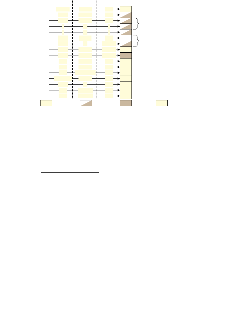
G3 The AArch32 Virtual Memory System Architecture
G3.17 Organization of the CP15 registers in VMSAv8-32
ARM DDI 0487A.a Copyright © 2013 ARM Limited. All rights reserved. G3-3717
ID090413 Non-Confidential - Beta
G3.17.1 CP15 32-bit register summary by coprocessor register number, CRn
Figure G3-26 summarizes the grouping of CP15 registers by primary coprocessor register number for a
VMSAv8-32 implementation.
Figure G3-26 CP15 32-bit register grouping by primary coprocessor register, CRn
Note
• Figure G3-26 gives only an overview of the assigned encodings for 32-registers for each of the CP15 primary
registers c0-c15. See the description of each primary register for the definition of the assigned and unassigned
encodings for that register, including any dependencies on the implemented Exception levels.
• 64-bit registers in the CP15 encoding space use the same primary coprocessor register model, but in the 64-bit
register read and write instructions,
MRRC
and
MCRR
, CRm identifies the primary coprocessor register.
The following sections give the register assignments for each of the CP15 primary registers, c0-c15:
•VMSAv8-32 CP15 c0 register summary.
•VMSAv8-32 CP15 c1 register summary on page G3-3718.
•VMSAv8-32 CP15 c2 and c3 register summary on page G3-3718
•VMSAv8-32 CP15 c4 register summary on page G3-3718.
•VMSAv8-32 CP15 c5 and c6 register summary on page G3-3719.
•VMSAv8-32 CP15 c7 register summary on page G3-3719.
•VMSAv8-32 CP15 c8 register summary on page G3-3719.
•VMSAv8-32 CP15 c9 register summary on page G3-3719.
•VMSAv8-32 CP15 c10 register summary on page G3-3720.
•VMSAv8-32 CP15 c11 register summary on page G3-3721.
•VMSAv8-32 CP15 c12 register summary on page G3-3721.
•VMSAv8-32 CP15 c13 register summary on page G3-3721.
•VMSAv8-32 CP15 c14 register summary on page G3-3722.
•VMSAv8-32 CP15 c15 register summary on page G3-3722.
VMSAv8-32 CP15 c0 register summary
The CP15 c0 registers provide device and feature identification.That is, they provide the register functional group
described in Identification registers, functional group on page G3-3736.
ID registers
System control registers
Cache maintenance, address translations, legacy operations
TLB maintenance operations
opc2CRm
{0-7}
{0-2}
0
{0,1}
Various
{c0-c2}
{c0, c1}
{c0, c1}
c0
{c0,c1}
c0
¶
{0-7}
Memory protection and
control registers
{0, 2, 4}
Memory system
fault registers
Various ¶
VariousVarious
0c6 GIC CPU Interface register *
Performance monitors, and reserved for maintenance operations
Reserved for DMA operations for TCM access
System control registers, GIC CPU Interface registers *
IMPLEMENTATION DEFINED registers
{0-7}
{0-7}
{0,1}
{0-4}
{0-7}
c0
{c0-c8,c15}
Various
{c0-c15}
¶
Various
¶ Memory mapping registers and TLB operations{0-7}Various
¶
¶
¶ Process, context, and thread ID registers
¶
Generic Timer registers *, Performance Monitors registers *
{0-7}{c0-c15} ¶
Read-only Read/Write Write-only ¶ Access depends on the implementation
CRn opc1
{0-2, 4}
{0, 4}
{0, 4}
0
{0, 4}
c0
c1
c2
c3
c5
c6
c7
c8
{0, 4}
{0, 4}
{0, 4}
0c4
{0-7}
{0-7}
{0-7}
c9
c10
c11
c12
c13
c15
{0-7}
{0-2, 4, 6}
{0, 4}
{0-7}c14
* If implemented

G3 The AArch32 Virtual Memory System Architecture
G3.17 Organization of the CP15 registers in VMSAv8-32
G3-3718 Copyright © 2013 ARM Limited. All rights reserved. ARM DDI 0487A.a
Non-Confidential - Beta ID090413
Table G3-46 on page G3-3723 shows all of the architecturally required CP15 c0 registers. CP15 c0 register
encodings not shown in the table, and encodings that are part of an unimplemented Exception level:
• If they have an opc1 value of zero, are RES0.
• Otherwise, are UNPREDICTABLE, see Accesses to unallocated CP14 and CP15 encodings on page G3-3693.
Note
Some of these registers were previously described as being part of the CPUID identification scheme, see The
CPUID identification scheme on page G3-3737.
VMSAv8-32 CP15 c1 register summary
The CP15 c1 registers provide system control, including security and virtualization control. That is, they provide
registers from the functional groups described in the following sections:
•Other system control registers, functional group on page G3-3737.
•Virtualization registers, functional group on page G3-3738.
•Security registers, functional group on page G3-3741.
Table G3-46 on page G3-3723 shows all of the architecturally required CP15 c1 registers. CP15 c1 register
encodings not shown in the table, and encodings that are part of an unimplemented Exception level are
UNPREDICTABLE, see Accesses to unallocated CP14 and CP15 encodings on page G3-3693.
VMSAv8-32 CP15 c2 and c3 register summary
The CP15 c2 and c3 registers provide memory system control. That is, they provide registers from the functional
group described in the section Virtual memory control registers, functional group on page G3-3737.
Table G3-46 on page G3-3723 shows all of the architecturally required CP15 c2 and c3 registers. CP15 c2 and c3
32-bit register encodings not shown in the table, and encodings that are part of an unimplemented Exception level
are UNPREDICTABLE, see Accesses to unallocated CP14 and CP15 encodings on page G3-3693.
Note
All 64-bit CP15 register encodings not shown in Table G3-46 on page G3-3723are UNDEFINED.
VMSAv8-32 CP15 c4 register summary
In an implementation that includes the System register interface to the Generic Interrupt Control CPU interface, the
CP15 c4 registers provide a register for this interface. That is, they provide a register from the functional group
described in the section Generic Interrupt Controller CPU interface registers, functional group on page G3-3749.
Table G3-46 on page G3-3723 shows all of the architecturally required CP15 c4 registers. CP15 c4 32-bit register
encodings not shown in the table are:
•UNPREDICTABLE if the implementation includes the System register interface to the Generic Interrupt Control
CPU interface. See Accesses to unallocated CP14 and CP15 encodings on page G3-3693.
•Otherwise,
UNDEFINED.

G3 The AArch32 Virtual Memory System Architecture
G3.17 Organization of the CP15 registers in VMSAv8-32
ARM DDI 0487A.a Copyright © 2013 ARM Limited. All rights reserved. G3-3719
ID090413 Non-Confidential - Beta
VMSAv8-32 CP15 c5 and c6 register summary
The CP15 c5 and c6 registers provide exception and fault handling. That is, they provide registers from the
functional group described in the section Exception and fault handling registers, functional group on page G3-3741.
Table G3-46 on page G3-3723 shows all of the architecturally required CP15 c5 and c6 registers. CP15 c5 and c6
32-bit register encodings not shown in the table, and encodings that are part of an unimplemented Exception level
are UNPREDICTABLE, see Accesses to unallocated CP14 and CP15 encodings on page G3-3693.
VMSAv8-32 CP15 c7 register summary
The CP15 c7 registers provide system operations for cache maintenance, address translation, and some legacy
operations. That is, they provide registers from the functional groups described in the following sections:
•Cache maintenance operations, functional group on page G3-3743.
•Address translation operations, functional group on page G3-3745.
•Legacy feature registers, functional group on page G3-3750.
Table G3-46 on page G3-3723 shows all of the architecturally required CP15 c7 registers. CP15 c7 32-bit register
encodings not shown in the table, and encodings that are part of an unimplemented Exception level are
UNPREDICTABLE, see Accesses to unallocated CP14 and CP15 encodings on page G3-3693.
Note
All 64-bit CP15 register encodings not shown in Table G3-46 on page G3-3723are UNDEFINED.
VMSAv8-32 CP15 c8 register summary
The CP15 c8 registers provide operations for TLB maintenance. That is, they provide registers from the functional
groups described in TLB maintenance operations, functional group on page G3-3744.
Table G3-46 on page G3-3723 shows all of the architecturally required CP15 c8 registers. CP15 c8 32-bit register
encodings not shown in the table, and encodings that are part of an unimplemented Exception level are
UNPREDICTABLE, see Accesses to unallocated CP14 and CP15 encodings on page G3-3693.
VMSAv8-32 CP15 c9 register summary
The CP15 c9 registers provide:
• Registers for the OPTIONAL Performance Monitors Extension. That is, they provide registers from the
functional group described in Performance Monitors Extension registers, functional group on page G3-3747.
• Reserved encodings for IMPLEMENTATION DEFINED memory system functions, in particular:
— Cache control, including lockdown.
— TCM control, including lockdown.
— Branch predictor control.
Note
The reserved encodings permit implementations that are compatible with previous versions of the ARM
architecture, in particular with the ARMv6 requirements.
• Reserved encodings for additional IMPLEMENTATION DEFINED performance monitors.
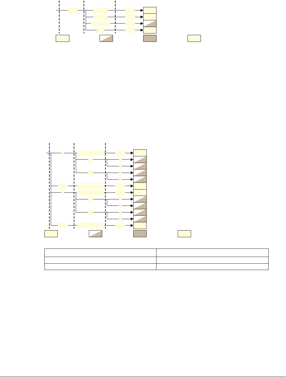
G3 The AArch32 Virtual Memory System Architecture
G3.17 Organization of the CP15 registers in VMSAv8-32
G3-3720 Copyright © 2013 ARM Limited. All rights reserved. ARM DDI 0487A.a
Non-Confidential - Beta ID090413
Figure G3-27 shows the VMSAv8-32 allocation of CP15 c9 register encodings.
Figure G3-27 VMSAv8-32 CP15 c9 32-bit register encodings
Table G3-46 on page G3-3723 shows all of the architecturally required CP15 c9 registers. Unimplemented CP15
c9 32-bit register encodings, including encodings that are part of an unimplemented Exception level, are
UNPREDICTABLE, see Accesses to unallocated CP14 and CP15 encodings on page G3-3693.
VMSAv8-32 CP15 c10 register summary
The CP15 c10 registers provide:
• Virtual memory control registers. That is, they provide registers from the functional group described in
Virtual memory control registers, functional group on page G3-3737.
• Reserved encodings for IMPLEMENTATION DEFINED TLB control functions, including lockdown.
Figure G3-28 shows the VMSAv8-32 allocation of CP15 c10 registers and reserved encodings.
Figure G3-28 VMSAv8-32 CP15 c10 32-bit register encodings
Table G3-46 on page G3-3723 shows all of the architecturally required CP15 c10 registers. Unimplemented CP15
c10 32-bit register encodings, including encodings that are part of an unimplemented Exception level, are
UNPREDICTABLE, see Accesses to unallocated CP14 and CP15 encodings on page G3-3693.
Read-only Read/Write
Reserved for Branch Predictor, Cache and TCM operations
{0-7}
{0-7}
{0-7}
{0-7}
{c0-c2}{0-7}
c9
Write-only
{c5-c8}
{c12-c14}
¶
¶
¶
Reserved for Branch Predictor, Cache and TCM operations
Registers for OPTIONAL ARM Performance Monitors Extension
Reserved for IMPLEMENTATION DEFINED performance monitors
¶ Access depends on the operation
c15
CRn opc1 opc2CRm
‡ Implemented only as part of EL2
Read-only Read/Write
Reserved for TLB Lockdown operations
{0-7}
0
1
{c0,c1,c4,c8}0
c10
Write-only
c2
¶
PRRR or MAIR0, see table
NMRR or MAIR1, see table
CRn opc1 opc2CRm
¶ Access depends on the operation
0
1
c3
0
1
c2
{5-7}
HMAIR0, Hyp Memory Attribute Indirection Register 0 ‡
HMAIR1, Hyp Memory Attribute Indirection Register 1 ‡
Reserved for TLB Lockdown operations
{0-7} ¶
{c0,c1,c4,c8}{1-3}
Reserved for TLB Lockdown operations
¶
4 {0-7}{c0,c1,c4,c8}
Reserved for TLB Lockdown operations¶
{0-7}{c0,c1,c4,c8}
HAMAIR0, Hyp Auxiliary Memory Attribute Indirection Register 0 ‡
HAMAIR1, Hyp Auxiliary Memory Attribute Indirection Register 1 ‡
0
1
c3
AMAIR0, Auxiliary Memory Attribute Indirection Register 0
AMAIR1, Auxiliary Memory Attribute Indirection Register 1
PRRR, Primary Region Remap Register MAIR0, Memory Attribute Indirection Register 0
NMRR, Normal Memory Remap Register MAIR1, Memory Attribute Indirection Register 1
When using Short-descriptor translation table format When using Long-descriptor translation table format

G3 The AArch32 Virtual Memory System Architecture
G3.17 Organization of the CP15 registers in VMSAv8-32
ARM DDI 0487A.a Copyright © 2013 ARM Limited. All rights reserved. G3-3721
ID090413 Non-Confidential - Beta
VMSAv8-32 CP15 c11 register summary
The CP15 c11 registers provide some reserved encodings for IMPLEMENTATION DEFINED DMA operations to and
from TCM. Figure G3-29 shows these reserved encodings:
Figure G3-29 VMSAv8-32 reserved CP15 c11 encodings
CP15 c11 encodings not shown in Figure G3-29 are UNPREDICTABLE, see Accesses to unallocated CP14 and CP15
encodings on page G3-3693.
VMSAv8-32 CP15 c12 register summary
The CP15 c12 registers provide registers from the functional groups described in the following sections:
•Exception and fault handling registers, functional group on page G3-3741.
•Virtualization registers, functional group on page G3-3738.
•Security registers, functional group on page G3-3741.
•Reset management registers, functional group on page G3-3742.
•Generic Interrupt Controller CPU interface registers, functional group on page G3-3749.
Table G3-46 on page G3-3723 shows all of the architecturally required CP15 c12 registers. CP15 c12 32-bit register
encodings not shown in the table, and encodings that are part of an unimplemented Exception level are
UNPREDICTABLE, see Accesses to unallocated CP14 and CP15 encodings on page G3-3693.
Note
• Some CP15 c12 registers are in more than one functional group.
• All 64-bit CP15 register encodings not shown in Table G3-46 on page G3-3723are UNDEFINED.
VMSAv8-32 CP15 c13 register summary
The CP15 c13 registers provide:
• An FCSE Process ID Register, that indicates that ARMv8 implementations do not include the FCSE.
• A Context ID Register.
• Software Thread ID Registers.
These registers are from the functional groups described in the following sections:
•Virtual memory control registers, functional group on page G3-3737.
•Virtualization registers, functional group on page G3-3738.
•Thread and process ID registers, functional group on page G3-3743.
•Legacy feature registers, functional group on page G3-3750.
Note
Some CP15 c12 registers are in more than one functional group.
Read-only Read/Write
Reserved for DMA operations for TCM access
{0-7}
{0-7}
{c0-c8}{0-7}
c11
Write-only
c15
¶
¶
¶ Access depends on the operation
Reserved for DMA operations for TCM access
CRn opc1 opc2CRm

G3 The AArch32 Virtual Memory System Architecture
G3.17 Organization of the CP15 registers in VMSAv8-32
G3-3722 Copyright © 2013 ARM Limited. All rights reserved. ARM DDI 0487A.a
Non-Confidential - Beta ID090413
Figure G3-30 shows these registers:
Figure G3-30 CP15 c13 registers in VMSAv8-32
Table G3-46 on page G3-3723 shows all of the architecturally required CP15 c13 registers. CP15 c13 32-bit register
encodings not shown in the table, and encodings that are part of an unimplemented Exception level are
UNPREDICTABLE, see Accesses to unallocated CP14 and CP15 encodings on page G3-3693.
VMSAv8-32 CP15 c14 register summary
The CP15 c14 registers provide Performance Monitors Extension and Generic Timer Extension registers. That is,
they provide registers from the functional group described in the following sections:
•Performance Monitors Extension registers, functional group on page G3-3747.
•Generic Timer Extension registers, functional group on page G3-3749
Table G3-46 on page G3-3723 shows all of the architecturally required CP15 c14 registers. CP15 c14 32-bit register
encodings not shown in the table, and encodings that are part of an unimplemented Exception level are
UNPREDICTABLE, see Accesses to unallocated CP14 and CP15 encodings on page G3-3693.
From issue C.a of this manual, CP15 c14 is reserved for the System registers of the OPTIONAL Generic Timer
Extension. For more information, see Chapter D7 The Generic Timer. On an implementation that does not include
the Generic Timer, c14 is an unallocated CP15 primary register, see UNPREDICTABLE and UNDEFINED
behavior for CP14 and CP15 accesses on page G3-3693.
Note
• Some CP15 c14 registers are also in the Virtualization group, see Virtualization registers, functional group
on page G3-3738.
• All 64-bit CP15 register encodings not shown in Table G3-46 on page G3-3723are UNDEFINED.
VMSAv8-32 CP15 c15 register summary
The CP15 c15 registers are reserved for IMPLEMENTATION DEFINED purposes. The architecture does not impose any
restrictions on the use of these encodings. For more information, see IMPLEMENTATION DEFINED registers,
functional group on page G3-3751.
G3.17.2 Full list of VMSAv8-32 CP15 registers, by coprocessor register number
Table G3-46 on page G3-3723 shows the CP15 registers in VMSAv8-32, in the order of the
{CRn, opc1, CRm, opc2} values used in
MCR
or
MRC
accesses to the 32-bit registers:
• For
MCR
or
MRC
accesses to the 32-bit registers, CRn identifies the CP15 primary register used for the access.
• For
MCRR
or
MRRC
accesses to the 64-bit registers, CRm identifies the CP15 primary register used for the access.
Table G3-46 on page G3-3723 lists the 64-bit registers with the 32-bit registers accessed using the same
CP15 primary register number.
Read-only Read/Write
FCSEIDR, FCSE PID Register
0
1
2
c00c13
Write-only
CONTEXTIDR, Context ID Register
TPIDRURW, User Read/Write
RAZ/WI when FCSE is not implemented, see register description
*
3
4
TPIDRURO, User Read Only ª
TPIDRPRW, PL1 only
Software Thread ID
Registers
*
Bold text = Accessible at PL0
ª Read-only at PL0
CRn opc1 opc2CRm
HTPIDR, Hyp Read/Write ‡
‡ Implemented only as part of EL2
2c04

G3 The AArch32 Virtual Memory System Architecture
G3.17 Organization of the CP15 registers in VMSAv8-32
ARM DDI 0487A.a Copyright © 2013 ARM Limited. All rights reserved. G3-3723
ID090413 Non-Confidential - Beta
Table G3-46 Summary of VMSAv8-32 CP15 register descriptions, in coprocessor register number order
CRn opc1 CRm opc2 Name Width Description
c0 0 c0 0 MIDR 32-bit Main ID Register
1CTR 32-bit Cache Type Register
2TCMTR 32-bit TCM Type Register
3TLBTR 32-bit TLB Type Register
4, 6a, 7 MIDR 32-bit Aliases of Main ID Register
5MPIDR 32-bit Multiprocessor Affinity Register
6aREVIDR 32-bit Revision ID Register
c0 0 c1 0 ID_PFR0 32-bit Processor Feature Register 0
1ID_PFR1 32-bit Processor Feature Register 1
2ID_DFR0 32-bit Debug Feature Register 0
3ID_AFR0 32-bit Auxiliary Feature Register 0
4ID_MMFR0 32-bit Memory Model Feature Register 0
5ID_MMFR1 32-bit Memory Model Feature Register 1
6ID_MMFR2 32-bit Memory Model Feature Register 2
7ID_MMFR3 32-bit Memory Model Feature Register 3
c2 0 ID_ISAR0 32-bit Instruction Set Attribute Register 0
1ID_ISAR1 32-bit Instruction Set Attribute Register 1
2ID_ISAR2 32-bit Instruction Set Attribute Register 2
3ID_ISAR3 32-bit Instruction Set Attribute Register 3
4ID_ISAR4 32-bit Instruction Set Attribute Register 4
5ID_ISAR5 32-bit Instruction Set Attribute Register 5
1c0 0 CCSIDR 32-bit Cache Size ID Registers
1CLIDR 32-bit Cache Level ID Register
7AIDR 32-bit Auxiliary ID Register, IMPLEMENTATION DEFINED
c0 2 c0 0 CSSELR 32-bit Cache Size Selection Register
4c0 0 VPIDRb32-bit Virtualization Processor ID Register
5VMPIDRb32-bit Virtualization Multiprocessor ID Register

G3 The AArch32 Virtual Memory System Architecture
G3.17 Organization of the CP15 registers in VMSAv8-32
G3-3724 Copyright © 2013 ARM Limited. All rights reserved. ARM DDI 0487A.a
Non-Confidential - Beta ID090413
c1 0 c0 0 SCTLR 32-bit System Control Register
1ACTLR 32-bit Auxiliary Control Register, IMPLEMENTATION DEFINED
2CPACR 32-bit Coprocessor Access Control Register
c1 0 SCRc32-bit Secure Configuration Register
1SDERc32-bit Secure Debug Enable Register
2NSACRc32-bit Non-Secure Access Control Register
c3 1 SDCRd32-bit Secure Debug Configuration Register
c1 4 c0 0 HSCTLRb32-bit Hyp System Control Register
1HACTLRb32-bit Hyp Auxiliary Control Register
c1 0 HCRb32-bit Hyp Configuration Register
1HDCRb32-bit Hyp Debug Configuration Register
2HCPTRb32-bit Hyp Coprocessor Trap Register
3HSTRb32-bit Hyp System Trap Register
4HCR2b, d 32-bit Hyp Configuration Register 2
7HACRb32-bit Hyp Auxiliary Configuration Register
c2 0 c0 0 TTBR0 32-bit Translation Table Base Register 0
-0c2 - TTBR0 64-bit
c2 0 c0 1 TTBR1 32-bit Translation Table Base Register 1
-1c2 - TTBR1 64-bit
c2 0 c0 2 TTBCR 32-bit Translation Table Base Control Register
4c0 2 HTCRb32-bit Hyp Translation Control Register
c1 2 VTCRb32-bit Virtualization Translation Control Register
-4c2 - HTTBRb64-bit Hyp Translation Table Base Register
-6c2 - VTTBRb64-bit Virtualization Translation Table Base Register
c3 0 c0 1 DACR 32-bit Domain Access Control Register
c4 0 c6 0 ICC_PMRe32-bit Interrupt Controller Interrupt Priority Mask Register
3c5 0 DSPSRd32-bit Debug Saved Program Status Registerf
1DLRd32-bit Debug Link Registerf
Table G3-46 Summary of VMSAv8-32 CP15 register descriptions, in coprocessor register number order (continued)
CRn opc1 CRm opc2 Name Width Description

G3 The AArch32 Virtual Memory System Architecture
G3.17 Organization of the CP15 registers in VMSAv8-32
ARM DDI 0487A.a Copyright © 2013 ARM Limited. All rights reserved. G3-3725
ID090413 Non-Confidential - Beta
c5 0 c0 0 DFSR 32-bit Data Fault Status Register
1IFSR 32-bit Instruction Fault Status Register
c1 0 ADFSR 32-bit Auxiliary Data Fault Status Register
1AIFSR 32-bit Auxiliary Instruction Fault Status Register
c5 4 c1 0 HADFSRb32-bit Hyp Auxiliary Data Fault Syndrome Register
1HAIFSR 32-bit Hyp Auxiliary Instruction Fault Syndrome Register
c2 0 HSRb32-bit Hyp Syndrome Register
c6 0 c0 0 DFAR 32-bit Data Fault Address Register
2IFAR 32-bit Instruction Fault Address Register
4c0 0 HDFARb32-bit Hyp Data Fault Address Register
2HIFARb32-bit Hyp Instruction Fault Address Register
4HPFARb32-bit Hyp IPA Fault Address Register
c7 0 c1 0 ICIALLUIS 32-bit See Cache maintenance operations, functional group on
page G3-3743
6BPIALLIS 32-bit
c4 0 PAR 32-bit Physical Address Register
0c7 - PAR 64-bit
c7 0 c5 0 ICIALLU 32-bit See Cache maintenance operations, functional group on
page G3-3743
1ICIMVAU 32-bit
4CP15ISB 32-bit See Memory barriers on page E2-2352
6BPIALL 32-bit See Cache maintenance operations, functional group on
page G3-3743
7BPIMVA 32-bit
c6 1 DCIMVAC 32-bit See Cache maintenance operations, functional group on
page G3-3743
2DCISW 32-bit
c7 0 c8 0 ATS1CPR 32-bit See Virtual Address to Physical Address translation
operations on page G3-3685
1ATS1CPW 32-bit
2ATS1CUR 32-bit
3ATS1CUW 32-bit
4ATS12NSOPRc32-bit
5ATS12NSOPWc32-bit
6ATS12NSOURc32-bit
7ATS12NSOUWc32-bit
Table G3-46 Summary of VMSAv8-32 CP15 register descriptions, in coprocessor register number order (continued)
CRn opc1 CRm opc2 Name Width Description

G3 The AArch32 Virtual Memory System Architecture
G3.17 Organization of the CP15 registers in VMSAv8-32
G3-3726 Copyright © 2013 ARM Limited. All rights reserved. ARM DDI 0487A.a
Non-Confidential - Beta ID090413
c7 0 c10 1 DCCMVAC 32-bit See Cache maintenance operations, functional group on
page G3-3743
2DCCSW 32-bit
4CP15DSB 32-bit See Memory barriers on page E2-2352
5CP15DMB 32-bit
c7 0 c11 1 DCCMVAU 32-bit See Cache maintenance operations, functional group on
page G3-3743
c14 1 DCCIMVAC 32-bit See Cache maintenance operations, functional group on
page G3-3743
2DCCISW 32-bit
4c8 0 ATS1HRb32-bit See Virtual Address to Physical Address translation
operations on page G3-3685
1ATS1HW b32-bit
c8 0 c3 0 TLBIALLIS 32-bit See The scope of TLB maintenance operations on
page G3-3640
1TLBIMVAIS 32-bit
2TLBIASIDIS 32-bit
3TLBIMVAAIS 32-bit
5TLBIMVALISd32-bit
7TLBIMVAALISd32-bit
c5 0 ITLBIALL 32-bit See The scope of TLB maintenance operations on
page G3-3640
1ITLBIMVA 32-bit
2ITLBIASID 32-bit
c6 0 DTLBIALL 32-bit See The scope of TLB maintenance operations on
page G3-3640
1DTLBIMVA 32-bit
2DTLBIASID 32-bit
c7 0 TLBIALL 32-bit See The scope of TLB maintenance operations on
page G3-3640
1TLBIMVA 32-bit
2TLBIASID 32-bit
3TLBIMVAA 32-bit
5TLBIMVALd32-bit
7TLBIMVAALd32-bit
c8 4 c0 1 TLBIIPAS2ISd32-bit See The scope of TLB maintenance operations on
page G3-3640
5TLBIIPAS2LISd32-bit
Table G3-46 Summary of VMSAv8-32 CP15 register descriptions, in coprocessor register number order (continued)
CRn opc1 CRm opc2 Name Width Description

G3 The AArch32 Virtual Memory System Architecture
G3.17 Organization of the CP15 registers in VMSAv8-32
ARM DDI 0487A.a Copyright © 2013 ARM Limited. All rights reserved. G3-3727
ID090413 Non-Confidential - Beta
c8 4 c3 0 TLBIALLHISb32-bit See The scope of TLB maintenance operations on
page G3-3640
1TLBIMVAHISb32-bit
4TLBIALLNSNHISb32-bit
5TLBIMVALHISd32-bit
c8 4 c4 1 TLBIIPAS2d32-bit See The scope of TLB maintenance operations on
page G3-3640
5TLBIIPAS2Ld32-bit
c7 0 TLBIALLHb32-bit See The scope of TLB maintenance operations on
page G3-3640
1TLBIMVAHb32-bit
4TLBIALLNSNHb32-bit
5TLBIMVALHd32-bit
c9 0 c12 0 PMCR 32-bit Performance Monitors Control Register
1PMCNTENSET 32-bit Performance Monitors Count Enable Set register
2PMCNTENCLR 32-bit Performance Monitors Count Enable Clear register
3PMOVSR 32-bit Performance Monitors Overflow Flag Status Register
4PMSWINC 32-bit Performance Monitors Software Increment register
5PMSELR 32-bit Performance Monitors Event Counter Selection Register
6PMCEID0 32-bit Performance Monitors Common Event Identification
register 0
7PMCEID1 32-bit Performance Monitors Common Event Identification
register 1
c9 0 c13 0 PMCCNTR 32-bit Performance Monitors Cycle Count Register
1PMXEVTYPER 32-bit Performance Monitors Event Type Select Register
2PMXEVCNTR 32-bit Performance Monitors Event Count Register
c9 0 c14 0 PMUSERENR 32-bit Performance Monitors User Enable Register
1PMINTENSET 32-bit Performance Monitors Interrupt Enable Set register
2PMINTENCLR 32-bit Performance Monitors Interrupt Enable Clear register
3PMOVSSETb32-bit Performance Monitors Overflow Flag Status Set register
c10 0 c2 0 PRRRg32-bit Primary Region Remap Register
MAIR0g32-bit Memory Attribute Indirection Register 0
1NMRRg32-bit Normal Memory Remap Register
MAIR1g32-bit Memory Attribute Indirection Register 1
Table G3-46 Summary of VMSAv8-32 CP15 register descriptions, in coprocessor register number order (continued)
CRn opc1 CRm opc2 Name Width Description

G3 The AArch32 Virtual Memory System Architecture
G3.17 Organization of the CP15 registers in VMSAv8-32
G3-3728 Copyright © 2013 ARM Limited. All rights reserved. ARM DDI 0487A.a
Non-Confidential - Beta ID090413
c10 0 c3 0 AMAIR0 32-bit Auxiliary Memory Attribute Indirection Register 0
1AMAIR1 32-bit Auxiliary Memory Attribute Indirection Register 1
4c2 0 HMAIR0b32-bit Hyp Memory Attribute Indirection Register 0
1HMAIR1b32-bit Hyp Memory Attribute Indirection Register 1
c3 0 HAMAIR0b32-bit Hyp Auxiliary Memory Attribute Indirection Register 0
1HAMAIR1b32-bit Hyp Auxiliary Memory Attribute Indirection Register 1
c11 0-7 c0-c8 0-7 - 32-bit See VMSAv8-32 CP15 c11 register summary on
page G3-3721
c15 c15 - 32-bit
-0c12 - ICC_SGI1Re64-bit Interrupt Controller SGI group 1 Register
c12 0 c0 0 VBAR 32-bit Vector Base Address Register
1MVBARc32-bit Monitor Vector Base Address Register
]RVBAR 32-bit Reset Vector Base Address Register
2RMR (at EL1)h32-bit Reset Management Register, at EL1
RMR (at EL3)h32-bit Reset Management Register, at EL3
c1 0 ISRc32-bit Interrupt Status Register
c8 0 ICC_IAR0e32-bit Interrupt Controller Interrupt Acknowledge Register 0
1ICC_EOIR0e32-bit Interrupt Controller End Of Interrupt Register 0
2ICC_HPPIR0e32-bit Interrupt Controller Highest Priority Pending Interrupt
Register 0
3ICC_BPR0e32-bit Interrupt Controller Binary Point Register 0
4ICC_AP0R0e32-bit Interrupt Controller Active Priorities Register (0,0)
5ICC_AP0R1e32-bit Interrupt Controller Active Priorities Register (0,1)
6ICC_AP0R2e32-bit Interrupt Controller Active Priorities Register (0,2)
7ICC_AP0R3e32-bit Interrupt Controller Active Priorities Register (0,3)
c12 0 c9 0 ICC_AP1R0e32-bit Interrupt Controller Active Priorities Register (1,0)
1ICC_AP1R1e32-bit Interrupt Controller Active Priorities Register (1,1)
2ICC_AP1R2e32-bit Interrupt Controller Active Priorities Register (1,2)
3ICC_AP1R3e32-bit Interrupt Controller Active Priorities Register (1,3)
c11 1 ICC_DIRe32-bit Interrupt Controller Deactivate Interrupt Register
3ICC_RPRe32-bit Interrupt Controller Running Priority Register
Table G3-46 Summary of VMSAv8-32 CP15 register descriptions, in coprocessor register number order (continued)
CRn opc1 CRm opc2 Name Width Description

G3 The AArch32 Virtual Memory System Architecture
G3.17 Organization of the CP15 registers in VMSAv8-32
ARM DDI 0487A.a Copyright © 2013 ARM Limited. All rights reserved. G3-3729
ID090413 Non-Confidential - Beta
c12 0 c12 0 ICC_IAR1e32-bit Interrupt Controller Interrupt Acknowledge Register 1
1ICC_EOIR1e32-bit Interrupt Controller End Of Interrupt Register 1
2ICC_HPPIR1e32-bit Interrupt Controller Highest Priority Pending Interrupt
Register 1
3ICC_BPR1e32-bit Interrupt Controller Binary Point Register 1
4ICC_CTLRe32-bit Interrupt Controller Control Register
5ICC_SREe32-bit Interrupt Controller System Register Enable Register
6ICC_IGRPEN0e32-bit Interrupt Controller Interrupt Group 0 Enable Register
7ICC_IGRPEN1e32-bit Interrupt Controller Interrupt Group 1 Enable Register
c13 0 ICC_SEIENe32-bit Interrupt Controller System Error Interrupt Enable
register
-1c12 - ICC_ASGI1Re64 bit Interrupt Controller Alias SGI group 1 Register
-2c12 - ICC_SGI0Re64 bit Interrupt Controller SGI group 0 Register
c12 4 c0 0 HVBARb, c 32-bit Hyp Vector Base Address Register
2HRMRh32-bit Hyp Reset Management Register
c8 0 ICH_AP0R0e32-bit Interrupt Controller Hyp Active Priorities Register (0,0)
1ICH_AP0R1e32-bit Interrupt Controller Hyp Active Priorities Register (0,1)
2ICH_AP0R2e32-bit Interrupt Controller Hyp Active Priorities Register (0,2)
3ICH_AP0R3e32-bit Interrupt Controller Hyp Active Priorities Register (0,3)
c9 0 ICH_AP1R0e32-bit Interrupt Controller Hyp Active Priorities Register (1,0)
1ICH_AP1R1e32-bit Interrupt Controller Hyp Active Priorities Register (1,1)
2ICH_AP1R2e32-bit Interrupt Controller Hyp Active Priorities Register (1,2)
3ICH_AP1R3e32-bit Interrupt Controller Hyp Active Priorities Register (1,3)
4ICH_VSEIRe32-bit Interrupt Controller Virtual System Error Interrupt
Register
5ICC_HSREe32-bit Interrupt Controller Hyp System Register Enable register
c12 4 c11 0 ICH_HCRe32-bit Interrupt Controller Hyp Control Register
1ICH_VTRe32-bit Interrupt Controller VGIC Type Register
2ICH_MISRe32-bit Interrupt Controller Maintenance Interrupt State Register
3ICH_EISRe32-bit Interrupt Controller End of Interrupt Status Register
5ICH_ELSRe32-bit Interrupt Controller Empty List Register Status Register
7ICH_VMCRe32-bit Interrupt Controller Virtual Machine Control Register
Table G3-46 Summary of VMSAv8-32 CP15 register descriptions, in coprocessor register number order (continued)
CRn opc1 CRm opc2 Name Width Description

G3 The AArch32 Virtual Memory System Architecture
G3.17 Organization of the CP15 registers in VMSAv8-32
G3-3730 Copyright © 2013 ARM Limited. All rights reserved. ARM DDI 0487A.a
Non-Confidential - Beta ID090413
c12 4 c12 0-7 ICH_LR<n>,
for n==0 to 7e
32-bit Interrupt Controller List Registers 0 to 7
c13 0-7 ICH_LR<n>,
for n==8 to 15e
32-bit Interrupt Controller List Registers 8 to 15
c14 0-7 ICH_LRC<n>,
for n==0 to 7e
32-bit Interrupt Controller List Registers 0 to 7, continuation
c15 0-7 ICH_LRC<n>,
for n==8 to 15e
32-bit Interrupt Controller List Registers 8 to 15, continuation
6 c12 4 ICC_MCTLRe32-bit Interrupt Controller Monitor Control Register
5ICC_MSREe32-bit Interrupt Controller Monitor System Register Enable
register
7ICC_MGRPEN1e32-bit Interrupt Controller Monitor Interrupt Group 1 Enable
register
c13 0 c0 0 FCSEIDR 32-bit FCSE Process ID Register
1CONTEXTIDR 32-bit Context ID Register
2TPIDRURW 32-bit User Read/Write Thread ID Register
3TPIDRURO 32-bit User Read-Only Thread ID Register
4TPIDRPRW 32-bit EL1 only Thread ID Register
4c0 2 HTPIDRb32-bit Hyp Software Thread ID Register
-0c14 - CNTPCTi64-bit Physical Count register
c14 0 c0 0 CNTFRQi32-bit Counter Frequency register
c14 0 c1 0 CNTKCTLi32-bit Timer EL1 Control register
c2 0 CNTP_TVALi32-bit EL1 Physical TimerValue register
1CNTP_CTLi32-bit EL1 Physical Timer Control register
c3 0 CNTV_TVALi32-bit Virtual TimerValue register
1CNTV_CTLi32-bit Virtual Timer Control register
c14 0 c8 0-7 PMEVCNTR<n>,
for n==0 to 7d
32-bit Performance Monitors Event Count Registers, 0-7
c9 0-7 PMEVCNTR<n>,
for n==8 to 15 d
32-bit Performance Monitors Event Count Registers, 8-15
c10 0-7 PMEVCNTR<n>,
for n==16 to 23d
32-bit Performance Monitors Event Count Registers, 16-23
c11 0-6 PMEVCNTR<n>,
for n==24 to 30d
32-bit Performance Monitors Event Count Registers, 24-30
c12 0-7 PMEVTYPER<n>,
for n==0 to 7d
32-bit Performance Monitors Event Type Registers, 0-7
Table G3-46 Summary of VMSAv8-32 CP15 register descriptions, in coprocessor register number order (continued)
CRn opc1 CRm opc2 Name Width Description

G3 The AArch32 Virtual Memory System Architecture
G3.17 Organization of the CP15 registers in VMSAv8-32
ARM DDI 0487A.a Copyright © 2013 ARM Limited. All rights reserved. G3-3731
ID090413 Non-Confidential - Beta
c14 0 c13 0-7 PMEVTYPER<n>,
for n==8 to 15d
32-bit Performance Monitors Event Type Registers, 8-15
c14 0-7 PMEVTYPER<n>,
for n==16 to 23d
32-bit Performance Monitors Event Type Registers, 16-23
c15 0-6 PMEVTYPER<n>,
for n==17 to 30d
32-bit Performance Monitors Event Type Registers, 24-30
c15 7 PMCCFILTRd32-bit Performance Monitors Cycle Count Filter Register
-1c14 - CNTVCTi64-bit Virtual Count register
2CNTP_CVALi64-bit EL1 Physical Timer CompareValue register
3CNTV_CVALi64-bit Virtual Timer CompareValue register
4CNTVOFFj64-bit Virtual Offset register
c14 4 c1 0 CNTHCTL 32-bit Timer EL2 Control register
c2 0 CNTHP_TVAL 32-bit EL2 Physical TimerValue register
1CNTHP_CTL 32-bit EL2 Physical Timer Control register
-6c14 - CNTHP_CVAL 64-bit EL2 Physical Timer CompareValue register
c15 0-7 c0-c15 0-7 - 32-bit See IMPLEMENTATION DEFINED registers, functional
group on page G3-3751
a. REVIDR is an optional register. If it is not implemented, the encoding with opc2 set to 6 is an alias of MIDR.
b. Implemented only as part of EL2, when EL2 is using AArch32. Otherwise, encoding is unallocated and UNPREDICTABLE, see Accesses to
unallocated CP14 and CP15 encodings on page G3-3693.
c. Implemented only as part of the EL3, when EL3 is using AArch32. Otherwise, as described in Accesses to unallocated CP14 and CP15
encodings on page G3-3693, encoding is unallocated and:
UNDEFINED, for the registers accessed using CRn set to c12.
UNPREDICTABLE, for the register accessed using CRn values other than c12.
d. Introduced in ARMv8.
e. Introduced in ARMv8. Implemented only if the implementation includes the System registers interface to the Generic Interrupt Controller
CPU interface.
f. This register is only accessible in Debug state.
g. When an implementation is using the Long descriptor translation table format these encodings access the MAIR0 and MAIR1registers.
Otherwise, they access the PRRR and NMRR.
h. Introduced in ARMv8. Only one of RMR (at EL1), HRMR, and RMR (at EL3) is implemented, corresponding to the highest implemented
Exception level, and the register is implemented only if that Exception level is using AArch32.
i. Implemented only as part of the Generic Timers Extension. Otherwise, encoding is unallocated and UNDEFINED, see Accesses to unallocated
CP14 and CP15 encodings on page G3-3693.
j. Implemented as RW only as part of the Generic Timers Extension on an implementation that includes EL2 and when EL2 is using AArch32.
For more information see Status of the CNTVOFF register on page D7-1864.
Table G3-46 Summary of VMSAv8-32 CP15 register descriptions, in coprocessor register number order (continued)
CRn opc1 CRm opc2 Name Width Description

G3 The AArch32 Virtual Memory System Architecture
G3.17 Organization of the CP15 registers in VMSAv8-32
G3-3732 Copyright © 2013 ARM Limited. All rights reserved. ARM DDI 0487A.a
Non-Confidential - Beta ID090413
G3.17.3 Views of the CP15 registers
The following sections summarize the different software views of the CP15 registers, for VMSAv8-32:
•EL0 views of the CP15 registers.
•EL1 views of the CP15 registers on page G3-3733.
•Non-secure EL2 view of the CP15 registers on page G3-3734.
EL0 views of the CP15 registers
Software executing at EL0, unprivileged, can access only a small subset of the CP15 registers, as Table G3-47
shows. This table excludes possible EL0 access to CP15 registers that are part of the following OPTIONAL extensions
to the architecture:
• The Performance Monitors Extension, see Possible EL0 access to the Performance Monitors Extension
CP15 registers.
•The Generic Timer Extension, see Possible EL0 access to the Generic Timer Extension CP15 registers on
page G3-3733.
Possible EL0 access to the Performance Monitors Extension CP15 registers
In a VMSAv8-32 implementation that includes the Performance Monitors Extension, when using CP15 to access
the Performance Monitors registers:
• The PMUSERENR is RO from EL0.
• When:
— The value of PMUSERENR.EN is 1, PMCNTENSET, PMCNTENCLR, PMOVSR, PMSWINC,
PMSELR, PMCEID0, PMCEID1, PMCCNTR, PMXEVTYPER, PMXEVCNTR, PMUSERENR,
PMOVSSET, PMEVCNTR<n>, PMEVTYPER<n>, and PMCCFILTR.are accessible by reads and
writes from EL0.
— The value of PMUSERENR.ER is 1, PMXEVCNTR and PMEVCNTR<n>.are accessible by reads
and from EL0, and PMSELR is accessible by reads and writes from EL0.
— The value of PMUSERENR.CR is 1, PMCCNTR is accessible by reads from EL0.
— The value of PMUSERENR.SW is 1, PMSWINC is accessible by writes from EL0.
In general, when the value of a PMUSERENR.{EN, ER, CR, SW} bit is 1, the enabled registers have the
same access permissions from EL0 as they do from EL1.
For more information, see:
•Traps to EL1 of EL0 accesses to Performance Monitors registers on page D1-1473.
•Chapter D6 The Performance Monitors Extension, in particular Access permissions on page D6-1851.
Table G3-47 CP15 registers accessible from EL0
Name Access Description Note
CP15ISB WO Memory barriers on page E2-2352 ARM deprecates use of these
operations
CP15DSB WO
CP15DMB WO
TPIDRURW RW TPIDRURW, Thread Pointer / ID Register, Unprivileged Read-Write
on page G4-4078 -
TPIDRURO RO TPIDRURO, Thread Pointer / ID Register, Unprivileged Read-Only
on page G4-4077 RW at EL1

G3 The AArch32 Virtual Memory System Architecture
G3.17 Organization of the CP15 registers in VMSAv8-32
ARM DDI 0487A.a Copyright © 2013 ARM Limited. All rights reserved. G3-3733
ID090413 Non-Confidential - Beta
Possible EL0 access to the Generic Timer Extension CP15 registers
In a VMSAv8-32 implementation that includes the Generic Timer Extension, when using CP15 to access the
Generic Timer registers:
•If CNTKCTL.PL0PCTEN is set to 1, then if the physical counter register CNTPCT is accessible from EL1
it is also accessible from EL0. For more information see Accessing the physical counter on page D7-1858.
•If CNTKCTL.PL0PVTEN is set to 1, the virtual counter register CNTVCT is accessible from EL0. For more
information, see Accessing the virtual counter on page D7-1859.
• If at least one of CNTKCTL.{PL0PCTEN, PL0PVTEN} is set to 1, the CNTFRQ register is RO from EL0.
•If:
—CNTKCTL.PL0PTEN is set to 1, the physical timer registers CNTP_CTL, CNTP_CVAL, and
CNTP_TVAL are accessible from EL0.
—CNTKCTL.PL0VTEN is set to 1, the virtual timer registers CNTV_CTL, CNTV_CVAL, and
CNTV_TVAL, are accessible from EL0.
For more information, see Accessing the timer registers on page D7-1861.
EL1 views of the CP15 registers
Software executing at EL1 can access all CP15 registers, with the following exceptions:
Non-secure EL1 software
EL3 restricts or prevents access to some registers by Non-secure EL1 software. In particular:
• The Restricted access CP15 registers are either not accessible to Non-secure EL1 software,
or are read-only to Non-secure EL1 software, see Restricted access System registers on
page G3-3698
• Configuration settings determine whether Non-secure EL1 software can access the
Configurable access CP15 registers, see Configurable access System registers on
page G3-3699.
The individual register descriptions identify these access restrictions.
In an implementation that includes EL2, Non-secure EL1 software has no visibility of the
EL2-mode registers summarized in Banked EL2-mode CP15 read/write registers on page G3-3700.
The individual register descriptions identify these registers as EL2-mode registers.
Secure EL1 software
In general, Secure EL1 software has access to all CP15 registers. However:
• The CP15SDISABLE signal disables write access to a number of Secure registers, see The
CP15SDISABLE input on page G3-3704.
• To access the EL2-mode registers, Secure EL1 software must move into Monitor mode, and
set SCR.NS to 1.
Banked EL2-mode CP15 read/write registers on page G3-3700 summarizes these registers.
The individual register descriptions identify:
• The registers affected by the CP15SDISABLE signal.
• The EL2-mode registers.

G3 The AArch32 Virtual Memory System Architecture
G3.17 Organization of the CP15 registers in VMSAv8-32
G3-3734 Copyright © 2013 ARM Limited. All rights reserved. ARM DDI 0487A.a
Non-Confidential - Beta ID090413
Non-secure EL2 view of the CP15 registers
Non-secure software executing at EL2 can access:
• The registers that are accessible to Non-secure software executing at EL1, as defined in EL1 views of the
CP15 registers on page G3-3733. Access permissions for these registers are identical to those for Non-secure
software executing at EL1.
• The EL2-mode registers summarized in Banked EL2-mode CP15 read/write registers on page G3-3700, and
described in Virtualization registers, functional group on page G3-3738.

G3 The AArch32 Virtual Memory System Architecture
G3.18 Functional grouping of VMSAv8-32 System registers
ARM DDI 0487A.a Copyright © 2013 ARM Limited. All rights reserved. G3-3735
ID090413 Non-Confidential - Beta
G3.18 Functional grouping of VMSAv8-32 System registers
This section describes how the System registers in an VMSAv8-32 implementation divide into functional groups.
General system control registers on page G4-3773 describes each of these registers.
Note
• Table G3-46 on page G3-3723 lists all of the VMSAv8-32 CP15 registers, ordered by:
1. The CP15 primary register used when accessing the register. This is the CRn value for an access to a
32-bit register, or the CRm value for an access to a 64-bit register.
2. The opc1 value used when accessing the register.
3. For 32-bit registers, the {CRm, opc2} values used when accessing the register.
• The functional groups defined in this section mainly consist of the VMSAv8-32 registers, but include some
additional System registers.
• Some registers belong to more than one functional group.
For other related information see:
•The conceptual coprocessor interface and system control on page G1-3492 for general information about the
System Control Coprocessor, CP15 and the register access instructions
MRC
and
MCR
•About the System registers for VMSAv8-32 on page G3-3691 for general information about the CP15 registers
for VMSAv8-32, including:
— Their organization, both by CP15 primary registers c0 to c15, and by function.
— Their general behavior.
— The effect of not implementing some Exception levels on the registers.
— Different views of the registers, that depend on the state of the PE.
— Conventions used in describing the registers.
The remainder of this chapter, and General system control registers on page G4-3773, assumes you are familiar with
About the System registers for VMSAv8-32 on page G3-3691, and uses conventions and other information from that
section without any explanation.
Each of the following sections summarizes a functional group of VMSAv8-32 System registers:
•Identification registers, functional group on page G3-3736.
•Other system control registers, functional group on page G3-3737.
•Virtual memory control registers, functional group on page G3-3737.
•Virtualization registers, functional group on page G3-3738.
•Security registers, functional group on page G3-3741.
•Exception and fault handling registers, functional group on page G3-3741.
•Reset management registers, functional group on page G3-3742.
•Thread and process ID registers, functional group on page G3-3743.
•Cache maintenance operations, functional group on page G3-3743.
•TLB maintenance operations, functional group on page G3-3744.
•Address translation operations, functional group on page G3-3745.
•Lockdown, DMA, and TCM features, functional group on page G3-3747.
•Performance Monitors Extension registers, functional group on page G3-3747.
•Generic Timer Extension registers, functional group on page G3-3749.
•Generic Interrupt Controller CPU interface registers, functional group on page G3-3749.
•Legacy feature registers, functional group on page G3-3750.
•IMPLEMENTATION DEFINED registers, functional group on page G3-3751.
•Floating-point registers, functional group on page G3-3752.
•Debug registers, functional group on page G3-3752.

G3 The AArch32 Virtual Memory System Architecture
G3.18 Functional grouping of VMSAv8-32 System registers
G3-3736 Copyright © 2013 ARM Limited. All rights reserved. ARM DDI 0487A.a
Non-Confidential - Beta ID090413
G3.18.1 Identification registers, functional group
Table G3-48 shows the VMSAv8-32 CP15 registers in the Identification registers functional group.
The other registers in this group are the FPSID, MVFR0, MVFR1, and MVFR2.
The JIDR holds legacy identification information.
Table G3-48 Identification registers, VMSAv8-32
Name CRn opc1 CRm opc2 Width Type Description
AIDR c0 1 c0 7 32-bit RO Auxiliary ID Register, IMPLEMENTATION DEFINED
CCSIDR c0 1 c0 0 32-bit RO Cache Size ID Registers
CLIDR c0 1 c0 1 32-bit RO Cache Level ID Register
CSSELR c0 2 c0 0 32-bit RW Cache Size Selection Register
CTR c0 0 c0 1 32-bit RO Cache Type Register
ID_AFR0 c0 0 c1 3 32-bit RO Auxiliary Feature Register 0a
ID_DFR0 c0 0 c1 2 32-bit RO Debug Feature Register 0a
ID_ISAR0 c0 0 c2 0 32-bit RO Instruction Set Attribute Register 0a
ID_ISAR1 c0 0 c2 1 32-bit RO Instruction Set Attribute Register 1a
ID_ISAR2 c0 0 c2 2 32-bit RO Instruction Set Attribute Register 2a
ID_ISAR3 c0 0 c2 3 32-bit RO Instruction Set Attribute Register 3a
ID_ISAR4 c0 0 c2 4 32-bit RO Instruction Set Attribute Register 4a
ID_ISAR5 c0 0 c2 5 32-bit RO Instruction Set Attribute Register 5a
ID_MMFR0 c0 0 c1 4 32-bit RO Memory Model Feature Register 0a
ID_MMFR1 c0 0 c1 5 32-bit RO Memory Model Feature Register 1a
ID_MMFR2 c0 0 c1 6 32-bit RO Memory Model Feature Register 2a
ID_MMFR3 c0 0 c1 7 32-bit RO Memory Model Feature Register 3a
ID_PFR0 c0 0 c1 0 32-bit RO Processor Feature Register 0a
ID_PFR1 c0 0 c1 1 32-bit RO Processor Feature Register 1a
MIDR c0 0 c0 0 32-bit RO Main ID Register
MPIDR c0 0 c0 5 32-bit RO Multiprocessor Affinity Register
REVIDR c0 0 c0 6 32-bit RO Revision ID Register
TCMTR c0 0 c0 2 32-bit RO TCM Type Register
TLBTR c0 0 c0 3 32-bit RO TLB Type Register
VMPIDR c0 4 c0 5 32-bit RW Virtualization Multiprocessor ID Register
VPIDR c0 4 c0 5 32-bit RW Virtualization Processor ID Register
a. CPUID register, see The CPUID identification scheme on page G3-3737.

G3 The AArch32 Virtual Memory System Architecture
G3.18 Functional grouping of VMSAv8-32 System registers
ARM DDI 0487A.a Copyright © 2013 ARM Limited. All rights reserved. G3-3737
ID090413 Non-Confidential - Beta
The CPUID identification scheme
The ID_* registers were originally called the CPUID identification scheme registers. A footnote to Table G3-48 on
page G3-3736 identifies these registers. However, functionally, there is no value in separating these registers from
the slightly larger Identification registers functional group.
G3.18.2 Other system control registers, functional group
Table G3-49 shows the VMSAv8-32 CP15 registers in the Other System registers functional group.
The following sections summarize the System registers added by the corresponding Exception levels:
•Security registers, functional group on page G3-3741.
•Virtualization registers, functional group on page G3-3738.
G3.18.3 Virtual memory control registers, functional group
Table G3-50 shows the VMSAv8-32 CP15 registers in the Virtual memory control registers functional group.
Table G3-49 Other System registers, VMSAv8-32
Name CRn opc1 CRm opc2 Width Type Description
ACTLR c1 0 c0 1 32-bit RW Auxiliary Control Register, IMPLEMENTATION DEFINED
CPACR c1 0 c0 2 32-bit RW Coprocessor Access Control Register
HACTLR c1 4 c0 0 32-bit RW Hyp Auxiliary System Control Register, IMPLEMENTATION
DEFINED
HSCTLR c1 4 c0 0 32-bit RW Hyp System Control Register
SCTLR c1 0 c0 0 32-bit RW System Control Register
Table G3-50 Virtual memory control registers
Name CRn opc1 CRm opc2 Width Type Description
AMAIR0 c10 0 c3 0 32-bit RW Auxiliary Memory Attribute Indirection Register 0,
IMPLEMENTATION DEFINED
AMAIR1 c10 0 c3 1 32-bit RW Auxiliary Memory Attribute Indirection Register 1,
IMPLEMENTATION DEFINED
CONTEXTIDR c13 0 c0 1 32-bit RW Context ID Register
DACR c3 0 c0 0 32-bit RW Domain Access Control Register
HAMAIR0 c10 4 c3 0 32-bit RW Hyp Auxiliary Memory Attribute Indirection Register 0
HAMAIR1 c10 4 c3 1 32-bit RW Hyp Auxiliary Memory Attribute Indirection Register 1
HMAIR0 c10 4 c2 0 32-bit RW Hyp Memory Attribute Indirection Register 0
HMAIR1 c10 4 c2 1 32-bit RW Hyp Memory Attribute Indirection Register 1
HTCR c2 4 c0 2 32-bit RW Hyp Translation Control Register
HTTBR - 4 c2 - 64-bit RW Hyp Translation Table Base Register
MAIR0 c10 0 c2 0 32-bit RW Memory Attribute Indirection Register 0
MAIR1 c10 0 c2 1 32-bit RW Memory Attribute Indirection Register 1

G3 The AArch32 Virtual Memory System Architecture
G3.18 Functional grouping of VMSAv8-32 System registers
G3-3738 Copyright © 2013 ARM Limited. All rights reserved. ARM DDI 0487A.a
Non-Confidential - Beta ID090413
The IMPLEMENTATION DEFINED ACTLR might provided additional virtual memory control.
G3.18.4 Virtualization registers, functional group
Table G3-51 shows the VMSAv8-32 CP15 registers in the Virtualization registers functional group, excluding the
CP15 operations in this group.
NMRR c10 0 c2 1 32-bit RW Normal Memory Remap Register
PRRR c10 0 c2 0 32-bit RW Primary Region Remap Register
SCTLR c1 0 c0 0 32-bit RW System Control Register
TTBCR c2 0 c0 2 32-bit RW Translation Table Base Control Register
TTBR0 c2 0 c0 0 32-bit RW Translation Table Base Register 0
TTBR0 - 0 c2 - 64-bit RW Translation Table Base Register 0
TTBR1 c2 0 c0 1 32-bit RW Translation Table Base Register 1
TTBR1 - 1 c2 - 64-bit RW Translation Table Base Register 1
VTCR c2 4 c1 2 32-bit RW Virtualization Translation Control Register
VTTBR - 6 c2 - 64-bit RW Virtualization Translation Table Base Register
Table G3-50 Virtual memory control registers (continued)
Name CRn opc1 CRm opc2 Width Type Description
Table G3-51 Virtualization registers, excluding CP15 operations
Name CRn opc1 CRm opc2 Width Type Description
CNTHCTL c14 4 c1 0 32-bit RW Counter-timer Hyp Control register
CNTHP_CTL c14 4 c2 1 32-bit RW Counter-timer Hyp Physical Timer Control register
CNTHP_CVAL - 6 c14 - 64-bit RW Counter-timer Hyp Physical CompareValue register
CNTHP_TVAL c14 4 c2 0 32-bit RW Counter-timer Hyp Physical Timer TimerValue register
CNTVOFF - 4 c14 - 64-bit RW Counter-timer Virtual Offset register
HACR c1 4 c1 7 32-bit RW Hyp Auxiliary Configuration Register
HACTLR c1 4 c0 1 32-bit RW Hyp Auxiliary Control Register, IMPLEMENTATION
DEFINED
HADFSR c5 4 c1 0 32-bit RW Hyp Auxiliary Data Fault Status Register,
IMPLEMENTATION DEFINED
HAIFSR c5 4 c1 1 32-bit RW Hyp Auxiliary Instruction Fault Status Register,
IMPLEMENTATION DEFINED
HAMAIR0 c10 4 c3 0 32-bit RW Hyp Auxiliary Memory Attribute Indirection Register 0,
IMPLEMENTATION DEFINED
HAMAIR1 c10 4 c3 1 32-bit RW Hyp Auxiliary Memory Attribute Indirection Register 1,
IMPLEMENTATION DEFINED
HCPTR c1 4 c1 2 32-bit RW Hyp Coprocessor Trap Register

G3 The AArch32 Virtual Memory System Architecture
G3.18 Functional grouping of VMSAv8-32 System registers
ARM DDI 0487A.a Copyright © 2013 ARM Limited. All rights reserved. G3-3739
ID090413 Non-Confidential - Beta
HCR c1 4 c1 0 32-bit RW Hyp Configuration Register
HCR2 c1 4 c1 4 32-bit RW Hyp Configuration Register 2
HDCR c1 4 c1 1 32-bit RW Hyp Debug Configuration Register
HDFAR c6 4 c0 0 32-bit RW Hyp Data Fault Address Register
HIFAR c6 4 c0 2 32-bit RW Hyp Instruction Fault Address Register
HMAIR0 c10 4 c2 0 32-bit RW Hyp Memory Attribute Indirection Register 0
HMAIR1 c10 4 c2 1 32-bit RW Hyp Memory Attribute Indirection Register 1
HPFAR c6 4 c0 4 32-bit RW Hyp IPA Fault Address Register
HRMR c12 4 c0 2 32-bit RW Hyp Reset Management Register
HSCTLR c1 4 c0 0 32-bit RW Hyp System Control Register
HSR c5 4 c2 0 32-bit RW Hyp Syndrome Register
HSTR c1 4 c1 3 32-bit RW Hyp System Trap Register
HTCR c2 4 c0 2 32-bit RW Hyp Translation Control Register
HTPIDR c13 4 c0 2 32-bit RW Hyp Thread and Process ID Register
HTTBR - 4 c2 - 64-bit RW Hyp Translation Table Base Register
HVBAR c12 4 c0 0 32-bit RW Hyp Vector Base Address Register
ICC_HSRE c12 4 c9 5 32-bit RW Interrupt Controller Hyp System Register Enable
register
ICH_AP0R0 c12 4 c8 0 32-bit RW Interrupt Controller Hyp Active Priorities Register (0,0)
ICH_AP0R1 c12 4 c8 1 32-bit RW Interrupt Controller Hyp Active Priorities Register (0,1)
ICH_AP0R2 c12 4 c8 2 32-bit RW Interrupt Controller Hyp Active Priorities Register (0,2)
ICH_AP0R3 c12 4 c8 3 32-bit RW Interrupt Controller Hyp Active Priorities Register (0,3)
ICH_AP1R0 c12 4 c9 0 32-bit RW Interrupt Controller Hyp Active Priorities Register (1,0)
ICH_AP1R1 c12 4 c9 1 32-bit RW Interrupt Controller Hyp Active Priorities Register (1,1)
ICH_AP1R2 c12 4 c9 2 32-bit RW Interrupt Controller Hyp Active Priorities Register (1,2)
ICH_AP1R3 c12 4 c9 3 32-bit RW Interrupt Controller Hyp Active Priorities Register (1,3)
ICH_EISR c12 4 c11 3 32-bit RO Interrupt Controller End of Interrupt Status Register
ICH_ELSR c12 4 c11 5 32-bit RO Interrupt Controller Empty List Register Status Register
ICH_HCR c12 4 c11 0 32-bit RW Interrupt Controller Hyp Control Register
ICH_LR<n>,
n==0-7 c12 4 c12 0-7 32-bit RW Interrupt Controller List Registers, 0-7
ICH_LR<n>,
n==8-15 c12 4 c13 0-7 32-bit RW Interrupt Controller List Registers, 8-15
Table G3-51 Virtualization registers, excluding CP15 operations (continued)
Name CRn opc1 CRm opc2 Width Type Description

G3 The AArch32 Virtual Memory System Architecture
G3.18 Functional grouping of VMSAv8-32 System registers
G3-3740 Copyright © 2013 ARM Limited. All rights reserved. ARM DDI 0487A.a
Non-Confidential - Beta ID090413
Table G3-52 shows the Hyp mode CP15 operations, that are part of this functional group. See also Table G3-51 on
page G3-3738.
ICH_LRC<n>,
n==0-7 c12 4 c14 0-7 32-bit RW Interrupt Controller List Registers Continuation, 0-7
ICH_LRC<n>,
n==8-15 c12 4 c15 0-7 32-bit RW Interrupt Controller List Registers Continuation, 8-15
ICH_MISR c12 4 c11 2 32-bit RO Interrupt Controller Maintenance Interrupt State
Register
ICH_VMCR c12 4 c11 7 32-bit RW Interrupt Controller Virtual Machine Control Register
ICH_VSEIR c12 4 c9 4 32-bit RW Interrupt Controller Virtual System Error Interrupt
Register
ICH_VTR c12 4 c11 1 32-bit RO Interrupt Controller VGIC Type Register
VMPIDR c0 4 c0 5 32-bit RW Virtualization Multiprocessor ID Register
VPIDR c0 4 c0 0 32-bit RW Virtualization Processor ID Register
VTCR c2 4 c1 2 32-bit RW Virtualization Translation Control Register
VTTBR - 6 c2 - 64-bit RW Virtualization Translation Table Base Register
Table G3-51 Virtualization registers, excluding CP15 operations (continued)
Name CRn opc1 CRm opc2 Width Type Description
Table G3-52 Hyp mode CP15 operations
Name CRn opc1 CRm opc2 Width Type Description
ATS1HR c7 4 c8 0 32-bit WO Address Translate Stage 1 Hyp mode Read
ATS1HW c7 4 c8 1 32-bit WO Address Translate Stage 1 Hyp mode Write
TLBIALLHac8 4 c7 0 32-bit WO Invalidate entire Hyp unified TLB
TLBIALLHISac8 4 c3 0 32-bit WO Invalidate entire Hyp unified TLB
TLBIALLNSNHac8 4 c7 4 32-bit WO Invalidate entire Non-secure Non-Hyp unified TLB
TLBIALLNSNHISac8 4 c3 4 32-bit WO Invalidate entire Non-secure Non-Hyp unified TLB
TLBIIPAS2ac8 4 c4 1 32-bit WO TLB Invalidate entry by IPA, Stage 2
TLBIIPAS2ISac8 4 c0 1 32-bit WO TLB Invalidate entry by IPA, Stage 2, Inner
Shareable
TLBIIPAS2Lac8 4 c4 5 32-bit WO TLB Invalidate entry by IPA, Stage 2, Last level
TLBIIPAS2LISac8 4 c0 5 32-bit WO TLB Invalidate entry by IPA, Stage 2, Last level,
Inner Shareable
TLBIMVAHac8 4 c7 1 32-bit WO Invalidate Hyp unified TLB by VA

G3 The AArch32 Virtual Memory System Architecture
G3.18 Functional grouping of VMSAv8-32 System registers
ARM DDI 0487A.a Copyright © 2013 ARM Limited. All rights reserved. G3-3741
ID090413 Non-Confidential - Beta
All the encodings shown in Table G3-51 on page G3-3738 and Table G3-52 on page G3-3740 are unallocated and
UNPREDICTABLE on an implementation that does not include EL2, see Accesses to unallocated CP14 and CP15
encodings on page G3-3693.
G3.18.5 Security registers, functional group
Table G3-53 shows the VMSAv8-32 CP15 registers in the Security registers functional group.
All the encodings shown in Table G3-53 are unallocated and UNPREDICTABLE on an implementation that does not
include EL3, see Accesses to unallocated CP14 and CP15 encodings on page G3-3693.
G3.18.6 Exception and fault handling registers, functional group
Table G3-54 shows the VMSAv8-32 CP15 registers in the Exception and fault handling registers functional group.
TLBIMVAHISac8 4 c3 1 32-bit WO Invalidate Hyp unified TLB by VA
TLBIMVALHac8 4 c7 5 32-bit WO TLB Invalidate entry by MVA, Last level, Hyp mode
TLBIMVALHISac8 4 c3 5 32-bit WO TLB Invalidate entry by MVA, Last level, Hyp mode,
Inner Shareable
a. These links are to a summary of the operation, and The scope of TLB maintenance operations on page G3-3640 describes the operation.
Table G3-52 Hyp mode CP15 operations (continued)
Name CRn opc1 CRm opc2 Width Type Description
Table G3-53 Security registers
Name CRn opc1 CRm opc2 Width Type Description
ICC_MCTLR c12 6 c12 4 32-bit RW Interrupt Controller Monitor Control Register
ICC_MGRPEN1 c12 6 c12 7 32-bit RW Interrupt Controller Monitor Interrupt Group 1 Enable
register
ICC_MSRE c12 6 c12 5 32-bit RW Interrupt Controller Monitor System Register Enable
register
MVBAR c12 0 c0 1 32-bit RW Monitor Vector Base Address Register
NSACR c1 0 c1 2 32-bit RW Non-Secure Access Control Register
RMR (at EL3) c12 0 c0 2 32-bit RW Reset Management Register
SCR c1 0 c1 0 32-bit RW Secure Configuration Register
SDER c1 0 c1 1 32-bit RW Secure Debug Enable Register
Table G3-54 Exception and fault handling registers
Name CRn opc1 CRm opc2 Width Type Description
ADFSR c5 0 c1 0 32-bit RW Auxiliary Data Fault Status Register, IMPLEMENTATION
DEFINED
AIFSR c5 0 c1 1 32-bit RW Auxiliary Instruction Fault Status Register,
IMPLEMENTATION DEFINED
DFAR c6 0 c0 0 32-bit RW Data Fault Address Register

G3 The AArch32 Virtual Memory System Architecture
G3.18 Functional grouping of VMSAv8-32 System registers
G3-3742 Copyright © 2013 ARM Limited. All rights reserved. ARM DDI 0487A.a
Non-Confidential - Beta ID090413
The PE returns fault information using the fault status registers and the fault address registers. For details of how
these registers are used see Exception reporting in a VMSAv8-32 implementation on page G3-3659.
Note
These registers also report information about debug exceptions. For more information see:
•Data Abort exceptions, taken to a PL1 mode on page G3-3661.
•Prefetch Abort exceptions, taken to a PL1 mode on page G3-3662.
•Reporting exceptions taken to Hyp mode on page G3-3668.
G3.18.7 Reset management registers, functional group
Table G3-55 shows the VMSAv8-32 CP15 registers in the Reset management registers functional group.
DFSR c5 0 c0 0 32-bit RW Data Fault Status Register
HADFSR c5 4 c1 0 32-bit RW Hyp Auxiliary Data Fault Status Register, IMPLEMENTATION
DEFINED
HAIFSR c5 4 c1 1 32-bit RW Hyp Auxiliary Instruction Fault Status Register,
IMPLEMENTATION DEFINED
HDFAR c6 4 c0 0 32-bit RW Hyp Data Fault Address Register
HIFAR c6 4 c0 2 32-bit RW Hyp Instruction Fault Address Register
HPFAR c6 4 c0 4 32-bit RW Hyp IPA Fault Address Register
HSR c5 4 c2 0 32-bit RW Hyp Syndrome Register
HVBAR c12 4 c0 1 32-bit RW Hyp Vector Base Address Register
IFAR c6 0 c0 2 32-bit RW Instruction Fault Address Register
IFSR c5 0 c0 1 32-bit RW Instruction Fault Status Register
ISR c12 0 c1 0 32-bit RO Interrupt Status Register
MVBAR c12 0 c0 1 32-bit RW Monitor Vector Base Address Register
RVBAR c12 0 c0 1 32-bit RW Reset Vector Base Address Register
VBAR c12 0 c0 0 32-bit RW Vector Base Address Register
Table G3-54 Exception and fault handling registers (continued)
Name CRn opc1 CRm opc2 Width Type Description
Table G3-55 Reset management registers
Name CRn opc1 CRm opc2 Width Type Description
HRMR c12 4 c0 2 32-bit RW Hyp Reset Management Register
RMR (at EL1) c12 0 c0 2 32-bit RW Reset Management Register, EL1
RMR (at EL3) c12 0 c0 2 32-bit RW Reset Management Register, EL3
RVBAR c12 0 c0 1 32-bit RW Reset Vector Base Address Register

G3 The AArch32 Virtual Memory System Architecture
G3.18 Functional grouping of VMSAv8-32 System registers
ARM DDI 0487A.a Copyright © 2013 ARM Limited. All rights reserved. G3-3743
ID090413 Non-Confidential - Beta
G3.18.8 Thread and process ID registers, functional group
Table G3-56 shows the VMSAv8-32 Thread and process ID registers.
G3.18.9 Cache maintenance operations, functional group
Table G3-57 shows the VMSAv8-32 Cache and branch predictor maintenance operations functional group.
Table G3-56 VMSAv8-32 Thread and process ID registers
Name CRn opc1 CRm opc2 Width TypeaDescription
HTPIDRbc13 4 c0 2 32-bit RW Hyp Software Thread ID Register
TPIDRPRW c13 0 c0 4 32-bit RW PL1 Software Thread ID Register
TPIDRURO c13 0 c0 3 32-bit RW, PL0 PL0 Read-Only Software Thread ID Register
TPIDRURW c13 0 c0 2 32-bit RW, PL0 PL0 Read/Write Software Thread ID Register
a. PL0 in a Type description indicates that the encoding is accessible by software executing at PL0. See the register description for more
information.
b. Implemented only as part of EL2. Otherwise, encoding is unallocated and UNPREDICTABLE, see Accesses to unallocated CP14 and CP15
encodings on page G3-3693.
Table G3-57 Cache and branch predictor maintenance operations
Name CRn opc1 CRm opc2 Width Type Description Limitsa
BPIALLbc7 0 c5 6 32-bit WO Branch predictor invalidate all -
BPIALLISbc7 0 c1 6 32-bit WO Branch predictor invalidate all IS
BPIMVAbc7 0 c5 7 32-bit WO Branch predictor invalidate by VA -
DCCIMVACbc7 0 c14 1 32-bit WO Data cache clean and invalidate by VA PoC
DCCISWbc7 0 c14 2 32-bit WO Data cache clean and invalidate by set/way -
DCCMVACbc7 0 c10 1 32-bit WO Data cache clean by VA PoC
DCCMVAUbc7 0 c11 1 32-bit WO Data cache clean by VA PoU
DCCSWbc7 0 c10 2 32-bit WO Data cache clean by set/way -
DCIMVACbc7 0 c6 1 32-bit WO Data cache invalidate by VA PoC
DCISWbc7 0 c6 2 32-bit WO Data cache invalidate by set/way -
ICIALLUbc7 0 c5 0 32-bit WO Instruction cache invalidate all PoU
ICIALLUISbc7 0 c1 0 32-bit WO Instruction cache invalidate all PoU, IS
ICIMVAUbc7 0 c5 1 32-bit WO Instruction cache invalidate by VA PoU
a. PoU = to Point of Unification, PoC = to Point of Coherence, IS = Inner Shareable.
b. The links in this column are to a summary of the operation, see Cache maintenance instructions on page G2-3534.

G3 The AArch32 Virtual Memory System Architecture
G3.18 Functional grouping of VMSAv8-32 System registers
G3-3744 Copyright © 2013 ARM Limited. All rights reserved. ARM DDI 0487A.a
Non-Confidential - Beta ID090413
G3.18.10 TLB maintenance operations, functional group
Table G3-58 shows the VMSAv8-32 TLB maintenance operations functional group. The scope of TLB maintenance
operations on page G3-3640 describes the operations.
Table G3-58 TLB maintenance operations
NameaCRn opc1 CRm opc2 Width Type Description Limits
b
DTLBIALLcc8 0 c6 0 32-bit WO Invalidate entire data TLB -
DTLBIASIDcc8 0 c6 2 32-bit WO Invalidate data TLB by ASID -
DTLBIMVAcc8 0 c6 1 32-bit WO Invalidate data TLB entry by VA -
ITLBIALLcc8 0 c5 0 32-bit WO Invalidate entire instruction TLB -
ITLBIASIDcc8 0 c5 2 32-bit WO Invalidate instruction TLB by ASID -
ITLBIMVAcc8 0 c5 1 32-bit WO Invalidate instruction TLB by VA -
TLBIALLdc8 0 c7 0 32-bit WO Invalidate entire unified TLB -
TLBIALLH c8 4 c7 0 32-bit WO Invalidate entire Hyp unified TLB -
TLBIALLHIS c8 4 c3 0 32-bit WO Invalidate entire Hyp unified TLB IS
TLBIALLIS c8 0 c3 0 32-bit WO Invalidate entire unified TLB IS
TLBIALLNSNH c8 4 c7 4 32-bit WO Invalidate entire Non-secure Non-Hyp
unified TLB -
TLBIALLNSNHIS c8 4 c3 4 32-bit WO Invalidate entire Non-secure Non-Hyp
unified TLB IS
TLBIASID c8 0 c7 2 32-bit WO Invalidate unified TLB by ASID -
TLBIASIDIS c8 0 c3 2 32-bit WO Invalidate unified TLB by ASID IS
TLBIIPAS2 c8 4 c4 1 32-bit WO TLB Invalidate entry by IPA, Stage 2 -
TLBIIPAS2IS c8 4 c0 1 32-bit WO TLB Invalidate entry by IPA, Stage 2,
Inner Shareable IS
TLBIIPAS2L c8 4 c4 5 32-bit WO TLB Invalidate entry by IPA, Stage 2,
Last level -
TLBIIPAS2LIS c8 4 c0 5 32-bit WO TLB Invalidate entry by IPA, Stage 2,
Last level, Inner Shareable IS
TLBIMVAA c8 0 c7 3 32-bit WO Invalidate unified TLB by VA, all ASID -
TLBIMVAAIS c8 0 c3 3 32-bit WO Invalidate unified TLB by VA, all ASID IS
TLBIMVAAL c8 0 c7 7 32-bit WO TLB Invalidate entry by MVA, All
ASID, Last level -
TLBIMVAALIS c8 0 c3 7 32-bit WO TLB Invalidate entry by MVA, All
ASID, Last level, Inner Shareable IS
TLBIMVA c8 0 c7 1 32-bit WO Invalidate unified TLB by VA -
TLBIMVAH c8 4 c7 1 32-bit WO Invalidate Hyp unified TLB by VA -

G3 The AArch32 Virtual Memory System Architecture
G3.18 Functional grouping of VMSAv8-32 System registers
ARM DDI 0487A.a Copyright © 2013 ARM Limited. All rights reserved. G3-3745
ID090413 Non-Confidential - Beta
G3.18.11 Address translation operations, functional group
Table G3-59 shows the VMSAv8-32 Address translation operations functional group.
TLBIMVAHIS c8 4 c3 1 32-bit WO Invalidate Hyp unified TLB by VA IS
TLBIMVAIS c8 0 c3 1 32-bit WO Invalidate unified TLB by VA IS
TLBIMVAL c8 0 c7 5 32-bit WO TLB Invalidate entry by MVA, Last
level -
TLBIMVALH c8 4 c7 5 32-bit WO TLB Invalidate entry by MVA, Last
level, Hyp mode -
TLBIMVALHIS c8 4 c3 5 32-bit WO TLB Invalidate entry by MVA, Last
level, Hyp mode, Inner Shareable IS
TLBIMVALIS c8 0 c3 5 32-bit WO TLB Invalidate entry by MVA, Last
level IS
a. These links are to a summary of the operation, and The scope of TLB maintenance operations on page G3-3640 describes the operation.
b. IS = Inner Shareable.
c. Deprecated. ARM deprecates use of operations that operate only on an Instruction TLB, or only on a Data TLB.
d. The mnemonics for the operations with CRm==c7, opc2=={0, 1, 2} were previously UTLBIALL, UTLBIMVA and UTLBIMASID.
Table G3-58 TLB maintenance operations (continued)
NameaCRn opc1 CRm opc2 Width Type Description Limits
b
Table G3-59 Address translation operations
Name CRn opc1 CRm opc2 Width Type Description
ATS12NSOPRa, c c7 0 c8 4 32-bit WO Stages 1 and 2 Non-secure only EL1 read
ATS12NSOPWa, c c7 0 c8 5 32-bit WO Stages 1 and 2 Non-secure only EL1 write
ATS12NSOURa, c c7 0 c8 6 32-bit WO Stages 1 and 2 Non-secure only unprivileged read
ATS12NSOUWa, c c7 0 c8 7 32-bit WO Stages 1 and 2 Non-secure only unprivileged write
ATS1CPR cc7 0 c8 0 32-bit WO Stage 1 Current state EL1 read
ATS1CPW cc7 0 c8 1 32-bit WO Stage 1 Current state EL1 write
ATS1CUR cc7 0 c8 2 32-bit WO Stage 1 Current state unprivileged read
ATS1CUW cc7 0 c8 3 32-bit WO Stage 1 Current state unprivileged write
ATS1HR b, c c7 4 c8 0 32-bit WO Stage 1 Hyp mode read
ATS1HW b, c c7 4 c8 1 32-bit WO Stage 1 Hyp mode write
PAR c7 0 c4 0 32-bit RW Physical Address Register
- 0 c7 - 64-bit RW
a. Implemented only as part of EL3. Otherwise, encoding is unallocated and UNPREDICTABLE, see Accesses to unallocated CP14 and CP15
encodings on page G3-3693.
b. Implemented only as part of EL2. Otherwise, encoding is unallocated and UNPREDICTABLE, see Accesses to unallocated CP14 and CP15
encodings on page G3-3693.
c. These links are to a summary of the operation.

G3 The AArch32 Virtual Memory System Architecture
G3.18 Functional grouping of VMSAv8-32 System registers
G3-3746 Copyright © 2013 ARM Limited. All rights reserved. ARM DDI 0487A.a
Non-Confidential - Beta ID090413
Virtual Address to Physical Address translation operations on page G3-3685 describes these operations.

G3 The AArch32 Virtual Memory System Architecture
G3.18 Functional grouping of VMSAv8-32 System registers
ARM DDI 0487A.a Copyright © 2013 ARM Limited. All rights reserved. G3-3747
ID090413 Non-Confidential - Beta
G3.18.12 Lockdown, DMA, and TCM features, functional group
Table G3-60 shows the VMSAv8-32 reserved encodings for the Lockdown, DMA, and TCM features registers
functional group.
G3.18.13 Performance Monitors Extension registers, functional group
Table G3-61 shows the VMSAv8-32 Performance Monitors Extension registers functional group. See also
IMPLEMENTATION DEFINED performance monitors on page G3-3748.
Table G3-60 Lockdown, DMA, and TCM features, VMSAv8-32
Name CRn opc1 CRm Width opc2 Type Description
IMPLEMENTATION
DEFINED
c9 0-7 c0-c2 32-bit 0-7 aVMSAv8-32 CP15 c9 register summary on
page G3-3719
c5-c8 32-bit 0-7 a
c10 0 c0-c1 32-bit 0-7 aVMSAv8-32 CP15 c10 register summary on
page G3-3720
c4 32-bit 0-7 a
c8 32-bit 0-7 a
c11 0-7 c0-c8 32-bit 0-7 aVMSAv8-32 CP15 c11 register summary on
page G3-3721
c15 32-bit 0-7 a
a. Access depends on the register or operation, and is IMPLEMENTATION DEFINED.
Table G3-61 Performance Monitors Extension registers
Name CRn opc1 CRm opc2 Width Description
PMCCFILTR c14 0 c15 7 32-bit Performance Monitors Cycle Count Filter Register
PMCCNTR c9 0 c13 0 32-bit Performance Monitors Cycle Count Register
PMCEID0 c9 0 c12 6 32-bit Performance Monitors Common Event Identification
register 0
PMCEID1 c9 0 c12 7 32-bit Performance Monitors Common Event Identification
register 1
PMCNTENCLR c9 0 c12 2 32-bit Performance Monitors Count Enable Clear register
PMCNTENSET c9 0 c12 1 32-bit Performance Monitors Count Enable Set register
PMCR c9 0 c12 0 32-bit Performance Monitors Control Register
PMEVCNTR<n>,
for n==0 to 7 c14 0 c8 0-7 32-bit Performance Monitors Event Count Registers, 0-7
PMEVCNTR<n>,
for n==16 to 23 c14 0 c10 0-7 32-bit Performance Monitors Event Count Registers, 16-23
PMEVCNTR<n>,
for n==24 to 30 c14 0 c11 0-6 32-bit Performance Monitors Event Count Registers, 24-30
PMEVCNTR<n>,
for n==8 to 15 c14 0 c9 0-7 32-bit Performance Monitors Event Count Registers, 8-15
PMEVTYPER<n>,
for n==0 to 7 c14 0 c12 0-7 32-bit Performance Monitors Event Type Registers, 0-7

G3 The AArch32 Virtual Memory System Architecture
G3.18 Functional grouping of VMSAv8-32 System registers
G3-3748 Copyright © 2013 ARM Limited. All rights reserved. ARM DDI 0487A.a
Non-Confidential - Beta ID090413
IMPLEMENTATION DEFINED performance monitors
VMSAv8-32 reserves some additional CP15c9 encodings for optional additional IMPLEMENTATION DEFINED
performance monitors. Table G3-62 shows the allocation of CP15 c9 encodings:
PMEVTYPER<n>,
for n==16 to 23 c14 0 c14 0-7 32-bit Performance Monitors Event Type Registers, 16-23
PMEVTYPER<n>,
for n==17 to 30 c14 0 c15 0-6 32-bit Performance Monitors Event Type Registers, 24-30
PMEVTYPER<n>,
for n==8 to 15 c14 0 c13 0-7 32-bit Performance Monitors Event Type Registers, 8-15
PMINTENCLR c9 0 c14 2 32-bit Performance Monitors Interrupt Enable Clear register
PMINTENSET c9 0 c14 1 32-bit Performance Monitors Interrupt Enable Set register
PMOVSR c9 0 c12 3 32-bit Performance Monitors Overflow Flag Status Register
PMOVSSET c9 0 c14 3 32-bit Performance Monitors Overflow Flag Status Set register
PMSELR c9 0 c12 5 32-bit Performance Monitors Event Counter Selection Register
PMSWINC c9 0 c12 4 32-bit Performance Monitors Software Increment register
PMUSERENR c9 0 c14 0 32-bit Performance Monitors User Enable Register
PMXEVCNTR c9 0 c13 2 32-bit Performance Monitors Event Count Register
PMXEVTYPER c9 0 c13 1 32-bit Performance Monitors Event Type Select Register
Table G3-61 Performance Monitors Extension registers (continued)
Name CRn opc1 CRm opc2 Width Description
Table G3-62 Performance Monitors register encoding allocations in CP15 c9
CRn opc1 CRm opc2 Name Width Type Description
c9 0-7 c12-c14 0-7 Performance Monitors Extension registers, see
Table G3-61 on page G3-3747 32-bit RW or
ROa
IMPLEMENTATION
DEFINED
performance monitors
c15 0-7 IMPLEMENTATION DEFINED 32-bit b
a. The table referenced in the Name entry shows the type of each of the OPTIONAL Performance Monitors Extension registers.
b. Access depends on the register or operation, and is IMPLEMENTATION DEFINED.

G3 The AArch32 Virtual Memory System Architecture
G3.18 Functional grouping of VMSAv8-32 System registers
ARM DDI 0487A.a Copyright © 2013 ARM Limited. All rights reserved. G3-3749
ID090413 Non-Confidential - Beta
G3.18.14 Generic Timer Extension registers, functional group
AArch32 state reserves CP15 primary coprocessor register c14 for access to the Generic Timer Extension registers.
For more information about these registers see About the Generic Timer registers on page D7-1864. Table G3-63
shows the VMSAv8-32 CP15 registers in the Generic Timer registers functional group.
G3.18.15 Generic Interrupt Controller CPU interface registers, functional group
Table G3-64 shows the VMSAv8-32 CP15 registers in the Generic Interrupt Controller CPU interface registers
functional group.
Table G3-63 Generic Timer Extension registers
Name CRn opc1 CRm opc2 Width TypeaDescription
CNTFRQ c14 0 c0 0 32-bit RW Counter Frequency register
CNTHCTL c14 4 c1 0 32-bit RW Timer EL2 Control register
CNTHP_CTL c14 4 c2 1 32-bit RW EL2 Physical Timer Control register
CNTHP_CVAL - 6 c14 - 64-bit RW EL2 Physical Timer CompareValue register
CNTHP_TVAL c14 4 c2 0 32-bit RW EL2 Physical TimerValue register
CNTKCTL c14 0 c1 0 32-bit RW Timer EL1 Control register
CNTP_CTL c14 0 c2 1 32-bit RW EL1 Physical Timer Control register
CNTP_CVAL - 2 c14 - 64-bit RW EL1 Physical Timer CompareValue register
CNTP_TVAL c14 0 c2 0 32-bit RW EL1 Physical TimerValue register
CNTPCT - 0 c14 - 64-bit RW Physical Count register
CNTV_CTL c14 0 c3 1 32-bit RW Virtual Timer Control register
CNTV_CVAL - 3 c14 - 64-bit RW Virtual Timer CompareValue register
CNTV_TVAL c14 0 c3 0 32-bit RW Virtual TimerValue register
CNTVCT - 1 c14 - 64-bit RO Virtual Count register
CNTVOFFb- 4 c14 - 64-bit RW Virtual Offset register
a. See the register descriptions for more information. Accessibility can depend on configuration settings as well as on the current Exception
level.
b. Implemented as RW only as part of the Generic Timers Extension on an implementation that includes EL2 and when EL2 is using AArch32.
For more information see Status of the CNTVOFF register on page D7-1864.
Table G3-64 Generic Interrupt Controller CPU interface registers
Name CRn opc1 CRm opc2 Width Type Description
ICC_HSRE c12 4 c9 5 32-bit RW Interrupt Controller Hyp System Register Enable register
ICH_AP0R0 c12 4 c8 0 32-bit RW Interrupt Controller Hyp Active Priorities Register (0,0)
ICH_AP0R1 c12 4 c8 1 32-bit RW Interrupt Controller Hyp Active Priorities Register (0,1)
ICH_AP0R2 c12 4 c8 2 32-bit RW Interrupt Controller Hyp Active Priorities Register (0,2)
ICH_AP0R3 c12 4 c8 3 32-bit RW Interrupt Controller Hyp Active Priorities Register (0,3)
ICH_AP1R0 c12 4 c9 0 32-bit RW Interrupt Controller Hyp Active Priorities Register (1,0)

G3 The AArch32 Virtual Memory System Architecture
G3.18 Functional grouping of VMSAv8-32 System registers
G3-3750 Copyright © 2013 ARM Limited. All rights reserved. ARM DDI 0487A.a
Non-Confidential - Beta ID090413
G3.18.16 Legacy feature registers, functional group
Table G3-65 shows the VMSAv8-32 CP15 Legacy features registers.
ICH_AP1R1 c12 4 c9 1 32-bit RW Interrupt Controller Hyp Active Priorities Register (1,1)
ICH_AP1R2 c12 4 c9 2 32-bit RW Interrupt Controller Hyp Active Priorities Register (1,2)
ICH_AP1R3 c12 4 c9 3 32-bit RW Interrupt Controller Hyp Active Priorities Register (1,3)
ICH_EISR c12 4 c11 3 32-bit RO Interrupt Controller End of Interrupt Status Register
ICH_ELSR c12 4 c11 5 32-bit RO Interrupt Controller Empty List Register Status Register
ICH_HCR c12 4 c11 0 32-bit RW Interrupt Controller Hyp Control Register
ICH_LR<n>,
n==0-7 c12 4 c12 0-7 32-bit RW Interrupt Controller List Registers, 0-7
ICH_LR<n>,
n==8-15 c12 4 c13 0-7 32-bit RW Interrupt Controller List Registers, 8-15
ICH_LRC<n>,
n==0-7 c12 4 c14 0-7 32-bit RW Interrupt Controller List Registers Continuation, 0-7
ICH_LRC<n>,
n==8-15 c12 4 c15 0-7 32-bit RW Interrupt Controller List Registers Continuation, 8-15
ICH_MISR c12 4 c11 2 32-bit RO Interrupt Controller Maintenance Interrupt State Register
ICH_VMCR c12 4 c11 7 32-bit RW Interrupt Controller Virtual Machine Control Register
ICH_VSEIR c12 4 c9 4 32-bit RW Interrupt Controller Virtual System Error Interrupt
Register
ICH_VTR c12 4 c11 1 32-bit RO Interrupt Controller VGIC Type Register
Table G3-64 Generic Interrupt Controller CPU interface registers (continued)
Name CRn opc1 CRm opc2 Width Type Description
Table G3-65 CP15 Legacy features registers
Name CRn opc1 CRm opc2 Width TypeaDescription
CP15DMB c7 0 c10 5 32-bit WO, PL0 Memory barriers on page E2-2352
CP15DSB c7 0 c10 4 32-bit WO, PL0
CP15ISB c7 0 c5 4 32-bit WO, PL0
FCSEIDR c13 0 c0 0 32-bit bFCSE Process ID Register
a. PL0 in a Type description indicates that the encoding is accessible by software executing at PL0. See the register
description for more information.
b. In ARMv8, the PE does not implement the FCSEIDR, and therefore the register is RO. See the register description for
more information.

G3 The AArch32 Virtual Memory System Architecture
G3.18 Functional grouping of VMSAv8-32 System registers
ARM DDI 0487A.a Copyright © 2013 ARM Limited. All rights reserved. G3-3751
ID090413 Non-Confidential - Beta
Table G3-66 shows the VMSAv8-32 CP14 Legacy features registers.
G3.18.17 IMPLEMENTATION DEFINED registers, functional group
AArch32 state reserves CP15 c15 for IMPLEMENTATION DEFINED purposes, and does not impose any restrictions on
the use of the CP15 c15 encodings. The documentation of the ARM implementation must describe fully any
registers implemented in CP15 c15. Normally, for processor implementations by ARM, this information is included
in the Technical Reference Manual for the processor.
Typically, an implementation uses CP15 c15 to provide test features, and any required configuration options that
are not covered by this manual.
In addition, VMSAv8-32 defines some encodings for IMPLEMENTATION DEFINED registers. Table G3-67 shows
these registers.
See also IMPLEMENTATION DEFINED performance monitors on page G3-3748.
Table G3-66 CP14 Legacy features registers
Name CRn opc1 CRm opc2 Width Type Description
JIDR c0 7 c0 0 32-bit RO Jazelle ID Register
JMCR c2 7 c0 0 32-bit RW Jazelle Main Configuration Register
JOSCR c1 7 c0 0 32-bit RW Jazelle OS Control Register
TEECRa
a. Implemented only if the implementation includes support for T32EE state. This support is deprecated and
OPTIONAL. When T32EE state is not supported, these encodings are reserved and UNDEFINED.
c0 6 c0 0 32-bit RW T32EE Configuration Register
TEEHBRac1 6 c0 0 32-bit RW T32EE Handler Base Register
Table G3-67 IMPLEMENTATION DEFINED registers with architecturally-defined encodings
Name CRn opc1 CRm opc2 Width Type Description
ACTLR c1 0 c0 1 32-bit RW Auxiliary Control Register
ADFSR c5 0 c1 0 32-bit RW Auxiliary Data Fault Status Register
AIDR c0 1 c0 7 32-bit RO Auxiliary ID Register
AIFSR c5 0 c1 1 32-bit RW Auxiliary Instruction Fault Status Register
AMAIR0 c10 0 c3 0 32-bit RW Auxiliary Memory Attribute Indirection Register 0
AMAIR1 c10 0 c3 1 32-bit RW Auxiliary Memory Attribute Indirection Register 1
HACTLR c1 4 c0 0 32-bit RW Hyp Auxiliary System Control Register
HADFSR c5 4 c1 0 32-bit RW Hyp Auxiliary Data Fault Status Register
HAIFSR c5 4 c1 1 32-bit RW Hyp Auxiliary Instruction Fault Status Register
HAMAIR0 c10 4 c3 0 32-bit RW Hyp Auxiliary Memory Attribute Indirection Register 0
HAMAIR1 c10 4 c3 1 32-bit RW Hyp Auxiliary Memory Attribute Indirection Register 1

G3 The AArch32 Virtual Memory System Architecture
G3.18 Functional grouping of VMSAv8-32 System registers
G3-3752 Copyright © 2013 ARM Limited. All rights reserved. ARM DDI 0487A.a
Non-Confidential - Beta ID090413
G3.18.18 Floating-point registers, functional group
Table G3-68 shows the VMSAv8-32 Floating-point registers. These registers are accesses using
MRS
and
MSR
instructions, see the register descriptions for more information.
G3.18.19 Debug registers, functional group
In AArch32 state, most Debug registers that are accessible through the System registers interface use CP14
encodings, and are accessed with an opc1 value of 0. Table G3-69 shows these registers.
Table G3-68 Floating-point registers
Name Width Type Description
FPEXC 32-bit RW Floating-Point Exception Control register
FPSCR 32-bit RW Floating-Point Status and Control Register
FPSID 32-bit RO Floating-Point System ID register
MVFR0 32-bit RO Media and VFP Feature Register 0
MVFR1 32-bit RO Media and VFP Feature Register 1
MVFR2 32-bit RO Media and VFP Feature Register 2
Table G3-69 System register CP14 encodings of Debug registers
Name CRn opc2 CRm Width Type Description Numbera
DBGAUTHSTATUS c7 6 c14 32-bit RO Authentication Status 1006
DBGBCR<n> c0 5 c0-c15 32-bit RW Breakpoint Control 80-95
DBGBVR<n> c0 4 c0-c15 32-bit RW Breakpoint Value 64-79
DBGBXVR<n> c1 1 c0-c15 32-bit RW Breakpoint Extended Value 144-159
DBGCLAIMCLR c7 6 c9 32-bit RW Claim Tag Clear 1001
DBGCLAIMSET c7 6 c8 32-bit RW Claim Tag Set 1000
DBGDCCINT c0 0 c2 32-bit RW Debug Communications Channel
Interrupt Enable Register 2
DBGDEVID c7 7 c2 32-bit RO Device ID 0 1010
DBGDEVID1 c7 7 c1 32-bit RO Device ID 1 1009
DBGDEVID2 c7 7 c0 32-bit RO Contents reserved, RAZ 1008
DBGDIDR c0 0 c0 32-bit RO Debug ID 0
DBGDRAR - - c1 64-bit RO Debug ROM Address 128
c1 0 c0 32-bit
DBGDSAR - - c2 64-bit RO Debug Self Address Offset 256
c2 0 c0 32-bit
DBGDSCRext c0 2 c2 32-bit RW Debug Status and Control external 34
DBGDSCRint c0 0 c1 32-bit RO Debug Status and Control internal 1

G3 The AArch32 Virtual Memory System Architecture
G3.18 Functional grouping of VMSAv8-32 System registers
ARM DDI 0487A.a Copyright © 2013 ARM Limited. All rights reserved. G3-3753
ID090413 Non-Confidential - Beta
In AArch32 state, some Debug registers that are accessible through the System registers interface use CP15
encodings. Table G3-70 shows these registers.
DBGDTRRXext c0 2 c0 32-bit RW Host to Target Data Transfer external 32
DBGDTRRXint c0 0 c5 32-bit RO Host to Target Data Transfer internal 5
DBGDTRTXext c0 2 c3 32-bit RW Target to Host Data Transfer external 35
DBGDTRTXint c0 0 c5 32-bit WO Target to Host Data Transfer internal 5
DBGOSDLR c1 4 c3 32-bit RW OS Double Lock 195
DBGOSECCR c0 2 c6 32-bit RW OS Lock Exception Catch Control
Register 38
DBGOSLAR c1 4 c0 32-bit WO OS Lock Access 192
DBGOSLSR c1 4 c1 32-bit RO OS Lock Status 193
DBGPRCR c1 4 c4 32-bit RW Device Powerdown and Reset Control 196
DBGVCR c0 0 c7 32-bit RW Vector Catch 7
DBGWCR<n> c0 7 c0-c15 32-bit RW Watchpoint Control 112-127
DBGWFAR c0 0 c6 32-bit RW Watchpoint Fault Address 6
DBGWVR<n> c0 6 c0-c15 32-bit RW Watchpoint Value 96-111
- c4 0-3 c0-c15 32-bit IMP DEF IMPLEMENTATION DEFINED 512-575
- c7 2-3 c0-c15 32-bit IMP DEF Integration registers 928-959
4 c0 32-bit IMP DEF 960
a. See Debug CP14 System register numbers on page G3-3754.
Table G3-69 System register CP14 encodings of Debug registers (continued)
Name CRn opc2 CRm Width Type Description Numbera
Table G3-70 System register CP15 encodings of Debug registers
Name CRn opc1 CRm opc2 Width Type Description
DLR c4 3 c5 1 32-bit RW Debug Link Register
DSPSR c4 3 c5 0 32-bit RW Debug Saved Program Status Register
HDCR c1 4 c1 1 32-bit RW Hyp Debug Control Register
SDCR c1 0 c3 1 32-bit RW Secure Debug Configuration Register
SDER c1 0 c1 1 32-bit RW Secure Debug Enable Register

G3 The AArch32 Virtual Memory System Architecture
G3.18 Functional grouping of VMSAv8-32 System registers
G3-3754 Copyright © 2013 ARM Limited. All rights reserved. ARM DDI 0487A.a
Non-Confidential - Beta ID090413
Debug CP14 System register numbers
In AArch32 state, each debug register that is accessible using a System registers CP14 encoding can be assigned a
register number, determined by the {CRn, opc2, CRm} values used to access the register. If the register is also
accessible in a memory-mapped interface, then its offset in that interface is (4*(register_number)). Figure G3-31
shows this mapping from {CRn, opc2, CRm} values to the debug register number.
Figure G3-31 Mapping from CP14 encoding to debug register number
Note
The CP14 debug register encodings only use CRn values c0-c7, meaning bit[10] of the register number is 0.
Example G3-6 shows this encoding for debug register 195, DBGOSDLR.
Example G3-6 CP14 encoding of debug register 195
CRn[3:0]
109876543210
Register number[9:0]
opc2[2:0] CRm[3:0]
Register number
CP14 encoding
0 0 1 1 0 0 0 0 1 10
0 0 1 1 0 0 0 0 1 1
109876543210
0
Register 195
CP14 encoding
CRm = c3opc2 = 4CRn = c1

G3 The AArch32 Virtual Memory System Architecture
G3.19 Pseudocode details of VMSAv8-32 memory system operations
ARM DDI 0487A.a Copyright © 2013 ARM Limited. All rights reserved. G3-3755
ID090413 Non-Confidential - Beta
G3.19 Pseudocode details of VMSAv8-32 memory system operations
This section contains pseudocode describing VMSAv8-32 memory operations. The following subsections describe
the pseudocode functions:
•Alignment fault.
•Address translation.
•Domain checking on page G3-3757.
•TLB operations on page G3-3757.
•Translation table walk on page G3-3757.
•Reporting syndrome information on page G3-3768.
•Calling the hypervisor on page G3-3769.
•Memory access decode when TEX remap is enabled on page G3-3769.
See also the pseudocode for general memory system operations in Pseudocode details of general memory system
instructions on page G2-3549.
G3.19.1 Alignment fault
The
AlignmentFault()
pseudocode function describes the generation of an Alignment fault Data Abort exception:
// AArch32.AlignmentFault()
// ========================
FaultRecord AArch32.AlignmentFault(AccType acctype, boolean iswrite, boolean secondstage)
ipaddress = bits(40) UNKNOWN;
domain = bits(4) UNKNOWN;
level = integer UNKNOWN;
extflag = bit UNKNOWN;
debugmoe = bits(4) UNKNOWN;
s2fs1walk = boolean UNKNOWN;
return AArch32.CreateFaultRecord(Fault_Alignment, ipaddress, domain, level, acctype, iswrite,
extflag, debugmoe, secondstage, s2fs1walk);
See also Abort exceptions on page G2-3555.
G3.19.2 Address translation
The
TranslateAddress()
pseudocode function describes a VMSAv8-32 address translation. This function calls
either:
• The function described in Address translation when the stage 1 address translation is disabled on
page G3-3756.
• One of the functions described in Translation table walk on page G3-3757.
// AArch32.TranslateAddress()
// ==========================
// Main entry point for translating an address
AddressDescriptor AArch32.TranslateAddress(bits(32) vaddress, AccType acctype, boolean iswrite,
boolean wasaligned, integer size)
if PSTATE.EL == EL0 && !ELUsingAArch32(EL1) then
return AArch64.TranslateAddress(ZeroExtend(vaddress, 64), acctype, iswrite, wasaligned,
size);
result = AArch32.FullTranslate(vaddress, acctype, iswrite, wasaligned, size);
if !(acctype IN {AccType_PTW, AccType_IC, AccType_AT}) && !IsFault(result) then
result.fault = AArch32.CheckDebug(vaddress, acctype, iswrite, size);
return result;

G3 The AArch32 Virtual Memory System Architecture
G3.19 Pseudocode details of VMSAv8-32 memory system operations
G3-3756 Copyright © 2013 ARM Limited. All rights reserved. ARM DDI 0487A.a
Non-Confidential - Beta ID090413
Stage 2 translation table walk on page G3-3765 describes the
CheckPermissionS2()
and
CombineS1S2Desc()
pseudocode functions.
Address translation when the stage 1 address translation is disabled
The
TranslateAddressS1Off()
pseudocode function describes the address translation performed when the stage 1
address translation is disabled.
// AArch32.TranslateAddressS1Off()
// ===============================
// Called for stage 1 translations when translation is disabled to supply a default translation.
// Note that there are additional constraints on instruction prefetching that are not described in
// this pseudocode.
TLBRecord AArch32.TranslateAddressS1Off(bits(32) vaddress, AccType acctype, boolean iswrite)
assert ELUsingAArch32(TranslationRegime());
TLBRecord result;
if HaveEL(EL2) && !IsSecure() && PSTATE.EL != EL2 && HCR.DC == ‘1’ then
// Use default cacheable settings
result.addrdesc.memattrs.type = MemType_Normal;
result.addrdesc.memattrs.device = DeviceType UNKNOWN;
result.addrdesc.memattrs.inner.attrs = MemAttr_WB; // Write-back
result.addrdesc.memattrs.inner.hints = MemHint_RWA;
result.addrdesc.memattrs.shareable = FALSE;
result.addrdesc.memattrs.outershareable = FALSE;
if HCR.VM != ‘1’ then UNPREDICTABLE;
elsif acctype != AccType_IFETCH then
// Treat data as Device
result.addrdesc.memattrs.type = MemType_Device;
result.addrdesc.memattrs.device = DeviceType_nGnRnE;
result.addrdesc.memattrs.inner = MemAttrHints UNKNOWN;
result.addrdesc.memattrs.shareable = TRUE;
result.addrdesc.memattrs.outershareable = TRUE;
else
// Instruction cacheability controlled by SCTLR/HSCTLR.I
if PSTATE.EL == EL2 then
cacheable = HSCTLR.I == ‘1’;
else
cacheable = SCTLR.I == ‘1’;
result.addrdesc.memattrs.type = MemType_Normal;
result.addrdesc.memattrs.device = DeviceType UNKNOWN;
if cacheable then
result.addrdesc.memattrs.inner.attrs = MemAttr_WT;
result.addrdesc.memattrs.inner.hints = MemHint_RA;
else
result.addrdesc.memattrs.inner.attrs = MemAttr_NC;
result.addrdesc.memattrs.inner.hints = MemHint_No;
result.addrdesc.memattrs.shareable = TRUE;
result.addrdesc.memattrs.outershareable = TRUE;
result.addrdesc.memattrs.outer = result.addrdesc.memattrs.inner;
result.perms.ap = bits(3) UNKNOWN;
result.perms.xn = ‘0’;
result.perms.pxn = ‘0’;
result.nG = bit UNKNOWN;
result.contiguous = boolean UNKNOWN;
result.domain = bits(4) UNKNOWN;
result.level = integer UNKNOWN;
result.blocksize = integer UNKNOWN;
result.addrdesc.paddress.physicaladdress = ZeroExtend(vaddress);
result.addrdesc.paddress.NS = if IsSecure() then ‘0’ else ‘1’;
result.addrdesc.fault = AArch32.NoFault();

G3 The AArch32 Virtual Memory System Architecture
G3.19 Pseudocode details of VMSAv8-32 memory system operations
ARM DDI 0487A.a Copyright © 2013 ARM Limited. All rights reserved. G3-3757
ID090413 Non-Confidential - Beta
return result;
G3.19.3 Domain checking
The
CheckDomain()
pseudocode function describes domain checking:
// AArch32.CheckDomain()
// =====================
(boolean, FaultRecord) AArch32.CheckDomain(bits(4) domain, bits(32) vaddress, integer level,
AccType acctype, boolean iswrite)
index = 2 * UInt(domain);
attrfield = DACR<index+1:index>;
if attrfield == ‘10’ then // Reserved, maps to an allocated value
// Reserved value maps to an allocated value
(-, attrfield) = ConstrainUnpredictableBits();
if attrfield == ‘00’ then
fault = AArch32.DomainFault(domain, level, acctype, iswrite);
else
fault = AArch32.NoFault();
permissioncheck = (attrfield == ‘01’);
return (permissioncheck, fault);
G3.19.4 TLB operations
The
TLBRecord()
type represents the contents of a TLB entry:
type TLBRecord is (
Permissions perms,
bit nG, // ‘0’ = Global, ‘1’ = not Global
bits(4) domain, // AArch32 only
boolean contiguous, // Contiguous bit from page table
integer level, // In AArch32 Short-descriptort format, indicates Section/Page
integer blocksize, // Describes size of memory translated in KBytes
AddressDescriptor addrdesc
)
G3.19.5 Translation table walk
Because of the complexity of a translation table walk, the following sections describe the different cases:
•Translation table walk using the Short-descriptor translation table format for stage 1.
•Translation table walk using the Long-descriptor translation table format for stage 1 on page G3-3761.
•Stage 2 translation table walk on page G3-3765.
Translation table walk using the Short-descriptor translation table format for stage 1
The
TranslationTableWalkSD()
pseudocode function describes the translation table walk when the stage 1 translation
tables use the Short-descriptor format. It calls the function described in Stage 2 translation table walk on
page G3-3765 if necessary:
// AArch32.TranslationTableWalkSD()
// ================================
// Returns a result of a translation table walk using the Short-descriptor format
//
// Implementations might cache information from memory in any number of non-coherent TLB
// caching structures, and so avoid memory accesses that have been expressed in this
// pseudocode. The use of such TLBs is not expressed in this pseudocode.
TLBRecord AArch32.TranslationTableWalkSD(bits(32) vaddress, AccType acctype, boolean iswrite,

G3 The AArch32 Virtual Memory System Architecture
G3.19 Pseudocode details of VMSAv8-32 memory system operations
G3-3758 Copyright © 2013 ARM Limited. All rights reserved. ARM DDI 0487A.a
Non-Confidential - Beta ID090413
integer size)
assert ELUsingAArch32(TranslationRegime());
// This is only called when the MMU is enabled
TLBRecord result;
AddressDescriptor l1descaddr;
AddressDescriptor l2descaddr;
bits(40) physicaladdress;
// Variables for Abort functions
ipaddress = bits(40) UNKNOWN;
secondstage = FALSE;
s2fs1walk = FALSE;
// Default setting of the domain
domain = bits(4) UNKNOWN;
// Determine correct Translation Table Base Register to use.
bits(64) ttbr;
n = UInt(TTBCR.N);
if n == 0 || IsZero(vaddress<31:(32-n)>) then
ttbr = TTBR0;
disabled = (TTBCR.PD0 == ‘1’);
else
ttbr = TTBR1;
disabled = (TTBCR.PD1 == ‘1’);
n = 0; // TTBR1 translation always works like N=0 TTBR0 translation
// Check this Translation Table Base Register is not disabled.
if disabled then
level = 1;
result.addrdesc.fault = AArch32.TranslationFault(ipaddress, domain, level, acctype, iswrite,
secondstage, s2fs1walk);
return result;
// Obtain First level descriptor.
l1descaddr.paddress.physicaladdress = ZeroExtend(ttbr<31:14-n>:vaddress<31-n:20>:’00’);
l1descaddr.paddress.NS = if IsSecure() then ‘0’ else ‘1’;
IRGN = ttbr<0>:ttbr<6>; // TTBR.IRGN
RGN = ttbr<4:3>; // TTBR.RGN
SH = ttbr<1>:ttbr<5>; // TTBR.S:TTBR.NOS
l1descaddr.memattrs = WalkAttrDecode(SH, RGN, IRGN);
if !HaveEL(EL2) || IsSecure() then
// if only 1 stage of translation
l1descaddr2 = l1descaddr;
else
l1descaddr2 = AArch32.SecondStageWalk(l1descaddr, vaddress, acctype, 4);
l1desc = _Mem[l1descaddr2, 4, AccType_PTW];
if SCTLR.EE == ‘1’ then
l1desc = BigEndianReverse(l1desc);
// Process First level descriptor.
case l1desc<1:0> of
when ‘00’ // Fault, Reserved
level = 1;
result.addrdesc.fault = AArch32.TranslationFault(ipaddress, domain, level, acctype,
iswrite, secondstage, s2fs1walk);
return result;
when ‘01’ // Large page or Small page
domain = l1desc<8:5>;
level = 2;
pxn = l1desc<2>;
NS = l1desc<3>;
// Obtain Second level descriptor.

G3 The AArch32 Virtual Memory System Architecture
G3.19 Pseudocode details of VMSAv8-32 memory system operations
ARM DDI 0487A.a Copyright © 2013 ARM Limited. All rights reserved. G3-3759
ID090413 Non-Confidential - Beta
l2descaddr.paddress.physicaladdress = ZeroExtend(l1desc<31:10>:vaddress<19:12>:’00’);
l2descaddr.paddress.NS = if IsSecure() then ‘0’ else ‘1’;
l2descaddr.memattrs = l1descaddr.memattrs;
if !HaveEL(EL2) || IsSecure() then
// if only 1 stage of translation
l2descaddr2 = l2descaddr;
else
l2descaddr2 = AArch32.SecondStageWalk(l2descaddr, vaddress, acctype, 4);
l2desc = _Mem[l2descaddr2, 4, AccType_PTW];
if SCTLR.EE == ‘1’ then
l2desc = BigEndianReverse(l2desc);
// Process Second level descriptor.
if l2desc<1:0> == ‘00’ then
result.addrdesc.fault = AArch32.TranslationFault(ipaddress, domain, level, acctype,
iswrite, secondstage, s2fs1walk);
return result;
nG = l2desc<11>;
S = l2desc<10>;
ap = l2desc<9,5:4>;
if SCTLR.AFE == ‘1’ && l2desc<4> == ‘0’ then
// Hardware access to the Access Flag is not supported in ARMv8
result.addrdesc.fault = AArch32.AccessFlagFault(ipaddress, domain, level, acctype,
iswrite, secondstage, s2fs1walk);
return result;
if l2desc<1> == ‘0’ then // Large page
xn = l2desc<15>;
tex = l2desc<14:12>;
c = l2desc<3>;
b = l2desc<2>;
blocksize = 64;
physicaladdress = ZeroExtend(l2desc<31:16>:vaddress<15:0>);
else // Small page
tex = l2desc<8:6>;
c = l2desc<3>;
b = l2desc<2>;
xn = l2desc<0>;
blocksize = 4;
physicaladdress = ZeroExtend(l2desc<31:12>:vaddress<11:0>);
when ‘1x’ // Section or Supersection
NS = l1desc<19>;
nG = l1desc<17>;
S = l1desc<16>;
ap = l1desc<15,11:10>;
tex = l1desc<14:12>;
xn = l1desc<4>;
c = l1desc<3>;
b = l1desc<2>;
pxn = l1desc<0>;
level = 1;
if SCTLR.AFE == ‘1’ && l1desc<10> == ‘0’ then
// Hardware management of the Access Flag is not supported in ARMv8
result.addrdesc.fault = AArch32.AccessFlagFault(ipaddress, domain, level, acctype,
iswrite, secondstage, s2fs1walk);
return result;
if l1desc<18> == ‘0’ then // Section
domain = l1desc<8:5>;
blocksize = 1024;
physicaladdress = ZeroExtend(l1desc<31:20>:vaddress<19:0>);
else // Supersection
domain = ‘0000’;

G3 The AArch32 Virtual Memory System Architecture
G3.19 Pseudocode details of VMSAv8-32 memory system operations
G3-3760 Copyright © 2013 ARM Limited. All rights reserved. ARM DDI 0487A.a
Non-Confidential - Beta ID090413
blocksize = 16384;
physicaladdress = l1desc<8:5>:l1desc<23:20>:l1desc<31:24>:vaddress<23:0>;
// Decode the TEX, C, B and S bits to produce the TLBRecord’s memory attributes
if SCTLR.TRE == ‘0’ then
if RemapRegsHaveResetValues() then
result.addrdesc.memattrs = AArch32.DefaultTEXDecode(tex, c, b, S, acctype);
else
result.addrdesc.memattrs = MemoryAttributes IMPLEMENTATION_DEFINED;
else
if SCTLR.M == ‘0’ then
result.addrdesc.memattrs = AArch32.DefaultTEXDecode(tex, c, b, S, acctype);
else
result.addrdesc.memattrs = AArch32.RemappedTEXDecode(tex, c, b, S, acctype);
// Set the rest of the TLBRecord, try to add it to the TLB, and return it.
result.perms.ap = ap;
result.perms.xn = xn;
result.perms.pxn = pxn;
result.nG = nG;
result.domain = domain;
result.level = level;
result.blocksize = blocksize;
result.addrdesc.paddress.physicaladdress = ZeroExtend(physicaladdress);
result.addrdesc.paddress.NS = if IsSecure() then NS else ‘1’;
result.addrdesc.fault = AArch32.NoFault();
return result;
The
ShortConvertAttrsHints()
pseudocode function converts the Normal memory cacheability attribute, from the
translation table base register or the translation table TEX field, into the separate cacheability attribute and cache
allocation hint defined in a Long-descriptor translation table descriptor:
// ShortConvertAttrsHints()
// ========================
// Converts the short attribute fields for Normal memory as used in the TTBR and
// TEX fields to orthogonal attributes and hints
MemAttrHints ShortConvertAttrsHints(bits(2) RGN, AccType acctype)
MemAttrHints result;
if CacheDisabled(acctype) then // Force Non-cacheable
result.attrs = MemAttr_NC;
result.hints = MemHint_No;
else
case RGN of
when ‘00’ // Non-cacheable (no allocate)
result.attrs = MemAttr_NC;
result.hints = MemHint_No;
when ‘01’ // Write-back, Read and Write allocate
result.attrs = MemAttr_WB;
result.hints = MemHint_RWA;
when ‘10’ // Write-through, Read allocate
result.attrs = MemAttr_WT;
result.hints = MemHint_RA;
when ‘11’ // Write-back, Read allocate
result.attrs = MemAttr_WB;
result.hints = MemHint_RA;
result.transient = FALSE;
return result;

G3 The AArch32 Virtual Memory System Architecture
G3.19 Pseudocode details of VMSAv8-32 memory system operations
ARM DDI 0487A.a Copyright © 2013 ARM Limited. All rights reserved. G3-3761
ID090413 Non-Confidential - Beta
Translation table walk using the Long-descriptor translation table format for stage 1
The
TranslationTableWalkLD()
pseudocode function describes the translation table walk when the stage 1 translation
tables use the Long-descriptor format. It calls the function described in Stage 2 translation table walk on
page G3-3765 if necessary:
// AArch32.TranslationTableWalkLD()
// ================================
// Returns a result of a translation table walk using the Long-descriptor format
//
// Implementations might cache information from memory in any number of non-coherent TLB
// caching structures, and so avoid memory accesses that have been expressed in this
// pseudocode. The use of such TLBs is not expressed in this pseudocode.
TLBRecord AArch32.TranslationTableWalkLD(bits(40) ipaddress, bits(32) vaddress,
AccType acctype, boolean iswrite, boolean secondstage,
boolean s2fs1walk, integer size)
if !secondstage then
assert ELUsingAArch32(TranslationRegime());
else
assert HaveEL(EL2) && !IsSecure() && ELUsingAArch32(EL2) && PSTATE.EL != EL2;
TLBRecord result;
AddressDescriptor descaddr;
domain = bits(4) UNKNOWN;
baseaddress = Zeros(40);
basefound = FALSE;
bits(64) base;
descaddr.memattrs.type = MemType_Normal;
// Determine parameters for the page table walk:
// grainsize = Log2(Size of Table) - in AArch32 this is a constant
// stride = Log2(Address per level) - in AArch32 this is a constant
constant integer grainsize = 12; // 4KB pages
constant integer stride = grainsize - 3;
// tablesize = Log2(Address Size)
// level = level to start walk from
// This means that the number of levels after start level = 3-level
if !secondstage then
// First stage translation
bits(40) inputaddr = ZeroExtend(vaddress);
if PSTATE.EL == EL2 then
tablesize = 32 - UInt(HTCR.T0SZ);
basefound = tablesize == 32 || IsZero(inputaddr<31:tablesize>);
base = TTBR0_EL2;
descaddr.memattrs = WalkAttrDecode(HTCR.SH0, HTCR.ORGN0, HTCR.IRGN0);
reversedescriptors = HSCTLR.EE == ‘1’;
lookupsecure = FALSE;
singlepriv = TRUE;
else
tablesize = 32 - UInt(TTBCR.T0SZ);
if tablesize == 32 || IsZero(inputaddr<31:tablesize>) then
basefound = TTBCR.EPD0 == ‘0’;
base = TTBR0_EL1;
descaddr.memattrs = WalkAttrDecode(TTBCR.SH0, TTBCR.ORGN0, TTBCR.IRGN0);
else
tablesize = 32 - UInt(TTBCR.T1SZ);
basefound = (tablesize == 32 || IsOnes(inputaddr<31:tablesize>)) && TTBCR.EPD1 == ‘0’;
base = TTBR1_EL1;
descaddr.memattrs = WalkAttrDecode(TTBCR.SH1, TTBCR.ORGN1, TTBCR.IRGN1);
reversedescriptors = SCTLR.EE == ‘1’;
lookupsecure = IsSecure();
singlepriv = FALSE;
if tablesize > (grainsize + 2*stride) then

G3 The AArch32 Virtual Memory System Architecture
G3.19 Pseudocode details of VMSAv8-32 memory system operations
G3-3762 Copyright © 2013 ARM Limited. All rights reserved. ARM DDI 0487A.a
Non-Confidential - Beta ID090413
level = 1;
else
level = 2;
else
// Second stage translation
bits(40) inputaddr = ipaddress;
lookupsecure = FALSE;
singlepriv = TRUE;
tablesize = 32 - SInt(VTCR.T0SZ);
base = VTTBR;
basefound = tablesize == 40 || IsZero(inputaddr<39:tablesize>);
descaddr.memattrs = WalkAttrDecode(VTCR.IRGN0, VTCR.ORGN0, VTCR.SH0);
reversedescriptors = HSCTLR.EE == ‘1’;
level = 2 - UInt(VTCR.SL0);
if level <= 0 then basefound = FALSE;
// Check for Translation Table of fewer than 2 entries or more than 16*(2^grainsize/8)
// entries
// Number entries in start table level =
// (Address Size)/((Address per level)^Num of levels after start + Size of Table)
if ((tablesize > stride*(3-level) + 2*grainsize + 1) ||
(tablesize < stride*(3-level) + grainsize + 1)) then
basefound = FALSE;
if !basefound then
result.addrdesc.fault = AArch32.TranslationFault(ipaddress, domain, 0, acctype, iswrite,
secondstage, s2fs1walk);
return result;
if !IsZero(base<47:40>) then
result.addrdesc.fault = AArch32.AddressSizeFault(ipaddress, domain, 0, acctype, iswrite,
secondstage, s2fs1walk);
return result;
// Bottom bound of the Base address is:
// log2(8 bytes per entry)+log2(num of entries in start table level)
// Number of entries in start table level =
// (Address Size)/((Address per level)^Num of levels after start level + Size of Table)
baselowerbound = 3 + tablesize - stride*(3-level) - grainsize;
baseaddress = base<39:baselowerbound>:Zeros(baselowerbound);
ns_table = if lookupsecure then ‘0’ else ‘1’;
ap_table = if singlepriv then ‘10’ else ‘11’;
xn_table = ‘0’;
pxn_table = ‘0’;
addrselecttop = tablesize - 1;
repeat
addrselectbottom = (3-level)*stride + grainsize;
bits(40) index = ZeroExtend(inputaddr<addrselecttop:addrselectbottom>:’000’);
descaddr.paddress.physicaladdress = ZeroExtend(baseaddress OR index);
descaddr.paddress.NS = ns_table;
// If there are two stages of translation, then the first stage table walk addresses
// are themselves subject to translation
if !HaveEL(EL2) || secondstage || IsSecure() || PSTATE.EL == EL2 then
descaddr2 = descaddr;
else
descaddr2 = AArch32.SecondStageWalk(descaddr, vaddress, acctype, 8);
desc = _Mem[descaddr2, 8, AccType_PTW];
if reversedescriptors then
desc = BigEndianReverse(desc);

G3 The AArch32 Virtual Memory System Architecture
G3.19 Pseudocode details of VMSAv8-32 memory system operations
ARM DDI 0487A.a Copyright © 2013 ARM Limited. All rights reserved. G3-3763
ID090413 Non-Confidential - Beta
// Process descriptor
case desc<1:0> of
when ‘x0’ // Fault or reserved
result.addrdesc.fault = AArch32.TranslationFault(ipaddress, domain,
level, acctype, iswrite,
secondstage, s2fs1walk);
return result;
when ‘01’
if level == 3 then // Invalid at level 3
result.addrdesc.fault = AArch32.TranslationFault(ipaddress, domain,
level, acctype, iswrite,
secondstage, s2fs1walk);
return result;
else // Block
blocktranslate = TRUE;
when ‘11’
if level != 3 then // Table
if !IsZero(desc<47:40>) then
result.addrdesc.fault = AArch32.AddressSizeFault(ipaddress, domain,
level, acctype,
iswrite, secondstage,
s2fs1walk);
return result;
baseaddress = desc<39:grainsize>:Zeros(grainsize);
if !secondstage then
// Unpack the upper and lower table attributes
// pxn_table and ap_table[0] apply only in EL0&1 translation regimes
ns_table = ns_table AND desc<63>;
ap_table<1> = ap_table<1> AND desc<62>;
xn_table = xn_table OR desc<60>;
if !singlepriv then
ap_table<0> = ap_table<0> AND desc<61>;
pxn_table = pxn_table OR desc<59>;
level = level + 1;
addrselecttop = addrselectbottom - 1;
blocktranslate = FALSE;
else // Page
blocktranslate = TRUE;
until blocktranslate;
if !IsZero(desc<47:40>) then
result.addrdesc.fault = AArch32.AddressSizeFault(ipaddress, domain, level, acctype,
iswrite, secondstage, s2fs1walk);
return result;
physicaladdress = desc<39:addrselectbottom>:inputaddr<addrselectbottom-1:0>;
// Check the access flag
if desc<10> == ‘0’ then
result.addrdesc.fault = AArch32.AccessFlagFault(ipaddress, domain, level,
acctype, iswrite,
secondstage, s2fs1walk);
return result;
// Unpack the upper and lower block attributes
xn = desc<54>;
pxn = desc<53>;
contiguousbit = desc<52>;
nG = desc<11>;
sh = desc<9:8>;
ap = desc<7:6>:’1’;
memattr = desc<5:2>; // AttrIndx and NS bit in stage 1

G3 The AArch32 Virtual Memory System Architecture
G3.19 Pseudocode details of VMSAv8-32 memory system operations
G3-3764 Copyright © 2013 ARM Limited. All rights reserved. ARM DDI 0487A.a
Non-Confidential - Beta ID090413
result.domain = bits(4) UNKNOWN; // Domains not used
result.level = level;
result.blocksize = 2^((3-level)*stride + grainsize);
// Stage 1 translation regimes also inherit attributes from the tables
if !secondstage then
result.perms.xn = xn OR xn_table;
result.perms.ap<2> = ap<2> OR ap_table<1>;
// PXN, nG and AP[1] apply only in EL0&1 stage 1 translation regimes
if !singlepriv then
result.perms.ap<1> = ap<1> OR NOT(ap_table<0>);
result.perms.pxn = pxn OR pxn_table;
// Pages from Non-secure tables are marked Global in Secure EL0&1
if IsSecure() then
result.nG = nG OR ns_table;
else
result.nG = nG;
else
result.perms.ap<1> = ‘1’;
result.perms.pxn = ‘0’;
result.nG = ‘0’;
result.perms.ap<0> = ‘1’;
result.addrdesc.memattrs = AArch32.S1AttrDecode(sh, memattr<2:0>, acctype);
result.addrdesc.paddress.NS = if lookupsecure then (memattr<3> OR ns_table) else ‘1’;
else
result.perms.ap<2:1> = ap<2:1>;
result.perms.ap<0> = ‘1’;
result.perms.xn = xn;
result.perms.pxn = ‘0’;
result.nG = ‘0’;
result.addrdesc.memattrs = S2AttrDecode(sh, memattr, acctype);
result.addrdesc.paddress.NS = ‘1’;
result.addrdesc.paddress.physicaladdress = ZeroExtend(physicaladdress);
result.addrdesc.fault = AArch32.NoFault();
result.contiguous = contiguousbit == ‘1’;
return result;
This function calls the
ConvertAttrsHints()
pseudocode function that is defined in Translation table walk using the
Short-descriptor translation table format for stage 1 on page G3-3757.
The
S1AttrDecode()
pseudocode function uses the MAIR0and MAIR1 registers to decode the Attr[2:0] value from
a stage 1 translation table descriptor:
// AArch32.S1AttrDecode()
// ======================
// Converts the Stage 1 attribute fields, using the MAIR, to orthogonal
// attributes and hints.
MemoryAttributes AArch32.S1AttrDecode(bits(2) SH, bits(3) attr, AccType acctype)
MemoryAttributes memattrs;
if PSTATE.EL == EL2 then
mair = HMAIR1:HMAIR0;
else
mair = MAIR1:MAIR0;
index = 8 * UInt(attr);
attrfield = mair<index+7:index>;
if ((attrfield<7:4> != ‘0000’ && attrfield<3:0> == ‘0000’) ||
(attrfield<7:4> == ‘0000’ && !(attrfield<3:0> IN {‘000x’, ‘1x00’}))) then
// Reserved, maps to an allocated value
(-, attrfield) = ConstrainUnpredictableBits();

G3 The AArch32 Virtual Memory System Architecture
G3.19 Pseudocode details of VMSAv8-32 memory system operations
ARM DDI 0487A.a Copyright © 2013 ARM Limited. All rights reserved. G3-3765
ID090413 Non-Confidential - Beta
if attrfield<7:4> == ‘0000’ then // Device
memattrs.type = MemType_Device;
memattrs.inner = MemAttrHints UNKNOWN;
memattrs.outer = MemAttrHints UNKNOWN;
memattrs.shareable = TRUE;
memattrs.outershareable = TRUE;
case attrfield<3:0> of
when ‘0000’ memattrs.device = DeviceType_nGnRnE;
when ‘0001’ memattrs.device = DeviceType_nGnRE;
when ‘1000’ memattrs.device = DeviceType_nGRE;
when ‘1100’ memattrs.device = DeviceType_GRE;
otherwise Unreachable(); // Reserved, handled above
elsif attrfield<3:0> != ‘0000’ then // Normal
memattrs.type = MemType_Normal;
memattrs.outer = LongConvertAttrsHints(attrfield<7:4>, acctype);
memattrs.inner = LongConvertAttrsHints(attrfield<3:0>, acctype);
memattrs.device = DeviceType UNKNOWN;
memattrs.shareable = SH<1> == ‘1’;
memattrs.outershareable = SH == ‘10’;
else
Unreachable(); // Reserved, handled above
return memattrs;
The
S2AttrDecode()
pseudocode function decodes the Attr[3:0] value from a stage 2 translation table descriptor:
// S2AttrDecode()
// ==============
// Converts the Stage 2 attribute fields into orthogonal attributes and hints
MemoryAttributes S2AttrDecode(bits(2) SH, bits(4) attr, AccType acctype)
MemoryAttributes memattrs;
if attr<3:2> == ‘00’ then // Device
memattrs.type = MemType_Device;
memattrs.inner = MemAttrHints UNKNOWN;
memattrs.outer = MemAttrHints UNKNOWN;
case attr<1:0> of
when ‘00’ memattrs.device = DeviceType_nGnRnE;
when ‘01’ memattrs.device = DeviceType_nGnRE;
when ‘10’ memattrs.device = DeviceType_nGRE;
when ‘11’ memattrs.device = DeviceType_GRE;
memattrs.shareable = TRUE;
memattrs.outershareable = TRUE;
elsif attr<1:0> != ‘00’ then // Normal
memattrs.type = MemType_Normal;
memattrs.device = DeviceType UNKNOWN;
memattrs.outer = S2ConvertAttrsHints(attr<3:2>, acctype);
memattrs.inner = S2ConvertAttrsHints(attr<1:0>, acctype);
memattrs.shareable = SH<1> == ‘1’;
memattrs.outershareable = SH == ‘10’;
else
memattrs = MemoryAttributes UNKNOWN; // Reserved
return memattrs;
Stage 2 translation table walk
The
SecondStageTranslate()
pseudocode function describes the stage 2 translation table walk. Stage 2 translations
tables always use the Long-descriptor format.

G3 The AArch32 Virtual Memory System Architecture
G3.19 Pseudocode details of VMSAv8-32 memory system operations
G3-3766 Copyright © 2013 ARM Limited. All rights reserved. ARM DDI 0487A.a
Non-Confidential - Beta ID090413
// AArch32.SecondStageTranslate()
// ==============================
// This function is called to perform a stage 2 translation walk.
AddressDescriptor AArch32.SecondStageTranslate(AddressDescriptor S1, bits(32) vaddress,
AccType acctype, boolean iswrite, boolean wasaligned,
boolean s2fs1walk, integer size)
assert HaveEL(EL2) && !IsSecure() && PSTATE.EL != EL2;
assert IsZero(S1.paddress.physicaladdress<47:40>);
if !ELUsingAArch32(EL2) then
return AArch64.SecondStageTranslate(S1, ZeroExtend(vaddress, 64), acctype, iswrite,
wasaligned, s2fs1walk, size);
s2_enabled = HCR.VM == ‘1’;
secondstage = TRUE;
if s2_enabled then // Second stage enabled
ipaddress = S1.paddress.physicaladdress<39:0>;
S2 = AArch32.TranslationTableWalkLD(ipaddress, vaddress, acctype, iswrite, secondstage,
s2fs1walk, size);
// Check for unaligned data accesses to Device memory
if (!wasaligned && !IsFault(S2.addrdesc) && S2.addrdesc.memattrs.type == MemType_Device &&
acctype != AccType_IFETCH) then
S2.addrdesc.fault = AArch32.AlignmentFault(acctype, iswrite, secondstage);
if !IsFault(S2.addrdesc) then
S2.addrdesc.fault = AArch32.CheckS2Permission(S2.perms, vaddress, ipaddress, S2.level,
acctype, iswrite, s2fs1walk);
// Check for instruction fetches from Device memory not marked as execute-never. As there
// has not been a Permission Fault then the memory is not marked execute-never.
if (!IsFault(S2.addrdesc) && S2.addrdesc.memattrs.type == MemType_Device &&
acctype == AccType_IFETCH) then
domain = bits(4) UNKNOWN;
S2.addrdesc = AArch32.InstructionDevice(S2.addrdesc, vaddress, ipaddress, S2.level,
domain, acctype, iswrite,
secondstage, s2fs1walk);
// Check for protected table walk
if (s2fs1walk && !IsFault(S2.addrdesc) && HCR.PTW == ‘1’ &&
S2.addrdesc.memattrs.type == MemType_Device) then
domain = bits(4) UNKNOWN;
S2.addrdesc.fault = AArch32.PermissionFault(ipaddress, domain, S2.level, acctype,
iswrite, secondstage, s2fs1walk);
result = CombineS1S2Desc(S1, S2.addrdesc);
else
result = S1;
return result;
The
CheckPermission()
pseudocode function checks the access permissions for the stage 1 translation.
// AArch32.CheckPermission()
// =========================
// Function used for permission checking from AArch32 stage 1 translations
FaultRecord AArch32.CheckPermission(Permissions perms, bits(32) vaddress, integer level,
bits(4) domain, bit NS, AccType acctype, boolean iswrite)
assert ELUsingAArch32(TranslationRegime());
if PSTATE.EL != EL2 then
wxn = SCTLR.WXN == ‘1’;
if TTBCR.EAE == ‘1’ || SCTLR.AFE == ‘1’ || perms.ap<0> == ‘1’ then
priv_r = TRUE;
priv_w = perms.ap<2> == ‘0’;
user_r = perms.ap<1> == ‘1’;

G3 The AArch32 Virtual Memory System Architecture
G3.19 Pseudocode details of VMSAv8-32 memory system operations
ARM DDI 0487A.a Copyright © 2013 ARM Limited. All rights reserved. G3-3767
ID090413 Non-Confidential - Beta
user_w = perms.ap<2:1> == ‘01’;
else
priv_r = perms.ap<2:1> != ‘00’;
priv_w = perms.ap<2:1> == ‘01’;
user_r = perms.ap<1> == ‘1’;
user_w = FALSE;
uwxn = SCTLR.UWXN == ‘1’;
user_x = user_r && perms.xn == ‘0’ && !(user_w && wxn);
priv_x = (priv_r && perms.xn == ‘0’ && perms.pxn == ‘0’ &&
!(priv_w && wxn) && !(user_w && uwxn));
ispriv = PSTATE.EL == EL1 && acctype != AccType_UNPRIV;
if ispriv then
(r, w, x) = (priv_r, priv_w, priv_x);
else
(r, w, x) = (user_r, user_w, user_x);
else
// Access from EL2
wxn = HSCTLR.WXN == ‘1’;
r = TRUE;
w = perms.ap<2> == ‘0’;
x = perms.xn == ‘0’ && !(w && wxn);
secure_instr_fetch = SCR_GEN[].SIF; // Restriction on Secure instruction fetch
if HaveEL(EL3) && IsSecure() && NS == ‘1’ && secure_instr_fetch == ‘1’ then
x = FALSE;
if acctype == AccType_IFETCH then
fail = !x;
elsif iswrite then
fail = !w;
else
fail = !r;
if fail then
secondstage = FALSE;
s2fs1walk = FALSE;
ipaddress = bits(40) UNKNOWN;
return AArch32.PermissionFault(ipaddress, domain, level, acctype, iswrite, secondstage,
s2fs1walk);
else
return AArch32.NoFault();
The
CheckS2Permission()
pseudocode function checks the access permissions for the stage 2 translation.
// AArch32.CheckS2Permission()
// ===========================
// Function used for permission checking from AArch32 stage 2 translations
FaultRecord AArch32.CheckS2Permission(Permissions perms, bits(32) vaddress, bits(40) ipaddress,
integer level, AccType acctype, boolean iswrite,
boolean s2fs1walk)
assert HaveEL(EL2) && !IsSecure() && ELUsingAArch32(EL2) && PSTATE.EL != EL2;
r = perms.ap<1> == ‘0’;
w = perms.ap<2> == ‘0’;
x = r && perms.xn == ‘0’;
// Stage 1 walk is checked as a read, regardless of the original type
if acctype == AccType_IFETCH && !s2fs1walk then
fail = !x;
elsif iswrite && !s2fs1walk then
fail = !w;
else
fail = !r;
if fail then
domain = bits(4) UNKNOWN;

G3 The AArch32 Virtual Memory System Architecture
G3.19 Pseudocode details of VMSAv8-32 memory system operations
G3-3768 Copyright © 2013 ARM Limited. All rights reserved. ARM DDI 0487A.a
Non-Confidential - Beta ID090413
secondstage = TRUE;
return AArch32.PermissionFault(ipaddress, domain, level, acctype, iswrite, secondstage,
s2fs1walk);
else
return AArch32.NoFault();
The
CombineS1S2Desc()
pseudocode function combines the stage 1 and stage 2 access permissions:
// CombineS1S2Desc()
// =================
// Combines the address descriptors from stage 1 and stage 2
AddressDescriptor CombineS1S2Desc(AddressDescriptor s1desc, AddressDescriptor s2desc)
AddressDescriptor result;
result.paddress = s2desc.paddress;
if IsFault(s1desc) || IsFault(s2desc) then
result = if IsFault(s1desc) then s1desc else s2desc;
elsif s2desc.memattrs.type == MemType_Device || s1desc.memattrs.type == MemType_Device then
result.memattrs.type = MemType_Device;
if s1desc.memattrs.type == MemType_Normal then
result.memattrs.device = s2desc.memattrs.device;
elsif s2desc.memattrs.type == MemType_Normal then
result.memattrs.device = s1desc.memattrs.device;
else // Both Device
result.memattrs.device = CombineS1S2Device(s1desc.memattrs.device,
s2desc.memattrs.device);
result.memattrs.inner = MemAttrHints UNKNOWN;
result.memattrs.outer = MemAttrHints UNKNOWN;
result.memattrs.shareable = TRUE;
result.memattrs.outershareable = TRUE;
else // Both Normal
result.memattrs.type = MemType_Normal;
result.memattrs.device = DeviceType UNKNOWN;
result.memattrs.inner = CombineS1S2AttrHints(s1desc.memattrs.inner, s2desc.memattrs.inner);
result.memattrs.outer = CombineS1S2AttrHints(s1desc.memattrs.outer, s2desc.memattrs.outer);
if (result.memattrs.inner.attrs == MemAttr_NC &&
result.memattrs.outer.attrs == MemAttr_NC) then
// something Non-cacheable at each level is Outer Shareable
result.memattrs.shareable = TRUE;
result.memattrs.outershareable = TRUE;
else
result.memattrs.shareable = (s1desc.memattrs.shareable || s2desc.memattrs.shareable);
result.memattrs.outershareable = (s1desc.memattrs.outershareable ||
s2desc.memattrs.outershareable);
return result;
G3.19.6 Reporting syndrome information
The
ReportHypEntry()
pseudocode function writes a syndrome value to the HSR:
// AArch32.ReportHypEntry()
// ========================
// Report syndrome information to Hyp mode registers.
AArch32.ReportHypEntry(ExceptionRecord exception)
Exception type = exception.type;
(ec,il) = AArch32.ExceptionClass(type);
iss = exception.syndrome;
// IL is not valid for Data Abort exceptions without valid instruction syndrome information
if ec IN {0x24,0x25} && iss<24> == ‘0’ then
il = ‘1’;

G3 The AArch32 Virtual Memory System Architecture
G3.19 Pseudocode details of VMSAv8-32 memory system operations
ARM DDI 0487A.a Copyright © 2013 ARM Limited. All rights reserved. G3-3769
ID090413 Non-Confidential - Beta
HSR = ec<5:0>:il:iss;
if type IN {Exception_InstructionAbort, Exception_PCAlignment} then
HIFAR = exception.vaddress<31:0>;
HDFAR = bits(32) UNKNOWN;
elsif type == Exception_DataAbort then
HIFAR = bits(32) UNKNOWN;
HDFAR = exception.vaddress<31:0>;
if exception.ipavalid then
HPFAR<31:4> = exception.ipaddress<39:12>;
return;
G3.19.7 Calling the hypervisor
The
CallHypervisor()
pseudocode function generates an HVC exception. Valid execution of the
HVC
instruction calls
this function.
// AArch32.CallHypervisor()
// ========================
// Performs a HVC call
AArch32.CallHypervisor(bits(16) immediate)
if !ELUsingAArch32(EL2) then
AArch64.CallHypervisor(immediate);
AArch32.TakeHVCException(immediate);
G3.19.8 Memory access decode when TEX remap is enabled
When using the Short-descriptor translation table format, the function
RemappedTEXDecode()
decodes the
texcb
and
S
attributes derived from the translation tables when TEX remap is enabled. Short-descriptor format memory region
attributes, with TEX remap on page G3-3620 shows the interpretation of the arguments.
// AArch32.RemappedTEXDecode()
// ===========================
MemoryAttributes AArch32.RemappedTEXDecode(bits(3) TEX, bit C, bit B, bit S, AccType acctype)
MemoryAttributes memattrs;
region = UInt(TEX<0>:C:B); // TEX<2:1> are ignored in this mapping scheme
if region == 6 then
memattrs = MemoryAttributes IMPLEMENTATION_DEFINED;
else
base = 2 * region;
attrfield = PRRR<base+1:base>;
if attrfield == ‘11’ then // Reserved, maps to allocated value
(-, attrfield) = ConstrainUnpredictableBits();
case attrfield of
when ‘00’ // Device-nGnRnE
memattrs.type = MemType_Device;
memattrs.device = DeviceType_nGnRnE;
memattrs.shareable = TRUE;
memattrs.outershareable = TRUE;
when ‘01’ // Device-nGnRE
memattrs.type = MemType_Device;
memattrs.device = DeviceType_nGnRE;
memattrs.shareable = TRUE;
memattrs.outershareable = TRUE;
when ‘10’

G3 The AArch32 Virtual Memory System Architecture
G3.19 Pseudocode details of VMSAv8-32 memory system operations
G3-3770 Copyright © 2013 ARM Limited. All rights reserved. ARM DDI 0487A.a
Non-Confidential - Beta ID090413
memattrs.type = MemType_Normal;
memattrs.inner = ShortConvertAttrsHints(NMRR<base+1:base>, acctype);
memattrs.outer = ShortConvertAttrsHints(NMRR<base+17:base+16>, acctype);
s_bit = if S == ‘0’ then PRRR.NS0 else PRRR.NS1;
memattrs.shareable = (s_bit == ‘1’);
memattrs.outershareable = (s_bit == ‘1’ && PRRR<region+24> == ‘0’);
when ‘11’
Unreachable();
// transient bits are not supported in this format
memattrs.inner.transient = FALSE;
memattrs.outer.transient = FALSE;
if memattrs.type == MemType_Device then
memattrs.inner = MemAttrHints UNKNOWN;
memattrs.outer = MemAttrHints UNKNOWN;
else
memattrs.device = DeviceType UNKNOWN;
return memattrs;

ARM DDI 0487A.a Copyright © 2013 ARM Limited. All rights reserved. G4-3771
ID090413 Non-Confidential - Beta
Chapter G4
AArch32 System Register Descriptions
This chapter describes each of the AArch32 System registers.
It contains the following sections:
•About the AArch32 System registers on page G4-3772.
•General system control registers on page G4-3773.
•Debug registers on page G4-4101.
•Performance Monitors registers on page G4-4170.
•Generic Timer registers on page G4-4208.
•Generic Interrupt Controller CPU interface registers on page G4-4230.

G4 AArch32 System Register Descriptions
G4.1 About the AArch32 System registers
G4-3772 Copyright © 2013 ARM Limited. All rights reserved. ARM DDI 0487A.a
Non-Confidential - Beta ID090413
G4.1 About the AArch32 System registers
The following sections describe the AArch32 system registers:
•General system control registers on page G4-3773.
•Debug registers on page G4-4101.
•Performance Monitors registers on page G4-4170.
•Generic Timer registers on page G4-4208.
•Generic Timer registers on page G4-4208.
For general information about these registers see:
•About the System registers for VMSAv8-32 on page G3-3691.
•Organization of the CP14 registers in VMSAv8-32 on page G3-3713.
•Organization of the CP15 registers in VMSAv8-32 on page G3-3716.
•Functional grouping of VMSAv8-32 System registers on page G3-3735.

G4 AArch32 System Register Descriptions
G4.2 General system control registers
ARM DDI 0487A.a Copyright © 2013 ARM Limited. All rights reserved. G4-3773
ID090413 Non-Confidential - Beta
G4.2 General system control registers
This section describe the system registers in AArch32 state that are not part of one of the other functional groups.
G4.2.1 ACTLR, Auxiliary Control Register
The ACTLR characteristics are:
Purpose
Provides IMPLEMENTATION DEFINED configuration and control options.
This register is part of:
• the Other system control registers functional group
• the IMPLEMENTATION DEFINED functional group.
Usage constraints
This register is accessible as shown below:
When accessed as ACTLR(S):
When accessed as ACTLR(NS):
Configurations
ACTLR(NS) is architecturally mapped to AArch64 register ACTLR_EL1.
ACTLR(S) can be mapped to AArch64 register ACTLR_EL3, but this is not architecturally
mandated.
If EL3 is using AArch32, there are separate Secure and Non-secure instances of this register.
Some bits might define global configuration settings, and be common to the Secure and Non-secure
copies of the register.
Attributes
ACTLR is a 32-bit register.
The ACTLR bit assignments are:
Accessing the ACTLR:
To access the ACTLR:
MRC p15,0,<Rt>,c1,c0,1 ; Read ACTLR into Rt
MCR p15,0,<Rt>,c1,c0,1 ; Write Rt to ACTLR
EL0 (NS) EL0 (S) EL1 (NS) EL1 (S) EL2 EL3 (SCR.NS=1) EL3 (SCR.NS=0)
---RW-- RW
EL0 (NS) EL0 (S) EL1 (NS) EL1 (S) EL2 EL3 (SCR.NS=1) EL3 (SCR.NS=0)
--RW-RWRW -
IMPLEMENTATION DEFINED
31 0

G4 AArch32 System Register Descriptions
G4.2 General system control registers
G4-3774 Copyright © 2013 ARM Limited. All rights reserved. ARM DDI 0487A.a
Non-Confidential - Beta ID090413
Register access is encoded as follows:
coproc opc1 CRn CRm opc2
1111 000 0001 0000 001

G4 AArch32 System Register Descriptions
G4.2 General system control registers
ARM DDI 0487A.a Copyright © 2013 ARM Limited. All rights reserved. G4-3775
ID090413 Non-Confidential - Beta
G4.2.2 ADFSR, Auxiliary Data Fault Status Register
The ADFSR characteristics are:
Purpose
Provides additional IMPLEMENTATION DEFINED fault status information for Data Abort exceptions
taken to EL1 modes.
This register is part of:
• the Exception and fault handling registers functional group
• the IMPLEMENTATION DEFINED functional group.
Usage constraints
This register is accessible as shown below:
When accessed as ADFSR(S):
When accessed as ADFSR(NS):
Configurations
ADFSR(NS) is architecturally mapped to AArch64 register AFSR0_EL1.
ADFSR(S) can be mapped to AArch64 register AFSR0_EL3, but this is not architecturally
mandated.
If EL3 is using AArch32, there are separate Secure and Non-secure instances of this register.
If EL3 is implemented and is using AArch32, this register also provides fault status information for
Data Abort exceptions taken to EL3 modes.
Attributes
ADFSR is a 32-bit register.
The ADFSR bit assignments are:
Accessing the ADFSR:
To access the ADFSR:
MRC p15,0,<Rt>,c5,c1,0 ; Read ADFSR into Rt
MCR p15,0,<Rt>,c5,c1,0 ; Write Rt to ADFSR
EL0 (NS) EL0 (S) EL1 (NS) EL1 (S) EL2 EL3 (SCR.NS=1) EL3 (SCR.NS=0)
---RW-- RW
EL0 (NS) EL0 (S) EL1 (NS) EL1 (S) EL2 EL3 (SCR.NS=1) EL3 (SCR.NS=0)
--RW-RWRW -
IMPLEMENTATION DEFINED
31 0

G4 AArch32 System Register Descriptions
G4.2 General system control registers
G4-3776 Copyright © 2013 ARM Limited. All rights reserved. ARM DDI 0487A.a
Non-Confidential - Beta ID090413
Register access is encoded as follows:
coproc opc1 CRn CRm opc2
1111 000 0101 0001 000

G4 AArch32 System Register Descriptions
G4.2 General system control registers
ARM DDI 0487A.a Copyright © 2013 ARM Limited. All rights reserved. G4-3777
ID090413 Non-Confidential - Beta
G4.2.3 AIDR, Auxiliary ID Register
The AIDR characteristics are:
Purpose
Provides IMPLEMENTATION DEFINED identification information.
This register is part of:
• the Identification registers functional group
• the IMPLEMENTATION DEFINED functional group.
Usage constraints
This register is accessible as shown below:
The value of this register must be used in conjunction with the value of MIDR.
Configurations
AIDR is architecturally mapped to AArch64 register AIDR_EL1.
There is one instance of this register that is used in both Secure and Non-secure states.
Attributes
AIDR is a 32-bit register.
The AIDR bit assignments are:
Accessing the AIDR:
To access the AIDR:
MRC p15,1,<Rt>,c0,c0,7 ; Read AIDR into Rt
Register access is encoded as follows:
EL0 (NS) EL0 (S) EL1 (NS) EL1 (S) EL2 EL3 (SCR.NS=1) EL3 (SCR.NS=0)
- - RO RO RO RO RO
IMPLEMENTATION DEFINED
31 0
coproc opc1 CRn CRm opc2
1111 001 0000 0000 111

G4 AArch32 System Register Descriptions
G4.2 General system control registers
G4-3778 Copyright © 2013 ARM Limited. All rights reserved. ARM DDI 0487A.a
Non-Confidential - Beta ID090413
G4.2.4 AIFSR, Auxiliary Instruction Fault Status Register
The AIFSR characteristics are:
Purpose
Provides additional IMPLEMENTATION DEFINED fault status information for Prefetch Abort
exceptions taken to EL1 modes.
This register is part of:
• the Exception and fault handling registers functional group
• the IMPLEMENTATION DEFINED functional group.
Usage constraints
This register is accessible as shown below:
When accessed as AIFSR(S):
When accessed as AIFSR(NS):
Configurations
AIFSR(NS) is architecturally mapped to AArch64 register AFSR1_EL1.
AIFSR(S) can be mapped to AArch64 register AFSR1_EL3, but this is not architecturally
mandated.
If EL3 is using AArch32, there are separate Secure and Non-secure instances of this register.
If EL3 is implemented and is using AArch32, this register also provides fault status information for
Data Abort exceptions taken to EL3 modes.
Attributes
AIFSR is a 32-bit register.
The AIFSR bit assignments are:
Accessing the AIFSR:
To access the AIFSR:
MRC p15,0,<Rt>,c5,c1,1 ; Read AIFSR into Rt
MCR p15,0,<Rt>,c5,c1,1 ; Write Rt to AIFSR
EL0 (NS) EL0 (S) EL1 (NS) EL1 (S) EL2 EL3 (SCR.NS=1) EL3 (SCR.NS=0)
---RW-- RW
EL0 (NS) EL0 (S) EL1 (NS) EL1 (S) EL2 EL3 (SCR.NS=1) EL3 (SCR.NS=0)
--RW-RWRW -
IMPLEMENTATION DEFINED
31 0

G4 AArch32 System Register Descriptions
G4.2 General system control registers
ARM DDI 0487A.a Copyright © 2013 ARM Limited. All rights reserved. G4-3779
ID090413 Non-Confidential - Beta
Register access is encoded as follows:
coproc opc1 CRn CRm opc2
1111 000 0101 0001 001

G4 AArch32 System Register Descriptions
G4.2 General system control registers
G4-3780 Copyright © 2013 ARM Limited. All rights reserved. ARM DDI 0487A.a
Non-Confidential - Beta ID090413
G4.2.5 AMAIR0, Auxiliary Memory Attribute Indirection Register 0
The AMAIR0 characteristics are:
Purpose
When using the Long-descriptor format translation tables for stage 1 translations, provides
IMPLEMENTATION DEFINED memory attributes for the memory regions specified by MAIR0.
This register is part of:
• the Virtual memory control registers functional group
• the IMPLEMENTATION DEFINED functional group.
Usage constraints
This register is accessible as shown below:
When accessed as AMAIR0(S):
When accessed as AMAIR0(NS):
If an implementation does not provide any IMPLEMENTATION DEFINED memory attributes, this
register is RES0. Otherwise, it is only valid when using the Long-descriptor translation table format.
If EL3 is implemented and is using AArch32:
• The Secure copy of the register gives the value for memory accesses from Secure state.
• The Non-secure copy of the register gives the value for memory accesses from Non-secure
states other than Hyp mode.
Any IMPLEMENTATION DEFINED memory attributes are additional qualifiers for the memory
locations and must not change the architected behavior specified by MAIR0 and MAIR1.
In a typical implementation, AMAIR0 and AMAIR1 split into eight one-byte fields, corresponding
to the MAIRn.Attr<n> fields, but the architecture does not require them to do so.
Configurations
AMAIR0(NS) is architecturally mapped to AArch64 register AMAIR_EL1[31:0].
AMAIR0(S) can be mapped to AArch64 register AMAIR_EL3[31:0], but this is not architecturally
mandated.
If EL3 is using AArch32, there are separate Secure and Non-secure instances of this register.
Write access to the Secure copy of AMAIR0 is disabled when the CP15SDISABLE signal is
asserted HIGH.
Attributes
AMAIR0 is a 32-bit register.
The AMAIR0 bit assignments are:
EL0 (NS) EL0 (S) EL1 (NS) EL1 (S) EL2 EL3 (SCR.NS=1) EL3 (SCR.NS=0)
---RW-- RW
EL0 (NS) EL0 (S) EL1 (NS) EL1 (S) EL2 EL3 (SCR.NS=1) EL3 (SCR.NS=0)
--RW-RWRW -

G4 AArch32 System Register Descriptions
G4.2 General system control registers
ARM DDI 0487A.a Copyright © 2013 ARM Limited. All rights reserved. G4-3781
ID090413 Non-Confidential - Beta
Accessing the AMAIR0:
To access the AMAIR0:
MRC p15,0,<Rt>,c10,c3,0 ; Read AMAIR0 into Rt
MCR p15,0,<Rt>,c10,c3,0 ; Write Rt to AMAIR0
Register access is encoded as follows:
IMPLEMENTATION DEFINED
31 0
coproc opc1 CRn CRm opc2
1111 000 1010 0011 000

G4 AArch32 System Register Descriptions
G4.2 General system control registers
G4-3782 Copyright © 2013 ARM Limited. All rights reserved. ARM DDI 0487A.a
Non-Confidential - Beta ID090413
G4.2.6 AMAIR1, Auxiliary Memory Attribute Indirection Register 1
The AMAIR1 characteristics are:
Purpose
When using the Long-descriptor format translation tables for stage 1 translations, provides
IMPLEMENTATION DEFINED memory attributes for the memory regions specified by MAIR1.
This register is part of:
• the Virtual memory control registers functional group
• the IMPLEMENTATION DEFINED functional group.
Usage constraints
This register is accessible as shown below:
When accessed as AMAIR1(S):
When accessed as AMAIR1(NS):
If an implementation does not provide any IMPLEMENTATION DEFINED memory attributes, this
register is RES0. Otherwise, it is only valid when using the Long-descriptor translation table format.
If EL3 is implemented and is using AArch32:
• The Secure copy of the register gives the value for memory accesses from Secure state.
• The Non-secure copy of the register gives the value for memory accesses from Non-secure
states other than Hyp mode.
Any IMPLEMENTATION DEFINED memory attributes are additional qualifiers for the memory
locations and must not change the architected behavior specified by MAIR0 and MAIR1.
In a typical implementation, AMAIR0 and AMAIR1 split into eight one-byte fields, corresponding
to the MAIRn.Attr<n> fields, but the architecture does not require them to do so.
Configurations
AMAIR1(NS) is architecturally mapped to AArch64 register AMAIR_EL1[63:32].
AMAIR1(S) can be mapped to AArch64 register AMAIR_EL3[63:32], but this is not
architecturally mandated.
If EL3 is using AArch32, there are separate Secure and Non-secure instances of this register.
Write access to the Secure copy of AMAIR1 is disabled when the CP15SDISABLE signal is
asserted HIGH.
Attributes
AMAIR1 is a 32-bit register.
The AMAIR1 bit assignments are:
EL0 (NS) EL0 (S) EL1 (NS) EL1 (S) EL2 EL3 (SCR.NS=1) EL3 (SCR.NS=0)
---RW-- RW
EL0 (NS) EL0 (S) EL1 (NS) EL1 (S) EL2 EL3 (SCR.NS=1) EL3 (SCR.NS=0)
--RW-RWRW -

G4 AArch32 System Register Descriptions
G4.2 General system control registers
ARM DDI 0487A.a Copyright © 2013 ARM Limited. All rights reserved. G4-3783
ID090413 Non-Confidential - Beta
Accessing the AMAIR1:
To access the AMAIR1:
MRC p15,0,<Rt>,c10,c3,1 ; Read AMAIR1 into Rt
MCR p15,0,<Rt>,c10,c3,1 ; Write Rt to AMAIR1
Register access is encoded as follows:
IMPLEMENTATION DEFINED
31 0
coproc opc1 CRn CRm opc2
1111 000 1010 0011 001

G4 AArch32 System Register Descriptions
G4.2 General system control registers
G4-3784 Copyright © 2013 ARM Limited. All rights reserved. ARM DDI 0487A.a
Non-Confidential - Beta ID090413
G4.2.7 APSR, Application Program Status Register
The APSR characteristics are:
Purpose
Hold program status and control information.
This register is part of the Process state registers functional group.
Usage constraints
The APSR can be read using the
MRS
instruction and written using the
MSR
(immediate) or
MSR
(register) instructions. For more information see MRS on page F7-2720, MSR (immediate) on
page F7-2722, and MSR (register) on page F7-2724.
Configurations
There is one instance of this register that is used in both Secure and Non-secure states.
Attributes
APSR is a 32-bit register.
The APSR bit assignments are:
N, bit [31]
Negative condition flag. Set to bit[31] of the result of the last flag-setting instruction. If the result is
regarded as a two's complement signed integer, then the processor sets N to 1 if the result was
negative, and sets N to 0 if it was positive or zero.
Z, bit [30]
Zero condition flag. Set to 1 if the result of the last flag-setting instruction was zero, and to 0
otherwise. A result of zero often indicates an equal result from a comparison.
C, bit [29]
Carry condition flag. Set to 1 if the last flag-setting instruction resulted in a carry condition, for
example an unsigned overflow on an addition.
V, bit [28]
Overflow condition flag. Set to 1 if the last flag-setting instruction resulted in an overflow condition,
for example a signed overflow on an addition.
Q, bit [27]
Cumulative saturation bit. Set to 1 to indicate that overflow or saturation occurred in some
instructions.
Bits [26:20]
Reserved, RES0.
GE, bits [19:16]
Greater than or Equal flags, for parallel addition and subtraction.
Bits [15:5]
Reserved, RES0.
N
31
Z
30
C
29
V
28
Q
27
RES0
26 20
GE
19 16
RES0
15 5 4
RES0
30
RES1

G4 AArch32 System Register Descriptions
G4.2 General system control registers
ARM DDI 0487A.a Copyright © 2013 ARM Limited. All rights reserved. G4-3785
ID090413 Non-Confidential - Beta
Bit [4]
Reserved, RES1.
Bits [3:0]
Reserved, RES0.

G4 AArch32 System Register Descriptions
G4.2 General system control registers
G4-3786 Copyright © 2013 ARM Limited. All rights reserved. ARM DDI 0487A.a
Non-Confidential - Beta ID090413
G4.2.8 ATS12NSOPR, Address Translate Stages 1 and 2 Non-secure Only PL1 Read
The ATS12NSOPR characteristics are:
Purpose
Performs stage 1 and 2 address translations as defined for EL1 and the current security state, with
permissions as if reading from the given virtual address.
This register is part of the Address translation operations functional group.
Usage constraints
This operation can be performed at the exception levels shown below:
If EL3 is implemented and is using AArch64, any execution of ATS12NSOPR in Secure EL1 state
in AArch32 is trapped as an exception to EL3.
Configurations
There are no configuration notes.
Attributes
ATS12NSOPR is a 32-bit system operation.
The ATS12NSOPR input value bit assignments are:
Bits [31:0]
Virtual address to translate to a physical address. The resulting physical address can be read from
the PAR.
Performing the ATS12NSOPR operation:
To perform the ATS12NSOPR operation:
MCR p15,0,<Rt>,c7,c8,4 ; ATS12NSOPR operation
The operation is encoded as follows:
EL0 (NS) EL0 (S) EL1 (NS) EL1 (S) EL2 EL3 (SCR.NS=1) EL3 (SCR.NS=0)
---WOWOWO WO
Virtual address to translate to a physical address
31 0
coproc opc1 CRn CRm opc2
1111 000 0111 1000 100

G4 AArch32 System Register Descriptions
G4.2 General system control registers
ARM DDI 0487A.a Copyright © 2013 ARM Limited. All rights reserved. G4-3787
ID090413 Non-Confidential - Beta
G4.2.9 ATS12NSOPW, Address Translate Stages 1 and 2 Non-secure Only PL1 Write
The ATS12NSOPW characteristics are:
Purpose
Performs stage 1 and 2 address translations as defined for EL1 and the current security state, with
permissions as if writing to the given virtual address.
This register is part of the Address translation operations functional group.
Usage constraints
This operation can be performed at the exception levels shown below:
If EL3 is implemented and is using AArch64, any execution of ATS12NSOPW in Secure EL1 state
in AArch32 is trapped as an exception to EL3.
Configurations
There are no configuration notes.
Attributes
ATS12NSOPW is a 32-bit system operation.
The ATS12NSOPW input value bit assignments are:
Bits [31:0]
Virtual address to translate to a physical address. The resulting physical address can be read from
the PAR.
Performing the ATS12NSOPW operation:
To perform the ATS12NSOPW operation:
MCR p15,0,<Rt>,c7,c8,5 ; ATS12NSOPW operation
The operation is encoded as follows:
EL0 (NS) EL0 (S) EL1 (NS) EL1 (S) EL2 EL3 (SCR.NS=1) EL3 (SCR.NS=0)
---WOWOWO WO
Virtual address to translate to a physical address
31 0
coproc opc1 CRn CRm opc2
1111 000 0111 1000 101

G4 AArch32 System Register Descriptions
G4.2 General system control registers
G4-3788 Copyright © 2013 ARM Limited. All rights reserved. ARM DDI 0487A.a
Non-Confidential - Beta ID090413
G4.2.10 ATS12NSOUR, Address Translate Stages 1 and 2 Non-secure Only Unprivileged Read
The ATS12NSOUR characteristics are:
Purpose
Performs stage 1 and 2 address translations as defined for EL0 and the current security state, with
permissions as if reading from the given virtual address.
This register is part of the Address translation operations functional group.
Usage constraints
This operation can be performed at the exception levels shown below:
If EL3 is implemented and is using AArch64, any execution of ATS12NSOUR in Secure EL1 state
in AArch32 is trapped as an exception to EL3.
Configurations
There are no configuration notes.
Attributes
ATS12NSOUR is a 32-bit system operation.
The ATS12NSOUR input value bit assignments are:
Bits [31:0]
Virtual address to translate to a physical address. The resulting physical address can be read from
the PAR.
Performing the ATS12NSOUR operation:
To perform the ATS12NSOUR operation:
MCR p15,0,<Rt>,c7,c8,6 ; ATS12NSOUR operation
The operation is encoded as follows:
EL0 (NS) EL0 (S) EL1 (NS) EL1 (S) EL2 EL3 (SCR.NS=1) EL3 (SCR.NS=0)
---WOWOWO WO
Virtual address to translate to a physical address
31 0
coproc opc1 CRn CRm opc2
1111 000 0111 1000 110

G4 AArch32 System Register Descriptions
G4.2 General system control registers
ARM DDI 0487A.a Copyright © 2013 ARM Limited. All rights reserved. G4-3789
ID090413 Non-Confidential - Beta
G4.2.11 ATS12NSOUW, Address Translate Stages 1 and 2 Non-secure Only Unprivileged Write
The ATS12NSOUW characteristics are:
Purpose
Performs stage 1 and 2 address translations as defined for EL0 and the current security state, with
permissions as if writing to the given virtual address.
This register is part of the Address translation operations functional group.
Usage constraints
This operation can be performed at the exception levels shown below:
If EL3 is implemented and is using AArch64, any execution of ATS12NSOUW in Secure EL1 state
in AArch32 is trapped as an exception to EL3.
Configurations
There are no configuration notes.
Attributes
ATS12NSOUW is a 32-bit system operation.
The ATS12NSOUW input value bit assignments are:
Bits [31:0]
Virtual address to translate to a physical address. The resulting physical address can be read from
the PAR.
Performing the ATS12NSOUW operation:
To perform the ATS12NSOUW operation:
MCR p15,0,<Rt>,c7,c8,7 ; ATS12NSOUW operation
The operation is encoded as follows:
EL0 (NS) EL0 (S) EL1 (NS) EL1 (S) EL2 EL3 (SCR.NS=1) EL3 (SCR.NS=0)
---WOWOWO WO
Virtual address to translate to a physical address
31 0
coproc opc1 CRn CRm opc2
1111 000 0111 1000 111

G4 AArch32 System Register Descriptions
G4.2 General system control registers
G4-3790 Copyright © 2013 ARM Limited. All rights reserved. ARM DDI 0487A.a
Non-Confidential - Beta ID090413
G4.2.12 ATS1CPR, Address Translate Stage 1 Current state PL1 Read
The ATS1CPR characteristics are:
Purpose
Performs stage 1 address translation as defined for EL1 and the current security state, with
permissions as if reading from the given virtual address.
This register is part of the Address translation operations functional group.
Usage constraints
This operation can be performed at the exception levels shown below:
Configurations
There are no configuration notes.
Attributes
ATS1CPR is a 32-bit system operation.
The ATS1CPR input value bit assignments are:
Bits [31:0]
Virtual address to translate to a physical address. The resulting physical address can be read from
the PAR.
Performing the ATS1CPR operation:
To perform the ATS1CPR operation:
MCR p15,0,<Rt>,c7,c8,0 ; ATS1CPR operation
The operation is encoded as follows:
EL0 (NS) EL0 (S) EL1 (NS) EL1 (S) EL2 EL3 (SCR.NS=1) EL3 (SCR.NS=0)
- - WO WO WO WO WO
Virtual address to translate to a physical address
31 0
coproc opc1 CRn CRm opc2
1111 000 0111 1000 000

G4 AArch32 System Register Descriptions
G4.2 General system control registers
ARM DDI 0487A.a Copyright © 2013 ARM Limited. All rights reserved. G4-3791
ID090413 Non-Confidential - Beta
G4.2.13 ATS1CPW, Address Translate Stage 1 Current state PL1 Write
The ATS1CPW characteristics are:
Purpose
Performs stage 1 address translation as defined for EL1 and the current security state, with
permissions as if writing to the given virtual address.
This register is part of the Address translation operations functional group.
Usage constraints
This operation can be performed at the exception levels shown below:
Configurations
There are no configuration notes.
Attributes
ATS1CPW is a 32-bit system operation.
The ATS1CPW input value bit assignments are:
Bits [31:0]
Virtual address to translate to a physical address. The resulting physical address can be read from
the PAR.
Performing the ATS1CPW operation:
To perform the ATS1CPW operation:
MCR p15,0,<Rt>,c7,c8,1 ; ATS1CPW operation
The operation is encoded as follows:
EL0 (NS) EL0 (S) EL1 (NS) EL1 (S) EL2 EL3 (SCR.NS=1) EL3 (SCR.NS=0)
- - WO WO WO WO WO
Virtual address to translate to a physical address
31 0
coproc opc1 CRn CRm opc2
1111 000 0111 1000 001

G4 AArch32 System Register Descriptions
G4.2 General system control registers
G4-3792 Copyright © 2013 ARM Limited. All rights reserved. ARM DDI 0487A.a
Non-Confidential - Beta ID090413
G4.2.14 ATS1CUR, Address Translate Stage 1 Current state Unprivileged Read
The ATS1CUR characteristics are:
Purpose
Performs stage 1 address translation as defined for EL0 and the current security state, with
permissions as if reading from the given virtual address.
This register is part of the Address translation operations functional group.
Usage constraints
This operation can be performed at the exception levels shown below:
Configurations
There are no configuration notes.
Attributes
ATS1CUR is a 32-bit system operation.
The ATS1CUR input value bit assignments are:
Bits [31:0]
Virtual address to translate to a physical address. The resulting physical address can be read from
the PAR.
Performing the ATS1CUR operation:
To perform the ATS1CUR operation:
MCR p15,0,<Rt>,c7,c8,2 ; ATS1CUR operation
The operation is encoded as follows:
EL0 (NS) EL0 (S) EL1 (NS) EL1 (S) EL2 EL3 (SCR.NS=1) EL3 (SCR.NS=0)
- - WO WO WO WO WO
Virtual address to translate to a physical address
31 0
coproc opc1 CRn CRm opc2
1111 000 0111 1000 010

G4 AArch32 System Register Descriptions
G4.2 General system control registers
ARM DDI 0487A.a Copyright © 2013 ARM Limited. All rights reserved. G4-3793
ID090413 Non-Confidential - Beta
G4.2.15 ATS1CUW, Address Translate Stage 1 Current state Unprivileged Write
The ATS1CUW characteristics are:
Purpose
Performs stage 1 address translation as defined for EL0 and the current security state, with
permissions as if writing to the given virtual address.
This register is part of the Address translation operations functional group.
Usage constraints
This operation can be performed at the exception levels shown below:
Configurations
There are no configuration notes.
Attributes
ATS1CUW is a 32-bit system operation.
The ATS1CUW input value bit assignments are:
Bits [31:0]
Virtual address to translate to a physical address. The resulting physical address can be read from
the PAR.
Performing the ATS1CUW operation:
To perform the ATS1CUW operation:
MCR p15,0,<Rt>,c7,c8,3 ; ATS1CUW operation
The operation is encoded as follows:
EL0 (NS) EL0 (S) EL1 (NS) EL1 (S) EL2 EL3 (SCR.NS=1) EL3 (SCR.NS=0)
- - WO WO WO WO WO
Virtual address to translate to a physical address
31 0
coproc opc1 CRn CRm opc2
1111 000 0111 1000 011

G4 AArch32 System Register Descriptions
G4.2 General system control registers
G4-3794 Copyright © 2013 ARM Limited. All rights reserved. ARM DDI 0487A.a
Non-Confidential - Beta ID090413
G4.2.16 ATS1HR, Address Translate Stage 1 Hyp mode Read
The ATS1HR characteristics are:
Purpose
Performs stage 1 address translation as defined for EL2 and the current security state, with
permissions as if reading from the given virtual address.
This register is part of:
• the Address translation operations functional group
• the Virtualization registers functional group.
Usage constraints
This operation can be performed at the exception levels shown below:
Configurations
There are no configuration notes.
Attributes
ATS1HR is a 32-bit system operation.
The ATS1HR input value bit assignments are:
Bits [31:0]
Virtual address to translate to a physical address. The resulting physical address can be read from
the PAR.
Performing the ATS1HR operation:
To perform the ATS1HR operation:
MCR p15,4,<Rt>,c7,c8,0 ; ATS1HR operation
The operation is encoded as follows:
EL0
(NS) EL0
(S) EL1
(NS) EL1
(S) EL2 EL3
(SCR.NS=1) EL3 (SCR.NS=0,
Mon) EL3 (SCR.NS=0,
!Mon)
- - - - WO WO WO UNPREDICTABLE
Virtual address to translate to a physical address
31 0
coproc opc1 CRn CRm opc2
1111 100 0111 1000 000

G4 AArch32 System Register Descriptions
G4.2 General system control registers
ARM DDI 0487A.a Copyright © 2013 ARM Limited. All rights reserved. G4-3795
ID090413 Non-Confidential - Beta
G4.2.17 ATS1HW, Address Translate Stage 1 Hyp mode Write
The ATS1HW characteristics are:
Purpose
Performs stage 1 address translation as defined for EL2 and the current security state, with
permissions as if writing to the given virtual address.
This register is part of:
• the Address translation operations functional group
• the Virtualization registers functional group.
Usage constraints
This operation can be performed at the exception levels shown below:
Configurations
There are no configuration notes.
Attributes
ATS1HW is a 32-bit system operation.
The ATS1HW input value bit assignments are:
Bits [31:0]
Virtual address to translate to a physical address. The resulting physical address can be read from
the PAR.
Performing the ATS1HW operation:
To perform the ATS1HW operation:
MCR p15,4,<Rt>,c7,c8,1 ; ATS1HW operation
The operation is encoded as follows:
EL0
(NS) EL0
(S) EL1
(NS) EL1
(S) EL2 EL3
(SCR.NS=1) EL3 (SCR.NS=0,
Mon) EL3 (SCR.NS=0,
!Mon)
- - - - WO WO WO UNPREDICTABLE
Virtual address to translate to a physical address
31 0
coproc opc1 CRn CRm opc2
1111 100 0111 1000 001

G4 AArch32 System Register Descriptions
G4.2 General system control registers
G4-3796 Copyright © 2013 ARM Limited. All rights reserved. ARM DDI 0487A.a
Non-Confidential - Beta ID090413
G4.2.18 BPIALL, Branch Predictor Invalidate All
The BPIALL characteristics are:
Purpose
Invalidate all entries from branch predictors.
This register is part of the Cache maintenance operations functional group.
Usage constraints
This operation can be performed at the exception levels shown below:
Configurations
There are no configuration notes.
Attributes
BPIALL is a 32-bit system operation.
The BPIALL operation ignores the value in the register specified by the instruction used to perform this operation.
Software does not have to write a value to the register before issuing this instruction.
Performing the BPIALL operation:
To perform the BPIALL operation:
MCR p15,0,<Rt>,c7,c5,6 ; BPIALL operation, ignoring the value in Rt
The operation is encoded as follows:
EL0 (NS) EL0 (S) EL1 (NS) EL1 (S) EL2 EL3 (SCR.NS=1) EL3 (SCR.NS=0)
- - WO WO WO WO WO
coproc opc1 CRn CRm opc2
1111 000 0111 0101 110

G4 AArch32 System Register Descriptions
G4.2 General system control registers
ARM DDI 0487A.a Copyright © 2013 ARM Limited. All rights reserved. G4-3797
ID090413 Non-Confidential - Beta
G4.2.19 BPIALLIS, Branch Predictor Invalidate All, Inner Shareable
The BPIALLIS characteristics are:
Purpose
Invalidate all entries from branch predictors Inner Shareable.
This register is part of the Cache maintenance operations functional group.
Usage constraints
This operation can be performed at the exception levels shown below:
Configurations
There are no configuration notes.
Attributes
BPIALLIS is a 32-bit system operation.
The BPIALLIS operation ignores the value in the register specified by the instruction used to perform this operation.
Software does not have to write a value to the register before issuing this instruction.
Performing the BPIALLIS operation:
To perform the BPIALLIS operation:
MCR p15,0,<Rt>,c7,c1,6 ; BPIALLIS operation, ignoring the value in Rt
The operation is encoded as follows:
EL0 (NS) EL0 (S) EL1 (NS) EL1 (S) EL2 EL3 (SCR.NS=1) EL3 (SCR.NS=0)
- - WO WO WO WO WO
coproc opc1 CRn CRm opc2
1111 000 0111 0001 110

G4 AArch32 System Register Descriptions
G4.2 General system control registers
G4-3798 Copyright © 2013 ARM Limited. All rights reserved. ARM DDI 0487A.a
Non-Confidential - Beta ID090413
G4.2.20 BPIMVA, Branch Predictor Invalidate VA
The BPIMVA characteristics are:
Purpose
Invalidate virtual address from branch predictors.
This register is part of the Cache maintenance operations functional group.
Usage constraints
This operation can be performed at the exception levels shown below:
Configurations
There are no configuration notes.
Attributes
BPIMVA is a 32-bit system operation.
The BPIMVA input value bit assignments are:
Bits [31:0]
Virtual address to use.
Performing the BPIMVA operation:
To perform the BPIMVA operation:
MCR p15,0,<Rt>,c7,c5,7 ; BPIMVA operation
The operation is encoded as follows:
EL0 (NS) EL0 (S) EL1 (NS) EL1 (S) EL2 EL3 (SCR.NS=1) EL3 (SCR.NS=0)
- - WO WO WO WO WO
Virtual address to use
31 0
coproc opc1 CRn CRm opc2
1111 000 0111 0101 111
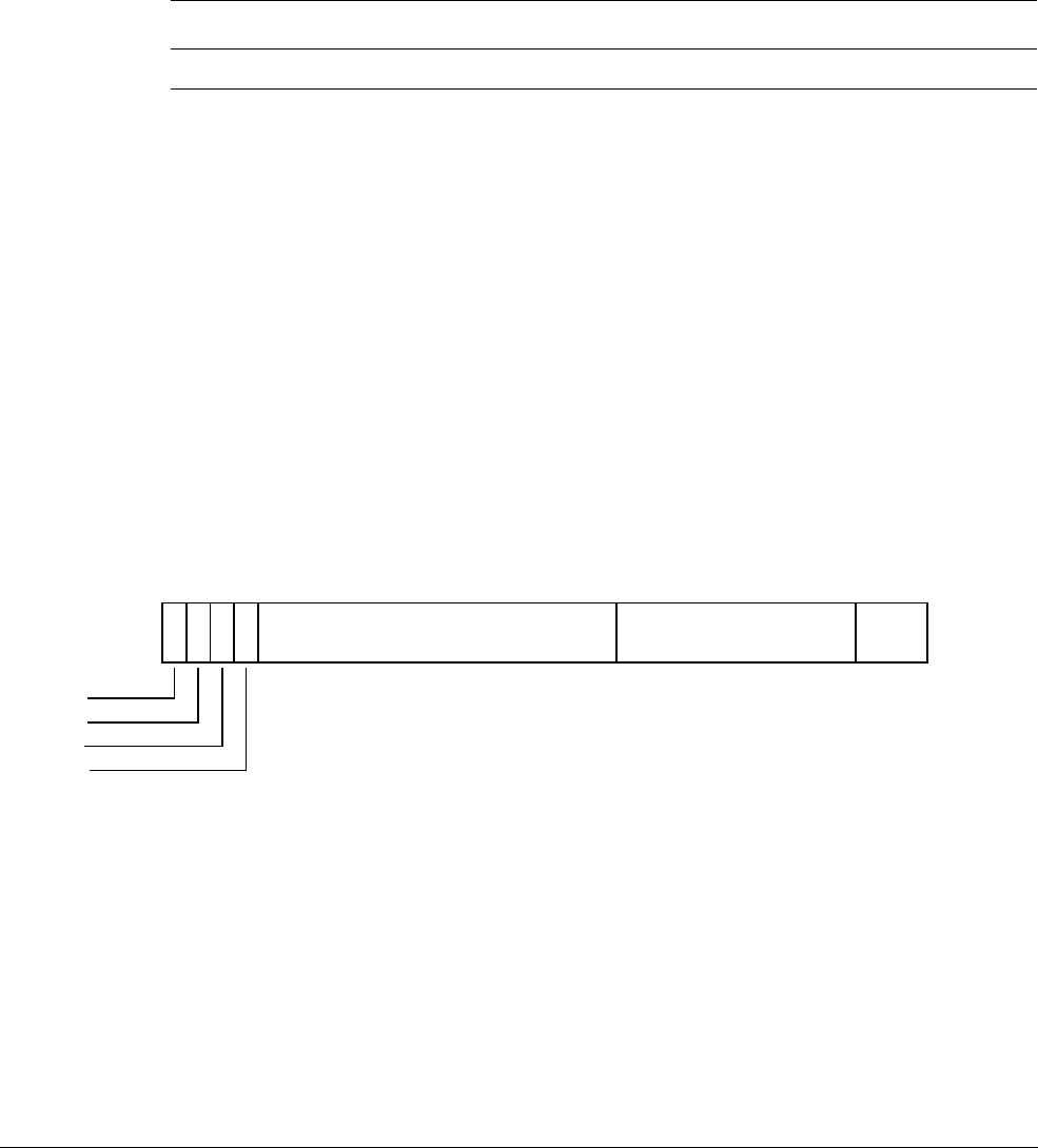
G4 AArch32 System Register Descriptions
G4.2 General system control registers
ARM DDI 0487A.a Copyright © 2013 ARM Limited. All rights reserved. G4-3799
ID090413 Non-Confidential - Beta
G4.2.21 CCSIDR, Current Cache Size ID Register
The CCSIDR characteristics are:
Purpose
Provides information about the architecture of the currently selected cache.
This register is part of the Identification registers functional group.
Usage constraints
This register is accessible as shown below:
If CSSELR indicates a cache that is not implemented, then on a read of the CCSIDR the behavior
is CONSTRAINED UNPREDICTABLE, and can be one of the following:
• The CCSIDR read is treated as NOP.
• The CCSIDR read is UNDEFINED.
• The CCSIDR read returns an UNKNOWN value.
Configurations
CCSIDR is architecturally mapped to AArch64 register CCSIDR_EL1.
There is one instance of this register that is used in both Secure and Non-secure states.
The implementation includes one CCSIDR for each cache that it can access. CSSELR and the
security state select which Cache Size ID Register is accessible.
Attributes
CCSIDR is a 32-bit register.
The CCSIDR bit assignments are:
WT, bit [31]
Indicates whether the selected cache level supports write-through. Permitted values are:
0
Write-through not supported.
1
Write-through supported.
WB, bit [30]
Indicates whether the selected cache level supports write-back. Permitted values are:
0
Write-back not supported.
1
Write-back supported.
EL0 (NS) EL0 (S) EL1 (NS) EL1 (S) EL2 EL3 (SCR.NS=1) EL3 (SCR.NS=0)
- - RO RO RO RO RO
31 30 29 28
NumSets
27 13
Associativity
12 3
LineSize
20
WT
WB
RA
WA

G4 AArch32 System Register Descriptions
G4.2 General system control registers
G4-3800 Copyright © 2013 ARM Limited. All rights reserved. ARM DDI 0487A.a
Non-Confidential - Beta ID090413
RA, bit [29]
Indicates whether the selected cache level supports read-allocation. Permitted values are:
0
Read-allocation not supported.
1
Read-allocation supported.
WA, bit [28]
Indicates whether the selected cache level supports write-allocation. Permitted values are:
0
Write-allocation not supported.
1
Write-allocation supported.
NumSets, bits [27:13]
(Number of sets in cache) - 1, therefore a value of 0 indicates 1 set in the cache. The number of sets
does not have to be a power of 2.
Associativity, bits [12:3]
(Associativity of cache) - 1, therefore a value of 0 indicates an associativity of 1. The associativity
does not have to be a power of 2.
LineSize, bits [2:0]
(Log2(Number of bytes in cache line)) - 4. For example:
For a line length of 16 bytes: Log2(16) = 4, LineSize entry = 0. This is the minimum line length.
For a line length of 32 bytes: Log2(32) = 5, LineSize entry = 1.
Accessing the CCSIDR:
To access the CCSIDR:
MRC p15,1,<Rt>,c0,c0,0 ; Read CCSIDR into Rt
Register access is encoded as follows:
coproc opc1 CRn CRm opc2
1111 001 0000 0000 000
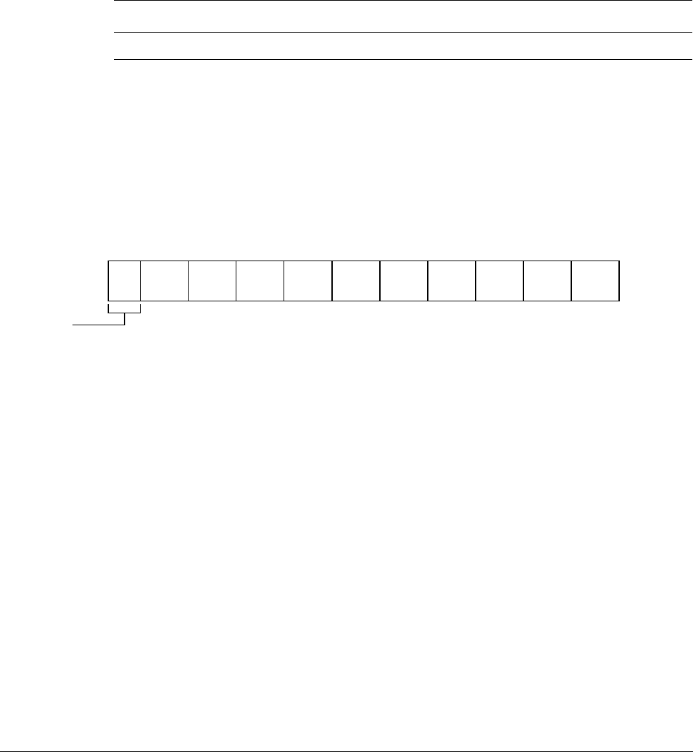
G4 AArch32 System Register Descriptions
G4.2 General system control registers
ARM DDI 0487A.a Copyright © 2013 ARM Limited. All rights reserved. G4-3801
ID090413 Non-Confidential - Beta
G4.2.22 CLIDR, Cache Level ID Register
The CLIDR characteristics are:
Purpose
Identifies the type of cache, or caches, implemented at each level, up to a maximum of seven levels.
Also identifies the Level of Coherency and Level of Unification for the cache hierarchy.
This register is part of the Identification registers functional group.
Usage constraints
This register is accessible as shown below:
Configurations
CLIDR is architecturally mapped to AArch64 register CLIDR_EL1.
There is one instance of this register that is used in both Secure and Non-secure states.
Attributes
CLIDR is a 32-bit register.
The CLIDR bit assignments are:
Bits [31:30]
Reserved, RES0.
LoUU, bits [29:27]
Level of Unification Uniprocessor for the cache hierarchy.
LoC, bits [26:24]
Level of Coherency for the cache hierarchy.
LoUIS, bits [23:21]
Level of Unification Inner Shareable for the cache hierarchy.
Ctype<n>, bits [3(n-1)+2:3(n-1)], for n = 1 to 7
Cache Type fields. Indicate the type of cache implemented at each level, from Level 1 up to a
maximum of seven levels of cache hierarchy. Possible values of each field are:
000
No cache.
001
Instruction cache only.
010
Data cache only.
011
Separate instruction and data caches.
100
Unified cache.
All other values are reserved.
EL0 (NS) EL0 (S) EL1 (NS) EL1 (S) EL2 EL3 (SCR.NS=1) EL3 (SCR.NS=0)
- - RO RO RO RO RO
31 30
LoUU
29 27
LoC
26 24
LoUIS
23 21
Ctype7
20 18
Ctype6
17 15
Ctype5
14 12
Ctype4
11 9
Ctype3
86
Ctype2
53
Ctype1
20
RES0

G4 AArch32 System Register Descriptions
G4.2 General system control registers
G4-3802 Copyright © 2013 ARM Limited. All rights reserved. ARM DDI 0487A.a
Non-Confidential - Beta ID090413
If software reads the Cache Type fields from Ctype1 upwards, once it has seen a value of
0b000
, no
caches exist at further-out levels of the hierarchy. So, for example, if Ctype3 is the first Cache Type
field with a value of
0b000
, the values of Ctype4 to Ctype7 must be ignored.
Accessing the CLIDR:
To access the CLIDR:
MRC p15,1,<Rt>,c0,c0,1 ; Read CLIDR into Rt
Register access is encoded as follows:
coproc opc1 CRn CRm opc2
1111 001 0000 0000 001

G4 AArch32 System Register Descriptions
G4.2 General system control registers
ARM DDI 0487A.a Copyright © 2013 ARM Limited. All rights reserved. G4-3803
ID090413 Non-Confidential - Beta
G4.2.23 CONTEXTIDR, Context ID Register
The CONTEXTIDR characteristics are:
Purpose
Identifies the current Process Identifier and, when using the Short-descriptor translation table
format, the Address Space Identifier.
This register is part of the Virtual memory control registers functional group.
Usage constraints
This register is accessible as shown below:
When accessed as CONTEXTIDR(S):
When accessed as CONTEXTIDR(NS):
The value of the whole of this register is called the Context ID and is used by:
• The debug logic, for Linked and Unlinked Context ID matching.
• The trace logic, to identify the current process.
Configurations
CONTEXTIDR(NS) is architecturally mapped to AArch64 register CONTEXTIDR_EL1.
If EL3 is using AArch32, there are separate Secure and Non-secure instances of this register.
The register format depends on whether address translation is using the Long-descriptor or the
Short-descriptor translation table format.
Attributes
CONTEXTIDR is a 32-bit register.
The CONTEXTIDR bit assignments are:
When TTBCR.EAE==0:
PROCID, bits [31:8]
Process Identifier. This field must be programmed with a unique value that identifies the current
process.
ASID, bits [7:0]
Address Space Identifier. This field is programmed with the value of the current ASID.
EL0 (NS) EL0 (S) EL1 (NS) EL1 (S) EL2 EL3 (SCR.NS=1) EL3 (SCR.NS=0)
---RW-- RW
EL0 (NS) EL0 (S) EL1 (NS) EL1 (S) EL2 EL3 (SCR.NS=1) EL3 (SCR.NS=0)
--RW-RWRW -
PROCID
31 8
ASID
70

G4 AArch32 System Register Descriptions
G4.2 General system control registers
G4-3804 Copyright © 2013 ARM Limited. All rights reserved. ARM DDI 0487A.a
Non-Confidential - Beta ID090413
When TTBCR.EAE==1:
PROCID, bits [31:0]
Process Identifier. This field must be programmed with a unique value that identifies the current
process.
Accessing the CONTEXTIDR:
To access the CONTEXTIDR:
MRC p15,0,<Rt>,c13,c0,1 ; Read CONTEXTIDR into Rt
MCR p15,0,<Rt>,c13,c0,1 ; Write Rt to CONTEXTIDR
Register access is encoded as follows:
PROCID
31 0
coproc opc1 CRn CRm opc2
1111 000 1101 0000 001

G4 AArch32 System Register Descriptions
G4.2 General system control registers
ARM DDI 0487A.a Copyright © 2013 ARM Limited. All rights reserved. G4-3805
ID090413 Non-Confidential - Beta
G4.2.24 CP15DMB, CP15 Data Memory Barrier operation
The CP15DMB characteristics are:
Purpose
Performs a Data Memory Barrier.
This register is part of the Legacy feature registers functional group.
Usage constraints
This operation can be performed at the exception levels shown below:
If SCTLR.CP15BEN is set to 0, this operation is disabled and its encoding is UNDEFINED.
ARM deprecates any use of this operation, and strongly recommends that software use the DMB
instruction instead.
Configurations
There are no configuration notes.
Attributes
CP15DMB is a 32-bit system operation.
The CP15DMB operation ignores the value in the register specified by the instruction used to perform this
operation. Software does not have to write a value to the register before issuing this instruction.
Performing the CP15DMB operation:
To perform the CP15DMB operation:
MCR p15,0,<Rt>,c7,c10,5 ; CP15DMB operation, ignoring the value in Rt
The operation is encoded as follows:
EL0 (NS) EL0 (S) EL1 (NS) EL1 (S) EL2 EL3 (SCR.NS=1) EL3 (SCR.NS=0)
WO WO WO WO WO WO WO
coproc opc1 CRn CRm opc2
1111 000 0111 1010 101

G4 AArch32 System Register Descriptions
G4.2 General system control registers
G4-3806 Copyright © 2013 ARM Limited. All rights reserved. ARM DDI 0487A.a
Non-Confidential - Beta ID090413
G4.2.25 CP15DSB, CP15 Data Synchronization Barrier operation
The CP15DSB characteristics are:
Purpose
Performs a Data Synchronization Barrier.
This register is part of the Legacy feature registers functional group.
Usage constraints
This operation can be performed at the exception levels shown below:
If SCTLR.CP15BEN is set to 0, this operation is disabled and its encoding is UNDEFINED.
ARM deprecates any use of this operation, and strongly recommends that software use the DSB
instruction instead.
Configurations
There are no configuration notes.
Attributes
CP15DSB is a 32-bit system operation.
The CP15DSB operation ignores the value in the register specified by the instruction used to perform this operation.
Software does not have to write a value to the register before issuing this instruction.
Performing the CP15DSB operation:
To perform the CP15DSB operation:
MCR p15,0,<Rt>,c7,c10,4 ; CP15DSB operation, ignoring the value in Rt
The operation is encoded as follows:
EL0 (NS) EL0 (S) EL1 (NS) EL1 (S) EL2 EL3 (SCR.NS=1) EL3 (SCR.NS=0)
WO WO WO WO WO WO WO
coproc opc1 CRn CRm opc2
1111 000 0111 1010 100

G4 AArch32 System Register Descriptions
G4.2 General system control registers
ARM DDI 0487A.a Copyright © 2013 ARM Limited. All rights reserved. G4-3807
ID090413 Non-Confidential - Beta
G4.2.26 CP15ISB, CP15 Instruction Synchronization Barrier operation
The CP15ISB characteristics are:
Purpose
Performs an Instruction Synchronization Barrier.
This register is part of the Legacy feature registers functional group.
Usage constraints
This operation can be performed at the exception levels shown below:
If SCTLR.CP15BEN is set to 0, this operation is disabled and its encoding is UNDEFINED.
ARM deprecates any use of this operation, and strongly recommends that software use the ISB
instruction instead.
Configurations
There are no configuration notes.
Attributes
CP15ISB is a 32-bit system operation.
The CP15ISB operation ignores the value in the register specified by the instruction used to perform this operation.
Software does not have to write a value to the register before issuing this instruction.
Performing the CP15ISB operation:
To perform the CP15ISB operation:
MCR p15,0,<Rt>,c7,c5,4 ; CP15ISB operation, ignoring the value in Rt
The operation is encoded as follows:
EL0 (NS) EL0 (S) EL1 (NS) EL1 (S) EL2 EL3 (SCR.NS=1) EL3 (SCR.NS=0)
WO WO WO WO WO WO WO
coproc opc1 CRn CRm opc2
1111 000 0111 0101 100
G4 AArch32 System Register Descriptions
G4.2 General system control registers
G4-3808 Copyright © 2013 ARM Limited. All rights reserved. ARM DDI 0487A.a
Non-Confidential - Beta ID090413
G4.2.27 CPACR, Architectural Feature Access Control Register
The CPACR characteristics are:
Purpose
Controls access to Trace, Floating-point, and Advanced SIMD functionality.
This register is part of the Other system control registers functional group.
Usage constraints
This register is accessible as shown below:
In an implementation that includes EL2, the CPACR has no effect on instructions executed at EL2.
Configurations
CPACR is architecturally mapped to AArch64 register CPACR_EL1.
There is one instance of this register that is used in both Secure and Non-secure states.
Bits in the NSACR control Non-secure access to the CPACR fields. See the field descriptions for
more information.
Attributes
CPACR is a 32-bit register.
The CPACR bit assignments are:
ASEDIS, bit [31]
Disable Advanced SIMD functionality:
0
Does not cause any instructions to be UNDEFINED.
1
All instruction encodings that are part of Advanced SIMD, but that are not VFPv3 or
VFPv4 instructions, are UNDEFINED.
In Non-secure state, if NSACR.NSASEDIS is set to 1, this bit is RES1.
Resets to 0.
Bits [30:29]
Reserved, RES0.
TRCDIS, bit [28]
Disable CP14 access to trace registers:
0
Does not cause any instructions to be UNDEFINED.
1
Any MRC or MCR instruction with coproc set to
0b1110
and opc1 set to
0b001
is
UNDEFINED.
EL0 (NS) EL0 (S) EL1 (NS) EL1 (S) EL2 EL3 (SCR.NS=1) EL3 (SCR.NS=0)
- - RW RW RW RW RW
31 30 29 28
RES0
27 24
cp11
23 22
cp10
21 20
RES0
19 0
ASEDIS
RES0
TRCDIS

G4 AArch32 System Register Descriptions
G4.2 General system control registers
ARM DDI 0487A.a Copyright © 2013 ARM Limited. All rights reserved. G4-3809
ID090413 Non-Confidential - Beta
In Non-secure state, if NSACR.NSTRCDIS is set to 1, this bit is RES1.
Reset value is architecturally UNKNOWN.
Bits [27:24]
Reserved, RES0.
cp<n>, bits [2n+1:2n], for n = 10 to 11
Defines the access rights for coprocessors 10 and 11, which control the Floating-point and
Advanced SIMD features. Possible values of the fields are:
00
Access denied. Any attempt to access Floating-point and Advanced SIMD registers or
instructions generates an Undefined Instruction exception.
01
Access at EL1 only. Any attempt to access Floating-point and Advanced SIMD registers
or instructions from software executing at EL0 generates an Undefined Instruction
exception.
11
Full access.
The value
0b10
is reserved.
In Non-secure state, if NSACR.cp<n> is set to 0, this bit is RES0.
The Floating-point and Advanced SIMD features controlled by these fields are:
• VFP floating-point instructions.
• Advanced SIMD instructions (both integer and floating-point).
• Advanced SIMD and Floating-point registers D0-D31 and their views as S0-S31 and
Q0-Q15.
•FPSCR, FPSID, MVFR0, MVFR1, MVFR2, FPEXC system registers.
If the cp11 and cp10 fields are set to different values, the behavior is CONSTRAINED UNPREDICTABLE,
and is the same as if both fields were set to the value of cp10, in all respects other than the value
read back by explicitly reading cp11.
Other coprocessors are not supported in ARMv8, so bits[27:24] and bits[19:0] are RES0.
Resets to 0.
Bits [19:0]
Reserved, RES0.
Accessing the CPACR:
To access the CPACR:
MRC p15,0,<Rt>,c1,c0,2 ; Read CPACR into Rt
MCR p15,0,<Rt>,c1,c0,2 ; Write Rt to CPACR
Register access is encoded as follows:
coproc opc1 CRn CRm opc2
1111 000 0001 0000 010
G4 AArch32 System Register Descriptions
G4.2 General system control registers
G4-3810 Copyright © 2013 ARM Limited. All rights reserved. ARM DDI 0487A.a
Non-Confidential - Beta ID090413
G4.2.28 CPSR, Current Program Status Register
The CPSR characteristics are:
Purpose
Holds processor status and control information.
This register is part of the Process state registers functional group.
Usage constraints
The CPSR can be read using the
MRS
instruction and written using the
MSR
(immediate) or
MSR
(register) instructions. For more information see MRS on page F7-2720, MSR (immediate) on
page F7-2722, and MSR (register) on page F7-2724.
Configurations
There is one instance of this register that is used in both Secure and Non-secure states.
Attributes
CPSR is a 32-bit register.
The CPSR bit assignments are:
N, bit [31]
Negative condition flag. Set to bit[31] of the result of the last flag-setting instruction. If the result is
regarded as a two's complement signed integer, then the processor sets N to 1 if the result was
negative, and sets N to 0 if it was positive or zero.
Z, bit [30]
Zero condition flag. Set to 1 if the result of the last flag-setting instruction was zero, and to 0
otherwise. A result of zero often indicates an equal result from a comparison.
C, bit [29]
Carry condition flag. Set to 1 if the last flag-setting instruction resulted in a carry condition, for
example an unsigned overflow on an addition.
V, bit [28]
Overflow condition flag. Set to 1 if the last flag-setting instruction resulted in an overflow condition,
for example a signed overflow on an addition.
Q, bit [27]
Cumulative saturation bit. Set to 1 to indicate that overflow or saturation occurred in some
instructions.
IT[1:0], bits [26:25]
If-Then execution state bits for the T32 IT (If-Then) instruction. See IT[7:2] for explanation of this
field.
Bits [23:20]
Reserved, RES0.
N
31
Z
30
C
29
V
28
Q
27 26 25
J
24
RES0
23 20
GE
19 16
IT[7:2]
15 10
E
9
A
8
I
7
F
6
T
54
M[3:0]
30
IT[1:0] RES1

G4 AArch32 System Register Descriptions
G4.2 General system control registers
ARM DDI 0487A.a Copyright © 2013 ARM Limited. All rights reserved. G4-3811
ID090413 Non-Confidential - Beta
GE, bits [19:16]
Greater than or Equal flags, for parallel addition and subtraction.
IT[7:2], bits [15:10]
If-Then execution state bits for the T32 IT (If-Then) instruction. This field must be interpreted in
two parts.
• IT[7:5] holds the base condition for the IT block. The base condition is the top 3 bits of the
condition code specified by the first condition field of the IT instruction.
• IT[4:0] encodes the size of the IT block, which is the number of instructions that are to be
conditionally executed, by the position of the least significant 1 in this field. It also encodes
the value of the least significant bit of the condition code for each instruction in the block.
The IT field is
0b00000000
when no IT block is active.
E, bit [9]
Endianness execution state bit. Controls the load and store endianness for data accesses:
0
Little-endian operation
1
Big-endian operation.
Instruction fetches ignore this bit.
When the reset value of the SCTLR.EE bit is defined by a configuration input signal, that value also
applies to the CPSR.E bit on reset, and therefore applies to software execution from reset.
If an implementation does not provide Big-endian support, this bit is RES0. If it does not provide
Little-endian support, this bit is RES1.
If an implementation provides Big-endian support but only at EL0, this bit is RES0 for an exception
return to any exception level other than EL0.
Likewise, if it provides Little-endian support only at EL0, this bit is RES1 for an exception return
to any exception level other than EL0.
A, bit [8]
Asynchronous data abort mask bit. The possible values of this bit are:
0
Exception not masked.
1
Exception masked.
I, bit [7]
IRQ mask bit. The possible values of this bit are:
0
Exception not masked.
1
Exception masked.
F, bit [6]
FIQ mask bit. The possible values of this bit are:
0
Exception not masked.
1
Exception masked.
Bit [4]
Reserved, RES1.

G4 AArch32 System Register Descriptions
G4.2 General system control registers
G4-3812 Copyright © 2013 ARM Limited. All rights reserved. ARM DDI 0487A.a
Non-Confidential - Beta ID090413
M[3:0], bits [3:0]
Current processor mode. Possible values are:
Other values are reserved.
M[3:0] Mode
0b0000
User
0b0001
FIQ
0b0010
IRQ
0b0011
Supervisor
0b0110
Monitor
0b0111
Abort
0b1010
Hyp
0b1011
Undefined
0b1111
System

G4 AArch32 System Register Descriptions
G4.2 General system control registers
ARM DDI 0487A.a Copyright © 2013 ARM Limited. All rights reserved. G4-3813
ID090413 Non-Confidential - Beta
G4.2.29 CSSELR, Cache Size Selection Register
The CSSELR characteristics are:
Purpose
Selects the current Cache Size ID Register, CCSIDR, by specifying the required cache level and the
cache type (either instruction or data cache).
This register is part of the Identification registers functional group.
Usage constraints
This register is accessible as shown below:
When accessed as CSSELR(S):
When accessed as CSSELR(NS):
If the CSSELR level field is programmed to a cache level that is not implemented, then a read of
CSSELR is CONSTRAINED UNPREDICTABLE, and returns an UNKNOWN value in CSSELR.Level.
Configurations
CSSELR(NS) is architecturally mapped to AArch64 register CSSELR_EL1.
If EL3 is using AArch32, there are separate Secure and Non-secure instances of this register.
Attributes
CSSELR is a 32-bit register.
The CSSELR bit assignments are:
Bits [31:4]
Reserved, RES0.
Level, bits [3:1]
Cache level of required cache. Permitted values are from
0b000
, indicating Level 1 cache, to
0b110
indicating Level 7 cache.
InD, bit [0]
Instruction not Data bit. Permitted values are:
0
Data or unified cache.
1
Instruction cache.
EL0 (NS) EL0 (S) EL1 (NS) EL1 (S) EL2 EL3 (SCR.NS=1) EL3 (SCR.NS=0)
---RW-- RW
EL0 (NS) EL0 (S) EL1 (NS) EL1 (S) EL2 EL3 (SCR.NS=1) EL3 (SCR.NS=0)
--RW-RWRW -
RES0
31 4
Level
31
0
InD

G4 AArch32 System Register Descriptions
G4.2 General system control registers
G4-3814 Copyright © 2013 ARM Limited. All rights reserved. ARM DDI 0487A.a
Non-Confidential - Beta ID090413
Accessing the CSSELR:
To access the CSSELR:
MRC p15,2,<Rt>,c0,c0,0 ; Read CSSELR into Rt
MCR p15,2,<Rt>,c0,c0,0 ; Write Rt to CSSELR
Register access is encoded as follows:
coproc opc1 CRn CRm opc2
1111 010 0000 0000 000

G4 AArch32 System Register Descriptions
G4.2 General system control registers
ARM DDI 0487A.a Copyright © 2013 ARM Limited. All rights reserved. G4-3815
ID090413 Non-Confidential - Beta
G4.2.30 CTR, Cache Type Register
The CTR characteristics are:
Purpose
Provides information about the architecture of the caches.
This register is part of the Identification registers functional group.
Usage constraints
This register is accessible as shown below:
Configurations
CTR is architecturally mapped to AArch64 register CTR_EL0.
There is one instance of this register that is used in both Secure and Non-secure states.
Attributes
CTR is a 32-bit register.
The CTR bit assignments are:
Bit [31]
Reserved, RES1.
Bits [30:28]
Reserved, RES0.
CWG, bits [27:24]
Cache Writeback Granule. Log2 of the number of words of the maximum size of memory that can
be overwritten as a result of the eviction of a cache entry that has had a memory location in it
modified.
A value of
0b0000
indicates that this register does not provide Cache Writeback Granule information
and either:
• The architectural maximum of 512 words (2Kbytes) must be assumed.
• The Cache Writeback Granule can be determined from maximum cache line size encoded in
the Cache Size ID Registers.
Values greater than
0b1001
are reserved.
ERG, bits [23:20]
Exclusives Reservation Granule. Log2 of the number of words of the maximum size of the
reservation granule that has been implemented for the Load-Exclusive and Store-Exclusive
instructions.
A value of
0b0000
indicates that this register does not provide Exclusives Reservation Granule
information and the architectural maximum of 512 words (2Kbytes) must be assumed.
EL0 (NS) EL0 (S) EL1 (NS) EL1 (S) EL2 EL3 (SCR.NS=1) EL3 (SCR.NS=0)
- - RO RO RO RO RO
31
RES0
30 28
CWG
27 24
ERG
23 20
DminLine
19 16
L1Ip
15 14
RES0
13 4
IminLine
30
RES1

G4 AArch32 System Register Descriptions
G4.2 General system control registers
G4-3816 Copyright © 2013 ARM Limited. All rights reserved. ARM DDI 0487A.a
Non-Confidential - Beta ID090413
Values greater than
0b1001
are reserved.
DminLine, bits [19:16]
Log2 of the number of words in the smallest cache line of all the data caches and unified caches that
are controlled by the processor.
L1Ip, bits [15:14]
Level 1 instruction cache policy. Indicates the indexing and tagging policy for the L1 instruction
cache. Possible values of this field are:
01
ASID-tagged Virtual Index, Virtual Tag (AIVIVT)
10
Virtual Index, Physical Tag (VIPT)
11
Physical Index, Physical Tag (PIPT)
Other values are reserved.
Bits [13:4]
Reserved, RES0.
IminLine, bits [3:0]
Log2 of the number of words in the smallest cache line of all the instruction caches that are
controlled by the processor.
Accessing the CTR:
To access the CTR:
MRC p15,0,<Rt>,c0,c0,1 ; Read CTR into Rt
Register access is encoded as follows:
coproc opc1 CRn CRm opc2
1111 000 0000 0000 001

G4 AArch32 System Register Descriptions
G4.2 General system control registers
ARM DDI 0487A.a Copyright © 2013 ARM Limited. All rights reserved. G4-3817
ID090413 Non-Confidential - Beta
G4.2.31 DACR, Domain Access Control Register
The DACR characteristics are:
Purpose
Defines the access permission for each of the sixteen memory domains.
This register is part of the Virtual memory control registers functional group.
Usage constraints
This register is accessible as shown below:
When accessed as DACR(S):
When accessed as DACR(NS):
Configurations
DACR(NS) is architecturally mapped to AArch64 register DACR32_EL2.
If EL3 is using AArch32, there are separate Secure and Non-secure instances of this register.
DACR has write access to the Secure copy of the register disabled when the CP15SDISABLE signal
is asserted HIGH.
In an implementation that includes the Large Physical Address Extension, this register has no
function when TTBCR.EAE is set to 1, to select the Long-descriptor translation table format.
Attributes
DACR is a 32-bit register.
The DACR bit assignments are:
D<n>, bits [2n+1:2n], for n = 0 to 15
Domain n access permission, where n = 0 to 15. Permitted values are:
00
No access. Any access to the domain generates a Domain fault.
01
Client. Accesses are checked against the permission bits in the translation tables.
11
Manager. Accesses are not checked against the permission bits in the translation tables.
The value
0b10
is reserved.
Accessing the DACR:
To access the DACR:
MRC p15,0,<Rt>,c3,c0,0 ; Read DACR into Rt
MCR p15,0,<Rt>,c3,c0,0 ; Write Rt to DACR
EL0 (NS) EL0 (S) EL1 (NS) EL1 (S) EL2 EL3 (SCR.NS=1) EL3 (SCR.NS=0)
---RW-- RW
EL0 (NS) EL0 (S) EL1 (NS) EL1 (S) EL2 EL3 (SCR.NS=1) EL3 (SCR.NS=0)
--RW-RWRW -
D15
31 30
D14
29 28
D13
27 26
D12
25 24
D11
23 22
D10
21 20
D9
19 18
D8
17 16
D7
15 14
D6
13 12
D5
11 10
D4
98
D3
76
D2
54
D1
32
D0
10

G4 AArch32 System Register Descriptions
G4.2 General system control registers
G4-3818 Copyright © 2013 ARM Limited. All rights reserved. ARM DDI 0487A.a
Non-Confidential - Beta ID090413
Register access is encoded as follows:
coproc opc1 CRn CRm opc2
1111 000 0011 0000 000

G4 AArch32 System Register Descriptions
G4.2 General system control registers
ARM DDI 0487A.a Copyright © 2013 ARM Limited. All rights reserved. G4-3819
ID090413 Non-Confidential - Beta
G4.2.32 DCCIMVAC, Data Cache line Clean and Invalidate by VA to PoC
The DCCIMVAC characteristics are:
Purpose
Clean and Invalidate data or unified cache line by virtual address to PoC.
This register is part of the Cache maintenance operations functional group.
Usage constraints
This operation can be performed at the exception levels shown below:
Configurations
DCCIMVAC performs the same function as AArch64 operation DC CIVAC.
Attributes
DCCIMVAC is a 32-bit system operation.
The DCCIMVAC input value bit assignments are:
Bits [31:0]
Virtual address to use.
Performing the DCCIMVAC operation:
To perform the DCCIMVAC operation:
MCR p15,0,<Rt>,c7,c14,1 ; DCCIMVAC operation
The operation is encoded as follows:
EL0 (NS) EL0 (S) EL1 (NS) EL1 (S) EL2 EL3 (SCR.NS=1) EL3 (SCR.NS=0)
- - WO WO WO WO WO
Virtual address to use
31 0
coproc opc1 CRn CRm opc2
1111 000 0111 1110 001

G4 AArch32 System Register Descriptions
G4.2 General system control registers
G4-3820 Copyright © 2013 ARM Limited. All rights reserved. ARM DDI 0487A.a
Non-Confidential - Beta ID090413
G4.2.33 DCCISW, Data Cache line Clean and Invalidate by Set/Way
The DCCISW characteristics are:
Purpose
Clean and Invalidate data or unified cache line by set/way.
This register is part of the Cache maintenance operations functional group.
Usage constraints
This operation can be performed at the exception levels shown below:
Configurations
DCCISW performs the same function as AArch64 operation DC CISW.
Attributes
DCCISW is a 32-bit system operation.
The DCCISW input value bit assignments are:
SetWay, bits [31:4]
Contains two fields:
• Way, bits[31:32-A], the number of the way to operate on.
• Set, bits[B-1:L], the number of the set to operate on.
Bits[L-1:4] are RES0.
A = Log2(ASSOCIATIVITY), L = Log2(LINELEN), B = (L + S), S = Log2(NSETS).
ASSOCIATIVITY, LINELEN (line length, in bytes), and NSETS (number of sets) have their usual
meanings and are the values for the cache level being operated on. The values of A and S are
rounded up to the next integer.
Level, bits [3:1]
Cache level to operate on, minus 1. For example, this field is 0 for operations on L1 cache, or 1 for
operations on L2 cache.
Bit [0]
Reserved, RES0.
Performing the DCCISW operation:
To perform the DCCISW operation:
MCR p15,0,<Rt>,c7,c14,2 ; DCCISW operation
EL0 (NS) EL0 (S) EL1 (NS) EL1 (S) EL2 EL3 (SCR.NS=1) EL3 (SCR.NS=0)
- - WO WO WO WO WO
SetWay
31 4
Level
31
0
RES0

G4 AArch32 System Register Descriptions
G4.2 General system control registers
ARM DDI 0487A.a Copyright © 2013 ARM Limited. All rights reserved. G4-3821
ID090413 Non-Confidential - Beta
The operation is encoded as follows:
coproc opc1 CRn CRm opc2
1111 000 0111 1110 010

G4 AArch32 System Register Descriptions
G4.2 General system control registers
G4-3822 Copyright © 2013 ARM Limited. All rights reserved. ARM DDI 0487A.a
Non-Confidential - Beta ID090413
G4.2.34 DCCMVAC, Data Cache line Clean by VA to PoC
The DCCMVAC characteristics are:
Purpose
Clean data or unified cache line by virtual address to PoC.
This register is part of the Cache maintenance operations functional group.
Usage constraints
This operation can be performed at the exception levels shown below:
Configurations
DCCMVAC performs the same function as AArch64 operation DC CVAC.
Attributes
DCCMVAC is a 32-bit system operation.
The DCCMVAC input value bit assignments are:
Bits [31:0]
Virtual address to use.
Performing the DCCMVAC operation:
To perform the DCCMVAC operation:
MCR p15,0,<Rt>,c7,c10,1 ; DCCMVAC operation
The operation is encoded as follows:
EL0 (NS) EL0 (S) EL1 (NS) EL1 (S) EL2 EL3 (SCR.NS=1) EL3 (SCR.NS=0)
- - WO WO WO WO WO
Virtual address to use
31 0
coproc opc1 CRn CRm opc2
1111 000 0111 1010 001

G4 AArch32 System Register Descriptions
G4.2 General system control registers
ARM DDI 0487A.a Copyright © 2013 ARM Limited. All rights reserved. G4-3823
ID090413 Non-Confidential - Beta
G4.2.35 DCCMVAU, Data Cache line Clean by VA to PoU
The DCCMVAU characteristics are:
Purpose
Clean data or unified cache line by virtual address to PoU.
This register is part of the Cache maintenance operations functional group.
Usage constraints
This operation can be performed at the exception levels shown below:
Configurations
DCCMVAU performs the same function as AArch64 operation DC CVAU.
Attributes
DCCMVAU is a 32-bit system operation.
The DCCMVAU input value bit assignments are:
Bits [31:0]
Virtual address to use.
Performing the DCCMVAU operation:
To perform the DCCMVAU operation:
MCR p15,0,<Rt>,c7,c11,1 ; DCCMVAU operation
The operation is encoded as follows:
EL0 (NS) EL0 (S) EL1 (NS) EL1 (S) EL2 EL3 (SCR.NS=1) EL3 (SCR.NS=0)
- - WO WO WO WO WO
Virtual address to use
31 0
coproc opc1 CRn CRm opc2
1111 000 0111 1011 001

G4 AArch32 System Register Descriptions
G4.2 General system control registers
G4-3824 Copyright © 2013 ARM Limited. All rights reserved. ARM DDI 0487A.a
Non-Confidential - Beta ID090413
G4.2.36 DCCSW, Data Cache line Clean by Set/Way
The DCCSW characteristics are:
Purpose
Clean data or unified cache line by set/way.
This register is part of the Cache maintenance operations functional group.
Usage constraints
This operation can be performed at the exception levels shown below:
Configurations
DCCSW performs the same function as AArch64 operation DC CSW.
Attributes
DCCSW is a 32-bit system operation.
The DCCSW input value bit assignments are:
SetWay, bits [31:4]
Contains two fields:
• Way, bits[31:32-A], the number of the way to operate on.
• Set, bits[B-1:L], the number of the set to operate on.
Bits[L-1:4] are RES0.
A = Log2(ASSOCIATIVITY), L = Log2(LINELEN), B = (L + S), S = Log2(NSETS).
ASSOCIATIVITY, LINELEN (line length, in bytes), and NSETS (number of sets) have their usual
meanings and are the values for the cache level being operated on. The values of A and S are
rounded up to the next integer.
Level, bits [3:1]
Cache level to operate on, minus 1. For example, this field is 0 for operations on L1 cache, or 1 for
operations on L2 cache.
Bit [0]
Reserved, RES0.
Performing the DCCSW operation:
To perform the DCCSW operation:
MCR p15,0,<Rt>,c7,c10,2 ; DCCSW operation
EL0 (NS) EL0 (S) EL1 (NS) EL1 (S) EL2 EL3 (SCR.NS=1) EL3 (SCR.NS=0)
- - WO WO WO WO WO
SetWay
31 4
Level
31
0
RES0

G4 AArch32 System Register Descriptions
G4.2 General system control registers
ARM DDI 0487A.a Copyright © 2013 ARM Limited. All rights reserved. G4-3825
ID090413 Non-Confidential - Beta
The operation is encoded as follows:
coproc opc1 CRn CRm opc2
1111 000 0111 1010 010

G4 AArch32 System Register Descriptions
G4.2 General system control registers
G4-3826 Copyright © 2013 ARM Limited. All rights reserved. ARM DDI 0487A.a
Non-Confidential - Beta ID090413
G4.2.37 DCIMVAC, Data Cache line Invalidate by VA to PoC
The DCIMVAC characteristics are:
Purpose
Invalidate data or unified cache line by virtual address to PoC.
This register is part of the Cache maintenance operations functional group.
Usage constraints
This operation can be performed at the exception levels shown below:
At EL1, this operation must be performed as DCCIMVAC if all of the following apply:
• EL2 is implemented.
•HCR.VM is set to 1.
•SCR.NS is set to 1 or EL3 is not implemented.
Configurations
DCIMVAC performs the same function as AArch64 operation DC IVAC.
Attributes
DCIMVAC is a 32-bit system operation.
The DCIMVAC input value bit assignments are:
Bits [31:0]
Virtual address to use.
Performing the DCIMVAC operation:
To perform the DCIMVAC operation:
MCR p15,0,<Rt>,c7,c6,1 ; DCIMVAC operation
The operation is encoded as follows:
EL0 (NS) EL0 (S) EL1 (NS) EL1 (S) EL2 EL3 (SCR.NS=1) EL3 (SCR.NS=0)
- - WO WO WO WO WO
Virtual address to use
31 0
coproc opc1 CRn CRm opc2
1111 000 0111 0110 001

G4 AArch32 System Register Descriptions
G4.2 General system control registers
ARM DDI 0487A.a Copyright © 2013 ARM Limited. All rights reserved. G4-3827
ID090413 Non-Confidential - Beta
G4.2.38 DCISW, Data Cache line Invalidate by Set/Way
The DCISW characteristics are:
Purpose
Invalidate data or unified cache line by set/way.
This register is part of the Cache maintenance operations functional group.
Usage constraints
This operation can be performed at the exception levels shown below:
At EL1, this operation must be performed as DCCISW if all of the following apply:
• EL2 is implemented
•HCR.VM is set to 1
•SCR.NS is set to 1 or EL3 is not implemented.
Configurations
DCISW performs the same function as AArch64 operation DC ISW.
Attributes
DCISW is a 32-bit system operation.
The DCISW input value bit assignments are:
SetWay, bits [31:4]
Contains two fields:
• Way, bits[31:32-A], the number of the way to operate on.
• Set, bits[B-1:L], the number of the set to operate on.
Bits[L-1:4] are RES0.
A = Log2(ASSOCIATIVITY), L = Log2(LINELEN), B = (L + S), S = Log2(NSETS).
ASSOCIATIVITY, LINELEN (line length, in bytes), and NSETS (number of sets) have their usual
meanings and are the values for the cache level being operated on. The values of A and S are
rounded up to the next integer.
Level, bits [3:1]
Cache level to operate on, minus 1. For example, this field is 0 for operations on L1 cache, or 1 for
operations on L2 cache.
Bit [0]
Reserved, RES0.
EL0 (NS) EL0 (S) EL1 (NS) EL1 (S) EL2 EL3 (SCR.NS=1) EL3 (SCR.NS=0)
- - WO WO WO WO WO
SetWay
31 4
Level
31
0
RES0

G4 AArch32 System Register Descriptions
G4.2 General system control registers
G4-3828 Copyright © 2013 ARM Limited. All rights reserved. ARM DDI 0487A.a
Non-Confidential - Beta ID090413
Performing the DCISW operation:
To perform the DCISW operation:
MCR p15,0,<Rt>,c7,c6,2 ; DCISW operation
The operation is encoded as follows:
coproc opc1 CRn CRm opc2
1111 000 0111 0110 010

G4 AArch32 System Register Descriptions
G4.2 General system control registers
ARM DDI 0487A.a Copyright © 2013 ARM Limited. All rights reserved. G4-3829
ID090413 Non-Confidential - Beta
G4.2.39 DFAR, Data Fault Address Register
The DFAR characteristics are:
Purpose
Holds the virtual address of the faulting address that caused a synchronous Data Abort exception.
This register is part of the Exception and fault handling registers functional group.
Usage constraints
This register is accessible as shown below:
When accessed as DFAR(S):
When accessed as DFAR(NS):
Configurations
DFAR(NS) is architecturally mapped to AArch64 register FAR_EL1[31:0].
DFAR(S) is architecturally mapped to AArch32 register HDFAR when EL2 is implemented.
DFAR(S) is architecturally mapped to AArch64 register FAR_EL2[31:0] when EL2 is
implemented.
DFAR(S) can be mapped to AArch64 register FAR_EL3[31:0] when EL2 is not implemented, but
this is not architecturally mandated.
If EL3 is using AArch32, there are separate Secure and Non-secure instances of this register.
Attributes
DFAR is a 32-bit register.
The DFAR bit assignments are:
Bits [31:0]
VA of faulting address of synchronous Data Abort exception.
Accessing the DFAR:
To access the DFAR:
MRC p15,0,<Rt>,c6,c0,0 ; Read DFAR into Rt
MCR p15,0,<Rt>,c6,c0,0 ; Write Rt to DFAR
EL0 (NS) EL0 (S) EL1 (NS) EL1 (S) EL2 EL3 (SCR.NS=1) EL3 (SCR.NS=0)
---RW-- RW
EL0 (NS) EL0 (S) EL1 (NS) EL1 (S) EL2 EL3 (SCR.NS=1) EL3 (SCR.NS=0)
--RW-RWRW -
VA of faulting address of synchronous Data Abort exception
31 0

G4 AArch32 System Register Descriptions
G4.2 General system control registers
G4-3830 Copyright © 2013 ARM Limited. All rights reserved. ARM DDI 0487A.a
Non-Confidential - Beta ID090413
Register access is encoded as follows:
coproc opc1 CRn CRm opc2
1111 000 0110 0000 000
G4 AArch32 System Register Descriptions
G4.2 General system control registers
ARM DDI 0487A.a Copyright © 2013 ARM Limited. All rights reserved. G4-3831
ID090413 Non-Confidential - Beta
G4.2.40 DFSR, Data Fault Status Register
The DFSR characteristics are:
Purpose
Holds status information about the last data fault.
This register is part of the Exception and fault handling registers functional group.
Usage constraints
This register is accessible as shown below:
When accessed as DFSR(S):
When accessed as DFSR(NS):
Configurations
DFSR(NS) is architecturally mapped to AArch64 register ESR_EL1.
DFSR(S) can be mapped to AArch64 register ESR_EL3, but this is not architecturally mandated.
If EL3 is using AArch32, there are separate Secure and Non-secure instances of this register.
The Large Physical Address Extension adds an alternative format for the register. If an
implementation includes the Large Physical Address Extension then the current translation table
format determines which format of the register is used.
Attributes
DFSR is a 32-bit register.
The DFSR bit assignments are:
When TTBCR.EAE==0:
Bits [31:14]
Reserved, RES0.
EL0 (NS) EL0 (S) EL1 (NS) EL1 (S) EL2 EL3 (SCR.NS=1) EL3 (SCR.NS=0)
---RW-- RW
EL0 (NS) EL0 (S) EL1 (NS) EL1 (S) EL2 EL3 (SCR.NS=1) EL3 (SCR.NS=0)
--RW-RWRW -
RES0
31 14 13 12 11 10 9 8
DOMAIN
74
FS[3:0]
30
RES0
LPAE
FS[4]
WnR
ExT
CM

G4 AArch32 System Register Descriptions
G4.2 General system control registers
G4-3832 Copyright © 2013 ARM Limited. All rights reserved. ARM DDI 0487A.a
Non-Confidential - Beta ID090413
CM, bit [13]
Cache maintenance fault. For synchronous faults, this bit indicates whether a cache maintenance
operation generated the fault. The possible values of this bit are:
0
Abort not caused by a cache maintenance operation.
1
Abort caused by a cache maintenance operation.
On an asynchronous fault, this bit is UNKNOWN.
ExT, bit [12]
External abort type. This bit can be used to provide an IMPLEMENTATION DEFINED classification of
external aborts.
For aborts other than external aborts this bit always returns 0.
WnR, bit [11]
Write not Read bit. Indicates whether the abort was caused by a write or read access. The possible
values of this bit are:
0
Abort caused by a read access.
1
Abort caused by a write access.
For faults on CP15 cache maintenance operations, including the VA to PA translation operations,
this bit always returns a value of 1.
FS[4], bit [10]
See below for description of the FS field.
LPAE, bit [9]
On taking a Data Abort exception, this bit is set as follows:
0
Using the Short-descriptor translation table formats.
1
Using the Long-descriptor translation table formats.
Hardware does not interpret this bit to determine the behavior of the memory system, and therefore
software can set this bit to 0 or 1 without affecting operation.
Bit [8]
Reserved, RES0.
DOMAIN, bits [7:4]
Domain of the fault address. Use of this field is deprecated.
FS[3:0], bits [3:0]
Fault status bits. Possible values of this field are:
0001
Alignment fault
0010
Debug event
0011
Access flag fault, first level
0100
Fault on instruction cache maintenance
0101
Translation fault, first level
0110
Access flag fault, second level
0111
Translation fault, second level
1000
Synchronous external abort
1001
Domain fault, first level
1011
Domain fault, second level
1100
Synchronous external abort on translation table walk, first level
1101
Permission fault, first level
G4 AArch32 System Register Descriptions
G4.2 General system control registers
ARM DDI 0487A.a Copyright © 2013 ARM Limited. All rights reserved. G4-3833
ID090413 Non-Confidential - Beta
1110
Synchronous external abort on translation table walk, second level
1111
Permission fault, second level
10000
TLB conflict abort
10100
IMPLEMENTATION DEFINED fault (Lockdown fault)
10101
IMPLEMENTATION DEFINED fault (Unsupported Exclusive access fault)
10110
Asynchronous external abort
11000
Asynchronous parity error on memory access
11001
Synchronous parity error on memory access
11100
Synchronous parity error on translation table walk, first level
11110
Synchronous parity error on translation table walk, second level
All other values are reserved.
When TTBCR.EAE==1:
Bits [31:14]
Reserved, RES0.
CM, bit [13]
Cache maintenance fault. For synchronous faults, this bit indicates whether a cache maintenance
operation generated the fault. The possible values of this bit are:
0
Abort not caused by a cache maintenance operation.
1
Abort caused by a cache maintenance operation.
On an asynchronous fault, this bit is UNKNOWN.
ExT, bit [12]
External abort type. This bit can be used to provide an IMPLEMENTATION DEFINED classification of
external aborts.
For aborts other than external aborts this bit always returns 0.
WnR, bit [11]
Write not Read bit. Indicates whether the abort was caused by a write or read access. The possible
values of this bit are:
0
Abort caused by a read access.
1
Abort caused by a write access.
For faults on CP15 cache maintenance operations, including the VA to PA translation operations,
this bit always returns a value of 1.
Bit [10]
Reserved, RES0.
RES0
31 14 13 12 11 10 9
RES0
86
STATUS
50
LPAE
RES0
WnR
ExT
CM

G4 AArch32 System Register Descriptions
G4.2 General system control registers
G4-3834 Copyright © 2013 ARM Limited. All rights reserved. ARM DDI 0487A.a
Non-Confidential - Beta ID090413
LPAE, bit [9]
On taking a Data Abort exception, this bit is set as follows:
0
Using the Short-descriptor translation table formats.
1
Using the Long-descriptor translation table formats.
Hardware does not interpret this bit to determine the behavior of the memory system, and therefore
software can set this bit to 0 or 1 without affecting operation.
Bits [8:6]
Reserved, RES0.
STATUS, bits [5:0]
Fault status bits. Possible values of this field are:
000000
Address size fault in TTBR0 or TTBR1
000101
Translation fault, first level
000110
Translation fault, second level
000111
Translation fault, third level
001001
Access flag fault, first level
001010
Access flag fault, second level
001011
Access flag fault, third level
001101
Permission fault, first level
001110
Permission fault, second level
001111
Permission fault, third level
010000
Synchronous external abort
010001
Asynchronous external abort
010101
Synchronous external abort on translation table walk, first level
010110
Synchronous external abort on translation table walk, second level
010111
Synchronous external abort on translation table walk, third level
011000
Synchronous parity error on memory access
011001
Asynchronous parity error on memory access
011101
Synchronous parity error on memory access on translation table walk, first level
011110
Synchronous parity error on memory access on translation table walk, second level
011111
Synchronous parity error on memory access on translation table walk, third level
100001
Alignment fault
100010
Debug event
110000
TLB conflict abort
110100
IMPLEMENTATION DEFINED fault (Lockdown fault)
110101
IMPLEMENTATION DEFINED fault (Unsupported Exclusive access fault)
All other values are reserved.
The lookup level associated with a fault is:
• For a fault generated on a translation table walk, the lookup level of the walk being
performed.
• For a Translation fault, the lookup level of the translation table that gave the fault. If a fault
occurs because an MMU is disabled, or because the input address is outside the range
specified by the appropriate base address register or registers, the fault is reported as a First
level fault.
• For an Access flag fault, the lookup level of the translation table that gave the fault.

G4 AArch32 System Register Descriptions
G4.2 General system control registers
ARM DDI 0487A.a Copyright © 2013 ARM Limited. All rights reserved. G4-3835
ID090413 Non-Confidential - Beta
• For a Permission fault, including a Permission fault caused by hierarchical permissions, the
lookup level of the final level of translation table accessed for the translation. That is, the
lookup level of the translation table that returned a Block or Page descriptor.
Accessing the DFSR:
To access the DFSR:
MRC p15,0,<Rt>,c5,c0,0 ; Read DFSR into Rt
MCR p15,0,<Rt>,c5,c0,0 ; Write Rt to DFSR
Register access is encoded as follows:
coproc opc1 CRn CRm opc2
1111 000 0101 0000 000

G4 AArch32 System Register Descriptions
G4.2 General system control registers
G4-3836 Copyright © 2013 ARM Limited. All rights reserved. ARM DDI 0487A.a
Non-Confidential - Beta ID090413
G4.2.41 DTLBIALL, Data TLB Invalidate All entries
The DTLBIALL characteristics are:
Purpose
Invalidate all EL1&0 regime stage 1 and 2 data TLB entries for the current VMID.
This register is part of the TLB maintenance operations functional group.
Usage constraints
This operation can be performed at the exception levels shown below:
If this operation is executed at Secure EL1 in AArch32 when EL3 is using AArch64, it only affects
TLB entries related to the Secure EL1 translation regime.
Configurations
There are no configuration notes.
Attributes
DTLBIALL is a 32-bit system operation.
The DTLBIALL operation ignores the value in the register specified by the instruction used to perform this
operation. Software does not have to write a value to the register before issuing this instruction.
Performing the DTLBIALL operation:
To perform the DTLBIALL operation:
MCR p15,0,<Rt>,c8,c6,0 ; DTLBIALL operation, ignoring the value in Rt
The operation is encoded as follows:
EL0 (NS) EL0 (S) EL1 (NS) EL1 (S) EL2 EL3 (SCR.NS=1) EL3 (SCR.NS=0)
- - WO WO WO WO WO
coproc opc1 CRn CRm opc2
1111 000 1000 0110 000

G4 AArch32 System Register Descriptions
G4.2 General system control registers
ARM DDI 0487A.a Copyright © 2013 ARM Limited. All rights reserved. G4-3837
ID090413 Non-Confidential - Beta
G4.2.42 DTLBIASID, Data TLB Invalidate by ASID match
The DTLBIASID characteristics are:
Purpose
Invalidate EL1&0 regime stage 1 data TLB entries for the given ASID and the current VMID.
This register is part of the TLB maintenance operations functional group.
Usage constraints
This operation can be performed at the exception levels shown below:
If this operation is executed at Secure EL1 in AArch32 when EL3 is using AArch64, it only affects
TLB entries related to the Secure EL1 translation regime.
Configurations
There are no configuration notes.
Attributes
DTLBIASID is a 32-bit system operation.
The DTLBIASID input value bit assignments are:
Bits [31:8]
Reserved, RES0.
ASID, bits [7:0]
ASID value to match. Any TLB entries for non-global pages that match the ASID values will be
affected by this operation.
Performing the DTLBIASID operation:
To perform the DTLBIASID operation:
MCR p15,0,<Rt>,c8,c6,2 ; DTLBIASID operation
The operation is encoded as follows:
EL0 (NS) EL0 (S) EL1 (NS) EL1 (S) EL2 EL3 (SCR.NS=1) EL3 (SCR.NS=0)
- - WO WO WO WO WO
RES0
31 8
ASID
70
coproc opc1 CRn CRm opc2
1111 000 1000 0110 010

G4 AArch32 System Register Descriptions
G4.2 General system control registers
G4-3838 Copyright © 2013 ARM Limited. All rights reserved. ARM DDI 0487A.a
Non-Confidential - Beta ID090413
G4.2.43 DTLBIMVA, Data TLB Invalidate entry by VA
The DTLBIMVA characteristics are:
Purpose
Invalidate EL1&0 regime stage 1 and 2 data TLB entries for the given VA and ASID and the current
VMID.
This register is part of the TLB maintenance operations functional group.
Usage constraints
This operation can be performed at the exception levels shown below:
If this operation is executed at Secure EL1 in AArch32 when EL3 is using AArch64, it only affects
TLB entries related to the Secure EL1 translation regime.
Configurations
There are no configuration notes.
Attributes
DTLBIMVA is a 32-bit system operation.
The DTLBIMVA input value bit assignments are:
VA, bits [31:12]
Virtual address to match. Any TLB entries that match the ASID value and VA value will be affected
by this operation.
Bits [11:8]
Reserved, RES0.
ASID, bits [7:0]
ASID value to match. Any TLB entries that match the ASID value and VA value will be affected
by this operation.
Global TLB entries that match the VA value will be affected by this operation, regardless of the
value of the ASID field.
Performing the DTLBIMVA operation:
To perform the DTLBIMVA operation:
MCR p15,0,<Rt>,c8,c6,1 ; DTLBIMVA operation
The operation is encoded as follows:
EL0 (NS) EL0 (S) EL1 (NS) EL1 (S) EL2 EL3 (SCR.NS=1) EL3 (SCR.NS=0)
- - WO WO WO WO WO
VA
31 12
RES0
11 8
ASID
70
coproc opc1 CRn CRm opc2
1111 000 1000 0110 001

G4 AArch32 System Register Descriptions
G4.2 General system control registers
ARM DDI 0487A.a Copyright © 2013 ARM Limited. All rights reserved. G4-3839
ID090413 Non-Confidential - Beta
G4.2.44 ELR_hyp, Exception Link Register (Hyp mode)
The ELR_hyp characteristics are:
Purpose
When taking an exception to Hyp mode, holds the address to return to.
This register is part of the Special purpose registers functional group.
Usage constraints
This register is accessible as shown below:
Configurations
ELR_hyp is architecturally mapped to AArch64 register ELR_EL2.
Attributes
ELR_hyp is a 32-bit register.
The ELR_hyp bit assignments are:
Bits [31:0]
Return address.
Accessing the ELR_hyp:
To access the ELR_hyp:
MRS <Rd>, ELR_hyp ; Read ELR_hyp into Rd
MSR ELR_hyp, <Rd> ; Write Rd to ELR_hyp
Register access is encoded as follows:
EL0 (NS) EL0 (S) EL1 (NS) EL1 (S) EL2 EL3 (SCR.NS=1) EL3 (SCR.NS=0)
- - - - RW RW RW
Return address
31 0
mm1R
1 1110 0

G4 AArch32 System Register Descriptions
G4.2 General system control registers
G4-3840 Copyright © 2013 ARM Limited. All rights reserved. ARM DDI 0487A.a
Non-Confidential - Beta ID090413
G4.2.45 FCSEIDR, FCSE Process ID register
The FCSEIDR characteristics are:
Purpose
Identifies whether the Fast Context Switch Extension (FCSE) is implemented, and if it is, also
identifies the current Process ID for the FCSE.
This register is part of the Legacy feature registers functional group.
Usage constraints
This register is accessible as shown below:
When accessed as FCSEIDR(S):
When accessed as FCSEIDR(NS):
In ARMv8, the FCSE is not implemented, so this register is RAZ/WI. Software can access this
register to determine that the implementation does not include the FCSE.
Configurations
If EL3 is using AArch32, there are separate Secure and Non-secure instances of this register.
Attributes
FCSEIDR is a 32-bit register.
The FCSEIDR bit assignments are:
Bits [31:0]
Reserved, RES0.
Accessing the FCSEIDR:
To access the FCSEIDR:
MRC p15,0,<Rt>,c13,c0,0 ; Read FCSEIDR into Rt
MCR p15,0,<Rt>,c13,c0,0 ; Write Rt to FCSEIDR
Register access is encoded as follows:
EL0 (NS) EL0 (S) EL1 (NS) EL1 (S) EL2 EL3 (SCR.NS=1) EL3 (SCR.NS=0)
---RW-- RW
EL0 (NS) EL0 (S) EL1 (NS) EL1 (S) EL2 EL3 (SCR.NS=1) EL3 (SCR.NS=0)
--RW-RWRW -
RES0
31 0
coproc opc1 CRn CRm opc2
1111 000 1101 0000 000
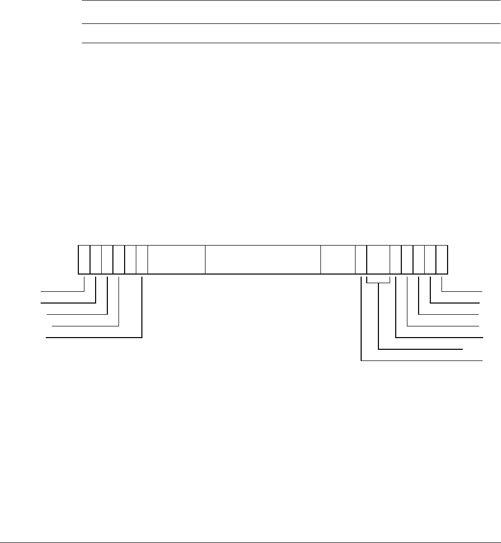
G4 AArch32 System Register Descriptions
G4.2 General system control registers
ARM DDI 0487A.a Copyright © 2013 ARM Limited. All rights reserved. G4-3841
ID090413 Non-Confidential - Beta
G4.2.46 FPEXC, Floating-Point Exception Control register
The FPEXC characteristics are:
Purpose
Provides a global enable for the Advanced SIMD and Floating-point (VFP) extensions, and
indicates how the state of these extensions is recorded.
This register is part of the Floating-point registers functional group.
Usage constraints
This register is accessible as shown below:
Access to this register depends on the values of CPACR.{cp10,cp11}, NSACR.{cp10,cp11}, and
HCPTR.{TCP10,TCP11}.
Configurations
FPEXC is architecturally mapped to AArch64 register FPEXC32_EL2.
There is one instance of this register that is used in both Secure and Non-secure states.
Implemented only if the implementation includes one or both of the Floating-point Extension or the
Advanced SIMD Extension.
Attributes
FPEXC is a 32-bit register.
The FPEXC bit assignments are:
EX, bit [31]
Exception bit. A status bit that specifies how much information must be saved to record the state of
the Advanced SIMD and VFP system:
0
The only significant state is the contents of the registers D0 - D31, FPSCR, and FPEXC.
A context switch can be performed by saving and restoring the values of these registers.
1
There is additional state that must be handled by any context switch system.
In ARMv8, this bit must be RES0.
EN, bit [30]
Enable bit. A global enable for the Advanced SIMD and VFP extensions:
0
The Advanced SIMD and VFP extensions are disabled.
EL0 (NS) EL0 (S) EL1 (NS) EL1 (S) EL2 EL3 (SCR.NS=1) EL3 (SCR.NS=0)
- - Config-RW RW Config-RW Config-RW RW
31 30 29 28
VV
27 26
RES0
25 21
IMPLEMENTATION DEFINED
20 11
VECITR
10 8 7654 3 2 1 0
EX
EN
DEX
FP2V
TFV
IOF
DZF
OFF
UFF
IXF
IMP DEF
IDF

G4 AArch32 System Register Descriptions
G4.2 General system control registers
G4-3842 Copyright © 2013 ARM Limited. All rights reserved. ARM DDI 0487A.a
Non-Confidential - Beta ID090413
1
The Advanced SIMD and VFP extensions are enabled and operate normally.
This bit is made obsolete by the features in the CPACR when executing in AArch64.
When executing in EL0 using AArch32 with EL1 using AArch64, the behavior is as if the
FPEXC.EN bit is set.
Resets to 0.
DEX, bit [29]
Defined synchronous instruction exception bit.
When a floating-point synchronous exception has occurred, if the exception was caused by an
allocated floating-point instruction that is not implemented in hardware then it is IMPLEMENTATION
DEFINED whether DEX is set to 0 or 1.
Otherwise, the meaning of this bit is:
0
A synchronous exception occurred when processing an unallocated floating-point or
Advanced SIMD instruction.
1
A synchronous exception occurred on an allocated floating-point instruction that
encountered an exceptional condition.
The exception-handling routine must clear DEX to 0.
In an implementation that does not require synchronous exception handling this bit is RES0.
Reset value is architecturally UNKNOWN.
FP2V, bit [28]
FPINST2 instruction valid bit. In ARMv8, this field is always RES0.
VV, bit [27]
VECITR valid bit. In ARMv8, this field is always RES0.
TFV, bit [26]
Trapped Fault Valid bit. Indicates whether FPEXC bits[7, 4:0] indicate trapped exceptions, or have
an IMPLEMENTATION DEFINED meaning:
0
FPEXC bits[7, 4:0] have an IMPLEMENTATION DEFINED meaning
1
FPEXC bits[7, 4:0] indicate the presence of trapped exceptions that have occurred at the
time of the exception. All trapped exceptions that occurred at the time of the exception
have their bits set.
This bit has a fixed value and ignores writes.
Bits [25:21]
Reserved, RES0.
VECITR, bits [10:8]
Vector iteration count. In ARMv8, this field is always RES1.
IDF, bit [7]
Input Denormal trapped exception bit, or IMPLEMENTATION DEFINED. The meaning of this bit
depends on the value of FPEXC.TFV.
If FPEXC.TFV is 0, this bit is IMPLEMENTATION DEFINED and can contain IMPLEMENTATION
DEFINED information about the cause of an exception.
If FPEXC.TFV is 1, this bit is the Input Denormal trapped exception bit, and indicates whether an
Input Denormal exception occurred while FPSCR.IDE was 1:
0
Input denormal exception has not occurred.
1
Input denormal exception has occurred.
Input Denormal exceptions can occur only when FPSCR.FZ is 1.
In both cases this bit must be cleared to 0 by the exception-handling routine.

G4 AArch32 System Register Descriptions
G4.2 General system control registers
ARM DDI 0487A.a Copyright © 2013 ARM Limited. All rights reserved. G4-3843
ID090413 Non-Confidential - Beta
Reset value is architecturally UNKNOWN.
IXF, bit [4]
Inexact trapped exception bit, or IMPLEMENTATION DEFINED. The meaning of this bit depends on the
value of FPEXC.TFV.
If FPEXC.TFV is 0, this bit is IMPLEMENTATION DEFINED and can contain IMPLEMENTATION
DEFINED information about the cause of an exception.
If FPEXC.TFV is 1, this bit is the Inexact trapped exception bit, and indicates whether an Inexact
exception occurred while FPSCR.IXE was 1:
In this case, the meaning of this bit is:
0
Inexact exception has not occurred.
1
Inexact exception has occurred.
In both cases this bit must be cleared to 0 by the exception-handling routine.
Reset value is architecturally UNKNOWN.
UFF, bit [3]
Underflow trapped exception bit, or IMPLEMENTATION DEFINED. The meaning of this bit depends on
the value of FPEXC.TFV.
If FPEXC.TFV is 0, this bit is IMPLEMENTATION DEFINED and can contain IMPLEMENTATION
DEFINED information about the cause of an exception.
If FPEXC.TFV is 1, this bit is the Underflow trapped exception bit, and indicates whether an
Underflow exception occurred while FPSCR.UFE was 1:
0
Underflow exception has not occurred.
1
Underflow exception has occurred.
Underflow trapped exceptions can occur only when FPSCR.FZ is 0.
In both cases this bit must be cleared to 0 by the exception-handling routine.
Reset value is architecturally UNKNOWN.
OFF, bit [2]
Overflow trapped exception bit, or IMPLEMENTATION DEFINED. The meaning of this bit depends on
the value of FPEXC.TFV.
If FPEXC.TFV is 0, this bit is IMPLEMENTATION DEFINED and can contain IMPLEMENTATION
DEFINED information about the cause of an exception.
If FPEXC.TFV is 1, this bit is the Overflow trapped exception bit, and indicates whether an
Overflow exception occurred while FPSCR.OFE was 1:
0
Overflow exception has not occurred.
1
Overflow exception has occurred.
In both cases this bit must be cleared to 0 by the exception-handling routine.
Reset value is architecturally UNKNOWN.
DZF, bit [1]
Divide-by-zero trapped exception bit, or IMPLEMENTATION DEFINED. The meaning of this bit
depends on the value of FPEXC.TFV.
If FPEXC.TFV is 0, this bit is IMPLEMENTATION DEFINED and can contain IMPLEMENTATION
DEFINED information about the cause of an exception.
If FPEXC.TFV is 1, this bit is the Divide-by-zero trapped exception bit, and indicates whether a
Divide-by-zero exception occurred while FPSCR.DZE was 1:
0
Divide-by-zero exception has not occurred.
1
Divide-by-zero exception has occurred.
In both cases this bit must be cleared to 0 by the exception-handling routine.

G4 AArch32 System Register Descriptions
G4.2 General system control registers
G4-3844 Copyright © 2013 ARM Limited. All rights reserved. ARM DDI 0487A.a
Non-Confidential - Beta ID090413
Reset value is architecturally UNKNOWN.
IOF, bit [0]
Invalid Operation trapped exception bit, or IMPLEMENTATION DEFINED. The meaning of this bit
depends on the value of FPEXC.TFV.
If FPEXC.TFV is 0, this bit is IMPLEMENTATION DEFINED and can contain IMPLEMENTATION
DEFINED information about the cause of an exception.
If FPEXC.TFV is 1, this bit is the Invalid Operation trapped exception bit, and indicates whether an
Invalid Operation exception occurred while FPSCR.IOE was 1:
0
Invalid Operation exception has not occurred.
1
Invalid Operation exception has occurred.
In both cases this bit must be cleared to 0 by the exception-handling routine.
Reset value is architecturally UNKNOWN.
Accessing the FPEXC:
To access the FPEXC:
VMRS <Rt>, FPEXC ; Read FPEXC into Rt
VMSR FPEXC, <Rt> ; Write Rt to FPEXC
Register access is encoded as follows:
spec_reg
1000
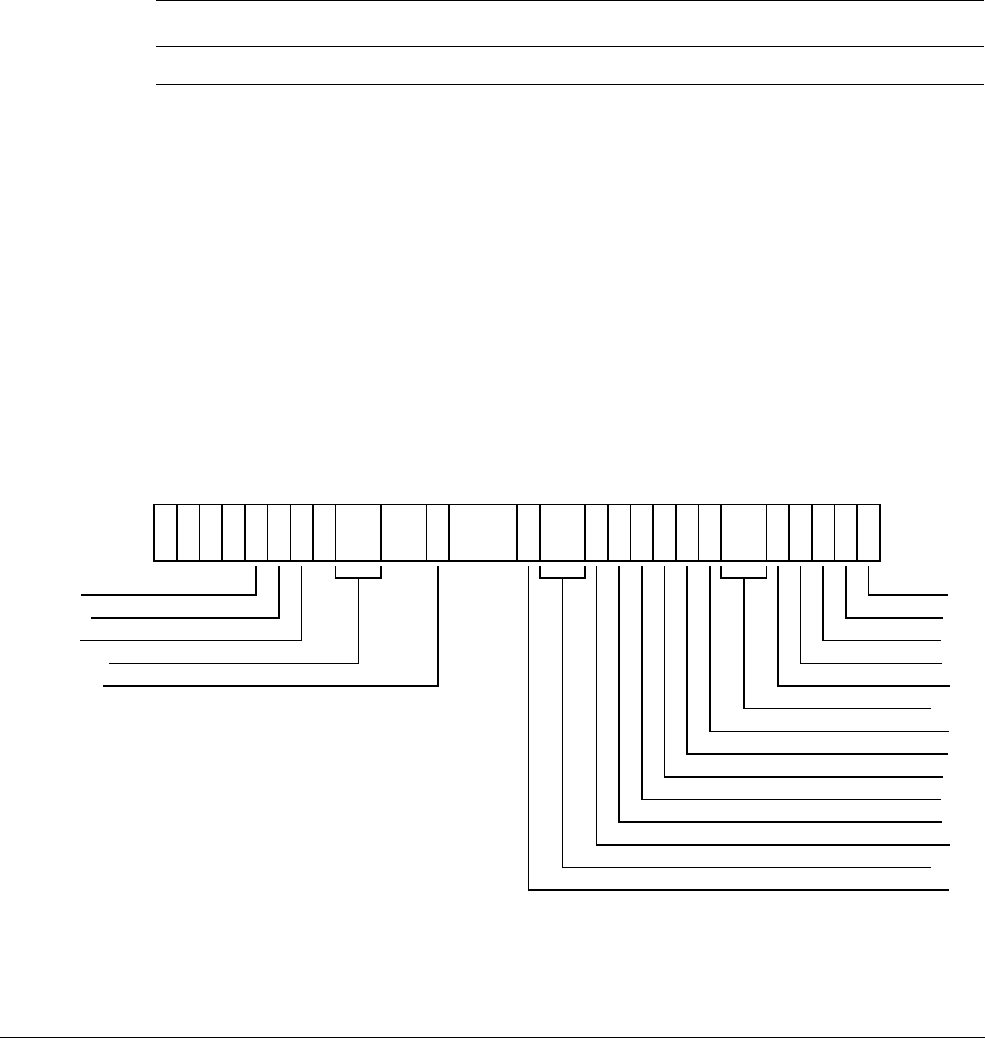
G4 AArch32 System Register Descriptions
G4.2 General system control registers
ARM DDI 0487A.a Copyright © 2013 ARM Limited. All rights reserved. G4-3845
ID090413 Non-Confidential - Beta
G4.2.47 FPSCR, Floating-Point Status and Control Register
The FPSCR characteristics are:
Purpose
Provides floating-point system status information and control.
This register is part of:
• the Special purpose registers functional group
• the Floating-point registers functional group.
Usage constraints
This register is accessible as shown below:
Access to this register depends on the values of CPACR.{cp10,cp11}, NSACR.{cp10,cp11},
HCPTR.{TCP10,TCP11}, and FPEXC.EN.
Configurations
There is one instance of this register that is used in both Secure and Non-secure states.
The named fields in this register map to the equivalent fields in the AArch64 FPCR and FPSR.
It is IMPLEMENTATION DEFINED whether the Len and Stride fields can be programmed to non-zero
values, which will cause some AArch32 floating-point instruction encodings to be UNDEFINED, or
whether these fields are RAZ.
Attributes
FPSCR is a 32-bit register.
The FPSCR bit assignments are:
N, bit [31]
Negative condition flag. This is updated by floating-point comparison operations.
EL0 (NS) EL0 (S) EL1 (NS) EL1 (S) EL2 EL3 (SCR.NS=1) EL3 (SCR.NS=0)
Config-RW RW Config-RW RW Config-RW Config-RW RW
N
31
Z
30
C
29
V
28 27 26 25
FZ
24 23 22
Stride
21 20 19
Len
18 16 15 14 13 12 11 10 9 8 7 654 3 2 1 0
QC
AHP
DN
RMode
RES0
IOC
DZC
OFC
UFC
IXC
RES0
IDC
IOE
DZE
OFE
UFE
IXE
RES0
IDE

G4 AArch32 System Register Descriptions
G4.2 General system control registers
G4-3846 Copyright © 2013 ARM Limited. All rights reserved. ARM DDI 0487A.a
Non-Confidential - Beta ID090413
Z, bit [30]
Zero condition flag. This is updated by floating-point comparison operations.
C, bit [29]
Carry condition flag. This is updated by floating-point comparison operations.
V, bit [28]
Overflow condition flag. This is updated by floating-point comparison operations.
QC, bit [27]
Cumulative saturation bit, Advanced SIMD only. This bit is set to 1 to indicate that an Advanced
SIMD integer operation has saturated since 0 was last written to this bit.
AHP, bit [26]
Alternative half-precision control bit:
0
IEEE half-precision format selected.
1
Alternative half-precision format selected.
DN, bit [25]
Default NaN mode control bit:
0
NaN operands propagate through to the output of a floating-point operation.
1
Any operation involving one or more NaNs returns the Default NaN.
The value of this bit only controls scalar floating-point arithmetic. Advanced SIMD arithmetic
always uses the Default NaN setting, regardless of the value of the DN bit.
FZ, bit [24]
Flush-to-zero mode control bit:
0
Flush-to-zero mode disabled. Behavior of the floating-point system is fully compliant
with the IEEE 754 standard.
1
Flush-to-zero mode enabled.
The value of this bit only controls scalar floating-point arithmetic. Advanced SIMD arithmetic
always uses the Flush-to-zero setting, regardless of the value of the FZ bit.
RMode, bits [23:22]
Rounding Mode control field. The encoding of this field is:
00
Round to Nearest (RN) mode
01
Round towards Plus Infinity (RP) mode
10
Round towards Minus Infinity (RM) mode
11
Round towards Zero (RZ) mode.
The specified rounding mode is used by almost all scalar floating-point instructions. Advanced
SIMD arithmetic always uses the Round to Nearest setting, regardless of the value of the RMode
bits.
Stride, bits [21:20]
It is IMPLEMENTATION DEFINED whether this field is RW or RAZ.
If this field is RW and is set to a value other than zero, some floating-point instruction encodings
are UNDEFINED. The instruction pseudocode identifies these instructions.
ARM strongly recommends that software never sets this field to a value other than zero.
The value of this field is ignored when processing Advanced SIMD instructions.
Bit [19]
Reserved, RES0.

G4 AArch32 System Register Descriptions
G4.2 General system control registers
ARM DDI 0487A.a Copyright © 2013 ARM Limited. All rights reserved. G4-3847
ID090413 Non-Confidential - Beta
Len, bits [18:16]
It is IMPLEMENTATION DEFINED whether this field is RW or RAZ.
If this field is RW and is set to a value other than zero, some floating-point instruction encodings
are UNDEFINED. The instruction pseudocode identifies these instructions.
ARM strongly recommends that software never sets this field to a value other than zero.
The value of this field is ignored when processing Advanced SIMD instructions.
IDE, bit [15]
Input Denormal exception trap enable. Possible values are:
0
Untrapped exception handling selected. If the floating-point exception occurs then the
IDC bit is set to 1.
1
Trapped exception handling selected. If the floating-point exception occurs, the PE does
not update the IDC bit. The trap handling software can decide whether to set the IDC
bit to 1.
This bit is RW only if the implementation supports the trapping of floating-point exceptions. In an
implementation that does not support floating-point exception trapping, this bit is RES0.
When this bit is RW, it applies only to floating-point operations. Advanced SIMD operations always
use untrapped floating-point exception handling in AArch32 state.
Bits [14:13]
Reserved, RES0.
IXE, bit [12]
Inexact exception trap enable. Possible values are:
0
Untrapped exception handling selected. If the floating-point exception occurs then the
IXC bit is set to 1.
1
Trapped exception handling selected. If the floating-point exception occurs, the PE does
not update the IXC bit. The trap handling software can decide whether to set the IXC
bit to 1.
This bit is RW only if the implementation supports the trapping of floating-point exceptions. In an
implementation that does not support floating-point exception trapping, this bit is RES0.
When this bit is RW, it applies only to floating-point operations. Advanced SIMD operations always
use untrapped floating-point exception handling in AArch32 state.
UFE, bit [11]
Underflow exception trap enable. Possible values are:
0
Untrapped exception handling selected. If the floating-point exception occurs then the
UFC bit is set to 1.
1
Trapped exception handling selected. If the floating-point exception occurs, the PE does
not update the UFC bit. The trap handling software can decide whether to set the UFC
bit to 1.
This bit is RW only if the implementation supports the trapping of floating-point exceptions. In an
implementation that does not support floating-point exception trapping, this bit is RES0.
When this bit is RW, it applies only to floating-point operations. Advanced SIMD operations always
use untrapped floating-point exception handling in AArch32 state.
OFE, bit [10]
Overflow exception trap enable. Possible values are:
0
Untrapped exception handling selected. If the floating-point exception occurs then the
OFC bit is set to 1.

G4 AArch32 System Register Descriptions
G4.2 General system control registers
G4-3848 Copyright © 2013 ARM Limited. All rights reserved. ARM DDI 0487A.a
Non-Confidential - Beta ID090413
1
Trapped exception handling selected. If the floating-point exception occurs, the PE does
not update the OFC bit. The trap handling software can decide whether to set the OFC
bit to 1.
This bit is RW only if the implementation supports the trapping of floating-point exceptions. In an
implementation that does not support floating-point exception trapping, this bit is RES0.
When this bit is RW, it applies only to floating-point operations. Advanced SIMD operations always
use untrapped floating-point exception handling in AArch32 state.
DZE, bit [9]
Division by Zero exception trap enable. Possible values are:
0
Untrapped exception handling selected. If the floating-point exception occurs then the
DZC bit is set to 1.
1
Trapped exception handling selected. If the floating-point exception occurs, the PE does
not update the DZC bit. The trap handling software can decide whether to set the DZC
bit to 1.
This bit is RW only if the implementation supports the trapping of floating-point exceptions. In an
implementation that does not support floating-point exception trapping, this bit is RES0.
When this bit is RW, it applies only to floating-point operations. Advanced SIMD operations always
use untrapped floating-point exception handling in AArch32 state.
IOE, bit [8]
Invalid Operation exception trap enable. Possible values are:
0
Untrapped exception handling selected. If the floating-point exception occurs then the
IOC bit is set to 1.
1
Trapped exception handling selected. If the floating-point exception occurs, the PE does
not update the IOC bit. The trap handling software can decide whether to set the IOC
bit to 1.
This bit is RW only if the implementation supports the trapping of floating-point exceptions. In an
implementation that does not support floating-point exception trapping, this bit is RES0.
When this bit is RW, it applies only to floating-point operations. Advanced SIMD operations always
use untrapped floating-point exception handling in AArch32 state.
IDC, bit [7]
Input Denormal cumulative exception bit. This bit is set to 1 to indicate that the Input Denormal
exception has occurred since 0 was last written to this bit.
How VFP instructions update this bit depends on the value of the IDE bit.
Advanced SIMD instructions set this bit if the Input Denormal exception occurs in one or more of
the floating-point calculations performed by the instruction, regardless of the value of the IDE bit.
Bits [6:5]
Reserved, RES0.
IXC, bit [4]
Inexact cumulative exception bit. This bit is set to 1 to indicate that the Inexact exception has
occurred since 0 was last written to this bit.
How VFP instructions update this bit depends on the value of the IXE bit.
Advanced SIMD instructions set this bit if the Inexact exception occurs in one or more of the
floating-point calculations performed by the instruction, regardless of the value of the IXE bit.
UFC, bit [3]
Underflow cumulative exception bit. This bit is set to 1 to indicate that the Underflow exception has
occurred since 0 was last written to this bit.
How VFP instructions update this bit depends on the value of the UFE bit.

G4 AArch32 System Register Descriptions
G4.2 General system control registers
ARM DDI 0487A.a Copyright © 2013 ARM Limited. All rights reserved. G4-3849
ID090413 Non-Confidential - Beta
Advanced SIMD instructions set this bit if the Underflow exception occurs in one or more of the
floating-point calculations performed by the instruction, regardless of the value of the UFE bit.
OFC, bit [2]
Overflow cumulative exception bit. This bit is set to 1 to indicate that the Overflow exception has
occurred since 0 was last written to this bit.
How VFP instructions update this bit depends on the value of the OFE bit.
Advanced SIMD instructions set this bit if the Overflow exception occurs in one or more of the
floating-point calculations performed by the instruction, regardless of the value of the OFE bit.
DZC, bit [1]
Division by Zero cumulative exception bit. This bit is set to 1 to indicate that the Division by Zero
exception has occurred since 0 was last written to this bit.
How VFP instructions update this bit depends on the value of the DZE bit.
Advanced SIMD instructions set this bit if the Division by Zero exception occurs in one or more of
the floating-point calculations performed by the instruction, regardless of the value of the DZE bit.
IOC, bit [0]
Invalid Operation cumulative exception bit. This bit is set to 1 to indicate that the Invalid Operation
exception has occurred since 0 was last written to this bit.
How VFP instructions update this bit depends on the value of the IOE bit.
Advanced SIMD instructions set this bit if the Invalid Operation exception occurs in one or more of
the floating-point calculations performed by the instruction, regardless of the value of the IOE bit.
Accessing the FPSCR:
To access the FPSCR:
VMRS <Rt>, FPSCR ; Read FPSCR into Rt
VMSR FPSCR, <Rt> ; Write Rt to FPSCR
Register access is encoded as follows:
spec_reg
0001

G4 AArch32 System Register Descriptions
G4.2 General system control registers
G4-3850 Copyright © 2013 ARM Limited. All rights reserved. ARM DDI 0487A.a
Non-Confidential - Beta ID090413
G4.2.48 FPSID, Floating-Point System ID register
The FPSID characteristics are:
Purpose
Provides top-level information about the floating-point implementation.
This register is part of:
• the Floating-point registers functional group
• the Identification registers functional group.
Usage constraints
This register is accessible as shown below:
Access to this register depends on the values of CPACR.{cp10,cp11}, NSACR.{cp10,cp11}, and
HCPTR.{TCP10,TCP11}.
This register largely duplicates information held in the MIDR. ARM deprecates use of it.
Configurations
There is one instance of this register that is used in both Secure and Non-secure states.
FPSID can be implemented in a system that provides only software emulation of the ARM
floating-point instructions, and must be implemented if the implementation includes one or both of
the Floating-point Extension or the Advanced SIMD Extension.
Attributes
FPSID is a 32-bit register.
The FPSID bit assignments are:
Implementer, bits [31:24]
Implementer codes are the same as those used for the MIDR.
For an implementation by ARM this field is
0x41
, the ASCII code for A.
SW, bit [23]
Software bit. This bit indicates whether a system provides only software emulation of the
floating-point instructions that are provided by the Floating-point extension:
0
The system includes hardware support for the floating-point instructions provided by
the Floating-point extension.
1
The system provides only software emulation of the floating-point instructions provided
by the Floating-point extension.
EL0 (NS) EL0 (S) EL1 (NS) EL1 (S) EL2 EL3 (SCR.NS=1) EL3 (SCR.NS=0)
- - Config-RO RO Config-RO Config-RO RO
Implementer
31 24 23
Subarchitecture
22 16
PartNum
15 8
Variant
74
Revision
30
SW

G4 AArch32 System Register Descriptions
G4.2 General system control registers
ARM DDI 0487A.a Copyright © 2013 ARM Limited. All rights reserved. G4-3851
ID090413 Non-Confidential - Beta
Subarchitecture, bits [22:16]
Subarchitecture version number. For an implementation by ARM, permitted values are:
0000000
VFPv1 architecture with an IMPLEMENTATION DEFINED subarchitecture. Not permitted
in an ARMv7 implementation.
0000001
VFPv2 architecture with Common VFP subarchitecture v1. Not permitted in an ARMv7
implementation.
0000010
VFPv3 architecture, or later, with Common VFP subarchitecture v2. The VFP
architecture version is indicated by the MVFR0 and MVFR1 registers.
0000011
VFPv3 architecture, or later, with Null subarchitecture. The entire floating-point
implementation is in hardware, and no software support code is required. The VFP
architecture version is indicated by the MVFR0 and MVFR1 registers. This value can
be used only by an implementation that does not support the trap enable bits in the
FPSCR.
0000100
VFPv3 architecture, or later, with Common VFP subarchitecture v3. The VFP
architecture version is indicated by the MVFR0 and MVFR1 registers.
For a subarchitecture designed by ARM the most significant bit of this field, register bit[22], is 0.
Values with a most significant bit of 0 that are not listed here are reserved.
When the subarchitecture designer is not ARM, the most significant bit of this field, register bit[22],
must be 1. Each implementer must maintain its own list of subarchitectures it has designed, starting
at subarchitecture version number
0x40
.
PartNum, bits [15:8]
An IMPLEMENTATION DEFINED part number for the floating-point implementation, assigned by the
implementer.
Variant, bits [7:4]
An IMPLEMENTATION DEFINED variant number. Typically, this field distinguishes between different
production variants of a single product.
Revision, bits [3:0]
An IMPLEMENTATION DEFINED revision number for the floating-point implementation.
Accessing the FPSID:
To access the FPSID:
VMRS <Rt>, FPSID ; Read FPSID into Rt
Register access is encoded as follows:
spec_reg
0000

G4 AArch32 System Register Descriptions
G4.2 General system control registers
G4-3852 Copyright © 2013 ARM Limited. All rights reserved. ARM DDI 0487A.a
Non-Confidential - Beta ID090413
G4.2.49 HACR, Hyp Auxiliary Configuration Register
The HACR characteristics are:
Purpose
Controls trapping to Hyp mode of IMPLEMENTATION DEFINED or IMPLEMENTATION SPECIFIC
aspects of Non-secure EL1 or EL0 operation.
This register is part of the Virtualization registers functional group.
Usage constraints
This register is accessible as shown below:
Configurations
HACR is architecturally mapped to AArch64 register HACR_EL2.
If EL2 is not implemented, this register is RES0 from EL3.
Attributes
HACR is a 32-bit register.
The HACR bit assignments are:
Accessing the HACR:
To access the HACR:
MRC p15,4,<Rt>,c1,c1,7 ; Read HACR into Rt
MCR p15,4,<Rt>,c1,c1,7 ; Write Rt to HACR
Register access is encoded as follows:
EL0 (NS) EL0 (S) EL1 (NS) EL1 (S) EL2 EL3 (SCR.NS=1) EL3 (SCR.NS=0)
- - - - RW RW -
IMPLEMENTATION DEFINED
31 0
coproc opc1 CRn CRm opc2
1111 100 0001 0001 111

G4 AArch32 System Register Descriptions
G4.2 General system control registers
ARM DDI 0487A.a Copyright © 2013 ARM Limited. All rights reserved. G4-3853
ID090413 Non-Confidential - Beta
G4.2.50 HACTLR, Hyp Auxiliary Control Register
The HACTLR characteristics are:
Purpose
Controls IMPLEMENTATION DEFINED features of Hyp mode operation.
This register is part of:
• the Virtualization registers functional group
• the Other system control registers functional group
• the IMPLEMENTATION DEFINED functional group.
Usage constraints
This register is accessible as shown below:
Configurations
HACTLR is architecturally mapped to AArch64 register ACTLR_EL2.
If EL2 is not implemented, this register is RES0 from EL3.
Attributes
HACTLR is a 32-bit register.
The HACTLR bit assignments are:
Accessing the HACTLR:
To access the HACTLR:
MRC p15,4,<Rt>,c1,c0,1 ; Read HACTLR into Rt
MCR p15,4,<Rt>,c1,c0,1 ; Write Rt to HACTLR
Register access is encoded as follows:
EL0 (NS) EL0 (S) EL1 (NS) EL1 (S) EL2 EL3 (SCR.NS=1) EL3 (SCR.NS=0)
- - - - RW RW -
IMPLEMENTATION DEFINED
31 0
coproc opc1 CRn CRm opc2
1111 100 0001 0000 001

G4 AArch32 System Register Descriptions
G4.2 General system control registers
G4-3854 Copyright © 2013 ARM Limited. All rights reserved. ARM DDI 0487A.a
Non-Confidential - Beta ID090413
G4.2.51 HADFSR, Hyp Auxiliary Data Fault Status Register
The HADFSR characteristics are:
Purpose
Provides additional IMPLEMENTATION DEFINED syndrome information for Data Abort exceptions
taken to Hyp mode.
This register is part of:
• the Virtualization registers functional group
• the Exception and fault handling registers functional group
• the IMPLEMENTATION DEFINED functional group.
Usage constraints
This register is accessible as shown below:
Configurations
HADFSR is architecturally mapped to AArch64 register AFSR0_EL2.
This is an optional register. An implementation that does not require this register can implement it
as RES0.
If EL2 is not implemented, this register is RES0 from EL3.
Attributes
HADFSR is a 32-bit register.
The HADFSR bit assignments are:
Accessing the HADFSR:
To access the HADFSR:
MRC p15,4,<Rt>,c5,c1,0 ; Read HADFSR into Rt
MCR p15,4,<Rt>,c5,c1,0 ; Write Rt to HADFSR
Register access is encoded as follows:
EL0 (NS) EL0 (S) EL1 (NS) EL1 (S) EL2 EL3 (SCR.NS=1) EL3 (SCR.NS=0)
- - - - RW RW -
IMPLEMENTATION DEFINED
31 0
coproc opc1 CRn CRm opc2
1111 100 0101 0001 000

G4 AArch32 System Register Descriptions
G4.2 General system control registers
ARM DDI 0487A.a Copyright © 2013 ARM Limited. All rights reserved. G4-3855
ID090413 Non-Confidential - Beta
G4.2.52 HAIFSR, Hyp Auxiliary Instruction Fault Status Register
The HAIFSR characteristics are:
Purpose
Provides additional IMPLEMENTATION DEFINED syndrome information for Prefetch Abort
exceptions taken to Hyp mode.
This register is part of:
• the Virtualization registers functional group
• the Exception and fault handling registers functional group
• the IMPLEMENTATION DEFINED functional group.
Usage constraints
This register is accessible as shown below:
Configurations
HAIFSR is architecturally mapped to AArch64 register AFSR1_EL2.
This is an optional register. An implementation that does not require this register can implement it
as RES0.
If EL2 is not implemented, this register is RES0 from EL3.
Attributes
HAIFSR is a 32-bit register.
The HAIFSR bit assignments are:
Accessing the HAIFSR:
To access the HAIFSR:
MRC p15,4,<Rt>,c5,c1,1 ; Read HAIFSR into Rt
MCR p15,4,<Rt>,c5,c1,1 ; Write Rt to HAIFSR
Register access is encoded as follows:
EL0 (NS) EL0 (S) EL1 (NS) EL1 (S) EL2 EL3 (SCR.NS=1) EL3 (SCR.NS=0)
- - - - RW RW -
IMPLEMENTATION DEFINED
31 0
coproc opc1 CRn CRm opc2
1111 100 0101 0001 001

G4 AArch32 System Register Descriptions
G4.2 General system control registers
G4-3856 Copyright © 2013 ARM Limited. All rights reserved. ARM DDI 0487A.a
Non-Confidential - Beta ID090413
G4.2.53 HAMAIR0, Hyp Auxiliary Memory Attribute Indirection Register 0
The HAMAIR0 characteristics are:
Purpose
Provides IMPLEMENTATION DEFINED memory attributes for the memory attribute encodings defined
by HMAIR0. These IMPLEMENTATION DEFINED attributes can only provide additional qualifiers for
the memory attribute encodings, and cannot change the memory attributes defined in HMAIR0.
This register is part of:
• the Virtualization registers functional group
• the Virtual memory control registers functional group
• the IMPLEMENTATION DEFINED functional group.
Usage constraints
This register is accessible as shown below:
If an implementation does not provide any IMPLEMENTATION DEFINED memory attributes, this
register is RES0.
Configurations
HAMAIR0 is architecturally mapped to AArch64 register AMAIR_EL2[31:0].
If EL2 is not implemented, this register is RES0 from EL3.
Attributes
HAMAIR0 is a 32-bit register.
The HAMAIR0 bit assignments are:
Accessing the HAMAIR0:
To access the HAMAIR0:
MRC p15,4,<Rt>,c10,c3,0 ; Read HAMAIR0 into Rt
MCR p15,4,<Rt>,c10,c3,0 ; Write Rt to HAMAIR0
Register access is encoded as follows:
EL0 (NS) EL0 (S) EL1 (NS) EL1 (S) EL2 EL3 (SCR.NS=1) EL3 (SCR.NS=0)
- - - - RW RW -
IMPLEMENTATION DEFINED
31 0
coproc opc1 CRn CRm opc2
1111 100 1010 0011 000

G4 AArch32 System Register Descriptions
G4.2 General system control registers
ARM DDI 0487A.a Copyright © 2013 ARM Limited. All rights reserved. G4-3857
ID090413 Non-Confidential - Beta
G4.2.54 HAMAIR1, Hyp Auxiliary Memory Attribute Indirection Register 1
The HAMAIR1 characteristics are:
Purpose
Provides IMPLEMENTATION DEFINED memory attributes for the memory attribute encodings defined
by HMAIR1. These IMPLEMENTATION DEFINED attributes can only provide additional qualifiers for
the memory attribute encodings, and cannot change the memory attributes defined in HMAIR1.
This register is part of:
• the Virtualization registers functional group
• the Virtual memory control registers functional group
• the IMPLEMENTATION DEFINED functional group.
Usage constraints
This register is accessible as shown below:
If an implementation does not provide any IMPLEMENTATION DEFINED memory attributes, this
register is RES0.
Configurations
HAMAIR1 is architecturally mapped to AArch64 register AMAIR_EL2[63:32].
If EL2 is not implemented, this register is RES0 from EL3.
Attributes
HAMAIR1 is a 32-bit register.
The HAMAIR1 bit assignments are:
Accessing the HAMAIR1:
To access the HAMAIR1:
MRC p15,4,<Rt>,c10,c3,1 ; Read HAMAIR1 into Rt
MCR p15,4,<Rt>,c10,c3,1 ; Write Rt to HAMAIR1
Register access is encoded as follows:
EL0 (NS) EL0 (S) EL1 (NS) EL1 (S) EL2 EL3 (SCR.NS=1) EL3 (SCR.NS=0)
- - - - RW RW -
IMPLEMENTATION DEFINED
31 0
coproc opc1 CRn CRm opc2
1111 100 1010 0011 001
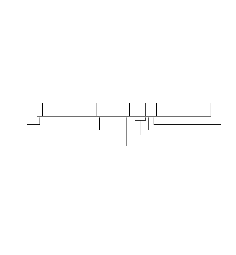
G4 AArch32 System Register Descriptions
G4.2 General system control registers
G4-3858 Copyright © 2013 ARM Limited. All rights reserved. ARM DDI 0487A.a
Non-Confidential - Beta ID090413
G4.2.55 HCPTR, Hyp Architectural Feature Trap Register
The HCPTR characteristics are:
Purpose
Controls trapping to Hyp mode of Non-secure access, at EL1 or lower, to Trace, Floating Point, and
Advanced SIMD functionality. Also controls access from Hyp mode to this functionality.
This register is part of the Virtualization registers functional group.
Usage constraints
This register is accessible as shown below:
If a bit in the NSACR prohibits a Non-secure access, then the corresponding bit in the HCPTR
behaves as RAO/WI for Non-secure accesses. See the bit descriptions for more information.
Configurations
HCPTR is architecturally mapped to AArch64 register CPTR_EL2.
If EL2 is not implemented, this register is RES0 from EL3.
Attributes
HCPTR is a 32-bit register.
The HCPTR bit assignments are:
TCPAC, bit [31]
Trap CPACR accesses. The possible values of this bit are:
0
Has no effect on CPACR accesses.
1
Trap valid Non-secure EL1 CPACR accesses to Hyp mode.
Resets to 0.
Bits [30:21]
Reserved, RES0.
TTA, bit [20]
Trap Trace Access. The possible values of this bit are:
0
Has no effect on accesses to CP14 Trace registers.
1
Trap valid Non-secure EL0 and EL1 accesses to CP14 Trace registers to Hyp mode.
Valid Hyp mode accesses to CP14 Trace registers generate an Undefined Instruction
exception, taken in Hyp mode.
EL0 (NS) EL0 (S) EL1 (NS) EL1 (S) EL2 EL3 (SCR.NS=1) EL3 (SCR.NS=0)
- - - - RW RW -
31
RES0
30 21 20
RES0
19 16 15 14 13 12 11 10
RES1
90
TCPAC
TTA
TCP10
TCP11
RES1
RES0
TASE

G4 AArch32 System Register Descriptions
G4.2 General system control registers
ARM DDI 0487A.a Copyright © 2013 ARM Limited. All rights reserved. G4-3859
ID090413 Non-Confidential - Beta
In an implementation that does not include Trace functionality, or does not include a CP14 interface
to the Trace registers, it is IMPLEMENTATION DEFINED whether this bit:
• Is RAO/WI.
•Is RAZ/WI.
• Can be written from Hyp mode, and from Secure Monitor mode when SCR.NS is set to 1.
Resets to 0.
Bits [19:16]
Reserved, RES0.
TASE, bit [15]
Trap Advanced SIMD Extension use. The possible values of this bit are:
0
If the NSACR settings permit Non-secure use of the Advanced SIMD functionality then
Hyp mode can access that functionality, regardless of any settings in the CPACR. This
bit value has no effect on the possible use of the Advanced SIMD functionality from
Non-secure EL1 and EL0 modes.
1
Trap valid Non-secure accesses to Advanced SIMD functionality to Hyp mode. Valid
Hyp mode accesses to Advanced SIMD functionality generate an Undefined Instruction
exception, taken in Hyp mode.
Resets to 0.
Bit [14]
Reserved, RES0.
Bits [13:12]
Reserved, RES1.
TCP<n>, bit [n], for n = 10 to 11
Trap coprocessor n (CP<n>). The possible values of each of these bits are:
0
If NSACR.cp<n> is set to 1, then Hyp mode can access CP<n>, regardless of the value
of CPACR.cp<n>. This bit value has no effect on possible use of CP<n> from
Non-secure EL1 and EL0 modes.
1
Trap valid Non-secure accesses to CP<n> to Hyp mode.
When TCP<n> is set to 1, any otherwise-valid access to CP<n> from:
• A Non-secure EL1 or EL0 mode is trapped to Hyp mode.
• Hyp mode generates an Undefined Instruction exception, taken in Hyp mode.
In an implementation that includes the Floating Point extension, the extension is controlled by
coprocessors 10 and 11. If bits 11 and 10 are set to different values, the behavior is the same as if
both bits were set to the value of bit 10, in all respects other than the value read back by explicitly
reading bit 11.
Other coprocessors are not supported in ARMv8, so bits[13:12] and bits[9:0] are RES1.
Resets to 0.
Bits [9:0]
Reserved, RES1.
Accessing the HCPTR:
To access the HCPTR:
MRC p15,4,<Rt>,c1,c1,2 ; Read HCPTR into Rt
MCR p15,4,<Rt>,c1,c1,2 ; Write Rt to HCPTR

G4 AArch32 System Register Descriptions
G4.2 General system control registers
G4-3860 Copyright © 2013 ARM Limited. All rights reserved. ARM DDI 0487A.a
Non-Confidential - Beta ID090413
Register access is encoded as follows:
coproc opc1 CRn CRm opc2
1111 100 0001 0001 010
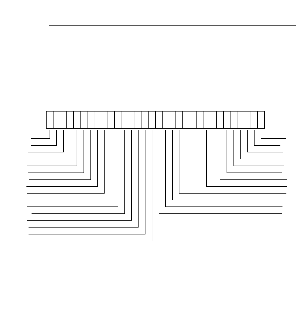
G4 AArch32 System Register Descriptions
G4.2 General system control registers
ARM DDI 0487A.a Copyright © 2013 ARM Limited. All rights reserved. G4-3861
ID090413 Non-Confidential - Beta
G4.2.56 HCR, Hyp Configuration Register
The HCR characteristics are:
Purpose
Provides configuration controls for virtualization, including defining whether various Non-secure
operations are trapped to Hyp mode.
This register is part of the Virtualization registers functional group.
Usage constraints
This register is accessible as shown below:
Configurations
HCR is architecturally mapped to AArch64 register HCR_EL2[31:0].
If EL2 is not implemented, this register is RES0 from EL3.
Attributes
HCR is a 32-bit register.
The HCR bit assignments are:
Bit [31]
Reserved, RES0.
TRVM, bit [30]
Trap Read of Virtual Memory controls. When this bit is set to 1, this causes Reads to the EL1 virtual
memory control registers from EL1 to be trapped to EL2. This covers the following registers:
SCTLR, TTBR0, TTBR1, TTBCR, DACR, DFSR, IFSR, DFAR, IFAR, ADFSR, AIFSR,
PRRR/MAIR0, NMRR/MAIR1, AMAIR0, AMAIR1, CONTEXTIDR.
EL0 (NS) EL0 (S) EL1 (NS) EL1 (S) EL2 EL3 (SCR.NS=1) EL3 (SCR.NS=0)
- - - - RW RW -
31 30 29 28 27 26 25 24 23 22 21 20 19 18 17 16 15 14 13 12
BSU
11 10
FB
98
VI
76 5 4 3 2 1 0
RES0
TRVM
HCD
RES0
TGE
TVM
TTLB
TPU
TPC
TSW
TAC
TIDCP
TSC
TID3
TID2
TID1
VM
SWIO
PTW
FMO
IMO
AMO
VF
VA
DC
TWI
TWE
TID0

G4 AArch32 System Register Descriptions
G4.2 General system control registers
G4-3862 Copyright © 2013 ARM Limited. All rights reserved. ARM DDI 0487A.a
Non-Confidential - Beta ID090413
Resets to 0.
HCD, bit [29]
Hypervisor Call Disable, if EL3 is not implemented:
0
HVC instruction is enabled at EL1 or EL2.
1
HVC instruction is UNDEFINED at all exception levels.
If EL3 is implemented, this bit is RES0.
Resets to 0.
Bit [28]
Reserved, RES0.
TGE, bit [27]
Trap General Exceptions. If this bit is set to 1, and SCR.NS is set to 1, then:
• All exceptions that would be routed to EL1 are routed to EL2.
• The SCTLR.M bit is treated as being 0 regardless of its actual state other than for the purpose
of reading the bit.
• The HCR.FMO, IMO, and AMO bits are treated as being 1 regardless of their actual state
other than for the purpose of reading the bits.
• All virtual interrupts are disabled.
• Any implementation defined mechanisms for signalling virtual interrupts are disabled.
• An exception return to EL1 is treated as an illegal exception return.
Additionally, if HCR.TGE == 1, the HDCR.{TDRA,TDOSA,TDA} bits are ignored and the
processor behaves as if they are set to 1, other than for the value read back from HDCR.
Resets to 0.
TVM, bit [26]
Trap Virtual Memory controls. When this bit is set to 1, this causes Writes to the EL1 virtual
memory control registers from EL1 to be trapped to EL2. This covers the following registers:
SCTLR, TTBR0, TTBR1, TTBCR, DACR, DFSR, IFSR, DFAR, IFAR, ADFSR, AIFSR,
PRRR/MAIR0, NMRR/MAIR1, AMAIR0, AMAIR1, CONTEXTIDR.
Resets to 0.
TTLB, bit [25]
Trap TLB maintenance instructions. When this bit is set to 1, this causes TLB maintenance
instructions executed from EL1 which are not UNDEFINED to be trapped to EL2. This covers the
following instructions:
TLBIALLIS, TLBIMVAIS, TLBIASIDIS, TLBIMVAAIS, TLBIALL, TLBIMVA, TLBIASID,
DTLBIALL, DTLBIMVA, DTLBIASID, ITLBIALL, ITLBIMVA, ITLBIASID, TLBIMVAA,
TLBIMVALIS, TLBIMVAALIS, TLBIMVAL, TLBIMVAAL.
Resets to 0.
TPU, bit [24]
Trap Cache maintenance instructions to Point of Unification. When this bit is set to 1, this causes
Cache maintenance instructions to the point of unification executed from EL1 or EL0 which are not
UNDEFINED to be trapped to EL2. This covers the following instructions:
ICIMVAU, ICIALLU, ICIALLUIS, DCCMVAU.
Resets to 0.

G4 AArch32 System Register Descriptions
G4.2 General system control registers
ARM DDI 0487A.a Copyright © 2013 ARM Limited. All rights reserved. G4-3863
ID090413 Non-Confidential - Beta
TPC, bit [23]
Trap Data/Unified Cache maintenance operations to Point of Coherency. When this bit is set to 1,
this causes Data or Unified Cache maintenance instructions by address to the point of coherency
executed from EL1 or EL0 which are not UNDEFINED to be trapped to EL2. This covers the
following instructions:
DCIMVAC, DCCIMVAC, DCCMVAC.
Resets to 0.
TSW, bit [22]
Trap Data/Unified Cache maintenance operations by Set/Way. When this bit is set to 1, this causes
Data or Unified Cache maintenance instructions by set/way executed from EL1 which are not
UNDEFINED to be trapped to EL2. This covers the following instructions:
DCISW, DCCSW, DCCISW.
Resets to 0.
TAC, bit [21]
Trap ACTLR accesses. When this bit is set to 1, any valid Non-secure access to the ACTLR is
trapped to Hyp mode.
Resets to 0.
TIDCP, bit [20]
Trap Implementation Dependent functionality. When this bit is set to 1, this causes accesses to the
following instruction set space executed from EL1 to be trapped to EL2.
AArch32: MCR and MRC instructions as follows:
• All CP15, CRn==9, Opcode1 = {0-7}, CRm == {c0-c2, c5-c8}, opcode2 == {0-7}.
• All CP15, CRn==10, Opcode1 =={0-7}, CRm == {c0, c1, c4, c8}, opcode2 == {0-7}.
• All CP15, CRn==11, Opcode1=={0-7}, CRm == {c0-c8, c15}, opcode2 == {0-7}.
It is IMPLEMENTATION DEFINED whether any of this functionality accessed from EL0 is trapped to
EL2 when the HCR.TIDCP bit is set. If it is not trapped to EL2, it results in an Undefined exception
taken to EL1.
Resets to 0.
TSC, bit [19]
Trap SMC instruction. When this bit is set to 1, any attempt from a Non-secure EL1 mode to execute
an SMC instruction, that passes its condition check if it is conditional, is trapped to Hyp mode.
Resets to 0.
TID3, bit [18]
Trap ID Group 3. When this bit is set to 1, this causes reads to the following registers executed from
EL1 to be trapped to EL2:
ID_PFR0, ID_PFR1, ID_DFR0, ID_AFR0, ID_MMFR0, ID_MMFR1, ID_MMFR2, ID_MMFR3,
ID_ISAR0, ID_ISAR1, ID_ISAR2, ID_ISAR3, ID_ISAR4, ID_ISAR5, MVFR0, MVFR1,
MVFR2. Also MRC to any of the following encodings:
• CP15, CRn == 0, Opc1 == 0, CRm == {3-7}, Opc2 == {0,1}.
• CP15, CRn == 0, Opc1 == 0, CRm == 3, Opc2 == 2.
• CP15, CRn == 0, Opc1 == 0, CRm == 5, Opc2 == {4,5}.
Resets to 0.
TID2, bit [17]
Trap ID Group 2. When this bit is set to 1, this causes reads (or writes to CSSELR/CSSELR_EL1)
to the following registers executed from EL1 or EL0 if not UNDEFINED to be trapped to EL2:
CTR, CCSIDR, CLIDR, CSSELR.

G4 AArch32 System Register Descriptions
G4.2 General system control registers
G4-3864 Copyright © 2013 ARM Limited. All rights reserved. ARM DDI 0487A.a
Non-Confidential - Beta ID090413
Resets to 0.
TID1, bit [16]
Trap ID Group 1. When this bit is set to 1, this causes reads to the following registers executed from
EL1 to be trapped to EL2:
TCMTR, TLBTR, AIDR, REVIDR.
Resets to 0.
TID0, bit [15]
Trap ID Group 0. When this bit is set to 1, this causes reads to the following registers executed from
EL1 or EL0 if not UNDEFINED to be trapped to EL2:
FPSID, JIDR.
Resets to 0.
TWE, bit [14]
Trap WFE. When this bit is set to 1, this causes execution of the WFE instruction from EL1 or EL0
to be trapped to EL2 if the instruction would otherwise cause suspension of execution (i.e. if the
event register is not set).
Conditional WFE instructions that fail their condition are not trapped if this bit is set to 1.
Resets to 0.
TWI, bit [13]
Trap WFI. When this bit is set to 1, this causes execution of the WFI instruction from EL1 or EL0
to be trapped to EL2 if the instruction would otherwise cause suspension of execution (i.e. if there
is not a pending WFI wakeup event).
Conditional WFI instructions that fail their condition are not trapped if this bit is set to 1.
Resets to 0.
DC, bit [12]
Default cacheable. When this bit is set to 1, and the Non-secure EL1 and EL0 stage 1 MMU is
disabled, the memory type and attributes determined by the stage 1 translation is Normal,
Non-shareable, Inner Write-Back Write-Allocate, Outer Write-Back Write-Allocate.
When this bit is 0 and the stage 1 MMU is disabled, the default memory attribute for Data accesses
is Device-nGnRnE.
This bit is permitted to be cached in a TLB.
Resets to 0.
BSU, bits [11:10]
Barrier Shareability upgrade. The value in this field determines the minimum shareability domain
that is applied to any barrier executed from EL1 or EL0:
00
No effect
01
Inner Shareable
10
Outer Shareable
11
Full system
This value is combined with the specified level of the barrier held in its instruction, using the same
principles as combining the shareability attributes from two stages of address translation.
Resets to 0.
FB, bit [9]
Force broadcast. When this bit is set to 1, this causes the following instructions to be broadcast
within the Inner Shareable domain when executed from Non-secure EL1:

G4 AArch32 System Register Descriptions
G4.2 General system control registers
ARM DDI 0487A.a Copyright © 2013 ARM Limited. All rights reserved. G4-3865
ID090413 Non-Confidential - Beta
BPIALL, TLBIALL, TLBIMVA, TLBIASID, DTLBIALL, DTLBIMVA, DTLBIASID,
ITLBIALL, ITLBIMVA, ITLBIASID, TLBIMVAA, ICIALLU, TLBIMVAL, TLBIMVAAL.
Resets to 0.
VA, bit [8]
Virtual Asynchronous Abort exception. When the AMO bit is set to 1, setting this bit to 1 generates
a virtual Asynchronous Abort exception to the Guest OS, when the processor is executing in
Non-secure state at EL0 or EL1.
The Guest OS cannot distinguish the virtual exception from the corresponding physical exception.
Resets to 0.
VI, bit [7]
Virtual IRQ exception. When the IMO bit is set to 1, setting this bit to 1 generates a virtual IRQ
exception to the Guest OS, when the processor is executing in Non-secure state at EL0 or EL1.
The Guest OS cannot distinguish the virtual exception from the corresponding physical exception.
Resets to 0.
VF, bit [6]
Virtual FIQ exception. When the FMO bit is set to 1, setting this bit to 1 generates a virtual FIQ
exception to the Guest OS, when the processor is executing in Non-secure state at EL0 or EL1.
The Guest OS cannot distinguish the virtual exception from the corresponding physical exception.
Resets to 0.
AMO, bit [5]
Asynchronous Abort Mask Override. When this bit is set to 1, it overrides the effect of CPSR.A,
and enables virtual exception signalling by the VA bit.
Resets to 0.
IMO, bit [4]
IRQ Mask Override. When this bit is set to 1, it overrides the effect of CPSR.I, and enables virtual
exception signalling by the VI bit.
Resets to 0.
FMO, bit [3]
FIQ Mask Override. When this bit is set to 1, it overrides the effect of CPSR.F, and enables virtual
exception signalling by the VF bit.
Resets to 0.
PTW, bit [2]
Protected Table Walk. When this bit is set to 1, if the stage 2 translation of a translation table access
made as part of a stage 1 translation table walk at EL0 or EL1 maps that translation table access to
Strongly-ordered or Device memory, the access is faulted as a stage 2 Permission fault.
This bit is permitted to be cached in a TLB.
Resets to 0.
SWIO, bit [1]
Set/Way Invalidation Override. When this bit is set to 1, this causes EL1 execution of the data cache
invalidate by set/way instruction to be treated as data cache clean and invalidate by set/way. That is,
DCISW is executed as DCCISW.
As a result of changes to the behavior of DCISW, this bit is redundant in v8-A. It is permissible that
an implementation makes this bit RES1.
Resets to 0.

G4 AArch32 System Register Descriptions
G4.2 General system control registers
G4-3866 Copyright © 2013 ARM Limited. All rights reserved. ARM DDI 0487A.a
Non-Confidential - Beta ID090413
VM, bit [0]
Virtualization MMU enable for EL1 and EL0 stage 2 address translation. Possible values of this bit
are:
0
EL1 and EL0 stage 2 address translation disabled.
1
EL1 and EL0 stage 2 address translation enabled.
This bit is permitted to be cached in a TLB.
If the HCR.DC bit is set to 1, then the behavior of the processor when executing in a Non-secure
mode other than Hyp mode is consistent with HCR.VM being 1, regardless of the actual value of
HCR.VM, other than the value returned by an explicit read of HCR.VM.
Resets to 0.
Accessing the HCR:
To access the HCR:
MRC p15,4,<Rt>,c1,c1,0 ; Read HCR into Rt
MCR p15,4,<Rt>,c1,c1,0 ; Write Rt to HCR
Register access is encoded as follows:
coproc opc1 CRn CRm opc2
1111 100 0001 0001 000

G4 AArch32 System Register Descriptions
G4.2 General system control registers
ARM DDI 0487A.a Copyright © 2013 ARM Limited. All rights reserved. G4-3867
ID090413 Non-Confidential - Beta
G4.2.57 HCR2, Hyp Configuration Register 2
The HCR2 characteristics are:
Purpose
Provides additional configuration controls for virtualization.
This register is part of the Virtualization registers functional group.
Usage constraints
This register is accessible as shown below:
Configurations
HCR2 is architecturally mapped to AArch64 register HCR_EL2[63:32].
If EL2 is not implemented, this register is RES0 from EL3.
Attributes
HCR2 is a 32-bit register.
The HCR2 bit assignments are:
Bits [31:2]
Reserved, RES0.
ID, bit [1]
Stage 2 Instruction cache disable. When HCR.VM==1, this forces all stage 2 translations for
instruction accesses to Normal memory to be Non-cacheable for the EL1&0 translation regime.
0
No effect on the stage 2 of the EL1&0 translation regime for instruction accesses.
1
Forces all stage 2 translations for instruction accesses to Normal memory to be
Non-cacheable for the EL1&0 translation regime.
This bit has no effect on the EL2 or EL3 translation regimes.
CD, bit [0]
Stage 2 Data cache disable. When HCR.VM==1, this forces all stage 2 translations for data accesses
and translation table walks to Normal memory to be Non-cacheable for the EL1&0 translation
regime.
0
No effect on the stage 2 of the EL1&0 translation regime for data accesses and
translation table walks.
1
Forces all stage 2 translations for data accesses and translation table walks to Normal
memory to be Non-cacheable for the EL1&0 translation regime.
This bit has no effect on the EL2 or EL3 translation regimes.
EL0 (NS) EL0 (S) EL1 (NS) EL1 (S) EL2 EL3 (SCR.NS=1) EL3 (SCR.NS=0)
- - - - RW RW -
RES0
31 2
ID
10
CD

G4 AArch32 System Register Descriptions
G4.2 General system control registers
G4-3868 Copyright © 2013 ARM Limited. All rights reserved. ARM DDI 0487A.a
Non-Confidential - Beta ID090413
Accessing the HCR2:
To access the HCR2:
MRC p15,4,<Rt>,c1,c1,4 ; Read HCR2 into Rt
MCR p15,4,<Rt>,c1,c1,4 ; Write Rt to HCR2
Register access is encoded as follows:
coproc opc1 CRn CRm opc2
1111 100 0001 0001 100

G4 AArch32 System Register Descriptions
G4.2 General system control registers
ARM DDI 0487A.a Copyright © 2013 ARM Limited. All rights reserved. G4-3869
ID090413 Non-Confidential - Beta
G4.2.58 HDFAR, Hyp Data Fault Address Register
The HDFAR characteristics are:
Purpose
Holds the virtual address of the faulting address that caused a synchronous Data Abort exception
that is taken to Hyp mode.
This register is part of:
• the Virtualization registers functional group
• the Exception and fault handling registers functional group.
Usage constraints
This register is accessible as shown below:
Any execution in a Non-secure PL1 mode, or in Secure state, makes the HDFAR UNKNOWN.
Configurations
HDFAR is architecturally mapped to AArch64 register FAR_EL2[31:0].
HDFAR is architecturally mapped to AArch32 register DFAR (S) when EL2 is implemented.
If EL2 is not implemented, this register is RES0 from EL3.
Attributes
HDFAR is a 32-bit register.
The HDFAR bit assignments are:
Bits [31:0]
VA of faulting address of synchronous Data Abort exception.
Accessing the HDFAR:
To access the HDFAR:
MRC p15,4,<Rt>,c6,c0,0 ; Read HDFAR into Rt
MCR p15,4,<Rt>,c6,c0,0 ; Write Rt to HDFAR
Register access is encoded as follows:
EL0 (NS) EL0 (S) EL1 (NS) EL1 (S) EL2 EL3 (SCR.NS=1) EL3 (SCR.NS=0)
- - - - RW RW -
VA of faulting address of synchronous Data Abort exception
31 0
coproc opc1 CRn CRm opc2
1111 100 0110 0000 000

G4 AArch32 System Register Descriptions
G4.2 General system control registers
G4-3870 Copyright © 2013 ARM Limited. All rights reserved. ARM DDI 0487A.a
Non-Confidential - Beta ID090413
G4.2.59 HIFAR, Hyp Instruction Fault Address Register
The HIFAR characteristics are:
Purpose
Holds the virtual address of the faulting address that caused a synchronous Prefetch Abort exception
that is taken to Hyp mode.
This register is part of:
• the Virtualization registers functional group
• the Exception and fault handling registers functional group.
Usage constraints
This register is accessible as shown below:
Any execution in a Non-secure PL1 mode, or in Secure state, makes the HIFAR UNKNOWN.
Configurations
HIFAR is architecturally mapped to AArch64 register FAR_EL2[63:32].
HIFAR is architecturally mapped to AArch32 register IFAR (S) when EL2 is implemented.
If EL2 is not implemented, this register is RES0 from EL3.
Attributes
HIFAR is a 32-bit register.
The HIFAR bit assignments are:
Bits [31:0]
VA of faulting address of synchronous Prefetch Abort exception.
Accessing the HIFAR:
To access the HIFAR:
MRC p15,4,<Rt>,c6,c0,2 ; Read HIFAR into Rt
MCR p15,4,<Rt>,c6,c0,2 ; Write Rt to HIFAR
Register access is encoded as follows:
EL0 (NS) EL0 (S) EL1 (NS) EL1 (S) EL2 EL3 (SCR.NS=1) EL3 (SCR.NS=0)
- - - - RW RW -
VA of faulting address of synchronous Prefetch Abort exception
31 0
coproc opc1 CRn CRm opc2
1111 100 0110 0000 010

G4 AArch32 System Register Descriptions
G4.2 General system control registers
ARM DDI 0487A.a Copyright © 2013 ARM Limited. All rights reserved. G4-3871
ID090413 Non-Confidential - Beta
G4.2.60 HMAIR0, Hyp Memory Attribute Indirection Register 0
The HMAIR0 characteristics are:
Purpose
Along with HMAIR1, provides the memory attribute encodings corresponding to the possible
AttrIndx values in a Long-descriptor format translation table entry for stage 1 translations for
memory accesses from Hyp mode.
This register is part of:
• the Virtualization registers functional group
• the Virtual memory control registers functional group.
Usage constraints
This register is accessible as shown below:
AttrIndx[2], from the translation table descriptor, selects the appropriate HMAIR: setting
AttrIndx[2] to 0 selects HMAIR0.
Configurations
HMAIR0 is architecturally mapped to AArch64 register MAIR_EL2[31:0].
If EL2 is not implemented, this register is RES0 from EL3.
Attributes
HMAIR0 is a 32-bit register.
The HMAIR0 bit assignments are:
When TTBCR.EAE==1:
Attr<n>, bits [8n+7:8n], for n = 0 to 3
The memory attribute encoding for an AttrIndx[2:0] entry in a Long descriptor format translation
table entry, where:
• AttrIndx[2:0] gives the value of <n> in Attr<n>.
• AttrIndx[2] defines which MAIR to access. Attr7 to Attr4 are in MAIR1, and Attr3 to Attr0
are in MAIR0.
Bits [7:4] are encoded as follows:
EL0 (NS) EL0 (S) EL1 (NS) EL1 (S) EL2 EL3 (SCR.NS=1) EL3 (SCR.NS=0)
- - - - RW RW -
Attr3
31 24
Attr2
23 16
Attr1
15 8
Attr0
70
Attr<n>[7:4] Meaning
0000
Device memory. See encoding of Attr<n>[3:0] for the type of Device memory.
00RW
, RW not
00
Normal Memory, Outer Write-through transient
0100
Normal Memory, Outer Non-Cacheable

G4 AArch32 System Register Descriptions
G4.2 General system control registers
G4-3872 Copyright © 2013 ARM Limited. All rights reserved. ARM DDI 0487A.a
Non-Confidential - Beta ID090413
R = Outer Read Allocate Policy, W = Outer Write Allocate Policy.
The meaning of bits [3:0] depends on the value of bits [7:4]:
R = Inner Read Allocate Policy, W = Inner Write Allocate Policy.
ARMv7's Strongly-ordered and Device memory types have been renamed to Device-nGnRnE and
Device-nGnRE in ARMv8.
The R and W bits in some Attr<n> fields have the following meanings:
Accessing the HMAIR0:
To access the HMAIR0:
MRC p15,4,<Rt>,c10,c2,0 ; Read HMAIR0 into Rt
MCR p15,4,<Rt>,c10,c2,0 ; Write Rt to HMAIR0
01RW
, RW not
00
Normal Memory, Outer Write-back transient
10RW
Normal Memory, Outer Write-through non-transient
11RW
Normal Memory, Outer Write-back non-transient
Attr<n>[3:0] Meaning when Attr<n>[7:4] is
0000 Meaning when Attr<n>[7:4] is not 0000
0000
Device-nGnRnE memory UNPREDICTABLE
00RW
, RW not
00
UNPREDICTABLE Normal Memory, Inner Write-through transient
0100
Device-nGnRE memory Normal memory, Inner Non-Cacheable
01RW
, RW not
00
UNPREDICTABLE Normal Memory, Inner Write-back transient
1000
Device-nGRE memory Normal Memory, Inner Write-through
non-transient (RW=00)
10RW
, RW not
00
UNPREDICTABLE Normal Memory, Inner Write-through
non-transient
1100
Device-GRE memory Normal Memory, Inner Write-back non-transient
(RW=00)
11RW
, RW not
00
UNPREDICTABLE Normal Memory, Inner Write-back non-transient
R or W Meaning
0
Do not allocate
1
Allocate
Attr<n>[7:4] Meaning

G4 AArch32 System Register Descriptions
G4.2 General system control registers
ARM DDI 0487A.a Copyright © 2013 ARM Limited. All rights reserved. G4-3873
ID090413 Non-Confidential - Beta
Register access is encoded as follows:
coproc opc1 CRn CRm opc2
1111 100 1010 0010 000

G4 AArch32 System Register Descriptions
G4.2 General system control registers
G4-3874 Copyright © 2013 ARM Limited. All rights reserved. ARM DDI 0487A.a
Non-Confidential - Beta ID090413
G4.2.61 HMAIR1, Hyp Memory Attribute Indirection Register 1
The HMAIR1 characteristics are:
Purpose
Along with HMAIR0, provides the memory attribute encodings corresponding to the possible
AttrIndx values in a Long-descriptor format translation table entry for stage 1 translations for
memory accesses from Hyp mode.
This register is part of:
• the Virtualization registers functional group
• the Virtual memory control registers functional group.
Usage constraints
This register is accessible as shown below:
AttrIndx[2], from the translation table descriptor, selects the appropriate HMAIR: setting
AttrIndx[2] to 1 selects HMAIR1.
Configurations
HMAIR1 is architecturally mapped to AArch64 register MAIR_EL2[63:32].
If EL2 is not implemented, this register is RES0 from EL3.
Attributes
HMAIR1 is a 32-bit register.
The HMAIR1 bit assignments are:
When TTBCR.EAE==1:
Attr<n>, bits [8(n-4)+7:8(n-4)], for n = 4 to 7
The memory attribute encoding for an AttrIndx[2:0] entry in a Long descriptor format translation
table entry, where:
• AttrIndx[2:0] gives the value of <n> in Attr<n>.
• AttrIndx[2] defines which MAIR to access. Attr7 to Attr4 are in MAIR1, and Attr3 to Attr0
are in MAIR0.
Bits [7:4] are encoded as follows:
EL0 (NS) EL0 (S) EL1 (NS) EL1 (S) EL2 EL3 (SCR.NS=1) EL3 (SCR.NS=0)
- - - - RW RW -
Attr7
31 24
Attr6
23 16
Attr5
15 8
Attr4
70
Attr<n>[7:4] Meaning
0000
Device memory. See encoding of Attr<n>[3:0] for the type of Device memory.
00RW
, RW not
00
Normal Memory, Outer Write-through transient
0100
Normal Memory, Outer Non-Cacheable

G4 AArch32 System Register Descriptions
G4.2 General system control registers
ARM DDI 0487A.a Copyright © 2013 ARM Limited. All rights reserved. G4-3875
ID090413 Non-Confidential - Beta
R = Outer Read Allocate Policy, W = Outer Write Allocate Policy.
The meaning of bits [3:0] depends on the value of bits [7:4]:
R = Inner Read Allocate Policy, W = Inner Write Allocate Policy.
ARMv7's Strongly-ordered and Device memory types have been renamed to Device-nGnRnE and
Device-nGnRE in ARMv8.
The R and W bits in some Attr<n> fields have the following meanings:
Accessing the HMAIR1:
To access the HMAIR1:
MRC p15,4,<Rt>,c10,c2,1 ; Read HMAIR1 into Rt
MCR p15,4,<Rt>,c10,c2,1 ; Write Rt to HMAIR1
01RW
, RW not
00
Normal Memory, Outer Write-back transient
10RW
Normal Memory, Outer Write-through non-transient
11RW
Normal Memory, Outer Write-back non-transient
Attr<n>[3:0] Meaning when Attr<n>[7:4] is
0000 Meaning when Attr<n>[7:4] is not 0000
0000
Device-nGnRnE memory UNPREDICTABLE
00RW
, RW not
00
UNPREDICTABLE Normal Memory, Inner Write-through transient
0100
Device-nGnRE memory Normal memory, Inner Non-Cacheable
01RW
, RW not
00
UNPREDICTABLE Normal Memory, Inner Write-back transient
1000
Device-nGRE memory Normal Memory, Inner Write-through
non-transient (RW=00)
10RW
, RW not
00
UNPREDICTABLE Normal Memory, Inner Write-through
non-transient
1100
Device-GRE memory Normal Memory, Inner Write-back non-transient
(RW=00)
11RW
, RW not
00
UNPREDICTABLE Normal Memory, Inner Write-back non-transient
R or W Meaning
0
Do not allocate
1
Allocate
Attr<n>[7:4] Meaning

G4 AArch32 System Register Descriptions
G4.2 General system control registers
G4-3876 Copyright © 2013 ARM Limited. All rights reserved. ARM DDI 0487A.a
Non-Confidential - Beta ID090413
Register access is encoded as follows:
coproc opc1 CRn CRm opc2
1111 100 1010 0010 001

G4 AArch32 System Register Descriptions
G4.2 General system control registers
ARM DDI 0487A.a Copyright © 2013 ARM Limited. All rights reserved. G4-3877
ID090413 Non-Confidential - Beta
G4.2.62 HPFAR, Hyp IPA Fault Address Register
The HPFAR characteristics are:
Purpose
Holds the faulting IPA for some aborts on a stage 2 translation taken to Hyp mode.
This register is part of:
• the Exception and fault handling registers functional group
• the Virtualization registers functional group.
Usage constraints
This register is accessible as shown below:
Execution in any Non-secure mode other than Hyp mode makes this register UNKNOWN.
Configurations
HPFAR is architecturally mapped to AArch64 register HPFAR_EL2[31:0].
If EL2 is not implemented, this register is RES0 from EL3.
Attributes
HPFAR is a 32-bit register.
The HPFAR bit assignments are:
FIPA[39:12], bits [31:4]
Bits [39:12] of the faulting intermediate physical address.
Bits [3:0]
Reserved, RES0.
Accessing the HPFAR:
To access the HPFAR:
MRC p15,4,<Rt>,c6,c0,4 ; Read HPFAR into Rt
MCR p15,4,<Rt>,c6,c0,4 ; Write Rt to HPFAR
Register access is encoded as follows:
EL0 (NS) EL0 (S) EL1 (NS) EL1 (S) EL2 EL3 (SCR.NS=1) EL3 (SCR.NS=0)
- - - - RW RW -
FIPA[39:12]
31 4
RES0
30
coproc opc1 CRn CRm opc2
1111 100 0110 0000 100

G4 AArch32 System Register Descriptions
G4.2 General system control registers
G4-3878 Copyright © 2013 ARM Limited. All rights reserved. ARM DDI 0487A.a
Non-Confidential - Beta ID090413
G4.2.63 HRMR, Hyp Reset Management Register
The HRMR characteristics are:
Purpose
If EL2 is the highest exception level implemented, and is capable of using both AArch32 and
AArch64, controls the execution state that the processor boots into and allows request of a Warm
reset.
This register is part of:
• the Virtualization registers functional group
• the Reset management registers functional group.
Usage constraints
This register is accessible as shown below:
Configurations
HRMR is architecturally mapped to AArch64 register RMR_EL2.
Only implemented if the highest exception level implemented is EL2 and supports AArch32 and
AArch64.
If EL2 is not the highest one implemented, then this register is not implemented and its encoding is
UNDEFINED.
Attributes
HRMR is a 32-bit register when EL2 implemented, EL3 not implemented.
The HRMR bit assignments are:
When EL2 implemented, EL3 not implemented:
Bits [31:2]
Reserved, RES0.
RR, bit [1]
When set to 1 this bit requests a Warm reset. The bit is strictly a request.
On Warm reset, the field resets to 0.
AA64, bit [0]
Determines which execution state the processor boots into after a Warm reset:
0
AArch32.
1
AArch64.
EL0 EL1 EL2
--RW
RES0
31 2
RR
10
AA64

G4 AArch32 System Register Descriptions
G4.2 General system control registers
ARM DDI 0487A.a Copyright © 2013 ARM Limited. All rights reserved. G4-3879
ID090413 Non-Confidential - Beta
The reset vector address on reset takes a choice between two IMP DEF values, depending on the
value in the AA64 bit. This ensures that even with reprogramming of the AA64 bit, it is not possible
to change the reset vector to go to a different location.
On Cold reset, the field resets to 0.
Accessing the HRMR:
To access the HRMR when EL2 implemented, EL3 not implemented:
MRC p15,4,<Rt>,c12,c0,2 ; Read HRMR into Rt
MCR p15,4,<Rt>,c12,c0,2 ; Write Rt to HRMR
Register access is encoded as follows:
coproc opc1 CRn CRm opc2
1111 100 1100 0000 010
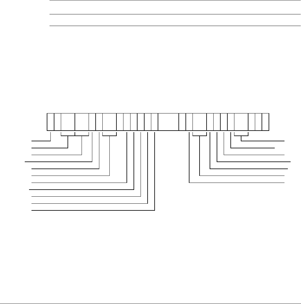
G4 AArch32 System Register Descriptions
G4.2 General system control registers
G4-3880 Copyright © 2013 ARM Limited. All rights reserved. ARM DDI 0487A.a
Non-Confidential - Beta ID090413
G4.2.64 HSCTLR, Hyp System Control Register
The HSCTLR characteristics are:
Purpose
Provides top level control of the system operation in Hyp mode. This register provides Hyp mode
control of features controlled by the Banked SCTLR bits, and shows the values of the non-Banked
SCTLR bits.
This register is part of:
• the Virtualization registers functional group
• the Other system control registers functional group.
Usage constraints
This register is accessible as shown below:
Configurations
HSCTLR is architecturally mapped to AArch64 register SCTLR_EL2.
If EL2 is not implemented, this register is RES0 from EL3.
Attributes
HSCTLR is a 32-bit register.
The HSCTLR bit assignments are:
Bit [31]
Reserved, RES0.
TE, bit [30]
Thumb Exception Enable. This bit controls whether exceptions are taken in A32 or T32 state:
0
Exceptions, including reset, taken in A32 state.
1
Exceptions, including reset, taken in T32 state.
Reset value is architecturally UNKNOWN.
EL0 (NS) EL0 (S) EL1 (NS) EL1 (S) EL2 EL3 (SCR.NS=1) EL3 (SCR.NS=0)
- - - - RW RW -
31
TE
30 29 28 27 26 25 24 23 22
FI
21 20 19 18 17 16
RES0
15 13
I
12 11 10 9 8 7 6 5 43
C
2
A
1
M
0
RES0
RES1
RES0
EE
RES0
RES1
RES0
WXN
RES1
RES0
RES1
RES1
CP15BEN
RES0
ITD
SED
RES0
RES1

G4 AArch32 System Register Descriptions
G4.2 General system control registers
ARM DDI 0487A.a Copyright © 2013 ARM Limited. All rights reserved. G4-3881
ID090413 Non-Confidential - Beta
Bits [29:28]
Reserved, RES1.
Bits [27:26]
Reserved, RES0.
EE, bit [25]
Exception Endianness. The value of this bit defines the value of the CPSR.E bit on entry to an
exception vector, including reset. This value also indicates the endianness of the translation table
data for translation table lookups. The possible values of this bit are:
0
Little-endian.
1
Big-endian.
If an implementation does not provide Big-endian support, this bit is RES0. If it does not provide
Little-endian support, this bit is RES1.
If this register is at the highest exception level implemented, field resets to an IMPLEMENTATION
DEFINED value. Otherwise, its reset value is UNKNOWN.
Bit [24]
Reserved, RES0.
Bits [23:22]
Reserved, RES1.
FI, bit [21]
Fast interrupts configuration enable. This bit can be used to reduce interrupt latency in an
implementation by disabling IMPLEMENTATION DEFINED performance features. The possible values
of this bit are:
0
All performance features enabled.
1
Low interrupt latency configuration. Some performance features disabled.
Reset value is architecturally UNKNOWN.
Bit [20]
Reserved, RES0.
WXN, bit [19]
Write permission implies XN (Execute Never). This bit can be used to require all memory regions
with write permission to be treated as XN. The possible values of this bit are:
0
Regions with write permission are not forced to XN.
1
Regions with write permission are forced to XN.
The WXN bit is permitted to be cached in a TLB.
Reset value is architecturally UNKNOWN.
Bit [18]
Reserved, RES1.
Bit [17]
Reserved, RES0.
Bit [16]
Reserved, RES1.
Bits [15:13]
Reserved, RES0.

G4 AArch32 System Register Descriptions
G4.2 General system control registers
G4-3882 Copyright © 2013 ARM Limited. All rights reserved. ARM DDI 0487A.a
Non-Confidential - Beta ID090413
I, bit [12]
Instruction cache enable. This is an enable bit for instruction caches at EL2:
0
Instruction caches disabled at EL2. If HSCTLR.M is set to 0, instruction accesses from
stage 1 of the EL2 translation regime are to Normal memory, Outer Shareable, Inner
Non-cacheable, Outer Non-cacheable.
1
Instruction caches enabled at EL2. If HSCTLR.M is set to 0, instruction accesses from
stage 1 of the EL2 translation regime are to Normal memory, Outer Shareable, Inner
Write-Through, Outer Write-Through.
When this bit is 0, all EL2 Normal memory instruction accesses are Non-cacheable.
If this register is at the highest exception level implemented, field resets to 0. Otherwise, its reset
value is UNKNOWN.
Bit [11]
Reserved, RES1.
Bits [10:9]
Reserved, RES0.
SED, bit [8]
SETEND Disable. The possible values of this bit are:
0
The SETEND instruction is available.
1
The SETEND instruction is UNALLOCATED.
If an implementation does not support mixed endian operation at EL2, this bit is RES1.
Reset value is architecturally UNKNOWN.
ITD, bit [7]
IT Disable. The possible values of this bit are:
0
The IT instruction functionality is available.
1
It is IMPLEMENTATION DEFINED whether the IT instruction is treated as either:
• A 16-bit instruction, which can only be followed by another 16-bit instruction.
• The first half of a 32-bit instruction.
An implementation might vary dynamically as to whether IT is treated as a 16-bit
instruction or the first half of a 32-bit instruction.
All encodings of the IT instruction with hw1[3:0]!=1000 are UNDEFINED and treated as
unallocated.
All encodings of the subsequent instruction with the following values for hw1 are
UNDEFINED (and treated as unallocated):
11xxxxxxxxxxxxxx
All 32-bit instructions, B(2), B(1), Undefined, SVC, Load/Store multiple
1x11xxxxxxxxxxxx
Miscellaneous 16-bit instructions
1x100xxxxxxxxxxx
ADD Rd, PC, #imm
01001xxxxxxxxxxx
LDR Rd, [PC, #imm]
0100x1xxx1111xxx
ADD(4),CMP(3), MOV, BX pc, BLX pc
010001xx1xxxx111
ADD(4),CMP(3), MOV (Note: this pattern also covers UNPREDICTABLE
cases with BLX Rn)

G4 AArch32 System Register Descriptions
G4.2 General system control registers
ARM DDI 0487A.a Copyright © 2013 ARM Limited. All rights reserved. G4-3883
ID090413 Non-Confidential - Beta
Contrary to the standard treatment of conditional UNDEFINED instructions in the ARM
architecture, in this case these instructions are always treated as UNDEFINED, regardless
of whether the instruction would pass or fail its condition codes as a result of being in
an IT block.
Reset value is architecturally UNKNOWN.
Bit [6]
Reserved, RES0.
CP15BEN, bit [5]
CP15 barrier enable. If implemented, this is an enable bit for the CP15 DMB, DSB, and ISB barrier
operations at EL2:
0
CP15 barrier operations disabled at EL2. Their encodings are UNDEFINED.
1
CP15 barrier operations enabled at EL2.
If an implementation does not support the CP15 barrier operations, this bit is RES0.
Reset value is architecturally UNKNOWN.
Bits [4:3]
Reserved, RES1.
C, bit [2]
Cache enable. This is an enable bit for data and unified caches at EL2:
0
Data and unified caches disabled at EL2.
1
Data and unified caches enabled at EL2.
When this bit is 0, all EL2 Normal memory data accesses and all accesses to the EL2 translation
tables are Non-cacheable.
If this register is at the highest exception level implemented, field resets to 0. Otherwise, its reset
value is UNKNOWN.
A, bit [1]
Alignment check enable. This is the enable bit for Alignment fault checking:
0
Alignment fault checking disabled.
Instructions that load or store one or more registers, other than load/store exclusive and
load-acquire/store-release, do not check that the address being accessed is aligned to the
size of the data element(s) being accessed.
1
Alignment fault checking enabled.
All instructions that load or store one or more registers have an alignment check that the
address being accessed is aligned to the size of the data element(s) being accessed. If
this check fails it causes an Alignment fault, which is taken as a Data Abort exception.
Load/store exclusive and load-acquire/store-release instructions have an alignment check regardless
of the value of the A bit.
If this register is at the highest exception level implemented, field resets to 0. Otherwise, its reset
value is UNKNOWN.
M, bit [0]
MMU enable for EL2 stage 1 address translation. Possible values of this bit are:
0
EL2 stage 1 address translation disabled.
1
EL2 stage 1 address translation enabled.
If this register is at the highest exception level implemented, field resets to 0. Otherwise, its reset
value is UNKNOWN.

G4 AArch32 System Register Descriptions
G4.2 General system control registers
G4-3884 Copyright © 2013 ARM Limited. All rights reserved. ARM DDI 0487A.a
Non-Confidential - Beta ID090413
Accessing the HSCTLR:
To access the HSCTLR:
MRC p15,4,<Rt>,c1,c0,0 ; Read HSCTLR into Rt
MCR p15,4,<Rt>,c1,c0,0 ; Write Rt to HSCTLR
Register access is encoded as follows:
coproc opc1 CRn CRm opc2
1111 100 0001 0000 000

G4 AArch32 System Register Descriptions
G4.2 General system control registers
ARM DDI 0487A.a Copyright © 2013 ARM Limited. All rights reserved. G4-3885
ID090413 Non-Confidential - Beta
G4.2.65 HSR, Hyp Syndrome Register
The HSR characteristics are:
Purpose
Holds syndrome information for an exception taken to Hyp mode.
This register is part of:
• the Virtualization registers functional group
• the Exception and fault handling registers functional group.
Usage constraints
This register is accessible as shown below:
Execution in any Non-secure mode other than Hyp mode makes this register UNKNOWN.
When an UNPREDICTABLE instruction is treated as UNDEFINED, and the exception is taken to EL2,
the value of HSR is UNKNOWN. The value written to HSR must be consistent with a value that could
be created as a result of an exception from the same exception level that generated the exception as
a result of a situation that is not UNPREDICTABLE at that exception level, in order to avoid the
possibility of a privilege violation.
Configurations
HSR is architecturally mapped to AArch64 register ESR_EL2.
If EL2 is not implemented, this register is RES0 from EL3.
Attributes
HSR is a 32-bit register.
The HSR bit assignments are:
EC, bits [31:26]
Exception Class. Indicates the reason for the exception that this register holds information about.
Possible values of this field are:
000000
Unknown reason.
000001
Trapped WFI or WFE instruction.
Conditional WFE and WFI instructions that fail their condition code check do not cause
an exception.
000011
Trapped MCR or MRC access to CP15.
000100
Trapped MCRR or MRRC access to CP15.
000101
Trapped MCR or MRC access to CP14.
000110
Trapped LDC or STC access to CP14.
000111
HCPTR-trapped access to CP10 or CP11.
001000
Trapped MRC or VMRS access to CP10, for ID group traps.
001100
Trapped MRRC or MCRR access to CP14.
EL0 (NS) EL0 (S) EL1 (NS) EL1 (S) EL2 EL3 (SCR.NS=1) EL3 (SCR.NS=0)
- - - - RW RW -
EC
31 26
IL
25
ISS
24 0

G4 AArch32 System Register Descriptions
G4.2 General system control registers
G4-3886 Copyright © 2013 ARM Limited. All rights reserved. ARM DDI 0487A.a
Non-Confidential - Beta ID090413
001111
Illegal exception return to AArch32 state.
010001
SVC taken to Hyp mode.
010010
HVC executed.
010011
Trapped SMC instruction.
100000
Prefetch Abort routed to Hyp mode.
100001
Prefetch Abort taken from Hyp mode.
100010
PC Alignment Exception.
100100
Data Abort routed to Hyp mode.
100101
Data Abort taken from Hyp mode.
Other values are reserved.
IL, bit [25]
Instruction Length. Indicates the size of the instruction that has been trapped to this exception level.
Possible values of this bit are:
0
16-bit instruction trapped.
1
32-bit instruction trapped. This value also applies to the following exceptions:
• An SError interrupt.
• An Instruction Abort exception.
• A Misaligned PC exception.
• A Misaligned Stack Pointer exception.
• A Data Abort for which the value of the ISV bit is 0.
• An Illegal Execution State exception.
• Any debug exception except for Software Breakpoint Instruction exceptions. For
Software Breakpoint Instruction exceptions, this bit has its standard meaning:
0
16-bit T32 BKPT instruction.
1
32-bit A32 BKPT instruction.
• An exception reported using EC value
0b000000
.
ISS, bits [24:0]
Instruction Specific Syndrome. Architecturally, this field can be defined independently for each
defined Exception class. However, in practice, some ISS encodings are used for more than one
Exception class.
Typically, an ISS encoding has a number of subfields. When an ISS subfield holds a register
number, the value returned in that field is the AArch64 view of the register number, even if the
reported exception was taken from AArch32 state. If the register number is AArch32 register R15,
then:
• If the instruction that generated the exception was not UNPREDICTABLE, the field takes the
value
0b11111
.
• If the instruction that generated the exception was UNPREDICTABLE, the field takes an
UNKNOWN value that must be either:
— The AArch64 view of the register number of a register that might have been used at
the Exception level from which the exception was taken.
— The value
0b11111
.

G4 AArch32 System Register Descriptions
G4.2 General system control registers
ARM DDI 0487A.a Copyright © 2013 ARM Limited. All rights reserved. G4-3887
ID090413 Non-Confidential - Beta
When the EC field is
0b000000
, indicating an exception with an unknown reason, the ISS field is not
valid, RES0.
Exceptions with an unknown reason:
Bits [24:0]
Reserved, RES0.
Exception from a WFI or WFE instruction:
CV, bit [24]
Condition code valid. Possible values of this bit are:
0
The COND field is not valid.
1
The COND field is valid.
When an A32 instruction is trapped, CV is set to 1.
When a T32 instruction is trapped, it is IMPLEMENTATION DEFINED whether:
• CV is set to 0 and COND is set to an UNKNOWN value. Software must
examine the SPSR.IT field to determine the condition of a T32
instruction.
• CV is set to 1 and COND is set to the condition code for the condition
that applied to the instruction.
COND, bits [23:20]
The condition code for the trapped instruction.
When an A32 instruction is trapped:
• If the instruction is conditional, COND is set to the condition code
field value from the instruction.
• If the instruction is unconditional, COND is set to
0xE
.
A conditional A32 instruction that is known to pass its condition code check
can be presented either:
• With COND set to
0xE
, the value for unconditional.
• With the COND value held in the instruction.
When a T32 instruction is trapped, it is IMPLEMENTATION DEFINED whether:
• CV is set to 0 and COND is set to an UNKNOWN value. Software must
examine the SPSR.IT field to determine the condition of a T32
instruction.
• CV is set to 1 and COND is set to the condition code for the condition
that applied to the instruction.
For an implementation that, for both A32 and T32 instructions, takes an
exception on a trapped conditional instruction only if the instruction passes
its condition code check, these definitions mean that when CV is set to 1 it
is IMPLEMENTATION DEFINED whether the COND field is set to
0xE
, or to the
value of any condition that applied to the instruction.
Bits [19:1]
Reserved, RES0.
RES0
24 0
24
COND
23 20
RES0
19 1
TI
0
CV

G4 AArch32 System Register Descriptions
G4.2 General system control registers
G4-3888 Copyright © 2013 ARM Limited. All rights reserved. ARM DDI 0487A.a
Non-Confidential - Beta ID090413
TI, bit [0]
Trapped instruction. Possible values of this bit are:
0
WFI trapped.
1
WFE trapped.
Exception from an MCR or MRC access:
CV, bit [24]
Condition code valid. Possible values of this bit are:
0
The COND field is not valid.
1
The COND field is valid.
When an A32 instruction is trapped, CV is set to 1.
When a T32 instruction is trapped, it is IMPLEMENTATION DEFINED whether:
• CV is set to 0 and COND is set to an UNKNOWN value. Software must
examine the SPSR.IT field to determine the condition of a T32
instruction.
• CV is set to 1 and COND is set to the condition code for the condition
that applied to the instruction.
COND, bits [23:20]
The condition code for the trapped instruction.
When an A32 instruction is trapped:
• If the instruction is conditional, COND is set to the condition code
field value from the instruction.
• If the instruction is unconditional, COND is set to
0xE
.
A conditional A32 instruction that is known to pass its condition code check
can be presented either:
• With COND set to
0xE
, the value for unconditional.
• With the COND value held in the instruction.
When a T32 instruction is trapped, it is IMPLEMENTATION DEFINED whether:
• CV is set to 0 and COND is set to an UNKNOWN value. Software must
examine the SPSR.IT field to determine the condition of a T32
instruction.
• CV is set to 1 and COND is set to the condition code for the condition
that applied to the instruction.
For an implementation that, for both A32 and T32 instructions, takes an
exception on a trapped conditional instruction only if the instruction passes
its condition code check, these definitions mean that when CV is set to 1 it
is IMPLEMENTATION DEFINED whether the COND field is set to
0xE
, or to the
value of any condition that applied to the instruction.
Opc2, bits [19:17]
The Opc2 value from the issued instruction.
Opc1, bits [16:14]
The Opc1 value from the issued instruction.
24
COND
23 20
Opc2
19 17
Opc1
16 14
CRn
13 10 9
Rt
85
CRm
41
0
CV Direction
RES0
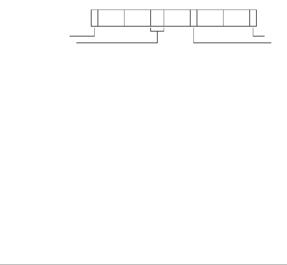
G4 AArch32 System Register Descriptions
G4.2 General system control registers
ARM DDI 0487A.a Copyright © 2013 ARM Limited. All rights reserved. G4-3889
ID090413 Non-Confidential - Beta
CRn, bits [13:10]
The CRn value from the issued instruction, the coprocessor primary register
value.
Bit [9]
Reserved, RES0.
Rt, bits [8:5]
The Rt value from the issued instruction, the general purpose register used
for the transfer.
CRm, bits [4:1]
The CRm value from the issued instruction.
Direction, bit [0]
Indicates the direction of the trapped instruction. The possible values of this
bit are:
0
Write to coprocessor. MCR instruction.
1
Read from coprocessor. MRC or VMRS instruction.
Exception from an MCRR or MRRC access:
CV, bit [24]
Condition code valid. Possible values of this bit are:
0
The COND field is not valid.
1
The COND field is valid.
When an A32 instruction is trapped, CV is set to 1.
When a T32 instruction is trapped, it is IMPLEMENTATION DEFINED whether:
• CV is set to 0 and COND is set to an UNKNOWN value. Software must
examine the SPSR.IT field to determine the condition of a T32
instruction.
• CV is set to 1 and COND is set to the condition code for the condition
that applied to the instruction.
COND, bits [23:20]
The condition code for the trapped instruction.
When an A32 instruction is trapped:
• If the instruction is conditional, COND is set to the condition code
field value from the instruction.
• If the instruction is unconditional, COND is set to
0xE
.
A conditional A32 instruction that is known to pass its condition code check
can be presented either:
• With COND set to
0xE
, the value for unconditional.
• With the COND value held in the instruction.
When a T32 instruction is trapped, it is IMPLEMENTATION DEFINED whether:
• CV is set to 0 and COND is set to an UNKNOWN value. Software must
examine the SPSR.IT field to determine the condition of a T32
instruction.
• CV is set to 1 and COND is set to the condition code for the condition
that applied to the instruction.
24
COND
23 20
Opc1
19 16 15 14
Rt2
13 10 9
Rt
85
CRm
41
0
CV
RES0
Direction
RES0
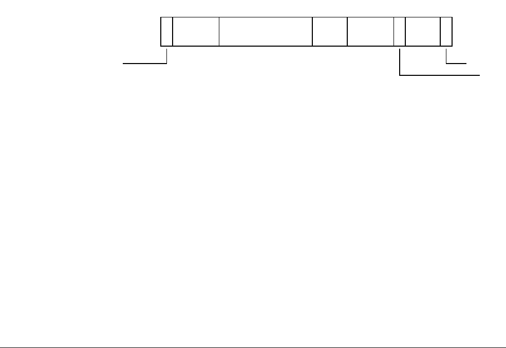
G4 AArch32 System Register Descriptions
G4.2 General system control registers
G4-3890 Copyright © 2013 ARM Limited. All rights reserved. ARM DDI 0487A.a
Non-Confidential - Beta ID090413
For an implementation that, for both A32 and T32 instructions, takes an
exception on a trapped conditional instruction only if the instruction passes
its condition code check, these definitions mean that when CV is set to 1 it
is IMPLEMENTATION DEFINED whether the COND field is set to
0xE
, or to the
value of any condition that applied to the instruction.
Opc1, bits [19:16]
The Opc1 value from the issued instruction.
Bits [15:14]
Reserved, RES0.
Rt2, bits [13:10]
The Rt2 value from the issued instruction, the second general purpose
register used for the transfer.
Bit [9]
Reserved, RES0.
Rt, bits [8:5]
The Rt value from the issued instruction, the general purpose register used
for the transfer.
CRm, bits [4:1]
The CRm value from the issued instruction.
Direction, bit [0]
Indicates the direction of the trapped instruction. The possible values of this
bit are:
0
Write to coprocessor. MCRR instruction.
1
Read from coprocessor. MRRC instruction.
Exception from an LDC or STC access to CP14:
CV, bit [24]
Condition code valid. Possible values of this bit are:
0
The COND field is not valid.
1
The COND field is valid.
When an A32 instruction is trapped, CV is set to 1.
When a T32 instruction is trapped, it is IMPLEMENTATION DEFINED whether:
• CV is set to 0 and COND is set to an UNKNOWN value. Software must
examine the SPSR.IT field to determine the condition of a T32
instruction.
• CV is set to 1 and COND is set to the condition code for the condition
that applied to the instruction.
COND, bits [23:20]
The condition code for the trapped instruction.
When an A32 instruction is trapped:
• If the instruction is conditional, COND is set to the condition code
field value from the instruction.
• If the instruction is unconditional, COND is set to
0xE
.
24
COND
23 20
imm8
19 12
RES0
11 9
Rn
85
4
AM
31
0
CV Direction
Offset

G4 AArch32 System Register Descriptions
G4.2 General system control registers
ARM DDI 0487A.a Copyright © 2013 ARM Limited. All rights reserved. G4-3891
ID090413 Non-Confidential - Beta
A conditional A32 instruction that is known to pass its condition code check
can be presented either:
• With COND set to
0xE
, the value for unconditional.
• With the COND value held in the instruction.
When a T32 instruction is trapped, it is IMPLEMENTATION DEFINED whether:
• CV is set to 0 and COND is set to an UNKNOWN value. Software must
examine the SPSR.IT field to determine the condition of a T32
instruction.
• CV is set to 1 and COND is set to the condition code for the condition
that applied to the instruction.
For an implementation that, for both A32 and T32 instructions, takes an
exception on a trapped conditional instruction only if the instruction passes
its condition code check, these definitions mean that when CV is set to 1 it
is IMPLEMENTATION DEFINED whether the COND field is set to
0xE
, or to the
value of any condition that applied to the instruction.
imm8, bits [19:12]
The immediate value from the issued instruction.
Bits [11:9]
Reserved, RES0.
Rn, bits [8:5]
The Rn value from the issued instruction. Valid only when the Direction
field is 0, indicating a trapped STC instruction.
When the Direction field is 1, indicating a trapped LDC instruction, this
field is RES0.
Offset, bit [4]
Indicates whether the offset is added or subtracted:
0
Subtract offset.
1
Add offset.
This bit corresponds to the U bit in the instruction encoding.
AM, bits [3:1]
Addressing mode. The permitted values of this field are:
000
Immediate unindexed.
001
Immediate post-indexed.
010
Immediate offset.
011
Immediate pre-indexed.
100
Literal unindexed.
A32 instruction set only.
For a trapped LDC or STC T32 instruction, this encoding is
reserved.
110
Literal offset.
For the STC instruction, valid only in the A32 instruction set.
For a trapped STC T32 instruction, this encoding is reserved.
The values
0b101
and
0b111
are reserved.
Bit [2] in this subfield indicates the instruction form, immediate or literal.
Bits [1:0] in this subfield correspond to the bits {P, W} in the instruction
encoding.

G4 AArch32 System Register Descriptions
G4.2 General system control registers
G4-3892 Copyright © 2013 ARM Limited. All rights reserved. ARM DDI 0487A.a
Non-Confidential - Beta ID090413
Direction, bit [0]
Indicates the direction of the trapped instruction. The possible values of this
bit are:
0
Write to coprocessor. STC instruction.
1
Read from coprocessor. LDC instruction.
Exception from an access to SIMD or floating-point registers:
CV, bit [24]
Condition code valid. Possible values of this bit are:
0
The COND field is not valid.
1
The COND field is valid.
When an A32 instruction is trapped, CV is set to 1.
When a T32 instruction is trapped, it is IMPLEMENTATION DEFINED whether:
• CV is set to 0 and COND is set to an UNKNOWN value. Software must
examine the SPSR.IT field to determine the condition of a T32
instruction.
• CV is set to 1 and COND is set to the condition code for the condition
that applied to the instruction.
COND, bits [23:20]
The condition code for the trapped instruction.
When an A32 instruction is trapped:
• If the instruction is conditional, COND is set to the condition code
field value from the instruction.
• If the instruction is unconditional, COND is set to
0xE
.
A conditional A32 instruction that is known to pass its condition code check
can be presented either:
• With COND set to
0xE
, the value for unconditional.
• With the COND value held in the instruction.
When a T32 instruction is trapped, it is IMPLEMENTATION DEFINED whether:
• CV is set to 0 and COND is set to an UNKNOWN value. Software must
examine the SPSR.IT field to determine the condition of a T32
instruction.
• CV is set to 1 and COND is set to the condition code for the condition
that applied to the instruction.
For an implementation that, for both A32 and T32 instructions, takes an
exception on a trapped conditional instruction only if the instruction passes
its condition code check, these definitions mean that when CV is set to 1 it
is IMPLEMENTATION DEFINED whether the COND field is set to
0xE
, or to the
value of any condition that applied to the instruction.
Bits [19:6]
Reserved, RES0.
24
COND
23 20
RES0
19 6
TA
54
coproc
30
CV RES0

G4 AArch32 System Register Descriptions
G4.2 General system control registers
ARM DDI 0487A.a Copyright © 2013 ARM Limited. All rights reserved. G4-3893
ID090413 Non-Confidential - Beta
TA, bit [5]
Indicates trapped use of the Advanced SIMD extension. The possible values
of this bit are:
0
Exception was not caused by trapped use of the Advanced
SIMD extension.
1
Exception was caused by trapped use of the Advanced SIMD
extension.
Any use of an Advanced SIMD instruction that is trapped to Hyp mode
because of a trap configured in the HCPTR sets this bit to 1.
Bit [4]
Reserved, RES0.
coproc, bits [3:0]
The number of the coprocessor accessed by the trapped operation, 0-13.
Exception from HVC or SVC instruction execution:
Bits [24:16]
Reserved, RES0.
imm16, bits [15:0]
The value of the immediate field from the HVC or SVC instruction.
For an HVC instruction this is the value of the imm16 field of the issued
instruction.
For an SVC instruction:
• If the instruction is unconditional, then:
— For the 16-bit T32 instruction, this field is zero-extended from
the imm8 field of the instruction.
— For the A32 instruction, this field is the bottom 16 bits of the
imm24 field of the instruction.
• If the instruction is conditional, this field is UNKNOWN.
The HVC instruction is unconditional, and a conditional SVC instruction
generates a Supervisor Call exception that is routed to Hyp mode only if it
passes its condition code check. Therefore, the syndrome information for
these exceptions does not include conditionality information.
Exception from SMC instruction execution in AArch32 state:
Bits [24:0]
Reserved, RES0.
RES0
24 16
imm16
15 0
RES0
24 0

G4 AArch32 System Register Descriptions
G4.2 General system control registers
G4-3894 Copyright © 2013 ARM Limited. All rights reserved. ARM DDI 0487A.a
Non-Confidential - Beta ID090413
Exception from an Instruction abort:
Bits [24:10]
Reserved, RES0.
EA, bit [9]
External abort type. This bit can be provide an IMPLEMENTATION DEFINED
classification of external aborts.
For any abort other than an External abort this bit returns a value of 0.
Bit [8]
Reserved, RES0.
S1PTW, bit [7]
For a stage 2 fault, indicates whether the fault was a fault on the stage 2
translation of an address accessed during a stage 1 translation table walk:
0
Fault not on a stage 2 translation for a stage 1 translation table
walk.
1
Fault on the stage 2 translation of an access for a stage 1
translation table walk.
For a stage 1 fault, this bit is RES0.
Bit [6]
Reserved, RES0.
IFSC, bits [5:0]
Instruction Fault Status Code. Possible values of this field are:
000000
Address size fault, zeroth level of translation or translation table
base register
000001
Address size fault, first level
000010
Address size fault, second level
000011
Address size fault, third level
000100
Translation fault, zeroth level
000101
Translation fault, first level
000110
Translation fault, second level
000111
Translation fault, third level
001001
Access flag fault, first level
001010
Access flag fault, second level
001011
Access flag fault, third level
001101
Permission fault, first level
001110
Permission fault, second level
001111
Permission fault, third level
010000
Synchronous external abort
011000
Synchronous parity error on memory access
RES0
24 10 9 8 7 6
IFSC
50
RES0
S1PTW
RES0
EA

G4 AArch32 System Register Descriptions
G4.2 General system control registers
ARM DDI 0487A.a Copyright © 2013 ARM Limited. All rights reserved. G4-3895
ID090413 Non-Confidential - Beta
010100
Synchronous external abort on translation table walk, zeroth
level
010101
Synchronous external abort on translation table walk, first level
010110
Synchronous external abort on translation table walk, second
level
010111
Synchronous external abort on translation table walk, third level
011100
Synchronous parity error on memory access on translation table
walk, zeroth level
011101
Synchronous parity error on memory access on translation table
walk, first level
011110
Synchronous parity error on memory access on translation table
walk, second level
011111
Synchronous parity error on memory access on translation table
walk, third level
100001
Alignment fault
100010
Debug event
110000
TLB conflict abort
110100
IMPLEMENTATION DEFINED fault (Lockdown fault)
All other values are reserved.
The lookup level associated with a fault is:
• For a fault generated on a translation table walk, the lookup level of
the walk being performed.
• For a Translation fault, the lookup level of the translation table that
gave the fault. If a fault occurs because a stage of address translation
is disabled, or because the input address is outside the range specified
by the appropriate base address register or registers, the fault is
reported as a level 1 fault.
• For an Access flag fault, the lookup level of the translation table that
gave the fault.
• For a Permission fault, including a Permission fault cased by
hierarchical permissions, the lookup level of the final level of
translation table accessed for the translation. That is, the lookup level
of the translation table that returned a Block or Page descriptor.
Exception from an Instruction set state, PC alignment, or SP alignment fault:
Bits [24:0]
Reserved, RES0.
RES0
24 0

G4 AArch32 System Register Descriptions
G4.2 General system control registers
G4-3896 Copyright © 2013 ARM Limited. All rights reserved. ARM DDI 0487A.a
Non-Confidential - Beta ID090413
Exception from a Data abort:
ISV, bit [24]
Instruction syndrome valid. Indicates whether the rest of the syndrome
information in this register is valid.
0
No valid instruction syndrome. ISS[23:16] are RES0.
1
ISS[24:16] hold a valid instruction syndrome.
This bit is 0 for all faults except those generated by a stage 2 translation. For
Data Abort exceptions generated by a stage 2 translation, this bit is 1 and a
valid instruction syndrome is returned, only if all of the following are true:
• The instruction that generated the Data Abort exception:
— Is an LDR, LDA, LDRT, LDRSH, LDRSHT, LDRH, LDAH,
LDRHT, LDRSB, LDRSBT, LDRB, LDAB, LDRBT, STR,
STL, STRT, STRH, STLH, STRHT, STRB, STLB, or STRBT
instruction.
— Is not performing register writeback.
— Is not using the PC as its source or destination register.
For ISS reporting, a stage 2 abort on a stage 1 translation table lookup is
treated as a stage 1 Translation fault, and does not return a valid instruction
syndrome.
It is IMPLEMENTATION DEFINED whether ISV is set to 1 or 0 on a
synchronous external abort on stage 2 translation table walks.
In the A32 instruction set, LDR*T and STR*T instructions always perform
register writeback and therefore never return a valid instruction syndrome.
SAS, bits [23:22]
Syndrome Access Size. Indicates the size of the access attempted by the
faulting operation.
00
Byte
01
Halfword
10
Word
11
Doubleword
SSE, bit [21]
Syndrome Sign Extend. For a byte, halfword, or word load operation,
indicates whether the data item must be sign extended. For these cases, the
possible values of this bit are:
0
Sign-extension not required.
1
Data item must be sign-extended.
For all other operations this bit is 0.
Bit [20]
Reserved, RES0.
24
SAS
23 22 21 20
SRT
19 16 15 14
RES0
13 10 9 8 7 6
DFSC
50
ISV
SSE
RES0
RES0
AR
WnR
S1PTW
CM
EA

G4 AArch32 System Register Descriptions
G4.2 General system control registers
ARM DDI 0487A.a Copyright © 2013 ARM Limited. All rights reserved. G4-3897
ID090413 Non-Confidential - Beta
SRT, bits [19:16]
Syndrome Register transfer. The register number of the Rt operand of the
faulting instruction.
Bit [15]
Reserved, RES0.
AR, bit [14]
Acquire/Release. Possible values of this bit are:
0
Instruction did not have acquire/release semantics.
1
Instruction did have acquire/release semantics.
Bits [13:10]
Reserved, RES0.
EA, bit [9]
External abort type. This bit can be provide an IMPLEMENTATION DEFINED
classification of external aborts.
For any abort other than an External abort this bit returns a value of 0.
CM, bit [8]
Cache maintenance. For a synchronous fault, identifies fault that comes
from a cache maintenance or address translation operation. For synchronous
faults, the possible values of this bit are:
0
Fault not generated by a cache maintenance or address
translation operation.
1
Fault generated by a cache maintenance or address translation
operation.
For asynchronous faults, this bit is 0.
S1PTW, bit [7]
For a stage 2 fault, indicates whether the fault was a fault on the stage 2
translation of an address accessed during a stage 1 translation table walk:
0
Fault not on a stage 2 translation for a stage 1 translation table
walk.
1
Fault on the stage 2 translation of an access for a stage 1
translation table walk.
For a stage 1 fault, this bit is RES0.
WnR, bit [6]
Write not Read. Indicates whether a synchronous abort was caused by a
write or a read operation. The possible values of this bit are:
0
Abort caused by a read operation.
1
Abort caused by a write operation.
For faults on cache maintenance and address translation operations, this bit
always returns a value of 1.
DFSC, bits [5:0]
Data Fault Status Code. Possible values of this field are:
000000
Address size fault, zeroth level of translation or translation table
base register
000001
Address size fault, first level
000010
Address size fault, second level
000011
Address size fault, third level
000100
Translation fault, zeroth level
000101
Translation fault, first level
000110
Translation fault, second level

G4 AArch32 System Register Descriptions
G4.2 General system control registers
G4-3898 Copyright © 2013 ARM Limited. All rights reserved. ARM DDI 0487A.a
Non-Confidential - Beta ID090413
000111
Translation fault, third level
001001
Access flag fault, first level
001010
Access flag fault, second level
001011
Access flag fault, third level
001101
Permission fault, first level
001110
Permission fault, second level
001111
Permission fault, third level
010000
Synchronous external abort
011000
Synchronous parity error on memory access
010001
Asynchronous external abort
011001
Asynchronous parity error on memory access
010100
Synchronous external abort on translation table walk, zeroth
level
010101
Synchronous external abort on translation table walk, first level
010110
Synchronous external abort on translation table walk, second
level
010111
Synchronous external abort on translation table walk, third level
011100
Synchronous parity error on memory access on translation table
walk, zeroth level
011101
Synchronous parity error on memory access on translation table
walk, first level
011110
Synchronous parity error on memory access on translation table
walk, second level
011111
Synchronous parity error on memory access on translation table
walk, third level
100001
Alignment fault
100010
Debug event
110000
TLB conflict abort
110100
IMPLEMENTATION DEFINED fault (Lockdown fault)
110101
IMPLEMENTATION DEFINED fault (Unsupported Exclusive
access fault)
111101
Section Domain Fault, used only for faults reported in the
PAR_EL1
111110
Page Domain Fault, used only for faults reported in the
PAR_EL1
All other values are reserved.
The lookup level associated with a fault is:
• For a fault generated on a translation table walk, the lookup level of
the walk being performed.
• For a Translation fault, the lookup level of the translation table that
gave the fault. If a fault occurs because a stage of address translation
is disabled, or because the input address is outside the range specified
by the appropriate base address register or registers, the fault is
reported as a level 1 fault.
• For an Access flag fault, the lookup level of the translation table that
gave the fault.

G4 AArch32 System Register Descriptions
G4.2 General system control registers
ARM DDI 0487A.a Copyright © 2013 ARM Limited. All rights reserved. G4-3899
ID090413 Non-Confidential - Beta
• For a Permission fault, including a Permission fault cased by
hierarchical permissions, the lookup level of the final level of
translation table accessed for the translation. That is, the lookup level
of the translation table that returned a Block or Page descriptor.
Accessing the HSR:
To access the HSR:
MRC p15,4,<Rt>,c5,c2,0 ; Read HSR into Rt
MCR p15,4,<Rt>,c5,c2,0 ; Write Rt to HSR
Register access is encoded as follows:
coproc opc1 CRn CRm opc2
1111 100 0101 0010 000
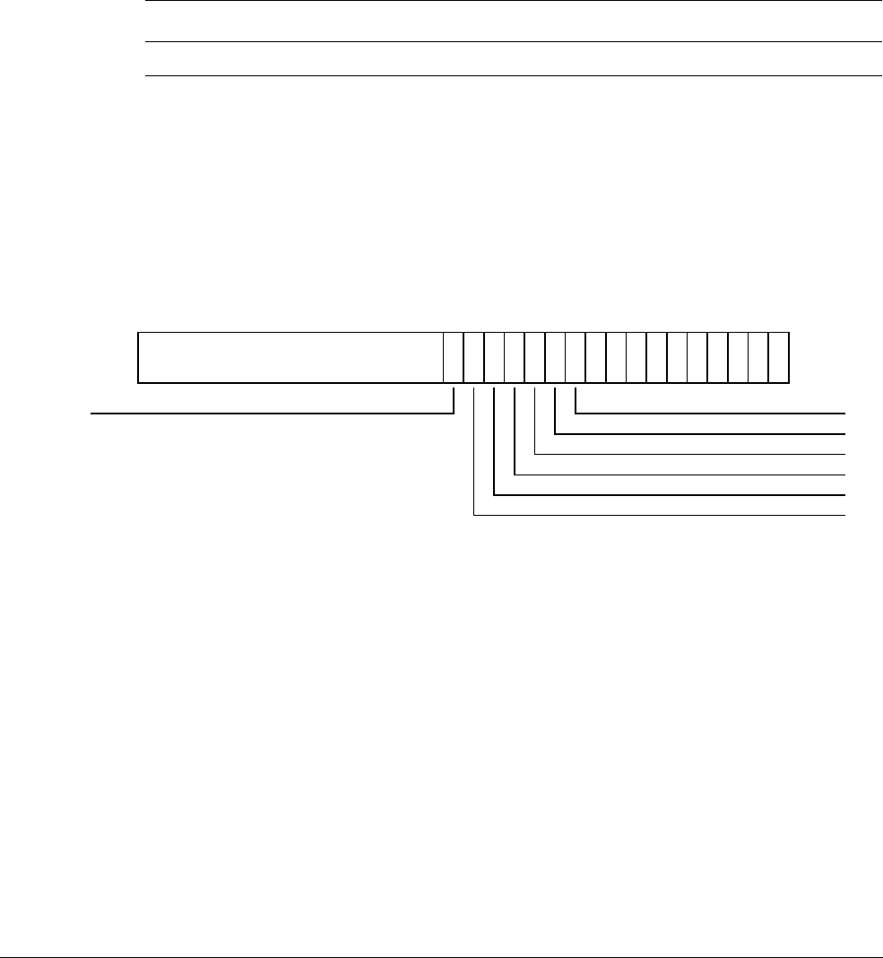
G4 AArch32 System Register Descriptions
G4.2 General system control registers
G4-3900 Copyright © 2013 ARM Limited. All rights reserved. ARM DDI 0487A.a
Non-Confidential - Beta ID090413
G4.2.66 HSTR, Hyp System Trap Register
The HSTR characteristics are:
Purpose
Controls trapping to Hyp mode of Non-secure accesses, at EL1 or lower, of use of T32EE or the
CP15 primary coprocessor registers, {c0-c3,c5-c13,c15}.
This register is part of the Virtualization registers functional group.
Usage constraints
This register is accessible as shown below:
Configurations
HSTR is architecturally mapped to AArch64 register HSTR_EL2.
If EL2 is not implemented, this register is RES0 from EL3.
Attributes
HSTR is a 32-bit register.
The HSTR bit assignments are:
Bits [31:17]
Reserved, RES0.
TTEE, bit [16]
Trap T32EE. The possible values of this bit are:
0
Has no effect on accesses to the T32EE configuration registers.
1
Trap valid Non-secure accesses to T32EE configuration registers to Hyp mode.
When this bit is set to 1, any valid Non-secure access to the T32EE configuration registers is trapped
to Hyp mode.
If T32EE is not implemented, then this bit is RES0.
Resets to 0.
T<n>, bit [n], for n = 0 to 15
Trap coprocessor primary register. For each field T<n>, the possible values of this bit are:
0
Has no effect on Non-secure accesses to CP15 coprocessor registers.
1
Trap valid Non-secure accesses to coprocessor primary register c<n> to Hyp mode.
EL0 (NS) EL0 (S) EL1 (NS) EL1 (S) EL2 EL3 (SCR.NS=1) EL3 (SCR.NS=0)
- - - - RW RW -
RES0
31 17 16 15 14 13 12 11 10
T9
9
T8
8
T7
7
T6
6
T5
5
T4
4
T3
3
T2
2
T1
1
T0
0
TTEE T10
T11
T12
T13
T14
T15

G4 AArch32 System Register Descriptions
G4.2 General system control registers
ARM DDI 0487A.a Copyright © 2013 ARM Limited. All rights reserved. G4-3901
ID090413 Non-Confidential - Beta
When T<n> is set to 1, any valid Non-secure access to CP15 primary coprocessor register c<n> is
trapped to Hyp mode. For example, when T7 is set to 1:
• Any valid Non-secure 32-bit CP15 accesses, using MRC or MCR instructions with
CRn==c7, are trapped to Hyp mode.
• Any valid Non-secure 64-bit CP15 accesses, using MRRC or MCRR instructions with
CRm==c7, are trapped to Hyp mode.
Fields T14 and T4 are RES0.
Resets to 0.
Accessing the HSTR:
To access the HSTR:
MRC p15,4,<Rt>,c1,c1,3 ; Read HSTR into Rt
MCR p15,4,<Rt>,c1,c1,3 ; Write Rt to HSTR
Register access is encoded as follows:
coproc opc1 CRn CRm opc2
1111 100 0001 0001 011
G4 AArch32 System Register Descriptions
G4.2 General system control registers
G4-3902 Copyright © 2013 ARM Limited. All rights reserved. ARM DDI 0487A.a
Non-Confidential - Beta ID090413
G4.2.67 HTCR, Hyp Translation Control Register
The HTCR characteristics are:
Purpose
Controls translation table walks required for the stage 1 translation of memory accesses from Hyp
mode, and holds cacheability and shareability information for the accesses.
This register is part of:
• the Virtualization registers functional group
• the Virtual memory control registers functional group.
Usage constraints
This register is accessible as shown below:
Used in conjunction with HTTBR, that defines the translation table base address for the translations.
Configurations
HTCR is architecturally mapped to AArch64 register TCR_EL2.
If EL2 is not implemented, this register is RES0 from EL3.
Attributes
HTCR is a 32-bit register.
The HTCR bit assignments are:
Bit [31]
Reserved, RES1.
Bits [29:24]
Reserved, RES0.
Bit [23]
Reserved, RES1.
Bits [22:14]
Reserved, RES0.
SH0, bits [13:12]
Shareability attribute for memory associated with translation table walks using TTBR0.
00
Non-shareable
10
Outer Shareable
EL0 (NS) EL0 (S) EL1 (NS) EL1 (S) EL2 EL3 (SCR.NS=1) EL3 (SCR.NS=0)
- - - - RW RW -
31 30
RES0
29 24 23
RES0
22 14
SH0
13 12 11 10 98
RES0
73
T0SZ
20
RES1
IMP DEF
RES1
IRGN0
ORGN0

G4 AArch32 System Register Descriptions
G4.2 General system control registers
ARM DDI 0487A.a Copyright © 2013 ARM Limited. All rights reserved. G4-3903
ID090413 Non-Confidential - Beta
11
Inner Shareable
Other values are reserved.
ORGN0, bits [11:10]
Outer cacheability attribute for memory associated with translation table walks using TTBR0.
00
Normal memory, Outer Non-cacheable
01
Normal memory, Outer Write-Back Write-Allocate Cacheable
10
Normal memory, Outer Write-Through Cacheable
11
Normal memory, Outer Write-Back no Write-Allocate Cacheable
IRGN0, bits [9:8]
Inner cacheability attribute for memory associated with translation table walks using TTBR0.
00
Normal memory, Inner Non-cacheable
01
Normal memory, Inner Write-Back Write-Allocate Cacheable
10
Normal memory, Inner Write-Through Cacheable
11
Normal memory, Inner Write-Back no Write-Allocate Cacheable
Bits [7:3]
Reserved, RES0.
T0SZ, bits [2:0]
The size offset of the memory region addressed by TTBR0. The region size is 232-T0SZ bytes.
Accessing the HTCR:
To access the HTCR:
MRC p15,4,<Rt>,c2,c0,2 ; Read HTCR into Rt
MCR p15,4,<Rt>,c2,c0,2 ; Write Rt to HTCR
Register access is encoded as follows:
coproc opc1 CRn CRm opc2
1111 100 0010 0000 010

G4 AArch32 System Register Descriptions
G4.2 General system control registers
G4-3904 Copyright © 2013 ARM Limited. All rights reserved. ARM DDI 0487A.a
Non-Confidential - Beta ID090413
G4.2.68 HTPIDR, Hyp Thread Pointer / ID Register
The HTPIDR characteristics are:
Purpose
Provides a location where software running in Hyp mode can store thread identifying information
that is not visible to Non-secure software executing at EL0 or EL1, for hypervisor management
purposes.
This register is part of:
• the Virtualization registers functional group
• the Thread and process ID registers functional group.
Usage constraints
This register is accessible as shown below:
Processor hardware never updates this register.
Configurations
HTPIDR is architecturally mapped to AArch64 register TPIDR_EL2[31:0].
If EL2 is not implemented, this register is RES0 from EL3.
Attributes
HTPIDR is a 32-bit register.
The HTPIDR bit assignments are:
Bits [31:0]
Thread ID. Thread identifying information stored by software running at this exception level.
Accessing the HTPIDR:
To access the HTPIDR:
MRC p15,4,<Rt>,c13,c0,2 ; Read HTPIDR into Rt
MCR p15,4,<Rt>,c13,c0,2 ; Write Rt to HTPIDR
Register access is encoded as follows:
EL0 (NS) EL0 (S) EL1 (NS) EL1 (S) EL2 EL3 (SCR.NS=1) EL3 (SCR.NS=0)
- - - - RW RW -
Thread ID
31 0
coproc opc1 CRn CRm opc2
1111 100 1101 0000 010
G4 AArch32 System Register Descriptions
G4.2 General system control registers
ARM DDI 0487A.a Copyright © 2013 ARM Limited. All rights reserved. G4-3905
ID090413 Non-Confidential - Beta
G4.2.69 HTTBR, Hyp Translation Table Base Register
The HTTBR characteristics are:
Purpose
Holds the base address of the translation table for the stage 1 translation of memory accesses from
Hyp mode.
This register is part of:
• the Virtualization registers functional group
• the Virtual memory control registers functional group.
Usage constraints
This register is accessible as shown below:
Used in conjunction with the HTCR.
Configurations
HTTBR is architecturally mapped to AArch64 register TTBR0_EL2.
If EL2 is not implemented, this register is RES0 from EL3.
Attributes
HTTBR is a 64-bit register.
The HTTBR bit assignments are:
Bits [63:48]
Reserved, RES0.
BADDR[47:x], bits [47:0]
Translation table base address, bits[47:x]. Bits [x-1:0] are RES0.
x is based on the value of HTCR.T0SZ, and is calculated as follows:
• If HTCR.T0SZ is 0 or 1, x = 5 - HTCR.T0SZ.
• If HTCR.T0SZ is greater than 1, x = 14 - HTCR.T0SZ.
The value of x determines the required alignment of the translation table, which must be aligned to
2x bytes.
If bits [x-1:3] are not all zero, this is a misaligned Translation Table Base Address. Its effects are
CONSTRAINED UNPREDICTABLE, and can be one of the following:
• Bits [x-1:3] are treated as if all the bits are zero. The value read back from those bits might
be the value written or might be zero.
• The calculation of an address for a translation table walk using this register can be corrupted
in those bits that are non-zero.
EL0 (NS) EL0 (S) EL1 (NS) EL1 (S) EL2 EL3 (SCR.NS=1) EL3 (SCR.NS=0)
- - - - RW RW -
RES0
63 48
BADDR[47:x]
47 0

G4 AArch32 System Register Descriptions
G4.2 General system control registers
G4-3906 Copyright © 2013 ARM Limited. All rights reserved. ARM DDI 0487A.a
Non-Confidential - Beta ID090413
Accessing the HTTBR:
To access the HTTBR:
MRRC p15,4,<Rt>,<Rt2>,c2 ; Read 64-bit HTTBR into Rt (low word) and Rt2 (high word)
MCRR p15,4,<Rt>,<Rt2>,c2 ; Write Rt (low word) and Rt2 (high word) to 64-bit HTTBR
Register access is encoded as follows:
coproc opc1 CRm
1111 0100 0010

G4 AArch32 System Register Descriptions
G4.2 General system control registers
ARM DDI 0487A.a Copyright © 2013 ARM Limited. All rights reserved. G4-3907
ID090413 Non-Confidential - Beta
G4.2.70 HVBAR, Hyp Vector Base Address Register
The HVBAR characteristics are:
Purpose
Holds the exception base address for any exception that is taken to Hyp mode.
This register is part of:
• the Virtualization registers functional group
• the Exception and fault handling registers functional group.
Usage constraints
This register is accessible as shown below:
Configurations
HVBAR is architecturally mapped to AArch64 register VBAR_EL2[31:0].
If EL2 is not implemented, this register is RES0 from EL3.
Attributes
HVBAR is a 32-bit register.
The HVBAR bit assignments are:
Bits [31:5]
Vector Base Address. Bits[31:5] of the base address of the exception vectors for exceptions taken
in this exception level. Bits[4:0] of an exception vector are the exception offset.
Bits [4:0]
Reserved, RES0.
Accessing the HVBAR:
To access the HVBAR:
MRC p15,4,<Rt>,c12,c0,0 ; Read HVBAR into Rt
MCR p15,4,<Rt>,c12,c0,0 ; Write Rt to HVBAR
Register access is encoded as follows:
EL0 (NS) EL0 (S) EL1 (NS) EL1 (S) EL2 EL3 (SCR.NS=1) EL3 (SCR.NS=0)
- - - - RW RW -
Vector Base Address
31 5
RES0
40
coproc opc1 CRn CRm opc2
1111 100 1100 0000 000

G4 AArch32 System Register Descriptions
G4.2 General system control registers
G4-3908 Copyright © 2013 ARM Limited. All rights reserved. ARM DDI 0487A.a
Non-Confidential - Beta ID090413
G4.2.71 ICIALLU, Instruction Cache Invalidate All to PoU
The ICIALLU characteristics are:
Purpose
Invalidate all instruction caches to PoU. If branch predictors are architecturally visible, also flush
branch predictors.
This register is part of the Cache maintenance operations functional group.
Usage constraints
This operation can be performed at the exception levels shown below:
Configurations
ICIALLU performs the same function as AArch64 operation IC IALLU.
Attributes
ICIALLU is a 32-bit system operation.
The ICIALLU operation ignores the value in the register specified by the instruction used to perform this operation.
Software does not have to write a value to the register before issuing this instruction.
Performing the ICIALLU operation:
To perform the ICIALLU operation:
MCR p15,0,<Rt>,c7,c5,0 ; ICIALLU operation, ignoring the value in Rt
The operation is encoded as follows:
EL0 (NS) EL0 (S) EL1 (NS) EL1 (S) EL2 EL3 (SCR.NS=1) EL3 (SCR.NS=0)
- - WO WO WO WO WO
coproc opc1 CRn CRm opc2
1111 000 0111 0101 000

G4 AArch32 System Register Descriptions
G4.2 General system control registers
ARM DDI 0487A.a Copyright © 2013 ARM Limited. All rights reserved. G4-3909
ID090413 Non-Confidential - Beta
G4.2.72 ICIALLUIS, Instruction Cache Invalidate All to PoU, Inner Shareable
The ICIALLUIS characteristics are:
Purpose
Invalidate all instruction caches Inner Shareable to PoU. If branch predictors are architecturally
visible, also flush branch predictors.
This register is part of the Cache maintenance operations functional group.
Usage constraints
This operation can be performed at the exception levels shown below:
Configurations
ICIALLUIS performs the same function as AArch64 operation IC IALLUIS.
Attributes
ICIALLUIS is a 32-bit system operation.
The ICIALLUIS operation ignores the value in the register specified by the instruction used to perform this
operation. Software does not have to write a value to the register before issuing this instruction.
Performing the ICIALLUIS operation:
To perform the ICIALLUIS operation:
MCR p15,0,<Rt>,c7,c1,0 ; ICIALLUIS operation, ignoring the value in Rt
The operation is encoded as follows:
EL0 (NS) EL0 (S) EL1 (NS) EL1 (S) EL2 EL3 (SCR.NS=1) EL3 (SCR.NS=0)
- - WO WO WO WO WO
coproc opc1 CRn CRm opc2
1111 000 0111 0001 000

G4 AArch32 System Register Descriptions
G4.2 General system control registers
G4-3910 Copyright © 2013 ARM Limited. All rights reserved. ARM DDI 0487A.a
Non-Confidential - Beta ID090413
G4.2.73 ICIMVAU, Instruction Cache line Invalidate by VA to PoU
The ICIMVAU characteristics are:
Purpose
Invalidate instruction cache line by virtual address to PoU.
This register is part of the Cache maintenance operations functional group.
Usage constraints
This operation can be performed at the exception levels shown below:
Configurations
ICIMVAU performs the same function as AArch64 operation IC IVAU.
Attributes
ICIMVAU is a 32-bit system operation.
The ICIMVAU input value bit assignments are:
Bits [31:0]
Virtual address to use.
Performing the ICIMVAU operation:
To perform the ICIMVAU operation:
MCR p15,0,<Rt>,c7,c5,1 ; ICIMVAU operation
The operation is encoded as follows:
EL0 (NS) EL0 (S) EL1 (NS) EL1 (S) EL2 EL3 (SCR.NS=1) EL3 (SCR.NS=0)
- - WO WO WO WO WO
Virtual address to use
31 0
coproc opc1 CRn CRm opc2
1111 000 0111 0101 001
G4 AArch32 System Register Descriptions
G4.2 General system control registers
ARM DDI 0487A.a Copyright © 2013 ARM Limited. All rights reserved. G4-3911
ID090413 Non-Confidential - Beta
G4.2.74 ID_AFR0, Auxiliary Feature Register 0
The ID_AFR0 characteristics are:
Purpose
Provides information about the IMPLEMENTATION DEFINED features of the processor in AArch32.
This register is part of the Identification registers functional group.
Usage constraints
This register is accessible as shown below:
Must be interpreted with the Main ID Register, MIDR.
Configurations
ID_AFR0 is architecturally mapped to AArch64 register ID_AFR0_EL1.
There is one instance of this register that is used in both Secure and Non-secure states.
Attributes
ID_AFR0 is a 32-bit register.
The ID_AFR0 bit assignments are:
Bits [31:16]
Reserved, RES0.
Accessing the ID_AFR0:
To access the ID_AFR0:
MRC p15,0,<Rt>,c0,c1,3 ; Read ID_AFR0 into Rt
Register access is encoded as follows:
EL0 (NS) EL0 (S) EL1 (NS) EL1 (S) EL2 EL3 (SCR.NS=1) EL3 (SCR.NS=0)
- - RO RO RO RO RO
RES0
31 16 15 12 11 8 7430
IMP DEF
IMP DEF
IMP DEF
IMP DEF
coproc opc1 CRn CRm opc2
1111 000 0000 0001 011

G4 AArch32 System Register Descriptions
G4.2 General system control registers
G4-3912 Copyright © 2013 ARM Limited. All rights reserved. ARM DDI 0487A.a
Non-Confidential - Beta ID090413
G4.2.75 ID_DFR0, Debug Feature Register 0
The ID_DFR0 characteristics are:
Purpose
Provides top level information about the debug system in AArch32.
This register is part of the Identification registers functional group.
Usage constraints
This register is accessible as shown below:
Must be interpreted with the Main ID Register, MIDR.
Configurations
ID_DFR0 is architecturally mapped to AArch64 register ID_DFR0_EL1.
There is one instance of this register that is used in both Secure and Non-secure states.
Attributes
ID_DFR0 is a 32-bit register.
The ID_DFR0 bit assignments are:
Bits [31:28]
Reserved, RES0.
PerfMon, bits [27:24]
Performance Monitors. Support for coprocessor-based ARM Performance Monitors Extension, for
A and R profile processors. Possible values are:
0000
Performance Monitors Extension system registers not implemented.
0001
Support for Performance Monitors Extension version 1 (PMUv1) system registers. Not
permitted in v8-A.
0010
Support for Performance Monitors Extension version 2 (PMUv2) system registers. Not
permitted in v8-A.
0011
Support for Performance Monitors Extension version 3 (PMUv3) system registers.
1111
IMPLEMENTATION DEFINED form of Performance Monitors system registers supported.
PMUv3 not supported.
All other values are reserved.
In v7, the value
0b0000
can mean that PMUv1 is implemented. PMUv1 is not permitted in a v8-A
implementation.
MProfDbg, bits [23:20]
M Profile Debug. Support for memory-mapped debug model for M profile processors. Permitted
values are:
0000
Not supported.
EL0 (NS) EL0 (S) EL1 (NS) EL1 (S) EL2 EL3 (SCR.NS=1) EL3 (SCR.NS=0)
- - RO RO RO RO RO
RES0
31 28
PerfMon
27 24
MProfDbg
23 20
MMapTrc
19 16
CopTrc
15 12
MMapDbg
11 8
CopSDbg
74
CopDbg
30

G4 AArch32 System Register Descriptions
G4.2 General system control registers
ARM DDI 0487A.a Copyright © 2013 ARM Limited. All rights reserved. G4-3913
ID090413 Non-Confidential - Beta
0001
Support for M profile Debug architecture, with memory-mapped access.
All other values are reserved. For v8-A, this field is
0b0000
.
MMapTrc, bits [19:16]
Memory Mapped Trace. Support for memory-mapped trace model. Permitted values are:
0000
Not supported.
0001
Support for ARM trace architecture, with memory-mapped access.
All other values are reserved.
In the Trace registers, the ETMIDR gives more information about the implementation.
CopTrc, bits [15:12]
Coprocessor Trace. Support for coprocessor-based trace model. Permitted values are:
0000
Not supported.
0001
Support for ARM trace architecture, with CP14 access.
All other values are reserved.
In the Trace registers, the ETMIDR gives more information about the implementation.
MMapDbg, bits [11:8]
Memory Mapped Debug. Support for v7 memory-mapped debug model, for A and R profile
processors.
In v8-A this field is RES0. The optional memory map defined by v8-A is not compatible with v7-A.
CopSDbg, bits [7:4]
Coprocessor Secure Debug. Support for coprocessor-based Secure debug model, for an A profile
processor that includes the Security Extensions.
If EL3 is not implemented and the processor is Non-secure, this field is RES0. Otherwise, this field
reads the same as bits [3:0].
CopDbg, bits [3:0]
Coprocessor Debug. Support for coprocessor based debug model, for A and R profile processors.
Permitted values are:
0000
Not supported.
0010
Support for v6 Debug architecture, with CP14 access.
0011
Support for v6.1 Debug architecture, with CP14 access.
0100
Support for v7 Debug architecture, with CP14 access.
0101
Support for v7.1 Debug architecture, with CP14 access.
0110
Support for v8-A debug architecture, with CP14 access. This is the value that this field
has in v8-A.
All other values are reserved.
Accessing the ID_DFR0:
To access the ID_DFR0:
MRC p15,0,<Rt>,c0,c1,2 ; Read ID_DFR0 into Rt
Register access is encoded as follows:
coproc opc1 CRn CRm opc2
1111 000 0000 0001 010

G4 AArch32 System Register Descriptions
G4.2 General system control registers
G4-3914 Copyright © 2013 ARM Limited. All rights reserved. ARM DDI 0487A.a
Non-Confidential - Beta ID090413
G4.2.76 ID_ISAR0, Instruction Set Attribute Register 0
The ID_ISAR0 characteristics are:
Purpose
Provides information about the instruction sets implemented by the processor in AArch32.
This register is part of the Identification registers functional group.
Usage constraints
This register is accessible as shown below:
Must be interpreted with ID_ISAR1, ID_ISAR2, ID_ISAR3, ID_ISAR4, and ID_ISAR5.
Configurations
ID_ISAR0 is architecturally mapped to AArch64 register ID_ISAR0_EL1.
There is one instance of this register that is used in both Secure and Non-secure states.
Attributes
ID_ISAR0 is a 32-bit register.
The ID_ISAR0 bit assignments are:
Bits [31:28]
Reserved, RES0.
Divide, bits [27:24]
Indicates the implemented Divide instructions. Permitted values are:
0000
None implemented.
0001
Adds SDIV and UDIV in the T32 instruction set.
0010
As for
0b0001
, and adds SDIV and UDIV in the A32 instruction set.
All other values are reserved.
Debug, bits [23:20]
Indicates the implemented Debug instructions. Permitted values are:
0000
None implemented.
0001
Adds BKPT.
All other values are reserved.
Coproc, bits [19:16]
Indicates the implemented Coprocessor instructions. Permitted values are:
0000
None implemented, except for instructions separately attributed by the architecture,
including CP15, CP14, and Advanced SIMD and VFP.
0001
Adds generic CDP, LDC, MCR, MRC, and STC.
0010
As for
0b0001
, and adds generic CDP2, LDC2, MCR2, MRC2, and STC2.
EL0 (NS) EL0 (S) EL1 (NS) EL1 (S) EL2 EL3 (SCR.NS=1) EL3 (SCR.NS=0)
- - RO RO RO RO RO
RES0
31 28
Divide
27 24
Debug
23 20
Coproc
19 16
CmpBranch
15 12
BitField
11 8
BitCount
74
Swap
30

G4 AArch32 System Register Descriptions
G4.2 General system control registers
ARM DDI 0487A.a Copyright © 2013 ARM Limited. All rights reserved. G4-3915
ID090413 Non-Confidential - Beta
0011
As for
0b0010
, and adds generic MCRR and MRRC.
0100
As for
0b0011
, and adds generic MCRR2 and MRRC2.
All other values are reserved.
CmpBranch, bits [15:12]
Indicates the implemented combined Compare and Branch instructions in the T32 instruction set.
Permitted values are:
0000
None implemented.
0001
Adds CBNZ and CBZ.
All other values are reserved.
BitField, bits [11:8]
Indicates the implemented BitField instructions. Permitted values are:
0000
None implemented.
0001
Adds BFC, BFI, SBFX, and UBFX.
All other values are reserved.
BitCount, bits [7:4]
Indicates the implemented Bit Counting instructions. Permitted values are:
0000
None implemented.
0001
Adds CLZ.
All other values are reserved.
Swap, bits [3:0]
Indicates the implemented Swap instructions in the A32 instruction set. Permitted values are:
0000
None implemented.
0001
Adds SWP and SWPB.
All other values are reserved.
In v8-A this field is
0b0000
. The SWP and SWPB instructions are not supported in v8-A.
Accessing the ID_ISAR0:
To access the ID_ISAR0:
MRC p15,0,<Rt>,c0,c2,0 ; Read ID_ISAR0 into Rt
Register access is encoded as follows:
coproc opc1 CRn CRm opc2
1111 000 0000 0010 000

G4 AArch32 System Register Descriptions
G4.2 General system control registers
G4-3916 Copyright © 2013 ARM Limited. All rights reserved. ARM DDI 0487A.a
Non-Confidential - Beta ID090413
G4.2.77 ID_ISAR1, Instruction Set Attribute Register 1
The ID_ISAR1 characteristics are:
Purpose
Provides information about the instruction sets implemented by the processor in AArch32.
This register is part of the Identification registers functional group.
Usage constraints
This register is accessible as shown below:
Must be interpreted with ID_ISAR0, ID_ISAR2, ID_ISAR3, ID_ISAR4, and ID_ISAR5.
Configurations
ID_ISAR1 is architecturally mapped to AArch64 register ID_ISAR1_EL1.
There is one instance of this register that is used in both Secure and Non-secure states.
Attributes
ID_ISAR1 is a 32-bit register.
The ID_ISAR1 bit assignments are:
Jazelle, bits [31:28]
Indicates the implemented Jazelle extension instructions. Permitted values are:
0000
No support for Jazelle.
0001
Adds the BXJ instruction, and the J bit in the PSR. This setting might indicate a trivial
implementation of the Jazelle extension.
All other values are reserved.
Interwork, bits [27:24]
Indicates the implemented Interworking instructions. Permitted values are:
0000
None implemented.
0001
Adds the BX instruction, and the T bit in the PSR.
0010
As for
0b0001
, and adds the BLX instruction. PC loads have BX-like behavior.
0011
As for
0b0010
, and guarantees that data-processing instructions in the A32 instruction
set with the PC as the destination and the S bit clear have BX-like behavior.
All other values are reserved.
Immediate, bits [23:20]
Indicates the implemented data-processing instructions with long immediates. Permitted values are:
0000
None implemented.
0001
Adds:
• The MOVT instruction.
EL0 (NS) EL0 (S) EL1 (NS) EL1 (S) EL2 EL3 (SCR.NS=1) EL3 (SCR.NS=0)
- - RO RO RO RO RO
Jazelle
31 28
Interwork
27 24
Immediate
23 20
IfThen
19 16
Extend
15 12
Except_AR
11 8
Except
74
Endian
30

G4 AArch32 System Register Descriptions
G4.2 General system control registers
ARM DDI 0487A.a Copyright © 2013 ARM Limited. All rights reserved. G4-3917
ID090413 Non-Confidential - Beta
• The MOV instruction encodings with zero-extended 16-bit immediates.
• The T32 ADD and SUB instruction encodings with zero-extended 12-bit
immediates, and the other ADD, ADR, and SUB encodings cross-referenced by
the pseudocode for those encodings.
All other values are reserved.
IfThen, bits [19:16]
Indicates the implemented If-Then instructions in the T32 instruction set. Permitted values are:
0000
None implemented.
0001
Adds the IT instructions, and the IT bits in the PSRs.
All other values are reserved.
Extend, bits [15:12]
Indicates the implemented Extend instructions. Permitted values are:
0000
No scalar sign-extend or zero-extend instructions are implemented, where scalar
instructions means non-Advanced SIMD instructions.
0001
Adds the SXTB, SXTH, UXTB, and UXTH instructions.
0010
As for
0b0001
, and adds the SXTB16, SXTAB, SXTAB16, SXTAH, UXTB16,
UXTAB, UXTAB16, and UXTAH instructions.
All other values are reserved.
Except_AR, bits [11:8]
Indicates the implemented A and R profile exception-handling instructions. Permitted values are:
0000
None implemented.
0001
Adds the SRS and RFE instructions, and the A and R profile forms of the CPS
instruction.
All other values are reserved.
Except, bits [7:4]
Indicates the implemented exception-handling instructions in the ARM instruction set. Permitted
values are:
0000
Not implemented. This indicates that the User bank and Exception return forms of the
LDM and STM instructions are not implemented.
0001
Adds the LDM (exception return), LDM (user registers), and STM (user registers)
instruction versions.
All other values are reserved.
Endian, bits [3:0]
Indicates the implemented Endian instructions. Permitted values are:
0000
None implemented.
0001
Adds the SETEND instruction, and the E bit in the PSRs.
All other values are reserved.
Accessing the ID_ISAR1:
To access the ID_ISAR1:
MRC p15,0,<Rt>,c0,c2,1 ; Read ID_ISAR1 into Rt

G4 AArch32 System Register Descriptions
G4.2 General system control registers
G4-3918 Copyright © 2013 ARM Limited. All rights reserved. ARM DDI 0487A.a
Non-Confidential - Beta ID090413
Register access is encoded as follows:
coproc opc1 CRn CRm opc2
1111 000 0000 0010 001

G4 AArch32 System Register Descriptions
G4.2 General system control registers
ARM DDI 0487A.a Copyright © 2013 ARM Limited. All rights reserved. G4-3919
ID090413 Non-Confidential - Beta
G4.2.78 ID_ISAR2, Instruction Set Attribute Register 2
The ID_ISAR2 characteristics are:
Purpose
Provides information about the instruction sets implemented by the processor in AArch32.
This register is part of the Identification registers functional group.
Usage constraints
This register is accessible as shown below:
Must be interpreted with ID_ISAR0, ID_ISAR1, ID_ISAR3, ID_ISAR4, and ID_ISAR5.
Configurations
ID_ISAR2 is architecturally mapped to AArch64 register ID_ISAR2_EL1.
There is one instance of this register that is used in both Secure and Non-secure states.
Attributes
ID_ISAR2 is a 32-bit register.
The ID_ISAR2 bit assignments are:
Reversal, bits [31:28]
Indicates the implemented Reversal instructions. Permitted values are:
0000
None implemented.
0001
Adds the REV, REV16, and REVSH instructions.
0010
As for
0b0001
, and adds the RBIT instruction.
All other values are reserved.
PSR_AR, bits [27:24]
Indicates the implemented A and R profile instructions to manipulate the PSR. Permitted values are:
0000
None implemented.
0001
Adds the MRS and MSR instructions, and the exception return forms of data-processing
instructions.
All other values are reserved.
The exception return forms of the data-processing instructions are:
• In the A32 instruction set, data-processing instructions with the PC as the destination and the
S bit set. These instructions might be affected by the WithShifts attribute.
• In the T32 instruction set, the SUBS PC,LR,#N instruction.
EL0 (NS) EL0 (S) EL1 (NS) EL1 (S) EL2 EL3 (SCR.NS=1) EL3 (SCR.NS=0)
- - RO RO RO RO RO
Reversal
31 28
PSR_AR
27 24
MultU
23 20
MultS
19 16
Mult
15 12 11 8
MemHint
74
LoadStore
30
MultiAccessInt

G4 AArch32 System Register Descriptions
G4.2 General system control registers
G4-3920 Copyright © 2013 ARM Limited. All rights reserved. ARM DDI 0487A.a
Non-Confidential - Beta ID090413
MultU, bits [23:20]
Indicates the implemented advanced unsigned Multiply instructions. Permitted values are:
0000
None implemented.
0001
Adds the UMULL and UMLAL instructions.
0010
As for
0b0001
, and adds the UMAAL instruction.
All other values are reserved.
MultS, bits [19:16]
Indicates the implemented advanced signed Multiply instructions. Permitted values are:
0000
None implemented.
0001
Adds the SMULL and SMLAL instructions.
0010
As for
0b0001
, and adds the SMLABB, SMLABT, SMLALBB, SMLALBT,
SMLALTB, SMLALTT, SMLATB, SMLATT, SMLAWB, SMLAWT, SMULBB,
SMULBT, SMULTB, SMULTT, SMULWB, and SMULWT instructions. Also adds the
Q bit in the PSRs.
0011
As for
0b0010
, and adds the SMLAD, SMLADX, SMLALD, SMLALDX, SMLSD,
SMLSDX, SMLSLD, SMLSLDX, SMMLA, SMMLAR, SMMLS, SMMLSR,
SMMUL, SMMULR, SMUAD, SMUADX, SMUSD, and SMUSDX instructions.
All other values are reserved.
Mult, bits [15:12]
Indicates the implemented additional Multiply instructions. Permitted values are:
0000
No additional instructions implemented. This means only MUL is implemented.
0001
Adds the MLA instruction.
0010
As for
0b0001
, and adds the MLS instruction.
All other values are reserved.
MultiAccessInt, bits [11:8]
Indicates the support for interruptible multi-access instructions. Permitted values are:
0000
No support. This means the LDM and STM instructions are not interruptible.
0001
LDM and STM instructions are restartable.
0010
LDM and STM instructions are continuable.
All other values are reserved.
MemHint, bits [7:4]
Indicates the implemented Memory Hint instructions. Permitted values are:
0000
None implemented.
0001
Adds the PLD instruction.
0010
Adds the PLD instruction. (
0b0001
and
0b0010
have identical effects.)
0011
As for
0b0001
(or
0b0010
), and adds the PLI instruction.
0100
As for
0b0011
, and adds the PLDW instruction.
All other values are reserved.
LoadStore, bits [3:0]
Indicates the implemented additional load/store instructions. Permitted values are:
0000
No additional load/store instructions implemented.
0001
Adds the LDRD and STRD instructions.

G4 AArch32 System Register Descriptions
G4.2 General system control registers
ARM DDI 0487A.a Copyright © 2013 ARM Limited. All rights reserved. G4-3921
ID090413 Non-Confidential - Beta
0010
As for
0b0001
, and adds the Load Acquire (LDAB, LDAH, LDA, LDAEXB, LDAEXH,
LDAEX, LDAEXD) and Store Release (STLB, STLH, STL, STLEXB, STLEXH,
STLEX, STLEXD) instructions.
All other values are reserved.
Accessing the ID_ISAR2:
To access the ID_ISAR2:
MRC p15,0,<Rt>,c0,c2,2 ; Read ID_ISAR2 into Rt
Register access is encoded as follows:
coproc opc1 CRn CRm opc2
1111 000 0000 0010 010

G4 AArch32 System Register Descriptions
G4.2 General system control registers
G4-3922 Copyright © 2013 ARM Limited. All rights reserved. ARM DDI 0487A.a
Non-Confidential - Beta ID090413
G4.2.79 ID_ISAR3, Instruction Set Attribute Register 3
The ID_ISAR3 characteristics are:
Purpose
Provides information about the instruction sets implemented by the processor in AArch32.
This register is part of the Identification registers functional group.
Usage constraints
This register is accessible as shown below:
Must be interpreted with ID_ISAR0, ID_ISAR1, ID_ISAR2, ID_ISAR4, and ID_ISAR5.
Configurations
ID_ISAR3 is architecturally mapped to AArch64 register ID_ISAR3_EL1.
There is one instance of this register that is used in both Secure and Non-secure states.
Attributes
ID_ISAR3 is a 32-bit register.
The ID_ISAR3 bit assignments are:
T32EE, bits [31:28]
Indicates the implemented TT32EE instructions. Permitted values are:
0000
None implemented.
0001
Adds the ENTERX and LEAVEX instructions, and modifies the load behavior to
include null checking.
All other values are reserved.
This field can only have a value other than
0b0000
when the ID_PFR0.State3 field has a value of
0b0001
.
TrueNOP, bits [27:24]
Indicates the implemented True NOP instructions. Permitted values are:
0000
None implemented. This means there are no NOP instructions that do not have any
register dependencies.
0001
Adds true NOP instructions in both the T32 and A32 instruction sets. This also permits
additional NOP-compatible hints.
All other values are reserved.
ThumbCopy, bits [23:20]
Indicates the support for T32 non flag-setting MOV instructions. Permitted values are:
0000
Not supported. This means that in the T32 instruction set, encoding T1 of the MOV
(register) instruction does not support a copy from a low register to a low register.
EL0 (NS) EL0 (S) EL1 (NS) EL1 (S) EL2 EL3 (SCR.NS=1) EL3 (SCR.NS=0)
- - RO RO RO RO RO
T32EE
31 28
TrueNOP
27 24
ThumbCopy
23 20
TabBranch
19 16
SynchPrim
15 12
SVC
11 8
SIMD
74
Saturate
30

G4 AArch32 System Register Descriptions
G4.2 General system control registers
ARM DDI 0487A.a Copyright © 2013 ARM Limited. All rights reserved. G4-3923
ID090413 Non-Confidential - Beta
0001
Adds support for T32 instruction set encoding T1 of the MOV (register) instruction,
copying from a low register to a low register.
All other values are reserved.
TabBranch, bits [19:16]
Indicates the implemented Table Branch instructions in the T32 instruction set. Permitted values
are:
0000
None implemented.
0001
Adds the TBB and TBH instructions.
All other values are reserved.
SynchPrim, bits [15:12]
Used in conjunction with ID_ISAR4.SynchPrim_frac to indicate the implemented Synchronization
Primitive instructions. Permitted values are:
0000
If SynchPrim_frac ==
0b0000
, no Synchronization Primitives implemented.
0001
If SynchPrim_frac ==
0b0000
, adds the LDREX and STREX instructions.
If SynchPrim_frac ==
0b0011
, also adds the CLREX, LDREXB, STREXB, and
STREXH instructions.
0010
If SynchPrim_frac ==
0b0000
, as for [
0b0001
,
0b0011
] and also adds the LDREXD and
STREXD instructions.
All other combinations of SynchPrim and SynchPrim_frac are reserved.
SVC, bits [11:8]
Indicates the implemented SVC instructions. Permitted values are:
0000
Not implemented.
0001
Adds the SVC instruction.
All other values are reserved.
SIMD, bits [7:4]
Indicates the implemented SIMD instructions. Permitted values are:
0000
None implemented.
0001
Adds the SSAT and USAT instructions, and the Q bit in the PSRs.
0011
As for
0b0001
, and adds the PKHBT, PKHTB, QADD16, QADD8, QASX, QSUB16,
QSUB8, QSAX, SADD16, SADD8, SASX, SEL, SHADD16, SHADD8, SHASX,
SHSUB16, SHSUB8, SHSAX, SSAT16, SSUB16, SSUB8, SSAX, SXTAB16,
SXTB16, UADD16, UADD8, UASX, UHADD16, UHADD8, UHASX, UHSUB16,
UHSUB8, UHSAX, UQADD16, UQADD8, UQASX, UQSUB16, UQSUB8, UQSAX,
USAD8, USADA8, USAT16, USUB16, USUB8, USAX, UXTAB16, and UXTB16
instructions. Also adds support for the GE[3:0] bits in the PSRs.
All other values are reserved.
The SIMD field relates only to implemented instructions that perform SIMD operations on the
general-purpose registers. MVFR0 and MVFR1 give information about the SIMD instructions
implemented by the optional Advanced SIMD Extension.
Saturate, bits [3:0]
Indicates the implemented Saturate instructions. Permitted values are:
0000
None implemented. This means no non-Advanced SIMD saturate instructions are
implemented.
0001
Adds the QADD, QDADD, QDSUB, and QSUB instructions, and the Q bit in the PSRs.
All other values are reserved.

G4 AArch32 System Register Descriptions
G4.2 General system control registers
G4-3924 Copyright © 2013 ARM Limited. All rights reserved. ARM DDI 0487A.a
Non-Confidential - Beta ID090413
Accessing the ID_ISAR3:
To access the ID_ISAR3:
MRC p15,0,<Rt>,c0,c2,3 ; Read ID_ISAR3 into Rt
Register access is encoded as follows:
coproc opc1 CRn CRm opc2
1111 000 0000 0010 011
G4 AArch32 System Register Descriptions
G4.2 General system control registers
ARM DDI 0487A.a Copyright © 2013 ARM Limited. All rights reserved. G4-3925
ID090413 Non-Confidential - Beta
G4.2.80 ID_ISAR4, Instruction Set Attribute Register 4
The ID_ISAR4 characteristics are:
Purpose
Provides information about the instruction sets implemented by the processor in AArch32.
This register is part of the Identification registers functional group.
Usage constraints
This register is accessible as shown below:
Must be interpreted with ID_ISAR0, ID_ISAR1, ID_ISAR2, ID_ISAR3, and ID_ISAR5.
Configurations
ID_ISAR4 is architecturally mapped to AArch64 register ID_ISAR4_EL1.
There is one instance of this register that is used in both Secure and Non-secure states.
Attributes
ID_ISAR4 is a 32-bit register.
The ID_ISAR4 bit assignments are:
SWP_frac, bits [31:28]
Indicates support for the memory system locking the bus for SWP or SWPB instructions. Permitted
values are:
0000
SWP or SWPB instructions not implemented.
0001
SWP or SWPB implemented but only in a uniprocessor context. SWP and SWPB do not
guarantee whether memory accesses from other masters can come between the load
memory access and the store memory access of the SWP or SWPB.
All other values are reserved. This field is valid only if the ID_ISAR0.Swap_instrs field is
0b0000
.
In v8-A this field is
0b0000
. The SWP and SWPB instructions are not supported in v8-A.
PSR_M, bits [27:24]
Indicates the implemented M profile instructions to modify the PSRs. Permitted values are:
0000
None implemented.
0001
Adds the M profile forms of the CPS, MRS, and MSR instructions.
All other values are reserved.
EL0 (NS) EL0 (S) EL1 (NS) EL1 (S) EL2 EL3 (SCR.NS=1) EL3 (SCR.NS=0)
- - RO RO RO RO RO
SWP_frac
31 28
PSR_M
27 24 23 20
Barrier
19 16
SMC
15 12
Writeback
11 8
WithShifts
74
Unpriv
30
SynchPrim_frac

G4 AArch32 System Register Descriptions
G4.2 General system control registers
G4-3926 Copyright © 2013 ARM Limited. All rights reserved. ARM DDI 0487A.a
Non-Confidential - Beta ID090413
SynchPrim_frac, bits [23:20]
Used in conjunction with ID_ISAR3.SynchPrim to indicate the implemented Synchronization
Primitive instructions. Possible values are:
0000
If SynchPrim ==
0b0000
, no Synchronization Primitives implemented. If SynchPrim ==
0b0001
, adds the LDREX and STREX instructions. If SynchPrim ==
0b0010
, also adds
the CLREX, LDREXB, LDREXH, STREXB, STREXH, LDREXD, and STREXD
instructions.
0011
If SynchPrim ==
0b0001
, adds the LDREX, STREX, CLREX, LDREXB, LDREXH,
STREXB, and STREXH instructions.
All other combinations of SynchPrim and SynchPrim_frac are reserved.
Barrier, bits [19:16]
Indicates the implemented Barrier instructions in the A32 and T32 instruction sets. Permitted values
are:
0000
None implemented. Barrier operations are provided only as CP15 operations.
0001
Adds the DMB, DSB, and ISB barrier instructions.
All other values are reserved.
SMC, bits [15:12]
Indicates the implemented SMC instructions. Permitted values are:
0000
None implemented.
0001
Adds the SMC instruction.
All other values are reserved.
Writeback, bits [11:8]
Indicates the support for Writeback addressing modes. Permitted values are:
0000
Basic support. Only the LDM, STM, PUSH, POP, SRS, and RFE instructions support
writeback addressing modes. These instructions support all of their writeback
addressing modes.
0001
Adds support for all of the writeback addressing modes defined in ARMv7.
All other values are reserved.
WithShifts, bits [7:4]
Indicates the support for instructions with shifts. Permitted values are:
0000
Nonzero shifts supported only in MOV and shift instructions.
0001
Adds support for shifts of loads and stores over the range LSL 0-3.
0011
As for
0b0001
, and adds support for other constant shift options, both on load/store and
other instructions.
0100
As for
0b0011
, and adds support for register-controlled shift options.
All other values are reserved.
Unpriv, bits [3:0]
Indicates the implemented unprivileged instructions. Permitted values are:
0000
None implemented. No T variant instructions are implemented.
0001
Adds the LDRBT, LDRT, STRBT, and STRT instructions.
0010
As for
0b0001
, and adds the LDRHT, LDRSBT, LDRSHT, and STRHT instructions.
All other values are reserved.
Accessing the ID_ISAR4:
To access the ID_ISAR4:

G4 AArch32 System Register Descriptions
G4.2 General system control registers
ARM DDI 0487A.a Copyright © 2013 ARM Limited. All rights reserved. G4-3927
ID090413 Non-Confidential - Beta
MRC p15,0,<Rt>,c0,c2,4 ; Read ID_ISAR4 into Rt
Register access is encoded as follows:
coproc opc1 CRn CRm opc2
1111 000 0000 0010 100

G4 AArch32 System Register Descriptions
G4.2 General system control registers
G4-3928 Copyright © 2013 ARM Limited. All rights reserved. ARM DDI 0487A.a
Non-Confidential - Beta ID090413
G4.2.81 ID_ISAR5, Instruction Set Attribute Register 5
The ID_ISAR5 characteristics are:
Purpose
Provides information about the instruction sets implemented by the processor in AArch32.
This register is part of the Identification registers functional group.
Usage constraints
This register is accessible as shown below:
Must be interpreted with ID_ISAR0, ID_ISAR1, ID_ISAR2, ID_ISAR3, and ID_ISAR4.
Configurations
ID_ISAR5 is architecturally mapped to AArch64 register ID_ISAR5_EL1.
There is one instance of this register that is used in both Secure and Non-secure states.
Attributes
ID_ISAR5 is a 32-bit register.
The ID_ISAR5 bit assignments are:
Bits [31:20]
Reserved, RES0.
CRC32, bits [19:16]
Indicates whether CRC32 instructions are implemented in AArch32.
0000
No CRC32 instructions implemented.
0001
CRC32B, CRC32H, CRC32W, CRC32CB, CRC32CH, and CRC32CW instructions
implemented.
All other values are reserved.
This field must have the same value as ID_AA64ISAR0_EL1.CRC32. The architecture requires
that if CRC32 is supported in one Execution state, it must be supported in both Execution states.
SHA2, bits [15:12]
Indicates whether SHA2 instructions are implemented in AArch32.
0000
No SHA2 instructions implemented.
0001
SHA256H, SHA256H2, SHA256SU0, and SHA256SU1 implemented.
All other values are reserved.
SHA1, bits [11:8]
Indicates whether SHA1 instructions are implemented in AArch32.
0000
No SHA1 instructions implemented.
0001
SHA1C, SHA1P, SHA1M, SHA1H, SHA1SU0, and SHA1SU1 implemented.
EL0 (NS) EL0 (S) EL1 (NS) EL1 (S) EL2 EL3 (SCR.NS=1) EL3 (SCR.NS=0)
- - RO RO RO RO RO
RES0
31 20
CRC32
19 16
SHA2
15 12
SHA1
11 8
AES
74
SEVL
30

G4 AArch32 System Register Descriptions
G4.2 General system control registers
ARM DDI 0487A.a Copyright © 2013 ARM Limited. All rights reserved. G4-3929
ID090413 Non-Confidential - Beta
All other values are reserved.
AES, bits [7:4]
Indicates whether AES instructions are implemented in AArch32.
0000
No AES instructions implemented.
0001
AESE, AESD, AESMC, and AESIMC implemented.
0010
As for
0b0001
, plus PMULL/PMULL2 instructions operating on 64-bit data quantities.
All other values are reserved.
SEVL, bits [3:0]
Indicates whether the SEVL instruction is implemented in AArch32.
0000
SEVL is implemented as a NOP.
0001
SEVL is implemented as Send Event Local.
Accessing the ID_ISAR5:
To access the ID_ISAR5:
MRC p15,0,<Rt>,c0,c2,5 ; Read ID_ISAR5 into Rt
Register access is encoded as follows:
coproc opc1 CRn CRm opc2
1111 000 0000 0010 101

G4 AArch32 System Register Descriptions
G4.2 General system control registers
G4-3930 Copyright © 2013 ARM Limited. All rights reserved. ARM DDI 0487A.a
Non-Confidential - Beta ID090413
G4.2.82 ID_MMFR0, Memory Model Feature Register 0
The ID_MMFR0 characteristics are:
Purpose
Provides information about the implemented memory model and memory management support in
AArch32.
This register is part of the Identification registers functional group.
Usage constraints
This register is accessible as shown below:
Must be interpreted with ID_MMFR1, ID_MMFR2, and ID_MMFR3.
Configurations
ID_MMFR0 is architecturally mapped to AArch64 register ID_MMFR0_EL1.
There is one instance of this register that is used in both Secure and Non-secure states.
Attributes
ID_MMFR0 is a 32-bit register.
The ID_MMFR0 bit assignments are:
InnerShr, bits [31:28]
Innermost Shareability. Indicates the innermost shareability domain implemented. Permitted values
are:
0000
Implemented as Non-cacheable.
0001
Implemented with hardware coherency support.
1111
Shareability ignored.
All other values are reserved.
This field is valid only if the implementation distinguishes between Inner Shareable and Outer
Shareable, by implementing two levels of shareability, as indicated by the value of the Shareability
levels field, bits[15:12].
When the Shareability level field is zero, this field is UNK.
FCSE, bits [27:24]
Indicates whether the implementation includes the FCSE. Permitted values are:
0000
Not supported.
0001
Support for FCSE.
All other values are reserved.
The value of
0b0001
is only permitted when the VMSA field has a value greater than
0b0010
.
EL0 (NS) EL0 (S) EL1 (NS) EL1 (S) EL2 EL3 (SCR.NS=1) EL3 (SCR.NS=0)
- - RO RO RO RO RO
InnerShr
31 28
FCSE
27 24
AuxReg
23 20
TCM
19 16
ShareLvl
15 12
OuterShr
11 8
PMSA
74
VMSA
30

G4 AArch32 System Register Descriptions
G4.2 General system control registers
ARM DDI 0487A.a Copyright © 2013 ARM Limited. All rights reserved. G4-3931
ID090413 Non-Confidential - Beta
AuxReg, bits [23:20]
Auxiliary Registers. Indicates support for Auxiliary registers. Permitted values are:
0000
None supported.
0001
Support for Auxiliary Control Register only.
0010
Support for Auxiliary Fault Status Registers (AIFSR and ADFSR) and Auxiliary
Control Register.
All other values are reserved.
TCM, bits [19:16]
Indicates support for TCMs and associated DMAs. Permitted values are:
0000
Not supported.
0001
Support is IMPLEMENTATION DEFINED. ARMv7 requires this setting.
0010
Support for TCM only, ARMv6 implementation.
0011
Support for TCM and DMA, ARMv6 implementation.
All other values are reserved.
An ARMv7 implementation might include an ARMv6 model for TCM support. However, in
ARMv7 this is an IMPLEMENTATION DEFINED option, and therefore it must be represented by the
0b0001
encoding in this field.
ShareLvl, bits [15:12]
Shareability Levels. Indicates the number of shareability levels implemented. Permitted values are:
0000
One level of shareability implemented.
0001
Two levels of shareability implemented.
All other values are reserved.
OuterShr, bits [11:8]
Outermost Shareability. Indicates the outermost shareability domain implemented. Permitted values
are:
0000
Implemented as Non-cacheable.
0001
Implemented with hardware coherency support.
1111
Shareability ignored.
All other values are reserved.
PMSA, bits [7:4]
Indicates support for a PMSA. Permitted values are:
0000
Not supported.
0001
Support for IMPLEMENTATION DEFINED PMSA.
0010
Support for PMSAv6, with a Cache Type Register implemented.
0011
Support for PMSAv7, with support for memory subsections. ARMv7-R profile.
All other values are reserved.
When the PMSA field is set to a value other than
0b0000
the VMSA field must be set to
0b0000
.
VMSA, bits [3:0]
Indicates support for a VMSA. Permitted values are:
0000
Not supported.
0001
Support for IMPLEMENTATION DEFINED VMSA.
0010
Support for VMSAv6, with Cache and TLB Type Registers implemented.
0011
Support for VMSAv7, with support for remapping and the Access flag. ARMv7-A
profile.

G4 AArch32 System Register Descriptions
G4.2 General system control registers
G4-3932 Copyright © 2013 ARM Limited. All rights reserved. ARM DDI 0487A.a
Non-Confidential - Beta ID090413
0100
As for
0b0011
, and adds support for the PXN bit in the Short-descriptor translation table
format descriptors.
0101
As for
0b0100
, and adds support for the Long-descriptor translation table format.
All other values are reserved.
When the VMSA field is set to a value other than
0b0000
the PMSA field must be set to
0b0000
.
Accessing the ID_MMFR0:
To access the ID_MMFR0:
MRC p15,0,<Rt>,c0,c1,4 ; Read ID_MMFR0 into Rt
Register access is encoded as follows:
coproc opc1 CRn CRm opc2
1111 000 0000 0001 100

G4 AArch32 System Register Descriptions
G4.2 General system control registers
ARM DDI 0487A.a Copyright © 2013 ARM Limited. All rights reserved. G4-3933
ID090413 Non-Confidential - Beta
G4.2.83 ID_MMFR1, Memory Model Feature Register 1
The ID_MMFR1 characteristics are:
Purpose
Provides information about the implemented memory model and memory management support in
AArch32.
This register is part of the Identification registers functional group.
Usage constraints
This register is accessible as shown below:
Must be interpreted with ID_MMFR0, ID_MMFR2, and ID_MMFR3.
Configurations
ID_MMFR1 is architecturally mapped to AArch64 register ID_MMFR1_EL1.
There is one instance of this register that is used in both Secure and Non-secure states.
Attributes
ID_MMFR1 is a 32-bit register.
The ID_MMFR1 bit assignments are:
BPred, bits [31:28]
Branch Predictor. Indicates branch predictor management requirements. Permitted values are:
0000
No branch predictor, or no MMU present. Implies a fixed MPU configuration.
0001
Branch predictor requires flushing on:
• Enabling or disabling the MMU.
• Writing new data to instruction locations.
• Writing new mappings to the translation tables.
• Any change to the TTBR0, TTBR1, or TTBCR registers.
• Changes of FCSE ProcessID or ContextID.
0010
Branch predictor requires flushing on:
• Enabling or disabling the MMU.
• Writing new data to instruction locations.
• Writing new mappings to the translation tables.
• Any change to the TTBR0, TTBR1, or TTBCR registers without a corresponding
change to the FCSE ProcessID or ContextID.
0011
Branch predictor requires flushing only on writing new data to instruction locations.
0100
For execution correctness, branch predictor requires no flushing at any time.
All other values are reserved.
The branch predictor is described in some documentation as the Branch Target Buffer.
EL0 (NS) EL0 (S) EL1 (NS) EL1 (S) EL2 EL3 (SCR.NS=1) EL3 (SCR.NS=0)
- - RO RO RO RO RO
BPred
31 28
L1TstCln
27 24
L1Uni
23 20
L1Hvd
19 16
L1UniSW
15 12
L1HvdSW
11 8
L1UniVA
74
L1HvdVA
30

G4 AArch32 System Register Descriptions
G4.2 General system control registers
G4-3934 Copyright © 2013 ARM Limited. All rights reserved. ARM DDI 0487A.a
Non-Confidential - Beta ID090413
L1TstCln, bits [27:24]
Level 1 cache Test and Clean. Indicates the supported Level 1 data cache test and clean operations,
for Harvard or unified cache implementations. Permitted values are:
0000
None supported. This is the required setting for ARMv7.
0001
Supported Level 1 data cache test and clean operations are:
• Test and clean data cache.
0010
As for
0b0001
, and adds:
• Test, clean, and invalidate data cache.
All other values are reserved.
L1Uni, bits [23:20]
Level 1 Unified cache. Indicates the supported entire Level 1 cache maintenance operations, for a
unified cache implementation. Permitted values are:
0000
None supported. This is the required setting for ARMv7, because ARMv7 requires a
hierarchical cache implementation.
0001
Supported entire Level 1 cache operations are:
• Invalidate cache, including branch predictor if appropriate.
• Invalidate branch predictor, if appropriate.
0010
As for
0b0001
, and adds:
• Clean cache, using a recursive model that uses the cache dirty status bit.
• Clean and invalidate cache, using a recursive model that uses the cache dirty
status bit.
All other values are reserved.
If this field is set to a value other than
0b0000
then the L1 Harvard cache field, bits[19:16], must be
set to
0b0000
.
L1Hvd, bits [19:16]
Level 1 Harvard cache. Indicates the supported entire Level 1 cache maintenance operations, for a
Harvard cache implementation. Permitted values are:
0000
None supported. This is the required setting for ARMv7, because ARMv7 requires a
hierarchical cache implementation.
0001
Supported entire Level 1 cache operations are:
• Invalidate instruction cache, including branch predictor if appropriate.
• Invalidate branch predictor, if appropriate.
0010
As for
0b0001
, and adds:
• Invalidate data cache.
• Invalidate data cache and instruction cache, including branch predictor if
appropriate.
0011
As for
0b0010
, and adds:
• Clean data cache, using a recursive model that uses the cache dirty status bit.
• Clean and invalidate data cache, using a recursive model that uses the cache dirty
status bit.
All other values are reserved.
If this field is set to a value other than
0b0000
then the L1 unified cache field, bits[23:20], must be
set to
0b0000
.

G4 AArch32 System Register Descriptions
G4.2 General system control registers
ARM DDI 0487A.a Copyright © 2013 ARM Limited. All rights reserved. G4-3935
ID090413 Non-Confidential - Beta
L1UniSW, bits [15:12]
Level 1 Unified cache by Set/Way. Indicates the supported Level 1 cache line maintenance
operations by set/way, for a unified cache implementation. Permitted values are:
0000
None supported. This is the required setting for ARMv7, because ARMv7 requires a
hierarchical cache implementation.
0001
Supported Level 1 unified cache line maintenance operations by set/way are:
• Clean cache line by set/way.
0010
As for
0b0001
, and adds:
• Clean and invalidate cache line by set/way.
0011
As for
0b0010
, and adds:
• Invalidate cache line by set/way.
All other values are reserved.
If this field is set to a value other than
0b0000
then the L1 Harvard cache s/w field, bits[11:8], must
be set to
0b0000
.
L1HvdSW, bits [11:8]
Level 1 Harvard cache by Set/Way. Indicates the supported Level 1 cache line maintenance
operations by set/way, for a Harvard cache implementation. Permitted values are:
0000
None supported. This is the required setting for ARMv7, because ARMv7 requires a
hierarchical cache implementation.
0001
Supported Level 1 Harvard cache line maintenance operations by set/way are:
• Clean data cache line by set/way.
• Clean and invalidate data cache line by set/way.
0010
As for
0b0001
, and adds:
• Invalidate data cache line by set/way.
0011
As for
0b0010
, and adds:
• Invalidate instruction cache line by set/way.
All other values are reserved.
If this field is set to a value other than
0b0000
then the L1 unified cache s/w field, bits[15:12], must
be set to
0b0000
.
L1UniVA, bits [7:4]
Level 1 Unified cache by Virtual Address. Indicates the supported Level 1 cache line maintenance
operations by VA, for a unified cache implementation. Permitted values are:
0000
None supported. This is the required setting for ARMv7, because ARMv7 requires a
hierarchical cache implementation.
0001
Supported Level 1 unified cache line maintenance operations by VA are:
• Clean cache line by VA.
• Invalidate cache line by VA.
• Clean and invalidate cache line by VA.
0010
As for
0b0001
, and adds:
• Invalidate branch predictor by VA, if branch predictor is implemented.
All other values are reserved.
If this field is set to a value other than
0b0000
then the L1 Harvard cache VA field, bits[3:0], must
be set to
0b0000
.

G4 AArch32 System Register Descriptions
G4.2 General system control registers
G4-3936 Copyright © 2013 ARM Limited. All rights reserved. ARM DDI 0487A.a
Non-Confidential - Beta ID090413
L1HvdVA, bits [3:0]
Level 1 Harvard cache by Virtual Address. Indicates the supported Level 1 cache line maintenance
operations by VA, for a Harvard cache implementation. Permitted values are:
0000
None supported. This is the required setting for ARMv7, because ARMv7 requires a
hierarchical cache implementation.
0001
Supported Level 1 Harvard cache line maintenance operations by VA are:
• Clean data cache line by VA.
• Invalidate data cache line by VA.
• Clean and invalidate data cache line by VA.
• Clean instruction cache line by VA.
0010
As for
0b0001
, and adds:
• Invalidate branch predictor by VA, if branch predictor is implemented.
All other values are reserved.
If this field is set to a value other than
0b0000
then the L1 unified cache VA field, bits[7:4], must be
set to
0b0000
.
Accessing the ID_MMFR1:
To access the ID_MMFR1:
MRC p15,0,<Rt>,c0,c1,5 ; Read ID_MMFR1 into Rt
Register access is encoded as follows:
coproc opc1 CRn CRm opc2
1111 000 0000 0001 101

G4 AArch32 System Register Descriptions
G4.2 General system control registers
ARM DDI 0487A.a Copyright © 2013 ARM Limited. All rights reserved. G4-3937
ID090413 Non-Confidential - Beta
G4.2.84 ID_MMFR2, Memory Model Feature Register 2
The ID_MMFR2 characteristics are:
Purpose
Provides information about the implemented memory model and memory management support in
AArch32.
This register is part of the Identification registers functional group.
Usage constraints
This register is accessible as shown below:
Must be interpreted with ID_MMFR0, ID_MMFR1, and ID_MMFR3.
Configurations
ID_MMFR2 is architecturally mapped to AArch64 register ID_MMFR2_EL1.
There is one instance of this register that is used in both Secure and Non-secure states.
Attributes
ID_MMFR2 is a 32-bit register.
The ID_MMFR2 bit assignments are:
HWAccFlg, bits [31:28]
Hardware Access Flag. Indicates support for a Hardware Access flag, as part of the VMSAv7
implementation. Permitted values are:
0000
Not supported.
0001
Support for VMSAv7 Access flag, updated in hardware.
All other values are reserved.
On an ARMv7-R implementation this field must be
0b0000
.
WFIStall, bits [27:24]
Wait For Interrupt Stall. Indicates the support for Wait For Interrupt (WFI) stalling. Permitted
values are:
0000
Not supported.
0001
Support for WFI stalling.
All other values are reserved.
MemBarr, bits [23:20]
Memory Barrier. Indicates the supported CP15 memory barrier operations:
0000
None supported.
0001
Supported CP15 Memory barrier operations are:
• Data Synchronization Barrier (DSB), which in previous versions of the ARM
architecture was named Data Write Barrier (DWB).
EL0 (NS) EL0 (S) EL1 (NS) EL1 (S) EL2 EL3 (SCR.NS=1) EL3 (SCR.NS=0)
- - RO RO RO RO RO
HWAccFlg
31 28
WFIStall
27 24
MemBarr
23 20
UniTLB
19 16
HvdTLB
15 12
L1HvdRng
11 8
L1HvdBG
74
L1HvdFG
30

G4 AArch32 System Register Descriptions
G4.2 General system control registers
G4-3938 Copyright © 2013 ARM Limited. All rights reserved. ARM DDI 0487A.a
Non-Confidential - Beta ID090413
0010
As for
0b0001
, and adds:
• Instruction Synchronization Barrier (ISB), which in previous versions of the
ARM architecture was called Prefetch Flush.
• Data Memory Barrier (DMB).
All other values are reserved.
From ARMv7, ARM deprecates the use of these operations. ID_ISAR4.Barrier_instrs indicates the
level of support for the preferred barrier instructions.
UniTLB, bits [19:16]
Unified TLB. Indicates the supported TLB maintenance operations, for a unified TLB
implementation. Permitted values are:
0000
Not supported.
0001
Supported unified TLB maintenance operations are:
• Invalidate all entries in the TLB.
• Invalidate TLB entry by VA.
0010
As for
0b0001
, and adds:
• Invalidate TLB entries by ASID match.
0011
As for
0b0010
, and adds:
• Invalidate instruction TLB and data TLB entries by VA All ASID. This is a
shared unified TLB operation.
0100
As for
0b0011
, and adds:
• Invalidate Hyp mode unified TLB entry by VA.
• Invalidate entire Non-secure EL1&0 unified TLB.
• Invalidate entire Hyp mode unified TLB.
0101
As for
0b0100
, and adds the following operations: TLBIMVALIS, TLBIMVAALIS,
TLBIMVALHIS, TLBIMVAL, TLBIMVAAL, TLBIMVALH.
0110
As for
0b0101
, and adds the following operations: TLBIIPAS2IS, TLBIIPAS2LIS,
TLBIIPAS2, TLBIIPAS2L.
All other values are reserved.
If this field is set to a value other than
0b0000
then the Harvard TLB field, bits[15:12], must be set
to
0b0000
.
HvdTLB, bits [15:12]
Harvard TLB. Indicates the supported TLB maintenance operations, for a Harvard TLB
implementation. Permitted values are:
0000
Not supported.
0001
Supported Harvard TLB maintenance operations are:
• Invalidate all entries in the ITLB and the DTLB. This is a shared unified TLB
operation.
• Invalidate all ITLB entries.
• Invalidate all DTLB entries.
• Invalidate ITLB entry by VA.
• Invalidate DTLB entry by VA.
0010
As for
0b0001
, and adds:
• Invalidate ITLB and DTLB entries by ASID match. This is a shared unified TLB
operation.
• Invalidate ITLB entries by ASID match.
• Invalidate DTLB entries by ASID match.

G4 AArch32 System Register Descriptions
G4.2 General system control registers
ARM DDI 0487A.a Copyright © 2013 ARM Limited. All rights reserved. G4-3939
ID090413 Non-Confidential - Beta
All other values are reserved.
If this field is set to a value other than
0b0000
then the Unified TLB field, bits[19:16], must be set to
0b0000
.
L1HvdRng, bits [11:8]
Level 1 Harvard cache Range. Indicates the supported Level 1 cache maintenance range operations,
for a Harvard cache implementation. Permitted values are:
0000
Not supported.
0001
Supported Level 1 Harvard cache maintenance range operations are:
• Invalidate data cache range by VA.
• Invalidate instruction cache range by VA.
• Clean data cache range by VA.
• Clean and invalidate data cache range by VA.
All other values are reserved.
L1HvdBG, bits [7:4]
Level 1 Harvard cache Background fetch. Indicates the supported Level 1 cache background fetch
operations, for a Harvard cache implementation. When supported, background fetch operations are
non-blocking operations. Permitted values are:
0000
Not supported.
0001
Supported Level 1 Harvard cache background fetch operations are:
• Fetch instruction cache range by VA.
• Fetch data cache range by VA.
All other values are reserved.
L1HvdFG, bits [3:0]
Level 1 Harvard cache Foreground fetch. Indicates the supported Level 1 cache foreground fetch
operations, for a Harvard cache implementation. When supported, foreground fetch operations are
blocking operations. Permitted values are:
0000
Not supported.
0001
Supported Level 1 Harvard cache foreground fetch operations are:
• Fetch instruction cache range by VA.
• Fetch data cache range by VA.
All other values are reserved.
Accessing the ID_MMFR2:
To access the ID_MMFR2:
MRC p15,0,<Rt>,c0,c1,6 ; Read ID_MMFR2 into Rt
Register access is encoded as follows:
coproc opc1 CRn CRm opc2
1111 000 0000 0001 110

G4 AArch32 System Register Descriptions
G4.2 General system control registers
G4-3940 Copyright © 2013 ARM Limited. All rights reserved. ARM DDI 0487A.a
Non-Confidential - Beta ID090413
G4.2.85 ID_MMFR3, Memory Model Feature Register 3
The ID_MMFR3 characteristics are:
Purpose
Provides information about the implemented memory model and memory management support in
AArch32.
This register is part of the Identification registers functional group.
Usage constraints
This register is accessible as shown below:
Must be interpreted with ID_MMFR0, ID_MMFR1, and ID_MMFR2.
Configurations
ID_MMFR3 is architecturally mapped to AArch64 register ID_MMFR3_EL1.
There is one instance of this register that is used in both Secure and Non-secure states.
Attributes
ID_MMFR3 is a 32-bit register.
The ID_MMFR3 bit assignments are:
Supersec, bits [31:28]
Supersections. On a VMSA implementation, indicates whether Supersections are supported.
Permitted values are:
0000
Supersections supported.
1111
Supersections not supported.
All other values are reserved.
The sense of this identification is reversed from the normal usage in the CPUID mechanism, with
the value of zero indicating that the feature is supported.
CMemSz, bits [27:24]
Cached Memory Size. Indicates the physical memory size supported by the processor caches.
Permitted values are:
0000
4GBbyte, corresponding to a 32-bit physical address range.
0001
64GBbyte, corresponding to a 36-bit physical address range.
0010
1TBbyte or more, corresponding to a 40-bit or larger physical address range.
All other values are reserved.
EL0 (NS) EL0 (S) EL1 (NS) EL1 (S) EL2 EL3 (SCR.NS=1) EL3 (SCR.NS=0)
- - RO RO RO RO RO
Supersec
31 28
CMemSz
27 24
CohWalk
23 20
RES0
19 16
MaintBcst
15 12
BPMaint
11 8
CMaintSW
74
CMaintVA
30

G4 AArch32 System Register Descriptions
G4.2 General system control registers
ARM DDI 0487A.a Copyright © 2013 ARM Limited. All rights reserved. G4-3941
ID090413 Non-Confidential - Beta
CohWalk, bits [23:20]
Coherent Walk. Indicates whether Translation table updates require a clean to the point of
unification. Permitted values are:
0000
Updates to the translation tables require a clean to the point of unification to ensure
visibility by subsequent translation table walks.
0001
Updates to the translation tables do not require a clean to the point of unification to
ensure visibility by subsequent translation table walks.
All other values are reserved.
Bits [19:16]
Reserved, RES0.
MaintBcst, bits [15:12]
Maintenance Broadcast. Indicates whether Cache, TLB, and branch predictor operations are
broadcast. Permitted values are:
0000
Cache, TLB, and branch predictor operations only affect local structures.
0001
Cache and branch predictor operations affect structures according to shareability and
defined behavior of instructions. TLB operations only affect local structures.
0010
Cache, TLB, and branch predictor operations affect structures according to shareability
and defined behavior of instructions.
All other values are reserved.
BPMaint, bits [11:8]
Branch Predictor Maintenance. Indicates the supported branch predictor maintenance operations in
an implementation with hierarchical cache maintenance operations. Permitted values are:
0000
None supported.
0001
Supported branch predictor maintenance operations are:
• Invalidate all branch predictors.
0010
As for
0b0001
, and adds:
• Invalidate branch predictors by VA.
All other values are reserved.
CMaintSW, bits [7:4]
Cache Maintenance by Set/Way. Indicates the supported cache maintenance operations by set/way,
in an implementation with hierarchical caches. Permitted values are:
0000
None supported.
0001
Supported hierarchical cache maintenance operations by set/way are:
• Invalidate data cache by set/way.
• Clean data cache by set/way.
• Clean and invalidate data cache by set/way.
All other values are reserved.
In a unified cache implementation, the data cache operations apply to the unified caches.
CMaintVA, bits [3:0]
Cache Maintenance by Virtual Address. Indicates the supported cache maintenance operations by
VA, in an implementation with hierarchical caches. Permitted values are:
0000
None supported.
0001
Supported hierarchical cache maintenance operations by VA are:
• Invalidate data cache by VA.
• Clean data cache by VA.

G4 AArch32 System Register Descriptions
G4.2 General system control registers
G4-3942 Copyright © 2013 ARM Limited. All rights reserved. ARM DDI 0487A.a
Non-Confidential - Beta ID090413
• Clean and invalidate data cache by VA.
• Invalidate instruction cache by VA.
• Invalidate all instruction cache entries.
All other values are reserved.
In a unified cache implementation, the data cache operations apply to the unified caches, and the
instruction cache operations are not implemented.
Accessing the ID_MMFR3:
To access the ID_MMFR3:
MRC p15,0,<Rt>,c0,c1,7 ; Read ID_MMFR3 into Rt
Register access is encoded as follows:
coproc opc1 CRn CRm opc2
1111 000 0000 0001 111

G4 AArch32 System Register Descriptions
G4.2 General system control registers
ARM DDI 0487A.a Copyright © 2013 ARM Limited. All rights reserved. G4-3943
ID090413 Non-Confidential - Beta
G4.2.86 ID_PFR0, Processor Feature Register 0
The ID_PFR0 characteristics are:
Purpose
Gives top-level information about the instruction sets supported by the processor in AArch32.
This register is part of the Identification registers functional group.
Usage constraints
This register is accessible as shown below:
Must be interpreted with ID_PFR1.
Configurations
ID_PFR0 is architecturally mapped to AArch64 register ID_PFR0_EL1.
There is one instance of this register that is used in both Secure and Non-secure states.
Attributes
ID_PFR0 is a 32-bit register.
The ID_PFR0 bit assignments are:
Bits [31:16]
Reserved, RES0.
State3, bits [15:12]
T32EE instruction set support. Permitted values are:
0000
Not implemented.
0001
T32EE instruction set implemented.
All other values are reserved.
The value of
0b0001
is only permitted when State1 ==
0b0011
.
State2, bits [11:8]
Jazelle extension support. Permitted values are:
0000
Not implemented.
0001
Jazelle extension implemented, without clearing of JOSCR.CV on exception entry.
0010
Jazelle extension implemented, with clearing of JOSCR.CV on exception entry.
All other values are reserved.
State1, bits [7:4]
T32 instruction set support. Permitted values are:
0000
T32 instruction set not implemented.
EL0 (NS) EL0 (S) EL1 (NS) EL1 (S) EL2 EL3 (SCR.NS=1) EL3 (SCR.NS=0)
- - RO RO RO RO RO
RES0
31 16
State3
15 12
State2
11 8
State1
74
State0
30

G4 AArch32 System Register Descriptions
G4.2 General system control registers
G4-3944 Copyright © 2013 ARM Limited. All rights reserved. ARM DDI 0487A.a
Non-Confidential - Beta ID090413
0001
T32 encodings before the introduction of Thumb-2 technology implemented:
• All instructions are 16-bit.
• A BL or BLX is a pair of 16-bit instructions.
• 32-bit instructions other than BL and BLX cannot be encoded.
0011
T32 encodings after the introduction of Thumb-2 technology implemented, for all
16-bit and 32-bit T32 basic instructions.
All other values are reserved.
State0, bits [3:0]
A32 instruction set support. Permitted values are:
0000
A32 instruction set not implemented.
0001
A32 instruction set implemented.
All other values are reserved.
Accessing the ID_PFR0:
To access the ID_PFR0:
MRC p15,0,<Rt>,c0,c1,0 ; Read ID_PFR0 into Rt
Register access is encoded as follows:
coproc opc1 CRn CRm opc2
1111 000 0000 0001 000
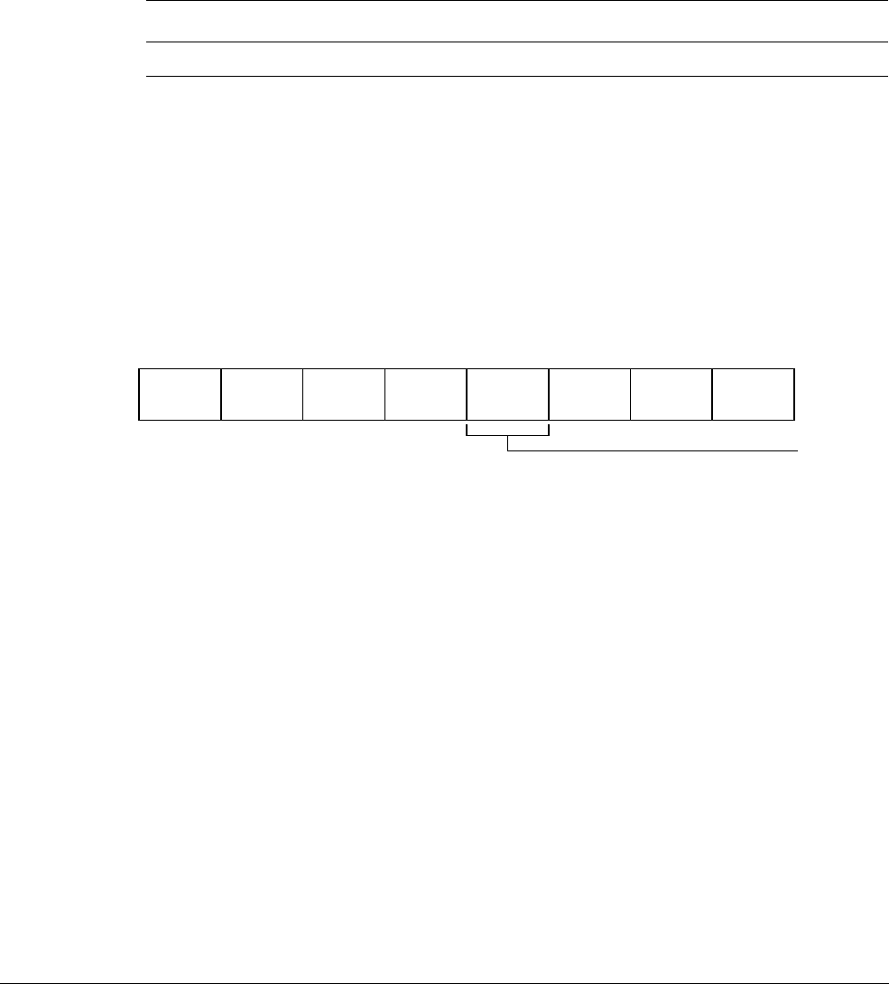
G4 AArch32 System Register Descriptions
G4.2 General system control registers
ARM DDI 0487A.a Copyright © 2013 ARM Limited. All rights reserved. G4-3945
ID090413 Non-Confidential - Beta
G4.2.87 ID_PFR1, Processor Feature Register 1
The ID_PFR1 characteristics are:
Purpose
Gives information about the programmers' model and extensions support in AArch32.
This register is part of the Identification registers functional group.
Usage constraints
This register is accessible as shown below:
Must be interpreted with ID_PFR0.
Configurations
ID_PFR1 is architecturally mapped to AArch64 register ID_PFR1_EL1.
There is one instance of this register that is used in both Secure and Non-secure states.
Attributes
ID_PFR1 is a 32-bit register.
The ID_PFR1 bit assignments are:
GIC, bits [31:28]
GIC CP15 interface. Permitted values are:
0000
No GIC CP15 registers are supported.
0001
GICv3 CP15 registers are supported.
All other values are reserved.
Virt_frac, bits [27:24]
Virtualization fractional field. When the Virtualization field is
0b0000
, determines the support for
features from the ARMv7 Virtualization Extensions. Permitted values are:
0000
No features from the ARMv7 Virtualization Extensions are implemented.
0001
The SCR.SIF bit is implemented. The modifications to the SCR.AW and SCR.FW bits
are part of the control of whether the CPSR.A and CPSR.F bits mask the corresponding
aborts. The MSR (Banked register) and MRS (Banked register) instructions are
implemented.
This value is permitted only when ID_PFR1.Security is not
0b0000
.
All other values are reserved.
This field is only valid when ID_PFR1[15:12] == 0, otherwise it holds the value
0b0000
.
EL0 (NS) EL0 (S) EL1 (NS) EL1 (S) EL2 EL3 (SCR.NS=1) EL3 (SCR.NS=0)
- - RO RO RO RO RO
GIC
31 28
Virt_frac
27 24
Sec_frac
23 20
GenTimer
19 16 15 12
MProgMod
11 8
Security
74
ProgMod
30
Virtualization

G4 AArch32 System Register Descriptions
G4.2 General system control registers
G4-3946 Copyright © 2013 ARM Limited. All rights reserved. ARM DDI 0487A.a
Non-Confidential - Beta ID090413
Sec_frac, bits [23:20]
Security fractional field. When the Security field is
0b0000
, determines the support for features from
the ARMv7 Security Extensions. Permitted values are:
0000
No features from the ARMv7 Security Extensions are implemented.
0001
The implementation includes the VBAR, and the TCR.PD0 and TCR.PD1 bits.
0010
As for
0b0001
, plus the ability to access Secure or Non-secure physical memory is
supported.
All other values are reserved.
This field is only valid when ID_PFR1[7:4] == 0, otherwise it holds the value
0b0000
.
GenTimer, bits [19:16]
Generic Timer Extension support. Permitted values are:
0000
Not implemented.
0001
Generic Timer Extension implemented.
All other values are reserved.
Virtualization, bits [15:12]
Virtualization support. Permitted values are:
0000
EL2 not implemented.
0001
EL2 implemented.
All other values are reserved.
A value of
0b0001
implies implementation of the HVC, ERET, MRS (banked register), and MSR
(banked register) instructions. The ID_ISARs do not identify whether these instructions are
implemented.
MProgMod, bits [11:8]
M profile programmers' model support. Permitted values are:
0000
Not supported.
0010
Support for two-stack programmers' model.
All other values are reserved.
Security, bits [7:4]
Security support. Permitted values are:
0000
EL3 not implemented.
0001
EL3 implemented.
This includes support for Monitor mode and the SMC instruction.
0010
As for
0b0001
, and adds the ability to set the NSACR.RFR bit. Not permitted in v8-A as
the NSACR.RFR bit is RES0.
All other values are reserved.
ProgMod, bits [3:0]
Support for the standard programmers' model for ARMv4 and later. Model must support User, FIQ,
IRQ, Supervisor, Abort, Undefined, and System modes. Permitted values are:
0000
Not supported.
0001
Supported.
All other values are reserved.
Accessing the ID_PFR1:
To access the ID_PFR1:

G4 AArch32 System Register Descriptions
G4.2 General system control registers
ARM DDI 0487A.a Copyright © 2013 ARM Limited. All rights reserved. G4-3947
ID090413 Non-Confidential - Beta
MRC p15,0,<Rt>,c0,c1,1 ; Read ID_PFR1 into Rt
Register access is encoded as follows:
coproc opc1 CRn CRm opc2
1111 000 0000 0001 001

G4 AArch32 System Register Descriptions
G4.2 General system control registers
G4-3948 Copyright © 2013 ARM Limited. All rights reserved. ARM DDI 0487A.a
Non-Confidential - Beta ID090413
G4.2.88 IFAR, Instruction Fault Address Register
The IFAR characteristics are:
Purpose
Holds the virtual address of the faulting address that caused a synchronous Prefetch Abort
exception.
This register is part of the Exception and fault handling registers functional group.
Usage constraints
This register is accessible as shown below:
When accessed as IFAR(S):
When accessed as IFAR(NS):
Configurations
IFAR(NS) is architecturally mapped to AArch64 register FAR_EL1[63:32].
IFAR(S) is architecturally mapped to AArch32 register HIFAR when EL2 is implemented.
IFAR(S) is architecturally mapped to AArch64 register FAR_EL2[63:32] when EL2 is
implemented.
IFAR(S) can be mapped to AArch64 register FAR_EL3[63:32] when EL2 is not implemented, but
this is not architecturally mandated.
If EL3 is using AArch32, there are separate Secure and Non-secure instances of this register.
Attributes
IFAR is a 32-bit register.
The IFAR bit assignments are:
Bits [31:0]
VA of faulting address of synchronous Prefetch Abort exception.
Accessing the IFAR:
To access the IFAR:
MRC p15,0,<Rt>,c6,c0,2 ; Read IFAR into Rt
MCR p15,0,<Rt>,c6,c0,2 ; Write Rt to IFAR
EL0 (NS) EL0 (S) EL1 (NS) EL1 (S) EL2 EL3 (SCR.NS=1) EL3 (SCR.NS=0)
---RW-- RW
EL0 (NS) EL0 (S) EL1 (NS) EL1 (S) EL2 EL3 (SCR.NS=1) EL3 (SCR.NS=0)
--RW-RWRW -
VA of faulting address of synchronous Prefetch Abort exception
31 0

G4 AArch32 System Register Descriptions
G4.2 General system control registers
ARM DDI 0487A.a Copyright © 2013 ARM Limited. All rights reserved. G4-3949
ID090413 Non-Confidential - Beta
Register access is encoded as follows:
coproc opc1 CRn CRm opc2
1111 000 0110 0000 010
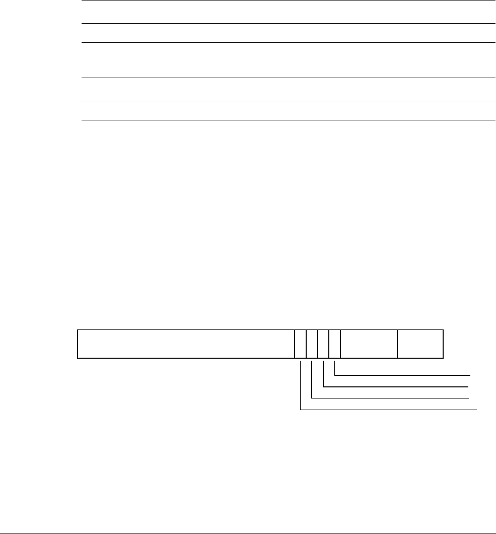
G4 AArch32 System Register Descriptions
G4.2 General system control registers
G4-3950 Copyright © 2013 ARM Limited. All rights reserved. ARM DDI 0487A.a
Non-Confidential - Beta ID090413
G4.2.89 IFSR, Instruction Fault Status Register
The IFSR characteristics are:
Purpose
Holds status information about the last instruction fault.
This register is part of the Exception and fault handling registers functional group.
Usage constraints
This register is accessible as shown below:
When accessed as IFSR(S):
When accessed as IFSR(NS):
Configurations
IFSR(NS) is architecturally mapped to AArch64 register IFSR32_EL2.
If EL3 is using AArch32, there are separate Secure and Non-secure instances of this register.
The Large Physical Address Extension adds an alternative format for the register. If an
implementation includes the Large Physical Address Extension then the current translation table
format determines which format of the register is used.
Attributes
IFSR is a 32-bit register.
The IFSR bit assignments are:
When TTBCR.EAE==0:
Bits [31:13]
Reserved, RES0.
ExT, bit [12]
External abort type. This bit can be used to provide an IMPLEMENTATION DEFINED classification of
external aborts.
For aborts other than external aborts this bit always returns 0.
EL0 (NS) EL0 (S) EL1 (NS) EL1 (S) EL2 EL3 (SCR.NS=1) EL3 (SCR.NS=0)
---RW-- RW
EL0 (NS) EL0 (S) EL1 (NS) EL1 (S) EL2 EL3 (SCR.NS=1) EL3 (SCR.NS=0)
--RW-RWRW -
RES0
31 13 12 11 10 9
RES0
84
FS[3:0]
30
LPAE
FS[4]
RES0
ExT

G4 AArch32 System Register Descriptions
G4.2 General system control registers
ARM DDI 0487A.a Copyright © 2013 ARM Limited. All rights reserved. G4-3951
ID090413 Non-Confidential - Beta
Bit [11]
Reserved, RES0.
FS[4], bit [10]
See below for description of the FS field.
LPAE, bit [9]
On taking a Data Abort exception, this bit is set as follows:
0
Using the Short-descriptor translation table formats.
1
Using the Long-descriptor translation table formats.
Hardware does not interpret this bit to determine the behavior of the memory system, and therefore
software can set this bit to 0 or 1 without affecting operation.
Bits [8:4]
Reserved, RES0.
FS[3:0], bits [3:0]
Fault status bits. Possible values of this field are:
0010
Debug event
0011
Access flag fault, first level
0101
Translation fault, first level
0110
Access flag fault, second level
0111
Translation fault, second level
1000
Synchronous external abort
1001
Domain fault, first level
1011
Domain fault, second level
1100
Synchronous external abort on translation table walk, first level
1101
Permission fault, first level
1110
Synchronous external abort on translation table walk, second level
1111
Permission fault, second level
10000
TLB conflict abort
10100
IMPLEMENTATION DEFINED fault (Lockdown fault)
11001
Synchronous parity error on memory access
11100
Synchronous parity error on translation table walk, first level
11110
Synchronous parity error on translation table walk, second level
All other values are reserved.
When TTBCR.EAE==1:
RES0
31 13 12 11 10 9
RES0
86
STATUS
50
LPAE
RES0
ExT

G4 AArch32 System Register Descriptions
G4.2 General system control registers
G4-3952 Copyright © 2013 ARM Limited. All rights reserved. ARM DDI 0487A.a
Non-Confidential - Beta ID090413
Bits [31:13]
Reserved, RES0.
ExT, bit [12]
External abort type. This bit can be used to provide an IMPLEMENTATION DEFINED classification of
external aborts.
For aborts other than external aborts this bit always returns 0.
Bits [11:10]
Reserved, RES0.
LPAE, bit [9]
On taking a Data Abort exception, this bit is set as follows:
0
Using the Short-descriptor translation table formats.
1
Using the Long-descriptor translation table formats.
Hardware does not interpret this bit to determine the behavior of the memory system, and therefore
software can set this bit to 0 or 1 without affecting operation.
Bits [8:6]
Reserved, RES0.
STATUS, bits [5:0]
Fault status bits. Possible values of this field are:
000000
Address size fault in TTBR0 or TTBR1
000101
Translation fault, first level
000110
Translation fault, second level
000111
Translation fault, third level
001001
Access flag fault, first level
001010
Access flag fault, second level
001011
Access flag fault, third level
001101
Permission fault, first level
001110
Permission fault, second level
001111
Permission fault, third level
010000
Synchronous external abort
010101
Synchronous external abort on translation table walk, first level
010110
Synchronous external abort on translation table walk, second level
010111
Synchronous external abort on translation table walk, third level
011000
Synchronous parity error on memory access
011101
Synchronous parity error on memory access on translation table walk, first level
011110
Synchronous parity error on memory access on translation table walk, second level
011111
Synchronous parity error on memory access on translation table walk, third level
100001
Alignment fault
100010
Debug event
110000
TLB conflict abort
110100
IMPLEMENTATION DEFINED fault (Lockdown fault)
All other values are reserved.

G4 AArch32 System Register Descriptions
G4.2 General system control registers
ARM DDI 0487A.a Copyright © 2013 ARM Limited. All rights reserved. G4-3953
ID090413 Non-Confidential - Beta
The lookup level associated with a fault is:
• For a fault generated on a translation table walk, the lookup level of the walk being
performed.
• For a Translation fault, the lookup level of the translation table that gave the fault. If a fault
occurs because an MMU is disabled, or because the input address is outside the range
specified by the appropriate base address register or registers, the fault is reported as a First
level fault.
• For an Access flag fault, the lookup level of the translation table that gave the fault.
• For a Permission fault, including a Permission fault caused by hierarchical permissions, the
lookup level of the final level of translation table accessed for the translation. That is, the
lookup level of the translation table that returned a Block or Page descriptor.
Accessing the IFSR:
To access the IFSR:
MRC p15,0,<Rt>,c5,c0,1 ; Read IFSR into Rt
MCR p15,0,<Rt>,c5,c0,1 ; Write Rt to IFSR
Register access is encoded as follows:
coproc opc1 CRn CRm opc2
1111 000 0101 0000 001
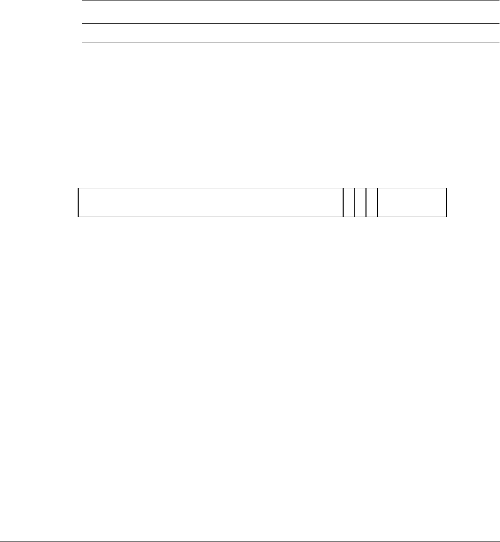
G4 AArch32 System Register Descriptions
G4.2 General system control registers
G4-3954 Copyright © 2013 ARM Limited. All rights reserved. ARM DDI 0487A.a
Non-Confidential - Beta ID090413
G4.2.90 ISR, Interrupt Status Register
The ISR characteristics are:
Purpose
Shows whether an IRQ, FIQ, or external abort is pending. If EL2 is implemented, an indicated
pending abort might be a physical abort or a virtual abort.
This register is part of the Exception and fault handling registers functional group.
Usage constraints
This register is accessible as shown below:
Configurations
ISR is architecturally mapped to AArch64 register ISR_EL1.
There is one instance of this register that is used in both Secure and Non-secure states.
Attributes
ISR is a 32-bit register.
The ISR bit assignments are:
Bits [31:9]
Reserved, RES0.
A, bit [8]
External abort pending bit:
0
No pending external abort.
1
An external abort is pending.
I, bit [7]
IRQ pending bit. Indicates whether an IRQ interrupt is pending:
0
No pending IRQ.
1
An IRQ interrupt is pending.
F, bit [6]
FIQ pending bit. Indicates whether an FIQ interrupt is pending.
0
No pending FIQ.
1
An FIQ interrupt is pending.
Bits [5:0]
Reserved, RES0.
EL0 (NS) EL0 (S) EL1 (NS) EL1 (S) EL2 EL3 (SCR.NS=1) EL3 (SCR.NS=0)
- - RO RO RO RO RO
RES0
31 9
A
8
I
7
F
6
RES0
50

G4 AArch32 System Register Descriptions
G4.2 General system control registers
ARM DDI 0487A.a Copyright © 2013 ARM Limited. All rights reserved. G4-3955
ID090413 Non-Confidential - Beta
Accessing the ISR:
To access the ISR:
MRC p15,0,<Rt>,c12,c1,0 ; Read ISR into Rt
Register access is encoded as follows:
coproc opc1 CRn CRm opc2
1111 000 1100 0001 000

G4 AArch32 System Register Descriptions
G4.2 General system control registers
G4-3956 Copyright © 2013 ARM Limited. All rights reserved. ARM DDI 0487A.a
Non-Confidential - Beta ID090413
G4.2.91 ITLBIALL, Instruction TLB Invalidate All entries
The ITLBIALL characteristics are:
Purpose
Invalidate all EL1&0 regime stage 1 and 2 instruction TLB entries for the current VMID.
This register is part of the TLB maintenance operations functional group.
Usage constraints
This operation can be performed at the exception levels shown below:
If this operation is executed at Secure EL1 in AArch32 when EL3 is using AArch64, it only affects
TLB entries related to the Secure EL1 translation regime.
Configurations
There are no configuration notes.
Attributes
ITLBIALL is a 32-bit system operation.
The ITLBIALL operation ignores the value in the register specified by the instruction used to perform this
operation. Software does not have to write a value to the register before issuing this instruction.
Performing the ITLBIALL operation:
To perform the ITLBIALL operation:
MCR p15,0,<Rt>,c8,c5,0 ; ITLBIALL operation, ignoring the value in Rt
The operation is encoded as follows:
EL0 (NS) EL0 (S) EL1 (NS) EL1 (S) EL2 EL3 (SCR.NS=1) EL3 (SCR.NS=0)
- - WO WO WO WO WO
coproc opc1 CRn CRm opc2
1111 000 1000 0101 000

G4 AArch32 System Register Descriptions
G4.2 General system control registers
ARM DDI 0487A.a Copyright © 2013 ARM Limited. All rights reserved. G4-3957
ID090413 Non-Confidential - Beta
G4.2.92 ITLBIASID, Instruction TLB Invalidate by ASID match
The ITLBIASID characteristics are:
Purpose
Invalidate EL1&0 regime stage 1 instruction TLB entries for the given ASID and the current VMID.
This register is part of the TLB maintenance operations functional group.
Usage constraints
This operation can be performed at the exception levels shown below:
If this operation is executed at Secure EL1 in AArch32 when EL3 is using AArch64, it only affects
TLB entries related to the Secure EL1 translation regime.
Configurations
There are no configuration notes.
Attributes
ITLBIASID is a 32-bit system operation.
The ITLBIASID input value bit assignments are:
Bits [31:8]
Reserved, RES0.
ASID, bits [7:0]
ASID value to match. Any TLB entries for non-global pages that match the ASID values will be
affected by this operation.
Performing the ITLBIASID operation:
To perform the ITLBIASID operation:
MCR p15,0,<Rt>,c8,c5,2 ; ITLBIASID operation
The operation is encoded as follows:
EL0 (NS) EL0 (S) EL1 (NS) EL1 (S) EL2 EL3 (SCR.NS=1) EL3 (SCR.NS=0)
- - WO WO WO WO WO
RES0
31 8
ASID
70
coproc opc1 CRn CRm opc2
1111 000 1000 0101 010

G4 AArch32 System Register Descriptions
G4.2 General system control registers
G4-3958 Copyright © 2013 ARM Limited. All rights reserved. ARM DDI 0487A.a
Non-Confidential - Beta ID090413
G4.2.93 ITLBIMVA, Instruction TLB Invalidate entry by VA
The ITLBIMVA characteristics are:
Purpose
Invalidate EL1&0 regime stage 1 and 2 instruction TLB entries for the given VA and ASID and the
current VMID.
This register is part of the TLB maintenance operations functional group.
Usage constraints
This operation can be performed at the exception levels shown below:
If this operation is executed at Secure EL1 in AArch32 when EL3 is using AArch64, it only affects
TLB entries related to the Secure EL1 translation regime.
Configurations
There are no configuration notes.
Attributes
ITLBIMVA is a 32-bit system operation.
The ITLBIMVA input value bit assignments are:
VA, bits [31:12]
Virtual address to match. Any TLB entries that match the ASID value and VA value will be affected
by this operation.
Bits [11:8]
Reserved, RES0.
ASID, bits [7:0]
ASID value to match. Any TLB entries that match the ASID value and VA value will be affected
by this operation.
Global TLB entries that match the VA value will be affected by this operation, regardless of the
value of the ASID field.
Performing the ITLBIMVA operation:
To perform the ITLBIMVA operation:
MCR p15,0,<Rt>,c8,c5,1 ; ITLBIMVA operation
The operation is encoded as follows:
EL0 (NS) EL0 (S) EL1 (NS) EL1 (S) EL2 EL3 (SCR.NS=1) EL3 (SCR.NS=0)
- - WO WO WO WO WO
VA
31 12
RES0
11 8
ASID
70
coproc opc1 CRn CRm opc2
1111 000 1000 0101 001

G4 AArch32 System Register Descriptions
G4.2 General system control registers
ARM DDI 0487A.a Copyright © 2013 ARM Limited. All rights reserved. G4-3959
ID090413 Non-Confidential - Beta
G4.2.94 JIDR, Jazelle ID Register
The JIDR characteristics are:
Purpose
A Jazelle register, which identifies the Jazelle architecture and subarchitecture version.
This register is part of the Legacy feature registers functional group.
Usage constraints
This register is accessible as shown below:
Configurations
There is one instance of this register that is used in both Secure and Non-secure states.
Implemented as RES0 in v8, which only contains a trivial implementation of the Jazelle Extension.
Attributes
JIDR is a 32-bit register.
The JIDR bit assignments are:
Bits [31:0]
Reserved, RES0.
Accessing the JIDR:
To access the JIDR:
MRC p14,7,<Rt>,c0,c0,0 ; Read JIDR into Rt
Register access is encoded as follows:
EL0 (NS) EL0 (S) EL1 (NS) EL1 (S) EL2 EL3 (SCR.NS=1) EL3 (SCR.NS=0)
RO RO RO RO RO RO RO
RES0
31 0
coproc opc1 CRn CRm opc2
1110 111 0000 0000 000

G4 AArch32 System Register Descriptions
G4.2 General system control registers
G4-3960 Copyright © 2013 ARM Limited. All rights reserved. ARM DDI 0487A.a
Non-Confidential - Beta ID090413
G4.2.95 JMCR, Jazelle Main Configuration Register
The JMCR characteristics are:
Purpose
A Jazelle register, which provides control of the Jazelle extension.
This register is part of the Legacy feature registers functional group.
Usage constraints
This register is accessible as shown below:
Configurations
There is one instance of this register that is used in both Secure and Non-secure states.
Implemented as RES0 in v8, which only contains a trivial implementation of the Jazelle Extension.
Attributes
JMCR is a 32-bit register.
The JMCR bit assignments are:
Bits [31:0]
Reserved, RES0.
Accessing the JMCR:
To access the JMCR:
MRC p14,7,<Rt>,c2,c0,0 ; Read JMCR into Rt
MCR p14,7,<Rt>,c2,c0,0 ; Write Rt to JMCR
Register access is encoded as follows:
EL0 (NS) EL0 (S) EL1 (NS) EL1 (S) EL2 EL3 (SCR.NS=1) EL3 (SCR.NS=0)
- - RW RW RW RW RW
RES0
31 0
coproc opc1 CRn CRm opc2
1110 111 0010 0000 000

G4 AArch32 System Register Descriptions
G4.2 General system control registers
ARM DDI 0487A.a Copyright © 2013 ARM Limited. All rights reserved. G4-3961
ID090413 Non-Confidential - Beta
G4.2.96 JOSCR, Jazelle OS Control Register
The JOSCR characteristics are:
Purpose
A Jazelle register, which provides operating system control of the use of the Jazelle extension by
processes and threads.
This register is part of the Legacy feature registers functional group.
Usage constraints
This register is accessible as shown below:
Configurations
There is one instance of this register that is used in both Secure and Non-secure states.
Implemented as RES0 in v8, which only contains a trivial implementation of the Jazelle Extension.
Attributes
JOSCR is a 32-bit register.
The JOSCR bit assignments are:
Bits [31:0]
Reserved, RES0.
Accessing the JOSCR:
To access the JOSCR:
MRC p14,7,<Rt>,c1,c0,0 ; Read JOSCR into Rt
MCR p14,7,<Rt>,c1,c0,0 ; Write Rt to JOSCR
Register access is encoded as follows:
EL0 (NS) EL0 (S) EL1 (NS) EL1 (S) EL2 EL3 (SCR.NS=1) EL3 (SCR.NS=0)
- - RW RW RW RW RW
RES0
31 0
coproc opc1 CRn CRm opc2
1110 111 0001 0000 000

G4 AArch32 System Register Descriptions
G4.2 General system control registers
G4-3962 Copyright © 2013 ARM Limited. All rights reserved. ARM DDI 0487A.a
Non-Confidential - Beta ID090413
G4.2.97 MAIR0, Memory Attribute Indirection Register 0
The MAIR0 characteristics are:
Purpose
Along with MAIR1, provides the memory attribute encodings corresponding to the possible
AttrIndx values in a Long-descriptor format translation table entry for stage 1 translations.
This register is part of the Virtual memory control registers functional group.
Usage constraints
This register is accessible as shown below:
When accessed as MAIR0(S):
When accessed as MAIR0(NS):
Only accessible when using the Long-descriptor translation table format.
AttrIndx[2], from the translation table descriptor, selects the appropriate MAIR: setting AttrIndx[2]
to 0 selects MAIR0.
In an implementation that includes EL3:
• The Secure copy of the register gives the value for memory accesses from Secure state.
• The Non-secure copy of the register gives the value for memory accesses from Non-secure
states other than Hyp mode.
Configurations
MAIR0(NS) is architecturally mapped to AArch64 register MAIR_EL1[31:0] when
TTBCR.EAE==1.
MAIR0(S) can be mapped to AArch64 register MAIR_EL3[31:0] when TTBCR.EAE==1, but this
is not architecturally mandated.
If EL3 is using AArch32, there are separate Secure and Non-secure instances of this register.
MAIR0 has write access to the Secure copy of the register disabled when the CP15SDISABLE
signal is asserted HIGH.
Attributes
MAIR0 is a 32-bit register when TTBCR.EAE==1.
The MAIR0 bit assignments are:
When TTBCR.EAE==1:
EL0 (NS) EL0 (S) EL1 (NS) EL1 (S) EL2 EL3 (SCR.NS=1) EL3 (SCR.NS=0)
---RW-- RW
EL0 (NS) EL0 (S) EL1 (NS) EL1 (S) EL2 EL3 (SCR.NS=1) EL3 (SCR.NS=0)
--RW-RWRW -
Attr3
31 24
Attr2
23 16
Attr1
15 8
Attr0
70

G4 AArch32 System Register Descriptions
G4.2 General system control registers
ARM DDI 0487A.a Copyright © 2013 ARM Limited. All rights reserved. G4-3963
ID090413 Non-Confidential - Beta
Attr<n>, bits [8n+7:8n], for n = 0 to 3
The memory attribute encoding for an AttrIndx[2:0] entry in a Long descriptor format translation
table entry, where:
• AttrIndx[2:0] gives the value of <n> in Attr<n>.
• AttrIndx[2] defines which MAIR to access. Attr7 to Attr4 are in MAIR1, and Attr3 to Attr0
are in MAIR0.
Bits [7:4] are encoded as follows:
R = Outer Read Allocate Policy, W = Outer Write Allocate Policy.
The meaning of bits [3:0] depends on the value of bits [7:4]:
R = Inner Read Allocate Policy, W = Inner Write Allocate Policy.
ARMv7's Strongly-ordered and Device memory types have been renamed to Device-nGnRnE and
Device-nGnRE in ARMv8.
Attr<n>[7:4] Meaning
0000
Device memory. See encoding of Attr<n>[3:0] for the type of Device memory.
00RW
, RW not
00
Normal Memory, Outer Write-through transient
0100
Normal Memory, Outer Non-Cacheable
01RW
, RW not
00
Normal Memory, Outer Write-back transient
10RW
Normal Memory, Outer Write-through non-transient
11RW
Normal Memory, Outer Write-back non-transient
Attr<n>[3:0] Meaning when Attr<n>[7:4] is
0000 Meaning when Attr<n>[7:4] is not 0000
0000
Device-nGnRnE memory UNPREDICTABLE
00RW
, RW not
00
UNPREDICTABLE Normal Memory, Inner Write-through transient
0100
Device-nGnRE memory Normal memory, Inner Non-Cacheable
01RW
, RW not
00
UNPREDICTABLE Normal Memory, Inner Write-back transient
1000
Device-nGRE memory Normal Memory, Inner Write-through
non-transient (RW=00)
10RW
, RW not
00
UNPREDICTABLE Normal Memory, Inner Write-through
non-transient
1100
Device-GRE memory Normal Memory, Inner Write-back non-transient
(RW=00)
11RW
, RW not
00
UNPREDICTABLE Normal Memory, Inner Write-back non-transient

G4 AArch32 System Register Descriptions
G4.2 General system control registers
G4-3964 Copyright © 2013 ARM Limited. All rights reserved. ARM DDI 0487A.a
Non-Confidential - Beta ID090413
The R and W bits in some Attr<n> fields have the following meanings:
Accessing the MAIR0:
To access the MAIR0 when TTBCR.EAE==1:
MRC p15,0,<Rt>,c10,c2,0 ; Read MAIR0 into Rt
MCR p15,0,<Rt>,c10,c2,0 ; Write Rt to MAIR0
Register access is encoded as follows:
R or W Meaning
0
Do not allocate
1
Allocate
coproc opc1 CRn CRm opc2
1111 000 1010 0010 000

G4 AArch32 System Register Descriptions
G4.2 General system control registers
ARM DDI 0487A.a Copyright © 2013 ARM Limited. All rights reserved. G4-3965
ID090413 Non-Confidential - Beta
G4.2.98 MAIR1, Memory Attribute Indirection Register 1
The MAIR1 characteristics are:
Purpose
Along with MAIR0, provides the memory attribute encodings corresponding to the possible
AttrIndx values in a Long-descriptor format translation table entry for stage 1 translations.
This register is part of the Virtual memory control registers functional group.
Usage constraints
This register is accessible as shown below:
When accessed as MAIR1(S):
When accessed as MAIR1(NS):
Only accessible when using the Long-descriptor translation table format.
AttrIndx[2], from the translation table descriptor, selects the appropriate MAIR: setting AttrIndx[2]
to 1 selects MAIR1.
In an implementation that includes EL3:
• The Secure copy of the register gives the value for memory accesses from Secure state.
• The Non-secure copy of the register gives the value for memory accesses from Non-secure
states other than Hyp mode.
Configurations
MAIR1(NS) is architecturally mapped to AArch64 register MAIR_EL1[63:32] when
TTBCR.EAE==1.
MAIR1(S) can be mapped to AArch64 register MAIR_EL3[63:32] when TTBCR.EAE==1, but this
is not architecturally mandated.
If EL3 is using AArch32, there are separate Secure and Non-secure instances of this register.
MAIR1 has write access to the Secure copy of the register disabled when the CP15SDISABLE
signal is asserted HIGH.
Attributes
MAIR1 is a 32-bit register when TTBCR.EAE==1.
The MAIR1 bit assignments are:
When TTBCR.EAE==1:
EL0 (NS) EL0 (S) EL1 (NS) EL1 (S) EL2 EL3 (SCR.NS=1) EL3 (SCR.NS=0)
---RW-- RW
EL0 (NS) EL0 (S) EL1 (NS) EL1 (S) EL2 EL3 (SCR.NS=1) EL3 (SCR.NS=0)
--RW-RWRW -
Attr7
31 24
Attr6
23 16
Attr5
15 8
Attr4
70

G4 AArch32 System Register Descriptions
G4.2 General system control registers
G4-3966 Copyright © 2013 ARM Limited. All rights reserved. ARM DDI 0487A.a
Non-Confidential - Beta ID090413
Attr<n>, bits [8(n-4)+7:8(n-4)], for n = 4 to 7
The memory attribute encoding for an AttrIndx[2:0] entry in a Long descriptor format translation
table entry, where:
• AttrIndx[2:0] gives the value of <n> in Attr<n>.
• AttrIndx[2] defines which MAIR to access. Attr7 to Attr4 are in MAIR1, and Attr3 to Attr0
are in MAIR0.
Bits [7:4] are encoded as follows:
R = Outer Read Allocate Policy, W = Outer Write Allocate Policy.
The meaning of bits [3:0] depends on the value of bits [7:4]:
R = Inner Read Allocate Policy, W = Inner Write Allocate Policy.
ARMv7's Strongly-ordered and Device memory types have been renamed to Device-nGnRnE and
Device-nGnRE in ARMv8.
Attr<n>[7:4] Meaning
0000
Device memory. See encoding of Attr<n>[3:0] for the type of Device memory.
00RW
, RW not
00
Normal Memory, Outer Write-through transient
0100
Normal Memory, Outer Non-Cacheable
01RW
, RW not
00
Normal Memory, Outer Write-back transient
10RW
Normal Memory, Outer Write-through non-transient
11RW
Normal Memory, Outer Write-back non-transient
Attr<n>[3:0] Meaning when Attr<n>[7:4] is
0000 Meaning when Attr<n>[7:4] is not 0000
0000
Device-nGnRnE memory UNPREDICTABLE
00RW
, RW not
00
UNPREDICTABLE Normal Memory, Inner Write-through transient
0100
Device-nGnRE memory Normal memory, Inner Non-Cacheable
01RW
, RW not
00
UNPREDICTABLE Normal Memory, Inner Write-back transient
1000
Device-nGRE memory Normal Memory, Inner Write-through
non-transient (RW=00)
10RW
, RW not
00
UNPREDICTABLE Normal Memory, Inner Write-through
non-transient
1100
Device-GRE memory Normal Memory, Inner Write-back non-transient
(RW=00)
11RW
, RW not
00
UNPREDICTABLE Normal Memory, Inner Write-back non-transient

G4 AArch32 System Register Descriptions
G4.2 General system control registers
ARM DDI 0487A.a Copyright © 2013 ARM Limited. All rights reserved. G4-3967
ID090413 Non-Confidential - Beta
The R and W bits in some Attr<n> fields have the following meanings:
Accessing the MAIR1:
To access the MAIR1 when TTBCR.EAE==1:
MRC p15,0,<Rt>,c10,c2,1 ; Read MAIR1 into Rt
MCR p15,0,<Rt>,c10,c2,1 ; Write Rt to MAIR1
Register access is encoded as follows:
R or W Meaning
0
Do not allocate
1
Allocate
coproc opc1 CRn CRm opc2
1111 000 1010 0010 001

G4 AArch32 System Register Descriptions
G4.2 General system control registers
G4-3968 Copyright © 2013 ARM Limited. All rights reserved. ARM DDI 0487A.a
Non-Confidential - Beta ID090413
G4.2.99 MIDR, Main ID Register
The MIDR characteristics are:
Purpose
Provides identification information for the processor, including an implementer code for the device
and a device ID number.
This register is part of the Identification registers functional group.
Usage constraints
This register is accessible as shown below:
Configurations
MIDR is architecturally mapped to AArch64 register MIDR_EL1.
MIDR is architecturally mapped to external register MIDR_EL1.
There is one instance of this register that is used in both Secure and Non-secure states.
Some fields of the MIDR are IMPLEMENTATION DEFINED. For details of the values of these fields for
a particular ARMv8 implementation, and any implementation-specific significance of these values,
see the product documentation.
Attributes
MIDR is a 32-bit register.
The MIDR bit assignments are:
Implementer, bits [31:24]
The Implementer code. This field must hold an implementer code that has been assigned by ARM.
Assigned codes include the following:
EL0 (NS) EL0 (S) EL1 (NS) EL1 (S) EL2 EL3 (SCR.NS=1) EL3 (SCR.NS=0)
- - RO RO RO RO RO
Implementer
31 24
Variant
23 20 19 16
PartNum
15 4
Revision
30
Architecture
Hex
representation ASCII
representation Implementer
0x41
A ARM Limited
0x42
B Broadcom Corporation
0x43
CCavium Inc.
0x44
D Digital Equipment Corporation
0x49
I Infineon Technologies AG
0x4D
M Motorola or Freescale Semiconductor Inc.
0x4E
N NVIDIA Corporation

G4 AArch32 System Register Descriptions
G4.2 General system control registers
ARM DDI 0487A.a Copyright © 2013 ARM Limited. All rights reserved. G4-3969
ID090413 Non-Confidential - Beta
ARM can assign codes that are not published in this manual. All values not assigned by ARM are
reserved and must not be used.
Variant, bits [23:20]
An IMPLEMENTATION DEFINED variant number. Typically, this field is used to distinguish between
different product variants, or major revisions of a product.
Architecture, bits [19:16]
The permitted values of this field are:
0001
ARMv4
0010
ARMv4T
0011
ARMv5 (obsolete)
0100
ARMv5T
0101
ARMv5TE
0110
ARMv5TEJ
0111
ARMv6
1111
Defined by CPUID scheme
All other values are reserved.
PartNum, bits [15:4]
An IMPLEMENTATION DEFINED primary part number for the device.
On processors implemented by ARM, if the top four bits of the primary part number are
0x0
or
0x7
,
the variant and architecture are encoded differently.
Revision, bits [3:0]
An IMPLEMENTATION DEFINED revision number for the device.
Accessing the MIDR:
To access the MIDR:
MRC p15,0,<Rt>,c0,c0,0 ; Read MIDR into Rt
Register access is encoded as follows:
0x50
P Applied Micro Circuits Corporation
0x51
Q Qualcomm Inc.
0x56
V Marvell International Ltd.
0x69
i Intel Corporation
coproc opc1 CRn CRm opc2
1111 000 0000 0000 000
Hex
representation ASCII
representation Implementer
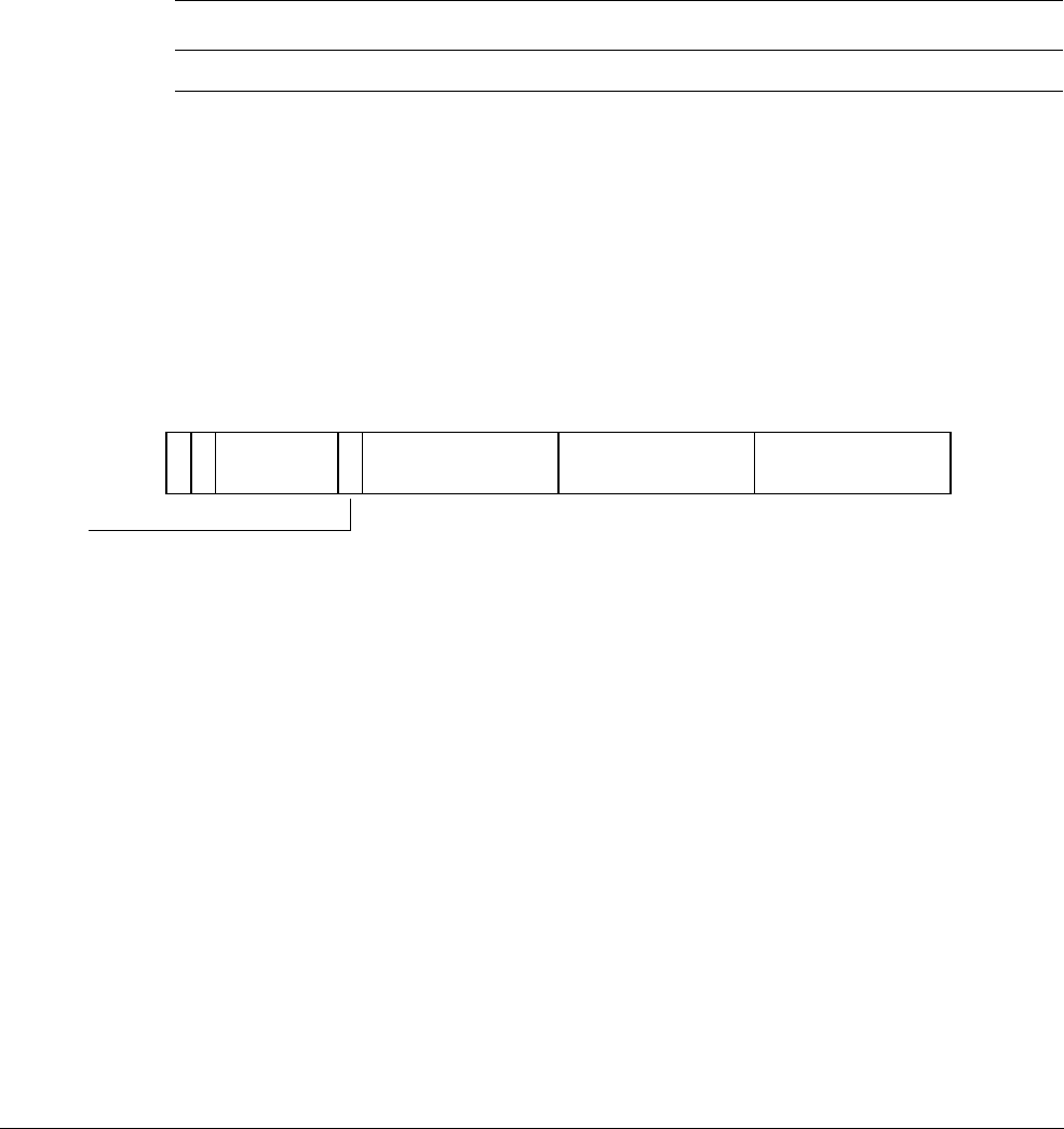
G4 AArch32 System Register Descriptions
G4.2 General system control registers
G4-3970 Copyright © 2013 ARM Limited. All rights reserved. ARM DDI 0487A.a
Non-Confidential - Beta ID090413
G4.2.100 MPIDR, Multiprocessor Affinity Register
The MPIDR characteristics are:
Purpose
In a multiprocessor system, provides an additional processor identification mechanism for
scheduling purposes, and indicates whether the implementation includes the Multiprocessing
Extensions.
This register is part of the Identification registers functional group.
Usage constraints
This register is accessible as shown below:
Configurations
MPIDR is architecturally mapped to AArch64 register MPIDR_EL1.
There is one instance of this register that is used in both Secure and Non-secure states.
In a uniprocessor system ARM recommends that this register returns a value of 0.
Attributes
MPIDR is a 32-bit register.
The MPIDR bit assignments are:
M, bit [31]
Indicates whether this implementation includes the Multiprocessing Extensions. The possible
values of this bit are:
0
This implementation does not include the Multiprocessing Extensions.
1
This implementation includes the Multiprocessing Extensions.
In v8-A this bit is RES1.
U, bit [30]
Indicates a Uniprocessor system, as distinct from processor 0 in a multiprocessor system. The
possible values of this bit are:
0
Processor is part of a multiprocessor system.
1
Processor is part of a uniprocessor system.
Bits [29:25]
Reserved, RES0.
EL0 (NS) EL0 (S) EL1 (NS) EL1 (S) EL2 EL3 (SCR.NS=1) EL3 (SCR.NS=0)
- - RO RO RO RO RO
M
31
U
30
RES0
29 25 24
Aff2
23 16
Aff1
15 8
Aff0
70
MT

G4 AArch32 System Register Descriptions
G4.2 General system control registers
ARM DDI 0487A.a Copyright © 2013 ARM Limited. All rights reserved. G4-3971
ID090413 Non-Confidential - Beta
MT, bit [24]
Indicates whether the lowest level of affinity consists of logical processors that are implemented
using a multi-threading type approach. The possible values of this bit are:
0
Performance of processors at the lowest affinity level is largely independent.
1
Performance of processors at the lowest affinity level is very interdependent.
Aff2, bits [23:16]
Affinity level 2. The least significant affinity level field, for this processor in the system.
Aff1, bits [15:8]
Affinity level 1. The intermediate affinity level field, for this processor in the system.
Aff0, bits [7:0]
Affinity level 0. The most significant affinity level field, for this processor in the system.
Accessing the MPIDR:
To access the MPIDR:
MRC p15,0,<Rt>,c0,c0,5 ; Read MPIDR into Rt
Register access is encoded as follows:
coproc opc1 CRn CRm opc2
1111 000 0000 0000 101

G4 AArch32 System Register Descriptions
G4.2 General system control registers
G4-3972 Copyright © 2013 ARM Limited. All rights reserved. ARM DDI 0487A.a
Non-Confidential - Beta ID090413
G4.2.101 MVBAR, Monitor Vector Base Address Register
The MVBAR characteristics are:
Purpose
Holds the exception base address for any exception that is taken to Monitor mode.
This register is part of:
• the Exception and fault handling registers functional group
• the Security registers functional group.
Usage constraints
This register is accessible as shown below:
Secure software must program the MVBAR with the required initial value as part of the processor
boot sequence.
If EL3 is implemented and is using AArch64, any read or write to MVBAR in Secure EL1 state in
AArch32 is trapped as an exception to EL3.
Configurations
There is one instance of this register that is used in both Secure and Non-secure states.
The reset value of MVBAR, when resetting into EL3 using AArch32, is an IMPLEMENTATION
DEFINED choice between the following:
•Either:
— MVBAR[31:5] is an IMPLEMENTATION DEFINED value, which might be UNKNOWN.
— MVBAR[4:1] is RES0.
— MVBAR[0] is 0.
•Or:
— MVBAR[31:1] is an IMPLEMENTATION DEFINED value being the AArch32 reset
address, bits[31:1].
— MVBAR[0] is 1.
The reset value of MVBAR[0] can be used to distinguish between these two approaches.
Attributes
MVBAR is a 32-bit register.
The MVBAR bit assignments are:
Bits [31:5]
Vector Base Address. Bits[31:5] of the base address of the exception vectors for exceptions taken
in this exception level. Bits[4:0] of an exception vector are the exception offset.
Bits [4:0]
Reserved, RES0.
EL0 (NS) EL0 (S) EL1 (NS) EL1 (S) EL2 EL3 (SCR.NS=1) EL3 (SCR.NS=0)
- - - RW - RW RW
Vector Base Address
31 5
RES0
40

G4 AArch32 System Register Descriptions
G4.2 General system control registers
ARM DDI 0487A.a Copyright © 2013 ARM Limited. All rights reserved. G4-3973
ID090413 Non-Confidential - Beta
Accessing the MVBAR:
To access the MVBAR:
MRC p15,0,<Rt>,c12,c0,1 ; Read MVBAR into Rt
MCR p15,0,<Rt>,c12,c0,1 ; Write Rt to MVBAR
Register access is encoded as follows:
coproc opc1 CRn CRm opc2
1111 000 1100 0000 001

G4 AArch32 System Register Descriptions
G4.2 General system control registers
G4-3974 Copyright © 2013 ARM Limited. All rights reserved. ARM DDI 0487A.a
Non-Confidential - Beta ID090413
G4.2.102 MVFR0, Media and VFP Feature Register 0
The MVFR0 characteristics are:
Purpose
Describes the features provided by the Advanced SIMD and Floating-point extensions.
This register is part of:
• the Floating-point registers functional group
• the Identification registers functional group.
Usage constraints
This register is accessible as shown below:
Access to this register depends on the values of CPACR.{cp10,cp11}, NSACR.{cp10,cp11}, and
HCPTR.{TCP10,TCP11}.
Must be interpreted with MVFR1 and MVFR2.
Configurations
MVFR0 is architecturally mapped to AArch64 register MVFR0_EL1.
There is one instance of this register that is used in both Secure and Non-secure states.
Implemented only if the implementation includes one or both of the Floating-point Extension or the
Advanced SIMD Extension.
Attributes
MVFR0 is a 32-bit register.
The MVFR0 bit assignments are:
FPRound, bits [31:28]
Floating-Point Rounding modes. Indicates the rounding modes supported by the VFP floating-point
hardware. Permitted values are:
0000
Only Round to Nearest mode supported, except that Round towards Zero mode is
supported for VCVT instructions that always use that rounding mode regardless of the
FPSCR setting.
0001
All rounding modes supported.
All other values are reserved.
FPShVec, bits [27:24]
Short Vectors. Indicates the hardware support for VFP short vectors. Permitted values are:
0000
Not supported.
0001
Short vector operation supported.
All other values are reserved.
EL0 (NS) EL0 (S) EL1 (NS) EL1 (S) EL2 EL3 (SCR.NS=1) EL3 (SCR.NS=0)
- - Config-RO RO Config-RO Config-RO RO
FPRound
31 28
FPShVec
27 24
FPSqrt
23 20
FPDivide
19 16
FPTrap
15 12
FPDP
11 8
FPSP
74
SIMDReg
30

G4 AArch32 System Register Descriptions
G4.2 General system control registers
ARM DDI 0487A.a Copyright © 2013 ARM Limited. All rights reserved. G4-3975
ID090413 Non-Confidential - Beta
FPSqrt, bits [23:20]
Square Root. Indicates the hardware support for VFP square root operations. Permitted values are:
0000
Not supported in hardware.
0001
Supported.
All other values are reserved.
The VSQRT.F32 instruction also requires the single-precision VFP attribute, and the VSQRT.F64
instruction also requires the double-precision VFP attribute.
FPDivide, bits [19:16]
Indicates the hardware support for VFP divide operations. Permitted values are:
0000
Not supported in hardware.
0001
Supported.
All other values are reserved.
The VDIV.F32 instruction also requires the single-precision VFP attribute, and the VDIV.F64
instruction also requires the double-precision VFP attribute.
FPTrap, bits [15:12]
Floating Point Exception Trapping. Indicates whether the VFP hardware implementation supports
exception trapping. Permitted values are:
0000
Not supported. This is the value for VFPv3 and VFPv4.
0001
Supported by the hardware. This is the value for VFPv3U, VFP4U, and for VFPv2.
When exception trapping is supported, support code is needed to handle the trapped
exceptions.
All other values are reserved.
A value of
0b0001
does not indicate that trapped exception handling is available. Because trapped
exception handling requires support code, only the support code can provide this information.
FPDP, bits [11:8]
Double Precision. Indicates the hardware support for VFP double-precision operations. Permitted
values are:
0000
Not supported in hardware.
0001
Supported, VFPv2.
0010
Supported, VFPv3 or VFPv4. VFPv3 adds an instruction to load a double-precision
floating-point constant, and conversions between double-precision and fixed-point
values.
All other values are reserved.
A value of
0b0001
or
0b0010
indicates support for all VFP double-precision instructions in the
supported version of VFP, except that, in addition to this field being nonzero:
• VSQRT.F64 is only available if the Square root field is
0b0001
.
• VDIV.F64 is only available if the Divide field is
0b0001
.
• Conversion between double-precision and single-precision is only available if the
single-precision field is nonzero.
FPSP, bits [7:4]
Single Precision. Indicates the hardware support for VFP single-precision operations. Permitted
values are:
0000
Not supported in hardware.
0001
Supported, VFPv2.

G4 AArch32 System Register Descriptions
G4.2 General system control registers
G4-3976 Copyright © 2013 ARM Limited. All rights reserved. ARM DDI 0487A.a
Non-Confidential - Beta ID090413
0010
Supported, VFPv3 or VFPv4. VFPv3 adds an instruction to load a single-precision
floating-point constant, and conversions between single-precision and fixed-point
values.
All other values are reserved.
A value of
0b0001
or
0b0010
indicates support for all VFP single-precision instructions in the
supported version of VFP, except that, in addition to this field being nonzero:
• VSQRT.F32 is only available if the Square root field is
0b0001
.
• VDIV.F32 is only available if the Divide field is
0b0001
.
• Conversion between double-precision and single-precision is only available if the
double-precision field is nonzero.
SIMDReg, bits [3:0]
Advanced SIMD registers. Indicates support for the Advanced SIMD register bank. Permitted
values are:
0000
Not supported.
0001
Supported, 16 x 64-bit registers.
0010
Supported, 32 x 64-bit registers.
All other values are reserved.
If this field is nonzero:
• All VFP LDC, STC, MCR, and MRC instructions are supported.
• If the CPUID registers show that the MCRR and MRRC instructions are supported then the
corresponding VFP instructions are supported.
Accessing the MVFR0:
To access the MVFR0:
VMRS <Rt>, MVFR0 ; Read MVFR0 into Rt
Register access is encoded as follows:
spec_reg
0111

G4 AArch32 System Register Descriptions
G4.2 General system control registers
ARM DDI 0487A.a Copyright © 2013 ARM Limited. All rights reserved. G4-3977
ID090413 Non-Confidential - Beta
G4.2.103 MVFR1, Media and VFP Feature Register 1
The MVFR1 characteristics are:
Purpose
Describes the features provided by the Advanced SIMD and Floating-point extensions.
This register is part of:
• the Floating-point registers functional group
• the Identification registers functional group.
Usage constraints
This register is accessible as shown below:
Access to this register depends on the values of CPACR.{cp10,cp11}, NSACR.{cp10,cp11}, and
HCPTR.{TCP10,TCP11}.
Must be interpreted with MVFR0 and MVFR2.
Configurations
MVFR1 is architecturally mapped to AArch64 register MVFR1_EL1.
There is one instance of this register that is used in both Secure and Non-secure states.
Implemented only if the implementation includes one or both of the Floating-point Extension or the
Advanced SIMD Extension.
Attributes
MVFR1 is a 32-bit register.
The MVFR1 bit assignments are:
SIMDFMAC, bits [31:28]
Advanced SIMD Fused Multiply-Accumulate. Indicates whether any implemented VFP or
Advanced SIMD extension implements the fused multiply accumulate instructions. Permitted
values are:
0000
Not implemented.
0001
Implemented.
All other values are reserved.
If an implementation includes both the VFP extension and the Advanced SIMD extension, both
extensions must provide the same level of support for these instructions.
FPHP, bits [27:24]
Floating Point Half Precision. Indicates whether the VFP extension implements half-precision
floating-point conversion instructions. Permitted values are:
0000
Not implemented.
EL0 (NS) EL0 (S) EL1 (NS) EL1 (S) EL2 EL3 (SCR.NS=1) EL3 (SCR.NS=0)
- - Config-RO RO Config-RO Config-RO RO
31 28
FPHP
27 24
SIMDHP
23 20
SIMDSP
19 16
SIMDInt
15 12
SIMDLS
11 8
FPDNaN
74
FPFtZ
30
SIMDFMAC

G4 AArch32 System Register Descriptions
G4.2 General system control registers
G4-3978 Copyright © 2013 ARM Limited. All rights reserved. ARM DDI 0487A.a
Non-Confidential - Beta ID090413
0001
Instructions to convert between half-precision and single-precision implemented.
0010
As for
0b0001
, and also instructions to convert between half-precision and
double-precision implemented.
All other values are reserved.
SIMDHP, bits [23:20]
Advanced SIMD Half Precision. Indicates whether the Advanced SIMD extension implements
half-precision floating-point conversion instructions. Permitted values are:
0000
Not implemented.
0001
Implemented. This value is permitted only if the AdvSIMD SPFP field is
0b0001
.
All other values are reserved.
SIMDSP, bits [19:16]
Advanced SIMD Single Precision. Indicates whether the Advanced SIMD extension implements
single-precision floating-point instructions. Permitted values are:
0000
Not implemented.
0001
Implemented. This value is permitted only if the AdvSIMD integer field is
0b0001
.
All other values are reserved.
SIMDInt, bits [15:12]
Advanced SIMD Integer. Indicates whether the Advanced SIMD extension implements integer
instructions. Permitted values are:
0000
Not implemented.
0001
Implemented.
All other values are reserved.
SIMDLS, bits [11:8]
Advanced SIMD Load/Store. Indicates whether the Advanced SIMD extension implements
load/store instructions. Permitted values are:
0000
Not implemented.
0001
Implemented.
All other values are reserved.
FPDNaN, bits [7:4]
Default NaN mode. Indicates whether the VFP hardware implementation supports only the Default
NaN mode. Permitted values are:
0000
Hardware supports only the Default NaN mode. If a VFP subarchitecture is
implemented its support code might include support for propagation of NaN values.
0001
Hardware supports propagation of NaN values.
All other values are reserved.
FPFtZ, bits [3:0]
Flush to Zero mode. Indicates whether the VFP hardware implementation supports only the
Flush-to-Zero mode of operation. Permitted values are:
0000
Hardware supports only the Flush-to-Zero mode of operation. If a VFP subarchitecture
is implemented its support code might include support for full denormalized number
arithmetic.
0001
Hardware supports full denormalized number arithmetic.
All other values are reserved.

G4 AArch32 System Register Descriptions
G4.2 General system control registers
ARM DDI 0487A.a Copyright © 2013 ARM Limited. All rights reserved. G4-3979
ID090413 Non-Confidential - Beta
Accessing the MVFR1:
To access the MVFR1:
VMRS <Rt>, MVFR1 ; Read MVFR1 into Rt
Register access is encoded as follows:
spec_reg
0110

G4 AArch32 System Register Descriptions
G4.2 General system control registers
G4-3980 Copyright © 2013 ARM Limited. All rights reserved. ARM DDI 0487A.a
Non-Confidential - Beta ID090413
G4.2.104 MVFR2, Media and VFP Feature Register 2
The MVFR2 characteristics are:
Purpose
Describes the features provided by the Advanced SIMD and Floating-point extensions.
This register is part of:
• the Floating-point registers functional group
• the Identification registers functional group.
Usage constraints
This register is accessible as shown below:
Access to this register depends on the values of CPACR.{cp10,cp11}, NSACR.{cp10,cp11}, and
HCPTR.{TCP10,TCP11}.
Must be interpreted with MVFR0 and MVFR1.
Configurations
MVFR2 is architecturally mapped to AArch64 register MVFR2_EL1.
There is one instance of this register that is used in both Secure and Non-secure states.
Implemented only if the implementation includes one or both of the Floating-point Extension or the
Advanced SIMD Extension.
Attributes
MVFR2 is a 32-bit register.
The MVFR2 bit assignments are:
Bits [31:8]
Reserved, RES0.
FPMisc, bits [7:4]
Indicates support for miscellaneous VFP features.
0000
No support for miscellaneous features.
0001
Support for Floating-point selection.
0010
As
0b0001
, and Floating-point Conversion to Integer with Directed Rounding modes.
0011
As
0b0010
, and Floating-point Round to Integral Floating-point.
0100
As
0b0011
, and Floating-point MaxNum and MinNum.
All other values are reserved.
SIMDMisc, bits [3:0]
Indicates support for miscellaneous Advanced SIMD features.
0000
No support for miscellaneous features.
EL0 (NS) EL0 (S) EL1 (NS) EL1 (S) EL2 EL3 (SCR.NS=1) EL3 (SCR.NS=0)
- - Config-RO RO Config-RO Config-RO RO
RES0
31 8
FPMisc
74
SIMDMisc
30

G4 AArch32 System Register Descriptions
G4.2 General system control registers
ARM DDI 0487A.a Copyright © 2013 ARM Limited. All rights reserved. G4-3981
ID090413 Non-Confidential - Beta
0001
Floating-point Conversion to Integer with Directed Rounding modes.
0010
As
0b0001
, and Floating-point Round to Integral Floating-point.
0011
As
0b0010
, and Floating-point MaxNum and MinNum.
All other values are reserved.
Accessing the MVFR2:
To access the MVFR2:
VMRS <Rt>, MVFR2 ; Read MVFR2 into Rt
Register access is encoded as follows:
spec_reg
0101

G4 AArch32 System Register Descriptions
G4.2 General system control registers
G4-3982 Copyright © 2013 ARM Limited. All rights reserved. ARM DDI 0487A.a
Non-Confidential - Beta ID090413
G4.2.105 NMRR, Normal Memory Remap Register
The NMRR characteristics are:
Purpose
Provides additional mapping controls for memory regions that are mapped as Normal memory by
their entry in the PRRR.
This register is part of the Virtual memory control registers functional group.
Usage constraints
This register is accessible as shown below:
When accessed as NMRR(S):
When accessed as NMRR(NS):
Used in conjunction with the PRRR.
Only accessible when using the Short-descriptor translation table format.
Configurations
NMRR(NS) is architecturally mapped to AArch64 register MAIR_EL1[63:32] when
TTBCR.EAE==0.
NMRR(S) can be mapped to AArch64 register MAIR_EL3[63:32] when TTBCR.EAE==0, but this
is not architecturally mandated.
If EL3 is using AArch32, there are separate Secure and Non-secure instances of this register.
NMRR has write access to the Secure copy of the register disabled when the CP15SDISABLE
signal is asserted HIGH.
Attributes
NMRR is a 32-bit register when TTBCR.EAE==0.
The NMRR bit assignments are:
When TTBCR.EAE==0:
OR<n>, bits [2n+17:2n+16], for n = 0 to 7
Outer Cacheable property mapping for memory attributes n, if the region is mapped as Normal
memory by the PRRR.TR<n> entry. n is the value of the TEX[0], C, and B bits concatenated. The
possible values of this field are:
00
Region is Non-cacheable.
01
Region is Write-Back, Write-Allocate.
EL0 (NS) EL0 (S) EL1 (NS) EL1 (S) EL2 EL3 (SCR.NS=1) EL3 (SCR.NS=0)
---RW-- RW
EL0 (NS) EL0 (S) EL1 (NS) EL1 (S) EL2 EL3 (SCR.NS=1) EL3 (SCR.NS=0)
--RW-RWRW -
OR7
31 30
OR6
29 28
OR5
27 26
OR4
25 24
OR3
23 22
OR2
21 20
OR1
19 18
OR0
17 16
IR7
15 14
IR6
13 12
IR5
11 10
IR4
98
IR3
76
IR2
54
IR1
32
IR0
10

G4 AArch32 System Register Descriptions
G4.2 General system control registers
ARM DDI 0487A.a Copyright © 2013 ARM Limited. All rights reserved. G4-3983
ID090413 Non-Confidential - Beta
10
Region is Write-Through, no Write-Allocate.
11
Region is Write-Back, no Write-Allocate.
The meaning of the field with n = 6 is IMPLEMENTATION DEFINED and might differ from the meaning
given here. This is because the meaning of the attribute combination {TEX[0] = 1, C = 1, B = 0} is
IMPLEMENTATION DEFINED.
IR<n>, bits [2n+1:2n], for n = 0 to 7
Inner Cacheable property mapping for memory attributes n, if the region is mapped as Normal
memory by the PRRR.TR<n> entry. n is the value of the TEX[0], C, and B bits concatenated. The
possible values of this field are:
00
Region is Non-cacheable.
01
Region is Write-Back, Write-Allocate.
10
Region is Write-Through, no Write-Allocate.
11
Region is Write-Back, no Write-Allocate.
The meaning of the field with n = 6 is IMPLEMENTATION DEFINED and might differ from the meaning
given here. This is because the meaning of the attribute combination {TEX[0] = 1, C = 1, B = 0} is
IMPLEMENTATION DEFINED.
Accessing the NMRR:
To access the NMRR when TTBCR.EAE==0:
MRC p15,0,<Rt>,c10,c2,1 ; Read NMRR into Rt
MCR p15,0,<Rt>,c10,c2,1 ; Write Rt to NMRR
Register access is encoded as follows:
coproc opc1 CRn CRm opc2
1111 000 1010 0010 001
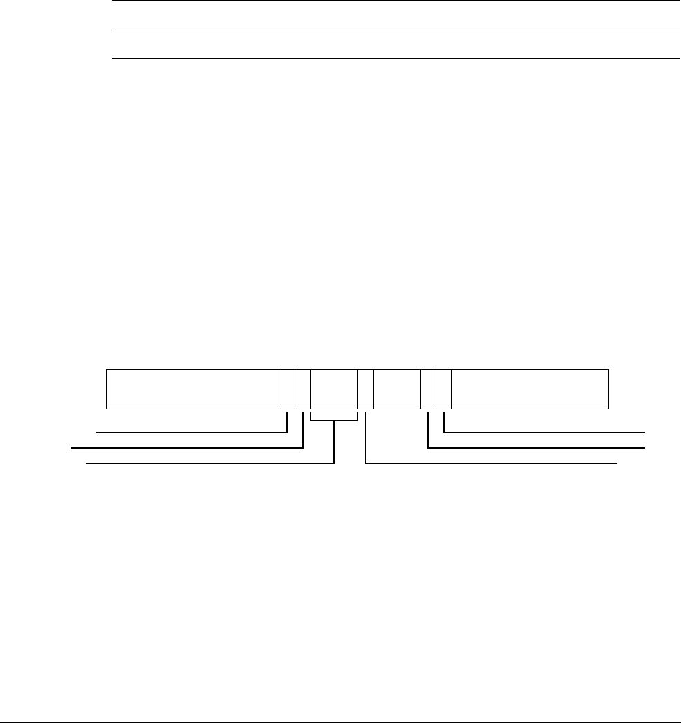
G4 AArch32 System Register Descriptions
G4.2 General system control registers
G4-3984 Copyright © 2013 ARM Limited. All rights reserved. ARM DDI 0487A.a
Non-Confidential - Beta ID090413
G4.2.106 NSACR, Non-Secure Access Control Register
The NSACR characteristics are:
Purpose
Defines the Non-secure access permissions to coprocessors CP0 to CP13, and can include additional
IMPLEMENTATION DEFINED bits that define Non-secure access permissions for IMPLEMENTATION
DEFINED functionality.
This register is part of the Security registers functional group.
Usage constraints
This register is accessible as shown below:
If EL3 is implemented and is using AArch64, any read or write to NSACR in Secure EL1 state in
AArch32 is trapped as an exception to EL3.
Configurations
There is one instance of this register that is used in both Secure and Non-secure states.
When EL3 is using AArch64, then any reads of the NSACR from Non-secure EL2 using AArch32
or Non-secure EL1 using AArch32 will return a fixed value of
0x00000C00
.
If EL3 is not implemented, then any reads of the NSACR from Non-secure EL2 using AArch32 or
Secure or Non-secure EL1 using AArch32 will return a fixed value of
0x00000C00
.
In AArch64, the NSACR functionality is replaced by the behavior in CPTR_EL3.
Attributes
NSACR is a 32-bit register.
The NSACR bit assignments are:
Bits [31:21]
Reserved, RES0.
NSTRCDIS, bit [20]
Disable Non-secure access to CP14 trace registers. The implementation of this bit must correspond
to the implementation of the CPACR.TRCDIS bit:
If CPACR.TRCDIS is RES0 then this bit is RES0.
If CPACR.TRCDIS is RW then this bit is RW and its possible values are:
0
This bit has no effect on the ability to write to CPACR.TRCDIS.
1
When executing in Non-secure state, CPACR.TRCDIS is RES1.
EL0 (NS) EL0 (S) EL1 (NS) EL1 (S) EL2 EL3 (SCR.NS=1) EL3 (SCR.NS=0)
- - RO RW RO RW RW
RES0
31 21 20 19 18 16 15
RES0
14 12 11 10
RES0
90
NSTRCDIS
RES0
IMP DEF
cp10
cp11
NSASEDIS

G4 AArch32 System Register Descriptions
G4.2 General system control registers
ARM DDI 0487A.a Copyright © 2013 ARM Limited. All rights reserved. G4-3985
ID090413 Non-Confidential - Beta
Bit [19]
Reserved, RES0.
NSASEDIS, bit [15]
Disable Non-secure Advanced SIMD functionality. The implementation of this bit must correspond
to the implementation of the CPACR.ASEDIS bit.
If CPACR.ASEDIS is not RW then this bit is RES0.
If CPACR.ASEDIS is RW then this bit is RW and its possible values are:
0
This bit has no effect on the ability to write to CPACR.ASEDIS.
1
When executing in Non-secure state, CPACR.ASEDIS is RES1.
Bits [14:12]
Reserved, RES0.
cp<n>, bit [n], for n = 10 to 11
Enable Non-secure access to coprocessors 10 and 11, which control the Floating-point and
Advanced SIMD features. Possible values of the fields are:
0
Coprocessor <n> can be accessed only from Secure state. Any attempt to access
coprocessor <n> in Non-secure state results in an Undefined Instruction exception. If
the processor is in Non-secure state, the corresponding bits in the CPACR ignore writes
and read as
0b00
, access denied.
1
Coprocessor <n> can be accessed from any security state.
If Non-secure access to a coprocessor is enabled, the CPACR must be checked to determine the level
of access that is permitted.
The Floating-point and Advanced SIMD features controlled by these fields are:
• VFP floating-point instructions.
• Advanced SIMD instructions (both integer and floating-point).
• Advanced SIMD and Floating-point registers D0-D31 and their views as S0-S31 and
Q0-Q15.
•FPSCR, FPSID, MVFR0, MVFR1, MVFR2, FPEXC system registers.
If the cp11 and cp10 fields are set to different values, the behavior is CONSTRAINED UNPREDICTABLE,
and is the same as if both fields were set to the value of cp10, in all respects other than the value
read back by explicitly reading cp11.
Other coprocessors are not supported in ARMv8, so bits[13:12] and bits[9:0] are RES0.
Bits [9:0]
Reserved, RES0.
Accessing the NSACR:
To access the NSACR:
MRC p15,0,<Rt>,c1,c1,2 ; Read NSACR into Rt
MCR p15,0,<Rt>,c1,c1,2 ; Write Rt to NSACR
Register access is encoded as follows:
coproc opc1 CRn CRm opc2
1111 000 0001 0001 010

G4 AArch32 System Register Descriptions
G4.2 General system control registers
G4-3986 Copyright © 2013 ARM Limited. All rights reserved. ARM DDI 0487A.a
Non-Confidential - Beta ID090413
G4.2.107 PAR, Physical Address Register
The PAR characteristics are:
Purpose
Receives the PA from any address translation operation.
This register is part of the Address translation operations functional group.
Usage constraints
This register is accessible as shown below:
When accessed as PAR(S):
When accessed as PAR(NS):
An implementation that does not support a cacheability attribute can report its corresponding
behavior instead of the actual value in the translation table entry.
Configurations
PAR(NS) is architecturally mapped to AArch64 register PAR_EL1.
If EL3 is using AArch32, there are separate Secure and Non-secure instances of this register.
If the implementation includes the Large Physical Address Extension, the PAR is extended to be a
64-bit register and:
• The 64-bit PAR is used:
— When using the Long-descriptor translation table format.
— In an implementation that includes EL2, for the result of an ATS1Cxx operation
performed from Hyp mode.
• The 32-bit PAR is used when using the Short-descriptor translation table format. In this case,
PAR[63:32] is RES0.
Otherwise, the PAR is a 32-bit register.
Attributes
PAR is a 32-bit register when TTBCR.EAE==0 and a 64-bit register when TTBCR.EAE==1.
The PAR bit assignments are:
For all register layouts:
F, bit [0]
Indicates whether the conversion completed successfully.
0
VA to PA conversion completed successfully.
1
VA to PA conversion aborted.
EL0 (NS) EL0 (S) EL1 (NS) EL1 (S) EL2 EL3 (SCR.NS=1) EL3 (SCR.NS=0)
---RW-- RW
EL0 (NS) EL0 (S) EL1 (NS) EL1 (S) EL2 EL3 (SCR.NS=1) EL3 (SCR.NS=0)
--RW-RWRW -

G4 AArch32 System Register Descriptions
G4.2 General system control registers
ARM DDI 0487A.a Copyright © 2013 ARM Limited. All rights reserved. G4-3987
ID090413 Non-Confidential - Beta
When TTBCR.EAE==0, PAR.F==0:
PA, bits [31:12]
Physical Address. The physical address corresponding to the supplied virtual address. This field
returns address bits[31:12].
LPAE, bit [11]
When updating the PAR with the result of a translation operation, this bit is set as follows:
0
Indicates use of the Short-descriptor translation table formats. This indicates that the
PAR returns a 32-bit value.
1
Indicates use of the Long-descriptor translation table formats. This indicates that the
PAR returns a 64-bit value.
Hardware does not interpret this bit to determine the behavior of the memory system, and therefore
software can set this bit to 0 or 1 without affecting operation.
NOS, bit [10]
Not Outer Shareable attribute for the region. Indicates whether Shareable physical memory is Outer
Shareable:
0
Memory is Outer Shareable.
1
Memory is not Outer Shareable.
NS, bit [9]
Non-secure. The NS attribute for a translation table entry read from Secure state.
This bit is UNKNOWN for a translation table entry read from Non-secure state.
SH, bit [7]
Shareable attribute for the region. Indicates whether the physical memory is Shareable:
0
Memory is Non-shareable.
1
Memory is Shareable.
Inner[2:0], bits [6:4]
Inner memory attributes for the region. Permitted values are:
000
Non-cacheable.
001
Strongly-ordered.
011
Device.
101
Write-Back, Write-Allocate.
110
Write-Through.
111
Write-Back, no Write-Allocate.
The values
0b010
and
0b100
are reserved.
PA
31 12 11 10
NS
98 7 6432
SS
1
F
0
Outer[1:0]
Inner[2:0]
SH
IMP DEF
NOS
LPAE

G4 AArch32 System Register Descriptions
G4.2 General system control registers
G4-3988 Copyright © 2013 ARM Limited. All rights reserved. ARM DDI 0487A.a
Non-Confidential - Beta ID090413
An implementation that does not support all of the defined attributes can return the behavior that the
cache supports, instead of the value in the translation table entry.
Outer[1:0], bits [3:2]
Outer memory attributes for the region. Permitted values are:
00
Non-cacheable.
01
Write-Back, Write-Allocate.
10
Write-Through, no Write-Allocate.
11
Write-Back, no Write-Allocate.
An implementation that does not support all of the defined attributes can return the behavior that the
cache supports, instead of the value in the translation table entry.
SS, bit [1]
Supersection. Used to indicate if the result is a Supersection:
0
Page is not a Supersection. That is, PAR[31:12] contains PA[31:12], regardless of the
page size.
1
Page is part of a Supersection:
• PAR[31:24] contains PA[31:24].
• PAR[23:16] contains PA[39:32].
• PAR[15:12] contains
0b0000
.
If an implementation supports less than 40 bits of physical address, the bits in the PAR
field that correspond to physical address bits that are not implemented are UNKNOWN.
F, bit [0]
Indicates whether the conversion completed successfully.
0
VA to PA conversion completed successfully.
When TTBCR.EAE==0, PAR.F==1:
Bits [31:12]
Reserved, RES0.
LPAE, bit [11]
When updating the PAR with the result of a translation operation, this bit is set as follows:
0
Indicates use of the Short-descriptor translation table formats. This indicates that the
PAR returns a 32-bit value.
1
Indicates use of the Long-descriptor translation table formats. This indicates that the
PAR returns a 64-bit value.
Hardware does not interpret this bit to determine the behavior of the memory system, and therefore
software can set this bit to 0 or 1 without affecting operation.
Bits [10:7]
Reserved, RES0.
RES0
31 12 11
RES0
10 7
FS
61
F
0
LPAE
G4 AArch32 System Register Descriptions
G4.2 General system control registers
ARM DDI 0487A.a Copyright © 2013 ARM Limited. All rights reserved. G4-3989
ID090413 Non-Confidential - Beta
FS, bits [6:1]
Fault status bits. Bits [12,10,3:0] from the DFSR, indicating the source of the abort.
F, bit [0]
Indicates whether the conversion completed successfully.
1
VA to PA conversion aborted.
When TTBCR.EAE==1, PAR.F==0:
ATTR, bits [63:56]
Memory attributes for the returned PA, as indicated by the translation table entry. This field uses the
same encoding as the Attr<7:0> fields in MAIR0 and MAIR1.
Bits [55:40]
Reserved, RES0.
PA, bits [39:12]
Physical Address. The physical address corresponding to the supplied virtual address. This field
returns address bits[39:12].
LPAE, bit [11]
When updating the PAR with the result of a translation operation, this bit is set as follows:
0
Indicates use of the Short-descriptor translation table formats. This indicates that the
PAR returns a 32-bit value.
1
Indicates use of the Long-descriptor translation table formats. This indicates that the
PAR returns a 64-bit value.
Hardware does not interpret this bit to determine the behavior of the memory system, and therefore
software can set this bit to 0 or 1 without affecting operation.
NS, bit [9]
Non-secure. The NS attribute for a translation table entry read from Secure state.
This bit is UNKNOWN for a translation table entry read from Non-secure state.
SHA, bits [8:7]
Shareability attribute, from the translation table entry for the returned PA. Permitted values are:
00
Non-shareable.
10
Outer Shareable.
11
Inner Shareable.
The value
0b01
is reserved.
Note: this takes the value
0b10
for:
• Any type of Device memory.
• Normal memory with both Inner Non-cacheable and Outer Non-cacheable attributes.
ATTR
63 56
RES0
55 40
PA
39 12 11 10
NS
9
SHA
87
RES0
61
F
0
IMP DEF
LPAE
G4 AArch32 System Register Descriptions
G4.2 General system control registers
G4-3990 Copyright © 2013 ARM Limited. All rights reserved. ARM DDI 0487A.a
Non-Confidential - Beta ID090413
Bits [6:1]
Reserved, RES0.
F, bit [0]
Indicates whether the conversion completed successfully.
0
VA to PA conversion completed successfully.
When TTBCR.EAE==1, PAR.F==1:
Bits [63:12]
Reserved, RES0.
LPAE, bit [11]
When updating the PAR with the result of a translation operation, this bit is set as follows:
0
Indicates use of the Short-descriptor translation table formats. This indicates that the
PAR returns a 32-bit value.
1
Indicates use of the Long-descriptor translation table formats. This indicates that the
PAR returns a 64-bit value.
Hardware does not interpret this bit to determine the behavior of the memory system, and therefore
software can set this bit to 0 or 1 without affecting operation.
Bit [10]
Reserved, RES0.
FSTAGE, bit [9]
Indicates the translation stage at which the translation aborted:
0
Translation aborted because of a fault in the stage 1 translation.
1
Translation aborted because of a fault in the stage 2 translation.
S2WLK, bit [8]
If this bit is set to 1, it indicates the translation aborted because of a stage 2 fault during a stage 1
translation table walk.
Bit [7]
Reserved, RES0.
FST, bits [6:1]
Fault status field. Values are as in the DFSR.STATUS and IFSR.STATUS fields (when using the
Long-descriptor translation table format).
F, bit [0]
Indicates whether the conversion completed successfully.
1
VA to PA conversion aborted.
RES0
63 12 11 10 9 8 7
FST
61
F
0
RES0
S2WLK
FSTAGE
RES0
LPAE

G4 AArch32 System Register Descriptions
G4.2 General system control registers
ARM DDI 0487A.a Copyright © 2013 ARM Limited. All rights reserved. G4-3991
ID090413 Non-Confidential - Beta
Accessing the PAR:
To access the PAR when TTBCR.EAE==0:
MRC p15,0,<Rt>,c7,c4,0 ; Read PAR into Rt
MCR p15,0,<Rt>,c7,c4,0 ; Write Rt to PAR
Register access is encoded as follows:
To access the PAR when TTBCR.EAE==1:
MRRC p15,0,<Rt>,<Rt2>,c7 ; Read 64-bit PAR into Rt (low word) and Rt2 (high word)
MCRR p15,0,<Rt>,<Rt2>,c7 ; Write Rt (low word) and Rt2 (high word) to 64-bit PAR
Register access is encoded as follows:
coproc opc1 CRn CRm opc2
1111 000 0111 0100 000
coproc opc1 CRm
1111 0000 0111

G4 AArch32 System Register Descriptions
G4.2 General system control registers
G4-3992 Copyright © 2013 ARM Limited. All rights reserved. ARM DDI 0487A.a
Non-Confidential - Beta ID090413
G4.2.108 PRRR, Primary Region Remap Register
The PRRR characteristics are:
Purpose
Controls the top level mapping of the TEX[0], C, and B memory region attributes.
This register is part of the Virtual memory control registers functional group.
Usage constraints
This register is accessible as shown below:
When accessed as PRRR(S):
When accessed as PRRR(NS):
Only accessible when using the Short-descriptor translation table format.
Configurations
PRRR(NS) is architecturally mapped to AArch64 register MAIR_EL1[31:0] when
TTBCR.EAE==0.
PRRR(S) can be mapped to AArch64 register MAIR_EL3[31:0] when TTBCR.EAE==0, but this
is not architecturally mandated.
If EL3 is using AArch32, there are separate Secure and Non-secure instances of this register.
PRRR has write access to the Secure copy of the register disabled when the CP15SDISABLE signal
is asserted HIGH.
Attributes
PRRR is a 32-bit register when TTBCR.EAE==0.
The PRRR bit assignments are:
EL0 (NS) EL0 (S) EL1 (NS) EL1 (S) EL2 EL3 (SCR.NS=1) EL3 (SCR.NS=0)
---RW-- RW
EL0 (NS) EL0 (S) EL1 (NS) EL1 (S) EL2 EL3 (SCR.NS=1) EL3 (SCR.NS=0)
--RW-RWRW -

G4 AArch32 System Register Descriptions
G4.2 General system control registers
ARM DDI 0487A.a Copyright © 2013 ARM Limited. All rights reserved. G4-3993
ID090413 Non-Confidential - Beta
When TTBCR.EAE==0:
NOS<n>, bit [n+24], for n = 0 to 7
NOS<n> is the Outer Shareable property mapping for memory attributes n, if the region is mapped
as Normal or Device memory that is Shareable. n is the value of the TEX[0], C, and B bits
concatenated. The possible values of each NOS<n> bit are:
0
Memory region is Outer Shareable.
1
Memory region is Inner Shareable.
The value of this bit is ignored if the region is Normal or Device memory that is not Shareable.
The meaning of the field with n = 6 is IMPLEMENTATION DEFINED and might differ from the meaning
given here. This is because the meaning of the attribute combination {TEX[0] = 1, C = 1, B = 0} is
IMPLEMENTATION DEFINED.
If the implementation does not distinguish between Inner Shareable and Outer Shareable then these
bits are reserved and are RES0.
Bits [23:20]
Reserved, RES0.
NS1, bit [19]
Mapping of S = 1 attribute for Normal memory. This bit gives the mapped Shareable attribute for a
region of memory that:
• Is mapped as Normal memory.
• Has the S bit set to 1.
The possible values of this bit are:
0
Region is not Shareable.
1
Region is Shareable.
NS0, bit [18]
Mapping of S = 0 attribute for Normal memory. This bit gives the mapped Shareable attribute for a
region of memory that:
• Is mapped as Normal memory.
• Has the S bit set to 0.
The possible values of this bit are:
0
Region is not Shareable.
31 30 29 28 27 26 25 24
RES0
23 20 19 18 17 16
TR7
15 14
TR6
13 12
TR5
11 10
TR4
98
TR3
76
TR2
54
TR1
32
TR0
10
NOS7
NOS6
NOS5
NOS4
NOS3
NOS2
NOS1
NOS0
NS1
NS0
DS1
DS0

G4 AArch32 System Register Descriptions
G4.2 General system control registers
G4-3994 Copyright © 2013 ARM Limited. All rights reserved. ARM DDI 0487A.a
Non-Confidential - Beta ID090413
1
Region is Shareable.
DS1, bit [17]
Mapping of S = 1 attribute for Device memory. This bit gives the mapped Shareable attribute for a
region of memory that:
• Is mapped as Device memory.
• Has the S bit set to 1.
The possible values of this bit are:
0
Region is not Shareable.
1
Region is Shareable.
DS0, bit [16]
Mapping of S = 0 attribute for Device memory. This bit gives the mapped Shareable attribute for a
region of memory that:
• Is mapped as Device memory.
• Has the S bit set to 0.
The possible values of this bit are:
0
Region is not Shareable.
1
Region is Shareable.
TR<n>, bits [2n+1:2n], for n = 0 to 7
TR<n> is the primary TEX mapping for memory attributes n, and defines the mapped memory type
for a region with attributes n. n is the value of the TEX[0], C, and B bits concatenated. The possible
values of this field are:
00
Device-nGnRnE memory
01
Device-nGnRE memory
10
Normal memory
The value
0b11
is reserved.
The meaning of the field with n = 6 is IMPLEMENTATION DEFINED and might differ from the meaning
given here. This is because the meaning of the attribute combination {TEX[0] = 1, C = 1, B = 0} is
IMPLEMENTATION DEFINED.
Accessing the PRRR:
To access the PRRR when TTBCR.EAE==0:
MRC p15,0,<Rt>,c10,c2,0 ; Read PRRR into Rt
MCR p15,0,<Rt>,c10,c2,0 ; Write Rt to PRRR
Register access is encoded as follows:
coproc opc1 CRn CRm opc2
1111 000 1010 0010 000

G4 AArch32 System Register Descriptions
G4.2 General system control registers
ARM DDI 0487A.a Copyright © 2013 ARM Limited. All rights reserved. G4-3995
ID090413 Non-Confidential - Beta
G4.2.109 REVIDR, Revision ID Register
The REVIDR characteristics are:
Purpose
Provides implementation-specific minor revision information that can only be interpreted in
conjunction with the Main ID Register.
This register is part of the Identification registers functional group.
Usage constraints
This register is accessible as shown below:
Configurations
REVIDR is architecturally mapped to AArch64 register REVIDR_EL1.
There is one instance of this register that is used in both Secure and Non-secure states.
An optional register. When REVIDR is not implemented, its encoding is an alias of the MIDR.
Attributes
REVIDR is a 32-bit register.
The REVIDR bit assignments are:
Accessing the REVIDR:
To access the REVIDR:
MRC p15,0,<Rt>,c0,c0,6 ; Read REVIDR into Rt
Register access is encoded as follows:
EL0 (NS) EL0 (S) EL1 (NS) EL1 (S) EL2 EL3 (SCR.NS=1) EL3 (SCR.NS=0)
- - RO RO RO RO RO
IMPLEMENTATION DEFINED
31 0
coproc opc1 CRn CRm opc2
1111 000 0000 0000 110

G4 AArch32 System Register Descriptions
G4.2 General system control registers
G4-3996 Copyright © 2013 ARM Limited. All rights reserved. ARM DDI 0487A.a
Non-Confidential - Beta ID090413
G4.2.110 RMR (at EL1), Reset Management Register
The RMR (at EL1) characteristics are:
Purpose
If this register's exception level is the highest exception level implemented, and is capable of using
both AArch32 and AArch64, controls the execution state that the processor boots into and allows
request of a Warm reset.
This register is part of the Reset management registers functional group.
Usage constraints
This register is accessible as shown below:
If EL3 is implemented, the AArch32 view of the RMR register is subject to CP15SDISABLE,
which prevents writing to this register when the CP15SDISABLE signal is asserted.
Configurations
RMR (at EL1) is architecturally mapped to AArch64 register RMR_EL1.
There is one instance of this register that is used in both Secure and Non-secure states.
Only implemented if this register's exception level is the highest exception level implemented, and
is capable of using both AArch32 and AArch64.
If this exception level is not the highest one implemented, then this register is not implemented and
its encoding is UNDEFINED.
Attributes
RMR (at EL1) is a 32-bit register when EL2 and EL3 not implemented.
The RMR (at EL1) bit assignments are:
When EL2 and EL3 not implemented:
Bits [31:2]
Reserved, RES0.
RR, bit [1]
When set to 1 this bit requests a Warm reset. The bit is strictly a request.
On Warm reset, the field resets to 0.
AA64, bit [0]
Determines which execution state the processor boots into after a Warm reset:
0
AArch32.
1
AArch64.
EL0 EL1
-RW
RES0
31 2
RR
10
AA64

G4 AArch32 System Register Descriptions
G4.2 General system control registers
ARM DDI 0487A.a Copyright © 2013 ARM Limited. All rights reserved. G4-3997
ID090413 Non-Confidential - Beta
The reset vector address on reset takes a choice between two IMP DEF values, depending on the
value in the AA64 bit. This ensures that even with reprogramming of the AA64 bit, it is not possible
to change the reset vector to go to a different location.
On Cold reset, the field resets to 0.
Accessing the RMR (at EL1):
To access the RMR (at EL1) when EL2 and EL3 not implemented:
MRC p15,0,<Rt>,c12,c0,2 ; Read RMR into Rt
MCR p15,0,<Rt>,c12,c0,2 ; Write Rt to RMR
Register access is encoded as follows:
coproc opc1 CRn CRm opc2
1111 000 1100 0000 010

G4 AArch32 System Register Descriptions
G4.2 General system control registers
G4-3998 Copyright © 2013 ARM Limited. All rights reserved. ARM DDI 0487A.a
Non-Confidential - Beta ID090413
G4.2.111 RMR (at EL3), Reset Management Register
The RMR (at EL3) characteristics are:
Purpose
If this register's exception level is the highest exception level implemented, and is capable of using
both AArch32 and AArch64, controls the execution state that the processor boots into and allows
request of a Warm reset.
This register is part of the Reset management registers functional group.
Usage constraints
This register is accessible as shown below:
If EL3 is implemented, the AArch32 view of the RMR register is subject to CP15SDISABLE,
which prevents writing to this register when the CP15SDISABLE signal is asserted.
Configurations
RMR (at EL3) is architecturally mapped to AArch64 register RMR_EL3.
There is one instance of this register that is used in both Secure and Non-secure states.
Only implemented if this register's exception level is the highest exception level implemented, and
is capable of using both AArch32 and AArch64.
If this exception level is not the highest one implemented, then this register is not implemented and
its encoding is UNDEFINED.
Attributes
RMR (at EL3) is a 32-bit register when EL3 implemented.
The RMR (at EL3) bit assignments are:
When EL3 implemented:
Bits [31:2]
Reserved, RES0.
RR, bit [1]
When set to 1 this bit requests a Warm reset. The bit is strictly a request.
On Warm reset, the field resets to 0.
AA64, bit [0]
Determines which execution state the processor boots into after a Warm reset:
0
AArch32.
1
AArch64.
EL0 (NS) EL0 (S) EL1 (NS) EL1 (S) EL2 EL3 (SCR.NS=1) EL3 (SCR.NS=0)
-----RW RW
RES0
31 2
RR
10
AA64

G4 AArch32 System Register Descriptions
G4.2 General system control registers
ARM DDI 0487A.a Copyright © 2013 ARM Limited. All rights reserved. G4-3999
ID090413 Non-Confidential - Beta
The reset vector address on reset takes a choice between two IMP DEF values, depending on the
value in the AA64 bit. This ensures that even with reprogramming of the AA64 bit, it is not possible
to change the reset vector to go to a different location.
On Cold reset, the field resets to 0.
Accessing the RMR (at EL3):
To access the RMR (at EL3) when EL3 implemented:
MRC p15,0,<Rt>,c12,c0,2 ; Read RMR into Rt
MCR p15,0,<Rt>,c12,c0,2 ; Write Rt to RMR
Register access is encoded as follows:
coproc opc1 CRn CRm opc2
1111 000 1100 0000 010

G4 AArch32 System Register Descriptions
G4.2 General system control registers
G4-4000 Copyright © 2013 ARM Limited. All rights reserved. ARM DDI 0487A.a
Non-Confidential - Beta ID090413
G4.2.112 RVBAR, Reset Vector Base Address Register
The RVBAR characteristics are:
Purpose
If EL3 is not implemented, contains the IMPLEMENTATION DEFINED address that execution starts
from after reset when executing in AArch32 state.
This register is part of the Reset management registers functional group.
Usage constraints
This register is accessible as shown below:
This register can only be read at the highest exception level implemented. It is UNDEFINED at all
other exception levels.
Configurations
There is one instance of this register that is used in both Secure and Non-secure states.
This register is only implemented if the highest exception level implemented is not EL3 and can use
AArch32. In such an implementation, whether this register is implemented is implementation
defined. If RVBAR is not implemented its encoding is UNDEFINED.
Attributes
RVBAR is a 32-bit register.
The RVBAR bit assignments are:
RVec, bits [31:1]
Bits [31:1] of the IMPLEMENTATION DEFINED AArch32 reset address.
Bit [0]
Reserved, RES1.
Accessing the RVBAR:
To access the RVBAR:
MRC p15,0,<Rt>,c12,c0,1 ; Read RVBAR into Rt
Register access is encoded as follows:
EL0 EL1 EL2
- Config-RO Config-RO
RVec
31 1 0
RES1
coproc opc1 CRn CRm opc2
1111 000 1100 0000 001
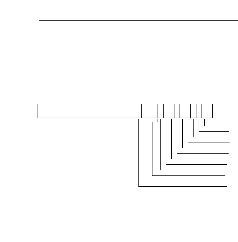
G4 AArch32 System Register Descriptions
G4.2 General system control registers
ARM DDI 0487A.a Copyright © 2013 ARM Limited. All rights reserved. G4-4001
ID090413 Non-Confidential - Beta
G4.2.113 SCR, Secure Configuration Register
The SCR characteristics are:
Purpose
Defines the configuration of the current security state. It specifies:
• The security state, either Secure or Non-secure.
• What mode the processor branches to if an IRQ, FIQ, or External Abort occurs.
• Whether the CPSR.F or CPSR.A bits can be modified when SCR.NS==1.
This register is part of the Security registers functional group.
Usage constraints
This register is accessible as shown below:
If EL3 is implemented and is using AArch64, any read or write to SCR in Secure EL1 state in
AArch32 is trapped as an exception to EL3.
Configurations
SCR can be mapped to AArch64 register SCR_EL3, but this is not architecturally mandated.
This register is only accessible in Secure state.
Attributes
SCR is a 32-bit register.
The SCR bit assignments are:
Bits [31:14]
Reserved, RES0.
TWE, bit [13]
Trap WFE. The possible values of this bit are:
0
WFE instructions are not trapped.
EL0 (NS) EL0 (S) EL1 (NS) EL1 (S) EL2 EL3 (SCR.NS=1) EL3 (SCR.NS=0)
- - - RW - RW RW
RES0
31 14 13 12 11 10 9 8 7 6 5 4 3 2 1
NS
0
IRQ
FIQ
EA
FW
AW
nET
SCD
HCE
SIF
RES0
TWI
TWE

G4 AArch32 System Register Descriptions
G4.2 General system control registers
G4-4002 Copyright © 2013 ARM Limited. All rights reserved. ARM DDI 0487A.a
Non-Confidential - Beta ID090413
1
WFE instructions executed in any mode other than Monitor mode are trapped to
Monitor mode as UNDEFINED if the instruction would otherwise cause suspension of
execution, i.e. if the event register is not set, there is not a pending WFE wakeup event,
and the instruction does not cause another exception.
Conditional WFE instructions that fail their condition do not cause an exception by this mechanism.
Resets to 0.
TWI, bit [12]
Trap WFI. The possible values of this bit are:
0
WFI instructions are not trapped.
1
WFI instructions executed in any mode other than Monitor mode are trapped to Monitor
mode as UNDEFINED if the instruction would otherwise cause suspension of execution.
Conditional WFI instructions that fail their condition do not cause an exception by this mechanism.
Resets to 0.
Bits [11:10]
Reserved, RES0.
SIF, bit [9]
Secure instruction fetch. When the processor is in Secure state, this bit disables instruction fetch
from Non-secure memory. The possible values for this bit are:
0
Secure state instruction fetches from Non-secure memory are permitted.
1
Secure state instruction fetches from Non-secure memory are not permitted.
This bit is permitted to be cached in a TLB.
Resets to 0.
HCE, bit [8]
Hypervisor Call enable. This bit enables use of the HVC instruction from Non-secure EL1 modes.
The possible values of this bit are:
0
HVC instruction is UNDEFINED in Non-secure EL1 modes, and either UNDEFINED or a
NOP in Hyp mode, depending on the implementation.
1
HVC instruction is enabled in Non-secure EL1 modes, and performs a Hypervisor Call.
If EL3 is implemented but EL2 is not implemented, this bit is RES0.
Resets to 0.
SCD, bit [7]
Secure Monitor Call disable. Makes the SMC instruction UNDEFINED in Non-secure state. The
possible values of this bit are:
0
SMC executes normally in Non-secure state, performing a Secure Monitor Call.
1
SMC instruction is either UNDEFINED or a NOP in Non-secure state, depending on the
implementation.
A trap of the SMC instruction to Hyp mode takes priority over the value of this bit.
Resets to 0.
nET, bit [6]
Not Early Termination. This bit disables early termination. The possible values of this bit are:
0
Early termination permitted. Execution time of data operations can depend on the data
values.
1
Disable early termination. The number of cycles required for data operations is forced
to be independent of the data values.

G4 AArch32 System Register Descriptions
G4.2 General system control registers
ARM DDI 0487A.a Copyright © 2013 ARM Limited. All rights reserved. G4-4003
ID090413 Non-Confidential - Beta
This IMPLEMENTATION DEFINED mechanism can disable data dependent timing optimizations from
multiplies and data operations. It can provide system support against information leakage that might
be exploited by timing correlation types of attack.
Resets to 0.
AW, bit [5]
When the value of SCR.EA is 1 and the value of HCR.AMO is 0, this bit controls whether CPSR.A
masks an external abort taken from Non-secure state, and the possible values of this bit are:
0
External aborts taken from Non-secure state are not masked by CPSR.A, and are taken
to EL3.
External aborts taken from Secure state are masked by CPSR.A.
1
External aborts taken from either security state are masked by CPSR.A. When CPSR.A
is 0, the abort is taken to EL3.
When SCR.EA is 0 or HCR.AMO is 1, this bit has no effect.
Resets to 0.
FW, bit [4]
When the value of SCR.FIQ is 1 and the value of HCR.FMO is 0, this bit controls whether CPSR.F
masks an FIQ interrupt taken from Non-secure state, and the possible values of this bit are:
0
An FIQ taken from Non-secure state is not masked by CPSR.F, and is taken to EL3.
An FIQ taken from Secure state is masked by CPSR.F.
1
An FIQ taken from either security state is masked by CPSR.F. When CPSR.F is 0, the
FIQ is taken to EL3.
When SCR.FIQ is 0 or HCR.FMO is 1, this bit has no effect.
Resets to 0.
EA, bit [3]
External Abort handler. This bit controls which mode takes external aborts. The possible values of
this bit are:
0
External aborts taken in Abort mode.
1
External aborts taken in Monitor mode.
Resets to 0.
FIQ, bit [2]
FIQ handler. This bit controls which mode takes FIQ exceptions. The possible values of this bit are:
0
FIQs taken in FIQ mode.
1
FIQs taken in Monitor mode.
Resets to 0.
IRQ, bit [1]
IRQ handler. This bit controls which mode takes IRQ exceptions. The possible values of this bit are:
0
IRQs taken in IRQ mode.
1
IRQs taken in Monitor mode.
Resets to 0.
NS, bit [0]
Non-secure bit. Except when the processor is in Monitor mode, this bit determines the security state
of the processor:
0
Processor is in Secure state.
1
Processor is in Non-secure state.

G4 AArch32 System Register Descriptions
G4.2 General system control registers
G4-4004 Copyright © 2013 ARM Limited. All rights reserved. ARM DDI 0487A.a
Non-Confidential - Beta ID090413
If the HCR.TGE bit is set, an attempt to change from a Secure Kernel mode to a Non-secure Kernel
mode by changing the SCR.NS bit from 0 to 1 will result in the SCR.NS bit remaining as 0.
Resets to 0.
Accessing the SCR:
To access the SCR:
MRC p15,0,<Rt>,c1,c1,0 ; Read SCR into Rt
MCR p15,0,<Rt>,c1,c1,0 ; Write Rt to SCR
Register access is encoded as follows:
coproc opc1 CRn CRm opc2
1111 000 0001 0001 000

G4 AArch32 System Register Descriptions
G4.2 General system control registers
ARM DDI 0487A.a Copyright © 2013 ARM Limited. All rights reserved. G4-4005
ID090413 Non-Confidential - Beta
G4.2.114 SCTLR, System Control Register
The SCTLR characteristics are:
Purpose
Provides the top level control of the system, including its memory system.
This register is part of the Other system control registers functional group.
Usage constraints
This register is accessible as shown below:
When accessed as SCTLR(S):
When accessed as SCTLR(NS):
Some bits in the register are read-only. These bits relate to non-configurable features of an
implementation, and are provided for compatibility with previous versions of the architecture.
Configurations
SCTLR(NS) is architecturally mapped to AArch64 register SCTLR_EL1.
SCTLR(S) can be mapped to AArch64 register SCTLR_EL3, but this is not architecturally
mandated.
If EL3 is using AArch32, there are separate Secure and Non-secure instances of this register.
SCTLR has write access to the Secure copy of the register disabled when the CP15SDISABLE
signal is asserted HIGH.
Attributes
SCTLR is a 32-bit register.
The SCTLR bit assignments are:
EL0 (NS) EL0 (S) EL1 (NS) EL1 (S) EL2 EL3 (SCR.NS=1) EL3 (SCR.NS=0)
---RW-- RW
EL0 (NS) EL0 (S) EL1 (NS) EL1 (S) EL2 EL3 (SCR.NS=1) EL3 (SCR.NS=0)
--RW-RWRW -

G4 AArch32 System Register Descriptions
G4.2 General system control registers
G4-4006 Copyright © 2013 ARM Limited. All rights reserved. ARM DDI 0487A.a
Non-Confidential - Beta ID090413
Bit [31]
Reserved, RES0.
TE, bit [30]
Thumb Exception Enable. This bit controls whether exceptions are taken in A32 or T32 state:
0
Exceptions, including reset, taken in A32 state.
1
Exceptions, including reset, taken in T32 state.
For the Secure copy of this register, the field resets to a value that is configurable by either input
signal or pin setting.
For the Non-secure copy of this register, the field reset value is architecturally UNKNOWN.
AFE, bit [29]
Access Flag Enable. When using the Short-descriptor translation table format, this bit enables use
of the AP[0] bit in the translation descriptors as the Access flag, and restricts access permissions in
the translation descriptors to the simplified model. The possible values of this bit are:
0
In the translation table descriptors, AP[0] is an access permissions bit. The full range of
access permissions is supported. No Access flag is implemented.
1
In the translation table descriptors, AP[0] is the Access flag. Only the simplified model
for access permissions is supported.
When using the Long-descriptor translation table format, the VMSA behaves as if this bit is set to
1, regardless of the value of this bit.
The AFE bit is permitted to be cached in a TLB.
For the Secure copy of this register, the field resets to 0.
For the Non-secure copy of this register, the field reset value is architecturally UNKNOWN.
TRE, bit [28]
TEX remap enable. This bit enables remapping of the TEX[2:1] bits for use as two translation table
bits that can be managed by the operating system. Enabling this remapping also changes the scheme
used to describe the memory region attributes in the VMSA. The possible values of this bit are:
0
TEX remap disabled. TEX[2:0] are used, with the C and B bits, to describe the memory
region attributes.
31
TE
30 29 28 27 26 25 24 23 22 21 20 19 18 17 16 15 14
V
13
I
12 11 10 9 8 7 6 5 43
C
2
A
1
M
0
RES0
AFE
TRE
RES0
EE
RES0
RES1
RES0
UWXN
WXN
nTWE
RES0
nTWI
RES1
CP15BEN
THEE
ITD
SED
RES0
RES1
RES0

G4 AArch32 System Register Descriptions
G4.2 General system control registers
ARM DDI 0487A.a Copyright © 2013 ARM Limited. All rights reserved. G4-4007
ID090413 Non-Confidential - Beta
1
TEX remap enabled. TEX[2:1] are reassigned for use as bits managed by the operating
system. The TEX[0], C, and B bits are used to describe the memory region attributes,
with the MMU remap registers.
The TRE bit is permitted to be cached in a TLB.
For the Secure copy of this register, the field resets to 0.
For the Non-secure copy of this register, the field reset value is architecturally UNKNOWN.
Bits [27:26]
Reserved, RES0.
EE, bit [25]
Exception Endianness. The value of this bit defines the value of the CPSR.E bit on entry to an
exception vector, including reset. This value also indicates the endianness of the translation table
data for translation table lookups. The possible values of this bit are:
0
Little-endian.
1
Big-endian.
If an implementation does not provide Big-endian support, this bit is RES0. If it does not provide
Little-endian support, this bit is RES1.
For the Secure copy of this register, the field resets to a value that is configurable by either input
signal or pin setting.
For the Non-secure copy of this register, the field reset value is architecturally UNKNOWN.
Bit [24]
Reserved, RES0.
Bits [23:22]
Reserved, RES1.
Bit [21]
Reserved, RES0.
UWXN, bit [20]
Unprivileged write permission implies EL1 XN (Execute Never). This bit can be used to require all
memory regions with unprivileged write permissions to be treated as XN for accesses from software
executing at EL1. The possible values of this bit are:
0
Regions with unprivileged write permission are not forced to XN.
1
Regions with unprivileged write permission are forced to XN for accesses from
software executing at EL1.
The UWXN bit is permitted to be cached in a TLB.
For the Secure copy of this register, the field resets to 0.
For the Non-secure copy of this register, the field resets to 0.
WXN, bit [19]
Write permission implies XN (Execute Never). This bit can be used to require all memory regions
with write permission to be treated as XN. The possible values of this bit are:
0
Regions with write permission are not forced to XN.
1
Regions with write permission are forced to XN.
The WXN bit is permitted to be cached in a TLB.
For the Secure copy of this register, the field resets to 0.
For the Non-secure copy of this register, the field resets to 0.

G4 AArch32 System Register Descriptions
G4.2 General system control registers
G4-4008 Copyright © 2013 ARM Limited. All rights reserved. ARM DDI 0487A.a
Non-Confidential - Beta ID090413
nTWE, bit [18]
Not trap WFE. Possible values of this bit are:
0
If a WFE instruction executed at EL0 would cause execution to be suspended, such as
if the event register is not set and there is not a pending WFE wakeup event, it is treated
as UNDEFINED.
1
WFE instructions are executed as normal.
Conditional WFE instructions that fail their condition do not cause an exception if this bit is 0.
For the Secure copy of this register, the field resets to 1.
For the Non-secure copy of this register, the field resets to 1.
Bit [17]
Reserved, RES0.
nTWI, bit [16]
Not trap WFI. Possible values of this bit are:
0
If a WFI instruction executed at EL0 would cause execution to be suspended, such as if
there is not a pending WFI wakeup event, it is treated as UNDEFINED.
1
WFI instructions are executed as normal.
Conditional WFI instructions that fail their condition do not cause an exception if this bit is 0.
For the Secure copy of this register, the field resets to 1.
For the Non-secure copy of this register, the field resets to 1.
Bits [15:14]
Reserved, RES0.
V, bit [13]
Vectors bit. This bit selects the base address of the exception vectors:
0
Normal exception vectors, base address
0x00000000
. In an implementation that includes
EL3, this base address can be re-mapped.
1
High exception vectors (Hivecs), base address
0xFFFF0000
. This base address is never
remapped.
For the Secure copy of this register, the field resets to a value that is configurable by either input
signal or pin setting.
For the Non-secure copy of this register, the field reset value is architecturally UNKNOWN.
I, bit [12]
Instruction cache enable. This is a global enable bit for instruction caches:
0
Instruction caches disabled. If SCTLR.M is set to 0, instruction accesses from stage 1
of the EL1&0 translation regime are to Normal memory, Outer Shareable, Inner
Non-cacheable, Outer Non-cacheable.
1
Instruction caches enabled. If SCTLR.M is set to 0, instruction accesses from stage 1 of
the EL1&0 translation regime are to Normal memory, Outer Shareable, Inner
Write-Through, Outer Write-Through.
When this bit is 0, all Normal memory instruction accesses are Non-cacheable.
If the HCR.DC bit is set to 1, then the Non-secure stage 1 EL1&0 translation regime is Cacheable
regardless of the value of this bit.
For the Secure copy of this register, the field if this register is at the highest exception level
implemented, field resets to 0. Otherwise, its reset value is UNKNOWN.
For the Non-secure copy of this register, the field reset value is architecturally UNKNOWN.

G4 AArch32 System Register Descriptions
G4.2 General system control registers
ARM DDI 0487A.a Copyright © 2013 ARM Limited. All rights reserved. G4-4009
ID090413 Non-Confidential - Beta
Bit [11]
Reserved, RES1.
Bits [10:9]
Reserved, RES0.
SED, bit [8]
SETEND Disable. The possible values of this bit are:
0
The SETEND instruction is available.
1
The SETEND instruction is UNALLOCATED.
If an implementation does not support mixed endian operation, this bit is RES1.
For the Secure copy of this register, the field resets to 0.
For the Non-secure copy of this register, the field resets to 1.
ITD, bit [7]
IT Disable. The possible values of this bit are:
0
The IT instruction functionality is available.
1
It is IMPLEMENTATION DEFINED whether the IT instruction is treated as either:
• A 16-bit instruction, which can only be followed by another 16-bit instruction.
• The first half of a 32-bit instruction.
An implementation might vary dynamically as to whether IT is treated as a 16-bit
instruction or the first half of a 32-bit instruction.
All encodings of the IT instruction with hw1[3:0]!=1000 are UNDEFINED and treated as
unallocated.
All encodings of the subsequent instruction with the following values for hw1 are
UNDEFINED (and treated as unallocated):
11xxxxxxxxxxxxxx
All 32-bit instructions, B(2), B(1), Undefined, SVC, Load/Store multiple
1x11xxxxxxxxxxxx
Miscellaneous 16-bit instructions
1x100xxxxxxxxxxx
ADD Rd, PC, #imm
01001xxxxxxxxxxx
LDR Rd, [PC, #imm]
0100x1xxx1111xxx
ADD(4),CMP(3), MOV, BX pc, BLX pc
010001xx1xxxx111
ADD(4),CMP(3), MOV (Note: this pattern also covers UNPREDICTABLE
cases with BLX Rn)
Contrary to the standard treatment of conditional UNDEFINED instructions in the ARM
architecture, in this case these instructions are always treated as UNDEFINED, regardless
of whether the instruction would pass or fail its condition codes as a result of being in
an IT block.
For the Secure copy of this register, the field resets to 0.
For the Non-secure copy of this register, the field resets to 0.
THEE, bit [6]
T32EE enable. The possible values of this bit are:
0
T32EE is disabled.
1
T32EE is enabled.

G4 AArch32 System Register Descriptions
G4.2 General system control registers
G4-4010 Copyright © 2013 ARM Limited. All rights reserved. ARM DDI 0487A.a
Non-Confidential - Beta ID090413
If T32EE is not implemented, this bit is RES0.
For the Secure copy of this register, the field resets to 1 if T32EE is implemented. Otherwise, its
reset value is UNKNOWN.
For the Non-secure copy of this register, the field resets to 1 if T32EE is implemented. Otherwise,
its reset value is UNKNOWN.
CP15BEN, bit [5]
CP15 barrier enable. If implemented, this is an enable bit for the CP15 DMB, DSB, and ISB barrier
operations at EL0 and EL1:
0
CP15 barrier operations disabled at EL0 and EL1. Their encodings are UNDEFINED.
1
CP15 barrier operations enabled at EL0 and EL1.
If an implementation does not support the CP15 barrier operations, this bit is RES0.
For the Secure copy of this register, the field resets to 1.
For the Non-secure copy of this register, the field resets to 1.
Bits [4:3]
Reserved, RES1.
C, bit [2]
Cache enable. This is a global enable bit for data and unified caches:
0
Data and unified caches disabled.
1
Data and unified caches enabled.
When this bit is 0, all Normal memory data accesses and all accesses to the EL1&0 stage 1
translation tables are Non-cacheable.
If the HCR.DC bit is set to 1, then the Non-secure stage 1 EL1&0 translation regime is Cacheable
regardless of the value of the SCTLR.C bit.
For the Secure copy of this register, the field resets to 0.
For the Non-secure copy of this register, the field reset value is architecturally UNKNOWN.
A, bit [1]
Alignment check enable. This is the enable bit for Alignment fault checking:
0
Alignment fault checking disabled.
Instructions that load or store one or more registers, other than load/store exclusive and
load-acquire/store-release, do not check that the address being accessed is aligned to the
size of the data element(s) being accessed.
1
Alignment fault checking enabled.
All instructions that load or store one or more registers have an alignment check that the
address being accessed is aligned to the size of the data element(s) being accessed. If
this check fails it causes an Alignment fault, which is taken as a Data Abort exception.
Load/store exclusive and load-acquire/store-release instructions have an alignment check regardless
of the value of the A bit.
For the Secure copy of this register, the field resets to 0.
For the Non-secure copy of this register, the field reset value is architecturally UNKNOWN.
M, bit [0]
MMU enable for EL1 and EL0 stage 1 address translation. Possible values of this bit are:
0
EL1 and EL0 stage 1 address translation disabled.
1
EL1 and EL0 stage 1 address translation enabled.
If the HCR.DC bit is set to 1, then the behavior of the processor when executing in a Non-secure
mode other than Hyp mode is consistent with SCTLR.M being 0, regardless of the actual value of
SCTLR.M, other than the value returned by an explicit read of SCTLR.M.

G4 AArch32 System Register Descriptions
G4.2 General system control registers
ARM DDI 0487A.a Copyright © 2013 ARM Limited. All rights reserved. G4-4011
ID090413 Non-Confidential - Beta
For the Secure copy of this register, the field resets to 0.
For the Non-secure copy of this register, the field reset value is architecturally UNKNOWN.
Accessing the SCTLR:
To access the SCTLR:
MRC p15,0,<Rt>,c1,c0,0 ; Read SCTLR into Rt
MCR p15,0,<Rt>,c1,c0,0 ; Write Rt to SCTLR
Register access is encoded as follows:
coproc opc1 CRn CRm opc2
1111 000 0001 0000 000
G4 AArch32 System Register Descriptions
G4.2 General system control registers
G4-4012 Copyright © 2013 ARM Limited. All rights reserved. ARM DDI 0487A.a
Non-Confidential - Beta ID090413
G4.2.115 SPSR, Saved Program Status Register
The SPSR characteristics are:
Purpose
Holds the saved processor state for the current mode.
Usage constraints
The SPSR can be read using the
MRS
instruction and written using the
MSR
(immediate) or
MSR
(register) instructions. For more information see MRS on page F7-2720, MSR (immediate) on
page F7-2722, and MSR (register) on page F7-2724.
Configurations
There is one instance of this register that is used in both Secure and Non-secure states.
Attributes
SPSR is a 32-bit register.
The SPSR bit assignments are:
N, bit [31]
Set to the value of CPSR.N on taking an exception to the current mode, and copied to CPSR.N on
executing an exception return operation in the current mode.
Z, bit [30]
Set to the value of CPSR.Z on taking an exception to the current mode, and copied to CPSR.Z on
executing an exception return operation in the current mode.
C, bit [29]
Set to the value of CPSR.C on taking an exception to the current mode, and copied to CPSR.C on
executing an exception return operation in the current mode.
V, bit [28]
Set to the value of CPSR.V on taking an exception to the current mode, and copied to CPSR.V on
executing an exception return operation in the current mode.
Q, bit [27]
Set to the value of CPSR.Q on taking an exception to the current mode, and copied to CPSR.Q on
executing an exception return operation in the current mode.
IT[1:0], bits [26:25]
If-Then execution state bits for the T32 IT (If-Then) instruction. See IT[7:2] for explanation of this
field.
J, bit [24]
Jazelle bit. Along with the T bit, determines the AArch32 instruction set state that the exception was
taken from. Possible values of this bit are:
0
Processor in A32 state if T is 0, or T32 state if T is 1.
1
Processor in an invalid state (Jazelle state before ARMv8) if T is 0, or T32EE state if T
is 1.
N
31
Z
30
C
29
V
28
Q
27 26 25
J
24
RES0
23 21
IL
20
GE
19 16
IT[7:2]
15 10
E
9
A
8
I
7
F
6
T
54
M[3:0]
30
IT[1:0] M[4]

G4 AArch32 System Register Descriptions
G4.2 General system control registers
ARM DDI 0487A.a Copyright © 2013 ARM Limited. All rights reserved. G4-4013
ID090413 Non-Confidential - Beta
Since the Jazelle state is obsolete in ARMv8, J==1 and T==0 is an invalid combination, and
attempting to perform an exception return with those values is an illegal exception return.
If T32EE is not implemented, this bit is RES0, so the possible values of the T bit signify either A32
or T32 state.
Bits [23:21]
Reserved, RES0.
IL, bit [20]
Illegal Execution State bit. Shows the value of PSTATE.IL immediately before the exception was
taken.
GE, bits [19:16]
Greater than or Equal flags, for parallel addition and subtraction.
IT[7:2], bits [15:10]
If-Then execution state bits for the T32 IT (If-Then) instruction. This field must be interpreted in
two parts.
• IT[7:5] holds the base condition for the IT block. The base condition is the top 3 bits of the
condition code specified by the first condition field of the IT instruction.
• IT[4:0] encodes the size of the IT block, which is the number of instructions that are to be
conditionally executed, by the position of the least significant 1 in this field. It also encodes
the value of the least significant bit of the condition code for each instruction in the block.
The IT field is
0b00000000
when no IT block is active.
E, bit [9]
Endianness execution state bit. Controls the load and store endianness for data accesses:
0
Little-endian operation
1
Big-endian operation.
Instruction fetches ignore this bit.
When the reset value of the SCTLR.EE bit is defined by a configuration input signal, that value also
applies to the CPSR.E bit on reset, and therefore applies to software execution from reset.
If an implementation does not provide Big-endian support, this bit is RES0. If it does not provide
Little-endian support, this bit is RES1.
If an implementation provides Big-endian support but only at EL0, this bit is RES0 for an exception
return to any exception level other than EL0.
Likewise, if it provides Little-endian support only at EL0, this bit is RES1 for an exception return
to any exception level other than EL0.
A, bit [8]
Asynchronous data abort mask bit. The possible values of this bit are:
0
Exception not masked.
1
Exception masked.
I, bit [7]
IRQ mask bit. The possible values of this bit are:
0
Exception not masked.
1
Exception masked.
F, bit [6]
FIQ mask bit. The possible values of this bit are:
0
Exception not masked.
1
Exception masked.

G4 AArch32 System Register Descriptions
G4.2 General system control registers
G4-4014 Copyright © 2013 ARM Limited. All rights reserved. ARM DDI 0487A.a
Non-Confidential - Beta ID090413
T, bit [5]
Thumb execution state bit. Along with the J bit, determines the AArch32 instruction set state that
the exception was taken from. Possible values of this bit are:
0
Processor in A32 state if J is 0, or an invalid state (Jazelle state before ARMv8) if J is 1.
1
Processor in T32 state if J is 0, or T32EE state if J is 1.
Since the Jazelle state is obsolete in ARMv8, J==1 and T==0 is an invalid combination, and
attempting to perform an exception return with those values is an illegal exception return.
If T32EE is not implemented, the J bit is RES0, so the possible values of this bit signify either A32
or T32 state.
M[4], bit [4]
Register width that the exception was taken from. Possible values of this bit are:
1
Exception taken from AArch32.
M[3:0], bits [3:0]
Mode that an exception was taken from. For exceptions taken from AArch32, the possible values
are:
Other values are reserved.
M[3:0] Mode
0b0000
User
0b0001
FIQ
0b0010
IRQ
0b0011
Supervisor
0b0110
Monitor
0b0111
Abort
0b1010
Hyp
0b1011
Undefined
0b1111
System

G4 AArch32 System Register Descriptions
G4.2 General system control registers
ARM DDI 0487A.a Copyright © 2013 ARM Limited. All rights reserved. G4-4015
ID090413 Non-Confidential - Beta
G4.2.116 SPSR_abt, Saved Program Status Register (Abort mode)
The SPSR_abt characteristics are:
Purpose
Holds the saved processor state when an exception is taken to Abort mode.
This register is part of the Special purpose registers functional group.
Usage constraints
This register is accessible as shown below:
This register is only accessible at EL1 in modes other than Abort mode. In Abort mode, it is
accessible as the current SPSR.
Configurations
SPSR_abt is architecturally mapped to AArch64 register SPSR_abt.
There is one instance of this register that is used in both Secure and Non-secure states.
Attributes
SPSR_abt is a 32-bit register.
The SPSR_abt bit assignments are:
N, bit [31]
Set to the value of CPSR.N on taking an exception to Abort mode, and copied to CPSR.N on
executing an exception return operation in Abort mode.
Z, bit [30]
Set to the value of CPSR.Z on taking an exception to Abort mode, and copied to CPSR.Z on
executing an exception return operation in Abort mode.
C, bit [29]
Set to the value of CPSR.C on taking an exception to Abort mode, and copied to CPSR.C on
executing an exception return operation in Abort mode.
V, bit [28]
Set to the value of CPSR.V on taking an exception to Abort mode, and copied to CPSR.V on
executing an exception return operation in Abort mode.
Q, bit [27]
Set to the value of CPSR.Q on taking an exception to Abort mode, and copied to CPSR.Q on
executing an exception return operation in Abort mode.
EL0 (NS) EL0 (S) EL1 (NS,
!ABT) EL1 (S,
!ABT) EL2 EL3 (SCR.NS=1) EL3 (SCR.NS=0)
- - RW RW RW RW RW
N
31
Z
30
C
29
V
28
Q
27 26 25
J
24
RES0
23 21
IL
20
GE
19 16
IT[7:2]
15 10
E
9
A
8
I
7
F
6
T
54
M[3:0]
30
IT[1:0] M[4]

G4 AArch32 System Register Descriptions
G4.2 General system control registers
G4-4016 Copyright © 2013 ARM Limited. All rights reserved. ARM DDI 0487A.a
Non-Confidential - Beta ID090413
IT[1:0], bits [26:25]
If-Then execution state bits for the T32 IT (If-Then) instruction. See IT[7:2] for explanation of this
field.
J, bit [24]
Jazelle bit. Along with the T bit, determines the AArch32 instruction set state that the exception was
taken from. Possible values of this bit are:
0
Processor in A32 state if T is 0, or T32 state if T is 1.
1
Processor in an invalid state (Jazelle state before ARMv8) if T is 0, or T32EE state if T
is 1.
Since the Jazelle state is obsolete in ARMv8, J==1 and T==0 is an invalid combination, and
attempting to perform an exception return with those values is an illegal exception return.
If T32EE is not implemented, this bit is RES0, so the possible values of the T bit signify either A32
or T32 state.
Bits [23:21]
Reserved, RES0.
IL, bit [20]
Illegal Execution State bit. Shows the value of PSTATE.IL immediately before the exception was
taken.
GE, bits [19:16]
Greater than or Equal flags, for parallel addition and subtraction.
IT[7:2], bits [15:10]
If-Then execution state bits for the T32 IT (If-Then) instruction. This field must be interpreted in
two parts.
• IT[7:5] holds the base condition for the IT block. The base condition is the top 3 bits of the
condition code specified by the first condition field of the IT instruction.
• IT[4:0] encodes the size of the IT block, which is the number of instructions that are to be
conditionally executed, by the position of the least significant 1 in this field. It also encodes
the value of the least significant bit of the condition code for each instruction in the block.
The IT field is
0b00000000
when no IT block is active.
E, bit [9]
Endianness execution state bit. Controls the load and store endianness for data accesses:
0
Little-endian operation
1
Big-endian operation.
Instruction fetches ignore this bit.
When the reset value of the SCTLR.EE bit is defined by a configuration input signal, that value also
applies to the CPSR.E bit on reset, and therefore applies to software execution from reset.
If an implementation does not provide Big-endian support, this bit is RES0. If it does not provide
Little-endian support, this bit is RES1.
If an implementation provides Big-endian support but only at EL0, this bit is RES0 for an exception
return to any exception level other than EL0.
Likewise, if it provides Little-endian support only at EL0, this bit is RES1 for an exception return
to any exception level other than EL0.
A, bit [8]
Asynchronous data abort mask bit. The possible values of this bit are:
0
Exception not masked.
1
Exception masked.

G4 AArch32 System Register Descriptions
G4.2 General system control registers
ARM DDI 0487A.a Copyright © 2013 ARM Limited. All rights reserved. G4-4017
ID090413 Non-Confidential - Beta
I, bit [7]
IRQ mask bit. The possible values of this bit are:
0
Exception not masked.
1
Exception masked.
F, bit [6]
FIQ mask bit. The possible values of this bit are:
0
Exception not masked.
1
Exception masked.
T, bit [5]
Thumb execution state bit. Along with the J bit, determines the AArch32 instruction set state that
the exception was taken from. Possible values of this bit are:
0
Processor in A32 state if J is 0, or an invalid state (Jazelle state before ARMv8) if J is 1.
1
Processor in T32 state if J is 0, or T32EE state if J is 1.
Since the Jazelle state is obsolete in ARMv8, J==1 and T==0 is an invalid combination, and
attempting to perform an exception return with those values is an illegal exception return.
If T32EE is not implemented, the J bit is RES0, so the possible values of this bit signify either A32
or T32 state.
M[4], bit [4]
Register width that the exception was taken from. Possible values of this bit are:
1
Exception taken from AArch32.
M[3:0], bits [3:0]
Mode that an exception was taken from. For exceptions taken from AArch32, the possible values
are:
Other values are reserved.
Accessing the SPSR_abt:
To access the SPSR_abt:
MRS <Rd>, SPSR_abt ; Read SPSR_abt into Rd
MSR SPSR_abt, <Rd> ; Write Rd to SPSR_abt
M[3:0] Mode
0b0000
User
0b0001
FIQ
0b0010
IRQ
0b0011
Supervisor
0b0110
Monitor (only valid in Secure state, if EL3 is implemented and can use AArch32)
0b0111
Abort
0b1011
Undefined
0b1111
System

G4 AArch32 System Register Descriptions
G4.2 General system control registers
G4-4018 Copyright © 2013 ARM Limited. All rights reserved. ARM DDI 0487A.a
Non-Confidential - Beta ID090413
Register access is encoded as follows:
mm1R
1 0100 1

G4 AArch32 System Register Descriptions
G4.2 General system control registers
ARM DDI 0487A.a Copyright © 2013 ARM Limited. All rights reserved. G4-4019
ID090413 Non-Confidential - Beta
G4.2.117 SPSR_fiq, Saved Program Status Register (FIQ mode)
The SPSR_fiq characteristics are:
Purpose
Holds the saved processor state when an exception is taken to FIQ mode.
This register is part of the Special purpose registers functional group.
Usage constraints
This register is accessible as shown below:
This register is only accessible at EL1 in modes other than FIQ mode. In FIQ mode, it is accessible
as the current SPSR.
Configurations
SPSR_fiq is architecturally mapped to AArch64 register SPSR_fiq.
There is one instance of this register that is used in both Secure and Non-secure states.
Attributes
SPSR_fiq is a 32-bit register.
The SPSR_fiq bit assignments are:
N, bit [31]
Set to the value of CPSR.N on taking an exception to FIQ mode, and copied to CPSR.N on
executing an exception return operation in FIQ mode.
Z, bit [30]
Set to the value of CPSR.Z on taking an exception to FIQ mode, and copied to CPSR.Z on executing
an exception return operation in FIQ mode.
C, bit [29]
Set to the value of CPSR.C on taking an exception to FIQ mode, and copied to CPSR.C on executing
an exception return operation in FIQ mode.
V, bit [28]
Set to the value of CPSR.V on taking an exception to FIQ mode, and copied to CPSR.V on
executing an exception return operation in FIQ mode.
Q, bit [27]
Set to the value of CPSR.Q on taking an exception to FIQ mode, and copied to CPSR.Q on
executing an exception return operation in FIQ mode.
EL0 (NS) EL0 (S) EL1 (NS,
!FIQ) EL1 (S,
!FIQ) EL2 EL3 (SCR.NS=1) EL3 (SCR.NS=0)
- - RW RW RW RW RW
N
31
Z
30
C
29
V
28
Q
27 26 25
J
24
RES0
23 21
IL
20
GE
19 16
IT[7:2]
15 10
E
9
A
8
I
7
F
6
T
54
M[3:0]
30
IT[1:0] M[4]

G4 AArch32 System Register Descriptions
G4.2 General system control registers
G4-4020 Copyright © 2013 ARM Limited. All rights reserved. ARM DDI 0487A.a
Non-Confidential - Beta ID090413
IT[1:0], bits [26:25]
If-Then execution state bits for the T32 IT (If-Then) instruction. See IT[7:2] for explanation of this
field.
J, bit [24]
Jazelle bit. Along with the T bit, determines the AArch32 instruction set state that the exception was
taken from. Possible values of this bit are:
0
Processor in A32 state if T is 0, or T32 state if T is 1.
1
Processor in an invalid state (Jazelle state before ARMv8) if T is 0, or T32EE state if T
is 1.
Since the Jazelle state is obsolete in ARMv8, J==1 and T==0 is an invalid combination, and
attempting to perform an exception return with those values is an illegal exception return.
If T32EE is not implemented, this bit is RES0, so the possible values of the T bit signify either A32
or T32 state.
Bits [23:21]
Reserved, RES0.
IL, bit [20]
Illegal Execution State bit. Shows the value of PSTATE.IL immediately before the exception was
taken.
GE, bits [19:16]
Greater than or Equal flags, for parallel addition and subtraction.
IT[7:2], bits [15:10]
If-Then execution state bits for the T32 IT (If-Then) instruction. This field must be interpreted in
two parts.
• IT[7:5] holds the base condition for the IT block. The base condition is the top 3 bits of the
condition code specified by the first condition field of the IT instruction.
• IT[4:0] encodes the size of the IT block, which is the number of instructions that are to be
conditionally executed, by the position of the least significant 1 in this field. It also encodes
the value of the least significant bit of the condition code for each instruction in the block.
The IT field is
0b00000000
when no IT block is active.
E, bit [9]
Endianness execution state bit. Controls the load and store endianness for data accesses:
0
Little-endian operation
1
Big-endian operation.
Instruction fetches ignore this bit.
When the reset value of the SCTLR.EE bit is defined by a configuration input signal, that value also
applies to the CPSR.E bit on reset, and therefore applies to software execution from reset.
If an implementation does not provide Big-endian support, this bit is RES0. If it does not provide
Little-endian support, this bit is RES1.
If an implementation provides Big-endian support but only at EL0, this bit is RES0 for an exception
return to any exception level other than EL0.
Likewise, if it provides Little-endian support only at EL0, this bit is RES1 for an exception return
to any exception level other than EL0.
A, bit [8]
Asynchronous data abort mask bit. The possible values of this bit are:
0
Exception not masked.
1
Exception masked.

G4 AArch32 System Register Descriptions
G4.2 General system control registers
ARM DDI 0487A.a Copyright © 2013 ARM Limited. All rights reserved. G4-4021
ID090413 Non-Confidential - Beta
I, bit [7]
IRQ mask bit. The possible values of this bit are:
0
Exception not masked.
1
Exception masked.
F, bit [6]
FIQ mask bit. The possible values of this bit are:
0
Exception not masked.
1
Exception masked.
T, bit [5]
Thumb execution state bit. Along with the J bit, determines the AArch32 instruction set state that
the exception was taken from. Possible values of this bit are:
0
Processor in A32 state if J is 0, or an invalid state (Jazelle state before ARMv8) if J is 1.
1
Processor in T32 state if J is 0, or T32EE state if J is 1.
Since the Jazelle state is obsolete in ARMv8, J==1 and T==0 is an invalid combination, and
attempting to perform an exception return with those values is an illegal exception return.
If T32EE is not implemented, the J bit is RES0, so the possible values of this bit signify either A32
or T32 state.
M[4], bit [4]
Register width that the exception was taken from. Possible values of this bit are:
1
Exception taken from AArch32.
M[3:0], bits [3:0]
Mode that an exception was taken from. For exceptions taken from AArch32, the possible values
are:
Other values are reserved.
Accessing the SPSR_fiq:
To access the SPSR_fiq:
MRS <Rd>, SPSR_fiq ; Read SPSR_fiq into Rd
MSR SPSR_fiq, <Rd> ; Write Rd to SPSR_fiq
M[3:0] Mode
0b0000
User
0b0001
FIQ
0b0010
IRQ
0b0011
Supervisor
0b0110
Monitor (only valid in Secure state, if EL3 is implemented and can use AArch32)
0b0111
Abort
0b1011
Undefined
0b1111
System

G4 AArch32 System Register Descriptions
G4.2 General system control registers
G4-4022 Copyright © 2013 ARM Limited. All rights reserved. ARM DDI 0487A.a
Non-Confidential - Beta ID090413
Register access is encoded as follows:
mm1R
0 1110 1
G4 AArch32 System Register Descriptions
G4.2 General system control registers
ARM DDI 0487A.a Copyright © 2013 ARM Limited. All rights reserved. G4-4023
ID090413 Non-Confidential - Beta
G4.2.118 SPSR_hyp, Saved Program Status Register (Hyp mode)
The SPSR_hyp characteristics are:
Purpose
Holds the saved processor state when an exception is taken to Hyp mode.
This register is part of the Special purpose registers functional group.
Usage constraints
This register is accessible as shown below:
Configurations
SPSR_hyp is architecturally mapped to AArch64 register SPSR_EL2.
There is one instance of this register that is used in both Secure and Non-secure states.
Attributes
SPSR_hyp is a 32-bit register.
The SPSR_hyp bit assignments are:
N, bit [31]
Set to the value of CPSR.N on taking an exception to Hyp mode, and copied to CPSR.N on
executing an exception return operation in Hyp mode.
Z, bit [30]
Set to the value of CPSR.Z on taking an exception to Hyp mode, and copied to CPSR.Z on executing
an exception return operation in Hyp mode.
C, bit [29]
Set to the value of CPSR.C on taking an exception to Hyp mode, and copied to CPSR.C on
executing an exception return operation in Hyp mode.
V, bit [28]
Set to the value of CPSR.V on taking an exception to Hyp mode, and copied to CPSR.V on
executing an exception return operation in Hyp mode.
Q, bit [27]
Set to the value of CPSR.Q on taking an exception to Hyp mode, and copied to CPSR.Q on
executing an exception return operation in Hyp mode.
IT[1:0], bits [26:25]
If-Then execution state bits for the T32 IT (If-Then) instruction. See IT[7:2] for explanation of this
field.
EL0 (NS) EL0 (S) EL1 (NS) EL1 (S) EL2 EL3 (SCR.NS=1) EL3 (SCR.NS=0)
-----RW RW
N
31
Z
30
C
29
V
28
Q
27 26 25
J
24
RES0
23 21
IL
20
GE
19 16
IT[7:2]
15 10
E
9
A
8
I
7
F
6
T
54
M[3:0]
30
IT[1:0] M[4]

G4 AArch32 System Register Descriptions
G4.2 General system control registers
G4-4024 Copyright © 2013 ARM Limited. All rights reserved. ARM DDI 0487A.a
Non-Confidential - Beta ID090413
J, bit [24]
Jazelle bit. Along with the T bit, determines the AArch32 instruction set state that the exception was
taken from. Possible values of this bit are:
0
Processor in A32 state if T is 0, or T32 state if T is 1.
1
Processor in an invalid state (Jazelle state before ARMv8) if T is 0, or T32EE state if T
is 1.
Since the Jazelle state is obsolete in ARMv8, J==1 and T==0 is an invalid combination, and
attempting to perform an exception return with those values is an illegal exception return.
If T32EE is not implemented, this bit is RES0, so the possible values of the T bit signify either A32
or T32 state.
Bits [23:21]
Reserved, RES0.
IL, bit [20]
Illegal Execution State bit. Shows the value of PSTATE.IL immediately before the exception was
taken.
GE, bits [19:16]
Greater than or Equal flags, for parallel addition and subtraction.
IT[7:2], bits [15:10]
If-Then execution state bits for the T32 IT (If-Then) instruction. This field must be interpreted in
two parts.
• IT[7:5] holds the base condition for the IT block. The base condition is the top 3 bits of the
condition code specified by the first condition field of the IT instruction.
• IT[4:0] encodes the size of the IT block, which is the number of instructions that are to be
conditionally executed, by the position of the least significant 1 in this field. It also encodes
the value of the least significant bit of the condition code for each instruction in the block.
The IT field is
0b00000000
when no IT block is active.
E, bit [9]
Endianness execution state bit. Controls the load and store endianness for data accesses:
0
Little-endian operation
1
Big-endian operation.
Instruction fetches ignore this bit.
When the reset value of the SCTLR.EE bit is defined by a configuration input signal, that value also
applies to the CPSR.E bit on reset, and therefore applies to software execution from reset.
If an implementation does not provide Big-endian support, this bit is RES0. If it does not provide
Little-endian support, this bit is RES1.
If an implementation provides Big-endian support but only at EL0, this bit is RES0 for an exception
return to any exception level other than EL0.
Likewise, if it provides Little-endian support only at EL0, this bit is RES1 for an exception return
to any exception level other than EL0.
A, bit [8]
Asynchronous data abort mask bit. The possible values of this bit are:
0
Exception not masked.
1
Exception masked.

G4 AArch32 System Register Descriptions
G4.2 General system control registers
ARM DDI 0487A.a Copyright © 2013 ARM Limited. All rights reserved. G4-4025
ID090413 Non-Confidential - Beta
I, bit [7]
IRQ mask bit. The possible values of this bit are:
0
Exception not masked.
1
Exception masked.
F, bit [6]
FIQ mask bit. The possible values of this bit are:
0
Exception not masked.
1
Exception masked.
T, bit [5]
Thumb execution state bit. Along with the J bit, determines the AArch32 instruction set state that
the exception was taken from. Possible values of this bit are:
0
Processor in A32 state if J is 0, or an invalid state (Jazelle state before ARMv8) if J is 1.
1
Processor in T32 state if J is 0, or T32EE state if J is 1.
Since the Jazelle state is obsolete in ARMv8, J==1 and T==0 is an invalid combination, and
attempting to perform an exception return with those values is an illegal exception return.
If T32EE is not implemented, the J bit is RES0, so the possible values of this bit signify either A32
or T32 state.
M[4], bit [4]
Register width that the exception was taken from. Possible values of this bit are:
1
Exception taken from AArch32.
M[3:0], bits [3:0]
Mode that an exception was taken from. For exceptions taken from AArch32, the possible values
are:
Other values are reserved.
Accessing the SPSR_hyp:
To access the SPSR_hyp:
MRS <Rd>, SPSR_hyp ; Read SPSR_hyp into Rd
MSR SPSR_hyp, <Rd> ; Write Rd to SPSR_hyp
M[3:0] Mode
0b0000
User
0b0001
FIQ
0b0010
IRQ
0b0011
Supervisor
0b0111
Abort
0b1010
Hyp
0b1011
Undefined
0b1111
System

G4 AArch32 System Register Descriptions
G4.2 General system control registers
G4-4026 Copyright © 2013 ARM Limited. All rights reserved. ARM DDI 0487A.a
Non-Confidential - Beta ID090413
Register access is encoded as follows:
mm1R
1 1110 1
G4 AArch32 System Register Descriptions
G4.2 General system control registers
ARM DDI 0487A.a Copyright © 2013 ARM Limited. All rights reserved. G4-4027
ID090413 Non-Confidential - Beta
G4.2.119 SPSR_irq, Saved Program Status Register (IRQ mode)
The SPSR_irq characteristics are:
Purpose
Holds the saved processor state when an exception is taken to IRQ mode.
This register is part of the Special purpose registers functional group.
Usage constraints
This register is accessible as shown below:
This register is only accessible at EL1 in modes other than IRQ mode. In IRQ mode, it is accessible
as the current SPSR.
Configurations
SPSR_irq is architecturally mapped to AArch64 register SPSR_irq.
There is one instance of this register that is used in both Secure and Non-secure states.
Attributes
SPSR_irq is a 32-bit register.
The SPSR_irq bit assignments are:
N, bit [31]
Set to the value of CPSR.N on taking an exception to IRQ mode, and copied to CPSR.N on
executing an exception return operation in IRQ mode.
Z, bit [30]
Set to the value of CPSR.Z on taking an exception to IRQ mode, and copied to CPSR.Z on executing
an exception return operation in IRQ mode.
C, bit [29]
Set to the value of CPSR.C on taking an exception to IRQ mode, and copied to CPSR.C on
executing an exception return operation in IRQ mode.
V, bit [28]
Set to the value of CPSR.V on taking an exception to IRQ mode, and copied to CPSR.V on
executing an exception return operation in IRQ mode.
Q, bit [27]
Set to the value of CPSR.Q on taking an exception to IRQ mode, and copied to CPSR.Q on
executing an exception return operation in IRQ mode.
EL0 (NS) EL0 (S) EL1 (NS,
!IRQ) EL1 (S,
!IRQ) EL2 EL3 (SCR.NS=1) EL3 (SCR.NS=0)
- - RW RW RW RW RW
N
31
Z
30
C
29
V
28
Q
27 26 25
J
24
RES0
23 21
IL
20
GE
19 16
IT[7:2]
15 10
E
9
A
8
I
7
F
6
T
54
M[3:0]
30
IT[1:0] M[4]

G4 AArch32 System Register Descriptions
G4.2 General system control registers
G4-4028 Copyright © 2013 ARM Limited. All rights reserved. ARM DDI 0487A.a
Non-Confidential - Beta ID090413
IT[1:0], bits [26:25]
If-Then execution state bits for the T32 IT (If-Then) instruction. See IT[7:2] for explanation of this
field.
J, bit [24]
Jazelle bit. Along with the T bit, determines the AArch32 instruction set state that the exception was
taken from. Possible values of this bit are:
0
Processor in A32 state if T is 0, or T32 state if T is 1.
1
Processor in an invalid state (Jazelle state before ARMv8) if T is 0, or T32EE state if T
is 1.
Since the Jazelle state is obsolete in ARMv8, J==1 and T==0 is an invalid combination, and
attempting to perform an exception return with those values is an illegal exception return.
If T32EE is not implemented, this bit is RES0, so the possible values of the T bit signify either A32
or T32 state.
Bits [23:21]
Reserved, RES0.
IL, bit [20]
Illegal Execution State bit. Shows the value of PSTATE.IL immediately before the exception was
taken.
GE, bits [19:16]
Greater than or Equal flags, for parallel addition and subtraction.
IT[7:2], bits [15:10]
If-Then execution state bits for the T32 IT (If-Then) instruction. This field must be interpreted in
two parts.
• IT[7:5] holds the base condition for the IT block. The base condition is the top 3 bits of the
condition code specified by the first condition field of the IT instruction.
• IT[4:0] encodes the size of the IT block, which is the number of instructions that are to be
conditionally executed, by the position of the least significant 1 in this field. It also encodes
the value of the least significant bit of the condition code for each instruction in the block.
The IT field is
0b00000000
when no IT block is active.
E, bit [9]
Endianness execution state bit. Controls the load and store endianness for data accesses:
0
Little-endian operation
1
Big-endian operation.
Instruction fetches ignore this bit.
When the reset value of the SCTLR.EE bit is defined by a configuration input signal, that value also
applies to the CPSR.E bit on reset, and therefore applies to software execution from reset.
If an implementation does not provide Big-endian support, this bit is RES0. If it does not provide
Little-endian support, this bit is RES1.
If an implementation provides Big-endian support but only at EL0, this bit is RES0 for an exception
return to any exception level other than EL0.
Likewise, if it provides Little-endian support only at EL0, this bit is RES1 for an exception return
to any exception level other than EL0.
A, bit [8]
Asynchronous data abort mask bit. The possible values of this bit are:
0
Exception not masked.
1
Exception masked.

G4 AArch32 System Register Descriptions
G4.2 General system control registers
ARM DDI 0487A.a Copyright © 2013 ARM Limited. All rights reserved. G4-4029
ID090413 Non-Confidential - Beta
I, bit [7]
IRQ mask bit. The possible values of this bit are:
0
Exception not masked.
1
Exception masked.
F, bit [6]
FIQ mask bit. The possible values of this bit are:
0
Exception not masked.
1
Exception masked.
T, bit [5]
Thumb execution state bit. Along with the J bit, determines the AArch32 instruction set state that
the exception was taken from. Possible values of this bit are:
0
Processor in A32 state if J is 0, or an invalid state (Jazelle state before ARMv8) if J is 1.
1
Processor in T32 state if J is 0, or T32EE state if J is 1.
Since the Jazelle state is obsolete in ARMv8, J==1 and T==0 is an invalid combination, and
attempting to perform an exception return with those values is an illegal exception return.
If T32EE is not implemented, the J bit is RES0, so the possible values of this bit signify either A32
or T32 state.
M[4], bit [4]
Register width that the exception was taken from. Possible values of this bit are:
1
Exception taken from AArch32.
M[3:0], bits [3:0]
Mode that an exception was taken from. For exceptions taken from AArch32, the possible values
are:
Other values are reserved.
Accessing the SPSR_irq:
To access the SPSR_irq:
MRS <Rd>, SPSR_irq ; Read SPSR_irq into Rd
MSR SPSR_irq, <Rd> ; Write Rd to SPSR_irq
M[3:0] Mode
0b0000
User
0b0001
FIQ
0b0010
IRQ
0b0011
Supervisor
0b0110
Monitor (only valid in Secure state, if EL3 is implemented and can use AArch32)
0b0111
Abort
0b1011
Undefined
0b1111
System

G4 AArch32 System Register Descriptions
G4.2 General system control registers
G4-4030 Copyright © 2013 ARM Limited. All rights reserved. ARM DDI 0487A.a
Non-Confidential - Beta ID090413
Register access is encoded as follows:
mm1R
1 0000 1
G4 AArch32 System Register Descriptions
G4.2 General system control registers
ARM DDI 0487A.a Copyright © 2013 ARM Limited. All rights reserved. G4-4031
ID090413 Non-Confidential - Beta
G4.2.120 SPSR_mon, Saved Program Status Register (Monitor mode)
The SPSR_mon characteristics are:
Purpose
Holds the saved processor state when an exception is taken to Monitor mode.
This register is part of the Special purpose registers functional group.
Usage constraints
This register is accessible as shown below:
Configurations
SPSR_mon can be mapped to AArch64 register SPSR_EL3, but this is not architecturally
mandated.
There is one instance of this register that is used in both Secure and Non-secure states.
Attributes
SPSR_mon is a 32-bit register.
The SPSR_mon bit assignments are:
N, bit [31]
Set to the value of CPSR.N on taking an exception to Monitor mode, and copied to CPSR.N on
executing an exception return operation in Monitor mode.
Z, bit [30]
Set to the value of CPSR.Z on taking an exception to Monitor mode, and copied to CPSR.Z on
executing an exception return operation in Monitor mode.
C, bit [29]
Set to the value of CPSR.C on taking an exception to Monitor mode, and copied to CPSR.C on
executing an exception return operation in Monitor mode.
V, bit [28]
Set to the value of CPSR.V on taking an exception to Monitor mode, and copied to CPSR.V on
executing an exception return operation in Monitor mode.
Q, bit [27]
Set to the value of CPSR.Q on taking an exception to Monitor mode, and copied to CPSR.Q on
executing an exception return operation in Monitor mode.
IT[1:0], bits [26:25]
If-Then execution state bits for the T32 IT (If-Then) instruction. See IT[7:2] for explanation of this
field.
EL0 (NS) EL0 (S) EL1 (NS) EL1 (S) EL2 EL3 (SCR.NS=1) EL3 (SCR.NS=0)
---RW-- -
N
31
Z
30
C
29
V
28
Q
27 26 25
J
24
RES0
23 21
IL
20
GE
19 16
IT[7:2]
15 10
E
9
A
8
I
7
F
6
T
54
M[3:0]
30
IT[1:0] M[4]

G4 AArch32 System Register Descriptions
G4.2 General system control registers
G4-4032 Copyright © 2013 ARM Limited. All rights reserved. ARM DDI 0487A.a
Non-Confidential - Beta ID090413
J, bit [24]
Jazelle bit. Along with the T bit, determines the AArch32 instruction set state that the exception was
taken from. Possible values of this bit are:
0
Processor in A32 state if T is 0, or T32 state if T is 1.
1
Processor in an invalid state (Jazelle state before ARMv8) if T is 0, or T32EE state if T
is 1.
Since the Jazelle state is obsolete in ARMv8, J==1 and T==0 is an invalid combination, and
attempting to perform an exception return with those values is an illegal exception return.
If T32EE is not implemented, this bit is RES0, so the possible values of the T bit signify either A32
or T32 state.
Bits [23:21]
Reserved, RES0.
IL, bit [20]
Illegal Execution State bit. Shows the value of PSTATE.IL immediately before the exception was
taken.
GE, bits [19:16]
Greater than or Equal flags, for parallel addition and subtraction.
IT[7:2], bits [15:10]
If-Then execution state bits for the T32 IT (If-Then) instruction. This field must be interpreted in
two parts.
• IT[7:5] holds the base condition for the IT block. The base condition is the top 3 bits of the
condition code specified by the first condition field of the IT instruction.
• IT[4:0] encodes the size of the IT block, which is the number of instructions that are to be
conditionally executed, by the position of the least significant 1 in this field. It also encodes
the value of the least significant bit of the condition code for each instruction in the block.
The IT field is
0b00000000
when no IT block is active.
E, bit [9]
Endianness execution state bit. Controls the load and store endianness for data accesses:
0
Little-endian operation
1
Big-endian operation.
Instruction fetches ignore this bit.
When the reset value of the SCTLR.EE bit is defined by a configuration input signal, that value also
applies to the CPSR.E bit on reset, and therefore applies to software execution from reset.
If an implementation does not provide Big-endian support, this bit is RES0. If it does not provide
Little-endian support, this bit is RES1.
If an implementation provides Big-endian support but only at EL0, this bit is RES0 for an exception
return to any exception level other than EL0.
Likewise, if it provides Little-endian support only at EL0, this bit is RES1 for an exception return
to any exception level other than EL0.
A, bit [8]
Asynchronous data abort mask bit. The possible values of this bit are:
0
Exception not masked.
1
Exception masked.

G4 AArch32 System Register Descriptions
G4.2 General system control registers
ARM DDI 0487A.a Copyright © 2013 ARM Limited. All rights reserved. G4-4033
ID090413 Non-Confidential - Beta
I, bit [7]
IRQ mask bit. The possible values of this bit are:
0
Exception not masked.
1
Exception masked.
F, bit [6]
FIQ mask bit. The possible values of this bit are:
0
Exception not masked.
1
Exception masked.
T, bit [5]
Thumb execution state bit. Along with the J bit, determines the AArch32 instruction set state that
the exception was taken from. Possible values of this bit are:
0
Processor in A32 state if J is 0, or an invalid state (Jazelle state before ARMv8) if J is 1.
1
Processor in T32 state if J is 0, or T32EE state if J is 1.
Since the Jazelle state is obsolete in ARMv8, J==1 and T==0 is an invalid combination, and
attempting to perform an exception return with those values is an illegal exception return.
If T32EE is not implemented, the J bit is RES0, so the possible values of this bit signify either A32
or T32 state.
M[4], bit [4]
Register width that the exception was taken from. Possible values of this bit are:
1
Exception taken from AArch32.
M[3:0], bits [3:0]
Mode that an exception was taken from. For exceptions taken from AArch32, the possible values
are:
Other values are reserved.
Accessing the SPSR_mon:
To access the SPSR_mon:
MRS <Rd>, SPSR_mon ; Read SPSR_mon into Rd
MSR SPSR_mon, <Rd> ; Write Rd to SPSR_mon
M[3:0] Mode
0b0000
User
0b0001
FIQ
0b0010
IRQ
0b0011
Supervisor
0b0110
Monitor (only valid in Secure state, if EL3 is implemented and can use AArch32)
0b0111
Abort
0b1010
Hyp
0b1011
Undefined
0b1111
System

G4 AArch32 System Register Descriptions
G4.2 General system control registers
G4-4034 Copyright © 2013 ARM Limited. All rights reserved. ARM DDI 0487A.a
Non-Confidential - Beta ID090413
Register access is encoded as follows:
mm1R
1 1100 1

G4 AArch32 System Register Descriptions
G4.2 General system control registers
ARM DDI 0487A.a Copyright © 2013 ARM Limited. All rights reserved. G4-4035
ID090413 Non-Confidential - Beta
G4.2.121 SPSR_svc, Saved Program Status Register (Sup. Call mode)
The SPSR_svc characteristics are:
Purpose
Holds the saved processor state when an exception is taken to Supervisor mode.
This register is part of the Special purpose registers functional group.
Usage constraints
This register is accessible as shown below:
This register is only accessible at EL1 in modes other than Supervisor mode. In Supervisor mode,
it is accessible as the current SPSR.
Configurations
SPSR_svc is architecturally mapped to AArch64 register SPSR_EL1.
There is one instance of this register that is used in both Secure and Non-secure states.
Attributes
SPSR_svc is a 32-bit register.
The SPSR_svc bit assignments are:
N, bit [31]
Set to the value of CPSR.N on taking an exception to Supervisor mode, and copied to CPSR.N on
executing an exception return operation in Supervisor mode.
Z, bit [30]
Set to the value of CPSR.Z on taking an exception to Supervisor mode, and copied to CPSR.Z on
executing an exception return operation in Supervisor mode.
C, bit [29]
Set to the value of CPSR.C on taking an exception to Supervisor mode, and copied to CPSR.C on
executing an exception return operation in Supervisor mode.
V, bit [28]
Set to the value of CPSR.V on taking an exception to Supervisor mode, and copied to CPSR.V on
executing an exception return operation in Supervisor mode.
Q, bit [27]
Set to the value of CPSR.Q on taking an exception to Supervisor mode, and copied to CPSR.Q on
executing an exception return operation in Supervisor mode.
EL0 (NS) EL0 (S) EL1 (NS,
!SVC) EL1 (S,
!SVC) EL2 EL3 (SCR.NS=1) EL3 (SCR.NS=0)
- - RW RW RW RW RW
N
31
Z
30
C
29
V
28
Q
27 26 25
J
24
RES0
23 21
IL
20
GE
19 16
IT[7:2]
15 10
E
9
A
8
I
7
F
6
T
54
M[3:0]
30
IT[1:0] M[4]

G4 AArch32 System Register Descriptions
G4.2 General system control registers
G4-4036 Copyright © 2013 ARM Limited. All rights reserved. ARM DDI 0487A.a
Non-Confidential - Beta ID090413
IT[1:0], bits [26:25]
If-Then execution state bits for the T32 IT (If-Then) instruction. See IT[7:2] for explanation of this
field.
J, bit [24]
Jazelle bit. Along with the T bit, determines the AArch32 instruction set state that the exception was
taken from. Possible values of this bit are:
0
Processor in A32 state if T is 0, or T32 state if T is 1.
1
Processor in an invalid state (Jazelle state before ARMv8) if T is 0, or T32EE state if T
is 1.
Since the Jazelle state is obsolete in ARMv8, J==1 and T==0 is an invalid combination, and
attempting to perform an exception return with those values is an illegal exception return.
If T32EE is not implemented, this bit is RES0, so the possible values of the T bit signify either A32
or T32 state.
Bits [23:21]
Reserved, RES0.
IL, bit [20]
Illegal Execution State bit. Shows the value of PSTATE.IL immediately before the exception was
taken.
GE, bits [19:16]
Greater than or Equal flags, for parallel addition and subtraction.
IT[7:2], bits [15:10]
If-Then execution state bits for the T32 IT (If-Then) instruction. This field must be interpreted in
two parts.
• IT[7:5] holds the base condition for the IT block. The base condition is the top 3 bits of the
condition code specified by the first condition field of the IT instruction.
• IT[4:0] encodes the size of the IT block, which is the number of instructions that are to be
conditionally executed, by the position of the least significant 1 in this field. It also encodes
the value of the least significant bit of the condition code for each instruction in the block.
The IT field is
0b00000000
when no IT block is active.
E, bit [9]
Endianness execution state bit. Controls the load and store endianness for data accesses:
0
Little-endian operation
1
Big-endian operation.
Instruction fetches ignore this bit.
When the reset value of the SCTLR.EE bit is defined by a configuration input signal, that value also
applies to the CPSR.E bit on reset, and therefore applies to software execution from reset.
If an implementation does not provide Big-endian support, this bit is RES0. If it does not provide
Little-endian support, this bit is RES1.
If an implementation provides Big-endian support but only at EL0, this bit is RES0 for an exception
return to any exception level other than EL0.
Likewise, if it provides Little-endian support only at EL0, this bit is RES1 for an exception return
to any exception level other than EL0.
A, bit [8]
Asynchronous data abort mask bit. The possible values of this bit are:
0
Exception not masked.
1
Exception masked.

G4 AArch32 System Register Descriptions
G4.2 General system control registers
ARM DDI 0487A.a Copyright © 2013 ARM Limited. All rights reserved. G4-4037
ID090413 Non-Confidential - Beta
I, bit [7]
IRQ mask bit. The possible values of this bit are:
0
Exception not masked.
1
Exception masked.
F, bit [6]
FIQ mask bit. The possible values of this bit are:
0
Exception not masked.
1
Exception masked.
T, bit [5]
Thumb execution state bit. Along with the J bit, determines the AArch32 instruction set state that
the exception was taken from. Possible values of this bit are:
0
Processor in A32 state if J is 0, or an invalid state (Jazelle state before ARMv8) if J is 1.
1
Processor in T32 state if J is 0, or T32EE state if J is 1.
Since the Jazelle state is obsolete in ARMv8, J==1 and T==0 is an invalid combination, and
attempting to perform an exception return with those values is an illegal exception return.
If T32EE is not implemented, the J bit is RES0, so the possible values of this bit signify either A32
or T32 state.
M[4], bit [4]
Register width that the exception was taken from. Possible values of this bit are:
1
Exception taken from AArch32.
M[3:0], bits [3:0]
Mode that an exception was taken from. For exceptions taken from AArch32, the possible values
are:
Other values are reserved.
Accessing the SPSR_svc:
To access the SPSR_svc:
MRS <Rd>, SPSR_svc ; Read SPSR_svc into Rd
MSR SPSR_svc, <Rd> ; Write Rd to SPSR_svc
M[3:0] Mode
0b0000
User
0b0001
FIQ
0b0010
IRQ
0b0011
Supervisor
0b0110
Monitor (only valid in Secure state, if EL3 is implemented and can use AArch32)
0b0111
Abort
0b1011
Undefined
0b1111
System

G4 AArch32 System Register Descriptions
G4.2 General system control registers
G4-4038 Copyright © 2013 ARM Limited. All rights reserved. ARM DDI 0487A.a
Non-Confidential - Beta ID090413
Register access is encoded as follows:
mm1R
1 0010 1

G4 AArch32 System Register Descriptions
G4.2 General system control registers
ARM DDI 0487A.a Copyright © 2013 ARM Limited. All rights reserved. G4-4039
ID090413 Non-Confidential - Beta
G4.2.122 SPSR_und, Saved Program Status Register (Undefined mode)
The SPSR_und characteristics are:
Purpose
Holds the saved processor state when an exception is taken to Undefined mode.
This register is part of the Special purpose registers functional group.
Usage constraints
This register is accessible as shown below:
This register is only accessible at EL1 in modes other than Undefined mode. In Undefined mode, it
is accessible as the current SPSR.
Configurations
SPSR_und is architecturally mapped to AArch64 register SPSR_und.
There is one instance of this register that is used in both Secure and Non-secure states.
Attributes
SPSR_und is a 32-bit register.
The SPSR_und bit assignments are:
N, bit [31]
Set to the value of CPSR.N on taking an exception to Undefined mode, and copied to CPSR.N on
executing an exception return operation in Undefined mode.
Z, bit [30]
Set to the value of CPSR.Z on taking an exception to Undefined mode, and copied to CPSR.Z on
executing an exception return operation in Undefined mode.
C, bit [29]
Set to the value of CPSR.C on taking an exception to Undefined mode, and copied to CPSR.C on
executing an exception return operation in Undefined mode.
V, bit [28]
Set to the value of CPSR.V on taking an exception to Undefined mode, and copied to CPSR.V on
executing an exception return operation in Undefined mode.
Q, bit [27]
Set to the value of CPSR.Q on taking an exception to Undefined mode, and copied to CPSR.Q on
executing an exception return operation in Undefined mode.
EL0 (NS) EL0 (S) EL1 (NS,
!UND) EL1 (S,
!UND) EL2 EL3 (SCR.NS=1) EL3 (SCR.NS=0)
- - RW RW RW RW RW
N
31
Z
30
C
29
V
28
Q
27 26 25
J
24
RES0
23 21
IL
20
GE
19 16
IT[7:2]
15 10
E
9
A
8
I
7
F
6
T
54
M[3:0]
30
IT[1:0] M[4]

G4 AArch32 System Register Descriptions
G4.2 General system control registers
G4-4040 Copyright © 2013 ARM Limited. All rights reserved. ARM DDI 0487A.a
Non-Confidential - Beta ID090413
IT[1:0], bits [26:25]
If-Then execution state bits for the T32 IT (If-Then) instruction. See IT[7:2] for explanation of this
field.
J, bit [24]
Jazelle bit. Along with the T bit, determines the AArch32 instruction set state that the exception was
taken from. Possible values of this bit are:
0
Processor in A32 state if T is 0, or T32 state if T is 1.
1
Processor in an invalid state (Jazelle state before ARMv8) if T is 0, or T32EE state if T
is 1.
Since the Jazelle state is obsolete in ARMv8, J==1 and T==0 is an invalid combination, and
attempting to perform an exception return with those values is an illegal exception return.
If T32EE is not implemented, this bit is RES0, so the possible values of the T bit signify either A32
or T32 state.
Bits [23:21]
Reserved, RES0.
IL, bit [20]
Illegal Execution State bit. Shows the value of PSTATE.IL immediately before the exception was
taken.
GE, bits [19:16]
Greater than or Equal flags, for parallel addition and subtraction.
IT[7:2], bits [15:10]
If-Then execution state bits for the T32 IT (If-Then) instruction. This field must be interpreted in
two parts.
• IT[7:5] holds the base condition for the IT block. The base condition is the top 3 bits of the
condition code specified by the first condition field of the IT instruction.
• IT[4:0] encodes the size of the IT block, which is the number of instructions that are to be
conditionally executed, by the position of the least significant 1 in this field. It also encodes
the value of the least significant bit of the condition code for each instruction in the block.
The IT field is
0b00000000
when no IT block is active.
E, bit [9]
Endianness execution state bit. Controls the load and store endianness for data accesses:
0
Little-endian operation
1
Big-endian operation.
Instruction fetches ignore this bit.
When the reset value of the SCTLR.EE bit is defined by a configuration input signal, that value also
applies to the CPSR.E bit on reset, and therefore applies to software execution from reset.
If an implementation does not provide Big-endian support, this bit is RES0. If it does not provide
Little-endian support, this bit is RES1.
If an implementation provides Big-endian support but only at EL0, this bit is RES0 for an exception
return to any exception level other than EL0.
Likewise, if it provides Little-endian support only at EL0, this bit is RES1 for an exception return
to any exception level other than EL0.
A, bit [8]
Asynchronous data abort mask bit. The possible values of this bit are:
0
Exception not masked.
1
Exception masked.

G4 AArch32 System Register Descriptions
G4.2 General system control registers
ARM DDI 0487A.a Copyright © 2013 ARM Limited. All rights reserved. G4-4041
ID090413 Non-Confidential - Beta
I, bit [7]
IRQ mask bit. The possible values of this bit are:
0
Exception not masked.
1
Exception masked.
F, bit [6]
FIQ mask bit. The possible values of this bit are:
0
Exception not masked.
1
Exception masked.
T, bit [5]
Thumb execution state bit. Along with the J bit, determines the AArch32 instruction set state that
the exception was taken from. Possible values of this bit are:
0
Processor in A32 state if J is 0, or an invalid state (Jazelle state before ARMv8) if J is 1.
1
Processor in T32 state if J is 0, or T32EE state if J is 1.
Since the Jazelle state is obsolete in ARMv8, J==1 and T==0 is an invalid combination, and
attempting to perform an exception return with those values is an illegal exception return.
If T32EE is not implemented, the J bit is RES0, so the possible values of this bit signify either A32
or T32 state.
M[4], bit [4]
Register width that the exception was taken from. Possible values of this bit are:
1
Exception taken from AArch32.
M[3:0], bits [3:0]
Mode that an exception was taken from. For exceptions taken from AArch32, the possible values
are:
Other values are reserved.
Accessing the SPSR_und:
To access the SPSR_und:
MRS <Rd>, SPSR_und ; Read SPSR_und into Rd
MSR SPSR_und, <Rd> ; Write Rd to SPSR_und
M[3:0] Mode
0b0000
User
0b0001
FIQ
0b0010
IRQ
0b0011
Supervisor
0b0110
Monitor (only valid in Secure state, if EL3 is implemented and can use AArch32)
0b0111
Abort
0b1011
Undefined
0b1111
System

G4 AArch32 System Register Descriptions
G4.2 General system control registers
G4-4042 Copyright © 2013 ARM Limited. All rights reserved. ARM DDI 0487A.a
Non-Confidential - Beta ID090413
Register access is encoded as follows:
mm1R
1 0110 1

G4 AArch32 System Register Descriptions
G4.2 General system control registers
ARM DDI 0487A.a Copyright © 2013 ARM Limited. All rights reserved. G4-4043
ID090413 Non-Confidential - Beta
G4.2.123 TCMTR, TCM Type Register
The TCMTR characteristics are:
Purpose
Provides information about the implementation of the TCM.
This register is part of the Identification registers functional group.
Usage constraints
This register is accessible as shown below:
Configurations
There is one instance of this register that is used in both Secure and Non-secure states.
Attributes
TCMTR is a 32-bit register.
The TCMTR bit assignments are:
For all register layouts:
Format, bits [31:29]
Indicates the implemented TCMTR format. The possible values of this are:
000
ARMv6 format, or no TCMs implemented.
100
ARMv7 format.
Other values are reserved.
When TCMTR.Format==0b000:
Format, bits [31:29]
Indicates the implemented TCMTR format. The possible values of this are:
000
ARMv6 format, or no TCMs implemented.
Other values are reserved.
Bits [18:16]
Reserved, RES0.
Bits [2:0]
Reserved, RES0.
EL0 (NS) EL0 (S) EL1 (NS) EL1 (S) EL2 EL3 (SCR.NS=1) EL3 (SCR.NS=0)
- - RO RO RO RO RO
Format
31 29
UNKNOWN
28 19
RES0
18 16
UNKNOWN
15 3
RES0
20

G4 AArch32 System Register Descriptions
G4.2 General system control registers
G4-4044 Copyright © 2013 ARM Limited. All rights reserved. ARM DDI 0487A.a
Non-Confidential - Beta ID090413
When TCMTR.Format==0b100:
Format, bits [31:29]
Indicates the implemented TCMTR format. The possible values of this are:
100
ARMv7 format.
Other values are reserved.
Accessing the TCMTR:
To access the TCMTR:
MRC p15,0,<Rt>,c0,c0,2 ; Read TCMTR into Rt
Register access is encoded as follows:
Format
31 29
IMPLEMENTATION DEFINED
28 0
coproc opc1 CRn CRm opc2
1111 000 0000 0000 010

G4 AArch32 System Register Descriptions
G4.2 General system control registers
ARM DDI 0487A.a Copyright © 2013 ARM Limited. All rights reserved. G4-4045
ID090413 Non-Confidential - Beta
G4.2.124 TEECR, T32EE Configuration Register
The TEECR characteristics are:
Purpose
A T32EE register. Controls unprivileged access to the TEEHBR.
This register is part of the Legacy feature registers functional group.
Usage constraints
This register is accessible as shown below:
Configurations
TEECR is architecturally mapped to AArch64 register TEECR32_EL1.
There is one instance of this register that is used in both Secure and Non-secure states.
This register is implemented in any system that implements T32EE.
It is optional in ARMv8, and is UNDEFINED when T32EE is not implemented, or when
SCTLR.THEE is 0.
Attributes
TEECR is a 32-bit register.
The TEECR bit assignments are:
Bits [31:1]
Reserved, RES0.
XED, bit [0]
Execution Environment Disable bit. Control unprivileged access to TEEHBR:
0
Unprivileged access permitted.
1
Unprivileged access disabled.
The effects of a write to this register on T32EE configuration are only guaranteed to be visible to
subsequent instructions after the execution of a context synchronization operation. However, a read
of this register always returns the value most recently written to the register.
Resets to 0.
Accessing the TEECR:
To access the TEECR:
MRC p14,6,<Rt>,c0,c0,0 ; Read TEECR into Rt
MCR p14,6,<Rt>,c0,c0,0 ; Write Rt to TEECR
EL0 (NS) EL0 (S) EL1 (NS) EL1 (S) EL2 EL3 (SCR.NS=1) EL3 (SCR.NS=0)
- - RW RW RW RW RW
RES0
31 1 0
XED

G4 AArch32 System Register Descriptions
G4.2 General system control registers
G4-4046 Copyright © 2013 ARM Limited. All rights reserved. ARM DDI 0487A.a
Non-Confidential - Beta ID090413
Register access is encoded as follows:
coproc opc1 CRn CRm opc2
1110 110 0000 0000 000

G4 AArch32 System Register Descriptions
G4.2 General system control registers
ARM DDI 0487A.a Copyright © 2013 ARM Limited. All rights reserved. G4-4047
ID090413 Non-Confidential - Beta
G4.2.125 TEEHBR, T32EE Handler Base Register
The TEEHBR characteristics are:
Purpose
A T32EE register. Holds the base address for T32EE handlers.
This register is part of the Legacy feature registers functional group.
Usage constraints
This register is accessible as shown below:
Configurations
TEEHBR is architecturally mapped to AArch64 register TEEHBR32_EL1.
There is one instance of this register that is used in both Secure and Non-secure states.
Implemented in any system that implements T32EE.
This register is optional in ARMv8, and is UNDEFINED when not implemented, or when disabled by
SCTLR.THEE.
Attributes
TEEHBR is a 32-bit register.
The TEEHBR bit assignments are:
HandlerBase, bits [31:2]
The address of the T32EE Handler_00 implementation. This is the address of the first of the T32EE
handlers.
Bits [1:0]
Reserved, RES0.
Accessing the TEEHBR:
To access the TEEHBR:
MRC p14,6,<Rt>,c1,c0,0 ; Read TEEHBR into Rt
MCR p14,6,<Rt>,c1,c0,0 ; Write Rt to TEEHBR
Register access is encoded as follows:
EL0 (NS) EL0 (S) EL1 (NS) EL1 (S) EL2 EL3 (SCR.NS=1) EL3 (SCR.NS=0)
- - RW RW RW RW RW
HandlerBase
31 2 10
RES0
coproc opc1 CRn CRm opc2
1110 110 0001 0000 000

G4 AArch32 System Register Descriptions
G4.2 General system control registers
G4-4048 Copyright © 2013 ARM Limited. All rights reserved. ARM DDI 0487A.a
Non-Confidential - Beta ID090413
G4.2.126 TLBIALL, TLB Invalidate All entries
The TLBIALL characteristics are:
Purpose
Invalidate all EL1&0 regime stage 1 and 2 TLB entries for the current VMID.
This register is part of the TLB maintenance operations functional group.
Usage constraints
This operation can be performed at the exception levels shown below:
If this operation is executed at Secure EL1 in AArch32 when EL3 is using AArch64, it only affects
TLB entries related to the Secure EL1 translation regime.
Configurations
There are no configuration notes.
Attributes
TLBIALL is a 32-bit system operation.
The TLBIALL operation ignores the value in the register specified by the instruction used to perform this operation.
Software does not have to write a value to the register before issuing this instruction.
Performing the TLBIALL operation:
To perform the TLBIALL operation:
MCR p15,0,<Rt>,c8,c7,0 ; TLBIALL operation, ignoring the value in Rt
The operation is encoded as follows:
EL0 (NS) EL0 (S) EL1 (NS) EL1 (S) EL2 EL3 (SCR.NS=1) EL3 (SCR.NS=0)
- - WO WO WO WO WO
coproc opc1 CRn CRm opc2
1111 000 1000 0111 000

G4 AArch32 System Register Descriptions
G4.2 General system control registers
ARM DDI 0487A.a Copyright © 2013 ARM Limited. All rights reserved. G4-4049
ID090413 Non-Confidential - Beta
G4.2.127 TLBIALLH, TLB Invalidate All entries, Hyp mode
The TLBIALLH characteristics are:
Purpose
Invalidate all EL2 regime stage 1 TLB entries.
This register is part of:
• the TLB maintenance operations functional group
• the Virtualization registers functional group.
Usage constraints
This operation can be performed at the exception levels shown below:
If this operation is executed at Secure EL3 not in Monitor mode, the result is CONSTRAINED
UNPREDICTABLE and may be one of the following:
• The operation is UNDEFINED.
• The operation is treated as a NOP.
• The operation is executed as if it had been executed in Monitor mode.
Configurations
There are no configuration notes.
Attributes
TLBIALLH is a 32-bit system operation.
The TLBIALLH operation ignores the value in the register specified by the instruction used to perform this
operation. Software does not have to write a value to the register before issuing this instruction.
Performing the TLBIALLH operation:
To perform the TLBIALLH operation:
MCR p15,4,<Rt>,c8,c7,0 ; TLBIALLH operation, ignoring the value in Rt
The operation is encoded as follows:
EL0
(NS) EL0
(S) EL1
(NS) EL1
(S) EL2 EL3
(SCR.NS=1) EL3 (SCR.NS=0,
Mon) EL3 (SCR.NS=0,
!Mon)
- - - - WO WO WO UNPREDICTABLE
coproc opc1 CRn CRm opc2
1111 100 1000 0111 000

G4 AArch32 System Register Descriptions
G4.2 General system control registers
G4-4050 Copyright © 2013 ARM Limited. All rights reserved. ARM DDI 0487A.a
Non-Confidential - Beta ID090413
G4.2.128 TLBIALLHIS, TLB Invalidate All entries, Hyp mode, Inner Shareable
The TLBIALLHIS characteristics are:
Purpose
Invalidate all EL2 regime stage 1 TLB entries on all PEs in the same Inner Shareable domain.
This register is part of:
• the TLB maintenance operations functional group
• the Virtualization registers functional group.
Usage constraints
This operation can be performed at the exception levels shown below:
If this operation is executed at Secure EL3 not in Monitor mode, the result is CONSTRAINED
UNPREDICTABLE and may be one of the following:
• The operation is UNDEFINED.
• The operation is treated as a NOP.
• The operation is executed as if it had been executed in Monitor mode.
Configurations
There are no configuration notes.
Attributes
TLBIALLHIS is a 32-bit system operation.
The TLBIALLHIS operation ignores the value in the register specified by the instruction used to perform this
operation. Software does not have to write a value to the register before issuing this instruction.
Performing the TLBIALLHIS operation:
To perform the TLBIALLHIS operation:
MCR p15,4,<Rt>,c8,c3,0 ; TLBIALLHIS operation, ignoring the value in Rt
The operation is encoded as follows:
EL0
(NS) EL0
(S) EL1
(NS) EL1
(S) EL2 EL3
(SCR.NS=1) EL3 (SCR.NS=0,
Mon) EL3 (SCR.NS=0,
!Mon)
- - - - WO WO WO UNPREDICTABLE
coproc opc1 CRn CRm opc2
1111 100 1000 0011 000

G4 AArch32 System Register Descriptions
G4.2 General system control registers
ARM DDI 0487A.a Copyright © 2013 ARM Limited. All rights reserved. G4-4051
ID090413 Non-Confidential - Beta
G4.2.129 TLBIALLIS, TLB Invalidate All entries, Inner Shareable
The TLBIALLIS characteristics are:
Purpose
Invalidate all EL1&0 regime stage 1 and 2 TLB entries for the current VMID on all PEs in the same
Inner Shareable domain.
This register is part of the TLB maintenance operations functional group.
Usage constraints
This operation can be performed at the exception levels shown below:
If this operation is executed at Secure EL1 in AArch32 when EL3 is using AArch64, it only affects
TLB entries related to the Secure EL1 translation regime.
Configurations
There are no configuration notes.
Attributes
TLBIALLIS is a 32-bit system operation.
The TLBIALLIS operation ignores the value in the register specified by the instruction used to perform this
operation. Software does not have to write a value to the register before issuing this instruction.
Performing the TLBIALLIS operation:
To perform the TLBIALLIS operation:
MCR p15,0,<Rt>,c8,c3,0 ; TLBIALLIS operation, ignoring the value in Rt
The operation is encoded as follows:
EL0 (NS) EL0 (S) EL1 (NS) EL1 (S) EL2 EL3 (SCR.NS=1) EL3 (SCR.NS=0)
- - WO WO WO WO WO
coproc opc1 CRn CRm opc2
1111 000 1000 0011 000

G4 AArch32 System Register Descriptions
G4.2 General system control registers
G4-4052 Copyright © 2013 ARM Limited. All rights reserved. ARM DDI 0487A.a
Non-Confidential - Beta ID090413
G4.2.130 TLBIALLNSNH, TLB Invalidate All entries, Non-Secure Non-Hyp
The TLBIALLNSNH characteristics are:
Purpose
Invalidate all Non-secure EL1&0 regime stage 1 and 2 TLB entries.
This register is part of the TLB maintenance operations functional group.
Usage constraints
This operation can be performed at the exception levels shown below:
If this operation is executed at Secure EL3 not in Monitor mode, the result is CONSTRAINED
UNPREDICTABLE and may be one of the following:
• The operation is UNDEFINED.
• The operation is treated as a NOP.
• The operation is executed as if it had been executed in Monitor mode.
Configurations
There are no configuration notes.
Attributes
TLBIALLNSNH is a 32-bit system operation.
The TLBIALLNSNH operation ignores the value in the register specified by the instruction used to perform this
operation. Software does not have to write a value to the register before issuing this instruction.
Performing the TLBIALLNSNH operation:
To perform the TLBIALLNSNH operation:
MCR p15,4,<Rt>,c8,c7,4 ; TLBIALLNSNH operation, ignoring the value in Rt
The operation is encoded as follows:
EL0
(NS) EL0
(S) EL1
(NS) EL1
(S) EL2 EL3
(SCR.NS=1) EL3 (SCR.NS=0,
Mon) EL3 (SCR.NS=0,
!Mon)
- - - - WO WO WO UNPREDICTABLE
coproc opc1 CRn CRm opc2
1111 100 1000 0111 100

G4 AArch32 System Register Descriptions
G4.2 General system control registers
ARM DDI 0487A.a Copyright © 2013 ARM Limited. All rights reserved. G4-4053
ID090413 Non-Confidential - Beta
G4.2.131 TLBIALLNSNHIS, TLB Invalidate All entries, Non-Secure Non-Hyp, Inner Shareable
The TLBIALLNSNHIS characteristics are:
Purpose
Invalidate all Non-secure EL1&0 regime stage 1 and 2 TLB entries on all PEs in the same Inner
Shareable domain.
This register is part of the TLB maintenance operations functional group.
Usage constraints
This operation can be performed at the exception levels shown below:
If this operation is executed at Secure EL3 not in Monitor mode, the result is CONSTRAINED
UNPREDICTABLE and may be one of the following:
• The operation is UNDEFINED.
• The operation is treated as a NOP.
• The operation is executed as if it had been executed in Monitor mode.
Configurations
There are no configuration notes.
Attributes
TLBIALLNSNHIS is a 32-bit system operation.
The TLBIALLNSNHIS operation ignores the value in the register specified by the instruction used to perform this
operation. Software does not have to write a value to the register before issuing this instruction.
Performing the TLBIALLNSNHIS operation:
To perform the TLBIALLNSNHIS operation:
MCR p15,4,<Rt>,c8,c3,4 ; TLBIALLNSNHIS operation, ignoring the value in Rt
The operation is encoded as follows:
EL0
(NS) EL0
(S) EL1
(NS) EL1
(S) EL2 EL3
(SCR.NS=1) EL3 (SCR.NS=0,
Mon) EL3 (SCR.NS=0,
!Mon)
- - - - WO WO WO UNPREDICTABLE
coproc opc1 CRn CRm opc2
1111 100 1000 0011 100

G4 AArch32 System Register Descriptions
G4.2 General system control registers
G4-4054 Copyright © 2013 ARM Limited. All rights reserved. ARM DDI 0487A.a
Non-Confidential - Beta ID090413
G4.2.132 TLBIASID, TLB Invalidate entry by ASID match
The TLBIASID characteristics are:
Purpose
Invalidate EL1&0 regime stage 1 TLB entries for the given ASID and the current VMID.
This register is part of the TLB maintenance operations functional group.
Usage constraints
This operation can be performed at the exception levels shown below:
If this operation is executed at Secure EL1 in AArch32 when EL3 is using AArch64, it only affects
TLB entries related to the Secure EL1 translation regime.
Configurations
There are no configuration notes.
Attributes
TLBIASID is a 32-bit system operation.
The TLBIASID input value bit assignments are:
Bits [31:8]
Reserved, RES0.
ASID, bits [7:0]
ASID value to match. Any TLB entries for non-global pages that match the ASID values will be
affected by this operation.
Performing the TLBIASID operation:
To perform the TLBIASID operation:
MCR p15,0,<Rt>,c8,c7,2 ; TLBIASID operation
The operation is encoded as follows:
EL0 (NS) EL0 (S) EL1 (NS) EL1 (S) EL2 EL3 (SCR.NS=1) EL3 (SCR.NS=0)
- - WO WO WO WO WO
RES0
31 8
ASID
70
coproc opc1 CRn CRm opc2
1111 000 1000 0111 010

G4 AArch32 System Register Descriptions
G4.2 General system control registers
ARM DDI 0487A.a Copyright © 2013 ARM Limited. All rights reserved. G4-4055
ID090413 Non-Confidential - Beta
G4.2.133 TLBIASIDIS, TLB Invalidate entry by ASID match, Inner Shareable
The TLBIASIDIS characteristics are:
Purpose
Invalidate EL1&0 regime stage 1 TLB entries for the given ASID and the current VMID on all PEs
in the same Inner Shareable domain.
This register is part of the TLB maintenance operations functional group.
Usage constraints
This operation can be performed at the exception levels shown below:
If this operation is executed at Secure EL1 in AArch32 when EL3 is using AArch64, it only affects
TLB entries related to the Secure EL1 translation regime.
Configurations
There are no configuration notes.
Attributes
TLBIASIDIS is a 32-bit system operation.
The TLBIASIDIS input value bit assignments are:
Bits [31:8]
Reserved, RES0.
ASID, bits [7:0]
ASID value to match. Any TLB entries for non-global pages that match the ASID values will be
affected by this operation.
Performing the TLBIASIDIS operation:
To perform the TLBIASIDIS operation:
MCR p15,0,<Rt>,c8,c3,2 ; TLBIASIDIS operation
The operation is encoded as follows:
EL0 (NS) EL0 (S) EL1 (NS) EL1 (S) EL2 EL3 (SCR.NS=1) EL3 (SCR.NS=0)
- - WO WO WO WO WO
RES0
31 8
ASID
70
coproc opc1 CRn CRm opc2
1111 000 1000 0011 010

G4 AArch32 System Register Descriptions
G4.2 General system control registers
G4-4056 Copyright © 2013 ARM Limited. All rights reserved. ARM DDI 0487A.a
Non-Confidential - Beta ID090413
G4.2.134 TLBIIPAS2, TLB Invalidate entry by Intermediate Physical Address, Stage 2
The TLBIIPAS2 characteristics are:
Purpose
Invalidate EL1&0 regime stage 2 TLB entries for the given IPA and the current VMID.
This register is part of:
• the TLB maintenance operations functional group
• the Virtualization registers functional group.
Usage constraints
This operation can be performed at the exception levels shown below:
This instruction is a NOP when executed in Monitor mode with SCR.NS==0, and is
UNPREDICTABLE when executed in any AArch32 Secure privileged mode other than Monitor mode.
This instruction must apply to structures that contain only stage 2 translation information, but does
not need to apply to structures that contain combined stage 1 and stage 2 translation information.
Configurations
This operation is not implemented in architecture versions before ARMv8.
Attributes
TLBIIPAS2 is a 32-bit system operation.
The TLBIIPAS2 input value bit assignments are:
Bits [31:28]
Reserved, RES0.
IPA[39:12], bits [27:0]
Bits[39:12] of the intermediate physical address to match.
Performing the TLBIIPAS2 operation:
To perform the TLBIIPAS2 operation:
MCR p15,4,<Rt>,c8,c4,1 ; TLBIIPAS2 operation
The operation is encoded as follows:
EL0 (NS) EL0 (S) EL1 (NS) EL1 (S) EL2 EL3 (SCR.NS=1) EL3 (SCR.NS=0)
- - - - WO WO WO
RES0
31 28
IPA[39:12]
27 0
coproc opc1 CRn CRm opc2
1111 100 1000 0100 001

G4 AArch32 System Register Descriptions
G4.2 General system control registers
ARM DDI 0487A.a Copyright © 2013 ARM Limited. All rights reserved. G4-4057
ID090413 Non-Confidential - Beta
G4.2.135 TLBIIPAS2IS, TLB Invalidate entry by Intermediate Physical Address, Stage 2, Inner
Shareable
The TLBIIPAS2IS characteristics are:
Purpose
Invalidate EL1&0 regime stage 2 TLB entries for the given IPA and the current VMID on all PEs
in the same Inner Shareable domain.
This register is part of:
• the TLB maintenance operations functional group
• the Virtualization registers functional group.
Usage constraints
This operation can be performed at the exception levels shown below:
This instruction is a NOP when executed in Monitor mode with SCR.NS==0, and is
UNPREDICTABLE when executed in any AArch32 Secure privileged mode other than Monitor mode.
This instruction must apply to structures that contain only stage 2 translation information, but does
not need to apply to structures that contain combined stage 1 and stage 2 translation information.
Configurations
This operation is not implemented in architecture versions before ARMv8.
Attributes
TLBIIPAS2IS is a 32-bit system operation.
The TLBIIPAS2IS input value bit assignments are:
Bits [31:28]
Reserved, RES0.
IPA[39:12], bits [27:0]
Bits[39:12] of the intermediate physical address to match.
Performing the TLBIIPAS2IS operation:
To perform the TLBIIPAS2IS operation:
MCR p15,4,<Rt>,c8,c0,1 ; TLBIIPAS2IS operation
The operation is encoded as follows:
EL0 (NS) EL0 (S) EL1 (NS) EL1 (S) EL2 EL3 (SCR.NS=1) EL3 (SCR.NS=0)
- - - - WO WO WO
RES0
31 28
IPA[39:12]
27 0
coproc opc1 CRn CRm opc2
1111 100 1000 0000 001

G4 AArch32 System Register Descriptions
G4.2 General system control registers
G4-4058 Copyright © 2013 ARM Limited. All rights reserved. ARM DDI 0487A.a
Non-Confidential - Beta ID090413
G4.2.136 TLBIIPAS2L, TLB Invalidate entry by Intermediate Physical Address, Stage 2, Last level
The TLBIIPAS2L characteristics are:
Purpose
Invalidate EL1&0 regime stage 2 TLB entries for the last level of translation, the given IPA, and the
current VMID.
This register is part of:
• the TLB maintenance operations functional group
• the Virtualization registers functional group.
Usage constraints
This operation can be performed at the exception levels shown below:
This instruction is a NOP when executed in Monitor mode with SCR.NS==0, and is
UNPREDICTABLE when executed in any AArch32 Secure privileged mode other than Monitor mode.
This instruction must apply to structures that contain only stage 2 translation information, but does
not need to apply to structures that contain combined stage 1 and stage 2 translation information.
Configurations
This operation is not implemented in architecture versions before ARMv8.
Attributes
TLBIIPAS2L is a 32-bit system operation.
The TLBIIPAS2L input value bit assignments are:
Bits [31:28]
Reserved, RES0.
IPA[39:12], bits [27:0]
Bits[39:12] of the intermediate physical address to match.
Performing the TLBIIPAS2L operation:
To perform the TLBIIPAS2L operation:
MCR p15,4,<Rt>,c8,c4,5 ; TLBIIPAS2L operation
The operation is encoded as follows:
EL0 (NS) EL0 (S) EL1 (NS) EL1 (S) EL2 EL3 (SCR.NS=1) EL3 (SCR.NS=0)
- - - - WO WO WO
RES0
31 28
IPA[39:12]
27 0
coproc opc1 CRn CRm opc2
1111 100 1000 0100 101

G4 AArch32 System Register Descriptions
G4.2 General system control registers
ARM DDI 0487A.a Copyright © 2013 ARM Limited. All rights reserved. G4-4059
ID090413 Non-Confidential - Beta
G4.2.137 TLBIIPAS2LIS, TLB Invalidate entry by Intermediate Physical Address, Stage 2, Last level,
Inner Shareable
The TLBIIPAS2LIS characteristics are:
Purpose
Invalidate EL1&0 regime stage 2 TLB entries for the last level of translation, the given IPA, and the
current VMID, on all PEs in the same Inner Shareable domain.
This register is part of:
• the TLB maintenance operations functional group
• the Virtualization registers functional group.
Usage constraints
This operation can be performed at the exception levels shown below:
This instruction is a NOP when executed in Monitor mode with SCR.NS==0, and is
UNPREDICTABLE when executed in any AArch32 Secure privileged mode other than Monitor mode.
This instruction must apply to structures that contain only stage 2 translation information, but does
not need to apply to structures that contain combined stage 1 and stage 2 translation information.
Configurations
This operation is not implemented in architecture versions before ARMv8.
Attributes
TLBIIPAS2LIS is a 32-bit system operation.
The TLBIIPAS2LIS input value bit assignments are:
Bits [31:28]
Reserved, RES0.
IPA[39:12], bits [27:0]
Bits[39:12] of the intermediate physical address to match.
Performing the TLBIIPAS2LIS operation:
To perform the TLBIIPAS2LIS operation:
MCR p15,4,<Rt>,c8,c0,5 ; TLBIIPAS2LIS operation
The operation is encoded as follows:
EL0 (NS) EL0 (S) EL1 (NS) EL1 (S) EL2 EL3 (SCR.NS=1) EL3 (SCR.NS=0)
- - - - WO WO WO
RES0
31 28
IPA[39:12]
27 0
coproc opc1 CRn CRm opc2
1111 100 1000 0000 101

G4 AArch32 System Register Descriptions
G4.2 General system control registers
G4-4060 Copyright © 2013 ARM Limited. All rights reserved. ARM DDI 0487A.a
Non-Confidential - Beta ID090413
G4.2.138 TLBIMVA, TLB Invalidate entry by VA
The TLBIMVA characteristics are:
Purpose
Invalidate EL1&0 regime stage 1 and 2 TLB entries for the given VA and ASID and the current
VMID.
This register is part of the TLB maintenance operations functional group.
Usage constraints
This operation can be performed at the exception levels shown below:
If this operation is executed at Secure EL1 in AArch32 when EL3 is using AArch64, it only affects
TLB entries related to the Secure EL1 translation regime.
Configurations
There are no configuration notes.
Attributes
TLBIMVA is a 32-bit system operation.
The TLBIMVA input value bit assignments are:
VA, bits [31:12]
Virtual address to match. Any TLB entries that match the ASID value and VA value will be affected
by this operation.
Bits [11:8]
Reserved, RES0.
ASID, bits [7:0]
ASID value to match. Any TLB entries that match the ASID value and VA value will be affected
by this operation.
Global TLB entries that match the VA value will be affected by this operation, regardless of the
value of the ASID field.
Performing the TLBIMVA operation:
To perform the TLBIMVA operation:
MCR p15,0,<Rt>,c8,c7,1 ; TLBIMVA operation
The operation is encoded as follows:
EL0 (NS) EL0 (S) EL1 (NS) EL1 (S) EL2 EL3 (SCR.NS=1) EL3 (SCR.NS=0)
- - WO WO WO WO WO
VA
31 12
RES0
11 8
ASID
70
coproc opc1 CRn CRm opc2
1111 000 1000 0111 001

G4 AArch32 System Register Descriptions
G4.2 General system control registers
ARM DDI 0487A.a Copyright © 2013 ARM Limited. All rights reserved. G4-4061
ID090413 Non-Confidential - Beta
G4.2.139 TLBIMVAA, TLB Invalidate entry by VA, All ASID
The TLBIMVAA characteristics are:
Purpose
Invalidate EL1&0 regime stage 1 TLB entries for the given VA and the current VMID.
This register is part of the TLB maintenance operations functional group.
Usage constraints
This operation can be performed at the exception levels shown below:
If this operation is executed at Secure EL1 in AArch32 when EL3 is using AArch64, it only affects
TLB entries related to the Secure EL1 translation regime.
Configurations
There are no configuration notes.
Attributes
TLBIMVAA is a 32-bit system operation.
The TLBIMVAA input value bit assignments are:
VA, bits [31:12]
Virtual address to match. Any unlocked TLB entries that match the VA will be affected by this
operation, regardless of the ASID.
Bits [11:0]
Reserved, RES0.
Performing the TLBIMVAA operation:
To perform the TLBIMVAA operation:
MCR p15,0,<Rt>,c8,c7,3 ; TLBIMVAA operation
The operation is encoded as follows:
EL0 (NS) EL0 (S) EL1 (NS) EL1 (S) EL2 EL3 (SCR.NS=1) EL3 (SCR.NS=0)
- - WO WO WO WO WO
VA
31 12
RES0
11 0
coproc opc1 CRn CRm opc2
1111 000 1000 0111 011

G4 AArch32 System Register Descriptions
G4.2 General system control registers
G4-4062 Copyright © 2013 ARM Limited. All rights reserved. ARM DDI 0487A.a
Non-Confidential - Beta ID090413
G4.2.140 TLBIMVAAIS, TLB Invalidate entry by VA, All ASID, Inner Shareable
The TLBIMVAAIS characteristics are:
Purpose
Invalidate EL1&0 regime stage 1 TLB entries for the given VA and the current VMID on all PEs in
the same Inner Shareable domain.
This register is part of the TLB maintenance operations functional group.
Usage constraints
This operation can be performed at the exception levels shown below:
If this operation is executed at Secure EL1 in AArch32 when EL3 is using AArch64, it only affects
TLB entries related to the Secure EL1 translation regime.
Configurations
There are no configuration notes.
Attributes
TLBIMVAAIS is a 32-bit system operation.
The TLBIMVAAIS input value bit assignments are:
VA, bits [31:12]
Virtual address to match. Any unlocked TLB entries that match the VA will be affected by this
operation, regardless of the ASID.
Bits [11:0]
Reserved, RES0.
Performing the TLBIMVAAIS operation:
To perform the TLBIMVAAIS operation:
MCR p15,0,<Rt>,c8,c3,3 ; TLBIMVAAIS operation
The operation is encoded as follows:
EL0 (NS) EL0 (S) EL1 (NS) EL1 (S) EL2 EL3 (SCR.NS=1) EL3 (SCR.NS=0)
- - WO WO WO WO WO
VA
31 12
RES0
11 0
coproc opc1 CRn CRm opc2
1111 000 1000 0011 011

G4 AArch32 System Register Descriptions
G4.2 General system control registers
ARM DDI 0487A.a Copyright © 2013 ARM Limited. All rights reserved. G4-4063
ID090413 Non-Confidential - Beta
G4.2.141 TLBIMVAAL, TLB Invalidate entry by VA, All ASID, Last level
The TLBIMVAAL characteristics are:
Purpose
Invalidate EL1&0 regime stage 1 TLB entries for the last level of translation table walk, the given
VA, and the current VMID.
This register is part of the TLB maintenance operations functional group.
Usage constraints
This operation can be performed at the exception levels shown below:
If this operation is executed at Secure EL1 in AArch32 when EL3 is using AArch64, it only affects
TLB entries related to the Secure EL1 translation regime.
Configurations
This operation is not implemented in architecture versions before ARMv8.
Attributes
TLBIMVAAL is a 32-bit system operation.
The TLBIMVAAL input value bit assignments are:
VA, bits [31:12]
Virtual address to match. Any unlocked TLB entries that match the VA will be affected by this
operation, regardless of the ASID.
Bits [11:0]
Reserved, RES0.
Performing the TLBIMVAAL operation:
To perform the TLBIMVAAL operation:
MCR p15,0,<Rt>,c8,c7,7 ; TLBIMVAAL operation
The operation is encoded as follows:
EL0 (NS) EL0 (S) EL1 (NS) EL1 (S) EL2 EL3 (SCR.NS=1) EL3 (SCR.NS=0)
- - WO WO WO WO WO
VA
31 12
RES0
11 0
coproc opc1 CRn CRm opc2
1111 000 1000 0111 111

G4 AArch32 System Register Descriptions
G4.2 General system control registers
G4-4064 Copyright © 2013 ARM Limited. All rights reserved. ARM DDI 0487A.a
Non-Confidential - Beta ID090413
G4.2.142 TLBIMVAALIS, TLB Invalidate entry by VA, All ASID, Last level, Inner Shareable
The TLBIMVAALIS characteristics are:
Purpose
Invalidate EL1&0 regime stage 1 TLB entries for the last level of translation table walk, the given
VA, and the current VMID, on all PEs in the same Inner Shareable domain.
This register is part of the TLB maintenance operations functional group.
Usage constraints
This operation can be performed at the exception levels shown below:
If this operation is executed at Secure EL1 in AArch32 when EL3 is using AArch64, it only affects
TLB entries related to the Secure EL1 translation regime.
Configurations
This operation is not implemented in architecture versions before ARMv8.
Attributes
TLBIMVAALIS is a 32-bit system operation.
The TLBIMVAALIS input value bit assignments are:
VA, bits [31:12]
Virtual address to match. Any unlocked TLB entries that match the VA will be affected by this
operation, regardless of the ASID.
Bits [11:0]
Reserved, RES0.
Performing the TLBIMVAALIS operation:
To perform the TLBIMVAALIS operation:
MCR p15,0,<Rt>,c8,c3,7 ; TLBIMVAALIS operation
The operation is encoded as follows:
EL0 (NS) EL0 (S) EL1 (NS) EL1 (S) EL2 EL3 (SCR.NS=1) EL3 (SCR.NS=0)
- - WO WO WO WO WO
VA
31 12
RES0
11 0
coproc opc1 CRn CRm opc2
1111 000 1000 0011 111

G4 AArch32 System Register Descriptions
G4.2 General system control registers
ARM DDI 0487A.a Copyright © 2013 ARM Limited. All rights reserved. G4-4065
ID090413 Non-Confidential - Beta
G4.2.143 TLBIMVAH, TLB Invalidate entry by VA, Hyp mode
The TLBIMVAH characteristics are:
Purpose
Invalidate EL2 regime stage 1 TLB entries for the given VA.
This register is part of:
• the TLB maintenance operations functional group
• the Virtualization registers functional group.
Usage constraints
This operation can be performed at the exception levels shown below:
If this operation is executed at Secure EL3 not in Monitor mode, the result is CONSTRAINED
UNPREDICTABLE and may be one of the following:
• The operation is UNDEFINED.
• The operation is treated as a NOP.
• The operation is executed as if it had been executed in Monitor mode.
Configurations
There are no configuration notes.
Attributes
TLBIMVAH is a 32-bit system operation.
The TLBIMVAH input value bit assignments are:
VA, bits [31:12]
Virtual address to match. Any TLB entries that match the ASID value and VA value will be affected
by this operation.
Bits [11:0]
Reserved, RES0.
Performing the TLBIMVAH operation:
To perform the TLBIMVAH operation:
MCR p15,4,<Rt>,c8,c7,1 ; TLBIMVAH operation
The operation is encoded as follows:
EL0
(NS) EL0
(S) EL1
(NS) EL1
(S) EL2 EL3
(SCR.NS=1) EL3 (SCR.NS=0,
Mon) EL3 (SCR.NS=0,
!Mon)
- - - - WO WO WO UNPREDICTABLE
VA
31 12
RES0
11 0
coproc opc1 CRn CRm opc2
1111 100 1000 0111 001

G4 AArch32 System Register Descriptions
G4.2 General system control registers
G4-4066 Copyright © 2013 ARM Limited. All rights reserved. ARM DDI 0487A.a
Non-Confidential - Beta ID090413
G4.2.144 TLBIMVAHIS, TLB Invalidate entry by VA, Hyp mode, Inner Shareable
The TLBIMVAHIS characteristics are:
Purpose
Invalidate EL2 regime stage 1 TLB entries for the given VA on all PEs in the same Inner Shareable
domain.
This register is part of:
• the TLB maintenance operations functional group
• the Virtualization registers functional group.
Usage constraints
This operation can be performed at the exception levels shown below:
If this operation is executed at Secure EL3 not in Monitor mode, the result is CONSTRAINED
UNPREDICTABLE and may be one of the following:
• The operation is UNDEFINED.
• The operation is treated as a NOP.
• The operation is executed as if it had been executed in Monitor mode.
Configurations
There are no configuration notes.
Attributes
TLBIMVAHIS is a 32-bit system operation.
The TLBIMVAHIS input value bit assignments are:
VA, bits [31:12]
Virtual address to match. Any TLB entries that match the ASID value and VA value will be affected
by this operation.
Bits [11:0]
Reserved, RES0.
Performing the TLBIMVAHIS operation:
To perform the TLBIMVAHIS operation:
MCR p15,4,<Rt>,c8,c3,1 ; TLBIMVAHIS operation
EL0
(NS) EL0
(S) EL1
(NS) EL1
(S) EL2 EL3
(SCR.NS=1) EL3 (SCR.NS=0,
Mon) EL3 (SCR.NS=0,
!Mon)
- - - - WO WO WO UNPREDICTABLE
VA
31 12
RES0
11 0

G4 AArch32 System Register Descriptions
G4.2 General system control registers
ARM DDI 0487A.a Copyright © 2013 ARM Limited. All rights reserved. G4-4067
ID090413 Non-Confidential - Beta
The operation is encoded as follows:
coproc opc1 CRn CRm opc2
1111 100 1000 0011 001

G4 AArch32 System Register Descriptions
G4.2 General system control registers
G4-4068 Copyright © 2013 ARM Limited. All rights reserved. ARM DDI 0487A.a
Non-Confidential - Beta ID090413
G4.2.145 TLBIMVAIS, TLB Invalidate entry by VA, Inner Shareable
The TLBIMVAIS characteristics are:
Purpose
Invalidate EL1&0 regime stage 1 and 2 TLB entries for the given VA and ASID, and the current
VMID, on all PEs in the same Inner Shareable domain.
This register is part of the TLB maintenance operations functional group.
Usage constraints
This operation can be performed at the exception levels shown below:
If this operation is executed at Secure EL1 in AArch32 when EL3 is using AArch64, it only affects
TLB entries related to the Secure EL1 translation regime.
Configurations
There are no configuration notes.
Attributes
TLBIMVAIS is a 32-bit system operation.
The TLBIMVAIS input value bit assignments are:
VA, bits [31:12]
Virtual address to match. Any TLB entries that match the ASID value and VA value will be affected
by this operation.
Bits [11:8]
Reserved, RES0.
ASID, bits [7:0]
ASID value to match. Any TLB entries that match the ASID value and VA value will be affected
by this operation.
Global TLB entries that match the VA value will be affected by this operation, regardless of the
value of the ASID field.
Performing the TLBIMVAIS operation:
To perform the TLBIMVAIS operation:
MCR p15,0,<Rt>,c8,c3,1 ; TLBIMVAIS operation
The operation is encoded as follows:
EL0 (NS) EL0 (S) EL1 (NS) EL1 (S) EL2 EL3 (SCR.NS=1) EL3 (SCR.NS=0)
- - WO WO WO WO WO
VA
31 12
RES0
11 8
ASID
70
coproc opc1 CRn CRm opc2
1111 000 1000 0011 001

G4 AArch32 System Register Descriptions
G4.2 General system control registers
ARM DDI 0487A.a Copyright © 2013 ARM Limited. All rights reserved. G4-4069
ID090413 Non-Confidential - Beta
G4.2.146 TLBIMVAL, TLB Invalidate entry by VA, Last level
The TLBIMVAL characteristics are:
Purpose
Invalidate EL1&0 regime stage 1 and 2 TLB entries for the last level of translation table walk, the
given VA and ASID, and the current VMID.
This register is part of the TLB maintenance operations functional group.
Usage constraints
This operation can be performed at the exception levels shown below:
If this operation is executed at Secure EL1 in AArch32 when EL3 is using AArch64, it only affects
TLB entries related to the Secure EL1 translation regime.
Configurations
This operation is not implemented in architecture versions before ARMv8.
Attributes
TLBIMVAL is a 32-bit system operation.
The TLBIMVAL input value bit assignments are:
VA, bits [31:12]
Virtual address to match. Any TLB entries that match the ASID value and VA value will be affected
by this operation.
Bits [11:8]
Reserved, RES0.
ASID, bits [7:0]
ASID value to match. Any TLB entries that match the ASID value and VA value will be affected
by this operation.
Global TLB entries that match the VA value will be affected by this operation, regardless of the
value of the ASID field.
Performing the TLBIMVAL operation:
To perform the TLBIMVAL operation:
MCR p15,0,<Rt>,c8,c7,5 ; TLBIMVAL operation
The operation is encoded as follows:
EL0 (NS) EL0 (S) EL1 (NS) EL1 (S) EL2 EL3 (SCR.NS=1) EL3 (SCR.NS=0)
- - WO WO WO WO WO
VA
31 12
RES0
11 8
ASID
70
coproc opc1 CRn CRm opc2
1111 000 1000 0111 101

G4 AArch32 System Register Descriptions
G4.2 General system control registers
G4-4070 Copyright © 2013 ARM Limited. All rights reserved. ARM DDI 0487A.a
Non-Confidential - Beta ID090413
G4.2.147 TLBIMVALH, TLB Invalidate entry by VA, Last level, Hyp mode
The TLBIMVALH characteristics are:
Purpose
Invalidate EL2 regime stage 1 TLB entries for the last level of translation table walk and the given
VA.
This register is part of:
• the TLB maintenance operations functional group
• the Virtualization registers functional group.
Usage constraints
This operation can be performed at the exception levels shown below:
If this operation is executed at Secure EL3 not in Monitor mode, the result is CONSTRAINED
UNPREDICTABLE and may be one of the following:
• The operation is UNDEFINED.
• The operation is treated as a NOP.
• The operation is executed as if it had been executed in Monitor mode.
Configurations
This operation is not implemented in architecture versions before ARMv8.
Attributes
TLBIMVALH is a 32-bit system operation.
The TLBIMVALH input value bit assignments are:
VA, bits [31:12]
Virtual address to match. Any TLB entries that match the ASID value and VA value will be affected
by this operation.
Bits [11:0]
Reserved, RES0.
Performing the TLBIMVALH operation:
To perform the TLBIMVALH operation:
MCR p15,4,<Rt>,c8,c7,5 ; TLBIMVALH operation
EL0
(NS) EL0
(S) EL1
(NS) EL1
(S) EL2 EL3
(SCR.NS=1) EL3 (SCR.NS=0,
Mon) EL3 (SCR.NS=0,
!Mon)
- - - - WO WO WO UNPREDICTABLE
VA
31 12
RES0
11 0

G4 AArch32 System Register Descriptions
G4.2 General system control registers
ARM DDI 0487A.a Copyright © 2013 ARM Limited. All rights reserved. G4-4071
ID090413 Non-Confidential - Beta
The operation is encoded as follows:
coproc opc1 CRn CRm opc2
1111 100 1000 0111 101

G4 AArch32 System Register Descriptions
G4.2 General system control registers
G4-4072 Copyright © 2013 ARM Limited. All rights reserved. ARM DDI 0487A.a
Non-Confidential - Beta ID090413
G4.2.148 TLBIMVALHIS, TLB Invalidate entry by VA, Last level, Hyp mode, Inner Shareable
The TLBIMVALHIS characteristics are:
Purpose
Invalidate EL2 regime stage 1 TLB entries for the last level of translation table walk and the given
VA on all PEs in the same Inner Shareable domain.
This register is part of:
• the TLB maintenance operations functional group
• the Virtualization registers functional group.
Usage constraints
This operation can be performed at the exception levels shown below:
If this operation is executed at Secure EL3 not in Monitor mode, the result is CONSTRAINED
UNPREDICTABLE and may be one of the following:
• The operation is UNDEFINED.
• The operation is treated as a NOP.
• The operation is executed as if it had been executed in Monitor mode.
Configurations
This operation is not implemented in architecture versions before ARMv8.
Attributes
TLBIMVALHIS is a 32-bit system operation.
The TLBIMVALHIS input value bit assignments are:
VA, bits [31:12]
Virtual address to match. Any TLB entries that match the ASID value and VA value will be affected
by this operation.
Bits [11:0]
Reserved, RES0.
Performing the TLBIMVALHIS operation:
To perform the TLBIMVALHIS operation:
MCR p15,4,<Rt>,c8,c3,5 ; TLBIMVALHIS operation
EL0
(NS) EL0
(S) EL1
(NS) EL1
(S) EL2 EL3
(SCR.NS=1) EL3 (SCR.NS=0,
Mon) EL3 (SCR.NS=0,
!Mon)
- - - - WO WO WO UNPREDICTABLE
VA
31 12
RES0
11 0

G4 AArch32 System Register Descriptions
G4.2 General system control registers
ARM DDI 0487A.a Copyright © 2013 ARM Limited. All rights reserved. G4-4073
ID090413 Non-Confidential - Beta
The operation is encoded as follows:
coproc opc1 CRn CRm opc2
1111 100 1000 0011 101

G4 AArch32 System Register Descriptions
G4.2 General system control registers
G4-4074 Copyright © 2013 ARM Limited. All rights reserved. ARM DDI 0487A.a
Non-Confidential - Beta ID090413
G4.2.149 TLBIMVALIS, TLB Invalidate entry by VA, Last level, Inner Shareable
The TLBIMVALIS characteristics are:
Purpose
Invalidate EL1&0 regime stage 1 and 2 TLB entries for the last level of translation table walk, the
given VA and ASID, and the current VMID, on all PEs in the same Inner Shareable domain.
This register is part of the TLB maintenance operations functional group.
Usage constraints
This operation can be performed at the exception levels shown below:
If this operation is executed at Secure EL1 in AArch32 when EL3 is using AArch64, it only affects
TLB entries related to the Secure EL1 translation regime.
Configurations
This operation is not implemented in architecture versions before ARMv8.
Attributes
TLBIMVALIS is a 32-bit system operation.
The TLBIMVALIS input value bit assignments are:
VA, bits [31:12]
Virtual address to match. Any TLB entries that match the ASID value and VA value will be affected
by this operation.
Bits [11:8]
Reserved, RES0.
ASID, bits [7:0]
ASID value to match. Any TLB entries that match the ASID value and VA value will be affected
by this operation.
Global TLB entries that match the VA value will be affected by this operation, regardless of the
value of the ASID field.
Performing the TLBIMVALIS operation:
To perform the TLBIMVALIS operation:
MCR p15,0,<Rt>,c8,c3,5 ; TLBIMVALIS operation
The operation is encoded as follows:
EL0 (NS) EL0 (S) EL1 (NS) EL1 (S) EL2 EL3 (SCR.NS=1) EL3 (SCR.NS=0)
- - WO WO WO WO WO
VA
31 12
RES0
11 8
ASID
70
coproc opc1 CRn CRm opc2
1111 000 1000 0011 101

G4 AArch32 System Register Descriptions
G4.2 General system control registers
ARM DDI 0487A.a Copyright © 2013 ARM Limited. All rights reserved. G4-4075
ID090413 Non-Confidential - Beta
G4.2.150 TLBTR, TLB Type Register
The TLBTR characteristics are:
Purpose
Provides information about the TLB implementation. The register must define whether the
implementation provides separate instruction and data TLBs, or a unified TLB. Normally, the
IMPLEMENTATION DEFINED information in this register includes the number of lockable entries in
the TLB.
This register is part of the Identification registers functional group.
Usage constraints
This register is accessible as shown below:
Configurations
There is one instance of this register that is used in both Secure and Non-secure states.
Attributes
TLBTR is a 32-bit register.
The TLBTR bit assignments are:
nU, bit [0]
Not Unified TLB. Indicates whether the implementation has a unified TLB:
0
Unified TLB.
1
Separate Instruction and Data TLBs.
Accessing the TLBTR:
To access the TLBTR:
MRC p15,0,<Rt>,c0,c0,3 ; Read TLBTR into Rt
Register access is encoded as follows:
EL0 (NS) EL0 (S) EL1 (NS) EL1 (S) EL2 EL3 (SCR.NS=1) EL3 (SCR.NS=0)
- - RO RO RO RO RO
IMPLEMENTATION DEFINED
31 1
nU
0
coproc opc1 CRn CRm opc2
1111 000 0000 0000 011

G4 AArch32 System Register Descriptions
G4.2 General system control registers
G4-4076 Copyright © 2013 ARM Limited. All rights reserved. ARM DDI 0487A.a
Non-Confidential - Beta ID090413
G4.2.151 TPIDRPRW, Thread Pointer / ID Register, Privileged Read-Write
The TPIDRPRW characteristics are:
Purpose
Provides a location where software executing at EL1 or higher can store thread identifying
information that is not visible to software executing at EL0, for OS management purposes.
This register is part of the Thread and process ID registers functional group.
Usage constraints
This register is accessible as shown below:
When accessed as TPIDRPRW(S):
When accessed as TPIDRPRW(NS):
Processor hardware never updates this register.
Configurations
TPIDRPRW(NS) is architecturally mapped to AArch64 register TPIDR_EL1[31:0].
If EL3 is using AArch32, there are separate Secure and Non-secure instances of this register.
Attributes
TPIDRPRW is a 32-bit register.
The TPIDRPRW bit assignments are:
Bits [31:0]
Thread ID. Thread identifying information stored by software running at this exception level.
Accessing the TPIDRPRW:
To access the TPIDRPRW:
MRC p15,0,<Rt>,c13,c0,4 ; Read TPIDRPRW into Rt
MCR p15,0,<Rt>,c13,c0,4 ; Write Rt to TPIDRPRW
Register access is encoded as follows:
EL0 (NS) EL0 (S) EL1 (NS) EL1 (S) EL2 EL3 (SCR.NS=1) EL3 (SCR.NS=0)
---RW-- RW
EL0 (NS) EL0 (S) EL1 (NS) EL1 (S) EL2 EL3 (SCR.NS=1) EL3 (SCR.NS=0)
--RW-RWRW -
Thread ID
31 0
coproc opc1 CRn CRm opc2
1111 000 1101 0000 100

G4 AArch32 System Register Descriptions
G4.2 General system control registers
ARM DDI 0487A.a Copyright © 2013 ARM Limited. All rights reserved. G4-4077
ID090413 Non-Confidential - Beta
G4.2.152 TPIDRURO, Thread Pointer / ID Register, Unprivileged Read-Only
The TPIDRURO characteristics are:
Purpose
Provides a location where software executing at EL1 or higher can store thread identifying
information that is visible to software executing at EL0, for OS management purposes.
This register is part of the Thread and process ID registers functional group.
Usage constraints
This register is accessible as shown below:
When accessed as TPIDRURO(S):
When accessed as TPIDRURO(NS):
Processor hardware never updates this register.
Configurations
TPIDRURO(NS) is architecturally mapped to AArch64 register TPIDRRO_EL0[31:0].
If EL3 is using AArch32, there are separate Secure and Non-secure instances of this register.
Attributes
TPIDRURO is a 32-bit register.
The TPIDRURO bit assignments are:
Bits [31:0]
Thread ID. Thread identifying information stored by software running at this exception level.
Accessing the TPIDRURO:
To access the TPIDRURO:
MRC p15,0,<Rt>,c13,c0,3 ; Read TPIDRURO into Rt
MCR p15,0,<Rt>,c13,c0,3 ; Write Rt to TPIDRURO
Register access is encoded as follows:
EL0 (NS) EL0 (S) EL1 (NS) EL1 (S) EL2 EL3 (SCR.NS=1) EL3 (SCR.NS=0)
- RO - RW - - RW
EL0 (NS) EL0 (S) EL1 (NS) EL1 (S) EL2 EL3 (SCR.NS=1) EL3 (SCR.NS=0)
RO - RW - RW RW -
Thread ID
31 0
coproc opc1 CRn CRm opc2
1111 000 1101 0000 011

G4 AArch32 System Register Descriptions
G4.2 General system control registers
G4-4078 Copyright © 2013 ARM Limited. All rights reserved. ARM DDI 0487A.a
Non-Confidential - Beta ID090413
G4.2.153 TPIDRURW, Thread Pointer / ID Register, Unprivileged Read-Write
The TPIDRURW characteristics are:
Purpose
Provides a location where software executing at EL0 can store thread identifying information, for
OS management purposes.
This register is part of the Thread and process ID registers functional group.
Usage constraints
This register is accessible as shown below:
When accessed as TPIDRURW(S):
When accessed as TPIDRURW(NS):
Processor hardware never updates this register.
Configurations
TPIDRURW(NS) is architecturally mapped to AArch64 register TPIDR_EL0[31:0].
If EL3 is using AArch32, there are separate Secure and Non-secure instances of this register.
Attributes
TPIDRURW is a 32-bit register.
The TPIDRURW bit assignments are:
Bits [31:0]
Thread ID. Thread identifying information stored by software running at this exception level.
Accessing the TPIDRURW:
To access the TPIDRURW:
MRC p15,0,<Rt>,c13,c0,2 ; Read TPIDRURW into Rt
MCR p15,0,<Rt>,c13,c0,2 ; Write Rt to TPIDRURW
Register access is encoded as follows:
EL0 (NS) EL0 (S) EL1 (NS) EL1 (S) EL2 EL3 (SCR.NS=1) EL3 (SCR.NS=0)
- RW - RW - - RW
EL0 (NS) EL0 (S) EL1 (NS) EL1 (S) EL2 EL3 (SCR.NS=1) EL3 (SCR.NS=0)
RW - RW - RW RW -
Thread ID
31 0
coproc opc1 CRn CRm opc2
1111 000 1101 0000 010

G4 AArch32 System Register Descriptions
G4.2 General system control registers
ARM DDI 0487A.a Copyright © 2013 ARM Limited. All rights reserved. G4-4079
ID090413 Non-Confidential - Beta
G4.2.154 TTBCR, Translation Table Base Control Register
The TTBCR characteristics are:
Purpose
Determines which of the Translation Table Base Registers defined the base address for a translation
table walk required for the stage 1 translation of a memory access from any mode other than Hyp
mode. Also controls the translation table format and, when using the Long-descriptor translation
table format, holds cacheability and shareability information.
This register is part of the Virtual memory control registers functional group.
Usage constraints
This register is accessible as shown below:
When accessed as TTBCR(S):
When accessed as TTBCR(NS):
Configurations
TTBCR(NS) is architecturally mapped to AArch64 register TCR_EL1[31:0].
TTBCR(S) can be mapped to AArch64 register TCR_EL3[31:0], but this is not architecturally
mandated.
If EL3 is using AArch32, there are separate Secure and Non-secure instances of this register.
The Large Physical Address Extension adds an alternative format for the register. If an
implementation includes the Large Physical Address Extension then the current translation table
format determines which format of the register is used.
TTBCR has write access to the Secure copy of the register disabled when the CP15SDISABLE
signal is asserted HIGH.
Attributes
TTBCR is a 32-bit register.
The TTBCR bit assignments are:
For all register layouts:
EAE, bit [31]
Extended Address Enable. The meanings of the possible values of this bit are:
0
Use the 32-bit translation system, with the Short-descriptor translation table format.
1
Use the 40-bit translation system, with the Long-descriptor translation table format.
EL0 (NS) EL0 (S) EL1 (NS) EL1 (S) EL2 EL3 (SCR.NS=1) EL3 (SCR.NS=0)
---RW-- RW
EL0 (NS) EL0 (S) EL1 (NS) EL1 (S) EL2 EL3 (SCR.NS=1) EL3 (SCR.NS=0)
--RW-RWRW -

G4 AArch32 System Register Descriptions
G4.2 General system control registers
G4-4080 Copyright © 2013 ARM Limited. All rights reserved. ARM DDI 0487A.a
Non-Confidential - Beta ID090413
When TTBCR.EAE==0:
EAE, bit [31]
Extended Address Enable. The meanings of the possible values of this bit are:
0
Use the 32-bit translation system, with the Short-descriptor translation table format.
Resets to 0.
Bits [30:6]
Reserved, RES0.
PD1, bit [5]
Translation table walk disable for translations using TTBR1. This bit controls whether a translation
table walk is performed on a TLB miss, for an address that is translated using TTBR1. The encoding
of this bit is:
0
Perform translation table walks using TTBR1.
1
A TLB miss on an address that is translated using TTBR1 generates a Translation fault.
No translation table walk is performed.
Resets to 0.
PD0, bit [4]
Translation table walk disable for translations using TTBR0. This bit controls whether a translation
table walk is performed on a TLB miss for an address that is translated using TTBR0. The encoding
of this bit is:
0
Perform translation table walks using TTBR0.
1
A TLB miss on an address that is translated using TTBR0 generates a Translation fault.
No translation table walk is performed.
Resets to 0.
Bit [3]
Reserved, RES0.
N, bits [2:0]
Indicate the width of the base address held in TTBR0. In TTBR0, the base address field is
bits[31:14-N]. The value of N also determines:
• Whether TTBR0 or TTBR1 is used as the base address for translation table walks.
• The size of the translation table pointed to by TTBR0.
N can take any value from 0 to 7, that is, from
0b000
to
0b111
.
When N has its reset value of 0, the translation table base is compatible with ARMv5 and ARMv6.
Resets to 0.
31
RES0
30 6 5 4 3
N
20
EAE RES0
PD0
PD1
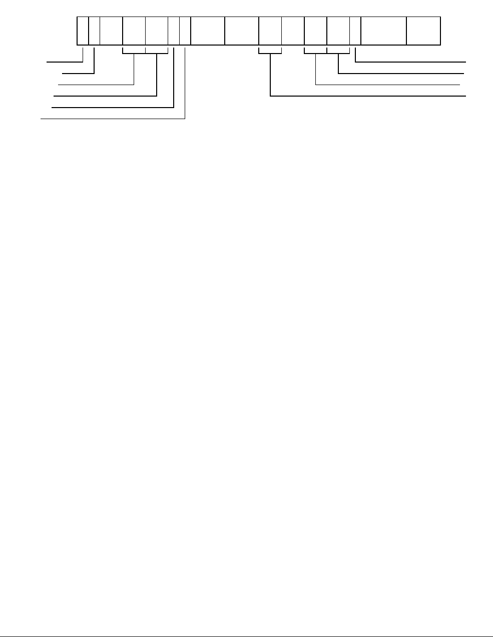
G4 AArch32 System Register Descriptions
G4.2 General system control registers
ARM DDI 0487A.a Copyright © 2013 ARM Limited. All rights reserved. G4-4081
ID090413 Non-Confidential - Beta
When TTBCR.EAE==1:
EAE, bit [31]
Extended Address Enable. The meanings of the possible values of this bit are:
1
Use the 40-bit translation system, with the Long-descriptor translation table format.
Resets to 0.
SH1, bits [29:28]
Shareability attribute for memory associated with translation table walks using TTBR1.
00
Non-shareable
10
Outer Shareable
11
Inner Shareable
Other values are reserved.
Resets to 0.
ORGN1, bits [27:26]
Outer cacheability attribute for memory associated with translation table walks using TTBR1.
00
Normal memory, Outer Non-cacheable
01
Normal memory, Outer Write-Back Write-Allocate Cacheable
10
Normal memory, Outer Write-Through Cacheable
11
Normal memory, Outer Write-Back no Write-Allocate Cacheable
Resets to 0.
IRGN1, bits [25:24]
Inner cacheability attribute for memory associated with translation table walks using TTBR1.
00
Normal memory, Inner Non-cacheable
01
Normal memory, Inner Write-Back Write-Allocate Cacheable
10
Normal memory, Inner Write-Through Cacheable
11
Normal memory, Inner Write-Back no Write-Allocate Cacheable
Resets to 0.
EPD1, bit [23]
Translation table walk disable for translations using TTBR1. This bit controls whether a translation
table walk is performed on a TLB miss, for an address that is translated using TTBR1. The encoding
of this bit is:
0
Perform translation table walks using TTBR1.
1
A TLB miss on an address that is translated using TTBR1 generates a Translation fault.
No translation table walk is performed.
31 30
SH1
29 28 27 26 25 24 23 22
RES0
21 19
T1SZ
18 16 15 14
SH0
13 12 11 10 987
RES0
63
T0SZ
20
EAE
IMP DEF
ORGN1
IRGN1
EPD1
A1
EPD0
IRGN0
ORGN0
RES0

G4 AArch32 System Register Descriptions
G4.2 General system control registers
G4-4082 Copyright © 2013 ARM Limited. All rights reserved. ARM DDI 0487A.a
Non-Confidential - Beta ID090413
Resets to 0.
A1, bit [22]
Selects whether TTBR0 or TTBR1 defines the ASID. The encoding of this bit is:
0
TTBR0.ASID defines the ASID.
1
TTBR1.ASID defines the ASID.
Resets to 0.
Bits [21:19]
Reserved, RES0.
T1SZ, bits [18:16]
The size offset of the memory region addressed by TTBR1. The region size is 232-T1SZ bytes.
Resets to 0.
Bits [15:14]
Reserved, RES0.
SH0, bits [13:12]
Shareability attribute for memory associated with translation table walks using TTBR0.
00
Non-shareable
10
Outer Shareable
11
Inner Shareable
Other values are reserved.
Resets to 0.
ORGN0, bits [11:10]
Outer cacheability attribute for memory associated with translation table walks using TTBR0.
00
Normal memory, Outer Non-cacheable
01
Normal memory, Outer Write-Back Write-Allocate Cacheable
10
Normal memory, Outer Write-Through Cacheable
11
Normal memory, Outer Write-Back no Write-Allocate Cacheable
Resets to 0.
IRGN0, bits [9:8]
Inner cacheability attribute for memory associated with translation table walks using TTBR0.
00
Normal memory, Inner Non-cacheable
01
Normal memory, Inner Write-Back Write-Allocate Cacheable
10
Normal memory, Inner Write-Through Cacheable
11
Normal memory, Inner Write-Back no Write-Allocate Cacheable
Resets to 0.
EPD0, bit [7]
Translation table walk disable for translations using TTBR0. This bit controls whether a translation
table walk is performed on a TLB miss, for an address that is translated using TTBR0. The encoding
of this bit is:
0
Perform translation table walks using TTBR0.
1
A TLB miss on an address that is translated using TTBR0 generates a Translation fault.
No translation table walk is performed.
Resets to 0.

G4 AArch32 System Register Descriptions
G4.2 General system control registers
ARM DDI 0487A.a Copyright © 2013 ARM Limited. All rights reserved. G4-4083
ID090413 Non-Confidential - Beta
Bits [6:3]
Reserved, RES0.
T0SZ, bits [2:0]
The size offset of the memory region addressed by TTBR0. The region size is 232-T0SZ bytes.
Resets to 0.
Accessing the TTBCR:
To access the TTBCR:
MRC p15,0,<Rt>,c2,c0,2 ; Read TTBCR into Rt
MCR p15,0,<Rt>,c2,c0,2 ; Write Rt to TTBCR
Register access is encoded as follows:
coproc opc1 CRn CRm opc2
1111 000 0010 0000 010

G4 AArch32 System Register Descriptions
G4.2 General system control registers
G4-4084 Copyright © 2013 ARM Limited. All rights reserved. ARM DDI 0487A.a
Non-Confidential - Beta ID090413
G4.2.155 TTBR0, Translation Table Base Register 0
The TTBR0 characteristics are:
Purpose
Holds the base address of translation table 0, and information about the memory it occupies. This is
one of the translation tables for the stage 1 translation of memory accesses from modes other than
Hyp mode.
This register is part of the Virtual memory control registers functional group.
Usage constraints
This register is accessible as shown below:
When accessed as TTBR0(S):
When accessed as TTBR0(NS):
Used in conjunction with the TTBCR. When the 64-bit TTBR0 format is used, cacheability and
shareability information is held in the TTBCR, not in TTBR0.
Configurations
TTBR0(NS) is architecturally mapped to AArch64 register TTBR0_EL1.
TTBR0(S) can be mapped to AArch64 register TTBR0_EL3, but this is not architecturally
mandated.
If EL3 is using AArch32, there are separate Secure and Non-secure instances of this register.
The Large Physical Address Extension extends TTBR0 to a 64-bit register. In an implementation
that includes the Large Physical Address Extension, TTBCR.EAE determines which TTBR0 format
is used:
EAE==0
32-bit format is used. TTBR0[63:32] are ignored.
EAE==1
64-bit format is used.
TTBR0 has write access to the Secure copy of the register disabled when the CP15SDISABLE
signal is asserted HIGH.
Attributes
TTBR0 is a 32-bit register when TTBCR.EAE==0 and a 64-bit register when TTBCR.EAE==1.
The TTBR0 bit assignments are:
EL0 (NS) EL0 (S) EL1 (NS) EL1 (S) EL2 EL3 (SCR.NS=1) EL3 (SCR.NS=0)
---RW-- RW
EL0 (NS) EL0 (S) EL1 (NS) EL1 (S) EL2 EL3 (SCR.NS=1) EL3 (SCR.NS=0)
--RW-RWRW -

G4 AArch32 System Register Descriptions
G4.2 General system control registers
ARM DDI 0487A.a Copyright © 2013 ARM Limited. All rights reserved. G4-4085
ID090413 Non-Confidential - Beta
When TTBCR.EAE==0:
TTB0, bits [31:7]
Translation table base 0 address, bits[31:x], where x is 14-(TTBCR.N). Bits [x-1:7] are RES0.
The value of x determines the required alignment of the translation table, which must be aligned to
2x bytes.
If bits [x-1:7] are not all zero, this is a misaligned Translation Table Base Address. Its effects are
CONSTRAINED UNPREDICTABLE, and can be one of the following:
• Bits [x-1:7] are treated as if all the bits are zero. The value read back from those bits might
be the value written or might be zero.
• The calculation of an address for a translation table walk using this register can be corrupted
in those bits that are non-zero.
IRGN[0], bit [6]
See IRGN[1] below for description of the IRGN field.
NOS, bit [5]
Not Outer Shareable bit. Indicates the Outer Shareable attribute for the memory associated with a
translation table walk that has the Shareable attribute, indicated by TTBR0.S == 1:
0
Outer Shareable
1
Inner Shareable.
This bit is ignored when TTBR0.S == 0.
RGN, bits [4:3]
Region bits. Indicates the Outer cacheability attributes for the memory associated with the
translation table walks:
00
Normal memory, Outer Non-cacheable.
01
Normal memory, Outer Write-Back Write-Allocate Cacheable.
10
Normal memory, Outer Write-Through Cacheable.
11
Normal memory, Outer Write-Back no Write-Allocate Cacheable.
IMP, bit [2]
The effect of this bit is IMPLEMENTATION DEFINED. If the translation table implementation does not
include any IMPLEMENTATION DEFINED features this bit is UNK/SBZP.
S, bit [1]
Shareable bit. Indicates the Shareable attribute for the memory associated with the translation table
walks:
0
Non-shareable
1
Shareable.
TTB0
31 7 6 5
RGN
432
S
10
IRGN[1]
IMP
NOS
IRGN[0]

G4 AArch32 System Register Descriptions
G4.2 General system control registers
G4-4086 Copyright © 2013 ARM Limited. All rights reserved. ARM DDI 0487A.a
Non-Confidential - Beta ID090413
IRGN[1], bit [0]
Inner region bits. Indicates the Inner Cacheability attributes for the memory associated with the
translation table walks. The possible values of IRGN[1:0] are:
00
Normal memory, Inner Non-cacheable.
01
Normal memory, Inner Write-Back Write-Allocate Cacheable.
10
Normal memory, Inner Write-Through Cacheable.
11
Normal memory, Inner Write-Back no Write-Allocate Cacheable.
The encoding of the IRGN bits is counter-intuitive, with register bit[6] being IRGN[0] and register
bit[0] being IRGN[1]. This encoding is chosen to give a consistent encoding of memory region
types and to ensure that software written for ARMv7 or later without the Multiprocessing
Extensions can run unmodified on an implementation that includes the Multiprocessing Extensions.
When TTBCR.EAE==1:
Bits [63:56]
Reserved, RES0.
ASID, bits [55:48]
An ASID for the translation table base address. The TTBCR.A1 field selects either TTBR0.ASID
or TTBR1.ASID.
BADDR[47:x], bits [47:0]
Translation table base address, bits[47:x]. Bits [x-1:0] are RES0.
x is based on the value of TTBCR.T0SZ, and is calculated as follows:
• If TTBCR.T0SZ is 0 or 1, x = 5 - TTBCR.T0SZ.
• If TTBCR.T0SZ is greater than 1, x = 14 - TTBCR.T0SZ.
The value of x determines the required alignment of the translation table, which must be aligned to
2x bytes.
If bits [x-1:3] are not all zero, this is a misaligned Translation Table Base Address. Its effects are
CONSTRAINED UNPREDICTABLE, and can be one of the following:
• Bits [x-1:3] are treated as if all the bits are zero. The value read back from those bits might
be the value written or might be zero.
• The calculation of an address for a translation table walk using this register can be corrupted
in those bits that are non-zero.
Accessing the TTBR0:
To access the TTBR0 when TTBCR.EAE==0:
MRC p15,0,<Rt>,c2,c0,0 ; Read TTBR0 into Rt
MCR p15,0,<Rt>,c2,c0,0 ; Write Rt to TTBR0
Register access is encoded as follows:
RES0
63 56
ASID
55 48
BADDR[47:x]
47 0
coproc opc1 CRn CRm opc2
1111 000 0010 0000 000

G4 AArch32 System Register Descriptions
G4.2 General system control registers
ARM DDI 0487A.a Copyright © 2013 ARM Limited. All rights reserved. G4-4087
ID090413 Non-Confidential - Beta
To access the TTBR0 when TTBCR.EAE==1:
MRRC p15,0,<Rt>,<Rt2>,c2 ; Read 64-bit TTBR0 into Rt (low word) and Rt2 (high word)
MCRR p15,0,<Rt>,<Rt2>,c2 ; Write Rt (low word) and Rt2 (high word) to 64-bit TTBR0
Register access is encoded as follows:
coproc opc1 CRm
1111 0000 0010
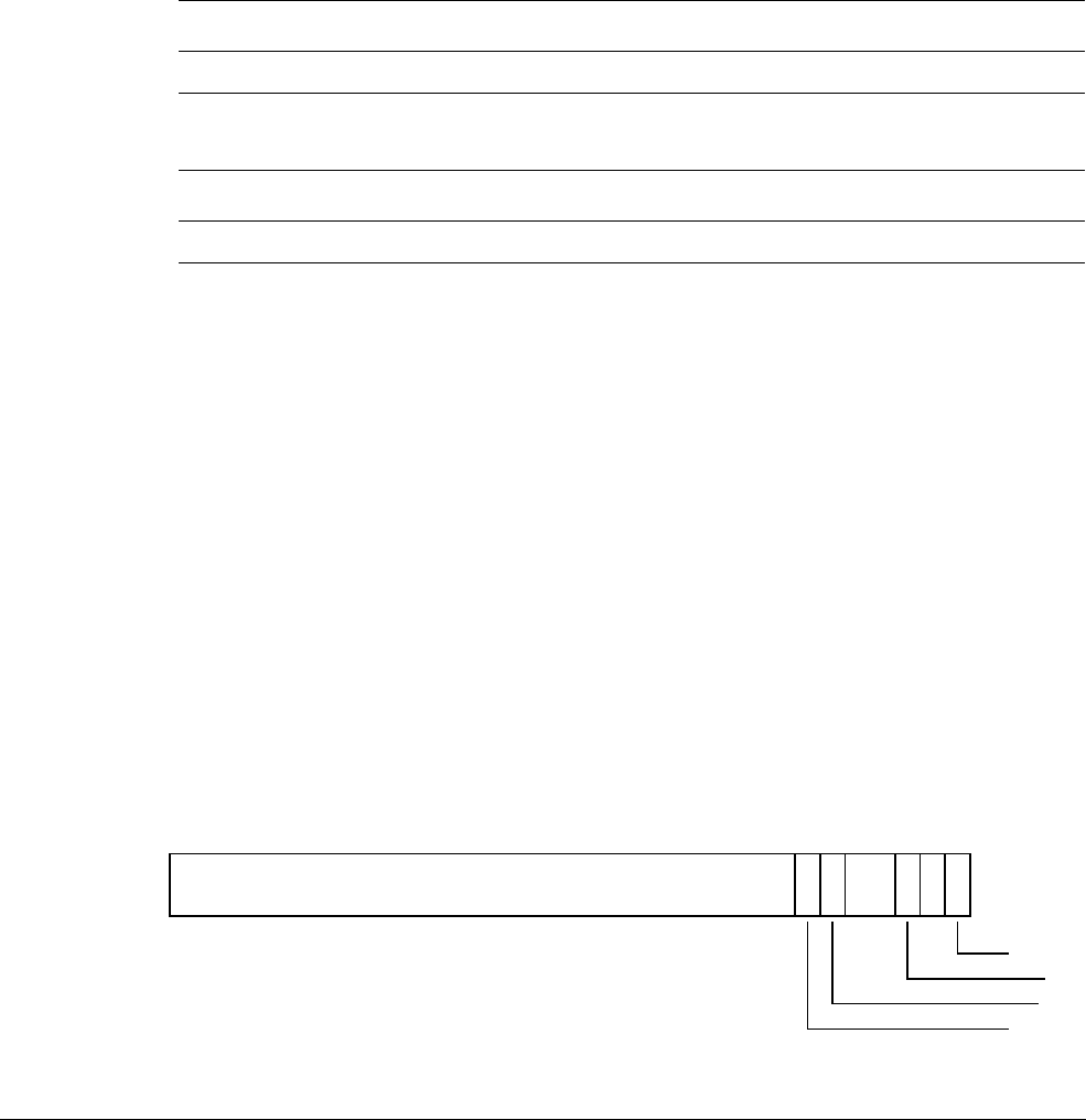
G4 AArch32 System Register Descriptions
G4.2 General system control registers
G4-4088 Copyright © 2013 ARM Limited. All rights reserved. ARM DDI 0487A.a
Non-Confidential - Beta ID090413
G4.2.156 TTBR1, Translation Table Base Register 1
The TTBR1 characteristics are:
Purpose
Holds the base address of translation table 1, and information about the memory it occupies. This is
one of the translation tables for the stage 1 translation of memory accesses from modes other than
Hyp mode.
This register is part of the Virtual memory control registers functional group.
Usage constraints
This register is accessible as shown below:
When accessed as TTBR1(S):
When accessed as TTBR1(NS):
Used in conjunction with the TTBCR. When the 64-bit TTBR1 format is used, cacheability and
shareability information is held in the TTBCR, not in TTBR1.
Configurations
TTBR1(NS) is architecturally mapped to AArch64 register TTBR1_EL1.
If EL3 is using AArch32, there are separate Secure and Non-secure instances of this register.
The Large Physical Address Extension extends TTBR1 to a 64-bit register. In an implementation
that includes the Large Physical Address Extension, TTBCR.EAE determines which TTBR1 format
is used:
EAE==0
32-bit format is used. TTBR1[63:32] are ignored.
EAE==1
64-bit format is used.
Attributes
TTBR1 is a 32-bit register when TTBCR.EAE==0 and a 64-bit register when TTBCR.EAE==1.
The TTBR1 bit assignments are:
When TTBCR.EAE==0:
EL0 (NS) EL0 (S) EL1 (NS) EL1 (S) EL2 EL3 (SCR.NS=1) EL3 (SCR.NS=0)
---RW-- RW
EL0 (NS) EL0 (S) EL1 (NS) EL1 (S) EL2 EL3 (SCR.NS=1) EL3 (SCR.NS=0)
--RW-RWRW -
TTB1
31 7 6 5
RGN
432
S
10
IRGN[1]
IMP
NOS
IRGN[0]

G4 AArch32 System Register Descriptions
G4.2 General system control registers
ARM DDI 0487A.a Copyright © 2013 ARM Limited. All rights reserved. G4-4089
ID090413 Non-Confidential - Beta
TTB1, bits [31:7]
Translation table base 1 address, bits[31:x], where x is 14-(TTBCR.N). Bits [x-1:7] are RES0.
The translation table must be aligned on a 16KByte boundary.
If bits [x-1:7] are not all zero, this is a misaligned Translation Table Base Address. Its effects are
CONSTRAINED UNPREDICTABLE, and can be one of the following:
• Bits [x-1:7] are treated as if all the bits are zero. The value read back from those bits might
be the value written or might be zero.
• The calculation of an address for a translation table walk using this register can be corrupted
in those bits that are non-zero.
IRGN[0], bit [6]
See IRGN[1] below for description of the IRGN field.
NOS, bit [5]
Not Outer Shareable bit. Indicates the Outer Shareable attribute for the memory associated with a
translation table walk that has the Shareable attribute, indicated by TTBR0.S == 1:
0
Outer Shareable
1
Inner Shareable.
This bit is ignored when TTBR0.S == 0.
RGN, bits [4:3]
Region bits. Indicates the Outer cacheability attributes for the memory associated with the
translation table walks:
00
Normal memory, Outer Non-cacheable.
01
Normal memory, Outer Write-Back Write-Allocate Cacheable.
10
Normal memory, Outer Write-Through Cacheable.
11
Normal memory, Outer Write-Back no Write-Allocate Cacheable.
IMP, bit [2]
The effect of this bit is IMPLEMENTATION DEFINED. If the translation table implementation does not
include any IMPLEMENTATION DEFINED features this bit is UNK/SBZP.
S, bit [1]
Shareable bit. Indicates the Shareable attribute for the memory associated with the translation table
walks:
0
Non-shareable
1
Shareable.
IRGN[1], bit [0]
Inner region bits. Indicates the Inner Cacheability attributes for the memory associated with the
translation table walks. The possible values of IRGN[1:0] are:
00
Normal memory, Inner Non-cacheable.
01
Normal memory, Inner Write-Back Write-Allocate Cacheable.
10
Normal memory, Inner Write-Through Cacheable.
11
Normal memory, Inner Write-Back no Write-Allocate Cacheable.
The encoding of the IRGN bits is counter-intuitive, with register bit[6] being IRGN[0] and register
bit[0] being IRGN[1]. This encoding is chosen to give a consistent encoding of memory region
types and to ensure that software written for ARMv7 or later without the Multiprocessing
Extensions can run unmodified on an implementation that includes the Multiprocessing Extensions.

G4 AArch32 System Register Descriptions
G4.2 General system control registers
G4-4090 Copyright © 2013 ARM Limited. All rights reserved. ARM DDI 0487A.a
Non-Confidential - Beta ID090413
When TTBCR.EAE==1:
Bits [63:56]
Reserved, RES0.
ASID, bits [55:48]
An ASID for the translation table base address. The TTBCR.A1 field selects either TTBR0.ASID
or TTBR1.ASID.
BADDR[47:x], bits [47:0]
Translation table base address, bits[47:x]. Bits [x-1:0] are RES0.
x is based on the value of TTBCR.T1SZ, and is calculated as follows:
• If TTBCR.T1SZ is 0 or 1, x = 5 - TTBCR.T1SZ.
• If TTBCR.T1SZ is greater than 1, x = 14 - TTBCR.T1SZ.
The value of x determines the required alignment of the translation table, which must be aligned to
2x bytes.
If bits [x-1:3] are not all zero, this is a misaligned Translation Table Base Address. Its effects are
CONSTRAINED UNPREDICTABLE, and can be one of the following:
• Bits [x-1:3] are treated as if all the bits are zero. The value read back from those bits might
be the value written or might be zero.
• The calculation of an address for a translation table walk using this register can be corrupted
in those bits that are non-zero.
Accessing the TTBR1:
To access the TTBR1 when TTBCR.EAE==0:
MRC p15,0,<Rt>,c2,c0,1 ; Read TTBR1 into Rt
MCR p15,0,<Rt>,c2,c0,1 ; Write Rt to TTBR1
Register access is encoded as follows:
To access the TTBR1 when TTBCR.EAE==1:
MRRC p15,1,<Rt>,<Rt2>,c2 ; Read 64-bit TTBR1 into Rt (low word) and Rt2 (high word)
MCRR p15,1,<Rt>,<Rt2>,c2 ; Write Rt (low word) and Rt2 (high word) to 64-bit TTBR1
Register access is encoded as follows:
RES0
63 56
ASID
55 48
BADDR[47:x]
47 0
coproc opc1 CRn CRm opc2
1111 000 0010 0000 001
coproc opc1 CRm
1111 0001 0010

G4 AArch32 System Register Descriptions
G4.2 General system control registers
ARM DDI 0487A.a Copyright © 2013 ARM Limited. All rights reserved. G4-4091
ID090413 Non-Confidential - Beta
G4.2.157 VBAR, Vector Base Address Register
The VBAR characteristics are:
Purpose
When high exception vectors are not selected, holds the exception base address for exceptions that
are not taken to Monitor mode or to Hyp mode.
This register is part of the Exception and fault handling registers functional group.
Usage constraints
This register is accessible as shown below:
When accessed as VBAR(S):
When accessed as VBAR(NS):
Software must program the Non-secure copy of the register with the required initial value as part of
the processor boot sequence.
Configurations
VBAR(NS) is architecturally mapped to AArch64 register VBAR_EL1[31:0].
VBAR(S) can be mapped to AArch64 register VBAR_EL3[31:0], but this is not architecturally
mandated.
If EL3 is using AArch32, there are separate Secure and Non-secure instances of this register.
VBAR has write access to the Secure copy of the register disabled when the CP15SDISABLE signal
is asserted HIGH.
Attributes
VBAR is a 32-bit register.
The VBAR bit assignments are:
Bits [31:5]
Vector Base Address. Bits[31:5] of the base address of the exception vectors for exceptions taken
in this exception level. Bits[4:0] of an exception vector are the exception offset.
For the Secure copy of this register, the field resets to 0.
For the Non-secure copy of this register, the field reset value is architecturally UNKNOWN.
Bits [4:0]
Reserved, RES0.
EL0 (NS) EL0 (S) EL1 (NS) EL1 (S) EL2 EL3 (SCR.NS=1) EL3 (SCR.NS=0)
---RW-- RW
EL0 (NS) EL0 (S) EL1 (NS) EL1 (S) EL2 EL3 (SCR.NS=1) EL3 (SCR.NS=0)
--RW-RWRW -
Vector Base Address
31 5
RES0
40

G4 AArch32 System Register Descriptions
G4.2 General system control registers
G4-4092 Copyright © 2013 ARM Limited. All rights reserved. ARM DDI 0487A.a
Non-Confidential - Beta ID090413
Accessing the VBAR:
To access the VBAR:
MRC p15,0,<Rt>,c12,c0,0 ; Read VBAR into Rt
MCR p15,0,<Rt>,c12,c0,0 ; Write Rt to VBAR
Register access is encoded as follows:
coproc opc1 CRn CRm opc2
1111 000 1100 0000 000
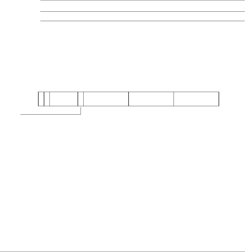
G4 AArch32 System Register Descriptions
G4.2 General system control registers
ARM DDI 0487A.a Copyright © 2013 ARM Limited. All rights reserved. G4-4093
ID090413 Non-Confidential - Beta
G4.2.158 VMPIDR, Virtualization Multiprocessor ID Register
The VMPIDR characteristics are:
Purpose
Holds the value of the Virtualization Multiprocessor ID. This is the value returned by Non-secure
EL1 reads of MPIDR.
This register is part of:
• the Identification registers functional group
• the Virtualization registers functional group.
Usage constraints
This register is accessible as shown below:
Configurations
VMPIDR is architecturally mapped to AArch64 register VMPIDR_EL2[31:0].
If EL2 is not implemented, this register is RES0 from EL3.
Attributes
VMPIDR is a 32-bit register.
The VMPIDR bit assignments are:
M, bit [31]
Indicates whether this implementation includes the Multiprocessing Extensions. The possible
values of this bit are:
0
This implementation does not include the Multiprocessing Extensions.
1
This implementation includes the Multiprocessing Extensions.
In v8-A this bit is RES1.
U, bit [30]
Indicates a Uniprocessor system, as distinct from processor 0 in a multiprocessor system. The
possible values of this bit are:
0
Processor is part of a multiprocessor system.
1
Processor is part of a uniprocessor system.
Resets to an IMPLEMENTATION DEFINED value.
Bits [29:25]
Reserved, RES0.
EL0 (NS) EL0 (S) EL1 (NS) EL1 (S) EL2 EL3 (SCR.NS=1) EL3 (SCR.NS=0)
- - - - RW RW -
M
31
U
30
RES0
29 25 24
Aff2
23 16
Aff1
15 8
Aff0
70
MT

G4 AArch32 System Register Descriptions
G4.2 General system control registers
G4-4094 Copyright © 2013 ARM Limited. All rights reserved. ARM DDI 0487A.a
Non-Confidential - Beta ID090413
MT, bit [24]
Indicates whether the lowest level of affinity consists of logical processors that are implemented
using a multi-threading type approach. The possible values of this bit are:
0
Performance of processors at the lowest affinity level is largely independent.
1
Performance of processors at the lowest affinity level is very interdependent.
Resets to an IMPLEMENTATION DEFINED value.
Aff2, bits [23:16]
Affinity level 2. The least significant affinity level field, for this processor in the system.
Resets to an IMPLEMENTATION DEFINED value.
Aff1, bits [15:8]
Affinity level 1. The intermediate affinity level field, for this processor in the system.
Resets to an IMPLEMENTATION DEFINED value.
Aff0, bits [7:0]
Affinity level 0. The most significant affinity level field, for this processor in the system.
Resets to an IMPLEMENTATION DEFINED value.
Accessing the VMPIDR:
To access the VMPIDR:
MRC p15,4,<Rt>,c0,c0,5 ; Read VMPIDR into Rt
MCR p15,4,<Rt>,c0,c0,5 ; Write Rt to VMPIDR
Register access is encoded as follows:
coproc opc1 CRn CRm opc2
1111 100 0000 0000 101

G4 AArch32 System Register Descriptions
G4.2 General system control registers
ARM DDI 0487A.a Copyright © 2013 ARM Limited. All rights reserved. G4-4095
ID090413 Non-Confidential - Beta
G4.2.159 VPIDR, Virtualization Processor ID Register
The VPIDR characteristics are:
Purpose
Holds the value of the Virtualization Processor ID. This is the value returned by Non-secure EL1
reads of MIDR.
This register is part of:
• the Virtualization registers functional group
• the Identification registers functional group.
Usage constraints
This register is accessible as shown below:
Configurations
VPIDR is architecturally mapped to AArch64 register VPIDR_EL2.
If EL2 is not implemented, this register is RES0 from EL3.
Attributes
VPIDR is a 32-bit register.
The VPIDR bit assignments are:
Implementer, bits [31:24]
The Implementer code. This field must hold an implementer code that has been assigned by ARM.
Assigned codes include the following:
EL0 (NS) EL0 (S) EL1 (NS) EL1 (S) EL2 EL3 (SCR.NS=1) EL3 (SCR.NS=0)
- - - - RW RW -
Implementer
31 24
Variant
23 20 19 16
PartNum
15 4
Revision
30
Architecture
Hex
representation ASCII
representation Implementer
0x41
A ARM Limited
0x42
B Broadcom Corporation
0x43
CCavium Inc.
0x44
D Digital Equipment Corporation
0x49
I Infineon Technologies AG
0x4D
M Motorola or Freescale Semiconductor Inc.
0x4E
N NVIDIA Corporation
0x50
P Applied Micro Circuits Corporation

G4 AArch32 System Register Descriptions
G4.2 General system control registers
G4-4096 Copyright © 2013 ARM Limited. All rights reserved. ARM DDI 0487A.a
Non-Confidential - Beta ID090413
ARM can assign codes that are not published in this manual. All values not assigned by ARM are
reserved and must not be used.
Resets to the value of the equivalent field in MIDR.
Variant, bits [23:20]
An IMPLEMENTATION DEFINED variant number. Typically, this field is used to distinguish between
different product variants, or major revisions of a product.
Resets to the value of the equivalent field in MIDR.
Architecture, bits [19:16]
The permitted values of this field are:
0001
ARMv4
0010
ARMv4T
0011
ARMv5 (obsolete)
0100
ARMv5T
0101
ARMv5TE
0110
ARMv5TEJ
0111
ARMv6
1111
Defined by CPUID scheme
All other values are reserved.
Resets to the value of the equivalent field in MIDR.
PartNum, bits [15:4]
An IMPLEMENTATION DEFINED primary part number for the device.
On processors implemented by ARM, if the top four bits of the primary part number are
0x0
or
0x7
,
the variant and architecture are encoded differently.
Resets to the value of the equivalent field in MIDR.
Revision, bits [3:0]
An IMPLEMENTATION DEFINED revision number for the device.
Resets to the value of the equivalent field in MIDR.
Accessing the VPIDR:
To access the VPIDR:
MRC p15,4,<Rt>,c0,c0,0 ; Read VPIDR into Rt
MCR p15,4,<Rt>,c0,c0,0 ; Write Rt to VPIDR
Register access is encoded as follows:
0x51
Q Qualcomm Inc.
0x56
V Marvell International Ltd.
0x69
i Intel Corporation
coproc opc1 CRn CRm opc2
1111 100 0000 0000 000
Hex
representation ASCII
representation Implementer
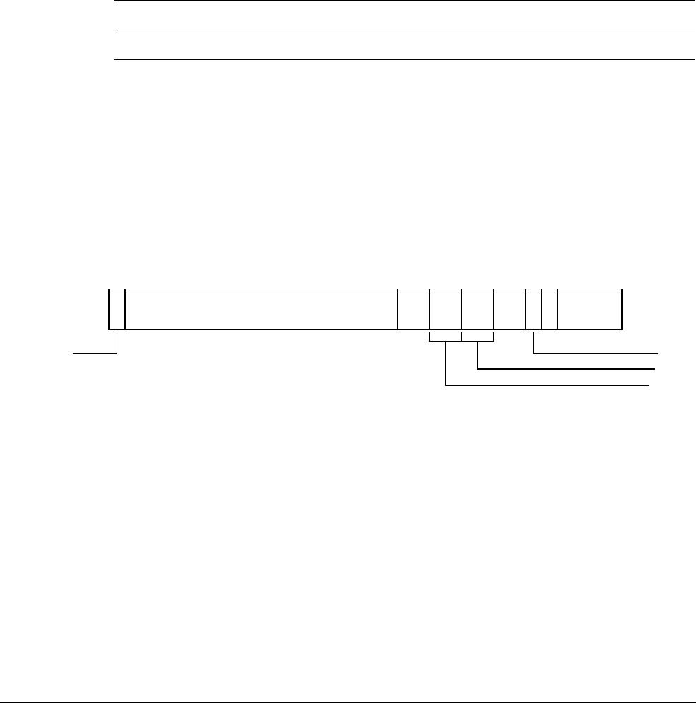
G4 AArch32 System Register Descriptions
G4.2 General system control registers
ARM DDI 0487A.a Copyright © 2013 ARM Limited. All rights reserved. G4-4097
ID090413 Non-Confidential - Beta
G4.2.160 VTCR, Virtualization Translation Control Register
The VTCR characteristics are:
Purpose
Controls the translation table walks required for the stage 2 translation of memory accesses from
Non-secure modes other than Hyp mode, and holds cacheability and shareability information for the
accesses.
This register is part of:
• the Virtualization registers functional group
• the Virtual memory control registers functional group.
Usage constraints
This register is accessible as shown below:
Used in conjunction with VTTBR, that defines the translation table base address for the translations.
Configurations
VTCR is architecturally mapped to AArch64 register VTCR_EL2.
If EL2 is not implemented, this register is RES0 from EL3.
Attributes
VTCR is a 32-bit register.
The VTCR bit assignments are:
Bit [31]
Reserved, RES1.
Bits [30:14]
Reserved, RES0.
SH0, bits [13:12]
Shareability attribute for memory associated with translation table walks using TTBR0.
00
Non-shareable
10
Outer Shareable
11
Inner Shareable
Other values are reserved.
EL0 (NS) EL0 (S) EL1 (NS) EL1 (S) EL2 EL3 (SCR.NS=1) EL3 (SCR.NS=0)
- - - - RW RW -
31
RES0
30 14
SH0
13 12 11 10 98
SL0
765
S
4
T0SZ
30
RES1 RES0
IRGN0
ORGN0

G4 AArch32 System Register Descriptions
G4.2 General system control registers
G4-4098 Copyright © 2013 ARM Limited. All rights reserved. ARM DDI 0487A.a
Non-Confidential - Beta ID090413
ORGN0, bits [11:10]
Outer cacheability attribute for memory associated with translation table walks using TTBR0.
00
Normal memory, Outer Non-cacheable
01
Normal memory, Outer Write-Back Write-Allocate Cacheable
10
Normal memory, Outer Write-Through Cacheable
11
Normal memory, Outer Write-Back no Write-Allocate Cacheable
IRGN0, bits [9:8]
Inner cacheability attribute for memory associated with translation table walks using TTBR0.
00
Normal memory, Inner Non-cacheable
01
Normal memory, Inner Write-Back Write-Allocate Cacheable
10
Normal memory, Inner Write-Through Cacheable
11
Normal memory, Inner Write-Back no Write-Allocate Cacheable
SL0, bits [7:6]
Starting level for translation table walks using VTTBR.
00
Start at second level
01
Start at first level
Other values are reserved.
If the stage 2 input address size, as programmed in VTCR.T0SZ, is out of range with respect to the
starting level at the time of a translation walk that uses the stage 2 translation, then a second stage
level 1 translation fault is generated.
Bit [5]
Reserved, RES0.
S, bit [4]
Sign extension bit. This bit must be programmed to the value of T0SZ[3]. If it is not, then the stage
2 T0SZ value is treated as an UNKNOWN value within the legal range that can be programmed.
T0SZ, bits [3:0]
The size offset of the memory region addressed by TTBR0. The region size is 232-T0SZ bytes.
Accessing the VTCR:
To access the VTCR:
MRC p15,4,<Rt>,c2,c1,2 ; Read VTCR into Rt
MCR p15,4,<Rt>,c2,c1,2 ; Write Rt to VTCR
Register access is encoded as follows:
coproc opc1 CRn CRm opc2
1111 100 0010 0001 010

G4 AArch32 System Register Descriptions
G4.2 General system control registers
ARM DDI 0487A.a Copyright © 2013 ARM Limited. All rights reserved. G4-4099
ID090413 Non-Confidential - Beta
G4.2.161 VTTBR, Virtualization Translation Table Base Register
The VTTBR characteristics are:
Purpose
Holds the base address of the translation table for the stage 2 translation of memory accesses from
Non-secure modes other than Hyp mode.
This register is part of:
• the Virtualization registers functional group
• the Virtual memory control registers functional group.
Usage constraints
This register is accessible as shown below:
Used in conjunction with the VTCR.
Configurations
VTTBR is architecturally mapped to AArch64 register VTTBR_EL2.
If EL2 is not implemented, this register is RES0 from EL3.
Attributes
VTTBR is a 64-bit register.
The VTTBR bit assignments are:
Bits [63:56]
Reserved, RES0.
VMID, bits [55:48]
The VMID for the translation table.
Resets to 0.
BADDR[47:x], bits [47:0]
Translation table base address, bits[47:x]. Bits [x-1:0] are RES0.
x is based on the value of VTCR.T0SZ, and is calculated as follows:
• If VTCR.T0SZ is 0 or 1, x = 5 - VTCR.T0SZ.
• If VTCR.T0SZ is greater than 1, x = 14 - VTCR.T0SZ.
The value of x determines the required alignment of the translation table, which must be aligned to
2x bytes.
If bits [x-1:3] are not all zero, this is a misaligned Translation Table Base Address. Its effects are
CONSTRAINED UNPREDICTABLE, and can be one of the following:
• Bits [x-1:3] are treated as if all the bits are zero. The value read back from those bits might
be the value written or might be zero.
EL0 (NS) EL0 (S) EL1 (NS) EL1 (S) EL2 EL3 (SCR.NS=1) EL3 (SCR.NS=0)
- - - - RW RW -
RES0
63 56
VMID
55 48
BADDR[47:x]
47 0

G4 AArch32 System Register Descriptions
G4.2 General system control registers
G4-4100 Copyright © 2013 ARM Limited. All rights reserved. ARM DDI 0487A.a
Non-Confidential - Beta ID090413
• The calculation of an address for a translation table walk using this register can be corrupted
in those bits that are non-zero.
Reset value is architecturally UNKNOWN.
Accessing the VTTBR:
To access the VTTBR:
MRRC p15,6,<Rt>,<Rt2>,c2 ; Read 64-bit VTTBR into Rt (low word) and Rt2 (high word)
MCRR p15,6,<Rt>,<Rt2>,c2 ; Write Rt (low word) and Rt2 (high word) to 64-bit VTTBR
Register access is encoded as follows:
coproc opc1 CRm
1111 0110 0010

G4 AArch32 System Register Descriptions
G4.3 Debug registers
ARM DDI 0487A.a Copyright © 2013 ARM Limited. All rights reserved. G4-4101
ID090413 Non-Confidential - Beta
G4.3 Debug registers
This section describes the Debug registers in AArch32 state.
G4.3.1 DBGAUTHSTATUS, Debug Authentication Status register
The DBGAUTHSTATUS characteristics are:
Purpose
Provides information about the state of the IMPLEMENTATION DEFINED authentication interface for
debug.
This register is part of the Debug registers functional group.
Usage constraints
This register is accessible as shown below:
Configurations
DBGAUTHSTATUS is architecturally mapped to AArch64 register DBGAUTHSTATUS_EL1.
DBGAUTHSTATUS is architecturally mapped to external register DBGAUTHSTATUS_EL1.
There is one instance of this register that is used in both Secure and Non-secure states.
This register is required in all implementations.
Attributes
DBGAUTHSTATUS is a 32-bit register.
The DBGAUTHSTATUS bit assignments are:
Bits [31:8]
Reserved, RES0.
SNID, bits [7:6]
Secure non-invasive debug. Possible values of this field are:
00
Not implemented. EL3 is not implemented and the processor is Non-secure.
10
Implemented and disabled. ExternalSecureNoninvasiveDebugEnabled() == FALSE.
11
Implemented and enabled. ExternalSecureNoninvasiveDebugEnabled() == TRUE.
Other values are reserved.
EL0 (NS) EL0 (S) EL1 (NS) EL1 (S) EL2 EL3 (SCR.NS=1) EL3 (SCR.NS=0)
- - RO RO RO RO RO
RES0
31 8
SNID
76
SID
5432
NSID
10
NSNID

G4 AArch32 System Register Descriptions
G4.3 Debug registers
G4-4102 Copyright © 2013 ARM Limited. All rights reserved. ARM DDI 0487A.a
Non-Confidential - Beta ID090413
SID, bits [5:4]
Secure invasive debug. Possible values of this field are:
00
Not implemented. EL3 is not implemented and the processor is Non-secure.
10
Implemented and disabled. ExternalSecureInvasiveDebugEnabled() == FALSE.
11
Implemented and enabled. ExternalSecureInvasiveDebugEnabled() == TRUE.
Other values are reserved.
NSNID, bits [3:2]
Non-secure non-invasive debug. Possible values of this field are:
00
Not implemented. EL3 is not implemented and the processor is Secure.
10
Implemented and disabled. ExternalNoninvasiveDebugEnabled() == FALSE.
11
Implemented and enabled. ExternalNoninvasiveDebugEnabled() == TRUE.
Other values are reserved.
NSID, bits [1:0]
Non-secure invasive debug. Possible values of this field are:
00
Not implemented. EL3 is not implemented and the processor is Secure.
10
Implemented and disabled. ExternalInvasiveDebugEnabled() == FALSE.
11
Implemented and enabled. ExternalInvasiveDebugEnabled() == TRUE.
Other values are reserved.
Accessing the DBGAUTHSTATUS:
To access the DBGAUTHSTATUS:
MRC p14,0,<Rt>,c7,c14,6 ; Read DBGAUTHSTATUS into Rt
Register access is encoded as follows:
coproc opc1 CRn CRm opc2
1110 000 0111 1110 110
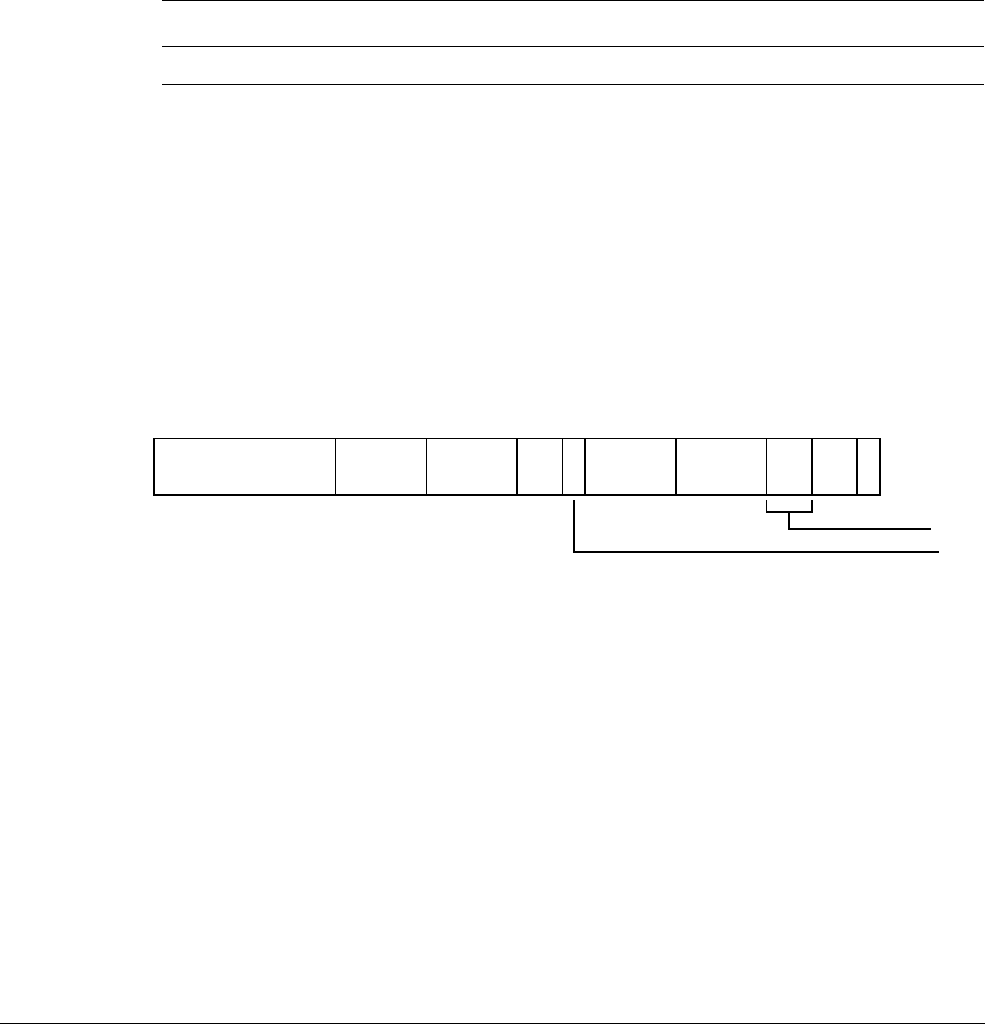
G4 AArch32 System Register Descriptions
G4.3 Debug registers
ARM DDI 0487A.a Copyright © 2013 ARM Limited. All rights reserved. G4-4103
ID090413 Non-Confidential - Beta
G4.3.2 DBGBCR<n>, Debug Breakpoint Control Registers, n = 0 - 15
The DBGBCR<n> characteristics are:
Purpose
Holds control information for a breakpoint. Forms breakpoint n together with value register
DBGBVR<n>, where n is 0 to 15. If EL2 is implemented and this breakpoint supports Context
matching, DBGBVR<n> can be associated with a Breakpoint Extended Value Register
DBGBXVR<n> for VMID matching.
This register is part of the Debug registers functional group.
Usage constraints
This register is accessible as shown below:
When the E field is zero, all the other fields in the register are ignored.
Configurations
DBGBCR<n> is architecturally mapped to AArch64 register DBGBCR<n>_EL1.
DBGBCR<n> is architecturally mapped to external register DBGBCR<n>_EL1.
There is one instance of this register that is used in both Secure and Non-secure states.
Attributes
DBGBCR<n> is a 32-bit register.
The DBGBCR<n> bit assignments are:
Bits [31:24]
Reserved, RES0.
BT, bits [23:20]
Breakpoint Type. Possible values are:
0000
Unlinked instruction address match.
0001
Linked instruction address match.
0010
Unlinked context ID match.
0011
Linked context ID match
0100
Unlinked instruction address mismatch.
0101
Linked instruction address mismatch.
1000
Unlinked VMID match.
1001
Linked VMID match.
1010
Unlinked VMID and context ID match.
EL0 (NS) EL0 (S) EL1 (NS) EL1 (S) EL2 EL3 (SCR.NS=1) EL3 (SCR.NS=0)
- - RW RW RW RW RW
RES0
31 24
BT
23 20
LBN
19 16
SSC
15 14 13
RES0
12 9
BAS
85
43
PMC
21
E
0
RES0
HMC

G4 AArch32 System Register Descriptions
G4.3 Debug registers
G4-4104 Copyright © 2013 ARM Limited. All rights reserved. ARM DDI 0487A.a
Non-Confidential - Beta ID090413
1011
Linked VMID and context ID match.
The field breaks down as follows:
• BT[3:1]: Base type.
000
Match address. DBGBVR<n> is the address of an instruction.
010
Mismatch address. Behaves as type
0b000
if in an AArch64 translation, or if
Halting debug-mode is enabled and halting is allowed. Otherwise, DBGBVR<n>
is the address of an instruction to be stepped.
001
Match context ID. DBGBVR<n> is a context ID.
100
Match VMID. DBGBXVR<n>[7:0] is a VMID.
101
Match VMID and context ID. DBGBVR<n> is a context ID, and
DBGBXVR<n>[7:0] is a VMID.
• BT[0]: Enable linking.
If the breakpoint is not context-aware, BT[3] and BT[1] are RES0. If EL2 is not implemented, BT[3]
is RES0. If EL1 using AArch32 is not implemented, BT[2] is RES0.
The values
011x
and
11xx
are reserved, but must behave as if the breakpoint is disabled. Software
must not rely on this property as the behavior of reserved values might change in a future revision
of the architecture.
On Cold reset, the field reset value is architecturally UNKNOWN.
LBN, bits [19:16]
Linked breakpoint number. For Linked address matching breakpoints, this specifies the index of the
Context-matching breakpoint linked to.
On Cold reset, the field reset value is architecturally UNKNOWN.
SSC, bits [15:14]
Security state control. Determines the security states under which a breakpoint debug event for
breakpoint n is generated. This field must be interpreted along with the HMC and PMC fields.
On Cold reset, the field reset value is architecturally UNKNOWN.
HMC, bit [13]
Higher mode control. Determines the debug perspective for deciding when a breakpoint debug
event for breakpoint n is generated. This field must be interpreted along with the SSC and PMC
fields.
On Cold reset, the field reset value is architecturally UNKNOWN.
Bits [12:9]
Reserved, RES0.
BAS, bits [8:5]
Byte address select. Defines which half-words an address-matching breakpoint matches, regardless
of the instruction set and execution state. In an AArch64-only implementation, this field is reserved,
RES1. Otherwise:
• BAS[2] and BAS[0] are read/write.
• BAS[3] and BAS[1] are read-only copies of BAS[2] and BAS[0] respectively.
The values
0b0011
and
0b1100
are only supported if AArch32 is supported at any exception level.
The permitted values depend on the breakpoint type.

G4 AArch32 System Register Descriptions
G4.3 Debug registers
ARM DDI 0487A.a Copyright © 2013 ARM Limited. All rights reserved. G4-4105
ID090413 Non-Confidential - Beta
For Address match breakpoints:
0b0000
is reserved and must behave as if the breakpoint is disabled or map to a permitted value.
For Address mismatch breakpoints in an AArch32 stage 1 translation regime:
For Context matching breakpoints, this field is RES1 and ignored.
On Cold reset, the field reset value is architecturally UNKNOWN.
Bits [4:3]
Reserved, RES0.
PMC, bits [2:1]
Privilege mode control. Determines the exception level or levels at which a breakpoint debug event
for breakpoint n is generated. This field must be interpreted along with the SSC and HMC fields.
On Cold reset, the field reset value is architecturally UNKNOWN.
E, bit [0]
Enable breakpoint DBGBVR<n>. Possible values are:
0
Breakpoint disabled.
1
Breakpoint enabled.
On Cold reset, the field reset value is architecturally UNKNOWN.
Accessing the DBGBCR<n>:
To access the DBGBCR<n>:
MRC p14,0,<Rt>,c0,<CRm>,5 ; Read DBGBCR<n> into Rt, where n is in the range 0 to 15
MCR p14,0,<Rt>,c0,<CRm>,5 ; Write Rt to DBGBCR<n>, where n is in the range 0 to 15
Register access is encoded as follows:
BAS Match instruction at Constraint for debuggers
0b0011
DBGBVR<n> Use for T32 and T32EE instructions.
0b1100
DBGBVR<n>+2 Use for T32 and T32EE instructions.
0b1111
DBGBVR<n> Use for A32 instructions.
BAS Step instruction at Constraint for debuggers
0b0000
- Use for a match anywhere breakpoint.
0b0011
DBGBVR<n> Use for stepping T32 and T32EE instructions.
0b1100
DBGBVR<n>+2 Use for stepping T32 and T32EE instructions.
0b1111
DBGBVR<n> Use for stepping A32 instructions.
coproc opc1 CRn CRm opc2
1110 000 0000 n<3:0> 101

G4 AArch32 System Register Descriptions
G4.3 Debug registers
G4-4106 Copyright © 2013 ARM Limited. All rights reserved. ARM DDI 0487A.a
Non-Confidential - Beta ID090413
G4.3.3 DBGBVR<n>, Debug Breakpoint Value Registers, n = 0 - 15
The DBGBVR<n> characteristics are:
Purpose
Holds a value for use in breakpoint matching, either the virtual address of an instruction or a context
ID. Forms breakpoint n together with control register DBGBCR<n>, where n is 0 to 15. If EL2 is
implemented and this breakpoint supports Context matching, DBGBVR<n> can be associated with
a Breakpoint Extended Value Register DBGBXVR<n> for VMID matching.
This register is part of the Debug registers functional group.
Usage constraints
This register is accessible as shown below:
Some breakpoints might not support Context ID comparison. For more information, see the
description of the DBGDIDR.CTX_CMPs field.
Configurations
DBGBVR<n> is architecturally mapped to AArch64 register DBGBVR<n>_EL1[31:0].
DBGBVR<n> is architecturally mapped to external register DBGBVR<n>_EL1[31:0].
There is one instance of this register that is used in both Secure and Non-secure states.
Attributes
DBGBVR<n> is a 32-bit register.
The DBGBVR<n> bit assignments are:
When DBGBCR<n>.BT==0b0x0x:
VA[31:2], bits [31:2]
Bits[31:2] of the address value for comparison.
On Cold reset, the field reset value is architecturally UNKNOWN.
Bits [1:0]
Reserved, RES0.
When DBGBCR<n>.BT==0b1x0x:
EL0 (NS) EL0 (S) EL1 (NS) EL1 (S) EL2 EL3 (SCR.NS=1) EL3 (SCR.NS=0)
- - RW RW RW RW RW
VA[31:2]
31 2 10
RES0
RES0
31 0

G4 AArch32 System Register Descriptions
G4.3 Debug registers
ARM DDI 0487A.a Copyright © 2013 ARM Limited. All rights reserved. G4-4107
ID090413 Non-Confidential - Beta
Bits [31:0]
Reserved, RES0.
When DBGBCR<n>.BT==0xxx1x:
ContextID, bits [31:0]
Context ID value for comparison.
On Cold reset, the field reset value is architecturally UNKNOWN.
Accessing the DBGBVR<n>:
To access the DBGBVR<n>:
MRC p14,0,<Rt>,c0,<CRm>,4 ; Read DBGBVR<n> into Rt, where n is in the range 0 to 15
MCR p14,0,<Rt>,c0,<CRm>,4 ; Write Rt to DBGBVR<n>, where n is in the range 0 to 15
Register access is encoded as follows:
ContextID
31 0
coproc opc1 CRn CRm opc2
1110 000 0000 n<3:0> 100

G4 AArch32 System Register Descriptions
G4.3 Debug registers
G4-4108 Copyright © 2013 ARM Limited. All rights reserved. ARM DDI 0487A.a
Non-Confidential - Beta ID090413
G4.3.4 DBGBXVR<n>, Debug Breakpoint Extended Value Registers, n = 0 - 15
The DBGBXVR<n> characteristics are:
Purpose
Holds a value for use in breakpoint matching, to support VMID matching. Used in conjunction with
a control register DBGBCR<n> and a value register DBGBVR<n>, where n is 0 to 15. Used if EL2
is implemented and breakpoint n supports Context matching.
This register is part of the Debug registers functional group.
Usage constraints
This register is accessible as shown below:
Configurations
DBGBXVR<n> is architecturally mapped to AArch64 register DBGBVR<n>_EL1[63:32].
DBGBXVR<n> is architecturally mapped to external register DBGBVR<n>_EL1[63:32].
There is one instance of this register that is used in both Secure and Non-secure states.
Attributes
DBGBXVR<n> is a 32-bit register.
The DBGBXVR<n> bit assignments are:
When DBGBCR<n>.BT==0b0xxx:
Bits [31:0]
Reserved, RES0.
When DBGBCR<n>.BT==0b1xxx and EL2 implemented:
Bits [31:8]
Reserved, RES0.
VMID, bits [7:0]
VMID value for comparison.
On Cold reset, the field reset value is architecturally UNKNOWN.
EL0 (NS) EL0 (S) EL1 (NS) EL1 (S) EL2 EL3 (SCR.NS=1) EL3 (SCR.NS=0)
- - RW RW RW RW RW
RES0
31 0
RES0
31 8
VMID
70

G4 AArch32 System Register Descriptions
G4.3 Debug registers
ARM DDI 0487A.a Copyright © 2013 ARM Limited. All rights reserved. G4-4109
ID090413 Non-Confidential - Beta
Accessing the DBGBXVR<n>:
To access the DBGBXVR<n>:
MRC p14,0,<Rt>,c1,<CRm>,1 ; Read DBGBXVR<n> into Rt, where n is in the range 0 to 15
MCR p14,0,<Rt>,c1,<CRm>,1 ; Write Rt to DBGBXVR<n>, where n is in the range 0 to 15
Register access is encoded as follows:
coproc opc1 CRn CRm opc2
1110 000 0001 n<3:0> 001

G4 AArch32 System Register Descriptions
G4.3 Debug registers
G4-4110 Copyright © 2013 ARM Limited. All rights reserved. ARM DDI 0487A.a
Non-Confidential - Beta ID090413
G4.3.5 DBGCLAIMCLR, Debug Claim Tag Clear register
The DBGCLAIMCLR characteristics are:
Purpose
Used by software to read the values of the CLAIM bits, and to clear these bits to 0.
This register is part of the Debug registers functional group.
Usage constraints
This register is accessible as shown below:
The architecture does not define any functionality for the CLAIM bits.
Used in conjunction with the DBGCLAIMSET register.
Configurations
DBGCLAIMCLR is architecturally mapped to AArch64 register DBGCLAIMCLR_EL1.
DBGCLAIMCLR is architecturally mapped to external register DBGCLAIMCLR_EL1.
There is one instance of this register that is used in both Secure and Non-secure states.
This register is required in all implementations. An implementation must include 8 CLAIM tag bits.
Attributes
DBGCLAIMCLR is a 32-bit register.
The DBGCLAIMCLR bit assignments are:
Bits [31:8]
Reserved, RAZ/SBZ. Software can rely on these bits reading as zero, and must use a should-be-zero
policy on writes. Implementations must ignore writes.
CLAIM, bits [7:0]
Claim clear bits. Reading this field returns the current value of the CLAIM bits.
Writing a 1 to one of these bits clears the corresponding CLAIM bit to 0. This is an indirect write
to the CLAIM bits.
A single write operation can clear multiple bits to 0. Writing 0 to one of these bits has no effect.
On Cold reset, the field resets to 0.
Accessing the DBGCLAIMCLR:
To access the DBGCLAIMCLR:
MRC p14,0,<Rt>,c7,c9,6 ; Read DBGCLAIMCLR into Rt
MCR p14,0,<Rt>,c7,c9,6 ; Write Rt to DBGCLAIMCLR
EL0 (NS) EL0 (S) EL1 (NS) EL1 (S) EL2 EL3 (SCR.NS=1) EL3 (SCR.NS=0)
- - RW RW RW RW RW
RAZ/SBZ
31 8
CLAIM
70

G4 AArch32 System Register Descriptions
G4.3 Debug registers
ARM DDI 0487A.a Copyright © 2013 ARM Limited. All rights reserved. G4-4111
ID090413 Non-Confidential - Beta
Register access is encoded as follows:
coproc opc1 CRn CRm opc2
1110 000 0111 1001 110

G4 AArch32 System Register Descriptions
G4.3 Debug registers
G4-4112 Copyright © 2013 ARM Limited. All rights reserved. ARM DDI 0487A.a
Non-Confidential - Beta ID090413
G4.3.6 DBGCLAIMSET, Debug Claim Tag Set register
The DBGCLAIMSET characteristics are:
Purpose
Used by software to set CLAIM bits to 1.
This register is part of the Debug registers functional group.
Usage constraints
This register is accessible as shown below:
The architecture does not define any functionality for the CLAIM bits.
Used in conjunction with the DBGCLAIMCLR register.
Configurations
DBGCLAIMSET is architecturally mapped to AArch64 register DBGCLAIMSET_EL1.
DBGCLAIMSET is architecturally mapped to external register DBGCLAIMSET_EL1.
There is one instance of this register that is used in both Secure and Non-secure states.
This register is required in all implementations. An implementation must include 8 CLAIM tag bits.
Attributes
DBGCLAIMSET is a 32-bit register.
The DBGCLAIMSET bit assignments are:
Bits [31:8]
Reserved, RAZ/SBZ. Software can rely on these bits reading as zero, and must use a should-be-zero
policy on writes. Implementations must ignore writes.
CLAIM, bits [7:0]
Claim set bits. RAO.
Writing a 1 to one of these bits sets the corresponding CLAIM bit to 1. This is an indirect write to
the CLAIM bits.
A single write operation can set multiple bits to 1. Writing 0 to one of these bits has no effect.
Accessing the DBGCLAIMSET:
To access the DBGCLAIMSET:
MRC p14,0,<Rt>,c7,c8,6 ; Read DBGCLAIMSET into Rt
MCR p14,0,<Rt>,c7,c8,6 ; Write Rt to DBGCLAIMSET
EL0 (NS) EL0 (S) EL1 (NS) EL1 (S) EL2 EL3 (SCR.NS=1) EL3 (SCR.NS=0)
- - RW RW RW RW RW
RAZ/SBZ
31 8
CLAIM
70

G4 AArch32 System Register Descriptions
G4.3 Debug registers
ARM DDI 0487A.a Copyright © 2013 ARM Limited. All rights reserved. G4-4113
ID090413 Non-Confidential - Beta
Register access is encoded as follows:
coproc opc1 CRn CRm opc2
1110 000 0111 1000 110

G4 AArch32 System Register Descriptions
G4.3 Debug registers
G4-4114 Copyright © 2013 ARM Limited. All rights reserved. ARM DDI 0487A.a
Non-Confidential - Beta ID090413
G4.3.7 DBGDCCINT, DCC Interrupt Enable Register
The DBGDCCINT characteristics are:
Purpose
Enables interrupt requests to be signaled based on the DCC status flags.
This register is part of the Debug registers functional group.
Usage constraints
This register is accessible as shown below:
Configurations
DBGDCCINT is architecturally mapped to AArch64 register MDCCINT_EL1.
There is one instance of this register that is used in both Secure and Non-secure states.
Attributes
DBGDCCINT is a 32-bit register.
The DBGDCCINT bit assignments are:
Bit [31]
Reserved, RES0.
RX, bit [30]
DCC interrupt request enable control for DTRRX. Enables a common COMMIRQ interrupt request
to be signaled based on the DCC status flags.
0
No interrupt request generated by DTRRX.
1
Interrupt request will be generated on RXfull == 1.
If legacy COMMRX and COMMTX signals are implemented, then these are not affected by the
value of this bit.
On Warm reset, the field resets to 0.
TX, bit [29]
DCC interrupt request enable control for DTRTX. Enables a common COMMIRQ interrupt request
to be signaled based on the DCC status flags.
0
No interrupt request generated by DTRTX.
1
Interrupt request will be generated on TXfull == 0.
If legacy COMMRX and COMMTX signals are implemented, then these are not affected by the
value of this bit.
On Warm reset, the field resets to 0.
EL0 (NS) EL0 (S) EL1 (NS) EL1 (S) EL2 EL3 (SCR.NS=1) EL3 (SCR.NS=0)
- - RW RW RW RW RW
31
RX
30
TX
29
RES0
28 0
RES0

G4 AArch32 System Register Descriptions
G4.3 Debug registers
ARM DDI 0487A.a Copyright © 2013 ARM Limited. All rights reserved. G4-4115
ID090413 Non-Confidential - Beta
Bits [28:0]
Reserved, RES0.
Accessing the DBGDCCINT:
To access the DBGDCCINT:
MRC p14,0,<Rt>,c0,c2,0 ; Read DBGDCCINT into Rt
MCR p14,0,<Rt>,c0,c2,0 ; Write Rt to DBGDCCINT
Register access is encoded as follows:
coproc opc1 CRn CRm opc2
1110 000 0000 0010 000
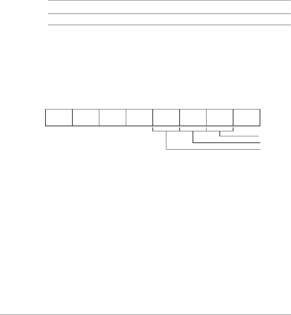
G4 AArch32 System Register Descriptions
G4.3 Debug registers
G4-4116 Copyright © 2013 ARM Limited. All rights reserved. ARM DDI 0487A.a
Non-Confidential - Beta ID090413
G4.3.8 DBGDEVID, Debug Device ID register 0
The DBGDEVID characteristics are:
Purpose
Adds to the information given by the DBGDIDR by describing other features of the debug
implementation.
This register is part of the Debug registers functional group.
Usage constraints
This register is accessible as shown below:
Configurations
There is one instance of this register that is used in both Secure and Non-secure states.
This register is required in all implementations.
Attributes
DBGDEVID is a 32-bit register.
The DBGDEVID bit assignments are:
CIDMask, bits [31:28]
Indicates the level of support for the Context ID matching breakpoint masking capability. Permitted
values of this field are:
0000
Context ID masking is not implemented.
0001
Context ID masking is implemented.
All other values are reserved. The value of this for v8-A is
0b0000
.
AuxRegs, bits [27:24]
Indicates support for Auxiliary registers. Permitted values for this field are:
0000
None supported.
0001
Support for External Debug Auxiliary Control Register, EDACR.
All other values are reserved.
DoubleLock, bits [23:20]
Indicates the presence of the DBGOSDLR, OS Double Lock Register. Permitted values of this field
are:
0000
The DBGOSDLR is not present.
0001
The DBGOSDLR is present.
All other values are reserved. The value of this for v8-A is
0b0001
.
EL0 (NS) EL0 (S) EL1 (NS) EL1 (S) EL2 EL3 (SCR.NS=1) EL3 (SCR.NS=0)
- - RO RO RO RO RO
CIDMask
31 28
AuxRegs
27 24
DoubleLock
23 20
VirtExtns
19 16 15 12 11 8 74
PCSample
30
WPAddrMask
BPAddrMask
VectorCatch

G4 AArch32 System Register Descriptions
G4.3 Debug registers
ARM DDI 0487A.a Copyright © 2013 ARM Limited. All rights reserved. G4-4117
ID090413 Non-Confidential - Beta
VirtExtns, bits [19:16]
Indicates whether EL2 is implemented. Permitted values of this field are:
0000
EL2 is not implemented.
0001
EL2 is implemented.
All other values are reserved.
VectorCatch, bits [15:12]
Defines the form of Vector catch debug event implemented. Permitted values of this field are:
0000
Address matching vector catch debug event implemented.
0001
Exception matching vector catch debug event implemented.
All other values are reserved.
BPAddrMask, bits [11:8]
Indicates the level of support for the IVA matching breakpoint masking capability. Permitted values
of this field are:
0000
Breakpoint address matching may be implemented. If not implemented,
DBGBCR<n>[28:24] is RAZ/WI.
0001
Breakpoint address matching is implemented.
1111
Breakpoint address matching is not implemented. DBGBCR<n>[28:24] is RES0.
All other values are reserved. The value of this for v8-A is
0b1111
.
WPAddrMask, bits [7:4]
Indicates the level of support for the data VA matching watchpoint masking capability. Permitted
values of this field are:
0000
Watchpoint address matching may be implemented. If not implemented,
DBGWCR<n>.MASK (Address mask) is RAZ/WI.
0001
Watchpoint address matching is implemented.
1111
Watchpoint address matching is not implemented. DBGWCR<n>.MASK (Address
mask) is RES0.
All other values are reserved. The value of this for v8-A is
0b0001
.
PCSample, bits [3:0]
Indicates the level of Sample-based profiling support using external debug registers 40 through 43.
Permitted values of this field in v8-A are:
0000
Architecture-defined form of Sample-based profiling not implemented.
0010
EDPCSR and EDCIDSR are implemented (only permitted if EL3 and EL2 are not
implemented).
0011
EDPCSR, EDCIDSR, and EDVIDSR are implemented.
All other values are reserved.
Accessing the DBGDEVID:
To access the DBGDEVID:
MRC p14,0,<Rt>,c7,c2,7 ; Read DBGDEVID into Rt
Register access is encoded as follows:
coproc opc1 CRn CRm opc2
1110 000 0111 0010 111

G4 AArch32 System Register Descriptions
G4.3 Debug registers
G4-4118 Copyright © 2013 ARM Limited. All rights reserved. ARM DDI 0487A.a
Non-Confidential - Beta ID090413
G4.3.9 DBGDEVID1, Debug Device ID register 1
The DBGDEVID1 characteristics are:
Purpose
Adds to the information given by the DBGDIDR by describing other features of the debug
implementation.
This register is part of the Debug registers functional group.
Usage constraints
This register is accessible as shown below:
Configurations
There is one instance of this register that is used in both Secure and Non-secure states.
This register is required in all implementations.
Attributes
DBGDEVID1 is a 32-bit register.
The DBGDEVID1 bit assignments are:
Bits [31:4]
Reserved, RES0.
PCSROffset, bits [3:0]
This field indicates the offset applied to PC samples returned by reads of EDPCSR. Permitted values
of this field in v8-A are:
0000
EDPCSR not implemented.
In v7-A, this field being
0b0000
can also mean that EDPCSR is implemented and that
values returned by reads have an offset applied and indicate the instruction set state.
This is not a permitted implementation for v8-A.
0010
EDPCSR implemented, and samples have no offset applied and do not sample the
instruction set state in AArch32 state.
Accessing the DBGDEVID1:
To access the DBGDEVID1:
MRC p14,0,<Rt>,c7,c1,7 ; Read DBGDEVID1 into Rt
Register access is encoded as follows:
EL0 (NS) EL0 (S) EL1 (NS) EL1 (S) EL2 EL3 (SCR.NS=1) EL3 (SCR.NS=0)
- - RO RO RO RO RO
RES0
31 4
PCSROffset
30
coproc opc1 CRn CRm opc2
1110 000 0111 0001 111

G4 AArch32 System Register Descriptions
G4.3 Debug registers
ARM DDI 0487A.a Copyright © 2013 ARM Limited. All rights reserved. G4-4119
ID090413 Non-Confidential - Beta
G4.3.10 DBGDEVID2, Debug Device ID register 2
The DBGDEVID2 characteristics are:
Purpose
Reserved for future descriptions of features of the debug implementation.
This register is part of the Debug registers functional group.
Usage constraints
This register is accessible as shown below:
Configurations
There is one instance of this register that is used in both Secure and Non-secure states.
Attributes
DBGDEVID2 is a 32-bit register.
The DBGDEVID2 bit assignments are:
Bits [31:0]
Reserved, RES0.
Accessing the DBGDEVID2:
To access the DBGDEVID2:
MRC p14,0,<Rt>,c7,c0,7 ; Read DBGDEVID2 into Rt
Register access is encoded as follows:
EL0 (NS) EL0 (S) EL1 (NS) EL1 (S) EL2 EL3 (SCR.NS=1) EL3 (SCR.NS=0)
- - RO RO RO RO RO
RES0
31 0
coproc opc1 CRn CRm opc2
1110 000 0111 0000 111

G4 AArch32 System Register Descriptions
G4.3 Debug registers
G4-4120 Copyright © 2013 ARM Limited. All rights reserved. ARM DDI 0487A.a
Non-Confidential - Beta ID090413
G4.3.11 DBGDIDR, Debug ID Register
The DBGDIDR characteristics are:
Purpose
Specifies which version of the Debug architecture is implemented, and some features of the debug
implementation.
This register is part of the Debug registers functional group.
Usage constraints
This register is accessible as shown below:
This register is accessible at EL0 if DBGDSCRext.UDCCdis is set to 0. When it is set to 1, EL0
access to this register is trapped to EL1.
Configurations
There is one instance of this register that is used in both Secure and Non-secure states.
This register is required in all implementations.
If external debug over powerdown is implemented, this register can be implemented in either or
both power domains.
Attributes
DBGDIDR is a 32-bit register.
The DBGDIDR bit assignments are:
WRPs, bits [31:28]
The number of watchpoints implemented, minus 1.
Permitted values of this field are from
0b0001
for 2 implemented watchpoints, to
0b1111
for 16
implemented watchpoints.
The value of
0b0000
is reserved.
If AArch64 is implemented, this field has the same value as ID_AA64DFR0_EL1.WRPs.
BRPs, bits [27:24]
The number of breakpoints implemented, minus 1.
Permitted values of this field are from
0b0001
for 2 implemented breakpoint, to
0b1111
for 16
implemented breakpoints.
The value of
0b0000
is reserved.
If AArch64 is implemented, this field has the same value as ID_AA64DFR0_EL1.BRPs.
EL0 (NS) EL0 (S) EL1 (NS) EL1 (S) EL2 EL3 (SCR.NS=1) EL3 (SCR.NS=0)
Config-RO Config-RO RO RO RO RO RO
WRPs
31 28
BRPs
27 24
CTX_CMPs
23 20
Version
19 16 15 14 13 12
RES0
11 0
SE_imp
RES0
nSUHD_imp
RES1

G4 AArch32 System Register Descriptions
G4.3 Debug registers
ARM DDI 0487A.a Copyright © 2013 ARM Limited. All rights reserved. G4-4121
ID090413 Non-Confidential - Beta
CTX_CMPs, bits [23:20]
The number of breakpoints that can be used for Context matching, minus 1.
Permitted values of this field are from
0b0000
for 1 Context matching breakpoint, to
0b1111
for 16
Context matching breakpoints.
The Context matching breakpoints must be the highest addressed breakpoints. For example, if six
breakpoints are implemented and two are Context matching breakpoints, they must be breakpoints
4 and 5.
If AArch64 is implemented, this field has the same value as ID_AA64DFR0_EL1.CTX_CMPs.
Version, bits [19:16]
The Debug architecture version. The permitted values of this field are:
0001
ARMv6, v6 Debug architecture
0010
ARMv6, v6.1 Debug architecture
0011
ARMv7, v7 Debug architecture, with baseline CP14 registers implemented
0100
ARMv7, v7 Debug architecture, with all CP14 registers implemented
0101
ARMv7, v7.1 Debug architecture.
0110
ARMv8, v8 Debug architecture.
All other values are reserved.
Bit [15]
Reserved, RES1.
nSUHD_imp, bit [14]
In v7-A, was Secure User Halting Debug not implemented.
The value of this bit must match the value of the SE_imp bit.
Bit [13]
Reserved, RES0.
SE_imp, bit [12]
EL3 implemented. The meanings of the values of this bit are:
0
EL3 not implemented.
1
EL3 implemented.
The value of this bit must match the value of the nSUHD_imp bit.
Bits [11:0]
Reserved, RES0.
Accessing the DBGDIDR:
To access the DBGDIDR:
MRC p14,0,<Rt>,c0,c0,0 ; Read DBGDIDR into Rt
Register access is encoded as follows:
coproc opc1 CRn CRm opc2
1110 000 0000 0000 000

G4 AArch32 System Register Descriptions
G4.3 Debug registers
G4-4122 Copyright © 2013 ARM Limited. All rights reserved. ARM DDI 0487A.a
Non-Confidential - Beta ID090413
G4.3.12 DBGDRAR, Debug ROM Address Register
The DBGDRAR characteristics are:
Purpose
Defines the base physical address of a memory-mapped debug component, usually a ROM table that
locates and describes the memory-mapped debug components in the system. However, if this
processor is the only memory-mapped debug component in the system, or the only memory
mapped-debug component visible to this processor, this register defines the base physical address
of this processor's debug registers.
This register is part of the Debug registers functional group.
Usage constraints
This register is accessible as shown below:
This register is accessible at EL0 if DBGDSCRext.UDCCdis is set to 0. When it is set to 1, EL0
access to this register is trapped to EL1.
Configurations
DBGDRAR is architecturally mapped to AArch64 register MDRAR_EL1.
There is one instance of this register that is used in both Secure and Non-secure states.
This register is required in all implementations.
If no memory-mapped debug components are implemented, DBGDRAR.Valid is RES0.
DBGDRAR is accessible either as a 64-bit register (using MRRC) or a 32-bit register (using MRC).
Attributes
DBGDRAR is a 32-bit register when accessing the 32-bit version and a 64-bit register when
accessing the 64-bit version.
The DBGDRAR bit assignments are:
When accessing the 32-bit version:
ROMADDR[31:12], bits [31:12]
Bits[31:12] of the ROM table physical address. Bits [11:0] of the address are zero.
Bits [11:2]
Reserved, RES0.
Valid, bits [1:0]
This field indicates whether the ROM Table address is valid. The permitted values of this field are:
00
ROM Table address is not valid
11
ROM Table address is valid.
Other values are reserved.
EL0 (NS) EL0 (S) EL1 (NS) EL1 (S) EL2 EL3 (SCR.NS=1) EL3 (SCR.NS=0)
Config-RO Config-RO RO RO RO RO RO
ROMADDR[31:12]
31 12
RES0
11 2
Valid
10

G4 AArch32 System Register Descriptions
G4.3 Debug registers
ARM DDI 0487A.a Copyright © 2013 ARM Limited. All rights reserved. G4-4123
ID090413 Non-Confidential - Beta
When accessing the 64-bit version:
Bits [63:48]
Reserved, RES0.
ROMADDR[P-1:12], bits [47:12]
Bits[P-1:12] of the ROM table physical address, where P is the physical address size in bits (up to
48 bits) as stored in ID_AA64MMFR0_EL1. If P is less than 48, bits[47:P] of this register are RES0.
Bits [11:0] of the ROM table physical address are zero.
If EL3 is implemented, ROMADDR is an address in Non-secure memory. Whether the ROM table
is also accessible in Secure memory is IMPLEMENTATION DEFINED.
ARM recommends that bits [P-1:32] are zero in systems that support AArch32 at the highest
exception level.
Bits [11:2]
Reserved, RES0.
Valid, bits [1:0]
This field indicates whether the ROM Table address is valid. The permitted values of this field are:
00
ROM Table address is not valid
11
ROM Table address is valid.
Other values are reserved.
Accessing the DBGDRAR:
To access the DBGDRAR when accessing the 32-bit version:
MRC p14,0,<Rt>,c1,c0,0 ; Read DBGDRAR into Rt
Register access is encoded as follows:
To access the DBGDRAR when accessing the 64-bit version:
MRRC p14,0,<Rt>,<Rt2>,c1 ; Read 64-bit DBGDRAR into Rt (low word) and Rt2 (high word)
Register access is encoded as follows:
RES0
63 48
ROMADDR[P-1:12]
47 12
RES0
11 2
Valid
10
coproc opc1 CRn CRm opc2
1110 000 0001 0000 000
coproc opc1 CRm
1110 0000 0001
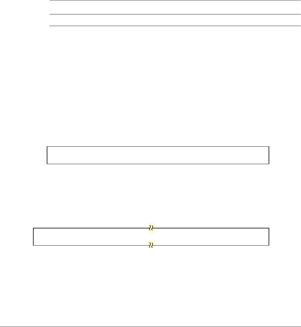
G4 AArch32 System Register Descriptions
G4.3 Debug registers
G4-4124 Copyright © 2013 ARM Limited. All rights reserved. ARM DDI 0487A.a
Non-Confidential - Beta ID090413
G4.3.13 DBGDSAR, Debug Self Address Register
The DBGDSAR characteristics are:
Purpose
Previously defined the offset from the base address defined in DBGDRAR of the physical base
address of the debug registers for the processor. Is now deprecated and RAZ.
This register is part of the Debug registers functional group.
Usage constraints
This register is accessible as shown below:
This register is accessible at EL0 if DBGDSCRext.UDCCdis is set to 0. When it is set to 1, EL0
access to this register is trapped to EL1.
Configurations
There is one instance of this register that is used in both Secure and Non-secure states.
Attributes
DBGDSAR is a 32-bit register when accessing the 32-bit version and a 64-bit register when
accessing the 64-bit version.
The DBGDSAR bit assignments are:
When accessing the 32-bit version:
Bits [31:0]
Reserved, RES0.
When accessing the 64-bit version:
Bits [63:0]
Reserved, RES0.
Accessing the DBGDSAR:
To access the DBGDSAR when accessing the 32-bit version:
MRC p14,0,<Rt>,c2,c0,0 ; Read DBGDSAR into Rt
EL0 (NS) EL0 (S) EL1 (NS) EL1 (S) EL2 EL3 (SCR.NS=1) EL3 (SCR.NS=0)
Config-RO Config-RO RO RO RO RO RO
RES0
31 0
RES0
63 0

G4 AArch32 System Register Descriptions
G4.3 Debug registers
ARM DDI 0487A.a Copyright © 2013 ARM Limited. All rights reserved. G4-4125
ID090413 Non-Confidential - Beta
Register access is encoded as follows:
To access the DBGDSAR when accessing the 64-bit version:
MRRC p14,0,<Rt>,<Rt2>,c2 ; Read 64-bit DBGDSAR into Rt (low word) and Rt2 (high word)
Register access is encoded as follows:
coproc opc1 CRn CRm opc2
1110 000 0010 0000 000
coproc opc1 CRm
1110 0000 0010
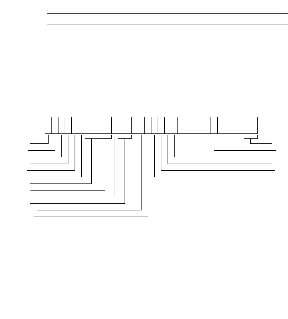
G4 AArch32 System Register Descriptions
G4.3 Debug registers
G4-4126 Copyright © 2013 ARM Limited. All rights reserved. ARM DDI 0487A.a
Non-Confidential - Beta ID090413
G4.3.14 DBGDSCRext, Debug Status and Control Register, External View
The DBGDSCRext characteristics are:
Purpose
Main control register for the debug implementation.
This register is part of the Debug registers functional group.
Usage constraints
This register is accessible as shown below:
Configurations
DBGDSCRext is architecturally mapped to AArch64 register MDSCR_EL1.
There is one instance of this register that is used in both Secure and Non-secure states.
This register is required in all implementations.
Attributes
DBGDSCRext is a 32-bit register.
The DBGDSCRext bit assignments are:
Bit [31]
Reserved, RES0.
RXfull, bit [30]
DTRRX full. Used for save/restore of EDSCR.RXfull.
When DBGOSLSR.OSLK == 0 (the OS lock is unlocked), this bit is RO.
When DBGOSLSR.OSLK == 1 (the OS lock is locked), this bit is RW.
ARM deprecates use of this bit other than for save/restore. Use DBGDSCRint to access the DTRRX
full status.
EL0 (NS) EL0 (S) EL1 (NS) EL1 (S) EL2 EL3 (SCR.NS=1) EL3 (SCR.NS=0)
- - RW RW RW RW RW
31 30 29 28 27 26 25 24 23 22 21 20 19
NS
18 17 16 15 14 13 12
RES0
11 7 6
MOE
52
10
RES0
RXfull
TXfull
RES0
RXO
TXU
RES0
INTdis
TDA
RES0
SPNIDdis
SPIDdis
RES0
ERR
UDCCdis
RES0
HDE
MDBGen

G4 AArch32 System Register Descriptions
G4.3 Debug registers
ARM DDI 0487A.a Copyright © 2013 ARM Limited. All rights reserved. G4-4127
ID090413 Non-Confidential - Beta
TXfull, bit [29]
DTRTX full. Used for save/restore of EDSCR.TXfull.
When DBGOSLSR.OSLK == 0 (the OS lock is unlocked), this bit is RO.
When DBGOSLSR.OSLK == 1 (the OS lock is locked), this bit is RW.
ARM deprecates use of this bit other than for save/restore. Use DBGDSCRint to access the DTRTX
full status.
Bit [28]
Reserved, RES0.
RXO, bit [27]
Used for save/restore of EDSCR.RXO.
When DBGOSLSR.OSLK == 0 (the OS lock is unlocked), this bit is RO. Software must treat it as
UNKNOWN and use an SBZP policy for writes.
When DBGOSLSR.OSLK == 1 (the OS lock is locked), this bit is RW.
TXU, bit [26]
Used for save/restore of EDSCR.TXU.
When DBGOSLSR.OSLK == 0 (the OS lock is unlocked), this bit is RO. Software must treat it as
UNKNOWN and use an SBZP policy for writes.
When DBGOSLSR.OSLK == 1 (the OS lock is locked), this bit is RW.
Bits [25:24]
Reserved, RES0.
INTdis, bits [23:22]
Used for save/restore of EDSCR.INTdis.
When DBGOSLSR.OSLK == 0 (the OS lock is unlocked), this field is RO. Software must treat it
as UNKNOWN and use an SBZP policy for writes.
When DBGOSLSR.OSLK == 1 (the OS lock is locked), this field is RW.
TDA, bit [21]
Used for save/restore of EDSCR.TDA.
When DBGOSLSR.OSLK == 0 (the OS lock is unlocked), this bit is RO. Software must treat it as
UNKNOWN and use an SBZP policy for writes.
When DBGOSLSR.OSLK == 1 (the OS lock is locked), this bit is RW.
Bits [20:19]
Reserved, RES0.
NS, bit [18]
Non-secure status. Returns the inverse of IsSecure(). This bit is RO.
ARM deprecates use of this field.
On Warm reset, the field reset value is architecturally UNKNOWN.
SPNIDdis, bit [17]
Secure privileged profiling disabled status bit. This bit is RO and reflects the value of
ProfilingProhibited(TRUE,EL1). Permitted values are:
0
Profiling allowed in Secure privileged modes.
1
Profiling prohibited in Secure privileged modes.
ARM deprecates use of this field.
On Warm reset, the field reset value is architecturally UNKNOWN.

G4 AArch32 System Register Descriptions
G4.3 Debug registers
G4-4128 Copyright © 2013 ARM Limited. All rights reserved. ARM DDI 0487A.a
Non-Confidential - Beta ID090413
SPIDdis, bit [16]
Secure privileged AArch32 invasive self-hosted debug disabled status bit. This bit is RO and returns
the inverse of DebugSPD32(). Permitted values are:
0
Self-hosted debug enabled in Secure privileged AArch32 modes.
1
Self-hosted debug disabled in Secure privileged AArch32 modes.
ARM deprecates use of this field.
On Warm reset, the field reset value is architecturally UNKNOWN.
MDBGen, bit [15]
Monitor debug events enable. Enable Breakpoint, Watchpoint, and Vector catch debug exceptions.
0
Breakpoint, Watchpoint, and Vector catch debug exceptions disabled.
1
Breakpoint, Watchpoint, and Vector catch debug exceptions enabled.
On Warm reset, the field resets to 0.
HDE, bit [14]
Used for save/restore of EDSCR.HDE.
When DBGOSLSR.OSLK == 0 (the OS lock is unlocked), this bit is RO. Software must treat it as
UNKNOWN and use an SBZP policy for writes.
When DBGOSLSR.OSLK == 1 (the OS lock is locked), this bit is RW.
On Warm reset, the field reset value is architecturally UNKNOWN.
Bit [13]
Reserved, RES0.
UDCCdis, bit [12]
User mode access to Debug Communications Channel disable. When set, then any EL0 access to
DBGDIDR, DBGDRAR, DBGDSAR, DBGDSCRint, DBGDTRTXint, or DBGDTRRXint is
trapped to EL1.
On Warm reset, the field resets to 0.
Bits [11:7]
Reserved, RES0.
ERR, bit [6]
Used for save/restore of EDSCR.ERR.
When DBGOSLSR.OSLK == 0 (the OS lock is unlocked), this bit is RO. Software must treat it as
UNKNOWN and use an SBZP policy for writes.
When DBGOSLSR.OSLK == 1 (the OS lock is locked), this bit is RW.
On Warm reset, the field reset value is architecturally UNKNOWN.
MOE, bits [5:2]
Method of Entry for debug exception. When a debug exception is taken to an exception level using
AArch32, this field is set to indicate the event that caused the exception:
0001
Breakpoint
0011
Software breakpoint (BKPT) instruction
0101
Vector catch
1010
Watchpoint
On Warm reset, the field reset value is architecturally UNKNOWN.
Bits [1:0]
Reserved, RES0.

G4 AArch32 System Register Descriptions
G4.3 Debug registers
ARM DDI 0487A.a Copyright © 2013 ARM Limited. All rights reserved. G4-4129
ID090413 Non-Confidential - Beta
Accessing the DBGDSCRext:
To access the DBGDSCRext:
MRC p14,0,<Rt>,c0,c2,2 ; Read DBGDSCRext into Rt
MCR p14,0,<Rt>,c0,c2,2 ; Write Rt to DBGDSCRext
Register access is encoded as follows:
coproc opc1 CRn CRm opc2
1110 000 0000 0010 010

G4 AArch32 System Register Descriptions
G4.3 Debug registers
G4-4130 Copyright © 2013 ARM Limited. All rights reserved. ARM DDI 0487A.a
Non-Confidential - Beta ID090413
G4.3.15 DBGDSCRint, Debug Status and Control Register, Internal View
The DBGDSCRint characteristics are:
Purpose
Main control register for the debug implementation. This is an internal, read-only view.
This register is part of the Debug registers functional group.
Usage constraints
This register is accessible as shown below:
This register can be read at EL0 when DBGDSCRext.UDCCdis is set to 0. When it is set to 1, EL0
access to this register is trapped to EL1.
Configurations
DBGDSCRint is architecturally mapped to AArch64 register MDCCSR_EL0.
There is one instance of this register that is used in both Secure and Non-secure states.
This register is required in all implementations.
DBGDSCRint.{NS, SPNIDdis, SPIDdis, MDBGen, UDCCdis, MOE} are UNKNOWN when the
register is accessed at EL0. However, although these values are not accessible at EL0 by instructions
that are neither UNPREDICTABLE nor return UNKNOWN values, it is permissible for an
implementation to return the values of DBGDSCRext.{NS, SPNIDdis, SPIDdis, MDBGen,
UDCCdis, MOE} for these fields at EL0.
It is also permissible for an implementation to return the same values as defined for a read of
DBGDSCRint at EL1 or above. (This is the case even if the implementation does not support
AArch32 at EL1 or above.)
Attributes
DBGDSCRint is a 32-bit register.
The DBGDSCRint bit assignments are:
Bit [31]
Reserved, RES0.
RXfull, bit [30]
DTRRX full. Read-only view of the equivalent bit in the EDSCR.
TXfull, bit [29]
DTRTX full. Read-only view of the equivalent bit in the EDSCR.
EL0 (NS) EL0 (S) EL1 (NS) EL1 (S) EL2 EL3 (SCR.NS=1) EL3 (SCR.NS=0)
Config-RO Config-RO RO RO RO RO RO
31 30 29
RES0
28 19
NS
18 17 16 15 14 13 12
RES0
11 6
MOE
52
10
RES0
RXfull
TXfull
SPNIDdis
SPIDdis
RES0
UDCCdis
RES0
MDBGen

G4 AArch32 System Register Descriptions
G4.3 Debug registers
ARM DDI 0487A.a Copyright © 2013 ARM Limited. All rights reserved. G4-4131
ID090413 Non-Confidential - Beta
Bits [28:19]
Reserved, RES0.
NS, bit [18]
Non-secure status.
Read-only view of the equivalent bit in the DBGDSCRext. ARM deprecates use of this field.
SPNIDdis, bit [17]
Secure privileged non-invasive debug disable.
Read-only view of the equivalent bit in the DBGDSCRext. ARM deprecates use of this field.
SPIDdis, bit [16]
Secure privileged invasive debug disable.
Read-only view of the equivalent bit in the DBGDSCRext. ARM deprecates use of this field.
MDBGen, bit [15]
Monitor debug events enable.
Read-only view of the equivalent bit in the DBGDSCRext.
Bits [14:13]
Reserved, RES0.
UDCCdis, bit [12]
User mode access to Debug Communications Channel disable.
Read-only view of the equivalent bit in the DBGDSCRext. ARM deprecates use of this field.
Bits [11:6]
Reserved, RES0.
MOE, bits [5:2]
Method of Entry for debug exception. When a debug exception is taken to an exception level using
AArch32, this field is set to indicate the event that caused the exception:
0001
Breakpoint
0011
Software breakpoint (BKPT) instruction
0101
Vector catch
1010
Watchpoint
Read-only view of the equivalent bit in the DBGDSCRext.
Bits [1:0]
Reserved, RES0.
Accessing the DBGDSCRint:
To access the DBGDSCRint:
MRC p14,0,<Rt>,c0,c1,0 ; Read DBGDSCRint into Rt, where Rt can be R0-R14 or APSR_nzcv. The last form
writes bits[31:28] of the transferred value to the N, Z, C and V condition flags and is specified by
setting the RT field of the encoding to 0b1111.
Register access is encoded as follows:
coproc opc1 CRn CRm opc2
1110 000 0000 0001 000

G4 AArch32 System Register Descriptions
G4.3 Debug registers
G4-4132 Copyright © 2013 ARM Limited. All rights reserved. ARM DDI 0487A.a
Non-Confidential - Beta ID090413
G4.3.16 DBGDTRRXext, Debug Data Transfer Register, Receive, External View
The DBGDTRRXext characteristics are:
Purpose
Used for save/restore of DBGDTRRXint. It is a component of the Debug Communications Channel.
This register is part of the Debug registers functional group.
Usage constraints
This register is accessible as shown below:
ARM deprecates reads and writes of DBGDTRRXext through the CP14 interface when the OS lock
is unlocked.
If EDSCR.ITE == 0 when the processor exits Debug state on receiving a Restart request trigger
event, the behavior of any operation issued by a DTR access in memory access mode that has not
completed execution is CONSTRAINED UNPREDICTABLE, and must do one of the following:
• It must complete execution in Debug state before the processor executes the restart sequence.
• It must complete execution in Non-debug state before the processor executes the restart
sequence.
• It must be abandoned. This means that the instruction does not execute. Any registers or
memory accessed by the instruction are left in an UNKNOWN state.
Configurations
DBGDTRRXext is architecturally mapped to AArch64 register OSDTRRX_EL1.
There is one instance of this register that is used in both Secure and Non-secure states.
This register is required in all implementations.
Attributes
DBGDTRRXext is a 32-bit register.
The DBGDTRRXext bit assignments are:
Bits [31:0]
Host to target data. One word of data for transfer from the debug host to the debug target.
For the full behavior of the Debug Communications Channel, see section 9 (The Debug
Communications Channel and Instruction Transfer Register) in document PRD03-PRDC-010486.
On Cold reset, the field reset value is architecturally UNKNOWN.
Accessing the DBGDTRRXext:
To access the DBGDTRRXext:
MRC p14,0,<Rt>,c0,c0,2 ; Read DBGDTRRXext into Rt
MCR p14,0,<Rt>,c0,c0,2 ; Write Rt to DBGDTRRXext
EL0 (NS) EL0 (S) EL1 (NS) EL1 (S) EL2 EL3 (SCR.NS=1) EL3 (SCR.NS=0)
- - RW RW RW RW RW
Host to target data
31 0

G4 AArch32 System Register Descriptions
G4.3 Debug registers
ARM DDI 0487A.a Copyright © 2013 ARM Limited. All rights reserved. G4-4133
ID090413 Non-Confidential - Beta
Register access is encoded as follows:
coproc opc1 CRn CRm opc2
1110 000 0000 0000 010

G4 AArch32 System Register Descriptions
G4.3 Debug registers
G4-4134 Copyright © 2013 ARM Limited. All rights reserved. ARM DDI 0487A.a
Non-Confidential - Beta ID090413
G4.3.17 DBGDTRRXint, Debug Data Transfer Register, Receive, Internal View
The DBGDTRRXint characteristics are:
Purpose
Transfers data from an external host to the ARM processor. For example, it is used by a debugger
transferring commands and data to a debug target. It is a component of the Debug Communications
Channel.
This register is part of the Debug registers functional group.
Usage constraints
This register is accessible as shown below:
This register can be read at EL0 when DBGDSCRint.UDCCdis is set to 0. When it is set to 1, EL0
access to this register is trapped to EL1.
If EDSCR.ITE == 0 when the processor exits Debug state on receiving a Restart request trigger
event, the behavior of any operation issued by a DTR access in memory access mode that has not
completed execution is CONSTRAINED UNPREDICTABLE, and must do one of the following:
• It must complete execution in Debug state before the processor executes the restart sequence.
• It must complete execution in Non-debug state before the processor executes the restart
sequence.
• It must be abandoned. This means that the instruction does not execute. Any registers or
memory accessed by the instruction are left in an UNKNOWN state.
Configurations
DBGDTRRXint is architecturally mapped to AArch64 register DBGDTRRX_EL0.
DBGDTRRXint is architecturally mapped to external register DBGDTRRX_EL0.
There is one instance of this register that is used in both Secure and Non-secure states.
This register is required in all implementations.
Attributes
DBGDTRRXint is a 32-bit register.
The DBGDTRRXint bit assignments are:
Bits [31:0]
Host to target data. One word of data for transfer from the debug host to the debug target.
For the full behavior of the Debug Communications Channel, see section 9 (The Debug
Communications Channel and Instruction Transfer Register) in document PRD03-PRDC-010486.
On Cold reset, the field reset value is architecturally UNKNOWN.
Accessing the DBGDTRRXint:
To access the DBGDTRRXint:
EL0 (NS) EL0 (S) EL1 (NS) EL1 (S) EL2 EL3 (SCR.NS=1) EL3 (SCR.NS=0)
Config-RO Config-RO RO RO RO RO RO
Host to target data
31 0

G4 AArch32 System Register Descriptions
G4.3 Debug registers
ARM DDI 0487A.a Copyright © 2013 ARM Limited. All rights reserved. G4-4135
ID090413 Non-Confidential - Beta
MRC p14,0,<Rt>,c0,c5,0 ; Read DBGDTRRXint into Rt
Register access is encoded as follows:
coproc opc1 CRn CRm opc2
1110 000 0000 0101 000

G4 AArch32 System Register Descriptions
G4.3 Debug registers
G4-4136 Copyright © 2013 ARM Limited. All rights reserved. ARM DDI 0487A.a
Non-Confidential - Beta ID090413
G4.3.18 DBGDTRTXext, Debug Data Transfer Register, Transmit, External View
The DBGDTRTXext characteristics are:
Purpose
Used for save/restore of DBGDTRTXint. It is a component of the Debug Communication Channel.
This register is part of the Debug registers functional group.
Usage constraints
This register is accessible as shown below:
ARM deprecates reads and writes of DBGDTRTXext through the CP14 interface when the OS Lock
is unlocked.
If EDSCR.ITE == 0 when the processor exits Debug state on receiving a Restart request trigger
event, the behavior of any operation issued by a DTR access in memory access mode that has not
completed execution is CONSTRAINED UNPREDICTABLE, and must do one of the following:
• It must complete execution in Debug state before the processor executes the restart sequence.
• It must complete execution in Non-debug state before the processor executes the restart
sequence.
• It must be abandoned. This means that the instruction does not execute. Any registers or
memory accessed by the instruction are left in an UNKNOWN state.
Configurations
DBGDTRTXext is architecturally mapped to AArch64 register OSDTRTX_EL1.
There is one instance of this register that is used in both Secure and Non-secure states.
This register is required in all implementations.
Attributes
DBGDTRTXext is a 32-bit register.
The DBGDTRTXext bit assignments are:
Bits [31:0]
Target to host data. One word of data for transfer from the debug target to the debug host.
For the full behavior of the Debug Communications Channel, see section 9 (The Debug
Communications Channel and Instruction Transfer Register) in document PRD03-PRDC-010486.
On Cold reset, the field reset value is architecturally UNKNOWN.
Accessing the DBGDTRTXext:
To access the DBGDTRTXext:
MRC p14,0,<Rt>,c0,c3,2 ; Read DBGDTRTXext into Rt
MCR p14,0,<Rt>,c0,c3,2 ; Write Rt to DBGDTRTXext
EL0 (NS) EL0 (S) EL1 (NS) EL1 (S) EL2 EL3 (SCR.NS=1) EL3 (SCR.NS=0)
- - RW RW RW RW RW
Target to host data
31 0

G4 AArch32 System Register Descriptions
G4.3 Debug registers
ARM DDI 0487A.a Copyright © 2013 ARM Limited. All rights reserved. G4-4137
ID090413 Non-Confidential - Beta
Register access is encoded as follows:
coproc opc1 CRn CRm opc2
1110 000 0000 0011 010

G4 AArch32 System Register Descriptions
G4.3 Debug registers
G4-4138 Copyright © 2013 ARM Limited. All rights reserved. ARM DDI 0487A.a
Non-Confidential - Beta ID090413
G4.3.19 DBGDTRTXint, Debug Data Transfer Register, Transmit, Internal View
The DBGDTRTXint characteristics are:
Purpose
Transfers data from the ARM processor to an external host. For example, it is used by a debug target
to transfer data to the debugger. It is a component of the Debug Communication Channel.
This register is part of the Debug registers functional group.
Usage constraints
This register is accessible as shown below:
This register can be written at EL0 when DBGDSCRint.UDCCdis is set to 0. When it is set to 1,
EL0 access to this register is trapped to EL1.
If EDSCR.ITE == 0 when the processor exits Debug state on receiving a Restart request trigger
event, the behavior of any operation issued by a DTR access in memory access mode that has not
completed execution is CONSTRAINED UNPREDICTABLE, and must do one of the following:
• It must complete execution in Debug state before the processor executes the restart sequence.
• It must complete execution in Non-debug state before the processor executes the restart
sequence.
• It must be abandoned. This means that the instruction does not execute. Any registers or
memory accessed by the instruction are left in an UNKNOWN state.
Configurations
DBGDTRTXint is architecturally mapped to AArch64 register DBGDTRTX_EL0.
DBGDTRTXint is architecturally mapped to external register DBGDTRTX_EL0.
There is one instance of this register that is used in both Secure and Non-secure states.
This register is required in all implementations.
Attributes
DBGDTRTXint is a 32-bit register.
The DBGDTRTXint bit assignments are:
Bits [31:0]
Target to host data. One word of data for transfer from the debug target to the debug host.
For the full behavior of the Debug Communications Channel, see section 9 (The Debug
Communications Channel and Instruction Transfer Register) in document PRD03-PRDC-010486.
On Cold reset, the field reset value is architecturally UNKNOWN.
Accessing the DBGDTRTXint:
To access the DBGDTRTXint:
MCR p14,0,<Rt>,c0,c5,0 ; Write Rt to DBGDTRTXint
EL0 (NS) EL0 (S) EL1 (NS) EL1 (S) EL2 EL3 (SCR.NS=1) EL3 (SCR.NS=0)
Config-WO Config-WO WO WO WO WO WO
Target to host data
31 0

G4 AArch32 System Register Descriptions
G4.3 Debug registers
ARM DDI 0487A.a Copyright © 2013 ARM Limited. All rights reserved. G4-4139
ID090413 Non-Confidential - Beta
Register access is encoded as follows:
coproc opc1 CRn CRm opc2
1110 000 0000 0101 000

G4 AArch32 System Register Descriptions
G4.3 Debug registers
G4-4140 Copyright © 2013 ARM Limited. All rights reserved. ARM DDI 0487A.a
Non-Confidential - Beta ID090413
G4.3.20 DBGOSDLR, Debug OS Double Lock Register
The DBGOSDLR characteristics are:
Purpose
Locks out the external debug interface.
This register is part of the Debug registers functional group.
Usage constraints
This register is accessible as shown below:
Configurations
DBGOSDLR is architecturally mapped to AArch64 register OSDLR_EL1.
There is one instance of this register that is used in both Secure and Non-secure states.
Attributes
DBGOSDLR is a 32-bit register.
The DBGOSDLR bit assignments are:
Bits [31:1]
Reserved, RES0.
DLK, bit [0]
OS Double Lock control bit. Possible values are:
0
OS Double Lock unlocked.
1
OS Double Lock locked, if DBGPRCR.CORENPDRQ (Core no power-down request)
bit is set to 0 and the processor is in Non-debug state.
On Warm reset, the field resets to 0.
Accessing the DBGOSDLR:
To access the DBGOSDLR:
MRC p14,0,<Rt>,c1,c3,4 ; Read DBGOSDLR into Rt
MCR p14,0,<Rt>,c1,c3,4 ; Write Rt to DBGOSDLR
Register access is encoded as follows:
EL0 (NS) EL0 (S) EL1 (NS) EL1 (S) EL2 EL3 (SCR.NS=1) EL3 (SCR.NS=0)
- - RW RW RW RW RW
RES0
31 1 0
DLK
coproc opc1 CRn CRm opc2
1110 000 0001 0011 100

G4 AArch32 System Register Descriptions
G4.3 Debug registers
ARM DDI 0487A.a Copyright © 2013 ARM Limited. All rights reserved. G4-4141
ID090413 Non-Confidential - Beta
G4.3.21 DBGOSECCR, Debug OS Lock Exception Catch Control Register
The DBGOSECCR characteristics are:
Purpose
Provides a mechanism for an operating system to access the contents of EDECCR that are otherwise
invisible to software, so it can save/restore the contents of EDECCR over powerdown on behalf of
the external debugger.
This register is part of the Debug registers functional group.
Usage constraints
This register is accessible as shown below:
Configurations
DBGOSECCR is architecturally mapped to AArch64 register OSECCR_EL1.
DBGOSECCR is architecturally mapped to external register EDECCR.
There is one instance of this register that is used in both Secure and Non-secure states.
Attributes
DBGOSECCR is a 32-bit register.
The DBGOSECCR bit assignments are:
When OSLSR.OSLK==1:
EDECCR, bits [31:0]
Used for save/restore to EDECCR over powerdown.
Accessing the DBGOSECCR:
To access the DBGOSECCR:
MRC p14,0,<Rt>,c0,c6,2 ; Read DBGOSECCR into Rt
MCR p14,0,<Rt>,c0,c6,2 ; Write Rt to DBGOSECCR
Register access is encoded as follows:
EL0 (NS) EL0 (S) EL1 (NS) EL1 (S) EL2 EL3 (SCR.NS=1) EL3 (SCR.NS=0)
- - RW RW RW RW RW
EDECCR
31 0
coproc opc1 CRn CRm opc2
1110 000 0000 0110 010

G4 AArch32 System Register Descriptions
G4.3 Debug registers
G4-4142 Copyright © 2013 ARM Limited. All rights reserved. ARM DDI 0487A.a
Non-Confidential - Beta ID090413
G4.3.22 DBGOSLAR, Debug OS Lock Access Register
The DBGOSLAR characteristics are:
Purpose
Provides a lock for the debug registers. The OS lock also disables some Software debug events.
This register is part of the Debug registers functional group.
Usage constraints
This register is accessible as shown below:
Configurations
DBGOSLAR is architecturally mapped to AArch64 register OSLAR_EL1.
DBGOSLAR is architecturally mapped to external register OSLAR_EL1.
There is one instance of this register that is used in both Secure and Non-secure states.
Attributes
DBGOSLAR is a 32-bit register.
The DBGOSLAR bit assignments are:
Bits [31:0]
OS Lock Access. Writing the value
0xC5ACCE55
to the DBGOSLAR sets the OS lock to 1. Writing
any other value sets the OS lock to 0.
Use DBGOSLSR.OSLK to check the current status of the lock.
Accessing the DBGOSLAR:
To access the DBGOSLAR:
MCR p14,0,<Rt>,c1,c0,4 ; Write Rt to DBGOSLAR
Register access is encoded as follows:
EL0 (NS) EL0 (S) EL1 (NS) EL1 (S) EL2 EL3 (SCR.NS=1) EL3 (SCR.NS=0)
- - WO WO WO WO WO
OS Lock Access
31 0
coproc opc1 CRn CRm opc2
1110 000 0001 0000 100

G4 AArch32 System Register Descriptions
G4.3 Debug registers
ARM DDI 0487A.a Copyright © 2013 ARM Limited. All rights reserved. G4-4143
ID090413 Non-Confidential - Beta
G4.3.23 DBGOSLSR, Debug OS Lock Status Register
The DBGOSLSR characteristics are:
Purpose
Provides status information for the OS lock.
This register is part of the Debug registers functional group.
Usage constraints
This register is accessible as shown below:
Configurations
DBGOSLSR is architecturally mapped to AArch64 register OSLSR_EL1.
There is one instance of this register that is used in both Secure and Non-secure states.
The OS lock status is also visible in the external debug interface through EDPRSR.
Attributes
DBGOSLSR is a 32-bit register.
The DBGOSLSR bit assignments are:
Bits [31:4]
Reserved, RES0.
OSLM[1], bit [3]
See below for description of the OSLM field.
nTT, bit [2]
Not 32-bit access. This bit is always RAZ. It indicates that a 32-bit access is needed to write the key
to the OS Lock Access Register.
OSLK, bit [1]
OS Lock Status. The possible values are:
0
OS lock unlocked.
1
OS lock locked.
The OS Lock is locked and unlocked by writing to the OS Lock Access Register.
On Cold reset, the field resets to 1.
EL0 (NS) EL0 (S) EL1 (NS) EL1 (S) EL2 EL3 (SCR.NS=1) EL3 (SCR.NS=0)
- - RO RO RO RO RO
RES0
31 4 3 2 1 0
OSLM[0]
OSLK
nTT
OSLM[1]

G4 AArch32 System Register Descriptions
G4.3 Debug registers
G4-4144 Copyright © 2013 ARM Limited. All rights reserved. ARM DDI 0487A.a
Non-Confidential - Beta ID090413
OSLM[0], bit [0]
OS lock model implemented. Identifies the form of OS save and restore mechanism implemented.
In v8-A these bits are as follows:
10
OS lock implemented. DBGOSSRR not implemented.
All other values are reserved.
Accessing the DBGOSLSR:
To access the DBGOSLSR:
MRC p14,0,<Rt>,c1,c1,4 ; Read DBGOSLSR into Rt
Register access is encoded as follows:
coproc opc1 CRn CRm opc2
1110 000 0001 0001 100

G4 AArch32 System Register Descriptions
G4.3 Debug registers
ARM DDI 0487A.a Copyright © 2013 ARM Limited. All rights reserved. G4-4145
ID090413 Non-Confidential - Beta
G4.3.24 DBGPRCR, Debug Power Control Register
The DBGPRCR characteristics are:
Purpose
Controls behavior of processor on power-down request.
This register is part of the Debug registers functional group.
Usage constraints
This register is accessible as shown below:
Configurations
DBGPRCR is architecturally mapped to AArch64 register DBGPRCR_EL1.
There is one instance of this register that is used in both Secure and Non-secure states.
This register is required in all implementations.
Bit [0] of this register is mapped to EDPRCR.CORENPDRQ, bit [0] of the external view of this
register. The other bits in these registers are not mapped to each other.
Attributes
DBGPRCR is a 32-bit register.
The DBGPRCR bit assignments are:
Bits [31:1]
Reserved, RES0.
CORENPDRQ, bit [0]
Core no powerdown request. Requests emulation of powerdown. Possible values of this bit are:
0
On a powerdown request, the system powers down the Core power domain.
1
On a powerdown request, the system emulates powerdown of the Core power domain.
In this emulation mode the Core power domain is not actually powered down.
On Cold reset, the field resets to the value of EDPRCR.COREPURQ.
Accessing the DBGPRCR:
To access the DBGPRCR:
MRC p14,0,<Rt>,c1,c4,4 ; Read DBGPRCR into Rt
MCR p14,0,<Rt>,c1,c4,4 ; Write Rt to DBGPRCR
EL0 (NS) EL0 (S) EL1 (NS) EL1 (S) EL2 EL3 (SCR.NS=1) EL3 (SCR.NS=0)
- - RW RW RW RW RW
RES0
31 1 0
CORENPDRQ

G4 AArch32 System Register Descriptions
G4.3 Debug registers
G4-4146 Copyright © 2013 ARM Limited. All rights reserved. ARM DDI 0487A.a
Non-Confidential - Beta ID090413
Register access is encoded as follows:
coproc opc1 CRn CRm opc2
1110 000 0001 0100 100

G4 AArch32 System Register Descriptions
G4.3 Debug registers
ARM DDI 0487A.a Copyright © 2013 ARM Limited. All rights reserved. G4-4147
ID090413 Non-Confidential - Beta
G4.3.25 DBGVCR, Debug Vector Catch Register
The DBGVCR characteristics are:
Purpose
Controls Vector catch debug events.
This register is part of the Debug registers functional group.
Usage constraints
This register is accessible as shown below:
Configurations
DBGVCR is architecturally mapped to AArch64 register DBGVCR32_EL2.
There is one instance of this register that is used in both Secure and Non-secure states.
This register is required in all implementations.
Attributes
DBGVCR is a 32-bit register.
The DBGVCR bit assignments are:
When EL3 implemented and using AArch32:
NSF, bit [31]
FIQ vector catch enable in Non-secure state.
The exception vector offset is
0x1C
.
On Warm reset, the field reset value is architecturally UNKNOWN.
NSI, bit [30]
IRQ vector catch enable in Non-secure state.
The exception vector offset is
0x18
.
On Warm reset, the field reset value is architecturally UNKNOWN.
EL0 (NS) EL0 (S) EL1 (NS) EL1 (S) EL2 EL3 (SCR.NS=1) EL3 (SCR.NS=0)
- - RW RW RW RW RW
31 30 29 28 27 26 25
RES0
24 16 15
MI
14 13 12 11 10 987
SI
65 4
SP
3
SS
2
SU
10
NSF
NSI
RES0
NSD
NSP
NSS
NSU
RES0
SD
RES0
SF
RES0
MS
MP
MD
RES0
MF

G4 AArch32 System Register Descriptions
G4.3 Debug registers
G4-4148 Copyright © 2013 ARM Limited. All rights reserved. ARM DDI 0487A.a
Non-Confidential - Beta ID090413
Bit [29]
Reserved, RES0.
NSD, bit [28]
Data Abort vector catch enable in Non-secure state.
The exception vector offset is
0x10
.
On Warm reset, the field reset value is architecturally UNKNOWN.
NSP, bit [27]
Prefetch Abort vector catch enable in Non-secure state.
The exception vector offset is
0x0C
.
On Warm reset, the field reset value is architecturally UNKNOWN.
NSS, bit [26]
Supervisor Call (SVC) vector catch enable in Non-secure state.
The exception vector offset is
0x08
.
On Warm reset, the field reset value is architecturally UNKNOWN.
NSU, bit [25]
Undefined Instruction vector catch enable in Non-secure state.
The exception vector offset is
0x04
.
On Warm reset, the field reset value is architecturally UNKNOWN.
Bits [24:16]
Reserved, RES0.
MF, bit [15]
FIQ vector catch enable in Monitor mode.
The exception vector offset is
0x1C
.
On Warm reset, the field reset value is architecturally UNKNOWN.
MI, bit [14]
IRQ vector catch enable in Monitor mode.
The exception vector offset is
0x18
.
On Warm reset, the field reset value is architecturally UNKNOWN.
Bit [13]
Reserved, RES0.
MD, bit [12]
Data Abort vector catch enable in Monitor mode.
The exception vector offset is
0x10
.
On Warm reset, the field reset value is architecturally UNKNOWN.
MP, bit [11]
Prefetch Abort vector catch enable in Monitor mode.
The exception vector offset is
0x0C
.
On Warm reset, the field reset value is architecturally UNKNOWN.
MS, bit [10]
Secure Monitor Call (SMC) vector catch enable in Monitor mode.
The exception vector offset is
0x08
.

G4 AArch32 System Register Descriptions
G4.3 Debug registers
ARM DDI 0487A.a Copyright © 2013 ARM Limited. All rights reserved. G4-4149
ID090413 Non-Confidential - Beta
On Warm reset, the field reset value is architecturally UNKNOWN.
Bits [9:8]
Reserved, RES0.
SF, bit [7]
FIQ vector catch enable in Secure state.
The exception vector offset is
0x1C
.
On Warm reset, the field reset value is architecturally UNKNOWN.
SI, bit [6]
IRQ vector catch enable in Secure state.
The exception vector offset is
0x18
.
On Warm reset, the field reset value is architecturally UNKNOWN.
Bit [5]
Reserved, RES0.
SD, bit [4]
Data Abort vector catch enable in Secure state.
The exception vector offset is
0x10
.
On Warm reset, the field reset value is architecturally UNKNOWN.
SP, bit [3]
Prefetch Abort vector catch enable in Secure state.
The exception vector offset is
0x0C
.
On Warm reset, the field reset value is architecturally UNKNOWN.
SS, bit [2]
Supervisor Call (SVC) vector catch enable in Secure state.
The exception vector offset is
0x08
.
On Warm reset, the field reset value is architecturally UNKNOWN.
SU, bit [1]
Undefined Instruction vector catch enable in Secure state.
The exception vector offset is
0x04
.
On Warm reset, the field reset value is architecturally UNKNOWN.
Bit [0]
Reserved, RES0.

G4 AArch32 System Register Descriptions
G4.3 Debug registers
G4-4150 Copyright © 2013 ARM Limited. All rights reserved. ARM DDI 0487A.a
Non-Confidential - Beta ID090413
When EL3 implemented and using AArch64:
NSF, bit [31]
FIQ vector catch enable in Non-secure state.
The exception vector offset is
0x1C
.
On Warm reset, the field reset value is architecturally UNKNOWN.
NSI, bit [30]
IRQ vector catch enable in Non-secure state.
The exception vector offset is
0x18
.
On Warm reset, the field reset value is architecturally UNKNOWN.
Bit [29]
Reserved, RES0.
NSD, bit [28]
Data Abort vector catch enable in Non-secure state.
The exception vector offset is
0x10
.
On Warm reset, the field reset value is architecturally UNKNOWN.
NSP, bit [27]
Prefetch Abort vector catch enable in Non-secure state.
The exception vector offset is
0x0C
.
On Warm reset, the field reset value is architecturally UNKNOWN.
NSS, bit [26]
Supervisor Call (SVC) vector catch enable in Non-secure state.
The exception vector offset is
0x08
.
On Warm reset, the field reset value is architecturally UNKNOWN.
NSU, bit [25]
Undefined Instruction vector catch enable in Non-secure state.
The exception vector offset is
0x04
.
On Warm reset, the field reset value is architecturally UNKNOWN.
Bits [24:8]
Reserved, RES0.
31 30 29 28 27 26 25
RES0
24 8 7
SI
65 4
SP
3
SS
2
SU
10
NSF
NSI
RES0
NSD
NSP
NSS
NSU
RES0
SD
RES0
SF
G4 AArch32 System Register Descriptions
G4.3 Debug registers
ARM DDI 0487A.a Copyright © 2013 ARM Limited. All rights reserved. G4-4151
ID090413 Non-Confidential - Beta
SF, bit [7]
FIQ vector catch enable in Secure state.
The exception vector offset is
0x1C
.
On Warm reset, the field reset value is architecturally UNKNOWN.
SI, bit [6]
IRQ vector catch enable in Secure state.
The exception vector offset is
0x18
.
On Warm reset, the field reset value is architecturally UNKNOWN.
Bit [5]
Reserved, RES0.
SD, bit [4]
Data Abort vector catch enable in Secure state.
The exception vector offset is
0x10
.
On Warm reset, the field reset value is architecturally UNKNOWN.
SP, bit [3]
Prefetch Abort vector catch enable in Secure state.
The exception vector offset is
0x0C
.
On Warm reset, the field reset value is architecturally UNKNOWN.
SS, bit [2]
Supervisor Call (SVC) vector catch enable in Secure state.
The exception vector offset is
0x08
.
On Warm reset, the field reset value is architecturally UNKNOWN.
SU, bit [1]
Undefined Instruction vector catch enable in Secure state.
The exception vector offset is
0x04
.
On Warm reset, the field reset value is architecturally UNKNOWN.
Bit [0]
Reserved, RES0.
When EL3 not implemented:
Bits [31:8]
Reserved, RES0.
F, bit [7]
FIQ vector catch enable.
RES0
31 8
F
7
I
65
D
4
P
3
S
2
U
10
RES0
RES0

G4 AArch32 System Register Descriptions
G4.3 Debug registers
G4-4152 Copyright © 2013 ARM Limited. All rights reserved. ARM DDI 0487A.a
Non-Confidential - Beta ID090413
The exception vector offset is
0x1C
.
On Warm reset, the field reset value is architecturally UNKNOWN.
I, bit [6]
IRQ vector catch enable.
The exception vector offset is
0x18
.
On Warm reset, the field reset value is architecturally UNKNOWN.
Bit [5]
Reserved, RES0.
D, bit [4]
Data Abort vector catch enable.
The exception vector offset is
0x10
.
On Warm reset, the field reset value is architecturally UNKNOWN.
P, bit [3]
Prefetch Abort vector catch enable.
The exception vector offset
0x0C
.
On Warm reset, the field reset value is architecturally UNKNOWN.
S, bit [2]
Supervisor Call (SVC) vector catch enable.
The exception vector offset is
0x08
.
On Warm reset, the field reset value is architecturally UNKNOWN.
U, bit [1]
Undefined Instruction vector catch enable.
The exception vector offset is
0x04
.
On Warm reset, the field reset value is architecturally UNKNOWN.
Bit [0]
Reserved, RES0.
Accessing the DBGVCR:
To access the DBGVCR:
MRC p14,0,<Rt>,c0,c7,0 ; Read DBGVCR into Rt
MCR p14,0,<Rt>,c0,c7,0 ; Write Rt to DBGVCR
Register access is encoded as follows:
coproc opc1 CRn CRm opc2
1110 000 0000 0111 000
G4 AArch32 System Register Descriptions
G4.3 Debug registers
ARM DDI 0487A.a Copyright © 2013 ARM Limited. All rights reserved. G4-4153
ID090413 Non-Confidential - Beta
G4.3.26 DBGWCR<n>, Debug Watchpoint Control Registers, n = 0 - 15
The DBGWCR<n> characteristics are:
Purpose
Holds control information for a watchpoint. Forms watchpoint n together with value register
DBGWVR<n>, where n is 0 to 15.
This register is part of the Debug registers functional group.
Usage constraints
This register is accessible as shown below:
When the E field is zero, all the other fields in the register are ignored.
Configurations
DBGWCR<n> is architecturally mapped to AArch64 register DBGWCR<n>_EL1.
DBGWCR<n> is architecturally mapped to external register DBGWCR<n>_EL1.
There is one instance of this register that is used in both Secure and Non-secure states.
Attributes
DBGWCR<n> is a 32-bit register.
The DBGWCR<n> bit assignments are:
Bits [31:29]
Reserved, RES0.
MASK, bits [28:24]
Address mask. Only objects up to 2GB can be watched using a single mask.
00000
No mask.
00001
Reserved.
00010
Reserved.
Other values mask the corresponding number of address bits, from
0b00011
masking 3 address bits
(
0x00000007
mask for address) to
0b11111
masking 31 address bits (
0x7FFFFFFF
mask for address).
On Cold reset, the field reset value is architecturally UNKNOWN.
Bits [23:21]
Reserved, RES0.
WT, bit [20]
Watchpoint type. Possible values are:
0
Unlinked data address match.
EL0 (NS) EL0 (S) EL1 (NS) EL1 (S) EL2 EL3 (SCR.NS=1) EL3 (SCR.NS=0)
- - RW RW RW RW RW
RES0
31 29
MASK
28 24
RES0
23 21 20
LBN
19 16
SSC
15 14 13
BAS
12 5
LSC
43
PAC
21
E
0
WT HMC

G4 AArch32 System Register Descriptions
G4.3 Debug registers
G4-4154 Copyright © 2013 ARM Limited. All rights reserved. ARM DDI 0487A.a
Non-Confidential - Beta ID090413
1
Linked data address match.
On Cold reset, the field reset value is architecturally UNKNOWN.
LBN, bits [19:16]
Linked breakpoint number. For Linked data address watchpoints, this specifies the index of the
Context-matching breakpoint linked to.
On Cold reset, the field reset value is architecturally UNKNOWN.
SSC, bits [15:14]
Security state control. Determines the security states under which a watchpoint debug event for
watchpoint n is generated. This field must be interpreted along with the HMC and PAC fields.
On Cold reset, the field reset value is architecturally UNKNOWN.
HMC, bit [13]
Higher mode control. Determines the debug perspective for deciding when a watchpoint debug
event for watchpoint n is generated. This field must be interpreted along with the SSC and PAC
fields.
On Cold reset, the field reset value is architecturally UNKNOWN.
BAS, bits [12:5]
Byte address select. Each bit of this field selects whether a byte from within the word or
double-word addressed by DBGWVR<n> is being watched.
In cases where DBGWVR<n> addresses a double-word:
If DBGWVR<n>[2] == 1, only BAS[3:0] is used. ARM deprecates setting DBGWVR<n> == 1.
The valid values for BAS are
0b0000000
, or a binary number all of whose set bits are contiguous. All
other values are reserved and must not be used by software.
If BAS is zero, no bytes are watched by this watchpoint.
Ignored if E is 0.
On Cold reset, the field reset value is architecturally UNKNOWN.
BAS Description
xxxxxxx1 Match byte at
DBGWVR<n>
xxxxxx1x Match byte at
DBGWVR<n>+1
xxxxx1xx Match byte at
DBGWVR<n>+2
xxxx1xxx Match byte at
DBGWVR<n>+3
BAS Description, if DBGWVR<n>[2] == 0
xxx1xxxx Match byte at DBGWVR<n>+4
xx1xxxxx Match byte at DBGWVR<n>+5
x1xxxxxx Match byte at DBGWVR<n>+6
1xxxxxxx Match byte at DBGWVR<n>+7

G4 AArch32 System Register Descriptions
G4.3 Debug registers
ARM DDI 0487A.a Copyright © 2013 ARM Limited. All rights reserved. G4-4155
ID090413 Non-Confidential - Beta
LSC, bits [4:3]
Load/store control. This field enables watchpoint matching on the type of access being made.
Possible values of this field are:
01
Match instructions that load from a watchpointed address.
10
Match instructions that store to a watchpointed address.
11
Match instructions that load from or store to a watchpointed address.
All other values are reserved, but must behave as if the watchpoint is disabled. Software must not
rely on this property as the behavior of reserved values might change in a future revision of the
architecture.
Ignored if E is 0.
On Cold reset, the field reset value is architecturally UNKNOWN.
PAC, bits [2:1]
Privilege of access control. Determines the exception level or levels at which a watchpoint debug
event for watchpoint n is generated. This field must be interpreted along with the SSC and HMC
fields.
On Cold reset, the field reset value is architecturally UNKNOWN.
E, bit [0]
Enable watchpoint n. Possible values are:
0
Watchpoint disabled.
1
Watchpoint enabled.
On Cold reset, the field reset value is architecturally UNKNOWN.
Accessing the DBGWCR<n>:
To access the DBGWCR<n>:
MRC p14,0,<Rt>,c0,<CRm>,7 ; Read DBGWCR<n> into Rt, where n is in the range 0 to 15
MCR p14,0,<Rt>,c0,<CRm>,7 ; Write Rt to DBGWCR<n>, where n is in the range 0 to 15
Register access is encoded as follows:
coproc opc1 CRn CRm opc2
1110 000 0000 n<3:0> 111

G4 AArch32 System Register Descriptions
G4.3 Debug registers
G4-4156 Copyright © 2013 ARM Limited. All rights reserved. ARM DDI 0487A.a
Non-Confidential - Beta ID090413
G4.3.27 DBGWFAR, Debug Watchpoint Fault Address Register
The DBGWFAR characteristics are:
Purpose
Previously returned information about the address of the instruction that accessed a watchpointed
address. Is now deprecated and RAZ.
This register is part of the Debug registers functional group.
Usage constraints
This register is accessible as shown below:
Configurations
There is one instance of this register that is used in both Secure and Non-secure states.
Attributes
DBGWFAR is a 32-bit register.
The DBGWFAR bit assignments are:
Bits [31:0]
Reserved, RES0.
Accessing the DBGWFAR:
To access the DBGWFAR:
MRC p14,0,<Rt>,c0,c6,0 ; Read DBGWFAR into Rt
MCR p14,0,<Rt>,c0,c6,0 ; Write Rt to DBGWFAR
Register access is encoded as follows:
EL0 (NS) EL0 (S) EL1 (NS) EL1 (S) EL2 EL3 (SCR.NS=1) EL3 (SCR.NS=0)
- - RW RW RW RW RW
RES0
31 0
coproc opc1 CRn CRm opc2
1110 000 0000 0110 000

G4 AArch32 System Register Descriptions
G4.3 Debug registers
ARM DDI 0487A.a Copyright © 2013 ARM Limited. All rights reserved. G4-4157
ID090413 Non-Confidential - Beta
G4.3.28 DBGWVR<n>, Debug Watchpoint Value Registers, n = 0 - 15
The DBGWVR<n> characteristics are:
Purpose
Holds a data address value for use in watchpoint matching. Forms watchpoint n together with
control register DBGWCR<n>, where n is 0 to 15.
This register is part of the Debug registers functional group.
Usage constraints
This register is accessible as shown below:
Configurations
DBGWVR<n> is architecturally mapped to AArch64 register DBGWVR<n>_EL1[31:0].
DBGWVR<n> is architecturally mapped to external register DBGWVR<n>_EL1[31:0].
There is one instance of this register that is used in both Secure and Non-secure states.
Attributes
DBGWVR<n> is a 32-bit register.
The DBGWVR<n> bit assignments are:
VA, bits [31:2]
Bits[31:2] of the address value for comparison.
ARM deprecates setting DBGWVR<n>[2] == 1.
On Cold reset, the field reset value is architecturally UNKNOWN.
Bits [1:0]
Reserved, RES0.
Accessing the DBGWVR<n>:
To access the DBGWVR<n>:
MRC p14,0,<Rt>,c0,<CRm>,6 ; Read DBGWVR<n> into Rt, where n is in the range 0 to 15
MCR p14,0,<Rt>,c0,<CRm>,6 ; Write Rt to DBGWVR<n>, where n is in the range 0 to 15
Register access is encoded as follows:
EL0 (NS) EL0 (S) EL1 (NS) EL1 (S) EL2 EL3 (SCR.NS=1) EL3 (SCR.NS=0)
- - RW RW RW RW RW
VA
31 2 10
RES0
coproc opc1 CRn CRm opc2
1110 000 0000 n<3:0> 110

G4 AArch32 System Register Descriptions
G4.3 Debug registers
G4-4158 Copyright © 2013 ARM Limited. All rights reserved. ARM DDI 0487A.a
Non-Confidential - Beta ID090413
G4.3.29 DLR, Debug Link Register
The DLR characteristics are:
Purpose
In Debug state, holds the address to restart from.
This register is part of:
• the Debug registers functional group
• the Special purpose registers functional group.
Usage constraints
This register is accessible as shown below:
Access to this register is from Debug state only. During normal execution this register is
UNALLOCATED.
Configurations
DLR is architecturally mapped to AArch64 register DLR_EL0[31:0].
There is one instance of this register that is used in both Secure and Non-secure states.
Attributes
DLR is a 32-bit register.
The DLR bit assignments are:
Bits [31:0]
Restart address.
Accessing the DLR:
To access the DLR:
MRC p15,3,<Rt>,c4,c5,1 ; Read DLR into Rt
MCR p15,3,<Rt>,c4,c5,1 ; Write Rt to DLR
Register access is encoded as follows:
EL0 (NS) EL0 (S) EL1 (NS) EL1 (S) EL2 EL3 (SCR.NS=1) EL3 (SCR.NS=0)
RW RW RW RW RW RW RW
Restart address
31 0
coproc opc1 CRn CRm opc2
1111 011 0100 0101 001
G4 AArch32 System Register Descriptions
G4.3 Debug registers
ARM DDI 0487A.a Copyright © 2013 ARM Limited. All rights reserved. G4-4159
ID090413 Non-Confidential - Beta
G4.3.30 DSPSR, Debug Saved Program Status Register
The DSPSR characteristics are:
Purpose
Holds the saved processor state on entry to Debug state.
This register is part of:
• the Debug registers functional group
• the Special purpose registers functional group.
Usage constraints
This register is accessible as shown below:
Access to this register is from Debug state only. During normal execution this register is
UNALLOCATED.
Configurations
DSPSR is architecturally mapped to AArch64 register DSPSR_EL0.
There is one instance of this register that is used in both Secure and Non-secure states.
Attributes
DSPSR is a 32-bit register.
The DSPSR bit assignments are:
N, bit [31]
Set to the value of CPSR.N on entering Debug state, and copied to CPSR.N on exiting Debug state.
Z, bit [30]
Set to the value of CPSR.Z on entering Debug state, and copied to CPSR.Z on exiting Debug state.
C, bit [29]
Set to the value of CPSR.C on entering Debug state, and copied to CPSR.C on exiting Debug state.
V, bit [28]
Set to the value of CPSR.V on entering Debug state, and copied to CPSR.V on exiting Debug state.
Q, bit [27]
Set to the value of CPSR.Q on entering Debug state, and copied to CPSR.Q on exiting Debug state.
IT[1:0], bits [26:25]
If-Then execution state bits for the T32 IT (If-Then) instruction. See IT[7:2] for explanation of this
field.
EL0 (NS) EL0 (S) EL1 (NS) EL1 (S) EL2 EL3 (SCR.NS=1) EL3 (SCR.NS=0)
RW RW RW RW RW RW RW
N
31
Z
30
C
29
V
28
Q
27 26 25
J
24 23 22
SS
21
IL
20
GE
19 16
IT[7:2]
15 10
E
9
A
8
I
7
F
6
T
54
M[3:0]
30
IT[1:0]
RES0
M[4]

G4 AArch32 System Register Descriptions
G4.3 Debug registers
G4-4160 Copyright © 2013 ARM Limited. All rights reserved. ARM DDI 0487A.a
Non-Confidential - Beta ID090413
J, bit [24]
Jazelle bit. Along with the T bit, determines the AArch32 instruction set state that the Debug state
entry was taken from. Possible values of this bit are:
0
Processor in A32 state if T is 0, or T32 state if T is 1.
1
Processor in an invalid state (Jazelle state before ARMv8) if T is 0, or T32EE state if T
is 1.
Since the Jazelle state is obsolete in ARMv8, J==1 and T==0 is an invalid combination, and
attempting to exit Debug state with those values is an illegal exception return.
If T32EE is not implemented, this bit is RES0, so the possible values of the T bit signify either A32
or T32 state.
Bits [23:22]
Reserved, RES0.
SS, bit [21]
Software step. Indicates whether software step was enabled when Debug state was entered.
IL, bit [20]
Illegal Execution State bit. Shows the value of PSTATE.IL immediately before Debug state was
entered.
GE, bits [19:16]
Greater than or Equal flags, for parallel addition and subtraction.
IT[7:2], bits [15:10]
If-Then execution state bits for the T32 IT (If-Then) instruction. This field must be interpreted in
two parts.
• IT[7:5] holds the base condition for the IT block. The base condition is the top 3 bits of the
condition code specified by the first condition field of the IT instruction.
• IT[4:0] encodes the size of the IT block, which is the number of instructions that are to be
conditionally executed, by the position of the least significant 1 in this field. It also encodes
the value of the least significant bit of the condition code for each instruction in the block.
The IT field is
0b00000000
when no IT block is active.
E, bit [9]
Endianness execution state bit. Controls the load and store endianness for data accesses:
0
Little-endian operation
1
Big-endian operation.
Instruction fetches ignore this bit.
When the reset value of the SCTLR.EE bit is defined by a configuration input signal, that value also
applies to the CPSR.E bit on reset, and therefore applies to software execution from reset.
If an implementation does not provide Big-endian support, this bit is RES0. If it does not provide
Little-endian support, this bit is RES1.
If an implementation provides Big-endian support but only at EL0, this bit is RES0 for an exception
return to any exception level other than EL0.
Likewise, if it provides Little-endian support only at EL0, this bit is RES1 for an exception return
to any exception level other than EL0.
A, bit [8]
Asynchronous data abort mask bit. The possible values of this bit are:
0
Exception not masked.
1
Exception masked.

G4 AArch32 System Register Descriptions
G4.3 Debug registers
ARM DDI 0487A.a Copyright © 2013 ARM Limited. All rights reserved. G4-4161
ID090413 Non-Confidential - Beta
I, bit [7]
IRQ mask bit. The possible values of this bit are:
0
Exception not masked.
1
Exception masked.
F, bit [6]
FIQ mask bit. The possible values of this bit are:
0
Exception not masked.
1
Exception masked.
T, bit [5]
Thumb execution state bit. Along with the J bit, determines the AArch32 instruction set state that
the Debug state entry was taken from. Possible values of this bit are:
0
Processor in A32 state if J is 0, or an invalid state (Jazelle state before ARMv8) if J is 1.
1
Processor in T32 state if J is 0, or T32EE state if J is 1.
Since the Jazelle state is obsolete in ARMv8, J==1 and T==0 is an invalid combination, and
attempting to exit Debug state with those values is an illegal exception return.
If T32EE is not implemented, the J bit is RES0, so the possible values of this bit signify either A32
or T32 state.
M[4], bit [4]
Register width that the exception was taken from. Possible values of this bit are:
1
Exception taken from AArch32.
M[3:0], bits [3:0]
Mode that an exception was taken from. For exceptions taken from AArch32, the possible values
are:
Other values are reserved.
Accessing the DSPSR:
To access the DSPSR:
MRC p15,3,<Rt>,c4,c5,0 ; Read DSPSR into Rt
MCR p15,3,<Rt>,c4,c5,0 ; Write Rt to DSPSR
M[3:0] Mode
0b0000
User
0b0001
FIQ
0b0010
IRQ
0b0011
Supervisor
0b0110
Monitor (only valid in Secure state, if EL3 is implemented and can use AArch32)
0b0111
Abort
0b1010
Hyp
0b1011
Undefined
0b1111
System

G4 AArch32 System Register Descriptions
G4.3 Debug registers
G4-4162 Copyright © 2013 ARM Limited. All rights reserved. ARM DDI 0487A.a
Non-Confidential - Beta ID090413
Register access is encoded as follows:
coproc opc1 CRn CRm opc2
1111 011 0100 0101 000
G4 AArch32 System Register Descriptions
G4.3 Debug registers
ARM DDI 0487A.a Copyright © 2013 ARM Limited. All rights reserved. G4-4163
ID090413 Non-Confidential - Beta
G4.3.31 HDCR, Hyp Debug Control Register
The HDCR characteristics are:
Purpose
Controls the trapping to Hyp mode of Non-secure accesses, at EL1 or lower, to functions provided
by the debug and trace architectures and the Performance Monitors extension.
This register is part of:
• the Debug registers functional group
• the Virtualization registers functional group.
Usage constraints
This register is accessible as shown below:
Configurations
HDCR is architecturally mapped to AArch64 register MDCR_EL2.
If EL2 is not implemented, this register is RES0 from EL3.
Attributes
HDCR is a 32-bit register.
The HDCR bit assignments are:
Bits [31:12]
Reserved, RES0.
TDRA, bit [11]
Trap debug ROM address register access. The possible values of this bit are:
0
Has no effect on accesses to debug ROM address registers from EL1 and EL0.
1
Trap valid Non-secure EL1 and EL0 access to debug ROM address registers to Hyp
mode.
When this bit is set to 1, any valid Non-secure access to the DBGDRAR or DBGDSAR is trapped
to Hyp mode.
If HCR.TGE == 1 or HDCR.TDE == 1, the behavior is CONSTRAINED UNPREDICTABLE, and this bit
is ignored and treated as though it is 1 other than for the value read back from HDCR.
On Warm reset, the field resets to 0.
EL0 (NS) EL0 (S) EL1 (NS) EL1 (S) EL2 EL3 (SCR.NS=1) EL3 (SCR.NS=0)
- - - - RW RW -
RES0
31 12 11 10 9 8 7 6 5
HPMN
40
TPMCR
TPM
HPME
TDE
TDA
TDOSA
TDRA

G4 AArch32 System Register Descriptions
G4.3 Debug registers
G4-4164 Copyright © 2013 ARM Limited. All rights reserved. ARM DDI 0487A.a
Non-Confidential - Beta ID090413
TDOSA, bit [10]
Trap debug OS-related register access. The possible values of this bit are:
0
Has no effect on accesses to CP14 debug registers.
1
Trap valid Non-secure accesses to CP14 OS-related debug registers to Hyp mode.
When this bit is set to 1, any valid Non-secure CP14 access to DBGOSLAR, DBGOSLSR,
DBGOSDLR, or DBGPRCR is trapped to Hyp mode.
If HCR.TGE == 1 or HDCR.TDE == 1, then this bit is ignored and treated as though it is 1 other
than for the value read back from HDCR.
On Warm reset, the field resets to 0.
TDA, bit [9]
Trap debug access. The possible values of this bit are:
0
Has no effect on accesses to CP14 Debug registers.
1
Trap valid Non-secure accesses to CP14 Debug registers to Hyp mode.
When this bit is set to 1, any valid access to the CP14 Debug registers, other than the registers
trapped by the TDRA and TDOSA bits, is trapped to Hyp mode.
If HCR.TGE == 1 or HDCR.TDE == 1, then this bit is ignored and treated as though it is 1 other
than for the value read back from HDCR.
On Warm reset, the field resets to 0.
TDE, bit [8]
Trap Debug exceptions. The possible values of this bit are:
0
Has no effect on Debug exceptions.
1
Route Non-secure Debug exceptions to Hyp mode.
When this bit is set to 1, any Debug exception taken in Non-secure state is routed to Hyp mode.
If HCR.TGE == 1, then this bit is ignored and treated as though it is 1 other than for the value read
back from HDCR.
On Warm reset, the field resets to 0.
HPME, bit [7]
Hypervisor Performance Monitors Enable. The possible values of this bit are:
0
Hyp mode Performance Monitors disabled.
1
Hyp mode Performance Monitors enabled.
When this bit is set to 1, the Performance Monitors counters that are reserved for use from Hyp
mode or Secure state are enabled. For more information see the description of the HPMN field.
If the Performance Monitors extension is not implemented, this field is RES0.
On Warm reset, the field reset value is architecturally UNKNOWN.
TPM, bit [6]
Trap Performance Monitors accesses. The possible values of this bit are:
0
Has no effect on Performance Monitors accesses.
1
Trap valid Non-secure Performance Monitors accesses to Hyp mode.
If the Performance Monitors extension is not implemented, this field is RES0.
On Warm reset, the field resets to 0.
TPMCR, bit [5]
Trap PMCR accesses. The possible values of this bit are:
0
Has no effect on PMCR accesses.
1
Trap valid Non-secure PMCR accesses to Hyp mode.

G4 AArch32 System Register Descriptions
G4.3 Debug registers
ARM DDI 0487A.a Copyright © 2013 ARM Limited. All rights reserved. G4-4165
ID090413 Non-Confidential - Beta
If the Performance Monitors extension is not implemented, this field is RES0.
On Warm reset, the field resets to 0.
HPMN, bits [4:0]
Defines the number of Performance Monitors counters that are accessible from Non-secure EL1
modes, and from Non-secure EL0 modes if unprivileged access is enabled.
If the Performance Monitors extension is not implemented, this field is RES0.
In Non-secure state, HPMN divides the Performance Monitors counters as follows. If software is
accessing Performance Monitors counter n then, in Non-secure state:
• If n is in the range 0<=n<HPMN, the counter is accessible from EL1 and EL2, and from EL0
if unprivileged access to the counters is enabled. PMCR.E enables the operation of counters
in this range.
• If n is in the range HPMN<=n<PMCR.N, the counter is accessible only from EL2.
HDCR.HPME enables the operation of counters in this range.
If this field is set to 0, or to a value larger than PMCR.N, then the behavior in Non-secure EL0 and
EL1 is CONSTRAINED UNPREDICTABLE, and one of the following must happen:
• The number of counters accessible is an UNKNOWN non-zero value less than PMCR.N.
• There is no access to any counters.
For reads of HDCR.HPMN by EL2 or higher, if this field is set to 0 or to a value larger than
PMCR.N, the processor must return a CONSTRAINED UNPREDICTABLE value being one of:
•PMCR.N.
• The value that was written to HDCR.HPMN.
• (The value that was written to HDCR.HPMN) modulo 2h, where h is the smallest number of
bits required for a value in the range 0 to PMCR.N.
On Warm reset, the field resets to an IMPLEMENTATION DEFINED value.
Accessing the HDCR:
To access the HDCR:
MRC p15,4,<Rt>,c1,c1,1 ; Read HDCR into Rt
MCR p15,4,<Rt>,c1,c1,1 ; Write Rt to HDCR
Register access is encoded as follows:
coproc opc1 CRn CRm opc2
1111 100 0001 0001 001

G4 AArch32 System Register Descriptions
G4.3 Debug registers
G4-4166 Copyright © 2013 ARM Limited. All rights reserved. ARM DDI 0487A.a
Non-Confidential - Beta ID090413
G4.3.32 SDCR, Secure Debug Configuration Register
The SDCR characteristics are:
Purpose
Controls debug and performance monitors functionality in Secure state.
This register is part of:
• the Debug registers functional group
• the Security registers functional group.
Usage constraints
This register is accessible as shown below:
If EL3 is implemented and is using AArch64, any read or write to SDCR in Secure EL1 state in
AArch32 is trapped as an exception to EL3.
Configurations
SDCR can be mapped to AArch64 register MDCR_EL3, but this is not architecturally mandated.
This register is only accessible in Secure state.
Attributes
SDCR is a 32-bit register.
The SDCR bit assignments are:
Bits [31:22]
Reserved, RES0.
EPMAD, bit [21]
External debugger access to Performance Monitors registers disabled. This disables access to these
registers by an external debugger:
0
Access to Performance Monitors registers from external debugger is permitted.
1
Access to Performance Monitors registers from external debugger is disabled, unless
overridden by authentication interface.
On Warm reset, the field resets to 0.
EL0 (NS) EL0 (S) EL1 (NS) EL1 (S) EL2 EL3 (SCR.NS=1) EL3 (SCR.NS=0)
- - - RW - RW RW
RES0
31 22 21 20 19 18 17 16
SPD
15 14
RES0
13 0
EPMAD
EDAD
RES0
SPME
RES0

G4 AArch32 System Register Descriptions
G4.3 Debug registers
ARM DDI 0487A.a Copyright © 2013 ARM Limited. All rights reserved. G4-4167
ID090413 Non-Confidential - Beta
EDAD, bit [20]
External debugger access to breakpoint and watchpoint registers disabled. This disables access to
these registers by an external debugger:
0
Access to breakpoint and watchpoint registers from external debugger is permitted.
1
Access to breakpoint and watchpoint registers from external debugger is disabled,
unless overridden by authentication interface.
On Warm reset, the field resets to 0.
Bits [19:18]
Reserved, RES0.
SPME, bit [17]
Secure performance monitors enable. This allows event counting in Secure state:
0
Event counting prohibited in Secure state, unless overridden by the authentication
interface.
1
Event counting allowed in Secure state.
On Warm reset, the field resets to 0.
Bit [16]
Reserved, RES0.
SPD, bits [15:14]
AArch32 secure privileged debug. Enables or disables debug exceptions from Secure state, other
than Software breakpoint instructions. Valid values for this field are:
00
Legacy mode. Debug exceptions from Secure EL1 are enabled by the authentication
interface.
10
Secure privileged debug disabled. Debug exceptions from Secure EL1 are disabled.
11
Secure privileged debug enabled. Debug exceptions from Secure EL1 are enabled.
Other values are reserved.
If debug exceptions from Secure EL1 are enabled, then debug exceptions from Secure EL0 are also
enabled.
Otherwise, debug exceptions from Secure EL0 are enabled only if SDER32_EL3.SUIDEN == 1.
Ignored in Non-secure state. Debug exceptions from Software breakpoint instruction debug events
are always enabled.
On Warm reset, the field resets to 0.
Bits [13:0]
Reserved, RES0.
Accessing the SDCR:
To access the SDCR:
MRC p15,0,<Rt>,c1,c3,1 ; Read SDCR into Rt
MCR p15,0,<Rt>,c1,c3,1 ; Write Rt to SDCR
Register access is encoded as follows:
coproc opc1 CRn CRm opc2
1111 000 0001 0011 001

G4 AArch32 System Register Descriptions
G4.3 Debug registers
G4-4168 Copyright © 2013 ARM Limited. All rights reserved. ARM DDI 0487A.a
Non-Confidential - Beta ID090413
G4.3.33 SDER, Secure Debug Enable Register
The SDER characteristics are:
Purpose
Controls invasive and non-invasive debug in the Secure EL0 mode.
This register is part of:
• the Debug registers functional group
• the Security registers functional group.
Usage constraints
This register is accessible as shown below:
Configurations
SDER is architecturally mapped to AArch64 register SDER32_EL3.
This register is only accessible in Secure state.
If EL3 is not implemented and EL1 supports AArch32, SDER is implemented only if the processor
is Secure.
Attributes
SDER is a 32-bit register.
The SDER bit assignments are:
Bits [31:2]
Reserved, RES0.
SUNIDEN, bit [1]
Secure User Non-Invasive Debug Enable:
0
Non-invasive debug not permitted in Secure EL0 mode.
1
Non-invasive debug permitted in Secure EL0 mode.
On Warm reset, the field resets to 0.
SUIDEN, bit [0]
Secure User Invasive Debug Enable:
0
Invasive debug not permitted in Secure EL0 mode.
1
Invasive debug permitted in Secure EL0 mode.
On Warm reset, the field resets to 0.
EL0 (NS) EL0 (S) EL1 (NS) EL1 (S) EL2 EL3 (SCR.NS=1) EL3 (SCR.NS=0)
- - - RW - RW RW
RES0
31 2 1 0
SUIDEN
SUNIDEN

G4 AArch32 System Register Descriptions
G4.3 Debug registers
ARM DDI 0487A.a Copyright © 2013 ARM Limited. All rights reserved. G4-4169
ID090413 Non-Confidential - Beta
Accessing the SDER:
To access the SDER:
MRC p15,0,<Rt>,c1,c1,1 ; Read SDER into Rt
MCR p15,0,<Rt>,c1,c1,1 ; Write Rt to SDER
Register access is encoded as follows:
coproc opc1 CRn CRm opc2
1111 000 0001 0001 001
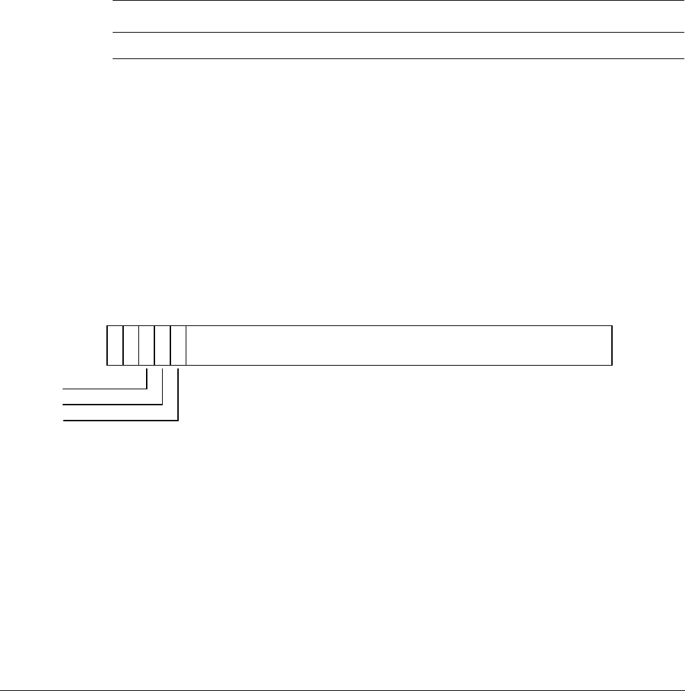
G4 AArch32 System Register Descriptions
G4.4 Performance Monitors registers
G4-4170 Copyright © 2013 ARM Limited. All rights reserved. ARM DDI 0487A.a
Non-Confidential - Beta ID090413
G4.4 Performance Monitors registers
This section describes the Performance Monitors registers in AArch32 state.
G4.4.1 PMCCFILTR, Performance Monitors Cycle Count Filter Register
The PMCCFILTR characteristics are:
Purpose
Determines the modes in which the Cycle Counter, PMCCNTR, increments.
This register is part of the Performance Monitors registers functional group.
Usage constraints
This register is accessible as shown below:
This register is accessible at EL0 when PMUSERENR.EN is set to 1.
PMCCFILTR can also be accessed by using PMXEVTYPER with PMSELR.SEL set to
0b11111
.
Configurations
PMCCFILTR is architecturally mapped to AArch64 register PMCCFILTR_EL0.
PMCCFILTR is architecturally mapped to external register PMCCFILTR_EL0.
There is one instance of this register that is used in both Secure and Non-secure states.
Attributes
PMCCFILTR is a 32-bit register.
The PMCCFILTR bit assignments are:
P, bit [31]
EL1 modes filtering bit. Controls counting in EL1. If EL3 is implemented, then counting in
Non-secure EL1 is further controlled by the NSK bit. The possible values of this bit are:
0
Count cycles in EL1.
1
Do not count cycles in EL1.
On Warm reset, the field resets to 0.
EL0 (NS) EL0 (S) EL1 (NS) EL1 (S) EL2 EL3 (SCR.NS=1) EL3 (SCR.NS=0)
Config-RW Config-RW RW RW RW RW RW
P
31
U
30 29 28 27
RES0
26 0
NSK
NSU
NSH

G4 AArch32 System Register Descriptions
G4.4 Performance Monitors registers
ARM DDI 0487A.a Copyright © 2013 ARM Limited. All rights reserved. G4-4171
ID090413 Non-Confidential - Beta
U, bit [30]
EL0 filtering bit. Controls counting in EL0. If EL3 is implemented, then counting in Non-secure
EL0 is further controlled by the NSU bit. The possible values of this bit are:
0
Count cycles in EL0.
1
Do not count cycles in EL0.
On Warm reset, the field resets to 0.
NSK, bit [29]
Non-secure kernel modes filtering bit. Controls counting in Non-secure EL1. If EL3 is not
implemented, this bit is RES0.
If the value of this bit is equal to the value of P, cycles in Non-secure EL1 are counted.
Otherwise, cycles in Non-secure EL1 are not counted.
On Warm reset, the field resets to 0.
NSU, bit [28]
Non-secure user modes filtering bit. Controls counting in Non-secure EL0. If EL3 is not
implemented, this bit is RES0.
If the value of this bit is equal to the value of U, cycles in Non-secure EL0 are counted.
Otherwise, cycles in Non-secure EL0 are not counted.
On Warm reset, the field resets to 0.
NSH, bit [27]
Non-secure Hyp modes filtering bit. Controls counting in Non-secure EL2. If EL2 is not
implemented, this bit is RES0.
0
Do not count cycles in EL2.
1
Count cycles in EL2.
On Warm reset, the field resets to 0.
Bits [26:0]
Reserved, RES0.
Accessing the PMCCFILTR:
To access the PMCCFILTR:
MRC p15,0,<Rt>,c14,c15,7 ; Read PMCCFILTR into Rt
MCR p15,0,<Rt>,c14,c15,7 ; Write Rt to PMCCFILTR
Register access is encoded as follows:
coproc opc1 CRn CRm opc2
1111 000 1110 1111 111

G4 AArch32 System Register Descriptions
G4.4 Performance Monitors registers
G4-4172 Copyright © 2013 ARM Limited. All rights reserved. ARM DDI 0487A.a
Non-Confidential - Beta ID090413
G4.4.2 PMCCNTR, Performance Monitors Cycle Count Register
The PMCCNTR characteristics are:
Purpose
Holds the value of the processor Cycle Counter, CCNT, that counts processor clock cycles.
This register is part of the Performance Monitors registers functional group.
Usage constraints
This register is accessible as shown below:
This register is accessible at EL0 when PMUSERENR.EN or PMUSERENR.CR is set to 1.
The PMCR.{LC, D} bits configure whether PMCCNTR increments every clock cycle, or once
every 64 clock cycles.
PMCCFILTR determines the modes and states in which the PMCCNTR can increment.
Configurations
PMCCNTR is architecturally mapped to AArch64 register PMCCNTR_EL0 when accessing as a
64-bit register.
PMCCNTR is architecturally mapped to external register PMCCNTR_EL0.
PMCCNTR is architecturally mapped to AArch64 register PMCCNTR_EL0[31:0].
There is one instance of this register that is used in both Secure and Non-secure states.
All counters are subject to any changes in clock frequency, including clock stopping caused by the
WFI and WFE instructions. This means that it is CONSTRAINED UNPREDICTABLE whether or not
PMCCNTR continues to increment when clocks are stopped by WFI and WFE instructions.
Attributes
PMCCNTR is a 32-bit register when accessing as a 32-bit register and a 64-bit register when
accessing as a 64-bit register.
The PMCCNTR bit assignments are:
When accessing as a 32-bit register:
CCNT, bits [31:0]
Cycle count. Depending on the values of PMCR.{LC,D}, this field increments in one of the
following ways:
• Every processor clock cycle.
• Every 64th processor clock cycle.
This field can be reset to zero by writing 1 to PMCR.C.
On Warm reset, the field reset value is architecturally UNKNOWN.
EL0 (NS) EL0 (S) EL1 (NS) EL1 (S) EL2 EL3 (SCR.NS=1) EL3 (SCR.NS=0)
Config-RW Config-RW RW RW RW RW RW
CCNT
31 0

G4 AArch32 System Register Descriptions
G4.4 Performance Monitors registers
ARM DDI 0487A.a Copyright © 2013 ARM Limited. All rights reserved. G4-4173
ID090413 Non-Confidential - Beta
When accessing as a 64-bit register:
CCNT, bits [63:0]
Cycle count. Depending on the values of PMCR.{LC,D}, this field increments in one of the
following ways:
• Every processor clock cycle.
• Every 64th processor clock cycle.
This field can be reset to zero by writing 1 to PMCR.C.
On Warm reset, the field reset value is architecturally UNKNOWN.
Accessing the PMCCNTR:
To access the PMCCNTR when accessing as a 32-bit register:
MRC p15,0,<Rt>,c9,c13,0 ; Read PMCCNTR into Rt
MCR p15,0,<Rt>,c9,c13,0 ; Write Rt to PMCCNTR
Register access is encoded as follows:
To access the PMCCNTR when accessing as a 64-bit register:
MRRC p15,0,<Rt>,<Rt2>,c9 ; Read 64-bit PMCCNTR into Rt (low word) and Rt2 (high word)
MCRR p15,0,<Rt>,<Rt2>,c9 ; Write Rt (low word) and Rt2 (high word) to 64-bit PMCCNTR
Register access is encoded as follows:
CCNT
63 0
coproc opc1 CRn CRm opc2
1111 000 1001 1101 000
coproc opc1 CRm
1111 0000 1001

G4 AArch32 System Register Descriptions
G4.4 Performance Monitors registers
G4-4174 Copyright © 2013 ARM Limited. All rights reserved. ARM DDI 0487A.a
Non-Confidential - Beta ID090413
G4.4.3 PMCEID0, Performance Monitors Common Event Identification register 0
The PMCEID0 characteristics are:
Purpose
Defines which common architectural and common microarchitectural feature events are
implemented. If a particular bit is set to 1, then the event for that bit is implemented.
This register is part of the Performance Monitors registers functional group.
Usage constraints
This register is accessible as shown below:
This register is accessible at EL0 when PMUSERENR.EN is set to 1.
Configurations
PMCEID0 is architecturally mapped to AArch64 register PMCEID0_EL0.
PMCEID0 is architecturally mapped to external register PMCEID0_EL0.
There is one instance of this register that is used in both Secure and Non-secure states.
Attributes
PMCEID0 is a 32-bit register.
The PMCEID0 bit assignments are:
CE[31:0], bits [31:0]
Common architectural and microarchitectural feature events that can be counted by the PMU event
counters.
For each bit described in the following table, the event is implemented if the bit is set to 1, or not
implemented if the bit is set to 0.
EL0 (NS) EL0 (S) EL1 (NS) EL1 (S) EL2 EL3 (SCR.NS=1) EL3 (SCR.NS=0)
Config-RO Config-RO RO RO RO RO RO
CE[31:0]
31 0
Bit Event
number Event mnemonic
31
0x01F
L1D_CACHE_ALLOCATE
30
0x01E
CHAIN
29
0x01D
BUS_CYCLES
28
0x01C
TTBR_WRITE_RETIRED
27
0x01B
INST_SPEC
26
0x01A
MEMORY_ERROR
25
0x019
BUS_ACCESS
24
0x018
L2D_CACHE_WB

G4 AArch32 System Register Descriptions
G4.4 Performance Monitors registers
ARM DDI 0487A.a Copyright © 2013 ARM Limited. All rights reserved. G4-4175
ID090413 Non-Confidential - Beta
Accessing the PMCEID0:
To access the PMCEID0:
MRC p15,0,<Rt>,c9,c12,6 ; Read PMCEID0 into Rt
Register access is encoded as follows:
23
0x017
L2D_CACHE_REFILL
22
0x016
L2D_CACHE
21
0x015
L1D_CACHE_WB
20
0x014
L1I_CACHE
19
0x013
MEM_ACCESS
18
0x012
BR_PRED
17
0x011
CPU_CYCLES
16
0x010
BR_MIS_PRED
15
0x00F
UNALIGNED_LDST_RETIRED
14
0x00E
BR_RETURN_RETIRED
13
0x00D
BR_IMMED_RETIRED
12
0x00C
PC_WRITE_RETIRED
11
0x00B
CID_WRITE_RETIRED
10
0x00A
EXC_RETURN
9
0x009
EXC_TAKEN
8
0x008
INST_RETIRED
7
0x007
ST_RETIRED
6
0x006
LD_RETIRED
5
0x005
L1D_TLB_REFILL
4
0x004
L1D_CACHE
3
0x003
L1D_CACHE_REFILL
2
0x002
L1I_TLB_REFILL
1
0x001
L1I_CACHE_REFILL
0
0x000
SW_INCR
coproc opc1 CRn CRm opc2
1111 000 1001 1100 110
Bit Event
number Event mnemonic

G4 AArch32 System Register Descriptions
G4.4 Performance Monitors registers
G4-4176 Copyright © 2013 ARM Limited. All rights reserved. ARM DDI 0487A.a
Non-Confidential - Beta ID090413
G4.4.4 PMCEID1, Performance Monitors Common Event Identification register 1
The PMCEID1 characteristics are:
Purpose
Reserved for future indication of which common architectural and common microarchitectural
feature events are implemented.
This register is part of the Performance Monitors registers functional group.
Usage constraints
This register is accessible as shown below:
This register is accessible at EL0 when PMUSERENR.EN is set to 1.
Configurations
PMCEID1 is architecturally mapped to AArch64 register PMCEID1_EL0.
PMCEID1 is architecturally mapped to external register PMCEID1_EL0.
There is one instance of this register that is used in both Secure and Non-secure states.
Attributes
PMCEID1 is a 32-bit register.
The PMCEID1 bit assignments are:
Bits [31:1]
Reserved, RES0.
CE[32], bit [0]
Common architectural and microarchitectural feature events that can be counted by the PMU event
counters.
For the bit described in the following table, the event is implemented if the bit is set to 1, or not
implemented if the bit is set to 0.
Accessing the PMCEID1:
To access the PMCEID1:
MRC p15,0,<Rt>,c9,c12,7 ; Read PMCEID1 into Rt
EL0 (NS) EL0 (S) EL1 (NS) EL1 (S) EL2 EL3 (SCR.NS=1) EL3 (SCR.NS=0)
Config-RO Config-RO RO RO RO RO RO
RES0
31 1 0
CE[32]
Bit Event
number Event mnemonic
0
0x020
L2D_CACHE_ALLOCATE

G4 AArch32 System Register Descriptions
G4.4 Performance Monitors registers
ARM DDI 0487A.a Copyright © 2013 ARM Limited. All rights reserved. G4-4177
ID090413 Non-Confidential - Beta
Register access is encoded as follows:
coproc opc1 CRn CRm opc2
1111 000 1001 1100 111

G4 AArch32 System Register Descriptions
G4.4 Performance Monitors registers
G4-4178 Copyright © 2013 ARM Limited. All rights reserved. ARM DDI 0487A.a
Non-Confidential - Beta ID090413
G4.4.5 PMCNTENCLR, Performance Monitors Count Enable Clear register
The PMCNTENCLR characteristics are:
Purpose
Disables the Cycle Count Register, PMCCNTR, and any implemented event counters
PMEVCNTR<x>. Reading this register shows which counters are enabled.
This register is part of the Performance Monitors registers functional group.
Usage constraints
This register is accessible as shown below:
This register is accessible at EL0 when PMUSERENR.EN is set to 1.
If EL2 is implemented, in Non-secure EL1 and EL0 modes, the value of HDCR.HPMN can change
the behavior of accesses to PMCNTENCLR. See the description of the Px bit.
PMCNTENCLR is used in conjunction with the PMCNTENSET register.
Configurations
PMCNTENCLR is architecturally mapped to AArch64 register PMCNTENCLR_EL0.
PMCNTENCLR is architecturally mapped to external register PMCNTENCLR_EL0.
There is one instance of this register that is used in both Secure and Non-secure states.
Attributes
PMCNTENCLR is a 32-bit register.
The PMCNTENCLR bit assignments are:
C, bit [31]
PMCCNTR disable bit. Disables the cycle counter register. Possible values are:
0
When read, means the cycle counter is disabled. When written, has no effect.
1
When read, means the cycle counter is enabled. When written, disables the cycle
counter.
On Warm reset, the field reset value is architecturally UNKNOWN.
P<x>, bit [x] for x = 0 to (N - 1)
Event counter disable bit for PMEVCNTR<x>.
When EL2 is implemented, in Non-secure EL1 and EL0, N is the value in HDCR.HPMN.
Otherwise, N is the value in PMCR.N.
Bits [30:N] are RAZ/WI.
Possible values of each bit are:
0
When read, means that PMEVCNTR<x> is disabled. When written, has no effect.
1
When read, means that PMEVCNTR<x> is enabled. When written, disables
PMEVCNTR<x>.
EL0 (NS) EL0 (S) EL1 (NS) EL1 (S) EL2 EL3 (SCR.NS=1) EL3 (SCR.NS=0)
Config-RW Config-RW RW RW RW RW RW
C
31
P<x>
30 0

G4 AArch32 System Register Descriptions
G4.4 Performance Monitors registers
ARM DDI 0487A.a Copyright © 2013 ARM Limited. All rights reserved. G4-4179
ID090413 Non-Confidential - Beta
On Warm reset, the field reset value is architecturally UNKNOWN.
Accessing the PMCNTENCLR:
To access the PMCNTENCLR:
MRC p15,0,<Rt>,c9,c12,2 ; Read PMCNTENCLR into Rt
MCR p15,0,<Rt>,c9,c12,2 ; Write Rt to PMCNTENCLR
Register access is encoded as follows:
coproc opc1 CRn CRm opc2
1111 000 1001 1100 010

G4 AArch32 System Register Descriptions
G4.4 Performance Monitors registers
G4-4180 Copyright © 2013 ARM Limited. All rights reserved. ARM DDI 0487A.a
Non-Confidential - Beta ID090413
G4.4.6 PMCNTENSET, Performance Monitors Count Enable Set register
The PMCNTENSET characteristics are:
Purpose
Enables the Cycle Count Register, PMCCNTR, and any implemented event counters
PMEVCNTR<x>. Reading this register shows which counters are enabled.
This register is part of the Performance Monitors registers functional group.
Usage constraints
This register is accessible as shown below:
This register is accessible at EL0 when PMUSERENR.EN is set to 1.
If EL2 is implemented, in Non-secure EL1 and EL0 modes, the value of HDCR.HPMN can change
the behavior of accesses to PMCNTENSET. See the description of the Px bit.
PMCNTENSET is used in conjunction with the PMCNTENCLR register.
Configurations
PMCNTENSET is architecturally mapped to AArch64 register PMCNTENSET_EL0.
PMCNTENSET is architecturally mapped to external register PMCNTENSET_EL0.
There is one instance of this register that is used in both Secure and Non-secure states.
Attributes
PMCNTENSET is a 32-bit register.
The PMCNTENSET bit assignments are:
C, bit [31]
PMCCNTR enable bit. Enables the cycle counter register. Possible values are:
0
When read, means the cycle counter is disabled. When written, has no effect.
1
When read, means the cycle counter is enabled. When written, enables the cycle
counter.
On Warm reset, the field reset value is architecturally UNKNOWN.
P<x>, bit [x] for x = 0 to (N - 1)
Event counter enable bit for PMEVCNTR<x>.
When EL2 is implemented, in Non-secure EL1 and EL0, N is the value in HDCR.HPMN.
Otherwise, N is the value in PMCR.N.
Bits [30:N] are RAZ/WI.
Possible values of each bit are:
0
When read, means that PMEVCNTR<x> is disabled. When written, has no effect.
1
When read, means that PMEVCNTR<x> event counter is enabled. When written,
enables PMEVCNTR<x>.
EL0 (NS) EL0 (S) EL1 (NS) EL1 (S) EL2 EL3 (SCR.NS=1) EL3 (SCR.NS=0)
Config-RW Config-RW RW RW RW RW RW
C
31
P<x>
30 0

G4 AArch32 System Register Descriptions
G4.4 Performance Monitors registers
ARM DDI 0487A.a Copyright © 2013 ARM Limited. All rights reserved. G4-4181
ID090413 Non-Confidential - Beta
On Warm reset, the field reset value is architecturally UNKNOWN.
Accessing the PMCNTENSET:
To access the PMCNTENSET:
MRC p15,0,<Rt>,c9,c12,1 ; Read PMCNTENSET into Rt
MCR p15,0,<Rt>,c9,c12,1 ; Write Rt to PMCNTENSET
Register access is encoded as follows:
coproc opc1 CRn CRm opc2
1111 000 1001 1100 001
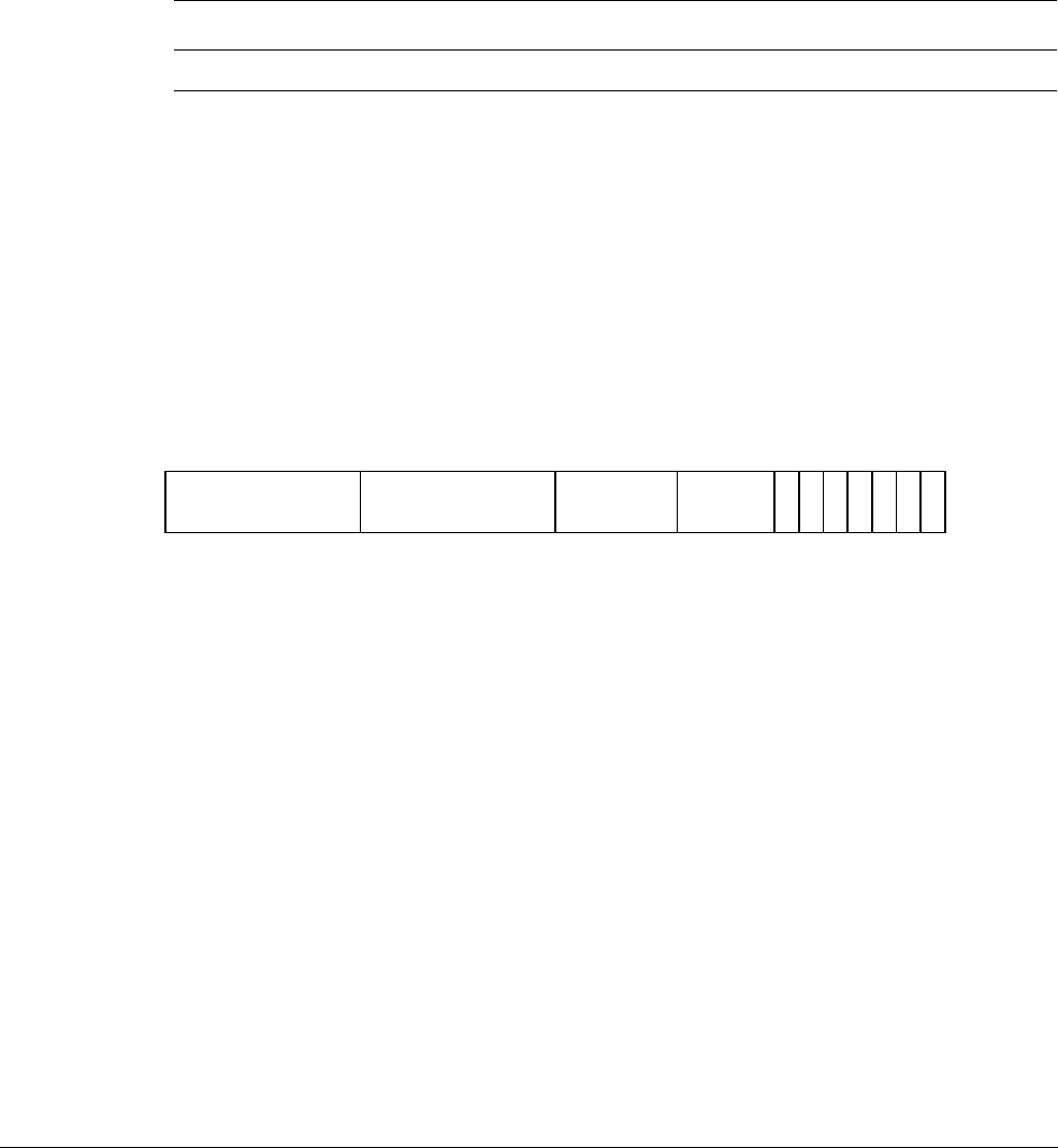
G4 AArch32 System Register Descriptions
G4.4 Performance Monitors registers
G4-4182 Copyright © 2013 ARM Limited. All rights reserved. ARM DDI 0487A.a
Non-Confidential - Beta ID090413
G4.4.7 PMCR, Performance Monitors Control Register
The PMCR characteristics are:
Purpose
Provides details of the Performance Monitors implementation, including the number of counters
implemented, and configures and controls the counters.
This register is part of the Performance Monitors registers functional group.
Usage constraints
This register is accessible as shown below:
This register is accessible at EL0 when PMUSERENR.EN is set to 1.
Configurations
PMCR is architecturally mapped to AArch64 register PMCR_EL0.
PMCR is architecturally mapped to external register PMCR_EL0.
There is one instance of this register that is used in both Secure and Non-secure states.
Attributes
PMCR is a 32-bit register.
The PMCR bit assignments are:
IMP, bits [31:24]
Implementer code. This field is RO with an IMPLEMENTATION DEFINED value.
The implementer codes are allocated by ARM. Values have the same interpretation as bits [31:24]
of the MIDR.
IDCODE, bits [23:16]
Identification code. This field is RO with an IMPLEMENTATION DEFINED value.
Each implementer must maintain a list of identification codes that is specific to the implementer. A
specific implementation is identified by the combination of the implementer code and the
identification code.
N, bits [15:11]
Number of event counters. This field is RO with an IMPLEMENTATION DEFINED value that indicates
the number of counters implemented.
The value of this field is the number of counters implemented, from
0b00000
for no counters to
0b11111
for 31 counters.
An implementation can implement only the Cycle Count Register, PMCCNTR. This is indicated by
a value of
0b00000
for the N field.
Bits [10:7]
Reserved, RES0.
EL0 (NS) EL0 (S) EL1 (NS) EL1 (S) EL2 EL3 (SCR.NS=1) EL3 (SCR.NS=0)
Config-RW Config-RW RW RW RW RW RW
IMP
31 24
IDCODE
23 16
N
15 11
RES0
10 7
LC
6
DP
5
X
4
D
3
C
2
P
1
E
0

G4 AArch32 System Register Descriptions
G4.4 Performance Monitors registers
ARM DDI 0487A.a Copyright © 2013 ARM Limited. All rights reserved. G4-4183
ID090413 Non-Confidential - Beta
LC, bit [6]
Long cycle counter enable. Determines which PMCCNTR bit generates an overflow recorded by
PMOVSR[31].
0
Cycle counter overflow on increment that changes PMCCNTR[31] from 1 to 0.
1
Cycle counter overflow on increment that changes PMCCNTR[63] from 1 to 0.
ARM deprecates use of PMCR.LC = 0.
On Warm reset, the field reset value is architecturally UNKNOWN.
DP, bit [5]
Disable cycle counter when event counting is prohibited. The possible values of this bit are:
0
PMCCNTR, if enabled, counts when event counting is prohibited.
1
PMCCNTR does not count when event counting is prohibited.
Event counting is prohibited when ProfilingProhibited(IsSecure(),PSTATE.EL) == TRUE.
This bit is RW.
On Warm reset, the field resets to 0.
X, bit [4]
Enable export of events in an IMPLEMENTATION DEFINED event stream. The possible values of this
bit are:
0
Do not export events.
1
Export events where not prohibited.
This bit is used to permit events to be exported to another debug device, such as an OPTIONAL trace
extension, over an event bus. If the implementation does not include such an event bus, this bit is
RAZ/WI.
This bit does not affect the generation of Performance Monitors overflow interrupt requests or
signaling to a cross-trigger interface (CTI) that can be implemented as signals exported from the
processor.
If the implementation does not include an exported event stream, this bit is RAZ/WI. Otherwise this
bit is RW.
On Warm reset, the field resets to 0.
D, bit [3]
Clock divider. The possible values of this bit are:
0
When enabled, PMCCNTR counts every clock cycle.
1
When enabled, PMCCNTR counts once every 64 clock cycles.
This bit is RW.
If PMCR.LC == 1, this bit is ignored and the cycle counter counts every clock cycle.
ARM deprecates use of PMCR.D = 1.
On Warm reset, the field resets to 0.
C, bit [2]
Cycle counter reset. This bit is WO. The effects of writing to this bit are:
0
No action.
1
Reset PMCCNTR to zero.
This bit is always RAZ.
Resetting PMCCNTR does not clear the PMCCNTR overflow bit to 0.
On Warm reset, the field reset value is architecturally UNKNOWN.

G4 AArch32 System Register Descriptions
G4.4 Performance Monitors registers
G4-4184 Copyright © 2013 ARM Limited. All rights reserved. ARM DDI 0487A.a
Non-Confidential - Beta ID090413
P, bit [1]
Event counter reset. This bit is WO. The effects of writing to this bit are:
0
No action.
1
Reset all event counters accessible in the current EL, not including PMCCNTR, to zero.
This bit is always RAZ.
In Non-secure EL0 and EL1, if EL2 is implemented, a write of 1 to this bit does not reset event
counters that HDCR.HPMN reserves for EL2 use.
In EL2 and EL3, a write of 1 to this bit resets all the event counters.
Resetting the event counters does not clear any overflow bits to 0.
On Warm reset, the field reset value is architecturally UNKNOWN.
E, bit [0]
Enable. The possible values of this bit are:
0
All counters, including PMCCNTR, are disabled.
1
All counters are enabled by PMCNTENSET.
This bit is RW.
In Non-secure EL0 and EL1, if EL2 is implemented, this bit does not affect the operation of event
counters that HDCR.HPMN reserves for EL2 use.
On Warm reset, the field resets to 0.
Accessing the PMCR:
To access the PMCR:
MRC p15,0,<Rt>,c9,c12,0 ; Read PMCR into Rt
MCR p15,0,<Rt>,c9,c12,0 ; Write Rt to PMCR
Register access is encoded as follows:
coproc opc1 CRn CRm opc2
1111 000 1001 1100 000

G4 AArch32 System Register Descriptions
G4.4 Performance Monitors registers
ARM DDI 0487A.a Copyright © 2013 ARM Limited. All rights reserved. G4-4185
ID090413 Non-Confidential - Beta
G4.4.8 PMEVCNTR<n>, Performance Monitors Event Count Registers, n = 0 - 30
The PMEVCNTR<n> characteristics are:
Purpose
Holds event counter n, which counts events, where n is 0 to 30.
This register is part of the Performance Monitors registers functional group.
Usage constraints
This register is accessible as shown below:
This register can be read at EL0 when PMUSERENR.EN or PMUSERENR.ER is set to 1, and can
be written at EL0 when PMUSERENR.ER is set to 1.
PMEVCNTR<n> can also be accessed by using PMXEVCNTR with PMSELR.SEL set to n.
If <n> is greater than the number of counters available in the current Exception level and state, reads
and writes of PMEVCNTR<n> are CONSTRAINED UNPREDICTABLE, and must behave as one of the
following:
•UNALLOCATED.
•RAZ/WI.
• No-op.
Configurations
PMEVCNTR<n> is architecturally mapped to AArch64 register PMEVCNTR<n>_EL0.
PMEVCNTR<n> is architecturally mapped to external register PMEVCNTR<n>_EL0.
There is one instance of this register that is used in both Secure and Non-secure states.
Attributes
PMEVCNTR<n> is a 32-bit register.
The PMEVCNTR<n> bit assignments are:
Bits [31:0]
Event counter n. Value of event counter n, where n is the number of this register and is a number
from 0 to 30.
On Warm reset, the field reset value is architecturally UNKNOWN.
Accessing the PMEVCNTR<n>:
To access the PMEVCNTR<n>:
MRC p15,0,<Rt>,c14,<CRm>,<opc2> ; Read PMEVCNTR<n> into Rt, where n is in the range 0 to 30
MCR p15,0,<Rt>,c14,<CRm>,<opc2> ; Write Rt to PMEVCNTR<n>, where n is in the range 0 to 30
EL0 (NS) EL0 (S) EL1 (NS) EL1 (S) EL2 EL3 (SCR.NS=1) EL3 (SCR.NS=0)
Config-RW Config-RW RW RW RW RW RW
Event counter n
31 0

G4 AArch32 System Register Descriptions
G4.4 Performance Monitors registers
G4-4186 Copyright © 2013 ARM Limited. All rights reserved. ARM DDI 0487A.a
Non-Confidential - Beta ID090413
Register access is encoded as follows:
coproc opc1 CRn CRm opc2
1111 000 1110 10:n<4:3> n<2:0>
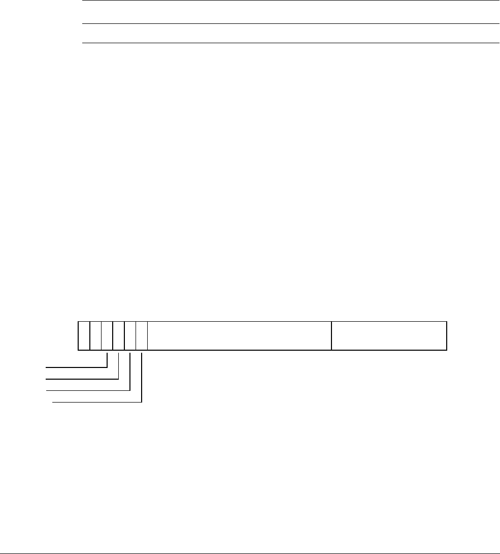
G4 AArch32 System Register Descriptions
G4.4 Performance Monitors registers
ARM DDI 0487A.a Copyright © 2013 ARM Limited. All rights reserved. G4-4187
ID090413 Non-Confidential - Beta
G4.4.9 PMEVTYPER<n>, Performance Monitors Event Type Registers, n = 0 - 30
The PMEVTYPER<n> characteristics are:
Purpose
Configures event counter n, where n is 0 to 30.
This register is part of the Performance Monitors registers functional group.
Usage constraints
This register is accessible as shown below:
This register is accessible at EL0 when PMUSERENR.EN is set to 1.
PMEVTYPER<n> can also be accessed by using PMXEVTYPER with PMSELR.SEL set to n.
If <n> is greater than the number of counters available in the current Exception level and state, reads
and writes of PMEVTYPER<n> are CONSTRAINED UNPREDICTABLE, and must behave as one of the
following:
•UNALLOCATED.
•RAZ/WI.
• No-op.
Configurations
PMEVTYPER<n> is architecturally mapped to AArch64 register PMEVTYPER<n>_EL0.
PMEVTYPER<n> is architecturally mapped to external register PMEVTYPER<n>_EL0.
There is one instance of this register that is used in both Secure and Non-secure states.
Attributes
PMEVTYPER<n> is a 32-bit register.
The PMEVTYPER<n> bit assignments are:
P, bit [31]
EL1 modes filtering bit. Controls counting in EL1. If EL3 is implemented, then counting in
Non-secure EL1 is further controlled by the NSK bit. The possible values of this bit are:
0
Count events in EL1.
1
Do not count events in EL1.
On Warm reset, the field reset value is architecturally UNKNOWN.
EL0 (NS) EL0 (S) EL1 (NS) EL1 (S) EL2 EL3 (SCR.NS=1) EL3 (SCR.NS=0)
Config-RW Config-RW RW RW RW RW RW
P
31
U
30 29 28 27 26
RES0
25 10
evtCount
90
NSK
NSU
NSH
RES0

G4 AArch32 System Register Descriptions
G4.4 Performance Monitors registers
G4-4188 Copyright © 2013 ARM Limited. All rights reserved. ARM DDI 0487A.a
Non-Confidential - Beta ID090413
U, bit [30]
EL0 filtering bit. Controls counting in EL0. If EL3 is implemented, then counting in Non-secure
EL0 is further controlled by the NSU bit. The possible values of this bit are:
0
Count events in EL0.
1
Do not count events in EL0.
On Warm reset, the field reset value is architecturally UNKNOWN.
NSK, bit [29]
Non-secure kernel modes filtering bit. Controls counting in Non-secure EL1. If EL3 is not
implemented, this bit is RES0.
If the value of this bit is equal to the value of P, events in Non-secure EL1 are counted.
Otherwise, events in Non-secure EL1 are not counted.
On Warm reset, the field reset value is architecturally UNKNOWN.
NSU, bit [28]
Non-secure user modes filtering bit. Controls counting in Non-secure EL0. If EL3 is not
implemented, this bit is RES0.
If the value of this bit is equal to the value of U, events in Non-secure EL0 are counted.
Otherwise, events in Non-secure EL0 are not counted.
On Warm reset, the field reset value is architecturally UNKNOWN.
NSH, bit [27]
Non-secure Hyp modes filtering bit. Controls counting in Non-secure EL2. If EL2 is not
implemented, this bit is RES0.
0
Do not count events in EL2.
1
Count events in EL2.
On Warm reset, the field reset value is architecturally UNKNOWN.
Bit [26]
Reserved, RES0.
Bits [25:10]
Reserved, RES0.
evtCount, bits [9:0]
Event to count. The event number of the event that is counted by event counter PMEVCNTR<n>.
Software must program this field with an event defined by the processor or a common event defined
by the architecture.
If evtCount is programmed to an event that is reserved or not implemented, the behavior depends
on the event type.
For common architectural and microarchitectural events:
• No events are counted.
• The value read back on evtCount is the value written.
For IMPLEMENTATION DEFINED events:
• It is UNPREDICTABLE what event, if any, is counted. UNPREDICTABLE in this case means the
event must not expose privileged information.
• The value read back on evtCount is an UNKNOWN value with the same effect.
ARM recommends that the behavior across a family of implementations is defined such that if a
given implementation does not include an event from a set of common IMPLEMENTATION DEFINED
events, then no event is counted and the value read back on evtCount is the value written.
On Warm reset, the field reset value is architecturally UNKNOWN.

G4 AArch32 System Register Descriptions
G4.4 Performance Monitors registers
ARM DDI 0487A.a Copyright © 2013 ARM Limited. All rights reserved. G4-4189
ID090413 Non-Confidential - Beta
Accessing the PMEVTYPER<n>:
To access the PMEVTYPER<n>:
MRC p15,0,<Rt>,c14,<CRm>,<opc2> ; Read PMEVTYPER<n> into Rt, where n is in the range 0 to 30
MCR p15,0,<Rt>,c14,<CRm>,<opc2> ; Write Rt to PMEVTYPER<n>, where n is in the range 0 to 30
Register access is encoded as follows:
coproc opc1 CRn CRm opc2
1111 000 1110 11:n<4:3> n<2:0>

G4 AArch32 System Register Descriptions
G4.4 Performance Monitors registers
G4-4190 Copyright © 2013 ARM Limited. All rights reserved. ARM DDI 0487A.a
Non-Confidential - Beta ID090413
G4.4.10 PMINTENCLR, Performance Monitors Interrupt Enable Clear register
The PMINTENCLR characteristics are:
Purpose
Disables the generation of interrupt requests on overflows from the Cycle Count Register,
PMCCNTR, and the event counters PMEVCNTR<n>. Reading the register shows which overflow
interrupt requests are enabled.
This register is part of the Performance Monitors registers functional group.
Usage constraints
This register is accessible as shown below:
If EL2 is implemented, in Non-secure EL1 and EL0 modes, the value of HDCR.HPMN can change
the behavior of accesses to PMINTENCLR. See the description of the P<x> bit.
PMINTENCLR is used in conjunction with the PMINTENSET register.
Configurations
PMINTENCLR is architecturally mapped to AArch64 register PMINTENCLR_EL1.
PMINTENCLR is architecturally mapped to external register PMINTENCLR_EL1.
There is one instance of this register that is used in both Secure and Non-secure states.
Attributes
PMINTENCLR is a 32-bit register.
The PMINTENCLR bit assignments are:
C, bit [31]
PMCCNTR overflow interrupt request disable bit. Possible values are:
0
When read, means the cycle counter overflow interrupt request is disabled. When
written, has no effect.
1
When read, means the cycle counter overflow interrupt request is enabled. When
written, disables the cycle count overflow interrupt request.
On Warm reset, the field reset value is architecturally UNKNOWN.
P<x>, bit [x] for x = 0 to (N - 1)
Event counter overflow interrupt request disable bit for PMEVCNTR<x>.
When EL2 is implemented, in Non-secure EL1 and EL0, N is the value in HDCR.HPMN.
Otherwise, N is the value in PMCR.N.
Bits [30:N] are RAZ/WI.
Possible values are:
0
When read, means that the PMEVCNTR<x> event counter interrupt request is disabled.
When written, has no effect.
EL0 (NS) EL0 (S) EL1 (NS) EL1 (S) EL2 EL3 (SCR.NS=1) EL3 (SCR.NS=0)
- - RW RW RW RW RW
C
31
P<x>
30 0

G4 AArch32 System Register Descriptions
G4.4 Performance Monitors registers
ARM DDI 0487A.a Copyright © 2013 ARM Limited. All rights reserved. G4-4191
ID090413 Non-Confidential - Beta
1
When read, means that the PMEVCNTR<x> event counter interrupt request is enabled.
When written, disables the PMEVCNTR<x> interrupt request.
On Warm reset, the field reset value is architecturally UNKNOWN.
Accessing the PMINTENCLR:
To access the PMINTENCLR:
MRC p15,0,<Rt>,c9,c14,2 ; Read PMINTENCLR into Rt
MCR p15,0,<Rt>,c9,c14,2 ; Write Rt to PMINTENCLR
Register access is encoded as follows:
coproc opc1 CRn CRm opc2
1111 000 1001 1110 010

G4 AArch32 System Register Descriptions
G4.4 Performance Monitors registers
G4-4192 Copyright © 2013 ARM Limited. All rights reserved. ARM DDI 0487A.a
Non-Confidential - Beta ID090413
G4.4.11 PMINTENSET, Performance Monitors Interrupt Enable Set register
The PMINTENSET characteristics are:
Purpose
Enables the generation of interrupt requests on overflows from the Cycle Count Register,
PMCCNTR, and the event counters PMEVCNTR<n>. Reading the register shows which overflow
interrupt requests are enabled.
This register is part of the Performance Monitors registers functional group.
Usage constraints
This register is accessible as shown below:
If EL2 is implemented, in Non-secure EL1 and EL0 modes, the value of HDCR.HPMN can change
the behavior of accesses to PMINTENSET. See the description of the P<x> bit.
PMINTENSET is used in conjunction with the PMINTENCLR register.
Configurations
PMINTENSET is architecturally mapped to AArch64 register PMINTENSET_EL1.
PMINTENSET is architecturally mapped to external register PMINTENSET_EL1.
There is one instance of this register that is used in both Secure and Non-secure states.
Attributes
PMINTENSET is a 32-bit register.
The PMINTENSET bit assignments are:
C, bit [31]
PMCCNTR overflow interrupt request enable bit. Possible values are:
0
When read, means the cycle counter overflow interrupt request is disabled. When
written, has no effect.
1
When read, means the cycle counter overflow interrupt request is enabled. When
written, enables the cycle count overflow interrupt request.
On Warm reset, the field reset value is architecturally UNKNOWN.
P<x>, bit [x] for x = 0 to (N - 1)
Event counter overflow interrupt request enable bit for PMEVCNTR<x>.
When EL2 is implemented, in Non-secure EL1 and EL0, N is the value in HDCR.HPMN.
Otherwise, N is the value in PMCR.N.
Bits [30:N] are RAZ/WI.
Possible values are:
0
When read, means that the PMEVCNTR<x> event counter interrupt request is disabled.
When written, has no effect.
EL0 (NS) EL0 (S) EL1 (NS) EL1 (S) EL2 EL3 (SCR.NS=1) EL3 (SCR.NS=0)
- - RW RW RW RW RW
C
31
P<x>
30 0

G4 AArch32 System Register Descriptions
G4.4 Performance Monitors registers
ARM DDI 0487A.a Copyright © 2013 ARM Limited. All rights reserved. G4-4193
ID090413 Non-Confidential - Beta
1
When read, means that the PMEVCNTR<x> event counter interrupt request is enabled.
When written, enables the PMEVCNTR<x> interrupt request.
On Warm reset, the field reset value is architecturally UNKNOWN.
Accessing the PMINTENSET:
To access the PMINTENSET:
MRC p15,0,<Rt>,c9,c14,1 ; Read PMINTENSET into Rt
MCR p15,0,<Rt>,c9,c14,1 ; Write Rt to PMINTENSET
Register access is encoded as follows:
coproc opc1 CRn CRm opc2
1111 000 1001 1110 001

G4 AArch32 System Register Descriptions
G4.4 Performance Monitors registers
G4-4194 Copyright © 2013 ARM Limited. All rights reserved. ARM DDI 0487A.a
Non-Confidential - Beta ID090413
G4.4.12 PMOVSR, Performance Monitors Overflow Flag Status Register
The PMOVSR characteristics are:
Purpose
Contains the state of the overflow bit for the Cycle Count Register, PMCCNTR, and each of the
implemented event counters PMEVCNTR<x>. Writing to this register clears these bits.
This register is part of the Performance Monitors registers functional group.
Usage constraints
This register is accessible as shown below:
This register is accessible at EL0 when PMUSERENR.EN is set to 1.
If EL2 is implemented, in Non-secure EL1 and EL0 modes, the value of HDCR.HPMN can change
the behavior of accesses to PMOVSR. See the description of the Px bit.
Configurations
PMOVSR is architecturally mapped to AArch64 register PMOVSCLR_EL0.
PMOVSR is architecturally mapped to external register PMOVSCLR_EL0.
There is one instance of this register that is used in both Secure and Non-secure states.
Attributes
PMOVSR is a 32-bit register.
The PMOVSR bit assignments are:
C, bit [31]
PMCCNTR overflow bit. Possible values are:
0
When read, means the cycle counter has not overflowed. When written, has no effect.
1
When read, means the cycle counter has overflowed. When written, clears the overflow
bit to 0.
PMCR.LC is used to control from which bit of PMCCNTR (bit 31 or bit 63) an overflow is detected.
On Warm reset, the field reset value is architecturally UNKNOWN.
P<x>, bit [x] for x = 0 to (N - 1)
Event counter overflow clear bit for PMEVCNTR<x>.
When EL2 is implemented, in Non-secure EL1 and EL0, N is the value in HDCR.HPMN.
Otherwise, N is the value in PMCR.N.
Bits [30:N] are RAZ/WI.
Possible values of each bit are:
0
When read, means that PMEVCNTR<x> has not overflowed. When written, has no
effect.
EL0 (NS) EL0 (S) EL1 (NS) EL1 (S) EL2 EL3 (SCR.NS=1) EL3 (SCR.NS=0)
Config-RW Config-RW RW RW RW RW RW
C
31
P<x>
30 0

G4 AArch32 System Register Descriptions
G4.4 Performance Monitors registers
ARM DDI 0487A.a Copyright © 2013 ARM Limited. All rights reserved. G4-4195
ID090413 Non-Confidential - Beta
1
When read, means that PMEVCNTR<x> has overflowed. When written, clears the
PMEVCNTR<x> overflow bit to 0.
On Warm reset, the field reset value is architecturally UNKNOWN.
Accessing the PMOVSR:
To access the PMOVSR:
MRC p15,0,<Rt>,c9,c12,3 ; Read PMOVSR into Rt
MCR p15,0,<Rt>,c9,c12,3 ; Write Rt to PMOVSR
Register access is encoded as follows:
coproc opc1 CRn CRm opc2
1111 000 1001 1100 011

G4 AArch32 System Register Descriptions
G4.4 Performance Monitors registers
G4-4196 Copyright © 2013 ARM Limited. All rights reserved. ARM DDI 0487A.a
Non-Confidential - Beta ID090413
G4.4.13 PMOVSSET, Performance Monitors Overflow Flag Status Set register
The PMOVSSET characteristics are:
Purpose
Sets the state of the overflow bit for the Cycle Count Register, PMCCNTR, and each of the
implemented event counters PMEVCNTR<x>.
This register is part of the Performance Monitors registers functional group.
Usage constraints
This register is accessible as shown below:
This register is accessible at EL0 when PMUSERENR.EN is set to 1.
If EL2 is implemented, in Non-secure EL1 and EL0 modes, the value of HDCR.HPMN can change
the behavior of accesses to PMOVSSET. See the description of the Px bit.
Configurations
PMOVSSET is architecturally mapped to AArch64 register PMOVSSET_EL0.
PMOVSSET is architecturally mapped to external register PMOVSSET_EL0.
There is one instance of this register that is used in both Secure and Non-secure states.
Attributes
PMOVSSET is a 32-bit register.
The PMOVSSET bit assignments are:
C, bit [31]
PMCCNTR overflow bit. Possible values are:
0
When read, means the cycle counter has not overflowed. When written, has no effect.
1
When read, means the cycle counter has overflowed. When written, sets the overflow
bit to 1.
On Warm reset, the field reset value is architecturally UNKNOWN.
P<x>, bit [x] for x = 0 to (N - 1)
Event counter overflow set bit for PMEVCNTR<x>.
When EL2 is implemented, in Non-secure EL1 and EL0, N is the value in HDCR.HPMN.
Otherwise, N is the value in PMCR.N.
Bits [30:N] are RAZ/WI.
Possible values are:
0
When read, means that PMEVCNTR<x> has not overflowed. When written, has no
effect.
1
When read, means that PMEVCNTR<x> has overflowed. When written, sets the
PMEVCNTR<x> overflow bit to 1.
EL0 (NS) EL0 (S) EL1 (NS) EL1 (S) EL2 EL3 (SCR.NS=1) EL3 (SCR.NS=0)
Config-RW Config-RW RW RW RW RW RW
C
31
P<x>
30 0

G4 AArch32 System Register Descriptions
G4.4 Performance Monitors registers
ARM DDI 0487A.a Copyright © 2013 ARM Limited. All rights reserved. G4-4197
ID090413 Non-Confidential - Beta
On Warm reset, the field reset value is architecturally UNKNOWN.
Accessing the PMOVSSET:
To access the PMOVSSET:
MRC p15,0,<Rt>,c9,c14,3 ; Read PMOVSSET into Rt
MCR p15,0,<Rt>,c9,c14,3 ; Write Rt to PMOVSSET
Register access is encoded as follows:
coproc opc1 CRn CRm opc2
1111 000 1001 1110 011

G4 AArch32 System Register Descriptions
G4.4 Performance Monitors registers
G4-4198 Copyright © 2013 ARM Limited. All rights reserved. ARM DDI 0487A.a
Non-Confidential - Beta ID090413
G4.4.14 PMSELR, Performance Monitors Event Counter Selection Register
The PMSELR characteristics are:
Purpose
Selects the current event counter PMEVCNTR<x> or the cycle counter, CCNT.
This register is part of the Performance Monitors registers functional group.
Usage constraints
This register is accessible as shown below:
This register is accessible at EL0 when PMUSERENR.EN or PMUSERENR.ER is set to 1.
PMSELR is used in conjunction with PMXEVTYPER to determine the event that increments a
selected event counter, and the modes and states in which the selected counter increments.
It is also used in conjunction with PMXEVCNTR, to determine the value of a selected event
counter.
Configurations
PMSELR is architecturally mapped to AArch64 register PMSELR_EL0.
There is one instance of this register that is used in both Secure and Non-secure states.
Attributes
PMSELR is a 32-bit register.
The PMSELR bit assignments are:
Bits [31:5]
Reserved, RES0.
SEL, bits [4:0]
Selects event counter, PMEVCNTR<x>, where x is the value held in this field. This value identifies
which event counter is accessed when a subsequent access to PMXEVTYPER or PMXEVCNTR
occurs.
This field can take any value from 0 (
0b00000
) to (PMCR.N)-1, or 31 (
0b11111
).
When PMSELR.SEL is
0b11111
it selects the cycle counter and:
• A read of the PMXEVTYPER returns the value of PMCCFILTR.
• A write of the PMXEVTYPER writes to PMCCFILTR.
• A read or write of PMXEVCNTR has CONSTRAINED UNPREDICTABLE effects, that can be one
of the following:
— Access to PMXEVCNTR is UNDEFINED.
— Access to PMXEVCNTR behaves as a NOP.
— Access to PMXEVCNTR behaves as if the register is RAZ/WI.
EL0 (NS) EL0 (S) EL1 (NS) EL1 (S) EL2 EL3 (SCR.NS=1) EL3 (SCR.NS=0)
Config-RW Config-RW RW RW RW RW RW
RES0
31 5
SEL
40

G4 AArch32 System Register Descriptions
G4.4 Performance Monitors registers
ARM DDI 0487A.a Copyright © 2013 ARM Limited. All rights reserved. G4-4199
ID090413 Non-Confidential - Beta
— Access to PMXEVCNTR behaves as if the PMSELR.SEL field contains an UNKNOWN
value.
If this field is set to a value greater than or equal to the number of implemented counters, but not
equal to 31, the results of access to PMXEVTYPER or PMXEVCNTR are CONSTRAINED
UNPREDICTABLE, and can be one of the following:
• Access to PMXEVTYPER or PMXEVCNTR is UNDEFINED.
• Access to PMXEVTYPER or PMXEVCNTR behaves as a NOP.
• Access to PMXEVTYPER or PMXEVCNTR behaves as if the register is RAZ/WI.
• Access to PMXEVTYPER or PMXEVCNTR behaves as if the PMSELR.SEL field contains
an UNKNOWN value.
• Access to PMXEVTYPER or PMXEVCNTR behaves as if the PMSELR.SEL field contains
0b11111
.
On Warm reset, the field reset value is architecturally UNKNOWN.
Accessing the PMSELR:
To access the PMSELR:
MRC p15,0,<Rt>,c9,c12,5 ; Read PMSELR into Rt
MCR p15,0,<Rt>,c9,c12,5 ; Write Rt to PMSELR
Register access is encoded as follows:
coproc opc1 CRn CRm opc2
1111 000 1001 1100 101

G4 AArch32 System Register Descriptions
G4.4 Performance Monitors registers
G4-4200 Copyright © 2013 ARM Limited. All rights reserved. ARM DDI 0487A.a
Non-Confidential - Beta ID090413
G4.4.15 PMSWINC, Performance Monitors Software Increment register
The PMSWINC characteristics are:
Purpose
Increments a counter that is configured to count the Software increment event, event
0x00
.
This register is part of the Performance Monitors registers functional group.
Usage constraints
This register is accessible as shown below:
This register is accessible at EL0 when PMUSERENR.EN or PMUSERENR.SW is set to 1.
If EL2 is implemented, in Non-secure EL1 and EL0 modes, the value of HDCR.HPMN can change
the behavior of accesses to PMSWINC. See the description of the Px bit.
Configurations
PMSWINC is architecturally mapped to AArch64 register PMSWINC_EL0.
PMSWINC is architecturally mapped to external register PMSWINC_EL0.
There is one instance of this register that is used in both Secure and Non-secure states.
Attributes
PMSWINC is a 32-bit register.
The PMSWINC bit assignments are:
Bit [31]
Reserved, RES0.
P<x>, bit [x] for x = 0 to (N - 1)
Event counter software increment bit for PMEVCNTR<x>.
When EL2 is implemented, in Non-secure EL1 and EL0, N is the value in HDCR.HPMN.
Otherwise, N is the value in PMCR.N.
Bits [30:N] are RAZ/WI.
The effects of writing to this bit are:
0
No action. The write to this bit is ignored.
1
If PMEVCNTR<x> is enabled and configured to count the software increment event,
increments PMEVCNTR<x> by 1. If PMEVCNTR<x> is disabled, or not configured to
count the software increment event, the write to this bit is ignored.
Accessing the PMSWINC:
To access the PMSWINC:
EL0 (NS) EL0 (S) EL1 (NS) EL1 (S) EL2 EL3 (SCR.NS=1) EL3 (SCR.NS=0)
Config-WO Config-WO WO WO WO WO WO
31
P<x>
30 0
RES0

G4 AArch32 System Register Descriptions
G4.4 Performance Monitors registers
ARM DDI 0487A.a Copyright © 2013 ARM Limited. All rights reserved. G4-4201
ID090413 Non-Confidential - Beta
MCR p15,0,<Rt>,c9,c12,4 ; Write Rt to PMSWINC
Register access is encoded as follows:
coproc opc1 CRn CRm opc2
1111 000 1001 1100 100
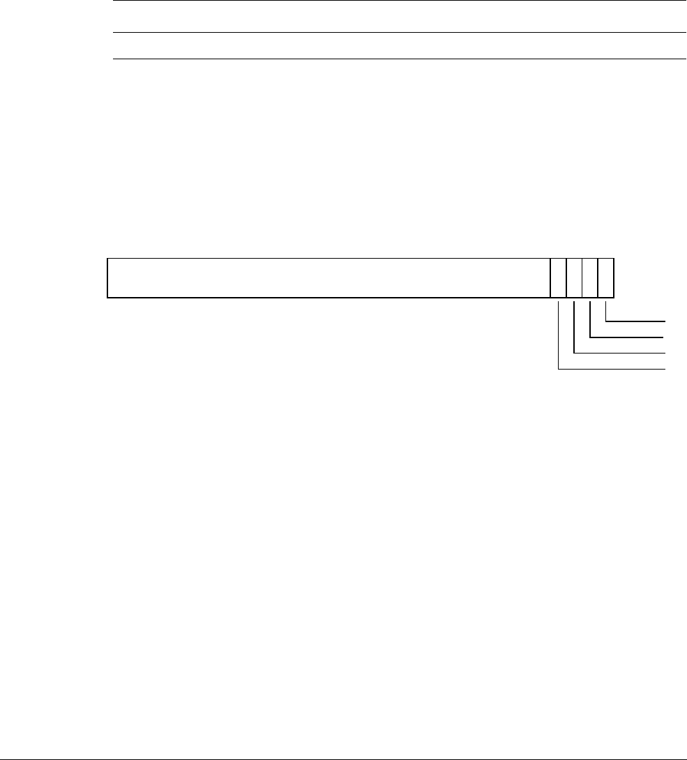
G4 AArch32 System Register Descriptions
G4.4 Performance Monitors registers
G4-4202 Copyright © 2013 ARM Limited. All rights reserved. ARM DDI 0487A.a
Non-Confidential - Beta ID090413
G4.4.16 PMUSERENR, Performance Monitors User Enable Register
The PMUSERENR characteristics are:
Purpose
Enables or disables User mode access to the Performance Monitors.
This register is part of the Performance Monitors registers functional group.
Usage constraints
This register is accessible as shown below:
Configurations
PMUSERENR is architecturally mapped to AArch64 register PMUSERENR_EL0.
There is one instance of this register that is used in both Secure and Non-secure states.
Attributes
PMUSERENR is a 32-bit register.
The PMUSERENR bit assignments are:
Bits [31:4]
Reserved, RES0.
ER, bit [3]
Event counter read enable. The possible values of this bit are:
0
EL0 read access to PMXEVCNTR / PMEVCNTR<n> and read/write access to
PMSELR disabled if PMUSERENR.EN is also 0.
1
EL0 read access to PMXEVCNTR / PMEVCNTR<n> and read/write access to
PMSELR enabled.
On Warm reset, the field resets to 0.
CR, bit [2]
Cycle counter read enable. The possible values of this bit are:
0
EL0 read access to PMCCNTR disabled if PMUSERENR.EN is also 0.
1
EL0 read access to PMCCNTR enabled.
On Warm reset, the field resets to 0.
EL0 (NS) EL0 (S) EL1 (NS) EL1 (S) EL2 EL3 (SCR.NS=1) EL3 (SCR.NS=0)
RO RO RW RW RW RW RW
RES0
31 4 3 2 1 0
EN
SW
CR
ER

G4 AArch32 System Register Descriptions
G4.4 Performance Monitors registers
ARM DDI 0487A.a Copyright © 2013 ARM Limited. All rights reserved. G4-4203
ID090413 Non-Confidential - Beta
SW, bit [1]
Software Increment write enable. The possible values of this bit are:
0
EL0 write access to PMSWINC disabled if PMUSERENR.EN is also 0.
1
EL0 write access to PMSWINC enabled.
On Warm reset, the field resets to 0.
EN, bit [0]
EL0 access enable bit. The possible values of this bit are:
0
EL0 access to the Performance Monitors disabled.
1
EL0 access to the Performance Monitors enabled. Can access all PMU registers at EL0,
except for writes to PMUSERENR and reads/writes of PMINTENSET and
PMINTENCLR.
On Warm reset, the field resets to 0.
Accessing the PMUSERENR:
To access the PMUSERENR:
MRC p15,0,<Rt>,c9,c14,0 ; Read PMUSERENR into Rt
MCR p15,0,<Rt>,c9,c14,0 ; Write Rt to PMUSERENR
Register access is encoded as follows:
coproc opc1 CRn CRm opc2
1111 000 1001 1110 000

G4 AArch32 System Register Descriptions
G4.4 Performance Monitors registers
G4-4204 Copyright © 2013 ARM Limited. All rights reserved. ARM DDI 0487A.a
Non-Confidential - Beta ID090413
G4.4.17 PMXEVCNTR, Performance Monitors Selected Event Count Register
The PMXEVCNTR characteristics are:
Purpose
Reads or writes the value of the selected event counter, PMEVCNTR<x>. PMSELR.SEL
determines which event counter is selected.
This register is part of the Performance Monitors registers functional group.
Usage constraints
This register is accessible as shown below:
This register can be read at EL0 when PMUSERENR.EN or PMUSERENR.ER is set to 1, and can
be written at EL0 when PMUSERENR.ER is set to 1.
If PMSELR.SEL selects a counter that is not accessible then reads and writes of PMXEVCNTR are
CONSTRAINED UNPREDICTABLE, and must behave as one of the following:
•UNALLOCATED.
•RAZ/WI.
• No-op.
•As if PMSELR.SEL has an UNKNOWN value less than the number of counters accessible at
the current exception level and security state.
•As if PMSELR.SEL is 31.
• If the counter is implemented but not accessible at the current exception level and security
state, generate a System Register Trap or CP14 Register Trap exception taken to EL2.
This applies:
• If PMSELR.SEL is larger than the number of implemented counters.
• In an implementation that includes EL2, in Non-secure EL1 and EL0 modes, if
PMSELR.SEL >= HDCR.HPMN.
Configurations
PMXEVCNTR is architecturally mapped to AArch64 register PMXEVCNTR_EL0.
There is one instance of this register that is used in both Secure and Non-secure states.
Attributes
PMXEVCNTR is a 32-bit register.
The PMXEVCNTR bit assignments are:
PMEVCNTR<x>, bits [31:0]
Value of the selected event counter, PMEVCNTR<x>, where x is the value stored in PMSELR.SEL.
Accessing the PMXEVCNTR:
To access the PMXEVCNTR:
EL0 (NS) EL0 (S) EL1 (NS) EL1 (S) EL2 EL3 (SCR.NS=1) EL3 (SCR.NS=0)
Config-RW Config-RW RW RW RW RW RW
PMEVCNTR<x>
31 0

G4 AArch32 System Register Descriptions
G4.4 Performance Monitors registers
ARM DDI 0487A.a Copyright © 2013 ARM Limited. All rights reserved. G4-4205
ID090413 Non-Confidential - Beta
MRC p15,0,<Rt>,c9,c13,2 ; Read PMXEVCNTR into Rt
MCR p15,0,<Rt>,c9,c13,2 ; Write Rt to PMXEVCNTR
Register access is encoded as follows:
coproc opc1 CRn CRm opc2
1111 000 1001 1101 010

G4 AArch32 System Register Descriptions
G4.4 Performance Monitors registers
G4-4206 Copyright © 2013 ARM Limited. All rights reserved. ARM DDI 0487A.a
Non-Confidential - Beta ID090413
G4.4.18 PMXEVTYPER, Performance Monitors Selected Event Type Register
The PMXEVTYPER characteristics are:
Purpose
When PMSELR.SEL selects an event counter, this accesses a PMEVTYPER<n> register. When
PMSELR.SEL selects the cycle counter, this accesses PMCCFILTR.
This register is part of the Performance Monitors registers functional group.
Usage constraints
This register is accessible as shown below:
This register is accessible at EL0 when PMUSERENR.EN is set to 1.
If PMSELR.SEL selects a counter that is not accessible then reads and writes of PMXEVTYPER
are CONSTRAINED UNPREDICTABLE, and must behave as one of the following:
•UNALLOCATED.
•RAZ/WI.
• No-op.
•As if PMSELR.SEL has an UNKNOWN value less than the number of counters accessible at
the current exception level and security state.
•As if PMSELR.SEL is 31.
• If the counter is implemented but not accessible at the current exception level and security
state, generate a System Register Trap or CP14 Register Trap exception taken to EL2.
This applies:
• If PMSELR.SEL is larger than the number of implemented counters.
• In an implementation that includes EL2, in Non-secure EL1 and EL0 modes, if
PMSELR.SEL >= HDCR.HPMN.
Configurations
PMXEVTYPER is architecturally mapped to AArch64 register PMXEVTYPER_EL0.
There is one instance of this register that is used in both Secure and Non-secure states.
Attributes
PMXEVTYPER is a 32-bit register.
The PMXEVTYPER bit assignments are:
Bits [31:0]
Event type register or PMCCFILTR.
When PMSELR.SEL == 31, this register accesses PMCCFILTR.
Otherwise, this register accesses PMEVTYPER<n> where n is the value in PMSELR.SEL.
EL0 (NS) EL0 (S) EL1 (NS) EL1 (S) EL2 EL3 (SCR.NS=1) EL3 (SCR.NS=0)
Config-RW Config-RW RW RW RW RW RW
Event type register or PMCCFILTR
31 0

G4 AArch32 System Register Descriptions
G4.4 Performance Monitors registers
ARM DDI 0487A.a Copyright © 2013 ARM Limited. All rights reserved. G4-4207
ID090413 Non-Confidential - Beta
Accessing the PMXEVTYPER:
To access the PMXEVTYPER:
MRC p15,0,<Rt>,c9,c13,1 ; Read PMXEVTYPER into Rt
MCR p15,0,<Rt>,c9,c13,1 ; Write Rt to PMXEVTYPER
Register access is encoded as follows:
coproc opc1 CRn CRm opc2
1111 000 1001 1101 001

G4 AArch32 System Register Descriptions
G4.5 Generic Timer registers
G4-4208 Copyright © 2013 ARM Limited. All rights reserved. ARM DDI 0487A.a
Non-Confidential - Beta ID090413
G4.5 Generic Timer registers
This section describes the Generic Timer registers in AArch32 state.
G4.5.1 CNTFRQ, Counter-timer Frequency register
The CNTFRQ characteristics are:
Purpose
Holds the clock frequency of the system counter.
This register is part of the Generic Timer registers functional group.
Usage constraints
This register is accessible as shown below:
Can only be written at the highest exception level implemented. For example, if EL3 is the highest
implemented exception level, CNTFRQ can only be written at EL3.
If EL3 is using AArch64, write access to CNTFRQ in AArch32 at Secure EL1 is UNDEFINED.
This register is accessible and read-only at EL0 when CNTKCTL.EL0PCTEN or
CNTKCTL.EL0VCTEN is set to 1.
Configurations
CNTFRQ is architecturally mapped to AArch64 register CNTFRQ_EL0.
CNTFRQ is architecturally mapped to external register CNTFRQ.
There is one instance of this register that is used in both Secure and Non-secure states.
Attributes
CNTFRQ is a 32-bit register.
The CNTFRQ bit assignments are:
Bits [31:0]
Clock frequency. Indicates the system counter clock frequency, in Hz.
Accessing the CNTFRQ:
To access the CNTFRQ:
MRC p15,0,<Rt>,c14,c0,0 ; Read CNTFRQ into Rt
MCR p15,0,<Rt>,c14,c0,0 ; Write Rt to CNTFRQ
Register access is encoded as follows:
EL0 (NS) EL0 (S) EL1 (NS) EL1 (S) EL2 EL3 (SCR.NS=1) EL3 (SCR.NS=0)
Config-RO Config-RO RO RO RO RO RW
Clock frequency
31 0
coproc opc1 CRn CRm opc2
1111 000 1110 0000 000
G4 AArch32 System Register Descriptions
G4.5 Generic Timer registers
ARM DDI 0487A.a Copyright © 2013 ARM Limited. All rights reserved. G4-4209
ID090413 Non-Confidential - Beta
G4.5.2 CNTHCTL, Counter-timer Hyp Control register
The CNTHCTL characteristics are:
Purpose
Controls the generation of an event stream from the physical counter, and access from Non-secure
EL1 modes to the physical counter and the Non-secure EL1 physical timer.
This register is part of:
• the Generic Timer registers functional group
• the Virtualization registers functional group.
Usage constraints
This register is accessible as shown below:
Configurations
CNTHCTL is architecturally mapped to AArch64 register CNTHCTL_EL2.
If EL2 is not implemented, this register is RES0 from EL3.
Attributes
CNTHCTL is a 32-bit register.
The CNTHCTL bit assignments are:
Bits [31:8]
Reserved, RES0.
EVNTI, bits [7:4]
Selects which bit (0 to 15) of the corresponding counter register (CNTPCT or CNTVCT) is the
trigger for the event stream generated from that counter, when that stream is enabled.
Reset value is architecturally UNKNOWN.
EVNTDIR, bit [3]
Controls which transition of the counter register (CNTPCT or CNTVCT) trigger bit, defined by
EVNTI, generates an event when the event stream is enabled:
0
A 0 to 1 transition of the trigger bit triggers an event.
1
A 1 to 0 transition of the trigger bit triggers an event.
Reset value is architecturally UNKNOWN.
EL0 (NS) EL0 (S) EL1 (NS) EL1 (S) EL2 EL3 (SCR.NS=1) EL3 (SCR.NS=0)
- - - - RW RW -
RES0
31 8
EVNTI
74
3 2 1 0
EL1PCTEN
EL1PCEN
EVNTEN
EVNTDIR

G4 AArch32 System Register Descriptions
G4.5 Generic Timer registers
G4-4210 Copyright © 2013 ARM Limited. All rights reserved. ARM DDI 0487A.a
Non-Confidential - Beta ID090413
EVNTEN, bit [2]
Enables the generation of an event stream from the corresponding counter:
0
Disables the event stream.
1
Enables the event stream.
Resets to 0.
EL1PCEN, bit [1]
Controls whether the Non-secure copies of the physical timer registers are accessible from
Non-secure EL1 and EL0 modes:
0
The Non-secure CNTP_CVAL, CNTP_TVAL, and CNTP_CTL registers are not
accessible from Non-secure EL1 and EL0 modes.
1
The Non-secure CNTP_CVAL, CNTP_TVAL, and CNTP_CTL registers are
accessible from Non-secure EL1 and EL0 modes.
If EL3 is implemented and EL2 is not implemented, this bit is treated as if it is 1 for all purposes
other than reading the register.
Resets to 1.
EL1PCTEN, bit [0]
Controls whether the physical counter, CNTPCT, is accessible from Non-secure EL1 and EL0
modes:
0
The CNTPCT register is not accessible from Non-secure EL1 and EL0 modes.
1
The CNTPCT register is accessible from Non-secure EL1 and EL0 modes.
If EL3 is implemented and EL2 is not implemented, this bit is treated as if it is 1 for all purposes
other than reading the register.
Resets to 1.
Accessing the CNTHCTL:
To access the CNTHCTL:
MRC p15,4,<Rt>,c14,c1,0 ; Read CNTHCTL into Rt
MCR p15,4,<Rt>,c14,c1,0 ; Write Rt to CNTHCTL
Register access is encoded as follows:
coproc opc1 CRn CRm opc2
1111 100 1110 0001 000

G4 AArch32 System Register Descriptions
G4.5 Generic Timer registers
ARM DDI 0487A.a Copyright © 2013 ARM Limited. All rights reserved. G4-4211
ID090413 Non-Confidential - Beta
G4.5.3 CNTHP_CTL, Counter-timer Hyp Physical Timer Control register
The CNTHP_CTL characteristics are:
Purpose
Control register for the Hyp mode physical timer.
This register is part of the Generic Timer registers functional group.
Usage constraints
This register is accessible as shown below:
Configurations
CNTHP_CTL is architecturally mapped to AArch64 register CNTHP_CTL_EL2.
If EL2 is not implemented, this register is RES0 from EL3.
Attributes
CNTHP_CTL is a 32-bit register.
The CNTHP_CTL bit assignments are:
Bits [31:3]
Reserved, RES0.
ISTATUS, bit [2]
The status of the timer interrupt. This bit is read-only. Permitted values are:
0
Interrupt not asserted.
1
Interrupt asserted.
A register write that sets IMASK to 1 latches this bit to reflect the status of the interrupt immediately
before that write.
Reset value is architecturally UNKNOWN.
IMASK, bit [1]
Timer interrupt mask bit. Permitted values are:
0
Timer interrupt is not masked.
1
Timer interrupt is masked.
Reset value is architecturally UNKNOWN.
ENABLE, bit [0]
Enables the timer. Permitted values are:
0
Timer disabled.
EL0 (NS) EL0 (S) EL1 (NS) EL1 (S) EL2 EL3 (SCR.NS=1) EL3 (SCR.NS=0)
- - - - RW RW -
RES0
31 3 2 1 0
ENABLE
IMASK
ISTATUS

G4 AArch32 System Register Descriptions
G4.5 Generic Timer registers
G4-4212 Copyright © 2013 ARM Limited. All rights reserved. ARM DDI 0487A.a
Non-Confidential - Beta ID090413
1
Timer enabled.
Disabling the timer masks the timer interrupt, but the timer value continues to count down.
Resets to 0.
Accessing the CNTHP_CTL:
To access the CNTHP_CTL:
MRC p15,4,<Rt>,c14,c2,1 ; Read CNTHP_CTL into Rt
MCR p15,4,<Rt>,c14,c2,1 ; Write Rt to CNTHP_CTL
Register access is encoded as follows:
coproc opc1 CRn CRm opc2
1111 100 1110 0010 001
G4 AArch32 System Register Descriptions
G4.5 Generic Timer registers
ARM DDI 0487A.a Copyright © 2013 ARM Limited. All rights reserved. G4-4213
ID090413 Non-Confidential - Beta
G4.5.4 CNTHP_CVAL, Counter-timer Hyp Physical CompareValue register
The CNTHP_CVAL characteristics are:
Purpose
Holds the compare value for the Hyp mode physical timer.
This register is part of:
• the Generic Timer registers functional group
• the Virtualization registers functional group.
Usage constraints
This register is accessible as shown below:
Configurations
CNTHP_CVAL is architecturally mapped to AArch64 register CNTHP_CVAL_EL2.
If EL2 is not implemented, this register is RES0 from EL3.
Attributes
CNTHP_CVAL is a 64-bit register.
The CNTHP_CVAL bit assignments are:
Bits [63:0]
EL2 physical timer compare value.
Accessing the CNTHP_CVAL:
To access the CNTHP_CVAL:
MRRC p15,6,<Rt>,<Rt2>,c14 ; Read 64-bit CNTHP_CVAL into Rt (low word) and Rt2 (high word)
MCRR p15,6,<Rt>,<Rt2>,c14 ; Write Rt (low word) and Rt2 (high word) to 64-bit CNTHP_CVAL
Register access is encoded as follows:
EL0 (NS) EL0 (S) EL1 (NS) EL1 (S) EL2 EL3 (SCR.NS=1) EL3 (SCR.NS=0)
- - - - RW RW -
EL2 physical timer compare value
63 0
coproc opc1 CRm
1111 0110 1110

G4 AArch32 System Register Descriptions
G4.5 Generic Timer registers
G4-4214 Copyright © 2013 ARM Limited. All rights reserved. ARM DDI 0487A.a
Non-Confidential - Beta ID090413
G4.5.5 CNTHP_TVAL, Counter-timer Hyp Physical Timer TimerValue register
The CNTHP_TVAL characteristics are:
Purpose
Holds the timer value for the Hyp mode physical timer.
This register is part of:
• the Generic Timer registers functional group
• the Virtualization registers functional group.
Usage constraints
This register is accessible as shown below:
Configurations
CNTHP_TVAL is architecturally mapped to AArch64 register CNTHP_TVAL_EL2.
If EL2 is not implemented, this register is RES0 from EL3.
Attributes
CNTHP_TVAL is a 32-bit register.
The CNTHP_TVAL bit assignments are:
Bits [31:0]
EL2 physical timer value.
Accessing the CNTHP_TVAL:
To access the CNTHP_TVAL:
MRC p15,4,<Rt>,c14,c2,0 ; Read CNTHP_TVAL into Rt
MCR p15,4,<Rt>,c14,c2,0 ; Write Rt to CNTHP_TVAL
Register access is encoded as follows:
EL0 (NS) EL0 (S) EL1 (NS) EL1 (S) EL2 EL3 (SCR.NS=1) EL3 (SCR.NS=0)
- - - - RW RW -
EL2 physical timer value
31 0
coproc opc1 CRn CRm opc2
1111 100 1110 0010 000

G4 AArch32 System Register Descriptions
G4.5 Generic Timer registers
ARM DDI 0487A.a Copyright © 2013 ARM Limited. All rights reserved. G4-4215
ID090413 Non-Confidential - Beta
G4.5.6 CNTKCTL, Counter-timer Kernel Control register
The CNTKCTL characteristics are:
Purpose
Controls the generation of an event stream from the virtual counter, and access from EL0 modes to
the physical counter, virtual counter, EL1 physical timers, and the virtual timer.
This register is part of the Generic Timer registers functional group.
Usage constraints
This register is accessible as shown below:
Configurations
CNTKCTL is architecturally mapped to AArch64 register CNTKCTL_EL1.
There is one instance of this register that is used in both Secure and Non-secure states.
Attributes
CNTKCTL is a 32-bit register.
The CNTKCTL bit assignments are:
Bits [31:10]
Reserved, RES0.
EL0PTEN, bit [9]
Controls whether the physical timer registers are accessible from EL0 modes:
0
The CNTP_CVAL, CNTP_CTL, and CNTP_TVAL registers are not accessible from
EL0.
1
The CNTP_CVAL, CNTP_CTL, and CNTP_TVAL registers are accessible from EL0.
Resets to 0.
EL0VTEN, bit [8]
Controls whether the virtual timer registers are accessible from EL0 modes:
0
The CNTV_CVAL, CNTV_CTL, and CNTV_TVAL registers are not accessible from
EL0.
1
The CNTV_CVAL, CNTV_CTL, and CNTV_TVAL registers are accessible from
EL0.
Resets to 0.
EL0 (NS) EL0 (S) EL1 (NS) EL1 (S) EL2 EL3 (SCR.NS=1) EL3 (SCR.NS=0)
- - RW RW RW RW RW
RES0
31 10 9 8
EVNTI
74
3 2 1 0
EL0PCTEN
EL0VCTEN
EVNTEN
EVNTDIR
EL0VTEN
EL0PTEN

G4 AArch32 System Register Descriptions
G4.5 Generic Timer registers
G4-4216 Copyright © 2013 ARM Limited. All rights reserved. ARM DDI 0487A.a
Non-Confidential - Beta ID090413
EVNTI, bits [7:4]
Selects which bit (0 to 15) of the corresponding counter register (CNTPCT or CNTVCT) is the
trigger for the event stream generated from that counter, when that stream is enabled.
Reset value is architecturally UNKNOWN.
EVNTDIR, bit [3]
Controls which transition of the counter register (CNTPCT or CNTVCT) trigger bit, defined by
EVNTI, generates an event when the event stream is enabled:
0
A 0 to 1 transition of the trigger bit triggers an event.
1
A 1 to 0 transition of the trigger bit triggers an event.
Reset value is architecturally UNKNOWN.
EVNTEN, bit [2]
Enables the generation of an event stream from the corresponding counter:
0
Disables the event stream.
1
Enables the event stream.
Resets to 0.
EL0VCTEN, bit [1]
Controls whether the virtual counter, CNTVCT, and the frequency register CNTFRQ, are accessible
from EL0 modes:
0
CNTVCT is not accessible from EL0. If EL0PCTEN is set to 0, CNTFRQ is not
accessible from EL0.
1
CNTVCT and CNTFRQ are accessible from EL0.
Resets to 0.
EL0PCTEN, bit [0]
Controls whether the physical counter, CNTPCT, and the frequency register CNTFRQ, are
accessible from EL0 modes:
0
CNTPCT is not accessible from EL0 modes. If EL0VCTEN is set to 0, CNTFRQ is not
accessible from EL0.
1
CNTPCT and CNTFRQ are accessible from EL0.
Resets to 0.
Accessing the CNTKCTL:
To access the CNTKCTL:
MRC p15,0,<Rt>,c14,c1,0 ; Read CNTKCTL into Rt
MCR p15,0,<Rt>,c14,c1,0 ; Write Rt to CNTKCTL
Register access is encoded as follows:
coproc opc1 CRn CRm opc2
1111 000 1110 0001 000

G4 AArch32 System Register Descriptions
G4.5 Generic Timer registers
ARM DDI 0487A.a Copyright © 2013 ARM Limited. All rights reserved. G4-4217
ID090413 Non-Confidential - Beta
G4.5.7 CNTP_CTL, Counter-timer Physical Timer Control register
The CNTP_CTL characteristics are:
Purpose
Control register for the EL1 physical timer.
This register is part of the Generic Timer registers functional group.
Usage constraints
This register is accessible as shown below:
When accessed as CNTP_CTL(S):
When accessed as CNTP_CTL(NS):
This register is accessible at EL0 when CNTKCTL.EL0PTEN is set to 1.
If EL2 is implemented, this register is accessible at Non-secure EL1 and EL0 when
CNTHCTL.EL1PCEN is set to 1.
Configurations
CNTP_CTL(NS) is architecturally mapped to AArch64 register CNTP_CTL_EL0.
CNTP_CTL is architecturally mapped to external register CNTP_CTL.
If EL3 is using AArch32, there are separate Secure and Non-secure instances of this register.
Attributes
CNTP_CTL is a 32-bit register.
The CNTP_CTL bit assignments are:
Bits [31:3]
Reserved, RES0.
ISTATUS, bit [2]
The status of the timer interrupt. This bit is read-only. Permitted values are:
0
Interrupt not asserted.
1
Interrupt asserted.
EL0 (NS) EL0 (S) EL1 (NS) EL1 (S) EL2 EL3 (SCR.NS=1) EL3 (SCR.NS=0)
- Config-RW - RW - - RW
EL0 (NS) EL0 (S) EL1 (NS) EL1 (S) EL2 EL3 (SCR.NS=1) EL3 (SCR.NS=0)
Config-RW - Config-RW - RW RW -
RES0
31 3 2 1 0
ENABLE
IMASK
ISTATUS

G4 AArch32 System Register Descriptions
G4.5 Generic Timer registers
G4-4218 Copyright © 2013 ARM Limited. All rights reserved. ARM DDI 0487A.a
Non-Confidential - Beta ID090413
A register write that sets IMASK to 1 latches this bit to reflect the status of the interrupt immediately
before that write.
Reset value is architecturally UNKNOWN.
IMASK, bit [1]
Timer interrupt mask bit. Permitted values are:
0
Timer interrupt is not masked.
1
Timer interrupt is masked.
Reset value is architecturally UNKNOWN.
ENABLE, bit [0]
Enables the timer. Permitted values are:
0
Timer disabled.
1
Timer enabled.
Disabling the timer masks the timer interrupt, but the timer value continues to count down.
Resets to 0.
Accessing the CNTP_CTL:
To access the CNTP_CTL:
MRC p15,0,<Rt>,c14,c2,1 ; Read CNTP_CTL into Rt
MCR p15,0,<Rt>,c14,c2,1 ; Write Rt to CNTP_CTL
Register access is encoded as follows:
coproc opc1 CRn CRm opc2
1111 000 1110 0010 001
G4 AArch32 System Register Descriptions
G4.5 Generic Timer registers
ARM DDI 0487A.a Copyright © 2013 ARM Limited. All rights reserved. G4-4219
ID090413 Non-Confidential - Beta
G4.5.8 CNTP_CVAL, Counter-timer Physical Timer CompareValue register
The CNTP_CVAL characteristics are:
Purpose
Holds the compare value for the EL1 physical timer.
This register is part of the Generic Timer registers functional group.
Usage constraints
This register is accessible as shown below:
When accessed as CNTP_CVAL(S):
When accessed as CNTP_CVAL(NS):
This register is accessible at EL0 when CNTKCTL.EL0PTEN is set to 1.
If EL2 is implemented, this register is accessible at Non-secure EL1 and EL0 when
CNTHCTL.EL1PCEN is set to 1.
Configurations
CNTP_CVAL(NS) is architecturally mapped to AArch64 register CNTP_CVAL_EL0.
CNTP_CVAL is architecturally mapped to external register CNTP_CVAL.
If EL3 is using AArch32, there are separate Secure and Non-secure instances of this register.
Attributes
CNTP_CVAL is a 64-bit register.
The CNTP_CVAL bit assignments are:
Bits [63:0]
EL1 physical timer compare value.
Accessing the CNTP_CVAL:
To access the CNTP_CVAL:
MRRC p15,2,<Rt>,<Rt2>,c14 ; Read 64-bit CNTP_CVAL into Rt (low word) and Rt2 (high word)
MCRR p15,2,<Rt>,<Rt2>,c14 ; Write Rt (low word) and Rt2 (high word) to 64-bit CNTP_CVAL
EL0 (NS) EL0 (S) EL1 (NS) EL1 (S) EL2 EL3 (SCR.NS=1) EL3 (SCR.NS=0)
- Config-RW - RW - - RW
EL0 (NS) EL0 (S) EL1 (NS) EL1 (S) EL2 EL3 (SCR.NS=1) EL3 (SCR.NS=0)
Config-RW - Config-RW - RW RW -
EL1 physical timer compare value
63 0

G4 AArch32 System Register Descriptions
G4.5 Generic Timer registers
G4-4220 Copyright © 2013 ARM Limited. All rights reserved. ARM DDI 0487A.a
Non-Confidential - Beta ID090413
Register access is encoded as follows:
coproc opc1 CRm
1111 0010 1110

G4 AArch32 System Register Descriptions
G4.5 Generic Timer registers
ARM DDI 0487A.a Copyright © 2013 ARM Limited. All rights reserved. G4-4221
ID090413 Non-Confidential - Beta
G4.5.9 CNTP_TVAL, Counter-timer Physical Timer TimerValue register
The CNTP_TVAL characteristics are:
Purpose
Holds the timer value for the EL1 physical timer. This provides a 32-bit downcounter.
This register is part of the Generic Timer registers functional group.
Usage constraints
This register is accessible as shown below:
When accessed as CNTP_TVAL(S):
When accessed as CNTP_TVAL(NS):
This register is accessible at EL0 when CNTKCTL.EL0PTEN is set to 1.
If EL2 is implemented, this register is accessible at Non-secure EL1 and EL0 when
CNTHCTL.EL1PCEN is set to 1.
Configurations
CNTP_TVAL(NS) is architecturally mapped to AArch64 register CNTP_TVAL_EL0.
CNTP_TVAL is architecturally mapped to external register CNTP_TVAL.
If EL3 is using AArch32, there are separate Secure and Non-secure instances of this register.
Attributes
CNTP_TVAL is a 32-bit register.
The CNTP_TVAL bit assignments are:
Bits [31:0]
EL1 physical timer value.
Accessing the CNTP_TVAL:
To access the CNTP_TVAL:
MRC p15,0,<Rt>,c14,c2,0 ; Read CNTP_TVAL into Rt
MCR p15,0,<Rt>,c14,c2,0 ; Write Rt to CNTP_TVAL
EL0 (NS) EL0 (S) EL1 (NS) EL1 (S) EL2 EL3 (SCR.NS=1) EL3 (SCR.NS=0)
- Config-RW - RW - - RW
EL0 (NS) EL0 (S) EL1 (NS) EL1 (S) EL2 EL3 (SCR.NS=1) EL3 (SCR.NS=0)
Config-RW - Config-RW - RW RW -
EL1 physical timer value
31 0

G4 AArch32 System Register Descriptions
G4.5 Generic Timer registers
G4-4222 Copyright © 2013 ARM Limited. All rights reserved. ARM DDI 0487A.a
Non-Confidential - Beta ID090413
Register access is encoded as follows:
coproc opc1 CRn CRm opc2
1111 000 1110 0010 000

G4 AArch32 System Register Descriptions
G4.5 Generic Timer registers
ARM DDI 0487A.a Copyright © 2013 ARM Limited. All rights reserved. G4-4223
ID090413 Non-Confidential - Beta
G4.5.10 CNTPCT, Counter-timer Physical Count register
The CNTPCT characteristics are:
Purpose
Holds the 64-bit physical count value.
This register is part of the Generic Timer registers functional group.
Usage constraints
This register is accessible as shown below:
This register is accessible at EL0 when CNTKCTL.EL0PCTEN is set to 1.
If EL2 is implemented, this register is accessible at Non-secure EL1 and EL0 when
CNTHCTL.EL1PCTEN is set to 1.
Configurations
CNTPCT is architecturally mapped to AArch64 register CNTPCT_EL0.
CNTPCT is architecturally mapped to external register CNTPCT.
There is one instance of this register that is used in both Secure and Non-secure states.
Attributes
CNTPCT is a 64-bit register.
The CNTPCT bit assignments are:
Bits [63:0]
Physical count value.
Accessing the CNTPCT:
To access the CNTPCT:
MRRC p15,0,<Rt>,<Rt2>,c14 ; Read 64-bit CNTPCT into Rt (low word) and Rt2 (high word)
Register access is encoded as follows:
EL0 (NS) EL0 (S) EL1 (NS) EL1 (S) EL2 EL3 (SCR.NS=1) EL3 (SCR.NS=0)
Config-RO Config-RO Config-RO RO RO RO RO
Physical count value
63 0
coproc opc1 CRm
1111 0000 1110

G4 AArch32 System Register Descriptions
G4.5 Generic Timer registers
G4-4224 Copyright © 2013 ARM Limited. All rights reserved. ARM DDI 0487A.a
Non-Confidential - Beta ID090413
G4.5.11 CNTV_CTL, Counter-timer Virtual Timer Control register
The CNTV_CTL characteristics are:
Purpose
Control register for the virtual timer.
This register is part of the Generic Timer registers functional group.
Usage constraints
This register is accessible as shown below:
This register is accessible at EL0 when CNTKCTL.EL0VTEN is set to 1.
Configurations
CNTV_CTL is architecturally mapped to AArch64 register CNTV_CTL_EL0.
CNTV_CTL is architecturally mapped to external register CNTV_CTL.
There is one instance of this register that is used in both Secure and Non-secure states.
Attributes
CNTV_CTL is a 32-bit register.
The CNTV_CTL bit assignments are:
Bits [31:3]
Reserved, RES0.
ISTATUS, bit [2]
The status of the timer interrupt. This bit is read-only. Permitted values are:
0
Interrupt not asserted.
1
Interrupt asserted.
A register write that sets IMASK to 1 latches this bit to reflect the status of the interrupt immediately
before that write.
Reset value is architecturally UNKNOWN.
IMASK, bit [1]
Timer interrupt mask bit. Permitted values are:
0
Timer interrupt is not masked.
1
Timer interrupt is masked.
Reset value is architecturally UNKNOWN.
EL0 (NS) EL0 (S) EL1 (NS) EL1 (S) EL2 EL3 (SCR.NS=1) EL3 (SCR.NS=0)
Config-RW Config-RW RW RW RW RW RW
RES0
31 3 2 1 0
ENABLE
IMASK
ISTATUS

G4 AArch32 System Register Descriptions
G4.5 Generic Timer registers
ARM DDI 0487A.a Copyright © 2013 ARM Limited. All rights reserved. G4-4225
ID090413 Non-Confidential - Beta
ENABLE, bit [0]
Enables the timer. Permitted values are:
0
Timer disabled.
1
Timer enabled.
Disabling the timer masks the timer interrupt, but the timer value continues to count down.
Resets to 0.
Accessing the CNTV_CTL:
To access the CNTV_CTL:
MRC p15,0,<Rt>,c14,c3,1 ; Read CNTV_CTL into Rt
MCR p15,0,<Rt>,c14,c3,1 ; Write Rt to CNTV_CTL
Register access is encoded as follows:
coproc opc1 CRn CRm opc2
1111 000 1110 0011 001

G4 AArch32 System Register Descriptions
G4.5 Generic Timer registers
G4-4226 Copyright © 2013 ARM Limited. All rights reserved. ARM DDI 0487A.a
Non-Confidential - Beta ID090413
G4.5.12 CNTV_CVAL, Counter-timer Virtual Timer CompareValue register
The CNTV_CVAL characteristics are:
Purpose
Holds the compare value for the virtual timer.
This register is part of the Generic Timer registers functional group.
Usage constraints
This register is accessible as shown below:
This register is accessible at EL0 when CNTKCTL.EL0VTEN is set to 1.
Configurations
CNTV_CVAL is architecturally mapped to AArch64 register CNTV_CVAL_EL0.
CNTV_CVAL is architecturally mapped to external register CNTV_CVAL.
There is one instance of this register that is used in both Secure and Non-secure states.
Attributes
CNTV_CVAL is a 64-bit register.
The CNTV_CVAL bit assignments are:
Bits [63:0]
Virtual timer compare value.
Accessing the CNTV_CVAL:
To access the CNTV_CVAL:
MRRC p15,3,<Rt>,<Rt2>,c14 ; Read 64-bit CNTV_CVAL into Rt (low word) and Rt2 (high word)
MCRR p15,3,<Rt>,<Rt2>,c14 ; Write Rt (low word) and Rt2 (high word) to 64-bit CNTV_CVAL
Register access is encoded as follows:
EL0 (NS) EL0 (S) EL1 (NS) EL1 (S) EL2 EL3 (SCR.NS=1) EL3 (SCR.NS=0)
Config-RW Config-RW RW RW RW RW RW
Virtual timer compare value
63 0
coproc opc1 CRm
1111 0011 1110

G4 AArch32 System Register Descriptions
G4.5 Generic Timer registers
ARM DDI 0487A.a Copyright © 2013 ARM Limited. All rights reserved. G4-4227
ID090413 Non-Confidential - Beta
G4.5.13 CNTV_TVAL, Counter-timer Virtual Timer TimerValue register
The CNTV_TVAL characteristics are:
Purpose
Holds the timer value for the virtual timer.
This register is part of the Generic Timer registers functional group.
Usage constraints
This register is accessible as shown below:
This register is accessible at EL0 when CNTKCTL.EL0VTEN is set to 1.
Configurations
CNTV_TVAL is architecturally mapped to AArch64 register CNTV_TVAL_EL0.
CNTV_TVAL is architecturally mapped to external register CNTV_TVAL.
There is one instance of this register that is used in both Secure and Non-secure states.
Attributes
CNTV_TVAL is a 32-bit register.
The CNTV_TVAL bit assignments are:
Bits [31:0]
Virtual timer value.
Accessing the CNTV_TVAL:
To access the CNTV_TVAL:
MRC p15,0,<Rt>,c14,c3,0 ; Read CNTV_TVAL into Rt
MCR p15,0,<Rt>,c14,c3,0 ; Write Rt to CNTV_TVAL
Register access is encoded as follows:
EL0 (NS) EL0 (S) EL1 (NS) EL1 (S) EL2 EL3 (SCR.NS=1) EL3 (SCR.NS=0)
Config-RW Config-RW RW RW RW RW RW
Virtual timer value
31 0
coproc opc1 CRn CRm opc2
1111 000 1110 0011 000

G4 AArch32 System Register Descriptions
G4.5 Generic Timer registers
G4-4228 Copyright © 2013 ARM Limited. All rights reserved. ARM DDI 0487A.a
Non-Confidential - Beta ID090413
G4.5.14 CNTVCT, Counter-timer Virtual Count register
The CNTVCT characteristics are:
Purpose
Holds the 64-bit virtual count value.
This register is part of the Generic Timer registers functional group.
Usage constraints
This register is accessible as shown below:
This register is accessible at EL0 when CNTKCTL.EL0VCTEN is set to 1.
Configurations
CNTVCT is architecturally mapped to AArch64 register CNTVCT_EL0.
CNTVCT is architecturally mapped to external register CNTVCT.
There is one instance of this register that is used in both Secure and Non-secure states.
The virtual count value is equal to the physical count value visible in CNTPCT minus the virtual
offset visible in CNTVOFF.
When EL2 is not implemented, CNTVOFF is RES0, and the value of this register is the same as the
value of CNTPCT.
Attributes
CNTVCT is a 64-bit register.
The CNTVCT bit assignments are:
Bits [63:0]
Virtual count value.
Accessing the CNTVCT:
To access the CNTVCT:
MRRC p15,1,<Rt>,<Rt2>,c14 ; Read 64-bit CNTVCT into Rt (low word) and Rt2 (high word)
Register access is encoded as follows:
EL0 (NS) EL0 (S) EL1 (NS) EL1 (S) EL2 EL3 (SCR.NS=1) EL3 (SCR.NS=0)
Config-RO Config-RO RO RO RO RO RO
Virtual count value
63 0
coproc opc1 CRm
1111 0001 1110
G4 AArch32 System Register Descriptions
G4.5 Generic Timer registers
ARM DDI 0487A.a Copyright © 2013 ARM Limited. All rights reserved. G4-4229
ID090413 Non-Confidential - Beta
G4.5.15 CNTVOFF, Counter-timer Virtual Offset register
The CNTVOFF characteristics are:
Purpose
Holds the 64-bit virtual offset.
This register is part of:
• the Generic Timer registers functional group
• the Virtualization registers functional group.
Usage constraints
This register is accessible as shown below:
Configurations
CNTVOFF is architecturally mapped to AArch64 register CNTVOFF_EL2.
CNTVOFF is architecturally mapped to external register CNTVOFF.
CNTVOFF is architecturally mapped to external register CNTVOFF<n>.
If EL2 is not implemented, this register is RES0 from EL3.
Attributes
CNTVOFF is a 64-bit register.
The CNTVOFF bit assignments are:
Bits [63:0]
Virtual offset.
Accessing the CNTVOFF:
To access the CNTVOFF:
MRRC p15,4,<Rt>,<Rt2>,c14 ; Read 64-bit CNTVOFF into Rt (low word) and Rt2 (high word)
MCRR p15,4,<Rt>,<Rt2>,c14 ; Write Rt (low word) and Rt2 (high word) to 64-bit CNTVOFF
Register access is encoded as follows:
EL0 (NS) EL0 (S) EL1 (NS) EL1 (S) EL2 EL3 (SCR.NS=1) EL3 (SCR.NS=0)
- - - - RW RW -
Virtual offset
63 0
coproc opc1 CRm
1111 0100 1110
G4 AArch32 System Register Descriptions
G4.6 Generic Interrupt Controller CPU interface registers
G4-4230 Copyright © 2013 ARM Limited. All rights reserved. ARM DDI 0487A.a
Non-Confidential - Beta ID090413
G4.6 Generic Interrupt Controller CPU interface registers
This section describes the GIC CPU interface registers in AArch32 state.
G4.6.1 ICC_AP0R0, Interrupt Controller Active Priorities Register (0,0)
The ICC_AP0R0 characteristics are:
Purpose
Provides information about the active priorities for the current interrupt regime.
This register is part of the GIC registers functional group.
Usage constraints
This register is accessible as shown below:
In implementations supporting fewer than 8 bits of priority, some of these registers correspond to
unimplemented priority levels. Access to such registers will generate an Undefined exception.
Configurations
ICC_AP0R0 is architecturally mapped to AArch64 register ICC_AP0R0_EL1.
There is one instance of this register that is used in both Secure and Non-secure states.
Attributes
ICC_AP0R0 is a 32-bit register.
The ICC_AP0R0 bit assignments are:
EL0 (NS) EL0 (S) EL1 (NS) EL1 (S) EL2 EL3 (SCR.NS=1) EL3 (SCR.NS=0)
- - RW RW RW RW RW
31 30 29 28 27 26 25 24 23 22 21 20 19 18 17 16 15 14 13 12 11 10
P9
9
P8
8
P7
7
P6
6
P5
5
P4
4
P3
3
P2
2
P1
1
P0
0
P31
P30
P29
P28
P27
P26
P25
P24
P23
P22
P21
P20
P19
P18
P17
P16
P10
P11
P12
P13
P14
P15

G4 AArch32 System Register Descriptions
G4.6 Generic Interrupt Controller CPU interface registers
ARM DDI 0487A.a Copyright © 2013 ARM Limited. All rights reserved. G4-4231
ID090413 Non-Confidential - Beta
P<n>, bit [n], for n = 0 to 31
Provides information about priority M, according to the following relationship:
Bit P<n> corresponds to priority (M divided by 2U) minus 1, where U is the number of
unimplemented bits of priority and is equal to (7 - ICC_CTLR_EL1.PRIbits).
For example, in a system with ICC_CTLR_EL1.PRIbits ==
0b100
:
• There are 5 bits of implemented priority.
• This means there are 3 bits of unimplemented priority, which are always at the least
significant end (bits [2:0] are RES0).
• Valid priorities are 8, 16, 24, 32, and so on. Dividing these by 23 gives 1, 2, 3, 4, and so on.
• Subtracting 1 from each gives bits 0, 1, 2, 3, and so on that provide information about those
priorities.
Accesses to these registers from an interrupt regime give a view of the active priorities that is
appropriate for that interrupt regime, to allow save and restore of the appropriate state.
Interrupt regime and the number of security states supported by the Distributor affect the view as
follows. Unless otherwise stated, when a bit is successfully set to one, this clears any other active
priorities corresponding to that bit.
A Virtual interrupt in this case means that the interrupt group associated with the register has been
virtualized.
Accessing the ICC_AP0R0:
To access the ICC_AP0R0:
MRC p15,0,<Rt>,c12,c8,4 ; Read ICC_AP0R0 into Rt
MCR p15,0,<Rt>,c12,c8,4 ; Write Rt to ICC_AP0R0
Register access is encoded as follows:
Exception level AP0Rn access
(Secure) EL3 Permitted. Accesses Group 0 Secure active
priorities.
Secure EL1 Permitted. Accesses Group 0 Secure active
priorities.
Non-secure EL1 access for a Virtual interrupt ICH_AP0Rn_EL2
Non-secure EL1 or EL2 when GIC Distributor supports two
Security states Permitted. Accesses Group 0 Secure active
priorities.
Non-secure EL1 or EL2 when GIC Distributor supports one
Security state Permitted. Accesses Group 0 active priorities.
coproc opc1 CRn CRm opc2
1111 000 1100 1000 100
G4 AArch32 System Register Descriptions
G4.6 Generic Interrupt Controller CPU interface registers
G4-4232 Copyright © 2013 ARM Limited. All rights reserved. ARM DDI 0487A.a
Non-Confidential - Beta ID090413
G4.6.2 ICC_AP0R1, Interrupt Controller Active Priorities Register (0,1)
The ICC_AP0R1 characteristics are:
Purpose
Provides information about the active priorities for the current interrupt regime.
This register is part of the GIC registers functional group.
Usage constraints
This register is accessible as shown below:
In implementations supporting fewer than 8 bits of priority, some of these registers correspond to
unimplemented priority levels. Access to such registers will generate an Undefined exception.
Configurations
ICC_AP0R1 is architecturally mapped to AArch64 register ICC_AP0R1_EL1.
There is one instance of this register that is used in both Secure and Non-secure states.
Attributes
ICC_AP0R1 is a 32-bit register.
The ICC_AP0R1 bit assignments are:
P<n>, bit [(n-32)], for n = 32 to 63
Provides information about priority M, according to the following relationship:
Bit P<n> corresponds to priority (M divided by 2U) minus 1, where U is the number of
unimplemented bits of priority and is equal to (7 - ICC_CTLR_EL1.PRIbits).
For example, in a system with ICC_CTLR_EL1.PRIbits ==
0b100
:
• There are 5 bits of implemented priority.
EL0 (NS) EL0 (S) EL1 (NS) EL1 (S) EL2 EL3 (SCR.NS=1) EL3 (SCR.NS=0)
- - RW RW RW RW RW
31 30 29 28 27 26 25 24 23 22 21 20 19 18 17 16 15 14 13 12 11 10 9 8 7 6 5 4 3 2 1 0
P63
P62
P61
P60
P59
P58
P57
P56
P55
P54
P53
P52
P51
P50
P49
P48
P32
P33
P34
P35
P36
P37
P38
P39
P40
P41
P42
P43
P44
P45
P46
P47

G4 AArch32 System Register Descriptions
G4.6 Generic Interrupt Controller CPU interface registers
ARM DDI 0487A.a Copyright © 2013 ARM Limited. All rights reserved. G4-4233
ID090413 Non-Confidential - Beta
• This means there are 3 bits of unimplemented priority, which are always at the least
significant end (bits [2:0] are RES0).
• Valid priorities are 8, 16, 24, 32, and so on. Dividing these by 23 gives 1, 2, 3, 4, and so on.
• Subtracting 1 from each gives bits 0, 1, 2, 3, and so on that provide information about those
priorities.
Accesses to these registers from an interrupt regime give a view of the active priorities that is
appropriate for that interrupt regime, to allow save and restore of the appropriate state.
Interrupt regime and the number of security states supported by the Distributor affect the view as
follows. Unless otherwise stated, when a bit is successfully set to one, this clears any other active
priorities corresponding to that bit.
A Virtual interrupt in this case means that the interrupt group associated with the register has been
virtualized.
Accessing the ICC_AP0R1:
To access the ICC_AP0R1:
MRC p15,0,<Rt>,c12,c8,5 ; Read ICC_AP0R1 into Rt
MCR p15,0,<Rt>,c12,c8,5 ; Write Rt to ICC_AP0R1
Register access is encoded as follows:
Exception level AP0Rn access
(Secure) EL3 Permitted. Accesses Group 0 Secure active
priorities.
Secure EL1 Permitted. Accesses Group 0 Secure active
priorities.
Non-secure EL1 access for a Virtual interrupt ICH_AP0Rn_EL2
Non-secure EL1 or EL2 when GIC Distributor supports two
Security states Permitted. Accesses Group 0 Secure active
priorities.
Non-secure EL1 or EL2 when GIC Distributor supports one
Security state Permitted. Accesses Group 0 active priorities.
coproc opc1 CRn CRm opc2
1111 000 1100 1000 101

G4 AArch32 System Register Descriptions
G4.6 Generic Interrupt Controller CPU interface registers
G4-4234 Copyright © 2013 ARM Limited. All rights reserved. ARM DDI 0487A.a
Non-Confidential - Beta ID090413
G4.6.3 ICC_AP0R2, Interrupt Controller Active Priorities Register (0,2)
The ICC_AP0R2 characteristics are:
Purpose
Provides information about the active priorities for the current interrupt regime.
This register is part of the GIC registers functional group.
Usage constraints
This register is accessible as shown below:
In implementations supporting fewer than 8 bits of priority, some of these registers correspond to
unimplemented priority levels. Access to such registers will generate an Undefined exception.
Configurations
ICC_AP0R2 is architecturally mapped to AArch64 register ICC_AP0R2_EL1.
There is one instance of this register that is used in both Secure and Non-secure states.
Attributes
ICC_AP0R2 is a 32-bit register.
The ICC_AP0R2 bit assignments are:
P<n>, bit [(n-64)], for n = 64 to 95
Provides information about priority M, according to the following relationship:
Bit P<n> corresponds to priority (M divided by 2U) minus 1, where U is the number of
unimplemented bits of priority and is equal to (7 - ICC_CTLR_EL1.PRIbits).
For example, in a system with ICC_CTLR_EL1.PRIbits ==
0b100
:
• There are 5 bits of implemented priority.
EL0 (NS) EL0 (S) EL1 (NS) EL1 (S) EL2 EL3 (SCR.NS=1) EL3 (SCR.NS=0)
- - RW RW RW RW RW
31 30 29 28 27 26 25 24 23 22 21 20 19 18 17 16 15 14 13 12 11 10 9 8 7 6 5 4 3 2 1 0
P95
P94
P93
P92
P91
P90
P89
P88
P87
P86
P85
P84
P83
P82
P81
P80
P64
P65
P66
P67
P68
P69
P70
P71
P72
P73
P74
P75
P76
P77
P78
P79

G4 AArch32 System Register Descriptions
G4.6 Generic Interrupt Controller CPU interface registers
ARM DDI 0487A.a Copyright © 2013 ARM Limited. All rights reserved. G4-4235
ID090413 Non-Confidential - Beta
• This means there are 3 bits of unimplemented priority, which are always at the least
significant end (bits [2:0] are RES0).
• Valid priorities are 8, 16, 24, 32, and so on. Dividing these by 23 gives 1, 2, 3, 4, and so on.
• Subtracting 1 from each gives bits 0, 1, 2, 3, and so on that provide information about those
priorities.
Accesses to these registers from an interrupt regime give a view of the active priorities that is
appropriate for that interrupt regime, to allow save and restore of the appropriate state.
Interrupt regime and the number of security states supported by the Distributor affect the view as
follows. Unless otherwise stated, when a bit is successfully set to one, this clears any other active
priorities corresponding to that bit.
A Virtual interrupt in this case means that the interrupt group associated with the register has been
virtualized.
Accessing the ICC_AP0R2:
To access the ICC_AP0R2:
MRC p15,0,<Rt>,c12,c8,6 ; Read ICC_AP0R2 into Rt
MCR p15,0,<Rt>,c12,c8,6 ; Write Rt to ICC_AP0R2
Register access is encoded as follows:
Exception level AP0Rn access
(Secure) EL3 Permitted. Accesses Group 0 Secure active
priorities.
Secure EL1 Permitted. Accesses Group 0 Secure active
priorities.
Non-secure EL1 access for a Virtual interrupt ICH_AP0Rn_EL2
Non-secure EL1 or EL2 when GIC Distributor supports two
Security states Permitted. Accesses Group 0 Secure active
priorities.
Non-secure EL1 or EL2 when GIC Distributor supports one
Security state Permitted. Accesses Group 0 active priorities.
coproc opc1 CRn CRm opc2
1111 000 1100 1000 110

G4 AArch32 System Register Descriptions
G4.6 Generic Interrupt Controller CPU interface registers
G4-4236 Copyright © 2013 ARM Limited. All rights reserved. ARM DDI 0487A.a
Non-Confidential - Beta ID090413
G4.6.4 ICC_AP0R3, Interrupt Controller Active Priorities Register (0,3)
The ICC_AP0R3 characteristics are:
Purpose
Provides information about the active priorities for the current interrupt regime.
This register is part of the GIC registers functional group.
Usage constraints
This register is accessible as shown below:
In implementations supporting fewer than 8 bits of priority, some of these registers correspond to
unimplemented priority levels. Access to such registers will generate an Undefined exception.
Configurations
ICC_AP0R3 is architecturally mapped to AArch64 register ICC_AP0R3_EL1.
There is one instance of this register that is used in both Secure and Non-secure states.
Attributes
ICC_AP0R3 is a 32-bit register.
The ICC_AP0R3 bit assignments are:
P<n>, bit [(n-96)], for n = 96 to 127
Provides information about priority M, according to the following relationship:
Bit P<n> corresponds to priority (M divided by 2U) minus 1, where U is the number of
unimplemented bits of priority and is equal to (7 - ICC_CTLR_EL1.PRIbits).
For example, in a system with ICC_CTLR_EL1.PRIbits ==
0b100
:
• There are 5 bits of implemented priority.
EL0 (NS) EL0 (S) EL1 (NS) EL1 (S) EL2 EL3 (SCR.NS=1) EL3 (SCR.NS=0)
- - RW RW RW RW RW
31 30 29 28 27 26 25 24 23 22 21 20 19 18 17 16 15 14 13 12 11 10 9 8 7 6 5 4 3 2 1 0
P127
P126
P125
P124
P123
P122
P121
P120
P119
P118
P117
P116
P115
P114
P113
P112
P96
P97
P98
P99
P100
P101
P102
P103
P104
P105
P106
P107
P108
P109
P110
P111

G4 AArch32 System Register Descriptions
G4.6 Generic Interrupt Controller CPU interface registers
ARM DDI 0487A.a Copyright © 2013 ARM Limited. All rights reserved. G4-4237
ID090413 Non-Confidential - Beta
• This means there are 3 bits of unimplemented priority, which are always at the least
significant end (bits [2:0] are RES0).
• Valid priorities are 8, 16, 24, 32, and so on. Dividing these by 23 gives 1, 2, 3, 4, and so on.
• Subtracting 1 from each gives bits 0, 1, 2, 3, and so on that provide information about those
priorities.
Accesses to these registers from an interrupt regime give a view of the active priorities that is
appropriate for that interrupt regime, to allow save and restore of the appropriate state.
Interrupt regime and the number of security states supported by the Distributor affect the view as
follows. Unless otherwise stated, when a bit is successfully set to one, this clears any other active
priorities corresponding to that bit.
A Virtual interrupt in this case means that the interrupt group associated with the register has been
virtualized.
Accessing the ICC_AP0R3:
To access the ICC_AP0R3:
MRC p15,0,<Rt>,c12,c8,7 ; Read ICC_AP0R3 into Rt
MCR p15,0,<Rt>,c12,c8,7 ; Write Rt to ICC_AP0R3
Register access is encoded as follows:
Exception level AP0Rn access
(Secure) EL3 Permitted. Accesses Group 0 Secure active
priorities.
Secure EL1 Permitted. Accesses Group 0 Secure active
priorities.
Non-secure EL1 access for a Virtual interrupt ICH_AP0Rn_EL2
Non-secure EL1 or EL2 when GIC Distributor supports two
Security states Permitted. Accesses Group 0 Secure active
priorities.
Non-secure EL1 or EL2 when GIC Distributor supports one
Security state Permitted. Accesses Group 0 active priorities.
coproc opc1 CRn CRm opc2
1111 000 1100 1000 111

G4 AArch32 System Register Descriptions
G4.6 Generic Interrupt Controller CPU interface registers
G4-4238 Copyright © 2013 ARM Limited. All rights reserved. ARM DDI 0487A.a
Non-Confidential - Beta ID090413
G4.6.5 ICC_AP1R0, Interrupt Controller Active Priorities Register (1,0)
The ICC_AP1R0 characteristics are:
Purpose
Provides information about the active priorities for the current interrupt regime.
This register is part of the GIC registers functional group.
Usage constraints
This register is accessible as shown below:
In implementations supporting fewer than 8 bits of priority, some of these registers correspond to
unimplemented priority levels. Access to such registers will generate an Undefined exception.
Configurations
ICC_AP1R0 is architecturally mapped to AArch64 register ICC_AP1R0_EL1.
There is one instance of this register that is used in both Secure and Non-secure states.
Attributes
ICC_AP1R0 is a 32-bit register.
The ICC_AP1R0 bit assignments are:
P<n>, bit [n], for n = 0 to 31
Provides information about priority M, according to the following relationship:
Bit P<n> corresponds to priority (M divided by 2U) minus 1, where U is the number of
unimplemented bits of priority and is equal to (7 - ICC_CTLR_EL1.PRIbits).
For example, in a system with ICC_CTLR_EL1.PRIbits ==
0b100
:
• There are 5 bits of implemented priority.
EL0 (NS) EL0 (S) EL1 (NS) EL1 (S) EL2 EL3 (SCR.NS=1) EL3 (SCR.NS=0)
- - RW RW RW RW RW
31 30 29 28 27 26 25 24 23 22 21 20 19 18 17 16 15 14 13 12 11 10
P9
9
P8
8
P7
7
P6
6
P5
5
P4
4
P3
3
P2
2
P1
1
P0
0
P31
P30
P29
P28
P27
P26
P25
P24
P23
P22
P21
P20
P19
P18
P17
P16
P10
P11
P12
P13
P14
P15

G4 AArch32 System Register Descriptions
G4.6 Generic Interrupt Controller CPU interface registers
ARM DDI 0487A.a Copyright © 2013 ARM Limited. All rights reserved. G4-4239
ID090413 Non-Confidential - Beta
• This means there are 3 bits of unimplemented priority, which are always at the least
significant end (bits [2:0] are RES0).
• Valid priorities are 8, 16, 24, 32, and so on. Dividing these by 23 gives 1, 2, 3, 4, and so on.
• Subtracting 1 from each gives bits 0, 1, 2, 3, and so on that provide information about those
priorities.
Accesses to these registers from an interrupt regime give a view of the active priorities that is
appropriate for that interrupt regime, to allow save and restore of the appropriate state.
Interrupt regime and the number of security states supported by the Distributor affect the view as
follows. Unless otherwise stated, when a bit is successfully set to one, this clears any other active
priorities corresponding to that bit.
A Virtual interrupt in this case means that the interrupt group associated with the register has been
virtualized.
Accessing the ICC_AP1R0:
To access the ICC_AP1R0:
MRC p15,0,<Rt>,c12,c9,0 ; Read ICC_AP1R0 into Rt
MCR p15,0,<Rt>,c12,c9,0 ; Write Rt to ICC_AP1R0
Register access is encoded as follows:
Current
exception level
and security
state
AP1Rn access
(Secure) EL3 Permitted. When SCR_EL3.NS is 0, accesses Group 1 Secure active priorities. When
SCR_EL3.NS is 1, accesses Group 1 Non-secure active priorities (unshifted). When a bit
is written, the bit is only updated if the corresponding Group 0 and Group 1 Secure active
priority is zero.
Secure EL1 Permitted. Accesses Group 1 Secure active priorities (unshifted). When a bit is written, the
bit is only updated if the corresponding Group 0 Secure active priority is zero.
Non-secure EL1
access for a
Virtual interrupt
ICH_AP1Rn_EL2
Non-secure EL1
or EL2 when GIC
Distributor
supports two
Security states
Permitted. Accesses Group 1 Non-secure active priorities (shifted). When a bit is written,
the bit is only updated if the corresponding Group 0 and Group 1 Secure active priority is
zero.
Non-secure EL1
or EL2 when GIC
Distributor
supports one
Security state
Permitted. Accesses Group 1 Non-secure active priorities (unshifted). When a bit is
written, the bit is only updated if the Group 0 active priority is zero.
coproc opc1 CRn CRm opc2
1111 000 1100 1001 000

G4 AArch32 System Register Descriptions
G4.6 Generic Interrupt Controller CPU interface registers
G4-4240 Copyright © 2013 ARM Limited. All rights reserved. ARM DDI 0487A.a
Non-Confidential - Beta ID090413
G4.6.6 ICC_AP1R1, Interrupt Controller Active Priorities Register (1,1)
The ICC_AP1R1 characteristics are:
Purpose
Provides information about the active priorities for the current interrupt regime.
This register is part of the GIC registers functional group.
Usage constraints
This register is accessible as shown below:
In implementations supporting fewer than 8 bits of priority, some of these registers correspond to
unimplemented priority levels. Access to such registers will generate an Undefined exception.
Configurations
ICC_AP1R1 is architecturally mapped to AArch64 register ICC_AP1R1_EL1.
There is one instance of this register that is used in both Secure and Non-secure states.
Attributes
ICC_AP1R1 is a 32-bit register.
The ICC_AP1R1 bit assignments are:
P<n>, bit [(n-32)], for n = 32 to 63
Provides information about priority M, according to the following relationship:
Bit P<n> corresponds to priority (M divided by 2U) minus 1, where U is the number of
unimplemented bits of priority and is equal to (7 - ICC_CTLR_EL1.PRIbits).
For example, in a system with ICC_CTLR_EL1.PRIbits ==
0b100
:
• There are 5 bits of implemented priority.
EL0 (NS) EL0 (S) EL1 (NS) EL1 (S) EL2 EL3 (SCR.NS=1) EL3 (SCR.NS=0)
- - RW RW RW RW RW
31 30 29 28 27 26 25 24 23 22 21 20 19 18 17 16 15 14 13 12 11 10 9 8 7 6 5 4 3 2 1 0
P63
P62
P61
P60
P59
P58
P57
P56
P55
P54
P53
P52
P51
P50
P49
P48
P32
P33
P34
P35
P36
P37
P38
P39
P40
P41
P42
P43
P44
P45
P46
P47

G4 AArch32 System Register Descriptions
G4.6 Generic Interrupt Controller CPU interface registers
ARM DDI 0487A.a Copyright © 2013 ARM Limited. All rights reserved. G4-4241
ID090413 Non-Confidential - Beta
• This means there are 3 bits of unimplemented priority, which are always at the least
significant end (bits [2:0] are RES0).
• Valid priorities are 8, 16, 24, 32, and so on. Dividing these by 23 gives 1, 2, 3, 4, and so on.
• Subtracting 1 from each gives bits 0, 1, 2, 3, and so on that provide information about those
priorities.
Accesses to these registers from an interrupt regime give a view of the active priorities that is
appropriate for that interrupt regime, to allow save and restore of the appropriate state.
Interrupt regime and the number of security states supported by the Distributor affect the view as
follows. Unless otherwise stated, when a bit is successfully set to one, this clears any other active
priorities corresponding to that bit.
A Virtual interrupt in this case means that the interrupt group associated with the register has been
virtualized.
Accessing the ICC_AP1R1:
To access the ICC_AP1R1:
MRC p15,0,<Rt>,c12,c9,1 ; Read ICC_AP1R1 into Rt
MCR p15,0,<Rt>,c12,c9,1 ; Write Rt to ICC_AP1R1
Register access is encoded as follows:
Current
exception level
and security
state
AP1Rn access
(Secure) EL3 Permitted. When SCR_EL3.NS is 0, accesses Group 1 Secure active priorities. When
SCR_EL3.NS is 1, accesses Group 1 Non-secure active priorities (unshifted). When a bit
is written, the bit is only updated if the corresponding Group 0 and Group 1 Secure active
priority is zero.
Secure EL1 Permitted. Accesses Group 1 Secure active priorities (unshifted). When a bit is written, the
bit is only updated if the corresponding Group 0 Secure active priority is zero.
Non-secure EL1
access for a
Virtual interrupt
ICH_AP1Rn_EL2
Non-secure EL1
or EL2 when GIC
Distributor
supports two
Security states
Permitted. Accesses Group 1 Non-secure active priorities (shifted). When a bit is written,
the bit is only updated if the corresponding Group 0 and Group 1 Secure active priority is
zero.
Non-secure EL1
or EL2 when GIC
Distributor
supports one
Security state
Permitted. Accesses Group 1 Non-secure active priorities (unshifted). When a bit is
written, the bit is only updated if the Group 0 active priority is zero.
coproc opc1 CRn CRm opc2
1111 000 1100 1001 001

G4 AArch32 System Register Descriptions
G4.6 Generic Interrupt Controller CPU interface registers
G4-4242 Copyright © 2013 ARM Limited. All rights reserved. ARM DDI 0487A.a
Non-Confidential - Beta ID090413
G4.6.7 ICC_AP1R2, Interrupt Controller Active Priorities Register (1,2)
The ICC_AP1R2 characteristics are:
Purpose
Provides information about the active priorities for the current interrupt regime.
This register is part of the GIC registers functional group.
Usage constraints
This register is accessible as shown below:
In implementations supporting fewer than 8 bits of priority, some of these registers correspond to
unimplemented priority levels. Access to such registers will generate an Undefined exception.
Configurations
ICC_AP1R2 is architecturally mapped to AArch64 register ICC_AP1R2_EL1.
There is one instance of this register that is used in both Secure and Non-secure states.
Attributes
ICC_AP1R2 is a 32-bit register.
The ICC_AP1R2 bit assignments are:
P<n>, bit [(n-64)], for n = 64 to 95
Provides information about priority M, according to the following relationship:
Bit P<n> corresponds to priority (M divided by 2U) minus 1, where U is the number of
unimplemented bits of priority and is equal to (7 - ICC_CTLR_EL1.PRIbits).
For example, in a system with ICC_CTLR_EL1.PRIbits ==
0b100
:
• There are 5 bits of implemented priority.
EL0 (NS) EL0 (S) EL1 (NS) EL1 (S) EL2 EL3 (SCR.NS=1) EL3 (SCR.NS=0)
- - RW RW RW RW RW
31 30 29 28 27 26 25 24 23 22 21 20 19 18 17 16 15 14 13 12 11 10 9 8 7 6 5 4 3 2 1 0
P95
P94
P93
P92
P91
P90
P89
P88
P87
P86
P85
P84
P83
P82
P81
P80
P64
P65
P66
P67
P68
P69
P70
P71
P72
P73
P74
P75
P76
P77
P78
P79

G4 AArch32 System Register Descriptions
G4.6 Generic Interrupt Controller CPU interface registers
ARM DDI 0487A.a Copyright © 2013 ARM Limited. All rights reserved. G4-4243
ID090413 Non-Confidential - Beta
• This means there are 3 bits of unimplemented priority, which are always at the least
significant end (bits [2:0] are RES0).
• Valid priorities are 8, 16, 24, 32, and so on. Dividing these by 23 gives 1, 2, 3, 4, and so on.
• Subtracting 1 from each gives bits 0, 1, 2, 3, and so on that provide information about those
priorities.
Accesses to these registers from an interrupt regime give a view of the active priorities that is
appropriate for that interrupt regime, to allow save and restore of the appropriate state.
Interrupt regime and the number of security states supported by the Distributor affect the view as
follows. Unless otherwise stated, when a bit is successfully set to one, this clears any other active
priorities corresponding to that bit.
A Virtual interrupt in this case means that the interrupt group associated with the register has been
virtualized.
Accessing the ICC_AP1R2:
To access the ICC_AP1R2:
MRC p15,0,<Rt>,c12,c9,2 ; Read ICC_AP1R2 into Rt
MCR p15,0,<Rt>,c12,c9,2 ; Write Rt to ICC_AP1R2
Register access is encoded as follows:
Current
exception level
and security
state
AP1Rn access
(Secure) EL3 Permitted. When SCR_EL3.NS is 0, accesses Group 1 Secure active priorities. When
SCR_EL3.NS is 1, accesses Group 1 Non-secure active priorities (unshifted). When a bit
is written, the bit is only updated if the corresponding Group 0 and Group 1 Secure active
priority is zero.
Secure EL1 Permitted. Accesses Group 1 Secure active priorities (unshifted). When a bit is written, the
bit is only updated if the corresponding Group 0 Secure active priority is zero.
Non-secure EL1
access for a
Virtual interrupt
ICH_AP1Rn_EL2
Non-secure EL1
or EL2 when GIC
Distributor
supports two
Security states
Permitted. Accesses Group 1 Non-secure active priorities (shifted). When a bit is written,
the bit is only updated if the corresponding Group 0 and Group 1 Secure active priority is
zero.
Non-secure EL1
or EL2 when GIC
Distributor
supports one
Security state
Permitted. Accesses Group 1 Non-secure active priorities (unshifted). When a bit is
written, the bit is only updated if the Group 0 active priority is zero.
coproc opc1 CRn CRm opc2
1111 000 1100 1001 010
G4 AArch32 System Register Descriptions
G4.6 Generic Interrupt Controller CPU interface registers
G4-4244 Copyright © 2013 ARM Limited. All rights reserved. ARM DDI 0487A.a
Non-Confidential - Beta ID090413
G4.6.8 ICC_AP1R3, Interrupt Controller Active Priorities Register (1,3)
The ICC_AP1R3 characteristics are:
Purpose
Provides information about the active priorities for the current interrupt regime.
This register is part of the GIC registers functional group.
Usage constraints
This register is accessible as shown below:
In implementations supporting fewer than 8 bits of priority, some of these registers correspond to
unimplemented priority levels. Access to such registers will generate an Undefined exception.
Configurations
ICC_AP1R3 is architecturally mapped to AArch64 register ICC_AP1R3_EL1.
There is one instance of this register that is used in both Secure and Non-secure states.
Attributes
ICC_AP1R3 is a 32-bit register.
The ICC_AP1R3 bit assignments are:
P<n>, bit [(n-96)], for n = 96 to 127
Provides information about priority M, according to the following relationship:
Bit P<n> corresponds to priority (M divided by 2U) minus 1, where U is the number of
unimplemented bits of priority and is equal to (7 - ICC_CTLR_EL1.PRIbits).
For example, in a system with ICC_CTLR_EL1.PRIbits ==
0b100
:
• There are 5 bits of implemented priority.
EL0 (NS) EL0 (S) EL1 (NS) EL1 (S) EL2 EL3 (SCR.NS=1) EL3 (SCR.NS=0)
- - RW RW RW RW RW
31 30 29 28 27 26 25 24 23 22 21 20 19 18 17 16 15 14 13 12 11 10 9 8 7 6 5 4 3 2 1 0
P127
P126
P125
P124
P123
P122
P121
P120
P119
P118
P117
P116
P115
P114
P113
P112
P96
P97
P98
P99
P100
P101
P102
P103
P104
P105
P106
P107
P108
P109
P110
P111

G4 AArch32 System Register Descriptions
G4.6 Generic Interrupt Controller CPU interface registers
ARM DDI 0487A.a Copyright © 2013 ARM Limited. All rights reserved. G4-4245
ID090413 Non-Confidential - Beta
• This means there are 3 bits of unimplemented priority, which are always at the least
significant end (bits [2:0] are RES0).
• Valid priorities are 8, 16, 24, 32, and so on. Dividing these by 23 gives 1, 2, 3, 4, and so on.
• Subtracting 1 from each gives bits 0, 1, 2, 3, and so on that provide information about those
priorities.
Accesses to these registers from an interrupt regime give a view of the active priorities that is
appropriate for that interrupt regime, to allow save and restore of the appropriate state.
Interrupt regime and the number of security states supported by the Distributor affect the view as
follows. Unless otherwise stated, when a bit is successfully set to one, this clears any other active
priorities corresponding to that bit.
A Virtual interrupt in this case means that the interrupt group associated with the register has been
virtualized.
Accessing the ICC_AP1R3:
To access the ICC_AP1R3:
MRC p15,0,<Rt>,c12,c9,3 ; Read ICC_AP1R3 into Rt
MCR p15,0,<Rt>,c12,c9,3 ; Write Rt to ICC_AP1R3
Register access is encoded as follows:
Current
exception level
and security
state
AP1Rn access
(Secure) EL3 Permitted. When SCR_EL3.NS is 0, accesses Group 1 Secure active priorities. When
SCR_EL3.NS is 1, accesses Group 1 Non-secure active priorities (unshifted). When a bit
is written, the bit is only updated if the corresponding Group 0 and Group 1 Secure active
priority is zero.
Secure EL1 Permitted. Accesses Group 1 Secure active priorities (unshifted). When a bit is written, the
bit is only updated if the corresponding Group 0 Secure active priority is zero.
Non-secure EL1
access for a
Virtual interrupt
ICH_AP1Rn_EL2
Non-secure EL1
or EL2 when GIC
Distributor
supports two
Security states
Permitted. Accesses Group 1 Non-secure active priorities (shifted). When a bit is written,
the bit is only updated if the corresponding Group 0 and Group 1 Secure active priority is
zero.
Non-secure EL1
or EL2 when GIC
Distributor
supports one
Security state
Permitted. Accesses Group 1 Non-secure active priorities (unshifted). When a bit is
written, the bit is only updated if the Group 0 active priority is zero.
coproc opc1 CRn CRm opc2
1111 000 1100 1001 011

G4 AArch32 System Register Descriptions
G4.6 Generic Interrupt Controller CPU interface registers
G4-4246 Copyright © 2013 ARM Limited. All rights reserved. ARM DDI 0487A.a
Non-Confidential - Beta ID090413
G4.6.9 ICC_ASGI1R, Interrupt Controller Alias Software Generated Interrupt group 1 Register
The ICC_ASGI1R characteristics are:
Purpose
Provides software the ability to generate group 1 SGIs for the other security state.
This register is part of the GIC registers functional group.
Usage constraints
This register is accessible as shown below:
When accessed as ICC_ASGI1R(S):
When accessed as ICC_ASGI1R(NS):
Configurations
ICC_ASGI1R(S) is architecturally mapped to AArch64 register ICC_ASGI1R_EL1 (S).
ICC_ASGI1R(NS) is architecturally mapped to AArch64 register ICC_ASGI1R_EL1 (NS).
If EL3 is using AArch32, there are separate Secure and Non-secure instances of this register.
Attributes
ICC_ASGI1R is a 64-bit register.
The ICC_ASGI1R bit assignments are:
Bits [63:56]
Reserved, RES0.
Aff3, bits [55:48]
The affinity 3 value of the affinity path of the cluster for which SGI interrupts will be generated.
Bits [47:41]
Reserved, RES0.
IRM, bit [40]
Interrupt Routing Mode. Determines how the generated interrupts should be distributed to
processors. Possible values are:
0
Interrupts routed to the processors specified by a.b.c.{target list}. In this routing, a, b,
and c are the values of fields Aff3, Aff2, and Aff1 respectively.
EL0 (NS) EL0 (S) EL1 (NS) EL1 (S) EL2 EL3 (SCR.NS=1) EL3 (SCR.NS=0)
---WO-- WO
EL0 (NS) EL0 (S) EL1 (NS) EL1 (S) EL2 EL3 (SCR.NS=1) EL3 (SCR.NS=0)
--WO-WOWO -
RES0
63 56
Aff3
55 48
RES0
47 41 40
Aff2
39 32
RES0
31 28
SGIID
27 24
Aff1
23 16
TargetList
15 0
IRM

G4 AArch32 System Register Descriptions
G4.6 Generic Interrupt Controller CPU interface registers
ARM DDI 0487A.a Copyright © 2013 ARM Limited. All rights reserved. G4-4247
ID090413 Non-Confidential - Beta
1
Interrupts routed to all processors in the system, excluding "self".
Aff2, bits [39:32]
The affinity 2 value of the affinity path of the cluster for which SGI interrupts will be generated.
Bits [31:28]
Reserved, RES0.
SGIID, bits [27:24]
SGI Interrupt ID.
Aff1, bits [23:16]
The affinity 1 value of the affinity path of the cluster for which SGI interrupts will be generated.
TargetList, bits [15:0]
Target List. The set of processors for which SGI interrupts will be generated. Each bit corresponds
to the processor within a cluster with an Affinity 0 value equal to the bit number.
If a bit is 1 and the bit does not correspond to a valid target processor, the bit must be ignored by the
Distributor. In such cases, a Distributor may optionally generate an SGI.
This restricts distribution of SGIs to the first 16 processors of an affinity 1 cluster.
Accessing the ICC_ASGI1R:
To access the ICC_ASGI1R:
MCRR p15,1,<Rt>,<Rt2>,c12 ; Write Rt (low word) and Rt2 (high word) to 64-bit ICC_ASGI1R
Register access is encoded as follows:
coproc opc1 CRm
1111 0001 1100

G4 AArch32 System Register Descriptions
G4.6 Generic Interrupt Controller CPU interface registers
G4-4248 Copyright © 2013 ARM Limited. All rights reserved. ARM DDI 0487A.a
Non-Confidential - Beta ID090413
G4.6.10 ICC_BPR0, Interrupt Controller Binary Point Register 0
The ICC_BPR0 characteristics are:
Purpose
Defines the point at which the priority value fields split into two parts, the group priority field and
the subpriority field. The group priority field is used to determine interrupt preemption.
This register is part of the GIC registers functional group.
Usage constraints
This register is accessible as shown below:
When accessed as ICC_BPR0(S):
When accessed as ICC_BPR0(NS):
In Secure state, this register is the binary point register for Group 0 interrupts. In Non-secure state,
this is the BPR for Group 1 interrupts.
The minimum binary point value is IMPLEMENTATION DEFINED in the range:
• 0-3 if the implementation supports one security state, and for the Secure copy of the register
if the implementation supports two security states.
• 1-4 for the Non-secure copy of the register.
An attempt to program the binary point field to a value less than the minimum value sets the field
to the minimum value. On a reset, the binary point field is set to the minimum supported value.
Configurations
ICC_BPR0(S) is architecturally mapped to AArch64 register ICC_BPR0_EL1 (S).
ICC_BPR0(NS) is architecturally mapped to AArch64 register ICC_BPR0_EL1 (NS).
If EL3 is using AArch32, there are separate Secure and Non-secure instances of this register.
Attributes
ICC_BPR0 is a 32-bit register.
The ICC_BPR0 bit assignments are:
Bits [31:3]
Reserved, RES0.
EL0 (NS) EL0 (S) EL1 (NS) EL1 (S) EL2 EL3 (SCR.NS=1) EL3 (SCR.NS=0)
---RW-- RW
EL0 (NS) EL0 (S) EL1 (NS) EL1 (S) EL2 EL3 (SCR.NS=1) EL3 (SCR.NS=0)
--RW-RWRW -
RES0
31 3 20
BinaryPoint

G4 AArch32 System Register Descriptions
G4.6 Generic Interrupt Controller CPU interface registers
ARM DDI 0487A.a Copyright © 2013 ARM Limited. All rights reserved. G4-4249
ID090413 Non-Confidential - Beta
BinaryPoint, bits [2:0]
The value of this field controls how the 8-bit interrupt priority field is split into a group priority field,
used to determine interrupt preemption, and a subpriority field. This is done as follows:
Accessing the ICC_BPR0:
To access the ICC_BPR0:
MRC p15,0,<Rt>,c12,c8,3 ; Read ICC_BPR0 into Rt
MCR p15,0,<Rt>,c12,c8,3 ; Write Rt to ICC_BPR0
Register access is encoded as follows:
Binary point value Group priority
field Subpriority
field Field with binary point
0 [7:1] [0] ggggggg.s
1 [7:2] [1:0] gggggg.ss
2 [7:3] [2:0] ggggg.sss
3 [7:4] [3:0] gggg.ssss
4 [7:5] [4:0] ggg.sssss
5 [7:6] [5:0] gg.ssssss
6 [7] [6:0] g.sssssss
7 No preemption [7:0] .ssssssss
coproc opc1 CRn CRm opc2
1111 000 1100 1000 011

G4 AArch32 System Register Descriptions
G4.6 Generic Interrupt Controller CPU interface registers
G4-4250 Copyright © 2013 ARM Limited. All rights reserved. ARM DDI 0487A.a
Non-Confidential - Beta ID090413
G4.6.11 ICC_BPR1, Interrupt Controller Binary Point Register 1
The ICC_BPR1 characteristics are:
Purpose
Defines the point at which the priority value fields split into two parts, the group priority field and
the subpriority field. The group priority field is used to determine Group 1 interrupt preemption.
This register is part of the GIC registers functional group.
Usage constraints
This register is accessible as shown below:
This register is an alias of the Non-secure view of ICC_BPR0, and a Secure access to this register
is identical to a Non-secure access to ICC_BPR0.
The minimum binary point value is IMPLEMENTATION DEFINED in the range 1-4.
An attempt to program the binary point field to a value less than the minimum value sets the field
to the minimum value. On a reset, the binary point field is set to the minimum supported value.
Configurations
ICC_BPR1 is architecturally mapped to AArch64 register ICC_BPR1_EL1.
There is one instance of this register that is used in both Secure and Non-secure states.
Attributes
ICC_BPR1 is a 32-bit register.
The ICC_BPR1 bit assignments are:
Bits [31:3]
Reserved, RES0.
BinaryPoint, bits [2:0]
The value of this field controls how the 8-bit interrupt priority field is split into a group priority field,
used to determine interrupt preemption, and a subpriority field. This is done as follows:
EL0 (NS) EL0 (S) EL1 (NS) EL1 (S) EL2 EL3 (SCR.NS=1) EL3 (SCR.NS=0)
- - RW RW RW RW RW
RES0
31 3 20
BinaryPoint
Binary point value Group priority
field Subpriority
field Field with binary point
0 [7:1] [0] ggggggg.s
1 [7:2] [1:0] gggggg.ss
2 [7:3] [2:0] ggggg.sss
3 [7:4] [3:0] gggg.ssss

G4 AArch32 System Register Descriptions
G4.6 Generic Interrupt Controller CPU interface registers
ARM DDI 0487A.a Copyright © 2013 ARM Limited. All rights reserved. G4-4251
ID090413 Non-Confidential - Beta
Accessing the ICC_BPR1:
To access the ICC_BPR1:
MRC p15,0,<Rt>,c12,c12,3 ; Read ICC_BPR1 into Rt
MCR p15,0,<Rt>,c12,c12,3 ; Write Rt to ICC_BPR1
Register access is encoded as follows:
4 [7:5] [4:0] ggg.sssss
5 [7:6] [5:0] gg.ssssss
6 [7] [6:0] g.sssssss
7 No preemption [7:0] .ssssssss
coproc opc1 CRn CRm opc2
1111 000 1100 1100 011
Binary point value Group priority
field Subpriority
field Field with binary point
G4 AArch32 System Register Descriptions
G4.6 Generic Interrupt Controller CPU interface registers
G4-4252 Copyright © 2013 ARM Limited. All rights reserved. ARM DDI 0487A.a
Non-Confidential - Beta ID090413
G4.6.12 ICC_CTLR, Interrupt Controller Control Register
The ICC_CTLR characteristics are:
Purpose
Controls aspects of the behavior of the GIC CPU interface and provides information about the
features implemented.
This register is part of the GIC registers functional group.
Usage constraints
This register is accessible as shown below:
When accessed as ICC_CTLR(S):
When accessed as ICC_CTLR(NS):
Configurations
ICC_CTLR(S) is architecturally mapped to AArch64 register ICC_CTLR_EL1 (S).
ICC_CTLR(NS) is architecturally mapped to AArch64 register ICC_CTLR_EL1 (NS).
If EL3 is using AArch32, there are separate Secure and Non-secure instances of this register.
Attributes
ICC_CTLR is a 32-bit register.
The ICC_CTLR bit assignments are:
Bits [31:16]
Reserved, RES0.
A3V, bit [15]
Affinity 3 Valid. Read-only. Possible values are:
0
The CPU interface logic only supports zero values of Affinity 3 in SGI generation
system registers.
1
The CPU interface logic supports non-zero values of Affinity 3 in SGI generation
system registers.
EL0 (NS) EL0 (S) EL1 (NS) EL1 (S) EL2 EL3 (SCR.NS=1) EL3 (SCR.NS=0)
---RW-- RW
EL0 (NS) EL0 (S) EL1 (NS) EL1 (S) EL2 EL3 (SCR.NS=1) EL3 (SCR.NS=0)
--RW-RWRW -
RES0
31 16 15 14
IDbits
13 11
PRIbits
10 8
RES0
73
2 1 0
CBPR
EOImode
PMHE
SEIS
A3V

G4 AArch32 System Register Descriptions
G4.6 Generic Interrupt Controller CPU interface registers
ARM DDI 0487A.a Copyright © 2013 ARM Limited. All rights reserved. G4-4253
ID090413 Non-Confidential - Beta
Virtual accesses return the value from ICH_VTR.A3V.
SEIS, bit [14]
SEI Support. Read-only. Indicates whether the CPU interface supports local generation of SEIs:
0
The CPU interface logic does not support local generation of SEIs by the CPU interface.
1
The CPU interface logic supports local generation of SEIs by the CPU interface.
Virtual accesses return the value from ICH_VTR.SEIS.
IDbits, bits [13:11]
The number of physical interrupt identifier bits supported:
000
16 bits.
001
24 bits.
All other values are reserved.
Virtual accesses return the value from ICH_VTR.IDbits.
Reset value is architecturally UNKNOWN.
PRIbits, bits [10:8]
The number of priority bits implemented, minus one. Read-only.
Virtual accesses return the value from ICH_VTR.PRIbits.
Bits [7:3]
Reserved, RES0.
PMHE, bit [2]
Priority Mask Hint Enable.
If EL3 is present and GICD_CTLR.DS == 0, this bit is a read-only alias of ICC_MCTLR.PMHE.
If EL3 is present and GICD_CTLR.DS == 1, this bit is writeable at EL1 and EL2.
Resets to 0.
EOImode, bit [1]
Alias of ICC_MCTLR.EOImode_EL1{S,NS} as appropriate to the current security state.
Virtual accesses modify ICH_VMCR.VEOIM.
Reset value is architecturally UNKNOWN.
CBPR, bit [0]
Common Binary Point Register.
If EL3 is present and GICD_CTLR.DS == 0, this bit is a read-only alias of
ICC_MCTLR.CBPR_EL1{S,NS} as appropriate.
If EL3 is not present, this field resets to zero.
If EL3 is present and GICD_CTLR.DS == 1, this bit is writeable at EL1 and EL2.
Virtual accesses modify ICH_VMCR.VCBPR. An access is virtual when accessed at non-secure
EL1 and either of FIQ or IRQ has been virtualized. That is, when (SCR.NS == '1' && (HCR.FMO
== '1' || HCR.IMO == '1')).
Accessing the ICC_CTLR:
To access the ICC_CTLR:
MRC p15,0,<Rt>,c12,c12,4 ; Read ICC_CTLR into Rt
MCR p15,0,<Rt>,c12,c12,4 ; Write Rt to ICC_CTLR

G4 AArch32 System Register Descriptions
G4.6 Generic Interrupt Controller CPU interface registers
G4-4254 Copyright © 2013 ARM Limited. All rights reserved. ARM DDI 0487A.a
Non-Confidential - Beta ID090413
Register access is encoded as follows:
coproc opc1 CRn CRm opc2
1111 000 1100 1100 100

G4 AArch32 System Register Descriptions
G4.6 Generic Interrupt Controller CPU interface registers
ARM DDI 0487A.a Copyright © 2013 ARM Limited. All rights reserved. G4-4255
ID090413 Non-Confidential - Beta
G4.6.13 ICC_DIR, Interrupt Controller Deactivate Interrupt Register
The ICC_DIR characteristics are:
Purpose
When interrupt priority drop is separated from interrupt deactivation, a write to this register
deactivates the specified interrupt.
This register is part of the GIC registers functional group.
Usage constraints
This register is accessible as shown below:
Configurations
ICC_DIR is architecturally mapped to AArch64 register ICC_DIR_EL1.
There is one instance of this register that is used in both Secure and Non-secure states.
Attributes
ICC_DIR is a 32-bit register.
The ICC_DIR bit assignments are:
Bits [31:24]
Reserved, RES0.
InterruptID, bits [23:0]
The interrupt ID.
This field has either 16 or 24 bits implemented. The number of implemented bits can be found in
ICC_CTLR_EL1.IDbits and ICC_CTLR_EL3.IDbits. If only 16 bits are implemented, bits [23:16]
of this register are RES0.
Accessing the ICC_DIR:
To access the ICC_DIR:
MCR p15,0,<Rt>,c12,c11,1 ; Write Rt to ICC_DIR
Register access is encoded as follows:
EL0 (NS) EL0 (S) EL1 (NS) EL1 (S) EL2 EL3 (SCR.NS=1) EL3 (SCR.NS=0)
- - WO WO WO WO WO
RES0
31 24
InterruptID
23 0
coproc opc1 CRn CRm opc2
1111 000 1100 1011 001

G4 AArch32 System Register Descriptions
G4.6 Generic Interrupt Controller CPU interface registers
G4-4256 Copyright © 2013 ARM Limited. All rights reserved. ARM DDI 0487A.a
Non-Confidential - Beta ID090413
G4.6.14 ICC_EOIR0, Interrupt Controller End Of Interrupt Register 0
The ICC_EOIR0 characteristics are:
Purpose
A processor writes to this register to inform the CPU interface that it has completed the processing
of the specified interrupt.
This register is part of the GIC registers functional group.
Usage constraints
This register is accessible as shown below:
When accessed as ICC_EOIR0(S):
When accessed as ICC_EOIR0(NS):
A write to this register must correspond to the most recent valid read from an Interrupt
Acknowledge Register. A valid read is a read that returns a valid interrupt ID, that is not a spurious
interrupt ID.
Configurations
ICC_EOIR0(S) is architecturally mapped to AArch64 register ICC_EOIR0_EL1 (S).
ICC_EOIR0(NS) is architecturally mapped to AArch64 register ICC_EOIR0_EL1 (NS).
If EL3 is using AArch32, there are separate Secure and Non-secure instances of this register.
In Secure state, this register is the end of interrupt register for Group 0 interrupts. In Non-secure
state, this is the EOIR for Group 1 interrupts.
Attributes
ICC_EOIR0 is a 32-bit register.
The ICC_EOIR0 bit assignments are:
Bits [31:24]
Reserved, RES0.
EOIINTID, bits [23:0]
The InterruptID value from the corresponding GICC_IAR access.
This field has either 16 or 24 bits implemented. The number of implemented bits can be found in
ICC_CTLR_EL1.IDbits and ICC_CTLR_EL3.IDbits. If only 16 bits are implemented, bits [23:16]
of this register are RES0.
EL0 (NS) EL0 (S) EL1 (NS) EL1 (S) EL2 EL3 (SCR.NS=1) EL3 (SCR.NS=0)
---WO-- WO
EL0 (NS) EL0 (S) EL1 (NS) EL1 (S) EL2 EL3 (SCR.NS=1) EL3 (SCR.NS=0)
--WO-WOWO -
RES0
31 24
EOIINTID
23 0

G4 AArch32 System Register Descriptions
G4.6 Generic Interrupt Controller CPU interface registers
ARM DDI 0487A.a Copyright © 2013 ARM Limited. All rights reserved. G4-4257
ID090413 Non-Confidential - Beta
Accessing the ICC_EOIR0:
To access the ICC_EOIR0:
MCR p15,0,<Rt>,c12,c8,1 ; Write Rt to ICC_EOIR0
Register access is encoded as follows:
coproc opc1 CRn CRm opc2
1111 000 1100 1000 001

G4 AArch32 System Register Descriptions
G4.6 Generic Interrupt Controller CPU interface registers
G4-4258 Copyright © 2013 ARM Limited. All rights reserved. ARM DDI 0487A.a
Non-Confidential - Beta ID090413
G4.6.15 ICC_EOIR1, Interrupt Controller End Of Interrupt Register 1
The ICC_EOIR1 characteristics are:
Purpose
A processor writes to this register to inform the CPU interface that it has completed the processing
of the specified Group 1 interrupt.
This register is part of the GIC registers functional group.
Usage constraints
This register is accessible as shown below:
A write to this register must correspond to the most recent valid read from an Interrupt
Acknowledge Register. A valid read is a read that returns a valid interrupt ID, that is not a spurious
interrupt ID.
Configurations
ICC_EOIR1 is architecturally mapped to AArch64 register ICC_EOIR1_EL1.
There is one instance of this register that is used in both Secure and Non-secure states.
This register is an alias of the Non-secure view of ICC_EOIR0, and a Secure access to this register
is identical to a Non-secure access to ICC_EOIR0.
Attributes
ICC_EOIR1 is a 32-bit register.
The ICC_EOIR1 bit assignments are:
Bits [31:24]
Reserved, RES0.
EOIINTID, bits [23:0]
The InterruptID value from the corresponding GICC_IAR access.
This field has either 16 or 24 bits implemented. The number of implemented bits can be found in
ICC_CTLR_EL1.IDbits and ICC_CTLR_EL3.IDbits. If only 16 bits are implemented, bits [23:16]
of this register are RES0.
Accessing the ICC_EOIR1:
To access the ICC_EOIR1:
MCR p15,0,<Rt>,c12,c12,1 ; Write Rt to ICC_EOIR1
EL0 (NS) EL0 (S) EL1 (NS) EL1 (S) EL2 EL3 (SCR.NS=1) EL3 (SCR.NS=0)
- - WO WO WO WO WO
RES0
31 24
EOIINTID
23 0

G4 AArch32 System Register Descriptions
G4.6 Generic Interrupt Controller CPU interface registers
ARM DDI 0487A.a Copyright © 2013 ARM Limited. All rights reserved. G4-4259
ID090413 Non-Confidential - Beta
Register access is encoded as follows:
coproc opc1 CRn CRm opc2
1111 000 1100 1100 001

G4 AArch32 System Register Descriptions
G4.6 Generic Interrupt Controller CPU interface registers
G4-4260 Copyright © 2013 ARM Limited. All rights reserved. ARM DDI 0487A.a
Non-Confidential - Beta ID090413
G4.6.16 ICC_HPPIR0, Interrupt Controller Highest Priority Pending Interrupt Register 0
The ICC_HPPIR0 characteristics are:
Purpose
Indicates the Interrupt ID, and processor ID if appropriate, of the highest priority pending interrupt
on the CPU interface.
This register is part of the GIC registers functional group.
Usage constraints
This register is accessible as shown below:
When accessed as ICC_HPPIR0(S):
When accessed as ICC_HPPIR0(NS):
Configurations
ICC_HPPIR0(S) is architecturally mapped to AArch64 register ICC_HPPIR0_EL1 (S).
ICC_HPPIR0(NS) is architecturally mapped to AArch64 register ICC_HPPIR0_EL1 (NS).
If EL3 is using AArch32, there are separate Secure and Non-secure instances of this register.
In Secure state, this register is the highest priority pending interrupt register for Group 0 interrupts.
In Non-secure state, this is the HPPIR for Group 1 interrupts.
Attributes
ICC_HPPIR0 is a 32-bit register.
The ICC_HPPIR0 bit assignments are:
Bits [31:24]
Reserved, RES0.
PENDINTID, bits [23:0]
The interrupt ID of the highest priority pending interrupt.
This field has either 16 or 24 bits implemented. The number of implemented bits can be found in
ICC_CTLR_EL1.IDbits and ICC_CTLR_EL3.IDbits. If only 16 bits are implemented, bits [23:16]
of this register are RES0.
Accessing the ICC_HPPIR0:
To access the ICC_HPPIR0:
MRC p15,0,<Rt>,c12,c8,2 ; Read ICC_HPPIR0 into Rt
EL0 (NS) EL0 (S) EL1 (NS) EL1 (S) EL2 EL3 (SCR.NS=1) EL3 (SCR.NS=0)
---RO-- RO
EL0 (NS) EL0 (S) EL1 (NS) EL1 (S) EL2 EL3 (SCR.NS=1) EL3 (SCR.NS=0)
--RO-RORO -
RES0
31 24
PENDINTID
23 0

G4 AArch32 System Register Descriptions
G4.6 Generic Interrupt Controller CPU interface registers
ARM DDI 0487A.a Copyright © 2013 ARM Limited. All rights reserved. G4-4261
ID090413 Non-Confidential - Beta
Register access is encoded as follows:
coproc opc1 CRn CRm opc2
1111 000 1100 1000 010

G4 AArch32 System Register Descriptions
G4.6 Generic Interrupt Controller CPU interface registers
G4-4262 Copyright © 2013 ARM Limited. All rights reserved. ARM DDI 0487A.a
Non-Confidential - Beta ID090413
G4.6.17 ICC_HPPIR1, Interrupt Controller Highest Priority Pending Interrupt Register 1
The ICC_HPPIR1 characteristics are:
Purpose
If the highest priority pending interrupt on the CPU interface is a Group 1 interrupt, returns the
interrupt ID of that interrupt. Otherwise, returns a spurious interrupt ID of 1023.
This register is part of the GIC registers functional group.
Usage constraints
This register is accessible as shown below:
Configurations
ICC_HPPIR1 is architecturally mapped to AArch64 register ICC_HPPIR1_EL1.
There is one instance of this register that is used in both Secure and Non-secure states.
This register is an alias of the Non-secure view of ICC_HPPIR0, and a Secure access to this register
is identical to a Non-secure access to ICC_HPPIR0.
Attributes
ICC_HPPIR1 is a 32-bit register.
The ICC_HPPIR1 bit assignments are:
Bits [31:24]
Reserved, RES0.
PENDINTID, bits [23:0]
The interrupt ID of the highest priority pending interrupt.
This field has either 16 or 24 bits implemented. The number of implemented bits can be found in
ICC_CTLR_EL1.IDbits and ICC_CTLR_EL3.IDbits. If only 16 bits are implemented, bits [23:16]
of this register are RES0.
Accessing the ICC_HPPIR1:
To access the ICC_HPPIR1:
MRC p15,0,<Rt>,c12,c12,2 ; Read ICC_HPPIR1 into Rt
Register access is encoded as follows:
EL0 (NS) EL0 (S) EL1 (NS) EL1 (S) EL2 EL3 (SCR.NS=1) EL3 (SCR.NS=0)
- - RO RO RO RO RO
RES0
31 24
PENDINTID
23 0
coproc opc1 CRn CRm opc2
1111 000 1100 1100 010

G4 AArch32 System Register Descriptions
G4.6 Generic Interrupt Controller CPU interface registers
ARM DDI 0487A.a Copyright © 2013 ARM Limited. All rights reserved. G4-4263
ID090413 Non-Confidential - Beta
G4.6.18 ICC_HSRE, Interrupt Controller Hyp System Register Enable register
The ICC_HSRE characteristics are:
Purpose
Controls whether the system register interface or the memory mapped interface to the GIC CPU
interface is used for EL2.
This register is part of:
• the GIC registers functional group
• the Virtualization registers functional group.
Usage constraints
This register is accessible as shown below:
If EL3 is present and ICC_MSRE.Enable is 0, EL2 accesses to this register will trap to EL3.
Configurations
ICC_HSRE is architecturally mapped to AArch64 register ICC_SRE_EL2.
Attributes
ICC_HSRE is a 32-bit register.
The ICC_HSRE bit assignments are:
Bits [31:4]
Reserved, RES0.
Enable, bit [3]
Enable. Enables lower exception level access to ICC_SRE_EL1.
0
Non-secure EL1 accesses to ICC_SRE_EL1 trap to EL2.
1
Non-secure EL1 accesses to ICC_SRE_EL1 are permitted if EL3 is not present or
ICC_SRE_EL3.Enable is 1, otherwise Non-secure EL1 accesses to ICC_SRE_EL1 trap
to EL3.
Resets to 0.
DIB, bit [2]
Disable IRQ bypass.
If EL3 is present and GICD_CTLR.DS is 0, this field is a read-only alias of ICC_MSRE.DIB.
Resets to 0.
EL0 (NS) EL0 (S) EL1 (NS) EL1 (S) EL2 EL3 (SCR.NS=1) EL3 (SCR.NS=0)
- - - - RW RW RW
RES0
31 4 3 2 1 0
SRE
DFB
DIB
Enable

G4 AArch32 System Register Descriptions
G4.6 Generic Interrupt Controller CPU interface registers
G4-4264 Copyright © 2013 ARM Limited. All rights reserved. ARM DDI 0487A.a
Non-Confidential - Beta ID090413
DFB, bit [1]
Disable FIQ bypass.
If EL3 is present and GICD_CTLR.DS is 0, this field is a read-only alias of ICC_MSRE.DFB.
Resets to 0.
SRE, bit [0]
System Register Enable.
0
The memory mapped interface must be used. Access at EL2 to any ICH_* system
register, or any EL1 or EL2 ICC_* register other than ICC_SRE or ICC_HSRE, results
in an Undefined exception.
1
The system register interface to the ICH_* registers and the EL1 and EL2 ICC_*
registers is enabled for EL2.
0
The memory mapped interface must be used. Access at EL2 to any ICH_* system
register, or any EL1 or EL2 ICC_* register other than ICC_SRE_EL1 or
ICC_SRE_EL2, results in an Undefined exception.
1
The system register interface to the ICH_* registers and the EL1 and EL2 ICC_*
registers is enabled for EL2.
System Register Enable.
Resets to 0.
Accessing the ICC_HSRE:
To access the ICC_HSRE:
MRC p15,4,<Rt>,c12,c9,5 ; Read ICC_HSRE into Rt
MCR p15,4,<Rt>,c12,c9,5 ; Write Rt to ICC_HSRE
Register access is encoded as follows:
coproc opc1 CRn CRm opc2
1111 100 1100 1001 101

G4 AArch32 System Register Descriptions
G4.6 Generic Interrupt Controller CPU interface registers
ARM DDI 0487A.a Copyright © 2013 ARM Limited. All rights reserved. G4-4265
ID090413 Non-Confidential - Beta
G4.6.19 ICC_IAR0, Interrupt Controller Interrupt Acknowledge Register 0
The ICC_IAR0 characteristics are:
Purpose
The processor reads this register to obtain the interrupt ID of the signaled interrupt. This read acts
as an acknowledge for the interrupt.
This register is part of the GIC registers functional group.
Usage constraints
This register is accessible as shown below:
When accessed as ICC_IAR0(S):
When accessed as ICC_IAR0(NS):
Configurations
ICC_IAR0(S) is architecturally mapped to AArch64 register ICC_IAR0_EL1 (S).
ICC_IAR0(NS) is architecturally mapped to AArch64 register ICC_IAR0_EL1 (NS).
If EL3 is using AArch32, there are separate Secure and Non-secure instances of this register.
In Secure state, this register is the interrupt acknowledge register for Group 0 interrupts. In
Non-secure state, this is the IAR for Group 1 interrupts.
Attributes
ICC_IAR0 is a 32-bit register.
The ICC_IAR0 bit assignments are:
Bits [31:24]
Reserved, RES0.
InterruptID, bits [23:0]
The ID of the signaled interrupt. IDs 1020 to 1023 are reserved and convey additional information
such as spurious interrupts.
This field has either 16 or 24 bits implemented. The number of implemented bits can be found in
ICC_CTLR_EL1.IDbits and ICC_CTLR_EL3.IDbits. If only 16 bits are implemented, bits [23:16]
of this register are RES0.
Accessing the ICC_IAR0:
To access the ICC_IAR0:
EL0 (NS) EL0 (S) EL1 (NS) EL1 (S) EL2 EL3 (SCR.NS=1) EL3 (SCR.NS=0)
---RO-- RO
EL0 (NS) EL0 (S) EL1 (NS) EL1 (S) EL2 EL3 (SCR.NS=1) EL3 (SCR.NS=0)
--RO-RORO -
RES0
31 24
InterruptID
23 0

G4 AArch32 System Register Descriptions
G4.6 Generic Interrupt Controller CPU interface registers
G4-4266 Copyright © 2013 ARM Limited. All rights reserved. ARM DDI 0487A.a
Non-Confidential - Beta ID090413
MRC p15,0,<Rt>,c12,c8,0 ; Read ICC_IAR0 into Rt
Register access is encoded as follows:
coproc opc1 CRn CRm opc2
1111 000 1100 1000 000

G4 AArch32 System Register Descriptions
G4.6 Generic Interrupt Controller CPU interface registers
ARM DDI 0487A.a Copyright © 2013 ARM Limited. All rights reserved. G4-4267
ID090413 Non-Confidential - Beta
G4.6.20 ICC_IAR1, Interrupt Controller Interrupt Acknowledge Register 1
The ICC_IAR1 characteristics are:
Purpose
The processor reads this register to obtain the interrupt ID of the signaled Group 1 interrupt. This
read acts as an acknowledge for the interrupt.
This register is part of the GIC registers functional group.
Usage constraints
This register is accessible as shown below:
Configurations
ICC_IAR1 is architecturally mapped to AArch64 register ICC_IAR1_EL1.
There is one instance of this register that is used in both Secure and Non-secure states.
This register is an alias of the Non-secure view of ICC_IAR0, and a Secure access to this register is
identical to a Non-secure access to ICC_IAR0.
Attributes
ICC_IAR1 is a 32-bit register.
The ICC_IAR1 bit assignments are:
Bits [31:24]
Reserved, RES0.
InterruptID, bits [23:0]
The ID of the signaled interrupt. IDs 1020 to 1023 are reserved and convey additional information
such as spurious interrupts.
This field has either 16 or 24 bits implemented. The number of implemented bits can be found in
ICC_CTLR_EL1.IDbits and ICC_CTLR_EL3.IDbits. If only 16 bits are implemented, bits [23:16]
of this register are RES0.
Accessing the ICC_IAR1:
To access the ICC_IAR1:
MRC p15,0,<Rt>,c12,c12,0 ; Read ICC_IAR1 into Rt
Register access is encoded as follows:
EL0 (NS) EL0 (S) EL1 (NS) EL1 (S) EL2 EL3 (SCR.NS=1) EL3 (SCR.NS=0)
- - RO RO RO RO RO
RES0
31 24
InterruptID
23 0
coproc opc1 CRn CRm opc2
1111 000 1100 1100 000

G4 AArch32 System Register Descriptions
G4.6 Generic Interrupt Controller CPU interface registers
G4-4268 Copyright © 2013 ARM Limited. All rights reserved. ARM DDI 0487A.a
Non-Confidential - Beta ID090413
G4.6.21 ICC_IGRPEN0, Interrupt Controller Interrupt Group 0 Enable register
The ICC_IGRPEN0 characteristics are:
Purpose
Controls whether Group 0 interrupts are enabled or not.
This register is part of the GIC registers functional group.
Usage constraints
This register is accessible as shown below:
When accessed as ICC_IGRPEN0(S):
When accessed as ICC_IGRPEN0(NS):
The lowest exception level at which this register may be accessed is governed by the exception level
to which FIQ is routed. This routing depends on SCR.FIQ, SCR.NS and HCR.FMO.
If an interrupt is pending within the CPU interface when Enable becomes 0, the interrupt must be
released to allow the Distributor to forward the interrupt to a different processor.
Configurations
ICC_IGRPEN0(S) is architecturally mapped to AArch64 register ICC_IGRPEN0_EL1 (S).
ICC_IGRPEN0(NS) is architecturally mapped to AArch64 register ICC_IGRPEN0_EL1 (NS).
If EL3 is using AArch32, there are separate Secure and Non-secure instances of this register.
Attributes
ICC_IGRPEN0 is a 32-bit register.
The ICC_IGRPEN0 bit assignments are:
Bits [31:1]
Reserved, RES0.
Accessing the ICC_IGRPEN0:
To access the ICC_IGRPEN0:
MRC p15,0,<Rt>,c12,c12,6 ; Read ICC_IGRPEN0 into Rt
MCR p15,0,<Rt>,c12,c12,6 ; Write Rt to ICC_IGRPEN0
EL0 (NS) EL0 (S) EL1 (NS) EL1 (S) EL2 EL3 (SCR.NS=1) EL3 (SCR.NS=0)
---RW-- RW
EL0 (NS) EL0 (S) EL1 (NS) EL1 (S) EL2 EL3 (SCR.NS=1) EL3 (SCR.NS=0)
--RW-RWRW -
RES0
31 1 0
Enable

G4 AArch32 System Register Descriptions
G4.6 Generic Interrupt Controller CPU interface registers
ARM DDI 0487A.a Copyright © 2013 ARM Limited. All rights reserved. G4-4269
ID090413 Non-Confidential - Beta
Register access is encoded as follows:
coproc opc1 CRn CRm opc2
1111 000 1100 1100 110

G4 AArch32 System Register Descriptions
G4.6 Generic Interrupt Controller CPU interface registers
G4-4270 Copyright © 2013 ARM Limited. All rights reserved. ARM DDI 0487A.a
Non-Confidential - Beta ID090413
G4.6.22 ICC_IGRPEN1, Interrupt Controller Interrupt Group 1 Enable register
The ICC_IGRPEN1 characteristics are:
Purpose
Controls whether Group 1 interrupts are enabled for the current security state.
This register is part of the GIC registers functional group.
Usage constraints
This register is accessible as shown below:
The lowest exception level at which this register may be accessed is governed by the exception level
to which FIQ is routed. This routing depends on SCR.FIQ, SCR.NS and HCR.FMO.
If an interrupt is pending within the CPU interface when Enable becomes 0, the interrupt must be
released to allow the Distributor to forward the interrupt to a different processor.
Configurations
ICC_IGRPEN1 is architecturally mapped to AArch64 register ICC_IGRPEN1_EL1.
There is one instance of this register that is used in both Secure and Non-secure states.
Attributes
ICC_IGRPEN1 is a 32-bit register.
The ICC_IGRPEN1 bit assignments are:
Bits [31:1]
Reserved, RES0.
Accessing the ICC_IGRPEN1:
To access the ICC_IGRPEN1:
MRC p15,0,<Rt>,c12,c12,7 ; Read ICC_IGRPEN1 into Rt
MCR p15,0,<Rt>,c12,c12,7 ; Write Rt to ICC_IGRPEN1
Register access is encoded as follows:
EL0 (NS) EL0 (S) EL1 (NS) EL1 (S) EL2 EL3 (SCR.NS=1) EL3 (SCR.NS=0)
- - RW RW RW RW RW
RES0
31 1 0
Enable
coproc opc1 CRn CRm opc2
1111 000 1100 1100 111
G4 AArch32 System Register Descriptions
G4.6 Generic Interrupt Controller CPU interface registers
ARM DDI 0487A.a Copyright © 2013 ARM Limited. All rights reserved. G4-4271
ID090413 Non-Confidential - Beta
G4.6.23 ICC_MCTLR, Interrupt Controller Monitor Control Register
The ICC_MCTLR characteristics are:
Purpose
Controls aspects of the behavior of the GIC CPU interface and provides information about the
features implemented.
This register is part of:
• the GIC registers functional group
• the Security registers functional group.
Usage constraints
This register is accessible as shown below:
Configurations
ICC_MCTLR is architecturally mapped to AArch64 register ICC_CTLR_EL3.
There is one instance of this register that is used in both Secure and Non-secure states.
Attributes
ICC_MCTLR is a 32-bit register.
The ICC_MCTLR bit assignments are:
Bits [31:16]
Reserved, RES0.
A3V, bit [15]
Affinity 3 Valid. Read-only. Possible values are:
0
The CPU interface logic only supports zero values of Affinity 3 in SGI generation
system registers.
1
The CPU interface logic supports non-zero values of Affinity 3 in SGI generation
system registers.
Virtual accesses return the value from ICH_VTR.A3V.
EL0 (NS) EL0 (S) EL1 (NS) EL1 (S) EL2 EL3 (SCR.NS=1) EL3 (SCR.NS=0)
-----RW RW
RES0
31 16 15 14
IDbits
13 11
PRIbits
10 8 7 6 5 4 3 2 1 0
CBPR_EL1S
CBPR_EL1NS
EOImode_EL3
EOImode_EL1S
EOImode_EL1NS
RM
PMHE
RES0
SEIS
A3V

G4 AArch32 System Register Descriptions
G4.6 Generic Interrupt Controller CPU interface registers
G4-4272 Copyright © 2013 ARM Limited. All rights reserved. ARM DDI 0487A.a
Non-Confidential - Beta ID090413
SEIS, bit [14]
SEI Support. Read-only. Indicates whether the CPU interface supports generation of SEIs:
0
The CPU interface logic does not support generation of SEIs.
1
The CPU interface logic supports generation of SEIs.
Virtual accesses return the value from ICH_VTR.SEIS.
IDbits, bits [13:11]
The number of physical interrupt identifier bits supported:
000
16 bits.
001
24 bits.
All other values are reserved.
Reset value is architecturally UNKNOWN.
PRIbits, bits [10:8]
The number of priority bits implemented, minus one. Read-only.
Bit [7]
Reserved, RES0.
PMHE, bit [6]
Priority Mask Hint Enable.
When set, enables use of the PMR as a hint for interrupt distribution.
Resets to 0.
RM, bit [5]
Routing Modifier. This bit is used to modify the behaviour of ICC_IAR0 and ICC_IAR1 such that
systems with legacy secure software may be supported correctly.
0
Reading ICC_IAR0 and ICC_IAR1 at EL3 acknowledges interrupts normally.
1
Reading ICC_IAR0 and ICC_IAR1 at EL3 returns special values:
• Reading ICC_IAR0 at EL3 returns ID 1020, indicating the interrupt should be
handled at Secure EL1.
• Reading ICC_IAR1 at EL3 returns ID 1021, indicating the interrupt should be
handled at Non-secure EL1 or EL2.
Reset value is architecturally UNKNOWN.
EOImode_EL1NS, bit [4]
EOI mode for interrupts handled at non-secure EL1 and EL2.
Reset value is architecturally UNKNOWN.
EOImode_EL1S, bit [3]
EOI mode for interrupts handled at secure EL1.
Reset value is architecturally UNKNOWN.
EOImode_EL3, bit [2]
EOI mode for interrupts handled at EL3.
Reset value is architecturally UNKNOWN.
CBPR_EL1NS, bit [1]
When set, non-secure accesses to GICC_BPR and ICC_BPR1 access the state of ICC_BPR0.
ICC_BPR0 is used to determine the preemption group for Non-secure Group 1 interrupts.
Reset value is architecturally UNKNOWN.

G4 AArch32 System Register Descriptions
G4.6 Generic Interrupt Controller CPU interface registers
ARM DDI 0487A.a Copyright © 2013 ARM Limited. All rights reserved. G4-4273
ID090413 Non-Confidential - Beta
CBPR_EL1S, bit [0]
When set, secure EL1 accesses to ICC_BPR1 access the state of ICC_BPR0. ICC_BPR0 is used to
determine the preemption group for Secure Group 1 interrupts.
Reset value is architecturally UNKNOWN.
Accessing the ICC_MCTLR:
To access the ICC_MCTLR:
MRC p15,6,<Rt>,c12,c12,4 ; Read ICC_MCTLR into Rt
MCR p15,6,<Rt>,c12,c12,4 ; Write Rt to ICC_MCTLR
Register access is encoded as follows:
coproc opc1 CRn CRm opc2
1111 110 1100 1100 100

G4 AArch32 System Register Descriptions
G4.6 Generic Interrupt Controller CPU interface registers
G4-4274 Copyright © 2013 ARM Limited. All rights reserved. ARM DDI 0487A.a
Non-Confidential - Beta ID090413
G4.6.24 ICC_MGRPEN1, Interrupt Controller Monitor Interrupt Group 1 Enable register
The ICC_MGRPEN1 characteristics are:
Purpose
Controls whether Group 1 interrupts are enabled or not.
This register is part of the GIC registers functional group.
Usage constraints
This register is accessible as shown below:
If an interrupt is pending within the CPU interface when an Enable bit becomes 0, the interrupt must
be released to allow the Distributor to forward the interrupt to a different processor.
Configurations
ICC_MGRPEN1 is architecturally mapped to AArch64 register ICC_IGRPEN1_EL3.
There is one instance of this register that is used in both Secure and Non-secure states.
Attributes
ICC_MGRPEN1 is a 32-bit register.
The ICC_MGRPEN1 bit assignments are:
Bits [31:2]
Reserved, RES0.
EnableGrp1S, bit [1]
Enables Group 1 interrupts for the Secure state.
0
Group 1 interrupts are disabled for the Secure state.
1
Group 1 interrupts are enabled for the Secure state.
Resets to 0.
EnableGrp1NS, bit [0]
Enables Group 1 interrupts for the Non-secure state.
0
Group 1 interrupts are disabled for the Non-secure state.
1
Group 1 interrupts are enabled for the Non-secure state.
Resets to 0.
Accessing the ICC_MGRPEN1:
To access the ICC_MGRPEN1:
EL0 (NS) EL0 (S) EL1 (NS) EL1 (S) EL2 EL3 (SCR.NS=1) EL3 (SCR.NS=0)
-----RW RW
RES0
31 2 1 0
EnableGrp1S
EnableGrp1NS

G4 AArch32 System Register Descriptions
G4.6 Generic Interrupt Controller CPU interface registers
ARM DDI 0487A.a Copyright © 2013 ARM Limited. All rights reserved. G4-4275
ID090413 Non-Confidential - Beta
MRC p15,6,<Rt>,c12,c12,7 ; Read ICC_MGRPEN1 into Rt
MCR p15,6,<Rt>,c12,c12,7 ; Write Rt to ICC_MGRPEN1
Register access is encoded as follows:
coproc opc1 CRn CRm opc2
1111 110 1100 1100 111
G4 AArch32 System Register Descriptions
G4.6 Generic Interrupt Controller CPU interface registers
G4-4276 Copyright © 2013 ARM Limited. All rights reserved. ARM DDI 0487A.a
Non-Confidential - Beta ID090413
G4.6.25 ICC_MSRE, Interrupt Controller Monitor System Register Enable register
The ICC_MSRE characteristics are:
Purpose
Controls whether the system register interface or the memory mapped interface to the GIC CPU
interface is used for EL2.
This register is part of:
• the GIC registers functional group
• the Security registers functional group.
Usage constraints
This register is accessible as shown below:
Configurations
ICC_MSRE is architecturally mapped to AArch64 register ICC_SRE_EL3.
There is one instance of this register that is used in both Secure and Non-secure states.
Attributes
ICC_MSRE is a 32-bit register.
The ICC_MSRE bit assignments are:
Bits [31:4]
Reserved, RES0.
Enable, bit [3]
Enable. Enables lower exception level access to ICC_SRE_EL1 and ICC_SRE_EL2.
0
EL1 and EL2 accesses to ICC_SRE_EL1 or ICC_SRE_EL2 trap to EL3.
1
EL2 accesses to ICC_SRE_EL2 are permitted. If the Enable bit of ICC_SRE_EL2 is 1,
then EL1 accesses to ICC_SRE_EL1 are also permitted.
Resets to 0.
DIB, bit [2]
Disable IRQ bypass.
Resets to 0.
DFB, bit [1]
Disable FIQ bypass.
Resets to 0.
EL0 (NS) EL0 (S) EL1 (NS) EL1 (S) EL2 EL3 (SCR.NS=1) EL3 (SCR.NS=0)
-----RW RW
RES0
31 4 3 2 1 0
SRE
DFB
DIB
Enable

G4 AArch32 System Register Descriptions
G4.6 Generic Interrupt Controller CPU interface registers
ARM DDI 0487A.a Copyright © 2013 ARM Limited. All rights reserved. G4-4277
ID090413 Non-Confidential - Beta
SRE, bit [0]
System Register Enable.
0
The memory mapped interface must be used. Access at EL3 to any ICH_* system
register, or any EL1, EL2, or EL3 ICC_* register other than ICC_SRE, ICC_HSRE, or
ICC_MSRE, results in an Undefined exception.
1
The system register interface to the ICH_* registers and the EL1, EL2, and EL3 ICC_*
registers is enabled for EL3.
Resets to 0.
Accessing the ICC_MSRE:
To access the ICC_MSRE:
MRC p15,6,<Rt>,c12,c12,5 ; Read ICC_MSRE into Rt
MCR p15,6,<Rt>,c12,c12,5 ; Write Rt to ICC_MSRE
Register access is encoded as follows:
coproc opc1 CRn CRm opc2
1111 110 1100 1100 101

G4 AArch32 System Register Descriptions
G4.6 Generic Interrupt Controller CPU interface registers
G4-4278 Copyright © 2013 ARM Limited. All rights reserved. ARM DDI 0487A.a
Non-Confidential - Beta ID090413
G4.6.26 ICC_PMR, Interrupt Controller Interrupt Priority Mask Register
The ICC_PMR characteristics are:
Purpose
Provides an interrupt priority filter. Only interrupts with higher priority than the value in this register
are signaled to the processor.
This register is part of the GIC registers functional group.
Usage constraints
This register is accessible as shown below:
Configurations
ICC_PMR is architecturally mapped to AArch64 register ICC_PMR_EL1.
There is one instance of this register that is used in both Secure and Non-secure states.
Attributes
ICC_PMR is a 32-bit register.
The ICC_PMR bit assignments are:
Bits [31:8]
Reserved, RES0.
Priority, bits [7:0]
The priority mask level for the CPU interface. If the priority of an interrupt is higher than the value
indicated by this field, the interface signals the interrupt to the processor.
If the GIC supports fewer than 256 priority levels then some bits are RAZ/WI, as follows:
128 supported levels
Bit [0] = 0.
64 supported levels
Bits [1:0] =
0b00
.
32 supported levels
Bits [2:0] =
0b000
.
16 supported levels
Bits [3:0] =
0b0000
.
The possible priority field values are as follows:
EL0 (NS) EL0 (S) EL1 (NS) EL1 (S) EL2 EL3 (SCR.NS=1) EL3 (SCR.NS=0)
- - RW RW RW RW RW
RES0
31 8
Priority
70
Implemented priority
bits Possible priority field values Number of priority
levels
[7:0]
0x00
-
0xFF
(0-255), all values 256
[7:1]
0x00
-
0xFE
(0-254), even values only 128

G4 AArch32 System Register Descriptions
G4.6 Generic Interrupt Controller CPU interface registers
ARM DDI 0487A.a Copyright © 2013 ARM Limited. All rights reserved. G4-4279
ID090413 Non-Confidential - Beta
Accessing the ICC_PMR:
To access the ICC_PMR:
MRC p15,0,<Rt>,c4,c6,0 ; Read ICC_PMR into Rt
MCR p15,0,<Rt>,c4,c6,0 ; Write Rt to ICC_PMR
Register access is encoded as follows:
[7:2]
0x00
-
0xFC
(0-252), in steps of 4 64
[7:3]
0x00
-
0xF8
(0-248), in steps of 8 32
[7:4]
0x00
-
0xF0
(0-240), in steps of 16 16
coproc opc1 CRn CRm opc2
1111 000 0100 0110 000
Implemented priority
bits Possible priority field values Number of priority
levels

G4 AArch32 System Register Descriptions
G4.6 Generic Interrupt Controller CPU interface registers
G4-4280 Copyright © 2013 ARM Limited. All rights reserved. ARM DDI 0487A.a
Non-Confidential - Beta ID090413
G4.6.27 ICC_RPR, Interrupt Controller Running Priority Register
The ICC_RPR characteristics are:
Purpose
Indicates the Running priority of the CPU interface.
This register is part of the GIC registers functional group.
Usage constraints
This register is accessible as shown below:
If there is no active interrupt on the CPU interface, the value returned is the Idle priority.
Software cannot determine the number of implemented priority bits from a read of this register.
Configurations
ICC_RPR is architecturally mapped to AArch64 register ICC_RPR_EL1.
There is one instance of this register that is used in both Secure and Non-secure states.
Attributes
ICC_RPR is a 32-bit register.
The ICC_RPR bit assignments are:
Bits [31:8]
Reserved, RES0.
Priority, bits [7:0]
The current running priority on the CPU interface. This is the priority of the current active interrupt.
Accessing the ICC_RPR:
To access the ICC_RPR:
MRC p15,0,<Rt>,c12,c11,3 ; Read ICC_RPR into Rt
Register access is encoded as follows:
EL0 (NS) EL0 (S) EL1 (NS) EL1 (S) EL2 EL3 (SCR.NS=1) EL3 (SCR.NS=0)
- - RO RO RO RO RO
RES0
31 8
Priority
70
coproc opc1 CRn CRm opc2
1111 000 1100 1011 011

G4 AArch32 System Register Descriptions
G4.6 Generic Interrupt Controller CPU interface registers
ARM DDI 0487A.a Copyright © 2013 ARM Limited. All rights reserved. G4-4281
ID090413 Non-Confidential - Beta
G4.6.28 ICC_SEIEN, Interrupt Controller System Error Interrupt Enable register
The ICC_SEIEN characteristics are:
Purpose
Controls whether System Error Interrupts generated by bus message are enabled.
This register is part of the GIC registers functional group.
Usage constraints
This register is accessible as shown below:
The lowest exception level at which this register may be accessed is governed by the exception level
to which SError is routed. This routing depends on SCR.EA, SCR.NS and HCR.AMO.
Internally generated SEIs and pin-generated SEIs might still be generated.
Configurations
ICC_SEIEN is architecturally mapped to AArch64 register ICC_SEIEN_EL1.
There is one instance of this register that is used in both Secure and Non-secure states.
Attributes
ICC_SEIEN is a 32-bit register.
The ICC_SEIEN bit assignments are:
Accessing the ICC_SEIEN:
To access the ICC_SEIEN:
MRC p15,0,<Rt>,c12,c13,0 ; Read ICC_SEIEN into Rt
MCR p15,0,<Rt>,c12,c13,0 ; Write Rt to ICC_SEIEN
Register access is encoded as follows:
EL0 (NS) EL0 (S) EL1 (NS) EL1 (S) EL2 EL3 (SCR.NS=1) EL3 (SCR.NS=0)
- - RW RW RW RW RW
IMPLEMENTATION DEFINED
31 0
coproc opc1 CRn CRm opc2
1111 000 1100 1101 000
G4 AArch32 System Register Descriptions
G4.6 Generic Interrupt Controller CPU interface registers
G4-4282 Copyright © 2013 ARM Limited. All rights reserved. ARM DDI 0487A.a
Non-Confidential - Beta ID090413
G4.6.29 ICC_SGI0R, Interrupt Controller Software Generated Interrupt group 0 Register
The ICC_SGI0R characteristics are:
Purpose
Provides software the ability to generate secure group 0 SGIs, including from the Non-secure state
when permitted by GICR_NSACR.
This register is part of the GIC registers functional group.
Usage constraints
This register is accessible as shown below:
Configurations
ICC_SGI0R is architecturally mapped to AArch64 register ICC_SGI0R_EL1.
There is one instance of this register that is used in both Secure and Non-secure states.
Attributes
ICC_SGI0R is a 64-bit register.
The ICC_SGI0R bit assignments are:
Bits [63:56]
Reserved, RES0.
Aff3, bits [55:48]
The affinity 3 value of the affinity path of the cluster for which SGI interrupts will be generated.
Bits [47:41]
Reserved, RES0.
IRM, bit [40]
Interrupt Routing Mode. Determines how the generated interrupts should be distributed to
processors. Possible values are:
0
Interrupts routed to the processors specified by a.b.c.{target list}. In this routing, a, b,
and c are the values of fields Aff3, Aff2, and Aff1 respectively.
1
Interrupts routed to all processors in the system, excluding "self".
Aff2, bits [39:32]
The affinity 2 value of the affinity path of the cluster for which SGI interrupts will be generated.
Bits [31:28]
Reserved, RES0.
EL0 (NS) EL0 (S) EL1 (NS) EL1 (S) EL2 EL3 (SCR.NS=1) EL3 (SCR.NS=0)
- - WO WO WO WO WO
RES0
63 56
Aff3
55 48
RES0
47 41 40
Aff2
39 32
RES0
31 28
SGIID
27 24
Aff1
23 16
TargetList
15 0
IRM

G4 AArch32 System Register Descriptions
G4.6 Generic Interrupt Controller CPU interface registers
ARM DDI 0487A.a Copyright © 2013 ARM Limited. All rights reserved. G4-4283
ID090413 Non-Confidential - Beta
SGIID, bits [27:24]
SGI Interrupt ID.
Aff1, bits [23:16]
The affinity 1 value of the affinity path of the cluster for which SGI interrupts will be generated.
TargetList, bits [15:0]
Target List. The set of processors for which SGI interrupts will be generated. Each bit corresponds
to the processor within a cluster with an Affinity 0 value equal to the bit number.
If a bit is 1 and the bit does not correspond to a valid target processor, the bit must be ignored by the
Distributor. In such cases, a Distributor may optionally generate an SGI.
This restricts distribution of SGIs to the first 16 processors of an affinity 1 cluster.
Accessing the ICC_SGI0R:
To access the ICC_SGI0R:
MCRR p15,2,<Rt>,<Rt2>,c12 ; Write Rt (low word) and Rt2 (high word) to 64-bit ICC_SGI0R
Register access is encoded as follows:
coproc opc1 CRm
1111 0010 1100
G4 AArch32 System Register Descriptions
G4.6 Generic Interrupt Controller CPU interface registers
G4-4284 Copyright © 2013 ARM Limited. All rights reserved. ARM DDI 0487A.a
Non-Confidential - Beta ID090413
G4.6.30 ICC_SGI1R, Interrupt Controller Software Generated Interrupt group 1 Register
The ICC_SGI1R characteristics are:
Purpose
Provides software the ability to generate group 1 SGIs for the current security state.
This register is part of the GIC registers functional group.
Usage constraints
This register is accessible as shown below:
When accessed as ICC_SGI1R(S):
When accessed as ICC_SGI1R(NS):
Configurations
ICC_SGI1R(S) is architecturally mapped to AArch64 register ICC_SGI1R_EL1 (S).
ICC_SGI1R(NS) is architecturally mapped to AArch64 register ICC_SGI1R_EL1 (NS).
If EL3 is using AArch32, there are separate Secure and Non-secure instances of this register.
Attributes
ICC_SGI1R is a 64-bit register.
The ICC_SGI1R bit assignments are:
Bits [63:56]
Reserved, RES0.
Aff3, bits [55:48]
The affinity 3 value of the affinity path of the cluster for which SGI interrupts will be generated.
Bits [47:41]
Reserved, RES0.
EL0 (NS) EL0 (S) EL1 (NS) EL1 (S) EL2 EL3 (SCR.NS=1) EL3 (SCR.NS=0)
---WO-- WO
EL0 (NS) EL0 (S) EL1 (NS) EL1 (S) EL2 EL3 (SCR.NS=1) EL3 (SCR.NS=0)
--WO-WOWO -
RES0
63 56
Aff3
55 48
RES0
47 41 40
Aff2
39 32
RES0
31 28
SGIID
27 24
Aff1
23 16
TargetList
15 0
IRM

G4 AArch32 System Register Descriptions
G4.6 Generic Interrupt Controller CPU interface registers
ARM DDI 0487A.a Copyright © 2013 ARM Limited. All rights reserved. G4-4285
ID090413 Non-Confidential - Beta
IRM, bit [40]
Interrupt Routing Mode. Determines how the generated interrupts should be distributed to
processors. Possible values are:
0
Interrupts routed to the processors specified by a.b.c.{target list}. In this routing, a, b,
and c are the values of fields Aff3, Aff2, and Aff1 respectively.
1
Interrupts routed to all processors in the system, excluding "self".
Aff2, bits [39:32]
The affinity 2 value of the affinity path of the cluster for which SGI interrupts will be generated.
Bits [31:28]
Reserved, RES0.
SGIID, bits [27:24]
SGI Interrupt ID.
Aff1, bits [23:16]
The affinity 1 value of the affinity path of the cluster for which SGI interrupts will be generated.
TargetList, bits [15:0]
Target List. The set of processors for which SGI interrupts will be generated. Each bit corresponds
to the processor within a cluster with an Affinity 0 value equal to the bit number.
If a bit is 1 and the bit does not correspond to a valid target processor, the bit must be ignored by the
Distributor. In such cases, a Distributor may optionally generate an SGI.
This restricts distribution of SGIs to the first 16 processors of an affinity 1 cluster.
Accessing the ICC_SGI1R:
To access the ICC_SGI1R:
MCRR p15,0,<Rt>,<Rt2>,c12 ; Write Rt (low word) and Rt2 (high word) to 64-bit ICC_SGI1R
Register access is encoded as follows:
coproc opc1 CRm
1111 0000 1100

G4 AArch32 System Register Descriptions
G4.6 Generic Interrupt Controller CPU interface registers
G4-4286 Copyright © 2013 ARM Limited. All rights reserved. ARM DDI 0487A.a
Non-Confidential - Beta ID090413
G4.6.31 ICC_SRE, Interrupt Controller System Register Enable register
The ICC_SRE characteristics are:
Purpose
Controls whether the system register interface or the memory mapped interface to the GIC CPU
interface is used for EL0 and EL1.
This register is part of the GIC registers functional group.
Usage constraints
This register is accessible as shown below:
When accessed as ICC_SRE(S):
When accessed as ICC_SRE(NS):
Configurations
ICC_SRE(S) is architecturally mapped to AArch64 register ICC_SRE_EL1 (S).
ICC_SRE(NS) is architecturally mapped to AArch64 register ICC_SRE_EL1 (NS).
If EL3 is using AArch32, there are separate Secure and Non-secure instances of this register.
Attributes
ICC_SRE is a 32-bit register.
The ICC_SRE bit assignments are:
Bits [31:3]
Reserved, RES0.
DIB, bit [2]
Disable IRQ bypass.
If EL3 is present, this field is a read-only alias of ICC_MSRE.DIB.
If EL3 is not present and EL2 is present, this field is a read-only alias of ICC_HSRE.DIB.
Resets to 0.
DFB, bit [1]
Disable FIQ bypass.
EL0 (NS) EL0 (S) EL1 (NS) EL1 (S) EL2 EL3 (SCR.NS=1) EL3 (SCR.NS=0)
---RW-- RW
EL0 (NS) EL0 (S) EL1 (NS) EL1 (S) EL2 EL3 (SCR.NS=1) EL3 (SCR.NS=0)
--RW-RWRW -
RES0
31 3 2 1 0
SRE
DFB
DIB

G4 AArch32 System Register Descriptions
G4.6 Generic Interrupt Controller CPU interface registers
ARM DDI 0487A.a Copyright © 2013 ARM Limited. All rights reserved. G4-4287
ID090413 Non-Confidential - Beta
If EL3 is present, this field is a read-only alias of ICC_MSRE.DFB.
If EL3 is not present and EL2 is present, this field is a read-only alias of ICC_HSRE.DFB.
Resets to 0.
SRE, bit [0]
System Register Enable.
0
The memory mapped interface must be used. Access at EL1 to any ICC_* system
register other than ICC_SRE results in an Undefined exception.
1
The system register interface for the current security state is enabled.
Virtual accesses modify ICH_VMCR.VSRE.
Resets to 0.
Accessing the ICC_SRE:
To access the ICC_SRE:
MRC p15,0,<Rt>,c12,c12,5 ; Read ICC_SRE into Rt
MCR p15,0,<Rt>,c12,c12,5 ; Write Rt to ICC_SRE
Register access is encoded as follows:
coproc opc1 CRn CRm opc2
1111 000 1100 1100 101

G4 AArch32 System Register Descriptions
G4.6 Generic Interrupt Controller CPU interface registers
G4-4288 Copyright © 2013 ARM Limited. All rights reserved. ARM DDI 0487A.a
Non-Confidential - Beta ID090413
G4.6.32 ICH_AP0R0, Interrupt Controller Hyp Active Priorities Register (0,0)
The ICH_AP0R0 characteristics are:
Purpose
Provides information about the active priorities for the current EL2 interrupt regime.
This register is part of:
• the GIC registers functional group
• the Virtualization registers functional group.
Usage constraints
This register is accessible as shown below:
In implementations supporting fewer than 8 bits of priority, some of these registers correspond to
unimplemented priority levels. Access to such registers will generate an Undefined exception.
Configurations
ICH_AP0R0 is architecturally mapped to AArch64 register ICH_AP0R0_EL2.
Attributes
ICH_AP0R0 is a 32-bit register.
The ICH_AP0R0 bit assignments are:
P<n>, bit [n], for n = 0 to 31
Provides information about priority M, according to the following relationship:
Bit P<n> corresponds to priority (M divided by 2U) minus 1, where U is the number of
unimplemented bits of priority and is equal to (7 - ICC_CTLR_EL1.PRIbits).
EL0 (NS) EL0 (S) EL1 (NS) EL1 (S) EL2 EL3 (SCR.NS=1) EL3 (SCR.NS=0)
- - - - RW RW -
31 30 29 28 27 26 25 24 23 22 21 20 19 18 17 16 15 14 13 12 11 10
P9
9
P8
8
P7
7
P6
6
P5
5
P4
4
P3
3
P2
2
P1
1
P0
0
P31
P30
P29
P28
P27
P26
P25
P24
P23
P22
P21
P20
P19
P18
P17
P16
P10
P11
P12
P13
P14
P15

G4 AArch32 System Register Descriptions
G4.6 Generic Interrupt Controller CPU interface registers
ARM DDI 0487A.a Copyright © 2013 ARM Limited. All rights reserved. G4-4289
ID090413 Non-Confidential - Beta
For example, in a system with ICC_CTLR_EL1.PRIbits ==
0b100
:
• There are 5 bits of implemented priority.
• This means there are 3 bits of unimplemented priority, which are always at the least
significant end (bits [2:0] are RES0).
• Valid priorities are 8, 16, 24, 32, and so on. Dividing these by 23 gives 1, 2, 3, 4, and so on.
• Subtracting 1 from each gives bits 0, 1, 2, 3, and so on that provide information about those
priorities.
Accesses to these registers from an interrupt regime give a view of the active priorities that is
appropriate for that interrupt regime, to allow save and restore of the appropriate state.
Interrupt regime and the number of security states supported by the Distributor affect the view as
follows. Unless otherwise stated, when a bit is successfully set to one, this clears any other active
priorities corresponding to that bit.
A Virtual interrupt in this case means that the interrupt group associated with the register has been
virtualized.
Accessing the ICH_AP0R0:
To access the ICH_AP0R0:
MRC p15,4,<Rt>,c12,c8,0 ; Read ICH_AP0R0 into Rt
MCR p15,4,<Rt>,c12,c8,0 ; Write Rt to ICH_AP0R0
Register access is encoded as follows:
Exception level AP0Rn access
(Secure) EL3 Permitted. Accesses Group 0 Secure active
priorities.
Secure EL1 Permitted. Accesses Group 0 Secure active
priorities.
Non-secure EL1 access for a Virtual interrupt ICH_AP0Rn_EL2
Non-secure EL1 or EL2 when GIC Distributor supports two
Security states Permitted. Accesses Group 0 Secure active
priorities.
Non-secure EL1 or EL2 when GIC Distributor supports one
Security state Permitted. Accesses Group 0 active priorities.
coproc opc1 CRn CRm opc2
1111 100 1100 1000 000

G4 AArch32 System Register Descriptions
G4.6 Generic Interrupt Controller CPU interface registers
G4-4290 Copyright © 2013 ARM Limited. All rights reserved. ARM DDI 0487A.a
Non-Confidential - Beta ID090413
G4.6.33 ICH_AP0R1, Interrupt Controller Hyp Active Priorities Register (0,1)
The ICH_AP0R1 characteristics are:
Purpose
Provides information about the active priorities for the current EL2 interrupt regime.
This register is part of:
• the GIC registers functional group
• the Virtualization registers functional group.
Usage constraints
This register is accessible as shown below:
In implementations supporting fewer than 8 bits of priority, some of these registers correspond to
unimplemented priority levels. Access to such registers will generate an Undefined exception.
Configurations
ICH_AP0R1 is architecturally mapped to AArch64 register ICH_AP0R1_EL2.
Attributes
ICH_AP0R1 is a 32-bit register.
The ICH_AP0R1 bit assignments are:
P<n>, bit [(n-32)], for n = 32 to 63
Provides information about priority M, according to the following relationship:
Bit P<n> corresponds to priority (M divided by 2U) minus 1, where U is the number of
unimplemented bits of priority and is equal to (7 - ICC_CTLR_EL1.PRIbits).
EL0 (NS) EL0 (S) EL1 (NS) EL1 (S) EL2 EL3 (SCR.NS=1) EL3 (SCR.NS=0)
- - - - RW RW -
31 30 29 28 27 26 25 24 23 22 21 20 19 18 17 16 15 14 13 12 11 10 9 8 7 6 5 4 3 2 1 0
P63
P62
P61
P60
P59
P58
P57
P56
P55
P54
P53
P52
P51
P50
P49
P48
P32
P33
P34
P35
P36
P37
P38
P39
P40
P41
P42
P43
P44
P45
P46
P47

G4 AArch32 System Register Descriptions
G4.6 Generic Interrupt Controller CPU interface registers
ARM DDI 0487A.a Copyright © 2013 ARM Limited. All rights reserved. G4-4291
ID090413 Non-Confidential - Beta
For example, in a system with ICC_CTLR_EL1.PRIbits ==
0b100
:
• There are 5 bits of implemented priority.
• This means there are 3 bits of unimplemented priority, which are always at the least
significant end (bits [2:0] are RES0).
• Valid priorities are 8, 16, 24, 32, and so on. Dividing these by 23 gives 1, 2, 3, 4, and so on.
• Subtracting 1 from each gives bits 0, 1, 2, 3, and so on that provide information about those
priorities.
Accesses to these registers from an interrupt regime give a view of the active priorities that is
appropriate for that interrupt regime, to allow save and restore of the appropriate state.
Interrupt regime and the number of security states supported by the Distributor affect the view as
follows. Unless otherwise stated, when a bit is successfully set to one, this clears any other active
priorities corresponding to that bit.
A Virtual interrupt in this case means that the interrupt group associated with the register has been
virtualized.
Accessing the ICH_AP0R1:
To access the ICH_AP0R1:
MRC p15,4,<Rt>,c12,c8,1 ; Read ICH_AP0R1 into Rt
MCR p15,4,<Rt>,c12,c8,1 ; Write Rt to ICH_AP0R1
Register access is encoded as follows:
Exception level AP0Rn access
(Secure) EL3 Permitted. Accesses Group 0 Secure active
priorities.
Secure EL1 Permitted. Accesses Group 0 Secure active
priorities.
Non-secure EL1 access for a Virtual interrupt ICH_AP0Rn_EL2
Non-secure EL1 or EL2 when GIC Distributor supports two
Security states Permitted. Accesses Group 0 Secure active
priorities.
Non-secure EL1 or EL2 when GIC Distributor supports one
Security state Permitted. Accesses Group 0 active priorities.
coproc opc1 CRn CRm opc2
1111 100 1100 1000 001
G4 AArch32 System Register Descriptions
G4.6 Generic Interrupt Controller CPU interface registers
G4-4292 Copyright © 2013 ARM Limited. All rights reserved. ARM DDI 0487A.a
Non-Confidential - Beta ID090413
G4.6.34 ICH_AP0R2, Interrupt Controller Hyp Active Priorities Register (0,2)
The ICH_AP0R2 characteristics are:
Purpose
Provides information about the active priorities for the current EL2 interrupt regime.
This register is part of:
• the GIC registers functional group
• the Virtualization registers functional group.
Usage constraints
This register is accessible as shown below:
In implementations supporting fewer than 8 bits of priority, some of these registers correspond to
unimplemented priority levels. Access to such registers will generate an Undefined exception.
Configurations
ICH_AP0R2 is architecturally mapped to AArch64 register ICH_AP0R2_EL2.
Attributes
ICH_AP0R2 is a 32-bit register.
The ICH_AP0R2 bit assignments are:
P<n>, bit [(n-64)], for n = 64 to 95
Provides information about priority M, according to the following relationship:
Bit P<n> corresponds to priority (M divided by 2U) minus 1, where U is the number of
unimplemented bits of priority and is equal to (7 - ICC_CTLR_EL1.PRIbits).
EL0 (NS) EL0 (S) EL1 (NS) EL1 (S) EL2 EL3 (SCR.NS=1) EL3 (SCR.NS=0)
- - - - RW RW -
31 30 29 28 27 26 25 24 23 22 21 20 19 18 17 16 15 14 13 12 11 10 9 8 7 6 5 4 3 2 1 0
P95
P94
P93
P92
P91
P90
P89
P88
P87
P86
P85
P84
P83
P82
P81
P80
P64
P65
P66
P67
P68
P69
P70
P71
P72
P73
P74
P75
P76
P77
P78
P79

G4 AArch32 System Register Descriptions
G4.6 Generic Interrupt Controller CPU interface registers
ARM DDI 0487A.a Copyright © 2013 ARM Limited. All rights reserved. G4-4293
ID090413 Non-Confidential - Beta
For example, in a system with ICC_CTLR_EL1.PRIbits ==
0b100
:
• There are 5 bits of implemented priority.
• This means there are 3 bits of unimplemented priority, which are always at the least
significant end (bits [2:0] are RES0).
• Valid priorities are 8, 16, 24, 32, and so on. Dividing these by 23 gives 1, 2, 3, 4, and so on.
• Subtracting 1 from each gives bits 0, 1, 2, 3, and so on that provide information about those
priorities.
Accesses to these registers from an interrupt regime give a view of the active priorities that is
appropriate for that interrupt regime, to allow save and restore of the appropriate state.
Interrupt regime and the number of security states supported by the Distributor affect the view as
follows. Unless otherwise stated, when a bit is successfully set to one, this clears any other active
priorities corresponding to that bit.
A Virtual interrupt in this case means that the interrupt group associated with the register has been
virtualized.
Accessing the ICH_AP0R2:
To access the ICH_AP0R2:
MRC p15,4,<Rt>,c12,c8,2 ; Read ICH_AP0R2 into Rt
MCR p15,4,<Rt>,c12,c8,2 ; Write Rt to ICH_AP0R2
Register access is encoded as follows:
Exception level AP0Rn access
(Secure) EL3 Permitted. Accesses Group 0 Secure active
priorities.
Secure EL1 Permitted. Accesses Group 0 Secure active
priorities.
Non-secure EL1 access for a Virtual interrupt ICH_AP0Rn_EL2
Non-secure EL1 or EL2 when GIC Distributor supports two
Security states Permitted. Accesses Group 0 Secure active
priorities.
Non-secure EL1 or EL2 when GIC Distributor supports one
Security state Permitted. Accesses Group 0 active priorities.
coproc opc1 CRn CRm opc2
1111 100 1100 1000 010

G4 AArch32 System Register Descriptions
G4.6 Generic Interrupt Controller CPU interface registers
G4-4294 Copyright © 2013 ARM Limited. All rights reserved. ARM DDI 0487A.a
Non-Confidential - Beta ID090413
G4.6.35 ICH_AP0R3, Interrupt Controller Hyp Active Priorities Register (0,3)
The ICH_AP0R3 characteristics are:
Purpose
Provides information about the active priorities for the current EL2 interrupt regime.
This register is part of:
• the GIC registers functional group
• the Virtualization registers functional group.
Usage constraints
This register is accessible as shown below:
In implementations supporting fewer than 8 bits of priority, some of these registers correspond to
unimplemented priority levels. Access to such registers will generate an Undefined exception.
Configurations
ICH_AP0R3 is architecturally mapped to AArch64 register ICH_AP0R3_EL2.
Attributes
ICH_AP0R3 is a 32-bit register.
The ICH_AP0R3 bit assignments are:
P<n>, bit [(n-96)], for n = 96 to 127
Provides information about priority M, according to the following relationship:
Bit P<n> corresponds to priority (M divided by 2U) minus 1, where U is the number of
unimplemented bits of priority and is equal to (7 - ICC_CTLR_EL1.PRIbits).
EL0 (NS) EL0 (S) EL1 (NS) EL1 (S) EL2 EL3 (SCR.NS=1) EL3 (SCR.NS=0)
- - - - RW RW -
31 30 29 28 27 26 25 24 23 22 21 20 19 18 17 16 15 14 13 12 11 10 9 8 7 6 5 4 3 2 1 0
P127
P126
P125
P124
P123
P122
P121
P120
P119
P118
P117
P116
P115
P114
P113
P112
P96
P97
P98
P99
P100
P101
P102
P103
P104
P105
P106
P107
P108
P109
P110
P111

G4 AArch32 System Register Descriptions
G4.6 Generic Interrupt Controller CPU interface registers
ARM DDI 0487A.a Copyright © 2013 ARM Limited. All rights reserved. G4-4295
ID090413 Non-Confidential - Beta
For example, in a system with ICC_CTLR_EL1.PRIbits ==
0b100
:
• There are 5 bits of implemented priority.
• This means there are 3 bits of unimplemented priority, which are always at the least
significant end (bits [2:0] are RES0).
• Valid priorities are 8, 16, 24, 32, and so on. Dividing these by 23 gives 1, 2, 3, 4, and so on.
• Subtracting 1 from each gives bits 0, 1, 2, 3, and so on that provide information about those
priorities.
Accesses to these registers from an interrupt regime give a view of the active priorities that is
appropriate for that interrupt regime, to allow save and restore of the appropriate state.
Interrupt regime and the number of security states supported by the Distributor affect the view as
follows. Unless otherwise stated, when a bit is successfully set to one, this clears any other active
priorities corresponding to that bit.
A Virtual interrupt in this case means that the interrupt group associated with the register has been
virtualized.
Accessing the ICH_AP0R3:
To access the ICH_AP0R3:
MRC p15,4,<Rt>,c12,c8,3 ; Read ICH_AP0R3 into Rt
MCR p15,4,<Rt>,c12,c8,3 ; Write Rt to ICH_AP0R3
Register access is encoded as follows:
Exception level AP0Rn access
(Secure) EL3 Permitted. Accesses Group 0 Secure active
priorities.
Secure EL1 Permitted. Accesses Group 0 Secure active
priorities.
Non-secure EL1 access for a Virtual interrupt ICH_AP0Rn_EL2
Non-secure EL1 or EL2 when GIC Distributor supports two
Security states Permitted. Accesses Group 0 Secure active
priorities.
Non-secure EL1 or EL2 when GIC Distributor supports one
Security state Permitted. Accesses Group 0 active priorities.
coproc opc1 CRn CRm opc2
1111 100 1100 1000 011
G4 AArch32 System Register Descriptions
G4.6 Generic Interrupt Controller CPU interface registers
G4-4296 Copyright © 2013 ARM Limited. All rights reserved. ARM DDI 0487A.a
Non-Confidential - Beta ID090413
G4.6.36 ICH_AP1R0, Interrupt Controller Hyp Active Priorities Register (1,0)
The ICH_AP1R0 characteristics are:
Purpose
Provides information about the active priorities for the current EL2 interrupt regime.
This register is part of:
• the GIC registers functional group
• the Virtualization registers functional group.
Usage constraints
This register is accessible as shown below:
In implementations supporting fewer than 8 bits of priority, some of these registers correspond to
unimplemented priority levels. Access to such registers will generate an Undefined exception.
Configurations
ICH_AP1R0 is architecturally mapped to AArch64 register ICH_AP1R0_EL2.
Attributes
ICH_AP1R0 is a 32-bit register.
The ICH_AP1R0 bit assignments are:
P<n>, bit [n], for n = 0 to 31
Provides information about priority M, according to the following relationship:
Bit P<n> corresponds to priority (M divided by 2U) minus 1, where U is the number of
unimplemented bits of priority and is equal to (7 - ICC_CTLR_EL1.PRIbits).
EL0 (NS) EL0 (S) EL1 (NS) EL1 (S) EL2 EL3 (SCR.NS=1) EL3 (SCR.NS=0)
- - - - RW RW -
31 30 29 28 27 26 25 24 23 22 21 20 19 18 17 16 15 14 13 12 11 10
P9
9
P8
8
P7
7
P6
6
P5
5
P4
4
P3
3
P2
2
P1
1
P0
0
P31
P30
P29
P28
P27
P26
P25
P24
P23
P22
P21
P20
P19
P18
P17
P16
P10
P11
P12
P13
P14
P15

G4 AArch32 System Register Descriptions
G4.6 Generic Interrupt Controller CPU interface registers
ARM DDI 0487A.a Copyright © 2013 ARM Limited. All rights reserved. G4-4297
ID090413 Non-Confidential - Beta
For example, in a system with ICC_CTLR_EL1.PRIbits ==
0b100
:
• There are 5 bits of implemented priority.
• This means there are 3 bits of unimplemented priority, which are always at the least
significant end (bits [2:0] are RES0).
• Valid priorities are 8, 16, 24, 32, and so on. Dividing these by 23 gives 1, 2, 3, 4, and so on.
• Subtracting 1 from each gives bits 0, 1, 2, 3, and so on that provide information about those
priorities.
Accesses to these registers from an interrupt regime give a view of the active priorities that is
appropriate for that interrupt regime, to allow save and restore of the appropriate state.
Interrupt regime and the number of security states supported by the Distributor affect the view as
follows. Unless otherwise stated, when a bit is successfully set to one, this clears any other active
priorities corresponding to that bit.
A Virtual interrupt in this case means that the interrupt group associated with the register has been
virtualized.
Accessing the ICH_AP1R0:
To access the ICH_AP1R0:
MRC p15,4,<Rt>,c12,c9,0 ; Read ICH_AP1R0 into Rt
MCR p15,4,<Rt>,c12,c9,0 ; Write Rt to ICH_AP1R0
Register access is encoded as follows:
Current
exception level
and security
state
AP1Rn access
(Secure) EL3 Permitted. When SCR_EL3.NS is 0, accesses Group 1 Secure active priorities. When
SCR_EL3.NS is 1, accesses Group 1 Non-secure active priorities (unshifted). When a bit
is written, the bit is only updated if the corresponding Group 0 and Group 1 Secure active
priority is zero.
Secure EL1 Permitted. Accesses Group 1 Secure active priorities (unshifted). When a bit is written, the
bit is only updated if the corresponding Group 0 Secure active priority is zero.
Non-secure EL1
access for a
Virtual interrupt
ICH_AP1Rn_EL2
Non-secure EL1
or EL2 when GIC
Distributor
supports two
Security states
Permitted. Accesses Group 1 Non-secure active priorities (shifted). When a bit is written,
the bit is only updated if the corresponding Group 0 and Group 1 Secure active priority is
zero.
Non-secure EL1
or EL2 when GIC
Distributor
supports one
Security state
Permitted. Accesses Group 1 Non-secure active priorities (unshifted). When a bit is
written, the bit is only updated if the Group 0 active priority is zero.
coproc opc1 CRn CRm opc2
1111 100 1100 1001 000

G4 AArch32 System Register Descriptions
G4.6 Generic Interrupt Controller CPU interface registers
G4-4298 Copyright © 2013 ARM Limited. All rights reserved. ARM DDI 0487A.a
Non-Confidential - Beta ID090413
G4.6.37 ICH_AP1R1, Interrupt Controller Hyp Active Priorities Register (1,1)
The ICH_AP1R1 characteristics are:
Purpose
Provides information about the active priorities for the current EL2 interrupt regime.
This register is part of:
• the GIC registers functional group
• the Virtualization registers functional group.
Usage constraints
This register is accessible as shown below:
In implementations supporting fewer than 8 bits of priority, some of these registers correspond to
unimplemented priority levels. Access to such registers will generate an Undefined exception.
Configurations
ICH_AP1R1 is architecturally mapped to AArch64 register ICH_AP1R1_EL2.
Attributes
ICH_AP1R1 is a 32-bit register.
The ICH_AP1R1 bit assignments are:
P<n>, bit [(n-32)], for n = 32 to 63
Provides information about priority M, according to the following relationship:
Bit P<n> corresponds to priority (M divided by 2U) minus 1, where U is the number of
unimplemented bits of priority and is equal to (7 - ICC_CTLR_EL1.PRIbits).
EL0 (NS) EL0 (S) EL1 (NS) EL1 (S) EL2 EL3 (SCR.NS=1) EL3 (SCR.NS=0)
- - - - RW RW -
31 30 29 28 27 26 25 24 23 22 21 20 19 18 17 16 15 14 13 12 11 10 9 8 7 6 5 4 3 2 1 0
P63
P62
P61
P60
P59
P58
P57
P56
P55
P54
P53
P52
P51
P50
P49
P48
P32
P33
P34
P35
P36
P37
P38
P39
P40
P41
P42
P43
P44
P45
P46
P47

G4 AArch32 System Register Descriptions
G4.6 Generic Interrupt Controller CPU interface registers
ARM DDI 0487A.a Copyright © 2013 ARM Limited. All rights reserved. G4-4299
ID090413 Non-Confidential - Beta
For example, in a system with ICC_CTLR_EL1.PRIbits ==
0b100
:
• There are 5 bits of implemented priority.
• This means there are 3 bits of unimplemented priority, which are always at the least
significant end (bits [2:0] are RES0).
• Valid priorities are 8, 16, 24, 32, and so on. Dividing these by 23 gives 1, 2, 3, 4, and so on.
• Subtracting 1 from each gives bits 0, 1, 2, 3, and so on that provide information about those
priorities.
Accesses to these registers from an interrupt regime give a view of the active priorities that is
appropriate for that interrupt regime, to allow save and restore of the appropriate state.
Interrupt regime and the number of security states supported by the Distributor affect the view as
follows. Unless otherwise stated, when a bit is successfully set to one, this clears any other active
priorities corresponding to that bit.
A Virtual interrupt in this case means that the interrupt group associated with the register has been
virtualized.
Accessing the ICH_AP1R1:
To access the ICH_AP1R1:
MRC p15,4,<Rt>,c12,c9,1 ; Read ICH_AP1R1 into Rt
MCR p15,4,<Rt>,c12,c9,1 ; Write Rt to ICH_AP1R1
Register access is encoded as follows:
Current
exception level
and security
state
AP1Rn access
(Secure) EL3 Permitted. When SCR_EL3.NS is 0, accesses Group 1 Secure active priorities. When
SCR_EL3.NS is 1, accesses Group 1 Non-secure active priorities (unshifted). When a bit
is written, the bit is only updated if the corresponding Group 0 and Group 1 Secure active
priority is zero.
Secure EL1 Permitted. Accesses Group 1 Secure active priorities (unshifted). When a bit is written, the
bit is only updated if the corresponding Group 0 Secure active priority is zero.
Non-secure EL1
access for a
Virtual interrupt
ICH_AP1Rn_EL2
Non-secure EL1
or EL2 when GIC
Distributor
supports two
Security states
Permitted. Accesses Group 1 Non-secure active priorities (shifted). When a bit is written,
the bit is only updated if the corresponding Group 0 and Group 1 Secure active priority is
zero.
Non-secure EL1
or EL2 when GIC
Distributor
supports one
Security state
Permitted. Accesses Group 1 Non-secure active priorities (unshifted). When a bit is
written, the bit is only updated if the Group 0 active priority is zero.
coproc opc1 CRn CRm opc2
1111 100 1100 1001 001

G4 AArch32 System Register Descriptions
G4.6 Generic Interrupt Controller CPU interface registers
G4-4300 Copyright © 2013 ARM Limited. All rights reserved. ARM DDI 0487A.a
Non-Confidential - Beta ID090413
G4.6.38 ICH_AP1R2, Interrupt Controller Hyp Active Priorities Register (1,2)
The ICH_AP1R2 characteristics are:
Purpose
Provides information about the active priorities for the current EL2 interrupt regime.
This register is part of:
• the GIC registers functional group
• the Virtualization registers functional group.
Usage constraints
This register is accessible as shown below:
In implementations supporting fewer than 8 bits of priority, some of these registers correspond to
unimplemented priority levels. Access to such registers will generate an Undefined exception.
Configurations
ICH_AP1R2 is architecturally mapped to AArch64 register ICH_AP1R2_EL2.
Attributes
ICH_AP1R2 is a 32-bit register.
The ICH_AP1R2 bit assignments are:
P<n>, bit [(n-64)], for n = 64 to 95
Provides information about priority M, according to the following relationship:
Bit P<n> corresponds to priority (M divided by 2U) minus 1, where U is the number of
unimplemented bits of priority and is equal to (7 - ICC_CTLR_EL1.PRIbits).
EL0 (NS) EL0 (S) EL1 (NS) EL1 (S) EL2 EL3 (SCR.NS=1) EL3 (SCR.NS=0)
- - - - RW RW -
31 30 29 28 27 26 25 24 23 22 21 20 19 18 17 16 15 14 13 12 11 10 9 8 7 6 5 4 3 2 1 0
P95
P94
P93
P92
P91
P90
P89
P88
P87
P86
P85
P84
P83
P82
P81
P80
P64
P65
P66
P67
P68
P69
P70
P71
P72
P73
P74
P75
P76
P77
P78
P79

G4 AArch32 System Register Descriptions
G4.6 Generic Interrupt Controller CPU interface registers
ARM DDI 0487A.a Copyright © 2013 ARM Limited. All rights reserved. G4-4301
ID090413 Non-Confidential - Beta
For example, in a system with ICC_CTLR_EL1.PRIbits ==
0b100
:
• There are 5 bits of implemented priority.
• This means there are 3 bits of unimplemented priority, which are always at the least
significant end (bits [2:0] are RES0).
• Valid priorities are 8, 16, 24, 32, and so on. Dividing these by 23 gives 1, 2, 3, 4, and so on.
• Subtracting 1 from each gives bits 0, 1, 2, 3, and so on that provide information about those
priorities.
Accesses to these registers from an interrupt regime give a view of the active priorities that is
appropriate for that interrupt regime, to allow save and restore of the appropriate state.
Interrupt regime and the number of security states supported by the Distributor affect the view as
follows. Unless otherwise stated, when a bit is successfully set to one, this clears any other active
priorities corresponding to that bit.
A Virtual interrupt in this case means that the interrupt group associated with the register has been
virtualized.
Accessing the ICH_AP1R2:
To access the ICH_AP1R2:
MRC p15,4,<Rt>,c12,c9,2 ; Read ICH_AP1R2 into Rt
MCR p15,4,<Rt>,c12,c9,2 ; Write Rt to ICH_AP1R2
Register access is encoded as follows:
Current
exception level
and security
state
AP1Rn access
(Secure) EL3 Permitted. When SCR_EL3.NS is 0, accesses Group 1 Secure active priorities. When
SCR_EL3.NS is 1, accesses Group 1 Non-secure active priorities (unshifted). When a bit
is written, the bit is only updated if the corresponding Group 0 and Group 1 Secure active
priority is zero.
Secure EL1 Permitted. Accesses Group 1 Secure active priorities (unshifted). When a bit is written, the
bit is only updated if the corresponding Group 0 Secure active priority is zero.
Non-secure EL1
access for a
Virtual interrupt
ICH_AP1Rn_EL2
Non-secure EL1
or EL2 when GIC
Distributor
supports two
Security states
Permitted. Accesses Group 1 Non-secure active priorities (shifted). When a bit is written,
the bit is only updated if the corresponding Group 0 and Group 1 Secure active priority is
zero.
Non-secure EL1
or EL2 when GIC
Distributor
supports one
Security state
Permitted. Accesses Group 1 Non-secure active priorities (unshifted). When a bit is
written, the bit is only updated if the Group 0 active priority is zero.
coproc opc1 CRn CRm opc2
1111 100 1100 1001 010
G4 AArch32 System Register Descriptions
G4.6 Generic Interrupt Controller CPU interface registers
G4-4302 Copyright © 2013 ARM Limited. All rights reserved. ARM DDI 0487A.a
Non-Confidential - Beta ID090413
G4.6.39 ICH_AP1R3, Interrupt Controller Hyp Active Priorities Register (1,3)
The ICH_AP1R3 characteristics are:
Purpose
Provides information about the active priorities for the current EL2 interrupt regime.
This register is part of:
• the GIC registers functional group
• the Virtualization registers functional group.
Usage constraints
This register is accessible as shown below:
In implementations supporting fewer than 8 bits of priority, some of these registers correspond to
unimplemented priority levels. Access to such registers will generate an Undefined exception.
Configurations
ICH_AP1R3 is architecturally mapped to AArch64 register ICH_AP1R3_EL2.
Attributes
ICH_AP1R3 is a 32-bit register.
The ICH_AP1R3 bit assignments are:
P<n>, bit [(n-96)], for n = 96 to 127
Provides information about priority M, according to the following relationship:
Bit P<n> corresponds to priority (M divided by 2U) minus 1, where U is the number of
unimplemented bits of priority and is equal to (7 - ICC_CTLR_EL1.PRIbits).
EL0 (NS) EL0 (S) EL1 (NS) EL1 (S) EL2 EL3 (SCR.NS=1) EL3 (SCR.NS=0)
- - - - RW RW -
31 30 29 28 27 26 25 24 23 22 21 20 19 18 17 16 15 14 13 12 11 10 9 8 7 6 5 4 3 2 1 0
P127
P126
P125
P124
P123
P122
P121
P120
P119
P118
P117
P116
P115
P114
P113
P112
P96
P97
P98
P99
P100
P101
P102
P103
P104
P105
P106
P107
P108
P109
P110
P111

G4 AArch32 System Register Descriptions
G4.6 Generic Interrupt Controller CPU interface registers
ARM DDI 0487A.a Copyright © 2013 ARM Limited. All rights reserved. G4-4303
ID090413 Non-Confidential - Beta
For example, in a system with ICC_CTLR_EL1.PRIbits ==
0b100
:
• There are 5 bits of implemented priority.
• This means there are 3 bits of unimplemented priority, which are always at the least
significant end (bits [2:0] are RES0).
• Valid priorities are 8, 16, 24, 32, and so on. Dividing these by 23 gives 1, 2, 3, 4, and so on.
• Subtracting 1 from each gives bits 0, 1, 2, 3, and so on that provide information about those
priorities.
Accesses to these registers from an interrupt regime give a view of the active priorities that is
appropriate for that interrupt regime, to allow save and restore of the appropriate state.
Interrupt regime and the number of security states supported by the Distributor affect the view as
follows. Unless otherwise stated, when a bit is successfully set to one, this clears any other active
priorities corresponding to that bit.
A Virtual interrupt in this case means that the interrupt group associated with the register has been
virtualized.
Accessing the ICH_AP1R3:
To access the ICH_AP1R3:
MRC p15,4,<Rt>,c12,c9,3 ; Read ICH_AP1R3 into Rt
MCR p15,4,<Rt>,c12,c9,3 ; Write Rt to ICH_AP1R3
Register access is encoded as follows:
Current
exception level
and security
state
AP1Rn access
(Secure) EL3 Permitted. When SCR_EL3.NS is 0, accesses Group 1 Secure active priorities. When
SCR_EL3.NS is 1, accesses Group 1 Non-secure active priorities (unshifted). When a bit
is written, the bit is only updated if the corresponding Group 0 and Group 1 Secure active
priority is zero.
Secure EL1 Permitted. Accesses Group 1 Secure active priorities (unshifted). When a bit is written, the
bit is only updated if the corresponding Group 0 Secure active priority is zero.
Non-secure EL1
access for a
Virtual interrupt
ICH_AP1Rn_EL2
Non-secure EL1
or EL2 when GIC
Distributor
supports two
Security states
Permitted. Accesses Group 1 Non-secure active priorities (shifted). When a bit is written,
the bit is only updated if the corresponding Group 0 and Group 1 Secure active priority is
zero.
Non-secure EL1
or EL2 when GIC
Distributor
supports one
Security state
Permitted. Accesses Group 1 Non-secure active priorities (unshifted). When a bit is
written, the bit is only updated if the Group 0 active priority is zero.
coproc opc1 CRn CRm opc2
1111 100 1100 1001 011
G4 AArch32 System Register Descriptions
G4.6 Generic Interrupt Controller CPU interface registers
G4-4304 Copyright © 2013 ARM Limited. All rights reserved. ARM DDI 0487A.a
Non-Confidential - Beta ID090413
G4.6.40 ICH_EISR, Interrupt Controller End of Interrupt Status Register
The ICH_EISR characteristics are:
Purpose
When a maintenance interrupt is received, this register helps determine which List registers have
outstanding EOI interrupts that require servicing.
This register is part of:
• the GIC registers functional group
• the Virtualization registers functional group.
Usage constraints
This register is accessible as shown below:
Configurations
ICH_EISR is architecturally mapped to AArch64 register ICH_EISR_EL2.
Attributes
ICH_EISR is a 32-bit register.
The ICH_EISR bit assignments are:
Bits [31:16]
Reserved, RES0.
Status<n>, bit [n], for n = 0 to 15
EOI status bit for List register <n>:
0
List register <n>, ICH_LR<n>_EL2, does not have an EOI.
1
List register <n>, ICH_LR<n>_EL2, has an EOI.
EL0 (NS) EL0 (S) EL1 (NS) EL1 (S) EL2 EL3 (SCR.NS=1) EL3 (SCR.NS=0)
- - - - RO RO -
RES0
31 16 15 14 13 12 11 10 9 8 7 6 5 4 3 2 1 0
Status0
Status1
Status2
Status3
Status4
Status5
Status6
Status7
Status8
Status9
Status10
Status11
Status12
Status13
Status14
Status15

G4 AArch32 System Register Descriptions
G4.6 Generic Interrupt Controller CPU interface registers
ARM DDI 0487A.a Copyright © 2013 ARM Limited. All rights reserved. G4-4305
ID090413 Non-Confidential - Beta
For any ICH_LR<n>_EL2, the corresponding status bit is set to 1 if ICH_LR<n>_EL2.State is
0b00
and ICH_LR<n>_EL2.HW is 0 and ICH_LR<n>_EL2.EOI is 1.
Accessing the ICH_EISR:
To access the ICH_EISR:
MRC p15,4,<Rt>,c12,c11,3 ; Read ICH_EISR into Rt
Register access is encoded as follows:
coproc opc1 CRn CRm opc2
1111 100 1100 1011 011

G4 AArch32 System Register Descriptions
G4.6 Generic Interrupt Controller CPU interface registers
G4-4306 Copyright © 2013 ARM Limited. All rights reserved. ARM DDI 0487A.a
Non-Confidential - Beta ID090413
G4.6.41 ICH_ELSR, Interrupt Controller Empty List Register Status Register
The ICH_ELSR characteristics are:
Purpose
This register can be used to locate a usable List register when the hypervisor is delivering an
interrupt to a Guest OS.
This register is part of:
• the GIC registers functional group
• the Virtualization registers functional group.
Usage constraints
This register is accessible as shown below:
Configurations
ICH_ELSR is architecturally mapped to AArch64 register ICH_ELSR_EL2.
Attributes
ICH_ELSR is a 32-bit register.
The ICH_ELSR bit assignments are:
Bits [31:16]
Reserved, RES0.
Status<n>, bit [n], for n = 0 to 15
Status bit for List register <n>, ICH_LR<n>_EL2:
0
List register ICH_LR<n>_EL2, if implemented, contains a valid interrupt. Using this
List register can result in overwriting a valid interrupt.
EL0 (NS) EL0 (S) EL1 (NS) EL1 (S) EL2 EL3 (SCR.NS=1) EL3 (SCR.NS=0)
- - - - RO RO -
RES0
31 16 15 14 13 12 11 10 9 8 7 6 5 4 3 2 1 0
Status0
Status1
Status2
Status3
Status4
Status5
Status6
Status7
Status8
Status9
Status10
Status11
Status12
Status13
Status14
Status15

G4 AArch32 System Register Descriptions
G4.6 Generic Interrupt Controller CPU interface registers
ARM DDI 0487A.a Copyright © 2013 ARM Limited. All rights reserved. G4-4307
ID090413 Non-Confidential - Beta
1
List register ICH_LR<n>_EL2 does not contain a valid interrupt. The List register is
empty and can be used without overwriting a valid interrupt or losing an EOI
maintenance interrupt.
For any ICH_LR<n>_EL2, the corresponding status bit is set to 1 if ICH_LR<n>_EL2.State is
0b00
and either ICH_LR<n>_EL2.HW is 1 or ICH_LR<n>_EL2.EOI is 0.
Accessing the ICH_ELSR:
To access the ICH_ELSR:
MRC p15,4,<Rt>,c12,c11,5 ; Read ICH_ELSR into Rt
Register access is encoded as follows:
coproc opc1 CRn CRm opc2
1111 100 1100 1011 101
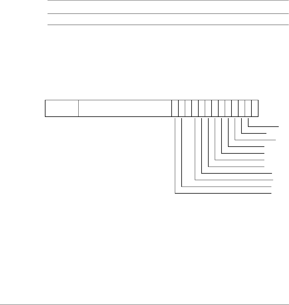
G4 AArch32 System Register Descriptions
G4.6 Generic Interrupt Controller CPU interface registers
G4-4308 Copyright © 2013 ARM Limited. All rights reserved. ARM DDI 0487A.a
Non-Confidential - Beta ID090413
G4.6.42 ICH_HCR, Interrupt Controller Hyp Control Register
The ICH_HCR characteristics are:
Purpose
Controls the environment for guest operating systems.
This register is part of:
• the GIC registers functional group
• the Virtualization registers functional group.
Usage constraints
This register is accessible as shown below:
Configurations
ICH_HCR is architecturally mapped to AArch64 register ICH_HCR_EL2.
Attributes
ICH_HCR is a 32-bit register.
The ICH_HCR bit assignments are:
EOIcount, bits [31:27]
Counts the number of EOIs received that do not have a corresponding entry in the List registers. The
virtual CPU interface increments this field automatically when a matching EOI is received.
EOIs that do not clear a bit in one of the Active Priorities registers ICH_APmRn do not cause an
increment.
Although not possible under correct operation, if an EOI occurs when the value of this field is 31,
this field wraps to 0.
The maintenance interrupt is asserted whenever this field is non-zero and the LRENPIE bit is set to
1.
Bits [26:13]
Reserved, RES0.
EL0 (NS) EL0 (S) EL1 (NS) EL1 (S) EL2 EL3 (SCR.NS=1) EL3 (SCR.NS=0)
- - - - RW RW -
EOIcount
31 27
RES0
26 13 12 11
TC
10 9 8 7 6 5 4 3 2 1
En
0
UIE
LRENPIE
NPIE
VGrp0EIE
VGrp0DIE
VGrp1EIE
VGrp1DIE
VSEIE
VARE
TALL0
TALL1

G4 AArch32 System Register Descriptions
G4.6 Generic Interrupt Controller CPU interface registers
ARM DDI 0487A.a Copyright © 2013 ARM Limited. All rights reserved. G4-4309
ID090413 Non-Confidential - Beta
TALL1, bit [12]
Trap all Non-secure EL1 accesses to ICC_* system registers for group 1 interrupts to EL2.
0
Non-Secure EL1 accesses to ICC_* registers for group 1 interrupts proceed as normal.
1
Any Non-secure EL1 accesses to ICC_* registers for group 1 interrupts trap to EL2.
TALL0, bit [11]
Trap all Non-secure EL1 accesses to ICC_* system registers for group 0 interrupts to EL2.
0
Non-Secure EL1 accesses to ICC_* registers for group 0 interrupts proceed as normal.
1
Any Non-secure EL1 accesses to ICC_* registers for group 0 interrupts trap to EL2.
TC, bit [10]
Trap all Non-secure El1 accesses to system registers that are common to group 0 and group 1 to
EL2.
0
Non-secure EL1 accesses to common registers proceed as normal.
1
Any Non-secure EL1 accesses to common registers trap to EL2.
This affects ICC_DIR, ICC_PMR, and ICC_RPR.
VARE, bit [9]
Virtual ARE.
0
The guest operating system does not use affinity routing and expects a Source CPU ID
for SGIs.
1
The guest operating system uses affinity routing.
When VARE is 0, the guest operating system does not support LPIs and software must ensure that
no LPIs are presented to the guest either using the List registers or from the Distributor.
VSEIE, bit [8]
Virtual SEI Enable. Enables the signaling of a maintenance interrupt when performing a virtual
access to a system register and a condition that would result in an (optional) SEI for a physical
access is detected.
0
VSEIE maintenance interrupt is disabled.
1
VSEIE maintenance interrupt is enabled.
VGrp1DIE, bit [7]
VM Disable Group 1 Interrupt Enable. Enables the signaling of a maintenance interrupt while
signaling of Group 1 interrupts from the virtual CPU interface to the connected virtual machine is
disabled:
0
Maintenance interrupt disabled.
1
Maintenance interrupt signaled while GICV_CTLR.EnableGrp1 is set to 0.
VGrp1EIE, bit [6]
VM Enable Group 1 Interrupt Enable. Enables the signaling of a maintenance interrupt while
signaling of Group 1 interrupts from the virtual CPU interface to the connected virtual machine is
enabled:
0
Maintenance interrupt disabled.
1
Maintenance interrupt signaled while GICV_CTLR.EnableGrp1 is set to 1.
VGrp0DIE, bit [5]
VM Disable Group 0 Interrupt Enable. Enables the signaling of a maintenance interrupt while
signaling of Group 0 interrupts from the virtual CPU interface to the connected virtual machine is
disabled:
0
Maintenance interrupt disabled.
1
Maintenance interrupt signaled while GICV_CTLR.EnableGrp0 is set to 0.

G4 AArch32 System Register Descriptions
G4.6 Generic Interrupt Controller CPU interface registers
G4-4310 Copyright © 2013 ARM Limited. All rights reserved. ARM DDI 0487A.a
Non-Confidential - Beta ID090413
VGrp0EIE, bit [4]
VM Enable Group 0 Interrupt Enable. Enables the signaling of a maintenance interrupt while
signaling of Group 0 interrupts from the virtual CPU interface to the connected virtual machine is
enabled:
0
Maintenance interrupt disabled.
1
Maintenance interrupt signaled while GICV_CTLR.EnableGrp0 is set to 1.
NPIE, bit [3]
No Pending Interrupt Enable. Enables the signaling of a maintenance interrupt while no pending
interrupts are present in the List registers:
0
Maintenance interrupt disabled.
1
Maintenance interrupt signaled while the List registers contain no interrupts in the
pending state.
LRENPIE, bit [2]
List Register Entry Not Present Interrupt Enable. Enables the signaling of a maintenance interrupt
while the virtual CPU interface does not have a corresponding valid List register entry for an EOI
request:
0
Maintenance interrupt disabled.
1
A maintenance interrupt is asserted while the EOIcount field is not 0.
UIE, bit [1]
Underflow Interrupt Enable. Enables the signaling of a maintenance interrupt when the List
registers are empty, or hold only one valid entry:
0
Maintenance interrupt disabled.
1
A maintenance interrupt is asserted if none, or only one, of the List register entries is
marked as a valid interrupt.
En, bit [0]
Enable. Global enable bit for the virtual CPU interface:
0
Virtual CPU interface operation disabled.
1
Virtual CPU interface operation enabled.
When this field is set to 0:
• The virtual CPU interface does not signal any maintenance interrupts.
• The virtual CPU interface does not signal any virtual interrupts.
• A read of GICV_IAR or GICV_AIAR returns a spurious interrupt ID.
Accessing the ICH_HCR:
To access the ICH_HCR:
MRC p15,4,<Rt>,c12,c11,0 ; Read ICH_HCR into Rt
MCR p15,4,<Rt>,c12,c11,0 ; Write Rt to ICH_HCR
Register access is encoded as follows:
coproc opc1 CRn CRm opc2
1111 100 1100 1011 000
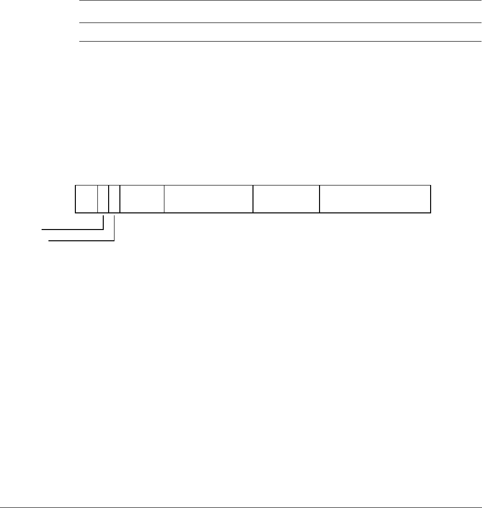
G4 AArch32 System Register Descriptions
G4.6 Generic Interrupt Controller CPU interface registers
ARM DDI 0487A.a Copyright © 2013 ARM Limited. All rights reserved. G4-4311
ID090413 Non-Confidential - Beta
G4.6.43 ICH_LRC<n>, Interrupt Controller List Registers, n = 0 - 15
The ICH_LRC<n> characteristics are:
Purpose
Provides interrupt context information for the virtual CPU interface.
This register is part of:
• the GIC registers functional group
• the Virtualization registers functional group.
Usage constraints
This register is accessible as shown below:
ICH_LR<n> and ICH_LRC<n> may be updated independently.
Configurations
ICH_LRC<n> is architecturally mapped to AArch64 register ICH_LR<n>_EL2[63:32].
Attributes
ICH_LRC<n> is a 32-bit register.
The ICH_LRC<n> bit assignments are:
State, bits [31:30]
The state of the interrupt:
00
Invalid
01
Pending
10
Active
11
Pending and active.
The GIC updates these state bits as virtual interrupts proceed through the interrupt life cycle. Entries
in the invalid state are ignored, except for the purpose of generating virtual maintenance interrupts.
For hardware interrupts, the pending and active state is held in the physical Distributor rather than
the virtual CPU interface. A hypervisor must only use the pending and active state for software
originated interrupts, which are typically associated with virtual devices, or SGIs.
HW, bit [29]
Indicates whether this virtual interrupt is a hardware interrupt, meaning that it corresponds to a
physical interrupt. Deactivation of the virtual interrupt also causes the deactivation of the physical
interrupt with the ID that the PhysicalID field indicates.
0
The interrupt is triggered entirely in software. No notification is sent to the Distributor
when the virtual interrupt is deactivated.
EL0 (NS) EL0 (S) EL1 (NS) EL1 (S) EL2 EL3 (SCR.NS=1) EL3 (SCR.NS=0)
- - - - RW RW -
State
31 30 29 28
RES0
27 24
Priority
23 16
RES0
15 10
PhysicalID
90
HW
Group

G4 AArch32 System Register Descriptions
G4.6 Generic Interrupt Controller CPU interface registers
G4-4312 Copyright © 2013 ARM Limited. All rights reserved. ARM DDI 0487A.a
Non-Confidential - Beta ID090413
1
The interrupt is a hardware interrupt. A deactivate interrupt request is sent to the
Distributor when the virtual interrupt is deactivated, using the PhysicalID field from this
register to indicate the physical interrupt ID.
If GICV_CTLR.EOImode is 0, this request corresponds to a write to the GICV_EOIR
or GICV_AEOIR, otherwise it corresponds to a write to the GICV_DIR.
Bits [27:24]
Reserved, RES0.
Priority, bits [23:16]
The priority of this interrupt.
It is IMPLEMENTATION DEFINED how many bits of priority are implemented, though at least five bits
must be implemented. Unimplemented bits are RES0 and start from bit [48] up to bit [50]. The
number of implemented bits can be discovered from ICH_VTR_EL2.PRIbits, and determines how
many GICH_APR<n> registers exist.
Bits [15:10]
Reserved, RES0.
PhysicalID, bits [9:0]
Physical ID, for hardware interrupts.
When HW is 0 (i.e. there is no corresponding physical interrupt), some of these bits have a special
meaning:
Bit [39]
EOI. When this bit is 1, a maintenance interrupt is asserted to signal EOI when the
interrupt state is invalid, which typically occurs when the interrupt is deactivated.
Bits [38:32]
Reserved, RES0.
It is IMPLEMENTATION DEFINED how many bits are implemented, though at least 16 bits must be
implemented. Unimplemented bits are RES0. The number of implemented bits can be discovered
from ICH_VTR_EL2.IDbits.
Accessing the ICH_LRC<n>:
To access the ICH_LRC<n>:
MRC p15,4,<Rt>,c12,<CRm>,<opc2> ; Read ICH_LRC<n> into Rt, where n is in the range 0 to 15
MCR p15,4,<Rt>,c12,<CRm>,<opc2> ; Write Rt to ICH_LRC<n>, where n is in the range 0 to 15
Register access is encoded as follows:
coproc opc1 CRn CRm opc2
1111 100 1100 111:n<3:3> n<2:0>

G4 AArch32 System Register Descriptions
G4.6 Generic Interrupt Controller CPU interface registers
ARM DDI 0487A.a Copyright © 2013 ARM Limited. All rights reserved. G4-4313
ID090413 Non-Confidential - Beta
G4.6.44 ICH_LR<n>, Interrupt Controller List Registers, n = 0 - 15
The ICH_LR<n> characteristics are:
Purpose
Provides interrupt context information for the virtual CPU interface.
This register is part of:
• the GIC registers functional group
• the Virtualization registers functional group.
Usage constraints
This register is accessible as shown below:
ICH_LR<n> and ICH_LRC<n> may be updated independently.
Configurations
ICH_LR<n> is architecturally mapped to AArch64 register ICH_LR<n>_EL2[31:0].
Attributes
ICH_LR<n> is a 32-bit register.
The ICH_LR<n> bit assignments are:
VirtualID, bits [31:0]
Virtual ID of the interrupt.
When VARE is zero, software must ensure the correct Source CPU ID is provided in bits [12:10].
Software must ensure there is only a single valid entry for a given VirtualID.
It is IMPLEMENTATION DEFINED how many bits are implemented, though at least 16 bits must be
implemented. Unimplemented bits are RES0. The number of implemented bits can be discovered
from ICH_VTR_EL2.IDbits.
Accessing the ICH_LR<n>:
To access the ICH_LR<n>:
MRC p15,4,<Rt>,c12,<CRm>,<opc2> ; Read ICH_LR<n> into Rt, where n is in the range 0 to 15
MCR p15,4,<Rt>,c12,<CRm>,<opc2> ; Write Rt to ICH_LR<n>, where n is in the range 0 to 15
Register access is encoded as follows:
EL0 (NS) EL0 (S) EL1 (NS) EL1 (S) EL2 EL3 (SCR.NS=1) EL3 (SCR.NS=0)
- - - - RW RW -
VirtualID
31 0
coproc opc1 CRn CRm opc2
1111 100 1100 110:n<3:3> n<2:0>
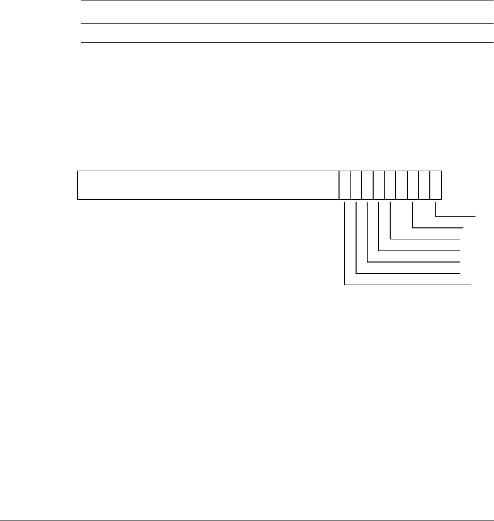
G4 AArch32 System Register Descriptions
G4.6 Generic Interrupt Controller CPU interface registers
G4-4314 Copyright © 2013 ARM Limited. All rights reserved. ARM DDI 0487A.a
Non-Confidential - Beta ID090413
G4.6.45 ICH_MISR, Interrupt Controller Maintenance Interrupt State Register
The ICH_MISR characteristics are:
Purpose
Indicates which maintenance interrupts are asserted.
This register is part of:
• the GIC registers functional group
• the Virtualization registers functional group.
Usage constraints
This register is accessible as shown below:
Configurations
ICH_MISR is architecturally mapped to AArch64 register ICH_MISR_EL2.
Attributes
ICH_MISR is a 32-bit register.
The ICH_MISR bit assignments are:
Bits [31:9]
Reserved, RES0.
VSEI, bit [8]
Virtual SEI. Set to 1 when a condition that would result in generation of an SEI is detected during
a virtual access to an ICC_* system register.
VGrp1D, bit [7]
Disabled Group 1 maintenance interrupt.
Asserted whenever ICH_HCR_EL2.VGrp1DIE is 1 and ICH_VMCR_EL2.VMGrp1En is 0.
VGrp1E, bit [6]
Enabled Group 1 maintenance interrupt.
Asserted whenever ICH_HCR_EL2.VGrp1EIE is 1 and ICH_VMCR_EL2.VMGrp1En is 1.
VGrp0D, bit [5]
Disabled Group 0 maintenance interrupt.
EL0 (NS) EL0 (S) EL1 (NS) EL1 (S) EL2 EL3 (SCR.NS=1) EL3 (SCR.NS=0)
- - - - RO RO -
RES0
31 9 8 7 6 5 4
NP
32
U
10
EOI
LRENP
VGrp0E
VGrp0D
VGrp1E
VGrp1D
VSEI

G4 AArch32 System Register Descriptions
G4.6 Generic Interrupt Controller CPU interface registers
ARM DDI 0487A.a Copyright © 2013 ARM Limited. All rights reserved. G4-4315
ID090413 Non-Confidential - Beta
Asserted whenever ICH_HCR_EL2.VGrp0DIE is 1 and ICH_VMCR_EL2.VMGrp0En is 0.
VGrp0E, bit [4]
Enabled Group 0 maintenance interrupt.
Asserted whenever ICH_HCR_EL2.VGrp0EIE is 1 and ICH_VMCR_EL2.VMGrp0En is 1.
NP, bit [3]
No Pending maintenance interrupt.
Asserted whenever ICH_HCR_EL2.NPIE is 1 and no List register is in pending state.
LRENP, bit [2]
List Register Entry Not Present maintenance interrupt.
Asserted whenever ICH_HCR_EL2.LRENPIE is 1 and ICH_HCR_EL2.EOIcount is non-zero.
U, bit [1]
Underflow maintenance interrupt.
Asserted whenever ICH_HCR_EL2.UIE is 1 and if none, or only one, of the List register entries are
marked as a valid interrupt, that is, if the corresponding ICH_LR<n>_EL2.State bits do not equal
0x0
.
EOI, bit [0]
EOI maintenance interrupt.
Asserted whenever at least one List register is asserting an EOI interrupt. That is, when at least one
bit in ICH_EISR0_EL1 or ICH_EISR1_EL1 is 1.
Accessing the ICH_MISR:
To access the ICH_MISR:
MRC p15,4,<Rt>,c12,c11,2 ; Read ICH_MISR into Rt
Register access is encoded as follows:
coproc opc1 CRn CRm opc2
1111 100 1100 1011 010
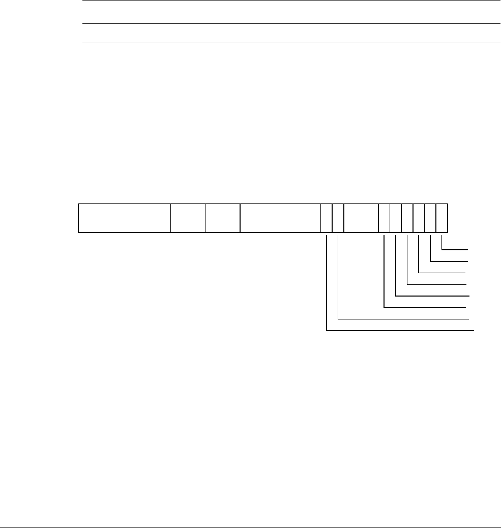
G4 AArch32 System Register Descriptions
G4.6 Generic Interrupt Controller CPU interface registers
G4-4316 Copyright © 2013 ARM Limited. All rights reserved. ARM DDI 0487A.a
Non-Confidential - Beta ID090413
G4.6.46 ICH_VMCR, Interrupt Controller Virtual Machine Control Register
The ICH_VMCR characteristics are:
Purpose
Enables the hypervisor to save and restore the virtual machine view of the GIC state.
This register is part of:
• the GIC registers functional group
• the Virtualization registers functional group.
Usage constraints
This register is accessible as shown below:
When EL2 is using system register access, EL1 using either system register or memory-mapped
access must be supported.
Configurations
ICH_VMCR is architecturally mapped to AArch64 register ICH_VMCR_EL2.
Attributes
ICH_VMCR is a 32-bit register.
The ICH_VMCR bit assignments are:
VPMR, bits [31:24]
Virtual Priority Mask.
Visible to the guest OS as ICC_PMR_EL1 / GICV_PMR.
VBPR0, bits [23:21]
Virtual BPR0.
Visible to the guest OS as ICC_BPR0_EL1 / GICV_BPR.
VBPR1, bits [20:18]
Virtual BPR1.
Visible to the guest OS as ICC_BPR1_EL1 / GICV_ABPR.
EL0 (NS) EL0 (S) EL1 (NS) EL1 (S) EL2 EL3 (SCR.NS=1) EL3 (SCR.NS=0)
- - - - RW RW -
VPMR
31 24
VBPR0
23 21
VBPR1
20 18
RES0
17 11 10 9
RES0
86
5 4 3 2 1 0
VENG0
VENG1
VAckCtl
VFIQEn
VCBPR
VENSEI
VEOIM
VSRE

G4 AArch32 System Register Descriptions
G4.6 Generic Interrupt Controller CPU interface registers
ARM DDI 0487A.a Copyright © 2013 ARM Limited. All rights reserved. G4-4317
ID090413 Non-Confidential - Beta
Bits [17:11]
Reserved, RES0.
VSRE, bit [10]
Virtual SRE.
Visible to the guest OS as ICC_SRE_EL1.SRE.
If EL2 is not configured to use system registers, this bit is treated as if it is 0.
VEOIM, bit [9]
Virtual EOImode.
Visible to the guest OS as ICC_CTLR_EL1.EOImode / GICV_CTLR.EOImode.
Bits [8:6]
Reserved, RES0.
VENSEI, bit [5]
This bit is IMPLEMENTATION DEFINED.
If an implementation does not have functionality associated with this bit, ARM recommends that
the bit is RES0.
VCBPR, bit [4]
Virtual CBPR.
Visible to the guest OS as ICC_CTLR_EL1.CBPR / GICV_CTLR.CBPR.
VFIQEn, bit [3]
Virtual FIQ enable.
Visible to the guest OS as GICV_CTLR.FIQEn.
VAckCtl, bit [2]
Virtual AckCtl.
Visible to the guest OS as GICV_CTLR.AckCtl.
VENG1, bit [1]
Virtual group 1 interrupt enable.
Visible to the guest OS as ICC_IGRPEN1_EL1.Enable / GICV_CTLR.EnableGrp1.
VENG0, bit [0]
Virtual group 0 interrupt enable.
Visible to the guest OS as ICC_IGRPEN0_EL1.Enable / GICV_CTLR.EnableGrp0.
Accessing the ICH_VMCR:
To access the ICH_VMCR:
MRC p15,4,<Rt>,c12,c11,7 ; Read ICH_VMCR into Rt
MCR p15,4,<Rt>,c12,c11,7 ; Write Rt to ICH_VMCR
Register access is encoded as follows:
coproc opc1 CRn CRm opc2
1111 100 1100 1011 111

G4 AArch32 System Register Descriptions
G4.6 Generic Interrupt Controller CPU interface registers
G4-4318 Copyright © 2013 ARM Limited. All rights reserved. ARM DDI 0487A.a
Non-Confidential - Beta ID090413
G4.6.47 ICH_VSEIR, Interrupt Controller Virtual System Error Interrupt Register
The ICH_VSEIR characteristics are:
Purpose
Allows the hypervisor to inject a virtual SEI.
This register is part of:
• the GIC registers functional group
• the Virtualization registers functional group.
Usage constraints
This register is accessible as shown below:
Configurations
ICH_VSEIR is architecturally mapped to AArch64 register ICH_VSEIR_EL2.
Attributes
ICH_VSEIR is a 32-bit register.
The ICH_VSEIR bit assignments are:
Accessing the ICH_VSEIR:
To access the ICH_VSEIR:
MRC p15,4,<Rt>,c12,c9,4 ; Read ICH_VSEIR into Rt
MCR p15,4,<Rt>,c12,c9,4 ; Write Rt to ICH_VSEIR
Register access is encoded as follows:
EL0 (NS) EL0 (S) EL1 (NS) EL1 (S) EL2 EL3 (SCR.NS=1) EL3 (SCR.NS=0)
- - - - RW RW -
IMPLEMENTATION DEFINED
31 0
coproc opc1 CRn CRm opc2
1111 100 1100 1001 100
G4 AArch32 System Register Descriptions
G4.6 Generic Interrupt Controller CPU interface registers
ARM DDI 0487A.a Copyright © 2013 ARM Limited. All rights reserved. G4-4319
ID090413 Non-Confidential - Beta
G4.6.48 ICH_VTR, Interrupt Controller VGIC Type Register
The ICH_VTR characteristics are:
Purpose
Describes the number of implemented virtual priority bits and List registers.
This register is part of:
• the GIC registers functional group
• the Virtualization registers functional group.
Usage constraints
This register is accessible as shown below:
Configurations
ICH_VTR is architecturally mapped to AArch64 register ICH_VTR_EL2.
Attributes
ICH_VTR is a 32-bit register.
The ICH_VTR bit assignments are:
PRIbits, bits [31:29]
The number of virtual priority bits implemented, minus one.
PREbits, bits [28:26]
The number of virtual preemption bits implemented, minus one.
IDbits, bits [25:23]
The number of virtual interrupt identifier bits supported:
000
16 bits.
001
24 bits.
All other values are reserved.
SEIS, bit [22]
SEI Support. Indicates whether the virtual CPU interface supports generation of SEIs:
0
The virtual CPU interface logic does not support generation of SEIs.
1
The virtual CPU interface logic supports generation of SEIs.
Virtual system errors may still be generated by writing to ICH_VSEIR_EL2 regardless of the value
of this field.
EL0 (NS) EL0 (S) EL1 (NS) EL1 (S) EL2 EL3 (SCR.NS=1) EL3 (SCR.NS=0)
- - - - RO RO -
PRIbits
31 29
PREbits
28 26
IDbits
25 23 22 21
RES0
20 5
ListRegs
40
SEIS
A3V

G4 AArch32 System Register Descriptions
G4.6 Generic Interrupt Controller CPU interface registers
G4-4320 Copyright © 2013 ARM Limited. All rights reserved. ARM DDI 0487A.a
Non-Confidential - Beta ID090413
A3V, bit [21]
Affinity 3 Valid. Possible values are:
0
The virtual CPU interface logic only supports zero values of Affinity 3 in SGI
generation system registers.
1
The virtual CPU interface logic supports non-zero values of Affinity 3 in SGI generation
system registers.
Bits [20:5]
Reserved, RES0.
ListRegs, bits [4:0]
The number of implemented List registers, minus one. For example, a value of
0b01111
indicates that
the maximum of 16 List registers are implemented.
Accessing the ICH_VTR:
To access the ICH_VTR:
MRC p15,4,<Rt>,c12,c11,1 ; Read ICH_VTR into Rt
Register access is encoded as follows:
coproc opc1 CRn CRm opc2
1111 100 1100 1011 001
Part H
External Debug

ARM DDI 0487A.a Copyright © 2013 ARM Limited. All rights reserved. H1-4323
ID090413 Non-Confidential - Beta
Chapter H1
Introduction to External Debug
This chapter introduces the external debug components of ARMv8. It contains the following sections:
•Introduction to external debug on page H1-4324.
•External debug on page H1-4325.
Note
For information about self-hosted debug, see Chapter D2 Debug Exceptions and Chapter D3 The Debug Exception
Model.

H1 Introduction to External Debug
H1.1 Introduction to external debug
H1-4324 Copyright © 2013 ARM Limited. All rights reserved. ARM DDI 0487A.a
Non-Confidential - Beta ID090413
H1.1 Introduction to external debug
ARMv8 supports both:
Self-hosted debug
The PE itself hosts a debugger. That is, developers developing software to run on the PE use
debugger software running on the same PE.
External debug
The debugger is external to the PE. The debugging might be either on-chip, for example in a second
PE, or off-chip, for example a JTAG debugger. External debug is particularly useful for:
• Hardware bring-up. That is, debugging during development when a system is first powered
up and not all of the software functionality is available.
• PEs that are deeply embedded inside systems.
To support external debug, the ARM architecture defines required features that are called external
debug features.
Note
When the description of external debug in this part of the manual describes a debugger as controlling external debug
this might be a second on-chip PE or a processor in an off-chip device such as a JTAG debugger.

H1 Introduction to External Debug
H1.2 External debug
ARM DDI 0487A.a Copyright © 2013 ARM Limited. All rights reserved. H1-4325
ID090413 Non-Confidential - Beta
H1.2 External debug
The following halting debug events are available in ARMv8:
•Halting Step debug event on page H3-4366:
— The debugger can use this resource to make the PE step through code one line at a time.
•Halt Instruction debug event on page H3-4376:
— This might occur when software executes the Halting software breakpoint instruction,
HLT
.
•Exception Catch debug event on page H3-4377:
— This can be programmed to occur on all entries to a given Exception level.
•External Debug Request debug event on page H3-4380:
— An embedded cross-trigger can signal this debug event.
•OS Unlock Catch debug event on page H3-4381:
— This might occur when the state of the OS Lock changes from locked to unlocked.
•Reset Catch debug event on page H3-4382:
— This might occur when the PE exits reset state.
•Software Access debug event on page H3-4383:
— This can be programmed to occur when software tries to access the Breakpoint Value registers, the
Breakpoint Control registers, the Watchpoint value registers, or the Watchpoint Control registers. It
caused a trap to Debug state.
Halting debug events allow an external debugger to halt the PE. Breakpoints and watchpoints can also halt the PE.
The PE then enters Debug state. When the PE is in Debug state:
• It stops executing instructions from the location indicated by the program counter, and is instead controlled
through the external debug interface.
• The Instruction Transfer Register, ITR, passes instructions to the PE to execute in Debug state:
— The ITR contains a single register, EDITR, and associated flow-control flags.
• The Debug Communications Channel, DCC, passes data between the PE and the debugger:
— The DCC includes the data transfer registers, DTRRX and DTRTX, and associated flow-control flags.
— Although the DCC is an essential part of Debug state operation, it can also be used in Non-debug state.
• The PE cannot service any interrupts in Debug state.
Chapter H2 Debug State describes Debug state in more detail.

H1 Introduction to External Debug
H1.2 External debug
H1-4326 Copyright © 2013 ARM Limited. All rights reserved. ARM DDI 0487A.a
Non-Confidential - Beta ID090413

ARM DDI 0487A.a Copyright © 2013 ARM Limited. All rights reserved. H2-4327
ID090413 Non-Confidential - Beta
Chapter H2
Debug State
This chapter describes Debug state. It contains the following sections:
•About Debug state on page H2-4328.
•Halting the PE on debug events on page H2-4329.
•Entering Debug state on page H2-4337.
•Behavior in Debug state on page H2-4341.
•Exiting Debug state on page H2-4361.
Note
Table J-1 on page AppxJ-5088 disambiguates the general register references used in this chapter.

H2 Debug State
H2.1 About Debug state
H2-4328 Copyright © 2013 ARM Limited. All rights reserved. ARM DDI 0487A.a
Non-Confidential - Beta ID090413
H2.1 About Debug state
In external debug, debug events allow an external debugger to halt the PE. The PE then enters Debug state. When
the PE is in Debug state:
• It stops executing instructions from the location indicated by the program counter, and is instead controlled
through the external debug interface.
• The Instruction Transfer Register, ITR, passes instructions to the PE to execute in Debug state.
• The Debug Communications Channel, DCC, passes data between the PE and the debugger.
The PE cannot service any interrupts in Debug state.

H2 Debug State
H2.2 Halting the PE on debug events
ARM DDI 0487A.a Copyright © 2013 ARM Limited. All rights reserved. H2-4329
ID090413 Non-Confidential - Beta
H2.2 Halting the PE on debug events
For details of debug events see Introduction to Halting debug events on page H3-4364 and Breakpoint and
Watchpoint debug events on page H2-4330.
On a debug event, the PE must do one of the following:
• Enter Debug state.
• Pend the debug event.
• Generate a debug exception.
• Ignore the debug event.
This behavior depends on both:
• Whether halting is allowed by the current state of the debug authentication interface. See Halting allowed
and halting prohibited.
• The type of debug event and the programming of the debug control registers.
—See Halting debug events for all Halting debug events.
—See Breakpoint and Watchpoint debug events on page H2-4330 for Breakpoint and Watchpoint debug
events.
See also Other debug exceptions on page H2-4331.
This means that behavior can be UNPREDICTABLE if the conditions change. See Synchronization and Halting debug
events on page H3-4384.
Summary of debug events and possible outcomes on page H3-4364 summarizes the possible outcomes of each type
of debug event.
H2.2.1 Halting allowed and halting prohibited
Halting can be either allowed or prohibited:
• Halting is always prohibited in Debug state.
• Halting is always prohibited when
DoubleLockStatus()
== TRUE.
— This means that OS Double Lock is locked, that is EDPRSR.DLK == 1.
• Halting is also controlled by the IMPLEMENTATION DEFINED authentication interface, and is prohibited when
either:
— The PE is in Non-secure state and
ExternalInvasiveDebugEnabled()
== FALSE.
— The PE is in Secure state and
ExternalSecureInvasiveDebugEnabled()
== FALSE.
Note
See Appendix B Recommended External Debug Interface for more information on these functions.
• Otherwise, halting is allowed.
See Pseudocode details of Halting on debug events on page H2-4335.
H2.2.2 Halting debug events
When a Halting debug event is generated, it causes entry to Debug state if both:
• Halting is allowed. See Halting allowed and halting prohibited.
• The Halting debug event is either:
— A Halt Instruction debug event and Halting debug-mode is enabled. This means that EDSCR.HDE ==
1.
— Not a Halt Instruction debug event.

H2 Debug State
H2.2 Halting the PE on debug events
H2-4330 Copyright © 2013 ARM Limited. All rights reserved. ARM DDI 0487A.a
Non-Confidential - Beta ID090413
Note
— An Halt Instruction debug event is the only Halting debug event that relies on EDSCR.HDE == 1. This
is to prevent malicious code from causing an entry Debug state. EDSCR.HDE == 0 on a Cold reset.
— Halting on Breakpoint and Watchpoint Software debug events is also controlled by EDSCR.HDE. See
Breakpoint and Watchpoint debug events.
—EDSCR.HDE can be written by software when the OS Lock is locked. Privileged code can use
SDCR.TDOSA and HDCR.TDOSA to trap writes to these registers.
If a Halting debug event does not generate entry to Debug state because the conditions listed in this section do not
hold, then:
• If the Halting debug event is a Halt Instruction debug event, it generates an Undefined Instruction exception.
• If the Halting debug event is an Exception Catch debug event or a Software Access debug event, it is ignored.
• In all other cases the Halting debug event is pended, meaning that:
— The pending Halting debug event is recorded in EDESR.
— The pending Halting debug event is taken when halting is allowed. See Pending Halting debug events
on page H3-4384.
Pending Halting debug events are discarded by a Cold reset. The debugger can also force a pending event to be
dropped by writing to EDESR. Summary of actions from debug events on page H2-4334 summarizes the possible
outcome for each type of Debug event.
Note
Halting debug events never generate Debug exceptions.
H2.2.3 Breakpoint and Watchpoint debug events
A breakpoint or watchpoint generates an entry to Debug state if all of the following conditions hold:
• Halting debug-mode is enabled, that is EDSCR.HDE == 1.
• Halting is allowed. See Halting allowed and halting prohibited on page H2-4329.
• The OS Lock is unlocked, that is OSLSR.OSLK == 0.
The Address Mismatch breakpoint type is reserved when all of these conditions are met. See Legacy debug
exceptions on page D2-1564.
MDSCR_EL1.MDE or DBGDSCRext.MDBGen is ignored when determining whether to enter Debug state. A
breakpoint or watchpoint that generates entry to Debug state is a Breakpoint or Watchpoint debug event and does
not generate a debug exception.
A breakpoint or watchpoint that does not generate an entry to Debug state either:
• Generates a Breakpoint or Watchpoint exception.
• Is ignored.
Note
EDSCR.HDE is ignored when determining whether to generate a debug exception. The debug exception is
suppressed only if the PE enters Debug state. This means that the use of Halting-debug mode in Non-secure state
does not affect the Exception model in Secure state.
See Chapter D2 Debug Exceptions and the Note in Other debug exceptions on page H2-4331.

H2 Debug State
H2.2 Halting the PE on debug events
ARM DDI 0487A.a Copyright © 2013 ARM Limited. All rights reserved. H2-4331
ID090413 Non-Confidential - Beta
H2.2.4 Other debug exceptions
The following events never generate entry to Debug state:
• Software Breakpoint Instruction exceptions.
• Software Step exceptions.
• Vector Catch exceptions. See also Legacy debug exceptions on page D2-1564.
The behavior of these events is unchanged when Halting debug mode is enabled, that is when EDSCR.HDE == 1.
This means that these events can do one of the following:
• They can generate a debug exception.
• They can be ignored.
For additional information, see Chapter D2 Debug Exceptions.
H2.2.5 Debug state entry and debug event prioritization
The architecture does not define when asynchronous Halting debug events are taken, and therefore the prioritization
of asynchronous debug events is IMPLEMENTATION DEFINED.
Synchronous Halting debug events do have a priority order.
The following are synchronous Halting debug events:
• Halting Step debug event.
• Halt Instruction debug event.
• Exception Catch debug event.
• Software Access debug event.
• Reset Catch debug event.
Each of these synchronous Halting debug events is treated as a synchronous exception generated by an instruction,
or by the taking of an exception or reset. That is, the synchronous Halting debug event must be taken before any
subsequent instructions are executed. Reset Catch debug events must be taken before the PE executes the instruction
at the reset vector.
Note
Reset Catch and Exception Catch debug events can also be generated asynchronously, because they can result from
an asynchronous exception. However, if halting is allowed after the asynchronous exception has been processed,
the Reset Catch or Exception Catch debug event is taken synchronously.
The Halting Step debug event is generated by the instruction after the stepped instruction. Therefore, if the stepped
instruction generates any other synchronous exceptions or debug events, these are taken first.
OS Unlock Catch debug events are always pended and taken asynchronously.
Halting Step debug events and Reset Catch debug events might be pended and taken asynchronously at a later time.
The following list shows how the events are prioritized, with -2.0 being the highest priority.
Note
The priority numbering is the same as the numbering for synchronous exception priorities listed in Synchronous
exception types, routing and priorities on page D1-1450. The Debug events in this section with a negative priority
are a higher priority than any synchronous exception. The debug events with fractional priorities have a priority
between two or more exceptions.
The priority for synchronous debug events is as follows:
-2 Reset Catch debug event. See Reset Catch debug event on page H3-4382.
This debug event has a higher priority than the synchronous exceptions listed in Synchronous
exception types, routing and priorities on page D1-1450.

H2 Debug State
H2.2 Halting the PE on debug events
H2-4332 Copyright © 2013 ARM Limited. All rights reserved. ARM DDI 0487A.a
Non-Confidential - Beta ID090413
-1 Exception Catch debug event. See Exception Catch debug event on page H3-4377.
This debug event can be assigned one of two priorities. When it has a priority of -1, it has a higher
priority than the synchronous exceptions listed in the Exception model. See Exception Catch debug
event on page H3-4377.
0 Halting Step debug event. See Halting Step debug event on page H3-4366.
This debug event has a higher priority than the synchronous exceptions listed in the Exception
model.
1 Software Step debug event. See Software Step exceptions on page D2-1634.
1.5 Exception Catch debug event. See Exception Catch debug event on page H3-4377.
This debug event can be assigned one of two priorities, -1 or 1.5. See Exception Catch debug event
on page H3-4377.
2 - 3 These events are not debug events.
4 Breakpoint exception or debug event or Address Matching Vector Catch exception. See Breakpoint
exceptions on page D2-1569 and Vector Catch exceptions on page D2-1627.
These two debug events have the same priority.
5 - 13 These events are not debug events.
14 Halt Instruction debug event. See Halt Instruction debug event on page H3-4376.
15 - 19 These events are not debug events.
19.5 Software Access debug event. See Software Access debug event on page H3-4383.
20 - 21 These events are not debug events.
22 Watchpoint exception or debug event. See Watchpoint exceptions on page D2-1606.
For Reset Catch debug events and Halting Step debug events the priorities listed in this section only apply when
halting is allowed at the time the event is generated. This means that the event is taken synchronously and not
pended.
The prioritization of asynchronous Halting debug events, including pending Halting debug events taken
asynchronously, is IMPLEMENTATION DEFINED. See Taking Halting debug events asynchronously on page H3-4385.
For more information on the prioritization of exceptions see Synchronous exception types, routing and priorities on
page D1-1450.
Debug state entry and Software Step
When Software Step is active, a debug event that causes entry to Debug state behaves like an exception taken to an
Exception level above the debug target Exception level. That is:
• If the instruction that is stepped generates a synchronous debug event that causes entry to Debug state, or an
asynchronous debug event is taken before the step completes, the PE enters Debug state with DSPSR.SS set
to 1.
• A pending Halting debug event or an asynchronous debug event can be taken after the step has completed.
In this case the PE enters Debug state with DSPSR.SS set to 0.
In addition:
• If the instruction that is stepped generates an exception trapped by an Exception Catch debug event, the PE
enters Debug state at the exception vector with DSPSR.SS set to 0. This is because PSTATE.SS is set to 0 by
taking the exception.

H2 Debug State
H2.2 Halting the PE on debug events
ARM DDI 0487A.a Copyright © 2013 ARM Limited. All rights reserved. H2-4333
ID090413 Non-Confidential - Beta
• If the PE is reset, PSTATE.SS is reset to 0. If the following debug events are enabled, the PE enters Debug
state with DSPSR.SS set to 0:
— Reset Catch debug events at the reset Exception level.
— Exception Catch debug events at the reset Exception level.
— Halting Step debug events.
• If Halting Step is also active, then Halting Step and Software Step operate in parallel and can both become
active-pending. In this case Halting step has a higher priority than Software step. This means that the PE
enters Debug state and DSPSR.SS is set to 0.
Breakpoint debug events and Vector Catch exception
An Address Matching Vector Catch exception has the same priority as a Breakpoint debug event. See Synchronous
exception prioritization on page D1-1451.
The prioritization of these events is unchanged even if the breakpoint generates entry to Debug state instead of a
Breakpoint exception. This means that if a single instruction generates both an Address Matching Vector Catch
exception and a Breakpoint debug event, there is a CONSTRAINED UNPREDICTABLE choice of:
• The PE entering Debug state due to the Breakpoint debug event.
• A Vector Catch exception.
This only applies if all of the following are true:
• Halting debug-mode is enabled.
• Halting is allowed.
• The OS Lock is unlocked.
An Exception Trapping Vector Catch exception must be generated immediately following the exception that
generated it. This means that it does not appear in the priority table.
H2.2.6 Forcing entry to Debug state
Entry to Debug state is normally precise, meaning that the PE cannot enter Debug state if it can neither complete
nor abandon all currently executing instructions and leave the PE in a precise state.
A debugger can write a value of 1 to EDRCR.CBRRQ to allow imprecise entry to Debug state. An External Debug
Request debug event must be pending before writing 1 to this bit. Support for this feature is OPTIONAL and it is
IMPLEMENTATION DEFINED when it is effective at forcing entry to Debug state.
The PE ignores writes to this bit if either:
• External debugging is not enabled, meaning
ExternalInvasiveDebugEnabled()
== FALSE.
• Secure external debugging is not enabled, meaning
ExternalSecureInvasiveDebugEnabled()
== FALSE, and
either:
— EL3 is not implemented and the PE is Secure.
— EL3 is implemented.
Example H2-1 shows how entry to Debug state can be forced.
Example H2-1 Forcing entry to Debug state
The debugger pends an External Debug Request debug event through the CTI to halt a program that has stopped
responding. However, the memory system is not responding and a memory access instruction cannot complete. This
means that Debug state cannot be entered precisely. The debugger writes a value of 1 to EDRCR.CBRRQ. The PE
cancels all outstanding memory accesses and enters Debug state. As some instructions might not have completed
correctly, entry to Debug state is imprecise.

H2 Debug State
H2.2 Halting the PE on debug events
H2-4334 Copyright © 2013 ARM Limited. All rights reserved. ARM DDI 0487A.a
Non-Confidential - Beta ID090413
When Debug state is entered imprecisely, all memory access instructions executed through the ITR have
UNPREDICTABLE behavior. The value of all registers is UNKNOWN, but might be useful for diagnostic purposes.
H2.2.7 Summary of actions from debug events
Table H2-2 on page H2-4347 shows the Software and Halting debug events. In Table H2-2 on page H2-4347 the
columns have the following meaning:
Debug event type
This means the type of debug event where:
Other software means one of:
•Software Step exceptions on page D2-1634.
•Software Breakpoint Instruction exceptions on page D2-1566.
•Vector Catch exceptions on page D2-1627.
Other Halting means one of the following:
•Halting Step debug event on page H3-4366.
•External Debug Request debug event on page H3-4380.
•Reset Catch debug event on page H3-4382.
•OS Unlock Catch debug event on page H3-4381.
Other debug events are referred to explicitly.
Authentication
This means halting is allowed by the IMPLEMENTATION DEFINED external authentication interface.
It is the result of one of the following pseudocode functions:
In Secure state
ExternalSecureInvasiveDebugEnabled()
.
In Non-secure state
ExternalInvasiveDebugEnabled()
.
DLK This is the value EDPRSR.DLK. It indicates whether the OS Double Lock is locked,
DoubleLockStatus()
== TRUE.
OSLK This is the value of EDSCR.OSLK. It indicates whether the OS Lock is locked.
HDE This is the value of EDSCR.HDE. It indicates whether Halting debug-mode is enabled.
The letter X in Table H2-1 indicates that the value can be either 0 or 1.
Table H2-1 Debug authentication for external debug
Debug event type Authentication DLK OSLK HDE Behavior
Other software X X X X Handled by the Exception
model

H2 Debug State
H2.2 Halting the PE on debug events
ARM DDI 0487A.a Copyright © 2013 ARM Limited. All rights reserved. H2-4335
ID090413 Non-Confidential - Beta
H2.2.8 Pseudocode details of Halting on debug events
The following pseudocode outlines the
Halting()
,
Restarting()
,
HaltOnBreakpointOrWatchpoint()
, and
HaltingAllowed()
functions.
// Halted()
// ========
boolean Halted()
return !(EDSCR.STATUS IN {‘000001’, ‘000010’}); // Halted
// Restarting()
// ============
boolean Restarting()
return EDSCR.STATUS == ‘000001’; // Restarting
Breakpoint or Watchpoint debug
event X 1 X X Handled by the Exception
model (ignored)
X 0 1 X Handled by the Exception
model (ignored)
FALSE 0 0 X Handled by the Exception
model
TRUE 0 0 0 Handled by the Exception
model
TRUE 0 0 1 Entry to Debug state
Halt Instruction debug event FALSE X X X UNALLOCATED
TRUE 1 X X UNALLOCATED
TRUE 0 X 0 UNALLOCATED
TRUE 0 X 1 Entry to Debug state
Exception Catch debug event FALSE X X X Ignored
TRUE 1 X X Ignored
TRUE 0 X X Entry to Debug state
Software Access debug event FALSE X X X Ignored
TRUE 1 X X Ignored
TRUE 0 1 X Ignored
TRUE 0 0 X Entry to Debug state
Other Halting FALSE X X X Ignored
TRUE 1 X X Debug event is pended
TRUE 0 X X Entry to Debug state
Table H2-1 Debug authentication for external debug (continued)
Debug event type Authentication DLK OSLK HDE Behavior

H2 Debug State
H2.2 Halting the PE on debug events
H2-4336 Copyright © 2013 ARM Limited. All rights reserved. ARM DDI 0487A.a
Non-Confidential - Beta ID090413
// HaltOnBreakpointOrWatchpoint()
// ==============================
// Returns TRUE if the Breakpoint and Watchpoint debug events should be considered for Debug
// state entry, FALSE if they should be considered for a debug exception.
boolean HaltOnBreakpointOrWatchpoint()
return HaltingAllowed() && EDSCR.HDE == ‘1’ && OSLSR_EL1.OSLK == ‘0’;
// HaltingAllowed()
// ================
// Returns TRUE if halting is currently allowed, FALSE if halting is prohibited.
boolean HaltingAllowed()
if Halted() || DoubleLockStatus() then
return FALSE;
elsif IsSecure() then
return ExternalSecureInvasiveDebugEnabled();
else
return ExternalInvasiveDebugEnabled();

H2 Debug State
H2.3 Entering Debug state
ARM DDI 0487A.a Copyright © 2013 ARM Limited. All rights reserved. H2-4337
ID090413 Non-Confidential - Beta
H2.3 Entering Debug state
On entry to Debug state the preferred restart address and PSTATE are saved in DLR and DSPSR. The PE remains
in the mode and security state from which it entered Debug state.
If EDRCR.CBRRQ has a value of 0, entry to Debug state is precise. If EDRCR.CBRRQ has a value of 1 imprecise
entry to Debug state is permitted.
If a Watchpoint debug event causes an entry to Debug state, the address of the access that generated the Watchpoint
debug event is recorded in EDWAR.
Other than the effect on PSTATE and EDSCR, entry to Debug state is not a Context synchronization operation. The
effects of entry to Debug state on PSTATE and EDSCR are synchronized.
H2.3.1 Entering Debug state from AArch32 state
When entering Debug state from AArch32 state, the PE remains in AArch32 state. In AArch32 Debug state the PE
executes T32 instructions, regardless of the values of PSTATE.{J,T} before entering Debug state.
To allow the debugger to determine the state of the PE, the current execution state for all four Exception levels can
be read from EDSCR.RW.
The current endianness state, PSTATE.E, is unchanged on entry to Debug state.
Note
• If EL1 is using AArch32 state, the current endianness state can differ from that indicated by SCTLR.EE.
• If EL2 is using AArch32 state, the current endianness state can differ from that indicated by HSCTLR.EE.
• On entry to Debug state from AArch32 state, PSTATE.SS is copied to DSPSR.SS, even though the PE
remains in AArch32 state.
See also Effect of entering Debug state on PSTATE on page H2-4338.
H2.3.2 Effect of entering Debug state on DLR and DSPSR
DLR is set to the preferred restart address for the debug event, and depends on the event type. The value of PSTATE
is saved in DSPSR. For entry to Debug state from AArch32 state, the values saved in DSPSR.IT, bits[7:0], are
always correct for the preferred return address.
For synchronous Halting debug events, the preferred restart address is the address of the instruction that generated
the debug event.
For asynchronous Halting debug events, including pending Halting debug events taken asynchronously, the
preferred restart address is the address of the first instruction that must be executed on exit from Debug state.
This means that:
• For Breakpoint and Watchpoint debug events, the preferred restart address is the same as the preferred return
address for a debug exception. See Preferred return addresses on page D3-1667.
• For Halt Instruction debug events DLR is set to the address of the
HLT
instruction and DSPSR.IT is correct
for the
HLT
instruction.
• For Software Access debug events, DLR is set to the address of the accessing instruction and DSPSR.IT is
correct for this instruction.
• For Halting Step debug events taken synchronously, DLR and DSPSR are set as the ELR and SPSR would
be set for a Software Step exception. This is usually the address of, and PSTATE for, the instruction after the
one that was stepped.

H2 Debug State
H2.3 Entering Debug state
H2-4338 Copyright © 2013 ARM Limited. All rights reserved. ARM DDI 0487A.a
Non-Confidential - Beta ID090413
• For Exception Catch debug events, DLR is set to the address of the exception vector the PE would have
started fetching from. This is UNKNOWN if the VBAR for the Exception level has never been initialized.
DSPSR records the value of PSTATE after taking the exception. The exception catch occurs after ELR_ELx
and SPSR_ELx are set, and the debugger can use these registers to determine where in the application
program the exception occurred.
• Reset Catch debug events taken synchronously behave like Exception Catch debug events.
• For pending Halting debug events and External Debug Request debug events, DLR is set to the address of
the first instruction that must be executed on exit from Debug state and DSPSR.IT is correct for this
instruction. See Pending Halting debug events on page H3-4384.
Normally DLR is aligned according to the instruction set state indicated in DSPSR. However, a debug event might
be taken at a point where the PC is not aligned.
H2.3.3 Effect of entering Debug state on system registers, the Event register, and exclusive monitors
Entering Debug state has no effect on system registers other than DLR and DSPSR. In particular, ESRs, FARs, and
FSRs are not updated on entering Debug state. SCR is unchanged, even when entering Debug state from EL3.
Entering Debug state has no architecturally-defined effect on the Event Register and exclusive monitors.
Note
Entry to Debug state might set the Event Register or clear the exclusive monitors, or both. However, this is not a
requirement, and debuggers must not rely on any implementation specific behavior.
Unless otherwise described in this reference manual, instructions executed in Debug state have their
architecturally-defined effects on the system registers, Event register, and exclusive monitors.
H2.3.4 Effect of entering Debug state on PSTATE
The effect of an entry to Debug state on PSTATE is described in Entering Debug state on page H2-4337 and
Entering Debug state from AArch32 state on page H2-4337.
PSTATE.{E, M, nRW, EL, SP} are unchanged on entry to Debug state.
PSTATE.IL is cleared to 0 on entry to Debug state, after being saved in DSPSR_EL0.
The other PSTATE fields are ignored and not observable in Debug state:
•PSTATE.{N, Z, C, V, Q, GE} are unchanged.
•PSTATE.{IT, J, T, SS, D, A, I, F} are set to UNKNOWN values, after being saved in DSPSR_EL0.
For more information see Process state (PSTATE) in Debug state on page H2-4341.
H2.3.5 Pseudocode details for entering Debug state
The following pseudocode shows the definition of the
DebugHalt()
function.
constant bits(6) DebugHalt_Breakpoint = ‘000111’;
constant bits(6) DebugHalt_EDBGRQ = ‘010011’;
constant bits(6) DebugHalt_Step_Normal = ‘011011’;
constant bits(6) DebugHalt_Step_Exclusive = ‘011111’;
constant bits(6) DebugHalt_OSUnlockCatch = ‘100011’;
constant bits(6) DebugHalt_ResetCatch = ‘100111’;
constant bits(6) DebugHalt_Watchpoint = ‘101011’;
constant bits(6) DebugHalt_HaltInstruction = ‘101111’;

H2 Debug State
H2.3 Entering Debug state
ARM DDI 0487A.a Copyright © 2013 ARM Limited. All rights reserved. H2-4339
ID090413 Non-Confidential - Beta
constant bits(6) DebugHalt_SoftwareAccess = ‘110011’;
constant bits(6) DebugHalt_ExceptionCatch = ‘110111’;
constant bits(6) DebugHalt_Step_NoSyndrome = ‘111011’;
The pseudocode for the
UpdateEDSCRFields()
function is as follows:
// UpdateEDSCRFields()
// ===================
// Update EDSCR processor state fields
UpdateEDSCRFields()
// This might be invoked at any time, but updates are explicitly visible only following a
// context synchronization operation and after entry to Debug state.
// This function illustrates how EDSCR.RW is constructed.
if !Halted() then
EDSCR.EL = ‘00’;
EDSCR.NS = bit UNKNOWN;
EDSCR.RW = ‘1111’;
else
EDSCR.EL = PSTATE.EL;
EDSCR.NS = if IsSecure() then ‘0’ else ‘1’;
EDSCR.RW<3> = (if HighestELUsingAArch32() then ‘0’ else ‘1’);
EDSCR.RW<2> = EDSCR.RW<3> AND (if !HaveEL(EL3) then ‘1’ else SCR_GEN[].RW);
EDSCR.RW<1> = EDSCR.RW<2> AND (if !CurrentStateHasEL2() then ‘1’ else HCR_EL2.RW);
EDSCR.RW<0> = EDSCR.RW<1> AND (if PSTATE.EL != EL0 || !UsingAArch32() then ‘1’ else ‘0’);
return;
The pseudocode for the
Halt()
function is as follows:
// Halt()
// ======
Halt(bits(6) reason)
CTI_SignalEvent(CrossTriggerIn_CrossHalt); // Trigger other cores to halt
// Save debug entry state in DLR_EL0 and DSPSR_EL0 (see text). Note: no offset on DLR_EL0.
// Preferred return address is always the address of instruction that generated the debug event.
// For a Halting Step debug event this is the address of the next instruction.
// For an Exception Catch debug event this is the target address inside the target EL.
DLR_EL0 = ThisInstrAddr();
DSPSR_EL0 = GetSPSRFromPSTATE();
DSPSR_EL0.SS = PSTATE.SS; // Always save PSTATE.SS
// Set up EDSCR bits
EDSCR.ITE = ‘1’; EDSCR.ITO = ‘0’;
if IsSecure() then
EDSCR.SDD = ‘0’; // If entered in Secure state, allow debug
elsif HaveEL(EL3) then
EDSCR.SDD = (if ExternalSecureInvasiveDebugEnabled() then ‘0’ else ‘1’);
else
assert EDSCR.SDD == ‘1’; // Otherwise EDSCR.SDD is RES1
EDSCR.MA = ‘0’;
// ERR is not explicitly cleared. An RXO or TXU error may be pending.
// PSTATE.{IT,J,T,SS,D,A,I,F} are not observable and ignored in Debug state, so it does not
// matter what they are set to on entry to Debug state. The processor treats them as if they
// have specific fixed values. This code sets them to UNKNOWN values to illustrate this.

H2 Debug State
H2.3 Entering Debug state
H2-4340 Copyright © 2013 ARM Limited. All rights reserved. ARM DDI 0487A.a
Non-Confidential - Beta ID090413
if UsingAArch32() then // entering from AArch32 state
PSTATE.<IT,J,T,SS,A,I,F> = bits(14) UNKNOWN;
else
PSTATE.<SS,D,A,I,F> = bits(5) UNKNOWN;
// However, a possible implementation is to to explicitly set them to values consistent with the
// behavior in Debug state, but this is not required. Such an implementation is shown in the
// following comments. See Effect of entering Debug state on PSTATE.
// if UsingAArch32() then // entering from AArch32 state
// PSTATE.<J,T> = ‘01’; // Force execution of T32 instructions
// PSTATE.IT = Zeros(8); // Force IT bits ignored
// PSTATE.<A,I,F> = ‘111’; // Mask asynchronous exceptions
// else
// PSTATE.<D,A,I,F> = ‘1111’; // Mask asynchronous exceptions
// PSTATE.SS = ‘0’;
// PSTATE.IL is cleared on entry to Debug state.
PSTATE.IL = ‘0’;
// PSTATE.{E,M,nRW,EL,SP} and PSTATE.{N,Z,C,V,Q,GE} are unchanged.
StopInstructionPrefetchAndEnableITR();
EDSCR.STATUS = reason; // Signal entered Debug state
UpdateEDSCRFields(); // Update EDSCR processor state flags.
return;

H2 Debug State
H2.4 Behavior in Debug state
ARM DDI 0487A.a Copyright © 2013 ARM Limited. All rights reserved. H2-4341
ID090413 Non-Confidential - Beta
H2.4 Behavior in Debug state
Instructions are executed in Debug state from the Instruction Transfer Register, ITR. The debugger controls which
instructions are executed in Debug state by writing the instructions to the External Debug Instruction Transfer
register, EDITR. The execution state of the PE determines which instruction set is executed:
• If the PE is in AArch64 state it executes A64 instructions.
• If the PE is in AArch32 state it executes T32 instructions.
The PE does not execute A32 instructions in Debug state.
Some instructions are available only in Debug state. See Debug state instructions on page H2-4344. In Non-debug
state these instructions are UNALLOCATED.
H2.4.1 Process state (PSTATE) in Debug state
PSTATE.{N, Z, C, V, Q, GE, IT, J, T, SS, D, A, I, F} are all ignored in Debug state:
• There are no conditional instruction in Debug state.
• In AArch32 state, the PE only executes T32 instructions and PSTATE.IT is ignored.
• Asynchronous exceptions and debug events are ignored.
• Software step is inactive.
Note
Halt()
and
DRPSInstruction()
set these fields to UNKNOWN, but the pseudocode provides comments that show how
an implementation can set them to fixed values on entry to Debug state and on changing Exception level within
Debug state. See Pseudocode details for entering Debug state on page H2-4338.
Instructions executed in Debug state indirectly read PSTATE.{IL, E, M, nRW, EL, SP} as they would in Non-debug
state.
H2.4.2 Executing instructions in Debug state
The instructions executed in Debug state must be either A64 instructions or T32 instructions, depending on the
current execution state.
In Debug state, an instruction does one of the following:
• It is UNALLOCATED.
• It behaves as defined in Debug state instructions on page H2-4344.
• It behaves as defined for Non-debug state.
The only A64 and T32 instructions with modified behavior in Debug state are:
• The hint instructions
WFE
and
WFI
, which do not cause a suspension of execution.
• The T32
ERET
instruction, which is decoded as
DRPS
.
Note
• This chapter is not the instruction set specification. In case of any encoding discrepancies, Chapter C3 A64
Instruction Set Encoding, Chapter F3 T32 Base Instruction Set Encoding, and Chapter D1 The AArch64
System Level Programmers’ Model, are authoritative.
•If EDSCR.SDD == 1 then an instruction executed in Non-secure state cannot cause entry into Secure state.
See Security in Debug state on page H2-4349.
All T32 instructions are treated as unconditional, regardless of PSTATE.IT. See Process state (PSTATE) in Debug
state.

H2 Debug State
H2.4 Behavior in Debug state
H2-4342 Copyright © 2013 ARM Limited. All rights reserved. ARM DDI 0487A.a
Non-Confidential - Beta ID090413
Instructions that are UNALLOCATED in Debug state
The instruction classes in this section are UNALLOCATED in Debug state. The behavior of UNALLOCATED instructions
in Debug state is described in Exceptions in Debug state on page H2-4355.
The A64 instruction classes that are UNALLOCATED are listed here.
Data Processing Immediate:
•All PC-rel. addressing instructions.
• The following Add/subtract (immediate) instructions:
— Flag-setting only.
•All Logical (immediate) instructions.
•All Bitfield instructions.
•All Extract instructions.
Branches, Exception Generating and System:
•All Unconditional branch (immediate) instructions.
•All Compare & branch (immediate) instructions.
•All Test & branch (immediate) instructions.
•All Conditional branch (immediate) instructions.
•All Exception generation instructions, except:
—DCPS, see Debug state instructions, DCPS, DRPS, MRS, MSR on page H2-4351.
• The following System instructions:
—
MSR
(set PSTATE field, immediate).
—
MSR | MRS SPSel
, register.
—
MSR | MRS DAIF
, register.
—
MSR | MRS NZCV
, register.
—
MRS CurrentEL
, register
•All Unconditional branch (register) instructions, except:
—DRPS.
Loads and Stores:
•All Load register (literal) instructions.
•All Load/store no-allocate pair (offset) instructions.
•All Load/store register pair (post-indexed) instructions.
•All Load/store register pair (offset) instructions.
•All Load/store register pair (pre-indexed) instructions.
• The following Load/store register (unscaled immediate) instructions:
— SIMD and FP only.
• The following Load/store register (immediate post-indexed) instructions:
— SIMD and FP only.
• The following Load/store register (immediate pre-indexed) instructions:
— SIMD and FP only.
•All Load/store register (register offset) instructions.
•All Load/store register (unsigned immediate) instructions.
•All AdvSIMD load/store multiple structures instructions.
•All AdvSIMD load/store multiple structures (post-indexed) instructions.
•All AdvSIMD load/store single structure instructions.
•All AdvSIMD load/store single structure (post-indexed) instructions.
Data Processing Register:
•All Logical (shifted register) instructions.
•All Add/subtract (shifted register) instructions.
•All Add/subtract (extended register) instructions.

H2 Debug State
H2.4 Behavior in Debug state
ARM DDI 0487A.a Copyright © 2013 ARM Limited. All rights reserved. H2-4343
ID090413 Non-Confidential - Beta
•All Add/subtract (with carry) instructions.
•All Conditional compare (register) instructions.
•All Conditional compare (immediate) instructions.
•All Conditional select instructions.
•All Data-processing (3 source) instructions.
•All Data-processing (2 source) instructions.
•All Data-processing (1 source) instructions.
SIMD Data Processing:
•All AdvSIMD three same instructions.
•All AdvSIMD three different instructions.
•All AdvSIMD two-reg misc instructions.
•All AdvSIMD across lanes instructions.
•All AdvSIMD vector x indexed element instructions.
•All AdvSIMD shift by immediate instructions.
•All AdvSIMD modified immediate instructions.
•All AdvSIMD TBL/TBX instructions.
•All AdvSIMD ZIP/UZP/TRN instructions.
•All AdvSIMD EXT instructions.
•All Crypto AES instructions.
•All Floating-point<->fixed-point conversions instructions.
•All Floating-point conditional compare instructions.
•All Floating-point conditional select instructions.
•All Floating-point immediate instructions.
•All Floating-point compare instructions.
•All Floating-point data-processing (1 source) instructions.
•All Floating-point data-processing (2 source) instructions.
•All Floating-point data-processing (3 source) instructions.
•All AdvSIMD scalar three same instructions.
•All AdvSIMD scalar three different instructions.
•All AdvSIMD scalar two-reg misc instructions.
•All AdvSIMD scalar pairwise instructions.
•All AdvSIMD scalar copy instructions.
•All AdvSIMD scalar x indexed element instructions.
•A
ll AdvSIMD scalar shift by immediate instructions.
•All Crypto three-reg SHA instructions.
•All Crypto two-reg SHA instructions.
The UNALLOCATED T32 instruction classes are:
•All 16-bit Thumb instruction encodings.
•All Data-processing (modified immediate) instructions.
•All Data-processing (plain binary immediate) instructions except:
— Move Wide (16-bit).
— Move Top (16-bit).
• The following Branches and miscellaneous control instructions:
— Conditional branch.
— Move to Special register, Application level.
— Move to Special register, System level, except
MSR SPSR
(register).
—
CPS
from Change Processor State, and hints.
—
ENTERX
from Miscellaneous control.
—
LEAVEX
from Miscellaneous control.
— Branch and Exchange Jazelle.

H2 Debug State
H2.4 Behavior in Debug state
H2-4344 Copyright © 2013 ARM Limited. All rights reserved. ARM DDI 0487A.a
Non-Confidential - Beta ID090413
— Exception Return. This excludes
ERET
, which is decoded as
DRPS
.
— Move from Special register, Application level.
— Move from Special register, System level, except
MRS SPSR
(register).
— Hypervisor Call.
— Secure Monitor Call.
— Branch.
— Permanently UNDEFINED.
— Branch with Link and Exchange.
— Branch with Link.
•All Load/store multiple instructions.
• The following Load/store dual, load/store exclusive, table branch instructions:
— All load/store with Rn(hw1[3:0]) ==
0b1111
.
— Table Branch Byte.
— Table Branch Halfword.
• The following Load word, Load halfword, memory hints, and Load byte, memory hints instructions:
— Preload data.
— Preload data with intent to Write.
— Preload instruction.
— All Load single data items with either Rt(hw2[15:12]) ==
0b1111
or Rn(hw1[3:0]) ==
0b1111
.
•All Data-processing (shifted register) instructions.
•All Data-processing (register) instructions.
•All Parallel addition and subtraction, signed instructions.
•All Parallel addition and subtraction, unsigned instructions.
•All Miscellaneous operations instructions.
•All Multiply, multiply accumulate, and absolute difference instructions.
•All Long multiply, long multiply accumulate, and divide instructions.
• The following Coprocessor, Advanced SIMD, and Floating-point instructions:
— Load Coprocessor (immediate).
— Load Coprocessor (literal).
— Store Coprocessor.
— Coprocessor data operations.
•All Advanced SIMD data-processing instructions.
•All Floating-point data-processing instructions.
•All Extension register load/store instructions.
•All Advanced SIMD element or structure load/store instructions.
Note
The Move to Special Register and Move From Special Register classes in this list refer only to those
MSR
and
MRS
instructions listed under Branches and miscellaneous control instructions. For
MRS
and
MSR
instructions in the Move
To Banked Register, Move From Banked Register, Move To Special Register and Move From Special Register
classes see Instructions that are unchanged in Debug state on page H2-4345.
Debug state instructions
The A64 and T32 instructions that are defined in Debug state instructions, DCPS, DRPS, MRS, MSR on
page H2-4351 are allowed in Debug state but are UNALLOCATED in Non-debug state:
•
DCPS
. See DCPS on page H2-4351.
Note
DCPS
can be UNALLOCATED in certain conditions in Debug state. See DCPS on page H2-4351.
•
DRPS
. See DRPS on page H2-4353.

H2 Debug State
H2.4 Behavior in Debug state
ARM DDI 0487A.a Copyright © 2013 ARM Limited. All rights reserved. H2-4345
ID090413 Non-Confidential - Beta
• System instructions for accessing DLR and DSPSR.
Instructions with modified behavior in Debug state
In Debug state the hint instructions are allowed, but:
•
NOP
,
YIELD
,
WFI
, and
WFE
must execute as
NOP
s. This means that
WFE
and
WFI
never cause a suspension of
execution in Debug state and are never trapped.
•
ERET
is decoded as
DRPS
.
Instructions that are unchanged in Debug state
The remaining instruction classes are allowed in Debug state if they are allowed at the current Exception level and
security state in Non-debug state.
The A64 instruction classes that are allowed in Debug state are listed here.
Data Processing Immediate:
• The following Add/subtract (immediate) instructions:
— All non flag-setting instructions.
•All Move wide (immediate) instructions.
Branches, Exception Generating and System:
•All System instructions, except:
—
MSR
, set PSTATE field, immediate.
—
MSR | MRS SPSel
, register.
—
MSR | MRS DAIF
, register.
—
MSR | MRS NZCV
, register.
—
MRS CurrentEL
, register.
—Hints, see Instructions with modified behavior in Debug state.
Loads and Stores:
•All Load/store exclusive instructions.
•All Load/store register (unscaled immediate) instructions except:
— SIMD and FP instructions.
•All Load/store register (immediate post-indexed) instructions except:
— SIMD and FP instructions.
•All Load/store register (unprivileged) instructions.
•All Load/store register (immediate pre-indexed) instructions, except:
— SIMD and FP instructions.
SIMD Data Processing:
•AdvSIMD copy, all.
•Floating-point<->integer conversions, all.
In T32 the allowed instruction classes in Debug state are:
• The following Data-processing (plain binary immediate) instructions:
— Move Wide (16-bit).
— Move Top (16-bit).
• The following Branches and miscellaneous control instructions
— Move to Banked or Special register.
—
MSR
SPSR
(register) from Move to Special Register, System level.
— All hint instructions in Change Processor State, and hints.

H2 Debug State
H2.4 Behavior in Debug state
H2-4346 Copyright © 2013 ARM Limited. All rights reserved. ARM DDI 0487A.a
Non-Confidential - Beta ID090413
Note
See Instructions with modified behavior in Debug state on page H2-4345 for further details.
— All miscellaneous control instructions except
ENTERX
and
LEAVEX
.
—
ERET
from Exception return. This is decoded as
DRPS
.
— Move from Banked or Special register.
—
MRS SPSR
register from Move from Special register, System level.
• The following Load/store dual, load/store exclusive, table branch instructions:
— All Load/Store with Rn(hw1[3:0]) !=
0b1111
.
• The following Load word, Load halfword, memory hints, Load byte, memory hints instructions:
— All load single data item with both Rt(hw2[15:12]) !=
0b1111
and Rn(hw1[3:0]) !=
0b1111.
•All Store single data item instructions.
• The following Coprocessor, Advanced SIMD, and Floating-point instructions:
— Move to Coprocessor from two general-purpose registers.
— Move to two general-purpose registers from Coprocessor.
— Move to Coprocessor from general-purpose register.
— Move to general-purpose register from Coprocessor.
•All 8, 16, and 32-bit transfer between ARM core and extension registers.
•All 64-bit transfers between ARM core and extension registers.
UNPREDICTABLE instructions in Debug state
The list of Instructions that are unchanged in Debug state on page H2-4345 includes instructions that are
UNPREDICTABLE in both Debug state and Non-debug state. This includes some T32 instructions that specify R15 as
a destination register or a source register, such as:
MOV.W R15, #<uimm16>
LDREX R15, [Rn]
Appendix A Architectural Constraints on UNPREDICTABLE behaviors describes the CONSTRAINED
UNPREDICTABLE behavior for these instructions. In Debug state, these CONSTRAINED UNPREDICTABLE choices are
further restricted:
• Instructions that specify R15 as a destination register are not permitted to branch. There is no concept of a
branch operation in Debug state:
— Instructions that specify R15 as a destination register are permitted to set DLR to an UNKNOWN value.
• Instructions that specify R15 as a source operand cannot use the PC + offset. There is no
architecturally-defined PC in Debug state.
All other options, for example treating the instruction as a NOP, are permitted in Debug state.

H2 Debug State
H2.4 Behavior in Debug state
ARM DDI 0487A.a Copyright © 2013 ARM Limited. All rights reserved. H2-4347
ID090413 Non-Confidential - Beta
H2.4.3 Debug state UNALLOCATED decode tables
Table H2-2 shows how the System Register instructions are modified in Debug state when using AArch64. All other
System Register instructions are unchanged.
Table H2-3 shows ow the System Register instructions are modified in Debug state when using AArch32. All other
System Register instructions are unchanged.
Table H2-2 System Register instructions decode in Debug state in AArch64 state
op0 CRn CRm op2 op1 Description Instruction in Debug state
0 c2 - - 3 Architectural Hint
Instruction Allowed, but see Instructions with modified
behavior in Debug state on page H2-4345
c4 - 5 0
MSR SPSel, #imm
UNALLOCATED
63
MSR DAIFSet, #imm
UNALLOCATED
73
MSR DAIFClr, #imm
UNALLOCATED
3c4c200
MSR|MRS SPSel
UNALLOCATED
03
MSR|MRS NZCV
UNALLOCATED
13
MSR|MRS DAIF
UNALLOCATED
20
MRS CurrentEL
UNALLOCATED
c5 0 3
MSR|MRS DSPSR_EL0
Alloweda
13
MSR|MRS DLR_EL0
Alloweda
a. These instructions are UNALLOCATED in Non-debug state.
Table H2-3 System Register instructions decode in Debug state in AArch32 state
coproc CRn CRm opc2 opc1 Description Instruction in
Debug state
15 - c5 0 3 The
MCR
and
MRC
instructions that access DSPSR Alloweda
13 The
MCR
and
MRC
instructions that access DLR Alloweda
a. These instructions are UNALLOCATED in Non-debug state.

H2 Debug State
H2.4 Behavior in Debug state
H2-4348 Copyright © 2013 ARM Limited. All rights reserved. ARM DDI 0487A.a
Non-Confidential - Beta ID090413
H2.4.4 Instructions that debuggers might use in Debug state
Executing instructions in Debug state on page H2-4341 lists the instructions that implementations must provide in
Debug state. However, ARM strongly recommends that debuggers use only the instructions shown in Table H2-4.
Table H2-4 Instructions that debug tools must use in Debug state
A64 Instruction Set T32 Instruction Set
Instructions that move the data in system registers to or from a general-purpose register, including DBGDTRRX, DBGDTRTX,
DBGDTR, DLR, and DSPSRa
MRS <system_reg>
b
MRC <coproc>, <opc1>, <Rt>, <CRn>, <CRm>{,<opc2>}
MSR <system_reg>
b
MCR <coproc>, <opc1>, <Rt>, <CRn>, <CRm>{, <opc2>}
-
VMRS <vfp_system_reg>
-
VMSR <vfp_system_reg>
MRS <special_reg>
b
MRS <banked_reg>_<mode>
MSR <special_reg>
b
MSR <banked_reg>_<mode>
Debug state instructions
DCPS
1,
DCPS2
,
DCPS3 DCPS
DRPS ERET
(decoded as
DRPS
)
|Instructions that move floating-point data between a SIMD and floating-point register and a general-purpose register
FMOV
(general-purpose register to or from a single-precision
SIMD and floating-point register)
VMOV
(between general-purpose register and a single-precision
register)
FMOV
(general-purpose register to or from a double-precision
SIMD and floating-point register)
VMOV
(between two general-purpose registers and a doubleword
extension register)
FMOV
(general-purpose register to or from a SIMD element) -
Instructions that move SIMD data between a SIMD and floating-point register and a general-purpose register
INS
(from a general-purpose register to a SIMD element)
VMOV
(general-purpose register to scalar)
UMOV
(from a SIMD element to general-purpose register)
VMOV
(scalar to general-purpose register)
-
VMOV
(between two general-purpose registers and a doubleword
extension register)
Barrier instructions
ISB ISB
DSB DSB
DMB DMB
Memory access instructions at various access sizesc
LDR, LDRB, LDRH
(immediate, not literal)
LDRB, LDRH
(immediate, not literal)
STR, STRB, STRH
(immediate)
STRB, STRH
(immediate)
-
LDRD
(immediate, not literal)
-
STRD
(immediate)

H2 Debug State
H2.4 Behavior in Debug state
ARM DDI 0487A.a Copyright © 2013 ARM Limited. All rights reserved. H2-4349
ID090413 Non-Confidential - Beta
H2.4.5 Security in Debug state
If EL3 is implemented or the PE is Secure, security in Debug state is governed by the Secure debug disabled flag,
EDSCR.SDD.
On entry to Debug state
Load-Exclusive/Store-Exclusive and Load-Acquire/Store-Release operations with the same addressing modes as memory accessd
LDXR, LDXRB, LDXRH LDREX. LDREXB, LDREXH
LDAR, LDARB, LDARH LDA, LDAB, LDAH
LDAXR, LDAXRB, LDAXRH LDAEX, LDAEXB, LDAEXH
STXR, STXRB, STXRH STREX, STREXB, STREXH
STLR, STLRB, STLRH STL, STLB, STLH
STLXR, STLXRB, STLXRH STLEX, STLEXB, STLEXH
LDXP LDREXD
LDAXP LDAEXD
STXP STREXD
STLXP STLEXD
CLREX CLREX
Move to register
MOVZ
(immediate)
MOVW
(immediate)
MOVN
(immediate)
MOVT
(immediate)
MOVK (
immediate) -
MOV
(between general-purpose register and SP) -
Cache and TLB maintenance and address translation operations
SEV
,
SEVL SEV.W
IC ICIALLU
,
ICIALLUIS
,
ICIMVAU
DC DCCIMVAC
,
DCCISW
,
DCCMVAC
,
DCCMVAU
,
DCCSW
,
DCIMVAC
,
DCISW
TLBI TLBIALL
,
TLBIALLIS
,
TLBIASID
,
TLBIASIDIS
,
TLBIMVAA
,
TLBIMVAAIS
,
TLBIMVA
,
TLBIMVAIS
AT ATS12NSOPR
,
ATS12NSOPW
,
ATS12NSOUR
,
ATS12NSOUW
,
ATS1CPR
,
ATS1CPW
,
ATS1CUR
,
ATS1CUW
,
ATS1HR
,
ATS1HW
a. These instructions cannot access banked registers in the current mode.
b. Other than NZCV, DAIF, SPSel, and CurrentEL.
c. This includes write-back addressing modes [<Rn>, #imm] ! or [<Rn>], #imm, immediate offsets only, and general-purpose register only.
It includes both 32-bit and 64-bit general-purpose registers in AArch64.
d. This includes both 32-bit and 64-bit general-purpose registers in AArch64.
Table H2-4 Instructions that debug tools must use in Debug state (continued)
A64 Instruction Set T32 Instruction Set

H2 Debug State
H2.4 Behavior in Debug state
H2-4350 Copyright © 2013 ARM Limited. All rights reserved. ARM DDI 0487A.a
Non-Confidential - Beta ID090413
If entering in Secure state, EDSCR.SDD is set to 0. Otherwise EDSCR.SDD is set to the inverse of
ExternalSecureInvasiveDebugEnabled()
. That is:
• If
ExternalSecureInvasiveDebugEnabled()
== TRUE, EDSCR.SDD is set to 0.
• If
ExternalSecureInvasiveDebugEnabled()
== FALSE, EDSCR.SDD is set to 1.
Note
Normally, if
ExternalSecureInvasiveDebugEnabled()
== FALSE then halting is prohibited and it is
not possible to enter Debug state from Secure state. However, because changes to the authentication
signals require a Context synchronization operation to guarantee their effect, there is a period during
which the PE might halt even though the authentication signals prohibit halting.
In Debug state
The value of EDSCR.SDD does not change, even if
ExternalSecureInvasiveDebugEnabled()
changes.
Note
•DBGAUTHSTATUS_EL1.{SNID, SID, NSNID, NSID} are not frozen in Debug state.
• If EDSCR.SDD set to 1 in Debug state, then there is no means no enter Secure state from
Non-secure state. In this case it is impossible for the PE to be in Secure state. This is a general
principle of behavior in Debug state.
In Non-debug state
EDSCR.SDD returns the inverse of
ExternalSecureInvasiveDebugEnabled()
. If the authentication
signals that control
ExternalSecureInvasiveDebugEnabled()
change, a Context synchronization
operation is required to guarantee their effect.
Note
• In Non-debug state, EDSCR.SDD is unaffected by the Security state of the PE.
•A Context synchronization operation is also required to guarantee that changes in the
authentication signals are visible in DBGAUTHSTATUS_EL1.{SNID, SID, NSNID,
NSID}.
If EL3 is not implemented and the PE is Non-secure, EDSCR.SDD is RES1.
H2.4.6 Privilege in Debug state
The only additional privileges offered to Debug state are:
• The privilege to execute Debug state instructions, DCPS, DRPS, MRS, MSR on page H2-4351.
• The privilege to execute DTR access instructions regardless of the Exception level and traps.
In Non-debug state, the Debug state instructions are UNALLOCATED, except for the T32
DRPS
instruction. The T32
DRPS
instruction uses the encoding of the Non-debug T32
ERET
instruction.
In Debug state, the Debug state instructions can be executed at any Exception level. However, there are some cases
where the instructions are UNALLOCATED. For more information, see Debug state instructions, DCPS, DRPS, MRS,
MSR on page H2-4351. These instructions generate an Undefined Instruction exception when they are
UNALLOCATED. If this Undefined Instruction exception is taken to an Exception level using AArch64, it is reported
using ESR_ELx.EC, with the code
0x00
, and if taken to AArch32 Hyp mode, reported using HSR.EC
of 0x00
.
The DTR access instructions can be executed at any Exception level, including EL0, regardless of any control
register settings that might force these instructions to be UNALLOCATED or trapped in Non-debug state. These
instruction are
MRS
and
MSR
:
• The
MRS
and
MSR
instructions that access DBGDTR_EL0, DBGDTRTX_EL0, and DBGDTRRX_EL0 in
AArch64 state.
• The
MRC
and
MCR
instructions that access DBGDTRTXint and DBGDTRRXint in AArch32 state.

H2 Debug State
H2.4 Behavior in Debug state
ARM DDI 0487A.a Copyright © 2013 ARM Limited. All rights reserved. H2-4351
ID090413 Non-Confidential - Beta
All other instructions operate with the privilege determined by the current Exception level and security state. This
applies to all special and system registers accesses, memory accesses, and UNALLOCATED instructions, and includes
generating exceptions when the system registers trap or disable an instruction.
H2.4.7 Debug state instructions, DCPS, DRPS, MRS, MSR
ARMv8 defines instructions to change between Exception levels in Debug state. These instructions can also change
the mode at the current Exception level.
DCPS
DCPS
allows the debugger to move the PE to a higher Exception level or to a specific mode at the current Exception
level.
If the DCPS instruction is executed in AArch32 state and the target Exception level is using AArch64:
• The current instruction set switches from T32 to A64.
• The effect on registers that are not visible or only partially visible in AArch32 state is the same as for system
calls in Non-debug state. See Execution state on page D1-1411.
Otherwise, the instruction set state does not change.
If the target Exception level is the same as the current Exception level, then the PE does not change Exception level.
However, the PE can change mode.
The effect on endianness is the same as for exceptions and exception returns in Non-debug state:
• In AArch64, the current endianness is set according to SCTLR_ELx.EE for the target Exception level.
• In AArch32, the current endianness is set according to SCTLR.EE or HSCTLR.EE for the target Exception
level.
The assembler syntax for the
DCPS
instructions is:
DCPS1 {#<uimm16>}
DCPS2 {#<uimm16>}
DCPS3 {#<uimm16>}
<uimm16>
is only available in the A64 encoding and is ignored by hardware.
The decode can be found in the instruction descriptions for DCPS1, DCPS2, and DCPS3 for A64, and DCPS1,
DCPS2, DCPS3 for T32.
DCPS
is UNALLOCATED in Non-debug state.
Table H2-5 on page H2-4352 shows the target of the instruction. In Table H2-5 on page H2-4352 the column entries
have the following meaning:
EL1h/Svc This means that the target mode is EL1 handler mode, if EL1 is using AArch64. Otherwise this is
Svc mode.
EL2h/Hyp This means that the target mode is EL2 handler mode, if EL2 is using AArch64. Otherwise this is
Hyp mode.

H2 Debug State
H2.4 Behavior in Debug state
H2-4352 Copyright © 2013 ARM Limited. All rights reserved. ARM DDI 0487A.a
Non-Confidential - Beta ID090413
EL3h/Monitor This means that the target mode is EL3 handler mode, if EL3 is using AArch64. Otherwise this is
Monitor mode.
Note
• In AArch32 Monitor mode, DCPS1 and DCPS3 clear SCR.NS to 0.
• In AArch64, at EL3, DCPS does not change SCR_EL3.NS.
However:
•DCPS1 is UNALLOCATED at EL0 in Non-secure state if both:
— EL2 is implemented.
—HCR_EL2.TGE == 1.
•DCPS2 is UNALLOCATED at all Exception levels if EL2 is not implemented.
•DCPS2 is UNALLOCATED at the following Exception levels if EL2 is implemented:
— At EL0 and EL1 in Secure state.
— At EL3 if EL3 is using AArch32.
•DCPS3 is UNALLOCATED at all Exception levels if either:
—EDSCR.SDD == 1.
— EL3 is not implemented.
DCPS
is also defined in T32, see DCPS1, DCPS2, DCPS3 on page F7-2597. There is no A32 encoding.
On executing a
DCPS
instruction:
• If the target Exception level is using AArch64:
—ELR_ELx of the target Exception level becomes UNKNOWN.
—SPSR_ELx of the target Exception level becomes UNKNOWN.
—ESR_ELx of the target Exception level becomes UNKNOWN.
—DLR_EL0 and DSPSR_EL0 become UNKNOWN.
• If the target Exception level is using AArch32 DLR and DSPSR become UNKNOWN and:
— If the target Exception level is EL1 or EL3, the LR and SPSR of the target mode become UNKNOWN.
— If the target Exception level is EL2, then ELR_hyp, SPSR_hyp, and HSR become UNKNOWN.
If the target Exception level is using AArch32, and the target Exception level is EL1 or EL3, the LR and SPSR of
the target mode become UNKNOWN.
The pseudocode for
DCPSInstruction()
is as follows:
// DCPSInstruction()
// =================
// Operation of the DCPS instruction in Debug state
DCPSInstruction(bits(2) target_el)
SynchronizeContext();
Table H2-5 Target for DCPS instructions in Debug state
Instruction Target modes when taken from Exception level
EL0 EL1 EL2 EL3
(AArch64) EL3
(AArch32)
DCPS1 EL1h/Svc EL1h/Svc EL2h/Hyp EL3h Svc, clears NS to 0
DCPS2 EL2h/Hyp EL2h/Hyp EL2h/Hyp EL3h UNDEFINED
DCPS3 EL3h/Monitor EL3h/Monitor EL3h/Monitor EL3h Monitor, clears NS to 0

H2 Debug State
H2.4 Behavior in Debug state
ARM DDI 0487A.a Copyright © 2013 ARM Limited. All rights reserved. H2-4353
ID090413 Non-Confidential - Beta
case target_el of
when EL1
if PSTATE.EL == EL2 || (PSTATE.EL == EL3 && !UsingAArch32()) then handle_el = PSTATE.EL;
elsif HaveEL(EL2) && !IsSecure() && HCR_EL2.TGE == ‘1’ then UndefinedFault();
else handle_el = EL1;
when EL2
if !HaveEL(EL2) then UndefinedFault();
elsif PSTATE.EL == EL3 && !UsingAArch32() then handle_el = EL3;
elsif IsSecure() then UndefinedFault();
else handle_el = EL2;
when EL3
if EDSCR.SDD == ‘1’ || !HaveEL(EL3) then UndefinedFault();
handle_el = EL3;
if ELUsingAArch32(handle_el) then
if PSTATE.M == M32_Monitor then SCR.NS = ‘0’;
assert UsingAArch32(); // Cannot move from AArch64 to AArch32
case handle_el of
when EL1 AArch32.WriteMode(M32_Svc);
when EL2 AArch32.WriteMode(M32_Hyp);
when EL3 AArch32.WriteMode(M32_Monitor);
if handle_el == EL2 then
ELR_hyp = bits(32) UNKNOWN; HSR = bits(32) UNKNOWN;
else
LR = bits(32) UNKNOWN;
SPSR[] = bits(32) UNKNOWN;
PSTATE.E = SCTLR[].EE;
else // Targetting AArch64
if UsingAArch32() then MaybeZeroRegisterUppers(handle_el);
ELR[] = bits(64) UNKNOWN; SPSR[] = bits(32) UNKNOWN; ESR[] = bits(32) UNKNOWN;
PSTATE.nRW = ‘0’; PSTATE.SP = ‘1’; PSTATE.EL = handle_el;
DLR_EL0 = bits(64) UNKNOWN; DSPSR_EL0 = bits(32) UNKNOWN;
UpdateEDSCRFields(); // Update EDSCR processor state flags.
return;
DRPS
DRPS allows the debugger to move the PE to a lower Exception level or to another mode at the current Exception
level by copying the current SPSR to PSTATE.
If DRPS is executed in AArch64 state and the target Exception level is using AArch32:
• The current instruction set switches from A64 to T32.
• The effect on registers that are not visible or only partially visible in AArch32 state is the same as for
exception returns in Non-debug state. See Execution state on page D1-1411.
Otherwise the instruction set state does not change.
If the target Exception level is the same as the current Exception level, then the PE does not change Exception level.
However, the PE can change mode.
The effect on endianness is the same as for exceptions and exception returns in Non-debug state:
• If targeting an Exception level using AArch64, current endianness is set according to SCTLR_ELx.EE, or
SCTLR_EL1.E0E for the target Exception level.
• If targeting an Exception level using AArch32, current endianness is set by SPSR.E as appropriate.
The assembler syntax for the DRPS instruction is:
DRPS

H2 Debug State
H2.4 Behavior in Debug state
H2-4354 Copyright © 2013 ARM Limited. All rights reserved. ARM DDI 0487A.a
Non-Confidential - Beta ID090413
The decode can be found in the instruction description for DRPS.
If the SPSR specifies an illegal exception return, then PSTATE.{M, nRW, EL, SP} are unchanged and PSTATE.IL
is set to 1. For further information on illegal exception returns, see Illegal return events on page D1-1441.
PSTATE.{N, Z, C, V, Q, GE, IT, J, T, SS, D, A, I, F} are ignored in Debug state. This means that the effect of DRPS
on these fields is to set them to an UNKNOWN value that might be the value from the SPSR. For more information
see Process state (PSTATE) in Debug state on page H2-4341.
All other PSTATE fields are copied from SPSR.
DRPS is UNALLOCATED at EL0 and in Non-debug state. In Debug state, the T32 encoding for ERET is decoded as
DRPS. There is no A32 encoding for DRPS.
Note
Unlike an exception return,
DRPS
has no architecturally-defined effect on the Event Register and exclusive monitors.
DRPS
might set the Event Register or clear the exclusive monitors, or both, but this is not a requirement and
debuggers must not rely on any implementation specific behavior.
On executing a
DRPS
instruction:
• If the target Exception level is using AArch64:
—DLR_EL0 and DSPSR_EL0 become UNKNOWN.
• If the target Exception level is using AArch32:
—DLR and DSPSR become UNKNOWN.
The pseudocode for
DRPSInstruction()
is as follows:
// DRPSInstruction()
// =================
// Operation of the A64 DRPS and T32 ERET instructions in Debug state
DRPSInstruction()
SynchronizeContext();
bits(32) spsr = SPSR[];
// This actions are the same as for an exception return. In particular, see [v8Exception] for
// details of illegal exception return handling.
// PSTATE.{NZCV,Q,GE,IT,J,T,SS,DAIF} are ignored and not onservable in Debug state, so it
// does not matter what they are set to by DRPS. The processor treats some of these fields as if
// they have specific fixed values in Debug state. This code sets them to UNKNOWN values to
// illustrate this.
if spsr<4> == ‘1’ then // returning to AArch32 state
spsr<31:24,21,19:10,8:5> = bits(23) UNKNOWN; // SPSR[].{NZCV,Q,GE,IT,J,SS,AIF,T}
else
spsr<31:28,21,9:6> = bits(9) UNKNOWN; // SPSR[].{NZCV,SS,DAIF}
// However, a possible implementation is to explicitly set them to values consistent with the
// behavior in Debug state, or unchanged (meaning they are copied to PSTATE) but this is not
// required. Such an implementation is shown in the following comments.
// if spsr<4> == ‘1’ then // returning to AArch32 state
// spsr<26:25,15:10> = Zeros(8); // SPSR[].IT
// spsr<24,5> = ‘01’; // SPSR[].{J,T}
// else
// spsr<9> = ‘1’; // SPSR[].D
// spsr<21> = ‘0’; // SPSR[].SS
// spsr<8:6> = ‘111’; // SPSR[].{A,I,F}
SetPSTATEFromSPSR(spsr);
DLR_EL0 = bits(64) UNKNOWN; DSPSR_EL0 = bits(32) UNKNOWN;
UpdateEDSCRFields(); // Update EDSCR processor state flags.
return;

H2 Debug State
H2.4 Behavior in Debug state
ARM DDI 0487A.a Copyright © 2013 ARM Limited. All rights reserved. H2-4355
ID090413 Non-Confidential - Beta
MRS and MSR instructions to access DLR_EL0 and DSPSR_EL0
The other Debug state instructions are MRS and MSR (register) instructions to read or write DLR_EL0 and
DSPSR_EL0, and the equivalent
MRC
and
MCR
operations in AArch32 state.
MRS <Xt>, DLR_EL0 ; Copy DLR_EL0 to <Xt>
MRS <Xt>, DSPSR_EL0 ; Copy DSPSR_EL0 to <Xt>
MSR DLR_EL0, <Xt> ; Copy <Xt> to DLR_EL0
MSR DSPSR_EL0, <Xt> ; Copy <Xt> to DSPSR_EL0
These instructions can be executed at any Exception level when in Debug state, including EL0. They are
UNALLOCATED in Non-debug state.
H2.4.8 Exceptions in Debug state
The following sections describe how exceptions are handled in Debug state:
•Generating exceptions in Debug state.
•Taking exceptions in Debug state on page H2-4356.
•Reset in Debug state on page H2-4357.
Generating exceptions in Debug state
In Debug state:
• Instruction Abort exceptions cannot happen because instructions are not fetched from memory.
• Interrupts, including SError and virtual interrupts are ignored and remain pending:
— The pending interrupt remains visible in ISR.
• Debug exceptions are ignored.
•SCR.EA is treated as if it were set to 0, regardless of its actual state, other than for the purpose of reading the
bit.
• All instruction bit patterns that are an allocated instruction at the current Exception level, but listed in
Executing instructions in Debug state on page H2-4341 as UNALLOCATED in Debug state, generate
Undefined Instruction exceptions, which are taken to the current Exception level, or to EL1 if executing at
EL0. This includes
SVC
,
HVC
,
SMC
,
BRK
, and
HLT
. The priority and syndrome for these exceptions is the same as
for executing an encoding that does not have an allocated instruction.
• Instructions executed at EL2, EL1 and EL0 that are configured by EL3 control registers to trap to EL3:
— Generate the appropriate trap exception taken to EL3 if EDSCR.SDD == 0.
— Generate an Undefined Instruction exception taken to the current Exception level, or to EL1 if
executing at EL0, if EDSCR.SDD == 1. If the exception is taken to an Exception level using AArch64
or to AArch32 Hyp mode, this is reported with an exception class of
0x00
.
Otherwise configurable traps, enables, and disables, for instructions are unaffected by Debug state, and
executing the affected instructions generates the appropriate exceptions.
Otherwise, synchronous exceptions, including Data Aborts, are generated as they would be in Non-debug state and
taken to the appropriate Exception level in Debug state.
Note
If EDSCR.SDD == 1 then an exception from Non-secure state is never taken to Secure state. See Security in Debug
state on page H2-4349.

H2 Debug State
H2.4 Behavior in Debug state
H2-4356 Copyright © 2013 ARM Limited. All rights reserved. ARM DDI 0487A.a
Non-Confidential - Beta ID090413
Taking exceptions in Debug state
Once generated, exceptions, all of which are synchronous, are taken in Debug state. This means that:
• The target Exception level and mode are as defined for the exception in Non-debug state. That is:
— For exceptions taken to an Exception level using AArch64, the mode is the handler mode for that
Exception level.
— For exceptions taken to an Exception level using AArch32, the mode is the exception mode
appropriate for the exception.
• The exception is reported as defined for the exception in Non-debug state, using the syndrome register or
registers for the target Exception level. In AArch64, these are ESR_ELx, and FAR_ELx. In AArch32, these
are DFSR, DFAR, HSR, HDFAR, and HPFAR. For example:
— If a Data Abort exception is taken to Abort mode at EL1 or EL3 and the exception is taken from
AArch32 state and using the Short-descriptor translation table format, the DFSR reports the exception
using the Short-descriptor format fault encoding. For exceptions other than Data Abort exceptions
taken in Abort mode, DFSR is not updated.
— If an instruction is trapped to an Exception level using AArch64 due to a configurable trap, disable, or
enable, the exception code reported is the same as it would be in Non-debug state.
The effect on auxiliary syndrome registers, such as AFSR, is IMPLEMENTATION DEFINED.
• The PE remains in Debug state and changes to the target mode.
• If EL3 is using AArch32 and the exception is taken from Monitor mode, SCR.NS is cleared to 0.
• If the exception is taken to an Exception level using AArch32, the PE continues to execute T32 instructions,
regardless of the TE bit in the system control register for the target Exception level.
• The endianness switches to that indicated by the EE bit of the system control register for the target Exception
level.
• The SPSR for the target Exception level or mode is corrupted and becomes UNKNOWN.
• If the target Exception level is using AArch64, ELR_ELx for the target Exception level becomes UNKNOWN.
• If the target Exception level is EL2 using AArch32, ELR_hyp becomes UNKNOWN.
• If the target Exception level is EL1 or EL3 using AArch32, LR_<mode> for the target mode becomes
UNKNOWN.
•DLR and DSPSR become UNKNOWN.
• The cumulative error flag, EDSCR.ERR, is set to 1. See Cumulative error flag on page H4-4397.
•PSTATE.IL is cleared to 0.
•PSTATE.{IT, J, T, SS, D, A, I, F} are set to UNKNOWN values, and PSTATE.{N, Z, C, V, Q, GE} are
unchanged. However, these fields are ignored and are not observable in Debug state. For more information
see Process state (PSTATE) in Debug state on page H2-4341.
The pseudocode for
TakeExceptionInDebugState()
is as follows:
// TakeExceptionInDebugState()
// ===========================
TakeExceptionInDebugState(bits(2) target_exception_level, bits(5) target_mode)
if ELUsingAArch32(target_exception_level) then
assert target_mode<4> == ‘1’;
if PSTATE.M == M32_Monitor then SCR_EL3.NS = ‘0’;
PSTATE.M = target_mode;
// PSTATE.{IT,J,T,SS,D,A,I,F} are not observable and ignored in Debug state, so it does not
// matter what they are set to on taking an exception in Debug state. The processor treats
// them as if they have specific fixed values. This code sets them to UNKNOWN values to

H2 Debug State
H2.4 Behavior in Debug state
ARM DDI 0487A.a Copyright © 2013 ARM Limited. All rights reserved. H2-4357
ID090413 Non-Confidential - Beta
// illustrate this.
PSTATE.<IT,J,T,SS,A,I,F> = bits(14) UNKNOWN;
// However, a possible implementation is to explicitly set them to values consistent with
// the behavior in Debug state, but this is not required. Such an implementation is shown in
// the following comments.
// PSTATE.<J,T> = ‘01’; // Force execution of T32 instructions
// PSTATE.IT = Zeros(8); // Force IT bits ignored
// PSTATE.<A,I,F> = ‘111’; // Mask asynchronous exceptions
// PSTATE.SS = ‘0’; // Disable step
if PSTATE.EL == EL2 then ELR_hyp = bits(32) UNKNOWN;
else R[14] = bits(32) UNKNOWN;
PSTATE.E = SCTLR[].EE;
else
PSTATE.EL = target_exception_level; PSTATE.nRW = ‘0’; PSTATE.SP = ‘1’;
ELR[] = bits(64) UNKNOWN;
// See comments above.
PSTATE.<SS,D,A,I,F> = bits(5) UNKNOWN;
// PSTATE.<D,A,I,F> = ‘1111’; // Mask asynchronous exceptions
// PSTATE.SS = ‘0’; // Disable step
_PC = bits(64) UNKNOWN; // PC is invisible in Debug state
SPSR[] = bits(32) UNKNOWN;
PSTATE.IL = ‘0’;
DLR_EL0 = bits(64) UNKNOWN;
DSPSR_EL0 = bits(32) UNKNOWN;
EDSCR.ERR = ‘1’;
UpdateEDSCRFields(); // Update EDSCR processor state flags.
return;
The debugger must save any state that can be corrupted by an exception before executing an instruction that might
generate another exception.
Reset in Debug state
If the PE is reset when in Debug state, it exits Debug state and enters Non-debug reset state. When the PE is in reset
state, EDSCR.STATUS ==
0b000010
and writes to EDITR are ignored.
Note
If EDECR.RCE == 1, meaning that a Reset Catch debug event is programmed, and if halting is allowed on exiting
reset state, then on exiting reset state the PE halts and re-enters Debug state. See Reset Catch debug event on
page H3-4382. All PE registers have taken their reset values, which might be UNKNOWN.
H2.4.9 Accessing registers in Debug state
Register accesses are unchanged in Debug state. The view of each register is determined by either the current
Exception level or the mode, or both, and accesses might be disabled or trapped by controls at a higher Exception
level.
General-purpose register access, other than SP access in AArch64 state
A single general-purpose register can be read by issuing an
MSR
instruction through the ITR to write DBGDTR_EL0
in AArch64 state, or an
MCR
instruction through the ITR to write DBGDTRTXint in AArch32 state. The debugger
can then read the DTR register or registers through the external debug interface. The reverse sequence writes to a
general-purpose register.
Figure H2-1 on page H2-4358 shows the reading and writing of general-purpose registers, other than SP, in Debug
state in AArch64 state.
H2 Debug State
H2.4 Behavior in Debug state
H2-4358 Copyright © 2013 ARM Limited. All rights reserved. ARM DDI 0487A.a
Non-Confidential - Beta ID090413
Figure H2-1 Reading and writing general-purpose registers, other than SP, in Debug state in AArch64 state
DBGDTRTX = D[63:32]
DBGDTRRX = D[31:0]
Sets RXfull to 1
EDITR = MRS Xn, DBGDTR_EL0
Clears RXfull to 0
TXfull == 0
ITE == 1
EDITR = MSR DBGDTR_EL0, Xn
Sets TXfull to 0
D[63:0] = DBGDTRRX
D[31:0] = DBGDTRTX
Clears TXfull to 0
DONE
Xn = D[63:0]
START
RXfull == 0
ITE == 1
No
Yes Yes
No
DONE
D[63:0] = Xn
START
H2 Debug State
H2.4 Behavior in Debug state
ARM DDI 0487A.a Copyright © 2013 ARM Limited. All rights reserved. H2-4359
ID090413 Non-Confidential - Beta
Figure H2-2 shows the reading and writing of general-purpose registers in Debug state in AArch32 state.
Figure H2-2 Reading and writing general-purpose registers in Debug state in AArch32 state
SIMD and floating-point, and system register accesses, and SP access in AArch64 state
To read a SIMD and floating-point register or a system register, the debugger must first copy the value into a
general-purpose register using:
•An
FMOV
instruction in AArch64 or a
VMOV
instruction in AArch32 for floating-point transfers to SIMD and FP
registers.
•A
UMOV
instruction in AArch64 or a
VMOV
instruction in AArch32 for SIMD transfers to SIMD and FP registers.
•An
MRS
instruction in AArch64 or an
MRC
instruction in AArch32 for system registers.
•A
MOV Xd, SP
instruction for the SP register in AArch64 state.
The debugger can then read out the particular general-purpose register. The reverse sequence writes a register.
PC and PSTATE access
The debugger reads the program counter and PSTATE of the process being debugged through the DLR_EL0 and
DSPSR_EL0 system registers. The actual values of PC and PSTATE cannot be directly observed in Debug state:
• Instructions that are used for direct reads and writes of PC and PSTATE in Non-debug state are
UNALLOCATED in Debug state.
• On taking an exception, ELR_ELx and SPSR_ELx at the target exception level are UNKNOWN. They do not
record the PC and PSTATE.
PSTATE.{IL, E, M, nRW, EL, SP} are indirectly read by instructions executed in Debug state, but all other PSTATE
fields are ignored and cannot be observed. See also:
•Process state (PSTATE) in Debug state on page H2-4341.
•Executing instructions in Debug state on page H2-4341.
•Exceptions in Debug state on page H2-4355.
DBGDTRRX = W[31:0]
Sets RXfull to 1
EDITR = MRC p14, 0, Rn, c0, c5, 0
Clears RXfull to 0
TXfull == 0
ITE == 1
EDITR = MCR p14, 0, Rn, c0, c5, 0
Sets TXfull to 0
W[31:0] = DBGDTRTX
Clears TXfull to 0
DONE
Rn = W[31:0]
START
RXfull == 0
ITE == 1
No
Yes Yes
No
DONE
W[31:0] = Rn
START

H2 Debug State
H2.4 Behavior in Debug state
H2-4360 Copyright © 2013 ARM Limited. All rights reserved. ARM DDI 0487A.a
Non-Confidential - Beta ID090413
H2.4.10 Accessing memory in Debug state
How the PE accesses memory is unchanged in Debug state. This includes:
• The operation of the MMU, including address translation, tagged address handling, access permissions,
memory attribute determination, and the operation of any TLBs.
• The operation of any caches and coherency mechanisms.
• Alignment support.
• Endianness support.
• The Memory order model.
Simple memory transfers
Simple memory accesses can be performed in Debug state by issuing memory access instructions through the ITR
and passing data through the DTR registers. Executing instructions in Debug state on page H2-4341 lists the
memory access instructions that are supported in Debug state.
Bulk memory transfers
Memory access mode can accelerate bulk memory transfers in Debug state. See DCC and ITR access modes on
page H4-4391.

H2 Debug State
H2.5 Exiting Debug state
ARM DDI 0487A.a Copyright © 2013 ARM Limited. All rights reserved. H2-4361
ID090413 Non-Confidential - Beta
H2.5 Exiting Debug state
The PE exits Debug state when it receives a Restart request trigger event. If EDSCR.ITE == 0 the behavior of any
instruction issued through the ITR in normal mode or an operation issued by a DTR access in memory access mode
that has not completed execution is CONSTRAINED UNPREDICTABLE, and must do one of the following:
• It must complete execution in Debug state before the PE executes the restart sequence.
• It must complete execution in Non-debug state after the PE executes the restart sequence.
• It must be abandoned. This means that the instruction does not execute. Any registers or memory accessed
by the instruction are left in an UNKNOWN state.
Note
• Implementations can set EDSCR.ITE to 1 to indicate that further instructions can be accepted by ITR before
the previous instructions have completed. If any previous instruction has not completed and EDSCR.ITE ==
1, then the PE must complete these instructions in Debug state before executing the restart sequence.
EDSCR.ITE == 0 indicates that the PE is not ready to restart.
• A debugger must observe that any instructions issued through EDITR that might generate a synchronous
exception, as complete, before issuing a restart request. It can do this by observing the completion of a later
instruction, as synchronous exceptions must occur in program order. For example, a debugger can observe
that an instruction that reads or writes a DTR register is complete because of its effect on the
EDSCR.{TXfull, RXfull} flags.
On exiting Debug state, the PE sets the program counter to the address in DLR, where:
• If exiting to AArch32 state:
— Bits[63:32] of DLR are ignored.
— Bits[31:1] of the PC are set to the value of bits[31:1] of DLR.
— Bit[0] of the PC is set to a CONSTRAINED UNPREDICTABLE choice of 0 or the value of bit[0] in DLR.
• If exiting to AArch64 state:
— Bits[63:56] of DLR might be ignored as part of tagged address handling. See Address tagging in
AArch64 state on page D5-1708.
— Otherwise the PC is set from DLR.
Exit from Debug state can give rise to a misaligned PC exception when the program counter is used. Unlike an
exception return, this might also happen when returning to AArch32 state. For more information, see PC alignment
checking on page D1-1423.
PSTATE is set from DSPSR_EL0 in the same way that an exception return sets PSTATE from SPSR_ELx:
• The same illegal exception return checks that apply to an exception return also apply to exiting Debug state.
If the return from Debug state is an illegal exception return then the effect on PSTATE and the PC is the same
as for any other illegal exception return. See Exception return on page D1-1439.
• The checks on the PSTATE.IT bits that apply to exiting Debug state into AArch32 state are the same as those
that apply to an exception return. See Appendix A Architectural Constraints on UNPREDICTABLE
behaviors.
•PSTATE.SS is copied from DSPSR.SS if all of the following hold:
—MDSCR_EL1.SS == 1.
— The debug target Exception level is using AArch64.
— Software step exceptions from the restart Exception level are enabled.
See Entering the active-not-pending state on page D2-1637.
Note
• One important difference between Debug state exit and an exception return is that the PE can exit Debug state
at EL0. Despite this, the behavior of an exit from Debug state is similar to an exception return. For example,
PSTATE.{D, A, I, F} is updated regardless of the value of SCTLR_EL1.UMA.

H2 Debug State
H2.5 Exiting Debug state
H2-4362 Copyright © 2013 ARM Limited. All rights reserved. ARM DDI 0487A.a
Non-Confidential - Beta ID090413
• Exit from Debug state has no architecturally-defined effect on the Event Register and exclusive monitors. An
exit from Debug state might set the Event Register or clear the exclusive monitors, or both, but this is not a
requirement and debuggers must not rely on any implementation specific behavior.
The pseudocode for
ExitDebugState()
is as follows.
// ExitDebugState()
// ================
ExitDebugState()
assert Halted();
SynchronizeContext();
// Although EDSCR.STATUS signals that the processor is restarting, debuggers must use EDPRSR.SDR
// to detect that the processor has restarted.
EDSCR.STATUS = ‘000001’; // Signal restarting
// Return to saved processing state
EDESR<2:0> = ‘000’; // Clear any pending Halting debug events
from_32 = (PSTATE.nRW == ‘1’);
new_pc = DLR_EL0;
spsr = DSPSR;
SetPSTATEFromSPSR(spsr); // Can update privileged bits, even at EL0.
if spsr<4> == ‘1’ then
// Requesting exit to AArch32 state. If coming from AArch64 and PSTATE.IL==1 then the state
// did not change, but the PC alignment might have occurred
// Align PC[1:0] according to the target instruction set state
if from_32 || PSTATE.IL == ‘0’ || ConstrainUnpredictableBool() then
if spsr<5> == ‘1’ then // T32 or T32EE state
new_pc<0> = ‘0’;
else // A32 state
new_pc<1:0> = ‘00’;
// Zero the 32 most significant bits of the target PC
if from_32 || PSTATE.IL == ‘0’ || ConstrainUnpredictableBool() then
new_pc<63:32> = Zeros();
if PSTATE.nRW == ‘1’ then
BranchTo(new_pc<31:0>, BranchType_UNKNOWN); // AArch32 branch
else
BranchTo(new_pc, BranchType_DBGEXIT); // A type of branch that is never predicted
(EDSCR.STATUS,EDPRSR.SDR) = (‘000010’,’1’); // Atomically signal restarted
UpdateEDSCRFields(); // Stop signalling processor state.
DisableITRAndResumeInstructionPrefetch();
return;

ARM DDI 0487A.a Copyright © 2013 ARM Limited. All rights reserved. H3-4363
ID090413 Non-Confidential - Beta
Chapter H3
Halting Debug Events
This chapter describes a particular class of debug events. It contains the following sections:
•Introduction to Halting debug events on page H3-4364.
•Halting Step debug event on page H3-4366.
•Halt Instruction debug event on page H3-4376.
•Exception Catch debug event on page H3-4377.
•External Debug Request debug event on page H3-4380.
•OS Unlock Catch debug event on page H3-4381.
•Reset Catch debug event on page H3-4382.
•Software Access debug event on page H3-4383.
•Synchronization and Halting debug events on page H3-4384.
Note
Table J-1 on page AppxJ-5088 disambiguates the general register references used in this chapter.

H3 Halting Debug Events
H3.1 Introduction to Halting debug events
H3-4364 Copyright © 2013 ARM Limited. All rights reserved. ARM DDI 0487A.a
Non-Confidential - Beta ID090413
H3.1 Introduction to Halting debug events
External debug defines Halting debug events. The following Halting debug events are available in ARMv8:
•Halting Step debug event on page H3-4366.
•Halt Instruction debug event on page H3-4376.
•Exception Catch debug event on page H3-4377.
•External Debug Request debug event on page H3-4380.
•OS Unlock Catch debug event on page H3-4381.
•Reset Catch debug event on page H3-4382.
•Software Access debug event on page H3-4383.
If halting is allowed, a Halting debug event halts the PE. The PE enters Debug state.
In addition, breakpoints and watchpoints might halt the PE if halting is allowed. See Breakpoint and Watchpoint
debug events on page H2-4330. Because breakpoints and watchpoints can generate an exception or halt the PE,
Breakpoint and Watchpoint debug events are not classified as Halting debug events.
For a definition of Debug state, see Chapter H2 Debug State. For a definition of halting allowed, see Halting
allowed and halting prohibited on page H2-4329.
Debug state entry and debug event prioritization on page H2-4331 describes the behavior when multiple debug
events are generated by an instruction.
See also Synchronization and Halting debug events on page H3-4384.
Table H3-1 shows the behavior of Breakpoint, Watchpoint, and Halting debug events.
Table H3-2 on page H3-4365 shows where the pseudocode details for each Halting debug event type is located.
Table H3-1 Summary of debug events and possible outcomes
Debug event type Outcome
Halting allowed Halting prohibited
Breakpoint and Watchpoint debug events on
page H2-4330 Address mismatch
breakpoint Not possibleaSee Table D2-1 on
page D2-1563
Other breakpoint Halt
Watchpoint Halt
Halt Instruction debug event on page H3-4376 Halt UNALLOCATED
Software Access debug event on page H3-4383 Halt Ignored
Exception Catch debug event on page H3-4377 Halt Ignored
Halting Step debug event on page H3-4366 Halt Pended
External Debug Request debug event on page H3-4380 Halt Pended
Reset Catch debug event on page H3-4382 Halt Pended
OS Unlock Catch debug event on page H3-4381 Pended Pended
a. Breakpoint programmed as Address Mismatch breakpoints are evaluated as Address Match breakpoints when halting. See Legacy debug
exceptions on page D2-1564.

H3 Halting Debug Events
H3.1 Introduction to Halting debug events
ARM DDI 0487A.a Copyright © 2013 ARM Limited. All rights reserved. H3-4365
ID090413 Non-Confidential - Beta
Table H3-2 Pseudocode details for Halting debug events
Halting debug event type Pseudocode details
Halt Instruction debug event on page H3-4376 HLT on page C5-484 for AArch64 and HLT on page F7-2608 for AArch32
Software Access debug event on page H3-4383 Pseudocode details for Software Access debug event on page H3-4383
Exception Catch debug event on page H3-4377 Pseudocode details for Exception Catch debug events on page H3-4379
Halting Step debug event on page H3-4366 Pseudocode details for Halting Step debug events on page H3-4375
External Debug Request debug event on page H3-4380 Pseudocode details for External Debug Request debug events on
page H3-4380
Reset Catch debug event on page H3-4382 Pseudocode details for Reset Catch debug event on page H3-4382
OS Unlock Catch debug event on page H3-4381 Pseudocode details for OS Unlock Catch debug event on page H3-4381

H3 Halting Debug Events
H3.2 Halting Step debug event
H3-4366 Copyright © 2013 ARM Limited. All rights reserved. ARM DDI 0487A.a
Non-Confidential - Beta ID090413
H3.2 Halting Step debug event
Halting Step is a debug resource that a debugger can use to make the PE step through code one instruction at a time.
This section describes the Halting Step debug events. It is divided into the following sections:
•Overview of a Halting Step debug event.
•The Halting Step state machine.
•Using Halting Step on page H3-4369.
•Detailed Halting Step state machine behavior on page H3-4369.
•Synchronization and the Halting Step state machine on page H3-4372.
•Stepping T32 IT instructions on page H3-4373.
•Disabling interrupts while stepping on page H3-4374.
•Syndrome information on Halting Step on page H3-4374.
•Pseudocode details for Halting Step debug events on page H3-4375.
The architecture describes the behavior as a simple Halting Step state machine. See The Halting Step state machine.
H3.2.1 Overview of a Halting Step debug event
The behavior of Halting Step is defined by a state machine, shown in Figure H3-1 on page H3-4368. A Halting Step
debug event executes a single instruction and then return control to the debugger. When debugger software wants
to execute a Halting Step:
1. With the PE in Debug state, the debugger activates Halting Step.
2. The debugger signals the PE to exit Debug state and return to the instruction that is to be stepped.
3. The PE executes that single instruction.
4. The PE enters Debug state before executing the next instruction.
However, an exception might be generated while the instruction is being stepped. That is either:
• A synchronous exception generated by the instruction being stepped.
• An asynchronous exception taken before or after the instruction being stepped.
Halting Step has its own enable control bit, EDECR.SS and EDESR.SS.
Note
Because the Halting Step state machine states occur as a result of normal PE operation, the states can be described
as both:
• PE states.
• Halting Step states.
H3.2.2 The Halting Step state machine
The state machine states are:
Inactive Halting Step is inactive. No Halting Step debug events can be generated, therefore execution is not
affected by Halting Step. The PE is in this state whenever either of the following is true:
• Halting Step is disabled. That is, EDECR.SS is set to 0 and EDESR.SS is set to 0.
• Halting is prohibited. See Halting the PE on debug events on page H2-4329.
In Figure H3-1 on page H3-4368 this state is shown in red.
Active-not-pending
Halting Step is enabled and active. This is the state in which the PE steps an instruction. EDECR.SS
== 1 and EDESR.SS == 0. A debugger must only set EDECR.SS to 1 when the PE is in Debug state.
In Figure H3-1 on page H3-4368 this state is shown in green.
Active-pending

H3 Halting Debug Events
H3.2 Halting Step debug event
ARM DDI 0487A.a Copyright © 2013 ARM Limited. All rights reserved. H3-4367
ID090413 Non-Confidential - Beta
Halting Step is enabled and active. The step has completed, and the PE enters Debug state.
EDESR.SS == 1.
In Figure H3-1 on page H3-4368 this state is shown in green.
Whenever Halting Step is enabled and active, whether the state machine is in the active-not-pending state or in the
active-pending state depends on EDESR.SS. Halting Step state machine states on page H3-4369 shows this.
In the simple sequential execution of the program the PE executes the Halting Step state machine, as follows:
1. Initially, Halting Step is inactive.
2. After exiting Debug state, Halting Step is active-not-pending.
3. The PE executes an instruction and Halting Step is active-pending.
4. The pending Debug state entry is taken on the next instruction and the step is complete.
Exceptions and other changes to the PE context can interrupt this sequence.
Figure H3-1 on page H3-4368 shows a Halting Step state machine.
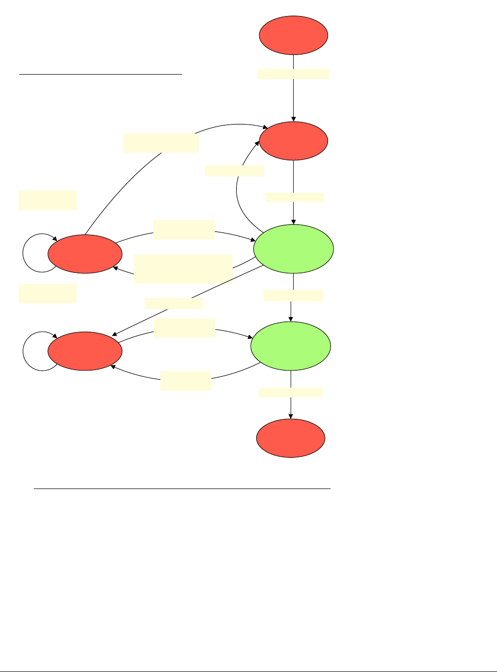
H3 Halting Debug Events
H3.2 Halting Step debug event
H3-4368 Copyright © 2013 ARM Limited. All rights reserved. ARM DDI 0487A.a
Non-Confidential - Beta ID090413
Figure H3-1 Halting Step state machine
Debugger activation
Inactive
EDECR.SS=0
Debug state
Inactive
EDECR.SS=1
Debug state
Active-not-pending
EDECR.SS=1
EDECR.SS=0
Halting allowed
Debug state exit
Halting step is disabled
Halting step is enabled
Inactive
EDECR.SS=1
EDESR.SS=1
Debug state
Return to
Non-secure state
Exception other than
SMC to Secure state where
halting is disallowed
Active pending
EDECR.SS=1
EDECR.SS=1
Halting allowed
Execution within
Secure state
Write 1 to
EDECR.SS
EDESR.SS is
set to 0 by the
exit from Debug
state
Return to
Non-secure state
Asynchronous
exception
Debug state entry
Step completed
b
a. Step completed occurs when:
• A debug event, other than a Halting Step debug event, causes entry into Debug state.
b. Step completed occurs when:
• An instruction is executed without taking an exception.
• An exception is taken to a state where halting is allowed.
• A reset.
c. Step completed occurs when:
• An SMC exception is taken to Secure state where halting is prohibited.
.
Step completed
a
Step completed
c
Inactive
EDECR.SS=1
EDESR.SS=0
Halting disallowed
Inactive
EDECR.SS=1
EDESR.SS=1
Halting disallowed
Execution within
Secure state
Debug state exit with
halting prohibited

H3 Halting Debug Events
H3.2 Halting Step debug event
ARM DDI 0487A.a Copyright © 2013 ARM Limited. All rights reserved. H3-4369
ID090413 Non-Confidential - Beta
Note
Figure H3-1 on page H3-4368 only describes state transitions to and from the inactive state by exit from Debug
state, executing an exception return, or taking an exception. Other changes to the PE context, including writes to
registers such as EDECR and OSDLR and changes to the authentication interface can also cause changes to the
Halting Step state machine. These can lead to UNPREDICTABLE behavior. See Synchronization and the Halting Step
state machine on page H3-4372.
The following bits control the state machine, as shown in Table H3-3:
•EDECR.SS. This is the Halting Step enable bit.
Note
— The EDECR value is preserved over powerdown, meaning that the step active state is maintained over
a powerdown event.
— A debugger must only set EDECR.SS to 1 when the PE is in Debug state.
•EDESR.SS.
Table H3-3 shows the Halting Step state machine states. The letter X in a register column means that the relevant
bit can be set to either zero or one.
H3.2.3 Using Halting Step
To step a single instruction the PE must be in Debug state:
1. The debugger sets EDECR.SS to 1 to enable Halting step.
2. The debugger signals the PE to exit Debug state with DLR set to the address of the instruction being stepped.
The PE clears EDESR.SS to 0 and the Halting Step state machine enter the active-not-pending state.
3. The PE executes the instruction being stepped.
If an exception is taken to a state where halting is prohibited, then EDESR.SS is always correct for the
preferred return address of the exception.
4. The PE enters Debug state before executing the next instruction and the step is complete.
H3.2.4 Detailed Halting Step state machine behavior
The behavior of the Halting Step state machine is described in the following sections:
•Entering the active-not-pending state on page H3-4370.
•PE behavior in the active-not-pending state on page H3-4370.
•Entering the active-pending state on page H3-4371.
•PE behavior in the inactive state when in Non-debug state on page H3-4372.
•PE behavior in Debug state on page H3-4372.
Table H3-3 Halting Step state machine states
Halting EDECR.SS EDESR.SS Halting Step state
Prohibited X X Inactive
Allowed 0 0 Inactive
Allowed 1 0 Active-not-pending
Allowed X 1 Active-pending

H3 Halting Debug Events
H3.2 Halting Step debug event
H3-4370 Copyright © 2013 ARM Limited. All rights reserved. ARM DDI 0487A.a
Non-Confidential - Beta ID090413
Entering the active-not-pending state
The PE enters the active-not-pending state:
• By exiting Debug state with EDECR.SS == 1.
• By an exception return from a state where halting is prohibited to a state where halting is allowed with
EDECR.SS == 1 and EDESR.SS == 0.
• As described in Synchronization and the Halting Step state machine on page H3-4372.
PE behavior in the active-not-pending state
When the PE is in the active-not-pending state it does one of the following:
• It executes one instruction and does one of the following:
— Completes it without generating a synchronous exception.
— Generates a synchronous exception.
— Generates a debug event that causes entry to Debug state.
• It takes an asynchronous exception without executing any instruction.
• It takes an asynchronous debug event into Debug state.
If no exception or debug event is generated
If no exception or debug event is generated the PE sets EDESR.SS to 1. This means that the Halting Step state
machine advances to the active-pending state.
If an exception or debug event is generated
The PE sets EDESR.SS according to all of the following:
• The type of exception.
• The target Exception level of the exception.
• If the exception is taken to Secure state, whether halting is prohibited in Secure state.
— This is determined by the result of
ExternalSecureInvasiveDebugEnabled().
If an exception or debug event is generated, the PE sets EDESR.SS to 1 if one of the following applies:
• A synchronous exception is generated by the instruction and one of the following applies:
— The exception is taken to EL1 or EL2.
— The exception is not an SMC exception and
ExternalSecureInvasiveDebugEnabled()
== TRUE.
— The exception is an SMC exception.
• An asynchronous exception is generated before executing an instruction and this is either:
— Taken to EL1 or EL2.
— Taken to EL3 and
ExternalSecureInvasiveDebugEnabled()
== TRUE.
• A PE reset occurs.
Otherwise EDESR.SS is unchanged. This happens when:
• No instruction is executed because either:
— An asynchronous exception is taken to EL3 and
ExternalSecureInvasiveDebugEnabled()
== FALSE.
— An asynchronous debug event causes entry to Debug state.
• An instruction is executed and either:
— Generates a synchronous exception other than an SMC exception which is taken to EL3, and
ExternalSecureInvasiveDebugEnabled()
== FALSE.
— Generates a synchronous debug event and causes entry to Debug state.

H3 Halting Debug Events
H3.2 Halting Step debug event
ARM DDI 0487A.a Copyright © 2013 ARM Limited. All rights reserved. H3-4371
ID090413 Non-Confidential - Beta
If halting is prohibited after taking the exception or debug event, then the Halting Step state machine advances to
the inactive state. Otherwise the Halting Step state machine advances to the active-pending state.
Note
The underlying criteria for the value of EDESR.SS on an exception are:
• Whether halting is allowed at the target of the exception. If halting is allowed, the PE must step into the
exception. If halting is prohibited, the PE must step over the exception.
• Whether the preferred return address of the exception is the instruction itself or the next instruction, if the PE
steps over the exception.
Table H3-4 shows the behavior of the active-not-pending state. The letter X indicates that
ExternalSecureInvasiveDebugEnabled()
can be either TRUE or FALSE.
Entering the active-pending state
The PE enters the active-pending state by one of the following:
• From the active-not-pending state by:
— Executing an instruction without taking an exception.
— Taking an exception so that the PE remains in a state where halting is allowed.
• An exception return from a state where halting is prohibited when EDESR.SS == 1.
Note
That is, an exception return from Secure state with
ExternalSecureInvasiveDebugEnabled()
== FALSE to
Non-secure state with
ExternalInvasiveDebugEnabled()
== TRUE.
• A reset when the value of EDECR.SS == 1, regardless of the state the PE was in before the reset occurred.
• Following the description in Synchronization and the Halting Step state machine on page H3-4372.
When the PE is in the active-pending state, it enters Debug state before executing an instruction. However, if
ExternalSecureInvasiveDebugEnabled()
== FALSE, the architecture does not define the prioritization of this Debug
state entry with respect to any pending asynchronous exception that is taken from Non-secure state to EL3.
If an exception is prioritized over the halt, then EDESR.SS is unchanged. On return from the exception the Halting
Step state machine re-enters the active-pending state.
Table H3-4 Summary of active-not-pending state behavior
Event Target EL
ExternalSecureInvasiveDebugEnabled()
Value written to
EDESR.SS
No exception or debug event Not applicable X 1
SMC exception EL3 X 1
Reset Highest X 1
Exception, other than SMC
exception EL1 X 1
EL2 X 1
EL3 TRUE 1
FALSE 0
Debug event Debug state X 0

H3 Halting Debug Events
H3.2 Halting Step debug event
H3-4372 Copyright © 2013 ARM Limited. All rights reserved. ARM DDI 0487A.a
Non-Confidential - Beta ID090413
The entry into Debug state has higher priority than all other types of exception, including all other asynchronous
exceptions.
Note
This means that it is possible to step a reentrant exception in the exception vector table.
PE behavior in the inactive state when in Non-debug state
EDESR.SS is not updated by the execution of an instruction or the taking of an exception when Halting Step is
inactive. This means that EDESR.SS is not changed by an exception handled in a state where halting is prohibited.
On return to a state where halting is allowed, the Halting Step state machine is restored either to the active-pending
state or the active-not-pending state, depending on the value of EDESR.SS. The return to a state where halting is
allowed is normally by an exception return, which is a Context synchronization operation.
See also Synchronization and the Halting Step state machine.
PE behavior in Debug state
Entry to Debug state, the execution of an instruction in Debug state, or the taking of an exception when in Debug
state, does not change EDESR.SS.
EDESR.SS is cleared to 0 on exiting Debug state as the result of a restart request. This forces the Halting Step state
machine to active-not-pending if EDECR.SS == 1.
Note
Using Halting Step to step over an A32 instruction that generates a misaligned PC value does not suppress the
resulting misaligned PC exception. On exiting Debug state, the misaligned PC value is written from DLR and a
misaligned PC exception is generated.
However, if the PE exits Debug state as the result of a PE reset and EDECR.SS == 1, then the PE immediately enters
the active-pending state, as EDESR.SS is set to the value of EDECR.SS.
H3.2.5 Synchronization and the Halting Step state machine
The Halting Step state machine also changes state if:
• Halting becomes allowed or prohibited other than by exit from Debug state, an exception return, or taking an
exception. This means that halting becomes allowed or prohibited because:
— The security state changes without an exception return. See State and mode changes without explicit
context synchronization operations on page D2-1647.
— The external authentication interface changes.
— The OS Double Lock status,
DoubleLockStatus()
, changes.
• A write to EDECR when the PE is in Non-debug state changes the value of EDECR.SS.
• A write to EDESR when the PE is in Non-debug state clears EDESR.SS to 0.
These operations are guaranteed to take effect only after a Context synchronization operation.
The PE must perform the required behavior of the new state before or immediately following the next Context
synchronization operation, but it is not required to do so immediately. This means that the PE can perform the
required behavior of the old state before the next Context synchronization operation. This is illustrated in
Example H3-1 on page H3-4373 and Example H3-2 on page H3-4373.

H3 Halting Debug Events
H3.2 Halting Step debug event
ARM DDI 0487A.a Copyright © 2013 ARM Limited. All rights reserved. H3-4373
ID090413 Non-Confidential - Beta
Example H3-1 Synchronization requirements 1
EDECR.SS is set to 1 in Debug state, requesting the active-not-pending state on exit from Debug state. On exit from
Debug state the PE immediately takes an exception to Secure state.
ExternalSecureInvasiveDebugEnabled()
==
FALSE, meaning that halting is prohibited in Secure state. The PE does not step any instructions but executes the
software in Secure state as normal. EDESR.SS remains set to 0. If
ExternalSecureInvasiveDebugEnabled()
subsequently becomes TRUE, meaning that halting is now allowed, the PE must perform the required behavior of
the active-not-pending state before or immediately following the next Context synchronization operation, but it is
not required to do so immediately.
Example H3-2 Synchronization requirements 2
EDECR.SS is set to 1 in Debug state. On exit from Debug the PE executes an
MSR
instruction that sets
OSDLR_EL1.DLK to 1 and
DoubleLockStatus()
becomes TRUE. This change requires a Context synchronization
operation to guarantee its effect, meaning it is CONSTRAINED UNPREDICTABLE whether:
• Halting is allowed:
— The PE enters Debug state on the next instruction.
• Halting is prohibited:
— The PE does not enter Debug state.
The value in EDESR.SS depends on whether halting was allowed or prohibited when the write to
OSDLR_EL1.DLK completed, and so it might be 0 or 1. If a second
MSR
instruction clears OSDLR_EL1.DLK to 0,
the PE must perform the required behavior of the state indicated by EDESR.SS before or immediately following the
next Context synchronization operation, but it is not required to do so immediately.
See also Synchronization and Halting debug events on page H3-4384.
H3.2.6 Stepping T32
IT
instructions
The ARMv8 architecture permits a combination of one T32
IT
instruction and another 16-bit T32 instruction to be
treated as one 32-bit instruction when the value of SCTLR.ITD, SCTLR_EL1.ITD or HSCTLR.ITD as applicable,
is 1.
For the purpose of stepping an item, it is IMPLEMENTATION DEFINED whether:
• The PE considers such a pair of instructions to be one instruction.
• The PE considers such a pair of instructions be two instructions.
It is IMPLEMENTATION DEFINED whether this behavior depends on the value of the applicable ITD bit. For example:
• The debug logic might consider such a pair of instructions to be one instruction, regardless of the state of
SCTLR.ITD, SCTLR_EL1.ITD, or HSCTLR.ITD.
• The debug logic might consider such a pair of instructions to be two instructions, regardless of the state of
SCTLR.ITD, SCTLR_EL1.ITD, or HSCTLR.ITD.
• The debug logic might consider such a pair of instructions to be one instruction when SCTLR.ITD,
SCTLR_EL1.ITD, or HSCTLR.ITD is set to 1, and two instructions when the ITD bit is set to 0.

H3 Halting Debug Events
H3.2 Halting Step debug event
H3-4374 Copyright © 2013 ARM Limited. All rights reserved. ARM DDI 0487A.a
Non-Confidential - Beta ID090413
H3.2.7 Disabling interrupts while stepping
When using Halting Step, the sequence of entering Debug state, interacting with the debugger, and then exiting
Debug state for each instruction reduces the rate at which the PE executes instructions. However, the rate at which
certain interrupts, such as timer interrupts, are generated might be fixed by the system. This means it might be
necessary to disable interrupts while using Halting Step by setting EDSCR.INTdis, to allow the code being
debugged to make forward progress.
H3.2.8 Syndrome information on Halting Step
Three EDSCR.STATUS encodings record different scenarios for entering Debug state on a Halting Step debug
event:
Halting Step, normal
An instruction other than a Load-Exclusive instruction was stepped.
Halting Step, exclusive
A Load-Exclusive instruction was stepped.
Halting Step, no syndrome
The syndrome data is not available.
If the PE enters Debug state due to a Halting Step debug event immediately after stepping an instruction in the
active-not-pending state, EDSCR.STATUS is set to either:
• Halting Step, normal, if the stepped instruction was not a Load-Exclusive instruction.
• Halting Step, exclusive, if the stepped instruction was a Load-Exclusive instruction.
If the stepped instruction was a conditional Load-Exclusive instruction that failed its condition code test,
EDSCR.STATUS is set to a CONSTRAINED UNPREDICTABLE choice of Halting Step, normal, or Halting Step,
exclusive.
Otherwise the PE enters Debug state without stepping an instruction. This means that the Halting Step state machine
enters the active-pending state directly from the inactive state, without going through active-not-pending state. In
this case, EDSCR.STATUS is set to Halting Step, no syndrome. This happens when:
• The PE enters directly into the active-pending state on an exception return to Non-secure state from EL3
when Halting is prohibited in Secure state.
• A pending asynchronous exception is taken before the instruction is executed.
• The active-pending state is entered for other reasons. See Synchronization and the Halting Step state machine
on page H3-4372
In these cases the debugger cannot determine whether the instruction that was stepped was a Load-Exclusive
instruction.
In addition, EDSCR.STATUS is set to one of a CONSTRAINED UNPREDICTABLE choice if:
• The instruction being stepped generated a synchronous exception, meaning that it was not completed.
In this case EDSCR.STATUS is set to a CONSTRAINED UNPREDICTABLE choice of:
— Halting Step, no syndrome, or Halting Step, normal, if the stepped instruction was not a
Load-Exclusive instruction.
— Halting Step, no syndrome, or Halting Step, exclusive, if the stepped instruction was a Load-Exclusive
instruction.
• The instruction that was stepped was an exception return instruction or an
ISB
. As these instructions are not
in the Load-Exclusive instructions, EDSCR.STATUS is set to a CONSTRAINED UNPREDICTABLE choice of
Halting Step, no syndrome or Halting Step, normal.

H3 Halting Debug Events
H3.2 Halting Step debug event
ARM DDI 0487A.a Copyright © 2013 ARM Limited. All rights reserved. H3-4375
ID090413 Non-Confidential - Beta
In all cases, if EDSCR.STATUS is not set to Halting Step, no syndrome, then it must indicate whether the stepped
instruction was a Load-Exclusive instruction by setting EDSCR.STATUS to Halting Step, normal or Halting Step,
exclusive.
Note
An implementation that always sets EDSCR.STATUS to Halting Step, no syndrome is not compliant.
H3.2.9 Pseudocode details for Halting Step debug events
There are two pseudocode functions for Halting Step debug events:
•
RunHaltingStep()
. This is called after an instruction has executed and any exception generated by the
instruction is taken. It is also called after taking a reset before executing any instructions. That is, reset is
treated like an asynchronous exception, even if EDECR.RCE == 1.
RunHaltingStep()
affects the next
instruction.
•
CheckHaltingDebugStep()
. This is called before the next instruction is executed. If a step is pending, it
generates the debug event.
// RunHaltingStep()
// ================
RunHaltingStep(boolean exception_generated, bits(2) exception_target, boolean syscall,
boolean reset)
// “exception_generated” is TRUE if the previous instruction generated a synchronous exception
// or was cancelled by an asynchronous exception.
// if “exception_generated” == TRUE then “exception_target” is the target of the exception, and
// “syscall” is TRUE if the exception is a synchronous exception where the preferred return
// address is the instruction following that which generated the exeception.
// “reset” = TRUE if exiting reset state into the highest EL.
if reset then assert !Halted(); // Cannot come out of reset halted
active = EDECR.SS == ‘1’ && !Halted();
if active && reset then // Coming out of reset with EDECR.SS set.
EDESR.SS = ‘1’;
elsif active && HaltingAllowed() then
if exception_generated && exception_target == EL3 then
advance = syscall || ExternalSecureInvasiveDebugEnabled();
else
advance = TRUE;
if advance then EDESR.SS = ‘1’;
return;
// CheckHaltingStep()
// ==================
// Check whether EDESR.SS has been set by Halting Step
CheckHaltingStep()
if HaltingAllowed() && EDESR.SS == ‘1’ then
// The STATUS code depends on how we arrived at the state where EDESR.SS == 1.
if HaltingStep_DidNotStep() then
Halt(DebugHalt_Step_NoSyndrome);
elsif HaltingStep_SteppedEX() then
Halt(DebugHalt_Step_Exclusive);
else
Halt(DebugHalt_Step_Normal);

H3 Halting Debug Events
H3.3 Halt Instruction debug event
H3-4376 Copyright © 2013 ARM Limited. All rights reserved. ARM DDI 0487A.a
Non-Confidential - Beta ID090413
H3.3 Halt Instruction debug event
A Halt Instruction debug event is generated when EDSCR.HDE == 1, halting is allowed, and software executes the
Halting software breakpoint instruction,
HLT
.
The pseudocode for Halt Instruction Debug events is described in HLT on page C5-484 for A64 and HLT on
page F7-2608 for A32 and T32.
HLT
never generates a debug exception. It is UNALLOCATED if EDSCR.HDE == 0, or if halting is prohibited.
Note
A debugger can replace a program instruction with a Halt instruction to generate a Halting Software Breakpoint.
Debuggers that use the
HLT
instruction must be aware of the ARMv8-A rules for concurrent modification of
executable code, CMODX. The rules for concurrent modification and execution of instructions do not allow one
thread of execution or an external debugger to replace an instruction with an
HLT
instruction when these same
instructions are being executed by a different thread of execution. See Concurrent modification and execution of
instructions on page B2-91.
The T32
HLT
instruction is unconditionally executed inside an
IT
block, even when it is UNALLOCATED. The A32
HLT
instruction is CONSTRAINED UNPREDICTABLE if the condition code field is not
0b1110
, with the set of behaviors
the same as for
BKPT
. See Appendix A Architectural Constraints on UNPREDICTABLE behaviors.
Note
The
HLT
instruction is part of the external debug solution for ARMv8-A. As such, the presence of the
HLT
instruction
is not indicated in the ID registers. In particular, the AArch32 CP15 register ID_ISAR0.Debug does not indicate the
presence of the
HLT
instruction.
H3.3.1 HLT instructions as the first instruction in a T32 IT block
The ARMv8 architecture defines combinations of
IT
and a single 16-bit T32 instruction that can be treated as a
32-bit instruction when SCTLR.ITD, SCTLR_EL1.ITD or HSCTLR.ITD, as applicable, is set to 1.
The T32
HLT
instruction is not such an instruction. If the first instruction in an IT block is an
HLT
instruction, then
the behavior of the instruction depends on the value of SCTLR.ITD, SCTLR_EL1.ITD or HSCTLR.ITD, as
applicable:
• If the ITD bit is set to 1, then the combination is UNALLOCATED and an Undefined Instruction exception is
generated either by the
IT
instruction or by the
HLT
instruction.
• If the ITD bit is set to 0, then the
HLT
instruction either:
—Is
UNALLOCATED and generates an Undefined Instruction exception.
— Generates an
HLT
Instruction debug event.
To set an
HLT
Instruction debug event on the first instruction of an IT block, debuggers must replace the
IT
instruction with an
HLT
instruction to ensure consistent behavior.
Note
An
HLT
instruction is always unconditional, even within an IT block.

H3 Halting Debug Events
H3.4 Exception Catch debug event
ARM DDI 0487A.a Copyright © 2013 ARM Limited. All rights reserved. H3-4377
ID090413 Non-Confidential - Beta
H3.4 Exception Catch debug event
Exception Catch debug events:
• Are generated when the corresponding bit in the Exception Catch Control Register, EDECCR, is set to 1 on
all entries to a given Exception level. This means:
— Exceptions taken to the Exception level.
— Exception returns to the Exception level.
— Entry to the Exception level due to reset. This is an overlap with a Reset Catch debug event. See Reset
Catch debug event on page H3-4382.
— Exit from Debug state to the Exception level.
• Are taken synchronously, after entry to the Exception level.
• Ignore the execution state of the target Exception level.
• Are ignored if halting is prohibited.
The EDECCR contains two fields:
• One field for Non-secure state.
• One field for Secure state.
Each field contains one bit for each Exception level in that state. Bits corresponding to Exception levels that are not
implemented are RES0. See EDECCR, External Debug Exception Catch Control Register on page H9-4501.
Note
• EDECCR does not replace DBGVCR:
—DBGVCR is retained in AArch32 state for backwards compatibility.
—DBGVCR is ignored in AArch64 state and never generates entries to Debug state.
—DBGVCR cannot be accessed by the external debug interface.
•EDECCR is only visible as OSECCR_EL1 by System Register instructions in AArch64 state, and as
DBGOSECCR by CP14 register access instructions in AArch32 state, when the OS Lock is locked to allow
software to save and restore it over a powerdown.
• Exception Catch debug events are not disabled when the OS Lock is locked.
For an Exception Catch debug event generated after taking an exception to a trapped Exception level:
• The PE must not fetch instructions from the vector address before entering Debug state, if the translation
regime MMU at the target Exception level is disabled.
• On entering Debug state:
— The current Exception level is the target Exception level of the exception.
— The ELR, SPSR, ESR, and other syndrome registers contain information about the exception.
—DLR contains the exception vector address.
H3.4.1 Prioritization of Exception Catch debug events
Exception Catch debug events have a higher priority than all synchronous exceptions other than Software Step
exceptions on page D2-1634 and a lower priority than Reset Catch debug event on page H3-4382. It is
IMPLEMENTATION DEFINED whether Exception Catch debug events are higher or lower priority than both:
•Software Step exceptions on page D2-1634.
•Halting Step debug event on page H3-4366.

H3 Halting Debug Events
H3.4 Exception Catch debug event
H3-4378 Copyright © 2013 ARM Limited. All rights reserved. ARM DDI 0487A.a
Non-Confidential - Beta ID090413
Note
As described in Synchronous exception prioritization on page D1-1451, an exception trapping form of a Vector
Catch debug event might generate a second debug exception as part of the exception entry, before the Exception
Catch debug event is taken. See Vector Catch exceptions on page D2-1627.
A second unmasked asynchronous exception can be taken before the PE enters Debug state. If this second exception
does not generate an Exception Catch debug event, the exception handler executed at the higher Exception level
later returns to the trapped Exception level, causing the Exception Catch debug event to be generated again.
See also Debug state entry and debug event prioritization on page H2-4331.
H3.4.2 UNPREDICTABLE generation of Exception Catch debug events
When the PE is executing code at a given Exception level and the corresponding EDECCR bit is 1, it is
CONSTRAINED UNPREDICTABLE whether an Exception Catch debug event is generated.
Note
It is possible to generate Exception Catch debug events:
• As a trap on all instruction fetches from the trapped Exception level as part of an instruction fetch.
• On entry to the Exception level, as described in Detailed Halting Step state machine behavior on
page H3-4369.
This is similar to the implementation options allowed for Vector Catch debug events. The architecture does not
require that the event is generated following an
ISB
operation executed at the Exception level.
Examples of this are:
• If the debugger writes to EDECCR so that the current Exception level is trapped.
• If the OS restore code writes to OSECCR so that the current Exception level is trapped.
• If the code executing in AArch32 state changes the Exception level or security state other than by an
exception return, and the target Exception level is trapped. See State and mode changes without explicit
context synchronization operations on page D2-1647.
H3.4.3 Examples of Exception Catch debug events
If EDECCR ==
0x20
, meaning that the Exception Catch debug event is enabled for Non-secure EL1, then the
following exceptions generate Exception Catch debug events:
• An exception taken from Non-secure EL0 to Non-secure EL1.
• An exception return from EL2 to Non-secure EL1.
• An exception return from EL3 to Non-secure EL1.
For example, on taking a Data Abort exception from Non-secure EL0 to Non-secure EL1, using AArch64:
•ELR_EL1 and SPSR_EL1 are written with the preferred return address and PE state for a return to EL0.
•ESR_EL1 and FAR_EL1 are written with the syndrome information for the exception.
•DLR_EL0 is set to VBAR_EL1 +
0x400
, the synchronous exception vector.
•DSPSR_EL0 is written with the PE state for an exit to EL1.
The following do not generate Exception Catch debug events:
• An exception taken from Non-secure EL0 to EL2 or EL3.
• An exception return from EL2 to Non-secure EL0.
• An exception taken from Secure EL0 to Secure EL1.
• An exception return from EL3 to Secure EL1.

H3 Halting Debug Events
H3.4 Exception Catch debug event
ARM DDI 0487A.a Copyright © 2013 ARM Limited. All rights reserved. H3-4379
ID090413 Non-Confidential - Beta
H3.4.4 Pseudocode details for Exception Catch debug events
The pseudocode for the
CheckExceptionCatch()
function is as follows:
// CheckExceptionCatch()
// =====================
// Check whether an Exception Catch debug event is set on the current Exception level
CheckExceptionCatch()
// Called after taking an exception, that is, such that IsSecure() and PSTATE.EL are correct
// for the exception target.
base = if IsSecure() then 0 else 4;
if HaltingAllowed() && EDECCR<UInt(PSTATE.EL) + base> == ‘1’ then
Halt(DebugHalt_ExceptionCatch);

H3 Halting Debug Events
H3.5 External Debug Request debug event
H3-4380 Copyright © 2013 ARM Limited. All rights reserved. ARM DDI 0487A.a
Non-Confidential - Beta ID090413
H3.5 External Debug Request debug event
An External Debug Request debug event is generated when signaled by the embedded cross-trigger. See Chapter H5
The Embedded Cross Trigger Interface.
Note
ARMv8-A requires the implementation of an embedded cross-trigger.
External Debug Request debug events are asynchronous debug events.
An implementation might also support IMPLEMENTATION DEFINED ways of generating an External Debug Request
debug event.
H3.5.1 Pseudocode details for External Debug Request debug events
The pseudocode details for the
ExternalDebugRequest()
function is as follows:
// ExternalDebugRequest()
// ======================
ExternalDebugRequest()
if HaltingAllowed() then
Halt(DebugHalt_EDBGRQ);
// Otherwise the CTI continues to assert the debug request until it is taken.

H3 Halting Debug Events
H3.6 OS Unlock Catch debug event
ARM DDI 0487A.a Copyright © 2013 ARM Limited. All rights reserved. H3-4381
ID090413 Non-Confidential - Beta
H3.6 OS Unlock Catch debug event
An OS Unlock Catch debug event is generated when EDECR.OSUCE == 1 and the state of the OS Lock changes
from locked to unlocked.
When the OS Unlock Catch debug event is generated, it is recorded by setting EDESR.OSUC to 1, meaning it
immediately becomes pending and is not guaranteed to be taken immediately. Clearing the OS Lock is not a
self-synchronizing operation. See Synchronization and Halting debug events on page H3-4384.
OS Unlock Catch debug events are not generated if the OS Lock is unlocked when the PE is in Debug state. See also:
•Debug behavior when the OS Lock is unlocked on page H6-4432.
•EDECR, External Debug Execution Control Register on page H9-4503.
•EDESR, External Debug Event Status Register on page H9-4505.
EDESR.OSUC is cleared to 0 on a Warm reset and on exiting Debug state.
H3.6.1 Using the OS Unlock Catch debug event
If the debugger attempts to access a debug register when the Core power down domain is completely off or in a
low-power state in which the core power domain registers cannot be accessed, and that access returns an error, then
the debugger must retry the access. However, if the Core power domain is regularly powered down, this can lead to
unreliable debugger behavior.
The debugger can program a Reset Catch debug event to halt the PE when it has powered-up, and can program the
debug registers from Debug state. However, if the PE boot software restores the debug registers, as described in
Debug OS Save and Restore sequences on page H6-4430, then newly written values are overwritten by the restore
sequence.
The debugger can program an OS Unlock Catch debug event to halt the PE after the restore sequence has completed,
and program the debug registers from Debug state.
H3.6.2 Pseudocode details for OS Unlock Catch debug event
The
CheckOSUnlockCatch()
function is called when the OS Lock is unlocked.
// CheckOSUnlockCatch()
// ====================
// Called on unlocking the OS Lock to pend an OS Unlock Catch debug event
CheckOSUnlockCatch()
if EDECR.OSUCE == ‘1’ && !Halted() then EDESR.OSUC = ‘1’;
The
CheckPendingOSUnlockCatch()
function is called before an instruction is executed. If an OS Unlock Catch is
pending, it generates the debug event.
// CheckPendingOSUnlockCatch()
// ===========================
// Check whether EDESR.OSUC has been set by an OS Unlock Catch debug event
CheckPendingOSUnlockCatch()
if HaltingAllowed() && EDESR.OSUC == ‘1’ then
Halt(DebugHalt_OSUnlockCatch);

H3 Halting Debug Events
H3.7 Reset Catch debug event
H3-4382 Copyright © 2013 ARM Limited. All rights reserved. ARM DDI 0487A.a
Non-Confidential - Beta ID090413
H3.7 Reset Catch debug event
A Reset Catch debug event is generated when EDECR.RCE == 1 and the PE exits reset state. When the Reset Catch
debug event is generated, it is recorded by setting EDESR.RC to 1.
If halting is allowed when the event is generated, the Reset Catch debug event is taken immediately and
synchronously. On entering Debug state, DLR has the address of the reset vector. The PE must not fetch any
instructions from memory.
Otherwise, the Reset Catch debug event is pended and taken when halting is allowed. See also:
•Synchronization and Halting debug events on page H3-4384.
•EDECR, External Debug Execution Control Register on page H9-4503.
•EDESR, External Debug Event Status Register on page H9-4505.
This means that EDESR.RC is set to the value of EDECR.RCE on a Warm reset. EDESR.RC is cleared to 0 on
exiting Debug state.
H3.7.1 Pseudocode details for Reset Catch debug event
The
CheckResetCatch()
function is called after reset before executing any instruction.
// CheckResetCatch()
// =================
// Called after reset
CheckResetCatch()
if EDECR.RCE == ‘1’ then
EDESR.RC = ‘1’;
// If halting is allowed then halt immediately
if HaltingAllowed() then Halt(DebugHalt_ResetCatch);
The
CheckPendingResetCatch()
function is called before an instruction is executed. If a Reset Catch is pending, it
generates the Reset Catch debug event.
// CheckPendingResetCatch()
// ========================
// Check whether EDESR.RC has been set by a Reset Catch debug event
CheckPendingResetCatch()
if HaltingAllowed() && EDESR.RC == ‘1’ then
Halt(DebugHalt_ResetCatch);

H3 Halting Debug Events
H3.8 Software Access debug event
ARM DDI 0487A.a Copyright © 2013 ARM Limited. All rights reserved. H3-4383
ID090413 Non-Confidential - Beta
H3.8 Software Access debug event
When the value of EDSCR.TDA == 1, software access to the following debug registers cause a trap to Debug state:
• The Breakpoint Value Registers, DBGBVR.
• The Breakpoint Control Registers, DBGBCR.
• The Watchpoint Value Registers, DBGWVR.
• The Watchpoint Control Registers, DBGWCR.
However, EDSCR.TDA is ignored if either:
• The value of OSLSR.OSLK == 1, meaning that the OS Lock is locked.
• Halting is prohibited. See Halting allowed and halting prohibited on page H2-4329.
Note
• The accesses are only trapped into Debug state if they do not generate an exception. For more information
see the relevant register description in Chapter D8 AArch64 System Register Descriptions, Chapter G4
AArch32 System Register Descriptions, or Chapter I1 Memory-Mapped System Register Descriptions.
•DBGPRCR.CORENPDRQ (Core No-powerdown Request), DCC registers, and CLAIM tag bits are also
shared, but are deliberately excluded from this list.
H3.8.1 Pseudocode details for Software Access debug event
The pseudocode details for
CheckSoftwareAccessToDebugRegisters()
are as follows:
// CheckSoftwareAccessToDebugRegisters()
// =====================================
// Check for access to Breakpoint and Watchpoint registers.
CheckSoftwareAccessToDebugRegisters()
if HaltingAllowed() && EDSCR.TDA == ‘1’ && OSLSR_EL1.OSLK == ‘0’ then
Halt(DebugHalt_SoftwareAccess);

H3 Halting Debug Events
H3.9 Synchronization and Halting debug events
H3-4384 Copyright © 2013 ARM Limited. All rights reserved. ARM DDI 0487A.a
Non-Confidential - Beta ID090413
H3.9 Synchronization and Halting debug events
The behavior of external debug depends on:
• Indirect reads of:
— External debug registers.
— System registers, including system debug registers.
— Special purpose registers.
• The state of the external authentication interface.
This means that any change to these registers or the external authentication interface requires explicit
synchronization by a Context synchronization operation before the change takes effect. This ensures that for
instructions appearing in program order after the change, the change affects the following:
• The generation and behavior of Software debug events. See Synchronization and debug exceptions on
page D2-1647.
• The generation of all Halting debug events.
• Taking a pending Halting debug event or other asynchronous Debug event. See:
—Pending Halting debug events.
—Taking Halting debug events asynchronously on page H3-4385.
• The behavior of the Halting Step state machine. See Synchronization and the Halting Step state machine on
page H3-4372.
If there is an instruction between the write and the Context synchronization operation, it is CONSTRAINED
UNPREDICTABLE whether the PE uses the old state or the new state.
Some register updates are self-synchronizing, but others require an explicit Context synchronization operation. For
more information on the synchronization of register updates see:
•Synchronization requirements for system registers on page D8-1866.
•Synchronization of changes to the external debug registers on page H8-4445.
•State and mode changes without explicit context synchronization operations on page D2-1647.
A change on the external authentication interface is typically asynchronous to software and can happen without a
Context synchronization operation.
External Debug Request debug events must be taken in finite time, without requiring the synchronization of any
necessary change to the external authentication interface.
Example H3-3 shows an example of the synchronization requirements.
Example H3-3 Synchronization requirements
Secure software locks up in a tight loop, so it executes indefinitely without any synchronization operations. An
External debug request must be able to break the PE out of that loop. This is a requirement even if DBGEN or
SPIDEN or both are LOW on entry to the loop, meaning that halting is prohibited, and are only asserted HIGH later.
H3.9.1 Pending Halting debug events
A pending Halting debug event is taken when halting becomes allowed. This can happen without a Context
synchronization operation if:
• The PE enters Non-secure state with
ExternalInvasiveDebugEnabled()
== TRUE, and this is not the result of
an exception return. See State and mode changes without explicit context synchronization operations on
page D2-1647.
• A change on the external authentication interface means halting becomes allowed in the current state.
• The OS Double Lock status,
DoubleLockStatus()
becomes FALSE. For example, this can happen when
software clears OSDLR.DLK to 0 or sets DBGPRCR.CORENPDRQ to 1.

H3 Halting Debug Events
H3.9 Synchronization and Halting debug events
ARM DDI 0487A.a Copyright © 2013 ARM Limited. All rights reserved. H3-4385
ID090413 Non-Confidential - Beta
• The debug event is an OS Unlock Catch debug event. OS Unlock Catch debug events are generated in a
pending state, rather than taken synchronously.
In these cases a pending Halting debug event is taken asynchronously.
H3.9.2 Taking Halting debug events asynchronously
The ARM architecture does not define when Halting debug events that are taken asynchronously are taken.
Any Halting debug event that is observed as pending in the EDESR before a Context synchronization operation, or
an External Debug Request debug event that is asserted before a Context synchronization operation, is taken and
the PE enters Debug state before the first instruction following the Context synchronization operation completes its
execution. This is only possible if halting is allowed after completion of the Context synchronization operation.
If the first instruction after the Context synchronization operation generates a synchronous exception, or an
asynchronous exception is also pending, then the architecture does not define the order in which the debug event
and the exception or exceptions are taken, unless both:
• A Halting Step debug event is pending. EDESR.SS == 1.
• The Context synchronization operation is an exception return from a state where halting is prohibited to a
state where halting is allowed.
Note
This applies to an exception return from Secure state with
ExternalSecureInvasiveDebugEnabled()
== FALSE
to Non-secure state with
ExternalInvasiveDebugEnabled()
== TRUE.
In this case the order in which the debug events are handled is specified to avoid a double-step. See Entering the
active-pending state on page H3-4371.
Note
These rules are based on the rules that apply to taking asynchronous exceptions. See Asynchronous exception types,
routing, masking and priorities on page D1-1456.

H3 Halting Debug Events
H3.9 Synchronization and Halting debug events
H3-4386 Copyright © 2013 ARM Limited. All rights reserved. ARM DDI 0487A.a
Non-Confidential - Beta ID090413

ARM DDI 0487A.a Copyright © 2013 ARM Limited. All rights reserved. H4-4387
ID090413 Non-Confidential - Beta
Chapter H4
The Debug Communication Channel and Instruction
Transfer Register
This chapter describes communication between a debugger and the implemented debug logic, using the Debug
Communications Channel (DCC) and the Instruction Transfer Register (ITR), and associated control flags. It
contains the following sections:
•Introduction on page H4-4388.
•DCC and ITR registers on page H4-4389.
•DCC and ITR access modes on page H4-4391.
•Flow-control of the DCC and ITR registers on page H4-4395.
•Synchronization of DCC and ITR accesses on page H4-4398.
•Interrupt-driven use of the DCC on page H4-4402.
•Pseudocode details for the operation of the DCC and ITR registers on page H4-4403.
Note
Where necessary Table J-1 on page AppxJ-5088 disambiguates the general register references used in this chapter.

H4 The Debug Communication Channel and Instruction Transfer Register
H4.1 Introduction
H4-4388 Copyright © 2013 ARM Limited. All rights reserved. ARM DDI 0487A.a
Non-Confidential - Beta ID090413
H4.1 Introduction
The Debug Communications Channel, DCC, is a channel for passing data between the PE and an external agent,
such as a debugger. The DCC provides a communications channel between:
• An external debugger, described as the debug host.
• The debug implementation on the PE, described as the debug target.
The DCC can be used:
• As a 32-bit full-duplex channel.
• As a 64-bit half-duplex channel.
The DCC is an essential part of Debug state operation and can also be used in Non-debug state.
The Instruction Transfer Register, ITR, passes instructions to the PE to execute in Debug state.
The PE includes flow-control mechanisms for both the DCC and ITR.

H4 The Debug Communication Channel and Instruction Transfer Register
H4.2 DCC and ITR registers
ARM DDI 0487A.a Copyright © 2013 ARM Limited. All rights reserved. H4-4389
ID090413 Non-Confidential - Beta
H4.2 DCC and ITR registers
The DCC comprises data transfer registers, the DTRs, and associated flow-control flags. The data transfer registers
are DTRRX and DTRTX.
The ITR comprises a single register, EDITR, and associated flow-control flags.
In AArch64 state, software can access the data transfer registers as:
• A receive and transmit pair for 32-bit full duplex operation:
— The write-only DBGDTRTX_EL0 register to transmit data.
— The read-only DBGDTRRX_EL0 register to receive data.
• A single 64-bit read/write register, DBGDTR_EL0, for 64-bit half-duplex operation.
• The read/write OSDTRTX_EL1 and OSDTRRX_EL1 registers for save and restore.
In AArch32 state, software can only access the data transfer registers as:
• A receive and transmit pair, for 32-bit full duplex operation:
— The write-only DBGDTRTXint register to transmit data.
— The read-only DBGDTRRXint register to receive data.
• The read/write DBGDTRTXext and DBGDTRRXext registers for save and restore.
The data transfer registers are also accessible by the external debug interface as a pair of 32-bit registers,
DBGDTRRX_EL0 and DBGDTRTX_EL0. Both registers are read/write, allowing both 32-bit full-duplex and
64-bit half-duplex operation.
The DCC flow-control flags are EDSCR.{RXfull, TXfull, RXO, TXU}:
• The RXfull and TXfull ready flags are used for flow-control and are visible to software in the debug system
registers in DCCSR.
• The RX overrun flag, RXO, and the TX underrun flag, TXU, report flow-control errors.
• The flow-control flags are also accessible by software as simple read/write bits for saving and restoring over
a powerdown when the OS Lock is locked in DSCR.
• The flow-control flags are accessible from the external debug interface in EDSCR.
Figure H4-1 on page H4-4390 shows the system register and external debug interface views of the EDSCR and
DTR registers in both AArch64 state and AArch32 state. These figures do not include the save and restore views.
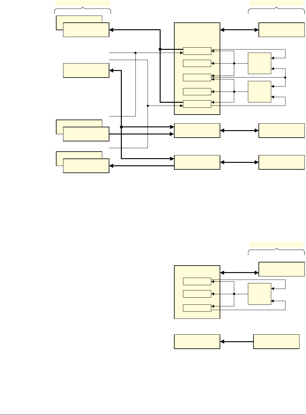
H4 The Debug Communication Channel and Instruction Transfer Register
H4.2 DCC and ITR registers
H4-4390 Copyright © 2013 ARM Limited. All rights reserved. ARM DDI 0487A.a
Non-Confidential - Beta ID090413
Figure H4-1 System register and external debug interface views of EDSCR and DTR registers, Normal access mode
EDITR and the ITR flow-control flags, EDSCR.{ITE, ITO} are accessible only by the external debug interface:
• The EDITR specifies an instruction to execute in Debug state.
• The ITR empty flag, ITE, is used for flow-control.
• The ITR overrun flag, ITO, reports flow-control errors.
Figure H4-2 External debug interface views of EDSCR and EDITR registers, Normal access mode
The sticky overflow flag, EDSCR.ERR, is used by both the DCC and ITR to report flow-control errors.
DBGDTRTXint †
DBGDTRRXint †
DBGDSCRint †
EDSCR
RXO
RXfull
TXfull
TXU
RX
write
logic §
TX
read
logic §
DTRTX DBGDTRTX_EL0
read/write
DTRRX DBGDTRRX_EL0
read/write
DBGDTRTX_EL0 ‡
32b, write-only
DBGDTRRX_EL0 ‡
32b, read-only
1, on writes
0, on reads
EDSCR
read/write
MDCCSR_EL0 ‡
read-only
External debug interface
DBGDTR_EL0 ‡
64b, read/write
1, on writes
0, on reads
§ underrun and overrun checks only performed
for accesses by the external debug interface
System register interface
† AArch32 state
‡ AArch64 state
ERR
EDSCR
ERR
ITO
ITR
write
logic
EDITR EDITR
write-only
EDSCR
read/write
External debug interface
ITE

H4 The Debug Communication Channel and Instruction Transfer Register
H4.3 DCC and ITR access modes
ARM DDI 0487A.a Copyright © 2013 ARM Limited. All rights reserved. H4-4391
ID090413 Non-Confidential - Beta
H4.3 DCC and ITR access modes
The DCC and ITR support two access modes:
•Normal access mode, when EDSCR.MA == 0 or the PE is in Non-debug state.
•Memory access mode on page H4-4392, when EDSCR.MA == 1 and the PE is in Debug state.
H4.3.1 Normal access mode
The Normal access mode allows use of the DCC as a communications channel between target and host. It also
allows the use of the ITR for issuing instructions to the PE in Debug state.
In Normal access mode, if there is no overrun or underrun, the following occurs:
For accesses by software:
• Direct writes to DBGDTRTX update the value in DTRTX and indirectly write 1 to TXfull.
• Direct reads from DBGDTRRX return the value in DTRRX and indirectly write 0 to RXfull.
• In AArch64 state, direct writes to DBGDTR_EL0 update both DTRTX and DTRRX,
indirectly write 1 to TXfull, and do not change RXfull:
— DTRTX is set from bits[31:0] of the transfer register.
— DTRRX is set from bits[63:32] of the transfer register.
• In AArch64 state, direct reads from DBGDTR_EL0 return the concatenation of DTRRX and
DTRTX, indirectly write 0 to RXfull, and do not change TXfull:
— Bits[31:0] of the transfer register are set from DTRRX.
— Bits[63:32] of the transfer register are set from DTRTX.
Note
For DBGDTR_EL0, the word order is reversed for reads with respect to writes.
Software reads TXfull and RXfull using DCCSR.
For accesses by the external debug interface:
• Writes to EDITR trigger the instruction to be executed if the PE is in Debug state:
— If the PE is in AArch64 state, this is an A64 instruction.
— If the PE is in AArch32 state, this is a T32 instruction. The T32 instruction is a pair of
halfwords where the first halfword is taken from the lower 16-bits, and the second
halfword is taken from the upper 16-bits.
• Reads of DBGDTRTX_EL0 return the value in DTRTX and indirectly write 0 to TXfull.
• Writes to DBGDTRTX_EL0 update the value in DTRTX and do not change TXfull.
• Reads of DBGDTRRX_EL0 return the value in DTRRX and do not change RXfull.
• Writes to DBGDTRRX_EL0 update the value in DTRRX and indirectly write 1 to RXfull.
TXfull and RXfull are visible to the external debug interface in EDSCR.
The PE detects overrun and underrun by the external debug interface, and records errors in
EDSCR.{TXU, RXO, ITO, ERR}. See Flow-control of the DCC and ITR registers on
page H4-4395.
See also Synchronization of DCC and ITR accesses on page H4-4398.

H4 The Debug Communication Channel and Instruction Transfer Register
H4.3 DCC and ITR access modes
H4-4392 Copyright © 2013 ARM Limited. All rights reserved. ARM DDI 0487A.a
Non-Confidential - Beta ID090413
H4.3.2 Memory access mode
When the PE is in Debug state, a special Memory access mode can be selected to accelerate word-aligned block
reads or writes of memory by an external debugger. Memory access mode can only be enabled in Debug state, and
no instructions can be issued directly by the debugger when in Memory access mode.
If there is no overrun or underrun when in Memory access mode, an access by the external debug interface results
in the following:
• External reads from DBGDTRTX_EL0 cause:
1. The existing value in DTRTX to be returned. This clears EDSCR.TXfull to 0.
2. The equivalent of
LDR W1,[X0],#4
, if in AArch64 state, or
LDR R1,[R0],#4
, if in AArch32 state, to be
executed.
3. The equivalent of the
MSR DBGDTRTX_EL0,X1
instruction, if in AArch64 state, or the
MCR p14,0,R1,c0,c5,0
instruction, if in AArch32 state, to be executed.
4. EDSCR.{TXfull, ITE} to be set to {1,1}, and X1 or R1 to be set to an UNKNOWN value.
• External writes to DBGDTRRX_EL0 cause:
1. The value in DTRRX to be updated. This sets EDSCR.RXfull to 1.
2. The equivalent of the instruction
MRS X1,DBGDTRRX_EL0
, if in AArch64 state, or
MRC p14,0,R1,c0,c5,0
if
in AArch32 state, to be executed.
3. The equivalent of the instruction
STR W1,[X0],#4
, if in AArch64 state, or
STR R1,[R0],#4,
if in AArch32
state, to be executed.
4. EDSCR.{RXfull, ITE} to be set to {0,1}, and X1 or R1 to be set to an UNKNOWN value.
• External reads from DBGDTRRX_EL0 return the last value written to DTRRX.
• External writes to EDITR generate an overrun error.
During these accesses, EDSCR.{TXfull, RXfull, ITE} are used for flow control.
The architecture does not require precisely when these flags are set or cleared by the sequence of operations outlined
in this section. For example, in the case of an external write to DBGDTRRX_EL0, in AArch64 state, RXfull might
be cleared after step 2, or it might not be cleared until after step 3, as an implementation is free to fuse these steps
into a single operation. The architecture does require that the flags are set as at step 4 when the PE is ready to accept
a further read or write without causing an overrun error or an underrun error.
The process outlined in this section represents a simple sequential execution model of Memory access mode. An
implementation is free to pipeline, buffer, and re-order instructions and transactions, as long as the following remain
true:
• Data items are transferred into and out of the DTR in order and without loss of data, other than as a result of
an overrun or an underrun.
• Data Aborts occur in order.
• The constraints of the memory type are met.
• In the list describing External reads from DBGDTRTX_EL0:
— The
MSR
equivalent operation at step 3 of the sequence reads the value loaded by step 2.
— If the list is performed in a loop, for all but the first iteration of this list, the value read by step 1 returns
the values written by the
MSR
equivalent operation at the previous iteration of step 3.
• In the list describing External writes to DBGDTRRX_EL0:
— The
MRS
equivalent operation at step 2 of the sequence returns the value written at step 1.
— The
STR
equivalent at step 3 of the sequence writes the value read at step 2.
• If the PE cannot accept a read or write, as applicable, during the sequence, then the flags are updated to
indicate an overrun or underrun

H4 The Debug Communication Channel and Instruction Transfer Register
H4.3 DCC and ITR access modes
ARM DDI 0487A.a Copyright © 2013 ARM Limited. All rights reserved. H4-4393
ID090413 Non-Confidential - Beta
See Flow-control of the DCC and ITR registers on page H4-4395 for more information on overrun and underrun.
Ordering, access sizes and effect on exclusive monitors
For the purposes of memory ordering, access sizes, and effect on the exclusive monitor, accesses in Memory access
mode are consistent with Load/Store word instructions executed by the PE.
Data aborts
If the memory access generates a Data Abort, then:
• The Data Abort exception is taken. See Exceptions in Debug state on page H2-4355. In particular,
EDSCR.ERR is set to 1. See Cumulative error flag on page H4-4397.
• Register R0 retains the address that generated the abort.
• Register R1 is set to an UNKNOWN value.
•EDSCR.TXfull, for a load, or EDSCR.RXfull, for a store, is set to an UNKNOWN value.
• DTRTX, for a load, or DTRRX, for a store, is set to an UNKNOWN value.
•EDSCR.ITE is set to 1.
Illegal State exception
If PSTATE.IL is set to 1 when EDSCR.MA == 1, then on an external write access to DBGDTRRX_EL0 or an
external read from DBGDTRTX_EL0, it is CONSTRAINED UNPREDICTABLE whether the PE:
• Does all of the following without performing any operations:
— The PE takes an Illegal State exception. See Exceptions in Debug state on page H2-4355. In particular,
EDSCR.ERR is set to 1, see Cumulative error flag on page H4-4397.
— Register R0 is unchanged.
— Register R1 is set to an UNKNOWN value.
—EDSCR.TXfull or EDSCR.RXfull, as applicable, is set to an UNKNOWN value.
— DTRTX or DTRRX, as applicable, is set an UNKNOWN value.
—EDSCR.ITE is set to 1.
• Ignores PSTATE.IL.
Note
The typical usage model for Memory access mode involves executing instructions in Normal mode to set up X0
before setting EDSCR.MA to 1. These instructions generate an Illegal State exception if PSTATE.IL is set to 1.
Alignment constraints
If the address in R0 is not aligned to a multiple of four, the behavior is as follows:
• For each external DTR access a CONSTRAINED UNPREDICTABLE choice of:
1. The PE makes an unaligned memory access to R0. If alignment checking is enabled for the memory
access, this generates an Alignment fault.
2. The PE makes a memory access to
Align(X[0],4)
in AArch64 state, or
Align(R[0],4)
in AArch32
state.
3. The PE generates an Alignment fault, regardless of whether alignment checking is enabled.
4. The PE does nothing.
• Following each memory access, if there is no Data Abort, R0 is updated with an UNKNOWN value.

H4 The Debug Communication Channel and Instruction Transfer Register
H4.3 DCC and ITR access modes
H4-4394 Copyright © 2013 ARM Limited. All rights reserved. ARM DDI 0487A.a
Non-Confidential - Beta ID090413
• For external writes to DBGDTRRX_EL0, if the PE writes to memory, an UNKNOWN value is written.
• For external reads of DBGDTRTX_EL0 an UNKNOWN value is returned.
• The RXfull and TXfull flags are left in an UNKNOWN state, meaning that a DBGDTRTX_EL0 read can trigger
a TX underrun, and a DBGDTRTX_EL0 write can trigger an RX overrun.
H4.3.3 Memory-mapped accesses to the DCC and ITR
Writes to the flags in EDSCR by external debug interface accesses to the DCC and the ITR registers are indirect
writes, because they are a side-effect of the access. The indirect write might not occur for a memory-mapped access
to the external debug interface. For more information, see Register access permissions for memory-mapped
accesses on page H8-4449.

H4 The Debug Communication Channel and Instruction Transfer Register
H4.4 Flow-control of the DCC and ITR registers
ARM DDI 0487A.a Copyright © 2013 ARM Limited. All rights reserved. H4-4395
ID090413 Non-Confidential - Beta
H4.4 Flow-control of the DCC and ITR registers
This sub-section describes the flow-control of the DCC and ITR registers:
•Ready flags.
•Overrun and underrun flags.
•Cumulative error flag on page H4-4397.
H4.4.1 Ready flags
In Normal mode:
• For the DTR registers there are two ready flags:
—EDSCR.RXfull == 1 indicates that DBGDTRRX_EL0 contains a valid value that has been written by
the external debugger and not yet read by software running on the target.
—EDSCR.TXfull == 1 indicates that DBGDTRTX_EL0 contains a valid value that has been written by
software running on the target and not yet read by an external debugger.
• For the ITR register there is a single ready flag:
—EDSCR.ITE == 1 indicates that the PE is ready to accept an instruction to the ITR.
Note
The architecture permits a PE to continue to accept and buffer instructions when previous instructions
have not completed their architecturally defined behavior, as long as those instructions are discarded
if EDSCR.ERR is set, either by an underrun or overrun or by any of the other error conditions
described in this architecture, such as an instruction generating an abort.
In Memory access mode:
•EDSCR.{RXfull, ITE} == {0,1} indicates that DBGDTRRX_EL0 is empty and the PE is ready to accept a
word external write to DBGDTRRX_EL0.
•EDSCR.{TXfull, ITE} == {1,1} indicates that DBGDTRTX_EL0 is full and the PE is ready to accept a word
external read from DBGDTRTX_EL0.
All other values indicate that the PE is not ready, and result in a DTR overrun or underrun error, an ITR overrun
error, or both, as defined in Overrun and underrun flags.
H4.4.2 Overrun and underrun flags
Each of the ready flags has a corresponding overrun or a corresponding underrun flag. These are sticky status flags
that are set if the register is accessed using the external debug interface when the corresponding ready flag is not in
the ready state.
If the PE is in Debug state and Memory access mode, the corresponding error flag is also set if the PE is not ready
to accept an operation because a previous load or store is still in progress. The sticky status flag remains set until
cleared by writing 1 to EDRCR.CSE.
Note
The architecture permits a PE to continue to accept and buffer data to write to memory in Memory access mode.

H4 The Debug Communication Channel and Instruction Transfer Register
H4.4 Flow-control of the DCC and ITR registers
H4-4396 Copyright © 2013 ARM Limited. All rights reserved. ARM DDI 0487A.a
Non-Confidential - Beta ID090413
Table H4-1 shows DCC and ITR ready flags and the overrun and underrun flags associated with them.
When an overrun or underrun flag is set to 1, the cumulative error flag, EDSCR.ERR, described in Cumulative error
flag on page H4-4397, is also set to 1. This has the effect that all subsequent external debug interface accesses to
the EDITR or DTR registers are ignored.
In the event of an external write to DBGDTRRX_EL0 or EDITR generating an overrun, or an external read from
DBGDTRTX_EL0 generating an underrun:
• For a write, the written value is ignored.
• For a read, an UNKNOWN value is returned.
•EDSCR.TXfull, EDSCR.RXfull or EDSCR.ITE, as applicable, are not updated.
There is no overrun or underrun detection on external reads of DBGDTRRX_EL0 or external writes of
DBGDTRTX_EL0.
There is no overrun or underrun detection of direct reads and direct writes of the DTR system registers by software:
• If RXfull == 0, a direct read of DBGDTRRX or DBGDTR_EL0 returns UNKNOWN.
• If TXfull == 1, a direct write of:
—DBGDTRTX sets DTRTX to UNKNOWN.
—DBGDTR_EL0 sets DTRRX and DTRTX to UNKNOWN.
See DCC accesses in Non-debug state on page H4-4399 for more information.
Accessing 64-bit data
In AArch64 state, a software access to the DBGDTR_EL0 register and an external debugger access to both
DBGDTRRX_EL0 and DBGDTRTX_EL0 can perform a 64-bit half-duplex operation.
However, there is only overrun and underrun detection on one of the external debug registers. That is:
• If software directly writes a 64-bit value to DBGDTR_EL0, only TXfull is set to 1, meaning:
— A subsequent external write to DBGDTRRX_EL0 would not be detected as an overrun.
— If the external debugger reads DBGDTRTX_EL0 first, software might observe
MDCCSR_EL0.TXfull == 0 and send a second value before the external debugger reads
DBGDTRRX_EL0, leading to an undetected overrun.
• On external writes to both DBGDTRRX_EL0 and DBGDTRTX_EL0 only RXfull is set to 1, meaning:
— A subsequent direct write of DBGDTRTX_EL0 would not be detected as an overrun.
— If the external debugger writes to DBGDTRRX_EL0 first, software might observe
MDCCSR_EL0.RXfull == 1 and read a full 64-bit value, before the external debugger writes to
DBGDTRTX_EL0, leading to an undetected underrun.
Table H4-1 DCC and ITR ready flags and the associated overrun/underrun flags
External debug
interface access Overrun/Underrun condition EDSCR
flag
Write DBGDTRRX_EL0
EDSCR.RXfull == ‘1’ || (Halted() && EDSCR.MA == ‘1’ && EDSCR.ITE == ‘0’)
RXO
Read DBGDTRTX_EL0
EDSCR.TXfull == ‘0’ || (Halted() && EDSCR.MA == ‘1’ && EDSCR.ITE == ‘0’
)TXU
Write EDITR
Halted() && (EDSCR.ITE == ‘0’ || EDSCR.MA == ‘1’)
ITO

H4 The Debug Communication Channel and Instruction Transfer Register
H4.4 Flow-control of the DCC and ITR registers
ARM DDI 0487A.a Copyright © 2013 ARM Limited. All rights reserved. H4-4397
ID090413 Non-Confidential - Beta
To avoid this, debuggers need to be aware of the data size used by software for transfers and ensure that 64-bit data
is read or written in the correct order. If the PE is in Non-debug state, this order is as follows:
• The external debugger must check EDSCR.{RXfull, TXfull} before each transfer.
• To receive a 64-bit value from the target, the external debugger must read DBGDTRRX_EL0 before reading
DBGDTRTX_EL0.
• To send a 64-bit value to the target, the external debugger must write to DBGDTRTX_EL0 before writing
DBGDTRRX_EL0.
Because three accesses are required to transfer 64 bits of data, 64-bit transfers are not recommended for regular
communication between host and target. The use of underrun and overrun detection means that only one access is
required for 32 bits of data when using 32-bit transfers.
In Debug state, the debugger controls the instructions executed by the PE, so these limitations do not apply. 64-bit
transfers provide a means to transfer a 64-bit general register between the host and the target in Debug state.
H4.4.3 Cumulative error flag
The cumulative error flag, EDSCR.ERR, is set to 1 on taking exceptions taken in Debug state and on any signaled
overrun or underrun in the DCC or ITR.
When EDSCR.ERR == 1:
• External reads of DBGDTRTX_EL0 do not have any side-effects.
• External writes to DBGDTRRX_EL0 are ignored.
• External writes to EDITR are ignored.
• No further instructions can be issued in Debug state. This includes any instructions previously accepted as
external writes to EDITR that occur in program order after the instruction or access that caused the error.
This allows a debugger to stream data, or, in Debug state, instructions, to the target without having to:
• Check EDSCR.{RXfull, TXfull, ITE} before each access.
• Check EDSCR.{ITO, RXO, TXU} following each access, for overrun or underrun.
• Check PSTATE or other syndrome registers, or both, for an exception following each instruction executed in
Debug state that might generate a synchronous exception.
The cumulative error flag remains set until cleared by writing 1 to EDRCR.CSE. See EDRCR, External Debug
Reserve Control Register on page H9-4529.
For overruns and underruns, EDSCR.{ITO, RXO, TXU} record the error type.
Pseudocode details for clearing the error flag
The pseudocode details for the
ClearStickyError()
function is as follows:
// ClearStickyErrors()
// ===================
ClearStickyErrors()
EDSCR.TXU = ‘0’; // Clear TX underrun flag
EDSCR.RXO = ‘0’; // Clear RX overrun flag
if Halted() then // in Debug state
EDSCR.ITO = ‘0’; // Clear ITR overrun flag
EDSCR.ERR = ‘0’; // Clear cumulative error flag
return;

H4 The Debug Communication Channel and Instruction Transfer Register
H4.5 Synchronization of DCC and ITR accesses
H4-4398 Copyright © 2013 ARM Limited. All rights reserved. ARM DDI 0487A.a
Non-Confidential - Beta ID090413
H4.5 Synchronization of DCC and ITR accesses
In addition to the standard synchronization requirements for register accesses, the following subsections describe
additional requirements that apply for the DCC and ITR registers:
•Summary of system register accesses to the DCC.
•DCC accesses in Non-debug state on page H4-4399.
In these sections, accesses by the external debug interface are referred to as external reads and external writes.
Accesses to system registers are referred to as direct reads, direct writes, indirect reads, and indirect writes.
Note
In Synchronization requirements for system registers on page D8-1866 external reads and external writes are
described as forms of indirect access. This whole section uses more explicit terminology.
The DTR registers and the DCC flags, TXfull and RXfull, form a communication channel, with one end operating
asynchronously to the other. Implementations must respect the ordering of accesses to these registers in order to
maintain the correct behavior of the channel.
External reads of, and external writes to DBGDTRRX_EL0 and DBGDTRTX_EL0 are asynchronous to direct
reads of, and direct writes to,DBGDTRRX, DBGDTRTX, and in AArch64 state DBGDTR_EL0, made by software
using system register access instructions. The direct reads and direct writes indirectly write to the DCC flags. The
external reads and external writes indirectly read the DCC flags to check for underrun and overrun.
H4.5.1 Summary of system register accesses to the DCC
System register accesses to the DTR registers are direct reads and writes of those registers, as shown in Table H4-2.
Several of these instructions access the same registers using different encodings.
With the exception of the read and write bits, DBGDTRRX and DBGDTRTX are the same encoding, but use
different registers. The ARMv8 architecture governs the order of these instructions, as described in Synchronization
requirements for system registers on page D8-1866. For more details, see the description of the individual register
in the relevant chapter, Chapter D8 AArch64 System Register Descriptions or Chapter G4 AArch32 System Register
Descriptions.
Table H4-2 shows a summary of system register accesses to the DCC.
Table H4-2 Summary of system register accesses to the DCC
Operation OS Lock AArch64
(MRS/MSR) AArch32
(MRC/MCR) Description
Read - DBGDTRRX_EL0 DBGDTRRXint Direct read of DTRRX
Write - DBGDTRTX_EL0 DBGDTRTXint Direct read of DTRTX
Read/write - DBGDTR_EL0 - Direct read/write of both DTRRX and DTRTX
All of the above Indirect write to the DCC flags
Read - MDCCSR_EL0 DBGDSCRint Direct read of the DCC flags
Read/write - OSDTRRX_EL1 DBGDTRRXext Direct read/write of DTRRX
Read/write - OSDTRTX_EL1 DBGDTRTXext Direct read/write of DTRTX
Read Unlocked MDSCR_EL1 DBGDSCRext Direct read of DCC flags
Read/write Locked MDSCR_EL1 DBGDSCRext Direct read/write of DCC flags

H4 The Debug Communication Channel and Instruction Transfer Register
H4.5 Synchronization of DCC and ITR accesses
ARM DDI 0487A.a Copyright © 2013 ARM Limited. All rights reserved. H4-4399
ID090413 Non-Confidential - Beta
H4.5.2 DCC accesses in Non-debug state
In Non-debug state DCC accesses are as described in Normal access mode on page H4-4391:
• If a direct read of DCCSR returns RXfull == 1, then a following direct read of DBGDTRRX or in AArch64
state of DBGDTR_EL0, returns valid data and indirectly writes 0 to DCCSR.RXfull as a side-effect.
• If a direct read of DCCSR returns TXfull == 0, then a following direct write to DBGDTRTX, or in AArch64
state to DBGDTR_EL0, writes the intended value, and indirectly writes 1 to DCCSR.TXfull as a side-effect.
No context synchronization operation is required between these two instructions. Overrun and underrun detection
prevents intervening external reads and external writes affecting the outcome of the second instruction.
The indirect write to the DCC flags as part of the DTR access instruction is made atomically with the DTR access.
Because a direct read of DBGDTRRX is an indirect write to DCCSR.RXfull, it must occur in program order with
respect to the direct read of DCCSR, meaning it must not return a speculative value for DTTRX that predates the
RXfull flag returned by the read of DCCSR. The direct write to DBGDTRTX must not be executed speculatively.
Direct reads of DBGDTRRX, or in AArch64 state DBGDTR_EL0, and DCCSR, must occur in program order with
respect to other direct reads of the same register using the same encoding.
All observers must observe the same order for accesses.
Note
These requirements do not create order where order does not otherwise exist. It applies only for ordered accesses.
The following accesses have an implied order within the atomic access:
• In the simple sequential execution of the program the indirect write of the DCC flags occurs immediately
after the direct DTR access.
• In the simple sequential execution model, for an external read of DBGDTRTX_EL0 or an external write of
DBGDTRRX_EL0:
— The check of the DCC flags for overrun or underrun occurs immediately before the access.
— If there is no underrun or overrun, the update of the DCC flags occurs immediately after the access.
— If there is underrun or overrun, the update of the DCC underrun or overrun flags occurs immediately
after the access.
This means that:
• Following a direct read of DBGDTRRX, or in AArch64 state DBGDTR_EL0, made when the value of
RXfull is 1, if an external write to DBGDTRRX_EL0 checks the RXfull flag for overrun and observes that
the value of RXfull is 0, the value returned by the previous direct read must not be affected by the external
write.
• Following a direct write to DBGDTRTX, or in AArch64 state DBGDTR_EL0, made when the value of
TXfull is 0, if an external read of DBGDTRTX_EL0 checks the TXfull flag for underrun and observes that
the value of TXfull is 1, the value returned by the external read must be the value written by the previous
direct write.
• Following an external read of DBGDTRTX_EL0 that does not underrun, if a direct read of DCCSR returns
a TXfull value of 0, then the value returned by the external read must not be affected by a following direct
write to DBGDTRTX, or in AArch64 state DBGDTR_EL0.
• Following an external write to DBGDTRRX_EL0 that does not overrun, if a direct read of DCCSR returns
the RXfull value of 1, then the value returned by a following direct read of DBGDTRRX must be the value
written by the previous external write.
Without explicit synchronization following external writes and external reads:
• The value written by the external write to DBGDTRRX_EL0 must be observable to direct reads of
DBGDTRRX in finite time.

H4 The Debug Communication Channel and Instruction Transfer Register
H4.5 Synchronization of DCC and ITR accesses
H4-4400 Copyright © 2013 ARM Limited. All rights reserved. ARM DDI 0487A.a
Non-Confidential - Beta ID090413
• The DCC flags that are updated as a side-effect of the external write or external read must be observable:
— To direct reads of DCCSR in finite time.
— To subsequent external reads of EDSCR.
— To subsequent external reads of DBGDTRRX_EL0 and external writes to DBGDTRTX_EL0 when
checking for overrun and underrun.
However, explicit synchronization is required to guarantee that a direct read of DCCSR returns up-to-date DCC
flags. This means that if a signal is received from another agent that indicates that DCCSR must be read, an
ISB
is
required to ensure that the read of DCCSR occurs after the signal has been received. This also synchronizes the
value in DBGDTRRX, if applicable. However, if that signal is an interrupt exception triggered by COMMIRQ,
COMMTX, or COMMRX, the exception entry is sufficient synchronization. See Synchronization of DCC
interrupt request signals.
Explicit synchronization is required following a direct read or direct write:
• To ensure that a value directly written to DBGDTRTX is observable to external reads of DBGDTRTX_EL0.
• To ensure that a value directly written to DBGDTR_EL0 is observable to external reads of
DBGDTRTX_EL0 and DBGDTRRX_EL0.
• To guarantee that the indirect writes to the DCC flags that were a side-effect of the direct read or direct write
have occurred, and therefore that the updated values are:
— Observable to external reads of EDSCR.
— Observable to external reads of DBGDTRRX_EL0.
— Observable to external writes of DBGDTRTX_EL0 when checking for overrun and underrun
— Returned by a following direct read of DCCSR.
See also Memory-mapped accesses to the DCC and ITR on page H4-4394 and Synchronization of changes to the
external debug registers on page H8-4445.
Note
These ordering rules mean that software:
• Must not read DBGDTRRX without first checking DCCSR.RXfull or if the previously-read value of
DCCSR.RXfull is 0.
It is not sufficient to read both registers and then later decide whether to discard the read value, as there might
be an intervening write from the external debug interface.
• Must not write DBGDTRTX without first checking DCCSR.TXfull or if the previously-read value of
DCCSR.TXfull is 1.
The write to DBGDTRTX overwrites the value in DTRTX, and the external debugger might or might not
have read this value.
• Must ensure there is an explicit context synchronization operation following a DTR access, even if not
immediately returning to read DCCSR again. This synchronization operation can be an exception return.
H4.5.3 Synchronization of DCC interrupt request signals
Following an external read or external write access to the DTR registers, the interrupt request signals, COMMIRQ,
COMMTX, and COMMRX, must be updated in finite time without explicit synchronization.
The updated values must be observable to a direct read of DCCSR or DBGDTRRX, or a direct write of
DBGDTRTX executed after taking an interrupt exception generated by the interrupt request. The updated values
must also be observable to a direct write of DBGDTRTX executed after taking an interrupt exception generated by
the interrupt request.

H4 The Debug Communication Channel and Instruction Transfer Register
H4.5 Synchronization of DCC and ITR accesses
ARM DDI 0487A.a Copyright © 2013 ARM Limited. All rights reserved. H4-4401
ID090413 Non-Confidential - Beta
Following a direct read of DBGDTRRX or a direct write to DBGDTRRX, software must execute a context
synchronization operation to guarantee the interrupt request signals have been updated in finite time. This
synchronization operation can be an exception return.
H4.5.4 DCC and ITR access in Debug state
In Debug state, stricter observability rules apply for instructions issued through the ITR, to maintain communication
between a debugger and the PE, without requiring excessive explicit synchronization.
In Normal mode, without explicit synchronization:
• A direct read or direct write of the DTR registers by an instruction written to EDITR must be observable to
an external write or an external read in finite time:
— A direct read of DBGDTRRX must be observable to an external write of DBGDTRRX_EL0.
— A direct write of DBGDTRTX must be observable to an external read of DBGDTRTX_EL0.
This includes the indirect write to the DCC flags that occurs atomically with the access as described in DCC
accesses in Non-debug state on page H4-4399.
The subsequent external write or external read must observe either the old or the new values of both the DTR
contents and DCC flags. If the old values are observed, this typically results in overrun or underrun, assuming
the old DCC flag values indicate an overrun or underrun condition, as would normally be the case.
This means the debugger can observe the direct read or direct write without explicit synchronization and
without explicitly testing the DCC flags in EDSCR, because it can rely on overrun and underrun tests.
• External reads of DBGDTRTX_EL0 that do not underrun and external writes to DBGDTRRX_EL0 that do
not overrun must be observable to an instruction subsequently written to EDITR on completion of the first
external access. This includes the indirect write to the DCC flags.
This means that without explicit synchronization and without the need to first check the DCC flags in
DCCSR:
— If the instruction is a direct read of DBGDTRRX, it observes the external write.
— If the instruction is a direct write of DBGDTRTX, it observes the external read.
• Writes to EDITR that do not overrun commit an instruction for execution immediately. The instruction must
complete execution in finite time without requiring any further operation by the debugger.
In Memory access mode, these requirements shift to the instructions implicitly executed by external reads and
external writes of the DTR registers, as described in Memory access mode on page H4-4392.

H4 The Debug Communication Channel and Instruction Transfer Register
H4.6 Interrupt-driven use of the DCC
H4-4402 Copyright © 2013 ARM Limited. All rights reserved. ARM DDI 0487A.a
Non-Confidential - Beta ID090413
H4.6 Interrupt-driven use of the DCC
ARM recommends implementations provide a level-sensitive DCC interrupt request through the IMPLEMENTATION
DEFINED interrupt controller as a private peripheral interrupt for the originating PE.
Note
In addition to connection to the interrupt controller ARM also recommends COMMIRQ, COMMTX, and
COMMRX signals that might be implemented for use by any legacy system peripherals.
The DCCINT register provides a first level of interrupt masking within the PE, meaning only a single interrupt
source, COMMIRQ, is needed at the interrupt controller.
See also Synchronization of DCC interrupt request signals on page H4-4400.

H4 The Debug Communication Channel and Instruction Transfer Register
H4.7 Pseudocode details for the operation of the DCC and ITR registers
ARM DDI 0487A.a Copyright © 2013 ARM Limited. All rights reserved. H4-4403
ID090413 Non-Confidential - Beta
H4.7 Pseudocode details for the operation of the DCC and ITR registers
The basic operation of the DCC and ITR registers is shown by the following pseudocode functions. These functions
do not cover the behavior when OSLSR.OSLK == 1, meaning that the OS lock is locked.
The definition of the DTR Registers is:
bits(32) DTRRX;
bits(32) DTRTX;
The pseudocode for the
DBGDTR_EL0(
) function is as follows:
// DBGDTR_EL0[] (write)
// ====================
// System register writes to DBGDTR_EL0, DBGDTRTX_EL0 (AArch64) and DBGDTRTXint (AArch32)
DBGDTR_EL0[] = bits(N) value
// For MSR DBGDTRTX_EL0,<Rt> N=32, value=X[t]<31:0>, X[t]<63:32> is ignored
// For MSR DBGDTR_EL0,<Xt> N=64, value=X[t]<63:0>
assert(N == 32 || N == 64);
if EDSCR.TXfull == ‘1’ then
value = bits(N) UNKNOWN;
// On a 64-bit write, implement a half-duplex channel
if N == 64 then DTRRX = value<63:32>;
DTRTX = value<31:0>; // 32-bit or 64-bit write
EDSCR.TXfull = ‘1’;
return;
// DBGDTR_EL0[] (read)
// ===================
// System register reads of DBGDTR_EL0, DBGDTRRX_EL0 (AArch64) and DBGDTRRXint (AArch32)
bits(N) DBGDTR_EL0[]
// For MRS <Rt>,DBGDTRTX_EL0 N=32, X[t]=Zeros(32):result
// For MRS <Xt>,DBGDTR_EL0 N=64, X[t]=result
assert(N == 32 || N == 64);
bits(N) result;
if EDSCR.RXfull == ‘0’ then
result = bits(N) UNKNOWN;
else
// On a 64-bit read, implement a half-duplex channel
// NOTE: the word order is reversed on reads with regards to writes
if N == 64 then result<63:32> = DTRTX;
result<31:0> = DTRRX;
EDSCR.RXfull = ‘0’;
return result;
The pseudocode for the
DBGDTRRX_EL0()
function is as follows:
// DBGDTRRX_EL0[] (external write)
// ===============================
// Called on writes to debug register 0x08C.
DBGDTRRX_EL0[boolean memory_mapped] = bits(32) value
if EDPRSR<6:5,0> != ‘001’ then // Check DLK, OSLK and PU bits
IMPLEMENTATION_DEFINED “signal slave-generated error”;
return;
if EDSCR.ERR == ‘1’ then return; // Error flag set: ignore write
// The Software lock is OPTIONAL.
if memory_mapped && EDLSR.SLK == ‘1’ then return; // Software lock locked: ignore write
if EDSCR.RXfull == ‘1’ || (Halted() && EDSCR.MA == ‘1’ && EDSCR.ITE == ‘0’) then

H4 The Debug Communication Channel and Instruction Transfer Register
H4.7 Pseudocode details for the operation of the DCC and ITR registers
H4-4404 Copyright © 2013 ARM Limited. All rights reserved. ARM DDI 0487A.a
Non-Confidential - Beta ID090413
EDSCR.RXO = ‘1’; EDSCR.ERR = ‘1’; // Overrun condition: ignore write
return;
EDSCR.RXfull = ‘1’;
DTRRX = value;
if Halted() && EDSCR.MA == ‘1’ then
EDSCR.ITE = ‘0’; // See comments in EDITR[] (external write)
if !UsingAArch32() then
ExecuteA64(0xD5330501<31:0>); // A64 “MRS X1,DBGDTRRX_EL0”
ExecuteA64(0xB8004401<31:0>); // A64 “STR W1,[X0],#4”
X[1] = bits(64) UNKNOWN;
else
ExecuteT32(0xEE10<15:0> /*hw1*/, 0x1E15<15:0> /*hw2*/); // T32 “MRS R1,DBGDTRRXint”
ExecuteT32(0xF840<15:0> /*hw1*/, 0x1B04<15:0> /*hw2*/); // T32 “STR R1,[R0],#4”
R[1] = bits(32) UNKNOWN;
// If the store aborts, the Data Abort exception is taken and EDSCR.ERR is set to 1
if EDSCR.ERR == ‘1’ then
EDSCR.RXfull = bit UNKNOWN;
DBGDTRRX_EL0 = bits(32) UNKNOWN;
else
// “MRS X1,DBGDTRRX_EL0” calls DBGDTR_EL0[] (read) which clears RXfull.
assert EDSCR.RXfull == ‘0’;
EDSCR.ITE = ‘1’; // See comments in EDITR[] (external write)
return;
// DBGDTRRX_EL0[] (external read)
// ==============================
bits(32) DBGDTRRX_EL0[boolean memory_mapped]
return DTRRX;
The pseudocode for the
DBGDTRTX_EL0()
function is as follows:
// DBGDTRTX_EL0[] (external read)
// ==============================
// Called on reads of debug register 0x080.
bits(32) DBGDTRTX_EL0[boolean memory_mapped]
if EDPRSR<6:5,0> != ‘001’ then // Check DLK, OSLK and PU bits
IMPLEMENTATION_DEFINED “signal slave-generated error”;
return bits(32) UNKNOWN;
if EDSCR.ERR == ‘1’ then return DTRTX; // Error flag set: no side-effects
// The Software lock is OPTIONAL.
if memory_mapped && EDLSR.SLK == ‘1’ then // Software lock locked: no side-effects
return DTRTX;
if EDSCR.TXfull == ‘0’ || (Halted() && EDSCR.MA == ‘1’ && EDSCR.ITE == ‘0’) then
EDSCR.TXU = ‘1’; EDSCR.ERR = ‘1’; // Underrun condition: block side-effects
return bits(32) UNKNOWN; // Return UNKNOWN
EDSCR.TXfull = ‘0’;
value = DTRTX; // Return previous value of DTRTX
if Halted() && EDSCR.MA == ‘1’ then
EDSCR.ITE = ‘0’; // See comments in EDITR[] (external write)
if !UsingAArch32() then
ExecuteA64(0xB8404401<31:0>); // A64 “LDR W1,[X0],#4”
else
ExecuteT32(0xF850<15:0> /*hw1*/, 0x1B04<15:0> /*hw2*/); // T32 “LDR R1,[R0],#4”

H4 The Debug Communication Channel and Instruction Transfer Register
H4.7 Pseudocode details for the operation of the DCC and ITR registers
ARM DDI 0487A.a Copyright © 2013 ARM Limited. All rights reserved. H4-4405
ID090413 Non-Confidential - Beta
// If the load aborts, the Data Abort exception is taken and EDSCR.ERR is set to 1
if EDSCR.ERR == ‘1’ then
EDSCR.TXfull = bit UNKNOWN;
DBGDTRTX_EL0 = bits(32) UNKNOWN;
else
if !UsingAArch32() then
ExecuteA64(0xD5130501<31:0>); // A64 “MSR DBGDTRTX_EL0,X1”
else
ExecuteT32(0xEE00<15:0> /*hw1*/, 0x1E15<15:0> /*hw2*/); // T32 “MSR DBGDTRTXint,R1”
// “MSR DBGDTRTX_EL0,X1” calls DBGDTR_EL0[] (write) which sets TXfull.
assert EDSCR.TXfull == ‘1’;
if !UsingAArch32() then
X[1] = bits(64) UNKNOWN;
else
R[1] = bits(32) UNKNOWN;
EDSCR.ITE = ‘1’; // See comments in EDITR[] (external write)
return value;
// DBGDTRTX_EL0[] (external write)
// ===============================
DBGDTRTX_EL0[boolean memory_mapped] = bits(32) value
// The Software lock is OPTIONAL.
if memory_mapped && EDLSR.SLK == ‘1’ then return; // Software lock locked: ignore write
DTRTX = value;
return;
The pseudocode for the
EDITR()
function is as follows:
// EDITR[] (external write)
// ========================
// Called on writes to debug register 0x088.
EDITR[boolean memory_mapped] = bits(32) value
if EDPRSR<6:5,0> != ‘001’ then // Check DLK, OSLK and PU bits
IMPLEMENTATION_DEFINED “signal slave-generated error”;
return;
if EDSCR.ERR == ‘1’ then return; // Error flag set: ignore write
// The Software lock is OPTIONAL.
if memory_mapped && EDLSR.SLK == ‘1’ then return; // Software lock locked: ignore write
if !Halted() then return; // Non-debug state: ignore write
if EDSCR.ITE == ‘0’ || EDSCR.MA == ‘1’ then
EDSCR.ITO = ‘1’; EDSCR.ERR = ‘1’; // Overrun condition: block write
return;
// ITE indicates whether the processor is ready to accept another instruction; the processor
// may support multiple outstanding instructions. Unlike the “InstrCompl” flag in [v7A] there
// is no indication that the pipeline is empty (all instructions have completed). In this
// pseudocode, the assumption is that only one instruction can be executed at a time,
// meaning ITE acts like “InstrCompl”.
EDSCR.ITE = ‘0’;
if !UsingAArch32() then
ExecuteA64(value);
else
ExecuteT32(value<15:0>/*hw1*/, value<31:16> /*hw2*/);
EDSCR.ITE = ‘1’;

H4 The Debug Communication Channel and Instruction Transfer Register
H4.7 Pseudocode details for the operation of the DCC and ITR registers
H4-4406 Copyright © 2013 ARM Limited. All rights reserved. ARM DDI 0487A.a
Non-Confidential - Beta ID090413
return;
The pseudocode for the
CheckForDCCInterrupts()
function is as follows:
// CheckForDCCInterrupts()
// =======================
CheckForDCCInterrupts()
commrx = (EDSCR.RXfull == ‘1’);
commtx = (EDSCR.TXfull == ‘0’);
// COMMRX and COMMTX support is optional and not recommended for new designs.
// SetInterruptRequestLevel(InterruptID_COMMRX, if commrx then HIGH else LOW);
// SetInterruptRequestLevel(InterruptID_COMMTX, if commtx then HIGH else LOW);
// The value to be driven onto the common COMMIRQ signal.
commirq = ((commrx && MDCCINT_EL1.RX == ‘1’) ||
(commtx && MDCCINT_EL1.TX == ‘1’));
SetInterruptRequestLevel(InterruptID_COMMIRQ, if commirq then HIGH else LOW);
return;

ARM DDI 0487A.a Copyright © 2013 ARM Limited. All rights reserved. H5-4407
ID090413 Non-Confidential - Beta
Chapter H5
The Embedded Cross Trigger Interface
This chapter describes the embedded cross-trigger interface. It contains the following sections:
•About the Embedded Cross Trigger (ECT) on page H5-4408.
•Basic operation on the ECT on page H5-4410.
•Cross-triggers on a PE in an ARMv8 implementation on page H5-4414.
•Description and allocation of CTI triggers on page H5-4415.
•CTI registers programmers’ model on page H5-4418.
•Examples on page H5-4419.

H5 The Embedded Cross Trigger Interface
H5.1 About the Embedded Cross Trigger (ECT)
H5-4408 Copyright © 2013 ARM Limited. All rights reserved. ARM DDI 0487A.a
Non-Confidential - Beta ID090413
H5.1 About the Embedded Cross Trigger (ECT)
The Embedded Cross Trigger, ECT, allows a debugger to:
• Send trigger events to a PE. For example, this might be done to halt the PE.
• Send a trigger event to one or more PEs when a trigger event occurs on another PE. For example, this might
be done to halt all PEs when one individual PE halts.
Figure H5-1 shows the logical structure of an ECT.
Figure H5-1 Structure of an embedded cross trigger
The ECT can deliver many types of trigger events, which are described in the following sections:
•Debug request trigger event on page H5-4415.
•Restart request trigger event on page H5-4416.
•Cross-halt trigger event on page H5-4416.
•Performance Monitors overflow trigger event on page H5-4416.
•Generic trace external input trigger events on page H5-4417.
•Generic trace external output trigger events on page H5-4417.
•Generic CTI interrupt trigger event on page H5-4417.
An ARMv8-A implementation must:
• Include a cross-trigger interface, CTI.
• Implement at least the input and output triggers defined in this architecture.
See Cross-triggers on a PE in an ARMv8 implementation on page H5-4414.
In addition, ARM recommends that the cross-trigger includes:
• The ability to route trigger events between Trace extensions:
— These typically have advanced event triggering logic.
• An output trigger to the interrupt controller.
Note
The ECT and CTI must only signal trigger events for external debugging. They must not route software events, such
as interrupts. For example, the Performance Monitors overflow input trigger is provided to allow entry to Debug
state on a counter overflow, and the output trigger to the interrupt controller is provided to generally allow events
from the external debug sub-system to be routed to a software agent. However, the combination of the two must not
be used as a mechanism to route Performance Monitors overflows to an interrupt controller.
PE
subsystem
PE
subsystem
PE
subsystem
PE
subsystem
Cross Trigger
Interface (CTI) CTI CTI CTI
Cross Trigger Matrix (CTM)
Embedded Cross Trigger

H5 The Embedded Cross Trigger Interface
H5.1 About the Embedded Cross Trigger (ECT)
ARM DDI 0487A.a Copyright © 2013 ARM Limited. All rights reserved. H5-4409
ID090413 Non-Confidential - Beta
H5.1.1 Implementation with a CoreSight CTI
For details of the recommended connections in an ARMv8-A implementation, see Appendix B Recommended
External Debug Interface. See also CoreSight™ SoC Technical Reference Manual.

H5 The Embedded Cross Trigger Interface
H5.2 Basic operation on the ECT
H5-4410 Copyright © 2013 ARM Limited. All rights reserved. ARM DDI 0487A.a
Non-Confidential - Beta ID090413
H5.2 Basic operation on the ECT
The ECT comprises a Cross-Trigger Matrix, CTM, and one Cross-Trigger Interface, CTI, for each PE. The CTM
passes events between the CTI blocks over channels. The CTM can have a maximum of 32 channels.
The main interfaces of the cross-trigger interface, CTI, are:
• The input triggers:
— These are trigger event inputs from the PE to the CTI.
• The output triggers:
— These are trigger event outputs from the CTI to the PE.
• The input channels:
— These are channel event inputs from the cross-trigger matrix, CTM, to the CTI.
• The output channels:
— These are channel event outputs from the CTI to the CTM.
Each CTI block has:
• Up to 32 input triggers that come from the PE:
— The input triggers are numbered 0-31.
• Up to 32 output triggers that go to the PE:
— The output triggers are numbered 0-31.
Figure H5-2 on page H5-4411 shows the logical internal structure of a CTI.
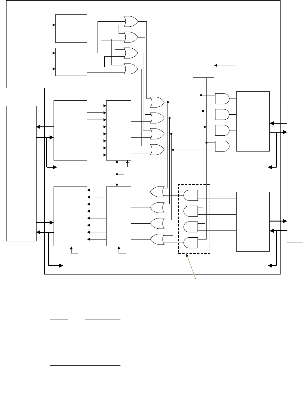
H5 The Embedded Cross Trigger Interface
H5.2 Basic operation on the ECT
ARM DDI 0487A.a Copyright © 2013 ARM Limited. All rights reserved. H5-4411
ID090413 Non-Confidential - Beta
Figure H5-2 Structure of a cross-trigger interface
Note
• The number of triggers in IMPLEMENTATION DEFINED. Figure H5-2 shows eight input and eight output
triggers.
• The number of channels is IMPLEMENTATION DEFINED. Figure H5-2 shows four channels.
•In Figure H5-2 the input channel gate function is a CTIv2 feature.
When the CTI receives an input trigger event, this generates channel events on one or more internal channels,
according to the mapping function defined by the Input trigger→output channel mapping registers, CTIINEN<n>.
The CTI also contains an application trigger and channel pulse to allow a debugger to create channel events directly
on internal channels by writing to the CTI control registers.
Gate
enable
Application
trigger
(CTIAPP)
Channel
pulse
CTIGATE
CTIAPPSET
CTIAPPPULSE
Cross Trigger Interface
Input
channel
to
Output
trigger
mapping
CTIAPPCLEAR
CTITRIGINSTATUS
CTITRIGOUTSTATUS
CTIOUTEN[ ]
PE CTM
CTIINTACK
Input
trigger
interface
Output
channel
interface
Input
trigger
to
Output
channel
mapping
CTIINEN[ ]
CTICHINSTATUS
CTICHOUTSTATUS
Input
channel
interface
The input channel gate function was not implemented
in previous versions of this architecture.
Output
trigger
interface
GLBEN

H5 The Embedded Cross Trigger Interface
H5.2 Basic operation on the ECT
H5-4412 Copyright © 2013 ARM Limited. All rights reserved. ARM DDI 0487A.a
Non-Confidential - Beta ID090413
Channel events on each internal channel are passed to a corresponding output channel that is controlled by a channel
gate. The channel gate can block propagation of channel events from an internal channel to an output channel.
The output channels from a CTI are combined, using a logical OR function, with the output channels from all other
CTIs to form the input channels on other CTIs. The input channels of this CTI are the logical OR of the output
channels on all other CTIs. This is the cross-trigger matrix, CTM. Therefore, the number of input channels must
equal the number of output channels.
Note
The number of input triggers and output triggers is not required to be the same.
The internal channels form an internal cross-trigger matrix within the CTI. This delivers events directly from the
input triggers to the output triggers. Therefore the number of internal channels is the same as the number of input
and output channels on the external CTM, and there is a direct mapping between the two.
Channel events received on each input channel are passed to the corresponding internal channel. It is
IMPLEMENTATION DEFINED whether the cross-trigger gate also blocks propagation of channel events from input
channels to internal channels.
When the CTI receives a channel event on an internal channel this generates trigger events on one or more output
triggers, according to the mapping function defined by the Input channel → output trigger mapping registers,
CTIOUTEN<n>.
The CTI contains the input and output trigger interfaces to the PE and the interface of the cross-trigger matrix. The
architecture does not define the signal protocol used on the trigger interfaces, and:
• It is IMPLEMENTATION DEFINED whether the CTI supports multicycle input trigger events.
• It is IMPLEMENTATION DEFINED whether the CTM supports multicycle channel events.
See Multicycle events.
However, an output trigger is asserted until acknowledged. The output trigger can be:
• Self-acknowledging. This means that no further action is required from the debugger.
• Acknowledged by the debugger writing 1 to the corresponding bit of CTIINTACK.
The time taken to propagate a trigger event from the first PE, through its CTI, across the CTM to another CTI, and
thereby to a second PE is IMPLEMENTATION DEFINED.
Note
ARM recommends that this path is not longer than the shortest software communication path between those PEs.
This is because if the first PE halts, the Cross-halt trigger event can propagate through the ECT and halt the second
PE without causing software on the second PE to malfunction because the first PE is in Debug state and is not
responding.
H5.2.1 Multicycle events
A multicycle event is one with a continuous state that might persist over many cycles, as opposed to a discrete event.
A typical implementation of a multicycle event is a level-based signal interface, whereas a discrete event might be
implemented as a pulse signal or message.
CTI support for multicycle trigger events is IMPLEMENTATION DEFINED. Use of multicycle trigger events is
deprecated. Of the architecturally defined input trigger events, the Performance Monitors overflow trigger event and
Generic trace external output trigger events can be multicycle input triggers.
CTM support for multicycle channel events is IMPLEMENTATION DEFINED. A CTM that does not support multicycle
channel events cannot propagate a multicycle trigger event between CTIs.
Note
A full ECT might comprise a mix of CTIs, some of which can support multicycle trigger events. In bridging these
components, multicycle channel events become single channel events at the boundary between the CTIs.

H5 The Embedded Cross Trigger Interface
H5.2 Basic operation on the ECT
ARM DDI 0487A.a Copyright © 2013 ARM Limited. All rights reserved. H5-4413
ID090413 Non-Confidential - Beta
An ECT that supports multicycle trigger events
When an ECT supports multicycle trigger events, an input trigger event to the CTI continuously asserts channel
events on all output channels mapped to it until either:
• The input trigger event is removed.
• The channel mapping function is disabled.
This means that an input trigger that is asserted for multiple cycles causes any channels that are mapped to it to
become active for multiple cycles. Consequently, any output triggers mapped from that channel are asserted for
multiple cycles.
Note
The output trigger remains asserted for at least as long as the channel remains active. This means that even if the
output trigger is acknowledged, it remains asserted until the channel deactivates.
The CTI does not guarantee that these events have precisely the same duration, as the triggers and channels can cross
between clock domains.
CTIAPPSET and CTIAPPCLEAR can set a channel active for multiple cycles. CTIAPPPULSE generates a single
channel event. CTICHINSTATUS and CTICHOUTSTATUS can report whether a channel is active.
An ECT that does not support multicycle trigger events
When an ECT does not support multicycle trigger events, an input trigger event to the CTI generates a single
channel event on all output channels mapped to it, regardless of how long the input trigger event is asserted.
This means that an input trigger event that is asserted for multiple cycles generates a single channel event on any
channels mapped to it. Consequently any self-acknowledging output triggers mapped from those channels are single
trigger events.
Note
A single event is typically a single cycle, but there is no guarantee that this is always the case.
CTIAPPSET and CTIAPPCLEAR can only generate a single channel event. CTIAPPPULSE generates a single
channel event. If the ECT does not support multicycle channel events, use of CTIAPPSET and CTIAPPCLEAR is
deprecated, and the debugger must only use CTIAPPPULSE. CTICHINSTATUS and CTICHOUTSTATUS must
be treated as UNKNOWN.

H5 The Embedded Cross Trigger Interface
H5.3 Cross-triggers on a PE in an ARMv8 implementation
H5-4414 Copyright © 2013 ARM Limited. All rights reserved. ARM DDI 0487A.a
Non-Confidential - Beta ID090413
H5.3 Cross-triggers on a PE in an ARMv8 implementation
An ARMv8 PE must include a cross-trigger interface, and the implementation must include at least the input and
output triggers defined in this architecture. The number of channels in the cross-trigger matrix is IMPLEMENTATION
DEFINED, but there must be a minimum of three. Software can read CTIDEVID.NUMCHAN to discover the number
of implemented channels.
The CTM must connect to all PEs in the same Inner Shareability domain as the ARMv8-A PE, but can also connect
to additional PEs. ARM strongly recommends that the CTM connects all PEs implementing a CTI in the system.
This includes ARMv7-A PEs and other PEs that can be connected using a CoreSight CTI module.
Note
In a uniprocessor system the CTM is OPTIONAL. The CTM might be connected other CTI modules for non-PEs, such
as triggers for system visibility components. ARM recommends that the CTM is implemented.
Any CTI connected to a PE that is not an ARMv8-A PE must implement at least:
• The Debug request trigger event.
• The Restart trigger event.
• The Cross-halt trigger event.
For more information about the CTI, see the CoreSight ™ SoC Technical Reference Manual. ARMv8-A refines the
generic CTI by defining roles for each of the implemented input and output triggers.

H5 The Embedded Cross Trigger Interface
H5.4 Description and allocation of CTI triggers
ARM DDI 0487A.a Copyright © 2013 ARM Limited. All rights reserved. H5-4415
ID090413 Non-Confidential - Beta
H5.4 Description and allocation of CTI triggers
Table H5-1 shows the output trigger events defined by the architecture and the related trigger numbers.
Note
Output triggers from the CTI are inputs to other blocks.
Table H5-2 shows the input trigger events defined by the architecture and the related trigger numbers.
Note
Input triggers to the CTI are outputs from other blocks.
Table H5-1 and Table H5-2 show the minimum set of trigger events defined by the architecture. However:
• The Generic trace external input and output trigger events are only required if the OPTIONAL Trace extension
is implemented. If the OPTIONAL Trace extension is not implemented, these trigger events are reserved.
• Support for the generic CTI interrupt trigger event is IMPLEMENTATION DEFINED because details of interrupt
handling in the system, including any interrupt controllers, are IMPLEMENTATION DEFINED. Details regarding
how the CTI interrupt is connected to an interrupt controller and its allocated interrupt number lie outside the
scope of the architecture. ARM strongly recommends that implementations provide a means to generate
interrupts based on external debug events.
• The other trigger events are required by the architecture.
An ARMv8-A implementation can extend the CTI with additional triggers. These start with the number eight.
H5.4.1 Debug request trigger event
This is an output trigger event from the CTI, and an input trigger event to the PE, asserted by the CTI to force the
PE into Debug state. The trigger event is asserted until acknowledged by the debugger. The debugger acknowledges
the assert by writing 1 to CTIINTACK[0].
Table H5-1 Allocation of CTI output trigger events
Number Source Destination Event description
0CTIPE Debug request trigger event
1CTIPE Restart request trigger event on page H5-4416
2 CTI IRQ controller Generic CTI interrupt trigger event on page H5-4417
3 - - Reserved
4 - 7 CTI Trace extension OPTIONAL Generic trace external input trigger events on page H5-4417
Table H5-2 Allocation of CTI input trigger events
Number Source Destination Event description
0PECTI Cross-halt trigger event on page H5-4416
1PECTI Performance Monitors overflow trigger event on page H5-4416
2 - 3 - - Reserved
4 - 7 Trace
extension CTI OPTIONAL Generic trace external output trigger events on page H5-4417

H5 The Embedded Cross Trigger Interface
H5.4 Description and allocation of CTI triggers
H5-4416 Copyright © 2013 ARM Limited. All rights reserved. ARM DDI 0487A.a
Non-Confidential - Beta ID090413
If the PE is already in Debug state, the PE ignores the trigger event, but the CTI continues to assert it until it is
removed by the debugger. See also External Debug Request debug event on page H3-4380.
H5.4.2 Restart request trigger event
This is an output trigger event from the CTI, and an input trigger event to the PE, asserted by the CTI to request the
PE to exit Debug state. If the PE is not in Debug state, the request is ignored and dropped by the CTI.
If a Restart request trigger event is received at or about the same time as the PE enters Debug state, it is
CONSTRAINED UNPREDICTABLE whether:
• The restart is ignored. In this case the PE enters Debug state and remains in Debug state.
• The PE enters Debug state and then immediately restarts.
Debuggers must program the CTI to send Restart request trigger events only to PEs that are halted. To enable the
PE to disambiguate discrete Restart request trigger events, after sending a Restart request trigger event, the debugger
must confirm that the PE has restarted and halted before sending another Restart request trigger event.
Debuggers can use EDPRSR.{SDR, HALTED} to determine the execution state of the PE.
The trigger event is self-acknowledging, meaning that the debugger requires no further action to remove the trigger
event. See also Exiting Debug state on page H2-4361.
H5.4.3 Cross-halt trigger event
This is an input trigger event to the CTI, and an output trigger event from the PE, asserted by a PE when it is entering
Debug state.
Note
To reduce the latency of halting, ARM recommends that an implementation issues the Cross-halt trigger event early
in the committed process of entering Debug state. This means that there is no requirement to wait until all aspects
of entry to Debug state have completed before issuing the trigger event. Speculative emission of Cross-halt trigger
events is not allowed. The Cross-halt trigger event must not be issued early enough for a subsequent Debug request
trigger event, that might be derived from the Cross-halt trigger event, to be recorded in the EDSCR.STATUS field.
This applies to Debug request trigger events that are acting as inputs to the PE.
H5.4.4 Performance Monitors overflow trigger event
This is an input trigger event to the CTI, and an output trigger event from the PE, asserted each time the PE asserts
a new Performance Monitors counter overflow interrupt request. See Chapter D6 The Performance Monitors
Extension.
If the CTI supports multicycle trigger events, then the trigger event remains asserted until the overflow is cleared
by a write to PMOVSCLR_EL0. Otherwise, the trigger event is not asserted again until the overflow is cleared by
a write to PMOVSCLR_EL0.
Note
• This does not replace the recommended connection of Performance Monitors overflow trigger event to an
interrupt controller. Software must be able to program an interrupt on Performance Monitors overflow
without programming the CTI.
• Events can be counted when
ExternalNoninvasiveDebugEnabled()
== FALSE, and, in Secure state, when
ExternalSecureNoninvasiveDebugEnabled()
== FALSE. Secure software must be aware that overflow trigger
events are nevertheless visible to the CTI.

H5 The Embedded Cross Trigger Interface
H5.4 Description and allocation of CTI triggers
ARM DDI 0487A.a Copyright © 2013 ARM Limited. All rights reserved. H5-4417
ID090413 Non-Confidential - Beta
H5.4.5 Generic trace external input trigger events
These are output trigger events from the CTI, and input trigger events to the OPTIONAL Trace extension, that are
used in conjunction with the Generic trace external output trigger events to pass trigger events between:
• The PE and the OPTIONAL Trace extension.
• The OPTIONAL Trace extension and any other component attached to the CTM, including other Trace
extensions.
There are four Generic trace external input trigger events.
The trigger events are self-acknowledging. This means that the debugger does not have to take any further action to
to remove the events.
H5.4.6 Generic trace external output trigger events
These are input trigger events to the CTI, and output trigger events from the OPTIONAL Trace extension, used in
conjunction with the Generic trace external input trigger events to pass trigger events between:
• The PE and the OPTIONAL Trace extension.
• The OPTIONAL Trace extension and any other component attached to the CTM, including other Trace
extensions.
There are four Generic trace external output trigger events.
H5.4.7 Generic CTI interrupt trigger event
This is an output trigger event from the CTI, and an input to an IMPLEMENTATION DEFINED interrupt controller, and
can transfer trigger events from the PE, Trace extension, or any other component attached to the CTI and CTM to
software as an interrupt. The Generic CTI interrupt trigger event must be connected to the interrupt controller as an
interrupt that can target the originating PE.
Note
ARM recommends that the Generic CTI interrupt trigger event is a private peripheral interrupt, but implementations
might instead make this trigger event available as a shared peripheral interrupt or a local peripheral interrupt.
It is IMPLEMENTATION DEFINED whether this trigger event is:
• Self-acknowledging. This means that the debugger is not required to take any further action, and that the
interrupt controller must treat the trigger event as a pulse or edge-sensitive interrupt.
• Acknowledged by the debugger. The debugger acknowledges the trigger event by writing 1 to
CTIINTACK[2]. This means that the interrupt controller must treat the trigger event as a level-sensitive
interrupt.
ARM recommends that the Generic CTI interrupt trigger event is a self-acknowledging trigger event.

H5 The Embedded Cross Trigger Interface
H5.5 CTI registers programmers’ model
H5-4418 Copyright © 2013 ARM Limited. All rights reserved. ARM DDI 0487A.a
Non-Confidential - Beta ID090413
H5.5 CTI registers programmers’ model
The CTI registers programmers’ model is described in Chapter H8 About the External Debug Registers. The
following sections contain information specific to the CTI:
•External debug register resets on page H8-4465.
•External debug interface register access permissions on page H8-4451.
•Cross-trigger interface registers on page H8-4461.
• The individual register descriptions in Cross-Trigger Interface registers on page H9-4554.
See also Memory-mapped accesses to the external debug interface on page H8-4449.
H5.5.1 CTI reset
An External Debug reset resets the CTI. See External debug register resets on page H8-4465 for details of CTI
register resets. All CTI output triggers and output channels are deasserted on an External Debug reset.
H5.5.2 CTI authentication
The CTI ignores the state of the IMPLEMENTATION DEFINED authentication interface. This means that:
•CTITRIGINSTATUS shows the status of the input triggers and CTICHINSTATUS shows the status of the
input channels, regardless of the value of
ExternalNoninvasiveDebugEnabled()
.
Note
The PE does not generate the Cross-halt trigger event and the Trace extension does not generate Generic trace
external output trigger events when
ExternalNoninvasiveDebugEnabled()
== FALSE. However, the PE can
generate Performance Monitors overflow trigger events.
• The CTI can generate external triggers regardless of the value of
ExternalInvasiveDebugEnabled()
.
Note
The PE ignores Debug request and Restart request trigger events when
ExternalInvasiveDebugEnabled()
==
FALSE. The Trace extension ignores Generic trace external input trigger events when
ExternalNoninvasiveDebugEnabled()
== FALSE. The behavior of Generic CTI interrupt requests is part of the
IMPLEMENTATION DEFINED handling of these interrupts, but it is permissible for an interrupt controller to
receive these requests even when
ExternalInvasiveDebugEnabled()
== FALSE.

H5 The Embedded Cross Trigger Interface
H5.6 Examples
ARM DDI 0487A.a Copyright © 2013 ARM Limited. All rights reserved. H5-4419
ID090413 Non-Confidential - Beta
H5.6 Examples
The CTI is fully programmable and allows for flexible cross-triggering of events within a PE and between PEs in a
multiprocessor system. For example:
• The Cross-halt trigger event and the Debug request trigger event can be used for cross-triggering in a
multiprocessor system.
• The Cross-halt trigger event and the Generic interrupt trigger event can be used for event-driven debugging
in a multiprocessor system.
• The Performance Monitors overflow trigger event and the Debug request trigger event can force entry to
Debug state on overflow of a Performance Monitors event counter, for event-driven profiling.
Note
This does not replace the recommended connection of Performance Monitors overflow trigger events to an
interrupt controller. Software must be able to program an interrupt on Performance Monitors overflow
without programming the CTI. ARM recommends that the Performance Monitors overflow signal is directly
available as a local interrupt source.
• The Generic trace external input and Generic trace external output trigger events can pass trace events into
and out of the event logic of the Trace extension. They can do this:
— To pass trace events between Trace extensions.
— In conjunction with the Performance Monitors overflow trigger event, to couple the Performance
Monitors to the Trace extension.
— In conjunction with the Debug request trigger event, to trigger entry to Debug state on a trace event.
— In conjunction with other CTIs, to signal a trace trigger event onto a CoreSight trace interconnect.
The following sections describe some examples in more detail:
•Halting a single PE.
•Halting all PEs in a group when any one PE halts on page H5-4420.
•Synchronously restarting a group of PEs on page H5-4420.
•Halting a single PE on Performance Monitors overflow on page H5-4420.
Example H5-1 Halting a single PE
To halt a single PE, set:
1. CTIGATE[0] = 0, so that the CTI does not pass channel events on internal channel 0 to the CTM.
2. CTIOUTEN<n>[0] = 1, so that the CTI generates a Debug request trigger event in response to a channel
event on channel 0.
Note
In this example, n is 0.
3. CTIAPPPULSE[0] = 1, to generate a channel event on channel 0.
When the PE has entered Debug state, clear the Debug request trigger event by writing 1 to CTIINTACK[0], before
restarting the PE.

H5 The Embedded Cross Trigger Interface
H5.6 Examples
H5-4420 Copyright © 2013 ARM Limited. All rights reserved. ARM DDI 0487A.a
Non-Confidential - Beta ID090413
Example H5-2 Halting all PEs in a group when any one PE halts
To program a group of PEs so that when one PE in the group halts, all of the PEs in that group halt, set the following
registers for each PE in the group:
1. CTIGATE[2] = 1, so that each CTI passes channel events on internal channel 2 to the CTM.
2. CTIINEN<n>[2] = 1,so that each CTI generates a channel event on channel 2 in response to a Cross-halt
trigger event.
Note
In this example, n is 0.
3. CTIOUTEN<n>[2] = 1, so that each CTI generates a Debug request trigger event in response to an channel
event on channel 2.
Note
In this example, n is 0.
When a PE has halted, clear the Debug request trigger event by writing a value of 1to CTIINTACK[0], before
restarting the PE.
Example H5-3 Synchronously restarting a group of PEs
To restart a group of PEs, for each PE in the group set:
1. CTIGATE[1] = 1, so that each CTI passes channel events on internal channel 1 to the CTM.
2. CTIOUTEN<n>[1] = 1, so that each CTI generates a Restart request trigger event in response to a channel
event on channel 1.
Note
In this example, n is 1.
3. CTIAPPPULSE[1] = 1 on any one PE in the group, to generate a channel event on channel 1.
Example H5-4 Halting a single PE on Performance Monitors overflow
To halt a single PE on a Performance Monitors overflow set:
1. CTIGATE[3] = 0, so that the CTI does not pass channel events on internal channel 3 to the CTM.
2. CTIINEN<n>[3] = 1, so that the CTI generates a channel event on channel 3 in response to a Performance
Monitors overflow trigger event.
Note
In this example, n is 1.

H5 The Embedded Cross Trigger Interface
H5.6 Examples
ARM DDI 0487A.a Copyright © 2013 ARM Limited. All rights reserved. H5-4421
ID090413 Non-Confidential - Beta
3. CTIOUTEN<n>[3] = 1, so that the CTI generates a Debug request trigger event in response to a channel
event on channel 3.
Note
. In this example, n is 0.
When the PE has entered Debug state, clear the Debug request trigger event by writing 1 to CTIINTACK[0], before
restarting the PE. Clear the overflow status by writing to PMOVSCLR_EL0.

H5 The Embedded Cross Trigger Interface
H5.6 Examples
H5-4422 Copyright © 2013 ARM Limited. All rights reserved. ARM DDI 0487A.a
Non-Confidential - Beta ID090413

ARM DDI 0487A.a Copyright © 2013 ARM Limited. All rights reserved. H6-4423
ID090413 Non-Confidential - Beta
Chapter H6
Debug Reset and Powerdown Support
This chapter describes the reset and powerdown support in the Debug architecture. It contains the following
sections:
•About Debug over powerdown on page H6-4424.
•Power domains and debug on page H6-4425.
•Core power domain power states on page H6-4426.
•Emulating low-power states on page H6-4428.
•Debug OS Save and Restore sequences on page H6-4430.
Note
Where necessary, Table J-1 on page AppxJ-5088 disambiguates the general register references used in this chapter.

H6 Debug Reset and Powerdown Support
H6.1 About Debug over powerdown
H6-4424 Copyright © 2013 ARM Limited. All rights reserved. ARM DDI 0487A.a
Non-Confidential - Beta ID090413
H6.1 About Debug over powerdown
Debug over powerdown is a facility for an operating system to save and restore the PE state on behalf of a
self-hosted or external debugger or both.
For external debug over powerdown, the architecture defines the OS Lock, OS Double Lock, and the logical split
of the hardware on which a PE executes into the Core power domain and the Debug power domain. See:
•Power domains and debug on page H6-4425.
•Core power domain power states on page H6-4426.
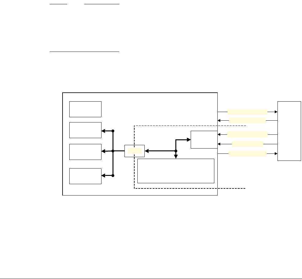
H6 Debug Reset and Powerdown Support
H6.2 Power domains and debug
ARM DDI 0487A.a Copyright © 2013 ARM Limited. All rights reserved. H6-4425
ID090413 Non-Confidential - Beta
H6.2 Power domains and debug
The external debug component of ARMv8-A has two logical power domains, each with its own reset:
• The debug power domain contains the interface between the PE and the external debugger, and is powered
up whenever an external debugger is connected to the SoC. It remains powered up while the external
debugger is connected. Registers in this domain are reset by an external debug reset.
• The core power domain contains the rest of the PE, and is allowed to power up and power down
independently of the Debug power domain.
The core power domain contains several types of registers:
• Non-debug logic refers to all registers and logic that are not associated with debug.
• Self-hosted debug logic refers to registers and logic associated solely with the self-hosted debug aspects of
the architecture.
• Shared debug logic refers to registers and logic associated with both the self-hosted and external debug
aspects of the architecture.
• External debug logic refers to registers and logic associated solely with the external debug aspects of the
architecture.
Note
• The model of two logical power domains has an impact on the reset and access permission requirements of
the debug programmers’ model.
• The power domains are described as logical because the architecture defines the requirements but does not
require two physical power domains. Any power domain split that meets the requirements of the
programmers’ model is a valid implementation.
Figure H6-1 shows the recommended power domain split. The signals DBGPWRUPREQ, DBGNOPWRDWN,
and DBGPWRDUP shown in Figure H6-1 provide an interface between the power controller and the PE debug
logic that is in the debug power domain. They are part of the recommended interface. See Appendix B
Recommended External Debug Interface.
Figure H6-1 Recommended power domain split between core and debug power domains
Processor
External
debug
interface
Debug power domain
external debug registers
Power
controller
Core domain Vdd
Debug domain Vdd
DBGPWRDUP
Power domain boundary
Debug
power domain
Core
power domain
Bridge DBGPWRUPREQ
DBGNOPWRDWN
Non-debug
logic
Self-hosted
debug logic
Shared debug
logic
External
debug logic

H6 Debug Reset and Powerdown Support
H6.3 Core power domain power states
H6-4426 Copyright © 2013 ARM Limited. All rights reserved. ARM DDI 0487A.a
Non-Confidential - Beta ID090413
H6.3 Core power domain power states
The ARM architecture does not define the power states of the PE as these are not normally visible to software.
However, they are visible to the external debugger. The Debug architecture uses a four logical power states model
for the core power domain. The four logical power states are as follows:
Normal The core power domain is fully powered on and the debug registers are accessible.
Standby The core power domain is on, but there are measures to reduce energy consumption. In a typical
implementation, the PE enters standby by executing a
WFI
or
WFE
instruction, and exits on a wake-up
event. There can be other IMPLEMENTATION DEFINED measures the OS can take to enter standby.
The PE preserves the PE state, including the debug logic state. Changing from standby to normal
operation does not involve a reset of the PE.
Standby is the least invasive OS energy saving state. Standby implies only that the PE is unavailable
and does not clear any debug settings. For standby, the debug architecture requires only the
following:
• An External Debug Request debug event is a wake-up event when halting is allowed. This
means that the PE must exit standby to handle the debug event. If the PE executed a
WFE
or a
WFI
instruction to enter standby, then it retires that instruction,
• If the external debug interface is accessed, the PE must respond to that access. ARM
recommends that, if the PE executed a
WFI
or
WFE
instruction to enter standby, then it does not
retire that instruction.
Standby is transparent, meaning that to software and to an external debugger it is indistinguishable
from normal operation.
Retention The OS takes some measures, including IMPLEMENTATION DEFINED measures, to reduce energy
consumption. The PE state, including debug settings, is preserved in low-power structures, allowing
the core power domain to be at least partially turned off.
Changing from low-power retention to normal operation does not involve a reset of the PE. The
saved PE state is restored on changing from low-power retention state to normal operation.
External Debug Request debug events stay pending and debug registers in the core power domain
cannot be accessed.
Note
• This model of retention does not include implementations where the PE exits the state in
response to a debug register access. From the Debug architecture perspective,
implementations like this are forms of standby.
Powerdown The OS takes some measures to reduce energy consumption by turning the core power domain off.
These measures must include the OS saving any PE state, including the debug settings, that must be
preserved over powerdown. Changing from powerdown to normal operation must include:
• A Cold reset of the PE after the power level has been restored.
• The OS restoring the saved PE state.
External Debug Request debug events stay pending and debug registers in the core power domain
cannot be accessed.
The Debug architecture uses a simpler two states model for the Debug power domain. The two states are:
Off The debug power domain is turned off.
On The debug power domain is turned on.
The available power states, including the cross-product of core power domain and debug power domain power
states is IMPLEMENTATION DEFINED. Implementations are not required to implement all of these states and might
include additional states. These additional states must appear to the debugger as one of the logical power states
defined by this model. The control of power states is IMPLEMENTATION DEFINED.

H6 Debug Reset and Powerdown Support
H6.3 Core power domain power states
ARM DDI 0487A.a Copyright © 2013 ARM Limited. All rights reserved. H6-4427
ID090413 Non-Confidential - Beta
Note
As a result, it is IMPLEMENTATION DEFINED whether it is possible for the debug power domain to be on when the
core power domain is off.

H6 Debug Reset and Powerdown Support
H6.4 Emulating low-power states
H6-4428 Copyright © 2013 ARM Limited. All rights reserved. ARM DDI 0487A.a
Non-Confidential - Beta ID090413
H6.4 Emulating low-power states
The control registers DBGPRCR.CORENPDRQ and EDPRCR.COREPURQ provide an interface between the
power controller and the PE. They typically map directly to signals in the recommended external debug interface.
With this interface the external debugger can request the power controller to:
• Emulate states where the core power domain is completely off or in a low-power state where the core power
domain registers cannot be accessed. This simplifies the requirements on software by sacrificing entirely
realistic behavior.
• Restore full power to the core power domain.
EDPRSR.{SPD, PU} indicates the core power domain power state. For more information see:
•DBGPRCR_EL1, Debug Power Control Register on page D8-2093 and DBGPRCR, Debug Power Control
Register on page G4-4145.
•EDPRCR, External Debug Power/Reset Control Register on page H9-4520.
•EDPRSR, External Debug Processor Status Register on page H9-4523.
•Appendix B Recommended External Debug Interface.
The measures to emulate powerdown are IMPLEMENTATION DEFINED. The ability of the debugger to access the state
of the PE and the system might be limited as a result of the measures adopted.
In an emulated powerdown state, the debugger must be able to access all debug registers in both the debug power
domain and the core power domain as if the core power domain were on. That is, the debugger must be able to read
and write to such registers without receiving errors. This allows an external debugger to debug the powerup
sequence. To stop the OS Double Lock preventing access to debug registers when powerdown is being emulated,
DoubleLockStatus() == FALSE
when DBGPRCR.CORENPDRQ == 1.
Otherwise, the behavior of the PE in emulated powerdown must be similar to that in a real powerdown state. In
particular, the PE must not respond to other system stimuli, such as interrupts.
Example H6-1 and Example H6-2 are examples of two approaches to emulating powerdown.
Example H6-1 An example of emulating powerdown
The PE is held in Standby state, isolated from any system stimuli. It is IMPLEMENTATION DEFINED whether the PE
can respond to debug stimuli such as an External Debug Request debug event.
If the PE can enter Debug state, then the external debugger is able to use the ITR to execute instructions, such as
loads and stores. This causes the external debugger to interact with the system. If the external debugger restarts the
PE, the PE leaves Standby state and restarts fetching instructions from memory.
Example H6-2 Another example of emulating powerdown
The PE is held in Warm reset. This limits the ability of an external debugger to access the resources of the PE. For
example, the PE cannot be put into Debug state.
On exit from emulated powerdown the PE is reset. However, the debug registers that are only reset by a Cold reset
must not be reset. Typically this means that a Warm reset is substituted for the Cold reset.
Note
• Warm reset and Cold reset have different effects apart from resetting the debug registers. In particular,
RMR_ELx is reset by a Cold reset and controls the reset state on a Warm reset. This means that if a Cold
reset is substituted by a Warm reset, the behavior of the reset code might be different.
• The timing effects of powering down are typically not factored in the powerdown emulation. Examples of
these timing effects are clock and voltage stabilization.

H6 Debug Reset and Powerdown Support
H6.4 Emulating low-power states
ARM DDI 0487A.a Copyright © 2013 ARM Limited. All rights reserved. H6-4429
ID090413 Non-Confidential - Beta
• Emulation does not model the state lost during powerdown, meaning that it might mask errors in the state
storage and recovery routines.

H6 Debug Reset and Powerdown Support
H6.5 Debug OS Save and Restore sequences
H6-4430 Copyright © 2013 ARM Limited. All rights reserved. ARM DDI 0487A.a
Non-Confidential - Beta ID090413
H6.5 Debug OS Save and Restore sequences
In ARMv8-A, the following registers provide the OS Save and restore mechanism:
• The OS Lock Access Register, OSLAR, locks the OS Lock to restrict access to debug registers before starting
an OS Save sequence, and unlocks the OS Lock after an OS Restore sequence.
• The OS Lock Status Register, OSLSR, shows the status of the OS Lock.
• The External Debug Execution Control Register, EDECR, can be configured to generate a debug event when
the OS Lock is unlocked.
• The OS Double Lock Register, OSDLR, locks out an external debug interface entirely. This is only used
immediately before a powerdown sequence.
See also:
•Reset and debug on page H8-4463
•Appendix D Example OS Save and Restore sequences
H6.5.1 Debug registers to save over powerdown
Table H6-1 shows the different requirements for self-hosted debug over powerdown and external debug over
powerdown:
• The column labeled Self-hosted lists registers that software must preserve over powerdown so that it can
support self-hosted debug over powerdown. This does not require use of the OS Save and Restore
mechanism.
• The column labeled External lists registers that software must preserve over powerdown so that it can support
external debug over powerdown. This requires use of the OS Save and Restore mechanism:
— Some external debug registers are not normally accessible to software executing on the PE. Additional
debug registers are provided that give software the required access to save and restore these external
debug registers when OSLSR.OSLK is locked. These registers include OSECCR, OSDTRRX, and
OSDTRTX.
• Some registers might only present in some implementations, or might not be accessible at all Exception levels
or in Non-secure state. DBGVCR32_EL2 and SDER32_EL3 are only required to support AArch32.
Table H6-1 does not include registers for the OPTIONAL Trace and Performance Monitor extensions.
Table H6-1 Debug registers to save over powerdown
Register in AArch64 Register in AArch32 Self-hosted External
MDSCR_EL1 DBGDSCRext Yes Yesa
DBGBVR<n>_EL1 DBGBVR<n> Yes Yes
DBGBCR<n>_EL1 DBGBCR<n> Yes Yes
DBGWVR<n>_EL1 DBGWVR<n> Yes Yes
DBGWCR<n>_EL1 DBGWCR<n> Yes Yes
DBGVCR32_EL2 DBGVCR Yes -
MDCR_EL2 HDCR Yes -
SDER32_EL3 SDER Yes -
MDCR_EL3 SDCR Yesb-
MDCCINT_EL1 DBGDCCINT -Yesb

H6 Debug Reset and Powerdown Support
H6.5 Debug OS Save and Restore sequences
ARM DDI 0487A.a Copyright © 2013 ARM Limited. All rights reserved. H6-4431
ID090413 Non-Confidential - Beta
H6.5.2 OS Save sequence
To preserve the debug logic state over a powerdown, the state must be saved to nonvolatile storage. This means the
OS Save sequence must:
1. Lock the OS Lock by:
• Writing the key value
0xC5ACCE55
to the DBGOSLAR in AArch32 state.
• Writing 1 to OSLAR_EL1.OSLK in AArch64 state.
2. Execute an
ISB
instruction.
3. Walk through the debug registers listed in Debug registers to save over powerdown on page H6-4430 and
save the values to the nonvolatile storage.
Before removing power from the core power domain, software must:
1. Lock the OS Double Lock by writing 1 to OSDLR_EL1.DLK.
2. Execute a context synchronization operation.
H6.5.3 OS Restore sequence
After a powerdown, the OS Restore sequence must perform the following steps to restore the debug logic state from
the non-volatile storage:
1. Lock the OS Lock, as described in Debug registers to save over powerdown on page H6-4430. The OS Lock
is generally locked by the Cold reset, but this step ensures that it is locked.
2. Execute an
ISB
instruction.
3. Walk through the debug registers listed in Debug registers to save over powerdown on page H6-4430, and
restore the values from the nonvolatile storage.
4. Execute an
ISB
instruction.
5. Unlock the OS Lock by:
• Writing any non-key value to DBGOSLAR in AArch32 state.
• Writing 0 to OSLAR_EL1.OSLK in AArch64 state.
6. Execute a context synchronization operation.
DBGCLAIMSET_EL1
DBGCLAIMCLR_EL1
DBGCLAIMSET,
DBGCLAIMCLR
-Yesc
OSECCR_EL1 DBGOSECCR -Yesab
OSDTRRX_EL1
OSDTRTX_EL1
DBGDTRRXext
DBGDTRTXext
-Yes
a. The OS Lock must be locked to save and restore for external debug. When the OS Lock is locked, DSCR is part of the software save and
restore mechanism for external debug. It provides a mechanism for an operating system to access some fields of EDSCR that are otherwise
read-only or not visible to software. This allows the operating system to save and restore these settings over a powerdown for the external
debugger.
b. This register is new in ARMv8-A. Sequences written for ARMv7 do not preserve the register over powerdown.
c. Read DBGCLAIMCLR to save, write DBGCLAIMSET to restore.
Table H6-1 Debug registers to save over powerdown (continued)
Register in AArch64 Register in AArch32 Self-hosted External

H6 Debug Reset and Powerdown Support
H6.5 Debug OS Save and Restore sequences
H6-4432 Copyright © 2013 ARM Limited. All rights reserved. ARM DDI 0487A.a
Non-Confidential - Beta ID090413
Note
The OS Restore sequence overwrites the debug registers with the values that were saved. If there are valid values
in these registers immediately before the restore sequence, then those values are lost.
H6.5.4 Debug behavior when the OS Lock is locked
The main purpose of the OS Lock is to prevent updates to debug registers during an OS Save or OS Restore
operation. The OS Lock is locked on a Cold reset.
When the OS Lock is locked:
• Access to debug registers through the system register interface is mainly unchanged except that:
— Certain registers are read and written without side-effects.
— Fields in DSCR and OSECCR that are normally read-only become read/write.
This allows the state to be saved or restored. For more information, see the relevant register description in
Chapter H9 External Debug Register Descriptions.
• Access to debug registers by the external debug interface is restricted to prevent an external debugger
modifying the registers that are being saved or restored. For more information see External debug interface
register access permissions summary on page H8-4453.
• Debug exceptions, other than Software Breakpoint Instruction exceptions are not generated.
The OS Lock has no effect on Software Breakpoint Instruction debug events and Halting debug events.
H6.5.5 Debug behavior when the OS Lock is unlocked
When the OS Lock is unlocked, an OS Unlock Catch debug event is generated if EDECR.OUCE is set to 1. See
OS Unlock Catch debug event on page H3-4381.
H6.5.6 Debug behavior when the OS Double Lock is locked
The OS Double Lock is locked immediately before a powerdown sequence. The OS Double Lock ensures that it is
safe to remove core power by forcing the debug interfaces to be quiescent.
When
DoubleLockStatus()
== TRUE:
• The external debug interface only has restricted access to the debug registers, so that it is quiescent before
removing power. See External debug interface register access permissions summary on page H8-4453.
• Debug exceptions, other than Software Breakpoint Instruction exceptions, are not generated.
• Halting is prohibited. See Halting allowed and halting prohibited on page H2-4329.
Note
Pending Halting debug events might be lost when core power is removed.
• No asynchronous debug events are
WFI
or
WFE
wake-up events.
Software must synchronize the update to OSDLR before it indicates to the system that core power can be removed.
The interface between the PE and its power controller is IMPLEMENTATION DEFINED.
Typically software indicates that core power can be removed by entering the Wait For Interrupt state. This means
that software must explicitly synchronize the OSDLR update before issuing the
WFI
instruction.
OSDLR.DLK is ignored and
DoubleLockStatus()
== FALSE if either:
• The PE is in Debug state.
•DBGPRCR.CORENPDRQ is set to 1.

H6 Debug Reset and Powerdown Support
H6.5 Debug OS Save and Restore sequences
ARM DDI 0487A.a Copyright © 2013 ARM Limited. All rights reserved. H6-4433
ID090413 Non-Confidential - Beta
Note
It is possible to enter Debug state with OSDLR.DLK set to 1. This is because a context synchronization operation
is required to ensure the OS Double Lock is locked, meaning that Debug state might be entered before the OSDLR
update is synchronized.
As the purpose of the OS Double Lock is to ensure that it is safe to remove core power, it is important to avoid race
conditions that defeat this purpose. ARM recommends that:
• Once the write to OSDLR.DLK has been synchronized by a Context synchronization operation and
DoubleLockStatus()
== TRUE, a PE must:
— Not allow a debug event generated before the Context synchronization operation to cause an entry to
Debug state or act as a wake-up event for a
WFI
or
WFE
instruction after the context synchronization
operation has completed.
— Complete any external debug access started before the Context synchronization operation by the time
the context synchronization operation completes.
Note
A debug register access might be in progress when software sets OSDLR.DLK to 1. An
implementation must not permit the synchronization of locking the OS Double Lock to stall
indefinitely while waiting for that access to complete. This means that any debug register access that
is in progress when software sets OSDLR.DLK to 1 must complete or return an error in finite time.
• If a write to DBGPRCR or EDPRCR made when OSDLR.DLK == 1 changes DBGPRCR.CORENPDRQ or
EDPRCR.CORENPDRQ from 1 to 0, meaning
DoubleLockStatus()
changes from FALSE to TRUE, then
before signaling to the system that the CORENPDRQ field has been cleared and emulation of powerdown is
no longer requested, meaning the system can remove core power, the PE must ensure that all the requirements
for
DoubleLockStatus()
== TRUE listed in this section are met.
In the standard OS Save sequence, the OS Lock is locked before the OS Double Lock is locked. This means that
writes to CORENPDRQ are ignored by the time the OS Double Lock is locked. However, if
DoubleLockStatus()
==
FALSE, an external debugger can clear the OS Lock at any time, and then write to EDPRCR.
The pseudocode for the
DoubleLockStatus()
function is as follows:
// DoubleLockStatus()
// ==================
boolean DoubleLockStatus()
// Returns the value of EDPRSR.DLK:
// FALSE if OSDLR_EL1.DLK == 0 or DBGPRCR_EL1.CORENPDRQ == 1 or the processor is in Debug state.
// TRUE if OSDLR_EL1.DLK == 1 and DBGPRCR_EL1.CORENPDRQ == 0 and the processor is in Non-debug
// state.
return OSDLR_EL1.DLK == ‘1’ && DBGPRCR_EL1.CORENPDRQ == ‘0’ && !Halted();

H6 Debug Reset and Powerdown Support
H6.5 Debug OS Save and Restore sequences
H6-4434 Copyright © 2013 ARM Limited. All rights reserved. ARM DDI 0487A.a
Non-Confidential - Beta ID090413

ARM DDI 0487A.a Copyright © 2013 ARM Limited. All rights reserved. H7-4435
ID090413 Non-Confidential - Beta
Chapter H7
The Sample-based Profiling Extension
This chapter describes the Sample-based Profiling extension, that is an OPTIONAL extension to the ARMv8
architecture. The extension provides a non-invasive external debug component.
Note
This form of the Sample-based Profiling extension is OPTIONAL. ARM recommends that if extension EDPCSR is
not implemented that an alternative IMPLEMENTATION DEFINED form of Sample-based Profiling is implemented.
It contains the following section:
•Sample-based profiling on page H7-4436.

H7 The Sample-based Profiling Extension
H7.1 Sample-based profiling
H7-4436 Copyright © 2013 ARM Limited. All rights reserved. ARM DDI 0487A.a
Non-Confidential - Beta ID090413
H7.1 Sample-based profiling
Sample-based profiling is an OPTIONAL extension to the architecture. It provides a mechanism for coarse-grained
profiling of software executing on the PE by an external debugger, without changing the behavior of that software.
The following sections describe this extension:
•The implemented Sample-based profiling registers
•Reads of the External Debug Program Counter Sampling Registers
•Reads of the External Debug Virtual Context Sample Register on page H7-4437
•Accuracy of sampling on page H7-4437
•Sample-based Profiling and security on page H7-4438
•Pseudocode details of Sample-based Profiling on page H7-4438
H7.1.1 The implemented Sample-based profiling registers
An implementation that includes the Sample-based profiling extension implements the following external debug
registers:
•EDPCSR is a 64-bit read-only register that contains a sampled program counter value. As external debug
register accesses are atomic only at word granularity, EDPCSR is split into two registers: EDPCSRhi and
EDPCSRlo. See Reads of the External Debug Program Counter Sampling Registers.
•EDCIDSR is a read-only register that contains the sampled value of CONTEXTIDR_EL1 captured on
reading EDPCSRlo.
Note
If EL3 is implemented and using AArch32 then CONTEXTIDR is a Banked register and EDCIDSR samples
the current Banked copy of CONTEXTIDR.
•EDVIDSR is a read-only register that contains sampled values captured on reading EDPSRlo. If neither EL3
nor EL2 are implemented, EDVIDSR is not implemented.
H7.1.2 Reads of the External Debug Program Counter Sampling Registers
A read of the EDPCSRlo normally has the side-effect of indirectly writing to EDCIDSR, EDVIDSR, and
EDPCSRhi. When EDPCSRlo is read, the bottom 32 bits of a program counter sample are returned. The top 32 bits
are captured in EDPCSRhi and can be read later. However:
• If the PE is in Debug state, or Sample-based Profiling is prohibited, EDPCSRlo reads as
0xFFFFFFFF
and
EDCIDSR, EDVIDSR and EDPCSRhi become UNKNOWN. See Sample-based Profiling and security on
page H7-4438.
• If the PE is in Reset state, the sampled value is UNKNOWN and EDCIDSR, EDVIDSR and EDPCSRhi become
UNKNOWN.
• If no instruction has been retired since the PE left Reset state, Debug state, or a state where Sample-based
Profiling is prohibited, the sampled value is UNKNOWN and EDCIDSR, EDVIDSR and EDPCSRhi become
UNKNOWN.
• The indirect writes to EDCIDSR, EDVIDSR, and EDPCSRhi might not occur for a memory-mapped access
to the external debug interface. For more information, see Memory-mapped accesses to the external debug
interface on page H8-4449.
Note
In ARMv7 the Sample-based Profiling extension an offset was applied to the sampled program counter value and
this offset and the instruction set state indicated in bits [1:0] of the sampled value. In the ARMv8 Sample-based
Profiling extension, the sampled value is the address of an instruction that has executed, with no offset and no
indication of the instruction set state.

H7 The Sample-based Profiling Extension
H7.1 Sample-based profiling
ARM DDI 0487A.a Copyright © 2013 ARM Limited. All rights reserved. H7-4437
ID090413 Non-Confidential - Beta
H7.1.3 Reads of the External Debug Virtual Context Sample Register
A read of the EDVIDSR contains sampled values captured on reading EDPSRlo, where:
•EDVIDSR.NS indicates the security state associated with the most recent EDPCSR sample.
•EDVIDSR.E2 indicates whether the most recent EDPCSR sample was associated with EL2. If
EDVIDSR.NS == 0, this bit is 0.
•EDVIDSR.E3 indicates whether the most recent EDPCSR sample was associated with EL3 using AArch64.
If EDVIDSR.NS == 1 or the PE was in AArch32 state when EDPCSRlo was read, this bit is 0.
•EDVIDSR.HV indicates whether EDPCSRhi is valid, that is, bits [63:32] of the most recent program counter
sample are non-zero.
Note
—EDVIDSR.HV == 1 does not mean that EDPCSRhi != 0. EDVIDSR.HV == 0 is a hint that EDPCSRhi
does not need to be read.
— Tools must take care to avoid skewing sampled data by over-sampling code for which
EDVIDSR.HV == 0.
•EDVIDSR.VMID indicates the value of the VTTBR_EL2.VMID register associated with the most recent
EDPCSRlo sample. If EDVIDSR.NS == 0 or EDVIDSR.E2 == 1, this field is RAZ.
If EL2 is not implemented, EDVIDSR.E2 and EDVIDSR.VMID are RES0.
If EL3 is not implemented, EDVIDSR.E3 is RES0, and EDVIDSR.NS has a fixed read-only value.
H7.1.4 Accuracy of sampling
Sample-based Profiling is provided as a mechanism for tools to populate a statistical model of the performance of
software executing on the PE. The statistical data returned by random sampling of EDPCSR, EDCIDSR, and
EDVIDSR must allow such statistical modeling.
It must be possible to sample references to branch targets. It is IMPLEMENTATION DEFINED whether references to
other instructions can be sampled. The branch target for a conditional branch instruction that fails its condition
check is the instruction that follows the conditional branch instruction. The branch target for an exception is the
exception vector address.
To keep the implementation and validation cost low, a reasonable degree of inaccuracy in the sampled data is
acceptable. ARM does not define a reasonable degree of inaccuracy but recommends the following guidelines:
• Under normal operating conditions, the whole sample, EDPCSR, EDCIDSR, and EDVIDSR, must reference
an instruction, including its context.
• In exceptional circumstances, such as a change in security state or other boundary condition, it is acceptable
for the sample to represent an instruction that was not committed for execution.
• Under very unusual non-repeating pathological cases the sample can represent an instruction that was not
committed for execution. These cases are likely to occur as a result of asynchronous exceptions, such as
interrupts, where the chance of a systematic error in sampling is very unlikely.
See also Non-invasive behavior on page D6-1824.

H7 The Sample-based Profiling Extension
H7.1 Sample-based profiling
H7-4438 Copyright © 2013 ARM Limited. All rights reserved. ARM DDI 0487A.a
Non-Confidential - Beta ID090413
H7.1.5 Sample-based Profiling and security
Sample-based Profiling is a non-invasive external debug component, controlled by an IMPLEMENTATION DEFINED
authentication interface. Sample-based Profiling is prohibited unless both:
• Allowed by the IMPLEMENTATION DEFINED authentication interface
ExternalNoninvasiveDebugEnabled()
• Any one of:
— Executing in Non-secure state.
— EL3 is not implemented.
— EL3 is implemented, executing in Secure state, and allowed by the IMPLEMENTATION DEFINED
authentication interface
ExternalSecureNoninvasiveDebugEnabled()
.
— EL3 is implemented, EL3 or EL1 is using AArch32, executing at EL0 in Secure state, and
SDER32_EL3.SUNIDEN == 1.
The state of IMPLEMENTATION DEFINED authentication interface is visible through DBGAUTHSTATUS_EL1.
See also Appendix B Recommended External Debug Interface.
H7.1.6 Pseudocode details of Sample-based Profiling
PCSample()
records a PC sample for the EDPCSR and associated registers.
type PCSample is (
boolean valid,
bits(64) pc,
bits(2) el,
bit rw,
bit ns,
bits(32) contextidr,
bits(8) vmid
)
PCSample pc_sample;
// CreatePCSample()
// ================
CreatePCSample()
// In a simple sequential execution of the program, CreatePCSample is executed each time the PE
// executes an instruction that can be sampled. An implementation is not constrained such that
// reads of EDPCSRlo return the current values of PC, etc.
enabled = (if IsSecure() then ExternalSecureNoninvasiveDebugEnabled()
else ExternalNoninvasiveDebugEnabled());
pc_sample.valid = enabled && !Halted();
pc_sample.pc = ThisInstrAddr();
pc_sample.el = PSTATE.EL;
pc_sample.rw = if UsingAArch32() then ‘0’ else ‘1’;
pc_sample.ns = if IsSecure() then ‘0’ else ‘1’;
pc_sample.contextidr = CONTEXTIDR_GEN[];
pc_sample.vmid = VTTBR_EL2.VMID;
return;
// EDPCSRlo[] (read)
// =================
bits(32) EDPCSRlo[]
if pc_sample.valid then
sample = pc_sample.pc<31:0>;
EDPCSRhi = (if pc_sample.rw == ‘0’ then Zeros(32) else pc_sample.pc<63:32>);
EDCIDSR = pc_sample.contextidr;
EDVIDSR.VMID = (if HaveEL(EL2) && pc_sample.ns == ‘1’ && pc_sample.el IN {EL1,EL0}
then pc_sample.vmid else Zeros(8));

H7 The Sample-based Profiling Extension
H7.1 Sample-based profiling
ARM DDI 0487A.a Copyright © 2013 ARM Limited. All rights reserved. H7-4439
ID090413 Non-Confidential - Beta
EDVIDSR.NS = pc_sample.ns;
EDVIDSR.E2 = (if pc_sample.el == EL2 then ‘1’ else ‘0’);
EDVIDSR.E3 = (if pc_sample.el == EL3 then ‘1’ else ‘0’) AND pc_sample.rw;
// The conditions for setting HV are not specified if PCSRhi is zero.
// An example implementation may be “pc_sample.rw”.
EDVIDSR.HV = (if !IsZero(EDPCSRhi) then ‘1’ else bit IMPLEMENTATION_DEFINED “0 or 1”);
else
sample = Ones(32);
EDPCSRhi = bits(32) UNKNOWN;
EDCIDSR = bits(32) UNKNOWN;
EDVIDSR = (bits(4) UNKNOWN):Zeros(20):(bits(8) UNKNOWN);
return sample;

H7 The Sample-based Profiling Extension
H7.1 Sample-based profiling
H7-4440 Copyright © 2013 ARM Limited. All rights reserved. ARM DDI 0487A.a
Non-Confidential - Beta ID090413

ARM DDI 0487A.a Copyright © 2013 ARM Limited. All rights reserved. H8-4441
ID090413 Non-Confidential - Beta
Chapter H8
About the External Debug Registers
This chapter provides some additional information about the external debug registers. It contains the following
sections:
•Relationship between external debug and System registers on page H8-4442.
•Supported access sizes on page H8-4444.
•Synchronization of changes to the external debug registers on page H8-4445.
•Memory-mapped accesses to the external debug interface on page H8-4449.
•External debug interface register access permissions on page H8-4451.
•External debug interface registers on page H8-4456.
•Cross-trigger interface registers on page H8-4461.
•Reset and debug on page H8-4463.
•External debug register resets on page H8-4465.
Note
Where necessary Table J-1 on page AppxJ-5088 disambiguates the general register references used in this chapter.

H8 About the External Debug Registers
H8.1 Relationship between external debug and System registers
H8-4442 Copyright © 2013 ARM Limited. All rights reserved. ARM DDI 0487A.a
Non-Confidential - Beta ID090413
H8.1 Relationship between external debug and System registers
Table H8-1 shows the relationship between external debug registers and system registers. Where no relationship
exists, the registers are not listed.
In addition:
•EDSCR.{TXfull, RXfull} are read-only aliases for DCCSR.{TXfull, RXfull}.
•EDPRCR.CORENPDRQ is a read/write alias for DBGPRCR.CORENPDRQ.
•EDPRSR.OSLK is a read-only alias for OSLSR.OSLK.
Table H8-1 Equivalence between external debug and System registers
System register
External debug register AArch64 AArch32 Notes
DBGDTRRX_EL0 DBGDTRRX_EL0 DBGDTRRXint See also Summary of system register
accesses to the DCC on page H4-4398
DBGDTRTX_EL0 DBGDTRTX_EL0 DBGDTRTXint
OSLAR_EL1 OSLAR_EL1 DBGOSLAR -
DBGBVR<n>_EL1[31:0]
DBGBVR<n>_EL1[63:32]
DBGBVR<n>_EL1[31:0]
DBGBVR<n>_EL1[63:32]
DBGBVR<n>
DBGBXVR<n>
-
DBGBCR<n>_EL1 DBGBCR<n>_EL1 DBGBCR<n> -
DBGWVR<n>_EL1[31:0]
DBGWVR<n>_EL1[63:32]
DBGWVR<n>_EL1[31:0]
DBGWVR<n>_EL1[63:32]
DBGWVR<n> -
DBGWCR<n>_EL1 DBGWCR<n>_EL1 DBGWCR<n> -
DBGCLAIMSET_EL1 DBGCLAIMSET_EL1 DBGCLAIMSET -
DBGCLAIMCLR_EL1 DBGCLAIMCLR_EL1 DBGCLAIMCLR -
DBGAUTHSTATUS_EL1 DBGAUTHSTATUS_EL1 DBGAUTHSTATUS Read-only
EDSCR MDSCR_EL1 DBGDSCRext Only some fields map
EDECCR OSECCR_EL1 DBGOSECCR Applies when the OS Lock is locked.
MIDR_EL1 MIDR_EL1 MIDR Read-only copies of Processor ID
Registers
ID_AA64DFR0_EL1 ID_AA64DFR0_EL1 -
ID_AA64DFR1_EL1 ID_AA64DFR1_EL1
ID_AA64ISAR0_EL1 ID_AA64ISAR0_EL1
ID_AA64ISAR1_EL1 ID_AA64ISAR1_EL1
ID_AA64MMFR0_EL1 ID_AA64MMFR0_EL1
ID_AA64MMFR1_EL1 ID_AA64MMFR1_EL1
ID_AA64PFR0_EL1 ID_AA64PFR0_EL1
ID_AA64PFR1_EL1 ID_AA64PFR1_EL1
EDDEVAFF0
EDDEVAFF1
MPIDR_EL1[31:0]a
MPIDR_EL1[63:32]a
MPIDR Read-only copies of system ID registers
a. This is a word of a 64-bit register.


H8 About the External Debug Registers
H8.2 Supported access sizes
H8-4444 Copyright © 2013 ARM Limited. All rights reserved. ARM DDI 0487A.a
Non-Confidential - Beta ID090413
H8.2 Supported access sizes
The memory access sizes supported by any peripheral is IMPLEMENTATION DEFINED by the peripheral. For accesses
to the debug registers, Performance Monitor registers, and CTI registers, implementations must support:
• Word-aligned 32-bit accesses to access 32-bit registers or either half of a 64-bit register mapped to a
doubleword-aligned pair of adjacent 32-bit locations.
• Doubleword-aligned 64-bit accesses to access 64-bit registers mapped to a doubleword-aligned pair of
adjacent 32-bit locations.
Note
This means that a system implementing the debug registers using a 32-bit bus, such as an AMBA™ APB3,
with a wider system interconnect must implement a bridge between the system and the debug bus that can
split 64-bit accesses.
All registers are only single-copy atomic at word granularity. This means that for 64-bit accesses to a 64-bit register,
the system might generate a pair of 32-bit accesses. The order in which the two halves are accessed is not specified.
The following accesses are not supported:
•Byte.
• Halfword.
• Unaligned word. These accesses are not word single-copy atomic.
• Unaligned doubleword. These accesses are not doubleword single-copy atomic.
• Doubleword accesses to a pair of 32-bit locations that are not a doubleword-aligned pair forming a 64-bit
register.
• Quadword or higher.
• Exclusive accesses.
For each of these access types, it is CONSTRAINED UNPREDICTABLE whether:
• The access generates an external abort or not.
• The defined side-effects of a read occur or not. A read returns UNKNOWN data.
• A write is ignored or sets the accessed register or registers to UNKNOWN.
For accesses from the external debug interface, the size of an access is determined by the interface. For an access
from an ADIv5-compliant Memory Access Port, MEM-AP, this is specified by the MEM-AP CSW register.
See Access sizes for memory-mapped accesses on page H8-4450.

H8 About the External Debug Registers
H8.3 Synchronization of changes to the external debug registers
ARM DDI 0487A.a Copyright © 2013 ARM Limited. All rights reserved. H8-4445
ID090413 Non-Confidential - Beta
H8.3 Synchronization of changes to the external debug registers
This section describes the synchronization requirements for the external debug interface.
For more information on how these requirements affect debug, see:
•Synchronization and debug exceptions on page D2-1647.
•Synchronization and Halting debug events on page H3-4384.
•Synchronization of DCC and ITR accesses on page H4-4398.
This section refers to accesses from the external debug interface as external reads and external writes. It refers to
accesses to system registers as direct reads, direct writes, indirect reads, and indirect writes.
Note
Synchronization requirements for system registers on page D8-1866 defines direct read, direct write, indirect read,
and indirect write, and classifies external reads as indirect reads, and external writes as indirect writes.
Writes to the same register are serialized, meaning they are observed in the same order by all observers, although
some observers might not observe all of the writes. With the exception of DBGBCR<n>_EL1, DBGBVR<n>_EL1,
DBGWCR<n>_EL1, and DBGWVR<n>_EL1, external writes to different registers are not necessarily observed in
the same order by all observers as the order in which they complete.
Synchronization of DCC and ITR accesses on page H4-4398 describes the synchronization requirements for the
DCC and ITR.
Changes to the IMPLEMENTATION DEFINED authentication interface are external writes to the authentication status
registers by the master of the authentication interface. See Synchronization and the authentication interface on
page H8-4446.
Explicit synchronization is not required for an external read or an external write by an external agent to be
observable to a following external read or external write by that agent to the same register using the same address,
and so is never required for registers that are accessible only in the external debug interface.
Some registers are guaranteed to be observable to all observers in finite time, without explicit synchronization. For
more information, see Synchronization requirements for system registers on page D8-1866. Otherwise, explicit
synchronization is normally required following an external write to any register for that write to be observable by:
• A direct access.
• An indirect read by an instruction.
• An external read of the register using a different address.
This means that an external write by an external agent is guaranteed to have an effect on subsequent instructions
executed by the PE only if all of the following are true:
• The write has completed.
• The PE has executed a context synchronization operation.
• The context synchronization operation was executed after the write completed.
The order and synchronization of direct reads and direct writes of system registers is defined by Synchronization
requirements for system registers on page D8-1866.
The external agent must be able to guarantee completion of a write. For example by:
• Marking the memory as Device-nGnRnE and executing a
DSB
barrier, if the system supports this property.
• Reading back the value written.
• Some guaranteed property of the connection between the PE and the external agent.
Note
For an external Debug Access Port, this is an IMPLEMENTATION DEFINED property. For a CoreSight system
using APB-AP to access a debug APB, a write is guaranteed to complete before the APB-AP allows a second
APB transaction to complete.

H8 About the External Debug Registers
H8.3 Synchronization of changes to the external debug registers
H8-4446 Copyright © 2013 ARM Limited. All rights reserved. ARM DDI 0487A.a
Non-Confidential - Beta ID090413
The external agent and PE can guarantee ordering by, for example, passing messages in an ordered way with respect
to the external write and the context synchronization operation, and relying on the memory ordering rules provided
by the memory model.
External reads and external writes complete in the order in which they arrive at the PE. For accesses to different
register locations the external agent must create this order by:
• Marking the memory as Device-nGnRnE or Device-nGnRE.
• Using the appropriate memory barriers.
• Some guaranteed property of the connection between the PE and the external agent.
Note
For an external Debug Access Port, this is an IMPLEMENTATION DEFINED property. For a CoreSight system
using APB-AP to access a debug APB, accesses complete in order.
However, the external agent cannot force synchronization of completed writes without halting the PE. Executing an
ISB
instruction, either in Debug state or in Non-debug state, and exiting from Debug state forces synchronization.
If the PE is in Debug state, executing an
ISB
instruction is guaranteed to explicitly synchronize any external reads,
external writes, and changes to the authentication interface that are ordered before the external write to EDITR.
For any given observer, external writes to the following register groups are guaranteed to be observable in the same
order in which they complete:
• The breakpoint registers, DBGBCR<n>_EL1 and DBGBVR<n>_EL1.
• The watchpoint registers, DBGWCR<n>_EL1 and DBGWVR<n>_EL1.
This guarantee only applies to external writes to registers within one of these groups. There is no guarantee
regarding the ordering of the observability of external writes within these groups with respect to external writes to
registers, for example EDSCR, or between breakpoints and watchpoints, including watchpoints linked to context
matching breakpoints.
Note
This means that a debugger can rely on the external writes to be observed in the same order in which they complete.
It does not mean that a debugger can rely on the external writes being observed in finite time.
In a simple sequential execution an indirect write that occurs as a side-effect of an access happens atomically with
the access, meaning no other accesses are allowed between the register access and its side-effect.
If two or more interfaces simultaneously access a register, the behavior must be as if the accesses occurred
atomically and in any order. This is described in Examples of the synchronization of changes to the external debug
registers on page H8-4447.
Some registers have the property that for certain bits a write of 0 is ignored and a write of 1 has an effect. This means
that simultaneous writes must be merged. Registers that have this property and support both external debug and
system register access include DBGCLAIMSET_EL1, DBGCLAIMCLR_EL1, PMCR_EL0.{C,P},
PMOVSSET_EL0, PMOVSCLR_EL0, PMCNTENSET_EL0, PMCNTENCLR_EL0, PMINTENSET_EL1,
PMINTENCLR_EL1, and PMSWINC_EL0. This last register is OPTIONAL and deprecated in the external debug
interface.
H8.3.1 Synchronization and the authentication interface
Changes to the authentication interface are indirect writes to the Authentication Status registers by the master of the
authentication interface. For each of these Authentication Status registers, it is IMPLEMENTATION DEFINED whether
a change on the authentication interface is guaranteed to be observable to an external debug interface read of the
register only after a context synchronization operation or in finite time.
For DBGAUTHSTATUS_EL1, a change on the authentication interface is guaranteed to be observable to a system
register read of DBGAUTHSTATUS_EL1 only after a context synchronization operation.

H8 About the External Debug Registers
H8.3 Synchronization of changes to the external debug registers
ARM DDI 0487A.a Copyright © 2013 ARM Limited. All rights reserved. H8-4447
ID090413 Non-Confidential - Beta
H8.3.2 Examples of the synchronization of changes to the external debug registers
Example H8-1, Example H8-2, and Example H8-3 show the synchronization of changes to the external debug
registers.
Example H8-1 Order of synchronization of Breakpoint and Watchpoint register writes
Initially DBGBVR<n>_EL1 is
0x8000
and DBGBCR<n>_EL1 is
0x0181
. This means that a breakpoint is enabled
on the halfword T32 instruction at address
0x8000
.
A sequence of external writes occurs in the following order:
1.
0x0000
is written to DBGBCR<n>_EL1, disabling the breakpoint.
2.
0x9000
is written to DBGBVR<n>_EL1[31:0].
3.
0x0061
is written to DBGBCR<n>_EL1, enabling a breakpoint on the halfword at address
0x9002
.
The external writes must be observable to indirect reads in the same order as the external writes complete. This
means that at no point is there a breakpoint enabled on either of the halfwords at address
0x8002
and
0x9000
.
Similarly a breakpoint or watchpoint must be disabled:
• If both halves of a 64-bit address have to be updated.
• If any of the DBGBCR<n>_EL1 or DBGWCR<n>_EL1 fields are modified at the same time as updating the
address.
Example H8-2 Simultaneous accesses to DTR registers
Initially EDSCR.{TXfull, TXU, ERR} are 0. Then:
•
0x0DCCDA7A
is directly written to DBGDTRTX_EL0 by an
MSR
instruction.
•DBGDTRTX_EL0 is indirectly read by the external debug interface.
These accesses might happen at the same time and in any order.
If the direct write of
0x0DCCDA7A
to DBGDTRTX_EL0 is handled first, then:
• The external debug interface read of DBGDTRTX_EL0 clears EDSCR.TXfull to 0.
•EDSCR.{TXU, ERR} are unchanged.
• The external debug interface read returns
0x0DCCDA7A
.
If the indirect read of DBGDTRTX_EL0 by the external debug interface is handled first, then:
• The external debug interface read of DBGDTRTX_EL0 causes an underrun and as a result EDSCR.{TXU,
ERR} are both set to 1.
• The external debug interface returns an UNKNOWN value.
• Writing
0x0DCCDA7A
to DBGDTRTX_EL0 sets DTRTX to
0x0DCCDA7A
and EDSCR.TXfull to 1.
Example H8-3 Simultaneous writes to CLAIM registers
Initially all CLAIM tag bits are 0. Then:
•
0x01
is written to DBGCLAIMSET_EL1 by a direct write, followed by an explicit context synchronization
operation.
•
0x02
is written to DBGCLAIMSET_EL1 by an external write.
These events might happen at the same time and in either order.
After this:
•DBGCLAIMCLR_EL1 is read by a direct read.

H8 About the External Debug Registers
H8.3 Synchronization of changes to the external debug registers
H8-4448 Copyright © 2013 ARM Limited. All rights reserved. ARM DDI 0487A.a
Non-Confidential - Beta ID090413
•DBGCLAIMCLR_EL1 is read by an external read.
In this case, a direct read can return either
0x01
or
0x03
, and the external read can return either
0x02
or
0x03
.
The only permitted final result for the CLAIM tags is the value
0x03
, because this would be the result regardless of
whether
0x01
or
0x02
is written first. This is because the external write is guaranteed to be observable to a direct read
in finite time. See Synchronization requirements for system registers on page D8-1866.
It is not possible for a direct read to return
0x01
and the external read to return
0x02
, because the writes to
DBGCLAIMCLR_EL1 are serialized.
In the following scenario, there is only one permitted result. Both observers observe the value
0x03
, and then, at the
same time, two writes occur:
•
0x04
is written to DBGCLAIMSET_EL1 by a direct write, followed by an explicit context synchronization
operation.
•
0x01
is written to DBGCLAIMCLR_EL1 by an external write.
In this case only permitted final result for the CLAIM tags is the value
0x06
.

H8 About the External Debug Registers
H8.4 Memory-mapped accesses to the external debug interface
ARM DDI 0487A.a Copyright © 2013 ARM Limited. All rights reserved. H8-4449
ID090413 Non-Confidential - Beta
H8.4 Memory-mapped accesses to the external debug interface
Support for memory-mapped access to the external debug interface is OPTIONAL.
If the external debug interface is CoreSight compliant, then an OPTIONAL Software Lock can be implemented for
memory-mapped accesses to each component. The Software Locks are controlled by EDLSR and EDLAR, PMLSR
and PMLAR, and CTILSR and CTILAR. See Management registers and CoreSight compliance on
page AppxB-4782.
With the exception of these registers and the effect of the Software Lock, the behavior of the memory-mapped
accesses is the same as for other accesses to the external debug interface.
Note
The recommended memory-mapped accesses to the external debug interface are not compatible with the
memory-mapped interface defined in ARMv7. In particular:
• The memory map is different.
• Memory-mapped accesses do not behave differently to Debug Access Port accesses when
OSLSR.OSLK == 1, meaning that the OS Lock is locked.
H8.4.1 Register access permissions for memory-mapped accesses
It is IMPLEMENTATION DEFINED whether unprivileged memory-mapped accesses are allowed. Privileged software
is responsible for controlling memory-mapped accesses using the MMU.
If memory-mapped accesses are made through an ADIv5 interface, the Debug Access Port can block the access
using DBGSWENABLE. This is outside the scope of the ARMv8-A architecture. See ARM® Debug Interface
Architecture Specification ADIv5.0 to ADIv5.2.
Effect of the OPTIONAL Software Lock on memory-mapped access
For memory-mapped accesses, if other controls permit access to a register, the OPTIONAL Software Lock is
implemented, and EDLSR.SLK, PMLSR.SLK, or CTILSR.SLK is set to 1, meaning the Software Lock is locked,
then with the exception of the LAR itself:
• If other controls permit access to a register, then writes are ignored. That is:
— Read/write (RW) registers become read-only (RO).
— Write-only (WO) registers become write-ignored (WI).
• Reads and writes have no side-effects. A side-effect is where a direct read or a direct write of a register creates
an indirect write of the same or another register. When the Software Lock is locked, the indirect write does
not occur.
• Writes to EDLAR, PMLAR, and CTILAR are unaffected.
This behavior must also apply to all IMPLEMENTATION DEFINED registers.
For example, if EDLSR.SLK is set to 1:
•EDSCR.{TXfull, TXU, ERR} are unchanged by a memory-mapped read from DBGDTRTX_EL0.
•EDSCR.{RXfull, RXO, ERR} are unchanged by a memory-mapped write to DBGDTRRX_EL0 that is
ignored.
•EDSCR.{ITE, ITO, ERR} are unchanged by a memory-mapped write to EDITR that is ignored.
•OSLSR.OSLK is unchanged by a memory-mapped write to OSLAR_EL1 that is ignored.
•EDPCSR[63:32], EDCIDSR, and EDVIDSR are unchanged by a memory-mapped read from
EDPCSR[31:0].

H8 About the External Debug Registers
H8.4 Memory-mapped accesses to the external debug interface
H8-4450 Copyright © 2013 ARM Limited. All rights reserved. ARM DDI 0487A.a
Non-Confidential - Beta ID090413
•EDPRSR.{SDR, SPMAD, SDAD, SR, SPD} are unchanged by a memory-mapped read from EDPRSR.
•EDPRSR.SDAD is not set if an error response is returned due to a memory-mapped read or write of any
debug register as the result of the value of the EDAD field.
• The CLAIM tags are unchanged by memory-mapped writes to DBGCLAIMSET_EL1 and
DBGCLAIMCLR_EL1 which are ignored.
Similarly, if PMLSR.SLK is set to 1, then EDPRSR.SPMAD is not set if an error response is returned to a
memory-mapped read or write of any Performance Monitors register due to the value of the EPMAD field.
Behavior of a not permitted memory-mapped access
Where the architecture requires that an external debug interface access generates an error response, a
memory-mapped access must also generate an error response. However, it is IMPLEMENTATION DEFINED how the
error response is handled, as this depends on the system.
ARM recommends that the error is returned as either:
• A synchronous external Data Abort.
• A System Error interrupt.
H8.4.2 Synchronization of memory-mapped accesses to external debug registers
The synchronization requirements for memory-mapped accesses to the external debug interface is described in
Synchronization of changes to the external debug registers on page H8-4445.
The synchronization requirements between different routes to the external debug interface, that is, between Debug
Access Port accesses and memory-mapped accesses are IMPLEMENTATION DEFINED.
H8.4.3 Access sizes for memory-mapped accesses
For memory-mapped accesses from a PE that complies with an ARM architecture, the single-copy atomicity rules
for the instruction, the type of instruction, and the type of memory accessed, determine the size of the access made
by an instruction. Example H8-4 shows this.
Example H8-4 Access sizes for memory-mapped accesses
Two Load Doubleword instructions made to consecutive doubleword-aligned locations generate a pair of
single-copy atomic doubleword reads. However, if the accesses are made to Normal memory or Device-GRE
memory they might appear as a single quadword access that is not supported by the peripheral.
ARMv8 does not require the size of each element accessed by a multi-register load or store instruction to be
identifiable by the memory system beyond the PE. Any memory-mapped access to a debug register is defined to be
beyond the PE.
Software must use a Device-nGRE or stronger memory-type and use only single register load and store instructions
to create memory accesses that are supported by the peripheral. For more information, see Memory types and
attributes on page B2-89.

H8 About the External Debug Registers
H8.5 External debug interface register access permissions
ARM DDI 0487A.a Copyright © 2013 ARM Limited. All rights reserved. H8-4451
ID090413 Non-Confidential - Beta
H8.5 External debug interface register access permissions
Some external accesses to debug registers and Performance Monitor registers are not permitted and return an error
response if:
• The Core power domain is powered-down or is in low-power state where the registers cannot be accessed.
•OSLSR.OSLK == 1. The OS Lock is locked.
•
DoubleLockStatus()
== TRUE. The OS Double Lock is locked, that is, EDPRSR.DLK == 1.
• Access by the external debug interface is disabled by the authentication interface or secure monitor.
Not all registers are affected in all of these cases. For details, see External debug interface register access
permissions summary on page H8-4453.
Note
OSLSR.OSLK is visible through EDPRSR.
H8.5.1 External debug over powerdown and locks
Accessing registers using the external debug interface is not possible when the Debug power domain is off. In this
case all accesses return an error.
External accesses to debug and Performance Monitors registers in the Core power domain are not permitted and
return an error response if:
• The Core power domain is off or in low-power state where the registers cannot be accessed.
•OSLSR.OSLK == 1, meaning that the OS Lock is locked. This allows software to prevent external debugger
modification of the registers while it saves and restores them over powerdown.
Note
In this case OSLAR_EL1 can be accessed, meaning an external debugger can override this lock.
•
DoubleLockStatus()
== TRUE. This means that the OS Double Lock is locked and EDPRSR.DLK == 1. The
OS Double Lock ensures that it is safe to remove Core power by forcing the debug interface to be quiescent.
See also Debug registers to save over powerdown on page H6-4430.
The following pseudocode outlines the
AllowExternalAccess()
function.
// AllowExternalAccess()
// =====================
boolean AllowExternalAccess()
return !DoubleLockStatus() && OSLSR_EL1.OSLK == ‘0’ && EDPRSR.PU == ‘1’;
H8.5.2 External access disabled
Accesses are further controlled by the external authentication interface. An untrusted external debugger cannot
program the breakpoint and watchpoint registers to generate spurious debug exceptions. If external invasive
debugging is not enabled, these external accesses to the registers are disabled. If EL3 is implemented, then SDCR
provides additional external access disable controls for those registers if Secure external invasive debugging is
disabled.
The disable applies to:
•DBGBVR<n>_EL1, Debug Breakpoint Value Registers, n = 0 - 15 on page H9-4474.
•DBGBCR<n>_EL1, Debug Breakpoint Control Registers, n = 0 - 15 on page H9-4471.
•DBGWVR<n>_EL1, Debug Watchpoint Value Registers, n = 0 - 15 on page H9-4484.
•DBGWCR<n>_EL1, Debug Watchpoint Control Registers, n = 0 - 15 on page H9-4481.

H8 About the External Debug Registers
H8.5 External debug interface register access permissions
H8-4452 Copyright © 2013 ARM Limited. All rights reserved. ARM DDI 0487A.a
Non-Confidential - Beta ID090413
The external debug interface cannot access these registers if either:
• External debugging is not enabled.
ExternalInvasiveDebugEnabled()
== FALSE.
• Secure external debugging is not enabled, meaning
ExternalSecureInvasiveDebugEnabled()
== FALSE, and
any of the following:
— EL3 is not implemented and the PE is Secure.
— EL3 is implemented and SDCR.EDAD == 1.
The following pseudocode outlines the
AllowExternalDebugAccess()
function.
// AllowExternalDebugAccess()
// ==========================
// Returns the status of EDPRSR.EDAD.
boolean AllowExternalDebugAccess()
// The access may also be subject to OS lock, power-down, etc.
if AllowExternalAccess() && ExternalInvasiveDebugEnabled() then
if ExternalSecureInvasiveDebugEnabled() then
return TRUE;
elsif HaveEL(EL3) then
return (if ELUsingAArch32(EL3) then SDCR.EDAD else MDCR_EL3.EDAD) == ‘0’;
else
return !IsSecure();
else
return FALSE;
PEs might also provide an OPTIONAL external debug interface to the Performance Monitor registers. The
authentication interface and SDCR provide similar external access disable controls for those registers.
The external debug interface cannot access the Performance Monitor registers if either:
• External non-invasive debug is not enabled.
ExternalNoninvasiveDebugEnabled()
== FALSE.
• Secure external non-invasive debugging is not enabled,
ExternalSecureNoninvasiveDebugEnabled()
==
FALSE, and any of:
— EL3 is not implemented and the PE is Secure.
— EL3 is implemented and SDCR.EPMAD == 1.
The following pseudocode outlines the
AllowExternalPMUAccess()
function.
// AllowExternalPMUAccess()
// ========================
// Returns the status of EDPRSR.EPMAD.
boolean AllowExternalPMUAccess()
// The access may also be subject to OS lock, power-down, etc.
if AllowExternalAccess() && ExternalNoninvasiveDebugEnabled() then
if ExternalSecureNoninvasiveDebugEnabled() then
return TRUE;
elsif HaveEL(EL3) then
return (if ELUsingAArch32(EL3) then SDCR.EPMAD else MDCR_EL3.EPMAD) == ‘0’;
else
return !IsSecure();
else
return FALSE;
Note
• ARM recommends that secure software that is not making use of debug hardware does not lock out the
external debug interface.
• ARMv8-A does not provide the equivalent control over access to Trace extension registers.

H8 About the External Debug Registers
H8.5 External debug interface register access permissions
ARM DDI 0487A.a Copyright © 2013 ARM Limited. All rights reserved. H8-4453
ID090413 Non-Confidential - Beta
H8.5.3 Behavior of a not permitted access
For an external debug interface access by a Debug Access Port, the Debug Access Port receives the error response
and must signal this to the external debugger. For an ADIv5 implementation of a Debug Access Port, the error sets
a sticky error flag in the Debug Access Port that the debugger can poll, and that suppresses further accesses until it
is explicitly cleared.
When an error is returned because external access is disabled, and this is the highest priority error condition, a sticky
error flag in EDPRSR is indirectly written to 1 as a side-effect of the access:
• For a debug register access when
AllowExternalDebugAccess()
== FALSE, EDPRSR.SDAD is indirectly
written to 1.
• For Performance Monitor register access when
AllowExternalPMUAccess()
== FALSE, EDPRSR.SPMAD is
indirectly written to 1.
The indirect write might not occur for a memory-mapped access to the external debug interface. For more
information, see Register access permissions for memory-mapped accesses on page H8-4449.
If no error is returned, or the error is returned because of a higher priority error condition, the flag in EDPRSR is
unchanged.
See also Behavior of a not permitted memory-mapped access on page H8-4450.
For more information, see ARM® Debug Interface Architecture Specification.
H8.5.4 Trapping software access to debug registers
When EDSCR.TDA == 1, software access to the breakpoint and watchpoint registers generate a Halting debug
event and entry to Debug state. For more information see Software Access debug event on page H3-4383.
H8.5.5 External debug interface register access permissions summary
For accesses to:
•IMPLEMENTATION DEFINED registers, see implementation defined registers.
•OPTIONAL registers for CoreSight compliance, see optional CoreSight management registers.
• Reserved, unallocated, or unimplemented registers, writes to read-only registers, and reads of write-only
registers, see Reserved and unallocated registers on page H8-4454.
For all other external debug interface, CTI, and Performance Monitor registers, Table H8-3 on page H8-4459,
Table H8-4 on page H8-4461 and Table I3-2 on page I3-4696, show the response of the PE to accesses by the
external debug interface.
H8.5.6 IMPLEMENTATION DEFINED registers
For debug registers, Performance Monitors registers, CTI registers, IMPLEMENTATION DEFINED register access
permissions are IMPLEMENTATION DEFINED. The power domain in which these registers are implemented is also
IMPLEMENTATION DEFINED.
If OPTIONAL memory-mapped access to the external debug interface is supported, there are additional constraints
on memory-mapped accesses to registers. These constraints must also apply to IMPLEMENTATION DEFINED registers.
In particular, if the OPTIONAL Software Lock is locked, writes are ignored and accesses have no side-effects. For
more information see Register access permissions for memory-mapped accesses on page H8-4449.
H8.5.7 OPTIONAL CoreSight management registers
Compliance with CoreSight architecture requires additional registers in the range
0xF00 - 0xFFC
that are always
accessible. See Management registers and CoreSight compliance on page AppxB-4782.

H8 About the External Debug Registers
H8.5 External debug interface register access permissions
H8-4454 Copyright © 2013 ARM Limited. All rights reserved. ARM DDI 0487A.a
Non-Confidential - Beta ID090413
H8.5.8 Reserved and unallocated registers
The following information relates to certain types of reserved accesses:
• Reads and writes of unallocated locations. These accesses are reserved for the architecture.
• Reads and writes of locations for features that are not implemented, including:
—OPTIONAL features that are not implemented.
— Breakpoints and watchpoints that are not implemented.
— Performance Monitors counters that are not implemented.
— CTI triggers that are not implemented.
These accesses are reserved.
• Reads of WO locations. These accesses are reserved for the architecture.
• Writes to RO locations. These accesses are reserved for the architecture.
Reserved accesses are normally RES0. That is, they must return zero on reads and ignore writes.
Note
Reads of WO and writes to RO refers to the default access permissions for a register. For example, when the SLK
field is set, meaning that the relevant registers become RO, a memory-mapped write to a RW register is ignored,
and not treated as a reserved access.
The following reserved registers are RES0 in all conditions, other than when debug power is off:
• If the implementation is CoreSight architecture compliant, all reserved registers in the range
0xF00 - 0xFFC
.
See Management register access permissions on page AppxB-4783.
• All unallocated Processor ID Registers. That is, unallocated debug registers in the range
0xD00 - 0xDFC
.
•All reserved CTI registers.
Otherwise, the architecture defines that:
1. If debug power is off, all register accesses, including reserved accesses, return an error.
2. For reserved debug registers and Performance Monitors registers, the response is a CONSTRAINED
UNPREDICTABLE choice of error or RES0, when any of the following hold:
Off The Core power domain is either completely off or in a low-power state in which the Core power
domain registers cannot be accessed.
DLK
DoubleLockStatus()
== TRUE. The OS Double Lock is locked, that is, EDPRSR.DLK == 1.
OSLK OSLSR.OSLK == 1. The OS Lock is locked.
3. In addition, for reserved debug registers in the address ranges
0x400 - 0x4FC
and
0x800
-
0x8FC
, the response
is a CONSTRAINED UNPREDICTABLE choice of error or RES0 when conditions 1 or 2 do not apply and:
EDAD
AllowExternalDebugAccess()
== FALSE. External debug is disabled.
Note
See also Behavior of a not permitted access on page H8-4453.
4. In addition, for reserved Performance Monitors registers in the address ranges
0x000 - 0x0FC
and
0x400 -
0x47C
, the response is a CONSTRAINED UNPREDICTABLE choice of error or RES0 when conditions 1 or 2 do not
apply and:
EPMAD
AllowExternalPMUAccess()
== FALSE. External Performance Monitor access is disabled.


H8 About the External Debug Registers
H8.6 External debug interface registers
H8-4456 Copyright © 2013 ARM Limited. All rights reserved. ARM DDI 0487A.a
Non-Confidential - Beta ID090413
H8.6 External debug interface registers
The external debug interface register map is described by:
•Performance Monitors memory-mapped register views on page I3-4694.
•Cross-trigger interface registers on page H8-4461.
•Table H8-2.
Table H8-2 External debug interface register map
Offset Mnemonic Register and location of further details
0x020
EDESR EDESR, External Debug Event Status Register on page H9-4505
0x024
EDECR EDECR, External Debug Execution Control Register on page H9-4503
0x030
0x034
EDWAR[31:0]
EDWAR[63:32]
EDWAR, External Debug Watchpoint Address Register on page H9-4537
0x080
DBGDTRRX_EL0 Chapter H4 The Debug Communication Channel and Instruction Transfer
Register
0x084
EDITR EDITR, External Debug Instruction Transfer Register on page H9-4508
0x088
EDSCR EDSCR, External Debug Status and Control Register on page H9-4531
0x08C
DBGDTRTX_EL0 Chapter H4 The Debug Communication Channel and Instruction Transfer
Register
0x090
EDRCR EDRCR, External Debug Reserve Control Register on page H9-4529
0x094
EDACR EDACR, External Debug Auxiliary Control Register on page H9-4486
0x098
EDECCR EDECCR, External Debug Exception Catch Control Register on page H9-4501
0x0A0
EDPCSRloaEDPCSR, External Debug Program Counter Sample Register on page H9-4513
0x0A4
EDCIDSRaEDCIDSR, External Debug Context ID Sample Register on page H9-4491
0x0A8
EDVIDSRaEDVIDSR, External Debug Virtual Context Sample Register on page H9-4535
0x0AC
EDPCSRhiaEDPCSR, External Debug Program Counter Sample Register on page H9-4513
0x0300
OSLAR_EL1 OSLAR_EL1, OS Lock Access Register on page H9-4553
0x0310
EDPRCR EDPRCR, External Debug Power/Reset Control Register on page H9-4520
0x0314
EDPRSR EDPRSR, External Debug Processor Status Register on page H9-4523
0x0400+16
×
n
0x0404+16
×
n
DBGBVR<n>_EL1[31:0]bc
DBGBVR<n>_EL1[63:32]bc
DBGBVR<n>_EL1, Debug Breakpoint Value Registers, n = 0 - 15 on
page H9-4474
0x0408+16
×
n
DBGBCR<n>_EL1 DBGBCR<n>_EL1, Debug Breakpoint Control Registers, n = 0 - 15 on
page H9-4471
0x800+16
0x804+16
×
n
DBGWVR<n>_EL1[31:0]bc
DBGWVR<n>_EL1[63:32]bc
DBGWVR<n>_EL1, Debug Watchpoint Value Registers, n = 0 - 15 on
page H9-4484
0x808+16
×
n
DBGWCR<n>_EL1cDBGWCR<n>_EL1, Debug Watchpoint Control Registers, n = 0 - 15 on
page H9-4481
0xC00-0xCFC
IMPLEMENTATION DEFINED -
0xD00
MIDR_EL1 Main ID register

H8 About the External Debug Registers
H8.6 External debug interface registers
ARM DDI 0487A.a Copyright © 2013 ARM Limited. All rights reserved. H8-4457
ID090413 Non-Confidential - Beta
0xD04-0xD1C
- Reserved, RES0
0xD20
ID_AA64PFR0_EL1[31:0] Processor Feature Register 0
0xD24
ID_AA64PFR0_EL1[63:32]
0xD28
ID_AA64DFR0_EL1[31:0] Debug Feature Register 0
0xD2C
ID_AA64DFR0_EL1[63:32]
0xD30
ID_AA64ISAR0_EL1[31:0] Instruction Set Attribute Register 0
0xD34
ID_AA64ISAR0_EL1[63:32]
0xD38
ID_AA64MMFR0_EL1[31:0] Memory Model Feature Register 0
0xD3C
ID_AA64MMFR0_EL1[63:32]
0xD40
ID_AA64PFR1_EL1[31:0] Processor Feature Register 1
0xD44
ID_AA64PFR1_EL1[63:32]
0xD48
ID_AA64DFR1_EL1[31:0] Debug Feature Register 1
0xD4C
ID_AA64DFR1_EL1[63:32]
0xD50
ID_AA64ISAR1_EL1[31:0] Instruction Set Attribute Register 1
0xD54
ID_AA64ISAR1_EL1[63:32]
0xD58
ID_AA64MMFR1_EL1[31:0]
0xD5C
ID_AA64MMFR1_EL1[63:32] Memory Model Feature Register 1
0xD60-0xDFC
- Reserved, RES0
0xE80-EFC
IMPLEMENTATION DEFINED -
0xF00-E8C
Management registers Management registers and CoreSight compliance on page AppxB-4782
0xFA0
DBGCLAIMSET_EL1 DBGCLAIMSET_EL1, Debug Claim Tag Set register on page H9-4478
0xFA4
DBGCLAIMCLR_EL1 DBGCLAIMCLR_EL1, Debug Claim Tag Clear register on page H9-4477
0xFA8
EDDEVAFF0 EDDEVAFF0, External Debug Device Affinity register 0 on page H9-4492
0xFAC
EDDEVAFF1 EDDEVAFF1, External Debug Device Affinity register 1 on page H9-4493
0xFB0-FB4
Management registers Management registers and CoreSight compliance on page AppxB-4782
0xFB8
DBGAUTHSTATUS_EL1 DBGAUTHSTATUS_EL1, Debug Authentication Status register on page H9-4469
0xFC0
EDDEVID2 EDDEVID, External Debug Device ID register 0 on page H9-4496
0xFC4
EDDEVID1 EDDEVID1, External Debug Device ID register 1 on page H9-4498
0xFC8
EDDEVID EDDEVID2, External Debug Device ID register 2 on page H9-4499
0xFD0-FFC
Management registers Management registers and CoreSight compliance on page AppxB-4782
a. Only if the OPTIONAL Sample-based Profiling extension is implemented.
Table H8-2 External debug interface register map (continued)
Offset Mnemonic Register and location of further details

H8 About the External Debug Registers
H8.6 External debug interface registers
H8-4458 Copyright © 2013 ARM Limited. All rights reserved. ARM DDI 0487A.a
Non-Confidential - Beta ID090413
Note
All other locations are reserved.
Table H8-3 on page H8-4459 shows the access permissions for the external debug interface registers in an
ARMv8-A Debug implementation. The terms are defined as follows:
Domain This describes the power domain in which the register is logically implemented. Registers described
as implemented in the Core power domain might be implemented in the Debug power domain, as
long as they exhibit the required behavior.
Conditions This lists the conditions under which the access is attempted.
To determine the access permissions for a register, read these columns from left to right, and stop
at first column which lists the condition as being true.
The conditions are:
Off EDPRSR.PU == 0. The Core power domain is completely off, or in low-power state. In
these cases the Core power domain registers cannot be accessed.
Note
If debug power is off, then all external debug interface accesses return an error.
DLK
DoubleLockStatus()
== TRUE. The OS Double Lock is locked, that is, EDPRSR.DLK
== 1.
OSLK OSLSR.OSLK == 1. The OS Lock is locked.
EDAD
AllowExternalDebugAccess()
== FALSE. External debug access is disabled. See also
Behavior of a not permitted access on page H8-4453.
EPMAD
AllowExternalPMUAccess()
== FALSE. Access to the external Performance Monitors is
disabled. See also Behavior of a not permitted access on page H8-4453.
Default This provides the default access permissions, if there are no conditions that prevent access to the
register.
SLK This provides the modified default access permissions for OPTIONAL memory-mapped accesses to
the external debug interface if the OPTIONAL Software Lock is locked. See Register access
permissions for memory-mapped accesses on page H8-4449. For all other accesses, this column is
ignored.
The access permissions are:
- This means that the default access permission applies. See the Default column, or the SLK column,
if applicable.
RO This means that the register or field is read-only.
RW This means that the register or field is read/write. Individual fields within the register might be RO.
See the relevant register description for details.
RC This means that the bit clears to 0 after a read.
(SE) This means that accesses to this register have indirect write side-effects. A side-effect occurs when
a direct read or a direct write of a register creates an indirect write to the same register or to another
register.
WO This means that the register or field is write-only.
b. A 64-bit register mapped to a pair of 32-bit locations. Doubleword accesses to this register are not guaranteed to be 64-bit single copy
atomic. See Supported access sizes on page H8-4444. Software must ensure a breakpoint or watchpoint is disabled before altering the value
register.
c. Implemented breakpoints and watchpoints only. n is the breakpoint or the watchpoint number.

H8 About the External Debug Registers
H8.6 External debug interface registers
ARM DDI 0487A.a Copyright © 2013 ARM Limited. All rights reserved. H8-4459
ID090413 Non-Confidential - Beta
WI This means that the register or field ignores writes.
IMP DEF This means that the access permissions are IMPLEMENTATION DEFINED.
If OPTIONAL memory-mapped access to the external debug interface is supported, there might be additional
constraints on memory-mapped accesses. See Register access permissions for memory-mapped accesses on
page H8-4449.
Table H8-3 Access permissions for the external debug interface registers
Conditions (priority from left to right)
Offset Register Domain Off DLK OSLK EDAD Default SLK
0x020
EDESR Core Error Error - - RW RO
0x024
EDECR Debug - - - - RW RO
0x030
0x034
EDWAR[31:0]
EDWAR[63:32]
Core Error Error Error - RO -
0x080
DBGDTRRX_EL0 Core Error Error Error - RW RO
0x084
EDITR Core Error Error Error - WO WI
0x088
EDSCR Core Error Error Error - RW RO
0x08C
DBGDTRTX_EL0 Core Error Error Error - RW RO
0x090
EDRCR Core Error Error Error - WO WI
0x094
EDACR IMP DEF IMP DEF IMP DEF IMP DEF -RWRO
0x098
EDECCR Core Error Error Error - RW RO
0x0A0
EDPCSR[31:0]aCore Error Error Error - RO RO
0x0A4
EDCIDSRaCore Error Error Error - RO RO
0x0A8
EDVIDSRaCore Error Error Error - RO RO
0x0AC
EDPCSR[63:32]aCore Error Error Error - RO RO
0x0300
OSLAR_EL1 Core Error Error - - WO WI
0x0310
bEDPRCR See register field descriptions for information
0x0314
cEDPRSR See register field descriptions for information
0x0400+16
×
n
0x0404+16
×
n
DBGBVR<n>_EL1[31:0]d
DBGBVR<n>_EL1[63:32]d
Core
Core
Error
Error
Error
Error
Error
Error
Error
Error
RW
RW
RO
RO
0x0408+16
×
n
DBGBCR<n>_EL1dCore Error Error Error Error RW RO
0x800+16
×
n
0x804+16
×
n
DBGWVR<n>_EL1[31:0]d
DBGWVR<n>_EL1[63:32]d
Core
Core
Error
Error
Error
Error
Error
Error
Error
Error
RW
RW
RO
RO
0x808+16
×
n
DBGWCR<n>_EL1dCore Error Error Error Error RW RO
0xD00
MIDR_EL1 Debug - - - - RO RO
0xD20
ID_AA64PFR0_EL1[31:0] Debug - - - - RO RO
0xD24
ID_AA64PFR0_EL1[63:32] Debug - - - - RO RO

H8 About the External Debug Registers
H8.6 External debug interface registers
H8-4460 Copyright © 2013 ARM Limited. All rights reserved. ARM DDI 0487A.a
Non-Confidential - Beta ID090413
For the reset values for the external debug interface registers, see Table H8-6 on page H8-4465.
0xD28
ID_AA64DFR0_EL1[31:0] Debug - - - - RO RO
0xD2C
ID_AA64DFR0_EL1[63:32] Debug - - - - RO RO
0xD30
ID_AA64ISAR0_EL1[31:0] Debug - - - - RO RO
0xD34
ID_AA64ISAR0_EL1[63:32] Debug - - - - RO RO
0xD38
ID_AA64MMFR0_EL1[31:0] Debug - - - - RO RO
0xD3C
ID_AA64MMFR0_EL1[63:32] Debug - - - - RO RO
0xD40
ID_AA64PFR1_EL1[31:0] Debug - - - - RO RO
0xD44
ID_AA64PFR1_EL1[63:32] Debug - - - - RO RO
0xD48
ID_AA64DFR1_EL1[31:0] Debug - - - - RO RO
0xD4C
ID_AA64DFR1_EL1[63:32] Debug - - - - RO RO
0xD50
ID_AA64ISAR1_EL1[31:0] Debug - - - - RO RO
0xD54
ID_AA64ISAR1_EL1[63:32] Debug - - - - RO RO
0xD58
ID_AA64MMFR1_EL1[31:0] Debug - - - - RO RO
0xD5C
ID_AA64MMFR1_EL1[63:32] Debug - - - - RO RO
0xFA0
DBGCLAIMSET_EL1 Core Error Error Error - RW RO
0xFA4
DBGCLAIMCLR_EL1 Core Error Error Error - RW RO
0xFA8
EDDEVAFF0 Debug - - - - RO RO
0xFAC
EDDEVAFF1 Debug - - - - RO RO
0xFB8
DBGAUTHSTATUS_EL1 Debug - - - - RO RO
0xFC0
EDDEVID2 Debug - - - - RO RO
0xFC4
EDDEVID1 Debug - - - - RO RO
0xFC8
EDDEVID Debug - - - - RO RO
a. Only if the Sample-based profiling extension is implemented.
b. Some control bits are in the Core power domain. These bits ignore writes when Core power domain registers cannot be accessed as shown.
c. Some status bits are fetched from the Core power domain. These bits read UNKNOWN when Core power domain registers cannot be accessed
as shown.
d. Implemented breakpoints and watchpoints only. n is the breakpoint or watchpoint number.
Table H8-3 Access permissions for the external debug interface registers (continued)
Conditions (priority from left to right)
Offset Register Domain Off DLK OSLK EDAD Default SLK

H8 About the External Debug Registers
H8.7 Cross-trigger interface registers
ARM DDI 0487A.a Copyright © 2013 ARM Limited. All rights reserved. H8-4461
ID090413 Non-Confidential - Beta
H8.7 Cross-trigger interface registers
The embedded Cross-trigger Interface, CTI, is located within its own block of the external debug memory map.
There must be one such block per PE or cluster of virtual PEs.
If the CTI of a PE does not implement the CTIDEVAFF0 or CTIDEVAFF1 registers it must be located 64KB above
the debug registers in the external debug interface.
Table H8-4 shows the CTI register map.
Table H8-4 Cross-trigger interface map
Offset Mnemonic Location of further details
0x000
CTICONTROL CTICONTROL, CTI Control register on page H9-4568
0x010
CTIINTACK CTIINTACK, CTI Output Trigger Acknowledge register on page H9-4580
0x014
CTIAPPSET CTIAPPSET, CTI Application Trigger Set register on page H9-4557
0x018
CTIAPPCLEAR CTIAPPCLEAR, CTI Application Trigger Clear register on page H9-4555
0x01C
CTIAPPPULSE CTIAPPPULSE, CTI Application Pulse register on page H9-4556
0x020+4
×
n
CTIINEN<n>aCTIINEN<n>, CTI Input Trigger to Output Channel Enable registers, n = 0 - 31 on
page H9-4579
0x0A0+4
×
n
CTIOUTEN<n>aCTIOUTEN<n>, CTI Input Channel to Output Trigger Enable registers, n = 0 - 31 on
page H9-4586
0x130
CTITRIGINSTATUS CTITRIGINSTATUS, CTI Trigger In Status register on page H9-4592
0x134
CTITRIGOUTSTATUS CTITRIGOUTSTATUS, CTI Trigger Out Status register on page H9-4593
0x138
CTICHINSTATUS CTICHINSTATUS, CTI Channel In Status register on page H9-4560
0x13C
CTICHOUTSTATUS CTICHOUTSTATUS, CTI Channel Out Status register on page H9-4561
0x140
CTIGATE CTIGATE, CTI Channel Gate Enable register on page H9-4578
0x144
ASICCTL ASICCTL, CTI External Multiplexer Control register on page H9-4554
0xE80 -
0xEFC
IMPLEMENTATION
DEFINED
IMPLEMENTATION DEFINED. See Management registers and CoreSight compliance on
page AppxB-4782
0xF00 -
0xFBC
Management registers Management registers and CoreSight compliance on page AppxB-4782
0xFC0
CTIDEVID2 CTIDEVID2, CTI Device ID register 2 on page H9-4576
0xFC4
CTIDEVID1 CTIDEVID1, CTI Device ID register 1 on page H9-4575
0xFC8
CTIDEVID CTIDEVID, CTI Device ID register 0 on page H9-4573
0xFD0 -
0xFFC
Management registers Management registers and CoreSight compliance on page AppxB-4782
a. Implemented triggers, including triggers that are not connected, only. n is the trigger number.

H8 About the External Debug Registers
H8.7 Cross-trigger interface registers
H8-4462 Copyright © 2013 ARM Limited. All rights reserved. ARM DDI 0487A.a
Non-Confidential - Beta ID090413
Table H8-5 shows the access permissions for the CTI registers in an ARMv8-A Debug implementation. For a
definition of the terms used, see External debug interface registers on page H8-4456.
For the reset values of the CTI registers, see Table H8-7 on page H8-4466.
Table H8-5 Access permissions for the CTI registers
Conditions (priority from left to right)
Offset Register Domain Off DLK OSLK EDAD Default SLK
0x000
CTICONTROL Debug - - - - RW RO
0x010
CTIINTACK Debug - - - - WO WI
0x014
CTIAPPSET Debug - - - - RW RO
0x018
CTIAPPCLEAR Debug - - - - WO WI
0x01C
CTIAPPPULSE Debug - - - - WO WI
0x020+4
×
n
CTIINEN<n>aDebug - - - - RW RO
0x0A0+4
×
n
CTIOUTEN<n> Debug - - - - RW RO
0x130
CTITRIGINSTATUS Debug - - - - RO RO
0x134
CTITRIGOUTSTATUS Debug - - - - RO RO
0x138
CTICHINSTATUS Debug - - - - RO RO
0x13C
CTICHOUTSTATUS Debug - - - - RO RO
0x140
CTIGATE Debug - - - - RW RO
0xFC0
CTIDEVID2 Debug - - - - RO RO
0xFC4
CTIDEVID1 Debug - - - - RO RO
0xFC8
CTIDEVID Debug - - - - RO RO
a. Implemented triggers only (including triggers that are not connected). n is the trigger number.

H8 About the External Debug Registers
H8.8 Reset and debug
ARM DDI 0487A.a Copyright © 2013 ARM Limited. All rights reserved. H8-4463
ID090413 Non-Confidential - Beta
H8.8 Reset and debug
All registers in the Core power domain are reset either by a Warm reset or a Cold reset, as described in Reset on
page D1-1426, including external debug logic registers.
All registers in the Debug power domain are reset by an External Debug reset.
Figure H8-1 shows this reset scheme. The following three reset signals are an example implementation of the reset
scheme:
•CORERESET, which must be asserted for a Warm reset.
•CPUPORESET, which must be asserted for a Cold reset.
•PRESETDBG, which must be asserted for an External Debug reset.
Figure H8-1 Power and reset domains
For more information about power domains and power states, see Power domains and debug on page H6-4425.
When power is first applied to the Debug power domain, PRESETDBG must be asserted.
When power is first applied to the Core power domain, CPUPORESET must be asserted.
Note
In this scheme, logic in the Warm reset domain is reset by asserting either CORERESET or CPUPORESET. This
implies a particular implementation style that permits these approaches.
CPUPORESET is not normally asserted on moving from a low-power state, where power has not been removed,
to a full-power state. This can occur, for example, on exiting a low-power retention state. See also Emulating
low-power states on page H6-4428 and EDPRSR, External Debug Processor Status Register on page H9-4523.
H8.8.1 External debug interface accesses to registers in reset
If a reset signal is asserted and the external debug interface:
• Writes a register, or indirectly writes a register or register field as a side-effect of an access:
— Then, if the register or register field is reset by that reset signal, it is CONSTRAINED UNPREDICTABLE
whether the register or register field takes the reset value or the value written. The reset value might
be UNKNOWN.
— Otherwise the register or register field takes the value that is written.
• Reads a register, or indirectly reads a register or register field, as part of an access:
— Then, if the register or register field is reset by that reset signal, the value returned in UNKNOWN.
External debug logic
PRESETDBG
External debug logic
Shared debug logic
CPUPORESET
Non-debug logic
Self-hosted debug logic
CORERESET OR
CPUPORESET
Debug power domain Core power domain
Warm reset
E
xterna
l
d
e
b
ug
l
og
ic
External debug reset
E
xterna
l
d
e
b
ug
l
og
ic
S
hared debug logic
N
on-
d
e
b
ug
l
og
i
c
Self
-hosted debug logic
f
f
W
arm reset
Cold reset

H8 About the External Debug Registers
H8.8 Reset and debug
H8-4464 Copyright © 2013 ARM Limited. All rights reserved. ARM DDI 0487A.a
Non-Confidential - Beta ID090413
— Otherwise, the value of the register or register field is returned.
It is IMPLEMENTATION DEFINED whether any register can be accessed when External Debug reset is being asserted.
The result of these accesses is IMPLEMENTATION DEFINED.

H8 About the External Debug Registers
H8.9 External debug register resets
ARM DDI 0487A.a Copyright © 2013 ARM Limited. All rights reserved. H8-4465
ID090413 Non-Confidential - Beta
H8.9 External debug register resets
Each register or field has a defined reset domain:
• Registers and fields in the Warm reset domain are also reset by a Cold reset and unchanged by an External
Debug reset that is not coincident with a Cold reset or a Warm reset.
• Registers and fields in the Cold reset domain are unchanged by a Warm reset or an External Debug reset that
is not coincident with a Cold reset.
• Registers and fields in the External Debug reset domain are unchanged by a Cold reset or a Warm reset that
is not coincident with an External Debug reset.
Table H8-6 and Table H8-7 on page H8-4466 show the external debug register and CTI register resets. For other
debug registers and Performance Monitors registers, see Management register resets on page AppxB-4787 and
Power domains and Performance Monitors registers reset on page I3-4697.
Note
By reference to Figure H8-1 on page H8-4463 the power domain can be deduced from the reset domain. Table B-7
on page AppxB-4787 also shows reset power domains.
Table H8-6 and Table H8-7 on page H8-4466 do not include:
• Read-only identification registers, such as Processor ID Registers and PMCFGR, that have a fixed value from
reset.
• Read-only status registers, such as EDSCR.RW, that are evaluated each time the register is read and that have
no meaningful reset value.
• Write-only registers, such as EDRCR, that only have an effect on writes, and have no meaningful reset value.
• Read/write registers, such as breakpoint and watchpoint registers, and EDPRCR.CORENPDRQ, that alias
other registers. The reset values are described by the descriptions of those other registers.
•IMPLEMENTATION DEFINED registers. The reset values and reset domains of these registers are also
IMPLEMENTATION DEFINED and might be UNKNOWN.
All other fields in the registers are set to an IMPLEMENTATION DEFINED value, that can be UNKNOWN. The register
is in the specified reset domain.
Table H8-6 Summary of external debug register resets, debug registers
Register Reset domain Field Value Description
EDESR Warm SS EDECR.SS Halting Step debug event pending
RC EDECR.RCE Reset Catch debug event pending
OSUC 0 OS Unlock Catch debug event pending
EDECR External debug SS 0 Halting Step debug event enable
RCE 0 Reset Catch debug event enable
OSUCE 0 OS Unlock Catch debug event enable
EDWAR Cold - - All fields

H8 About the External Debug Registers
H8.9 External debug register resets
H8-4466 Copyright © 2013 ARM Limited. All rights reserved. ARM DDI 0487A.a
Non-Confidential - Beta ID090413
Table H8-7 shows the reset values for the CTI registers
EDSCR Cold RXfull 0 DTRRX register full
TXfull 0 DTRTX register full
RXO 0 DTRRX overrun
TXU 0 DTRTX underrun
INTdis 0 Interrupt disable
TDA 0 Trap debug register accesses to Debug state
MA 0 Memory access mode in Debug state
HDE 0 Halting debug mode enable
ERR 0 Cumulative error flag
EDECCR Cold NSE[2:1]
0b00
Coarse-grained Non-secure exception catch
SE[3,1]
0b00
Coarse-grained Secure exception catch
EDPCSR Cold - - All fields
EDCIDSR Cold - - All fields
EDVIDSR Cold - - All fields
EDPRCR External debug COREPURQ 0 Core powerup request
EDPRSR Warm SDR - Sticky debug restart
Cold SPMAD 0 Sticky EPMAD error
SDAD 0 Sticky EDAD error
Warm SR 1 Sticky reset status
Cold SPD 1 Sticky powerdown status
Table H8-6 Summary of external debug register resets, debug registers (continued)
Register Reset domain Field Value Description
Table H8-7 Summary of external debug register resets, CTI registers
Register Reset domain Field Value Description
CTICONTROL External debug GLBEN 0 CTI global enable
CTIAPPSET External debug - - All fields
CTIINEN<n> External debug - - All fields
CTIOUTEN<n> External debug - - All fields
CTIGATE External debug - - All fields

ARM DDI 0487A.a Copyright © 2013 ARM Limited. All rights reserved. H9-4467
ID090413 Non-Confidential - Beta
Chapter H9
External Debug Register Descriptions
This chapter provides a description of the external debug registers.
It contains the following items:
•Introduction on page H9-4468
•Debug registers on page H9-4469
•Cross-Trigger Interface registers on page H9-4554

H9 External Debug Register Descriptions
H9.1 Introduction
H9-4468 Copyright © 2013 ARM Limited. All rights reserved. ARM DDI 0487A.a
Non-Confidential - Beta ID090413
H9.1 Introduction
The following sections describe the registers that are accessible through the external debug interface:
•Debug registers on page H9-4469.
•Cross-Trigger Interface registers on page H9-4554.

H9 External Debug Register Descriptions
H9.2 Debug registers
ARM DDI 0487A.a Copyright © 2013 ARM Limited. All rights reserved. H9-4469
ID090413 Non-Confidential - Beta
H9.2 Debug registers
This section describes the Debug registers that are accessible through the external debug interface.
H9.2.1 DBGAUTHSTATUS_EL1, Debug Authentication Status register
The DBGAUTHSTATUS_EL1 characteristics are:
Purpose
Provides information about the state of the IMPLEMENTATION DEFINED authentication interface for
debug.
This register is part of the Debug registers functional group.
Usage constraints
This register is accessible as shown below:
Configurations
DBGAUTHSTATUS_EL1 is architecturally mapped to AArch64 register
DBGAUTHSTATUS_EL1.
DBGAUTHSTATUS_EL1 is architecturally mapped to AArch32 register DBGAUTHSTATUS.
DBGAUTHSTATUS_EL1 is in the Debug power domain.
Attributes
DBGAUTHSTATUS_EL1 is a 32-bit register.
The DBGAUTHSTATUS_EL1 bit assignments are:
Bits [31:8]
Reserved, RES0.
SNID, bits [7:6]
Secure non-invasive debug. Possible values of this field are:
00
Not implemented. EL3 is not implemented and the processor is Non-secure.
10
Implemented and disabled. ExternalSecureNoninvasiveDebugEnabled() == FALSE.
11
Implemented and enabled. ExternalSecureNoninvasiveDebugEnabled() == TRUE.
Other values are reserved.
Default
RO
RES0
31 8
SNID
76
SID
5432
NSID
10
NSNID

H9 External Debug Register Descriptions
H9.2 Debug registers
H9-4470 Copyright © 2013 ARM Limited. All rights reserved. ARM DDI 0487A.a
Non-Confidential - Beta ID090413
SID, bits [5:4]
Secure invasive debug. Possible values of this field are:
00
Not implemented. EL3 is not implemented and the processor is Non-secure.
10
Implemented and disabled. ExternalSecureInvasiveDebugEnabled() == FALSE.
11
Implemented and enabled. ExternalSecureInvasiveDebugEnabled() == TRUE.
Other values are reserved.
NSNID, bits [3:2]
Non-secure non-invasive debug. Possible values of this field are:
00
Not implemented. EL3 is not implemented and the processor is Secure.
10
Implemented and disabled. ExternalNoninvasiveDebugEnabled() == FALSE.
11
Implemented and enabled. ExternalNoninvasiveDebugEnabled() == TRUE.
Other values are reserved.
NSID, bits [1:0]
Non-secure invasive debug. Possible values of this field are:
00
Not implemented. EL3 is not implemented and the processor is Secure.
10
Implemented and disabled. ExternalInvasiveDebugEnabled() == FALSE.
11
Implemented and enabled. ExternalInvasiveDebugEnabled() == TRUE.
Other values are reserved.
Accessing the DBGAUTHSTATUS_EL1:
DBGAUTHSTATUS_EL1 can be accessed through the internal memory-mapped interface and the external debug
interface:
Component Offset
Debug
0xFB8
H9 External Debug Register Descriptions
H9.2 Debug registers
ARM DDI 0487A.a Copyright © 2013 ARM Limited. All rights reserved. H9-4471
ID090413 Non-Confidential - Beta
H9.2.2 DBGBCR<n>_EL1, Debug Breakpoint Control Registers, n = 0 - 15
The DBGBCR<n>_EL1 characteristics are:
Purpose
Holds control information for a breakpoint. Forms breakpoint n together with value register
DBGBVR<n>_EL1, where n is 0 to 15.
This register is part of the Debug registers functional group.
Usage constraints
This register is accessible as shown below:
When the E field is zero, all the other fields in the register are ignored.
Configurations
DBGBCR<n>_EL1 is architecturally mapped to AArch64 register DBGBCR<n>_EL1.
DBGBCR<n>_EL1 is architecturally mapped to AArch32 register DBGBCR<n>.
DBGBCR<n>_EL1 is in the Core power domain.
Attributes
DBGBCR<n>_EL1 is a 32-bit register.
The DBGBCR<n>_EL1 bit assignments are:
Bits [31:24]
Reserved, RES0.
BT, bits [23:20]
Breakpoint Type. Possible values are:
0000
Unlinked instruction address match.
0001
Linked instruction address match.
0010
Unlinked context ID match.
0011
Linked context ID match
0100
Unlinked instruction address mismatch.
0101
Linked instruction address mismatch.
1000
Unlinked VMID match.
1001
Linked VMID match.
1010
Unlinked VMID and context ID match.
1011
Linked VMID and context ID match.
Off DLK OSLK EDAD SLK Default
Error Error Error Error RO RW
RES0
31 24
BT
23 20
LBN
19 16
SSC
15 14 13
RES0
12 9
BAS
85
43
PMC
21
E
0
RES0
HMC

H9 External Debug Register Descriptions
H9.2 Debug registers
H9-4472 Copyright © 2013 ARM Limited. All rights reserved. ARM DDI 0487A.a
Non-Confidential - Beta ID090413
The field breaks down as follows:
• BT[3:1]: Base type.
000
Match address. DBGBVR<n>_EL1 is the address of an instruction.
010
Mismatch address. Behaves as type
0b000
if in an AArch64 translation, or if
halting debug-mode is enabled and halting is allowed. Otherwise,
DBGBVR<n>_EL1 is the address of an instruction to be stepped.
001
Match context ID. DBGBVR<n>_EL1[31:0] is a context ID.
100
Match VMID. DBGBVR<n>_EL1[39:32] is a VMID.
101
Match VMID and context ID. DBGBVR<n>_EL1[31:0] is a context ID, and
DBGBVR<n>_EL1[39:32] is a VMID.
• BT[0]: Enable linking.
If the breakpoint is not context-aware, BT[3] and BT[1] are RES0. If EL2 is not implemented, BT[3]
is RES0. If EL1 using AArch32 is not implemented, BT[2] is RES0.
The values
011x
and
11xx
are reserved, but must behave as if the breakpoint is disabled. Software
must not rely on this property as the behavior of reserved values might change in a future revision
of the architecture.
LBN, bits [19:16]
Linked breakpoint number. For Linked address matching breakpoints, this specifies the index of the
Context-matching breakpoint linked to.
SSC, bits [15:14]
Security state control. Determines the security states under which a breakpoint debug event for
breakpoint n is generated. This field must be interpreted along with the HMC and PMC fields.
HMC, bit [13]
Higher mode control. Determines the debug perspective for deciding when a breakpoint debug
event for breakpoint n is generated. This field must be interpreted along with the SSC and PMC
fields.
Bits [12:9]
Reserved, RES0.
BAS, bits [8:5]
Byte address select. Defines which half-words an address-matching breakpoint matches, regardless
of the instruction set and execution state. In an AArch64-only implementation, this field is reserved,
RES1. Otherwise:
• BAS[2] and BAS[0] are read/write.
• BAS[3] and BAS[1] are read-only copies of BAS[2] and BAS[0] respectively.
The values
0b0011
and
0b1100
are only supported if AArch32 is supported at any exception level.
The permitted values depend on the breakpoint type.
For Address match breakpoints in either AArch32 or AArch64 state:
0b0000
is reserved and must behave as if the breakpoint is disabled or map to a permitted value.
BAS Match instruction at Constraint for debuggers
0b0011
DBGBVR<n>_EL1 Use for T32 and T32EE instructions.
0b1100
DBGBVR<n>_EL1+2 Use for T32 and T32EE instructions.
0b1111
DBGBVR<n>_EL1 Use for A64 and A32 instructions.

H9 External Debug Register Descriptions
H9.2 Debug registers
ARM DDI 0487A.a Copyright © 2013 ARM Limited. All rights reserved. H9-4473
ID090413 Non-Confidential - Beta
For Address mismatch breakpoints in an AArch32 stage 1 translation regime:
For Context matching breakpoints, this field is RES1 and ignored.
Bits [4:3]
Reserved, RES0.
PMC, bits [2:1]
Privilege mode control. Determines the exception level or levels at which a breakpoint debug event
for breakpoint n is generated. This field must be interpreted along with the SSC and HMC fields.
E, bit [0]
Enable breakpoint DBGBVR<n>_EL1. Possible values are:
0
Breakpoint disabled.
1
Breakpoint enabled.
Accessing the DBGBCR<n>_EL1:
DBGBCR<n>_EL1 can be accessed through the internal memory-mapped interface and the external debug
interface:
BAS Step instruction at Constraint for debuggers
0b0000
- Use for a match anywhere breakpoint.
0b0011
DBGBVR<n>_EL1 Use for stepping T32 and T32EE instructions.
0b1100
DBGBVR<n>_EL1+2 Use for stepping T32 and T32EE instructions.
0b1111
DBGBVR<n>_EL1 Use for stepping A64 and A32 instructions.
Component Offset
Debug
0x408
+ 16n
H9 External Debug Register Descriptions
H9.2 Debug registers
H9-4474 Copyright © 2013 ARM Limited. All rights reserved. ARM DDI 0487A.a
Non-Confidential - Beta ID090413
H9.2.3 DBGBVR<n>_EL1, Debug Breakpoint Value Registers, n = 0 - 15
The DBGBVR<n>_EL1 characteristics are:
Purpose
Holds a virtual address, or a VMID and/or a context ID, for use in breakpoint matching. Forms
breakpoint n together with control register DBGBCR<n>_EL1, where n is 0 to 15.
This register is part of the Debug registers functional group.
Usage constraints
This register is accessible as shown below:
Configurations
DBGBVR<n>_EL1 is architecturally mapped to AArch64 register DBGBVR<n>_EL1.
DBGBVR<n>_EL1[31:0] is architecturally mapped to AArch32 register DBGBVR<n>.
DBGBVR<n>_EL1[63:32] is architecturally mapped to AArch32 register DBGBXVR<n>.
DBGBVR<n>_EL1 is in the Core power domain.
Attributes
DBGBVR<n>_EL1 is a 64-bit register.
The DBGBVR<n>_EL1 bit assignments are:
When DBGBCR<n>_EL1.BT==0b0x0x:
RESS, bits [63:49]
Reserved, Sign extended. Hardwired to the value of the sign bit, bit [48]. Hardware and software
must treat this field as RES0 if bit[48] is 0, and as RES1 if bit[48] is 1.
VA, bits [48:2]
If the address is being matched in an AArch64 stage 1 translation regime, this field contains
bits[48:2] of the address for comparison.
If the address is being matched in an AArch32 stage 1 translation regime, the first 16 bits of this
field are RES0, and the rest of the field contains bits[31:2] of the address for comparison.
Bits [1:0]
Reserved, RES0.
Off DLK OSLK EDAD SLK Default
Error Error Error Error RO RW
RESS
63 49
VA
48 2 10
RES0
H9 External Debug Register Descriptions
H9.2 Debug registers
ARM DDI 0487A.a Copyright © 2013 ARM Limited. All rights reserved. H9-4475
ID090413 Non-Confidential - Beta
When DBGBCR<n>_EL1.BT==0b0x1x:
Bits [63:32]
Reserved, RES0.
ContextID, bits [31:0]
Context ID value for comparison.
When DBGBCR<n>_EL1.BT==0b1x0x and EL2 implemented:
Bits [63:40]
Reserved, RES0.
VMID, bits [39:32]
VMID value for comparison.
Bits [31:0]
Reserved, RES0.
When DBGBCR<n>_EL1.BT==0x1x1x and EL2 implemented:
Bits [63:40]
Reserved, RES0.
VMID, bits [39:32]
VMID value for comparison.
ContextID, bits [31:0]
Context ID value for comparison.
RES0
63 32
ContextID
31 0
RES0
63 40
VMID
39 32
RES0
31 0
RES0
63 40
VMID
39 32
ContextID
31 0

H9 External Debug Register Descriptions
H9.2 Debug registers
H9-4476 Copyright © 2013 ARM Limited. All rights reserved. ARM DDI 0487A.a
Non-Confidential - Beta ID090413
Accessing the DBGBVR<n>_EL1:
DBGBVR<n>_EL1[31:0] can be accessed through the internal memory-mapped interface and the external debug
interface:
DBGBVR<n>_EL1[63:32] can be accessed through the internal memory-mapped interface and the external debug
interface:
Component Offset
Debug
0x400
+ 16n
Component Offset
Debug
0x404
+ 16n

H9 External Debug Register Descriptions
H9.2 Debug registers
ARM DDI 0487A.a Copyright © 2013 ARM Limited. All rights reserved. H9-4477
ID090413 Non-Confidential - Beta
H9.2.4 DBGCLAIMCLR_EL1, Debug Claim Tag Clear register
The DBGCLAIMCLR_EL1 characteristics are:
Purpose
Used by software to read the values of the CLAIM bits, and to clear these bits to 0.
This register is part of the Debug registers functional group.
Usage constraints
This register is accessible as shown below:
Configurations
DBGCLAIMCLR_EL1 is architecturally mapped to AArch64 register DBGCLAIMCLR_EL1.
DBGCLAIMCLR_EL1 is architecturally mapped to AArch32 register DBGCLAIMCLR.
DBGCLAIMCLR_EL1 is in the Core power domain.
Attributes
DBGCLAIMCLR_EL1 is a 32-bit register.
The DBGCLAIMCLR_EL1 bit assignments are:
Bits [31:8]
Reserved, RAZ/SBZ. Software can rely on these bits reading as zero, and must use a should-be-zero
policy on writes. Implementations must ignore writes.
CLAIM, bits [7:0]
Claim clear bits. Reading this field returns the current value of the CLAIM bits.
Writing a 1 to one of these bits clears the corresponding CLAIM bit to 0. This is an indirect write
to the CLAIM bits.
A single write operation can clear multiple bits to 0. Writing 0 to one of these bits has no effect.
Accessing the DBGCLAIMCLR_EL1:
DBGCLAIMCLR_EL1 can be accessed through the internal memory-mapped interface and the external debug
interface:
Off DLK OSLK SLK Default
Error Error Error RO RW
RAZ/SBZ
31 8
CLAIM
70
Component Offset
Debug
0xFA4

H9 External Debug Register Descriptions
H9.2 Debug registers
H9-4478 Copyright © 2013 ARM Limited. All rights reserved. ARM DDI 0487A.a
Non-Confidential - Beta ID090413
H9.2.5 DBGCLAIMSET_EL1, Debug Claim Tag Set register
The DBGCLAIMSET_EL1 characteristics are:
Purpose
Used by software to set CLAIM bits to 1.
This register is part of the Debug registers functional group.
Usage constraints
This register is accessible as shown below:
Configurations
DBGCLAIMSET_EL1 is architecturally mapped to AArch64 register DBGCLAIMSET_EL1.
DBGCLAIMSET_EL1 is architecturally mapped to AArch32 register DBGCLAIMSET.
DBGCLAIMSET_EL1 is in the Core power domain.
Attributes
DBGCLAIMSET_EL1 is a 32-bit register.
The DBGCLAIMSET_EL1 bit assignments are:
Bits [31:8]
Reserved, RAZ/SBZ. Software can rely on these bits reading as zero, and must use a should-be-zero
policy on writes. Implementations must ignore writes.
CLAIM, bits [7:0]
Claim set bits. RAO.
Writing a 1 to one of these bits sets the corresponding CLAIM bit to 1. This is an indirect write to
the CLAIM bits.
A single write operation can set multiple bits to 1. Writing 0 to one of these bits has no effect.
Accessing the DBGCLAIMSET_EL1:
DBGCLAIMSET_EL1 can be accessed through the internal memory-mapped interface and the external debug
interface:
Off DLK OSLK SLK Default
Error Error Error RO RW
RAZ/SBZ
31 8
CLAIM
70
Component Offset
Debug
0xFA0

H9 External Debug Register Descriptions
H9.2 Debug registers
ARM DDI 0487A.a Copyright © 2013 ARM Limited. All rights reserved. H9-4479
ID090413 Non-Confidential - Beta
H9.2.6 DBGDTRRX_EL0, Debug Data Transfer Register, Receive
The DBGDTRRX_EL0 characteristics are:
Purpose
Transfers 32 bits of data from an external host to the processor.
This register is part of the Debug registers functional group.
Usage constraints
This register is accessible as shown below:
Configurations
DBGDTRRX_EL0 is architecturally mapped to AArch64 register DBGDTRRX_EL0.
DBGDTRRX_EL0 is architecturally mapped to AArch32 register DBGDTRRXint.
DBGDTRRX_EL0 is in the Core power domain.
Attributes
DBGDTRRX_EL0 is a 32-bit register.
The DBGDTRRX_EL0 bit assignments are:
Bits [31:0]
Update DTRRX. Writes to this register update the value in DTRRX and set RXfull to 1.
Reads of this register return the last value written to DTRRX and do not change RXfull.
Accessing the DBGDTRRX_EL0:
DBGDTRRX_EL0 can be accessed through the internal memory-mapped interface and the external debug
interface:
Off DLK OSLK SLK Default
Error Error Error RO RW
Update DTRRX
31 0
Component Offset
Debug
0x080

H9 External Debug Register Descriptions
H9.2 Debug registers
H9-4480 Copyright © 2013 ARM Limited. All rights reserved. ARM DDI 0487A.a
Non-Confidential - Beta ID090413
H9.2.7 DBGDTRTX_EL0, Debug Data Transfer Register, Transmit
The DBGDTRTX_EL0 characteristics are:
Purpose
Transfers 32 bits of data from the processor to an external host.
This register is part of the Debug registers functional group.
Usage constraints
This register is accessible as shown below:
Configurations
DBGDTRTX_EL0 is architecturally mapped to AArch64 register DBGDTRTX_EL0.
DBGDTRTX_EL0 is architecturally mapped to AArch32 register DBGDTRTXint.
DBGDTRTX_EL0 is in the Core power domain.
Attributes
DBGDTRTX_EL0 is a 32-bit register.
The DBGDTRTX_EL0 bit assignments are:
Bits [31:0]
Return DTRTX. Reads of this register return the value in DTRTX and clear TXfull to 0.
Writes of this register update the value in DTRTX and do not change TXfull.
Accessing the DBGDTRTX_EL0:
DBGDTRTX_EL0 can be accessed through the internal memory-mapped interface and the external debug interface:
Off DLK OSLK SLK Default
Error Error Error RO RW
Return DTRTX
31 0
Component Offset
Debug
0x08C
H9 External Debug Register Descriptions
H9.2 Debug registers
ARM DDI 0487A.a Copyright © 2013 ARM Limited. All rights reserved. H9-4481
ID090413 Non-Confidential - Beta
H9.2.8 DBGWCR<n>_EL1, Debug Watchpoint Control Registers, n = 0 - 15
The DBGWCR<n>_EL1 characteristics are:
Purpose
Holds control information for a watchpoint. Forms watchpoint n together with value register
DBGWVR<n>_EL1, where n is 0 to 15.
This register is part of the Debug registers functional group.
Usage constraints
This register is accessible as shown below:
When the E field is zero, all the other fields in the register are ignored.
Configurations
DBGWCR<n>_EL1 is architecturally mapped to AArch64 register DBGWCR<n>_EL1.
DBGWCR<n>_EL1 is architecturally mapped to AArch32 register DBGWCR<n>.
DBGWCR<n>_EL1 is in the Core power domain.
Attributes
DBGWCR<n>_EL1 is a 32-bit register.
The DBGWCR<n>_EL1 bit assignments are:
Bits [31:29]
Reserved, RES0.
MASK, bits [28:24]
Address mask. Only objects up to 2GB can be watched using a single mask.
00000
No mask.
00001
Reserved.
00010
Reserved.
Other values mask the corresponding number of address bits, from
0b00011
masking 3 address bits
(
0x00000007
mask for address) to
0b11111
masking 31 address bits (
0x7FFFFFFF
mask for address).
Bits [23:21]
Reserved, RES0.
WT, bit [20]
Watchpoint type. Possible values are:
0
Unlinked data address match.
1
Linked data address match.
Off DLK OSLK EDAD SLK Default
Error Error Error Error RO RW
RES0
31 29
MASK
28 24
RES0
23 21 20
LBN
19 16
SSC
15 14 13
BAS
12 5
LSC
43
PAC
21
E
0
WT HMC

H9 External Debug Register Descriptions
H9.2 Debug registers
H9-4482 Copyright © 2013 ARM Limited. All rights reserved. ARM DDI 0487A.a
Non-Confidential - Beta ID090413
LBN, bits [19:16]
Linked breakpoint number. For Linked data address watchpoints, this specifies the index of the
Context-matching breakpoint linked to.
SSC, bits [15:14]
Security state control. Determines the security states under which a watchpoint debug event for
watchpoint n is generated. This field must be interpreted along with the HMC and PAC fields.
HMC, bit [13]
Higher mode control. Determines the debug perspective for deciding when a watchpoint debug
event for watchpoint n is generated. This field must be interpreted along with the SSC and PAC
fields.
BAS, bits [12:5]
Byte address select. Each bit of this field selects whether a byte from within the word or
double-word addressed by DBGWVR<n>_EL1 is being watched.
In cases where DBGWVR<n>_EL1 addresses a double-word:
If DBGWVR<n>_EL1[2] == 1, only BAS[3:0] is used. ARM deprecates setting
DBGWVR<n>_EL1 == 1.
The valid values for BAS are
0b0000000
, or a binary number all of whose set bits are contiguous. All
other values are reserved and must not be used by software.
If BAS is zero, no bytes are watched by this watchpoint.
Ignored if E is 0.
LSC, bits [4:3]
Load/store control. This field enables watchpoint matching on the type of access being made.
Possible values of this field are:
01
Match instructions that load from a watchpointed address.
10
Match instructions that store to a watchpointed address.
11
Match instructions that load from or store to a watchpointed address.
All other values are reserved, but must behave as if the watchpoint is disabled. Software must not
rely on this property as the behavior of reserved values might change in a future revision of the
architecture.
BAS Description
xxxxxxx1 Match byte at DBGWVR<n>_EL1
xxxxxx1x Match byte at DBGWVR<n>_EL1+1
xxxxx1xx Match byte at DBGWVR<n>_EL1+2
xxxx1xxx Match byte at DBGWVR<n>_EL1+3
BAS Description, if DBGWVR<n>_EL1[2] == 0
xxx1xxxx Match byte at DBGWVR<n>_EL1+4
xx1xxxxx Match byte at DBGWVR<n>_EL1+5
x1xxxxxx Match byte at DBGWVR<n>_EL1+6
1xxxxxxx Match byte at DBGWVR<n>_EL1+7

H9 External Debug Register Descriptions
H9.2 Debug registers
ARM DDI 0487A.a Copyright © 2013 ARM Limited. All rights reserved. H9-4483
ID090413 Non-Confidential - Beta
Ignored if E is 0.
PAC, bits [2:1]
Privilege of access control. Determines the exception level or levels at which a watchpoint debug
event for watchpoint n is generated. This field must be interpreted along with the SSC and HMC
fields.
E, bit [0]
Enable watchpoint n. Possible values are:
0
Watchpoint disabled.
1
Watchpoint enabled.
Accessing the DBGWCR<n>_EL1:
DBGWCR<n>_EL1 can be accessed through the internal memory-mapped interface and the external debug
interface:
Component Offset
Debug
0x808
+ 16n
H9 External Debug Register Descriptions
H9.2 Debug registers
H9-4484 Copyright © 2013 ARM Limited. All rights reserved. ARM DDI 0487A.a
Non-Confidential - Beta ID090413
H9.2.9 DBGWVR<n>_EL1, Debug Watchpoint Value Registers, n = 0 - 15
The DBGWVR<n>_EL1 characteristics are:
Purpose
Holds a data address value for use in watchpoint matching. Forms watchpoint n together with
control register DBGWCR<n>_EL1, where n is 0 to 15.
This register is part of the Debug registers functional group.
Usage constraints
This register is accessible as shown below:
Configurations
DBGWVR<n>_EL1 is architecturally mapped to AArch64 register DBGWVR<n>_EL1.
DBGWVR<n>_EL1[31:0] is architecturally mapped to AArch32 register DBGWVR<n>.
DBGWVR<n>_EL1 is in the Core power domain.
Attributes
DBGWVR<n>_EL1 is a 64-bit register.
The DBGWVR<n>_EL1 bit assignments are:
RESS, bits [63:49]
Reserved, Sign extended. Hardwired to the value of the sign bit, bit [48]. Hardware and software
must treat this field as RES0 if bit[48] is 0, and as RES1 if bit[48] is 1.
VA, bits [48:2]
Bits[48:2] of the address value for comparison.
ARM deprecates setting DBGWVR<n>_EL1[2] == 1.
Bits [1:0]
Reserved, RES0.
Accessing the DBGWVR<n>_EL1:
DBGWVR<n>_EL1[31:0] can be accessed through the internal memory-mapped interface and the external debug
interface:
Off DLK OSLK EDAD SLK Default
Error Error Error Error RO RW
RESS
63 49
VA
48 2 10
RES0
Component Offset
Debug
0x800
+ 16n

H9 External Debug Register Descriptions
H9.2 Debug registers
ARM DDI 0487A.a Copyright © 2013 ARM Limited. All rights reserved. H9-4485
ID090413 Non-Confidential - Beta
DBGWVR<n>_EL1[63:32] can be accessed through the internal memory-mapped interface and the external debug
interface:
Component Offset
Debug
0x804
+ 16n

H9 External Debug Register Descriptions
H9.2 Debug registers
H9-4486 Copyright © 2013 ARM Limited. All rights reserved. ARM DDI 0487A.a
Non-Confidential - Beta ID090413
H9.2.10 EDACR, External Debug Auxiliary Control Register
The EDACR characteristics are:
Purpose
Allows implementations to support IMPLEMENTATION DEFINED controls.
This register is part of the Debug registers functional group.
Usage constraints
This register is accessible as shown below:
Configurations
It is IMPLEMENTATION DEFINED whether EDACR is in the Core power domain or in the Debug
power domain.
Attributes
EDACR is a 32-bit register.
The EDACR bit assignments are:
Accessing the EDACR:
EDACR can be accessed through the internal memory-mapped interface and the external debug interface:
Off DLK OSLK SLK Default
IMP DEF IMP DEF IMP DEF RO RW
IMPLEMENTATION DEFINED
31 0
Component Offset
Debug
0x094

H9 External Debug Register Descriptions
H9.2 Debug registers
ARM DDI 0487A.a Copyright © 2013 ARM Limited. All rights reserved. H9-4487
ID090413 Non-Confidential - Beta
H9.2.11 EDCIDR0, External Debug Component Identification Register 0
The EDCIDR0 characteristics are:
Purpose
Provides information to identify an external debug component.
This register is part of the Debug registers functional group.
Usage constraints
This register is accessible as shown below:
Configurations
EDCIDR0 is in the Debug power domain.
EDCIDR0 is optional to implement in the external register interface.
This register is required for CoreSight compliance.
Attributes
EDCIDR0 is a 32-bit register.
The EDCIDR0 bit assignments are:
Bits [31:8]
Reserved, RES0.
PRMBL_0, bits [7:0]
Preamble. Must read as
0x0D
.
Accessing the EDCIDR0:
EDCIDR0 can be accessed through the internal memory-mapped interface and the external debug interface:
Default
RO
RES0
31 8
PRMBL_0
70
Component Offset
Debug
0xFF0

H9 External Debug Register Descriptions
H9.2 Debug registers
H9-4488 Copyright © 2013 ARM Limited. All rights reserved. ARM DDI 0487A.a
Non-Confidential - Beta ID090413
H9.2.12 EDCIDR1, External Debug Component Identification Register 1
The EDCIDR1 characteristics are:
Purpose
Provides information to identify an external debug component.
This register is part of the Debug registers functional group.
Usage constraints
This register is accessible as shown below:
Configurations
EDCIDR1 is in the Debug power domain.
EDCIDR1 is optional to implement in the external register interface.
This register is required for CoreSight compliance.
Attributes
EDCIDR1 is a 32-bit register.
The EDCIDR1 bit assignments are:
Bits [31:8]
Reserved, RES0.
CLASS, bits [7:4]
Component class. Reads as
0x9
, debug component.
PRMBL_1, bits [3:0]
Preamble. RAZ.
Accessing the EDCIDR1:
EDCIDR1 can be accessed through the internal memory-mapped interface and the external debug interface:
Default
RO
RES0
31 8
CLASS
74
PRMBL_1
30
Component Offset
Debug
0xFF4

H9 External Debug Register Descriptions
H9.2 Debug registers
ARM DDI 0487A.a Copyright © 2013 ARM Limited. All rights reserved. H9-4489
ID090413 Non-Confidential - Beta
H9.2.13 EDCIDR2, External Debug Component Identification Register 2
The EDCIDR2 characteristics are:
Purpose
Provides information to identify an external debug component.
This register is part of the Debug registers functional group.
Usage constraints
This register is accessible as shown below:
Configurations
EDCIDR2 is in the Debug power domain.
EDCIDR2 is optional to implement in the external register interface.
This register is required for CoreSight compliance.
Attributes
EDCIDR2 is a 32-bit register.
The EDCIDR2 bit assignments are:
Bits [31:8]
Reserved, RES0.
PRMBL_2, bits [7:0]
Preamble. Must read as
0x05
.
Accessing the EDCIDR2:
EDCIDR2 can be accessed through the internal memory-mapped interface and the external debug interface:
Default
RO
RES0
31 8
PRMBL_2
70
Component Offset
Debug
0xFF8

H9 External Debug Register Descriptions
H9.2 Debug registers
H9-4490 Copyright © 2013 ARM Limited. All rights reserved. ARM DDI 0487A.a
Non-Confidential - Beta ID090413
H9.2.14 EDCIDR3, External Debug Component Identification Register 3
The EDCIDR3 characteristics are:
Purpose
Provides information to identify an external debug component.
This register is part of the Debug registers functional group.
Usage constraints
This register is accessible as shown below:
Configurations
EDCIDR3 is in the Debug power domain.
EDCIDR3 is optional to implement in the external register interface.
This register is required for CoreSight compliance.
Attributes
EDCIDR3 is a 32-bit register.
The EDCIDR3 bit assignments are:
Bits [31:8]
Reserved, RES0.
PRMBL_3, bits [7:0]
Preamble. Must read as
0xB1
.
Accessing the EDCIDR3:
EDCIDR3 can be accessed through the internal memory-mapped interface and the external debug interface:
Default
RO
RES0
31 8
PRMBL_3
70
Component Offset
Debug
0xFFC

H9 External Debug Register Descriptions
H9.2 Debug registers
ARM DDI 0487A.a Copyright © 2013 ARM Limited. All rights reserved. H9-4491
ID090413 Non-Confidential - Beta
H9.2.15 EDCIDSR, External Debug Context ID Sample Register
The EDCIDSR characteristics are:
Purpose
Contains the sampled value of CONTEXTIDR_EL1, captured on reading the low half of EDPCSR.
This register is part of the Debug registers functional group.
Usage constraints
This register is accessible as shown below:
Configurations
EDCIDSR is in the Core power domain.
Attributes
EDCIDSR is a 32-bit register.
The EDCIDSR bit assignments are:
CONTEXTIDR, bits [31:0]
The sampled value of CONTEXTIDR_EL1, captured on reading the low half of EDPCSR.
If EL3 is implemented and using AArch32 then CONTEXTIDR is a Banked register, and
EDCIDSR samples the current Banked copy of CONTEXTIDR.
On Cold reset, the field reset value is architecturally UNKNOWN.
Accessing the EDCIDSR:
EDCIDSR can be accessed through the internal memory-mapped interface and the external debug interface:
Off DLK OSLK Default
Error Error Error RO
CONTEXTIDR
31 0
Component Offset
Debug
0x0A4

H9 External Debug Register Descriptions
H9.2 Debug registers
H9-4492 Copyright © 2013 ARM Limited. All rights reserved. ARM DDI 0487A.a
Non-Confidential - Beta ID090413
H9.2.16 EDDEVAFF0, External Debug Device Affinity register 0
The EDDEVAFF0 characteristics are:
Purpose
Copy of the low half of the processor MPIDR_EL1 register that allows a debugger to determine
which processor in a multiprocessor system the external debug component relates to.
This register is part of the Debug registers functional group.
Usage constraints
This register is accessible as shown below:
Configurations
EDDEVAFF0 is in the Debug power domain.
EDDEVAFF0 is optional to implement in the external register interface.
Attributes
EDDEVAFF0 is a 32-bit register.
The EDDEVAFF0 bit assignments are:
Bits [31:0]
MPIDR_EL1 low half. Read-only copy of the low half of MPIDR_EL1, as seen from the highest
implemented exception level.
Accessing the EDDEVAFF0:
EDDEVAFF0 can be accessed through the internal memory-mapped interface and the external debug interface:
Default
RO
MPIDR_EL1 low half
31 0
Component Offset
Debug
0xFA8

H9 External Debug Register Descriptions
H9.2 Debug registers
ARM DDI 0487A.a Copyright © 2013 ARM Limited. All rights reserved. H9-4493
ID090413 Non-Confidential - Beta
H9.2.17 EDDEVAFF1, External Debug Device Affinity register 1
The EDDEVAFF1 characteristics are:
Purpose
Copy of the high half of the processor MPIDR_EL1 register that allows a debugger to determine
which processor in a multiprocessor system the external debug component relates to.
This register is part of the Debug registers functional group.
Usage constraints
This register is accessible as shown below:
Configurations
EDDEVAFF1 is in the Debug power domain.
EDDEVAFF1 is optional to implement in the external register interface.
Attributes
EDDEVAFF1 is a 32-bit register.
The EDDEVAFF1 bit assignments are:
Bits [31:0]
MPIDR_EL1 high half. Read-only copy of the high half of MPIDR_EL1, as seen from the highest
implemented exception level.
Accessing the EDDEVAFF1:
EDDEVAFF1 can be accessed through the internal memory-mapped interface and the external debug interface:
Default
RO
MPIDR_EL1 high half
31 0
Component Offset
Debug
0xFAC

H9 External Debug Register Descriptions
H9.2 Debug registers
H9-4494 Copyright © 2013 ARM Limited. All rights reserved. ARM DDI 0487A.a
Non-Confidential - Beta ID090413
H9.2.18 EDDEVARCH, External Debug Device Architecture register
The EDDEVARCH characteristics are:
Purpose
Identifies the programmers' model architecture of the external debug component.
This register is part of the Debug registers functional group.
Usage constraints
This register is accessible as shown below:
Configurations
EDDEVARCH is in the Debug power domain.
EDDEVARCH is optional to implement in the external register interface.
Attributes
EDDEVARCH is a 32-bit register.
The EDDEVARCH bit assignments are:
ARCHITECT, bits [31:21]
Defines the architecture of the component. For debug, this is ARM Limited.
Bits [31:28] are the JEP 106 continuation code,
0x4
.
Bits [27:21] are the JEP 106 ID code,
0x3B
.
PRESENT, bit [20]
When set to 1, indicates that the DEVARCH is present.
This field is 1 in v8-A.
REVISION, bits [19:16]
Defines the architecture revision. For architectures defined by ARM this is the minor revision.
For debug, the revision defined by v8-A is
0x0
.
All other values are reserved.
ARCHID, bits [15:0]
Defines this part to be a v8-A debug component. For architectures defined by ARM this is further
subdivided.
For debug:
• Bits [15:12] are the architecture version,
0x6
.
• Bits [11:0] are the architecture part number,
0xA15
.
This corresponds to debug architecture version v8-A.
Default
RO
ARCHITECT
31 21 20
REVISION
19 16
ARCHID
15 0
PRESENT

H9 External Debug Register Descriptions
H9.2 Debug registers
ARM DDI 0487A.a Copyright © 2013 ARM Limited. All rights reserved. H9-4495
ID090413 Non-Confidential - Beta
Accessing the EDDEVARCH:
EDDEVARCH can be accessed through the internal memory-mapped interface and the external debug interface:
Component Offset
Debug
0xFBC

H9 External Debug Register Descriptions
H9.2 Debug registers
H9-4496 Copyright © 2013 ARM Limited. All rights reserved. ARM DDI 0487A.a
Non-Confidential - Beta ID090413
H9.2.19 EDDEVID, External Debug Device ID register 0
The EDDEVID characteristics are:
Purpose
Provides extra information for external debuggers about features of the debug implementation.
This register is part of the Debug registers functional group.
Usage constraints
This register is accessible as shown below:
Configurations
EDDEVID is in the Debug power domain.
Attributes
EDDEVID is a 32-bit register.
The EDDEVID bit assignments are:
Bits [31:28]
Reserved, RES0.
AuxRegs, bits [27:24]
Indicates support for Auxiliary registers. Permitted values for this field are:
0000
None supported.
0001
Support for External Debug Auxiliary Control Register, EDACR.
All other values are reserved.
Bits [23:4]
Reserved, RES0.
PCSample, bits [3:0]
Indicates the level of Sample-based profiling support using external debug registers 40 through 43.
Permitted values of this field in v8-A are:
0000
Architecture-defined form of Sample-based profiling not implemented.
0010
EDPCSR and EDCIDSR are implemented (only permitted if EL3 and EL2 are not
implemented).
0011
EDPCSR, EDCIDSR, and EDVIDSR are implemented.
All other values are reserved.
Default
RO
RES0
31 28
AuxRegs
27 24
RES0
23 4
PCSample
30

H9 External Debug Register Descriptions
H9.2 Debug registers
ARM DDI 0487A.a Copyright © 2013 ARM Limited. All rights reserved. H9-4497
ID090413 Non-Confidential - Beta
Accessing the EDDEVID:
EDDEVID can be accessed through the internal memory-mapped interface and the external debug interface:
Component Offset
Debug
0xFC8

H9 External Debug Register Descriptions
H9.2 Debug registers
H9-4498 Copyright © 2013 ARM Limited. All rights reserved. ARM DDI 0487A.a
Non-Confidential - Beta ID090413
H9.2.20 EDDEVID1, External Debug Device ID register 1
The EDDEVID1 characteristics are:
Purpose
Provides extra information for external debuggers about features of the debug implementation.
This register is part of the Debug registers functional group.
Usage constraints
This register is accessible as shown below:
Configurations
EDDEVID1 is in the Debug power domain.
Attributes
EDDEVID1 is a 32-bit register.
The EDDEVID1 bit assignments are:
Bits [31:4]
Reserved, RES0.
PCSROffset, bits [3:0]
This field indicates the offset applied to PC samples returned by reads of EDPCSR. Permitted values
of this field in v8-A are:
0000
EDPCSR not implemented.
0010
EDPCSR implemented, and samples have no offset applied and do not sample the
instruction set state in AArch32 state.
Accessing the EDDEVID1:
EDDEVID1 can be accessed through the internal memory-mapped interface and the external debug interface:
Default
RO
RES0
31 4
PCSROffset
30
Component Offset
Debug
0xFC4

H9 External Debug Register Descriptions
H9.2 Debug registers
ARM DDI 0487A.a Copyright © 2013 ARM Limited. All rights reserved. H9-4499
ID090413 Non-Confidential - Beta
H9.2.21 EDDEVID2, External Debug Device ID register 2
The EDDEVID2 characteristics are:
Purpose
Reserved for future descriptions of features of the debug implementation.
This register is part of the Debug registers functional group.
Usage constraints
This register is accessible as shown below:
Configurations
EDDEVID2 is in the Debug power domain.
Attributes
EDDEVID2 is a 32-bit register.
The EDDEVID2 bit assignments are:
Bits [31:0]
Reserved, RES0.
Accessing the EDDEVID2:
EDDEVID2 can be accessed through the internal memory-mapped interface and the external debug interface:
Default
RO
RES0
31 0
Component Offset
Debug
0xFC0

H9 External Debug Register Descriptions
H9.2 Debug registers
H9-4500 Copyright © 2013 ARM Limited. All rights reserved. ARM DDI 0487A.a
Non-Confidential - Beta ID090413
H9.2.22 EDDEVTYPE, External Debug Device Type register
The EDDEVTYPE characteristics are:
Purpose
Indicates to a debugger that this component is part of a processor's debug logic.
This register is part of the Debug registers functional group.
Usage constraints
This register is accessible as shown below:
Configurations
EDDEVTYPE is in the Debug power domain.
EDDEVTYPE is optional to implement in the external register interface.
Attributes
EDDEVTYPE is a 32-bit register.
The EDDEVTYPE bit assignments are:
Bits [31:8]
Reserved, RES0.
SUB, bits [7:4]
Subtype. Must read as
0x1
to indicate this is a processor component.
MAJOR, bits [3:0]
Major type. Must read as
0x5
to indicate this is a debug logic component.
Accessing the EDDEVTYPE:
EDDEVTYPE can be accessed through the internal memory-mapped interface and the external debug interface:
Default
RO
RES0
31 8
SUB
74
MAJOR
30
Component Offset
Debug
0xFCC

H9 External Debug Register Descriptions
H9.2 Debug registers
ARM DDI 0487A.a Copyright © 2013 ARM Limited. All rights reserved. H9-4501
ID090413 Non-Confidential - Beta
H9.2.23 EDECCR, External Debug Exception Catch Control Register
The EDECCR characteristics are:
Purpose
Controls exception catch debug events.
This register is part of the Debug registers functional group.
Usage constraints
This register is accessible as shown below:
Configurations
EDECCR is architecturally mapped to AArch64 register OSECCR_EL1.
EDECCR is architecturally mapped to AArch32 register DBGOSECCR.
EDECCR is in the Core power domain.
Attributes
EDECCR is a 32-bit register.
The EDECCR bit assignments are:
Bits [31:8]
Reserved, RES0.
NSE, bits [7:4]
Coarse-grained Non-secure exception catch. Possible values of this field are:
0000
Exception catch debug event disabled for Non-secure exception levels.
0010
Exception catch debug event enabled for Non-secure EL1.
0100
Exception catch debug event enabled for Non-secure EL2.
0110
Exception catch debug event enabled for Non-secure EL1 and EL2.
All other values are reserved. Bits [7,4] are reserved, RES0.
On Cold reset, the field resets to 0.
SE, bits [3:0]
Coarse-grained Secure exception catch. Possible values of this field are:
0000
Exception catch debug event disabled for Secure exception levels.
0010
Exception catch debug event enabled for Secure EL1.
1000
Exception catch debug event enabled for Secure EL3.
1010
Exception catch debug event enabled for Secure EL1 and EL3.
All other values are reserved. Bits [2,0] are reserved. RES0. Ignored if
ExternalSecureInvasiveDebugEnabled() == FALSE.
On Cold reset, the field resets to 0.
Off DLK OSLK SLK Default
Error Error Error RO RW
RES0
31 8
NSE
74
SE
30

H9 External Debug Register Descriptions
H9.2 Debug registers
H9-4502 Copyright © 2013 ARM Limited. All rights reserved. ARM DDI 0487A.a
Non-Confidential - Beta ID090413
Accessing the EDECCR:
EDECCR can be accessed through the internal memory-mapped interface and the external debug interface:
Component Offset
Debug
0x098

H9 External Debug Register Descriptions
H9.2 Debug registers
ARM DDI 0487A.a Copyright © 2013 ARM Limited. All rights reserved. H9-4503
ID090413 Non-Confidential - Beta
H9.2.24 EDECR, External Debug Execution Control Register
The EDECR characteristics are:
Purpose
Controls Halting debug events.
This register is part of the Debug registers functional group.
Usage constraints
This register is accessible as shown below:
Configurations
EDECR is in the Debug power domain.
Attributes
EDECR is a 32-bit register.
The EDECR bit assignments are:
Bits [31:3]
Reserved, RES0.
SS, bit [2]
Halting step enable. Possible values of this field are:
0
Halting step debug event disabled.
1
Halting step debug event enabled.
If the value of EDECR.SS is changed when the processor is in Non-debug state, the resulting value
of EDECR.SS is UNKNOWN.
On External debug reset, the field resets to 0.
RCE, bit [1]
Reset catch enable. Possible values of this field are:
0
Reset catch debug event disabled.
1
Reset catch debug event enabled.
On External debug reset, the field resets to 0.
OSUCE, bit [0]
OS unlock catch enabled. Possible values of this field are:
0
OS unlock catch debug event disabled.
1
OS unlock catch debug event enabled.
On External debug reset, the field resets to 0.
SLK Default
RO RW
RES0
31 3
SS
21 0
OSUCE
RCE

H9 External Debug Register Descriptions
H9.2 Debug registers
H9-4504 Copyright © 2013 ARM Limited. All rights reserved. ARM DDI 0487A.a
Non-Confidential - Beta ID090413
Accessing the EDECR:
EDECR can be accessed through the internal memory-mapped interface and the external debug interface:
Component Offset
Debug
0x024

H9 External Debug Register Descriptions
H9.2 Debug registers
ARM DDI 0487A.a Copyright © 2013 ARM Limited. All rights reserved. H9-4505
ID090413 Non-Confidential - Beta
H9.2.25 EDESR, External Debug Event Status Register
The EDESR characteristics are:
Purpose
Indicates the status of internally pending Halting debug events.
This register is part of the Debug registers functional group.
Usage constraints
This register is accessible as shown below:
If a request to clear a pending Halting debug event is received at or about the time when halting
becomes allowed, it is CONSTRAINED UNPREDICTABLE whether the event is taken.
If Core power is removed while a Halting debug event is pending, it is lost. However, it may become
pending again when the Core is powered back on and Cold reset.
Configurations
EDESR is in the Core power domain.
Attributes
EDESR is a 32-bit register.
The EDESR bit assignments are:
Bits [31:3]
Reserved, RES0.
SS, bit [2]
Halting step debug event pending. Possible values of this field are:
0
Reading this means that a Halting step debug event is not pending. Writing this means
no action.
1
Reading this means that a Halting step debug event is pending. Writing this clears the
pending Halting step debug event.
On Warm reset, the field resets to 0.
RC, bit [1]
Reset catch debug event pending. Possible values of this field are:
0
Reading this means that a Reset catch debug event is not pending. Writing this means
no action.
1
Reading this means that a Reset catch debug event is pending. Writing this clears the
pending Reset catch debug event.
On Warm reset, the field resets to 0.
Off DLK SLK Default
Error Error RO RW
RES0
31 3
SS
21 0
OSUC
RC

H9 External Debug Register Descriptions
H9.2 Debug registers
H9-4506 Copyright © 2013 ARM Limited. All rights reserved. ARM DDI 0487A.a
Non-Confidential - Beta ID090413
OSUC, bit [0]
OS unlock debug event pending. Possible values of this field are:
0
Reading this means that an OS unlock catch debug event is not pending. Writing this
means no action.
1
Reading this means that an OS unlock catch debug event is pending. Writing this clears
the pending OS unlock catch debug event.
On Warm reset, the field resets to 0.
Accessing the EDESR:
EDESR can be accessed through the internal memory-mapped interface and the external debug interface:
Component Offset
Debug
0x020

H9 External Debug Register Descriptions
H9.2 Debug registers
ARM DDI 0487A.a Copyright © 2013 ARM Limited. All rights reserved. H9-4507
ID090413 Non-Confidential - Beta
H9.2.26 EDITCTRL, External Debug Integration mode Control register
The EDITCTRL characteristics are:
Purpose
Enables the external debug to switch from its default mode into integration mode, where test
software can control directly the inputs and outputs of the processor, for integration testing or
topology detection.
This register is part of the Debug registers functional group.
Usage constraints
This register is accessible as shown below:
Configurations
It is IMPLEMENTATION DEFINED whether EDITCTRL is in the Core power domain or in the Debug
power domain.
EDITCTRL is optional to implement in the external register interface.
Attributes
EDITCTRL is a 32-bit register.
The EDITCTRL bit assignments are:
Bits [31:1]
Reserved, RES0.
IME, bit [0]
Integration mode enable. When IME == 1, the device reverts to an integration mode to enable
integration testing or topology detection. The integration mode behavior is IMPLEMENTATION
DEFINED.
0
Normal operation.
1
Integration mode enabled.
On IMPLEMENTATION DEFINED reset, the field resets to 0.
Accessing the EDITCTRL:
EDITCTRL can be accessed through the internal memory-mapped interface and the external debug interface:
Off DLK OSLK Default
IMP DEF IMP DEF IMP DEF RW
RES0
31 1 0
IME
Component Offset
Debug
0xF00

H9 External Debug Register Descriptions
H9.2 Debug registers
H9-4508 Copyright © 2013 ARM Limited. All rights reserved. ARM DDI 0487A.a
Non-Confidential - Beta ID090413
H9.2.27 EDITR, External Debug Instruction Transfer Register
The EDITR characteristics are:
Purpose
Used in Debug state for passing instructions to the processor for execution.
This register is part of the Debug registers functional group.
Usage constraints
This register is accessible as shown below:
If EDSCR.ITE == 0 when the processor exits Debug state on receiving a Restart request trigger
event, the behavior of any instruction issued through the ITR in normal mode that has not completed
execution is CONSTRAINED UNPREDICTABLE, and must do one of the following:
• It must complete execution in Debug state before the processor executes the restart sequence.
• It must complete execution in Non-debug state before the processor executes the restart
sequence.
• It must be abandoned. This means that the instruction does not execute. Any registers or
memory accessed by the instruction are left in an UNKNOWN state.
Configurations
EDITR is in the Core power domain.
Attributes
EDITR is a 32-bit register.
The EDITR bit assignments are:
When in AArch32 state:
T32Second, bits [31:16]
Second halfword of the T32 instruction to be executed on the processor.
T32First, bits [15:0]
First halfword of the T32 instruction to be executed on the processor.
When in AArch64 state:
Off DLK OSLK SLK Default
Error Error Error WI WO
T32Second
31 16
T32First
15 0
A64 instruction to be executed on the processor
31 0

H9 External Debug Register Descriptions
H9.2 Debug registers
ARM DDI 0487A.a Copyright © 2013 ARM Limited. All rights reserved. H9-4509
ID090413 Non-Confidential - Beta
Bits [31:0]
A64 instruction to be executed on the processor.
Accessing the EDITR:
EDITR can be accessed through the internal memory-mapped interface and the external debug interface:
Component Offset
Debug
0x084

H9 External Debug Register Descriptions
H9.2 Debug registers
H9-4510 Copyright © 2013 ARM Limited. All rights reserved. ARM DDI 0487A.a
Non-Confidential - Beta ID090413
H9.2.28 EDLAR, External Debug Lock Access Register
The EDLAR characteristics are:
Purpose
Allows or disallows access to the external debug registers through a memory-mapped interface.
This register is part of the Debug registers functional group.
Usage constraints
This register is accessible as shown below:
Configurations
EDLAR is in the Debug power domain.
If OPTIONAL memory-mapped access to the external debug interface is supported then an OPTIONAL
Software lock can be implemented as part of CoreSight compliance.
EDLAR ignores writes if the Software lock is not implemented and ignores writes for other accesses
to the external debug interface.
The Software lock provides a lock to prevent memory-mapped writes to the debug registers. Use of
this lock mechanism reduces the risk of accidental damage to the contents of the debug registers. It
does not, and cannot, prevent all accidental or malicious damage.
Software uses EDLAR to set or clear the lock, and EDLSR to check the current status of the lock.
Attributes
EDLAR is a 32-bit register.
The EDLAR bit assignments are:
KEY, bits [31:0]
Lock Access control. Writing the key value
0xC5ACCE55
to this field unlocks the lock, enabling write
accesses to this component's registers through a memory-mapped interface.
Writing any other value to this register locks the lock, disabling write accesses to this component's
registers through a memory mapped interface.
Accessing the EDLAR:
EDLAR can be accessed through the internal memory-mapped interface:
Default
WO
KEY
31 0
Component Offset
Debug
0xFB0

H9 External Debug Register Descriptions
H9.2 Debug registers
ARM DDI 0487A.a Copyright © 2013 ARM Limited. All rights reserved. H9-4511
ID090413 Non-Confidential - Beta
H9.2.29 EDLSR, External Debug Lock Status Register
The EDLSR characteristics are:
Purpose
Indicates the current status of the software lock for external debug registers.
This register is part of the Debug registers functional group.
Usage constraints
This register is accessible as shown below:
Configurations
EDLSR is in the Debug power domain.
If OPTIONAL memory-mapped access to the external debug interface is supported then an OPTIONAL
Software lock can be implemented as part of CoreSight compliance.
EDLSR is RAZ if the Software lock is not implemented and is RAZ for other accesses to the
external debug interface.
The Software lock provides a lock to prevent memory-mapped writes to the debug registers. Use of
this lock mechanism reduces the risk of accidental damage to the contents of the debug registers. It
does not, and cannot, prevent all accidental or malicious damage.
Software uses EDLAR to set or clear the lock, and EDLSR to check the current status of the lock.
Attributes
EDLSR is a 32-bit register.
The EDLSR bit assignments are:
Bits [31:3]
Reserved, RES0.
nTT, bit [2]
Not thirty-two bit access required. RAZ.
SLK, bit [1]
Software lock status for this component. For an access to LSR that is not a memory-mapped access,
or when the software lock is not implemented, this field is RES0.
For memory-mapped accesses when the software lock is implemented, possible values of this field
are:
0
Lock clear. Writes are permitted to this component's registers.
1
Lock set. Writes to this component's registers are ignored, and reads have no side
effects.
Default
RO
RES0
31 3 2 1 0
SLI
SLK
nTT

H9 External Debug Register Descriptions
H9.2 Debug registers
H9-4512 Copyright © 2013 ARM Limited. All rights reserved. ARM DDI 0487A.a
Non-Confidential - Beta ID090413
On External debug reset, the field resets to 1.
SLI, bit [0]
Software lock implemented. For an access to LSR that is not a memory-mapped access, this field is
RAZ. For memory-mapped accesses, the value of this field is IMPLEMENTATION DEFINED. Permitted
values are:
0
Software lock not implemented or not memory-mapped access.
1
Software lock implemented and memory-mapped access.
Accessing the EDLSR:
EDLSR can be accessed through the internal memory-mapped interface:
Component Offset
Debug
0xFB4

H9 External Debug Register Descriptions
H9.2 Debug registers
ARM DDI 0487A.a Copyright © 2013 ARM Limited. All rights reserved. H9-4513
ID090413 Non-Confidential - Beta
H9.2.30 EDPCSR, External Debug Program Counter Sample Register
The EDPCSR characteristics are:
Purpose
Holds a sampled instruction address value.
This register is part of the Debug registers functional group.
Usage constraints
This register is accessible as shown below:
Configurations
EDPCSR is in the Core power domain.
EDPCSR is optional to implement in the external register interface.
Attributes
EDPCSR is a 64-bit register.
The EDPCSR bit assignments are:
Bits [63:32]
PC Sample high word, EDPCSRhi. If EDVIDSR.HV == 0 then this field is RAZ, otherwise bits
[63:32] of the sampled PC.
On Cold reset, the field reset value is architecturally UNKNOWN.
Bits [31:0]
PC Sample low word, EDPCSRlo. Bits [31:0] of the sampled instruction address value. Reading
EDPCSRlo has the side-effect of updating EDCIDSR, EDVIDSR, and EDPCSRhi. However:
• If the processor is in Debug state, or Sample-based profiling is prohibited, EDPCSRlo reads
as
0xFFFFFFFF
and EDCIDSR, EDVIDSR, and EDPCSRhi become UNKNOWN.
• If the processor is in Reset state, the sampled value is unknown and EDCIDSR, EDVIDSR
and EDPCSRhi become UNKNOWN.
• If no instruction has been retired since the processor left Reset state, Debug state, or a state
where Non-invasive debug is not permitted, the sampled value is UNKNOWN and EDCIDSR,
EDVIDSR, and EDPCSRhi become UNKNOWN.
• For a read of EDPCSRlo from the memory-mapped interface, if EDLSR.SLK == 1, meaning
the Software Lock is locked, then the access has no side-effects. That is, EDCIDSR,
EDVIDSR, and EDPCSRhi are unchanged.
On Cold reset, the field reset value is architecturally UNKNOWN.
Off DLK OSLK SLK Default
Error Error Error RO RO
PC Sample high word, EDPCSRhi
63 32
PC Sample low word, EDPCSRlo
31 0

H9 External Debug Register Descriptions
H9.2 Debug registers
H9-4514 Copyright © 2013 ARM Limited. All rights reserved. ARM DDI 0487A.a
Non-Confidential - Beta ID090413
Accessing the EDPCSR:
EDPCSR[31:0] can be accessed through the internal memory-mapped interface and the external debug interface:
EDPCSR[63:32] can be accessed through the internal memory-mapped interface and the external debug interface:
Component Offset
Debug
0x0A0
Component Offset
Debug
0x0AC

H9 External Debug Register Descriptions
H9.2 Debug registers
ARM DDI 0487A.a Copyright © 2013 ARM Limited. All rights reserved. H9-4515
ID090413 Non-Confidential - Beta
H9.2.31 EDPIDR0, External Debug Peripheral Identification Register 0
The EDPIDR0 characteristics are:
Purpose
Provides information to identify an external debug component.
This register is part of the Debug registers functional group.
Usage constraints
This register is accessible as shown below:
Configurations
EDPIDR0 is in the Debug power domain.
EDPIDR0 is optional to implement in the external register interface.
This register is required for CoreSight compliance.
Attributes
EDPIDR0 is a 32-bit register.
The EDPIDR0 bit assignments are:
Bits [31:8]
Reserved, RES0.
PART_0, bits [7:0]
Part number, least significant byte.
Accessing the EDPIDR0:
EDPIDR0 can be accessed through the internal memory-mapped interface and the external debug interface:
Default
RO
RES0
31 8
PART_0
70
Component Offset
Debug
0xFE0

H9 External Debug Register Descriptions
H9.2 Debug registers
H9-4516 Copyright © 2013 ARM Limited. All rights reserved. ARM DDI 0487A.a
Non-Confidential - Beta ID090413
H9.2.32 EDPIDR1, External Debug Peripheral Identification Register 1
The EDPIDR1 characteristics are:
Purpose
Provides information to identify an external debug component.
This register is part of the Debug registers functional group.
Usage constraints
This register is accessible as shown below:
Configurations
EDPIDR1 is in the Debug power domain.
EDPIDR1 is optional to implement in the external register interface.
This register is required for CoreSight compliance.
Attributes
EDPIDR1 is a 32-bit register.
The EDPIDR1 bit assignments are:
Bits [31:8]
Reserved, RES0.
DES_0, bits [7:4]
Designer, least significant nibble of JEP106 ID code. For ARM Limited, this field is
0b1011
.
PART_1, bits [3:0]
Part number, most significant nibble.
Accessing the EDPIDR1:
EDPIDR1 can be accessed through the internal memory-mapped interface and the external debug interface:
Default
RO
RES0
31 8
DES_0
74
PART_1
30
Component Offset
Debug
0xFE4

H9 External Debug Register Descriptions
H9.2 Debug registers
ARM DDI 0487A.a Copyright © 2013 ARM Limited. All rights reserved. H9-4517
ID090413 Non-Confidential - Beta
H9.2.33 EDPIDR2, External Debug Peripheral Identification Register 2
The EDPIDR2 characteristics are:
Purpose
Provides information to identify an external debug component.
This register is part of the Debug registers functional group.
Usage constraints
This register is accessible as shown below:
Configurations
EDPIDR2 is in the Debug power domain.
EDPIDR2 is optional to implement in the external register interface.
This register is required for CoreSight compliance.
Attributes
EDPIDR2 is a 32-bit register.
The EDPIDR2 bit assignments are:
Bits [31:8]
Reserved, RES0.
REVISION, bits [7:4]
Part major revision. Parts can also use this field to extend Part number to 16-bits.
JEDEC, bit [3]
RAO. Indicates a JEP106 identity code is used.
DES_1, bits [2:0]
Designer, most significant bits of JEP106 ID code. For ARM Limited, this field is
0b011
.
Accessing the EDPIDR2:
EDPIDR2 can be accessed through the internal memory-mapped interface and the external debug interface:
Default
RO
RES0
31 8
REVISION
74
3
DES_1
20
JEDEC
Component Offset
Debug
0xFE8

H9 External Debug Register Descriptions
H9.2 Debug registers
H9-4518 Copyright © 2013 ARM Limited. All rights reserved. ARM DDI 0487A.a
Non-Confidential - Beta ID090413
H9.2.34 EDPIDR3, External Debug Peripheral Identification Register 3
The EDPIDR3 characteristics are:
Purpose
Provides information to identify an external debug component.
This register is part of the Debug registers functional group.
Usage constraints
This register is accessible as shown below:
Configurations
EDPIDR3 is in the Debug power domain.
EDPIDR3 is optional to implement in the external register interface.
This register is required for CoreSight compliance.
Attributes
EDPIDR3 is a 32-bit register.
The EDPIDR3 bit assignments are:
Bits [31:8]
Reserved, RES0.
REVAND, bits [7:4]
Part minor revision. Parts using EDPIDR2.REVISION as an extension to the Part number must use
this field as a major revision number.
CMOD, bits [3:0]
Customer modified. Indicates someone other than the Designer has modified the component.
Accessing the EDPIDR3:
EDPIDR3 can be accessed through the internal memory-mapped interface and the external debug interface:
Default
RO
RES0
31 8
REVAND
74
CMOD
30
Component Offset
Debug
0xFEC

H9 External Debug Register Descriptions
H9.2 Debug registers
ARM DDI 0487A.a Copyright © 2013 ARM Limited. All rights reserved. H9-4519
ID090413 Non-Confidential - Beta
H9.2.35 EDPIDR4, External Debug Peripheral Identification Register 4
The EDPIDR4 characteristics are:
Purpose
Provides information to identify an external debug component.
This register is part of the Debug registers functional group.
Usage constraints
This register is accessible as shown below:
Configurations
EDPIDR4 is in the Debug power domain.
EDPIDR4 is optional to implement in the external register interface.
This register is required for CoreSight compliance.
Attributes
EDPIDR4 is a 32-bit register.
The EDPIDR4 bit assignments are:
Bits [31:8]
Reserved, RES0.
SIZE, bits [7:4]
Size of the component. RAZ. Log2 of the number of 4KB pages from the start of the component to
the end of the component ID registers.
DES_2, bits [3:0]
Designer, JEP106 continuation code, least significant nibble. For ARM Limited, this field is
0b0100
.
Accessing the EDPIDR4:
EDPIDR4 can be accessed through the internal memory-mapped interface and the external debug interface:
Default
RO
RES0
31 8
SIZE
74
DES_2
30
Component Offset
Debug
0xFD0

H9 External Debug Register Descriptions
H9.2 Debug registers
H9-4520 Copyright © 2013 ARM Limited. All rights reserved. ARM DDI 0487A.a
Non-Confidential - Beta ID090413
H9.2.36 EDPRCR, External Debug Power/Reset Control Register
The EDPRCR characteristics are:
Purpose
Controls processor functionality related to powerup, reset, and powerdown.
This register is part of the Debug registers functional group.
Usage constraints
Accessing this register depends on which field is being accessed; see the register field descriptions
for the states that they are accessible in.
Configurations
EDPRCR contains fields that are in the Core power domain and fields that are in the Debug power
domain.
Bit [0] of this register is mapped to DBGPRCR.CORENPDRQ, bit [0] of the AArch32 view of this
register.
Bit [0] of this register is mapped to DBGPRCR_EL1.CORENPDRQ, bit [0] of the AArch64 view
of this register.
The other bits in these registers are not mapped to each other.
Attributes
EDPRCR is a 32-bit register.
The EDPRCR bit assignments are:
Bits [31:4]
Reserved, RES0.
COREPURQ, bit [3]
Core powerup request. Allows a debugger to request that the power controller power up the core,
enabling access to the debug register in the Core power domain. The actions on writing to this bit
are:
0
No effect.
1
Request the power controller to powerup the core.
In an implementation that includes the recommended external debug interface, this bit drives the
DBGPWRUPREQ signal.
This bit can be read and written when the Core power domain is powered off.
The power controller must not allow the Core power domain to switch off while this bit is one.
On External debug reset, the field resets to 0.
RES0
31 4 3 2 1 0
CORENPDRQ
CWRR
RES0
COREPURQ

H9 External Debug Register Descriptions
H9.2 Debug registers
ARM DDI 0487A.a Copyright © 2013 ARM Limited. All rights reserved. H9-4521
ID090413 Non-Confidential - Beta
This field is accessible as shown below:
The meanings of the conditions in the table above are summarized in the "External debug register
access permissions summary" section of the Debug specification (PRD03-PRDC-010486). The
priority at which each condition applies is from highest priority on the left to lowest on the right.
Bit [2]
Reserved, RES0.
CWRR, bit [1]
Warm reset request. Write only bit that reads as zero. The actions on writing to this bit are:
0
No action.
1
Request Warm reset.
The processor ignores writes to this bit if any of the following are the case:
• ExternalInvasiveDebugEnabled() == FALSE, EL3 is not implemented, and the processor is
Non-secure.
• ExternalSecureInvasiveDebugEnabled() == FALSE and one of the following is true:
— EL3 is implemented.
— The processor is Secure.
• The Core power domain is either completely off or in a low-power state where the Core
power domain registers cannot be accessed.
• DoubleLockStatus() == TRUE (OS Double Lock is set).
• OSLSR.OSLK == 1 (OS lock is locked).
In an implementation that includes the recommended external debug interface, this bit drives the
DBGRSTREQ signal.
On Warm reset, the field resets to 0.
This field is accessible as shown below:
The meanings of the conditions in the table above are summarized in the "External debug register
access permissions summary" section of the Debug specification (PRD03-PRDC-010486). The
priority at which each condition applies is from highest priority on the left to lowest on the right.
CORENPDRQ, bit [0]
Core no powerdown request. Requests emulation of powerdown. Possible values of this bit are:
0
On a powerdown request, the system powers down the Core power domain.
1
On a powerdown request, the system emulates powerdown of the Core power domain.
In this emulation mode the Core power domain is not actually powered down.
On Cold reset, the field reset value is architecturally UNKNOWN.
SLK Default
RO RW
Off DLK OSLK SLK Default
WI WI WI WI WO

H9 External Debug Register Descriptions
H9.2 Debug registers
H9-4522 Copyright © 2013 ARM Limited. All rights reserved. ARM DDI 0487A.a
Non-Confidential - Beta ID090413
This field is accessible as shown below:
The meanings of the conditions in the table above are summarized in the "External debug register
access permissions summary" section of the Debug specification (PRD03-PRDC-010486). The
priority at which each condition applies is from highest priority on the left to lowest on the right.
Accessing the EDPRCR:
EDPRCR can be accessed through the internal memory-mapped interface and the external debug interface:
Off DLK OSLK SLK Default
WI WI WI RO RW
Component Offset
Debug
0x310
H9 External Debug Register Descriptions
H9.2 Debug registers
ARM DDI 0487A.a Copyright © 2013 ARM Limited. All rights reserved. H9-4523
ID090413 Non-Confidential - Beta
H9.2.37 EDPRSR, External Debug Processor Status Register
The EDPRSR characteristics are:
Purpose
Holds information about the reset and powerdown state of the processor.
This register is part of the Debug registers functional group.
Usage constraints
Accessing this register depends on which field is being accessed; see the register field descriptions
for the states that they are accessible in.
If the Core power domain is on (EDPRSR.PU == 1), then following a read of EDPRSR:
• If EDPRSR.DLK == 0, then:
— EDPRSR.{SDR, SPMAD, SDAD, SPD} are cleared to 0.
— EDPRSR.SR is cleared to 0 if the non-debug logic of the processor is not in reset state
(EDPRSR.R == 0).
• Otherwise it is CONSTRAINED UNPREDICTABLE whether or not this clearing occurs.
Configurations
EDPRSR contains fields that are in the Core power domain and fields that are in the Debug power
domain.
Attributes
EDPRSR is a 32-bit register.
The EDPRSR bit assignments are:
Bits [31:12]
Reserved, RES0.
SDR, bit [11]
Sticky debug restart. Set to 1 when the processor exits Debug state and cleared to 0 following reads
of EDPRSR.
0
The processor has not restarted since EDPRSR was last read.
1
The processor has restarted since EDPRSR was last read.
This bit is UNKNOWN on reads if either of EDPRSR.{DLK, R} is 1, or EDPRSR.PU is 0.
This bit clears to 0 when following a read of EDPRSR.
On Warm reset, the field reset value is architecturally UNKNOWN.
RES0
31 12 11 10 9 8 7 6 5 4
SR
3
R
21
PU
0
SPD
HALTED
OSLK
DLK
EDAD
SDAD
EPMAD
SPMAD
SDR

H9 External Debug Register Descriptions
H9.2 Debug registers
H9-4524 Copyright © 2013 ARM Limited. All rights reserved. ARM DDI 0487A.a
Non-Confidential - Beta ID090413
This field is accessible as shown below:
The meanings of the conditions in the table above are summarized in the "External debug register
access permissions summary" section of the Debug specification (PRD03-PRDC-010486). The
priority at which each condition applies is from highest priority on the left to lowest on the right.
SPMAD, bit [10]
Sticky EPMAD error. Set to 1 if an access returns an error because AllowExternalPMUAccess() ==
FALSE.
0
No accesses to the external performance monitors registers have failed since EDPRSR
was last read.
1
At least one access to the external performance monitors registers has failed since
EDPRSR was last read.
This bit is UNKNOWN on reads if either of EDPRSR.{DLK, R} is 1, or EDPRSR.PU is 0.
This bit clears to 0 when following a read of EDPRSR.
On Cold reset, the field resets to 0.
This field is accessible as shown below:
The meanings of the conditions in the table above are summarized in the "External debug register
access permissions summary" section of the Debug specification (PRD03-PRDC-010486). The
priority at which each condition applies is from highest priority on the left to lowest on the right.
EPMAD, bit [9]
External performance monitors access disable status.
0
External performance monitors access enabled.
1
External performance monitors access disabled.
If external performance monitors access is not implemented, EPMAD is RAO. This bit is UNKNOWN
on reads if either of EDPRSR.{DLK, R} is 1, or EDPRSR.PU is 0.
On Warm reset, the field reset value is architecturally UNKNOWN.
This field is accessible as shown below:
The meanings of the conditions in the table above are summarized in the "External debug register
access permissions summary" section of the Debug specification (PRD03-PRDC-010486). The
priority at which each condition applies is from highest priority on the left to lowest on the right.
SDAD, bit [8]
Sticky EDAD error. Set to 1 if an access returns an error because AllowExternalDebugAccess() ==
FALSE.
0
No accesses to the external debug registers have failed since EDPRSR was last read.
Off DLK SLK Default
UNK UNK RO RC
Off DLK SLK Default
UNK UNK RO RC
Off DLK Default
UNK UNK RO

H9 External Debug Register Descriptions
H9.2 Debug registers
ARM DDI 0487A.a Copyright © 2013 ARM Limited. All rights reserved. H9-4525
ID090413 Non-Confidential - Beta
1
At least one access to the external debug registers has failed since EDPRSR was last
read.
This bit is UNKNOWN on reads if either of EDPRSR.{DLK, R} is 1, or EDPRSR.PU is 0.
This bit clears to 0 following a read of EDPRSR.
On Cold reset, the field resets to 0.
This field is accessible as shown below:
The meanings of the conditions in the table above are summarized in the "External debug register
access permissions summary" section of the Debug specification (PRD03-PRDC-010486). The
priority at which each condition applies is from highest priority on the left to lowest on the right.
EDAD, bit [7]
External debug access disable status.
0
External debug access enabled.
1
External debug access disabled.
This bit is UNKNOWN on reads if either of EDPRSR.{DLK, R} is 1, or EDPRSR.PU is 0.
On Warm reset, the field reset value is architecturally UNKNOWN.
This field is accessible as shown below:
The meanings of the conditions in the table above are summarized in the "External debug register
access permissions summary" section of the Debug specification (PRD03-PRDC-010486). The
priority at which each condition applies is from highest priority on the left to lowest on the right.
DLK, bit [6]
OS Double Lock status bit.
0
OSDLR_EL1.DLK == 0 or EDPRCR.CORENPDRQ == 1 or the processor is in Debug
state.
1
OSDLR_EL1.DLK == 1 and EDPRCR.CORENPDRQ == 0 and the processor is in
Non-debug state.
This bit is UNKNOWN on reads if EDPRSR.PU is 0.
On Warm reset, the field reset value is architecturally UNKNOWN.
This field is accessible as shown below:
The meanings of the conditions in the table above are summarized in the "External debug register
access permissions summary" section of the Debug specification (PRD03-PRDC-010486). The
priority at which each condition applies is from highest priority on the left to lowest on the right.
OSLK, bit [5]
OS lock status bit. A read of this bit returns the value of OSLSR_EL1.OSLK.
Off DLK SLK Default
UNK UNK RO RC
Off DLK EDAD Default
UNK UNK RAO RAZ
Off DLK Default
UNK RAO RAZ

H9 External Debug Register Descriptions
H9.2 Debug registers
H9-4526 Copyright © 2013 ARM Limited. All rights reserved. ARM DDI 0487A.a
Non-Confidential - Beta ID090413
This bit is UNKNOWN on reads if either of EDPRSR.{DLK, R} is 1 or EDPRSR.PU is 0.
On Warm reset, the field reset value is architecturally UNKNOWN.
This field is accessible as shown below:
The meanings of the conditions in the table above are summarized in the "External debug register
access permissions summary" section of the Debug specification (PRD03-PRDC-010486). The
priority at which each condition applies is from highest priority on the left to lowest on the right.
HALTED, bit [4]
Halted status bit. Possible values are:
0
EDSCR.STATUS is
0b000010
(processor in Non-debug state).
1
EDSCR.STATUS is not
0b000010
.
This bit is UNKNOWN on reads if EDPRSR.PU is 0.
On Warm reset, the field reset value is architecturally UNKNOWN.
This field is accessible as shown below:
The meanings of the conditions in the table above are summarized in the "External debug register
access permissions summary" section of the Debug specification (PRD03-PRDC-010486). The
priority at which each condition applies is from highest priority on the left to lowest on the right.
SR, bit [3]
Sticky core reset status bit. Possible values are:
0
The non-debug logic of the processor is not in reset state and has not been reset since
the last time EDPRSR was read.
1
The non-debug logic of the processor is in reset state or has been reset since the last time
EDPRSR was read.
This bit is UNKNOWN on reads if EDPRSR.DLK is 1 or EDPRSR.PU is 0.
This bit clears to 0 following a read of EDPRSR if the non-debug logic of the processor is not in
reset state.
On Warm reset, the field resets to 1.
This field is accessible as shown below:
The meanings of the conditions in the table above are summarized in the "External debug register
access permissions summary" section of the Debug specification (PRD03-PRDC-010486). The
priority at which each condition applies is from highest priority on the left to lowest on the right.
R, bit [2]
Core reset status bit. Possible values are:
0
The non-debug logic of the processor is not in reset state.
Off DLK OSLK Default
UNK UNK RAO RAZ
Off DLK Default
UNK RAZ RO
Off DLK SLK Default
UNK UNK RO RC

H9 External Debug Register Descriptions
H9.2 Debug registers
ARM DDI 0487A.a Copyright © 2013 ARM Limited. All rights reserved. H9-4527
ID090413 Non-Confidential - Beta
1
The non-debug logic of the processor is in reset state.
This bit is UNKNOWN on reads if either EDPRSR.DLK is 1 or EDPRSR.PU is 0.
On Warm reset, the field reset value is architecturally UNKNOWN.
This field is accessible as shown below:
The meanings of the conditions in the table above are summarized in the "External debug register
access permissions summary" section of the Debug specification (PRD03-PRDC-010486). The
priority at which each condition applies is from highest priority on the left to lowest on the right.
SPD, bit [1]
Sticky core power-down status bit.
This bit is set to 1 on Cold reset to indicate the state of the debug registers has been lost. Since a
Cold reset is required on powering up the processor, this usually indicates the Core power domain
has been completely powered off.
Possible values are:
0
If the Core power domain is off (EDPRSR.PU is 0), it is not known whether the state of
the debug registers in the Core power domain is lost. Otherwise, the Core power domain
is on, and the state of the debug registers in the Core power domain has not been lost.
1
The state of the debug registers in the Core power domain is lost.
This bit is UNKNOWN on reads if both EDPRSR.DLK and EDPRSR.PU are 1.
This bit clears to 0 following a read of EDPRSR if the processor is not in the powered down state.
There are two logical power off states for the Core power domain:
Retention
The states of the debug registers, including EDPRSR.SPD, in the Core power domain
is preserved, and restored on leaving retention state.
Power-down
The states of the debug registers in the Core power domain is lost, and a Cold reset is
asserted on leaving power-down state.
In these states, it is IMPLEMENTATION DEFINED whether:
• EDPRSR.SPD shows whether the state of the debug registers in the Core power domain has
been lost since the last time EDPRSR was read when the Core power domain was on.
• EDPRSR.SPD reads-as-zero.
EDPRSR.SPD is not cleared following a read of EDPRSR in these states.
This means it is IMPLEMENTATION DEFINED whether a processor implements EDPRSR.SPD as:
• Fixed RAZ when in one or both of the retention and power-down states.
• Retaining its previous value when in the retention state.
• Fixed RAO in the power-down state.
Note that this definition does not allow EDPRSR.SPD to be fixed RAO in the low-power retention
state, as the state of the debug registers in the Core power domain is not lost by entering this state.
However, the bit can be read as 1 in this state if the state of the registers was lost before entering this
state (i.e. EDPRSR has not been read since the last Cold reset).
ARM recommends that an implementation make EDPRSR.SPD fixed RAO when in the
power-down state, particularly if it does not support a low-power retention state.
On Cold reset, the field resets to 1.
Off DLK Default
UNK UNK RO

H9 External Debug Register Descriptions
H9.2 Debug registers
H9-4528 Copyright © 2013 ARM Limited. All rights reserved. ARM DDI 0487A.a
Non-Confidential - Beta ID090413
This field is accessible as shown below:
The meanings of the conditions in the table above are summarized in the "External debug register
access permissions summary" section of the Debug specification (PRD03-PRDC-010486). The
priority at which each condition applies is from highest priority on the left to lowest on the right.
PU, bit [0]
Core power-up status bit. Indicates whether the Core power domain debug registers can be accessed:
0
Core is in a low-power or power-down state where the debug registers cannot be
accessed.
1
Core is in a power-up state where the debug registers can be accessed.
On Warm reset, the field reset value is architecturally UNKNOWN.
This field is accessible as shown below:
The meanings of the conditions in the table above are summarized in the "External debug register
access permissions summary" section of the Debug specification (PRD03-PRDC-010486). The
priority at which each condition applies is from highest priority on the left to lowest on the right.
Accessing the EDPRSR:
EDPRSR can be accessed through the internal memory-mapped interface and the external debug interface:
Off DLK SLK Default
RO UNK RO RC
Off Default
RAZ RAO
Component Offset
Debug
0x314
H9 External Debug Register Descriptions
H9.2 Debug registers
ARM DDI 0487A.a Copyright © 2013 ARM Limited. All rights reserved. H9-4529
ID090413 Non-Confidential - Beta
H9.2.38 EDRCR, External Debug Reserve Control Register
The EDRCR characteristics are:
Purpose
This register is used to allow imprecise entry to Debug state and clear sticky bits in EDSCR.
This register is part of the Debug registers functional group.
Usage constraints
This register is accessible as shown below:
Configurations
EDRCR is in the Core power domain.
Attributes
EDRCR is a 32-bit register.
The EDRCR bit assignments are:
Bits [31:5]
Reserved, RES0.
CBRRQ, bit [4]
Allow imprecise entry to Debug state. The actions on writing to this bit are:
0
No action.
1
Allow imprecise entry to Debug state, for example by canceling pending bus accesses.
Setting this bit to 1 allows a debugger to request imprecise entry to Debug state. An External Debug
Request debug event must be pending before the debugger sets this bit to 1.
This feature is optional. If this feature is not implemented, writes to this bit are ignored.
CSPA, bit [3]
Clear Sticky Pipeline Advance. This bit is used to clear the EDSCR.PipeAdv bit to 0. The actions
on writing to this bit are:
0
No action.
1
Clear the EDSCR.PipeAdv bit to 0.
CSE, bit [2]
Clear Sticky Error. Used to clear the EDSCR cumulative error bits to 0. The actions on writing to
this bit are:
0
No action.
Off DLK OSLK SLK Default
Error Error Error WI WO
RES0
31 5 4 3 2 10
RES0
CSE
CSPA
CBRRQ

H9 External Debug Register Descriptions
H9.2 Debug registers
H9-4530 Copyright © 2013 ARM Limited. All rights reserved. ARM DDI 0487A.a
Non-Confidential - Beta ID090413
1
Clear the EDSCR.{TXU, RXO, ERR} bits, and, if the processor is in Debug state, the
EDSCR.ITO bit, to 0.
Bits [1:0]
Reserved, RES0.
Accessing the EDRCR:
EDRCR can be accessed through the internal memory-mapped interface and the external debug interface:
Component Offset
Debug
0x090
H9 External Debug Register Descriptions
H9.2 Debug registers
ARM DDI 0487A.a Copyright © 2013 ARM Limited. All rights reserved. H9-4531
ID090413 Non-Confidential - Beta
H9.2.39 EDSCR, External Debug Status and Control Register
The EDSCR characteristics are:
Purpose
Main control register for the debug implementation.
This register is part of the Debug registers functional group.
Usage constraints
This register is accessible as shown below:
Configurations
EDSCR is in the Core power domain.
Attributes
EDSCR is a 32-bit register.
The EDSCR bit assignments are:
Bit [31]
Reserved, RES0.
RXfull, bit [30]
DTRRX full. This bit is RO.
On Cold reset, the field resets to 0.
TXfull, bit [29]
DTRTX full. This bit is RO.
On Cold reset, the field resets to 0.
Off DLK OSLK SLK Default
Error Error Error RO RW
31 30 29 28 27 26 25 24 23 22 21 20 19
NS
18 17 16 15 14
RW
13 10
EL
98
A
76
STATUS
50
RES0
RXfull
TXfull
ITO
RXO
TXU
PipeAdv
ITE
INTdis
TDA
MA
RES0
RES0
SDD
ERR
HDE
RES0

H9 External Debug Register Descriptions
H9.2 Debug registers
H9-4532 Copyright © 2013 ARM Limited. All rights reserved. ARM DDI 0487A.a
Non-Confidential - Beta ID090413
ITO, bit [28]
EDITR overrun. This bit is RO.
If the processor is not in Debug state, this bit is UNKNOWN. ITO is set to 0 on entry to Debug state.
RXO, bit [27]
DTRRX overrun. This bit is RO.
On Cold reset, the field resets to 0.
TXU, bit [26]
DTRTX underrun. This bit is RO.
On Cold reset, the field resets to 0.
PipeAdv, bit [25]
Pipeline advance. Read-only. Set to 1 every time the processor pipeline retires one or more
instructions. Cleared to 0 by a write to EDRCR.CSPA.
The architecture does not define precisely when this bit is set to 1. It requires only that this happen
periodically in Non-debug state to indicate that software execution is progressing.
ITE, bit [24]
ITR empty. This bit is RO.
If the processor is not in Debug state, this bit is UNKNOWN. It is always valid in Debug state.
INTdis, bits [23:22]
Interrupt disable. Disables taking interrupts (including virtual interrupts and System Error
interrupts) in Non-Debug state.
If external invasive debug is disabled, the value of this field is ignored.
If external invasive debug is enabled, the possible values of this field are:
00
Do not disable interrupts
01
Disable interrupts targeting Non-secure EL1.
10
Disable interrupts targeting only Non-secure EL1 and Non-secure EL2. If external
secure invasive debug is enabled, also disable interrupts targeting Secure EL1.
11
Disable interrupts targeting only Non-secure EL1 and Non-secure EL2. If external
secure invasive debug is enabled, also disable all other interrupts.
The value of INTdis does not affect whether an interrupt is a WFI wake-up event, but can mask an
interrupt as a WFE wake-up event.
If EL3 and EL2 are not implemented, INTdis[0] is RO and reads the same value as INTdis[1],
meaning only the values
0b00
and
0b11
can be selected.
On Cold reset, the field resets to 0.
TDA, bit [21]
Trap debug registers accesses.
On Cold reset, the field resets to 0.
MA, bit [20]
Memory access mode. Controls use of memory-access mode for accessing EDITR and the DCC.
This bit is ignored if in Non-debug state and set to zero on entry to Debug state.
Possible values of this field are:
0
Normal access mode
1
Memory access mode.
On Cold reset, the field resets to 0.

H9 External Debug Register Descriptions
H9.2 Debug registers
ARM DDI 0487A.a Copyright © 2013 ARM Limited. All rights reserved. H9-4533
ID090413 Non-Confidential - Beta
Bit [19]
Reserved, RES0.
NS, bit [18]
Non-secure status. Read-only. When in Debug state, gives the current security state:
0
Secure state, IsSecure() == TRUE
1
Non-secure state, IsSecure() == FALSE.
In Non-debug state, this bit is UNKNOWN.
Bit [17]
Reserved, RES0.
SDD, bit [16]
Secure debug disabled. This bit is RO.
On entry to Debug state:
• If entering in Secure state, SDD is set to 0.
• If entering in Non-secure state, SDD is set to the inverse of
ExternalSecureInvasiveDebugEnabled().
In Debug state, the value of the SDD bit does not change, even if
ExternalSecureInvasiveDebugEnabled() changes.
In Non-debug state:
• SDD returns the inverse of ExternalSecureInvasiveDebugEnabled(). If the authentication
signals that control ExternalSecureInvasiveDebugEnabled() change, a context
synchronization operation is required to guarantee their effect.
• This bit is unaffected by the Security state of the processor.
If EL3 is not implemented and the implementation is Non-secure, this bit is RES1.
Bit [15]
Reserved, RES0.
HDE, bit [14]
Halting debug mode enable. Possible values of this bit are:
0
Halting debug mode disabled.
1
Halting debug mode enabled.
On Cold reset, the field resets to 0.
RW, bits [13:10]
Exception level register-width status. Read-only. In Debug state, each bit gives the current register
width status of each EL:
1111
All exception levels are AArch64 state.
1110
EL0 is AArch32 state. All other exception levels are AArch64 state.
1100
EL0 and EL1 are AArch32 state. All other exception levels are AArch64 state. Never
seen if EL2 is not implemented in the current security state.
1000
EL0, EL1, and, if implemented in the current security state, EL2 are AArch32 state. All
other exception levels are AArch64 state.
0000
All exception levels are set to AArch32 state (32-bit configuration).
However:
• If not at EL0: RW[0] == RW[1].
• If EL2 is not implemented in the current security state: RW[2] == RW[1].
• If EL3 is not implemented: RW[3] == RW[2].

H9 External Debug Register Descriptions
H9.2 Debug registers
H9-4534 Copyright © 2013 ARM Limited. All rights reserved. ARM DDI 0487A.a
Non-Confidential - Beta ID090413
In Non-debug state, this field is RAO.
EL, bits [9:8]
Exception level. Read-only. In Debug state, this gives the current EL of the processor.
In Non-debug state, this field is RAZ.
A, bit [7]
System Error interrupt pending. Read-only. In Debug state, indicates whether a SError interrupt is
pending:
• If HCR_EL2.{AMO, TGE} = {1, 0} and in Non-secure EL0 or EL1, a virtual SError
interrupt.
• Otherwise, a physical SError interrupt.
0
No SError interrupt pending.
1
SError interrupt pending.
A debugger can read EDSCR to check whether a SError interrupt is pending without having to
execute further instructions. A pending SError might indicate data from target memory is corrupted.
UNKNOWN in Non-debug state.
ERR, bit [6]
Cumulative error flag. This field is RO. It is set to 1 following exceptions in Debug state and on any
signaled overrun or underrun on the DTR or EDITR.
On Cold reset, the field resets to 0.
STATUS, bits [5:0]
Debug status flags. This field is RO.
The possible values of this field are:
000010
Processor is in Non-debug state.
000001
Processor is restarting (exiting Debug state).
000111
Breakpoint.
010011
External debug request.
011011
Halting step, normal.
011111
Halting step, exclusive.
100011
OS unlock catch.
100111
Reset catch.
101011
Watchpoint.
101111
HLT instruction.
110011
Software access to debug register.
110111
Exception catch.
111011
Halting step, no syndrome.
All other values of STATUS are reserved.
Accessing the EDSCR:
EDSCR can be accessed through the internal memory-mapped interface and the external debug interface:
Component Offset
Debug
0x088
H9 External Debug Register Descriptions
H9.2 Debug registers
ARM DDI 0487A.a Copyright © 2013 ARM Limited. All rights reserved. H9-4535
ID090413 Non-Confidential - Beta
H9.2.40 EDVIDSR, External Debug Virtual Context Sample Register
The EDVIDSR characteristics are:
Purpose
Contains sampled values captured on reading EDPCSR.
This register is part of the Debug registers functional group.
Usage constraints
This register is accessible as shown below:
Configurations
EDVIDSR is in the Core power domain.
Attributes
EDVIDSR is a 32-bit register.
The EDVIDSR bit assignments are:
NS, bit [31]
Non-secure state sample. Indicates the security state associated with the most recent EDPCSR
sample.
On Cold reset, the field reset value is architecturally UNKNOWN.
E2, bit [30]
Exception level 2 status sample. Indicates whether the most recent EDPCSR sample was associated
with EL2. If EDVIDSR.NS == 0, this bit is 0.
On Cold reset, the field reset value is architecturally UNKNOWN.
E3, bit [29]
Exception level 3 status sample. Indicates whether the most recent EDPCSR sample was associated
with AArch64 EL3. If EDVIDSR.NS == 1 or the processor was in AArch32 state when EDPCSR
was read, this bit is 0.
On Cold reset, the field reset value is architecturally UNKNOWN.
HV, bit [28]
EDPCSR high half valid. Indicates whether bits [63:32] of the most recent EDPCSR sample are
valid. If EDVIDSR.HV == 0, the value of EDPCSR[63:32] is RAZ.
On Cold reset, the field reset value is architecturally UNKNOWN.
Bits [27:8]
Reserved, RES0.
Off DLK OSLK Default
Error Error Error RO
NS
31 30 29 28
RES0
27 8
VMID
70
E2
E3
HV

H9 External Debug Register Descriptions
H9.2 Debug registers
H9-4536 Copyright © 2013 ARM Limited. All rights reserved. ARM DDI 0487A.a
Non-Confidential - Beta ID090413
VMID, bits [7:0]
VMID sample. The value of VTTBR_EL2.VMID associated with the most recent EDPCSR sample.
If EDVIDSR.NS == 0 or EDVIDSR.E2 == 1, this field is RAZ.
On Cold reset, the field reset value is architecturally UNKNOWN.
Accessing the EDVIDSR:
EDVIDSR can be accessed through the internal memory-mapped interface and the external debug interface:
Component Offset
Debug
0x0A8

H9 External Debug Register Descriptions
H9.2 Debug registers
ARM DDI 0487A.a Copyright © 2013 ARM Limited. All rights reserved. H9-4537
ID090413 Non-Confidential - Beta
H9.2.41 EDWAR, External Debug Watchpoint Address Register
The EDWAR characteristics are:
Purpose
Contains the virtual data address being accessed when a watchpoint debug event was triggered.
This register is part of the Debug registers functional group.
Usage constraints
This register is accessible as shown below:
Configurations
EDWAR is in the Core power domain.
Attributes
EDWAR is a 64-bit register.
The EDWAR bit assignments are:
Bits [63:0]
Watchpoint address. The virtual data address being accessed when a watchpoint debug event was
triggered and caused entry to Debug state.
UNKNOWN if the processor is not in Debug state, or if Debug state was entered other than for a
watchpoint debug event.
The address must be within a naturally-aligned block of memory of power-of-two size no larger than
the DC ZVA block size.
Accessing the EDWAR:
EDWAR[31:0] can be accessed through the internal memory-mapped interface and the external debug interface:
EDWAR[63:32] can be accessed through the internal memory-mapped interface and the external debug interface:
Off DLK OSLK Default
Error Error Error RO
Watchpoint address
63 0
Component Offset
Debug
0x030
Component Offset
Debug
0x034
H9 External Debug Register Descriptions
H9.2 Debug registers
H9-4538 Copyright © 2013 ARM Limited. All rights reserved. ARM DDI 0487A.a
Non-Confidential - Beta ID090413
H9.2.42 ID_AA64DFR0_EL1, Debug Feature Register 0
The ID_AA64DFR0_EL1 characteristics are:
Purpose
Provides top level information about the debug system in AArch64.
This register is part of the Identification registers functional group.
Usage constraints
This register is accessible as shown below:
Configurations
ID_AA64DFR0_EL1 is architecturally mapped to AArch64 register ID_AA64DFR0_EL1.
ID_AA64DFR0_EL1 is in the Debug power domain.
Attributes
ID_AA64DFR0_EL1 is a 64-bit register.
The ID_AA64DFR0_EL1 bit assignments are:
Bits [63:32]
Reserved, RES0.
CTX_CMPs, bits [31:28]
Number of breakpoints that are context-aware, minus 1. These are the highest numbered
breakpoints.
Bits [27:24]
Reserved, RES0.
WRPs, bits [23:20]
Number of watchpoints, minus 1. The value of
0b0000
is reserved.
Bits [19:16]
Reserved, RES0.
BRPs, bits [15:12]
Number of breakpoints, minus 1. The value of
0b0000
is reserved.
PMUVer, bits [11:8]
Performance Monitors extension version. Indicates whether system register interface to
Performance Monitors extension is implemented. Permitted values are:
0000
Performance Monitors extension system registers not implemented.
0001
Performance Monitors extension system registers implemented, PMUv3.
1111
IMPLEMENTATION DEFINED form of performance monitors supported, PMUv3 not
supported.
Default
RO
RES0
63 32
CTX_CMPs
31 28
RES0
27 24
WRPs
23 20
RES0
19 16
BRPs
15 12
PMUVer
11 8
TraceVer
74
DebugVer
30

H9 External Debug Register Descriptions
H9.2 Debug registers
ARM DDI 0487A.a Copyright © 2013 ARM Limited. All rights reserved. H9-4539
ID090413 Non-Confidential - Beta
All other values are reserved.
TraceVer, bits [7:4]
Trace extension. Indicates whether system register interface to Trace extension is implemented.
Permitted values are:
0000
Trace extension system registers not implemented.
0001
Trace extension system registers implemented.
All other values are reserved.
A value of
0b0000
only indicates that no system register interface to the trace extension is
implemented. A trace extension may nevertheless be implemented without a system register
interface.
DebugVer, bits [3:0]
Debug architecture version. Indicates presence of v8-A debug architecture.
0110
v8-A debug architecture.
All other values are reserved.
Accessing the ID_AA64DFR0_EL1:
ID_AA64DFR0_EL1[31:0] can be accessed through the internal memory-mapped interface and the external debug
interface:
ID_AA64DFR0_EL1[63:32] can be accessed through the internal memory-mapped interface and the external
debug interface:
Component Offset
Debug
0xD28
Component Offset
Debug
0xD2C

H9 External Debug Register Descriptions
H9.2 Debug registers
H9-4540 Copyright © 2013 ARM Limited. All rights reserved. ARM DDI 0487A.a
Non-Confidential - Beta ID090413
H9.2.43 ID_AA64DFR1_EL1, Debug Feature Register 1
The ID_AA64DFR1_EL1 characteristics are:
Purpose
Reserved for future expansion of top level information about the debug system in AArch64.
This register is part of the Identification registers functional group.
Usage constraints
This register is accessible as shown below:
Configurations
ID_AA64DFR1_EL1 is architecturally mapped to AArch64 register ID_AA64DFR1_EL1.
ID_AA64DFR1_EL1 is in the Debug power domain.
Attributes
ID_AA64DFR1_EL1 is a 64-bit register.
The ID_AA64DFR1_EL1 bit assignments are:
Bits [63:0]
Reserved, RES0.
Accessing the ID_AA64DFR1_EL1:
ID_AA64DFR1_EL1[31:0] can be accessed through the internal memory-mapped interface and the external debug
interface:
ID_AA64DFR1_EL1[63:32] can be accessed through the internal memory-mapped interface and the external
debug interface:
Default
RO
RES0
63 0
Component Offset
Debug
0xD48
Component Offset
Debug
0xD4C
H9 External Debug Register Descriptions
H9.2 Debug registers
ARM DDI 0487A.a Copyright © 2013 ARM Limited. All rights reserved. H9-4541
ID090413 Non-Confidential - Beta
H9.2.44 ID_AA64ISAR0_EL1, Instruction Set Attribute Register 0
The ID_AA64ISAR0_EL1 characteristics are:
Purpose
Provides information about the instructions implemented by the processor in AArch64.
This register is part of the Identification registers functional group.
Usage constraints
This register is accessible as shown below:
Configurations
ID_AA64ISAR0_EL1 is architecturally mapped to AArch64 register ID_AA64ISAR0_EL1.
ID_AA64ISAR0_EL1 is in the Debug power domain.
Attributes
ID_AA64ISAR0_EL1 is a 64-bit register.
The ID_AA64ISAR0_EL1 bit assignments are:
Bits [63:20]
Reserved, RES0.
CRC32, bits [19:16]
CRC32 instructions in AArch64. Possible values of this field are:
0000
No CRC32 instructions implemented.
0001
CRC32B, CRC32H, CRC32W, CRC32X, CRC32CB, CRC32CH, CRC32CW, and
CRC32CX instructions implemented.
All other values are reserved.
This field must have the same value as ID_ISAR5.CRC32. The architecture requires that if CRC32
is supported in one Execution state, it must be supported in both Execution states.
SHA2, bits [15:12]
SHA2 instructions in AArch64. Possible values of this field are:
0000
No SHA2 instructions implemented.
0001
SHA256H, SHA256H2, SHA256SU0, and SHA256SU1 instructions implemented.
All other values are reserved.
SHA1, bits [11:8]
SHA1 instructions in AArch64. Possible values of this field are:
0000
No SHA1 instructions implemented.
0001
SHA1C, SHA1P, SHA1M, SHA1H, SHA1SU0, and SHA1SU1 instructions
implemented.
Default
RO
RES0
63 20
CRC32
19 16
SHA2
15 12
SHA1
11 8
AES
74
RES0
30

H9 External Debug Register Descriptions
H9.2 Debug registers
H9-4542 Copyright © 2013 ARM Limited. All rights reserved. ARM DDI 0487A.a
Non-Confidential - Beta ID090413
All other values are reserved.
AES, bits [7:4]
AES instructions in AArch64. Possible values of this field are:
0000
No AES instructions implemented.
0001
AESE, AESD, AESMC, and AESIMC instructions implemented.
0010
As for
0b0001
, plus PMULL/PMULL2 instructions operating on 64-bit data quantities.
Bits [3:0]
Reserved, RES0.
Accessing the ID_AA64ISAR0_EL1:
ID_AA64ISAR0_EL1[31:0] can be accessed through the internal memory-mapped interface and the external debug
interface:
ID_AA64ISAR0_EL1[63:32] can be accessed through the internal memory-mapped interface and the external
debug interface:
Component Offset
Debug
0xD30
Component Offset
Debug
0xD34

H9 External Debug Register Descriptions
H9.2 Debug registers
ARM DDI 0487A.a Copyright © 2013 ARM Limited. All rights reserved. H9-4543
ID090413 Non-Confidential - Beta
H9.2.45 ID_AA64ISAR1_EL1, Instruction Set Attribute Register 1
The ID_AA64ISAR1_EL1 characteristics are:
Purpose
Reserved for future expansion of the information about the instruction sets implemented by the
processor in AArch64.
This register is part of the Identification registers functional group.
Usage constraints
This register is accessible as shown below:
Configurations
ID_AA64ISAR1_EL1 is architecturally mapped to AArch64 register ID_AA64ISAR1_EL1.
ID_AA64ISAR1_EL1 is in the Debug power domain.
Attributes
ID_AA64ISAR1_EL1 is a 64-bit register.
The ID_AA64ISAR1_EL1 bit assignments are:
Bits [63:0]
Reserved, RES0.
Accessing the ID_AA64ISAR1_EL1:
ID_AA64ISAR1_EL1[31:0] can be accessed through the internal memory-mapped interface and the external debug
interface:
ID_AA64ISAR1_EL1[63:32] can be accessed through the internal memory-mapped interface and the external
debug interface:
Default
RO
RES0
63 0
Component Offset
Debug
0xD50
Component Offset
Debug
0xD54
H9 External Debug Register Descriptions
H9.2 Debug registers
H9-4544 Copyright © 2013 ARM Limited. All rights reserved. ARM DDI 0487A.a
Non-Confidential - Beta ID090413
H9.2.46 ID_AA64MMFR0_EL1, Memory Model Feature Register 0
The ID_AA64MMFR0_EL1 characteristics are:
Purpose
Provides information about the implemented memory model and memory management support in
AArch64.
This register is part of the Identification registers functional group.
Usage constraints
This register is accessible as shown below:
Configurations
ID_AA64MMFR0_EL1 is architecturally mapped to AArch64 register ID_AA64MMFR0_EL1.
ID_AA64MMFR0_EL1 is in the Debug power domain.
Attributes
ID_AA64MMFR0_EL1 is a 64-bit register.
The ID_AA64MMFR0_EL1 bit assignments are:
Bits [63:32]
Reserved, RES0.
TGran4, bits [31:28]
Support for 4 Kbyte memory translation granule size. Permitted values are:
0000
4 KB granule supported.
1111
4 KB granule not supported.
All other values are reserved.
TGran64, bits [27:24]
Support for 64 Kbyte memory translation granule size. Permitted values are:
0000
64 KB granule supported.
1111
64 KB granule not supported.
All other values are reserved.
TGran16, bits [23:20]
Support for 16 Kbyte memory translation granule size. Permitted values are:
0000
16 KB granule not supported.
0001
16 KB granule supported.
All other values are reserved.
Default
RO
RES0
63 32
TGran4
31 28
TGran64
27 24
TGran16
23 20
BigEndEL0
19 16
SNSMem
15 12
BigEnd
11 8
ASIDBits
74
PARange
30

H9 External Debug Register Descriptions
H9.2 Debug registers
ARM DDI 0487A.a Copyright © 2013 ARM Limited. All rights reserved. H9-4545
ID090413 Non-Confidential - Beta
BigEndEL0, bits [19:16]
Mixed-endian support at EL0 only. Permitted values are:
0000
No mixed-endian support at EL0. The SCTLR_EL1.E0E bit has a fixed value.
0001
Mixed-endian support at EL0. The SCTLR_EL1.E0E bit can be configured.
All other values are reserved.
This field is invalid and is RES0 if the BigEnd field, bits [11:8], is not
0b0000
.
SNSMem, bits [15:12]
Secure versus Non-secure Memory distinction. Permitted values are:
0000
Does not support a distinction between Secure and Non-secure Memory.
0001
Does support a distinction between Secure and Non-secure Memory.
All other values are reserved.
BigEnd, bits [11:8]
Mixed-endian configuration support. Permitted values are:
0000
No mixed-endian support. The SCTLR_ELx.EE bits have a fixed value. See the
BigEndEL0 field, bits[19:16], for whether EL0 supports mixed-endian.
0001
Mixed-endian support. The SCTLR_ELx.EE and SCTLR_EL1.E0E bits can be
configured.
All other values are reserved.
ASIDBits, bits [7:4]
Number of ASID bits. Permitted values are:
0000
8 bits.
0010
16 bits.
All other values are reserved.
PARange, bits [3:0]
Physical Address range supported. Permitted values are:
0000
32 bits, 4 GB.
0001
36 bits, 64 GB.
0010
40 bits, 1 TB.
0011
42 bits, 4 TB.
0100
44 bits, 16 TB.
0101
48 bits, 256 TB.
All other values are reserved.
Accessing the ID_AA64MMFR0_EL1:
ID_AA64MMFR0_EL1[31:0] can be accessed through the internal memory-mapped interface and the external
debug interface:
Component Offset
Debug
0xD38

H9 External Debug Register Descriptions
H9.2 Debug registers
H9-4546 Copyright © 2013 ARM Limited. All rights reserved. ARM DDI 0487A.a
Non-Confidential - Beta ID090413
ID_AA64MMFR0_EL1[63:32] can be accessed through the internal memory-mapped interface and the external
debug interface:
Component Offset
Debug
0xD3C

H9 External Debug Register Descriptions
H9.2 Debug registers
ARM DDI 0487A.a Copyright © 2013 ARM Limited. All rights reserved. H9-4547
ID090413 Non-Confidential - Beta
H9.2.47 ID_AA64MMFR1_EL1, Memory Model Feature Register 1
The ID_AA64MMFR1_EL1 characteristics are:
Purpose
Reserved for future expansion of the information about the implemented memory model and
memory management support in AArch64.
This register is part of the Identification registers functional group.
Usage constraints
This register is accessible as shown below:
Configurations
ID_AA64MMFR1_EL1 is architecturally mapped to AArch64 register ID_AA64MMFR1_EL1.
ID_AA64MMFR1_EL1 is in the Debug power domain.
Attributes
ID_AA64MMFR1_EL1 is a 64-bit register.
The ID_AA64MMFR1_EL1 bit assignments are:
Bits [63:0]
Reserved, RES0.
Accessing the ID_AA64MMFR1_EL1:
ID_AA64MMFR1_EL1[31:0] can be accessed through the internal memory-mapped interface and the external
debug interface:
ID_AA64MMFR1_EL1[63:32] can be accessed through the internal memory-mapped interface and the external
debug interface:
Default
RO
RES0
63 0
Component Offset
Debug
0xD58
Component Offset
Debug
0xD5C
H9 External Debug Register Descriptions
H9.2 Debug registers
H9-4548 Copyright © 2013 ARM Limited. All rights reserved. ARM DDI 0487A.a
Non-Confidential - Beta ID090413
H9.2.48 ID_AA64PFR0_EL1, Processor Feature Register 0
The ID_AA64PFR0_EL1 characteristics are:
Purpose
Provides additional information about implemented processor features in AArch64.
This register is part of the Identification registers functional group.
Usage constraints
This register is accessible as shown below:
Configurations
ID_AA64PFR0_EL1 is architecturally mapped to AArch64 register ID_AA64PFR0_EL1.
ID_AA64PFR0_EL1 is in the Debug power domain.
Attributes
ID_AA64PFR0_EL1 is a 64-bit register.
The ID_AA64PFR0_EL1 bit assignments are:
Bits [63:28]
Reserved, RES0.
GIC, bits [27:24]
GIC system register interface. Permitted values are:
0000
No GIC system registers are supported.
0001
GICv3 system registers are supported.
All other values are reserved.
AdvSIMD, bits [23:20]
Advanced SIMD. Permitted values are:
0000
Advanced SIMD is implemented.
1111
Advanced SIMD is not implemented.
All other values are reserved.
FP, bits [19:16]
Floating-point. Permitted values are:
0000
Floating-point is implemented.
1111
Floating-point is not implemented.
All other values are reserved.
Default
RO
RES0
63 28
GIC
27 24
AdvSIMD
23 20
FP
19 16
EL3
15 12
EL2
11 8
EL1
74
EL0
30

H9 External Debug Register Descriptions
H9.2 Debug registers
ARM DDI 0487A.a Copyright © 2013 ARM Limited. All rights reserved. H9-4549
ID090413 Non-Confidential - Beta
EL3, bits [15:12]
EL3 exception level handling. Permitted values are:
0000
EL3 is not implemented.
0001
EL3 can be executed in AArch64 state only.
0010
EL3 can be executed in either AArch64 or AArch32 state.
All other values are reserved.
EL2, bits [11:8]
EL2 exception level handling. Permitted values are:
0000
EL2 is not implemented.
0001
EL2 can be executed in AArch64 state only.
0010
EL2 can be executed in either AArch64 or AArch32 state.
All other values are reserved.
EL1, bits [7:4]
EL1 exception level handling. Permitted values are:
0000
EL1 is not implemented.
0001
EL1 can be executed in AArch64 state only.
0010
EL1 can be executed in either AArch64 or AArch32 state.
All other values are reserved.
EL0, bits [3:0]
EL0 exception level handling. Permitted values are:
0000
EL0 is not implemented.
0001
EL0 can be executed in AArch64 state only.
0010
EL0 can be executed in either AArch64 or AArch32 state.
All other values are reserved.
Accessing the ID_AA64PFR0_EL1:
ID_AA64PFR0_EL1[31:0] can be accessed through the internal memory-mapped interface and the external debug
interface:
ID_AA64PFR0_EL1[63:32] can be accessed through the internal memory-mapped interface and the external debug
interface:
Component Offset
Debug
0xD20
Component Offset
Debug
0xD24

H9 External Debug Register Descriptions
H9.2 Debug registers
H9-4550 Copyright © 2013 ARM Limited. All rights reserved. ARM DDI 0487A.a
Non-Confidential - Beta ID090413
H9.2.49 ID_AA64PFR1_EL1, Processor Feature Register 1
The ID_AA64PFR1_EL1 characteristics are:
Purpose
Reserved for future expansion of information about implemented processor features in AArch64.
This register is part of the Identification registers functional group.
Usage constraints
This register is accessible as shown below:
Configurations
ID_AA64PFR1_EL1 is architecturally mapped to AArch64 register ID_AA64PFR1_EL1.
ID_AA64PFR1_EL1 is in the Debug power domain.
Attributes
ID_AA64PFR1_EL1 is a 64-bit register.
The ID_AA64PFR1_EL1 bit assignments are:
Bits [63:0]
Reserved, RES0.
Accessing the ID_AA64PFR1_EL1:
ID_AA64PFR1_EL1[31:0] can be accessed through the internal memory-mapped interface and the external debug
interface:
ID_AA64PFR1_EL1[63:32] can be accessed through the internal memory-mapped interface and the external debug
interface:
Default
RO
RES0
63 0
Component Offset
Debug
0xD40
Component Offset
Debug
0xD44

H9 External Debug Register Descriptions
H9.2 Debug registers
ARM DDI 0487A.a Copyright © 2013 ARM Limited. All rights reserved. H9-4551
ID090413 Non-Confidential - Beta
H9.2.50 MIDR_EL1, Main ID Register
The MIDR_EL1 characteristics are:
Purpose
Provides identification information for the processor, including an implementer code for the device
and a device ID number.
This register is part of the Identification registers functional group.
Usage constraints
This register is accessible as shown below:
Configurations
MIDR_EL1 is architecturally mapped to AArch64 register MIDR_EL1.
MIDR_EL1 is architecturally mapped to AArch32 register MIDR.
MIDR_EL1 is in the Debug power domain.
Attributes
MIDR_EL1 is a 32-bit register.
The MIDR_EL1 bit assignments are:
Implementer, bits [31:24]
The Implementer code. This field must hold an implementer code that has been assigned by ARM.
Assigned codes include the following:
Default
RO
Implementer
31 24
Variant
23 20 19 16
PartNum
15 4
Revision
30
Architecture
Hex
representation ASCII
representation Implementer
0x41
A ARM Limited
0x42
B Broadcom Corporation
0x43
C Cavium Inc.
0x44
D Digital Equipment Corporation
0x49
I Infineon Technologies AG
0x4D
M Motorola or Freescale Semiconductor Inc.
0x4E
N NVIDIA Corporation
0x50
P Applied Micro Circuits Corporation

H9 External Debug Register Descriptions
H9.2 Debug registers
H9-4552 Copyright © 2013 ARM Limited. All rights reserved. ARM DDI 0487A.a
Non-Confidential - Beta ID090413
ARM can assign codes that are not published in this manual. All values not assigned by ARM are
reserved and must not be used.
Variant, bits [23:20]
An IMPLEMENTATION DEFINED variant number. Typically, this field is used to distinguish between
different product variants, or major revisions of a product.
Architecture, bits [19:16]
The permitted values of this field are:
0001
ARMv4
0010
ARMv4T
0011
ARMv5 (obsolete)
0100
ARMv5T
0101
ARMv5TE
0110
ARMv5TEJ
0111
ARMv6
1111
Defined by CPUID scheme
All other values are reserved.
PartNum, bits [15:4]
An IMPLEMENTATION DEFINED primary part number for the device.
On processors implemented by ARM, if the top four bits of the primary part number are
0x0
or
0x7
,
the variant and architecture are encoded differently.
Revision, bits [3:0]
An IMPLEMENTATION DEFINED revision number for the device.
Accessing the MIDR_EL1:
MIDR_EL1 can be accessed through the internal memory-mapped interface and the external debug interface:
0x51
Q Qualcomm Inc.
0x56
V Marvell International Ltd.
0x69
i Intel Corporation
Component Offset
Debug
0xD00
Hex
representation ASCII
representation Implementer

H9 External Debug Register Descriptions
H9.2 Debug registers
ARM DDI 0487A.a Copyright © 2013 ARM Limited. All rights reserved. H9-4553
ID090413 Non-Confidential - Beta
H9.2.51 OSLAR_EL1, OS Lock Access Register
The OSLAR_EL1 characteristics are:
Purpose
Used to lock or unlock the OS lock.
This register is part of the Debug registers functional group.
Usage constraints
This register is accessible as shown below:
Configurations
OSLAR_EL1 is architecturally mapped to AArch64 register OSLAR_EL1.
OSLAR_EL1 is architecturally mapped to AArch32 register DBGOSLAR.
OSLAR_EL1 is in the Core power domain.
Attributes
OSLAR_EL1 is a 32-bit register.
The OSLAR_EL1 bit assignments are:
Bits [31:1]
Reserved, RES0.
OSLK, bit [0]
On writes to OSLAR_EL1, bit[0] is copied to the OS lock.
Use EDPRSR.OSLK to check the current status of the lock.
Accessing the OSLAR_EL1:
OSLAR_EL1 can be accessed through the internal memory-mapped interface and the external debug interface:
Off DLK SLK Default
Error Error WI WO
RES0
31 1 0
OSLK
Component Offset
Debug
0x300

H9 External Debug Register Descriptions
H9.3 Cross-Trigger Interface registers
H9-4554 Copyright © 2013 ARM Limited. All rights reserved. ARM DDI 0487A.a
Non-Confidential - Beta ID090413
H9.3 Cross-Trigger Interface registers
This section lists the Cross-Trigger Interface registers that are accessible through the external debug interface.
H9.3.1 ASICCTL, CTI External Multiplexer Control register
The ASICCTL characteristics are:
Purpose
Provides a control for external multiplexing of additional triggers into the CTI.
This register is part of the Cross-Trigger Interface registers functional group.
Usage constraints
This register is accessible as shown below:
Configurations
ASICCTL is in the Debug power domain.
Attributes
ASICCTL is a 32-bit register.
The ASICCTL bit assignments are:
Bits [31:8]
Reserved, RES0.
ASICCTL, bits [7:0]
IMPLEMENTATION DEFINED ASIC control. Provides a control for external multiplexing of additional
triggers into the CTI.
If external multiplexing of trigger signals is implemented then the number of multiplexed signals
on each trigger must be reflected in CTIDEVID.EXTMUXNUM.
If CTIDEVID.EXTMUXNUM is zero, this field is RAZ.
On IMPLEMENTATION DEFINED reset, the field resets to an IMPLEMENTATION DEFINED
value.
Accessing the ASICCTL:
ASICCTL can be accessed through the internal memory-mapped interface and the external debug interface:
SLK Default
RO RW
RES0
31 8
ASICCTL
70
Component Offset
CTI
0x144

H9 External Debug Register Descriptions
H9.3 Cross-Trigger Interface registers
ARM DDI 0487A.a Copyright © 2013 ARM Limited. All rights reserved. H9-4555
ID090413 Non-Confidential - Beta
H9.3.2 CTIAPPCLEAR, CTI Application Trigger Clear register
The CTIAPPCLEAR characteristics are:
Purpose
Clears bits of the Application Trigger register.
This register is part of the Cross-Trigger Interface registers functional group.
Usage constraints
This register is accessible as shown below:
Configurations
CTIAPPCLEAR is in the Debug power domain.
Attributes
CTIAPPCLEAR is a 32-bit register.
The CTIAPPCLEAR bit assignments are:
APPCLEAR<x>, bit [x] for x = 0 to (N - 1)
Application trigger <x> disable.
N is the number of ECT channels implemented as defined by the CTIDEVID.NUMCHAN field.
Bits [31:N] are RAZ/WI.
Writing to this bit has the following effect:
0
No effect.
1
Clear corresponding bit in CTIAPPTRIG to 0 and clear the corresponding channel
event.
If the ECT does not support multicycle channel events, use of CTIAPPCLEAR is deprecated and
the debugger must only use CTIAPPPULSE.
Accessing the CTIAPPCLEAR:
CTIAPPCLEAR can be accessed through the internal memory-mapped interface and the external debug interface:
SLK Default
RO WO
APPCLEAR<x>
31 0
Component Offset
CTI
0x018

H9 External Debug Register Descriptions
H9.3 Cross-Trigger Interface registers
H9-4556 Copyright © 2013 ARM Limited. All rights reserved. ARM DDI 0487A.a
Non-Confidential - Beta ID090413
H9.3.3 CTIAPPPULSE, CTI Application Pulse register
The CTIAPPPULSE characteristics are:
Purpose
Causes event pulses to be generated on ECT channels.
This register is part of the Cross-Trigger Interface registers functional group.
Usage constraints
This register is accessible as shown below:
Configurations
CTIAPPPULSE is in the Debug power domain.
Attributes
CTIAPPPULSE is a 32-bit register.
The CTIAPPPULSE bit assignments are:
APPPULSE<x>, bit [x] for x = 0 to (N - 1)
Generate event pulse on ECT channel <x>.
N is the number of ECT channels implemented as defined by the CTIDEVID.NUMCHAN field.
Bits [31:N] are RAZ/WI.
Writing to this bit has the following effect:
0
No effect.
1
Channel <x> event pulse generated for one clock period.
Accessing the CTIAPPPULSE:
CTIAPPPULSE can be accessed through the internal memory-mapped interface and the external debug interface:
SLK Default
RO WO
APPPULSE<x>
31 0
Component Offset
CTI
0x01C

H9 External Debug Register Descriptions
H9.3 Cross-Trigger Interface registers
ARM DDI 0487A.a Copyright © 2013 ARM Limited. All rights reserved. H9-4557
ID090413 Non-Confidential - Beta
H9.3.4 CTIAPPSET, CTI Application Trigger Set register
The CTIAPPSET characteristics are:
Purpose
Sets bits of the Application Trigger register.
This register is part of the Cross-Trigger Interface registers functional group.
Usage constraints
This register is accessible as shown below:
Configurations
CTIAPPSET is in the Debug power domain.
Attributes
CTIAPPSET is a 32-bit register.
The CTIAPPSET bit assignments are:
APPSET<x>, bit [x] for x = 0 to (N - 1)
Application trigger <x> enable.
N is the number of ECT channels implemented as defined by the CTIDEVID.NUMCHAN field.
Bits [31:N] are RAZ/WI.
Possible values of this bit are:
0
Reading this means the application trigger is inactive. Writing this has no effect.
1
Reading this means the application trigger is active. Writing this sets the corresponding
bit in CTIAPPTRIG to 1 and generates a channel event.
If the ECT does not support multicycle channel events, use of CTIAPPSET is deprecated and the
debugger must only use CTIAPPPULSE.
On External debug reset, the field reset value is architecturally UNKNOWN.
Accessing the CTIAPPSET:
CTIAPPSET can be accessed through the internal memory-mapped interface and the external debug interface:
SLK Default
RO RW
APPSET<x>
31 0
Component Offset
CTI
0x014
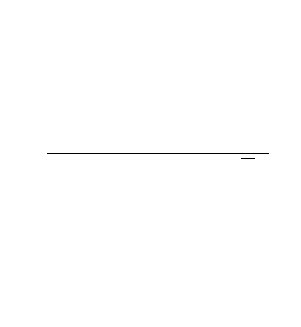
H9 External Debug Register Descriptions
H9.3 Cross-Trigger Interface registers
H9-4558 Copyright © 2013 ARM Limited. All rights reserved. ARM DDI 0487A.a
Non-Confidential - Beta ID090413
H9.3.5 CTIAUTHSTATUS, CTI Authentication Status register
The CTIAUTHSTATUS characteristics are:
Purpose
Provides information about the state of the IMPLEMENTATION DEFINED authentication interface for
CTI.
This register is part of the Cross-Trigger Interface registers functional group.
Usage constraints
This register is accessible as shown below:
Configurations
CTIAUTHSTATUS is in the Debug power domain.
This register is OPTIONAL, and is required for CoreSight compliance. ARM recommends that this
register is implemented.
CTIAUTHSTATUS.{SNID,SID} are RAZ, because the CTI does not itself provide Secure
authentication.
Attributes
CTIAUTHSTATUS is a 32-bit register.
The CTIAUTHSTATUS bit assignments are:
Bits [31:4]
Reserved, RES0.
NSNID, bits [3:2]
If EL3 is not implemented and the processor is Secure, holds the same value as
DBGAUTHSTATUS_EL1.SNID.
Otherwise, holds the same value as DBGAUTHSTATUS_EL1.NSNID.
NSID, bits [1:0]
If EL3 is not implemented and the processor is Secure, holds the same value as
DBGAUTHSTATUS_EL1.SID.
Otherwise, holds the same value as DBGAUTHSTATUS_EL1.NSID.
SLK Default
RO RO
RES0
31 4 32
NSID
10
NSNID

H9 External Debug Register Descriptions
H9.3 Cross-Trigger Interface registers
ARM DDI 0487A.a Copyright © 2013 ARM Limited. All rights reserved. H9-4559
ID090413 Non-Confidential - Beta
Accessing the CTIAUTHSTATUS:
CTIAUTHSTATUS can be accessed through the internal memory-mapped interface and the external debug
interface:
Component Offset
CTI
0xFB8

H9 External Debug Register Descriptions
H9.3 Cross-Trigger Interface registers
H9-4560 Copyright © 2013 ARM Limited. All rights reserved. ARM DDI 0487A.a
Non-Confidential - Beta ID090413
H9.3.6 CTICHINSTATUS, CTI Channel In Status register
The CTICHINSTATUS characteristics are:
Purpose
Provides the raw status of the ECT channel inputs to the CTI.
This register is part of the Cross-Trigger Interface registers functional group.
Usage constraints
This register is accessible as shown below:
Configurations
CTICHINSTATUS is in the Debug power domain.
Attributes
CTICHINSTATUS is a 32-bit register.
The CTICHINSTATUS bit assignments are:
CHIN<n>, bit [x] for x = 0 to (N - 1)
Input channel <n> status.
N is the number of ECT channels implemented as defined by the CTIDEVID.NUMCHAN field.
Bits [31:N] are RAZ.
Possible values of this bit are:
0
Input channel <n> is inactive.
1
Input channel <n> is active.
Accessing the CTICHINSTATUS:
CTICHINSTATUS can be accessed through the internal memory-mapped interface and the external debug
interface:
SLK Default
RO RO
CHIN<n>
31 0
Component Offset
CTI
0x138

H9 External Debug Register Descriptions
H9.3 Cross-Trigger Interface registers
ARM DDI 0487A.a Copyright © 2013 ARM Limited. All rights reserved. H9-4561
ID090413 Non-Confidential - Beta
H9.3.7 CTICHOUTSTATUS, CTI Channel Out Status register
The CTICHOUTSTATUS characteristics are:
Purpose
Provides the status of the ECT channel outputs from the CTI.
This register is part of the Cross-Trigger Interface registers functional group.
Usage constraints
This register is accessible as shown below:
Configurations
CTICHOUTSTATUS is in the Debug power domain.
Attributes
CTICHOUTSTATUS is a 32-bit register.
The CTICHOUTSTATUS bit assignments are:
CHOUT<n>, bit [x] for x = 0 to (N - 1)
Output channel <n> status.
N is the number of ECT channels implemented as defined by the CTIDEVID.NUMCHAN field.
Bits [31:N] are RAZ.
Possible values of this bit are:
0
Output channel <n> is inactive.
1
Output channel <n> is active.
Accessing the CTICHOUTSTATUS:
CTICHOUTSTATUS can be accessed through the internal memory-mapped interface and the external debug
interface:
SLK Default
RO RO
CHOUT<n>
31 0
Component Offset
CTI
0x13C

H9 External Debug Register Descriptions
H9.3 Cross-Trigger Interface registers
H9-4562 Copyright © 2013 ARM Limited. All rights reserved. ARM DDI 0487A.a
Non-Confidential - Beta ID090413
H9.3.8 CTICIDR0, CTI Component Identification Register 0
The CTICIDR0 characteristics are:
Purpose
Provides information to identify a CTI component.
This register is part of the Cross-Trigger Interface registers functional group.
Usage constraints
This register is accessible as shown below:
Configurations
CTICIDR0 is in the Debug power domain.
CTICIDR0 is optional to implement in the external register interface.
This register is required for CoreSight compliance.
Attributes
CTICIDR0 is a 32-bit register.
The CTICIDR0 bit assignments are:
Bits [31:8]
Reserved, RES0.
PRMBL_0, bits [7:0]
Preamble. Must read as
0x0D
.
Accessing the CTICIDR0:
CTICIDR0 can be accessed through the internal memory-mapped interface and the external debug interface:
SLK Default
RO RO
RES0
31 8
PRMBL_0
70
Component Offset
CTI
0xFF0

H9 External Debug Register Descriptions
H9.3 Cross-Trigger Interface registers
ARM DDI 0487A.a Copyright © 2013 ARM Limited. All rights reserved. H9-4563
ID090413 Non-Confidential - Beta
H9.3.9 CTICIDR1, CTI Component Identification Register 1
The CTICIDR1 characteristics are:
Purpose
Provides information to identify a CTI component.
This register is part of the Cross-Trigger Interface registers functional group.
Usage constraints
This register is accessible as shown below:
Configurations
CTICIDR1 is in the Debug power domain.
CTICIDR1 is optional to implement in the external register interface.
This register is required for CoreSight compliance.
Attributes
CTICIDR1 is a 32-bit register.
The CTICIDR1 bit assignments are:
Bits [31:8]
Reserved, RES0.
CLASS, bits [7:4]
Component class. Reads as
0x9
, debug component.
PRMBL_1, bits [3:0]
Preamble. RAZ.
Accessing the CTICIDR1:
CTICIDR1 can be accessed through the internal memory-mapped interface and the external debug interface:
SLK Default
RO RO
RES0
31 8
CLASS
74
PRMBL_1
30
Component Offset
CTI
0xFF4

H9 External Debug Register Descriptions
H9.3 Cross-Trigger Interface registers
H9-4564 Copyright © 2013 ARM Limited. All rights reserved. ARM DDI 0487A.a
Non-Confidential - Beta ID090413
H9.3.10 CTICIDR2, CTI Component Identification Register 2
The CTICIDR2 characteristics are:
Purpose
Provides information to identify a CTI component.
This register is part of the Cross-Trigger Interface registers functional group.
Usage constraints
This register is accessible as shown below:
Configurations
CTICIDR2 is in the Debug power domain.
CTICIDR2 is optional to implement in the external register interface.
This register is required for CoreSight compliance.
Attributes
CTICIDR2 is a 32-bit register.
The CTICIDR2 bit assignments are:
Bits [31:8]
Reserved, RES0.
PRMBL_2, bits [7:0]
Preamble. Must read as
0x05
.
Accessing the CTICIDR2:
CTICIDR2 can be accessed through the internal memory-mapped interface and the external debug interface:
SLK Default
RO RO
RES0
31 8
PRMBL_2
70
Component Offset
CTI
0xFF8

H9 External Debug Register Descriptions
H9.3 Cross-Trigger Interface registers
ARM DDI 0487A.a Copyright © 2013 ARM Limited. All rights reserved. H9-4565
ID090413 Non-Confidential - Beta
H9.3.11 CTICIDR3, CTI Component Identification Register 3
The CTICIDR3 characteristics are:
Purpose
Provides information to identify a CTI component.
This register is part of the Cross-Trigger Interface registers functional group.
Usage constraints
This register is accessible as shown below:
Configurations
CTICIDR3 is in the Debug power domain.
CTICIDR3 is optional to implement in the external register interface.
This register is required for CoreSight compliance.
Attributes
CTICIDR3 is a 32-bit register.
The CTICIDR3 bit assignments are:
Bits [31:8]
Reserved, RES0.
PRMBL_3, bits [7:0]
Preamble. Must read as
0xB1
.
Accessing the CTICIDR3:
CTICIDR3 can be accessed through the internal memory-mapped interface and the external debug interface:
SLK Default
RO RO
RES0
31 8
PRMBL_3
70
Component Offset
CTI
0xFFC

H9 External Debug Register Descriptions
H9.3 Cross-Trigger Interface registers
H9-4566 Copyright © 2013 ARM Limited. All rights reserved. ARM DDI 0487A.a
Non-Confidential - Beta ID090413
H9.3.12 CTICLAIMCLR, CTI Claim Tag Clear register
The CTICLAIMCLR characteristics are:
Purpose
Used by software to read the values of the CLAIM bits, and to clear these bits to 0.
This register is part of the Cross-Trigger Interface registers functional group.
Usage constraints
This register is accessible as shown below:
Configurations
CTICLAIMCLR is in the Debug power domain.
CTICLAIMCLR is optional to implement in the external register interface.
Attributes
CTICLAIMCLR is a 32-bit register.
The CTICLAIMCLR bit assignments are:
CLAIM[x], bit [x], bits [31:0]
Clear CLAIM tag. If x is greater than or equal to the IMPLEMENTATION DEFINED number of CLAIM
tags, this bit is RAZ/SBZ. Software can rely on these bits reading as zero, and must use a
should-be-zero policy on writes. Implementations must ignore writes.
Otherwise, reads return the value of CLAIM[x] and the behavior on writes is:
0
No action.
1
Indirectly clear CLAIM[x] to 0.
A single write to CTICLAIMCLR can clear multiple tags to 0.
Accessing the CTICLAIMCLR:
CTICLAIMCLR can be accessed through the internal memory-mapped interface and the external debug interface:
SLK Default
RO RW
CLAIM[x], bit [x]
31 0
Component Offset
CTI
0xFA4

H9 External Debug Register Descriptions
H9.3 Cross-Trigger Interface registers
ARM DDI 0487A.a Copyright © 2013 ARM Limited. All rights reserved. H9-4567
ID090413 Non-Confidential - Beta
H9.3.13 CTICLAIMSET, CTI Claim Tag Set register
The CTICLAIMSET characteristics are:
Purpose
Used by software to set CLAIM bits to 1.
This register is part of the Cross-Trigger Interface registers functional group.
Usage constraints
This register is accessible as shown below:
Configurations
CTICLAIMSET is in the Debug power domain.
CTICLAIMSET is optional to implement in the external register interface.
Attributes
CTICLAIMSET is a 32-bit register.
The CTICLAIMSET bit assignments are:
CLAIM[x], bit [x], bits [31:0]
CLAIM tag set bit. If x is greater than or equal to the IMPLEMENTATION DEFINED number of CLAIM
tags, this bit is RAZ/SBZ. Software can rely on these bits reading as zero, and must use a
should-be-zero policy on writes. Implementations must ignore writes.
Otherwise, the bit is RAO and the behavior on writes is:
0
No action.
1
Indirectly set CLAIM[x] tag to 1.
A single write to CTICLAIMSET can set multiple tags to 1.
Accessing the CTICLAIMSET:
CTICLAIMSET can be accessed through the internal memory-mapped interface and the external debug interface:
SLK Default
RO RW
CLAIM[x], bit [x]
31 0
Component Offset
CTI
0xFA0

H9 External Debug Register Descriptions
H9.3 Cross-Trigger Interface registers
H9-4568 Copyright © 2013 ARM Limited. All rights reserved. ARM DDI 0487A.a
Non-Confidential - Beta ID090413
H9.3.14 CTICONTROL, CTI Control register
The CTICONTROL characteristics are:
Purpose
Controls whether the CTI is enabled.
This register is part of the Cross-Trigger Interface registers functional group.
Usage constraints
This register is accessible as shown below:
Configurations
CTICONTROL is in the Debug power domain.
Attributes
CTICONTROL is a 32-bit register.
The CTICONTROL bit assignments are:
Bits [31:1]
Reserved, RES0.
GLBEN, bit [0]
Enables or disables the CTI mapping functions. Possible values of this field are:
0
CTI mapping functions disabled.
1
CTI mapping functions enabled.
When the mapping functions are disabled, no new events are signaled on either output triggers or
output channels. If a previously asserted output trigger has not been acknowledged, it remains
asserted after the mapping functions are disabled. All output triggers are disabled by CTI reset.
On External debug reset, the field resets to 0.
Accessing the CTICONTROL:
CTICONTROL can be accessed through the internal memory-mapped interface and the external debug interface:
SLK Default
RO RW
RES0
31 1 0
GLBEN
Component Offset
CTI
0x000

H9 External Debug Register Descriptions
H9.3 Cross-Trigger Interface registers
ARM DDI 0487A.a Copyright © 2013 ARM Limited. All rights reserved. H9-4569
ID090413 Non-Confidential - Beta
H9.3.15 CTIDEVAFF0, CTI Device Affinity register 0
The CTIDEVAFF0 characteristics are:
Purpose
Copy of the low half of the processor MPIDR_EL1 register that allows a debugger to determine
which processor in a multiprocessor system the CTI component relates to.
This register is part of the Cross-Trigger Interface registers functional group.
Usage constraints
This register is accessible as shown below:
Configurations
CTIDEVAFF0 is in the Debug power domain.
CTIDEVAFF0 is optional to implement in the external register interface.
Attributes
CTIDEVAFF0 is a 32-bit register.
The CTIDEVAFF0 bit assignments are:
Bits [31:0]
MPIDR_EL1 low half. Read-only copy of the low half of MPIDR_EL1, as seen from the highest
implemented exception level.
Accessing the CTIDEVAFF0:
CTIDEVAFF0 can be accessed through the internal memory-mapped interface and the external debug interface:
SLK Default
RO RO
MPIDR_EL1 low half
31 0
Component Offset
CTI
0xFA8

H9 External Debug Register Descriptions
H9.3 Cross-Trigger Interface registers
H9-4570 Copyright © 2013 ARM Limited. All rights reserved. ARM DDI 0487A.a
Non-Confidential - Beta ID090413
H9.3.16 CTIDEVAFF1, CTI Device Affinity register 1
The CTIDEVAFF1 characteristics are:
Purpose
Copy of the high half of the processor MPIDR_EL1 register that allows a debugger to determine
which processor in a multiprocessor system the CTI component relates to.
This register is part of the Cross-Trigger Interface registers functional group.
Usage constraints
This register is accessible as shown below:
Configurations
CTIDEVAFF1 is in the Debug power domain.
CTIDEVAFF1 is optional to implement in the external register interface.
Attributes
CTIDEVAFF1 is a 32-bit register.
The CTIDEVAFF1 bit assignments are:
Bits [31:0]
MPIDR_EL1 high half. Read-only copy of the high half of MPIDR_EL1, as seen from the highest
implemented exception level.
Accessing the CTIDEVAFF1:
CTIDEVAFF1 can be accessed through the internal memory-mapped interface and the external debug interface:
SLK Default
RO RO
MPIDR_EL1 high half
31 0
Component Offset
CTI
0xFAC

H9 External Debug Register Descriptions
H9.3 Cross-Trigger Interface registers
ARM DDI 0487A.a Copyright © 2013 ARM Limited. All rights reserved. H9-4571
ID090413 Non-Confidential - Beta
H9.3.17 CTIDEVARCH, CTI Device Architecture register
The CTIDEVARCH characteristics are:
Purpose
Identifies the programmers' model architecture of the CTI component.
This register is part of the Cross-Trigger Interface registers functional group.
Usage constraints
This register is accessible as shown below:
Configurations
CTIDEVARCH is in the Debug power domain.
CTIDEVARCH is optional to implement in the external register interface.
Attributes
CTIDEVARCH is a 32-bit register.
The CTIDEVARCH bit assignments are:
ARCHITECT, bits [31:21]
Defines the architecture of the component. For CTI, this is ARM Limited.
Bits [31:28] are the JEP 106 continuation code,
0x4
.
Bits [27:21] are the JEP 106 ID code,
0x3B
.
PRESENT, bit [20]
When set to 1, indicates that the DEVARCH is present.
This field is 1 in v8-A.
REVISION, bits [19:16]
Defines the architecture revision. For architectures defined by ARM this is the minor revision.
For CTI, the revision defined by v8-A is
0x0
.
All other values are reserved.
ARCHID, bits [15:0]
Defines this part to be a v8-A debug component. For architectures defined by ARM this is further
subdivided.
For CTI:
• Bits [15:12] are the architecture version,
0x1
.
• Bits [11:0] are the architecture part number,
0xA14
.
This corresponds to CTI architecture version CTIv2.
SLK Default
RO RO
ARCHITECT
31 21 20
REVISION
19 16
ARCHID
15 0
PRESENT

H9 External Debug Register Descriptions
H9.3 Cross-Trigger Interface registers
H9-4572 Copyright © 2013 ARM Limited. All rights reserved. ARM DDI 0487A.a
Non-Confidential - Beta ID090413
Accessing the CTIDEVARCH:
CTIDEVARCH can be accessed through the internal memory-mapped interface and the external debug interface:
Component Offset
CTI
0xFBC
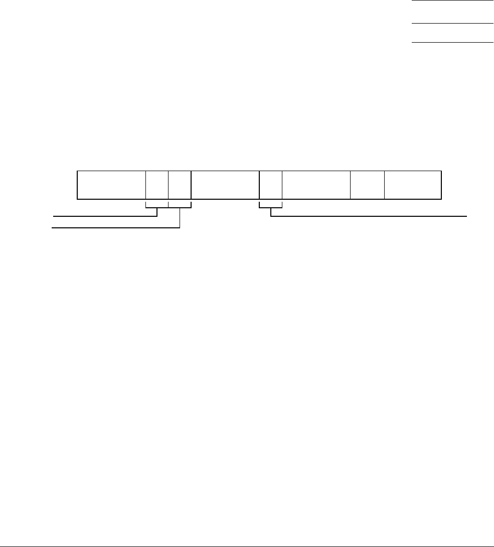
H9 External Debug Register Descriptions
H9.3 Cross-Trigger Interface registers
ARM DDI 0487A.a Copyright © 2013 ARM Limited. All rights reserved. H9-4573
ID090413 Non-Confidential - Beta
H9.3.18 CTIDEVID, CTI Device ID register 0
The CTIDEVID characteristics are:
Purpose
Describes the CTI component to the debugger.
This register is part of the Cross-Trigger Interface registers functional group.
Usage constraints
This register is accessible as shown below:
Configurations
CTIDEVID is in the Debug power domain.
Attributes
CTIDEVID is a 32-bit register.
The CTIDEVID bit assignments are:
Bits [31:26]
Reserved, RES0.
INOUT, bits [25:24]
Input/output options. Indicates presence of the input gate. If the CTM is not implemented, this field
is RAZ.
00
CTIGATE does not mask propagation of input events from external channels.
01
CTIGATE masks propagation of input events from external channels.
All other values are reserved.
Bits [23:22]
Reserved, RES0.
NUMCHAN, bits [21:16]
Number of ECT channels implemented. IMPLEMENTATION DEFINED. For v8-A, valid values are:
000011
3 channels (0-2) implemented.
000100
4 channels (0-3) implemented.
000101
5 channels (0-4) implemented.
000110
6 channels (0-5) implemented.
and so on up to
0b100000
, 32 channels (0-31) implemented.
All other values are reserved.
SLK Default
RO RO
RES0
31 26 25 24 23 22
NUMCHAN
21 16 15 14
NUMTRIG
13 8
RES0
75
EXTMUXNUM
40
INOUT
RES0
RES0

H9 External Debug Register Descriptions
H9.3 Cross-Trigger Interface registers
H9-4574 Copyright © 2013 ARM Limited. All rights reserved. ARM DDI 0487A.a
Non-Confidential - Beta ID090413
Bits [15:14]
Reserved, RES0.
NUMTRIG, bits [13:8]
Number of triggers implemented. IMPLEMENTATION DEFINED. This is one more than the index of the
largest trigger, rather than the actual number of triggers.
For v8-A, valid values are:
000011
Up to 3 triggers (0-2) implemented.
001000
Up to 8 triggers (0-7) implemented.
001001
Up to 9 triggers (0-8) implemented.
001010
Up to 10 triggers (0-9) implemented.
and so on up to
0b100000
, 32 triggers (0-31) implemented.
All other values are reserved. If the Trace Extension is implemented, this field must be at least
001000. There is no guarantee that any of the implemented triggers, including the highest numbered,
are connected to any components.
Bits [7:5]
Reserved, RES0.
EXTMUXNUM, bits [4:0]
Maximum number of external triggers available for multiplexing into the CTI. This relates only to
additional external triggers outside those defined for v8-A.
Accessing the CTIDEVID:
CTIDEVID can be accessed through the internal memory-mapped interface and the external debug interface:
Component Offset
CTI
0xFC8

H9 External Debug Register Descriptions
H9.3 Cross-Trigger Interface registers
ARM DDI 0487A.a Copyright © 2013 ARM Limited. All rights reserved. H9-4575
ID090413 Non-Confidential - Beta
H9.3.19 CTIDEVID1, CTI Device ID register 1
The CTIDEVID1 characteristics are:
Purpose
Reserved for future information about the CTI component to the debugger.
This register is part of the Cross-Trigger Interface registers functional group.
Usage constraints
This register is accessible as shown below:
Configurations
CTIDEVID1 is in the Debug power domain.
Attributes
CTIDEVID1 is a 32-bit register.
The CTIDEVID1 bit assignments are:
Bits [31:0]
Reserved, RES0.
Accessing the CTIDEVID1:
CTIDEVID1 can be accessed through the internal memory-mapped interface and the external debug interface:
SLK Default
RO RO
RES0
31 0
Component Offset
CTI
0xFC4

H9 External Debug Register Descriptions
H9.3 Cross-Trigger Interface registers
H9-4576 Copyright © 2013 ARM Limited. All rights reserved. ARM DDI 0487A.a
Non-Confidential - Beta ID090413
H9.3.20 CTIDEVID2, CTI Device ID register 2
The CTIDEVID2 characteristics are:
Purpose
Reserved for future information about the CTI component to the debugger.
This register is part of the Cross-Trigger Interface registers functional group.
Usage constraints
This register is accessible as shown below:
Configurations
CTIDEVID2 is in the Debug power domain.
Attributes
CTIDEVID2 is a 32-bit register.
The CTIDEVID2 bit assignments are:
Bits [31:0]
Reserved, RES0.
Accessing the CTIDEVID2:
CTIDEVID2 can be accessed through the internal memory-mapped interface and the external debug interface:
SLK Default
RO RO
RES0
31 0
Component Offset
CTI
0xFC0

H9 External Debug Register Descriptions
H9.3 Cross-Trigger Interface registers
ARM DDI 0487A.a Copyright © 2013 ARM Limited. All rights reserved. H9-4577
ID090413 Non-Confidential - Beta
H9.3.21 CTIDEVTYPE, CTI Device Type register
The CTIDEVTYPE characteristics are:
Purpose
Indicates to a debugger that this component is part of a processor's cross-trigger interface.
This register is part of the Cross-Trigger Interface registers functional group.
Usage constraints
This register is accessible as shown below:
Configurations
CTIDEVTYPE is in the Debug power domain.
CTIDEVTYPE is optional to implement in the external register interface.
Attributes
CTIDEVTYPE is a 32-bit register.
The CTIDEVTYPE bit assignments are:
Bits [31:8]
Reserved, RES0.
SUB, bits [7:4]
Subtype. Must read as
0x1
to indicate this is a processor component.
MAJOR, bits [3:0]
Major type. Must read as
0x4
to indicate this is a cross-trigger component.
Accessing the CTIDEVTYPE:
CTIDEVTYPE can be accessed through the internal memory-mapped interface and the external debug interface:
SLK Default
RO RO
RES0
31 8
SUB
74
MAJOR
30
Component Offset
CTI
0xFCC

H9 External Debug Register Descriptions
H9.3 Cross-Trigger Interface registers
H9-4578 Copyright © 2013 ARM Limited. All rights reserved. ARM DDI 0487A.a
Non-Confidential - Beta ID090413
H9.3.22 CTIGATE, CTI Channel Gate Enable register
The CTIGATE characteristics are:
Purpose
Determines whether events on channels propagate through the CTM to other ECT components, or
from the CTM into the CTI.
This register is part of the Cross-Trigger Interface registers functional group.
Usage constraints
This register is accessible as shown below:
Configurations
CTIGATE is in the Debug power domain.
Attributes
CTIGATE is a 32-bit register.
The CTIGATE bit assignments are:
GATE<x>, bit [x] for x = 0 to (N - 1)
Channel <x> gate enable.
N is the number of ECT channels implemented as defined by the CTIDEVID.NUMCHAN field.
Bits [31:N] are RAZ/WI.
Possible values of this bit are:
0
Disable output and, if CTIDEVID.INOUT ==
0b01
, input channel <x> propagation.
1
Enable output and, if CTIDEVID.INOUT ==
0b01
, input channel <x> propagation.
On External debug reset, the field reset value is architecturally UNKNOWN.
Accessing the CTIGATE:
CTIGATE can be accessed through the internal memory-mapped interface and the external debug interface:
SLK Default
RO RW
GATE<x>
31 0
Component Offset
CTI
0x140

H9 External Debug Register Descriptions
H9.3 Cross-Trigger Interface registers
ARM DDI 0487A.a Copyright © 2013 ARM Limited. All rights reserved. H9-4579
ID090413 Non-Confidential - Beta
H9.3.23 CTIINEN<n>, CTI Input Trigger to Output Channel Enable registers, n = 0 - 31
The CTIINEN<n> characteristics are:
Purpose
Enables the signaling of an event on output channels when input trigger event n is received by the
CTI.
This register is part of the Cross-Trigger Interface registers functional group.
Usage constraints
This register is accessible as shown below:
Configurations
CTIINEN<n> is in the Debug power domain.
Attributes
CTIINEN<n> is a 32-bit register.
The CTIINEN<n> bit assignments are:
INEN<x>, bit [x] for x = 0 to (N - 1)
Input trigger <n> to output channel <x> enable.
N is the number of ECT channels implemented as defined by the CTIDEVID.NUMCHAN field.
Bits [31:N] are RAZ/WI.
Possible values of this bit are:
0
Input trigger <n> will not generate an event on output channel <x>.
1
Input trigger <n> will generate an event on output channel <x>.
On External debug reset, the field reset value is architecturally UNKNOWN.
Accessing the CTIINEN<n>:
CTIINEN<n> can be accessed through the internal memory-mapped interface and the external debug interface:
SLK Default
RO RW
INEN<x>
31 0
Component Offset
CTI
0x020
+ 4n

H9 External Debug Register Descriptions
H9.3 Cross-Trigger Interface registers
H9-4580 Copyright © 2013 ARM Limited. All rights reserved. ARM DDI 0487A.a
Non-Confidential - Beta ID090413
H9.3.24 CTIINTACK, CTI Output Trigger Acknowledge register
The CTIINTACK characteristics are:
Purpose
Can be used to create soft acknowledges for output triggers.
This register is part of the Cross-Trigger Interface registers functional group.
Usage constraints
This register is accessible as shown below:
Configurations
CTIINTACK is in the Debug power domain.
Attributes
CTIINTACK is a 32-bit register.
The CTIINTACK bit assignments are:
ACK<n>, bit [x] for x = 0 to (N - 1)
Acknowledge for output trigger <n>.
N is the number of CTI triggers implemented as defined by the CTIDEVID.NUMTRIG field. Bits
[31:N] are RAZ/WI.
If any of the following is true, writes to ACK<n> are ignored:
•n >= CTIDEVID.NUMTRIG, the number of implemented triggers.
• Output trigger n is not active.
• The channel mapping function output, as controlled by CTIOUTEN<n>, is still active.
Otherwise, if any of the following are true, it is IMPLEMENTATION DEFINED whether writes to
ACK<n> are ignored:
• Output trigger n is not implemented.
• Output trigger n is not connected.
• Output trigger n is self-acknowledging and does not require software acknowledge.
Otherwise, the behavior on writes to ACK<n> is as follows:
0
No effect
1
Deactivate the trigger.
SLK Default
RO WO
ACK<n>
31 0

H9 External Debug Register Descriptions
H9.3 Cross-Trigger Interface registers
ARM DDI 0487A.a Copyright © 2013 ARM Limited. All rights reserved. H9-4581
ID090413 Non-Confidential - Beta
Accessing the CTIINTACK:
CTIINTACK can be accessed through the internal memory-mapped interface and the external debug interface:
Component Offset
CTI
0x010

H9 External Debug Register Descriptions
H9.3 Cross-Trigger Interface registers
H9-4582 Copyright © 2013 ARM Limited. All rights reserved. ARM DDI 0487A.a
Non-Confidential - Beta ID090413
H9.3.25 CTIITCTRL, CTI Integration mode Control register
The CTIITCTRL characteristics are:
Purpose
Enables the CTI to switch from its default mode into integration mode, where test software can
control directly the inputs and outputs of the processor, for integration testing or topology detection.
This register is part of the Cross-Trigger Interface registers functional group.
Usage constraints
This register is accessible as shown below:
Configurations
CTIITCTRL is in the Debug power domain.
CTIITCTRL is optional to implement in the external register interface.
Attributes
CTIITCTRL is a 32-bit register.
The CTIITCTRL bit assignments are:
Bits [31:1]
Reserved, RES0.
IME, bit [0]
Integration mode enable. When IME == 1, the device reverts to an integration mode to enable
integration testing or topology detection. The integration mode behavior is IMPLEMENTATION
DEFINED.
0
Normal operation.
1
Integration mode enabled.
On IMPLEMENTATION DEFINED reset, the field resets to 0.
Accessing the CTIITCTRL:
CTIITCTRL can be accessed through the internal memory-mapped interface and the external debug interface:
Default
RW
RES0
31 1 0
IME
Component Offset
CTI
0xF00

H9 External Debug Register Descriptions
H9.3 Cross-Trigger Interface registers
ARM DDI 0487A.a Copyright © 2013 ARM Limited. All rights reserved. H9-4583
ID090413 Non-Confidential - Beta
H9.3.26 CTILAR, CTI Lock Access Register
The CTILAR characteristics are:
Purpose
Allows or disallows access to the CTI registers through a memory-mapped interface.
This register is part of the Cross-Trigger Interface registers functional group.
Usage constraints
This register is accessible as shown below:
Configurations
CTILAR is in the Debug power domain.
If OPTIONAL memory-mapped access to the external debug interface is supported then an OPTIONAL
Software lock can be implemented as part of CoreSight compliance.
CTILAR ignores writes if the Software lock is not implemented and ignores writes for other
accesses to the external debug interface.
The Software lock provides a lock to prevent memory-mapped writes to the Cross-Trigger Interface
registers. Use of this lock mechanism reduces the risk of accidental damage to the contents of the
Cross-Trigger Interface registers. It does not, and cannot, prevent all accidental or malicious
damage.
Software uses CTILAR to set or clear the lock, and CTILSR to check the current status of the lock.
Attributes
CTILAR is a 32-bit register.
The CTILAR bit assignments are:
KEY, bits [31:0]
Lock Access control. Writing the key value
0xC5ACCE55
to this field unlocks the lock, enabling write
accesses to this component's registers through a memory-mapped interface.
Writing any other value to this register locks the lock, disabling write accesses to this component's
registers through a memory mapped interface.
Accessing the CTILAR:
CTILAR can be accessed through the internal memory-mapped interface:
Default
WO
KEY
31 0
Component Offset
CTI
0xFB0

H9 External Debug Register Descriptions
H9.3 Cross-Trigger Interface registers
H9-4584 Copyright © 2013 ARM Limited. All rights reserved. ARM DDI 0487A.a
Non-Confidential - Beta ID090413
H9.3.27 CTILSR, CTI Lock Status Register
The CTILSR characteristics are:
Purpose
Indicates the current status of the software lock for CTI registers.
This register is part of the Cross-Trigger Interface registers functional group.
Usage constraints
This register is accessible as shown below:
Configurations
CTILSR is in the Debug power domain.
If OPTIONAL memory-mapped access to the external debug interface is supported then an OPTIONAL
Software lock can be implemented as part of CoreSight compliance.
CTILSR is RAZ if the Software lock is not implemented and is RAZ for other accesses to the
external debug interface.
The Software lock provides a lock to prevent memory-mapped writes to the Cross-Trigger Interface
registers. Use of this lock mechanism reduces the risk of accidental damage to the contents of the
Cross-Trigger Interface registers. It does not, and cannot, prevent all accidental or malicious
damage.
Software uses CTILAR to set or clear the lock, and CTILSR to check the current status of the lock.
Attributes
CTILSR is a 32-bit register.
The CTILSR bit assignments are:
Bits [31:3]
Reserved, RES0.
nTT, bit [2]
Not thirty-two bit access required. RAZ.
SLK, bit [1]
Software lock status for this component. For an access to LSR that is not a memory-mapped access,
or when the software lock is not implemented, this field is RES0.
For memory-mapped accesses when the software lock is implemented, possible values of this field
are:
0
Lock clear. Writes are permitted to this component's registers.
Default
RO
RES0
31 3 2 1 0
SLI
SLK
nTT

H9 External Debug Register Descriptions
H9.3 Cross-Trigger Interface registers
ARM DDI 0487A.a Copyright © 2013 ARM Limited. All rights reserved. H9-4585
ID090413 Non-Confidential - Beta
1
Lock set. Writes to this component's registers are ignored, and reads have no side
effects.
On External debug reset, the field resets to 1.
SLI, bit [0]
Software lock implemented. For an access to LSR that is not a memory-mapped access, this field is
RAZ. For memory-mapped accesses, the value of this field is IMPLEMENTATION DEFINED. Permitted
values are:
0
Software lock not implemented or not memory-mapped access.
1
Software lock implemented and memory-mapped access.
Accessing the CTILSR:
CTILSR can be accessed through the internal memory-mapped interface:
Component Offset
CTI
0xFB4

H9 External Debug Register Descriptions
H9.3 Cross-Trigger Interface registers
H9-4586 Copyright © 2013 ARM Limited. All rights reserved. ARM DDI 0487A.a
Non-Confidential - Beta ID090413
H9.3.28 CTIOUTEN<n>, CTI Input Channel to Output Trigger Enable registers, n = 0 - 31
The CTIOUTEN<n> characteristics are:
Purpose
Defines which input channels generate output trigger n.
This register is part of the Cross-Trigger Interface registers functional group.
Usage constraints
This register is accessible as shown below:
Configurations
CTIOUTEN<n> is in the Debug power domain.
Attributes
CTIOUTEN<n> is a 32-bit register.
The CTIOUTEN<n> bit assignments are:
OUTEN<x>, bit [x] for x = 0 to (N - 1)
Input channel <x> to output trigger <n> enable.
N is the number of ECT channels implemented as defined by the CTIDEVID.NUMCHAN field.
Bits [31:N] are RAZ/WI.
Possible values of this bit are:
0
An event on input channel <x> will not cause output trigger <n> to be asserted.
1
An event on input channel <x> will cause output trigger <n> to be asserted.
On External debug reset, the field reset value is architecturally UNKNOWN.
Accessing the CTIOUTEN<n>:
CTIOUTEN<n> can be accessed through the internal memory-mapped interface and the external debug interface:
SLK Default
RO RW
OUTEN<x>
31 0
Component Offset
CTI
0x0A0
+ 4n

H9 External Debug Register Descriptions
H9.3 Cross-Trigger Interface registers
ARM DDI 0487A.a Copyright © 2013 ARM Limited. All rights reserved. H9-4587
ID090413 Non-Confidential - Beta
H9.3.29 CTIPIDR0, CTI Peripheral Identification Register 0
The CTIPIDR0 characteristics are:
Purpose
Provides information to identify a CTI component.
This register is part of the Cross-Trigger Interface registers functional group.
Usage constraints
This register is accessible as shown below:
Configurations
CTIPIDR0 is in the Debug power domain.
CTIPIDR0 is optional to implement in the external register interface.
This register is required for CoreSight compliance.
Attributes
CTIPIDR0 is a 32-bit register.
The CTIPIDR0 bit assignments are:
Bits [31:8]
Reserved, RES0.
PART_0, bits [7:0]
Part number, least significant byte.
Accessing the CTIPIDR0:
CTIPIDR0 can be accessed through the internal memory-mapped interface and the external debug interface:
SLK Default
RO RO
RES0
31 8
PART_0
70
Component Offset
CTI
0xFE0

H9 External Debug Register Descriptions
H9.3 Cross-Trigger Interface registers
H9-4588 Copyright © 2013 ARM Limited. All rights reserved. ARM DDI 0487A.a
Non-Confidential - Beta ID090413
H9.3.30 CTIPIDR1, CTI Peripheral Identification Register 1
The CTIPIDR1 characteristics are:
Purpose
Provides information to identify a CTI component.
This register is part of the Cross-Trigger Interface registers functional group.
Usage constraints
This register is accessible as shown below:
Configurations
CTIPIDR1 is in the Debug power domain.
CTIPIDR1 is optional to implement in the external register interface.
This register is required for CoreSight compliance.
Attributes
CTIPIDR1 is a 32-bit register.
The CTIPIDR1 bit assignments are:
Bits [31:8]
Reserved, RES0.
DES_0, bits [7:4]
Designer, least significant nibble of JEP106 ID code. For ARM Limited, this field is
0b1011
.
PART_1, bits [3:0]
Part number, most significant nibble.
Accessing the CTIPIDR1:
CTIPIDR1 can be accessed through the internal memory-mapped interface and the external debug interface:
SLK Default
RO RO
RES0
31 8
DES_0
74
PART_1
30
Component Offset
CTI
0xFE4

H9 External Debug Register Descriptions
H9.3 Cross-Trigger Interface registers
ARM DDI 0487A.a Copyright © 2013 ARM Limited. All rights reserved. H9-4589
ID090413 Non-Confidential - Beta
H9.3.31 CTIPIDR2, CTI Peripheral Identification Register 2
The CTIPIDR2 characteristics are:
Purpose
Provides information to identify a CTI component.
This register is part of the Cross-Trigger Interface registers functional group.
Usage constraints
This register is accessible as shown below:
Configurations
CTIPIDR2 is in the Debug power domain.
CTIPIDR2 is optional to implement in the external register interface.
This register is required for CoreSight compliance.
Attributes
CTIPIDR2 is a 32-bit register.
The CTIPIDR2 bit assignments are:
Bits [31:8]
Reserved, RES0.
REVISION, bits [7:4]
Part major revision. Parts can also use this field to extend Part number to 16-bits.
JEDEC, bit [3]
RAO. Indicates a JEP106 identity code is used.
DES_1, bits [2:0]
Designer, most significant bits of JEP106 ID code. For ARM Limited, this field is
0b011
.
Accessing the CTIPIDR2:
CTIPIDR2 can be accessed through the internal memory-mapped interface and the external debug interface:
SLK Default
RO RO
RES0
31 8
REVISION
74
3
DES_1
20
JEDEC
Component Offset
CTI
0xFE8

H9 External Debug Register Descriptions
H9.3 Cross-Trigger Interface registers
H9-4590 Copyright © 2013 ARM Limited. All rights reserved. ARM DDI 0487A.a
Non-Confidential - Beta ID090413
H9.3.32 CTIPIDR3, CTI Peripheral Identification Register 3
The CTIPIDR3 characteristics are:
Purpose
Provides information to identify a CTI component.
This register is part of the Cross-Trigger Interface registers functional group.
Usage constraints
This register is accessible as shown below:
Configurations
CTIPIDR3 is in the Debug power domain.
CTIPIDR3 is optional to implement in the external register interface.
This register is required for CoreSight compliance.
Attributes
CTIPIDR3 is a 32-bit register.
The CTIPIDR3 bit assignments are:
Bits [31:8]
Reserved, RES0.
REVAND, bits [7:4]
Part minor revision. Parts using CTIPIDR2.REVISION as an extension to the Part number must use
this field as a major revision number.
CMOD, bits [3:0]
Customer modified. Indicates someone other than the Designer has modified the component.
Accessing the CTIPIDR3:
CTIPIDR3 can be accessed through the internal memory-mapped interface and the external debug interface:
SLK Default
RO RO
RES0
31 8
REVAND
74
CMOD
30
Component Offset
CTI
0xFEC

H9 External Debug Register Descriptions
H9.3 Cross-Trigger Interface registers
ARM DDI 0487A.a Copyright © 2013 ARM Limited. All rights reserved. H9-4591
ID090413 Non-Confidential - Beta
H9.3.33 CTIPIDR4, CTI Peripheral Identification Register 4
The CTIPIDR4 characteristics are:
Purpose
Provides information to identify a CTI component.
This register is part of the Cross-Trigger Interface registers functional group.
Usage constraints
This register is accessible as shown below:
Configurations
CTIPIDR4 is in the Debug power domain.
CTIPIDR4 is optional to implement in the external register interface.
This register is required for CoreSight compliance.
Attributes
CTIPIDR4 is a 32-bit register.
The CTIPIDR4 bit assignments are:
Bits [31:8]
Reserved, RES0.
SIZE, bits [7:4]
Size of the component. RAZ. Log2 of the number of 4KB pages from the start of the component to
the end of the component ID registers.
DES_2, bits [3:0]
Designer, JEP106 continuation code, least significant nibble. For ARM Limited, this field is
0b0100
.
Accessing the CTIPIDR4:
CTIPIDR4 can be accessed through the internal memory-mapped interface and the external debug interface:
SLK Default
RO RO
RES0
31 8
SIZE
74
DES_2
30
Component Offset
CTI
0xFD0

H9 External Debug Register Descriptions
H9.3 Cross-Trigger Interface registers
H9-4592 Copyright © 2013 ARM Limited. All rights reserved. ARM DDI 0487A.a
Non-Confidential - Beta ID090413
H9.3.34 CTITRIGINSTATUS, CTI Trigger In Status register
The CTITRIGINSTATUS characteristics are:
Purpose
Provides the status of the trigger inputs.
This register is part of the Cross-Trigger Interface registers functional group.
Usage constraints
This register is accessible as shown below:
Configurations
CTITRIGINSTATUS is in the Debug power domain.
Attributes
CTITRIGINSTATUS is a 32-bit register.
The CTITRIGINSTATUS bit assignments are:
TRIN<n>, bit [x] for x = 0 to (N - 1)
Trigger input <n> status.
N is the number of CTI triggers implemented as defined by the CTIDEVID.NUMTRIG field.
Bits [31:N] are RAZ.
Possible values of this bit are:
0
Input trigger n is inactive.
1
Input trigger n is active.
Not implemented and not-connected input triggers are always inactive.
Accessing the CTITRIGINSTATUS:
CTITRIGINSTATUS can be accessed through the internal memory-mapped interface and the external debug
interface:
SLK Default
RO RO
TRIN<n>
31 0
Component Offset
CTI
0x130

H9 External Debug Register Descriptions
H9.3 Cross-Trigger Interface registers
ARM DDI 0487A.a Copyright © 2013 ARM Limited. All rights reserved. H9-4593
ID090413 Non-Confidential - Beta
H9.3.35 CTITRIGOUTSTATUS, CTI Trigger Out Status register
The CTITRIGOUTSTATUS characteristics are:
Purpose
Provides the status of the trigger outputs.
This register is part of the Cross-Trigger Interface registers functional group.
Usage constraints
This register is accessible as shown below:
Configurations
CTITRIGOUTSTATUS is in the Debug power domain.
Attributes
CTITRIGOUTSTATUS is a 32-bit register.
The CTITRIGOUTSTATUS bit assignments are:
TROUT<n>, bit [x] for x = 0 to (N - 1)
Trigger output <n> status.
N is the number of CTI triggers implemented as defined by the CTIDEVID.NUMTRIG field.
Bits [31:N] are RAZ.
If output trigger <n> is implemented and connected, possible values of this bit are:
0
Output trigger n is inactive.
1
Output trigger n is active.
Otherwise it is IMPLEMENTATION DEFINED whether TROUT<n> is RAZ or behaves as above.
Accessing the CTITRIGOUTSTATUS:
CTITRIGOUTSTATUS can be accessed through the internal memory-mapped interface and the external debug
interface:
SLK Default
RO RO
TROUT<n>
31 0
Component Offset
CTI
0x134

H9 External Debug Register Descriptions
H9.3 Cross-Trigger Interface registers
H9-4594 Copyright © 2013 ARM Limited. All rights reserved. ARM DDI 0487A.a
Non-Confidential - Beta ID090413
Part I
Memory-mapped Components of the ARMv8 Architecture

ARM DDI 0487A.a Copyright © 2013 ARM Limited. All rights reserved. I1-4597
ID090413 Non-Confidential - Beta
Chapter I1
Memory-Mapped System Register Descriptions
This chapter describes the memory-mapped system control registers.
It contains the following items:
•Introduction on page I1-4598.
•Performance Monitors registers on page I1-4599.
•Generic Timer registers on page I1-4647.

I1 Memory-Mapped System Register Descriptions
I1.1 Introduction
I1-4598 Copyright © 2013 ARM Limited. All rights reserved. ARM DDI 0487A.a
Non-Confidential - Beta ID090413
I1.1 Introduction
The following sections describe the memory-mapped system control registers:
•Performance Monitors registers on page I1-4599.
•Generic Timer registers on page I1-4647.
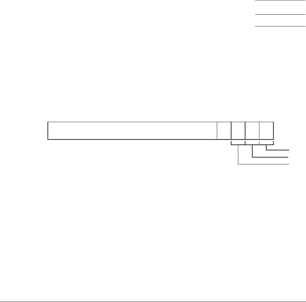
I1 Memory-Mapped System Register Descriptions
I1.2 Performance Monitors registers
ARM DDI 0487A.a Copyright © 2013 ARM Limited. All rights reserved. I1-4599
ID090413 Non-Confidential - Beta
I1.2 Performance Monitors registers
This section describes the Performance Monitoring registers.
I1.2.1 PMAUTHSTATUS, Performance Monitors Authentication Status register
The PMAUTHSTATUS characteristics are:
Purpose
Provides information about the state of the IMPLEMENTATION DEFINED authentication interface for
Performance Monitors.
This register is part of the Performance Monitors registers functional group.
Usage constraints
This register is accessible as shown below:
Configurations
PMAUTHSTATUS is in the Debug power domain.
This register is OPTIONAL, and is required for CoreSight compliance. ARM recommends that this
register is implemented.
Attributes
PMAUTHSTATUS is a 32-bit register.
The PMAUTHSTATUS bit assignments are:
Bits [31:8]
Reserved, RES0.
SNID, bits [7:6]
Holds the same value as DBGAUTHSTATUS_EL1.SNID.
Bits [5:4]
Reserved, RES0.
NSNID, bits [3:2]
Holds the same value as DBGAUTHSTATUS_EL1.NSNID.
Bits [1:0]
Reserved, RES0.
SLK Default
RO RO
RES0
31 8
SNID
76543210
RES0
NSNID
RES0

I1 Memory-Mapped System Register Descriptions
I1.2 Performance Monitors registers
I1-4600 Copyright © 2013 ARM Limited. All rights reserved. ARM DDI 0487A.a
Non-Confidential - Beta ID090413
Accessing the PMAUTHSTATUS:
PMAUTHSTATUS can be accessed through the internal memory-mapped interface and the external debug
interface:
Component Offset
PMU
0xFB8
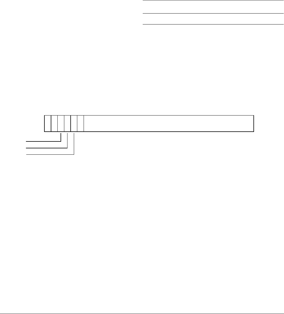
I1 Memory-Mapped System Register Descriptions
I1.2 Performance Monitors registers
ARM DDI 0487A.a Copyright © 2013 ARM Limited. All rights reserved. I1-4601
ID090413 Non-Confidential - Beta
I1.2.2 PMCCFILTR_EL0, Performance Monitors Cycle Counter Filter Register
The PMCCFILTR_EL0 characteristics are:
Purpose
Determines the modes in which the Cycle Counter, PMCCNTR_EL0, increments.
This register is part of the Performance Monitors registers functional group.
Usage constraints
This register is accessible as shown below:
Configurations
PMCCFILTR_EL0 is architecturally mapped to AArch64 register PMCCFILTR_EL0.
PMCCFILTR_EL0 is architecturally mapped to AArch32 register PMCCFILTR.
PMCCFILTR_EL0 is in the Core power domain.
Attributes
PMCCFILTR_EL0 is a 32-bit register.
The PMCCFILTR_EL0 bit assignments are:
P, bit [31]
EL1 modes filtering bit. Controls counting in EL1. If EL3 is implemented, then counting in
Non-secure EL1 is further controlled by the NSK bit. The possible values of this bit are:
0
Count cycles in EL1.
1
Do not count cycles in EL1.
U, bit [30]
EL0 filtering bit. Controls counting in EL0. If EL3 is implemented, then counting in Non-secure
EL0 is further controlled by the NSU bit. The possible values of this bit are:
0
Count cycles in EL0.
1
Do not count cycles in EL0.
NSK, bit [29]
Non-secure kernel modes filtering bit. Controls counting in Non-secure EL1. If EL3 is not
implemented, this bit is RES0.
If the value of this bit is equal to the value of P, cycles in Non-secure EL1 are counted.
Otherwise, cycles in Non-secure EL1 are not counted.
Off DLK OSLK EPMAD SLK Default
Error Error Error Error RO RW
P
31
U
30 29 28 27
M
26
RES0
25 0
NSK
NSU
NSH

I1 Memory-Mapped System Register Descriptions
I1.2 Performance Monitors registers
I1-4602 Copyright © 2013 ARM Limited. All rights reserved. ARM DDI 0487A.a
Non-Confidential - Beta ID090413
NSU, bit [28]
Non-secure user modes filtering bit. Controls counting in Non-secure EL0. If EL3 is not
implemented, this bit is RES0.
If the value of this bit is equal to the value of U, cycles in Non-secure EL0 are counted.
Otherwise, cycles in Non-secure EL0 are not counted.
NSH, bit [27]
Non-secure Hyp modes filtering bit. Controls counting in Non-secure EL2. If EL2 is not
implemented, this bit is RES0.
0
Do not count cycles in EL2.
1
Count cycles in EL2.
M, bit [26]
Secure EL3 filtering bit. Most applications can ignore this bit and set the value to zero. If EL3 is not
implemented, this bit is RES0.
If the value of this bit is equal to the value of P, cycles in Secure EL3 are counted.
Otherwise, cycles in Secure EL3 are not counted.
Bits [25:0]
Reserved, RES0.
Accessing the PMCCFILTR_EL0:
PMCCFILTR_EL0 can be accessed through the internal memory-mapped interface and the external debug
interface:
Component Offset
PMU
0x47C

I1 Memory-Mapped System Register Descriptions
I1.2 Performance Monitors registers
ARM DDI 0487A.a Copyright © 2013 ARM Limited. All rights reserved. I1-4603
ID090413 Non-Confidential - Beta
I1.2.3 PMCCNTR_EL0, Performance Monitors Cycle Counter
The PMCCNTR_EL0 characteristics are:
Purpose
Holds the value of the processor Cycle Counter, CCNT, that counts processor clock cycles.
This register is part of the Performance Monitors registers functional group.
Usage constraints
This register is accessible as shown below:
Configurations
PMCCNTR_EL0 is architecturally mapped to AArch64 register PMCCNTR_EL0.
PMCCNTR_EL0 is architecturally mapped to AArch32 register PMCCNTR.
PMCCNTR_EL0 is in the Core power domain.
Attributes
PMCCNTR_EL0 is a 64-bit register.
The PMCCNTR_EL0 bit assignments are:
CCNT, bits [63:0]
Cycle count. Depending on the values of PMCR_EL0.{LC,D}, the cycle count increments in one
of the following ways:
• Every processor clock cycle.
• Every 64th processor clock cycle.
The cycle count can be reset to zero by writing 1 to PMCR_EL0.C.
Accessing the PMCCNTR_EL0:
PMCCNTR_EL0[31:0] can be accessed through the internal memory-mapped interface and the external debug
interface:
PMCCNTR_EL0[63:32] can be accessed through the internal memory-mapped interface and the external debug
interface:
Off DLK OSLK EPMAD SLK Default
Error Error Error Error RO RW
CCNT
63 0
Component Offset
PMU
0x0F8
Component Offset
PMU
0x0FC

I1 Memory-Mapped System Register Descriptions
I1.2 Performance Monitors registers
I1-4604 Copyright © 2013 ARM Limited. All rights reserved. ARM DDI 0487A.a
Non-Confidential - Beta ID090413
I1.2.4 PMCEID0_EL0, Performance Monitors Common Event Identification register 0
The PMCEID0_EL0 characteristics are:
Purpose
Defines which common architectural and common microarchitectural feature events are
implemented. If a particular bit is set to 1, then the event for that bit is implemented.
This register is part of the Performance Monitors registers functional group.
Usage constraints
This register is accessible as shown below:
Configurations
PMCEID0_EL0 is architecturally mapped to AArch64 register PMCEID0_EL0.
PMCEID0_EL0 is architecturally mapped to AArch32 register PMCEID0.
PMCEID0_EL0 is in the Core power domain.
Attributes
PMCEID0_EL0 is a 32-bit register.
The PMCEID0_EL0 bit assignments are:
CE[31:0], bits [31:0]
Common architectural and microarchitectural feature events that can be counted by the PMU event
counters.
For each bit described in the following table, the event is implemented if the bit is set to 1, or not
implemented if the bit is set to 0.
Off DLK OSLK EPMAD SLK Default
Error Error Error Error RO RO
CE[31:0]
31 0
Bit Event
number Event mnemonic
31
0x01F
L1D_CACHE_ALLOCATE
30
0x01E
CHAIN
29
0x01D
BUS_CYCLES
28
0x01C
TTBR_WRITE_RETIRED
27
0x01B
INST_SPEC
26
0x01A
MEMORY_ERROR
25
0x019
BUS_ACCESS
24
0x018
L2D_CACHE_WB
23
0x017
L2D_CACHE_REFILL

I1 Memory-Mapped System Register Descriptions
I1.2 Performance Monitors registers
ARM DDI 0487A.a Copyright © 2013 ARM Limited. All rights reserved. I1-4605
ID090413 Non-Confidential - Beta
Accessing the PMCEID0_EL0:
PMCEID0_EL0 can be accessed through the internal memory-mapped interface and the external debug interface:
22
0x016
L2D_CACHE
21
0x015
L1D_CACHE_WB
20
0x014
L1I_CACHE
19
0x013
MEM_ACCESS
18
0x012
BR_PRED
17
0x011
CPU_CYCLES
16
0x010
BR_MIS_PRED
15
0x00F
UNALIGNED_LDST_RETIRED
14
0x00E
BR_RETURN_RETIRED
13
0x00D
BR_IMMED_RETIRED
12
0x00C
PC_WRITE_RETIRED
11
0x00B
CID_WRITE_RETIRED
10
0x00A
EXC_RETURN
9
0x009
EXC_TAKEN
8
0x008
INST_RETIRED
7
0x007
ST_RETIRED
6
0x006
LD_RETIRED
5
0x005
L1D_TLB_REFILL
4
0x004
L1D_CACHE
3
0x003
L1D_CACHE_REFILL
2
0x002
L1I_TLB_REFILL
1
0x001
L1I_CACHE_REFILL
0
0x000
SW_INCR
Component Offset
PMU
0xE20
Bit Event
number Event mnemonic

I1 Memory-Mapped System Register Descriptions
I1.2 Performance Monitors registers
I1-4606 Copyright © 2013 ARM Limited. All rights reserved. ARM DDI 0487A.a
Non-Confidential - Beta ID090413
I1.2.5 PMCEID1_EL0, Performance Monitors Common Event Identification register 1
The PMCEID1_EL0 characteristics are:
Purpose
Reserved for future indication of which common architectural and common microarchitectural
feature events are implemented.
This register is part of the Performance Monitors registers functional group.
Usage constraints
This register is accessible as shown below:
Configurations
PMCEID1_EL0 is architecturally mapped to AArch64 register PMCEID1_EL0.
PMCEID1_EL0 is architecturally mapped to AArch32 register PMCEID1.
PMCEID1_EL0 is in the Core power domain.
Attributes
PMCEID1_EL0 is a 32-bit register.
The PMCEID1_EL0 bit assignments are:
Bits [31:1]
Reserved, RES0.
CE[32], bit [0]
Common architectural and microarchitectural feature events that can be counted by the PMU event
counters.
For the bit described in the following table, the event is implemented if the bit is set to 1, or not
implemented if the bit is set to 0.
Off DLK OSLK EPMAD SLK Default
Error Error Error Error RO RO
RES0
31 1 0
CE[32]
Bit Event
number Event mnemonic
0
0x020
L2D_CACHE_ALLOCATE

I1 Memory-Mapped System Register Descriptions
I1.2 Performance Monitors registers
ARM DDI 0487A.a Copyright © 2013 ARM Limited. All rights reserved. I1-4607
ID090413 Non-Confidential - Beta
Accessing the PMCEID1_EL0:
PMCEID1_EL0 can be accessed through the internal memory-mapped interface and the external debug interface:
Component Offset
PMU
0xE24
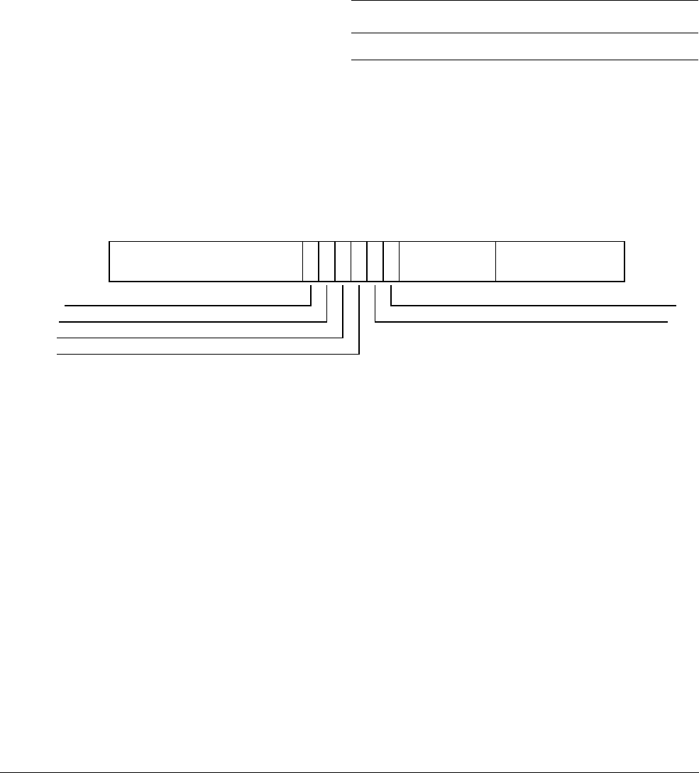
I1 Memory-Mapped System Register Descriptions
I1.2 Performance Monitors registers
I1-4608 Copyright © 2013 ARM Limited. All rights reserved. ARM DDI 0487A.a
Non-Confidential - Beta ID090413
I1.2.6 PMCFGR, Performance Monitors Configuration Register
The PMCFGR characteristics are:
Purpose
Contains PMU-specific configuration data.
This register is part of the Performance Monitors registers functional group.
Usage constraints
This register is accessible as shown below:
Configurations
PMCFGR is in the Core power domain.
Attributes
PMCFGR is a 32-bit register.
The PMCFGR bit assignments are:
Bits [31:20]
Reserved, RES0.
UEN, bit [19]
User-mode Enable Register supported. PMUSERENR_EL0 is not visible in the external debug
interface, so this bit is RES0.
WT, bit [18]
This feature is not supported, so this bit is RES0.
NA, bit [17]
This feature is not supported, so this bit is RES0.
EX, bit [16]
Export supported. Value is IMPLEMENTATION DEFINED.
0
PMCR_EL0.X is RES0.
1
PMCR_EL0.X is read/write.
CCD, bit [15]
Cycle counter has prescale. This is RES1 if AArch32 is supported at any EL, and RES0 otherwise.
0
PMCR_EL0.D is RES0.
Off DLK OSLK EPMAD SLK Default
Error Error Error Error RO RO
RES0
31 20 19 18 17 16 15 14
SIZE
13 8
N
70
UEN
WT
NA
EX
CC
CCD

I1 Memory-Mapped System Register Descriptions
I1.2 Performance Monitors registers
ARM DDI 0487A.a Copyright © 2013 ARM Limited. All rights reserved. I1-4609
ID090413 Non-Confidential - Beta
1
PMCR_EL0.D is read/write.
CC, bit [14]
Dedicated cycle counter (counter 31) supported. This bit is RES1.
SIZE, bits [13:8]
Size of counters. This field determines the spacing of counters in the memory-map.
In v8-A the counters are at doubleword-aligned addresses, and the largest counter is 64-bits, so this
field is
0b111111
.
N, bits [7:0]
Number of counters implemented in addition to the cycle counter, PMCCNTR_EL0. The maximum
number of event counters is 31, so bits[7:5] are always RES0.
00000000
Only PMCCNTR_EL0 implemented.
00000001
PMCCNTR_EL0 plus one event counter implemented.
and so on up to
0b00011111
, which indicates PMCCNTR_EL0 and 31 event counters implemented.
Accessing the PMCFGR:
PMCFGR can be accessed through the internal memory-mapped interface and the external debug interface:
Component Offset
PMU
0xE00

I1 Memory-Mapped System Register Descriptions
I1.2 Performance Monitors registers
I1-4610 Copyright © 2013 ARM Limited. All rights reserved. ARM DDI 0487A.a
Non-Confidential - Beta ID090413
I1.2.7 PMCIDR0, Performance Monitors Component Identification Register 0
The PMCIDR0 characteristics are:
Purpose
Provides information to identify a Performance Monitor component.
This register is part of the Performance Monitors registers functional group.
Usage constraints
This register is accessible as shown below:
Configurations
PMCIDR0 is in the Debug power domain.
PMCIDR0 is optional to implement in the external register interface.
This register is required for CoreSight compliance.
Attributes
PMCIDR0 is a 32-bit register.
The PMCIDR0 bit assignments are:
Bits [31:8]
Reserved, RES0.
PRMBL_0, bits [7:0]
Preamble. Must read as
0x0D
.
Accessing the PMCIDR0:
PMCIDR0 can be accessed through the internal memory-mapped interface and the external debug interface:
SLK Default
RO RO
RES0
31 8
PRMBL_0
70
Component Offset
PMU
0xFF0

I1 Memory-Mapped System Register Descriptions
I1.2 Performance Monitors registers
ARM DDI 0487A.a Copyright © 2013 ARM Limited. All rights reserved. I1-4611
ID090413 Non-Confidential - Beta
I1.2.8 PMCIDR1, Performance Monitors Component Identification Register 1
The PMCIDR1 characteristics are:
Purpose
Provides information to identify a Performance Monitor component.
This register is part of the Performance Monitors registers functional group.
Usage constraints
This register is accessible as shown below:
Configurations
PMCIDR1 is in the Debug power domain.
PMCIDR1 is optional to implement in the external register interface.
This register is required for CoreSight compliance.
Attributes
PMCIDR1 is a 32-bit register.
The PMCIDR1 bit assignments are:
Bits [31:8]
Reserved, RES0.
CLASS, bits [7:4]
Component class. Reads as
0x9
, debug component.
PRMBL_1, bits [3:0]
Preamble. RAZ.
Accessing the PMCIDR1:
PMCIDR1 can be accessed through the internal memory-mapped interface and the external debug interface:
SLK Default
RO RO
RES0
31 8
CLASS
74
PRMBL_1
30
Component Offset
PMU
0xFF4

I1 Memory-Mapped System Register Descriptions
I1.2 Performance Monitors registers
I1-4612 Copyright © 2013 ARM Limited. All rights reserved. ARM DDI 0487A.a
Non-Confidential - Beta ID090413
I1.2.9 PMCIDR2, Performance Monitors Component Identification Register 2
The PMCIDR2 characteristics are:
Purpose
Provides information to identify a Performance Monitor component.
This register is part of the Performance Monitors registers functional group.
Usage constraints
This register is accessible as shown below:
Configurations
PMCIDR2 is in the Debug power domain.
PMCIDR2 is optional to implement in the external register interface.
This register is required for CoreSight compliance.
Attributes
PMCIDR2 is a 32-bit register.
The PMCIDR2 bit assignments are:
Bits [31:8]
Reserved, RES0.
PRMBL_2, bits [7:0]
Preamble. Must read as
0x05
.
Accessing the PMCIDR2:
PMCIDR2 can be accessed through the internal memory-mapped interface and the external debug interface:
SLK Default
RO RO
RES0
31 8
PRMBL_2
70
Component Offset
PMU
0xFF8

I1 Memory-Mapped System Register Descriptions
I1.2 Performance Monitors registers
ARM DDI 0487A.a Copyright © 2013 ARM Limited. All rights reserved. I1-4613
ID090413 Non-Confidential - Beta
I1.2.10 PMCIDR3, Performance Monitors Component Identification Register 3
The PMCIDR3 characteristics are:
Purpose
Provides information to identify a Performance Monitor component.
This register is part of the Performance Monitors registers functional group.
Usage constraints
This register is accessible as shown below:
Configurations
PMCIDR3 is in the Debug power domain.
PMCIDR3 is optional to implement in the external register interface.
This register is required for CoreSight compliance.
Attributes
PMCIDR3 is a 32-bit register.
The PMCIDR3 bit assignments are:
Bits [31:8]
Reserved, RES0.
PRMBL_3, bits [7:0]
Preamble. Must read as
0xB1
.
Accessing the PMCIDR3:
PMCIDR3 can be accessed through the internal memory-mapped interface and the external debug interface:
SLK Default
RO RO
RES0
31 8
PRMBL_3
70
Component Offset
PMU
0xFFC

I1 Memory-Mapped System Register Descriptions
I1.2 Performance Monitors registers
I1-4614 Copyright © 2013 ARM Limited. All rights reserved. ARM DDI 0487A.a
Non-Confidential - Beta ID090413
I1.2.11 PMCNTENCLR_EL0, Performance Monitors Count Enable Clear register
The PMCNTENCLR_EL0 characteristics are:
Purpose
Disables the Cycle Count Register, PMCCNTR_EL0, and any implemented event counters
PMEVCNTR<x>. Reading this register shows which counters are enabled.
This register is part of the Performance Monitors registers functional group.
Usage constraints
This register is accessible as shown below:
Configurations
PMCNTENCLR_EL0 is architecturally mapped to AArch64 register PMCNTENCLR_EL0.
PMCNTENCLR_EL0 is architecturally mapped to AArch32 register PMCNTENCLR.
PMCNTENCLR_EL0 is in the Core power domain.
Attributes
PMCNTENCLR_EL0 is a 32-bit register.
The PMCNTENCLR_EL0 bit assignments are:
C, bit [31]
PMCCNTR_EL0 disable bit. Disables the cycle counter register. Possible values are:
0
When read, means the cycle counter is disabled. When written, has no effect.
1
When read, means the cycle counter is enabled. When written, disables the cycle
counter.
P<x>, bit [x] for x = 0 to (N - 1)
Event counter disable bit for PMEVCNTR<x>.
N is the value in PMCR_EL0.N. Bits [30:N] are RAZ/WI.
Possible values of each bit are:
0
When read, means that PMEVCNTR<x> is disabled. When written, has no effect.
1
When read, means that PMEVCNTR<x> is enabled. When written, disables
PMEVCNTR<x>.
Off DLK OSLK EPMAD SLK Default
Error Error Error Error RO RW
C
31
P<x>
30 0

I1 Memory-Mapped System Register Descriptions
I1.2 Performance Monitors registers
ARM DDI 0487A.a Copyright © 2013 ARM Limited. All rights reserved. I1-4615
ID090413 Non-Confidential - Beta
Accessing the PMCNTENCLR_EL0:
PMCNTENCLR_EL0 can be accessed through the internal memory-mapped interface and the external debug
interface:
Component Offset
PMU
0xC20

I1 Memory-Mapped System Register Descriptions
I1.2 Performance Monitors registers
I1-4616 Copyright © 2013 ARM Limited. All rights reserved. ARM DDI 0487A.a
Non-Confidential - Beta ID090413
I1.2.12 PMCNTENSET_EL0, Performance Monitors Count Enable Set register
The PMCNTENSET_EL0 characteristics are:
Purpose
Enables the Cycle Count Register, PMCCNTR_EL0, and any implemented event counters
PMEVCNTR<x>. Reading this register shows which counters are enabled.
This register is part of the Performance Monitors registers functional group.
Usage constraints
This register is accessible as shown below:
Configurations
PMCNTENSET_EL0 is architecturally mapped to AArch64 register PMCNTENSET_EL0.
PMCNTENSET_EL0 is architecturally mapped to AArch32 register PMCNTENSET.
PMCNTENSET_EL0 is in the Core power domain.
Attributes
PMCNTENSET_EL0 is a 32-bit register.
The PMCNTENSET_EL0 bit assignments are:
C, bit [31]
PMCCNTR_EL0 enable bit. Enables the cycle counter register. Possible values are:
0
When read, means the cycle counter is disabled. When written, has no effect.
1
When read, means the cycle counter is enabled. When written, enables the cycle
counter.
P<x>, bit [x] for x = 0 to (N - 1)
Event counter enable bit for PMEVCNTR<x>.
N is the value in PMCR_EL0.N. Bits [30:N] are RAZ/WI.
Possible values of each bit are:
0
When read, means that PMEVCNTR<x> is disabled. When written, has no effect.
1
When read, means that PMEVCNTR<x> event counter is enabled. When written,
enables PMEVCNTR<x>.
Off DLK OSLK EPMAD SLK Default
Error Error Error Error RO RW
C
31
P<x>
30 0

I1 Memory-Mapped System Register Descriptions
I1.2 Performance Monitors registers
ARM DDI 0487A.a Copyright © 2013 ARM Limited. All rights reserved. I1-4617
ID090413 Non-Confidential - Beta
Accessing the PMCNTENSET_EL0:
PMCNTENSET_EL0 can be accessed through the internal memory-mapped interface and the external debug
interface:
Component Offset
PMU
0xC00
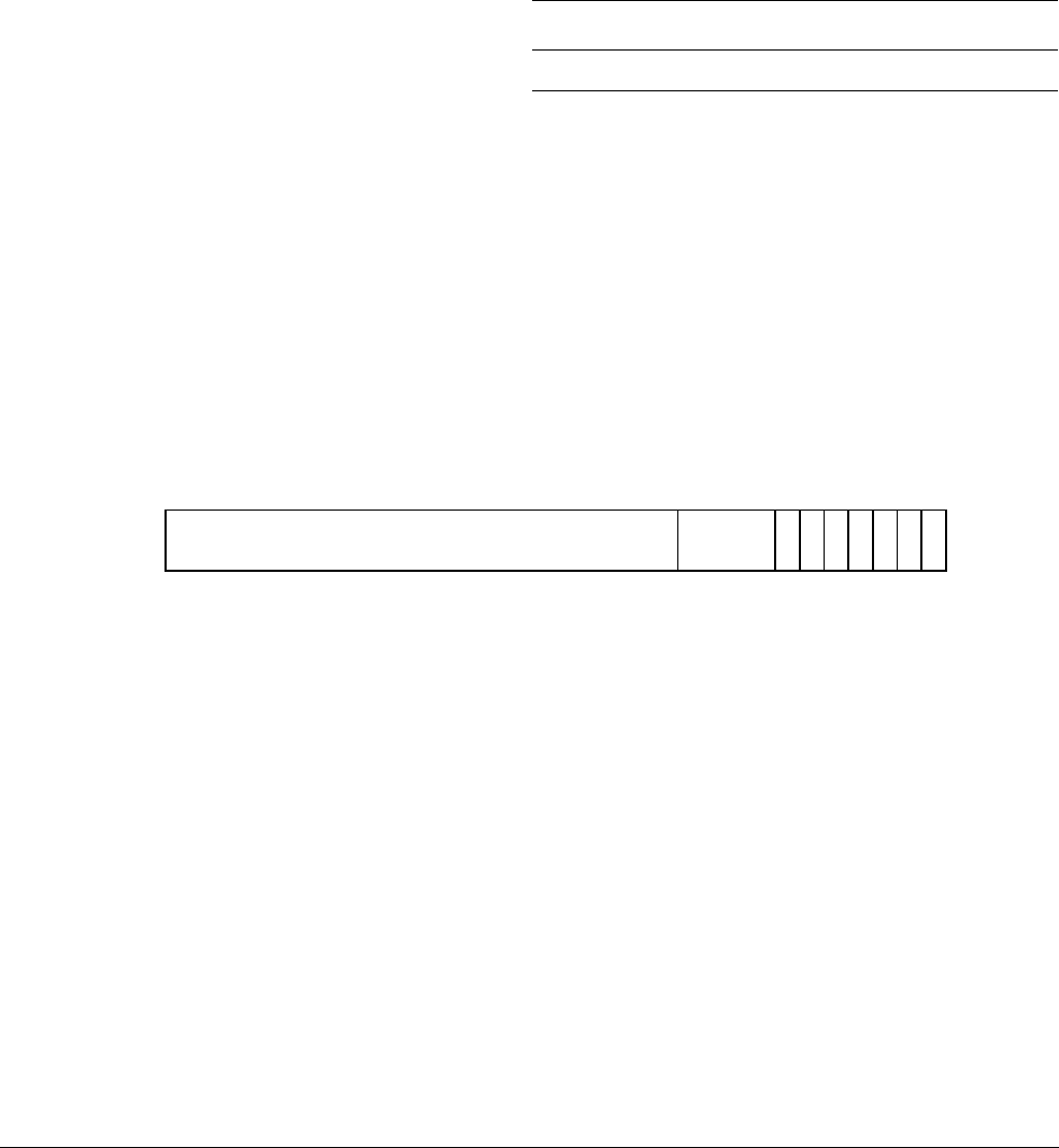
I1 Memory-Mapped System Register Descriptions
I1.2 Performance Monitors registers
I1-4618 Copyright © 2013 ARM Limited. All rights reserved. ARM DDI 0487A.a
Non-Confidential - Beta ID090413
I1.2.13 PMCR_EL0, Performance Monitors Control Register
The PMCR_EL0 characteristics are:
Purpose
Provides details of the Performance Monitors implementation, including the number of counters
implemented, and configures and controls the counters.
This register is part of the Performance Monitors registers functional group.
Usage constraints
This register is accessible as shown below:
Configurations
PMCR_EL0 is architecturally mapped to AArch64 register PMCR_EL0.
PMCR_EL0 is architecturally mapped to AArch32 register PMCR.
PMCR_EL0 is in the Core power domain.
Bits [31:11] of this register must be implemented as RAZ/WI despite the mapping to the internal
PMCR system register. An external agent must use other means to discover this information, such
as PMCFGR and the ID registers.
Attributes
PMCR_EL0 is a 32-bit register.
The PMCR_EL0 bit assignments are:
Bits [31:11]
Reserved, RAZ/WI.
Bits [10:7]
Reserved, RES0.
LC, bit [6]
Long cycle counter enable. Determines which PMCCNTR_EL0 bit generates an overflow recorded
by PMOVSR[31].
0
Cycle counter overflow on increment that changes PMCCNTR_EL0[31] from 1 to 0.
1
Cycle counter overflow on increment that changes PMCCNTR_EL0[63] from 1 to 0.
ARM deprecates use of PMCR_EL0.LC = 0.
DP, bit [5]
Disable cycle counter when event counting is prohibited. The possible values of this bit are:
0
PMCCNTR_EL0, if enabled, counts when event counting is prohibited.
1
PMCCNTR_EL0 does not count when event counting is prohibited.
Event counting is prohibited when ProfilingProhibited(IsSecure(),PSTATE.EL) == TRUE.
This bit is RW.
Off DLK OSLK EPMAD SLK Default
Error Error Error Error RO RW
RAZ/WI
31 11
RES0
10 7
LC
6
DP
5
X
4
D
3
C
2
P
1
E
0

I1 Memory-Mapped System Register Descriptions
I1.2 Performance Monitors registers
ARM DDI 0487A.a Copyright © 2013 ARM Limited. All rights reserved. I1-4619
ID090413 Non-Confidential - Beta
X, bit [4]
Enable export of events in an IMPLEMENTATION DEFINED event stream. The possible values of this
bit are:
0
Do not export events.
1
Export events where not prohibited.
This bit is used to permit events to be exported to another debug device, such as an OPTIONAL trace
extension, over an event bus. If the implementation does not include such an event bus, this bit is
RAZ/WI.
This bit does not affect the generation of Performance Monitors overflow interrupt requests or
signaling to a cross-trigger interface (CTI) that can be implemented as signals exported from the
processor.
If the implementation does not include an exported event stream, this bit is RAZ/WI. Otherwise this
bit is RW.
D, bit [3]
Clock divider. The possible values of this bit are:
0
When enabled, PMCCNTR_EL0 counts every clock cycle.
1
When enabled, PMCCNTR_EL0 counts once every 64 clock cycles.
This bit is RW.
If PMCR_EL0.LC == 1, this bit is ignored and the cycle counter counts every clock cycle.
ARM deprecates use of PMCR.D = 1.
C, bit [2]
Cycle counter reset. This bit is WO. The effects of writing to this bit are:
0
No action.
1
Reset PMCCNTR_EL0 to zero.
This bit is always RAZ.
Resetting PMCCNTR_EL0 does not clear the PMCCNTR_EL0 overflow bit to 0.
P, bit [1]
Event counter reset. This bit is WO. The effects of writing to this bit are:
0
No action.
1
Reset all event counters, not including PMCCNTR_EL0, to zero.
This bit is always RAZ.
Resetting the event counters does not clear any overflow bits to 0.
E, bit [0]
Enable. The possible values of this bit are:
0
All counters, including PMCCNTR_EL0, are disabled.
1
All counters are enabled by PMCNTENSET_EL0.
This bit is RW.
Accessing the PMCR_EL0:
PMCR_EL0 can be accessed through the internal memory-mapped interface and the external debug interface:
Component Offset
PMU
0xE04

I1 Memory-Mapped System Register Descriptions
I1.2 Performance Monitors registers
I1-4620 Copyright © 2013 ARM Limited. All rights reserved. ARM DDI 0487A.a
Non-Confidential - Beta ID090413
I1.2.14 PMDEVAFF0, Performance Monitors Device Affinity register 0
The PMDEVAFF0 characteristics are:
Purpose
Copy of the low half of the processor MPIDR_EL1 register that allows a debugger to determine
which processor in a multiprocessor system the Performance Monitor component relates to.
This register is part of the Performance Monitors registers functional group.
Usage constraints
This register is accessible as shown below:
Configurations
PMDEVAFF0 is in the Debug power domain.
PMDEVAFF0 is optional to implement in the external register interface.
Attributes
PMDEVAFF0 is a 32-bit register.
The PMDEVAFF0 bit assignments are:
Bits [31:0]
MPIDR_EL1 low half. Read-only copy of the low half of MPIDR_EL1, as seen from the highest
implemented exception level.
Accessing the PMDEVAFF0:
PMDEVAFF0 can be accessed through the internal memory-mapped interface and the external debug interface:
SLK Default
RO RO
MPIDR_EL1 low half
31 0
Component Offset
PMU
0xFA8

I1 Memory-Mapped System Register Descriptions
I1.2 Performance Monitors registers
ARM DDI 0487A.a Copyright © 2013 ARM Limited. All rights reserved. I1-4621
ID090413 Non-Confidential - Beta
I1.2.15 PMDEVAFF1, Performance Monitors Device Affinity register 1
The PMDEVAFF1 characteristics are:
Purpose
Copy of the high half of the processor MPIDR_EL1 register that allows a debugger to determine
which processor in a multiprocessor system the Performance Monitor component relates to.
This register is part of the Performance Monitors registers functional group.
Usage constraints
This register is accessible as shown below:
Configurations
PMDEVAFF1 is in the Debug power domain.
PMDEVAFF1 is optional to implement in the external register interface.
Attributes
PMDEVAFF1 is a 32-bit register.
The PMDEVAFF1 bit assignments are:
Bits [31:0]
MPIDR_EL1 high half. Read-only copy of the high half of MPIDR_EL1, as seen from the highest
implemented exception level.
Accessing the PMDEVAFF1:
PMDEVAFF1 can be accessed through the internal memory-mapped interface and the external debug interface:
SLK Default
RO RO
MPIDR_EL1 high half
31 0
Component Offset
PMU
0xFAC

I1 Memory-Mapped System Register Descriptions
I1.2 Performance Monitors registers
I1-4622 Copyright © 2013 ARM Limited. All rights reserved. ARM DDI 0487A.a
Non-Confidential - Beta ID090413
I1.2.16 PMDEVARCH, Performance Monitors Device Architecture register
The PMDEVARCH characteristics are:
Purpose
This register is part of the Performance Monitors registers functional group.
Usage constraints
This register is accessible as shown below:
Configurations
PMDEVARCH is in the Debug power domain.
PMDEVARCH is optional to implement in the external register interface.
Attributes
PMDEVARCH is a 32-bit register.
The PMDEVARCH bit assignments are:
ARCHITECT, bits [31:21]
Defines the architecture of the component. For Performance Monitors, this is ARM Limited.
Bits [31:28] are the JEP 106 continuation code,
0x4
.
Bits [27:21] are the JEP 106 ID code,
0x3B
.
PRESENT, bit [20]
When set to 1, indicates that the DEVARCH is present.
This field is 1 in v8-A.
REVISION, bits [19:16]
Defines the architecture revision. For architectures defined by ARM this is the minor revision.
For Performance Monitors, the revision defined by v8-A is
0x0
.
All other values are reserved.
ARCHID, bits [15:0]
Defines this part to be a v8-A debug component. For architectures defined by ARM this is further
subdivided.
For Performance Monitors:
• Bits [15:12] are the architecture version,
0x2
.
• Bits [11:0] are the architecture part number,
0xA16
.
This corresponds to Performance Monitors architecture version PMUv3.
SLK Default
RO RO
ARCHITECT
31 21 20
REVISION
19 16
ARCHID
15 0
PRESENT

I1 Memory-Mapped System Register Descriptions
I1.2 Performance Monitors registers
ARM DDI 0487A.a Copyright © 2013 ARM Limited. All rights reserved. I1-4623
ID090413 Non-Confidential - Beta
Accessing the PMDEVARCH:
PMDEVARCH can be accessed through the internal memory-mapped interface and the external debug interface:
Component Offset
PMU
0xFBC

I1 Memory-Mapped System Register Descriptions
I1.2 Performance Monitors registers
I1-4624 Copyright © 2013 ARM Limited. All rights reserved. ARM DDI 0487A.a
Non-Confidential - Beta ID090413
I1.2.17 PMDEVTYPE, Performance Monitors Device Type register
The PMDEVTYPE characteristics are:
Purpose
Indicates to a debugger that this component is part of a processor's performance monitor interface.
This register is part of the Performance Monitors registers functional group.
Usage constraints
This register is accessible as shown below:
Configurations
PMDEVTYPE is in the Debug power domain.
PMDEVTYPE is optional to implement in the external register interface.
Attributes
PMDEVTYPE is a 32-bit register.
The PMDEVTYPE bit assignments are:
Bits [31:8]
Reserved, RES0.
SUB, bits [7:4]
Subtype. Must read as
0x1
to indicate this is a processor component.
MAJOR, bits [3:0]
Major type. Must read as
0x6
to indicate this is a performance monitor component.
Accessing the PMDEVTYPE:
PMDEVTYPE can be accessed through the internal memory-mapped interface and the external debug interface:
SLK Default
RO RO
RES0
31 8
SUB
74
MAJOR
30
Component Offset
PMU
0xFCC

I1 Memory-Mapped System Register Descriptions
I1.2 Performance Monitors registers
ARM DDI 0487A.a Copyright © 2013 ARM Limited. All rights reserved. I1-4625
ID090413 Non-Confidential - Beta
I1.2.18 PMEVCNTR<n>_EL0, Performance Monitors Event Count Registers, n = 0 - 30
The PMEVCNTR<n>_EL0 characteristics are:
Purpose
Holds event counter n, which counts events, where n is 0 to 30.
This register is part of the Performance Monitors registers functional group.
Usage constraints
This register is accessible as shown below:
External accesses to the performance monitors ignore PMUSERENR_EL0 and, if implemented,
MDCR_EL2.{TPM, TPMCR, HPMN} and MDCR_EL3.TPM. This means that all counters are
accessible regardless of the current EL or privilege of the access.
Configurations
PMEVCNTR<n>_EL0 is architecturally mapped to AArch64 register PMEVCNTR<n>_EL0.
PMEVCNTR<n>_EL0 is architecturally mapped to AArch32 register PMEVCNTR<n>.
PMEVCNTR<n>_EL0 is in the Core power domain.
Attributes
PMEVCNTR<n>_EL0 is a 32-bit register.
The PMEVCNTR<n>_EL0 bit assignments are:
Bits [31:0]
Event counter n. Value of event counter n, where n is the number of this register and is a number
from 0 to 30.
Accessing the PMEVCNTR<n>_EL0:
PMEVCNTR<n>_EL0 can be accessed through the internal memory-mapped interface and the external debug
interface:
Off DLK OSLK EPMAD SLK Default
Error Error Error Error RO RW
Event counter n
31 0
Component Offset
PMU
0x000
+ 8n
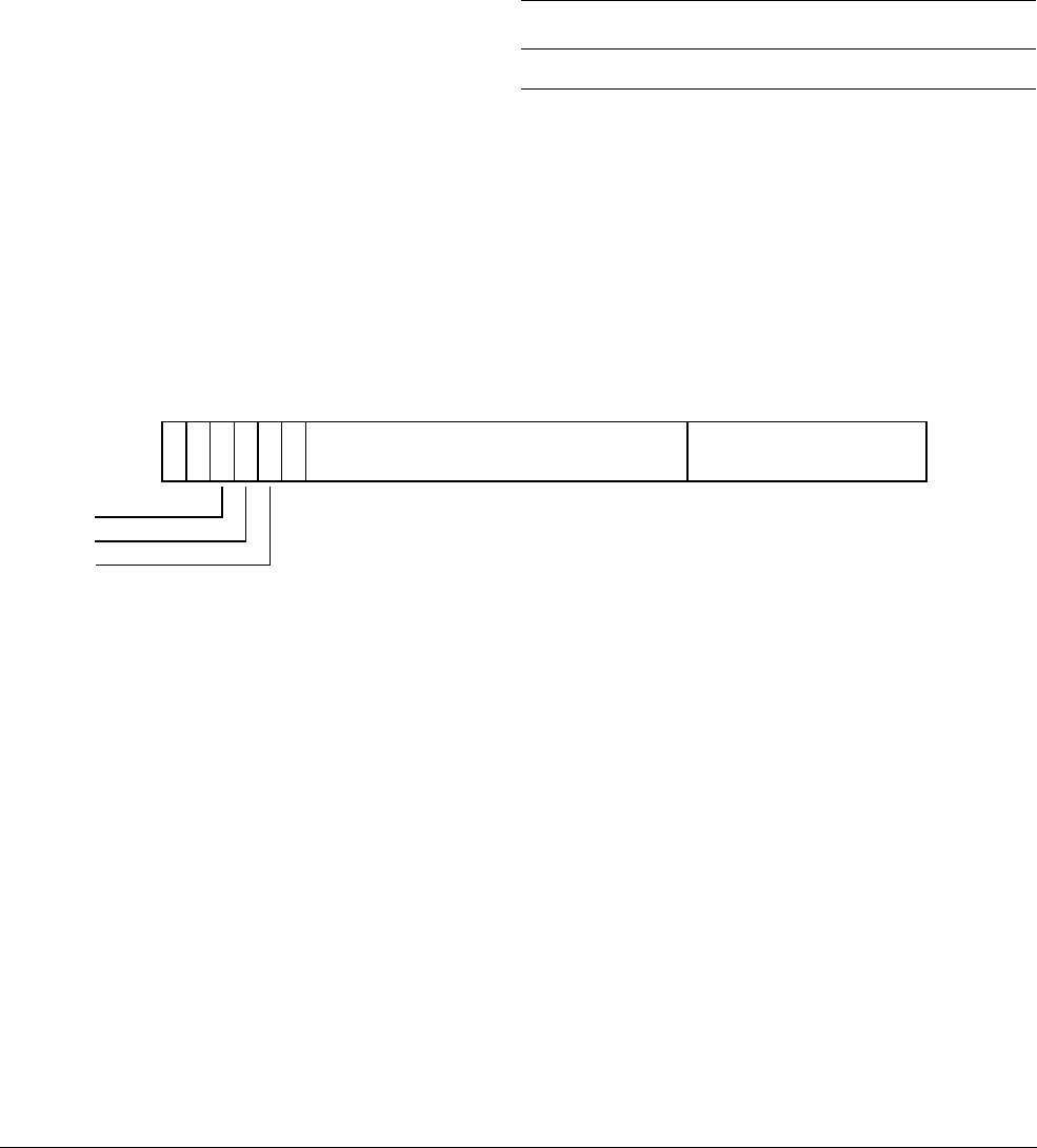
I1 Memory-Mapped System Register Descriptions
I1.2 Performance Monitors registers
I1-4626 Copyright © 2013 ARM Limited. All rights reserved. ARM DDI 0487A.a
Non-Confidential - Beta ID090413
I1.2.19 PMEVTYPER<n>_EL0, Performance Monitors Event Type Registers, n = 0 - 30
The PMEVTYPER<n>_EL0 characteristics are:
Purpose
Configures event counter n, where n is 0 to 30.
This register is part of the Performance Monitors registers functional group.
Usage constraints
This register is accessible as shown below:
Configurations
PMEVTYPER<n>_EL0 is architecturally mapped to AArch64 register PMEVTYPER<n>_EL0.
PMEVTYPER<n>_EL0 is architecturally mapped to AArch32 register PMEVTYPER<n>.
PMEVTYPER<n>_EL0 is in the Core power domain.
Attributes
PMEVTYPER<n>_EL0 is a 32-bit register.
The PMEVTYPER<n>_EL0 bit assignments are:
P, bit [31]
EL1 modes filtering bit. Controls counting in EL1. If EL3 is implemented, then counting in
Non-secure EL1 is further controlled by the NSK bit. The possible values of this bit are:
0
Count events in EL1.
1
Do not count events in EL1.
U, bit [30]
EL0 filtering bit. Controls counting in EL0. If EL3 is implemented, then counting in Non-secure
EL0 is further controlled by the NSU bit. The possible values of this bit are:
0
Count events in EL0.
1
Do not count events in EL0.
NSK, bit [29]
Non-secure kernel modes filtering bit. Controls counting in Non-secure EL1. If EL3 is not
implemented, this bit is RES0.
If the value of this bit is equal to the value of P, events in Non-secure EL1 are counted.
Otherwise, events in Non-secure EL1 are not counted.
Off DLK OSLK EPMAD SLK Default
Error Error Error Error RO RW
P
31
U
30 29 28 27
M
26
RES0
25 10
evtCount
90
NSK
NSU
NSH

I1 Memory-Mapped System Register Descriptions
I1.2 Performance Monitors registers
ARM DDI 0487A.a Copyright © 2013 ARM Limited. All rights reserved. I1-4627
ID090413 Non-Confidential - Beta
NSU, bit [28]
Non-secure user modes filtering bit. Controls counting in Non-secure EL0. If EL3 is not
implemented, this bit is RES0.
If the value of this bit is equal to the value of U, events in Non-secure EL0 are counted.
Otherwise, events in Non-secure EL0 are not counted.
NSH, bit [27]
Non-secure Hyp modes filtering bit. Controls counting in Non-secure EL2. If EL2 is not
implemented, this bit is RES0.
0
Do not count events in EL2.
1
Count events in EL2.
M, bit [26]
Secure EL3 filtering bit. Most applications can ignore this bit and set the value to zero. If EL3 is not
implemented, this bit is RES0.
If the value of this bit is equal to the value of P, events in Secure EL3 are counted.
Otherwise, events in Secure EL3 are not counted.
Bits [25:10]
Reserved, RES0.
evtCount, bits [9:0]
Event to count. The event number of the event that is counted by event counter
PMEVCNTR<n>_EL0.
Software must program this field with an event defined by the processor or a common event defined
by the architecture.
If evtCount is programmed to an event that is reserved or not implemented, the behavior depends
on the event type.
For common architectural and microarchitectural events:
• No events are counted.
• The value read back on evtCount is the value written.
For IMPLEMENTATION DEFINED events:
• It is UNPREDICTABLE what event, if any, is counted. UNPREDICTABLE in this case means the
event must not expose privileged information.
• The value read back on evtCount is an UNKNOWN value with the same effect.
ARM recommends that the behavior across a family of implementations is defined such that if a
given implementation does not include an event from a set of common IMPLEMENTATION DEFINED
events, then no event is counted and the value read back on evtCount is the value written.
Accessing the PMEVTYPER<n>_EL0:
PMEVTYPER<n>_EL0 can be accessed through the internal memory-mapped interface and the external debug
interface:
Component Offset
PMU
0x400
+ 4n

I1 Memory-Mapped System Register Descriptions
I1.2 Performance Monitors registers
I1-4628 Copyright © 2013 ARM Limited. All rights reserved. ARM DDI 0487A.a
Non-Confidential - Beta ID090413
I1.2.20 PMINTENCLR_EL1, Performance Monitors Interrupt Enable Clear register
The PMINTENCLR_EL1 characteristics are:
Purpose
Disables the generation of interrupt requests on overflows from the Cycle Count Register,
PMCCNTR_EL0, and the event counters PMEVCNTR<n>_EL0. Reading the register shows which
overflow interrupt requests are enabled.
This register is part of the Performance Monitors registers functional group.
Usage constraints
This register is accessible as shown below:
Configurations
PMINTENCLR_EL1 is architecturally mapped to AArch64 register PMINTENCLR_EL1.
PMINTENCLR_EL1 is architecturally mapped to AArch32 register PMINTENCLR.
PMINTENCLR_EL1 is in the Core power domain.
Attributes
PMINTENCLR_EL1 is a 32-bit register.
The PMINTENCLR_EL1 bit assignments are:
C, bit [31]
PMCCNTR_EL0 overflow interrupt request disable bit. Possible values are:
0
When read, means the cycle counter overflow interrupt request is disabled. When
written, has no effect.
1
When read, means the cycle counter overflow interrupt request is enabled. When
written, disables the cycle count overflow interrupt request.
P<x>, bit [x] for x = 0 to (N - 1)
Event counter overflow interrupt request disable bit for PMEVCNTR<x>_EL0.
N is the value in PMCR_EL0.N. Bits [30:N] are RAZ/WI.
Possible values are:
0
When read, means that the PMEVCNTR<x>_EL0 event counter interrupt request is
disabled. When written, has no effect.
1
When read, means that the PMEVCNTR<x>_EL0 event counter interrupt request is
enabled. When written, disables the PMEVCNTR<x>_EL0 interrupt request.
Off DLK OSLK EPMAD SLK Default
Error Error Error Error RO RW
C
31
P<x>
30 0

I1 Memory-Mapped System Register Descriptions
I1.2 Performance Monitors registers
ARM DDI 0487A.a Copyright © 2013 ARM Limited. All rights reserved. I1-4629
ID090413 Non-Confidential - Beta
Accessing the PMINTENCLR_EL1:
PMINTENCLR_EL1 can be accessed through the internal memory-mapped interface and the external debug
interface:
Component Offset
PMU
0xC60

I1 Memory-Mapped System Register Descriptions
I1.2 Performance Monitors registers
I1-4630 Copyright © 2013 ARM Limited. All rights reserved. ARM DDI 0487A.a
Non-Confidential - Beta ID090413
I1.2.21 PMINTENSET_EL1, Performance Monitors Interrupt Enable Set register
The PMINTENSET_EL1 characteristics are:
Purpose
Enables the generation of interrupt requests on overflows from the Cycle Count Register,
PMCCNTR_EL0, and the event counters PMEVCNTR<n>_EL0. Reading the register shows which
overflow interrupt requests are enabled.
This register is part of the Performance Monitors registers functional group.
Usage constraints
This register is accessible as shown below:
Configurations
PMINTENSET_EL1 is architecturally mapped to AArch64 register PMINTENSET_EL1.
PMINTENSET_EL1 is architecturally mapped to AArch32 register PMINTENSET.
PMINTENSET_EL1 is in the Core power domain.
Attributes
PMINTENSET_EL1 is a 32-bit register.
The PMINTENSET_EL1 bit assignments are:
C, bit [31]
PMCCNTR_EL0 overflow interrupt request enable bit. Possible values are:
0
When read, means the cycle counter overflow interrupt request is disabled. When
written, has no effect.
1
When read, means the cycle counter overflow interrupt request is enabled. When
written, enables the cycle count overflow interrupt request.
P<x>, bit [x] for x = 0 to (N - 1)
Event counter overflow interrupt request enable bit for PMEVCNTR<x>_EL0.
N is the value in PMCR_EL0.N. Bits [30:N] are RAZ/WI.
Possible values are:
0
When read, means that the PMEVCNTR<x>_EL0 event counter interrupt request is
disabled. When written, has no effect.
1
When read, means that the PMEVCNTR<x>_EL0 event counter interrupt request is
enabled. When written, enables the PMEVCNTR<x>_EL0 interrupt request.
Off DLK OSLK EPMAD SLK Default
Error Error Error Error RO RW
C
31
P<x>
30 0

I1 Memory-Mapped System Register Descriptions
I1.2 Performance Monitors registers
ARM DDI 0487A.a Copyright © 2013 ARM Limited. All rights reserved. I1-4631
ID090413 Non-Confidential - Beta
Accessing the PMINTENSET_EL1:
PMINTENSET_EL1 can be accessed through the internal memory-mapped interface and the external debug
interface:
Component Offset
PMU
0xC40

I1 Memory-Mapped System Register Descriptions
I1.2 Performance Monitors registers
I1-4632 Copyright © 2013 ARM Limited. All rights reserved. ARM DDI 0487A.a
Non-Confidential - Beta ID090413
I1.2.22 PMITCTRL, Performance Monitors Integration mode Control register
The PMITCTRL characteristics are:
Purpose
Enables the Performance Monitors to switch from default mode into integration mode, where test
software can control directly the inputs and outputs of the processor, for integration testing or
topology detection.
This register is part of the Performance Monitors registers functional group.
Usage constraints
This register is accessible as shown below:
Configurations
It is IMPLEMENTATION DEFINED whether PMITCTRL is in the Core power domain or in the Debug
power domain.
PMITCTRL is optional to implement in the external register interface.
Attributes
PMITCTRL is a 32-bit register.
The PMITCTRL bit assignments are:
Bits [31:1]
Reserved, RES0.
IME, bit [0]
Integration mode enable. When IME == 1, the device reverts to an integration mode to enable
integration testing or topology detection. The integration mode behavior is IMPLEMENTATION
DEFINED.
0
Normal operation.
1
Integration mode enabled.
On IMPLEMENTATION DEFINED reset, the field resets to 0.
Accessing the PMITCTRL:
PMITCTRL can be accessed through the internal memory-mapped interface and the external debug interface:
Off DLK OSLK Default
IMP DEF IMP DEF IMP DEF RW
RES0
31 1 0
IME
Component Offset
PMU
0xF00

I1 Memory-Mapped System Register Descriptions
I1.2 Performance Monitors registers
ARM DDI 0487A.a Copyright © 2013 ARM Limited. All rights reserved. I1-4633
ID090413 Non-Confidential - Beta
I1.2.23 PMLAR, Performance Monitors Lock Access Register
The PMLAR characteristics are:
Purpose
Allows or disallows access to the Performance Monitors registers through a memory-mapped
interface.
This register is part of the Performance Monitors registers functional group.
Usage constraints
This register is accessible as shown below:
Configurations
PMLAR is in the Debug power domain.
If OPTIONAL memory-mapped access to the external debug interface is supported then an OPTIONAL
Software lock can be implemented as part of CoreSight compliance.
PMLAR ignores writes if the Software lock is not implemented and ignores writes for other accesses
to the external debug interface.
The Software lock provides a lock to prevent memory-mapped writes to the Performance Monitors
registers. Use of this lock mechanism reduces the risk of accidental damage to the contents of the
Performance Monitors registers. It does not, and cannot, prevent all accidental or malicious damage.
Software uses PMLAR to set or clear the lock, and PMLSR to check the current status of the lock.
Attributes
PMLAR is a 32-bit register.
The PMLAR bit assignments are:
KEY, bits [31:0]
Lock Access control. Writing the key value
0xC5ACCE55
to this field unlocks the lock, enabling write
accesses to this component's registers through a memory-mapped interface.
Writing any other value to this register locks the lock, disabling write accesses to this component's
registers through a memory mapped interface.
Accessing the PMLAR:
PMLAR can be accessed through the internal memory-mapped interface:
Default
WO
KEY
31 0
Component Offset
PMU
0xFB0

I1 Memory-Mapped System Register Descriptions
I1.2 Performance Monitors registers
I1-4634 Copyright © 2013 ARM Limited. All rights reserved. ARM DDI 0487A.a
Non-Confidential - Beta ID090413
I1.2.24 PMLSR, Performance Monitors Lock Status Register
The PMLSR characteristics are:
Purpose
Indicates the current status of the software lock for Performance Monitors registers.
This register is part of the Performance Monitors registers functional group.
Usage constraints
This register is accessible as shown below:
Configurations
PMLSR is in the Debug power domain.
If OPTIONAL memory-mapped access to the external debug interface is supported then an OPTIONAL
Software lock can be implemented as part of CoreSight compliance.
PMLSR is RAZ if the Software lock is not implemented and is RAZ for other accesses to the
external debug interface.
The Software lock provides a lock to prevent memory-mapped writes to the Performance Monitors
registers. Use of this lock mechanism reduces the risk of accidental damage to the contents of the
Performance Monitors registers. It does not, and cannot, prevent all accidental or malicious damage.
Software uses PMLAR to set or clear the lock, and PMLSR to check the current status of the lock.
Attributes
PMLSR is a 32-bit register.
The PMLSR bit assignments are:
Bits [31:3]
Reserved, RES0.
nTT, bit [2]
Not thirty-two bit access required. RAZ.
SLK, bit [1]
Software lock status for this component. For an access to LSR that is not a memory-mapped access,
or when the software lock is not implemented, this field is RES0.
For memory-mapped accesses when the software lock is implemented, possible values of this field
are:
0
Lock clear. Writes are permitted to this component's registers.
1
Lock set. Writes to this component's registers are ignored, and reads have no side
effects.
Default
RO
RES0
31 3 2 1 0
SLI
SLK
nTT

I1 Memory-Mapped System Register Descriptions
I1.2 Performance Monitors registers
ARM DDI 0487A.a Copyright © 2013 ARM Limited. All rights reserved. I1-4635
ID090413 Non-Confidential - Beta
On External debug reset, the field resets to 1.
SLI, bit [0]
Software lock implemented. For an access to LSR that is not a memory-mapped access, this field is
RAZ. For memory-mapped accesses, the value of this field is IMPLEMENTATION DEFINED. Permitted
values are:
0
Software lock not implemented or not memory-mapped access.
1
Software lock implemented and memory-mapped access.
Accessing the PMLSR:
PMLSR can be accessed through the internal memory-mapped interface:
Component Offset
PMU
0xFB4

I1 Memory-Mapped System Register Descriptions
I1.2 Performance Monitors registers
I1-4636 Copyright © 2013 ARM Limited. All rights reserved. ARM DDI 0487A.a
Non-Confidential - Beta ID090413
I1.2.25 PMOVSCLR_EL0, Performance Monitors Overflow Flag Status Clear register
The PMOVSCLR_EL0 characteristics are:
Purpose
Contains the state of the overflow bit for the Cycle Count Register, PMCCNTR_EL0, and each of
the implemented event counters PMEVCNTR<x>. Writing to this register clears these bits.
This register is part of the Performance Monitors registers functional group.
Usage constraints
This register is accessible as shown below:
Configurations
PMOVSCLR_EL0 is architecturally mapped to AArch64 register PMOVSCLR_EL0.
PMOVSCLR_EL0 is architecturally mapped to AArch32 register PMOVSR.
PMOVSCLR_EL0 is in the Core power domain.
Attributes
PMOVSCLR_EL0 is a 32-bit register.
The PMOVSCLR_EL0 bit assignments are:
C, bit [31]
PMCCNTR_EL0 overflow bit. Possible values are:
0
When read, means the cycle counter has not overflowed. When written, has no effect.
1
When read, means the cycle counter has overflowed. When written, clears the overflow
bit to 0.
PMCR_EL0.LC is used to control from which bit of PMCCNTR_EL0 (bit 31 or bit 63) an overflow
is detected.
P<x>, bit [x] for x = 0 to (N - 1)
Event counter overflow clear bit for PMEVCNTR<x>.
N is the value in PMCR_EL0.N. Bits [30:N] are RAZ/WI.
Possible values of each bit are:
0
When read, means that PMEVCNTR<x> has not overflowed. When written, has no
effect.
1
When read, means that PMEVCNTR<x> has overflowed. When written, clears the
PMEVCNTR<x> overflow bit to 0.
Off DLK OSLK EPMAD SLK Default
Error Error Error Error RO RW
C
31
P<x>
30 0

I1 Memory-Mapped System Register Descriptions
I1.2 Performance Monitors registers
ARM DDI 0487A.a Copyright © 2013 ARM Limited. All rights reserved. I1-4637
ID090413 Non-Confidential - Beta
Accessing the PMOVSCLR_EL0:
PMOVSCLR_EL0 can be accessed through the internal memory-mapped interface and the external debug interface:
Component Offset
PMU
0xC80

I1 Memory-Mapped System Register Descriptions
I1.2 Performance Monitors registers
I1-4638 Copyright © 2013 ARM Limited. All rights reserved. ARM DDI 0487A.a
Non-Confidential - Beta ID090413
I1.2.26 PMOVSSET_EL0, Performance Monitors Overflow Flag Status Set register
The PMOVSSET_EL0 characteristics are:
Purpose
Sets the state of the overflow bit for the Cycle Count Register, PMCCNTR_EL0, and each of the
implemented event counters PMEVCNTR<x>.
This register is part of the Performance Monitors registers functional group.
Usage constraints
This register is accessible as shown below:
Configurations
PMOVSSET_EL0 is architecturally mapped to AArch64 register PMOVSSET_EL0.
PMOVSSET_EL0 is architecturally mapped to AArch32 register PMOVSSET.
PMOVSSET_EL0 is in the Core power domain.
Attributes
PMOVSSET_EL0 is a 32-bit register.
The PMOVSSET_EL0 bit assignments are:
C, bit [31]
PMCCNTR_EL0 overflow bit. Possible values are:
0
When read, means the cycle counter has not overflowed. When written, has no effect.
1
When read, means the cycle counter has overflowed. When written, sets the overflow
bit to 1.
P<x>, bit [x] for x = 0 to (N - 1)
Event counter overflow set bit for PMEVCNTR<x>.
N is the value in PMCR_EL0.N. Bits [30:N] are RAZ/WI.
Possible values are:
0
When read, means that PMEVCNTR<x> has not overflowed. When written, has no
effect.
1
When read, means that PMEVCNTR<x> has overflowed. When written, sets the
PMEVCNTR<x> overflow bit to 1.
Off DLK OSLK EPMAD SLK Default
Error Error Error Error RO RW
C
31
P<x>
30 0

I1 Memory-Mapped System Register Descriptions
I1.2 Performance Monitors registers
ARM DDI 0487A.a Copyright © 2013 ARM Limited. All rights reserved. I1-4639
ID090413 Non-Confidential - Beta
Accessing the PMOVSSET_EL0:
PMOVSSET_EL0 can be accessed through the internal memory-mapped interface and the external debug interface:
Component Offset
PMU
0xCC0

I1 Memory-Mapped System Register Descriptions
I1.2 Performance Monitors registers
I1-4640 Copyright © 2013 ARM Limited. All rights reserved. ARM DDI 0487A.a
Non-Confidential - Beta ID090413
I1.2.27 PMPIDR0, Performance Monitors Peripheral Identification Register 0
The PMPIDR0 characteristics are:
Purpose
Provides information to identify a Performance Monitor component.
This register is part of the Performance Monitors registers functional group.
Usage constraints
This register is accessible as shown below:
Configurations
PMPIDR0 is in the Debug power domain.
PMPIDR0 is optional to implement in the external register interface.
This register is required for CoreSight compliance.
Attributes
PMPIDR0 is a 32-bit register.
The PMPIDR0 bit assignments are:
Bits [31:8]
Reserved, RES0.
PART_0, bits [7:0]
Part number, least significant byte.
Accessing the PMPIDR0:
PMPIDR0 can be accessed through the internal memory-mapped interface and the external debug interface:
SLK Default
RO RO
RES0
31 8
PART_0
70
Component Offset
PMU
0xFE0

I1 Memory-Mapped System Register Descriptions
I1.2 Performance Monitors registers
ARM DDI 0487A.a Copyright © 2013 ARM Limited. All rights reserved. I1-4641
ID090413 Non-Confidential - Beta
I1.2.28 PMPIDR1, Performance Monitors Peripheral Identification Register 1
The PMPIDR1 characteristics are:
Purpose
Provides information to identify a Performance Monitor component.
This register is part of the Performance Monitors registers functional group.
Usage constraints
This register is accessible as shown below:
Configurations
PMPIDR1 is in the Debug power domain.
PMPIDR1 is optional to implement in the external register interface.
This register is required for CoreSight compliance.
Attributes
PMPIDR1 is a 32-bit register.
The PMPIDR1 bit assignments are:
Bits [31:8]
Reserved, RES0.
DES_0, bits [7:4]
Designer, least significant nibble of JEP106 ID code. For ARM Limited, this field is
0b1011
.
PART_1, bits [3:0]
Part number, most significant nibble.
Accessing the PMPIDR1:
PMPIDR1 can be accessed through the internal memory-mapped interface and the external debug interface:
SLK Default
RO RO
RES0
31 8
DES_0
74
PART_1
30
Component Offset
PMU
0xFE4

I1 Memory-Mapped System Register Descriptions
I1.2 Performance Monitors registers
I1-4642 Copyright © 2013 ARM Limited. All rights reserved. ARM DDI 0487A.a
Non-Confidential - Beta ID090413
I1.2.29 PMPIDR2, Performance Monitors Peripheral Identification Register 2
The PMPIDR2 characteristics are:
Purpose
Provides information to identify a Performance Monitor component.
This register is part of the Performance Monitors registers functional group.
Usage constraints
This register is accessible as shown below:
Configurations
PMPIDR2 is in the Debug power domain.
PMPIDR2 is optional to implement in the external register interface.
This register is required for CoreSight compliance.
Attributes
PMPIDR2 is a 32-bit register.
The PMPIDR2 bit assignments are:
Bits [31:8]
Reserved, RES0.
REVISION, bits [7:4]
Part major revision. Parts can also use this field to extend Part number to 16-bits.
JEDEC, bit [3]
RAO. Indicates a JEP106 identity code is used.
DES_1, bits [2:0]
Designer, most significant bits of JEP106 ID code. For ARM Limited, this field is
0b011
.
Accessing the PMPIDR2:
PMPIDR2 can be accessed through the internal memory-mapped interface and the external debug interface:
SLK Default
RO RO
RES0
31 8
REVISION
74
3
DES_1
20
JEDEC
Component Offset
PMU
0xFE8

I1 Memory-Mapped System Register Descriptions
I1.2 Performance Monitors registers
ARM DDI 0487A.a Copyright © 2013 ARM Limited. All rights reserved. I1-4643
ID090413 Non-Confidential - Beta
I1.2.30 PMPIDR3, Performance Monitors Peripheral Identification Register 3
The PMPIDR3 characteristics are:
Purpose
Provides information to identify a Performance Monitor component.
This register is part of the Performance Monitors registers functional group.
Usage constraints
This register is accessible as shown below:
Configurations
PMPIDR3 is in the Debug power domain.
PMPIDR3 is optional to implement in the external register interface.
This register is required for CoreSight compliance.
Attributes
PMPIDR3 is a 32-bit register.
The PMPIDR3 bit assignments are:
Bits [31:8]
Reserved, RES0.
REVAND, bits [7:4]
Part minor revision. Parts using PMPIDR2.REVISION as an extension to the Part number must use
this field as a major revision number.
CMOD, bits [3:0]
Customer modified. Indicates someone other than the Designer has modified the component.
Accessing the PMPIDR3:
PMPIDR3 can be accessed through the internal memory-mapped interface and the external debug interface:
SLK Default
RO RO
RES0
31 8
REVAND
74
CMOD
30
Component Offset
PMU
0xFEC

I1 Memory-Mapped System Register Descriptions
I1.2 Performance Monitors registers
I1-4644 Copyright © 2013 ARM Limited. All rights reserved. ARM DDI 0487A.a
Non-Confidential - Beta ID090413
I1.2.31 PMPIDR4, Performance Monitors Peripheral Identification Register 4
The PMPIDR4 characteristics are:
Purpose
Provides information to identify a Performance Monitor component.
This register is part of the Performance Monitors registers functional group.
Usage constraints
This register is accessible as shown below:
Configurations
PMPIDR4 is in the Debug power domain.
PMPIDR4 is optional to implement in the external register interface.
This register is required for CoreSight compliance.
Attributes
PMPIDR4 is a 32-bit register.
The PMPIDR4 bit assignments are:
Bits [31:8]
Reserved, RES0.
SIZE, bits [7:4]
Size of the component. RAZ. Log2 of the number of 4KB pages from the start of the component to
the end of the component ID registers.
DES_2, bits [3:0]
Designer, JEP106 continuation code, least significant nibble. For ARM Limited, this field is
0b0100
.
Accessing the PMPIDR4:
PMPIDR4 can be accessed through the internal memory-mapped interface and the external debug interface:
SLK Default
RO RO
RES0
31 8
SIZE
74
DES_2
30
Component Offset
PMU
0xFD0

I1 Memory-Mapped System Register Descriptions
I1.2 Performance Monitors registers
ARM DDI 0487A.a Copyright © 2013 ARM Limited. All rights reserved. I1-4645
ID090413 Non-Confidential - Beta
I1.2.32 PMSWINC_EL0, Performance Monitors Software Increment register
The PMSWINC_EL0 characteristics are:
Purpose
Increments a counter that is configured to count the Software increment event, event
0x00
.
This register is part of the Performance Monitors registers functional group.
Usage constraints
This register is accessible as shown below:
Configurations
PMSWINC_EL0 is architecturally mapped to AArch64 register PMSWINC_EL0.
PMSWINC_EL0 is architecturally mapped to AArch32 register PMSWINC.
PMSWINC_EL0 is in the Core power domain.
PMSWINC_EL0 is optional to implement in the external register interface.
If this register is implemented, use of it is deprecated.
If 1 is written to bit [x] from the external debug interface, it is CONSTRAINED UNPREDICTABLE
whether or not a SW_INCR event is created for counter x. This is consistent with not implementing
the register in the external debug interface.
Attributes
PMSWINC_EL0 is a 32-bit register.
The PMSWINC_EL0 bit assignments are:
Bit [31]
Reserved, RES0.
P<x>, bit [x] for x = 0 to (N - 1)
Event counter software increment bit for PMEVCNTR<x>.
P<x> is WI if x >= PMCR_EL0.N, the number of implemented counters.
Otherwise, the effects of writing to this bit are:
0
No action. The write to this bit is ignored.
1
It is CONSTRAINED UNPREDICTABLE whether a SW_INCR event is generated for event
counter x.
Off DLK OSLK EPMAD SLK Default
Error Error Error Error RO WO
31
P<x>
30 0
RES0

I1 Memory-Mapped System Register Descriptions
I1.2 Performance Monitors registers
I1-4646 Copyright © 2013 ARM Limited. All rights reserved. ARM DDI 0487A.a
Non-Confidential - Beta ID090413
Accessing the PMSWINC_EL0:
PMSWINC_EL0 can be accessed through the internal memory-mapped interface and the external debug interface:
Component Offset
PMU
0xCA0

I1 Memory-Mapped System Register Descriptions
I1.3 Generic Timer registers
ARM DDI 0487A.a Copyright © 2013 ARM Limited. All rights reserved. I1-4647
ID090413 Non-Confidential - Beta
I1.3 Generic Timer registers
This section describes the Generic Timer registers.
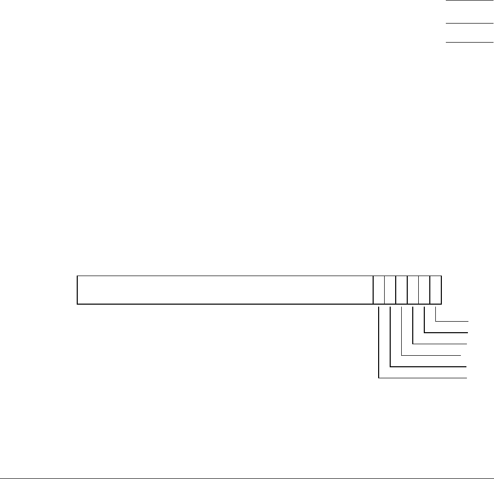
I1 Memory-Mapped System Register Descriptions
I1.3 Generic Timer registers
I1-4648 Copyright © 2013 ARM Limited. All rights reserved. ARM DDI 0487A.a
Non-Confidential - Beta ID090413
I1.3.1 CNTACR<n>, Counter-timer Access Control Registers, n = 0 - 7
The CNTACR<n> characteristics are:
Purpose
Provides top-level access controls for the elements of a timer frame. CNTACR<n> provides the
controls for frame CNTBaseN.
In addition to the CNTACR<n> control:
•CNTNSAR controls whether CNTACR<n> is accessible from Non-secure state.
• If frame CNTEL0BaseN is implemented, the CNTEL0ACR in frame CNTBaseN provides
additional control of accesses to frame CNTEL0BaseN.
This register is part of the Generic Timer registers functional group.
Usage constraints
This register is accessible as shown below:
In a system that implements both Secure and Non-secure states:
• This register is always accessible in Secure state.
•CNTNSAR.NS<n> determines whether CNTACR<n> is accessible in Non-secure state.
Configurations
Implemented only if CNTTIDR.FI<n> is RAO.
An implementation of the counters might not provide configurable access to some or all of the
features. In this case, the associated field in the CNTACR<n> register is:
• RAZ/WI if access is always denied.
• RAO/WI if access is always permitted.
Attributes
CNTACR<n> is a 32-bit register.
The CNTACR<n> bit assignments are:
Bits [31:6]
Reserved, RES0.
Default
RW
RES0
31 6 5 4 3 2 1 0
RPCT
RVCT
RFRQ
RVOFF
RWVT
RWPT

I1 Memory-Mapped System Register Descriptions
I1.3 Generic Timer registers
ARM DDI 0487A.a Copyright © 2013 ARM Limited. All rights reserved. I1-4649
ID090413 Non-Confidential - Beta
RWPT, bit [5]
Read/write access to the EL1 Physical Timer registers CNTP_CVAL, CNTP_TVAL, and
CNTP_CTL, in frame <n>. The possible values of this bit are:
0
No access to the EL1 Physical Timer registers in frame <n>. The registers are RES0.
1
Read/write access to the EL1 Physical Timer registers in frame <n>.
RWVT, bit [4]
Read/write access to the Virtual Timer register CNTV_CVAL, CNTV_TVAL, and CNTV_CTL, in
frame <n>. The possible values of this bit are:
0
No access to the Virtual Timer registers in frame <n>. The registers are RES0.
1
Read/write access to the Virtual Timer registers in frame <n>.
RVOFF, bit [3]
Read-only access to CNTVOFF, in frame <n>. The possible values of this bit are:
0
No access to CNTVOFF in frame <n>. The register is RES0.
1
Read-only access to CNTVOFF in frame <n>.
RFRQ, bit [2]
Read-only access to CNTFRQ, in frame <n>. The possible values of this bit are:
0
No access to CNTFRQ in frame <n>. The register is RES0.
1
Read-only access to CNTFRQ in frame <n>.
RVCT, bit [1]
Read-only access to CNTVCT, in frame <n>. The possible values of this bit are:
0
No access to CNTVCT in frame <n>. The register is RES0.
1
Read-only access to CNTVCT in frame <n>.
RPCT, bit [0]
Read-only access to CNTPCT, in frame <n>. The possible values of this bit are:
0
No access to CNTPCT in frame <n>. The register is RES0.
1
Read-only access to CNTPCT in frame <n>.
Accessing the CNTACR<n>:
CNTACR<n> can be accessed through the internal memory-mapped interface:
Component Frame Offset
Timer CNTCTLBase
0x040
+ 4n
I1 Memory-Mapped System Register Descriptions
I1.3 Generic Timer registers
I1-4650 Copyright © 2013 ARM Limited. All rights reserved. ARM DDI 0487A.a
Non-Confidential - Beta ID090413
I1.3.2 CNTCR, Counter Control Register
The CNTCR characteristics are:
Purpose
Enables the counter, controls the counter frequency setting, and controls counter behavior during
debug.
This register is part of the Generic Timer registers functional group.
Usage constraints
This register is accessible as shown below:
In a system that implements both Secure and Non-secure states, this register is only writable in
Secure state.
Configurations
There are no configuration notes.
Attributes
CNTCR is a 32-bit register.
The CNTCR bit assignments are:
FCREQ, bits [31:8]
Frequency change request. Indicates the number of the entry in the frequency table to select.
Selecting an unimplemented entry, or the 0 entry (base frequency) has no effect on the counter.
Resets to 0.
Bits [7:2]
Reserved, RES0.
HDBG, bit [1]
Halt-on-debug. Controls whether a Halt-on-debug signal halts the system counter:
0
System counter ignores Halt-on-debug.
1
Asserted Halt-on-debug signal halts system counter update.
Reset value is architecturally UNKNOWN.
EN, bit [0]
Enables the counter:
0
System counter disabled.
1
System counter enabled.
Resets to 0.
Default
RW
FCREQ
31 8
RES0
72
1 0
EN
HDBG

I1 Memory-Mapped System Register Descriptions
I1.3 Generic Timer registers
ARM DDI 0487A.a Copyright © 2013 ARM Limited. All rights reserved. I1-4651
ID090413 Non-Confidential - Beta
Accessing the CNTCR:
CNTCR can be accessed through the internal memory-mapped interface:
Component Frame Offset
Timer CNTControlBase
0x000

I1 Memory-Mapped System Register Descriptions
I1.3 Generic Timer registers
I1-4652 Copyright © 2013 ARM Limited. All rights reserved. ARM DDI 0487A.a
Non-Confidential - Beta ID090413
I1.3.3 CNTCV, Counter Count Value register
The CNTCV characteristics are:
Purpose
Indicates the current count value.
This register is part of the Generic Timer registers functional group.
Usage constraints
This register is accessible as shown below:
Configurations
There are no configuration notes.
Attributes
CNTCV is a 64-bit register.
The CNTCV bit assignments are:
CountValue, bits [63:0]
Indicates the counter value.
Accessing the CNTCV:
CNTCV[31:0] can be accessed through the internal memory-mapped interface:
CNTCV[63:32] can be accessed through the internal memory-mapped interface:
Default
RW in CNTControlBase, RO in CNTReadBase
CountValue
63 0
Component Frame Offset
Timer CNTControlBase
0x008
Timer CNTReadBase
0x000
Component Frame Offset
Timer CNTControlBase
0x00C
Timer CNTReadBase
0x004

I1 Memory-Mapped System Register Descriptions
I1.3 Generic Timer registers
ARM DDI 0487A.a Copyright © 2013 ARM Limited. All rights reserved. I1-4653
ID090413 Non-Confidential - Beta
I1.3.4 CNTEL0ACR, Counter-timer EL0 Access Control Register
The CNTEL0ACR characteristics are:
Purpose
An implementation of CNTEL0ACR in the frame at CNTBaseN controls whether the CNTPCT,
CNTVCT, CNTFRQ, EL1 Physical Timer, and Virtual Timer registers are visible in the frame at
CNTEL0BaseN.
This register is part of the Generic Timer registers functional group.
Usage constraints
This register is accessible as shown below:
Configurations
CNTEL0ACR is optional to implement in the external register interface.
In each implemented CNTBaseN frame, CNTEL0ACR is optional. If it is not implemented:
• Its location is RAZ/WI.
• The registers it controls are not visible in the corresponding CNTEL0BaseN frame.
Attributes
CNTEL0ACR is a 32-bit register.
The CNTEL0ACR bit assignments are:
Bits [31:10]
Reserved, RES0.
EL0PTEN, bit [9]
Second view read/write access control for the EL1 Physical Timer registers. This bit controls
whether the CNTP_CVAL, CNTP_TVAL, and CNTP_CTL registers in the current CNTBaseN
frame are also accessible in the corresponding CNTEL0BaseN frame. The possible values of this
bit are:
0
No access. Registers are RES0 in the second view.
1
Access permitted. If the registers are accessible in the current frame then they are
accessible in the second view.
Default
RW
RES0
31 10 9 8
RES0
72
1 0
EL0PCTEN
EL0VCTEN
EL0VTEN
EL0PTEN

I1 Memory-Mapped System Register Descriptions
I1.3 Generic Timer registers
I1-4654 Copyright © 2013 ARM Limited. All rights reserved. ARM DDI 0487A.a
Non-Confidential - Beta ID090413
EL0VTEN, bit [8]
Second view read/write access control for the Virtual Timer registers. This bit controls whether the
CNTV_CVAL, CNTV_TVAL, and CNTV_CTL registers in the current CNTBaseN frame are also
accessible in the corresponding CNTEL0BaseN frame. The possible values of this bit are:
0
No access. Registers are RES0 in the second view.
1
Access permitted. If the registers are accessible in the current frame then they are
accessible in the second view.
The definition of this bit means that, if the Virtual Timer registers are not implemented in the current
CNTBaseN frame, then the Virtual Timer register addresses are RES0 in the corresponding
CNTEL0BaseN frame, regardless of the value of this bit.
Bits [7:2]
Reserved, RES0.
EL0VCTEN, bit [1]
Second view read access control for CNTVCT and CNTFRQ. The possible values of this bit are:
0
CNTVCT is not visible in the second view.
If EL0PCTEN is set to 0, CNTFRQ is not visible in the second view.
1
Access permitted. If CNTVCT and CNTFRQ are visible in the current frame then they
are visible in the second view.
EL0PCTEN, bit [0]
Second view read access control for CNTPCT and CNTFRQ. The possible values of this bit are:
0
CNTPCT is not visible in the second view.
If EL0VCTEN is set to 0, CNTFRQ is not visible in the second view.
1
Access permitted. If CNTPCT and CNTFRQ are visible in the current frame then they
are visible in the second view.
Accessing the CNTEL0ACR:
CNTEL0ACR can be accessed through the internal memory-mapped interface:
Component Frame Offset
Timer CNTBaseN
0x014

I1 Memory-Mapped System Register Descriptions
I1.3 Generic Timer registers
ARM DDI 0487A.a Copyright © 2013 ARM Limited. All rights reserved. I1-4655
ID090413 Non-Confidential - Beta
I1.3.5 CNTFID0, Counter Frequency ID
The CNTFID0 characteristics are:
Purpose
Indicates the base frequency of the system counter.
This register is part of the Generic Timer registers functional group.
Usage constraints
This register is accessible as shown below:
Configurations
The possible frequencies for the system counter are stored as 32-bit words starting with the base
frequency, CNTFID0.
A 32-bit word of zero value after the final frequency mode entry marks the end of the frequency
modes table.
Typically, the frequency modes table will be in read-only memory. However, a system
implementation might use read/write memory for the table, and initialise the table entries as part of
its start-up sequence.
If the frequency modes table is in read/write memory, ARM strongly recommends that the
frequency modes table is not updated once the system is running.
Attributes
CNTFID0 is a 32-bit register.
The CNTFID0 bit assignments are:
Frequency, bits [31:0]
The base frequency of the system counter, in Hz.
Accessing the CNTFID0:
CNTFID0 can be accessed through the internal memory-mapped interface:
Default
RO or RW
Frequency
31 0
Component Frame Offset
Timer CNTControlBase
0x020

I1 Memory-Mapped System Register Descriptions
I1.3 Generic Timer registers
I1-4656 Copyright © 2013 ARM Limited. All rights reserved. ARM DDI 0487A.a
Non-Confidential - Beta ID090413
I1.3.6 CNTFID<n>, Counter Frequency IDs, n = 1 - 23
The CNTFID<n> characteristics are:
Purpose
Indicates alternative system counter update frequencies.
This register is part of the Generic Timer registers functional group.
Usage constraints
This register is accessible as shown below:
Configurations
CNTFID<n> is optional to implement in the external register interface.
The possible frequencies for the system counter are stored as 32-bit words starting with the base
frequency, CNTFID0.
A 32-bit word of zero value after the final frequency mode entry marks the end of the frequency
modes table. The only required entry in the table is the entry for CNTFID0.
Typically, the frequency modes table will be in read-only memory. However, a system
implementation might use read/write memory for the table, and initialise the table entries as part of
its start-up sequence.
If the frequency modes table is in read/write memory, ARM strongly recommends that the
frequency modes table is not updated once the system is running.
Attributes
CNTFID<n> is a 32-bit register.
The CNTFID<n> bit assignments are:
Frequency, bits [31:0]
A system counter update frequency, in Hz. Must be an exact divisor of the base frequency. ARM
strongly recommends that all frequency values in the table are integer power-of-two divisors of the
base frequency.
When the system timer is operating at a lower frequency than the base frequency, the increment
applied at each counter update is given by:
increment = (base frequency) / selected frequency)
Accessing the CNTFID<n>:
CNTFID<n> can be accessed through the internal memory-mapped interface:
Default
RO or RW
Frequency
31 0
Component Frame Offset
Timer CNTControlBase
0x020
+ 4n

I1 Memory-Mapped System Register Descriptions
I1.3 Generic Timer registers
ARM DDI 0487A.a Copyright © 2013 ARM Limited. All rights reserved. I1-4657
ID090413 Non-Confidential - Beta
I1.3.7 CNTFRQ, Counter-timer Frequency
The CNTFRQ characteristics are:
Purpose
Holds the clock frequency of the system counter.
This register is part of the Generic Timer registers functional group.
Usage constraints
This register is accessible as shown below:
In a system that implements both Secure and Non-secure states, this register is only accessible in
Secure state.
Configurations
CNTFRQ is architecturally mapped to AArch64 register CNTFRQ_EL0.
CNTFRQ is architecturally mapped to AArch32 register CNTFRQ.
Attributes
CNTFRQ is a 32-bit register.
The CNTFRQ bit assignments are:
Bits [31:0]
Clock frequency. Indicates the system counter clock frequency, in Hz.
Accessing the CNTFRQ:
CNTFRQ can be accessed through the internal memory-mapped interface:
Default
RO
Clock frequency
31 0
Component Frame Offset
Timer CNTBaseN
0x010
Timer CNTEL0BaseN
0x010
Timer CNTCTLBase
0x000
I1 Memory-Mapped System Register Descriptions
I1.3 Generic Timer registers
I1-4658 Copyright © 2013 ARM Limited. All rights reserved. ARM DDI 0487A.a
Non-Confidential - Beta ID090413
I1.3.8 CNTNSAR, Counter-timer Non-secure Access Register
The CNTNSAR characteristics are:
Purpose
Provides the highest-level control of whether frames CNTBaseN and CNTEL0BaseN are accessible
by Non-secure accesses.
This register is part of the Generic Timer registers functional group.
Usage constraints
This register is accessible as shown below:
In a system that implements both Secure and Non-secure states, this register is only accessible in
Secure state.
Configurations
There are no configuration notes.
Attributes
CNTNSAR is a 32-bit register.
The CNTNSAR bit assignments are:
Bits [31:8]
Reserved, RES0.
NS<n>, bit [n], for n = 0 to 7
Non-secure access to frame n. The possible values of this bit are:
0
Secure access only. Behaves as RES0 to Non-secure accesses.
1
Secure and Non-secure accesses permitted.
If frame CNTBase<n>:
• Is not implemented, then NS<n> is RES0.
• Is not Configurable access, and is accessible only by Secure accesses, then NS<n> is RES0.
• Is not Configurable access, and is accessible only by Non-secure accesses, then NS<n> is
RES1.
Default
RW
RES0
31 8 7 6 5 4 3 2 1 0
NS0
NS1
NS2
NS3
NS4
NS5
NS6
NS7

I1 Memory-Mapped System Register Descriptions
I1.3 Generic Timer registers
ARM DDI 0487A.a Copyright © 2013 ARM Limited. All rights reserved. I1-4659
ID090413 Non-Confidential - Beta
Accessing the CNTNSAR:
CNTNSAR can be accessed through the internal memory-mapped interface:
Component Frame Offset
Timer CNTCTLBase
0x004

I1 Memory-Mapped System Register Descriptions
I1.3 Generic Timer registers
I1-4660 Copyright © 2013 ARM Limited. All rights reserved. ARM DDI 0487A.a
Non-Confidential - Beta ID090413
I1.3.9 CNTP_CTL, Counter-timer Physical Timer Control
The CNTP_CTL characteristics are:
Purpose
Control register for the physical timer.
This register is part of the Generic Timer registers functional group.
Usage constraints
This register is accessible as shown below:
CNTACR<n>.RWPT enables access to this register in frame <n>.
Configurations
CNTP_CTL is architecturally mapped to AArch64 register CNTP_CTL_EL0.
CNTP_CTL is architecturally mapped to AArch32 register CNTP_CTL.
Attributes
CNTP_CTL is a 32-bit register.
The CNTP_CTL bit assignments are:
Bits [31:3]
Reserved, RES0.
ISTATUS, bit [2]
The status of the timer interrupt:
0
Interrupt not asserted.
1
Interrupt asserted.
This bit is read-only.
A register write that sets IMASK to 1 latches this bit to reflect the status of the interrupt immediately
before that write.
IMASK, bit [1]
Timer interrupt mask bit. Permitted values are:
0
Timer interrupt is not masked.
1
Timer interrupt is masked.
Default
RW
RES0
31 3 2 1 0
ENABLE
IMASK
ISTATUS

I1 Memory-Mapped System Register Descriptions
I1.3 Generic Timer registers
ARM DDI 0487A.a Copyright © 2013 ARM Limited. All rights reserved. I1-4661
ID090413 Non-Confidential - Beta
ENABLE, bit [0]
Enables the timer. Permitted values are:
0
Timer disabled.
1
Timer enabled.
Disabling the timer masks the timer interrupt, but the timer value continues to count down.
Accessing the CNTP_CTL:
CNTP_CTL can be accessed through the internal memory-mapped interface:
Component Frame Offset
Timer CNTBaseN
0x02C
Timer CNTEL0BaseN
0x02C

I1 Memory-Mapped System Register Descriptions
I1.3 Generic Timer registers
I1-4662 Copyright © 2013 ARM Limited. All rights reserved. ARM DDI 0487A.a
Non-Confidential - Beta ID090413
I1.3.10 CNTP_CVAL, Counter-timer Physical Timer CompareValue
The CNTP_CVAL characteristics are:
Purpose
Holds the 64-bit compare value for the EL1 physical timer.
This register is part of the Generic Timer registers functional group.
Usage constraints
This register is accessible as shown below:
CNTACR<n>.RWPT enables access to this register in frame <n>.
If the implementation supports 64-bit atomic accesses, then the CNTP_CVAL register must be
accessible as an atomic 64-bit value.
Configurations
CNTP_CVAL is architecturally mapped to AArch64 register CNTP_CVAL_EL0.
CNTP_CVAL is architecturally mapped to AArch32 register CNTP_CVAL.
Attributes
CNTP_CVAL is a 64-bit register.
The CNTP_CVAL bit assignments are:
Bits [63:0]
EL1 physical timer compare value.
Accessing the CNTP_CVAL:
CNTP_CVAL[31:0] can be accessed through the internal memory-mapped interface:
CNTP_CVAL[63:32] can be accessed through the internal memory-mapped interface:
Default
RW
EL1 physical timer compare value
63 0
Component Frame Offset
Timer CNTBaseN
0x020
Timer CNTEL0BaseN
0x020
Component Frame Offset
Timer CNTBaseN
0x024
Timer CNTEL0BaseN
0x024

I1 Memory-Mapped System Register Descriptions
I1.3 Generic Timer registers
ARM DDI 0487A.a Copyright © 2013 ARM Limited. All rights reserved. I1-4663
ID090413 Non-Confidential - Beta
I1.3.11 CNTP_TVAL, Counter-timer Physical Timer TimerValue
The CNTP_TVAL characteristics are:
Purpose
Holds the timer value for the EL1 physical timer. This provides a 32-bit downcounter.
This register is part of the Generic Timer registers functional group.
Usage constraints
This register is accessible as shown below:
CNTACR<n>.RWPT enables access to this register in frame <n>.
Configurations
CNTP_TVAL is architecturally mapped to AArch64 register CNTP_TVAL_EL0.
CNTP_TVAL is architecturally mapped to AArch32 register CNTP_TVAL.
Attributes
CNTP_TVAL is a 32-bit register.
The CNTP_TVAL bit assignments are:
Bits [31:0]
EL1 physical timer value.
Accessing the CNTP_TVAL:
CNTP_TVAL can be accessed through the internal memory-mapped interface:
Default
RW
EL1 physical timer value
31 0
Component Frame Offset
Timer CNTBaseN
0x028
Timer CNTEL0BaseN
0x028

I1 Memory-Mapped System Register Descriptions
I1.3 Generic Timer registers
I1-4664 Copyright © 2013 ARM Limited. All rights reserved. ARM DDI 0487A.a
Non-Confidential - Beta ID090413
I1.3.12 CNTPCT, Counter-timer Physical Count
The CNTPCT characteristics are:
Purpose
Holds the 64-bit physical count value.
This register is part of the Generic Timer registers functional group.
Usage constraints
This register is accessible as shown below:
CNTACR<n>.RPCT enables access to this register in frame <n>.
If the implementation supports 64-bit atomic accesses, then the CNTPCT register must be
accessible as an atomic 64-bit value.
Configurations
CNTPCT is architecturally mapped to AArch64 register CNTPCT_EL0.
CNTPCT is architecturally mapped to AArch32 register CNTPCT.
Attributes
CNTPCT is a 64-bit register.
The CNTPCT bit assignments are:
Bits [63:0]
Physical count value.
Accessing the CNTPCT:
CNTPCT[31:0] can be accessed through the internal memory-mapped interface:
CNTPCT[63:32] can be accessed through the internal memory-mapped interface:
Default
RO
Physical count value
63 0
Component Frame Offset
Timer CNTBaseN
0x000
Timer CNTEL0BaseN
0x000
Component Frame Offset
Timer CNTBaseN
0x004
Timer CNTEL0BaseN
0x004

I1 Memory-Mapped System Register Descriptions
I1.3 Generic Timer registers
ARM DDI 0487A.a Copyright © 2013 ARM Limited. All rights reserved. I1-4665
ID090413 Non-Confidential - Beta
I1.3.13 CNTSR, Counter Status Register
The CNTSR characteristics are:
Purpose
Provides counter frequency status information.
This register is part of the Generic Timer registers functional group.
Usage constraints
This register is accessible as shown below:
Configurations
There are no configuration notes.
Attributes
CNTSR is a 32-bit register.
The CNTSR bit assignments are:
FCACK, bits [31:8]
Frequency change acknowledge. Indicates the currently selected entry in the frequency table.
Selecting an unimplemented entry, or the 0 entry (base frequency) has no effect on the counter.
Resets to 0.
Bits [7:2]
Reserved, RES0.
DBGH, bit [1]
Indicates whether the counter is halted because the Halt-on-Debug signal is asserted:
0
Counter is not halted.
1
Counter is halted.
Reset value is architecturally UNKNOWN.
Bit [0]
Reserved, RES0.
Default
RO
FCACK
31 8
RES0
72
1 0
RES0
DBGH

I1 Memory-Mapped System Register Descriptions
I1.3 Generic Timer registers
I1-4666 Copyright © 2013 ARM Limited. All rights reserved. ARM DDI 0487A.a
Non-Confidential - Beta ID090413
Accessing the CNTSR:
CNTSR can be accessed through the internal memory-mapped interface:
Component Frame Offset
Timer CNTControlBase
0x004

I1 Memory-Mapped System Register Descriptions
I1.3 Generic Timer registers
ARM DDI 0487A.a Copyright © 2013 ARM Limited. All rights reserved. I1-4667
ID090413 Non-Confidential - Beta
I1.3.14 CNTTIDR, Counter-timer Timer ID Register
The CNTTIDR characteristics are:
Purpose
Indicates the implemented timers in the memory map, and their features. For each value of N from
0 to 7 it indicates whether:
• Frame CNTBaseN is a view of an implemented timer.
• Frame CNTBaseN has a second view, CNTEL0BaseN.
• Frame CNTBaseN has a virtual timer capability.
This register is part of the Generic Timer registers functional group.
Usage constraints
This register is accessible as shown below:
Configurations
There are no configuration notes.
Attributes
CNTTIDR is a 32-bit register.
The CNTTIDR bit assignments are:
Frame<n>, bits [4n+3:4n], for n = 0 to 7
A 4-bit field indicating the features of frame CNTBase<n>.
Bit[3] of the field is RES0.
Bit[2] indicates whether frame CNTBase<n> has a second view, CNTEL0Base<n>. The possible
values of this bit are:
If bit[0] is 0, bit[2] is RES0.
Bit[1] indicates whether both:
• Frame CNTBase<n> implements the virtual timer registers CNTV_CVAL, CNTV_TVAL,
and CNTV_CTL.
• This CNTCTLBase frame implements the virtual timer offset register CNTVOFF<n>.
Default
RO
Frame7
31 28
Frame6
27 24
Frame5
23 20
Frame4
19 16
Frame3
15 12
Frame2
11 8
Frame1
74
Frame0
30
Bit[2] Meaning
0 Frame <n> does not have a second view. CNTEL0Base<n> is RES0.
1 Frame <n> has a second view, CNTEL0Base<n>.

I1 Memory-Mapped System Register Descriptions
I1.3 Generic Timer registers
I1-4668 Copyright © 2013 ARM Limited. All rights reserved. ARM DDI 0487A.a
Non-Confidential - Beta ID090413
The possible values of bit[1] are:
If bit[0] is 0, bit[1] is RES0.
Bit[0] indicates whether frame <n> is implemented. The possible values of this bit are:
Accessing the CNTTIDR:
CNTTIDR can be accessed through the internal memory-mapped interface:
Bit[1] Meaning
0 Frame <n> does not have virtual capability. The virtual time and offset registers are RES0.
1 Frame <n> has virtual capability. The virtual time and offset registers are implemented.
Bit[0] Meaning
0 Frame <n> not implemented. All registers associated with the frame are RES0.
1 Frame <n> is implemented.
Component Frame Offset
Timer CNTCTLBase
0x008

I1 Memory-Mapped System Register Descriptions
I1.3 Generic Timer registers
ARM DDI 0487A.a Copyright © 2013 ARM Limited. All rights reserved. I1-4669
ID090413 Non-Confidential - Beta
I1.3.15 CNTV_CTL, Counter-timer Virtual Timer Control
The CNTV_CTL characteristics are:
Purpose
Control register for the virtual timer.
This register is part of the Generic Timer registers functional group.
Usage constraints
This register is accessible as shown below:
Bit [1] of CNTTIDR.Frame<n> indicates whether CNTV_CTL is implemented for frame <n>.
If CNTV_CTL is implemented, CNTACR<n>.RWVT enables access to the register in frame <n>.
If CNTV_CTL is not implemented, the register location is RAZ/WI.
Configurations
CNTV_CTL is architecturally mapped to AArch64 register CNTV_CTL_EL0.
CNTV_CTL is architecturally mapped to AArch32 register CNTV_CTL.
CNTV_CTL is optional to implement in the external register interface.
Attributes
CNTV_CTL is a 32-bit register.
The CNTV_CTL bit assignments are:
Bits [31:3]
Reserved, RES0.
ISTATUS, bit [2]
The status of the timer interrupt:
0
Interrupt not asserted.
1
Interrupt asserted.
This bit is read-only.
A register write that sets IMASK to 1 latches this bit to reflect the status of the interrupt immediately
before that write.
IMASK, bit [1]
Timer interrupt mask bit. Permitted values are:
0
Timer interrupt is not masked.
1
Timer interrupt is masked.
Default
RW
RES0
31 3 2 1 0
ENABLE
IMASK
ISTATUS

I1 Memory-Mapped System Register Descriptions
I1.3 Generic Timer registers
I1-4670 Copyright © 2013 ARM Limited. All rights reserved. ARM DDI 0487A.a
Non-Confidential - Beta ID090413
ENABLE, bit [0]
Enables the timer. Permitted values are:
0
Timer disabled.
1
Timer enabled.
Disabling the timer masks the timer interrupt, but the timer value continues to count down.
Accessing the CNTV_CTL:
CNTV_CTL can be accessed through the internal memory-mapped interface:
Component Frame Offset
Timer CNTBaseN
0x03C
Timer CNTEL0BaseN
0x03C

I1 Memory-Mapped System Register Descriptions
I1.3 Generic Timer registers
ARM DDI 0487A.a Copyright © 2013 ARM Limited. All rights reserved. I1-4671
ID090413 Non-Confidential - Beta
I1.3.16 CNTV_CVAL, Counter-timer Virtual Timer CompareValue
The CNTV_CVAL characteristics are:
Purpose
Holds the 64-bit compare value for the virtual timer.
This register is part of the Generic Timer registers functional group.
Usage constraints
This register is accessible as shown below:
Bit [1] of CNTTIDR.Frame<n> indicates whether CNTV_CVAL is implemented for frame <n>.
If CNTV_CVAL is implemented, CNTACR<n>.RWVT enables access to the register in frame <n>.
If CNTV_CVAL is not implemented, the register location is RAZ/WI.
If the implementation supports 64-bit atomic accesses, then the CNTV_CVAL register must be
accessible as an atomic 64-bit value.
Configurations
CNTV_CVAL is architecturally mapped to AArch64 register CNTV_CVAL_EL0.
CNTV_CVAL is architecturally mapped to AArch32 register CNTV_CVAL.
CNTV_CVAL is optional to implement in the external register interface.
Attributes
CNTV_CVAL is a 64-bit register.
The CNTV_CVAL bit assignments are:
Bits [63:0]
Virtual timer compare value.
Accessing the CNTV_CVAL:
CNTV_CVAL[31:0] can be accessed through the internal memory-mapped interface:
Default
RW
Virtual timer compare value
63 0
Component Frame Offset
Timer CNTBaseN
0x030
Timer CNTEL0BaseN
0x030

I1 Memory-Mapped System Register Descriptions
I1.3 Generic Timer registers
I1-4672 Copyright © 2013 ARM Limited. All rights reserved. ARM DDI 0487A.a
Non-Confidential - Beta ID090413
CNTV_CVAL[63:32] can be accessed through the internal memory-mapped interface:
Component Frame Offset
Timer CNTBaseN
0x034
Timer CNTEL0BaseN
0x034

I1 Memory-Mapped System Register Descriptions
I1.3 Generic Timer registers
ARM DDI 0487A.a Copyright © 2013 ARM Limited. All rights reserved. I1-4673
ID090413 Non-Confidential - Beta
I1.3.17 CNTV_TVAL, Counter-timer Virtual Timer TimerValue
The CNTV_TVAL characteristics are:
Purpose
Holds the timer value for the virtual timer.
This register is part of the Generic Timer registers functional group.
Usage constraints
This register is accessible as shown below:
Bit [1] of CNTTIDR.Frame<n> indicates whether CNTV_TVAL is implemented for frame <n>.
If CNTV_TVAL is implemented, CNTACR<n>.RWVT enables access to the register in frame <n>.
If CNTV_TVAL is not implemented, the register location is RAZ/WI.
Configurations
CNTV_TVAL is architecturally mapped to AArch64 register CNTV_TVAL_EL0.
CNTV_TVAL is architecturally mapped to AArch32 register CNTV_TVAL.
CNTV_TVAL is optional to implement in the external register interface.
Attributes
CNTV_TVAL is a 32-bit register.
The CNTV_TVAL bit assignments are:
Bits [31:0]
Virtual timer value.
Accessing the CNTV_TVAL:
CNTV_TVAL can be accessed through the internal memory-mapped interface:
Default
RW
Virtual timer value
31 0
Component Frame Offset
Timer CNTBaseN
0x038
Timer CNTEL0BaseN
0x038

I1 Memory-Mapped System Register Descriptions
I1.3 Generic Timer registers
I1-4674 Copyright © 2013 ARM Limited. All rights reserved. ARM DDI 0487A.a
Non-Confidential - Beta ID090413
I1.3.18 CNTVCT, Counter-timer Virtual Count
The CNTVCT characteristics are:
Purpose
Holds the 64-bit virtual count value.
This register is part of the Generic Timer registers functional group.
Usage constraints
This register is accessible as shown below:
CNTACR<n>.RVCT enables access to this register in frame <n>.
If the implementation supports 64-bit atomic accesses, then the CNTPCT register must be
accessible as an atomic 64-bit value.
Configurations
CNTVCT is architecturally mapped to AArch64 register CNTVCT_EL0.
CNTVCT is architecturally mapped to AArch32 register CNTVCT.
Attributes
CNTVCT is a 64-bit register.
The CNTVCT bit assignments are:
Bits [63:0]
Virtual count value.
Accessing the CNTVCT:
CNTVCT[31:0] can be accessed through the internal memory-mapped interface:
CNTVCT[63:32] can be accessed through the internal memory-mapped interface:
Default
RO
Virtual count value
63 0
Component Frame Offset
Timer CNTBaseN
0x008
Timer CNTEL0BaseN
0x008
Component Frame Offset
Timer CNTBaseN
0x00C
Timer CNTEL0BaseN
0x00C

I1 Memory-Mapped System Register Descriptions
I1.3 Generic Timer registers
ARM DDI 0487A.a Copyright © 2013 ARM Limited. All rights reserved. I1-4675
ID090413 Non-Confidential - Beta
I1.3.19 CNTVOFF, Counter-timer Virtual Offset
The CNTVOFF characteristics are:
Purpose
Holds the 64-bit virtual offset.
This register is part of the Generic Timer registers functional group.
Usage constraints
This register is accessible as shown below:
If the implementation supports 64-bit atomic accesses, then the CNTVOFF register must be
accessible as an atomic 64-bit value.
Configurations
CNTVOFF is architecturally mapped to AArch64 register CNTVOFF_EL2.
CNTVOFF is architecturally mapped to AArch32 register CNTVOFF.
CNTACR<n>.RVOFF enables access to this register for frame CNTBase<n>.
Attributes
CNTVOFF is a 64-bit register.
The CNTVOFF bit assignments are:
Bits [63:0]
Virtual offset.
Accessing the CNTVOFF:
CNTVOFF[31:0] can be accessed through the internal memory-mapped interface:
CNTVOFF[63:32] can be accessed through the internal memory-mapped interface:
Default
RO
Virtual offset
63 0
Component Frame Offset
Timer CNTBaseN
0x018
Component Frame Offset
Timer CNTBaseN
0x01C

I1 Memory-Mapped System Register Descriptions
I1.3 Generic Timer registers
I1-4676 Copyright © 2013 ARM Limited. All rights reserved. ARM DDI 0487A.a
Non-Confidential - Beta ID090413
I1.3.20 CNTVOFF<n>, Counter-timer Virtual Offsets, n = 0 - 7
The CNTVOFF<n> characteristics are:
Purpose
Holds the 64-bit virtual offset for frame CNTBase<n>.
This register is part of the Generic Timer registers functional group.
Usage constraints
This register is accessible as shown below:
If the implementation supports 64-bit atomic accesses, then the CNTVOFF<n> registers must be
accessible as atomic 64-bit values.
Configurations
CNTVOFF<n> is architecturally mapped to AArch64 register CNTVOFF_EL2.
CNTVOFF<n> is architecturally mapped to AArch32 register CNTVOFF.
CNTVOFF<n> is optional to implement in the external register interface.
CNTVOFF<n> is accessible in the CNTCTLBase register map if CNTACR<n>.RVOFF is 1 and bit
[1] of CNTTIDR.Frame<n> is 1.
If bit [1] of CNTTIDR.Frame<n> is 0, or CNTACR<n>.RVOFF is 1, CNTVOFF<n> is RAZ/WI.
Attributes
CNTVOFF<n> is a 64-bit register.
The CNTVOFF<n> bit assignments are:
Bits [63:0]
Virtual offset.
Accessing the CNTVOFF<n>:
CNTVOFF<n>[31:0] can be accessed through the internal memory-mapped interface:
CNTVOFF<n>[63:32] can be accessed through the internal memory-mapped interface:
Default
RW
Virtual offset
63 0
Component Frame Offset
Timer CNTCTLBase
0x080
+ 8n
Component Frame Offset
Timer CNTCTLBase
0x084
+ 8n

I1 Memory-Mapped System Register Descriptions
I1.3 Generic Timer registers
ARM DDI 0487A.a Copyright © 2013 ARM Limited. All rights reserved. I1-4677
ID090413 Non-Confidential - Beta
I1.3.21 CounterID<n>, Counter ID registers, n = 0 - 11
The CounterID<n> characteristics are:
Purpose
IMPLEMENTATION DEFINED identification registers 0 to 11 for the memory-mapped Generic Timer.
This register is part of the Generic Timer registers functional group.
Usage constraints
This register is accessible as shown below:
Configurations
These registers are implemented independently in each of the frames accessed through the different
memory maps.
If the implementation of the Counter ID registers requires an architecture version, the value for this
version of the ARM Generic Timer is version 0.
The Counter ID registers can be implemented as a set of CoreSight ID registers, comprising
Peripheral ID Registers and Component ID Registers. An implementation of these registers for the
Generic Timer must use a Component class value of
0xF
.
Attributes
CounterID<n> is a 32-bit register.
The CounterID<n> bit assignments are:
Accessing the CounterID<n>:
CounterID<n> can be accessed through the internal memory-mapped interface:
Default
RO
IMPLEMENTATION DEFINED
31 0
Component Frame Offset
Timer CNTControlBase
0xFD0
+ 4n
Timer CNTReadBase
0xFD0
+ 4n
Timer CNTBaseN
0xFD0
+ 4n
Timer CNTEL0BaseN
0xFD0
+ 4n
Timer CNTCTLBase
0xFD0
+ 4n

I1 Memory-Mapped System Register Descriptions
I1.3 Generic Timer registers
I1-4678 Copyright © 2013 ARM Limited. All rights reserved. ARM DDI 0487A.a
Non-Confidential - Beta ID090413

ARM DDI 0487A.a Copyright © 2013 ARM Limited. All rights reserved. I2-4679
ID090413 Non-Confidential - Beta
Chapter I2
System Level Implementation of the Generic Timer
This chapter defines the system level implementation of the optional Generic Timer. It contains the following
sections:
•About the Generic Timer specification on page I2-4680.
•Memory-mapped counter module on page I2-4681.
•Counter module control and status register summary on page I2-4684.
•About the memory-mapped view of the counter and timer on page I2-4686.
•The CNTBaseN and CNTPL0BaseN frames on page I2-4687.
•The CNTCTLBase frame on page I2-4689.
•Providing a complete set of counter and timer features on page I2-4690.
•Gray-count scheme for timer distribution scheme on page I2-4692.
Note
• Generic Timer registers on page I1-4647 describes the System level Generic Timer registers. These registers
are memory-mapped.
•Chapter D7 The Generic Timer gives a general description of the Generic Timer, and describes the system
control register interface to the Generic Timer.

I2 System Level Implementation of the Generic Timer
I2.1 About the Generic Timer specification
I2-4680 Copyright © 2013 ARM Limited. All rights reserved. ARM DDI 0487A.a
Non-Confidential - Beta ID090413
I2.1 About the Generic Timer specification
Chapter D7 The Generic Timer describes the ARM Generic Timer, and its implementation as an optional extension
to an ARMv8 processor implementation. Chapter D7 includes the definition of the low-latency System register
interface to the Generic Timer Extension. However, the ARM Generic Timer architecture requires the
implementation of some parts of the timer at the system level. This system level implementation includes a
memory-mapped interface to the timer that:
• Provides some top-level management of the Generic Timer, that is not available from the System register
interface from any PE in the system.
• Provides memory-mapped access to Generic Timer features, for system components that cannot implement
a System register interface to the timer. The latency of this memory-mapped access can be significantly
higher than the latency of System register accesses.
The Generic Timer architecture defines both a counter and a timer. The counter and timer work in combination, but
each has a distinct purpose:
• The counter counts the passing of time.
• The timer schedules the triggering of events.
See About the Generic Timer on page D7-1856 for more information about the timer and the counter. Generic Timer
example on page D7-1856 shows a system-wide implementation of the Generic Timer.
Most of this chapter describes the system level implementation of the Generic Timer. Gray-count scheme for timer
distribution scheme on page I2-4692 describes a possible scheme for distributing the counter value across this
system.
I2.1.1 The memory-mapped view of the Generic Timer
The memory-mapped view of the Generic Timer provides:
• Access to the system level features of the Generic Timer:
—Memory-mapped counter module on page I2-4681 describes these features.
—Counter module control and status register summary on page I2-4684 describes the memory-mapped
interface to those features.
• Memory-mapped access to the Generic Timer features defined in Chapter D7 The Generic Timer. This
provides memory-mapped access to different views of the system control registers described in that chapter.
About the memory-mapped view of the counter and timer on page I2-4686 describes this access.

I2 System Level Implementation of the Generic Timer
I2.2 Memory-mapped counter module
ARM DDI 0487A.a Copyright © 2013 ARM Limited. All rights reserved. I2-4681
ID090413 Non-Confidential - Beta
I2.2 Memory-mapped counter module
The memory-mapped counter module provides top-level control of the system counter. It provides:
• A RW control register CNTCR, that provides:
— An enable bit for the system counter.
— An enable bit for Halt-on-Debug. When this is enabled, if the debug halt signal into the system counter
is asserted, it halts the system counter. Otherwise, the system counter ignores the state of this halt
signal. For more information about Halt-on-Debug, contact ARM.
— A field that can be written to request a change to the update frequency of the system counter, with a
corresponding change to the increment made at each update. For more information see Control of
counter operating frequency and increment on page I2-4682.
Writes to this register are rare. In a system that uses security, this register is writable only by Secure writes.
• A RO status register, CNTSR, that provides:
— A bit that indicates whether the system counter is halted because of an asserted Halt-on-Debug signal.
— A field that indicates the current update frequency of the system counter. This field can be polled to
determine when a requested change to the update frequency has been made.
• Two contiguous RW registers that hold the current system counter value, CNTCV. If the system supports
64-bit atomic accesses, these two registers must be accessible by such accesses.
The system counter must be disabled before writing to these registers, otherwise the effect of the write is
UNPREDICTABLE.
Writes to these registers are rare. In a system that uses security, these registers are writable only by Secure
writes.
• A table of one or more 32-bit entries, where:
— The first entry defines the base frequency of the system counter. This is the maximum frequency at
which the counter updates.
— Each subsequent entry defines an alternative frequency of the system counter, and must be an exact
divisor of the base frequency.
A 32-bit zero entry immediately follows the last table entry.
This table can be WO or RW. For more information, see The frequency modes table on page I2-4682.
• Two contiguous RO registers that hold the current system counter value, CNTCV. If the system supports
64-bit atomic accesses, these two registers must be accessible by such accesses.
These registers are located in two memory frames, identified by different base addresses:
• The locations of the RO copies of CNTCV are defined relative to the CNTReadBase base address.
• The locations of all the other registers are defined relative to the CNTControlBase base address.
Note
The final twelve words of the first or only 4KB block of a register memory frame is an ID block.
Counter module control and status register summary on page I2-4684 describes CNTReadBase and
CNTControlBase memory maps, and the registers in each frame.

I2 System Level Implementation of the Generic Timer
I2.2 Memory-mapped counter module
I2-4682 Copyright © 2013 ARM Limited. All rights reserved. ARM DDI 0487A.a
Non-Confidential - Beta ID090413
I2.2.1 Control of counter operating frequency and increment
The system counter has a fixed base frequency, and must maintain the required counter accuracy, meaning ARM
recommends that it does not gain or lose more than ten seconds in a 24-hour period, see System counter on
page D7-1857. However, the counter can increment at a lower frequency than the base frequency, using a
correspondingly larger increment. For example, it can increment by four at a quarter of the base frequency. Any
lower-frequency operation, and any switching between operating frequencies, must not reduce the accuracy of the
counter.
Control of the system counter frequency and increment is provided only through the memory-mapped counter
module. The following sections describe this control:
•The frequency modes table
•Changing the system counter and increment.
The frequency modes table
The frequency modes table starts at offset
0x20
from CNTControlBase.
Table entries are 32-bits, and each entry specifies a system counter update frequency, in Hz.
The first entry in the table specifies the base frequency of the system counter.
To ensure overall counter accuracy is maintained, any subsequent entries in the table must be exact divisors of the
base frequency. That is, ARM strongly recommends that all frequency values in the table are integer power-of-two
divisors of the base frequency.
When the system timer is operating at a lower frequency than the base frequency, the increment applied at each
counter update is given by:
increment = (base_frequency) / (selected_frequency)
A 32-bit word of zero value marks the end of the table. That is, the word of memory immediately after the last entry
in the table must be zero.
The only required entry in the table is the entry for the base frequency.
Typically, the frequency modes table are in RO memory. However, a system implementation might use RW memory
for the table, and initialize the table entries as part of its startup sequence. Therefore, the CNTControlBase memory
map shows the table region as RO or RW.
ARM strongly recommends that the frequency modes table is not updated once the system is running.
The architecture can support up to 1004 entries in the frequency modes table, and the maximum number of entries
is IMPLEMENTATION DEFINED, up to this limit.
Note
ARM considers it unlikely that implementations will require significantly fewer entries than the architectural limit.
Changing the system counter and increment
The CNTCR.FREQ field defines which frequency modes table entry specifies the system counter update frequency.
The value in the FCREQ specifies the entry.
Changing the value of CNTCR.FREQ requests a change to the system counter update frequency. To ensure the
frequency change does not affect the overall accuracy of the counter, it is made as follows:
• When changing from a higher frequency to a lower frequency, the counter:
1. Continues running at the higher frequency until the count reaches an integer multiple of the required
lower frequency.
2. Switches to operating at the lower frequency.
• When changing from a lower frequency to a higher frequency, the counter:
1. Waits until the end of the current lower-frequency cycle.

I2 System Level Implementation of the Generic Timer
I2.2 Memory-mapped counter module
ARM DDI 0487A.a Copyright © 2013 ARM Limited. All rights reserved. I2-4683
ID090413 Non-Confidential - Beta
2. Makes the counter increment required for operation at that lower frequency.
3. Switches to operating at the higher frequency.
When the frequency has changed, CNTSR is updated to indicate the new frequency. Therefore, a system component
that is waiting for a frequency change can poll CNTSR to detect the change.

I2 System Level Implementation of the Generic Timer
I2.3 Counter module control and status register summary
I2-4684 Copyright © 2013 ARM Limited. All rights reserved. ARM DDI 0487A.a
Non-Confidential - Beta ID090413
I2.3 Counter module control and status register summary
The Counter module control and status registers are memory-mapped registers in the following register memory
frames:
• A control frame, with base address CNTControlBase.
• A status frame, with base address CNTReadBase.
Each of these register memory frames is at least 4KB in size, or is at least the size of the memory protection granule
if this granule size is larger than 4KB. Similarly, each base address must be aligned to 4KB, or to the memory
protection granule if that is larger than 4KB.
Note
The memory protection granule is either 4KB or 64KB.
In each register memory frame, the memory at offset
0xFD0
-
0xFFF
is reserved for twelve 32-bit IMPLEMENTATION
DEFINED ID registers, see the CounterID<n> register descriptions for more information.
The counter is assumed to be little-endian.
In an implementation that supports Secure and Non-secure memory spaces, CNTControlBase is implemented only
in the Secure memory space.
Table I2-1 shows the CNTControlBase control registers, in order of their offsets from CNTControlBase. Generic
Timer registers on page I1-4647 describes each of these registers.
Table I2-1 CNTControlBase memory map
Offset Name Type Description
0x000
CNTCR RW Counter Control Register.
0x004
CNTSR RO Counter Status Register.
0x008
CNTCV[31:0] RW Counter Count Value register.
0x00C
CNTCV[63:32] RW
0x010
-
0x01C
-RES0 Reserved.
0x020
CNTFID0 RO or RW Frequency modes table, and end marker.
CNTFID0 is the base frequency, and each CNTFIDn is an
alternative frequency. For more information see The frequency
modes table on page I2-4682.
0x020
+4nCNTFIDnRO or RW
0x024
+4n-RO or RW
(
0x024
+4n)-
0x0BC
-RES0 Reserved.
0x0C0
-
0x0FC
-IMPLEMENTATION DEFINED Reserved for IMPLEMENTATION DEFINED registers.
0x100
-
0xFCC
-RES0 Reserved.
0xFD0
-
0xFFC
CounterID<n> RO Counter ID registers 0-11.

I2 System Level Implementation of the Generic Timer
I2.3 Counter module control and status register summary
ARM DDI 0487A.a Copyright © 2013 ARM Limited. All rights reserved. I2-4685
ID090413 Non-Confidential - Beta
Table I2-2 shows the CNTReadBase control registers, in order of their offsets from CNTReadBase. Generic Timer
registers on page I1-4647 describes each of these registers.
Table I2-2 CNTReadBase memory map
Offset Name Type Description
0x000
CNTCV[31:0] RO Counter Count Value register
0x004
CNTCV[63:32] RO
0x008
-
0xFCC
-RES0 Reserved
0xFD0
-
0xFFC
CounterID<n> RO Counter ID registers 0-11

I2 System Level Implementation of the Generic Timer
I2.4 About the memory-mapped view of the counter and timer
I2-4686 Copyright © 2013 ARM Limited. All rights reserved. ARM DDI 0487A.a
Non-Confidential - Beta ID090413
I2.4 About the memory-mapped view of the counter and timer
To provide the Generic Timer functionality to any programmable system components that cannot implement a
coprocessor interface to the Generic Timer, the Generic Timer specification defines a memory-mapped component
that can be placed close to such a component. ARM recommends that the system implementation includes an
instance of this memory-mapped structure for each system component requiring memory-mapped access to the
Generic Timer.
The memory map consists of up to 8 timer frames. Each timer frame:
• Provides its own set of timers and associated interrupts.
• Is in its own memory protection region that is:
— In its own memory protection region, with a system-defined size of 4KB or 64KB.
— At a start address that is aligned to 4KB.
Note
The 4KB alignment requirement applies regardless of the memory protection region size.
The base address of a frame is CNTBaseN, where N numbers from 0 up to a maximum permitted value of 7.
The system provides a second view of each implemented CNTBaseN frame. The base address of the second view
of the CNTBaseN frame is CNTPL0BaseN, and in this view:
• All registers visible in CNTBaseN are visible, except for CNTVOFF and CNTEL0ACR.
• The offsets of all visible registers are the same as their offsets in the CNTBaseN frame.
In addition, the system provides a control frame at base address CNTCTLBase.
The memory protection region and alignment requirements for the CNTPL0BaseN and CNTCTLBase frames are
the same as the requirements for the CNTBaseN frames.
The system defines the position of each frame in the memory map. This means the values of each of the CNTBaseN,
CNTPL0BaseN, and CNTCTLBase base addresses is IMPLEMENTATION DEFINED.
The memory-mapped timers are assumed to be little-endian.
The following sections describe the implementation of a memory-mapped view of the counter and timer:
•The CNTBaseN and CNTPL0BaseN frames on page I2-4687.
•The CNTCTLBase frame on page I2-4689.
•Providing a complete set of counter and timer features on page I2-4690.

I2 System Level Implementation of the Generic Timer
I2.5 The CNTBaseN and CNTPL0BaseN frames
ARM DDI 0487A.a Copyright © 2013 ARM Limited. All rights reserved. I2-4687
ID090413 Non-Confidential - Beta
I2.5 The CNTBaseN and CNTPL0BaseN frames
Table I2-3 shows the CNTBaseN registers, in order of their offsets from CNTBaseN. Whether a frame includes a
virtual timer is IMPLEMENTATION DEFINED. If it does not then memory at offsets
0x030
-
0x03C
is RAZ/WI. Except for
CNTEL0ACR and the CounterID<n> registers, these registers are also implemented in the system control register
interface to the Generic Timer.
Generic Timer registers on page I1-4647 describes each of these registers.
For any value of N, the layout of the registers in the frame at CNTPL0BaseN is identical to that at CNTBaseN,
except that:
•CNTVOFF is not visible, and the memory at
0x018
-
0x01C
is RAZ/WI.
•CNTEL0ACR is never visible, and the memory at
0x014
is always RAZ/WI.
Table I2-3 CNTBaseN memory map
Offset Register, VMSA Type Description
0x000
CNTPCT[31:0]aRO Physical Count register
0x004
CNTPCT[63:32]aRO
0x008
CNTVCT[31:0]aRO Virtual Count register
0x00C
CNTVCT[63:32]aRO
0x010
CNTFRQaRObCounter Frequency register
0x014
CNTEL0ACR RWcCounter EL0 Access Control Register, optional in the CNTBaseN memory
map
0x018
CNTVOFF[31:0]aROdVirtual Offset register, if implementation includes EL2
0x01C
CNTVOFF[63:32]aROd
0x020
CNTP_CVAL[31:0]aRW EL1 Physical Timer CompareValue register
0x024
CNTP_CVAL[63:32]aRW
0x028
CNTP_TVALaRW EL1 Physical TimerValue register
0x02C
CNTP_CTL aRW EL1 Physical Timer Control register
0x030
CNTV_CVAL[31:0]aRWcVirtual Timer CompareValue register, optional in the CNTBaseN memory
map
0x034
CNTV_CVAL[63:32]aRWc
0x038
CNTV_TVALaRW cVirtual TimerValue register, optional in the CNTBaseN memory map
0x03C
CNTV_CTLaRW cVirtual Timer Control register, optional in the CNTBaseN memory map
0x040
-
0xFCF
-RES0 Reserved
0xFD0
-
0xFFC
CounterID<n> RO Counter ID registers 0-11
a. These registers are also defined in the System register interface to the Generic Timer, and therefore are also described in Generic Timer
registers on page D8-2170 and Generic Timer registers on page G4-4208. The bit assignments of the registers are identical in the System
register interface and in the memory-mapped system level interface.
b. But must be writable for initial configuration.
c. Address is reserved, RAZ/WI if register not implemented
d. The CNTCTLBase frame includes a RW view of this register.

I2 System Level Implementation of the Generic Timer
I2.5 The CNTBaseN and CNTPL0BaseN frames
I2-4688 Copyright © 2013 ARM Limited. All rights reserved. ARM DDI 0487A.a
Non-Confidential - Beta ID090413
• If implemented in the frame at CNTBaseN, CNTEL0ACR controls whether CNTPCT, CNTVCT, CNTFRQ,
the EL1 Physical Timer, and the Virtual Timer registers are visible in the frame at CNTPL0BaseN.
If CNTEL0ACR is not implemented then these registers are not visible in the frame at CNTPL0BaseN, and
their addresses are RAZ/WI.
•If CNTFRQ is visible it is always RO. That is, it is not RW for initial configuration.
If an implementation supports 64-bit atomic accesses, then CNTPCT, CNTVCT, CNTVOFF, CNTP_CVAL, and
CNTV_CVAL must be accessible as atomic 64-bit values.

I2 System Level Implementation of the Generic Timer
I2.6 The CNTCTLBase frame
ARM DDI 0487A.a Copyright © 2013 ARM Limited. All rights reserved. I2-4689
ID090413 Non-Confidential - Beta
I2.6 The CNTCTLBase frame
The CNTCTLBase frame contains an identification register for the features of the memory-mapped counter and
timer implementation, access controls for each CNTBaseN frame, and a virtual offset register for frames that
implement a virtual timer. Table I2-4 shows the CNTCTLBase registers, in order of their offsets from
CNTCTLBase. The CNTFRQ and CNTVOFF registers are also implemented in the Secure system control register
interface to the Generic Timer.
Generic Timer registers on page I1-4647 describes each of these registers.
Table I2-4 CNTCTLBase memory map
Offset Register Type Security Description
0x000
CNTFRQaRW Secure Counter Frequency register.
0x004
CNTNSAR RW Secure Counter Non-Secure Access Register.
0x008
CNTTIDR RO Both Counter Timer ID Register.
0x00C
-
0x03F
-RES0- Reserved.
0x040
+4NbCNTACR<n> RW ConfigurablecCounter Access Control Register N.
0x060
-
0x07F
-RES0- Reserved.
0x080
+8NbCNTVOFF<n>[31:0]aRWdConfigurablecVirtual Offset register, if implementation includes EL2.
Optional in the CNTCTLBase memory map
0x084
+8NbCNTVOFF<n>[63:32]aRWd
0x0C0
-
0xFCF
-RES0- Reserved.
0xFD0
-
0xFFC
CounterID<n> RO Both Counter ID registers 0-11.
a. These registers are also defined in the Secure System registers interface to the Generic Timer, and therefore are also described in Generic
Timer registers on page D8-2170 and Generic Timer registers on page G4-4208. The bit assignments of the registers are identical in the
System registers interface and in the memory-mapped system level interface.
b. Implemented for each value of N from 0 to 7.
c. The CNTNSAR determines the Non-secure accessibility of the CNTACR<n>s and the CNTVOFF<n>s in the CNTCTLBase frame. For
more information, see the register descriptions.
d. Address is reserved, RAZ/WI if register not implemented.

I2 System Level Implementation of the Generic Timer
I2.7 Providing a complete set of counter and timer features
I2-4690 Copyright © 2013 ARM Limited. All rights reserved. ARM DDI 0487A.a
Non-Confidential - Beta ID090413
I2.7 Providing a complete set of counter and timer features
Using the general model for implementing a memory-mapped interface to the Generic Timer described in this
section, the feature set of a System registers counter and timer, in an implementation that includes EL2 and EL3,
can be implemented using the following set of timer frames:
• A CNTCTLBase control frame.
• The following CNTBaseN timer frames:
Frame 0 Accessible from Non-secure state, with second view and virtual capability. This provide the
Non-secure EL1&0 timers.
Frame 1 Accessible from Non-secure state, with no second view and no virtual capability. This provide
the Non-secure EL2 timers.
Frame 2 Accessible only Secure state, with a second view but no virtual capability. This provide the
Secure EL1&0 timers.
In this implementation, the full set of implemented frames, and their configuration in the memory map, is as follows:
CNTCTLBase
The control frame. This frame is located in both Secure and Non-secure physical memory, and:
• In the Secure EL1&0 translation regime, this frame is accessible only at EL1.
• In the Non-secure EL2 translation regime, this frame is accessible.
• In the Non-secure EL1&0 translation regime, this frame is not accessible.
CNTBase0 The first view of the Non-secure EL1&0 timers. This frame is located only in Non-secure physical
memory, and:
• In the Secure EL1&0 translation regime, this frame is accessible only at EL1.
• In the Non-secure EL2 translation regime, this frame is accessible.
• In the Non-secure EL1&0 translation regime, this frame is accessible only at EL1.
CNTPL0Base0
The second view of CNTBase0, meaning it is the EL0 view of the Non-secure EL1&0 timers. This
frame is located only in Non-secure physical memory, and:
• In the Secure EL1&0 translation regime, this frame can be accessible at EL1, or at EL1 and
EL0, but this is not required.
• In the Non-secure EL2 translation regime, this frame is accessible.
• In the Non-secure EL1&0 translation regime, this frame is accessible at EL1 and EL0.
CNTBase1 The first and only view of the Non-secure EL2 timers. This frame is located only in Non-secure
physical memory, and:
• In the Secure EL1&0 translation regime, this frame is accessible only at EL1.
• In the Non-secure EL2 translation regime, this frame is accessible.
• In the Non-secure EL1&0 translation regime, this frame is not accessible.
CNTBase2 The first view of the Secure EL1&0 timers. This frame is located only in Secure physical memory,
and:
• In the Secure EL1&0 translation regime, this frame is accessible only at EL1.
• Because the frame is in Secure memory, it is not accessible in any Non-secure translation
regime.
CNTPL0Base2
The second view of CNTBase2, meaning it is the EL0 view of the Secure EL1&0 timers. This frame
is located only in Secure physical memory, and:
• In the Secure EL1&0 translation regime, this frame is accessible at EL1 and EL0.
• Because the frame is in Secure memory, it is not accessible in any Non-secure translation
regime.


I2 System Level Implementation of the Generic Timer
I2.8 Gray-count scheme for timer distribution scheme
I2-4692 Copyright © 2013 ARM Limited. All rights reserved. ARM DDI 0487A.a
Non-Confidential - Beta ID090413
I2.8 Gray-count scheme for timer distribution scheme
The distribution of the Counter value using a Gray-code provides a relatively simple mechanism to avoid any danger
of the count being sampled with an intermediate value even if the clocking is asynchronous. It has a further
advantage that the distribution is relatively low power, since only one bit changes on the main distribution wires for
each clock tick.
A suitable Gray-coding scheme can be achieved with the following logic:
Gray[N] = Count[N]
Gray[i] = (XOR(Gray[N:i+1])) XOR Count[i] for N–1 >= i >= 0
Count[i] = XOR(Gray[N:i]) for N >= i >= 0
This is for an N+1 bit counter, where Count is a conventional binary count value, and Gray is the corresponding
Gray count value.
Note
This scheme has the advantage of being relatively simple to switch, in either direction, between operating with
low-frequency and low-precision, and operating with high-frequency and high-precision. To achieve this, the ratio
of the frequencies must be 2n, where n is an integer. A switch-over can occur only on the 2n+1 boundary to avoid
losing the Gray-coding property on a switch-over.

ARM DDI 0487A.a Copyright © 2013 ARM Limited. All rights reserved. I3-4693
ID090413 Non-Confidential - Beta
Chapter I3
Recommended Memory-mapped Interfaces to the
Performance Monitors
This chapter describes the recommended memory-mapped and external debug interfaces to the Performance
Monitors. It contains the following section:
•About the memory-mapped views of the Performance Monitors registers on page I3-4694.
Note
Performance Monitors registers on page I1-4599 describes the memory-mapped registers for the Performance
Monitors.

I3 Recommended Memory-mapped Interfaces to the Performance Monitors
I3.1 About the memory-mapped views of the Performance Monitors registers
I3-4694 Copyright © 2013 ARM Limited. All rights reserved. ARM DDI 0487A.a
Non-Confidential - Beta ID090413
I3.1 About the memory-mapped views of the Performance Monitors registers
An implementation can provide:
• Memory-mapped access to the Performance Monitors registers. Software running on any processor in a
system can use this interface to access counters in the Performance Monitors.
• Access to the Performance Monitors registers through an external debug interface. A debugger can use this
interface to access counters in the Performance Monitors.
ARM recommends that any external debug interface is implemented as defined in the ARM Debug Interface
v5 Architecture Specification.
An external debug interface provides a memory-mapped view of the Performance Monitors registers.
The following sections describe the memory-mapped views of the Performance Monitors registers:
•Differences in the memory-mapped views of the Performance Monitors registers.
•Synchronization of changes to the memory-mapped views.
•Performance Monitors memory-mapped register views.
•Access permissions for memory-mapped views of the Performance Monitors on page I3-4695.
In this appendix, unless the context explicitly indicates otherwise, any reference to a memory-mapped view applies
equally to a register view using:
• A access through an external debug interface.
• A memory-mapped access.
I3.1.1 Differences in the memory-mapped views of the Performance Monitors registers
A memory-mapped view of the Performance Monitors registers accesses the same registers as the System registers
interface described in Performance Monitors Extension registers on page D6-1851, except that:
1. The PMSELR is accessible only in the System registers interface.
2. The PMCFGR, PMLAR, PMLSR, PMAUTHSTATUS, PMDEVTYPE, PMPIDR0, PMPIDR1, PMPIDR2,
PMPIDR3, PMPIDR4, PMCIDR0, PMCIDR1, PMCIDR2 and PMCIDR3 registers are accessible only in
memory-mapped views. Performance Monitors registers on page I1-4599 describes these registers.
3. The following controls do not affect the memory-mapped view:
•PMSELR.
•PMUSERENR.
•HDCR.{TPM, TPMCR, HPMN}.
Instead, see the register descriptions in Chapter I1 Memory-Mapped System Register Descriptions.
I3.1.2 Synchronization of changes to the memory-mapped views
If a Performance Monitor is visible in both system register and a memory-mapped views, and is accessed
simultaneously through these two mechanisms, the behavior must be as if the access occurred atomically in any
order. For more information, see Synchronization of changes to the external debug registers on page H8-4445.
I3.1.3 Performance Monitors memory-mapped register views
Table I3-1 on page I3-4695 shows the memory-mapped view of the Performance Monitors registers. All other
entries are reserved.
Note
• Counters that are reserved because HDCR.HPMN has been changed from its reset value remain visible in
any memory-mapped view.

I3 Recommended Memory-mapped Interfaces to the Performance Monitors
I3.1 About the memory-mapped views of the Performance Monitors registers
ARM DDI 0487A.a Copyright © 2013 ARM Limited. All rights reserved. I3-4695
ID090413 Non-Confidential - Beta
• The registers that relate to an implemented event counter, PMNx, are PMEVCNTR<n> and
PMEVTYPER<n>.
I3.1.4 Access permissions for memory-mapped views of the Performance Monitors
For more information, see External debug interface register access permissions on page H8-4451.
Table I3-2 on page I3-4696 shows the access permissions for the Performance Monitors registers in a v8 Debug
implementation. This table uses the following terms:
DLK When the OS Double Lock is locked, EDPRSR.DLK == 1, accesses to some registers produce an
error. Applies to both interfaces.
Table I3-1 Performance Monitors memory-mapped register views
Offset Type Name Description
0x000+8xn
RW PMEVCNTR<n>_EL0aPerformance Monitors Event Counter Register.
0x0F8
-
0x0FC
RW PMCCNTR_EL0[31:0]aP
MCCNTR_EL0[63:32]a
Performance Monitors Cycle Counter Registerb
0x400+4xn
RW PMEVTYPER<n>_EL0aPerformance Monitors Event Type and Filter Register.
0x47C
RW PMCCFILTR_EL0aPerformance Monitors Cycle Counter Filter Register
0x600
-
0x6FC
-- IMPLEMENTATION DEFINED
0xA00
-
0xBFC
-- IMPLEMENTATION DEFINED
0xC00
RW PMCNTENSET_EL0aPerformance Monitors Count Enable Set register
0xC20
RW PMCNTENCLR_EL0aPerformance Monitors Count Enable Clear register
0xC40
RW PMINTENSET_EL1aPerformance Monitors Interrupt Enable Set register
0xC60
RW PMINTENCLR_EL1aPerformance Monitors Interrupt Enable Clear register
0xC80
RW PMOVSCLR_EL0aPerformance Monitors Overflow Flag Status Clear register
0xCA0
WO PMSWINC_EL0aPerformance Monitors Software Increment register
0xCC0
RW PMOVSSET_EL0aPerformance Monitors Overflow Flag Status Set register
0xD80
-
0xDFC
-- IMPLEMENTATION DEFINED
0xE00
RO PMCFGRcPerformance Monitors Configuration Register
0xE04
RW PMCR_EL0aPerformance Monitors Control Register
0xE20
RO PMCEID0_EL0aPerformance Monitors Common Event Identification register 0
0xE24
RO PMCEID1_EL0aPerformance Monitors Common Event Identification register 1
0xE80
-
0xEFC
-- IMPLEMENTATION DEFINED
0xF00-0xFFC
-- Management registers and CoreSight compliance on page AppxB-4782
a. These registers are also defined in the System registers interface to the Performance Monitors.
b. The interface must support at least single-copy atomic 32-bit accesses. If single-copy atomic 64-bit access to the registers is not possible,
software must use a high-low-high read access to read the counter value if the counter is enabled.
c. These registers are defined only in the memory-mapped views of the Performance Monitors.

I3 Recommended Memory-mapped Interfaces to the Performance Monitors
I3.1 About the memory-mapped views of the Performance Monitors registers
I3-4696 Copyright © 2013 ARM Limited. All rights reserved. ARM DDI 0487A.a
Non-Confidential - Beta ID090413
EPMAD When
AllowExternalPMUAccess()
== FALSE, external debug access is disabled. See also Behavior
of a not permitted memory-mapped access on page H8-4450.
Error Indicates that the access gives an error response.
Default This shows the default access permissions, if none of the conditions in this list prevent access to the
register.
Off When EDPRSR.PU == 0, the Core power domain is completely off, or in a low-power state where
the Core power domain registers cannot be accessed.
Note
If debug power is off, then all external debug interface accesses return an error.
OSLK When the OS Lock is locked, OSLAR_EL1.OSLK == 1, accesses to some registers produces an
error. This column shows the effect of this control on accesses using the external debug interface.
SLK This indicates the modified default access permissions for OPTIONAL memory-mapped accesses to
the external debug interface if the OPTIONAL Software lock is locked. See Register access
permissions for memory-mapped accesses on page H8-4449.
For all other accesses, this column is ignored.
- Indicates that the control has no effect on the behavior of the access:
• If no other control affects the behavior, the Default access behavior applies.
• However, another control might determine the behavior.
Table I3-2 Access permissions for the Performance Monitors registers
Offset Register Domain Off DLK OSLK EPMAD Default SLK
0x000+8xn
PMEVCNTR<n>_EL0aCore Error Error Error Error RW RO
0x0F8
PMCCNTR_EL0[31:0] Core Error Error Error Error RW RO
0x0FC
PMCCNTR_EL0[63:32] Core Error Error Error Error RW RO
0x400+4xn
PMEVTYPER<n>_EL0aCore Error Error Error Error RW RO
0x47C
PMCCFILTR_EL0 Core Error Error Error Error RW RO
0x600
-
0x6FC
- - Access is IMPLEMENTATION DEFINED
0xA00
-
0xBFC
- - Access is IMPLEMENTATION DEFINED
0xC00
PMCNTENSET_EL0 Core Error Error Error Error RW RO
0xC20
PMCNTENCLR_EL0 Core Error Error Error Error RW RO
0xC40
PMINTENSET_EL1 Core Error Error Error Error RW RO
0xC60
PMINTENCLR_EL1 Core Error Error Error Error RW RO
0xC80
PMOVSCLR_EL0 Core Error Error Error Error RW RO
0xCA0
PMSWINC_EL0bCore Error Error Error Error WO WI
0xCC0
PMOVSSET_EL0 Core Error Error Error Error RW RO
0xD80
-
0xDFC
- - Access is IMPLEMENTATION DEFINED
0xE00
PMCFGR Core Error Error Error Error RO RO
0xE04
PMCR_EL0 Core Error Error Error Error RW RO

I3 Recommended Memory-mapped Interfaces to the Performance Monitors
I3.1 About the memory-mapped views of the Performance Monitors registers
ARM DDI 0487A.a Copyright © 2013 ARM Limited. All rights reserved. I3-4697
ID090413 Non-Confidential - Beta
I3.1.5 Power domains and Performance Monitors registers reset
For ARMv8-A implementations, ARM recommends that Performance Monitors are implemented as part of the core
power domain, not as part of a separate debug power domain. There is no interface to access the Performance
Monitors registers when the core power domain is powered down.
A Warm or Cold reset sets the Performance Monitors registers to their reset values. An External Debug reset does
not change the values of the Performance Monitors registers.
For more information about the reset scheme recommended for a v8 Debug implementation see Chapter H6 Debug
Reset and Powerdown Support.
Table I3-3 shows the Performance Monitors register resets for writable register fields. The column headings use the
following terms:
64 This is the architectural reset value when resetting into AArch64 state.
32 This is the architectural reset value when resetting into AArch32 state.
- This indicates an IMPLEMENTATION DEFINED reset value on the specified reset. This might be
UNKNOWN.
Note
This table does not include:
• Read-only identification registers and fields that have a fixed value. In this case, the reset value is that fixed
value. An example of this is PMCR_EL0.N.
• Write-only registers and fields that only have an effect on writes. These do not have a reset value. An example
of this is PMSWINC_EL0.
•IMPLEMENTATION DEFINED registers, In this case, the reset domains are IMPLEMENTATION DEFINED. The reset
values are IMPLEMENTATION DEFINED and might be UNKNOWN.
0xE20
PMCEID0_EL0 Core Error Error Error Error RO RO
0xE24
PMCEID1_EL0 Core Error Error Error Error RO RO
0xE80
-
0xEFC
Integration registers - Access is IMPLEMENTATION DEFINED
0xF00
-
0xFFC
Management registers and CoreSight compliance on page AppxB-4782
a. Implemented counters only. n is the counter number.
b. Only if the OPTIONAL PMSWINC_EL0 register is implemented in the external debug interface.
Table I3-2 Access permissions for the Performance Monitors registers (continued)
Offset Register Domain Off DLK OSLK EPMAD Default SLK
Table I3-3 Performance Monitors system register resets
Register Domain Field 64 32 Description
PMCR_EL0 Warm DP - 0 Disable PMCCNTR_EL0 when prohibited
X - 0 Export enable
D - 0 Clock divider
E 0 0 Performance Monitors enable

I3 Recommended Memory-mapped Interfaces to the Performance Monitors
I3.1 About the memory-mapped views of the Performance Monitors registers
I3-4698 Copyright © 2013 ARM Limited. All rights reserved. ARM DDI 0487A.a
Non-Confidential - Beta ID090413
PMCNTENSET_EL0
PMCNTENCLR_EL0
Warm - - - All fields in register
PMOVSSET_EL0
PMOVSCLR_EL0
Warm - - - All fields in register
PMSELR_EL0 Warm SEL - - Selected event counter
PMCCNTR_EL0 Warm - - - All fields in register
PMEVTYPER<n>_EL0 Warm - - - All fields in register
PMCCFILTR_EL0 Warm [31:26] -
0x00
PMCCNTR_EL0 filtering controls
PMEVCNTR<n>_EL0 Warm - - - All fields in register
PMUSERENR_EL0 Warm ER - 0 Enable counter read access in EL0
CR - 0 Enable PMCCNTR_EL0 read access in EL0
SW - 0 Enable PMSWINC_EL0 write access in EL0
EN - 0 Enable Performance Monitors access in EL0
PMINTENSET_EL1
PMINTENCLR_EL1
Warm - - - All fields in register
Table I3-3 Performance Monitors system register resets (continued)
Register Domain Field 64 32 Description
Part J
Appendixes

ARM DDI 0487A.a Copyright © 2013 ARM Limited. All rights reserved. AppxA-4701
ID090413 Non-Confidential - Beta
Appendix A
Architectural Constraints on UNPREDICTABLE
behaviors
This chapter describes the architectural constraints on UNPREDICTABLE behaviors in the ARMv8 architecture. It
contains the following sections:
•AArch32 CONSTRAINED UNPREDICTABLE behaviors on page AppxA-4702.
•Constraints on AArch64 state UNPREDICTABLE behaviors on page AppxA-4765.

Appendix A Architectural Constraints on UNPREDICTABLE behaviors
A.1 AArch32 CONSTRAINED UNPREDICTABLE behaviors
AppxA-4702 Copyright © 2013 ARM Limited. All rights reserved. ARM DDI 0487A.a
Non-Confidential - Beta ID090413
A.1 AArch32 CONSTRAINED UNPREDICTABLE behaviors
ARMv8 defines architecturally-required constraints on many behaviors that are UNPREDICTABLE in ARMv7. The
following sections define those constraints:
•Overview of the constraints on ARMv7 UNPREDICTABLE behaviors.
•CONSTRAINED UNPREDICTABLE behavior for A32 and T32 instructions.
•CONSTRAINED UNPREDICTABLE behavior, A32 and T32 system instructions on page AppxA-4753.
•CONSTRAINED UNPREDICTABLE behavior in Debug state on page AppxA-4759.
•Using R13 on page AppxA-4759.
•Using R15 on page AppxA-4760.
•SBZ or SBO fields in instructions on page AppxA-4760.
•CONSTRAINED UNPREDICTABLE behavior in an IT block on page AppxA-4761.
•Branching into an IT block on page AppxA-4762.
•Syndrome register handling for CONSTRAINED UNPREDICTABLE instructions treated as UNDEFINED
on page AppxA-4762.
•Unallocated values in register fields of CP14 and CP 15 registers and translation table entries on
page AppxA-4762.
•Unallocated CP14 and CP15 instructions on page AppxA-4763.
•Loads and Stores to unaligned locations on page AppxA-4763.
•Branching to an unaligned PC on page AppxA-4763.
•Unpredictable CPACR and NSACR settings on page AppxA-4763.
•Instruction fetches from Device memory on page AppxA-4764.
•Multi-access instructions that load the PC from Device memory on page AppxA-4764.
•Out of range virtual address on page AppxA-4764.
•Translation Table Base Address alignment on page AppxA-4764.
A.1.1 Overview of the constraints on ARMv7 UNPREDICTABLE behaviors
The term UNPREDICTABLE describes a number of cases where the architecture has a feature that software must not
use. For execution in AArch32 state, where previous versions of the architecture define behavior as
UNPREDICTABLE, the ARMv8-A architecture specifies a narrow range of permitted behaviors. This range is the
range of CONSTRAINED UNPREDICTABLE behavior. All implementations that are compliant with the architecture
must follow the CONSTRAINED UNPREDICTABLE behavior.
Note
Software designed to be compatible with the ARMv8-A architecture must not rely on these CONSTRAINED
UNPREDICTABLE cases being handled in any way other than those listed under the heading CONSTRAINED
UNPREDICTABLE.
A.1.2 CONSTRAINED UNPREDICTABLE behavior for A32 and T32 instructions
This section lists the CONSTRAINED UNPREDICTABLE behavior for the different A32 and T32 instructions listed in
Alphabetical list of T32 and A32 base instruction set instructions on page F7-2534 and Alphabetical list of
floating-point and Advanced SIMD instructions on page F8-3076.
BFC
For a description of these instructions and the encodings, see BFC on page F7-2568.
CONSTRAINED UNPREDICTABLE behavior
If
msbit < lsbit
, then one of the following behaviors can occur:
• The instruction is UNDEFINED.
• The instruction executes as a NOP.

Appendix A Architectural Constraints on UNPREDICTABLE behaviors
A.1 AArch32 CONSTRAINED UNPREDICTABLE behaviors
ARM DDI 0487A.a Copyright © 2013 ARM Limited. All rights reserved. AppxA-4703
ID090413 Non-Confidential - Beta
• The output value is the registers in UNKNOWN.
BFI
For a description of these instructions and the encodings, see BFI on page F7-2569.
CONSTRAINED UNPREDICTABLE behavior
If
msbit < lsbit
, then one of the following behaviors can occur:
• The instruction is UNDEFINED.
• The instruction executes as a NOP.
• The output value is the registers in UNKNOWN.
BKPT
For a description of this instruction and the encoding, see BKPT on page F7-2575.
CONSTRAINED UNPREDICTABLE behavior
For the A1 encoding:
•If
cond !=
’
1110’
, then one of the following behaviors can occur:
— The instruction is UNDEFINED.
— The instruction executes as a NOP.
— The instruction executes unconditionally.
— The instruction executes conditionally.
CLZ
For a description of this instruction and the encoding, see CLZ on page F7-2585.
CONSTRAINED UNPREDICTABLE behavior
For the T1 encoding:
•If
!consistent(Rm)
, then one of the following behaviors can occur:
— The instruction is UNDEFINED.
— The instruction executes as a NOP.
— The register specified by hw1[3:0] is used as the source register.
— The register specified by hw2[3:0] is used a the source register.
— The value in the destination register is UNKNOWN.
CMP (register)
For a description of this instruction and the encoding, see CMP (register) on page F7-2590.
CONSTRAINED UNPREDICTABLE behavior
For the T2 encoding:
•If
n < 8 && m < 8,
then one of the following behaviors can occur:
— The instruction is UNDEFINED.
— The instruction executes as a NOP.
— The instruction performs the comparison between Rn and Rm.
— The condition flags become UNKNOWN.

Appendix A Architectural Constraints on UNPREDICTABLE behaviors
A.1 AArch32 CONSTRAINED UNPREDICTABLE behaviors
AppxA-4704 Copyright © 2013 ARM Limited. All rights reserved. ARM DDI 0487A.a
Non-Confidential - Beta ID090413
CRC32, CRC32C
For a description of this instruction and the encoding, see CRC32, CRC32C on page F7-2594.
CONSTRAINED UNPREDICTABLE behavior
If
size == 64,
then one of the following behaviors can occur:
• The instruction is UNDEFINED.
• The instruction executes as a NOP.
• The instruction behaves as if
sz == ‘10’
.
For the A1 encoding:
•If
cond! = ‘1110’
, then one of the following behaviors can occur:
• The instruction is UNDEFINED.
• The instruction executes as a NOP.
• The instruction is executed unconditionally.
• The instruction is executed conditionally.
HLT
For a description of this instruction and the encoding, see HLT on page F7-2608.
CONSTRAINED UNPREDICTABLE behavior
For the A1 encoding:
• If
cond !=
’
1110’
, then one of the following behaviors can occur:
— The instruction is UNDEFINED.
— The instruction executes as a NOP.
— The instruction is executed unconditionally.
— The instruction is executed conditionally.
IT
For a description of this instruction and the encoding, see IT on page F7-2610.
CONSTRAINED UNPREDICTABLE behavior
For the T1 encoding:
•If
firstcond
==
‘1111’||(firstcond == ‘1110’ && BitCount(mask)!= 1)
then one of the following behaviors
occurs:
— The instruction is undefined.
— The instruction executes as a NOP.
—
firstcond == ‘1111’
is treated the same as
firstcond
== ‘1110’, meaning the always condition, and
the ITSTATE state machine is progressed in the same way as for any other
cond_base
value.
LDC/LDC2 (literal)
For a description of this instruction and the encoding, see LDC, LDC2 (literal) on page F7-2622.
CONSTRAINED UNPREDICTABLE behavior
If
W == ‘1’ || (P == ‘0’ && CurrentInstrSet() != InstrSet_ARM
, then one of the following behaviors can occur:
• The instruction is undefined.
• The instruction executes as a NOP.
• The load instruction operates without writeback.

Appendix A Architectural Constraints on UNPREDICTABLE behaviors
A.1 AArch32 CONSTRAINED UNPREDICTABLE behaviors
ARM DDI 0487A.a Copyright © 2013 ARM Limited. All rights reserved. AppxA-4705
ID090413 Non-Confidential - Beta
Note
This is consistent with ignoring writes to the PC.
• The instruction uses the addressing mode described in the equivalent immediate offset instruction.
LDM/LDMIA/LDMFD (T32)
For a description of this instruction and the encoding, see LDM/LDMIA/LDMFD (T32) on page F7-2624.
CONSTRAINED UNPREDICTABLE behavior
For the T1 encoding:
•If
BitCount(registers) < 1
, then one of the following behaviors can occur:
— The instruction is UNDEFINED.
— The instruction executes as a NOP.
— The instruction operates as an
LDM
with the same addressing mode but targeting an unspecified set of
registers. These registers might include R15.
For the T2 encoding:
•If
BitCount(registers) < 2
, then one of the following behaviors can occur:
— The instruction is UNDEFINED.
— The instruction executes as a NOP.
— The instruction loads a single register using the specified addressing modes.
— The instruction operates as an
LDM
with the same addressing mode but targeting an unspecified set of
registers. These registers might include R15.
• If hw2[13] is set to 1, then one of the following behaviors can occur:
— The instruction is undefined.
— The instruction executes as a NOP.
— The instruction performs all of the loads using the specified addressing mode, but R13 is UNKNOWN.
Note
This is an exception to the requirements described in SBZ or SBO fields in instructions on page AppxA-4760.
•If
P == ‘1’ && M == ‘1’
, then one of the following behaviors can occur:
— The instruction is undefined.
— The instruction executes as a NOP.
— The instruction loads the register list and either R14 or R15, both R14 and R15, or neither of these
registers.
•If
wback && registers<n> == ‘1’
, then one of the following behaviors can occur:
— The instruction is UNDEFINED.
— The instruction executes as a NOP.
— The instruction performs all of the loads using the specified addressing mode, and the content of the
register being written back in UNKNOWN. In addition, if an exception occurs during such an instruction,
the base address might be corrupted so that the instruction cannot be repeated.
LDM/LDMIA/LDMFD (A32)
For a description of this instruction and the encoding, see LDM/LDMIA/LDMFD (A32) on page F7-2626.

Appendix A Architectural Constraints on UNPREDICTABLE behaviors
A.1 AArch32 CONSTRAINED UNPREDICTABLE behaviors
AppxA-4706 Copyright © 2013 ARM Limited. All rights reserved. ARM DDI 0487A.a
Non-Confidential - Beta ID090413
CONSTRAINED UNPREDICTABLE behavior
For the A1 encoding:
•If
BitCount(registers) < 1
, then one of the following behaviors can occur:
— The instruction is UNDEFINED.
— The instruction executes as a NOP.
— The instruction operates as an
LDM
with the same addressing mode but targeting an unspecified set of
registers. These registers might include R15.
•If
wback && registers<n> == ‘1’
, then one of the following behaviors can occur:
— The instruction is UNDEFINED.
— The instruction executes as a NOP.
— The instruction performs all of the loads using the specified addressing mode, and the content of the
register being written back in UNKNOWN. In addition, if an exception occurs during such an instruction,
the base address might be corrupted so that the instruction cannot be repeated.
LDMDA/LDMFA
For a description of this instruction and the encoding, see LDMDA/LDMFA on page F7-2628.
CONSTRAINED UNPREDICTABLE behavior
For the A1 encoding:
•If
BitCount(registers) < 1
, then one of the following behaviors can occurs:
— The instruction is undefined.
— The instruction executes as a NOP.
— The instruction operates as an
LDM
with the same addressing mode, but targeting an unspecified set of
registers. These registers might include R15.
•If
wback && registers<n> == ‘1’
, then one of the following behaviors can occur:
— The instruction is UNDEFINED.
— The instruction executes as a NOP.
— The instruction performs all of the loads using the specified addressing mode and the content of the
register that is written back in UNKNOWN. In addition, if an exception occurs during such as instruction,
the base address might be corrupted so that the instruction cannot be repeated.
LDMIB/LDMED
For a description of this instruction and the encoding, see LDMIB/LDMED on page F7-2632.
CONSTRAINED UNPREDICTABLE behavior
For the A1 encoding:
•If
BitCount(registers) < 1
, then one of the following behaviors can occurs:
— The instruction is undefined.
— The instruction executes as a NOP.
— The instruction operates as an
LDM
with the same addressing mode, but targeting an unspecified set of
registers. These registers might include R15.
•If
wback && registers<n> == ‘1’
, then one of the following behaviors can occur:
— The instruction is UNDEFINED.
— The instruction executes as a NOP.

Appendix A Architectural Constraints on UNPREDICTABLE behaviors
A.1 AArch32 CONSTRAINED UNPREDICTABLE behaviors
ARM DDI 0487A.a Copyright © 2013 ARM Limited. All rights reserved. AppxA-4707
ID090413 Non-Confidential - Beta
— The instruction performs all of the loads using the specified addressing mode and the content of the
register that is written back in UNKNOWN. In addition, if an exception occurs during such as instruction,
the base address might be corrupted so that the instruction cannot be repeated.
LDMDB/LDMEA
For a description of this instruction and the encoding, see LDMDB/LDMEA on page F7-2630.
CONSTRAINED UNPREDICTABLE behavior
For all encodings:
•If
wback && registers<n> == ‘1’
, then one of the following behaviors can occur:
— The instruction is UNDEFINED.
— The instruction executes as a NOP.
— The instruction performs all of the loads using the specified addressing mode and the content of the
register that is written back is UNKNOWN. In addition, if an exception occurs during such as instruction,
the base address might be corrupted so that the instruction cannot be repeated.
For the A1 encoding:
•If
BitCount(registers) < 1
, then one of the following behaviors can occur:
— The instruction is UNDEFINED
— The instruction executes as a NOP.
— The instruction operates as an
LDM
with the same addressing mode, but targeting an unspecified set of
registers. These registers might include R15.
For the T1 encoding:
•If
BitCount(registers) < 2
, one of the following behaviors can occur:
— The instruction is UNDEFINED.
— The instruction executes as a NOP.
— The instruction loads a single register using the specified addressing modes.
— The instruction operates as an
LDM
with the same addressing mode, but targeting an unspecified set of
registers. These registers might include R15.
• If hw2[13] is set to 1, then one of the following behaviors can occur:
— The instruction is UNDEFINED.
— The instruction executes as a NOP.
— The instruction performs all of the loads using the specified addressing mode, but R13 is UNKNOWN.
Note
This is an exception to the requirements described in SBZ or SBO fields in instructions on page AppxA-4760.
•If
P == ‘1’ && M == ‘1’
, then one of the following behaviors can occur:
— The instruction is undefined.
— The instruction executes as a NOP.
— The instruction loads the register list and either R14 or R15, both R14 and R15, or neither of these
registers.
LDR (immediate, T32)
For a description of this instruction and the encoding, see LDR (immediate, T32) on page F7-2634.

Appendix A Architectural Constraints on UNPREDICTABLE behaviors
A.1 AArch32 CONSTRAINED UNPREDICTABLE behaviors
AppxA-4708 Copyright © 2013 ARM Limited. All rights reserved. ARM DDI 0487A.a
Non-Confidential - Beta ID090413
CONSTRAINED UNPREDICTABLE behavior
For the T4 encoding:
•If
wback && n == t
, then one of the following behaviors can occur:
— The instruction is UNDEFINED.
— The instruction executes as a NOP.
— The instruction performs all the loads using the specified addressing mode and the content of the
register that is written back is UNKNOWN. In addition, if an exception occurs during such as instruction,
the base register might be corrupted so that the instruction cannot be repeated.
LDR (immediate, A32)
For a description of this instruction and the encoding, see LDR (immediate, A32) on page F7-2636.
CONSTRAINED UNPREDICTABLE behavior
For the A1encoding:
•If
wback && n == t
, then one of the following behaviors can occur:
— The instruction is UNDEFINED.
— The instruction executes as a NOP.
— The instruction performs all the loads using the specified addressing mode and the content of the
register that is written back is UNKNOWN. In addition, if an exception occurs during such as instruction,
the base register might be corrupted so that the instruction cannot be repeated.
LDR (register, A32)
For a description of this instruction and the encoding, see LDR (register, A32) on page F7-2642.
CONSTRAINED UNPREDICTABLE behavior
For the A1 encoding:
•If
wback && n == t
, then one of the following behaviors can occur:
— The instruction is UNDEFINED.
— The instruction executes as a NOP.
— The instruction performs all the loads using the specified addressing mode and the content of the
register that is written back is UNKNOWN. In addition, if an exception occurs during such as instruction,
the base register might be corrupted so that the instruction cannot be repeated.
LDRB (immediate, T32)
For a description of this instruction and the encoding, see LDRB (immediate, T32) on page F7-2644.
CONSTRAINED UNPREDICTABLE behavior
For the T3 encoding:
•If
wback && n == t
, then one of the following behaviors can occur:
— The instruction is UNDEFINED.
— The instruction executes as a NOP.
— The instruction performs all the loads using the specified addressing mode and the content of the
register that is written back is UNKNOWN. In addition, if an exception occurs during such as instruction,
the base register might be corrupted so that the instruction cannot be repeated.

Appendix A Architectural Constraints on UNPREDICTABLE behaviors
A.1 AArch32 CONSTRAINED UNPREDICTABLE behaviors
ARM DDI 0487A.a Copyright © 2013 ARM Limited. All rights reserved. AppxA-4709
ID090413 Non-Confidential - Beta
LDRB (immediate, A32)
For a description of this instruction and the encoding, see LDRB (immediate, A32) on page F7-2646.
CONSTRAINED UNPREDICTABLE behavior
For the A1 encoding:
•If
wback && n == t
, then one of the following behaviors can occur:
— The instruction is UNDEFINED.
— The instruction executes as a NOP.
— The instruction performs all the loads using the specified addressing mode and the content of the
register that is written back is UNKNOWN. In addition, if an exception occurs during such as instruction,
the base register might be corrupted so that the instruction cannot be repeated.
LDRB (register)
For a description of this instruction and the encoding, see LDRB (register) on page F7-2650.
CONSTRAINED UNPREDICTABLE behavior
For the A1 encoding:
•If
wback && n == t
, then one of the following behaviors can occur:
— The instruction is UNDEFINED.
— The instruction executes as a NOP.
— The instruction performs all the loads using the specified addressing mode and the content of the
register that is written back is UNKNOWN. In addition, if an exception occurs during such as instruction,
the base register might be corrupted so that the instruction cannot be repeated.
LDRBT
For a description of this instruction and the encoding, see LDRBT on page F7-2652.
CONSTRAINED UNPREDICTABLE behavior
For the A1 and A2 encoding:
•If
wback && n == t
, then one of the following behaviors can occur:
— The instruction is UNDEFINED.
— The instruction executes as a NOP.
— The instruction performs all the loads using the specified addressing mode and the content of the
register that is written back is UNKNOWN. In addition, if an exception occurs during such as instruction,
the base register might be corrupted so that the instruction cannot be repeated.
Note
Pre-indexed and post-indexed addressing implies writeback.
• When the Rn field specifies R15, then this instruction can be treated either as described in this section or as
described in LDRB (literal) on page AppxA-4713.
LDRH (immediate, T32)
For a description of this instruction and the encoding, see LDRH (immediate, T32) on page F7-2664.

Appendix A Architectural Constraints on UNPREDICTABLE behaviors
A.1 AArch32 CONSTRAINED UNPREDICTABLE behaviors
AppxA-4710 Copyright © 2013 ARM Limited. All rights reserved. ARM DDI 0487A.a
Non-Confidential - Beta ID090413
CONSTRAINED UNPREDICTABLE behavior
For the T3 encoding:
•If
wback && n == t
, then one of the following behaviors can occur:
— The instruction is UNDEFINED.
— The instruction executes as a NOP.
— The instruction performs all the loads using the specified addressing mode and the content of the
register that is written back is UNKNOWN. In addition, if an exception occurs during such as instruction,
the base register might be corrupted so that the instruction cannot be repeated.
LDRH (immediate, A32)
For a description of this instruction and the encoding, see LDRH (immediate, A32) on page F7-2666.
CONSTRAINED UNPREDICTABLE behavior
For the A1 encoding:
•If
wback && n == t
, then one of the following behaviors can occur:
— The instruction is UNDEFINED.
— The instruction executes as a NOP.
— The instruction performs all the loads using the specified addressing mode and the content of the
register that is written back is UNKNOWN. In addition, if an exception occurs during such as instruction,
the base register might be corrupted so that the instruction cannot be repeated.
LDRH (register)
For a description of this instruction and the encoding, see LDRH (register) on page F7-2670.
CONSTRAINED UNPREDICTABLE behavior
For the A1 encoding:
•If
wback && n == t
, then one of the following behaviors can occur:
— The instruction is UNDEFINED.
— The instruction executes as a NOP.
— The instruction performs all the loads using the specified addressing mode and the content of the
register that is written back is UNKNOWN. In addition, if an exception occurs during such as instruction,
the base register might be corrupted so that the instruction cannot be repeated.
LDRHT
For a description of this instruction and the encoding, see LDRHT on page F7-2672.
CONSTRAINED UNPREDICTABLE behavior
For the A1 and A2 encoding:
•If
wback && n == t
, then one of the following behaviors can occur:
— The instruction is UNDEFINED.
— The instruction executes as a NOP.
— The instruction performs all the loads using the specified addressing mode and the content of the
register that is written back is UNKNOWN. In addition, if an exception occurs during such as instruction,
the base register might be corrupted so that the instruction cannot be repeated.

Appendix A Architectural Constraints on UNPREDICTABLE behaviors
A.1 AArch32 CONSTRAINED UNPREDICTABLE behaviors
ARM DDI 0487A.a Copyright © 2013 ARM Limited. All rights reserved. AppxA-4711
ID090413 Non-Confidential - Beta
Note
Pre-indexed and post-indexed addressing implies writeback.
• When the Rn field specifies R15, then this instruction can be treated either as described in this section or as
described in LDRH (literal) on page AppxA-4714.
LDRSB (immediate)
For a description of this instruction and the encoding, see LDRSB (immediate) on page F7-2674.
CONSTRAINED UNPREDICTABLE behavior
For the A1 encoding:
•If
wback && n == t
, then one of the following behaviors can occur:
— The instruction is UNDEFINED.
— The instruction executes as a NOP.
— The instruction performs all the loads using the specified addressing mode and the content of the
register that is written back is UNKNOWN. In addition, if an exception occurs during such as instruction,
the base register might be corrupted so that the instruction cannot be repeated.
LDRSB (register)
For a description of this instruction and the encoding, see LDRSB (register) on page F7-2678.
CONSTRAINED UNPREDICTABLE behavior
For the A1 encoding:
•If
wback && n == t
, then one of the following behaviors can occur:
— The instruction is UNDEFINED.
— The instruction executes as a NOP.
— The instruction performs all the loads using the specified addressing mode and the content of the
register that is written back is UNKNOWN. In addition, if an exception occurs during such as instruction,
the base register might be corrupted so that the instruction cannot be repeated.
LDRSBT
For a description of this instruction and the encoding, see LDRSBT on page F7-2680.
CONSTRAINED UNPREDICTABLE behavior
For the A1 and A2 encoding:
•If
wback && n == t
, then one of the following behaviors can occur:
— The instruction is UNDEFINED.
— The instruction executes as a NOP.
— The instruction performs all the loads using the specified addressing mode and the content of the
register that is written back is UNKNOWN. In addition, if an exception occurs during such as instruction,
the base register might be corrupted so that the instruction cannot be repeated.

Appendix A Architectural Constraints on UNPREDICTABLE behaviors
A.1 AArch32 CONSTRAINED UNPREDICTABLE behaviors
AppxA-4712 Copyright © 2013 ARM Limited. All rights reserved. ARM DDI 0487A.a
Non-Confidential - Beta ID090413
Note
Pre-indexed and post-indexed addressing implies writeback.
• When the Rn field specifies R15, then this instruction can be treated either as described in this section or as
described in LDRSB (literal) on page AppxA-4714.
LDRSH (immediate)
For a description of this instruction and the encoding, see LDRSH (immediate) on page F7-2682.
CONSTRAINED UNPREDICTABLE behavior
For the T2 and A1 encoding:
•If
wback && n == t
, then one of the following behaviors can occur:
— The instruction is UNDEFINED.
— The instruction executes as a NOP.
— The instruction performs all the loads using the specified addressing mode and the content of the
register that is written back is UNKNOWN. In addition, if an exception occurs during such as instruction,
the base register might be corrupted so that the instruction cannot be repeated.
LDRSH (register)
For a description of this instruction and the encoding, see LDRSH (register) on page F7-2686.
CONSTRAINED UNPREDICTABLE behavior
For the A1 encoding:
•If
wback && n == t
, then one of the following behaviors can occur:
— The instruction is UNDEFINED.
— The instruction executes as a NOP.
— The instruction performs all the loads using the specified addressing mode and the content of the
register that is written back is UNKNOWN. In addition, if an exception occurs during such as instruction,
the base register might be corrupted so that the instruction cannot be repeated.
LDRSHT
For a description of this instruction and the encoding, see LDRSHT on page F7-2688.
For the A1 and A2 encoding:
•If
wback && n == t
, then one of the following behaviors can occur:
— The instruction is UNDEFINED.
— The instruction executes as a NOP.
— The instruction performs all the loads using the specified addressing mode and the content of the
register that is written back is UNKNOWN. In addition, if an exception occurs during such as instruction,
the base register might be corrupted so that the instruction cannot be repeated.
Note
Pre-indexed and post-indexed addressing implies writeback.
• When the Rn field specifies R15, then this instruction can be treated either as described in this section or as
described in LDRSB (literal) on page AppxA-4714.

Appendix A Architectural Constraints on UNPREDICTABLE behaviors
A.1 AArch32 CONSTRAINED UNPREDICTABLE behaviors
ARM DDI 0487A.a Copyright © 2013 ARM Limited. All rights reserved. AppxA-4713
ID090413 Non-Confidential - Beta
LDRT
For a description of this instruction and the encoding, see LDRT on page F7-2690.
For the A1 and A2 encoding:
•If
wback && n == t
, then one of the following behaviors can occur:
— The instruction is UNDEFINED.
— The instruction executes as a NOP.
— The instruction performs all the loads using the specified addressing mode and the content of the
register that is written back is UNKNOWN. In addition, if an exception occurs during such as instruction,
the base register might be corrupted so that the instruction cannot be repeated.
Note
Pre-indexed and post-indexed addressing implies writeback.
• When the Rn field specifies R15, then this instruction can be treated either as described in this section or as
described in LDRSB (literal) on page AppxA-4714.
LDR (literal)
For a description of this instruction and the encoding, see LDR (literal) on page F7-2638.
CONSTRAINED UNPREDICTABLE behavior
For the A1 encoding:
• If bit[24] has the same value as bit[21]:
— The instruction is UNDEFINED.
— The instruction is treated as a NOP.
— The instruction is treated as if bit[24] had value of 1 and bit[21] had a value of 0.
— The instruction treats bit[24] as the P bit, and bit[21] as the writeback bit, and uses the same addressing
mode as described in the immediate offset instruction. If this results in writeback to the PC, then the
requirements described in Using R15 on page AppxA-4760 apply.
Note
This is an exception to the principle in SBZ or SBO fields in instructions on page AppxA-4760.
• If bit[24] == 0 and bit[21] == 1, then the instruction can be handled according to the requirements described
in SBZ or SBO fields in instructions on page AppxA-4760 or the requirements described in LDR (immediate,
T32) on page AppxA-4707.
LDRB (literal)
For a description of this instruction and the encoding, see LDRB (literal) on page F7-2648.
CONSTRAINED UNPREDICTABLE behavior
For the A1 encoding:
• If bit[24] has the same value as bit[21]:
— The instruction is UNDEFINED.
— The instruction is treated as a NOP.
— The instruction is treated as if bit[24] had value of 1 and bit[21] had a value of 0.

Appendix A Architectural Constraints on UNPREDICTABLE behaviors
A.1 AArch32 CONSTRAINED UNPREDICTABLE behaviors
AppxA-4714 Copyright © 2013 ARM Limited. All rights reserved. ARM DDI 0487A.a
Non-Confidential - Beta ID090413
— The instruction treats bit[24] as the P bit, and bit[21] as the writeback bit, and uses the same addressing
mode as described in the immediate offset instruction. If this results in writeback to the PC, then the
requirements described in Using R15 on page AppxA-4760 apply.
Note
This is an exception to the principle in SBZ or SBO fields in instructions on page AppxA-4760.
• If bit[24] == 0 and bit[21] == 1, then the instruction can be handled according to the requirements described
in SBZ or SBO fields in instructions on page AppxA-4760 or the requirements described in LDRB
(immediate, T32) on page AppxA-4708.
LDRH (literal)
For a description of this instruction and the encoding, see LDRH (literal) on page F7-2668.
CONSTRAINED UNPREDICTABLE behavior
For the A1 encoding:
• If bit[24] has the same value as bit[21]:
— The instruction is UNDEFINED.
— The instruction is treated as a NOP.
— The instruction is treated as if bit[24] had value of 1 and bit[21] had a value of 0.
— The instruction treats bit[24] as the P bit, and bit[21] as the writeback bit, and uses the same addressing
mode as described in the immediate offset instruction. If this results in writeback to the PC, then the
requirements described in Using R15 on page AppxA-4760 apply.
Note
This is an exception to the principle in SBZ or SBO fields in instructions on page AppxA-4760.
• If bit[24] == 0 and bit[21] == 1, then the instruction can be handled according to the requirements described
in SBZ or SBO fields in instructions on page AppxA-4760 or the requirements described in LDRH
(immediate, T32) on page AppxA-4709.
LDRSB (literal)
For a description of this instruction and the encoding, see LDRSB (literal) on page F7-2676.
CONSTRAINED UNPREDICTABLE behavior
For the A1 encoding:
• If bit[24] has the same value as bit[21]:
— The instruction is UNDEFINED.
— The instruction is treated as a NOP.
— The instruction is treated as if bit[24] had value of 1 and bit[21] had a value of 0.
— The instruction treats bit[24] as the P bit, and bit[21] as the writeback bit, and uses the same addressing
mode as described in the immediate offset instruction. If this results in writeback to the PC, then the
requirements described in Using R15 on page AppxA-4760 apply.
Note
This is an exception to the principle in SBZ or SBO fields in instructions on page AppxA-4760.
• If bit[24] == 0 and bit[21] == 1, then the instruction can be handled according to the requirements described
in SBZ or SBO fields in instructions on page AppxA-4760 or the requirements described in LDRSB
(immediate) on page AppxA-4711.

Appendix A Architectural Constraints on UNPREDICTABLE behaviors
A.1 AArch32 CONSTRAINED UNPREDICTABLE behaviors
ARM DDI 0487A.a Copyright © 2013 ARM Limited. All rights reserved. AppxA-4715
ID090413 Non-Confidential - Beta
LDRSH (literal)
For a description of this instruction and the encoding, see LDRSH (literal) on page F7-2684.
CONSTRAINED UNPREDICTABLE behavior
For the A1 encoding:
• If bit[24] has the same value as bit[21]:
— The instruction is UNDEFINED.
— The instruction is treated as a NOP.
— The instruction is treated as if bit[24] had value of 1 and bit[21] had a value of 0.
— The instruction treats bit[24] as the P bit, and bit[21] as the writeback bit, and uses the same addressing
mode as described in the immediate offset instruction. If this results in writeback to the PC, then the
requirements described in Using R15 on page AppxA-4760 apply.
Note
This is an exception to the principle in SBZ or SBO fields in instructions on page AppxA-4760.
• If bit[24] == 0 and bit[21] == 1, then the instruction can be handled according to the requirements described
in SBZ or SBO fields in instructions on page AppxA-4760 or the requirements described in LDRSH
(immediate) on page AppxA-4712.
LDRD (immediate)
For a description of this instruction and the encoding, see LDRD (immediate) on page F7-2654.
CONSTRAINED UNPREDICTABLE behavior
For all encodings:
•If
wback && (n == t || n == t2)
, then one of the following behaviors can occur:
— The instruction is UNDEFINED.
— The instruction executes as a NOP.
— The instruction performs all the loads using the specified addressing mode and the content of the
register that is written back is UNKNOWN. In addition, if an exception occurs during such an instruction,
the base address might be corrupted so that the instruction cannot be repeated.
For the T1 encoding:
•If
t == t2
, then one of the following behaviors can occur:
— The instruction is UNDEFINED.
— The instruction executes as a NOP.
— The instruction performs all of the loads using the specified addressing mode and the register that is
loaded takes an UNKNOWN value.
For the A1 encoding:
• If
P==’0’ && W==’1
’ then one of the following behaviors can occurs:
— The instruction is UNDEFINED.
— The instruction executes as a NOP.
— The instruction behaves as if the values of P and W were as follows:
P == ’1’ && W == ‘0’
P == ‘1’ && W == ‘1’
P == ‘0’ && W == ‘0’

Appendix A Architectural Constraints on UNPREDICTABLE behaviors
A.1 AArch32 CONSTRAINED UNPREDICTABLE behaviors
AppxA-4716 Copyright © 2013 ARM Limited. All rights reserved. ARM DDI 0487A.a
Non-Confidential - Beta ID090413
•If
Rt<0>==’1’
, then one of the following behaviors can occur:
— The instruction is UNDEFINED.
— The instruction executes as a NOP.
— The behavior is the same as if
Rt<0> ==’0’
.
— The register accessed are both specified by Rt. This means that Rt and Rt+1 are the same, and both
have bit[0] == 1.
— The registers accessed are specified by Rt and Rt+1.
Note
This does not apply if
Rt==’1111’
.
LDRD (register)
For a description of this instruction and the encoding, see LDRD (register) on page F7-2658.
CONSTRAINED UNPREDICTABLE behavior
For the A1 encoding:
•If
wback && (n == t || n == t2)
, then one of the following behaviors can occur:
— The instruction is UNDEFINED.
— The instruction executes as a NOP.
— The instruction performs all the loads using the specified addressing mode and the content of the
register that is written back is UNKNOWN. In addition, if an exception occurs during such an instruction,
the base address might be corrupted so that the instruction cannot be repeated.
•If
P == ‘0’ && W == ‘1
’, then one of the following behaviors can occur:
— The instruction is UNDEFINED.
— The instruction executes as a NOP.
— The instruction behaves as if the values of P and W were as follows:
P == ‘1’ && W == ‘0’
P == ‘1’ && W == ‘1’
P == ‘0’ && W == ‘0’
•If
m == t || m ==t2
, then one of the following behaviors can occur;
— The instruction is UNDEFINED.
— The instruction is treated as a NOP.
— The instruction loads register Rm with an UNKNOWN value.
•If
Rt<0>==’1’
, then one of the following behaviors can occur:
— The instruction is UNDEFINED.
— The instruction executes as a NOP.
— The behavior is the same as if
Rt<0> == ‘0’
.
— The registers accessed are both specified by Rt. This means that Rt and Rt+1 are the same, and in both
cases bit[0] == 1.
— The registers accessed are specified by Rt and Rt+1.
Note
This does not apply if
Rt==’1111’
.

Appendix A Architectural Constraints on UNPREDICTABLE behaviors
A.1 AArch32 CONSTRAINED UNPREDICTABLE behaviors
ARM DDI 0487A.a Copyright © 2013 ARM Limited. All rights reserved. AppxA-4717
ID090413 Non-Confidential - Beta
LDRD (literal)
For a description of this instruction and the encoding, see LDRD (literal) on page F7-2656.
CONSTRAINED UNPREDICTABLE behavior
For the A1 encoding:
• If bit[24] and bit[21] do not have their should be values, then one of the following behaviors can occur:
— The instruction is UNDEFINED.
— The instruction executes as a NOP.
— The instruction is treated as if the bits had their should be values.
•If
Rt<0>==’1’
, then one of the following behaviors can occur:
— The instruction is UNDEFINED.
— The instruction executes as a NOP.
— The behavior is the same as if
Rt<0> ==’0’
.
— The registers accessed are both specified by Rt. This means that Rt and Rt+1 are the same, and both
have bit[0] equal to 1.
— The registers accessed are specified by Rt and Rt+1.
Note
This does not apply if
Rt==’1111’
.
For the T1 encoding:
•If
t == t2
, then one of the following behaviors can occur:
— The instruction is UNDEFINED.
— The instruction executes as a NOP.
— The instruction performs all of the loads using the specified addressing mode and the register that is
loaded takes an UNKNOWN value.
•If
W == ’1’
, then one of the following behaviors can occur:
— The instruction is UNDEFINED.
— The instruction executes as a NOP.
— The instruction is treated as if
W == ’0’
.
— The instruction uses the P and W bits as described for LDRD (immediate) on page AppxA-4715.
LDREX
For a description of this instruction and the encoding, see LDREX on page F7-2660.
CONSTRAINED UNPREDICTABLE behavior
If the Load-Exclusive is to any type of Device memory, then the instruction operates as if the access were to Normal
memory.
LDREXH
For a description of this instruction and the encoding, see LDREXH on page F7-2663.
CONSTRAINED UNPREDICTABLE behavior
If the Load-Exclusive is to any type of Device memory, then the instruction operates as if the access were to Normal
memory.

Appendix A Architectural Constraints on UNPREDICTABLE behaviors
A.1 AArch32 CONSTRAINED UNPREDICTABLE behaviors
AppxA-4718 Copyright © 2013 ARM Limited. All rights reserved. ARM DDI 0487A.a
Non-Confidential - Beta ID090413
LDREXB
For a description of this instruction and the encoding, see LDREXB on page F7-2661.
CONSTRAINED UNPREDICTABLE behavior
If the Load-Exclusive is to any type of Device memory, then the instruction operates as if the access were to Normal
memory.
LDAEX
For a description of this instruction and the encoding, see LDAEX on page F7-2614.
CONSTRAINED UNPREDICTABLE behavior
If the Load-Exclusive is to any type of Device memory, then the instruction operates as if the access were to Normal
memory.
LDAEXH
For a description of this instruction and the encoding, see LDAEXH on page F7-2617.
CONSTRAINED UNPREDICTABLE behavior
If the Load-Exclusive is to any type of Device memory, then the instruction operates as if the access were to Normal
memory.
LDAEXB
For a description of this instruction and the encoding, see LDAEXB on page F7-2615.
CONSTRAINED UNPREDICTABLE behavior
If the Load-Exclusive is to any type of Device memory, then the instruction operates as if the access were to Normal
memory.
LDREXD
For a description of this instruction and the encoding, see LDREXD on page F7-2662.
CONSTRAINED UNPREDICTABLE behavior
For all encodings:
• If the Load-Exclusive is to any type of Device memory, then the instruction operates as if the access were to
Normal memory.
For the T1 encoding:
•If
t == t2
, then one of the following behaviors can occur:
— The instruction is UNDEFINED.
— The instruction executes as a NOP.
— The instruction performs all of the loads using the specified addressing mode and the register that is
loaded takes an UNKNOWN value.
For the A1 encoding:
•If
Rt<0>==’1
’, then one of the following behaviors can occur:
— The instruction is UNDEFINED.
— The instruction executes as a NOP.

Appendix A Architectural Constraints on UNPREDICTABLE behaviors
A.1 AArch32 CONSTRAINED UNPREDICTABLE behaviors
ARM DDI 0487A.a Copyright © 2013 ARM Limited. All rights reserved. AppxA-4719
ID090413 Non-Confidential - Beta
— The behavior is the same as if the
Rt<0>==’0
’.
— The registers accessed are both specified by Rt. This means that Rt and Rt+1 are the same, and both
have bit[0] == 1.
— The registers accessed are specified by Rt and Rt+1.
Note
If
t2 == 15
, then the requirements described in Using R15 on page AppxA-4760 apply.
LDAEXD
For a description of this instruction and the encoding, see LDAEXD on page F7-2616.
CONSTRAINED UNPREDICTABLE behavior
For all encodings:
• If the Load-Exclusive is to any type of Device memory, then the instruction operates as if the access were to
Normal memory.
For the T1 encoding:
•If
t == t2
, then one of the following behaviors can occur:
— The instruction is UNDEFINED.
— The instruction executes as a NOP.
— The instruction performs all of the loads using the specified addressing mode and the register that is
loaded takes an UNKNOWN value.
For the A1 encoding:
•If
Rt<0>==’1
’, then one of the following behaviors can occur:
— The instruction is UNDEFINED.
— The instruction executes as a NOP.
— The behavior is the same as if the
Rt<0>==’0
’.
— The registers accessed are both specified by Rt. This means that Rt and Rt+1 are the same, and both
have bit[0] == 1.
— The registers accessed are specified by Rt and Rt+1.
Note
If
t2 == 15
, then the requirements described in Using R15 on page AppxA-4760 apply.
MOV (register, T32)
For a description of this instruction and the encoding, see MOV (register, T32) on page F7-2710.
CONSTRAINED UNPREDICTABLE behavior
For the T2 encoding:
•If
InITBlock()
, then one of the following behaviors can occur:
— The instruction generates an UNDEFINED exception.
— The instruction is executed as if it passed its condition code check.
— The instruction executes as a NOP. That is, it behaves as if it failed its condition code check.
— The instruction is treated as MOV Rd, Rm.

Appendix A Architectural Constraints on UNPREDICTABLE behaviors
A.1 AArch32 CONSTRAINED UNPREDICTABLE behaviors
AppxA-4720 Copyright © 2013 ARM Limited. All rights reserved. ARM DDI 0487A.a
Non-Confidential - Beta ID090413
Note
This is an exception to the general behavior described in CONSTRAINED UNPREDICTABLE behavior in an IT
block on page AppxA-4761.
MRRC, MRRC2
For a description of this instruction and the encoding, see MRRC, MRRC2 on page F7-2718.
CONSTRAINED UNPREDICTABLE behavior
For all encodings:
•If
t == t2
, then one of the following behaviors can occur:
— The instruction is UNDEFINED.
— The instruction executes as a NOP.
— The register that is transferred takes an UNKNOWN value.
MSR (register)
For a description of this instruction and the encoding, see MSR (register) on page F7-2724.
CONSTRAINED UNPREDICTABLE behavior
For all encodings:
•If
mask == ‘00’
, then one of the following behaviors can occur:
— The instruction is UNDEFINED.
— The instruction executes as a NOP.
POP (T32)
For a description of this instruction and the encoding, see POP (T32) on page F7-2756.
CONSTRAINED UNPREDICTABLE behavior
For the T1 encoding:
•If
BitCount(registers) < 1
, then one of the following behaviors can occur:
— The instruction is UNDEFINED.
— The instruction executes as a NOP.
— The instruction operates as a
POP
with the same addressing mode but targeting an unspecified set of
registers. These registers might include R15.
For the T2 encoding:
•If
BitCount(registers) < 2
, one of the following behaviors can occur:
— The instruction is UNDEFINED.
— The instruction executes as a NOP.
— The instruction loads a single register using the specified addressing modes.
— The instruction operates as an
LDM
with the same addressing mode but targeting an unspecified set of
registers. These might include R15.
• If hw2 bit[13] is set to 1, then one of the following behaviors can occur:
— The instruction is UNDEFINED.
— The instruction executes as a NOP.

Appendix A Architectural Constraints on UNPREDICTABLE behaviors
A.1 AArch32 CONSTRAINED UNPREDICTABLE behaviors
ARM DDI 0487A.a Copyright © 2013 ARM Limited. All rights reserved. AppxA-4721
ID090413 Non-Confidential - Beta
— The instruction performs all of the loads using the specified addressing mode but R13 in UNKNOWN.
In addition, if an exception occurs during such an instruction, the base address might be corrupted so
that the instruction cannot be repeated.
Note
This is an exception to the requirements described in SBZ or SBO fields in instructions on
page AppxA-4760.
• If
P == ‘1’ && M == ‘1’
, then one of the following behaviors can occur:
— The instruction is UNDEFINED.
— The instruction executes as a NOP.
— The instruction loads the register list and either R14 or R15, both R14 and R15, or neither of these
registers.
For the T3 encoding:
•If
t == 13
, then one of the following behaviors can occur:
— The instruction is UNDEFINED.
— The instruction executes as a NOP.
— The instruction performs the load using the specified addressing mode but R15 is UNKNOWN.
Note
This is an exception to the requirements described in Using R13 on page AppxA-4759.
POP (A32)
For a description of this instruction and the encoding, see POP (A32) on page F7-2758.
CONSTRAINED UNPREDICTABLE behavior
For the A1 encoding:
• If bit[13] is set to 1, then one of the following behaviors can occur:
— The instruction is UNDEFINED.
— The instruction executes as a NOP.
— The instruction performs all of the loads using the specified addressing mode but R13 is UNKNOWN.
In addition, if an exception occurs during such an instruction, the base address might be corrupted so
that the instruction cannot be repeated.
For the A2 encoding:
•If
t == 13
, then one of the following behaviors can occur:
— The instruction is UNDEFINED.
— The instruction executes as a NOP.
— The instruction performs the load using the specified addressing mode but R15 is UNKNOWN.
Note
This is an exception to the requirements described in Using R13 on page AppxA-4759.
PUSH
For a description of this instruction and the encoding, see PUSH on page F7-2760.

Appendix A Architectural Constraints on UNPREDICTABLE behaviors
A.1 AArch32 CONSTRAINED UNPREDICTABLE behaviors
AppxA-4722 Copyright © 2013 ARM Limited. All rights reserved. ARM DDI 0487A.a
Non-Confidential - Beta ID090413
CONSTRAINED UNPREDICTABLE behavior
For the T1 encoding:
•If
BitCount(registers) < 1
, then one of the following behaviors can occur:
— The instruction is UNDEFINED.
— The instruction executes as a NOP.
— The instruction operates as a
PUSH
with the same addressing mode but targeting an unspecified set of
registers. These registers might include R15.
For the T2 encoding:
•If
BitCount(registers) < 2
, one of the following behaviors can occur:
— The instruction is UNDEFINED.
— The instruction executes as a NOP.
— The instruction stores a single register using the specified addressing modes.
— The instruction operates as a
PUSH
with the same addressing mode but targeting an unspecified set of
registers. These might include R15.
• If hw2 bit[13] is set, then one of the following behaviors can occur:
— The instruction is UNDEFINED.
— The instruction executes as a NOP.
— The instruction performs all of the stores using the specified addressing mode but R13 in UNKNOWN.
Note
This is an exception to the requirements described in SBZ or SBO fields in instructions on
page AppxA-4760.
• If hw2 bit[15] is set to 1, then one of the following behaviors can occur:
— The instruction is UNDEFINED.
— The instruction executes as a NOP.
— The instruction performs all of the stores using the specified addressing mode, but R15 is UNKNOWN.
RBIT
For a description of this instruction and the encoding, see RBIT on page F7-2772.
CONSTRAINED UNPREDICTABLE behavior
For the T1 encoding:
•If
! Consistent(Rm)
, then one of the following behaviors can occur:
— The instruction is UNDEFINED.
— The instruction executes as a NOP.
— The register specified by Rm in halfword 1 is used as the source register.
— The register specified by Rm in halfword 2] is used as the source register.
— The value in the destination register is UNKNOWN.
REV
For a description of this instruction and the encoding, see REV on page F7-2773.

Appendix A Architectural Constraints on UNPREDICTABLE behaviors
A.1 AArch32 CONSTRAINED UNPREDICTABLE behaviors
ARM DDI 0487A.a Copyright © 2013 ARM Limited. All rights reserved. AppxA-4723
ID090413 Non-Confidential - Beta
CONSTRAINED UNPREDICTABLE behavior
For the T2 encoding:
•If
! Consistent(Rm)
, then one of the following behaviors can occur:
— The instruction is UNDEFINED.
— The instruction executes as a NOP.
— The register specified by Rm in halfword 1 is used as the source register.
— The register specified by Rm in halfword 2 is used as the source register.
— The value in the destination register is UNKNOWN.
REV16
For a description of this instruction and the encoding, see REV16 on page F7-2774.
CONSTRAINED UNPREDICTABLE behavior
For the T2 encoding:
• If
! Consistent(Rm)
, then one of the following behaviors can occur:
— The instruction is UNDEFINED.
— The instruction executes as a NOP.
— The register specified by Rm in halfword 1 is used as the source register.
— The register specified by Rm in halfword 2 is used as the source register.
— The value in the destination register is UNKNOWN.
REVSH
For a description of this instruction and the encoding, see REVSH on page F7-2775.
CONSTRAINED UNPREDICTABLE behavior
For the T2 encoding:
• If
! Consistent(Rm)
, then one of the following behaviors can occur:
— The instruction is UNDEFINED.
— The instruction executes as a NOP.
— The register specified by Rm in halfword 1 is used as the source register.
— The register specified by Rm in halfword 2 is used as the source register.
— The value in the destination register is UNKNOWN.
SBFX
For a description of this instruction and the encoding, see SBFX on page F7-2798.
CONSTRAINED UNPREDICTABLE behavior
For all encodings:
•If
msbit > 31
, then one of the following behaviors can occur:
— The instruction is UNDEFINED.
— The instruction executes as a NOP.
— The output value in the register is UNKNOWN.
UBFX
For a description of this instruction and the encoding, see UBFX on page F7-2960.

Appendix A Architectural Constraints on UNPREDICTABLE behaviors
A.1 AArch32 CONSTRAINED UNPREDICTABLE behaviors
AppxA-4724 Copyright © 2013 ARM Limited. All rights reserved. ARM DDI 0487A.a
Non-Confidential - Beta ID090413
CONSTRAINED UNPREDICTABLE behavior
For all encodings:
•If
msbit > 31
, then one of the following behaviors can occur:
— The instruction is UNDEFINED.
— The instruction executes as a NOP.
— The output value in the register is UNKNOWN.
SDIV
For a description of this instruction and the encoding, see SDIV on page F7-2800.
CONSTRAINED UNPREDICTABLE behavior
For all encodings:
• If halfword 2 bits[15:12] !=
‘1111’
, then one of the following behaviors can occur:
— The instruction is UNDEFINED.
— The instruction executes as a NOP.
— The instruction performs a divide with no side-effects on other registers.
— The instruction performs a divide and the register specified by bits[15:12] becomes UNKNOWN.
Note
This is an exception to the requirements described in SBZ or SBO fields in instructions on page AppxA-4760.
UDIV
For a description of this instruction and the encoding, see UDIV on page F7-2964.
CONSTRAINED UNPREDICTABLE behavior
For all encodings:
• If halfword 2 bits[15:12] !=
‘1111’
, then one of the following behaviors can occur:
— The instruction is UNDEFINED.
— The instruction executes as a NOP.
— The instruction performs a divide with no side-effects on other registers.
— The instruction performs a divide and the register specified by bits[15:12] becomes UNKNOWN.
Note
This is an exception to the requirements described in SBZ or SBO fields in instructions on page AppxA-4760.
SMULL
For a description of this instruction and the encoding, see SMULL on page F7-2838.
CONSTRAINED UNPREDICTABLE behavior
For all encodings:
•If
dHi == dLo,
then one of the following behaviors can occur:
— The instruction is UNDEFINED.
— The instruction executes as a NOP.
— The target register takes an UNKNOWN value.

Appendix A Architectural Constraints on UNPREDICTABLE behaviors
A.1 AArch32 CONSTRAINED UNPREDICTABLE behaviors
ARM DDI 0487A.a Copyright © 2013 ARM Limited. All rights reserved. AppxA-4725
ID090413 Non-Confidential - Beta
SMLAL
For a description of this instruction and the encoding, see SMLAL on page F7-2816.
CONSTRAINED UNPREDICTABLE behavior
For all encodings:
•If
dHi == dLo,
then one of the following behaviors can occur:
— The instruction is UNDEFINED.
— The instruction executes as a NOP.
— The target register takes an UNKNOWN value.
SMLALBB, SMLALBT, SMLALTB, SMLALTT
For a description of this instruction and the encoding, see SMLALBB, SMLALBT, SMLALTB, SMLALTT on
page F7-2818.
CONSTRAINED UNPREDICTABLE behavior
For all encodings:
•If
dHi == dLo,
then one of the following behaviors can occur:
— The instruction is UNDEFINED.
— The instruction executes as a NOP.
— The target register takes an UNKNOWN value.
SMLALD
For a description of this instruction and the encoding, see SMLALD on page F7-2820.
CONSTRAINED UNPREDICTABLE behavior
For all encodings:
•If
dHi == dLo,
then one of the following behaviors can occur:
— The instruction is UNDEFINED.
— The instruction executes as a NOP.
— The target register takes an UNKNOWN value.
SMLSLD
For a description of this instruction and the encoding, see SMLSLD on page F7-2826.
CONSTRAINED UNPREDICTABLE behavior
For all encodings:
•If
dHi == dLo,
then one of the following behaviors can occur:
— The instruction is UNDEFINED.
— The instruction executes as a NOP.
— The target register takes an UNKNOWN value.
UMULL
For a description of this instruction and the encoding, see UMULL on page F7-2982.

Appendix A Architectural Constraints on UNPREDICTABLE behaviors
A.1 AArch32 CONSTRAINED UNPREDICTABLE behaviors
AppxA-4726 Copyright © 2013 ARM Limited. All rights reserved. ARM DDI 0487A.a
Non-Confidential - Beta ID090413
CONSTRAINED UNPREDICTABLE behavior
For all encodings:
•If
dHi == dLo,
then one of the following behaviors can occur:
— The instruction is UNDEFINED.
— The instruction executes as a NOP.
— The target register takes an UNKNOWN value.
UMAAL
For a description of this instruction and the encoding, see UMAAL on page F7-2978.
CONSTRAINED UNPREDICTABLE behavior
For all encodings:
•If
dHi == dLo,
then one of the following behaviors can occur:
— The instruction is UNDEFINED.
— The instruction executes as a NOP.
— The target register takes an UNKNOWN value.
UMLAL
For a description of this instruction and the encoding, see UMLAL on page F7-2980.
CONSTRAINED UNPREDICTABLE behavior
For all encodings:
•If
dHi == dLo,
then one of the following behaviors can occur:
— The instruction is UNDEFINED.
— The instruction executes as a NOP.
— The target register takes an UNKNOWN value.
STC, STC2
For a description of this instruction and the encoding, see STC, STC2 on page F7-2854.
CONSTRAINED UNPREDICTABLE behavior
For all encodings:
•If
n == 15 && (wback || CurrentInstrSet() != InstrSet_A32)
, then one of the following behaviors can occur:
— The instruction is UNDEFINED.
— The instruction executes as a NOP.
— The store instruction operates without writeback.
Note
This is consistent with ignoring writes to the PC.
— The instruction set uses the addressing mode described in the equivalent immediate offset instruction.
If this results in writeback to the PC, then the requirements described in Using R15 on
page AppxA-4760 apply.
For the T1 and T2 encoding:
• The value used by stores using R15 as a base register follows the requirements described in Using R15 on
page AppxA-4760.

Appendix A Architectural Constraints on UNPREDICTABLE behaviors
A.1 AArch32 CONSTRAINED UNPREDICTABLE behaviors
ARM DDI 0487A.a Copyright © 2013 ARM Limited. All rights reserved. AppxA-4727
ID090413 Non-Confidential - Beta
STM (STMIA, STMEA)
For a description of this instruction and the encoding, see STM (STMIA, STMEA) on page F7-2870.
CONSTRAINED UNPREDICTABLE behavior
For all encodings:
• The value used by stores using R15 as a base register follow the requirements described in Using R15 on
page AppxA-4760.
For the T1 and A1 encoding:
•If
BitCount(registers) < 1
, then one of the following behaviors can occur:
— The instruction is UNDEFINED.
— The instruction executes as a NOP.
— The instruction operates as an
STM
with the same addressing mode but targeting an unspecified set of
registers. These registers might include R15.
For the T2 encoding:
•If
BitCount(registers) < 2
, then one of the following behaviors occurs:
— The instruction is UNDEFINED.
— The instruction executes as a NOP.
— The instruction stores a single register using the specified addressing modes.
— The instruction operates as an
STM
with the same addressing mode but targeting an unspecified set of
registers. These might include R15.
• If hw2 bit[13] is set, then one of the following behaviors can occur:
— The instruction is UNDEFINED.
— The instruction executes as a NOP.
— The instruction performs all the stores using the specified addressing mode but the value of R13 is
UNKNOWN.
Note
This is an exception to the requirements described in SBZ or SBO fields in instructions on page AppxA-4760.
• If hw2 bit[15] is set to 1, then one of the following behaviors can occur:
— The instruction is UNDEFINED.
— The instruction executes as a NOP.
— The instruction performs all of the stores using the specified addressing mode but the value of R15 is
UNKNOWN.
Note
This is an exception to the requirements described in SBZ or SBO fields in instructions on page AppxA-4760.
•If
wback && registers<n> == ‘1’
, then one of the following behaviors can occur:
— The instruction is UNDEFINED.
— The instruction executes as a NOP.
— The instruction performs all of the stores using the specified addressing mode and the value stored for
the base register is UNKNOWN.
STMDA (STMED)
For a description of this instruction and the encoding, see STMDA (STMED) on page F7-2872.

Appendix A Architectural Constraints on UNPREDICTABLE behaviors
A.1 AArch32 CONSTRAINED UNPREDICTABLE behaviors
AppxA-4728 Copyright © 2013 ARM Limited. All rights reserved. ARM DDI 0487A.a
Non-Confidential - Beta ID090413
CONSTRAINED UNPREDICTABLE behavior
For the A1encoding:
•If
BitCount(registers) < 1
, then one of the following behaviors can occur:
— The instruction is UNDEFINED.
— The instruction executes as a NOP.
— The instruction operates as an
STM
with the same addressing mode but targeting an unspecified set of
registers. These registers might include R15.
• The value used by stores using R15 as a base register follow the requirements described in Using R15 on
page AppxA-4760.
STMIB (STMFA)
For a description of this instruction and the encoding, see STMIB (STMFA) on page F7-2876.
CONSTRAINED UNPREDICTABLE behavior
For the A1encoding:
•If
BitCount(registers) < 1
, then one of the following behaviors can occur:
— The instruction is UNDEFINED.
— The instruction executes as a NOP.
— The instruction operates as an
STM
with the same addressing mode but targeting an unspecified set of
registers. These registers might include R15.
• The value used by stores using R15 as a base register follow the requirements described in Using R15 on
page AppxA-4760.
STMDB (STMFD)
For a description of this instruction and the encoding, see STMDB (STMFD) on page F7-2874.
CONSTRAINED UNPREDICTABLE behavior
For all encodings:
• The value used by stores using R15 as a base register follow the requirements described in Using R15 on
page AppxA-4760.
For the A1 encoding:
•If
BitCount(registers) < 1
, then one of the following behaviors can occur:
— The instruction is UNDEFINED.
— The instruction executes as a NOP.
— The store instruction operates as an
STM
with the same addressing mode but targeting an unspecified
set of registers. These registers might include R15.
For the T1 encoding:
•If
BitCount(register) < 2
, then one of the following behaviors can occur:
— The instruction is UNDEFINED.
— The instruction executes as a NOP.
— The instruction stores a single register using the specified addressing mode.
— The instruction operates as an
STM
with the same addressing mode but targeting an unspecified set of
registers. These might include R15.
•If
wback && registers<n> == ‘1’
, then one of the following behaviors can occur:
— The instruction is UNDEFINED.

Appendix A Architectural Constraints on UNPREDICTABLE behaviors
A.1 AArch32 CONSTRAINED UNPREDICTABLE behaviors
ARM DDI 0487A.a Copyright © 2013 ARM Limited. All rights reserved. AppxA-4729
ID090413 Non-Confidential - Beta
— The instruction executes as a NOP.
— The instruction performs all of the stores using the specified addressing mode and the value stored for
the base register is UNKNOWN.
• If hw2 bit[13] is set to 1, then one of the following behaviors occurs:
— The instruction is UNDEFINED.
— The instruction executes as a NOP.
— The instruction performs all of the stores using the specified addressing mode but the value of R13 is
UNKNOWN.
Note
This an exception to the requirements described in SBZ or SBO fields in instructions on
page AppxA-4760.
• If hw2 bit[15] is set to 1, then one of the following behaviors occurs:
— The instruction is UNDEFINED.
— The instruction executes as a NOP.
— The instruction performs all of the stores using the specified addressing mode but the value of R15 is
UNKNOWN.
Note
This is an exception to the requirement described in SBZ or SBO fields in instructions on
page AppxA-4760.
STR (immediate, T32)
For a description of this instruction and the encoding, see STR (immediate, T32) on page F7-2878.
CONSTRAINED UNPREDICTABLE behavior
For the T3 encoding:
•If
t == 15
is UNPREDICTABLE, then one of the following behaviors can occur:
— The instruction is UNDEFINED.
— The instruction executes as a NOP.
— The store instruction performs the store using the specified addressing mode but the value
corresponding to R15 is UNKNOWN.
• The value used by stores using R15 as a base register follow the requirements described in Using R15 on
page AppxA-4760.
For the T4 encoding:
•If
wback && n == t
, then one of the following behaviors can occur:
— The instruction is UNDEFINED.
— The instruction executes as a NOP.
— The instruction performs the store using the specified addressing mode but the value stored is
UNKNOWN.
•If
wback && n == 15
, then one of the following behaviors can occur:
— The instruction is UNDEFINED.
— The instruction executes as a NOP.
— The store instruction operates without writeback.

Appendix A Architectural Constraints on UNPREDICTABLE behaviors
A.1 AArch32 CONSTRAINED UNPREDICTABLE behaviors
AppxA-4730 Copyright © 2013 ARM Limited. All rights reserved. ARM DDI 0487A.a
Non-Confidential - Beta ID090413
Note
This is consistent with ignoring writes to the PC.
— The instruction uses the addressing mode described in the equivalent immediate offset instruction. If
this results in writeback to the PC, then the requirements described in Using R15 on page AppxA-4760
apply.
Note
Pre-indexed and post-indexed addressing implies writeback.
• The value used by stores using R15 as a base register follow the requirements described in Using R15 on
page AppxA-4760.
STR (immediate, A32)
For a description of this instruction and the encoding, see STR (immediate, A32) on page F7-2880.
CONSTRAINED UNPREDICTABLE behavior
For the A1encoding:
•If
t == 15
is UNPREDICTABLE, then one of the following behaviors can occur:
— The instruction is UNDEFINED.
— The instruction executes as a NOP.
— The store instruction performs the store using the specified addressing mode but the value
corresponding to R15 is UNKNOWN.
•If
wback && n == t
, then one of the following behaviors can occur:
— The instruction is UNDEFINED.
— The instruction executes as a NOP.
— The instruction performs the store using the specified addressing mode but the value stored is
UNKNOWN.
•If
wback && n == 15
, then one of the following behaviors can occur:
— The instruction is UNDEFINED.
— The instruction executes as a NOP.
— The store instruction operates without writeback.
Note
This is consistent with ignoring writes to the PC.
— The instruction uses the addressing mode described in the equivalent immediate offset instruction. If
this results in writeback to the PC, then the requirements described in Using R15 on page AppxA-4760
apply.
Note
Pre-indexed and post-indexed addressing implies writeback.
• The value used by stores using R15 as a base register follow the requirements described in Using R15 on
page AppxA-4760.

Appendix A Architectural Constraints on UNPREDICTABLE behaviors
A.1 AArch32 CONSTRAINED UNPREDICTABLE behaviors
ARM DDI 0487A.a Copyright © 2013 ARM Limited. All rights reserved. AppxA-4731
ID090413 Non-Confidential - Beta
STR (register)
For a description of this instruction and the encoding, see STR (register) on page F7-2882.
CONSTRAINED UNPREDICTABLE behavior
For the T2 encoding:
•If
t == 15
is UNPREDICTABLE, then one of the following behaviors can occur:
— The instruction is UNDEFINED.
— The instruction executes as a NOP.
— The store instruction performs the store using the specified addressing mode but the value
corresponding to R15 is UNKNOWN.
• The value used by stores using R15 as a base register follow the requirements described in Using R15 on
page AppxA-4760.
For the A1encoding:
•If
wback && n == t
, then one of the following behaviors can occur:
— The instruction is UNDEFINED.
— The instruction executes as a NOP.
— The instruction performs the store using the specified addressing mode but the value stored is
UNKNOWN.
•If
wback && n == 15
, then one of the following behaviors can occur:
— The instruction is UNDEFINED.
— The instruction executes as a NOP.
— The store instruction operates without writeback.
Note
This is consistent with ignoring writes to the PC.
— The instruction uses the addressing mode described in the equivalent immediate offset instruction. If
this results in writeback to the PC, then the requirements described in Using R15 on page AppxA-4760
apply.
Note
Pre-indexed and post-indexed addressing implies writeback.
• The value used by stores using R15 as a base register follow the requirements described in Using R15 on
page AppxA-4760.
STRB (immediate, T32)
For a description of this instruction and the encoding, see STRB (immediate, T32) on page F7-2884.
CONSTRAINED UNPREDICTABLE behavior
For the T3 encoding:
•If
t == 15
is UNPREDICTABLE, then one of the following behaviors can occur:
— The instruction is UNDEFINED.
— The instruction executes as a NOP.

Appendix A Architectural Constraints on UNPREDICTABLE behaviors
A.1 AArch32 CONSTRAINED UNPREDICTABLE behaviors
AppxA-4732 Copyright © 2013 ARM Limited. All rights reserved. ARM DDI 0487A.a
Non-Confidential - Beta ID090413
— The store instruction performs the store using the specified addressing mode but the value
corresponding to R15 is UNKNOWN.
•If
wback && n == t
, then one of the following behaviors can occur:
— The instruction is UNDEFINED.
— The instruction executes as a NOP.
— The instruction performs the store using the specified addressing mode but the value stored is
UNKNOWN.
•If
wback && n == 15
, then one of the following behaviors can occur:
— The instruction is UNDEFINED.
— The instruction executes as a NOP.
— The store instruction operates without writeback.
Note
This is consistent with ignoring writes to the PC.
— The instruction uses the addressing mode described in the equivalent immediate offset instruction. If
this results in writeback to the PC, then the requirements described in Using R15 on page AppxA-4760
apply.
Note
Pre-indexed and post-indexed addressing implies writeback.
• The value used by stores using R15 as a base register follow the requirements described in Using R15 on
page AppxA-4760.
STRB (immediate, A32)
For a description of this instruction and the encoding, see STRB (immediate, A32) on page F7-2886.
CONSTRAINED UNPREDICTABLE behavior
For the A1 encoding:
•If
t == 15
is UNPREDICTABLE, then one of the following behaviors can occur:
— The instruction is UNDEFINED.
— The instruction executes as a NOP.
— The store instruction performs the store using the specified addressing mode but the value
corresponding to R15 is UNKNOWN.
•If
wback && n == t
, then one of the following behaviors can occur:
— The instruction is UNDEFINED.
— The instruction executes as a NOP.
— The instruction performs the store using the specified addressing mode but the value stored is
UNKNOWN.
•If
wback && n == 15
, then one of the following behaviors can occur:
— The instruction is UNDEFINED.
— The instruction executes as a NOP.
— The store instruction operates without writeback.
Note
This is consistent with ignoring writes to the PC.

Appendix A Architectural Constraints on UNPREDICTABLE behaviors
A.1 AArch32 CONSTRAINED UNPREDICTABLE behaviors
ARM DDI 0487A.a Copyright © 2013 ARM Limited. All rights reserved. AppxA-4733
ID090413 Non-Confidential - Beta
— The instruction uses the addressing mode described in the equivalent immediate offset instruction. If
this results in writeback to the PC, then the requirements described in Using R15 on page AppxA-4760
apply.
Note
Pre-indexed and post-indexed addressing implies writeback.
• The value used by stores using R15 as a base register follow the requirements described in Using R15 on
page AppxA-4760.
STRB (register)
For a description of this instruction and the encoding, see STRB (register) on page F7-2888.
CONSTRAINED UNPREDICTABLE behavior
For the A1 and T2 encoding:
•If
t == 15
is UNPREDICTABLE, then one of the following behaviors can occur:
— The instruction is UNDEFINED.
— The instruction executes as a NOP.
— The store instruction performs the store using the specified addressing mode but the value
corresponding to R15 is UNKNOWN.
For the A1 encoding:
•If
wback && n == t
, then one of the following behaviors can occur:
— The instruction is UNDEFINED.
— The instruction executes as a NOP.
— The instruction performs the store using the specified addressing mode but the value stored is
UNKNOWN.
•If
wback && n == 15
, then one of the following behaviors can occur:
— The instruction is UNDEFINED.
— The instruction executes as a NOP.
— The store instruction operates without writeback.
Note
This is consistent with ignoring writes to the PC.
— The instruction uses the addressing mode described in the equivalent immediate offset instruction. If
this results in writeback to the PC, then the requirements described in Using R15 on page AppxA-4760
apply.
Note
Pre-indexed and post-indexed addressing implies writeback.
• The value used by stores using R15 as a base register follow the requirements described in Using R15 on
page AppxA-4760.
STRBT
For a description of this instruction and the encoding, see STRBT on page F7-2890.

Appendix A Architectural Constraints on UNPREDICTABLE behaviors
A.1 AArch32 CONSTRAINED UNPREDICTABLE behaviors
AppxA-4734 Copyright © 2013 ARM Limited. All rights reserved. ARM DDI 0487A.a
Non-Confidential - Beta ID090413
CONSTRAINED UNPREDICTABLE behavior
For all encodings:
•If
t == 15
is UNPREDICTABLE, then one of the following behaviors can occur:
— The instruction is UNDEFINED.
— The instruction executes as a NOP.
— The store instruction performs the store using the specified addressing mode but the value
corresponding to R15 is UNKNOWN.
• The value used by stores using R15 as a base register follow the requirements described in Using R15 on
page AppxA-4760.
For the T4 encoding:
•If
wback && n == t
, then one of the following behaviors can occur:
— The instruction is UNDEFINED.
— The instruction executes as a NOP.
— The instruction performs the store using the specified addressing mode but the value stored is
UNKNOWN.
•If
wback && n == 15
, then one of the following behaviors can occur:
— The instruction is UNDEFINED.
— The instruction executes as a NOP.
— The store instruction operates without writeback.
Note
This is consistent with ignoring writes to the PC.
— The instruction uses the addressing mode described in the equivalent immediate offset instruction. If
this results in writeback to the PC, then the requirements described in Using R15 on page AppxA-4760
apply.
Note
Pre-indexed and post-indexed addressing implies writeback.
STRH (immediate, T32)
For a description of this instruction and the encoding, see STRH (immediate, T32) on page F7-2904.
CONSTRAINED UNPREDICTABLE behavior
For the T3 and T4 encoding:
•If
t == 15
is UNPREDICTABLE, then one of the following behaviors can occur:
— The instruction is UNDEFINED.
— The instruction executes as a NOP.
— The store instruction performs the store using the specified addressing mode but the value
corresponding to R15 is UNKNOWN.
• The value used by stores using R15 as a base register follow the requirements described in Using R15 on
page AppxA-4760.
For the T4 encoding:
•If
wback && n == t
, then one of the following behaviors can occur:
— The instruction is UNDEFINED.
— The instruction executes as a NOP.

Appendix A Architectural Constraints on UNPREDICTABLE behaviors
A.1 AArch32 CONSTRAINED UNPREDICTABLE behaviors
ARM DDI 0487A.a Copyright © 2013 ARM Limited. All rights reserved. AppxA-4735
ID090413 Non-Confidential - Beta
— The instruction performs the store using the specified addressing mode but the value stored is
UNKNOWN.
•If
wback && n == 15
, then one of the following behaviors can occur:
— The instruction is UNDEFINED.
— The instruction executes as a NOP.
— The store instruction operates without writeback.
Note
This is consistent with ignoring writes to the PC.
— The instruction uses the addressing mode described in the equivalent immediate offset instruction. If
this results in writeback to the PC, then the requirements described in Using R15 on page AppxA-4760
apply.
Note
Pre-indexed and post-indexed addressing implies writeback.
STRH (immediate, A32)
For a description of this instruction and the encoding, see STRH (immediate, A32) on page F7-2906.
CONSTRAINED UNPREDICTABLE behavior
For the A1 encoding:
•If
t == 15
is UNPREDICTABLE, then one of the following behaviors can occur:
— The instruction is UNDEFINED.
— The instruction executes as a NOP.
— The store instruction performs the store using the specified addressing mode but the value
corresponding to R15 is UNKNOWN.
•If
wback && n == t
, then one of the following behaviors can occur:
— The instruction is UNDEFINED.
— The instruction executes as a NOP.
— The instruction performs the store using the specified addressing mode but the value stored is
UNKNOWN.
•If
wback && n == 15
, then one of the following behaviors can occur:
— The instruction is UNDEFINED.
— The instruction executes as a NOP.
— The store instruction operates without writeback.
Note
This is consistent with ignoring writes to the PC.
— The instruction uses the addressing mode described in the equivalent immediate offset instruction. If
this results in writeback to the PC, then the requirements described in Using R15 on page AppxA-4760
apply.
Note
Pre-indexed and post-indexed addressing implies writeback.
• The value used by stores using R15 as a base register follow the requirements described in Using R15 on
page AppxA-4760.

Appendix A Architectural Constraints on UNPREDICTABLE behaviors
A.1 AArch32 CONSTRAINED UNPREDICTABLE behaviors
AppxA-4736 Copyright © 2013 ARM Limited. All rights reserved. ARM DDI 0487A.a
Non-Confidential - Beta ID090413
STRH (register)
For a description of this instruction and the encoding, see STRH (register) on page F7-2908.
CONSTRAINED UNPREDICTABLE behavior
For the T2 and A1 encoding:
•If
t == 15
is UNPREDICTABLE, then one of the following behaviors can occur:
— The instruction is UNDEFINED.
— The instruction executes as a NOP.
— The store instruction performs the store using the specified addressing mode but the value
corresponding to R15 is UNKNOWN.
• The value used by stores using R15 as a base register follow the requirements described in Using R15 on
page AppxA-4760.
For the A1 encoding:
•If
wback && n == t
, then one of the following behaviors can occur:
— The instruction is UNDEFINED.
— The instruction executes as a NOP.
— The instruction performs the store using the specified addressing mode but the value stored is
UNKNOWN.
•If
wback && n == 15
, then one of the following behaviors can occur:
— The instruction is UNDEFINED.
— The instruction executes as a NOP.
— The store instruction operates without writeback.
Note
This is consistent with ignoring writes to the PC.
— The instruction uses the addressing mode described in the equivalent immediate offset instruction. If
this results in writeback to the PC, then the requirements described in Using R15 on page AppxA-4760
apply.
Note
Pre-indexed and post-indexed addressing implies writeback.
STRHT
For a description of this instruction and the encoding, see STRHT on page F7-2910.
CONSTRAINED UNPREDICTABLE behavior
For all encodings:
•If
t == 15
is UNPREDICTABLE, then one of the following behaviors can occur:
— The instruction is UNDEFINED.
— The instruction executes as a NOP.
— The store instruction performs the store using the specified addressing mode but the value
corresponding to R15 is UNKNOWN.
• The value used by stores using R15 as a base register follow the requirements described in Using R15 on
page AppxA-4760.

Appendix A Architectural Constraints on UNPREDICTABLE behaviors
A.1 AArch32 CONSTRAINED UNPREDICTABLE behaviors
ARM DDI 0487A.a Copyright © 2013 ARM Limited. All rights reserved. AppxA-4737
ID090413 Non-Confidential - Beta
For the A1 and A2 encoding:
•If
wback && n == t
, then one of the following behaviors can occur:
— The instruction is UNDEFINED.
— The instruction executes as a NOP.
— The instruction performs the store using the specified addressing mode but the value stored is
UNKNOWN.
•If
wback && n == 15
, then one of the following behaviors can occur:
— The instruction is UNDEFINED.
— The instruction executes as a NOP.
— The store instruction operates without writeback.
Note
This is consistent with ignoring writes to the PC.
— The instruction uses the addressing mode described in the equivalent immediate offset instruction. If
this results in writeback to the PC, then the requirements described in Using R15 on page AppxA-4760
apply.
Note
Pre-indexed and post-indexed addressing implies writeback.
STRT
For a description of this instruction and the encoding, see STRT on page F7-2912.
CONSTRAINED UNPREDICTABLE behavior
For the T1 encoding:
•If
t == 15
is UNPREDICTABLE, then one of the following behaviors can occur:
— The instruction is UNDEFINED.
— The instruction executes as a NOP.
— The store instruction performs the store using the specified addressing mode but the value
corresponding to R15 is UNKNOWN.
For the A1 and A2 encoding:
•If
wback && n == t
, then one of the following behaviors can occur:
— The instruction is UNDEFINED.
— The instruction executes as a NOP.
— The instruction performs the store using the specified addressing mode but the value stored is
UNKNOWN.
•If
wback && n == 15
, then one of the following behaviors can occur:
— The instruction is UNDEFINED.
— The instruction executes as a NOP.
— The store instruction operates without writeback.
Note
This is consistent with ignoring writes to the PC.
— The instruction uses the addressing mode described in the equivalent immediate offset instruction. If
this results in writeback to the PC, then the requirements described in Using R15 on page AppxA-4760
apply.

Appendix A Architectural Constraints on UNPREDICTABLE behaviors
A.1 AArch32 CONSTRAINED UNPREDICTABLE behaviors
AppxA-4738 Copyright © 2013 ARM Limited. All rights reserved. ARM DDI 0487A.a
Non-Confidential - Beta ID090413
Note
Pre-indexed and post-indexed addressing implies writeback.
• The value used by stores using R15 as a base register follow the requirements described in Using R15 on
page AppxA-4760.
STRD (immediate)
For a description of this instruction and the encoding, see STRD (immediate) on page F7-2892.
CONSTRAINED UNPREDICTABLE behavior
For all encodings:
•If
t == 15
or
t2 == 15
, then one of the following behaviors can occur:
— The instruction is UNDEFINED.
— The instruction executes as a NOP.
— The store instruction performs the store using the specified addressing mode but the value
corresponding to R15 is UNKNOWN.
•If
wback && (n == t || n == t2)
, then one of the following behaviors can occur:
— The instruction is UNDEFINED.
— The instruction executes as a NOP.
— The instruction performs the store of the registers specified using the specified addressing mode but
the value of the registers stored is UNKNOWN.
• The value used by stores using R15 as a base register follow the requirements described in Using R15 on
page AppxA-4760.
For the A1 encoding:
•If
wback && n == 15
, then one of the following behaviors can occur:
— The instruction is UNDEFINED.
— The instruction executes as a NOP.
— The store instruction operates without writeback.
Note
This is consistent with ignoring writes to the PC.
— The instruction uses the addressing mode described in the equivalent immediate offset instruction. If
this results in writeback to the PC, then the requirements described in Using R15 on page AppxA-4760
apply.
Note
Pre-indexed and post-indexed addressing implies writeback.
•If
Rt<0>==’1’
, then one of the following behaviors can occur:
— The instruction is UNDEFINED.
— The instruction executes as a NOP.
— The behavior is the same as if
Rt<0>==’0’
.
— The registers accessed are both specified by Rt. For example, Rt and Rt+1 are the same, and both have
bit[0] equal to 1.
— The registers accessed are specified by Rt and Rt+1.

Appendix A Architectural Constraints on UNPREDICTABLE behaviors
A.1 AArch32 CONSTRAINED UNPREDICTABLE behaviors
ARM DDI 0487A.a Copyright © 2013 ARM Limited. All rights reserved. AppxA-4739
ID090413 Non-Confidential - Beta
Note
This does not apply if
Rt==’1111’
.
•If
P == ‘0’ && W == ‘1’
, then one of the following behaviors can occur:
— The instruction is UNDEFINED.
— The instruction is treated as a NOP.
— The instruction behaves as if the values of P and W were one of:
P == ‘1’ && W == ‘0’
P == ‘1’ && W == ‘1’
P == ‘0’ && W == ‘0’
STRD (register)
For a description of this instruction and the encoding, see STRD (register) on page F7-2894.
CONSTRAINED UNPREDICTABLE behavior
For all encodings:
•If
t2 == 15
, then one of the following behaviors can occur:
— The instruction is UNDEFINED.
— The instruction executes as a NOP.
— The store instruction performs the store using the specified addressing mode but the value
corresponding to R15 is UNKNOWN.
•If
wback && (n == t || n == t2)
, then one of the following behaviors can occur:
— The instruction is UNDEFINED.
— The instruction executes as a NOP.
— The instruction performs the store of the registers specified using the specified addressing mode but
the value of the registers stored is UNKNOWN.
• The value used by stores using R15 as a base register follow the requirements described in Using R15 on
page AppxA-4760.
•If
wback && n == 15
, then one of the following behaviors can occur:
— The instruction is UNDEFINED.
— The instruction executes as a NOP.
— The store instruction operates without writeback.
Note
This is consistent with ignoring writes to the PC.
— The instruction uses the addressing mode described in the equivalent immediate offset instruction. If
this results in writeback to the PC, then the requirements described in Using R15 on page AppxA-4760
apply.
Note
Pre-indexed and post-indexed addressing implies writeback.
•If
Rt<0>==’1’
, then one of the following behaviors can occur:
— The instruction is UNDEFINED.
— The instruction executes as a NOP.
— The behavior is the same as if
Rt<0>==’0’
.

Appendix A Architectural Constraints on UNPREDICTABLE behaviors
A.1 AArch32 CONSTRAINED UNPREDICTABLE behaviors
AppxA-4740 Copyright © 2013 ARM Limited. All rights reserved. ARM DDI 0487A.a
Non-Confidential - Beta ID090413
— The registers accessed are both specified by Rt. For example, Rt and Rt+1 are the same, and both have
bit[0] equal to 1.
— The registers accessed are specified by Rt and Rt+1.
Note
This does not apply if
Rt==’1111’
.
•If
P == ‘0’ && W == ‘1’
, then one of the following behaviors can occur:
— The instruction is UNDEFINED.
— The instruction is treated as a NOP.
— The instruction behaves as if the values of P and W were one of:
P == ‘1’ && W == ‘0’
P == ‘1’ && W == ‘1’
P == ‘0’ && W == ‘0’
STREX
For a description of this instruction and the encoding, see STREX on page F7-2896.
CONSTRAINED UNPREDICTABLE behavior
For all encodings:
•If
d == t
, then one of the following behaviors can occur:
— The instruction is UNDEFINED.
— The instruction executes as a NOP.
— The store instruction executes, but the value stored is UNKNOWN.
•If
d == n
, then one of the following behaviors can occur:
— The instruction is UNDEFINED.
— The instruction executes as a NOP.
— The instruction performs the store to an UNKNOWN address.
• If the Store-Exclusive is to any type of Device memory, then the instruction operates as if the access were to
Normal memory.
• If the instruction specifies that
t2==15
, then the requirements described in Using R15 on page AppxA-4760
apply.
STREXB
For a description of this instruction and the encoding, see STREXB on page F7-2898.
CONSTRAINED UNPREDICTABLE behavior
For all encodings:
•If
d == t
, then one of the following behaviors can occur:
— The instruction is UNDEFINED.
— The instruction executes as a NOP.
— The store instruction executes, but the value stored is UNKNOWN.
•If
d == n
, then one of the following behaviors can occur:
— The instruction is UNDEFINED.
— The instruction executes as a NOP.
— The instruction performs the store to an UNKNOWN address.

Appendix A Architectural Constraints on UNPREDICTABLE behaviors
A.1 AArch32 CONSTRAINED UNPREDICTABLE behaviors
ARM DDI 0487A.a Copyright © 2013 ARM Limited. All rights reserved. AppxA-4741
ID090413 Non-Confidential - Beta
• If the Store-Exclusive is to any type of Device memory, then the instruction operates as if the access were to
Normal memory.
• If the instruction specifies that
t2==15
, then the requirements described in Using R15 on page AppxA-4760
apply.
STREXD
For a description of this instruction and the encoding, see STREXD on page F7-2900.
CONSTRAINED UNPREDICTABLE behavior
For all encodings:
•If
d == t
, then one of the following behaviors can occur:
— The instruction is UNDEFINED.
— The instruction executes as a NOP.
— The store instruction executes, but the value stored is UNKNOWN.
•If
d == n
, then one of the following behaviors can occur:
— The instruction is UNDEFINED.
— The instruction executes as a NOP.
— The instruction performs the store to an UNKNOWN address.
• If the Store-Exclusive is to any type of Device memory, then the instruction operates as if the access were to
Normal memory.
• If the instruction specifies that
t2==15
, then the requirements described in Using R15 on page AppxA-4760
apply.
For the A1 encoding:
•If
Rt<0>==’1’
, then one of the following behaviors can occur:
— The instruction is UNDEFINED.
— The instruction executes as a NOP.
— The behavior is the same as if
Rt<0>==’0’
.
— The register accessed are both specified by Rt. For example, Rt and Rt+1 are the same, and both have
bit[0] == 1.
— The registers accessed are specified by Rt and R+1.
STREXH
For a description of this instruction and the encoding, see STREXH on page F7-2902.
CONSTRAINED UNPREDICTABLE behavior
For all encodings:
•If
d == t
, then one of the following behaviors can occur:
— The instruction is UNDEFINED.
— The instruction executes as a NOP.
— The store instruction executes, but the value stored is UNKNOWN.
•If
d == n
, then one of the following behaviors can occur:
— The instruction is UNDEFINED.
— The instruction executes as a NOP.
— The instruction performs the store to an UNKNOWN address.

Appendix A Architectural Constraints on UNPREDICTABLE behaviors
A.1 AArch32 CONSTRAINED UNPREDICTABLE behaviors
AppxA-4742 Copyright © 2013 ARM Limited. All rights reserved. ARM DDI 0487A.a
Non-Confidential - Beta ID090413
• If the Store-Exclusive is to any type of Device memory, then the instruction operates as if the access were to
Normal memory.
• If the instruction specifies that
t2==15
, then the requirements described in Using R15 on page AppxA-4760
apply.
STLEX
For a description of this instruction and the encoding, see STLEX on page F7-2860.
CONSTRAINED UNPREDICTABLE behavior
For all encodings:
•If
d == t
, then one of the following behaviors can occur:
— The instruction is UNDEFINED.
— The instruction executes as a NOP.
— The store instruction executes, but the value stored is UNKNOWN.
•If
d == n
, then one of the following behaviors can occur:
— The instruction is UNDEFINED.
— The instruction executes as a NOP.
— The instruction performs the store to an UNKNOWN address.
• If the Store-Exclusive is to any type of Device memory, then the instruction operates as if the access were to
Normal memory.
• If the instruction specifies that
t2==15
, then the requirements described in Using R15 on page AppxA-4760
apply.
STLEXB
For a description of this instruction and the encoding, see STLEXB on page F7-2862.
CONSTRAINED UNPREDICTABLE behavior
For all encodings:
•If
d == t
, then one of the following behaviors can occur:
— The instruction is UNDEFINED.
— The instruction executes as a NOP.
— The store instruction executes, but the value stored is UNKNOWN.
•If
d == n
, then one of the following behaviors can occur:
— The instruction is UNDEFINED.
— The instruction executes as a NOP.
— The instruction performs the store to an UNKNOWN address.
• If the Store-Exclusive is to any type of Device memory, then the instruction operates as if the access were to
Normal memory.
• If the instruction specifies that
t2==15
, then the requirements described in Using R15 on page AppxA-4760
apply.
STLEXD
For a description of this instruction and the encoding, see STLEXD on page F7-2864.

Appendix A Architectural Constraints on UNPREDICTABLE behaviors
A.1 AArch32 CONSTRAINED UNPREDICTABLE behaviors
ARM DDI 0487A.a Copyright © 2013 ARM Limited. All rights reserved. AppxA-4743
ID090413 Non-Confidential - Beta
CONSTRAINED UNPREDICTABLE behavior
For all encodings:
•If
d == t
, then one of the following behaviors can occur:
— The instruction is UNDEFINED.
— The instruction executes as a NOP.
— The store instruction executes, but the value stored is UNKNOWN.
•If
d == n
, then one of the following behaviors can occur:
— The instruction is UNDEFINED.
— The instruction executes as a NOP.
— The instruction performs the store to an UNKNOWN address.
• If the Store-Exclusive is to any type of Device memory, then the instruction operates as if the access were to
Normal memory.
• If the instruction specifies that
t2==15
, then the requirements described in Using R15 on page AppxA-4760
apply.
For the A1 encoding:
•If
Rt<0>==’1’
, then one of the following behaviors can occur:
— The instruction is UNDEFINED.
— The instruction executes as a NOP.
— The behavior is the same as if
Rt<0>==’0’
.
— The register accessed are both specified by Rt. For example, Rt and Rt+1 are the same, and both have
bit[0] == 1.
— The registers accessed are specified by Rt and R+1.
STLEXH
For a description of this instruction and the encoding, see STLEXH on page F7-2866.
CONSTRAINED UNPREDICTABLE behavior
For all encodings:
•If
d == t
, then one of the following behaviors can occur:
— The instruction is UNDEFINED.
— The instruction executes as a NOP.
— The store instruction executes, but the value stored is UNKNOWN.
•If
d == n
, then one of the following behaviors can occur:
— The instruction is UNDEFINED.
— The instruction executes as a NOP.
— The instruction performs the store to an UNKNOWN address.
• If the Store-Exclusive is to any type of Device memory, then the instruction operates as if the access were to
Normal memory.
• If the instruction specifies that
t2==15
, then the requirements described in Using R15 on page AppxA-4760
apply.
VCVT (between floating-point and fixed-point)
For a description of this instruction and the encoding, see VCVT (between floating-point and fixed-point,
floating-point) on page F8-3148.

Appendix A Architectural Constraints on UNPREDICTABLE behaviors
A.1 AArch32 CONSTRAINED UNPREDICTABLE behaviors
AppxA-4744 Copyright © 2013 ARM Limited. All rights reserved. ARM DDI 0487A.a
Non-Confidential - Beta ID090413
CONSTRAINED UNPREDICTABLE behavior
For all encodings:
•If
frac_bits < 0
, then one of the following behaviors can occur:
— The instruction is UNDEFINED.
— The instruction executes as a NOP.
— The result of the conversion is UNKNOWN.
If this instruction is not UNDEFINED, then whether it is affected by traps or enables relating to the use of the
SIMD&FP registers when it is CONSTRAINED UNPREDICTABLE is IMPLEMENTATION DEFINED. The implementation
must ensure that the CONSTRAINED UNPREDICTABLE behavior does not corrupt registers that are not accessible at the
current Exception level by instructions that are not CONSTRAINED UNPREDICTABLE.
VLD1 (multiple single elements)
For a description of this instruction and the encoding, see VLD1 (multiple single elements) on page F8-3174.
CONSTRAINED UNPREDICTABLE behavior
For all encodings:
•If
d+regs > 32
, then one of the following behaviors can occur:
— The instruction is UNDEFINED.
— The instruction executes as a NOP.
— One or more of the SIMD and floating-point registers are UNKNOWN. If the instruction specifies
writeback, the base register becomes UNKNOWN. This behavior does not affect any general-purpose
registers.
If this instruction is not UNDEFINED, then whether it is affected by traps or enables relating to the use of the
SIMD&FP registers when it is CONSTRAINED UNPREDICTABLE is IMPLEMENTATION DEFINED. The implementation
must ensure that the CONSTRAINED UNPREDICTABLE behavior does not corrupt registers that are not accessible at the
current Exception level by instructions that are not CONSTRAINED UNPREDICTABLE.
VLD1 (single element to all lanes)
For a description of this instruction and the encoding, see VLD1 (single element to all lanes) on page F8-3178.
CONSTRAINED UNPREDICTABLE behavior
For all encodings:
•If
d+regs > 32
, then one of the following behaviors can occur:
— The instruction is UNDEFINED.
— The instruction executes as a NOP.
— One or more of the SIMD and floating-point registers are UNKNOWN. If the instruction specifies
writeback, the base register becomes UNKNOWN. This behavior does not affect any general-purpose
registers.
If this instruction is not UNDEFINED, then whether it is affected by traps or enables relating to the use of the
SIMD&FP registers when it is CONSTRAINED UNPREDICTABLE is IMPLEMENTATION DEFINED. The implementation
must ensure that the CONSTRAINED UNPREDICTABLE behavior does not corrupt registers that are not accessible at the
current Exception level by instructions that are not CONSTRAINED UNPREDICTABLE.
VLD2 (multiple 2-element structures)
For a description of this instruction and the encoding, see VLD2 (multiple 2-element structures) on page F8-3180.

Appendix A Architectural Constraints on UNPREDICTABLE behaviors
A.1 AArch32 CONSTRAINED UNPREDICTABLE behaviors
ARM DDI 0487A.a Copyright © 2013 ARM Limited. All rights reserved. AppxA-4745
ID090413 Non-Confidential - Beta
CONSTRAINED UNPREDICTABLE behavior
For all encodings:
•If
d2+regs > 32
, then one of the following behaviors can occur:
— The instruction is UNDEFINED.
— The instruction executes as a NOP.
— One or more of the SIMD and floating-point registers are UNKNOWN. If the instruction specifies
writeback, the base register becomes UNKNOWN. This behavior does not affect any general-purpose
registers.
If this instruction is not UNDEFINED, then whether it is affected by traps or enables relating to the use of the
SIMD&FP registers when it is CONSTRAINED UNPREDICTABLE is IMPLEMENTATION DEFINED. The implementation
must ensure that the CONSTRAINED UNPREDICTABLE behavior does not corrupt registers that are not accessible at the
current Exception level by instructions that are not CONSTRAINED UNPREDICTABLE.
VLD2 (single 2-element structure to one lane)
For a description of this instruction and the encoding, see VLD2 (single 2-element structure to one lane) on
page F8-3182.
CONSTRAINED UNPREDICTABLE behavior
For all encodings:
•If
d2 > 31
, then one of the following behaviors can occur:
— The instruction is UNDEFINED.
— The instruction executes as a NOP.
— One or more of the SIMD and floating-point registers are UNKNOWN. If the instruction specifies
writeback, the base register becomes UNKNOWN. This behavior does not affect any general-purpose
registers.
If this instruction is not UNDEFINED, then whether it is affected by traps or enables relating to the use of the
SIMD&FP registers when it is CONSTRAINED UNPREDICTABLE is IMPLEMENTATION DEFINED. The implementation
must ensure that the CONSTRAINED UNPREDICTABLE behavior does not corrupt registers that are not accessible at the
current Exception level by instructions that are not CONSTRAINED UNPREDICTABLE.
VLD2 (single 2-element structure to all lanes)
For a description of this instruction and the encoding, see VLD2 (single 2-element structure to all lanes) on
page F8-3184.
CONSTRAINED UNPREDICTABLE behavior
For all encodings:
•If
d2 > 31
, then one of the following behaviors can occur:
— The instruction is UNDEFINED.
— The instruction executes as a NOP.
— One or more of the SIMD and floating-point registers are UNKNOWN. If the instruction specifies
writeback, the base register becomes UNKNOWN. This behavior does not affect any general-purpose
registers.
If this instruction is not UNDEFINED, then whether it is affected by traps or enables relating to the use of the
SIMD&FP registers when it is CONSTRAINED UNPREDICTABLE is IMPLEMENTATION DEFINED. The implementation
must ensure that the CONSTRAINED UNPREDICTABLE behavior does not corrupt registers that are not accessible at the
current Exception level by instructions that are not CONSTRAINED UNPREDICTABLE.

Appendix A Architectural Constraints on UNPREDICTABLE behaviors
A.1 AArch32 CONSTRAINED UNPREDICTABLE behaviors
AppxA-4746 Copyright © 2013 ARM Limited. All rights reserved. ARM DDI 0487A.a
Non-Confidential - Beta ID090413
VLD3 (multiple 3-element structures)
For a description of this instruction and the encoding, see VLD3 (multiple 3-element structures) on page F8-3186.
CONSTRAINED UNPREDICTABLE behavior
For all encodings:
•If
d3 > 31
, then one of the following behaviors can occur:
— The instruction is UNDEFINED.
— The instruction executes as a NOP.
— One or more of the SIMD and floating-point registers are UNKNOWN. If the instruction specifies
writeback, the base register becomes UNKNOWN. This behavior does not affect any general-purpose
registers.
If this instruction is not UNDEFINED, then whether it is affected by traps or enables relating to the use of the
SIMD&FP registers when it is CONSTRAINED UNPREDICTABLE is IMPLEMENTATION DEFINED. The implementation
must ensure that the CONSTRAINED UNPREDICTABLE behavior does not corrupt registers that are not accessible at the
current Exception level by instructions that are not CONSTRAINED UNPREDICTABLE.
VLD3 (single 3-element structure to one lane)
For a description of this instruction and the encoding, see VLD3 (single 3-element structure to one lane) on
page F8-3188.
CONSTRAINED UNPREDICTABLE behavior
For all encodings:
•If
d3 > 31
, then one of the following behaviors can occur:
— The instruction is UNDEFINED.
— The instruction executes as a NOP.
— One or more of the SIMD and floating-point registers are UNKNOWN. If the instruction specifies
writeback, the base register becomes UNKNOWN. This behavior does not affect any general-purpose
registers.
If this instruction is not UNDEFINED, then whether it is affected by traps or enables relating to the use of the
SIMD&FP registers when it is CONSTRAINED UNPREDICTABLE is IMPLEMENTATION DEFINED. The implementation
must ensure that the CONSTRAINED UNPREDICTABLE behavior does not corrupt registers that are not accessible at the
current Exception level by instructions that are not CONSTRAINED UNPREDICTABLE.
VLD3 (single 3-element structure to all lanes)
For a description of this instruction and the encoding, see VLD3 (single 3-element structure to all lanes) on
page F8-3190.
CONSTRAINED UNPREDICTABLE behavior
For all encodings:
•If
d+regs > 32
, then one of the following behaviors can occur:
— The instruction is UNDEFINED.
— The instruction executes as a NOP.
— One or more of the SIMD and floating-point registers are UNKNOWN. If the instruction specifies
writeback, the base register becomes UNKNOWN. This behavior does not affect any general-purpose
registers.
If this instruction is not UNDEFINED, then whether it is affected by traps or enables relating to the use of the
SIMD&FP registers when it is CONSTRAINED UNPREDICTABLE is IMPLEMENTATION DEFINED. The implementation
must ensure that the CONSTRAINED UNPREDICTABLE behavior does not corrupt registers that are not accessible at the
current Exception level by instructions that are not CONSTRAINED UNPREDICTABLE.

Appendix A Architectural Constraints on UNPREDICTABLE behaviors
A.1 AArch32 CONSTRAINED UNPREDICTABLE behaviors
ARM DDI 0487A.a Copyright © 2013 ARM Limited. All rights reserved. AppxA-4747
ID090413 Non-Confidential - Beta
VLD4 (multiple 4-element structures)
For a description of this instruction and the encoding, see VLD4 (multiple 4-element structures) on page F8-3192.
CONSTRAINED UNPREDICTABLE behavior
If
d3 > 31
, then one of the following behaviors can occur:
• The instruction is UNDEFINED.
• The instruction executes as a NOP.
• One or more of the SIMD and floating-point registers are UNKNOWN. If the instruction specifies writeback,
the base register becomes UNKNOWN. This behavior does not affect any general-purpose registers.
If this instruction is not UNDEFINED, then whether it is affected by traps or enables relating to the use of the
SIMD&FP registers when it is CONSTRAINED UNPREDICTABLE is IMPLEMENTATION DEFINED. The implementation
must ensure that the CONSTRAINED UNPREDICTABLE behavior does not corrupt registers that are not accessible at the
current Exception level by instructions that are not CONSTRAINED UNPREDICTABLE.
VLD4 (single 4-element structure to one lane)
For a description of this instruction and the encoding, see VLD4 (single 4-element structure to one lane) on
page F8-3194.
CONSTRAINED UNPREDICTABLE behavior
For all encodings:
•If
d4 > 31
, then one of the following behaviors can occur:
— The instruction is UNDEFINED.
— The instruction executes as a NOP.
— One or more of the SIMD and floating-point registers are UNKNOWN. If the instruction specifies
writeback, the base register becomes UNKNOWN. This behavior does not affect any general-purpose
registers.
If this instruction is not UNDEFINED, then whether it is affected by traps or enables relating to the use of the
SIMD&FP registers when it is CONSTRAINED UNPREDICTABLE is IMPLEMENTATION DEFINED. The implementation
must ensure that the CONSTRAINED UNPREDICTABLE behavior does not corrupt registers that are not accessible at the
current Exception level by instructions that are not CONSTRAINED UNPREDICTABLE.
VLD4 (single 4-element structure to all lanes)
For a description of this instruction and the encoding, see VLD4 (single 4-element structure to all lanes) on
page F8-3196.
CONSTRAINED UNPREDICTABLE behavior
For all encodings:
•If
d4 > 31
, then one of the following behaviors can occur:
— The instruction is UNDEFINED.
— The instruction executes as a NOP.
— One or more of the SIMD and floating-point registers are UNKNOWN. If the instruction specifies
writeback, the base register becomes UNKNOWN. This behavior does not affect any general-purpose
registers.
If this instruction is not UNDEFINED, then whether it is affected by traps or enables relating to the use of the
SIMD&FP registers when it is CONSTRAINED UNPREDICTABLE is IMPLEMENTATION DEFINED. The implementation
must ensure that the CONSTRAINED UNPREDICTABLE behavior does not corrupt registers that are not accessible at the
current Exception level by instructions that are not CONSTRAINED UNPREDICTABLE.

Appendix A Architectural Constraints on UNPREDICTABLE behaviors
A.1 AArch32 CONSTRAINED UNPREDICTABLE behaviors
AppxA-4748 Copyright © 2013 ARM Limited. All rights reserved. ARM DDI 0487A.a
Non-Confidential - Beta ID090413
VLDM
For a description of this instruction and the encoding, see VLDM on page F8-3198.
CONSTRAINED UNPREDICTABLE behavior
For all encodings:
•If
regs == 0
, then one of the following behaviors can occur:
— The instruction is UNDEFINED.
— The instruction executes as a NOP.
— The instruction operates as a
VLDM
or a
VPOP
with the same addressing mode but loads no registers.
• If the register list includes a register that is out of range, then one of the following behaviors can occur:
— The instruction is UNDEFINED.
— The instruction executes as a NOP.
— One or more of the SIMD&FP registers become UNKNOWN. If the instruction specifies writeback, the
base register becomes UNKNOWN. This behavior does not affect any general-purpose registers.
Note
Out of range means that the register list includes:
• A register with a number greater than the number of registers implemented.
• More than 16 double word registers.
• A double word register greater than D16 with an odd value of
imm8
.
If this instruction is not UNDEFINED, then whether it is affected by traps or enables relating to the use of the
SIMD&FP registers when it is CONSTRAINED UNPREDICTABLE is IMPLEMENTATION DEFINED. The implementation
must ensure that the CONSTRAINED UNPREDICTABLE behavior does not corrupt registers that are not accessible at the
current Exception level by instructions that are not CONSTRAINED UNPREDICTABLE.
VPOP
For a description of this instruction and the encoding, see VPOP on page F8-3268.
CONSTRAINED UNPREDICTABLE behavior
For all encodings:
•If
regs == 0
, then one of the following behaviors can occur:
— The instruction is UNDEFINED.
— The instruction executes as a NOP.
— The instruction operates as a
VLDM
or a
VPOP
with the same addressing mode but loads no registers.
• If the register list includes a register that is out of range, then one of the following behaviors can occur:
— The instruction is UNDEFINED.
— The instruction executes as a NOP.
— One or more of the SIMD&FP registers become UNKNOWN. If the instruction specifies writeback, the
base register becomes UNKNOWN. This behavior does not affect any general-purpose registers.
Note
Out of range means that the register list includes:
• A register with a number greater than the number of registers implemented.
• More than 16 double word registers.
• A double word register greater than D16 with an odd value of
imm8
.

Appendix A Architectural Constraints on UNPREDICTABLE behaviors
A.1 AArch32 CONSTRAINED UNPREDICTABLE behaviors
ARM DDI 0487A.a Copyright © 2013 ARM Limited. All rights reserved. AppxA-4749
ID090413 Non-Confidential - Beta
If this instruction is not UNDEFINED, then whether it is affected by traps or enables relating to the use of the
SIMD&FP registers when it is CONSTRAINED UNPREDICTABLE is IMPLEMENTATION DEFINED. The implementation
must ensure that the CONSTRAINED UNPREDICTABLE behavior does not corrupt registers that are not accessible at the
current Exception level by instructions that are not CONSTRAINED UNPREDICTABLE.
VMOV (between two general-purpose registers and two single-precision registers)
For a description of this instruction and the encoding, see VMOV (between two general-purpose registers and two
single-precision registers) on page F8-3224.
CONSTRAINED UNPREDICTABLE behavior
For all encodings:
•If t
o_arm_registers && t == t2
, then one of the following behaviors can occur:
— The instruction is UNDEFINED.
— The instruction executes as a NOP.
— The destination register becomes UNKNOWN.
If this instruction is not UNDEFINED, then whether it is affected by traps or enables relating to the use of the
SIMD&FP registers when it is CONSTRAINED UNPREDICTABLE is IMPLEMENTATION DEFINED. The
implementation must ensure that the CONSTRAINED UNPREDICTABLE behavior does not corrupt registers that
are not accessible at the current Exception level by instructions that are not CONSTRAINED UNPREDICTABLE.
•If
m == 31
, then one of the following behaviors can occur:
— The instruction is UNDEFINED.
— The instruction executes as a NOP.
— One or more of the SIMD&FP single-precision registers become UNKNOWN for a move to the
single-precision register. The general-purpose registers listed in the instruction become UNKNOWN for
a move from the single-precision registers. This behavior does not affect any other general-purpose
registers.
VMOV (between two general-purpose registers and a doubleword extension register)
For a description of this instruction and the encoding, see VMOV (between two general-purpose registers and a
doubleword extension register) on page F8-3226.
CONSTRAINED UNPREDICTABLE behavior
For all encodings:
•If t
o_arm_registers && t == t2
, then one of the following behaviors can occur:
— The instruction is UNDEFINED.
— The instruction executes as a NOP.
— The destination register becomes UNKNOWN.
If this instruction is not UNDEFINED, then whether it is affected by traps or enables relating to the use of the
SIMD&FP registers when it is CONSTRAINED UNPREDICTABLE is IMPLEMENTATION DEFINED. The
implementation must ensure that the CONSTRAINED UNPREDICTABLE behavior does not corrupt registers that
are not accessible at the current Exception level by instructions that are not CONSTRAINED UNPREDICTABLE.
VST1 (multiple single elements)
For a description of this instruction and the encoding, see VST1 (multiple single elements) on page F8-3356.

Appendix A Architectural Constraints on UNPREDICTABLE behaviors
A.1 AArch32 CONSTRAINED UNPREDICTABLE behaviors
AppxA-4750 Copyright © 2013 ARM Limited. All rights reserved. ARM DDI 0487A.a
Non-Confidential - Beta ID090413
CONSTRAINED UNPREDICTABLE behavior
For all encodings:
•If
d+regs > 32
, then one of the following behaviors can occur:
— The instruction is UNDEFINED.
— The instruction executes as a NOP.
— The memory locations specified by the instruction and the number of registers specified by the
instruction if the register list had not gone out of range, become UNKNOWN. If the instruction specifies
writeback, then that register become unknown. This behavior does not affect any other memory
locations.
If this instruction is not UNDEFINED, then whether it is affected by traps or enables relating to the use of the
SIMD&FP registers when it is CONSTRAINED UNPREDICTABLE is IMPLEMENTATION DEFINED. The implementation
must ensure that the CONSTRAINED UNPREDICTABLE behavior does not corrupt registers that are not accessible at the
current Exception level by instructions that are not CONSTRAINED UNPREDICTABLE.
VST2 (multiple 2-element structures)
For a description of this instruction and the encoding, see VST2 (multiple 2-element structures) on page F8-3360.
CONSTRAINED UNPREDICTABLE behavior
For all encodings:
•If
d2+regs > 32
, then one of the following behaviors can occur:
— The instruction is UNDEFINED.
— The instruction executes as a NOP.
— The memory locations specified by the instruction and the number of registers specified by the
instruction if the register list had not gone out of range, become UNKNOWN. If the instruction specifies
writeback, then that register become unknown. This behavior does not affect any other memory
locations.
If this instruction is not UNDEFINED, then whether it is affected by traps or enables relating to the use of the
SIMD&FP registers when it is CONSTRAINED UNPREDICTABLE is IMPLEMENTATION DEFINED. The implementation
must ensure that the CONSTRAINED UNPREDICTABLE behavior does not corrupt registers that are not accessible at the
current Exception level by instructions that are not CONSTRAINED UNPREDICTABLE.
VST2 (single 2-element structure from one lane)
For a description of this instruction and the encoding, see VST2 (single 2-element structure from one lane) on
page F8-3362.
CONSTRAINED UNPREDICTABLE behavior
For all encodings:
•If
d2 > 31
, then one of the following behaviors can occur:
— The instruction is UNDEFINED.
— The instruction executes as a NOP.
— The memory locations specified by the instruction and the number of registers specified by the
instruction if the register list had not gone out of range, become UNKNOWN. If the instruction specifies
writeback, then that register become unknown. This behavior does not affect any other memory
locations.
If this instruction is not UNDEFINED, then whether it is affected by traps or enables relating to the use of the
SIMD&FP registers when it is CONSTRAINED UNPREDICTABLE is IMPLEMENTATION DEFINED. The implementation
must ensure that the CONSTRAINED UNPREDICTABLE behavior does not corrupt registers that are not accessible at the
current Exception level by instructions that are not CONSTRAINED UNPREDICTABLE.

Appendix A Architectural Constraints on UNPREDICTABLE behaviors
A.1 AArch32 CONSTRAINED UNPREDICTABLE behaviors
ARM DDI 0487A.a Copyright © 2013 ARM Limited. All rights reserved. AppxA-4751
ID090413 Non-Confidential - Beta
VST3 (multiple 3-element structures)
For a description of this instruction and the encoding, see VST3 (multiple 3-element structures) on page F8-3364.
CONSTRAINED UNPREDICTABLE behavior
For all encodings:
•If
d3 > 31
, then one of the following behaviors can occur:
— The instruction is UNDEFINED.
— The instruction executes as a NOP.
— The memory locations specified by the instruction and the number of registers specified by the
instruction if the register list had not gone out of range, become UNKNOWN. If the instruction specifies
writeback, then that register become unknown. This behavior does not affect any other memory
locations.
If this instruction is not UNDEFINED, then whether it is affected by traps or enables relating to the use of the
SIMD&FP registers when it is CONSTRAINED UNPREDICTABLE is IMPLEMENTATION DEFINED. The implementation
must ensure that the CONSTRAINED UNPREDICTABLE behavior does not corrupt registers that are not accessible at the
current Exception level by instructions that are not CONSTRAINED UNPREDICTABLE.
VST3 (single 3-element structure from one lane)
For a description of this instruction and the encoding, see VST3 (single 3-element structure from one lane) on
page F8-3366.
CONSTRAINED UNPREDICTABLE behavior
For all encodings:
•If
d3 > 31
, then one of the following behaviors can occur:
— The instruction is UNDEFINED.
— The instruction executes as a NOP.
— The memory locations specified by the instruction and the number of registers specified by the
instruction if the register list had not gone out of range, become UNKNOWN. If the instruction specifies
writeback, then that register become unknown. This behavior does not affect any other memory
locations.
If this instruction is not UNDEFINED, then whether it is affected by traps or enables relating to the use of the
SIMD&FP registers when it is CONSTRAINED UNPREDICTABLE is IMPLEMENTATION DEFINED. The implementation
must ensure that the CONSTRAINED UNPREDICTABLE behavior does not corrupt registers that are not accessible at the
current Exception level by instructions that are not CONSTRAINED UNPREDICTABLE.
VST4 (multiple 4-element structures)
For a description of this instruction and the encoding, see VST4 (multiple 4-element structures) on page F8-3368.
CONSTRAINED UNPREDICTABLE behavior
For all encodings:
•If
d4 > 31
, then one of the following behaviors can occur:
— The instruction is UNDEFINED.
— The instruction executes as a NOP.
— The memory locations specified by the instruction and the number of registers specified by the
instruction if the register list had not gone out of range, become UNKNOWN. If the instruction specifies
writeback, then that register become unknown. This behavior does not affect any other memory
locations.

Appendix A Architectural Constraints on UNPREDICTABLE behaviors
A.1 AArch32 CONSTRAINED UNPREDICTABLE behaviors
AppxA-4752 Copyright © 2013 ARM Limited. All rights reserved. ARM DDI 0487A.a
Non-Confidential - Beta ID090413
If this instruction is not UNDEFINED, then whether it is affected by traps or enables relating to the use of the
SIMD&FP registers when it is CONSTRAINED UNPREDICTABLE is IMPLEMENTATION DEFINED. The implementation
must ensure that the CONSTRAINED UNPREDICTABLE behavior does not corrupt registers that are not accessible at the
current Exception level by instructions that are not CONSTRAINED UNPREDICTABLE.
VST4 (single 4-element structure from one lane)
For a description of this instruction and the encoding, see VST4 (single 4-element structure from one lane) on
page F8-3370.
CONSTRAINED UNPREDICTABLE behavior
For all encodings:
•If
d4 > 31
, then one of the following behaviors can occur:
— The instruction is UNDEFINED.
— The instruction executes as a NOP.
— The memory locations specified by the instruction and the number of registers specified by the
instruction if the register list had not gone out of range, become UNKNOWN. If the instruction specifies
writeback, then that register become unknown. This behavior does not affect any other memory
locations.
If this instruction is not UNDEFINED, then whether it is affected by traps or enables relating to the use of the
SIMD&FP registers when it is CONSTRAINED UNPREDICTABLE is IMPLEMENTATION DEFINED. The implementation
must ensure that the CONSTRAINED UNPREDICTABLE behavior does not corrupt registers that are not accessible at the
current Exception level by instructions that are not CONSTRAINED UNPREDICTABLE.
VSTM
For a description of this instruction and the encoding, see VSTM on page F8-3372.
CONSTRAINED UNPREDICTABLE behavior
For all encodings:
•If
regs == 0
, then one of the following behaviors can occur:
— The instruction is UNDEFINED.
— The instruction executes as a NOP.
— The instruction operates as a
VSTM
or
VPUSH
with the same addressing mode but loads no registers.
• If the register list includes a register that is out of range, then one of the following behaviors can occur:
— The instruction is UNDEFINED.
— The instruction executes as a NOP.
— The memory locations specified by the instruction and the number of registers specified by the
instruction if the register list had not gone out of range, become UNKNOWN. If the instruction specifies
writeback, then that register become unknown. This behavior does not affect any other memory
locations.
Note
Out of range means that the register list includes:
• A register with a number greater than the number of registers implemented.
• More than 16 double word registers.
• A double word register greater than D16 with an odd value of
imm8
.

Appendix A Architectural Constraints on UNPREDICTABLE behaviors
A.1 AArch32 CONSTRAINED UNPREDICTABLE behaviors
ARM DDI 0487A.a Copyright © 2013 ARM Limited. All rights reserved. AppxA-4753
ID090413 Non-Confidential - Beta
If this instruction is not UNDEFINED, then whether it is affected by traps or enables relating to the use of the
SIMD&FP registers when it is CONSTRAINED UNPREDICTABLE is IMPLEMENTATION DEFINED. The implementation
must ensure that the CONSTRAINED UNPREDICTABLE behavior does not corrupt registers that are not accessible at the
current Exception level by instructions that are not CONSTRAINED UNPREDICTABLE.
VPUSH
For a description of this instruction and the encoding, see VPUSH on page F8-3270.
CONSTRAINED UNPREDICTABLE behavior
For all encodings:
•If
regs == 0
, then one of the following behaviors can occur:
— The instruction is UNDEFINED.
— The instruction executes as a NOP.
— The instruction operates as a
VSTM
or
VPUSH
with the same addressing mode but loads no registers.
• If the register list includes a register that is out of range, then one of the following behaviors can occur:
— The instruction is UNDEFINED.
— The instruction executes as a NOP.
— The memory locations specified by the instruction and the number of registers specified by the
instruction if the register list had not gone out of range, become UNKNOWN. If the instruction specifies
writeback, then that register become unknown. This behavior does not affect any other memory
locations.
Note
Out of range means that the register list includes:
• A register with a number greater than the number of registers implemented.
• More than 16 double word registers.
• A double word register greater than D16 with an odd value of
imm8
.
If this instruction is not UNDEFINED, then whether it is affected by traps or enables relating to the use of the
SIMD&FP registers when it is CONSTRAINED UNPREDICTABLE is IMPLEMENTATION DEFINED. The implementation
must ensure that the CONSTRAINED UNPREDICTABLE behavior does not corrupt registers that are not accessible at the
current Exception level by instructions that are not CONSTRAINED UNPREDICTABLE.
VTBL, VTBX
For a description of this instruction and the encoding, see VTBL, VTBX on page F8-3386.
CONSTRAINED UNPREDICTABLE behavior
For all encodings:
•If
n + length > 32
, then one of the following behaviors can occur:
— The instruction is UNDEFINED.
— The instruction executes as a NOP.
— One or more of the SIMD&FP registers become UNKNOWN. This behavior does not affect any
general-purpose registers.
A.1.3 CONSTRAINED UNPREDICTABLE behavior, A32 and T32 system instructions
This section lists the CONSTRAINED UNPREDICTABLE behavior for the different A32 and T32 system instructions
listed in Alphabetical list of system instructions on page F7-3033 in alphabetical order. Unless specifically stated
otherwise, the CONSTRAINED UNPREDICTABLE behavior applies to all encodings that can result in CONSTRAINED
UNPREDICTABLE behavior,

Appendix A Architectural Constraints on UNPREDICTABLE behaviors
A.1 AArch32 CONSTRAINED UNPREDICTABLE behaviors
AppxA-4754 Copyright © 2013 ARM Limited. All rights reserved. ARM DDI 0487A.a
Non-Confidential - Beta ID090413
CPS (A32)
For a description of this instruction and the encoding, see CPS (A32) on page F7-3036.
CONSTRAINED UNPREDICTABLE behavior
If the instruction transfers an illegal mode encoding to the CPSR mode field, then this invokes the Illegal Exception
Return mechanism by not the changing the mode, and setting CPSR.IL.
Note
• An illegal mode encoding is either an UNALLOCATED mode encoding or one that is not accessible at the
current Exception level.
•
CPS
executed from User mode acts as a NOP.
For the A1 encoding:
•If (
imod == ‘00 && M ==’0’) || imod == ‘01’
, then one of the following behaviors can occur:
— The instruction is UNDEFINED.
— The instruction executes as a NOP.
•If
mode != ’00000’ && M == ‘0’
, then one of the following behaviors can occur:
— The instruction is UNDEFINED.
— The instruction executes as a NOP.
— The instruction operates as if
M == ‘1’
.
— The instruction operates as if
mode == ‘0000’
.
•If
(imod<1> == ‘1’ && A:I:F == ‘000’)
, then one of the following behaviors can occur:
— The instruction is UNDEFINED.
— The instruction executes as a NOP.
— The instruction behaves as if
imod<1> == ‘0’
.
— The instruction behaves as if
A:I:F
had an UNKNOWN nonzero value.
•If
(imod<1> == ‘0’ && A:I:F != 000)
then one of the following behaviors can occur:
— The instruction is UNDEFINED.
— The instruction executes as a NOP.
— The instruction behaves as if
imod<1> == ‘1
’.
— The instruction behaves as if
A:I:F == 000
.
CPS (T32)
For a description of this instruction and the encoding, see CPS (T32) on page F7-3034.
CONSTRAINED UNPREDICTABLE behavior
If the instruction transfers an illegal mode encoding to the CPSR mode field, then this invokes the Illegal Exception
Return mechanism by not the changing the mode, and setting CPSR.IL.
Note
• An illegal mode encoding is either an UNALLOCATED mode encoding or one that is not accessible at the
current Exception level.
•
CPS
executed from User mode acts as a NOP.
For the T1 encoding:
• If
A:I:F == ‘000
’, then one of the following behaviors can occur:
— The instruction is UNDEFINED.
— The instruction executes as a NOP.

Appendix A Architectural Constraints on UNPREDICTABLE behaviors
A.1 AArch32 CONSTRAINED UNPREDICTABLE behaviors
ARM DDI 0487A.a Copyright © 2013 ARM Limited. All rights reserved. AppxA-4755
ID090413 Non-Confidential - Beta
For the T2 encoding:
•If
imod == ‘01’
, then one of the following behaviors can occur:
— The instruction is UNDEFINED.
— The instruction executes as a NOP.
•If
mode != ’00000’ && M == ‘0’
, then one of the following behaviors can occur:
— The instruction is UNDEFINED.
— The instruction executes as a NOP.
— The instruction operates as if
M ==’1’
.
— The instruction behaves as if
mode == ‘0000’
.
•If
(imod<1> == ‘1’ && A:I:F == ‘000’)
, then one of the following behaviors can occur:
— The instruction is UNDEFINED.
— The instruction executes as a NOP.
— The instruction behaves as if
imod<1> == ‘0’
.
— The instruction behaves as if
A:I:F
had an UNKNOWN nonzero value.
•If
(imod<1> == ‘0’ && A:I:F != ‘000’)
then one of the following behaviors can occur:
— The instruction is UNDEFINED.
— The instruction executes as a NOP.
— The instruction behaves as if
imod<1> == ‘1
’.
— The instruction behaves as if
A:I:F == ‘000’
.
LDM (exception return)
For a description of this instruction and the encoding, see LDM (exception return) on page F7-3042.
CONSTRAINED UNPREDICTABLE behavior
If this instruction is executed in User mode or in System mode, then one of the following behaviors can occur:
• The instruction is UNDEFINED.
• The instruction executes as a NOP.
If
wback && registers<n> == ‘1’
, then one of the following behaviors can occur:
• The instruction is UNDEFINED.
• The instruction executes as a NOP.
• The instruction performs all the loads using the specified addressing mode and the content of the register
being written back is UNKNOWN. In addition, if an exception occurs during the execution of this instruction,
the base address might be corrupted so that the instruction cannot be repeated.
If the instruction transfers an illegal mode encoding to the CPSR mode field, then this invokes the Illegal Exception
Return mechanism.
Note
An illegal mode encoding is either an UNALLOCATED mode encoding or one that is not accessible at the current
Exception level.
LDM (User registers)
For a description of this instruction and the encoding, see LDM (User registers) on page F7-3044.

Appendix A Architectural Constraints on UNPREDICTABLE behaviors
A.1 AArch32 CONSTRAINED UNPREDICTABLE behaviors
AppxA-4756 Copyright © 2013 ARM Limited. All rights reserved. ARM DDI 0487A.a
Non-Confidential - Beta ID090413
CONSTRAINED UNPREDICTABLE behavior
If
BitCount(registers) < 1
, then one of the following behaviors can occur:
• The instruction is UNDEFINED.
• The instruction executes as a NOP.
• The instruction operates as an
LDM
with the same addressing mode but targeting an unspecified set of registers.
These registers might include R15.
If this instruction is executed in User mode or in System mode, then one of the following behaviors can occur:
• The instruction is undefined.
• The instruction executes as a NOP.
• The instruction operates as an
LDM
with the same addressing mode but targeting an unspecified set of registers.
These registers might include R15.
MRS
For a description of this instruction and the encoding, see MRS on page F7-3046.
CONSTRAINED UNPREDICTABLE behavior
If this instruction is executed in User mode or in System mode and is accessing the SPSR, then one of the following
behaviors can occur:
• The instruction is UNDEFINED.
• The instruction executes as a NOP.
MSR (immediate)
For a description of this instruction and the encoding, see MSR (immediate) on page F7-3052.
CONSTRAINED UNPREDICTABLE behavior
If this instruction is executed in User mode or in System mode and is accessing the SPSR, then one of the following
behaviors can occur:
• The instruction is UNDEFINED.
• The instruction executes as a NOP.
If
mask == ‘0000’ && R == ‘1’
, then one of the following behaviors can occur:
• The instruction is UNDEFINED.
• The instruction executes as a NOP.
If the instruction transfers an illegal mode encoding to the CPSR mode field, then this invokes the Illegal Exception
Return mechanism by not the changing the mode, and setting CPSR.IL.
Note
An illegal mode encoding is either an UNALLOCATED mode encoding or one that is not accessible at the current
Exception level.
MSR (register)
For a description of this instruction and the encoding, see MSR (register) on page F7-3054.

Appendix A Architectural Constraints on UNPREDICTABLE behaviors
A.1 AArch32 CONSTRAINED UNPREDICTABLE behaviors
ARM DDI 0487A.a Copyright © 2013 ARM Limited. All rights reserved. AppxA-4757
ID090413 Non-Confidential - Beta
CONSTRAINED UNPREDICTABLE behavior
If this instruction is executed in User mode or in System mode and is accessing the SPSR, then one of the following
behaviors can occur:
• The instruction is UNDEFINED.
• The instruction executes as a NOP.
If
mask == ‘0000’
, then one of the following behaviors can occur:
• The instruction is UNDEFINED.
• The instruction executes as a NOP.
If the instruction transfers an illegal mode encoding to the CPSR mode field, then this invokes the Illegal Exception
Return mechanism by not the changing the mode, and setting CPSR.IL.
Note
An illegal mode encoding is either an UNALLOCATED mode encoding or one that is not accessible at the current
Exception level.
RFE
For a description of this instruction and the encoding, see RFE on page F7-3056.
CONSTRAINED UNPREDICTABLE behavior
If this instruction is executed in User mode or in T32EE state, then one of the following behaviors can occur:
• The instruction is UNDEFINED.
• The instruction executes as a NOP.
If the instruction transfers an illegal mode encoding to the CPSR mode field, then this invokes the Illegal Exception
Return mechanism.
Note
An illegal mode encoding is either an UNALLOCATED mode encoding or one that is not accessible at the current
Exception level.
SRS (T32)
For a description of this instruction and the encoding, see SRS (T32) on page F7-3060.
CONSTRAINED UNPREDICTABLE behavior
If this instruction is executed in User mode or in System mode, or the instruction is executed in T32EE state, then
one of the following behaviors can occur:
• The instruction is UNDEFINED.
• The instruction executes as a NOP.
If the instruction specifies an illegal mode field, then one of the following behaviors can occur:
• The instruction is UNDEFINED.
• The instruction executes as a NOP.
• R13 of the current mode is used.
• The store occurs to an UNKNOWN address, and if the instruction specifies writeback, any general-purpose
register that can be accessed without privilege violation from the current Exception level become unknown.

Appendix A Architectural Constraints on UNPREDICTABLE behaviors
A.1 AArch32 CONSTRAINED UNPREDICTABLE behaviors
AppxA-4758 Copyright © 2013 ARM Limited. All rights reserved. ARM DDI 0487A.a
Non-Confidential - Beta ID090413
SRS (A32)
For a description of this instruction and the encoding, see SRS (A32) on page F7-3062.
CONSTRAINED UNPREDICTABLE behavior
If this instruction is executed in User mode or in System mode, then one of the following behaviors can occur:
• The instruction is UNDEFINED.
• The instruction executes as a NOP.
If the instruction specifies an illegal mode field, then one of the following behaviors can occur:
• The instruction is UNDEFINED.
• The instruction executes as a NOP.
• R13 of the current mode is used.
• The store occurs to an UNKNOWN address, and if the instruction specifies writeback, any general-purpose
register that can be accessed without privilege violation from the current Exception level become unknown.
STM (User registers)
For a description of this instruction and the encoding, see STM (User registers) on page F7-3064.
CONSTRAINED UNPREDICTABLE behavior
If
BitCount(registers) < 1
, then one of the following behaviors can occur:
• The instruction is UNDEFINED.
• The instruction executes as a NOP.
• The instruction operates as an
STM
with the same addressing mode but targeting an unspecified set of registers.
These registers might include R15.
If the instruction is executed from User mode or System mode, then one of the following behaviors can occur:
• The instruction is UNDEFINED.
• The instruction executes as a NOP.
• The instruction operates as an
STM
with the same addressing mode but targeting an unspecified set of registers.
These registers might include R15.
SUBS PC, LR and related instructions (T32)
For a description of this instruction and the encoding, see SUBS PC, LR and related instructions (T32) on
page F7-3066.
CONSTRAINED UNPREDICTABLE behavior
If this instruction is executed in User mode or in System mode, or the instructions are executed in T32EE state, then
one of the following behaviors can occur:
• The instruction is UNDEFINED.
• The instruction executes as a NOP.
If the instruction transfers an illegal mode encoding to the CPSR mode field, then this invokes the Illegal Exception
Return mechanism.
Note
An illegal mode encoding is either an UNALLOCATED mode encoding or one that is not accessible at the current
Exception level.

Appendix A Architectural Constraints on UNPREDICTABLE behaviors
A.1 AArch32 CONSTRAINED UNPREDICTABLE behaviors
ARM DDI 0487A.a Copyright © 2013 ARM Limited. All rights reserved. AppxA-4759
ID090413 Non-Confidential - Beta
SUBS PC. LR and related instructions (A32)
For a description of this instruction and the encoding, see SUBS PC, LR and related instructions (A32) on
page F7-3068.
CONSTRAINED UNPREDICTABLE behavior
If this instruction is executed in User mode or in System mode, then one of the following behaviors can occur:
• The instruction is UNDEFINED.
• The instruction executes as a NOP.
If the instruction transfers an illegal mode encoding to the CPSR mode field, then this invokes the Illegal Exception
Return mechanism.
Note
An illegal mode encoding is either an UNALLOCATED mode encoding or one that is not accessible at the current
Exception level.
VMRS
For a description of this instruction and the encoding, see VMRS on page F7-3070.
CONSTRAINED UNPREDICTABLE behavior
If
t == 15 &&
reg !=’0001’
, then one of the following behaviors can occur:
• The instruction is UNDEFINED.
• The instruction executes as a NOP.
• The instruction transfers an UNKNOWN value to the specified general-purpose register.
In addition,
CheckVFPEnabled(FALSE)
can be called by this instruction for the CONSTRAINED UNPREDICTABLE cases.
VMSR
For a description of this instruction and the encoding, see VMSR on page F7-3072.
CONSTRAINED UNPREDICTABLE behavior
If
reg == “001x” || reg ++ “01xx”
, then one of the following behaviors can occur:
• The instruction is UNDEFINED.
• The instruction executes as a NOP.
• The instruction transfers the value in the general-purpose register to one of the allocated registers accessible
using
VMSR
at the same Exception level.
In addition,
CheckVFPEnabled(FALSE)
can be called by this instruction for the CONSTRAINED UNPREDICTABLE cases.
A.1.4 CONSTRAINED UNPREDICTABLE behavior in Debug state
Behavior in Debug state on page H2-4341 of this manual describes the CONSTRAINED UNPREDICTABLE behaviors
that are specifically associated with Debug state.
A.1.5 Using R13
In prior versions of the architecture, the use of R13 as a named register specifier was described as UNPREDICTABLE
in the pseudocode. In the ARMv8-A architecture, the use of R13 as a named register specifier is not
UNPREDICTABLE, and R13 can be used in the regular form. Bits[1:0] of R13 are not treated as RES0, but can hold
any values programmed into them.

Appendix A Architectural Constraints on UNPREDICTABLE behaviors
A.1 AArch32 CONSTRAINED UNPREDICTABLE behaviors
AppxA-4760 Copyright © 2013 ARM Limited. All rights reserved. ARM DDI 0487A.a
Non-Confidential - Beta ID090413
A.1.6 Using R15
All uses of R15 as a named register specifier for a source register that are described as CONSTRAINED
UNPREDICTABLE in the pseudocode or in other places in this reference manual can do one of the following:
• Cause the instruction to be treated as an UNDEFINED instruction.
• Cause the instruction to execute as a NOP.
• Read the PC with the standard offset that applies for the current instruction set.
• Read the PC with the standard offset that applies for the current instruction set with alignment to a word
boundary.
• Read 0.
• Read an UNKNOWN value.
All uses of R15 as a named register specifier for a destination register that are described as CONSTRAINED
UNPREDICTABLE in the pseudocode or in other places in this reference manual can do one of the following:
• Cause the instruction to be treated as UNDEFINED.
• Cause the instruction to execute as a NOP.
• Ignore the write.
• Branch to an UNKNOWN location in either A32 or T32 state.
The choice between these behaviors might in some implementations vary from instruction to instruction, or between
different instances of the same instruction.
Instructions that are CONSTRAINED UNPREDICTABLE when the base register is R15 and the instruction specifies a
writeback of the base register, are treated as having R15 as both a source register and a destination register.
For instructions that have two destination registers, for example
LDRD
,
MRRC
, and many of the multiply instructions,
if Rt, Rt2, RdLo, or RdHi is R15, then the other destination register of the pair is UNKNOWN if the CONSTRAINED
UNPREDICTABLE behavior for the write to R15 is either to ignore the write or to branch to an UNKNOWN location.
For instructions that affect any or all of CPSR.NZCV, CPSR.Q, and CPSR.GE when the register specifier is not R15,
if the instruction is CONSTRAINED UNPREDICTABLE when the register specifier is R15, then the flags that the
instruction would affect become UNKNOWN.
In addition. for
MRC
instructions for CP14 and CP15 that use R15 as the destination register descriptor, and thereby
target APSR.NZCV, where these are described as being CONSTRAINED UNPREDICTABLE, ASPR.NZCV becomes
UNKNOWN.
A.1.7 SBZ or SBO fields in instructions
|Many of the A32 and T32 instructions have (0) or (1) in the instruction decode to indicate should-be-zero, SBZ, or
should-be-one, SBO. Except for the specific cases called out in CONSTRAINED UNPREDICTABLE behavior for
A32 and T32 instructions on page AppxA-4702, if the instruction bit pattern of an instruction is executed with these
fields not having the should be values, one of the following can occur:
• The instruction is UNDEFINED.
• The instruction executes as a NOP.
• The instruction operates as if the bit had the should-be value.
The exceptions to this rule are:
•LDM/LDMIA/LDMFD (T32) on page AppxA-4705.
•LDMDB/LDMEA on page AppxA-4707.
•LDR (literal) on page AppxA-4713.
•LDRB (literal) on page AppxA-4713.
•LDRH (literal) on page AppxA-4714.

Appendix A Architectural Constraints on UNPREDICTABLE behaviors
A.1 AArch32 CONSTRAINED UNPREDICTABLE behaviors
ARM DDI 0487A.a Copyright © 2013 ARM Limited. All rights reserved. AppxA-4761
ID090413 Non-Confidential - Beta
•LDRSB (literal) on page AppxA-4714.
•LDRSH (literal) on page AppxA-4715.
•LDRD (immediate) on page AppxA-4715.
•LDRD (register) on page AppxA-4716.
•LDRD (literal) on page AppxA-4717.
•POP (T32) on page AppxA-4720.
•POP (A32) on page AppxA-4721.
•PUSH on page AppxA-4721.
•SDIV on page AppxA-4724.
•UDIV on page AppxA-4724.
•STM (STMIA, STMEA) on page AppxA-4727.
•STMDB (STMFD) on page AppxA-4728.
A.1.8 CONSTRAINED UNPREDICTABLE behavior in an IT block
A number of instructions in the architecture are described as being CONSTRAINED UNPREDICTABLE either:
• Anywhere within an IT block.
• As an instruction in an IT block other than the last instruction within an IT block.
Unless otherwise stated in this manual, when these instructions are committed for execution, one of the following
occurs:
•An
UNDEFINED exception results.
• The instructions are executed as if they had passed their condition code.
• The instructions are treated as NOPs. This means that they behave as if they had failed the condition code.
The behavior might in some implementations vary from instruction to instruction, or between different instances of
the same instruction.
Many instructions that are CONSTRAINED UNPREDICTABLE in an IT block are branch instructions or other
non-sequential instructions that change the PC. Where these instructions are not treated as UNDEFINED within an IT
block, the remaining iterations of the CPSR.ITSTATE state machine can:
•Clear CPSR.ITSTATE.
• Advance CPSR.ITSTATE for either a sequential or a nonsequential change of the PC in the same way as they
would do for instructions that are not CONSTRAINED UNPREDICTABLE that cause a sequential change of the
PC.
Note
This does not apply to an instruction that is the last instruction in an IT block.
The instructions addressed by the updated PC can be:
• Executed as if they had passed the condition code check for the remaining iterations of the CPSR. ITSTATE
state machine.
• Executed as NOPs. That is, they behave as if they failed the condition code check for the remaining iterations
of the CPSR.ITSTATE state machine.
• Executed as if they were unconditional, or, if the instructions are part of another IT block, in accordance with
the behavior in Branching into an IT block on page AppxA-4762.
The behavior might in some implementations vary from instruction to instruction, or between different instances of
the same instruction.
For exception returns or Debug state exits that cause CPSR.ITSTATE to be set to a reserved value in T32 state or
that return to A32 state with a nonzero value in CPSR.ITSTATE, the ITSTATE bits are forced to
00000000
.
The reserved values are:

Appendix A Architectural Constraints on UNPREDICTABLE behaviors
A.1 AArch32 CONSTRAINED UNPREDICTABLE behaviors
AppxA-4762 Copyright © 2013 ARM Limited. All rights reserved. ARM DDI 0487A.a
Non-Confidential - Beta ID090413
ITState[7:4] != ‘0000’ && ITState[3:0] = ‘0000’
ITState[2:0] != ‘000’ when SCTLR/SCTLR_EL_1.ITD == ‘1’
Exception returns or Debug state exits that set CPSR.ITSTATE to a non-reserved value in T32 state can occur when
the flow of execution returns to a point:
• Outside an IT block, but with ITSTATE set to a value other than
0b00000000
.
• Inside an IT block, but with a different value of ITSTATE than if the IT block had been executed without an
exception return or Debug state exit.
In this case the instructions at the target of the exception return or Debug state exit can:
• Execute as if they passed the condition code check for the remaining iterations of the ITSTATE state
machine.
• Execute as NOPs. That is, they behave as if they failed the condition code check for the remaining iterations
of the ITState state machine.
• Execute as if they were unconditional, or as if the instruction were part of another IT block, in accordance
with the behavior in Branching into an IT block.
The remaining iterations of the CPSR.ITSTATE state machine can behaves as follows:
• The ITSTATE state machine advances as if it were in an IT block.
• The ITSTATE bits are ignored.
• The ITSTATE bits are forced to
00000000
.
A.1.9 Branching into an IT block
Branching into an IT block leads to CONSTRAINED UNPREDICTABLE behavior. Execution starts from the address
determined by the branch, but each instruction in the IT block is:
• Executed as if it were not in an IT block. This means that it is executed unconditionally.
• Executed as if it had passed its condition code check within an IT block.
• Executed as a NOP. That is, it behaves as if it had failed its condition code checks.
A.1.10 Syndrome register handling for CONSTRAINED UNPREDICTABLE instructions treated as
UNDEFINED
When a CONSTRAINED UNPREDICTABLE instruction is treated as UNDEFINED, this generates an UNDEFINED
instruction exception:
• If this exception is taken in AArch64, then ESR_ELx is UNKNOWN.
• If this exception is taken at EL2 in AArch32, then HSR is unknown.
Note
The value written in ESR or HSR must be consistent with a value that could be created as the result of an exception
from the same Exception level that generated the exception, but was the result of a situation that is not CONSTRAINED
UNPREDICTABLE at that Exception level. This is to avoid a possible privilege violation.
A.1.11 Unallocated values in register fields of CP14 and CP 15 registers and translation table entries
Unless otherwise stated, all unallocated or reserved values of fields with allocated values within CP15 registers and
translation table entries behave in one of the following ways:
• The encoding maps onto any of the allocated values, but otherwise does not cause CONSTRAINED
UNPREDICTABLE behavior.

Appendix A Architectural Constraints on UNPREDICTABLE behaviors
A.1 AArch32 CONSTRAINED UNPREDICTABLE behaviors
ARM DDI 0487A.a Copyright © 2013 ARM Limited. All rights reserved. AppxA-4763
ID090413 Non-Confidential - Beta
• The encoding causes effects that could be achieved by a combination of more than one of the allocated
encodings.
• The encoding causes the field to have no functional effect.
A.1.12 Unallocated CP14 and CP15 instructions
In ARMv8-A, accesses to unallocated CP14 and CP15 register encodings are UNDEFINED.
A.1.13 Loads and Stores to unaligned locations
Some unaligned loads and stores in the ARMv7 architecture are described as UNPREDICTABLE. These are defined in
the ARMv8-A architecture to do one of the following:
• Take an alignment fault.
• Perform the specified load or store to the unaligned memory location.
A.1.14 Branching to an unaligned PC
If branching to an address in A32 state which is not word aligned is defined to be UNPREDICTABLE, then one of the
following behaviors can occur:
• The unaligned location is forced to be aligned.
• The unaligned address generates a Prefetch Abort exception on the first instruction using the unaligned PC
value. If this is executed in EL0 when EL2 is using AArch32 and HCR.TGE == 1, or EL2 is using AArch64
and HCR_EL2.TGE == 1, then the exception is taken to EL2.
Where the exception is taken to EL1 or EL3 using AArch32:
—If TTBCR.EAE == 0, IFSR[10, 3:0] takes the value 00001.
—If TTBCR.EAE== 1, IFSR[5:0] takes the value 100001.
If the exception is taken to EL2 using AArch32, then:
— The HCR.EC code of
0x22
is used.
—HSR.IL is UNKNOWN
— HCR.ISS [24:0] is RES0.
The IFAR or HIFAR takes the value of the address that faulted, including the misaligned low order bit[1].
The R14_abt/ELR holds the address that faulted, including the misaligned low order bit[1] with the standard
offset associated with that exception.
Note
Because bit[0] is used for interworking, it is impossible to specify a branch to A32 state when the bottom bit
of the target address is 1. Therefore the bottom bit of IFAR or HIFAR is 0 for all these cases.
A.1.15 Unpredictable CPACR and NSACR settings
If CPACR.cp<n> contains the encoding
0b10
, then one of the following behaviors can occur:
• The encoding maps onto any of the allocated values, but otherwise does not cause UNPREDICTABLE behavior.
• The encoding causes effects that could be achieved by a combination of more than one of the allocated
encodings.
Note
In ARMv7, CPACR had a D32DIS bit, and NSACR had a NSD32DIS bit. There is no CPACR.D32DIS or
NSACR.NSD32DIS in ARMv8-A, and the corresponding bits in the two registers are RES0.

Appendix A Architectural Constraints on UNPREDICTABLE behaviors
A.1 AArch32 CONSTRAINED UNPREDICTABLE behaviors
AppxA-4764 Copyright © 2013 ARM Limited. All rights reserved. ARM DDI 0487A.a
Non-Confidential - Beta ID090413
A.1.16 Instruction fetches from Device memory
Instruction fetches from Device memory are UNPREDICTABLE.
If a location in memory with the Device attribute is not marked as execute-never, then an implementation might
perform speculative instruction accesses to this memory location at times when the MMU is enabled.
If branches cause the program counter to point to an area of memory with the Device attribute that is not marked as
execute-never for the current Exception level for instruction fetches, then an implementation can perform one of the
following behaviors:
• It can treat the instruction fetch as if it were to a memory location with the Normal, Non-cacheable attribute.
• It can take a permission fault.
A.1.17 Multi-access instructions that load the PC from Device memory
Multi-access instructions that load the PC from Device memory when the MMU is enabled are unpredictable in
AArch32 state. In the ARMv8-A architecture in AArch32, an implementation can perform one of the following
behaviors:
• It can load the PC from the memory location as if the memory location had the Normal Non-cacheable
attribute.
• It can take a permission fault.
A.1.18 Out of range virtual address
If the PE executes an instruction for which the instruction address, size, and alignment mean it contains the bytes
0xFFFFFFFF
and
0x00000000
, then the bytes that wrap around and appear to be from
0x00000000
onwards come from
an UNKNOWN address.
If the PE executes a load or store instruction for which the computed address, total access size, and alignment mean
it accesses bytes
0xFFFFFFFF
and
0x00000000
, then the bytes that wrap around and appear to be from
0x00000000
onwards come from an UNKNOWN address.
A.1.19 Translation Table Base Address alignment
An misaligned Translation Table Base Address can occur if:
• The VMSAv8-32 Short-descriptor translation table format is enabled and TTBR0[13-N:7], which is defined
to be RES0, contains one or more nonzero values.
• The VMSAv8-32 Long-descriptor translation table format is enabled, and TTBR0[x-1:3], TTBR1[x-1:3],
HTTBR[x-1:3], or VTTBR[x-1:3], which are defined to be RES0, contain one or more nonzero values.
If a misaligned Translation Table Base Address occurs, then one of the following behaviors can occur:
• The field that is defined to be RES0 is treated as if all bits were zero:
— The value that is read back might be the value written or it might be zero.
• The calculation of an address for a translation table walk using that register can be corrupted in those bits that
are nonzero.

Appendix A Architectural Constraints on UNPREDICTABLE behaviors
A.2 Constraints on AArch64 state UNPREDICTABLE behaviors
ARM DDI 0487A.a Copyright © 2013 ARM Limited. All rights reserved. AppxA-4765
ID090413 Non-Confidential - Beta
A.2 Constraints on AArch64 state UNPREDICTABLE behaviors
It contains the following sections:
•Overview of the constraints on AArch64 UNPREDICTABLE behaviors.
•CONSTRAINED UNPREDICTABLE behavior for A64 instructions.
A.2.1 Overview of the constraints on AArch64 UNPREDICTABLE behaviors
The term UNPREDICTABLE describes a number of cases where the architecture has a feature that software must not
use. For execution in AArch64 state, the ARMv8-A architecture specifies a narrow range of permitted behaviors.
This range is the range of CONSTRAINED UNPREDICTABLE behavior. All implementations that are compliant with the
architecture must follow the CONSTRAINED UNPREDICTABLE behavior.
Note
Software designed to be compatible with the ARMv8-A architecture must not rely on these CONSTRAINED
UNPREDICTABLE cases being handled in any way other than those listed under the heading CONSTRAINED
UNPREDICTABLE.
A.2.2 CONSTRAINED UNPREDICTABLE behavior for A64 instructions
This section lists the CONSTRAINED UNPREDICTABLE behavior for the different A64 instructions listed in Chapter C5
A64 Base Instruction Descriptions and Chapter C6 A64 SIMD and Floating-point Instruction Descriptions.
LDR (immediate)
For a description of this instruction and the encoding, see LDR (immediate) on page C5-517.
CONSTRAINED UNPREDICTABLE behavior
If the instruction encoding specifies pre-indexed addressing or post-indexed addressing, and
n == t && n != 31
, then
one of the following behaviors can occur:
• The instruction is UNDEFINED.
• The instruction executes as a NOP.
• The instruction performs the load using the specified addressing mode, and the base register is set to an
UNKNOWN value. In addition, if an exception occurs during such an instruction, the base register might be
corrupted so that the instruction cannot be repeated.
Note
Pre-indexed and post-indexed addressing implies writeback.
LDRB (immediate)
For a description of this instruction and the encoding, see LDRB (immediate) on page C5-524.
CONSTRAINED UNPREDICTABLE behavior
If the instruction encoding specifies pre-indexed addressing or post-indexed addressing, and
n == t && n != 31
, then
one of the following behaviors can occur:
• The instruction is UNDEFINED.
• The instruction executes as a NOP.
• The instruction performs the load using the specified addressing mode, and the base register is set to an
UNKNOWN value. In addition, if an exception occurs during such an instruction, the base register might be
corrupted so that the instruction cannot be repeated.

Appendix A Architectural Constraints on UNPREDICTABLE behaviors
A.2 Constraints on AArch64 state UNPREDICTABLE behaviors
AppxA-4766 Copyright © 2013 ARM Limited. All rights reserved. ARM DDI 0487A.a
Non-Confidential - Beta ID090413
Note
Pre-indexed and post-indexed addressing implies writeback.
LDRH (immediate)
For a description of this instruction and the encoding, see LDRH (immediate) on page C5-530.
CONSTRAINED UNPREDICTABLE behavior
If the instruction encoding specifies pre-indexed addressing or post-indexed addressing, and
n == t && n != 31
, then
one of the following behaviors can occur:
• The instruction is UNDEFINED.
• The instruction executes as a NOP.
• The instruction performs the load using the specified addressing mode, and the base register is set to an
UNKNOWN value. In addition, if an exception occurs during such an instruction, the base register might be
corrupted so that the instruction cannot be repeated.
Note
Pre-indexed and post-indexed addressing implies writeback.
LDRSB (immediate)
For a description of this instruction and the encoding, see LDRSB (immediate) on page C5-536.
CONSTRAINED UNPREDICTABLE behavior
If the instruction encoding specifies pre-indexed addressing or post-indexed addressing, and
n == t && n != 31
, then
one of the following behaviors can occur:
• The instruction is UNDEFINED.
• The instruction executes as a NOP.
• The instruction performs the load using the specified addressing mode, and the base register is set to an
UNKNOWN value. In addition, if an exception occurs during such an instruction, the base register might be
corrupted so that the instruction cannot be repeated.
Note
Pre-indexed and post-indexed addressing implies writeback.
LDRSH (immediate)
For a description of this instruction and the encoding, see LDRSH (immediate) on page C5-542.
CONSTRAINED UNPREDICTABLE behavior
If the instruction encoding specifies pre-indexed addressing or post-indexed addressing, and
n == t && n != 31
, then
one of the following behaviors can occur:
• The instruction is UNDEFINED.
• The instruction executes as a NOP.
• The instruction performs the load using the specified addressing mode, and the base register is set to an
UNKNOWN value. In addition, if an exception occurs during such an instruction, the base register might be
corrupted so that the instruction cannot be repeated.
Note
Pre-indexed and post-indexed addressing implies writeback.

Appendix A Architectural Constraints on UNPREDICTABLE behaviors
A.2 Constraints on AArch64 state UNPREDICTABLE behaviors
ARM DDI 0487A.a Copyright © 2013 ARM Limited. All rights reserved. AppxA-4767
ID090413 Non-Confidential - Beta
LDRSW (immediate)
For a description of this instruction and the encoding, see LDRSW (immediate) on page C5-548.
CONSTRAINED UNPREDICTABLE behavior
If the instruction encoding specifies pre-indexed addressing or post-indexed addressing, and
n == t && n != 31
, then
one of the following behaviors can occur:
• The instruction is UNDEFINED.
• The instruction executes as a NOP.
• The instruction performs the load using the specified addressing mode, and the base register is set to an
UNKNOWN value. In addition, if an exception occurs during such an instruction, the base register might be
corrupted so that the instruction cannot be repeated.
Note
Pre-indexed and post-indexed addressing implies writeback.
LDP
For a description of this instruction and the encoding, see LDP on page C5-511.
CONSTRAINED UNPREDICTABLE behavior
If the instruction encoding specifies pre-indexed addressing or post-indexed addressing, and
(t == n || t2 == n)
&& n != 31
, then one of the following behaviors can occur:
• The instruction is UNDEFINED.
• The instruction executes as a NOP.
• The instruction performs a load using the specified addressing mode, and the base register is set to an
UNKNOWN value. In addition, if an exception occurs during such an instruction, the base register might be
corrupted so that the instruction cannot be repeated.
If t == t2, then one of the following behaviors can occur:
• The instruction is UNDEFINED.
• The instruction executes as a NOP.
• The instruction performs all of the loads using the specified addressing mode, and the register loaded is set
to an UNKNOWN value.
Note
Pre-indexed and post-indexed addressing implies writeback.
LDPSW
For a description of this instruction and the encoding, see LDPSW on page C5-514.
CONSTRAINED UNPREDICTABLE behavior
If the instruction encoding specifies pre-indexed addressing or post-indexed addressing, and
(t == n || t2 == n)
&& n != 31
, then one of the following behaviors can occur:
• The instruction is UNDEFINED.
• The instruction executes as a NOP.
• The instruction performs a load using the specified addressing mode, and the base register is set to an
UNKNOWN value. In addition, if an exception occurs during such an instruction, the base register might be
corrupted so that the instruction cannot be repeated.
If
t == t2
, then one of the following behaviors can occur:
• The instruction is UNDEFINED.

Appendix A Architectural Constraints on UNPREDICTABLE behaviors
A.2 Constraints on AArch64 state UNPREDICTABLE behaviors
AppxA-4768 Copyright © 2013 ARM Limited. All rights reserved. ARM DDI 0487A.a
Non-Confidential - Beta ID090413
• The instruction executes as a NOP.
• The instruction performs all of the loads using the specified addressing mode, and the register loaded is set
to an UNKNOWN value.
Note
Pre-indexed and post-indexed addressing implies writeback.
LDNP (SIMD&FP)
For a description of this instruction and the encoding, see LDNP (SIMD&FP) on page C6-1052.
CONSTRAINED UNPREDICTABLE behavior
If
t == t2
, then one of the following behaviors can occur:
• The instruction is UNDEFINED.
• The instruction executes as a NOP.
• The instruction performs a load using the specified addressing mode, and the base register is set to an
UNKNOWN value.
LDP (SIMD&FP)
For a description of this instruction and the encoding, see LDP (SIMD&FP) on page C6-1054.
CONSTRAINED UNPREDICTABLE behavior
If
t == t2
, then one of the following behaviors can occur:
• The instruction is UNDEFINED.
• The instruction executes as a NOP.
• The instruction performs a load using the specified addressing mode, and the base register is set to an
UNKNOWN value.
LDAXP
For a description of this instruction and the encoding, see LDAXP on page C5-497LDP on page C5-511.
CONSTRAINED UNPREDICTABLE behavior
If
t == t2
, then one of the following behaviors can occur:
• The instruction is UNDEFINED.
• The instruction executes as a NOP.
• The instruction performs a load using the specified addressing mode, and the base register is set to an
UNKNOWN value.
LDXP
For a description of this instruction and the encoding, see LDXP on page C5-579.
CONSTRAINED UNPREDICTABLE behavior
If
t == t2
, then one of the following behaviors can occur:
• The instruction is UNDEFINED.
• The instruction executes as a NOP.
• The instruction performs a load using the specified addressing mode, and the base register is set to an
UNKNOWN value.

Appendix A Architectural Constraints on UNPREDICTABLE behaviors
A.2 Constraints on AArch64 state UNPREDICTABLE behaviors
ARM DDI 0487A.a Copyright © 2013 ARM Limited. All rights reserved. AppxA-4769
ID090413 Non-Confidential - Beta
STR (immediate)
For a description of this instruction and the encoding, see STR (immediate) on page C5-694.
CONSTRAINED UNPREDICTABLE behavior
If the instruction encoding specifies pre-indexed addressing or post-indexed addressing, and
n == t && n != 31
, then
one of the following behaviors can occur:
• The instruction is UNDEFINED.
• The instruction executes as a NOP.
• The instruction performs a store using the specified addressing mode but the value stored is UNKNOWN.
Note
Pre-indexed and post-indexed addressing implies writeback.
STRB (immediate)
For a description of this instruction and the encoding, see STRB (immediate) on page C5-700.
CONSTRAINED UNPREDICTABLE behavior
If the instruction encoding specifies pre-indexed addressing or post-indexed addressing, and
n == t && n != 31
, then
one of the following behaviors can occur:
• The instruction is UNDEFINED.
• The instruction executes as a NOP.
• The instruction performs a store using the specified addressing mode but the value stored is UNKNOWN.
Note
Pre-indexed and post-indexed addressing implies writeback.
STRH (immediate)
For a description of this instruction and the encoding, see STRH (immediate) on page C5-706.
CONSTRAINED UNPREDICTABLE behavior
If the instruction encoding specifies pre-indexed addressing or post-indexed addressing, and
n == t && n != 31
, then
one of the following behaviors can occur:
• The instruction is UNDEFINED.
• The instruction executes as a NOP.
• The instruction performs a store using the specified addressing mode but the value stored is UNKNOWN.
Note
Pre-indexed and post-indexed addressing implies writeback.
STP
For a description of this instruction and the encoding, see STP on page C5-691.
CONSTRAINED UNPREDICTABLE behavior
If the instruction encoding specifies pre-indexed addressing or post-indexed addressing, and
(t == n || t2 == n)
&& n != 31
, then one of the following behaviors can occur:
• The instruction is UNDEFINED.
• The instruction executes as a NOP.

Appendix A Architectural Constraints on UNPREDICTABLE behaviors
A.2 Constraints on AArch64 state UNPREDICTABLE behaviors
AppxA-4770 Copyright © 2013 ARM Limited. All rights reserved. ARM DDI 0487A.a
Non-Confidential - Beta ID090413
• The instruction performs a store using the specified addressing mode but the value stored is UNKNOWN.
Note
Pre-indexed and post-indexed addressing implies writeback.
STLXR
For a description of this instruction and the encoding, see STLXR on page C5-680.
CONSTRAINED UNPREDICTABLE behavior
If
s == t || (pair && s == t2)
, then one of the following behaviors can occur:
• The instruction is UNDEFINED.
• The instruction executes as a NOP.
• The instruction performs the store to the specified address, but the value stored in UNKNOWN.
If
s == n && n != 31
then one of the following behaviors can occur:
• The instruction is UNDEFINED.
• The instruction executes as a NOP.
• The instruction performs the store to an UNKNOWN address.
STLXRB
For a description of this instruction and the encoding, see STLXRB on page C5-683.
CONSTRAINED UNPREDICTABLE behavior
If
s == t || (pair && s == t2)
, then one of the following behaviors can occur:
• The instruction is UNDEFINED.
• The instruction executes as a NOP.
• The instruction performs the store to the specified address, but the value stored in UNKNOWN.
If
s == n && n != 31
then one of the following behaviors can occur:
• The instruction is UNDEFINED.
• The instruction executes as a NOP.
• The instruction performs the store to an UNKNOWN address.
STLXRH
For a description of this instruction and the encoding, see STLXRH on page C5-686.
CONSTRAINED UNPREDICTABLE behavior
If
s == t || (pair && s == t2)
, then one of the following behaviors can occur:
• The instruction is UNDEFINED.
• The instruction executes as a NOP.
• The instruction performs the store to the specified address, but the value stored in UNKNOWN.
If
s == n && n != 31
then one of the following behaviors can occur:
• The instruction is UNDEFINED.
• The instruction executes as a NOP.
• The instruction performs the store to an UNKNOWN address.
STXR
For a description of this instruction and the encoding, see STXR on page C5-727.

Appendix A Architectural Constraints on UNPREDICTABLE behaviors
A.2 Constraints on AArch64 state UNPREDICTABLE behaviors
ARM DDI 0487A.a Copyright © 2013 ARM Limited. All rights reserved. AppxA-4771
ID090413 Non-Confidential - Beta
CONSTRAINED UNPREDICTABLE behavior
If
s == t || (pair && s == t2)
, then one of the following behaviors can occur:
• The instruction is UNDEFINED.
• The instruction executes as a NOP.
• The instruction performs the store to the specified address, but the value stored in UNKNOWN.
If
s == n && n != 31
then one of the following behaviors can occur:
• The instruction is UNDEFINED.
• The instruction executes as a NOP.
• The instruction performs the store to an UNKNOWN address.
STXRB
For a description of this instruction and the encoding, see STXRB on page C5-730.
CONSTRAINED UNPREDICTABLE behavior
If
s == t || (pair && s == t2)
, then one of the following behaviors can occur:
• The instruction is UNDEFINED.
• The instruction executes as a NOP.
• The instruction performs the store to the specified address, but the value stored in UNKNOWN.
If
s == n && n != 31
then one of the following behaviors can occur:
• The instruction is UNDEFINED.
• The instruction executes as a NOP.
• The instruction performs the store to an UNKNOWN address.
STXRH
For a description of this instruction and the encoding, see STXRH on page C5-733.
CONSTRAINED UNPREDICTABLE behavior
If
s == t || (pair && s == t2)
, then one of the following behaviors can occur:
• The instruction is UNDEFINED.
• The instruction executes as a NOP.
• The instruction performs the store to the specified address, but the value stored in UNKNOWN.
If
s == n && n != 31
then one of the following behaviors can occur:
• The instruction is UNDEFINED.
• The instruction executes as a NOP.
• The instruction performs the store to an UNKNOWN address.
STLXP
For a description of this instruction and the encoding, see STLXP on page C5-677.
CONSTRAINED UNPREDICTABLE behavior
If
s == t || (pair && s == t2)
, then one of the following behaviors can occur:
• The instruction is UNDEFINED.
• The instruction executes as a NOP.
• The instruction performs the store to the specified address, but the value stored in UNKNOWN.
If
s == n && n != 31
then one of the following behaviors can occur:
• The instruction is UNDEFINED.
• The instruction executes as a NOP.

Appendix A Architectural Constraints on UNPREDICTABLE behaviors
A.2 Constraints on AArch64 state UNPREDICTABLE behaviors
AppxA-4772 Copyright © 2013 ARM Limited. All rights reserved. ARM DDI 0487A.a
Non-Confidential - Beta ID090413
• The instruction performs the store to an UNKNOWN address.
STXP
For a description of this instruction and the encoding, see STXP on page C5-724.
CONSTRAINED UNPREDICTABLE behavior
If
s == t || (pair && s == t2)
, then one of the following behaviors can occur:
• The instruction is UNDEFINED.
• The instruction executes as a NOP.
• The instruction performs the store to the specified address, but the value stored in UNKNOWN.
If
s == n && n != 31
then one of the following behaviors can occur:
• The instruction is UNDEFINED.
• The instruction executes as a NOP.
• The instruction performs the store to an UNKNOWN address.

ARM DDI 0487A.a Copyright © 2013 ARM Limited. All rights reserved. AppxB-4773
ID090413 Non-Confidential - Beta
Appendix B
Recommended External Debug Interface
This appendix describes the recommended external debug interface. It contains the following sections:
•About the recommended external debug interface on page AppxB-4774.
•PMUEVENT bus on page AppxB-4777.
•DBGCPUDONE on page AppxB-4778.
•Recommended authentication interface on page AppxB-4779.
•Management registers and CoreSight compliance on page AppxB-4782.
Note
This recommended external debug interface specification is not part of the ARM architecture specification.
Implementers and users of the ARMv8 architecture must not consider this appendix as a requirement of the
architecture. It is included as an appendix to this manual only:
• As reference material for users of ARM products that implement this interface.
• As an example of how an external debug interface might be implemented.
The inclusion of this appendix is no indication of whether any ARM products might, or might not, implement this
external debug interface. For details of the implemented external debug interface you must always see the
appropriate product documentation.

Appendix B Recommended External Debug Interface
B.1 About the recommended external debug interface
AppxB-4774 Copyright © 2013 ARM Limited. All rights reserved. ARM DDI 0487A.a
Non-Confidential - Beta ID090413
B.1 About the recommended external debug interface
See the Note on the first page of this appendix for information about the architectural status of this recommended
debug interface.
This specification provides a recommended external debug interface for ARMv8 to define a standard set of
connections for validation environments. The connection between components, such as between the PE and Trace
extension or between the PE and the CTI, is not described here. Table B-1 shows the signals in the recommended
interface.
Table B-1 Recommended debug interface signals
Name Direction Description Notes
DBGEN In External debug enable -
SPIDEN In Secure privileged external debug enable -
Secure privileged self-hosted debug enable Only in Secure AArch32 modes when
enabled by MDCR_EL3.SPD32
NIDEN In External profiling and trace enable -
SPNIDEN In Secure external profiling and trace enable -
DBGRESTART In External debug restart
Provided for legacy connections only.
DBGRESTARTED Out External debug restart acknowledge
EDBGRQ In External halt request
DBGACK Out External halt request acknowledge
DBGTRIGGER Out External trigger notification
DBGTRIGGERACK In External trigger notification acknowledge
DBGCPUDONE Out PE is in Debug state See DBGCPUDONE on
page AppxB-4778
COMMIRQ Out DCC interrupt Interface to an interrupt controller. See
Interrupt-driven use of the DCC on
page H4-4402 and the pseudocode for
function
CheckForDCCInterrupts()
in
Pseudocode details for the operation of
the DCC and ITR registers on
page H4-4403.
PMUIRQ Out Performance Monitor overflow Interface to an interrupt controller. See
Behavior on overflow on page D6-1826.
COMMRX Out DTRRX is full Provided for legacy connection to an
interrupt controller only. See
Interrupt-driven use of the DCC on
page H4-4402 and the pseudocode for
function
CheckForDCCInterrupts()
in
Pseudocode details for the operation of
the DCC and ITR registers on
page H4-4403.
COMMTX Out DTRTX is empty
PMUEVENT[n:0] Out Performance Monitors event bus See PMUEVENT bus on
page AppxB-4777

Appendix B Recommended External Debug Interface
B.1 About the recommended external debug interface
ARM DDI 0487A.a Copyright © 2013 ARM Limited. All rights reserved. AppxB-4775
ID090413 Non-Confidential - Beta
Figure B-1 on page AppxB-4776 shows the recommended debug interface.
DBGNOPWRDWN Out Core no powerdown request Interface to a power controller.
See DBGPRCR_EL1.CORENPDRQ.
DBGPWRUPREQ Out Core powerup request Interface to a power controller.
See EDPRCR.COREPURQ.
DBGRSTREQ Out Warm reset request Interface to a power controller.
See EDPRCR.CWRR.
DBGBUSCANCELREQ Out All asynchronous entry to Debug state Extension to the bus interface.
See EDPRCR.CBRRQ.
DBGPWRDUP In Core powerup status Interface to a power controller.
See EDPRSR.PU.
DBGROMADDR[n:12] In MDRAR_EL1.ROMADDR n depends on the size of the physical
address space.
DBGROMADDRV In MDRAR_EL1.Valid -
PRESETDBG In External debug reset -
CPUPORESET In Cold reset -
CORERESET In Warm reset -
PSELDBG In
Debug APB slave port
For details see AMBA APB3. ARM
recommends a single slave port for all
integrated debug components.
PADDRDBG31 distinguishes
memory-mapped and DAP accesses:
0 Memory-mapped
access
1 DAP access
PENABLEDBG In
PWRITEDBG In
PRDATADBG[31:0] Out
PWDATADBG[31:0] In
PADDRDBG[n:2]aIn
PREADYDBG Out
PSLVERRDBG Out
PCLKDBG In
PCLKENDBG In
a. The value of n depends on the size of the address space occupied by the Debug port.
Table B-1 Recommended debug interface signals (continued)
Name Direction Description Notes
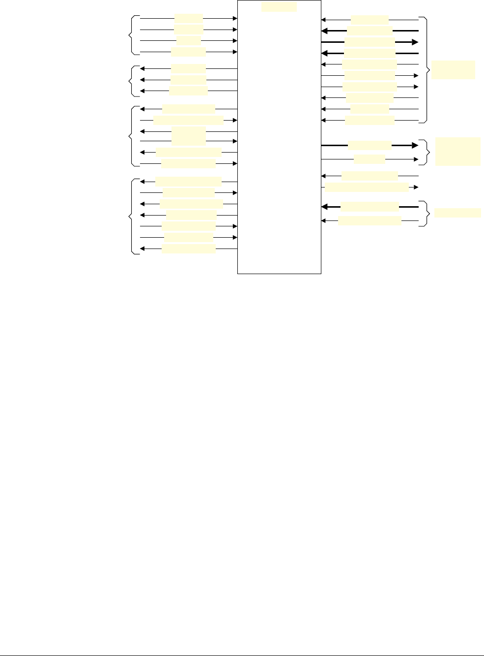
Appendix B Recommended External Debug Interface
B.1 About the recommended external debug interface
AppxB-4776 Copyright © 2013 ARM Limited. All rights reserved. ARM DDI 0487A.a
Non-Confidential - Beta ID090413
Figure B-1 Recommended external debug interface, including the APB3 slave port
In Figure B-1, signals with a lower-case n suffix are active LOW and all other signals are active HIGH.
Processor
DCC
handshake
PSELDBG
PADDRDBG
PRDATADBG
PWDATADBG
PENABLEDBG
PREADYDBG
PSLVERRDBG
PWRITEDBG
PCLKDBG
PCLKENDBG
Debug slave
port, APB3
Configuration
DBGROMADDR
DBGROMADDRV
DBGBUSCANCELREQ
DBGEN
SPIDEN
NIDEN
SPNIDEN
Authentication
interface
COMMTX
COMMRX
COMMIRQ
DBGCPUDONE
DBGACK
DBGNOPWRDWN
DBGPWRDUP
Power and reset
controller
interface
DBGPWRUPREQ
DBGRSTREQ
CPUPORESET
CORERESET
DBGTRIGGER
EDBGRQ
DBGRESTARTED
DBGRESTART
Cross-trigger
interface
DBGTRIGGERACK
PRESETDBGn
PMUEVENT
PMUIRQ
Performance
Monitor
Interface

Appendix B Recommended External Debug Interface
B.2 PMUEVENT bus
ARM DDI 0487A.a Copyright © 2013 ARM Limited. All rights reserved. AppxB-4777
ID090413 Non-Confidential - Beta
B.2 PMUEVENT bus
The PMUEVENT bus exports Performance Monitor events from the PE to an on-chip agent. ARM recommends
that it has the following characteristics:
• The bus is synchronous.
• The width of the bus is IMPLEMENTATION DEFINED.
• It is IMPLEMENTATION DEFINED which events are exported on the bus.
• Each exported event occupies a contiguous sub-field of the bus. ARM recommends that the sub-fields of the
bus are occupied in the same order as the event numbers.
• If the event can only occur once per cycle, it occupies a single bit. If the event can occur more than once per
cycle, it is IMPLEMENTATION DEFINED how the event is encoded. The encoding depends on constraints such
as the designated use of the event bus and the number of pins available. For example, the event can be
encoded:
— As a count, using a plain binary number. This is the most useful encoding when exporting to an
external counter. It is not a useful encoding for exporting to a Trace extension external input.
— As a count, using thermometer encoding. This is the most useful encoding when exporting to a Trace
extension.
— Using a single bit encoding to indicate whether the event count is zero or non-zero. This is useful for
exporting to an activity monitor where the number of pins is constrained.
If a Trace extension is implemented, the PMUEVENT bus is normally connected to the Trace extension using the
external inputs. TRCEXTINSELR multiplexes a wide PMUEVENT bus to a narrow set of inputs. An external
PMUEVENT bus might also be provided. For more information, contact ARM.

Appendix B Recommended External Debug Interface
B.3 DBGCPUDONE
AppxB-4778 Copyright © 2013 ARM Limited. All rights reserved. ARM DDI 0487A.a
Non-Confidential - Beta ID090413
B.3 DBGCPUDONE
The PE asserts DBGCPUDONE only after it has completed all Non-debug state memory accesses. Therefore, the
system can use DBGCPUDONE as an indicator that all memory accesses issued by the PE result from operations
performed by a debugger.

Appendix B Recommended External Debug Interface
B.4 Recommended authentication interface
ARM DDI 0487A.a Copyright © 2013 ARM Limited. All rights reserved. AppxB-4779
ID090413 Non-Confidential - Beta
B.4 Recommended authentication interface
The details of the debug authentication interface are IMPLEMENTATION DEFINED.
ARM recommends the use of the CoreSight interface, which has four signals for external debug authentication:
•DBGEN,
•SPIDEN.
•NIDEN.
•SPNIDEN.
CoreSight forbids asserting SPIDEN without also asserting DBGEN. CoreSight also forbids asserting SPNIDEN
without also asserting NIDEN.
ARM recommends an interface in which DBGEN and SPIDEN are also used for self-hosted secure debug
authentication if either:
• EL3 is using AArch32 and SDCR.SPD ==
0b00
.
• Secure EL1 is using AArch32 and MDCR_EL3.SPD32 ==
0b00
.
If EL3 is not implemented and the PE is in Non-secure state, SPIDEN and SPNIDEN are not implemented, and the
PE behaves as if these signals were tied LOW.
If EL3 is not implemented and the PE is in Secure state, SPIDEN is usually connected to DBGEN and SPNIDEN
is connected to NIDEN, but this is not required. The recommended interface is defined as if all four signals are
implemented.
How the authentication signals are driven is IMPLEMENTATION DEFINED. For example, the signals might be
hard-wired, connected to fuses, or to an authentication module. The architecture permits PEs within a cluster to have
independent authentication interfaces, but this is not required. ARM recommends that any Trace extension has the
same authentication interface as the PE it is connected to.
Table B-2 shows the debug authentication pseudocode functions and the recommended implementations.
The following assertions must apply to all implementations:
if
!ExternalInvasiveDebugEnabled()
then assert
!ExternalSecureInvasiveDebugEnabled()
if
!ExternalNoninvasiveDebugEnabled()
then assert
!ExternalSecureNoninvasiveDebugEnabled()
Table B-2 Recommended implementation of debug enable pseudocode functions
Pseudocode function Description Implementation
AArch32SelfHostedSecurePrivilegedInvasvieDebugEnabled()
See Pseudocode details for AArch32 Self-Hosted Secure
Privileged Invasive Debug Enabled on page AppxB-4780
Secure invasive self-hosted
debug enabled in AArch32
state (legacy)
(DBGEN AND SPIDEN)
ExternalSecureNoninvasiveDebugEnabled()
See Pseudocode details for External Invasive Debug Enabled on
page AppxB-4780
Secure non-invasive debug
enabled (DBGEN OR NIDEN) AND
(SPIDEN OR SPNIDEN)
ExternalSecureInvasiveDebugEnabled()
See Pseudocode details for External Secure Invasive Debug
Enabled on page AppxB-4780
Secure invasive debug enabled (DBGEN AND SPIDEN)
ExternalNoninvasiveDebugEnabled()
See Pseudocode details for External Non-invasive Debug
Enabled on page AppxB-4781
Non-secure non-invasive debug
enabled (DBGEN OR NIDEN)
ExternalInvasiveDebugEnabled()
See Pseudocode details for External Secure Non-invasive Debug
Enabled on page AppxB-4781
Non-secure invasive debug
enabled DBGEN

Appendix B Recommended External Debug Interface
B.4 Recommended authentication interface
AppxB-4780 Copyright © 2013 ARM Limited. All rights reserved. ARM DDI 0487A.a
Non-Confidential - Beta ID090413
if
ExternalInvasiveDebugEnabled()
then assert
ExternalNoninvasiveDebugEnabled()
if
ExternalSecureInvasiveDebugEnabled()
then assert
ExternalSecureNoninvasiveDebugEnabled()
The definition for the
Debug_authentication()
function is as follows:
signal DBGEN;
signal NIDEN;
signal SPIDEN;
signal SPNIDEN;
B.4.1 Pseudocode details for AArch32 Self-Hosted Secure Privileged Invasive Debug Enabled
The pseudocode for the
AArch32SelfHostedSecurePrivilegedInvasiveDebugEnabled()
function is as follows:
// AArch32SelfHostedSecurePrivilegedInvasiveDebugEnabled()
// =======================================================
boolean AArch32SelfHostedSecurePrivilegedInvasiveDebugEnabled()
// In the recommended interface, AArch32SelfHostedSecurePrivilegedInvasiveDebugEnabled returns
// the state of the (DBGEN AND SPIDEN) signal.
if !HaveEL(EL3) && !IsSecure() then return FALSE;
return DBGEN == HIGH && SPIDEN == HIGH;
B.4.2 Pseudocode details for External Invasive Debug Enabled
The pseudocode for the
ExternalInvasiveDebugEnabled()
function is as follows:
// ExternalInvasiveDebugEnabled()
// ==============================
boolean ExternalInvasiveDebugEnabled()
// In the recommended interface, ExternalInvasiveDebugEnabled returns the state of the DBGEN
// signal.
return DBGEN == HIGH;
B.4.3 Pseudocode details for External Secure Invasive Debug Enabled
The pseudocode for the
ExternalSecureInvasiveDebugEnabled()
function is as follows:
// ExternalSecureInvasiveDebugEnabled()
// ====================================
boolean ExternalSecureInvasiveDebugEnabled()

Appendix B Recommended External Debug Interface
B.4 Recommended authentication interface
ARM DDI 0487A.a Copyright © 2013 ARM Limited. All rights reserved. AppxB-4781
ID090413 Non-Confidential - Beta
// In the recommended interface, ExternalSecureInvasiveDebugEnabled returns the state of the
// (DBGEN AND SPIDEN) signal.
// CoreSight allows asserting SPIDEN without also asserting DBGEN, but this is not recommended.
if !HaveEL(EL3) && !IsSecure() then return FALSE;
return ExternalInvasiveDebugEnabled() && SPIDEN == HIGH;
B.4.4 Pseudocode details for External Non-invasive Debug Enabled
The pseudocode for the
ExternalNoninvasiveDebugEnabled()
function is as follows:
// ExternalNoninvasiveDebugEnabled()
// =================================
boolean ExternalNoninvasiveDebugEnabled()
// In the recommended interface, ExternalNoninvasiveDebugEnabled returns the state of the (DBGEN
// OR NIDEN) signal.
return ExternalInvasiveDebugEnabled() || NIDEN == HIGH;
B.4.5 Pseudocode details for External Secure Non-invasive Debug Enabled
The pseudocode for the
ExternalSecureNoninvasiveDebugEnabled()
function is as follows:
// ExternalSecureNoninvasiveDebugEnabled()
// =======================================
boolean ExternalSecureNoninvasiveDebugEnabled()
// In the recommended interface, ExternalSecureNoninvasiveDebugEnabled returns the state of the
// (DBGEN OR NIDEN) AND (SPIDEN OR SPNIDEN) signal.
if !HaveEL(EL3) && !IsSecure() then return FALSE;
return ExternalNoninvasiveDebugEnabled() && (SPIDEN == HIGH || SPNIDEN == HIGH);

Appendix B Recommended External Debug Interface
B.5 Management registers and CoreSight compliance
AppxB-4782 Copyright © 2013 ARM Limited. All rights reserved. ARM DDI 0487A.a
Non-Confidential - Beta ID090413
B.5 Management registers and CoreSight compliance
The CoreSight architecture requires the implementation of a set of management registers that occupy the memory
map from
0xF00
upwards in each of the debug components.
CoreSight compliance and complete implementation of the management registers is OPTIONAL, but ARM
recommends that the registers are implemented.
The CoreSight architecture specification recommends that any integration test registers are implemented starting
from
0xEFC
downwards. Each of the debug components has an IMPLEMENTATION DEFINED region from
0xE80
to
0xEFC
for this purpose.
B.5.1 CoreSight interface register map
Table B-3 shows the external management register maps for the following registers:
ED These are the external debug register.
CTI These are the Cross-trigger interface registers.
PMU These are the Performance Monitors registers.
Table B-3 CoreSight interface register map
Offset Mnemonic Name
ED CTI PMU
0xF00
EDITCTRL CTIITCTRL PMITCTRL Integration Model Control registers
0xF04-0xF8C
- - - Reserved, RES0
0xFA0
DBGCLAIMSET_EL1aCTICLAIMSETb- Claim Tag Set registers
0xFA4
DBGCLAIMCLR_EL1aCTICLAIMCLRb- Claim Tag Clear registers
0xFA8
EDDEVAFF0aCTIDEVAFF0cPMDEVAFF0 Device Affinity registers
0xFAC
EDDEVAFF1aCTIDEVAFF1cPMDEVAFF0
0xFB0
EDLARdCTILARdPMLARdLock Access register
0xFB4
EDLSRdCTILSRdPMLSRdLock Status register
0XFB8
DBGAUTHSTATUS_EL1aCTIAUTHSTATUS PMAUTHSTATUS Authentication Status register
0xFBC
EDDEVARCH CTIDEVARCH PMDEVARCH Device Architecture register
0xFC0
EDDEVID2aCTIDEVID2a- Device ID register
0xFC4
EDDEVID1aCTIDEVID1a-
0xFC8
EDDEVIDaCTIDEVIDa-
0xFCC
EDDEVTYPE CTIDEVTYPE PMDEVTYPE Device Type register
0xFD0
EDPIDR4 CTIPIDR4 PMPIDR4 Peripheral ID registers
0xFD4-0xFDC
- - - Reserved, RES0
0xFE0
EDPIDR0 CTIPIDR0 PMPIDR0 Peripheral ID registers
0xFE4
EDPIDR1 CTIPIDR1 PMPIDR1
0xFE8
EDPIDR2 CTIPIDR2 PMPIDR2
0xFEC
EDPIDR3 CTIPIDR3 PMPIDR3

Appendix B Recommended External Debug Interface
B.5 Management registers and CoreSight compliance
ARM DDI 0487A.a Copyright © 2013 ARM Limited. All rights reserved. AppxB-4783
ID090413 Non-Confidential - Beta
B.5.2 Management register access permissions
Access to the OPTIONAL Integration Control register (ITCTRL) is IMPLEMENTATION DEFINED.
If the Debug power domain is off, all register accesses return an error.
Otherwise, Table B-4 on page AppxB-4784, Table B-5 on page AppxB-4785, and Table B-6 on page AppxB-4786
show the response to accesses by the external debug interface to the CoreSight management registers. For
definitions of the terms used in the tables, see External debug interface register access permissions summary on
page H8-4453.
Note
Access to the CoreSight management registers is not affected by the values of EDAD and EPMAD.
Table B-4 on page AppxB-4784, Table B-5 on page AppxB-4785, and Table B-6 on page AppxB-4786 include
reserved management registers, because the CoreSight architecture requires that these registers are always RES0.
The descriptions in Reserved and unallocated registers on page H8-4454 does not apply to reserved management
registers if the implementation is CoreSight compliant.
If OPTIONAL memory-mapped access to the external debug interface is supported, there are additional constraints
on memory-mapped accesses. See Register access permissions for memory-mapped accesses on page H8-4449.
The terms in Table B-4 on page AppxB-4784, Table B-5 on page AppxB-4785, and Table B-6 on
page AppxB-4786 are defined as follows:
Domain This describes the power domain in which the register is logically implemented. Registers described
as implemented in the Core power domain might be implemented in the Debug power domain, as
long as they exhibit the required behavior.
Conditions This lists the conditions under which the access is attempted.
To determine the access permissions for a register, read these columns from left to right, and stop
at first column which lists the condition as being true.
The conditions are:
Off EDPRSR.PU == 0. The Core power domain is completely off, or in low-power state. In
these cases the Core power domain registers cannot be accessed.
Note
If debug power is off, then all external debug interface accesses return an error.
0xFF0
EDCIDR0 CTICIDR0 PMCIDR0 Component ID registers
0xFF4
EDCIDR1 CTICIDR1 PMCIDR1
0xFF8
EDCIDR2 CTICIDR2 PMCIDR2
0xFFC
EDCIDR3 CTICIDR3 PMCIDR3
a. This register must always be implemented, regardless of whether the component is CoreSight compliant.
b. If implemented, the number of CLAIM bits is IMPLEMENTATION DEFINED and can be discovered by reading CLAIMSET.
c. If the CTI implements CTIv1, this register is not implemented. See the register description for details.
d. The Software lock registers are defined as part of CoreSight compliance, but their contents depend on the type of access that is made and
whether the OPTIONAL Software lock is implemented. See the register description for details.
Table B-3 CoreSight interface register map (continued)
Offset Mnemonic Name
ED CTI PMU

Appendix B Recommended External Debug Interface
B.5 Management registers and CoreSight compliance
AppxB-4784 Copyright © 2013 ARM Limited. All rights reserved. ARM DDI 0487A.a
Non-Confidential - Beta ID090413
DLK
DoubleLockStatus()
== TRUE. The OS Double Lock is locked, that is, EDPRSR.DLK
== 1.
OSLK OSLSR.OSLK == 1. The OS Lock is locked.
Default This provides the default access permissions, if there are no conditions that prevent access to the
register.
SLK This provides the modified default access permissions for OPTIONAL memory-mapped accesses to
the external debug interface if the OPTIONAL Software Lock is locked. See Register access
permissions for memory-mapped accesses on page H8-4449. For all other accesses, this column is
ignored.
The access permissions are:
- This means that the default access permission applies. See the Default column, or the SLK column,
if applicable.
RO This means that the register or field is read-only.
RW This means that the register or field is read/write. Individual fields within the register might be RO.
See the relevant register description for details.
RC This means that the bit clears to 0 after a read.
(SE) This means that accesses to this register have indirect write side-effects. A side-effect occurs when
a direct read or a direct write of a register creates an indirect write to the same register or to another
register.
WO This means that the register or field is write-only.
WI This means that the register or field ignores writes.
IMP DEF This means that the access permissions are IMPLEMENTATION DEFINED.
Table B-4 External debug interface access permissions, CoreSight registers (debug)
Conditions (priority left
to right)
Offset Register Domain Off DLK OSLK Default SLK
0xF00
EDITCTRL IMP DEF IMPLEMENTATION DEFINED IMP DEF RO/WI
0xF04 -
0xF8C
Reserved Debug - - - RES0-
0xFA0
DBGCLAIMSET_EL1 Core Error Error Error RW (SE) RO
0xFA4
DBGCLAIMCLR_EL1 Core Error Error Error RW (SE) RO
0xFA8
EDDEVAFF0 Debug - - - RO -
0xFAC
EDDEVAFF1 Debug - - - RO -
0xFB0
EDLAR Debug - - - WO (SE) -
0xFB4
EDLSR Debug - - - RO -
0xFB8
DBGAUTHSTATUS_EL1 Debug - - - RO -
0xFBC
EDDEVARCH Debug - - - RO -
0xFC0
EDDEVID2 Debug - - - RO -
0xFC4
EDDEVID1 Debug - - - RO -

Appendix B Recommended External Debug Interface
B.5 Management registers and CoreSight compliance
ARM DDI 0487A.a Copyright © 2013 ARM Limited. All rights reserved. AppxB-4785
ID090413 Non-Confidential - Beta
0xFC8
EDDEVID Debug - - - RO -
0xFCC
EDDEVTYPE Debug - - - RO -
0xFD0
EDPIDR4 Debug - - - RO -
0xFD4 -
0xFDC
Reserved Debug - - - RES0-
0xFE0 -
0xFEC
EDPIDR0 Debug - - - RO -
0xFE4
EDPIDR1 Debug - - - RO -
0xFE8
EDPIDR2 Debug - - - RO -
0xFEC
EDPIDR3 Debug - - - RO -
0xFF0
EDCIDR0 Debug - - - RO -
0xFF4
EDCIDR1 Debug - - - RO -
0xFF8
EDCIDR2 Debug - - - RO -
0xFFC
EDCIDR3 Debug - - - RO -
Table B-5 External debug interface access permissions, CoreSight registers (CTI)
Offset Register Domain Off DLK OSLK Default SLK
0xF00
CTIITCTRL IMP DEF IMPLEMENTATION DEFINED IMP DEF RO/WI
0xF04 -
0xF8C
Reserved Debug - - - RES0-
0xFA0
CTICLAIMSET Debug - - - RW (SE) RO
0xFA4
CTICLAIMCLR Debug - - - RW (SE) RO
0xFA8
CTIDEVAFF0 Debug - - - RO -
0xFAC
CTIDEVAFF1 Debug - - - RO -
0xFB0
CTILAR Debug - - - WO (SE) -
0xFB4
CTILSR Debug - - - RO -
0xFB8
CTIAUTHSTATUS Debug - - - RO -
0xFBC
CTIDEVARCH Debug - - - RO -
0xFC0
CTIDEVID2 Debug - - - RO -
0xFC4
CTIDEVID1 Debug - - - RO -
0xFC8
CTIDEVID Debug - - - RO -
Table B-4 External debug interface access permissions, CoreSight registers (debug) (continued)
Conditions (priority left
to right)
Offset Register Domain Off DLK OSLK Default SLK

Appendix B Recommended External Debug Interface
B.5 Management registers and CoreSight compliance
AppxB-4786 Copyright © 2013 ARM Limited. All rights reserved. ARM DDI 0487A.a
Non-Confidential - Beta ID090413
0xFCC
CTIDEVTYPE Debug - - - RO -
0xFD0
CTIPIDR4 Debug - - - RO -
0xFD4 -
0xFDC
Reserved Debug - - - RES0-
0xFE0
CTIPIDR0 Debug - - - RO -
0xFE4
CTIPIDR1 Debug - - - RO -
0xFE8
CTIPIDR2 Debug - - - RO -
0xFEC
CTIPIDR3 Debug - - - RO -
0xFF0
CTICIDR0 Debug - - - RO -
0xFF4
CTICIDR1 Debug - - - RO -
0xFF8
CTICIDR2 Debug - - - RO -
0xFFC
CTICIDR3 Debug - - - RO -
Table B-6 External debug interface access permissions, CoreSight registers (PMU)
Offset Register Domain Off DLK OSLK Default SLK
0xF00
PMITCTRL IMP DEF IMPLEMENTATION DEFINED IMP DEF RO/WI
0xF04 -
0xFA4
Reserved Debug - - - RES0-
0xFA8
PMDEVAFF0 Debug - - - RO -
0xFAC
PMDEVAFF1 Debug - - - RO -
0xFB0
PMLAR Debug - - - WO (SE) -
0xFB4
PMLSR Debug - - - RO -
0xFB8
PMAUTHSTATUS Debug - - - RO -
0xFBC
PMDEVARCH Debug - - - RO -
0xFC0 -
0xFC8
Reserved Debug - - - RES0-
0xFCC
PMDEVTYPE Debug - - - RO -
0xFD0
PMPIDR4 Debug - - - RO -
0xFD4 -
0xFDC
Reserved Debug - - - RES0-
0xFE0
PMPIDR0 Debug - - - RO -
0xFE4
PMPIDR1 Debug - - - RO -
Table B-5 External debug interface access permissions, CoreSight registers (CTI) (continued)
Offset Register Domain Off DLK OSLK Default SLK

Appendix B Recommended External Debug Interface
B.5 Management registers and CoreSight compliance
ARM DDI 0487A.a Copyright © 2013 ARM Limited. All rights reserved. AppxB-4787
ID090413 Non-Confidential - Beta
B.5.3 Management register resets
Table B-7 shows the management register resets. This table does not include:
• Read-only identification registers that have a fixed value from reset. These registers include those with the
DEVAFFn, DEVARCH, DEVID{n}, DEVTYPE, PIDRn, and CIDRn mnemonics.
• Registers that have the AUTHSTATUS mnemonic. This is a read-only status register that reflects the status
outside of the reset domain of the register.
• Registers that have the LAR mnemonic. These are write-only registers that only have an effect on writes.
All other fields in the management registers are reset to an IMPLEMENTATION DEFINED value which can be
UNKNOWN. The registers are in the reset domain specified in the table.
Table B-7 shows a summary of the management register resets.
0xFE8
PMPIDR2 Debug - - - RO -
0xFEC
PMPIDR3 Debug - - - RO -
0xFF0
PMCIDR0 Debug - - - RO -
0xFF4
PMCIDR1 Debug - - - RO -
0xFF8
PMCIDR2 Debug - - - RO -
0xFFC
PMCIDR3 Debug - - - RO -
Table B-6 External debug interface access permissions, CoreSight registers (PMU) (continued)
Offset Register Domain Off DLK OSLK Default SLK
Table B-7 Management register resets
Register Reset domain Field Value Description
CTIITCTRL
EDITCTRL
PMITCTRL
IMPLEMENTATION DEFINED IME 0 Integration mode enable
DBGCLAIMCLR_EL1
CTICLAIMCLRa
External debug CLAIM
0x0
Claim tags
CTILSRb
EDLSRb
PMLSRb
External debug SLK 1 Software Lock
a. CTICLAIMCLR only if implemented. For DBGCLAIMCLR_EL1, see DBGCLAIMCLR_EL1, Debug Claim Tag Clear
register on page H9-4477.
b. Only if the OPTIONAL Software Lock is implemented

Appendix B Recommended External Debug Interface
B.5 Management registers and CoreSight compliance
AppxB-4788 Copyright © 2013 ARM Limited. All rights reserved. ARM DDI 0487A.a
Non-Confidential - Beta ID090413

ARM DDI 0487A.a Copyright © 2013 ARM Limited. All rights reserved. AppxC-4789
ID090413 Non-Confidential - Beta
Appendix C
Recommendations for Performance Monitors Event
Numbers for IMPLEMENTATION DEFINED Events
This appendix describes the ARM recommendations for the use of the IMPLEMENTATION DEFINED event numbers.
It contains the following section:
•ARM recommendations for IMPLEMENTATION DEFINED event numbers on page AppxC-4790.
•Summary of events taken to an Exception Level using AArch64 on page AppxC-4801.

Appendix C Recommendations for Performance Monitors Event Numbers for IMPLEMENTATION DEFINED Events
C.1 ARM recommendations for IMPLEMENTATION DEFINED event numbers
AppxC-4790 Copyright © 2013 ARM Limited. All rights reserved. ARM DDI 0487A.a
Non-Confidential - Beta ID090413
C.1 ARM recommendations for IMPLEMENTATION DEFINED event numbers
These are the ARM recommendations for the use of the IMPLEMENTATION DEFINED event numbers. ARM does not
define these events as rigorously as those in the architectural and microarchitectural event lists, and an
implementation might:
• Modify the definition of an event to better correspond to the implementation.
• Not use some, or many, of these event numbers.
• Include cumulative occupancy for resource queues such as data access queues, and entry/exit counts, so that
average latencies can be determined and counts for key resources that might exist can be separated.
• Provide registers in the IMPLEMENTATION DEFINED space to further extend such counts by, for example,
specifying a minimum latency for an event to be counted.
• Use cumulative occupancy for resource queues, such as data access queues, and entry/exit counts, so that
average latencies can be determined, separating out counts for key resources that might exist:
— An implementation might also provide registers in the IMPLEMENTATION DEFINED space to further
extend such counts, by, for example specifying a minimum latency for an event to be counted.
Table C-1 lists the PMU IMPLEMENTATION DEFINED event numbers in event number order.
Table C-1 PMU IMPLEMENTATION DEFINED event numbers
Event number Event mnemonic Description
0x40
L1D_CACHE_LD Level 1 data cache access, read
0x41
L1D_CACHE_ST Level 1 data cache access, write
0x42
L1D_CACHE_REFILL_LD Level 1 data cache refill, read
0x43
L1D_CACHE_REFILL_ST Level 1 data cache refill, write
0x44
L1D_CACHE_REFILL_INNER Level 1 data cache refill, inner
0x45
L1D_CACHE_REFILL_OUTER Level 1 data cache refill, outer
0x46
L1D_CACHE_WB_VICTIM Level 1 data cache write-back, victim
0x47
L1D_CACHE_WB_CLEAN Level 1 data cache write-back, cleaning and coherency
0x48
L1D_CACHE_INVAL Level 1 data cache invalidate
0x49
-
0x4B
- Reserved
0x4C
L1D_TLB_REFILL_LD Level 1 data TLB refill, read
0x4D
L1D_TLB_REFILL_ST Level 1 data TLB refill, write
0x4E
-
0x4F
- Reserved
0x50
L2D_CACHE_LD Level 2 data cache access, read
0x51
L2D_CACHE_ST Level 2 data cache access, write
0x52
L2D_CACHE_REFILL_LD Level 2 data cache refill, read
0x53
L2D_CACHE_REFILL_ST Level 2 data cache refill, write
0x54
-
0x55
- Reserved
0x56
L2D_CACHE_WB_VICTIM Level 2 data cache write-back, victim
0x57
L2D_CACHE_WB_CLEAN Level 2 data cache write-back, cleaning and coherency

Appendix C Recommendations for Performance Monitors Event Numbers for IMPLEMENTATION DEFINED Events
C.1 ARM recommendations for IMPLEMENTATION DEFINED event numbers
ARM DDI 0487A.a Copyright © 2013 ARM Limited. All rights reserved. AppxC-4791
ID090413 Non-Confidential - Beta
0x58
L2D_CACHE_INVAL Level 2 data cache invalidate
0x59
-
0x5F
- Reserved
0x60
BUS_ACCESS_LD Bus access, read
0x61
BUS_ACCESS_ST Bus access, write
0x62
BUS_ACCESS_SHARED Bus access, Normal, Cacheable, Shareable
0x63
BUS_ACCESS_NOT_SHARED Bus access, not Normal, Cacheable, Shareable
0x64
BUS_ACCESS_NORMAL Bus access, normal
0x65
BUS_ACCESS_PERIPH Bus access, peripheral
0x66
MEM_ACCESS_LD Data memory access, read
0x67
MEM_ACCESS_ST Data memory access, write
0x68
UNALIGNED_LD_SPEC Unaligned access, read
0x69
UNALIGNED_ST_SPEC Unaligned access, write
0x6A
UNALIGNED_LDST_SPEC Unaligned access
0x6B
- Reserved
0x6C
LDREX_SPEC Exclusive operation speculatively executed,
LDREX
or
LDX
0x6D
STREX_PASS_SPEC Exclusive operation speculatively executed,
STREX
or
STX
pass
0x6E
STREX_FAIL_SPEC Exclusive operation speculatively executed,
STREX
or
STX
pass
0x6F
STREX_SPEC Exclusive operation speculatively executed,
STREX
or
STX
0x70
LD_SPEC Operation speculatively executed, load
0x71
ST_SPEC Operation speculatively executed, store
0x72
LDST_SPEC Operation speculatively executed, load or store
0x73
DP_SPEC Operation speculatively executed, integer data-processing
0x74
ASE_SPEC Operation speculatively executed, Advanced SIMD instruction
0x75
VFP_SPEC Operation speculatively executed, floating-point instruction
0x76
PC_WRITE_SPEC Operation speculatively executed, software change of the PC
0x77
CRYPTO_SPEC Operation speculatively executed, Cryptographic instruction
0x78
BR_IMMED_SPEC Branch speculatively executed, immediate branch
0x79
BR_RETURN_SPEC Branch speculatively executed, procedure return
0x7A
BR_INDIRECT_SPEC Branch speculatively executed, indirect branch
0x7B
- Reserved
0x7C
ISB_SPEC Barrier speculatively executed,
ISB
0x7D
DSB_SPEC Barrier speculatively executed,
DSB
Table C-1 PMU IMPLEMENTATION DEFINED event numbers (continued)
Event number Event mnemonic Description

Appendix C Recommendations for Performance Monitors Event Numbers for IMPLEMENTATION DEFINED Events
C.1 ARM recommendations for IMPLEMENTATION DEFINED event numbers
AppxC-4792 Copyright © 2013 ARM Limited. All rights reserved. ARM DDI 0487A.a
Non-Confidential - Beta ID090413
0x40
, Level 1 data cache access, read
This event is similar to Level 1 data cache access but the counter counts only memory-read
operations that access at least the Level 1 data or unified cache.
0x41
, Level 1 data cache access, write
This event is similar to Level 1 data cache access but the counter counts only memory-write
operations that access at least the Level 1 data or unified cache.
The counter counts DC ZVA as a store instruction.
0x42
, Level 1 data cache refill, read
This event is similar to Level 1 data cache refill but the counter counts only memory-read operations
that cause a refill of at least the Level 1 data or unified cache.
0x43
, Level 1 data cache refill, write
This event is similar to Level 1 data cache refill but the counter counts only memory-write
operations that cause a refill of at least the Level 1 data or unified cache.
The counter counts DC ZVA as a store instruction.
0x7E
DMB_SPEC Barrier speculatively executed,
DMB
0x7F
-
0x80
- Reserved
0x81
EXC_UNDEF Exception taken, Other synchronous
0x82
EXC_SVC Exception taken, Supervisor Call
0x83
EXC_PABORT Exception taken, Instruction Abort
0x84
EXC_DABORT Exception taken, Data Abort and SError
0x85
- Reserved
0x86
EXC_IRQ Exception taken, IRQ
0x87
EXC_FIQ Exception taken, FIQ
0x88
EXC_SMC Exception taken, Secure Monitor Call
0x89
- Reserved
0x8A
EXC_HVC Exception taken, Hypervisor Call
0x8B
EXC_TRAP_PABORT Exception taken, Instruction Abort not taken locally
0x8C
EXC_TRAP_DABORT Exception taken, Data Abort or SError not taken locally
0x8D
EXC_TRAP_OTHER Exception taken, Other traps not taken locally
0x8E
EXC_TRAP_IRQ Exception taken, IRQ not taken locally
0x8F
EXC_TRAP_FIQ Exception taken, FIQ not taken locally
0x90
RC_LD_SPEC Release consistency operation speculatively executed, Load-Acquire
0x91
RC_ST_SPEC Release consistency operation speculatively executed, Store-Release
Table C-1 PMU IMPLEMENTATION DEFINED event numbers (continued)
Event number Event mnemonic Description

Appendix C Recommendations for Performance Monitors Event Numbers for IMPLEMENTATION DEFINED Events
C.1 ARM recommendations for IMPLEMENTATION DEFINED event numbers
ARM DDI 0487A.a Copyright © 2013 ARM Limited. All rights reserved. AppxC-4793
ID090413 Non-Confidential - Beta
0x44
, Level 1 data cache refill, inner
This event is similar to Level 1 data cache refill but the counter counts only memory-read and
memory-write operations that generate refills satisfied by transfer from another cache inside of the
immediate cluster.
Note
The boundary between inner and outer is IMPLEMENTATION DEFINED, and it is not necessarily linked
to other similar boundaries, such as the boundary between Inner Cacheable and Outer Cacheable or
the boundary between Inner Shareable and Outer Shareable.
0x45
, Level 1 data cache refill, outer
This event is similar to Level 1 data cache refill but the counter counts only memory-read and
memory-write operations that generate refills satisfied from outside of the immediate cluster.
0x46
, Level 1 data cache write-back, victim
This event is similar to Level 1 data cache write-back but the counter counts only write-backs that
are a result of the line being allocated for an access made by the PE.
CP15 cache maintenance operations do not count as events.
It is IMPLEMENTATION DEFINED whether a write of a whole cache line that is not the result of the
eviction of a line from the cache is counted. For example, this might occur if the PE detects
streaming writes to memory and does not allocate lines to the cache, or as the result of a DC ZVA.
0x47
, Level 1 data cache write-back, cleaning and coherency
This event is similar to Level 1 data cache write-back but the counter counts only write-backs that
are a result of a coherency operation made by another PE or from a CP15 cache maintenance
operation. Whether write-backs made as a result of CP15 cache maintenance operations are counted
is IMPLEMENTATION DEFINED.
If a coherency request from a requestor outside the PE results in a write-back, it is an Unattributable
event.
Note
The transfer of a dirty cache line from the Level 1 data cache of this PE to the Level 1 data cache of
another PE due to a hardware coherency operation is not counted unless the dirty cache line is also
written back to a Level 2 cache or memory.
0x48
, Level 1 data cache invalidate
The counter counts each invalidation of a cache line in the Level 1 data or unified cache.
The counter does not count events:
• If a cache refill invalidates a line.
• For locally executed CP15 cache set/way maintenance operations.
If a coherency request from a requestor outside the PE results in a write-back, it is an Unattributable
event.
0x4C
, Level 1 data TLB refill, read
This event is similar to Level 1 data TLB refill but the counter counts only memory-read operations
that cause a data TLB refill of a least the Level 1 data or unified TLB.
0x4D
, Level 1 data TLB refill, write
This event is similar to Level 1 data TLB refill but the counter counts only memory-write operations
that cause a data TLB refill of a least the Level 1 data or unified TLB.
The counter counts DC ZVA as a store instruction.

Appendix C Recommendations for Performance Monitors Event Numbers for IMPLEMENTATION DEFINED Events
C.1 ARM recommendations for IMPLEMENTATION DEFINED event numbers
AppxC-4794 Copyright © 2013 ARM Limited. All rights reserved. ARM DDI 0487A.a
Non-Confidential - Beta ID090413
0x50
, Level 2 data cache access, read
This event is similar to Level 2 data cache access but the counter counts only memory-read
operations that access at least the Level 2 data or unified cache.
0x51
, Level 2 data cache access, write
This event is similar to Level 2 data cache access but the counter counts only memory-write
operations that access at least the Level 2 data or unified cache.
The counter counts DC ZVA as a store instruction.
0x52
, Level 2 data cache refill, read
This event is similar to Level 2 data cache refill but the counter counts only memory-read operations
that cause a refill of at least the Level 2 data or unified cache.
0x53
, Level 2 data cache refill, write
This event is similar to Level 2 data cache refill but the counter counts only memory-write
operations that cause a refill of at least the Level 2 data or unified cache.
The counter counts DC ZVA as a store instruction.
0x56
, Level 2 data cache write-back, victim
This event is similar to Level 2 data cache write-back but the counter counts only write-backs that
are a result of the line being allocated for an access made by the PE.
CP15 cache maintenance operations do not count as events.
It is IMPLEMENTATION DEFINED whether a write of a whole cache line that is not the result of the
eviction of a line from the cache is counted. For example, this might occur if the PE detects
streaming writes to memory and does not allocate lines to the cache, or as the result of a DC ZVA.
0x57
, Level 2 data cache write-back, cleaning and coherency
This event is similar to Level 2 data cache write-back but the counter counts only write-backs that
are a result of a coherency operation made by another PE or CP15 cache maintenance operation.
Whether write-backs made as a result of CP15 cache maintenance operations are counted is
IMPLEMENTATION DEFINED.
Note
The transfer of a dirty cache line from the Level 2 data cache of this PE to the Level 2 data cache of
another PE due to a hardware coherency operation is not counted unless the dirty cache line is also
written back to a Level 3 cache or memory.
If a coherency request from a requestor outside the PE results in a write-back, it is an Unattributable
event.
0x58
, Level 2 data cache invalidate
The counter counts each invalidation of a cache line in the Level 2 data or unified cache.
The counter does not count events:
• If a cache refill invalidates a line.
• For locally executed CP15 set/way cache maintenance operations.
Note
Software that uses this event must know whether the Level 2 data cache is shared with other PEs.
This event does not follow the general rule of Level 2 data cache events of only counting events that
directly affect this PE.
If a coherency request from a requestor outside the PE results in a write-back, it is an Unattributable
event.

Appendix C Recommendations for Performance Monitors Event Numbers for IMPLEMENTATION DEFINED Events
C.1 ARM recommendations for IMPLEMENTATION DEFINED event numbers
ARM DDI 0487A.a Copyright © 2013 ARM Limited. All rights reserved. AppxC-4795
ID090413 Non-Confidential - Beta
0x60
, Bus access, read
This event is similar to bus access but the counter counts only memory-read operations that access
outside the boundary of the PE and its closely-coupled caches.
0x61
, Bus access, write
This event is similar to bus access but the counter counts only memory-write operations that access
outside the boundary of the PE and its closely-coupled caches.
0x62
, Bus access, Normal, Cacheable, Shareable
This event is similar to bus access but the counter counts only memory-read and memory-write
operations that make Normal, Cacheable, Shareable accesses outside the boundary of the PE and its
closely-coupled caches.
Note
It is IMPLEMENTATION DEFINED how the PE translates the attributes from the translation table entry
for a region to the attributes on the bus.
In particular, a region of memory designated as Normal, Cacheable, Inner Shareable, Not Outer
Shareable by a translation table entry, might be marked as either Shareable or Not Shareable at the
boundary of the PE and its closely-coupled caches. This depends on where the IMPLEMENTATION
DEFINED boundary lies, between Inner and Outer Shareable.
If the Inner Shareable extends beyond the PE boundary, and the bus indicates the distinction
between Inner and Outer Shareable, then either is counted as Shareable for the purposes of defining
this event.
0x63
, Bus access, not Normal, Cacheable, Shareable
This event is similar to bus access but the counter counts only memory-read and memory-write
operations that make accesses outside the boundary of the PE and its closely-coupled caches that
are not Normal, Cacheable, Shareable. For example, the counter counts accesses marked as:
• Normal, Cacheable, Not Shareable.
• Normal, Not Cacheable.
•Device.
Note
It is IMPLEMENTATION DEFINED, how the PE translates the attributes from the translation table
entries for a region to the attributes on the bus.
In particular, a region of memory designated as Normal, Cacheable, Inner Shareable, Not Outer
Shareable by a translation table entry, might be marked as either Shareable or Not Shareable at the
boundary of the PE and its closely-coupled caches. This depends on where the IMPLEMENTATION
DEFINED boundary lies, between Inner and Outer Shareable.
If the Inner Shareable extends beyond the PE boundary, and the bus indicates the distinction
between Inner and Outer Shareable, then either is counted as Shareable for the purposes of defining
this event.
0x64
, Bus access, normal
This event is similar to bus access but the counter counts only memory-read and memory-write
operations that make Normal accesses outside the boundary of the PE and its closely-coupled
caches. For example, the counter counts Normal, Cacheable and Normal, Not Cacheable accesses
but does not count Device accesses.
0x65
, Bus access, peripheral
This event is similar to bus access but the counter counts only memory-read and memory-write
operations that make Device accesses outside the boundary of the PE and its closely-coupled caches.

Appendix C Recommendations for Performance Monitors Event Numbers for IMPLEMENTATION DEFINED Events
C.1 ARM recommendations for IMPLEMENTATION DEFINED event numbers
AppxC-4796 Copyright © 2013 ARM Limited. All rights reserved. ARM DDI 0487A.a
Non-Confidential - Beta ID090413
0x66
, Data memory access, read
This event is similar to data memory access but the counter counts only memory-read operations
that the PE made.
0x67
, Data memory access, write
This event is similar to data memory access but the counter counts only memory-write operations
made by the PE.
0x68
, Unaligned access, read
This event is similar to data memory access but the counter counts only unaligned memory-read
operations that the PE made. It also counts unaligned accesses if they are subsequently transposed
into multiple aligned accesses.
0x69
, Unaligned access, write
This event is similar to data memory access but the counter counts only unaligned memory-read
operations that the PE made. It also counts unaligned accesses if they are subsequently transposed
into multiple aligned accesses.
0x6A
, Unaligned access
This event is similar to data memory access but the counter counts only unaligned memory-read
operations and unaligned memory-write operations that the PE made. It also counts unaligned
accesses if they are subsequently transposed into multiple aligned accesses.
0x6C
, Exclusive operation speculatively executed, Load-Exclusive
The counter counts Load-Exclusive instructions speculatively executed.
The definition of speculatively executed is IMPLEMENTATION DEFINED.
0x6D
, Exclusive operation speculatively executed, Store-Exclusive pass
The counter counts Store-Exclusive instructions speculatively executed that completed a write.
The definition of speculatively executed is IMPLEMENTATION DEFINED but must be the same as for
the exclusive operation speculatively executed, Load-Exclusive event.
0x6E
, Exclusive operation speculatively executed, Store-Exclusive fail
The counter counts Store-Exclusive instructions speculatively executed that fail to complete a write.
It is within the IMPLEMENTATION DEFINED definition of speculatively executed whether this
includes conditional instructions that fail the condition code check.
The definition of speculatively executed is IMPLEMENTATION DEFINED but must be the same as for
the exclusive operation speculatively executed, Load-Exclusive event.
0x6F
, Exclusive operation speculatively executed, Store-Exclusive
The counter counts Store-Exclusive instructions speculatively executed.
The definition of speculatively executed is IMPLEMENTATION DEFINED but it must be the same as for
the exclusive operation speculatively executed, Load-Exclusive event.
ARM recommends that this event is implemented if it is not possible to implement the exclusive
operation speculatively executed, Store-Exclusive pass, and exclusive operation speculatively
executed, Store-Exclusive fail, events with the same degree of speculation as the exclusive
operation speculatively executed, Load-Exclusive event.
0x70
, Operation speculatively executed, load
This event is similar to the operation speculatively executed but the counter counts only
memory-reading instructions. Defined by the instruction architecturally executed, condition code
check pass, load event, see Common event numbers on page D6-1839.
The definition of speculatively executed is IMPLEMENTATION DEFINED but must be the same as for
the operation speculatively executed event.

Appendix C Recommendations for Performance Monitors Event Numbers for IMPLEMENTATION DEFINED Events
C.1 ARM recommendations for IMPLEMENTATION DEFINED event numbers
ARM DDI 0487A.a Copyright © 2013 ARM Limited. All rights reserved. AppxC-4797
ID090413 Non-Confidential - Beta
0x71
, Operation speculatively executed, store
This event is similar to the operation speculatively executed but the counter counts only
memory-writing instructions. Defined by the instruction architecturally executed, condition code
check pass, store event, see Common event numbers on page D6-1839.
The counter counts DC ZVA as a store operation.
The definition of speculatively executed is IMPLEMENTATION DEFINED but must be the same as for
the operation speculatively executed event.
0x72
, Operation speculatively executed, load or store
This event is similar to the operation speculatively executed but the counter counts only
memory-reading instructions and memory-writing instructions. Defined by the instruction
architecturally executed, condition code check pass, load and instruction architecturally executed,
condition code check pass, store events, see Common event numbers on page D6-1839.
The definition of speculatively executed is IMPLEMENTATION DEFINED but must be the same as for
the operation speculatively executed event.
0x73
, Operation speculatively executed, integer data-processing
This event is similar to the operation speculatively executed but counts only integer data-processing
instructions. It counts the following operations that operate on the general-purpose registers:
• In AArch64 state, Data processing - immediate on page C2-140 and Data processing -
register on page C2-145.
• In AArch32 state, Data-processing instructions on page F1-2383.
This includes
MOV
and
MVN
operations.
This event also counts the following miscellaneous instructions:
• In AArch64 state, System register instructions on page C2-126, System instructions on
page C2-126, and Hint instructions on page C2-127.
• In AArch32 state, Status register access instructions on page F1-2391, Banked register
access instructions on page F1-2391, Miscellaneous instructions on page F1-2395, other
than
ISB
and preloads, and Coprocessor instructions on page F1-2397, other than coprocessor
load and store instructions.
If the preload instructions
PRFM, PLD
,
PLDW
, and
PLI
, do not count as memory-reading instructions
then they must count as integer data-processing instructions.
If
ISB
s do not count as software change of the PC then they must count as integer data-processing
instructions.
The definition of speculatively executed is IMPLEMENTATION DEFINED, but must be the same as for
the operation speculatively executed event.
It is IMPLEMENTATION DEFINED whether the following instructions are counted as integer
data-processing operations, SIMD operations, or floating-point operations, but ARM recommends
that the instructions are all counted as integer data-processing operations:
• For AArch64 state, from the A64 floating-point convert to integer class, operations that move
a value between a general-purpose register and a SIMD and floating-point register without
type conversion:
—
FMOV
(general).
• For AArch64 state, from the SIMD Move group, operations that move a values between a
general-purpose register and an element or elements in a SIMD and floating-point register:
—
DUP
(general).
—
SMOV
.
—
UMOV
.
—
INS
(general).

Appendix C Recommendations for Performance Monitors Event Numbers for IMPLEMENTATION DEFINED Events
C.1 ARM recommendations for IMPLEMENTATION DEFINED event numbers
AppxC-4798 Copyright © 2013 ARM Limited. All rights reserved. ARM DDI 0487A.a
Non-Confidential - Beta ID090413
• In AArch32 state:
—
VDUP
(general-purpose register) and all
VMOV
instructions that transfer data between a
general-purpose register and a SIMD and floating-point register.
—
VMRS
.
—
VMSR
.
0x74
, Operation speculatively executed, Advanced SIMD
This event is similar to the operation speculatively executed but the counter counts only Advanced
SIMD data-processing instructions, see:
• For AArch64 state, the SIMD operations listed in Data processing - SIMD and floating-point
on page C2-152
• For AArch32 state, Advanced SIMD data-processing instructions on page F1-2401
This includes all operations that operate on the SIMD and floating-point registers, except those that
are counted as:
• Integer data-processing operations.
• Floating-point data-processing operations.
• Memory-reading operations.
• Memory-writing operations.
• Cryptographic operations other than
PMULL
, in AArch64 state.
•
VMULL
, in AArch32 state.
Advanced SIMD scalar operations are counted as Advanced SIMD operations, including those
which operate on floating-point values. In AArch64 state,
PMULL
, and in AArch32 state,
VMULL
are
counted as Advanced SIMD operations.
The definition of speculatively executed is IMPLEMENTATION DEFINED, but must be the same as for
the operation speculatively executed event.
0x75
, Operation speculatively executed, floating-point
This event is similar to the operation speculatively executed but the counter counts only
floating-point data-processing instructions, see:
• In AArch64 state, the floating-point operations listed in Data processing - SIMD and
floating-point on page C2-152.
• In AArch32 state, Floating-point data-processing instructions on page F1-2408.
This includes all operations that operate on the SIMD and floating-point registers as floating-point
values, except for SIMD scalar operations and those that are counted as one of:
• Integer data-processing.
• Memory-reading operations.
• Memory-writing operations.
The following instructions that take both an integer register and a floating-point register argument
and perform a type conversion (to/from integer or to/from fixed-point), are counted as floating-point
data-processing operations:
• In AArch64 state,
FCVT{<mode>}
,
UCVTF
, and
SCVTF
.
• In AArch32,
VCVT<mode>
(floating-point),
VCVT
,
VCVTT
, and
VCVTB
.
The definition of speculatively executed is IMPLEMENTATION DEFINED, but must be the same as for
the operation speculatively executed event.
0x76
, Operation speculatively executed, software change of the PC
This event is similar to the operation speculatively executed but the counter counts only software
changes of the PC. Defined by the instruction architecturally executed, condition code check pass,
software change of the PC event, see Common event numbers on page D6-1839.
The definition of speculatively executed is IMPLEMENTATION DEFINED but must be the same as for
the operation speculatively executed event.

Appendix C Recommendations for Performance Monitors Event Numbers for IMPLEMENTATION DEFINED Events
C.1 ARM recommendations for IMPLEMENTATION DEFINED event numbers
ARM DDI 0487A.a Copyright © 2013 ARM Limited. All rights reserved. AppxC-4799
ID090413 Non-Confidential - Beta
See also PC_WRITE_RETIRED in Table D6-6 on page D6-1839.
0x77
, Operation speculatively executed, Cryptographic instruction
This event is similar to the operation speculatively executed but the counter counts only
Cryptographic instructions, except
PMULL
and
VMULL
, see Cryptography extensions on page C2-169.
The definition of speculatively executed is IMPLEMENTATION DEFINED but must be the same as for
the operation speculatively executed event.
0x78
, Branch speculatively executed, immediate branch
The counter counts immediate branch instructions speculatively executed. Defined by the
instruction architecturally executed, immediate branch event, see Common event numbers on
page D6-1839.
The definition of speculatively executed is IMPLEMENTATION DEFINED.
See also BR_IMMED_RETIRED in Table D6-6 on page D6-1839.
0x79
, Branch speculatively executed, procedure return
The counter counts procedure return instructions speculatively executed. Defined by the instruction
architecturally executed, condition code check pass, procedure return event, see Common event
numbers on page D6-1839.
The definition of speculatively executed is IMPLEMENTATION DEFINED.
See also BR_RETURN_RETIRED in Table D6-6 on page D6-1839.
0x7A
, Branch speculatively executed, indirect branch
The counter counts indirect branch instructions speculatively executed. This includes software
change of the PC other than exception-generating instructions and immediate branch instructions.
The definition of speculatively executed is IMPLEMENTATION DEFINED.
0x7C
, Barrier speculatively executed,
ISB
The counter counts instruction synchronization barrier instructions speculatively executed,
including CP15ISB.
The definition of speculatively executed is IMPLEMENTATION DEFINED.
0x7D
, Barrier speculatively executed,
DSB
The counter counts data synchronization barrier instructions speculatively executed, including
CP15DSB.
The definition of speculatively executed is IMPLEMENTATION DEFINED.
0x7E
, Barrier speculatively executed,
DMB
The counter counts data memory barrier instructions speculatively executed, including CP15DSB.
It does not include the implied barrier operations of load/store operations with release consistency
semantics.
The definition of speculatively executed is IMPLEMENTATION DEFINED.
0x81
, Exception taken, other synchronous
This event is similar to exception taken but the counter counts only synchronous exceptions that are
not counted by the other Exception taken events. This event counts only exceptions taken locally.
0x82
, Exception taken, Supervisor Call
This event is similar to exception taken but the counter counts only Supervisor Call exceptions. This
event counts only exceptions taken locally.
0x83
, Exception taken, Instruction Abort
This event is similar to exception taken but the counter counts only Instruction Abort exceptions.
This event counts only exceptions taken locally.

Appendix C Recommendations for Performance Monitors Event Numbers for IMPLEMENTATION DEFINED Events
C.1 ARM recommendations for IMPLEMENTATION DEFINED event numbers
AppxC-4800 Copyright © 2013 ARM Limited. All rights reserved. ARM DDI 0487A.a
Non-Confidential - Beta ID090413
0x84
, Exception taken, Data Abort or SError
This event is similar to exception taken but the counter counts only Data Abort or SError interrupt
exceptions. The counter counts only exceptions taken locally.
0x86
, Exception taken, IRQ
This event is similar to exception taken but the counter counts only IRQ exceptions. The counter
counts only exceptions taken locally, including Virtual IRQ exceptions.
0x87
, Exception taken, FIQ
This event is similar to exception taken but the counter counts only FIQ exceptions. The counter
counts only exceptions taken locally, including Virtual FIQ exceptions.
0x88
, Exception taken, Secure Monitor Call
This event is similar to exception taken but the counter counts only Secure Monitor Call exceptions.
The counter does not increment on
SMC
instructions trapped as a Hyp Trap exception.
0x8A
, Exception taken, Hypervisor Call
This event is similar to exception taken but the counter counts only Hypervisor Call exceptions. The
counter counts for both Hypervisor Call exceptions taken locally in the hypervisor and those taken
as an exception from Non-secure EL1.
0x8B
, Exception taken, Instruction Abort not taken locally
This event is similar to exception taken but the counter counts only Instruction Abort exceptions not
taken locally.
0x8C
, Exception taken, Data Abort or SError not taken locally
This event is similar to exception taken but the counter counts only Data Abort or SError interrupt
exceptions not taken locally.
0x8D
, Exception taken, other traps not taken locally
This event is similar to exception taken but the counter counts only those traps that are not counted
as:
• Exception taken, Hypervisor Call.
• Exception taken, Instruction Abort not taken locally.
• Exception taken, Data Abort or SError not taken locally.
• Exception taken, IRQ not taken locally.
• Exception taken, FIQ not taken locally.
0x8E
, Exception taken, IRQ not taken locally
This event is similar to exception taken but the counter counts only IRQ exceptions not taken
locally.
0x8F
, Exception taken, FIQ not taken locally
This event is similar to exception taken but the counter counts only FIQ exceptions not taken locally.
0x90
, Release consistency operation speculatively executed, Load-Acquire
The counter counts Load-Acquire operations that are speculatively executed. The definition of
speculatively executed is IMPLEMENTATION DEFINED.
0x91
, Release consistency operation speculatively executed, Store-Release
The counter counts Store-Release operations that are speculatively executed. The definition of
speculatively executed is IMPLEMENTATION DEFINED.

Appendix C Recommendations for Performance Monitors Event Numbers for IMPLEMENTATION DEFINED Events
C.2 Summary of events taken to an Exception Level using AArch64
ARM DDI 0487A.a Copyright © 2013 ARM Limited. All rights reserved. AppxC-4801
ID090413 Non-Confidential - Beta
C.2 Summary of events taken to an Exception Level using AArch64
Table C-2 shows the events for exceptions taken to an Exception level using AArch64.
Table C-2 Events for exceptions taken to an EL using AArch64
ESR.EC Description Event number and classification for exception taken to
EL1, or the current EL EL2 or EL3, from below
0x00
Unknown or uncategorized
0x081
, Other synchronous
0x08D
, Other traps not taken locally
0x01 WFE
/
WFI
traps
0x081
, Other synchronous
0x08D
, Other traps not taken locally
0x03
AArch32 CP15
MCR
/
MRC
traps
0x081
, Other synchronous
0x08D
, Other traps not taken locally
0x04
AArch32 CP15
MCRR
/
MRRC
traps
0x081
, Other synchronous
0x08D
, Other traps not taken locally
0x05
AArch32 CP14
MCR
/
MRC
traps
0x081
, Other synchronous
0x08D
, Other traps not taken locally
0x06
AArch32 CP14
LDC
/
STC
traps
0x081
, Other synchronous
0x08D
, Other traps not taken locally
0x07
Advanced SIMD or FP traps
0x081
, Other synchronous
0x08D
, Other traps not taken locally
0x08
AArch32 MVFR* and FPSID
traps -
0x08D
, Other traps not taken locally
0x0C
AArch32 CP14
MCRR
/
MRRC
traps
0x081
, Other synchronous
0x08D
, Other traps not taken locally
0x0E
Illegal instruction set state
0x081
, Other synchronous
0x08D
, Other traps not taken locally
0x11
AArch32
SVC 0x082
, Supervisor Call
0x08D
, Other traps not taken locally
0x12
AArch32
HVC
that is not disabled -
0x08A
, Hypervisor Call
0x13
AArch32
SMC
that is not disabled to EL2 -
0x08D
, Other traps not taken locally
to EL3 -
0x088
, Secure Monitor Call
0x15
AArch64
SVC 0x082
, Supervisor Call
0x08D
, Other traps not taken locally
0x16
AArch64
HVC
that is not disabled
0x08A
, Hypervisor Call
0x08A
, Hypervisor Call
0x17
AArch64
SMC
that is not disabled to EL2 -
0x08D
, Other traps not taken locally
to EL3
0x088
, Secure Monitor Call
0x088
, Secure Monitor Call
0x18
AArch64
MSR
,
MRS
and system
instruction traps
0x081
, Other synchronous
0x08D
, Other traps not taken locally
0x20
Instruction abort from below
0x083
, Instruction Abort
0x08B
, Instruction Abort not taken
locally
0x21
Instruction abort from current EL
0x083
, Instruction Abort -
0x22
PC alignment
0x083
, Instruction Abort
0x08B
, Instruction Abort not taken
locally
0x24
Data Abort from below
0x084
, Data Abort or SError
0x08C
, Data Abort or SError not taken
locally
0x25
Data Abort from current EL
0x084
, Data Abort or SError -
0x26
Stack pointer alignment
0x084
, Data Abort or SError
0x08C
, Data Abort or SError not taken
locally

Appendix C Recommendations for Performance Monitors Event Numbers for IMPLEMENTATION DEFINED Events
C.2 Summary of events taken to an Exception Level using AArch64
AppxC-4802 Copyright © 2013 ARM Limited. All rights reserved. ARM DDI 0487A.a
Non-Confidential - Beta ID090413
Note
In these definitions, an exception that is taken locally means an exception that is taken to the default Exception level,
and is not routed to another Exception level. See Exception levels on page D1-1408 for more information.
0x28
AArch32 FP exception
0x081
, Other synchronous
0x08D
, Other traps not taken locally
0x2C
AArch64 FP exception
0x081
, Other synchronous
0x08D
, Other traps not taken locally
0x2F
SError interrupt
0x084
, Data Abort or SError
0x08C
, Data Abort or SError not taken
locally
0x30
Breakpoint from below
0x083
, Instruction Abort
0x08B
, Instruction Abort not taken
locally
0x31
Breakpoint from current EL
0x083
, Instruction Abort -
0x32
Software step from below
0x083
, Instruction Abort
0x08B
, Instruction Abort not taken
locally
0x33
Software step from current EL
0x083
, Instruction Abort -
0x34
Watchpoint from below
0x084
, Data Abort or SError
0x08C
, Data Abort or SError not taken
locally
0x35
Watchpoint from current EL
0x084
, Data Abort or SError -
0x38
AArch32
BKPT
instruction
0x083
, Instruction Abort
0x08B
, Instruction Abort not taken
locally
0x3A
AArch32 Vector Catch debug
event
0x083
, Instruction Abort
0x08B
, Instruction Abort not taken
locally
0x3C
AArch64
BRK
instruction
0x083
, Instruction Abort
0x08B
, Instruction Abort not taken
locally
- IRQ interrupt
0x086
, IRQ
0x08E
, IRQ not taken locally
- FIQ interrupt
0x087
, FIQ
0x08F
, FIQ not taken locally
Table C-2 Events for exceptions taken to an EL using AArch64 (continued)
ESR.EC Description Event number and classification for exception taken to
EL1, or the current EL EL2 or EL3, from below

ARM DDI 0487A.a Copyright © 2013 ARM Limited. All rights reserved. AppxD-4803
ID090413 Non-Confidential - Beta
Appendix D
Example OS Save and Restore sequences
This appendix provides possible OS Save and Restore sequences for a v8 Debug implementation. It contains the
following sections:
•Save Debug registers on page AppxD-4804.
•Restore Debug registers on page AppxD-4806.

Appendix D Example OS Save and Restore sequences
D.1 Save Debug registers
AppxD-4804 Copyright © 2013 ARM Limited. All rights reserved. ARM DDI 0487A.a
Non-Confidential - Beta ID090413
D.1 Save Debug registers
This section shows how to save the registers that are used by an external debugger.
; On entry, X0 points to a block to save the debug registers in.
; Returns the pointer beyond the block and corrupts X1-X3
SaveDebugRegisters
; (1) Set OS lock.
MOV X2,#1 ; Set the OS lock. In AArch64 state, the OS lock
MSR OSLAR_EL1,X2 ; is writable via OSLAR.
ISB ; Context synchronization operation
; (2) Walk through the registers, saving them
MRS X1,OSDTRRX_EL1 ; Read DTRRX
MRS X2,OSDTRTX_EL1 ; Read DTRTX
STP W1,W2,[X0],#8 ; Save { DTRRX, DTRTX }
MRS X1,MDSCR_EL1 ; Read DSCR
MRS X2,OSECCR_EL1 ; Read ECCR
STP W1,W2,[X0],#8 ; Save { DSCR, ECCR }
[ AARCH32_SUPPORTED
MRS X1,DBGVCR32_EL2 ; Read DBGVCR
MRS X2,DBGCLAIMCLR_EL1 ; Read CLAIM - note, have to read via CLAIMCLR
STP W1,W2,[X0],#8 ; Save { VCR, CLAIM }
]
;; Macros for saving off a “register pair”
;; $WB is W for watchpoint, B for breakpoint
;; $num is the pair’s number
;; X0 contains a pointer for the value words
;; X1 contains a pointer for the control words
;; W2 contains the max index
MACRO
SaveRP $WB,$num, $exit
MRS X3,DBG$WB.VR$num._EL1 ; Read DBGxVRn
STR X3,[X0],#8 ; Save { xVRn }
MRS X3,DBG$WB.CR$num._EL1 ; Read DBGxCRn
STR W3,[X0],#4 ; Save { xCRn }.
[ $num > 1 :LAND: $num < 15

Appendix D Example OS Save and Restore sequences
D.1 Save Debug registers
ARM DDI 0487A.a Copyright © 2013 ARM Limited. All rights reserved. AppxD-4805
ID090413 Non-Confidential - Beta
CMP W1,#$num
BEQ $exit
]
MEND
; (3) Breakpoints
MRS X1,ID_AA64DFR0_EL1
UBFX W1,W1,#12,#4 ; Extract BRPs field
MACRO
SaveBRP $num ; Save a Breakpoint Register Pair
SaveRP B,$num,SaveDebugRegisters_Watchpoints
MEND
SaveBRP 0
SaveBRP 1
SaveBRP 2
;; and so on to ...
SaveBRP 15
SaveDebugRegisters_Watchpoints
; (4) Watchpoints
MRS X1,ID_AA64DFR0_EL1 ; Read DBGDIDR
UBFX W1,W1,#20,#4 ; Extract WRPs field
MACRO
SaveWRP $num ; Save a Watchpoint Register Pair
SaveRP W,$num,SaveDebugRegisters_Exit
MEND
SaveWRP 0
SaveWRP 1
SaveWRP 2
;; and so on to ...
SaveWRP 15
SaveDebugRegisters_Exit
; (5) Return the pointer to first word not read. This pointer is already in X0, so
; all that is needed is to return from this function. The OS double-lock (OSDLR_EL1.DLK) is
; locked later, just before the final entry to WFI state.
RET

Appendix D Example OS Save and Restore sequences
D.2 Restore Debug registers
AppxD-4806 Copyright © 2013 ARM Limited. All rights reserved. ARM DDI 0487A.a
Non-Confidential - Beta ID090413
D.2 Restore Debug registers
This section shows how to restore the registers that are used by an external debugger.
; On entry, X0 points to a block of saved debug registers.
; Returns the pointer beyond the block and corrupts R1-R3,R12.
RestoreDebugRegisters
; (1) Lock OS lock. The lock will already be set, but this write is included to ensure it
; is locked.
MOV X2,#1 ; Lock the OS lock. In AArch64 state, the OS lock
MSR OSLAR_EL1,X2 ; is writable via OSLAR.
ISB ; Context synchronization operation
; (2) Walk through the registers, restoring them
LDP W1,W2,[X0],#8 ; Read { DTRRX,DTRTX }
MSR OSDTRRX_EL1,X1 ; Restore DTRRX
MSR OSDTRTX_EL1,X2 ; Restore DTRTX
LDP W1,W2,[X0],#8 ; Read { DSCR, ECCR }
MSR MDSCR_EL1,X1 ; Restore DSCR
MSR OSECCR_EL1,X2 ; Restore ECCR
[ AARCH32_SUPPORTED
LDP W1,W2,[X0],#8 ; Read { VCR,CLAIM }
MSR DBGVCR32_EL2,X1 ; Restore DBGVCR
MSR DBGCLAIMSET_EL1,X2 ; Restore CLAIM – note, writes CLAIMSET
]
;; Macro for restoring a “register pair”
MACRO
RestoreRP $WB,$num,$exit
LDR X3,[X0],#8 ; Read { xVRn }
MSR DBG$WB.VR$num._EL1,X3 ; Restore DBGxVRn
LDR W3,[X0],#4 ; Read { xCRn }
MSR DBG$WB.CR$num._EL1,X3 ; Restore DBGxCRn
[ $num >= 1 :LAND: $num < 15
CMP W1,#$num
BEQ $exit
]
MEND

Appendix D Example OS Save and Restore sequences
D.2 Restore Debug registers
ARM DDI 0487A.a Copyright © 2013 ARM Limited. All rights reserved. AppxD-4807
ID090413 Non-Confidential - Beta
; (3) Breakpoints
MRS X1,ID_AA64DFR0_EL1
UBFX W1,W1,#12,#4 ; Extract BRPs field
MACRO
RestoreBRP $num ; Restore a Breakpoint Register Pair
RestoreRP B,$num,RestoreDebugRegisters_Watchpoints
MEND
RestoreBRP 0
RestoreBRP 1
RestoreBRP 2
;; and so on until ...
RestoreBRP 15
RestoreDebugRegisters_Watchpoints
; (4) Watchpoints
MRS X1,ID_AA64DFR0_EL1 ; Read DBGDIDR
UBFX W1,W1,#20,#4 ; Extract WRPs field
MACRO
RestoreWRP $num ; Restore a Watchpoint Register Pair
RestoreRP W,$num,RestoreDebugRegisters_Exit
MEND
RestoreWRP 0
RestoreWRP 1
RestoreWRP 2
;; and so on until ...
RestoreWRP 15
RestoreDebugRegisters_Exit
; (5) Clear the OS lock.
ISB
MOV X2,#0 ; Clear the OS lock. In AArch64 state, the OS lock
MSR OSLAR_EL1,X2 ; is writable via OSLAR.
; (6) A final ISB guarantees the restored register values are visible to subsequent
; instructions.
ISB

Appendix D Example OS Save and Restore sequences
D.2 Restore Debug registers
AppxD-4808 Copyright © 2013 ARM Limited. All rights reserved. ARM DDI 0487A.a
Non-Confidential - Beta ID090413
; (7) Return the pointer to first word not read. This pointer is already in X0, so
; all that is needed is to return from this function.
RET

ARM DDI 0487A.a Copyright © 2013 ARM Limited. All rights reserved. AppxE-4809
ID090413 Non-Confidential - Beta
Appendix E
Additional Guidance
This chapter provides information about implementing and using the ARM architecture. It contains the following
sections:
•Implementation guidance for multiple views of Debug registers on page AppxE-4810.
•AArch32 equivalent Advanced SIMD Mnemonics on page AppxE-4813.
•Identifying the cache resources in ARMv8 on page AppxE-4821.
•Memory access mode in Debug state on page AppxE-4822.
Note
This description is not part of the ARM architecture specification. It is included here as supplementary information,
for the convenience of developers and users who might find this information useful.

Appendix E Additional Guidance
E.1 Implementation guidance for multiple views of Debug registers
AppxE-4810 Copyright © 2013 ARM Limited. All rights reserved. ARM DDI 0487A.a
Non-Confidential - Beta ID090413
E.1 Implementation guidance for multiple views of Debug registers
Table E-1 and Table E-2 on page AppxE-4811 show the aliases and list the access permissions for each of the bits
in the Debug System Control Registers.
For definitions of each system register bit see MDSCR_EL1[18:15, 13:12, 5:2, 0], and EDSCR[30:29, 27:26, 23:21,
14, 6]. All other bits are reserved, RES0.
Table E-1 shows the implementation requirements for Debug system control registers in AArch64 state, but
software must not rely on reserved fields being RAZ or RAZ/WI.
Table E-1 Implementation requirements for Debug system control registers (AArch64 state)
Bits Physical register or status
value for system register
views EDSCR MDCCSR_EL0
(read-only)
MDSCR_EL1
OSLK == 0 OSLK == 1
31 Reserved RAZ/WI RAZ RAZ/WI RAZ/WI
30 EDSCR.RXfull RO RO ROaR/W
29 EDSCR.TXfull RO RO ROaRO
28 Reserved (ITO)bRAZ RAZ/WI RAZ/WI
27 EDSCR.RXO RO RAZ ROaR/Wc
26 EDSCR.TXO RO RAZ ROaR/Wc
25 Reserved (PipeAdv)bRAZ RAZ/WI RAZ/WI
24 Reserved (ITE)cRAZ RAZ/WI RAZ/WI
23:22 EDSCR.INTdis R/W RAZ ROaR/Wc
21 EDSCR.TDA R/W RAZ ROaR/Wc
20 Reserved (MA)bRAZ RAZ/WI RAZ/WI
19 Reserved RAZ/WI RAZ RAZ/WI RAZ/WI
18
!IsSecure()
RO RAZ RAZ/WI RAZ/WI
17
ProfilingProhibited(TRUE, EL1)
RAZ/WI RAZ RAZ/WI RAZ/WI
16
!DebugSPD32()
(SDD)bRAZ RAZ/WI RAZ/WI
15 MDSCR_EL1.MDE RAZ/WI RAZ R/W R/W
14 EDSCR.HDE R/W RAZ ROaR/Wc
13 MDSCR_EL1.KDE (RW[3])bRAZ R/W R/W
12 MDSCR_EL1.TDCC (RW[2])bRAZ R/W R/W
11:10 Reserved (RW[1:0])bRAZ RAZ/WI RAZ/WI
9:8 Reserved (EL)bRAZ RAZ/WI RAZ/WI
7 Reserved (A)bRAZ RAZ/WI RAZ/WI
6EDSCR.ERR RO RAZ ROaR/Wc

Appendix E Additional Guidance
E.1 Implementation guidance for multiple views of Debug registers
ARM DDI 0487A.a Copyright © 2013 ARM Limited. All rights reserved. AppxE-4811
ID090413 Non-Confidential - Beta
Table E-2 shows the implementation requirements for Debug system control registers in AArch32 state, but
software must not rely on reserved fields being RAZ or RAZ/WI.
5:2 DBGDSCRext.MOE (STATUS[5:2])bRAZ RES0RES0
1 Reserved (STATUS[1])bRAZ RAZ/WI RAZ/WI
0MDSCR_EL1.SS (STATUS[0])bRAZ R/W R/W
a. Software must not rely on this bit ignoring writes when OSLK == 0, and must treat the value read as UNKNOWN.
b. This field does not map to a system register view. See EDSCR, External Debug Status and Control Register on page H9-4531.
c. Software must treat this value as an UNKNOWN value on save. It must be preserved on restore.
Table E-1 Implementation requirements for Debug system control registers (AArch64 state) (continued)
Bits Physical register or status
value for system register
views EDSCR MDCCSR_EL0
(read-only)
MDSCR_EL1
OSLK == 0 OSLK == 1
Table E-2 Implementation requirements for Debug system control registers (AArch32 state)
Bits
Physical register
or status value for
system register
views
EDSCR DBGDSCRint
(read-only)
DBGDSCRext
OSLK == 0 OSLK == 1
31 Reserved RAZ/WI RAZ RAZ/WI RAZ/WI
30 EDSCR.RXfull RO RO ROaR/W
29 EDSCR.TXfull RO RO ROaR/W
28 Reserved (ITO)bRAZ RAZ/WI RAZ/WI
27 EDSCR.RXO RO RAZ ROaR/Wc
26 EDSCR.TXO RO RAZ ROaR/Wc
25 Reserved (PipeAdv)bRAZ RAZ/WI RAZ/WI
24 Reserved (ITE)cRAZ RAZ/WI RAZ/WI
23:22 EDSCR.INTdis R/W RAZ ROaR/Wc
21 EDSCR.TDA R/W RAZ ROaR/Wc
20 Reserved (MA)bRAZ RAZ/WI RAZ/WI
19 Reserved RAZ/WI RAZ RAZ/WI RAZ/WI
18
!IsSecure()
RO ROaROaROa
17
ProfilingProhibited(
TRUE, EL1)
RAZ/WI ROaROaROa
16
!DebugSPD32()
(SDD)bRO ROaROa
15 MDSCR_EL1.MDE RAZ/WI ROdR/W R/W
14 EDSCR.HDE R/W RAZ ROeR/Wc
13 MDSCR_EL1.KDE (RW[3])bRAZ RES0gRES0g

Appendix E Additional Guidance
E.1 Implementation guidance for multiple views of Debug registers
AppxE-4812 Copyright © 2013 ARM Limited. All rights reserved. ARM DDI 0487A.a
Non-Confidential - Beta ID090413
12 MDSCR_EL1.TDCC (RW[2])bROfR/W R/W
11:10 Reserved (RW[1:0])bRAZ RAZ/WI RAZ/WI
9:8 Reserved (EL)bRAZ RAZ/WI RAZ/WI
7 Reserved (A)bRAZ RAZ/WI RAZ/WI
6EDSCR.ERR RO RAZ ROeR/Wc
5:2 DBGDSCRext.MOE (STATUS[5:2])bRAZ RES0gRES0d
1 Reserved (STATUS[1])bRAZ RAZ/WI RAZ/WI
0MDSCR_EL1.SS (STATUS[0])bRAZ RES0gRES0g
a. ARM deprecates the use of this field.
b. This field does not map to a system register view. See EDSCR, External Debug Status and Control Register on page H9-4531.
c. Software must treat this value as an UNKNOWN value on save. It must be preserved on restore.
d. UNKNOWN at EL0.
e. Software must not rely on this bit ignoring writes when OSLK == 0, and must treat the value read as UNKNOWN.
f. UNKNOWN at EL0. ARM deprecates the use of this field.
g. See RES0 for details of how RES0 applies to this bit.
Table E-2 Implementation requirements for Debug system control registers (AArch32 state) (continued)
Bits
Physical register
or status value for
system register
views
EDSCR DBGDSCRint
(read-only)
DBGDSCRext
OSLK == 0 OSLK == 1

Appendix E Additional Guidance
E.2 AArch32 equivalent Advanced SIMD Mnemonics
ARM DDI 0487A.a Copyright © 2013 ARM Limited. All rights reserved. AppxE-4813
ID090413 Non-Confidential - Beta
E.2 AArch32 equivalent Advanced SIMD Mnemonics
Table E-3 shows a comparison of the AArch32 instructions and their AArch64 counterparts. It also lists instructions
that are new to AArch64.
Note
All Advanced SIMD floating-point functionality changes implicitly to comply with the FPCR rounding mode field,
the Default NaN control, the Flush-to-Zero control, and, where supported by the implementation, the Exception trap
enable bits.
Table E-3 AArch32 equivalent SIMD mnemonics
AArch32
AArch64
DescriptionInteger
Agnostic Unsigned Signed Floating-point Polynomial
VABA
-
UABA SABA
- - Integer vector absolute
difference and accumulate
VABAL
-
UBAL
UABAL2
SABAL
SABAL2
- - Integer vector absolute
difference and accumulate
long
VABD
-
UABD SABD FABD
- Vector absolute difference
VABDL
-
UABDL
UABDL2
SABDL
SABDL2
- - Integer vector absolute
difference long
VABS
--
ABS FABS
- Vector absolute value
VACGE
---
FACGE
- Floating-point vector
absolute compare greater
than or equal
VACGT
---
FACGT
- Floating-point vector
absolute compare greater
than
VACLE
---
FACLE
- Floating-point vector
absolute compare less than
or equal
VACLT
---
FACLT
- Floating-point vector
absolute compare less than
VADD ADD
--
FADD
- Vector add
VADDHN ADDHN
ADDHN2
- - - - Integer vector add
returning high narrow
VADDL
-
UADDL
UADDL2
SADDL
SADDL2
- - Integer vector add long
VADDW
-
UADDW
UADDW2
SADDW
SADDW2
- - Integer vector add wide
VAND AND
- - - - Bitwise vector
AND

Appendix E Additional Guidance
E.2 AArch32 equivalent Advanced SIMD Mnemonics
AppxE-4814 Copyright © 2013 ARM Limited. All rights reserved. ARM DDI 0487A.a
Non-Confidential - Beta ID090413
VBIC BIC
- - - - Bitwise vector bit clear
VBIF BIF
- - - - Bitwise vector insert if
false
VBIT BIT
- - - - Bitwise vector insert if true
VBSL BSL
- - - - Bitwise vector select
VCEQ CMEQ
--
FCMEQ
- Vector compare equal
VCGE
-
CMHS CMGE FCMGE
- Vector compare greater
than or equal
VCGT
-
CMHI CMGT FCMGT
- Vector compare greater
than
VCLE
-
CMLS CMLE FCMLE
- Vector compare less than
or equal
VCLS CLS
- - - - Integer vector count
leading sign bits
VCLT
-
CMLO CMLT FCMLT
- Vector compare less than
VCLZ CLZ
- - - - Integer vector count
leading zero bits
VCMP
---
FCMP
- Floating-point compare
VCMPE
---
FCMPE
- Floating-point compare
(exception on quiet NaNs)
VCNT CNT
- - - - Vector count non-zero bits
VCVT.s32.f32
---
FCVTZS
- Vector floating-point
convert to signed integer
(round to zero)
new - - -
FCVTxS
- Vector floating-point
convert to signed integer
(round to x)
VCVT.u32.f32
---
FCVTZU
- Vector floating-point
convert to unsigned integer
(round to zero)
new - - -
FCVTxU
- Vector floating-point
convert to unsigned integer
(round to x)
VCVT.f32.i32
-
UCVTF SCVTF
- - Vector integer convert to
floating-point
VCVT.f*.f*
---
FCVTN
FCVTL
- Vector convert
floating-point precision
Table E-3 AArch32 equivalent SIMD mnemonics (continued)
AArch32
AArch64
DescriptionInteger
Agnostic Unsigned Signed Floating-point Polynomial

Appendix E Additional Guidance
E.2 AArch32 equivalent Advanced SIMD Mnemonics
ARM DDI 0487A.a Copyright © 2013 ARM Limited. All rights reserved. AppxE-4815
ID090413 Non-Confidential - Beta
new - - -
FCVTXN
- Vector convert
double-precision to
single-precision (rounding
to odd)
new - - -
FRINTx
- Vector floating-point
round to integral
floating-point value
(towards x)
new - - -
FDIV
Vector floating point
divide
VDUP DUP
- - - - Duplicate single vector
element to all elements
new
INS
- - - - Insert single element in
another element
VEOR EOR
- - - - Bitwise exclusive
OR
VEXT EXT
- - - - Bitwise vector extract
VHADD
-
UHADD SHADD
- - Integer vector halving add
VHSUB
-
UHSUB SHSUB
- - Integer vector halving
subtract
VLD1..4 LD1..4
- - - - Vector structure/element
load
VLD1..4R LD1..4R
- - - - Vector replicated element
load
VLDM/VLDR LDP/LDR
- - - - Vector load pair/register
VMAX
-
UMAX SMAX FMAX
- Vector maximum
new - - -
FMAXNM
- Floating-point vector
maxNum
VMIN
-
UMIN SMIN FMIN
- Vector minimum
new - - -
FMINNM
- Floating-point vector
minNum
VMLA MLA
- - n/a - Vector chained
multiply-add
VFMA
---
FMLA
- Vector fused multiply-add
VMLAL
-
UMLAL
UMLAL2
SMLAL
SMLAL2
- - Integer vector multiply-add
long
VMLS MLS
- - n/a - Vector chained
multiply-subtract
Table E-3 AArch32 equivalent SIMD mnemonics (continued)
AArch32
AArch64
DescriptionInteger
Agnostic Unsigned Signed Floating-point Polynomial

Appendix E Additional Guidance
E.2 AArch32 equivalent Advanced SIMD Mnemonics
AppxE-4816 Copyright © 2013 ARM Limited. All rights reserved. ARM DDI 0487A.a
Non-Confidential - Beta ID090413
VFMS
---
FMLS
- Vector fused
multiply-subtract
VMLSL
-
UMLSL
UMLSL2
SMLSL
SMLSL2
- - Integer vector
multiply-subtract long
VMOV MOV UMOV SMOV FMOV
- Vector move
VMOVL
-
UXTL
UXTL2
SXTL
SXTL2
- - Integer vector lengthen
(pseudo for
USHLL#0
or
SSHL#0)
VMOVN XTN
- - - - Integer vector narrow
VMUL MUL
--
FMUL PMUL
Vector multiply
new - - -
FMULX
- Floating-point vector
multiply extended (0xINF
→ 2)
VMULL
-
UMULL
UMULL2
SMULL
SMULL2
-
PMULL
PMULL2
Vector multiply long
VMVN MVN
- - - - Bitwise vector
NOT
VNEG
--
NEG FNEG
- Vector negate
VORN ORN
- - - - Bitwise vector
OR NOT
VORR ORR
- - - - Bitwise vector OR
VPADAL
-
UADALP SADALP
- - Integer vector add and
accumulate long pair
VPADD ADDP
--
FADDP
- Vector add pair
VPADDL
-
UADDLP SADDLP
- - Integer vector add long pair
VPMAX
-
UMAXP SMAXP FMAXP
- Vector max pair
new - - -
FMAXNMP
- Floating-point vector
maxNum pair
VPMIN
-
UMINP SMINP FMINP
- Vector min pair
new - - -
FMINNMP
- Floating-point vector
minNum pair
VQABS
--
SQABS
- - Signed integer saturating
vector absolute
VQADD
-
UQADD SQADD
- - Integer saturating vector
add
Table E-3 AArch32 equivalent SIMD mnemonics (continued)
AArch32
AArch64
DescriptionInteger
Agnostic Unsigned Signed Floating-point Polynomial

Appendix E Additional Guidance
E.2 AArch32 equivalent Advanced SIMD Mnemonics
ARM DDI 0487A.a Copyright © 2013 ARM Limited. All rights reserved. AppxE-4817
ID090413 Non-Confidential - Beta
new -
SUQADD
- - - Signed integer saturating
vector accumulate of
unsigned value
new - -
USQADD
- - Unsigned integer
saturating vector
accumulate of signed value
VQDMLAL
--
SQDMLAL
SQDMLAL2
- - Signed integer saturating
vector doubling multiply
add long
VQDMLSL
--
SQDMLSL
SQDMLSL2
- - Signed integer saturating
vector doubling multiply
subtract long
VQDMULH
--
SQDMULH
- - Signed integer saturating
vector doubling multiply
high half
VQDMULL
--
SQDMULL
SQDMULL2
- - Signed integer saturating
vector doubling multiply
long
VQMOVN
-
UQXTN
UQXTN2
SQXTN
SQXTN2
- - Integer saturating vector
narrow
VQMOVUN
--
SQXTUN
SQXTUN2
- - Signed integer saturating
vector and unsigned
narrow
VQNEG
--
SQNEG
- - Signed integer saturating
vector negate
VQRDMULH
--
SQRDMULH
- - Signed integer vector
saturating rounding
doubling multiply high half
VQRSHL
-
UQRSHL SQRSHL
- - Integer saturating vector
rounding shift left
VQRSHRN
-
UQRSHRN SQRSHRN
- - Integer saturating vector
shift right rounded narrow
VQRSHRUN
--
SQRSHRUN
- - Signed integer saturating
vector shift right rounded
unsigned narrow
VQSHL
-
UQSHL SQSHL
- - Integer saturating vector
shift left
VQSHLU
--
SQSHLU
- - Signed integer saturating
vector shift left unsigned
Table E-3 AArch32 equivalent SIMD mnemonics (continued)
AArch32
AArch64
DescriptionInteger
Agnostic Unsigned Signed Floating-point Polynomial

Appendix E Additional Guidance
E.2 AArch32 equivalent Advanced SIMD Mnemonics
AppxE-4818 Copyright © 2013 ARM Limited. All rights reserved. ARM DDI 0487A.a
Non-Confidential - Beta ID090413
VQSHRN
-
UQSHRN SQSHRN
- - Integer saturating vector
shift right narrow
VQSHRUN
--
SQSHRUN
- - Signed integer saturating
vector shift right unsigned
narrow
VQSUB
-
UQSUB SQSUB
- - Integer saturating vector
subtract
VRADDHN RADDHN
- - - - Integer vector rounding
add returning high narrow
VRECPE
-
URECPE
-
FRECPE
- Vector reciprocal estimate
VRECPS
---
FRECPS
- Floating-point vector
reciprocal step
Note
FRECPS
uses fused mac,
VRECPS
remains non-fused
new - - -
FRECPX
- Floating-point reciprocal
exponent
new
RBIT
- - - - Vector reverse bits in bytes
VREV16
VREV32
VREV64
REV16
REV32
REV64
- - - - Vector reverse elements
VRHADD
-
URHADD SRHADD
- - Integer rounding vector
halving add
VRSHL
-
URSHL SRSHL
- - Integer rounding vector
shift left
VRSHR
-
URSHR SRSHR
- - Integer rounding vector
shift right
VRSHRN RSHRN
RSHRN2
- - - - Integer rounding vector
shift right narrow
VRSQRTE
-
URSQRTE
-
FRSQRTE
- Vector reciprocal square
root estimate
VRSQRTS
---
FRSQRTS
- Floating-point reciprocal
square root step.
Note
FRSQRTS uses fused mac,
VRSQRTS remains
non-fused
Table E-3 AArch32 equivalent SIMD mnemonics (continued)
AArch32
AArch64
DescriptionInteger
Agnostic Unsigned Signed Floating-point Polynomial

Appendix E Additional Guidance
E.2 AArch32 equivalent Advanced SIMD Mnemonics
ARM DDI 0487A.a Copyright © 2013 ARM Limited. All rights reserved. AppxE-4819
ID090413 Non-Confidential - Beta
VRSRA
-
URSRA SRSRA
- - Integer rounding vector
shift right and accumulate
VRSUBHN RSUBHN
RSUBHN2
- - - - Integer rounding vector
subtract returning high
narrow
VSHL SHL
- - - - Integer vector shift left
VSHLL
-
USHLL SSHLL
- - Integer vector shift left
long
VSHR
-
USHR SSHR
- - Integer vector shift right
VSHRN SHRN
SHRN2
- - - - Integer vector shift right
narrow
VSLI SLI
- - - - Integer vector shift left and
insert
new - - -
FSQRT
- Floating-point vector
square root
VSRA
-
USRA SSRA
- - Integer vector shift right
and accumulate
VSRI SRI
- - - - Integer vector shift right
and insert
VST1..4 ST1..4
- - - - Vector structure store
VSTM
or
VSTR STP
or
STR
- - - - Vector store pair/register
VSUB SUB
--
FSUB
- Vector subtract
VSUBHN SUBHN
SUBHN2
- - - - Integer vector subtract
returning high narrow
VSUBL
-
USUBL
USUBL2
SSUBL
SSUBL2
- - Integer vector subtract long
VSUBW
-
USUBW
USUBW2
SSUBW
SSUBW2
- - Integer vector subtract
wide
VSWP
--- - -Vector swap
VTBL TBL
- - - - Vector table lookup
VTBX TBX
- - - - Vector table extension
VTRN
|
TRN1
TRN2
- - - - Vector element transpose
VTST CMTST
- - - - Vector test bits
Table E-3 AArch32 equivalent SIMD mnemonics (continued)
AArch32
AArch64
DescriptionInteger
Agnostic Unsigned Signed Floating-point Polynomial

Appendix E Additional Guidance
E.2 AArch32 equivalent Advanced SIMD Mnemonics
AppxE-4820 Copyright © 2013 ARM Limited. All rights reserved. ARM DDI 0487A.a
Non-Confidential - Beta ID090413
VUZP UZP1
UZP2
- - - - Vector element unzip
VZIP ZIP
ZIP2
- - - - Vector element zip
new
ADDV
- - - - Integer sum elements in
vector
new -
SADDLV UADDLV
- - Integer sum elements in
vector long
new -
SMAXV UMAXV FMAXV
- Maximum element in
vector
new - - -
FMAXNMV
- Floating-point maxNum
element in vector
new -
SMINV UMINV FMINV
- Minimum element in
vector
new - - -
FMINNMV
- Floating-point minNum
element in vector
Table E-3 AArch32 equivalent SIMD mnemonics (continued)
AArch32
AArch64
DescriptionInteger
Agnostic Unsigned Signed Floating-point Polynomial

Appendix E Additional Guidance
E.3 Identifying the cache resources in ARMv8
ARM DDI 0487A.a Copyright © 2013 ARM Limited. All rights reserved. AppxE-4821
ID090413 Non-Confidential - Beta
E.3 Identifying the cache resources in ARMv8
In ARMv8 the architecture defines support for multiple levels of cache, up to a maximum of seven levels. This
complicates the process of identifying the cache resources available to a PE on an ARMv8 implementation. To
obtain this information, software must:
1. Read the Cache Type Register to find the indexing and tagging policy used for the Level 1 instruction cache.
This register also provides the size of the smallest cache lines used for the instruction caches, and for the data
and unified caches. These values are used in cache maintenance operations.
2. Read the Cache Level ID Register to find what caches are implemented. The register includes seven Cache
type fields, for cache levels 1 to 7. Scanning these fields, starting from Level 1, identifies the instruction, data
or unified caches implemented at each level. This scan ends when it reaches a level at which no caches are
defined. The Cache Level ID Register also provides the Level of Unification and the Level of Coherency for
the cache implementation.
3. For each cache identified at stage 2:
• Write to the Cache Size Selection Register to select the required cache. A cache is identified by its
level, and whether it is:
— An instruction cache.
— A data or unified cache.
• Read the Cache Size ID Register to find details of the cache.

Appendix E Additional Guidance
E.4 Memory access mode in Debug state
AppxE-4822 Copyright © 2013 ARM Limited. All rights reserved. ARM DDI 0487A.a
Non-Confidential - Beta ID090413
E.4 Memory access mode in Debug state
The following subsections provide information about memory access modes in Debug state:
•Alignment constraints.
•Using memory access mode in AArch64 state.
This information is an addition to the information provided in Chapter H4 The Debug Communication Channel and
Instruction Transfer Register.
E.4.1 Alignment constraints
If the address in X0 or R0 is not aligned to a multiple of four, the behavior is as follows:
• For each external DTR access a CONSTRAINED UNPREDICTABLE choice of:
1. The PE makes an unaligned memory access to X0 or R0. If alignment checking is enabled for the
memory access, this generates an Alignment fault.
2. The PE makes a memory access to Align(X[0],4) in AArch64 state, or Align(R[0],4) in AArch32 state.
3. The PE generates an Alignment fault, regardless of whether alignment checking is enabled.
4. The PE does nothing.
• Following each memory access, if there is no Data Abort, X0 or R0 is updated with an UNKNOWN value.
• For external writes to DBGDTRRX_EL0, if the PE writes to memory, an UNKNOWN value is written.
• For external reads of DBGDTRTX_EL0 an UNKNOWN value is returned.
• The RXfull and TXfull flags are left in an UNKNOWN state, meaning that a DBGDTRTX_EL0 read can trigger
a TX underrun, and a DBGDTRRX_EL0 write can trigger an RX overrun.
The ARM preferred implementation is:
• The PE makes an unaligned memory access to X0 or R0. If alignment checking is enabled for the memory
access, this generates an Alignment fault.
• Following each memory access, if there is no Data Abort, X0 is updated with X0 + 4 or R0 is updated with
R0 + 4.
• For external writes to DBGDTRRX_EL0, if the PE writes to memory, the word written to DBGDTRRX_EL0
is written.
• For external reads of DBGDTRTX_EL0, the result of the unaligned load is returned.
• The RXfull and TXfull flags are updated as normal.
E.4.2 Using memory access mode in AArch64 state
Figure E-1 on page AppxE-4823 and Figure E-2 on page AppxE-4824 show the processes for using memory access
mode to implement a download (external host to target) and an upload (target to external host).
To transfer n words of data:
• The download sequence needs n+6 accesses by the external debug interface.
• The upload sequence needs n+8 accesses by the external debug interface.
In both cases, in the innermost loop the debugger can make an external access to a DTR without polling EDSCR
after each write as underrun and overrun detection prevent failure. Normally external accesses from the debugger
are outpaced by the memory accesses of the PE, making underruns and overruns unlikely. If this is not the case, the
EDSCR.ERR flag is set to 1. This is checked once at the end of the sequence, although a debugger can check it more
often, for example once for each page. If the EDSCR.ERR flag is set to 1 because of overrun or underrun, the
debugger can restart. The address to restart from is frozen in X0. EDSCR.ERR might also be set because of a Data
abort.
If underruns and overruns are common, the debugger can pace itself accordingly.
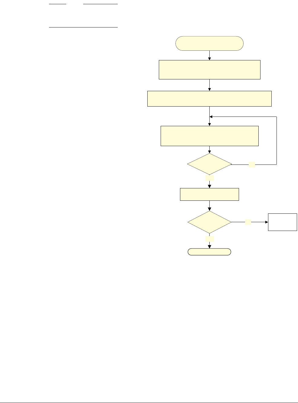
Appendix E Additional Guidance
E.4 Memory access mode in Debug state
ARM DDI 0487A.a Copyright © 2013 ARM Limited. All rights reserved. AppxE-4823
ID090413 Non-Confidential - Beta
Note
• The base address must be a multiple of 4.
• The order of the writes that set up the address does not matter in Debug state.
Figure E-1 Fast code download in AArch64 (external host to target)
In Figure E-1, the sequence for the fast code download is as follows:
1. Setup. From the external debug interface:
a. Write address [31:0] to DBGDTRRX_EL0.
b. Write address [63:32] to DBGDTRTX_EL0.
c. Write
MRS X0, DBGDTR_EL0
to EDITR. The PE executes this instruction.
d. Set EDSCR.MA to 1.
2. Loop n times. From the external debug interface:
a. Write to DBGDTRRX_EL0. The PE reads the word from DTRRX and stores it to memory. It
increments X0 by 4.
3. Epilogue. From the external debug interface:
a. Clear EDSCR.MA to 0.
b. Read EDSCR to check for overruns or Data Aborts during download.
i = i + 1
i == n
AArch64
Write D[n] to A
1. DBGDTRTX = A[63:32]
2. DBGDTRRX = A[31:0]
3. EDITR=“MRS X0,DBGDTR_EL0”
4. EDSCR.MA == 1
Set i = 0
DBGDTRRX = D[i]
Issues store through ITR
Sets ERR to 1 if there is an overrun
5. EDSCR.MA = 1
Error
recovery
6. ERR == 0
Yes
End
No
No
Yes
Appendix E Additional Guidance
E.4 Memory access mode in Debug state
AppxE-4824 Copyright © 2013 ARM Limited. All rights reserved. ARM DDI 0487A.a
Non-Confidential - Beta ID090413
Figure E-2 Fast data upload in AArch64 (target to external host)
In Figure E-2, the sequence for the fast code download is as follows:
1. Setup. From the external debug interface:
a. Write address [31:0] to DBGDTRRX_EL0.
b. Write address [63:32] to DBGDTRTX_EL0.
c. Write
MRS X0, DBGDTR_EL0
to EDITR.
d. Write
MSR DBGDTR_EL0, X0
to EDITR. This dummy operation ensures EDSCR.TXfull == 1.
e. Set EDSCR.MA to 1.
f. Read DBGDTRTX_EL0 and discard the value. The PE returns the previous DTR value, loads the first
word, and writes it to DTR. It increments X0 by 4.
2. Loop n-1 times. From the external debug interface:
a. Read DBGDTRTX_EL0. The PE returns the previous DTRTX value, loads a new word, and writes it
to DTRTX. It increments X0 by 4.
3. Epilogue. From the external debug interface:
a. Clear EDSCR.MA to 0.
b. Read DBGDTRTX_EL0 for the nth value.
i = i + 1
i == n
AArch64
Read D[n] from A
1. DBGDTRTX = A[63:32]
2. DBGDTRRX = A[31:0]
3. EDITR=“MRS X0,DBGDTR_EL0”
4. EDITR = “MSR, DBGDTR_EL0,X0” (sets TXfull to 1)
5. EDSCR.MA = 1
Set i = 0
6. Discard DBGDTRTX
Sets ERR to 1 in the case of an underrrun
Issues a load through ITR
7. EDSCR.MA = 1
8. D[n-1] = DBGDTRTX
Sets ERR to 1 if there is an underrun
Error
recovery
D[i-1] = DBGDTRTX
Sets ERR to i if there is an underrun
Issues a load through ITR
9. ERR == 0
End
No
No
Yes
Yes


Appendix E Additional Guidance
E.4 Memory access mode in Debug state
AppxE-4826 Copyright © 2013 ARM Limited. All rights reserved. ARM DDI 0487A.a
Non-Confidential - Beta ID090413

ARM DDI 0487A.a Copyright © 2013 ARM Limited. All rights reserved. AppxF-4827
ID090413 Non-Confidential - Beta
Appendix F
Barrier Litmus Tests
This appendix gives examples of the use of the barrier instructions provided by the ARMv8 architecture. It contains
the following sections:
•Introduction on page AppxF-4828.
•Load-Acquire, Store-Release and barriers on page AppxF-4831.
•Load-Acquire Exclusive, Store-Release Exclusive and barriers on page AppxF-4839.
•Using a mailbox to send an interrupt on page AppxF-4845.
•Cache and TLB maintenance operations and barriers on page AppxF-4846.
•ARMv7 compatible approaches for ordering, using DMB and DSB barriers on page AppxF-4859.
Note
This information is not part of the ARM architecture specification. It is included here as supplementary information,
for the convenience of developers and users who might require this information.

Appendix F Barrier Litmus Tests
F.1 Introduction
AppxF-4828 Copyright © 2013 ARM Limited. All rights reserved. ARM DDI 0487A.a
Non-Confidential - Beta ID090413
F.1 Introduction
The exact rules for the insertion of barriers into code sequences is a very complicated subject, and this appendix
describes many of the corner cases and behaviors that are possible in an implementation of the ARMv8 architecture.
This appendix is to help programmers, hardware design engineers, and validation engineers understand the need for
the different kinds of barriers.
F.1.1 Overview of memory consistency
Early generations of microprocessors were relatively simple processing engines that executed each instruction in
program order. In such processors, the effective behavior was that each instruction was executed in its entirety
before a subsequent instruction started to be executed. This behavior is sometimes referred to as the Sequential
Execution Model (SEM).
In later processor generations, the needs to increase processor performance, both in terms of the frequency of
operation and the number of instructions executed each cycle, mean that such a simple form of execution is
abandoned. Many techniques, such as pipelining, write buffering, caching, speculation, and out-of-order execution,
are introduced to provide improved performance.
For general purpose PEs, such as ARM, these microarchitectural innovations are largely hidden from the
programmer by a number of microarchitectural techniques. These techniques ensure that, within an individual PE,
the behavior of the PE largely remains the same as the SEM. There are some exceptions to this where explicit
synchronization is required. In the ARM architecture, these are limited to cases such as:
• Synchronization of changes to the instruction stream.
• Synchronization of changes to system control registers.
In both these cases, the
ISB
instruction provides the necessary synchronization.
While the effect of ordering is largely hidden from the programmer within a single PE, the microarchitectural
innovations have a profound impact on the ordering of memory accesses. Write buffering, speculation, and cache
coherency protocols, in particular, can all mean that the order in which memory accesses occur, as seen by an
external observer, differs significantly from the order of accesses that would appear in the SEM. This is usually
invisible in a uniprocessor environment, but the effect becomes much more significant when multiple PEs are trying
to communicate in memory. In reality, these effects are often only significant at particular synchronization
boundaries between the different threads of execution.
The problems that arise from memory ordering considerations are sometimes described as the problem of memory
consistency. Processor architectures have adopted one or more memory consistency models, or memory models, that
describe the permitted limits of the memory re-ordering that can be performed by an implementation of the
architecture. The comparison and categorization of these has generated significant research and comment in
academic circles, and ARM recommends the Memory Consistency Models for Shared Memory-Multiprocessors
paper as an excellent detailed treatment of this subject.
This appendix does not reproduce such a work, but instead concentrates on some cases that demonstrate the features
of the weakly-ordered memory model of the ARM architecture from ARMv6. In particular, the examples show how
the use of the
DMB
and
DSB
memory barrier instructions can provide the necessary safeguards to limit memory
ordering effects at the required synchronization points.
F.1.2 Barrier operation definitions
The following reference, or provide, definitions of terms used in this appendix:
DMB See Data Memory Barrier (DMB) on page B2-85.
DSB See Data Synchronization Barrier (DSB) on page B2-86.
ISB See Instruction Synchronization Barrier (ISB) on page B2-85.
Observer, Completion
See Observability and completion on page B2-82.

Appendix F Barrier Litmus Tests
F.1 Introduction
ARM DDI 0487A.a Copyright © 2013 ARM Limited. All rights reserved. AppxF-4829
ID090413 Non-Confidential - Beta
Program order
The order of instructions as they appear in an assembly language program. This appendix does not
attempt to describe or define the legal transformations from a program written in a higher level
programming language, such as C or C++, into the machine language that can then be disassembled
to give an equivalent assembly language program. Such transformations are a function of the
semantics of the higher level language and the capabilities and options on the compiler.
F.1.3 Conventions
Many of the examples are written in a stylized extension to ARM assembler, to avoid confusing the examples with
unnecessary code sequences.
AArch32
The construct
WAIT([Rx]==1)
describes the following sequence:
loop
LDR R12, [Rx]
CMP R12, #1
BNE loop
Also, the construct
WAIT_ACQ([Rx]==1)
describes the following sequence:
loop
LDA R12, [Rx] ; load acquire ensures it is ordered before subsequent loads/stores
CMP R12, #1
BNE loop
R12 is chosen as an arbitrary temporary register that is not in use. It is named to permit the generation of a false
dependency to ensure ordering.
AArch64
The construct
WAIT([Xx]==1)
describes the following sequence:
loop
LDR W12, [Xx]
CMP W12, #1
B.NE loop
Also, the construct
WAIT_ACQ([Xx]==1)
and describes the following sequence:
loop
LDAR W12, [Xx] ; load acquire ensures it is ordered before subsequent loads/stores
CMP W12, #1
B.NE loop
For each example, a code sequence is preceded by an identifier of the observer running it:
• P0, P1…Px refer to caching coherent PEs that implement the ARMv8 architecture, and are in the same
shareability domain.
• E0, E1…Ex refer to non-caching observers, that do not participate in the coherency protocol, but execute
ARM instructions and have a weakly-ordered memory model. This does not preclude these observers being
different objects, such as DMA engines or other system masters.
These observers are unsynchronized other than as required by the documented code sequence.

Appendix F Barrier Litmus Tests
F.1 Introduction
AppxF-4830 Copyright © 2013 ARM Limited. All rights reserved. ARM DDI 0487A.a
Non-Confidential - Beta ID090413
Note
Throughout this appendix, ARM instruction and instruction refer to instructions from the A64, A32, or T32
instruction set, provided by ARMv8 implementations.
Results are expressed in terms of
<agent>:<register>
, such as
P0:R5
. The results can be described as:
Permissible This does not imply that the results expressed are required or are the only possible results.
In most cases they are results that would not be possible under a sequentially consistent
running of the code sequences on the agents involved. In general terms, this means that these
results might be unexpected to anyone unfamiliar with memory consistency issues.
Not permissible Results that the architecture expressly forbids.
Required Results that the architecture expressly requires.
The examples omit the required shareability domain arguments of
DMB
and
DSB
instructions. The arguments are
assumed to be selected appropriately for the shareability domains of the observers.
In AArch32 state, where the barrier function in the litmus test can be achieved by a
DMB ST
, that is a barrier to stores
only, this is shown by the use of
DMB [ST]
. This indicates that the
ST
qualifier can be omitted without affecting the
result of the test. In some implementations
DMB ST
is faster than
DMB
.
For AArch64 code, the shareability domain of the
DMB
or
DSB
must be included. This is shown in this document using
the notation
DMB <domain>
and
DSB <domain>
respectively.
Except where otherwise stated, other conventions are:
• All memory initializes to 0.
• R0 and W0 contain the value 1.
• R1 - R4 and W1 - W4 contain arbitrary independent addresses that initialize to the same value on all PEs.
The addresses held in these registers are Shareable and:
— The addresses held in R1 and R2 are in Write-Back Cacheable Normal memory.
— The address held in R3 is in Write-Through Cacheable Normal memory.
— The address held in R4 is in Non-cacheable Normal memory.
• R5 - R8 and W5 - W8 contain:
— When used with an
STR
instruction,
0x55
,
0x66
,
0x77
, and
0x88
respectively.
— When used with an
LDR
instruction, the value 0.
• R11 and W11 contain a new instruction or new translation table entry, as appropriate, and R10 contains the
virtual address and the ASID, for use in this change of translation table entry.
• Memory locations are Normal memory locations unless otherwise stated.
The examples use mnemonics for the cache maintenance and TLB maintenance operations. The following tables
describe the mnemonics:
•Cache maintenance operations, functional group on page G3-3743
•TLB maintenance operations, functional group on page G3-3744.
Notes on timing effects
The ARMv8 architecture makes no statement about when an instruction will occur. In particular, stores may take an
unbounded time to be observed by other observers. Therefore the
WAIT
loop waiting for the result of that store may
take an unbounded time to move forward.
In cases that it is necessary to guarantee the completion of a store, a
DSB
instruction can be used to force this drain.
In general, the examples in this document associated with ordering assume that stores will become observable over
time and so a final
DSB
barrier to ensure the completion of stores is omitted.

Appendix F Barrier Litmus Tests
F.2 Load-Acquire, Store-Release and barriers
ARM DDI 0487A.a Copyright © 2013 ARM Limited. All rights reserved. AppxF-4831
ID090413 Non-Confidential - Beta
F.2 Load-Acquire, Store-Release and barriers
The Load-Acquire and Store-Release instructions are described in Load-Acquire, Store-Release on page B2-87.
The following sections show that most of the examples in sections Simple ordering and barrier cases on
page AppxF-4859 and Load-Exclusive, Store-Exclusive and barriers on page AppxF-4866 can be achieved using
the Load-Acquire and Store-Release instructions without the need for additional barriers.
F.2.1 Message passing
The following sections describe:
•Resolving weakly-ordered message passing by using Acquire and Release.
•Resolving message passing by the use of Store-Release and address dependency on page AppxF-4832.
Resolving weakly-ordered message passing by using Acquire and Release
The message passing problem described in Weakly-ordered message passing problem on page AppxF-4859 can be
solved by the use of Load-Acquire and Store-Release instructions when accessing the communications flag:
AArch32
P1
STR R5, [R1] ; set new data
STL R0, [R2] ; send flag indicating data ready, which is ordered after all
P2
WAIT_ACQ([R2]==1) ; wait on flag
LDR R5, [R1]
AArch64
P1
STR W5, [X1] ; set new data
STL W0, [X2] ; send flag indicating data ready, which is ordered after all
P2
WAIT_ACQ([X2]==1) ; wait on flag
LDR W5, [X1]
This ensures the observed order of both the reads and the writes allows transfer of data such that the result
P2:R5==
0x55
is guaranteed.
This approach also works with multiple observers, in a way that further observers use the same sequence as P2 uses:
AArch32
P3
WAIT_ACQ([R2]==1) ; wait on flag
LDR R5, [R1]

Appendix F Barrier Litmus Tests
F.2 Load-Acquire, Store-Release and barriers
AppxF-4832 Copyright © 2013 ARM Limited. All rights reserved. ARM DDI 0487A.a
Non-Confidential - Beta ID090413
AArch64
P3
WAIT_ACQ([X2]==1) ; wait on flag
LDR W5, [X1]
Resolving message passing by the use of Store-Release and address dependency
The lack of ordering of stores discussed in Message passing with multiple observers on page AppxF-4861 can be
resolved by the use of Store-Release for the store of the valid flag by P1, even when the observers are using an
address dependency:
AArch32
P1
STR R5, [R1] ; set new data
STL R0, [R2] ; send flag indicating data ready using a Store Release
P2
WAIT([R2]==1)
AND R12, R12, #0 ; R12 is destination of LDR in WAIT macro
LDR R5, [R1, R12] ; Load is dependent and so is ordered after the flag has been seen
AArch64
P1
STR W5, [X1] ; set new data
STLR W0, [X2] ; send flag indicating data ready using a Store Release
P2
WAIT([X2]==1)
AND W12, W12, WZR ; R12 is destination of LDR in WAIT macro
LDR W5, [X1, X12] ; Load is dependent and so is ordered after the flag has been seen
This ensures the observed order of the writes allows transfer of data such that P2:R5 and P3:R5 contain the same
value of
0x55
.
This approach also works with multiple observers, in a way that further observers use the same sequence as P2 uses:
AArch32
P3
WAIT([R2]==1)
AND R12, R12, #0 ; R12 is destination of LDR in WAIT macro
LDR R5, [R1, R12] ; Load is dependent and so is ordered after the flag has been seen

Appendix F Barrier Litmus Tests
F.2 Load-Acquire, Store-Release and barriers
ARM DDI 0487A.a Copyright © 2013 ARM Limited. All rights reserved. AppxF-4833
ID090413 Non-Confidential - Beta
AArch64
P3
WAIT([X2]==1)
AND W12, W12, WZR ; R12 is destination of LDR in WAIT macro
LDR W5, [X1, X12] ; Load is dependent and so is ordered after the flag has been seen
F.2.2 Address dependency with object construction
When accessing an object-oriented data structure, the address dependency rule means that barriers are not required,
even when initializing the object. A Store-Release can be used to ensure the order of the update of the base address:
AArch32
P1
STR R5, [R1, #offset] ; set new data in a field
STL R1, [R2] ; update base address
P2
LDR R1, [R2] ; read for base address
CMP R1, #0 ; check if it is valid
BEQ null_trap
LDR R5, [R1, #offset] ; use base address to read field
AArch64
P1
STR W5, [X1, #offset] ; set new data in a field
STLR X1, [X2] ; update base address
P2
LDR X1, [X2] ; read for base address
CMP X1, #0 ; check if it is valid
B.EQ null_trap
LDR W5, [X1, #offset] ; use base address to read field
It is required that P2:R5==
0x55
if the null_trap is not taken. This avoids P2 observing a partially constructed object
from P1. Significantly, P2 does not need a barrier to ensure this behavior.
The read of the base address in P2 could be a Load-Acquire, but it is not necessary in this case.

Appendix F Barrier Litmus Tests
F.2 Load-Acquire, Store-Release and barriers
AppxF-4834 Copyright © 2013 ARM Limited. All rights reserved. ARM DDI 0487A.a
Non-Confidential - Beta ID090413
F.2.3 Causal consistency issues with multiple observers
The cause consistent problem discussed in Causal consistency issues with multiple observers on page AppxF-4862
can be addressed by the use of a Store-Release, as this requires that the store is multicopy atomic in the case of a
Load-Acquire. In addition, a Store-Release has an effect on the observation order of any stores observed by the
observer executing the Store-Release.
The following sequences guarantee causal consistency:
•Using multi-copy atomicity of the Store-Release when observed by Load-Acquire.
•Using ordering property of Store-Release on stores observed by the PE on page AppxF-4835.
Using multi-copy atomicity of the Store-Release when observed by Load-Acquire
AArch32
P1
STL R0, [R2] ; set new data
; this is made multi-copy atomic
P2
WAIT_ACQ([R2]==1) ; wait to see new data from P1
STR R0, [R3] ; send flag
; must be after the new data has been by P2 as stores must not be speculative
; this does not need to be a store release, though it could be a store
release
P3
WAIT([R3]==1) ; wait for P2 flag
; this does not need to be a WAIT_ACQ, although
; it could be a WAIT_ACQ (at which point the dependency is not needed)
AND R12, R12, #0 ; dependency to ensure order (only needed for a WAIT, not WAIT_ACQ)
LDA R0, [R2, R12] ; read P1 data using a Load-Acquire
AArch64
P1
STLR W0, [X2] ; set new data
; this is made multi-copy atomic
P2
WAIT_ACQ([X2]==1) ; wait to see new data from P1
STR W0, [X3] ; send flag
; must be after the new data has been by P2 as stores
; must not be speculative
; this does not need to be a store release, though it could be a
; store release
P3
WAIT([X3]==1) ; wait for P2 flag
; this does not need to be a WAIT_ACQ, though

Appendix F Barrier Litmus Tests
F.2 Load-Acquire, Store-Release and barriers
ARM DDI 0487A.a Copyright © 2013 ARM Limited. All rights reserved. AppxF-4835
ID090413 Non-Confidential - Beta
; it could be a WAIT_ACQ (at which point the dependency is not needed
AND W12, W12, WZR ; dependency to ensure order (only needed for a WAIT, not WAIT_ACQ)
LDAR W0, [X2, X12] ; read P1 data using a Load-Acquire
In this case, P3:R0 == 0 is not permissible. P3 is guaranteed to see the store from P1 if P2 has seen the store from
P1 using a Load-Acquire.
Using ordering property of Store-Release on stores observed by the PE
AArch32
P1
STR R0, [R2] ; set new data
; this does not have to be a store release, though it
; could be a store release
P2
WAIT ([R2]==1) ; wait to see new data from P1
; this does not need to be a WAIT_ACQ, though it could be a WAIT_ACQ
STL R0, [R3] ; send flag
; must be after the new data has been by P2 as stores must not be speculative
; as a store release, this orders P1 store
P3
WAIT([R3]==1) ; wait for P2 flag
; this does not need to be a WAIT_ACQ, although it could be a WAIT_ACQ
; (at which point the dependency is not needed)
AND R12, R12, #0 ; dependency to ensure order (only needed for a WAIT, not WAIT_ACQ)
LDR R0, [R2, R12] ; read P1 data
AArch64
P1
STR W0, [X2] ; set new data
; this does not have to be a store release, though it
; could be a store release
P2
WAIT ([X2]==1) ; wait to see new data from P1
; this does not need to be a WAIT_ACQ, though it could be a WAIT_ACQ
STLR W0, [X3] ; send flag
; must be after the new data has been by P2 as stores must not be speculative
; as a store release, this orders P1 store
P3
WAIT([X3]==1) ; wait for P2 flag
; this does not need to be a WAIT_ACQ, though it could be a WAIT_ACQ

Appendix F Barrier Litmus Tests
F.2 Load-Acquire, Store-Release and barriers
AppxF-4836 Copyright © 2013 ARM Limited. All rights reserved. ARM DDI 0487A.a
Non-Confidential - Beta ID090413
; at which point the dependency is not needed
AND W12, W12, WZR ; dependency to ensure order
; only needed for a WAIT, not WAIT_ACQ
LDR W0, [X2, X12] ; read P1 data
In this case, P3:R0 == 0 is not permissible. P3 is guaranteed to see the store from P1 if P2 has seen the store from
P1 using a Load-Acquire.
Note
The use of dependency by P3 could be replaced by a Load-Acquire.
F.2.4 Multiple observers of writes to multiple locations
The ARM weakly consistent memory model means that different observers can observe writes to different locations
in different orders as was shown in Multiple observers of writes to multiple locations on page AppxF-4863, but the
use of Load-Acquire and Store-Release can resolve this. In this case, the loads by P3 and P4 must be Load-Acquire
in order to ensure the perceived multi-copy atomicity of the stores:
AArch32
P1
STL R0, [R1] ; set new data
P2
STL R0, [R2] ; set new data
P3
LDA R10, [R2] ; read P2 data before P1
LDA R9, [R1] ;
BIC R9, R10, R9 ; R9 <- R10 & ~R9
; R9 contains 1 if read from [R2] is observed to be 1 and
; read from [R1] is observed to be 0
P4
LDA R9, [R1]
LDA R10, [R2]
BIC R9, R9, R10 ; R9 <- R9 & ~R10
; R9 contains 1 if read from [R2] is observed to be 0 and
; read from [R1] is observed to be 1
AArch64
P1
STLR W0, [X1] ; set new data
P2
STLR W0, [X2] ; set new data
P3
LDAR W10, [X2] ; read P2 data before P1

Appendix F Barrier Litmus Tests
F.2 Load-Acquire, Store-Release and barriers
ARM DDI 0487A.a Copyright © 2013 ARM Limited. All rights reserved. AppxF-4837
ID090413 Non-Confidential - Beta
LDAR W9, [X1] ;
BIC W9, W10, W9 ; W9 <- W10 & ~W9
; W9 contains 1 if read from [X2] is observed to be 1 and
; read from [X1] is observed to be 0
P4
LDAR W9, [X1]
LDAR W10, [X2]
BIC W9, W9, W10 ; W9 <- W9 & ~W10
; W9 contains 1 if read from [X2] is observed to be 0 and
; read from [X1] is observed to be 1
In this case, the result P3:R9==1 and P4:R9==1 is not permissible, as the stores from P1 and P2 are multi-copy
atomic when read by Load-Acquire.
Therefore, if P3 gets R10==1, then we know that the P3 load of R9 can only be observed after we know that P4 has
also observed the P2 store to [R2]. Similarly, if the P4 load of R9 returns 1, and the P3 load of R9 returns 0, then
the P3 load must have occurred before the P4 load.
Therefore, if the P3 load of R10 returns 1 and the P3 load of R9 returns 0, then we know that if the P4 load of R9
returns 1, it must have happened after P4 has observed the P2 store to [R2], so the P4 load of R10 must return 1.
This shows that, of the 4 possible values for {P3:R9, P4:R9}, the use of these instructions makes the result {1,1}
impossible.
F.2.5 WFE and WFI and barriers
The Wait For Event and Wait For Interrupt instructions permit the PE to suspend execution and enter a low-power
state. An explicit
DSB
barrier instruction is required if it is necessary to ensure memory accesses made before the
WFI
or
WFE
are visible to other observers, unless some other mechanism has ensured this visibility. Examples of other
mechanism that would guarantee the required visibility are the
DMB
described in Posting a store before polling for
acknowledgement on page AppxF-4864, or a dependency on a load.
The following example requires the
DSB
to ensure that the store is visible:
AArch32
P1
STR R0, [R2]
DSB
Loop
WFI
B Loop
AArch64
P1
STR W0, [X2]
DSB <domain>
Loop

Appendix F Barrier Litmus Tests
F.2 Load-Acquire, Store-Release and barriers
AppxF-4838 Copyright © 2013 ARM Limited. All rights reserved. ARM DDI 0487A.a
Non-Confidential - Beta ID090413
WFI
B Loop
This requirement is unchanged in ARMv8 by the presence of Load-Acquire or Store-Release.

Appendix F Barrier Litmus Tests
F.3 Load-Acquire Exclusive, Store-Release Exclusive and barriers
ARM DDI 0487A.a Copyright © 2013 ARM Limited. All rights reserved. AppxF-4839
ID090413 Non-Confidential - Beta
F.3 Load-Acquire Exclusive, Store-Release Exclusive and barriers
The ARMv8 architecture adds the acquire and release semantics to Load-Exclusive and Store-Exclusive
instructions, which allows them to gain ordering acquire and/or release semantics.
The Load-Exclusive instruction can be specified to have acquire semantics, and the Store-Exclusive instruction can
be specified to have release semantics. These can be arbitrarily combined to allow the atomic update created by a
successful Load-Exclusive and Store-Exclusive pair to have any of:
• No Ordering semantics (using
LDREX
and
STREX
).
• Acquire only semantics (using
LDAEX
and
STREX
).
• Release only semantics (using
LDREX
and
STLEX
).
• Sequentially consistent semantics (using
LDAEX
and
STLEX
).
In addition, the ARMv8 specification requires that the clearing of a global monitor will generate an event for the PE
associated with the global monitor, which can simplify the use of
WFE
, by removing the need for a
DSB
barrier and
SEV
instruction.
F.3.1 Acquiring a lock
A common use of Load-Exclusive and Store-Exclusive instructions is to claim a lock to permit entry into a critical
region. This is typically performed by testing a lock variable that indicates 0 for a free lock and some other value,
commonly 1 or an identifier of the process holding the lock, for a taken lock.
For a critical region, the requirement on taking a lock is usually for acquire semantics, while the clearing of a lock
requires release semantics:
AArch32
Px
PLDW[R1] ; preload into cache in unique state
Loop
LDAEX R5, [R1] ; read lock with acquire
CMP R5, #0 ; check if 0
STREXEQ R5, R0, [R1] ; attempt to store new value
CMPEQ R5, #0 ; test if store suceeded
BNE Loop ; retry if not
; loads and stores in the critical region can now be performed
AArch64
Px
PRFM PSTL1KEEP, [X1] ; preload into cache in unique state
Loop
LDAXR W5, [X1] ; read lock with acquire
CBNZ W5, Loop ; check if 0
STXR W5, W0, [X1] ; attempt to store new value
CBNZ W5, Loop ; test if store succeeded and retry if not
; loads and stores in the critical region can now be performed

Appendix F Barrier Litmus Tests
F.3 Load-Acquire Exclusive, Store-Release Exclusive and barriers
AppxF-4840 Copyright © 2013 ARM Limited. All rights reserved. ARM DDI 0487A.a
Non-Confidential - Beta ID090413
The acquire associated with the load is sufficient to ensure the required ordering in a lock situation. The
Store-Exclusive will fail (and so be retried) if there is a store to the location being monitored between the
Load-Exclusive and the Store-Exclusive.
F.3.2 Releasing a lock
The converse operation of releasing a lock does not require the use of Load-Exclusive and Store-Exclusive
instructions, because only a single observer is able to write to the lock. However, often it is necessary for any
observer to observe any memory updates, or any values that are loaded into memory, before they observe the release
of the lock. Therefore, the lock release needs release semantics:
AArch32
Px
; loads and stores in the critical region
MOV R0, #0
STL R0, [R1] ; clear the lock with release semantics
AArch64
Px
; loads and stores in the critical region
STLR WZR, [X1] ; clear the lock with release semantics
F.3.3 Ticket locks
When a lock is free, in order to avoid a rush to get the lock by many PEs, the use of ticket locks is common in more
advanced systems. When the use is requested, the ticket locks determine the order of the users of the critical
sections, in order to avoid starvation that can occur with a simple contention based spin lock.
A ticket lock allocates each thread a ticket number when it first requests the lock, and then compares that number
with the current number for the lock. If they are the same, then the critical section can be entered. Otherwise the
thread waits until the current number is equal to the ticket number for that thread.
The reading of the current number of the lock needs acquire semantics for the lock to be acquired.
Note
The code in this section is little-endian code, as it views the combined current and next values as a single combined
quantity. The addresses of the current and next ticket values need to be adjusted for a big-endian system.
This is shown in the implementation below:
AArch32
Px
; R1 holds two 16 bit quantities
; the lower halfword holds the current ticket number
; the higher halfword holds the next ticket number
PLDW[R1] ; preload into cache in unique state
Loop1
LDAEX R5, [R1] ; read current and next

Appendix F Barrier Litmus Tests
F.3 Load-Acquire Exclusive, Store-Release Exclusive and barriers
ARM DDI 0487A.a Copyright © 2013 ARM Limited. All rights reserved. AppxF-4841
ID090413 Non-Confidential - Beta
ADD R5, R5, #0x10000 ; increment the next number
STREX R6, R5, [R1] ; and update the value
CMP R6, #0 ; did the exclusive pass
BNE Loop1 ; retry if not
CMP R5, R5, ROR #16 ; is the current ticket ours
BEQ block_start
Loop2
LDAH R6, [R1] ; read current value
CMP R6, R5, LSR #16 ; compare it with our allocated ticket
BNE Loop2 ; retry (spin) if it is not the same
block_start
AArch64
Px
; X1 holds 2 16 bit quantities
; the lower halfword holds the current ticket number
; the higher halfword holds the next ticket number
PRFM PSTL1KEEP, [X1] ; preload into cache in unique state
Loop1
LDAXR W5, [X1] ; read current and next
ADD W5, W5, #0x10000 ; increment the next number
STXR W6, W5, [X1] ; and update the value
CBNZ W6, Loop1 ; did the exclusive pass – retry if not
AND W6, W5, #0xFFFF
CMP W6, W5, LSR #16 ; is the current ticket ours
B.EQ block_start
Loop2
LDARH W6, [X1] ; read current value
CMP W6, W5, LSR #16 ; compare it with the our allocated ticket
B.NE Loop2 ; retry (spin) if it isn’t the same
block_start
Releasing the ticket lock simply involves incrementing the current ticket number, that is still assumed to be in R3,
and doing a Store-Release:
AArch32
ADD R6, R6, #1

Appendix F Barrier Litmus Tests
F.3 Load-Acquire Exclusive, Store-Release Exclusive and barriers
AppxF-4842 Copyright © 2013 ARM Limited. All rights reserved. ARM DDI 0487A.a
Non-Confidential - Beta ID090413
STLH R6, [R1]
AArch64
ADD W6, W6, #1
STLRH W6, [X1]
F.3.4 Use of Wait For Event (WFE) and Send Event (SEV) with locks
The ARMv8 architecture can use the Wait For Event mechanism to minimise the energy cost of polling variables
by putting the PE into a low power state, suspending execution, until an asynchronous exception or an explicit event
is seen by that PE. In ARMv8, the event can be generated as a result of clearing the global monitor, so removing the
need for a
DSB
barrier or an explicit send event message.
This can be used with simple locks or with ticket locks.
Simple lock
The following is an example of lock acquire code using
WFE
:
AArch32
Px
PLDW[R1] ; preload into cache in unique state
Loop
LDAEX R5, [R1] ; read lock with acquire
CMP R5, #0 ; check if 0
WFENE ; sleep if the lock is held
STREXEQ R5, R0, [R1] ; attempt to store new value
CMPEQ R5, #0 ; test if store succeeded
BNE Loop ; retry if not
AArch64
Px
SEVL ; invalidates the WFE on the first loop iteration
PRFM PSTL1KEEP, [X1] ; allocate into cache in unique state
Loop
WFE
LDAXR W5, [X1] ; read lock with acquire
CBNZ W5, Loop ; check if 0
STXR W5, W0, [X1] ; attempt to store new value
CBNZ W5, Loop ; test if store succeeded and retry if not
; loads and stores in the critical region can now be performed
And the following is an example of lock release code:
AArch32

Appendix F Barrier Litmus Tests
F.3 Load-Acquire Exclusive, Store-Release Exclusive and barriers
ARM DDI 0487A.a Copyright © 2013 ARM Limited. All rights reserved. AppxF-4843
ID090413 Non-Confidential - Beta
Px
; loads and stores in the critical region
MOV R0, #0
STL R0, [R1] ; clear the lock
AArch64
Px
; loads and stores in the critical region
STLR WZR, [X1] ; clear the lock
Ticket lock
In the Ticket lock case, the Load-Exclusive instruction can be used to move the monitor into the exclusive state for
the express purpose of creating an event when the monitor changes state:
AArch32
Px
; R1 holds 2 16 bit quantities
; the lower halfword holds the current ticket number
; the higher halfword holds the next ticket number
PLDW[R1] ; preload into cache in unique state
Loop1
LDAEX R5, [R1] ; read current and next
ADD R5, R5, #0x10000 ; increment the next number
STREX R6, R5, [R1] ; and update the value
CMP R6, #0 ; did the exclusive pass
BNE Loop ; retry if not
CMP R5, R5, ROR #16 ; is the current ticket ours
BEQ block_start
SEVL
Loop2
WFE ; wait if there has not been a change to the count since last
; read
LDAEXH R6, [R1] ; check the current count
CMP R6, R5, LSR #16 ; check if it is equal
BNE Loop2
block_start
AArch64
Px
; X1 holds 2 16 bit quantities
; the lower halfword holds the current ticket number
; the higher halfword holds the next ticket number
PRFM PSTL1KEEP, [X1] ; preload into cache in unique state
Loop1
LDAXR W5, [X1] ; read current and next
ADD W5, W5, #0x10000 ; increment the next number
STXR W6, W5, [X1] ; and update the value
CBNZ W6, Loop1 ; did the exclusive pass – retry if not
AND W6, W5, 0xFFFF
CMP W6, W5, LSR #16 ; is the current ticket ours

Appendix F Barrier Litmus Tests
F.3 Load-Acquire Exclusive, Store-Release Exclusive and barriers
AppxF-4844 Copyright © 2013 ARM Limited. All rights reserved. ARM DDI 0487A.a
Non-Confidential - Beta ID090413
B.EQ block_start
SEVL
Loop2
WFE
LDAXRH W6, [X1] ; read current value
CMP W6, W5, LSR #16 ; compare it with our allocated ticket
B.NE Loop2 ; retry (spin) if it is not the same
block_start

Appendix F Barrier Litmus Tests
F.4 Using a mailbox to send an interrupt
ARM DDI 0487A.a Copyright © 2013 ARM Limited. All rights reserved. AppxF-4845
ID090413 Non-Confidential - Beta
F.4 Using a mailbox to send an interrupt
In some message passing systems, it is common for one observer to update memory and then notify a second
observer of the update by sending an interrupt, using a mailbox.
Although a memory access might be made to initiate the sending of the mailbox interrupt, a
DSB
instruction is
required to ensure the completion of previous memory accesses.
Therefore, the following sequence is required to ensure that P2 observes the updated value:
AArch32
P1
STR R5, [R1] ; message stored to shared memory location
DSB ST
STR R0, [R4] ; R4 contains the address of a mailbox
P2
; interrupt service routine
LDR R5, [R1]
AArch64
P1
STR W5, [X1] ; message stored to shared memory location
DSB ST
STR W0, [X4] ; R4 contains the address of a mailbox
P2
; interrupt service routine
LDR W5, [X1]
These rules are required in connection to the ARM Generic Interrupt Controller (GIC).

Appendix F Barrier Litmus Tests
F.5 Cache and TLB maintenance operations and barriers
AppxF-4846 Copyright © 2013 ARM Limited. All rights reserved. ARM DDI 0487A.a
Non-Confidential - Beta ID090413
F.5 Cache and TLB maintenance operations and barriers
The following sections describe the use of barriers with cache and TLB maintenance operations:
•Data cache maintenance operations
•Instruction cache maintenance operations on page AppxF-4851
•TLB maintenance operations and barriers on page AppxF-4854.
F.5.1 Data cache maintenance operations
The following sections describe the use of barriers with data cache maintenance operations:
•Message passing to non-caching observers
•Multiprocessing message passing to non-caching observers on page AppxF-4847
•Invalidating DMA buffers, non-functional example on page AppxF-4848
•Invalidating DMA buffers, functional example with single PE on page AppxF-4849
•Invalidating DMA buffers, functional example with multiple coherent PEs on page AppxF-4850.
Message passing to non-caching observers
The ARMv8 architecture requires the use of
DMB
instructions to ensure the ordering of data cache maintenance
operations and their effects. The Load-Acquire and Store-Release instructions have no effect on cache maintenance
operation. This means the following message passing approaches can be used when communicating between
caching observers and non-caching observers:
AArch32
P1
STR R5, [R1] ; update data (assumed to be in P1 cache)
DCCMVAC R1 ; clean cache to point of coherency
DMB ; ensure effects of the clean will be observed before the
; flag is set
STR R0, [R4] ; send flag to external agent (Non-cacheable location)
E1
WAIT_ACQ ([R4] == 1) ; wait for the flag (with order)
LDR R5, [R1] ; read the data
AArch64
P1
STR W5, [X1] ; update data (assumed to be in P1 cache)
DC CVAC, X1 ; clean cache to point of coherency
DMB ISH ; ensure effects of the clean will be observed before the
; flag is set
STR W0, [X4] ; send flag to external agent (Non-cacheable location)
E1
WAIT_ACQ ([X4] == 1) ; wait for the flag (with order)
LDR W5, [X1] ; read the data
In this example, it is required that E1:R5==
0x55
.

Appendix F Barrier Litmus Tests
F.5 Cache and TLB maintenance operations and barriers
ARM DDI 0487A.a Copyright © 2013 ARM Limited. All rights reserved. AppxF-4847
ID090413 Non-Confidential - Beta
Multiprocessing message passing to non-caching observers
The broadcast nature of the cache maintenance operations combined with properties of barriers, means that the
message passing principle for non-caching observers is:
AArch32
P1
STR R5, [R1] ; update data (assumed to be in P1 cache)
STL R0, [R2] ; send a flag for P2 (ordered by the store release)
P2
WAIT ([R2] == 1) ; wait for P1 flag
DMB ; ensure cache clean is observed after P1 flag is observed
DCCMVAC R1 ; clean cache to point of coherency ? will clean P1 cache
DMB ; ensure effects of the clean will be observed before the
; flag to E1 is set
STR R0, [R4] ; send flag to E1
E1
WAIT_ACQ ([R4] == 1) ; wait for P2 flag (ordered)
LDR R5, [R1] ; read data
AArch64
P1
STR W5, [X1] ; update data (assumed to be in P1 cache)
STLR W0, [X2] ; send a flag for P2 (ordered)
P2
WAIT ([X2] == 1) ; wait for P1 flag
DMB SY ; ensure cache clean is observed after P1 flag is observed
DC CVAC, X1 ; clean cache to point of coherency, will clean P1 cache
DMB SY ; ensure effects of the clean will be observed before the
; flag to E1 is set
STR W0, [X4] ; send flag to E1
E1
WAIT_ACQ ([X4] == 1) ; wait for P2 flag
LDR W5, [X1] ; read data
In this example, it is required that E1:R5==
0x55
. The clean operation executed by P2 affects the data location in the
P1 cache. The cast-out from the P1 cache is guaranteed to be observed before P2 updates [R4].

Appendix F Barrier Litmus Tests
F.5 Cache and TLB maintenance operations and barriers
AppxF-4848 Copyright © 2013 ARM Limited. All rights reserved. ARM DDI 0487A.a
Non-Confidential - Beta ID090413
Note
The cache maintenance operations are not ordered by the Load-Acquire and Store-Release instructions.
Invalidating DMA buffers, non-functional example
The basic scheme for communicating with an external observer that is a process that passes data in to a Cacheable
memory region must take account of the architectural requirement that regions marked as Cacheable can be
allocated into a cache at any time, for example as a result of speculation. The following example shows this
possibility:
AArch32
P1
DCIMVAC R1 ; ensure cache clean wrt memory. A clean operation could be used
; but as the DMA will subsequently overwrite this region an
; invalidate operation is sufficient and usually more efficient
DMB ; ensures cache invalidation is observed before the next store
; is observed
STR R0, [R3] ; send flag to external agent
WAIT_ACQ ([R4]==1) ; wait for a different flag from an external agent
LDR R5, [R1]
E1
WAIT ([R3] == 1) ; wait for flag
STR R5, [R1] ; store new data
STL R0, [R4] ; send a flag
AArch64
P1
DC IVAC, X1 ; ensure cache clean wrt memory. A clean operation could be used
; but as the DMA will subsequently overwrite this region an
; invalidate operation is sufficient and usually more efficient
DMB SY ; ensures cache invalidation is observed before the next store
; is observed
STR W0, [X3] ; send flag to external agent
WAIT_ACQ ([X4]==1) ; wait for a different flag from an external agent
LDR W5, [X1]
E1
WAIT ([X3] == 1) ; wait for flag
STR W5, [X1] ; store new data
STLR W0, [X4] ; send a flag
If a speculative access occurs, there is no guarantee that the cache line containing [R1] is not brought back into the
cache after the cache invalidation, but before [R1] is written by E1. Therefore, the result P1:R5=0 is permissible.

Appendix F Barrier Litmus Tests
F.5 Cache and TLB maintenance operations and barriers
ARM DDI 0487A.a Copyright © 2013 ARM Limited. All rights reserved. AppxF-4849
ID090413 Non-Confidential - Beta
Invalidating DMA buffers, functional example with single PE
AArch32
P1
DCIMVAC R1 ; ensure cache clean wrt memory. A clean operation could be used
; but as the DMA will subsequently overwrite this region an
; invalidate operation is sufficient and usually more efficient
DMB ; ensures cache invalidation is observed before the next store
; is observed
STR R0, [R3] ; send flag to external agent
WAIT ([R4]==1) ; wait for a different flag from an external agent
DMB ; ensure that cache invalidate is observed after the flag
; from external agent is observed
DCIMVAC R1 ; ensure cache discards stale copies before use
LDR R5, [R1]
E1
WAIT ([R3] == 1) ; wait for flag
STR R5, [R1] ; store new data
STL R0, [R4] ; send a flag
AArch64
P1
DC IVAC, X1 ; ensure cache clean wrt memory. A clean operation could be used
; but as the DMA will subsequently overwrite this region an
; invalidate operation is sufficient and usually more efficient
DMB SY ; ensures cache invalidation is observed before the next store
; is observed
STR W0, [X3] ; send flag to external agent
WAIT ([X4]==1) ; wait for a different flag from an external agent
DMB SY ; ensure that cache invalidate is observed after the flag
; from external agent is observed
DC IVAC, X1 ; ensure cache discards stale copies before use
LDR W5, [X1]
E1
WAIT ([X3] == 1) ; wait for flag
STR W5, [X1] ; store new data
STLR W0, [X4] ; send a flag
In this example, the result P1:R5 ==
0x55
is required. Including a cache invalidation after the store by E1 to [R1] is
observed ensures that the line is fetched from external memory after it has been updated.

Appendix F Barrier Litmus Tests
F.5 Cache and TLB maintenance operations and barriers
AppxF-4850 Copyright © 2013 ARM Limited. All rights reserved. ARM DDI 0487A.a
Non-Confidential - Beta ID090413
Invalidating DMA buffers, functional example with multiple coherent PEs
The broadcasting of cache maintenance operations, and the use of
DMB
instructions to ensure their observability,
means that the previous example extends naturally to a multiprocessor system. Typically this requires a transfer of
ownership of the region that the external observer is updating.
AArch32
P0
(Use data from [R1], potentially using [R1] as scratch space)
STL R0, [R2] ; signal release of [R1]
WAIT_ACQ ([R2] == 0) ; wait for new value from DMA
LDR R5, [R1]
P1
WAIT ([R2] == 1) ; wait for release of [R1] by P0
DCIMVAC R1 ; ensure caches are clean wrt memory, invalidate is sufficient
DMB
STR R0, [R3] ; request new data for [R1]
WAIT ([R4] == 1) ; wait for new data
DMB
DCIMVAC R1 ; ensure caches discard stale copies before use
DMB
MOV R0, #0
STR R0, [R2] ; signal availability of new [R1]
E1
WAIT ([R3] == 1) ; wait for new data request
STR R5, [R1] ; send new [R1]
DMB [ST]
STR R0, [R4] ; indicate new data available to P1
AArch64
P0
(Use data from [X1], potentially using [X1] as scratch space)
STLR W0, [X2] ; signal release of [X1]
WAIT_ACQ ([X2] == 0) ; wait for new value from DMA
LDR W5, [X1]
P1
WAIT ([X2] == 1) ; wait for release of [R1] by P0
DC IVAC, X1 ; ensure caches are clean wrt memory, invalidate is sufficient
DMB SY
STR W0, [X3] ; request new data for [R1]
WAIT ([X4] == 1) ; wait for new data

Appendix F Barrier Litmus Tests
F.5 Cache and TLB maintenance operations and barriers
ARM DDI 0487A.a Copyright © 2013 ARM Limited. All rights reserved. AppxF-4851
ID090413 Non-Confidential - Beta
DMB SY
DCIMVAC X1 ; ensure caches discard stale copies before use
DMB SY
STR WZR, [X2] ; signal availability of new [R1]
E1
WAIT ([X3] == 1) ; wait for new data request
STR W5, [X1] ; send new [R1]
STR W0, [X4] ; indicate new data available to P1
In this example, the result P0:R5 ==
0x55
is required. The
DMB
issued by P1 after the first data cache invalidation
ensures that effect of the cache invalidation on P0 is seen by E1 before the store by E1 to [R1]. The
DMB
issued by
P1 after the second data cache invalidation ensures that its effects are seen before the store of 0 to the semaphore
location in [R2].
F.5.2 Instruction cache maintenance operations
The following sections describe the use of barriers with instruction cache maintenance operations:
•Ensuring the visibility of updates to instructions for a uniprocessor
•Ensuring the visibility of updates to instructions for a multiprocessor on page AppxF-4852.
Ensuring the visibility of updates to instructions for a uniprocessor
On a single PE, the agent that causes instruction fetches, or instruction cache linefills, is a separate memory system
observer from the agent that causes data accesses. Therefore, any operations to invalidate the instruction cache can
rely only on seeing updates to memory that are complete. This must be ensured by the use of a
DSB
instruction.
Also, instruction cache maintenance operations are only guaranteed to complete after the execution of a
DSB
, and an
ISB
is required to discard any instructions that might have been prefetched before the instruction cache invalidation
completed. Therefore, on a uniprocessor, to ensure the visibility of an update to code and to branch to it, the
following sequence is required:
AArch32
P1
STR R11, [R1] ; R11 contains a new instruction to stored in program memory
DCCMVAU R1 ; clean to PoU makes visible to instruction cache
DSB
ICIMVAU R1 ; ensure instruction cache/branch predictor discard stale data
BPIMVA R1
DSB ; ensure completion of the invalidation
ISB ; ensure instruction fetch path sees new I cache state
BX R1
In AArch64, the branch predictor maintenance is not required.
AArch64
P1
STR W11, [X1] ; W11 contains a new instruction to stored in program memory
DC CVAU, X1 ; clean to PoU makes visible to instruction cache

Appendix F Barrier Litmus Tests
F.5 Cache and TLB maintenance operations and barriers
AppxF-4852 Copyright © 2013 ARM Limited. All rights reserved. ARM DDI 0487A.a
Non-Confidential - Beta ID090413
DSB ISH
IC IVAU, X1 ; ensure instruction cache/branch predictor discard stale data
DSB ISH ; ensure completion of the invalidation
ISB ; ensure instruction fetch path sees new I cache state
BR X1
Note
Where the changes to the instructions span multiple cache lines, then the data cache and instruction cache
maintenance instructions can be duplicated to cover each of the lines to be cleaned and to be invalidated.
Ensuring the visibility of updates to instructions for a multiprocessor
The ARMv8 architecture requires a PE that performs an instruction cache maintenance operation to execute a
DSB
instruction to ensure completion of the maintenance operation. This ensures that the cache maintenance operation
is complete on all PEs in the Inner Shareable shareability domain.
An
ISB
is not broadcast, and so does not affect other PEs. This means that any other PE must perform its own
ISB
synchronization after it knows that the update is visible, if it is necessary to ensure its synchronization with the
update. The following example shows how this might be done:
AArch32
P1
STR R11, [R1] ; R11 contains a new instruction to stored in program memory
DCCMVAU R1 ; clean to PoU makes visible to instruction cache
DSB ; ensure completion of the clean on all processors
ICIMVAU R1 ; ensure instruction cache/branch predictor discard stale data
BPIMVA R1
DSB ; ensure completion of the ICache and branch predictor
; invalidation on all processors
STR R0, [R2] ; set flag to signal completion
ISB ; synchronize context on this processor
BX R1 ; branch to new code
P2-Px
WAIT ([R2] == 1) ; wait for flag signalling completion
ISB ; synchronize context on this processor
BX R1 ; branch to new code
AArch64
P1
STR X11, [X1] ; X11 contains a new instruction to stored in program memory
DC CVAU, X1 ; clean to PoU makes visible to instruction cache
DSB ISH ; ensure completion of the clean on all processors
IC IVAU, X1 ; ensure instruction cache/branch predictor discard stale data
DSB ISH ; ensure completion of the ICache and branch predictor

Appendix F Barrier Litmus Tests
F.5 Cache and TLB maintenance operations and barriers
ARM DDI 0487A.a Copyright © 2013 ARM Limited. All rights reserved. AppxF-4853
ID090413 Non-Confidential - Beta
; invalidation on all processors
STR W0, [X2] ; set flag to signal completion
ISB ; synchronize context on this processor
BR R1 ; branch to new code
P2-Px
WAIT ([X2] == 1) ; wait for flag signalling completion
ISB ; synchronize context on this processor
BR X1 ; branch to new code
Nonfunctional approach
The following sequence does not have the same effect, because a
DSB
is not required to complete the instruction
cache maintenance operations that other PEs issue:
AArch32
P1
STR R11, [R1] ; R11 contains a new instruction to stored in program memory
DCCMVAU R1 ; clean to PoU makes visible to instruction cache
DSB ; ensure completion of the clean on all processors
ICIMVAU R1 ; ensure instruction cache/branch predictor discard stale data
BPIMVA R1
DMB ; ensure ordering of the store after the invalidation
; DOES NOT guarantee completion of instruction cache/branch
; predictor on other processors
STR R0, [R2] ; set flag to signal completion
DSB ; ensure completion of the invalidation on all processors
ISB ; synchronize context on this processor
BX R1 ; branch to new code
P2-Px
WAIT ([R2] == 1) ; wait for flag signalling completion
DSB ; this DSB does not guarantee completion of P1
; ICIMVAU/BPIMVA
ISB
BX R1
AArch64
P1
STR W11, [X1] ; W11 contains a new instruction to stored in program memory
DC CVAU, X1 ; clean to PoU makes visible to instruction cache
DSB ISH ; ensure completion of the clean on all processors
IC IVAU, X1 ; ensure instruction cache/branch predictor discard stale data

Appendix F Barrier Litmus Tests
F.5 Cache and TLB maintenance operations and barriers
AppxF-4854 Copyright © 2013 ARM Limited. All rights reserved. ARM DDI 0487A.a
Non-Confidential - Beta ID090413
DMB ISH ; ensure ordering of the store after the invalidation
; DOES NOT guarantee completion of instruction cache/branch
; predictor on other processors
STR W0, [X2] ; set flag to signal completion
DSB ISH ; ensure completion of the invalidation on all processors
ISB ; synchronize context on this processor
BR X1 ; branch to new code
P2-Px
WAIT ([X2] == 1) ; wait for flag signalling completion
DSB ISH ; this DSB does not guarantee completion of P1
; ICIMVAU/BPIMVA
ISB
BR X1
In this example, P2…Px might not see the updated region of code at R1.
F.5.3 TLB maintenance operations and barriers
The following sections describe the use of barriers with TLB maintenance operations:
•Ensuring the visibility of updates to translation tables for a uniprocessor
•Ensuring the visibility of updates to translation tables for a multiprocessor on page AppxF-4855
•Paging memory in and out on page AppxF-4856.
Ensuring the visibility of updates to translation tables for a uniprocessor
On a single PE, the agent that causes translation table walks is a separate memory system observer from the agent
that causes data accesses. Therefore, any operations to invalidate the TLB can only rely on seeing updates to
memory that are complete. This must be ensured by the use of a
DSB
instruction.
The ARMv8 architecture requires that translation table walks look in the data or unified caches at L1, so such
systems do not require data cache cleaning.
After the translation tables update, any old copies of entries that might be held in the TLBs must be invalidated. This
operation is only guaranteed to affect all instructions, including instruction fetches and data accesses, after the
execution of a
DSB
and an
ISB
. Therefore, the code for updating a translation table entry is:
AArch32
P1
STR R11, [R1] ; update the translation table entry
DSB ; ensure visibility of the update to translation table walks
TLBIMVA R10
BPIALL
DSB ; ensure completion of the BP and TLB invalidation
ISB ; synchronise context on this processor
; new translation table entry can be relied upon at this point and all accesses
; generated by this observer using
; the old mapping have been completed

Appendix F Barrier Litmus Tests
F.5 Cache and TLB maintenance operations and barriers
ARM DDI 0487A.a Copyright © 2013 ARM Limited. All rights reserved. AppxF-4855
ID090413 Non-Confidential - Beta
AArch64
P1
STR X11, [X1] ; update the translation table entry
DSB ISH ; ensure visibility of the update to translation table walks
TLBI VAE1, X10 ; assumes we are in the EL1
DSB ISH ; ensure completion of the TLB invalidation
ISB ; synchronise context on this processor
; new translation table entry can be relied upon at this point and all accesses
; generated by this observer using
; the old mapping have been completed
Importantly, by the end of this sequence, all accesses that used the old translation table mappings have been
observed by all observers.
An example of this is where a translation table entry is marked as invalid. Such a system must provide a mechanism
to ensure that any access to a region of memory being marked as invalid has completed before any action is taken
as a result of the region being marked as invalid.
Ensuring the visibility of updates to translation tables for a multiprocessor
The same code sequence can be used in a multiprocessing system. The ARMv8 architecture requires a PE that
performs a TLB maintenance operation to execute a
DSB
instruction to ensure completion of the maintenance
operation. This ensures that the TLB maintenance operation is complete on all PEs in the Inner Shareable
shareability domain.
The completion of a
DSB
that completes a TLB maintenance operation ensures that all accesses that used the old
mapping have completed.
AArch32
P1
STR R11, [R1] ; update the translation table entry
DSB ; ensure visibility of the update to translation table walks
TLBIMVAIS R10
BPIALLIS
DSB ; ensure completion of the BP and TLB invalidation
ISB ; Note ISB is not broadcast and must be executed locally
; on other processors
; new translation table entry can be relied upon at this point and all accesses
; generated by any observers affected by the broadcast TLBIMVAIS operation using
; the old mapping have been completed
AArch64
P1
STR X11, [X1] ; update the translation table entry
DSB ISH ; ensure visibility of the update to translation table walks
TLBI VAE1IS, X10

Appendix F Barrier Litmus Tests
F.5 Cache and TLB maintenance operations and barriers
AppxF-4856 Copyright © 2013 ARM Limited. All rights reserved. ARM DDI 0487A.a
Non-Confidential - Beta ID090413
DSB ISH ; ensure completion of the TLB invalidation
ISB ; Note ISB is not broadcast and must be executed locally
; on other processors
; new translation table entry can be relied upon at this point and all accesses
; generated by any observers affected by the broadcast TLBIMVAIS operation using
; the old mapping have been completed
The completion of the TLB maintenance operation is guaranteed only by the execution of a
DSB
by the observer that
performed the TLB maintenance operation. The execution of a
DSB
by a different observer does not have this effect,
even if the
DSB
is known to be executed after the TLB maintenance operation is observed by that different observer.
Paging memory in and out
In a multiprocessor system there is a requirement to ensure the visibility of translation table updates when paging
regions of memory into RAM from a backing store. This might, or might not, also involve paging existing locations
in memory from RAM to a backing store. In such situations, the operating system selects one or more pages of
memory that might be in use but are suitable to discard, with or without copying to a backing store, depending on
whether or not the region of memory is writable. Disabling the translation table mappings for a page, and ensuring
the visibility of that update to the translation tables, prevents agents accessing the page.
For this reason, it is important that the
DSB
that is performed after the TLB invalidation ensures that no other updates
to memory using those mappings are possible.
An example sequence for the paging out of an updated region of memory, and the subsequent paging in of memory,
is as follows:
AArch32
P1
STR R11, [R1] ; update the translation table for the region being paged out
DSB ; ensure visibility of the update to translation table walks
TLBIMVAIS R10 ; invalidate the old entry
DSB ; ensure completion of the invalidation on all processors
ISB ; ensure visibility of the invalidation
BL SaveMemoryPageToBackingStore
BL LoadMemoryFromBackingStore
DSB ; ensure completion of the memory transfer (this could be part of
; LoadMemoryFromBackingStore
ICIALLUIS ; also invalidates the branch predictor
STR R9, [R1] ; create a new translation table entry with a new mapping
DSB ; ensure completion of the I Cache & Branch Predictor invalidation
; AND ensure visibility of the new translation table mapping
ISB ; ensure synchronisation of this instruction stream
AArch64
P1
STR X11, [X1] ; update the translation table for the region being paged out
DSB ISH ; ensure visibility of the update to translation table walks

Appendix F Barrier Litmus Tests
F.5 Cache and TLB maintenance operations and barriers
ARM DDI 0487A.a Copyright © 2013 ARM Limited. All rights reserved. AppxF-4857
ID090413 Non-Confidential - Beta
TLBI VAE1IS, X10 ; invalidate the old entry
DSB ISH ; ensure completion of the invalidation on all processors
ISB ; ensure visibility of the invalidation
BL SaveMemoryPageToBackingStore
BL LoadMemoryFromBackingStore
DSB ISH ; ensure completion of the memory transfer (this could be part of
; LoadMemoryFromBackingStore
IC IALLUIS ; also invalidates the branch predictor
STR X9, [X1] ; create a new translation table entry with a new mapping
DSB ISH ; ensure completion of the I Cache & Branch Predictor invalidation
; AND ensure visibility of the new translation table mapping
ISB ; ensure synchronisation of this instruction stream
This example assumes the memory copies are performed by an observer that is coherent with the caches of PE P1.
This observer might be P1 itself, using a specific paging mapping. For clarity, the example omits the functional
descriptions of
SaveMemoryPageToBackingStore
and
LoadMemoryFromBackingStore
.
LoadMemoryFromBackingStore
is
required to ensure that the memory updates that it makes are visible to instruction fetches.
In this example, the use of ICIALLUIS in AArch32 and IC IALLUIS in AArch64 to invalidate the entire instruction
cache is a simplification, that might not be optimal for performance. An alternative approach involves invalidating
all of the lines in the caches using ICIMVAU and IC IVAU operations in AArch32 and AArch64 respectively. This
invalidation must be done when the mapping used for the ICIMVAU and IC IVAU operations is valid but not
executable.
F.5.4 Ordering of Memory-mapped device control with payloads
With a Memory-mapped peripheral, such as a DMA, which can also access memory for its own use, it is common
to have control or status registers which are Memory-mapped. These registers need to be accessed in an ordered
manner with respect to the data that the Memory-mapped peripheral is handling.
Two simple examples of this are:
• When a Processing Element is writing a buffer of data, and then writing to a control register in the DMA
peripheral to start that peripheral to access the buffer of data.
• When a DMA peripheral has written to a buffer of data in memory, and the Processing Element is reading a
status register to determine that the DMA transfer has completed, and then is reading the data.
For the case of the Processing Element writing a buffer of data, before starting the DMA peripheral, the ordering
requirements between the stores to the data buffer and the stores to the Memory-mapped a to the DMA peripheral
can be met by the insertion of a
DSB <domain>
instruction between these sets of accesses as this ensures the global
observation of the stores before the DMA is started. this is shown by the following code:
AArch32
P1
STR R5, [R2] ; data written to the data buffer
DSB
STR R0, [R4] ; R4 contains the address of the DMA control register
AArch64
P1
STR W5, [X2] ; data written to the data buffer

Appendix F Barrier Litmus Tests
F.5 Cache and TLB maintenance operations and barriers
AppxF-4858 Copyright © 2013 ARM Limited. All rights reserved. ARM DDI 0487A.a
Non-Confidential - Beta ID090413
DSB <domain>
STR W0, [X4] ; X4 contains the address of the DMA control register
For the case of DMA peripheral writing the data buffer and then setting a status register when those stores are
complete (and so globally observed) and then having this status register polled by the Processing element before the
processing element reads the data buffer, the processing element must insert a
DSB <domain>
between the load that
reads the status register, and the read of the buffer. A DMB, or load-acquire, is not sufficient as this problem is not
solely concerned with observation order, since the polling read is actually a read of a status register at a slave, not
the polling a data value that has been written by an observer.
For this case, the code is therefore:
AArch32
P1
WAIT ([R4] == 1) ; R4 contains the address of the status register,
; and the value ‘1’ indicates completion of the DMA transfer
DSB
LDR R5, [R2] ; read data from the data buffer
AArch64
P1
WAIT ([X4] == 1) ; X4 contains the address of the status register,
; and the value ‘1’ indicates completion of the DMA transfer
DSB <domain>
LDR W5, [X2] ; read data from the data buffer

Appendix F Barrier Litmus Tests
F.6 ARMv7 compatible approaches for ordering, using DMB and DSB barriers
ARM DDI 0487A.a Copyright © 2013 ARM Limited. All rights reserved. AppxF-4859
ID090413 Non-Confidential - Beta
F.6 ARMv7 compatible approaches for ordering, using DMB and DSB barriers
The following sections describe the ARMv7 compatible approaches for ordering, using DMB and DSB barriers:
•Simple ordering and barrier cases.
•Load-Exclusive, Store-Exclusive and barriers on page AppxF-4866.
•Using a mailbox to send an interrupt on page AppxF-4868.
•Cache and TLB maintenance operations and barriers on page AppxF-4868.
F.6.1 Simple ordering and barrier cases
ARM implements a weakly consistent memory model for Normal memory. In general terms, this means that the
order of memory accesses observed by other observers might not be the order that appears in the program, for either
loads or stores.
This section includes examples of this.
Simple weakly consistent ordering example
P1
STR R5, [R1]
LDR R6, [R2]
P2
STR R6, [R2]
LDR R5, [R1]
In the absence of barriers, the result of P1: R6=0, P2: R5=0 is permissible.
Message passing
The following sections describe:
•Weakly-ordered message passing problem
•Message passing with multiple observers on page AppxF-4861.
Weakly-ordered message passing problem
P1
STR R5, [R1] ; set new data
STR R0, [R2] ; send flag indicating data ready
P2
WAIT([R2]==1) ; wait on flag
LDR R5, [R1] ; read new data
In the absence of barriers, an end result of P2: R5=0 is permissible.
Resolving by the addition of barriers
The addition of barriers, to ensure the observed order of the reads and the writes, ensures that data is transferred so
that the result P2:R5==
0x55
is guaranteed, as follows:
P1
STR R5, [R1] ; set new data
DMB [ST] ; ensure all observers observe data before the flag

Appendix F Barrier Litmus Tests
F.6 ARMv7 compatible approaches for ordering, using DMB and DSB barriers
AppxF-4860 Copyright © 2013 ARM Limited. All rights reserved. ARM DDI 0487A.a
Non-Confidential - Beta ID090413
STR R0, [R2] ; send flag indicating data ready
P2
WAIT([R2]==1) ; wait on flag
DMB ; ensure that the load of data is after the flag has been observed
LDR R5, [R1]
Resolving by the use of barriers and address dependency
There is a rule within the ARM architecture that:
• Where the value returned by a read is used for computation of the virtual address of a subsequent read or
write, then these two memory accesses are observed in program order.
Where the value returned by a read is used for computation of the virtual address of a subsequent read or
write, this is called an address dependency. An address dependency exists even if the value returned by the
first read has no effect on the virtual address. This might occur if the value returned is masked off before it
is used, or if it confirms a predicted address value that it might have changed.
This restriction applies only when the data value returned by a read is used as a data value to calculate the
address of a subsequent read or write. It does not apply if the data value returned by a read determines the
condition flags values, and the values of the flags are used for condition code evaluation to determine the
address of a subsequent read, either through conditional execution or the evaluation of a branch. This is called
a control dependency.
Where both a control and address dependency exist, the ordering behavior is consistent with the address
dependency.
Table F-1 shows examples of address dependencies, control dependencies, and an address and control dependency.
This means that the data transfer example of Weakly-ordered message passing problem on page AppxF-4859 can
also be satisfied as shown in the following example:
P1
STR R5, [R1] ; set new data
DMB [ST] ; ensure all observers observe data before the flag
STR R0, [R2] ; send flag indicating data ready
P2
WAIT([R2]==1)
AND R12, R12, #0 ; R12 is destination of LDR in WAIT macro
LDR R5, [R1, R12] ; Load is dependent and so is ordered after the flag has been seen
Table F-1 Dependency examples
Address dependency Control dependency Address and control dependencya
(a) (b) (c) (d) (e)
LDR r1, [r0] LDR r1, [r0] LDR r1, [r0] LDR r1, [r0] LDR r1, [r0]
LDR r2, [r1] AND r1, r1, #0 CMP r1, #55 CMP r1, #55 CMP r1, #0
LDR r2, [r3, r1] LDRNE r2, [r3] MOVNE r4, #22 LDRNE r2, [r1]
LDR r2, [r3, r4]
a. The address dependency takes priority.

Appendix F Barrier Litmus Tests
F.6 ARMv7 compatible approaches for ordering, using DMB and DSB barriers
ARM DDI 0487A.a Copyright © 2013 ARM Limited. All rights reserved. AppxF-4861
ID090413 Non-Confidential - Beta
The load of R5 by P2 is ordered with respect to the load from [R2] because there is an address dependency using
R12. P1 uses a
DMB
to ensure that P2 does not observe the write of [R2] before the write of [R1].
Message passing with multiple observers
Where the ordering of Normal memory accesses is not resolved by the use of barriers or dependencies, then different
observers might observe the accesses in a different order, as shown in the following example:
P1
STR R5, [R1] ; set new data
STR R0, [R2] ; send flag indicating data ready
P2
WAIT([R2]==1)
AND R12, R12, #0 ; R12 is destination of LDR in WAIT macro
LDR R5, [R1, R12] ; Load is dependent and so is ordered after the flag has been seen
P3
WAIT([R2]==1)
AND R12, R12, #0 ; R12 is destination of LDR in WAIT macro
LDR R5, [R1, R12] ; Load is dependent and so is ordered after the flag has been seen
In this case, it is permissible for P2:R5 and P3:R5 to contain different values, because there is no order guaranteed
between the two stores performed by P1.
Resolving by the addition of barriers
The addition of a barrier by P1, as shown in the following example, ensures the observed order of the writes,
transferring data so that P2:R5 and P3:R5 both contain the value
0x55
:
P1
STR R5, [R1] ; set new data
DMB [ST] ; ensure all observers observe data before the flag
STR R0, [R2] ; send flag indicating data ready
P2
WAIT([R2]==1)
AND R12, R12, #0 ; R12 is destination of LDR in WAIT macro
LDR R5, [R1, R12] ; Load is dependent and so is ordered after the flag has been seen
P3
WAIT([R2]==1)
AND R12, R12, #0 ; R12 is destination of LDR in WAIT macro
LDR R5, [R1, R12] ; Load is dependent and so is ordered after the flag has been seen
Address dependency with object construction
When accessing an object-oriented data structure, the address dependency rule means that barriers are not required,
even when initializing the object:
P1
STR R5, [R1, #offset] ; set new data in a field

Appendix F Barrier Litmus Tests
F.6 ARMv7 compatible approaches for ordering, using DMB and DSB barriers
AppxF-4862 Copyright © 2013 ARM Limited. All rights reserved. ARM DDI 0487A.a
Non-Confidential - Beta ID090413
DMB [ST] ; ensure all observers observe data before base address is updated
STR R1, [R2] ; update base address
P2
LDR R1, [R2] ; read for base address
CMP R1, #0 ; check if it is valid
BEQ null_trap
LDR R5, [R1, #offset] ; use base address to read field
If the null_trap is not taken, it is required that P2:R5==
0x55
. This avoids P2 observing a partially constructed object
from P1. Significantly, P2 does not require a barrier to ensure this behavior.
P1 requires a barrier to ensure the observed order of the writes by P1. In general, the impact of requiring a barrier
during the construction phase is much less than the impact of requiring a barrier for every read access.
Causal consistency issues with multiple observers
The fact that different observers can observe memory accesses in different orders extends, in the absence of barriers,
to behaviors that do not fit naturally expected causal properties, as the following example shows:
P1
STR R0, [R2] ; set new data
P2
WAIT([R2]==1) ; wait to see new data from P1
STR R0, [R3] ; send flag, must be after the new data has been by P2 as stores
; must not be speculative
P3
WAIT([R3]==1) ; wait for P2’s flag
AND R12, R12, #0 ; dependency to ensure order
LDR R0, [R2, R12] ; read P1’s data
In this example, P3:R0==0 is permissible. P3 is not guaranteed to seethe stores from P1 and P2 in any particular
order. This applies despite the fact that the store from P2 can only happen after P2 has observed the store from P1.
This example shows that the ARM memory order model for Normal memory does not conform to causal
consistency. This means that the apparently transitive causal relationship between two variables is not guaranteed
to be transitive.
The following example shows the insertion of a barrier by P2 to create causal consistency:
P1
STR R0, [R2] ; set new data
P2
WAIT([R2]==1) ; wait to see new data from P1
DMB ; ensure P1’s data is observed by all observers before any following store
STR R0, [R3] ; send flag
P3
WAIT([R3]==1) ; wait for P2’s flag
AND R12, R12, #0 ; dependency to ensure order

Appendix F Barrier Litmus Tests
F.6 ARMv7 compatible approaches for ordering, using DMB and DSB barriers
ARM DDI 0487A.a Copyright © 2013 ARM Limited. All rights reserved. AppxF-4863
ID090413 Non-Confidential - Beta
LDR R0, [R2, R12] ; read P1’s data
This creates causal consistency because a
DMB
is required to order all accesses that the executing PE observed before
the
DMB
, not only those it issued, before any of the accesses that follow the
DMB
.
Multiple observers of writes to multiple locations
The ARM weakly consistent memory model means that different observers can observe writes to different locations
in different orders, as the following example shows:
P1
STR R0, [R1] ; set new data
P2
STR R0, [R2] ; set new data
P3
LDR R10, [R2] ; read P2’s data before P1’s
LDR R9, [R1] ;
BIC R9, R10, R9 ; R9 <- R10 && ~R9
; R9 contains 1 iff read from [R2] is observed to be 1 and
; read from [R1] is observed to be 0.
P4
LDR R9, [R1]
LDR R10, [R2]
BIC R9, R9, R10 ; R9 <- R9 && ~R10
; R9 contains 1 iff read from [R2] is observed to be 0 and
; read from [R1] is observed to be 1.
In this example, the result P3:R9==1 and P4:R9==1 is permissible. This means that P3 and P4 observed the stores
from P1 and P2 in different orders.
The following example shows the use of
DMB
instructions to ensure sequential consistency:
P1
STR R0, [R1] ; set new data
P2
STR R0, [R2] ; set new data
P3
LDR R10, [R2] ; read P2’s data before P1’s
DMB
LDR R9, [R1]
BIC R9, R10, R9 ; R9 <- R10 && ~R9
; R9 contains 1 iff read from [R2] is observed to be 1 and
; read from [R1] is observed to be 0.
P4
LDR R9, [R1] ; read P1’s data before P2’s

Appendix F Barrier Litmus Tests
F.6 ARMv7 compatible approaches for ordering, using DMB and DSB barriers
AppxF-4864 Copyright © 2013 ARM Limited. All rights reserved. ARM DDI 0487A.a
Non-Confidential - Beta ID090413
DMB
LDR R10, [R2]
BIC R9, R9, R10 ; R9 <- R9 && ~R10
; R9 contains 1 iff read from [R2] is observed to be 0 and
; read from [R1] is observed to be 1.
In this example:
• the
DMB
executed by P3 ensures that, if the P3 load from [R2] observes the P2 store to [R2], then all observers
observe the P2 store to [R2] before they observe the P3 load from [R1]
• the
DMB
executed by P4 ensures that, if the P4 load from [R1] observes the P1 store to [R1], then all observers
observe the P1 store to [R1 before they observe the P4 load from [R2].
If the P3 load from [R1] returns 0, then it has not observed the P1 store to [R1]. Also, if the P3 load of [R2] returns 1,
then all observers must have observed the P2 store to [R2] before they observed the P1 store to [R1]. This means
that P4 cannot observe the P1 store to [R1] without also observing the P2 store to [R2].
Alternatively, if the P4 load from [R2] returns 0, then it has not observed the P2 store to [R2]. If, also, the P4 load
of [R1] returns 1, then all observers must have observed the P1 store to [R1] before they observed the P2 store to
[R2]. This means that P3 cannot observe the P2 store to [R2] without also observing the P1 store to [R1].
This shows that, of the four possible results for {P3:R9, P4:R9}, the insertion of these barriers makes the result
{1, 1} impossible.
Posting a store before polling for acknowledgement
In the case where an observer stores to a location, and then polls for an acknowledge from a different observer, the
weak ordering of the memory model can lead to a deadlock, as the following example shows:
P1
STR R0, [R2]
WAIT ([R3]==1)
P2
WAIT ([R2]==1)
STR R0, [R3]
In ARMv7 implements that do not include the Multiprocessing Extensions, then this can deadlock because P2 might
not observe the store by P1 in finite time. For ARMv7 implementations with the Multiprocessing Extensions and
for ARMv8, this is not an issue as all stores must be observed by all observers within their shareability domain in
finite time.
The addition of a
DMB
instruction prevents this deadlock in ARMv7 implementations that do not include the
Multiprocessing Extensions:
P1
STR R0, [R2]
DMB
WAIT ([R3]==1)
P2
WAIT ([R2]==1)
STR R0, [R3]

Appendix F Barrier Litmus Tests
F.6 ARMv7 compatible approaches for ordering, using DMB and DSB barriers
ARM DDI 0487A.a Copyright © 2013 ARM Limited. All rights reserved. AppxF-4865
ID090413 Non-Confidential - Beta
The
DMB
executed by P1 ensures that P2 observes the store by P1 before it observes the load by P1. This ensures a
timely completion.
The following example is a variant of the previous example, where the two observers poll the same memory
location:
P1
STR R0, [R2]
WAIT ([R2]==2)
P2
WAIT ([R2]==1)
LDR R0, [R2]
ADD R0, R0, #1
STR R0, [R2]
In this example, the same deadlock can occur, because the architecture permits P1 to read the result of its own store
to [R2] early, and continue doing so for an indefinite amount of time. The addition of a
DMB
instruction prevents this
deadlock:
P1
STR R0, [R2]
DMB
WAIT ([R2]==2)
P2
WAIT ([R2]==1)
LDR R0, [R2]
ADD R0, R0, #1
STR R0, [R2]
WFE and WFI and barriers
The Wait For Event and Wait For Interrupt instructions permit the PE to suspend execution and enter a low-power
state. A
DSB
barrier instruction is required if it is necessary to ensure that memory accesses made before the
WFI
or
WFE
are visible to other observers, unless some other mechanism has ensured this visibility. Examples of other
mechanism that would guarantee the required visibility are the
DMB
described in Posting a store before polling for
acknowledgement on page AppxF-4864, or a dependency on a load.
The following example requires the
DSB
to ensure that the store is visible:
P1
STR R0, [R2]
DSB
Loop
WFI
B Loop
However, if the example in Posting a store before polling for acknowledgement on page AppxF-4864 is extended
to include a WFE, there is no risk of a deadlock. The extended example is:
P1

Appendix F Barrier Litmus Tests
F.6 ARMv7 compatible approaches for ordering, using DMB and DSB barriers
AppxF-4866 Copyright © 2013 ARM Limited. All rights reserved. ARM DDI 0487A.a
Non-Confidential - Beta ID090413
STR R0, [R2]
DMB
Loop
LDR R12, [R3]
CMP R12, #1
WFENE
BNE Loop
P2
WAIT ([R2]==1)
STR R0, [R3]
DSB
SEV
In this example:
• the
DMB
by P1 ensures that P2 observes the store by P1 before it observes the load by P1
• the dependency of the
WFE
on the result of the load by P1 means that this load must complete before P1
executes the
WFE
.
For more information about
SEV
, see Use of Wait For Event (WFE) and Send Event (SEV) with locks on
page AppxF-4867.
F.6.2 Load-Exclusive, Store-Exclusive and barriers
The Load-Exclusive and Store-Exclusive instructions, described in Synchronization and semaphores on
page B2-100, are predictable only with Normal memory. These instructions do not have any implicit barrier
functionality. Therefore, any use of these instructions to implement locks of any type requires the addition of explicit
barriers.
Acquiring a lock
A common use of Load-Exclusive and Store-Exclusive instructions is to claim a lock to permit entry into a critical
region. This is typically performed by testing a lock variable that indicates 0 for a free lock and some other value,
commonly 1 or an identifier of the process holding the lock, for a taken lock.
The lack of implicit barriers in the Load-Exclusive and Store-Exclusive instructions means that the mechanism
requires a
DMB
instruction between acquiring a lock and making the first access to the critical region, to ensure that
all observers observe the successful claim of the lock before they observe any subsequent loads or stores to the
region. This example shows Px acquiring a lock:
Px
Loop
LDREX R5, [R1] ; read lock
CMP R5, #0 ; check if 0
STREXEQ R5, R0, [R1] ; attempt to store new value
CMPEQ R5, #0 ; test if store succeeded
BNE Loop ; retry if not
DMB ; ensures that all subsequent accesses are observed after the
; gaining of the lock is observed

Appendix F Barrier Litmus Tests
F.6 ARMv7 compatible approaches for ordering, using DMB and DSB barriers
ARM DDI 0487A.a Copyright © 2013 ARM Limited. All rights reserved. AppxF-4867
ID090413 Non-Confidential - Beta
; loads and stores in the critical region can now be performed
Releasing a lock
The converse operation of releasing a lock does not require the use of Load-Exclusive and Store-Exclusive
instructions, because only a single observer is able to write to the lock. However, often it is necessary for any
observer to observe any memory updates, or any values that are loaded into memory, before they observe the release
of the lock. Therefore, a
DMB
usually precedes the lock release, as the following example shows.
Px
; loads and stores in the critical region
MOV R0, #0
DMB ; ensure all previous accesses are observed before the lock is cleared
STR R0, [R1] ; clear the lock
Use of Wait For Event (WFE) and Send Event (SEV) with locks
The ARMv8 architecture includes Wait For Event and Send Event instructions, that can be executed to reduce the
required number of iterations of a lock-acquire loop, or spinlock, to reduce power. The basic mechanism involves
an observer that is in a spinlock executing a
WFE
instruction that suspends execution on that observer until an
asynchronous exception or an explicit event, sent by some other observer using the
SEV
instruction, is seen by the
suspended observer. An observer that holds the lock executes an
SEV
instruction to send an event after it has released
the lock.
The Event signal is a non-memory communication, and therefore the memory update that releases the lock must be
observable by all observers before the
SEV
instruction is executed and the event is sent. This requires the use of
DSB
instruction, rather than
DMB
.
Therefore, the following is an example of lock acquire code using
WFE
:
Px
Loop
LDREX R5, [R1] ; read lock
CMP R5, #0 ; check if 0
WFENE ; sleep if the lock is held
STREXEQ R5, R0, [R1] ; attempt to store new value
CMPEQ R5, #0 ; test if store succeeded
BNE Loop ; retry if not
DMB ; ensures that all subsequent accesses are observed after the
; gaining of the lock is observed
; loads and stores in the critical region can now be performed
And the following is an example of lock release code using
SEV
:
Px
; loads and stores in the critical region
MOV R0, #0
DMB ; ensure all previous accesses are observed before the lock is cleared
STR R0, [R1] ; clear the lock
DSB ; ensure completion of the store that cleared the lock before

Appendix F Barrier Litmus Tests
F.6 ARMv7 compatible approaches for ordering, using DMB and DSB barriers
AppxF-4868 Copyright © 2013 ARM Limited. All rights reserved. ARM DDI 0487A.a
Non-Confidential - Beta ID090413
; sending the event
SEV
F.6.3 Using a mailbox to send an interrupt
In some message passing systems, it is common for one observer to update memory and then notify a second
observer of the update by sending an interrupt, using a mailbox.
Although a memory access might be made to initiate the sending of the mailbox interrupt, a
DSB
instruction is
required to ensure the completion of previous memory accesses.
Therefore, the following sequence is required to ensure that P2 observes the updated value:
P1
STR R5, [R1] ; message stored to shared memory location
DSB [ST]
STR R1, [R4] ; R4 contains the address of a mailbox
P2
; interrupt service routine
LDR R5, [R1]
Note
The
DSB
executed by P1 ensures global observation of the store to [R1].The interrupt timing ensures that the code
executed by P2 is executed after the global observation of the update to [R1], and therefore must see this update. In
some implementations, this might be implemented by requiring that interrupts flush non-coherent buffers that hold
speculatively loaded data.
F.6.4 Cache and TLB maintenance operations and barriers
The following sections describe the use of barriers with cache and TLB maintenance operations:
•Data cache maintenance operations
•Instruction cache maintenance operations on page AppxF-4871
•TLB maintenance operations and barriers on page AppxF-4873.
Data cache maintenance operations
The following sections describe the use of barriers with data cache maintenance operations:
•Message passing to non-caching observers
•Multiprocessing message passing to non-caching observers on page AppxF-4869
•Invalidating DMA buffers, non-functional example on page AppxF-4869
•Invalidating DMA buffers, functional example with single PE on page AppxF-4870
•Invalidating DMA buffers, functional example with multiple coherent PEs on page AppxF-4870.
Message passing to non-caching observers
The ARMv8 architecture requires the use of
DMB
instructions to ensure the ordering of data cache maintenance
operations and their effects. This means the following message passing approaches can be used when
communicating between caching observers and non-caching observers:
P1
STR R5, [R1] ; update data (assumed to be in P1’s cache)
DCCMVAC R1 ; clean cache to point of coherency

Appendix F Barrier Litmus Tests
F.6 ARMv7 compatible approaches for ordering, using DMB and DSB barriers
ARM DDI 0487A.a Copyright © 2013 ARM Limited. All rights reserved. AppxF-4869
ID090413 Non-Confidential - Beta
DMB ; ensure effects of the clean will be observed before the flag is set
STR R0, [R4] ; send flag to external agent (Non-cacheable location)
E1
WAIT ([R4] == 1) ; wait for the flag
DMB ; ensure that flag has been seen before reading data
LDR R5, [R1] ; read the data
In this example, it is required that E1:R5==
0x55
.
Multiprocessing message passing to non-caching observers
The broadcast nature of the cache maintenance operations in ARMv8, and in ARMv7 implementations that include
the Multiprocessing Extensions, combined with properties of barriers, means that the message passing principle for
non-caching observers is:
P1
STR R5, [R1] ; update data (assumed to be in P1’s cache)
DMB [ST] ; ensure new data is observed before the flag to P2 is set
STR R0, [R2] ; send flag to P2
P2
WAIT ([R2] == 1) ; wait for flag from P1
DMB ; ensure cache clean is observed after P1’s flag is observed
DCCMVAC R1 ; clean cache to point of coherency - this cleans the cache of P1
DMB ; ensure effects of the clean are observed before the flag to E1 is set
STR R0, [R4] ; send flag to E1
E1
WAIT ([R4] == 1) ; wait for flag from P2
DMB ; ensure that flag has been observed before reading the data
LDR R5, [R1] ; read the data
In this example, it is required that E1:R5==
0x55
. The clean operation executed by P2 affects the data location in the
P1 cache. The cast-out from the P1 cache is guaranteed to be observed before P2 updates [R4].
Invalidating DMA buffers, non-functional example
The basic scheme for communicating with an external observer that is a process that passes data in to a Cacheable
memory region must take account of the architectural requirement that regions marked as Cacheable can be
allocated into a cache at any time, for example as a result of speculation. The following example shows this
possibility:
P1
DCIMVAC R1 ; ensure cache clean with respect to memory. A clean operation could be
; used but the DMA overwrites this region so an invalidate operation
; is sufficient and usually more efficient
DMB ; ensures cache invalidation is observed before the next store is observed
STR R0, [R3] ; send flag to external agent
WAIT ([R4]==1) ; wait for a different flag from an external agent

Appendix F Barrier Litmus Tests
F.6 ARMv7 compatible approaches for ordering, using DMB and DSB barriers
AppxF-4870 Copyright © 2013 ARM Limited. All rights reserved. ARM DDI 0487A.a
Non-Confidential - Beta ID090413
DMB ; observe flag from external agent before reading new data. However [R1]
; could have been brought into cache earlier
LDR R5, [R1]
E1
WAIT ([R3] == 1) ; wait for flag
STR R5, [R1] ; store new data
DMB
STR R0, [R4] ; send a flag
If a speculative access occurs, there is no guarantee that the cache line containing [R1] is not brought back into the
cache after the cache invalidation, but before [R1] is written by E1. Therefore, the result P1:R5=0 is permissible.
Invalidating DMA buffers, functional example with single PE
P1
DCIMVAC R1 ; ensure cache clean with respect to memory. A clean operation could be
; used but the DMA overwrites this region so an invalidate operation
; is sufficient and usually more efficient
DMB ; ensures cache invalidation is observed before the next store is observed
STR R0, [R3] ; send flag to external agent
WAIT ([R4]==1) ; wait for a different flag from an external agent
DMB ; ensure that cache invalidate is observed after the flag
; from external agent is observed
DCIMVAC R1 ; ensure cache discards stale copies before use
LDR R5, [R1]
E1
WAIT ([R3] == 1) ; wait for flag
STR R5, [R1] ; store new data
DMB [ST]
STR R0, [R4] ; send a flag
In this example, the result P1:R5 ==
0x55
is required. Including a cache invalidation after the store by E1 to [R1] is
observed ensures that the line is fetched from external memory after it has been updated.
Invalidating DMA buffers, functional example with multiple coherent PEs
The broadcasting of cache maintenance operations, and the use of
DMB
instructions to ensure their observability,
means that the previous example extends naturally to a multiprocessor system. Typically this requires a transfer of
ownership of the region that the external observer is updating.
P0
(Use data from [R1], potentially using [R1] as scratch space)
DMB
STR R0, [R2] ; signal release of [R1]
WAIT ([R2] == 0) ; wait for new value from DMA

Appendix F Barrier Litmus Tests
F.6 ARMv7 compatible approaches for ordering, using DMB and DSB barriers
ARM DDI 0487A.a Copyright © 2013 ARM Limited. All rights reserved. AppxF-4871
ID090413 Non-Confidential - Beta
DMB
LDR R5, [R1]
P1
WAIT ([R2] == 1) ; wait for release of [R1] by P0
DCIMVAC R1 ; ensure caches are clean with respect to memory, invalidate is sufficient
DMB
STR R0, [R3] ; request new data for [R1]
WAIT ([R4] == 1) ; wait for new data
DMB
DCIMVAC R1 ; ensure caches discard stale copies before use
DMB
MOV R0, #0
STR R0, [R2] ; signal availability of new [R1]
E1
WAIT ([R3] == 1) ; wait for new data request
STR R5, [R1] ; send new [R1]
DMB [ST]
STR R0, [R4] ; indicate new data available to P1
In this example, the result P0:R5 ==
0x55
is required. The
DMB
issued by P1 after the first data cache invalidation
ensures that effect of the cache invalidation on P0 is seen by E1 before the store by E1 to [R1]. The
DMB
issued by
P1 after the second data cache invalidation ensures that its effects are seen before the store of 0 to the semaphore
location in [R2].
Instruction cache maintenance operations
The following sections describe the use of barriers with instruction cache maintenance operations:
•Ensuring the visibility of updates to instructions for a uniprocessor
•Ensuring the visibility of updates to instructions for a multiprocessor on page AppxF-4872.
Ensuring the visibility of updates to instructions for a uniprocessor
On a single PE, the agent that causes instruction fetches, or instruction cache linefills, is a separate memory system
observer from the agent that causes data accesses. Therefore, any operations to invalidate the instruction cache can
rely only on seeing updates to memory that are complete. This must be ensured by the use of a
DSB
instruction.
Also, instruction cache maintenance operations are only guaranteed to complete after the execution of a
DSB
, and an
ISB
is required to discard any instructions that might have been prefetched before the instruction cache invalidation
completed. Therefore, on a uniprocessor, to ensure the visibility of an update to code and to branch to it, the
following sequence is required:
P1
STR R11, [R1] ; R11 contains a new instruction to store in program memory
DCCMVAU R1 ; clean to PoU makes visible to instruction cache
DSB
ICIMVAU R1 ; ensure instruction cache and branch predictor discards stale data
BPIMVA R1

Appendix F Barrier Litmus Tests
F.6 ARMv7 compatible approaches for ordering, using DMB and DSB barriers
AppxF-4872 Copyright © 2013 ARM Limited. All rights reserved. ARM DDI 0487A.a
Non-Confidential - Beta ID090413
DSB ; ensure completion of the invalidation
ISB ; ensure instruction fetch path observes new instruction cache state
BX R1
Ensuring the visibility of updates to instructions for a multiprocessor
ARMv8, and an ARMv7 implementation that includes the Multiprocessing Extensions, requires a PE that performs
an instruction cache maintenance operation to execute a
DSB
instruction to ensure completion of the maintenance
operation. This ensures that the cache maintenance operation is complete on all PEs in the Inner Shareable
shareability domain.
An
ISB
is not broadcast, and so does not affect other PEs. This means that any other PE must perform its own
ISB
synchronization after it knows that the update is visible, if it is necessary to ensure its synchronization with the
update. The following example shows how this might be done:
P1
STR R11, [R1] ; R11 contains a new instruction to store in program memory
DCCMVAU R1 ; clean to PoU makes visible to instruction cache
DSB ; ensure completion of the clean on all processors
ICIMVAU R1 ; ensure instruction cache/branch predictor discards stale data
BPIMVA R1
DSB ; ensure completion of the ICache and branch predictor
; invalidation on all processors
STR R0, [R2] ; set flag to signal completion
ISB ; synchronize context on this processor
BX R1 ; branch to new code
P2-Px
WAIT ([R2] == 1) ; wait for flag signaling completion
ISB ; synchronize context on this processor
BX R1 ; branch to new code
Nonfunctional approach
The following sequence does not have the same effect, because a
DSB
is not required to complete the instruction
cache maintenance operations that other PEs issue:
P1
STR R11, [R1] ; R11 contains a new instruction to store in program memory
DCCMVAU R1 ; clean to PoU makes visible to instruction cache
DSB ; ensure completion of the clean on all processors
ICIMVAU R1 ; ensure instruction cache/branch predictor discards stale data
BPIMVA R1
DMB ; ensure ordering of the store after the invalidation
; DOES NOT guarantee completion of instruction cache/branch
; predictor on other processors
STR R0, [R2] ; set flag to signal completion

Appendix F Barrier Litmus Tests
F.6 ARMv7 compatible approaches for ordering, using DMB and DSB barriers
ARM DDI 0487A.a Copyright © 2013 ARM Limited. All rights reserved. AppxF-4873
ID090413 Non-Confidential - Beta
DSB ; ensure completion of the invalidation on all processors
ISB ; synchronize context on this processor
BX R1 ; branch to new code
P2-Px
WAIT ([R2] == 1) ; wait for flag signaling completion
DSB ; this DSB does not guarantee completion of P1’s ICIMVAU/BPIMVA
ISB
BX R1
In this example, P2…Px might not see the updated region of code at R1.
TLB maintenance operations and barriers
The following sections describe the use of barriers with TLB maintenance operations:
•Ensuring the visibility of updates to translation tables for a uniprocessor
•Ensuring the visibility of updates to translation tables for a multiprocessor on page AppxF-4874
•Paging memory in and out on page AppxF-4874.
Ensuring the visibility of updates to translation tables for a uniprocessor
On a single PE, the agent that causes translation table walks is a separate memory system observer from the agent
that causes data accesses. Therefore, any operations to invalidate the TLB can only rely on seeing updates to
memory that are complete. This must be ensured by the use of a
DSB
instruction.
In the ARMv8 architecture, and in an ARMv7 implementation that includes the Multiprocessing Extensions,
translation table walks must look in the data or unified caches at L1, so such systems do not require data cache
cleaning.
After the translation tables update, any old copies of entries that might be held in the TLBs must be invalidated. This
operation is only guaranteed to affect all instructions, including instruction fetches and data accesses, after the
execution of a
DSB
and an
ISB
. Therefore, the code for updating a translation table entry is:
P1
STR R11, [R1] ; update the translation table entry
DSB ; ensure visibility of the update to translation table walks
TLBIMVA R10
BPIALL
DSB ; ensure completion of the BP and TLB invalidation
ISB ; synchronize context on this processor
;
; new translation table entry can be relied upon at this point and all accesses
; generated by this observer using the old mapping have been completed
Importantly, by the end of this sequence, all accesses that used the old translation table mappings have been
observed by all observers.
An example of this is where a translation table entry is marked as invalid. Such a system must provide a mechanism
to ensure that any access to a region of memory being marked as invalid has completed before any action is taken
as a result of the region being marked as invalid.

Appendix F Barrier Litmus Tests
F.6 ARMv7 compatible approaches for ordering, using DMB and DSB barriers
AppxF-4874 Copyright © 2013 ARM Limited. All rights reserved. ARM DDI 0487A.a
Non-Confidential - Beta ID090413
Ensuring the visibility of updates to translation tables for a multiprocessor
The same code sequence can be used in a multiprocessing system. In the ARMv8 architecture, and in an ARMv7
implementation that includes the Multiprocessing Extensions, a PE that performs a TLB maintenance operation
must execute a
DSB
instruction to ensure completion of the maintenance operation. This ensures that the TLB
maintenance operation is complete on all PEs in the Inner Shareable shareability domain.
The completion of a
DSB
that completes a TLB maintenance operation ensures that all accesses that used the old
mapping have completed.
P1
STR R11, [R1] ; update the translation table entry
DSB ; ensure visibility of the update to translation table walks
TLBIMVAIS R10
BPIALLIS
DSB ; ensure completion of the BP and TLB invalidation
ISB ; Note ISB is not broadcast and must be executed locally on other processors
;
; new translation table entry can be relied upon at this point and all accesses generated by any
; observers affected by the broadcast TLBIMVAIS operation using the old mapping have completed
The completion of the TLB maintenance operation is guaranteed only by the execution of a
DSB
by the observer that
performed the TLB maintenance operation. The execution of a
DSB
by a different observer does not have this effect,
even if the
DSB
is known to be executed after the TLB maintenance operation is observed by that different observer.
Paging memory in and out
In a multiprocessor system there is a requirement to ensure the visibility of translation table updates when paging
regions of memory into RAM from a backing store. This might, or might not, also involve paging existing locations
in memory from RAM to a backing store. In such situations, the operating system selects one or more pages of
memory that might be in use but are suitable to discard, with or without copying to a backing store, depending on
whether or not the region of memory is writable. Disabling the translation table mappings for a page, and ensuring
the visibility of that update to the translation tables, prevents agents accessing the page.
For this reason, it is important that the
DSB
that is performed after the TLB invalidation ensures that no other updates
to memory using those mappings are possible.
An example sequence for the paging out of an updated region of memory, and the subsequent paging in of memory,
is as follows:
P1
STR R11, [R1] ; update the translation table for the region being paged out
DSB ; ensure visibility of the update to translation table walks
TLBIMVAIS R10 ; invalidate the old entry
DSB ; ensure completion of the invalidation on all processors
ISB ; ensure visibility of the invalidation
BL SaveMemoryPageToBackingStore
BL LoadMemoryFromBackingStore
DSB ; ensure completion of the memory transfer (this could be part of
; LoadMemoryFromBackingStore
ICIALLUIS ; also invalidates the branch predictor

Appendix F Barrier Litmus Tests
F.6 ARMv7 compatible approaches for ordering, using DMB and DSB barriers
ARM DDI 0487A.a Copyright © 2013 ARM Limited. All rights reserved. AppxF-4875
ID090413 Non-Confidential - Beta
STR R9, [R1] ; create a new translation table entry with a new mapping
DSB ; ensure completion of instruction cache and branch predictor invalidation
; and ensure visibility of the new translation table mapping
ISB ; ensure synchronization of this instruction stream
This example assumes the memory copies are performed by an observer that is coherent with the caches of PE P1.
This observer might be P1 itself, using a specific paging mapping. For clarity, the example omits the functional
descriptions of
SaveMemoryPageToBackingStore
and
LoadMemoryFromBackingStore
.
LoadMemoryFromBackingStore
is
required to ensure that the memory updates that it makes are visible to instruction fetches.
In this example, the use of ICIALLUIS to invalidate the entire instruction cache is a simplification, that might not
be optimal for performance. An alternative approach involves invalidating all of the lines in the caches using
ICIMVAU operations. This invalidation must be done when the mapping used for the ICIMVAU operations is valid
but not executable.

Appendix F Barrier Litmus Tests
F.6 ARMv7 compatible approaches for ordering, using DMB and DSB barriers
AppxF-4876 Copyright © 2013 ARM Limited. All rights reserved. ARM DDI 0487A.a
Non-Confidential - Beta ID090413

ARM DDI 0487A.a Copyright © 2013 ARM Limited. All rights reserved. AppxG-4877
ID090413 Non-Confidential - Beta
Appendix G
ARMv8 Pseudocode Library
This appendix contains the ARMv8 pseudocode library. It contains the following sections:
•Library pseudocode for AArch64 on page AppxG-4878.
•Library pseudocode for AArch32 on page AppxG-4927.
•Common library pseudocode on page AppxG-4986.
Note
Status of this appendix in the beta release document
ARM is currently working to improve the organization and presentation of the pseudocode in this
document, including providing improved linking within the pseudocode. Currently, this chapter
contains the complete pseudocode library for ARMv8, split between:
• Functions, or versions of functions, that are specific to execution in AArch64 state.
• Functions, or versions of functions, that are specific to execution in AArch32state.
• Functions that apply to execution in either Execution state.
Many pseudocode functions are included elsewhere in the document, to accompany the description
of the associated functionality. Currently, those functions are repeated in this appendix.

Appendix G ARMv8 Pseudocode Library
G.1 Library pseudocode for AArch64
AppxG-4878 Copyright © 2013 ARM Limited. All rights reserved. ARM DDI 0487A.a
Non-Confidential - Beta ID090413
G.1 Library pseudocode for AArch64
This section holds the pseudocode for execution in AArch64 state. Functions listed in this section are identified as
AArch64.FunctionName
. Some of these functions have an equivalent AArch32 function,
AArch32.FunctionName
. This
section is organized by functional groups, with the functional groups being indicated by hierarchical path names,
for example
aarch64/debug/breakpoint
.
G.1.1 aarch64/debug
This section contains the pseudocode for AArch64 state that relates to debug.
aarch64/debug/breakpoint
// Breakpoints in an AArch64 translation regime
// AArch64.BreakpointValueMatch()
// ==============================
boolean AArch64.BreakpointValueMatch(integer n, bits(64) vaddress, boolean linked_to)
// "n" is the identity of the breakpoint unit to match against
// "vaddress" is the current instruction address, ignored if linked_to is TRUE and Context
// matching breakpoints.
// "linked_to" is TRUE if this is a call from StateMatch for linking.
// If a non-existant breakpoint then it is CONSTRAINED UNPREDICTABLE whether this gives
// no match or the breakpoint is mapped to another UNKNOWN implemented breakpoint.
if n > UInt(ID_AA64DFR0_EL1.BRPs) then
(c, n) = ConstrainUnpredictableInteger(0, UInt(ID_AA64DFR0_EL1.BRPs));
assert c IN {Constraint_NONE, Constraint_UNKNOWN};
if c == Constraint_NONE then return FALSE;
// If this breakpoint is not enabled, it cannot generate a match. (This could also happen on a
// call from StateMatch for linking.)
if DBGBCR_EL1[n].E == '0' then return FALSE;
// Return FALSE if BT is set to a reserved type.
if DBGBCR_EL1[n].BT IN {'011x','11xx'} then return FALSE;
// Determine what to compare against.
match_addr = DBGBCR_EL1[n].BT<3,1> == '00';
match_vmid = DBGBCR_EL1[n].BT<3> == '1';
match_cid = DBGBCR_EL1[n].BT<1> == '1';
linked = DBGBCR_EL1[n].BT<0> == '1';
// Assertions based on the definition of DBGBCR_EL1[n].BT.
// Unless this breakpoint is context-aware, BT<3,1> are RAZ, and
// doesn't match VMID or CONTEXTIDR
assert (n >= UInt(ID_AA64DFR0_EL1.BRPs) - UInt(ID_AA64DFR0_EL1.CTX_CMPs) ||
(IsZero(DBGBCR_EL1[n].BT<3,1>) && !match_vmid && !match_cid));
// Must be matching either address, or one or both of CONTEXTIDR and VMID. This assertion is
// obviously true given the definition of these variables.
assert ((match_addr && !match_cid && !match_vmid) ||
(!match_addr && match_cid) || (!match_addr && match_vmid));
// VMID matching is not possible/allowable if no EL2 support.
assert HaveEL(EL2) || !match_vmid;
// If this is a call from StateMatch, return FALSE if the breakpoint is not programmed for a
// VMID and/or context ID match, of if not context-aware. The above assertions mean that the
// code can just test for match_addr == TRUE to confirm all these things.
if linked_to && (!linked || match_addr) then return FALSE;
// If this is a call from BreakpointMatch return FALSE for Linked context ID and/or
// VMID matches.
if !linked_to && linked && !match_addr then return FALSE;

Appendix G ARMv8 Pseudocode Library
G.1 Library pseudocode for AArch64
ARM DDI 0487A.a Copyright © 2013 ARM Limited. All rights reserved. AppxG-4879
ID090413 Non-Confidential - Beta
// Do the comparison.
if match_addr then
top = AddrTop(vaddress);
byte_select_match = (DBGBCR_EL1[n].BAS<0> != '0');
BVR_match = vaddress<top:2> == DBGBVR_EL1[n]<top:2> && byte_select_match;
elsif match_cid then
BVR_match = (PSTATE.EL IN {EL0,EL1} && CONTEXTIDR_EL1 == DBGBVR_EL1[n]<31:0>);
if match_vmid then
BXVR_match = (CurrentStateHasEL2() && PSTATE.EL IN {EL1,EL0} &&
VTTBR_EL2.VMID == DBGBVR_EL1[n]<39:32>);
match = (!match_vmid || BXVR_match) && (!(match_addr || match_cid) || BVR_match);
return match;
// AArch64.StateMatch()
// ====================
boolean AArch64.StateMatch(bits(2) SSC, bit HMC, bits(2) PxC, boolean linked, bits(4) LBN,
boolean ispriv)
// Function used in both Breakpoint and Watchpoint matching to determine whether the point is
// enabled in the current mode and state.
// "SSC", "HMC", "PxC" and "LBN" are the control fields from the DBGBCRn_EL1 or DBGWCRn_EL1
// register.
// "ispriv" is only valid for watchpoints, and selects between privileged and unprivileged
// accesses.
// "linked" is TRUE if this is a linked breakpoint/watchpoint address type.
// Return FALSE if parameters are set to a reserved type.
if (HMC:SSC:PxC) IN {'100x0','101x0','11010','011xx','111x1','11110'} then return FALSE;
EL3_match = HaveEL(EL3) && HMC == '1' && SSC<0> == '0';
EL2_match = HaveEL(EL2) && HMC == '1';
EL1_match = PxC<0> == '1';
EL0_match = PxC<1> == '1';
case PSTATE.EL of
when EL3 priv_match = EL3_match;
when EL2 priv_match = EL2_match;
when EL1 priv_match = if ispriv then EL1_match else EL0_match;
when EL0 priv_match = EL0_match;
// The determination of security_state_match relies on these assertions to avoid reserved cases.
if !HaveEL(EL3) then assert SSC<0> == SSC<1>;
if SSC == '11' then assert HMC == '1';
case SSC of
when '00' security_state_match = TRUE; // Both
when '01' security_state_match = !IsSecure(); // Non-secure only
when '10' security_state_match = IsSecure(); // Secure only
when '11' security_state_match = TRUE; // Both
if linked then
// "LBN" must be an enabled context-aware breakpoint unit. If it is not context-aware
// then it is CONSTRAINED UNPREDICTABLE whether this gives no match, or LBN is mapped to
// some UNKNOWN breakpoint that is context-aware.
lbn = UInt(LBN);
first_ctx_cmp = (UInt(ID_AA64DFR0_EL1.BRPs) - UInt(ID_AA64DFR0_EL1.CTX_CMPs));
last_ctx_cmp = UInt(ID_AA64DFR0_EL1.BRPs);
if (lbn < first_ctx_cmp || lbn > last_ctx_cmp) then
(c, lbn) = ConstrainUnpredictableInteger(first_ctx_cmp, last_ctx_cmp);
assert c IN {Constraint_NONE, Constraint_UNKNOWN};
if c == Constraint_NONE then return FALSE;
vaddress = bits(64) UNKNOWN;
linked_to = TRUE;
linked_match = AArch64.BreakpointValueMatch(lbn, vaddress, linked_to);
return priv_match && security_state_match && (!linked || linked_match);

Appendix G ARMv8 Pseudocode Library
G.1 Library pseudocode for AArch64
AppxG-4880 Copyright © 2013 ARM Limited. All rights reserved. ARM DDI 0487A.a
Non-Confidential - Beta ID090413
// AArch64.BreakpointMatch()
// =========================
// Breakpoint matching in an AArch64 translation regime.
boolean AArch64.BreakpointMatch(integer n, bits(64) vaddress, integer size)
// For details of arguments and return values, see BreakpointValueMatch.
assert !ELUsingAArch32(TranslationRegime());
assert n <= UInt(ID_AA64DFR0_EL1.BRPs);
enabled = DBGBCR_EL1[n].E == '1';
ispriv = PSTATE.EL != EL0;
linked = DBGBCR_EL1[n].BT == '0x01';
linked_to = FALSE;
state_match = AArch64.StateMatch(DBGBCR_EL1[n].SSC, DBGBCR_EL1[n].HMC, DBGBCR_EL1[n].PMC,
linked, DBGBCR_EL1[n].LBN, ispriv);
value_match = AArch64.BreakpointValueMatch(n, vaddress, linked_to);
if HaveAnyAArch32() && size == 4 then // Check second halfword
// If the breakpoint address and BAS of an Address breakpoint match the address of the
// second halfword of an instruction, but not the address of the first halfword, it is
// CONSTRAINED UNPREDICTABLE whether or not this breakpoint generates a Breakpoint debug
// event.
match_i = AArch64.BreakpointValueMatch(n, vaddress + 2, linked_to);
if !value_match && match_i then
value_match = ConstrainUnpredictableBool();
if vaddress<1> == '1' && DBGBCR_EL1[n].BAS == '1111' then
// The above notwithstanding, if DBGBCR_EL1[n].BAS == '1111', then it is CONSTRAINED
// UNPREDICTABLE whether or not a Breakpoint debug event is generated for an instruction
// at the address DBGBVR_EL1[n]+2.
if value_match then value_match = ConstrainUnpredictableBool();
match = value_match && state_match && enabled;
return match;
aarch64/debug/enables
// Debug enables etc. in an AArch64 translation regime
// AArch64.GenerateDebugExceptionsFrom()
// =====================================
boolean AArch64.GenerateDebugExceptionsFrom(bits(2) from, boolean secure, bit mask)
if OSLSR_EL1.OSLK == '1' || DoubleLockStatus() || Halted() then
return FALSE;
route_to_el2 = HaveEL(EL2) && !secure && (HCR_EL2.TGE == '1' || MDCR_EL2.TDE == '1');
if HaveEL(EL3) && secure then
enabled = MDCR_EL3.SDD == '0' && from != EL3;
else
enabled = TRUE;
if (route_to_el2 && from == EL2) || (!route_to_el2 && from == EL1) then
enabled = enabled && (MDSCR_EL1.KDE == '1' && mask == '0');
return enabled;
// AArch64.GenerateDebugExceptions()
// =================================
boolean AArch64.GenerateDebugExceptions()
return AArch64.GenerateDebugExceptionsFrom(PSTATE.EL, IsSecure(), PSTATE.D);

Appendix G ARMv8 Pseudocode Library
G.1 Library pseudocode for AArch64
ARM DDI 0487A.a Copyright © 2013 ARM Limited. All rights reserved. AppxG-4881
ID090413 Non-Confidential - Beta
aarch64/debug/watchpoint
// Watchpoints in an AArch64 translation regime
// AArch64.WatchpointByteMatch()
// =============================
boolean AArch64.WatchpointByteMatch(integer n, bits(64) vaddress)
top = AddrTop(vaddress);
bottom = if DBGWVR_EL1[n]<2> == '1' then 2 else 3;
byte_select_match = (DBGWCR_EL1[n].BAS<UInt(vaddress<bottom-1:0>)> != '0');
mask = UInt(DBGWCR_EL1[n].MASK);
// If the address mask is set to a reserved value, no address masking is performed.
if mask <= 2 then mask = bottom;
// If masked bits of DBGWVR_EL1[n] are not zero, no Watchpoint debug event is generated.
if mask > bottom then
WVR_match = vaddress<top:mask>:Zeros(mask - bottom) == DBGWVR_EL1[n]<top:bottom>;
else
WVR_match = vaddress<top:bottom> == DBGWVR_EL1[n]<top:bottom>;
// If DBGWCR_EL1[n].MASK is set to a non-zero (not reserved) value, DBGWCR_EL1[n].BAS is not set
// to '11111111', the generation of Watchpoint debug events by that watchpoint is CONSTRAINED
// UNPREDICTABLE.
if UInt(DBGWCR_EL1[n].MASK) > 2 && !IsOnes(DBGWCR_EL1[n].BAS) then
// See Constraints on programming Watchpoint debug events.
c = ConstrainUnpredictable();
case c of
when Constraint_IGNOREMASK
WVR_match = vaddress<top:bottom> == DBGWVR_EL1[n]<top:bottom>;
when Constraint_IGNOREBAS
byte_select_match = TRUE;
when Constraint_REPEATBAS
/*do nothing*/
otherwise Unreachable();
else
// If DBGWCR_EL1[n].BAS specifies a non-contiguous set of bytes, the generation of
// Watchpoint debug events for the doubleword is CONSTRAINED UNPREDICTABLE.
LSB = (DBGWCR_EL1[n].BAS AND NOT(DBGWCR_EL1[n].BAS - 1)); MSB = (DBGWCR_EL1[n].BAS + LSB);
if !IsZero(MSB AND (MSB - 1)) && vaddress<top:3> == DBGWVR_EL1[n]<top:3> then
byte_select_match = ConstrainUnpredictableBool();
return WVR_match && byte_select_match;
// AArch64.WatchpointMatch()
// =========================
// Watchpoint matching in an AArch64 translation regime.
boolean AArch64.WatchpointMatch(integer n, bits(64) vaddress, integer size, boolean ispriv,
boolean iswrite)
assert !ELUsingAArch32(TranslationRegime());
assert n <= UInt(ID_AA64DFR0_EL1.WRPs);
// "ispriv" is FALSE for LDTR/STTR instructions executed at EL1 and all
// load/stores at EL0, TRUE for all other load/stores. "iswrite" is TRUE for stores, FALSE for
// loads.
enabled = DBGWCR_EL1[n].E == '1';
linked = DBGWCR_EL1[n].WT == '1';
state_match = AArch64.StateMatch(DBGWCR_EL1[n].SSC, DBGWCR_EL1[n].HMC, DBGWCR_EL1[n].PAC,
linked, DBGWCR_EL1[n].LBN, ispriv);
ls_match = (DBGWCR_EL1[n].LSC<(if iswrite then 1 else 0)> == '1');
value_match = FALSE;
for byte = 0 to size - 1

Appendix G ARMv8 Pseudocode Library
G.1 Library pseudocode for AArch64
AppxG-4882 Copyright © 2013 ARM Limited. All rights reserved. ARM DDI 0487A.a
Non-Confidential - Beta ID090413
value_match = value_match || AArch64.WatchpointByteMatch(n, vaddress + byte);
return value_match && state_match && ls_match && enabled;
G.1.2 aarch64/exceptions
This section contains the pseudocode for AArch64 state that relates to exception handling.
aarch64/exceptions/aborts
// ~~~~~~~~~~~~~~~~~~~~~~~~~~~~~~~~~~~~~~~~~~~~~~~~~~~~~~~~~~~~~~~~~~~~~~~~~~~~~~~~~~~
// AArch64 Exception Model
// ~~~~~~~~~~~~~~~~~~~~~~~~~~~~~~~~~~~~~~~~~~~~~~~~~~~~~~~~~~~~~~~~~~~~~~~~~~~~~~~~~~~
// ~~~~~~~~~~~~~~~~~~~~~~~~~~~~~~~~~~~~~~~~~~~~~~~~~~~~~~~~~~~~~~~~~~~~~~~~~~~~~~~~~~~
// Abort exceptions
// AArch64.AbortSyndrome()
// =======================
// Creates an exception syndrome record for Abort and Watchpoint exceptions
// from an AArch64 translation regime.
ExceptionRecord AArch64.AbortSyndrome(Exception type, FaultRecord fault, bits(64) vaddress)
exception = ExceptionSyndrome(type);
d_side = type IN {Exception_DataAbort, Exception_Watchpoint};
exception.syndrome = FaultSyndrome(d_side, fault);
exception.vaddress = ZeroExtend(vaddress);
if IPAValid(fault) then
exception.ipavalid = TRUE;
exception.ipaddress = fault.ipaddress;
else
exception.ipavalid = FALSE;
return exception;
// AArch64.InstructionAbort()
// ==========================
AArch64.InstructionAbort(bits(64) vaddress, FaultRecord fault)
route_to_el3 = HaveEL(EL3) && SCR_EL3.EA == '1' && IsExternalAbort(fault);
route_to_el2 = AArch64.GeneralExceptionsToEL2() || IsSecondStage(fault);
bits(64) preferred_exception_return = ThisInstrAddr();
exception = AArch64.AbortSyndrome(Exception_InstructionAbort, fault, vaddress);
vect_offset = 0x0;
if PSTATE.EL == EL3 || route_to_el3 then
AArch64.TakeException(EL3, exception, preferred_exception_return, vect_offset);
elsif PSTATE.EL == EL2 || route_to_el2 then
AArch64.TakeException(EL2, exception, preferred_exception_return, vect_offset);
else
AArch64.TakeException(EL1, exception, preferred_exception_return, vect_offset);
// AArch64.CheckPCAlignment()
// ==========================
AArch64.CheckPCAlignment()
bits(64) pc = ThisInstrAddr();
if pc<1:0> != '00' then
AArch64.PCAlignmentFault();

Appendix G ARMv8 Pseudocode Library
G.1 Library pseudocode for AArch64
ARM DDI 0487A.a Copyright © 2013 ARM Limited. All rights reserved. AppxG-4883
ID090413 Non-Confidential - Beta
// AArch64.PCAlignmentFault()
// ==========================
// Called on unaligned program counter in AArch64 state.
AArch64.PCAlignmentFault()
exception = ExceptionSyndrome(Exception_PCAlignment);
exception.vaddress = ThisInstrAddr();
bits(64) preferred_exception_return = ThisInstrAddr();
vect_offset = 0x0;
if UInt(PSTATE.EL) > UInt(EL1) then
AArch64.TakeException(PSTATE.EL, exception, preferred_exception_return, vect_offset);
elsif AArch64.GeneralExceptionsToEL2() then
AArch64.TakeException(EL2, exception, preferred_exception_return, vect_offset);
else
AArch64.TakeException(EL1, exception, preferred_exception_return, vect_offset);
// AArch64.SPAlignmentFault()
// ==========================
// Called on an unaligned stack pointer in AArch64 state.
AArch64.SPAlignmentFault()
exception = ExceptionSyndrome(Exception_SPAlignment);
bits(64) preferred_exception_return = ThisInstrAddr();
vect_offset = 0x0;
if UInt(PSTATE.EL) > UInt(EL1) then
AArch64.TakeException(PSTATE.EL, exception, preferred_exception_return, vect_offset);
elsif AArch64.GeneralExceptionsToEL2() then
AArch64.TakeException(EL2, exception, preferred_exception_return, vect_offset);
else
AArch64.TakeException(EL1, exception, preferred_exception_return, vect_offset);
// AArch64.DataAbort()
// ===================
AArch64.DataAbort(bits(64) vaddress, FaultRecord fault)
route_to_el3 = HaveEL(EL3) && SCR_EL3.EA == '1' && IsExternalAbort(fault);
route_to_el2 = AArch64.GeneralExceptionsToEL2() || IsSecondStage(fault);
bits(64) preferred_exception_return = ThisInstrAddr();
exception = AArch64.AbortSyndrome(Exception_DataAbort, fault, vaddress);
vect_offset = 0x0;
if PSTATE.EL == EL3 || route_to_el3 then
AArch64.TakeException(EL3, exception, preferred_exception_return, vect_offset);
elsif PSTATE.EL == EL2 || route_to_el2 then
AArch64.TakeException(EL2, exception, preferred_exception_return, vect_offset);
else
AArch64.TakeException(EL1, exception, preferred_exception_return, vect_offset);
// AArch64.Abort()
// ===============
// Abort and Debug exception handling in an AArch64 translation regime.
AArch64.Abort(bits(64) vaddress, FaultRecord fault)
if IsDebugException(fault) then
if fault.acctype == AccType_IFETCH then
if UsingAArch32() && fault.debugmoe == DebugException_VectorCatch then
AArch64.VectorCatchException(fault);
else
AArch64.BreakpointException(fault);
else
AArch64.WatchpointException(vaddress, fault);

Appendix G ARMv8 Pseudocode Library
G.1 Library pseudocode for AArch64
AppxG-4884 Copyright © 2013 ARM Limited. All rights reserved. ARM DDI 0487A.a
Non-Confidential - Beta ID090413
elsif fault.acctype == AccType_IFETCH then
AArch64.InstructionAbort(vaddress, fault);
else
AArch64.DataAbort(vaddress, fault);
aarch64/exceptions/asynch
// ~~~~~~~~~~~~~~~~~~~~~~~~~~~~~~~~~~~~~~~~~~~~~~~~~~~~~~~~~~~~~~~~~~~~~~~~~~~~~~~~~~~
// AArch64 Exception Model
// ~~~~~~~~~~~~~~~~~~~~~~~~~~~~~~~~~~~~~~~~~~~~~~~~~~~~~~~~~~~~~~~~~~~~~~~~~~~~~~~~~~~
// ~~~~~~~~~~~~~~~~~~~~~~~~~~~~~~~~~~~~~~~~~~~~~~~~~~~~~~~~~~~~~~~~~~~~~~~~~~~~~~~~~~~
// Interrupt exceptions
// AArch64.TakePhysicalSystemErrorException()
// ==========================================
AArch64.TakePhysicalSystemErrorException(boolean syndrome_valid, bits(24) syndrome)
route_to_el3 = HaveEL(EL3) && SCR_EL3.EA == '1';
route_to_el2 = (AArch64.GeneralExceptionsToEL2() ||
(HaveEL(EL2) && !IsSecure() && HCR_EL2.AMO == '1'));
exception = ExceptionSyndrome(Exception_SError);
if syndrome_valid then
exception.syndrome<24> = '1';
exception.syndrome<23:0> = syndrome;
bits(64) preferred_exception_return = ThisInstrAddr();
vect_offset = 0x180;
if PSTATE.EL == EL3 || route_to_el3 then
AArch64.TakeException(EL3, exception, preferred_exception_return, vect_offset);
elsif PSTATE.EL == EL2 || route_to_el2 then
AArch64.TakeException(EL2, exception, preferred_exception_return, vect_offset);
else
AArch64.TakeException(EL1, exception, preferred_exception_return, vect_offset);
// AArch64.TakeVirtualSystemErrorException()
// =========================================
AArch64.TakeVirtualSystemErrorException()
assert HaveEL(EL2) && !IsSecure() && PSTATE.EL != EL2 && HCR_EL2.TGE == '0';
exception = ExceptionSyndrome(Exception_SError);
if boolean IMPLEMENTATION_DEFINED "Virtual System Error syndrome valid" then
exception.syndrome<24> = '1';
exception.syndrome<23:0> = bits(24) IMPLEMENTATION_DEFINED "Virtual System Error syndrome";
bits(64) preferred_exception_return = ThisInstrAddr();
vect_offset = 0x180;
HCR_EL2.VSE = '0';
AArch64.TakeException(EL1, exception, preferred_exception_return, vect_offset);
// AArch64.TakePhysicalIRQException()
// ==================================
// Take an enabled physical IRQ exception.
AArch64.TakePhysicalIRQException()
route_to_el3 = HaveEL(EL3) && SCR_EL3.IRQ == '1';
route_to_el2 = (AArch64.GeneralExceptionsToEL2() ||
(HaveEL(EL2) && !IsSecure() && HCR_EL2.IMO == '1'));
exception = ExceptionSyndrome(Exception_IRQ);
bits(64) preferred_exception_return = ThisInstrAddr();
vect_offset = 0x80;

Appendix G ARMv8 Pseudocode Library
G.1 Library pseudocode for AArch64
ARM DDI 0487A.a Copyright © 2013 ARM Limited. All rights reserved. AppxG-4885
ID090413 Non-Confidential - Beta
if route_to_el3 then
AArch64.TakeException(EL3, exception, preferred_exception_return, vect_offset);
elsif route_to_el2 then
assert PSTATE.EL != EL3;
AArch64.TakeException(EL2, exception, preferred_exception_return, vect_offset);
else
assert PSTATE.EL IN {EL0,EL1};
AArch64.TakeException(EL1, exception, preferred_exception_return, vect_offset);
// AArch64.TakeVirtualIRQException()
// =================================
AArch64.TakeVirtualIRQException()
assert HaveEL(EL2) && !IsSecure() && PSTATE.EL != EL2 && HCR_EL2.TGE == '0';
exception = ExceptionSyndrome(Exception_IRQ);
bits(64) preferred_exception_return = ThisInstrAddr();
vect_offset = 0x80;
AArch64.TakeException(EL1, exception, preferred_exception_return, vect_offset);
// AArch64.TakePhysicalFIQException()
// ==================================
AArch64.TakePhysicalFIQException()
route_to_el3 = HaveEL(EL3) && SCR_EL3.FIQ == '1';
route_to_el2 = (AArch64.GeneralExceptionsToEL2() ||
(HaveEL(EL2) && !IsSecure() && HCR_EL2.FMO == '1'));
exception = ExceptionSyndrome(Exception_FIQ);
bits(64) preferred_exception_return = ThisInstrAddr();
vect_offset = 0x100;
if route_to_el3 then
AArch64.TakeException(EL3, exception, preferred_exception_return, vect_offset);
elsif route_to_el2 then
assert PSTATE.EL != EL3;
AArch64.TakeException(EL2, exception, preferred_exception_return, vect_offset);
else
assert PSTATE.EL IN {EL0,EL1};
AArch64.TakeException(EL1, exception, preferred_exception_return, vect_offset);
// AArch64.TakeVirtualFIQException()
// =================================
AArch64.TakeVirtualFIQException()
assert HaveEL(EL2) && !IsSecure() && PSTATE.EL != EL2 && HCR_EL2.TGE == '0';
exception = ExceptionSyndrome(Exception_FIQ);
bits(64) preferred_exception_return = ThisInstrAddr();
vect_offset = 0x100;
AArch64.TakeException(EL1, exception, preferred_exception_return, vect_offset);
aarch64/exceptions/debug
// ~~~~~~~~~~~~~~~~~~~~~~~~~~~~~~~~~~~~~~~~~~~~~~~~~~~~~~~~~~~~~~~~~~~~~~~~~~~~~~~~~~~
// AArch64 Exception Model
// ~~~~~~~~~~~~~~~~~~~~~~~~~~~~~~~~~~~~~~~~~~~~~~~~~~~~~~~~~~~~~~~~~~~~~~~~~~~~~~~~~~~
// ~~~~~~~~~~~~~~~~~~~~~~~~~~~~~~~~~~~~~~~~~~~~~~~~~~~~~~~~~~~~~~~~~~~~~~~~~~~~~~~~~~~
// Debug exceptions
// AArch64.SoftwareBreakpoint()
// ============================

Appendix G ARMv8 Pseudocode Library
G.1 Library pseudocode for AArch64
AppxG-4886 Copyright © 2013 ARM Limited. All rights reserved. ARM DDI 0487A.a
Non-Confidential - Beta ID090413
AArch64.SoftwareBreakpoint(bits(16) immediate)
route_to_el2 = (AArch64.GeneralExceptionsToEL2() ||
(HaveEL(EL2) && !IsSecure() && MDCR_EL2.TDE == '1'));
exception = ExceptionSyndrome(Exception_SoftwareBreakpoint);
exception.syndrome<15:0> = immediate;
bits(64) preferred_exception_return = ThisInstrAddr();
vect_offset = 0x0;
if UInt(PSTATE.EL) > UInt(EL1) then
AArch64.TakeException(PSTATE.EL, exception, preferred_exception_return, vect_offset);
elsif route_to_el2 then
AArch64.TakeException(EL2, exception, preferred_exception_return, vect_offset);
else
AArch64.TakeException(EL1, exception, preferred_exception_return, vect_offset);
// BRKInstruction()
// =================
BRKInstruction(bits(16) immediate)
AArch64.SoftwareBreakpoint(immediate);
// AArch64.BreakpointException()
// =============================
AArch64.BreakpointException(FaultRecord fault)
assert PSTATE.EL != EL3;
route_to_el2 = (AArch64.GeneralExceptionsToEL2() ||
(HaveEL(EL2) && !IsSecure() && MDCR_EL2.TDE == '1'));
vaddress = bits(64) UNKNOWN;
exception = AArch64.AbortSyndrome(Exception_Breakpoint, fault, vaddress);
bits(64) preferred_exception_return = ThisInstrAddr();
vect_offset = 0x0;
if PSTATE.EL == EL2 || route_to_el2 then
AArch64.TakeException(EL2, exception, preferred_exception_return, vect_offset);
else
AArch64.TakeException(EL1, exception, preferred_exception_return, vect_offset);
// AArch64.VectorCatchException()
// ==============================
// Vector Catch taken from EL0 or EL1 to EL2. This can only be called when debug exceptions are
// being routed to EL2, as Vector Catch is a legacy debug event.
AArch64.VectorCatchException(FaultRecord fault)
assert PSTATE.EL != EL2;
assert AArch64.GeneralExceptionsToEL2() || (HaveEL(EL2) && !IsSecure() && MDCR_EL2.TDE == '1');
vaddress = bits(64) UNKNOWN;
exception = AArch64.AbortSyndrome(Exception_VectorCatch, fault, vaddress);
bits(64) preferred_exception_return = ThisInstrAddr();
vect_offset = 0x0;
AArch64.TakeException(EL2, exception, preferred_exception_return, vect_offset);
// AArch64.WatchpointException()
// =============================
AArch64.WatchpointException(bits(64) vaddress, FaultRecord fault)
assert PSTATE.EL != EL3;
route_to_el2 = (AArch64.GeneralExceptionsToEL2() ||
(HaveEL(EL2) && !IsSecure() && MDCR_EL2.TDE == '1'));

Appendix G ARMv8 Pseudocode Library
G.1 Library pseudocode for AArch64
ARM DDI 0487A.a Copyright © 2013 ARM Limited. All rights reserved. AppxG-4887
ID090413 Non-Confidential - Beta
exception = AArch64.AbortSyndrome(Exception_Watchpoint, fault, vaddress);
bits(64) preferred_exception_return = ThisInstrAddr();
vect_offset = 0x0;
if PSTATE.EL == EL2 || route_to_el2 then
AArch64.TakeException(EL2, exception, preferred_exception_return, vect_offset);
else
AArch64.TakeException(EL1, exception, preferred_exception_return, vect_offset);
// AArch64.SoftwareStepException()
// ===============================
AArch64.SoftwareStepException()
assert PSTATE.EL != EL3;
route_to_el2 = (AArch64.GeneralExceptionsToEL2() ||
(HaveEL(EL2) && !IsSecure() && MDCR_EL2.TDE == '1'));
ExceptionRecord exception;
exception = ExceptionSyndrome(Exception_SoftwareStep);
if SoftwareStep_DidNotStep() then
exception.syndrome<24> = '0';
else
exception.syndrome<24> = '1';
exception.syndrome<6> = if SoftwareStep_SteppedEX() then '1' else '0';
bits(64) preferred_exception_return = ThisInstrAddr();
vect_offset = 0x0;
if PSTATE.EL == EL2 || route_to_el2 then
AArch64.TakeException(EL2, exception, preferred_exception_return, vect_offset);
else
AArch64.TakeException(EL1, exception, preferred_exception_return, vect_offset);
aarch64/exceptions/exceptions
// ~~~~~~~~~~~~~~~~~~~~~~~~~~~~~~~~~~~~~~~~~~~~~~~~~~~~~~~~~~~~~~~~~~~~~~~~~~~~~~~~~~~~~~~~~~~~~~~~
// AArch64 Exception Model
// ~~~~~~~~~~~~~~~~~~~~~~~~~~~~~~~~~~~~~~~~~~~~~~~~~~~~~~~~~~~~~~~~~~~~~~~~~~~~~~~~~~~~~~~~~~~~~~~~
// ~~~~~~~~~~~~~~~~~~~~~~~~~~~~~~~~~~~~~~~~~~~~~~~~~~~~~~~~~~~~~~~~~~~~~~~~~~~~~~~~~~~~~~~~~~~~~~~~
// Functions for entering exception handling modes and reporting the syndrome information.
// AArch64.ExceptionClass()
// ========================
// Return the Exception Class and Instruction Length fields for reported in ESR
(integer,bit) AArch64.ExceptionClass(Exception type, bits(2) target_el)
il = if ThisInstrLength() == 32 then '1' else '0';
from_32 = UsingAArch32();
assert from_32 || il == '1'; // AArch64 instructions always 32-bit
case type of
when Exception_Uncategorized ec = 0x00; il = '1';
when Exception_WFxTrap ec = 0x01;
when Exception_CP15RTTrap ec = 0x03; assert from_32;
when Exception_CP15RRTTrap ec = 0x04; assert from_32;
when Exception_CP14RTTrap ec = 0x05; assert from_32;
when Exception_CP14DTTrap ec = 0x06; assert from_32;
when Exception_AdvSIMDFPAccessTrap ec = 0x07;
when Exception_FPIDTrap ec = 0x08;
when Exception_CP14RRTTrap ec = 0x0C; assert from_32;
when Exception_IllegalState ec = 0x0E; il = '1';
when Exception_SupervisorCall ec = 0x11;
when Exception_HypervisorCall ec = 0x12;
when Exception_MonitorCall ec = 0x13;

Appendix G ARMv8 Pseudocode Library
G.1 Library pseudocode for AArch64
AppxG-4888 Copyright © 2013 ARM Limited. All rights reserved. ARM DDI 0487A.a
Non-Confidential - Beta ID090413
when Exception_SystemRegisterTrap ec = 0x18; assert !from_32;
when Exception_InstructionAbort ec = 0x20; il = '1';
when Exception_PCAlignment ec = 0x22; il = '1';
when Exception_DataAbort ec = 0x24;
when Exception_SPAlignment ec = 0x26; il = '1'; assert !from_32;
when Exception_FPTrappedException ec = 0x28;
when Exception_SError ec = 0x2F; il = '1';
when Exception_Breakpoint ec = 0x30; il = '1';
when Exception_SoftwareStep ec = 0x32; il = '1';
when Exception_Watchpoint ec = 0x34; il = '1';
when Exception_SoftwareBreakpoint ec = 0x38;
when Exception_VectorCatch ec = 0x3A; il = '1'; assert from_32;
otherwise Unreachable();
if ec IN {0x20,0x24,0x30,0x32,0x34} && target_el == PSTATE.EL then
ec = ec + 1;
if ec IN {0x11,0x12,0x13,0x28,0x38} && !from_32 then
ec = ec + 4;
return (ec,il);
// AArch64.ReportException()
// =========================
// Report syndrome information for exception taken to AArch64 state.
AArch64.ReportException(ExceptionRecord exception, bits(2) target_el)
Exception type = exception.type;
(ec,il) = AArch64.ExceptionClass(type, target_el);
iss = exception.syndrome;
// IL is not valid for Data Abort exceptions without valid instruction syndrome information
if ec IN {0x24,0x25} && iss<24> == '0' then
il = '1';
ESR[target_el] = ec<5:0>:il:iss;
if type IN {Exception_InstructionAbort, Exception_PCAlignment, Exception_DataAbort,
Exception_Watchpoint} then
FAR[target_el] = exception.vaddress;
else
FAR[target_el] = bits(64) UNKNOWN;
if target_el == EL2 && exception.ipavalid then
HPFAR_EL2<39:4> = exception.ipaddress<47:12>;
return;
// AArch64.TakeException()
// =======================
// Take an exception to an Exception Level using AArch64.
AArch64.TakeException(bits(2) target_el, ExceptionRecord exception,
bits(64) preferred_exception_return, integer vect_offset)
assert !ELUsingAArch32(target_el);
assert UInt(target_el) >= UInt(PSTATE.EL);
// If being routed to from AArch32 state, the top parts of the X[] registers may
// be set to zero
if UsingAArch32() then MaybeZeroRegisterUppers(target_el);
if UInt(target_el) > UInt(PSTATE.EL) then
boolean lower_32;
if target_el == EL3 then
if !IsSecure() && HaveEL(EL2) then
lower_32 = ELUsingAArch32(EL2);

Appendix G ARMv8 Pseudocode Library
G.1 Library pseudocode for AArch64
ARM DDI 0487A.a Copyright © 2013 ARM Limited. All rights reserved. AppxG-4889
ID090413 Non-Confidential - Beta
else
lower_32 = ELUsingAArch32(EL1);
else
lower_32 = ELUsingAArch32(target_el - 1);
vect_offset = vect_offset + (if lower_32 then 0x600 else 0x400);
elsif PSTATE.SP == '1' then
vect_offset = vect_offset + 0x200;
spsr = GetSPSRFromPSTATE();
if !(exception.type IN {Exception_IRQ, Exception_FIQ}) then
AArch64.ReportException(exception, target_el);
PSTATE.EL = target_el;
PSTATE.nRW = '0';
PSTATE.SP = '1';
SPSR[] = spsr;
ELR[] = preferred_exception_return;
PSTATE.<D,A,I,F> = '1111';
if spsr<4> == '1' then // Coming from AArch32
PSTATE.IT = '00000000';
PSTATE.J = '0';
PSTATE.T = '0';
BranchTo(VBAR[] + vect_offset, BranchType_EXCEPTION);
EndOfInstruction();
// AArch64.GeneralExceptionsToEL2()
// ================================
// Return TRUE if HCR_EL2.TGE is in force to route general exceptions to EL2
boolean AArch64.GeneralExceptionsToEL2()
return HaveEL(EL2) && !IsSecure() && PSTATE.EL != EL2 && HCR_EL2.TGE == '1';
aarch64/exceptions/ieeefp
// ~~~~~~~~~~~~~~~~~~~~~~~~~~~~~~~~~~~~~~~~~~~~~~~~~~~~~~~~~~~~~~~~~~~~~~~~~~~~~~~~~~~
// AArch64 Exception Model
// ~~~~~~~~~~~~~~~~~~~~~~~~~~~~~~~~~~~~~~~~~~~~~~~~~~~~~~~~~~~~~~~~~~~~~~~~~~~~~~~~~~~
// ~~~~~~~~~~~~~~~~~~~~~~~~~~~~~~~~~~~~~~~~~~~~~~~~~~~~~~~~~~~~~~~~~~~~~~~~~~~~~~~~~~~
// Optional trapped IEEE floating-point
// AArch64.FPTrappedException()
// ============================
AArch64.FPTrappedException(boolean is_ase, integer element, bits(8) accumulated_exceptions)
exception = ExceptionSyndrome(Exception_FPTrappedException);
exception.syndrome<23> = '1'; // TFV
exception.syndrome<7,4:0> = accumulated_exceptions<7,4:0>; // IDF,IXF,UFF,OFF,DZF,IOF
bits(64) preferred_exception_return = ThisInstrAddr();
vect_offset = 0x0;
if UInt(PSTATE.EL) > UInt(EL1) then
AArch64.TakeException(PSTATE.EL, exception, preferred_exception_return, vect_offset);
elsif AArch64.GeneralExceptionsToEL2() then
AArch64.TakeException(EL2, exception, preferred_exception_return, vect_offset);
else
AArch64.TakeException(EL1, exception, preferred_exception_return, vect_offset);

Appendix G ARMv8 Pseudocode Library
G.1 Library pseudocode for AArch64
AppxG-4890 Copyright © 2013 ARM Limited. All rights reserved. ARM DDI 0487A.a
Non-Confidential - Beta ID090413
aarch64/exceptions/syscalls
// ~~~~~~~~~~~~~~~~~~~~~~~~~~~~~~~~~~~~~~~~~~~~~~~~~~~~~~~~~~~~~~~~~~~~~~~~~~~~~~~~~~~
// AArch64 Exception Model
// ~~~~~~~~~~~~~~~~~~~~~~~~~~~~~~~~~~~~~~~~~~~~~~~~~~~~~~~~~~~~~~~~~~~~~~~~~~~~~~~~~~~
// ~~~~~~~~~~~~~~~~~~~~~~~~~~~~~~~~~~~~~~~~~~~~~~~~~~~~~~~~~~~~~~~~~~~~~~~~~~~~~~~~~~~
// System call exceptions
// AArch64.CallSecureMonitor()
// ===========================
AArch64.CallSecureMonitor(bits(16) immediate)
assert HaveEL(EL3) && !ELUsingAArch32(EL3);
if UsingAArch32() then AArch32.ITAdvance();
SSAdvance();
bits(64) preferred_exception_return = NextInstrAddr();
exception = ExceptionSyndrome(Exception_MonitorCall);
exception.syndrome<15:0> = immediate;
vect_offset = 0x0;
AArch64.TakeException(EL3, exception, preferred_exception_return, vect_offset);
// AArch64.CallHypervisor()
// ========================
// Performs a HVC call
AArch64.CallHypervisor(bits(16) immediate)
if UsingAArch32() then AArch32.ITAdvance();
SSAdvance();
exception = ExceptionSyndrome(Exception_HypervisorCall);
exception.syndrome<15:0> = immediate;
bits(64) preferred_exception_return = NextInstrAddr();
vect_offset = 0x0;
AArch64.TakeException(EL2, exception, preferred_exception_return, vect_offset);
// AArch64.CallSupervisor()
// ========================
// Calls the Supervisor
AArch64.CallSupervisor(bits(16) immediate)
if UsingAArch32() then AArch32.ITAdvance();
SSAdvance();
route_to_el2 = AArch64.GeneralExceptionsToEL2();
bits(64) preferred_exception_return = NextInstrAddr();
exception = ExceptionSyndrome(Exception_SupervisorCall);
exception.syndrome<15:0> = immediate;
vect_offset = 0x0;
if UInt(PSTATE.EL) > UInt(EL1) then
AArch64.TakeException(PSTATE.EL, exception, preferred_exception_return, vect_offset);
elsif route_to_el2 then
AArch64.TakeException(EL2, exception, preferred_exception_return, vect_offset);
else
AArch64.TakeException(EL1, exception, preferred_exception_return, vect_offset);

Appendix G ARMv8 Pseudocode Library
G.1 Library pseudocode for AArch64
ARM DDI 0487A.a Copyright © 2013 ARM Limited. All rights reserved. AppxG-4891
ID090413 Non-Confidential - Beta
aarch64/exceptions/traps
// ~~~~~~~~~~~~~~~~~~~~~~~~~~~~~~~~~~~~~~~~~~~~~~~~~~~~~~~~~~~~~~~~~~~~~~~~~~~~~~~~~~~
// AArch64 Exception Model
// ~~~~~~~~~~~~~~~~~~~~~~~~~~~~~~~~~~~~~~~~~~~~~~~~~~~~~~~~~~~~~~~~~~~~~~~~~~~~~~~~~~~
// ~~~~~~~~~~~~~~~~~~~~~~~~~~~~~~~~~~~~~~~~~~~~~~~~~~~~~~~~~~~~~~~~~~~~~~~~~~~~~~~~~~~
// Configurable traps and enables and Undefined Instruction exceptions
// AArch64.UndefinedFault()
// ========================
AArch64.UndefinedFault()
route_to_el2 = AArch64.GeneralExceptionsToEL2();
bits(64) preferred_exception_return = ThisInstrAddr();
exception = ExceptionSyndrome(Exception_Uncategorized);
vect_offset = 0x0;
if UInt(PSTATE.EL) > UInt(EL1) then
AArch64.TakeException(PSTATE.EL, exception, preferred_exception_return, vect_offset);
elsif route_to_el2 then
AArch64.TakeException(EL2, exception, preferred_exception_return, vect_offset);
else
AArch64.TakeException(EL1, exception, preferred_exception_return, vect_offset);
// AArch64.CheckIllegalState()
// ===========================
// Check PSTATE.IL bit and generate Illegal State exception if set.
AArch64.CheckIllegalState()
if PSTATE.IL == '1' then
route_to_el2 = AArch64.GeneralExceptionsToEL2();
bits(64) preferred_exception_return = ThisInstrAddr();
exception = ExceptionSyndrome(Exception_IllegalState);
vect_offset = 0x0;
if UInt(PSTATE.EL) > UInt(EL1) then
AArch64.TakeException(PSTATE.EL, exception, preferred_exception_return, vect_offset);
elsif route_to_el2 then
AArch64.TakeException(EL2, exception, preferred_exception_return, vect_offset);
else
AArch64.TakeException(EL1, exception, preferred_exception_return, vect_offset);
// AArch64.SMCTrap()
// =================
AArch64.SMCTrap()
bits(64) preferred_exception_return = ThisInstrAddr();
exception = ExceptionSyndrome(Exception_MonitorCall);
vect_offset = 0x0;
AArch64.TakeException(EL2, exception, preferred_exception_return, vect_offset);
// AArch64.WFxTrap()
// =================
// Trapped WFE or WFI instruction
AArch64.WFxTrap(bits(2) target_el, boolean is_wfe)
assert UInt(target_el) > UInt(PSTATE.EL);
exception = ExceptionSyndrome(Exception_WFxTrap);
exception.syndrome<0> = if is_wfe then '1' else '0';
bits(64) preferred_exception_return = ThisInstrAddr();

Appendix G ARMv8 Pseudocode Library
G.1 Library pseudocode for AArch64
AppxG-4892 Copyright © 2013 ARM Limited. All rights reserved. ARM DDI 0487A.a
Non-Confidential - Beta ID090413
vect_offset = 0x0;
if target_el == EL1 && AArch64.GeneralExceptionsToEL2() then
AArch64.TakeException(EL2, exception, preferred_exception_return, vect_offset);
else
AArch64.TakeException(target_el, exception, preferred_exception_return, vect_offset);
// AArch64.SystemRegisterTrap()
// ============================
// Trapped system register access other than due to HCPTR_EL2 and CPACR_EL1
AArch64.SystemRegisterTrap(bits(2) target_el, bits(2) op0, bits(3) op2, bits(3) op1, bits(4) crn,
bits(5) rt, bits(4) crm, bit dir)
assert UInt(target_el) >= UInt(PSTATE.EL);
exception = ExceptionSyndrome(Exception_SystemRegisterTrap);
exception.syndrome<21:20> = op0;
exception.syndrome<19:17> = op2;
exception.syndrome<16:14> = op1;
exception.syndrome<13:10> = crn;
exception.syndrome<9:5> = rt;
exception.syndrome<4:1> = crm;
exception.syndrome<0> = dir;
bits(64) preferred_exception_return = ThisInstrAddr();
vect_offset = 0x0;
if target_el == EL1 && AArch64.GeneralExceptionsToEL2() then
AArch64.TakeException(EL2, exception, preferred_exception_return, vect_offset);
else
AArch64.TakeException(target_el, exception, preferred_exception_return, vect_offset);
// AArch64.CPRegTrap()
// ===================
// Trapped AArch32 CP14 and CP15 access other than due to CPTR_EL2 or CPACR_EL1.
AArch64.CPRegTrap(bits(2) target_el, bits(32) aarch32_instr)
assert HaveEL(target_el) && target_el != EL0 && UInt(target_el) >= UInt(PSTATE.EL);
exception = CPRegTrapSyndrome(aarch32_instr);
bits(64) preferred_exception_return = ThisInstrAddr();
vect_offset = 0x0;
if target_el == EL1 && AArch64.GeneralExceptionsToEL2() then
AArch64.TakeException(EL2, exception, preferred_exception_return, vect_offset);
else
AArch64.TakeException(target_el, exception, preferred_exception_return, vect_offset);
// AArch64.AdvSIMDFPAccessTrap()
// =============================
// Trapped access to Advanced SIMD or FP registers due to CPACR_EL1, CPTR_EL2, or CPTR_EL3.
AArch64.AdvSIMDFPAccessTrap(bits(2) target_el)
assert UInt(target_el) >= UInt(PSTATE.EL);
assert target_el != EL0;
assert HaveEL(target_el);
bits(64) preferred_exception_return = ThisInstrAddr();
vect_offset = 0x0;
if target_el == EL1 && AArch64.GeneralExceptionsToEL2() then
exception = ExceptionSyndrome(Exception_Uncategorized);
AArch64.TakeException(EL2, exception, preferred_exception_return, vect_offset);
else
exception = ExceptionSyndrome(Exception_AdvSIMDFPAccessTrap);
// No syndrome information when taken to AArch64 state
AArch64.TakeException(target_el, exception, preferred_exception_return, vect_offset);

Appendix G ARMv8 Pseudocode Library
G.1 Library pseudocode for AArch64
ARM DDI 0487A.a Copyright © 2013 ARM Limited. All rights reserved. AppxG-4893
ID090413 Non-Confidential - Beta
// AArch64.CheckFPAdvSIMDEnabled()
// ===============================
// Check against CPACR_EL1, CPTR_EL2 and CPTR_EL3.
AArch64.CheckFPAdvSIMDEnabled()
if PSTATE.EL != EL2 then
// Check if access disabled in CPACR_EL1
case CPACR_EL1.FPEN of
when 'x0' disabled = TRUE;
when '01' disabled = (PSTATE.EL == EL0);
otherwise disabled = FALSE;
if disabled then AArch64.AdvSIMDFPAccessTrap(EL1);
if HaveEL(EL2) && !IsSecure() then
// Check if access disabled in CPTR_EL2
if CPTR_EL2.TFP == '1' then AArch64.AdvSIMDFPAccessTrap(EL2);
if HaveEL(EL3) then
// Check if access disabled in CPTR_EL3
if CPTR_EL3.TFP == '1' then AArch64.AdvSIMDFPAccessTrap(EL3);
return;
// CheckFPAdvSIMDEnabled64()
// =======================
// AArch64 instruction wrapper
CheckFPAdvSIMDEnabled64()
AArch64.CheckFPAdvSIMDEnabled();
G.1.3 aarch64/functions
This section contains the general pseudocode functions for AArch64 state.
aarch64/functions/aborts
// ~~~~~~~~~~~~~~~~~~~~~~~~~~~~~~~~~~~~~~~~~~~~~~~~~~~~~~~~~~~~~~~~~~~~~~~~~~~~~~~~~~~~~~~~~~~
// AArch64 Abort handling
// ~~~~~~~~~~~~~~~~~~~~~~~~~~~~~~~~~~~~~~~~~~~~~~~~~~~~~~~~~~~~~~~~~~~~~~~~~~~~~~~~~~~~~~~~~~~
// AArch64.CreateFaultRecord()
// ===========================
FaultRecord AArch64.CreateFaultRecord(Fault type, bits(48) ipaddress,
integer level, AccType acctype, boolean write, bit extflag,
boolean secondstage, boolean s2fs1walk)
FaultRecord fault;
fault.type = type;
fault.domain = bits(4) UNKNOWN; // Not used from AArch64
fault.debugmoe = bits(4) UNKNOWN; // Not used from AArch64
fault.ipaddress = ipaddress;
fault.level = level;
fault.acctype = acctype;
fault.write = write;
fault.extflag = extflag;
fault.secondstage = secondstage;
fault.s2fs1walk = s2fs1walk;
return fault;

Appendix G ARMv8 Pseudocode Library
G.1 Library pseudocode for AArch64
AppxG-4894 Copyright © 2013 ARM Limited. All rights reserved. ARM DDI 0487A.a
Non-Confidential - Beta ID090413
aarch64/functions/exclusive
// AArch64.IsExclusiveVA()
// =======================
// An optional IMPLEMENTATION DEFINED test for an exclusive access to a virtual
// address region of size bytes starting at address.
//
// It is permitted (but not required) for this function to return FALSE and
// and cause a store exclusive to fail if the virtual address region is not
// totally included within the region recorded by MarkExclusiveVA().
//
// It is always safe to return TRUE which will check the physical address only.
boolean AArch64.IsExclusiveVA(bits(64) address, integer processorid, integer size);
// AArch64.MarkExclusiveVA()
// =========================
// Optionally record an exclusive access to the virtual address region of size bytes
// starting at address for processorid.
AArch64.MarkExclusiveVA(bits(64) address, integer processorid, integer size);
// AArch64.SetExclusiveMonitors()
// ==============================
// Sets the Exclusive Monitors for the current PE to record the addresses associated
// with the virtual address region of size bytes starting at address.
AArch64.SetExclusiveMonitors(bits(64) address, integer size)
acctype = AccType_ATOMIC;
iswrite = FALSE;
aligned = (address != Align(address, size));
memaddrdesc = AArch64.TranslateAddress(address, acctype, iswrite, aligned, size);
// Check for aborts or debug exceptions
if IsFault(memaddrdesc) then
return;
if memaddrdesc.memattrs.shareable then
MarkExclusiveGlobal(memaddrdesc.paddress, ProcessorID(), size);
MarkExclusiveLocal(memaddrdesc.paddress, ProcessorID(), size);
AArch64.MarkExclusiveVA(address, ProcessorID(), size);
// AArch64.ExclusiveMonitorsPass()
// ===============================
// Return TRUE if the Exclusive Monitors for the current PE include all of the addresses
// associated with the virtual address region of size bytes starting at address.
// The immediately following memory write must be to the same addresses.
boolean AArch64.ExclusiveMonitorsPass(bits(64) address, integer size)
// It is IMPLEMENTATION DEFINED whether the detection of memory aborts happens
// before or after the check on the local Exclusive Monitor. As a result a failure
// of the local monitor can occur on some implementations even if the memory
// access would give an memory abort.
acctype = AccType_ATOMIC;
iswrite = TRUE;
aligned = (address == Align(address, size));
if !aligned then
secondstage = FALSE;
AArch64.Abort(address, AArch64.AlignmentFault(acctype, iswrite, secondstage));
passed = AArch64.IsExclusiveVA(address, ProcessorID(), size);

Appendix G ARMv8 Pseudocode Library
G.1 Library pseudocode for AArch64
ARM DDI 0487A.a Copyright © 2013 ARM Limited. All rights reserved. AppxG-4895
ID090413 Non-Confidential - Beta
if !passed then
return FALSE;
memaddrdesc = AArch64.TranslateAddress(address, acctype, iswrite, aligned, size);
// Check for aborts or debug exceptions
if IsFault(memaddrdesc) then
AArch64.Abort(address, memaddrdesc.fault);
passed = IsExclusiveLocal(memaddrdesc.paddress, ProcessorID(), size);
if passed && memaddrdesc.memattrs.shareable then
passed = IsExclusiveGlobal(memaddrdesc.paddress, ProcessorID(), size);
if passed then
ClearExclusiveLocal(ProcessorID());
return passed;
aarch64/functions/fusedrstep
// FPRecipStepFused()
// ==================
bits(N) FPRecipStepFused(bits(N) op1, bits(N) op2)
assert N IN {32, 64};
bits(N) result;
op1 = FPNeg(op1); // per FMSUB/FMLS
(type1,sign1,value1) = FPUnpack(op1, FPCR);
(type2,sign2,value2) = FPUnpack(op2, FPCR);
(done,result) = FPProcessNaNs(type1, type2, op1, op2, FPCR);
if !done then
inf1 = (type1 == FPType_Infinity);
inf2 = (type2 == FPType_Infinity);
zero1 = (type1 == FPType_Zero);
zero2 = (type2 == FPType_Zero);
if (inf1 && zero2) || (zero1 && inf2) then
result = FPTwo('0');
elsif inf1 || inf2 then
result = FPInfinity(sign1 EOR sign2);
else
// Fully fused multiply-add
result_value = 2.0 + (value1 * value2);
if result_value == 0.0 then
// Sign of exact zero result depends on rounding mode
sign = if FPRoundingMode(FPCR) == FPRounding_NEGINF then '1' else '0';
result = FPZero(sign);
else
result = FPRound(result_value, FPCR);
return result;
// FPRSqrtStepFused()
// ==================
bits(N) FPRSqrtStepFused(bits(N) op1, bits(N) op2)
assert N IN {32, 64};
bits(N) result;
op1 = FPNeg(op1); // per FMSUB/FMLS
(type1,sign1,value1) = FPUnpack(op1, FPCR);
(type2,sign2,value2) = FPUnpack(op2, FPCR);
(done,result) = FPProcessNaNs(type1, type2, op1, op2, FPCR);
if !done then
inf1 = (type1 == FPType_Infinity);
inf2 = (type2 == FPType_Infinity);
zero1 = (type1 == FPType_Zero);
zero2 = (type2 == FPType_Zero);
if (inf1 && zero2) || (zero1 && inf2) then
result = FPOnePointFive('0');

Appendix G ARMv8 Pseudocode Library
G.1 Library pseudocode for AArch64
AppxG-4896 Copyright © 2013 ARM Limited. All rights reserved. ARM DDI 0487A.a
Non-Confidential - Beta ID090413
elsif inf1 || inf2 then
result = FPInfinity(sign1 EOR sign2);
else
// Fully fused multiply-add and halve
result_value = (3.0 + (value1 * value2)) / 2.0;
if result_value == 0.0 then
// Sign of exact zero result depends on rounding mode
sign = if FPRoundingMode(FPCR) == FPRounding_NEGINF then '1' else '0';
result = FPZero(sign);
else
result = FPRound(result_value, FPCR);
return result;
aarch64/functions/memory
// AArch64.CheckAlignment()
// ========================
boolean AArch64.CheckAlignment(bits(64) address, integer size, AccType acctype, boolean iswrite)
aligned = (address == Align(address, size));
A = SCTLR[].A;
if !aligned && (acctype == AccType_ATOMIC || acctype == AccType_ORDERED || A == '1') then
secondstage = FALSE;
AArch64.Abort(address, AArch64.AlignmentFault(acctype, iswrite, secondstage));
return aligned;
// CheckSPAlignment()
// ==================
// Check correct stack pointer alignment for AArch64 state.
CheckSPAlignment()
bits(64) sp = SP[];
if PSTATE.EL == EL0 then
stack_align_check = (SCTLR_EL1.SA0 != '0');
else
stack_align_check = (SCTLR[].SA != '0');
if stack_align_check && sp != Align(sp, 16) then
AArch64.SPAlignmentFault();
return;
// MemSingle[] - non-assignment (read) form
// ========================================
bits(size*8) MemSingle[bits(64) address, integer size, AccType acctype, boolean wasaligned]
assert size IN {1, 2, 4, 8, 16};
assert address == Align(address, size);
AddressDescriptor memaddrdesc;
bits(size*8) value;
iswrite = FALSE;
// MMU or MPU
memaddrdesc = AArch64.TranslateAddress(address, acctype, iswrite, wasaligned, size);
// Check for aborts or debug exceptions
if IsFault(memaddrdesc) then
AArch64.Abort(address, memaddrdesc.fault);
// Memory array access
value = _Mem[memaddrdesc, size, acctype];
return value;

Appendix G ARMv8 Pseudocode Library
G.1 Library pseudocode for AArch64
ARM DDI 0487A.a Copyright © 2013 ARM Limited. All rights reserved. AppxG-4897
ID090413 Non-Confidential - Beta
// MemSingle[] - assignment (write) form
// =====================================
MemSingle[bits(64) address, integer size, AccType acctype, boolean wasaligned] = bits(size*8) value
assert size IN {1, 2, 4, 8, 16};
assert address == Align(address, size);
AddressDescriptor memaddrdesc;
iswrite = TRUE;
// MMU or MPU
memaddrdesc = AArch64.TranslateAddress(address, acctype, iswrite, wasaligned, size);
// Check for aborts or debug exceptions
if IsFault(memaddrdesc) then
AArch64.Abort(address, memaddrdesc.fault);
// Effect on exclusives
if memaddrdesc.memattrs.shareable then
ClearExclusiveByAddress(memaddrdesc.paddress, ProcessorID(), size);
// Memory array access
_Mem[memaddrdesc, size, acctype] = value;
return;
// Mem[] - non-assignment (read) form
// ==================================
bits(size*8) Mem[bits(64) address, integer size, AccType acctype]
assert size IN {1, 2, 4, 8, 16};
bits(size*8) value;
integer i;
boolean iswrite = FALSE;
aligned = AArch64.CheckAlignment(address, size, acctype, iswrite);
atomic = (aligned && !(acctype IN {AccType_VEC, AccType_VECSTREAM})) || size == 1;
if !atomic then
assert size > 1;
value<7:0> = MemSingle[address, 1, acctype, aligned];
// For subsequent bytes it is CONSTRAINED UNPREDICTABLE whether an unaligned Device memory
// access will generate an Alignment Fault, as to get this far means the first byte did
// not, so we must be changing to a new translation page.
if !aligned then
c = ConstrainUnpredictable();
assert c IN {Constraint_FAULT, Constraint_NONE};
if c == Constraint_NONE then aligned = TRUE;
for i = 1 to size-1
value<8*i+7:8*i> = MemSingle[address+i, 1, acctype, aligned];
else
value = MemSingle[address, size, acctype, aligned];
if BigEndian() then
value = BigEndianReverse(value);
return value;
// Mem[] - assignment (write) form
// ===============================
Mem[bits(64) address, integer size, AccType acctype] = bits(size*8) value
integer i;
boolean iswrite = TRUE;
if BigEndian() then
value = BigEndianReverse(value);

Appendix G ARMv8 Pseudocode Library
G.1 Library pseudocode for AArch64
AppxG-4898 Copyright © 2013 ARM Limited. All rights reserved. ARM DDI 0487A.a
Non-Confidential - Beta ID090413
aligned = AArch64.CheckAlignment(address, size, acctype, iswrite);
atomic = (aligned && !(acctype IN {AccType_VEC, AccType_VECSTREAM})) || size == 1;
if !atomic then
assert size > 1;
MemSingle[address, 1, acctype, aligned] = value<7:0>;
// For subsequent bytes it is CONSTRAINED UNPREDICTABLE whether an unaligned Device memory
// access will generate an Alignment Fault, as to get this far means the first byte did
// not, so we must be changing to a new translation page.
if !aligned then
c = ConstrainUnpredictable();
assert c IN {Constraint_FAULT, Constraint_NONE};
if c == Constraint_NONE then aligned = TRUE;
for i = 1 to size-1
MemSingle[address+i, 1, acctype, aligned] = value<8*i+7:8*i>;
else
MemSingle[address, size, acctype, aligned] = value;
return;
aarch64/functions/registers
// General registers
// +++++++++++++++++
// X[] - assignment form
// =====================
// Write to general-purpose register from either a 32-bit and 64-bit value.
X[integer n] = bits(width) value
assert n >= 0 && n <= 31;
assert width IN {32,64};
if n != 31 then
_R[n] = ZeroExtend(value);
return;
// X[] - non-assignment form
// =========================
// Read from general-purpose register with implicit slice of 8, 16, 32 or 64 bits.
bits(width) X[integer n]
assert n >= 0 && n <= 31;
assert width IN {8,16,32,64};
if n != 31 then
return _R[n]<width-1:0>;
else
return Zeros(width);
// Stack pointers
// ++++++++++++++
// SP_EL3
// ======
// SP_EL3 is not accessible as a System Register, but SP_EL0 to SP_EL2 are
bits(64) _SP_EL3;
// SP[] - assignment form
// ======================
// Write to stack pointer from either a 32-bit and 64-bit value.
SP[] = bits(width) value
assert width IN {32,64};
if PSTATE.SP == '0' then
SP_EL0 = ZeroExtend(value);

Appendix G ARMv8 Pseudocode Library
G.1 Library pseudocode for AArch64
ARM DDI 0487A.a Copyright © 2013 ARM Limited. All rights reserved. AppxG-4899
ID090413 Non-Confidential - Beta
else
case PSTATE.EL of
when EL0 SP_EL0 = ZeroExtend(value);
when EL1 SP_EL1 = ZeroExtend(value);
when EL2 SP_EL2 = ZeroExtend(value);
when EL3 _SP_EL3 = ZeroExtend(value);
return;
// SP[] - non-assignment form
// ==========================
// Read stack pointer with implicit slice of 8, 16, 32 or 64 bits.
bits(width) SP[]
assert width IN {8,16,32,64};
if PSTATE.SP == '0' then
return SP_EL0<width-1:0>;
else
case PSTATE.EL of
when EL0 return SP_EL0<width-1:0>;
when EL1 return SP_EL1<width-1:0>;
when EL2 return SP_EL2<width-1:0>;
when EL3 return _SP_EL3<width-1:0>;
// SIMD&FP registers
// +++++++++++++++++
// V[] - assignment form
// =====================
// Write to SIMD&FP register with implicit extension from
// 8, 16, 32, 64 or 128 bits.
V[integer n] = bits(width) value
assert n >= 0 && n <= 31;
assert width IN {8,16,32,64,128};
_V[n] = ZeroExtend(value);
return;
// V[] - non-assignment form
// =========================
// Read from SIMD&FP register with implicit slice of 8, 16
// 32, 64 or 128 bits.
bits(width) V[integer n]
assert n >= 0 && n <= 31;
assert width IN {8,16,32,64,128};
return _V[n]<width-1:0>;
// Vpart[] - non-assignment form
// =============================
// Read lower half of a SIMD&FP register with implicit slice
// of 8, 16, 32 or 64 bits, or read upper half as 64 bits.
bits(width) Vpart[integer n, integer part]
assert n >= 0 && n <= 31;
assert part IN {0, 1};
if part == 0 then
assert width IN {8,16,32,64};
return _V[n]<width-1:0>;
else
assert width == 64;
return _V[n]<127:64>;
// Vpart[] - assignment form
// =========================
// Write lower half of a SIMD&FP register with implicit extension
// from 8, 16, 32, or 64 bits, or write upper half from 64 bits.
Vpart[integer n, integer part] = bits(width) value

Appendix G ARMv8 Pseudocode Library
G.1 Library pseudocode for AArch64
AppxG-4900 Copyright © 2013 ARM Limited. All rights reserved. ARM DDI 0487A.a
Non-Confidential - Beta ID090413
assert n >= 0 && n <= 31;
assert part IN {0, 1};
if part == 0 then
assert width IN {8,16,32,64};
_V[n] = ZeroExtend(value);
else
assert width == 64;
_V[n]<127:64> = value<63:0>;
// Program counter
// +++++++++++++++
// PC - non-assignment form
// ========================
// Read program counter.
bits(64) PC[]
return _PC;
aarch64/functions/sysregisters
// SCTLRType
// =========
// Placeholder for generic AArch64 SCTLR_ELx system register definition
type SCTLRType;
// SCTLR[] - non-assignment form
// =============================
SCTLRType SCTLR[bits(2) regime]
bits(32) r;
case regime of
when EL1 r = SCTLR_EL1;
when EL2 r = SCTLR_EL2;
when EL3 r = SCTLR_EL3;
otherwise Unreachable();
return r;
// SCTLR[] - non-assignment form
// =============================
SCTLRType SCTLR[]
return SCTLR[TranslationRegime()];
// FAR[] - non-assignment form
// ===========================
bits(64) FAR[bits(2) regime]
bits(64) r;
case regime of
when EL1 r = FAR_EL1;
when EL2 r = FAR_EL2;
when EL3 r = FAR_EL3;
otherwise Unreachable();
return r;
// FAR[] - non-assignment form
// ===========================
bits(64) FAR[]
return FAR[TranslationRegime()];
// FAR[] - assignment form
// =======================

Appendix G ARMv8 Pseudocode Library
G.1 Library pseudocode for AArch64
ARM DDI 0487A.a Copyright © 2013 ARM Limited. All rights reserved. AppxG-4901
ID090413 Non-Confidential - Beta
FAR[bits(2) regime] = bits(64) value
bits(64) r = value;
case regime of
when EL1 FAR_EL1 = r;
when EL2 FAR_EL2 = r;
when EL3 FAR_EL3 = r;
otherwise Unreachable();
return;
// FAR[] - assignment form
// =======================
FAR[] = bits(64) value
FAR[TranslationRegime()] = value;
return;
// ELR[] - non-assignment form
// ===========================
bits(64) ELR[bits(2) el]
bits(64) r;
case el of
when EL1 r = ELR_EL1;
when EL2 r = ELR_EL2;
when EL3 r = ELR_EL3;
otherwise Unreachable();
return r;
// ELR[] - non-assignment form
// ===========================
bits(64) ELR[]
assert PSTATE.EL != EL0;
return ELR[PSTATE.EL];
// ELR[] - assignment form
// =======================
ELR[bits(2) el] = bits(64) value
bits(64) r = value;
case el of
when EL1 ELR_EL1 = r;
when EL2 ELR_EL2 = r;
when EL3 ELR_EL3 = r;
otherwise Unreachable();
return;
// ELR[] - assignment form
// =======================
ELR[] = bits(64) value
assert PSTATE.EL != EL0;
ELR[PSTATE.EL] = value;
return;
// VBAR[] - non-assignment form
// ============================
bits(64) VBAR[bits(2) regime]
bits(64) r;
case regime of
when EL1 r = VBAR_EL1;
when EL2 r = VBAR_EL2;
when EL3 r = VBAR_EL3;
otherwise Unreachable();
return r;
// VBAR[] - non-assignment form

Appendix G ARMv8 Pseudocode Library
G.1 Library pseudocode for AArch64
AppxG-4902 Copyright © 2013 ARM Limited. All rights reserved. ARM DDI 0487A.a
Non-Confidential - Beta ID090413
// ============================
bits(64) VBAR[]
return VBAR[TranslationRegime()];
// TTBR0[] - non-assignment form
// =============================
bits(64) TTBR0[bits(2) regime]
bits(64) r;
case regime of
when EL1 r = TTBR0_EL1;
when EL2 r = TTBR0_EL2;
when EL3 r = TTBR0_EL3;
otherwise Unreachable();
return r;
// TTBR0[] - non-assignment form
// =============================
bits(64) TTBR0[]
return TTBR0[TranslationRegime()];
// ESRType
// =======
// Placeholder for generic AArch64 ESR_ELx system register definition
type ESRType;
// ESR[] - non-assignment form
// ===========================
ESRType ESR[bits(2) regime]
bits(32) r;
case regime of
when EL1 r = ESR_EL1;
when EL2 r = ESR_EL2;
when EL3 r = ESR_EL3;
otherwise Unreachable();
return r;
// ESR[] - non-assignment form
// ===========================
ESRType ESR[]
return ESR[TranslationRegime()];
// ESR[] - assignment form
// =======================
ESR[bits(2) regime] = ESRType value
bits(32) r = value;
case regime of
when EL1 ESR_EL1 = r;
when EL2 ESR_EL2 = r;
when EL3 ESR_EL3 = r;
otherwise Unreachable();
return;
// ESR[] - assignment form
// =======================
ESR[] = ESRType value
ESR[TranslationRegime()] = value;
// MAIRType
// =========

Appendix G ARMv8 Pseudocode Library
G.1 Library pseudocode for AArch64
ARM DDI 0487A.a Copyright © 2013 ARM Limited. All rights reserved. AppxG-4903
ID090413 Non-Confidential - Beta
// Placeholder for generic AArch64 MAIR_ELx system register definition
type MAIRType;
// MAIR[] - non-assignment form
// ============================
MAIRType MAIR[bits(2) regime]
bits(64) r;
case regime of
when EL1 r = MAIR_EL1;
when EL2 r = MAIR_EL2;
when EL3 r = MAIR_EL3;
otherwise Unreachable();
return r;
// MAIR[] - non-assignment form
// ============================
MAIRType MAIR[]
return MAIR[TranslationRegime()];
// TCRType
// =======
// Placeholder for generic AArch64 TCR_ELx system register definition
type TCRType;
// TCR[] - non-assignment form
// ===========================
TCRType TCR[bits(2) regime]
bits(64) r;
case regime of
when EL1 r = TCR_EL1;
when EL2 r = ZeroExtend(TCR_EL2);
when EL3 r = ZeroExtend(TCR_EL3);
otherwise Unreachable();
return r;
// TCR[] - non-assignment form
// ===========================
TCRType TCR[]
return TCR[TranslationRegime()];
aarch64/functions/system
// CheckSystemAccess()
// ===================
CheckSystemAccess(bits(3) op1)
// Perform the generic checks that an AArch64 MSR/MRS/SYS instruction is valid at the
// current exception level, based on the opcode's 'op1' field value.
// Further checks for enables/disables/traps specific to a particular system register
// or operation will be performed in System_Put(), System_Get(), SysOp_W(), or SysOp_R().
boolean need_secure = FALSE;
bits(2) min_EL;
case op1 of
when '00x', '010'
min_EL = EL1;
when '011'
min_EL = EL0;
when '100'
min_EL = EL2;

Appendix G ARMv8 Pseudocode Library
G.1 Library pseudocode for AArch64
AppxG-4904 Copyright © 2013 ARM Limited. All rights reserved. ARM DDI 0487A.a
Non-Confidential - Beta ID090413
when '101'
UnallocatedEncoding();
when '110'
min_EL = EL3;
when '111'
min_EL = EL1;
need_secure = TRUE;
if UInt(PSTATE.EL) < UInt(min_EL) then
UnallocatedEncoding();
if need_secure && !IsSecure() then
UnallocatedEncoding();
// System_Put()
// ============
// Write to system register
System_Put(integer op0, integer op1, integer crn, integer crm, integer op2, bits(64) val);
// System_Get()
// ============
// Read from system register
bits(64) System_Get(integer op0, integer op1, integer crn, integer crm, integer op2);
// SysOp_W()
// =========
// Execute system operation with write (source operand)
SysOp_W(integer op0, integer op1, integer crn, integer crm, integer op2, bits(64) val);
// SysOp_R()
// =========
// Execute system operation with read (result operand)
bits(64) SysOp_R(integer op0, integer op1, integer crn, integer crm, integer op2);
G.1.4 aarch64/instrs
This section contains the pseudocode for AArch64 state that relates to instruction execution.
aarch64/instrs/branch/eret
// AArch64.ExceptionReturn()
// =========================
AArch64.ExceptionReturn(bits(64) new_pc, bits(32) spsr)
SetPSTATEFromSPSR(spsr);
ClearExclusiveLocal(ProcessorID());
EventRegisterSet();
if spsr<4> == '1' then // Attempted to change to AArch32 state
// Align PC[1:0] according to the target instruction set state
// If PSTATE.IL==1 then the state did not change, but the PC alignment might have occurred
if PSTATE.IL == '0' || ConstrainUnpredictableBool() then
if spsr<5> == '1' then // T32 or T32EE state
new_pc = Align(new_pc, 2);
else // A32 state
new_pc = Align(new_pc, 4);
// Zero the 32 most significant bits of the target PC
if PSTATE.IL == '0' || ConstrainUnpredictableBool() then
new_pc<63:32> = Zeros();
if PSTATE.nRW == '1' then
BranchTo(new_pc<31:0>, BranchType_UNKNOWN);

Appendix G ARMv8 Pseudocode Library
G.1 Library pseudocode for AArch64
ARM DDI 0487A.a Copyright © 2013 ARM Limited. All rights reserved. AppxG-4905
ID090413 Non-Confidential - Beta
else
BranchTo(new_pc, BranchType_ERET);
return;
aarch64/instrs/countop
// CountOp
// =======
// Bit counting instruction types
enumeration CountOp {CountOp_CLZ, CountOp_CLS, CountOp_CNT};
aarch64/instrs/extendreg
//~~~~~~~~~~~~~~~~~~~~~~~~~~~~~~~~~~
// AArch64 register extend and shift
//~~~~~~~~~~~~~~~~~~~~~~~~~~~~~~~~~~
// ExtendType
// ==========
enumeration ExtendType {ExtendType_SXTB, ExtendType_SXTH, ExtendType_SXTW, ExtendType_SXTX,
ExtendType_UXTB, ExtendType_UXTH, ExtendType_UXTW, ExtendType_UXTX};
// DecodeRegExtend()
// =================
// Decode a register extension option
ExtendType DecodeRegExtend(bits(3) op)
case op of
when '000' return ExtendType_UXTB;
when '001' return ExtendType_UXTH;
when '010' return ExtendType_UXTW;
when '011' return ExtendType_UXTX;
when '100' return ExtendType_SXTB;
when '101' return ExtendType_SXTH;
when '110' return ExtendType_SXTW;
when '111' return ExtendType_SXTX;
// ExtendReg()
// ===========
// Perform a register extension and shift
bits(N) ExtendReg(integer reg, ExtendType type, integer shift)
assert shift >= 0 && shift <= 4;
bits(N) val = X[reg];
boolean unsigned;
integer len;
case type of
when ExtendType_SXTB unsigned = FALSE; len = 8;
when ExtendType_SXTH unsigned = FALSE; len = 16;
when ExtendType_SXTW unsigned = FALSE; len = 32;
when ExtendType_SXTX unsigned = FALSE; len = 64;
when ExtendType_UXTB unsigned = TRUE; len = 8;
when ExtendType_UXTH unsigned = TRUE; len = 16;
when ExtendType_UXTW unsigned = TRUE; len = 32;
when ExtendType_UXTX unsigned = TRUE; len = 64;
// Note the extended width of the intermediate value and
// that sign extension occurs from bit <len+shift-1>, not
// from bit <len-1>. This is equivalent to the instruction
// [SU]BFIZ Rtmp, Rreg, #shift, #len
// It may also be seen as a sign/zero extend followed by a shift:
// LSL(Extend(val<len-1:0>, N, unsigned), shift);

Appendix G ARMv8 Pseudocode Library
G.1 Library pseudocode for AArch64
AppxG-4906 Copyright © 2013 ARM Limited. All rights reserved. ARM DDI 0487A.a
Non-Confidential - Beta ID090413
len = Min(len, N - shift);
return Extend(val<len-1:0> : Zeros(shift), N, unsigned);
aarch64/instrs/float/arithmetic/max-min/fpmaxminop
// FPMaxMinOp
// ==========
// Floating-point min/max instruction types
enumeration FPMaxMinOp {FPMaxMinOp_MAX, FPMaxMinOp_MIN,
FPMaxMinOp_MAXNUM, FPMaxMinOp_MINNUM};
aarch64/instrs/float/arithmetic/unary/fpunaryop
// FPUnaryOp
// =========
// Floating-point unary instruction types
enumeration FPUnaryOp {FPUnaryOp_ABS, FPUnaryOp_MOV,
FPUnaryOp_NEG, FPUnaryOp_SQRT};
aarch64/instrs/float/convert/fpconvop
// FPConvOp
// ========
// Floating-point convert/move instruction types
enumeration FPConvOp {FPConvOp_CVT_FtoI, FPConvOp_CVT_ItoF,
FPConvOp_MOV_FtoI, FPConvOp_MOV_ItoF};
aarch64/instrs/integer/arithmetic/rev/revop
// RevOp
// =====
// Reverse bit/byte instruction types
enumeration RevOp {RevOp_RBIT, RevOp_REV16, RevOp_REV32, RevOp_REV64};
aarch64/instrs/integer/bitfield/bfxpreferred
// BFXPreferred()
// ==============
//
// Return TRUE if UBFX or SBFX is the preferred disassembly of a
// UBFM or SBFM bitfield instruction. Must exclude more specific
// aliases UBFIZ, SBFIZ, UXT[BH], SXT[BHW], LSL, LSR and ASR.
boolean BFXPreferred(bit sf, bit uns, bits(6) imms, bits(6) immr)
integer S = UInt (imms);
integer R = UInt (immr);
// must not match UBFIZ/SBFIX alias
if UInt(imms) < UInt(immr) then
return FALSE;
// must not match LSR/ASR/LSL alias (imms == 31 or 63)
if imms == sf:'11111' then
return FALSE;
// must not match UXTx/SXTx alias
if immr == '000000' then
// must not match 32-bit UXT[BH] or SXT[BH]
if sf == '0' && imms IN {'000111', '001111'} then

Appendix G ARMv8 Pseudocode Library
G.1 Library pseudocode for AArch64
ARM DDI 0487A.a Copyright © 2013 ARM Limited. All rights reserved. AppxG-4907
ID090413 Non-Confidential - Beta
return FALSE;
// must not match 64-bit SXT[BHW]
if sf:uns == '10' && imms IN {'000111', '001111', '011111'} then
return FALSE;
// must be UBFX/SBFX alias
return TRUE;
aarch64/instrs/integer/bitmasks
// DecodeBitMasks()
// ================
// Decode AArch64 bitfield and logical immediate masks which use a similar encoding structure
(bits(M), bits(M)) DecodeBitMasks (bit immN, bits(6) imms, bits(6) immr, boolean immediate)
bits(M) tmask, wmask;
bits(6) levels;
// Compute log2 of element size
// 2^len must be in range [2, M]
len = HighestSetBit(immN:NOT(imms));
if len < 1 then ReservedValue();
assert M >= (1 << len);
// Determine S, R and S - R parameters
levels = ZeroExtend(Ones(len), 6);
// For logical immediates an all-ones value of S is reserved
// since it would generate a useless all-ones result (many times)
if immediate && (imms AND levels) == levels then
ReservedValue();
S = UInt(imms AND levels);
R = UInt(immr AND levels);
diff = S - R; // 6-bit subtract with borrow
esize = 1 << len;
d = UInt(diff<len-1:0>);
welem = ZeroExtend(Ones(S + 1), esize);
telem = ZeroExtend(Ones(d + 1), esize);
wmask = Replicate(ROR(welem, R));
tmask = Replicate(telem);
return (wmask, tmask);
aarch64/instrs/integer/ins-ext/insert/movewide/movewideop
// MoveWideOp
// ==========
// Move wide 16-bit immediate instruction types
enumeration MoveWideOp {MoveWideOp_N, MoveWideOp_Z, MoveWideOp_K};
aarch64/instrs/integer/logical/movwpreferred
//
// MoveWidePreferred()
// ===================
//
// Return TRUE if a bitmask immediate encoding would generate an immediate
// value that could also be represented by a single MOVZ or MOVN instruction.
// Used as a condition for the preferred MOV<-ORR alias.
boolean MoveWidePreferred(bit sf, bit immN, bits(6) imms, bits(6) immr)
integer S = UInt (imms);
integer R = UInt (immr);

Appendix G ARMv8 Pseudocode Library
G.1 Library pseudocode for AArch64
AppxG-4908 Copyright © 2013 ARM Limited. All rights reserved. ARM DDI 0487A.a
Non-Confidential - Beta ID090413
integer width = if sf == '1' then 64 else 32;
// element size must equal total immediate size
if sf == '1' && immN:imms != '1xxxxxx' then
return FALSE;
if sf == '0' && immN:imms != '00xxxxx' then
return FALSE;
// for MOVZ must contain no more than 16 ones
if S < 16 then
// ones must not span halfword boundary when rotated
return (-R MOD 16) <= (15 - S);
// for MOVN must contain no more than 16 zeros
if S >= width - 15 then
// zeros must not span halfword boundary when rotated
return (R MOD 16) <= (S - (width - 15));
return FALSE;
aarch64/instrs/integer/shiftreg
// ~~~~~~~~~~~~~~~~~~~~~~~
// AArch64 register shifts
// ~~~~~~~~~~~~~~~~~~~~~~~
// ShiftType
// =========
enumeration ShiftType {ShiftType_LSL, ShiftType_LSR, ShiftType_ASR, ShiftType_ROR};
// DecodeShift()
// =============
// Decode shift encodings
ShiftType DecodeShift(bits(2) op)
case op of
when '00' return ShiftType_LSL;
when '01' return ShiftType_LSR;
when '10' return ShiftType_ASR;
when '11' return ShiftType_ROR;
// ShiftReg()
// ==========
// Perform shift of a register operand
bits(N) ShiftReg(integer reg, ShiftType type, integer amount)
bits(N) result = X[reg];
case type of
when ShiftType_LSL result = LSL(result, amount);
when ShiftType_LSR result = LSR(result, amount);
when ShiftType_ASR result = ASR(result, amount);
when ShiftType_ROR result = ROR(result, amount);
return result;
aarch64/instrs/logicalop
// LogicalOp
// =========
// Logical instruction types
enumeration LogicalOp {LogicalOp_AND, LogicalOp_EOR, LogicalOp_ORR};

Appendix G ARMv8 Pseudocode Library
G.1 Library pseudocode for AArch64
ARM DDI 0487A.a Copyright © 2013 ARM Limited. All rights reserved. AppxG-4909
ID090413 Non-Confidential - Beta
aarch64/instrs/memory/memop
// MemOp
// =====
// Memory access instruction types
enumeration MemOp {MemOp_LOAD, MemOp_STORE, MemOp_PREFETCH};
aarch64/instrs/memory/prefetch
// Prefetch()
// ==========
// Decode and execute the prefetch hint on ADDRESS specified by PRFOP
Prefetch(bits(64) address, bits(5) prfop)
PrefetchHint hint;
integer target;
boolean stream;
case prfop<4:3> of
when '00' hint = Prefetch_READ; // PLD: prefetch for load
when '01' hint = Prefetch_EXEC; // PLI: preload instructions
when '10' hint = Prefetch_WRITE; // PST: prepare for store
when '11' return; // unallocated hint
target = UInt(prfop<2:1>); // target cache level
stream = (prfop<0> != '0'); // streaming (non-temporal)
Hint_Prefetch(address, hint, target, stream);
return;
aarch64/instrs/system/barriers/barrierop
// MemBarrierOp
// ============
// Memory barrier instruction types
enumeration MemBarrierOp {MemBarrierOp_DSB, MemBarrierOp_DMB, MemBarrierOp_ISB};
aarch64/instrs/system/hints/syshintop
// SystemHintOp
// ============
// System Hint instruction types
enumeration SystemHintOp {SystemHintOp_NOP, SystemHintOp_YIELD,
SystemHintOp_WFE, SystemHintOp_WFI,
SystemHintOp_SEV, SystemHintOp_SEVL};
aarch64/instrs/system/register/cpsr/pstatefield
// PSTATEField
// ===========
// MSR (immediate) instruction destinations
enumeration PSTATEField {PSTATEField_DAIFSet, PSTATEField_DAIFClr,
PSTATEField_SP};
aarch64/instrs/system/sysops/sysop
// SystemOp
// ========
// System operation intruction types
enumeration SystemOp {Sys_AT, Sys_DC, Sys_IC, Sys_TLBI, Sys_SYS};

Appendix G ARMv8 Pseudocode Library
G.1 Library pseudocode for AArch64
AppxG-4910 Copyright © 2013 ARM Limited. All rights reserved. ARM DDI 0487A.a
Non-Confidential - Beta ID090413
// SysOp()
// =======
SystemOp SysOp(bits(3) op1, bits(4) CRn, bits(4) CRm, bits(3) op2)
case op1:CRn:CRm:op2 of
when '000 0111 1000 000' return Sys_AT; // S1E1R
when '100 0111 1000 000' return Sys_AT; // S1E2R
when '110 0111 1000 000' return Sys_AT; // S1E3R
when '000 0111 1000 001' return Sys_AT; // S1E1W
when '100 0111 1000 001' return Sys_AT; // S1E2W
when '110 0111 1000 001' return Sys_AT; // S1E3W
when '000 0111 1000 010' return Sys_AT; // S1E0R
when '000 0111 1000 011' return Sys_AT; // S1E0W
when '100 0111 1000 100' return Sys_AT; // S12E1R
when '100 0111 1000 101' return Sys_AT; // S12E1W
when '100 0111 1000 110' return Sys_AT; // S12E0R
when '100 0111 1000 111' return Sys_AT; // S12E0W
when '011 0111 0100 001' return Sys_DC; // ZVA
when '000 0111 0110 001' return Sys_DC; // IVAC
when '000 0111 0110 010' return Sys_DC; // ISW
when '011 0111 1010 001' return Sys_DC; // CVAC
when '000 0111 1010 010' return Sys_DC; // CSW
when '011 0111 1011 001' return Sys_DC; // CVAU
when '011 0111 1110 001' return Sys_DC; // CIVAC
when '000 0111 1110 010' return Sys_DC; // CISW
when '000 0111 0001 000' return Sys_IC; // IALLUIS
when '000 0111 0101 000' return Sys_IC; // IALLU
when '011 0111 0101 001' return Sys_IC; // IVAU
when '100 1000 0000 001' return Sys_TLBI; // IPAS2E1IS
when '100 1000 0000 101' return Sys_TLBI; // IPAS2LE1IS
when '000 1000 0011 000' return Sys_TLBI; // VMALLE1IS
when '100 1000 0011 000' return Sys_TLBI; // ALLE2IS
when '110 1000 0011 000' return Sys_TLBI; // ALLE3IS
when '000 1000 0011 001' return Sys_TLBI; // VAE1IS
when '100 1000 0011 001' return Sys_TLBI; // VAE2IS
when '110 1000 0011 001' return Sys_TLBI; // VAE3IS
when '000 1000 0011 010' return Sys_TLBI; // ASIDE1IS
when '000 1000 0011 011' return Sys_TLBI; // VAAE1IS
when '100 1000 0011 100' return Sys_TLBI; // ALLE1IS
when '000 1000 0011 101' return Sys_TLBI; // VALE1IS
when '100 1000 0011 101' return Sys_TLBI; // VALE2IS
when '110 1000 0011 101' return Sys_TLBI; // VALE3IS
when '100 1000 0011 110' return Sys_TLBI; // VMALLS12E1IS
when '000 1000 0011 111' return Sys_TLBI; // VAALE1IS
when '100 1000 0100 001' return Sys_TLBI; // IPAS2E1
when '100 1000 0100 101' return Sys_TLBI; // IPAS2LE1
when '000 1000 0111 000' return Sys_TLBI; // VMALLE1
when '100 1000 0111 000' return Sys_TLBI; // ALLE2
when '110 1000 0111 000' return Sys_TLBI; // ALLE3
when '000 1000 0111 001' return Sys_TLBI; // VAE1
when '100 1000 0111 001' return Sys_TLBI; // VAE2
when '110 1000 0111 001' return Sys_TLBI; // VAE3
when '000 1000 0111 010' return Sys_TLBI; // ASIDE1
when '000 1000 0111 011' return Sys_TLBI; // VAAE1
when '100 1000 0111 100' return Sys_TLBI; // ALLE1
when '000 1000 0111 101' return Sys_TLBI; // VALE1
when '100 1000 0111 101' return Sys_TLBI; // VALE2
when '110 1000 0111 101' return Sys_TLBI; // VALE3
when '100 1000 0111 110' return Sys_TLBI; // VMALLS12E1
when '000 1000 0111 111' return Sys_TLBI; // VAALE1
return Sys_SYS;

Appendix G ARMv8 Pseudocode Library
G.1 Library pseudocode for AArch64
ARM DDI 0487A.a Copyright © 2013 ARM Limited. All rights reserved. AppxG-4911
ID090413 Non-Confidential - Beta
aarch64/instrs/vector/arithmetic/binary/uniform/logical/bsl-eor/vbitop
// VBitOp
// ======
// Vector bit select instruction types
enumeration VBitOp {VBitOp_VBIF, VBitOp_VBIT, VBitOp_VBSL, VBitOp_VEOR};
aarch64/instrs/vector/arithmetic/unary/cmp/compareop
// CompareOp
// =========
// Vector compare instruction types
enumeration CompareOp {CompareOp_GT, CompareOp_GE, CompareOp_EQ,
CompareOp_LE, CompareOp_LT};
aarch64/instrs/vector/crypto/enabled
// CheckCryptoEnabled64()
// ======================
CheckCryptoEnabled64()
AArch64.CheckFPAdvSIMDEnabled();
return;
aarch64/instrs/vector/logical/immediateop
// ImmediateOp
// ===========
// Vector logical immediate instruction types
enumeration ImmediateOp {ImmediateOp_MOVI, ImmediateOp_MVNI,
ImmediateOp_ORR, ImmediateOp_BIC};
aarch64/instrs/vector/reduce/reduceop
// ReduceOp
// ========
// Vector reduce instruction types
enumeration ReduceOp {ReduceOp_FMINNUM, ReduceOp_FMAXNUM,
ReduceOp_FMIN, ReduceOp_FMAX,
ReduceOp_FADD, ReduceOp_ADD};
// Reduce()
// ========
bits(esize) Reduce(ReduceOp op, bits(N) input, integer esize)
integer half;
bits(esize) hi;
bits(esize) lo;
bits(esize) result;
if N == esize then
return input;
half = N DIV 2;
hi = Reduce (op, input<N-1:half>, esize);
lo = Reduce (op, input<half-1:0>, esize);
case op of
when ReduceOp_FMINNUM

Appendix G ARMv8 Pseudocode Library
G.1 Library pseudocode for AArch64
AppxG-4912 Copyright © 2013 ARM Limited. All rights reserved. ARM DDI 0487A.a
Non-Confidential - Beta ID090413
result = FPMinNum(lo, hi, FPCR);
when ReduceOp_FMAXNUM
result = FPMaxNum(lo, hi, FPCR);
when ReduceOp_FMIN
result = FPMin(lo, hi, FPCR);
when ReduceOp_FMAX
result = FPMax(lo, hi, FPCR);
when ReduceOp_FADD
result = FPAdd(lo, hi, FPCR);
when ReduceOp_ADD
result = lo + hi;
return result;
G.1.5 aarch64/translation
This section contains the pseudocode for AArch64 state that relates to address translation.
aarch64/translation/attrs
// ~~~~~~~~~~~~~~~~~~~~~~~~~~~~~~~~~~~~~~~~~~~~~~~~~~~~~~~~~~~~~~~~~~~~~~~~~~~~~~~~~~~~~~~~~~~~~~~~
// AArch64 Translation System
// ~~~~~~~~~~~~~~~~~~~~~~~~~~~~~~~~~~~~~~~~~~~~~~~~~~~~~~~~~~~~~~~~~~~~~~~~~~~~~~~~~~~~~~~~~~~~~~~~
// ~~~~~~~~~~~~~~~~~~~~~~~~~~~~~~~~~~~~~~~~~~~~~~~~~~~~~~~~~~~~~~~~~~~~~~~~~~~~~~~~~~~~~~~~~~~~~~~~
// Functions for decoding attributes
// AArch64.TranslateAddressS1Off()
// ===============================
// Called for stage 1 translations when translation is disabled to supply a default translation.
// Note that there are additional constraints on instruction prefetching that are not described in
// this pseudocode.
TLBRecord AArch64.TranslateAddressS1Off(bits(64) vaddress, AccType acctype, boolean iswrite)
assert !ELUsingAArch32(TranslationRegime());
TLBRecord result;
Top = AddrTop(vaddress);
if !IsZero(vaddress<Top:PAMax()>) then
level = 0;
ipaddress = bits(48) UNKNOWN;
secondstage = FALSE;
s2fs1walk = FALSE;
result.addrdesc.fault = AArch64.AddressSizeFault(ipaddress, level, acctype,
iswrite, secondstage, s2fs1walk);
return result;
if HaveEL(EL2) && !IsSecure() && PSTATE.EL != EL2 && HCR_EL2.DC == '1' then
// Use default cacheable settings
result.addrdesc.memattrs.type = MemType_Normal;
result.addrdesc.memattrs.device = DeviceType UNKNOWN;
result.addrdesc.memattrs.inner.attrs = MemAttr_WB; // Write-back
result.addrdesc.memattrs.inner.hints = MemHint_RWA;
result.addrdesc.memattrs.shareable = FALSE;
result.addrdesc.memattrs.outershareable = FALSE;
if HCR_EL2.VM != '1' then UNPREDICTABLE;
elsif acctype != AccType_IFETCH then
// Treat data as Device
result.addrdesc.memattrs.type = MemType_Device;
result.addrdesc.memattrs.device = DeviceType_nGnRnE;
result.addrdesc.memattrs.inner = MemAttrHints UNKNOWN;
result.addrdesc.memattrs.shareable = TRUE;
result.addrdesc.memattrs.outershareable = TRUE;
else
// Instruction cacheability controlled by SCTLR_ELx.I

Appendix G ARMv8 Pseudocode Library
G.1 Library pseudocode for AArch64
ARM DDI 0487A.a Copyright © 2013 ARM Limited. All rights reserved. AppxG-4913
ID090413 Non-Confidential - Beta
cacheable = SCTLR[].I == '1';
result.addrdesc.memattrs.type = MemType_Normal;
result.addrdesc.memattrs.device = DeviceType UNKNOWN;
if cacheable then
result.addrdesc.memattrs.inner.attrs = MemAttr_WT;
result.addrdesc.memattrs.inner.hints = MemHint_RA;
else
result.addrdesc.memattrs.inner.attrs = MemAttr_NC;
result.addrdesc.memattrs.inner.hints = MemHint_No;
result.addrdesc.memattrs.shareable = TRUE;
result.addrdesc.memattrs.outershareable = TRUE;
result.addrdesc.memattrs.outer = result.addrdesc.memattrs.inner;
result.perms.ap = bits(3) UNKNOWN;
result.perms.xn = '0';
result.perms.pxn = '0';
result.nG = bit UNKNOWN;
result.contiguous = boolean UNKNOWN;
result.domain = bits(4) UNKNOWN;
result.level = integer UNKNOWN;
result.blocksize = integer UNKNOWN;
result.addrdesc.paddress.physicaladdress = vaddress<47:0>;
result.addrdesc.paddress.NS = if IsSecure() then '0' else '1';
result.addrdesc.fault = AArch64.NoFault();
return result;
// AArch64.InstructionDevice()
// ===========================
// Instruction fetches from memory marked as Device but not execute-never might generate a
// Permission Fault but are otherwise treated as if from Normal Non-cacheable memory.
AddressDescriptor AArch64.InstructionDevice(AddressDescriptor addrdesc, bits(64) vaddress,
bits(48) ipaddress, integer level,
AccType acctype, boolean iswrite, boolean secondstage,
boolean s2fs1walk)
if ConstrainUnpredictableBool() then
addrdesc.fault = AArch64.PermissionFault(ipaddress, level, acctype, iswrite,
secondstage, s2fs1walk);
else
addrdesc.memattrs.type = MemType_Normal;
addrdesc.memattrs.device = DeviceType UNKNOWN;
addrdesc.memattrs.inner.attrs = MemAttr_NC;
addrdesc.memattrs.inner.hints = MemHint_No;
addrdesc.memattrs.outer = addrdesc.memattrs.inner;
addrdesc.memattrs.shareable = TRUE;
addrdesc.memattrs.outershareable = TRUE;
return addrdesc;
// AArch64.S1AttrDecode()
// ======================
// Converts the Stage 1 attribute fields, using the MAIR, to orthogonal
// attributes and hints.
MemoryAttributes AArch64.S1AttrDecode(bits(2) SH, bits(3) attr, AccType acctype)
MemoryAttributes memattrs;
mair = MAIR[];
index = 8 * UInt(attr);
attrfield = mair<index+7:index>;
if ((attrfield<7:4> != '0000' && attrfield<3:0> == '0000') ||
(attrfield<7:4> == '0000' && !(attrfield<3:0> IN {'000x', '1x00'}))) then

Appendix G ARMv8 Pseudocode Library
G.1 Library pseudocode for AArch64
AppxG-4914 Copyright © 2013 ARM Limited. All rights reserved. ARM DDI 0487A.a
Non-Confidential - Beta ID090413
// Reserved, maps to an allocated value
(-, attrfield) = ConstrainUnpredictableBits();
if attrfield<7:4> == '0000' then // Device
memattrs.type = MemType_Device;
memattrs.inner = MemAttrHints UNKNOWN;
memattrs.outer = MemAttrHints UNKNOWN;
memattrs.shareable = TRUE;
memattrs.outershareable = TRUE;
case attrfield<3:0> of
when '0000' memattrs.device = DeviceType_nGnRnE;
when '0001' memattrs.device = DeviceType_nGnRE;
when '1000' memattrs.device = DeviceType_nGRE;
when '1100' memattrs.device = DeviceType_GRE;
otherwise Unreachable(); // Reserved, handled above
elsif attrfield<3:0> != '0000' then // Normal
memattrs.type = MemType_Normal;
memattrs.outer = LongConvertAttrsHints(attrfield<7:4>, acctype);
memattrs.inner = LongConvertAttrsHints(attrfield<3:0>, acctype);
memattrs.device = DeviceType UNKNOWN;
memattrs.shareable = SH<1> == '1';
memattrs.outershareable = SH == '10';
else
Unreachable(); // Reserved, handled above
return memattrs;
aarch64/translation/checks
// ~~~~~~~~~~~~~~~~~~~~~~~~~~~~~~~~~~~~~~~~~~~~~~~~~~~~~~~~~~~~~~~~~~~~~~~~~~~~~~~~~~~~~~~~~~~~~~~~
// AArch64 Translation System
// ~~~~~~~~~~~~~~~~~~~~~~~~~~~~~~~~~~~~~~~~~~~~~~~~~~~~~~~~~~~~~~~~~~~~~~~~~~~~~~~~~~~~~~~~~~~~~~~~
// ~~~~~~~~~~~~~~~~~~~~~~~~~~~~~~~~~~~~~~~~~~~~~~~~~~~~~~~~~~~~~~~~~~~~~~~~~~~~~~~~~~~~~~~~~~~~~~~~
// Functions for checking permissions
// AArch64.CheckPermission()
// =========================
// Function used for permission checking from AArch64 stage 1 translations
FaultRecord AArch64.CheckPermission(Permissions perms, bits(64) vaddress, integer level,
bit NS, AccType acctype, boolean iswrite)
assert !ELUsingAArch32(TranslationRegime());
wxn = SCTLR[].WXN == '1';
if PSTATE.EL IN {EL0,EL1} then
priv_r = TRUE;
priv_w = perms.ap<2> == '0';
user_r = perms.ap<1> == '1';
user_w = perms.ap<2:1> == '01';
user_x = perms.xn == '0' && !(user_w && wxn);
priv_x = perms.pxn == '0' && !(priv_w && wxn) && !user_w;
ispriv = PSTATE.EL == EL1 && acctype != AccType_UNPRIV;
if ispriv then
(r, w, x) = (priv_r, priv_w, priv_x);
else
(r, w, x) = (user_r, user_w, user_x);
else
// Access from EL2 or EL3
r = TRUE;
w = perms.ap<2> == '0';
x = perms.xn == '0' && !(w && wxn);

Appendix G ARMv8 Pseudocode Library
G.1 Library pseudocode for AArch64
ARM DDI 0487A.a Copyright © 2013 ARM Limited. All rights reserved. AppxG-4915
ID090413 Non-Confidential - Beta
secure_instr_fetch = SCR_EL3.SIF; // Restriction on Secure instruction fetch
if HaveEL(EL3) && IsSecure() && NS == '1' && secure_instr_fetch == '1' then
x = FALSE;
if acctype == AccType_IFETCH then
fail = !x;
elsif iswrite then
fail = !w;
else
fail = !r;
if fail then
secondstage = FALSE;
s2fs1walk = FALSE;
ipaddress = bits(48) UNKNOWN;
return AArch64.PermissionFault(ipaddress, level, acctype, iswrite, secondstage,
s2fs1walk);
else
return AArch64.NoFault();
// AArch64.CheckS2Permission()
// ===========================
// Function used for permission checking from AArch64 stage 2 translations
FaultRecord AArch64.CheckS2Permission(Permissions perms, bits(64) vaddress, bits(48) ipaddress,
integer level, AccType acctype, boolean iswrite,
boolean s2fs1walk)
assert HaveEL(EL2) && !IsSecure() && !ELUsingAArch32(EL2) && PSTATE.EL != EL2;
r = perms.ap<1> == '0';
w = perms.ap<2> == '0';
x = perms.xn == '0';
// Stage 1 walk is checked as a read, regardless of the original type
if acctype == AccType_IFETCH && !s2fs1walk then
fail = !x;
elsif iswrite && !s2fs1walk then
fail = !w;
else
fail = !r;
if fail then
domain = bits(4) UNKNOWN;
secondstage = TRUE;
return AArch64.PermissionFault(ipaddress, level, acctype, iswrite, secondstage,
s2fs1walk);
else
return AArch64.NoFault();
aarch64/translation/debug
// ~~~~~~~~~~~~~~~~~~~~~~~~~~~~~~~~~~~~~~~~~~~~~~~~~~~~~~~~~~~~~~~~~~~~~~~~~~~~~~~~~~~~~~~~~~~~~~~~
// AArch64 Translation System
// ~~~~~~~~~~~~~~~~~~~~~~~~~~~~~~~~~~~~~~~~~~~~~~~~~~~~~~~~~~~~~~~~~~~~~~~~~~~~~~~~~~~~~~~~~~~~~~~~
// ~~~~~~~~~~~~~~~~~~~~~~~~~~~~~~~~~~~~~~~~~~~~~~~~~~~~~~~~~~~~~~~~~~~~~~~~~~~~~~~~~~~~~~~~~~~~~~~~
// Debug functions that are part of the translation system.
// AArch64.CheckDebug()
// ====================
// Called on each access to check for a debug exception or entry to Debug state.
FaultRecord AArch64.CheckDebug(bits(64) vaddress, AccType acctype, boolean iswrite, integer size)
FaultRecord fault = AArch64.NoFault();
d_side = (acctype != AccType_IFETCH);

Appendix G ARMv8 Pseudocode Library
G.1 Library pseudocode for AArch64
AppxG-4916 Copyright © 2013 ARM Limited. All rights reserved. ARM DDI 0487A.a
Non-Confidential - Beta ID090413
generate_exception = AArch64.GenerateDebugExceptions() && MDSCR_EL1.MDE == '1';
halt = HaltOnBreakpointOrWatchpoint();
if generate_exception || halt then
if d_side then
fault = AArch64.CheckWatchpoint(vaddress, acctype, iswrite, size);
else
fault = AArch64.CheckBreakpoint(vaddress, size);
return fault;
// AArch64.CheckBreakpoint()
// =========================
// Called before executing the instruction of length "size" bytes at "vaddress" in an AArch64
// translation regime.
// The breakpoint can in fact be evaluated well ahead of execution, for example, at instruction
// fetch. This is the simple sequential execution of the program.
FaultRecord AArch64.CheckBreakpoint(bits(64) vaddress, integer size)
assert !ELUsingAArch32(TranslationRegime());
assert (UsingAArch32() && size IN {2,4}) || size == 4;
match = FALSE;
for i = 0 to UInt(ID_AA64DFR0_EL1.BRPs)
match_i = AArch64.BreakpointMatch(i, vaddress, size);
match = match || match_i;
if match && HaltOnBreakpointOrWatchpoint() then
reason = DebugHalt_Breakpoint;
Halt(reason);
elsif match && MDSCR_EL1.MDE == '1' && AArch64.GenerateDebugExceptions() then
acctype = AccType_IFETCH;
iswrite = FALSE;
return AArch64.DebugFault(acctype, iswrite);
else
return AArch64.NoFault();
// AArch64.CheckWatchpoint()
// =========================
// Called before accessing the memory location of "size" bytes at "address".
FaultRecord AArch64.CheckWatchpoint(bits(64) vaddress, AccType acctype,
boolean iswrite, integer size)
assert !ELUsingAArch32(TranslationRegime());
match = FALSE;
ispriv = PSTATE.EL != EL0 && !(PSTATE.EL == EL1 && acctype == AccType_UNPRIV);
for i = 0 to UInt(ID_AA64DFR0_EL1.WRPs)
match = match || AArch64.WatchpointMatch(i, vaddress, size, ispriv, iswrite);
if match && HaltOnBreakpointOrWatchpoint() then
reason = DebugHalt_Watchpoint;
Halt(reason);
elsif match && MDSCR_EL1.MDE == '1' && AArch64.GenerateDebugExceptions() then
return AArch64.DebugFault(acctype, iswrite);
else
return AArch64.NoFault();
aarch64/translation/faults
// ~~~~~~~~~~~~~~~~~~~~~~~~~~~~~~~~~~~~~~~~~~~~~~~~~~~~~~~~~~~~~~~~~~~~~~~~~~~~~~~~~~~~~~~~~~~~~~~~
// AArch64 Translation System
// ~~~~~~~~~~~~~~~~~~~~~~~~~~~~~~~~~~~~~~~~~~~~~~~~~~~~~~~~~~~~~~~~~~~~~~~~~~~~~~~~~~~~~~~~~~~~~~~~
// ~~~~~~~~~~~~~~~~~~~~~~~~~~~~~~~~~~~~~~~~~~~~~~~~~~~~~~~~~~~~~~~~~~~~~~~~~~~~~~~~~~~~~~~~~~~~~~~~

Appendix G ARMv8 Pseudocode Library
G.1 Library pseudocode for AArch64
ARM DDI 0487A.a Copyright © 2013 ARM Limited. All rights reserved. AppxG-4917
ID090413 Non-Confidential - Beta
// Wrapper functions for generating Aborts.
// AArch64.NoFault()
// =================
FaultRecord AArch64.NoFault()
ipaddress = bits(48) UNKNOWN;
level = integer UNKNOWN;
acctype = AccType_NORMAL;
iswrite = boolean UNKNOWN;
extflag = bit UNKNOWN;
secondstage = FALSE;
s2fs1walk = FALSE;
return AArch64.CreateFaultRecord(Fault_None, ipaddress, level, acctype, iswrite,
extflag, secondstage, s2fs1walk);
// AArch64.TranslationFault()
// ==========================
FaultRecord AArch64.TranslationFault(bits(48) ipaddress, integer level,
AccType acctype, boolean iswrite, boolean secondstage,
boolean s2fs1walk)
extflag = bit UNKNOWN;
return AArch64.CreateFaultRecord(Fault_Translation, ipaddress, level, acctype, iswrite,
extflag, secondstage, s2fs1walk);
// AArch64.AccessFlagFault()
// =========================
FaultRecord AArch64.AccessFlagFault(bits(48) ipaddress, integer level,
AccType acctype, boolean iswrite, boolean secondstage,
boolean s2fs1walk)
extflag = bit UNKNOWN;
return AArch64.CreateFaultRecord(Fault_AccessFlag, ipaddress, level, acctype, iswrite,
extflag, secondstage, s2fs1walk);
// AArch64.AddressSizeFault()
// ==========================
FaultRecord AArch64.AddressSizeFault(bits(48) ipaddress, integer level,
AccType acctype, boolean iswrite, boolean secondstage,
boolean s2fs1walk)
extflag = bit UNKNOWN;
return AArch64.CreateFaultRecord(Fault_AddressSize, ipaddress, level, acctype, iswrite,
extflag, secondstage, s2fs1walk);
// AArch64.PermissionFault()
// =========================
FaultRecord AArch64.PermissionFault(bits(48) ipaddress, integer level,
AccType acctype, boolean iswrite, boolean secondstage,
boolean s2fs1walk)
extflag = bit UNKNOWN;
return AArch64.CreateFaultRecord(Fault_Permission, ipaddress, level, acctype, iswrite,
extflag, secondstage, s2fs1walk);
// AArch64.AlignmentFault()
// ========================
FaultRecord AArch64.AlignmentFault(AccType acctype, boolean iswrite, boolean secondstage)
ipaddress = bits(48) UNKNOWN;

Appendix G ARMv8 Pseudocode Library
G.1 Library pseudocode for AArch64
AppxG-4918 Copyright © 2013 ARM Limited. All rights reserved. ARM DDI 0487A.a
Non-Confidential - Beta ID090413
level = integer UNKNOWN;
extflag = bit UNKNOWN;
s2fs1walk = boolean UNKNOWN;
return AArch64.CreateFaultRecord(Fault_Alignment, ipaddress, level, acctype, iswrite,
extflag, secondstage, s2fs1walk);
// AArch64.DebugFault()
// ====================
FaultRecord AArch64.DebugFault(AccType acctype, boolean iswrite)
ipaddress = bits(48) UNKNOWN;
level = integer UNKNOWN;
extflag = bit UNKNOWN;
secondstage = FALSE;
s2fs1walk = FALSE;
return AArch64.CreateFaultRecord(Fault_Debug, ipaddress, level, acctype, iswrite,
extflag, secondstage, s2fs1walk);
// AArch64.AsynchExternalAbort()
// =============================
// Wrapper function for asynchronous external aborts
FaultRecord AArch64.AsynchExternalAbort(boolean parity, bit extflag)
type = if parity then Fault_AsyncParity else Fault_AsyncExternal;
ipaddress = bits(48) UNKNOWN;
level = integer UNKNOWN;
acctype = AccType_NORMAL;
iswrite = boolean UNKNOWN;
secondstage = FALSE;
s2fs1walk = FALSE;
return AArch64.CreateFaultRecord(type, ipaddress, level, acctype, iswrite, extflag,
secondstage, s2fs1walk);
aarch64/translation/translation
// ~~~~~~~~~~~~~~~~~~~~~~~~~~~~~~~~~~~~~~~~~~~~~~~~~~~~~~~~~~~~~~~~~~~~~~~~~~~~~~~~~~~~~~~~~~~~~~~~
// AArch64 Translation System
// ~~~~~~~~~~~~~~~~~~~~~~~~~~~~~~~~~~~~~~~~~~~~~~~~~~~~~~~~~~~~~~~~~~~~~~~~~~~~~~~~~~~~~~~~~~~~~~~~
// ~~~~~~~~~~~~~~~~~~~~~~~~~~~~~~~~~~~~~~~~~~~~~~~~~~~~~~~~~~~~~~~~~~~~~~~~~~~~~~~~~~~~~~~~~~~~~~~~
// Top level address translation functions.
// AArch64.TranslateAddress()
// ==========================
// Main entry point for translating an address
AddressDescriptor AArch64.TranslateAddress(bits(64) vaddress, AccType acctype, boolean iswrite,
boolean wasaligned, integer size)
result = AArch64.FullTranslate(vaddress, acctype, iswrite, wasaligned, size);
if !(acctype IN {AccType_PTW, AccType_IC, AccType_AT}) && !IsFault(result) then
result.fault = AArch64.CheckDebug(vaddress, acctype, iswrite, size);
return result;
// AArch64.FullTranslate()
// =======================
// This function is called to perform both stage 1 and stage 2 translation walks for the current
// translation regime. The function used by Address Translation operations is similar except it uses
// the translation regime specified for the instruction.
AddressDescriptor AArch64.FullTranslate(bits(64) vaddress, AccType acctype, boolean iswrite,

Appendix G ARMv8 Pseudocode Library
G.1 Library pseudocode for AArch64
ARM DDI 0487A.a Copyright © 2013 ARM Limited. All rights reserved. AppxG-4919
ID090413 Non-Confidential - Beta
boolean wasaligned, integer size)
// First Stage Translation
S1 = AArch64.FirstStageTranslate(vaddress, acctype, iswrite, wasaligned, size);
if !IsFault(S1) && HaveEL(EL2) && !IsSecure() && PSTATE.EL != EL2 then
s2fs1walk = FALSE;
result = AArch64.SecondStageTranslate(S1, vaddress, acctype, iswrite, wasaligned, s2fs1walk,
size);
else
result = S1;
return result;
// AArch64.FirstStageTranslate()
// =============================
// This function is called to perform a stage 1 translation walk. If necessary,
// it calls SecondStageTranslate to perform the stage 2 translation walk.
// The function used by Address Translation operations is similar except it uses
// the translation regime specified for the instruction.
AddressDescriptor AArch64.FirstStageTranslate(bits(64) vaddress, AccType acctype, boolean iswrite,
boolean wasaligned, integer size)
s1_enabled = SCTLR[].M == '1';
ipaddress = bits(48) UNKNOWN;
secondstage = FALSE;
s2fs1walk = FALSE;
boolean permissioncheck = TRUE; // By default, permissions will need to be checked
if s1_enabled then // First stage enabled
S1 = AArch64.TranslationTableWalk(ipaddress, vaddress, acctype, iswrite, secondstage,
s2fs1walk, size);
else
S1 = AArch64.TranslateAddressS1Off(vaddress, acctype, iswrite);
permissioncheck = FALSE;
// Check for unaligned data accesses to Device memory
if (!wasaligned && !IsFault(S1.addrdesc) && S1.addrdesc.memattrs.type == MemType_Device &&
acctype != AccType_IFETCH) then
S1.addrdesc.fault = AArch64.AlignmentFault(acctype, iswrite, secondstage);
if !IsFault(S1.addrdesc) && permissioncheck then
S1.addrdesc.fault = AArch64.CheckPermission(S1.perms, vaddress, S1.level,
S1.addrdesc.paddress.NS,
acctype, iswrite);
// Check for instruction fetches from Device memory not marked as execute-never. If there has
// not been a Permission Fault then the memory is not marked execute-never.
if (!IsFault(S1.addrdesc) && S1.addrdesc.memattrs.type == MemType_Device &&
acctype == AccType_IFETCH) then
S1.addrdesc = AArch64.InstructionDevice(S1.addrdesc, vaddress, ipaddress, S1.level,
acctype, iswrite,
secondstage, s2fs1walk);
return S1.addrdesc;
// AArch64.SecondStageTranslate()
// ==============================
// This function is called to perform a stage 2 translation walk.
AddressDescriptor AArch64.SecondStageTranslate(AddressDescriptor S1, bits(64) vaddress,
AccType acctype, boolean iswrite, boolean wasaligned,
boolean s2fs1walk, integer size)
assert HaveEL(EL2) && !IsSecure() && PSTATE.EL != EL2;

Appendix G ARMv8 Pseudocode Library
G.1 Library pseudocode for AArch64
AppxG-4920 Copyright © 2013 ARM Limited. All rights reserved. ARM DDI 0487A.a
Non-Confidential - Beta ID090413
s2_enabled = HCR_EL2.VM == '1';
secondstage = TRUE;
if s2_enabled then // Second stage enabled
ipaddress = S1.paddress.physicaladdress<47:0>;
S2 = AArch64.TranslationTableWalk(ipaddress, vaddress, acctype, iswrite, secondstage,
s2fs1walk, size);
// Check for unaligned data accesses to Device memory
if (!wasaligned && !IsFault(S2.addrdesc) && S2.addrdesc.memattrs.type == MemType_Device &&
acctype != AccType_IFETCH) then
S2.addrdesc.fault = AArch64.AlignmentFault(acctype, iswrite, secondstage);
if !IsFault(S2.addrdesc) then
S2.addrdesc.fault = AArch64.CheckS2Permission(S2.perms, vaddress, ipaddress, S2.level,
acctype, iswrite, s2fs1walk);
// Check for instruction fetches from Device memory not marked as execute-never. As there
// has not been a Permission Fault then the memory is not marked execute-never.
if (!IsFault(S2.addrdesc) && S2.addrdesc.memattrs.type == MemType_Device &&
acctype == AccType_IFETCH) then
S2.addrdesc = AArch64.InstructionDevice(S2.addrdesc, vaddress, ipaddress, S2.level,
acctype, iswrite,
secondstage, s2fs1walk);
// Check for protected table walk
if (s2fs1walk && !IsFault(S2.addrdesc) && HCR_EL2.PTW == '1' &&
S2.addrdesc.memattrs.type == MemType_Device) then
S2.addrdesc.fault = AArch64.PermissionFault(ipaddress, S2.level, acctype,
iswrite, secondstage, s2fs1walk);
result = CombineS1S2Desc(S1, S2.addrdesc);
else
result = S1;
return result;
// AArch64.SecondStageWalk()
// =========================
// This function is called from a stage 1 translation table walk when
// the accesses generated from that requires a second stage of translation
AddressDescriptor AArch64.SecondStageWalk(AddressDescriptor S1, bits(64) vaddress, AccType acctype,
integer size)
assert HaveEL(EL2) && !IsSecure() && PSTATE.EL != EL2;
iswrite = FALSE;
s2fs1walk = TRUE;
wasaligned = TRUE;
return AArch64.SecondStageTranslate(S1, vaddress, acctype, iswrite, wasaligned, s2fs1walk,
size);
aarch64/translation/walk
// ~~~~~~~~~~~~~~~~~~~~~~~~~~~~~~~~~~~~~~~~~~~~~~~~~~~~~~~~~~~~~~~~~~~~~~~~~~~~~~~~~~~~~~~~~~~~~~~~
// AArch64 Translation System
// ~~~~~~~~~~~~~~~~~~~~~~~~~~~~~~~~~~~~~~~~~~~~~~~~~~~~~~~~~~~~~~~~~~~~~~~~~~~~~~~~~~~~~~~~~~~~~~~~
// ~~~~~~~~~~~~~~~~~~~~~~~~~~~~~~~~~~~~~~~~~~~~~~~~~~~~~~~~~~~~~~~~~~~~~~~~~~~~~~~~~~~~~~~~~~~~~~~~
// Main translation table walk functions
// AArch64.TranslationTableWalk()
// ==============================
// Returns a result of a translation table walk
//
// Implementations might cache information from memory in any number of non-coherent TLB
// caching structures, and so avoid memory accesses that have been expressed in this
// pseudocode. The use of such TLBs is not expressed in this pseudocode.

Appendix G ARMv8 Pseudocode Library
G.1 Library pseudocode for AArch64
ARM DDI 0487A.a Copyright © 2013 ARM Limited. All rights reserved. AppxG-4921
ID090413 Non-Confidential - Beta
TLBRecord AArch64.TranslationTableWalk(bits(48) ipaddress, bits(64) vaddress,
AccType acctype, boolean iswrite, boolean secondstage,
boolean s2fs1walk, integer size)
if !secondstage then
assert !ELUsingAArch32(TranslationRegime());
else
assert HaveEL(EL2) && !IsSecure() && !ELUsingAArch32(EL2) && PSTATE.EL != EL2;
TLBRecord result;
AddressDescriptor descaddr;
domain = bits(4) UNKNOWN;
baseaddress = Zeros(48);
basefound = FALSE;
bits(64) base;
descaddr.memattrs.type = MemType_Normal;
// Determine parameters for the page table walk:
// grainsize = Log2(Size of Table) - one of 4KB, 16KB or 64KB
// stride = Log2(Address per level)
// firstblocklevel = first level where a block entry is allowed
// psize = Physical Address size as encoded in TCR_EL1.IPS or TCR_ELx/VTCR_EL2.PS
// tablesize = Log2(Address Size)
// level = level to start walk from
// This means that the number of levels after start level = 3-level
if !secondstage then
// First stage translation
bits(64) inputaddr = ZeroExtend(vaddress);
if PSTATE.EL == EL3 then
tablesize = 64 - UInt(TCR_EL3.T0SZ);
if tablesize > 48 then tablesize = 48;
if tablesize < 25 then tablesize = 25;
largegrain = TCR_EL3.TG0 == '01';
midgrain = TCR_EL3.TG0 == '10';
reversedescriptors = SCTLR_EL3.EE == '1';
psize = TCR_EL3.PS;
top = AddrTop(inputaddr);
basefound = tablesize == 48 || IsZero(inputaddr<top:tablesize>);
base = TTBR0_EL3;
descaddr.memattrs = WalkAttrDecode(TCR_EL3.SH0, TCR_EL3.ORGN0, TCR_EL3.IRGN0);
lookupsecure = TRUE;
singlepriv = TRUE;
elsif PSTATE.EL == EL2 then
tablesize = 64 - UInt(TCR_EL2.T0SZ);
if tablesize > 48 then tablesize = 48;
if tablesize < 25 then tablesize = 25;
largegrain = TCR_EL2.TG0 == '01';
midgrain = TCR_EL2.TG0 == '10';
psize = TCR_EL2.PS;
top = AddrTop(inputaddr);
basefound = tablesize == 48 || IsZero(inputaddr<top:tablesize>);
base = TTBR0_EL2;
descaddr.memattrs = WalkAttrDecode(TCR_EL2.SH0, TCR_EL2.ORGN0, TCR_EL2.IRGN0);
reversedescriptors = SCTLR_EL2.EE == '1';
lookupsecure = FALSE;
singlepriv = TRUE;
else
psize = TCR_EL1.IPS;
top = AddrTop(inputaddr);
if inputaddr<top> == '0' then
tablesize = 64 - UInt(TCR_EL1.T0SZ);
if tablesize > 48 then tablesize = 48;
if tablesize < 25 then tablesize = 25;
largegrain = TCR_EL1.TG0 == '01';
midgrain = TCR_EL1.TG0 == '10';

Appendix G ARMv8 Pseudocode Library
G.1 Library pseudocode for AArch64
AppxG-4922 Copyright © 2013 ARM Limited. All rights reserved. ARM DDI 0487A.a
Non-Confidential - Beta ID090413
basefound = IsZero(inputaddr<top:tablesize>) && TCR_EL1.EPD0 == '0';
base = TTBR0_EL1;
descaddr.memattrs = WalkAttrDecode(TCR_EL1.SH0, TCR_EL1.ORGN0, TCR_EL1.IRGN0);
else
tablesize = 64 - UInt(TCR_EL1.T1SZ);
if tablesize > 48 then tablesize = 48;
if tablesize < 25 then tablesize = 25;
largegrain = TCR_EL1.TG1 == '11'; // TG1 and TG0 encodings differ
midgrain = TCR_EL1.TG1 == '01';
basefound = IsOnes(inputaddr<top:tablesize>) && TCR_EL1.EPD1 == '0';
base = TTBR1_EL1;
descaddr.memattrs = WalkAttrDecode(TCR_EL1.SH1, TCR_EL1.ORGN1, TCR_EL1.IRGN1);
reversedescriptors = SCTLR_EL1.EE == '1';
lookupsecure = IsSecure();
singlepriv = FALSE;
if largegrain then // 64KB pages
grainsize = 16;
stride = grainsize - 3;
if tablesize > (grainsize + 2*stride) then level = 1;
elsif tablesize > (grainsize + stride) then level = 2;
else level = 3;
firstblocklevel = 2;
elsif midgrain then // 16KB pages
grainsize = 14;
stride = grainsize - 3;
if tablesize > (grainsize + 3*stride) then level = 0;
elsif tablesize > (grainsize + 2*stride) then level = 1;
elsif tablesize > (grainsize + stride) then level = 2;
else level = 3;
firstblocklevel = 2;
else // Small grain, 4KB pages
grainsize = 12;
stride = grainsize - 3;
if tablesize > (grainsize + 3*stride) then level = 0;
elsif tablesize > (grainsize + 2*stride) then level = 1;
else level = 2;
firstblocklevel = 1;
else
// Second stage translation
bits(64) inputaddr = ZeroExtend(ipaddress);
lookupsecure = FALSE;
singlepriv = TRUE;
tablesize = 64 - UInt(VTCR_EL2.T0SZ);
if tablesize > 48 then tablesize = 48;
if tablesize < 25 then tablesize = 25;
largegrain = VTCR_EL2.TG0 == '01';
midgrain = VTCR_EL2.TG0 == '10';
base = VTTBR_EL2;
basefound = IsZero(inputaddr<63:tablesize>);
descaddr.memattrs = WalkAttrDecode(VTCR_EL2.IRGN0, VTCR_EL2.ORGN0, VTCR_EL2.SH0);
reversedescriptors = SCTLR_EL2.EE == '1';
psize = VTCR_EL2.PS;
startlevel = UInt(VTCR_EL2.SL0);
// Limits on IPA controls based on implemented PA size
if startlevel == 3 then basefound = FALSE;
if midgrain then
if PAMax() < 41 && startlevel == 2 then basefound = FALSE;
else
if PAMax() < 43 && startlevel == 2 then basefound = FALSE;
// force the tablesize not to exceed the PAMax value
if tablesize > PAMax() then tablesize = PAMax();
if largegrain then
grainsize = 16;

Appendix G ARMv8 Pseudocode Library
G.1 Library pseudocode for AArch64
ARM DDI 0487A.a Copyright © 2013 ARM Limited. All rights reserved. AppxG-4923
ID090413 Non-Confidential - Beta
stride = grainsize - 3;
level = 3 - startlevel;
firstblocklevel = 2;
elsif midgrain then
grainsize = 14;
stride = grainsize - 3;
level = 3 - startlevel;
firstblocklevel = 2;
else
grainsize = 12;
stride = grainsize - 3;
level = 2 - startlevel;
firstblocklevel = 1;
// Check for Translation Table of fewer than 2 entries or more than 16*(2^grainsize/8)
// entries
// Number entries in start table level =
// (Address Size)/((Address per level)^Num of levels after start + Size of Table)
// Upper bound check is
// (tablesize - stride*(3-level) - grainsize > (grainsize - 3) + 4)
// Lower bound check is
// (tablesize - stride*(3-level) - grainsize < 1
if ((tablesize > stride*(3-level) + 2*grainsize + 1) ||
(tablesize < stride*(3-level) + grainsize + 1)) then
basefound = FALSE;
if !basefound then
result.addrdesc.fault = AArch64.TranslationFault(ipaddress, 0, acctype, iswrite,
secondstage, s2fs1walk);
return result;
case psize of
when '000' cpamax = 32;
when '001' cpamax = 36;
when '010' cpamax = 40;
when '011' cpamax = 42;
when '100' cpamax = 44;
when '101' cpamax = 48;
otherwise cpamax = 48;
if cpamax > PAMax() then cpamax = PAMax();
if cpamax != 48 && !IsZero(base<47:cpamax>) then
result.addrdesc.fault = AArch64.AddressSizeFault(ipaddress, 0, acctype, iswrite,
secondstage, s2fs1walk);
return result;
// Bottom bound of the Base address is:
// log2(8 bytes per entry)+log2(num of entries in start table level)
// Number of entries in start table level =
// (Address Size)/((Address per level)^Num of levels after start level + Size of Table)
baselowerbound = 3 + tablesize - stride*(3-level) - grainsize;
baseaddress = base<47:baselowerbound>:Zeros(baselowerbound);
ns_table = if lookupsecure then '0' else '1';
ap_table = if singlepriv then '10' else '11';
xn_table = '0';
pxn_table = '0';
addrselecttop = tablesize - 1;
repeat
addrselectbottom = (3-level)*stride + grainsize;
bits(48) index = ZeroExtend(inputaddr<addrselecttop:addrselectbottom>:'000');
descaddr.paddress.physicaladdress = baseaddress OR index;
descaddr.paddress.NS = ns_table;

Appendix G ARMv8 Pseudocode Library
G.1 Library pseudocode for AArch64
AppxG-4924 Copyright © 2013 ARM Limited. All rights reserved. ARM DDI 0487A.a
Non-Confidential - Beta ID090413
// If there are two stages of translation, then the first stage table walk addresses
// are themselves subject to translation
if !HaveEL(EL2) || secondstage || IsSecure() || PSTATE.EL == EL2 then
descaddr2 = descaddr;
else
descaddr2 = AArch64.SecondStageWalk(descaddr, vaddress, acctype, 8);
desc = _Mem[descaddr2, 8, AccType_PTW];
if reversedescriptors then
desc = BigEndianReverse(desc);
// Process descriptor
case desc<1:0> of
when 'x0' // Fault or reserved
result.addrdesc.fault = AArch64.TranslationFault(ipaddress,
level, acctype, iswrite,
secondstage, s2fs1walk);
return result;
when '01'
if level == 3 then // Invalid at level 3
result.addrdesc.fault = AArch64.TranslationFault(ipaddress,
level, acctype, iswrite,
secondstage, s2fs1walk);
return result;
else // Block
blocktranslate = TRUE;
when '11'
if level != 3 then // Table
if cpamax != 48 && !IsZero(desc<47:cpamax>) then
result.addrdesc.fault = AArch64.AddressSizeFault(ipaddress,
level, acctype,
iswrite, secondstage,
s2fs1walk);
return result;
baseaddress = desc<47:grainsize>:Zeros(grainsize);
if !secondstage then
// Unpack the upper and lower table attributes
// pxn_table and ap_table[0] apply only in EL0&1 translation regimes
ns_table = ns_table AND desc<63>;
ap_table<1> = ap_table<1> AND desc<62>;
xn_table = xn_table OR desc<60>;
if !singlepriv then
ap_table<0> = ap_table<0> AND desc<61>;
pxn_table = pxn_table OR desc<59>;
level = level + 1;
addrselecttop = addrselectbottom - 1;
blocktranslate = FALSE;
else // Page
blocktranslate = TRUE;
until blocktranslate;
// Check block size is supported at this level
if level < firstblocklevel then
result.addrdesc.fault = AArch64.TranslationFault(ipaddress, level, acctype,
iswrite, secondstage, s2fs1walk);
return result;
if cpamax != 48 && !IsZero(desc<47:cpamax>) then
result.addrdesc.fault = AArch64.AddressSizeFault(ipaddress, level, acctype,
iswrite, secondstage, s2fs1walk);
return result;
physicaladdress = desc<47:addrselectbottom>:inputaddr<addrselectbottom-1:0>;

Appendix G ARMv8 Pseudocode Library
G.1 Library pseudocode for AArch64
ARM DDI 0487A.a Copyright © 2013 ARM Limited. All rights reserved. AppxG-4925
ID090413 Non-Confidential - Beta
// check for misprogramming of the contiguous bit
if largegrain then
contiguousbitcheck = level == 2 && tablesize < 34;
elsif midgrain then
contiguousbitcheck = level == 2 && tablesize < 38;
else
contiguousbitcheck = level == 1 && tablesize < 34;
if contiguousbitcheck && desc<52> == '1' then
if boolean IMPLEMENTATION_DEFINED "Translation fault on misprogrammed contiguous bit" then
result.addrdesc.fault = AArch64.TranslationFault(ipaddress, level,
acctype, iswrite,
secondstage, s2fs1walk);
return result;
// Check the access flag
if desc<10> == '0' then
result.addrdesc.fault = AArch64.AccessFlagFault(ipaddress, level,
acctype, iswrite,
secondstage, s2fs1walk);
return result;
// Unpack the upper and lower block attributes
xn = desc<54>;
pxn = desc<53>;
contiguousbit = desc<52>;
nG = desc<11>;
sh = desc<9:8>;
ap = desc<7:6>:'1';
memattr = desc<5:2>; // AttrIndx and NS bit in stage 1
result.domain = bits(4) UNKNOWN; // Domains not used
result.level = level;
result.blocksize = 2^((3-level)*stride + grainsize);
// Stage 1 translation regimes also inherit attributes from the tables
if !secondstage then
result.perms.xn = xn OR xn_table;
result.perms.ap<2> = ap<2> OR ap_table<1>;
// PXN, nG and AP[1] apply only in EL0&1 stage 1 translation regimes
if !singlepriv then
result.perms.ap<1> = ap<1> OR NOT(ap_table<0>);
result.perms.pxn = pxn OR pxn_table;
// Pages from Non-secure tables are marked Global in Secure EL0&1
if IsSecure() then
result.nG = nG OR ns_table;
else
result.nG = nG;
else
result.perms.ap<1> = '1';
result.perms.pxn = '0';
result.nG = '0';
result.perms.ap<0> = '1';
result.addrdesc.memattrs = AArch64.S1AttrDecode(sh, memattr<2:0>, acctype);
result.addrdesc.paddress.NS = if lookupsecure then (memattr<3> OR ns_table) else '1';
else
result.perms.ap<2:1> = ap<2:1>;
result.perms.ap<0> = '1';
result.perms.xn = xn;
result.perms.pxn = '0';
result.nG = '0';
result.addrdesc.memattrs = S2AttrDecode(sh, memattr, acctype);
result.addrdesc.paddress.NS = '1';
result.addrdesc.paddress.physicaladdress = physicaladdress;
result.addrdesc.fault = AArch64.NoFault();

Appendix G ARMv8 Pseudocode Library
G.1 Library pseudocode for AArch64
AppxG-4926 Copyright © 2013 ARM Limited. All rights reserved. ARM DDI 0487A.a
Non-Confidential - Beta ID090413
result.contiguous = contiguousbit == '1';
return result;

Appendix G ARMv8 Pseudocode Library
G.2 Library pseudocode for AArch32
ARM DDI 0487A.a Copyright © 2013 ARM Limited. All rights reserved. AppxG-4927
ID090413 Non-Confidential - Beta
G.2 Library pseudocode for AArch32
This section holds the pseudocode for execution in AArch32 state. Functions listed in this section are identified as
AArch32.FunctionName
. Some of these functions have an equivalent AArch64 function,
AArch64.FunctionName
. This
section is organized by functional groups, with the functional groups being indicated by hierarchical path names,
for example
aarch32/debug/breakpoint
.
G.2.1 aarch32/debug
This section contains the pseudocode for AArch32 state that relates to debug.
aarch32/debug/VCRMatch
// AArch32.VCRMatch()
// ==================
boolean AArch32.VCRMatch(bits(32) vaddress)
if UsingAArch32() && ELUsingAArch32(EL1) && IsZero(vaddress<1:0>) && PSTATE.EL != EL2 then
// Each bit position in this string corresponds to a bit in DBGVCR and an exception vector.
match_word = Zeros(32);
if vaddress<31:5> == ExcVectorBase()<31:5> then
if HaveEL(EL3) && !IsSecure() then
match_word<UInt(vaddress<4:2>) + 24> = '1'; // Non-secure vectors
else
match_word<UInt(vaddress<4:2>) + 0> = '1'; // Secure vectors (or no EL3)
if HaveEL(EL3) && ELUsingAArch32(EL3) && IsSecure() && vaddress<31:5> == MVBAR<31:5> then
match_word<UInt(vaddress<4:2>) + 8> = '1'; // Monitor vectors
// Mask out bits not corresponding to vectors.
if !HaveEL(EL3) then
mask = '00000000':'00000000':'00000000':'11011110'; // DBGVCR[31:8] are RES0
elsif !ELUsingAArch32(EL3) then
mask = '11011110':'00000000':'00000000':'11011110'; // DBGVCR[15:8] are RES0
else
mask = '11011110':'00000000':'11011100':'11011110';
match_word = match_word AND DBGVCR AND mask;
match = !IsZero(match_word);
// Check for UNPREDICTABLE case - match on Prefetch Abort and Data Abort vectors
if !IsZero(match_word<28:27,12:11,4:3>) && DebugTarget() == PSTATE.EL then
match = ConstrainUnpredictableBool();
else
match = FALSE;
return match;
aarch32/debug/breakpoint
// Breakpoints in an AArch32 translation regime
// AArch32.BreakpointValueMatch()
// ==============================
// The first result is whether an Address Match or Context breakpoint is programmed
// on the instruction at "address".
// The second result is whether an Address Mismatch breakpoint is programmed on the instruction,
// that is, whether the instruction is one which has a "mismatch" step pending on it. This only
// applies in an AArch32 code translation regime, for v7-A compatibility.
(boolean,boolean) AArch32.BreakpointValueMatch(integer n, bits(32) vaddress, boolean linked_to)
// "n" is the identity of the breakpoint unit to match against
// "vaddress" is the current instruction address, ignored if linked_to is TRUE and Context

Appendix G ARMv8 Pseudocode Library
G.2 Library pseudocode for AArch32
AppxG-4928 Copyright © 2013 ARM Limited. All rights reserved. ARM DDI 0487A.a
Non-Confidential - Beta ID090413
// matching breakpoints.
// "linked_to" is TRUE if this is a call from StateMatch for linking.
// If a non-existant breakpoint then it is CONSTRAINED UNPREDICTABLE whether this gives
// no match or the breakpoint is mapped to another UNKNOWN implemented breakpoint.
if n > UInt(DBGDIDR.BRPs) then
(c, n) = ConstrainUnpredictableInteger(0, UInt(DBGDIDR.BRPs));
assert c IN {Constraint_NONE, Constraint_UNKNOWN};
if c == Constraint_NONE then return (FALSE,FALSE);
// If this breakpoint is not enabled, it cannot generate a match. (This could also happen on a
// call from StateMatch for linking.)
if DBGBCR[n].E == '0' then return (FALSE,FALSE);
// Return FALSE if BT is set to a reserved type.
if DBGBCR[n].BT IN {'011x','11xx'} then return (FALSE,FALSE);
// Determine what to compare against.
match_addr = DBGBCR[n].BT<3,1> == '00';
match_vmid = DBGBCR[n].BT<3> == '1';
mismatch = DBGBCR[n].BT<2> == '1' && !HaltOnBreakpointOrWatchpoint();
match_cid = DBGBCR[n].BT<1> == '1';
linked = DBGBCR[n].BT<0> == '1';
// Assertions based on the definition of DBGBCR[n].BT.
// Unless this breakpoint is context-aware, BT<3,1> are RAZ, and
// doesn't match VMID or CONTEXTIDR
assert (n >= UInt(DBGDIDR.BRPs) - UInt(DBGDIDR.CTX_CMPs) ||
(IsZero(DBGBCR[n].BT<3,1>) && !match_vmid && !match_cid));
// Unless EL1 using AArch32 is supported, BT<2> is RAZ, and doesn't support mismatch
assert HaveAArch32EL(EL1) || (IsZero(DBGBCR[n].BT<2>) && !mismatch);
// Must be matching either address, or one or both of CONTEXTIDR and VMID. This assertion is
// obviously true given the definition of these variables.
assert ((match_addr && !match_cid && !match_vmid) ||
(!match_addr && match_cid) || (!match_addr && match_vmid));
// VMID matching is not possible/allowable if no EL2 support.
assert HaveEL(EL2) || !match_vmid;
// If this is a call from StateMatch, return FALSE if the breakpoint is not programmed for a
// VMID and/or context ID match, of if not context-aware. The above assertions mean that the
// code can just test for match_addr == TRUE to confirm all these things.
if linked_to && (!linked || match_addr) then return (FALSE,FALSE);
// If this is a call from BreakpointMatch return FALSE for Linked context ID and/or
// VMID matches.
if !linked_to && linked && !match_addr then return (FALSE,FALSE);
// Do the comparison.
if match_addr then
assert vaddress<0> == '0'; // Direct execution of Java bytecodes not supported in v8-A.
byte = UInt(vaddress<1:0>); assert byte IN {2,0};
assert DBGBCR[n].BAS<byte+1> == DBGBCR[n].BAS<byte>;
byte_select_match = (DBGBCR[n].BAS<byte> != '0');
BVR_match = vaddress<31:2> == DBGBVR[n]<31:2> && byte_select_match;
elsif match_cid then
BVR_match = ((PSTATE.EL != EL3 || ELUsingAArch32(EL3)) && PSTATE.EL != EL2 &&
CONTEXTIDR_GEN[] == DBGBVR[n]<31:0>);
if match_vmid then
BXVR_match = (CurrentStateHasEL2() && PSTATE.EL IN {EL1,EL0} &&
VTTBR_EL2.VMID == DBGBXVR[n]<7:0>);
match = (!match_vmid || BXVR_match) && (!(match_addr || match_cid) || BVR_match);
return (match && !mismatch, !match && mismatch);
// AArch32.StateMatch()

Appendix G ARMv8 Pseudocode Library
G.2 Library pseudocode for AArch32
ARM DDI 0487A.a Copyright © 2013 ARM Limited. All rights reserved. AppxG-4929
ID090413 Non-Confidential - Beta
// ====================
boolean AArch32.StateMatch(bits(2) SSC, bit HMC, bits(2) PxC, boolean linked, bits(4) LBN,
boolean isbreakpnt, boolean ispriv)
// Function used in both Breakpoint and Watchpoint matching to determine whether the point is
// enabled in the current mode and state.
// "SSC", "HMC", "PxC" and "LBN" are the control fields from the DBGBCRn_EL1 or DBGWCRn_EL1
// register.
// "ispriv" is only valid for watchpoints, and selects between privileged and unprivileged
// accesses.
// "linked" is TRUE if this is a linked breakpoint/watchpoint address type.
// "isbreakpnt" is TRUE for breakpoints if any of EL3, EL2 or EL1 is using AArch32, FALSE for
// watchpoints. It allows selection of the "Svs/Sys/User" match in AArch32 modes.
// Return FALSE if parameters are set to a reserved type.
if (HMC:SSC:PxC) IN {'100x0','101x0','11010','011xx','111x1','11110'} then return FALSE;
PL3_match = HaveEL(EL3) && HMC == '1' && SSC<0> == '0';
PL2_match = HaveEL(EL2) && HMC == '1';
PL1_match = PxC<0> == '1';
PL0_match = PxC<1> == '1';
SSU_match = HMC == '0' && PxC == '00' && SSC != '11';
// no Sys/Svc/Usr matching for watchpoints or for breakpoints when EL1 is using AArch64.
if !isbreakpnt && SSU_match then return FALSE;
if SSU_match then
priv_match = PSTATE.M IN {M32_User,M32_Svc,M32_System};
else
case PSTATE.EL of
when EL3, EL1 priv_match = if ispriv then PL1_match else PL0_match;
when EL2 priv_match = PL2_match;
when EL0 priv_match = PL0_match;
// The determination of security_state_match relies on these assertions to avoid reserved cases.
if !HaveEL(EL3) then assert SSC<0> == SSC<1>;
if SSC == '11' then assert HMC == '1';
case SSC of
when '00' security_state_match = TRUE; // Both
when '01' security_state_match = !IsSecure(); // Non-secure only
when '10' security_state_match = IsSecure(); // Secure only
when '11' security_state_match = TRUE; // Both
if linked then
// "LBN" must be an enabled context-aware breakpoint unit. If it is not context-aware
// then it is CONSTRAINED UNPREDICTABLE whether this gives no match, or LBN is mapped to
// some UNKNOWN breakpoint that is context-aware.
lbn = UInt(LBN);
first_ctx_cmp = (UInt(DBGDIDR.BRPs) - UInt(DBGDIDR.CTX_CMPs));
last_ctx_cmp = UInt(DBGDIDR.BRPs);
if (lbn < first_ctx_cmp || lbn > last_ctx_cmp) then
(c, lbn) = ConstrainUnpredictableInteger(first_ctx_cmp, last_ctx_cmp);
assert c IN {Constraint_NONE, Constraint_UNKNOWN};
if c == Constraint_NONE then return FALSE;
vaddress = bits(32) UNKNOWN;
linked_to = TRUE;
(linked_match,-) = AArch32.BreakpointValueMatch(lbn, vaddress, linked_to);
return priv_match && security_state_match && (!linked || linked_match);
// AArch32.BreakpointMatch()
// =========================
// Breakpoint matching in an AArch32 translation regime.
(boolean,boolean) AArch32.BreakpointMatch(integer n, bits(32) vaddress, integer size)
// For details of arguments and return values, see BreakpointValueMatch.
assert ELUsingAArch32(TranslationRegime());
assert n <= UInt(DBGDIDR.BRPs);

Appendix G ARMv8 Pseudocode Library
G.2 Library pseudocode for AArch32
AppxG-4930 Copyright © 2013 ARM Limited. All rights reserved. ARM DDI 0487A.a
Non-Confidential - Beta ID090413
enabled = DBGBCR[n].E == '1';
ispriv = PSTATE.EL != EL0;
linked = DBGBCR[n].BT == '0x01';
isbreakpnt = TRUE;
linked_to = FALSE;
state_match = AArch32.StateMatch(DBGBCR[n].SSC, DBGBCR[n].HMC, DBGBCR[n].PMC,
linked, DBGBCR[n].LBN, isbreakpnt, ispriv);
(value_match, value_mismatch) = AArch32.BreakpointValueMatch(n, vaddress, linked_to);
if size == 4 then // Check second halfword
// If the breakpoint address and BAS of an Address breakpoint match the address of the
// second halfword of an instruction, but not the address of the first halfword, it is
// CONSTRAINED UNPREDICTABLE whether or not this breakpoint generates a Breakpoint debug
// event.
(match_i, mismatch_i) = AArch32.BreakpointValueMatch(n, vaddress + 2, linked_to);
if !value_match && match_i then
value_match = ConstrainUnpredictableBool();
if value_mismatch && !mismatch_i then
value_mismatch = ConstrainUnpredictableBool();
if vaddress<1> == '1' && DBGBCR[n].BAS == '1111' then
// The above notwithstanding, if DBGBCR[n].BAS == '1111', then it is CONSTRAINED
// UNPREDICTABLE whether or not a Breakpoint debug event is generated for an instruction
// at the address DBGBVR[n]+2.
if value_match then value_match = ConstrainUnpredictableBool();
if !value_mismatch then value_mismatch = ConstrainUnpredictableBool();
match = value_match && state_match && enabled;
mismatch = value_mismatch && state_match && enabled;
return (match, mismatch);
aarch32/debug/enables
// Debug enables etc. in an AArch32 translation regime
// AArch32.GenerateDebugExceptionsFrom()
// =====================================
boolean AArch32.GenerateDebugExceptionsFrom(bits(2) from, boolean secure)
if OSLSR_EL1.OSLK == '1' || DoubleLockStatus() || Halted() then
return FALSE;
if from == EL0 && !ELStateUsingAArch32(EL1, secure) then
mask = bit UNKNOWN; // PSTATE.D mask, unused for EL0 case
return AArch64.GenerateDebugExceptionsFrom(from, secure, mask);
route_to_hyp = HaveEL(EL2) && !secure && (HCR.TGE == '1' || HDCR.TDE == '1');
if HaveEL(EL3) && secure then
spd = (if ELUsingAArch32(EL3) then SDCR.SPD else MDCR_EL3.SPD32);
if spd<1> == '1' then
enabled = spd<0> == '1';
else
// SPD == 0b01 is reserved, but behaves the same as 0b00.
enabled = AArch32SelfHostedSecurePrivilegedInvasiveDebugEnabled();
if from == EL0 then enabled = enabled || SDER.SUIDEN == '1';
else
enabled = from != EL2;
return enabled;
// AArch32.GenerateDebugExceptions()
// =================================

Appendix G ARMv8 Pseudocode Library
G.2 Library pseudocode for AArch32
ARM DDI 0487A.a Copyright © 2013 ARM Limited. All rights reserved. AppxG-4931
ID090413 Non-Confidential - Beta
boolean AArch32.GenerateDebugExceptions()
return AArch32.GenerateDebugExceptionsFrom(PSTATE.EL, IsSecure());
aarch32/debug/watchpoint
// Watchpoints in an AArch32 translation regime
// AArch32.WatchpointByteMatch()
// =============================
boolean AArch32.WatchpointByteMatch(integer n, bits(32) vaddress)
bottom = if DBGWVR[n]<2> == '1' then 2 else 3;
byte_select_match = (DBGWCR[n].BAS<UInt(vaddress<bottom-1:0>)> != '0');
mask = UInt(DBGWCR[n].MASK);
// If the address mask is set to a reserved value, no address masking is performed.
if mask <= 2 then mask = bottom;
// If masked bits of DBGWVR[n] are not zero, no Watchpoint debug event is generated.
if mask > bottom then
WVR_match = vaddress<31:mask>:Zeros(mask - bottom) == DBGWVR[n]<31:bottom>;
else
WVR_match = vaddress<31:bottom> == DBGWVR[n]<31:bottom>;
// If DBGWCR[n].MASK is set to a non-zero (not reserved) value, DBGWCR[n].BAS is not set
// to '11111111', the generation of Watchpoint debug events by that watchpoint is CONSTRAINED
// UNPREDICTABLE.
if UInt(DBGWCR[n].MASK) > 2 && !IsOnes(DBGWCR[n].BAS) then
// See Constraints on programming Watchpoint debug events.
c = ConstrainUnpredictable();
case c of
when Constraint_IGNOREMASK
WVR_match = vaddress<31:bottom> == DBGWVR[n]<31:bottom>;
when Constraint_IGNOREBAS
byte_select_match = TRUE;
when Constraint_REPEATBAS
/*do nothing*/
otherwise Unreachable();
else
// If DBGWCR[n].BAS specifies a non-contiguous set of bytes, the generation of
// Watchpoint debug events for the doubleword is CONSTRAINED UNPREDICTABLE.
LSB = (DBGWCR[n].BAS AND NOT(DBGWCR[n].BAS - 1)); MSB = (DBGWCR[n].BAS + LSB);
if !IsZero(MSB AND (MSB - 1)) && vaddress<31:3> == DBGWVR[n]<31:3> then
byte_select_match = ConstrainUnpredictableBool();
return WVR_match && byte_select_match;
// AArch32.WatchpointMatch()
// =========================
// Watchpoint matching in an AArch32 translation regime.
boolean AArch32.WatchpointMatch(integer n, bits(32) vaddress, integer size, boolean ispriv,
boolean iswrite)
assert ELUsingAArch32(TranslationRegime());
assert n <= UInt(DBGDIDR.WRPs);
// "ispriv" is FALSE for LDRT/STRT instructions executed at EL1 and all
// load/stores at EL0, TRUE for all other load/stores. "iswrite" is TRUE for stores, FALSE for
// loads.
enabled = DBGWCR[n].E == '1';
linked = DBGWCR[n].WT == '1';
isbreakpnt = FALSE;
state_match = AArch32.StateMatch(DBGWCR[n].SSC, DBGWCR[n].HMC, DBGWCR[n].PAC,
linked, DBGWCR[n].LBN, isbreakpnt, ispriv);

Appendix G ARMv8 Pseudocode Library
G.2 Library pseudocode for AArch32
AppxG-4932 Copyright © 2013 ARM Limited. All rights reserved. ARM DDI 0487A.a
Non-Confidential - Beta ID090413
ls_match = (DBGWCR[n].LSC<(if iswrite then 1 else 0)> == '1');
value_match = FALSE;
for byte = 0 to size - 1
value_match = value_match || AArch32.WatchpointByteMatch(n, vaddress + byte);
return value_match && state_match && ls_match && enabled;
G.2.2 aarch32/exceptions
This section contains the pseudocode for AArch32 state that relates to exception handling.
aarch32/exceptions/aborts
// ~~~~~~~~~~~~~~~~~~~~~~~~~~~~~~~~~~~~~~~~~~~~~~~~~~~~~~~~~~~~~~~~~~~~~~~~~~~~~~~~~~~
// AArch32 Exception Model
// ~~~~~~~~~~~~~~~~~~~~~~~~~~~~~~~~~~~~~~~~~~~~~~~~~~~~~~~~~~~~~~~~~~~~~~~~~~~~~~~~~~~
// ~~~~~~~~~~~~~~~~~~~~~~~~~~~~~~~~~~~~~~~~~~~~~~~~~~~~~~~~~~~~~~~~~~~~~~~~~~~~~~~~~~~
// Abort exceptions
// AArch32.AbortSyndrome()
// =======================
// Creates an exception syndrome record for Abort exceptions taken to Hyp mode
// from an AArch32 translation regime.
ExceptionRecord AArch32.AbortSyndrome(Exception type, FaultRecord fault, bits(32) vaddress)
exception = ExceptionSyndrome(type);
d_side = type == Exception_DataAbort;
exception.syndrome = FaultSyndrome(d_side, fault);
exception.vaddress = ZeroExtend(vaddress);
if IPAValid(fault) then
exception.ipavalid = TRUE;
exception.ipaddress = ZeroExtend(fault.ipaddress);
else
exception.ipavalid = FALSE;
return exception;
// AArch32.ReportPrefetchAbort()
// =============================
// Report syndrome information for aborts taken to modes other than Hyp mode. Called after entering
// the mode in case there is a change in state.
AArch32.ReportPrefetchAbort(boolean secure, FaultRecord fault, bits(32) vaddress)
d_side = FALSE;
if TTBCR.EAE == '1' then
fsr = AArch32.FaultStatusLD(d_side, fault);
else
fsr = AArch32.FaultStatusSD(d_side, fault);
if secure then
IFSR_s = fsr;
IFAR_s = vaddress;
else
IFSR_ns = fsr;
IFAR_ns = vaddress;
return;
// AArch32.TakePrefetchAbortException()

Appendix G ARMv8 Pseudocode Library
G.2 Library pseudocode for AArch32
ARM DDI 0487A.a Copyright © 2013 ARM Limited. All rights reserved. AppxG-4933
ID090413 Non-Confidential - Beta
// ====================================
AArch32.TakePrefetchAbortException(bits(32) vaddress, FaultRecord fault)
route_to_monitor = HaveEL(EL3) && SCR_GEN[].EA == '1' && IsExternalAbort(fault);
take_to_hyp = PSTATE.EL == EL2;
route_to_hyp = (AArch32.GeneralExceptionsToHyp() || IsSecondStage(fault) ||
(HaveEL(EL2) && !IsSecure() && IsDebugException(fault) && HDCR.TDE == '1'));
bits(32) preferred_exception_return = ThisInstrAddr();
vect_offset = 0x0C;
lr_offset = 4;
secure = route_to_monitor || IsSecure();
if IsDebugException(fault) then DBGDSCRext.MOE = fault.debugmoe;
if route_to_monitor then
AArch32.ReportPrefetchAbort(secure, fault, vaddress);
AArch32.EnterMonitorMode(preferred_exception_return, lr_offset, vect_offset);
elsif take_to_hyp || route_to_hyp then
if fault.type == Fault_Alignment then // PC Alignment fault
exception = ExceptionSyndrome(Exception_PCAlignment);
else
exception = AArch32.AbortSyndrome(Exception_InstructionAbort, fault, vaddress);
if take_to_hyp then
AArch32.EnterHypMode(exception, preferred_exception_return, vect_offset);
else
AArch32.EnterHypMode(exception, preferred_exception_return, 0x14);
else
AArch32.ReportPrefetchAbort(secure, fault, vaddress);
AArch32.EnterMode(M32_Abort, preferred_exception_return, lr_offset, vect_offset);
// AArch32.CheckPCAlignment()
// ==========================
AArch32.CheckPCAlignment()
bits(32) pc = ThisInstrAddr();
if (CurrentInstrSet() == InstrSet_A32 && pc<1> == '1') || pc<0> == '1' then
if AArch32.GeneralExceptionsToAArch64() then
AArch64.PCAlignmentFault();
vaddress = pc;
acctype = AccType_IFETCH;
iswrite = FALSE;
secondstage = FALSE;
AArch32.Abort(vaddress, AArch32.AlignmentFault(acctype, iswrite, secondstage));
// AArch32.ReportDataAbort()
// =========================
// Report syndrome information for aborts taken to modes other than Hyp mode.
AArch32.ReportDataAbort(boolean secure, FaultRecord fault, bits(32) vaddress)
d_side = TRUE;
if TTBCR.EAE == '1' then
syndrome = AArch32.FaultStatusLD(d_side, fault);
else
syndrome = AArch32.FaultStatusSD(d_side, fault);
if fault.acctype == AccType_IC then
if (TTBCR.EAE == '0' &&
boolean IMPLEMENTATION_DEFINED "Report I-cache maintenance fault in IFSR") then
i_syndrome = syndrome;
syndrome<10,3:0> = EncodeSDFSC(Fault_ICacheMaint, 1);
else
i_syndrome = bits(32) UNKNOWN;
if secure then

Appendix G ARMv8 Pseudocode Library
G.2 Library pseudocode for AArch32
AppxG-4934 Copyright © 2013 ARM Limited. All rights reserved. ARM DDI 0487A.a
Non-Confidential - Beta ID090413
IFSR_s = i_syndrome;
else
IFSR_ns = i_syndrome;
if secure then
DFSR_s = syndrome;
DFAR_s = vaddress;
else
DFSR_ns = syndrome;
DFAR_ns = vaddress;
return;
// AArch32.TakeDataAbortException()
// ================================
AArch32.TakeDataAbortException(bits(32) vaddress, FaultRecord fault)
route_to_monitor = HaveEL(EL3) && SCR_GEN[].EA == '1' && IsExternalAbort(fault);
take_to_hyp = PSTATE.EL == EL2;
route_to_hyp = (AArch32.GeneralExceptionsToHyp() || IsSecondStage(fault) ||
(HaveEL(EL2) && !IsSecure() && IsDebugException(fault) && HDCR.TDE == '1'));
bits(32) preferred_exception_return = ThisInstrAddr();
vect_offset = 0x10;
lr_offset = 8;
secure = route_to_monitor || IsSecure();
if IsDebugException(fault) then DBGDSCRext.MOE = fault.debugmoe;
if route_to_monitor then
AArch32.ReportDataAbort(secure, fault, vaddress);
AArch32.EnterMonitorMode(preferred_exception_return, lr_offset, vect_offset);
elsif take_to_hyp || route_to_hyp then
exception = AArch32.AbortSyndrome(Exception_DataAbort, fault, vaddress);
if take_to_hyp then
AArch32.EnterHypMode(exception, preferred_exception_return, vect_offset);
else
AArch32.EnterHypMode(exception, preferred_exception_return, 0x14);
else
AArch32.ReportDataAbort(secure, fault, vaddress);
AArch32.EnterMode(M32_Abort, preferred_exception_return, lr_offset, vect_offset);
// AArch32.Abort()
// ===============
// Abort and Debug exception handling in an AArch32 translation regime.
AArch32.Abort(bits(32) vaddress, FaultRecord fault)
route_to_monitor = HaveEL(EL3) && SCR_GEN[].EA == '1' && IsExternalAbort(fault);
route_to_hyp = (AArch32.GeneralExceptionsToHyp() || IsSecondStage(fault) ||
(HaveEL(EL2) && !IsSecure() && IsDebugException(fault) && HDCR.TDE == '1'));
if (route_to_monitor && !ELUsingAArch32(EL3)) || (route_to_hyp && !ELUsingAArch32(EL2)) then
AArch64.Abort(ZeroExtend(vaddress), fault);
if fault.acctype == AccType_IFETCH then
AArch32.TakePrefetchAbortException(vaddress, fault);
else
AArch32.TakeDataAbortException(vaddress, fault);
aarch32/exceptions/asynch
// ~~~~~~~~~~~~~~~~~~~~~~~~~~~~~~~~~~~~~~~~~~~~~~~~~~~~~~~~~~~~~~~~~~~~~~~~~~~~~~~~~~~
// AArch32 Exception Model
// ~~~~~~~~~~~~~~~~~~~~~~~~~~~~~~~~~~~~~~~~~~~~~~~~~~~~~~~~~~~~~~~~~~~~~~~~~~~~~~~~~~~

Appendix G ARMv8 Pseudocode Library
G.2 Library pseudocode for AArch32
ARM DDI 0487A.a Copyright © 2013 ARM Limited. All rights reserved. AppxG-4935
ID090413 Non-Confidential - Beta
// ~~~~~~~~~~~~~~~~~~~~~~~~~~~~~~~~~~~~~~~~~~~~~~~~~~~~~~~~~~~~~~~~~~~~~~~~~~~~~~~~~~~
// Interrupt exceptions
// AArch32.TakePhysicalAsynchAbortException()
// ==========================================
AArch32.TakePhysicalAsynchAbortException(boolean parity, bit extflag,
boolean syndrome_valid, bits(24) full_syndrome)
route_to_monitor = HaveEL(EL3) && SCR_GEN[].EA == '1';
take_to_hyp = PSTATE.EL == EL2;
route_to_hyp = (AArch32.GeneralExceptionsToHyp() ||
(HaveEL(EL2) && !IsSecure() && HCR.AMO == '1'));
if AArch32.ExceptionToAArch64(route_to_monitor, route_to_hyp) then
AArch64.TakePhysicalSystemErrorException(syndrome_valid, full_syndrome);
fault = AArch32.AsynchExternalAbort(parity, extflag);
secure = route_to_monitor || IsSecure();
vaddress = bits(32) UNKNOWN;
vect_offset = 0x10;
bits(32) preferred_exception_return = ThisInstrAddr();
lr_offset = 8;
if route_to_monitor then
AArch32.ReportDataAbort(secure, fault, vaddress);
AArch32.EnterMonitorMode(preferred_exception_return, lr_offset, vect_offset);
elsif take_to_hyp || route_to_hyp then
exception = AArch32.AbortSyndrome(Exception_DataAbort, fault, vaddress);
if take_to_hyp then
AArch32.EnterHypMode(exception, preferred_exception_return, vect_offset);
else
AArch32.EnterHypMode(exception, preferred_exception_return, 0x14);
else
AArch32.ReportDataAbort(secure, fault, vaddress);
AArch32.EnterMode(M32_Abort, preferred_exception_return, lr_offset, vect_offset);
// AArch32.TakeVirtualAsynchAbortException()
// =========================================
AArch32.TakeVirtualAsynchAbortException()
assert HaveEL(EL2) && !IsSecure() && PSTATE.EL != EL2 && HCR.TGE == '0';
if !ELUsingAArch32(EL1) then
AArch64.TakeVirtualSystemErrorException();
secure = FALSE;
parity = FALSE;
extflag = bit IMPLEMENTATION_DEFINED "Virtual Asynchronous Abort ExT bit";
fault = AArch32.AsynchExternalAbort(parity, extflag);
vaddress = bits(32) UNKNOWN;
vect_offset = 0x10;
bits(32) preferred_exception_return = ThisInstrAddr();
lr_offset = 8;
HCR.VA = '0';
AArch32.ReportDataAbort(secure, fault, vaddress);
AArch32.EnterMode(M32_Abort, preferred_exception_return, lr_offset, vect_offset);
// AArch32.TakePhysicalIRQException()
// ==================================
// Take an enabled physical IRQ exception.
AArch32.TakePhysicalIRQException()

Appendix G ARMv8 Pseudocode Library
G.2 Library pseudocode for AArch32
AppxG-4936 Copyright © 2013 ARM Limited. All rights reserved. ARM DDI 0487A.a
Non-Confidential - Beta ID090413
route_to_monitor = HaveEL(EL3) && SCR_GEN[].IRQ == '1';
take_to_hyp = PSTATE.EL == EL2;
route_to_hyp = (AArch32.GeneralExceptionsToHyp() ||
(HaveEL(EL2) && !IsSecure() && HCR.IMO == '1'));
if AArch32.ExceptionToAArch64(route_to_monitor, route_to_hyp) then
AArch64.TakePhysicalIRQException();
vect_offset = 0x18;
bits(32) preferred_exception_return = ThisInstrAddr();
lr_offset = 4;
if route_to_monitor then
AArch32.EnterMonitorMode(preferred_exception_return, lr_offset, vect_offset);
elsif take_to_hyp || route_to_hyp then
exception = ExceptionSyndrome(Exception_IRQ);
AArch32.EnterHypMode(exception, preferred_exception_return, vect_offset);
else
AArch32.EnterMode(M32_IRQ, preferred_exception_return, lr_offset, vect_offset);
// AArch32.TakeVirtualIRQException()
// =================================
AArch32.TakeVirtualIRQException()
assert HaveEL(EL2) && !IsSecure() && PSTATE.EL != EL2 && HCR.TGE == '0';
if !ELUsingAArch32(EL1) then
AArch64.TakeVirtualFIQException();
vect_offset = 0x18;
bits(32) preferred_exception_return = ThisInstrAddr();
lr_offset = 4;
AArch32.EnterMode(M32_IRQ, preferred_exception_return, lr_offset, vect_offset);
// AArch32.TakePhysicalFIQException()
// ==================================
AArch32.TakePhysicalFIQException()
route_to_monitor = HaveEL(EL3) && SCR_GEN[].FIQ == '1';
take_to_hyp = PSTATE.EL == EL2;
route_to_hyp = (AArch32.GeneralExceptionsToHyp() ||
(HaveEL(EL2) && !IsSecure() && HCR.FMO == '1'));
if AArch32.ExceptionToAArch64(route_to_monitor, route_to_hyp) then
AArch64.TakePhysicalFIQException();
vect_offset = 0x1C;
bits(32) preferred_exception_return = ThisInstrAddr();
lr_offset = 4;
if route_to_monitor then
AArch32.EnterMonitorMode(preferred_exception_return, lr_offset, vect_offset);
elsif take_to_hyp || route_to_hyp then
exception = ExceptionSyndrome(Exception_FIQ);
AArch32.EnterHypMode(exception, preferred_exception_return, vect_offset);
else
AArch32.EnterMode(M32_IRQ, preferred_exception_return, lr_offset, vect_offset);
// AArch32.TakeVirtualFIQException()
// =================================
AArch32.TakeVirtualFIQException()
assert HaveEL(EL2) && !IsSecure() && PSTATE.EL != EL2 && HCR.TGE == '0';
if !ELUsingAArch32(EL1) then
AArch64.TakeVirtualFIQException();

Appendix G ARMv8 Pseudocode Library
G.2 Library pseudocode for AArch32
ARM DDI 0487A.a Copyright © 2013 ARM Limited. All rights reserved. AppxG-4937
ID090413 Non-Confidential - Beta
vect_offset = 0x1C;
bits(32) preferred_exception_return = ThisInstrAddr();
lr_offset = 4;
AArch32.EnterMode(M32_FIQ, preferred_exception_return, lr_offset, vect_offset);
aarch32/exceptions/debug
// ~~~~~~~~~~~~~~~~~~~~~~~~~~~~~~~~~~~~~~~~~~~~~~~~~~~~~~~~~~~~~~~~~~~~~~~~~~~~~~~~~~~
// AArch32 Exception Model
// ~~~~~~~~~~~~~~~~~~~~~~~~~~~~~~~~~~~~~~~~~~~~~~~~~~~~~~~~~~~~~~~~~~~~~~~~~~~~~~~~~~~
// ~~~~~~~~~~~~~~~~~~~~~~~~~~~~~~~~~~~~~~~~~~~~~~~~~~~~~~~~~~~~~~~~~~~~~~~~~~~~~~~~~~~
// Debug exceptions
// DebugException
// ==============
// Reason codes for debug exceptions, taken to AArch32
constant bits(4) DebugException_Breakpoint = '0001';
constant bits(4) DebugException_BKPT = '0011';
constant bits(4) DebugException_VectorCatch = '0101';
constant bits(4) DebugException_Watchpoint = '1010';
// AArch32.BKPTInstrDebugEvent()
// =============================
AArch32.BKPTInstrDebugEvent(bits(16) immediate)
route_to_hyp = (AArch32.GeneralExceptionsToHyp() ||
(HaveEL(EL2) && !IsSecure() && HDCR.TDE == '1'));
if route_to_hyp && !ELUsingAArch32(EL2) then
AArch64.SoftwareBreakpoint(immediate);
vaddress = bits(32) UNKNOWN;
acctype = AccType_IFETCH; // Take as a Prefetch Abort
iswrite = FALSE;
entry = DebugException_BKPT;
fault = AArch32.DebugFault(acctype, iswrite, entry);
AArch32.Abort(vaddress, fault);
aarch32/exceptions/exceptions
// ExcVectorBase()
// ===============
bits(32) ExcVectorBase()
if SCTLR.V == '1' then // Hivecs selected, base = 0xFFFF0000
return Ones(16):Zeros(16);
else
return VBAR;
// ~~~~~~~~~~~~~~~~~~~~~~~~~~~~~~~~~~~~~~~~~~~~~~~~~~~~~~~~~~~~~~~~~~~~~~~~~~~~~~~~~~~~~~~~~~~~~~~~
// AArch32 Exception Model
// ~~~~~~~~~~~~~~~~~~~~~~~~~~~~~~~~~~~~~~~~~~~~~~~~~~~~~~~~~~~~~~~~~~~~~~~~~~~~~~~~~~~~~~~~~~~~~~~~
// ~~~~~~~~~~~~~~~~~~~~~~~~~~~~~~~~~~~~~~~~~~~~~~~~~~~~~~~~~~~~~~~~~~~~~~~~~~~~~~~~~~~~~~~~~~~~~~~~
// Functions for entering exception handling modes and reporting the syndrome information.
// AArch32.ExceptionClass()
// ========================
// Return the Exception Class and Instruction Length fields for reported in HSR

Appendix G ARMv8 Pseudocode Library
G.2 Library pseudocode for AArch32
AppxG-4938 Copyright © 2013 ARM Limited. All rights reserved. ARM DDI 0487A.a
Non-Confidential - Beta ID090413
(integer,bit) AArch32.ExceptionClass(Exception type)
il = if ThisInstrLength() == 32 then '1' else '0';
case type of
when Exception_Uncategorized ec = 0x00; il = '1';
when Exception_WFxTrap ec = 0x01;
when Exception_CP15RTTrap ec = 0x03;
when Exception_CP15RRTTrap ec = 0x04;
when Exception_CP14RTTrap ec = 0x05;
when Exception_CP14DTTrap ec = 0x06;
when Exception_AdvSIMDFPAccessTrap ec = 0x07;
when Exception_FPIDTrap ec = 0x08;
when Exception_CP14RRTTrap ec = 0x0C;
when Exception_IllegalState ec = 0x0E; il = '1';
when Exception_SupervisorCall ec = 0x11;
when Exception_HypervisorCall ec = 0x12;
when Exception_MonitorCall ec = 0x13;
when Exception_InstructionAbort ec = 0x20; il = '1';
when Exception_PCAlignment ec = 0x22; il = '1';
when Exception_DataAbort ec = 0x24;
when Exception_FPTrappedException ec = 0x28;
otherwise Unreachable();
if ec IN {0x20,0x24} && PSTATE.EL == EL2 then
ec = ec + 1;
return (ec,il);
// AArch32.ReportHypEntry()
// ========================
// Report syndrome information to Hyp mode registers.
AArch32.ReportHypEntry(ExceptionRecord exception)
Exception type = exception.type;
(ec,il) = AArch32.ExceptionClass(type);
iss = exception.syndrome;
// IL is not valid for Data Abort exceptions without valid instruction syndrome information
if ec IN {0x24,0x25} && iss<24> == '0' then
il = '1';
HSR = ec<5:0>:il:iss;
if type IN {Exception_InstructionAbort, Exception_PCAlignment} then
HIFAR = exception.vaddress<31:0>;
HDFAR = bits(32) UNKNOWN;
elsif type == Exception_DataAbort then
HIFAR = bits(32) UNKNOWN;
HDFAR = exception.vaddress<31:0>;
if exception.ipavalid then
HPFAR<31:4> = exception.ipaddress<39:12>;
return;
// AArch32.EnterMonitorMode()
// ==========================
// Take an exception to Monitor mode.
AArch32.EnterMonitorMode(bits(32) preferred_exception_return, integer lr_offset,
integer vect_offset)
assert HaveEL(EL3) && ELUsingAArch32(EL3);
spsr = GetSPSRFromPSTATE();
if PSTATE.M == M32_Monitor then SCR.NS = '0';

Appendix G ARMv8 Pseudocode Library
G.2 Library pseudocode for AArch32
ARM DDI 0487A.a Copyright © 2013 ARM Limited. All rights reserved. AppxG-4939
ID090413 Non-Confidential - Beta
AArch32.WriteMode(M32_Monitor);
SPSR[] = spsr;
R[14] = preferred_exception_return + lr_offset;
PSTATE.J = '0';
PSTATE.T = SCTLR.TE;
PSTATE.E = SCTLR.EE;
PSTATE.<A,I,F> = '111';
PSTATE.IT = '00000000';
BranchTo(MVBAR + vect_offset, BranchType_UNKNOWN);
// AArch32.EnterHypMode()
// ======================
// Take an exception to Hyp mode.
AArch32.EnterHypMode(ExceptionRecord exception, bits(32) preferred_exception_return,
integer vect_offset)
assert HaveEL(EL2) && !IsSecure() && ELUsingAArch32(EL2);
spsr = GetSPSRFromPSTATE();
AArch32.WriteMode(M32_Hyp);
if !(exception.type IN {Exception_IRQ, Exception_FIQ}) then
AArch32.ReportHypEntry(exception);
SPSR[] = spsr;
R[14] = preferred_exception_return;
PSTATE.J = '0';
PSTATE.T = HSCTLR.TE;
PSTATE.E = HSCTLR.EE;
if !HaveEL(EL3) || SCR_GEN[].EA == '0' then PSTATE.A = '1';
if !HaveEL(EL3) || SCR_GEN[].IRQ == '0' then PSTATE.I = '1';
if !HaveEL(EL3) || SCR_GEN[].FIQ == '0' then PSTATE.F = '1';
PSTATE.IT = '00000000';
BranchTo(HVBAR + vect_offset, BranchType_UNKNOWN);
// AArch32.EnterMode()
// ===================
// Take an excpetion to a mode other than Monitor and Hyp mode.
AArch32.EnterMode(bits(5) target_mode, bits(32) preferred_exception_return, integer lr_offset,
integer vect_offset)
assert ELUsingAArch32(EL1);
spsr = GetSPSRFromPSTATE();
if PSTATE.M == M32_Monitor then SCR.NS = '0';
AArch32.WriteMode(target_mode);
SPSR[] = spsr;
R[14] = preferred_exception_return + lr_offset;
PSTATE.J = '0';
PSTATE.T = SCTLR.TE;
PSTATE.E = SCTLR.EE;
if target_mode == M32_FIQ then
PSTATE.<A,I,F> = '111';
elsif target_mode IN {M32_Abort, M32_IRQ} then
PSTATE.<A,I> = '11';
else
PSTATE.I = '1';
PSTATE.IT = '00000000';
BranchTo(ExcVectorBase() + vect_offset, BranchType_UNKNOWN);
// AArch32.GeneralExceptionsToHyp()
// ================================
// Return TRUE if HCR.TGE is in force to route general exceptions to Hyp mode
boolean AArch32.GeneralExceptionsToHyp()
return HaveEL(EL2) && !IsSecure() && PSTATE.EL != EL2 && HCR.TGE == '1';
// AArch32.ExceptionToAArch64()
// ============================

Appendix G ARMv8 Pseudocode Library
G.2 Library pseudocode for AArch32
AppxG-4940 Copyright © 2013 ARM Limited. All rights reserved. ARM DDI 0487A.a
Non-Confidential - Beta ID090413
// Returns TRUE if the exception is routed to an exception level using AArch64, given
// the exception routing information passed.
boolean AArch32.ExceptionToAArch64(boolean route_to_monitor, boolean route_to_hyp)
if route_to_monitor then
return !ELUsingAArch32(EL3);
elsif route_to_hyp then
return !ELUsingAArch32(EL2);
else
return !ELUsingAArch32(EL1);
// AArch32.GeneralExceptionsToAArch64()
// ====================================
// Returns TRUE if exceptions normally routed to EL1 are being handled at an Exception
// level using AArch64, because either EL1 is using AArch64 or TGE is in force and EL2
// is using AArch64.
boolean AArch32.GeneralExceptionsToAArch64()
route_to_monitor = FALSE;
route_to_hyp = AArch32.GeneralExceptionsToHyp();
return AArch32.ExceptionToAArch64(route_to_monitor, route_to_hyp);
aarch32/exceptions/ieeefp
// ~~~~~~~~~~~~~~~~~~~~~~~~~~~~~~~~~~~~~~~~~~~~~~~~~~~~~~~~~~~~~~~~~~~~~~~~~~~~~~~~~~~
// AArch32 Exception Model
// ~~~~~~~~~~~~~~~~~~~~~~~~~~~~~~~~~~~~~~~~~~~~~~~~~~~~~~~~~~~~~~~~~~~~~~~~~~~~~~~~~~~
// ~~~~~~~~~~~~~~~~~~~~~~~~~~~~~~~~~~~~~~~~~~~~~~~~~~~~~~~~~~~~~~~~~~~~~~~~~~~~~~~~~~~
// Optional trapped IEEE floating-point
// AArch32.FPTrappedException()
// ============================
AArch32.FPTrappedException(bits(8) accumulated_exceptions)
if AArch32.GeneralExceptionsToAArch64() then
is_ase = FALSE;
element = 0;
AArch64.FPTrappedException(is_ase, element, accumulated_exceptions);
bits(32) syndrome = Zeros();
syndrome<29> = '1'; // DEX
syndrome<26> = '1'; // TFV
syndrome<7,4:0> = accumulated_exceptions<7,4:0>; // IDF,IXF,UFF,OFF,DZF,IOF
FPEXC = syndrome;
AArch32.TakeUndefInstrException();
aarch32/exceptions/syscalls
// ~~~~~~~~~~~~~~~~~~~~~~~~~~~~~~~~~~~~~~~~~~~~~~~~~~~~~~~~~~~~~~~~~~~~~~~~~~~~~~~~~~~
// AArch32 Exception Model
// ~~~~~~~~~~~~~~~~~~~~~~~~~~~~~~~~~~~~~~~~~~~~~~~~~~~~~~~~~~~~~~~~~~~~~~~~~~~~~~~~~~~
// ~~~~~~~~~~~~~~~~~~~~~~~~~~~~~~~~~~~~~~~~~~~~~~~~~~~~~~~~~~~~~~~~~~~~~~~~~~~~~~~~~~~
// System call exceptions
// AArch32.TakeSMCException()
// ==========================
AArch32.TakeSMCException()
assert HaveEL(EL3) && ELUsingAArch32(EL3);

Appendix G ARMv8 Pseudocode Library
G.2 Library pseudocode for AArch32
ARM DDI 0487A.a Copyright © 2013 ARM Limited. All rights reserved. AppxG-4941
ID090413 Non-Confidential - Beta
AArch32.ITAdvance();
SSAdvance();
bits(32) preferred_exception_return = NextInstrAddr();
vect_offset = 0x08;
lr_offset = 0;
AArch32.EnterMonitorMode(preferred_exception_return, lr_offset, vect_offset);
// AArch32.CallHypervisor()
// ========================
// Performs a HVC call
AArch32.CallHypervisor(bits(16) immediate)
if !ELUsingAArch32(EL2) then
AArch64.CallHypervisor(immediate);
AArch32.TakeHVCException(immediate);
// AArch32.TakeHVCException()
// ==========================
AArch32.TakeHVCException(bits(16) immediate)
assert ELUsingAArch32(EL2);
AArch32.ITAdvance();
SSAdvance();
exception = ExceptionSyndrome(Exception_HypervisorCall);
exception.syndrome<15:0> = immediate;
bits(32) preferred_exception_return = NextInstrAddr();
vect_offset = 0x08;
if PSTATE.EL == EL2 then
AArch32.EnterHypMode(exception, preferred_exception_return, vect_offset);
else
AArch32.EnterHypMode(exception, preferred_exception_return, 0x14);
// AArch32.CallSupervisor()
// ========================
// Calls the Supervisor
AArch32.CallSupervisor(bits(16) immediate)
if AArch32.CurrentCond() != '1110' then
immediate = bits(16) UNKNOWN;
if AArch32.GeneralExceptionsToAArch64() then
AArch64.CallSupervisor(immediate);
AArch32.TakeSVCException(immediate);
// AArch32.TakeSVCException()
// ==========================
AArch32.TakeSVCException(bits(16) immediate)
assert !AArch32.GeneralExceptionsToAArch64();
AArch32.ITAdvance();
SSAdvance();
take_to_hyp = PSTATE.EL == EL2;
route_to_hyp = AArch32.GeneralExceptionsToHyp();
bits(32) preferred_exception_return = NextInstrAddr();
vect_offset = 0x08;

Appendix G ARMv8 Pseudocode Library
G.2 Library pseudocode for AArch32
AppxG-4942 Copyright © 2013 ARM Limited. All rights reserved. ARM DDI 0487A.a
Non-Confidential - Beta ID090413
lr_offset = 0;
if take_to_hyp || route_to_hyp then
exception = ExceptionSyndrome(Exception_SupervisorCall);
exception.syndrome<15:0> = immediate;
if take_to_hyp then
AArch32.EnterHypMode(exception, preferred_exception_return, vect_offset);
else
AArch32.EnterHypMode(exception, preferred_exception_return, 0x14);
else
AArch32.EnterMode(M32_Svc, preferred_exception_return, lr_offset, vect_offset);
aarch32/exceptions/traps
// ~~~~~~~~~~~~~~~~~~~~~~~~~~~~~~~~~~~~~~~~~~~~~~~~~~~~~~~~~~~~~~~~~~~~~~~~~~~~~~~~~~~
// AArch32 Exception Model
// ~~~~~~~~~~~~~~~~~~~~~~~~~~~~~~~~~~~~~~~~~~~~~~~~~~~~~~~~~~~~~~~~~~~~~~~~~~~~~~~~~~~
// ~~~~~~~~~~~~~~~~~~~~~~~~~~~~~~~~~~~~~~~~~~~~~~~~~~~~~~~~~~~~~~~~~~~~~~~~~~~~~~~~~~~
// Configurable traps and enables and Undefined Instruction exceptions
// AArch32.TakeHypTrapException()
// ==============================
// Exceptions routed to Hyp mode as a Hyp Trap exception.
AArch32.TakeHypTrapException(ExceptionRecord exception)
assert HaveEL(EL2) && !IsSecure() && ELUsingAArch32(EL2);
bits(32) preferred_exception_return = ThisInstrAddr();
AArch32.EnterHypMode(exception, preferred_exception_return, 0x14);
// AArch32.UndefinedFault()
// ========================
AArch32.UndefinedFault()
if AArch32.GeneralExceptionsToAArch64() then
AArch64.UndefinedFault();
AArch32.TakeUndefInstrException();
// AArch32.TakeUndefInstrException()
// =================================
AArch32.TakeUndefInstrException()
assert !AArch32.GeneralExceptionsToAArch64();
take_to_hyp = PSTATE.EL == EL2;
route_to_hyp = AArch32.GeneralExceptionsToHyp();
bits(32) preferred_exception_return = ThisInstrAddr();
vect_offset = 0x4;
lr_offset = if CurrentInstrSet() == InstrSet_A32 then 8 else 4;
if take_to_hyp || route_to_hyp then
exception = ExceptionSyndrome(Exception_Uncategorized);
if take_to_hyp then
AArch32.EnterHypMode(exception, preferred_exception_return, vect_offset);
else
AArch32.EnterHypMode(exception, preferred_exception_return, 0x14);
else
AArch32.EnterMode(M32_Undef, preferred_exception_return, lr_offset, vect_offset);
// AArch32.CheckIllegalState()
// ===========================
// Check PSTATE.IL bit and generate Illegal State exception if set.

Appendix G ARMv8 Pseudocode Library
G.2 Library pseudocode for AArch32
ARM DDI 0487A.a Copyright © 2013 ARM Limited. All rights reserved. AppxG-4943
ID090413 Non-Confidential - Beta
AArch32.CheckIllegalState()
if PSTATE.IL == '1' then
take_to_hyp = PSTATE.EL == EL2;
route_to_hyp = AArch32.GeneralExceptionsToHyp();
if route_to_hyp && !ELUsingAArch32(EL2) then
AArch64.CheckIllegalState();
bits(32) preferred_exception_return = ThisInstrAddr();
vect_offset = 0x4;
if take_to_hyp || route_to_hyp then
exception = ExceptionSyndrome(Exception_IllegalState);
if take_to_hyp then
AArch32.EnterHypMode(exception, preferred_exception_return, vect_offset);
else
AArch32.EnterHypMode(exception, preferred_exception_return, 0x14);
else
AArch32.TakeUndefInstrException();
// AArch32.SMCTrap()
// =================
AArch32.SMCTrap()
if !ELUsingAArch32(EL2) then
AArch64.SMCTrap();
exception = ExceptionSyndrome(Exception_MonitorCall);
AArch32.TakeHypTrapException(exception);
// AArch32.WFxTrap()
// =================
// Trapped WFE or WFI instruction
AArch32.WFxTrap(bits(2) target_el, boolean is_wfe)
assert UInt(target_el) > UInt(PSTATE.EL);
if !ELUsingAArch32(target_el) || AArch32.GeneralExceptionsToAArch64() then
AArch64.WFxTrap(target_el, is_wfe);
if target_el == EL2 then
exception = ExceptionSyndrome(Exception_WFxTrap);
exception.syndrome<0> = if is_wfe then '1' else '0';
AArch32.TakeHypTrapException(exception);
else
AArch32.TakeUndefInstrException();
// AArch32.CPRegTrap()
// ===================
// Trapped AArch32 CP14 and CP15 access other than due to HCPTR or CPACR.
AArch32.CPRegTrap(bits(2) target_el, bits(32) instr)
assert HaveEL(target_el) && target_el != EL0 && UInt(target_el) >= UInt(PSTATE.EL);
if !ELUsingAArch32(target_el) || AArch32.GeneralExceptionsToAArch64() then
AArch64.CPRegTrap(target_el, instr);
assert target_el IN {EL1,EL2};
if target_el == EL2 then
exception = CPRegTrapSyndrome(instr);
AArch32.TakeHypTrapException(exception);
else
AArch32.TakeUndefInstrException();
// AArch32.AdvSIMDFPAccessTrap()

Appendix G ARMv8 Pseudocode Library
G.2 Library pseudocode for AArch32
AppxG-4944 Copyright © 2013 ARM Limited. All rights reserved. ARM DDI 0487A.a
Non-Confidential - Beta ID090413
// =============================
// Trapped access to Advanced SIMD or FP registers due to CPACR, HCPTR, or CPTR_EL3.
AArch32.AdvSIMDFPAccessTrap(bits(2) target_el, boolean advsimd, bits(32) instr)
assert UInt(target_el) >= UInt(PSTATE.EL);
assert target_el != EL0;
assert HaveEL(target_el);
if !ELUsingAArch32(target_el) || AArch32.GeneralExceptionsToAArch64() then
AArch64.AdvSIMDFPAccessTrap(target_el);
if target_el == EL2 then
exception = ExceptionSyndrome(Exception_AdvSIMDFPAccessTrap);
if advsimd then
exception.syndrome<5> = '1';
else
exception.syndrome<5> = '0';
exception.syndrome<3:0> = instr<11:8>; // coproc number
AArch32.TakeHypTrapException(exception);
else
AArch32.TakeUndefInstrException();
// AArch32.CheckAdvSIMDOrFPEnabled()
// =================================
// Check against CPACR, FPEXC, HCPTR, NSACR, and CPTR_EL3.
AArch32.CheckAdvSIMDOrFPEnabled(boolean fpexc_check, boolean advsimd, bits(32) instr)
if !ELUsingAArch32(EL1) then
AArch64.CheckFPAdvSIMDEnabled();
else
cpacr_asedis = CPACR.ASEDIS;
cpacr_cp10 = CPACR.cp10;
if HaveEL(EL2) && !IsSecure() then
hcptr_tase = if ELUsingAArch32(EL2) then HCPTR.TASE else '0';
hcptr_cp10 = HCPTR.TCP10;
if HaveEL(EL3) && ELUsingAArch32(EL3) && !IsSecure() then
// Check if access disabled in NSACR
if NSACR.NSASEDIS == '1' then
cpacr_asedis = '1';
if HaveEL(EL2) then hcptr_tase = '1';
if NSACR.cp10 == '0' then
cpacr_cp10 = '00';
if HaveEL(EL2) then hcptr_cp10 = '1';
if PSTATE.EL != EL2 then
// Check if Advanced SIMD disabled in CPACR
if advsimd && cpacr_asedis == '1' then
AArch32.AdvSIMDFPAccessTrap(EL1, advsimd, instr);
// Check if access disabled in CPACR
if cpacr_cp10<0> == '0' || (cpacr_cp10<1> == '0' && PSTATE.EL == EL0) then
AArch32.AdvSIMDFPAccessTrap(EL1, advsimd, instr);
// If required, check FPEXC enabled bit. If EL1 is using AArch64, then do not
// make this check
if fpexc_check && FPEXC.EN == '0' then UNDEFINED;
if HaveEL(EL2) && !IsSecure() then
// Check if Advanced SIMD access disabled in HCPTR
if advsimd && hcptr_tase == '1' then
AArch32.AdvSIMDFPAccessTrap(EL2, advsimd, instr);
// Check if access disabled in HCPTR
if hcptr_cp10 == '1' then
AArch32.AdvSIMDFPAccessTrap(EL2, advsimd, instr);

Appendix G ARMv8 Pseudocode Library
G.2 Library pseudocode for AArch32
ARM DDI 0487A.a Copyright © 2013 ARM Limited. All rights reserved. AppxG-4945
ID090413 Non-Confidential - Beta
if HaveEL(EL3) && !ELUsingAArch32(EL3) then
// Check if access disabled in CPTR_EL3
if CPTR_EL3.TFP == '1' then
AArch64.AdvSIMDFPAccessTrap(EL3);
return;
G.2.3 aarch32/functions
This section contains the general pseudocode functions for AArch32 state.
aarch32/functions/aborts
// ~~~~~~~~~~~~~~~~~~~~~~~~~~~~~~~~~~~~~~~~~~~~~~~~~~~~~~~~~~~~~~~~~~~~~~~~~~~~~~~~~~~~~~~~~~~
// AArch32 Abort handling
// ~~~~~~~~~~~~~~~~~~~~~~~~~~~~~~~~~~~~~~~~~~~~~~~~~~~~~~~~~~~~~~~~~~~~~~~~~~~~~~~~~~~~~~~~~~~
// AArch32.DomainValid()
// =====================
// Returns TRUE if the Domain is valid for a Short-descriptor translation scheme.
boolean AArch32.DomainValid(Fault type, integer level)
assert type != Fault_None;
case type of
when Fault_Domain return TRUE;
when Fault_Translation, Fault_AccessFlag, Fault_SyncExternalOnWalk, Fault_SyncParityOnWalk
return level == 2;
otherwise
return FALSE;
// AArch32.CreateFaultRecord()
// ===========================
FaultRecord AArch32.CreateFaultRecord(Fault type, bits(40) ipaddress, bits(4) domain,
integer level, AccType acctype, boolean write, bit extflag,
bits(4) debugmoe, boolean secondstage, boolean s2fs1walk)
FaultRecord fault;
fault.type = type;
if (PSTATE.EL != EL2 && TTBCR.EAE == '0' && !secondstage && !s2fs1walk &&
AArch32.DomainValid(type, level)) then
fault.domain = domain;
else
fault.domain = bits(4) UNKNOWN;
fault.debugmoe = debugmoe;
fault.ipaddress = ZeroExtend(ipaddress);
fault.level = level;
fault.acctype = acctype;
fault.write = write;
fault.extflag = extflag;
fault.secondstage = secondstage;
fault.s2fs1walk = s2fs1walk;
return fault;
// EncodeSDFSC()
// =============
// Function that gives the Short-descriptor FSR code for different types of Fault
bits(5) EncodeSDFSC(Fault type, integer level)
bits(5) result;
case type of

Appendix G ARMv8 Pseudocode Library
G.2 Library pseudocode for AArch32
AppxG-4946 Copyright © 2013 ARM Limited. All rights reserved. ARM DDI 0487A.a
Non-Confidential - Beta ID090413
when Fault_AccessFlag result = if level == 1 then '00011' else '00110';
when Fault_Alignment result = '00001';
when Fault_Permission result = '0111':level<1>;
when Fault_Domain result = '0101':level<1>;
when Fault_Translation result = '0011':level<1>;
when Fault_SyncExternal result = '01000';
when Fault_SyncExternalOnWalk result = '0110':level<1>;
when Fault_SyncParity result = '11001';
when Fault_SyncParityOnWalk result = '1110':level<1>;
when Fault_AsyncParity result = '11000';
when Fault_AsyncExternal result = '10110';
when Fault_Debug result = '00010';
when Fault_TLBConflict result = '10000';
when Fault_Lockdown result = '10100';
when Fault_Coproc result = '11010';
when Fault_ICacheMaint result = '00100';
otherwise Unreachable();
return result;
// AArch32.FaultStatusLD()
// =======================
// Creates an exception fault status value for Abort and Watchpoint exceptions taken
// to Abort mode using AArch32 and Long-descriptor format.
bits(32) AArch32.FaultStatusLD(boolean d_side, FaultRecord fault)
assert fault.type != Fault_None;
bits(32) fsr = Zeros();
if d_side then
fsr<13> = if fault.acctype IN {AccType_DC, AccType_IC} then '1' else '0';
fsr<11> = if fault.write then '1' else '0';
if IsExternalAbort(fault) then fsr<12> = fault.extflag;
fsr<9> = '1';
fsr<5:0> = EncodeLDFSC(fault.type, fault.level);
return fsr;
// AArch32.FaultStatusSD()
// =======================
// Creates an exception fault status value for Abort and Watchpoint exceptions taken
// to Abort mode using AArch32 and Short-descriptor format.
bits(32) AArch32.FaultStatusSD(boolean d_side, FaultRecord fault)
assert fault.type != Fault_None;
bits(32) fsr = Zeros();
if d_side then
fsr<13> = if fault.acctype IN {AccType_DC, AccType_IC} then '1' else '0';
fsr<11> = if fault.write then '1' else '0';
if IsExternalAbort(fault) then fsr<12> = fault.extflag;
fsr<9> = '0';
fsr<10,3:0> = EncodeSDFSC(fault.type, fault.level);
if d_side then
fsr<7:4> = fault.domain; // Domain field (data fault only)
return fsr;
aarch32/functions/common
// AArch32-specific common functions
enumeration SRType {SRType_LSL, SRType_LSR, SRType_ASR, SRType_ROR, SRType_RRX};
// ARMExpandImm_C()
// ================

Appendix G ARMv8 Pseudocode Library
G.2 Library pseudocode for AArch32
ARM DDI 0487A.a Copyright © 2013 ARM Limited. All rights reserved. AppxG-4947
ID090413 Non-Confidential - Beta
(bits(32), bit) ARMExpandImm_C(bits(12) imm12, bit carry_in)
unrotated_value = ZeroExtend(imm12<7:0>, 32);
(imm32, carry_out) = Shift_C(unrotated_value, SRType_ROR, 2*UInt(imm12<11:8>), carry_in);
return (imm32, carry_out);
// ARMExpandImm()
// ==============
bits(32) ARMExpandImm(bits(12) imm12)
// APSR.C argument to following function call does not affect the imm32 result.
(imm32, -) = ARMExpandImm_C(imm12, APSR.C);
return imm32;
// DecodeImmShift()
// ================
(SRType, integer) DecodeImmShift(bits(2) type, bits(5) imm5)
case type of
when '00'
shift_t = SRType_LSL; shift_n = UInt(imm5);
when '01'
shift_t = SRType_LSR; shift_n = if imm5 == '00000' then 32 else UInt(imm5);
when '10'
shift_t = SRType_ASR; shift_n = if imm5 == '00000' then 32 else UInt(imm5);
when '11'
if imm5 == '00000' then
shift_t = SRType_RRX; shift_n = 1;
else
shift_t = SRType_ROR; shift_n = UInt(imm5);
return (shift_t, shift_n);
// DecodeRegShift()
// ================
SRType DecodeRegShift(bits(2) type)
case type of
when '00' shift_t = SRType_LSL;
when '01' shift_t = SRType_LSR;
when '10' shift_t = SRType_ASR;
when '11' shift_t = SRType_ROR;
return shift_t;
// RRX_C()
// =======
(bits(N), bit) RRX_C(bits(N) x, bit carry_in)
result = carry_in : x<N-1:1>;
carry_out = x<0>;
return (result, carry_out);
// RRX()
// =====
bits(N) RRX(bits(N) x, bit carry_in)
(result, -) = RRX_C(x, carry_in);
return result;
// Shift_C()
// =========
(bits(N), bit) Shift_C(bits(N) value, SRType type, integer amount, bit carry_in)
assert !(type == SRType_RRX && amount != 1);

Appendix G ARMv8 Pseudocode Library
G.2 Library pseudocode for AArch32
AppxG-4948 Copyright © 2013 ARM Limited. All rights reserved. ARM DDI 0487A.a
Non-Confidential - Beta ID090413
if amount == 0 then
(result, carry_out) = (value, carry_in);
else
case type of
when SRType_LSL
(result, carry_out) = LSL_C(value, amount);
when SRType_LSR
(result, carry_out) = LSR_C(value, amount);
when SRType_ASR
(result, carry_out) = ASR_C(value, amount);
when SRType_ROR
(result, carry_out) = ROR_C(value, amount);
when SRType_RRX
(result, carry_out) = RRX_C(value, carry_in);
return (result, carry_out);
// Shift()
// =======
bits(N) Shift(bits(N) value, SRType type, integer amount, bit carry_in)
(result, -) = Shift_C(value, type, amount, carry_in);
return result;
// ThumbExpandImm_C()
// ==================
(bits(32), bit) ThumbExpandImm_C(bits(12) imm12, bit carry_in)
if imm12<11:10> == '00' then
case imm12<9:8> of
when '00'
imm32 = ZeroExtend(imm12<7:0>, 32);
when '01'
if imm12<7:0> == '00000000' then UNPREDICTABLE;
imm32 = '00000000' : imm12<7:0> : '00000000' : imm12<7:0>;
when '10'
if imm12<7:0> == '00000000' then UNPREDICTABLE;
imm32 = imm12<7:0> : '00000000' : imm12<7:0> : '00000000';
when '11'
if imm12<7:0> == '00000000' then UNPREDICTABLE;
imm32 = imm12<7:0> : imm12<7:0> : imm12<7:0> : imm12<7:0>;
carry_out = carry_in;
else
unrotated_value = ZeroExtend('1':imm12<6:0>, 32);
(imm32, carry_out) = ROR_C(unrotated_value, UInt(imm12<11:7>));
return (imm32, carry_out);
// ThumbExpandImm()
// ================
bits(32) ThumbExpandImm(bits(12) imm12)
// APSR.C argument to following function call does not affect the imm32 result.
(imm32, -) = ThumbExpandImm_C(imm12, APSR.C);
return imm32;

Appendix G ARMv8 Pseudocode Library
G.2 Library pseudocode for AArch32
ARM DDI 0487A.a Copyright © 2013 ARM Limited. All rights reserved. AppxG-4949
ID090413 Non-Confidential - Beta
aarch32/functions/coproc
// AArch32 coprocessor functions
// GenerateCoprocessorException()
// ==============================
GenerateCoprocessorException()
UNDEFINED;
// Coproc_Accepted()
// =================
// Determines whether the AArch32 CP14 or CP15 coprocessor instruction is accepted.
boolean Coproc_Accepted(integer cp_num, bits(32) instr)
assert UsingAArch32();
assert !(cp_num IN {10,11});
assert cp_num == UInt(instr<11:8>);
if instr<27:24> == '1110' && instr<4> == '1' && instr<31:28> != '1111' then
// MRC/MCR
nreg = 1;
opc1 = UInt(instr<23:21>);
opc2 = UInt(instr<7:5>);
CRn = UInt(instr<19:16>);
CRm = UInt(instr<3:0>);
elsif instr<27:21> == '1100010' && instr<31:28> != '1111' then
// MRRC/MCRR
nreg = 2;
opc1 = UInt(instr<7:4>);
CRm = UInt(instr<3:0>);
elsif instr<27:25> == '110' && instr<31:28> != '1111' then
// LDC/STC
nreg = 0;
CRn = UInt(instr<15:12>);
else
Unreachable();
case cp_num of
when 14
if Coproc_UnallocatedAtEL(PSTATE.EL, instr) then UNDEFINED;
// Coarse-grained decode of CP14 based on opc1 field
case opc1 of
when 0 accepted = CP14DebugInstrDecode(instr);
when 1 accepted = CP14TraceInstrDecode(instr);
when 6 accepted = CP14TEEInstrDecode(instr);
otherwise
Unreachable(); // All other codes are UNDEFINED
when 15
// Check for coarse-grained Hyp traps
if HaveEL(EL2) && !IsSecure() then
// Disabled in HSTR
if CRn != 14 && HSTR<CRn> == '1' then
if (PSTATE.EL == EL0 && Coproc_UnallocatedAtEL(EL0, instr) &&
boolean IMPLEMENTATION_DEFINED "choice to be UNDEFINED") then
UNDEFINED;
AArch32.CPRegTrap(EL2, instr);
// Check for TIDCP as a coarse-grain check for PL1 accesses
if (HCR.TIDCP == '1' && nreg == 1 &&
((CRn == 9 && CRm IN {0, 2, 5,6,7,8 }) ||
(CRn == 10 && CRm IN {0,1, 4, 8 }) ||
(CRn == 11 && CRm IN {0,1,2,3,4,5,6,7,8,15}))) then
if (PSTATE.EL == EL0 && Coproc_UnallocatedAtEL(EL0, instr) &&
boolean IMPLEMENTATION_DEFINED "choice to be UNDEFINED") then
UNDEFINED;
AArch32.CPRegTrap(EL2, instr);

Appendix G ARMv8 Pseudocode Library
G.2 Library pseudocode for AArch32
AppxG-4950 Copyright © 2013 ARM Limited. All rights reserved. ARM DDI 0487A.a
Non-Confidential - Beta ID090413
if Coproc_UnallocatedAtEL(PSTATE.EL, instr) then
UNDEFINED;
else
accepted = CP15InstrDecode(instr);
otherwise
// In ARMv8 this case should be Unreachable()
Unreachable();
return accepted;
// Coproc_DoneLoading()
// ====================
boolean Coproc_DoneLoading(integer cp_num, bits(32) instr)
// Coproc_DoneStoring()
// ====================
boolean Coproc_DoneStoring(integer cp_num, bits(32) instr)
// Coproc_GetOneWord()
// ===================
bits(32) Coproc_GetOneWord(integer cp_num, bits(32) instr)
// Coproc_GetTwoWords()
// ====================
(bits(32), bits(32)) Coproc_GetTwoWords(integer cp_num, bits(32) instr)
// Coproc_GetWordToStore()
// =======================
bits(32) Coproc_GetWordToStore(integer cp_num, bits(32) instr)
// Coproc_InternalOperation()
// ==========================
Coproc_InternalOperation(integer cp_num, bits(32) instr)
// Coproc_SendLoadedWord()
// =======================
Coproc_SendLoadedWord(bits(32) word, integer cp_num, bits(32) instr)
// Coproc_SendOneWord()
// ====================
Coproc_SendOneWord(bits(32) word, integer cp_num, bits(32) instr)
// Coproc_SendTwoWords()
// =====================
Coproc_SendTwoWords(bits(32) word2, bits(32) word1, integer cp_num, bits(32) instr)
// CP14DebugInstrDecode()
// ======================
boolean CP14DebugInstrDecode(bits(32) instr)
// CP14JazelleInstrDecode()
// ========================
boolean CP14JazelleInstrDecode(bits(32) instr)
// CP14TraceInstrDecode()

Appendix G ARMv8 Pseudocode Library
G.2 Library pseudocode for AArch32
ARM DDI 0487A.a Copyright © 2013 ARM Limited. All rights reserved. AppxG-4951
ID090413 Non-Confidential - Beta
// ======================
boolean CP14TraceInstrDecode(bits(32) instr)
// CP15InstrDecode()
// =================
boolean CP15InstrDecode(bits(32) instr)
aarch32/functions/exclusive
// AArch32.IsExclusiveVA()
// =======================
// An optional IMPLEMENTATION DEFINED test for an exclusive access to a virtual
// address region of size bytes starting at address.
//
// It is permitted (but not required) for this function to return FALSE and
// and cause a store exclusive to fail if the virtual address region is not
// totally included within the region recorded by MarkExclusiveVA().
//
// It is always safe to return TRUE which will check the physical address only.
boolean AArch32.IsExclusiveVA(bits(32) address, integer processorid, integer size);
// AArch32.MarkExclusiveVA()
// =========================
// Optionally record an exclusive access to the virtual address region of size bytes
// starting at address for processorid.
AArch32.MarkExclusiveVA(bits(32) address, integer processorid, integer size);
// AArch32.SetExclusiveMonitors()
// ==============================
// Sets the Exclusive Monitors for the current PE to record the addresses associated
// with the virtual address region of size bytes starting at address.
AArch32.SetExclusiveMonitors(bits(32) address, integer size)
acctype = AccType_ATOMIC;
iswrite = FALSE;
aligned = (address != Align(address, size));
memaddrdesc = AArch32.TranslateAddress(address, acctype, iswrite, aligned, size);
// Check for aborts or debug exceptions
if IsFault(memaddrdesc) then
return;
if memaddrdesc.memattrs.shareable then
MarkExclusiveGlobal(memaddrdesc.paddress, ProcessorID(), size);
MarkExclusiveLocal(memaddrdesc.paddress, ProcessorID(), size);
AArch32.MarkExclusiveVA(address, ProcessorID(), size);
// AArch32.ExclusiveMonitorsPass()
// ===============================
// Return TRUE if the Exclusive Monitors for the current PE include all of the addresses
// associated with the virtual address region of size bytes starting at address.
// The immediately following memory write must be to the same addresses.
boolean AArch32.ExclusiveMonitorsPass(bits(32) address, integer size)
// It is IMPLEMENTATION DEFINED whether the detection of memory aborts happens
// before or after the check on the local Exclusive Monitor. As a result a failure
// of the local monitor can occur on some implementations even if the memory
// access would give an memory abort.

Appendix G ARMv8 Pseudocode Library
G.2 Library pseudocode for AArch32
AppxG-4952 Copyright © 2013 ARM Limited. All rights reserved. ARM DDI 0487A.a
Non-Confidential - Beta ID090413
acctype = AccType_ATOMIC;
iswrite = TRUE;
aligned = (address == Align(address, size));
if !aligned then
secondstage = FALSE;
AArch32.Abort(address, AArch32.AlignmentFault(acctype, iswrite, secondstage));
passed = AArch32.IsExclusiveVA(address, ProcessorID(), size);
if !passed then
return FALSE;
memaddrdesc = AArch32.TranslateAddress(address, acctype, iswrite, aligned, size);
// Check for aborts or debug exceptions
if IsFault(memaddrdesc) then
AArch32.Abort(address, memaddrdesc.fault);
passed = IsExclusiveLocal(memaddrdesc.paddress, ProcessorID(), size);
if passed && memaddrdesc.memattrs.shareable then
passed = IsExclusiveGlobal(memaddrdesc.paddress, ProcessorID(), size);
if passed then
ClearExclusiveLocal(ProcessorID());
return passed;
aarch32/functions/float
// AArch32-specific FP functions
// CheckAdvSIMDEnabled()
// =====================
CheckAdvSIMDEnabled()
fpexc_check = TRUE;
advsimd = TRUE;
instr = ThisInstr();
AArch32.CheckAdvSIMDOrFPEnabled(fpexc_check, advsimd, instr);
// Return from CheckAdvSIMDOrFPEnabled() occurs only if Advanced SIMD access is permitted
// Make temporary copy of D registers
// _Dclone[] is used as input data for instruction pseudocode
for i = 0 to 31
_Dclone[i] = D[i];
return;
// CheckAdvSIMDOrVFPEnabled()
// ==========================
CheckAdvSIMDOrVFPEnabled(boolean include_fpexc_check, boolean advsimd)
instr = ThisInstr();
AArch32.CheckAdvSIMDOrFPEnabled(include_fpexc_check, advsimd, instr);
// Return from CheckAdvSIMDOrFPEnabled() occurs only if VFP access is permitted
return;
// CheckCryptoEnabled32()
// ======================
CheckCryptoEnabled32()
CheckAdvSIMDEnabled();
// Return from CheckAdvSIMDEnabled() occurs only if access is permitted
return;

Appendix G ARMv8 Pseudocode Library
G.2 Library pseudocode for AArch32
ARM DDI 0487A.a Copyright © 2013 ARM Limited. All rights reserved. AppxG-4953
ID090413 Non-Confidential - Beta
// CheckVFPEnabled()
// =================
CheckVFPEnabled(boolean include_fpexc_check)
advsimd = FALSE;
instr = ThisInstr();
AArch32.CheckAdvSIMDOrFPEnabled(include_fpexc_check, advsimd, instr);
// Return from CheckAdvSIMDOrFPEnabled() occurs only if VFP access is permitted
return;
// FPHalvedSub()
// =============
bits(N) FPHalvedSub(bits(N) op1, bits(N) op2, FPCRType fpcr)
assert N IN {32,64};
rounding = FPRoundingMode(fpcr);
(type1,sign1,value1) = FPUnpack(op1, fpcr);
(type2,sign2,value2) = FPUnpack(op2, fpcr);
(done,result) = FPProcessNaNs(type1, type2, op1, op2, fpcr);
if !done then
inf1 = (type1 == FPType_Infinity); inf2 = (type2 == FPType_Infinity);
zero1 = (type1 == FPType_Zero); zero2 = (type2 == FPType_Zero);
if inf1 && inf2 && sign1 == sign2 then
result = FPDefaultNaN();
FPProcessException(FPExc_InvalidOp, fpcr);
elsif (inf1 && sign1 == '0') || (inf2 && sign2 == '1') then
result = FPInfinity('0');
elsif (inf1 && sign1 == '1') || (inf2 && sign2 == '0') then
result = FPInfinity('1');
elsif zero1 && zero2 && sign1 != sign2 then
result = FPZero(sign1);
else
result_value = (value1 - value2) / 2.0;
if result_value == 0.0 then // Sign of exact zero result depends on rounding mode
result_sign = if rounding == FPRounding_NEGINF then '1' else '0';
result = FPZero(result_sign);
else
result = FPRound(result_value, fpcr);
return result;
// FPRecipStep()
// =============
bits(32) FPRecipStep(bits(32) op1, bits(32) op2)
FPCRType fpcr = StandardFPSCRValue();
(type1,sign1,value1) = FPUnpack(op1, fpcr);
(type2,sign2,value2) = FPUnpack(op2, fpcr);
(done,result) = FPProcessNaNs(type1, type2, op1, op2, fpcr)
if !done then
inf1 = (type1 == FPType_Infinity); inf2 = (type2 == FPType_Infinity);
zero1 = (type1 == FPType_Zero); zero2 = (type2 == FPType_Zero);
bits(32) product();
if(inf1 && zero2) || (zero1 && inf2) then
product = FPZero(‘0’);
else
product = FPMul(op1, op2, fpcr);
result = FPSub(FPTwo(‘0’), product, fpcr);
return result;
// FPRSqrtStep()
// =============
bits(32) FPSqrtStep(bits(32) op1, bits(32) op2)
FPCRType fpcr = StandardFPSCRValue();
(type1,sign1,value1) = FPUnpack(op1, fpcr);
(type2,sign2,value2) = FPUnpack(op2, fpcr);
(done,result) = FPProcessNaNs(type1, type2, op1, op2, fpcr);

Appendix G ARMv8 Pseudocode Library
G.2 Library pseudocode for AArch32
AppxG-4954 Copyright © 2013 ARM Limited. All rights reserved. ARM DDI 0487A.a
Non-Confidential - Beta ID090413
if !done then
inf1 = (type1 == FPType_Infinity); inf2 = (type2 == FPType_Infinity);
zero1 = (type1 == FPType_Zero); zero2 = (type2 == FPType_Zero);
bits(32) product;
if (inf1 && zero2) || (zero1 && inf2) then
product = FPZero(‘0’);
else
product = FPMul(op1, op2, fpcr);
result = FPHalvedSub(FPThree(‘0’), product, fpcr);
return result;
// StandardFPSCRValue()
// ====================
FPCRType StandardFPSCRValue()
return '00000' : FPSCR.AHP : '11000000000000000000000000';
// SerializeVFP()
// ==============
SerializeVFP()
// VFPExcBarrier()
// ===============
VFPExcBarrier()
// VFPSmallRegisterBank()
// ======================
boolean VFPSmallRegisterBank()
aarch32/functions/memory
// AArch32.CheckAlignment()
// ========================
boolean AArch32.CheckAlignment(bits(32) address, integer size, AccType acctype, boolean iswrite)
aligned = (address == Align(address, size));
A = (if PSTATE.EL == EL2 then HSCTLR.A else SCTLR.A);
if !aligned && (acctype == AccType_ATOMIC || acctype == AccType_ORDERED || A == '1') then
secondstage = FALSE;
AArch32.Abort(address, AArch32.AlignmentFault(acctype, iswrite, secondstage));
return aligned;
// MemA_with_type[] - non-assignment (read) form
// ==============================================
bits(size*8) MemA_with_type[bits(32) address, integer size, AccType acctype, boolean wasaligned]
assert size IN {1, 2, 4, 8, 16};
assert address == Align(address, size);
AddressDescriptor memaddrdesc;
bits(size*8) value;
iswrite = FALSE;
// MMU or MPU
memaddrdesc = AArch32.TranslateAddress(address, acctype, iswrite, wasaligned, size);
// Check for aborts or debug exceptions
if IsFault(memaddrdesc) then
AArch32.Abort(address, memaddrdesc.fault);
// Memory array access

Appendix G ARMv8 Pseudocode Library
G.2 Library pseudocode for AArch32
ARM DDI 0487A.a Copyright © 2013 ARM Limited. All rights reserved. AppxG-4955
ID090413 Non-Confidential - Beta
value = _Mem[memaddrdesc, size, acctype];
return value;
// MemA_with_type[] - assignment (write) form
// ==========================================
MemA_with_type[bits(32) address, integer size, AccType acctype, boolean wasaligned] = bits(size*8) value
assert size IN {1, 2, 4, 8, 16};
assert address == Align(address, size);
AddressDescriptor memaddrdesc;
iswrite = TRUE;
// MMU or MPU
memaddrdesc = AArch32.TranslateAddress(address, acctype, iswrite, wasaligned, size);
// Check for aborts or debug exceptions
if IsFault(memaddrdesc) then
AArch32.Abort(address, memaddrdesc.fault);
// Effect on exclusives
if memaddrdesc.memattrs.shareable then
ClearExclusiveByAddress(memaddrdesc.paddress, ProcessorID(), size);
// Memory array access
_Mem[memaddrdesc, size, acctype] = value;
return;
// MemU_with_type[] - non-assignment (read) form
// =============================================
bits(size*8) MemU_with_type[bits(32) address, integer size, AccType acctype]
assert size IN {1, 2, 4, 8, 16};
bits(size*8) value;
integer i;
boolean iswrite = FALSE;
aligned = AArch32.CheckAlignment(address, size, acctype, iswrite);
if !aligned then
assert size > 1;
value<7:0> = MemA_with_type[address, 1, acctype, aligned];
// For subsequent bytes it is CONSTRAINED UNPREDICTABLE whether an unaligned Device memory
// access will generate an Alignment Fault, as to get this far means the first byte did
// not, so we must be changing to a new translation page.
c = ConstrainUnpredictable();
assert c IN {Constraint_FAULT, Constraint_NONE};
if c == Constraint_NONE then aligned = TRUE;
for i = 1 to size-1
value<8*i+7:8*i> = MemA_with_type[address+i, 1, acctype, aligned];
else
value = MemA_with_type[address, size, acctype, aligned];
if BigEndian() then
value = BigEndianReverse(value);
return value;
// MemU_with_type[] - assignment (write) form
// ==========================================
MemU_with_type[bits(32) address, integer size, AccType acctype] = bits(size*8) value
integer i;
boolean iswrite = TRUE;
if BigEndian() then
value = BigEndianReverse(value);

Appendix G ARMv8 Pseudocode Library
G.2 Library pseudocode for AArch32
AppxG-4956 Copyright © 2013 ARM Limited. All rights reserved. ARM DDI 0487A.a
Non-Confidential - Beta ID090413
aligned = AArch32.CheckAlignment(address, size, acctype, iswrite);
if !aligned then
assert size > 1;
MemA_with_type[address, 1, acctype, aligned] = value<7:0>;
// For subsequent bytes it is CONSTRAINED UNPREDICTABLE whether an unaligned Device memory
// access will generate an Alignment Fault, as to get this far means the first byte did
// not, so we must be changing to a new translation page.
c = ConstrainUnpredictable();
assert c IN {Constraint_FAULT, Constraint_NONE};
if c == Constraint_NONE then aligned = TRUE;
for i = 1 to size-1
MemA_with_type[address+i, 1, acctype, aligned] = value<8*i+7:8*i>;
else
MemA_with_type[address, size, acctype, aligned] = value;
return;
// MemA[] - non-assignment form
// ============================
bits(8*size) MemA[bits(32) address, integer size]
acctype = AccType_ATOMIC;
return MemU_with_type[address, size, acctype];
// MemA[] - assignment form
// ========================
MemA[bits(32) address, integer size] = bits(8*size) value
acctype = AccType_ATOMIC;
MemU_with_type[address, size, acctype] = value;
return;
// MemU[] - non-assignment form
// ============================
bits(8*size) MemU[bits(32) address, integer size]
acctype = AccType_NORMAL;
return MemU_with_type[address, size, acctype];
// MemU[] - assignment form
// ========================
MemU[bits(32) address, integer size] = bits(8*size) value
acctype = AccType_NORMAL;
MemU_with_type[address, size, acctype] = value;
return;
// MemU_unpriv[] - non-assignment form
// ===================================
bits(8*size) MemU_unpriv[bits(32) address, integer size]
acctype = AccType_UNPRIV;
return MemU_with_type[address, size, acctype];
// MemU_unpriv[] - assignment form
// ===============================
MemU_unpriv[bits(32) address, integer size] = bits(8*size) value
acctype = AccType_UNPRIV;
MemU_with_type[address, size, acctype] = value;
return;
// NullCheckIfThumbEE()
// ====================

Appendix G ARMv8 Pseudocode Library
G.2 Library pseudocode for AArch32
ARM DDI 0487A.a Copyright © 2013 ARM Limited. All rights reserved. AppxG-4957
ID090413 Non-Confidential - Beta
NullCheckIfThumbEE(integer n)
if CurrentInstrSet() == InstrSet_T32EE then
if n == 15 then
if IsZero(Align(PC,4)) then UNPREDICTABLE;
elsif n == 13 then
if IsZero(SP) then UNPREDICTABLE;
else
if IsZero(R[n]) then
LR = PC<31:1> : '1'; // PC holds this instruction's address plus 4
ITSTATE.IT = '00000000';
BranchWritePC(TEEHBR - 4);
EndOfInstruction();
return;
// Hint_PreloadDataForWrite()
// ==========================
Hint_PreloadDataForWrite(bits(32) address)
// Hint_PreloadData()
// ==================
Hint_PreloadData(bits(32) address)
// Hint_PreloadInstr()
// ===================
Hint_PreloadInstr(bits(32) address)
// AArch32 vector code also calls GenerateAlignmentException()
// GenerateAlignmentException()
// ============================
GenerateAlignmentException()
aarch32/functions/registers
// AArch32 general-purpose registers
// Monitor_mode_registers
// ======================
// The Monitor mode registers do not map to X registers, so must be defined separately
bits(32) SP_mon;
bits(32) LR_mon;
// RBankSelect()
// =============
integer RBankSelect(bits(5) mode, integer usr, integer fiq, integer irq,
integer svc, integer abt, integer und, integer hyp)
case mode of
when M32_User result = usr; // User mode
when M32_FIQ result = fiq; // FIQ mode
when M32_IRQ result = irq; // IRQ mode
when M32_Svc result = svc; // Supervisor mode
when M32_Abort result = abt; // Abort mode
when M32_Hyp result = hyp; // Hyp mode
when M32_Undef result = und; // Undefined mode
when M32_System result = usr; // System mode uses User mode registers
otherwise Unreachable(); // Monitor mode
return result;

Appendix G ARMv8 Pseudocode Library
G.2 Library pseudocode for AArch32
AppxG-4958 Copyright © 2013 ARM Limited. All rights reserved. ARM DDI 0487A.a
Non-Confidential - Beta ID090413
// LookUpRIndex()
// ==============
integer LookUpRIndex(integer n, bits(5) mode)
assert n >= 0 && n <= 14;
case n of // Select index by mode: usr fiq irq svc abt und hyp
when 8 result = RBankSelect(mode, 8, 24, 8, 8, 8, 8, 8);
when 9 result = RBankSelect(mode, 9, 25, 9, 9, 9, 9, 9);
when 10 result = RBankSelect(mode, 10, 26, 10, 10, 10, 10, 10);
when 11 result = RBankSelect(mode, 11, 27, 11, 11, 11, 11, 11);
when 12 result = RBankSelect(mode, 12, 28, 12, 12, 12, 12, 12);
when 13 result = RBankSelect(mode, 13, 29, 17, 19, 21, 23, 15);
when 14 result = RBankSelect(mode, 14, 30, 16, 18, 20, 22, 14);
otherwise result = n;
return result;
// Rmode[] - non-assignment form
// =============================
bits(32) Rmode[integer n, bits(5) mode]
assert n >= 0 && n <= 14;
// Check for attempted use of Monitor mode in Non-secure state.
if !IsSecure() then assert mode != M32_Monitor;
assert !BadMode(mode);
if mode == M32_Monitor && n == 13 then
return SP_mon;
elsif mode == M32_Monitor && n == 14 then
return LR_mon;
else
return _R[LookUpRIndex(n, mode)]<31:0>;
// Rmode[] - assignment form
// =========================
Rmode[integer n, bits(5) mode] = bits(32) value
assert n >= 0 && n <= 14;
// Check for attempted use of Monitor mode in Non-secure state.
if !IsSecure() then assert mode != M32_Monitor;
assert !BadMode(mode);
if mode == M32_Monitor && n == 13 then
SP_mon = value;
elsif mode == M32_Monitor && n == 14 then
LR_mon = value;
else
// It is CONSTRAINED UNPREDICTABLE whether the upper 32 bits of the X
// register are unchanged or set to zero. This is also tested for on
// exception entry, as this applies to all AArch32 registers.
if ConstrainUnpredictableBool() then
_R[LookUpRIndex(n, mode)] = ZeroExtend(value);
else
_R[LookUpRIndex(n, mode)]<31:0> = value;
return;
// R[] - assignment form
// =====================
R[integer n] = bits(32) value
Rmode[n, PSTATE.M] = value;
return;
// R[] - non-assignment form

Appendix G ARMv8 Pseudocode Library
G.2 Library pseudocode for AArch32
ARM DDI 0487A.a Copyright © 2013 ARM Limited. All rights reserved. AppxG-4959
ID090413 Non-Confidential - Beta
// =========================
bits(32) R[integer n]
if n == 15 then
offset = (if CurrentInstrSet() == InstrSet_A32 then 8 else 4);
return _PC<31:0> + offset;
else
return Rmode[n, PSTATE.M];
// Aliases for AArch32 general-purpose registers
// LR - assignment form
// ====================
LR = bits(32) value
R[14] = value;
return;
// LR - non-assignment form
// ========================
bits(32) LR return R[14];
// SP - assignment form
// ====================
SP = bits(32) value
R[13] = value;
return;
// SP - non-assignment form
// ========================
bits(32) SP
return R[13];
// AArch32 SIMD&FP registers
// S[] - non-assignment form
// =========================
bits(32) S[integer n]
assert n >= 0 && n <= 31;
base = (n MOD 4) * 32;
return _V[n DIV 4]<base+31:base>;
// S[] - assignment form
// =====================
S[integer n] = bits(32) value
assert n >= 0 && n <= 31;
base = (n MOD 4) * 32;
_V[n DIV 4]<base+31:base> = value;
return;
// D[] - non-assignment form
// =========================
bits(64) D[integer n]
assert n >= 0 && n <= 31;
base = (n MOD 2) * 64;
return _V[n DIV 2]<base+63:base>;
// D[] - assignment form
// =====================
D[integer n] = bits(64) value
assert n >= 0 && n <= 31;

Appendix G ARMv8 Pseudocode Library
G.2 Library pseudocode for AArch32
AppxG-4960 Copyright © 2013 ARM Limited. All rights reserved. ARM DDI 0487A.a
Non-Confidential - Beta ID090413
base = (n MOD 2) * 64;
_V[n DIV 2]<base+63:base> = value;
return;
// Q[] - non-assignment form
// =========================
bits(128) Q[integer n]
assert n >= 0 && n <= 15;
return _V[n];
// Q[] - assignment form
// =====================
Q[integer n] = bits(128) value
assert n >= 0 && n <= 15;
_V[n] = value;
return;
// AArch32 program counter
// PC - non-assignment form
// ========================
bits(32) PC
return R[15]; // This includes the offset from AArch32 state
// Other AArch32 registers functions
// ALUWritePC()
// ============
ALUWritePC(bits(32) address)
if CurrentInstrSet() == InstrSet_A32 then
BXWritePC(address);
else
BranchWritePC(address);
// BranchWritePC()
// ===============
BranchWritePC(bits(32) address)
if CurrentInstrSet() == InstrSet_A32 then
address<1:0> = '00';
else
address<0> = '0';
BranchTo(address, BranchType_UNKNOWN);
// BXWritePC()
// ===========
BXWritePC(bits(32) address)
if CurrentInstrSet() == InstrSet_T32EE then
if address<0> == '1' then
// Remaining in T32EE state
address<0> = '0';
else
// For branches to an unaligned PC counter in T32EE state, the processor takes the
// branch and does one of:
// * take the branch and remain in T32EE state
// * take the branch and enter A32 state
// * take the branch and set PSTATE.IL to 1, meaning the target generates an Illegal
// Execution State exception.
UNPREDICTABLE;
else // T32 or A32 state
if address<0> == '1' then
SelectInstrSet(InstrSet_T32);
address<0> = '0';

Appendix G ARMv8 Pseudocode Library
G.2 Library pseudocode for AArch32
ARM DDI 0487A.a Copyright © 2013 ARM Limited. All rights reserved. AppxG-4961
ID090413 Non-Confidential - Beta
else
SelectInstrSet(InstrSet_A32);
// For branches to an unaligned PC counter in A32 state, the processor takes the branch
// and does one of:
// * Forces the address to be aligned
// * Leaves the PC unaligned, meaning the target generates a PC Alignment fault.
if address<1> == '1' && ConstrainUnpredictableBool() then
address<1> = '0';
BranchTo(address, BranchType_UNKNOWN);
// LoadWritePC()
// =============
LoadWritePC(bits(32) address)
BXWritePC(address);
// PCStoreValue()
// ==============
bits(32) PCStoreValue()
// This function returns the PC value. On architecture versions before ARMv7, it
// is permitted to instead return PC+4, provided it does so consistently. It is
// used only to describe ARM instructions, so it returns the address of the current
// instruction plus 8 (normally) or 12 (when the alternative is permitted).
return PC;
// _Dclone[]
// =========
// Clone the 64-bit Advanced SIMD and VFP extension register bank for use as input to
// instruction pseudocode, to avoid read-after-write for Advanced SIMD and VFP operations.
array bits(64) _Dclone[0..31];
// Din[] - non-assignment form
// ===========================
bits(64) Din[integer n]
assert n >= 0 && n <= 31;
if n >= 16 && VFPSmallRegisterBank() then UNDEFINED;
return _Dclone[n];
// Qin[] - non-assignment form
// ===========================
bits(128) Qin[integer n]
assert n >= 0 && n <= 15;
return Din[2*n+1]:Din[2*n];
aarch32/functions/system
// AArch32.WriteMode()
// ===================
// Function for dealing with writes to CPSR.M from AArch32 state only.
// This ensures that PSTATE.EL and PSTATE.SP are always valid.
//
// The functions in [v7A] that write to CPSR.M directly are:
// TakeReset, TakeUndefInstrException, TakeSVCException, TakePrefetchAbortException,
// TakeDataAbortException, TakeVirtualAbortException, TakePhysicalIRQException,
// TakeVirtualIRQException, TakePhysicalFIQException, TakeVirtualFIQException,
// EnterMonitorMode, EnterHypMode and CPSRWriteByInstr
AArch32.WriteMode(bits(5) mode)
(valid,el) = ELFromM32(mode);
if !valid then
PSTATE.IL = '1';

Appendix G ARMv8 Pseudocode Library
G.2 Library pseudocode for AArch32
AppxG-4962 Copyright © 2013 ARM Limited. All rights reserved. ARM DDI 0487A.a
Non-Confidential - Beta ID090413
else
PSTATE.M = mode;
PSTATE.EL = el;
PSTATE.nRW = '1';
PSTATE.SP = if mode IN {M32_User,M32_System} then '0' else '1';
return;
// AArch32.ITAdvance()
// ===================
AArch32.ITAdvance()
if PSTATE.IT<2:0> == '000' then
PSTATE.IT = '00000000';
else
PSTATE.IT<4:0> = LSL(PSTATE.IT<4:0>, 1);
return;
// AArch32.ExceptionReturn()
// =========================
AArch32.ExceptionReturn(bits(32) new_pc, bits(32) spsr)
// Attempts to change to an illegal mode, or return to Hyp mode with PSTATE.<J,T> = '11'
// will invoke the Illegal Execution State mechanism
CPSRWriteByInstr(spsr, '1111', TRUE);
if PSTATE.T == '1' then // T32 or T32EE
new_pc<0> = '0';
elsif spsr<5> == '1' && ConstrainUnpredictableBool() then
// Arrived in A32 state but was attempting change to T32 or T32EE
new_pc<0> = '0';
else // A32
new_pc<1:0> = '00';
BranchTo(new_pc, BranchType_UNKNOWN);
// CPSRType
// ========
// Placeholder for AArch32 CPSR special-purpose register definition, subset of PSTATE
type CPSRType;
// APSRType
// ========
// Placeholder for AArch32 APSR special-purpose register definiton, application level subset of CPSR
type APSRType;
// ITSTATEType
// ===========
// Placeholder for AArch32 ITSTATE register definitions
type ITSTATEType;
// CPSR - non-assignment form
// ==========================
CPSRType CPSR
bits(32) cpsr = GetSPSRFromPSTATE();
return cpsr;
// CPSR - assignment form
// ======================
CPSR = CPSRType cpsr
bits(32) v = cpsr;
SetPSTATEFromSPSR(v);

Appendix G ARMv8 Pseudocode Library
G.2 Library pseudocode for AArch32
ARM DDI 0487A.a Copyright © 2013 ARM Limited. All rights reserved. AppxG-4963
ID090413 Non-Confidential - Beta
// ISETSTATE - non-assignment form
// ===============================
bits(2) ISETSTATE
return CPSR.<J,T>;
// ISETSTATE - assignment form
// ===========================
ISETSTATE = bits(2) iset
CPSR.<J,T> = iset;
// ITSTATE - non-assignment form
// =============================
ITSTATEType ITSTATE
bits(8) v = CPSR.IT;
return v;
// ITSTATE - assignment form
// =========================
ITSTATE = ITSTATEType it
bits(8) v = it;
CPSR.IT = v;
// ENDIANSTATE - non-assignment form
// =================================
bits(1) ENDIANSTATE
return CPSR.E;
// ENDIANSTATE - assignment form
// =============================
ENDIANSTATE = bits(1) e
CPSR.E = e;
// APSR - non-assignment form
// ==========================
APSRType APSR
APSRType apsr = Zeros();
apsr.<N,Z,C,V,Q,GE> = CPSR.<N,Z,C,V,Q,GE>;
return apsr;
// APSR - assignment form
// ======================
APSR = APSRType apsr
CPSR.<N,Z,C,V,Q,GE> = apsr.<N,Z,C,V,Q,GE>;
// Other AArch32 system functions
// BadMode()
// =========
boolean BadMode(bits(5) mode)
case mode of
when M32_User result = FALSE;
when M32_FIQ result = FALSE;
when M32_IRQ result = FALSE;
when M32_Svc result = FALSE;
when M32_Monitor result = HaveEL(EL3);
when M32_Abort result = FALSE;
when M32_Hyp result = HaveEL(EL2);
when M32_Undef result = FALSE;
when M32_System result = FALSE;

Appendix G ARMv8 Pseudocode Library
G.2 Library pseudocode for AArch32
AppxG-4964 Copyright © 2013 ARM Limited. All rights reserved. ARM DDI 0487A.a
Non-Confidential - Beta ID090413
otherwise result = TRUE;
return result;
// BankedRegisterAccessValid()
// ===========================
// Checks for MRS (Banked register) or MSR (Banked register) accesses to registers
// other than the SPSRs that are invalid. This includes ELR_hyp accesses.
BankedRegisterAccessValid(bits(5) SYSm, bits(5) mode)
if SYSm<4:3> == '00' then // User mode registers
if SYSm<2:0> == '111' then
UNPREDICTABLE;
elsif SYSm<2:0> == '110' then // LR_usr
if mode IN {M32_Hyp,M32_System} then
UNPREDICTABLE;
elsif SYSm<2:0> == '101' then // SP_usr
if mode == M32_System then
UNPREDICTABLE;
elsif mode != M32_FIQ then
UNPREDICTABLE;
elsif SYSm<4:3> == '01' then // FIQ mode registers
if SYSm<2:0> == '111' || mode == M32_FIQ then
UNPREDICTABLE;
elsif SYSm<4:3> == '11' then // Registers for Monitor or Hyp mode
if SYSm<2> == '0' then
UNPREDICTABLE;
elsif SYSm<1> == '0' then // LR_mon or SP_mon
if !IsSecure() || mode == M32_Monitor then
UNPREDICTABLE;
elsif SYSm<0> == '0' then // ELR_hyp, only from Monitor or Hyp mode
if !((mode == M32_Monitor) || (mode == M32_Hyp)) then
UNPREDICTABLE;
else // SP_hyp, only from Monitor mode
if mode != M32_Monitor then
UNPREDICTABLE;
return;
// ConditionPassed()
// =================
boolean ConditionPassed()
return ConditionHolds(AArch32.CurrentCond());
// CPSRWriteByInstr()
// ==================
CPSRWriteByInstr(bits(32) value, bits(4) bytemask, boolean is_excpt_return)
privileged = CurrentModeIsNotUser();
new_cpsr = CPSR;
if bytemask<3> == '1' then
new_cpsr<31:27> = value<31:27>; // N,Z,C,V,Q flags
if is_excpt_return then
new_cpsr<26:24> = value<26:24>; // IT<1:0>,J execution state bits
if bytemask<2> == '1' then
// bits <23:20> are RES0
new_cpsr<19:16> = value<19:16>; // GE<3:0> flags
if bytemask<1> == '1' then
if is_excpt_return then
new_cpsr<15:10> = value<15:10>; // IT<7:2> execution state bits
new_cpsr<9> = value<9>; // E bit is user-writable

Appendix G ARMv8 Pseudocode Library
G.2 Library pseudocode for AArch32
ARM DDI 0487A.a Copyright © 2013 ARM Limited. All rights reserved. AppxG-4965
ID090413 Non-Confidential - Beta
if privileged then
new_cpsr<8> = value<8>; // A interrupt mask
if bytemask<0> == '1' then
if privileged then
new_cpsr<7> = value<7>; // I interrupt mask
new_cpsr<6> = value<6>; // F interrupt mask
if is_excpt_return then
new_cpsr<5> = value<5>; // T execution state bit
if privileged then
new_cpsr<4:0> = value<4:0>; // mode bits
// Attempts to change to an illegal mode, or return to Hyp mode with CPSR.<J,T> = '11'
// will invoke the Illegal Execution State mechanism
CPSR = new_cpsr; // Assign new CPSR value
return;
// CurrentModeIsHyp()
// ==================
boolean CurrentModeIsHyp()
if BadMode(CPSR.M) then UNPREDICTABLE;
if CPSR.M == M32_Hyp then return TRUE;
return FALSE; // Other modes
// CurrentModeIsNotUser()
// ======================
boolean CurrentModeIsNotUser()
if BadMode(CPSR.M) then UNPREDICTABLE;
if CPSR.M == M32_User then return FALSE;
return TRUE; // Other modes
// CurrentModeIsUserOrSystem()
// ===========================
boolean CurrentModeIsUserOrSystem()
if BadMode(CPSR.M) then UNPREDICTABLE;
if CPSR.M == M32_User then return TRUE;
if CPSR.M == M32_System then return TRUE;
return FALSE; // Other modes
// InITBlock()
// ===========
boolean InITBlock()
if CurrentInstrSet() IN {InstrSet_T32, InstrSet_T32EE} then
return ITSTATE.IT<3:0> != '0000';
else
return FALSE;
// LastInITBlock()
// ===============
boolean LastInITBlock()
return (ITSTATE.IT<3:0> == '1000');
// SelectInstrSet()
// ================
SelectInstrSet(InstrSet iset)
assert CurrentInstrSet() != InstrSet_A64;
case iset of
when InstrSet_A32
assert CurrentInstrSet() != InstrSet_T32EE;
ISETSTATE = '00';
when InstrSet_T32

Appendix G ARMv8 Pseudocode Library
G.2 Library pseudocode for AArch32
AppxG-4966 Copyright © 2013 ARM Limited. All rights reserved. ARM DDI 0487A.a
Non-Confidential - Beta ID090413
ISETSTATE = '01';
when InstrSet_T32EE
assert CurrentInstrSet() != InstrSet_A32;
ISETSTATE = '11';
otherwise
Unreachable();
return;
// SPSRaccessValid()
// =================
// Checks for MRS (Banked register) or MSR (Banked register) accesses to the SPSRs
// that are UNPREDICTABLE.
SPSRaccessValid(bits(5) SYSm, bits(5) mode)
case SYSm of
when '01110' // SPSR_fiq
if mode == M32_FIQ then UNPREDICTABLE;
when '10000' // SPSR_irq
if mode == M32_IRQ then UNPREDICTABLE;
when '10010' // SPSR_svc
if mode == M32_Svc then UNPREDICTABLE;
when '10100' // SPSR_abt
if mode == M32_Abort then UNPREDICTABLE;
when '10110' // SPSR_und
if mode == M32_Undef then UNPREDICTABLE;
when '11100' // SPSR_mon
if mode == M32_Monitor || !IsSecure() then UNPREDICTABLE;
when '11110' // SPSR_hyp
if mode != M32_Monitor then UNPREDICTABLE;
otherwise
UNPREDICTABLE;
return;
// SPSRWriteByInstr()
// ==================
SPSRWriteByInstr(bits(32) value, bits(4) bytemask)
if CurrentModeIsUserOrSystem() then UNPREDICTABLE;
if bytemask<3> == '1' then
SPSR[]<31:24> = value<31:24>; // N,Z,C,V,Q flags, IT<1:0>,J execution state bits
if bytemask<2> == '1' then
// bits <23:20> are reserved SBZP bits
SPSR[]<19:16> = value<19:16>; // GE<3:0> flags
if bytemask<1> == '1' then
SPSR[]<15:8> = value<15:8>; // IT<7:2> execution state bits, E bit, A interrupt mask
if bytemask<0> == '1' then
SPSR[]<7:5> = value<7:5>; // I,F interrupt masks, T execution state bit
if BadMode(value<4:0>) then // Mode bits
UNPREDICTABLE;
else
SPSR[]<4:0> = value<4:0>;
return;
// CurrentCond()
// =============
bits(4) AArch32.CurrentCond()
// GenerateIntegerZeroDivide()
// ===========================

Appendix G ARMv8 Pseudocode Library
G.2 Library pseudocode for AArch32
ARM DDI 0487A.a Copyright © 2013 ARM Limited. All rights reserved. AppxG-4967
ID090413 Non-Confidential - Beta
GenerateIntegerZeroDivide()
// IntegerZeroDivideTrappingEnabled()
// ==================================
boolean IntegerZeroDivideTrappingEnabled()
// JazelleAcceptsExecution()
// =========================
boolean JazelleAcceptsExecution()
aarch32/functions/v6simd
// AArch32 functions for v6 SIMD operations
// UnsignedSat()
// =============
bits(N) UnsignedSat(integer i, integer N)
(result, -) = UnsignedSatQ(i, N);
return result;
// SignedSat()
// ===========
bits(N) SignedSat(integer i, integer N)
(result, -) = SignedSatQ(i, N);
return result;
// Sat()
// =====
bits(N) Sat(integer i, integer N, boolean unsigned)
result = if unsigned then UnsignedSat(i, N) else SignedSat(i, N);
return result;
G.2.4 aarch32/translation
This section contains the pseudocode for AArch32 state that relates to address translation.
aarch32/translation/attrs
// ~~~~~~~~~~~~~~~~~~~~~~~~~~~~~~~~~~~~~~~~~~~~~~~~~~~~~~~~~~~~~~~~~~~~~~~~~~~~~~~~~~~~~~~~~~~~~~~~
// AArch32 Translation System
// ~~~~~~~~~~~~~~~~~~~~~~~~~~~~~~~~~~~~~~~~~~~~~~~~~~~~~~~~~~~~~~~~~~~~~~~~~~~~~~~~~~~~~~~~~~~~~~~~
// ~~~~~~~~~~~~~~~~~~~~~~~~~~~~~~~~~~~~~~~~~~~~~~~~~~~~~~~~~~~~~~~~~~~~~~~~~~~~~~~~~~~~~~~~~~~~~~~~
// Functions for decoding attributes
// AArch32.TranslateAddressS1Off()
// ===============================
// Called for stage 1 translations when translation is disabled to supply a default translation.
// Note that there are additional constraints on instruction prefetching that are not described in
// this pseudocode.
TLBRecord AArch32.TranslateAddressS1Off(bits(32) vaddress, AccType acctype, boolean iswrite)
assert ELUsingAArch32(TranslationRegime());
TLBRecord result;
if HaveEL(EL2) && !IsSecure() && PSTATE.EL != EL2 && HCR.DC == '1' then
// Use default cacheable settings
result.addrdesc.memattrs.type = MemType_Normal;
result.addrdesc.memattrs.device = DeviceType UNKNOWN;

Appendix G ARMv8 Pseudocode Library
G.2 Library pseudocode for AArch32
AppxG-4968 Copyright © 2013 ARM Limited. All rights reserved. ARM DDI 0487A.a
Non-Confidential - Beta ID090413
result.addrdesc.memattrs.inner.attrs = MemAttr_WB; // Write-back
result.addrdesc.memattrs.inner.hints = MemHint_RWA;
result.addrdesc.memattrs.shareable = FALSE;
result.addrdesc.memattrs.outershareable = FALSE;
if HCR.VM != '1' then UNPREDICTABLE;
elsif acctype != AccType_IFETCH then
// Treat data as Device
result.addrdesc.memattrs.type = MemType_Device;
result.addrdesc.memattrs.device = DeviceType_nGnRnE;
result.addrdesc.memattrs.inner = MemAttrHints UNKNOWN;
result.addrdesc.memattrs.shareable = TRUE;
result.addrdesc.memattrs.outershareable = TRUE;
else
// Instruction cacheability controlled by SCTLR/HSCTLR.I
if PSTATE.EL == EL2 then
cacheable = HSCTLR.I == '1';
else
cacheable = SCTLR.I == '1';
result.addrdesc.memattrs.type = MemType_Normal;
result.addrdesc.memattrs.device = DeviceType UNKNOWN;
if cacheable then
result.addrdesc.memattrs.inner.attrs = MemAttr_WT;
result.addrdesc.memattrs.inner.hints = MemHint_RA;
else
result.addrdesc.memattrs.inner.attrs = MemAttr_NC;
result.addrdesc.memattrs.inner.hints = MemHint_No;
result.addrdesc.memattrs.shareable = TRUE;
result.addrdesc.memattrs.outershareable = TRUE;
result.addrdesc.memattrs.outer = result.addrdesc.memattrs.inner;
result.perms.ap = bits(3) UNKNOWN;
result.perms.xn = '0';
result.perms.pxn = '0';
result.nG = bit UNKNOWN;
result.contiguous = boolean UNKNOWN;
result.domain = bits(4) UNKNOWN;
result.level = integer UNKNOWN;
result.blocksize = integer UNKNOWN;
result.addrdesc.paddress.physicaladdress = ZeroExtend(vaddress);
result.addrdesc.paddress.NS = if IsSecure() then '0' else '1';
result.addrdesc.fault = AArch32.NoFault();
return result;
// AArch32.InstructionDevice()
// ===========================
// Instruction fetches from memory marked as Device but not execute-never might generate a
// Permission Fault but are otherwise treated as if from Normal Non-cacheable memory.
AddressDescriptor AArch32.InstructionDevice(AddressDescriptor addrdesc, bits(32) vaddress,
bits(40) ipaddress, integer level, bits(4) domain,
AccType acctype, boolean iswrite, boolean secondstage,
boolean s2fs1walk)
if ConstrainUnpredictableBool() then
addrdesc.fault = AArch32.PermissionFault(ipaddress, domain, level, acctype, iswrite,
secondstage, s2fs1walk);
else
addrdesc.memattrs.type = MemType_Normal;
addrdesc.memattrs.device = DeviceType UNKNOWN;
addrdesc.memattrs.inner.attrs = MemAttr_NC;
addrdesc.memattrs.inner.hints = MemHint_No;
addrdesc.memattrs.outer = addrdesc.memattrs.inner;
addrdesc.memattrs.shareable = TRUE;
addrdesc.memattrs.outershareable = TRUE;

Appendix G ARMv8 Pseudocode Library
G.2 Library pseudocode for AArch32
ARM DDI 0487A.a Copyright © 2013 ARM Limited. All rights reserved. AppxG-4969
ID090413 Non-Confidential - Beta
return addrdesc;
// AArch32.S1AttrDecode()
// ======================
// Converts the Stage 1 attribute fields, using the MAIR, to orthogonal
// attributes and hints.
MemoryAttributes AArch32.S1AttrDecode(bits(2) SH, bits(3) attr, AccType acctype)
MemoryAttributes memattrs;
if PSTATE.EL == EL2 then
mair = HMAIR1:HMAIR0;
else
mair = MAIR1:MAIR0;
index = 8 * UInt(attr);
attrfield = mair<index+7:index>;
if ((attrfield<7:4> != '0000' && attrfield<3:0> == '0000') ||
(attrfield<7:4> == '0000' && !(attrfield<3:0> IN {'000x', '1x00'}))) then
// Reserved, maps to an allocated value
(-, attrfield) = ConstrainUnpredictableBits();
if attrfield<7:4> == '0000' then // Device
memattrs.type = MemType_Device;
memattrs.inner = MemAttrHints UNKNOWN;
memattrs.outer = MemAttrHints UNKNOWN;
memattrs.shareable = TRUE;
memattrs.outershareable = TRUE;
case attrfield<3:0> of
when '0000' memattrs.device = DeviceType_nGnRnE;
when '0001' memattrs.device = DeviceType_nGnRE;
when '1000' memattrs.device = DeviceType_nGRE;
when '1100' memattrs.device = DeviceType_GRE;
otherwise Unreachable(); // Reserved, handled above
elsif attrfield<3:0> != '0000' then // Normal
memattrs.type = MemType_Normal;
memattrs.outer = LongConvertAttrsHints(attrfield<7:4>, acctype);
memattrs.inner = LongConvertAttrsHints(attrfield<3:0>, acctype);
memattrs.device = DeviceType UNKNOWN;
memattrs.shareable = SH<1> == '1';
memattrs.outershareable = SH == '10';
else
Unreachable(); // Reserved, handled above
return memattrs;
// AArch32.DefaultTEXDecode()
// ==========================
MemoryAttributes AArch32.DefaultTEXDecode(bits(3) TEX, bit C, bit B, bit S, AccType acctype)
MemoryAttributes memattrs;
// Reserved values map to allocated values
if (TEX == '001' && C:B == '01') || (TEX == '010' && C:B != '00') || TEX == '011' then
bits(5) texcb;
(-, texcb) = ConstrainUnpredictableBits();
TEX = texcb<4:2>; C = texcb<1>; B = texcb<0>;
case TEX:C:B of
when '00000'
// Device-nGnRnE
memattrs.type = MemType_Device;
memattrs.device = DeviceType_nGnRnE;
memattrs.shareable = TRUE;

Appendix G ARMv8 Pseudocode Library
G.2 Library pseudocode for AArch32
AppxG-4970 Copyright © 2013 ARM Limited. All rights reserved. ARM DDI 0487A.a
Non-Confidential - Beta ID090413
when '00001'
// Device-nGnRE Shareable
memattrs.type = MemType_Device;
memattrs.device = DeviceType_nGnRE;
memattrs.shareable = TRUE;
when '00010', '00011', '00100'
// Write-back or Write-through Read allocate, or Non-cacheable
memattrs.type = MemType_Normal;
memattrs.inner = ShortConvertAttrsHints(C:B, acctype);
memattrs.outer = ShortConvertAttrsHints(C:B, acctype);
memattrs.shareable = (S == '1');
when '00110'
memattrs = MemoryAttributes IMPLEMENTATION_DEFINED;
when '00111'
// Non-cacheable, or Write-back Write allocate
memattrs.type = MemType_Normal;
memattrs.inner = ShortConvertAttrsHints('01', acctype);
memattrs.outer = ShortConvertAttrsHints('01', acctype);
memattrs.shareable = (S == '1');
when '01000'
// Device-nGnRE Non-shareable
memattrs.type = MemType_Device;
memattrs.device = DeviceType_nGnRE;
memattrs.shareable = FALSE;
when '1xxxx'
// Cacheable, TEX<1:0> = Outer attrs, {C,B} = Inner attrs
memattrs.type = MemType_Normal;
memattrs.inner = ShortConvertAttrsHints(C:B, acctype);
memattrs.outer = ShortConvertAttrsHints(TEX<1:0>, acctype);
memattrs.shareable = (S == '1');
otherwise
// Reserved, handled above
Unreachable();
// transient bits are not supported in this format
memattrs.inner.transient = FALSE;
memattrs.outer.transient = FALSE;
if memattrs.type == MemType_Device then
memattrs.inner = MemAttrHints UNKNOWN;
memattrs.outer = MemAttrHints UNKNOWN;
else
memattrs.device = DeviceType UNKNOWN;
memattrs.outershareable = memattrs.shareable;
return memattrs;
// AArch32.RemappedTEXDecode()
// ===========================
MemoryAttributes AArch32.RemappedTEXDecode(bits(3) TEX, bit C, bit B, bit S, AccType acctype)
MemoryAttributes memattrs;
region = UInt(TEX<0>:C:B); // TEX<2:1> are ignored in this mapping scheme
if region == 6 then
memattrs = MemoryAttributes IMPLEMENTATION_DEFINED;
else
base = 2 * region;
attrfield = PRRR<base+1:base>;
if attrfield == '11' then // Reserved, maps to allocated value
(-, attrfield) = ConstrainUnpredictableBits();
case attrfield of
when '00' // Device-nGnRnE
memattrs.type = MemType_Device;

Appendix G ARMv8 Pseudocode Library
G.2 Library pseudocode for AArch32
ARM DDI 0487A.a Copyright © 2013 ARM Limited. All rights reserved. AppxG-4971
ID090413 Non-Confidential - Beta
memattrs.device = DeviceType_nGnRnE;
memattrs.shareable = TRUE;
memattrs.outershareable = TRUE;
when '01' // Device-nGnRE
memattrs.type = MemType_Device;
memattrs.device = DeviceType_nGnRE;
memattrs.shareable = TRUE;
memattrs.outershareable = TRUE;
when '10'
memattrs.type = MemType_Normal;
memattrs.inner = ShortConvertAttrsHints(NMRR<base+1:base>, acctype);
memattrs.outer = ShortConvertAttrsHints(NMRR<base+17:base+16>, acctype);
s_bit = if S == '0' then PRRR.NS0 else PRRR.NS1;
memattrs.shareable = (s_bit == '1');
memattrs.outershareable = (s_bit == '1' && PRRR<region+24> == '0');
when '11'
Unreachable();
// transient bits are not supported in this format
memattrs.inner.transient = FALSE;
memattrs.outer.transient = FALSE;
if memattrs.type == MemType_Device then
memattrs.inner = MemAttrHints UNKNOWN;
memattrs.outer = MemAttrHints UNKNOWN;
else
memattrs.device = DeviceType UNKNOWN;
return memattrs;
aarch32/translation/checks
// ~~~~~~~~~~~~~~~~~~~~~~~~~~~~~~~~~~~~~~~~~~~~~~~~~~~~~~~~~~~~~~~~~~~~~~~~~~~~~~~~~~~~~~~~~~~~~~~~
// AArch32 Translation System
// ~~~~~~~~~~~~~~~~~~~~~~~~~~~~~~~~~~~~~~~~~~~~~~~~~~~~~~~~~~~~~~~~~~~~~~~~~~~~~~~~~~~~~~~~~~~~~~~~
// ~~~~~~~~~~~~~~~~~~~~~~~~~~~~~~~~~~~~~~~~~~~~~~~~~~~~~~~~~~~~~~~~~~~~~~~~~~~~~~~~~~~~~~~~~~~~~~~~
// Functions for checking permissions
// AArch32.CheckDomain()
// =====================
(boolean, FaultRecord) AArch32.CheckDomain(bits(4) domain, bits(32) vaddress, integer level,
AccType acctype, boolean iswrite)
index = 2 * UInt(domain);
attrfield = DACR<index+1:index>;
if attrfield == '10' then // Reserved, maps to an allocated value
// Reserved value maps to an allocated value
(-, attrfield) = ConstrainUnpredictableBits();
if attrfield == '00' then
fault = AArch32.DomainFault(domain, level, acctype, iswrite);
else
fault = AArch32.NoFault();
permissioncheck = (attrfield == '01');
return (permissioncheck, fault);
// AArch32.CheckPermission()
// =========================
// Function used for permission checking from AArch32 stage 1 translations
FaultRecord AArch32.CheckPermission(Permissions perms, bits(32) vaddress, integer level,
bits(4) domain, bit NS, AccType acctype, boolean iswrite)

Appendix G ARMv8 Pseudocode Library
G.2 Library pseudocode for AArch32
AppxG-4972 Copyright © 2013 ARM Limited. All rights reserved. ARM DDI 0487A.a
Non-Confidential - Beta ID090413
assert ELUsingAArch32(TranslationRegime());
if PSTATE.EL != EL2 then
wxn = SCTLR.WXN == '1';
if TTBCR.EAE == '1' || SCTLR.AFE == '1' || perms.ap<0> == '1' then
priv_r = TRUE;
priv_w = perms.ap<2> == '0';
user_r = perms.ap<1> == '1';
user_w = perms.ap<2:1> == '01';
else
priv_r = perms.ap<2:1> != '00';
priv_w = perms.ap<2:1> == '01';
user_r = perms.ap<1> == '1';
user_w = FALSE;
uwxn = SCTLR.UWXN == '1';
user_x = user_r && perms.xn == '0' && !(user_w && wxn);
priv_x = (priv_r && perms.xn == '0' && perms.pxn == '0' &&
!(priv_w && wxn) && !(user_w && uwxn));
ispriv = PSTATE.EL == EL1 && acctype != AccType_UNPRIV;
if ispriv then
(r, w, x) = (priv_r, priv_w, priv_x);
else
(r, w, x) = (user_r, user_w, user_x);
else
// Access from EL2
wxn = HSCTLR.WXN == '1';
r = TRUE;
w = perms.ap<2> == '0';
x = perms.xn == '0' && !(w && wxn);
secure_instr_fetch = SCR_GEN[].SIF; // Restriction on Secure instruction fetch
if HaveEL(EL3) && IsSecure() && NS == '1' && secure_instr_fetch == '1' then
x = FALSE;
if acctype == AccType_IFETCH then
fail = !x;
elsif iswrite then
fail = !w;
else
fail = !r;
if fail then
secondstage = FALSE;
s2fs1walk = FALSE;
ipaddress = bits(40) UNKNOWN;
return AArch32.PermissionFault(ipaddress, domain, level, acctype, iswrite, secondstage,
s2fs1walk);
else
return AArch32.NoFault();
// AArch32.CheckS2Permission()
// ===========================
// Function used for permission checking from AArch32 stage 2 translations
FaultRecord AArch32.CheckS2Permission(Permissions perms, bits(32) vaddress, bits(40) ipaddress,
integer level, AccType acctype, boolean iswrite,
boolean s2fs1walk)
assert HaveEL(EL2) && !IsSecure() && ELUsingAArch32(EL2) && PSTATE.EL != EL2;
r = perms.ap<1> == '0';
w = perms.ap<2> == '0';
x = r && perms.xn == '0';
// Stage 1 walk is checked as a read, regardless of the original type
if acctype == AccType_IFETCH && !s2fs1walk then
fail = !x;
elsif iswrite && !s2fs1walk then

Appendix G ARMv8 Pseudocode Library
G.2 Library pseudocode for AArch32
ARM DDI 0487A.a Copyright © 2013 ARM Limited. All rights reserved. AppxG-4973
ID090413 Non-Confidential - Beta
fail = !w;
else
fail = !r;
if fail then
domain = bits(4) UNKNOWN;
secondstage = TRUE;
return AArch32.PermissionFault(ipaddress, domain, level, acctype, iswrite, secondstage,
s2fs1walk);
else
return AArch32.NoFault();
aarch32/translation/debug
// ~~~~~~~~~~~~~~~~~~~~~~~~~~~~~~~~~~~~~~~~~~~~~~~~~~~~~~~~~~~~~~~~~~~~~~~~~~~~~~~~~~~~~~~~~~~~~~~~
// AArch32 Translation System
// ~~~~~~~~~~~~~~~~~~~~~~~~~~~~~~~~~~~~~~~~~~~~~~~~~~~~~~~~~~~~~~~~~~~~~~~~~~~~~~~~~~~~~~~~~~~~~~~~
// ~~~~~~~~~~~~~~~~~~~~~~~~~~~~~~~~~~~~~~~~~~~~~~~~~~~~~~~~~~~~~~~~~~~~~~~~~~~~~~~~~~~~~~~~~~~~~~~~
// Debug functions that are part of the translation system.
// AArch32.CheckDebug()
// ====================
// Called on each access to check for a debug exception or entry to Debug state.
FaultRecord AArch32.CheckDebug(bits(32) vaddress, AccType acctype, boolean iswrite, integer size)
FaultRecord fault = AArch32.NoFault();
d_side = (acctype != AccType_IFETCH);
generate_exception = AArch32.GenerateDebugExceptions() && DBGDSCRext.MDBGen == '1';
halt = HaltOnBreakpointOrWatchpoint();
// Relative priority of Vector Catch and Breakpoint exceptions not defined in the architecture
vector_catch_first = ConstrainUnpredictableBool();
if !d_side && vector_catch_first && generate_exception then
fault = AArch32.CheckVectorCatch(vaddress, size);
if fault.type == Fault_None && (generate_exception || halt) then
if d_side then
fault = AArch32.CheckWatchpoint(vaddress, acctype, iswrite, size);
else
fault = AArch32.CheckBreakpoint(vaddress, size);
if fault.type == Fault_None && !d_side && !vector_catch_first && generate_exception then
return AArch32.CheckVectorCatch(vaddress, size);
return fault;
// AArch32.CheckBreakpoint()
// =========================
// Called before executing the instruction of length "size" bytes at "vaddress" in an AArch32
// translation regime.
// The breakpoint can in fact be evaluated well ahead of execution, for example, at instruction
// fetch. This is the simple sequential execution of the program.
FaultRecord AArch32.CheckBreakpoint(bits(32) vaddress, integer size)
assert ELUsingAArch32(TranslationRegime());
assert size IN {2,4};
match = FALSE;
mismatch = FALSE;
for i = 0 to UInt(DBGDIDR.BRPs)
(match_i, mismatch_i) = AArch32.BreakpointMatch(i, vaddress, size);
match = match || match_i;
mismatch = mismatch || mismatch_i;

Appendix G ARMv8 Pseudocode Library
G.2 Library pseudocode for AArch32
AppxG-4974 Copyright © 2013 ARM Limited. All rights reserved. ARM DDI 0487A.a
Non-Confidential - Beta ID090413
if match && HaltOnBreakpointOrWatchpoint() then
reason = DebugHalt_Breakpoint;
Halt(reason);
elsif (match || mismatch) && DBGDSCRext.MDBGen == '1' && AArch32.GenerateDebugExceptions() then
acctype = AccType_IFETCH;
iswrite = FALSE;
debugmoe = DebugException_Breakpoint;
return AArch32.DebugFault(acctype, iswrite, debugmoe);
else
return AArch32.NoFault();
// AArch32.CheckVectorCatch()
// ==========================
// Called before executing the instruction of length "size" bytes at "vaddress" in an AArch32
// translation regime.
// Vector Catch can in fact be evaluated well ahead of execution, for example, at instruction
// fetch. This is the simple sequential execution of the program.
FaultRecord AArch32.CheckVectorCatch(bits(32) vaddress, integer size)
assert ELUsingAArch32(TranslationRegime());
match = AArch32.VCRMatch(vaddress);
if size == 4 && !match && AArch32.VCRMatch(vaddress + 2) then
match = ConstrainUnpredictableBool();
if match && DBGDSCRext.MDBGen == '1' && AArch32.GenerateDebugExceptions() then
acctype = AccType_IFETCH;
iswrite = FALSE;
debugmoe = DebugException_VectorCatch;
return AArch32.DebugFault(acctype, iswrite, debugmoe);
else
return AArch32.NoFault();
// AArch32.CheckWatchpoint()
// =========================
// Called before accessing the memory location of "size" bytes at "address".
FaultRecord AArch32.CheckWatchpoint(bits(32) vaddress, AccType acctype,
boolean iswrite, integer size)
assert ELUsingAArch32(TranslationRegime());
match = FALSE;
ispriv = PSTATE.EL != EL0 && !(PSTATE.EL == EL1 && acctype == AccType_UNPRIV);
for i = 0 to UInt(DBGDIDR.WRPs)
match = match || AArch32.WatchpointMatch(i, vaddress, size, ispriv, iswrite);
if match && HaltOnBreakpointOrWatchpoint() then
reason = DebugHalt_Watchpoint;
Halt(reason);
elsif match && DBGDSCRext.MDBGen == '1' && AArch32.GenerateDebugExceptions() then
debugmoe = DebugException_Watchpoint;
return AArch32.DebugFault(acctype, iswrite, debugmoe);
else
return AArch32.NoFault();
aarch32/translation/faults
// ~~~~~~~~~~~~~~~~~~~~~~~~~~~~~~~~~~~~~~~~~~~~~~~~~~~~~~~~~~~~~~~~~~~~~~~~~~~~~~~~~~~~~~~~~~~~~~~~
// AArch32 Translation System
// ~~~~~~~~~~~~~~~~~~~~~~~~~~~~~~~~~~~~~~~~~~~~~~~~~~~~~~~~~~~~~~~~~~~~~~~~~~~~~~~~~~~~~~~~~~~~~~~~
// ~~~~~~~~~~~~~~~~~~~~~~~~~~~~~~~~~~~~~~~~~~~~~~~~~~~~~~~~~~~~~~~~~~~~~~~~~~~~~~~~~~~~~~~~~~~~~~~~
// Wrapper functions for generating Aborts.
// AArch32.NoFault()

Appendix G ARMv8 Pseudocode Library
G.2 Library pseudocode for AArch32
ARM DDI 0487A.a Copyright © 2013 ARM Limited. All rights reserved. AppxG-4975
ID090413 Non-Confidential - Beta
// =================
FaultRecord AArch32.NoFault()
ipaddress = bits(40) UNKNOWN;
domain = bits(4) UNKNOWN;
level = integer UNKNOWN;
acctype = AccType_NORMAL;
iswrite = boolean UNKNOWN;
extflag = bit UNKNOWN;
debugmoe = bits(4) UNKNOWN;
secondstage = FALSE;
s2fs1walk = FALSE;
return AArch32.CreateFaultRecord(Fault_None, ipaddress, domain, level, acctype, iswrite,
extflag, debugmoe, secondstage, s2fs1walk);
// AArch32.TranslationFault()
// ==========================
FaultRecord AArch32.TranslationFault(bits(40) ipaddress, bits(4) domain, integer level,
AccType acctype, boolean iswrite, boolean secondstage,
boolean s2fs1walk)
extflag = bit UNKNOWN;
debugmoe = bits(4) UNKNOWN;
return AArch32.CreateFaultRecord(Fault_Translation, ipaddress, domain, level, acctype, iswrite,
extflag, debugmoe, secondstage, s2fs1walk);
// AArch32.AccessFlagFault()
// =========================
FaultRecord AArch32.AccessFlagFault(bits(40) ipaddress, bits(4) domain, integer level,
AccType acctype, boolean iswrite, boolean secondstage,
boolean s2fs1walk)
extflag = bit UNKNOWN;
debugmoe = bits(4) UNKNOWN;
return AArch32.CreateFaultRecord(Fault_AccessFlag, ipaddress, domain, level, acctype, iswrite,
extflag, debugmoe, secondstage, s2fs1walk);
// AArch32.AddressSizeFault()
// ==========================
FaultRecord AArch32.AddressSizeFault(bits(40) ipaddress, bits(4) domain, integer level,
AccType acctype, boolean iswrite, boolean secondstage,
boolean s2fs1walk)
extflag = bit UNKNOWN;
debugmoe = bits(4) UNKNOWN;
return AArch32.CreateFaultRecord(Fault_AddressSize, ipaddress, domain, level, acctype, iswrite,
extflag, debugmoe, secondstage, s2fs1walk);
// AArch32.PermissionFault()
// =========================
FaultRecord AArch32.PermissionFault(bits(40) ipaddress, bits(4) domain, integer level,
AccType acctype, boolean iswrite, boolean secondstage,
boolean s2fs1walk)
extflag = bit UNKNOWN;
debugmoe = bits(4) UNKNOWN;
return AArch32.CreateFaultRecord(Fault_Permission, ipaddress, domain, level, acctype, iswrite,
extflag, debugmoe, secondstage, s2fs1walk);
// AArch32.AlignmentFault()
// ========================

Appendix G ARMv8 Pseudocode Library
G.2 Library pseudocode for AArch32
AppxG-4976 Copyright © 2013 ARM Limited. All rights reserved. ARM DDI 0487A.a
Non-Confidential - Beta ID090413
FaultRecord AArch32.AlignmentFault(AccType acctype, boolean iswrite, boolean secondstage)
ipaddress = bits(40) UNKNOWN;
domain = bits(4) UNKNOWN;
level = integer UNKNOWN;
extflag = bit UNKNOWN;
debugmoe = bits(4) UNKNOWN;
s2fs1walk = boolean UNKNOWN;
return AArch32.CreateFaultRecord(Fault_Alignment, ipaddress, domain, level, acctype, iswrite,
extflag, debugmoe, secondstage, s2fs1walk);
// AArch32.DomainFault()
// =====================
FaultRecord AArch32.DomainFault(bits(4) domain, integer level, AccType acctype, boolean iswrite)
ipaddress = bits(40) UNKNOWN;
extflag = bit UNKNOWN;
debugmoe = bits(4) UNKNOWN;
secondstage = FALSE;
s2fs1walk = FALSE;
return AArch32.CreateFaultRecord(Fault_Domain, ipaddress, domain, level, acctype, iswrite,
extflag, debugmoe, secondstage, s2fs1walk);
// AArch32.DebugFault()
// ====================
FaultRecord AArch32.DebugFault(AccType acctype, boolean iswrite, bits(4) debugmoe)
ipaddress = bits(40) UNKNOWN;
domain = bits(4) UNKNOWN;
level = integer UNKNOWN;
extflag = bit UNKNOWN;
secondstage = FALSE;
s2fs1walk = FALSE;
return AArch32.CreateFaultRecord(Fault_Debug, ipaddress, domain, level, acctype, iswrite,
extflag, debugmoe, secondstage, s2fs1walk);
// AArch32.AsynchExternalAbort()
// =============================
// Wrapper function for asynchronous external aborts
FaultRecord AArch32.AsynchExternalAbort(boolean parity, bit extflag)
type = if parity then Fault_AsyncParity else Fault_AsyncExternal;
ipaddress = bits(40) UNKNOWN;
domain = bits(4) UNKNOWN;
level = integer UNKNOWN;
acctype = AccType_NORMAL;
iswrite = boolean UNKNOWN;
debugmoe = bits(4) UNKNOWN;
secondstage = FALSE;
s2fs1walk = FALSE;
return AArch32.CreateFaultRecord(type, ipaddress, domain, level, acctype, iswrite, extflag,
debugmoe, secondstage, s2fs1walk);
aarch32/translation/translation
// ~~~~~~~~~~~~~~~~~~~~~~~~~~~~~~~~~~~~~~~~~~~~~~~~~~~~~~~~~~~~~~~~~~~~~~~~~~~~~~~~~~~~~~~~~~~~~~~~
// AArch32 Translation System
// ~~~~~~~~~~~~~~~~~~~~~~~~~~~~~~~~~~~~~~~~~~~~~~~~~~~~~~~~~~~~~~~~~~~~~~~~~~~~~~~~~~~~~~~~~~~~~~~~
// ~~~~~~~~~~~~~~~~~~~~~~~~~~~~~~~~~~~~~~~~~~~~~~~~~~~~~~~~~~~~~~~~~~~~~~~~~~~~~~~~~~~~~~~~~~~~~~~~
// Top level address translation functions.

Appendix G ARMv8 Pseudocode Library
G.2 Library pseudocode for AArch32
ARM DDI 0487A.a Copyright © 2013 ARM Limited. All rights reserved. AppxG-4977
ID090413 Non-Confidential - Beta
// AArch32.TranslateAddress()
// ==========================
// Main entry point for translating an address
AddressDescriptor AArch32.TranslateAddress(bits(32) vaddress, AccType acctype, boolean iswrite,
boolean wasaligned, integer size)
if PSTATE.EL == EL0 && !ELUsingAArch32(EL1) then
return AArch64.TranslateAddress(ZeroExtend(vaddress, 64), acctype, iswrite, wasaligned,
size);
result = AArch32.FullTranslate(vaddress, acctype, iswrite, wasaligned, size);
if !(acctype IN {AccType_PTW, AccType_IC, AccType_AT}) && !IsFault(result) then
result.fault = AArch32.CheckDebug(vaddress, acctype, iswrite, size);
return result;
// AArch32.FullTranslate()
// =======================
// This function is called to perform both stage 1 and stage 2 translation walks for the current
// translation regime. The function used by Address Translation operations is similar except it uses
// the translation regime specified for the instruction.
AddressDescriptor AArch32.FullTranslate(bits(32) vaddress, AccType acctype, boolean iswrite,
boolean wasaligned, integer size)
// First Stage Translation
S1 = AArch32.FirstStageTranslate(vaddress, acctype, iswrite, wasaligned, size);
if !IsFault(S1) && HaveEL(EL2) && !IsSecure() && PSTATE.EL != EL2 then
s2fs1walk = FALSE;
result = AArch32.SecondStageTranslate(S1, vaddress, acctype, iswrite, wasaligned, s2fs1walk,
size);
else
result = S1;
return result;
// AArch32.FirstStageTranslate()
// =============================
// This function is called to perform a stage 1 translation walk. If necessary,
// it calls SecondStageTranslate to perform the stage 2 translation walk.
// The function used by Address Translation operations is similar except it uses
// the translation regime specified for the instruction.
AddressDescriptor AArch32.FirstStageTranslate(bits(32) vaddress, AccType acctype, boolean iswrite,
boolean wasaligned, integer size)
if PSTATE.EL == EL2 then
s1_enabled = HSCTLR.M == '1';
else
s1_enabled = SCTLR.M == '1';
ipaddress = bits(40) UNKNOWN;
secondstage = FALSE;
s2fs1walk = FALSE;
boolean permissioncheck = TRUE; // By default, permissions will need to be checked
if s1_enabled then // First stage enabled
use_long_descriptor_format = PSTATE.EL == EL2 || TTBCR.EAE == '1';
if use_long_descriptor_format then
S1 = AArch32.TranslationTableWalkLD(ipaddress, vaddress, acctype, iswrite, secondstage,
s2fs1walk, size);
else
S1 = AArch32.TranslationTableWalkSD(vaddress, acctype, iswrite, size);

Appendix G ARMv8 Pseudocode Library
G.2 Library pseudocode for AArch32
AppxG-4978 Copyright © 2013 ARM Limited. All rights reserved. ARM DDI 0487A.a
Non-Confidential - Beta ID090413
if !IsFault(S1.addrdesc) then
(permissioncheck, abort) = AArch32.CheckDomain(S1.domain, vaddress, S1.level,
acctype, iswrite);
S1.addrdesc.fault = abort;
else
S1 = AArch32.TranslateAddressS1Off(vaddress, acctype, iswrite);
permissioncheck = FALSE;
// Check for unaligned data accesses to Device memory
if (!wasaligned && !IsFault(S1.addrdesc) && S1.addrdesc.memattrs.type == MemType_Device &&
acctype != AccType_IFETCH) then
S1.addrdesc.fault = AArch32.AlignmentFault(acctype, iswrite, secondstage);
if !IsFault(S1.addrdesc) && permissioncheck then
S1.addrdesc.fault = AArch32.CheckPermission(S1.perms, vaddress, S1.level,
S1.domain, S1.addrdesc.paddress.NS,
acctype, iswrite);
// Check for instruction fetches from Device memory not marked as execute-never. If there has
// not been a Permission Fault then the memory is not marked execute-never.
if (!IsFault(S1.addrdesc) && S1.addrdesc.memattrs.type == MemType_Device &&
acctype == AccType_IFETCH) then
S1.addrdesc = AArch32.InstructionDevice(S1.addrdesc, vaddress, ipaddress, S1.level,
S1.domain, acctype, iswrite,
secondstage, s2fs1walk);
return S1.addrdesc;
// AArch32.SecondStageTranslate()
// ==============================
// This function is called to perform a stage 2 translation walk.
AddressDescriptor AArch32.SecondStageTranslate(AddressDescriptor S1, bits(32) vaddress,
AccType acctype, boolean iswrite, boolean wasaligned,
boolean s2fs1walk, integer size)
assert HaveEL(EL2) && !IsSecure() && PSTATE.EL != EL2;
assert IsZero(S1.paddress.physicaladdress<47:40>);
if !ELUsingAArch32(EL2) then
return AArch64.SecondStageTranslate(S1, ZeroExtend(vaddress, 64), acctype, iswrite,
wasaligned, s2fs1walk, size);
s2_enabled = HCR.VM == '1';
secondstage = TRUE;
if s2_enabled then // Second stage enabled
ipaddress = S1.paddress.physicaladdress<39:0>;
S2 = AArch32.TranslationTableWalkLD(ipaddress, vaddress, acctype, iswrite, secondstage,
s2fs1walk, size);
// Check for unaligned data accesses to Device memory
if (!wasaligned && !IsFault(S2.addrdesc) && S2.addrdesc.memattrs.type == MemType_Device &&
acctype != AccType_IFETCH) then
S2.addrdesc.fault = AArch32.AlignmentFault(acctype, iswrite, secondstage);
if !IsFault(S2.addrdesc) then
S2.addrdesc.fault = AArch32.CheckS2Permission(S2.perms, vaddress, ipaddress, S2.level,
acctype, iswrite, s2fs1walk);
// Check for instruction fetches from Device memory not marked as execute-never. As there
// has not been a Permission Fault then the memory is not marked execute-never.
if (!IsFault(S2.addrdesc) && S2.addrdesc.memattrs.type == MemType_Device &&
acctype == AccType_IFETCH) then
domain = bits(4) UNKNOWN;
S2.addrdesc = AArch32.InstructionDevice(S2.addrdesc, vaddress, ipaddress, S2.level,
domain, acctype, iswrite,
secondstage, s2fs1walk);

Appendix G ARMv8 Pseudocode Library
G.2 Library pseudocode for AArch32
ARM DDI 0487A.a Copyright © 2013 ARM Limited. All rights reserved. AppxG-4979
ID090413 Non-Confidential - Beta
// Check for protected table walk
if (s2fs1walk && !IsFault(S2.addrdesc) && HCR.PTW == '1' &&
S2.addrdesc.memattrs.type == MemType_Device) then
domain = bits(4) UNKNOWN;
S2.addrdesc.fault = AArch32.PermissionFault(ipaddress, domain, S2.level, acctype,
iswrite, secondstage, s2fs1walk);
result = CombineS1S2Desc(S1, S2.addrdesc);
else
result = S1;
return result;
// AArch32.SecondStageWalk()
// =========================
// This function is called from a stage 1 translation table walk when
// the accesses generated from that requires a second stage of translation
AddressDescriptor AArch32.SecondStageWalk(AddressDescriptor S1, bits(32) vaddress, AccType acctype,
integer size)
assert HaveEL(EL2) && !IsSecure() && PSTATE.EL != EL2;
iswrite = FALSE;
s2fs1walk = TRUE;
wasaligned = TRUE;
return AArch32.SecondStageTranslate(S1, vaddress, acctype, iswrite, wasaligned, s2fs1walk,
size);
aarch32/translation/walk
// ~~~~~~~~~~~~~~~~~~~~~~~~~~~~~~~~~~~~~~~~~~~~~~~~~~~~~~~~~~~~~~~~~~~~~~~~~~~~~~~~~~~~~~~~~~~~~~~~
// AArch32 Translation System
// ~~~~~~~~~~~~~~~~~~~~~~~~~~~~~~~~~~~~~~~~~~~~~~~~~~~~~~~~~~~~~~~~~~~~~~~~~~~~~~~~~~~~~~~~~~~~~~~~
// ~~~~~~~~~~~~~~~~~~~~~~~~~~~~~~~~~~~~~~~~~~~~~~~~~~~~~~~~~~~~~~~~~~~~~~~~~~~~~~~~~~~~~~~~~~~~~~~~
// Main translation table walk functions
// AArch32.TranslationTableWalkLD()
// ================================
// Returns a result of a translation table walk using the Long-descriptor format
//
// Implementations might cache information from memory in any number of non-coherent TLB
// caching structures, and so avoid memory accesses that have been expressed in this
// pseudocode. The use of such TLBs is not expressed in this pseudocode.
TLBRecord AArch32.TranslationTableWalkLD(bits(40) ipaddress, bits(32) vaddress,
AccType acctype, boolean iswrite, boolean secondstage,
boolean s2fs1walk, integer size)
if !secondstage then
assert ELUsingAArch32(TranslationRegime());
else
assert HaveEL(EL2) && !IsSecure() && ELUsingAArch32(EL2) && PSTATE.EL != EL2;
TLBRecord result;
AddressDescriptor descaddr;
domain = bits(4) UNKNOWN;
baseaddress = Zeros(40);
basefound = FALSE;
bits(64) base;
descaddr.memattrs.type = MemType_Normal;
// Determine parameters for the page table walk:
// grainsize = Log2(Size of Table) - in AArch32 this is a constant
// stride = Log2(Address per level) - in AArch32 this is a constant
constant integer grainsize = 12; // 4KB pages
constant integer stride = grainsize - 3;

Appendix G ARMv8 Pseudocode Library
G.2 Library pseudocode for AArch32
AppxG-4980 Copyright © 2013 ARM Limited. All rights reserved. ARM DDI 0487A.a
Non-Confidential - Beta ID090413
// tablesize = Log2(Address Size)
// level = level to start walk from
// This means that the number of levels after start level = 3-level
if !secondstage then
// First stage translation
bits(40) inputaddr = ZeroExtend(vaddress);
if PSTATE.EL == EL2 then
tablesize = 32 - UInt(HTCR.T0SZ);
basefound = tablesize == 32 || IsZero(inputaddr<31:tablesize>);
base = TTBR0_EL2;
descaddr.memattrs = WalkAttrDecode(HTCR.SH0, HTCR.ORGN0, HTCR.IRGN0);
reversedescriptors = HSCTLR.EE == '1';
lookupsecure = FALSE;
singlepriv = TRUE;
else
tablesize = 32 - UInt(TTBCR.T0SZ);
if tablesize == 32 || IsZero(inputaddr<31:tablesize>) then
basefound = TTBCR.EPD0 == '0';
base = TTBR0_EL1;
descaddr.memattrs = WalkAttrDecode(TTBCR.SH0, TTBCR.ORGN0, TTBCR.IRGN0);
else
tablesize = 32 - UInt(TTBCR.T1SZ);
basefound = (tablesize == 32 || IsOnes(inputaddr<31:tablesize>)) && TTBCR.EPD1 == '0';
base = TTBR1_EL1;
descaddr.memattrs = WalkAttrDecode(TTBCR.SH1, TTBCR.ORGN1, TTBCR.IRGN1);
reversedescriptors = SCTLR.EE == '1';
lookupsecure = IsSecure();
singlepriv = FALSE;
if tablesize > (grainsize + 2*stride) then
level = 1;
else
level = 2;
else
// Second stage translation
bits(40) inputaddr = ipaddress;
lookupsecure = FALSE;
singlepriv = TRUE;
tablesize = 32 - SInt(VTCR.T0SZ);
base = VTTBR;
basefound = tablesize == 40 || IsZero(inputaddr<39:tablesize>);
descaddr.memattrs = WalkAttrDecode(VTCR.IRGN0, VTCR.ORGN0, VTCR.SH0);
reversedescriptors = HSCTLR.EE == '1';
level = 2 - UInt(VTCR.SL0);
if level <= 0 then basefound = FALSE;
// Check for Translation Table of fewer than 2 entries or more than 16*(2^grainsize/8)
// entries
// Number entries in start table level =
// (Address Size)/((Address per level)^Num of levels after start + Size of Table)
if ((tablesize > stride*(3-level) + 2*grainsize + 1) ||
(tablesize < stride*(3-level) + grainsize + 1)) then
basefound = FALSE;
if !basefound then
result.addrdesc.fault = AArch32.TranslationFault(ipaddress, domain, 0, acctype, iswrite,
secondstage, s2fs1walk);
return result;
if !IsZero(base<47:40>) then
result.addrdesc.fault = AArch32.AddressSizeFault(ipaddress, domain, 0, acctype, iswrite,
secondstage, s2fs1walk);
return result;
// Bottom bound of the Base address is:

Appendix G ARMv8 Pseudocode Library
G.2 Library pseudocode for AArch32
ARM DDI 0487A.a Copyright © 2013 ARM Limited. All rights reserved. AppxG-4981
ID090413 Non-Confidential - Beta
// log2(8 bytes per entry)+log2(num of entries in start table level)
// Number of entries in start table level =
// (Address Size)/((Address per level)^Num of levels after start level + Size of Table)
baselowerbound = 3 + tablesize - stride*(3-level) - grainsize;
baseaddress = base<39:baselowerbound>:Zeros(baselowerbound);
ns_table = if lookupsecure then '0' else '1';
ap_table = if singlepriv then '10' else '11';
xn_table = '0';
pxn_table = '0';
addrselecttop = tablesize - 1;
repeat
addrselectbottom = (3-level)*stride + grainsize;
bits(40) index = ZeroExtend(inputaddr<addrselecttop:addrselectbottom>:'000');
descaddr.paddress.physicaladdress = ZeroExtend(baseaddress OR index);
descaddr.paddress.NS = ns_table;
// If there are two stages of translation, then the first stage table walk addresses
// are themselves subject to translation
if !HaveEL(EL2) || secondstage || IsSecure() || PSTATE.EL == EL2 then
descaddr2 = descaddr;
else
descaddr2 = AArch32.SecondStageWalk(descaddr, vaddress, acctype, 8);
desc = _Mem[descaddr2, 8, AccType_PTW];
if reversedescriptors then
desc = BigEndianReverse(desc);
// Process descriptor
case desc<1:0> of
when 'x0' // Fault or reserved
result.addrdesc.fault = AArch32.TranslationFault(ipaddress, domain,
level, acctype, iswrite,
secondstage, s2fs1walk);
return result;
when '01'
if level == 3 then // Invalid at level 3
result.addrdesc.fault = AArch32.TranslationFault(ipaddress, domain,
level, acctype, iswrite,
secondstage, s2fs1walk);
return result;
else // Block
blocktranslate = TRUE;
when '11'
if level != 3 then // Table
if !IsZero(desc<47:40>) then
result.addrdesc.fault = AArch32.AddressSizeFault(ipaddress, domain,
level, acctype,
iswrite, secondstage,
s2fs1walk);
return result;
baseaddress = desc<39:grainsize>:Zeros(grainsize);
if !secondstage then
// Unpack the upper and lower table attributes
// pxn_table and ap_table[0] apply only in EL0&1 translation regimes
ns_table = ns_table AND desc<63>;
ap_table<1> = ap_table<1> AND desc<62>;
xn_table = xn_table OR desc<60>;
if !singlepriv then
ap_table<0> = ap_table<0> AND desc<61>;
pxn_table = pxn_table OR desc<59>;

Appendix G ARMv8 Pseudocode Library
G.2 Library pseudocode for AArch32
AppxG-4982 Copyright © 2013 ARM Limited. All rights reserved. ARM DDI 0487A.a
Non-Confidential - Beta ID090413
level = level + 1;
addrselecttop = addrselectbottom - 1;
blocktranslate = FALSE;
else // Page
blocktranslate = TRUE;
until blocktranslate;
if !IsZero(desc<47:40>) then
result.addrdesc.fault = AArch32.AddressSizeFault(ipaddress, domain, level, acctype,
iswrite, secondstage, s2fs1walk);
return result;
physicaladdress = desc<39:addrselectbottom>:inputaddr<addrselectbottom-1:0>;
// Check the access flag
if desc<10> == '0' then
result.addrdesc.fault = AArch32.AccessFlagFault(ipaddress, domain, level,
acctype, iswrite,
secondstage, s2fs1walk);
return result;
// Unpack the upper and lower block attributes
xn = desc<54>;
pxn = desc<53>;
contiguousbit = desc<52>;
nG = desc<11>;
sh = desc<9:8>;
ap = desc<7:6>:'1';
memattr = desc<5:2>; // AttrIndx and NS bit in stage 1
result.domain = bits(4) UNKNOWN; // Domains not used
result.level = level;
result.blocksize = 2^((3-level)*stride + grainsize);
// Stage 1 translation regimes also inherit attributes from the tables
if !secondstage then
result.perms.xn = xn OR xn_table;
result.perms.ap<2> = ap<2> OR ap_table<1>;
// PXN, nG and AP[1] apply only in EL0&1 stage 1 translation regimes
if !singlepriv then
result.perms.ap<1> = ap<1> OR NOT(ap_table<0>);
result.perms.pxn = pxn OR pxn_table;
// Pages from Non-secure tables are marked Global in Secure EL0&1
if IsSecure() then
result.nG = nG OR ns_table;
else
result.nG = nG;
else
result.perms.ap<1> = '1';
result.perms.pxn = '0';
result.nG = '0';
result.perms.ap<0> = '1';
result.addrdesc.memattrs = AArch32.S1AttrDecode(sh, memattr<2:0>, acctype);
result.addrdesc.paddress.NS = if lookupsecure then (memattr<3> OR ns_table) else '1';
else
result.perms.ap<2:1> = ap<2:1>;
result.perms.ap<0> = '1';
result.perms.xn = xn;
result.perms.pxn = '0';
result.nG = '0';
result.addrdesc.memattrs = S2AttrDecode(sh, memattr, acctype);
result.addrdesc.paddress.NS = '1';
result.addrdesc.paddress.physicaladdress = ZeroExtend(physicaladdress);
result.addrdesc.fault = AArch32.NoFault();
result.contiguous = contiguousbit == '1';

Appendix G ARMv8 Pseudocode Library
G.2 Library pseudocode for AArch32
ARM DDI 0487A.a Copyright © 2013 ARM Limited. All rights reserved. AppxG-4983
ID090413 Non-Confidential - Beta
return result;
// RemapRegsHaveResetValues()
// ==========================
boolean RemapRegsHaveResetValues();
// AArch32.TranslationTableWalkSD()
// ================================
// Returns a result of a translation table walk using the Short-descriptor format
//
// Implementations might cache information from memory in any number of non-coherent TLB
// caching structures, and so avoid memory accesses that have been expressed in this
// pseudocode. The use of such TLBs is not expressed in this pseudocode.
TLBRecord AArch32.TranslationTableWalkSD(bits(32) vaddress, AccType acctype, boolean iswrite,
integer size)
assert ELUsingAArch32(TranslationRegime());
// This is only called when the MMU is enabled
TLBRecord result;
AddressDescriptor l1descaddr;
AddressDescriptor l2descaddr;
bits(40) physicaladdress;
// Variables for Abort functions
ipaddress = bits(40) UNKNOWN;
secondstage = FALSE;
s2fs1walk = FALSE;
// Default setting of the domain
domain = bits(4) UNKNOWN;
// Determine correct Translation Table Base Register to use.
bits(64) ttbr;
n = UInt(TTBCR.N);
if n == 0 || IsZero(vaddress<31:(32-n)>) then
ttbr = TTBR0;
disabled = (TTBCR.PD0 == '1');
else
ttbr = TTBR1;
disabled = (TTBCR.PD1 == '1');
n = 0; // TTBR1 translation always works like N=0 TTBR0 translation
// Check this Translation Table Base Register is not disabled.
if disabled then
level = 1;
result.addrdesc.fault = AArch32.TranslationFault(ipaddress, domain, level, acctype, iswrite,
secondstage, s2fs1walk);
return result;
// Obtain First level descriptor.
l1descaddr.paddress.physicaladdress = ZeroExtend(ttbr<31:14-n>:vaddress<31-n:20>:'00');
l1descaddr.paddress.NS = if IsSecure() then '0' else '1';
IRGN = ttbr<0>:ttbr<6>; // TTBR.IRGN
RGN = ttbr<4:3>; // TTBR.RGN
SH = ttbr<1>:ttbr<5>; // TTBR.S:TTBR.NOS
l1descaddr.memattrs = WalkAttrDecode(SH, RGN, IRGN);
if !HaveEL(EL2) || IsSecure() then
// if only 1 stage of translation
l1descaddr2 = l1descaddr;
else
l1descaddr2 = AArch32.SecondStageWalk(l1descaddr, vaddress, acctype, 4);
l1desc = _Mem[l1descaddr2, 4, AccType_PTW];
if SCTLR.EE == '1' then

Appendix G ARMv8 Pseudocode Library
G.2 Library pseudocode for AArch32
AppxG-4984 Copyright © 2013 ARM Limited. All rights reserved. ARM DDI 0487A.a
Non-Confidential - Beta ID090413
l1desc = BigEndianReverse(l1desc);
// Process First level descriptor.
case l1desc<1:0> of
when '00' // Fault, Reserved
level = 1;
result.addrdesc.fault = AArch32.TranslationFault(ipaddress, domain, level, acctype,
iswrite, secondstage, s2fs1walk);
return result;
when '01' // Large page or Small page
domain = l1desc<8:5>;
level = 2;
pxn = l1desc<2>;
NS = l1desc<3>;
// Obtain Second level descriptor.
l2descaddr.paddress.physicaladdress = ZeroExtend(l1desc<31:10>:vaddress<19:12>:'00');
l2descaddr.paddress.NS = if IsSecure() then '0' else '1';
l2descaddr.memattrs = l1descaddr.memattrs;
if !HaveEL(EL2) || IsSecure() then
// if only 1 stage of translation
l2descaddr2 = l2descaddr;
else
l2descaddr2 = AArch32.SecondStageWalk(l2descaddr, vaddress, acctype, 4);
l2desc = _Mem[l2descaddr2, 4, AccType_PTW];
if SCTLR.EE == '1' then
l2desc = BigEndianReverse(l2desc);
// Process Second level descriptor.
if l2desc<1:0> == '00' then
result.addrdesc.fault = AArch32.TranslationFault(ipaddress, domain, level, acctype,
iswrite, secondstage, s2fs1walk);
return result;
nG = l2desc<11>;
S = l2desc<10>;
ap = l2desc<9,5:4>;
if SCTLR.AFE == '1' && l2desc<4> == '0' then
// Hardware access to the Access Flag is not supported in ARMv8
result.addrdesc.fault = AArch32.AccessFlagFault(ipaddress, domain, level, acctype,
iswrite, secondstage, s2fs1walk);
return result;
if l2desc<1> == '0' then // Large page
xn = l2desc<15>;
tex = l2desc<14:12>;
c = l2desc<3>;
b = l2desc<2>;
blocksize = 64;
physicaladdress = ZeroExtend(l2desc<31:16>:vaddress<15:0>);
else // Small page
tex = l2desc<8:6>;
c = l2desc<3>;
b = l2desc<2>;
xn = l2desc<0>;
blocksize = 4;
physicaladdress = ZeroExtend(l2desc<31:12>:vaddress<11:0>);
when '1x' // Section or Supersection
NS = l1desc<19>;
nG = l1desc<17>;
S = l1desc<16>;
ap = l1desc<15,11:10>;
tex = l1desc<14:12>;
xn = l1desc<4>;

Appendix G ARMv8 Pseudocode Library
G.2 Library pseudocode for AArch32
ARM DDI 0487A.a Copyright © 2013 ARM Limited. All rights reserved. AppxG-4985
ID090413 Non-Confidential - Beta
c = l1desc<3>;
b = l1desc<2>;
pxn = l1desc<0>;
level = 1;
if SCTLR.AFE == '1' && l1desc<10> == '0' then
// Hardware management of the Access Flag is not supported in ARMv8
result.addrdesc.fault = AArch32.AccessFlagFault(ipaddress, domain, level, acctype,
iswrite, secondstage, s2fs1walk);
return result;
if l1desc<18> == '0' then // Section
domain = l1desc<8:5>;
blocksize = 1024;
physicaladdress = ZeroExtend(l1desc<31:20>:vaddress<19:0>);
else // Supersection
domain = '0000';
blocksize = 16384;
physicaladdress = l1desc<8:5>:l1desc<23:20>:l1desc<31:24>:vaddress<23:0>;
// Decode the TEX, C, B and S bits to produce the TLBRecord's memory attributes
if SCTLR.TRE == '0' then
if RemapRegsHaveResetValues() then
result.addrdesc.memattrs = AArch32.DefaultTEXDecode(tex, c, b, S, acctype);
else
result.addrdesc.memattrs = MemoryAttributes IMPLEMENTATION_DEFINED;
else
if SCTLR.M == '0' then
result.addrdesc.memattrs = AArch32.DefaultTEXDecode(tex, c, b, S, acctype);
else
result.addrdesc.memattrs = AArch32.RemappedTEXDecode(tex, c, b, S, acctype);
// Set the rest of the TLBRecord, try to add it to the TLB, and return it.
result.perms.ap = ap;
result.perms.xn = xn;
result.perms.pxn = pxn;
result.nG = nG;
result.domain = domain;
result.level = level;
result.blocksize = blocksize;
result.addrdesc.paddress.physicaladdress = ZeroExtend(physicaladdress);
result.addrdesc.paddress.NS = if IsSecure() then NS else '1';
result.addrdesc.fault = AArch32.NoFault();
return result;

Appendix G ARMv8 Pseudocode Library
G.3 Common library pseudocode
AppxG-4986 Copyright © 2013 ARM Limited. All rights reserved. ARM DDI 0487A.a
Non-Confidential - Beta ID090413
G.3 Common library pseudocode
This section holds the pseudocode that is common to execution in AArch64 state and in AArch32 state. Functions
listed in this section are identified only by a
FunctionName
, without an
AArch64.
or
AArch32.
prefix. This section is
organized by functional groups, with the functional groups being indicated by hierarchical path names, for example
shared/debug/DebugTarget
.
G.3.1 shared/debug
This section contains the pseudocode that relates to debug and is common to AArch32 state and AArch64 state.
shared/debug/CONTEXTIDR_GEN
// CONTEXTIDR_GEN()
// ================
bits(32) CONTEXTIDR_GEN[]
// AArch32 CONTEXTIDR is Banked, but there is no banking in AArch64.
return (if ELUsingAArch32(EL3) && IsSecure() then CONTEXTIDR_S else CONTEXTIDR_EL1);
shared/debug/ClearStickyErrors
// ClearStickyErrors()
// ===================
ClearStickyErrors()
EDSCR.TXU = '0'; // Clear TX underrun flag
EDSCR.RXO = '0'; // Clear RX overrun flag
if Halted() then // in Debug state
EDSCR.ITO = '0'; // Clear ITR overrun flag
EDSCR.ERR = '0'; // Clear cumulative error flag
return;
shared/debug/DebugTarget
// DebugTargetFrom()
// =================
bits(2) DebugTargetFrom(boolean secure)
// Returns the debug exception target EL
route_to_el2 = HaveEL(EL2) && !secure && (MDCR_EL2.TDE == '1' || HCR_EL2.TGE == '1');
if route_to_el2 then
target = EL2;
elsif HaveEL(EL3) && HighestELUsingAArch32() && secure then
target = EL3;
else
target = EL1;
return target;
// DebugTarget()
// =============
bits(2) DebugTarget()
secure = IsSecure();
return DebugTargetFrom(secure);
shared/debug/DoubleLockStatus
// DoubleLockStatus()
// ==================

Appendix G ARMv8 Pseudocode Library
G.3 Common library pseudocode
ARM DDI 0487A.a Copyright © 2013 ARM Limited. All rights reserved. AppxG-4987
ID090413 Non-Confidential - Beta
boolean DoubleLockStatus()
// Returns the value of EDPRSR.DLK:
// FALSE if OSDLR_EL1.DLK == 0 or DBGPRCR_EL1.CORENPDRQ == 1 or the processor is in Debug state.
// TRUE if OSDLR_EL1.DLK == 1 and DBGPRCR_EL1.CORENPDRQ == 0 and the processor is in Non-debug
// state.
return OSDLR_EL1.DLK == '1' && DBGPRCR_EL1.CORENPDRQ == '0' && !Halted();
shared/debug/FindWatchpoint
// FindWatchpoint()
// ================
integer FindWatchpoint()
address = FAR[];
base = Align(address, ZVAGranuleSize());
limit = base + ZVAGranuleSize();
repeat
for i = 0 to UInt(ID_AA64DFR0_EL1.WRPs)
if WatchpointByteMatch(i, address) then // Candidate found
return i;
address = address + 1;
if address == limit then address = base; // Wrap round, as this must be a DC ZVA
while address != FAR[];
return -1; // No candidate found (should not happen)
shared/debug/authentication
// Debug authentication
// ~~~~~~~~~~~~~~~~~~~~
// Debug_authentication signals
// ============================
signal DBGEN;
signal NIDEN;
signal SPIDEN;
signal SPNIDEN;
// AArch32SelfHostedSecurePrivilegedInvasiveDebugEnabled()
// =======================================================
boolean AArch32SelfHostedSecurePrivilegedInvasiveDebugEnabled()
// In the recommended interface, AArch32SelfHostedSecurePrivilegedInvasiveDebugEnabled returns
// the state of the (DBGEN AND SPIDEN) signal.
if !HaveEL(EL3) && !IsSecure() then return FALSE;
return DBGEN == HIGH && SPIDEN == HIGH;
// ExternalNoninvasiveDebugEnabled()
// =================================
boolean ExternalNoninvasiveDebugEnabled()
// In the recommended interface, ExternalNoninvasiveDebugEnabled returns the state of the (DBGEN
// OR NIDEN) signal.
return ExternalInvasiveDebugEnabled() || NIDEN == HIGH;
// ExternalInvasiveDebugEnabled()
// ==============================
boolean ExternalInvasiveDebugEnabled()
// In the recommended interface, ExternalInvasiveDebugEnabled returns the state of the DBGEN
// signal.
return DBGEN == HIGH;
// ExternalSecureInvasiveDebugEnabled()
// ====================================

Appendix G ARMv8 Pseudocode Library
G.3 Common library pseudocode
AppxG-4988 Copyright © 2013 ARM Limited. All rights reserved. ARM DDI 0487A.a
Non-Confidential - Beta ID090413
boolean ExternalSecureInvasiveDebugEnabled()
// In the recommended interface, ExternalSecureInvasiveDebugEnabled returns the state of the
// (DBGEN AND SPIDEN) signal.
// CoreSight allows asserting SPIDEN without also asserting DBGEN, but this is not recommended.
if !HaveEL(EL3) && !IsSecure() then return FALSE;
return ExternalInvasiveDebugEnabled() && SPIDEN == HIGH;
// ExternalSecureNoninvasiveDebugEnabled()
// =======================================
boolean ExternalSecureNoninvasiveDebugEnabled()
// In the recommended interface, ExternalSecureNoninvasiveDebugEnabled returns the state of the
// (DBGEN OR NIDEN) AND (SPIDEN OR SPNIDEN) signal.
if !HaveEL(EL3) && !IsSecure() then return FALSE;
return ExternalNoninvasiveDebugEnabled() && (SPIDEN == HIGH || SPNIDEN == HIGH);
// AllowExternalAccess()
// =====================
boolean AllowExternalAccess()
return !DoubleLockStatus() && OSLSR_EL1.OSLK == '0' && EDPRSR.PU == '1';
// AllowExternalDebugAccess()
// ==========================
// Returns the status of EDPRSR.EDAD.
boolean AllowExternalDebugAccess()
// The access may also be subject to OS lock, power-down, etc.
if AllowExternalAccess() && ExternalInvasiveDebugEnabled() then
if ExternalSecureInvasiveDebugEnabled() then
return TRUE;
elsif HaveEL(EL3) then
return (if ELUsingAArch32(EL3) then SDCR.EDAD else MDCR_EL3.EDAD) == '0';
else
return !IsSecure();
else
return FALSE;
// AllowExternalPMUAccess()
// ========================
// Returns the status of EDPRSR.EPMAD.
boolean AllowExternalPMUAccess()
// The access may also be subject to OS lock, power-down, etc.
if AllowExternalAccess() && ExternalNoninvasiveDebugEnabled() then
if ExternalSecureNoninvasiveDebugEnabled() then
return TRUE;
elsif HaveEL(EL3) then
return (if ELUsingAArch32(EL3) then SDCR.EPMAD else MDCR_EL3.EPMAD) == '0';
else
return !IsSecure();
else
return FALSE;
shared/debug/cti
// Cross-Trigger Interface
// ~~~~~~~~~~~~~~~~~~~~~~~
// CrossTrigger
// ============
enumeration CrossTriggerOut {CrossTriggerOut_DebugRequest, CrossTriggerOut_RestartRequest,
CrossTriggerOut_IRQ, CrossTriggerOut_RSVD3,
CrossTriggerOut_TraceExtIn0, CrossTriggerOut_TraceExtIn1,
CrossTriggerOut_TraceExtIn2, CrossTriggerOut_TraceExtIn3};

Appendix G ARMv8 Pseudocode Library
G.3 Common library pseudocode
ARM DDI 0487A.a Copyright © 2013 ARM Limited. All rights reserved. AppxG-4989
ID090413 Non-Confidential - Beta
enumeration CrossTriggerIn {CrossTriggerIn_CrossHalt, CrossTriggerIn_PMUOverflow,
CrossTriggerIn_RSVD2, CrossTriggerIn_RSVD3,
CrossTriggerIn_TraceExtOut0, CrossTriggerIn_TraceExtOut1,
CrossTriggerIn_TraceExtOut2, CrossTriggerIn_TraceExtOut3};
// CTI_SetEventLevel()
// ===================
// Set a Cross Trigger multi-cycle input event trigger to the specified level
CTI_SetEventLevel(CrossTriggerIn id, signal level);
// CTI_SignalEvent()
// =================
// Signal a discrete event on a Cross Trigger input event trigger
CTI_SignalEvent(CrossTriggerIn id);
shared/debug/dccanditr
// Debug comms channel and instruction transfer register
// ~~~~~~~~~~~~~~~~~~~~~~~~~~~~~~~~~~~~~~~~~~~~~~~~~~~~~
// DTR
// ===
bits(32) DTRRX;
bits(32) DTRTX;
// DBGDTR_EL0[] (write)
// ====================
// System register writes to DBGDTR_EL0, DBGDTRTX_EL0 (AArch64) and DBGDTRTXint (AArch32)
DBGDTR_EL0[] = bits(N) value
// For MSR DBGDTRTX_EL0,<Rt> N=32, value=X[t]<31:0>, X[t]<63:32> is ignored
// For MSR DBGDTR_EL0,<Xt> N=64, value=X[t]<63:0>
assert N IN {32,64};
if EDSCR.TXfull == '1' then
value = bits(N) UNKNOWN;
// On a 64-bit write, implement a half-duplex channel
if N == 64 then DTRRX = value<63:32>;
DTRTX = value<31:0>; // 32-bit or 64-bit write
EDSCR.TXfull = '1';
return;
// DBGDTR_EL0[] (read)
// ===================
// System register reads of DBGDTR_EL0, DBGDTRRX_EL0 (AArch64) and DBGDTRRXint (AArch32)
bits(N) DBGDTR_EL0[]
// For MRS <Rt>,DBGDTRTX_EL0 N=32, X[t]=Zeros(32):result
// For MRS <Xt>,DBGDTR_EL0 N=64, X[t]=result
assert N IN {32,64};
bits(N) result;
if EDSCR.RXfull == '0' then
result = bits(N) UNKNOWN;
else
// On a 64-bit read, implement a half-duplex channel
// NOTE: the word order is reversed on reads with regards to writes
if N == 64 then result<63:32> = DTRTX;
result<31:0> = DTRRX;
EDSCR.RXfull = '0';
return result;
// DBGDTRRX_EL0[] (external write)
// ===============================
// Called on writes to debug register 0x08C.

Appendix G ARMv8 Pseudocode Library
G.3 Common library pseudocode
AppxG-4990 Copyright © 2013 ARM Limited. All rights reserved. ARM DDI 0487A.a
Non-Confidential - Beta ID090413
DBGDTRRX_EL0[boolean memory_mapped] = bits(32) value
if EDPRSR<6:5,0> != '001' then // Check DLK, OSLK and PU bits
IMPLEMENTATION_DEFINED "signal slave-generated error";
return;
if EDSCR.ERR == '1' then return; // Error flag set: ignore write
// The Software lock is OPTIONAL.
if memory_mapped && EDLSR.SLK == '1' then return; // Software lock locked: ignore write
if EDSCR.RXfull == '1' || (Halted() && EDSCR.MA == '1' && EDSCR.ITE == '0') then
EDSCR.RXO = '1'; EDSCR.ERR = '1'; // Overrun condition: ignore write
return;
EDSCR.RXfull = '1';
DTRRX = value;
if Halted() && EDSCR.MA == '1' then
EDSCR.ITE = '0'; // See comments in EDITR[] (external write)
if !UsingAArch32() then
ExecuteA64(0xD5330501<31:0>); // A64 "MRS X1,DBGDTRRX_EL0"
ExecuteA64(0xB8004401<31:0>); // A64 "STR W1,[X0],#4"
X[1] = bits(64) UNKNOWN;
else
ExecuteT32(0xEE10<15:0> /*hw1*/, 0x1E15<15:0> /*hw2*/); // T32 "MRS R1,DBGDTRRXint"
ExecuteT32(0xF840<15:0> /*hw1*/, 0x1B04<15:0> /*hw2*/); // T32 "STR R1,[R0],#4"
R[1] = bits(32) UNKNOWN;
// If the store aborts, the Data Abort exception is taken and EDSCR.ERR is set to 1
if EDSCR.ERR == '1' then
EDSCR.RXfull = bit UNKNOWN;
DBGDTRRX_EL0 = bits(32) UNKNOWN;
else
// "MRS X1,DBGDTRRX_EL0" calls DBGDTR_EL0[] (read) which clears RXfull.
assert EDSCR.RXfull == '0';
EDSCR.ITE = '1'; // See comments in EDITR[] (external write)
return;
// DBGDTRRX_EL0[] (external read)
// ==============================
bits(32) DBGDTRRX_EL0[boolean memory_mapped]
return DTRRX;
// DBGDTRTX_EL0[] (external read)
// ==============================
// Called on reads of debug register 0x080.
bits(32) DBGDTRTX_EL0[boolean memory_mapped]
if EDPRSR<6:5,0> != '001' then // Check DLK, OSLK and PU bits
IMPLEMENTATION_DEFINED "signal slave-generated error";
return bits(32) UNKNOWN;
if EDSCR.ERR == '1' then return DTRTX; // Error flag set: no side-effects
// The Software lock is OPTIONAL.
if memory_mapped && EDLSR.SLK == '1' then // Software lock locked: no side-effects
return DTRTX;
if EDSCR.TXfull == '0' || (Halted() && EDSCR.MA == '1' && EDSCR.ITE == '0') then
EDSCR.TXU = '1'; EDSCR.ERR = '1'; // Underrun condition: block side-effects
return bits(32) UNKNOWN; // Return UNKNOWN
EDSCR.TXfull = '0';

Appendix G ARMv8 Pseudocode Library
G.3 Common library pseudocode
ARM DDI 0487A.a Copyright © 2013 ARM Limited. All rights reserved. AppxG-4991
ID090413 Non-Confidential - Beta
value = DTRTX; // Return previous value of DTRTX
if Halted() && EDSCR.MA == '1' then
EDSCR.ITE = '0'; // See comments in EDITR[] (external write)
if !UsingAArch32() then
ExecuteA64(0xB8404401<31:0>); // A64 "LDR W1,[X0],#4"
else
ExecuteT32(0xF850<15:0> /*hw1*/, 0x1B04<15:0> /*hw2*/); // T32 "LDR R1,[R0],#4"
// If the load aborts, the Data Abort exception is taken and EDSCR.ERR is set to 1
if EDSCR.ERR == '1' then
EDSCR.TXfull = bit UNKNOWN;
DBGDTRTX_EL0 = bits(32) UNKNOWN;
else
if !UsingAArch32() then
ExecuteA64(0xD5130501<31:0>); // A64 "MSR DBGDTRTX_EL0,X1"
else
ExecuteT32(0xEE00<15:0> /*hw1*/, 0x1E15<15:0> /*hw2*/); // T32 "MSR DBGDTRTXint,R1"
// "MSR DBGDTRTX_EL0,X1" calls DBGDTR_EL0[] (write) which sets TXfull.
assert EDSCR.TXfull == '1';
if !UsingAArch32() then
X[1] = bits(64) UNKNOWN;
else
R[1] = bits(32) UNKNOWN;
EDSCR.ITE = '1'; // See comments in EDITR[] (external write)
return value;
// DBGDTRTX_EL0[] (external write)
// ===============================
DBGDTRTX_EL0[boolean memory_mapped] = bits(32) value
// The Software lock is OPTIONAL.
if memory_mapped && EDLSR.SLK == '1' then return; // Software lock locked: ignore write
DTRTX = value;
return;
// CheckForDCCInterrupts()
// =======================
CheckForDCCInterrupts()
commrx = (EDSCR.RXfull == '1');
commtx = (EDSCR.TXfull == '0');
// COMMRX and COMMTX support is optional and not recommended for new designs.
// SetInterruptRequestLevel(InterruptID_COMMRX, if commrx then HIGH else LOW);
// SetInterruptRequestLevel(InterruptID_COMMTX, if commtx then HIGH else LOW);
// The value to be driven onto the common COMMIRQ signal.
commirq = ((commrx && MDCCINT_EL1.RX == '1') ||
(commtx && MDCCINT_EL1.TX == '1'));
SetInterruptRequestLevel(InterruptID_COMMIRQ, if commirq then HIGH else LOW);
return;
// EDITR[] (external write)
// ========================
// Called on writes to debug register 0x088.
EDITR[boolean memory_mapped] = bits(32) value
if EDPRSR<6:5,0> != '001' then // Check DLK, OSLK and PU bits
IMPLEMENTATION_DEFINED "signal slave-generated error";
return;
if EDSCR.ERR == '1' then return; // Error flag set: ignore write

Appendix G ARMv8 Pseudocode Library
G.3 Common library pseudocode
AppxG-4992 Copyright © 2013 ARM Limited. All rights reserved. ARM DDI 0487A.a
Non-Confidential - Beta ID090413
// The Software lock is OPTIONAL.
if memory_mapped && EDLSR.SLK == '1' then return; // Software lock locked: ignore write
if !Halted() then return; // Non-debug state: ignore write
if EDSCR.ITE == '0' || EDSCR.MA == '1' then
EDSCR.ITO = '1'; EDSCR.ERR = '1'; // Overrun condition: block write
return;
// ITE indicates whether the processor is ready to accept another instruction; the processor
// may support multiple outstanding instructions. Unlike the "InstrCompl" flag in [v7A] there
// is no indication that the pipeline is empty (all instructions have completed). In this
// pseudocode, the assumption is that only one instruction can be executed at a time,
// meaning ITE acts like "InstrCompl".
EDSCR.ITE = '0';
if !UsingAArch32() then
ExecuteA64(value);
else
ExecuteT32(value<15:0>/*hw1*/, value<31:16> /*hw2*/);
EDSCR.ITE = '1';
return;
shared/debug/halting
// Debug state processing
// ~~~~~~~~~~~~~~~~~~~~~~
// DebugHalt
// =========
// Reason codes for entry to Debug state
constant bits(6) DebugHalt_Breakpoint = '000111';
constant bits(6) DebugHalt_EDBGRQ = '010011';
constant bits(6) DebugHalt_Step_Normal = '011011';
constant bits(6) DebugHalt_Step_Exclusive = '011111';
constant bits(6) DebugHalt_OSUnlockCatch = '100011';
constant bits(6) DebugHalt_ResetCatch = '100111';
constant bits(6) DebugHalt_Watchpoint = '101011';
constant bits(6) DebugHalt_HaltInstruction = '101111';
constant bits(6) DebugHalt_SoftwareAccess = '110011';
constant bits(6) DebugHalt_ExceptionCatch = '110111';
constant bits(6) DebugHalt_Step_NoSyndrome = '111011';
// Halt()
// ======
Halt(bits(6) reason)
CTI_SignalEvent(CrossTriggerIn_CrossHalt); // Trigger other cores to halt
// Save debug entry state in DLR_EL0 and DSPSR_EL0 (see text). Note: no offset on DLR_EL0.
// Preferred return address is always the address of instruction that generated the debug event.
// For a Halting Step debug event this is the address of the next instruction.
// For an Exception Catch debug event this is the target address inside the target EL.
DLR_EL0 = ThisInstrAddr();
DSPSR_EL0 = GetSPSRFromPSTATE();
DSPSR_EL0.SS = PSTATE.SS; // Always save PSTATE.SS
// Set up EDSCR bits
EDSCR.ITE = '1'; EDSCR.ITO = '0';
if IsSecure() then
EDSCR.SDD = '0'; // If entered in Secure state, allow debug

Appendix G ARMv8 Pseudocode Library
G.3 Common library pseudocode
ARM DDI 0487A.a Copyright © 2013 ARM Limited. All rights reserved. AppxG-4993
ID090413 Non-Confidential - Beta
elsif HaveEL(EL3) then
EDSCR.SDD = (if ExternalSecureInvasiveDebugEnabled() then '0' else '1');
else
assert EDSCR.SDD == '1'; // Otherwise EDSCR.SDD is RES1
EDSCR.MA = '0';
// ERR is not explicitly cleared. An RXO or TXU error may be pending.
// PSTATE.{IT,J,T,SS,D,A,I,F} are not observable and ignored in Debug state, so it does not
// matter what they are set to on entry to Debug state. The processor treats them as if they
// have specific fixed values. This code sets them to UNKNOWN values to illustrate this.
if UsingAArch32() then // entering from AArch32 state
PSTATE.<IT,J,T,SS,A,I,F> = bits(14) UNKNOWN;
else
PSTATE.<SS,D,A,I,F> = bits(5) UNKNOWN;
// However, a possible implementation is to to explicitly set them to values consistent with the
// behavior in Debug state, but this is not required. Such an implementation is shown in the
// following comments. See Effect of entering Debug state on PSTATE.
// if UsingAArch32() then // entering from AArch32 state
// PSTATE.<J,T> = '01'; // Force execution of T32 instructions
// PSTATE.IT = Zeros(8); // Force IT bits ignored
// PSTATE.<A,I,F> = '111'; // Mask asynchronous exceptions
// else
// PSTATE.<D,A,I,F> = '1111'; // Mask asynchronous exceptions
// PSTATE.SS = '0';
// PSTATE.IL is cleared on entry to Debug state.
PSTATE.IL = '0';
// PSTATE.{E,M,nRW,EL,SP} and PSTATE.{N,Z,C,V,Q,GE} are unchanged.
StopInstructionPrefetchAndEnableITR();
EDSCR.STATUS = reason; // Signal entered Debug state
UpdateEDSCRFields(); // Update EDSCR processor state flags.
return;
// Halted()
// ========
boolean Halted()
return !(EDSCR.STATUS IN {'000001', '000010'}); // Halted
// Restarting()
// ============
boolean Restarting()
return EDSCR.STATUS == '000001'; // Restarting
// HaltingAllowed()
// ================
// Returns TRUE if halting is currently allowed, FALSE if halting is prohibited.
boolean HaltingAllowed()
if Halted() || DoubleLockStatus() then
return FALSE;
elsif IsSecure() then
return ExternalSecureInvasiveDebugEnabled();
else
return ExternalInvasiveDebugEnabled();
// HaltOnBreakpointOrWatchpoint()
// ==============================
// Returns TRUE if the Breakpoint and Watchpoint debug events should be considered for Debug
// state entry, FALSE if they should be considered for a debug exception.
boolean HaltOnBreakpointOrWatchpoint()
return HaltingAllowed() && EDSCR.HDE == '1' && OSLSR_EL1.OSLK == '0';

Appendix G ARMv8 Pseudocode Library
G.3 Common library pseudocode
AppxG-4994 Copyright © 2013 ARM Limited. All rights reserved. ARM DDI 0487A.a
Non-Confidential - Beta ID090413
// DisableITRAndResumeInstructionPrefetch()
// ========================================
DisableITRAndResumeInstructionPrefetch();
// StopInstructionPrefetchAndEnableITR()
// =====================================
StopInstructionPrefetchAndEnableITR();
// ExecuteA64()
// ============
// Execute an A64 instruction in Debug state
ExecuteA64(bits(32) instr);
// ExecuteT32()
// ============
// Execute a T32 instruction in Debug state
ExecuteT32(bits(16) hw1, bits(16) hw2);
// TakeExceptionInDebugState()
// ===========================
TakeExceptionInDebugState(bits(2) target_exception_level, bits(5) target_mode)
if ELUsingAArch32(target_exception_level) then
assert target_mode<4> == '1';
if PSTATE.M == M32_Monitor then SCR_EL3.NS = '0';
PSTATE.M = target_mode;
// PSTATE.{IT,J,T,SS,D,A,I,F} are not observable and ignored in Debug state, so it does not
// matter what they are set to on taking an exception in Debug state. The processor treats
// them as if they have specific fixed values. This code sets them to UNKNOWN values to
// illustrate this.
PSTATE.<IT,J,T,SS,A,I,F> = bits(14) UNKNOWN;
// However, a possible implementation is to explicitly set them to values consistent with
// the behavior in Debug state, but this is not required. Such an implementation is shown in
// the following comments.
// PSTATE.<J,T> = '01'; // Force execution of T32 instructions
// PSTATE.IT = Zeros(8); // Force IT bits ignored
// PSTATE.<A,I,F> = '111'; // Mask asynchronous exceptions
// PSTATE.SS = '0'; // Disable step
if PSTATE.EL == EL2 then ELR_hyp = bits(32) UNKNOWN;
else R[14] = bits(32) UNKNOWN;
PSTATE.E = SCTLR[].EE;
else
PSTATE.EL = target_exception_level; PSTATE.nRW = '0'; PSTATE.SP = '1';
ELR[] = bits(64) UNKNOWN;
// See comments above.
PSTATE.<SS,D,A,I,F> = bits(5) UNKNOWN;
// PSTATE.<D,A,I,F> = '1111'; // Mask asynchronous exceptions
// PSTATE.SS = '0'; // Disable step
_PC = bits(64) UNKNOWN; // PC is invisible in Debug state
SPSR[] = bits(32) UNKNOWN;
PSTATE.IL = '0';
DLR_EL0 = bits(64) UNKNOWN;
DSPSR_EL0 = bits(32) UNKNOWN;
EDSCR.ERR = '1';
UpdateEDSCRFields(); // Update EDSCR processor state flags.
return;
// UpdateEDSCRFields()
// ===================

Appendix G ARMv8 Pseudocode Library
G.3 Common library pseudocode
ARM DDI 0487A.a Copyright © 2013 ARM Limited. All rights reserved. AppxG-4995
ID090413 Non-Confidential - Beta
// Update EDSCR processor state fields
UpdateEDSCRFields()
// This might be invoked at any time, but updates are explicitly visible only following a
// context synchronization operation and after entry to Debug state.
// This function illustrates how EDSCR.RW is constructed.
if !Halted() then
EDSCR.EL = '00';
EDSCR.NS = bit UNKNOWN;
EDSCR.RW = '1111';
else
EDSCR.EL = PSTATE.EL;
EDSCR.NS = if IsSecure() then '0' else '1';
EDSCR.RW<3> = (if HighestELUsingAArch32() then '0' else '1');
EDSCR.RW<2> = EDSCR.RW<3> AND (if !HaveEL(EL3) then '1' else SCR_GEN[].RW);
EDSCR.RW<1> = EDSCR.RW<2> AND (if !CurrentStateHasEL2() then '1' else HCR_EL2.RW);
EDSCR.RW<0> = EDSCR.RW<1> AND (if PSTATE.EL != EL0 || !UsingAArch32() then '1' else '0');
return;
// DCPSInstruction()
// =================
// Operation of the DCPS instruction in Debug state
DCPSInstruction(bits(2) target_el)
SynchronizeContext();
case target_el of
when EL1
if PSTATE.EL == EL2 || (PSTATE.EL == EL3 && !UsingAArch32()) then handle_el = PSTATE.EL;
elsif HaveEL(EL2) && !IsSecure() && HCR_EL2.TGE == '1' then UndefinedFault();
else handle_el = EL1;
when EL2
if !HaveEL(EL2) then UndefinedFault();
elsif PSTATE.EL == EL3 && !UsingAArch32() then handle_el = EL3;
elsif IsSecure() then UndefinedFault();
else handle_el = EL2;
when EL3
if EDSCR.SDD == '1' || !HaveEL(EL3) then UndefinedFault();
handle_el = EL3;
if ELUsingAArch32(handle_el) then
if PSTATE.M == M32_Monitor then SCR.NS = '0';
assert UsingAArch32(); // Cannot move from AArch64 to AArch32
case handle_el of
when EL1 AArch32.WriteMode(M32_Svc);
when EL2 AArch32.WriteMode(M32_Hyp);
when EL3 AArch32.WriteMode(M32_Monitor);
if handle_el == EL2 then
ELR_hyp = bits(32) UNKNOWN; HSR = bits(32) UNKNOWN;
else
LR = bits(32) UNKNOWN;
SPSR[] = bits(32) UNKNOWN;
PSTATE.E = SCTLR[].EE;
else // Targetting AArch64
if UsingAArch32() then MaybeZeroRegisterUppers(handle_el);
ELR[] = bits(64) UNKNOWN; SPSR[] = bits(32) UNKNOWN; ESR[] = bits(32) UNKNOWN;
PSTATE.nRW = '0'; PSTATE.SP = '1'; PSTATE.EL = handle_el;
DLR_EL0 = bits(64) UNKNOWN; DSPSR_EL0 = bits(32) UNKNOWN;
UpdateEDSCRFields(); // Update EDSCR processor state flags.
return;

Appendix G ARMv8 Pseudocode Library
G.3 Common library pseudocode
AppxG-4996 Copyright © 2013 ARM Limited. All rights reserved. ARM DDI 0487A.a
Non-Confidential - Beta ID090413
// DRPSInstruction()
// =================
// Operation of the A64 DRPS and T32 ERET instructions in Debug state
DRPSInstruction()
SynchronizeContext();
bits(32) spsr = SPSR[];
// This actions are the same as for an exception return. In particular, see [v8Exception] for
// details of illegal exception return handling.
// PSTATE.{NZCV,Q,GE,IT,J,T,SS,DAIF} are ignored and not onservable in Debug state, so it
// does not matter what they are set to by DRPS. The processor treats some of these fields as if
// they have specific fixed values in Debug state. This code sets them to UNKNOWN values to
// illustrate this.
if spsr<4> == '1' then // returning to AArch32 state
spsr<31:24,21,19:10,8:5> = bits(23) UNKNOWN; // SPSR[].{NZCV,Q,GE,IT,J,SS,AIF,T}
else
spsr<31:28,21,9:6> = bits(9) UNKNOWN; // SPSR[].{NZCV,SS,DAIF}
// However, a possible implementation is to explicitly set them to values consistent with the
// behavior in Debug state, or unchanged (meaning they are copied to PSTATE) but this is not
// required. Such an implementation is shown in the following comments.
// if spsr<4> == '1' then // returning to AArch32 state
// spsr<26:25,15:10> = Zeros(8); // SPSR[].IT
// spsr<24,5> = '01'; // SPSR[].{J,T}
// else
// spsr<9> = '1'; // SPSR[].D
// spsr<21> = '0'; // SPSR[].SS
// spsr<8:6> = '111'; // SPSR[].{A,I,F}
SetPSTATEFromSPSR(spsr);
DLR_EL0 = bits(64) UNKNOWN; DSPSR_EL0 = bits(32) UNKNOWN;
UpdateEDSCRFields(); // Update EDSCR processor state flags.
return;
// ExitDebugState()
// ================
ExitDebugState()
assert Halted();
SynchronizeContext();
// Although EDSCR.STATUS signals that the processor is restarting, debuggers must use EDPRSR.SDR
// to detect that the processor has restarted.
EDSCR.STATUS = '000001'; // Signal restarting
// Return to saved processing state
EDESR<2:0> = '000'; // Clear any pending Halting debug events
from_32 = (PSTATE.nRW == '1');
new_pc = DLR_EL0;
spsr = DSPSR;
SetPSTATEFromSPSR(spsr); // Can update privileged bits, even at EL0.
if spsr<4> == '1' then
// Requesting exit to AArch32 state. If coming from AArch64 and PSTATE.IL==1 then the state
// did not change, but the PC alignment might have occurred
// Align PC[1:0] according to the target instruction set state
if from_32 || PSTATE.IL == '0' || ConstrainUnpredictableBool() then
if spsr<5> == '1' then // T32 or T32EE state
new_pc<0> = '0';
else // A32 state
new_pc<1:0> = '00';

Appendix G ARMv8 Pseudocode Library
G.3 Common library pseudocode
ARM DDI 0487A.a Copyright © 2013 ARM Limited. All rights reserved. AppxG-4997
ID090413 Non-Confidential - Beta
// Zero the 32 most significant bits of the target PC
if from_32 || PSTATE.IL == '0' || ConstrainUnpredictableBool() then
new_pc<63:32> = Zeros();
if PSTATE.nRW == '1' then
BranchTo(new_pc<31:0>, BranchType_UNKNOWN); // AArch32 branch
else
BranchTo(new_pc, BranchType_DBGEXIT); // A type of branch that is never predicted
(EDSCR.STATUS,EDPRSR.SDR) = ('000010','1'); // Atomically signal restarted
UpdateEDSCRFields(); // Stop signalling processor state.
DisableITRAndResumeInstructionPrefetch();
return;
shared/debug/haltingevents
// RunHaltingStep()
// ================
RunHaltingStep(boolean exception_generated, bits(2) exception_target, boolean syscall,
boolean reset)
// "exception_generated" is TRUE if the previous instruction generated a synchronous exception
// or was cancelled by an asynchronous exception.
// if "exception_generated" == TRUE then "exception_target" is the target of the exception, and
// "syscall" is TRUE if the exception is a synchronous exception where the preferred return
// address is the instruction following that which generated the exeception.
// "reset" = TRUE if exiting reset state into the highest EL.
if reset then assert !Halted(); // Cannot come out of reset halted
active = EDECR.SS == '1' && !Halted();
if active && reset then // Coming out of reset with EDECR.SS set.
EDESR.SS = '1';
elsif active && HaltingAllowed() then
if exception_generated && exception_target == EL3 then
advance = syscall || ExternalSecureInvasiveDebugEnabled();
else
advance = TRUE;
if advance then EDESR.SS = '1';
return;
// HaltingStep_DidNotStep()
// ========================
// Returns TRUE if the previously executed instruction was executed in the inactive state, that is,
// it was not itself stepped
boolean HaltingStep_DidNotStep();
// HaltingStep_SteppedEX()
// =======================
// Returns TRUE if the previously executed instruction was a Load-Exclusive class instruction
// executed in the active-not-pending state
boolean HaltingStep_SteppedEX();
// CheckHaltingStep()
// ==================
// Check whether EDESR.SS has been set by Halting Step
CheckHaltingStep()
if HaltingAllowed() && EDESR.SS == '1' then
// The STATUS code depends on how we arrived at the state where EDESR.SS == 1.
if HaltingStep_DidNotStep() then
Halt(DebugHalt_Step_NoSyndrome);
elsif HaltingStep_SteppedEX() then

Appendix G ARMv8 Pseudocode Library
G.3 Common library pseudocode
AppxG-4998 Copyright © 2013 ARM Limited. All rights reserved. ARM DDI 0487A.a
Non-Confidential - Beta ID090413
Halt(DebugHalt_Step_Exclusive);
else
Halt(DebugHalt_Step_Normal);
// CheckPendingResetCatch()
// ========================
// Check whether EDESR.RC has been set by a Reset Catch debug event
CheckPendingResetCatch()
if HaltingAllowed() && EDESR.RC == '1' then
Halt(DebugHalt_ResetCatch);
// CheckResetCatch()
// =================
// Called after reset
CheckResetCatch()
if EDECR.RCE == '1' then
EDESR.RC = '1';
// If halting is allowed then halt immediately
if HaltingAllowed() then Halt(DebugHalt_ResetCatch);
// CheckPendingOSUnlockCatch()
// ===========================
// Check whether EDESR.OSUC has been set by an OS Unlock Catch debug event
CheckPendingOSUnlockCatch()
if HaltingAllowed() && EDESR.OSUC == '1' then
Halt(DebugHalt_OSUnlockCatch);
// CheckOSUnlockCatch()
// ====================
// Called on unlocking the OS Lock to pend an OS Unlock Catch debug event
CheckOSUnlockCatch()
if EDECR.OSUCE == '1' && !Halted() then EDESR.OSUC = '1';
// CheckExceptionCatch()
// =====================
// Check whether an Exception Catch debug event is set on the current Exception level
CheckExceptionCatch()
// Called after taking an exception, that is, such that IsSecure() and PSTATE.EL are correct
// for the exception target.
base = if IsSecure() then 0 else 4;
if HaltingAllowed() && EDECCR<UInt(PSTATE.EL) + base> == '1' then
Halt(DebugHalt_ExceptionCatch);
// CheckSoftwareAccessToDebugRegisters()
// =====================================
// Check for access to Breakpoint and Watchpoint registers.
CheckSoftwareAccessToDebugRegisters()
if HaltingAllowed() && EDSCR.TDA == '1' && OSLSR_EL1.OSLK == '0' then
Halt(DebugHalt_SoftwareAccess);
// ExternalDebugRequest()
// ======================
ExternalDebugRequest()
if HaltingAllowed() then
Halt(DebugHalt_EDBGRQ);
// Otherwise the CTI continues to assert the debug request until it is taken.

Appendix G ARMv8 Pseudocode Library
G.3 Common library pseudocode
ARM DDI 0487A.a Copyright © 2013 ARM Limited. All rights reserved. AppxG-4999
ID090413 Non-Confidential - Beta
shared/debug/interrupts
// Debug interrupts (possibly generic)
// ~~~~~~~~~~~~~~~~~~~~~~~~~~~~~~~~~~~
// InterruptID
// ===========
enumeration InterruptID {InterruptID_PMUIRQ, InterruptID_COMMIRQ, InterruptID_CTIIRQ,
InterruptID_COMMRX, InterruptID_COMMTX};
// SetInterruptRequestLevel()
// ==========================
// Set a level-sensitive interrupt to the specified level
SetInterruptRequestLevel(InterruptID id, signal level);
shared/debug/pmu
// Performance Monitors
// ~~~~~~~~~~~~~~~~~~~~
// CheckForPMUOverflow()
// =====================
// Signal Performance Monitors overflow IRQ and CTI overflow events
CheckForPMUOverflow()
pmuirq = (PMCR_EL0.E == '1' && PMINTENSET_EL1<31> == '1' && PMOVSSET_EL0<31> == '1');
for n = 0 to UInt(PMCR_EL0.N) - 1
E = (if !HaveEL(EL2) || n < UInt(MDCR_EL2.HPMN) then PMCR_EL0.E else MDCR_EL2.HPME);
if E == '1' && PMINTENSET_EL1<n> == '1' && PMOVSSET_EL0<n> == '1' then pmuirq = TRUE;
SetInterruptRequestLevel(InterruptID_PMUIRQ, if pmuirq then HIGH else LOW);
CTI_SetEventLevel(CrossTriggerIn_PMUOverflow, if pmuirq then HIGH else LOW);
// The request remains set until the condition is cleared. (For example, an interrupt handler
// or cross-triggered event handler clears the overflow status flag by writing to PMOVSCLR_EL0.)
return;
// ProfilingProhibited()
// =====================
// Determine whether Performance Monitors counting is prohibited in the current state.
boolean ProfilingProhibited(boolean secure, bits(2) el)
// Events are always counted in Non-secure state.
if !secure then return FALSE;
// Counting events in Secure state is prohibited unless any one of:
// * EL3 is not implemented
if !HaveEL(EL3) then return FALSE;
// * EL3 is using AArch64 and MDCR_EL3.SPME == 1
// * EL3 is using AArch32 and SDCR.SPME == 1
spme = (if ELUsingAArch32(EL3) then SDCR.SPME else MDCR_EL3.SPME);
if spme == '1' then return FALSE;
// * Allowed by the IMPLEMENTATION DEFINED authentication interface
if ExternalSecureNoninvasiveDebugEnabled() then return FALSE;
// * EL3 or EL1 is using AArch32, executing at EL0, and SDER32_EL3.SUNIDEN == 1.
if el == EL0 && ELUsingAArch32(EL1) && SDER32_EL3.SUNIDEN == '1' then return FALSE;
return TRUE;

Appendix G ARMv8 Pseudocode Library
G.3 Common library pseudocode
AppxG-5000 Copyright © 2013 ARM Limited. All rights reserved. ARM DDI 0487A.a
Non-Confidential - Beta ID090413
// CountEvents()
// =============
boolean CountEvents(integer n)
assert(n == 31 || n < UInt(PMCR_EL0.N));
filter = (if n == 31 then PMCCFILTR_EL0<31:26> else PMEVTYPER_EL0[n]<31:26>);
M = if !HaveEL(EL3) then '0' else (filter<5> EOR filter<0>);
H = if !HaveEL(EL2) then '0' else filter<1>;
P = filter<5>; U = filter<4>;
if !IsSecure() && HaveEL(EL3) then
P = P EOR filter<3>; U = U EOR filter<2>;
prohibited = ProfilingProhibited(TRUE, PSTATE.EL);
if prohibited && n == 31 && PMCR_EL0.DP == '0' then prohibited = FALSE;
E = (if !HaveEL(EL2) || n == 31 || n < UInt(MDCR_EL2.HPMN) then PMCR_EL0.E else MDCR_EL2.HPME);
enabled = (E == '1' && PMCNTENSET_EL0<n> == '1');
case PSTATE.EL of
when EL0 filtered = U == '1';
when EL1 filtered = P == '1';
when EL2 filtered = H == '0'; // assert kpmuen; assert HaveEL(EL2);
when EL3 filtered = M == '1'; // assert HaveEL(EL3);
return !prohibited && !filtered && enabled && !Halted();
shared/debug/samplebasedprofiling
// PCSample
// ========
type PCSample is (
boolean valid,
bits(64) pc,
bits(2) el,
bit rw,
bit ns,
bits(32) contextidr,
bits(8) vmid
)
PCSample pc_sample;
// CreatePCSample()
// ================
CreatePCSample()
// In a simple sequential execution of the program, CreatePCSample is executed each time the PE
// executes an instruction that can be sampled. An implementation is not constrained such that
// reads of EDPCSRlo return the current values of PC, etc.
enabled = (if IsSecure() then ExternalSecureNoninvasiveDebugEnabled()
else ExternalNoninvasiveDebugEnabled());
pc_sample.valid = enabled && !Halted();
pc_sample.pc = ThisInstrAddr();
pc_sample.el = PSTATE.EL;
pc_sample.rw = if UsingAArch32() then '0' else '1';
pc_sample.ns = if IsSecure() then '0' else '1';
pc_sample.contextidr = CONTEXTIDR_GEN[];
pc_sample.vmid = VTTBR_EL2.VMID;
return;
// EDPCSRlo[] (read)
// =================

Appendix G ARMv8 Pseudocode Library
G.3 Common library pseudocode
ARM DDI 0487A.a Copyright © 2013 ARM Limited. All rights reserved. AppxG-5001
ID090413 Non-Confidential - Beta
bits(32) EDPCSRlo[]
if pc_sample.valid then
sample = pc_sample.pc<31:0>;
EDPCSRhi = (if pc_sample.rw == '0' then Zeros(32) else pc_sample.pc<63:32>);
EDCIDSR = pc_sample.contextidr;
EDVIDSR.VMID = (if HaveEL(EL2) && pc_sample.ns == '1' && pc_sample.el IN {EL1,EL0}
then pc_sample.vmid else Zeros(8));
EDVIDSR.NS = pc_sample.ns;
EDVIDSR.E2 = (if pc_sample.el == EL2 then '1' else '0');
EDVIDSR.E3 = (if pc_sample.el == EL3 then '1' else '0') AND pc_sample.rw;
// The conditions for setting HV are not specified if PCSRhi is zero.
// An example implementation may be "pc_sample.rw".
EDVIDSR.HV = (if !IsZero(EDPCSRhi) then '1' else bit IMPLEMENTATION_DEFINED "0 or 1");
else
sample = Ones(32);
EDPCSRhi = bits(32) UNKNOWN;
EDCIDSR = bits(32) UNKNOWN;
EDVIDSR = (bits(4) UNKNOWN):Zeros(20):(bits(8) UNKNOWN);
return sample;
shared/debug/softwarestep
// Software Step state machine
// ~~~~~~~~~~~~~~~~~~~~~~~~~~~
// SSAdvance()
// ===========
// Advance the Software Step state machine.
SSAdvance()
// A simpler implementation of this function just clears PSTATE.SS to zero regardless of the
// current Software Step state machine. However, this check is made to illustrate that the
// processor only needs to consider advancing the state machine from the active-not-pending
// state.
target = DebugTarget();
step_enabled = !ELUsingAArch32(target) && MDSCR_EL1.SS == '1';
active_not_pending = step_enabled && PSTATE.SS == '1';
if active_not_pending then PSTATE.SS = '0';
return;
// CheckSoftwareStep()
// ===================
// Take a Software Step exception if in the active-pending state
CheckSoftwareStep()
if (!ELUsingAArch32(DebugTarget()) && AArch64.GenerateDebugExceptions() &&
MDSCR_EL1.SS == '1' && PSTATE.SS == '0') then
AArch64.SoftwareStepException();
// DebugExceptionReturnSS()
// ========================
// Returns value to write to PSTATE.SS on an exception return or Debug state exit.
bit DebugExceptionReturnSS(bits(32) spsr)
assert Halted() || Restarting() || PSTATE.EL != EL0;
SS_bit = '0';
if MDSCR_EL1.SS == '1' then
if Restarting() then

Appendix G ARMv8 Pseudocode Library
G.3 Common library pseudocode
AppxG-5002 Copyright © 2013 ARM Limited. All rights reserved. ARM DDI 0487A.a
Non-Confidential - Beta ID090413
enabled_at_source = FALSE;
elsif UsingAArch32() then
enabled_at_source = AArch32.GenerateDebugExceptions();
else
enabled_at_source = AArch64.GenerateDebugExceptions();
if IllegalExceptionReturn(spsr) then
dest = PSTATE.EL;
else
(valid, dest) = ELFromSPSR(spsr); assert valid;
secure = IsSecureBelowEL3() || dest == EL3;
if ELUsingAArch32(dest) then
enabled_at_dest = AArch32.GenerateDebugExceptionsFrom(dest, secure);
else
mask = spsr<9>;
enabled_at_dest = AArch64.GenerateDebugExceptionsFrom(dest, secure, mask);
ELd = DebugTargetFrom(secure);
if !ELUsingAArch32(ELd) && !enabled_at_source && enabled_at_dest then
SS_bit = spsr<21>;
return SS_bit;
// SoftwareStep_DidNotStep()
// =========================
// Returns TRUE if the previously executed instruction was executed in the inactive state, that is,
// it was not itself stepped
boolean SoftwareStep_DidNotStep();
// SoftwareStep_SteppedEX()
// ========================
// Returns TRUE if the previously executed instruction was a Load-Exclusive class instruction
// executed in the active-not-pending state
boolean SoftwareStep_SteppedEX();
G.3.2 shared/exceptions
This section contains the pseudocode that relates to exception handling and is common to AArch32 state and
AArch64 state.
shared/exceptions/exceptions
// ~~~~~~~~~~~~~~~~~~~~~~~~~~~~~~~~~~~~~~~~~~~~~~~~~~~~~~~~~~~~~~~~~~~~~~~~~~~~~~~~~~~~~~~~~~~~~~~~
// Shared Exception Model
// ~~~~~~~~~~~~~~~~~~~~~~~~~~~~~~~~~~~~~~~~~~~~~~~~~~~~~~~~~~~~~~~~~~~~~~~~~~~~~~~~~~~~~~~~~~~~~~~~
// Typical flow through a translation for EL0 using AArch32 under EL1 using AArch64
// is as follows:
//
//
// WFE instruction pseudocode (AArch32)
// |
// `-> AArch32.WFxTrap(EL2)
// |
// `-> AArch32.TakeHypTrapException()
// |
// `-> AArch32.EnterHypMode()
// |
// |-> AArch32.ReportHypEntry()
// |
// `-> AArch32.BranchTo(HVBAR + offset)
//

Appendix G ARMv8 Pseudocode Library
G.3 Common library pseudocode
ARM DDI 0487A.a Copyright © 2013 ARM Limited. All rights reserved. AppxG-5003
ID090413 Non-Confidential - Beta
// However, as necessary the exception handlers are marshalled to the correct
// exception regime for the exception type:
//
// WFE instruction pseudocode (AArch32)
// |
// `-> AArch32.WFxTrap(EL2)
// |
// `-> AArch64.WFxTrap(EL2)
// |
// `-> AArch64.TakeException(EL2)
// |
// |-> MaybeZeroRegisterUppers()
// |
// |-> AArch64.ReportException()
// |
// `-> AArch64.BranchTo(VBAR[EL2] + offset)
//
// Syndrome handling is different in the two worlds, and this is deliberate (though
// not necessarily fortunate). AArch64 passes the syndrome down to the exception
// entry which writes ESR and FAR; AArch32 does this for Hyp entries but otherwise
// writes these before calling the entry point. This is necessary in the AArch32
// case because of the variance due to descriptor format, eventual destination of
// the exception, etc.
// Exception
// =========
// Classes of exception
enumeration Exception {Exception_Uncategorized, // Uncategorized or unknown reason
Exception_WFxTrap, // Trapped WFI or WFE instruction
Exception_CP15RTTrap, // Trapped AArch32 MCR or MRC access to CP15
Exception_CP15RRTTrap, // Trapped AArch32 MCRR or MRRC access to CP15
Exception_CP14RTTrap, // Trapped AArch32 MCR or MRC access to CP14
Exception_CP14DTTrap, // Trapped AArch32 LDC or STC access to CP14
Exception_AdvSIMDFPAccessTrap, // HCPTR-trapped access to SIMD or FP
Exception_FPIDTrap, // Trapped access to SIMD or FP ID register
// Trapped BXJ instruction not supported in ARMv8
Exception_CP14RRTTrap, // Trapped MRRC access to CP14 from AArch32
Exception_IllegalState, // Illegal state
Exception_SupervisorCall, // Supervisor Call
Exception_HypervisorCall, // Hypervisor Call
Exception_MonitorCall, // Monitor Call or Trapped SMC instruction
Exception_SystemRegisterTrap, // Trapped MRS or MSR system register access
Exception_InstructionAbort, // Instruction/Prefetch Abort
Exception_PCAlignment, // PC alignment
Exception_DataAbort, // Data Abort
Exception_SPAlignment, // SP alignment
Exception_FPTrappedException, // IEEE trapped FP exception
Exception_SError, // System Error/Asynchronous Abort
Exception_Breakpoint, // Hardware breakpoint
Exception_SoftwareStep, // Hardware single-step
Exception_Watchpoint, // Hardware watchpoint
Exception_SoftwareBreakpoint, // BRK or BKPT instruction
Exception_VectorCatch, // AArch32 Vector catch
Exception_IRQ, // IRQ interrupt
Exception_FIQ}; // FIQ interrupt
// ExceptionRecord
// ===============
type ExceptionRecord is (Exception type, // Exception class
bits(25) syndrome, // Syndrome record
bits(64) vaddress, // Virtual fault address
boolean ipavalid, // Physical fault address is valid
bits(48) ipaddress) // Physical fault address for second stage faults
// ExceptionSyndrome()
// ===================

Appendix G ARMv8 Pseudocode Library
G.3 Common library pseudocode
AppxG-5004 Copyright © 2013 ARM Limited. All rights reserved. ARM DDI 0487A.a
Non-Confidential - Beta ID090413
// Return a blank exception syndrome record for an exception of the given type.
ExceptionRecord ExceptionSyndrome(Exception type)
ExceptionRecord r;
r.type = type;
r.syndrome = Zeros();
if r.type IN {Exception_WFxTrap, Exception_CP15RTTrap, Exception_CP15RRTTrap,
Exception_CP14RTTrap, Exception_CP14DTTrap,
Exception_AdvSIMDFPAccessTrap, Exception_CP14RRTTrap} then
if UsingAArch32() then
cond = AArch32.CurrentCond();
case CurrentInstrSet() of
when InstrSet_A32
r.syndrome<24> = '1';
// A conditional A32 instruction that is known to pass its condition code check
// can be presented either with COND set to 0xE, the value for unconditional, or
// the COND value held in the instruction.
if ConditionHolds(cond) && ConstrainUnpredictableBool() then
r.syndrome<23:20> = '1110';
else
r.syndrome<23:20> = cond;
when InstrSet_T32, InstrSet_T32EE
// When a T32 instruction is trapped, it is IMPLEMENTATION DEFINED whether:
// * CV set to 0 and COND is set to an UNKNOWN value
// * CV set to 1 and COND is set to the condition code for the condition that
// applied to the instruction.
if boolean IMPLEMENTATION_DEFINED "Condition valid for trapped T32" then
r.syndrome<24> = '1';
r.syndrome<23:20> = cond;
else
r.syndrome<24> = '1';
r.syndrome<23:20> = bits(4) UNKNOWN;
else
r.syndrome<24> = '1';
r.syndrome<23:20> = '1110';
// Initialize all other fields
r.vaddress = Zeros();
r.ipavalid = FALSE;
r.ipaddress = Zeros();
return r;
shared/exceptions/traps
// ~~~~~~~~~~~~~~~~~~~~~~~~~~~~~~~~~~~~~~~~~~~~~~~~~~~~~~~~~~~~~~~~~~~~~~~~~~~~~~~~~~~
// Shared Exception Model
// ~~~~~~~~~~~~~~~~~~~~~~~~~~~~~~~~~~~~~~~~~~~~~~~~~~~~~~~~~~~~~~~~~~~~~~~~~~~~~~~~~~~
// ~~~~~~~~~~~~~~~~~~~~~~~~~~~~~~~~~~~~~~~~~~~~~~~~~~~~~~~~~~~~~~~~~~~~~~~~~~~~~~~~~~~
// Configurable traps and enables and Undefined Instruction exceptions
// UnallocatedEncoding()
// =====================
UnallocatedEncoding()
// If the unallocated encoding is an AArch32 CP10 or CP11 instruction, FPEXC.DEX must be written
// to zero. This is omitted from this code.
if UsingAArch32() && !AArch32.GeneralExceptionsToAArch64() then
AArch32.TakeUndefInstrException();
else
AArch64.UndefinedFault();

Appendix G ARMv8 Pseudocode Library
G.3 Common library pseudocode
ARM DDI 0487A.a Copyright © 2013 ARM Limited. All rights reserved. AppxG-5005
ID090413 Non-Confidential - Beta
// ReservedValue()
// ===============
ReservedValue()
if UsingAArch32() && !AArch32.GeneralExceptionsToAArch64() then
AArch32.TakeUndefInstrException();
else
AArch64.UndefinedFault();
// CPRegTrapSyndrome()
// ===================
// Return the syndrome information for coprocessor register traps other than
// due to HCPTR or CPACR
ExceptionRecord CPRegTrapSyndrome(bits(32) instr)
ExceptionRecord exception;
cpnum = UInt(instr<11:8>);
bits(25) iss = Zeros();
if instr<27:24> == '1110' && instr<4> == '1' && instr<31:28> != '1111' then
// MRC/MCR
case cpnum of
when 10 exception = ExceptionSyndrome(Exception_FPIDTrap);
when 14 exception = ExceptionSyndrome(Exception_CP14RTTrap);
when 15 exception = ExceptionSyndrome(Exception_CP15RTTrap);
otherwise Unreachable();
iss<19:17> = instr<7:5>; // opc2
iss<16:14> = instr<23:21>; // opc1
iss<13:10> = instr<19:16>; // CRn
iss<8:5> = instr<15:12>; // Rt
iss<4:1> = instr<3:0>; // CRm
elsif instr<27:21> == '1100010' && instr<31:28> != '1111' then
// MRRC/MCRR
case cpnum of
when 14 exception = ExceptionSyndrome(Exception_CP14RRTTrap);
when 15 exception = ExceptionSyndrome(Exception_CP15RRTTrap);
otherwise Unreachable();
iss<19:16> = instr<7:4>; // opc1
iss<13:10> = instr<19:16>; // Rt2
iss<8:5> = instr<15:12>; // Rt
iss<4:1> = instr<3:0>; // CRm
elsif instr<27:25> == '110' && instr<31:28> != '1111' then
// LDC/STC
assert cpnum == 14;
exception = ExceptionSyndrome(Exception_CP14DTTrap);
iss<19:12> = instr<7:0>; // imm8
iss<4,2:1> = instr<24:23,21>;
if instr<19:16> == '1111' then // Literal addressing
iss<8:5> = bits(4) UNKNOWN;
iss<3> = '1';
else
iss<8:5> = instr<19:16>; // Rn
iss<3> = '0';
else
Unreachable();
iss<0> = instr<20>; // Direction
exception.syndrome = iss;
return exception;

Appendix G ARMv8 Pseudocode Library
G.3 Common library pseudocode
AppxG-5006 Copyright © 2013 ARM Limited. All rights reserved. ARM DDI 0487A.a
Non-Confidential - Beta ID090413
G.3.3 shared/functions
This section contains the general pseudocode functions that are common to AArch32 state and AArch64 state.
shared/functions/aborts
// ~~~~~~~~~~~~~~~~~~~~~~~~~~~~~~~~~~~~~~~~~~~~~~~~~~~~~~~~~~~~~~~~~~~~~~~~~~~~~~~~~~~~~~~~~~~
// Shared Abort handling
// ~~~~~~~~~~~~~~~~~~~~~~~~~~~~~~~~~~~~~~~~~~~~~~~~~~~~~~~~~~~~~~~~~~~~~~~~~~~~~~~~~~~~~~~~~~~
// IsFault()
// =========
// Return true if a fault is associated with an address descriptor
boolean IsFault(AddressDescriptor addrdesc)
return addrdesc.fault.type != Fault_None;
// IPAValid()
// ==========
// Return TRUE if the IPA is reported for the abort
boolean IPAValid(FaultRecord fault)
assert fault.type != Fault_None;
if fault.s2fs1walk then
return fault.type IN {Fault_AccessFlag, Fault_Permission, Fault_Translation,
Fault_AddressSize};
elsif fault.secondstage then
return fault.type IN {Fault_AccessFlag, Fault_Translation, Fault_AddressSize};
else
return FALSE;
// IsExternalAbort()
// =================
boolean IsExternalAbort(Fault type)
assert type != Fault_None;
return (type IN {Fault_SyncExternal, Fault_SyncParity, Fault_AsyncExternal, Fault_AsyncParity,
Fault_SyncExternalOnWalk, Fault_SyncParityOnWalk});
// IsExternalAbort()
// =================
boolean IsExternalAbort(FaultRecord fault)
return IsExternalAbort(fault.type);
// IsDebugException()
// ==================
boolean IsDebugException(FaultRecord fault)
assert fault.type != Fault_None;
return fault.type == Fault_Debug;
// IsSecondStage()
// ===============
boolean IsSecondStage(FaultRecord fault)
assert fault.type != Fault_None;
return fault.secondstage;
// IsAsyncAbort()
// ==============
boolean IsAsyncAbort(Fault type)
assert type != Fault_None;

Appendix G ARMv8 Pseudocode Library
G.3 Common library pseudocode
ARM DDI 0487A.a Copyright © 2013 ARM Limited. All rights reserved. AppxG-5007
ID090413 Non-Confidential - Beta
return (type IN {Fault_AsyncExternal, Fault_AsyncParity});
// IsAsyncAbort()
// ==============
boolean IsAsyncAbort(FaultRecord fault)
return IsAsyncAbort(fault.type);
// EncodeLDFSC()
// =============
// Function that gives the Long-descriptor FSC code for types of Fault
bits(6) EncodeLDFSC(Fault type, integer level)
bits(6) result;
case type of
when Fault_AddressSize result = '0000':level<1:0>;
when Fault_AccessFlag result = '0010':level<1:0>;
when Fault_Permission result = '0011':level<1:0>;
when Fault_Translation result = '0001':level<1:0>;
when Fault_SyncExternal result = '010000';
when Fault_SyncExternalOnWalk result = '0101':level<1:0>;
when Fault_SyncParity result = '011000';
when Fault_SyncParityOnWalk result = '0111':level<1:0>;
when Fault_AsyncParity result = '011001';
when Fault_AsyncExternal result = '010001';
when Fault_Alignment result = '100001';
when Fault_Debug result = '100010';
when Fault_TLBConflict result = '110000';
when Fault_Lockdown result = '110100';
when Fault_Coproc result = '111010';
otherwise Unreachable();
return result;
// LSInstructionSyndrome()
// =======================
// Returns the extended syndrome information for a second stage fault.
// <10> - Syndrome valid bit. The syndrome is only valid for certain types of access instruction.
// <9:8> - Access size.
// <7> - Sign extended (for loads).
// <6:2> - Transfer register.
// <1> - Transfer register is 64-bit.
// <0> - Instruction has acquire/release semantics.
bits(11) LSInstructionSyndrome();
// FaultSyndrome()
// ===============
// Creates an exception syndrome value for Abort and Watchpoint exceptions taken to
// AArch32 Hyp mode or an Exception Level using AArch64.
bits(25) FaultSyndrome(boolean d_side, FaultRecord fault)
assert fault.type != Fault_None;
bits(25) iss = Zeros();
if d_side && IsSecondStage(fault) then
iss<24:14> = LSInstructionSyndrome();
if IsExternalAbort(fault) then iss<9> = fault.extflag;
if d_side then
iss<8> = if fault.acctype IN {AccType_DC, AccType_IC} then '1' else '0';
iss<7> = if fault.s2fs1walk then '1' else '0';
iss<6> = if fault.write then '1' else '0';
iss<5:0> = EncodeLDFSC(fault.type, fault.level);
return iss;

Appendix G ARMv8 Pseudocode Library
G.3 Common library pseudocode
AppxG-5008 Copyright © 2013 ARM Limited. All rights reserved. ARM DDI 0487A.a
Non-Confidential - Beta ID090413
shared/functions/common
// Helpers mostly identical to the ARM ARM
// IsZero()
// ========
boolean IsZero(bits(N) x)
return x == Zeros(N);
// IsZeroBit()
// ===========
bit IsZeroBit(bits(N) x)
return if IsZero(x) then '1' else '0';
// IsOnes()
// ========
boolean IsOnes(bits(N) x)
return x == Ones(N);
// LSL()
// =====
bits(N) LSL(bits(N) x, integer shift)
assert shift >= 0;
if shift == 0 then
result = x;
else
(result, -) = LSL_C(x, shift);
return result;
// LSL_C()
// =======
(bits(N), bit) LSL_C(bits(N) x, integer shift)
assert shift > 0;
extended_x = x : Zeros(shift);
result = extended_x<N-1:0>;
carry_out = extended_x<N>;
return (result, carry_out);
// LSR()
// =====
bits(N) LSR(bits(N) x, integer shift)
assert shift >= 0;
if shift == 0 then
result = x;
else
(result, -) = LSR_C(x, shift);
return result;
// LSR_C()
// =======
(bits(N), bit) LSR_C(bits(N) x, integer shift)
assert shift > 0;
extended_x = ZeroExtend(x, shift+N);
result = extended_x<shift+N-1:shift>;
carry_out = extended_x<shift-1>;
return (result, carry_out);
// ASR()
// =====
bits(N) ASR(bits(N) x, integer shift)

Appendix G ARMv8 Pseudocode Library
G.3 Common library pseudocode
ARM DDI 0487A.a Copyright © 2013 ARM Limited. All rights reserved. AppxG-5009
ID090413 Non-Confidential - Beta
assert shift >= 0;
if shift == 0 then
result = x;
else
(result, -) = ASR_C(x, shift);
return result;
// ASR_C()
// =======
(bits(N), bit) ASR_C(bits(N) x, integer shift)
assert shift > 0;
extended_x = SignExtend(x, shift+N);
result = extended_x<shift+N-1:shift>;
carry_out = extended_x<shift-1>;
return (result, carry_out);
// ROR()
// =====
bits(N) ROR(bits(N) x, integer shift)
assert shift >= 0;
if shift == 0 then
result = x;
else
(result, -) = ROR_C(x, shift);
return result;
// ROR_C()
// =======
(bits(N), bit) ROR_C(bits(N) x, integer shift)
assert shift != 0;
m = shift MOD N;
result = LSR(x,m) OR LSL(x,N-m);
carry_out = result<N-1>;
return (result, carry_out);
// Replicate()
// ===========
bits(M*N) Replicate(bits(M) x, integer N);
// Replicate()
// ===========
bits(N) Replicate(bits(M) x)
assert N MOD M == 0;
return Replicate(x, N DIV M);
// RoundDown()
// ===========
integer RoundDown(real x);
// RoundUp()
// =========
integer RoundUp(real x);
// RoundTowardsZero()
// ==================
integer RoundTowardsZero(real x)
return if x == 0.0 then 0 else if x >= 0.0 then RoundDown(x) else RoundUp(x);
// SignExtend()
// ============

Appendix G ARMv8 Pseudocode Library
G.3 Common library pseudocode
AppxG-5010 Copyright © 2013 ARM Limited. All rights reserved. ARM DDI 0487A.a
Non-Confidential - Beta ID090413
bits(N) SignExtend(bits(M) x, integer N)
assert N >= M;
return Replicate(x<M-1>, N-M) : x;
// SignExtend()
// ============
bits(N) SignExtend(bits(M) x)
return SignExtend(x, N);
// ZeroExtend()
// ============
bits(N) ZeroExtend(bits(M) x, integer N)
assert N >= M;
return Zeros(N-M) : x;
// ZeroExtend()
// ============
bits(N) ZeroExtend(bits(M) x)
return ZeroExtend(x, N);
// Extend()
// ========
bits(N) Extend(bits(M) x, integer N, boolean unsigned)
return if unsigned then ZeroExtend(x, N) else SignExtend(x, N);
// Extend()
// ========
bits(N) Extend(bits(M) x, boolean unsigned)
return Extend(x, N, unsigned);
// Zeros()
// =======
bits(N) Zeros(integer N)
return Replicate('0',N);
// Zeros()
// =======
bits(N) Zeros()
return Zeros(N);
// Ones()
// ======
bits(N) Ones(integer N)
return Replicate('1',N);
// Ones()
// ======
bits(N) Ones()
return Ones(N);
// NOT()
// =====
bits(N) NOT(bits(N) x);
// UInt()
// ======

Appendix G ARMv8 Pseudocode Library
G.3 Common library pseudocode
ARM DDI 0487A.a Copyright © 2013 ARM Limited. All rights reserved. AppxG-5011
ID090413 Non-Confidential - Beta
integer UInt(bits(N) x)
result = 0;
for i = 0 to N-1
if x<i> == '1' then result = result + 2^i;
return result;
// SInt()
// ======
integer SInt(bits(N) x)
result = 0;
for i = 0 to N-1
if x<i> == '1' then result = result + 2^i;
if x<N-1> == '1' then result = result - 2^N;
return result;
// Int()
// =====
integer Int(bits(N) x, boolean unsigned)
result = if unsigned then UInt(x) else SInt(x);
return result;
// Abs()
// =====
integer Abs(integer x)
return if x >= 0 then x else -x;
// Abs()
// =====
real Abs(real x)
return if x >= 0.0 then x else -x;
// Max()
// =====
integer Max(integer a, integer b)
return if a >= b then a else b;
// Max()
// =====
real Max(real a, real b)
return if a >= b then a else b;
// Min()
// =====
integer Min(integer a, integer b)
return if a <= b then a else b;
// Min()
// =====
real Min(real a, real b)
return if a <= b then a else b;
// LowestSetBit()
// ==============
integer LowestSetBit(bits(N) x)
for i = 0 to N-1
if x<i> == '1' then return i;
return N;
// HighestSetBit()

Appendix G ARMv8 Pseudocode Library
G.3 Common library pseudocode
AppxG-5012 Copyright © 2013 ARM Limited. All rights reserved. ARM DDI 0487A.a
Non-Confidential - Beta ID090413
// ===============
integer HighestSetBit(bits(N) x)
for i = N-1 downto 0
if x<i> == '1' then return i;
return -1;
// BitCount()
// ==========
integer BitCount(bits(N) x)
integer result = 0;
for i = 0 to N-1
if x<i> == '1' then
result = result + 1;
return result;
// CountLeadingZeroBits()
// ======================
integer CountLeadingZeroBits(bits(N) x)
return N - 1 - HighestSetBit(x);
// CountLeadingSignBits()
// ======================
integer CountLeadingSignBits(bits(N) x)
return CountLeadingZeroBits(x<N-1:1> EOR x<N-2:0>);
// Align()
// =======
integer Align(integer x, integer y)
return y * (x DIV y);
// Align()
// =======
bits(N) Align(bits(N) x, integer y)
return Align(UInt(x), y)<N-1:0>;
// GetVectorElement()
// ==================
bits(size) GetVectorElement(bits(N) vector, integer e)
assert e >= 0 && (e+1)*size <= N;
return vector<e*size+size-1 : e*size>;
// SetVectorElement()
// ==================
bits(N) SetVectorElement(bits(N) vector, integer e, bits(size) value)
assert e >= 0 && (e+1)*size <= N;
vector<(e+1)*size-1:e*size> = value;
return vector;
// Elem[] - non-assignment form
// ============================
bits(size) Elem[bits(N) vector, integer e, integer size]
assert e >= 0 && (e+1)*size <= N;
return vector<e*size+size-1 : e*size>;
// Elem[] - non-assignment form
// ============================
bits(size) Elem[bits(N) vector, integer e]
return Elem[vector, e, size];

Appendix G ARMv8 Pseudocode Library
G.3 Common library pseudocode
ARM DDI 0487A.a Copyright © 2013 ARM Limited. All rights reserved. AppxG-5013
ID090413 Non-Confidential - Beta
// Elem[] - assignment form
// ========================
Elem[bits(N) &vector, integer e, integer size] = bits(size) value
assert e >= 0 && (e+1)*size <= N;
vector<(e+1)*size-1:e*size> = value;
return;
// Elem[] - assignment form
// ========================
Elem[bits(N) &vector, integer e] = bits(size) value
Elem[vector, e, size] = value;
return;
shared/functions/crc
// HaveCRCExt()
// ============
boolean HaveCRCExt()
return boolean IMPLEMENTATION_DEFINED;
// BitReverse()
// ============
bits(N) BitReverse(bits(N) data)
bits(N) result;
for i = 0 to N-1
result<N-i-1> = data<i>;
return result;
// Poly32Mod2()
// ============
// Poly32Mod2 on a bitstring does a polynomial Modulus over {0,1} operation
bits(32) Poly32Mod2(bits(N) data, bits(32) poly)
assert N > 32;
for i = N-1 downto 32
if data<i> == '1' then
data<i-1:0> = data<i-1:0> EOR poly:Zeros(i-32);
return data<31:0>;
shared/functions/crypto
// HaveCryptoExt()
// ===============
boolean HaveCryptoExt();
// ROL()
// =====
bits(N) ROL(bits(N) x, integer shift)
assert shift >= 0 && shift <= N;
if (shift == 0) then
return x;
return ROR(x, N-shift);
// AES
// +++
// AES worker functions
// As described in FIPS 197

Appendix G ARMv8 Pseudocode Library
G.3 Common library pseudocode
AppxG-5014 Copyright © 2013 ARM Limited. All rights reserved. ARM DDI 0487A.a
Non-Confidential - Beta ID090413
// Each 128-bit value is assumed to hold an array of 16 bytes loaded
// into a vector with little-endian element ordering, i.e.
//
// a[15]:a[14]:a[13]:a[12]:...:a[1]:a[0]
//
// In other words as if loaded from memory using an LD1 {Vt.16B} instruction.
//
// Note that this differs from the FIPS 197 documentation which illustrates
// a big-endian data organisation.
// AESShiftRows
// ============
bits(128) AESShiftRows(bits(128) op);
// AESInvShiftRows()
// =================
bits(128) AESInvShiftRows(bits(128) op);
// AESSubBytes()
// =============
bits(128) AESSubBytes(bits(128) op);
// AESInvSubBytes()
// ================
bits(128) AESInvSubBytes(bits(128) op);
// AESMixColumns()
// ===============
bits(128) AESMixColumns(bits (128) op);
// AESInvMixColumns()
// ==================
bits(128) AESInvMixColumns(bits (128) op);
// SHA
// +++
// SHAchoose()
// ===========
bits(32) SHAchoose(bits(32) x, bits(32) y, bits(32) z)
return (((y EOR z) AND x) EOR z);
// SHAparity()
// ===========
bits(32) SHAparity(bits(32) x, bits(32) y, bits(32) z)
return (x EOR y EOR z);
// SHAmajority()
// =============
bits(32) SHAmajority(bits(32) x, bits(32) y, bits(32) z)
return ((x AND y) OR ((x OR y) AND z));
// SHAhashSIGMA0()
// ===============
bits(32) SHAhashSIGMA0(bits(32) x)
return ROR(x, 2) EOR ROR(x, 13) EOR ROR(x, 22);

Appendix G ARMv8 Pseudocode Library
G.3 Common library pseudocode
ARM DDI 0487A.a Copyright © 2013 ARM Limited. All rights reserved. AppxG-5015
ID090413 Non-Confidential - Beta
// SHAhashSIGMA1()
// ===============
bits(32) SHAhashSIGMA1(bits(32) x)
return ROR(x, 6) EOR ROR(x, 11) EOR ROR(x, 25);
// SHA-256
// +++++++
// SHA256hash()
// ============
bits(128) SHA256hash (bits (128) X, bits(128) Y, bits(128) W, boolean part1)
bits(32) chs, maj, t;
for e = 0 to 3
chs = SHAchoose(Y<31:0>, Y<63:32>, Y<95:64>);
maj = SHAmajority(X<31:0>, X<63:32>, X<95:64>);
t = Y<127:96> + SHAhashSIGMA1(Y<31:0>) + chs + Elem[W, e, 32];
X<127:96> = t + X<127:96>;
Y<127:96> = t + SHAhashSIGMA0(X<31:0>) + maj;
<Y, X> = ROL(Y : X, 32);
return (if part1 then X else Y);
shared/functions/exclusive
// ProcessorID()
// =============
// Return the Processor ID of the currently executing PE.
integer ProcessorID();
// IsExclusiveLocal()
// ==================
// Return TRUE if the local Exclusive Monitor for processorid includes all of
// the physical address region of size bytes starting at paddress.
boolean IsExclusiveLocal(FullAddress paddress, integer processorid, integer size);
// IsExclusiveGlobal()
// ===================
// Return TRUE if the global Exclusive Monitor for processorid includes all of
// the physical address region of size bytes starting at paddress.
boolean IsExclusiveGlobal(FullAddress paddress, integer processorid, integer size);
// MarkExclusiveLocal()
// ====================
// Record the physical address region of size bytes starting at paddress in
// the local Exclusive Monitor for processorid.
MarkExclusiveLocal(FullAddress paddress, integer processorid, integer size);
// MarkExclusiveGlobal()
// =====================
// Record the physical address region of size bytes starting at paddress in
// the global Exclusive Monitor for processorid.
MarkExclusiveGlobal(FullAddress paddress, integer processorid, integer size);
// ClearExclusiveLocal()
// =====================
// Clear the local Exclusive Monitor for the specified processorid.
ClearExclusiveLocal(integer processorid);
// ClearExclusiveMonitors()

Appendix G ARMv8 Pseudocode Library
G.3 Common library pseudocode
AppxG-5016 Copyright © 2013 ARM Limited. All rights reserved. ARM DDI 0487A.a
Non-Confidential - Beta ID090413
// ========================
// Clear the local Exclusive Monitor for the executing PE.
ClearExclusiveMonitors()
ClearExclusiveLocal(ProcessorID());
// ClearExclusiveByAddress()
// =========================
// Clear the global Exclusive Monitors for all processors EXCEPT processorid if they
// record any part the physical address region of size bytes starting at paddress.
// It is IMPLEMENTATION DEFINED whether the global Exclusive Monitor for processorid
// is also cleared if it records any part of the address region.
ClearExclusiveByAddress(FullAddress paddress, integer processorid, integer size);
// ExclusiveMonitorsStatus()
// =========================
// Returns '0' to indicate success if the last memory write by this processor was to
// the same physical address region endorsed by ExclusiveMonitorsPass().
// Returns '1' to indicate failure if address translation resulted in a different
// physical address.
bit ExclusiveMonitorsStatus();
shared/functions/float
// ~~~~~~~~~~~~~~~~~~~~~~~~~~~
// Floating-point support code
// ~~~~~~~~~~~~~~~~~~~~~~~~~~~
// FPRounding
// ==========
// The new AArch64 conversion and rounding functions take an explicit
// rounding mode enumeration instead of booleans or FPCR values.
enumeration FPRounding {FPRounding_TIEEVEN, FPRounding_POSINF,
FPRounding_NEGINF, FPRounding_ZERO,
FPRounding_TIEAWAY, FPRounding_ODD};
// FPType
// ======
enumeration FPType {FPType_Nonzero, FPType_Zero, FPType_Infinity,
FPType_QNaN, FPType_SNaN};
// FPCRType
// ========
// Placeholder for AArch64 FPCR and (part of) AArch32 FPSCR special-purpose register definitions
type FPCRType;
// FPExc
// =====
enumeration FPExc {FPExc_InvalidOp, FPExc_DivideByZero, FPExc_Overflow,
FPExc_Underflow, FPExc_Inexact, FPExc_InputDenorm};
// FPProcessException()
// ====================
//
// The 'fpcr' argument supplies FPCR control bits. Status information is
// updated directly in the FPSR where appropriate.
FPProcessException(FPExc exception, FPCRType fpcr)
// Determine the cumulative exception bit number

Appendix G ARMv8 Pseudocode Library
G.3 Common library pseudocode
ARM DDI 0487A.a Copyright © 2013 ARM Limited. All rights reserved. AppxG-5017
ID090413 Non-Confidential - Beta
case exception of
when FPExc_InvalidOp cumul = 0;
when FPExc_DivideByZero cumul = 1;
when FPExc_Overflow cumul = 2;
when FPExc_Underflow cumul = 3;
when FPExc_Inexact cumul = 4;
when FPExc_InputDenorm cumul = 7;
enable = cumul + 8;
if fpcr<enable> == '1' then
// Trapping of the exception enabled.
// It is IMPLEMENTATION DEFINED whether the enable bit may be set at all, and
// if so then how exceptions may be accumulated before calling FPTrapException()
IMPLEMENTATION_DEFINED "floating-point trap handling";
else if UsingAArch32() then
// Set the cumulative exception bit
FPSCR<cumul> = '1';
else
// Set the cumulative exception bit
FPSR<cumul> = '1';
return;
// FPUnpack()
// ==========
//
// Unpack a floating-point number into its type, sign bit and the real number
// that it represents. The real number result has the correct sign for numbers
// and infinities, is very large in magnitude for infinities, and is 0.0 for
// NaNs. (These values are chosen to simplify the description of comparisons
// and conversions.)
//
// The 'fpcr' argument supplies FPCR control bits. Status information is
// updated directly in the FPSR where appropriate.
(FPType, bit, real) FPUnpack(bits(N) fpval, FPCRType fpcr)
assert N IN {16,32,64};
if N == 16 then
sign = fpval<15>;
exp16 = fpval<14:10>;
frac16 = fpval<9:0>;
if IsZero(exp16) then
// Produce zero if value is zero
if IsZero(frac16) then
type = FPType_Zero; value = 0.0;
else
type = FPType_Nonzero; value = 2.0^-14 * (UInt(frac16) * 2.0^-10);
elsif IsOnes(exp16) && fpcr.AHP == '0' then // Infinity or NaN in IEEE format
if IsZero(frac16) then
type = FPType_Infinity; value = 2.0^1000000;
else
type = if frac16<9> == '1' then FPType_QNaN else FPType_SNaN;
value = 0.0;
else
type = FPType_Nonzero; value = 2.0^(UInt(exp16)-15) * (1.0 + UInt(frac16) * 2.0^-10);
elsif N == 32 then
sign = fpval<31>;
exp32 = fpval<30:23>;
frac32 = fpval<22:0>;
if IsZero(exp32) then
// Produce zero if value is zero or flush-to-zero is selected.
if IsZero(frac32) || fpcr.FZ == '1' then
type = FPType_Zero; value = 0.0;
if !IsZero(frac32) then // Denormalized input flushed to zero
FPProcessException(FPExc_InputDenorm, fpcr);
else
type = FPType_Nonzero; value = 2.0^-126 * (UInt(frac32) * 2.0^-23);

Appendix G ARMv8 Pseudocode Library
G.3 Common library pseudocode
AppxG-5018 Copyright © 2013 ARM Limited. All rights reserved. ARM DDI 0487A.a
Non-Confidential - Beta ID090413
elsif IsOnes(exp32) then
if IsZero(frac32) then
type = FPType_Infinity; value = 2.0^1000000;
else
type = if frac32<22> == '1' then FPType_QNaN else FPType_SNaN;
value = 0.0;
else
type = FPType_Nonzero; value = 2.0^(UInt(exp32)-127) * (1.0 + UInt(frac32) * 2.0^-23);
else // N == 64
sign = fpval<63>;
exp64 = fpval<62:52>;
frac64 = fpval<51:0>;
if IsZero(exp64) then
// Produce zero if value is zero or flush-to-zero is selected.
if IsZero(frac64) || fpcr.FZ == '1' then
type = FPType_Zero; value = 0.0;
if !IsZero(frac64) then // Denormalized input flushed to zero
FPProcessException(FPExc_InputDenorm, fpcr);
else
type = FPType_Nonzero; value = 2.0^-1022 * (UInt(frac64) * 2.0^-52);
elsif IsOnes(exp64) then
if IsZero(frac64) then
type = FPType_Infinity; value = 2.0^1000000;
else
type = if frac64<51> == '1' then FPType_QNaN else FPType_SNaN;
value = 0.0;
else
type = FPType_Nonzero; value = 2.0^(UInt(exp64)-1023) * (1.0 + UInt(frac64) * 2.0^-52);
if sign == '1' then value = -value;
return (type, sign, value);
// FPProcessNaN()
// ==============
bits(N) FPProcessNaN(FPType type, bits(N) op, FPCRType fpcr)
assert N IN {32,64};
assert type IN {FPType_QNaN, FPType_SNaN};
topfrac = if N == 32 then 22 else 51;
result = op;
if type == FPType_SNaN then
result<topfrac> = '1';
FPProcessException(FPExc_InvalidOp, fpcr);
if fpcr.DN == '1' then // DefaultNaN requested
result = FPDefaultNaN();
return result;
// FPProcessNaNs()
// ===============
//
// The boolean part of the return value says whether a NaN has been found and
// processed. The bits(N) part is only relevant if it has and supplies the
// result of the operation.
//
// The 'fpcr' argument supplies FPCR control bits. Status information is
// updated directly in the FPSR where appropriate.
(boolean, bits(N)) FPProcessNaNs(FPType type1, FPType type2,
bits(N) op1, bits(N) op2,
FPCRType fpcr)
assert N IN {32,64};
if type1 == FPType_SNaN then
done = TRUE; result = FPProcessNaN(type1, op1, fpcr);
elsif type2 == FPType_SNaN then
done = TRUE; result = FPProcessNaN(type2, op2, fpcr);

Appendix G ARMv8 Pseudocode Library
G.3 Common library pseudocode
ARM DDI 0487A.a Copyright © 2013 ARM Limited. All rights reserved. AppxG-5019
ID090413 Non-Confidential - Beta
elsif type1 == FPType_QNaN then
done = TRUE; result = FPProcessNaN(type1, op1, fpcr);
elsif type2 == FPType_QNaN then
done = TRUE; result = FPProcessNaN(type2, op2, fpcr);
else
done = FALSE; result = Zeros(); // 'Don't care' result
return (done, result);
// FPProcessNaNs3()
// ===============
//
// The boolean part of the return value says whether a NaN has been found and
// processed. The bits(N) part is only relevant if it has and supplies the
// result of the operation.
//
// The 'fpcr' argument supplies FPCR control bits. Status information is
// updated directly in the FPSR where appropriate.
(boolean, bits(N)) FPProcessNaNs3(FPType type1, FPType type2, FPType type3,
bits(N) op1, bits(N) op2, bits(N) op3,
FPCRType fpcr)
assert N IN {32,64};
if type1 == FPType_SNaN then
done = TRUE; result = FPProcessNaN(type1, op1, fpcr);
elsif type2 == FPType_SNaN then
done = TRUE; result = FPProcessNaN(type2, op2, fpcr);
elsif type3 == FPType_SNaN then
done = TRUE; result = FPProcessNaN(type3, op3, fpcr);
elsif type1 == FPType_QNaN then
done = TRUE; result = FPProcessNaN(type1, op1, fpcr);
elsif type2 == FPType_QNaN then
done = TRUE; result = FPProcessNaN(type2, op2, fpcr);
elsif type3 == FPType_QNaN then
done = TRUE; result = FPProcessNaN(type3, op3, fpcr);
else
done = FALSE; result = Zeros(); // 'Don't care' result
return (done, result);
// FPDecodeRM()
// ============
// Decode most common AArch32 floating-point rounding encoding.
FPRounding FPDecodeRM(bits(2) rm)
case rm of
when '00' return FPRounding_TIEAWAY; // A
when '01' return FPRounding_TIEEVEN; // N
when '10' return FPRounding_POSINF; // P
when '11' return FPRounding_NEGINF; // M
// FPDecodeRounding()
// ==================
// Decode floating-point rounding mode and common AArch64 encoding.
FPRounding FPDecodeRounding(bits(2) rmode)
case rmode of
when '00' return FPRounding_TIEEVEN; // N
when '01' return FPRounding_POSINF; // P
when '10' return FPRounding_NEGINF; // M
when '11' return FPRounding_ZERO; // Z
// FPRoundingMode()
// ================
// Return the current floating-point rounding mode.

Appendix G ARMv8 Pseudocode Library
G.3 Common library pseudocode
AppxG-5020 Copyright © 2013 ARM Limited. All rights reserved. ARM DDI 0487A.a
Non-Confidential - Beta ID090413
FPRounding FPRoundingMode(FPCRType fpcr)
return FPDecodeRounding(fpcr.RMode);
// FPRound()
// =========
// Convert a real number OP into an N-bit floating-point value using the
// supplied rounding mode RMODE.
bits(N) FPRound(real op, FPCRType fpcr, FPRounding rounding)
assert N IN {16,32,64};
assert op != 0.0;
assert rounding != FPRounding_TIEAWAY;
bits(N) result;
// Obtain format parameters - minimum exponent, numbers of exponent and fraction bits.
if N == 16 then
minimum_exp = -14; E = 5; F = 10;
elsif N == 32 then
minimum_exp = -126; E = 8; F = 23;
else // N == 64
minimum_exp = -1022; E = 11; F = 52;
// Split value into sign, unrounded mantissa and exponent.
if op < 0.0 then
sign = '1'; mantissa = -op;
else
sign = '0'; mantissa = op;
exponent = 0;
while mantissa < 1.0 do
mantissa = mantissa * 2.0; exponent = exponent - 1;
while mantissa >= 2.0 do
mantissa = mantissa / 2.0; exponent = exponent + 1;
// Deal with flush-to-zero.
if fpcr.FZ == '1' && N != 16 && exponent < minimum_exp then
// Flush-to-zero never generates a trapped exception
if UsingAArch32() then
FPSCR.UFC = '1';
else
FPSR.UFC = '1';
return FPZero(sign);
// Start creating the exponent value for the result. Start by biasing the actual exponent
// so that the minimum exponent becomes 1, lower values 0 (indicating possible underflow).
biased_exp = Max(exponent - minimum_exp + 1, 0);
if biased_exp == 0 then mantissa = mantissa / 2^(minimum_exp - exponent);
// Get the unrounded mantissa as an integer, and the "units in last place" rounding error.
int_mant = RoundDown(mantissa * 2^F); // < 2^F if biased_exp == 0, >= 2^F if not
error = mantissa * 2^F - int_mant;
// Underflow occurs if exponent is too small before rounding, and result is inexact or
// the Underflow exception is trapped.
if biased_exp == 0 && (error != 0.0 || fpcr.UFE == '1') then
FPProcessException(FPExc_Underflow, fpcr);
// Round result according to rounding mode.
case rounding of
when FPRounding_TIEEVEN
round_up = (error > 0.5 || (error == 0.5 && int_mant<0> == '1'));
overflow_to_inf = TRUE;
when FPRounding_POSINF
round_up = (error != 0.0 && sign == '0');
overflow_to_inf = (sign == '0');
when FPRounding_NEGINF
round_up = (error != 0.0 && sign == '1');
overflow_to_inf = (sign == '1');

Appendix G ARMv8 Pseudocode Library
G.3 Common library pseudocode
ARM DDI 0487A.a Copyright © 2013 ARM Limited. All rights reserved. AppxG-5021
ID090413 Non-Confidential - Beta
when FPRounding_ZERO, FPRounding_ODD
round_up = FALSE;
overflow_to_inf = FALSE;
if round_up then
int_mant = int_mant + 1;
if int_mant == 2^F then // Rounded up from denormalized to normalized
biased_exp = 1;
if int_mant == 2^(F+1) then // Rounded up to next exponent
biased_exp = biased_exp + 1; int_mant = int_mant DIV 2;
// Handle rounding to odd aka Von Neumann rounding
if error != 0.0 && rounding == FPRounding_ODD then
int_mant<0> = '1';
// Deal with overflow and generate result.
if N != 16 || fpcr.AHP == '0' then // Single, double or IEEE half precision
if biased_exp >= 2^E - 1 then
result = if overflow_to_inf then FPInfinity(sign) else FPMaxNormal(sign);
FPProcessException(FPExc_Overflow, fpcr);
error = 1.0; // Ensure that an Inexact exception occurs
else
result = sign : biased_exp<N-F-2:0> : int_mant<F-1:0>;
else // Alternative half precision
if biased_exp >= 2^E then
result = sign : Ones(N-1);
FPProcessException(FPExc_InvalidOp, fpcr);
error = 0.0; // Ensure that an Inexact exception does not occur
else
result = sign : biased_exp<N-F-2:0> : int_mant<F-1:0>;
// Deal with Inexact exception.
if error != 0.0 then
FPProcessException(FPExc_Inexact, fpcr);
return result;
// FPRound()
// =========
bits(N) FPRound(real op, FPCRType fpcr)
return FPRound(op, fpcr, FPRoundingMode(fpcr));
// FPToFixed()
// ===========
// Convert N-bit precision floating point OP to M-bit fixed point with
// FBITS fractional bits, controlled by UNSIGNED and ROUNDING.
bits(M) FPToFixed(bits(N) op, integer fbits, boolean unsigned, FPCRType fpcr, FPRounding rounding)
assert N IN {32,64};
assert M IN {32,64};
assert fbits >= 0;
assert rounding != FPRounding_ODD;
// Unpack using fpcr to determine if subnormals are flushed-to-zero
(type,sign,value) = FPUnpack(op, fpcr);
// If NaN, set cumulative flag or take exception
if type == FPType_SNaN || type == FPType_QNaN then
FPProcessException(FPExc_InvalidOp, fpcr);
// Scale by fractional bits and produce integer rounded towards minus-infinity
value = value * 2^fbits;
int_result = RoundDown(value);
error = value - int_result;
// Determine whether supplied rounding mode requires an increment

Appendix G ARMv8 Pseudocode Library
G.3 Common library pseudocode
AppxG-5022 Copyright © 2013 ARM Limited. All rights reserved. ARM DDI 0487A.a
Non-Confidential - Beta ID090413
case rounding of
when FPRounding_TIEEVEN
round_up = (error > 0.5 || (error == 0.5 && int_result<0> == '1'));
when FPRounding_POSINF
round_up = (error != 0.0);
when FPRounding_NEGINF
round_up = FALSE;
when FPRounding_ZERO
round_up = (error != 0.0 && int_result < 0);
when FPRounding_TIEAWAY
round_up = (error > 0.5 || (error == 0.5 && int_result >= 0));
if round_up then int_result = int_result + 1;
// Generate saturated result and exceptions
(result, overflow) = SatQ(int_result, M, unsigned);
if overflow then
FPProcessException(FPExc_InvalidOp, fpcr);
elsif error != 0.0 then
FPProcessException(FPExc_Inexact, fpcr);
return result;
// FixedToFP()
// ===========
// Convert M-bit fixed point OP with FBITS fractional bits to
// N-bit precision floating point, controlled by UNSIGNED and ROUNDING.
bits(N) FixedToFP(bits(M) op, integer fbits, boolean unsigned, FPCRType fpcr, FPRounding rounding)
assert N IN {32,64};
assert M IN {32,64};
bits(N) result;
assert fbits >= 0;
assert rounding != FPRounding_ODD;
// Correct signed-ness
int_operand = Int(op, unsigned);
// Scale by fractional bits and generate a real value
real_operand = int_operand / 2^fbits;
if real_operand == 0.0 then
result = FPZero('0');
else
result = FPRound(real_operand, fpcr, rounding);
return result;
// FPConvertNaN()
// ==============
// Converts a NaN of one floating-point type to another
bits(M) FPConvertNaN(bits(N) op)
assert N IN {16,32,64};
assert M IN {16,32,64};
bits(M) result;
bits(51) frac;
sign = op<N-1>;
// Unpack payload from input NaN
case N of
when 64 frac = op<50:0>;
when 32 frac = op<21:0>:Zeros(29);
when 16 frac = op<8:0>:Zeros(42);

Appendix G ARMv8 Pseudocode Library
G.3 Common library pseudocode
ARM DDI 0487A.a Copyright © 2013 ARM Limited. All rights reserved. AppxG-5023
ID090413 Non-Confidential - Beta
// Repack payload into output NaN, while
// converting an SNaN to a QNaN.
case M of
when 64 result = sign:Ones(M-52):frac;
when 32 result = sign:Ones(M-23):frac<50:29>;
when 16 result = sign:Ones(M-10):frac<50:42>;
return result;
// FPConvert()
// ===========
// Convert floating point OP with N-bit precision to M-bit precision,
// with rounding controlled by ROUNDING.
bits(M) FPConvert(bits(N) op, FPCRType fpcr, FPRounding rounding)
assert M IN {16,32,64};
assert N IN {16,32,64};
bits(M) result;
// Unpack floating-point operand optionally with flush-to-zero.
(type,sign,value) = FPUnpack(op, fpcr);
alt_hp = (M == 16) && (fpcr.AHP == '1');
if type == FPType_SNaN || type == FPType_QNaN then
if alt_hp then
result = FPZero(sign);
elsif fpcr.DN == '1' then
result = FPDefaultNaN();
else
result = FPConvertNaN(op);
if type == FPType_SNaN || alt_hp then
FPProcessException(FPExc_InvalidOp,fpcr);
elsif type == FPType_Infinity then
if alt_hp then
result = sign:Ones(M-1);
FPProcessException(FPExc_InvalidOp, fpcr);
else
result = FPInfinity(sign);
elsif type == FPType_Zero then
result = FPZero(sign);
else
result = FPRound(value, fpcr, rounding);
return result;
// FPConvert()
// ===========
bits(M) FPConvert(bits(N) op, FPCRType fpcr)
return FPConvert(op, fpcr, FPRoundingMode(fpcr));
// FPRoundInt()
// ============
// Round OP to nearest integral floating point value using rounding mode ROUNDING.
// If EXACT is TRUE, set FPSR.IXC if result is not numerically equal to OP.
bits(N) FPRoundInt(bits(N) op, FPCRType fpcr, FPRounding rounding, boolean exact)
assert rounding != FPRounding_ODD;
assert N IN {32,64};
// Unpack using FPCR to determine if subnormals are flushed-to-zero
(type,sign,value) = FPUnpack(op, fpcr);
if type == FPType_SNaN || type == FPType_QNaN then
result = FPProcessNaN(type, op, fpcr);

Appendix G ARMv8 Pseudocode Library
G.3 Common library pseudocode
AppxG-5024 Copyright © 2013 ARM Limited. All rights reserved. ARM DDI 0487A.a
Non-Confidential - Beta ID090413
elsif type == FPType_Infinity then
result = FPInfinity(sign);
elsif type == FPType_Zero then
result = FPZero(sign);
else
// extract integer component
int_result = RoundDown(value);
error = value - int_result;
// Determine whether supplied rounding mode requires an increment
case rounding of
when FPRounding_TIEEVEN
round_up = (error > 0.5 || (error == 0.5 && int_result<0> == '1'));
when FPRounding_POSINF
round_up = (error != 0.0);
when FPRounding_NEGINF
round_up = FALSE;
when FPRounding_ZERO
round_up = (error != 0.0 && int_result < 0);
when FPRounding_TIEAWAY
round_up = (error > 0.5 || (error == 0.5 && int_result >= 0));
if round_up then int_result = int_result + 1;
// Convert integer value into an equivalent real value
real_result = 1.0 * int_result;
// Re-encode as a floating-point value, result is always exact
if real_result == 0.0 then
result = FPZero(sign);
else
result = FPRound(real_result, fpcr, FPRounding_ZERO);
// Generate inexact exceptions
if error != 0.0 && exact then
FPProcessException(FPExc_Inexact, fpcr);
return result;
// FPZero()
// ========
bits(N) FPZero(bit sign)
assert N IN {16,32,64};
constant integer E = (if N == 16 then 5 elsif N == 32 then 8 else 11);
constant integer F = N - E - 1;
exp = Zeros(E);
frac = Zeros(F);
return sign : exp : frac;
// FPTwo()
// =======
bits(N) FPTwo(bit sign)
assert N IN {32,64};
constant integer E = (if N == 32 then 8 else 11);
constant integer F = N - E - 1;
exp = '1':Zeros(E-1);
frac = Zeros(F);
return sign : exp : frac;
// FPThree()
// =========
bits(N) FPThree(bit sign)
assert N IN {32,64};
constant integer E = (if N == 32 then 8 else 11);
constant integer F = N - E - 1;

Appendix G ARMv8 Pseudocode Library
G.3 Common library pseudocode
ARM DDI 0487A.a Copyright © 2013 ARM Limited. All rights reserved. AppxG-5025
ID090413 Non-Confidential - Beta
exp = '1':Zeros(E-1);
frac = '1':Zeros(F-1);
return sign : exp : frac;
// FPOnePointFive()
// ================
bits(N) FPOnePointFive(bit sign)
assert N IN {32,64};
constant integer E = (if N == 32 then 8 else 11);
constant integer F = N - E - 1;
exp = '0':Ones(E-1);
frac = '1':Zeros(F-1);
return sign : exp : frac;
// FPInfinity()
// ============
bits(N) FPInfinity(bit sign)
assert N IN {16,32,64};
constant integer E = (if N == 16 then 5 elsif N == 32 then 8 else 11);
constant integer F = N - E - 1;
exp = Ones(E);
frac = Zeros(F);
return sign : exp : frac;
// FPDefaultNaN()
// ==============
bits(N) FPDefaultNaN()
assert N IN {16,32,64};
constant integer E = (if N == 16 then 5 elsif N == 32 then 8 else 11);
constant integer F = N - E - 1;
sign = '0';
exp = Ones(E);
frac = '1':Zeros(F-1);
return sign : exp : frac;
// FPMaxNormal()
// =============
bits(N) FPMaxNormal(bit sign)
assert N IN {16,32,64};
constant integer E = (if N == 16 then 5 elsif N == 32 then 8 else 11);
constant integer F = N - E - 1;
exp = Ones(E-1):'0';
frac = Ones(F);
return sign : exp : frac;
// VFPExpandImm()
// ==============
bits(N) VFPExpandImm(bits(8) imm8)
assert N IN {32,64};
constant integer E = (if N == 32 then 8 else 11);
constant integer F = N - E - 1;
sign = imm8<7>;
exp = NOT(imm8<6>):Replicate(imm8<6>,E-3):imm8<5:4>;
frac = imm8<3:0>:Zeros(F-4);
return sign : exp : frac;
// FPAbs()
// =======
bits(N) FPAbs(bits(N) op)
assert N IN {32,64};
return '0' : op<N-2:0>;

Appendix G ARMv8 Pseudocode Library
G.3 Common library pseudocode
AppxG-5026 Copyright © 2013 ARM Limited. All rights reserved. ARM DDI 0487A.a
Non-Confidential - Beta ID090413
// FPNeg()
// =======
bits(N) FPNeg(bits(N) op)
assert N IN {32,64};
return NOT(op<N-1>) : op<N-2:0>;
// FPCompare()
// ===========
bits(4) FPCompare(bits(N) op1, bits(N) op2, boolean signal_nans, FPCRType fpcr)
assert N IN {32,64};
(type1,sign1,value1) = FPUnpack(op1, fpcr);
(type2,sign2,value2) = FPUnpack(op2, fpcr);
if type1==FPType_SNaN || type1==FPType_QNaN || type2==FPType_SNaN || type2==FPType_QNaN then
result = '0011';
if type1==FPType_SNaN || type2==FPType_SNaN || signal_nans then
FPProcessException(FPExc_InvalidOp, fpcr);
else
// All non-NaN cases can be evaluated on the values produced by FPUnpack()
if value1 == value2 then
result = '0110';
elsif value1 < value2 then
result = '1000';
else // value1 > value2
result = '0010';
return result;
// FPCompareEQ()
// =============
boolean FPCompareEQ(bits(N) op1, bits(N) op2, FPCRType fpcr)
assert N IN {32,64};
(type1,sign1,value1) = FPUnpack(op1, fpcr);
(type2,sign2,value2) = FPUnpack(op2, fpcr);
if type1==FPType_SNaN || type1==FPType_QNaN || type2==FPType_SNaN || type2==FPType_QNaN then
result = FALSE;
if type1==FPType_SNaN || type2==FPType_SNaN then
FPProcessException(FPExc_InvalidOp, fpcr);
else
// All non-NaN cases can be evaluated on the values produced by FPUnpack()
result = (value1 == value2);
return result;
// FPCompareGE()
// =============
boolean FPCompareGE(bits(N) op1, bits(N) op2, FPCRType fpcr)
assert N IN {32,64};
(type1,sign1,value1) = FPUnpack(op1, fpcr);
(type2,sign2,value2) = FPUnpack(op2, fpcr);
if type1==FPType_SNaN || type1==FPType_QNaN || type2==FPType_SNaN || type2==FPType_QNaN then
result = FALSE;
FPProcessException(FPExc_InvalidOp, fpcr);
else
// All non-NaN cases can be evaluated on the values produced by FPUnpack()
result = (value1 >= value2);
return result;
// FPCompareGT()
// =============
boolean FPCompareGT(bits(N) op1, bits(N) op2, FPCRType fpcr)
assert N IN {32,64};
(type1,sign1,value1) = FPUnpack(op1, fpcr);
(type2,sign2,value2) = FPUnpack(op2, fpcr);
if type1==FPType_SNaN || type1==FPType_QNaN || type2==FPType_SNaN || type2==FPType_QNaN then
result = FALSE;

Appendix G ARMv8 Pseudocode Library
G.3 Common library pseudocode
ARM DDI 0487A.a Copyright © 2013 ARM Limited. All rights reserved. AppxG-5027
ID090413 Non-Confidential - Beta
FPProcessException(FPExc_InvalidOp, fpcr);
else
// All non-NaN cases can be evaluated on the values produced by FPUnpack()
result = (value1 > value2);
return result;
// FPAdd()
// =======
bits(N) FPAdd(bits(N) op1, bits(N) op2, FPCRType fpcr)
assert N IN {32,64};
rounding = FPRoundingMode(fpcr);
(type1,sign1,value1) = FPUnpack(op1, fpcr);
(type2,sign2,value2) = FPUnpack(op2, fpcr);
(done,result) = FPProcessNaNs(type1, type2, op1, op2, fpcr);
if !done then
inf1 = (type1 == FPType_Infinity); inf2 = (type2 == FPType_Infinity);
zero1 = (type1 == FPType_Zero); zero2 = (type2 == FPType_Zero);
if inf1 && inf2 && sign1 == NOT(sign2) then
result = FPDefaultNaN();
FPProcessException(FPExc_InvalidOp, fpcr);
elsif (inf1 && sign1 == '0') || (inf2 && sign2 == '0') then
result = FPInfinity('0');
elsif (inf1 && sign1 == '1') || (inf2 && sign2 == '1') then
result = FPInfinity('1');
elsif zero1 && zero2 && sign1 == sign2 then
result = FPZero(sign1);
else
result_value = value1 + value2;
if result_value == 0.0 then // Sign of exact zero result depends on rounding mode
result_sign = if rounding == FPRounding_NEGINF then '1' else '0';
result = FPZero(result_sign);
else
result = FPRound(result_value, fpcr, rounding);
return result;
// FPSub()
// =======
bits(N) FPSub(bits(N) op1, bits(N) op2, FPCRType fpcr)
assert N IN {32,64};
rounding = FPRoundingMode(fpcr);
(type1,sign1,value1) = FPUnpack(op1, fpcr);
(type2,sign2,value2) = FPUnpack(op2, fpcr);
(done,result) = FPProcessNaNs(type1, type2, op1, op2, fpcr);
if !done then
inf1 = (type1 == FPType_Infinity);
inf2 = (type2 == FPType_Infinity);
zero1 = (type1 == FPType_Zero);
zero2 = (type2 == FPType_Zero);
if inf1 && inf2 && sign1 == sign2 then
result = FPDefaultNaN();
FPProcessException(FPExc_InvalidOp, fpcr);
elsif (inf1 && sign1 == '0') || (inf2 && sign2 == '1') then
result = FPInfinity('0');
elsif (inf1 && sign1 == '1') || (inf2 && sign2 == '0') then
result = FPInfinity('1');
elsif zero1 && zero2 && sign1 == NOT(sign2) then
result = FPZero(sign1);
else
result_value = value1 - value2;
if result_value == 0.0 then // Sign of exact zero result depends on rounding mode
result_sign = if rounding == FPRounding_NEGINF then '1' else '0';
result = FPZero(result_sign);
else
result = FPRound(result_value, fpcr, rounding);
return result;

Appendix G ARMv8 Pseudocode Library
G.3 Common library pseudocode
AppxG-5028 Copyright © 2013 ARM Limited. All rights reserved. ARM DDI 0487A.a
Non-Confidential - Beta ID090413
// FPMul()
// =======
bits(N) FPMul(bits(N) op1, bits(N) op2, FPCRType fpcr)
assert N IN {32,64};
(type1,sign1,value1) = FPUnpack(op1, fpcr);
(type2,sign2,value2) = FPUnpack(op2, fpcr);
(done,result) = FPProcessNaNs(type1, type2, op1, op2, fpcr);
if !done then
inf1 = (type1 == FPType_Infinity);
inf2 = (type2 == FPType_Infinity);
zero1 = (type1 == FPType_Zero);
zero2 = (type2 == FPType_Zero);
if (inf1 && zero2) || (zero1 && inf2) then
result = FPDefaultNaN();
FPProcessException(FPExc_InvalidOp, fpcr);
elsif inf1 || inf2 then
result = FPInfinity(sign1 EOR sign2);
elsif zero1 || zero2 then
result = FPZero(sign1 EOR sign2);
else
result = FPRound(value1*value2, fpcr);
return result;
// FPMulX()
// ========
bits(N) FPMulX(bits(N) op1, bits(N) op2, FPCRType fpcr)
assert N IN {32,64};
bits(N) result;
(type1,sign1,value1) = FPUnpack(op1, fpcr);
(type2,sign2,value2) = FPUnpack(op2, fpcr);
(done,result) = FPProcessNaNs(type1, type2, op1, op2, fpcr);
if !done then
inf1 = (type1 == FPType_Infinity);
inf2 = (type2 == FPType_Infinity);
zero1 = (type1 == FPType_Zero);
zero2 = (type2 == FPType_Zero);
if (inf1 && zero2) || (zero1 && inf2) then
result = FPTwo(sign1 EOR sign2);
elsif inf1 || inf2 then
result = FPInfinity(sign1 EOR sign2);
elsif zero1 || zero2 then
result = FPZero(sign1 EOR sign2);
else
result = FPRound(value1*value2, fpcr);
return result;
// FPMulAdd()
// ==========
//
// Calculates addend + op1*op2 with a single rounding.
bits(N) FPMulAdd(bits(N) addend, bits(N) op1, bits(N) op2, FPCRType fpcr)
assert N IN {32,64};
rounding = FPRoundingMode(fpcr);
(typeA,signA,valueA) = FPUnpack(addend, fpcr);
(type1,sign1,value1) = FPUnpack(op1, fpcr);
(type2,sign2,value2) = FPUnpack(op2, fpcr);
inf1 = (type1 == FPType_Infinity); zero1 = (type1 == FPType_Zero);
inf2 = (type2 == FPType_Infinity); zero2 = (type2 == FPType_Zero);
(done,result) = FPProcessNaNs3(typeA, type1, type2, addend, op1, op2, fpcr);
if typeA == FPType_QNaN && ((inf1 && zero2) || (zero1 && inf2)) then
result = FPDefaultNaN();
FPProcessException(FPExc_InvalidOp, fpcr);
if !done then

Appendix G ARMv8 Pseudocode Library
G.3 Common library pseudocode
ARM DDI 0487A.a Copyright © 2013 ARM Limited. All rights reserved. AppxG-5029
ID090413 Non-Confidential - Beta
infA = (typeA == FPType_Infinity); zeroA = (typeA == FPType_Zero);
// Determine sign and type product will have if it does not cause an Invalid
// Operation.
signP = sign1 EOR sign2;
infP = inf1 || inf2;
zeroP = zero1 || zero2;
// Non SNaN-generated Invalid Operation cases are multiplies of zero by infinity and
// additions of opposite-signed infinities.
if (inf1 && zero2) || (zero1 && inf2) || (infA && infP && signA != signP) then
result = FPDefaultNaN();
FPProcessException(FPExc_InvalidOp, fpcr);
// Other cases involving infinities produce an infinity of the same sign.
elsif (infA && signA == '0') || (infP && signP == '0') then
result = FPInfinity('0');
elsif (infA && signA == '1') || (infP && signP == '1') then
result = FPInfinity('1');
// Cases where the result is exactly zero and its sign is not determined by the
// rounding mode are additions of same-signed zeros.
elsif zeroA && zeroP && signA == signP then
result = FPZero(signA);
// Otherwise calculate numerical result and round it.
else
result_value = valueA + (value1 * value2);
if result_value == 0.0 then // Sign of exact zero result depends on rounding mode
result_sign = if rounding == FPRounding_NEGINF then '1' else '0';
result = FPZero(result_sign);
else
result = FPRound(result_value, fpcr);
return result;
// FPRecpX()
// =========
bits(N) FPRecpX(bits(N) op, FPCRType fpcr)
assert N IN {32,64};
bits(N) result;
integer esize = if N == 32 then 8 else 11;
bits(esize) exp;
bits(esize) max_exp;
bits(N-esize-1) frac = Zeros();
if N == 32 then
exp = op<23+esize-1:23>;
else
exp = op<52+esize-1:52>;
max_exp = Ones(esize) - 1;
(type,sign,value) = FPUnpack(op, fpcr);
if type == FPType_SNaN || type == FPType_QNaN then
result = FPProcessNaN(type, op, fpcr);
else
if IsZero(exp) then // Zero and denormals
result = sign:max_exp:frac;
else // Infinities and normals
result = sign:NOT(exp):frac;
return result;
// FPRecipEstimate()
// =================
bits(N) FPRecipEstimate(bits(N) operand, FPCRType fpcr)

Appendix G ARMv8 Pseudocode Library
G.3 Common library pseudocode
AppxG-5030 Copyright © 2013 ARM Limited. All rights reserved. ARM DDI 0487A.a
Non-Confidential - Beta ID090413
assert N IN {32, 64};
(type,sign,value) = FPUnpack(operand, fpcr);
if type == FPType_SNaN || type == FPType_QNaN then
result = FPProcessNaN(type, operand, fpcr);
elsif type == FPType_Infinity then
result = FPZero(sign);
elsif type == FPType_Zero then
result = FPInfinity(sign);
FPProcessException(FPExc_DivideByZero, fpcr);
elsif (N == 32 && Abs(value) < 2.0^-128)
|| (N == 64 && Abs(value) < 2.0^-1024) then
case FPRoundingMode(fpcr) of
when FPRounding_TIEEVEN
overflow_to_inf = TRUE;
when FPRounding_POSINF
overflow_to_inf = (sign == '0');
when FPRounding_NEGINF
overflow_to_inf = (sign == '1');
when FPRounding_ZERO
overflow_to_inf = FALSE;
result = if overflow_to_inf then FPInfinity(sign) else FPMaxNormal(sign);
FPProcessException(FPExc_Overflow, fpcr);
FPProcessException(FPExc_Inexact, fpcr);
elsif fpcr.FZ == '1'
&& ((N == 32 && Abs(value) >= 2.0^126)
|| (N == 64 && Abs(value) >= 2.0^1022)) then
// Result flushed to zero of correct sign
result = FPZero(sign);
FPProcessException(FPExc_Underflow, fpcr);
else
// Scale to a double-precision value in the range 0.5 <= x < 1.0, and
// calculate result exponent. Scaled value has copied sign bit,
// exponent = 1022 = double-precision biased version of -1,
// fraction = original fraction extended with zeros.
if N == 32 then
fraction = operand<22:0> : Zeros(29);
exp = UInt(operand<30:23>);
else // N == 64
fraction = operand<51:0>;
exp = UInt(operand<62:52>);
if exp == 0 then
if fraction<51> == 0 then
exp = -1;
fraction = fraction<49:0>:'00';
else
fraction = fraction<50:0>:'0';
scaled = '0' : '01111111110' : fraction<51:44> : Zeros(44);
if N == 32 then
result_exp = 253 - exp; // In range 253-254 = -1 to 253+1 = 254
else // N == 64
result_exp = 2045 - exp; // In range 2045-2046 = -1 to 2045+1 = 2046
// Call C function to get reciprocal estimate of scaled value.
// Input is rounded down to a multiple of 1/512.
estimate = recip_estimate(scaled);
// Result is double-precision and a multiple of 1/256 in the range 1 to 511/256.
// Convert to scaled single-precision result with copied sign bit and high-order
// fraction bits, and exponent calculated above.
fraction = estimate<51:0>;
if result_exp == 0 then
fraction = '1' : fraction<51:1>;
elsif result_exp == -1 then
fraction = '01' : fraction<51:2>;

Appendix G ARMv8 Pseudocode Library
G.3 Common library pseudocode
ARM DDI 0487A.a Copyright © 2013 ARM Limited. All rights reserved. AppxG-5031
ID090413 Non-Confidential - Beta
result_exp = 0;
if N == 32 then
result = sign : result_exp<N-25:0> : fraction<51:29>;
else // N == 64
result = sign : result_exp<N-54:0> : fraction<51:0>;
return result;
// FPRSqrtEstimate()
// =================
bits(N) FPRSqrtEstimate(bits(N) operand, FPCRType fpcr)
assert N IN {32, 64};
(type,sign,value) = FPUnpack(operand, fpcr);
if type == FPType_SNaN || type == FPType_QNaN then
result = FPProcessNaN(type, operand, fpcr);
elsif type == FPType_Zero then
result = FPInfinity(sign);
FPProcessException(FPExc_DivideByZero, fpcr);
elsif sign == '1' then
result = FPDefaultNaN();
FPProcessException(FPExc_InvalidOp, fpcr);
elsif type == FPType_Infinity then
result = FPZero('0');
else
// Scale to a double-precision value in the range 0.25 <= x < 1.0, with the
// evenness or oddness of the exponent unchanged, and calculate result exponent.
// Scaled value has copied sign bit, exponent = 1022 or 1021 = double-precision
// biased version of -1 or -2, fraction = original fraction extended with zeros.
if N == 32 then
fraction = operand<22:0> : Zeros(29);
exp = UInt(operand<30:23>);
else // N == 64
fraction = operand<51:0>;
exp = UInt(operand<62:52>);
if exp == 0 then
while fraction<51> == 0 do
fraction = fraction<50:0> : '0';
exp = exp - 1;
fraction = fraction<50:0> : '0';
if exp<0> == '0' then
scaled = '0' : '01111111110' : fraction<51:44> : Zeros(44);
else
scaled = '0' : '01111111101' : fraction<51:44> : Zeros(44);
if N == 32 then
result_exp = (380 - exp) DIV 2;
else // N == 64
result_exp = (3068 - exp) DIV 2;
// Call C function to get reciprocal estimate of scaled value.
estimate = recip_sqrt_estimate(scaled);
// Result is double-precision and a multiple of 1/256 in the range 1 to 511/256.
// Convert to scaled single-precision result with copied sign bit and high-order
// fraction bits, and exponent calculated above.
if N == 32 then
result = '0' : result_exp<N-25:0> : estimate<51:29>;
else // N == 64
result = '0' : result_exp<N-54:0> : estimate<51:0>;
return result;

Appendix G ARMv8 Pseudocode Library
G.3 Common library pseudocode
AppxG-5032 Copyright © 2013 ARM Limited. All rights reserved. ARM DDI 0487A.a
Non-Confidential - Beta ID090413
// FPMin()
// =======
bits(N) FPMin(bits(N) op1, bits(N) op2, FPCRType fpcr)
assert N IN {32,64};
(type1,sign1,value1) = FPUnpack(op1, fpcr);
(type2,sign2,value2) = FPUnpack(op2, fpcr);
(done,result) = FPProcessNaNs(type1, type2, op1, op2, fpcr);
if !done then
if value1 < value2 then
(type,sign,value) = (type1,sign1,value1);
else
(type,sign,value) = (type2,sign2,value2);
if type == FPType_Infinity then
result = FPInfinity(sign);
elsif type == FPType_Zero then
sign = sign1 OR sign2; // Use most negative sign
result = FPZero(sign);
else
result = FPRound(value, fpcr);
return result;
// FPMax()
// =======
bits(N) FPMax(bits(N) op1, bits(N) op2, FPCRType fpcr)
assert N IN {32,64};
(type1,sign1,value1) = FPUnpack(op1, fpcr);
(type2,sign2,value2) = FPUnpack(op2, fpcr);
(done,result) = FPProcessNaNs(type1, type2, op1, op2, fpcr);
if !done then
if value1 > value2 then
(type,sign,value) = (type1,sign1,value1);
else
(type,sign,value) = (type2,sign2,value2);
if type == FPType_Infinity then
result = FPInfinity(sign);
elsif type == FPType_Zero then
sign = sign1 AND sign2; // Use most positive sign
result = FPZero(sign);
else
result = FPRound(value, fpcr);
return result;
// FPMinNum()
// ==========
bits(N) FPMinNum(bits(N) op1, bits(N) op2, FPCRType fpcr)
assert N IN {32,64};
(type1,-,-) = FPUnpack(op1, fpcr);
(type2,-,-) = FPUnpack(op2, fpcr);
// Treat a single quiet-NaN as +Infinity
if type1 == FPType_QNaN && type2 != FPType_QNaN then
op1 = FPInfinity('0');
elsif type1 != FPType_QNaN && type2 == FPType_QNaN then
op2 = FPInfinity('0');
return FPMin(op1, op2, fpcr);
// FPMaxNum()
// ==========
bits(N) FPMaxNum(bits(N) op1, bits(N) op2, FPCRType fpcr)
assert N IN {32,64};
(type1,-,-) = FPUnpack(op1, fpcr);

Appendix G ARMv8 Pseudocode Library
G.3 Common library pseudocode
ARM DDI 0487A.a Copyright © 2013 ARM Limited. All rights reserved. AppxG-5033
ID090413 Non-Confidential - Beta
(type2,-,-) = FPUnpack(op2, fpcr);
// treat a single quiet-NaN as -Infinity
if type1 == FPType_QNaN && type2 != FPType_QNaN then
op1 = FPInfinity('1');
elsif type1 != FPType_QNaN && type2 == FPType_QNaN then
op2 = FPInfinity('1');
return FPMax(op1, op2, fpcr);
// FPDiv()
// =======
bits(N) FPDiv(bits(N) op1, bits(N) op2, FPCRType fpcr)
assert N IN {32,64};
(type1,sign1,value1) = FPUnpack(op1, fpcr);
(type2,sign2,value2) = FPUnpack(op2, fpcr);
(done,result) = FPProcessNaNs(type1, type2, op1, op2, fpcr);
if !done then
inf1 = (type1 == FPType_Infinity);
inf2 = (type2 == FPType_Infinity);
zero1 = (type1 == FPType_Zero);
zero2 = (type2 == FPType_Zero);
if (inf1 && inf2) || (zero1 && zero2) then
result = FPDefaultNaN();
FPProcessException(FPExc_InvalidOp, fpcr);
elsif inf1 || zero2 then
result = FPInfinity(sign1 EOR sign2);
if !inf1 then FPProcessException(FPExc_DivideByZero, fpcr);
elsif zero1 || inf2 then
result = FPZero(sign1 EOR sign2);
else
result = FPRound(value1/value2, fpcr);
return result;
// FPSqrt()
// ========
bits(N) FPSqrt(bits(N) op, FPCRType fpcr)
assert N IN {32,64};
(type,sign,value) = FPUnpack(op, fpcr);
if type == FPType_SNaN || type == FPType_QNaN then
result = FPProcessNaN(type, op, fpcr);
elsif type == FPType_Zero then
result = FPZero(sign);
elsif type == FPType_Infinity && sign == '0' then
result = FPInfinity(sign);
elsif sign == '1' then
result = FPDefaultNaN();
FPProcessException(FPExc_InvalidOp, fpcr);
else
result = FPRound(Sqrt(value), fpcr);
return result;
shared/functions/gray
// BinaryToGray()
// ==============
//
// Convert plain binary to reflected-binary Gray code
bits(N) BinaryToGray(bits(N) value)
if N >= 2 then
value<N-2:0> = value<N-2:0> EOR value<N-1:1>;
return value;

Appendix G ARMv8 Pseudocode Library
G.3 Common library pseudocode
AppxG-5034 Copyright © 2013 ARM Limited. All rights reserved. ARM DDI 0487A.a
Non-Confidential - Beta ID090413
// GrayToBinary()
// ==============
//
// Convert binary-reflected Gray code to plain binary
bits(N) GrayToBinary(bits(N) value)
if N >= 2 then
for i = 2 to N
value<N-i> = value<N-i> EOR value<N-i+1>;
return value;
shared/functions/integer
// ~~~~~~~~~~~~~~~~~~
// Integer arithmetic
// ~~~~~~~~~~~~~~~~~~
// AddWithCarry()
// ==============
// Integer addition with carry input, returning result and NZCV flags
(bits(N), bits(4)) AddWithCarry(bits(N) x, bits(N) y, bit carry_in)
integer unsigned_sum = UInt(x) + UInt(y) + UInt(carry_in);
integer signed_sum = SInt(x) + SInt(y) + UInt(carry_in);
bits(N) result = unsigned_sum<N-1:0>; // same value as signed_sum<N-1:0>
bit n = result<N-1>;
bit z = if IsZero(result) then '1' else '0';
bit c = if UInt(result) == unsigned_sum then '0' else '1';
bit v = if SInt(result) == signed_sum then '0' else '1';
return (result, n:z:c:v);
shared/functions/memory
// AccType
// =======
// Access types
enumeration AccType {AccType_NORMAL, AccType_VEC, // Normal loads and stores
AccType_STREAM, AccType_VECSTREAM, // Streaming loads and stores
AccType_ATOMIC, // Atomic loads and stores
AccType_ORDERED, // Load-Acquire and Store-Release
AccType_UNPRIV, // Load and store unprivileged
AccType_IFETCH, // Instruction fetch
AccType_PTW, // Page table walk
// Other operations
AccType_DC, // Data cache maintenance
AccType_IC, // Instruction cache maintenance
AccType_AT}; // Address translation
// MemType
// =======
// Basic memory types
enumeration MemType {MemType_Normal, MemType_Device};
// DeviceType
// ==========
// Extended memory types for Device memory
enumeration DeviceType {DeviceType_GRE, DeviceType_nGRE, DeviceType_nGnRE, DeviceType_nGnRnE};
// MemAttrHints
// ============

Appendix G ARMv8 Pseudocode Library
G.3 Common library pseudocode
ARM DDI 0487A.a Copyright © 2013 ARM Limited. All rights reserved. AppxG-5035
ID090413 Non-Confidential - Beta
// Attributes and hints for Normal memory
type MemAttrHints is (
bits(2) attrs, // The possible encodings for each attributes field are as below
bits(2) hints, // The possible encodings for the hints are below
boolean transient
)
// Cacheability attributes
// =======================
constant bits(2) MemAttr_NC = '00'; // Non-cacheable
constant bits(2) MemAttr_WT = '10'; // Write-through
constant bits(2) MemAttr_WB = '11'; // Write-back
// Allocation hints
// ================
constant bits(2) MemHint_No = '00'; // No allocate
constant bits(2) MemHint_WA = '01'; // Write-allocate, Read-no-allocate
constant bits(2) MemHint_RA = '10'; // Read-allocate, Write-no-allocate
constant bits(2) MemHint_RWA = '11'; // Read-allocate and Write-allocate
// MemoryAttributes
// ================
// Memory attributes descriptor
type MemoryAttributes is (
MemType type,
DeviceType device, // For Device memory types
MemAttrHints inner, // Inner hints and attributes
MemAttrHints outer, // Outer hints and attributes
boolean shareable,
boolean outershareable
)
// FullAddress
// ===========
// Physical address type. Although AArch32 only has access to 40 bits of
// physical address space, the full address type has 48 bits to allow
// interprocessing with AArch64. The maximum physical address size is
// IMPLEMENTATION DEFINED and up-to 48 bits.
type FullAddress is (
bits(48) physicaladdress,
bit NS // '0' = Secure, '1' = Non-secure
)
// Fault
// =====
// Fault types.
enumeration Fault {Fault_None,
Fault_AccessFlag,
Fault_Alignment,
Fault_Background,
Fault_Domain,
Fault_Permission,
Fault_Translation,
Fault_AddressSize,
Fault_SyncExternal,
Fault_SyncExternalOnWalk,
Fault_SyncParity,
Fault_SyncParityOnWalk,
Fault_AsyncParity,
Fault_AsyncExternal,

Appendix G ARMv8 Pseudocode Library
G.3 Common library pseudocode
AppxG-5036 Copyright © 2013 ARM Limited. All rights reserved. ARM DDI 0487A.a
Non-Confidential - Beta ID090413
Fault_Debug,
Fault_TLBConflict,
Fault_Lockdown,
Fault_Coproc,
Fault_ICacheMaint};
// FaultRecord
// ===========
// Fields that relate only to Faults
type FaultRecord is (Fault type, // Fault Status
AccType acctype, // Type of access that faulted
bits(48) ipaddress, // Intermediate physical address
boolean s2fs1walk, // Is on a Stage 1 page table walk
boolean write, // TRUE for a read, FALSE for a write
integer level, // For translation, access flag and permission faults
bit extflag, // IMPLEMENTATION DEFINED syndrome for external aborts
boolean secondstage, // Is a Stage 2 abort
bits(4) domain, // Domain number, AArch32 only
bits(4) debugmoe) // Debug method of entry, from AArch32 only
// AddressDescriptor
// =================
// Descriptor used to access the underlying memory array
type AddressDescriptor is (
FaultRecord fault, // fault.type indicates whether the address is valid
MemoryAttributes memattrs,
FullAddress paddress
)
// Permissions
// ===========
// Access permissions descriptor
type Permissions is (
bits(3) ap, // Access permission bits
bit xn, // Execute-never bit
bit pxn // Privileged execute-never bit
)
// TLBRecord
// =========
type TLBRecord is (
Permissions perms,
bit nG, // '0' = Global, '1' = not Global
bits(4) domain, // AArch32 only
boolean contiguous, // Contiguous bit from page table
integer level, // In AArch32 Short-descriptort format, indicates Section/Page
integer blocksize, // Describes size of memory translated in KBytes
AddressDescriptor addrdesc
)
// MBReqDomain
// ===========
// Memory barrier domain
enumeration MBReqDomain {MBReqDomain_Nonshareable, MBReqDomain_InnerShareable,
MBReqDomain_OuterShareable, MBReqDomain_FullSystem};
// MBReqTypes
// ==========
// Memory barrier read/write
enumeration MBReqTypes {MBReqTypes_Reads, MBReqTypes_Writes, MBReqTypes_All};
// DataSynchronizationBarrier()

Appendix G ARMv8 Pseudocode Library
G.3 Common library pseudocode
ARM DDI 0487A.a Copyright © 2013 ARM Limited. All rights reserved. AppxG-5037
ID090413 Non-Confidential - Beta
// ============================
DataSynchronizationBarrier(MBReqDomain domain, MBReqTypes types);
// DataMemoryBarrier()
// ===================
DataMemoryBarrier(MBReqDomain domain, MBReqTypes types);
// PrefetchHint
// ============
// Prefetch hint types
enumeration PrefetchHint {Prefetch_READ, Prefetch_WRITE, Prefetch_EXEC};
// Hint_Prefetch()
// ===============
// Signals the memory system that memory accesses of type HINT to or from the specified ADDRESS are
// likely in the near future. The memory system may take some action to speed up the memory accesses
// when they do occur, such as pre-loading the the specified address into one or more caches as
// indicated by the innermost cache level TARGET (0=L1, 1=L2, etc) and non-temporal hint STREAM.
// Any or all prefetch hints may be treated as a NOP. A prefetch hint must not cause a synchronous
// abort due to alignment or translation faults and the like. Its only effect on software visible
// state should be on caches and TLBs associated with ADDRESS, which must be accessable by reads,
// writes or execution as defined in the translation regime of the current exception level.
// It is guaranteed not to access Device memory.
// A Prefetch_EXEC hint must not result in any access that could not be performed by a speculative
// instruction fetch, therefore if all associated MMUs are disabled, then it cannot access any
// memory location that cannot be accessed by instruction fetches.
Hint_Prefetch(bits(64) address, PrefetchHint hint, integer target, boolean stream);
// BigEndian()
// ===========
boolean BigEndian()
boolean bigend;
if UsingAArch32() then
bigend = (PSTATE.E != '0');
elsif PSTATE.EL == EL0 then
bigend = (SCTLR_EL1.E0E != '0');
else
bigend = (SCTLR[].EE != '0');
return bigend;
// AddrTop()
// =========
integer AddrTop(bits(64) address)
// Return the MSB number of a virtual address in the current stage 1 translation
// regime. If EL1 is using AArch64 then addresses from EL0 using AArch32
// are zero-extended to 64 bits.
if UsingAArch32() && !(PSTATE.EL == EL0 && !ELUsingAArch32(EL1)) then
// AArch32 translation regime.
return 31;
else
// AArch64 translation regime.
case PSTATE.EL of
when EL0, EL1
tbi = if address<55> == '1' then TCR_EL1.TBI1 else TCR_EL1.TBI0;
when EL2
tbi = TCR_EL2.TBI;
when EL3
tbi = TCR_EL3.TBI;
return (if tbi == '1' then 55 else 63);

Appendix G ARMv8 Pseudocode Library
G.3 Common library pseudocode
AppxG-5038 Copyright © 2013 ARM Limited. All rights reserved. ARM DDI 0487A.a
Non-Confidential - Beta ID090413
// _Mem[]
// ======
// These two _Mem[] accessors are the hardware operations which perform
// single-copy atomic, aligned, little-endian memory accesses of SIZE
// bytes from/to the underlying physical memory array of bytes.
//
// The functions address the array using DESC.PADDRESS which supplies:
//
// * A 48-bit physical address
// * A single NS bit to select between Secure and Non-secure parts of
// the array.
//
// The ACCTYPE parameter describes the access type: normal, exclusive,
// ordered, streaming, etc.
// _Mem[] - non-assignment (memory read) form
// ==========================================
bits(8*size) _Mem[AddressDescriptor desc, integer size, AccType acctype];
// _Mem[] - assignment (memory write) form
// =======================================
_Mem[AddressDescriptor desc, integer size, AccType acctype] = bits(8*size) value;
// BigEndianReverse()
// ==================
bits(width) BigEndianReverse (bits(width) value)
assert width IN {8, 16, 32, 64, 128};
integer half = width DIV 2;
if width == 8 then return value;
return BigEndianReverse(value<half-1:0>) : BigEndianReverse(value<width-1:half>);
shared/functions/registers
// _R[] - the general-purpose register file
// ========================================
array bits(64) _R[0..30];
// _V[] - the SIMD&FP register file
// ================================
array bits(128) _V[0..31];
// _PC - the program counter
// =========================
bits(64) _PC;
// BranchType
// ==========
// Hint associated with a change in control flow
enumeration BranchType {BranchType_CALL, BranchType_ERET, BranchType_DBGEXIT,
BranchType_RET, BranchType_JMP, BranchType_EXCEPTION,
BranchType_UNKNOWN};
// Hint_Branch()
// =============
// Report hint passed to BranchTo, for consideration when processing the next instruction

Appendix G ARMv8 Pseudocode Library
G.3 Common library pseudocode
ARM DDI 0487A.a Copyright © 2013 ARM Limited. All rights reserved. AppxG-5039
ID090413 Non-Confidential - Beta
Hint_Branch(BranchType hint);
// BranchTo()
// ==========
// Set program counter to a new address, with a branch reason hint
// for possible use by hardware fetching the next instruction.
BranchTo(bits(N) target, BranchType branch_type)
HintBranch(branch_type);
if N == 32 then
assert UsingAArch32();
_PC = ZeroExtend(target);
else
assert N == 64 && !UsingAArch32();
// Remove the tag bits from a tagged target
case PSTATE.EL of
when EL0, EL1
if target<55> == '1' && TCR_EL1.TBI1 == '1' then
target<63:56> = '11111111';
if target<55> == '0' && TCR_EL1.TBI0 == '1' then
target<63:56> = '00000000';
when EL2
if TCR_EL2.TBI == '1' then
target<63:56> = '00000000';
when EL3
if TCR_EL3.TBI == '1' then
target<63:56> = '00000000';
_PC = target<63:0>;
return;
// ThisInstrAddr()
// ===============
// Return address of the current instruction.
bits(N) ThisInstrAddr()
assert N == 64 || (N == 32 && UsingAArch32());
return _PC<N-1:0>;
shared/functions/sysregisters
// Shared system register wrappers
// ~~~~~~~~~~~~~~~~~~~~~~~~~~~~~~~
// SPSR[] - non-assignment form
// ============================
bits(32) SPSR[]
bits(32) result;
if UsingAArch32() then
case CPSR.M of
when M32_FIQ result = SPSR_fiq;
when M32_IRQ result = SPSR_irq;
when M32_Svc result = SPSR_svc;
when M32_Monitor result = SPSR_mon;
when M32_Abort result = SPSR_abt;
when M32_Hyp result = SPSR_hyp;
when M32_Undef result = SPSR_und;
otherwise Unreachable();
else
case PSTATE.EL of
when EL1 result = SPSR_EL1;
when EL2 result = SPSR_EL2;
when EL3 result = SPSR_EL3;
otherwise Unreachable();
return result;

Appendix G ARMv8 Pseudocode Library
G.3 Common library pseudocode
AppxG-5040 Copyright © 2013 ARM Limited. All rights reserved. ARM DDI 0487A.a
Non-Confidential - Beta ID090413
// SPSR[] - assignment form
// ========================
SPSR[] = bits(32) value
if UsingAArch32() then
case CPSR.M of
when M32_FIQ SPSR_fiq = value;
when M32_IRQ SPSR_irq = value;
when M32_Svc SPSR_svc = value;
when M32_Monitor SPSR_mon = value;
when M32_Abort SPSR_abt = value;
when M32_Hyp SPSR_hyp = value;
when M32_Undef SPSR_und = value;
otherwise Unreachable();
else
case PSTATE.EL of
when EL1 SPSR_EL1 = value;
when EL2 SPSR_EL2 = value;
when EL3 SPSR_EL3 = value;
otherwise Unreachable();
return;
shared/functions/system
// Mode_Bits
// =========
// AArch32 PSTATE.M mode bits
constant bits(5) M32_User = '10000';
constant bits(5) M32_FIQ = '10001';
constant bits(5) M32_IRQ = '10010';
constant bits(5) M32_Svc = '10011';
constant bits(5) M32_Monitor = '10110';
constant bits(5) M32_Abort = '10111';
constant bits(5) M32_Hyp = '11010';
constant bits(5) M32_Undef = '11011';
constant bits(5) M32_System = '11111';
// EL0-3
// =====
// PSTATE.EL exception level bits
constant bits(2) EL3 = '11';
constant bits(2) EL2 = '10';
constant bits(2) EL1 = '01';
constant bits(2) EL0 = '00';
// ProcState
// =========
// ARMv8 processor state bits.
// There is no significance to the field order.
type ProcState is (
bits (1) N, // Negative condition flag
bits (1) Z, // Zero condition flag
bits (1) C, // Carry condition flag
bits (1) V, // oVerflow condition flag
bits (1) D, // Debug mask bit [AArch64 only]
bits (1) A, // Asynchronous abort mask bit
bits (1) I, // IRQ mask bit
bits (1) F, // FIQ mask bit
bits (1) SS, // Single-step bit
bits (1) IL, // Illegal state bit
bits (2) EL, // Exception Level (see above)
bits (1) nRW, // not Register Width: 0=64, 1=32

Appendix G ARMv8 Pseudocode Library
G.3 Common library pseudocode
ARM DDI 0487A.a Copyright © 2013 ARM Limited. All rights reserved. AppxG-5041
ID090413 Non-Confidential - Beta
bits (1) SP, // Stack pointer select: 0=SP0, 1=SPx [AArch64 only]
bits (1) Q, // Cumulative saturation flag [AArch32 only]
bits (4) GE, // Greater than or Equal flags [AArch32 only]
bits (8) IT, // If-then state [AArch32 only]
bits (1) J, // Jazelle state [AArch32 only]
bits (1) T, // Thumb state [AArch32 only]
bits (1) E, // Endian state [AArch32 only]
bits (5) M // Mode field (see above) [AArch32 only]
)
// PSTATE
// ======
// Global per-processor state
ProcState PSTATE;
// PrivilegeLevel
// ==============
// Privilege Level abstraction
enumeration PrivilegeLevel {PL3, PL2, PL1, PL0};
// HaveAnyAArch32()
// ================
boolean HaveAnyAArch32()
// Return TRUE if AArch32 state is supported at any exception level
return boolean IMPLEMENTATION_DEFINED;
// HighestELUsingAArch32()
// =======================
boolean HighestELUsingAArch32()
// Return TRUE if configured to boot into AArch32 operation
if !HaveAnyAArch32() then return FALSE;
return boolean IMPLEMENTATION_DEFINED; // e.g. CFG32SIGNAL == HIGH
// HaveEL()
// ========
boolean HaveEL(bits(2) el)
// Return TRUE if exception level 'el' is supported
if el IN {EL1,EL0} then
return TRUE; // EL1 and EL0 must exist
return boolean IMPLEMENTATION_DEFINED;
// HighestEL()
// ===========
// Returns the highest implemented exception level.
bits(2) HighestEL()
if HaveEL(EL3) then
return EL3;
elsif HaveEL(EL2) then
return EL2;
else
return EL1;
// HaveAArch32EL()
// ===============
boolean HaveAArch32EL(bits(2) el)
// Return TRUE if exception level 'el' supports AArch32
if !HaveEL(el) then
return FALSE;
elsif !HaveAnyAArch32() then
return FALSE; // No exception level can use AArch32
elsif HighestELUsingAArch32() then

Appendix G ARMv8 Pseudocode Library
G.3 Common library pseudocode
AppxG-5042 Copyright © 2013 ARM Limited. All rights reserved. ARM DDI 0487A.a
Non-Confidential - Beta ID090413
return TRUE; // All exception levels must use AArch32
elsif el == EL0 then
return TRUE; // EL0 must support using AArch32
return boolean IMPLEMENTATION_DEFINED;
// UsingAArch32()
// ==============
// Return TRUE if the current EL is using AArch32, FALSE if using AArch64.
boolean UsingAArch32()
boolean aarch32 = (PSTATE.nRW == '1');
if !HaveAnyAArch32() then assert !aarch32;
if HighestELUsingAArch32() then assert aarch32;
return aarch32;
// ELFromM32()
// ===========
// Function to convert an AArch32 mode encoding to an EL.
(boolean,bits(2)) ELFromM32(bits(5) mode)
case mode of
when M32_Monitor
if HaveAArch32EL(EL3) then
return (TRUE, EL3);
when M32_Hyp
if HaveAArch32EL(EL2) && CurrentStateHasEL2() then
return (TRUE, EL2);
when M32_FIQ, M32_IRQ, M32_Svc, M32_Abort, M32_Undef, M32_System
if HaveAArch32EL(EL1) then
if HaveAArch32EL(EL3) && SCR.NS == '0' then
return (TRUE, EL3);
return (TRUE, EL1);
when M32_User
if HaveAArch32EL(EL0) then
return (TRUE, EL0);
return (FALSE, bits(2) UNKNOWN); // Passed an illegal mode value
// ELFromSPSR()
// ============
// Convert an SPSR value encoding to an EL.
// Returns (valid,EL):
// 'valid' is TRUE if 'spsr' represents a valid mode for the current state.
// 'EL' is the exception level from 'spsr'.
(boolean,bits(2)) ELFromSPSR(bits(32) spsr)
if spsr<4> == '0' then // AArch64 state
el = spsr<3:2>;
if HighestELUsingAArch32() then // No AArch64 support
valid = FALSE;
elsif !HaveEL(el) then // EL must be implemented
valid = FALSE;
elsif spsr<1> == '1' then // M[1] must be 0
valid = FALSE;
elsif el == EL0 && spsr<0> == '1' then // for EL0, M[0] must be 0
valid = FALSE;
elsif el == EL2 && !CurrentStateHasEL2() then // EL2 only valid in Non-secure state
valid = FALSE;
else
valid = TRUE;
else // AArch32 state
(valid, el) = ELFromM32(spsr<4:0>);
return (valid,el);
// ELStateUsingAArch32K()
// ======================

Appendix G ARMv8 Pseudocode Library
G.3 Common library pseudocode
ARM DDI 0487A.a Copyright © 2013 ARM Limited. All rights reserved. AppxG-5043
ID090413 Non-Confidential - Beta
(boolean,boolean) ELStateUsingAArch32K(bits(2) el, boolean secure)
// Returns (known, aarch32):
// 'known' is FALSE for EL0 if the current exception level is not EL0 and EL1 is
// using AArch64, since it cannot determine the state of EL0; TRUE otherwise.
// 'aarch32' is TRUE if the specified exception level is using AArch32; FALSE otherwise.
boolean known = TRUE;
boolean aarch32;
if !HaveAArch32EL(el) then
aarch32 = FALSE; // All levels are using AArch64
elsif HighestELUsingAArch32() then
aarch32 = TRUE; // All levels are using AArch32
else
SCR_RW = (if HaveEL(EL3) then SCR_EL3.RW else '1');
HCR_RW = (if StateHasEL2(secure) then HCR_EL2.RW else SCR_RW);
case el of
when EL3 // EL3 must be using AArch64
aarch32 = FALSE;
when EL2 // EL2 controlled SCR_EL3.RW
assert StateHasEL2(secure);
aarch32 = (SCR_RW == '0');
when EL1 // EL1 controlled by HCR_EL2 if EL2 using AArch64
aarch32 = (SCR_RW == '0' || HCR_RW == '0');
when EL0
if PSTATE.EL == EL0 then
aarch32 = (PSTATE.nRW == '1'); // EL0 controlled by processor state
elsif ELStateUsingAArch32(EL1, secure) then
aarch32 = TRUE; // EL0 using AArch32 if EL1 using AArch32
else
known = FALSE; // EL0 state is unknown
aarch32 = boolean UNKNOWN;
return (known, aarch32);
// ELStateUsingAArch32()
// =====================
boolean ELStateUsingAArch32(bits(2) el, boolean secure)
// See ELStateUsingAArch32K() for description. Must only be called in circumstances where
// result is valid (typically, that means 'el IN {EL1,EL2,EL3}').
(known, aarch32) = ELStateUsingAArch32K(el, secure);
assert known;
return aarch32;
// ELUsingAArch32K()
// =================
(boolean,boolean) ELUsingAArch32K(bits(2) el)
return ELStateUsingAArch32K(el, IsSecureBelowEL3());
// ELUsingAArch32()
// ================
boolean ELUsingAArch32(bits(2) el)
return ELStateUsingAArch32(el, IsSecureBelowEL3());
// IllegalExceptionReturn()
// ========================
boolean IllegalExceptionReturn(bits(32) spsr)
// Check for return:
// * to an unimplemented exeception level
// * to EL2 in Secure state
// * to EL0 using AArch64 state, with SPSR.M[0]==1
// * to AArch64 state with SPSR.M[1]==1
// * to AArch32 state with an illegal value of SPSR.M
(valid, target) = ELFromSPSR(spsr);
if !valid then return TRUE;

Appendix G ARMv8 Pseudocode Library
G.3 Common library pseudocode
AppxG-5044 Copyright © 2013 ARM Limited. All rights reserved. ARM DDI 0487A.a
Non-Confidential - Beta ID090413
// Check for return to higher exception level
if UInt(target) > UInt(PSTATE.EL) then return TRUE;
from32 = (spsr<4> == '1');
// Check for return:
// * to EL1, EL2 or EL3 with register width specified in the SPSR
// different from the register width used in the exception level
// being returned to, as determined by the SCR_EL3.RW or HCR_EL2.RW
// bits, or as configured from reset.
// * to EL0 where the register width specified in the SPSR is greater
// than the target Register Width state for EL1 as determined by
// the SCR_EL3.RW or HCR_EL2.RW bits or as configured from reset.
// * in AArch32 state when the SPSR indicates a return to AArch64 EL0
// execution (should be caught by above)
(known, to32) = ELUsingAArch32K(target);
assert known || (target == EL0 && !ELUsingAArch32(EL1));
if known then
if from32 != to32 then return TRUE;
if from32 then
// Check for illegal return to AArch32 T32EE state (J=1, T=1)
if spsr<24> == '1' && spsr<5> == '1' then
if target == EL2 then return TRUE;
if SCTLR_EL1.THEE == '0' then return TRUE;
else // from AArch64 state
// Check for illegal return from AArch32 to AArch64
if PSTATE.nRW == '1' then return TRUE;
// Check for illegal returns to EL1 in Non-secure state when HCR_EL2.TGE is set
if target == EL1 && !IsSecureBelowEL3() && HCR_EL2.TGE == '1' then return TRUE;
return FALSE;
// SetPSTATEFromSPSR()
// ===================
// Set PSTATE based on an SPSR value
SetPSTATEFromSPSR(bits(32) spsr)
SynchronizeContext();
PSTATE.SS = DebugExceptionReturnSS(spsr);
if IllegalExceptionReturn(spsr) then
PSTATE.IL = '1';
else
// State that is reinstated only on a legal exception return
PSTATE.IL = spsr<20>;
if spsr<4> == '1' then // AArch32 state
AArch32.WriteMode(spsr<4:0>); // Sets PSTATE.EL correctly
else // AArch64 state
PSTATE.nRW = '0';
PSTATE.EL = spsr<3:2>;
PSTATE.SP = spsr<0>;
// If PSTATE.IL is set and returning to AArch32 state, it is CONSTRAINED UNPREDICTABLE whether
// the IT, J and T bits are each set to zero or copied from SPSR. This can be either because the
// exception return was illegal or because SPSR[20] was set to 1.
if PSTATE.IL == '1' then
if ConstrainUnpredictableBool() then spsr<26:25,15:10> = Zeros();
if ConstrainUnpredictableBool() then spsr<24> = '0';
if ConstrainUnpredictableBool() then spsr<5> = '0';
// State that is reinstated regardless of illegal exception return
PSTATE.<N,Z,C,V> = spsr<31:28>;
if PSTATE.nRW == '1' then // AArch32 state

Appendix G ARMv8 Pseudocode Library
G.3 Common library pseudocode
ARM DDI 0487A.a Copyright © 2013 ARM Limited. All rights reserved. AppxG-5045
ID090413 Non-Confidential - Beta
PSTATE.Q = spsr<27>;
PSTATE.IT = spsr<26:25,15:10>;
PSTATE.J = spsr<24>;
PSTATE.GE = spsr<19:16>;
PSTATE.E = spsr<9>;
PSTATE.<D,A,I,F> = '0':spsr<8:6>; // No PSTATE.D in AArch32 state
PSTATE.T = spsr<5>;
else // AArch64 state
PSTATE.<D,A,I,F> = spsr<9:6>;
return;
// GetSPSRFromPSTATE()
// ===================
bits(32) GetSPSRFromPSTATE()
// Return an SPSR value which represents the current PSTATE
bits(32) spsr = Zeros();
spsr<31:28> = PSTATE.<N,Z,C,V>;
spsr<21> = PSTATE.IL;
spsr<20> = PSTATE.SS;
if PSTATE.nRW == '1' then // AArch32 state
spsr<27> = PSTATE.Q;
spsr<26:25> = PSTATE.IT<7:6>;
spsr<24> = PSTATE.J;
spsr<19:16> = PSTATE.GE;
spsr<15:10> = PSTATE.IT<5:0>;
spsr<9> = PSTATE.E;
spsr<8:6> = PSTATE.<A,I,F>; // No PSTATE.D in AArch32 state
spsr<5> = PSTATE.T;
assert PSTATE.M<4> == PSTATE.nRW; // bit [4] is the discriminator
spsr<4:0> = PSTATE.M;
else // AArch64 state
spsr<9:6> = PSTATE.<D,A,I,F>;
spsr<4> = PSTATE.nRW;
spsr<3:2> = PSTATE.EL;
spsr<0> = PSTATE.SP;
return spsr;
// PLOfEL()
// ========
PrivilegeLevel PLOfEL(bits(2) el)
case el of
when EL3 return if HighestELUsingAArch32() then PL1 else PL3;
when EL2 return PL2;
when EL1 return PL1;
when EL0 return PL0;
// CurrentPL()
// ===========
PrivilegeLevel CurrentPL()
return PLOfEL(PSTATE.EL);
// SCRType
// =========
// Placeholder for generic AArch64 SCR_EL3 & AArch32 SCR system register definition
type SCRType;
// SCR_GEN[]
// =========
SCRType SCR_GEN[]
// AArch32 secure & AArch64 EL3 registers are not architecturally mapped
bits(32) r;

Appendix G ARMv8 Pseudocode Library
G.3 Common library pseudocode
AppxG-5046 Copyright © 2013 ARM Limited. All rights reserved. ARM DDI 0487A.a
Non-Confidential - Beta ID090413
if HaveAArch32EL(EL3) then
r = SCR;
else
r = SCR_EL3;
return r;
// IsSecureBelowEL3()
// ==================
// Return TRUE if an exception level below EL3 is in Secure state
// or would be following an exception return to that level.
//
// Differs from IsSecure in that it ignores the current EL or Mode
// in considering security state.
// That is, if at AArch64 EL3 or in AArch32 Monitor mode, whether an
// exception return would pass to Secure or Non-secure state.
boolean IsSecureBelowEL3()
if HaveEL(EL3) then
return SCR_GEN[].NS == '0';
elsif HaveEL(EL2) then
return FALSE;
else
// TRUE if processor is Secure or FALSE if Non-secure;
return boolean IMPLEMENTATION_DEFINED;
// IsSecure()
// ==========
boolean IsSecure()
// Return TRUE if current exception level is in Secure state.
if HaveEL(EL3) && !UsingAArch32() && PSTATE.EL == EL3 then
return TRUE;
elsif HaveEL(EL3) && UsingAArch32() && PSTATE.M == M32_Monitor then
return TRUE;
return IsSecureBelowEL3();
// StateHasEL2()
// =============
boolean StateHasEL2(boolean secure)
// TRUE if EL2 is implemented in the indicated security state, that is EL2 is
// implemented and in Non-secure state.
// FALSE if EL2 is either unimplemented, or Secure state is indicated
if HaveEL(EL3) then
return HaveEL(EL2) && !secure;
return HaveEL(EL2);
// CurrentStateHasEL2()
// ====================
boolean CurrentStateHasEL2()
// TRUE if EL2 is implemented in the current security state, FALSE otherwise.
return StateHasEL2(IsSecureBelowEL3());
// ConditionHolds()
// ================
// Return TRUE iff COND currently holds
boolean ConditionHolds(bits(4) cond)
// Evaluate base condition.
case cond<3:1> of
when '000' result = (PSTATE.Z == '1'); // EQ or NE
when '001' result = (PSTATE.C == '1'); // CS or CC
when '010' result = (PSTATE.N == '1'); // MI or PL
when '011' result = (PSTATE.V == '1'); // VS or VC
when '100' result = (PSTATE.C == '1' && PSTATE.Z == '0'); // HI or LS

Appendix G ARMv8 Pseudocode Library
G.3 Common library pseudocode
ARM DDI 0487A.a Copyright © 2013 ARM Limited. All rights reserved. AppxG-5047
ID090413 Non-Confidential - Beta
when '101' result = (PSTATE.N == PSTATE.V); // GE or LT
when '110' result = (PSTATE.N == PSTATE.V && PSTATE.Z == '0'); // GT or LE
when '111' result = TRUE; // AL
// Condition flag values in the set '111x' indicate always true
// Otherwise, invert condition if necessary.
if cond<0> == '1' && cond != '1111' then
result = !result;
return result;
// InstrSet
// ========
enumeration InstrSet {InstrSet_A64, InstrSet_A32, InstrSet_T32, InstrSet_T32EE};
// CurrentInstrSet()
// =================
InstrSet CurrentInstrSet()
if UsingAArch32() then
case PSTATE.<J,T> of
when '00' result = InstrSet_A32;
when '01' result = InstrSet_T32;
when '10' Unreachable(); // Non-trivial implementation of Jazelle not permitted
when '11' result = InstrSet_T32EE;
else
return InstrSet_A64;
return result;
// MaybeZeroRegisterUppers()
// =========================
// On taking an exception to "handle_el" using AArch64 from AArch32, it is CONSTRAINED
// UNPREDICTABLE whether the top 32 bits of registers visible at any lower Exception level
// using AArch32 are set to zero.
MaybeZeroRegisterUppers(bits(2) handle_el)
assert UsingAArch32() && !ELUsingAArch32(handle_el);
SCR_RW = if HaveEL(EL3) then SCR_EL3.RW else '1';
HCR_RW = if CurrentStateHasEL2() && SCR_RW == '1' then HCR_EL2.RW else SCR_RW;
case SCR_RW:HCR_RW:handle_el of
when '0011' first = 0; last = 30; include_R15 = TRUE;
when '101x' first = 0; last = 30; include_R15 = FALSE;
when '11xx' first = 0; last = 14; include_R15 = FALSE;
otherwise Unreachable();
for n = first to last
if (n != 15 || include_R15) && ConstrainUnpredictableBool() then
_R[n]<63:32> = Zeros();
return;
// EndOfInstruction()
// ==================
// Terminate processing of current instruction
EndOfInstruction();
// Hint_Yield()
// ============
Hint_Yield();
// Hint_Debug()
// ============

Appendix G ARMv8 Pseudocode Library
G.3 Common library pseudocode
AppxG-5048 Copyright © 2013 ARM Limited. All rights reserved. ARM DDI 0487A.a
Non-Confidential - Beta ID090413
Hint_Debug(bits(4) option);
// SendEvent()
// ===========
// Signal an event to all processors
SendEvent();
// EventRegisterSet()
// ==================
// Set this processor's local event register
EventRegisterSet();
// ClearEventRegister()
// ====================
ClearEventRegister();
// EventRegistered()
// =================
boolean EventRegistered();
// WaitForEvent()
// ==============
WaitForEvent();
// WaitForInterrupt()
// ==================
WaitForInterrupt();
// InstructionSynchronizationBarrier()
// ===================================
InstructionSynchronizationBarrier();
// SynchronizeContext()
// ====================
SynchronizeContext();
// Unreachable()
// =============
Unreachable()
assert FALSE;
// ThisInstrLength()
// =================
integer ThisInstrLength();
// ThisInstr()
// ===========
bits(32) ThisInstr();
// ArchVersion()
// =============
integer ArchVersion()
return 8;

Appendix G ARMv8 Pseudocode Library
G.3 Common library pseudocode
ARM DDI 0487A.a Copyright © 2013 ARM Limited. All rights reserved. AppxG-5049
ID090413 Non-Confidential - Beta
shared/functions/unpredictable
// Constrained Unpredictable handling
// ++++++++++++++++++++++++++++++++++
// Unpredictable
// =============
// Constraint
// ==========
// List of Constrained Unpredictable behaviours
enumeration Constraint {// General:
Constraint_NONE, Constraint_UNKNOWN,
Constraint_UNDEF, Constraint_NOP,
Constraint_TRUE, Constraint_FALSE,
Constraint_UNKINRANGE,
// Load-store:
Constraint_WBSUPPRESS, Constraint_FAULT,
// Debug watchpoints:
Constraint_IGNOREMASK, Constraint_IGNOREBAS,
Constraint_REPEATBAS};
// ConstrainUnpredictable()
// ========================
// This definition is an example placeholder only and does not imply a fixed implementation of these
// behaviors. Indeed the intention is that it should be defined by each implementation, according
// to its implementation choices.
// The function returns the appropriate Constraint result above to control the caller's behavior.
Constraint ConstrainUnpredictable()
return Constraint IMPLEMENTATION_DEFINED;
// ConstrainUnpredictableBool()
// ============================
// This is a simple wrapper function for cases where the constrained result is either TRUE or FALSE.
boolean ConstrainUnpredictableBool()
c = ConstrainUnpredictable();
assert c IN {Constraint_TRUE, Constraint_FALSE};
return (c == Constraint_TRUE);
// ConstrainUnpredictableInteger()
// ===============================
// This is a variant of ConstrainUnpredictable for when the result can be Constraint_UNKINRANGE. If
// the result is Constraint_UNKINRANGE then the function also returns an UNKNOWN value in the range
// low to high, inclusive.
// This is an example placeholder only and does not imply a fixed implementation of the integer part
// of the result.
(Constraint,integer) ConstrainUnpredictableInteger(integer low, integer high)
c = ConstrainUnpredictable();
if c == Constraint_UNKINRANGE then
return (c, low); // See notes; this is an example implementation only
else
return (c, integer UNKNOWN); // integer result not used
// ConstrainUnpredictableBits()
// ============================

Appendix G ARMv8 Pseudocode Library
G.3 Common library pseudocode
AppxG-5050 Copyright © 2013 ARM Limited. All rights reserved. ARM DDI 0487A.a
Non-Confidential - Beta ID090413
// This is a variant of ConstrainUnpredictable for when the result can be Constraint_UNKINRANGE.
// If the result is Constraint_UNKINRANGE then the function also returns UNKNOWN value, but that
// value is always an allocated value; that is, one for which the behavior is not itself
// CONSTRAINED.
// This is an example placeholder only and does not imply a fixed implementation of the bits part
// of the result, and may not be applicable in all cases.
(Constraint,bits(width)) ConstrainUnpredictableBits()
c = ConstrainUnpredictable();
if c == Constraint_UNKINRANGE then
return (c, Zeros(width)); // See notes; this is an example implementation only
else
return (c, bits(width) UNKNOWN); // bits result not used
shared/functions/vector
// UnsignedRecipEstimate()
// =======================
bits(32) UnsignedRecipEstimate(bits(32) operand)
if operand<31> == '0' then // Operands <= 0x7FFFFFFF produce 0xFFFFFFFF
result = Ones(32);
else
// Generate double-precision value = operand * 2^(-32). This has zero sign bit, with:
// exponent = 1022 = double-precision representation of 2^(-1)
// fraction taken from operand, excluding its most significant bit.
dp_operand = '0 01111111110' : operand<30:0> : Zeros(21);
// Call C function to get reciprocal estimate of scaled value.
estimate = recip_estimate(dp_operand);
// Result is double-precision and a multiple of 1/256 in the range 1 to 511/256.
// Multiply by 2^31 and convert to an unsigned integer - this just involves
// concatenating the implicit units bit with the top 31 fraction bits.
result = '1' : estimate<51:21>;
return result;
// UnsignedRSqrtEstimate()
// =======================
bits(32) UnsignedRSqrtEstimate(bits(32) operand)
if operand<31:30> == '00' then // Operands <= 0x3FFFFFFF produce 0xFFFFFFFF
result = Ones(32);
else
// Generate double-precision value = operand * 2^(-32). This has zero sign bit, with:
// exponent = 1022 or 1021 = double-precision representation of 2^(-1) or 2^(-2)
// fraction taken from operand, excluding its most significant one or two bits.
if operand<31> == '1' then
dp_operand = '0 01111111110' : operand<30:0> : Zeros(21);
else // operand<31:30> == '01'
dp_operand = '0 01111111101' : operand<29:0> : Zeros(22);
// Call C function to get reciprocal estimate of scaled value.
estimate = recip_sqrt_estimate(dp_operand);
// Result is double-precision and a multiple of 1/256 in the range 1 to 511/256.
// Multiply by 2^31 and convert to an unsigned integer - this just involves
// concatenating the implicit units bit with the top 31 fraction bits.
result = '1' : estimate<51:21>;
return result;

Appendix G ARMv8 Pseudocode Library
G.3 Common library pseudocode
ARM DDI 0487A.a Copyright © 2013 ARM Limited. All rights reserved. AppxG-5051
ID090413 Non-Confidential - Beta
// SignedSatQ()
// ============
(bits(N), boolean) SignedSatQ(integer i, integer N)
if i > 2^(N-1) - 1 then
result = 2^(N-1) - 1; saturated = TRUE;
elsif i < -(2^(N-1)) then
result = -(2^(N-1)); saturated = TRUE;
else
result = i; saturated = FALSE;
return (result<N-1:0>, saturated);
// UnsignedSatQ()
// ==============
(bits(N), boolean) UnsignedSatQ(integer i, integer N)
if i > 2^N - 1 then
result = 2^N - 1; saturated = TRUE;
elsif i < 0 then
result = 0; saturated = TRUE;
else
result = i; saturated = FALSE;
return (result<N-1:0>, saturated);
// SatQ()
// ======
(bits(N), boolean) SatQ(integer i, integer N, boolean unsigned)
(result, sat) = if unsigned then UnsignedSatQ(i, N) else SignedSatQ(i, N);
return (result, sat);
// AdvSIMDExpandImm()
// ==================
bits(64) AdvSIMDExpandImm(bit op, bits(4) cmode, bits(8) imm8)
case cmode<3:1> of
when '000'
imm64 = Replicate(Zeros(24):imm8, 2);
when '001'
imm64 = Replicate(Zeros(16):imm8:Zeros(8), 2);
when '010'
imm64 = Replicate(Zeros(8):imm8:Zeros(16), 2);
when '011'
imm64 = Replicate(imm8:Zeros(24), 2);
when '100'
imm64 = Replicate(Zeros(8):imm8, 4);
when '101'
imm64 = Replicate(imm8:Zeros(8), 4);
when '110'
if cmode<0> == '0' then
imm64 = Replicate(Zeros(16):imm8:Ones(8), 2);
else
imm64 = Replicate(Zeros(8):imm8:Ones(16), 2);
when '111'
if cmode<0> == '0' && op == '0' then
imm64 = Replicate(imm8, 8);
if cmode<0> == '0' && op == '1' then
imm8a = Replicate(imm8<7>, 8); imm8b = Replicate(imm8<6>, 8);
imm8c = Replicate(imm8<5>, 8); imm8d = Replicate(imm8<4>, 8);
imm8e = Replicate(imm8<3>, 8); imm8f = Replicate(imm8<2>, 8);
imm8g = Replicate(imm8<1>, 8); imm8h = Replicate(imm8<0>, 8);
imm64 = imm8a:imm8b:imm8c:imm8d:imm8e:imm8f:imm8g:imm8h;
if cmode<0> == '1' && op == '0' then
imm32 = imm8<7>:NOT(imm8<6>):Replicate(imm8<6>,5):imm8<5:0>:Zeros(19);
imm64 = Replicate(imm32, 2);
if cmode<0> == '1' && op == '1' then
if UsingAArch32() then ReservedEncoding();

Appendix G ARMv8 Pseudocode Library
G.3 Common library pseudocode
AppxG-5052 Copyright © 2013 ARM Limited. All rights reserved. ARM DDI 0487A.a
Non-Confidential - Beta ID090413
imm64 = imm8<7>:NOT(imm8<6>):Replicate(imm8<6>,8):imm8<5:0>:Zeros(48);
return imm64;
// PolynomialMult()
// ================
bits(M+N) PolynomialMult(bits(M) op1, bits(N) op2)
result = Zeros(M+N);
extended_op2 = ZeroExtend(op2, M+N);
for i=0 to M-1
if op1<i> == '1' then
result = result EOR LSL(extended_op2, i);
return result;
G.3.4 shared/translation
This section contains the pseudocode that relates to address translation and is common to AArch32 state and
AArch64 state
shared/translation/attrs
// ~~~~~~~~~~~~~~~~~~~~~~~~~~~~~~~~~~~~~~~~~~~~~~~~~~~~~~~~~~~~~~~~~~~~~~~~~~~~~~~~~~~~~~~~~~~~~~~~
// Shared Translation System
// ~~~~~~~~~~~~~~~~~~~~~~~~~~~~~~~~~~~~~~~~~~~~~~~~~~~~~~~~~~~~~~~~~~~~~~~~~~~~~~~~~~~~~~~~~~~~~~~~
// ~~~~~~~~~~~~~~~~~~~~~~~~~~~~~~~~~~~~~~~~~~~~~~~~~~~~~~~~~~~~~~~~~~~~~~~~~~~~~~~~~~~~~~~~~~~~~~~~
// Functions for decoding attributes
// CacheDisabled()
// ===============
boolean CacheDisabled(AccType acctype)
if TranslationRegime() == EL3 && ELUsingAArch32(EL3) then
// SCTLR_EL3 is not architecturally mapped to any AArch32 system control register,
// so this function explicitly references the Secure AArch32 SCTLR.
enable = if acctype == AccType_IFETCH then SCTLR.I else SCTLR.C;
else
// SCTLR[] returns the AArch64 SCTLR_ELx for the current translation regime, which
// maps to the appropriate AArch32 register.
enable = if acctype == AccType_IFETCH then SCTLR[].I else SCTLR[].C;
if !HaveEL(EL2) || IsSecure() || PSTATE.EL == EL2 then
return enable == '0';
else
return enable == '0' || S2CacheDisabled(acctype);
return enable == '0';
// S2CacheDisabled()
// =================
boolean S2CacheDisabled(AccType acctype)
// HCR_EL2.{ID,CD} are mapped to the AArch32 system registers HCR2.{ID,CD}
disable = if acctype == AccType_IFETCH then HCR_EL2.ID else HCR_EL2.CD;
return disable == '1';
// CombineS1S2Device()
// ===================
// Combines device types from stage 1 and stage 2
DeviceType CombineS1S2Device(DeviceType s1device, DeviceType s2device)

Appendix G ARMv8 Pseudocode Library
G.3 Common library pseudocode
ARM DDI 0487A.a Copyright © 2013 ARM Limited. All rights reserved. AppxG-5053
ID090413 Non-Confidential - Beta
if s2device == DeviceType_nGnRnE || s1device == DeviceType_nGnRnE then
result = DeviceType_nGnRnE;
elsif s2device == DeviceType_nGnRE || s1device == DeviceType_nGnRE then
result = DeviceType_nGnRE;
elsif s2device == DeviceType_nGRE || s1device == DeviceType_nGRE then
result = DeviceType_nGRE;
else
result = DeviceType_GRE;
return result;
// CombineS1S2AttrHints()
// ======================
MemAttrHints CombineS1S2AttrHints(MemAttrHints s1desc, MemAttrHints s2desc)
MemAttrHints result;
if s2desc.attrs == '01' || s1desc.attrs == '01' then
result.attrs = bits(2) UNKNOWN; // Reserved
elsif s2desc.attrs == MemAttr_NC || s1desc.attrs == MemAttr_NC then
result.attrs = MemAttr_NC; // Non-cacheable
elsif s2desc.attrs == MemAttr_WT || s1desc.attrs == MemAttr_WT then
result.attrs = MemAttr_WT; // Write-through
else
result.attrs = MemAttr_WB; // Write-back
result.hints = s1desc.hints;
result.transient = s1desc.transient;
return result;
// CombineS1S2Desc()
// =================
// Combines the address descriptors from stage 1 and stage 2
AddressDescriptor CombineS1S2Desc(AddressDescriptor s1desc, AddressDescriptor s2desc)
AddressDescriptor result;
result.paddress = s2desc.paddress;
if IsFault(s1desc) || IsFault(s2desc) then
result = if IsFault(s1desc) then s1desc else s2desc;
elsif s2desc.memattrs.type == MemType_Device || s1desc.memattrs.type == MemType_Device then
result.memattrs.type = MemType_Device;
if s1desc.memattrs.type == MemType_Normal then
result.memattrs.device = s2desc.memattrs.device;
elsif s2desc.memattrs.type == MemType_Normal then
result.memattrs.device = s1desc.memattrs.device;
else // Both Device
result.memattrs.device = CombineS1S2Device(s1desc.memattrs.device,
s2desc.memattrs.device);
result.memattrs.inner = MemAttrHints UNKNOWN;
result.memattrs.outer = MemAttrHints UNKNOWN;
result.memattrs.shareable = TRUE;
result.memattrs.outershareable = TRUE;
else // Both Normal
result.memattrs.type = MemType_Normal;
result.memattrs.device = DeviceType UNKNOWN;
result.memattrs.inner = CombineS1S2AttrHints(s1desc.memattrs.inner, s2desc.memattrs.inner);
result.memattrs.outer = CombineS1S2AttrHints(s1desc.memattrs.outer, s2desc.memattrs.outer);
if (result.memattrs.inner.attrs == MemAttr_NC &&
result.memattrs.outer.attrs == MemAttr_NC) then
// something Non-cacheable at each level is Outer Shareable
result.memattrs.shareable = TRUE;
result.memattrs.outershareable = TRUE;
else

Appendix G ARMv8 Pseudocode Library
G.3 Common library pseudocode
AppxG-5054 Copyright © 2013 ARM Limited. All rights reserved. ARM DDI 0487A.a
Non-Confidential - Beta ID090413
result.memattrs.shareable = (s1desc.memattrs.shareable || s2desc.memattrs.shareable);
result.memattrs.outershareable = (s1desc.memattrs.outershareable ||
s2desc.memattrs.outershareable);
return result;
// ShortConvertAttrsHints()
// ========================
// Converts the short attribute fields for Normal memory as used in the TTBR and
// TEX fields to orthogonal attributes and hints
MemAttrHints ShortConvertAttrsHints(bits(2) RGN, AccType acctype)
MemAttrHints result;
if CacheDisabled(acctype) then // Force Non-cacheable
result.attrs = MemAttr_NC;
result.hints = MemHint_No;
else
case RGN of
when '00' // Non-cacheable (no allocate)
result.attrs = MemAttr_NC;
result.hints = MemHint_No;
when '01' // Write-back, Read and Write allocate
result.attrs = MemAttr_WB;
result.hints = MemHint_RWA;
when '10' // Write-through, Read allocate
result.attrs = MemAttr_WT;
result.hints = MemHint_RA;
when '11' // Write-back, Read allocate
result.attrs = MemAttr_WB;
result.hints = MemHint_RA;
result.transient = FALSE;
return result;
// LongConvertAttrsHints()
// =======================
// Convert the long attribute fields for Normal memory as used in the MAIR fields
// to orthogonal attributes and hints
MemAttrHints LongConvertAttrsHints(bits(4) attrfield, AccType acctype)
assert !IsZero(attrfield);
MemAttrHints result;
if CacheDisabled(acctype) then // Force Non-cacheable
result.attrs = MemAttr_NC;
result.hints = MemHint_No;
else
if attrfield<3:2> == '00' then // Write-through transient
result.attrs = MemAttr_WT;
result.hints = attrfield<1:0>;
result.transient = TRUE;
elsif attrfield<3:0> == '0100' then // Non-cacheable (no allocate)
result.attrs = MemAttr_NC;
result.hints = MemHint_No;
result.transient = FALSE;
elsif attrfield<3:2> == '01' then // Write-back transient
result.attrs = attrfield<1:0>;
result.hints = MemAttr_WB;
result.transient = TRUE;
else // Write-through/Write-back non-transient
result.attrs = attrfield<3:2>;
result.hints = attrfield<1:0>;
result.transient = FALSE;

Appendix G ARMv8 Pseudocode Library
G.3 Common library pseudocode
ARM DDI 0487A.a Copyright © 2013 ARM Limited. All rights reserved. AppxG-5055
ID090413 Non-Confidential - Beta
return result;
// S2ConvertAttrsHints()
// =====================
// Converts the attribute fields for Normal memory as used in stage 2
// descriptors to orthogonal attributes and hints
MemAttrHints S2ConvertAttrsHints(bits(2) attr, AccType acctype)
assert !IsZero(attr);
MemAttrHints result;
if S2CacheDisabled(acctype) then // Force Non-cacheable
result.attrs = MemAttr_NC;
result.hints = MemHint_No;
else
case attr of
when '01' // Non-cacheable (no allocate)
result.attrs = MemAttr_NC;
result.hints = MemHint_No;
when '10' // Write-through
result.attrs = MemAttr_WT;
result.hints = MemHint_RWA;
when '11' // Write-back
result.attrs = MemAttr_WB;
result.hints = MemHint_RWA;
result.transient = FALSE;
return result;
// S2AttrDecode()
// ==============
// Converts the Stage 2 attribute fields into orthogonal attributes and hints
MemoryAttributes S2AttrDecode(bits(2) SH, bits(4) attr, AccType acctype)
MemoryAttributes memattrs;
if attr<3:2> == '00' then // Device
memattrs.type = MemType_Device;
memattrs.inner = MemAttrHints UNKNOWN;
memattrs.outer = MemAttrHints UNKNOWN;
case attr<1:0> of
when '00' memattrs.device = DeviceType_nGnRnE;
when '01' memattrs.device = DeviceType_nGnRE;
when '10' memattrs.device = DeviceType_nGRE;
when '11' memattrs.device = DeviceType_GRE;
memattrs.shareable = TRUE;
memattrs.outershareable = TRUE;
elsif attr<1:0> != '00' then // Normal
memattrs.type = MemType_Normal;
memattrs.device = DeviceType UNKNOWN;
memattrs.outer = S2ConvertAttrsHints(attr<3:2>, acctype);
memattrs.inner = S2ConvertAttrsHints(attr<1:0>, acctype);
memattrs.shareable = SH<1> == '1';
memattrs.outershareable = SH == '10';
else
memattrs = MemoryAttributes UNKNOWN; // Reserved
return memattrs;
// WalkAttrDecode()
// ================
MemoryAttributes WalkAttrDecode(bits(2) SH, bits(2) ORGN, bits(2) IRGN)

Appendix G ARMv8 Pseudocode Library
G.3 Common library pseudocode
AppxG-5056 Copyright © 2013 ARM Limited. All rights reserved. ARM DDI 0487A.a
Non-Confidential - Beta ID090413
MemoryAttributes memattrs;
AccType acctype = AccType_NORMAL;
memattrs.type = MemType_Normal;
memattrs.device = DeviceType UNKNOWN;
memattrs.inner = ShortConvertAttrsHints(IRGN, acctype);
memattrs.outer = ShortConvertAttrsHints(ORGN, acctype);
memattrs.shareable = SH<1> == '1';
memattrs.outershareable = SH == '10';
return memattrs;
shared/translation/translation
// ~~~~~~~~~~~~~~~~~~~~~~~~~~~~~~~~~~~~~~~~~~~~~~~~~~~~~~~~~~~~~~~~~~~~~~~~~~~~~~~~~~~~~~~~~~~~~~~~
// Shared Translation System
// ~~~~~~~~~~~~~~~~~~~~~~~~~~~~~~~~~~~~~~~~~~~~~~~~~~~~~~~~~~~~~~~~~~~~~~~~~~~~~~~~~~~~~~~~~~~~~~~~
// Shared exception model and translation table walking code.
//
// Typical flow through a translation for EL0 using AArch32 under EL1 using AArch64
// is as follows:
//
// AArch32.TranslateAddress(bits(32) vaddress)
// |
// `-> AArch64.TranslateAddress(ZeroExtend(vaddress, 64))
// |
// |-> AArch64.FirstStageTranslate(vaddress)
// | |
// | `-> AArch64.TranslationTableWalkLD()
// | |
// | `-> AArch64.SecondStageWalk()
// | |
// | `-> AArch64.SecondStageTranslate()
// | |
// | `-> AArch64.TranslationTableWalkLD()
// |
// `-> AArch64.SecondStageTranslate(vaddress)
// |
// `-> AArch64.TranslationTableWalkLD()
//
// In ARMv7 "SecondStageTranslate" was used only for the recursive call from
// TranslationTableWalk{SD|LD}. For ARMv8 it is extended to deal with all
// second stage translations, so as to support EL0 and EL1 using AArch32
// under EL2 using AArch64:
//
// AArch32.TranslateAddress(bits(32) vaddress)
// |
// |-> AArch32.FirstStageTranslate(vaddress)
// | |
// | `-> AArch32.TranslationTableWalkLD()
// | |
// | `-> AArch32.SecondStageWalk()
// | |
// | `-> AArch32.SecondStageTranslate()
// | |
// | `-> AArch64.SecondStageTranslate()
// | |
// | `-> AArch64.TranslationTableWalkLD()
// |
// `-> AArch32.SecondStageTranslate(vaddress)
// |
// `-> AArch64.SecondStageTranslate(vaddress)
// |
// `-> AArch64.TranslationTableWalkLD()
//

Appendix G ARMv8 Pseudocode Library
G.3 Common library pseudocode
ARM DDI 0487A.a Copyright © 2013 ARM Limited. All rights reserved. AppxG-5057
ID090413 Non-Confidential - Beta
// Should translation fail then it calls DataAbort, but importantly it stays in
// the right translation regime so calls the correct exception handler.
// PAMax()
// =======
// Returns the IMPLEMENTATION DEFINED upper limit on the physical address
// size for this processor, as log2().
integer PAMax()
case ID_AA64MMFR0_EL1.PARange of
when '0000' pa_size = 32;
when '0001' pa_size = 36;
when '0010' pa_size = 40;
when '0011' pa_size = 42;
when '0100' pa_size = 44;
when '0101' pa_size = 48;
otherwise Unreachable();
return pa_size;
// TranslationRegime()
// ===================
// Returns the Exception Level controlling the current translation regime. For the most part this
// is unused in code because the system register accessors (SCTLR[], etc.) implicitly return the
// correct value.
bits(2) TranslationRegime()
if PSTATE.EL != EL0 then
return PSTATE.EL;
elsif IsSecure() && HaveEL(EL3) && ELUsingAArch32(EL3) then
return EL3;
else
return EL1;

Appendix G ARMv8 Pseudocode Library
G.3 Common library pseudocode
AppxG-5058 Copyright © 2013 ARM Limited. All rights reserved. ARM DDI 0487A.a
Non-Confidential - Beta ID090413

ARM DDI 0487A.a Copyright © 2013 ARM Limited. All rights reserved. AppxH-5059
ID090413 Non-Confidential - Beta
Appendix H
ARM Pseudocode Definition
This appendix provides a definition of the pseudocode used in this manual, and defines some helper procedures and
functions used by pseudocode. It contains the following sections:
•About the ARM pseudocode on page AppxH-5060.
•Pseudocode for instruction descriptions on page AppxH-5061.
•Data types on page AppxH-5063.
•Expressions on page AppxH-5067.
•Operators and built-in functions on page AppxH-5069.
•Statements and program structure on page AppxH-5074.
•Miscellaneous helper procedures and functions on page AppxH-5078.
Note
Status of this appendix in the beta release document
ARM is currently working to improve the organization and presentation of the pseudocode in this
document. Currently, this chapter contains the ARMv7 definition, and needs updating to incorporate
changes and extensions to the pseudocode made for ARMv8. These updates will appear in the next
issue of this manual.
The pseudocode in this manual describes ARMv8 execution in both AArch32 state and AArch64
state. It does not describe differences in earlier versions of the architecture.

Appendix H ARM Pseudocode Definition
H.1 About the ARM pseudocode
AppxH-5060 Copyright © 2013 ARM Limited. All rights reserved. ARM DDI 0487A.a
Non-Confidential - Beta ID090413
H.1 About the ARM pseudocode
See the Note on the front page of this appendix, Status of this appendix in the beta release document on
page AppxH-5059.
The ARM pseudocode provides precise descriptions of some areas of the ARM architecture. This includes
description of the decoding and operation of all valid instructions. Pseudocode for instruction descriptions on
page AppxH-5061 gives general information about this instruction pseudocode, including its limitations.
The following sections describe the ARM pseudocode in detail:
•Data types on page AppxH-5063.
•Expressions on page AppxH-5067.
•Operators and built-in functions on page AppxH-5069.
•Statements and program structure on page AppxH-5074.
Miscellaneous helper procedures and functions on page AppxH-5078 describes some pseudocode helper functions,
that are used by the pseudocode functions that are described elsewhere in this manual. Appendix I contains the
indexes to the pseudocode.
H.1.1 General limitations of ARM pseudocode
The pseudocode statements
IMPLEMENTATION_DEFINED
,
SEE
,
SUBARCHITECTURE_DEFINED
,
UNDEFINED
, and
UNPREDICTABLE
indicate behavior that differs from that indicated by the pseudocode being executed. If one of them is encountered:
• Earlier behavior indicated by the pseudocode is only specified as occurring to the extent required to
determine that the statement is executed.
• No subsequent behavior indicated by the pseudocode occurs. This means that these statements terminate
pseudocode execution.
For more information, see Simple statements on page AppxH-5074.

Appendix H ARM Pseudocode Definition
H.2 Pseudocode for instruction descriptions
ARM DDI 0487A.a Copyright © 2013 ARM Limited. All rights reserved. AppxH-5061
ID090413 Non-Confidential - Beta
H.2 Pseudocode for instruction descriptions
Each instruction description includes pseudocode that provides a precise description of what the instruction does,
subject to the limitations described in General limitations of ARM pseudocode on page AppxH-5060 and
Limitations of the instruction pseudocode on page AppxH-5062.
In the instruction pseudocode, instruction fields are referred to by the names shown in the encoding diagram for the
instruction. Instruction encoding diagrams and instruction pseudocode gives more information about the
pseudocode provided for each instruction.
H.2.1 Instruction encoding diagrams and instruction pseudocode
Note
Currently this appendix only describes A32/T32 instruction pseudocode. This information is only partially
applicable to the A64 instruction descriptions. This will be corrected in the next issue of the document.
Instruction descriptions in this manual contain:
• An Encoding section, containing one or more encoding diagrams, each followed by some encoding-specific
pseudocode that translates the fields of the encoding into inputs for the common pseudocode of the
instruction, and picks out any encoding-specific special cases.
• An Operation section, containing common pseudocode that applies to all of the encodings being described.
The Operation section pseudocode contains a call to the
EncodingSpecificOperations()
function, either at its
start or only after a condition code check performed by
if ConditionPassed() then
.
An encoding diagram specifies each bit of the instruction as one of the following:
• An obligatory 0 or 1, represented in the diagram as 0 or 1. If this bit does not have this value, the encoding
corresponds to a different instruction.
•A should be 0 or 1, represented in the diagram as (0) or (1). If this bit does not have this value, the instruction
is UNPREDICTABLE. For more information, see SBZ or SBO fields in instructions on page AppxA-4760.
• A named single bit or a bit in a named multi-bit field. The
cond
field in bits[31:28] of many A32/T32
instructions has some special rules associated with it.
An encoding diagram matches an instruction if all obligatory bits are identical in the encoding diagram and the
instruction, and one of the following is true:
• The encoding diagram is not for an A32/T32 instruction.
• The encoding diagram is for an A32/T32 instruction that does not have a
cond
field in bits[31:28].
• The encoding diagram is for an A32/T32 instruction that has a
cond
field in bits[31:28], and bits[31:28] of
the instruction are not
0b1111
.
In the context of the instruction pseudocode, the execution model for an instruction is:
1. Find all encoding diagrams that match the instruction. It is possible that no encoding diagram matches. In
that case, abandon this execution model and consult the relevant instruction set chapter instead to find out
how the instruction is to be treated. The bit pattern of such an instruction is usually reserved and UNDEFINED,
though there are some other possibilities. For example, unallocated hint instructions are documented as being
reserved and executed as NOPs.
2. If the operation pseudocode for the matching encoding diagrams starts with a condition code check, perform
that check. If the condition code check fails, abandon this execution model and treat the instruction as a NOP.
If there are multiple matching encoding diagrams, either all or none of their corresponding pieces of common
pseudocode start with a condition code check.

Appendix H ARM Pseudocode Definition
H.2 Pseudocode for instruction descriptions
AppxH-5062 Copyright © 2013 ARM Limited. All rights reserved. ARM DDI 0487A.a
Non-Confidential - Beta ID090413
3. Perform the encoding-specific pseudocode for each of the matching encoding diagrams independently and in
parallel. Each such piece of encoding-specific pseudocode starts with a bitstring variable for each named bit
or multi-bit field in its corresponding encoding diagram, named the same as the bit or multi-bit field and
initialized with the values of the corresponding bit or bits from the bit pattern of the instruction.
In a few cases, the encoding diagram contains more than one bit or field with same name. In these cases, the
values of the different instances of those bits or fields must be identical. The encoding-specific pseudocode
contains a special case using the
Consistent()
function to specify what happens if they are not identical.
Consistent()
returns
TRUE
if all instruction bits or fields with the same name as its argument have the same
value, and
FALSE
otherwise.
If there are multiple matching encoding diagrams, all but one of the corresponding pieces of pseudocode must
contain a special case that indicates that it does not apply. Discard the results of all such pieces of pseudocode
and their corresponding encoding diagrams.
There is now one remaining piece of pseudocode and its corresponding encoding diagram left to consider.
This pseudocode might also contain a special case, most commonly one indicating that it is UNPREDICTABLE.
If so, abandon this execution model and treat the instruction according to the special case.
4. Check the should be bits of the encoding diagram against the corresponding bits of the bit pattern of the
instruction. If any of them do not match, abandon this execution model and treat the instruction as
UNPREDICTABLE.
5. Perform the rest of the operation pseudocode for the instruction description that contains the encoding
diagram. That pseudocode starts with all variables set to the values they were left with by the
encoding-specific pseudocode.
The
ConditionPassed()
call in the common pseudocode, if present, performs step 2, and the
EncodingSpecificOperations()
call performs steps 3 and 4.
H.2.2 Limitations of the instruction pseudocode
The pseudocode descriptions of instruction functionality have a number of limitations. These are mainly due to the
fact that, for clarity and brevity, the pseudocode is a sequential and mostly deterministic language.
These limitations include:
• Pseudocode does not describe the ordering requirements when an instruction generates multiple memory
accesses. For a description of the ordering requirements on memory accesses see Ordering requirements on
page E2-2351.
• Pseudocode does not describe the exact rules when an UNDEFINED instruction fails its condition code check.
In such cases, the
UNDEFINED
pseudocode statement lies inside the
if ConditionPassed() then …
structure,
either directly or in the
EncodingSpecificOperations()
function call, and so the pseudocode indicates that the
instruction executes as a NOP. Conditional execution of undefined instructions on page G1-3478 describes
the exact rules.
• Pseudocode does not describe the exact ordering requirements when a single floating-point instruction
generates more than one floating-point exception and one or more of those floating-point exceptions is
trapped. Combinations of exceptions on page E1-2309 describes the exact rules.
Note
There is no limitation in the case where all the floating-point exceptions are untrapped, because the
pseudocode specifies the same behavior as the cross-referenced section.
• An exception can be taken during execution of the pseudocode for an instruction, either explicitly as a result
of the execution of a pseudocode function such as
Abort()
, or implicitly, for example if an interrupt is taken
during execution of an
LDM
instruction. If this happens, the pseudocode does not describe the extent to which
the normal behavior of the instruction occurs. To determine that, see the descriptions of the exceptions in
Handling exceptions that are taken to an Exception level using AArch32 on page G1-3431.

Appendix H ARM Pseudocode Definition
H.3 Data types
ARM DDI 0487A.a Copyright © 2013 ARM Limited. All rights reserved. AppxH-5063
ID090413 Non-Confidential - Beta
H.3 Data types
This section describes:
•General data type rules.
•Bitstrings.
•Integers on page AppxH-5064.
•Reals on page AppxH-5064.
•Booleans on page AppxH-5064.
•Enumerations on page AppxH-5064.
•Lists on page AppxH-5065.
•Arrays on page AppxH-5066.
H.3.1 General data type rules
ARM architecture pseudocode is a strongly-typed language. Every constant and variable is of one of the following
types:
• Bitstring.
• Integer.
• Boolean.
•Real.
• Enumeration.
• List.
•Array.
The type of a constant is determined by its syntax. The type of a variable is normally determined by assignment to
the variable, with the variable being implicitly declared to be of the same type as whatever is assigned to it. For
example, the assignments
x = 1, y = '1'
, and
z = TRUE
implicitly declare the variables
x
,
y
and
z
to have types
integer, bitstring of length 1, and Boolean, respectively.
Variables can also have their types declared explicitly by preceding the variable name with the name of the type.
This is most often done in function definitions for the arguments and the result of the function.
The remaining subsections describe each data type in more detail.
H.3.2 Bitstrings
A bitstring is a finite-length string of 0s and 1s. Each length of bitstring is a different type. The minimum permitted
length of a bitstring is 1.
The type name for bitstrings of length
N
is
bits(N)
. A synonym of
bits(1)
is
bit
.
Bitstring constants are written as a single quotation mark, followed by the string of 0s and 1s, followed by another
single quotation mark. For example, the two constants of type
bit
are
'0'
and
'1'
. Spaces can be included in
bitstrings for clarity.
A special form of bitstring constant with
'x'
bits is permitted in bitstring comparisons, see Equality and
non-equality testing on page AppxH-5069.
Every bitstring value has a left-to-right order, with the bits being numbered in standard little-endian order. That is,
the leftmost bit of a bitstring of length N is bit (N–1) and its right-most bit is bit 0. This order is used as the
most-significant-to-least-significant bit order in conversions to and from integers. For bitstring constants and
bitstrings derived from encoding diagrams, this order matches the way they are printed.
Bitstrings are the only concrete data type in pseudocode, in the sense that they correspond directly to the contents
of registers, memory locations, instructions, and so on. All of the remaining data types are abstract.

Appendix H ARM Pseudocode Definition
H.3 Data types
AppxH-5064 Copyright © 2013 ARM Limited. All rights reserved. ARM DDI 0487A.a
Non-Confidential - Beta ID090413
H.3.3 Integers
Pseudocode integers are unbounded in size and can be either positive or negative. That is, they are mathematical
integers rather than what computer languages and architectures commonly call integers. Computer integers are
represented in pseudocode as bitstrings of the appropriate length, associated with suitable functions to interpret
those bitstrings as integers.
The type name for integers is
integer
.
Integer constants are normally written in decimal, such as
0
,
15
,
-1234
. They can also be written in C-style
hexadecimal, such as
0x55
or
0x80000000
. Hexadecimal integer constants are treated as positive unless they have a
preceding minus sign. For example,
0x80000000
is the integer
+2
31
. If
-2
31
needs to be written in hexadecimal, it must
be written as
-0x80000000
.
H.3.4 Reals
Pseudocode reals are unbounded in size and precision. That is, they are mathematical real numbers, not computer
floating-point numbers. Computer floating-point numbers are represented in pseudocode as bitstrings of the
appropriate length, associated with suitable functions to interpret those bitstrings as reals.
The type name for reals is
real
.
Real constants are written in decimal with a decimal point. This means
0
is an integer constant, but
0.0
is a real
constant.
H.3.5 Booleans
A Boolean is a logical
TRUE
or
FALSE
value.
The type name for Booleans is
boolean
. This is not the same type as
bit
, which is a length-1 bitstring. Boolean
constants are
TRUE
and
FALSE
.
H.3.6 Enumerations
An enumeration is a defined set of symbolic constants, such as:
enumeration InstrSet {InstrSet_ARM, InstrSet_Thumb, InstrSet_Jazelle, InstrSet_ThumbEE};
An enumeration always contains at least one symbolic constant, and a symbolic constant must not be shared
between enumerations.
Enumerations must be declared explicitly, although a variable of an enumeration type can be declared implicitly by
assigning one of the symbolic constants to it. By convention, each of the symbolic constants starts with the name of
the enumeration followed by an underscore. The name of the enumeration is its type name, or type, and the symbolic
constants are its possible constants.
Note
A
boolean
is a pre-declared enumeration that does not follow the normal naming convention and that has a special
role in some pseudocode constructs, such as
if
statements. This means the enumeration of a
boolean
is:
enumeration boolean {FALSE, TRUE};

Appendix H ARM Pseudocode Definition
H.3 Data types
ARM DDI 0487A.a Copyright © 2013 ARM Limited. All rights reserved. AppxH-5065
ID090413 Non-Confidential - Beta
H.3.7 Lists
A list is an ordered set of other data items, separated by commas and enclosed in parentheses, for example:
(bits(32) shifter_result, bit shifter_carry_out)
A list always contains at least one data item.
Lists are often used as the return type for a function that returns multiple results. For example, the list at the start of
this section is the return type of the function
Shift_C()
that performs a standard A32/T32 shift or rotation, when its
first operand is of type
bits(32)
.
Some specific pseudocode operators use lists surrounded by other forms of bracketing than the
(…)
parentheses.
These are:
• Bitstring extraction operators, that use lists of bit numbers or ranges of bit numbers surrounded by angle
brackets
<…>
.
• Array indexing, that uses lists of array indexes surrounded by square brackets
[…]
.
• Array-like function argument passing, that uses lists of function arguments surrounded by square brackets
[…]
.
Each combination of data types in a list is a separate type, with type name given by listing the data types. This means
that the example list at the start of this section is of type
(bits(32), bit)
. The general principle that types can be
declared by assignment extends to the types of the individual list items in a list. For example:
(shift_t, shift_n) = ('00', 0);
implicitly declares:
•
shift_t
to be of type
bits(2)
.
•
shift_n
to be of type
integer
.
•
(shift_t, shift_n)
to be of type
(bits(2), integer)
.
A list type can also be explicitly named, with explicitly named elements in the list. For example:
type ShiftSpec is (bits(2) shift, integer amount);
After this definition and the declaration:
ShiftSpec abc;
The elements of the resulting list can then be referred to as
abc.shift
and
abc.amount
. This qualified naming of list
elements is only permitted for variables that have been explicitly declared, not for those that have been declared by
assignment only.
Explicitly naming a type does not alter what type it is. For example, after the above definition of
ShiftSpec
,
ShiftSpec
and
(bits(2), integer)
are two different names for the same type, not the names of two different types.
To avoid ambiguity in references to list elements, it is an error to declare a list variable multiple times using different
names of its type or to qualify it with list element names not associated with the name by which it was declared.
An item in a list that is being assigned to can be written as “
-
” to indicate that the corresponding item of the assigned
list value is discarded. For example:
(shifted, -) = LSL_C(operand, amount);
List constants are written as a list of constants of the appropriate types, for example the
('00', 0)
in the earlier
example.

Appendix H ARM Pseudocode Definition
H.3 Data types
AppxH-5066 Copyright © 2013 ARM Limited. All rights reserved. ARM DDI 0487A.a
Non-Confidential - Beta ID090413
H.3.8 Arrays
Pseudocode arrays are indexed by either enumerations or integer ranges. An integer range is represented by the
lower inclusive end of the range, then
..
, then the upper inclusive end of the range.
For example:
array bits(64) _R[0..30];
Arrays are always explicitly declared, and there is no notation for a constant array. Arrays always contain at least
one element, because:
• Enumerations always contain at least one symbolic constant.
• Integer ranges always contain at least one integer.
Arrays do not usually appear directly in pseudocode. The items that syntactically look like arrays in pseudocode are
usually array-like functions such as
R[i]
,
MemU[address, size]
or
Elem[vector, i, size]
. These functions package
up and abstract additional operations normally performed on accesses to the underlying arrays, such as register
banking, memory protection, endian-dependent byte ordering, exclusive-access housekeeping and Advanced SIMD
element processing.

Appendix H ARM Pseudocode Definition
H.4 Expressions
ARM DDI 0487A.a Copyright © 2013 ARM Limited. All rights reserved. AppxH-5067
ID090413 Non-Confidential - Beta
H.4 Expressions
This section describes:
•General expression syntax.
•Operators and functions - polymorphism and prototypes on page AppxH-5068.
•Precedence rules on page AppxH-5068.
H.4.1 General expression syntax
An expression is one of the following:
• A constant.
• A variable, optionally preceded by a data type name to declare its type.
• The word
UNKNOWN
preceded by a data type name to declare its type.
• The result of applying a language-defined operator to other expressions.
• The result of applying a function to other expressions.
Variable names normally consist of alphanumeric and underscore characters, starting with an alphabetic or
underscore character.
Each register described in the text is to be regarded as declaring a correspondingly named bitstring variable, and
that variable has the stated behavior of the register. For example, if a bit of a register is defined as RAZ/WI, then
the corresponding bit of its variable reads as 0 and ignore writes.
An expression like
bits(32) UNKNOWN
indicates that the result of the expression is a value of the given type, but the
architecture does not specify what value it is and software must not rely on such values. The value produced must
not:
• Return information that cannot be accessed at the current or a lower level of privilege using instructions that
are not UNPREDICTABLE and do not return UNKNOWN values,
• Be promoted as providing any useful information to software.
Note
UNKNOWN values are similar to the definition of UNPREDICTABLE, but do not indicate that the entire architectural
state becomes unspecified.
Only the following expressions are assignable. This means that these are the only expressions that can be placed on
the left-hand side of an assignment.
• Variables.
• The results of applying some operators to other expressions.
The description of each language-defined operator that can generate an assignable expression specifies the
circumstances under which it does so. For example, those circumstances might require that one or more of
the expressions the operator operates on is an assignable expression.
• The results of applying array-like functions to other expressions. The description of an array-like function
specifies the circumstances under which it can generate an assignable expression.
Every expression has a data type.
• For a constant, this data type is determined by the syntax of the constant.
• For a variable, there are the following possible sources for the data type
— An optional preceding data type name.
— A data type the variable was given earlier in the pseudocode by recursive application of this rule.
— A data type the variable is being given by assignment, either by direct assignment to the variable, or
by assignment to a list of which the variable is a member.

Appendix H ARM Pseudocode Definition
H.4 Expressions
AppxH-5068 Copyright © 2013 ARM Limited. All rights reserved. ARM DDI 0487A.a
Non-Confidential - Beta ID090413
It is a pseudocode error if none of these data type sources exists for a variable, or if more than one of them
exists and they do not agree about the type.
• For a language-defined operator, the definition of the operator determines the data type.
• For a function, the definition of the function determines the data type.
H.4.2 Operators and functions - polymorphism and prototypes
Operators and functions in pseudocode can be polymorphic, producing different functionality when applied to
different data types. Each resulting form of an operator or function has a different prototype definition. For example,
the operator
+
has forms that act on various combinations of integers, reals and bitstrings.
One particularly common form of polymorphism is between bitstrings of different lengths. This is represented by
using
bits(N)
,
bits(M)
, or similar, in the prototype definition.
H.4.3 Precedence rules
The precedence rules for expressions are:
1. Constants, variables and function invocations are evaluated with higher priority than any operators using
their results.
2. Expressions on integers follow the normal operator precedence rules of exponentiation before multiply/divide
before add/subtract, with sequences of multiply/divides or add/subtracts evaluated left-to-right.
3. Other expressions must be parenthesized to indicate operator precedence if ambiguity is possible, but need
not be if all permitted precedence orders under the type rules necessarily lead to the same result. For example,
if
i
,
j
and
k
are integer variables,
i > 0 && j > 0 && k > 0
is acceptable, but
i > 0 && j > 0 || k > 0
is not.

Appendix H ARM Pseudocode Definition
H.5 Operators and built-in functions
ARM DDI 0487A.a Copyright © 2013 ARM Limited. All rights reserved. AppxH-5069
ID090413 Non-Confidential - Beta
H.5 Operators and built-in functions
This section describes:
•Operations on generic types.
•Operations on Booleans.
•Bitstring manipulation.
•Arithmetic on page AppxH-5072.
H.5.1 Operations on generic types
The following operations are defined for all types.
Equality and non-equality testing
Any two values
x
and
y
of the same type can be tested for equality by the expression
x == y
and for non-equality by
the expression
x!=y
. In both cases, the result is of type
boolean
.
A special form of comparison is defined with a bitstring constant that includes
'x'
bits as well as
'0'
and
'1'
bits.
The bits corresponding to the
'x'
bits are ignored in determining the result of the comparison. For example, if
opcode is a 4-bit bitstring,
opcode == '1x0x'
, this matches the values
‘1000’
,
‘1100’
,
‘1001’
and
‘1101’
.
Note
This special form is permitted in the implied equality comparisons in
when
parts of
case … of …
structures.
Conditional selection
If
x
and
y
are two values of the same type and
t
is a value of type
boolean
, then
if t then x else y
is an expression
of the same type as
x
and
y
that produces
x
if
t
is
TRUE
and
y
if
t
is
FALSE
.
H.5.2 Operations on Booleans
If
x
is a
boolean
, then
!x
is its logical inverse.
If
x
and
y
are
boolean
s, then
x && y
is the result of ANDing them together. As in the C language, if
x
is
FALSE
, the
result is determined to be
FALSE
without evaluating
y
.
If
x
and
y
are
boolean
s, then
x || y
is the result of ORing them together. As in the C language, if
x
is
TRUE
, the result
is determined to be
TRUE
without evaluating
y
.
Note
If
x
and
y
are
boolean
s, then the result of
x != y
is the same as the result of exclusive-ORing
x
and
y
together.
H.5.3 Bitstring manipulation
The following bitstring manipulation functions are defined:
Bitstring length and most significant bit
If
x
is a bitstring:
• The bitstring length function
Len(x)
returns the length of
x
as an integer.
•
TopBit(x)
is the leftmost bit of x. Using bitstring extraction, this means:
TopBit(x)= x<Len(x)-1>
.

Appendix H ARM Pseudocode Definition
H.5 Operators and built-in functions
AppxH-5070 Copyright © 2013 ARM Limited. All rights reserved. ARM DDI 0487A.a
Non-Confidential - Beta ID090413
Bitstring concatenation and replication
If
x
and
y
are bitstrings of lengths
N
and
M
respectively, then
x:y
is the bitstring of length
N+M
constructed by
concatenating
x
and
y
in left-to-right order.
If
x
is a bitstring and
n
is an integer with
n > 0
:
•
Replicate(x, n)
is the bitstring of length
n*Len(x)
consisting of
n
copies of
x
concatenated together.
•
Zeros(n)
=
Replicate('0', n)
,
Ones(n)
=
Replicate('1', n)
.
Bitstring extraction
The bitstring extraction operator extracts a bitstring from either another bitstring or an integer. Its syntax is
x<integer_list>
, where
x
is the integer or bitstring being extracted from, and
<integer_list>
is a list of integers
enclosed in angle brackets rather than the usual parentheses. The length of the resulting bitstring is equal to the
number of integers in
<integer_list>
. In
x<integer_list>
, each of the integers in
<integer_list>
must be:
•
>= 0
.
•
< Len(x)
if
x
is a bitstring.
The definition of
x<integer_list>
depends on whether
integer_list
contains more than one integer:
•If
integer_list
contains more than one integer,
x<i, j, k,…, n>
is defined to be the concatenation:
x<i> : x<j> : x<k> : … : x<n>
.
•If
integer_list
consists of just one integer
i
,
x<i>
is defined to be:
—If
x
is a bitstring,
'0'
if bit
i
of
x
is a zero and
'1'
if bit
i
of
x
is a one.
—If
x
is an integer, let
y
be the unique integer in the range
0
to
2^(i+1)-1
that is congruent to
x
modulo
2^(i+1)
. Then
x<i>
is
'0'
if
y < 2^i
and
'1'
if
y >= 2^i
.
Loosely, this definition treats an integer as equivalent to a sufficiently long two’s complement
representation of it as a bitstring.
In
<integer_list>
, the notation
i:j
with
i >= j
is shorthand for the integers in order from
i
down to
j
, with both
end values included. For example,
instr<31:28>
is shorthand for
instr<31, 30, 29, 28>
.
The expression
x<integer_list>
is assignable provided
x
is an assignable bitstring and no integer appears more than
once in
<integer_list>
. In particular,
x<i>
is assignable if
x
is an assignable bitstring and
0 <= i < Len(x)
.
Encoding diagrams for registers frequently show named bits or multi-bit fields. For example, the encoding diagram
for the APSR shows its bit<31> as N. In such cases, the syntax
APSR.N
is used as a more readable synonym for
APSR<31>
.
Logical operations on bitstrings
If
x
is a bitstring,
NOT(x)
is the bitstring of the same length obtained by logically inverting every bit of
x
.
If
x
and
y
are bitstrings of the same length,
x AND y
,
x OR y
, and
x EOR y
are the bitstrings of that same length obtained
by logically ANDing, ORing, and exclusive-ORing corresponding bits of
x
and
y
together.
Bitstring count
If
x
is a bitstring,
BitCount(x)
produces an integer result equal to the number of bits of
x
that are ones.

Appendix H ARM Pseudocode Definition
H.5 Operators and built-in functions
ARM DDI 0487A.a Copyright © 2013 ARM Limited. All rights reserved. AppxH-5071
ID090413 Non-Confidential - Beta
Testing a bitstring for being all zero or all ones
If
x
is a bitstring:
•
IsZero(x)
produces
TRUE
if all of the bits of
x
are zeros and
FALSE
if any of them are ones
•
IsZeroBit(x)
produces
'1'
if all of the bits of
x
are zeros and
'0'
if any of them are ones.
IsOnes(x)
and
IsOnesBit(x)
work in the corresponding ways. This means:
IsZero(x) = (BitCount(x) == 0)
IsOnes(x) = (BitCount(x) == Len(x))
IsZeroBit(x) = if IsZero(x) then '1' else '0'
IsOnesBit(x) = if IsOnes(x) then '1' else '0'
Lowest and highest set bits of a bitstring
If
x
is a bitstring, and
N
=
Len(x)
:
•
LowestSetBit(x)
is the minimum bit number of any of its bits that are ones. If all of its bits are zeros,
LowestSetBit(x) = N
.
•
HighestSetBit(x)
is the maximum bit number of any of its bits that are ones. If all of its bits are zeros,
HighestSetBit(x) = -1
.
•
CountLeadingZeroBits(x)
is the number of zero bits at the left end of x, in the range 0 to N. This means:
CountLeadingZeroBits(x) = N - 1 - HighestSetBit(x)
.
•
CountLeadingSignBits(x)
is the number of copies of the sign bit of x at the left end of x, excluding the sign
bit itself, and is in the range 0 to N-1. This means:
CountLeadingSignBits(x) = CountLeadingZeroBits(x<N-1:1> EOR x<N-2:0>)
.
Zero-extension and sign-extension of bitstrings
If
x
is a bitstring and
i
is an integer, then
ZeroExtend(x, i)
is
x
extended to a length of
i
bits, by adding sufficient
zero bits to its left. That is, if
i == Len(x)
, then
ZeroExtend(x, i) = x
, and if
i > Len(x)
, then:
ZeroExtend(x, i) = Replicate('0', i-Len(x)) : x
If
x
is a bitstring and
i
is an integer, then
SignExtend(x, i)
is
x
extended to a length of
i
bits, by adding sufficient
copies of its leftmost bit to its left. That is, if
i == Len(x)
, then
SignExtend(x, i) = x
, and if
i > Len(x)
, then:
SignExtend(x, i) = Replicate(TopBit(x), i-Len(x)) : x
It is a pseudocode error to use either
ZeroExtend(x, i)
or
SignExtend(x, i)
in a context where it is possible that
i < Len(x)
.
Converting bitstrings to integers
If
x
is a bitstring,
SInt(x)
is the integer whose two’s complement representation is
x
:
// SInt()
// ======
integer SInt(bits(N) x)
result = 0;
for i = 0 to N-1
if x<i> == ‘1’ then result = result + 2^i;
if x<N-1> == ‘1’ then result = result - 2^N;

Appendix H ARM Pseudocode Definition
H.5 Operators and built-in functions
AppxH-5072 Copyright © 2013 ARM Limited. All rights reserved. ARM DDI 0487A.a
Non-Confidential - Beta ID090413
return result;
UInt(x)
is the integer whose unsigned representation is
x
:
// UInt()
// ======
integer UInt(bits(N) x)
result = 0;
for i = 0 to N-1
if x<i> == ‘1’ then result = result + 2^i;
return result;
Int(x, unsigned)
returns either
SInt(x)
or
UInt(x)
depending on the value of its second argument:
// Int()
// =====
integer Int(bits(N) x, boolean unsigned)
result = if unsigned then UInt(x) else SInt(x);
return result;
H.5.4 Arithmetic
Most pseudocode arithmetic is performed on integer or real values, with operands being obtained by conversions
from bitstrings and results converted back to bitstrings afterwards. As these data types are the unbounded
mathematical types, no issues arise about overflow or similar errors.
Unary plus, minus and absolute value
If
x
is an integer or real, then
+x
is
x
unchanged,
-x
is
x
with its sign reversed, and
Abs(x)
is the absolute value of
x
.
All three are of the same type as
x
.
Addition and subtraction
If
x
and
y
are integers or reals,
x+y
and
x-y
are their sum and difference. Both are of type
integer
if
x
and
y
are both
of type
integer
, and
real
otherwise.
Addition and subtraction are particularly common arithmetic operations in pseudocode, and so it is also convenient
to have definitions of addition and subtraction acting directly on bitstring operands.
If
x
and
y
are bitstrings of the same length
N
, so that
N = Len(x) = Len(y)
, then
x+y
and
x-y
are the least significant
N
bits of the results of converting them to integers and adding or subtracting them. Signed and unsigned conversions
produce the same result:
x+y = (SInt(x) + SInt(y))<N-1:0>
= (UInt(x) + UInt(y))<N-1:0>
x-y = (SInt(x) - SInt(y))<N-1:0>
= (UInt(x) - UInt(y))<N-1:0>
If
x
is a bitstring of length
N
and
y
is an integer,
x+y
and
x-y
are the bitstrings of length
N
defined by
x+y = x + y<N-1:0>
and
x-y = x - y<N-1:0>
. Similarly, if
x
is an integer and
y
is a bitstring of length
M
,
x+y
and
x-y
are the bitstrings of
length
M
defined by
x+y = x<M-1:0> + y
and
x-y = x<M-1:0> - y
.

Appendix H ARM Pseudocode Definition
H.5 Operators and built-in functions
ARM DDI 0487A.a Copyright © 2013 ARM Limited. All rights reserved. AppxH-5073
ID090413 Non-Confidential - Beta
Comparisons
If
x
and
y
are integers or reals, then
x == y
,
x!=y
,
x < y
,
x <= y, x > y
, and
x >= y
are equal, not equal, less than,
less than or equal, greater than, and greater than or equal comparisons between them, producing Boolean results. In
the case of
==
and
!=
, this extends the generic definition applying to any two values of the same type to also act
between integers and reals.
Multiplication
If
x
and
y
are integers or reals, then
x * y
is the product of
x
and
y
. It is of type
integer
if
x
and
y
are both of type
integer
, and
real
otherwise.
Division and modulo
If
x
and
y
are integers or reals, then
x/y
is the result of dividing
x
by
y
, and is always of type
real
.
If
x
and
y
are integers, then
x DIV y
and
x MOD y
are defined by:
x DIV y = RoundDown(x/y)
x MOD y = x - y * (x DIV y)
It is a pseudocode error to use any of
x/y
,
x MOD y
, or
x DIV y
in any context where
y
can be zero.
Square root
If
x
is an integer or a real,
Sqrt(x)
is its square root, and is always of type
real
.
Rounding and aligning
If
x
is a real:
•
RoundDown(x)
produces the largest integer
n
such that
n <= x
.
•
RoundUp(x)
produces the smallest integer
n
such that
n >= x
.
•
RoundTowardsZero(x)
produces
RoundDown(x)
if
x > 0.0
,
0 if x == 0.0
, and
RoundUp(x) if x < 0.0
.
If
x
and
y
are both of type
integer
,
Align(x, y) = y * (x DIV y)
is of type
integer
.
If
x
is of type
bitstring
and
y
is of type
integer
,
Align(x, y) = (Align(UInt(x), y))<Len(x)-1:0>
is a
bitstring
of
the same length as
x
.
It is a pseudocode error to use either form of
Align(x, y)
in any context where
y
can be 0. In practice,
Align(x, y)
is only used with
y
a constant power of two, and the bitstring form used with
y = 2^n
has the effect of producing its
argument with its n low-order bits forced to zero.
Scaling
If
x
and
n
are of type
integer
, then:
•
x << n = RoundDown(x * 2^n)
.
•
x >> n = RoundDown(x * 2^(-n))
.
Maximum and minimum
If
x
and
y
are integers or reals, then
Max(x, y)
and
Min(x, y)
are their maximum and minimum respectively. Both
are of type
integer
if
x
and
y
are both of type
integer
, and
real
otherwise.
Raising to a power
If
x
is an integer or a real and
n
is an integer then
x^n
is the result of raising
x
to the power of
n
, and:
•If
x
is of type
integer
then
x^n
is of type
integer
.
•If
x
is of type
real
then
x^n
is of type
real
.

Appendix H ARM Pseudocode Definition
H.6 Statements and program structure
AppxH-5074 Copyright © 2013 ARM Limited. All rights reserved. ARM DDI 0487A.a
Non-Confidential - Beta ID090413
H.6 Statements and program structure
This section describes the control statements used in the pseudocode.
H.6.1 Simple statements
Each of the following simple statements must be terminated with a semicolon, as shown.
Assignments
An assignment statement takes the form:
<assignable_expression> = <expression>;
Procedure calls
A procedure call takes the form:
<procedure_name>(<arguments>);
Return statements
A procedure return takes the form:
return;
And a function return takes the form:
return <expression>;
where
<expression>
is of the type declared in the function prototype line.
UNDEFINED
This subsection describes the statement:
UNDEFINED;
This statement indicates a special case that replaces the behavior defined by the current pseudocode, apart from
behavior required to determine that the special case applies. The replacement behavior is that the Undefined
Instruction exception is taken.
UNPREDICTABLE
This subsection describes the statement:
UNPREDICTABLE;
This statement indicates a special case that replaces the behavior defined by the current pseudocode, apart from
behavior required to determine that the special case applies. The replacement behavior is UNPREDICTABLE.
SEE…
This subsection describes the statement:
SEE <reference>;
This statement indicates a special case that replaces the behavior defined by the current pseudocode, apart from
behavior required to determine that the special case applies. The replacement behavior is that nothing occurs as a
result of the current pseudocode because some other piece of pseudocode defines the required behavior. The
<reference>
indicates where that other pseudocode can be found.
It usually refers to another instruction, but can also refer to another encoding or note of the same instruction.

Appendix H ARM Pseudocode Definition
H.6 Statements and program structure
ARM DDI 0487A.a Copyright © 2013 ARM Limited. All rights reserved. AppxH-5075
ID090413 Non-Confidential - Beta
IMPLEMENTATION_DEFINED
This subsection describes the statement:
IMPLEMENTATION_DEFINED {<text>};
This statement indicates a special case that replaces the behavior defined by the current pseudocode, apart from
behavior required to determine that the special case applies. The replacement behavior is IMPLEMENTATION
DEFINED. An optional
<text>
field can give more information.
SUBARCHITECTURE_DEFINED
This subsection describes the statement:
SUBARCHITECTURE_DEFINED {<text>};
This statement indicates a special case that replaces the behavior defined by the current pseudocode, apart from
behavior required to determine that the special case applies. The replacement behavior is SUBARCHITECTURE
DEFINED. An optional
<text>
field can give more information.
H.6.2 Compound statements
Indentation normally indicates the structure in compound statements. The statements contained in structures such
as
if … then … else …
or procedure and function definitions are indented more deeply than the statement itself, and
their end is indicated by returning to the original indentation level or less.
Indentation is normally done by four spaces for each level.
if … then … else …
A multi-line
if … then … else …
structure takes the form:
if <boolean_expression> then
<statement 1>
<statement 2>
…
<statement n>
elsif <boolean_expression> then
<statement a>
<statement b>
…
<statement z>
else
<statement A>
<statement B>
…
<statement Z>
The block of lines consisting of
elsif
and its indented statements is optional, and multiple
elseif
blocks can be
used.
The block of lines consisting of
else
and its indented statements is optional.
Abbreviated one-line forms can be used when there are only simple statements in the
then
part and in the
else
part,
if it is present, such as:
if <boolean_expression> then <statement 1>
if <boolean_expression> then <statement 1> else <statement A>
if <boolean_expression> then <statement 1> <statement 2> else <statement A>
Note
In these forms,
<statement 1>
,
<statement 2>
and
<statement A>
must be terminated by semicolons. This and the
fact that the
else
part is optional are differences from the
if … then … else …
expression.

Appendix H ARM Pseudocode Definition
H.6 Statements and program structure
AppxH-5076 Copyright © 2013 ARM Limited. All rights reserved. ARM DDI 0487A.a
Non-Confidential - Beta ID090413
repeat … until …
A
repeat … until …
structure takes the form:
repeat
<statement 1>
<statement 2>
…
<statement n>
until <boolean_expression>;
while … do
A
while … do
structure takes the form:
while <boolean_expression> do
<statement 1>
<statement 2>
…
<statement n>
for …
A
for …
structure takes the form:
for <assignable_expression> = <integer_expr1> to <integer_expr2>
<statement 1>
<statement 2>
…
<statement n>
case … of …
A
case … of …
structure takes the form:
case <expression> of
when <constant values>
<statement 1>
<statement 2>
…
<statement n>
… more "when" groups …
otherwise
<statement A>
<statement B>
…
<statement Z>
In this structure,
<constant values>
consists of one or more constant values of the same type as
<expression>
,
separated by commas. Abbreviated one line forms of
when
and
otherwise
parts can be used when they contain only
simple statements.
If
<expression>
has a bitstring type,
<constant values>
can also include bitstring constants containing
'x'
bits. For
details see Equality and non-equality testing on page AppxH-5069.

Appendix H ARM Pseudocode Definition
H.6 Statements and program structure
ARM DDI 0487A.a Copyright © 2013 ARM Limited. All rights reserved. AppxH-5077
ID090413 Non-Confidential - Beta
Procedure and function definitions
A procedure definition takes the form:
<procedure name>(<argument prototypes>)
<statement 1>
<statement 2>
…
<statement n>
where
<argument prototypes>
consists of zero or more argument definitions, separated by commas. Each argument
definition consists of a type name followed by the name of the argument.
Note
This first prototype line is not terminated by a semicolon. This helps to distinguish it from a procedure call.
A function definition is similar, but also declares the return type of the function:
<return type> <function name>(<argument prototypes>)
<statement 1>
<statement 2>
…
<statement n>
An array-like function is similar, but with square brackets:
<return type> <function name>[<argument prototypes>]
<statement 1>
<statement 2>
…
<statement n>
An array-like function also usually has an assignment prototype:
<function name>[<argument prototypes>] = <value prototypes>
<statement 1>
<statement 2>
…
<statement n>
H.6.3 Comments
Two styles of pseudocode comment exist:
•
//
starts a comment that is terminated by the end of the line.
•
/*
starts a comment that is terminated by
*/
.

Appendix H ARM Pseudocode Definition
H.7 Miscellaneous helper procedures and functions
AppxH-5078 Copyright © 2013 ARM Limited. All rights reserved. ARM DDI 0487A.a
Non-Confidential - Beta ID090413
H.7 Miscellaneous helper procedures and functions
The functions described in this section are not part of the pseudocode specification. They are miscellaneous helper
procedures and functions used by pseudocode that are not described elsewhere in this manual. Each has a brief
description and a pseudocode prototype, except that the prototype is omitted where it is identical to the section title.
H.7.1 ArchVersion()
This function returns the major version number of the architecture.
// ArchVersion()
// =============
integer ArchVersion()
return 8;
H.7.2 EndOfInstruction()
This procedure terminates processing of the current instruction.
EndOfInstruction();
H.7.3 GenerateAlignmentException()
This procedure generates the appropriate exception for an alignment error.
In all architecture variants and profiles described in this manual,
GenerateAlignmentException()
generates a Data
Abort exception.
H.7.4 GenerateCoprocessorException()
This procedure generates the appropriate exception for a rejected coprocessor instruction.
In all architecture variants and profiles described in this manual,
GenerateCoprocessorException()
generates an
Undefined Instruction exception.
H.7.5 Hint_Debug()
This procedure supplies a hint to the debug system.
Hint_Debug(bits(4) option);
H.7.6 Hint_PreloadData()
This procedure performs a preload data hint.
Hint_PreloadData(bits(32) address);
H.7.7 Hint_PreloadDataForWrite()
This procedure performs a preload data hint with a probability that the use will be for a write.
Hint_PreloadDataForWrite(bits(32) address);

Appendix H ARM Pseudocode Definition
H.7 Miscellaneous helper procedures and functions
ARM DDI 0487A.a Copyright © 2013 ARM Limited. All rights reserved. AppxH-5079
ID090413 Non-Confidential - Beta
H.7.8 Hint_PreloadInstr()
This procedure performs a preload instructions hint.
Hint_PreloadInstr(bits(32) address);
H.7.9 Hint_Yield()
This procedure performs a Yield hint.
Hint_Yield();
H.7.10 IntegerZeroDivideTrappingEnabled()
This function returns
TRUE
if the trapping of divisions by zero in the integer division instructions
SDIV
and
UDIV
is
enabled, and
FALSE
otherwise.
The A-profile
SDIV
and
UDIV
implementation does not support trapping of integer division by zero and therefore this
function always returns FALSE.
boolean IntegerZeroDivideTrappingEnabled();
H.7.11 IsExternalAbort()
This function returns
TRUE
if the abort currently being processed is an external abort and FALSE otherwise. It is used
only in exception entry pseudocode.
boolean IsExternalAbort(Fault type)
assert type != Fault_None;
boolean IsExternalAbort(FaultRecord fault);
H.7.12 IsAsyncAbort()
This function returns
TRUE
if the abort currently being processed is an asynchronous abort, and
FALSE
otherwise. It
is used only in exception entry pseudocode.
boolean IsAsyncAbort(Fault type)
assert type != Fault_None;
boolean IsAsyncAbort(FaultRecord fault);
H.7.13 JazelleAcceptsExecution()
This function indicates whether Jazelle hardware will take over execution when a
BXJ
instruction is executed.
boolean JazelleAcceptsExecution();
H.7.14 LSInstructionSyndrome()
This function returns the extended syndrome information for a fault reported in the HSR.
bits(11) LSInstructionSyndrome();
H.7.15 ProcessorID()
This function returns an integer that uniquely identifies the executing PE in the system.

Appendix H ARM Pseudocode Definition
H.7 Miscellaneous helper procedures and functions
AppxH-5080 Copyright © 2013 ARM Limited. All rights reserved. ARM DDI 0487A.a
Non-Confidential - Beta ID090413
integer ProcessorID();
H.7.16 RemapRegsHaveResetValues()
This function returns
TRUE
if the remap registers PRRR and NMRR have their IMPLEMENTATION DEFINED reset
values, and
FALSE
otherwise.
boolean RemapRegsHaveResetValues();
H.7.17 ThisInstr()
This function returns the bitstring encoding of the currently-executing instruction.
bits(32) ThisInstr();
Note
Currently, this function is used only on 32-bit instruction encodings.
H.7.18 ThisInstrLength()
This function returns the length, in bits, of the current instruction. This means it returns 32 or 16:
integer ThisInstrLength();

ARM DDI 0487A.a Copyright © 2013 ARM Limited. All rights reserved. AppxI-5081
ID090413 Non-Confidential - Beta
Appendix I
Pseudocode Index
This appendix provides indexes to pseudocode definitions and to the pseudocode functions. It contains the following
sections:
•Pseudocode operators and keywords on page AppxI-5082.
•Pseudocode indexes on page AppxI-5085.
Note
Status of this appendix in the beta release document
ARM is currently working to improve the organization of the pseudocode in this document,
including providing improved linking within the pseudocode. The pseudocode indexes will be
added as part of this work. At present, this chapter contains only a list of the pseudocode operators
and keywords.

Appendix I Pseudocode Index
I.1 Pseudocode operators and keywords
AppxI-5082 Copyright © 2013 ARM Limited. All rights reserved. ARM DDI 0487A.a
Non-Confidential - Beta ID090413
I.1 Pseudocode operators and keywords
Table I-1 shows the pseudocode operators and keywords.
Table I-1 Pseudocode operators and keywords
Operator Meaning
-
Unary minus on integers or reals
-
Subtraction of integers, reals and bitstrings
+
Unary plus on integers or reals
+
Addition of integers, reals and bitstrings
.
Extract named member from a list
.
Extract named bit or field from a register
:
Bitstring concatenation
:
Integer range in bitstring extraction operator
!
Boolean NOT
!=
Compare for non-equality (any type)
!=
Compare for non-equality (between integers and reals)
(…)
Around arguments of procedure
(…)
Around arguments of function
[…]
Around array index
[…]
Around arguments of array-like function
*
Multiplication of integers and reals
/
Division of integers and reals (real result)
/*…*/
Comment delimiters
//
Introduces comment terminated by end of line
&&
Boolean AND
<
Less than comparison of integers and reals
<…>
Extraction of specified bits of bitstring or integer
<<
Multiply integer by power of 2 (with rounding towards -infinity)
<=
Less than or equal comparison of integers and reals
=
Assignment
==
Compare for equality (any type)
==
Compare for equality (between integers and reals)
>
Greater than comparison of integers and reals
>=
Greater than or equal comparison of integers and reals
>>
Divide integer by power of 2 (with rounding towards -infinity)

Appendix I Pseudocode Index
I.1 Pseudocode operators and keywords
ARM DDI 0487A.a Copyright © 2013 ARM Limited. All rights reserved. AppxI-5083
ID090413 Non-Confidential - Beta
||
Boolean OR
x^N
Nth integer power of integers or reala
AND
Bitwise AND of bitstrings
array
Keyword introducing array type definition
bit
Bitstring type of length 1
bits(N)
Bitstring type of length N
boolean
Boolean type
case … of …
Control structure
DIV
Quotient from integer division
enumeration
Keyword introducing enumeration type definition
EOR
Bitwise EOR of bitstrings
FALSE
Boolean constant
for …
Control structure
for ... downto
Counts down
if … then … else …
Expression selecting between two values
if … then … else …
Control structure
IN
Tests membership of a set of values
IMPLEMENTATION_DEFINED
Describes IMPLEMENTATION DEFINED behavior
integer
Unbounded integer type
MOD
Remainder from integer division
OR
Bitwise OR of bitstrings
otherwise
Introduces default case in
case … of …
control structure
real
Real number type
repeat … until …
Control structure
return
Procedure or function return
SEE
Points to other pseudocode to use instead
SUBARCHITECTURE_DEFINED
Describes SUBARCHITECTURE DEFINED behavior
TRUE
Boolean constant
type
Names a type
UNDEFINED
Cause Undefined Instruction exception
UNKNOWN
Unspecified value
Table I-1 Pseudocode operators and keywords (continued)
Operator Meaning

Appendix I Pseudocode Index
I.1 Pseudocode operators and keywords
AppxI-5084 Copyright © 2013 ARM Limited. All rights reserved. ARM DDI 0487A.a
Non-Confidential - Beta ID090413
UNPREDICTABLE
Unspecified behavior
when
Introduces specific case in
case … of …
control structure
while … do …
Control structure
a. N must be an integer, x can be an integer or a real.
Table I-1 Pseudocode operators and keywords (continued)
Operator Meaning

Appendix I Pseudocode Index
I.2 Pseudocode indexes
ARM DDI 0487A.a Copyright © 2013 ARM Limited. All rights reserved. AppxI-5085
ID090413 Non-Confidential - Beta
I.2 Pseudocode indexes
Note
ARM is continuing to work on the structuring and linking of the pseudocode in this document. The next release of
this manual will include a pseudocode index by function or procedure name.

Appendix I Pseudocode Index
I.2 Pseudocode indexes
AppxI-5086 Copyright © 2013 ARM Limited. All rights reserved. ARM DDI 0487A.a
Non-Confidential - Beta ID090413

ARM DDI 0487A.a Copyright © 2013 ARM Limited. All rights reserved. AppxJ-5087
ID090413 Non-Confidential - Beta
Appendix J
Registers Index
This appendix provides indexes to the register descriptions in this manual. It contains the following sections:
•Introduction and register disambiguation on page AppxJ-5088.
•Alphabetical index of AArch64 registers and system instructions on page AppxJ-5092.
•Functional index of AArch64 registers and system instructions on page AppxJ-5102.
•Alphabetical index of AArch32 registers and system instructions on page AppxJ-5113.
•Functional index of AArch32 registers and system instructions on page AppxJ-5122.
•Alphabetical index of memory-mapped registers on page AppxJ-5133.
•Functional index of memory-mapped registers on page AppxJ-5138.

Appendix J Registers Index
J.1 Introduction and register disambiguation
AppxJ-5088 Copyright © 2013 ARM Limited. All rights reserved. ARM DDI 0487A.a
Non-Confidential - Beta ID090413
J.1 Introduction and register disambiguation
In some sections of this manual, registers are referred to by a general name, where the description applies to more
than one context. Generally, this is one of the following:
• The description applies to both AArch32 state and AArch64 state, and therefore the register names could
apply to either AArch32 system registers or AArch64 system registers.
• The description applies to multiple Exception levels, and therefore at a particular Exception level the register
names need to take the appropriate Exception. level suffix, _EL0, _EL1, _EL2, or _EL3.
The following sections disambiguate the general register names:
•Register name disambiguation by Execution state.
•Register name disambiguation by Exception level on page AppxJ-5091.
J.1.1 Register name disambiguation by Execution state
Table J-1 disambiguates the general names of the registers by Execution state.
Table J-1 Disambiguation of general names of registers by Execution state
General name Short description AArch64 register AArch32 register
CONTEXTIDR Context ID CONTEXTIDR_EL1 CONTEXTIDR
DBGBCR Debug Breakpoint Control Registers DBGBCR<n>_EL1 DBGBCR<n>
DBGBVR Debug Breakpoint Value Registers DBGBVR<n>_EL1 DBGBVR<n>
DBGBXVR<n>
DBGCLAIMCLR Debug Claim Tag Clear register DBGCLAIMCLR_EL1 DBGCLAIMCLR
DBGCLAIMSET Debug Claim Tag Set register DBGCLAIMSET_EL1 DBGCLAIMSET
DBGDTRRX Debug Data Transfer Register, Receive DBGDTRRX_EL0 DBGDTRRXint
DBGDTRTX Debug Data Transfer Register, Transmit DBGDTRTX_EL0 DBGDTRTXint
DBGPRCR Debug Power Control Register DBGPRCR_EL1 DBGPRCR
DBGVCR Debug Vector Catch Register DBGVCR32_EL2 DBGVCR
DBGWCR Debug Watchpoint Control Registers DBGWCR<n>_EL1 DBGWCR<n>
DBGWVR Debug Watchpoint Value Registers DBGWVR<n>_EL1 DBGWVR<n>
DCCINT Debug Comms Channel Interrupt Enable Register MDCCINT_EL1 DBGDCCINT
DCCSR Debug Comms Channel Status Register MDCCSR_EL0 DBGDSCRint
DBGAUTHSTATUS Debug Authentication Status DBGAUTHSTATUS_EL1 DBGAUTHSTATUS
DLR Debug Link Register DLR_EL0[31:0] DLR
DSCR Debug System Control Register MDSCR_EL1 DBGDSCRext
DSPSR Debug Saved PE State Register DSPSR_EL0 DSPSR
FAR Fault Address Register FAR_EL1
FAR_EL2
FAR_EL3
HPFAR_EL2
DFAR, IFAR
HDFAR, HIFAR
FAR_EL3
HPFAR

Appendix J Registers Index
J.1 Introduction and register disambiguation
ARM DDI 0487A.a Copyright © 2013 ARM Limited. All rights reserved. AppxJ-5089
ID090413 Non-Confidential - Beta
HCR Hypervisor Configuration Register HCR_EL2 HCR
HCR2
HDCR Hyp or EL2 Debug Control Register MDCR_EL2 HDCR
HSCTLR Hypervisor System Control Register SCTLR_EL2 HSCTLR
HTTBR EL2 Translation Table Base Register TTBR0_EL2 HTTBR
ISR Interrupt Status Register ISR_EL1 ISR
OSDLR OS Double-Lock Register OSDLR_EL1 DBGOSDLR
OSDTRRX OS Lock Data Transfer Register, Receive OSDTRRX_EL1 DBGDTRRXext
OSDTRTX OS Lock Data Transfer Register, Transmit OSDTRTX_EL1 DBGDTRTXext
OSECCR OS Lock Exception Catch Control Register OSECCR_EL1 DBGOSECCR
OSLAR OS Lock Access Register OSLAR_EL1 DBGOSLAR
OSLSR OS Lock Status Register OSLSR_EL1 DBGOSLSR
SCR EL3 Debug Control Register SCR_EL3 SCR
SCTLR System Control Register SCTLR_EL1
SCTLR_EL2
SCTLR_EL3
SCTLR (NS)
HSCTLR
SCTLR (S)
SDCR Secure or EL3 Debug Configuration Register MDCR_EL3 SDCR
SDER Secure Debug Enable Register SDER32_EL3 SDER
SPSR Saved Program Status Register SPSR_EL1
SPSR_EL2
SPSR_EL3
SPSR
TCR Translation Control Register TCR_EL1
TCR_EL2
TCR_EL3
TTBCR(NS)
HTCR
TTBCR(S)
TTBR Translation Table Base Register TTBR0_EL1
TTBR0_EL2
TTBR1_EL1
TTBR0
TTBR1
VCR EL1&0 stage 2 Translation Control Register VTCR_EL2 VTCR
VTTBR EL1&0 stage 2 Translation Table Base Register VTTBR_EL2 VTTBR
Table J-1 Disambiguation of general names of registers by Execution state (continued)
General name Short description AArch64 register AArch32 register

Appendix J Registers Index
J.1 Introduction and register disambiguation
AppxJ-5090 Copyright © 2013 ARM Limited. All rights reserved. ARM DDI 0487A.a
Non-Confidential - Beta ID090413
Table J-2 disambiguates the general names of the System registers that provide access to the Performance Monitors
by Execution state.
Table J-3 disambiguates the general names of the System registers that provide access to the Performance Monitors
by Execution state.
Table J-2 Disambiguation of general names of the Performance Monitors System registers by Execution state
General name Short description AArch64 register AArch32 register
PMCCFILTR Cycle Count Filter Register PMCCFILTR_EL0 PMCCFILTR
PMCCNTR Cycle Count Register PMCCNTR_EL0 PMCCNTR
PMCEID0 Performance Monitors Cycle Count Filter Register 0 PMCEID0_EL0 PMCEID0
PMCEID1 Performance Monitors Cycle Count Filter Register 1 PMCEID1_EL0 PMCEID1
PMCNTENCLR Performance Monitors Count Enable Clear register PMCNTENCLR_EL0 PMINTENCLR
PMCNTENSET Performance Monitors Count Enable Set register PMCNTENSET_EL0 PMCNTENSET
PMCR Performance Monitors Control Register PMCR_EL0 PMCR
PMEVCNTR<n> Performance Monitors Event Count Registers, n = 0-30 PMEVCNTR<n>_EL0 PMEVCNTR<n>
PMEVTYPER<n> Performance Monitors Event Type Registers, n = 0-30 PMEVTYPER<n>_EL0 PMEVTYPER<n>
PMINTENCLR Performance Monitors Interrupt Enable Clear register PMINTENCLR_EL1 PMINTENCLR
PMINTENSET Performance Monitors Interrupt Enable Set register PMINTENSET_EL1 PMINTENSET
PMOVSCLR Performance Monitors Overflow Flag Status Register PMOVSCLR_EL0 PMOVSR
PMOVSSET Performance Monitors Overflow Flag Status Set register PMOVSSET_EL0 PMOVSSET
PMSELR Performance Monitors Event Counter Selection Register PMSELR_EL0 PMSELR
PMSWINC Performance Monitors Software Increment register PMSWINC_EL0 PMSWINC
PMUSERENR Performance Monitors User Enable Register PMUSERENR_EL0 PMUSERENR
PMXEVCNTR Performance Monitors Selected Event Count Register PMXEVCNTR_EL0 PMXEVCNTR
PMXEVTYPER Performance Monitors Selected Event Type Register PMXEVTYPER_EL0 PMXEVTYPER
Table J-3 Disambiguation of general names of the Generic Timer System registers by Execution state
General name Short description AArch64 register AArch32 register
CNTFRQ Counter-timer Frequency register CNTFRQ_EL0 CNTFRQ
CNTHCTL Counter-timer Hypervisor Control register CNTHCTL_EL2 CNTHCTL
CNTHP_CTL Counter-timer Hypervisor Physical Timer Control
register CNTHP_CTL_EL2 CNTHP_CTL
CNTHP_CVAL Counter-timer Hypervisor Physical Timer CompareValue
register CNTHP_CVAL_EL2 CNTHP_CVAL
CNTHP_TVAL Counter-timer Hypervisor Physical Timer TimerValue
register CNTHP_TVAL_EL2 CNTHP_TVAL
CNTKCTL Counter-timer Kernel Control register CNTKCTL_EL1 CNTKCTL

Appendix J Registers Index
J.1 Introduction and register disambiguation
ARM DDI 0487A.a Copyright © 2013 ARM Limited. All rights reserved. AppxJ-5091
ID090413 Non-Confidential - Beta
J.1.2 Register name disambiguation by Exception level
Table J-4 disambiguates the general names of the AArch64 System registers by Exception level.
CNTP_CTL Counter-timer Physical Timer Control register CNTP_CTL_EL0 CNTP_CTL
CNTP_CVAL Counter-timer Physical Timer CompareValue register CNTP_CVAL_EL0 CNTP_CVAL
CNTP_TVAL Counter-timer Physical Timer TimerValue register CNTP_TVAL_EL0 CNTP_TVAL
CNTPCT Counter-timer Physical Count register CNTPCT_EL0 CNTPCT
CNTPS_CTL Counter-timer Physical Secure Timer Control register CNTPS_CTL_EL1 -
CNTPS_CVAL Counter-timer Physical Secure Timer CompareValue
register CNTPS_CVAL_EL1 -
CNTPS_TVAL Counter-timer Physical Secure Timer TimerValue
register CNTPS_TVAL_EL1 -
CNTV_CTL Counter-timer Virtual Timer Control register CNTV_CTL_EL0 CNTV_CTL
CNTV_CVAL Counter-timer Virtual Timer CompareValue register CNTV_CVAL_EL0 CNTV_CVAL
CNTV_TVAL Counter-timer Virtual Timer TimerValue register CNTV_TVAL_EL0 CNTV_TVAL
CNTVCT Counter-timer Virtual Count register CNTVCT_EL0 CNTVCT
CNTVOFF Counter-timer Virtual Offset register CNTVOFF_EL2 CNTVOFF
Table J-3 Disambiguation of general names of the Generic Timer System registers by Execution state (continued)
General name Short description AArch64 register AArch32 register
Table J-4 Disambiguation of AArch64 system registers by Exception level
General form EL0 EL1 EL2 EL3
AFSR0_ELx - AFSR0_EL1 AFSR0_EL2 AFSR0_EL3
AFSR1_ELx - AFSR1_EL1 AFSR1_EL2 AFSR1_EL3
ELR_ELx - ELR_EL1 ELR_EL2 ELR_EL3
ESR_ELx - ESR_EL1 ESR_EL2 ESR_EL3
FAR_ELx - FAR_EL1 FAR_EL2 FAR_EL3
MAIR_ELx - MAIR_EL1 MAIR_EL2 MAIR_EL3
RMR_ELx - RMR_EL1 RMR_EL2 RMR_EL3
RVBAR_ELx - RVBAR_EL1 RVBAR_EL2 RVBAR_EL3
SCTLR_ELx - SCTLR_EL1 SCTLR_EL2 SCTLR_EL3
SP_ELx SP_EL0 SP_EL1 SP_EL2 SP_EL3
SPSR_ELx - SPSR_EL1 SPSR_EL2 SPSR_EL3
TCR_ELx - TCR_EL1 TCR_EL2 TCR_EL3
VBAR_ELx - VBAR_EL1 VBAR_EL2 VBAR_EL3

Appendix J Registers Index
J.2 Alphabetical index of AArch64 registers and system instructions
AppxJ-5092 Copyright © 2013 ARM Limited. All rights reserved. ARM DDI 0487A.a
Non-Confidential - Beta ID090413
J.2 Alphabetical index of AArch64 registers and system instructions
This section is an index of AArch64 registers and system instructions in alphabetical order.
Table J-5 Alphabetical index of AArch64 Registers
Register Description, see
ACTLR_EL1 ACTLR_EL1, Auxiliary Control Register (EL1) on page D8-1870
ACTLR_EL2 ACTLR_EL2, Auxiliary Control Register (EL2) on page D8-1871
ACTLR_EL3 ACTLR_EL3, Auxiliary Control Register (EL3) on page D8-1872
AFSR0_EL1 AFSR0_EL1, Auxiliary Fault Status Register 0 (EL1) on page D8-1873
AFSR0_EL2 AFSR0_EL2, Auxiliary Fault Status Register 0 (EL2) on page D8-1874
AFSR0_EL3 AFSR0_EL3, Auxiliary Fault Status Register 0 (EL3) on page D8-1875
AFSR1_EL1 AFSR1_EL1, Auxiliary Fault Status Register 1 (EL1) on page D8-1876
AFSR1_EL2 AFSR1_EL2, Auxiliary Fault Status Register 1 (EL2) on page D8-1877
AFSR1_EL3 AFSR1_EL3, Auxiliary Fault Status Register 1 (EL3) on page D8-1878
AIDR_EL1 AIDR_EL1, Auxiliary ID Register on page D8-1879
AMAIR_EL1 AMAIR_EL1, Auxiliary Memory Attribute Indirection Register (EL1) on page D8-1880
AMAIR_EL2 AMAIR_EL2, Auxiliary Memory Attribute Indirection Register (EL2) on page D8-1881
AMAIR_EL3 AMAIR_EL3, Auxiliary Memory Attribute Indirection Register (EL3) on page D8-1882
AT S12E0R AT S12E0R, Address Translate Stages 1 and 2 EL0 Read on page C4-323
AT S12E0W AT S12E0W, Address Translate Stages 1 and 2 EL0 Write on page C4-324
AT S12E1R AT S12E1R, Address Translate Stages 1 and 2 EL1 Read on page C4-325
AT S12E1W AT S12E1W, Address Translate Stages 1 and 2 EL1 Write on page C4-326
AT S1E0R AT S1E0R, Address Translate Stage 1 EL0 Read on page C4-327
AT S1E0W AT S1E0W, Address Translate Stage 1 EL0 Write on page C4-328
AT S1E1R AT S1E1R, Address Translate Stage 1 EL1 Read on page C4-329
AT S1E1W AT S1E1W, Address Translate Stage 1 EL1 Write on page C4-330
AT S1E2R AT S1E2R, Address Translate Stage 1 EL2 Read on page C4-331
AT S1E2W AT S1E2W, Address Translate Stage 1 EL2 Write on page C4-332
AT S1E3R AT S1E3R, Address Translate Stage 1 EL3 Read on page C4-333
AT S1E3W AT S1E3W, Address Translate Stage 1 EL3 Write on page C4-334
CCSIDR_EL1 CCSIDR_EL1, Current Cache Size ID Register on page D8-1883
CLIDR_EL1 CLIDR_EL1, Cache Level ID Register on page D8-1885
CNTFRQ_EL0 CNTFRQ_EL0, Counter-timer Frequency register on page D8-2170
CNTHCTL_EL2 CNTHCTL_EL2, Counter-timer Hypervisor Control register on page D8-2171
CNTHP_CTL_EL2 CNTHP_CTL_EL2, Counter-timer Hypervisor Physical Timer Control register on page D8-2173

Appendix J Registers Index
J.2 Alphabetical index of AArch64 registers and system instructions
ARM DDI 0487A.a Copyright © 2013 ARM Limited. All rights reserved. AppxJ-5093
ID090413 Non-Confidential - Beta
CNTHP_CVAL_EL2 CNTHP_CVAL_EL2, Counter-timer Hypervisor Physical Timer CompareValue register on
page D8-2175
CNTHP_TVAL_EL2 CNTHP_TVAL_EL2, Counter-timer Hypervisor Physical Timer TimerValue register on
page D8-2176
CNTKCTL_EL1 CNTKCTL_EL1, Counter-timer Kernel Control register on page D8-2177
CNTP_CTL_EL0 CNTP_CTL_EL0, Counter-timer Physical Timer Control register on page D8-2179
CNTP_CVAL_EL0 CNTP_CVAL_EL0, Counter-timer Physical Timer CompareValue register on page D8-2181
CNTP_TVAL_EL0 CNTP_TVAL_EL0, Counter-timer Physical Timer TimerValue register on page D8-2182
CNTPCT_EL0 CNTPCT_EL0, Counter-timer Physical Count register on page D8-2183
CNTPS_CTL_EL1 CNTPS_CTL_EL1, Counter-timer Physical Secure Timer Control register on page D8-2184
CNTPS_CVAL_EL1 CNTPS_CVAL_EL1, Counter-timer Physical Secure Timer CompareValue register on
page D8-2186
CNTPS_TVAL_EL1 CNTPS_TVAL_EL1, Counter-timer Physical Secure Timer TimerValue register on page D8-2187
CNTV_CTL_EL0 CNTV_CTL_EL0, Counter-timer Virtual Timer Control register on page D8-2188
CNTV_CVAL_EL0 CNTV_CVAL_EL0, Counter-timer Virtual Timer CompareValue register on page D8-2190
CNTV_TVAL_EL0 CNTV_TVAL_EL0, Counter-timer Virtual Timer TimerValue register on page D8-2191
CNTVCT_EL0 CNTVCT_EL0, Counter-timer Virtual Count register on page D8-2192
CNTVOFF_EL2 CNTVOFF_EL2, Counter-timer Virtual Offset register on page D8-2193
CONTEXTIDR_EL1 CONTEXTIDR_EL1, Context ID Register on page D8-1887
CPACR_EL1 CPACR_EL1, Architectural Feature Access Control Register on page D8-1888
CPTR_EL2 CPTR_EL2, Architectural Feature Trap Register (EL2) on page D8-1890
CPTR_EL3 CPTR_EL3, Architectural Feature Trap Register (EL3) on page D8-1892
CSSELR_EL1 CSSELR_EL1, Cache Size Selection Register on page D8-1894
CTR_EL0 CTR_EL0, Cache Type Register on page D8-1895
CurrentEL CurrentEL, Current Exception Level on page C4-252
DACR32_EL2 DACR32_EL2, Domain Access Control Register on page D8-1897
DAIF DAIF, Interrupt Mask Bits on page C4-254
DBGAUTHSTATUS_EL1 DBGAUTHSTATUS_EL1, Debug Authentication Status register on page D8-2077
DBGBCR<n>_EL1 DBGBCR<n>_EL1, Debug Breakpoint Control Registers, n = 0 - 15 on page D8-2079
DBGBVR<n>_EL1 DBGBVR<n>_EL1, Debug Breakpoint Value Registers, n = 0 - 15 on page D8-2082
DBGCLAIMCLR_EL1 DBGCLAIMCLR_EL1, Debug Claim Tag Clear register on page D8-2085
DBGCLAIMSET_EL1 DBGCLAIMSET_EL1, Debug Claim Tag Set register on page D8-2086
DBGDTR_EL0 DBGDTR_EL0, Debug Data Transfer Register, half-duplex on page D8-2087
Table J-5 Alphabetical index of AArch64 Registers (continued)
Register Description, see

Appendix J Registers Index
J.2 Alphabetical index of AArch64 registers and system instructions
AppxJ-5094 Copyright © 2013 ARM Limited. All rights reserved. ARM DDI 0487A.a
Non-Confidential - Beta ID090413
DBGDTRRX_EL0 DBGDTRRX_EL0, Debug Data Transfer Register, Receive on page D8-2089
DBGDTRTX_EL0 DBGDTRTX_EL0, Debug Data Transfer Register, Transmit on page D8-2091
DBGPRCR_EL1 DBGPRCR_EL1, Debug Power Control Register on page D8-2093
DBGVCR32_EL2 DBGVCR32_EL2, Debug Vector Catch Register on page D8-2094
DBGWCR<n>_EL1 DBGWCR<n>_EL1, Debug Watchpoint Control Registers, n = 0 - 15 on page D8-2098
DBGWVR<n>_EL1 DBGWVR<n>_EL1, Debug Watchpoint Value Registers, n = 0 - 15 on page D8-2101
DC CISW DC CISW, Data or unified Cache line Clean and Invalidate by Set/Way on page C4-307
DC CIVAC DC CIVAC, Data or unified Cache line Clean and Invalidate by VA to PoC on page C4-309
DC CSW DC CSW, Data or unified Cache line Clean by Set/Way on page C4-310
DC CVAC DC CVAC, Data or unified Cache line Clean by VA to PoC on page C4-312
DC CVAU DC CVAU, Data or unified Cache line Clean by VA to PoU on page C4-313
DC ISW DC ISW, Data or unified Cache line Invalidate by Set/Way on page C4-314
DC IVAC DC IVAC, Data or unified Cache line Invalidate by VA to PoC on page C4-316
DC ZVA DC ZVA, Data Cache Zero by VA on page C4-317
DCZID_EL0 DCZID_EL0, Data Cache Zero ID register on page D8-1898
DLR_EL0 DLR_EL0, Debug Link Register on page D8-2103
DSPSR_EL0 DSPSR_EL0, Debug Saved Program Status Register on page D8-2104
ELR_EL1 ELR_EL1, Exception Link Register (EL1) on page C4-258
ELR_EL2 ELR_EL2, Exception Link Register (EL2) on page C4-259
ELR_EL3 ELR_EL3, Exception Link Register (EL3) on page C4-260
ESR_EL1 ESR_EL1, Exception Syndrome Register (EL1) on page D8-1899
ESR_EL2 ESR_EL2, Exception Syndrome Register (EL2) on page D8-1904
ESR_EL3 ESR_EL3, Exception Syndrome Register (EL3) on page D8-1909
FAR_EL1 FAR_EL1, Fault Address Register (EL1) on page D8-1914
FAR_EL2 FAR_EL2, Fault Address Register (EL2) on page D8-1915
FAR_EL3 FAR_EL3, Fault Address Register (EL3) on page D8-1917
FPCR FPCR, Floating-point Control Register on page C4-261
FPEXC32_EL2 FPEXC32_EL2, Floating-point Exception Control register on page D8-1918
FPSR FPSR, Floating-point Status Register on page C4-264
HACR_EL2 HACR_EL2, Hypervisor Auxiliary Control Register on page D8-1922
HCR_EL2 HCR_EL2, Hypervisor Configuration Register on page D8-1923
HPFAR_EL2 HPFAR_EL2, Hypervisor IPA Fault Address Register on page D8-1930
Table J-5 Alphabetical index of AArch64 Registers (continued)
Register Description, see

Appendix J Registers Index
J.2 Alphabetical index of AArch64 registers and system instructions
ARM DDI 0487A.a Copyright © 2013 ARM Limited. All rights reserved. AppxJ-5095
ID090413 Non-Confidential - Beta
HSTR_EL2 HSTR_EL2, Hypervisor System Trap Register on page D8-1931
IC IALLU IC IALLU, Instruction Cache Invalidate All to PoU on page C4-319
IC IALLUIS IC IALLUIS, Instruction Cache Invalidate All to PoU, Inner Shareable on page C4-320
IC IVAU IC IVAU, Instruction Cache line Invalidate by VA to PoU on page C4-321
ICC_AP0R0_EL1 ICC_AP0R0_EL1, Interrupt Controller Active Priorities Register (0,0) on page D8-2194
ICC_AP0R1_EL1 ICC_AP0R1_EL1, Interrupt Controller Active Priorities Register (0,1) on page D8-2196
ICC_AP0R2_EL1 ICC_AP0R2_EL1, Interrupt Controller Active Priorities Register (0,2) on page D8-2198
ICC_AP0R3_EL1 ICC_AP0R3_EL1, Interrupt Controller Active Priorities Register (0,3) on page D8-2200
ICC_AP1R0_EL1 ICC_AP1R0_EL1, Interrupt Controller Active Priorities Register (1,0) on page D8-2202
ICC_AP1R1_EL1 ICC_AP1R1_EL1, Interrupt Controller Active Priorities Register (1,1) on page D8-2204
ICC_AP1R2_EL1 ICC_AP1R2_EL1, Interrupt Controller Active Priorities Register (1,2) on page D8-2206
ICC_AP1R3_EL1 ICC_AP1R3_EL1, Interrupt Controller Active Priorities Register (1,3) on page D8-2208
ICC_ASGI1R_EL1 ICC_ASGI1R_EL1, Interrupt Controller Alias Software Generated Interrupt group 1 Register on
page D8-2210
ICC_BPR0_EL1 ICC_BPR0_EL1, Interrupt Controller Binary Point Register 0 on page D8-2212
ICC_BPR1_EL1 ICC_BPR1_EL1, Interrupt Controller Binary Point Register 1 on page D8-2214
ICC_CTLR_EL1 ICC_CTLR_EL1, Interrupt Controller Control Register (EL1) on page D8-2216
ICC_CTLR_EL3 ICC_CTLR_EL3, Interrupt Controller Control Register (EL3) on page D8-2219
ICC_DIR_EL1 ICC_DIR_EL1, Interrupt Controller Deactivate Interrupt Register on page D8-2222
ICC_EOIR0_EL1 ICC_EOIR0_EL1, Interrupt Controller End Of Interrupt Register 0 on page D8-2223
ICC_EOIR1_EL1 ICC_EOIR1_EL1, Interrupt Controller End Of Interrupt Register 1 on page D8-2225
ICC_HPPIR0_EL1 ICC_HPPIR0_EL1, Interrupt Controller Highest Priority Pending Interrupt Register 0 on
page D8-2226
ICC_HPPIR1_EL1 ICC_HPPIR1_EL1, Interrupt Controller Highest Priority Pending Interrupt Register 1 on
page D8-2228
ICC_IAR0_EL1 ICC_IAR0_EL1, Interrupt Controller Interrupt Acknowledge Register 0 on page D8-2229
ICC_IAR1_EL1 ICC_IAR1_EL1, Interrupt Controller Interrupt Acknowledge Register 1 on page D8-2231
ICC_IGRPEN0_EL1 ICC_IGRPEN0_EL1, Interrupt Controller Interrupt Group 0 Enable register on page D8-2232
ICC_IGRPEN1_EL1 ICC_IGRPEN1_EL1, Interrupt Controller Interrupt Group 1 Enable register on page D8-2234
ICC_IGRPEN1_EL3 ICC_IGRPEN1_EL3, Interrupt Controller Interrupt Group 1 Enable register (EL3) on
page D8-2236
ICC_PMR_EL1 ICC_PMR_EL1, Interrupt Controller Interrupt Priority Mask Register on page D8-2238
ICC_RPR_EL1 ICC_RPR_EL1, Interrupt Controller Running Priority Register on page D8-2240
ICC_SEIEN_EL1 ICC_SEIEN_EL1, Interrupt Controller System Error Interrupt Enable register on page D8-2241
Table J-5 Alphabetical index of AArch64 Registers (continued)
Register Description, see

Appendix J Registers Index
J.2 Alphabetical index of AArch64 registers and system instructions
AppxJ-5096 Copyright © 2013 ARM Limited. All rights reserved. ARM DDI 0487A.a
Non-Confidential - Beta ID090413
ICC_SGI0R_EL1 ICC_SGI0R_EL1, Interrupt Controller Software Generated Interrupt group 0 Register on
page D8-2242
ICC_SGI1R_EL1 ICC_SGI1R_EL1, Interrupt Controller Software Generated Interrupt group 1 Register on
page D8-2244
ICC_SRE_EL1 ICC_SRE_EL1, Interrupt Controller System Register Enable register (EL1) on page D8-2246
ICC_SRE_EL2 ICC_SRE_EL2, Interrupt Controller System Register Enable register (EL2) on page D8-2248
ICC_SRE_EL3 ICC_SRE_EL3, Interrupt Controller System Register Enable register (EL3) on page D8-2250
ICH_AP0R0_EL2 ICH_AP0R0_EL2, Interrupt Controller Hyp Active Priorities Register (0,0) on page D8-2252
ICH_AP0R1_EL2 ICH_AP0R1_EL2, Interrupt Controller Hyp Active Priorities Register (0,1) on page D8-2254
ICH_AP0R2_EL2 ICH_AP0R2_EL2, Interrupt Controller Hyp Active Priorities Register (0,2) on page D8-2256
ICH_AP0R3_EL2 ICH_AP0R3_EL2, Interrupt Controller Hyp Active Priorities Register (0,3) on page D8-2258
ICH_AP1R0_EL2 ICH_AP1R0_EL2, Interrupt Controller Hyp Active Priorities Register (1,0) on page D8-2260
ICH_AP1R1_EL2 ICH_AP1R1_EL2, Interrupt Controller Hyp Active Priorities Register (1,1) on page D8-2262
ICH_AP1R2_EL2 ICH_AP1R2_EL2, Interrupt Controller Hyp Active Priorities Register (1,2) on page D8-2264
ICH_AP1R3_EL2 ICH_AP1R3_EL2, Interrupt Controller Hyp Active Priorities Register (1,3) on page D8-2266
ICH_EISR_EL2 ICH_EISR_EL2, Interrupt Controller End of Interrupt Status Register on page D8-2268
ICH_ELSR_EL2 ICH_ELSR_EL2, Interrupt Controller Empty List Register Status Register on page D8-2270
ICH_HCR_EL2 ICH_HCR_EL2, Interrupt Controller Hyp Control Register on page D8-2272
ICH_LR<n>_EL2 ICH_LR<n>_EL2, Interrupt Controller List Registers, n = 0 - 15 on page D8-2275
ICH_MISR_EL2 ICH_MISR_EL2, Interrupt Controller Maintenance Interrupt State Register on page D8-2277
ICH_VMCR_EL2 ICH_VMCR_EL2, Interrupt Controller Virtual Machine Control Register on page D8-2279
ICH_VSEIR_EL2 ICH_VSEIR_EL2, Interrupt Controller Virtual System Error Interrupt Register on page D8-2281
ICH_VTR_EL2 ICH_VTR_EL2, Interrupt Controller VGIC Type Register on page D8-2282
ID_AA64AFR0_EL1 ID_AA64AFR0_EL1, AArch64 Auxiliary Feature Register 0 on page D8-1933
ID_AA64AFR1_EL1 ID_AA64AFR1_EL1, AArch64 Auxiliary Feature Register 1 on page D8-1934
ID_AA64DFR0_EL1 ID_AA64DFR0_EL1, AArch64 Debug Feature Register 0 on page D8-1935
ID_AA64DFR1_EL1 ID_AA64DFR1_EL1, AArch64 Debug Feature Register 1 on page D8-1937
ID_AA64ISAR0_EL1 ID_AA64ISAR0_EL1, AArch64 Instruction Set Attribute Register 0 on page D8-1938
ID_AA64ISAR1_EL1 ID_AA64ISAR1_EL1, AArch64 Instruction Set Attribute Register 1 on page D8-1940
ID_AA64MMFR0_EL1 ID_AA64MMFR0_EL1, AArch64 Memory Model Feature Register 0 on page D8-1941
ID_AA64MMFR1_EL1 ID_AA64MMFR1_EL1, AArch64 Memory Model Feature Register 1 on page D8-1943
ID_AA64PFR0_EL1 ID_AA64PFR0_EL1, AArch64 Processor Feature Register 0 on page D8-1944
ID_AA64PFR1_EL1 ID_AA64PFR1_EL1, AArch64 Processor Feature Register 1 on page D8-1946
Table J-5 Alphabetical index of AArch64 Registers (continued)
Register Description, see

Appendix J Registers Index
J.2 Alphabetical index of AArch64 registers and system instructions
ARM DDI 0487A.a Copyright © 2013 ARM Limited. All rights reserved. AppxJ-5097
ID090413 Non-Confidential - Beta
ID_AFR0_EL1 ID_AFR0_EL1, AArch32 Auxiliary Feature Register 0 on page D8-1947
ID_DFR0_EL1 ID_DFR0_EL1, AArch32 Debug Feature Register 0 on page D8-1948
ID_ISAR0_EL1 ID_ISAR0_EL1, AArch32 Instruction Set Attribute Register 0 on page D8-1950
ID_ISAR1_EL1 ID_ISAR1_EL1, AArch32 Instruction Set Attribute Register 1 on page D8-1952
ID_ISAR2_EL1 ID_ISAR2_EL1, AArch32 Instruction Set Attribute Register 2 on page D8-1955
ID_ISAR3_EL1 ID_ISAR3_EL1, AArch32 Instruction Set Attribute Register 3 on page D8-1958
ID_ISAR4_EL1 ID_ISAR4_EL1, AArch32 Instruction Set Attribute Register 4 on page D8-1961
ID_ISAR5_EL1 ID_ISAR5_EL1, AArch32 Instruction Set Attribute Register 5 on page D8-1964
ID_MMFR0_EL1 ID_MMFR0_EL1, AArch32 Memory Model Feature Register 0 on page D8-1966
ID_MMFR1_EL1 ID_MMFR1_EL1, AArch32 Memory Model Feature Register 1 on page D8-1969
ID_MMFR2_EL1 ID_MMFR2_EL1, AArch32 Memory Model Feature Register 2 on page D8-1973
ID_MMFR3_EL1 ID_MMFR3_EL1, AArch32 Memory Model Feature Register 3 on page D8-1976
ID_PFR0_EL1 ID_PFR0_EL1, AArch32 Processor Feature Register 0 on page D8-1979
ID_PFR1_EL1 ID_PFR1_EL1, AArch32 Processor Feature Register 1 on page D8-1981
IFSR32_EL2 IFSR32_EL2, Instruction Fault Status Register (EL2) on page D8-1984
ISR_EL1 ISR_EL1, Interrupt Status Register on page D8-1988
MAIR_EL1 MAIR_EL1, Memory Attribute Indirection Register (EL1) on page D8-1990
MAIR_EL2 MAIR_EL2, Memory Attribute Indirection Register (EL2) on page D8-1992
MAIR_EL3 MAIR_EL3, Memory Attribute Indirection Register (EL3) on page D8-1994
MDCCINT_EL1 MDCCINT_EL1, Monitor DCC Interrupt Enable Register on page D8-2110
MDCCSR_EL0 MDCCSR_EL0, Monitor DCC Status Register on page D8-2112
MDCR_EL2 MDCR_EL2, Monitor Debug Configuration Register (EL2) on page D8-2114
MDCR_EL3 MDCR_EL3, Monitor Debug Configuration Register (EL3) on page D8-2117
MDRAR_EL1 MDRAR_EL1, Monitor Debug ROM Address Register on page D8-2120
MDSCR_EL1 MDSCR_EL1, Monitor Debug System Control Register on page D8-2122
MIDR_EL1 MIDR_EL1, Main ID Register on page D8-1996
MPIDR_EL1 MPIDR_EL1, Multiprocessor Affinity Register on page D8-1998
MVFR0_EL1 MVFR0_EL1, Media and VFP Feature Register 0 on page D8-2000
MVFR1_EL1 MVFR1_EL1, Media and VFP Feature Register 1 on page D8-2003
MVFR2_EL1 MVFR2_EL1, Media and VFP Feature Register 2 on page D8-2006
NZCV NZCV, Condition Flags on page C4-267
OSDLR_EL1 OSDLR_EL1, OS Double Lock Register on page D8-2125
Table J-5 Alphabetical index of AArch64 Registers (continued)
Register Description, see

Appendix J Registers Index
J.2 Alphabetical index of AArch64 registers and system instructions
AppxJ-5098 Copyright © 2013 ARM Limited. All rights reserved. ARM DDI 0487A.a
Non-Confidential - Beta ID090413
OSDTRRX_EL1 OSDTRRX_EL1, OS Lock Data Transfer Register, Receive on page D8-2126
OSDTRTX_EL1 OSDTRTX_EL1, OS Lock Data Transfer Register, Transmit on page D8-2127
OSECCR_EL1 OSECCR_EL1, OS Lock Exception Catch Control Register on page D8-2128
OSLAR_EL1 OSLAR_EL1, OS Lock Access Register on page D8-2129
OSLSR_EL1 OSLSR_EL1, OS Lock Status Register on page D8-2130
PAR_EL1 PAR_EL1, Physical Address Register on page D8-2008
PMCCFILTR_EL0 PMCCFILTR_EL0, Performance Monitors Cycle Count Filter Register on page D8-2134
PMCCNTR_EL0 PMCCNTR_EL0, Performance Monitors Cycle Count Register on page D8-2136
PMCEID0_EL0 PMCEID0_EL0, Performance Monitors Common Event Identification register 0 on
page D8-2138
PMCEID1_EL0 PMCEID1_EL0, Performance Monitors Common Event Identification register 1 on
page D8-2140
PMCNTENCLR_EL0 PMCNTENCLR_EL0, Performance Monitors Count Enable Clear register on page D8-2142
PMCNTENSET_EL0 PMCNTENSET_EL0, Performance Monitors Count Enable Set register on page D8-2144
PMCR_EL0 PMCR_EL0, Performance Monitors Control Register on page D8-2146
PMEVCNTR<n>_EL0 PMEVCNTR<n>_EL0, Performance Monitors Event Count Registers, n = 0 - 30 on
page D8-2149
PMEVTYPER<n>_EL0 PMEVTYPER<n>_EL0, Performance Monitors Event Type Registers, n = 0 - 30 on
page D8-2151
PMINTENCLR_EL1 PMINTENCLR_EL1, Performance Monitors Interrupt Enable Clear register on page D8-2154
PMINTENSET_EL1 PMINTENSET_EL1, Performance Monitors Interrupt Enable Set register on page D8-2156
PMOVSCLR_EL0 PMOVSCLR_EL0, Performance Monitors Overflow Flag Status Clear Register on page D8-2158
PMOVSSET_EL0 PMOVSSET_EL0, Performance Monitors Overflow Flag Status Set register on page D8-2160
PMSELR_EL0 PMSELR_EL0, Performance Monitors Event Counter Selection Register on page D8-2162
PMSWINC_EL0 PMSWINC_EL0, Performance Monitors Software Increment register on page D8-2164
PMUSERENR_EL0 PMUSERENR_EL0, Performance Monitors User Enable Register on page D8-2166
PMXEVCNTR_EL0 PMXEVCNTR_EL0, Performance Monitors Selected Event Count Register on page D8-2168
PMXEVTYPER_EL0 PMXEVTYPER_EL0, Performance Monitors Selected Event Type Register on page D8-2169
REVIDR_EL1 REVIDR_EL1, Revision ID Register on page D8-2011
RMR_EL1 RMR_EL1, Reset Management Register (if EL2 and EL3 not implemented) on page D8-2012
RMR_EL2 RMR_EL2, Reset Management Register (if EL3 not implemented) on page D8-2014
RMR_EL3 RMR_EL3, Reset Management Register (if EL3 implemented) on page D8-2016
RVBAR_EL1 RVBAR_EL1, Reset Vector Base Address Register (if EL2 and EL3 not implemented) on
page D8-2018
Table J-5 Alphabetical index of AArch64 Registers (continued)
Register Description, see

Appendix J Registers Index
J.2 Alphabetical index of AArch64 registers and system instructions
ARM DDI 0487A.a Copyright © 2013 ARM Limited. All rights reserved. AppxJ-5099
ID090413 Non-Confidential - Beta
RVBAR_EL2 RVBAR_EL2, Reset Vector Base Address Register (if EL3 not implemented) on page D8-2019
RVBAR_EL3 RVBAR_EL3, Reset Vector Base Address Register (if EL3 implemented) on page D8-2020
S3_<op1>_<Cn>_<Cm>_<op2> S3_<op1>_<Cn>_<Cm>_<op2>, IMPLEMENTATION DEFINED registers on page D8-2021
SCR_EL3 SCR_EL3, Secure Configuration Register on page D8-2022
SCTLR_EL1 SCTLR_EL1, System Control Register (EL1) on page D8-2025
SCTLR_EL2 SCTLR_EL2, System Control Register (EL2) on page D8-2031
SCTLR_EL3 SCTLR_EL3, System Control Register (EL3) on page D8-2035
SDER32_EL3 SDER32_EL3, AArch32 Secure Debug Enable Register on page D8-2132
SP_EL0 SP_EL0, Stack Pointer (EL0) on page C4-269
SP_EL1 SP_EL1, Stack Pointer (EL1) on page C4-270
SP_EL2 SP_EL2, Stack Pointer (EL2) on page C4-271
SP_EL3 SP_EL3, Stack Pointer (EL3) on page C4-272
SPSel SPSel, Stack Pointer Select on page C4-273
SPSR_abt SPSR_abt, Saved Program Status Register (Abort mode) on page C4-274
SPSR_EL1 SPSR_EL1, Saved Program Status Register (EL1) on page C4-278
SPSR_EL2 SPSR_EL2, Saved Program Status Register (EL2) on page C4-283
SPSR_EL3 SPSR_EL3, Saved Program Status Register (EL3) on page C4-288
SPSR_fiq SPSR_fiq, Saved Program Status Register (FIQ mode) on page C4-294
SPSR_irq SPSR_irq, Saved Program Status Register (IRQ mode) on page C4-298
SPSR_und SPSR_und, Saved Program Status Register (Undefined mode) on page C4-302
TCR_EL1 TCR_EL1, Translation Control Register (EL1) on page D8-2038
TCR_EL2 TCR_EL2, Translation Control Register (EL2) on page D8-2043
TCR_EL3 TCR_EL3, Translation Control Register (EL3) on page D8-2046
TEECR32_EL1 TEECR32_EL1, T32EE Configuration Register on page D8-2049
TEEHBR32_EL1 TEEHBR32_EL1, T32EE Handler Base Register on page D8-2051
TLBI ALLE1 TLBI ALLE1, TLB Invalidate All entries, EL1 on page C4-336
TLBI ALLE1IS TLBI ALLE1IS, TLB Invalidate All entries, EL1, Inner Shareable on page C4-337
TLBI ALLE2 TLBI ALLE2, TLB Invalidate All entries, EL2 on page C4-338
TLBI ALLE2IS TLBI ALLE2IS, TLB Invalidate All entries, EL2, Inner Shareable on page C4-339
TLBI ALLE3 TLBI ALLE3, TLB Invalidate All entries, EL3 on page C4-340
TLBI ALLE3IS TLBI ALLE3IS, TLB Invalidate All entries, EL3, Inner Shareable on page C4-341
TLBI ASIDE1 TLBI ASIDE1, TLB Invalidate by ASID, EL1 on page C4-342
Table J-5 Alphabetical index of AArch64 Registers (continued)
Register Description, see

Appendix J Registers Index
J.2 Alphabetical index of AArch64 registers and system instructions
AppxJ-5100 Copyright © 2013 ARM Limited. All rights reserved. ARM DDI 0487A.a
Non-Confidential - Beta ID090413
TLBI ASIDE1IS TLBI ASIDE1IS, TLB Invalidate by ASID, EL1, Inner Shareable on page C4-343
TLBI IPAS2E1 TLBI IPAS2E1, TLB Invalidate by Intermediate Physical Address, Stage 2, EL1 on page C4-344
TLBI IPAS2E1IS TLBI IPAS2E1IS, TLB Invalidate by Intermediate Physical Address, Stage 2, EL1, Inner
Shareable on page C4-345
TLBI IPAS2LE1 TLBI IPAS2LE1, TLB Invalidate by Intermediate Physical Address, Stage 2, Last level, EL1 on
page C4-346
TLBI IPAS2LE1IS TLBI IPAS2LE1IS, TLB Invalidate by Intermediate Physical Address, Stage 2, Last level, EL1,
Inner Shareable on page C4-347
TLBI VAAE1 TLBI VAAE1, TLB Invalidate by VA, All ASID, EL1 on page C4-348
TLBI VAAE1IS TLBI VAAE1IS, TLB Invalidate by VA, All ASID, EL1, Inner Shareable on page C4-350
TLBI VAALE1 TLBI VAALE1, TLB Invalidate by VA, All ASID, Last level, EL1 on page C4-352
TLBI VAALE1IS TLBI VAALE1IS, TLB Invalidate by VA, All ASID, EL1, Inner Shareable on page C4-354
TLBI VAE1 TLBI VAE1, TLB Invalidate by VA, EL1 on page C4-356
TLBI VAE1IS TLBI VAE1IS, TLB Invalidate by VA, EL1, Inner Shareable on page C4-358
TLBI VAE2 TLBI VAE2, TLB Invalidate by VA, EL2 on page C4-360
TLBI VAE2IS TLBI VAE2IS, TLB Invalidate by VA, EL2, Inner Shareable on page C4-362
TLBI VAE3 TLBI VAE3, TLB Invalidate by VA, EL3 on page C4-364
TLBI VAE3IS TLBI VAE3IS, TLB Invalidate by VA, EL3, Inner Shareable on page C4-366
TLBI VALE1 TLBI VALE1, TLB Invalidate by VA, Last level, EL1 on page C4-368
TLBI VALE1IS TLBI VALE1IS, TLB Invalidate by VA, Last level, EL1, Inner Shareable on page C4-370
TLBI VALE2 TLBI VALE2, TLB Invalidate by VA, Last level, EL2 on page C4-372
TLBI VALE2IS TLBI VALE2IS, TLB Invalidate by VA, Last level, EL2, Inner Shareable on page C4-374
TLBI VALE3 TLBI VALE3, TLB Invalidate by VA, Last level, EL3 on page C4-376
TLBI VALE3IS TLBI VALE3IS, TLB Invalidate by VA, Last level, EL3, Inner Shareable on page C4-378
TLBI VMALLE1 TLBI VMALLE1, TLB Invalidate by VMID, All entries at stage 1, EL1 on page C4-380
TLBI VMALLE1IS TLBI VMALLE1IS, TLB Invalidate by VMID, All entries at stage 1, EL1, Inner Shareable on
page C4-381
TLBI VMALLS12E1 TLBI VMALLS12E1, TLB Invalidate by VMID, All entries at Stage 1 and 2, EL1 on page C4-382
TLBI VMALLS12E1IS TLBI VMALLS12E1IS, TLB Invalidate by VMID, All entries at Stage 1 and 2, EL1, Inner
Shareable on page C4-383
TPIDR_EL0 TPIDR_EL0, Thread Pointer / ID Register (EL0) on page D8-2052
TPIDR_EL1 TPIDR_EL1, Thread Pointer / ID Register (EL1) on page D8-2053
TPIDR_EL2 TPIDR_EL2, Thread Pointer / ID Register (EL2) on page D8-2054
TPIDR_EL3 TPIDR_EL3, Thread Pointer / ID Register (EL3) on page D8-2055
Table J-5 Alphabetical index of AArch64 Registers (continued)
Register Description, see

Appendix J Registers Index
J.2 Alphabetical index of AArch64 registers and system instructions
ARM DDI 0487A.a Copyright © 2013 ARM Limited. All rights reserved. AppxJ-5101
ID090413 Non-Confidential - Beta
TPIDRRO_EL0 TPIDRRO_EL0, Thread Pointer / ID Register, Read-Only (EL0) on page D8-2056
TTBR0_EL1 TTBR0_EL1, Translation Table Base Register 0 (EL1) on page D8-2057
TTBR0_EL2 TTBR0_EL2, Translation Table Base Register 0 (EL2) on page D8-2059
TTBR0_EL3 TTBR0_EL3, Translation Table Base Register 0 (EL3) on page D8-2061
TTBR1_EL1 TTBR1_EL1, Translation Table Base Register 1 on page D8-2063
VBAR_EL1 VBAR_EL1, Vector Base Address Register (EL1) on page D8-2065
VBAR_EL2 VBAR_EL2, Vector Base Address Register (EL2) on page D8-2066
VBAR_EL3 VBAR_EL3, Vector Base Address Register (EL3) on page D8-2067
VMPIDR_EL2 VMPIDR_EL2, Virtualization Multiprocessor ID Register on page D8-2068
VPIDR_EL2 VPIDR_EL2, Virtualization Processor ID Register on page D8-2070
VTCR_EL2 VTCR_EL2, Virtualization Translation Control Register on page D8-2072
VTTBR_EL2 VTTBR_EL2, Virtualization Translation Table Base Register on page D8-2075
Table J-5 Alphabetical index of AArch64 Registers (continued)
Register Description, see

Appendix J Registers Index
J.3 Functional index of AArch64 registers and system instructions
AppxJ-5102 Copyright © 2013 ARM Limited. All rights reserved. ARM DDI 0487A.a
Non-Confidential - Beta ID090413
J.3 Functional index of AArch64 registers and system instructions
This section is an index of the AArch64 registers and system instructions, divided by functional group.
J.3.1 Special-purpose registers
This section is an index to the registers in the Special purpose and Processor state functional groups.
J.3.2 VMSA-specific registers
This section is an index to the registers in the Virtual memory control functional group.
Table J-6 Special-purpose registers
Register Description, see
DLR_EL0 DLR_EL0, Debug Link Register on page D8-2103
DSPSR_EL0 DSPSR_EL0, Debug Saved Program Status Register on page D8-2104
ELR_EL1 ELR_EL1, Exception Link Register (EL1) on page C4-258
ELR_EL2 ELR_EL2, Exception Link Register (EL2) on page C4-259
ELR_EL3 ELR_EL3, Exception Link Register (EL3) on page C4-260
FPCR FPCR, Floating-point Control Register on page C4-261
FPSR FPSR, Floating-point Status Register on page C4-264
SP_EL0 SP_EL0, Stack Pointer (EL0) on page C4-269
SP_EL1 SP_EL1, Stack Pointer (EL1) on page C4-270
SP_EL2 SP_EL2, Stack Pointer (EL2) on page C4-271
SP_EL3 SP_EL3, Stack Pointer (EL3) on page C4-272
SPSR_abt SPSR_abt, Saved Program Status Register (Abort mode) on page C4-274
SPSR_EL1 SPSR_EL1, Saved Program Status Register (EL1) on page C4-278
SPSR_EL2 SPSR_EL2, Saved Program Status Register (EL2) on page C4-283
SPSR_EL3 SPSR_EL3, Saved Program Status Register (EL3) on page C4-288
SPSR_fiq SPSR_fiq, Saved Program Status Register (FIQ mode) on page C4-294
SPSR_irq SPSR_irq, Saved Program Status Register (IRQ mode) on page C4-298
SPSR_und SPSR_und, Saved Program Status Register (Undefined mode) on page C4-302
Table J-7 VMSA-specific registers
Register Description, see
AMAIR_EL1 AMAIR_EL1, Auxiliary Memory Attribute Indirection Register (EL1) on page D8-1880
AMAIR_EL2 AMAIR_EL2, Auxiliary Memory Attribute Indirection Register (EL2) on page D8-1881
AMAIR_EL3 AMAIR_EL3, Auxiliary Memory Attribute Indirection Register (EL3) on page D8-1882
CONTEXTIDR_EL1 CONTEXTIDR_EL1, Context ID Register on page D8-1887
DACR32_EL2 DACR32_EL2, Domain Access Control Register on page D8-1897

Appendix J Registers Index
J.3 Functional index of AArch64 registers and system instructions
ARM DDI 0487A.a Copyright © 2013 ARM Limited. All rights reserved. AppxJ-5103
ID090413 Non-Confidential - Beta
J.3.3 ID registers
This section is an index to the registers in the Identification functional group.
MAIR_EL1 MAIR_EL1, Memory Attribute Indirection Register (EL1) on page D8-1990
MAIR_EL2 MAIR_EL2, Memory Attribute Indirection Register (EL2) on page D8-1992
MAIR_EL3 MAIR_EL3, Memory Attribute Indirection Register (EL3) on page D8-1994
TCR_EL1 TCR_EL1, Translation Control Register (EL1) on page D8-2038
TCR_EL2 TCR_EL2, Translation Control Register (EL2) on page D8-2043
TCR_EL3 TCR_EL3, Translation Control Register (EL3) on page D8-2046
TTBR0_EL1 TTBR0_EL1, Translation Table Base Register 0 (EL1) on page D8-2057
TTBR0_EL2 TTBR0_EL2, Translation Table Base Register 0 (EL2) on page D8-2059
TTBR0_EL3 TTBR0_EL3, Translation Table Base Register 0 (EL3) on page D8-2061
TTBR1_EL1 TTBR1_EL1, Translation Table Base Register 1 on page D8-2063
VTCR_EL2 VTCR_EL2, Virtualization Translation Control Register on page D8-2072
VTTBR_EL2 VTTBR_EL2, Virtualization Translation Table Base Register on page D8-2075
Table J-7 VMSA-specific registers (continued)
Register Description, see
Table J-8 ID registers
Register Description, see
AIDR_EL1 AIDR_EL1, Auxiliary ID Register on page D8-1879
CCSIDR_EL1 CCSIDR_EL1, Current Cache Size ID Register on page D8-1883
CLIDR_EL1 CLIDR_EL1, Cache Level ID Register on page D8-1885
CSSELR_EL1 CSSELR_EL1, Cache Size Selection Register on page D8-1894
CTR_EL0 CTR_EL0, Cache Type Register on page D8-1895
DCZID_EL0 DCZID_EL0, Data Cache Zero ID register on page D8-1898
ID_AA64AFR0_EL1 ID_AA64AFR0_EL1, AArch64 Auxiliary Feature Register 0 on page D8-1933
ID_AA64AFR1_EL1 ID_AA64AFR1_EL1, AArch64 Auxiliary Feature Register 1 on page D8-1934
ID_AA64DFR0_EL1 ID_AA64DFR0_EL1, AArch64 Debug Feature Register 0 on page D8-1935
ID_AA64DFR1_EL1 ID_AA64DFR1_EL1, AArch64 Debug Feature Register 1 on page D8-1937
ID_AA64ISAR0_EL1 ID_AA64ISAR0_EL1, AArch64 Instruction Set Attribute Register 0 on page D8-1938
ID_AA64ISAR1_EL1 ID_AA64ISAR1_EL1, AArch64 Instruction Set Attribute Register 1 on page D8-1940
ID_AA64MMFR0_EL1 ID_AA64MMFR0_EL1, AArch64 Memory Model Feature Register 0 on page D8-1941
ID_AA64MMFR1_EL1 ID_AA64MMFR1_EL1, AArch64 Memory Model Feature Register 1 on page D8-1943
ID_AA64PFR0_EL1 ID_AA64PFR0_EL1, AArch64 Processor Feature Register 0 on page D8-1944

Appendix J Registers Index
J.3 Functional index of AArch64 registers and system instructions
AppxJ-5104 Copyright © 2013 ARM Limited. All rights reserved. ARM DDI 0487A.a
Non-Confidential - Beta ID090413
J.3.4 Performance monitors registers
This section is an index to the registers in the Performance Monitors functional group.
ID_AA64PFR1_EL1 ID_AA64PFR1_EL1, AArch64 Processor Feature Register 1 on page D8-1946
ID_AFR0_EL1 ID_AFR0_EL1, AArch32 Auxiliary Feature Register 0 on page D8-1947
ID_DFR0_EL1 ID_DFR0_EL1, AArch32 Debug Feature Register 0 on page D8-1948
ID_ISAR0_EL1 ID_ISAR0_EL1, AArch32 Instruction Set Attribute Register 0 on page D8-1950
ID_ISAR1_EL1 ID_ISAR1_EL1, AArch32 Instruction Set Attribute Register 1 on page D8-1952
ID_ISAR2_EL1 ID_ISAR2_EL1, AArch32 Instruction Set Attribute Register 2 on page D8-1955
ID_ISAR3_EL1 ID_ISAR3_EL1, AArch32 Instruction Set Attribute Register 3 on page D8-1958
ID_ISAR4_EL1 ID_ISAR4_EL1, AArch32 Instruction Set Attribute Register 4 on page D8-1961
ID_ISAR5_EL1 ID_ISAR5_EL1, AArch32 Instruction Set Attribute Register 5 on page D8-1964
ID_MMFR0_EL1 ID_MMFR0_EL1, AArch32 Memory Model Feature Register 0 on page D8-1966
ID_MMFR1_EL1 ID_MMFR1_EL1, AArch32 Memory Model Feature Register 1 on page D8-1969
ID_MMFR2_EL1 ID_MMFR2_EL1, AArch32 Memory Model Feature Register 2 on page D8-1973
ID_MMFR3_EL1 ID_MMFR3_EL1, AArch32 Memory Model Feature Register 3 on page D8-1976
ID_PFR0_EL1 ID_PFR0_EL1, AArch32 Processor Feature Register 0 on page D8-1979
ID_PFR1_EL1 ID_PFR1_EL1, AArch32 Processor Feature Register 1 on page D8-1981
MIDR_EL1 MIDR_EL1, Main ID Register on page D8-1996
MPIDR_EL1 MPIDR_EL1, Multiprocessor Affinity Register on page D8-1998
MVFR0_EL1 MVFR0_EL1, Media and VFP Feature Register 0 on page D8-2000
MVFR1_EL1 MVFR1_EL1, Media and VFP Feature Register 1 on page D8-2003
MVFR2_EL1 MVFR2_EL1, Media and VFP Feature Register 2 on page D8-2006
REVIDR_EL1 REVIDR_EL1, Revision ID Register on page D8-2011
VMPIDR_EL2 VMPIDR_EL2, Virtualization Multiprocessor ID Register on page D8-2068
VPIDR_EL2 VPIDR_EL2, Virtualization Processor ID Register on page D8-2070
Table J-8 ID registers (continued)
Register Description, see
Table J-9 Performance monitors registers
Register Description, see
PMCCFILTR_EL0 PMCCFILTR_EL0, Performance Monitors Cycle Count Filter Register on page D8-2134
PMCCNTR_EL0 PMCCNTR_EL0, Performance Monitors Cycle Count Register on page D8-2136
PMCEID0_EL0 PMCEID0_EL0, Performance Monitors Common Event Identification register 0 on page D8-2138
PMCEID1_EL0 PMCEID1_EL0, Performance Monitors Common Event Identification register 1 on page D8-2140

Appendix J Registers Index
J.3 Functional index of AArch64 registers and system instructions
ARM DDI 0487A.a Copyright © 2013 ARM Limited. All rights reserved. AppxJ-5105
ID090413 Non-Confidential - Beta
J.3.5 Debug registers
This section is an index to the registers in the Debug functional group.
PMCNTENCLR_EL0 PMCNTENCLR_EL0, Performance Monitors Count Enable Clear register on page D8-2142
PMCNTENSET_EL0 PMCNTENSET_EL0, Performance Monitors Count Enable Set register on page D8-2144
PMCR_EL0 PMCR_EL0, Performance Monitors Control Register on page D8-2146
PMEVCNTR<n>_EL0 PMEVCNTR<n>_EL0, Performance Monitors Event Count Registers, n = 0 - 30 on page D8-2149
PMEVTYPER<n>_EL0 PMEVTYPER<n>_EL0, Performance Monitors Event Type Registers, n = 0 - 30 on page D8-2151
PMINTENCLR_EL1 PMINTENCLR_EL1, Performance Monitors Interrupt Enable Clear register on page D8-2154
PMINTENSET_EL1 PMINTENSET_EL1, Performance Monitors Interrupt Enable Set register on page D8-2156
PMOVSCLR_EL0 PMOVSCLR_EL0, Performance Monitors Overflow Flag Status Clear Register on page D8-2158
PMOVSSET_EL0 PMOVSSET_EL0, Performance Monitors Overflow Flag Status Set register on page D8-2160
PMSELR_EL0 PMSELR_EL0, Performance Monitors Event Counter Selection Register on page D8-2162
PMSWINC_EL0 PMSWINC_EL0, Performance Monitors Software Increment register on page D8-2164
PMUSERENR_EL0 PMUSERENR_EL0, Performance Monitors User Enable Register on page D8-2166
PMXEVCNTR_EL0 PMXEVCNTR_EL0, Performance Monitors Selected Event Count Register on page D8-2168
PMXEVTYPER_EL0 PMXEVTYPER_EL0, Performance Monitors Selected Event Type Register on page D8-2169
Table J-9 Performance monitors registers (continued)
Register Description, see
Table J-10 Debug registers
Register Description, see
DBGAUTHSTATUS_EL1 DBGAUTHSTATUS_EL1, Debug Authentication Status register on page D8-2077
DBGBCR<n>_EL1 DBGBCR<n>_EL1, Debug Breakpoint Control Registers, n = 0 - 15 on page D8-2079
DBGBVR<n>_EL1 DBGBVR<n>_EL1, Debug Breakpoint Value Registers, n = 0 - 15 on page D8-2082
DBGCLAIMCLR_EL1 DBGCLAIMCLR_EL1, Debug Claim Tag Clear register on page D8-2085
DBGCLAIMSET_EL1 DBGCLAIMSET_EL1, Debug Claim Tag Set register on page D8-2086
DBGDTR_EL0 DBGDTR_EL0, Debug Data Transfer Register, half-duplex on page D8-2087
DBGDTRRX_EL0 DBGDTRRX_EL0, Debug Data Transfer Register, Receive on page D8-2089
DBGDTRTX_EL0 DBGDTRTX_EL0, Debug Data Transfer Register, Transmit on page D8-2091
DBGPRCR_EL1 DBGPRCR_EL1, Debug Power Control Register on page D8-2093
DBGVCR32_EL2 DBGVCR32_EL2, Debug Vector Catch Register on page D8-2094
DBGWCR<n>_EL1 DBGWCR<n>_EL1, Debug Watchpoint Control Registers, n = 0 - 15 on page D8-2098
DBGWVR<n>_EL1 DBGWVR<n>_EL1, Debug Watchpoint Value Registers, n = 0 - 15 on page D8-2101
DLR_EL0 DLR_EL0, Debug Link Register on page D8-2103

Appendix J Registers Index
J.3 Functional index of AArch64 registers and system instructions
AppxJ-5106 Copyright © 2013 ARM Limited. All rights reserved. ARM DDI 0487A.a
Non-Confidential - Beta ID090413
J.3.6 Generic timer registers
This section is an index to the registers in the Generic Timer functional group.
DSPSR_EL0 DSPSR_EL0, Debug Saved Program Status Register on page D8-2104
MDCCINT_EL1 MDCCINT_EL1, Monitor DCC Interrupt Enable Register on page D8-2110
MDCCSR_EL0 MDCCSR_EL0, Monitor DCC Status Register on page D8-2112
MDCR_EL2 MDCR_EL2, Monitor Debug Configuration Register (EL2) on page D8-2114
MDCR_EL3 MDCR_EL3, Monitor Debug Configuration Register (EL3) on page D8-2117
MDRAR_EL1 MDRAR_EL1, Monitor Debug ROM Address Register on page D8-2120
MDSCR_EL1 MDSCR_EL1, Monitor Debug System Control Register on page D8-2122
OSDLR_EL1 OSDLR_EL1, OS Double Lock Register on page D8-2125
OSDTRRX_EL1 OSDTRRX_EL1, OS Lock Data Transfer Register, Receive on page D8-2126
OSDTRTX_EL1 OSDTRTX_EL1, OS Lock Data Transfer Register, Transmit on page D8-2127
OSECCR_EL1 OSECCR_EL1, OS Lock Exception Catch Control Register on page D8-2128
OSLAR_EL1 OSLAR_EL1, OS Lock Access Register on page D8-2129
OSLSR_EL1 OSLSR_EL1, OS Lock Status Register on page D8-2130
SDER32_EL3 SDER32_EL3, AArch32 Secure Debug Enable Register on page D8-2132
Table J-10 Debug registers (continued)
Register Description, see
Table J-11 Generic timer registers
Register Description, see
CNTFRQ_EL0 CNTFRQ_EL0, Counter-timer Frequency register on page D8-2170
CNTHCTL_EL2 CNTHCTL_EL2, Counter-timer Hypervisor Control register on page D8-2171
CNTHP_CTL_EL2 CNTHP_CTL_EL2, Counter-timer Hypervisor Physical Timer Control register on page D8-2173
CNTHP_CVAL_EL2 CNTHP_CVAL_EL2, Counter-timer Hypervisor Physical Timer CompareValue register on
page D8-2175
CNTHP_TVAL_EL2 CNTHP_TVAL_EL2, Counter-timer Hypervisor Physical Timer TimerValue register on
page D8-2176
CNTKCTL_EL1 CNTKCTL_EL1, Counter-timer Kernel Control register on page D8-2177
CNTP_CTL_EL0 CNTP_CTL_EL0, Counter-timer Physical Timer Control register on page D8-2179
CNTP_CVAL_EL0 CNTP_CVAL_EL0, Counter-timer Physical Timer CompareValue register on page D8-2181
CNTP_TVAL_EL0 CNTP_TVAL_EL0, Counter-timer Physical Timer TimerValue register on page D8-2182
CNTPCT_EL0 CNTPCT_EL0, Counter-timer Physical Count register on page D8-2183
CNTPS_CTL_EL1 CNTPS_CTL_EL1, Counter-timer Physical Secure Timer Control register on page D8-2184
CNTPS_CVAL_EL1 CNTPS_CVAL_EL1, Counter-timer Physical Secure Timer CompareValue register on page D8-2186

Appendix J Registers Index
J.3 Functional index of AArch64 registers and system instructions
ARM DDI 0487A.a Copyright © 2013 ARM Limited. All rights reserved. AppxJ-5107
ID090413 Non-Confidential - Beta
J.3.7 Generic Interrupt Controller CPU interface registers
This section is an index to the registers in the GIC functional group.
CNTPS_TVAL_EL1 CNTPS_TVAL_EL1, Counter-timer Physical Secure Timer TimerValue register on page D8-2187
CNTV_CTL_EL0 CNTV_CTL_EL0, Counter-timer Virtual Timer Control register on page D8-2188
CNTV_CVAL_EL0 CNTV_CVAL_EL0, Counter-timer Virtual Timer CompareValue register on page D8-2190
CNTV_TVAL_EL0 CNTV_TVAL_EL0, Counter-timer Virtual Timer TimerValue register on page D8-2191
CNTVCT_EL0 CNTVCT_EL0, Counter-timer Virtual Count register on page D8-2192
CNTVOFF_EL2 CNTVOFF_EL2, Counter-timer Virtual Offset register on page D8-2193
Table J-11 Generic timer registers (continued)
Register Description, see
Table J-12 Generic Interrupt Controller CPU interface registers
Register Description, see
ICC_AP0R0_EL1 ICC_AP0R0_EL1, Interrupt Controller Active Priorities Register (0,0) on page D8-2194
ICC_AP0R1_EL1 ICC_AP0R1_EL1, Interrupt Controller Active Priorities Register (0,1) on page D8-2196
ICC_AP0R2_EL1 ICC_AP0R2_EL1, Interrupt Controller Active Priorities Register (0,2) on page D8-2198
ICC_AP0R3_EL1 ICC_AP0R3_EL1, Interrupt Controller Active Priorities Register (0,3) on page D8-2200
ICC_AP1R0_EL1 ICC_AP1R0_EL1, Interrupt Controller Active Priorities Register (1,0) on page D8-2202
ICC_AP1R1_EL1 ICC_AP1R1_EL1, Interrupt Controller Active Priorities Register (1,1) on page D8-2204
ICC_AP1R2_EL1 ICC_AP1R2_EL1, Interrupt Controller Active Priorities Register (1,2) on page D8-2206
ICC_AP1R3_EL1 ICC_AP1R3_EL1, Interrupt Controller Active Priorities Register (1,3) on page D8-2208
ICC_ASGI1R_EL1 ICC_ASGI1R_EL1, Interrupt Controller Alias Software Generated Interrupt group 1 Register on
page D8-2210
ICC_BPR0_EL1 ICC_BPR0_EL1, Interrupt Controller Binary Point Register 0 on page D8-2212
ICC_BPR1_EL1 ICC_BPR1_EL1, Interrupt Controller Binary Point Register 1 on page D8-2214
ICC_CTLR_EL1 ICC_CTLR_EL1, Interrupt Controller Control Register (EL1) on page D8-2216
ICC_CTLR_EL3 ICC_CTLR_EL3, Interrupt Controller Control Register (EL3) on page D8-2219
ICC_DIR_EL1 ICC_DIR_EL1, Interrupt Controller Deactivate Interrupt Register on page D8-2222
ICC_EOIR0_EL1 ICC_EOIR0_EL1, Interrupt Controller End Of Interrupt Register 0 on page D8-2223
ICC_EOIR1_EL1 ICC_EOIR1_EL1, Interrupt Controller End Of Interrupt Register 1 on page D8-2225
ICC_HPPIR0_EL1 ICC_HPPIR0_EL1, Interrupt Controller Highest Priority Pending Interrupt Register 0 on page D8-2226
ICC_HPPIR1_EL1 ICC_HPPIR1_EL1, Interrupt Controller Highest Priority Pending Interrupt Register 1 on page D8-2228
ICC_IAR0_EL1 ICC_IAR0_EL1, Interrupt Controller Interrupt Acknowledge Register 0 on page D8-2229
ICC_IAR1_EL1 ICC_IAR1_EL1, Interrupt Controller Interrupt Acknowledge Register 1 on page D8-2231
ICC_IGRPEN0_EL1 ICC_IGRPEN0_EL1, Interrupt Controller Interrupt Group 0 Enable register on page D8-2232

Appendix J Registers Index
J.3 Functional index of AArch64 registers and system instructions
AppxJ-5108 Copyright © 2013 ARM Limited. All rights reserved. ARM DDI 0487A.a
Non-Confidential - Beta ID090413
ICC_IGRPEN1_EL1 ICC_IGRPEN1_EL1, Interrupt Controller Interrupt Group 1 Enable register on page D8-2234
ICC_IGRPEN1_EL3 ICC_IGRPEN1_EL3, Interrupt Controller Interrupt Group 1 Enable register (EL3) on page D8-2236
ICC_PMR_EL1 ICC_PMR_EL1, Interrupt Controller Interrupt Priority Mask Register on page D8-2238
ICC_RPR_EL1 ICC_RPR_EL1, Interrupt Controller Running Priority Register on page D8-2240
ICC_SEIEN_EL1 ICC_SEIEN_EL1, Interrupt Controller System Error Interrupt Enable register on page D8-2241
ICC_SGI0R_EL1 ICC_SGI0R_EL1, Interrupt Controller Software Generated Interrupt group 0 Register on page D8-2242
ICC_SGI1R_EL1 ICC_SGI1R_EL1, Interrupt Controller Software Generated Interrupt group 1 Register on page D8-2244
ICC_SRE_EL1 ICC_SRE_EL1, Interrupt Controller System Register Enable register (EL1) on page D8-2246
ICC_SRE_EL2 ICC_SRE_EL2, Interrupt Controller System Register Enable register (EL2) on page D8-2248
ICC_SRE_EL3 ICC_SRE_EL3, Interrupt Controller System Register Enable register (EL3) on page D8-2250
ICH_AP0R0_EL2 ICH_AP0R0_EL2, Interrupt Controller Hyp Active Priorities Register (0,0) on page D8-2252
ICH_AP0R1_EL2 ICH_AP0R1_EL2, Interrupt Controller Hyp Active Priorities Register (0,1) on page D8-2254
ICH_AP0R2_EL2 ICH_AP0R2_EL2, Interrupt Controller Hyp Active Priorities Register (0,2) on page D8-2256
ICH_AP0R3_EL2 ICH_AP0R3_EL2, Interrupt Controller Hyp Active Priorities Register (0,3) on page D8-2258
ICH_AP1R0_EL2 ICH_AP1R0_EL2, Interrupt Controller Hyp Active Priorities Register (1,0) on page D8-2260
ICH_AP1R1_EL2 ICH_AP1R1_EL2, Interrupt Controller Hyp Active Priorities Register (1,1) on page D8-2262
ICH_AP1R2_EL2 ICH_AP1R2_EL2, Interrupt Controller Hyp Active Priorities Register (1,2) on page D8-2264
ICH_AP1R3_EL2 ICH_AP1R3_EL2, Interrupt Controller Hyp Active Priorities Register (1,3) on page D8-2266
ICH_EISR_EL2 ICH_EISR_EL2, Interrupt Controller End of Interrupt Status Register on page D8-2268
ICH_ELSR_EL2 ICH_ELSR_EL2, Interrupt Controller Empty List Register Status Register on page D8-2270
ICH_HCR_EL2 ICH_HCR_EL2, Interrupt Controller Hyp Control Register on page D8-2272
ICH_LR<n>_EL2 ICH_LR<n>_EL2, Interrupt Controller List Registers, n = 0 - 15 on page D8-2275
ICH_MISR_EL2 ICH_MISR_EL2, Interrupt Controller Maintenance Interrupt State Register on page D8-2277
ICH_VMCR_EL2 ICH_VMCR_EL2, Interrupt Controller Virtual Machine Control Register on page D8-2279
ICH_VSEIR_EL2 ICH_VSEIR_EL2, Interrupt Controller Virtual System Error Interrupt Register on page D8-2281
ICH_VTR_EL2 ICH_VTR_EL2, Interrupt Controller VGIC Type Register on page D8-2282
Table J-12 Generic Interrupt Controller CPU interface registers (continued)
Register Description, see

Appendix J Registers Index
J.3 Functional index of AArch64 registers and system instructions
ARM DDI 0487A.a Copyright © 2013 ARM Limited. All rights reserved. AppxJ-5109
ID090413 Non-Confidential - Beta
J.3.8 Cache maintenance system instructions
This section is an index to the system instructions in the Cache maintenance functional group.
J.3.9 Address translation system instructions
This section is an index to the system instructions in the Address translation functional group.
Table J-13 Cache maintenance system instructions
Register Description, see
DC CISW DC CISW, Data or unified Cache line Clean and Invalidate by Set/Way on page C4-307
DC CIVAC DC CIVAC, Data or unified Cache line Clean and Invalidate by VA to PoC on page C4-309
DC CSW DC CSW, Data or unified Cache line Clean by Set/Way on page C4-310
DC CVAC DC CVAC, Data or unified Cache line Clean by VA to PoC on page C4-312
DC CVAU DC CVAU, Data or unified Cache line Clean by VA to PoU on page C4-313
DC ISW DC ISW, Data or unified Cache line Invalidate by Set/Way on page C4-314
DC IVAC DC IVAC, Data or unified Cache line Invalidate by VA to PoC on page C4-316
DC ZVA DC ZVA, Data Cache Zero by VA on page C4-317
IC IALLU IC IALLU, Instruction Cache Invalidate All to PoU on page C4-319
IC IALLUIS IC IALLUIS, Instruction Cache Invalidate All to PoU, Inner Shareable on page C4-320
IC IVAU IC IVAU, Instruction Cache line Invalidate by VA to PoU on page C4-321
Table J-14 Address translation system instructions
Register Description, see
AT S12E0R AT S12E0R, Address Translate Stages 1 and 2 EL0 Read on page C4-323
AT S12E0W AT S12E0W, Address Translate Stages 1 and 2 EL0 Write on page C4-324
AT S12E1R AT S12E1R, Address Translate Stages 1 and 2 EL1 Read on page C4-325
AT S12E1W AT S12E1W, Address Translate Stages 1 and 2 EL1 Write on page C4-326
AT S1E0R AT S1E0R, Address Translate Stage 1 EL0 Read on page C4-327
AT S1E0W AT S1E0W, Address Translate Stage 1 EL0 Write on page C4-328
AT S1E1R AT S1E1R, Address Translate Stage 1 EL1 Read on page C4-329
AT S1E1W AT S1E1W, Address Translate Stage 1 EL1 Write on page C4-330
AT S1E2R AT S1E2R, Address Translate Stage 1 EL2 Read on page C4-331
AT S1E2W AT S1E2W, Address Translate Stage 1 EL2 Write on page C4-332
AT S1E3R AT S1E3R, Address Translate Stage 1 EL3 Read on page C4-333
AT S1E3W AT S1E3W, Address Translate Stage 1 EL3 Write on page C4-334

Appendix J Registers Index
J.3 Functional index of AArch64 registers and system instructions
AppxJ-5110 Copyright © 2013 ARM Limited. All rights reserved. ARM DDI 0487A.a
Non-Confidential - Beta ID090413
J.3.10 TLB maintenance system instructions
This section is an index to the system instructions in the TLB maintenance functional group.
Table J-15 TLB maintenance system instructions
Register Description, see
TLBI ALLE1 TLBI ALLE1, TLB Invalidate All entries, EL1 on page C4-336
TLBI ALLE1IS TLBI ALLE1IS, TLB Invalidate All entries, EL1, Inner Shareable on page C4-337
TLBI ALLE2 TLBI ALLE2, TLB Invalidate All entries, EL2 on page C4-338
TLBI ALLE2IS TLBI ALLE2IS, TLB Invalidate All entries, EL2, Inner Shareable on page C4-339
TLBI ALLE3 TLBI ALLE3, TLB Invalidate All entries, EL3 on page C4-340
TLBI ALLE3IS TLBI ALLE3IS, TLB Invalidate All entries, EL3, Inner Shareable on page C4-341
TLBI ASIDE1 TLBI ASIDE1, TLB Invalidate by ASID, EL1 on page C4-342
TLBI ASIDE1IS TLBI ASIDE1IS, TLB Invalidate by ASID, EL1, Inner Shareable on page C4-343
TLBI IPAS2E1 TLBI IPAS2E1, TLB Invalidate by Intermediate Physical Address, Stage 2, EL1 on page C4-344
TLBI IPAS2E1IS TLBI IPAS2E1IS, TLB Invalidate by Intermediate Physical Address, Stage 2, EL1, Inner Shareable on
page C4-345
TLBI IPAS2LE1 TLBI IPAS2LE1, TLB Invalidate by Intermediate Physical Address, Stage 2, Last level, EL1 on
page C4-346
TLBI IPAS2LE1IS TLBI IPAS2LE1IS, TLB Invalidate by Intermediate Physical Address, Stage 2, Last level, EL1, Inner
Shareable on page C4-347
TLBI VAAE1 TLBI VAAE1, TLB Invalidate by VA, All ASID, EL1 on page C4-348
TLBI VAAE1IS TLBI VAAE1IS, TLB Invalidate by VA, All ASID, EL1, Inner Shareable on page C4-350
TLBI VAALE1 TLBI VAALE1, TLB Invalidate by VA, All ASID, Last level, EL1 on page C4-352
TLBI VAALE1IS TLBI VAALE1IS, TLB Invalidate by VA, All ASID, EL1, Inner Shareable on page C4-354
TLBI VAE1 TLBI VAE1, TLB Invalidate by VA, EL1 on page C4-356
TLBI VAE1IS TLBI VAE1IS, TLB Invalidate by VA, EL1, Inner Shareable on page C4-358
TLBI VAE2 TLBI VAE2, TLB Invalidate by VA, EL2 on page C4-360
TLBI VAE2IS TLBI VAE2IS, TLB Invalidate by VA, EL2, Inner Shareable on page C4-362
TLBI VAE3 TLBI VAE3, TLB Invalidate by VA, EL3 on page C4-364
TLBI VAE3IS TLBI VAE3IS, TLB Invalidate by VA, EL3, Inner Shareable on page C4-366
TLBI VALE1 TLBI VALE1, TLB Invalidate by VA, Last level, EL1 on page C4-368
TLBI VALE1IS TLBI VALE1IS, TLB Invalidate by VA, Last level, EL1, Inner Shareable on page C4-370
TLBI VALE2 TLBI VALE2, TLB Invalidate by VA, Last level, EL2 on page C4-372
TLBI VALE2IS TLBI VALE2IS, TLB Invalidate by VA, Last level, EL2, Inner Shareable on page C4-374
TLBI VALE3 TLBI VALE3, TLB Invalidate by VA, Last level, EL3 on page C4-376
TLBI VALE3IS TLBI VALE3IS, TLB Invalidate by VA, Last level, EL3, Inner Shareable on page C4-378

Appendix J Registers Index
J.3 Functional index of AArch64 registers and system instructions
ARM DDI 0487A.a Copyright © 2013 ARM Limited. All rights reserved. AppxJ-5111
ID090413 Non-Confidential - Beta
J.3.11 Base system registers
This section is an index to the registers that are not a part of any of the other functional groups in this index.
TLBI VMALLE1 TLBI VMALLE1, TLB Invalidate by VMID, All entries at stage 1, EL1 on page C4-380
TLBI VMALLE1IS TLBI VMALLE1IS, TLB Invalidate by VMID, All entries at stage 1, EL1, Inner Shareable on
page C4-381
TLBI VMALLS12E1 TLBI VMALLS12E1, TLB Invalidate by VMID, All entries at Stage 1 and 2, EL1 on page C4-382
TLBI VMALLS12E1IS TLBI VMALLS12E1IS, TLB Invalidate by VMID, All entries at Stage 1 and 2, EL1, Inner Shareable on
page C4-383
Table J-15 TLB maintenance system instructions (continued)
Register Description, see
Table J-16 Base system registers
Register Description, see
ACTLR_EL1 ACTLR_EL1, Auxiliary Control Register (EL1) on page D8-1870
ACTLR_EL2 ACTLR_EL2, Auxiliary Control Register (EL2) on page D8-1871
ACTLR_EL3 ACTLR_EL3, Auxiliary Control Register (EL3) on page D8-1872
AFSR0_EL1 AFSR0_EL1, Auxiliary Fault Status Register 0 (EL1) on page D8-1873
AFSR0_EL2 AFSR0_EL2, Auxiliary Fault Status Register 0 (EL2) on page D8-1874
AFSR0_EL3 AFSR0_EL3, Auxiliary Fault Status Register 0 (EL3) on page D8-1875
AFSR1_EL1 AFSR1_EL1, Auxiliary Fault Status Register 1 (EL1) on page D8-1876
AFSR1_EL2 AFSR1_EL2, Auxiliary Fault Status Register 1 (EL2) on page D8-1877
AFSR1_EL3 AFSR1_EL3, Auxiliary Fault Status Register 1 (EL3) on page D8-1878
CPACR_EL1 CPACR_EL1, Architectural Feature Access Control Register on page D8-1888
CPTR_EL2 CPTR_EL2, Architectural Feature Trap Register (EL2) on page D8-1890
CPTR_EL3 CPTR_EL3, Architectural Feature Trap Register (EL3) on page D8-1892
CurrentEL CurrentEL, Current Exception Level on page C4-252
DAIF DAIF, Interrupt Mask Bits on page C4-254
ESR_EL1 ESR_EL1, Exception Syndrome Register (EL1) on page D8-1899
ESR_EL2 ESR_EL2, Exception Syndrome Register (EL2) on page D8-1904
ESR_EL3 ESR_EL3, Exception Syndrome Register (EL3) on page D8-1909
FAR_EL1 FAR_EL1, Fault Address Register (EL1) on page D8-1914
FAR_EL2 FAR_EL2, Fault Address Register (EL2) on page D8-1915
FAR_EL3 FAR_EL3, Fault Address Register (EL3) on page D8-1917
FPEXC32_EL2 FPEXC32_EL2, Floating-point Exception Control register on page D8-1918
HACR_EL2 HACR_EL2, Hypervisor Auxiliary Control Register on page D8-1922

Appendix J Registers Index
J.3 Functional index of AArch64 registers and system instructions
AppxJ-5112 Copyright © 2013 ARM Limited. All rights reserved. ARM DDI 0487A.a
Non-Confidential - Beta ID090413
HCR_EL2 HCR_EL2, Hypervisor Configuration Register on page D8-1923
HPFAR_EL2 HPFAR_EL2, Hypervisor IPA Fault Address Register on page D8-1930
HSTR_EL2 HSTR_EL2, Hypervisor System Trap Register on page D8-1931
IFSR32_EL2 IFSR32_EL2, Instruction Fault Status Register (EL2) on page D8-1984
ISR_EL1 ISR_EL1, Interrupt Status Register on page D8-1988
NZCV NZCV, Condition Flags on page C4-267
PAR_EL1 PAR_EL1, Physical Address Register on page D8-2008
RMR_EL1 RMR_EL1, Reset Management Register (if EL2 and EL3 not implemented) on page D8-2012
RMR_EL2 RMR_EL2, Reset Management Register (if EL3 not implemented) on page D8-2014
RMR_EL3 RMR_EL3, Reset Management Register (if EL3 implemented) on page D8-2016
RVBAR_EL1 RVBAR_EL1, Reset Vector Base Address Register (if EL2 and EL3 not implemented) on
page D8-2018
RVBAR_EL2 RVBAR_EL2, Reset Vector Base Address Register (if EL3 not implemented) on page D8-2019
RVBAR_EL3 RVBAR_EL3, Reset Vector Base Address Register (if EL3 implemented) on page D8-2020
S3_<op1>_<Cn>_<Cm>_<op2> S3_<op1>_<Cn>_<Cm>_<op2>, IMPLEMENTATION DEFINED registers on page D8-2021
SCR_EL3 SCR_EL3, Secure Configuration Register on page D8-2022
SCTLR_EL1 SCTLR_EL1, System Control Register (EL1) on page D8-2025
SCTLR_EL2 SCTLR_EL2, System Control Register (EL2) on page D8-2031
SCTLR_EL3 SCTLR_EL3, System Control Register (EL3) on page D8-2035
SPSel SPSel, Stack Pointer Select on page C4-273
TPIDR_EL0 TPIDR_EL0, Thread Pointer / ID Register (EL0) on page D8-2052
TPIDR_EL1 TPIDR_EL1, Thread Pointer / ID Register (EL1) on page D8-2053
TPIDR_EL2 TPIDR_EL2, Thread Pointer / ID Register (EL2) on page D8-2054
TPIDR_EL3 TPIDR_EL3, Thread Pointer / ID Register (EL3) on page D8-2055
TPIDRRO_EL0 TPIDRRO_EL0, Thread Pointer / ID Register, Read-Only (EL0) on page D8-2056
VBAR_EL1 VBAR_EL1, Vector Base Address Register (EL1) on page D8-2065
VBAR_EL2 VBAR_EL2, Vector Base Address Register (EL2) on page D8-2066
VBAR_EL3 VBAR_EL3, Vector Base Address Register (EL3) on page D8-2067
Table J-16 Base system registers (continued)
Register Description, see

Appendix J Registers Index
J.4 Alphabetical index of AArch32 registers and system instructions
ARM DDI 0487A.a Copyright © 2013 ARM Limited. All rights reserved. AppxJ-5113
ID090413 Non-Confidential - Beta
J.4 Alphabetical index of AArch32 registers and system instructions
This section is an index of AArch32 registers and system instructions in alphabetical order.
Table J-17 Alphabetical index of AArch32 Registers
Register Description, see
ACTLR ACTLR, Auxiliary Control Register on page G4-3773
ADFSR ADFSR, Auxiliary Data Fault Status Register on page G4-3775
AIDR AIDR, Auxiliary ID Register on page G4-3777
AIFSR AIFSR, Auxiliary Instruction Fault Status Register on page G4-3778
AMAIR0 AMAIR0, Auxiliary Memory Attribute Indirection Register 0 on page G4-3780
AMAIR1 AMAIR1, Auxiliary Memory Attribute Indirection Register 1 on page G4-3782
APSR APSR, Application Program Status Register on page G4-3784
ATS12NSOPR ATS12NSOPR, Address Translate Stages 1 and 2 Non-secure Only PL1 Read on page G4-3786
ATS12NSOPW ATS12NSOPW, Address Translate Stages 1 and 2 Non-secure Only PL1 Write on page G4-3787
ATS12NSOUR ATS12NSOUR, Address Translate Stages 1 and 2 Non-secure Only Unprivileged Read on page G4-3788
ATS12NSOUW ATS12NSOUW, Address Translate Stages 1 and 2 Non-secure Only Unprivileged Write on page G4-3789
ATS1CPR ATS1CPR, Address Translate Stage 1 Current state PL1 Read on page G4-3790
ATS1CPW ATS1CPW, Address Translate Stage 1 Current state PL1 Write on page G4-3791
ATS1CUR ATS1CUR, Address Translate Stage 1 Current state Unprivileged Read on page G4-3792
ATS1CUW ATS1CUW, Address Translate Stage 1 Current state Unprivileged Write on page G4-3793
ATS1HR ATS1HR, Address Translate Stage 1 Hyp mode Read on page G4-3794
ATS1HW ATS1HW, Address Translate Stage 1 Hyp mode Write on page G4-3795
BPIALL BPIALL, Branch Predictor Invalidate All on page G4-3796
BPIALLIS BPIALLIS, Branch Predictor Invalidate All, Inner Shareable on page G4-3797
BPIMVA BPIMVA, Branch Predictor Invalidate VA on page G4-3798
CCSIDR CCSIDR, Current Cache Size ID Register on page G4-3799
CLIDR CLIDR, Cache Level ID Register on page G4-3801
CNTFRQ CNTFRQ, Counter-timer Frequency register on page G4-4208
CNTHCTL CNTHCTL, Counter-timer Hyp Control register on page G4-4209
CNTHP_CTL CNTHP_CTL, Counter-timer Hyp Physical Timer Control register on page G4-4211
CNTHP_CVAL CNTHP_CVAL, Counter-timer Hyp Physical CompareValue register on page G4-4213
CNTHP_TVAL CNTHP_TVAL, Counter-timer Hyp Physical Timer TimerValue register on page G4-4214
CNTKCTL CNTKCTL, Counter-timer Kernel Control register on page G4-4215
CNTP_CTL CNTP_CTL, Counter-timer Physical Timer Control register on page G4-4217
CNTP_CVAL CNTP_CVAL, Counter-timer Physical Timer CompareValue register on page G4-4219

Appendix J Registers Index
J.4 Alphabetical index of AArch32 registers and system instructions
AppxJ-5114 Copyright © 2013 ARM Limited. All rights reserved. ARM DDI 0487A.a
Non-Confidential - Beta ID090413
CNTP_TVAL CNTP_TVAL, Counter-timer Physical Timer TimerValue register on page G4-4221
CNTPCT CNTPCT, Counter-timer Physical Count register on page G4-4223
CNTV_CTL CNTV_CTL, Counter-timer Virtual Timer Control register on page G4-4224
CNTV_CVAL CNTV_CVAL, Counter-timer Virtual Timer CompareValue register on page G4-4226
CNTV_TVAL CNTV_TVAL, Counter-timer Virtual Timer TimerValue register on page G4-4227
CNTVCT CNTVCT, Counter-timer Virtual Count register on page G4-4228
CNTVOFF CNTVOFF, Counter-timer Virtual Offset register on page G4-4229
CONTEXTIDR CONTEXTIDR, Context ID Register on page G4-3803
CP15DMB CP15DMB, CP15 Data Memory Barrier operation on page G4-3805
CP15DSB CP15DSB, CP15 Data Synchronization Barrier operation on page G4-3806
CP15ISB CP15ISB, CP15 Instruction Synchronization Barrier operation on page G4-3807
CPACR CPACR, Architectural Feature Access Control Register on page G4-3808
CPSR CPSR, Current Program Status Register on page G4-3810
CSSELR CSSELR, Cache Size Selection Register on page G4-3813
CTR CTR, Cache Type Register on page G4-3815
DACR DACR, Domain Access Control Register on page G4-3817
DBGAUTHSTATUS DBGAUTHSTATUS, Debug Authentication Status register on page G4-4101
DBGBCR<n> DBGBCR<n>, Debug Breakpoint Control Registers, n = 0 - 15 on page G4-4103
DBGBVR<n> DBGBVR<n>, Debug Breakpoint Value Registers, n = 0 - 15 on page G4-4106
DBGBXVR<n> DBGBXVR<n>, Debug Breakpoint Extended Value Registers, n = 0 - 15 on page G4-4108
DBGCLAIMCLR DBGCLAIMCLR, Debug Claim Tag Clear register on page G4-4110
DBGCLAIMSET DBGCLAIMSET, Debug Claim Tag Set register on page G4-4112
DBGDCCINT DBGDCCINT, DCC Interrupt Enable Register on page G4-4114
DBGDEVID DBGDEVID, Debug Device ID register 0 on page G4-4116
DBGDEVID1 DBGDEVID1, Debug Device ID register 1 on page G4-4118
DBGDEVID2 DBGDEVID2, Debug Device ID register 2 on page G4-4119
DBGDIDR DBGDIDR, Debug ID Register on page G4-4120
DBGDRAR DBGDRAR, Debug ROM Address Register on page G4-4122
DBGDSAR DBGDSAR, Debug Self Address Register on page G4-4124
DBGDSCRext DBGDSCRext, Debug Status and Control Register, External View on page G4-4126
DBGDSCRint DBGDSCRint, Debug Status and Control Register, Internal View on page G4-4130
DBGDTRRXext DBGDTRRXext, Debug Data Transfer Register, Receive, External View on page G4-4132
Table J-17 Alphabetical index of AArch32 Registers (continued)
Register Description, see

Appendix J Registers Index
J.4 Alphabetical index of AArch32 registers and system instructions
ARM DDI 0487A.a Copyright © 2013 ARM Limited. All rights reserved. AppxJ-5115
ID090413 Non-Confidential - Beta
DBGDTRRXint DBGDTRRXint, Debug Data Transfer Register, Receive, Internal View on page G4-4134
DBGDTRTXext DBGDTRTXext, Debug Data Transfer Register, Transmit, External View on page G4-4136
DBGDTRTXint DBGDTRTXint, Debug Data Transfer Register, Transmit, Internal View on page G4-4138
DBGOSDLR DBGOSDLR, Debug OS Double Lock Register on page G4-4140
DBGOSECCR DBGOSECCR, Debug OS Lock Exception Catch Control Register on page G4-4141
DBGOSLAR DBGOSLAR, Debug OS Lock Access Register on page G4-4142
DBGOSLSR DBGOSLSR, Debug OS Lock Status Register on page G4-4143
DBGPRCR DBGPRCR, Debug Power Control Register on page G4-4145
DBGVCR DBGVCR, Debug Vector Catch Register on page G4-4147
DBGWCR<n> DBGWCR<n>, Debug Watchpoint Control Registers, n = 0 - 15 on page G4-4153
DBGWFAR DBGWFAR, Debug Watchpoint Fault Address Register on page G4-4156
DBGWVR<n> DBGWVR<n>, Debug Watchpoint Value Registers, n = 0 - 15 on page G4-4157
DCCIMVAC DCCIMVAC, Data Cache line Clean and Invalidate by VA to PoC on page G4-3819
DCCISW DCCISW, Data Cache line Clean and Invalidate by Set/Way on page G4-3820
DCCMVAC DCCMVAC, Data Cache line Clean by VA to PoC on page G4-3822
DCCMVAU DCCMVAU, Data Cache line Clean by VA to PoU on page G4-3823
DCCSW DCCSW, Data Cache line Clean by Set/Way on page G4-3824
DCIMVAC DCIMVAC, Data Cache line Invalidate by VA to PoC on page G4-3826
DCISW DCISW, Data Cache line Invalidate by Set/Way on page G4-3827
DFAR DFAR, Data Fault Address Register on page G4-3829
DFSR DFSR, Data Fault Status Register on page G4-3831
DLR DLR, Debug Link Register on page G4-4158
DSPSR DSPSR, Debug Saved Program Status Register on page G4-4159
DTLBIALL DTLBIALL, Data TLB Invalidate All entries on page G4-3836
DTLBIASID DTLBIASID, Data TLB Invalidate by ASID match on page G4-3837
DTLBIMVA DTLBIMVA, Data TLB Invalidate entry by VA on page G4-3838
ELR_hyp ELR_hyp, Exception Link Register (Hyp mode) on page G4-3839
FCSEIDR FCSEIDR, FCSE Process ID register on page G4-3840
FPEXC FPEXC, Floating-Point Exception Control register on page G4-3841
FPSCR FPSCR, Floating-Point Status and Control Register on page G4-3845
FPSID FPSID, Floating-Point System ID register on page G4-3850
HACR HACR, Hyp Auxiliary Configuration Register on page G4-3852
Table J-17 Alphabetical index of AArch32 Registers (continued)
Register Description, see

Appendix J Registers Index
J.4 Alphabetical index of AArch32 registers and system instructions
AppxJ-5116 Copyright © 2013 ARM Limited. All rights reserved. ARM DDI 0487A.a
Non-Confidential - Beta ID090413
HACTLR HACTLR, Hyp Auxiliary Control Register on page G4-3853
HADFSR HADFSR, Hyp Auxiliary Data Fault Status Register on page G4-3854
HAIFSR HAIFSR, Hyp Auxiliary Instruction Fault Status Register on page G4-3855
HAMAIR0 HAMAIR0, Hyp Auxiliary Memory Attribute Indirection Register 0 on page G4-3856
HAMAIR1 HAMAIR1, Hyp Auxiliary Memory Attribute Indirection Register 1 on page G4-3857
HCPTR HCPTR, Hyp Architectural Feature Trap Register on page G4-3858
HCR HCR, Hyp Configuration Register on page G4-3861
HCR2 HCR2, Hyp Configuration Register 2 on page G4-3867
HDCR HDCR, Hyp Debug Control Register on page G4-4163
HDFAR HDFAR, Hyp Data Fault Address Register on page G4-3869
HIFAR HIFAR, Hyp Instruction Fault Address Register on page G4-3870
HMAIR0 HMAIR0, Hyp Memory Attribute Indirection Register 0 on page G4-3871
HMAIR1 HMAIR1, Hyp Memory Attribute Indirection Register 1 on page G4-3874
HPFAR HPFAR, Hyp IPA Fault Address Register on page G4-3877
HRMR HRMR, Hyp Reset Management Register on page G4-3878
HSCTLR HSCTLR, Hyp System Control Register on page G4-3880
HSR HSR, Hyp Syndrome Register on page G4-3885
HSTR HSTR, Hyp System Trap Register on page G4-3900
HTCR HTCR, Hyp Translation Control Register on page G4-3902
HTPIDR HTPIDR, Hyp Thread Pointer / ID Register on page G4-3904
HTTBR HTTBR, Hyp Translation Table Base Register on page G4-3905
HVBAR HVBAR, Hyp Vector Base Address Register on page G4-3907
ICC_AP0R0 ICC_AP0R0, Interrupt Controller Active Priorities Register (0,0) on page G4-4230
ICC_AP0R1 ICC_AP0R1, Interrupt Controller Active Priorities Register (0,1) on page G4-4232
ICC_AP0R2 ICC_AP0R2, Interrupt Controller Active Priorities Register (0,2) on page G4-4234
ICC_AP0R3 ICC_AP0R3, Interrupt Controller Active Priorities Register (0,3) on page G4-4236
ICC_AP1R0 ICC_AP1R0, Interrupt Controller Active Priorities Register (1,0) on page G4-4238
ICC_AP1R1 ICC_AP1R1, Interrupt Controller Active Priorities Register (1,1) on page G4-4240
ICC_AP1R2 ICC_AP1R2, Interrupt Controller Active Priorities Register (1,2) on page G4-4242
ICC_AP1R3 ICC_AP1R3, Interrupt Controller Active Priorities Register (1,3) on page G4-4244
ICC_ASGI1R ICC_ASGI1R, Interrupt Controller Alias Software Generated Interrupt group 1 Register on page G4-4246
ICC_BPR0 ICC_BPR0, Interrupt Controller Binary Point Register 0 on page G4-4248
Table J-17 Alphabetical index of AArch32 Registers (continued)
Register Description, see

Appendix J Registers Index
J.4 Alphabetical index of AArch32 registers and system instructions
ARM DDI 0487A.a Copyright © 2013 ARM Limited. All rights reserved. AppxJ-5117
ID090413 Non-Confidential - Beta
ICC_BPR1 ICC_BPR1, Interrupt Controller Binary Point Register 1 on page G4-4250
ICC_CTLR ICC_CTLR, Interrupt Controller Control Register on page G4-4252
ICC_DIR ICC_DIR, Interrupt Controller Deactivate Interrupt Register on page G4-4255
ICC_EOIR0 ICC_EOIR0, Interrupt Controller End Of Interrupt Register 0 on page G4-4256
ICC_EOIR1 ICC_EOIR1, Interrupt Controller End Of Interrupt Register 1 on page G4-4258
ICC_HPPIR0 ICC_HPPIR0, Interrupt Controller Highest Priority Pending Interrupt Register 0 on page G4-4260
ICC_HPPIR1 ICC_HPPIR1, Interrupt Controller Highest Priority Pending Interrupt Register 1 on page G4-4262
ICC_HSRE ICC_HSRE, Interrupt Controller Hyp System Register Enable register on page G4-4263
ICC_IAR0 ICC_IAR0, Interrupt Controller Interrupt Acknowledge Register 0 on page G4-4265
ICC_IAR1 ICC_IAR1, Interrupt Controller Interrupt Acknowledge Register 1 on page G4-4267
ICC_IGRPEN0 ICC_IGRPEN0, Interrupt Controller Interrupt Group 0 Enable register on page G4-4268
ICC_IGRPEN1 ICC_IGRPEN1, Interrupt Controller Interrupt Group 1 Enable register on page G4-4270
ICC_MCTLR ICC_MCTLR, Interrupt Controller Monitor Control Register on page G4-4271
ICC_MGRPEN1 ICC_MGRPEN1, Interrupt Controller Monitor Interrupt Group 1 Enable register on page G4-4274
ICC_MSRE ICC_MSRE, Interrupt Controller Monitor System Register Enable register on page G4-4276
ICC_PMR ICC_PMR, Interrupt Controller Interrupt Priority Mask Register on page G4-4278
ICC_RPR ICC_RPR, Interrupt Controller Running Priority Register on page G4-4280
ICC_SEIEN ICC_SEIEN, Interrupt Controller System Error Interrupt Enable register on page G4-4281
ICC_SGI0R ICC_SGI0R, Interrupt Controller Software Generated Interrupt group 0 Register on page G4-4282
ICC_SGI1R ICC_SGI1R, Interrupt Controller Software Generated Interrupt group 1 Register on page G4-4284
ICC_SRE ICC_SRE, Interrupt Controller System Register Enable register on page G4-4286
ICH_AP0R0 ICH_AP0R0, Interrupt Controller Hyp Active Priorities Register (0,0) on page G4-4288
ICH_AP0R1 ICH_AP0R1, Interrupt Controller Hyp Active Priorities Register (0,1) on page G4-4290
ICH_AP0R2 ICH_AP0R2, Interrupt Controller Hyp Active Priorities Register (0,2) on page G4-4292
ICH_AP0R3 ICH_AP0R3, Interrupt Controller Hyp Active Priorities Register (0,3) on page G4-4294
ICH_AP1R0 ICH_AP1R0, Interrupt Controller Hyp Active Priorities Register (1,0) on page G4-4296
ICH_AP1R1 ICH_AP1R1, Interrupt Controller Hyp Active Priorities Register (1,1) on page G4-4298
ICH_AP1R2 ICH_AP1R2, Interrupt Controller Hyp Active Priorities Register (1,2) on page G4-4300
ICH_AP1R3 ICH_AP1R3, Interrupt Controller Hyp Active Priorities Register (1,3) on page G4-4302
ICH_EISR ICH_EISR, Interrupt Controller End of Interrupt Status Register on page G4-4304
ICH_ELSR ICH_ELSR, Interrupt Controller Empty List Register Status Register on page G4-4306
ICH_HCR ICH_HCR, Interrupt Controller Hyp Control Register on page G4-4308
Table J-17 Alphabetical index of AArch32 Registers (continued)
Register Description, see

Appendix J Registers Index
J.4 Alphabetical index of AArch32 registers and system instructions
AppxJ-5118 Copyright © 2013 ARM Limited. All rights reserved. ARM DDI 0487A.a
Non-Confidential - Beta ID090413
ICH_LRC<n> ICH_LRC<n>, Interrupt Controller List Registers, n = 0 - 15 on page G4-4311
ICH_LR<n> ICH_LR<n>, Interrupt Controller List Registers, n = 0 - 15 on page G4-4313
ICH_MISR ICH_MISR, Interrupt Controller Maintenance Interrupt State Register on page G4-4314
ICH_VMCR ICH_VMCR, Interrupt Controller Virtual Machine Control Register on page G4-4316
ICH_VSEIR ICH_VSEIR, Interrupt Controller Virtual System Error Interrupt Register on page G4-4318
ICH_VTR ICH_VTR, Interrupt Controller VGIC Type Register on page G4-4319
ICIALLU ICIALLU, Instruction Cache Invalidate All to PoU on page G4-3908
ICIALLUIS ICIALLUIS, Instruction Cache Invalidate All to PoU, Inner Shareable on page G4-3909
ICIMVAU ICIMVAU, Instruction Cache line Invalidate by VA to PoU on page G4-3910
ID_AFR0 ID_AFR0, Auxiliary Feature Register 0 on page G4-3911
ID_DFR0 ID_DFR0, Debug Feature Register 0 on page G4-3912
ID_ISAR0 ID_ISAR0, Instruction Set Attribute Register 0 on page G4-3914
ID_ISAR1 ID_ISAR1, Instruction Set Attribute Register 1 on page G4-3916
ID_ISAR2 ID_ISAR2, Instruction Set Attribute Register 2 on page G4-3919
ID_ISAR3 ID_ISAR3, Instruction Set Attribute Register 3 on page G4-3922
ID_ISAR4 ID_ISAR4, Instruction Set Attribute Register 4 on page G4-3925
ID_ISAR5 ID_ISAR5, Instruction Set Attribute Register 5 on page G4-3928
ID_MMFR0 ID_MMFR0, Memory Model Feature Register 0 on page G4-3930
ID_MMFR1 ID_MMFR1, Memory Model Feature Register 1 on page G4-3933
ID_MMFR2 ID_MMFR2, Memory Model Feature Register 2 on page G4-3937
ID_MMFR3 ID_MMFR3, Memory Model Feature Register 3 on page G4-3940
ID_PFR0 ID_PFR0, Processor Feature Register 0 on page G4-3943
ID_PFR1 ID_PFR1, Processor Feature Register 1 on page G4-3945
IFAR IFAR, Instruction Fault Address Register on page G4-3948
IFSR IFSR, Instruction Fault Status Register on page G4-3950
ISR ISR, Interrupt Status Register on page G4-3954
ITLBIALL ITLBIALL, Instruction TLB Invalidate All entries on page G4-3956
ITLBIASID ITLBIASID, Instruction TLB Invalidate by ASID match on page G4-3957
ITLBIMVAITLBIMVA, Instruction TLB Invalidate entry by VA on page G4-3958
JIDR JIDR, Jazelle ID Register on page G4-3959
JMCR JMCR, Jazelle Main Configuration Register on page G4-3960
JOSCR JOSCR, Jazelle OS Control Register on page G4-3961
Table J-17 Alphabetical index of AArch32 Registers (continued)
Register Description, see

Appendix J Registers Index
J.4 Alphabetical index of AArch32 registers and system instructions
ARM DDI 0487A.a Copyright © 2013 ARM Limited. All rights reserved. AppxJ-5119
ID090413 Non-Confidential - Beta
MAIR0 MAIR0, Memory Attribute Indirection Register 0 on page G4-3962
MAIR1 MAIR1, Memory Attribute Indirection Register 1 on page G4-3965
MIDR MIDR, Main ID Register on page G4-3968
MPIDR MPIDR, Multiprocessor Affinity Register on page G4-3970
MVBAR MVBAR, Monitor Vector Base Address Register on page G4-3972
MVFR0 MVFR0, Media and VFP Feature Register 0 on page G4-3974
MVFR1 MVFR1, Media and VFP Feature Register 1 on page G4-3977
MVFR2 MVFR2, Media and VFP Feature Register 2 on page G4-3980
NMRR NMRR, Normal Memory Remap Register on page G4-3982
NSACR NSACR, Non-Secure Access Control Register on page G4-3984
PAR PAR, Physical Address Register on page G4-3986
PMCCFILTR PMCCFILTR, Performance Monitors Cycle Count Filter Register on page G4-4170
PMCCNTR PMCCNTR, Performance Monitors Cycle Count Register on page G4-4172
PMCEID0 PMCEID0, Performance Monitors Common Event Identification register 0 on page G4-4174
PMCEID1 PMCEID1, Performance Monitors Common Event Identification register 1 on page G4-4176
PMCNTENCLR PMCNTENCLR, Performance Monitors Count Enable Clear register on page G4-4178
PMCNTENSET PMCNTENSET, Performance Monitors Count Enable Set register on page G4-4180
PMCR PMCR, Performance Monitors Control Register on page G4-4182
PMEVCNTR<n> PMEVCNTR<n>, Performance Monitors Event Count Registers, n = 0 - 30 on page G4-4185
PMEVTYPER<n> PMEVTYPER<n>, Performance Monitors Event Type Registers, n = 0 - 30 on page G4-4187
PMINTENCLR PMINTENCLR, Performance Monitors Interrupt Enable Clear register on page G4-4190
PMINTENSET PMINTENSET, Performance Monitors Interrupt Enable Set register on page G4-4192
PMOVSR PMOVSR, Performance Monitors Overflow Flag Status Register on page G4-4194
PMOVSSET PMOVSSET, Performance Monitors Overflow Flag Status Set register on page G4-4196
PMSELR PMSELR, Performance Monitors Event Counter Selection Register on page G4-4198
PMSWINC PMSWINC, Performance Monitors Software Increment register on page G4-4200
PMUSERENR PMUSERENR, Performance Monitors User Enable Register on page G4-4202
PMXEVCNTR PMXEVCNTR, Performance Monitors Selected Event Count Register on page G4-4204
PMXEVTYPER PMXEVTYPER, Performance Monitors Selected Event Type Register on page G4-4206
PRRR PRRR, Primary Region Remap Register on page G4-3992
REVIDR REVIDR, Revision ID Register on page G4-3995
RMR (at EL1) RMR (at EL1), Reset Management Register on page G4-3996
Table J-17 Alphabetical index of AArch32 Registers (continued)
Register Description, see

Appendix J Registers Index
J.4 Alphabetical index of AArch32 registers and system instructions
AppxJ-5120 Copyright © 2013 ARM Limited. All rights reserved. ARM DDI 0487A.a
Non-Confidential - Beta ID090413
RMR (at EL3) RMR (at EL3), Reset Management Register on page G4-3998
RVBAR RVBAR, Reset Vector Base Address Register on page G4-4000
SCR SCR, Secure Configuration Register on page G4-4001
SCTLR SCTLR, System Control Register on page G4-4005
SDCR SDCR, Secure Debug Configuration Register on page G4-4166
SDER SDER, Secure Debug Enable Register on page G4-4168
SPSR SPSR, Saved Program Status Register on page G4-4012
SPSR_abt SPSR_abt, Saved Program Status Register (Abort mode) on page G4-4015
SPSR_fiq SPSR_fiq, Saved Program Status Register (FIQ mode) on page G4-4019
SPSR_hyp SPSR_hyp, Saved Program Status Register (Hyp mode) on page G4-4023
SPSR_irq SPSR_irq, Saved Program Status Register (IRQ mode) on page G4-4027
SPSR_mon SPSR_mon, Saved Program Status Register (Monitor mode) on page G4-4031
SPSR_svc SPSR_svc, Saved Program Status Register (Sup. Call mode) on page G4-4035
SPSR_und SPSR_und, Saved Program Status Register (Undefined mode) on page G4-4039
TCMTR TCMTR, TCM Type Register on page G4-4043
TEECR TEECR, T32EE Configuration Register on page G4-4045
TEEHBR TEEHBR, T32EE Handler Base Register on page G4-4047
TLBIALL TLBIALL, TLB Invalidate All entries on page G4-4048
TLBIALLH TLBIALLH, TLB Invalidate All entries, Hyp mode on page G4-4049
TLBIALLHIS TLBIALLHIS, TLB Invalidate All entries, Hyp mode, Inner Shareable on page G4-4050
TLBIALLIS TLBIALLIS, TLB Invalidate All entries, Inner Shareable on page G4-4051
TLBIALLNSNH TLBIALLNSNH, TLB Invalidate All entries, Non-Secure Non-Hyp on page G4-4052
TLBIALLNSNHIS TLBIALLNSNHIS, TLB Invalidate All entries, Non-Secure Non-Hyp, Inner Shareable on page G4-4053
TLBIASID TLBIASID, TLB Invalidate entry by ASID match on page G4-4054
TLBIASIDIS TLBIASIDIS, TLB Invalidate entry by ASID match, Inner Shareable on page G4-4055
TLBIIPAS2 TLBIIPAS2, TLB Invalidate entry by Intermediate Physical Address, Stage 2 on page G4-4056
TLBIIPAS2IS TLBIIPAS2IS, TLB Invalidate entry by Intermediate Physical Address, Stage 2, Inner Shareable on
page G4-4057
TLBIIPAS2L TLBIIPAS2L, TLB Invalidate entry by Intermediate Physical Address, Stage 2, Last level on page G4-4058
TLBIIPAS2LIS TLBIIPAS2LIS, TLB Invalidate entry by Intermediate Physical Address, Stage 2, Last level, Inner
Shareable on page G4-4059
TLBIMVA TLBIMVA, TLB Invalidate entry by VA on page G4-4060
TLBIMVAA TLBIMVAA, TLB Invalidate entry by VA, All ASID on page G4-4061
Table J-17 Alphabetical index of AArch32 Registers (continued)
Register Description, see

Appendix J Registers Index
J.4 Alphabetical index of AArch32 registers and system instructions
ARM DDI 0487A.a Copyright © 2013 ARM Limited. All rights reserved. AppxJ-5121
ID090413 Non-Confidential - Beta
TLBIMVAAIS TLBIMVAAIS, TLB Invalidate entry by VA, All ASID, Inner Shareable on page G4-4062
TLBIMVAAL TLBIMVAAL, TLB Invalidate entry by VA, All ASID, Last level on page G4-4063
TLBIMVAALIS TLBIMVAALIS, TLB Invalidate entry by VA, All ASID, Last level, Inner Shareable on page G4-4064
TLBIMVAH TLBIMVAH, TLB Invalidate entry by VA, Hyp mode on page G4-4065
TLBIMVAHIS TLBIMVAHIS, TLB Invalidate entry by VA, Hyp mode, Inner Shareable on page G4-4066
TLBIMVAIS TLBIMVAIS, TLB Invalidate entry by VA, Inner Shareable on page G4-4068
TLBIMVAL TLBIMVAL, TLB Invalidate entry by VA, Last level on page G4-4069
TLBIMVALH TLBIMVALH, TLB Invalidate entry by VA, Last level, Hyp mode on page G4-4070
TLBIMVALHIS TLBIMVALHIS, TLB Invalidate entry by VA, Last level, Hyp mode, Inner Shareable on page G4-4072
TLBIMVALIS TLBIMVALIS, TLB Invalidate entry by VA, Last level, Inner Shareable on page G4-4074
TLBTR TLBTR, TLB Type Register on page G4-4075
TPIDRPRW TPIDRPRW, Thread Pointer / ID Register, Privileged Read-Write on page G4-4076
TPIDRURO TPIDRURO, Thread Pointer / ID Register, Unprivileged Read-Only on page G4-4077
TPIDRURW TPIDRURW, Thread Pointer / ID Register, Unprivileged Read-Write on page G4-4078
TTBCR TTBCR, Translation Table Base Control Register on page G4-4079
TTBR0 TTBR0, Translation Table Base Register 0 on page G4-4084
TTBR1 TTBR1, Translation Table Base Register 1 on page G4-4088
VBAR VBAR, Vector Base Address Register on page G4-4091
VMPIDR VMPIDR, Virtualization Multiprocessor ID Register on page G4-4093
VPIDR VPIDR, Virtualization Processor ID Register on page G4-4095
VTCR VTCR, Virtualization Translation Control Register on page G4-4097
VTTBR VTTBR, Virtualization Translation Table Base Register on page G4-4099
Table J-17 Alphabetical index of AArch32 Registers (continued)
Register Description, see

Appendix J Registers Index
J.5 Functional index of AArch32 registers and system instructions
AppxJ-5122 Copyright © 2013 ARM Limited. All rights reserved. ARM DDI 0487A.a
Non-Confidential - Beta ID090413
J.5 Functional index of AArch32 registers and system instructions
This section is an index of the AArch32 registers and system instructions, divided by functional group.
J.5.1 Special-purpose registers
This section is an index to the registers in the Processor state and Special-purpose functional groups.
J.5.2 VMSA-specific registers
This section is an index to the registers in the Virtual memory control functional group.
Table J-18 Special-purpose registers
Register Description, see
DLR DLR, Debug Link Register on page G4-4158
DSPSR DSPSR, Debug Saved Program Status Register on page G4-4159
ELR_hyp ELR_hyp, Exception Link Register (Hyp mode) on page G4-3839
FPSCR FPSCR, Floating-Point Status and Control Register on page G4-3845
SPSR_abt SPSR_abt, Saved Program Status Register (Abort mode) on page G4-4015
SPSR_fiq SPSR_fiq, Saved Program Status Register (FIQ mode) on page G4-4019
SPSR_hyp SPSR_hyp, Saved Program Status Register (Hyp mode) on page G4-4023
SPSR_irq SPSR_irq, Saved Program Status Register (IRQ mode) on page G4-4027
SPSR_mon SPSR_mon, Saved Program Status Register (Monitor mode) on page G4-4031
SPSR_svc SPSR_svc, Saved Program Status Register (Sup. Call mode) on page G4-4035
SPSR_und SPSR_und, Saved Program Status Register (Undefined mode) on page G4-4039
Table J-19 VMSA-specific registers
Register Description, see
AMAIR0 AMAIR0, Auxiliary Memory Attribute Indirection Register 0 on page G4-3780
AMAIR1 AMAIR1, Auxiliary Memory Attribute Indirection Register 1 on page G4-3782
CONTEXTIDR CONTEXTIDR, Context ID Register on page G4-3803
DACR DACR, Domain Access Control Register on page G4-3817
HAMAIR0 HAMAIR0, Hyp Auxiliary Memory Attribute Indirection Register 0 on page G4-3856
HAMAIR1 HAMAIR1, Hyp Auxiliary Memory Attribute Indirection Register 1 on page G4-3857
HMAIR0 HMAIR0, Hyp Memory Attribute Indirection Register 0 on page G4-3871
HMAIR1 HMAIR1, Hyp Memory Attribute Indirection Register 1 on page G4-3874
HTCR HTCR, Hyp Translation Control Register on page G4-3902
HTTBR HTTBR, Hyp Translation Table Base Register on page G4-3905
MAIR0 MAIR0, Memory Attribute Indirection Register 0 on page G4-3962
MAIR1 MAIR1, Memory Attribute Indirection Register 1 on page G4-3965

Appendix J Registers Index
J.5 Functional index of AArch32 registers and system instructions
ARM DDI 0487A.a Copyright © 2013 ARM Limited. All rights reserved. AppxJ-5123
ID090413 Non-Confidential - Beta
J.5.3 ID registers
This section is an index to the registers in the Identification functional group.
NMRR NMRR, Normal Memory Remap Register on page G4-3982
PRRR PRRR, Primary Region Remap Register on page G4-3992
TTBCR TTBCR, Translation Table Base Control Register on page G4-4079
TTBR0 TTBR0, Translation Table Base Register 0 on page G4-4084
TTBR1 TTBR1, Translation Table Base Register 1 on page G4-4088
VTCR VTCR, Virtualization Translation Control Register on page G4-4097
VTTBR VTTBR, Virtualization Translation Table Base Register on page G4-4099
Table J-19 VMSA-specific registers (continued)
Register Description, see
Table J-20 ID registers
Register Description, see
AIDR AIDR, Auxiliary ID Register on page G4-3777
CCSIDR CCSIDR, Current Cache Size ID Register on page G4-3799
CLIDR CLIDR, Cache Level ID Register on page G4-3801
CSSELR CSSELR, Cache Size Selection Register on page G4-3813
CTR CTR, Cache Type Register on page G4-3815
FPSID FPSID, Floating-Point System ID register on page G4-3850
ID_AFR0 ID_AFR0, Auxiliary Feature Register 0 on page G4-3911
ID_DFR0 ID_DFR0, Debug Feature Register 0 on page G4-3912
ID_ISAR0 ID_ISAR0, Instruction Set Attribute Register 0 on page G4-3914
ID_ISAR1 ID_ISAR1, Instruction Set Attribute Register 1 on page G4-3916
ID_ISAR2 ID_ISAR2, Instruction Set Attribute Register 2 on page G4-3919
ID_ISAR3 ID_ISAR3, Instruction Set Attribute Register 3 on page G4-3922
ID_ISAR4 ID_ISAR4, Instruction Set Attribute Register 4 on page G4-3925
ID_ISAR5 ID_ISAR5, Instruction Set Attribute Register 5 on page G4-3928
ID_MMFR0 ID_MMFR0, Memory Model Feature Register 0 on page G4-3930
ID_MMFR1 ID_MMFR1, Memory Model Feature Register 1 on page G4-3933
ID_MMFR2 ID_MMFR2, Memory Model Feature Register 2 on page G4-3937
ID_MMFR3 ID_MMFR3, Memory Model Feature Register 3 on page G4-3940
ID_PFR0 ID_PFR0, Processor Feature Register 0 on page G4-3943
ID_PFR1 ID_PFR1, Processor Feature Register 1 on page G4-3945

Appendix J Registers Index
J.5 Functional index of AArch32 registers and system instructions
AppxJ-5124 Copyright © 2013 ARM Limited. All rights reserved. ARM DDI 0487A.a
Non-Confidential - Beta ID090413
J.5.4 Performance monitors registers
This section is an index to the registers in the Performance Monitors functional group.
MIDR MIDR, Main ID Register on page G4-3968
MPIDR MPIDR, Multiprocessor Affinity Register on page G4-3970
MVFR0 MVFR0, Media and VFP Feature Register 0 on page G4-3974
MVFR1 MVFR1, Media and VFP Feature Register 1 on page G4-3977
MVFR2 MVFR2, Media and VFP Feature Register 2 on page G4-3980
REVIDR REVIDR, Revision ID Register on page G4-3995
TCMTR TCMTR, TCM Type Register on page G4-4043
TLBTR TLBTR, TLB Type Register on page G4-4075
VMPIDR VMPIDR, Virtualization Multiprocessor ID Register on page G4-4093
VPIDR VPIDR, Virtualization Processor ID Register on page G4-4095
Table J-20 ID registers (continued)
Register Description, see
Table J-21 Performance monitors registers
Register Description, see
PMCCFILTR PMCCFILTR, Performance Monitors Cycle Count Filter Register on page G4-4170
PMCCNTR PMCCNTR, Performance Monitors Cycle Count Register on page G4-4172
PMCEID0 PMCEID0, Performance Monitors Common Event Identification register 0 on
page G4-4174
PMCEID1 PMCEID1, Performance Monitors Common Event Identification register 1 on
page G4-4176
PMCNTENCLR PMCNTENCLR, Performance Monitors Count Enable Clear register on page G4-4178
PMCNTENSET PMCNTENSET, Performance Monitors Count Enable Set register on page G4-4180
PMCR PMCR, Performance Monitors Control Register on page G4-4182
PMEVCNTR<n> PMEVCNTR<n>, Performance Monitors Event Count Registers, n = 0 - 30 on
page G4-4185
PMEVTYPER<n> PMEVTYPER<n>, Performance Monitors Event Type Registers, n = 0 - 30 on
page G4-4187
PMINTENCLR PMINTENCLR, Performance Monitors Interrupt Enable Clear register on page G4-4190
PMINTENSET PMINTENSET, Performance Monitors Interrupt Enable Set register on page G4-4192
PMOVSR PMOVSR, Performance Monitors Overflow Flag Status Register on page G4-4194
PMOVSSET PMOVSSET, Performance Monitors Overflow Flag Status Set register on page G4-4196
PMSELR PMSELR, Performance Monitors Event Counter Selection Register on page G4-4198
PMSWINC PMSWINC, Performance Monitors Software Increment register on page G4-4200

Appendix J Registers Index
J.5 Functional index of AArch32 registers and system instructions
ARM DDI 0487A.a Copyright © 2013 ARM Limited. All rights reserved. AppxJ-5125
ID090413 Non-Confidential - Beta
J.5.5 Debug registers
This section is an index to the registers in the Debug functional group.
PMUSERENR PMUSERENR, Performance Monitors User Enable Register on page G4-4202
PMXEVCNTR PMXEVCNTR, Performance Monitors Selected Event Count Register on page G4-4204
PMXEVTYPER PMXEVTYPER, Performance Monitors Selected Event Type Register on page G4-4206
Table J-21 Performance monitors registers (continued)
Register Description, see
Table J-22 Debug registers
Register Description, see
DBGAUTHSTATUS DBGAUTHSTATUS, Debug Authentication Status register on page G4-4101
DBGBCR<n> DBGBCR<n>, Debug Breakpoint Control Registers, n = 0 - 15 on page G4-4103
DBGBVR<n> DBGBVR<n>, Debug Breakpoint Value Registers, n = 0 - 15 on page G4-4106
DBGBXVR<n> DBGBXVR<n>, Debug Breakpoint Extended Value Registers, n = 0 - 15 on page G4-4108
DBGCLAIMCLR DBGCLAIMCLR, Debug Claim Tag Clear register on page G4-4110
DBGCLAIMSET DBGCLAIMSET, Debug Claim Tag Set register on page G4-4112
DBGDCCINT DBGDCCINT, DCC Interrupt Enable Register on page G4-4114
DBGDEVID DBGDEVID, Debug Device ID register 0 on page G4-4116
DBGDEVID1 DBGDEVID1, Debug Device ID register 1 on page G4-4118
DBGDEVID2 DBGDEVID2, Debug Device ID register 2 on page G4-4119
DBGDIDR DBGDIDR, Debug ID Register on page G4-4120
DBGDRAR DBGDRAR, Debug ROM Address Register on page G4-4122
DBGDSAR DBGDSAR, Debug Self Address Register on page G4-4124
DBGDSCRext DBGDSCRext, Debug Status and Control Register, External View on page G4-4126
DBGDSCRint DBGDSCRint, Debug Status and Control Register, Internal View on page G4-4130
DBGDTRRXext DBGDTRRXext, Debug Data Transfer Register, Receive, External View on page G4-4132
DBGDTRRXint DBGDTRRXint, Debug Data Transfer Register, Receive, Internal View on page G4-4134
DBGDTRTXext DBGDTRTXext, Debug Data Transfer Register, Transmit, External View on page G4-4136
DBGDTRTXint DBGDTRTXint, Debug Data Transfer Register, Transmit, Internal View on page G4-4138
DBGOSDLR DBGOSDLR, Debug OS Double Lock Register on page G4-4140
DBGOSECCR DBGOSECCR, Debug OS Lock Exception Catch Control Register on page G4-4141
DBGOSLAR DBGOSLAR, Debug OS Lock Access Register on page G4-4142
DBGOSLSR DBGOSLSR, Debug OS Lock Status Register on page G4-4143
DBGPRCR DBGPRCR, Debug Power Control Register on page G4-4145

Appendix J Registers Index
J.5 Functional index of AArch32 registers and system instructions
AppxJ-5126 Copyright © 2013 ARM Limited. All rights reserved. ARM DDI 0487A.a
Non-Confidential - Beta ID090413
J.5.6 Generic timer registers
This section is an index to the registers in the Generic Timer functional group.
DBGVCR DBGVCR, Debug Vector Catch Register on page G4-4147
DBGWCR<n> DBGWCR<n>, Debug Watchpoint Control Registers, n = 0 - 15 on page G4-4153
DBGWFAR DBGWFAR, Debug Watchpoint Fault Address Register on page G4-4156
DBGWVR<n> DBGWVR<n>, Debug Watchpoint Value Registers, n = 0 - 15 on page G4-4157
DLR DLR, Debug Link Register on page G4-4158
DSPSR DSPSR, Debug Saved Program Status Register on page G4-4159
HDCR HDCR, Hyp Debug Control Register on page G4-4163
SDCR SDCR, Secure Debug Configuration Register on page G4-4166
SDER SDER, Secure Debug Enable Register on page G4-4168
Table J-22 Debug registers (continued)
Register Description, see
Table J-23 Generic timer registers
Register Description, see
CNTFRQ CNTFRQ, Counter-timer Frequency register on page G4-4208
CNTHCTL CNTHCTL, Counter-timer Hyp Control register on page G4-4209
CNTHP_CTL CNTHP_CTL, Counter-timer Hyp Physical Timer Control register on page G4-4211
CNTHP_CVAL CNTHP_CVAL, Counter-timer Hyp Physical CompareValue register on page G4-4213
CNTHP_TVAL CNTHP_TVAL, Counter-timer Hyp Physical Timer TimerValue register on page G4-4214
CNTKCTL CNTKCTL, Counter-timer Kernel Control register on page G4-4215
CNTP_CTL CNTP_CTL, Counter-timer Physical Timer Control register on page G4-4217
CNTP_CVAL CNTP_CVAL, Counter-timer Physical Timer CompareValue register on page G4-4219
CNTP_TVAL CNTP_TVAL, Counter-timer Physical Timer TimerValue register on page G4-4221
CNTPCT CNTPCT, Counter-timer Physical Count register on page G4-4223
CNTV_CTL CNTV_CTL, Counter-timer Virtual Timer Control register on page G4-4224
CNTV_CVAL CNTV_CVAL, Counter-timer Virtual Timer CompareValue register on page G4-4226
CNTV_TVAL CNTV_TVAL, Counter-timer Virtual Timer TimerValue register on page G4-4227
CNTVCT CNTVCT, Counter-timer Virtual Count register on page G4-4228
CNTVOFF CNTVOFF, Counter-timer Virtual Offset register on page G4-4229

Appendix J Registers Index
J.5 Functional index of AArch32 registers and system instructions
ARM DDI 0487A.a Copyright © 2013 ARM Limited. All rights reserved. AppxJ-5127
ID090413 Non-Confidential - Beta
J.5.7 Generic Interrupt Controller CPU interface registers
This section is an index to the registers in the GIC functional group.
Table J-24 Generic Interrupt Controller CPU interface registers
Register Description, see
ICC_AP0R0 ICC_AP0R0, Interrupt Controller Active Priorities Register (0,0) on page G4-4230
ICC_AP0R1 ICC_AP0R1, Interrupt Controller Active Priorities Register (0,1) on page G4-4232
ICC_AP0R2 ICC_AP0R2, Interrupt Controller Active Priorities Register (0,2) on page G4-4234
ICC_AP0R3 ICC_AP0R3, Interrupt Controller Active Priorities Register (0,3) on page G4-4236
ICC_AP1R0 ICC_AP1R0, Interrupt Controller Active Priorities Register (1,0) on page G4-4238
ICC_AP1R1 ICC_AP1R1, Interrupt Controller Active Priorities Register (1,1) on page G4-4240
ICC_AP1R2 ICC_AP1R2, Interrupt Controller Active Priorities Register (1,2) on page G4-4242
ICC_AP1R3 ICC_AP1R3, Interrupt Controller Active Priorities Register (1,3) on page G4-4244
ICC_ASGI1R ICC_ASGI1R, Interrupt Controller Alias Software Generated Interrupt group 1 Register on page G4-4246
ICC_BPR0 ICC_BPR0, Interrupt Controller Binary Point Register 0 on page G4-4248
ICC_BPR1 ICC_BPR1, Interrupt Controller Binary Point Register 1 on page G4-4250
ICC_CTLR ICC_CTLR, Interrupt Controller Control Register on page G4-4252
ICC_DIR ICC_DIR, Interrupt Controller Deactivate Interrupt Register on page G4-4255
ICC_EOIR0 ICC_EOIR0, Interrupt Controller End Of Interrupt Register 0 on page G4-4256
ICC_EOIR1 ICC_EOIR1, Interrupt Controller End Of Interrupt Register 1 on page G4-4258
ICC_HPPIR0 ICC_HPPIR0, Interrupt Controller Highest Priority Pending Interrupt Register 0 on page G4-4260
ICC_HPPIR1 ICC_HPPIR1, Interrupt Controller Highest Priority Pending Interrupt Register 1 on page G4-4262
ICC_HSRE ICC_HSRE, Interrupt Controller Hyp System Register Enable register on page G4-4263
ICC_IAR0 ICC_IAR0, Interrupt Controller Interrupt Acknowledge Register 0 on page G4-4265
ICC_IAR1 ICC_IAR1, Interrupt Controller Interrupt Acknowledge Register 1 on page G4-4267
ICC_IGRPEN0 ICC_IGRPEN0, Interrupt Controller Interrupt Group 0 Enable register on page G4-4268
ICC_IGRPEN1 ICC_IGRPEN1, Interrupt Controller Interrupt Group 1 Enable register on page G4-4270
ICC_MCTLR ICC_MCTLR, Interrupt Controller Monitor Control Register on page G4-4271
ICC_MGRPEN1 ICC_MGRPEN1, Interrupt Controller Monitor Interrupt Group 1 Enable register on page G4-4274
ICC_MSRE ICC_MSRE, Interrupt Controller Monitor System Register Enable register on page G4-4276
ICC_PMR ICC_PMR, Interrupt Controller Interrupt Priority Mask Register on page G4-4278
ICC_RPR ICC_RPR, Interrupt Controller Running Priority Register on page G4-4280
ICC_SEIEN ICC_SEIEN, Interrupt Controller System Error Interrupt Enable register on page G4-4281
ICC_SGI0R ICC_SGI0R, Interrupt Controller Software Generated Interrupt group 0 Register on page G4-4282
ICC_SGI1R ICC_SGI1R, Interrupt Controller Software Generated Interrupt group 1 Register on page G4-4284

Appendix J Registers Index
J.5 Functional index of AArch32 registers and system instructions
AppxJ-5128 Copyright © 2013 ARM Limited. All rights reserved. ARM DDI 0487A.a
Non-Confidential - Beta ID090413
J.5.8 Cache maintenance system instructions
This section is an index to the system instructions in the Cache maintenance functional group.
ICC_SRE ICC_SRE, Interrupt Controller System Register Enable register on page G4-4286
ICH_AP0R0 ICH_AP0R0, Interrupt Controller Hyp Active Priorities Register (0,0) on page G4-4288
ICH_AP0R1 ICH_AP0R1, Interrupt Controller Hyp Active Priorities Register (0,1) on page G4-4290
ICH_AP0R2 ICH_AP0R2, Interrupt Controller Hyp Active Priorities Register (0,2) on page G4-4292
ICH_AP0R3 ICH_AP0R3, Interrupt Controller Hyp Active Priorities Register (0,3) on page G4-4294
ICH_AP1R0 ICH_AP1R0, Interrupt Controller Hyp Active Priorities Register (1,0) on page G4-4296
ICH_AP1R1 ICH_AP1R1, Interrupt Controller Hyp Active Priorities Register (1,1) on page G4-4298
ICH_AP1R2 ICH_AP1R2, Interrupt Controller Hyp Active Priorities Register (1,2) on page G4-4300
ICH_AP1R3 ICH_AP1R3, Interrupt Controller Hyp Active Priorities Register (1,3) on page G4-4302
ICH_EISR ICH_EISR, Interrupt Controller End of Interrupt Status Register on page G4-4304
ICH_ELSR ICH_ELSR, Interrupt Controller Empty List Register Status Register on page G4-4306
ICH_HCR ICH_HCR, Interrupt Controller Hyp Control Register on page G4-4308
ICH_LRC<n> ICH_LRC<n>, Interrupt Controller List Registers, n = 0 - 15 on page G4-4311
ICH_LR<n> ICH_LR<n>, Interrupt Controller List Registers, n = 0 - 15 on page G4-4313
ICH_MISR ICH_MISR, Interrupt Controller Maintenance Interrupt State Register on page G4-4314
ICH_VMCR ICH_VMCR, Interrupt Controller Virtual Machine Control Register on page G4-4316
ICH_VSEIR ICH_VSEIR, Interrupt Controller Virtual System Error Interrupt Register on page G4-4318
ICH_VTR ICH_VTR, Interrupt Controller VGIC Type Register on page G4-4319
Table J-24 Generic Interrupt Controller CPU interface registers (continued)
Register Description, see
Table J-25 Cache maintenance system instructions
Register Description, see
BPIALL BPIALL, Branch Predictor Invalidate All on page G4-3796
BPIALLIS BPIALLIS, Branch Predictor Invalidate All, Inner Shareable on page G4-3797
BPIMVA BPIMVA, Branch Predictor Invalidate VA on page G4-3798
DCCIMVAC DCCIMVAC, Data Cache line Clean and Invalidate by VA to PoC on page G4-3819
DCCISW DCCISW, Data Cache line Clean and Invalidate by Set/Way on page G4-3820
DCCMVAC DCCMVAC, Data Cache line Clean by VA to PoC on page G4-3822
DCCMVAU DCCMVAU, Data Cache line Clean by VA to PoU on page G4-3823
DCCSW DCCSW, Data Cache line Clean by Set/Way on page G4-3824
DCIMVAC DCIMVAC, Data Cache line Invalidate by VA to PoC on page G4-3826

Appendix J Registers Index
J.5 Functional index of AArch32 registers and system instructions
ARM DDI 0487A.a Copyright © 2013 ARM Limited. All rights reserved. AppxJ-5129
ID090413 Non-Confidential - Beta
J.5.9 Address translation system instructions
This section is an index to the system instructions in the Address translation functional group.
J.5.10 TLB maintenance system instructions
This section is an index to the system instructions in the TLB maintenance functional group.
DCISW DCISW, Data Cache line Invalidate by Set/Way on page G4-3827
ICIALLU ICIALLU, Instruction Cache Invalidate All to PoU on page G4-3908
ICIALLUIS ICIALLUIS, Instruction Cache Invalidate All to PoU, Inner Shareable on page G4-3909
ICIMVAU ICIMVAU, Instruction Cache line Invalidate by VA to PoU on page G4-3910
Table J-25 Cache maintenance system instructions (continued)
Register Description, see
Table J-26 Address translation system instructions
Register Description, see
ATS12NSOPR ATS12NSOPR, Address Translate Stages 1 and 2 Non-secure Only PL1 Read on
page G4-3786
ATS12NSOPW ATS12NSOPW, Address Translate Stages 1 and 2 Non-secure Only PL1 Write on
page G4-3787
ATS12NSOUR ATS12NSOUR, Address Translate Stages 1 and 2 Non-secure Only Unprivileged Read on
page G4-3788
ATS12NSOUW ATS12NSOUW, Address Translate Stages 1 and 2 Non-secure Only Unprivileged Write on
page G4-3789
ATS1CPR ATS1CPR, Address Translate Stage 1 Current state PL1 Read on page G4-3790
ATS1CPW ATS1CPW, Address Translate Stage 1 Current state PL1 Write on page G4-3791
ATS1CUR ATS1CUR, Address Translate Stage 1 Current state Unprivileged Read on page G4-3792
ATS1CUW ATS1CUW, Address Translate Stage 1 Current state Unprivileged Write on page G4-3793
ATS1HR ATS1HR, Address Translate Stage 1 Hyp mode Read on page G4-3794
ATS1HW ATS1HW, Address Translate Stage 1 Hyp mode Write on page G4-3795
Table J-27 TLB maintenance system instructions
Register Description, see
DTLBIALL DTLBIALL, Data TLB Invalidate All entries on page G4-3836
DTLBIASID DTLBIASID, Data TLB Invalidate by ASID match on page G4-3837
DTLBIMVA DTLBIMVA, Data TLB Invalidate entry by VA on page G4-3838
ITLBIALL ITLBIALL, Instruction TLB Invalidate All entries on page G4-3956
ITLBIASID ITLBIASID, Instruction TLB Invalidate by ASID match on page G4-3957
ITLBIMVA ITLBIMVA, Instruction TLB Invalidate entry by VA on page G4-3958

Appendix J Registers Index
J.5 Functional index of AArch32 registers and system instructions
AppxJ-5130 Copyright © 2013 ARM Limited. All rights reserved. ARM DDI 0487A.a
Non-Confidential - Beta ID090413
TLBIALL TLBIALL, TLB Invalidate All entries on page G4-4048
TLBIALLH TLBIALLH, TLB Invalidate All entries, Hyp mode on page G4-4049
TLBIALLHIS TLBIALLHIS, TLB Invalidate All entries, Hyp mode, Inner Shareable on page G4-4050
TLBIALLIS TLBIALLIS, TLB Invalidate All entries, Inner Shareable on page G4-4051
TLBIALLNSNH TLBIALLNSNH, TLB Invalidate All entries, Non-Secure Non-Hyp on page G4-4052
TLBIALLNSNHIS TLBIALLNSNHIS, TLB Invalidate All entries, Non-Secure Non-Hyp, Inner Shareable on page G4-4053
TLBIASID TLBIASID, TLB Invalidate entry by ASID match on page G4-4054
TLBIASIDIS TLBIASIDIS, TLB Invalidate entry by ASID match, Inner Shareable on page G4-4055
TLBIIPAS2 TLBIIPAS2, TLB Invalidate entry by Intermediate Physical Address, Stage 2 on page G4-4056
TLBIIPAS2IS TLBIIPAS2IS, TLB Invalidate entry by Intermediate Physical Address, Stage 2, Inner Shareable on
page G4-4057
TLBIIPAS2L TLBIIPAS2L, TLB Invalidate entry by Intermediate Physical Address, Stage 2, Last level on page G4-4058
TLBIIPAS2LIS TLBIIPAS2LIS, TLB Invalidate entry by Intermediate Physical Address, Stage 2, Last level, Inner Shareable on
page G4-4059
TLBIMVA TLBIMVA, TLB Invalidate entry by VA on page G4-4060
TLBIMVAA TLBIMVAA, TLB Invalidate entry by VA, All ASID on page G4-4061
TLBIMVAAIS TLBIMVAAIS, TLB Invalidate entry by VA, All ASID, Inner Shareable on page G4-4062
TLBIMVAAL TLBIMVAAL, TLB Invalidate entry by VA, All ASID, Last level on page G4-4063
TLBIMVAALIS TLBIMVAALIS, TLB Invalidate entry by VA, All ASID, Last level, Inner Shareable on page G4-4064
TLBIMVAH TLBIMVAH, TLB Invalidate entry by VA, Hyp mode on page G4-4065
TLBIMVAHIS TLBIMVAHIS, TLB Invalidate entry by VA, Hyp mode, Inner Shareable on page G4-4066
TLBIMVAIS TLBIMVAIS, TLB Invalidate entry by VA, Inner Shareable on page G4-4068
TLBIMVAL TLBIMVAL, TLB Invalidate entry by VA, Last level on page G4-4069
TLBIMVALH TLBIMVALH, TLB Invalidate entry by VA, Last level, Hyp mode on page G4-4070
TLBIMVALHIS TLBIMVALHIS, TLB Invalidate entry by VA, Last level, Hyp mode, Inner Shareable on page G4-4072
TLBIMVALIS TLBIMVALIS, TLB Invalidate entry by VA, Last level, Inner Shareable on page G4-4074
Table J-27 TLB maintenance system instructions (continued)
Register Description, see

Appendix J Registers Index
J.5 Functional index of AArch32 registers and system instructions
ARM DDI 0487A.a Copyright © 2013 ARM Limited. All rights reserved. AppxJ-5131
ID090413 Non-Confidential - Beta
J.5.11 Legacy feature registers and system instructions
This section is an index to the registers and system instructions in the Legacy feature functional group.
J.5.12 Base system registers
This section is an index to the registers that are not a part of any of the other functional groups in this index.
Table J-28 Legacy feature registers and system instructions
Register Description, see
CP15DMB CP15DMB, CP15 Data Memory Barrier operation on page G4-3805
CP15DSB CP15DSB, CP15 Data Synchronization Barrier operation on page G4-3806
CP15ISB CP15ISB, CP15 Instruction Synchronization Barrier operation on page G4-3807
FCSEIDR FCSEIDR, FCSE Process ID register on page G4-3840
JIDR JIDR, Jazelle ID Register on page G4-3959
JMCR JMCR, Jazelle Main Configuration Register on page G4-3960
JOSCR JOSCR, Jazelle OS Control Register on page G4-3961
TEECR TEECR, T32EE Configuration Register on page G4-4045
TEEHBR TEEHBR, T32EE Handler Base Register on page G4-4047
Table J-29 Base system registers
Register Description, see
ACTLR ACTLR, Auxiliary Control Register on page G4-3773
ADFSR ADFSR, Auxiliary Data Fault Status Register on page G4-3775
AIFSR AIFSR, Auxiliary Instruction Fault Status Register on page G4-3778
APSR APSR, Application Program Status Register on page G4-3784
CPACR CPACR, Architectural Feature Access Control Register on page G4-3808
CPSR CPSR, Current Program Status Register on page G4-3810
DFAR DFAR, Data Fault Address Register on page G4-3829
DFSR DFSR, Data Fault Status Register on page G4-3831
FPEXC FPEXC, Floating-Point Exception Control register on page G4-3841
HACR HACR, Hyp Auxiliary Configuration Register on page G4-3852
HACTLR HACTLR, Hyp Auxiliary Control Register on page G4-3853
HADFSR HADFSR, Hyp Auxiliary Data Fault Status Register on page G4-3854
HAIFSR HAIFSR, Hyp Auxiliary Instruction Fault Status Register on page G4-3855
HCPTR HCPTR, Hyp Architectural Feature Trap Register on page G4-3858
HCR HCR, Hyp Configuration Register on page G4-3861
HCR2 HCR2, Hyp Configuration Register 2 on page G4-3867

Appendix J Registers Index
J.5 Functional index of AArch32 registers and system instructions
AppxJ-5132 Copyright © 2013 ARM Limited. All rights reserved. ARM DDI 0487A.a
Non-Confidential - Beta ID090413
HDFAR HDFAR, Hyp Data Fault Address Register on page G4-3869
HIFAR HIFAR, Hyp Instruction Fault Address Register on page G4-3870
HPFAR HPFAR, Hyp IPA Fault Address Register on page G4-3877
HRMR HRMR, Hyp Reset Management Register on page G4-3878
HSCTLR HSCTLR, Hyp System Control Register on page G4-3880
HSR HSR, Hyp Syndrome Register on page G4-3885
HSTR HSTR, Hyp System Trap Register on page G4-3900
HTPIDR HTPIDR, Hyp Thread Pointer / ID Register on page G4-3904
HVBAR HVBAR, Hyp Vector Base Address Register on page G4-3907
IFAR IFAR, Instruction Fault Address Register on page G4-3948
IFSR IFSR, Instruction Fault Status Register on page G4-3950
ISR ISR, Interrupt Status Register on page G4-3954
MVBAR MVBAR, Monitor Vector Base Address Register on page G4-3972
NSACR NSACR, Non-Secure Access Control Register on page G4-3984
PAR PAR, Physical Address Register on page G4-3986
RMR (at EL1) RMR (at EL1), Reset Management Register on page G4-3996
RMR (at EL3) RMR (at EL3), Reset Management Register on page G4-3998
RVBAR RVBAR, Reset Vector Base Address Register on page G4-4000
SCR SCR, Secure Configuration Register on page G4-4001
SCTLR SCTLR, System Control Register on page G4-4005
SPSR SPSR, Saved Program Status Register on page G4-4012
TPIDRPRW TPIDRPRW, Thread Pointer / ID Register, Privileged Read-Write on page G4-4076
TPIDRURO TPIDRURO, Thread Pointer / ID Register, Unprivileged Read-Only on page G4-4077
TPIDRURW TPIDRURW, Thread Pointer / ID Register, Unprivileged Read-Write on page G4-4078
VBAR VBAR, Vector Base Address Register on page G4-4091
Table J-29 Base system registers (continued)
Register Description, see

Appendix J Registers Index
J.6 Alphabetical index of memory-mapped registers
ARM DDI 0487A.a Copyright © 2013 ARM Limited. All rights reserved. AppxJ-5133
ID090413 Non-Confidential - Beta
J.6 Alphabetical index of memory-mapped registers
This section is an index of memory-mapped registers in alphabetical order.
Table J-30 Alphabetical index of Memory-Mapped Registers
Register Description, see
ASICCTL ASICCTL, CTI External Multiplexer Control register on page H9-4554
CNTACR<n> CNTACR<n>, Counter-timer Access Control Registers, n = 0 - 7 on page I1-4648
CNTCR CNTCR, Counter Control Register on page I1-4650
CNTCV CNTCV, Counter Count Value register on page I1-4652
CNTEL0ACR CNTEL0ACR, Counter-timer EL0 Access Control Register on page I1-4653
CNTFID0 CNTFID0, Counter Frequency ID on page I1-4655
CNTFID<n> CNTFID<n>, Counter Frequency IDs, n = 1 - 23 on page I1-4656
CNTFRQ CNTFRQ, Counter-timer Frequency on page I1-4657
CNTNSAR CNTNSAR, Counter-timer Non-secure Access Register on page I1-4658
CNTP_CTL CNTP_CTL, Counter-timer Physical Timer Control on page I1-4660
CNTP_CVAL CNTP_CVAL, Counter-timer Physical Timer CompareValue on page I1-4662
CNTP_TVAL CNTP_TVAL, Counter-timer Physical Timer TimerValue on page I1-4663
CNTPCT CNTPCT, Counter-timer Physical Count on page I1-4664
CNTSR CNTSR, Counter Status Register on page I1-4665
CNTTIDR CNTTIDR, Counter-timer Timer ID Register on page I1-4667
CNTV_CTL CNTV_CTL, Counter-timer Virtual Timer Control on page I1-4669
CNTV_CVAL CNTV_CVAL, Counter-timer Virtual Timer CompareValue on page I1-4671
CNTV_TVAL CNTV_TVAL, Counter-timer Virtual Timer TimerValue on page I1-4673
CNTVCT CNTVCT, Counter-timer Virtual Count on page I1-4674
CNTVOFF CNTVOFF, Counter-timer Virtual Offset on page I1-4675
CNTVOFF<n> CNTVOFF<n>, Counter-timer Virtual Offsets, n = 0 - 7 on page I1-4676
CounterID<n> CounterID<n>, Counter ID registers, n = 0 - 11 on page I1-4677
CTIAPPCLEAR CTIAPPCLEAR, CTI Application Trigger Clear register on page H9-4555
CTIAPPPULSE CTIAPPPULSE, CTI Application Pulse register on page H9-4556
CTIAPPSET CTIAPPSET, CTI Application Trigger Set register on page H9-4557
CTIAUTHSTATUS CTIAUTHSTATUS, CTI Authentication Status register on page H9-4558
CTICHINSTATUS CTICHINSTATUS, CTI Channel In Status register on page H9-4560
CTICHOUTSTATUS CTICHOUTSTATUS, CTI Channel Out Status register on page H9-4561
CTICIDR0 CTICIDR0, CTI Component Identification Register 0 on page H9-4562
CTICIDR1 CTICIDR1, CTI Component Identification Register 1 on page H9-4563

Appendix J Registers Index
J.6 Alphabetical index of memory-mapped registers
AppxJ-5134 Copyright © 2013 ARM Limited. All rights reserved. ARM DDI 0487A.a
Non-Confidential - Beta ID090413
CTICIDR2 CTICIDR2, CTI Component Identification Register 2 on page H9-4564
CTICIDR3 CTICIDR3, CTI Component Identification Register 3 on page H9-4565
CTICLAIMCLR CTICLAIMCLR, CTI Claim Tag Clear register on page H9-4566
CTICLAIMSET CTICLAIMSET, CTI Claim Tag Set register on page H9-4567
CTICONTROL CTICONTROL, CTI Control register on page H9-4568
CTIDEVAFF0 CTIDEVAFF0, CTI Device Affinity register 0 on page H9-4569
CTIDEVAFF1 CTIDEVAFF1, CTI Device Affinity register 1 on page H9-4570
CTIDEVARCH CTIDEVARCH, CTI Device Architecture register on page H9-4571
CTIDEVID CTIDEVID, CTI Device ID register 0 on page H9-4573
CTIDEVID1 CTIDEVID1, CTI Device ID register 1 on page H9-4575
CTIDEVID2 CTIDEVID2, CTI Device ID register 2 on page H9-4576
CTIDEVTYPE CTIDEVTYPE, CTI Device Type register on page H9-4577
CTIGATE CTIGATE, CTI Channel Gate Enable register on page H9-4578
CTIINEN<n> CTIINEN<n>, CTI Input Trigger to Output Channel Enable registers, n = 0 - 31 on page H9-4579
CTIINTACK CTIINTACK, CTI Output Trigger Acknowledge register on page H9-4580
CTIITCTRL CTIITCTRL, CTI Integration mode Control register on page H9-4582
CTILAR CTILAR, CTI Lock Access Register on page H9-4583
CTILSR CTILSR, CTI Lock Status Register on page H9-4584
CTIOUTEN<n> CTIOUTEN<n>, CTI Input Channel to Output Trigger Enable registers, n = 0 - 31 on page H9-4586
CTIPIDR0 CTIPIDR0, CTI Peripheral Identification Register 0 on page H9-4587
CTIPIDR1 CTIPIDR1, CTI Peripheral Identification Register 1 on page H9-4588
CTIPIDR2 CTIPIDR2, CTI Peripheral Identification Register 2 on page H9-4589
CTIPIDR3 CTIPIDR3, CTI Peripheral Identification Register 3 on page H9-4590
CTIPIDR4 CTIPIDR4, CTI Peripheral Identification Register 4 on page H9-4591
CTITRIGINSTATUS CTITRIGINSTATUS, CTI Trigger In Status register on page H9-4592
CTITRIGOUTSTATUS CTITRIGOUTSTATUS, CTI Trigger Out Status register on page H9-4593
DBGAUTHSTATUS_EL1 DBGAUTHSTATUS_EL1, Debug Authentication Status register on page H9-4469
DBGBCR<n>_EL1 DBGBCR<n>_EL1, Debug Breakpoint Control Registers, n = 0 - 15 on page H9-4471
DBGBVR<n>_EL1 DBGBVR<n>_EL1, Debug Breakpoint Value Registers, n = 0 - 15 on page H9-4474
DBGCLAIMCLR_EL1 DBGCLAIMCLR_EL1, Debug Claim Tag Clear register on page H9-4477
DBGCLAIMSET_EL1 DBGCLAIMSET_EL1, Debug Claim Tag Set register on page H9-4478
DBGDTRRX_EL0 DBGDTRRX_EL0, Debug Data Transfer Register, Receive on page H9-4479
Table J-30 Alphabetical index of Memory-Mapped Registers (continued)
Register Description, see

Appendix J Registers Index
J.6 Alphabetical index of memory-mapped registers
ARM DDI 0487A.a Copyright © 2013 ARM Limited. All rights reserved. AppxJ-5135
ID090413 Non-Confidential - Beta
DBGDTRTX_EL0 DBGDTRTX_EL0, Debug Data Transfer Register, Transmit on page H9-4480
DBGWCR<n>_EL1 DBGWCR<n>_EL1, Debug Watchpoint Control Registers, n = 0 - 15 on page H9-4481
DBGWVR<n>_EL1 DBGWVR<n>_EL1, Debug Watchpoint Value Registers, n = 0 - 15 on page H9-4484
EDACR EDACR, External Debug Auxiliary Control Register on page H9-4486
EDCIDR0 EDCIDR0, External Debug Component Identification Register 0 on page H9-4487
EDCIDR1 EDCIDR1, External Debug Component Identification Register 1 on page H9-4488
EDCIDR2 EDCIDR2, External Debug Component Identification Register 2 on page H9-4489
EDCIDR3 EDCIDR3, External Debug Component Identification Register 3 on page H9-4490
EDCIDSR EDCIDSR, External Debug Context ID Sample Register on page H9-4491
EDDEVAFF0 EDDEVAFF0, External Debug Device Affinity register 0 on page H9-4492
EDDEVAFF1 EDDEVAFF1, External Debug Device Affinity register 1 on page H9-4493
EDDEVARCH EDDEVARCH, External Debug Device Architecture register on page H9-4494
EDDEVID EDDEVID, External Debug Device ID register 0 on page H9-4496
EDDEVID1 EDDEVID1, External Debug Device ID register 1 on page H9-4498
EDDEVID2 EDDEVID2, External Debug Device ID register 2 on page H9-4499
EDDEVTYPE EDDEVTYPE, External Debug Device Type register on page H9-4500
EDECCR EDECCR, External Debug Exception Catch Control Register on page H9-4501
EDECR EDECR, External Debug Execution Control Register on page H9-4503
EDESR EDESR, External Debug Event Status Register on page H9-4505
EDITCTRL EDITCTRL, External Debug Integration mode Control register on page H9-4507
EDITR EDITR, External Debug Instruction Transfer Register on page H9-4508
EDLAR EDLAR, External Debug Lock Access Register on page H9-4510
EDLSR EDLSR, External Debug Lock Status Register on page H9-4511
EDPCSR EDPCSR, External Debug Program Counter Sample Register on page H9-4513
EDPIDR0 EDPIDR0, External Debug Peripheral Identification Register 0 on page H9-4515
EDPIDR1 EDPIDR1, External Debug Peripheral Identification Register 1 on page H9-4516
EDPIDR2 EDPIDR2, External Debug Peripheral Identification Register 2 on page H9-4517
EDPIDR3 EDPIDR3, External Debug Peripheral Identification Register 3 on page H9-4518
EDPIDR4 EDPIDR4, External Debug Peripheral Identification Register 4 on page H9-4519
EDPRCR EDPRCR, External Debug Power/Reset Control Register on page H9-4520
EDPRSR EDPRSR, External Debug Processor Status Register on page H9-4523
EDRCR EDRCR, External Debug Reserve Control Register on page H9-4529
Table J-30 Alphabetical index of Memory-Mapped Registers (continued)
Register Description, see

Appendix J Registers Index
J.6 Alphabetical index of memory-mapped registers
AppxJ-5136 Copyright © 2013 ARM Limited. All rights reserved. ARM DDI 0487A.a
Non-Confidential - Beta ID090413
EDSCR EDSCR, External Debug Status and Control Register on page H9-4531
EDVIDSR EDVIDSR, External Debug Virtual Context Sample Register on page H9-4535
EDWAR EDWAR, External Debug Watchpoint Address Register on page H9-4537
ID_AA64DFR0_EL1 ID_AA64DFR0_EL1, Debug Feature Register 0 on page H9-4538
ID_AA64DFR1_EL1 ID_AA64DFR1_EL1, Debug Feature Register 1 on page H9-4540
ID_AA64ISAR0_EL1 ID_AA64ISAR0_EL1, Instruction Set Attribute Register 0 on page H9-4541
ID_AA64ISAR1_EL1 ID_AA64ISAR1_EL1, Instruction Set Attribute Register 1 on page H9-4543
ID_AA64MMFR0_EL1 ID_AA64MMFR0_EL1, Memory Model Feature Register 0 on page H9-4544
ID_AA64MMFR1_EL1 ID_AA64MMFR1_EL1, Memory Model Feature Register 1 on page H9-4547
ID_AA64PFR0_EL1 ID_AA64PFR0_EL1, Processor Feature Register 0 on page H9-4548
ID_AA64PFR1_EL1 ID_AA64PFR1_EL1, Processor Feature Register 1 on page H9-4550
MIDR_EL1 MIDR_EL1, Main ID Register on page H9-4551
OSLAR_EL1 OSLAR_EL1, OS Lock Access Register on page H9-4553
PMAUTHSTATUS PMAUTHSTATUS, Performance Monitors Authentication Status register on page I1-4599
PMCCFILTR_EL0 PMCCFILTR_EL0, Performance Monitors Cycle Counter Filter Register on page I1-4601
PMCCNTR_EL0 PMCCNTR_EL0, Performance Monitors Cycle Counter on page I1-4603
PMCEID0_EL0 PMCEID0_EL0, Performance Monitors Common Event Identification register 0 on page I1-4604
PMCEID1_EL0 PMCEID1_EL0, Performance Monitors Common Event Identification register 1 on page I1-4606
PMCFGR PMCFGR, Performance Monitors Configuration Register on page I1-4608
PMCIDR0 PMCIDR0, Performance Monitors Component Identification Register 0 on page I1-4610
PMCIDR1 PMCIDR1, Performance Monitors Component Identification Register 1 on page I1-4611
PMCIDR2 PMCIDR2, Performance Monitors Component Identification Register 2 on page I1-4612
PMCIDR3 PMCIDR3, Performance Monitors Component Identification Register 3 on page I1-4613
PMCNTENCLR_EL0 PMCNTENCLR_EL0, Performance Monitors Count Enable Clear register on page I1-4614
PMCNTENSET_EL0 PMCNTENSET_EL0, Performance Monitors Count Enable Set register on page I1-4616
PMCR_EL0 PMCR_EL0, Performance Monitors Control Register on page I1-4618
PMDEVAFF0 PMDEVAFF0, Performance Monitors Device Affinity register 0 on page I1-4620
PMDEVAFF1 PMDEVAFF1, Performance Monitors Device Affinity register 1 on page I1-4621
PMDEVARCH PMDEVARCH, Performance Monitors Device Architecture register on page I1-4622
PMDEVTYPE PMDEVTYPE, Performance Monitors Device Type register on page I1-4624
PMEVCNTR<n>_EL0 PMEVCNTR<n>_EL0, Performance Monitors Event Count Registers, n = 0 - 30 on page I1-4625
PMEVTYPER<n>_EL0 PMEVTYPER<n>_EL0, Performance Monitors Event Type Registers, n = 0 - 30 on page I1-4626
Table J-30 Alphabetical index of Memory-Mapped Registers (continued)
Register Description, see

Appendix J Registers Index
J.6 Alphabetical index of memory-mapped registers
ARM DDI 0487A.a Copyright © 2013 ARM Limited. All rights reserved. AppxJ-5137
ID090413 Non-Confidential - Beta
PMINTENCLR_EL1 PMINTENCLR_EL1, Performance Monitors Interrupt Enable Clear register on page I1-4628
PMINTENSET_EL1 PMINTENSET_EL1, Performance Monitors Interrupt Enable Set register on page I1-4630
PMITCTRL PMITCTRL, Performance Monitors Integration mode Control register on page I1-4632
PMLAR PMLAR, Performance Monitors Lock Access Register on page I1-4633
PMLSR PMLSR, Performance Monitors Lock Status Register on page I1-4634
PMOVSCLR_EL0 PMOVSCLR_EL0, Performance Monitors Overflow Flag Status Clear register on page I1-4636
PMOVSSET_EL0 PMOVSSET_EL0, Performance Monitors Overflow Flag Status Set register on page I1-4638
PMPIDR0 PMPIDR0, Performance Monitors Peripheral Identification Register 0 on page I1-4640
PMPIDR1 PMPIDR1, Performance Monitors Peripheral Identification Register 1 on page I1-4641
PMPIDR2 PMPIDR2, Performance Monitors Peripheral Identification Register 2 on page I1-4642
PMPIDR3 PMPIDR3, Performance Monitors Peripheral Identification Register 3 on page I1-4643
PMPIDR4 PMPIDR4, Performance Monitors Peripheral Identification Register 4 on page I1-4644
PMSWINC_EL0 PMSWINC_EL0, Performance Monitors Software Increment register on page I1-4645
Table J-30 Alphabetical index of Memory-Mapped Registers (continued)
Register Description, see

Appendix J Registers Index
J.7 Functional index of memory-mapped registers
AppxJ-5138 Copyright © 2013 ARM Limited. All rights reserved. ARM DDI 0487A.a
Non-Confidential - Beta ID090413
J.7 Functional index of memory-mapped registers
This section is an index of the memory-mapped registers, divided by functional group.
J.7.1 ID registers
This section is an index to the registers in the Identification functional group.
J.7.2 Performance monitors registers
This section is an index to the registers in the Performance Monitors functional group.
Table J-31 ID registers
Register Description, see
ID_AA64DFR0_EL1 ID_AA64DFR0_EL1, Debug Feature Register 0 on page H9-4538
ID_AA64DFR1_EL1 ID_AA64DFR1_EL1, Debug Feature Register 1 on page H9-4540
ID_AA64ISAR0_EL1 ID_AA64ISAR0_EL1, Instruction Set Attribute Register 0 on page H9-4541
ID_AA64ISAR1_EL1 ID_AA64ISAR1_EL1, Instruction Set Attribute Register 1 on page H9-4543
ID_AA64MMFR0_EL1 ID_AA64MMFR0_EL1, Memory Model Feature Register 0 on page H9-4544
ID_AA64MMFR1_EL1 ID_AA64MMFR1_EL1, Memory Model Feature Register 1 on page H9-4547
ID_AA64PFR0_EL1 ID_AA64PFR0_EL1, Processor Feature Register 0 on page H9-4548
ID_AA64PFR1_EL1 ID_AA64PFR1_EL1, Processor Feature Register 1 on page H9-4550
MIDR_EL1 MIDR_EL1, Main ID Register on page H9-4551
Table J-32 Performance monitors registers
Register Description, see
PMAUTHSTATUS PMAUTHSTATUS, Performance Monitors Authentication Status register on page I1-4599
PMCCFILTR_EL0 PMCCFILTR_EL0, Performance Monitors Cycle Counter Filter Register on page I1-4601
PMCCNTR_EL0 PMCCNTR_EL0, Performance Monitors Cycle Counter on page I1-4603
PMCEID0_EL0 PMCEID0_EL0, Performance Monitors Common Event Identification register 0 on page I1-4604
PMCEID1_EL0 PMCEID1_EL0, Performance Monitors Common Event Identification register 1 on page I1-4606
PMCFGR PMCFGR, Performance Monitors Configuration Register on page I1-4608
PMCIDR0 PMCIDR0, Performance Monitors Component Identification Register 0 on page I1-4610
PMCIDR1 PMCIDR1, Performance Monitors Component Identification Register 1 on page I1-4611
PMCIDR2 PMCIDR2, Performance Monitors Component Identification Register 2 on page I1-4612
PMCIDR3 PMCIDR3, Performance Monitors Component Identification Register 3 on page I1-4613
PMCNTENCLR_EL0 PMCNTENCLR_EL0, Performance Monitors Count Enable Clear register on page I1-4614
PMCNTENSET_EL0 PMCNTENSET_EL0, Performance Monitors Count Enable Set register on page I1-4616
PMCR_EL0 PMCR_EL0, Performance Monitors Control Register on page I1-4618
PMDEVAFF0 PMDEVAFF0, Performance Monitors Device Affinity register 0 on page I1-4620

Appendix J Registers Index
J.7 Functional index of memory-mapped registers
ARM DDI 0487A.a Copyright © 2013 ARM Limited. All rights reserved. AppxJ-5139
ID090413 Non-Confidential - Beta
J.7.3 Debug registers
This section is an index to the registers in the Debug functional group.
PMDEVAFF1 PMDEVAFF1, Performance Monitors Device Affinity register 1 on page I1-4621
PMDEVARCH PMDEVARCH, Performance Monitors Device Architecture register on page I1-4622
PMDEVTYPE PMDEVTYPE, Performance Monitors Device Type register on page I1-4624
PMEVCNTR<n>_EL0 PMEVCNTR<n>_EL0, Performance Monitors Event Count Registers, n = 0 - 30 on page I1-4625
PMEVTYPER<n>_EL0 PMEVTYPER<n>_EL0, Performance Monitors Event Type Registers, n = 0 - 30 on page I1-4626
PMINTENCLR_EL1 PMINTENCLR_EL1, Performance Monitors Interrupt Enable Clear register on page I1-4628
PMINTENSET_EL1 PMINTENSET_EL1, Performance Monitors Interrupt Enable Set register on page I1-4630
PMITCTRL PMITCTRL, Performance Monitors Integration mode Control register on page I1-4632
PMLAR PMLAR, Performance Monitors Lock Access Register on page I1-4633
PMLSR PMLSR, Performance Monitors Lock Status Register on page I1-4634
PMOVSCLR_EL0 PMOVSCLR_EL0, Performance Monitors Overflow Flag Status Clear register on page I1-4636
PMOVSSET_EL0 PMOVSSET_EL0, Performance Monitors Overflow Flag Status Set register on page I1-4638
PMPIDR0 PMPIDR0, Performance Monitors Peripheral Identification Register 0 on page I1-4640
PMPIDR1 PMPIDR1, Performance Monitors Peripheral Identification Register 1 on page I1-4641
PMPIDR2 PMPIDR2, Performance Monitors Peripheral Identification Register 2 on page I1-4642
PMPIDR3 PMPIDR3, Performance Monitors Peripheral Identification Register 3 on page I1-4643
PMPIDR4 PMPIDR4, Performance Monitors Peripheral Identification Register 4 on page I1-4644
PMSWINC_EL0 PMSWINC_EL0, Performance Monitors Software Increment register on page I1-4645
Table J-32 Performance monitors registers (continued)
Register Description, see
Table J-33 Debug registers
Register Description, see
DBGAUTHSTATUS_EL1 DBGAUTHSTATUS_EL1, Debug Authentication Status register on page H9-4469
DBGBCR<n>_EL1 DBGBCR<n>_EL1, Debug Breakpoint Control Registers, n = 0 - 15 on page H9-4471
DBGBVR<n>_EL1 DBGBVR<n>_EL1, Debug Breakpoint Value Registers, n = 0 - 15 on page H9-4474
DBGCLAIMCLR_EL1 DBGCLAIMCLR_EL1, Debug Claim Tag Clear register on page H9-4477
DBGCLAIMSET_EL1 DBGCLAIMSET_EL1, Debug Claim Tag Set register on page H9-4478
DBGDTRRX_EL0 DBGDTRRX_EL0, Debug Data Transfer Register, Receive on page H9-4479
DBGDTRTX_EL0 DBGDTRTX_EL0, Debug Data Transfer Register, Transmit on page H9-4480
DBGWCR<n>_EL1 DBGWCR<n>_EL1, Debug Watchpoint Control Registers, n = 0 - 15 on page H9-4481
DBGWVR<n>_EL1 DBGWVR<n>_EL1, Debug Watchpoint Value Registers, n = 0 - 15 on page H9-4484

Appendix J Registers Index
J.7 Functional index of memory-mapped registers
AppxJ-5140 Copyright © 2013 ARM Limited. All rights reserved. ARM DDI 0487A.a
Non-Confidential - Beta ID090413
EDACR EDACR, External Debug Auxiliary Control Register on page H9-4486
EDCIDR0 EDCIDR0, External Debug Component Identification Register 0 on page H9-4487
EDCIDR1 EDCIDR1, External Debug Component Identification Register 1 on page H9-4488
EDCIDR2 EDCIDR2, External Debug Component Identification Register 2 on page H9-4489
EDCIDR3 EDCIDR3, External Debug Component Identification Register 3 on page H9-4490
EDCIDSR EDCIDSR, External Debug Context ID Sample Register on page H9-4491
EDDEVAFF0 EDDEVAFF0, External Debug Device Affinity register 0 on page H9-4492
EDDEVAFF1 EDDEVAFF1, External Debug Device Affinity register 1 on page H9-4493
EDDEVARCH EDDEVARCH, External Debug Device Architecture register on page H9-4494
EDDEVID EDDEVID, External Debug Device ID register 0 on page H9-4496
EDDEVID1 EDDEVID1, External Debug Device ID register 1 on page H9-4498
EDDEVID2 EDDEVID2, External Debug Device ID register 2 on page H9-4499
EDDEVTYPE EDDEVTYPE, External Debug Device Type register on page H9-4500
EDECCR EDECCR, External Debug Exception Catch Control Register on page H9-4501
EDECR EDECR, External Debug Execution Control Register on page H9-4503
EDESR EDESR, External Debug Event Status Register on page H9-4505
EDITCTRL EDITCTRL, External Debug Integration mode Control register on page H9-4507
EDITR EDITR, External Debug Instruction Transfer Register on page H9-4508
EDLAR EDLAR, External Debug Lock Access Register on page H9-4510
EDLSR EDLSR, External Debug Lock Status Register on page H9-4511
EDPCSR EDPCSR, External Debug Program Counter Sample Register on page H9-4513
EDPIDR0 EDPIDR0, External Debug Peripheral Identification Register 0 on page H9-4515
EDPIDR1 EDPIDR1, External Debug Peripheral Identification Register 1 on page H9-4516
EDPIDR2 EDPIDR2, External Debug Peripheral Identification Register 2 on page H9-4517
EDPIDR3 EDPIDR3, External Debug Peripheral Identification Register 3 on page H9-4518
EDPIDR4 EDPIDR4, External Debug Peripheral Identification Register 4 on page H9-4519
EDPRCR EDPRCR, External Debug Power/Reset Control Register on page H9-4520
EDPRSR EDPRSR, External Debug Processor Status Register on page H9-4523
EDRCR EDRCR, External Debug Reserve Control Register on page H9-4529
EDSCR EDSCR, External Debug Status and Control Register on page H9-4531
Table J-33 Debug registers (continued)
Register Description, see

Appendix J Registers Index
J.7 Functional index of memory-mapped registers
ARM DDI 0487A.a Copyright © 2013 ARM Limited. All rights reserved. AppxJ-5141
ID090413 Non-Confidential - Beta
J.7.4 Cross-trigger interface registers
This section is an index to the registers in the Cross-Trigger Interface functional group.
EDVIDSR EDVIDSR, External Debug Virtual Context Sample Register on page H9-4535
EDWAR EDWAR, External Debug Watchpoint Address Register on page H9-4537
OSLAR_EL1 OSLAR_EL1, OS Lock Access Register on page H9-4553
Table J-33 Debug registers (continued)
Register Description, see
Table J-34 Cross-trigger interface registers
Register Description, see
ASICCTL ASICCTL, CTI External Multiplexer Control register on page H9-4554
CTIAPPCLEAR CTIAPPCLEAR, CTI Application Trigger Clear register on page H9-4555
CTIAPPPULSE CTIAPPPULSE, CTI Application Pulse register on page H9-4556
CTIAPPSET CTIAPPSET, CTI Application Trigger Set register on page H9-4557
CTIAUTHSTATUS CTIAUTHSTATUS, CTI Authentication Status register on page H9-4558
CTICHINSTATUS CTICHINSTATUS, CTI Channel In Status register on page H9-4560
CTICHOUTSTATUS CTICHOUTSTATUS, CTI Channel Out Status register on page H9-4561
CTICIDR0 CTICIDR0, CTI Component Identification Register 0 on page H9-4562
CTICIDR1 CTICIDR1, CTI Component Identification Register 1 on page H9-4563
CTICIDR2 CTICIDR2, CTI Component Identification Register 2 on page H9-4564
CTICIDR3 CTICIDR3, CTI Component Identification Register 3 on page H9-4565
CTICLAIMCLR CTICLAIMCLR, CTI Claim Tag Clear register on page H9-4566
CTICLAIMSET CTICLAIMSET, CTI Claim Tag Set register on page H9-4567
CTICONTROL CTICONTROL, CTI Control register on page H9-4568
CTIDEVAFF0 CTIDEVAFF0, CTI Device Affinity register 0 on page H9-4569
CTIDEVAFF1 CTIDEVAFF1, CTI Device Affinity register 1 on page H9-4570
CTIDEVARCH CTIDEVARCH, CTI Device Architecture register on page H9-4571
CTIDEVID CTIDEVID, CTI Device ID register 0 on page H9-4573
CTIDEVID1 CTIDEVID1, CTI Device ID register 1 on page H9-4575
CTIDEVID2 CTIDEVID2, CTI Device ID register 2 on page H9-4576
CTIDEVTYPE CTIDEVTYPE, CTI Device Type register on page H9-4577
CTIGATE CTIGATE, CTI Channel Gate Enable register on page H9-4578
CTIINEN<n> CTIINEN<n>, CTI Input Trigger to Output Channel Enable registers, n = 0 - 31 on page H9-4579
CTIINTACK CTIINTACK, CTI Output Trigger Acknowledge register on page H9-4580

Appendix J Registers Index
J.7 Functional index of memory-mapped registers
AppxJ-5142 Copyright © 2013 ARM Limited. All rights reserved. ARM DDI 0487A.a
Non-Confidential - Beta ID090413
CTIITCTRL CTIITCTRL, CTI Integration mode Control register on page H9-4582
CTILAR CTILAR, CTI Lock Access Register on page H9-4583
CTILSR CTILSR, CTI Lock Status Register on page H9-4584
CTIOUTEN<n> CTIOUTEN<n>, CTI Input Channel to Output Trigger Enable registers, n = 0 - 31 on page H9-4586
CTIPIDR0 CTIPIDR0, CTI Peripheral Identification Register 0 on page H9-4587
CTIPIDR1 CTIPIDR1, CTI Peripheral Identification Register 1 on page H9-4588
CTIPIDR2 CTIPIDR2, CTI Peripheral Identification Register 2 on page H9-4589
CTIPIDR3 CTIPIDR3, CTI Peripheral Identification Register 3 on page H9-4590
CTIPIDR4 CTIPIDR4, CTI Peripheral Identification Register 4 on page H9-4591
CTITRIGINSTATUS CTITRIGINSTATUS, CTI Trigger In Status register on page H9-4592
CTITRIGOUTSTATUS CTITRIGOUTSTATUS, CTI Trigger Out Status register on page H9-4593
Table J-34 Cross-trigger interface registers (continued)
Register Description, see

ARM DDI 0487A.a Copyright © 2013 ARM Limited. All rights reserved. Glossary-5143
ID090413 Non-Confidential - Beta
Glossary
Note
The update of the Glossary from ARMv7 to ARMv8 has been started but remains work-in-progress.
A32 instruction A word that specifies an operation to be performed by a PE that is executing in an Exception level that is using
AArch32 and is in A32 state. A32 instructions must be word-aligned.
A32 instructions were previously called ARM instructions, and A32 state was previously called ARM state.
See also A64 instruction, T32 instruction
A64 instruction A word that specifies an operation to be performed by a PE that is executing in an Exception level that is using
AArch64. A64 instructions must be word-aligned.
See also A32 instruction, T32 instruction
AArch32 The 32-bit Execution state. In AArch32 state, addresses are held in 32-bit registers, and instructions in the base
instruction sets use 32-bit registers for their processing. AArch32 state supports the T32 and A32 instruction sets
See also AArch64, A32 instruction, T32 instruction.
AArch64 The 64-bit Execution state. In AArch64 state, addresses are held in 64-bit registers, and instructions in the base
instruction set can use 64-bit registers for their processing. AArch64 state supports the A64 instruction set.
See also AArch32, A64 instruction.
Abort An exception caused by an illegal memory access. Aborts can be caused by the external memory system or the
MMU.
Addressing mode Means a method for generating the memory address used by a load/store instruction.

Glossary
Glossary-5144 Copyright © 2013 ARM Limited. All rights reserved. ARM DDI 0487A.a
Non-Confidential - Beta ID090413
Advanced SIMD A feature of the ARM architecture that provides SIMD operations on a register file of SIMD and floating-point
registers. Where an implementation supports both Advanced SIMD and floating-point instructions, these
instructions operate on the same register file.
Aligned A data item stored at an address that is divisible by the highest power of 2 that divides into its size in bytes. Aligned
halfwords, words and doublewords therefore have addresses that are divisible by 2, 4 and 8 respectively.
An aligned access is one where the address of the access is aligned to the size of each element of the access.
Architecturally executed
An instruction is architecturally executed only if it would be executed in a simple sequential execution of the
program. When such an instruction has been executed and retired is has been architecturally executed. Any
instruction that, in a simple sequential execution of a program, is treated as a
NOP
because it fails its condition code
check, is an architecturally executed instruction.
In a PE that performs speculative execution, an instruction is not architecturally executed if the PE discards the
results of a speculative execution.
See also Condition code check.
ARM core registers
Some older documentation uses ARM core registers to refer to the following set of registers for execution in
AArch32 state:
• The thirteen general-purpose registers, R0-R12, that software can use for processing.
•SP, the stack pointer, that can also be referred to as R13.
•LR, the link register, that can also be referred to as R14.
•PC, the program counter, that can also be referred to as R15.
See also General-purpose registers.
ARM instruction See A32 instruction.
Associativity See Cache associativity.
Atomicity Describes either single-copy atomicity or multi-copy atomicity. Atomicity in the ARM architecture on page B2-79
defines these forms of atomicity for the ARM architecture.
See also Multi-copy atomicity, Single-copy atomicity.
Banked register A register that has multiple instances, with the instance that is in use depending on the PE mode, Security state, or
other PE state.
Base register A register specified by a load/store instruction that is used as the base value for the address calculation for the
instruction. Depending on the instruction and its addressing mode, an offset can be added to or subtracted from the
base register value to form the virtual address that is sent to memory.
Base register writeback
Describes writing back a modified value to the base register used in an address calculation.
Big-endian memory
Means that, for example:
• A byte or halfword at a word-aligned address is the most significant byte or halfword in the word at that
address.
• A byte at a halfword-aligned address is the most significant byte in the halfword at that address.
Blocking Describes an operation that does not permit following instructions to be executed before the operation completes.
A non-blocking operation can permit following instructions to be executed before the operation completes, and in
the event of encountering an exception does not signal an exception to the PE. This enables implementations to retire
following instructions while the non-blocking operation is executing, without the need to retain precise PE state.

Glossary
ARM DDI 0487A.a Copyright © 2013 ARM Limited. All rights reserved. Glossary-5145
ID090413 Non-Confidential - Beta
Branch prediction Is where a PE selects a future execution path to fetch along. For example, after a branch instruction, the PE can
choose to speculatively fetch either the instruction following the branch or the instruction at the branch target.
See also Prefetching.
Breakpoint A debug event triggered by the execution of a particular instruction, specified by one or both of the address of the
instruction and the state of the PE when the instruction is executed.
Byte An 8-bit data item.
Cache associativity
The number of locations in a cache set to which an address can be assigned. Each location is identified by its way
value.
Cache level The position of a cache in the cache hierarchy. In the ARM architecture, the lower numbered levels are those closest
to the PE. For more information see Terms used in describing the maintenance instructions on page D4-1680.
Cache line The basic unit of storage in a cache. Its size in words is always a power of two, usually 4 or 8 words. A cache line
must be aligned to a suitable memory boundary. A memory cache line is a block of memory locations with the same
size and alignment as a cache line. Memory cache lines are sometimes loosely called cache lines.
Cache lockdown Enables critical software and data to be loaded into the cache so that the cache lines containing them are not
subsequently reallocated. It alleviates the delays caused by accessing a cache in a worst-case situation. This ensures
that all subsequent accesses to the software and data concerned are cache hits and so complete quickly.
Cache miss A memory access that cannot be processed at high speed because the data it addresses is not in the cache.
Cache sets Areas of a cache, divided up to simplify and speed up the process of determining whether a cache hit occurs. The
number of cache sets is always a power of two.
Cache way A cache way consists of one cache line from each cache set. The cache ways are indexed from 0 to (Associativity-1).
Each cache line in a cache way is chosen to have the same index as the cache way. For example, cache way n consists
of the cache line with index n from each cache set.
Coherence order See Coherent.
Coherent Data accesses from a set of observers to a memory location are coherent if accesses to that memory location by the
members of the set of observers are consistent with there being a single total order of all writes to that memory
location by all members of the set of observers. This single total order of all to writes to that memory location is the
coherence order for that location.
Condition code check
The process of determining whether a conditional instruction executes normally or is treated as a
NOP.
For an
instruction that includes a condition code field, that field is compared with the condition flags to determine whether
the instruction is executed normally. For a T32 instruction in an IT block, the value of the ITSTATE register
determines whether the instruction is executed normally.
See also Condition code field, Condition flags, Conditional execution.
Condition code field
A 4-bit field in an instruction that specifies the condition under which the instruction executes.
See also Condition code check.
Condition flags The N, Z, C, and V bits of PSTATE, or of the APSR, CPSR, SPSR, or FPSCR. See the register descriptions for more
information.
See also Condition code check, PSTATE.
Conditional execution
When a conditional instruction starts executing, if the condition code check returns TRUE, the instruction executes
normally. Otherwise, it is treated as a
NOP
.
See also Condition code check.

Glossary
Glossary-5146 Copyright © 2013 ARM Limited. All rights reserved. ARM DDI 0487A.a
Non-Confidential - Beta ID090413
CONSTRAINED UNPREDICTABLE
Where an instruction can result in UNPREDICTABLE behavior, the ARMv8 architecture specifies a narrow range of
permitted behaviors. This range is the range of CONSTRAINED UNPREDICTABLE behavior. All implementations that
are compliant with the architecture must follow the CONSTRAINED UNPREDICTABLE behavior.
See also UNPREDICTABLE.
Context switch The saving and restoring of computational state when switching between different threads or processes. In this
manual, the term context switch describes any situation where the context is switched by an operating system and
might or might not include changes to the address space.
Context synchronization operation
One of:
• Performing an ISB operation. An ISB operation is performed when an
ISB
instruction is executed and does
not fail its condition code check.
• Taking an exception.
• Returning from an exception.
• Exit from Debug state.
• Executing a
DCPS
instruction.
• Executing a
DRPS
instruction.
The architecture requires a context synchronization operation to guarantee visibility of any change to a system
control register.
Digital signal processing (DSP)
Algorithms for processing signals that have been sampled and converted to digital form. DSP algorithms often use
saturated arithmetic.
Direct Memory Access (DMA)
An operation that accesses main memory directly, without the PE performing any accesses to the data concerned.
DMA See Direct Memory Access (DMA).
DNM See Do-Not-Modify (DNM).
Domain In the ARM architecture, domain is used in the following contexts.
Shareability domain Defines a set of observers for which the shareability attributes make the data or unified
caches transparent for data accesses.
Power domain Defines a block of logic with a single, common, power supply.
Memory regions domain
When using the Short-descriptor translation table format, defines a collection of Sections,
Large pages and Small pages of memory, that can have their access permissions switched
rapidly by writing to the Domain Access Control Register (DACR). ARM deprecates any
use of memory regions domains.
Do-Not-Modify (DNM)
Means the value must not be altered by software. DNM fields read as UNKNOWN values, and must only be written
with the value read from the same field on the same PE.
Double-precision value
Consists of two consecutive 32-bit words that are interpreted as a basic double-precision floating-point number
according to the IEEE 754 standard.
Deprecated Something that is present in the ARM architecture for backwards compatibility. Whenever possible software must
avoid using deprecated features. Features that are deprecated but are not optional are present in current
implementations of the ARM architecture, but might not be present, or might be deprecated and OPTIONAL, in future
versions of the ARM architecture.
See also OPTIONAL.
Doubleword A 64-bit data item. Doublewords are normally at least word-aligned in ARM systems.

Glossary
ARM DDI 0487A.a Copyright © 2013 ARM Limited. All rights reserved. Glossary-5147
ID090413 Non-Confidential - Beta
Doubleword-aligned
Means that the address is divisible by 8.
DSP See Digital signal processing (DSP).
Endianness An aspect of the system memory mapping.
See also Big-endian memory and Little-endian memory.
Exception Handles an event. For example, an exception could handle an external interrupt or an undefined instruction.
Exception vector A fixed address that contains the address of the first instruction of the corresponding exception handler.
Execution stream The stream of instructions that would have been executed by sequential execution of the program.
Explicit access A read from memory, or a write to memory, generated by a load or store instruction executed by the PE. Reads and
writes generated by hardware translation table accesses are not explicit accesses.
External abort An abort that is generated by the external memory system.
Fast Context Switch Extension (FCSE)
Modifies the behavior of an ARM memory system to enable multiple programs running on the ARM PE to use
identical address ranges, while ensuring that the addresses they present to the rest of the memory system differ. From
ARMv6, ARM deprecates any use of the FCSE. The FCSE is:
• Optional in an ARMv7 implementation that does not include the Multiprocessing Extensions.
• Obsolete from the introduction of the Multiprocessing Extensions.
FCSE See Fast Context Switch Extension (FCSE).
Flat address mapping
Is where the physical address for every access is equal to its virtual address.
Flush-to-zero mode
A special processing mode that optimizes the performance of some floating-point algorithms by replacing the
denormalized operands and intermediate results with zeros, without significantly affecting the accuracy of their
final results.
General-purpose registers
The registers that the base instructions use for processing:
• In AArch32 state the general-purpose registers are R0-R14, that can also be described as R0-R12, SP, LR.
Note
Older documentation defines the AArch32 general-purpose registers as R0-R12, and the ARM core registers
as R0-R12, SP, LR, and PC.
• In AArch64 state the general-purpose registers are:
— W0-W30 when accessed as 32-bit registers.
— X0-X30 when accessed as 64-bit registers.
See also High registers, Low registers.
Halfword A 16-bit data item. Halfwords are normally halfword-aligned in ARM systems.
Halfword-aligned Means that the address is divisible by 2.

Glossary
Glossary-5148 Copyright © 2013 ARM Limited. All rights reserved. ARM DDI 0487A.a
Non-Confidential - Beta ID090413
High registers InAArch32 state, the general-purpose registers R8-R14. Most 16-bit T32 instructions cannot access the high
registers.
Note
• In some contexts, high registers refers to R8-R15, meaning R8-R14 and the PC.
See also General-purpose registers, Low registers.
High vectors An alternative location for the exception vectors. The high vector address range is near the top of the address space,
rather than at the bottom.
Immediate and offset fields
Are unsigned unless otherwise stated.
Immediate value A value that is encoded directly in the instruction and used as numeric data when the instruction is executed. Many
A64, A32, and T32 instructions can be used with an immediate argument.
IMP An abbreviation used in diagrams to indicate that one or more bits have IMPLEMENTATION DEFINED behavior.
IMPLEMENTATION DEFINED
Means that the behavior is not architecturally defined, but must be defined and documented by individual
implementations. In body text, the term IMPLEMENTATION DEFINED is shown in SMALL CAPITALS.
Index register A register specified in some load and store instructions. The value of this register is used as an offset to be added to
or subtracted from the base register value to form the virtual address that is sent to memory. Some instruction forms
permit the index register value to be shifted before the addition or subtraction.
Inline literals These are constant addresses and other data items held in the same area as the software itself. They are automatically
generated by compilers, and can also appear in assembler code.
Intermediate Physical Address (IPA)
An implementation of virtualization, the address to which an Guest OS maps a VA. A hypervisor might then map
the IPA to a PA. Typically, the Guest OS is unaware of the translation from IPA to PA.
See also Physical address (PA), Virtual address (VA).
Interworking A method of working that permits branches between software using the A32 and T32 instruction sets.
IPA See Intermediate Physical Address (IPA).
Level See Cache level.
Level of coherence (LoC)
The last level of cache that must be cleaned or invalidated when cleaning or invalidating to the point of coherency.
For more information see Terms used in describing the maintenance instructions on page D4-1680.
See also Cache level, Point of coherency (PoC).
Level of unification, Inner Shareable (LoUIS)
The last level of cache that must be cleaned or invalidated when cleaning or invalidating to the point of unification
for the Inner Shareable shareability domain. For more information see Terms used in describing the maintenance
instructions on page D4-1680.
See also Cache level, Point of unification (PoU).
Level of unification, uniprocessor (LoUU)
For a PE, the last level of cache that must be cleaned or invalidated when cleaning or invalidating to the point of
unification for that PE. For more information see Terms used in describing the maintenance instructions on
page D4-1680.
See also Cache level, Point of unification (PoU).
Line See Cache line.

Glossary
ARM DDI 0487A.a Copyright © 2013 ARM Limited. All rights reserved. Glossary-5149
ID090413 Non-Confidential - Beta
Little-endian memory
Means that:
• A byte or halfword at a word-aligned address is the least significant byte or halfword in the word at that
address.
• A byte at a halfword-aligned address is the least significant byte in the halfword at that address.
Load/Store architecture
An architecture where data-processing operations only operate on register contents, not directly on memory
contents.
LoC See Level of coherence (LoC).
LoUIS See Level of unification, Inner Shareable (LoUIS).
LoUU See Level of unification, uniprocessor (LoUU).
Lockdown See Cache lockdown.
Low registers InAArch32 state, general-purpose registers R0-R7. Unlike the high registers, all T32 instructions can access the
Low registers.
See also General-purpose registers. High registers.
Memory barrier See Memory barriers on page B2-85
Memory coherencyThe problem of ensuring that when a memory location is read, either by a data read or an instruction fetch, the value
actually obtained is always the value that was most recently written to the location. This can be difficult when there
are multiple possible physical locations, such as main memory and at least one of a write buffer and one or more
levels of cache.
Memory Management Unit (MMU)
Provides detailed control of the part of a memory system that provides a single stage of address translation. Most of
the control is provided using translation tables that are held in memory, and define the attributes of different regions
of the physical memory map.
Memory Protection Unit (MPU)
A hardware unit whose registers provide simple control of a limited number of protection regions in memory.
Miss See Cache miss.
MMU See Memory Management Unit (MMU).
MPU See Memory Protection Unit (MPU).
Multi-copy atomicity
The form of atomicity described in Requirements for multi-copy atomicity on page B2-80.
See also Atomicity, Single-copy atomicity.
NaN Special floating-point values that can be used when neither a numeric value nor an infinity is appropriate. NaNs can
be quiet NaNs that propagate through most floating-point operations, or signaling NaNs that cause Invalid
Operation floating-point exceptions when used. For more information, see the IEEE 754 standard.
Natural eviction A natural eviction is an eviction that occurs in the course of the normal operation of the memory system, rather than
because of an operation that explicitly causes an eviction from the cache, such as a cache maintenance operation.
Typically, a natural eviction occurs when the caching algorithm requires data to be cached but the cache does not
have room for that data.
Observer A PE or mechanism in the system, such as a peripheral device, that can generate reads from or writes to memory.
Obsolete Obsolete indicates something that is no longer supported by ARM. When an architectural feature is described as
obsolete, this indicates that the architecture has no support for that feature, although an earlier version of the
architecture did support it.

Glossary
Glossary-5150 Copyright © 2013 ARM Limited. All rights reserved. ARM DDI 0487A.a
Non-Confidential - Beta ID090413
Offset addressing Means that the memory address is formed by adding or subtracting an offset to or from the base register value.
OPTIONAL When applied to a feature of the architecture, OPTIONAL indicates a feature that is not required in an implementation
of the ARM architecture:
• If a feature is OPTIONAL and deprecated, this indicates that the feature is being phased out of the architecture.
ARM expects such a features to be included in a new implementation only if there is a known
backwards-compatibility reason for the inclusion of the feature.
A feature that is OPTIONAL and deprecated might not be present in future versions of the architecture.
• A feature that is OPTIONAL but not deprecated is, typically, a feature added to a version of the ARM
architecture after the initial release of that version of the architecture. ARM recommends that such features
are included in all new implementations of the architecture.
In body text, these meanings of the term OPTIONAL are shown in SMALL CAPITALS.
Note: Do not confuse these ARM-specific uses of OPTIONAL with other uses of optional, where it has its usual
meaning. These include:
• Optional arguments in the syntax of many instructions.
• Behavior determined by an implementation choice, for example the optional byte order reversal in an
ARMv7-R implementation, where the SCTLR.IE bit indicates the implemented option.
See also Deprecated.
PA See Physical address (PA).
PE See Processing element (PE).
Physical address (PA)
An address that identifies a location in the physical memory map.
See also Intermediate Physical Address (IPA), Virtual address (VA).
PoC See Point of coherency (PoC).
PoU See Point of unification (PoU).
Point of coherency (PoC)
For a particular MVA, the point at which all agents that can access memory are guaranteed to see the same copy of
a memory location. For more information see Terms used in describing the maintenance instructions on
page D4-1680.
Point of unification (PoU)
For a particular PE, the point by which the instruction and data caches and the translation table walks of that PE are
guaranteed to see the same copy of a memory location. For more information see Terms used in describing the
maintenance instructions on page D4-1680.
Post-indexed addressing
Means that the memory address is the base register value, but an offset is added to or subtracted from the base
register value and the result is written back to the base register.
Prefetching Prefetching refers to speculatively fetching instructions or data from the memory system. In particular, instruction
prefetching is the process of fetching instructions from memory before the instructions that precede them, in simple
sequential execution of the program, have finished executing. Prefetching an instruction does not mean that the
instruction has to be executed.
In this manual, references to instruction or data fetching apply also to prefetching, unless the context explicitly
indicates otherwise.
Note, in particular, that the Prefetch Abort exception can be generated on any instruction fetch, and is not limited
to speculative instruction fetches.

Glossary
ARM DDI 0487A.a Copyright © 2013 ARM Limited. All rights reserved. Glossary-5151
ID090413 Non-Confidential - Beta
Pre-indexed addressing
Means that the memory address is formed in the same way as for offset addressing, but the memory address is also
written back to the base register.
Processing element (PE)
The abstract machine defined in the ARM architecture, as documented in an ARM Architecture Reference Manual.
A PE implementation compliant with the ARM architecture must conform with the behaviors described in the
corresponding ARM Architecture Reference Manual.
Protection region A memory region whose position, size, and other properties are defined by Memory Protection Unit registers.
Protection Unit See Memory Protection Unit (MPU).
Pseudo-instructionUAL assembler syntax that assembles to an instruction encoding that is expected to disassemble to a different
assembler syntax, and is described in this manual under that other syntax. For example,
MOV <Rd>, <Rm>, LSL #<n>
is a pseudo-instruction that is expected to disassemble as
LSL <Rd>, <Rm>, #<n>
.
PSTATE An abstraction of process state information. All of the instruction sets provide instructions that operate on elements
of PSTATE.
See also Condition flags.
Quadword A 128-bit data item. Quadwords are normally at least word-aligned in ARM systems.
Quadword-aligned Means that the address is divisible by 16.
Quiet NaN A NaN that propagates unchanged through most floating-point operations.
RAO See Read-As-One (RAO)
RAZ See Read-As-Zero (RAZ).
RAO/SBOP In versions of the ARM architecture before ARMv8, Read-As-One, Should-Be-One-or-Preserved on writes.
In ARMv8, RES1 replaces this description.
See also UNK/SBOP, Read-As-One (RAO), Should-Be-One-or-Preserved (SBOP).
RAO/WI Read-As-One, Writes Ignored.
Hardware must implement the field as read as Read-as-One, and must ignore writes to the field.
Software can rely on the field reading as all 1s, and on writes being ignored.
This description can apply to a single bit that reads as 1, or to a field that reads as all 1s.
See also Read-As-One (RAO).
RAZ/SBZP In versions of the ARM architecture before ARMv8, Read-As-Zero, Should-Be-Zero-or-Preserved on writes.
In ARMv8, RES0 replaces this description.
See also UNK/SBZP, Read-As-Zero (RAZ), Should-Be-Zero-or-Preserved (SBZP).
RAZ/WI Read-As-Zero, Writes Ignored.
Hardware must implement the field as Read-as-Zero, and must ignore writes to the field.
Software can rely on the field reading as all 0s, and on writes being ignored.
This description can apply to a single bit that reads as 0, or to a field that reads as all 0s.
See also Read-As-Zero (RAZ).
Read-allocate cache
A cache in which a cache miss on reading data causes a cache line to be allocated into the cache.

Glossary
Glossary-5152 Copyright © 2013 ARM Limited. All rights reserved. ARM DDI 0487A.a
Non-Confidential - Beta ID090413
Read-As-One (RAO)
Hardware must implement the field as reading as all 1s.
Software can rely on the field reading as all 1s.
This description can apply to a single bit that reads as 1, or to a field that reads as all 1s.
Read-As-Zero (RAZ)
Hardware must implement the field as reading as all 0s.
Software can rely on the field reading as all 0s
This description can apply to a single bit that reads as 0, or to a field that reads as all 0s.
Read, modify, writeIn a read, modify, write instruction sequence, a value is read to a general-purpose register, the relevant fields updated
in that register, and the new value written back.
RES0 Hardware must implement the bit as Read-As-Zero, and must ignore writes to the field.
Software must not rely on the field reading as all 0s, and except for writing back to the register must treat the value
as if it is UNKNOWN. Software must use an SBZP policy to write to the field.
This description can apply to a single bit that should be written as its preserved value or as 0, or to a field that should
be written as its preserved value or as all 0s.
This definition of RES0 applies only to a bit or field that is RES0 in all contexts. In the ARM architecture a small
number of fields are RES0 in one context, and have different behavior in another context. An extended definition of
RES0 applies to these bits, see Fixed values in instruction and register descriptions on page C4-230.
In body text, the term RES0 is shown in SMALL CAPITALS.
See also Read-As-Zero (RAZ), Should-Be-Zero-or-Preserved (SBZP), UNKNOWN.
RES1 Hardware must implement the field as Read-As-One, and must ignore writes to the field.
Software must not rely on the field reading as all 1s, and except for writing back to the register it must treat the value
as if it is UNKNOWN. Software must use an SBOP policy to write to the field.
This description can apply to a single bit that should be written as its preserved value or as 1, or to a field that should
be written as its preserved value or as all 1s.
This definition of RES1 applies only to a bit or field that is RES1 in all contexts. In the ARM architecture a small
number of fields are RES1 in one context, and have different behavior in another context. An extended definition of
RES1 applies to these bits, see Fixed values in instruction and register descriptions on page C4-230.
In body text, the term RES1 is shown in SMALL CAPITALS.
See also Read-As-One (RAO), Should-Be-One-or-Preserved (SBOP), UNKNOWN.
Reserved Unless otherwise stated:
• Instructions that are reserved or that access reserved registers have UNPREDICTABLE behavior.
• Bit positions described as reserved are:
— In an RW register, RES0.
— In an RO register, UNK.
— In a WO register, RES0.
RISC Reduced Instruction Set Computer.
Rounding error The value of the rounded result of an arithmetic operation minus the exact result of the operation.
Rounding mode Specifies how the exact result of a floating-point operation is rounded to a value that is representable in the
destination format.
Round to Nearest (RN) mode
Means that the rounded result is the nearest representable number to the unrounded result.

Glossary
ARM DDI 0487A.a Copyright © 2013 ARM Limited. All rights reserved. Glossary-5153
ID090413 Non-Confidential - Beta
Round towards Plus Infinity (RP) mode
Means that the rounded result is the nearest representable number that is greater than or equal to the exact result.
Round towards Minus Infinity (RM) mode
Means that the rounded result is the nearest representable number that is less than or equal to the exact result.
Round towards Zero (RZ) mode
Means that results are rounded to the nearest representable number that is no greater in magnitude than the
unrounded result.
Saturated arithmetic
Integer arithmetic in which a result that would be greater than the largest representable number is set to the largest
representable number, and a result that would be less than the smallest representable number is set to the smallest
representable number. Signed saturated arithmetic is often used in DSP algorithms. It contrasts with the normal
signed integer arithmetic used in ARM processors, in which overflowing results wrap around from +231–1 to –231
or vice versa.
SBO See Should-Be-One (SBO).
SBOP See Should-Be-One-or-Preserved (SBOP).
SBZ See Should-Be-Zero (SBZ).
SBZP See Should-Be-Zero-or-Preserved (SBZP).
Security hole A mechanism by which execution at the current level of privilege can achieve an outcome that cannot be achieved
at the current or a lower level of privilege using instructions that are not UNPREDICTABLE. The ARM architecture
forbids security holes.
Self-modifying code
Code that writes one or more instructions to memory and then executes them. When using self-modifying code you
must use cache maintenance and barrier instructions to ensure synchronization. For more information see Caches
and memory hierarchy on page B2-70.
Set See Cache sets.
Should-Be-One (SBO)
Hardware must ignore writes to the field.
Software should write the field as all 1s. If software writes a value that is not all 1s, it must expect an
UNPREDICTABLE result.
This description can apply to a single bit that should be written as 1, or to a field that should be written as all 1s.
Should-Be-One-or-Preserved (SBOP)
From the introduction of the ARMv7 Large Physical Address Extension the definition of SBOP is modified for
register bits that are SBOP in some but not all contexts. For more information see Meaning of fixed bit values in
register diagrams on page G3-3711. The generic definition of SBOP given here applies only to bits that are not
affected by this modification.
Hardware must ignore writes to the field.
If software has read the field since the PE implementing the field was last reset and initialized, it should preserve
the value of the field by writing the value that it previously read from the field. Otherwise, it should write the field
as all 1s.
If software writes a value to the field that is not a value previously read for the field and is not all 1s, it must expect
an UNPREDICTABLE result.
This description can apply to a single bit that should be written as its preserved value or as 1, or to a field that should
be written as its preserved value or as all 1s.
Should-Be-Zero (SBZ)
Hardware must ignore writes to the field.
Software should write the field as all 0s. If software writes a value that is not all 0s, it must expect an
UNPREDICTABLE result.

Glossary
Glossary-5154 Copyright © 2013 ARM Limited. All rights reserved. ARM DDI 0487A.a
Non-Confidential - Beta ID090413
This description can apply to a single bit that should be written as 0, or to a field that should be written as all 0s.
Should-Be-Zero-or-Preserved (SBZP)
From the introduction of the ARMv7 Large Physical Address Extension, the definition of SBZP is modified for
register bits that are SBZP in some but not all contexts. For more information see Meaning of fixed bit values in
register diagrams on page G3-3711. The generic definition of SBZP given here applies only to bits that are not
affected by this modification.
Hardware must ignore writes to the field.
If software has read the field since the PE implementing the field was last reset and initialized, it must preserve the
value of the field by writing the value that it previously read from the field. Otherwise, it must write the field as all
0s.
If software writes a value to the field that is not a value previously read for the field and is not all 0s, it must expect
an UNPREDICTABLE result.
This description can apply to a single bit that should be written as its preserved value or as 0, or to a field that should
be written as its preserved value or as all 0s.
Signaling NaNs Cause an Invalid Operation exception whenever any floating-point operation receives a signaling NaN as an
operand. Signaling NaNs can be used in debugging, to track down some uses of uninitialized variables.
Signed immediate and offset fields
Are encoded in two’s complement notation unless otherwise stated.
SIMD Single-Instruction, Multiple-Data.
The SIMD instructions in AArch32 state are:
• The instructions summarized in Parallel addition and subtraction instructions on page F1-2389.
• The Advanced SIMD instructions summarized in Advanced SIMD and floating-point instructions on
page E1-2303, when operating on vectors.
Note
In ARMv7, some VFP instructions can operate on vectors. However, ARM deprecates those instruction uses,
and strongly recommends that Advanced SIMD instructions are always used for vector operations.
Simple sequential execution
The behavior of an implementation that fetches, decodes and completely executes each instruction before
proceeding to the next instruction. Such an implementation performs no speculative accesses to memory, including
to instruction memory. The implementation does not pipeline any phase of execution. In practice, this is the
theoretical execution model that the architecture is based on, and ARM does not expect this model to correspond to
a realistic implementation of the architecture.
Single-copy atomicity
The form of atomicity described in Single-copy atomicity on page B2-79.
See also Atomicity, Multi-copy atomicity.
Single-precision value
A 32-bit word that is interpreted as a basic single-precision floating-point number according to the IEEE 754
standard.
Spatial locality The observed effect that after a program has accessed a memory location, it is likely to also access nearby memory
locations in the near future. Caches with multi-word cache lines exploit this effect to improve performance.
SUBARCHITECTURE DEFINED
Means that the behavior is expected to be specified by a subarchitecture definition. This definition might be shared
by multiple implementations, but it must not be relied on by architecturally-portable software.
Subarchitecture definitions are used for:
• The interface between an ARMv7 VFP Extension implementation and its support code.
• The interface between an ARMv7 implementation of the Jazelle extension and an Enabled JVM.

Glossary
ARM DDI 0487A.a Copyright © 2013 ARM Limited. All rights reserved. Glossary-5155
ID090413 Non-Confidential - Beta
In body text, the term SUBARCHITECTURE DEFINED is shown in SMALL CAPITALS.
T32 instruction One or two halfwords that specify an operation to be performed by a PE that is executing in an Exception level that
is using AArch32 and is in T32 state. T32 instructions must be halfword-aligned.
T32 instructions were previously called Thumb instructions, and T32 state was previously called Thumb state.
See also A32 instruction, A64 instruction
Temporal locality The observed effect that after a program has accesses a memory location, it is likely to access the same memory
location again in the near future. Caches exploit this effect to improve performance.
Thumb instruction See T32 instruction.
TLB See Translation Lookaside Buffer (TLB).
TLB lockdown A way to prevent specific translation table walk results being accessed. This ensures that accesses to the associated
memory areas never cause a translation table walk.
Translation Lookaside Buffer (TLB)
A memory structure containing the results of translation table walks. They help to reduce the average cost of a
memory access. Usually, there is a TLB for each memory interface of the ARM implementation.
Translation table A table held in memory that defines the properties of memory areas of various sizes from 1KB to 1MB.
Translation table walk
The process of doing a full translation table lookup. It is performed automatically by hardware.
Trap enable bits In VFPv2, VFPv3U, and VFPv4U, determine whether trapped or untrapped exception handling is selected. If
trapped exception handling is selected, the way it is carried out is IMPLEMENTATION DEFINED.
Unaligned An unaligned access is an access where the address of the access is not aligned to the size of an element of the access.
Unaligned memory accesses
Are memory accesses that are not, or might not be, appropriately halfword-aligned, word-aligned, or
doubleword-aligned.
Unallocated Except where otherwise stated, an instruction encoding is unallocated if the architecture does not assign a specific
function to the entire bit pattern of the instruction, but instead describes it as UNDEFINED, UNPREDICTABLE, or an
unallocated hint instruction.
A bit in a register is unallocated if the architecture does not assign a function to that bit.
UNDEFINED Indicates an instruction that generates an Undefined Instruction exception.
In body text, the term UNDEFINED is shown in SMALL CAPITALS.
See also Undefined Instruction exception on page G1-3476.
Unified cache Is a cache used for both processing instruction fetches and processing data loads and stores.
Unindexed addressing
Means addressing in which the base register value is used directly as the virtual address to send to memory, without
adding or subtracting an offset. In most types of load/store instruction, unindexed addressing is performed by using
offset addressing with an immediate offset of 0. The
LDC
,
LDC2
,
STC
, and
STC2
instructions have an explicit unindexed
addressing mode that permits the offset field in the instruction to specify additional coprocessor options.
UNK An abbreviation indicating that software must treat a field as containing an UNKNOWN value.
Hardware must implement the bit as read as 0, or all 0s for a bit field. Software must not rely on the field reading
as zero.
See also UNKNOWN.
UNK/SBOP Hardware must implement the field as Read-As-One, and must ignore writes to the field.

Glossary
Glossary-5156 Copyright © 2013 ARM Limited. All rights reserved. ARM DDI 0487A.a
Non-Confidential - Beta ID090413
Software must not rely on the field reading as all 1s, and except for writing back to the register it must treat the value
as if it is UNKNOWN. Software must use an SBOP policy to write to the field.
This description can apply to a single bit that should be written as its preserved value or as 1, or to a field that should
be written as its preserved value or as all 1s.
See also Read-As-One (RAO), Should-Be-One-or-Preserved (SBOP), UNKNOWN.
UNK/SBZP Hardware must implement the bit as Read-As-Zero, and must ignore writes to the field.
Software must not rely on the field reading as all 0s, and except for writing back to the register must treat the value
as if it is UNKNOWN. Software must use an SBZP policy to write to the field.
This description can apply to a single bit that should be written as its preserved value or as 0, or to a field that should
be written as its preserved value or as all 0s.
See also Read-As-Zero (RAZ), Should-Be-Zero-or-Preserved (SBZP), UNKNOWN.
UNKNOWN An UNKNOWN value does not contain valid data, and can vary from moment to moment, instruction to instruction,
and implementation to implementation. An UNKNOWN value must not return information that cannot be accessed at
the current or a lower level of privilege using instructions that are not UNPREDICTABLE and do not return UNKNOWN
values.
An UNKNOWN value must not be documented or promoted as having a defined value or effect.
In body text, the term UNKNOWN is shown in SMALL CAPITALS.
See also UNK.
UNPREDICTABLE Means the behavior cannot be relied upon. UNPREDICTABLE behavior must not perform any function that cannot be
performed at the current or a lower level of privilege using instructions that are not UNPREDICTABLE.
UNPREDICTABLE behavior must not be documented or promoted as having a defined effect.
An instruction that is UNPREDICTABLE can be implemented as UNDEFINED.
Execution in a Non-secure EL1 or EL0 mode of an instruction that is UNPREDICTABLE can be implemented as
generating a Hyp Trap exception, provided that at least one instruction that is not UNPREDICTABLE causes a Hyp
Trap exception.
In body text, the term UNPREDICTABLE is shown in SMALL CAPITALS.
See also CONSTRAINED UNPREDICTABLE.
VA See Virtual address (VA).
VFP In ARMv7, an extension to the ARM architecture, that provides single-precision and double-precision
floating-point arithmetic.
Virtual address (VA)
An address generated by an ARM PE. This means it is an address that might be held in the program counter of the
PE. For a PMSA implementation, the virtual address is identical to the physical address.
See also Intermediate Physical Address (IPA), Physical address (PA).
Watchpoint A debug event triggered by an access to memory, specified in terms of the address of the location in memory being
accessed.
Way See Cache way.
Word A 32-bit data item. Words are normally word-aligned in ARM systems.
Word-aligned Means that the address is divisible by 4.
Write-allocate cache
A cache in which a cache miss on storing data causes a cache line to be allocated into the cache.

Glossary
ARM DDI 0487A.a Copyright © 2013 ARM Limited. All rights reserved. Glossary-5157
ID090413 Non-Confidential - Beta
Write-back cache A cache in which when a cache hit occurs on a store access, the data is only written to the cache. Data in the cache
can therefore be more up-to-date than data in main memory. Any such data is written back to main memory when
the cache line is cleaned or reallocated. Another common term for a write-back cache is a copy-back cache.
Write-through cache
A cache in which when a cache hit occurs on a store access, the data is written both to the cache and to main memory.
This is normally done via a write buffer, to avoid slowing down the PE.
Write buffer A block of high-speed memory that optimizes stores to main memory.

Glossary
Glossary-5158 Copyright © 2013 ARM Limited. All rights reserved. ARM DDI 0487A.a
Non-Confidential - Beta ID090413
