AD5304/AD5314/AD5324 (Rev. I) 5314 AD5304 5324
User Manual: 5314
Open the PDF directly: View PDF ![]() .
.
Page Count: 24
- FEATURES
- APPLICATIONS
- GENERAL DESCRIPTION
- FUNCTIONAL BLOCK DIAGRAM
- REVISION HISTORY
- SPECIFICATIONS
- ABSOLUTE MAXIMUM RATINGS
- PIN CONFIGURATIONS AND FUNCTION DESCRIPTIONS
- TYPICAL PERFORMANCE CHARACTERISTICS
- TERMINOLOGY
- THEORY OF OPERATION
- APPLICATIONS INFORMATION
- OUTLINE DIMENSIONS
2.5 V to 5.5 V, 500 μA, Quad Voltage Output
8-/10-/12-Bit DACs in 10-Lead Packages
Data Sheet AD5304/AD5314/AD5324
Rev. I Document Feedback
Information furnished by Analog Devices is believed to be accurate and reliable. However, no
responsibility is assumed by Analog Devices for its use, nor for any infringements of patents or other
rights of third parties that may result from its use. Specifications subject to change without notice. No
license is granted by implication or otherwise under any patent or patent rights of Analog Devices.
Trademarks and registered trademarks are the property of their respective owners.
One Technology Way, P.O. Box 9106, Norwood, MA 02062-9106, U.S.A.
Tel: 781.329.4700 ©2011–2017 Analog Devices, Inc. All rights reserved.
Technical Support www.analog.com
FEATURES
AD5304: 4 buffered 8-Bit DACs in 10-lead MSOP and
10-lead LFCSP
A, W Version: ±1 LSB INL, B Version: ±0.625 LSB INL
AD5314: 4 buffered 10-Bit DACs in 10-lead MSOP and
10-lead LFCSP
A, W Version: ±4 LSB INL, B Version: ±2.5 LSB INL
AD5324: 4 buffered 12-Bit DACs in 10-lead MSOP and
10-lead LFCSP
A, W Version: ±16 LSB INL, B Version: ±10 LSB INL
Low power operation: 500 μA @ 3 V, 600 μA @ 5 V
2.5 V to 5.5 V power supply
Guaranteed monotonic by design over all codes
Power-down to 80 nA @ 3 V, 200 nA @ 5 V
Double-buffered input logic
Output range: 0 V to VREF
Power-on reset to 0 V
Simultaneous update of outputs (LDAC function)
Low power-, SPI®-, QSPI™-, MICROWIRE™-, and DSP-
compatible 3-wire serial interface
On-chip, rail-to-rail output buffer amplifiers
Temperature range −40°C to +105°C
Qualified for automotive applications
APPLICATIONS
Portable battery-powered instruments
Digital gain and offset adjustment
Programmable voltage and current sources
Programmable attenuators
Industrial process controls
GENERAL DESCRIPTION
The AD5304/AD5314/AD53241 are quad 8-, 10-, and 12-bit
buffered voltage output DACs in 10-lead MSOP and 10-lead
LFCSP packages that operate from a single 2.5 V to 5.5 V supply,
consuming 500 μA at 3 V. Their on-chip output amplifiers allow
rail-to-rail output swing to be achieved with a slew rate of 0.7 V/μs.
A 3-wire serial interface is used; it operates at clock rates up to
30 MHz and is compatible with standard SPI, QSPI, MICROWIRE,
and DSP interface standards.
The references for the four DACs are derived from one reference
pin. The outputs of all DACs can be updated simultaneously using
the software LDAC function. The parts incorporate a power-on
reset circuit, and ensure that the DAC outputs power up to 0 V
and remains there until a valid write takes place to the device.
The parts contain a power-down feature that reduces the current
consumption of the device to 200 nA @ 5 V (80 nA @ 3 V).
The low power consumption of these parts in normal operation
makes them ideally suited to portable battery-operated equipment.
The power consumption is 3 mW at 5 V, 1.5 mW at 3 V, reducing
to 1 μW in power-down mode.
1 Protected by U.S. Patent No. 5,969,657.
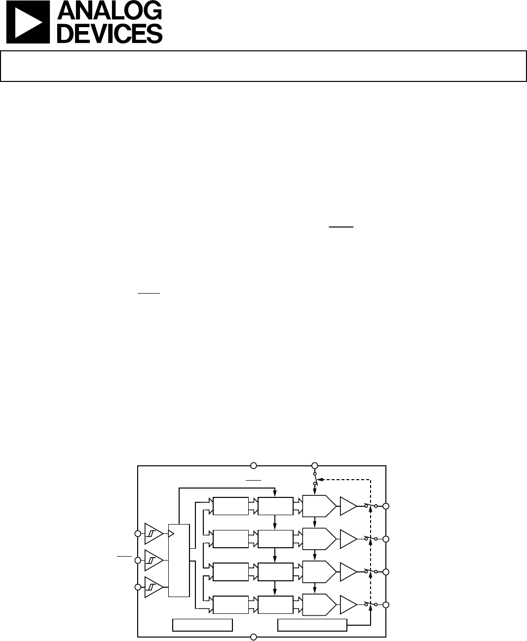
FUNCTIONAL BLOCK DIAGRAM
INPUT
REGISTER
DAC
REGISTER
STRING
DAC A V
OUT
A
BUFFER
INPUT
REGISTER
DAC
REGISTER
STRING
DAC B V
OUT
B
BUFFER
AD5304/AD5314/AD5324
INPUT
REGISTER
DAC
REGISTER
STRING
DAC C V
OUT
C
BUFFER
INPUT
REGISTER
DAC
REGISTER
STRING
DAC D V
OUT
D
BUFFER
REFIN
V
DD
GND
POWER-DOWN LOGICPOWER-ON RESET
LDAC
INTERFACE
LOGIC
SCLK
SYNC
DIN
00929-001
Figure 1.

AD5304/AD5314/AD5324 Data Sheet
Rev. I | Page 2 of 24
TABLE OF CONTENTS
Features .............................................................................................. 1
Applications ....................................................................................... 1
General Description ......................................................................... 1
Functional Block Diagram .............................................................. 1
Revision History ............................................................................... 2
Specifications ..................................................................................... 3
AC Characteristics ........................................................................ 4
Timing Characteristics ................................................................ 5
Absolute Maximum Ratings ............................................................ 6
ESD Caution .................................................................................. 6
Pin Configurations and Function Descriptions ........................... 7
Typical Performance Characteristics ............................................. 8
Terminology .................................................................................... 12
Theory of Operation ...................................................................... 14
Functional Description .............................................................. 14
Power-On Reset .......................................................................... 14
Serial Interface ............................................................................ 14
Power-Down Mode .................................................................... 16
Microprocessor Interfacing ....................................................... 16
Applications Information .............................................................. 18
Typical Application Circuit ....................................................... 18
Decoding Multiple AD5304/AD5314/AD5324s .................... 19
Power Supply Bypassing and Grounding ................................ 20
Outline Dimensions ....................................................................... 22
Ordering Guide .......................................................................... 23
Automotive Products ................................................................. 23
REVISION HISTORY
5/2017—Rev. H to Rev. I
Changes to Figure 4 .......................................................................... 7
Changes to Address and Control Bits Section ............................ 15
Updated Outline Dimensions ....................................................... 22
Changes to Ordering Guide .......................................................... 23
9/2011—Rev. G to Rev. H
Changes to Table 4 ............................................................................ 6
5/2011—Rev. F to Rev. G
Added W Version ............................................................... Universal
Added EPAD Notation to Figure 4 ................................................. 7
Updated Outline Dimensions ....................................................... 22
Changes to Ordering Guide .......................................................... 23
Added Automotive Products Section........................................... 23
9/2006—Rev. E to Rev. F
Updated Format .................................................................. Universal
Changes to Specifications Section .................................................. 3
Changes to Table 5 ............................................................................ 7
Updated Outline Dimensions ...................................................... 22
Changes to Ordering Guide .......................................................... 23
5/2005—Rev. D to Rev. E
Added 10-lead LFCSP package ......................................... Universal
Changes to Title ................................................................................. 1
Changes to Ordering Guide ............................................................. 4
8/2003—Rev. C to Rev. D
Added A Version ................................................................ Universal
Changes to Features .......................................................................... 1
Changes to Specifications ................................................................. 2
Changes to Absolute Maximum Ratings ........................................ 4
Changes to Ordering Guide ............................................................. 4
Changes to Figure 6 ........................................................................ 11
Added OCTALS Section to Table 2 .............................................. 15
Updated Outline Dimensions ....................................................... 16

Data Sheet AD5304/AD5314/AD5324
Rev. I | Page 3 of 24
SPECIFICATIONS
VDD = 2.5 V to 5.5 V; VREF = 2 V; RL = 2 kΩ to GND; CL = 200 pF to GND; all specifications TMIN to TMAX, unless otherwise noted.
Table 1.
Parameter1
A, W Version2 B Version2
Min Typ Max Min Typ Max Unit Test Conditions/Comments
DC PERFORMANCE3, 4
AD5304
Resolution 8 8 Bits
Relative Accuracy ±0.15 ±1 ±0.15 ±0.625 LSB
Differential Nonlinearity ±0.02 ±0.25 ±0.02 ±0.25 LSB Guaranteed monotonic by
design over all codes
AD5314
Resolution 10 10 Bits
Relative Accuracy ±0.5 ±4 ±0.5 ±2.5 LSB
Differential Nonlinearity ±0.05 ±0.5 ±0.05 ±0.5 LSB Guaranteed monotonic by
design over all codes
AD5324
Resolution 12 12 Bits
Relative Accuracy ±2 ±16 ±2 ±10 LSB
Differential Nonlinearity ±0.2 ±1 ±0.2 ±1 LSB Guaranteed monotonic by
design over all codes
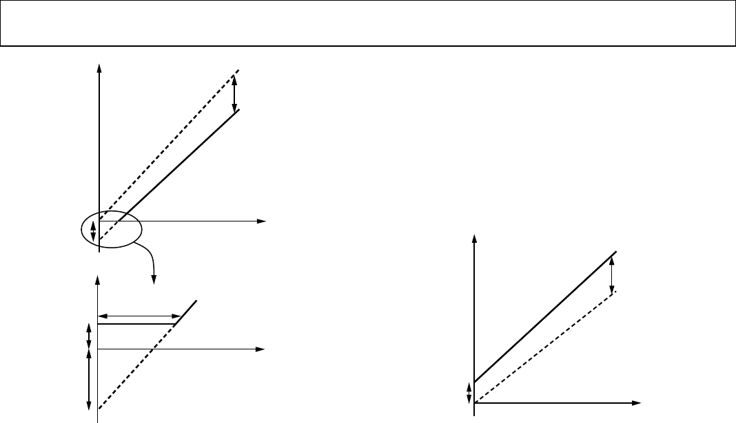
Offset Error ±0.4 ±3 ±0.4 ±3 % of FSR See Figure 2 and Figure 3
Gain Error ±0.15 ±1 ±0.15 ±1 % of FSR See Figure 2 and Figure 3
Lower Dead Band 20 60 20 60 mV Lower dead band exists only
if offset error is negative
Offset Error Drift5 –12 –12 ppm of
FSR/°C
Gain Error Drift5 –5 –5 ppm of
FSR/°C
DC Power Supply Rejection
Ratio5
–60 –60 dB ΔVDD = ±10%
DC Crosstalk5 200 200 µV RL = 2 kΩ to GND or VDD
DAC REFERENCE INPUTS5
VREF Input Range 0.25 VDD
0.25 VDD V
VREF Input Impedance 37 45 37 45 kΩ Normal operation
>10
>10
MΩ Power-down mode
Reference Feedthrough
–90
–90
dB Frequency = 10 kHz
OUTPUT CHARACTERISTICS5
Minimum Output Voltage
6
0.001
0.001
V
Measurement of the
minimum and maximum
Maximum Output Voltage6 VDD – 0.001
VDD – 0.001
V drive capability of the
output amplifier
DC Output Impedance
0.5
0.5 Ω
Short Circuit Current
25
25
mA
V
DD
= 5 V
16
16 mA VDD = 3 V
Power-Up Time
2.5
2.5 µs Coming out of power-
down mode VDD = 5 V
5
5 µs Coming out of power-
down mode VDD = 3 V

AD5304/AD5314/AD5324 Data Sheet
Rev. I | Page 4 of 24
Parameter1
A, W Version2 B Version2
Min Typ Max Min Typ Max Unit Test Conditions/Comments
LOGIC INPUTS5
Input Current
±1
±1
µA
VIL, Input Low Voltage
0.8 0.8 V VDD = 5 V ± 10%
0.6 0.6 V VDD = 3 V ± 10%
0.5 0.5 V VDD = 2.5 V
VIH, Input High Voltage 2.4
2.4
V VDD = 5 V ± 10%
2.1
2.1
V VDD = 3 V ± 10%
2.0
2.0
V
V
DD
= 2.5 V
Pin Capacitance
3
3
pF
POWER REQUIREMENTS
VDD 2.5 5.5 2.5 5.5 V
IDD (Normal Mode)7
VDD = 4.5 V to 5.5 V
600 900 600 900 µA VIH = VDD and VIL = GND
VDD = 2.5 V to 3.6 V
500 700 500 700 µA VIH = VDD and VIL = GND
I
DD
(Power-Down Mode)
VDD = 4.5 V to 5.5 V
0.2 1 0.2 1 µA VIH = VDD and VIL = GND
VDD = 2.5 V to 3.6 V
0.08 1 0.08 1 µA VIH = VDD and VIL = GND
1 See the Terminology section.
2 Temperature range (A, B, W Version): −40°C to +105°C; typical at +25°C.
3 DC specifications tested with the outputs unloaded.
4 Linearity is tested using a reduced code range: AD5304 (Code 8 to Code 248); AD5314 (Code 28 to Code 995); AD5324 (Code 115 to Code 3981).
5 Guaranteed by design and characterization, not production tested.
6 For the amplifier output to reach its minimum voltage, offset error must be negative. For the amplifier output to reach its maximum voltage, VREF = VDD and offset plus
gain error must be positive.
7 IDD specification is valid for all DAC codes; interface inactive; all DACs active; load currents excluded.
AC CHARACTERISTICS
VDD = 2.5 V to 5.5 V; RL = 2 kΩ to GND; CL = 200 pF to GND; all specifications TMIN to TMAX, unless otherwise noted.
Table 2.
Parameter1, 2
A, B, W Version3
Min Typ Max Unit Test Conditions/Comments
Output Voltage Settling Time VREF = VDD = 5 V
AD5304 6 8 µs ¼ scale to ¾ scale change (0x40 to 0xC0)
AD5314 7 9 µs ¼ scale to ¾ scale change (0x100 to 0x300)
AD5324 8 10 µs ¼ scale to ¾ scale change (0x400 to 0xC00)
Slew Rate 0.7 V/µs
Major-Code Transition Glitch Energy 12 nV-sec 1 LSB change around major carry
Digital Feedthrough 1 nV-sec
Digital Crosstalk 1 nV-sec
DAC-to-DAC Crosstalk 3 nV-sec
Multiplying Bandwidth 200 kHz VREF = 2 V ± 0.1 V p-p
Total Harmonic Distortion –70 dB VREF = 2.5 V ± 0.1 V p-p; frequency = 10 kHz
1 See the Terminology section.
2 Guaranteed by design and characterization, not production tested.
3 Temperature range (A, B, W Version): −40°C to +105°C; typical at +25°C.
Data Sheet AD5304/AD5314/AD5324
Rev. I | Page 5 of 24
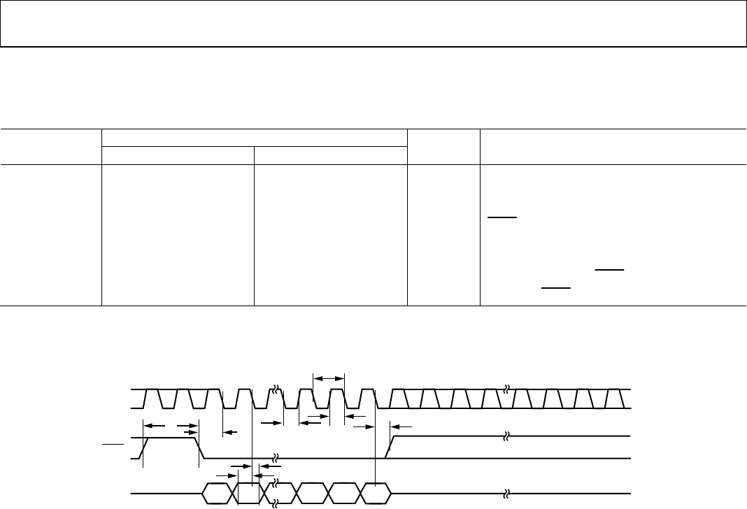
TIMING CHARACTERISTICS
VDD = 2.5 V to 5.5 V; all specifications TMIN to TMAX, unless otherwise noted.
Table 3.
Parameter1, 2, 3
Limit at TMIN, TMAX
VDD = 2.5 V to 3.6 V VDD = 3.6 V to 5.5 V Unit Test Conditions/Comments
t1 40 33 ns min SCLK cycle time
t2 16 13 ns min SCLK high time
t3 16 13 ns min SCLK low time
t4 16 13 ns min SYNC to SCLK falling edge setup time
t5 5 5 ns min Data setup time
t6 4.5 4.5 ns min Data hold time
t7 0 0 ns min SCLK falling edge to SYNC rising edge
t8 80 33 ns min Minimum SYNC high time
1 Guaranteed by design and characterization, not production tested.
2 All input signals are specified with tr = tf = 5 ns (10% to 90 % of VDD) and timed from a voltage level of (VIL + VIH)/2.
3 See Figure 2.
SCLK
DIN DB15 DB0
t
1
t
3
t
2
t
7
t
5
t
4
t
6
t
8
SYNC
00929-002
Figure 2. Serial Interface Timing Diagram
AD5304/AD5314/AD5324 Data Sheet
Rev. I | Page 6 of 24
ABSOLUTE MAXIMUM RATINGS
TA = 25°C, unless otherwise noted.
Table 4.
Parameter1 Rating
VDD to GND
–0.3 V to +7 V
Digital Input Voltage to GND –0.3 V to VDD + 0.3 V
Reference Input Voltage to GND –0.3 V to VDD + 0.3 V
VOUTA through VOUTD to GND
–0.3 V to VDD + 0.3 V
Operating Temperature Range
Industrial (A, B, W Version) –40°C to +105°C
Storage Temperature Range –65°C to +150°C
Junction Temperature (TJ max)
150°C
10-Lead MSOP
Power Dissipation (TJ max – TA)/ θJA
θJA Thermal Impedance
206°C/W
θJC Thermal Impedance
44°C/W
10-Lead LFCSP
Power Dissipation (TJ max – TA)/ θJA
θJA Thermal Impedance
84°C/W
Reflow Soldering
Peak Temperature (Pb-free) 260°C
Peak Temperature (non Pb-free) 220°C
Time at Peak Temperature 10 sec to 40 sec
1 Transient currents of up to 100 mA do not cause SCR latch-up.
Stresses at or above those listed under Absolute Maximum
Ratings may cause permanent damage to the product. This is a
stress rating only; functional operation of the product at these
or any other conditions above those indicated in the operational
section of this specification is not implied. Operation beyond
the maximum operating conditions for extended periods may
affect product reliability.
ESD CAUTION
Data Sheet AD5304/AD5314/AD5324
Rev. I | Page 7 of 24
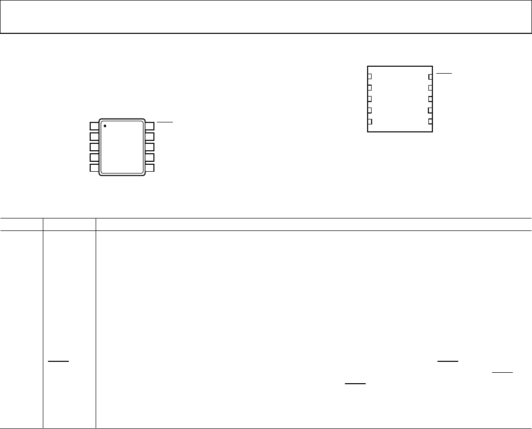
PIN CONFIGURATIONS AND FUNCTION DESCRIPTIONS
VDD 1
V
OUTA2
V
OUTB3
V
OUTC4
REFIN 5
AD5304/
AD5314/
AD5324
TOP VIEW
(Not to Scale)
SYNC10
SCLK
9
DIN8
GND7
VOUTD6
0
0929-003
Figure 3. 10-Lead MSOP Pin Configuration
Figure 4. 10-Lead LFCSP Pin Configuration
Table 5. Pin Function Descriptions
Pin No. Mnemonic Description
1 VDD Power Supply Input. These parts can be operated from 2.5 V to 5.5 V and the supply can be decoupled to GND.
2 VOUTA Buffered Analog Output Voltage from DAC A. The output amplifier has rail-to-rail operation.
3 VOUTB Buffered Analog Output Voltage from DAC B. The output amplifier has rail-to-rail operation.
4 VOUTC Buffered Analog Output Voltage from DAC C. The output amplifier has rail-to-rail operation.
5 REFIN Reference Input Pin for All Four DACs. It has an input range from 0.25 V to VDD.
6 VOUTD Buffered Analog Output Voltage from DAC D. The output amplifier has rail-to-rail operation.
7 GND Ground Reference Point for All Circuitry on the Part.
8 DIN Serial Data Input. This device has a 16-bit shift register. Data is clocked into the register on the falling edge of the
serial clock input. The DIN input buffer is powered down after each write cycle.
9 SCLK Serial Clock Input. Data is clocked into the input shift register on the falling edge of the serial clock input. Data can
be transferred at clock speeds up to 30 MHz. The SCLK input buffer is powered down after each write cycle.
10 SYNC Active Low Control Input. This is the frame synchronization signal for the input data. When SYNC goes low, it
enables the input shift register and data is transferred in on the falling edges of the following 16 clocks. If SYNC is
taken high before the 16th falling edge of SCLK, the rising edge of SYNC acts as an interrupt and the write
sequence is ignored by the device.
Exposed
Paddle1
Ground Reference Point for All Circuitry on the Part. Can be connected to 0 V or left unconnected provided there is
a connection to 0 V via the GND pin.
1 For the 10-Lead LFCSP only.
V
DD
V
OUT
A
V
OUT
B
V
OUT
C
REFIN
AD5304/
AD5314/
AD5324
NOTES
1. THE EXPOSED PAD IS THE GROUND REFERENCE POINT
FOR ALL CIRCUITRY ON THE PART. IT CAN BE
CONNECTED TO 0V OR LEFT UNCONNECTED PROVIDED
THERE IS A CONNECTION TO 0V VIA THE GND PIN.
TOP VIEW
(Not to Scale)
SCLK
DIN
GND
V
OUT
D
SYNC
1
2
3
4
5
00929-004
10
9
8
7
6
AD5304/AD5314/AD5324 Data Sheet
Rev. I | Page 8 of 24
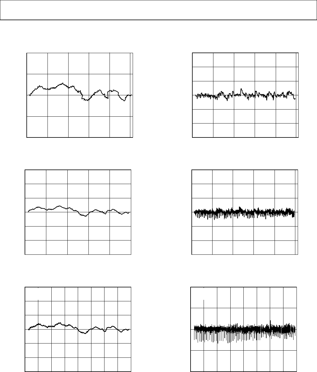
TYPICAL PERFORMANCE CHARACTERISTICS
1.0
0.5
0
–0.5
–1.0 050 100 150 200 250
INL ERROR (LSB)
CODE
TA = 25°C
VDD = 5V
00929-005
Figure 5. AD5304 Typical INL Plot
3
0
–1
–3
2
1
–2
0200 400 600 800 1000
INL ERROR (LSB)
CODE
T
A
= 25°C
V
DD
= 5V
00929-006
Figure 6. AD5314 Typical INL Plot
12
0
–4
–12
8
4
–8
0500 1000 1500 2000 2500 3000 3500 4000
INL ERROR (LSB)
CODE
T
A
= 25°C
V
DD
= 5V
00929-007
Figure 7. AD5324 Typical INL Plot
0.3
0.1
0
–0.2
0.2
–0.1
–0.3 050 100 150 200 250
DNL ERROR (LSB)
CODE
T
A
= 25°C
V
DD
= 5V
00929-008
Figure 8. AD5304 Typical DNL Plot
0.6
0.2
0
–0.4
0.4
–0.2
–0.6 0200 400 600 800 1000
DNL ERROR (LSB)
CODE
T
A
= 25°C
V
DD
= 5V
00929-009
Figure 9. AD5314 Typical DNL Plot
1.0
0
–1.0
0.5
–0.5
0500 1000 1500 2000 2500 3000 3500 4000
DNL ERROR (LSB)
CODE
T
A
= 25°C
V
DD
= 5V
00929-010
Figure 10. AD5324 Typical DNL Plot
Data Sheet AD5304/AD5314/AD5324
Rev. I | Page 9 of 24
0.50
0
–0.50
0.25
–0.25
012345
ERROR (LSB)
V
REF
(V)
T
A
= 25°C
V
DD
= 5V
MAX INL
MAX DNL
MIN INL
MIN DNL
00929-011
Figure 11. AD5304 INL and DNL Error vs. VREF
0.5
–0.5
–0.4
–0.3
–0.2
–0.1
0
0.1
0.2
0.3
0.4
–40 12080400
ERROR (LSB)
TEMPERATURE (°C)
MAX INL
MAX DNL
MIN INL
MIN DNL
V
DD
= 5V
V
REF
= 3V
00929-012
Figure 12. AD5304 INL Error and DNL Error vs. Temperature
1.0
–1.0
–0.5
0
0.5
–40 12080400
ERROR (%)
TEMPERATURE (°C)
V
DD
= 5V
V
REF
= 2V
GAIN ERROR
OFFSET ERROR
00929-013
Figure 13. AD5304 Offset Error and Gain Error vs. Temperature
0.2
–0.6
–0.5
–0.4
–0.3
–0.2
–0.1
0
0.1
0654321
ERROR (%)
V
DD
(V)
GAIN ERROR
OFFSET ERROR
T
A
= 25°C
V
REF
= 2V
00929-014
Figure 14. Offset Error and Gain Error vs. VDD
5
0
4
3
2
1
0654321
V
OUT
(V)
SINK/SOURCE CURRENT (mA)
5V SOURCE
3V SOURCE
5V SINK
3V SINK
00929-015
Figure 15. VOUT Source and Sink Current Capability
600
500
400
300
200
100
0
ZERO SCALE FULL SCALE
I
DD
(µA)
CODE
T
A
= 25°C
V
DD
= 5V
V
REF
= 2V
00929-016
Figure 16. Supply Current vs. DAC Code
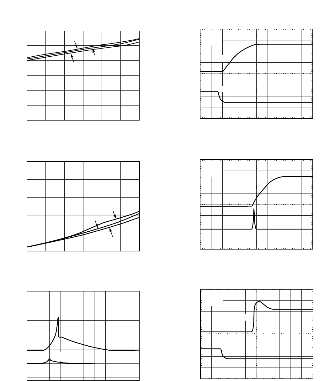
AD5304/AD5314/AD5324 Data Sheet
Rev. I | Page 10 of 24
600
500
400
300
200
100
0
2.5 3.0 3.5 4.0 4.5 5.0 5.5
I
DD
(µA)
V
DD
(V)
–40°C
+105°C
+25°C
00929-017
Figure 17. Supply Current vs. Supply Voltage
0.5
0.4
0.3
0.2
0.1
0
2.5 3.0 3.5 4.0 4.5 5.0 5.5
I
DD
(µA)
V
DD
(V)
–40°C
+105°C
+25°C
00929-018
Figure 18. Power-Down Current vs. Supply Voltage
1000
900
800
700
600
500
400
05.04.54.03.53.02.52.01.51.00.5
I
DD
(µA)
V
LOGIC
(V)
T
A
= 25°C
V
DD
= 5V
V
DD
= 3V
00929-019
Figure 19. Supply Current vs. Logic Input Voltage
CH1 1V, CH2 5V, TIME BASE = 1µs/DIV
CH2
CH1
T
A
= 25°C
V
DD
= 5V
V
REF
= 5V
V
OUT
A
SCLK
0
0929-020
Figure 20. Half-Scale Settling (¼ to ¾ Scale Code Change)
CH1 2V, CH2 200mV, TIME BASE = 200µs/DIV
CH2
CH1
T
A
= 25°C
V
DD
= 5V
V
REF
= 2V
V
DD
V
OUT
A
0
0929-021
Figure 21. Power-On Reset to 0 V
CH1 500mV, CH2 5V, TIME BASE = 1µs/DIV
CH2
CH1
T
A
= 25°C
V
DD
= 5V
V
REF
= 2V
V
OUT
A
SCLK
0
0929-022
Figure 22. Exiting Power-Down to Midscale
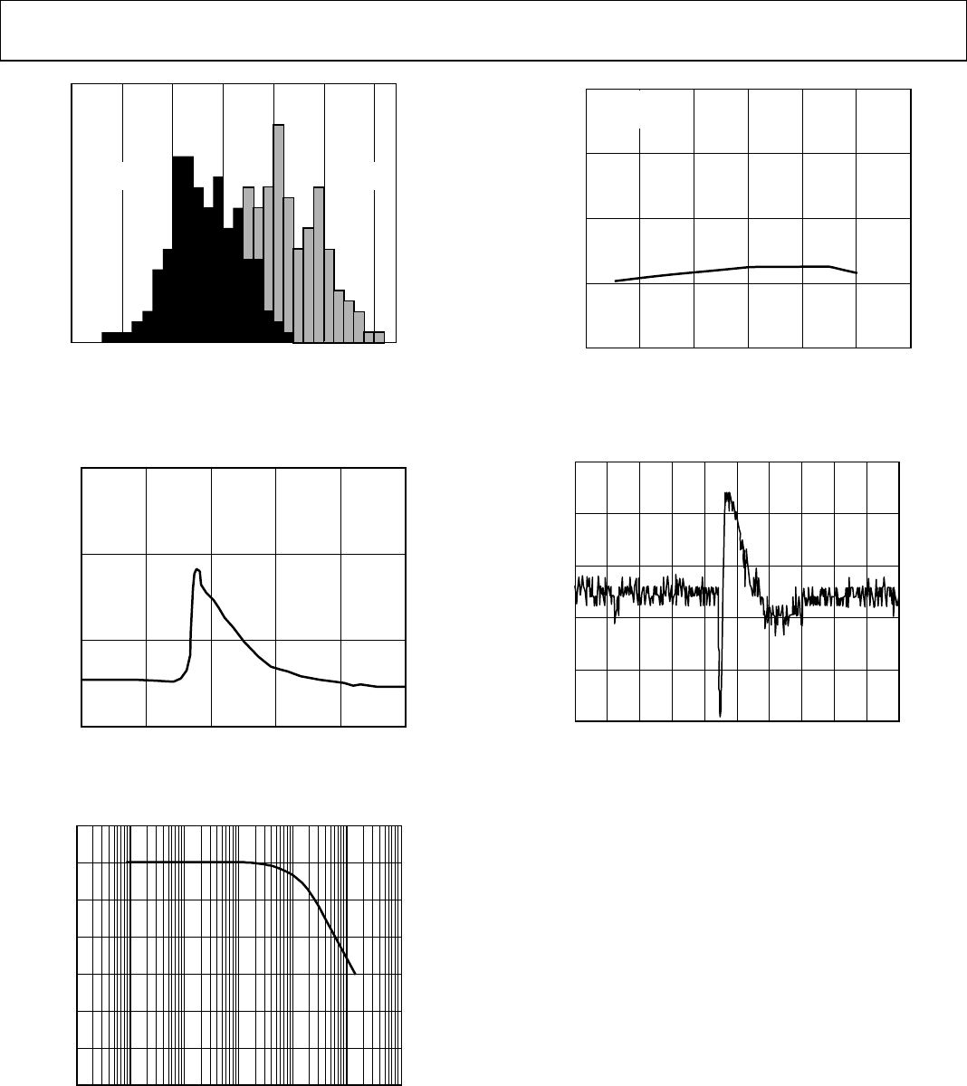
Data Sheet AD5304/AD5314/AD5324
Rev. I | Page 11 of 24
300 350 400 450 500 550 600
FREQUENCY
I
DD
(µA)
V
DD
= 3V V
DD
= 5V
00929-023
Figure 23. IDD Histogram with VDD = 3 V and VDD = 5 V
2.50
2.47
2.48
2.49
V
OUT
(V)
1µs/DIV
00929-024
Figure 24. AD5324 Major-Code Transition Glitch Energy
10
0
–10
–20
–30
–40
–50
–60
10 10M1M100k10k1k100
(dB)
FREQUENCY (Hz)
00929-025
Figure 25. Multiplying Bandwidth (Small-Signal Frequency Response)
0.02
0.01
0
–0.01
–0.02
0654321
FULL-SCALE ERROR (V)
V
REF
(V)
V
DD
= 5V
T
A
= 25°C
00929-026
Figure 26. Full-Scale Error vs. VREF
1mV/DI
V
150ns/DIV
0
0929-027
Figure 27. DAC-to-DAC Crosstalk

AD5304/AD5314/AD5324 Data Sheet
Rev. I | Page 12 of 24
TERMINOLOGY
Relative Accuracy or Integral Nonlinearity (INL)
For the DAC, relative accuracy or integral nonlinearity (INL)
is a measure of the maximum deviation, in LSB, from a straight
line passing through the endpoints of the DAC transfer function.
Typical INL vs. code plots can be seen in Figure 5, Figure 6,
and Figure 7.
Differential Nonlinearity
Differential nonlinearity (DNL) is the difference between the
measured change and the ideal 1 LSB change between any two
adjacent codes. A specified differential nonlinearity of ±1 LSB
maximum ensures monotonicity. This DAC is guaranteed mono-
tonic by design. Typical DNL vs. code plots can be seen in Figure 8,
Figure 9, and Figure 10.
Offset Error
This is a measure of the offset error of the DAC and the output
amplifier. It is expressed as a percentage of the full-scale range.
Gain Error
This is a measure of the span error of the DAC. It is the deviation
in slope of the actual DAC transfer characteristic from the ideal
expressed as a percentage of the full-scale range.
Offset Error Drift
This is a measure of the change in offset error with changes in
temperature. It is expressed in (ppm of full-scale range)/°C.
Gain Error Drift
This is a measure of the change in gain error with changes in
temperature. It is expressed in (ppm of full-scale range)/°C.
Power Supply Rejection Ratio (PSRR)
This indicates how the output of the DAC is affected by changes
in the supply voltage. PSRR is the ratio of the change in VOUT to
a change in VDD for full-scale output of the DAC. It is measured
in decibels. VREF is held at 2 V and VDD is varied ±10%.
DC Crosstalk
This is the dc change in the output level of one DAC at midscale
in response to a full-scale code change (all 0s to all 1s and vice
versa) and output change of another DAC. It is expressed in
microvolts.
Reference Feedthrough
This is the ratio of the amplitude of the signal at the DAC output to
the reference input when the DAC output is not being updated.
It is expressed in decibels.
Major-Code Transition Glitch Energy
Major-code transition glitch energy is the energy of the impulse
injected into the analog output when the code in the DAC register
changes state. It is normally specified as the area of the glitch in
nV-s and is measured when the digital code is changed by 1 LSB
at the major carry transition (011 . . . 11 to 100 . . . 00 or 100 . . .
00 to 011 . . . 11).
Digital Feedthrough
Digital feedthrough is a measure of the impulse injected into the
analog output of the DAC from the digital input pins of the
device when the DAC output is not being written to (SYNC
held high). It is specified in nV-s and is measured with a worst-
case change on the digital input pins (for example, from all 0s
to all 1s or vice versa.)
Digital Crosstalk
This is the glitch impulse transferred to the output of one DAC
at midscale in response to a full-scale code change (all 0s to all
1s and vice versa) in the input register of another DAC. It is
expressed in nV-s.
DAC-to-DAC Crosstalk
This is the glitch impulse transferred to the output of one DAC
due to a digital code change and subsequent output change of
another DAC. This includes both digital and analog crosstalk.
It is measured by loading one of the DACs with a full-scale code
change (all 0s to all 1s and vice versa) with the LDAC bit set low
and monitoring the output of another DAC. The energy of the
glitch is expressed in nV-s.
Multiplying Bandwidth
The amplifiers within the DAC have a finite bandwidth. The
multiplying bandwidth is a measure of this. A sine wave on the
reference (with full-scale code loaded to the DAC) appears on
the output. The multiplying bandwidth is the frequency at which
the output amplitude falls to 3 dB below the input.
Total Harmonic Distortion (THD)
This is the difference between an ideal sine wave and its attenuated
version using the DAC. The sine wave is used as the reference for
the DAC and the THD is a measure of the harmonics present on
the DAC output. It is measured in decibels.
Data Sheet AD5304/AD5314/AD5324
Rev. I | Page 13 of 24
DAC CODE
GAIN ERROR
PLUS
OFFSET ERROR
OUTPUT
VOLTAGE
NEGATIVE
OFFSET
ERROR
ACTUAL
IDEAL
NEGATIVE
OFFSET
ERROR
AMPLIFIER
FOOTROOM
(1mV)
DEAD BAND
CODES
00929-028
Figure 28. Transfer Function with Negative Offset
ACTUAL
IDEAL
DAC CODE
POSITIVE
OFFSET
OUTPUT
VOLTAGE
GAIN ERROR
PLUS
OFFSET ERROR
00929-029
Figure 29. Transfer Function with Positive Offset
AD5304/AD5314/AD5324 Data Sheet
Rev. I | Page 14 of 24
THEORY OF OPERATION
FUNCTIONAL DESCRIPTION
The AD5304/AD5314/AD5324 are quad, resistor-string DACs
fabricated on a CMOS process with resolutions of 8, 10, and 12
bits, respectively. Each contains four output buffer amplifiers and
is written to via a 3-wire serial interface. They operate from single
supplies of 2.5 V to 5.5 V, and the output buffer amplifiers provide
rail-to-rail output swing with a slew rate of 0.7 V/μs. The four
DACs share a single reference input pin. The devices have pro-
grammable power-down modes, in which all DACs can be turned
off completely with a high impedance output.
Digital-to-Analog
The architecture of one DAC channel consists of a resistor-string
DAC followed by an output buffer amplifier. The voltage at the
REFIN pin provides the reference voltage for the DAC. Figure 30
shows a block diagram of the DAC architecture. Since the input
coding to the DAC is straight binary, the ideal output voltage is
given by
N
REF
OUT
DV
V
2
×
=
where
D = decimal equivalent of the binary code that is loaded to the
DAC register:
0–255 for AD5304 (8 bits)
0–1023 for AD5314 (10 bits)
0–4095 for AD5324 (12 bits)
N = DAC resolution.
REFIN
OUTPUT BUFFER
AMPLIFIER
RESISTOR
STRING
DAC
REGISTER
INPUT
REGISTER VOUTA
00929-030
Figure 30. DAC Channel Architecture
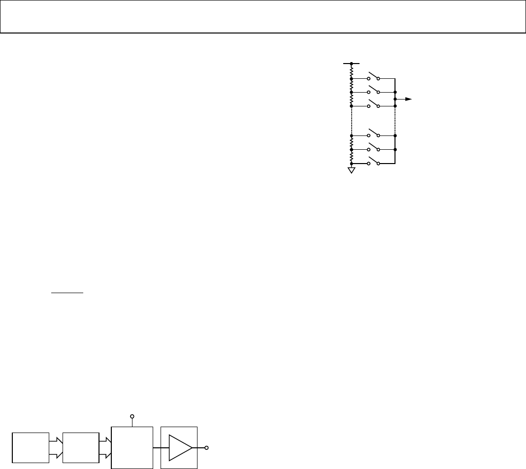
Resistor String
The resistor string section is shown in Figure 31. It is simply a
string of resistors, each of value R. The digital code loaded to the
DAC register determines at which node on the string the voltage
is tapped off to be fed into the output amplifier. The voltage is
tapped off by closing one of the switches connecting the string
to the amplifier. Because it is a string of resistors, it is guaranteed
monotonic.
R
R
R
R
RTO OUTPUT
AMPLIFIER
00929-031
Figure 31. Resistor String
DAC Reference Inputs
There is a single reference input pin for the four DACs. The
reference input is not buffered. The user can have a reference
voltage as low as 0.25 V or as high as VDD because there is no
restriction due to the headroom or footroom requirements of
any reference amplifier. It is recommended to use a buffered
reference in the external circuit (for example, REF192). The
input impedance is typically 45 kΩ.
Output Amplifier
The output buffer amplifier is capable of generating rail-to-rail
voltages on its output, giving an output range of 0 V to VDD when
the reference is VDD. It is capable of driving a load of 2 kΩto
GND or VDD, in parallel with 500 pF to GND or VDD. The source
and sink capabilities of the output amplifier can be seen in the
plot in Figure 15.
The slew rate is 0.7 V/μs with a half-scale settling time to
±0.5 LSB (at eight bits) of 6 μs.
POWER-ON RESET
The AD5304/AD5314/AD5324 are provided with a power-on reset
function, so that they power up in a defined state. The power-on
state uses normal operation and an output voltage set to 0 V.
Both input and DAC registers are filled with zeros and remain
so until a valid write sequence is made to the device. This is
particularly useful in applications where it is important to know
the state of the DAC outputs while the device is powering up.
SERIAL INTERFACE
The AD5304/AD5314/AD5324 are controlled over a versatile,
3-wire serial interface that operates at clock rates up to 30 MHz
and are compatible with SPI, QSPI, MICROWIRE, and DSP
interface standards.
Data Sheet AD5304/AD5314/AD5324
Rev. I | Page 15 of 24
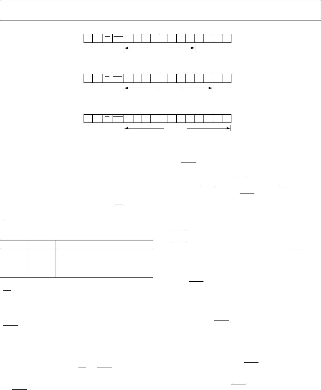
BIT15
(MSB)
A1 A0 D7 D6 D5 D4 D3 D2 D1 D0 0 0 X X
BIT0
(LSB)
PD LDAC
DATA BITS
00929-032
Figure 32. AD5304 Input Shift Register Contents
BIT15
(MSB) BIT0
(LSB)
A1 A0 D7D8D9 D6 D5 D4 D3 D2 D1 D0 X X
PD LDAC
DATA BITS
00929-033
Figure 33. AD5314 Input Shift Register Contents
BIT15
(MSB) BIT0
(LSB)
A1 A0 D7D8D9D10D11 D6 D5 D4 D3 D2 D1 D0PD LDAC
DATA BITS
00929-034
Figure 34. AD5324 Input Shift Register Contents
Input Shift Register
The input shift register is 16 bits wide. Data is loaded into the
device as a 16-bit word under the control of a serial clock input,
SCLK. See Figure 2 for the timing diagram of this operation. The
16-bit word consists of four control bits followed by 8, 10, or 12
bits of DAC data, depending on the device type. Data is loaded
MSB first (Bit 15) and the first two bits determine whether the
data is for DAC A, DAC B, DAC C, or DAC D. Bit 13 and Bit 12
control the operating mode of the DAC. Bit 13 is PD, and deter-
mines whether the part is in normal or power-down mode. Bit 12 is
LDAC, and controls when DAC registers and outputs are updated.
Table 6. Address Bits
A1 A0 DAC Addressed
0 0 DAC A
0 1 DAC B
1 0 DAC C
1 1 DAC D
Address and Control Bits
PD 0: All four DACs go into power-down mode, consuming
only 200 nA at 5 V. The DAC outputs enter a high
impedance state.
1: Normal operation.
LDAC 0: All four DAC registers and, therefore, all DAC outputs
updated simultaneously on completion of the write
sequence.
1: Only addressed input register is updated. There is
no change in the content of the DAC registers.
It is not recommended to set the PD and LDAC control bits
simultaneously. Depending on the SPI transmission rate, this
causes the data transferred to be loaded into the DAC register if
the LDAC control bit was previously set.
The AD5324 uses all 12 bits of DAC data; the AD5314 uses 10 bits
and ignores the 2 LSB Bits. The AD5304 uses eight bits and ignores
the last four bits. The data format is straight binary, with all 0s
corresponding to 0 V output and all 1s corresponding to full-scale
output (VREF − 1 LSB).
The SYNC input is a level-triggered input that acts as a frame
synchronization signal and chip enable. Data can be transferred
into the device only while SYNC is low. To start the serial data
transfer, take SYNC low, observing the minimum SYNC to SCLK
falling edge setup time, t4. After SYNC goes low, serial data shifts
into the device’s input shift register on the falling edges of SCLK
for 16 clock pulses. Any data and clock pulses after the 16th falling
edge of SCLK are ignored because the SCLK and DIN input buffers
are powered down. No further serial data transfer occurs until
SYNC is taken high and low again.
SYNC can be taken high after the falling edge of the 16th SCLK
pulse, observing the minimum SCLK falling edge to SYNC
rising edge time, t7.
After the end of the serial data transfer, data automatically transfers
from the input shift register to the input register of the selected
DAC. If SYNC is taken high before the 16th falling edge of SCLK,
the data transfer is aborted and the DAC input registers are not
updated.
When data has been transferred into three of the DAC input
registers, all DAC registers and all DAC outputs are simultaneously
updated by setting LDAC low when writing to the remaining
DAC input register.
Low Power Serial Interface
To reduce the power consumption of the device even further, the
interface fully powers up only when the device is being written
to, that is, on the falling edge of SYNC. As soon as the 16-bit
control word has been written to the part, the SCLK and DIN
input buffers are powered down. They power up again only
following a falling edge of SYNC.
AD5304/AD5314/AD5324 Data Sheet
Rev. I | Page 16 of 24
Double-Buffered Interface
The AD5304/AD5314/AD5324 DACs have double-buffered inter-
faces consisting of two banks of registers—input registers and
DAC registers. The input register is directly connected to the input
shift register and the digital code is transferred to the relevant input
register on completion of a valid write sequence. The DAC
register contains the digital code used by the resistor string.
Access to the DAC register is controlled by the LDAC bit. When
the LDAC bit is set high, the DAC register is latched and hence
the input register can change state without affecting the contents of
the DAC register. However, when the LDAC bit is set low, all DAC
registers are updated after a complete write sequence.
This is useful if the user requires simultaneous updating of all
DAC outputs. The user can write to three of the input registers
individually and then, by setting the LDAC bit low when
writing to the remaining DAC input register, all outputs
update simultaneously.
These parts contain an extra feature whereby the DAC register
is not updated unless its input register has been updated since
the last time that LDAC was brought low. Normally, when LDAC
is brought low, the DAC registers are filled with the contents of
the input registers. In the case of the AD5304/AD5314/AD5324,
the part updates the DAC register only if the input register has
been changed since the last time the DAC register was updated,
thereby removing unnecessary digital crosstalk.
POWER-DOWN MODE
The AD5304/AD5314/AD5324 have low power consumption,
dissipating only 1.5 mW with a 3 V supply and 3 mW with a
5 V supply. Power consumption can be further reduced when
the DACs are not in use by putting them into power-down mode,
selected by a 0 on Bit 13 (PD) of the control word.
When the PD bit is set to 1, all DACs work normally with a typical
power consumption of 600 μA at 5 V (500 μA at 3 V). However, in
power-down mode, the supply current falls to 200 nA at 5 V
(80 nA at 3 V) when all DACs are powered down. Not only does
the supply current drop, but also the output stage is internally
switched from the output of the amplifier, making it open-circuit.
This has the advantage that the output is three-stated while the
part is in power-down mode, and provides a defined input
condition for whatever is connected to the output of the DAC
amplifier. The output stage is illustrated in Figure 35.
The bias generator, the output amplifier, the resistor string, and
all other associated linear circuitry are shut down when the power-
down mode is activated. However, the contents of the registers
are unaffected when in power-down. The time to exit power-down
is typically 2.5 μs for VDD = 5 V and 5 μs when VDD = 3 V. This is
the time from the falling edge of the 16th SCLK pulse to when
the output voltage deviates from its power down voltage. See
Figure 22 for a plot.
RESISTOR
STRING DAC
A
MPLIFIE
R
VOUT
POWER-DOWN
CIRCUITRY
0
0929-035
Figure 35. Output Stage during Power-Down
MICROPROCESSOR INTERFACING
AD5304/AD5314/AD5324 to ADSP-21xx
Figure 36 shows a serial interface between the AD5304/AD5314/
AD5324 and the ADSP-21xx family. The ADSP-21xx is set up
to operate in the SPORT transmit alternate framing mode. The
ADSP-21xx sport is programmed through the SPORT control
register and must be configured as follows: internal clock operation,
active-low framing, and 16-bit word length. Transmission is
initiated by writing a word to the Tx register after the SPORT
has been enabled. The data is clocked out on each rising edge of
the DSP’s serial clock and clocked into the AD5304/AD5314/
AD5324 on the falling edge of the DAC’s SCLK.
AD5304/
AD5314/
AD5324*
ADSP-21xx*
*ADDITIONAL PINS OMITTED FOR CLARITY.
DIN
DT
SCLKSCLK
SYNCTFS
0
0929-036
Figure 36. AD5304/AD5314/AD5324 to ADSP-21xx Interface
Data Sheet AD5304/AD5314/AD5324
Rev. I | Page 17 of 24
AD5304/AD5314/AD5324 to 68HC11/68L11 Interface
Figure 37 shows a serial interface between the AD5304/AD5314/
AD5324 and the 68HC11/68L11 microcontroller. SCK of the
68HC11/68L11 drives the SCLK of the AD5304/AD5314/AD5324,
while the MOSI output drives the serial data line (DIN) of the
DAC. The SYNC signal is derived from a port line (PC7). The
setup conditions for the correct operation of this interface are as
follows: the 68HC11/68L11 is configured so that its CPOL bit is
a 0 and its CPHA bit is a 1. When data is being transmitted to the
DAC, the SYNC line is taken low (PC7). When the 68HC11/68L11
is configured as above, data appearing on the MOSI output is
valid on the falling edge of SCK. Serial data from the 68HC11/
68L11 is transmitted in 8-bit bytes with only eight falling clock
edges occurring in the transmit cycle. Data is transmitted MSB
first. To load data to the AD5304/ AD5314/AD5324, PC7 is left
low after the first eight bits are transferred, a second serial write
operation is performed to the DAC, and PC7 is taken high at
the end of this procedure.
AD5304/
AD5314/
AD5324*
68HC11/68L11*
*ADDITIONAL PINS OMITTED FOR CLARITY.
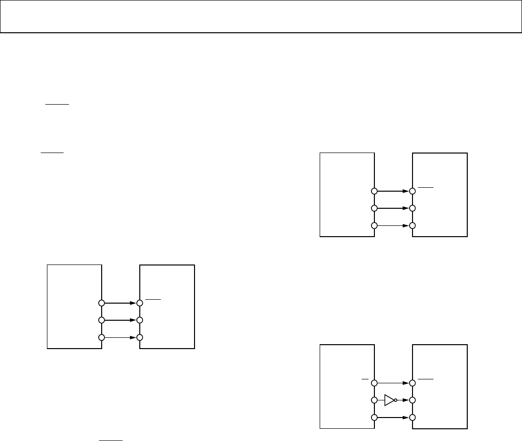
SCLK
SCK
DINMOSI
SYNCPC7
0
0929-037
Figure 37. AD5304/AD5314/AD5324 to 68HC11/68L11 Interface
AD5304/AD5314/AD5324 to 80C51/80L51 Interface
Figure 38 shows a serial interface between the AD5304/AD5314/
AD5324 and the 80C51/80L51 microcontroller. The setup for
the interface is as follows: TxD of the 80C51/80L51 drives SCLK
of the AD5304/AD5314/AD5324, while RxD drives the serial
data line of the part. The SYNC signal is again derived from a
bit-programmable pin on the port. In this case, port line P3.3 is
used. When data is to be transmitted to the AD5304/AD5314/
AD5324, P3.3 is taken low. The 80C51/80L51 transmits data
only in 8-bit bytes; thus only eight falling clock edges occur in
the transmit cycle. To load data to the DAC, P3.3 is left low after
the first eight bits are transmitted, and a second write cycle is
initiated to transmit the second byte of data. P3.3 is taken high
following the completion of this cycle. The 80C51/80L51 outputs
the serial data in a format that has the LSB first. The AD5304/
AD5314/AD5324 requires its data with the MSB as the first bit
received. The 80C51/80L51 transmit routine takes this into
account.
AD5304/
AD5314/
AD5324*
80C51/80L51*
*ADDITIONAL PINS OMITTED FOR CLARITY.
SCLK
TxD
DINRxD
SYNCP3.3
0
0929-038
Figure 38. AD5304/AD5314/AD5324 to 80C51/80L51 Interface
AD5304/AD5314/AD5324 to MICROWIRE Interface
Figure 39 shows an interface between the AD5304/AD5314/
AD5324 and any MICROWIRE-compatible device. Serial data
is shifted out on the falling edge of the serial clock, SK, and is
clocked into the AD5304/AD5314/AD5324 on the rising edge
of SK, which corresponds to the falling edge of the DAC’s SCLK.
AD5304/
AD5314/
AD5324*
MICROWIRE*
*ADDITIONAL PINS OMITTED FOR CLARITY.
SCLK
SK
DINSO
SYNCCS
0
0929-039
Figure 39. AD5304/AD5314/AD5324 to MICROWIRE Interface
AD5304/AD5314/AD5324 Data Sheet
Rev. I | Page 18 of 24
APPLICATIONS INFORMATION
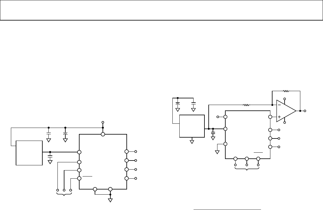
TYPICAL APPLICATION CIRCUIT
The AD5304/AD5314/AD5324 can be used with a wide range
of reference voltages where the devices offer full, one-quadrant
multiplying capability over a reference range of 0 V to VDD.
More typically, these devices are used with a fixed, precision
reference voltage. Suitable references for 5 V operation are the
AD780 and REF192 (2.5 V references). For 2.5 V operation, a
suitable external reference would be the AD589, a 1.23 V band
gap reference. Figure 40 shows a typical setup for the AD5304/
AD5314/AD5324 when using an external reference.
AD5304/AD5314/
AD5324
V
DD
= 2.5V TO 5.5V
SCLK
REFIN
DIN
SYNC
V
OUT
A
V
OUT
B
V
OUT
C
V
OUT
D
GND
A0
SERIAL
INTERFACE
V
OUT
V
IN
EXTERNAL
REFERENCE
AD790/REF192
WITH V
DD
= 5V
OR AD589 WITH
V
DD
= 2.5V
1µF
0.1µF 10µF
00929-040
Figure 40. AD5304/AD5314/AD5324 Using External Reference
If an output range of 0 V to VDD is required, the simplest solution is
to connect the reference input to VDD. As this supply is not very
accurate and can be noisy, the AD5304/AD5314/AD5324 can
be powered from the reference voltage; for example, using a 5 V
reference such as the REF195. The REF195 can output a steady
supply voltage for the AD5304/AD5314/AD5324. The current
required from the REF195 is 600 μA supply current and approxi-
mately 112 μA into the reference input. This is with no load on
the DAC outputs. When the DAC outputs are loaded, the REF195
also needs to supply the current to the loads. The total current
required (with a 10 kΩload on each output) is
712 μA + 4 (5 V/10 kΩ) = 2.70 mA
The load regulation of the REF195 is typically 2 ppm/mA, resulting
in an error of 5.4 ppm (27 μV) for the 2.7 mA current drawn from
it. This corresponds to a 0.0014 LSB error at eight bits and
0.022 LSB error at 12 bits.
Bipolar Operation Using the AD5304/AD5314/AD5324
The AD5304/AD5314/AD5324 have been designed for single
supply operation, but a bipolar output range is also possible
using the circuit in Figure 41. This circuit gives an output voltage
range of ±5 V. R a i l -to-rail operation at the amplifier output is
achievable using an AD820 or an OP295 as the output amplifier.
AD5304
REFIN
GND
V
OUT
A
V
OUT
B
V
OUT
C
V
OUT
D
SERIAL
INTERFACE
DIN SCLK SYNC
V
OUT
V
IN
GND
REF195
1µF
0.1µF
10µF
+6V TO +16V
V
DD
+5V
–5V
±5V
+5V
AD820/
OP295
R1 = 10kΩ
R2 = 10kΩ
00929-041
Figure 41. Bipolar Operation with the AD5304
The output voltage for any input code can be calculated as follows:
)1/2(
)(
)2/( RR
REFIN
R1
R2
R1DREFIN
V
N
OUT
×−
+×
×
=
where:
D is the decimal equivalent of the code loaded to the DAC.
N is the DAC resolution.
REFIN is the reference voltage input:
REFIN = 5 V, R1 = R2 = 10 kΩ
VOUT = (10 × D/2N) − 5 V
Data Sheet AD5304/AD5314/AD5324
Rev. I | Page 19 of 24
Opto-Isolated Interface for Process Control Applications
The AD5304/AD5314/AD5324 have a versatile 3-wire serial
inter-face, making them ideal for generating accurate voltages
in process control and industrial applications. Due to noise,
safety requirements, or distance, it might be necessary to isolate
the AD5304/AD5314/AD5324 from the controller. This can
easily be achieved by using opto-isolators, which provide isolation
in excess of 3 kV. The actual data rate achieved is limited by the
type of optocouplers chosen. The serial loading structure of the
AD5304/AD5314/AD5324 makes them ideally suited for use in
opto-isolated applications. Figure 42 shows an opto-isolated
interface to the AD5304 where DIN, SCLK, and SYNC are driven
from optocouplers. The power supply to the part also needs to
be isolated. This is done by using a transformer. On the DAC
side of the transformer, a 5 V regulator provides the 5 V supply
required for the AD5304.
SCLK
DIN
AD5304
SYNC
GND
5V
REGULATOR
POWER
V
DD
10µF 0.1µF
REFIN
V
DD
10kΩ
10kΩ
10kΩ
DIN
SYNC
SCLK
V
DD
V
DD
V
OUT
A
V
OUT
B
V
OUT
C
V
OUT
D
00929-042
Figure 42. AD5304 in an Opto-Isolated Interface
DECODING MULTIPLE AD5304/AD5314/AD5324S
The SYNC pin on the AD5304/AD5314/AD5324 can be used
in applications to decode a number of DACs. In this application, all
the DACs in the system receive the same serial clock and serial
data, but SYNC can only be active to one of the devices at any one
time, allowing access to four channels in this 16-channel system.
The 74HC139 is used as a 2-to-4-line decoder to address any of the
DACs in the system. To prevent timing errors, the enable input
must be brought to its inactive state while the coded address
inputs are changing state. Figure 43 shows a diagram of a typical
setup for decoding multiple AD5304 devices in a system.
00929-043
74HC139
ENABLE
CODED
A
DDRESS
1G
1A
1B
DGND
1Y0
1Y1
1Y2
1Y3
SCLK
DIN
V
CC
V
DD
DIN
SCLK
AD5304
SYNC
DIN
SCLK
AD5304
SYNC
DIN
SCLK
AD5304
SYNC
DIN
SCLK
AD5304
SYNC
V
OUT
A
V
OUT
B
V
OUT
C
V
OUT
D
V
OUT
A
V
OUT
B
V
OUT
C
V
OUT
D
V
OUT
A
V
OUT
B
V
OUT
C
V
OUT
D
V
OUT
A
V
OUT
B
V
OUT
C
V
OUT
D
Figure 43. Decoding Multiple AD5304 Devices in a System
AD5304/AD5314/AD5324 as a Digitally Programmable
Window Detector
A digitally programmable upper/lower limit detector using two
DACs in the AD5304/AD5314/AD5324 is shown in Figure 44.
The upper and lower limits for the test are loaded to DAC A
and DAC B, which, in turn, set the limits on the CMP04. If the
signal at the VIN input is not within the programmed window,
an LED indicates the fail condition. Similarly, DAC C and DAC D
can be used for window detection on a second VIN signal.
*
ADDITIONAL PINS OMITTED FOR CLARITY.
5V
1/2
CMP04
FAIL PASS
1/6 74HC05
V
REF
SCLK
DIN
V
OUT
A
V
DD
1/2
AD5304/AD5314/
AD5324*
REFIN
GND
0.1µF 10µF 1kΩ1kΩ
V
IN
PASS/FAIL
DIN
SCLK
SYNC SYNC
V
OUT
B
00929-044
Figure 44. Window Detection

AD5304/AD5314/AD5324 Data Sheet
Rev. I | Page 20 of 24
POWER SUPPLY BYPASSING AND GROUNDING
In any circuit where accuracy is important, careful consideration of
the power supply and ground return layout helps to ensure the
rated performance. The printed circuit board on which the
AD5304/AD5314/AD5324 is mounted is designed so that the
analog and digital sections are separated and confined to certain
areas of the board. If the AD5304/AD5314/AD5324 are in a
system where multiple devices require an AGND-to-DGND
connection, the connection is made at one point only. The star
ground point is established as close as possible to the device. The
AD5304/AD5314/AD5324 has ample supply bypassing of 10 μF in
parallel with 0.1 μF on the supply located as close to the package as
possible, ideally right up against the device. The 10 μF capacitors
are the tantalum bead type. The 0.1 μF capacitor has low effective
series resistance (ESR) and effective series inductance (ESI), like
the common ceramic types that provide a low impedance path
to ground at high frequencies, to handle transient currents due
to internal logic switching.
The power supply lines of the AD5304/AD5314/AD5324 use as
large a trace as possible to provide low impedance paths and reduce
the effects of glitches on the power supply line. Fast switching
signals such as clocks are shielded with digital ground to avoid
radiating noise to other parts of the board, and are never run
near the reference inputs. Avoid crossover of digital and analog
signals. Traces on opposite sides of the board run at right angles
to each other. This reduces the effects of feedthrough through
the board. A microstrip technique is by far the best, but is not
always possible with a double-sided board. In this technique,
the component side of the board is dedicated to a ground plane
while signal traces are placed on the solder side.
Table 7. Overview of AD53xx Serial Devices
Part No. Resolution No. of DACs DNL Interface Settling Time (μs) Package Pins
SINGLES
AD5300 8 1 ±0.25 SPI 4 SOT-23, MSOP 6, 8
AD5310 10 1 ±0.5 SPI 6 SOT-23, MSOP 6, 8
AD5320 12 1 ±1.0 SPI 8 SOT-23, MSOP 6, 8
AD5301
8
1
±0.25
2-Wire
6
SOT-23, MSOP
6, 8
AD5311 10 1 ±0.5 2-Wire 7 SOT-23, MSOP 6, 8
AD5321 12 1 ±1.0 2-Wire 8 SOT-23, MSOP 6, 8
DUALS
AD5302 8 2 ±0.25 SPI 6 MSOP 8
AD5312 10 2 ±0.5 SPI 7 MSOP 8
AD5322 12 2 ±1.0 SPI 8 MSOP 8
AD5303 8 2 ±0.25 SPI 6 TSSOP 16
AD5313 10 2 ±0.5 SPI 7 TSSOP 16
AD5323 12 2 ±1.0 SPI 8 TSSOP 16
QUADS
AD5304 8 4 ±0.25 SPI 6 MSOP, LFCSP 10
AD5314
10
4
±0.5
SPI
7
MSOP, LFCSP
10
AD5324 12 4 ±1.0 SPI 8 MSOP, LFCSP 10
AD5305 8 4 ±0.25 2-Wire 6 MSOP 10
AD5315 10 4 ±0.5 2-Wire 7 MSOP 10
AD5325 12 4 ±1.0 2-Wire 8 MSOP 10
AD5306 8 4 ±0.25 2-Wire 6 TSSOP 16
AD5316 10 4 ±0.5 2-Wire 7 TSSOP 16
AD5326 12 4 ±1.0 2-Wire 8 TSSOP 16
AD5307 8 4 ±0.25 SPI 6 TSSOP 16
AD5317 10 4 ±0.5 SPI 7 TSSOP 16
AD5327 12 4 ±1.0 SPI 8 TSSOP 16
OCTALS
AD5308 8 8 ±0.25 SPI 6 TSSOP 16
AD5318 10 8 ±0.5 SPI 7 TSSOP 16
AD5328 12 8 ±1.0 SPI 8 TSSOP 16

Data Sheet AD5304/AD5314/AD5324
Rev. I | Page 21 of 24
Table 8. Overview of AD53xx Parallel Devices
Part No. Resolution DNL VREF Pins Settling Time (μs) Additional Pin Functions Package Pins
SINGLES BUF GAIN HBEN CLR
AD5330 8 ±0.25 1 6 ✓ ✓ ✓ TSSOP 20
AD5331 10 ±0.5 1 7 ✓ ✓ TSSOP 20
AD5340 12 ±1.0 1 8 ✓ ✓ ✓ TSSOP 24
AD5341 12 ±1.0 1 8 ✓ ✓ ✓ ✓ TSSOP 20
DUALS
AD5332 8 ±0.25 2 6 ✓ TSSOP 20
AD5333 10 ±0.5 2 7 ✓ ✓ ✓ TSSOP 24
AD5342 12 ±1.0 2 8 ✓ ✓ ✓ TSSOP 28
AD5343 12 ±1.0 1 8 ✓ ✓ TSSOP 20
QUADS
AD5334 8 ±0.25 2 6 ✓ ✓ TSSOP 24
AD5335 10 ±0.5 2 7 ✓ ✓ TSSOP 24
AD5336 10 ±0.5 4 7 ✓ ✓ TSSOP 28
AD5344 12 ±1.0 4 8
TSSOP 28
AD5304/AD5314/AD5324 Data Sheet
Rev. I | Page 22 of 24
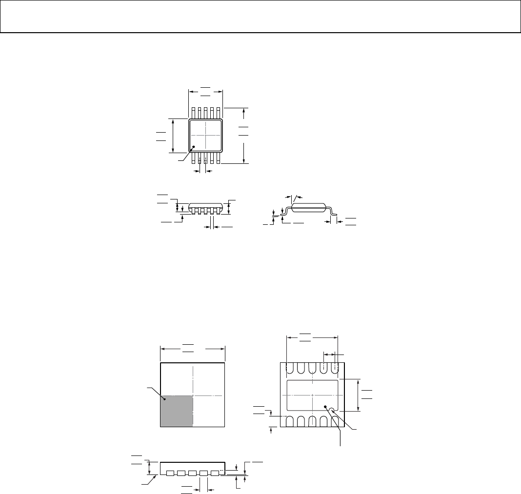
OUTLINE DIMENSIONS
COMPLIANT TO JEDEC STANDARDS MO-187-BA
091709-A
6°
0°
0.70
0.55
0.40
5
10
1
6
0.50 BSC
0.30
0.15
1.10 MAX
3.10
3.00
2.90
COPLANARITY
0.10
0.23
0.13
3.10
3.00
2.90
5.15
4.90
4.65
PIN 1
IDENTIFIER
15° MAX
0.95
0.85
0.75
0.15
0.05
Figure 45. 10-Lead Mini Small Outline Package [MSOP]
(RM-10)
Dimensions shown in millimeters
2.48
2.38
2.23
0.50
0.40
0.30
121009-A
TOP VIEW
10
1
6
5
0.30
0.25
0.20
BOTTO
MVIEW
PIN 1INDEX
AREA
SEATING
PLANE
0.80
0.75
0.70
1.74
1.64
1.49
0.20 REF
0.05 MAX
0.02 NOM
0.50 BSC
EXPOSED
PAD
3.10
3.00 SQ
2.90
PIN 1
INDICATOR
(R0.15)
FOR PROPER CONNECTION OF
THE EXPOSED PAD, REFER TO
THE PIN CONFIGURATION AND
FUNCTION DESCRIPTIONS
SECTION OF THIS DATA SHEET.
Figure 46. 10-Lead Lead Frame Chip Scale Package [LFCSP]
3 mm × 3 mm Body and 0.75 mm Package Height
(CP-10-9)
Dimensions shown in millimeters

Data Sheet AD5304/AD5314/AD5324
Rev. I | Page 23 of 24
ORDERING GUIDE
Model
1, 2
Temperature Range
Package Description
Package Option
Branding
AD5304ARM –40°C to +105°C 10-Lead MSOP RM-10 DBA
AD5304ARMZ –40°C to +105°C 10-Lead MSOP RM-10 D9W
AD5304ARMZ-REEL7 –40°C to +105°C 10-Lead MSOP RM-10 D9W
AD5304ACPZ-REEL7 –40°C to +105°C 10-Lead LFCSP CP-10-9 DBA#
AD5304BRMZ –40°C to +105°C 10-Lead MSOP RM-10 DBB#
AD5304BRMZ-REEL –40°C to +105°C 10-Lead MSOP RM-10 DBB#
AD5304BRMZ-REEL7 –40°C to +105°C 10-Lead MSOP RM-10 DBB#
AD5304BCPZ-REEL7 –40°C to +105°C 10-Lead LFCSP CP-10-9 DBB#
AD5314ACPZ-REEL7 –40°C to +105°C 10-Lead LFCSP CP-10-9 DCA#
AD5314ARM-REEL7
–40°C to +105°C
10-Lead MSOP
RM-10
DCA
AD5314ARMZ –40°C to +105°C 10-Lead MSOP RM-10 DCA#
AD5314ARMZ-REEL7 –40°C to +105°C 10-Lead MSOP RM-10 DCA#
AD5314WARMZ-REEL7 –40°C to +105°C 10-Lead MSOP RM-10 DCA#
AD5314BCPZ-REEL7 –40°C to +105°C 10-Lead LFCSP CP-10-9 DCB#
AD5314BRM –40°C to +105°C 10-Lead MSOP RM-10 DCB
AD5314BRM-REEL7 –40°C to +105°C 10-Lead MSOP RM-10 DCB
AD5314BRMZ –40°C to +105°C 10-Lead MSOP RM-10 DCB#
AD5314BRMZ-REEL –40°C to +105°C 10-Lead MSOP RM-10 DCB#
AD5314BRMZ-REEL7 –40°C to +105°C 10-Lead MSOP RM-10 DCB#
AD5324ACPZ-REEL7 –40°C to +105°C 10-Lead LFCSP CP-10-9 DDA#
AD5324ARM –40°C to +105°C 10-Lead MSOP RM-10 DDA
AD5324ARMZ –40°C to +105°C 10-Lead MSOP RM-10 D8F
AD5324ARMZ-REEL7 –40°C to +105°C 10-Lead MSOP RM-10 D8F
AD5324BCPZ-REEL7
–40°C to +105°C
10-Lead LFCSP
CP-10-9
DDB#
AD5324BRM –40°C to +105°C 10-Lead MSOP RM-10 DDB
AD5324BRM-REEL7 –40°C to +105°C 10-Lead MSOP RM-10 DDB
AD5324BRMZ –40°C to +105°C 10-Lead MSOP RM-10 DDB#
AD5324BRMZ-REEL –40°C to +105°C 10-Lead MSOP RM-10 DDB#
AD5324BRMZ-REEL7 –40°C to +105°C 10-Lead MSOP RM-10 DDB#
EVAL-AD5324DBZ Evaluation Board
1 Z = RoHS Compliant Part; # denotes lead-free product can be top or bottom marked.
2 W = Qualified for Automotive Applications.
AUTOMOTIVE PRODUCTS
The AD5314WARMZ-REEL7 model is available with controlled manufacturing to support the quality and reliability requirements of
automotive applications. Note that this automotive model may have specifications that differ from the commercial models; therefore
designers should review the Specifications section of this data sheet carefully. Only the automotive grade product shown is available for
use in automotive applications. Contact your local Analog Devices account representative for specific product ordering information and
to obtain the specific Automotive Reliability reports for this model.