AD9361 Reference Manual (Rev. A)
User Manual:
Open the PDF directly: View PDF ![]() .
.
Page Count: 128 [warning: Documents this large are best viewed by clicking the View PDF Link!]
- General Information
- Table of Contents
- Revision History
- Introduction
- Initialization and Calibration
- Overview
- Initalization Calibrations
- BBPLL VCO Calibration
- RF Synthesizer Charge Pump Calibration
- RF Synthesizer VCO Calibration
- Baseband Rx Analog Filter Calibration
- Baseband Tx Analog Filter Calibration
- Baseband Tx Secondary Filter
- Rx TIA Calibration Equations
- Rx ADC Setup
- Baseband DC Offset Calibration
- Baseband DC Offset Tracking
- RF DC Offset Calibration
- Rx Quadrature Tracking Calibration
- Tx Quadrature Calibration
- Reference Clock Requirements
- RF and BBPLL Synthesizer
- Overview
- RFPLL Introduction
- AD9361 PLL Architecture
- Reference Block
- Main PLL Block
- Charge Pump Current
- RFPLL Loop Filter
- VCO Configuration
- VCO Calibration
- VCO Vtune Measurement
- Lock Detector
- Synthesizer Look Up Table
- TDD Mode Faster Lock Times
- External LO
- Baseband PLL (BBPLL)
- BBPLL VCO
- BBPLL Charge Pump
- BBPLL Loop Filter
- Fast Lock Profiles
- Enable State Machine Guide
- Filter Guide
- Gain Control
- Overview
- Gain Control Threshold Detectors
- LMT Overload Detector
- ADC Overload Detector
- Low Power Threshold
- Average Signal Power
- Settling Times
- Peak Overload Wait Time
- Settling Delay
- Gain Table Overview
- Full Table Mode
- Split Table Mode
- Digital Gain
- MGC Overview
- Slow Attack AGC Mode
- Slow Attack AGC Gain Update Time
- Overloads in Slow Attack AGC Mode
- Slow Attack AGC and Gain Tables
- Hybrid AGC Mode
- Fast Attack AGC Mode
- State 0: RESET
- State 1: Peak Overload Detect
- State 2: Measure Power and Lock Level Gain Change
- State 3: Measure Power and Peak Overload Detect
- State 4: Unlock Gain
- State 5: Gain Lock and Measure Power
- Custom Gain Tables
- Received Signal Strength Indicator (RSSI)
- Transmit Power Control
- Tx Power Monitor
- RF Port Interface
- Factory Calibrations
- Control Output
- Overview
- Description of Control Output Signals
- 0x035 = 0x00 (Calibration Busy and Done)
- 0x035 = 0x01 (PLL Lock)
- 0x035 = 0x02 (Calibration Busy)
- 0x035 = 0x03 (Rx Gain Control)
- 0x035 = 0x04 (Rx Gain Control)
- 0x035 = 0x05 (Rx Gain Control)
- 0x035 = 0x06 (Rx Gain Control)
- 0x035 = 0x07 (Rx Gain Control)
- 0x035 = 0x08 (Rx Gain Control)
- 0x035 = 0x09 (RxOn, TxOn, RSSI)
- 0x035 = 0x0A (Digital Overflow)
- 0x035 = 0x0B (Calibration and ENSM States)
- 0x035 = 0x0C (Gain Control)
- 0x035 = 0x0D (Tx Quadrature and RF DC Calibration Status)
- 0x035 = 0x0E (Rx Quadrature and BB DC Calibration Status)
- 0x035 = 0x0F (Gain Control)
- 0x035 = 0x10 (Gain Control and RSSI)
- 0x035 = 0x11 (AuxADC Digital Output)
- 0x035 = 0x12 (Gain Control, Power Word Ready)
- 0x035 = 0x13 (Gain Control, Power Word Ready)
- 0x035 = 0x14 (Digital Overflow)
- 0x035 = 0x15 (DC Offset Tracking)
- 0x035 = 0x16 (Gain Control)
- 0x035 = 0x17 (Gain Control)
- 0x035 = 0x18 (DC Offset Tracking, Power Word Ready)
- 0x035 = 0x19 (Charge Pump Calibration States)
- 0x035 = 0x1A (Rx VCO and ALC Calibration States)
- 0x035 = 0x1B (Tx VCO and ALC Calibration States)
- 0x035 = 0x1C (Rx VCO Calibration States)
- 0x035 = 0x1D (Tx VCO Calibration States)
- 0x035 = 0x1E (Gain Control, Temp Sense Valid, AuxADC Valid)
- 0x035 = 0x1F (Gain Control)
- AuxADC/AuxDAC/GPO/Temp Sensor
- Baseband Synchronization
- Digital Interface Specification
- Overview
- CMOS Mode Data Path and Clock Signals
- CMOS Maximum Clock Rates and Signal Bandwidths
- Single Port Half Duplex Mode (CMOS)
- Single Port TDD Functional Timing (CMOS)
- Single Port Full Duplex Mode (CMOS)
- Single Port FDD Functional Timing (CMOS)
- Dual Port Half Duplex Mode (CMOS)
- Dual Port TDD Functional Timing (CMOS)
- Dual Port Full Duplex Mode (CMOS)
- Dual Port FDD Functional Timing (CMOS)
- Data Bus Idle and Turnaround Periods (CMOS)
- Data Path Timing Parameters (CMOS)
- LVDS Mode Data Path and Clock Signals
- LVDS Mode Data Path Signals
- LVDS Maximum Clock Rates and Signal Bandwidths
- Dual Port Full Duplex Mode (LVDS)
- Data Path Functional Timing (LVDS)
- Data Path Timing Parameters (LVDS)
- Serial Peripheral Interface (SPI)
- Additional Interface Signals
- Power Supply and Layout Guide
- Overview
- PCB Material And Stack Up Selection
- RF Transmission Line Layout
- Fan-out and Trace Space Guidelines
- Component Placement and Routing Guidelines
- Power Management and System Noise Considerations
- Power Distributions for Different Power Supply Domains
- Rx LO Frequency Deviations Due to Power Supply Transients
- Related Links

AD9361 Reference Manual
UG-570
One Technology Way • P. O. Box 9106 • Norwood, MA 02062-9106, U.S.A. • Tel: 781.329.4700 • Fax: 781.461.3113 • www.analog.com
AD9361 Reference Manual
PLEASE SEE THE LAST PAGE FOR AN IMPORTANT
WARNING AND LEGAL TERMS AND CONDITIONS. | Page 1 of 128
GENERAL INFORMATION
Complete specifications for the AD9361 part can be found in the AD9361 data sheet, which is available from Analog Devices, Inc., and
should be consulted in conjunction with this user guide when using the evaluation board.
Additional information about the AD9361 registers can be found in the AD9361 Register Map Reference Manual. While the register map
is provided as a convince and informational for those who want to understand the low level operation of the part, it is not recommended
to attempt to create your own software. Analog Devices provides complete drivers for the AD9361 for both bare metal/No-OS and
operating systems (Linux). The AD9361 and AD9364 share the same API. The AD9361 and AD9364 drivers can be found at:
•Linux wiki page
•No-OS wiki page
Support for these drivers can be found at:
•Linux engineer zone page
•No-OS engineer zone page
Rev. A

UG-570 AD9361 Reference Manual
| Page 2 of 128
TABLE OF CONTENTS
General Information ........................................................................ 1
Revision History ............................................................................... 4
Introduction ...................................................................................... 5
Terminology .................................................................................. 5
Register and Bit Syntax ................................................................ 5
Initialization and Calibration .......................................................... 6
Overview ........................................................................................ 6
Initalization Calibrations ............................................................. 7
BBPLL VCO Calibration ............................................................. 8
RF Synthesizer Charge Pump Calibration ................................ 8
RF Synthesizer VCO Calibration ............................................... 8
Baseband Rx Analog Filter Calibration ..................................... 9
Baseband Tx Analog Filter Calibration ................................... 10
Baseband Tx Secondary Filter .................................................. 11
Rx TIA Calibration Equations .................................................. 11
Rx ADC Setup ............................................................................. 11
Baseband DC Offset Calibration .............................................. 11
Baseband DC Offset Tracking .................................................. 11
RF DC Offset Calibration .......................................................... 12
Rx Quadrature Tracking Calibration ....................................... 13
Tx Quadrature Calibration ....................................................... 13
Reference Clock Requirements ..................................................... 14
Overview ...................................................................................... 14
DCXO Setup and Operation ..................................................... 14
Reference Clock Setup and Operation .................................... 15
Phase Noise Specification .......................................................... 15
RF and BBPLL Synthesizer ............................................................ 16
Overview ...................................................................................... 16
RFPLL Introduction ................................................................... 16
AD9361 PLL Architecture ......................................................... 16
Reference Block .......................................................................... 16
Main PLL Block .......................................................................... 17
Charge Pump Current ............................................................... 18
RFPLL Loop Filter ...................................................................... 18
VCO Configuration ................................................................... 18
VCO Calibration......................................................................... 18
VCO Vtune Measurement ......................................................... 18
Lock Detector .............................................................................. 18
Synthesizer Look Up Table ........................................................ 19
TDD Mode Faster Lock Times ................................................. 19
External LO ................................................................................. 19
Baseband PLL (BBPLL) ............................................................. 19
BBPLL VCO ................................................................................ 20
BBPLL Charge Pump ................................................................. 21
BBPLL Loop Filter ...................................................................... 21
Fast Lock Profiles ............................................................................ 22
Overview ..................................................................................... 22
Fast Lock Initial Wider BW Option ......................................... 22
Configuring and Using a Fast Lock Profile............................. 23
Fast Lock Pin Select ................................................................... 24
Enable State Machine Guide ......................................................... 25
Overview ..................................................................................... 25
ENSM State Definitions............................................................. 25
Modes of Operation ................................................................... 26
Sleep State .................................................................................... 30
Filter Guide...................................................................................... 31
Overview ..................................................................................... 31
Tx Signal Path ............................................................................. 31
Tx Digital Filter Blocks .............................................................. 31
Tx Analog Filter Blocks ............................................................. 32
Rx Signal Path ............................................................................. 33
Rx Analog Filter Blocks ............................................................. 33
Rx Digital Filter Blocks .............................................................. 33
Digital Rx Block Delay ............................................................... 34
Gain Control ................................................................................... 35
Overview ..................................................................................... 35
Gain Control Threshold Detectors .......................................... 36
LMT Overload Detector ............................................................ 36
ADC Overload Detector ........................................................... 36
Low Power Threshold ................................................................ 36
Average Signal Power ................................................................. 36
Settling Times ............................................................................. 37
Peak Overload Wait Time ......................................................... 37
Settling Delay .............................................................................. 37
Gain Table Overview ................................................................. 37
Full Table Mode .......................................................................... 37
Split Table Mode ......................................................................... 38
Digital Gain ................................................................................. 38
MGC Overview .......................................................................... 38
Slow Attack AGC Mode ............................................................ 40
Rev. A

AD9361 Reference Manual UG-570
| Page 3 of 128
Slow Attack AGC Gain Update Time ....................................... 40
Overloads in Slow Attack AGC Mode ...................................... 41
Slow Attack AGC and Gain Tables ........................................... 41
Hybrid AGC Mode ..................................................................... 42
Fast Attack AGC Mode ............................................................... 42
State 0: RESET ............................................................................. 43
State 1: Peak Overload Detect ................................................... 43
State 2: Measure Power and Lock Level Gain Change ........... 44
State 3: Measure Power and Peak Overload Detect ................ 44
State 4: Unlock Gain ................................................................... 44
State 5: Gain Lock and Measure Power .................................... 45
Custom Gain Tables ........................................................................ 47
Overview ...................................................................................... 47
RF DC Cal Bit .............................................................................. 49
Maximum Full Table/LMT Table Index ................................... 49
External LNA ............................................................................... 49
Received Signal Strength Indicator (RSSI) .................................. 50
Overview ...................................................................................... 50
Mode Select and Measurement Duration ................................ 50
RSSI Weighting ............................................................................ 50
RSSI Delay and RSSI Wait .......................................................... 50
RSSI Preamble and RSSI Symbol .............................................. 51
RSSI RFIR ..................................................................................... 51
RSSI Gain Step Calibration ........................................................ 51
Transmit Power Control ................................................................. 55
Overview ...................................................................................... 55
Tx Attenuation Words ................................................................ 55
Attenuation Word Update Options .......................................... 55
Tx Power Monitor ........................................................................... 56
Overview ...................................................................................... 56
Tx Power Monitor Description ................................................. 56
Input Matching/Attenuation Network ..................................... 57
Tx Power Monitor Gain Control ............................................... 58
TPM Dynamic Range ................................................................. 59
Example of Tx Mon Configuration and Measurement of TPM
Transfer Function ........................................................................ 59
TPM Test Mode ........................................................................... 60
RF Port Interface ............................................................................. 61
Overview ...................................................................................... 61
Rx Signal Path Interface ............................................................. 62
Tx Signal Path Interface ............................................................. 69
Factory Calibrations ....................................................................... 71
Overview ...................................................................................... 71
Internal DCXO ............................................................................ 71
Tx RSSI (Tx Monitor) ................................................................. 71
Rx RSSI ......................................................................................... 71
Rx GM/LNA Gain Step Calibration ......................................... 72
Tx Power Out vs. Tx Attenuation and Tx Power Out vs.
Carrier Frequency ....................................................................... 72
Control Output ................................................................................ 73
Overview ...................................................................................... 73
Description of Control Output Signals .................................... 74
0x035 = 0x00 (Calibration Busy and Done) ............................ 74
0x035 = 0x01 (PLL Lock) ........................................................... 75
0x035 = 0x02 (Calibration Busy) .............................................. 75
0x035 = 0x03 (Rx Gain Control) .............................................. 75
0x035 = 0x04 (Rx Gain Control) .............................................. 76
0x035 = 0x05 (Rx Gain Control) .............................................. 76
0x035 = 0x06 (Rx Gain Control) .............................................. 76
0x035 = 0x07 (Rx Gain Control) .............................................. 76
0x035 = 0x08 (Rx Gain Control) .............................................. 76
0x035 = 0x09 (RxOn, TxOn, RSSI) .......................................... 77
0x035 = 0x0A (Digital Overflow) ............................................. 77
0x035 = 0x0B (Calibration and ENSM States) ........................ 77
0x035 = 0x0C (Gain Control) ................................................... 77
0x035 = 0x0D (Tx Quadrature and RF DC Calibration
Status) ........................................................................................... 78
0x035 = 0x0E (Rx Quadrature and BB DC Calibration
Status) ........................................................................................... 78
0x035 = 0x0F (Gain Control) .................................................... 78
0x035 = 0x10 (Gain Control and RSSI) ................................... 78
0x035 = 0x11 (AuxADC Digital Output) ................................ 78
0x035 = 0x12 (Gain Control, Power Word Ready)................. 78
0x035 = 0x13 (Gain Control, Power Word Ready)................. 79
0x035 = 0x14 (Digital Overflow) .............................................. 79
0x035 = 0x15 (DC Offset Tracking) ......................................... 79
0x035 = 0x16 (Gain Control) .................................................... 79
0x035 = 0x17 (Gain Control) .................................................... 80
0x035 = 0x18 (DC Offset Tracking, Power Word Ready) ..... 80
0x035 = 0x19 (Charge Pump Calibration States) ................... 80
0x035 = 0x1A (Rx VCO and ALC Calibration States) ........... 80
0x035 = 0x1B (Tx VCO and ALC Calibration States) ........... 80
0x035 = 0x1C (Rx VCO Calibration States) ............................ 80
Rev. A

UG-570 AD9361 Reference Manual
Rev. A | Page 4 of 128
0x035 = 0x1D (Tx VCO Calibration States) ........................... 80
0x035 = 0x1E (Gain Control, Temp Sense Valid, AuxADC
Valid) ............................................................................................ 81
0x035 = 0x1F (Gain Control) .................................................... 81
AuxADC/AuxDAC/GPO/Temp Sensor ...................................... 82
Overview ...................................................................................... 82
AuxDAC ...................................................................................... 82
AuxADC ...................................................................................... 83
Internal Temperature Sensor .................................................... 84
General Purpose Output Control ............................................. 85
Baseband Synchronization ............................................................ 87
Overview ...................................................................................... 87
Multichip Synchronization ........................................................ 87
Procedure ..................................................................................... 88
Synchronization Verification .................................................... 89
Digital Interface Specification ....................................................... 90
Overview ...................................................................................... 90
CMOS Mode Data Path and Clock Signals ............................. 91
CMOS Maximum Clock Rates and Signal Bandwidths ........ 92
Single Port Half Duplex Mode (CMOS).................................. 93
Single Port TDD Functional Timing (CMOS) ....................... 94
Single Port Full Duplex Mode (CMOS) .................................. 97
Single Port FDD Functional Timing (CMOS) ....................... 99
Dual Port Half Duplex Mode (CMOS).................................. 100
Dual Port TDD Functional Timing (CMOS) ....................... 101
Dual Port Full Duplex Mode (CMOS) .................................. 103
Dual Port FDD Functional Timing (CMOS) ....................... 104
Data Bus Idle and Turnaround Periods (CMOS) ................ 105
Data Path Timing Parameters (CMOS) ................................ 105
LVDS Mode Data Path and Clock Signals ............................ 106
LVDS Mode Data Path Signals ............................................... 107
LVDS Maximum Clock Rates and Signal Bandwidths ....... 108
Dual Port Full Duplex Mode (LVDS) .................................... 109
Data Path Functional Timing (LVDS) ................................... 109
Data Path Timing Parameters (LVDS) .................................. 111
Serial Peripheral Interface (SPI) ............................................. 113
Additional Interface Signals .................................................... 116
Power Supply and Layout Guide ................................................ 117
Overview ................................................................................... 117
PCB Material And Stack Up Selection .................................. 117
RF Transmission Line Layout ................................................. 118
Fan-out and Trace Space Guidelines ..................................... 119
Component Placement and Routing Guidelines ................. 120
Power Management and System Noise Considerations ...... 120
Power Distributions for Different Power Supply Domains 124
Rx LO Frequency Deviations Due to Power Supply
Transients .................................................................................. 126
Related Links ................................................................................. 128
REVISION HISTORY
6/15—Rev. 0 to Rev. A
Change to Table 50 ....................................................................... 108
3/14—Revision 0: Initial Version

AD9361 Reference Manual UG-570
| Page 5 of 128
INTRODUCTION
TERMINOLOGY
AGC
Automatic gain control where an algorithm in the AD9361
controls the receive path gain.
BBP
Baseband processor (or digital baseband).
BB
Baseband. Baseband received signals are those that have already
been downconverted from RF. Baseband transmit signals are
those that have not yet been upconverted to RF.
BB DC Cal
Baseband DC calibration. An on-chip calibration that reduces
the DC power in the received data by adding digital correction
words to the data between the Half-Band 1 filter and the receive
FIR filter. See the Initialization and Calibration section for more
information.
BBP
Baseband processor (or, digital baseband).
Cal
Calibration.
DC
Literally direct current. In this document, DC refers to
undesired received power in the center of the complex received
baseband spectrum.
ENSM
Enable state machine. This on-chip state machine moves the
AD9361 through its states and it also controls other functions
within the AD9361. See the Enable State Machine Guide section
for more information.
FDD
Frequency division duplex in which transmit and receive signals
can be present at the same time but use different frequencies
LMT
LNA, mixer, TIA. LMT refers to the LMT gain table as well as
an analog peak detector that monitors the signal level at the
input of the analog LPF. See the Gain Control section for more
information.
LO
Local oscillator, which refers to the desired RF carrier frequency
for the receiver and the transmitter.
LPF
Low-pass filter, which refers to the third-order analog low-pass
filter preceding the receive ADC and following the transmit
DAC.
LUT
Look up table, several calibration and functions depend on
either reading or storing look up tables for future use.
MGC
Manual gain control where the BBP controls some or all of the
gain control parameters in the AD9361.
PLL
Phase locked loop. The AD9361 uses PLLs to generate the
various clock rates within the chip as well as the Tx and Rx LO
frequencies.
RF
Radio frequency.
RF DC Cal
Radio frequency DC calibration is an on-chip calibration that
reduces DC power in the received data by applying a compen-
sating voltage between the LNA and the mixer. See the
Initialization and Calibration section for more information.
TDD
Time division duplex in which transmit and receive signals can
be present on the same frequency but at different times.
VCO
A voltage controlled oscillator (VCO) is a circuit in which the
output frequency of the oscillator is controlled by an input
voltage level. These VCOs are part of the PLLs on the AD9361.
The AD9361 must calibrate the VCOs before the frequency they
produce is accurate and stable.
REGISTER AND BIT SYNTAX
When a register with absolute bit locations is described in this
user guide, the format is always in hex for the register and
[Dx:Dy] for the bits. This format is best described by an
example such as 0x016[D0], which equates to Register 0x016
(hex), and only the lowest bit of this register. Thus, the register
and the bit locations are specifically delineated.
When describing the value of just a few bits, the following
format is used: x’byyy.
where
x equals the number of bits described.
b indicates binary.
yyy represents three digital bits with values of 0 or 1.
As an example, if two bits equal 2’b01, then the LSB = 1 and the
next higher bit = 0.
Rev. A

UG-570 AD9361 Reference Manual
| Page 6 of 128
INITIALIZATION AND CALIBRATION
OVERVIEW
The AD9361 powers up into a sleep state for minimal power consumption. Before the AD9361 is operational, its clocks must be
enabled and initial calibrations completed. The purpose of this section is to describe in detail the operation of the different initialization
calibrations.
Table 1 lists the initialization calibrations documented in this section.
Table 1. Initialization Calibrations Detailed in this Section
Calibration Run Frequency Calibration Done Bit
BBPLL VCO calibration Once; any time BBPLL frequency changes 0x5E[7], 1 when locked
RF synthesizer charge pump
calibration
Once Rx: 0x244[7], 1 when done
Tx: 0x284[7], 1 when done
RF synthesizer VCO calibration Occurs automatically when integer frequency word written. In TDD, occurs when TXNRX
changes logic level.
Rx: 0x247[1], 1 when locked
Tx: 0x287[1], 1 when locked
Baseband Rx analog filter tune
Once; update when BW changes
0x016[7], self clears when
done
Baseband Tx analog filter tune Once; update when BW changes
0x016[6], self clears when
done
Baseband Tx secondary filter tune Once; manual equations, update when BW changes
Rx TIA calibration Once; manual equations, update when BW changes
Rx ADC setup Once; manual LUT or equations, update when ADC sampling rate changes
Baseband DC offset Once 0x016[0], self clears when
done
RF DC offset Any time LO frequency changes more than 100 MHz 0x016[1], self clears when
done
Rx quadrature calibration Any time LO frequency changes more than 100 MHz Tracking runs continuously
Tx quadrature calibration Any time LO frequency changes more than 100 MHz 0x016[4], self clears when
done
Rev. A

AD9361 Reference Manual UG-570
| Page 7 of 128
INITALIZATION CALIBRATIONS
Initialization calibrations are calibrations that must be run each
time the AD9361 device is powered up or hard reset using the
RESETB pin. Several of the calibrations only need to run once
during initialization and do not re-run during operation.
Others are dependent on the carrier frequency, temperature, or
other parameters and need to run initially and when certain
events occur (such as changing the carrier frequency more than
100 MHz). As long as power is applied to the AD9361 device,
the calibration results are stored, including while in the SLEEP
state.
The six calibrations in the calibration control are part of a
calibration sequence state machine. After a calibration
completes, the bit that was set to initialize the calibration will
self clear. If more than one calibration is enabled in a single
register write, the calibrations will progress in a set order
controlled by a state machine in the AD9361. Table 2 shows the
sequence of calibrations. When the calibration sequence state
holds a value of 0x1, the calibrations are complete. Some
calibrations depend on the results of previously run
calibrations. The Rx baseband filter and Tx baseband filter
calibrations are not part of the calibration sequence state
machine, and should run only when all other calibrations are
not running.
Table 2. Automatic Calibration Sequence and Calibration Status
Calibration Sequence State[3:0] Active Calibration
0x0 Calibration WAIT state
0x1 Calibrations done
0x2 Baseband DC offset calibration
0x3 RF Rx DC offset calibration
0x4 Tx1 quadrature calibration
0x5
Tx2 quadrature calibration
0x6 Rx1 quadrature calibration
0x7 Rx2 quadrature calibration
0x8 Tx monitor calibration (DC offset)
0x9 Rx GM\LNA gain step calibration
0xA to 0xF Flush states
Rev. A

UG-570 AD9361 Reference Manual
| Page 8 of 128
BBPLL VCO CALIBRATION
The BBPLL VCO calibration must be run during initialization
of the AD9361 device. This calibration is run as part of the
ad9361_bbpll_set_rate function. The maximum calibration
time is calculated in Equation 1.
3456
_
max
×
×
=ScaleCLKREF
ingDivideSett
BBPLL
VCOcalTime
(1)
RF SYNTHESIZER CHARGE PUMP CALIBRATION
The charge pump calibration must be run once during
initialization of the AD9361 device. This calibration matches
the up and down currents for the RF PLL’s charge pump, and is
run during the ad9361_txrx_synth_cp_calib function. This
calibration must be run the first time the AD9361 device enters
the ALERT state. The calibration completes after a maximum of
36864 (Scaled_REF_CLK_IN) cycles.
RF SYNTHESIZER VCO CALIBRATION
The AD9361 contains two synthesizers. When using TDD
mode, the Rx synthesizer is only enabled when TXNRX is low.
The Tx synthesizer is only enabled when TXNRX is high.
During initial calibrations, it is recommended to set the
AD9361 device into FDD mode to enable both synthesizers
while in the ALERT state to simplify calibrations.
The VCO calibration is run during the ad9361_set_rx_lo_freq
and ad9361_set_tx_lo_freq functions. First, set up any
synthesizer setup registers, then write the fractional frequency
words, followed by the integer frequency word last. The
calibration time can be traded off with calibration accuracy. It is
recommended for FDD applications, to use the longest
calibration for better accuracy since once in the FDD state, it
may be a long time before a synthesizer VCO calibration occurs
again. In TDD, the calibration time will need to be set to meet
the TDD turnaround time, while achieving the most accurate
calibration possible. In TDD, the Rx VCO calibration will occur
each time the receiver synthesizer is powered up (when TxRNX
switches from high to low logic level). The Tx VCO calibration
will occur each time the transmitter synthesizer is powered up
(when TXNRX switches from low to high logic level). See
Equation 2 for the calibration time.
The VCO calibrations can be masked (disabled) for certain
cases such as the fast lock synthesizer mode, or when an HFDD
application is required. Using the FDD Synth LUT instead of
the TDD Synth LUT could be used to acquire a temperature
stable lock for cases where there is not time to run the VCO
calibration in TDD.
Calibration completion can be detected by reading the Rx PLL
Lock bit and the Tx PLL Lock bit. The lock bits will read Logic 1
when the PLLs are locked. The bits are also available on the
control output pins.
9
_
12
2
,max
×
+
×
+
++=
ALC
count
2
us
usVCOcalTime
wait
ScaleCLKREF
N
waitRFPLL
(2)
where:
=8
+18
( ×)
=40
_ ×
= 2( )
Table 3. Example Calculated VCO Calibration Times for FDD Default Settings
VCO Cal Count REF_CLK Scale wait2 (µs) waitALC (µs) Ncount Calibration Time (µs)
3 19.20 2 0.885 1.042 1024 255.073
3 30.72 2 0.553 0.651 1024 160.171
3 40.00 2 0.425 0.500 1024 123.475
Table 4. Example Calculated VCO Calibration Times for TDD Defaults
VCO Cal Count REF_CLK Scale wait2 (µs) waitALC (µs) Ncount Calibration Time (µs)
1 19.20 2 0.885 1.042 256 75.073
1 30.72 2 0.553 0.651 256 47.671
1 40.00 2 0.425 0.500 256 37.075
Rev. A

AD9361 Reference Manual UG-570
| Page 9 of 128
BASEBAND Rx ANALOG FILTER CALIBRATION
The baseband Rx analog filter calibration tunes the cutoff
frequency of the third-order Butterworth Rx anti-aliasing filter.
The Rx filter is located just before the ADC in the Rx signal
path and is normally calibrated to 1.4× the baseband channel
bandwidth (BBBW). This calibration is important for Rx
interferer rejection. Note that the BBBW is half the complex
bandwidth and coerced between 28 MHz to 0.20 MHz for the
equations used in this filter tuning. To calibrate this filter, the
BBPLL is divided down using a divide by 1 to 511 divider
dedicated to the Rx tuner block.
= × ()
, × . × (3)
The Rx baseband analog filter calibration runs during the
ad9361_set_rx_rf_bandwidth function. Calibration completion
can be monitored on a control output pin or by reading the
calibration control register until the Rx baseband filter
calibration bit self clears.
Because the filter calculation uses a ceiling function to generate
the divider there will be some quantization of the corner
frequency. If the quantization is too large it may be necessary to
adjust the desired BBBW to compensate.
, = × ()
. × × (4)
=610 × ()
, × . × (5)
Table 5. Typical Rx Baseband Filter Calibration Times
Standard
Desired
BBBW (MHz)
BBPLL
Frequency (MHz) RxBBF Divider (decimal) Actual BBBW (MHz)
Maximum Calibration
Time (µs)
LTE 5 MHz 2.5 983.04 31 2.499 19.236
LTE 10MHz 5 983.04 16 4.841 9.928
LTE 15 MHz 7.5 737.28 8 7.262 6.619
LTE 20 MHz
10
983.04
8
9.683
4.964
Rev. A

UG-570 AD9361 Reference Manual
| Page 10 of 128
BASEBAND Tx ANALOG FILTER CALIBRATION
The baseband Tx analog filter calibration tunes the cutoff
frequency of the third-order Butterworth Tx anti-imaging filter.
The Tx filter is located just after the DAC in the Tx signal path
and is normally calibrated to 1.6× the BBBW. Note that the
BBBW is half the complex bandwidth and coerced between
20 MHz to 0.625 MHz for the equations used in this filter
tuning. To generate this Tx tune clock, the BBPLL is divided
down using a divide by 1 to 511 divider dedicated to the Tx
tuner block.
= × ()
, × . × (6)
The Tx baseband analog filter calibration runs as part of the
ad9361_set_tx_rf_bandwidth. Calibration completion can be
monitored on a control out pin or by reading calibration
control until the Tx baseband filter calibration bit self clears.
, = × ()
. × × (7)
=355 × ()
, × . × (8)
Similar to the baseband Rx analog filter, there is quantization of
the corner frequency for the Tx analog filter as well. If the
quantization becomes too large it may be necessary to adjust the
desired BBBW.
Table 6. Typical Tx Baseband Filter Calibration Times
Standard
Desired
BBBW (MHz)
BBPLL Frequency
(MHz)
TxBBF Divider
(decimal) Actual BBBW (MHz)
Max Calibration
time (µs)
LTE 5 MHz 2.5 983.04 28 35.1086 10.1115
LTE 10MHz 5 983.04 14 70.2171 5.0558
LTE 15 MHz 7.5 737.28 7 105.326 3.3705
LTE 20 MHz 10 983.04 7 140.434 2.5278
Rev. A

AD9361 Reference Manual UG-570
| Page 11 of 128
BASEBAND Tx SECONDARY FILTER
The baseband Tx secondary filter is a tunable single pole filter
after the baseband Tx analog filter. The Tx secondary filter
corner is ideally set to 5 times the baseband bandwidth to help
filter out of band Tx noise emissions. This filter is programmed
when the ad9361_set_tx_rf_bandwidth function is called.
Rx TIA CALIBRATION EQUATIONS
The Rx transimpedance amplifier (TIA) is located between the
mixer and Rx baseband analog filter. The TIA has two gain
settings (0 dB gain and −6 dB gain), and applies a single pole
filter with a corner at 2.5× the baseband bandwidth. The
corner frequency of the Rx TIA is programmed when the
ad9361_set_rx_rf_bandwidth function is called. When the gain
index in the AD9361 Rx gain table changes the Rx TIA gain
setting, the AD9361 device will automatically scale the amplifier
to maintain the same corner frequency.
Rx ADC SETUP
The receive ADC is a third-order continuous time delta-sigma
modulator and is highly programmable. The values in many of
the ADC registers change with sampling clock frequency while
others do not change but the correct initial settings are critical
for proper operation. The ADC is programmed with the
ad9361_set_rx_rf_bandwidth function.
BASEBAND DC OFFSET CALIBRATION
It is recommended to run the baseband DC offset calibration
once during device initialization in the ALERT state. Since the
baseband signal path does not change with different wireless
standards or clock frequencies, it should not need to be run
again. The baseband DC offset correction values are stored for
all of the Rx analog baseband filter gain steps. The correction
words are applied as the Rx gain changes based on the current
Rx gain table index. This calibration is run during the
ad9361_bb_dc_offset_calib function call.
The one-shot baseband DC offset calibration will complete in a
finite time depending on the device settings. The calibration
time is 404,000 ClkRF cycles.
BASEBAND DC OFFSET TRACKING
Baseband DC offset tracking should be used in conjunction
with the RF DC offset tracking option. A high-pass filter loop is
utilized to track DC changes caused by the RF DC offset and Rx
quadrature correction block. The speed and accuracy of the BB
DC tracking loop are configurable. Also, an option exists for the
BB DC offset tracking to attack/settle quickly after a gain
change and then after a certain time switch to slower DC offset
tracking updates. When using the tracking mode, first run an
initial one-shot baseband DC offset calibration to minimize any
static DC offsets in the signal chain. Then enable tracking along
with the desired tracking loop settings. Baseband DC offset
tracking is enabled in the ad9361_tracking_control function
call.
Rev. A

UG-570 AD9361 Reference Manual
| Page 12 of 128
RF DC OFFSET CALIBRATION
The RF DC offset calibration should be run once during
initialization, or potentially when moving to a new carrier
frequency that is more than 100 MHz away from the previous
carrier frequency. This calibration should be run in the ALERT
state while the Rx synthesizer is enabled. The calibration is run
during the ad9361_rf_dc_offset_calib function. The internal
calibration results LUT stores separate results for the RF Rx A
input. If using the RF Rx B or C inputs along with the RF Rx A
input, you should run the calibration twice, once with each
input band selected. After calibrating each band, switching
between from the A input to the B or C input should not
require another calibration. Since the B and C inputs use the
same calibration results, switching from Input B to Input C may
require running the RF DC offset calibration.
When using the full Rx gain table, the RF DC offset calibration
only calibrates at gain indexes that are designated to calibrate in
the Rx gain table. This is because several consecutive gain steps
may leave the front end gain at the same setting, while only
changing baseband gain settings. The RF DC offset correction is
only designed to remove DC offset due to the RF parts of the
signal chain. By only running the calibration at gain indexes
that actually change the front end gain, the calibration time is
reduced. If the LUT does not hold a DC correction value for the
current Rx gain index, it will use the DC offset correction for
the next higher gain index that was calibrated. In the case of a
split Rx gain table, the calibration runs at each LMT gain index.
The RF DC offset tracking is enabled by with the ad9361_
tracking_control function. The tracking triggers an RF DC
offset update based on three events: Rx gain change, no energy
detected, or when the ENSM exits the Rx state. The DC Offset
Update bit field setting allows enabling or disabling any
combination of these events. Disabling RF DC offset tracking
would use the initially calibrated RF DC offset and never update
the correction words.
The calibration time and accuracy is calculated using Equation 9
and Equation 10. The calibration begins at minimum gain
(index = 0) and moves toward maximum gain. The RF DC
offset correction for each enabled Rx gain index is stored in a
LUT and applied when the Rx gain index is used. If the full Rx
gain table is used, the RF DC offset is calibrated only at gain
indexes specified to calibrate in the Rx gain table. If the Rx
gain table is split, the Number of Enabled Gain indexes in
Equation 10 equals 41 gain steps.
Length Of Each Average = [{(RF DC Offset Count × 256) + 255} + 32] (9)
Total Calibration time(CLKRF Clock Cycles) = 21 × Length Of Each Average × (Number of Enabled Gain indexes + 1) (10)
Rev. A

AD9361 Reference Manual UG-570
| Page 13 of 128
Rx QUADRATURE TRACKING CALIBRATION
The Rx quadrature tracking uses the Rx data to continuously
minimize the phase and gain error in the receive path. The
tracking algorithm is configured and enabled in the
ad9361_tracking_control function. As soon as the AD9361
ENSM enters the Rx or FDD state, the tracking will begin
minimizing the quadrature error.
Tx QUADRATURE CALIBRATION
The Tx quadrature calibration uses a calibration signal
internally to minimize the Tx DC offset, gain, and phase errors
to improve the performance of the transmit chain. The
ad9361_tx_quad_calib function configures and runs this
calibration during initialization in the ALERT state. Completion
of the calibration can be monitored by reading the Calibration
Control register until the appropriate bit self clears. When
changing the carrier frequency, a much faster refresh calibration
can be initiated if desired to update the Tx offset, gain and
phase error corrections. It is also recommended to refresh the
calibration results if the device temperature changes
dramatically. The AuxADC can be used to measure the device
temperature using the internal temperature sensor, and to know
when to refresh the Tx quadrature calibration.
The Tx quadrature calibration is a convergence algorithm, but
has a maximum calibration time described in the following
paragraphs. Equation 11 calculates the number of CLKRF clock
cycles used for maximum calibration time. CLKRF is the clock
rate at the output of the Tx FIR filter (after Tx FIR
interpolation).
94464#
)( ×= TxChannelsTX sclockcycleCLKRFeQuadcalTim
(11)
The Tx quadrature calibration stores a separate set of
calibration results for the Tx_A and Tx_B output paths. If using
both the Tx_A output and the Tx_B outputs, run the calibration
twice, once with each output path selected.
To setup the Tx quadrature calibration first make sure that the
NCO frequency is within the Rx baseband filter bandwidth.
Depending on the digital filter configuration, it may be
necessary to sweep the NCO phase offset to find the optimal
setting. More information on the setup of this phase sweep can
be found in the Tx Quad Cal FAQ on the AD9361 Engineer
Zone website.
If using a custom Rx gain table, verify that the Tx quadrature
calibration gain index in register Tx quad full/LMT gain points
to an index with the TIA index = 1 and LPF index = 0. When
using a split gain table, Register Tx Quad Full/LMT Gain
should point to a gain index with TIA index = 1. For a split gain
table, set the LPF index in Register Tx Quad LPF Gain to a
value of 0x00.
Rev. A
UG-570 AD9361 Reference Manual
| Page 14 of 128
REFERENCE CLOCK REQUIREMENTS
OVERVIEW
The AD9361 uses fractional-n phase locked loops (PLLs) to
generate the transmitter and receiver local oscillator (LO)
frequencies as well as the oscillator (the baseband PLL) used for
the data converters, digital filters, and I/O port. These PLLs all
require a reference clock input, which can be provided by an
external oscillator or by an external crystal (XO) and a digitally
programmable on-chip variable capacitor. The capacitor fine-
tunes the resulting reference clock frequency. This combination
of XO and trimming capacitor is collectively referred to as the
DCXO.
Applications such as wireless base stations require that the
reference clock lock to a system master clock. In these
situations, use an external oscillator such as a VCTCXO in
conjunction with a synchronizing PLL such as the AD9548.
Wireless user equipment (UE), however, dos not typically need
to be locked to a master clock but they do need to adjust the LO
frequency periodically to maintain connection with a base
station. The base station (BTS) occasionally informs the UE of
its frequency error relative to the BTS. By adjusting the
trimming capacitor, the baseband processor can adjust the
reference clock frequency and thus the LO frequency as needed.
The RFPLLs and the BBPLL should maintain minimal
frequency drift with temperature. However, typical XOs have an
S curve response of frequency vs. temperature, making it more
difficult for a baseband processor to correct the frequency error
at startup and during operation.
This section describes the setup, operation, and recommended
specification of the DCXO and reference clock.
DCXO SETUP AND OPERATION
To use the DCXO, connect an external crystal (XO) between the
XTALP and XTALN pins of the AD9361. Valid crystal resonant
frequencies range from 19 MHz to 50 MHz. The crystal must be
an AT cut fundamental mode of vibration with a load
capacitance of 10 p F.
By adjusting a capacitor within the AD9361, the resulting
DCXO frequency can be adjusted to compensate for XO
frequency tolerance and stability. This adjustment is enabled
using the ad9361_set_dcxo_tune function. The resolution of the
DCXO varies with coarse word with a worst-case resolution (at
coarse word = 0) of 0.0125 ppm. Using both coarse and fine
words, the DCXO can vary the frequency over a ±60 ppm
range.
Using a bench test, nominal DCXO trimming words should be
determined and then used in during initialization. These
nominal words should be written before the BBPLL is
calibrated. After initialization (after the BBPLL and RFPLLs are
programmed, calibrated, and locked), the DCXO words may be
written at any time.
Figure 1 shows the variation of DCXO frequency over all
possible variations of coarse and fine word. The XO nominal
frequency used in this test was 40 MHz.
Figure 1. DCXO Frequency vs. Coarse and Fine Words
40003000
39995000
39996000
39997000
39998000
39999000
40000000
40001000
40002000
01000 2000 3000 4000 5000 6000 7000 8000
DCXO FREQUENCY (Hz)
DCXO FINE WORD (REG 0x293 AND 0x294)
COARSE WORD IN 0x292 = 63
COARSE WORD IN 0x292 = 0
11668-002
Rev. A
AD9361 Reference Manual UG-570
| Page 15 of 128
REFERENCE CLOCK SETUP AND OPERATION
If the DCXO is not used, an external reference clock needs to
be ac-coupled to XTALN (Pin M12). XTALP (Pin M11) is not
connected (leave floating). The clock frequency must be
between 5 MHz and 320 MHz, and can be scaled by 1×, ½×, ¼×
and 2× using BBPLL, Rx and Tx reference dividers. The valid
frequency range for the RFPLL phase detectors is 10 MHz to
80 MHz, and the scaled frequency of the reference clock must
be within this range. For optimum phase noise it is
recommended to operate the scaled clock as close to 80 MHz as
possible. The selection between DCXO and external reference
clock is made in the ad9361_init function.
The level for the clock should be 1.3 V p-p maximum(lower
swings can be used but will limit performance). This signal can
be a clipped sine wave or a CMOS signal. The best performance
will be seen with the highest slew rate possible.
The XTALN (Pin M12) has an input resistance of ~ 10 kΩ in
parallel with 10 pF.
PHASE NOISE SPECIFICATION
The AD9361 Rx and Tx RFPLLs use the DCXO or external
clock as their reference clock as well. For this reason, it is
extremely critical that the crystal or clock source have very low
phase noise. The recommended phase noise specification is
shown in Figure 2.
Figure 2. Phase Noise vs. Offset Frequency
–160
–140
–130
–120
–110
–100
–90
–80
10 100 1k 10k 100k 1M
PHASE NOISE (dBc/Hz)
OFFSET FREQUENCY (Hz)
–150
11668-003
Rev. A
UG-570 AD9361 Reference Manual
| Page 16 of 128
RF AND BBPLL SYNTHESIZER
OVERVIEW
The AD9361 transceiver contains two identical RFPLL
synthesizers to generate the required LO signals, which are
programmed independently. One is programmed for the Rx
channel and the other for the Tx channel. The transceiver also
contains a BBPLL synthesizer to generate the required sampling
and internal operational clocks. The PLL synthesizers are all of
fractional–N architecture with completely integrated VCOs and
loop filters. They require no external parts to cover the entire
frequency range of the device. This configuration allows the use
of any convenient reference frequency for operation on any
channel with any sample rate. For FDD operation, the
frequency of Tx and Rx can be the same or different, and both
RFPLL synthesizers operate simultaneously. For TDD
operation, the RFPLL synthesizers alternately turn on as
appropriate for Rx and Tx frames.
RFPLL INTRODUCTION
The fundamental frequency of the RFPLLs is from 6 GHz to
12 GHz. Local oscillator frequencies ranging from 47 MHz to
6 GHz are created by dividing the PLL frequency. The Rx PLL is
configured and calibrated using the ad9361_set_rx_lo_freq
function, and the Tx PLL is configured using the
ad9361_set_tx_lo_freq function. Each synthesizer must be
configured and calibrated separately.
AD9361 PLL ARCHITECTURE
The following sections show block diagrams of the AD9361 PLL
that consist of the reference block, the main PLL block, and the
LO GEN output block. The VCO always operates between
6 GHz to 12 GHz.
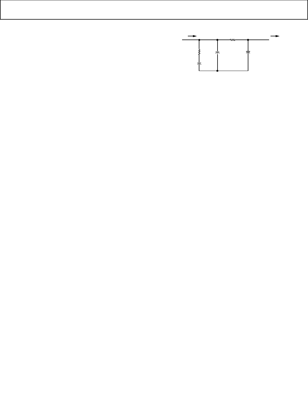
REFERENCE BLOCK
The reference frequency can be generated via the on-chip
DCXO or an external clock source can provide this input to the
device. A MUX selects the desired source. The reference is then
split and applied to three independent conditioning blocks also
known as ref dividers. The conditioning blocks provide four
options such that the PLL reference frequency, FREF, (the loop
reference applied to the PLL phase detector) is either buffered,
doubled, halved, or divided by 4. Independent blocks make it
possible to have a different FREF for the RF and BBPLLs. The
reference scalers will be set by the ad9361_init function. For
best RFPLL performance, Analog Devices recommends
selecting a reference clock or crystal that will be able to scale as
close to 80 MHz as possible.
Figure 3. PLL Reference Block
H6
DO NOT USE
CONNECT H6 TO GROUND
DCXO
20MHz TO 50MHz
M11
M12
1
0
1
0
BBPLL
F
REF
FOR BEST
PERFORMANCE:
35MHz TO 80MHz
FOR BEST
PERFORMANCE:
35MHz TO 70MHz
XTALP OR
OPEN FOR EXTERNAL REFERENCE
XTALN OR
EXTERNAL REFERENCE INPUT
5MHz TO 320MHz
(19MHz TO 80MHz RECOMMENDED)
÷2
÷4
×2
÷2
÷4
×2
÷2
÷4
×2
TX SYNTH
F
REF
RX SYNTH
F
REF
10MHz TO 80MHz
10MHz TO 80MHz
11668-004
Rev. A
AD9361 Reference Manual UG-570
| Page 17 of 128
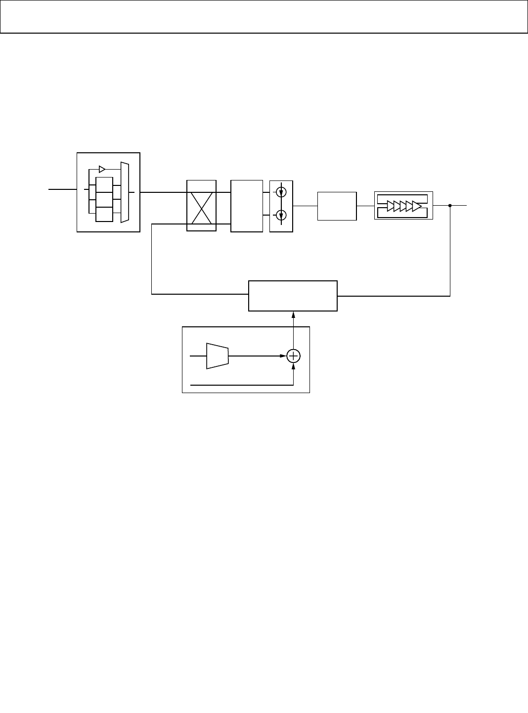
MAIN PLL BLOCK
The independent Rx and Tx PLLs use fractional-N techniques
to achieve the channel synthesis. The entire PLL is integrated
on-chip, including the VCO and the loop filter. The PLL always
operates over the range of 6 GHz 12 GHz. The charge pump
current is programmable as are all of the loop filter components
allowing optimization of performance parameters for almost
any application.
Configuration for a given frequency consists of a combination
of calculating the required divider values and referring to an
Analog Devices supplied lookup table to configure the VCO for
stable performance over temperature. The main PLL output is
divided by the VCO divider block to create the frequency bands
that allow the device to operate continuously from 70 MHz to
6 GHz. Figure 5 shows how the bands are created. The
synthesizer configuration registers, loop filter, integer and
fractional words, and VCO divider are calculated in the
ad9361_rx_lo_freq and ad9361_tx_lo_freq function calls.
Figure 4. PLL Synthesizer Block Diagram (Rx and Tx Synthesizers are Identical)
Figure 5. VCO Divider
8/9
PRE-SCALER
Σ-Δ
MODULATOR
LC VCO
PROGRAMMABLE
INTEGRATED LOOP
FILTER
CHARGE
PUMP
PFD
UP
DN
B COUNTER
A COUNTER
FO CAL
ALC CAL
VCO
LDO
2
4
×2
1Ω 1µF
CERAMIC
VCO LDO IN
CONNECTED EXTERNALLY
NECESSARY FOR LDO STABILITY
VCO LDO OUT
VDDA1P1 -VCO
FOR BEST
PERFORMANCE
F
REF
= 35MHz TO 80MHz
FREF =
10MHz TO 80MHz
FREF =
5MHz TO 320MHz
0.1mA TO 6.4mA 0µA TO 787.5µA
12.5µA STEPS
TO
VCO DIVIDER
BLOCK
6GHz TO 12GHz
100µF
÷
÷
11668-005
MUX/SELECTABLE BUFFERS
÷ 2 ÷ 2 ÷ 2 ÷2 ÷2 ÷2 ÷2
VCO INPUT
6GHz TO 12GHz
IQIQIQIQ
LOILOQ
47MHz TO 6GHz
3GHz TO 6GHz
1.5GHz TO 3GHz
750MHz TO 1.5GHz
375MHz TO 750MHz
187.5MHz TO 375MHz
93.75MHz TO 187.5MHz
46.875MHz TO 93.750MHz
11668-006
Rev. A
UG-570 AD9361 Reference Manual
| Page 18 of 128
CHARGE PUMP CURRENT
The charge pump current is 6-bit programmable and varies
from 0.1 mA to 6.4 mA with 0.1 mA steps. The charge pump
current needs to be calibrated during initialization, and can
then use the Analog Devices supplied LUTs during operation.
RFPLL LOOP FILTER
The RFPLL loop filter is fully integrated on-chip and is a
standard passive Type II third-order filter with five 4-bit
programmable components (see Figure 6). The loop filter
values are included in the Analog Devices provided synthesizer
LUTs and should not be modified.
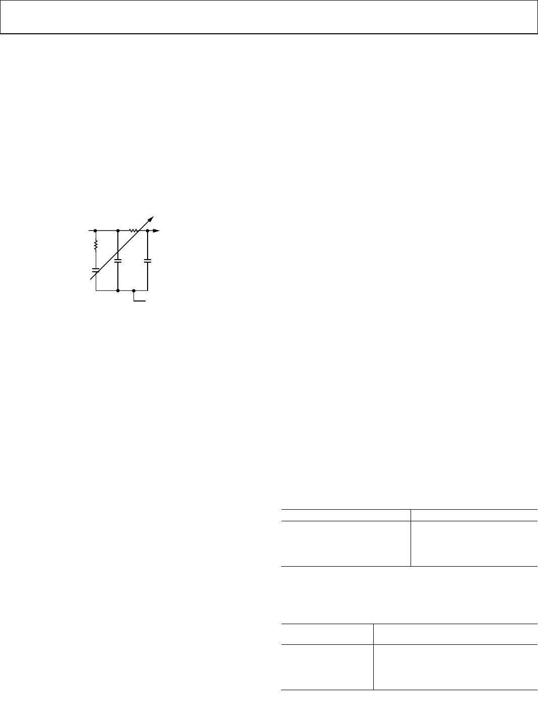
Figure 6. Loop Filter
VCO CONFIGURATION
VCO configuration consists of writing a few static registers
from an Analog Devices provided lookup table and then enabling
an automatic calibration procedure to configure the VCO tune
voltage (Vtune) and ALC. The VCO calibration is triggered in
one of three ways: when going from wait state to alert state,
when going from the synthesizer power-down state to the alert
state (TDD), or writing the LSBs of the Rx or Tx frequency
integer word. All LUT writes for the VCO, loop filter, and other
synthesizer settings should be written into the chip before
triggering the VCO calibration. Note that charge pump calibra-
tion should be completed before a VCO calibration is started.
When in TDD mode using hardware (ENABLE/TXNRX)
control and the device state machine is in the ALERT state, the
synthesizers power up and down with the state of the TXNRX
control line. A typical example sequence for TDD operation is
Rx-ALERT-Tx-ALERT-Rx. The BB controller sets the level of
the TXNRX line in ALERT to steer the device into the correct
next state. Then state machine advances to the next state with
the following ENABLE edge. During ALERT, as the BB
controller changes the level of TXNRX from low to high, the Rx
synthesizer turns off, the Tx synthesizer will turn on, and a Tx
VCO calibration will be triggered. Similarly, during a following
cycle, as the BB controller changes the state of TXNRX from
HIGH to LOW, the Tx synthesizer turns off, the Rx synthesizer
will turn on, and a Rx VCO calibration will be triggered.
Operationally, the BB processor should transition the TXNRX
line shortly after entering the alert mode so that the synthesizer
has as much of the time as possible between frames to calibrate
and lock. Typical TDD calibration plus lock times are on the
order of 45 µs to 60 µs. For faster lock times, refer to the TDD
Mode Faster Lock Times section.
VCO CALIBRATION
The time the calibration takes to complete is programmable.
Usually a fast calibration is appropriate for TDD systems, and a
slow calibration is appropriate for FDD. For TDD, the
synthesizer will only be on for a short time, so the danger that
temperature drift would cause it to lose lock is small. For FDD,
the synthesizer could potentially be locked indefinitely, so a
longer more accurate calibration is called for to ensure that
Vtune is sufficiently centered. Example calibration times are
shown in the RF Synthesizer VCO Calibration section.
The device includes a Fast Lock mode that makes it possible to
achieve faster than normal frequency changes by storing all
synthesizer programming information, including the VCO cal
result of this section, into either device registers or the BB
processor memory space to be recalled at a later time. See the
Fast Lock Profiles section for details.
VCO VTUNE MEASUREMENT
For debug purposes, the Vtune voltage can be output to a
package pin. The Vtune voltage is MUXed with the
corresponding (Rx or Tx) EXT_LO_IN pin. This is configured
by setting the VTune Out bit, 0x23B[6] (Rx) or 0x27B[6] (Tx).
For normal operation, these bits should be cleared.
LOCK DETECTOR
A lock detector bit is provided to indicate that the correspond-
ing synthesizer has achieved lock in the configured number of
clock. The lock detector is configured by setting the mode and
count values in the Lock Detect Config registers.
The Lock Detect Count bits set the maximum time allowed for
the RFPLL to lock. If it locks within the specified time, the lock
bits go high. The time is measured in reference clock cycles per
Table 7. It is recommended to use at least 1024 reference clock
cycles.
Table 7. Lock Detect Count
Lock Detect Count (decimal) Reference Clock Cycles
0 256
1 512
2 1024
3 2048
The Lock Detect Mode bits set the lock detect mode of
operation per Table 8. It is recommended to use run lock detect
continuously mode.
Table 8. RFPLL Lock Detect Mode
Lock Detect Mode
(Decimal) RFPLL Lock Detect Mode
0 Disable lock detect
1 Run lock detect once, when RFPLL is enabled
2 Run lock detect continuously
3 Do not use
C1
FROM
CHARGE
PUMP
TO VCO LDO
TO VCO
PROGRAMMABLE
INTEGRATED LOOP
FILTER
11668-007
Rev. A
AD9361 Reference Manual UG-570
| Page 19 of 128
SYNTHESIZER LOOK UP TABLE
Analog Devices provides synthesizer LUTs to generate the static
register writes needed for the VCO and loop filter. There is a set
of tables for FDD operation and a set of tables for TDD
operation. Each set of tables covers the entire VCO frequency
range, as well three different RFPLL loop reference frequencies.
The FDD tables enable the VCO temperature compensation
with the intent that the user will use longer, more accurate
calibration times for the device to remain in operation
indefinitely. In the TDD tables, the temperature compensation
is not enabled, because it is assumed that the VCO will be
calibrated between Tx and Rx frames. If temperature
compensation is required in a TDD operation then the FDD
tables can be used during the TDD synthesizer calibrations.
The provided LUTs are separated into three tables for 40 MHz,
60 MHz, and 80 MHz reference frequencies. The correct table
to use is the one that closest matches the loop FREF for the
operating mode. Refer to Table 9 for LUT selection based on
scaled reference frequency.
Table 9. Lookup Table Reference
RFPLL FREF Use Lookup Table
35 MHz to 50 MHz 40 MHz
50 MHz o 70 MHz 60 MHz
70 MHz to 80 MHz 80 MHz
TDD MODE FASTER LOCK TIMES
In TDD mode, the Rx and Tx synthesizers are alternately
turned on and off, following the state of the TXNRX control
line. Typically, the synthesizer is set to trigger a VCO
calibration every time it powers up so that it has a fresh
calibration value. If the LO frequency in TDD does not change
from frame to frame, it is not necessary to recalibrate the VCO
every time. The synthesizers retain the VCO calibration result
even after the synthesizer is powered down. When bursting
between Tx/ALERT/Rx … on the same LO frequency, the
synthesizer only needs to relock and can possibly be completed
in 25 µs or less, depending on the loop bandwidth.
To s etup synthesizer in this mode:
1. Setup the VCO for an FDD calibration.
2. Perform VCO calibration.
3. Set the Disable VCO Cal bit.
Step 3 disables the triggering of all VCO calibrations, including
writing of new Integer word. If a new calibration is needed, this
must be cleared.
Note that if the LO frequency is changed, the VCOs will need to
be recalibrated so it will retain the information pertaining to the
new frequency.
EXTERNAL LO
Unlike the internal synthesizers that always operate from 6 GHz
to 12 GHz no matter the RF tune frequency, the frequency
applied when an External LO is used is 2× the desired RF LO
frequency. The range of the EXT LO signal is from 140 MHz to
8 GHz, covering the RF tune frequency range of 70 MHz to
4 GHz. To setup the external LO use the ad9361_trx_ext_
lo_control function.
There are two separate EXT LO inputs, one for Rx and the other
for Tx. The recommended power level for the EXT LO signal at
the AD9361 pin is −3 dBm ≤ pin ≤ +3 dBm, and the maximum
pin must not exceed +6 dBm.
Note that the EXT_LO_IN package pins are multi-purposed
and they can take on a different functionality (Vtune
measurement) when the device is using internal synthesizers.
See the VCO Vtune Measurement section for information.
BASEBAND PLL (BBPLL)
The BBPLL is a fractional-N synthesizer used to synthesize the
digital clocks for the AD9361 chip. The BBPLL synthesizes an
integer multiple of the Rx ADC clock, the Tx DAC clock, all
analog calibration clocks, as well as the clocks used in the digital
section. The BBPLL operates of the range of 715 MHz to
1.430 GHz, which allows practically any sample rate to be
generated from any reference frequency. Table 10 is a listing of
common communication systems showing the system sample
rate and the corresponding BBPLL frequency. The output of the
BBPLL drives a programmable divider chain to result in the
desired sample rate and bus communication rate. The required
BBPLL frequency is usually back-calculated by deciding how
the channel filtering will be accomplished and then selecting
the appropriate output divider that allows the BBPLL to operate
within range. Refer to the Filter Guide section for available
filtering and decimation/integration setups.
Table 10. Clock Rates for the Rx and Tx Digital Data Paths
Plus the Appropriate BBPLL Output Frequencies
System
Sample Rate (MSPS)
BBPLL (MHz)
GSM 0.542 832
LTE 1.4 1.92 983.04
LTE 3.0 3.84 983.04
LTE 5 7.68 983.04
LTE 10 15.36 983.04
LTE 15 23.04 737.28
LTE 20
30.72
983.04
WiMAX 1.75 2 1024
WiMAX 3.5 4 1024
WiMAX 4.375 5 1280
WiMAX 7 8 1024
WiMAX 8.75 10 1280
WiMAX 5 5.6 716.8
WiMAX 10 11.2 716.8
WiMAX 20 22.4 1075.2
802.11a 20 1280
802.11n 40 1280
Rev. A
UG-570 AD9361 Reference Manual
| Page 20 of 128
BBPLL VCO
The BBPLL VCO is a multiband ring oscillator with Kv of
550 MHz/V that requires a frequency calibration before
operation. The calibration is configured and run with the
ad9361_bbpll_set_rate function.
Figure 7 is a block diagram of the BBPLL. The reference
frequency for the loop is the output of the reference scaler
block, which is identical to, but independent from the reference
scaler blocks for the RFPLLs. The reference block is configured
to buffer, multiply, or divide the device reference frequency
before passing to the to the BBPLL phase detector. For best
performance, it is recommended that the BBPLL reference
scaler block be configured such that the resulting BBPLL FREF is
between 35 MHz to 70 MHz.
Figure 7. BBPLL Block Diagram
F
REF
÷2
÷4 UP
DWN
PFD LPF
F
OUT
F
VCO
715MHz TO 1430MHz
N ÷ (N + 1)
DSM
MODULUS = 2088960
FRACTIONAL WORD
INTEGER WORD
×2
11668-008
Rev. A
AD9361 Reference Manual UG-570
| Page 21 of 128
BBPLL CHARGE PUMP
The charge pump has programmable output current from
25 µA to 1575 µA in 25 µA steps. In addition, a programmable
bleed current is available. This is an NMOS current source
programmable from 0 µA to 316 µA.
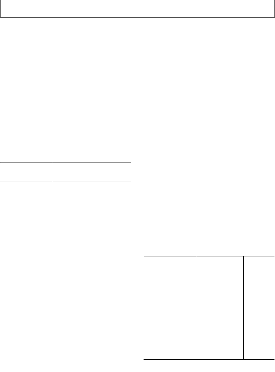
BBPLL LOOP FILTER
The loop filter is fully integrated on-chip and is a standard
passive Type II third-order filter with five programmable
components. The filter is programmed by the
ad9361_bbpll_set_rate function.
Figure 8. BBPLL Internal Loop Filter (R2 and C3 Can Be Bypassed)
R1
C1
C2
R2
C3
VCO TUNEICP
11668-009
Rev. A

UG-570 AD9361 Reference Manual
| Page 22 of 128
FAST LOCK PROFILES
OVERVIEW
The AD9361 includes a fast lock mode that makes it possible to
achieve faster than normal frequency changes by storing sets of
synthesizer programming information (called profiles) either
into device registers or the BB processor’s memory space to be
recalled at a later time. The fast lock mode eliminates most of
the overhead of synthesizer programming by allowing up to
8 full Rx profiles and 8 full Tx profiles of frequency
configuration information (including VCO calibration results)
to be stored in the device for faster frequency changes.
To use a particular profile, first it must be configured. Typically,
this would be accomplished at power-up, but a new or updated
profile can be defined at any convenient time.
To define a profile, the synthesizer is configured, calibrated, and
allowed to lock at a particular frequency. The VCO calibration
time should be set to the longest, most accurate time period
(FDD mode) since these values are to be stored for future use.
Once the synthesizer has been configured and the VCO
calibration has completed, the baseband processor transfers the
resulting information from the synthesizer registers into the fast
lock memory space by profile number. This is repeated for each
desired profile (0 to 7 Rx and 0 to 7 Tx).
If more than the 8 on-chip profiles are needed, the synthesizer
is tuned and calibrated as if the information were to be stored in
a profile, but instead it is stored in baseband processor memory
space and written into the desired profile at a later, more
convenient time. In this way, an unlimited number of profiles
can be available, and a given profile can be changed or updated
at any appropriate time during operation.
In addition, the user can also define a higher initial charge
pump current and R1 value of the loop filter to increase the
synthesizer’s bandwidth for a programmable amount of time to
further reduce lock time. These values are defined in the profile
information as well.
A profile can be recalled by either issuing a single SPI command
that contains the desired profile number and transfer bit, or
alternatively, a profile can be selected in hardware by setting the
appropriate code on control input pins. At that time, all the
on-chip stored profile information is transferred into the
synthesizer registers, the synthesizer is immediately configured,
and it is released to lock as quickly as the loop BW allows.
FAST LOCK INITIAL WIDER BW OPTION
The fact that the VCO calibration is eliminated in fast lock
may provide fast-enough synthesizer locking for a particular
application. However, when a profile is selected, it is also
possible to initially have different loop filter values and charge
pump current resulting in a wider loop BW for a programmable
time period, possibly resulting in an even faster lock mode.
After the time period expires, the loop filter values take on the
steady state narrow values of the profile. If this feature is not
needed or desired, simply program the init values the same as
the narrow values.
Assuming the same phase margin for wide (init) and narrow
BW is desired,
For a BW Ratio, N = Init BW/Narrow BW,
CP_current_init = CP_current_narrow × N2
R1_init = R1_narrow/N
In practice, CP_current_init will probably max out before it
could actually be the square of the narrow value. Even though
this occurs, a lock time advantage is still possible; the absolute
values that result in the fastest lock and settling times will need
optimization by the customer during product development.
Note that charge pump currents and all loop filter components
can be completely different between wide (initial) and narrow
values, so exercise care when configuring to result in optimum
and stable performance in both wide and narrow BW modes.
The amount of time the wider BW is active is programmed into
the Fast Lock Setup Init Delay register in increments of 250 ns
per bit.
Rev. A

AD9361 Reference Manual UG-570
| Page 23 of 128
CONFIGURING AND USING A FAST LOCK PROFILE
The Fast Lock registers (Address 0x25C through Address 0x25F for Rx, Address 0x29C through Address 0x29F for Tx) allow access to the
internal memory area. Refer to Table 11 for Rx and Table 12 for Tx fast lock register contents. The following procedure describes how to
define a particular profile to the currently programmed synthesizer frequency:
1. If using faster lock (wide BW), determine fast lock delay and N. If not using wide BW, then delay is not important and N = 1.
2. To configure profiles:
a. For each profile (Rx and Tx are independent),
i. Calibrate the synthesizer to the desired frequency using FDD calibration settings
ii. Create the profile and store in the AD9361 using the ad9361_fastlock_store function.
iii. If the profile also needs to be stored in the BBP then use the ad9361_fastlock_save function.
3. To use profiles:
a. To use a profile that is stored inside the AD9361 use the ad9361_fastlock_recall function.
b. If the profile is stored in the BBP then first load it into the AD9361 by using the ad9361_fastlock_load function, and then
use the recall function to use the profile.
Table 11. Rx Fast Lock Internal Addressing
Program Address[7:4] Assignment Program Address[3:0] Assignment (Written to 0x25D) Location of Setup Words
0 profile0 0 Synthesizer Integer Word[7:0] 0x231[D7:D0]
1 profile1 1 Synthesizer Integer Word[10:8] 0x232[D2:D0]
2 profile2 2 Synthesizer Fractional Word[7:0] 0x233[D7:D0]
3 profile3 3 Synthesizer Fractional Word [15:8] 0x234[D7:D0]
4 profile4 4 Synthesizer Fractional Word [22:16] 0x235[D6:D0]
5 profile5 5 VCO Bias Ref[2:0] shift left by 4
+
VCO Varactor [3:0]
0x242[D2:D0]
0x239[D3:D0]
6 profile6 6 VCO Bias Tcf[1:0] shift left by 3
+
Charge Pump Current (Init)[5:0]
0x242[D4:D3]
Set per Init N calculation
7 profile7 7 Charge Pump Current[5:0] 0x23B[D5:D0]
8 Not used 8 Loop Filter R3[3:0] shift left by 4
+
Loop Filter R3 (Init)[3:0]
0x240[D3:D0]
Set desired Init value
9 Not used 9 Loop Filter C3[3:0] shift left by 4
+
Loop Filter C3 (Init)[3:0]
0x23F[D3:D0]
Set desired Init value
A Not used A Loop Filter C1[3:0] shift left by 4
+
Loop Filter C2[3:0] shift right by 4
0x23E[D3:D0]
0x23E[D7:D4])
B Not used B Loop Filter R1[3:0]
+
Loop Filter R1 (Init)[3:0]
0x23F[D7:D4]
Set per Init N calculation
C Not used C VCO Varactor Reference Tcf[2:0]
+
Rx VCO Divider[3:0]
0x250[D6:D4]
0x005[D3:D0]
D Not used D VCO Cal Offset[3:0] shift left by 1
+
VCO Varactor Reference[3:0]
0x238[D6:D3]
0x251[D3:D0]
E Not used E Force VCO Tune[7:0] 0x237[D7:D0]
F Not used F Force ALC word[6:0] shift left by 1
+
Force VCO Tune[8]
0x236[D6:D0]
0x238[D0]
Rev. A

UG-570 AD9361 Reference Manual
| Page 24 of 128
Table 12. Tx Fast Lock Internal Addressing
Program Address[7:4] Assignment Program Address[3:0] Assignment (written to 0x25D) Location of Setup Words
0 profile0 0 Synthesizer Integer Word[7:0] 0x271[D7:D0]
1 profile1 1 Synthesizer Integer Word[10:8] 0x272[D2:D0]
2 profile2 2 Synthesizer Fractional Word[7:0] 0x273[D7:D0]
3 profile3 3 Synthesizer Fractional Word[15:8] 0x274[D7:D0]
4 profile4 4 Synthesizer Fractional Word[22:16] 0x275[D6:D0]
5 profile5 5 VCO Bias Ref[2:0] shift left by 4
+
VCO Varactor[3:0]
0x282[D2:D0]
0x279[D3:D0]
6 profile6 6 VCO Bias Tcf[1:0] shift left by 6
+
Charge Pump Current (Init)[5:0]
0x282[D4:D3]
Set per Init N calculation
7 profile7 7 Charge Pump Current[5:0] 0x27B[D5:D0]
8 Not used 8 Loop Filter R3[3:0] shift left by 4
+
Loop Filter R3 (Init)[3:0]
0x280[D3:D0]
Set per Init N calculation
9
Not used
9
Loop Filter C3[3:0] shift left by 4
+
Loop Filter C3 (Init)[3:0]
0x27F[D3:D0]
Set per Init N calculation
A Not used A Loop Filter C1[3:0] shift left by 4
+
Loop Filter C2[3:0] shift right by 4
0x27E[D3:D0]
0x27E[D7:D4])
B Not used B Loop Filter R1[3:0]
+
Loop Filter R1 (Init)[3:0]
0x27F[D7:D4]
Set per Init N calculation
C Not used C VCO Varactor Reference Tcf[2:0]
+
Rx VCO Divider[3:0]
0x290[D6:D4]
0x005[D7:D4]
D Not used D VCO Cal Offset[3:0] shift left by 1
+
VCO Varactor Reference[3:0]
0x278[D6:D3]
0x291[D3:D0]
E Not used E Force VCO Tune[7:0] 0x277[D7:D0]
F Not used F Force ALC word[6:0] shift left by 1
+
Force VCO Tune[8]
0x276[D6:D0]
0x278[D0]
FAST LOCK PIN SELECT
The previous example demonstrated how to setup profiles and select a profile using SPI commands. It is also possible to use hardware
control to select a particular profile if desired. The control input pins in this mode are used to select the desired profile. This mode is
enabled by setting Bit D1, Fast Lock Profile Pin Select in Rx Register 0x25A and/or Tx Register 0x29A along with enabling fast lock mode
in the same registers. When this is set, CTRL_IN0 through CTRL_IN2 select the profile (if both pin select bits are set, profiles are selected
in parallel). In the system design, it should be noted that CTRL_IN pins are configurable for other functions as well so they are not
available for other functions simultaneously.
Rev. A
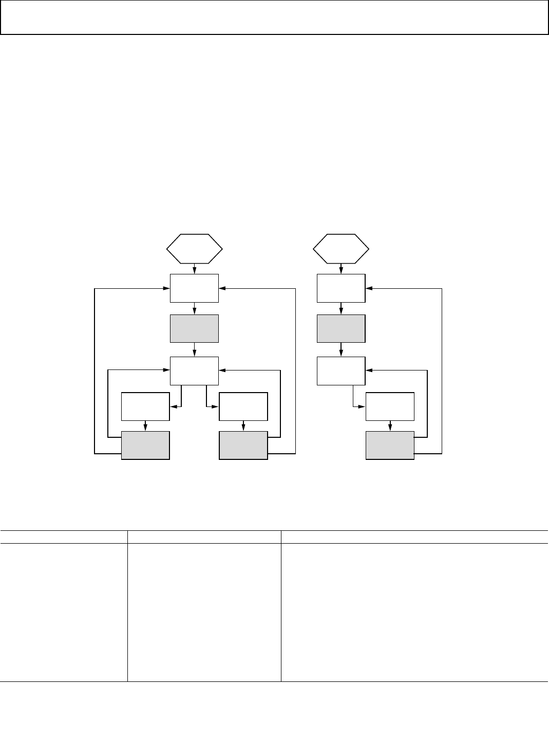
AD9361 Reference Manual UG-570
| Page 25 of 128
ENABLE STATE MACHINE GUIDE
OVERVIEW
The AD9361 transceiver includes an enable state machine
(ENSM), allowing real time control over the current state of the
device. The ENSM has two possible control methods—SPI
control and pin control. The ENSM is controlled asynchro-
nously by writing SPI registers to advance the current state to
the next state. The ENABLE and TXNRX pins allow real time
control of the current state. The ENSM also allows TDD or
FDD operation. The ad9361_set_en_state_machine_mode
function configures the ENSM.
The gray states displayed in Figure 9 require no user control
and will fall through to the next state after a set time. The
TO_ALERT signal is a setting in the ENSM Config 1 register.
To move to the WAIT state, clear the TO_ALERT bit while in
the Rx or Tx states. In that configuration when moving out of
the Rx, Tx, or FDD states, the ENSM will transition to the
WAIT state. If the bit is set the ENSM will transition to the
ALERT state. The SLEEP state is the WAIT state with the
AD9361 clocks disabled. To enter the sleep state, transition to
the WAIT state, then disable the AD9361 clocks in the BPLL
register.
Figure 9. TDD and FDD State Diagrams for the Enable State Machine
ENSM STATE DEFINITIONS
The enable state machine contains the states shown in Table 13.
Table 13. ENSM State Values
ENSM State Name Value in ENSM State (decimal) Description
SLEEP 0 WAIT state with AD9361 clocks/BBPLL disabled
WAIT1 0 Synthesizers disabled (power saving mode)
CALIBRATION 1, 2, 3
WAIT to ALERT delay 4 Fixed delay set by Register 0x024 and Register 0x025
ALERT1 5 Synthesizers enabled.
Tx
1
6
Tx signal chain enabled
Tx FLUSH 7 Time to allow digital filters and signal path to flush
Rx1 8 Rx signal chain enabled
Rx FLUSH 9 Time to allow digital filters and signal path to flush
FDD1 10 Tx and Rx signal chains enabled
FDD FLUSH 11 Time to allow digital filters and signal path to flush
1 These states require user interaction to move to the next state.
SLEEP
WAIT
ALERT
TXRX
RX
FLUSH TX
FLUSH
POWER ON
VCO LDO
TO_ALERT = 0TO_ALERT = 0
TO_ALERT = 1TO_ALERT = 1
TDD ENABLE STATE
MACHINE
SLEEP
WAIT
ALERT
FDD
FDD
FLUSH
POWER ON
VCO LDO
TO_ALERT = 0
TO_ALERT = 1
FDD ENABLE STATE
MACHINE
11668-010
Rev. A

UG-570 AD9361 Reference Manual
| Page 26 of 128
MODES OF OPERATION
The ENSM can either be controlled by SPI writes or the
ENABLE/TXNRX pins. SPI control is considered asynchronous
to the DATA_CLK because the SPI_CLK can be derived from a
different clock reference and still function properly. The SPI
control ENSM method is recommended when real time control
of the synthesizers is not necessary. SPI control can be used for
real time control as long as the BBP has the ability to perform
timed SPI writes accurately. The ENABLE/TXNRX pin control
method is recommended if the BBP has extra control outputs
that can be controlled in real time, allowing a simple two-wire
interface to control the state of the AD9361 device. The
ENABLE pin can be driven by either a pulse (edge detected
internal to the AD9361) or a level to advance the current state
of the ENSM to the next state. If a pulse is used on the ENABLE
pin, it must have a minimum pulse width of one FB_CLK cycle.
In level mode, the ENABLE and TXNRX pins are also edge
detected in the AD9361, and must meet the same minimum
pulse width requirements of one FB_CLK cycle.
SPI Control
SPI control is disabled by default and can be enabled in the
ENSM Config 1 register. Once in the ALERT state, the AD9361
enables its RF synthesizers for the transmitters and receivers. If
for some reason the synthesizers did not calibrate correctly, the
ENSM will not be able to transition to the Rx or Tx states. This
feature protects the AD9361 from transmitting or receiving data
when the synthesizers are not calibrated properly, protecting the
wireless spectrum.
Once in the ALERT state, with the RFPLLs properly calibrated,
the ENSM is ready to move into the Rx, Tx, or FDD state. To
move from ALERT to Rx, set the Force Rx On bit. To move
back to ALERT or WAIT, clear the bit. To move from ALERT to
Tx or FDD, set the Force Tx On bit. To move back to ALERT or
WAIT clear the bit. In FDD mode, the Force Rx On bit is
ignored. While in TDD, the ENSM must transition to the
ALERT state between Rx and Tx states. The ENSM cannot
move from Rx directly to Tx, or Tx directly to Rx.
After sending the Force Alert State bit from the WAIT state,
allow the ENSM time to pass through ENSM State 4 before
sending another command. The time for State 4 to complete
depends on the time setting written into the Rx and Tx Load
Synth Delay registers. This delay is 2 µs.
After sending the SPI write to exit the Rx or Tx states, allow six
ADC_CLK/64 clock cycles of flush time before sending another
ENSM SPI command. If a SPI command is received during an
intermediate ENSM state, the command will be ignored.
Rev. A
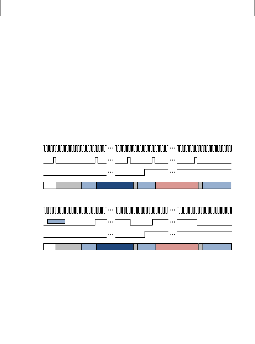
AD9361 Reference Manual UG-570
| Page 27 of 128
ENABLE/TXNRX Pin Control
ENABLE/TXNRX Pin Control mode is enabled by default. The
ENABLE pin can operate with a pulse or a level to transition the
ENSM state to the next state. In pulse mode, a pulse with
minimum width of one FB_CLK cycle is necessary to advance
the current ENSM state. The BBP sends an ENABLE pulse to
move into Rx or Tx, and then another pulse when it is time to
move back to the ALERT or WAIT state. In TDD, the state of
the TXNRX pin controls whether the AD9361 will transition
from ALERT to Rx or ALERT to Tx. If TXNRX is high, the
device will move into the Tx state. If TXNRX is low, the device
will move into the Rx state. The TXNRX pin level should be set
during the ALERT state. The logic level of TXNRX must not
change during the Rx, Tx, or FDD states.
In level mode, the ENABLE pin level controls the ENSM state.
The falling edge of the ENABLE pin moves the AD9361 device
into the ALERT state. TXNRX must be set or cleared while in
the ALERT state. The rising edge of the ENABLE pin moves the
AD9361 into the Rx state if TXNRX is low, or the Tx state if
TXNRX is high. In FDD, the logic level of TXNRX is ignored.
The ENSM will exit the Rx, Tx, or FDD states when the
ENABLE pin is pulled back to a logic low. If the To Alert bit is
clear the device will move from Rx, Tx, or FDD to the WAIT
state. To move from WAIT to ALERT in level mode, the BBP
can drive a pulse on the ENABLE pin or perform a SPI write to
the Force Alert State bit. If an ENABLE pulse is used, it must
have a pulse width larger than one FB_CLK cycle wide. The
rising edge of the ENABLE pulse advances the ENSM state from
WAIT to ALERT. The falling edge of the ENABLE pulse is
ignored in ALERT. See Figure 10, Figure 11, Figure 12, and
Figure 13 for simplified graphical references.
When moving from WAIT to ALERT, time must be allowed for
State 4 to complete before sending another ENABLE pulse. The
time required to wait depends on the Rx and Tx Load Synth
Delay. Also, after the Rx, Tx, and FDD states, allow six
ADC_CLK/64 clock cycles for each corresponding FLUSH state
to complete.
Figure 10. ENABLE Pulse Mode, TDD (Minimum Pulse Width = One FB_CLK Cycle)
Figure 11. ENABLE Level Mode (TDD)
ENABLE
TXNRX
ENSM STATE[3:0]
FB_CLK
ALERTWAIT POWER UP VCO
LDO ALERT RX ALERT TX
11668-011
FB_CLK
ENABLE
TXNRX
ENSM STATE[3:0] ALERTWAIT POWER UP VCO
LDO ALERT RX ALERT TX
SPIWRITE
11668-012
Rev. A
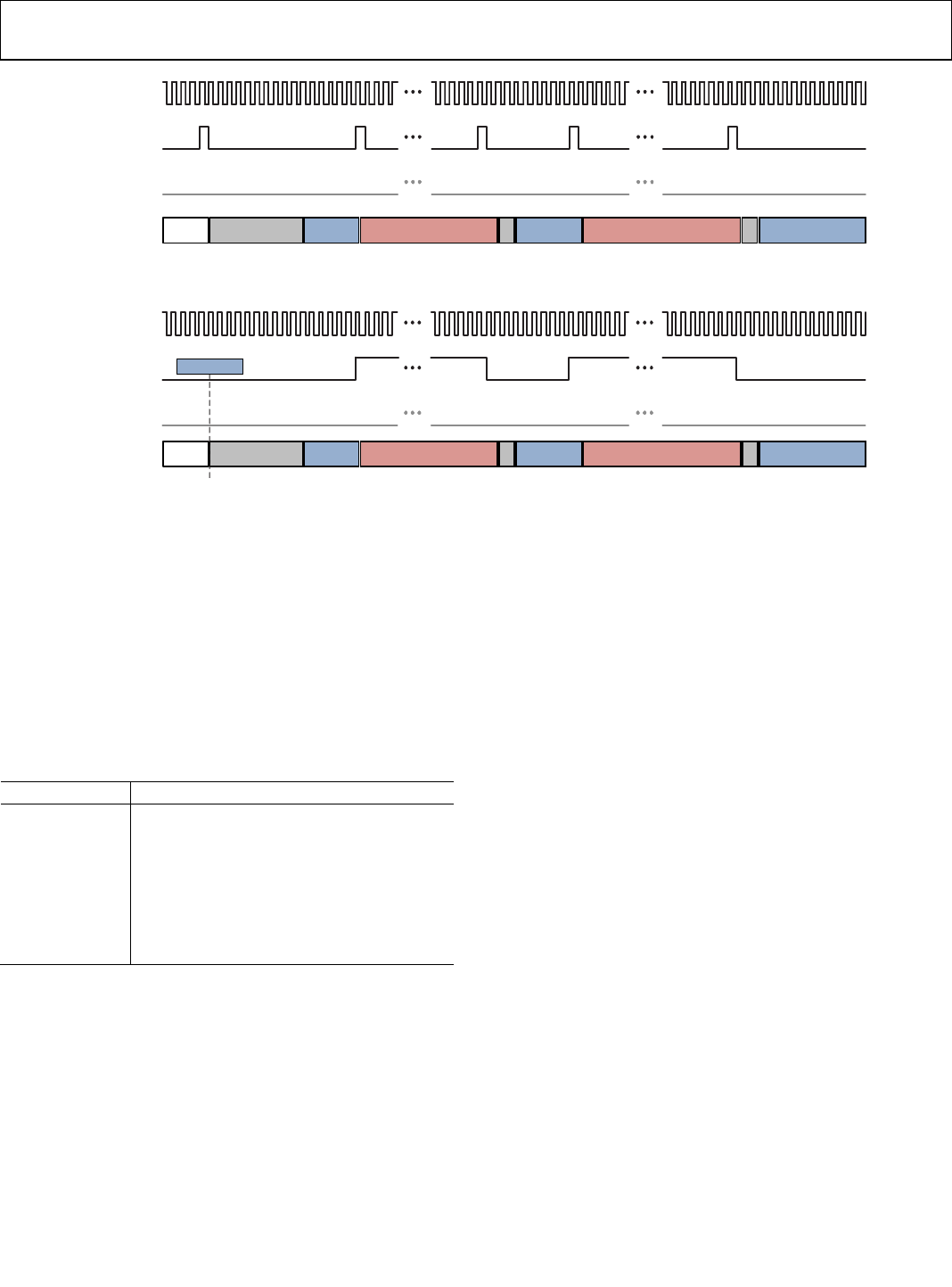
UG-570 AD9361 Reference Manual
| Page 28 of 128
Figure 12. ENABLE Pulse Mode, FDD (Minimum Pulse Width = One FB_CLK Cycle)
Figure 13. ENABLE Level Mode, FDD
FDD Independent Control
When the AD9361 is in FDD mode, the FDD independent
control option allows the receive chain and transmit chain to be
enabled independently. This mode is enabled by setting the
FDD External Control Enable bit (0x015[D7]). Note that SPI
writes must be used to move the ENSM into the FDD state.
Then the ENABLE and TXNRX pins are internally remapped to
Force Rx On and Force Tx On, respectively. Once in the FDD
state, the control combinations in Table 14 are allowed.
Table 14. ENABLE/TXNRX Pin Alternative Functionality
Pin Level Description
ENABLE low,
TXNRX low
Rx and Tx signal chains disabled (Operates
like ALERT state)
ENABLE high,
TXNRX low
Rx signal chain enabled, Tx signal chain
disabled (Operates like Rx state)
ENABLE low,
TXNRX high
Rx signal chain disabled, Tx signal chain
enabled (Operates like Tx state)
ENABLE high,
TXNRX high
Rx signal chain enabled, Tx signal chain
enabled. (Operates like FDD state)
Note that since the ENSM always stays in the FDD state, it
never moves to the FDD FLUSH state. Therefore, the BBP must
allow enough time after enabling the receive chain for the
digital filters to flush, and enough time after sending Tx data
for the Tx to finish its transmission before disabling the
corresponding signal chain. If Tx_FRAME is held low, the data
port in the AD9361 will force zeros into the Tx data path.
Note that in pulse mode the BBP should send pulses on the
ENABLE pin to enable/disable the Rx signal chain. Pulses sent
on the TXNRX pin will enable/disable the Tx signal chain.
When using a SPI write to move from ALERT into the FDD
state, both the Rx and Tx signal chains start disabled until the
first pulse is received. The pulse should have a minimum pulse
width of one FB_CLK cycle. No maximum pulse width is
defined; the pulse is edge detected and internally generates a
one cycle wide pulse.
FB_CLK
ENABLE
TXNRX
ENSM STATE[3:0] ALERTWAIT POWER UP VCO
LDO ALERT FDD ALERT FDD
11668-013
FB_CLK
ENABLE
TXNRX
ENSM STATE[3:0] ALERTWAIT POWER UP VCO
LDO ALERT FDD ALERT FDD
SPIWRITE
11668-014
Rev. A
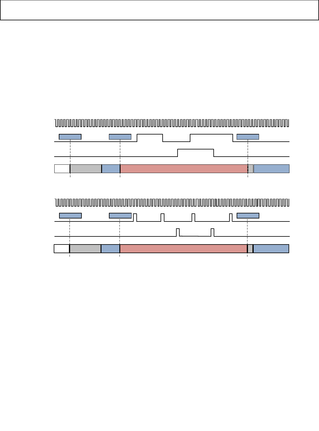
AD9361 Reference Manual UG-570
| Page 29 of 128
ENSM and RF VCO Calibrations
The ENSM controls an internal signal that tells the Rx and Tx
synthesizers when to calibrate. In FDD, both the Rx and Tx
synthesizers calibrate when moving from WAIT to ALERT and
when the integer RF frequency word is written. Otherwise, the
synthesizers remain powered on and locked.
Similar to FDD, in TDD the enabled synthesizer (depending on
TXNRX logic level) will be calibrated when moving from WAIT
to ALERT. When in the ALERT, Rx, or Tx state, the enabled
synthesizer (depending on the TXNRX logic level) will calibrate
when the integer frequency word is written in the SPI register map.
In TDD, the synthesizers do not remain locked all the time.
While in the Rx state, the Tx synthesizer is disabled to save
power. While in the Tx state, the Rx synthesizer is disabled. In
TDD, the ENSM will generate a signal to recalibrate the correct
VCO anytime the state of TXNRX changes. This signal will be
issued from the ENSM to the synthesizer after the delay in Rx
or Tx Load Synth Delay has completed.
It is important to change the state of TXNRX as soon as the
device moves into the ALERT state to allow time for the
selected synthesizer to calibrate before moving into the Rx or
Tx states.
Figure 14. FDD Independent Control, Level Mode
Figure 15. FDD Independent Control, Pulse Mode
FB_CLK
ENABLE
TXNRX
ENSM STATE[3:0] ALERTWAIT POWER UP VCO
LDO ALERT FDD
SPIWRITE SPIWRITE RX ENABLED
TX ENABLED
RX ENABLED SPIWRITE
RX DISABLED
TX DISABLED
11668-015
FB_CLK
ENABLE
TXNRX
ENSM STATE[3:0] ALERTWAIT POWER UP VCO
LDO ALERT FDD
SPIWRITE SPIWRITE RX ENABLED
TX ENABLED
RX ENABLED SPIWRITE
RX DISABLED
TX DISABLEDTX DISABLED
11668-016
Rev. A

UG-570 AD9361 Reference Manual
| Page 30 of 128
SLEEP STATE
The AD9361 initially powers up in a very low power state called
the SLEEP state. In this state, the AD9361 SPI registers are
powered up; however, all internal clocks and other circuits are
powered down. After power up, the BBP programs the AD9361
using the SPI port and runs the internal calibrations necessary
for optimal performance. After normal transmit/receive
operation, if the AD9361 is not required for radio activity, the
BBP can instruct the AD9361 to return to the SLEEP state to
minimize power consumption.
The SLEEP state is technically the ENSM WAIT state with the
digital clocks turned off. When returning to the SLEEP state, all
calibration results will be stored because the AD9361 SPI
registers remain powered up.
Sleep Procedure (Assumes Current State = ALERT)
1. Disable VCO calibrations to prevent VCO settings from
being overwritten by possible automatic calibrations.
SPIWrite 0x230 = 0x55 Disable Rx VCO
calibration, set 0x230[0]
SPIWrite 0x270 = 0x55 Disable Tx VCO
calibration, set 0x270[0]
2. Move ENSM from ALERT to the WAIT state using the SPI
port. Note that when using FDD, only the Force Tx On bit
controls the ENSM. If using TDD, using Force Rx On will
limit energy being transmitted from the AD9361. In either
case, it is recommended to power down the external PA
before moving the AD9361 into the FDD or Tx states.
SPIWrite 0x014 = 0x00 Clear the To Alert bit in
0x014[0]
SPIWrite 0x014 = 0x20 Move to FDD state (by
setting Force Tx On bit in 0x014[5])
WA I T Wait for FDD flush time
(six ADC_CLK/64 clock cycles)
SPIWrite 0x014=0x00 Move to Wait State (by
clearing 0x014[5])
SPIWrite 0x009=0x00 Turn off all clocks (sleep
state)
3. The AD9361 is now in the SLEEP state.
4. To wake up the AD9361, enable digital clocks and BBPLL,
and then move into the ALERT state.
SPIWrite 0x009 = 0x17 Turn on all clocks
(assumes external clock in this case)
WA I T Wait for BBPLL to lock
(BBPLL lock bit in 0x5E[7], locked =1)
SPIWrite 0x014 = 0x05 Set the To Alert bit and
force Alert state
SPIWrite 0x230 = 0x54 Allow Rx VCO
calibration, clear 0x230[0]
SPIWrite 0x270 = 0x54 Allow Tx VCO
calibration, clear 0x270[0]
Calibrations After Waking from SLEEP
Although the previous calibration results are stored through the
SLEEP state, some calibrations may need to be updated if time
permits. For instance, the AD9361 normally is set to track out
DC offset over time once in the active receive state. The first
time back into the Rx or FDD states, the DC offset may not be
optimal. Running the RF DC Offset Calibration may improve
the DC offset for the first time back in the Rx state. Another
advantage is the calibration stores RF DC offset corrections for
all front-end gain indexes. The tracking mode only allows the
RF DC offset to update at the current gain index.
If using TDD, the Rx VCO and/or Tx VCO used first will need
to be calibrated before moving into the Rx or Tx state. This can
be accomplished by toggling the TXNRX after enabling VCO
calibrations in Register 0x230 and Register 0x270. The TxRNX
edge triggers the calibration to occur. In FDD, a VCO calibra-
tion should not be required.
Rev. A
AD9361 Reference Manual UG-570
| Page 31 of 128
FILTER GUIDE
OVERVIEW
This section contains a description of the analog and digital
filtering available in both the Tx and Rx signal paths of the
AD9361.
Tx SIGNAL PATH
The AD9361 Tx signal path receives 12-bit twos complement
data in I-Q format from the AD9361 digital interface, and each
channel (I and Q) passes this data through four digital
interpolating filters to a 12-bit DAC. Each of the four
interpolating filters can be bypassed. The DAC’s analog output
is passed through two low-pass filters prior to the RF mixer.
The corner frequency for each low-pass filter is programmable
with the ad9361_set_tx_rf_bandwidth function. Figure 16
shows a block diagram for the AD9361 Tx signal path. Note
that both the I and the Q paths are schematically identical to
each other.
Overranging is detected in the Tx digital signal path at each
stage and limited to the maximum code value (preventing data
wrapping). An overrange occurrence can be monitored in the
Overflow registers or at the control output pins.
Tx DIGITAL FILTER BLOCKS
The four blocks leading up to the DAC in Figure 16 comprise
the digital filtering for the transmit path. These programmable
filters provide the bandwidth limiting required prior to
conversion from digital to analog. They also provide
interpolation to translate from the input data rate to the rate
needed for proper digital to analog conversion. In each filter,
interpolation is performed first, followed by the filter transfer
function. The digital filters are configured using the
ad9361_calculate_rf_clock_chain functions. ADC_CLK (the
ADC sample clock) is the fastest signal path clock available in
the device’s digital processing section, so it is used as the master
clock reference for the digital filters in the Tx signal path. The
sample clock of each fixed-coefficient filter is always equal to
the output data clock. The following sections describe the
details of these blocks.
Tx FIR
The first digital filter in the Tx signal path is a programmable
polyphase FIR filter. The Tx FIR filter can also interpolate by a
factor of 1, 2, or 4, or it can be bypassed if not needed. This
filter is controlled in the ad9361_set_tx_fir_config. The filter
taps are stored in 16-bit twos complement format, and the
number of taps is configurable between a minimum of 16 taps
and a maximum of 128 taps in groups of 16. The Tx FIR also
has a programmable gain setting of 0 dB or −6 dB. Each
coefficient is stored in two registers as a 16-bit number.
The Tx FIR uses DAC_CLK (Tx DAC sample clock) as its
sample clock. DAC_CLK is either set equal to ADC_CLK or is
set to ADC_CLK/2. The Tx FIR calculates 16 taps per clock
cycle. This limits the number of available taps to the ratio of
DAC_CLK to the input data rate multiplied by 16. For example,
if the input data rate is 25 MHz and DAC_CLK is 100 MHz,
then the ratio of DAC_CLK to the input data rate is 100/25 or 4.
In this scenario, the total number of taps available is 64.
Another limitation is the memory inside the filter. The total
number of operations that can be performed is limited to 64
per clock cycle. This means that the number of taps available is
limited to 64 if the interpolation factor is set to 1. If an
interpolation rate greater than 1 is used, then the memory space
can be utilized to include more taps. Table 15 lists the allowable
number of taps for each interpolation rate.
Table 15. Filter Taps Based on Interpolation Rate
Interpolation Maximum Number of Taps
1 64
2 128
4 128
Tx HB1
Tx HB1 is a fixed-coefficient half-band interpolating filter. Tx
HB1 can interpolate by a factor of 2, or it may be bypassed. Tx
HB1 has the following coefficients: [−53, 0, 313, 0, −1155, 0,
4989, 8192, 4989, 0, −1155, 0, 313, 0, −53]. Note that the full-
scale range for this filter is 8192 (213).
Tx HB2
Tx HB2 is a fixed-coefficient half-band interpolating filter. Tx
HB2 can interpolate by a factor of 2, or it may be bypassed. Tx
HB2 has the following coefficients: [−9, 0, 73, 128, 73, 0, −9].
Note that the full-scale range for this filter is 128 (27).
Figure 16. AD9361 Tx Signal Path
HB1
PROG
TX FIR DACHB2 HB3/
INT3 BB
LPF 2
ND
LPF
11668-017
Rev. A

UG-570 AD9361 Reference Manual
| Page 32 of 128
Tx HB3/INT3
Tx HB3/INT3 provides the choice between two different fixed-
coefficient interpolating filters. Tx HB3/INT3 can interpolate
by a factor of 2 or 3, or it may be bypassed. Tx HB3 has the
following coefficients: [1, 2, 1], and Tx INT3 has the following
coefficients: [36, −19, 0, −156, −12, 0, 479, 223, 0, −1215, −993,
0, 3569, 6277, 8192, 6277, 3569, 0, −993, −1215, 0, 223, 479, 0,
−12, −156, 0, −19, 36]. Note that the full-scale range for the Tx
HB3 filter is 2, and the full-scale range for the Tx INT3 filter is
8192 (213). It is important to note that if the interpolation factor
for this filter is set to 3, then the decimation factor for the Rx
HB3/DEC3 filter must also be set to 3 so the clocks are properly
aligned.
Digital Tx Block Delay
The digital Tx filter blocks are designed to minimize delay
caused by mathematical operations so that the total delay is
dominated by the inherent filter delays. Each block’s
contribution to the total data latency is approximated using
the following relationship:
S
data
f
N
t1
2×=∆
(12)
where:
N is the filter order (number of taps)
fS is the output sampling clock frequency (after any
interpolation).
Tx ANALOG FILTER BLOCKS
Analog filtering after the DAC reduces spurious outputs by
removing sampling artifacts and providing general low-pass
filtering prior to upconversion. The corner frequency for these
filters is programmed with the ad9361_set_tx_rf_bandwidth
function call.
Tx BB LPF
The Tx BB LPF is a third-order Butterworth low-pass filter with
a programmable 3 dB corner frequency. The Tx BB LPF corner
frequency is programmable over the range of 625 kHz to
32 MHz. The Tx BB LPF is typically calibrated to 1.6 times the
baseband channel bandwidth.
Tx Secondary LPF
The Tx secondary LPF is a single-pole low-pass filter with a
programmable 3 dB corner frequency. The Tx secondary LPF
corner frequency is programmable over the range of 2.7 MHz
to 100 MHz. The Tx Secondary LPF is typically calibrated to
5 times the baseband channel bandwidth.
Rev. A
AD9361 Reference Manual UG-570
| Page 33 of 128
Rx SIGNAL PATH
The AD9361 Rx signal path passes downconverted signals (I
and Q) to the baseband receiver section. The baseband Rx
signal path is composed of two programmable analog low-pass
filters, a 12-bit ADC, and four stages of digital decimating
filters. Each of the four decimating filters can be bypassed.
Figure 17 shows a block diagram for the AD9361 Rx signal
path. Note that both the I and Q paths are schematically
identical to each other.
The digital Rx HB filters are sized to eliminate over-ranging.
The Rx FIR filter can over-range based on the filter coefficients.
The Rx FIR output is limited to the maximum code value when
overranging occurs (preventing data wrapping). An overrange
occurrence in the Rx FIR filter is indicated in the Overflow
register or at the CTRL_OUT pins.
Rx ANALOG FILTER BLOCKS
Analog filtering before the ADC reduces spurious signal levels
by removing mixer products and providing general low pass
filtering prior to upconversion. The corner frequency for these
filters is programmed with the ad9361_set_rx_rf_bandwidth
function call.
Rx TIA LPF
The Rx TIA LPF is a single-pole low-pass filter with a
programmable 3 dB corner frequency. The corner frequency is
programmable over the range of 1 MHz to 70 MHz. The Rx TIA
LPF is typically calibrated to 2.5 times the baseband channel
bandwidth.
Rx BB LPF
The Rx BB LPF is a third-order Butterworth low-pass filter with
a programmable 3 dB corner frequency. The corner frequency
is programmable over the range of 200 kHz to 39.2 MHz. The
Rx BB LPF is typically calibrated to 1.4 times the baseband
channel bandwidth.
Rx DIGITAL FILTER BLOCKS
The four blocks following the ADC in Figure 17 comprise the
digital filtering for the receive path. These programmable filters
provide the bandwidth limiting and out of band noise and
spurious signal reduction after digitization. They also provide
decimation needed to generate the correct data rates. In each
filter, decimation is performed after the filtering has taken
place. ADC_CLK serves as the master clock reference for all
digital filters in the Rx signal path. The sample clock of each
fixed-coefficient filter is always equal to the input data clock.
These digital filters are configured using the ad9361_calculate_
rf_clock_chain function.
Rx HB3/DEC3
Rx HB3/DEC3 provides the choice between two different fixed-
coefficient decimating filters. Rx HB3/DEC3 can decimate by a
factor of 2 or 3, or it may be bypassed. Rx HB3 has the following
coefficients: [1, 4, 6, 4, 1], and Rx DEC3 has the following
coefficients: [55, 83, 0, −393, −580, 0, 1914, 4041, 5120, 4041,
1914, 0, −580, −393, 0, 83, 55]. Note that the full-scale range for
the Rx HB3 filter is 16 (24), and the full-scale range for the Rx
DEC3 filter is 16384 (214). It is important to note that the if the
decimation factor for this filter is set to 3, then the interpolation
factor for the Tx HB3/INT3 filter must also be set to 3 so the
clocks are properly aligned.
Rx HB2
Rx HB2 is a fixed-coefficient half-band decimating filter. Rx
HB2 can decimate by a factor of 2, or it may be bypassed. Rx
HB2 has the following coefficients: [−9, 0, 73, 128, 73, 0, −9].
Note that the full-scale range for this filter is 256 (28).
Rx HB1
Rx HB1 is a fixed-coefficient half-band decimating filter. Rx
HB1 can decimate by a factor of 2, or it may be bypassed. Rx
HB1 has the following coefficients: [−8, 0, 42, 0, −147, 0, 619,
1013, 619, 0, −147, 0, 42, 0, −8]. Note that the full-scale range
for this filter is 2048 (211).
Figure 17. AD9361 Rx Signal Path
ADC HB1HB2 PROG
RX FIR
BB
LPF
TIA
LPF HB3/
DEC3
11668-018
Rev. A

UG-570 AD9361 Reference Manual
| Page 34 of 128
Rx FIR
The last digital filter in the Rx signal path is a programmable
poly-phase FIR filter. The Rx FIR filter can also decimate by a
factor of 1, 2, or 4, or it can be bypassed if not needed. The filter
taps are configurable in groups of 16 between a minimum of 16
and a maximum of 128 taps. The taps are in 16-bit 2s
complement format. The Rx FIR also has a programmable gain
of −12 dB, −6 dB, 0 dB, or +6 dB. The filter provides a fixed
+6dB gain to maximize dynamic range, so the programmable
gain is typically set to −6 dB to produce a net gain of 0 dB. Each
coefficient is stored in two registers as a 16-bit number.
The Rx FIR has two options for its sample clock, either
ADC_CLK or ADC_CLK/2. The Rx FIR calculates 16 taps per
clock cycle. This limits the number of available taps to the ratio
of the sample clock to the filter’s output data rate multiplied by
16. For example, if the output data rate is 50 MHz and sample
clock is 200 MHz, then the ratio of the sample clock to the
output data rate is 200/50 or 4. In this scenario, the total
number of taps available is 64.
Unlike the Tx FIR, the Rx FIR has enough internal memory to
allow the maximum number of taps to be used for any
decimation setting. This means that all 128 taps can be used if
the previously described clock ratio is satisfied. This filter is
setup using the ad9361_set_rx_fir_config function.
DIGITAL Rx BLOCK DELAY
The digital Rx filter blocks are designed to minimize delay
caused by mathematical operations so that the total delay is
dominated by the inherent filter delays. Each block’s
contribution to the total data latency is approximated using
the following relationship:
S
data
f
N
t1
2×=∆
(13)
where:
N is the filter order (number of taps)
fS is the input sampling clock frequency (before any
decimation).
Example—LTE 10 MHz
In this example, the receiver is set to operate in an LTE 10 MHz
system with a 40 MHz reference clock used. All 128 FIR filter
taps are used, and the data rate is set to 15.36 MSPS. To achieve
this data rate with the given reference clock, each digital filter –
HB3, HB2, HB1, and the FIR filter – have their decimation
factors set to 2. The resulting sample clocks are:
•HB3 (4th order filter) − 245.76 MHz
•HB2 (6th order filter) − 122.88 MHz
•HB1 (14th order filter) − 61.44 MHz
•FIR(128th order filter) − 30.72 MHz
The resulting data delay due to digital filtering is
MMMM
t72.30
1
64
44.61
1
7
88.122
1
3
76.245
1
2×+×+×+×=∆
or
μs23.2=∆t
(14)
Note that the FIR filter is the largest component of this value
due to its large number of taps and lower sampling frequency.
For rough estimate calculations, the half band filters can be
ignored provided the order of the FIR filter is much larger than
the orders of the half band filters.
Rev. A
AD9361 Reference Manual UG-570
| Page 35 of 128
GAIN CONTROL
OVERVIEW
The AD9361 transceiver has several gain control modes that
enable its use in a variety of applications. Fully automatic gain
control (AGC) modes are available that address time division
duplex (TDD) as well as frequency division duplex (FDD)
scenarios. In addition, the AD9361 has manual gain control
(MGC) options that allow the BBP to control the gain of the
receiver. The ad9361_set_rx_gain_control_mode function
configures all of the gain control modes.
The AD9361 receive signal path can be broken up into several
blocks as shown in Figure 18. The gain of almost all of the
blocks is variable as shown by the arrows through the shapes in
Figure 18.
Each receiver has its own gain table that maps a gain control
word to each of the variable gain blocks in Figure 19. A pointer
to the table determines the control word values sent to each
block as shown in Figure 19. Whether automatic gain control
(AGC) or manual gain control (MGC) is used, the pointer
moves up and down the table, which changes the gain in one or
more of the blocks shown in Figure 18.
The ADC maximum input (0 dBFS) is 0.625 V peak. However,
to avoid compression the maximum recommend peak input
level to the ADC is 0.5 V peak, which is 1.9 dB lower than full
scale.
Figure 18. AD9361 Receive Signal Path
Figure 19. AD9361 Gain Table Mapping
ADC
RX
INPU
T
TO INPUT/
OUTPUT
PORT
LMTLPF
TRANS-Z
AMP (TIA) DIGITAL
MILTIPLICAND
HALF-
BAND
FILTERS
RX
FIR
MIXERLNA LOW PASS
FILTER
DIGITAL
LMTPEAK
OVERLOAD
DETECTOR
A
DC PEAK
OVERLOAD
DETECTOR
LOW AVERAGE
POWER
DETECTOR
DIGITAL SAT
PEAK
DETECTOR
BYPASS
11668-019
GAIN INDEX
(POINTER)
LNA
GAIN MIXER
GAIN TIA
GAIN LPF
GAIN DIGITAL
GAIN
LMT GAIN
11668-020
Rev. A
UG-570 AD9361 Reference Manual
| Page 36 of 128
GAIN CONTROL THRESHOLD DETECTORS
The AD9361 uses detectors to determine if the received signal is
overloading a particular block or if the signal has dropped below
programmable thresholds. LMT and ADC overload detectors
(also referred to as peak detectors) react to nearly instantaneous
overload events. In contrast, a power measurement in the
AD9361 occurs over 16 or more Rx samples. Figure 18 shows
where these detectors are located in signal path.
LMT OVERLOAD DETECTOR
The LNA/mixer/transimpedance amplifier (LMT) overload
detector is an analog peak detector used to determine if the
received signal is overloading the blocks before the analog low-
pass filter. If an LMT overload occurs but the ADC does not
overload, it may indicate that an out-of-band interfering signal is
resulting in the overload condition.
There are two different LMT overload thresholds, one used to
indicate larger overloads and one used to indicate smaller
overloads. Both thresholds are programmable and are configured
in the ad9361_set_rx_gain_control_mode function. The small
threshold should be set such that it is lower than (or equal to)
the large threshold since the AGC will be affected differently
depending on which threshold is exceeded. In MGC mode, the
BBP can monitor the overload flags via the control output pins.
Equation 15 describes both large and small thresholds.
16mV
5:0 1 (15)
ADC OVERLOAD DETECTOR
The ADC is a highly oversampled sigma-delta modulator (SDM)
with an output ranging from +4 to −4. A particular ADC output
sample does not necessarily represent the input signal at a
particular time. Rather, a positive value indicates that the input
signal is more positive since the last sample and a negative value
indicates that the input signal is more negative since the last
sample. Note that since the ADC is highly oversampled, the ADC
clock is much faster than the receive sample rate. Decimating and
low-pass filtering result in digital samples that represent the
analog signal.
When the ADC is overloaded, the error between its samples and
the input signal will cause the ADC to output more samples with
values of +4 or −4 as it struggles to track the input signal.
Figure 20 shows how the ADC overload detector processes
signals and how the thresholds are used.
Figure 20. ADC Over Range Detection Algorithm
There are two programmable thresholds, both of which are
configured in the ad9361_set_rx_gain_control_mode function.
The thresholds are common to both receivers. The number of
samples to use in the sum-of-squares calculation is also set in the
ad9361_set_rx_gain_control_mode function. The resulting value,
z, shown in the Figure 20 is compared against the two thresholds
and if a particular threshold is exceeded, a flag is set. In MGC
mode, the BBP can monitor the overload flag(s) via the control
output pins.
LOW POWER THRESHOLD
The low power threshold is an absolute threshold measured in
−dBFS with a resolution of 0.5 dBFS per LSB. The range is from
0 dBFS to −63.5 dBFS. The value is programmed with the
ad9361_set_rx_gain_control_mode function. The AD9361 uses
this threshold in the fast attack AGC mode and it can also be used
in MGC mode, both of which are described later in the Fast
Attack AGC Mode section and MGC Overview section. In fast
attack AGC mode, the low power flag does not assert immediately
after the average signal power drops below the low power
threshold. The flag only asserts once the signal power has
remained below the low power Threshold for a time equal to the
increment time. The increment time value is measured in ClkRF
cycles (the clock used at the input of the receive FIR filter). In
MGC mode, the increment time value is not used and the low
power flag asserts as soon as the power drops below the low
power threshold.
AVERAGE SIGNAL POWER
When measuring power (such as for low power threshold), the
measurement is an average of a certain number of samples set by
the decimated power measurement duration, which is set in the
ad9361_set_rx_gain_control_mode function. The duration is
common to both receivers. At the end of each measurement
period, the average signal power value updates. The actual
duration in Rx sample periods is per Equation 16.
abcdabcd
a
2
+ ++ +++
= z = z
A
DC SAMPLE VALUES
b
2
c
2
d
2
a
2
b
2
c
2
d
2
11668-021
Rev. A
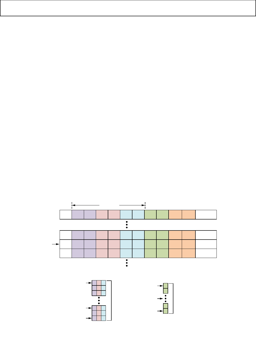
AD9361 Reference Manual UG-570
| Page 37 of 128
SETTLING TIMES
After a gain change, the AD9361 must reset overload detectors
and power measurement circuits and wait for the receive path to
settle before re-enabling detectors and power measurement
blocks.
PEAK OVERLOAD WAIT TIME
All gain control modes use peak overload wait time. After a gain
change, the AD9361 waits for the time set by this register before
re-enabling its LMT and ADC overload detectors, which allows
the signal in the analog path and the ADCs to settle. The default
is fine for all applications unless an external LNA with a bypass
mode is part of the signal path. The Peak Overload Wait Time is
set by the ad9361_set_rx_gain_control_mode function and is
clocked at the ClkRF rate (the input to the Rx FIR Filter clock
rate).
SETTLING DELAY
All AGC modes use settling delay, which is the time that the AGC
holds the power measurement blocks in reset after a gain change.
Power measurement occurs at the output of the receive HB1 filter
(which is the input to the receive FIR filter) so all stages up to the
Rx FIR must have settled before power measurement resumes
after a gain change. The delay is equal to the register value
multiplied by 2 and is clocked at the ClkRF rate. The default for
settling delay is 20 ClkRF cycles, and that is based on a ClkRF rate
of 30.72 MHz. For optimum fast attack AGC performance, the
delay needs to scale with ClkRF.
16
2: 16
GAIN TABLE OVERVIEW
The AD9361 uses a pointer to a row in a gain table. That row
contains the gain values of each independent gain block. In this
way, a gain index value (pointer) maps to a set of gain values for
each gain block. However, there are two different ways that the
AD9361 can implement the gain table. In full table mode, there is
one table for the receiver. In split table mode, the AD9361 splits
the LMT and LPF tables apart and controls each independently
with separate pointers. If digital gain is enabled, there is a third
table that is independently controlled, also with its own pointer.
Each receiver has its own set of two (or three) tables. The gain
table mode is set in the ad9361_load_gt function. The table
architecture affects all gain control modes and is a common
setting for both receivers.
FULL TABLE MODE
Full table mode is useful for most situations. A single gain table
contains all of the variable gain blocks in the Rx signal path.
Figure 21 shows a portion of a full gain table. The figure also
shows the gain of each block next to each gain index. If the gain
index moves up or down, the gain indices of one or more blocks
will change. If the gain index pointer moves down one step (to a
table index of 54), both the LNA gain and the LPF gain will
change. These changes allow the AD9361 to handle widely
varying signal levels while still optimizing noise figure and
linearity.
To read back the full table gain index in any gain control mode,
read use the ad9361_get_rx_rf_gain function.
The Max LMT/Full Gain register limits the maximum index
allowed.
Figure 21. Portion of the Analog Devices 2300 MHz Example Full Gain Table
Figure 22. Split Table in Manual Gain Mode, SPI Writes Control Gain Indices
0
3 0
3 4 0
2
LNA
INDEX
4
4
1
1
1
14
15
17
LNA
GAIN
21
21
17
15
15
15
0
0
0
14
15
17 0
0
0
55
56
54
TABLE
INDEX
50
51
49
TOTAL GAIN
(dB)
MIXER
INDEX MIXER
GAIN TIA
INDEX TIA
GAIN LPF
INDEX LPF
GAIN DIGITAL
INDEX DIGITAL
GAIN
GAIN INDEX
(POINTER)
LMT GAIN
11668-022
INDEX 0
INDEX 24
LMT
TABLE
LMT INDEX
(0x11A)
LMT MAX INDEX
(0x0FD)
INDEX 0
LPF INDEX
(0x10A AND 0x10D) LPF GAIN
(TABLE)
11668-023
Rev. A

UG-570 AD9361 Reference Manual
| Page 38 of 128
SPLIT TABLE MODE
In situations where high power out-of-band interfering signals are
often present, it can be advantageous to split the gain table to
optimize noise figure in the presence of these interferers. In this
case, separate pointers control the LMT gain and the LPF gain
independently (and digital gain if it is enabled). This allows the
gain to be changed in the area of the receive path that is
overloading. Recall that for the full gain table, gain changes could
affect any or all of the gain blocks in the receive path regardless of
where the overload occurs.
The architecture of the LMT table depends on which gain control
mode is used so this aspect is covered in the next sections, which
cover the various gain control modes in detail. An LMT table
must be written to the AD9361 using the ad9361_load_gt
function. A LPF table per se does not exist. Instead, the LPF index
directly translates to LPF gain in dB. The same is true of digital
gain (if it is enabled). LPF gain ranges from 0 to 24(d) while
digital ranges as mentioned previously from 0 to 31(d).
The total gain in dB of the AD9361 is not necessarily equal to the
LMT and LPF indices added together. The actual gain of the LMT
stages vary with LO frequency and in addition some of the LMT
steps are larger than one dB. Thus, changing the LMT index by
one may not change the gain by 1 dB. This concept is easier to
understand when looking at the tables.
The maximum index when using the split table mode is 40(d).
To read back the split table gain indices in any gain control mode,
use the ad9361_get_rx_rf_gain function.
Table 16. Reading Split Table Gain Indices
Register(hex) Function
2B0[D6:D0] Rx1 LMT gain index
2B1[D4:D0] Rx1 LPF gain index
2B2D4:D0][ Rx1 digital gain index (if enabled)
2B5[D6:D0] Rx2 LMT gain index
2B6[D4:D0] Rx2 LPF gain index
2B7[D4:D0][ Rx2 digital gain index (if enabled)
DIGITAL GAIN
All modes (MGC, AGC) and both gain table modes allow for the
addition of digital gain. The maximum allowable index for a full
gain table is 90(d). The maximum digital index is 31(d). A
standard full gain table with only analog gain has a maximum
index of 76(d). For the gain tables provided by Analog Devices,
this leaves 24(d) indices left over for digital gain. Alternative gain
tables that reach their maximum analog gain at an index lower
than 76(d) can accommodate more digital gain steps (up to 31).
It is important to point out that digital gain does not increase
signal-to-noise (SNR) ratio as it is merely multiplies the digital
word by a factor. In this way, both noise and signal are increased
and thus SNR remains the same. For many applications, digital
gain is not needed. Further, modifying the gain table and
sacrificing analog gain to add more digital gain will decrease
the performance of the system.
In some cases, however, it is desired that the signal power
received by the BBP, be equal to some nominal value. For very
low signal levels in which the maximum analog gain is still not
high enough to achieve this goal, variable digital gain can be used.
MGC OVERVIEW
In MGC mode, the BBP controls the gain index pointer(s). This
mode is setup with the ad9361_set_rx_gain_control_mode
function. In its simplest form, in MGC the BBP evaluates the
digital signal level at the I/O port and then adjusts the gain
appropriately. In this scenario, the BBP needs no other
information other than the digital signal level that it receives. For
the full (single) gain table, this is all that is needed—an overload
requires that the gain be decreased.
However, the AD9361 has programmable thresholds that indicate
the condition of the signal in each receiver. Routing these signals
to the control output pins and then connecting them to the BBP
inputs allows the BBP to determine the status of the received
signals in more detail. For a split gain table, this information
allows the BBP to adjust the gain in the area, which is overloading
because it indicates where the overload is occurring (LMT, LPF,
digital).
Rev. A
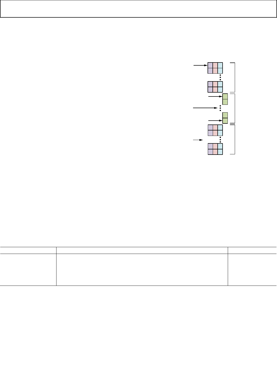
AD9361 Reference Manual UG-570
| Page 39 of 128
The BBP can control manual gain in one of two ways. The default
method uses SPI writes of the gain indices. Alternatively, the BBP
can pulse the control input pins to move the gain indices.
CTRL_IN0 causes the gain index to increase for Rx1 and
CTRL_IN1 causes the gain index to decrease for Rx1. Similarly,
CTRL_IN2 causes the gain to increase for Rx2 and CTRL_IN3
causes the gain to decrease for Rx2. This mode can be configured
using the ad9361_set_rx_gain_control_mode function. The pulse
is asynchronous so setup and hold are not relevant but the time
high and low must be at least two ClkRF cycles for the AD9361 to
detect the event. ClkRF is the clock used at the input of the
receive FIR filters.
In full table mode, a single index for the receiver controls the
gain. If SPI writes are used to control the gain, then writing the
registers sets the gain index directly. If the control input pins are
used to control the gain, then pulsing the various pins moves the
gain index pointer(s) up and down the full table.
In split table mode, if the BBP uses SPI writes to control the gain,
then separate register writes are needed to set the LMT and LPF
gain indexes. Digital gain (if enabled) would require a third
register write. If the BBP uses the control inputs to change the
gain in split table mode, then there are two options. There are
only four control inputs but there are eight different analog gain
adjustments to make (LPF, LMT, Rx1, Rx2, increment, and
decrement for each). One option is to use an SPI bit to determine
where the gain index changes (LMT or LPF). Clearing the Use
AGC for LMT/LPF Gain bit (0x0FC[D3]) enables this option and
the Inc/Dec LMT Gain bit (0x0FC[D4]) selects the gain change
location. For this option, the gain table architecture still looks like
Figure 22. If digital gain is enabled, the BBP must change this gain
by via SPI writes. The CTRL_IN pins do not change digital gain
in split table mode.
Alternatively, if the Use AGC for LMT/LPF Gain bit is set, the
AD9361 peak detectors determine where the gain changes. With
this option, the architecture of the split table changes as shown in
Figure 23. Note that the LMT table has been split into two
sections, an upper LMT table and a lower LMT table. The
dividing line is the initial LMT gain limit.
Figure 23. Split Table in Manual Gain Mode, Control Inputs and Peak Detectors
Control Gain Indices
Additionally, where overloads occur and where the gain indices
are currently pointing affects where the gain changes as noted in
Table 17. As the table demonstrates, the algorithm decreases LMT
gain first and then, when the LMT index reaches the LMT Index
Limit, the type of overload determines where the gain decreases.
Increment and decrements registers 0x0FC and 0x0FE set the
amount of gain change.
If more than one overload condition occurs simultaneously, then
LMT overloads are first priority, ADC overloads are second, and
Digital Saturation is third.
Table 17. Manual Gain Split Table Gain Change Location vs. Index Position and Overload Location
Overload Type Gain Index Position(s) Change Gain in
Large LMT LMT index > 0 LMT table
Large LMT LMT index = 0 LPF table
Large or Small ADC LMT index is in upper LMT table (index > initial LMT gain limit) LMT table
Large or Small ADC LMT index is in lower LMT table (index ≤ initial LMT gain limit) LPF table
Digital Saturation N/A Digital table
INDEX 0
INDEX 0
INDEX 24
LMT INDEX LIMIT + 1
LMT
UPPER
TABLE
LMT
LOWER
TABLE
LPF
GAIN
LMT INDEX LIMIT
(0x11A)
LMT MAX INDEX
(0x0FD)
LMT INDEX
(0x10A AND 0x10C)
LPF INDEX
(0x10B AND 0x10D)
11668-024
Rev. A
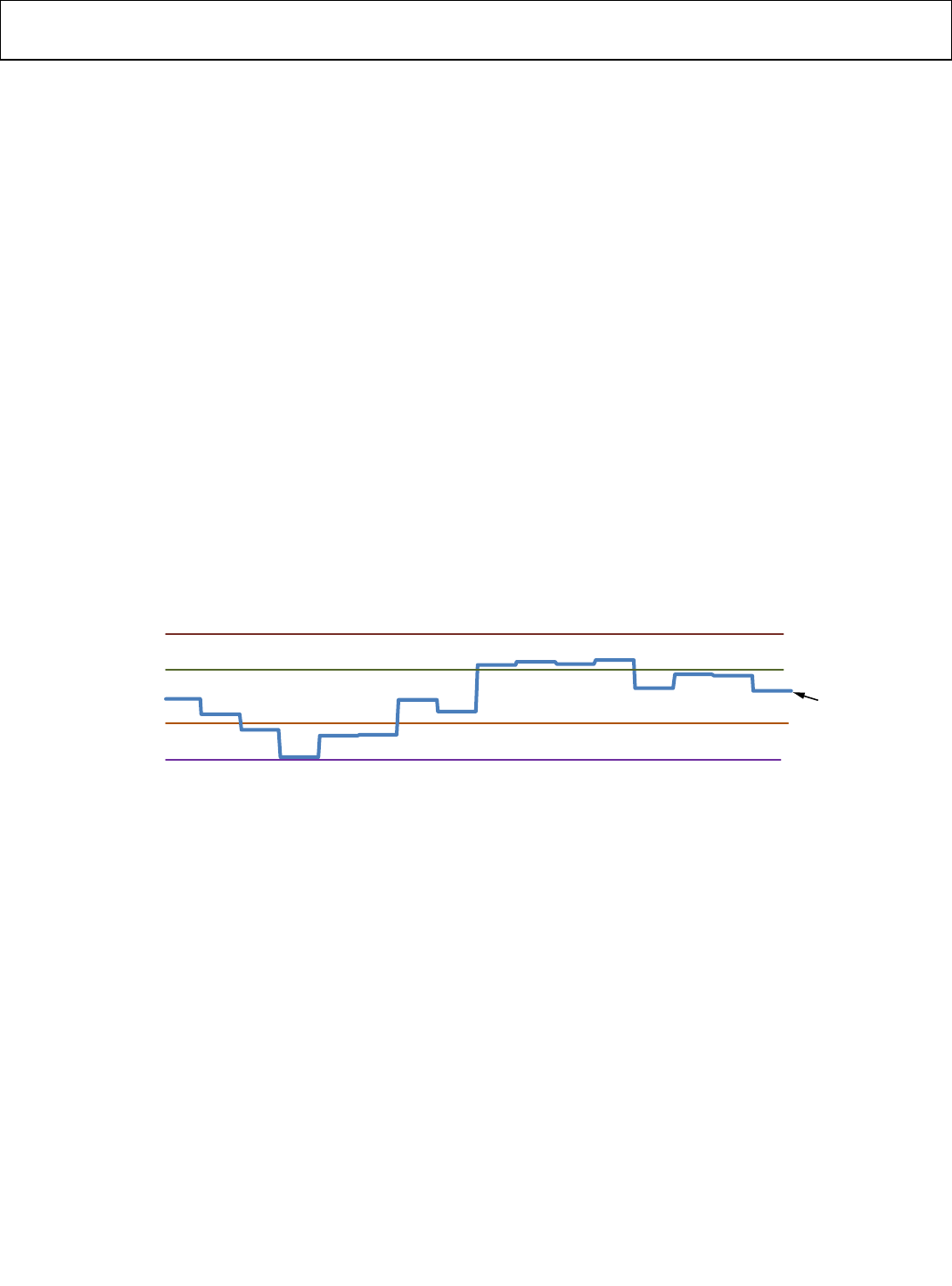
UG-570 AD9361 Reference Manual
| Page 40 of 128
SLOW ATTACK AGC MODE
Slow attack mode is intended for slowly changing signals such as
those found in some FDD applications, for example, WCDMA
and FDD LTE. The slow attack AGC uses a second-order control
loop with hysteresis that changes the gain to keep the average
signal power within a programmable window. The power is
measured between HB1 and the Rx FIR filter. This is the same
location as the low power detector in Figure 18. In addition, the
BBP can set bits to enable faster reactions for signals that exceed
the LMT and ADC thresholds. Enable AGC slow attack mode
with the ad9361_set_rx_gain_control_mode function.
Figure 24 demonstrates the concept of the control loop. Where
inner high threshold and inner low threshold are stored in
negative dBFS. The outer high threshold and outer low threshold
are stored as dB deltas to the inner thresholds. The A, B, C, and D
step sizes are programmable. These step sizes determine how
much the gain index pointer changes after the average signal
power exceeds a threshold.
Note that the AD9361 does not have default thresholds or step
sizes. The BBP must write all of these values using the
ad9361_set_rx_gain_control_mode function.
SLOW ATTACK AGC GAIN UPDATE TIME
When the average signal power exceeds a threshold, the gain does
not necessarily change immediately. In FDD systems, there are
typically brief periods (such as those around slot boundaries) that
accommodate gain changes or other system parameter updates.
To accommodate this aspect of FDD protocols, the AD9361 gain
will only update after the gain update counter expires. The
counter is clocked at the ClkRF rate (the input rate of the RFIR).
The depth of the counter can be set equal to double or quadruple
the value in these registers.
The counter clock begins running three clock cycles after the
AD9361 enters the receive state. Since the BBP is responsible for
moving the AD9361 among its states, it can determine when the
gain update counter will expire. In this way, the Gain Update
Counter can be set such that it always expires at slot (or other)
boundaries. Additionally the BBP can reset the gain update
counter by setting the Enable Sync for Gain Counter bit and
taking CTRL_IN2 high.
The slow AGC is typically configured to have multiple power
measurement cycles within each gain update period. The last
power measurement performed before a gain update boundary
determines whether (and by how much) the gain should change.
Figure 24. Slow Attack AGC Control Loop Limits and Step Sizes
DECREASE GAIN A STEPS
OUTER THRESHOLD HIGH
INNER THRESHOLD HIGH
INNER THRESHOLD LOW
OUTER THRESHOLD LOW
DECREASE GAIN B STEPS
INCREASE GAIN C STEPS
INCREASE GAIN D STEPS
NO GAIN CHANGE EXAMPLE OF
AVERAGE
SIGNAL POWER
11668-025
Rev. A

AD9361 Reference Manual UG-570
| Page 41 of 128
OVERLOADS IN SLOW ATTACK AGC MODE
In addition to the control loop discussed previously, the slow
attack AGC can react more quickly to peak overload events such
as the large LMT and large ADC overloads.
In slow attack mode, the AD9361 counts the number of times a
particular overload event occurs. Only if the event(s) occur more
than a programmable number of times will the gain change. Even
for these peak overloads, the gain only changes when the Gain
Update Counter expires. The counters are stored as the LMT and
ADC Overload Counters. The AD9361 does not have default
values for these counters so the BBP must write all of these values
using the ad9361_set_rx_gain_control_mode function.
During the a gain change event, the highest priority is given to
the large LMT detector, followed by the large ADC detector, and
followed lastly by the power detectors used by the second-order
window control loop.
It is also possible to setup the AD9361 such that large LMT
overloads and/or large ADC overloads result in an immediate
gain change, ignoring the Gain Update Counter. This mode is set
with the Immed Gain Change if Lg LMT Overload bit and Immed
Gain Change if Lg ADC Overload bit.
If the average signal power falls below one or both of the control
loop low thresholds (which would normally result in a gain
increase) but one or both of the small peak overload detectors
(LMT or ADC) has tripped, setting the Prevent Gain Inc bit
prevents the gain from increasing.
Like LMT and ADC overloads, the AD9361 uses a counter to
determine how many times digital saturation has occurred. This
counter is the Dig Saturation Exceeded Counter, and if it is
exceeded, the gain index is reduced.
SLOW ATTACK AGC AND GAIN TABLES
In full table mode, a single table controls the gain of all Rx signal
path stages. Table 18 shows the effect of peak overloads (after
their associated counters are exceeded). Recall that a particular
overload condition results in the gain index moving a program-
mable number of steps but the gain may change in any number of
different gain blocks.
In split table mode, the gain table is split as described earlier in
the document and as shown in Figure 23.
In a split table, there are two independent index pointers for
analog gain and one additional pointer for digital gain (if
enabled). Table 19 describes the effect of various peak overload
conditions, identical to split table shown in the manual gain
section. If the gain changes in the LPF table, the LPF step size
used is Decrement Step Size for: Large LPF Gain Change.
Similarly, if the gain is changed in the LMT table, the step size
used is Dec Step Size for: Large LMT Overload.
Table 18. Slow Attack AGC Full Gain Table Overload Steps
Peak Overload Reduce Gain by this many Indices (Step Size) Step Size Location
Large LMT Dec Step Size for Large LMT Overload Step Size for: Large LMT Overload/Full Table Case #3
Large ADC Decrement Step Size for Large LPF Gain Change Decrement Step Size for: Large LPF Gain Change/Full Table Case #1
Digital Saturation Digital Gain Step Size + 1 Digital Gain Step Size
Table 19. Slow Attack/Hybrid AGC Split Gain Table Overload Steps
Overload Type Gain Index Position(s) Change Gain in
Large LMT LMT Index > 0 LMT table
Large LMT LMT Index = 0 LPF table
Large or Small ADC LMT Index is in Upper LMT Table (Index > Initial LMT Gain Limit) LMT table
Large or Small ADC LMT Index is in Lower LMT Table (Index ≤ Initial LMT Gain Limit) LPF table
Digital Saturation N/A Digital table
Rev. A
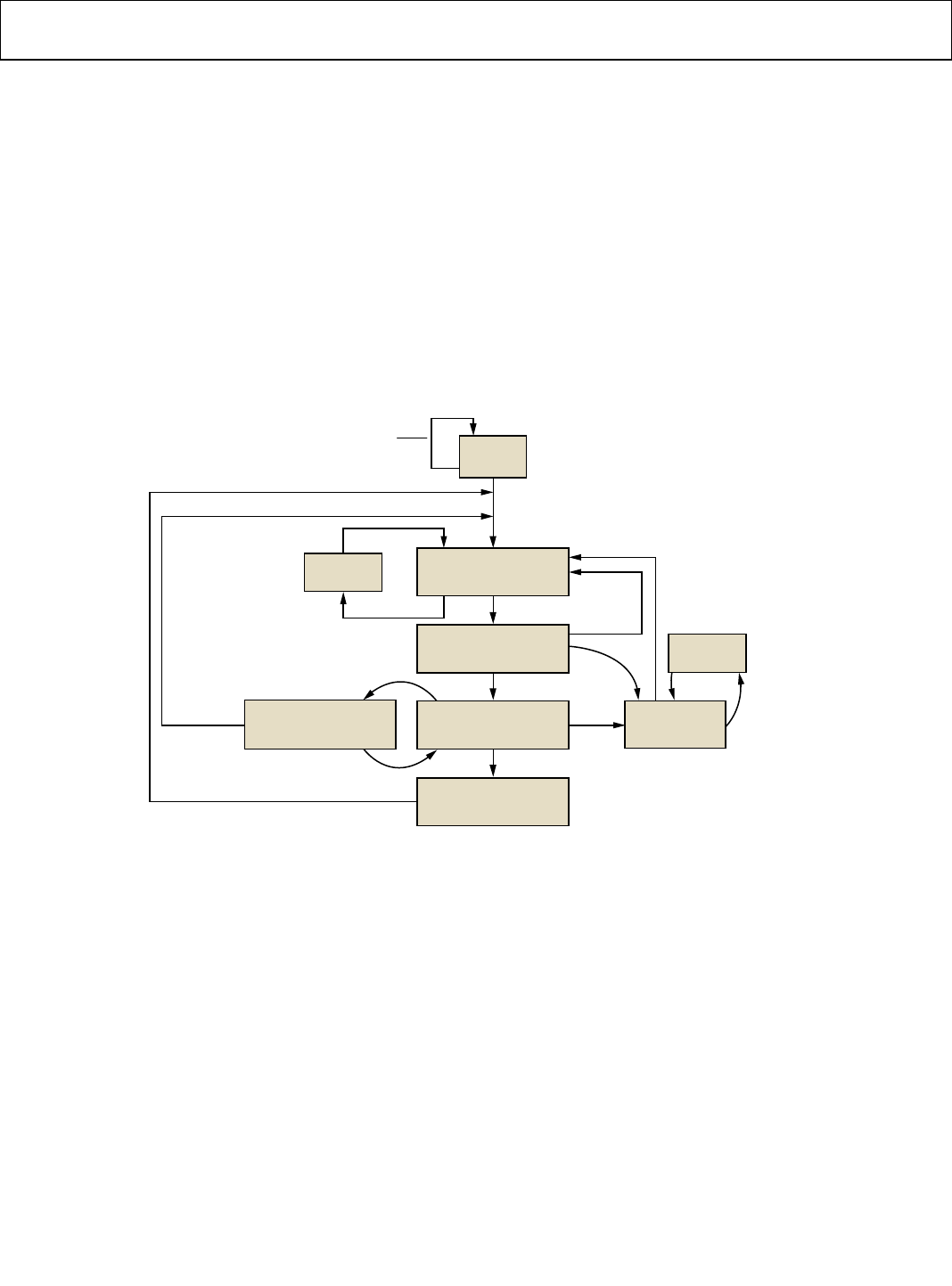
UG-570 AD9361 Reference Manual
| Page 42 of 128
HYBRID AGC MODE
The hybrid AGC mode is the same as the slow AGC mode with
the exception that the gain update counter is not used. Instead,
gain updates occur when the BBP pulls the CTRL_IN2 signal
high. The hybrid term arises because the BBP has taken some
control of the algorithm away from the AD9361 so gain control is
no longer completely automatic. Hybrid mode is enabled with the
ad9361_set_rx_gain_control_mode function.
FAST ATTACK AGC MODE
Fast attack AGC mode is intended for waveforms that burst on
and off, such as those found in TDD applications or GSM/EDGE
FDD applications. The AGC responds very quickly to overloads at
the start of a burst so that the AGC can settle to an optimum gain
index by the time the data portion of the signal arrives. The AGC
also has an optional slow decay that allows the gain to increase if
the signal power decreases while the AGC is locking to an
optimum gain. Fast attack mode is configured with the
ad9361_set_rx_gain_control_mode function.
When the AD9361 enters the Rx state, the fast attack AGC state
machine leaves State 0 and enters State 1 as shown in Figure 25.
Its goal is to adjust the gain index such that an optimum receive
gain is realized in a very short period of time. The AGC
progresses through several states on its way to Gain Lock, in
which state the gain does not change (unlock) unless large signal
level changes occur or if the burst ends. When the gain unlocks,
the AGC state machine moves back to its reset state and starts
over. Figure 25 shows a high-level diagram of the AGC states.
Figure 25. Fast Attack AGC High Level Stage Diagram
STATE 0
(RESET)
STATE 1
PEAK OVERLOAD
DETECT
STATE 2
MEASURE POWER LOCK
LEVEL GAIN CHANGE
DECREASE
GAIN
STATE 3
MEASURE POWER PEAK
OVERLOAD DETECT
STATE 4
UNLOCK GAIN
DECREASE GAIN
STATE 5
GAIN LOCK MEASURE
POWER
RXON
PEAK
OVERLOAD
PEAK
OVERLOAD
PEAK
OVERLOAD
FINAL OVERRANGE
COUNT EXCEEDED
VARIOUS OVERLOAD
CONDITIONS OR ENERGY LOST
STATE 2A
LOWER POWER
DETECT
INCREASE
GAIN
LOW
POWER
LOW
POWER
LOW
POWER
11668-026
Rev. A
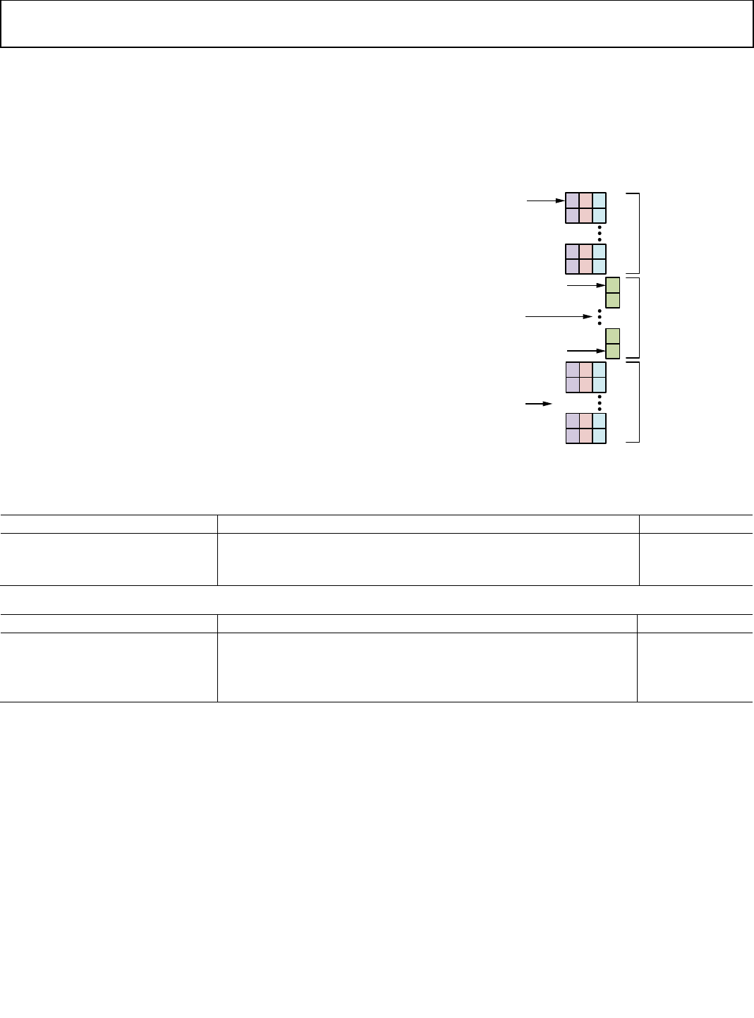
AD9361 Reference Manual UG-570
| Page 43 of 128
STATE 0: RESET
The AGC remains in this state when the AD9361 is not in the Rx
state. The AGC performs no actions while in this state.
STATE 1: PEAK OVERLOAD DETECT
When the AD9361 enters the Rx state, the AGC first waits for a
time in microseconds set by the AGC attack delay register. This
delay allows the receive path to settle before the AGC begins
determining the optimum gain index.
After this delay, the AGC enters State 1, where it detects peak
overloads (LMT and ADC) and adjusts the gain. The digital
saturation detector is also enabled, but in State 1 the signal may
not have enough time to reach the detector. Each time the gain
changes, the AD9361 holds the peak detectors in a reset state
until the Peak Overload Wait Time counter expires. If no peak
overloads are detected for the Energy Detect Count, then the
AGC can proceed to State 2. The Energy Detect Count is clocked
at the ClkRF rate (the clock used at the input to the Rx FIR filter).
The overloads affect the gain index in different ways for different
gain table types as shown in the Table 20 and Table 21. In full gain
table mode, the AD9361 uses different step sizes (changes in gain
index) for differing extremes of overload. Table 20 shows where
the step sizes are stored for the fast attack AGC in full table mode.
The Case #1 step size is typically larger than Case #2 which itself
is typically larger than Case #3.
Table 21 shows the effects of various overloads when using a split
table. Figure 26 shows the split table architecture. Note that the
gain first decreases from the LMT table regardless of where the
overload occurs. When the gain index reaches the LMT index
limit, the gain decreases where the overload occurs.
Figure 26. Fast AGC Split Gain Table Architecture
Table 20. Fast Attack AGC Peak Overload Step Sizes for Full Gain Table
Peak Overloads
Reduce Gain by this many Indices (Step Size)
Step Size Set By
Large ADC Λ (Large LMT V Digital Sat) Decrement Step Size for Full Table Case #1 0x106[D3:D0]
Large ADC V Large LMT V Digital Sat Fast Attack Only. Decrement Step Size for Full Table Case #2 0x106[D6:D4]
Small ADC Dec Step Size for Full Table Case #3 0x103[D4:D2]
Table 21. Fast Attack AGC Peak Overload Step Sizes for Split Gain Table
Overload Type Gain Index Position Change Gain In
Large LMT N/A LMT Table
Large or Small ADC LMT Index is in Upper LMT Table (Index > Initial LMT Gain Limit) LMT Table
Large or Small ADC LMT Index is in Lower LMT Table (Index ≤ Initial LMT Gain Limit) LPF Table
Digital Saturation N/A Digital Table
INDEX 0
INDEX 0
INDEX 24
LMT INDEX LIMIT + 1
LMT
UPPER
TABLE
LMT
LOWER
TABLE
LPF
GAIN
LMT INDEX LIMIT
(0x11A)
LMT MAX INDEX
(0x0FD)
LMT INDEX
(0x10A AND 0x10C)
LPF INDEX
(0x10B AND 0x10D)
11668-027
Rev. A

UG-570 AD9361 Reference Manual
| Page 44 of 128
STATE 2: MEASURE POWER AND LOCK LEVEL GAIN
CHANGE
Upon entering State 2, the AGC waits for a time equal to Settling
Delay minus Energy Detect Count. The subtraction is performed
because the AGC has already waited for the Energy Detect
Counter to expire in order to exit State 1. Thus, the delay before
measuring power does not need to count through this delay
again. After the delay calculated above, the AGC measures
average signal power at the output of the HB1 filter (see the
Average Signal Power section).
The AGC keeps the LMT, ADC, and digital saturation overload
detectors enabled while it is in State 2. If overloads occur, the
AGC will go back to State 1 to reduce the gain.
If the Enable Incr Gain bit is set, then the AGC is allowed to
increase gain if the average signal power stays below the Low
Power Threshold for a time greater than the Increment Time. The
gain step size used Increment Gain Step + 1. The gain continues
to increase until the signal does not remain below the Low Power
Threshold longer than the Increment Time. Figure 25 shows this
as State 2A. The AGC exits State 2A by going back to State 1 to
check again for Peak Overloads.
If the AGC has entered State 2 and does not detect a low power
condition, or the Enable Incr Gain bit is cleared, then the
measured signal power is compared against the AGC Lock Level
(Fast). The AGC then adjusts the gain to match the average signal
power to the AGC Lock Level setting. The lock level is stored in
−dBFS in a resolution of 1 dB/LSB. If the gain needs to increase to
achieve the lock level setting, then there is a maximum amount
that it can increase, set by AGCLL Max Increase.
In the full gain table mode, the AGC simply changes the gain
index such that the signal power matches the lock level (unless
limited by the AGCLL Max Increase). In split table mode, if the
Enable LMT Gain Incr for Lock Level bit is set high, the actions
are per Table 22. If that bit is not set high, then only LPF gain can
be used for gain increases. In addition, regardless of the bit
setting, if a small LMT overload occurs during the lock level
calculation, LMT gain will not be allowed to increase to meet the
lock level.
STATE 3: MEASURE POWER AND PEAK OVERLOAD
DETECT
When the AGC enters State 3, it locks the gain. This state can
affect other portions of the AD9361 such as DC offset tracking
updates and RSSI measurement start times.
The AGC continues to measure power and it keeps its large LMT,
large ADC, and digital saturation overload detectors enabled.
If the Enable Gain Inc After Gain Lock bit is set and the Enable
Incr Gain bit is set, then the AGC will check to see if a Low Power
condition occurs. The method used is the same as that used in
State 2 (including the transition to State 1 if the gain must
increase). If Enable Gain Inc After Gain Lock is clear, then the
AGC does not perform the low power test in State 3. If the AGC
exits State 3 due to a low power condition, the gain unlocks.
If the thresholds have been set correctly, then the overload
detectors should not assert even after the lock level adjustment
unless the signal-of-interest level increases or an out-of-band
blocker is suddenly present. To guard against these possibilities,
the AGC monitors its overload detectors. If overloads occur after
the lock level adjustment, the AGC uses different step sizes to
change the gain.
In full gain table mode, regardless of the type of overload, the step
size (number of indices reduced) is always the Post Lock Level
Step Size for Full Table value. In split gain table mode, the step
size is the Post Lock Level Step Size for LPF Table for ADC
overloads and the Post Lock Level Step for LMT Table for LMT
overloads. These step sizes are usually smaller than those used in
State 1 and State 2. State 1 and State 2 overload step sizes are
designed to respond to large overloads very quickly. The overload
that may occur in State 3 would normally be smaller and require
less adjustment.
STATE 4: UNLOCK GAIN
If these overloads occur, the AGC decreases gain in State 4. The
gain unlocks while the AGC is in State 4. The AGC then returns
to State 3.
The AGC counts the number of overload conditions that occur
after the Lock Level adjustment. If this number exceeds the Final
Overrange Count, then the AGC goes back to State 1 and resets
its peak detectors.
Table 22.Fast Attack AGC Lock Level Gain Index Change for Split Gain Table
If Gain Needs To Do This First And If Then Do This
Decrease Reduce LPF gain index LPF gain index = 0 Reduce LMT gain index
Increase Increase LMT gain up to LMT step size Total gain change > LMT step size Increase LPF gain index
Rev. A

AD9361 Reference Manual UG-570
| Page 45 of 128
STATE 5: GAIN LOCK AND MEASURE POWER
When the AGC reaches State 5, the AGC locks the gain (if it was
unlocked). The AGC also measures the average signal power
when the gain locks and stores this value as a reference power
level. This value is used for comparisons against other thresholds,
which can unlock the gain. State 5 is the final state in the AGC
algorithm and is intended to maintain the same gain unless a
large change in signal amplitude occurs (such the end of the burst
or subframe or a large interfering signal suddenly arrives or
departs). In State 2 and State 3, the measurement length is set by
Dec Power Measurement Duration. In State 5, the measurement
length is set by Power Meas in State 5. The mapping of bits to
duration is the same for both sets of registers and is defined in
Equation 17. The reason for the difference is that in earlier states,
the object is to lock the gain as quickly as possible. This would
mean that a shorter measurement time may be used for earlier
states but a longer time can be used once the gain has locked.
When the gain unlocks, the AGC can reset the gain to maximum
gain or to one of several other gain positions as shown in
Table 23. When the gain unlocks, the AGC returns to State 1 (or
State 0 if the AD9361 exits the Rx state). When the AGC returns
to State 1, it sets the digital gain to 0 dB (unless the digital gain is
forced to a fixed value). Optimize Gain and Set Gain both can
reduce the time required for gain lock since they both use the
previous burst gain index information.
Set Gain can use either the beginning or ending gain lock index
of the previous burst. The setting of Use Last Lock Level for Set
Gain determines which gain index is used. The front of the burst
would typically be used if a preamble or boosted portion of the
signal occurs at the beginning of the burst. The AGC should lock
on that boosted portion. If the entire burst uses the same nominal
power level, then the AGC should use the end of the burst gain
index.
If the thresholds are set correctly, then the most likely scenario is
for the AGC to unlock the gain at the end of the burst (Energy
Lost Threshold) or if the AD9361 exits the Rx State. Unlocking
the gain for an ADC overload is similar to a stronger signal test
but is a peak detector rather than a power detector. Unlocking the
gain for a large LMT overload checks for large interfering signals
and is a peak detector. All of these tests are recommended for a
typical fast AGC configuration. Even in this simple case, there are
options for what happens to the Gain Index when the gain
unlocks (see Table 24).
( )=16 × 2 [:] (17)
Table 23.Gain Unlock Index Options
Gain Index
When Reset Set By Definition
Maximum Gain Maximum Full Table or Maximum LMT Table Index
(0x0FD) and Maximum LPF of 0x18
Maximum Analog Gain
Optimize Gain AGC gain lock index at end of last burst
Plus
Optimize Gain Offset (0x116[D3:D0])
An optimized value that reduces the amount of steps the AGC
should typically take to lock the gain for each burst
Set Gain AGC gain lock index at the start of the last burst
Or
AGC gain lock index at the end of the last burst
Similar to Optimize Gain but allows use of front of burst gain or
end of burst gain setting
No Gain
Change
N/A No change to the gain index
Table 24.Gain Unlock Condition vs. Gain Index
Condition that Unlocks the Gain Gain Index Type1 Set Bits Clear Bits
Exit Rx State Max gain None required 0x110[D4], 0x110[D2]
Exit Rx State Optimize gain 0x110[D2] 0x110[D4]
Exit Rx State Set gain 0x110[D4] 0x110[D2]
Energy Lost Threshold Exceeded Max gain None required 0x110[D6]. 0x110[D3] only if 0x0FB[D6] set
Energy Lost Threshold Exceeded Optimize gain 0x110[D6] 0x110[D3] only if 0x0FB[D6] set
Stronger Signal Threshold Exceeded No change None required 0x115[D7] if 0x0FB[D6] set
Large ADC Overload No change None required 0x114[D7] and 0x110[D1] if 0x0FB[D6] set
Large LMT Overload No change None required 0x110[D1] if 0x0FB[D6] set
1 A gain index type of no change indicates that the gain index does not immediately change but the AGC algorithm does start over so the gain index will very likely
change after the AGC moves through its states and re-locks. For other gain index types such as set gain, the AGC first changes the gain index to the proper position
and then restarts the algorithm.
Rev. A
UG-570 AD9361 Reference Manual
| Page 46 of 128
When comparing the signal power with the energy lost threshold,
there is also a time factor as well. Each time the signal power
value updates, the AGC computes the difference between the
power measured at the beginning of gain lock and the current
signal power. This difference is compared against the Energy Lost
Threshold. If the difference exceeds the threshold for a time equal
to twice the Gain Lock Exit Count then the gain unlocks as
shown in Table 24. The Gain Lock Exit Count is clocked at the
ClkRF rate. The same comparison is made for the Stronger Signal
Threshold, which appears in Table 26.
The large ADC threshold is stored in Register 0x105 and the large
LMT threshold is stored in Register 0x108. For the peak
detectors, there are no time requirements. A single overload will
unlock the gain.
Generally, the AGC is the best arbiter of when the gain should
unlock. However, in some situations, it may be advantageous for
the BBP to initiate an unlock condition. If the BBP pulls the
EN_AGC pin high, the gain will unlock and the AGC algorithm
will restart. The BBP cannot force the gain to lock at a certain
time but it can control when the gain unlocks. Table 25 shows
how to use this feature.
If the thresholds are set correctly, the typical setup which unlocks
the gain when the AD9361 exits Rx mode or if the burst/subframe
ends is sufficient for most applications. However, if desired, it is
also possible to prevent the gain from unlocking in some
instances (see Table 26). The settings are dependent on whether
the BBP will use the EN_AGC pin to unlock the gain. If this is the
case, then the EN_AGC pin should be low except when the gain
should be unlocked. If the EN_AGC pin is not used, then the
Gain Lock Delay bit must be set high.
Table 25. Full List of Gain Unlock Conditions vs. Target Gain Index
Condition that Unlocks the Gain Gain Index Type Set Bits Clear Bits
EN_AGC pulled high Maximum gain 0x0FB[D6], 0x111[D5] 0x110[D6:D5]
EN_AGC pulled high Optimize gain 0x0FB[D6], 0x110[D6], 0x111[D5] 0x110[D5]
EN_AGC pulled high
Set gain
0x0FB[D6], 0x110[D5]
0x111[D5]
EN_AGC Pulled high No gain change 0x0FB[D6] 0x110[D5], 0x111[D5]
Table 26. Preventing Gain Unlock Conditions in State 5
If EN_AGC Pin Is Used Don’t Unlock Gain Even If: Set Bits
No Energy Lost Threshold Exceeded 0x0FB[D6], 0x014[D1], 0x110[D3]
No Stronger Signal Threshold Exceeded 0x0FB[D6], 0x014[D1], 0x115[D7]
No Large ADC or Large LMT Overload 0x0FB[D6], 0x014[D1], 0x110[D1]
Yes Energy Lost Threshold Exceeded 0x0FB[D6], 0x110[D3]
Yes
Stronger Signal Threshold Exceeded
0x0FB[D6], 0x115[D7]
Yes Large ADC or Large LMT Overload 0x0FB[D6], 0x110[D1]
Rev. A
AD9361 Reference Manual UG-570
| Page 47 of 128
CUSTOM GAIN TABLES
OVERVIEW
Analog Devices supplies gain tables to use with the AD9361, but
some applications require modifying those tables to optimize the
RF performance (using an external LNA or creating 3 dB gain
steps for example). This section shows how to modify the gain
tables that the AD9361 uses for all gain control modes. Once
created the custom gain table can be loaded into the AD9361
using the ad9361_load_gt function.
The various gain block indices map to approximate gain per the
following tables (all values for 2300 MHz). Note that these are
nominal values and some variation with carrier frequency,
temperature, and process is expected for the LNA and mixer
tables. For accurate gain vs. gain index values RF characterization
needs to be done with the specific customer configuration.
Table 27. LNA Gain vs. Index
Internal LNA Index Internal LNA Gain (dB)
0 3
1 14
2 17
3 21
Table 28. Mixer Gm Gain vs. Index
Mixer Gm Index (d)
Mixer Gm Index Gain (dB)
0 0
1 3
2 9
3 − 15 = Index + 11
Table 29. TIA Gain vs. Index
TIA Index Internal LNA Gain (dB)
0 −6
1 0
Table 30. LPF Index vs. Gain
LPF Index (d) LPF Gain (dB)
0 − 24 = Index
Table 31. Digital Index vs. Digital Gain
Digital Index (d) Digital Gain (dB)
0 − 31 = Index
Rev. A

UG-570 AD9361 Reference Manual
| Page 48 of 128
Table 32 shows a small portion of an example full gain table. This
is the same format as the Analog Devices supplied full gain table,
but some of the columns are color-coded to aid in the clarity of
the column purposes. It is important to note that the BBP only
uses the values in the table index column as well as the 0x131,
0x132, 0x133 columns when programming a gain table into the
AD9361. These 0x131, 0x132, 0x133 columns have register
addresses as column headers. The 0x131, 0x132, 0x133 columns
are concatenations of various gain stage indices. For example,
0x131 is a digital word that includes the gain indices for the
external LNA, the internal LNA, and the mixer. All other columns
are only used to make the gain table more readable.
Starting at the far left of Table 32, table index is the index or
pointer to the table. When the AD9361 is in the FDD or receive
states, this index controls the receive path gain.
The next column to the right is the external LNA index. See the
External LNA section for details on how the AD9361 can control
an external LNA. Briefly, a bit in the gain table can be output to a
GPO and used to control the gain of an external LNA.
The next column to the right is the external LNA gain. This
column has no purpose except to indicate total receive path gain
when using an external LNA.
Moving to the right again leads to the iLNA index. This is the
internal LNA index, which controls LNA gain. iLNA Gain in dB is
next to iLNA index which is only used to add to other stages gains
and which result in the estimated total receive path gain.
Again moving to the right results in the mixer index and next to
that column is the mixer gain, both of which are analogous to the
iLNA index and iLNA gain described previously.
The 0x131 column to the right is the digital word that is a
concatenation of all of the previous indices.
The TIA index and TIA gain are related as described previously
for other gain stages. The LPF index is always equal to the LPF
gain in dB so only the index column is shown. 0x132 is a
concatenation of the TIA and LPF indices.
The RF DC Cal bit is described in the RF DC Cal Bit section.
Digital gain, like the LPF gain, is equal to the digital index so only
the index column is shown. 0x133 is a concatenation of the DC
Cal bit and the digital index.
Finally, the total gain column shows the estimated total Rx path
gain of the AD9361 for each gain index.
Table 32. Portion of Analog Devices 800 MHz Full Gain Table
Table
Index
eLNA
Index
eLNA
Gain
iLNA
Index
iLNA
Gain
Mixer
Index
Mixer
Gain 0x131
TIA
Index
TIA
Gain
LPF
Index 0x132
DC
Cal
Digital
Index 0x133
Total
Gain
0 0 0 0 5 0 0 0 0 −6 0 0 1 0 20 −1
1 0 0 0 5 0 0 0 0 −6 0 0 0 0 0 −1
2 0 0 0 5 0 0 0 0 −6 0 0 0 0 0 −1
3 0 0 0 5 0 0 0 0 −6 1 1 0 0 0 0
4 0 0 0 5 0 0 0 0 −6 2 2 0 0 0 1
5 0 0 0 5 0 0 0 0 −6 3 3 0 0 0 2
6 0 0 0 5 0 0 0 0 −6 4 4 0 0 0 3
7 0 0 0 5 0 0 0 0 −6 5 5 0 0 0 4
8 0 0 0 5 1 3 1 0 −6 3 3 1 0 20 5
9 0 0 0 5 1 3 1 0 −6 4 4 0 0 0 6
10 0 0 0 5 1 3 1 0 −6 5 5 0 0 0 7
11
0
0
0
5
1
3
1
0
−6
6
6
0
0
0
8
12 0 0 0 5 1 3 1 0 −6 7 7 0 0 0 9
13
0
0
0
5
1
3
1
0
−6
8
8
0
0
0
10
Rev. A

AD9361 Reference Manual UG-570
| Page 49 of 128
RF DC CAL BIT
As referenced in the RF DC Offset Calibration section, the RF DC
Cal bit is set for unique combinations of LMT gains. Setting this
bit forces the RF DC calibration algorithm to reduce RF DC offset
at those gain indices that involve unique LMT gain settings. In a
split gain table, each index will have this bit set as each index is
likely a unique LMT gain configuration. In a full table, each index
will not have a unique LMT gain setting. There may be several
gain indices using the same LMT configuration while the LPF
gain changes for each index. In this case, set the RF DC Cal bit in
the lowest index of the unique LMT gain. In Table 32, note that
the RF DC Cal bit is set for Index 0 but not set for Indices 1
through 7. In all of these indices, only LPF gain is changing so the
RF DC Cal bit is only set for one index. The RF DC offset
correction words used for index 0 is also used for the higher
indices.
MAXIMUM FULL TABLE/LMT TABLE INDEX
All Analog Devices suggested gain tables have a maximum full
table index of 76(d). The split table maximum index is 40(d). The
Maximum Full Table/LMT Table Index register sets the highest
gain table index that is calibrated as described in the RF DC Cal
Bit section. The chip default is 76(h) so if a suggested full table is
used, no change is required. If the BBP programs a gain table with
a different maximum index or a split table is used, this value must
be changed to the proper maximum index value.
EXTERNAL LNA
An external LNA may be added to the receive path to improve the
system noise figure. All gain control modes work seamlessly with
external LNAs, whether they are fixed gain devices or devices that
can be bypassed with the use of a control signal. Note that the
maximum single-ended level allowed at an AD9361 RF pin is
+2.5 dBm peak. The system engineer should perform an analysis
of the maximum possible signal at the external LNA input added
to the external LNA gain to determine if the external LNA gain is
acceptable. If the signal level at the AD9361 RF input will be
greater than the maximum allowable level, then an external LNA
with lower gain or an attenuator must be used.
Fixed-gain LNAs are external amplifiers (or attenuators) that
always provide a nominal amount of gain. This gain is not
controllable and the LNA cannot be bypassed. In this case, there
are no programming changes necessary for the AD9361.
Varia ble-gain external LNAs use a control signal to select between
two different gains. Usually one is the high gain setting and the
other is the low gain or bypass setting, which is typically a loss.
The external LNA would use high gain in most conditions unless
the input to the internal LNA is too high (+2.5 dBm peak). For
those conditions, the external LNA would use low gain (bypass
mode).
If manual gain mode is used, then there are two methods of
controlling the external LNA gain. In the first method, the BBP
controls the gain using a GPO pin connected to the external LNA.
Since the BBP controls the gain in the AD9361, it also can control
the gain of the external LNA. In the second method, the gain
table in conjunction with an AD9361 GPO controls the external
LNA. A bit in the gain table drives GPO0 for Rx1 and GPO1 for
Rx2. Setting this bit to a zero results in a low GPO output level
while a one results in a high GPO output level. To route the
external LNA bits set in the gain table to GPO pins, set the
External LNA1 control and External LNA2 control bits.
For AGC modes, the AD9361 must control the external LNA gain
since the changes will occur quickly and the BBP will not have
knowledge of the gain index that is used until it is selected by the
AGC.
Every time the gain changes, the gain control algorithm waits for
a duration equal to the Peak Wait Time while the analog signal
path settles. This value should be increased to allow for the
settling time of the external LNA, otherwise, the peak detectors
will be enabled before the analog stages have settled.
If the AD9361 will be used to measure RSSI, then the Ext LNA
High Gain and Ext LNA Low Gain registers should be
programmed with the external LNA gain values. The part
considers both values to represent positive gain in the front end
prior to the AD9361. Both registers use 0.5 dB/LSB resolution
and range from 0 dB to 31.5 dB. If the low gain value is negative
then the Ext LNA High Gain should be offset by this amount and
the Ext LNA Low Gain should be set to 0 (for example, high gain
value = 15 dB, low gain value = −5 dB, program Ext LNA High
Gain = 20 dB and Ext LNA Low Gain = 0 dB). This will prevent a
step in the RSSI value when the external LNA goes from an on to
an off condition.
Rev. A
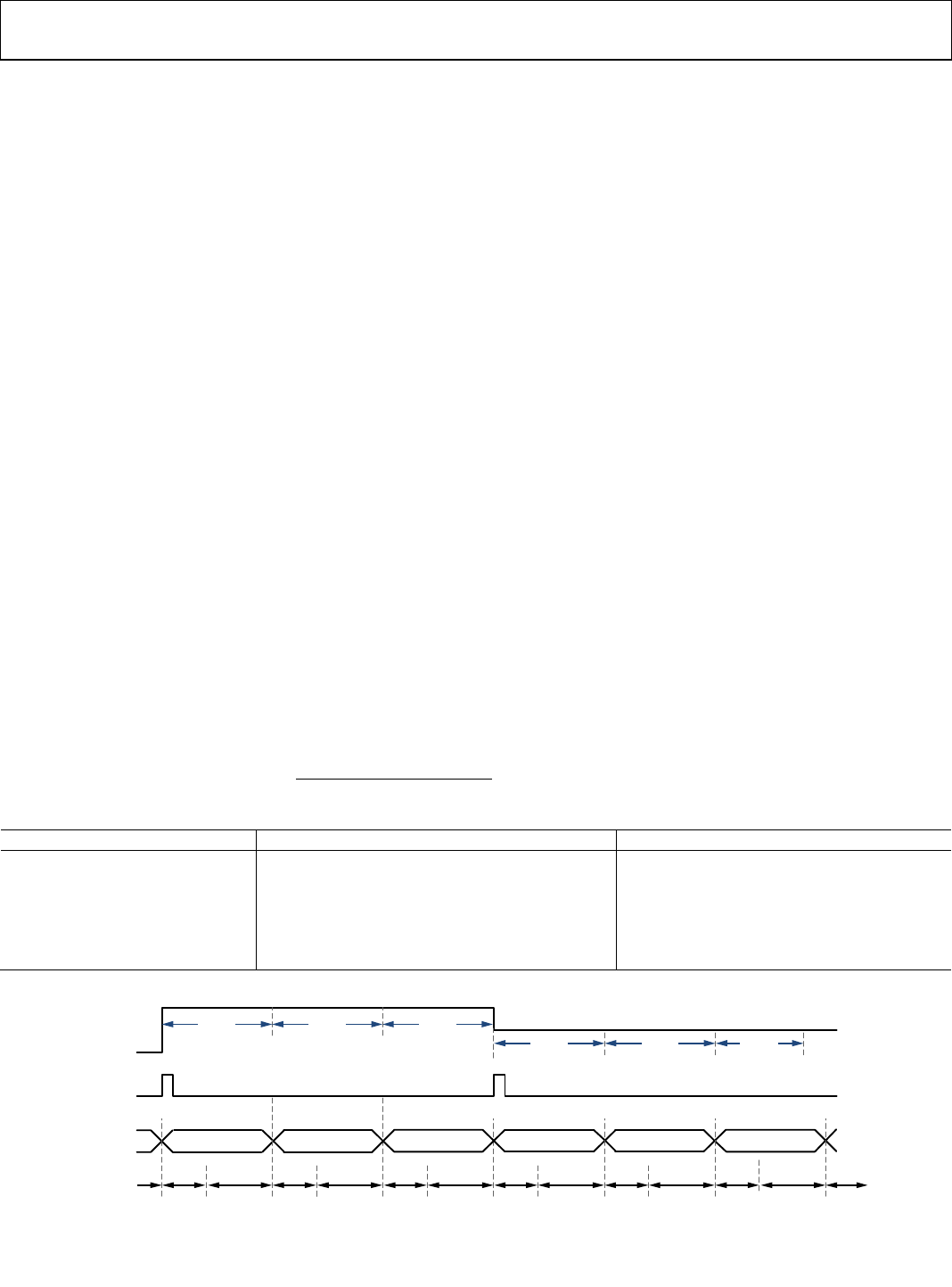
UG-570 AD9361 Reference Manual
| Page 50 of 128
RECEIVED SIGNAL STRENGTH INDICATOR (RSSI)
OVERVIEW
Given the wide variety of applications for which the AD9361 is
suited, the received strength signal indicator (RSSI) many be
setup in one of several configurations, allowing the user to
optimize the RSSI to produce extremely accurate results with a
minimum of BBP interaction. RSSI accuracy is inherently very
good but can be improved through various means, including the
gain step calibration.
The AD9361 measures RSSI by measuring the power level in dB
and compensating for the receive path gain. The various options
available support both TDD and FDD applications. Note that the
RSSI value is not in absolute units. Equating the RSSI readback
value to an absolute power level (for example, in dBm) requires a
factory calibration. To calibrate the RSSI word to an absolute
reference, inject a signal into the antenna port of the completed
system and read the RSSI word. From this test, generate a
correction factor that equates the RSI word to the injected signal
level at the antenna port. This calibration is separate from the
gain step calibration.
MODE SELECT AND MEASUREMENT DURATION
The RSSI Mode Select bits determine what event starts or restarts
the RSSI algorithm and clears the accumulator, per Table 33.
If the Default RSSI Meas Mode bit is set, then the duration is
a simple power-of-two value shown in Equation 18.
If the Default RSSI Meas Mode bit is clear, then non-power-of-two
durations are possible per Equation 19. The four duration
values are stored in Register 0x150 and Register 0x151.
Duration is always Rx sample-rate cycles.
RSSI WEIGHTING
If the Default RSSI Meas Mode bit is clear, then the RSSI
measurement duration consists of up to 4 values summed
together. Since each value can be different, each value must be
correctly weighted by its duration in Rx samples. Weighting is
calculated per Equation 20. If the Default RSSI Meas Mode bit is
set, the AD9361 automatically populates Multiplier 0 with 0xFF
and the other multipliers with 0x00. When calculated correctly,
the total of all four weights added together will be 255 (d).
RSSI DELAY AND RSSI WAIT
When the RSSI algorithm (re)starts, the AD9361 first waits for
the Rx signal path to settle. This is the RSSI delay and it is clocked
at the Rx sample rate divided by 8. From this point on, the RSSI
algorithm alternates between measuring RSSI and waiting to
measure RSSI. The purpose of the RSSI Wait value is to align the
RSSI measurement start with boundaries (such as slot
boundaries) and is most useful in FDD applications. Figure 27
shows the use of RSSI Wait, RSSI Delay, and the measurement
duration.
2:(18)
∑2
: (19)
255 :
(20)
Table 33.RSSI Mode Select
RSSI Mode Select The RSSI Algorithm (re)starts when: Useful For
000 AGC in Fast Attack Mode Locks the Gain TDD
001 EN_AGC pin is pulled high TDD, measuring a symbol late in the burst
010 AD9361 enters Rx mode TDD
011 Gain change occurs FDD
100 SPI write to Register 0x158[D5] FDD
101 Gain change occurs or EN_AGC pin pulled high FDD
Figure 27. RSSI Used in FDD Application
Rx SIGNAL
ENVELOPE
RSSI SYMBOL
RSSI STATE
...
...
ACCUMULATOR RESETS IF A GAIN CHANGE OCCURS. USEFUL FOR FDD MODE.
DIAGRAM NOT TO SCALE.
SLOT SLOT SLOT
SLOT SLOT SLOT
RSSI
DELAY RSSI
DELAY
RSSI
CALC RSSI
WAIT RSSI
CALC RSSI
CALC RSSI
CALC RSSI
CALC RSSI
CALC
RSSI
WAIT RSSI
WAIT RSSI
WAIT
...
GAIN CHANGE
11668-028
Rev. A

AD9361 Reference Manual UG-570
| Page 51 of 128
RSSI PREAMBLE AND RSSI SYMBOL
The first RSSI calculation performed after the RSSI Delay counter
expires is stored in both the RSSI Symbol and RSSI Preamble
registers. The RSSI Preamble value remains fixed and does not
continue to update unless the algorithm restarts. The RSSI
symbol value updates at the end of each calculation as shown in
Figure 27. An exception is that the RSSI preamble words do not
update after a gain change (RSSI Mode Select settings 3’b011 and
3’b101).
The RSSI Symbol value is stored in 0.5 dB/LSB resolution. An
additional LSB is also available, and if this bit is used, the
resulting 9-bit word has a resolution of 0.25 dB/LSB. In either
case, the range is 0 dB to −128 dB (note the negative sign). As the
input signal power at the receiver increases, the RSSI value
becomes less negative.
The RSSI Preamble can also be treated as an 8-bit or 9-bit word.
The range and format is the same as the RSSI Symbol
RSSI RFIR
If the Rx Signal Path RFIR is used, RSSI uses the data from this
FIR for its calculation. If the Rx Signal Path RFIR is bypassed,
then it is still possible to use the RFIR for the RSSI data. The RFIR
for RSSI Measurement bits set the RSSI RFIR operation per the
following table.
Table 34. RSSI RFIR
RFIR for RSSI
Measurement (decimal)
RSSI RFIR Decimation Factor
and Filter Function
0 Decimate by 1 and bypass filter
1 Decimate by 1 and enable filter
2 Decimate by 2 and enable filter
3 Decimate by 4 and enable filter
RSSI GAIN STEP CALIBRATION
After the AD9361 digitizes and filters the signal, the RSSI
algorithm subtracts the gain of the receive path. The resulting
value is in dB and referenced to the input of the AD9361. If the
actual gain of the AD9361 is different from the gain used by the
RSSI algorithm, then as the receive path gain changes, the RSSI
word may differ from an expected value. RSSI error typically is
within 2 dB of the expected value, which is satisfactory for most
applications.
For greater RSSI accuracy, the AD9361 uses a gain step
calibration algorithm. Running this calibration does not change
the actual gain of the receive path but instead only affects RSSI.
LNA gain varies over frequency and the difference in gain from
one step to another varies as well. The AD9361 stores gain steps
as Max LNA Gain and differences from this maximum LNA gain
stored in an indirectly addressed internal table accessed by
Register 0x140 through Register 0x144. Maximum LNA gain
occurs when the LNA gain index = 3.
In combination with an external single tone provided at the
system input, the algorithm measures the actual gain steps to
0.25 dB precision and creates error terms that are added to the
calculated RSSI value. Error terms are calculated for each LNA
and mixer gain step. Each system runs this calibration as part of
its factory test routine so that RSSI is optimized for each unit. The
test fixture reads the resulting error terms out of the AD9361 and
stores them in nonvolatile BBP memory. In the field during
initialization, the BBP writes the error terms back into the
AD9361.
The first step, performed only once, is to determine the optimum
single tone amplitude. Provide a single tone within the channel
bandwidth and monitor the received data. Adjust the tone
amplitude until the received data is within a few dB of full scale
but not overloading. This will be the single tone amplitude used
during factory test. The calibration steps are:
1. Initialize the AD9361, making sure that the BB DC and RF
DC calibrations run as part of this routine. In addition, make
sure that BB DC tracking is turned on.
2. Put the AD9361 into the Alert state.
3. Table 35 shows the register values to use depending on the
LO frequency used. The next steps that program the step
values will use the values from this table.
Rev. A

UG-570 AD9361 Reference Manual
| Page 52 of 128
Table 35. Gain Step Calibration Register Values vs. LO Frequency
LO Frequency
Range (MHz) Step Description
Step
Value (dB)
Register Value
(hex)
Variable in Table 36, Table 37,
and Table 39
600 to 1300 Maximum LNA Gain 24 C0 Xx
LNA Gain difference word for Index 0 23 2E Aa
LNA Gain difference word for Index 1
8
10
Bb
LNA Gain difference word for Index 2 3 6 Cc
LNA Gain difference word for Index 3 0 0 Dd
1300 to 3300 Maximum LNA Gain 24 C0 Xx
LNA Gain difference word for Index 0
22
2C
Aa
LNA Gain difference word for Index 1 8 10 Bb
LNA Gain difference word for Index 2 3 6 Cc
LNA Gain difference word for Index 3 0 0 Dd
2700 to 4100 Maximum LNA Gain 23 B8 Xx
LNA Gain difference word for Index 0 22 2C Aa
LNA Gain difference word for Index 1 8 10 Bb
LNA Gain difference word for Index 2 3 6 Cc
LNA Gain difference word for Index 3 0 0 Dd
4000 to 6000 Maximum LNA Gain 20 A0 Xx
LNA Gain difference word for Index 0 18 24 Aa
LNA Gain difference word for Index 1 8 10 Bb
LNA Gain difference word for Index 2 3 6 Cc
LNA Gain difference word for Index 3 0 0 Dd
4. Program the directly-addressable register values as shown in Table 36.
Table 36. Configure LNA Gain Step Parameters
Line Number Command Addr/Data Comment
1 SPIWrite 145,0F //Set maximum mixer gain index (always 0x0F)
2 SPIWrite 148,0E //Maximum measurement time
3 SPIWrite 147,3F //Maximum settling time
4 SPIWrite 158,0D //Default RSSI measurement mode
5 SPIWrite 150,0E //Maximum RSSI measurement time
6 SPIWrite 15D,xx //Maximum LNA Gain (from Table 35)
Rev. A

AD9361 Reference Manual UG-570
| Page 53 of 128
5. Program the LNA gain step words into the internal table.
Table 37. Programming the LNA Gain Steps into the Internal Table
Command Addr/Data Comment
SPIWrite 143,61 //Write R1 and R2 internal LNA tables & start clock
SPIWrite 140,00 //LNA index
SPIWrite 141,aa //LNA gain step from Table 35
SPIWrite
143,63
//Write data
WAIT 3us //Wait for data to fully write to internal table
SPIWrite 140,01 //LNA index
SPIWrite 141,bb //LNA gain step from Table 35
SPIWrite 143,63 //Write data
WAIT
3us
//Wait for data to fully write to internal table
SPIWrite 140,02 //LNA index
SPIWrite 141,cc //LNA gain step from Table 35
SPIWrite 143,63 //Write data
WAIT 3us //Wait for data to fully write to internal table
SPIWrite 140,03 //LNA index
SPIWrite 141,dd //LNA gain step from Table 35
SPIWrite 143,63 //Write data
WAIT 3us //Wait for data to fully write to internal table
SPIWrite 143,01 //Clear write bit
SPIWrite 143,00 //Stop clock
6. Turn on the external single tone at the amplitude determined previously and inject it into Rx1.
7. Run the calibration by setting 0x016[D3].
8. The calibration completes when 0x016[D3] clears.
9. Read the LNA and Mixer error terms as shown in Table 38 into nonvolatile memory.
Table 38. Reading Gain Step Error Words from the AD9361
Line
Number Command Addr/Data Comment
1 SPIWrite 143,30 //Setup to read LNA error words from Rx1
2 SPIWrite 140,00 //Set LNA index address to 0
3 SPIRead 142 //Read LNA error for index 0. Store in non-volatile table
4 Repeat Step 2 and Step 3 for 3 remaining LNA indices
5 SPIWrite 143,20 //Setup to read Mixer Error Words from Rx1
6 SPIWrite 140,00 //Set Mixer Index address to 0
7 SPIRead 142 //Read Mixer error for index 0. Store in non-volatile table
8 Repeat Step 6 and Step 7 for 14 remaining Mixer indices
9 SPIWrite 143,00 //Put calibration register back to default
Programming Gain Step Errors in the Field
During initialization (while the transceiver is in the Alert or Wait states), program the two configuration registers as shown in Table 39
(again, “xx” is the value from Table 35).
Table 39. Config Registers
Line Number Command Addr/Data Comment
1 SPIWrite 145,0F //Set maximum mixer gain index (always 0x0F)
2 SPIWrite 15D,xx //Maximum LNA Gain (from Table 35)
Rev. A

UG-570 AD9361 Reference Manual
| Page 54 of 128
Program the indirectly-addressable LNA gain difference words exactly as done in Step 5. Finally, program the error words back into the
AD9361 as described in Table 40.
In the processes and scripts shown previously, Rx1 is calibrated and then the error word results are programmed into Rx1 and Rx2. The
resulting RSSI errors are expected to be within approximately 0.5 dB for Rx2 when using Rx1 error words. For maximum accuracy, each
receiver should be calibrated independently with error words saved to nonvolatile memory for each receiver. When programming in the
field, the words would be programmed into the internal tables for each receiver separately.
Table 40. Programming Gain Step Errors into the AD9361 in the Field
Line Number Command Addr/Data Comment
1 SPIWrite 143,61 //Setup to write both Rx1 and Rx2 and start clock
2 SPIWrite 140,00 //Set LNA index address to 0
3 SPIWrite 141,ff //Write LNA index 0 error word from non-volatile memory
4 SPIWrite 143,65 //Write data into address 0
5 Repeat Step 2 to Step 4 for 3
remaining LNA indices
6 SPIWrite 143,61 //Setup to write both Rx1 and Rx2 and start clock
7 SPIWrite 140,00 //Set Mixer Index address to 0
8 SPIWrite 141,gg //Write Mixer index 0 error word from non-volatile memory
9 SPIWrite 143,69 //Write data into address 0
10 Repeat Step 7 to Step 9 for
14 remaining Mixer indices
11 SPIWrite 143,00 //Stop clock
Rev. A

AD9361 Reference Manual UG-570
| Page 55 of 128
TRANSMIT POWER CONTROL
OVERVIEW
The AD9361 transceiver uses an accurate and efficient method
of transmit power control (TPC) that involves a minimum of
interaction with the BBP. This section shows how to setup the
registers for the various modes and how to use transmit power
control during normal operation.
Tx ATTENUATION WORDS
A single 9-bit word controls the attenuation of a particular
transmitter path. The internal lookup table is 360(d) entries
deep and the overall transmit path attenuation step size is
0.25 dB/LSB across the entire table. An attenuation word of zero
results in 0 dB of attenuation. The value of 359(d) results in an
overall attenuation of 89.75 dB. The lookup table is hard-coded
in the AD9361 and it not programmable.
ATTENUATION WORD UPDATE OPTIONS
The BBP can write attenuation words at any time using the
ad9361_set_tx_attenuation function. There are two choices for
when the new attenuation word is implemented. The default
mode will implement the attenuation as soon as the function is
executed. The other option is to write the new attenuation
word, but require the AD9361 go through an alert cycle before
the word is implemented.
Additionally, setting the Sel Tx1 and Tx2 bit causes the AD9361
to use the Tx1 attenuation word for both transmitters. The bit is
normally cleared.
Rev. A
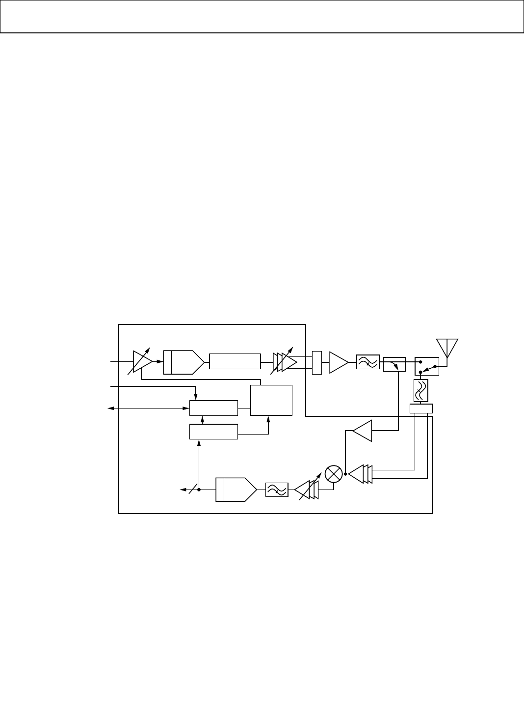
UG-570 AD9361 Reference Manual
| Page 56 of 128
Tx POWER MONITOR
OVERVIEW
This section describes the Tx power monitor (TPM) circuit
operation and features. TPM is available in TDD mode only
because it uses the inactive receiver to perform power
measurements during transmit. This feature is very useful as a
transmit power detector with over 66 dB of linear dynamic
range (the linear range can be extended to more than 80 dB as
shown later in this section). The AD9361 has two TPM inputs,
TX_MON1 (Pin M5) and TX_MON2 (Pin A5). The maximum
input signal level is +4 dBm CW referenced to 50 Ω. If the
inputs are not being used, tie them to ground.
This section explains in detail how to set up transmit control
registers and how to use transmit power control (TPC) in
normal operation.
Tx POWER MONITOR DESCRIPTION
One of the many features that the AD9361 contains is the ability
to accurately measure the level of a received signal resulting in
an receiver signal strength indicator (RSSI) reading available to
the system. Recognizing that in TDD systems the receiver and
transmitter are not operating simultaneously, the AD9361
provides the ability to reuse the receiver circuitry by
multiplexing the power detector into the receive path. The
receiver RSSI circuitry is then turned on during the transmit
burst and results in accurate Tx RSSI measurements. Refer to
Figure 28 for a TPM circuit block diagram in a typical TDD
system diagram.
Since the Tx signal is high level (with respect to a Rx signal), it
is multiplexed into the receiver chain after the LNA. The
receiver circuitry reuses results in an accurate, wide dynamic
range measurement utilizing the existing otherwise idle
circuitry. The measurement is an RMS level that has a
configurable time measurement window and returns results in
TxRSSI units with 0.25 dB/LSB resolution in –dBFS units over a
more than 66 dB of detector dynamic range. The measurement
starts as the device is moved into Tx mode by the enable state
machine. The measurement can be performed once after the
enable state machine (ENSM) enters the Tx state or the
measurement can be done continuously until ENSM exits the
Tx state.
Figure 28. TPM Circuit Block Diagram
DAC MODULATOR
FILT
PA
BALUN
BALUN
TX
TX DATA
ENABLE PIN
(STATE MACHINE
CONTROL)
SPI BUS
MODE/REGISTER
CONFIG
FILT
ADC
RX DATA
CONTROL
RMS
DECODE
TIA
LNA RX
TxRSSI
TX_MON
30dB
(TYP)
EXTERNAL ANTENNA
INTERFACE
11668-029
AD9361
Rev. A
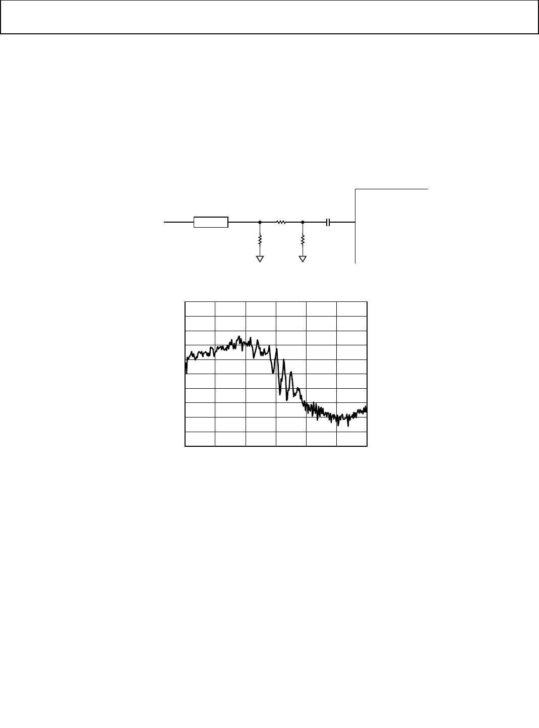
AD9361 Reference Manual UG-570
| Page 57 of 128
INPUT MATCHING/ATTENUATION NETWORK
Tx_MON inputs require a matching/attenuation network to
provide matching to the driving source (typically a 50 Ω coupler
output) and to scale the input signal. Place matching
components, R1 to R3 and C1, as close as possible to the
AD9361. Tx_MON inputs are DC biased and the C1 capacitor
is an ac-coupling capacitor used to ac couple Tx_MON input.
R2 is a damping resistor to minimize series resonance
comprised of on-chip inductance and capacitance. The best way
to determine the optimum value for R2 is to empirically tune it
for desired TPM frequency response. Use proper transmission
line design techniques to design the signal path (TL1) from the
transmitter output coupler to the input of TPM. The higher the
frequency of operation the more critical this path becomes in
terms of loss and signal reflections.
Figure 30 shows a measured TPM frequency response using the
matching circuit and component values in Figure 29. The
frequency response was optimized for 2.3 GHz frequency of
operation.
Figure 29. TPM Matching/Attenuation Input Network
Figure 30. TPM Frequency Response
R3R1 DNI
49.9Ω
R2
TX_MON
10Ω100pF
ZO = 50Ω
C1TL1TX MONITOR INPUT
(FROM COUPLER AFTER PA)
11668-030
–5
50 6050
GAIN (dB)
FREQUENCY (MHz)
11668-130
50504050305020501050
–6
–7
–8
–9
–10
–11
–12
–13
–14
–15
Rev. A
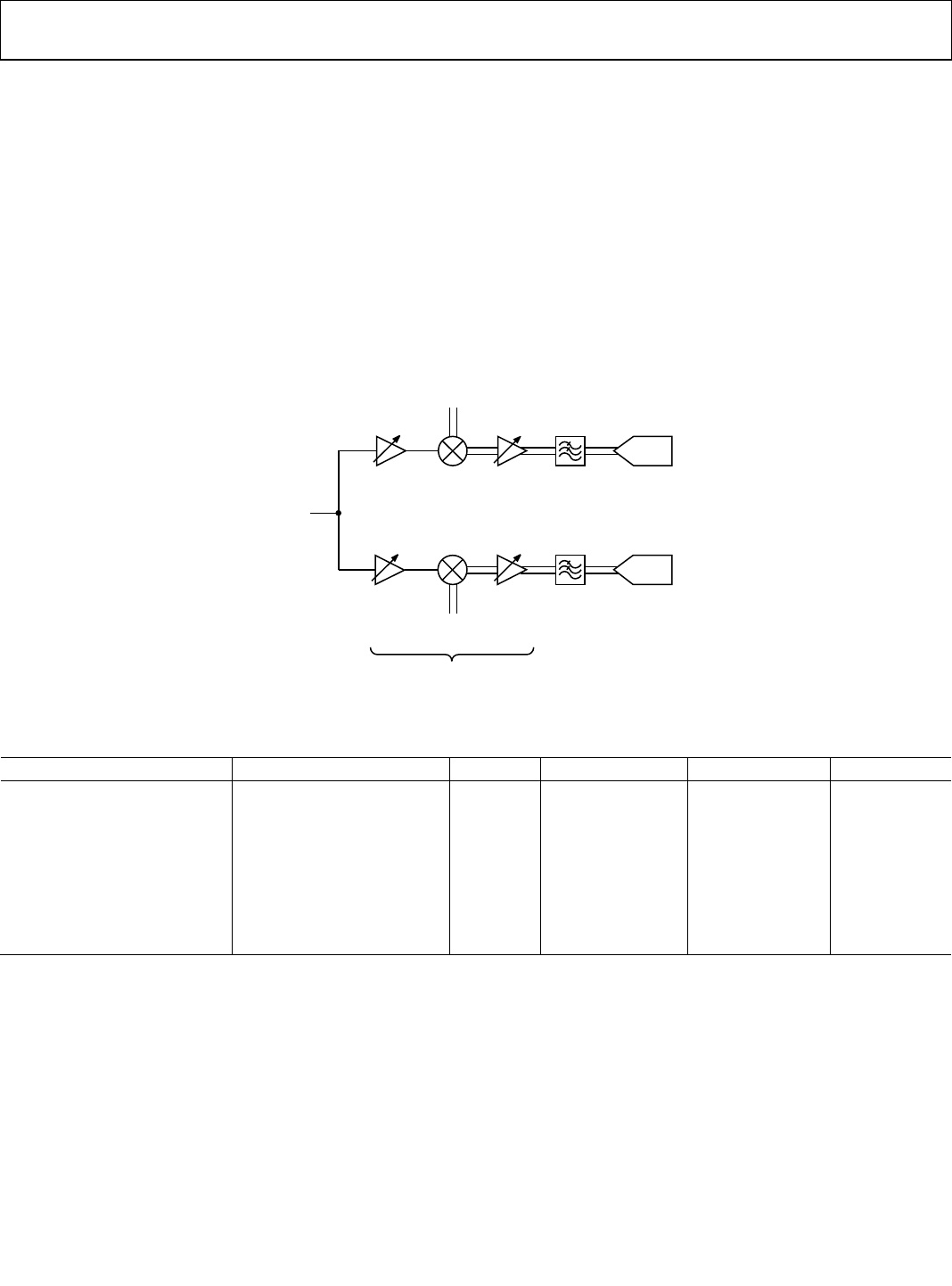
UG-570 AD9361 Reference Manual
| Page 58 of 128
Tx POWER MONITOR GAIN CONTROL
TPM total gain comprises of two gains, front-end gain (Tx Mon
Gain) and receive low pass filter gain (GBBF). TPM front-end
gain is set by Tx Mon 1 Config and Tx Mon 2 Config registers
(Register 0x070 [D1:D0] and Register 0x071 [D1:D0],
respectively). Tx Mon TIA Gain values are shown in Table 41. In
addition to the two gains, Table 41 also includes minimum and
maximum TPM input signal levels and associated SNR.
Figure 31 shows a block diagram of the TPM signal chain. Note
that the local oscillator signal used to downconvert the TPM
input signal is Tx LO.
Receive low-pass filter gain, GBBF, is set by register values Tx
Mon Low Gain and Tx Mon High Gain (Register 0x067
[D4:D0] and Register 0x068 [D4:D0], respectively). These
values set the receive low-pass filter gain index in the 0 dB to
24 dB range. TPM gain mode, low or high is determined by a
threshold in Tx Atten Threshold register (Register 0x078
[D7:D0]). If the Tx Attenuation value (Register 0x073 and
Register 0x074) is equal to or less than the threshold the low
gain index value is used and if the value is greater than the
threshold the high gain index is used in the receive path.
Transimpedance amplifier (TIA) gain is automatically set high
or low by the AD9361. Tx RSSI1 and Tx RSSI2 values in
Register 0x06B, Register 0x06C, and Register 0x06D are
compensated for gain changes.
Figure 31. TPM Gain Distribution
Table 41. TPM Gain and Dynamic Range
Tx Mon TIA Gain[1:0] Tx Mon TIA Gain (dB) GBBF (dB) Pinmax (dBm) Pinmin (dBm) SNR (dB)1
00 Open -- -- -- --
-- -- -- --
01 0 0 4 −62.7 67
30 −25.7 −70.1 44
10 6 0 −2.2 −68.6 67
30 −31.7 −75.8 44
11 9.5 0 −5.7 −72.1 66
30 −35.2 −78.9 44
1 Bandwidth used for SNR calculation is 10 MHz.
ADC
BBF
TX_MON1
OR
TX_MON2
ADC
BBF
LOQ
LOI
TX MON GAIN
0dB, 6dB, 9.5dB GBBF
0dB TO 30dB
11668-032
Rev. A
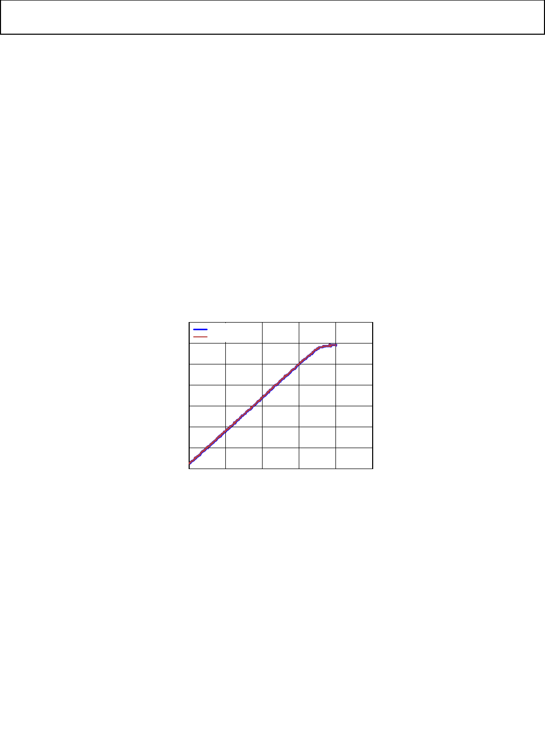
AD9361 Reference Manual UG-570
| Page 59 of 128
TPM DYNAMIC RANGE
TPM dynamic range can be maximized on the top end by
minimizing total TPM gain, that is, Tx Mon gain = 0 dB and
GBBF = 0 dB. The upper range of the input signal is +4 dBm in
that case (the upper range of the input signal can be increased
to 9 dBm by forcing TIA feedback resistor value to 1.75 kΩ by
setting Bits D6 and D7 in Register 0x1DC and Bits D0 and D2
in Register 0x1DB). Maximizing total TPM gain, that is, Tx
Mon Gain = 9.5 dB and GBBF = 30 dB minimizes the total input
referred noise thereby increasing the lower range of the input
signal to −78.9 dBm. The resulting total dynamic range can be
as high as 82.8 dB by following the previously described gain
control and making the gain switch threshold occur at
−35.2 dBm input signal level.
Figure 32 shows a linear dynamic range of about 70 dB that can
be achieved for three different input signal ranges with Tx Mon
Gain set to 0 dB, 6 dB or 9.5 dB and GBBF = 0 dB (see Table 41
for the input signal level ranges that correspond with these
three different gain settings. This approach uses the same Tx
Mon Gain and GBBF gain settings across the whole attenuation
range.
EXAMPLE OF TxMON CONFIGURATION AND
MEASUREMENT OF TPM TRANSFER FUNCTION
The following example is based on measured results using a
direct connection from the Tx1 output to the Tx Mon input on
an evaluation board. The goal of the example is to show how to
use the AD9361 TPM and an advanced application to extend
the dynamic range of TPM. The frequency of operation was
2300 MHz and transmitted signal was a 1 MHz CW signal.
TPM can be enabled in multi-chip sync and Tx Mon Control
Register 0x001 using Bits D5 and D6, and in TPM Mode Enable
Register 0x06E Bits D5 and D7. The preferred way to enable
TPM is to set Bits D7 and D5 in Register 0x06E. The user also
needs to clear Bits D2 and D3 in Analog Power Down Override
Register 0x057 because TPM is powered down by default.
To maximize SNR, the Tx Mon Track bit should be set in
0x067[D5], which minimizes DC offset in the Tx monitor
signal path.
3
Figure 32. TPM Frequency Response
350
0
50
100
150
200
250
300
010080604020
RSSI CODE
TX ATTENUATION (dB)
FREE RUNNING
ONE SHOT
11668-033
Rev. A
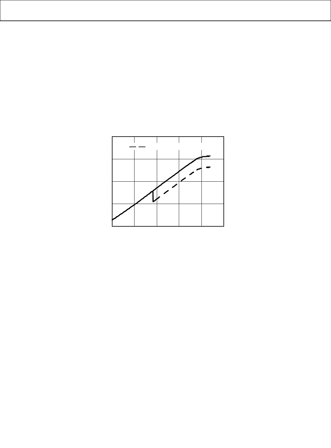
UG-570 AD9361 Reference Manual
| Page 60 of 128
The resulting measured TPM transfer characteristics are shown
in Figure 33. The dashed line is uncompensated for Tx Mon
TIA gain change at the threshold and it shows a transition at
37 dB Tx attenuation (this corresponds to a threshold setting of
0x94 in Register 0x078). Below the threshold Tx Mon gain is
0 dB and GBBF is 0 dB. Above the threshold Tx Mon gain is
9.5 dB and GBBF is 0 dB. The compensated characteristic (solid
line in Figure 33) is a gain compensated version of the dashed
line. The resulting linear dynamic range is 76 dB, which is about
10 dB greater than the 66 dB dynamic range achievable with a
single gain setting.
As Figure 33 shows, the TPM TIA gain is not compensated by
the Tx RSSI algorithm. The 9.5 dB compensation that results in
the solid line would occur in the baseband processor.
TPM TEST MODE
It is possible to output TPM I/Q data at the Rx data port
in TDD mode in Tx state. This may be useful in some
applications.
The Enable Rx Data Port bit for calibration (Register 0x014 Bit
D7) needs to be set and TPM enable in Register 0x06E to be in
this test mode.
Figure 33. Tx Monitor TxRSSI vs. Tx Attenuation
400
300
200
100
00204060 100
TxRSSI
TX ATTENUATION (dB)
80
UNCOMPENSATED FOR TX MON GAIN
11668-034
Rev. A

AD9361 Reference Manual UG-570
| Page 61 of 128
RF PORT INTERFACE
OVERVIEW
The purpose of this section is to define the expected AD9361
port impedance values and potential impedance matching
techniques.
The AD9361 has with two independent receive paths and two
independent transmit paths. Each receive path has three (A, B,
and C) LNA inputs and each transmit path has two (A and B)
Tx outputs. The LNA inputs and Tx outputs require external
impedance matching networks. The receiver LNA input ports
may be utilized in either a single-ended mode or differential
mode. The transmitter output ports may only be utilized in a
differential mode.
It is critical to have these interfaces working properly to achieve
data sheet performance levels. The main considerations are as
follows:
• Rx interface type: single ended or differential?
• Device to be interfaced: such as, filter, balun, T/R switch,
external LNA, external PA: Short to ground at DC?
• Rx LNA maximum (no damage) input power ( +2.5 dBm
Peak: single-ended: lossless match: 50 Ω source).
• Rx LNA input port DC voltage level (~ +0.6 VDC ).
• Tx output port bias (+1.3 VDC @ 75 mA per side @
maximum output power).
• Board design: such as reference-planes, transmission lines,
impedance matching.
Rev. A
UG-570 AD9361 Reference Manual
| Page 62 of 128
Rx SIGNAL PATH INTERFACE
The AD9361 LNA devices (1A, 1B, 1C, 2A, 2B, 2C) are
functional for the full 70 MHz to 6.0 GHz receive frequency
range. When operating at or below 3 GHz, any LNA input port
will provide optimal performance. When operating above
3 GHz, utilize the Rx1A and Rx2A LNA input ports for optimal
performance. All three LNAs provide differential inputs that
can also be configured as single-ended inputs (either side of the
differential input can be used as a single ended input). It is
recommended to configure the LNA inputs in differential mode
to achieve best noise figure and even order distortion (IP2)
performance. The LNA input pins have DC bias (~ 0.6 Vdc)
present on them and may need to be ac-coupled depending on
the common-mode voltage level of the external circuit. The
maximum safe input level is +2.5 dBm peak (single-ended, ideal
match, 50 Ω source). Figure 34 shows basic single ended and
differential interface configurations. Note that matching
networks will most likely be required to achieve optimum
performance.
Given a single-ended operation mode, a positive side
connection is delineated by the _P at the end of the Rx input
port name and a negative side connection is delineated by the
_N at the end of the Rx input port name.
The Rx differential input impedance varies over frequency and
is shown in Figure 38 through Figure 47. The reference plane
for this data is the AD9361 ball pads.
Note that Zo within the graph marker sections is 50 Ω.
Figure 34. AD9361 Rx Input Interface Circuit—Single-Ended Interface to the Negative Side of the Differential Input
Figure 35. AD9361 Rx Input Interface Circuits—Single-Ended Interface to the Positive Side of the Differential Input
Figure 36. AD9361 Rx Input Interface Circuits—Differential Interface Using a Transformer
Figure 37. AD9361 Rx Input Interface Circuits—Differential Interface Using a Transmission Line Balun
C
C
RxA_N
RxA_P
LNA
OPEN,
SHORT,
OTHER BAND/PATH
11668-035
CCRxA_P
LNA
RxA_N
OPEN,
SHORT,
OTHER BAND/PATH
11668-036
RxA_N
RxA_P
LNA
11668-037
RxA_N
RxA_P
LNA
CC
CC
11668-038
Rev. A
AD9361 Reference Manual UG-570
| Page 63 of 128
Figure 38. AD9361 Rx1A and Rx2A Input Differential Impedance
Figure 39. AD9361 Rx1A and Rx2A Input Differential Impedance Magnitude
250
0
10
–10
–9
–8
–7
–6
–5
–4
–3
–2
–1
0
1
2
3
4
5
6
7
8
9
50
100
150
200
DIFFERENTIAL_R_SE
RC DEEMBEDDED MEASUREMENT DATA
DIFFERENTIAL_L_OR_C_SE
L_OR_C_STATUS
FREQUENCY (GHz)
0.07
0.32
0.57
0.82
1.07
1.32
1.57
1.82
2.07
2.32
2.57
2.82
3.07
3.32
3.57
3.82
4.07
4.32
4.57
4.82
5.07
5.32
5.57
5.82
6.00
Rx1A AND Rx2A SERIES EQUVALENT DIFFERENTIAL IMPEDANCE Rx1A AND Rx2A SERIES EQUVALENT DIFFERENTIAL IMPEDANCE
FREQUENCY (70MHz TO 6GHz)
11668-039
250
0
50
100
150
200
ZDIFF MAGNITUDE
FREQUENCY (GHz)
0.07
0.32
0.57
0.82
1.07
1.32
1.57
1.82
2.07
2.32
2.57
2.82
3.07
3.32
3.57
3.82
4.07
4.32
4.57
4.82
5.07
5.32
5.57
5.82
6.00
11668-040
Rev. A
UG-570 AD9361 Reference Manual
| Page 64 of 128
Figure 40. AD9361 Rx1B Input Differential Impedance
Figure 41. AD9361 Rx1B Input Differential Impedance Magnitude
250
0
10
–10
–9
–8
–7
–6
–5
–4
–3
–2
–1
0
1
2
3
4
5
6
7
8
9
50
100
150
200
DIFFERENTIAL_R_SE
RC DEEMBEDDED MEASUREMENT DATA
DIFFERENTIAL_L_OR_C_SE
L_OR_C_STATUS
FREQUENCY (GHz)
0.07
0.32
0.57
0.82
1.07
1.32
1.57
1.82
2.07
2.32
2.57
2.82
3.07
3.32
3.57
3.82
4.07
4.32
4.57
4.82
5.07
5.32
5.57
5.82
6.00
Rx1B SERIES EQUVALENT DIFFERENTIAL IMPEDANCE Rx1B SERIES EQUVALENT DIFFERENTIAL IMPEDANCE
FREQUENCY (70MHz TO 6GHz)
11668-041
450
0
50
100
150
350
ZDIFF MAGNITUDE
FREQUENCY (GHz)
0.07
0.32
0.57
0.82
1.07
1.32
1.57
1.82
2.07
2.32
2.57
2.82
3.07
3.32
3.57
3.82
4.07
4.32
4.57
4.82
5.07
5.32
5.57
5.82
6.00
11668-241
400
300
250
200
Rev. A
AD9361 Reference Manual UG-570
| Page 65 of 128
Figure 42. AD9361 Rx1C Input Differential Impedance
Figure 43. AD9361 Rx1C Input Differential Impedance Magnitude
450
400
350
300
250
0
10
–10
–9
–8
–7
–6
–5
–4
–3
–2
–1
0
1
2
3
4
5
6
7
8
9
50
100
150
200
DIFFERENTIAL_R_SE
RC DEEMBEDDED MEASUREMENT DATA
DIFFERENTIAL_L_OR_C_SE
L_OR_C_STATUS
FREQUENCY (GHz)
0.07
0.32
0.57
0.82
1.07
1.32
1.57
1.82
2.07
2.32
2.57
2.82
3.07
3.32
3.57
3.82
4.07
4.32
4.57
4.82
5.07
5.32
5.57
5.82
6.00
Rx1C SERIES EQUVALENT DIFFERENTIAL IMPEDANCE Rx1C SERIES EQUVALENT DIFFERENTIAL IMPEDANCE
FREQUENCY (70MHz TO 6GHz)
11668-043
450
0
50
100
150
350
ZDIFF MAGNITUDE
FREQUENCY (GHz)
0.07
0.32
0.57
0.82
1.07
1.32
1.57
1.82
2.07
2.32
2.57
2.82
3.07
3.32
3.57
3.82
4.07
4.32
4.57
4.82
5.07
5.32
5.57
5.82
6.00
11668-343
400
300
250
200
Rev. A
UG-570 AD9361 Reference Manual
| Page 66 of 128
Figure 44. AD9361 Rx2B Input Differential Impedance
Figure 45. AD9361 Rx2B Input Differential Impedance Magnitude
400
350
300
250
0
10
–10
–9
–8
–7
–6
–5
–4
–3
–2
–1
0
1
2
3
4
5
6
7
8
9
50
100
150
200
DIFFERENTIAL_R_SE
RC DEEMBEDDED MEASUREMENT DATA
DIFFERENTIAL_L_OR_C_SE
L_OR_C_STATUS
FREQUENCY (GHz)
0.07
0.32
0.57
0.82
1.07
1.32
1.57
1.82
2.07
2.32
2.57
2.82
3.07
3.32
3.57
3.82
4.07
4.32
4.57
4.82
5.07
5.32
5.57
5.82
6.00
Rx2B SERIES EQUVALENT DIFFERENTIAL IMPEDANCE Rx2B SERIES EQUVALENT DIFFERENTIAL IMPEDANCE
FREQUENCY (70MHz TO 6GHz)
11668-243
400
350
300
250
0
50
100
150
200
ZDIFF MAGNITUDE
FREQUENCY (GHz)
0.07
0.32
0.57
0.82
1.07
1.32
1.57
1.82
2.07
2.32
2.57
2.82
3.07
3.32
3.57
3.82
4.07
4.32
4.57
4.82
5.07
5.32
5.57
5.82
6.00
11668-042
Rev. A
AD9361 Reference Manual UG-570
| Page 67 of 128
Figure 46. AD9361 Rx2C Input Differential Impedance
Figure 47. AD9361 Rx2C Input Differential Impedance Magnitude
450
400
350
300
250
0
10
–10
–9
–8
–7
–6
–5
–4
–3
–2
–1
0
1
2
3
4
5
6
7
8
9
50
100
150
200
DIFFERENTIAL_R_SE
RC DEEMBEDDED MEASUREMENT DATA
DIFFERENTIAL_L_OR_C_SE
L_OR_C_STATUS
FREQUENCY (GHz)
0.07
0.32
0.57
0.82
1.07
1.32
1.57
1.82
2.07
2.32
2.57
2.82
3.07
3.32
3.57
3.82
4.07
4.32
4.57
4.82
5.07
5.32
5.57
5.82
6.00
Rx2C SERIES EQUVALENT DIFFERENTIAL IMPEDANCE Rx2C SERIES EQUVALENT DIFFERENTIAL IMPEDANCE
FREQUENCY (70MHz TO 6GHz)
11668-246
450
400
350
300
250
0
50
100
150
200
ZDIFF MAGNITUDE
FREQUENCY (GHz)
0.07
0.32
0.57
0.82
1.07
1.32
1.57
1.82
2.07
2.32
2.57
2.82
3.07
3.32
3.57
3.82
4.07
4.32
4.57
4.82
5.07
5.32
5.57
5.82
6.00
11668-044
Rev. A
UG-570 AD9361 Reference Manual
| Page 68 of 128
From a design flexibility viewpoint, the following Rx path
impedance matching strategy is preferred.
• Place a differential matching network between the
balun/filter and the LNA input port.
• Place a single-ended matching network on the balun/filter
input port.
The best matching network topology is application dependent.
The examples within this section are simpler narrow-band
cases. As the matching bandwidth increases, the required
number of matching sections increases.
The LNA input ports have a DC voltage on them. A short to
ground at DC is to be avoided. Figure 48 defines the general
purpose matching topology.
The balun/filter single-ended port is impedance matched with a
simple PII network. The balun/filter differential port is
impedance matched with either a DC-blocked differential PII
network or a DC-blocked differential T network.
The DC-blocked differential T network is represented by the
smaller box in Figure 48. The DC-blocked differential PII
network is represented by the larger box in Figure 48.
The main advantages of the DC-blocked differential PII
network topology are a relatively wide impedance matching
bandwidth (up to 830 MHz) and Impedance Matching
Topology selection flexibility. The main disadvantage is a higher
number of SMD components.
The main advantage of the DC-blocked differential T network
topology is a lower SMD component count. The main
disadvantage is the impedance matching bandwidth may be up
to 5% smaller than the DC-blocked differential PII topology.
Figure 48. AD9361 Rx Input General Purpose Impedance Matching Topology
DIFFERENTIAL MATCH
SINGLE-ENDED MATCH
S1P_EQN
S1P_EQN
S1P_EQN
S1P_EQN
S1P_EQN
S1P_EQN S1P_EQN
S1P_EQN
S1P_EQN
BALUN3PORT
CMP1
S1P3
S1P1
S1P2
S1P4
S1P5
S1P6
S1P8
S1P9 S1P7
D
C
11668-049
Rev. A
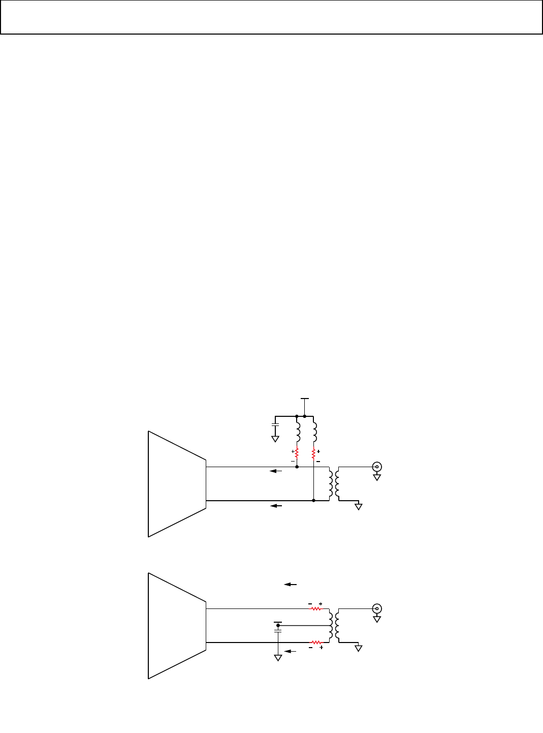
AD9361 Reference Manual UG-570
| Page 69 of 128
Tx SIGNAL PATH INTERFACE
The AD9361 transmit path covers a full 70 MHz to 6.0 GHz
transmit frequency range and the 2 Tx outputs exhibit similar
performance. The Tx outputs are differential and require an
external output bias. These outputs need to be biased to 1.3 V
DC supply voltage (nominal) using either chokes (wire-wound
inductors) or a transformer center tap connection. Each side of
the differential output draws ≈75 mA of DC bias current at full
output power. It is important to select components with low DC
resistance (RDCR) to minimize voltage drop ΔV across the series
parasitic resistance element (see the red resistor symbol in
Figure 49). As the ΔV voltage drop increases, the Tx buffer RF
performance (OP1dB, max output power) degrades. Choke
inductance (LC) should be selected such that the choke
impedance is high enough relative to the load impedance so
that it does not affect the frequency response. The Tx outputs
will have to be ac-coupled in most applications due to the
presence of 1.3 V DC supply bias voltage. The approach in
Figure 50 is preferred because there are fewer parasitics and the
component count is lower.
The Tx differential output port is a medium signal device.
Therefore, impedance matching is based on load-pull
techniques. Very similar to a PA (power amplifier). The goal is
to provide a Tx output differential load impedance that
represents the best compromise between the maximum output
power delivered and the highest possible third-order linearity
(OIP3).
Load-pull based impedance matching is very simple. The focus
is on developing the preferred load impedance at the Tx output
ball pads. This matching technique is quite different from the
small-signal techniques utilized for the Rx input.
• Load-pull: Design the matching network for the preferred
Load impedance at the Tx output pads.
• Small-signal: Design the matching network for maximum
power transfer (TG: transducer gain).
Based on present load-pull data, the preferred Tx output
differential load impedance is 50 Ω.
• The reference plane is the Tx output ball pads.
• The fundamental power is inversely proportional to the
real part of the load impedance.
• The OIP3 is inversely proportional to the real part of the
load impedance.
• The OIP3 is higher for capacitive loads as compared to
inductive loads. If residual impedance matching errors
exist, it is better to error with a capacitive termination as
opposed to an Inductive termination.
Figure 51 to Figure 54 show the basic differential Tx output
interface configurations. Note that matching networks (balun
single-ended port) will most likely be required to achieve
optimum performance.
Figure 49. AD9361 Tx Output DC Biasing Using Chokes
Figure 50. AD9361 Tx Output DC Biasing Using Center Tapped Transformer
1.3V
TXA_N
TXA_P
TX OUTPUT
CBLCLC
RDCR RDCR
1.3V – ΔV
1.3V – ΔV
ΔV ΔV
IBIAS
~75mA
IBIAS
~75mA
11668-050
TXA_N
TXA_P
TX OUTPUT
IBIAS
~75mA
IBIAS
~75mA
1.3V
ΔV
ΔV
1.3V – ΔV
1.3V – ΔV CB
11668-051
Rev. A
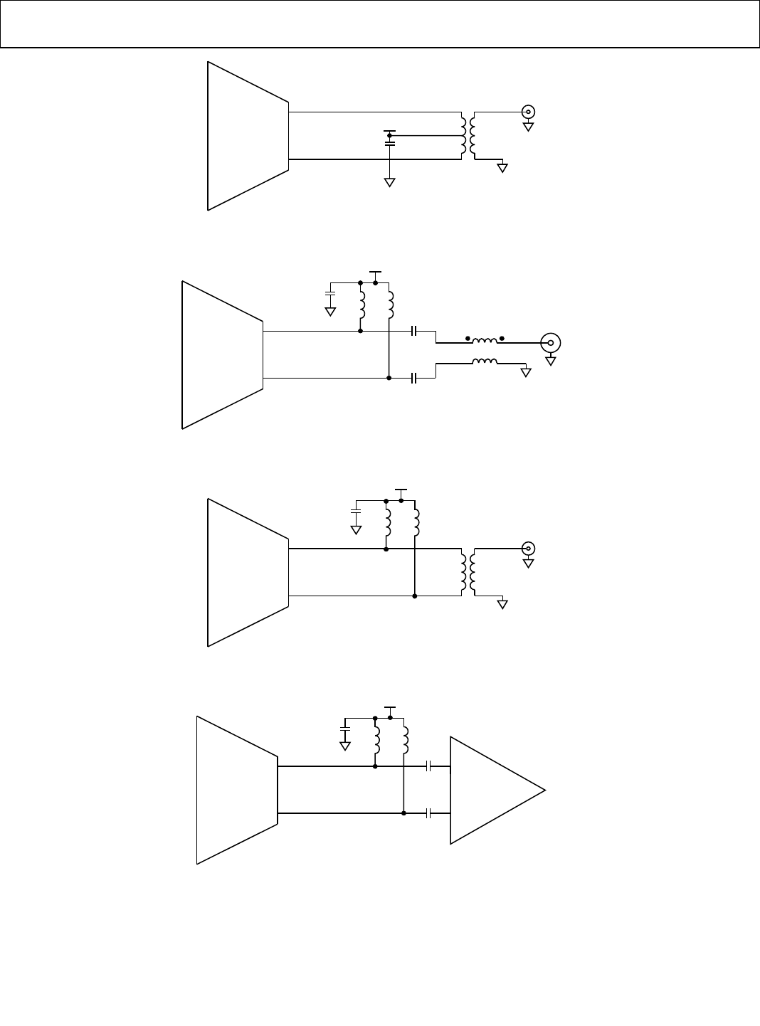
UG-570 AD9361 Reference Manual
| Page 70 of 128
Figure 51. AD9361 Tx Output Differential Interface Configurations
Figure 52. AD9361 Tx Output Differential Interface Configurations
Figure 53. AD9361 Tx Output Differential Interface Configurations
Figure 54. AD9361 Tx Output Differential Interface Configurations
TXA_N
TXA_P
TX OUTPUT
1.3V
CB
11668-052
TXA_N
TXA_P
TX OUTPUT
1.3V
1.3V
1.3V
C
B
C
C
C
C
11668-053
TXA_N
TXA_P
TX OUTPUT
1.3V
1.3V
1.3V
C
B
11668-054
TXA_N
TXA_P
TX OUTPUT
1.3V
1.3V
1.3V
C
B
C
C
C
C
DRIVER
AMPLIFIER
11668-055
Rev. A

AD9361 Reference Manual UG-570
| Page 71 of 128
FACTORY CALIBRATIONS
OVERVIEW
Factory calibrations are necessary to limit the amount of
variation seen across a large quantity of circuit boards. Some
calibrations are used to increase the accuracy of the AD9361
device, while others are needed to calibrate non-linearities of
external components in the RF front-end. The factory
calibrations described in Table 42 are suggested calibrations.
The number of calibration points for a specific design is
dependent on the temperature stability and linearity of the RF
components. The actual factory calibrations necessary might
vary from Table 42 depending on the accuracy and
performance of the desired system.
Table 42. Suggested Factory Calibrations
# Factory Calibration
1 Internal DCXO (AFC tune range)
2 Tx RSSI (Tx monitor)
3 Rx RSSI
4 Rx GM/LNA gain step error
5 Tx power out vs. Tx attenuation
6 Tx power out vs. frequency
INTERNAL DCXO
If using an external clock into the REF_CLK_IN pin, ignore this
calibration.
The AD9361 device can use a crystal oscillator (XO) to clock
the chip. In this mode, the AD9361 has an internal DCXO
(digitally control oscillator) that can pull the XO frequency.
This is necessary to cancel out carrier frequency offset and
Doppler shift due to mobility. Carrier frequency offset can also
occur due to the XO changing temperature.
The DCXO tune registers consist of a coarse tune value and a
fine tune value. During factory calibration, the coarse tune
setting should be found such that the fine tune range is centered
evenly around the desired XO frequency. This would ensure the
widest usable DCXO range.
If necessary by the system, the factory calibration could also
sweep the DCXO fine tune codes to produce a LUT of
frequency error vs. fine tune code to allow quick updates of
the XO tuning. The temperature sensor could also be read to
aid in correcting for the frequency variation across temperature
of the XO.
Tx RSSI (Tx MONITOR)
If the power detector is used, at minimum, a single point Tx
RSSI measurement must be made to correlate the absolute
output power after the PA to the Tx RSSI value reported by the
AD9361 device. Typically, a coupler is used to sample the power
after the PA back into the Tx monitor input of the AD9361
device. During this measurement, transmit a typical burst. A
signal with constant power (such as a preamble) would give the
most accurate results. Once a single point measurement has
been measured, the Tx RSSI for other Tx power out levels can
be calculated with the assumption that the assumption that the
Tx path is linear, the power detector path is linear and all
external RF components in the path are operating in their linear
regions. If the system requires a higher precision of power
control, multiple points across the AD9361 Tx attenuation
range and carrier frequency range can be measured during this
factory calibration to generate a matrix of Tx RSSI correction
values.
The factory calibration should be completed using the
corresponding transmitter on the AD9361 device to transmit a
known reference signal while the Tx RSSI is read across the SPI
port for each desired output power point. Refer to the Tx Power
Monitor section for detailed information on this process and
the different power control modes.
Rx RSSI
The receive signal strength indicator (RSSI) measurement
occurs after the Rx gain is set (manual gain)/frozen(AGC). For
the power measurement to be meaningful to the BBP, the RSSI
code must be related to an absolute Rx input level (dBm) during
factory calibration. Depending on the RSSI accuracy desired,
this calibration can be a signal point calibration at a single
frequency and input power level, or can consist of a matrix of
frequencies and input power levels. The calibration signal
should be a typical burst of the associated standard. For each
receiver, there are two different RSSI read back registers. One
register stores the first power measurement (RSSI preamble).
The second register updates the power measurement at the
symbol rate (RSSI Symbol). If a calibration signal has a
preamble or symbol with constant power, the RSSI will be more
accurate and repeatable. For more details, see the Received
Signal Strength Indicator (RSSI) section. The function
ad9361_rssi_setup configures the RSSI measurement. The
AD9361 automatically takes into account the Rx gain step used
and factors it into the RSSI value. For improved RSSI accuracy
over frequency, run the Rx GM/LNA gain step calibration
before the RSSI factory calibration.
Rev. A

UG-570 AD9361 Reference Manual
| Page 72 of 128
Rx GM/LNA GAIN STEP CALIBRATION
The gain of the LNA and mixer stages inside the AD9361 varies
over temperature and frequency. This calibration is a onetime
factory calibration that measures the gain step error for the
LNA and mixer to reduce the error of the Rx RSSI measure-
ment. In the field, the BBP would write the error-corrected
expected gain steps into the AD9361 for the current frequency
used. This process will improve Rx RSSI accuracy and linearity.
Complete this procedure before calibrating the Rx RSSI. The Rx
GM/LNA gain step calibration is only necessary if using the Rx
RSSI feature, and more detail on this calibration can be found in
the Received Signal Strength Indicator (RSSI) section.
Tx POWER OUT VS. Tx ATTENUATION AND Tx
POWER OUT VS. CARRIER FREQUENCY
A factory calibration should be completed such that the output
power of the system is known. Depending on the linearity of
the RF components chosen, a single point calibration may be
sufficient. If higher accuracy is desired, a matrix of carrier
frequencies and AD9361 Tx attenuation points may be evalu-
ated to measure the Tx power output. This factory calibration
would prevent the output power from exceeding regulatory
limits. This calibration should also check for transmit mask
compliance and transmit emission limits (ACLR).
Rev. A
AD9361 Reference Manual UG-570
| Page 73 of 128
CONTROL OUTPUT
OVERVIEW
The AD9361 provides real-time status information on up to
eight dedicated pins. Information such as when calibrations are
running and the state of the overload detectors in the receive
signal path are just a few of the many options available. This
section describes the signals and their behavior in detail while
also showing how to program the registers so that the desired
signals are available on the appropriate balls. This section also
provides some information about how a BBP could use the
signals in an application. The control outputs are configured
using the ad9361_ctrl_outs_setup function.
As shown in Table 44, the control output signals are mapped as
a table. The Control Output Pointer selects the row (address)
that will be sent to the output pins. And the bits in Control
Output Enable individually select which output pins will be
active. The AD9361 will hold low any pins not enabled.
Some internal signals are available on more than one
combination of Control Output Pointer and Control Output
Enable. For example, to enable a control output that indicates
that the Rx1 gain has changed, the Control Output Pointer
register could be set to 0x08 and the Control Output Enable
register would then be set to 0x10. The same signal is also
available by setting Control Output Pointer to 0x05 and Control
Output Enable to 0x40 or alternatively with Control Output
Pointer set to 0x1E and Control Output Enable set to 0x04. Any
one of these options is valid. The BBP can only monitor the
signals in one row at a time because Register Control Output
Pointer can only have a single value loaded at any given time.
Thus, selecting one over the other depends on which other
signals the BBP needs to monitor simultaneously. From the
example, if the BBP also needs to know when the AuxADC
word is valid, only the option of setting Control Output Pointer
to 0x1E will allow this combination of the two signals. In this
case, Control Output Enable would need to be set to 0x05. The
BBP can also set more of the bits in Control Output Enable even
if it does not monitor those signals.
Some of the signals are helpful in a production system while
some others are useful for debug. In either case, Analog Devices
recommends connecting the AD9361 control outputs to BBP
inputs on the BBP so that the BBP can monitor real-time
conditions in the AD9361.
Table 43. Control Output Bit Descriptions
Register
Address Name D7 D6 D5 D4 D3 D2 D1 D0 Default R/W
0x035 Control Output Pointer Control Output Pointer[7:0] 0x00 R/W
0x036 Control Output Enable En ctrl7 En ctrl6 En ctrl5 En ctrl4 En ctrl3 En ctrl2 En ctrl1 En ctrl0 FF R/W
Table 44. Control Output Table
Register
0x035
Control Output Bit Position
D7 D6 D5 D4 D3 D2 D1 D0
00 Cal Done Tx CP Cal Done Rx CP Cal
Done
Rx BB Filter
Tuning Done
Tx BB Filter
Tuning Done
Gain Step Cal
Busy
Rx Synth VCO
Cal Busy
Tx Synth VCO
Cal Busy
01 Tx RF PLL Lock Rx RF PLL Lock BBPLL Lock 0 0 0 0 0
02 BB DC Cal Busy RF DC Cal Busy CH1 Rx Quad
Cal Busy
CH1 Tx Quad
Cal Busy
CH2 Rx Quad
Cal Busy
CH2 Tx Quad
Cal Busy
Gain Step Cal
Busy
Tx Mon Cal
Busy
03 CH1 ADC Low
Power
CH1 Lg LMT
Ovrg
CH1 Lg ADC
Ovrg
CH1 Sm ADC
Ovrg
CH2 Low Power CH2 Lg LMT
Ovrg
CH2 Lg ADC
Ovrg
CH2 Sm ADC
Ovrg
04 CH 2 Rx Gain[6] CH2 Rx Gain[5] CH2 Rx
Gain[4]
CH2 Rx Gain[3] CH2 Rx Gain[2] CH2 Lg LMT
Ovrg
CH2 Lg ADC
Ovrg
CH2 Gain
Lock
05 CH2 Gain
Change
CH1 Gain
Change
CH2 Low
Power
CH2 Lg LMT
Ovrg
CH2 Lg ADC
Ovrg
CH2 Gain Lock CH2 Energy
Lost
CH2 Stronger
Signal
06 CH1 Low Power CH1 Lg LMT
Ovrg
CH1 Lg ADC
Ovrg
CH1 Rx Gain[6] CH1 Rx Gain[5] CH1 Rx
Gain[4]
CH1 Rx
Gain[3]
CH1 Rx
Gain[2]
07 CH1 Low Power CH1 Lg LMT
Ovrg
CH1 Lg ADC
Ovrg
CH1 Sm ADC
Ovrg
CH1 AGC SM[2] CH1 AGC
SM[1]
CH1 AGC
SM[0]
CH1 Gain
Lock
08 CH1 Stronger
Signal
CH1 Gain Lock CH1 Energy
Lost
CH1 Gain
Change
CH2 Stronger
Signal
CH2 Gain Lock CH2 Energy
Lost
CH2 Gain
Change
09 RxOn CH1 RSSI
Preamble
Ready
CH1 RSSI
Symbol Ready
TxOn CH2 RSSI
Preamble
Ready
CH2 RSSI
Symbol Ready
0A CH1 Tx Int3
Overflow
CH1 Tx HB3
Overflow
CH1 Tx HB2
Overflow
CH1 Tx QEC
Overflow
CH1 Tx HB1
Overflow
CH1 Tx FIR
Overflow
CH1 Rx FIR
Overflow
0B Cal Seq State[3] Cal Seq State
[2]
Cal Seq State
[1]
Cal Seq State
[0]
ENSM[3] ENSM[2] ENSM[1] ENSM[0]
Rev. A

UG-570 AD9361 Reference Manual
| Page 74 of 128
Register
0x035
Control Output Bit Position
D7 D6 D5 D4 D3 D2 D1 D0
0C CH1 Energy
Lost
CH1 Reset Peak
Detect
CH2 Energy
Lost
CH2 Reset Peak
Detect
Gain Freeze CH1 Digital
Sat
CH2 Digital
Sat
0D CH1 Tx Quad
Cal Status[1]
CH1 Tx Quad
Cal Status[0]
CH1 Tx Quad
Cal Done
RF DC Cal Busy CH2 Tx Quad
Cal Status[1]
CH2 Tx Quad
Cal Status[0]
CH2 Tx Quad
Cal Done
0E
BB DC Cal Busy
0F CH1 AGC
State[2]
CH1 AGC
State[1]
CH1 AGC
State[0]
CH1 Reset Peak
Detect
CH2 Reset Peak
Detect
CH1 RF DC Cal
State[1]
CH1 RF DC
Cal State[0]
10
CH2 AGC
State[2]
CH2 AGC
State[1]
CH2 AGC
State[0]
CH2 Enable
RSSI
CH1 Enable
RSSI
CH2 RF DC Cal
State[1]
CH2 RF DC
Cal State[0]
11 AuxADC
Output[11]
AuxADC
Output[10]
AuxADC
Output[9]
AuxADC
Output[8]
AuxADC
Output[7]
AuxADC
Output[6]
AuxADC
Output[5]
AuxADC
Output[4]
12 CH1 Filter
Power Ready
CH1 Gain Lock CH1 Energy
Lost
CH1 Stronger
Signal
CH1 ADC
Power Ready
CH1 AGC
State[2]
CH1 AGC
State[1]
CH1 AGC
State[0]
13 CH2 Filter
Power Ready
CH2 Gain Lock CH2 Energy
Lost
CH2 Stronger
Signal
CH2 ADC
Power Ready
CH2 AGC
State[2]
CH2 AGC
State[1]
CH2 AGC
State[0]
14 CH2 Tx Int3
Overflow
CH2 Tx HB3
Overflow
CH2 Tx HB2
Overflow
CH2 Tx QEC
Overflow
CH2 Tx HB1
Overflow
CH2 Tx FIR
Overflow
CH2 Rx FIR
Overflow
0
15
CH1 SOI
Present
CH1 Update
DCRF
CH1 Measure
DCRF
CH1 DC Track
Count Reached
0 0 0 0
16 CH1 Gain Lock CH1 Rx Gain[6] CH1 Rx
Gain[5]
CH1 Rx Gain[4] CH1 Rx Gain[3] CH1 Rx
Gain[2]
CH1 Rx
Gain[1]
CH1 Rx
Gain[0]
17 CH2 Gain Lock CH2 Rx Gain[6] CH2 Rx
Gain[5]
CH2 Rx Gain[4] CH2 Rx Gain[3] CH2 Rx
Gain[2]
CH2 Rx
Gain[1]
CH2 Rx
Gain[0]
18 CH2 SOI
Present
CH2 Update
DCRF
CH2 Measure
DCRF
CH2 DC Track
Count Reached
CH2Enable Dec
Pwr
CH2 Enable
ADC Pwr
CH1 Enable
Dec Pwr
CH1 Enable
ADC Pwr
19 Rx Syn Cp
Cal[3]
Rx Syn Cp
Cal[2]
Rx Syn Cp
Cal[1]
Rx Syn Cp
Cal[0]
Tx Syn Cp
Cal[3]
Tx Syn Cp
Cal[2]
Tx Syn Cp
Cal[1]
Tx Syn Cp
Cal[0]
1A
Rx Syn VCO
Tuning[8]
Rx Synth VCO
ALC[6]
Rx Synth VCO
ALC[5]
Rx Synth VCO
ALC[4]
Rx Synth VCO
ALC[3]
Rx Synth VCO
ALC[2]
Rx Synth VCO
ALC[1]
Rx Synth VCO
ALC[0]
1B Tx Syn VCO
Tuning[8]
Tx Synth VCO
ALC[6]
Tx Synth VCO
ALC[5]
Tx Synth VCO
ALC[4]
Tx Synth VCO
ALC[3]
Tx Synth VCO
ALC[2]
Tx Synth VCO
ALC[1]
Tx Synth VCO
ALC[0]
1C Rx Syn VCO
Tuning[7]
Rx Syn VCO
Tuning[6]
Rx Syn VCO
Tuning[5]
Rx Syn VCO
Tuning[4]
Rx Syn VCO
Tuning[3]
Rx Syn VCO
Tuning[2]
Rx Syn VCO
Tuning[1]
Rx Syn VCO
Tuning[0]
1D Tx Syn VCO
Tuning[7]
Tx Syn VCO
Tuning[6]
Tx Syn VCO
Tuning[5]
Tx Syn VCO
Tuning[4]
Tx Syn VCO
Tuning[3]
Tx Syn VCO
Tuning[2]
Tx Syn VCO
Tuning[1]
Tx Syn VCO
Tuning[0]
1E CH1 Low
Thresh
Exceeded
CH1 High
Thresh
Exceeded
CH1 Gain Upd
Count Exp
CH1 AGC State
[1]
CH1 AGC State
[0]
CH1 Gain
Change
Temp Sense
Valid
AuxADC
Valid
1F
CH2 Low
Thresh
Exceeded
CH2 High
Thresh
Exceeded
CH2 Gain Upd
Count Exp
CH2 AGC SM[1] CH2 AGC SM[0]
CH2 Gain
Change
DESCRIPTION OF CONTROL OUTPUT SIGNALS
Any control output options not listed in the following sections
are undefined. For example, if Control Output Pointer is set to
0x0E the logic level of Control Output 0 is undefined and it is
not listed in the following description section.
Once the BBP initiates a calibration on the AD9361, the BBP
should not execute additional code until the calibration
completes. There are three methods to meet this requirement:
• The BBP can wait until the longest time that the calibration
could take to run.
• The BBP can poll the bit used to initiate the calibration or
it can poll a lock bit for VCO calibrations.
• The BBP can monitor various control output signals which
inform the BBP in real time when the calibration completes.
0x035 = 0x00 (CALIBRATION BUSY AND DONE)
Control Output 7 (Cal Done)
When the AD9361 powers up into the sleep state, this signal is
low. The signal responds only to the RF DC, BB DC, Tx
quadrature, Rx quadrature, and gain step calibrations. After one
these calibrations completes, the Cal Done signal transitions
high. From that point on, while any of the previously listed
calibrations runs, Cal Done is low, returning high at the
completion of the calibration. If several bits in Calibration
Control register are set simultaneously, the calibration state
machine will run the calibrations automatically in a particular
order. Only after all calibrations previously listed have
completed will the Cal Done signal transition high.
Rev. A

AD9361 Reference Manual UG-570
| Page 75 of 128
Control Output 6 (Tx CP Cal Done)
When the AD9361 powers up into the sleep state, this signal
is low. It transitions high after a Tx charge pump calibration
completes. If this signal is already high, it will transition and
stay low during the CP cal and transition high after the
calibration completes.
Control Output 5 (Rx CP Cal Done)
Same as Tx CP Cal Done in Control Output 6 but applies to the
Rx charge pump calibration.
Control Output 4 (Rx BB Filter Tuning Done)
Normally high. This signal is low only when the Rx baseband
filter calibration runs.
Control Output 3 (Tx BB Filter Tuning Done)
Normally high. This signal is low only when the Tx baseband
filter calibration runs.
Control Output 2 (Gain Step Cal Busy)
Normally low. This signal is high only when the gain step
calibration runs.
Control Output 1 (Rx Synth VCO Cal Busy)
Normally low. This signal is high only when the Rx RF VCO
calibration runs.
Control Output 0 (Tx Synth VCO Cal Busy)
Normally low. This signal is high only when the Rx RF VCO
calibration runs.
0x035 = 0x01 (PLL LOCK)
Control Output 7 (Tx RF PLL Lock)
This signal reflects the state of the Tx RFPLL lock detect circuit.
If the lock detect mode is continuous, then this control output
signal will be high when the RFPLL is locked and low otherwise
(including when a calibration runs). If the lock detect mode is
run once, then this bit will indicate the status of the lock detect
circuit every time the frequency integer word is written (causing
a VCO cal to occur) but after that occurs, the lock detect circuit
will stop monitoring the state of the RFPLL.
Control Output 6 (Rx RF PLL Lock)
Same as Tx RF PLL Lock in Control Output 7 but applies to the
Rx RFPLL.
Control Output 5 (BBPLL Lock)
This signal is high when the BBPLL is locked. Otherwise, this
signal is low.
Control Output 4 Through Control Output 0
Always low.
0x035 = 0x02 (CALIBRATION BUSY)
Control Output 7 (BB DC Cal Busy)
Normally low. This signal is high only when the baseband DC
calibration runs.
Control Output 6 (RF DC Cal Busy)
Normally low. This signal is high only when the RF DC
calibration runs.
Control Output 5 (CH1 Rx Quad Cal Busy)
Normally low. This signal is high only when the Rx1 quadrature
calibration runs.
Control Output 4 (CH1 Tx Quad Cal Busy)
Normally low. This signal is high only when the Tx1 quadrature
calibration runs.
Control Output 3 (CH2 Rx Quad Cal Busy)
Normally low. This signal is high only when the Rx2 quadrature
calibration runs.
Control Output 2 (CH2 Tx Quad Cal Busy)
Normally low. This signal is high only when the Tx2 quadrature
calibration runs.
Control Output 1 (Gain Step Cal Busy)
Normally low. This signal is high only when the gain step
calibration runs.
Control Output 0 (Tx Mon Cal Busy)
Normally low. This signal is high only when the Tx monitor
calibration runs.
0x035 = 0x03 (Rx GAIN CONTROL)
Control Output 7 (CH1 ADC Low Power)
The low power signal is used in the fast AGC and the MGC
modes. This signal will be high if a low power condition exists
in the AD9361.
Control Output 6 (CH1 Lg LMT Ovrg)
This signal transitions high if a large LMT overload occurs. The
signal will stay high until the gain changes. After a gain change,
the signal transitions low even if the input signal exceeds the
threshold because the gain control holds the LMT detect in
reset until the Peak Wait Time counter expires. If an overload
still occurs, this control output will again transition high.
Control Output 5 (CH1 Lg ADC Ovrg)
This signal transitions high if a large ADC overload occurs. The
signal will stay high until the gain changes. After a gain change,
the signal transitions low even if the ADC overload still occurs
because the gain control holds the ADC detect in reset until the
Peak Wait Time counter expires. If an overload still occurs, this
control output will again transition high.
Rev. A

UG-570 AD9361 Reference Manual
| Page 76 of 128
Control Output 4 (CH1 Sm ADC Ovrg)
This signal transitions high if a small ADC overload occurs.
The signal will stay high until the gain changes. After a gain
change, the signal transitions low even if the ADC overload still
occurs because the gain control holds the ADC detect in reset
until the Peak Wait Time counter expires. If an overload still
occurs, this control output will again transition high.
Control Output 3 (CH2 Low Power)
Same as Control Output 7 but applies to Rx2.
Control Output 2 (CH2 Lg LMT Ovrg)
Same as Control Output 6 but applies to Rx2.
Control Output 1 (CH2 Lg ADC Ovrg)
Same as Control Output 5 but applies to Rx2.
Control Output 0 (CH2 Sm ADC Ovrg)
Same as Control Output 4 but applies to Rx2.
0x035 = 0x04 (Rx GAIN CONTROL)
Control Output 7 Through Control Output 3 (CH2 Rx
Gain [6:2])
These control outputs represent the most significant 5 bits of
the gain index pointer for Rx2. For a split table, these bits
represent the most significant 5 bits of the LMT gain index.
Control Output 2 (CH2 Lg LMT Ovrg)
See 0x035 = 0x03 Control Output 2.
Control Output 1 (CH2 Lg ADC Ovrg)
See 0x035 = 0x03 Control Output 1.
Control Output 0 (CH2 Gain Lock)
Applies only to fast AGC mode. This signal is high if the AGC
locks the gain and low otherwise.
0x035 = 0x05 (Rx GAIN CONTROL)
Control Output 7 (CH2 Gain Change)
Normally low. Pulses high when the Rx2 gain changes. The
internal clock rates of the AD9361 determine the duration of
the pulse. For the standard LTE 10 MHz profile, the duration is
approximately 30 ns.
Control Output 6 (CH1 Gain Change)
Same as Control Output 7 but applies to Rx1.
Control Output 5 (CH2 Low Power)
See 0x035 = 0x03 Control Output 3.
Control Output 4 (CH2 Lg LMT Ovrg)
See 0x035 = 0x03 Control Output 2.
Control Output 3 (CH2 Lg ADC Ovrg)
See 0x035 = 0x03 Control Output 1.
Control Output 2 (CH2 Gain Lock)
Same as 0x035 = 0x04 Control Output 0.
Control Output 1 (CH2 Energy Lost)
This signal is normally low and applies only to the fast AGC. It
transitions high when the energy lost condition occurs and
stays high as long as the condition is true.
Control Output 0 (CH2 Stronger Signal)
This signal is normally low and applies only to the fast AGC. It
transitions high when the stronger signal condition occurs and
stays high as long as the condition is true.
0x035 = 0x06 (Rx GAIN CONTROL)
Control Output 7 (CH1 ADC Low Power)
See 0x035 = 0x03 Control Output 7.
Control Output 6 (CH1 Lg LMT Ovrg)
See 0x035 = 0x03 Control Output 6.
Control Output 5 (CH1 Lg ADC Ovrg)
See 0x035 = 0x03 Control Output 5.
Control Output 4 Through Control Output 0 (CH1 Rx
Gain[6:2])
Same as 0x035 = 0x04 Control Output 7 Through Control
Output 3 but applies to Rx1.
0x035 = 0x07 (Rx GAIN CONTROL)
Control Output 7 (CH1 ADC Low Power)
See 0x035 = 0x03 Control Output 7.
Control Output 6 (CH1 Lg LMT Ovrg)
See 0x035 = 0x03 Control Output 6.
Control Output 5 (CH1 Lg ADC Ovrg)
See 0x035 = 0x03 Control Output 5.
Control Output 4 (CH1 Sm ADC Ovrg)
See 0x035 = 0x03 Control Output 4.
Control Output 3 Through Control Output 1 (CH1 AGC
SM[2:0])
These control outputs correspond to the slow and fast AGC
state machines. Note that in slow AGC mode, there are only 4
states (0 through 3) so the MSB will not go high in this mode.
Control Output 0 (CH1 Gain Lock)
Same as 0x035 = 0x04 Control Output 0 but applies to Rx1.
0x035 = 0x08 (Rx GAIN CONTROL)
Control Output 7 (CH1 Stronger Signal)
Same as 0x035 = 0x05 Control Output 0 but applies to Rx1.
Control Output 6 (CH1 Gain Lock)
See 0x035 = 0x07 Control Output 0.
Control Output 5 (CH1 Energy Lost)
Same as 0x035 = 0x05 Control Output 1 but applies to Rx1.
Control Output 4 (CH1 Gain Change)
See 0x035 = 0x05 Control Output 6.
Rev. A

AD9361 Reference Manual UG-570
| Page 77 of 128
Control Output 3 (CH2 Stronger Signal)
See 0x035 = 0x05 Control Output 0.
Control Output 2 (CH2 Gain Lock)
See 0x035 = 0x04 Control Output 0.
Control Output 1 (CH2 Energy Lost)
See 0x035 = 0x05 Control Output 1.
Control Output 0 (CH2 Gain Change)
See 0x035 = 0x05 Control output 7.
0x035 = 0x09 (RxON, TxON, RSSI)
Control Output 7 (RxON)
This signal is high when the receiver signal path is enabled. For
this to occur, at least one receiver must be enabled in Register
0x003. In addition, the AD9361 must be in the receive state (for
TDD ENSM) or the FDD state (for FDD ENSM). If the FDD
External Control Enable bit is set, then in addition to being in
the FDD state, the BBP must turn on one or both receivers via
the ENABLE pin.
Control Output 6 (CH1 RSSI Preamble Ready)
This signal is high when the RSSI preamble word is valid. Once
the preamble word is valid, it will stay valid until some event
(controlled by the RSSI Mode Select bits) causes the RSSI
algorithm to restart. If the AD9361 is in the receive state and
the preamble word is valid, the preamble word remains valid
even if the AD9361 is moved to the Alert or Tx states. If the
RSSI algorithm is set to restart when the AD9361 enters Rx
mode and the AD9361 moves from Alert to the Rx or FDD
state, this signal will transition low while the new preamble
word is calculated and then it will transition high when it is
valid. If the RSSI algorithm is set to restart when the Fast AGC
locks the gain, the preamble will only update if the ENSM
moves into the Rx state and then locks the gain. It will not
update if the ENSM is already in the Rx (or FDD) state. Gain
changes in slow AGC mode never update the preamble.
Control Output 5 (CH1 RSSI Symbol Ready)
This signal pulses high when the Rx1 RSSI Symbol value has
been updated. The AD9361 internal clock rates determine the
pulse duration. For the standard LTE 10 MHz profile, the
duration is approximately 60 ns.
Control Output 4 (TxON)
High when the transmit signal path is enabled. For this to
occur, at least one transmitter must be enabled. In addition, the
AD9361 must be in the transmit state (for TDD ENSM) or the
FDD state (for FDD ENSM). If the External Control Enable bit
is set, then in addition to being in the FDD State, the BBP must
turn on one or both transmitters via the TXNRX pin.
Control Output 3 (CH2 RSSI Preamble Ready)
Same as Control Output 6 but applies to Rx2.
Control Output 2 (CH2 RSSI Symbol Ready)
Same as Control Output 5 but applies to Rx2
0x035 = 0x0A (DIGITAL OVERFLOW)
Control Output 7 (CH1 Tx Int3 Overflow)
This signal is high if the Tx Int3 filter overflows. If the overflow
condition stops, the signal goes low.
Control Output 6 (CH1 Tx HB3 Overflow)
This signal is high if the Tx HB3 filter overflows. If the overflow
condition stops, the signal goes low.
Control Output 5 (CH1 Tx HB2 Overflow)
This signal is high if the Tx HB2 filter overflows. If the overflow
condition stops, the signal goes low.
Control Output 4 (CH1 Tx QEC Overflow)
This signal is high if the Tx QEC algorithm overflows. If the
overflow condition stops, the signal goes low.
Control Output 3 (CH1 Tx HB1 Overflow)
This signal is high if the Tx HB1 filter overflows. If the overflow
condition stops, the signal goes low.
Control Output 2 (CH1 Tx FIR Overflow)
This signal is high if the Tx FIR filter overflows. If the overflow
condition stops, the signal goes low.
Control Output 1 (CH1 Rx FIR Overflow)
This signal is high if the Rx FIR filter overflows. If the overflow
condition stops, the signal goes low.
0x035 = 0x0B (CALIBRATION AND ENSM STATES)
Control Output 7 Through Control Output 4 (Cal Seq
State [3:0])
These four control outputs represent the state of the calibration
state machine. For example, while a BB DC calibration is
running, the state of the calibration state machine is 0x2. In this
case, only Control Output 5 is high.
Control Output 3 Through Control Output 0 (ENSM[3:0])
These four control outputs represent the state of the ENSM. For
example, in the alert state, the ENSM is in State 5 so Control
Output 2 and Control Output 0 are high.
0x035 = 0x0C (GAIN CONTROL)
Control Output 7 (CH1 Energy Lost)
See 0x035 = 0x08 Control Output 5.
Control Output 6 (CH1 Reset Peak Detect)
Applies to all Rx gain control modes. This signal is high when
the gain control circuit holds the peak detectors in the reset
state.
Control Output 5 (CH2 Energy Lost)
See 0x035 = 0x05 Control Output 1.
Control Output 4 (CH2 Reset Peak Detect)
Same as Control Output 6 but applies to Rx2.
Rev. A

UG-570 AD9361 Reference Manual
| Page 78 of 128
Control Output 3 (Gain Freeze)
If the gain is frozen, this signal is high. Else, it is low. Frozen
gain indicates that one or more bits have been set which will
prevent the gain from unlocking even if a case such as a peak
overload occurs. Gain only freezes after lock.
Control Output 2 (CH1 Digital Sat)
Normally low. If this signal is high that indicates that a digital
overload is occurring or has occurred. Once the signal is high,
the gain must change for it to transition low. If the gain changes
but the overload condition persists, the signal will still
transition and stay low while the AD9361 holds the peak
detectors in the reset state for a duration set by the Peak
Overload Wait Time. The signal then transitions high after the
peak detectors exit the reset state.
Control Output 1 (CH2 Digital Sat)
Same as Control Output 2 but applies to Rx2.
0x035 = 0x0D (Tx QUADRATURE AND RF DC
CALIBRATION STATUS)
Control Output 7 and Control Output 6 (CH1 Tx Quad Cal
Status[1:0])
These control outputs display the status of the Tx quadrature
calibration state machine, stepping through State 0 through
State 3 as the calibration runs. It returns to State 0 when the
calibration completes.
Control Output 5 (CH1 Tx Quad Cal Done)
Pulses high when the Tx Quad Cal finishes. The AD9361 digital
clock rates determine the pulse duration. For the LTE 10 MHz
standard customer software profile, the signal pulses high for
approximately 480 ns.
Control Output 4 (RF DC Cal Busy)
This signal transitions high while the RF DC calibration runs,
then transitions low.
Control Output 3 and Control Output 2 (CH2 Tx Quad Cal
Status[1:0])
Same as Control Output 7 and Control Output 6 but applies to
Tx2.
Control Output 1 (CH2 Tx Quad Cal Done)
Same as Control Output 5 but applies to Tx2
0x035 = 0x0E (Rx QUADRATURE AND BB DC
CALIBRATION STATUS)
Control Output 4 (BB DC Cal Busy)
This signal is high when the BB DC calibration runs. If only the
BB DC calibration is run, then the signal will only be high once.
If an RF calibration only runs or if a BB DC calibration is run
followed by an RF DC calibration, the signal will be high for the
BB DC calibration and then it will pulse high again during the
RF DC calibration.
0x035 = 0x0F (GAIN CONTROL)
Control Output 7 Through Control Output 5 (CH1 AGC
State[2:0])
See 0x035 = 0x07 Control Output 3 through Control Output 1.
Control Output 4 (CH1 Reset Peak Detect)
See 0x035 = 0x0C Control Output 6.
Control Output 3 (CH2 Reset Peak Detect)
See 0x035 = 0x0C Control Output 4.
Control Output 2 and Control Output 1 (CH1 RF DC Cal
State[1:0])
These signals represent the state of the Rx1 RF DC calibration
state machine.
0x035 = 0x10 (GAIN CONTROL AND RSSI)
Control Output 7 Through Control Output 5 (CH2 AGC
State[2:0])
Same as 0x035 = 0x0F Control Output 7 through Control
Output 5 but apply to Rx2.
Control Output 4 (CH2 Enable RSSI)
This signal is high when the RSSI word is valid and low
otherwise.
Control Output 3 (CH1 Enable RSSI)
Same as Control Output 4 but applies to Rx1.
Control Output 2 and Control Output 1(CH2 RF DC Cal
State[1:0])
Same as 0x035 = 0x0F Control Output 2 and Control Output 1
but apply to Rx2.
0x035 = 0x11 (AUXADC DIGITAL OUTPUT)
Control Output 7 Through Control Output 0 (AuxADC
Output[11:4])
These bits are the most significant 8 bits of the AuxADC digital
word.
0x035 = 0x12 (GAIN CONTROL, POWER WORD
READY)
Control Output 7 (CH1 Filter Power Ready)
Pulses high when the power measurement using the HB1 or
FIR outputs is valid. The time the signal remains high is
dependent on the internal clock rates of the AD9361. For the
standard customer software LTE 10 MHz profile, the signal is
high for approximately 65 ns.
Control Output 6 (CH1 Gain Lock)
See 0x035 = 0x08 Control Output 6.
Control Output 5 (CH1 Energy Lost)
See 0x035 = 0x08 Control Output 5.
Control Output 4 (CH1 Stronger Signal)
See 0x035 = 0x08 Control Output 7.
Rev. A

AD9361 Reference Manual UG-570
| Page 79 of 128
Control Output 3 (CH1 ADC Power Ready)
If ADC power is used for AGC power measurements, this signal
will pulse high when a new power word is ready. The AD9361
internal clock rates determine the pulse durations. The interval
between updates is set by the Weight ADC Power Multipliers.
Control Output 2 Through Control Output 0 (CH1 AGC
State[2:0])
See 0x035 = 0x07 Control Output 3 through Control Output 1.
0x035 = 0x13 (GAIN CONTROL, POWER WORD
READY)
Control Output 7 (CH2 Filter Power Ready)
Same as 0x035 = 0x12 Control Output 7 but applies to Rx2.
Control Output 6 (CH2 Gain Lock)
See 0x035 = 0x08 Control Output 2.
Control Output 5 (CH2 Energy Lost)
See 0x035 = 0x08 Control Output 1.
Control Output 4 (CH2 Stronger Signal)
See 0x035 = 0x08 Control Output 3.
Control Output 3 (CH2 ADC Power Ready)
Same as 0x035 = 0x12 Control Output 3 but applies to Rx2.
Control Output 2 Through Control Output 0 (CH2 AGC
State[2:0])
Same as 0x035 = 0x12 Control Output 2 through Control
Output 0 but apply to Rx2.
0x035 = 0x14 (DIGITAL OVERFLOW)
Control Output 7 (CH2 Tx Int3 Overflow)
Same as 0x035 = 0x0A Control Output 7, but applies to Tx2.
Control Output 6 (CH2 Tx HB3 Overflow)
Same as 0x035 = 0x0A Control Output 6, but applies to Tx2.
Control Output 5 (CH2 Tx HB2 Overflow)
Same as 0x035 = 0x0A Control Output 5, but applies to Tx2.
Control Output 4 (CH2 Tx QEC Overflow)
Same as 0x035 = 0x0A Control Output 4, but applies to Tx2.
Control Output 3 (CH2 Tx HB1 Overflow)
Same as 0x035 = 0x0A Control Output 3, but applies to Tx2.
Control Output 2 (CH2 Tx FIR Overflow)
Same as 0x035 = 0x0A Control Output 2, but applies to Tx2.
Control Output 1 (CH2 Rx FIR Overflow)
Same as 0x035 = 0x0A Control Output 1, but applies to Tx2.
Control Output 0
Always zero.
0x035 = 0x15 (DC OFFSET TRACKING)
Control Output 7 (CH1 SOI Present)
This signal is high when the digital signal power exceeds the RF
DC offset SOI threshold. In MGC mode, this is always true. For
AGC modes, this signal will go low when the gain updates. The
pulse low occurs each time the gain update counter expires (for
the slow AGC) or when Control Input 2 transitions high (for
hybrid mode). Time duration of the low pulse is dependent on
the AD9361 internal clock rates. For the standard LTE 10 MHz
profile, the duration is approximately 400 ns. In the fast AGC
mode, the signal will go low while the AGC moves through its
states. When the gain locks, the signal will transition high if the
digital signal level exceeds the SOI threshold.
Control Output 6 (CH1 Update DCRF)
This signal pulses high when the RF DC offset word updates.
The duration of the pulse is dependent on the AD9361 internal
clock rates. For the standard LTE 10 MHz profile, the pulse is
approximately 30 ns.
Control Output 5 (CH1 Measure DCRF)
This signal is high when the RF DC offset is actively being
calculated and correction words generated. New correction
words are only applied at times set by DC offset update. In any
gain control mode, if the gain changes, this signal will be low,
indicating that the RF DC offset algorithm is waiting for the
gain to finish changing before calculating new correction
words.
Control Output 4 (CH1 DC Track Count Reached)
This signal pulses high whenever the RF DC tracking count has
been reached. This event signals that the correction word may
update with a new value. The value will not be applied until an
event occurs as specified in DC offset update. The AD9361
internal clock rates determine the duration of the pulse. For the
standard LTE 10 MHz profile, the pulse is approximately 30 ns.
Control Output 3 Through Control Output 0
Always zero.
0x035 = 0x16 (GAIN CONTROL)
Control Output 7 (CH1 Gain Lock)
See 0x035 = 0x08 Control Output 6.
Control Output 6 Through Control Output 0 (CH1 Rx
Gain[6:0])
These signals represent the gain index of Rx1 but only apply to
AGC modes. For the full gain table mode, this is the index of
the full gain table. For the split gain table mode, this index is for
the LMT table. The BBP must read the index of the LPF table
using SPI reads.
Rev. A

UG-570 AD9361 Reference Manual
| Page 80 of 128
0x035 = 0x17 (GAIN CONTROL)
Control Output 7 (CH2 Gain Lock)
See 0x035 = 0x08 Control Output 2.
Control Output 6 Through Control Output 0 (CH2 Rx
Gain[6:0])
Same as 0x035 = 0x16 Control Output 6 through Control
Output 0 but apply to Rx2.
0x035 = 0x18 (DC OFFSET TRACKING, POWER
WORD READY)
Control Output 7 (CH2 SOI Present)
Same as 0x035 = 0x15 Control Output 7 but applies to Rx2.
Control Output 6 (CH2 Update DCRF)
Same as 0x035 = 0x15 Control Output 6 but applies to Rx2.
Control Output 5 (CH2 Measure DCRF)
Same as 0x035 = 0x15 Control Output 5 but applies to Rx2.
Control Output 4 (CH2 DC Track Count Reached)
Same as 0x035 = 0x15 Control Output 4 but applies to Rx2.
Control Output 3 (CH2 Enable Dec Pwr)
This signal is high when the Rx2 decimated power word is
valid. In manual gain mode, this is always true. In the AGC
modes, the signal pulses low when the gain changes, indicating
that the decimated power word is not correct while the gain is
changing. The time that the signal is held low depends on the
gain control mode and the AD9361 internal clock rates but is
generally in the hundreds of nanoseconds. For example, for the
slow AGC mode and the standard LTE 10 MHz customer
software profile, the signal is low approximately 400 ns.
Control Output 2 (CH2 Enable ADC Pwr)
Operates in the same manner as Control Output 3 but applies to
the ADC power measurement for Channel 2.
Control Output 1 (CH1 Enable Dec Pwr)
Same as Control Output 3 but applies to Rx1.
Control Output 0 (CH1 Enable ADC Pwr)
Same as Control Output 2 but applies to Rx1.
0x035 = 0x19 (CHARGE PUMP CALIBRATION
STATES)
Control Output 7 Through Control Output 4 (Rx Syn CP
Cal[3:0])
These signals represent the state of the receiver charge pump
calibration state machine. Most of the cal time (10 s of
milliseconds) is spent in State 1. Near the end of the calibration,
the state machine jumps to State 8 and then approximately
10 ms later it steps through State 0 through State 8 in
approximately 200 µs, remaining in State 8 after the calibration.
Control Output 3 Through Control Output 0 (Tx Syn CP
Cal[3:0])
These signals represent the state of the transmitter charge pump
calibration state machine. However, response of these signals is
different than the Rx CP cal bits in Control Output 7 through
Control Output 4. For the Tx CP cal, the Control Outputs step
through State 0 through State 8 in approximately 200 µs and
remain at State 8 after the calibration completes.
0x035 = 0x1A (Rx VCO AND ALC CALIBRATION
STATES)
Control Output 7 (Rx Syn VCO Tuning[8])
The Rx synthesizer VCO tuning algorithm uses a state machine,
the state of which is represented by 9 bits. This is the most
significant bit of the state. The lower 8 bits are found in 0x035 =
0x1C, Control Output 7 through Control Output 0.
Control Output 6 Through Control Output 0 (Rx Synth
VCO ALC[6:0])
The Rx synthesizer VCO tuning algorithm incorporates an
automatic level control calibration to fine tune the VCO level.
These signals represent the state of the ALC state machine as it
calibrates.
0x035 = 0x1B (Tx VCO AND ALC CALIBRATION
STATES)
Control Output 7 (Tx Syn VCO Tuning[8])
Same as 0x035 = 0x1A Control Output 7 but applies to the Tx
synthesizer.
Control Output 6 Through Control Output 0 (Tx Synth
VCO ALC[6:0])
Same as 0x035 = 0x1A Control Output 6 through Control
Output 0 but apply to the Tx synthesizer.
0x035 = 0x1C (Rx VCO CALIBRATION STATES)
Control Output 7 Through Control Output 0 (Rx Syn VCO
Tuning[7:0])
These are the lower 8 bits of the Rx synthesizer VCO tuning
state machine. See 0x035 = 0x1A Control Output 7.
0x035 = 0x1D (Tx VCO CALIBRATION STATES)
Control Output 7 Through Control Output 0 (Tx Syn VCO
Tuning[7:0])
These bits are the same as those in 0x035 = 0x1C but they apply
to the Tx synthesizer VCO tuning state machine.
Rev. A

AD9361 Reference Manual UG-570
| Page 81 of 128
0x035 = 0x1E (GAIN CONTROL, TEMP SENSE
VALID, AUXADC VALID)
Control Output 7 (CH1 Low Thresh Exceeded)
This signal only applies to the slow AGC. If the signal power
drops below the inner low threshold, this signal goes high until
the measured power is no longer lower than the threshold.
When this condition occurs, the slow AGC will adjust the gain
in an attempt to keep the signal power between the two inner
thresholds. After the gain changes (and assuming that the signal
power is now within the inner thresholds), this signal will
remain high until a new power measurement completes. Thus,
it can be hundreds of microseconds or longer before this signal
transitions low, even though the gain change has already
occurred.
Control Output 6 (CH1 High Thresh Exceeded)
Similar to Control Output 7 but applies to the inner high
threshold of the slow AGC.
Control Output 5 (CH1 Gain Upd Count Exp)
This signal pulses high when the slow AGC gain update counter
expires. The length of the pulse depends on the AD9361
internal clock rates. For the standard LTE 10 MHz customer
software profile, the signal is high for approximately 40 ns.
Control Output 4 and Control Output 3 (CH1 AGC
State[1:0])
See 0x035 = 0x0F Control Output 7 and Control Output 6.
Control Output 2 (CH1 Gain Change)
See 0x035 = 0x08 Control Output 4.
Control Output 1 (Temp Sense Valid)
This signal changes state when the temperature sensor word is
valid. The BBP can manually start a temperature measurement
or it can set up the AD9361 for periodic measurements. For
periodic measurements, this control output signal will be a
square wave with a period equal to double the measurement
time interval.
Control Output 0 (AuxADC Valid)
If the AuxADC is enabled, this signal changes state when the
AuxADC word in Register 0x01E and Register 0x01F is valid.
This signal will be a square wave with a period equal to twice
the update time of the AuxADC.
0x035 = 0x1F (GAIN CONTROL)
Control Output 7 (CH2 Low Thresh Exceeded)
Same as 0x035 = 0x1E Control Output 7 but applies to Rx2.
Control Output 6 (CH2 High Thresh Exceeded)
Same as 0x035 = 0x1E Control Output 6 but applies to Rx2.
Control Output 5 (CH2 Gain Upd Count Exp)
Same as 0x035 = 0x1E Control Output 5 but applies to Rx2.
Control Output 4 and Control Output 3 (CH2 AGC
SM[1:0])
See 0x035 = 0x10 Control Output 7 and Control Output 6.
Control Output 2 (CH2 Gain Change)
See 0x035 = 0x08 Control Output 0.
Rev. A
UG-570 AD9361 Reference Manual
| Page 82 of 128
AuxADC/AuxDAC/GPO/TEMP SENSOR
OVERVIEW
This section describes operation of the auxiliary features
available in the AD9361. These features help simplify system
tasks and lower overall system cost. They include two 10-bit
auxiliary DACs, one 12-bit auxiliary ADC, an internal tempera-
ture sensor, and four general-purpose output (GPO) pins.
AuxDAC
The two AuxDACs are 10-bit general purpose DACs. Each is
capable of sourcing 10 mA. For stability, place a 0.1 µF capacitor
on the output of each AuxDAC. SPI writes enable the AuxDAC.
The AuxDAC may be set for manual operation or be set to
automatically toggle during TDD operation to reduce control
required from the B B P. The AuxDAC is configured using the
ad9361_auxdac_setup function. By default, the AuxDACs are
disabled when the device is first powered up.
In certain applications, it is desirable to delay the AuxDAC
transition after the enable signal transitions. Each AuxDAC has
its own receive and transmit mode delay setting in Register
0x30 through Register 0x33. Each LSB equals approximately
1 µs. Register 0x3A must be set based on your reference clock
to program a 1 µs delay. Set Bits[D6:D0] to the number of
reference clock cycles per µs minus one. Figure 55 shows the
AuxDAC code vs. output voltage for four different reference
voltage settings for AuxDAC 1.
Figure 55. AuxDAC Output Voltage vs. Register 0x18 through Register 0x1B Code
3.5
0
0.5
1.0
1.5
2.0
2.5
3.0
0128 256 384 512 640 768 896 1024
OUTPUT VOLTAGE (V)
AUXDAC CODE (Decimal)
REFERENCE VOLTAGE = 2.0V
REFERENCE VOLTAGE = 1.5V
REFERENCE VOLTAGE = 1.0V
REFERENCE VOLTAGE = 2.5V
11668-056
Rev. A
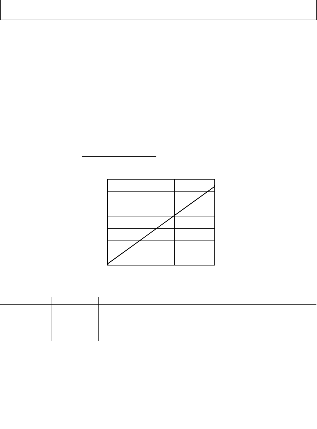
AD9361 Reference Manual UG-570
| Page 83 of 128
AuxADC
The AuxADC is a 12-bit auxiliary converter with an input level
range 0 V to 1.3 V with an adjustable conversion time. The
AuxADC is configured using the ad9361_auxadc_setup
function. The AuxADC allows monitoring of desired voltages
such as a PA power detector or an external temperature sensor.
A small value capacitor (680 pF) may be placed on the
AUXADC pin to improve noise performance. The AD9361 also
includes an internal temperature sensor that can be measured
using the AuxADC. Note that the AuxADC can only be used to
measure either the internal temperature or the voltage on the
AUXADC pin at a time.
Figure 56 shows the AuxADC code vs. input voltage. The
AuxADC is off by default. The AuxADC clock is generated by
dividing the baseband PLL frequency. Equation 21 and
Equation 22 determine the AuxADC clock frequency and the
decimation rates.
The AuxADC output is read from Register 0x1E (D7:D0) and
Register 0x1F (D3:D0). To capture the voltage on the
AUXADC pin, the decimation filter clock should be routed on
the CTRL_OUT0 pin. To select the AuxADC decimation clock
on the CTRL_OUT0 pin write Register 0x35 to Register 0x1E.
Data from Register 0x1E (D7:D0) and Register 0x1F (D3:D0)
can be latched on the falling edge or on the rising edge of
decimation clock coming out of the CTRL_OUT0 pin. The SPI
reads must occur before the edge on the control out signal
toggles again.
The register settings used during the ramp test shown in
Figure 56 are shown in Table 45.
]0:5[1 DividerClockAuxADC
FrequencyBBPLL
FrequencyClockAuxADC
(21)
AuxADC Decimation = 256 × 2AuxADC Decimation[2:0] (22)
Figure 56. AuxADC Code vs. Input Voltage
Table 45. Example Code for AuxADC Set Up
Command Address(hex) Data(hex) Comment
SPI Write 0F 4 Disable temp sensor read back
SPI Write 1C 63 Set the AuxADC clock frequency to BBPLL/36
SPI Write 1D 0 Enable AuxADC and set decimation to 256
SPI Write 35 1E Select AuxADC valid on control out [0]
SPI Write 36 FF Enable all control out pins
1.4
0
0.2
0.4
0.6
0.8
1.0
1.2
0 512 1024 1536 2048 2560 3072 3584 4096
VOLTAGE (V)
AUXDAC CODE (Decimal)
11668-057
Rev. A
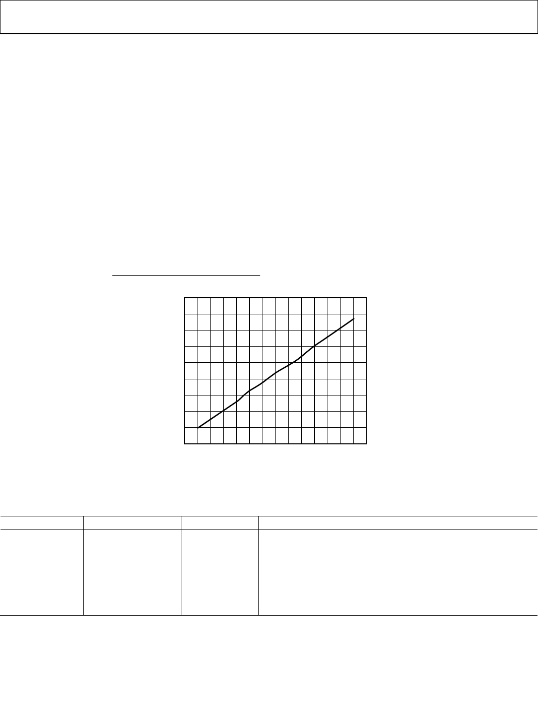
UG-570 AD9361 Reference Manual
| Page 84 of 128
INTERNAL TEMPERATURE SENSOR
The AuxADC can also be used to measure the internal
temperature of the DUT. To measure the temperature sensor,
use the ad9361_auxadc_setup function to configure the part in
temperature sensor mode, and then use the ad9361_get_temp
function to do a reading. The temperature word has a slope of
approximately 1.14 LSB/°C. A single point factory or bench
calibration is required to equate absolute temperature to the
temperature word.
Bits[D2:D0] of Register 0x0F set the decimation rate for
AuxADC in temperature sensor mode per Equation 23.
For temperature measurement, the clock frequency of the
AuxADC is set to the frequency of BBPLL divided by 64.
Bits D7:D1 of Register 0x0D set the rate at which the
temperature sensor periodically takes temperature readings as
per Equation 24. If temperature measurements are to be
performed manually (Bit D0 of Register 0x0D is clear) then the
measurements start when Bit D0 of Register 0x0C (Start Temp
Reading) is set.
Data from register 0x0E can be latched into the baseband
processor on the toggle of the temp sensor valid signal, Bit D1
of Register 0x0C. This signal should be routed out on the
CTRL_OUT1 pin by writing 0x36 to Register 0x03.
Figure 57 shows the temperature sweep of the AD9361 while
reading the internal temperature sensor. Table 46 specifies the
register settings used to generate the internal temperature
sensor graph plotted in Figure 57.
Temp Sensor Decimation = 256 × 2Temp Sensor Decimation[2:0] (23)
)(
2]0:6[
)(
29
HzFrequencyClockBBPLL
IntervalTimetMeasuremen
sTimenCalculatio
(24)
Figure 57. AuxADC Measuring Internal Temp Sensor
Table 46. Example Code for Temperature Sensor Setup
Command Address(hex) Data(hex) Comment
SPI Write B 0 Set the Temp sense offset to 0
SPI Write C F Temp sensor set in manual mode
SPI Write D 0 Calculation time set to 0sec
SPI Write F 0 Set the temp sensor decimation to 256
SPI Write 1D 1 Disable AuxADC pin voltage measurement
SPI Write 35 1E Select Temp sense valid on control out [1]
SPI Write 36 FF Enable all control out pins
180
160
140
120
100
80
60
40
20
0
–50 –30 –10 10 30 50 70 90–40–200 20406080
AUXADC CODE (Decimal)
TEMPERATURE (°C)
11668-058
Rev. A

AD9361 Reference Manual UG-570
| Page 85 of 128
GENERAL PURPOSE OUTPUT CONTROL
The AD9361 has four GPO pins that can be setup using the
ad9361_gpo_setup function. The GPOs commonly control
antenna switches or LNA enable. There are two options for
controlling the GPOs. The manual method uses SPI writes
from the BBP. The automatic method slaves the GPOs to the
enable state machine (ENSM). When using external LNAs, the
AD9361 can optionally slave GPO_0 and GPO_1 off the receive
gain tables to control LNA gain on each of the two receivers.
The supply voltage to the GPOs comes from a pin VDD_GPO
(B8) on the AD9361 with a nominal supply voltage range of
1.3 V to 3.3 V. Setting Bit D4 of Register 0x026 puts the GPOs
in manual control mode. Use the upper nibble (four bits) of
Register 0x027 as the GPO logic level controls. GPO_3 uses D7;
GPO_2 uses D6, GPO_1 uses D5, GPO_0 uses D4. In this
mode, the lower nibble of Register 0x26 is ignored.
GPO Auto Toggle
When initializing the GPOs for ENSM Control the initial states
of the GPOs should be set in the lower nibble of Register 0x27
with GPO_0 corresponding to Bit D0, GPO_1 corresponding to
Bit D1, GPO_2 corresponding to Bit D2 and GPO_3
corresponding to Bit D3. Register 0x20 contains the bits that
determine how the GPOs respond to state changes from Alert.
The upper nibble controls, which GPO pins, will change states
when moving to Rx mode and the lower nibble controls, which
GPO pins, will change states in Tx. For example let Register
0x26 be 0x00 (ENSM control enabled), Register 0x27 be 0xFF
(initialize all GPO pins to 1), and Register 0x20 = 0x24(toggle
the GPO_1 pin in Rx and GPO_2 in Tx). When the part enters
alert state, all GPO pins will become high. When the part enters
Tx, only Pin GPO_2 pin will toggle low. When the part enters
Rx, GPO_1 pin will toggle low. This is a typical scenario for a
T/R switch with differential control.
Some applications have a need to insert a delay between the
DUT state transitions and GPO pin toggles. To accommodate
these needs, there are GPO registers that can be programmed to
the required delay. Register 0x28 through Register 0x2B set the
delay from an ENSM state change of alert to receive while
Register 0x02C through Register 0x02F set the delay from an
ENSM state change from Alert to Transmit. Each LSB is 1 µs.
The delay settings will only work when the TXNRX and
ENABLE pins are used to control the state machine. The delay
settings will not work when SPI is used to control the state
machine. Depending on the reference clock, program Register
0x3A for a resolution of 1 µs/LSB. Set Bits[D6:D0] to the
number of reference clock cycles per µs minus one. In FDD
mode, the Tx enable and Tx delays are applied while the Rx
enable and Rx delays are ignored.
Rev. A
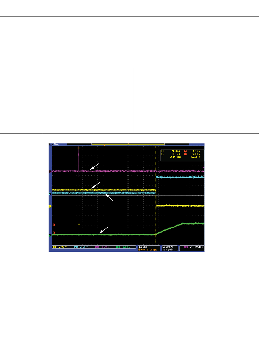
UG-570 AD9361 Reference Manual
| Page 86 of 128
Figure 58 shows the timing of the GPOs and AuxDAC1 based
on the code written in Table 47 when the device transitions
from alert to receive. The pink trace shows when the ENABLE
pin is toggled. Note that after 10 µs, GPO0 (blue trace) and
GPO1 (yellow trace) change states and the AUXDAC (green
trace) starts ramping up to the desired voltage.
GPO Voltage Level, Drive Strength
The VDD_GPO pin (B8) which has a voltage range of 1.3 V to
3.3 V sets the output high logic level of the GPO. The off
resistance of the GPO pins is 15 Ω. The on resistance of the
GPO pins is 32 Ω.
Table 47. Example Code for Auto Toggle Timing of GPO and AuxDAC
Command Address(hex) Data(hex) Comment
SPI Write 27 02 Set all GPOs to 0 except GPO_1
SPI Write 26 0 Set GPO to auto mode
SPI Write 20 10 Set GPO_1 to 0 and GPO_0 to 1 in Rx
SPI Write 29 0A GPO_1 delay 10 µs in Rx
SPI Write 28 0A GPO_0 delay 10 µs in Rx
SPI Write 2C 0A GPO_0 delay 10 µs in Tx
SPI Write 2D 0A GPO_1 delay 10 µs in Tx
SPI Write 1A 1F Vref = 2.5 V, step factor = 1
SPI Write 18 7F AUXDAC Vout ~ 2.2 V
SPI Write 30 A AUXDAC1 delay =10 µs in Rx
Figure 58. GPO/AuxDAC Toggle going from Alert to Rx
GPO0
GPO1
AUXDAC
ENABLE
11668-059
Rev. A
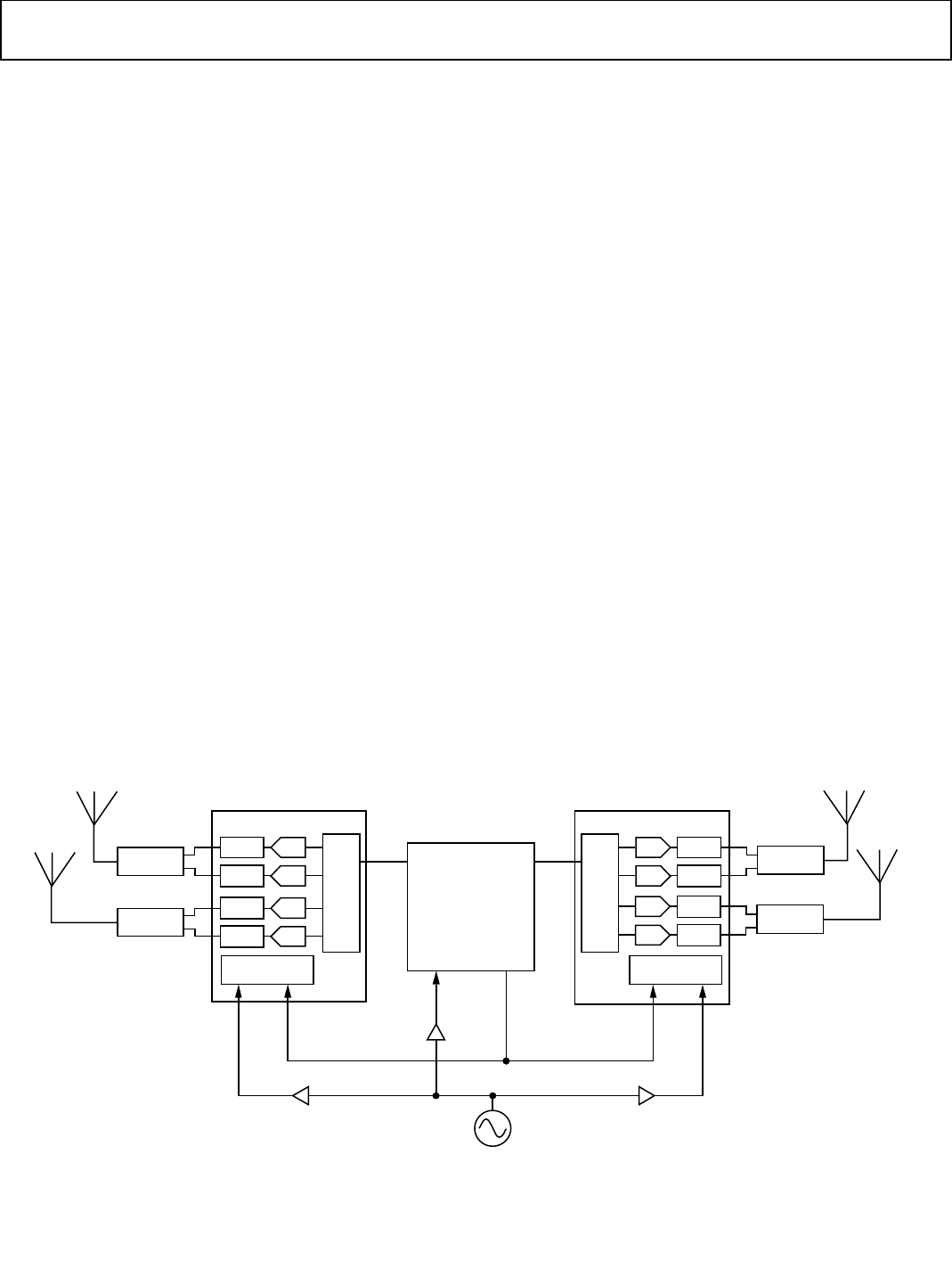
AD9361 Reference Manual UG-570
| Page 87 of 128
BASEBAND SYNCHRONIZATION
OVERVIEW
For broadband wireless access (BWA) systems, multi input-
multi output (MIMO) operation and RF beamforming are
proven techniques for maximizing throughput and efficient
spectrum utilization. Modern integrated devices with
multichannel Rx and multichannel Tx capability such as the
AD9361 make developing MIMO systems with high
performance and linearity utilizing integrated receivers,
transmitters, and synthesizers a simpler task.
Some systems may require more complex configurations that
combine multiple devices. Operating multiple devices while
trying to coordinate data for each channel of each device is not
practical for devices that operate independently without any
mechanism for aligning data timing. Data synchronization into
and out of multiple devices is required to implement such
configurations successfully.
The AD9361 is capable of providing the synchronization
necessary to implement multichannel systems. This device
contains the external control inputs and internal circuitry
needed to synchronize baseband sampling and data clocks,
allowing the system design to utilize multiple devices in parallel
with equivalent performance to a single device.
MULTICHIP SYNCHRONIZATION
The device utilizes a fractional-N synthesizer in the baseband
PLL block to generate the desired sample rate for the system.
This synthesizer generates the ADC sample clock, DAC sample
clock, and baseband digital clocks from any reference clock in
the frequency range specified for the reference clock input. For
MIMO systems requiring more than two input or two output
channels, multiple AD9361 devices and a common reference
oscillator are required. The AD9361 provides the capability to
accept an external reference clock and synchronize operation
with other devices using simple control logic. Each AD9361
includes its own baseband PLL that generates sampling and data
clocks from the reference clock input, so an additional control
mechanism is required to synchronize multiple devices. A
logical SYNC_IN pulse input is needed to align each device’s
data clock with a common reference. Figure 59 illustrates the
connections necessary to synchronize two AD9361 devices. The
oscillator output is buffered into each device using an ADA4851-4
quad high-speed op amp as a clock buffer amplifier. Another
alternative is to use a clock buffer IC like the AD9548 to
distribute a buffered clock to each device while minimizing the
noise coupling between devices. The procedure following
Figure 59 explains how to synchronize two devices, but it
should be noted that additional devices could be connected in
parallel using this procedure. The total number of devices that
can be connected in parallel is limited only by the drive
capability of the clock and logic signals.
Note that this function does not include RF synchronization.
The ability to synchronize RF local oscillators is not available
with this device. Baseband PLL synchronization is the only
alignment among multiple chips that is possible using this
feature. If the MCS RF Enable bit is set then the RF LO dividers
will remain enabled in the alert state. This will allow for the RF
phase relationship between multiple devices to remain constant
throughout operation.
Figure 59. BB Multichip Synchronization Configuration
DUPLEXER DUPLEXER
TX1
RX1
TX1
RX1
DAC DAC
ADC ADC
BB
I/F BB
I/F
BASEBAND
PROCESSOR
REFERENCE
OCILLATOR
ADA4851-4 ADA4851-4
ADA4851-4
BBPLL BBPLL
XTALN XTALN
SYNC_IN SYNC_IN
SYS
CLK BB
SYNC
11668-060
DUPLEXER TX2
RX2
DAC
ADC
DUPLEXER
TX2
RX2
DAC
ADC
Rev. A
UG-570 AD9361 Reference Manual
| Page 88 of 128
PROCEDURE
1. Connect all AD9361 clock inputs to a common buffered
reference using the XTALN pin as shown in Figure 59 for
proper synchronization. (Figure 59 uses the ADA4851-4
configured as a clock buffer amplifier.) In addition, the
electrical length of the trace feeding the reference to each
device must be equivalent to avoid clock skew that could
cause the sync function to fail.
2. After power-up, set each BBPLL to the same frequency by
sending the same frequency command to each device.
3. Determine standard register settings that will generate the
same internal sampling clocks and DATA_CLK outputs
using the customer software and write them to each device.
4. In each device set the MCS BBPLL Enable and MCS BB
Enable bits and then set the MCS refclk Scale En bit. This
enables multichip synchronization (MCS) for the BBPLLs
and references the proper internal clock.
5. Input a rising-edge pulse to the SYNC_IN pin of each
device. The timing requirements of this signal are
illustrated in Figure 60 for the case where the internal
BBPLL REF_CLK is a buffered version of the external
REF_CLK and in Figure 61 for the case where the internal
BBPLL REF_CLK is 2× the external REF_CLK. MCS
cannot be used if the 1/2× or 1/4× options are selected for
the internal BBPLL REF_CLK. Note that the SYNC_IN
pulse rising edge must have a delay from the REF_CLK
input to XTALN to ensure synchronization. This action
synchronizes the BBPLL of each device to the same
reference clock.
6. Once the BBPLLs are synchronized, clear the MCS BBPLL
Enable bit, and set the MCS Digital Clocks Enable bit while
keeping the MCS BB Enable bits set. This enables MCS to
synchronize the digital clock dividers.
7. After this register write, input another rising-edge pulse
simultaneously to the SYNC_IN pin of each device. This
action synchronizes the data clock of each device to the
same reference clock. The timing requirements of this
signal are identical to those for the first SYNC_IN pulse.
The results of this action can be observed by monitoring
the DATA_CLK output of each device and noting their
relative phases before and after the second SYNC_IN pulse
is received.
8. After synchronization is complete, clear the MCS Digital
CLK Enable and MCS BB Enable bits to prevent any
accidental triggering of the synchronization function.
Figure 60. AD9361 BB Multichip Synchronization SYNC_IN Pulse Timing (BBPLL Internal REF_CLK Set to 1×)
Figure 61. AD9361 BB Multichip Synchronization SYNC_IN Pulse Timing (BBPLL internal REF_CLK Set to 2×)
SYNC_IN
REF_CLK
t
CLK
t
OD
t
SC
t
HC
t
OD
t
SC
t
HC
t
PW_SYNC_IN
t
PW_SYNC_IN
PULSE 1
SYNCHRONIZES
BBPLLs
PULSE 2
SYNCHRONIZES
DIGITAL SAMPLING
CLOCKS
t
CLK =
1/f
REF_CLK
OUTPUT DELAY:
t
OD = 1ns MINIMUM
SETUP TIME:
t
SC = 3ns MINIMUM
HOLD TIME:
t
HC = 3ns MINIMUM
SYNC PULSE WIDTH:
t
PW_SYNC_IN
≥
t
CLK
11668-061
SYNC_IN
REF_CLK
t
CLK
t
OD
t
SC
t
HC
t
OD
t
SC
t
HC
t
PW_SYNC_IN
t
PW_SYNC_IN
PULSE 1
SYNCHRONIZES
BBPLLs
PULSE 2
SYNCHRONIZES
DIGITAL SAMPLING
CLOCKS
t
CLK
=
1/f
REF_CLK
OUTPUT DELAY:
t
OD
= 1ns MINIMUM
SETUP TIME:
t
SC
= 3ns MINIMUM*
HOLD TIME:
t
HC
= 3ns MINIMUM*
SYNC PULSE WIDTH:
t
PW_SYNC_IN
≥
t
CLK
*RELATIVE TO RISING AND FALLING EDGE OF REF_CLK.
11668-062
Rev. A
AD9361 Reference Manual UG-570
| Page 89 of 128
SYNCHRONIZATION VERIFICATION
Data synchronization can be verified by observing the
DATA_CLK signal of each chip simultaneously using an
oscilloscope. The waveforms will overlap after successfully
completing the sync procedure. Similarly, the CLK_OUT pin on
each device (when enabled) can be monitored to determine if
the ADC clocks are synchronized. Figure 62 illustrates the
DATA_CLK signals of two devices before and after the second
SYNC_IN pulse occurs. Note that the SYNC_IN pulse is much
longer in duration than the DATA_CLK signals in this example.
As long as the setup and hold times meet the requirements
listed in Figure 60 and Figure 61, this is an acceptable
combination because the SYNC_IN input is edge detected by
the REF_CLK reference.
Figure 62. Clock Signals of AD9361 IC1 and IC2 Before and After Second
SYNC_IN Pulse (Initial Phase Random)
SYNC_IN INPUT PULSE
DATA_CLK BOARD 2
DATA_CLK BOARD 1
11668-063
Rev. A
UG-570 AD9361 Reference Manual
| Page 90 of 128
DIGITAL INTERFACE SPECIFICATION
OVERVIEW
This section defines the parallel data ports and the serial
peripheral interface (SPI) that enable the transfer of data and
control/status information between the AD9361 and a BBP.
Figure 63 illustrates these interfaces as well as provides a high-
level view of how the AD9361 and BBP are used in a broadband
wireless system. The data interface operates in one of two
modes: standard CMOS compatible mode or low-voltage
differential signal (LVDS) compatible mode. Each interface
possesses unique characteristics described in the following
sections.
When CMOS mode is used:
•Single ended-CMOS logic compatibility is maintained.
•Either one or both data ports may be utilized. Using two
ports allows for higher data throughput.
•Both frequency-division duplex (FDD) and time-division
duplex (TDD) operation are supported with one data port
or two.
When LVDS mode is used:
•Data port signaling is differential LVDS, allowing up to
12-inch PCB traces/connector interconnects between the
AD9361 and the BBP.
•Only the data port (including clocking and other
associated timing signals) is LVDS compatible.
•Both FDD and TDD operation are supported.
Figure 63. AD9361 Interface
2
8
12
2
4
12
P1_D[11:0]
12
P0_D[11:0]
2
DATA_CLK
2
FB_CLK
2
RX_FRAME
2
TX_FRAME
TXNRX
ENABLE
EN_AGC
8
CTRL_OUT
4
CTRL_IN
SPI_ENB
SPI_CLK
SPI_DI
SPI_DO
SYNC_IN
XTAL_N
AD9361
RF
FRONT END
BBP
AUX_DAC
TX
RX
TX_MON
GPO
CLK_OUT
XTAL_P
PLL
11668-064
Rev. A

AD9361 Reference Manual UG-570
| Page 91 of 128
CMOS MODE DATA PATH AND CLOCK SIGNALS
This section describes operation of the AD9361 data path in
CMOS mode. In this mode, the AD9361 data path interface can
use either or both parallel data ports to transfer data samples
between the AD9361 and the BBP. The bus transfers are
controlled using simple hardware handshake signaling. The two
ports can be operated in either FDD mode or bidirectional
TDD mode. In FDD mode, half of the bits transmit data and the
other half receive data simultaneously. In TDD mode, the
transmit data and receive data are alternately transferred
between the AD9361 and the BPP on the same pins during
different time slots. For applications that do not require fast
effective data rates, a single port can be used to minimize
connections to the AD9361. The data path interface consists of
the signals described in the following sections.
P0_D[11:0] and P1_D[11:0]
Both Port 0 (P0) and Port 1 (P1) have a 12-bit parallel data bus
(D[11:0]) that transfers data between the BBP and the AD9361.
Each bus is identical to the other in size and function, so
D[11:0] is used to refer to either P0 or P1. These buses can be
configured as transmit-only, receive-only, or bi-directional.
DATA_CLK
The DATA_CLK signal is provided to the BBP as a master clock
for the Rx data path. In CMOS mode, it is generated internally
and output on the DATA_CLK_P pin (DATA_CLK_N is left
unconnected). The same clock is used for P0, P1, or both ports
depending on the data bus configuration. The BBP uses this
master clock as the timing reference for the interface data
transfers and for the baseband data processing. DATA_CLK
provides source-synchronous timing with dual edge capture
(DDR) or single rising-edge capture (SDR) data transfer during
receive operation.
The DATA_CLK frequency generated depends on the system
architecture (such as, number of RF channels, degree of over-
sampling, and bandwidth mode).
FB_CLK
FB_CLK is a feedback (looped-back) version of DATA_CLK
driven from the BBP to the FB_CLK_P pin in CMOS mode
(FB_CLK_N is left unconnected). FB_CLK allows source
synchronous timing with rising edge capture for the burst
control signals (TX_FRAME, ENABLE, and TXNRX). FB_CLK
also provides source synchronous timing with dual edge capture
(DDR) or single rising-edge capture (SDR) for D[11:0] data
signals during Tx bursts (both P0 and P1). Note that FB_CLK
must be a feedback version of DATA_CLK (exact same
frequency and duty cycle), but there is no phase relationship
requirement between the two clock signals.
RX_FRAME
RX_FRAME is driven by the AD9361 to identify valid data for
the Rx data path (both P0 and P1). A high transition indicates
the beginning of the frame. RX_FRAME can be set to be a
single high transition at the beginning of a burst and stay high
throughout the burst, or it can be set to be a pulse train that has
a rising edge at the beginning of each frame (50% duty cycle).
In CMOS mode, this signal is output from the RX_FRAME_P
pin (RX_FRAME_N can be left unconnected).
TX_FRAME
TX_FRAME is driven by the BBP to identify valid data for the
Tx data path (both P0 and P1). A high transition indicates the
beginning of the frame. The BBP can set TX_FRAME to be a
single high transition at the beginning of a burst that stays high
throughout the burst, or it can set TX_FRAME to a pulse train
that has a rising edge at the beginning of each frame (50% duty
cycle). The AD9361 accepts either format. In CMOS mode, this
signal is input to the TX_FRAME_P pin (TX_FRAME_N is tied
to ground).
The AD9361 transmits null data (all zeros) until the first
TX_FRAME indicates valid data. This is a useful feature when
the Tx path completes a transmit operation in FDD
independent mode and the data path is not automatically
flushed. In this case, the TX_FRAME pin can be held low to
complete the data flushing operation. See the Enable State
Machine Guide section for more details.
Note that the interface requires both RX_FRAME and
TX_FRAME signals to function properly.
Rev. A
UG-570 AD9361 Reference Manual
| Page 92 of 128
ENABLE
ENABLE is driven from the BBP to the AD9361 to provide data
transfer burst control (along with TXNRX) in TDD mode.
ENABLE is asserted by the BBP for a minimum of a single
DATA_CLK cycle to indicate the start of each burst. It is
subsequently asserted a second time for a minimum of a single
DATA_CLK cycle to indicate the end of each burst.
The AD9361 internally tracks the sequence of ENABLE pulses
to interpret each pulse correctly as either the start or finish of
each burst. The ENABLE signal also can be configured in level
mode, in which an edge transition (not pulses) determines
when the ENSM moves between states. The level sampled on
TXNRX during each ENABLE start event controls the bus
direction in TDD mode. The start and finish latencies (between
the ENABLE pulses being sampled by the AD9361 and the
presence of the first and last valid data samples on the bus) vary
depending on data path configuration. The RX_FRAME and
TX_FRAME signals are used to determine valid data by the
BBP and the AD9361, respectively. The FB_CLK signal is used
to sample this input.
In FDD mode, the ENABLE signal serves as the single control
input to determine the state of the ENSM. There is also an
alternative FDD mode in which the ENABLE signal can be
redefined as RxON, a direct hardware control input to the
ENSM that controls the Rx function. In this mode (called FDD
independent control mode), the BBP independently controls
the Rx function, which can result in power consumption
savings.
TXNRX
TXNRX is driven from the BBP to the AD9361 and provides
data transfer burst control (along with ENABLE) when the data
bus is in TDD mode. When ENABLE is sampled high by the
AD9361 to start a burst, the level on TXNRX is also sampled to
determine the data direction. In TDD mode, TXNRX sampled
high indicates a transmit burst and TXNRX sampled low
indicates a receive burst.
The TXNRX signal level must be maintained throughout a data
transfer burst (a valid logic level). The TXNRX signal may be
established any number of cycles (≥ 0) before the ENABLE start
pulse is sampled, and it may be changed any number of cycles
(≥ 0) after the ENABLE finish pulse is sampled. It is important
to note that the TXNRX signal should only change state while
the ENSM is in the ALERT state because the TXNRX signal
powers up and down the synthesizers directly in TDD mode.
In normal FDD mode, the TXNRX signal is ignored but must
be held at a valid logic level. There is also an alternative FDD
mode in which the TXNRX signal can be redefined as TxON, a
direct hardware control input to the ENSM that controls the Tx
function. In this mode (called FDD independent control mode),
the BBP independently controls the Tx function, which can
result in power consumption savings.
CMOS MAXIMUM CLOCK RATES AND SIGNAL
BANDWIDTHS
The data listed in Table 48 compares the maximum data clock
rates and maximum RF signal bandwidths in the different
allowable operating modes for the CMOS data bus
configuration. Maximum RF bandwidths are listed for two
cases: sampling using the minimum sample rate that avoids
aliasing, and sampling using 2× oversampling. Details of each
mode are given in subsequent sections. The maximum
DATA_CLK rate is limited to 61.44 MHz, so the data rates are
limited by this factor and the 56 MHz maximum analog filter
bandwidth.
Table 48. Maximum Data Rates (SDR and DDR) and Signal Bandwidths
Operating
Mode
1R1T Configurations 1R2T/2R1T/2R2T Configurations
Maximum Data Rate
(Combined I and Q
Words)
Maximum RF Channel Signal
Bandwidth Maximum Data Rate
(Combined I and Q
Words)
Maximum RF Channel Signal
Bandwidth (Per Channel)
Using Minimum
Sample Frequency
Using 2×
Oversampling
Using Minimum
Sample Frequency
Using 2×
Oversampling
SDR
(MSPS)
DDR
(MSPS)
SDR
Bus
(MHz)
DDR
Bus
(MHz)
SDR
Bus
(MHz)
DDR
Bus
(MHz)
SDR
(MSPS)
DDR
(MSPS)
SDR
Bus
(MHz)
DDR
Bus
(MHz)
SDR
Bus
(MHz)
DDR
Bus
(MHz)
Single Port
Half Duplex
30.72 61.44 30.72
561 15.36 30.72 15.36 30.72 15.36 30.72 7.68 15.36
Single Port
Full Duplex
15.36 30.72 15.36 30.72 7.68 15.36 7.68 15.36 7.68 15.36 3.84 7.68
Dual Port
Half Duplex
61.44 122.88 561 561 30.72 561 30.72 61.44 30.72
561 15.36 30.72
Dual Port Full
Duplex
30.72 61.44 30.72
561 15.36 30.72 15.36 30.72 15.36 30.72 7.68 15.36
1 Limited by the analog filter bandwidth.
Rev. A
AD9361 Reference Manual UG-570
| Page 93 of 128
SINGLE PORT HALF DUPLEX MODE (CMOS)
Single port half duplex mode is used in applications requiring
TDD operation and data rates less than 61.44 MHz. In this
mode, the bus is utilized in a bidirectional manner so that data
can be received or transmitted on the same lines. This mode can
be used with all receiver-transmitter configurations (1R1T,
2R1T, 1R2T, and 2R2T) and is typically employed when there is
limited PCB space or the BBP has only a single data bus port
available. The bus can be operated as either single data rate
(SDR) or dual data rate (DDR) in this configuration. In this
mode, the enabled port is multiplexed between transmit and
receive operation while the unused port is disabled. The
enabled port is determined by the Swap Ports bit in SPI register
0x012. Figure 64 illustrates the connections between the
AD9361 and the BBP for this mode of operation.
During an Rx burst, D[11:0] is driven by the AD9361 such that
the setup and hold times between DATA_CLK and D[11:0]
arriving allow the BBP to use DATA_CLK to capture the data.
Similarly, during a Tx burst, D[11:0] is driven by the BBP such
that the setup and hold times between FB_CLK and D[11:0]
allow the AD9361 to use FB_CLK to capture the data. A data
transfer starts when the ENABLE signal pulses (or goes high),
and the end of the data transfer is marked but another pulse on
the ENABLE line (or when it returns low). The direction of data
transfer is determined by the TXNRX signal. When this signal
is low and the ENSM is in the Rx or FDD state, the bus is
configured in the receive direction (data transferred from
AD9361 to BBP). When TXNRX is driven high and the ENSM
has moved out of the Rx or FDD state, the ENSM changes the
bus to the transmit direction (data transferred from BBP to
AD9361).
The Rx_FRAME and Tx_FRAME signals indicate the
beginning of a set (frame) of data samples. The Rx_FRAME
can be set to occur once at the beginning of the burst (one high
transition only) for each data transfer or to have a rising edge at
the beginning of each frame and repeat with a 50% duty cycle
until the data transfer is complete. Similarly, Tx_FRAME
accepts either format from the BBP.
During a transmit burst, the BBP drives the data values on
P0_D[11:0] using FB_CLK and Tx_FRAME. During a Rx
burst, the AD9361 drives the data values on P0_D[11:0] using
DATA_CLK and Rx_FRAME.
Figure 64. Single Port TDD Mode Bus Configuration
DATA_CLK
RX_FRAME
P0_D[11:0]
TX_FRAME
FB_CLK
TXNRX
ENABLE
RX
DATA RX
DATA
TX
DATA TX
DATA
CTRL CTRL
PLL
FEEDBACK
CLK GEN
AD9361
BBP
11668-065
Rev. A

UG-570 AD9361 Reference Manual
| Page 94 of 128
The data samples are carried in two’s complement format, with
D[11] as the numerically most significant bit and D[0] as the
least significant bit. In other words, the most positive sample
value is 0x7FF and the most negative value is 0x800. In this
mode, the I and Q data samples are time-interleaved on the data
bus. For a single RF path in each direction (a 1R1T system), the
I and Q samples are carried in a 2-way interleave:
I, Q, I, Q, …
For a system utilizing two Rx/Tx channels, the I and Q samples
from RF channels 1 and 2 are carried in a 4-way interleave:
I1, Q1, I2, Q2, I1, Q1, I2, Q2, …
For a system with a 2R1T or 1R2T configuration, the clock
frequencies, sample periods, and data capture timing are the
same as if configured for a 2R2T system. However, in the path
with only a single channel used, the disabled channel’s I-Q pair
in each data group is unused. These unused slots are ignored by
the AD9361. For example, in a 2R1T system with only Tx
Channel 1 used, the transmit burst would have two unused
slots, as follows:
I, Q, X, X, I, Q, X, X, …
The unused X slots may be filled with arbitrary data values by
the BBP. Such values can be fixed constant values, or the
preceding data sample values can be repeated to reduce the bus-
switching factor and; therefore, power consumption.
SINGLE PORT TDD FUNCTIONAL TIMING (CMOS)
The timing diagrams in Figure 65 and Figure 66 illustrate the
relationship among the bus signals in single port TDD mode.
These diagrams show an example of timing for both SDR and
DDR modes of operation. For all subsequent sections in this
section, only DDR timing will be shown. Figure 65 and
Figure 66 also include the timing diagrams for the 1R1T
scenario where the 2R2T Timing bit is set, forcing the data
transfer format to be the same as the 2R2T case. This mode is
useful for single port systems that may need to switch between
single channel and multichannel operation but cannot change
their data transfer format. The 2R2T bit has no effect if the
device is not configured 1R1T mode.
Note that the Tx_FRAME and Tx data must be transmitted
such that they meet the setup and hold requirements relative to
FB_CLK. In addition to the 1R1T and 2R2T scenarios, 1R2T
and 2R1T configurations are shown to illustrate that their
timing is identical to the 2R2T configuration. Behavior with
different combinations of receiver and transmitter channels in
other modes also follows the 2R2T timing behavior, so for all
subsequent sections these plots are omitted from the figures.
Rev. A
AD9361 Reference Manual UG-570
| Page 95 of 128
Figure 65. Receiver Data Path, Single Port TDD (DNC = Do Not Care)
DATA _CLK
RX _FRAME
P0_D[11:0]
P1_D[11:0]
DATA _CLK
RX _FRAME
P0_D[11:0]
P1_D[11:0]
DNC DNC DNC DNC DNC DNC
DATA _CLK
RX _FRAME
P0_D[11:0]
P1_D[11:0]
DATA _CLK
RX _FRAME
P0_D[11:0]
P1_D[11:0]
DATA _CLK
RX _FRAME
P0_D[11:0]
P1_D[11:0]
R1_I[11:0] R1_Q[11:0] R2_I[11:0] R2_Q[11:0] R1_I[11:0] R1_Q[11:0] R2_I[11:0] R2_Q[11:0] R1_I[11:0] R1_Q[11:0] R2_I[11:0]
R2_Q[11:0]
2R2T, DDR, TDD, SINGLE PORT, 0x010 = 0xC8, 0x011 = 0x00, 0x012 = 0x0C
2R2T, DDR, TDD, SINGLE PORT, 0x010 = 0xC8, 0x011 = 0x00, 0x012 = 0x0C
R1_I[11:0] R1_Q[11:0] R1_I[11:0] R1_Q[11:0] R1_I[11:0] R1_Q[11:0]
DNC DNC DNC DNC DNC DNC
R1_I[11:0] R1_Q[11:0] R1_I[11:0] R1_Q[11:0] R1_I[11:0] R1_Q[11:0]
R1_I[11:0] R1_Q[11:0] R1_I[11:0] R1_Q[11:0] R1_I[11:0] R1_Q[11:0]
R1_I[11:0] R1_Q[11:0] R1_I[11:0] R1_Q[11:0] R1_I[11:0] R1_Q[11:0]
1R2T, DDR, TDD, SINGLE PORT, 0x010 = 0xC8, 0x011 = 0x00, 0x012 = 0x0C
1R1T, DDR, TDD, SINGLE PORT, 0x010 = 0xC8, 0x011 = 0x00, 0x012 = 0x0C
1R1T, DDR, TDD, SINGLE PORT, 0x010 = 0xC8, 0x011 = 0x00, 0x012 = 0x2C
11668-066
Rev. A
UG-570 AD9361 Reference Manual
| Page 96 of 128
Figure 66. Transmitter Data Path, Single Port TDD (DNC = Do Not Care)
TX _FRAME
P0_D[11:0]
P1_D[11:0]
TX _FRAME
P0_D[11:0]
P1_D[11:0]
DNC DNC DNC DNC DNC DNC
TX _FRAME
P0_D[11:0]
P1_D[11:0]
TX _FRAME
P0_D[11:0]
P1_D[11:0]
FB_CLK
TX _FRAME
P0_D[11:0]
P1_D[11:0]
T1_I[11:0] T1_Q[11:0] T2_I[11:0] T2_Q[11:0] T1_I[11:0] T1_Q[11:0] T2_I[11:0] T2_Q[11:0] T1_I[11:0] T1_Q[11:0] T2_I[11:0]
T2_Q[11:0]
2R2T, DDR, TDD, SINGLE PORT, 0x010 = 0xC8, 0x011 = 0x00, 0x012 = 0x0C
2R2T, DDR, TDD, SINGLE PORT, 0x010 = 0xC8, 0x011 = 0x00, 0x012 = 0x0C
T1_I[11:0] T1_Q[11:0] T1_I[11:0] T1_Q[11:0] T1_I[11:0] T1_Q[11:0]
DNC DNC DNC DNC DNC DNC
T1_I[11:0] T1_Q[11:0] T1_I[11:0] T1_Q[11:0] T1_I[11:0] T1_Q[11:0]
T1_I[11:0] T1_Q[11:0] T1_I[11:0] T1_Q[11:0] T1_I[11:0] T1_Q[11:0]
T1_I[11:0] T1_Q[11:0] T1_I[11:0] T1_Q[11:0] T1_I[11:0] T1_Q[11:0]
1R2T, DDR, TDD, SINGLE PORT, 0x010 = 0xC8, 0x011 = 0x00, 0x012 = 0x0C
1R1T, DDR, TDD, SINGLE PORT, 0x010 = 0xC8, 0x011 = 0x00, 0x012 = 0x0C
1R1T, DDR, TDD, SINGLE PORT, 0x010 = 0xC8, 0x011 = 0x00, 0x012 = 0x2C
11668-067
FB_CLK
FB_CLK
FB_CLK
0
0
0
0
0
FB_CLK
0
0
0
0
0
Rev. A

AD9361 Reference Manual UG-570
| Page 97 of 128
SINGLE PORT FULL DUPLEX MODE (CMOS)
Single port full duplex mode is used in applications requiring
FDD operation and data rates less than 30.72 MHz. In this
mode, the bus is split in half with six bits dedicated to Rx data
and six bits dedicated to Tx data. This mode can be used with
all receiver-transmitter configurations. The bus can be operated
as either SDR or DDR in this configuration. In this example,
only P0 is enabled and the data bus is split into separate subbuses.
Each sub-bus operates simultaneously allowing full duplex of
transmit and receive data between the BBP and the AD9361.
Because the bus must complete twice as many data transfers for
full duplex mode, the data bus must operate at twice the speed
of the TDD mode to achieve the same transmit and receive data
rates (as each are running concurrently in full duplex).
Figure 67 illustrates the connections between the AD9361 and
the BBP for this mode of operation.
Transmit data is driven on P0_D[11:6] by the BBP such that the
setup and hold times between FB_CLK and P0_D[11:6] allow
the AD9361 to use FB_CLK to capture the data. Receive data is
driven on P0_D[5:0] by the AD9361 such that the setup and
hold times between DATA_CLK and P0_D[5:0] arriving at the
BBP enable the BBP to use DATA_CLK to capture the data. A
pulse on the ENABLE pin (or a rising edge) triggers the
beginning of data transfer, and another pulse (or falling edge)
signifies the end of data transfer.
The Rx_FRAME and Tx_FRAME signals indicate the
beginning of a set (frame) of data samples. The Rx_FRAME
signal can be set to occur once at the beginning of the burst
(one high transition only) for each data transfer or to have a
rising edge at the beginning of each frame and repeat with a
50% duty cycle until the data transfer is complete. Similarly,
Tx_FRAME accepts either format from the BBP.
The transmit data samples are carried in two’s complement
format, with the first 6-bit byte (P0_D[11:6]) containing the
MSBs and the second 6-bit byte (P0_D[11:6]) containing the
LSBs. P0_D[11] is the numerically most significant bit and
P0_D[6] is the least significant bit. The receive data samples are
also carried in two’s complement format, with the first 6-bit byte
(P0_D[5:0]) containing the MSB’s and the second 6-bit byte
(P0_D[5:0]) containing the LSB’s. P0_D[5] is the numerically
most significant bit and P0_D[0] is the least significant bit. In
both cases, the most positive sample value is 0x7FF, with the
first byte being 0x1F and the second byte being 0x3F. The most
negative value is 0x800, with the first byte being 0x20 and the
second byte being 0x00.
In this mode, the I and Q data samples are time-interleaved on
the data bus. For a single RF path in each direction (a 1R1T
system), the data is carried in a 4-way interleave, as follows:
IMSB, QMSB, ILSB, QLSB, …
For a system with two active Rx/Tx channels, the I and Q
samples from RF Channel 1 and Channel 2 are carried in an
8-way interleave, as follows:
I1 MSB, Q1 MSB, I1 LSB, Q1 LSB, I2 MSB, Q2 MSB, I2 LSB, Q2 LSB, …
For a system with a 2R1T or a 1R2T configuration, the clock
frequencies, sample periods, and data capture timing are the
same as if configured for a 2R2T system. However, in the path
with only a single channel used, the disabled channel’s I-Q pair
in each data group is unused. These unused slots are ignored by
the AD9361. As an example, for a 2R1T system using Transmit
Channel 1, the transmit burst would have four unused slots, as
follows:
I1 MSB, Q1 MSB, I1 LSB, Q1 LSB, X, X, X, X, …
The unused X slots can be filled with arbitrary data values by
the BBP. Such values can be constant values, or the preceding
data sample values can be repeated to reduce the bus-switching
factor and, therefore, power consumption.
Rev. A
UG-570 AD9361 Reference Manual
| Page 98 of 128
Figure 67. Single Port Full Duplex Mode
DATA_CLK
RX_FRAME
P0_D[11:6]
FB_CLK
TXNRX
ENABLE
RX
DATA RX
DATA
TX
DATA TX
DATA
CTRL CTRL
PLL
FEEDBACK
CLK GEN
AD9361
BBP
TX_FRAME
P0_D[5:0]
11668-068
Rev. A
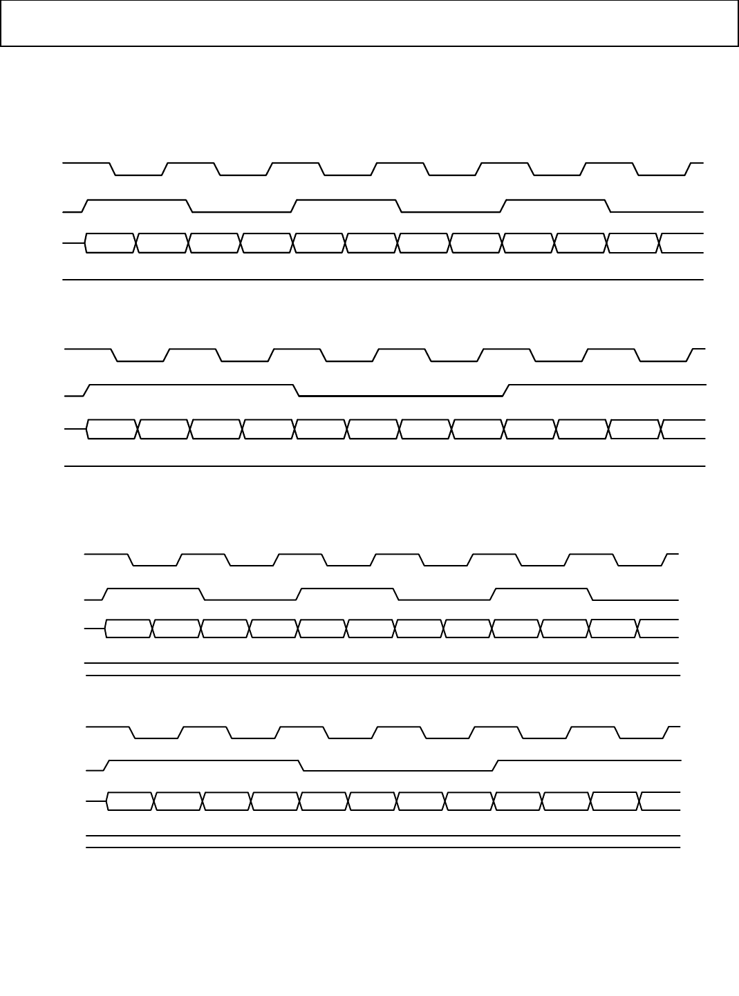
AD9361 Reference Manual UG-570
| Page 99 of 128
SINGLE PORT FDD FUNCTIONAL TIMING (CMOS)
The timing diagrams in Figure 68 and Figure 69 illustrate the relationship among the bus signals in single port FDD mode. Note that
because 2R1T and 1R2T systems follow the 2R2T timing diagrams, they are omitted from Figure 68 and Figure 69.
Figure 68. Receive Data Path, Single Port FDD
Figure 69. Transmit Data Path, Single Port FDD
DATA_CLK
RX_FRAME
P0_D[5:0]
P1_D[5:0]
R1_I[11:6] R1_Q[11:6] R1_I[5:0] R1_I[5:0] R1_I[11:6] R1_Q[11:6] R1_I[5:0] R1_I[5:0] R1_I[11:6] R1_Q[11:6] R1_I[5:0] R1_I[5:0]
1R1T, DDR, FDD, SINGLE PORT, 0x010 = 0xC8, 0x011 = 0x00, 0x012 = 0x04
11668-069
DATA_CLK
RX_FRAME
P0_D[5:0]
P1_D[5:0]
R1_I[11:6] R1_Q[11:6] R1_I[5:0] R1_I[5:0] R1_I[11:6] R1_Q[11:6] R1_I[5:0] R1_I[5:0] R1_I[11:6] R1_Q[11:6] R1_I[5:0] R1_I[5:0]
2R2T, DDR, FDD, SINGLE PORT, 0x010 = 0xC8, 0x011 = 0x00, 0x012 = 0x04
FB_CLK
TX_FRAME
P0_D[11:6]
P1_D[11:6]
T1_I[11:6] T1_Q[11:6] T1_I[5:0] T1_I[5:0] T1_I[11:6] T1_Q[11:6] T1_I[5:0] T1_I[5:0] T1_I[11:6] T1_Q[11:6] T1_I[5:0] T1_I[5:0]
1R1T, DDR, FDD, SINGLE PORT, 0x010 = 0xC8, 0x011 = 0x00, 0x012 = 0x04
11668-070
FB_CLK
TX_FRAME
P0_D[11:6]
P1_D[11:6]
T1_I[11:6] T1_Q[11:6] T1_I[5:0] T1_I[5:0] T1_I[11:6] T1_Q[11:6] T1_I[5:0] T1_I[5:0] T1_I[11:6] T1_Q[11:6] T1_I[5:0] T1_I[5:0]
2R2T, DDR, FDD, SINGLE PORT, 0x010 = 0xC8, 0x011 = 0x00, 0x012 = 0x04
0
0
Rev. A
UG-570 AD9361 Reference Manual
| Page 100 of 128
DUAL PORT HALF DUPLEX MODE (CMOS)
Dual port half duplex mode is used in applications requiring
TDD operation and data rates up to 122.88 MHz. In this mode,
both data ports are utilized, with P0 assigned to I data and P1
assigned to Q data. The ports operate bidirectionally in this
mode, and data direction is determined by which channel is
active: transmit or receive. Each bus can be operated as either
SDR or DDR in this configuration. This mode can be used with
all receiver-transmitter configurations. Figure 70 illustrates the
connections between the AD9361 and the BBP for this mode of
operation.
During an Rx burst, both ports are driven by the AD9361 such
that the setup and hold times between DATA_CLK and each
data sample arriving at the BBP enable the BBP to use
DATA_CLK to capture the data. A data transfer starts when the
ENABLE signal pulses (or goes high), and the end of the data
transfer is marked but another pulse on the ENABLE line (or
when it returns low).
The direction of data transfer is determined by the TXNRX
signal. When this signal is low and the AD9361 is in the FDD
state or the Rx state, the ENSM configures the bus in the receive
direction (data transferred from AD9361 to BBP). All other
states result in the bus being set to high impedance. When
TXNRX is driven high, the ENSM changes the bus to the
transmit direction (data transferred from BBP to AD9361).
During a transmit burst, both ports (P0_D[11:0] and
P1_D[11:0]) are driven by the BBP such that the setup and hold
times between FB_CLK and each D[11:0] allow the AD9361 to
use FB_CLK to capture the data.
The Rx_FRAME and Tx_FRAME signals indicate the
beginning of a set (frame) of data samples. The Rx_FRAME
signal can be set to occur once at the beginning of the burst
(one high transition only) or to have a rising edge at the
beginning of each frame and have a 50% duty cycle. Similarly,
Tx_FRAME accepts either format from the BBP.
Figure 70. Dual Port TDD Mode
DATA_CLK
RX_FRAME
P0_D[11:0]
TX_FRAME
FB_CLK
TXNRX
ENABLE
RX
DATA RX
DATA
TX
DATA TX
DATA
CTRL CTRL
PLL
FEEDBACK
CLK GEN
AD9361
BBP
P1_D[11:0]
11668-072
Rev. A
AD9361 Reference Manual UG-570
| Page 101 of 128
The data samples are carried in two’s complement format, with
D[11] as the numerically most significant bit and D[0] as the
least significant bit. The most positive sample value is 0x7FF
and the most negative value is 0x800. For a single RF path in
each direction (that is, a 1R1T system), the I and Q samples are
separated with I data on P0_D[11:0] and Q data on P1_D[11:0]
as follows:
P0: I, I, I, …
P1: Q, Q, Q, …
For a system with two active Rx channels, the I and Q samples
from RF Path 1 and RF Path 2 are carried in a 2-way interleave
with I samples on P0 and Q samples on P1.
P0: I1, I2, I1, I2, …
P1: Q1, Q2, Q1, Q2, …
For a system with a 2R1T or a 1R2T configuration, the clock
frequencies, sample periods, and data capture timing are the
same as if configured for a 2R2T system. However, in the path
with only a single channel used, the disabled channel’s I-Q pair
in each data group is unused. As an example, for a 2R1T system
with only the Tx Channel 1 used, the Tx burst would have two
unused slots, as follows:
The AD9361 captures P0: I1, X, I1, X , …
P1: Q1, X, Q1, X , …
The unused X slots can be filled with arbitrary data values by
the BBP. Such values can be either constant values, or the
preceding data sample values can be repeated to reduce the bus
switching factor and, therefore, power consumption.
DUAL PORT TDD FUNCTIONAL TIMING (CMOS)
The timing diagrams in Figure 71 and Figure 72 illustrate the
relationship among the bus signals in dual port TDD mode.
Note that because 2R1T and 1R2T systems follow the 2R2T
timing diagrams, they are omitted from these Figure 71 and
Figure 72.
Figure 71. Receiver Data Path, Dual Port TDD
DATA _CLK
RX_FRAME
P0_D[11:0]
P1_D[11:0]
1R1T, DDR, TDD, DUAL PORT, 0x010 = 0xC8, 0x011 = 0x00, 0x012 = 0x08
R1_I[11:0] R1_I[11:0] R1_I[11:0] R1_I[11:0] R1_I[11:0] R1_I[11:0]
R1_Q[11:0] R1_Q[11:0] R1_Q[11:0] R1_Q[11:0] R1_Q[11:0] R1_Q[11:0]
11668-073
DATA _CLK
RX_FRAME
P0_D[11:0]
P1_D[11:0]
2R2T, DDR, TDD, DUAL PORT, 0x010 = 0xC8, 0x011 = 0x00, 0x012 = 0x08
R1_I[11:0] R2_I[11:0] R1_I[11:0] R2_I[11:0] R1_I[11:0] R2_I[11:0]
R1_Q[11:0] R2_Q[11:0] R1_Q[11:0] R2_Q[11:0] R1_Q[11:0] R2_Q[11:0]
Rev. A
UG-570 AD9361 Reference Manual
| Page 102 of 128
Figure 72. Transmitter Data Path, Dual Port TDD
FB_CLK
TX_FRAME
P0_D[11:0]
P1_D[11:0]
1R1T, DDR, TDD, DUAL PORT, 0x010 = 0xC8, 0x011 = 0x00, 0x012 = 0x08
T1_I[11:0] T1_I[11:0] T1_I[11:0] T1_I[11:0] T1_I[11:0] T1_I[11:0]
T1_Q[11:0] T1_Q[11:0] T1_Q[11:0] T1_Q[11:0] T1_Q[11:0] T1_Q[11:0]
11668-272
FB_CLK
TX_FRAME
P0_D[11:0]
P1_D[11:0]
2R2T, DDR, TDD, DUAL PORT, 0x010 = 0xC8, 0x011 = 0x00, 0x012 = 0x08
T1_I[11:0] T2_I[11:0] T1_I[11:0] T2_I[11:0] T1_I[11:0] T2_I[11:0]
T1_Q[11:0] T2_Q[11:0] T1_Q[11:0] T2_Q[11:0] T1_Q[11:0] T2_Q[11:0]
0
0
0
0
Rev. A
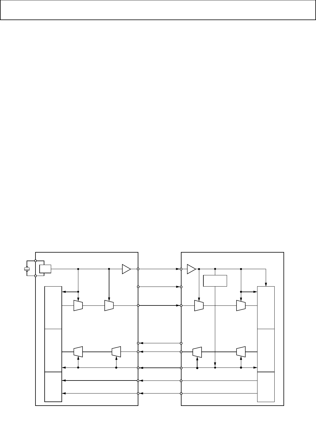
AD9361 Reference Manual UG-570
| Page 103 of 128
DUAL PORT FULL DUPLEX MODE (CMOS)
Dual port full duplex mode (full port) is used in applications
requiring FDD operation and data rates less than 61.44 MHz. In
this mode, both data ports are utilized, with P0 assigned to
receive data and P1 assigned to transmit data. Each bus operates
simultaneously, allowing full duplex transfer of Tx and Rx data
between the BBP and the AD9361. For this mode, each data bus
must operate at twice the speed of the dual port TDD mode to
achieve the same Tx and Rx data rates (as each are running
concurrently in full duplex). Each bus can be operated as either
SDR or DDR in this configuration. This mode can be used with
all receiver-transmitter configurations. Figure 73 illustrates the
connections between the AD9361 and the BBP for this mode of
operation.
Transmit data is driven on P1_D[11:0] by the BBP such that the
setup and hold times between FB_CLK and data allow the
AD9361 to use FB_CLK to capture the data. Receive data is
driven on P0_D[11:0] by the AD9361 such that the setup and
hold times between DATA_CLK and data arriving at the BBP
enable the BBP to use DATA_CLK to capture the data. A pulse
on the ENABLE pin (or a rising edge) triggers the beginning of
data transfer, and another pulse (or falling edge) signifies the
end of data transfer.
The Rx_FRAME and Tx_FRAME signals indicate the
beginning of a set (frame) of data samples. Rx_FRAME can be
set to occur once at the beginning of the burst (one high
transition only) for each data transfer, or it can be set to have a
rising edge at the beginning of each frame and repeat with a
50% duty cycle until the data transfer is complete. Similarly,
Tx_FRAME accepts either format from the BBP.
The Tx data samples are carried in two’s complement format.
P1_D[11] is the numerically most significant bit and P1_D[0] is
the least significant bit. The Rx data samples are also carried in
two’s complement format. P0_D[11] is the numerically most
significant bit and P0_D[0] is the least significant bit. In both
cases, the most positive sample value is 0x7FF and the most
negative value is 0x800.
The I and Q data samples are carried on the same data bus in
each direction. For a single RF path in each direction, the data
is carried as follows:
Px: I, Q, I, Q, I, Q, …
For a system with two Rx/Tx channels, the I and Q samples
from RF channels 1 and 2 are carried as follows:
Px: I1, Q1, I2, Q2, …
For a system with a 2R1T or a 1R2T configuration, the clock
frequencies, sample periods, and data capture timing are the
same as when configured for a 2R2T system. However, in the
path with only a single channel used, the disabled channel’s I-Q
pair in each data group is unused. These unused slots are
ignored by the AD9361. For example, for a 2R1T system using
Tx channel 1, the Tx burst would have two unused slots, as
follows:
The AD9361 captures P1: I1, Q1, X, X, …
The unused X slots may be filled with arbitrary data values by
the BBP. Such values could be either constant values, or the
preceding data sample values can be repeated to reduce the bus
switching factor and, therefore, power consumption.
Figure 73. Dual Port Full Duplex Mode (Full Port)
DATA_CLK
RX_FRAME
P1_D[11:0]
FB_CLK
TXNRX
ENABLE
RX
DATA RX
DATA
TX
DATA TX
DATA
CTRL CTRL
PLL
FEEDBACK
CLK GEN
AD9361
BBP
TX_FRAME
P0_D[11:0]
11668-074
Rev. A
UG-570 AD9361 Reference Manual
| Page 104 of 128
DUAL PORT FDD FUNCTIONAL TIMING (CMOS)
The timing diagrams in Figure 74 and Figure 75 illustrate the relationship among the bus signals in dual port full duplex mode. Note that
because 2R1T and 1R2T systems follow the 2R2T timing diagrams, they are omitted from Figure 74 and Figure 75.
Figure 74. Receiver Data Path, Dual Port FDD (Full Port)
Figure 75. Transmit Data Path, Dual Port FDD (Full Port)
DATA _CLK
RX _FRAME
P 0_D [11 :0]
DATA _CLK
RX _FRAME
P 0_D [11 :0]
1R1T, DDR, FDD, DUAL PORT, 0X010 = 0XC8, 0X011 = 0X00, 0X012 = 0X02
2R2T, DDR, FDD, DUAL PORT, 0X010 = 0XC8, 0X011 = 0X00, 0X012 = 0X02
R1_I[11:0] R1_Q[11:0] R1_I[11:0] R1_Q[11:0] R1_I[11:0] R1_Q[11:0]
R1_I[11:0] R1_Q[11:0] R1_I[11:0] R1_Q[11:0] R1_I[11:0] R1_Q[11:0] R1_I[11:0] R1_Q[11:0] R1_I[11:0] R1_Q[11:0] R1_I[11:0] R1_Q[11:0]
11668-075
FB _CLK
TX_FRAME
P0 _D [11 :0]
FB _CLK
TX_FRAME
P0 _D [11 :0]
1R1T, DDR, FDD, DUAL PORT, 0X010 = 0XC8, 0X011 = 0X00, 0X012 = 0X02
2R2T, DDR, FDD, DUAL PORT, 0X010 = 0XC8, 0X011 = 0X00, 0X012 = 0X02
T1_I[11:0] T1_Q[11:0] T1_I[11:0] T1_Q[11:0] T1_I[11:0] T1_Q[11:0]
T1_I[11:0] T1_Q[11:0] T1_I[11:0] T1_Q[11:0] T1_I[11:0] T1_Q[11:0] T1_I[11:0] T1_Q[11:0] T1_I[11:0] T1_Q[11:0] T1_I[11:0] T1_Q[11:0]
11668-076
0
0
Rev. A
AD9361 Reference Manual UG-570
| Page 105 of 128
DATA BUS IDLE AND TURNAROUND PERIODS
(CMOS)
The P0_D[11:0] and P1_D[11:0] bus signals are usually actively
driven by the BBP or by the AD9361. During any idle periods,
the data bus values are ignored by both components. Both
ports, however, must have valid logic levels even if they are
unused.
DATA PATH TIMING PARAMETERS (CMOS)
The timing parameters in Table 49 are listed to provide
guidance when interfacing the AD9361 to a BBP. Figure 76
shows the relationship between the data clocks and the
hardware control inputs. Figure 77 show the relationship
among all other parameters.
Table 49. Data Path Timing Constraint Values
Parameter Min Typical Max Description
tCP 16.276 ns DATA_CLK cycle time (clock period)
tMP 45% of tCP 55% of tCP DATA_CLK and FB_CLK high and/or low minimum pulse width
(including effects of duty cycle distortion, period jitter, cycle-cycle jitter and half-
period jitter)
tSC 1 ns Control signal setup time to FB_CLK at AD9361 inputs (ENABLE, TXNRX)
tHC 0 ns Control signal hold time from FB_CLK at AD9361 inputs (ENABLE, TXNRX)
tSTx 1 ns Tx data setup time to FB_CLK at AD9361 inputs
tHTx 0 ns Tx data hold time from FB_CLK at AD9361 inputs
tDDRx 0 ns 1.5 ns
1.2 ns
Rx data delay from DATA_CLK to D[11:0] outputs – 1.8 V supply
Rx data delay from DATA_CLK to D[11:0] outputs – 2.5 V supply
tDDDV 0 ns 1.0 ns Rx data delay from DATA_CLK to Rx_FRAME
tENPW t
CP ENABLE pulse width (edge-detected by FB_CLK)
tTXNRXPW t
CP TXNRX pulse width (edge-detected by FB_CLK)
tTXNRXSU 0 ns TXNRX setup time to ENABLE
tRPRE 2 × tCP Time at which BBP stops driving D[11:0] before a receive burst, TDD
tRPST 2 × tCP Time at which BBP starts driving D[11:0] after a receive burst, TDD
Figure 76. Data Port Timing Parameter Diagrams – Data Reference Clocks and Hardware Control Inputs (CMOS Bus Configuration)
Figure 77. Data Port Timing Parameter Diagrams – CMOS Bus Configuration (Example shown is Single Port, DDR, TDD Operation)
DATA_CLK_P
FB_CLK_P
ENABLE
1
1
THE SAME TIMING RULES APPLY TO TXNRX.
t
CP
t
MP
t
HC
t
SC
11668-077
P0_D[11:0]
TXNRX
ENABLE
DAT
A
_CLK_P
FB_CLK_P
TX_FRAME
RX_FRAME
RI RQ RI RI RIRQ RQ RQ TQ TI TQ TI TQ TI TQ RI RQ RI RQTI
t
DDRX,
t
DDDV
t
RPST
t
DDRX,
t
DDDV
t
TXNRXSU
t
ENPW
t
TXNRXSU
t
RPRE
t
TXNRXPW
t
HTX
t
HTX
t
STX
t
STX
11668-078
Rev. A
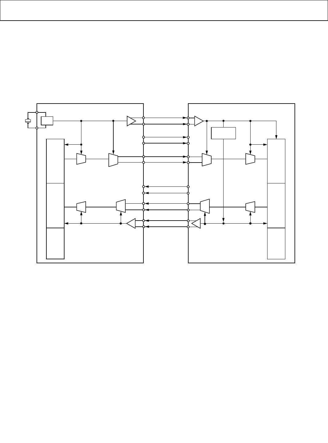
UG-570 AD9361 Reference Manual
| Page 106 of 128
LVDS MODE DATA PATH AND CLOCK SIGNALS
The following information describes operation of the AD9361
data path in low voltage differential signal (LVDS) mode
(ANSI-644 compatible). The AD9361 data path interface uses
parallel data buses (P0 and P1) to transfer data samples between
the AD9361 and the BBP. The bus transfers are controlled using
simple hardware handshake signaling. In LVDS mode, both
buses are used with differential LVDS signaling.
The AD9361 LVDS interface facilitates connecting to custom
ASICs and FPGAs that have LVDS capability. LVDS interfaces
are typically used when a system needs superior switching
performance in noisy environments and higher data rates than
a standard CMOS interface can provide. When utilizing LVDS
mode, it is recommended to keep all trace lengths no longer
than 12 inches and to keep differential traces close together and
at equal lengths.
Figure 78. AD9361 Data Path, LVDS Mode
DATA_CLK_P
RX_FRAME_P
TX_P[5:0]
FB_CLK_P
RX
DATA RX
DATA
TX
DATA TX
DATA
CTRL CTRL
PLL
FEEDBACK
CLK GEN
AD9361
BBP
TX_FRAME_P
RX_P[5:0]
DATA_CLK_N
RX_FRAME_N
RX_N[5:0]
TX_FRAME_N
TX_N[5:0]
FB_CLK_N
11668-079
Rev. A

AD9361 Reference Manual UG-570
| Page 107 of 128
LVDS MODE DATA PATH SIGNALS
The data path interface consists of the following signals.
DATA_CLK
DATA_CLK is a differential LVDS signal generated in the
AD9361 and provided to the BBP as a master clock for the
Rx data path. The BBP uses this master clock as the timing
reference for the interface data transfers and for the baseband
processing of the data samples. DATA_CLK provides source-
synchronous timing with DDR operation for the Rx_D[5:0]
signals during receive operation. SDR is not available in LVDS
mode.
The frequency of DATA_CLK depends on the system
architecture (number of RF channels, degree of oversampling
and BW mode). This frequency is set via SPI writes to the
AD9361.
DATA_CLK can be stopped by the AD9361 (in response to a
SPI transaction from the BBP) during interface idle periods to
reduce power consumption. If DATA_CLK is disabled, the
transition to and from the nontoggling state must obey the
electrical layer requirements for clean signal transitions, and a
valid level must be driven by the AD9361 at all times.
FB_CLK
FB_CLK is a differential LVDS signal driven from the BBP
and is a feedback (loop back) version of DATA_CLK. FB_CLK
provides source-synchronous timing with dual edge capture for
Tx_D[5:0] signals during Tx bursts.
FB_CLK can be stopped by the BBP during interface idle
periods to reduce power consumption. If so, the transitions to
and from the nontoggling state must obey the electrical layer
requirements for clean signal transitions, and a valid level must
be driven by the BBP at all times.
Rx_FRAME
Rx_FRAME is a differential LVDS signal driven from the
AD9361 and provided to the BBP to frame the data samples
provided by the AD9361. A high transition indicates the
beginning of the frame. Rx_FRAME can be set to be a single
high transition at the beginning of a burst and stay high
throughout the burst, or it can be set to be a pulse train that has
a rising edge at the beginning of each frame (50% duty cycle).
Rx_D[5:0]
Rx_D[5:0] is a differential LVDS data bus consisting of six
differential pairs. It is driven from the AD9361 to the BBP with
received data. Data is transmitted on this bus in pairs of data
words to create a 12-bit data bus.
Tx_FRAME
Tx_FRAME is a differential LVDS signal driven from the BBP
and provided to the AD9361 to frame the data samples
provided by the BBP. A high transition indicates the beginning
of the frame. Tx_FRAME can accept a single high transition at
the beginning of a burst that stays high throughout the burst or
a pulse train that has a rising edge at the beginning of each
frame (50% duty cycle).
The AD9361 transmits null data (all zeros) until the first
Tx_FRAME indicates valid data. This is a useful feature when
the Tx path completes a transmit operation in FDD
independent mode and the data path is not automatically
flushed. In this case, the TX_FRAME pin can be held low to
complete the data flushing operation. See the Enable State
Machine Guide section for more details.
Note that both Rx_FRAME and Tx_FRAME are required
signals for the interface to function properly.
Tx_D[5:0]
Tx_D[5:0] is a differential LVDS data bus consisting of six
differential pairs. It is driven from the BBP to the AD9361 with
data to be output through the transmitter. Data is transmitted
on this bus in pairs of data words to create a 12-bit data bus.
ENABLE
ENABLE is driven from the BBP to the AD9361 to provide data
transfer burst control (along with TXNRX) in TDD mode.
ENABLE is asserted by the BBP for a minimum of a single
DATA_CLK cycle to indicate the start of each burst. It is
subsequently asserted a second time for a minimum of a single
DATA_CLK cycle to indicate the end of each burst.
The AD9361 internally tracks the sequence of ENABLE pulses
to interpret each pulse correctly as either the start or finish of
each burst. The ENABLE signal can also be configured in level
mode, in which the state of the signal (not pulses) determines
when the ENSM moves between states. In LVDS mode, the data
ports are always active. In TDD mode, both the BBP and the
AD9361 ignore data in the inactive direction. The start and
finish latencies (between the ENABLE pulses being sampled by
the AD9361 and the presence of the first and last valid data
samples on the bus) vary depending on data path configuration.
The Rx_FRAME and Tx_FRAME signals are used to determine
valid data by the BBP and the AD9361, respectively. The
FB_CLK signal is used to sample this input.
In FDD mode, the ENABLE signal serves as the single control
input to determine the state of the ENSM. There is also an
alternative FDD mode in which the ENABLE signal can be
redefined as RxON, a direct hardware control input to the
ENSM that controls the Rx function. In this mode (called FDD
independent control mode), the BBP independently controls
the Rx function, which can result in power consumption
savings.
Rev. A
UG-570 AD9361 Reference Manual
Rev. A | Page 108 of 128
TXNRX
TXNRX is driven from the BBP to the AD9361 and provides
data transfer burst control (along with ENABLE) when the
ENSM is in TDD mode. When ENABLE is sampled high by the
AD9361 to start a burst, the level on TXNRX is also sampled to
determine the data direction. In TDD mode, TXNRX sampled
high indicates a transmit burst and TXNRX sampled low
indicates a receive burst.
The TXNRX signal level must be maintained throughout a data
transfer burst (a valid logic level). The TXNRX signal may be
established any number of cycles (≥ 0) before the ENABLE start
pulse is sampled, and it may be changed any number of cycles
(≥ 0) after the ENABLE finish pulse is sampled. It is important
to note that the TXNRX signal should only change state while
the ENSM is in the ALERT state because the TXNRX rising and
falling edges power-up and power-down the corresponding
synthesizers directly in TDD mode.
In normal FDD mode, the TXNRX signal is ignored but must
be held at a valid logic level. There is also an alternative FDD
mode in which the TXNRX signal can be redefined as TxON, a
direct hardware control input to the ENSM that controls the Tx
function. In this mode (called FDD independent control mode),
the BBP independently controls the Tx function, which can
result in power consumption savings.
LVDS MAXIMUM CLOCK RATES AND SIGNAL
BANDWIDTHS
The data listed in Table 50 compares the maximum data clock
rates and signal bandwidths in the different allowable operating
modes for the LVDS data bus configuration. Maximum RF band-
widths are listed for two cases: sampling using the minimum
sample rate that avoids aliasing, and sampling using 2× over-
sampling. Details of each mode are given in subsequent sections.
The maximum DATA_CLK rate is increased to 245.76 MHz in
LVDS mode. This clock and the 56 MHz maximum analog filter
bandwidth limit RF channel signal bandwidth. Note that the
data bus timing is identical for TDD and FDD modes because
each path (transmit and receive) has a dedicated bus.
Table 50. Maximum LVDS Data Rates and Signal Bandwidths
Operating Mode
1R1T Configurations 1R2T/2R1T/2R2T Configurations
Maximum Data Rate -
Combined I and Q
Words (MSPS)
Maximum RF Channel Signal
Bandwidth (MHz)
Maximum Data
Rate—Combined I
and Q Words
Maximum RF Channel Signal
Bandwidth (MHz) per Channel
Using Minimum
Sample
Frequency
Using 2×
Oversampling
Using Minimum
Sample
Frequency
Using 2×
Oversampling
Dual Port Full Duplex 61.44 561 561 61.44 561 30.72
1 Limited by the analog filter bandwidth.

AD9361 Reference Manual UG-570
| Page 109 of 128
DUAL PORT FULL DUPLEX MODE (LVDS)
Dual bus full duplex LVDS mode is enabled by writing a SPI
register. In this mode, both P0 and P1 are enabled as LVDS
signals and the data buses (D[11:0]) are split into separate sub-
buses (Rx_D[5:0] and Tx_D[5:0]). Each sub-bus operates
simultaneously allowing full duplex of transmit and receive data
between the BBP and the AD9361.
Transmit data (Tx_D[5:0]), FB_CLK, and Tx_FRAME are
driven by the BBP such that the setup and hold times between
FB_CLK, Tx_D[5:0] and Tx_FRAME allow the AD9361 to use
FB_CLK to capture Tx_D[5:0] and Tx_FRAME. The data
samples on the Tx_D[5:0] bus are framed by the Tx_FRAME
signal as shown in the timing diagrams. The transmit data
samples are carried in two’s complement format, with the first
6-bit word in each data packet containing the MSB’s and the
second 6-bit word containing the LSB’s. The most positive
sample value is 0x7FF, with the first word being 0x1F and the
second word being 0x3F, and the most negative value is 0x800,
with the first word being 0x20 and the second word being 0x00.
Tx_D[5] is the most significant bit and Tx_D[0] is the least
significant bit in each word.
Receive data (Rx_D[5:0]), DATA_CLK, and Rx_FRAME are
driven by the AD9361 such that the setup and hold times
between DATA_CLK, Rx_D[5:0] and Rx_FRAME allow the
BBP to use DATA_CLK to capture Rx_D[5:0] and Rx_FRAME.
The data samples on the Rx_D[5:0] bus are framed by the
Rx_FRAME signal as shown in the timing diagrams. The
receive data samples are carried in two’s complement format,
with the first 6-bit word in each data packet containing the
MSBs and the second 6-bit word containing the LSBs. This
means the most positive sample value is 0x7FF, with the first
word being 0x1F and the second word being 0x3F, and the most
negative value is 0x800, with the first word being 0x20 and the
second word being 0x00. Rx_D[5] is the most significant bit
and D[0] as the least significant bit in each word.
Note that, like in CMOS mode, FB_CLK must be generated
from DATA_CLK so that it retains the same frequency and duty
cycle. There is no phase relationship requirement between the
two clock signals.
As mentioned previously, the I and Q data samples are time-
interleaved on each data bus. For a 1R1T system, the I and Q
samples are carried in a 4-way interleave:
IMSB, QMSB, ILSB, QLSB, …
For this case, the Tx_FRAME and Rx_FRAME signals are
coincident with data switching. Each is in a high state for IMSB
and QMSB and a low state for ILSB and QLSB when 50% duty cycle
framing is enabled. These signals then switch high again with
IMSB to indicate the start of a new frame.
For a 2R2T system, the I and Q samples from RF path 1 and 2
are carried in an 8-way interleave:
I1 MSB, Q1 MSB, I1 LSB, Q1 LSB, I2 MSB, Q2 MSB, I2 LSB, Q2 LSB, …
For this case, the Tx_FRAME and Rx_FRAME signals are
coincident with data switching. Each is in a high state for I1MSB,
Q1MSB, I1LSB, Q1LSB and a low state for I2MSB, Q2MSB, I2LSB and Q2LSB
when 50% duty cycle framing is enabled. These signals then
switch high again with IAMSB to indicate the start of a new frame.
For a system with a 2R1T or a 1R2T configuration, the clock
frequencies, bus transfer rates and sample periods, and data
capture timing are the same as if configured for a 2R2T system.
However, in the path with only a single channel used, the
disabled channel’s I-Q pair in each data group is unused. These
unused slots are ignored by the AD9361. As an example, for a
2R1T system using Tx channel 1, the transmit burst would have
four unused slots:
I1 MSB, Q1 MSB, I1 LSB, Q1 LSB, X, X, X, X, …
For this case, the Tx_FRAME and Rx_FRAME are coincident
with data switching and high for I1MSB, Q1MSB, I1LSB, Q1LSB and
then low for unused slots. These signals then switch high again
with I1MSB to indicate the start of a new frame. The unused X
slots may be filled with arbitrary data values by the BBP. Such
values could be either constant values, or the preceding data
sample values can be repeated to reduce the bus switching
factor and, therefore, power consumption.
DATA PATH FUNCTIONAL TIMING (LVDS)
The timing diagrams in Figure 79 and Figure 80 illustrate the
relationship among the bus signals in dual port FDD LVDS
mode. The differential data in the timing diagrams are drawn
with solid and dashed lines to illustrate the differential nature of
the data lines. Solid lines for the positive leg match solid lines
for the negative leg of the differential pair, and dashed lines for
the positive leg pair with dashed lines for the negative leg. Note
that because 2R1T and 1R2T systems follow the 2R2T timing
diagrams, they are omitted from Figure 79 and Figure 80.
Rev. A
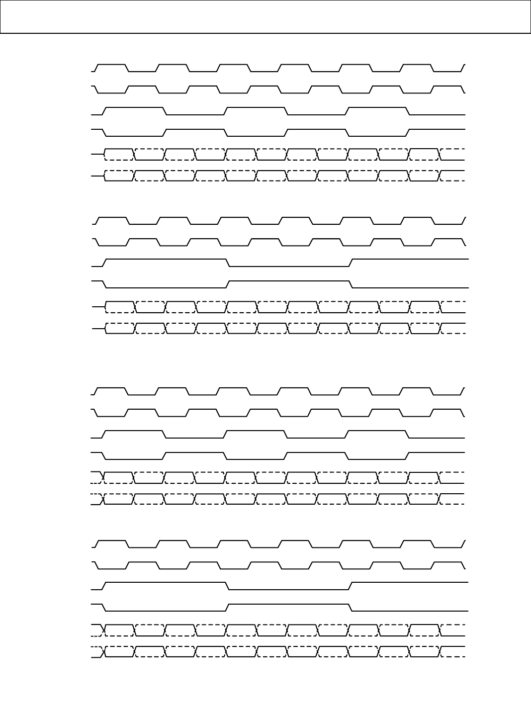
UG-570 AD9361 Reference Manual
| Page 110 of 128
Figure 79. Receive Data Path, LVDS
Figure 80. Transmit Data Path, LVDS
DATA_CLK_P
RX_FRAME_P
RX_D[5:0]_P
RX_D[5:0]_N
DATA_CLK_N
RX_FRAME_N
1R1T, DDR, FDD, LVDS, 0x010 = 0xC8, 0x011 = 0x00, 0x012 = 0x10
R_I[11:6] R_Q[11:6] R_I[5:0] R_Q[5:0]
R_I[11:6] R_Q[11:6] R_I[5:0] R_Q[5:0]
R_I[11:6] R_Q[11:6] R_I[5:0] R_Q[5:0]
R_I[11:6] R_Q[11:6] R_I[5:0] R_Q[5:0]
R_I[11:6] R_Q[11:6] R_I[5:0] R_Q[5:0]
R_I[11:6] R_Q[11:6] R_I[5:0] R_Q[5:0]
11668-080
DATA_CLK_P
RX_FRAME_P
RX_D[5:0]_P
RX_D[5:0]_N
DATA_CLK_N
RX_FRAME_N
2R2T, DDR, FDD, LVDS, 0x010 = 0xC8, 0x011 = 0x00, 0x012 = 0x10
R1_I[11:6] R1_Q[11:6] R1_I[5:0] R1_Q[5:0]
R1_I[11:6] R1_Q[11:6] R1_I[5:0] R1_Q[5:0]
R2_I[11:6] R2_Q[11:6] R2_I[5:0] R2_Q[5:0]
R2_I[11:6] R2_Q[11:6] R2_I[5:0] R2_Q[5:0]
R1_I[11:6] R1_Q[11:6] R1_I[5:0] R1_Q[5:0]
R1_I[11:6] R1_Q[11:6] R1_I[5:0] R1_Q[5:0]
FB_CLK_P
TX_FRAME_P
TX_D[5:0]_P
TX_D[5:0]_N
FB_CLK_N
TX_FRAME_N
1R1T, DDR, FDD, LVDS, 0x010 = 0xC8, 0x011 = 0x00, 0x012 = 0x10
T_I[11:6] T_Q[11:6] T_I[5:0] T_Q[5:0]
T_I[11:6] T_Q[11:6] T_I[5:0] T_Q[5:0]
T_I[11:6] T_Q[11:6] T_I[5:0] T_Q[5:0]
T_I[11:6] T_Q[11:6] T_I[5:0] T_Q[5:0]
T_I[11:6] T_Q[11:6] T_I[5:0] T_Q[5:0]
T_I[11:6] T_Q[11:6] T_I[5:0] T_Q[5:0]
11668-081
FB_CLK_P
TX_FRAME_P
TX_D[5:0]_P
TX_D[5:0]_N
FB_CLK_N
TX_FRAME_N
2R2T, DDR, FDD, LVDS, 0x010 = 0xC8, 0x011 = 0x00, 0x012 = 0x10
T1_I[11:6] T1_Q[11:6] T1_I[5:0] T1_Q[5:0]
T1_I[11:6] T1_Q[11:6] T1_I[5:0] T1_Q[5:0]
T2_I[11:6] T2_Q[11:6] T2_I[5:0] T2_Q[5:0]
T2_I[11:6] T2_Q[11:6] T2_I[5:0] T2_Q[5:0]
T1_I[11:6] T1_Q[11:6] T1_I[5:0] T1_Q[5:0]
T1_I[11:6] T1_Q[11:6] T1_I[5:0] T1_Q[5:0]
0
0
0
0
Rev. A

AD9361 Reference Manual UG-570
| Page 111 of 128
The following bits are not supported in LVDS mode:
•Swap Ports—In LVDS mode, P0 is Tx and P1 is Rx. This configuration cannot be changed.
•Single Port Mode —Both ports are enabled in LVDS mode.
•FDD Full Port—Not supported in LVDS.
•FDD Alt Word Order—Not supported in LVDS.
•FDD Swap Bits—Not supported in LVDS.
DATA PATH TIMING PARAMETERS (LVDS)
Table 51 lists the timing constraints for the LVDS data buses.
Table 51. Data Path Timing Constraint Values—LVDS Mode
Parameter Min Typ Max Description
tCP 4.069 ns DATA_CLK cycle time (clock period)
tMP 45% of tCP 55% of tCP DATA_CLK and FB_CLK high and/or low minimum pulse width (including effects of duty
cycle distortion, period jitter, cycle-cycle jitter and half-period jitter)
tSTx 1 ns Tx_D[5:0], Tx_FRAME setup time to FB_CLK falling edge at AD9361 inputs
t
HTx
0 ns
Tx_D[5:0], Tx_FRAME hold time from FB_CLK falling edge at AD9361 inputs
tDDRx 0.25 ns 1.25 ns Delay from DATA_CLK to Rx_D[5:0] outputs
tDDDV 0.25 ns 1.25 ns Delay from DATA_CLK to Rx_FRAME
Rev. A
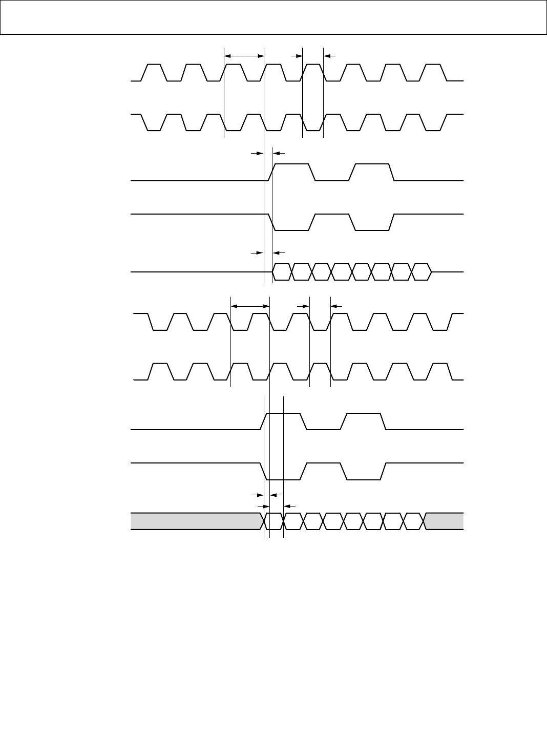
UG-570 AD9361 Reference Manual
| Page 112 of 128
Figure 81. Data Port Timing Parameter Diagrams—LVDS Bus Configuration
I_M Q_M
Q_MI_M Q_LI_L Q_LI_L Q_LI_L
I_L Q_L I_M Q_M I_L Q_L
DATA_CLK_P
DATA_CLK_N
RX_FRAME_P
RX_FRAME_N
RX_D[5:0]
TX_FRAME_N
TX_FRAME_P
FB_CLK_P
FB_CLK_N
TX_D[5:0]
tMP
tCP
tDDDV
tDDRX
tMP
tCP
tSTX
tHTX
11668-082
Rev. A
AD9361 Reference Manual UG-570
| Page 113 of 128
SERIAL PERIPHERAL INTERFACE (SPI)
The SPI bus provides the mechanism for all digital control of
the AD9361. Each SPI register is 8-bit wide, and each register
contains control bits, status monitors, or other settings that
control all functions of the device. The following sections
explain the specifics of this interface.
SPI Functional Layer
The SPI bus can be configured by setting the bit values in the
SPI Configuration register. This register is symmetrical; that is,
D6 is equivalent to D1, and D5 is equivalent to D2 (D4 and D3
are unused). The device powers up in its default mode (MSB-
first addressing), but can accept an LSB-first write to the SPI
Configuration register because of this symmetry. The
symmetrical bits are OR’ed together, so setting one bit sets both
in the pair. The bit order is MSB-first when D5 and D2 are left
clear, while bit order is swapped to LSB-first when these bits are
set. Once properly configured, all subsequent register writes
must follow the selected format.
The bus is configured as a 4-wire interface by default. If Bit D6
and Bit D1are set, the SPI bus is configured as a 3-wire
interface. Bit D7 and Bit D0 asynchronously reset all registers to
their default values when set, and these bits must be cleared
before other registers can be changed.
Each SPI bus signal is described in the following sections.
SPI_ENB
SPI_ENB is the bus enable signal driven from the BBP to the
AD9361. SPI_ENB is driven low before the first SPI_CLK rising
edge and is normally driven high again after the last SPI_CLK
falling edge. The AD9361 ignores the clock and data signals
while SPI_ENB is high. If the AD9361 is the only device on the
SPI bus, SPI_ENB can be tied low.
The SPI_DO and SPI_DI pins transition to a high impedance
state when this input is high. If driven high during any
communications cycle, that cycle is suspended until SPI_ENB
is reactivated low.
SPI_CLK
SPI_CLK is the interface reference clock driven by the BBP to
the AD9361. It is only active while SPI_ENB is low. The
maximum SPI_CLK frequency is 50 MHz.
SPI_DI, SPI_DO and SPI_DIO
When configured as a 4-wire bus, the SPI utilizes two data
signals: SPI_DI and SPI_DO. SPI_DI is the data input line
driven from the BBP to the AD9361 and SPI_DO is the data
output from the AD9361 to the BBP in this configuration.
When configured as a 3-wire bus, SP_DI is used as a
bidirectional data signal that both receives and transmits serial
data. In 3-wire configuration, this signal is referred to as
SP_DIO in this section to distinguish between the two
configurations.
The data signals are launched on the rising edge of SPI_CLK
and sampled on the falling edge of SPI_CLK by both the BBP
and the AD9361. SPI_DI (or SPI_DIO) carries the control field
from BBP to the AD9361 during all transactions and the write
data fields during a write transaction. SPI_DO (or SPI_DIO)
carries the returning read data fields from the AD9361 to BBP
during a read transaction.
The AD9361 does not provide any weak pull-ups or pull-downs
on these pins. When SPI_DO is inactive, it is floated in a high
impedance state. If a valid logic state on SPI_DO is required at
all times, an external weak pull-up/pull-down should be added
on the PCB.
SPI Data Transfer Protocol
The AD9361 SPI is a flexible, synchronous serial communica-
tions bus allowing seamless interfacing to many industry
standard microcontrollers and microprocessors. The serial I/O
is compatible with most synchronous transfer formats,
including both the Motorola SPI and Intel® SSR protocols. The
control field width for the AD9361 is limited to 16-bit only, and
multibyte IO operation is allowed. The AD9361 cannot be used
to control other devices on the bus—it only operates as a slave.
There are two phases to a communication cycle. Phase 1 is the
control cycle, which is the writing of a control word into the
AD9361. The control word provides the AD9361 serial port
controller with information regarding the data field transfer
cycle, which is Phase 2 of the communication cycle. The Phase 1
control field defines whether the upcoming data transfer is read
or write. It also defines the register address being accessed.
Phase 1 Instruction Format
The 16-bit control field contains the following information:
MSB D14 D13 D12 D11 D10 D9:D0
W/Rb NB2 NB1 NB0 X X A[9:0]
W/Rb—Bit 15 of the instruction word determines whether a
read or write data transfer occurs after the instruction byte
write. Logic high indicates a write operation; logic zero
indicates a read operation.
NB2, NB1, NB0—Bits [14:12] of the instruction word specify
the number of bytes transferred during Phase 2 of the IO
operation. Table 52 details the number of bytes transferred
during Phase 2 for each NB[2:0] combination.
Table 52.
NB2, NB1, NB0 Description
000 Transfer 1 byte
001 Transfer 2 bytes
010 Transfer 3 bytes
011 Transfer 4 bytes
100 Transfer 5 bytes
101 Transfer 6 bytes
110 Transfer 7 bytes
111 Transfer 8 bytes
Rev. A

UG-570 AD9361 Reference Manual
| Page 114 of 128
[D11:D10]—Bits[11:10] of the instruction word are unused.
[D9:D0]—Bits[9:0] specify the starting byte address for the data
transfer during Phase 2 of the IO operation.
All byte addresses, both starting and internally generated
addresses, are assumed to be valid. That is, if an invalid address
(undefined register) is accessed, the IO operation continues as if
the address space were valid. For write operations, the written
bits are discarded, and read operations result in logic zeros at
the output.
Single-Byte Data Transfer
When NB2, NB1, and NB0 are all zero, a single-byte data
transfer is selected. In this scenario, the next eight bits to follow
the address bits contain the data being written to or read from
the AD9361 register. Once the final bit is transferred, the data
signals return to their idle states and the SPI_ENB signal goes
high to end the communication session.
Multi-Byte Data Transfer
When NB2, NB1, and NB0 are all nonzero, a multibyte data
transfer is selected. The format and ordering of the data to be
transferred in this mode depend on whether the device is
configured for LSB-first or MSB-first data transfer.
For multibyte data transfers in LSB mode, the user writes an
instruction byte that includes the register address of the least
significant byte. The SPI internal byte address generator incre-
ments for each byte required in the multibyte communication
cycle. Data is written in least to most significant order as the
byte addresses are also generated in least to most significant
order.
For multi-byte data transfers in MSB mode, the user writes an
instruction word that includes the register address of the most
significant byte. The serial port internal byte address generator
decrements for each byte required by the multibyte commu-
nication cycle. Data is written in most to least significant order
as the byte addresses are generated in most to least significant
order.
Example: MSB-First Multibyte Transfer
To complete a 4-byte write, starting at Register 0x02A in MSB
first format, apply an instruction word of 1_011_000000101010
(binary). This instruction directs the AD9361 SPI controller to
perform a write transfer of four bytes with the starting byte
address of 0x02A. After the first data byte is written, the
internal byte address generation logic decrements to 0x029,
which is the destination of the second byte. After the second
byte is written, the internal byte address generation logic
decrements to 0x028, which is the destination of the third byte.
After the third byte is written, the internal byte address
generation logic decrements to 0x027, which is the destination
of the last byte. After the fourth byte is written, the IO
communication cycle is complete and the next 16 falling clock
cycles on SPI_CLK are utilized to clock in the next instruction
word. If no further communication is needed, the data signals
return to their idle states, SPI_CLK goes low, and the SPI_ENB
signal goes high to end the communication session.
Example: LSB-First Multibyte Transfer
To complete a 4-byte write, starting at register 0x02A in LSB
first format, apply an instruction word of 010101000000_110_1
(binary). This instruction directs the AD9361 SPI controller to
perform a write transfer of four bytes with the starting byte
address of 0x02A. After the first data byte is written, the
internal byte address generation logic increments to 0x02B,
which is the destination of the second byte. After the second
byte is written, the internal byte address generation logic
increments to 0x02C, which is the destination of the third byte.
After the third byte is written, the internal byte address
generation logic increments to 0x02D, which is the destination
of the last byte. After the fourth byte is written, the IO
communication cycle is complete and the next 16 falling clock
cycles on SPI_CLK are utilized to clock in the next instruction
word. If no further communication is needed, the data signals
return to their idle states, SPI_CLK goes low, and the SPI_ENB
signal goes high to end the communication session.
Timing Diagrams
The following diagrams in Figure 82 and Figure 83 detail the
SPI bus waveforms for a single-register write operation and a
single-register read operation, respectively. In the first figure,
the value 0x55 is written to Register 0x15A. In the second value,
Register 0x15A is read and the value returned by the device is
0x55. If the same operations were performed with a 3-wire bus,
the SPI_DO line in Figure 82 would be eliminated, and the
SPI_DI and SPI_DO lines in Figure 83 would be combined on
the SPI_DI line.
Rev. A
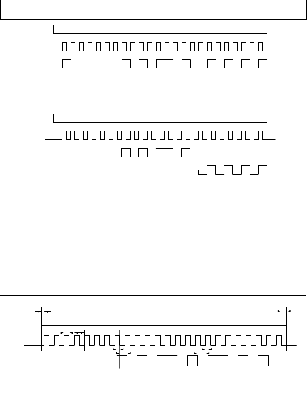
AD9361 Reference Manual UG-570
| Page 115 of 128
Figure 82. Nominal Timing Diagram, SPI Write
Figure 83. Nominal Timing Diagram, SPI Read
Table 53 lists the timing specifications for the SPI bus. The relationship between these parameters is shown in Figure 84. This diagram
shows a 3-wire SPI bus timing diagram with these parameters marked. Note that this is a single read operation, so the bus-ready
parameter after the data is driven from the AD9361 is not shown in the diagram.
Table 53. SPI Bus Timing Constraint Values
Parameter Min Typ Max Description
tCP 20 ns SPI_CLK cycle time (clock period)
tMP 9 ns SPI_CLK pulse width
tSC 1 ns SPI_ENB setup time to first SPI_CLK rising edge
tHC 0 ns Last SPI_CLK falling edge to SPI_ENB hold
tS 2 ns SPI_DI data input setup time to SPI_CLK
tH 1 ns SPI_DI data input hold time to SPI_CLK
tCO 3 ns 8 ns SPI_CLK rising edge to output data delay (3-wire or 4-wire mode)
tHZM t
Ht
CO (max) Bus turnaround time after BBP drives the last address bit
tHZS 0 ns tCO (max) Bus turnaround time after AD9361 drives the last data bit
Figure 84. 3-Wire SPI Timing with Parameter Labels, SPI Read
SPI_ENB
SPI_CLK
SPI_DI
SPI_DO
WRITE TO REGISTER 0x15A, VALUE = 0x55
11668-083
SPI_ENB
SPI_CLK
SPI_DI
SPI_DO
READ REGISTER 0x15A, VALUE = 0x55
11668-084
SPI_ENB
SPI_CLK
SPI_DI
t
MP
t
CP
t
S
t
H
t
SC
t
HC
t
CO
t
HZM
11668-085
Rev. A

UG-570 AD9361 Reference Manual
| Page 116 of 128
ADDITIONAL INTERFACE SIGNALS
CLOCK_OUT
CLOCK_OUT is an output signal designed to be used as a
master clock source for the BBP. This output can be
programmed to be a buffered version of the input clock or a
multiple of the Rx data path ADC clock. Note that the clock
frequency must always be less than 61.44 MHz.
CTRL_IN[3:0]
The CTRL_IN pins are four programmable input signals used
for real time control Rx gain settings as described in the Gain
Control section.
CTRL_IN2 can also be used to provide hardware control in the
receiver AGC hybrid mode. In this mode, gain changes occur
when the BBP pulls the CTRL_IN2 pin high. This allows the
BBP to directly control the time that the gain setting changes.
CTRL_OUT[7:0]
The CTRL_OUT pins are eight programmable digital output
signals used for real time processing. These outputs include
internally generated functions and status bits such as PLL lock,
calibration complete, and AGC functions.
EN_AGC
EN_AGC is an input signal that provides real time control of
when the AGC is active. When pulled high, the EN_AGC pin
forces the AGC to unlock so that adjustments to the gain setting
can be made. If the EN_AGC pin is not used, then the Gain
Lock Delay bit must be set high.
GPO[3:0]
The GPO pins are digital outputs that can be configured to
monitor the status of the ENSM or serve as general-purpose
logic outputs. These pins are especially useful for biasing a
connected power amplifier or controlling front-end switches
used in TDD systems. See the General Purpose Output Control
section for more detail.
RESETB
RESETB is an input signal allowing asynchronous hardware
reset of the AD9361. A logic low applied to this pin resets the
device (all SPI registers are reset to default settings and the
device is placed in SLEEP mode). The RESETB line should be
held low for at least 1 µs, and the device should not be
programmed for at least 1 µs after the RESETB line has been
taken back high.
SYNC_IN
SYNC_IN is a logic input that can be used to provide
synchronization between the data ports of multiple AD9361
devices. See the Baseband Synchronization section for more
details.
Rev. A
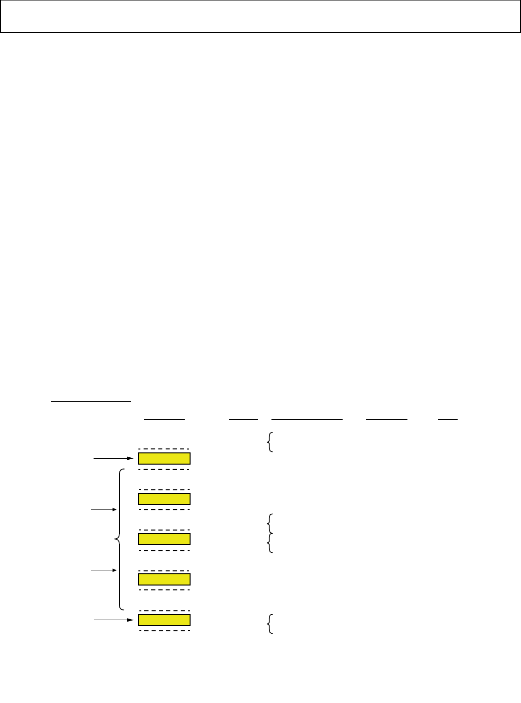
AD9361 Reference Manual UG-570
| Page 117 of 128
POWER SUPPLY AND LAYOUT GUIDE
OVERVIEW
Due to the increased complexity of the AD9361 and the high
pin count, printed circuit board (PCB) layout is important to
get the best performance. This section provides a checklist of
issues to look for and how to work on them. The goal of this
section is help achieve the best performance from the AD9361
while reducing board layout effort. This section assumes that
the reader is a RF engineer who understands RF PCB layout
and has an understanding of RF transmission lines. This section
discusses the following issues and provides guidelines for
system designers to get the best performance out of the
AD9361.
•PCB material and stack up selection
•RF transmission line layout
•Fan-out and trace-space layout guidelines
•Special components placement and routing guidelines
•Power management and system noise considerations
•Power distribution to all the different power domains
PCB MATERIAL AND STACK UP SELECTION
Figure 85 shows the stack up used for the AD9361 customer
evaluation boards. The top and the bottom layers are Rogers
4003 with an 8 mil dielectric. The remaining layers are FR4-370
HR. The board design uses the Rogers laminate for the top and
the bottom layers for its low loss tangent at high frequencies.
The ground planes under the Rogers laminate (Layer 2 and
Layer 9) are the reference planes for the transmission lines
routed on the outer surfaces. These layers are solid copper plane
without any splits under the RF traces. Layer 2 and Layer 9 are
crucial to maintaining the RF signal integrity and, therefore, the
AD9361 performance. Layer 3 and Layer 8 contain the 1.3 V
analog supply, the 3.3 V GPO supply, and the 1.8 V
VDD_INTERFACE supply. To keep the RF section of the
AD9361 isolated from the fast transients of the digital section,
the digital lines from the AD9361 are on inner Layer 5 and
Layer 6. The RF traces on the outer layers need to be controlled
impedance to get the best performance from the AD9361.
1 ounce copper is used for all the inner layers in this board. The
outer layers use 1.5 ounce copper so that the RF traces are less
prone to pealing. Ground planes on this board are full copper
floods with no splits except for vias and through-hole
components. The ground planes must route entirely to the edge
of the PCB under the SMAs to maintain signal launch integrity.
Power planes on the other hand can be pulled back from the
board edge to decrease the risk of shorting from the board edge.
Figure 85. AD9361 Customer Evaluation Board Stack Up
0.008
0.003
0.008
0.008
0.003
SIGNAL
GND
PWR
PWR
SIGNAL
SIGNAL
SIGNAL
GND
GND
GND
1
2
3
4
5
6
7
8
9
10
1.5
1
1
1
1
1
1
1
1
0.003
0.003
0.0046
0.0046
OVERALL THICKNESS = 0.062
DIELECTRIC COPPER TARGET IMPEDANCE LINE/SPACE CALC
OZ
OZ
OZ
OZ
OZ
OZ
OZ
OZ
OZ
OZ1.5
0.0606 FINAL THICKNESS (AFTER PLATING)
R4003
NEW LAYER
NEW LAYER
R4003
370 HR
50.1
100.0
50.0
100.2
50.0
100.2
ROGERS 4003 (DK = 3.38)
370 HR (DK = 4.1)
0.0155
0.008/0.006
0.008/0.006
0.0155
0.0038/0.0062
0.0038/0.0062
0.0049
0.0049
50Ω ± 10%
50Ω ± 10%
50Ω ±10%
50Ω ± 10%
100 DIFFERENTIAL ± 10%
100 DIFFERENTIAL ± 10%
100 DIFFERENTIAL ± 10%
100 DIFFERENTIAL ± 10%
±10%
50.1
100.0
11668-086
Rev. A
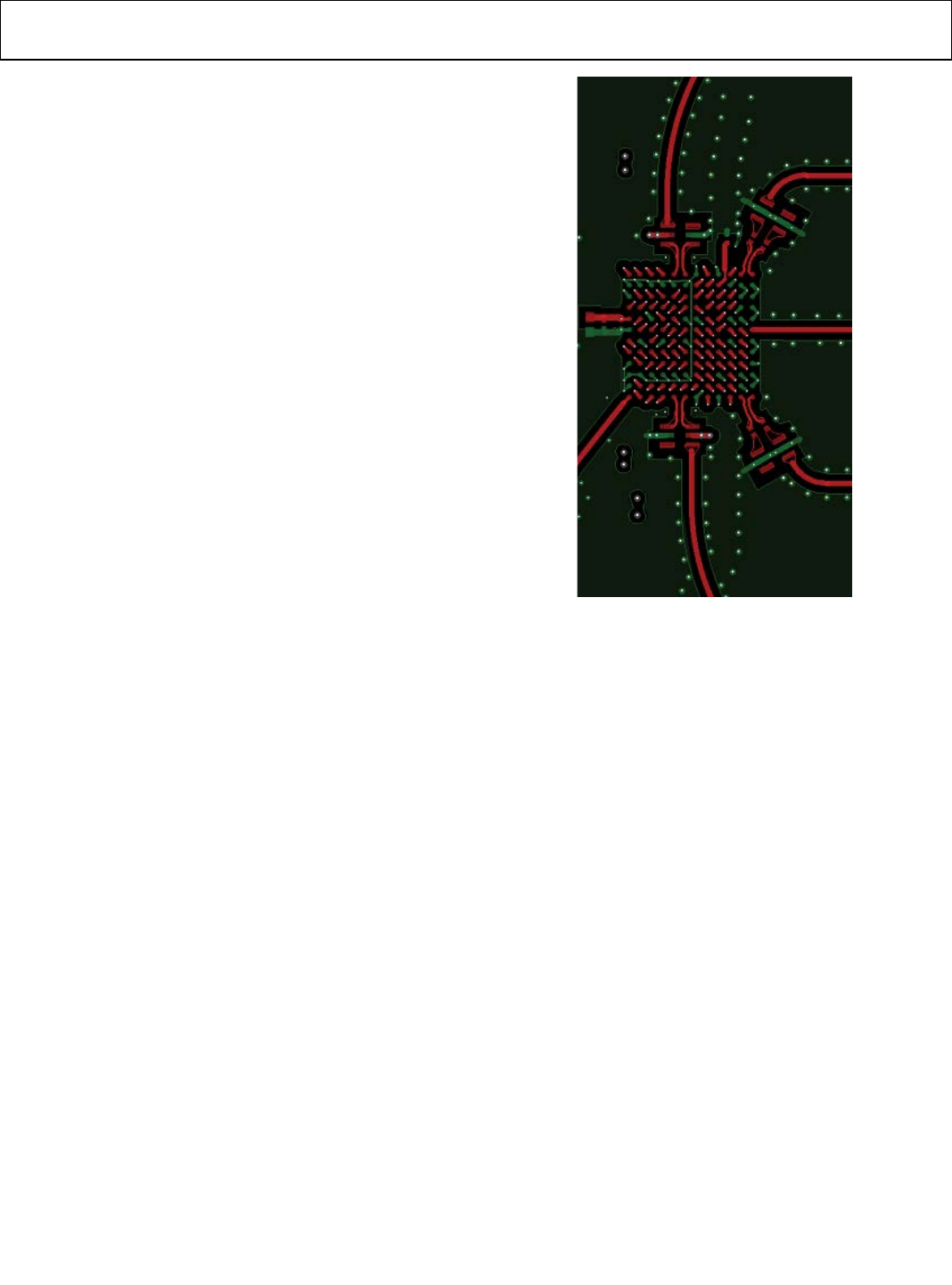
UG-570 AD9361 Reference Manual
| Page 118 of 128
RF TRANSMISSION LINE LAYOUT
The AD9361 evaluation boards use micro strip lines for all the
RF traces. The critical Rx and Tx lines route on the top side of
the board. It is not recommend to use vias to route RF traces.
The differential lines from the balun secondary to the Rx and
Tx balls need to be as short as possible. The length of the single-
ended transmission line should be short to minimize the effects
of parasitic coupling. Since the receiver front end is DC-biased
internally, the differential side of the balun is ac-coupled. The
system designer can optimize the RF performance with a proper
selection of the balun and the ac-coupling capacitors. The Tx
monitor traces, external LO traces and the external clock traces
could require matching components as well, to ensure best
performance.
All the previous RF signals mentioned must have a solid ground
reference under them. None of the critical traces should run
over a section of the reference plane that is discontinuous. The
ground flood on the reference layer must extend all the way to
the edge of the board. This ensures good signal integrity for the
SMA launch.
See the RF Port Interface section for more information on the
RF matching issues associated with the AD9361.
Figure 86. RF Match Structures on Rx and Tx on FMComms2 Board
11668-087
Rev. A
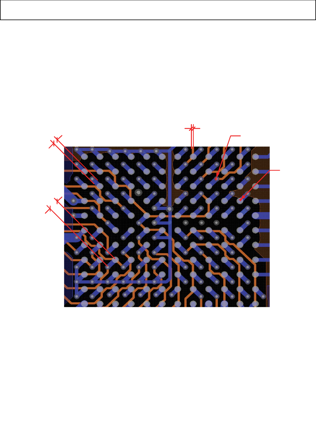
AD9361 Reference Manual UG-570
| Page 119 of 128
FAN-OUT AND TRACE SPACE GUIDELINES
The AD9361 is in a 10 mm × 10 mm 144-pin BGA package.
The pitch between the balls is 0.8 mm. This small pitch makes it
impractical to route all signals on a single layer. RF balls are on
the outer edges of the AD9361 package. This helps in routing
the critical signals without a fan-out via. The digital signals are
buried in the inner layers of the board. The digital balls
corresponding to the Rx data port are buried on one signal layer
and those corresponding to the Tx data port are buried on a
different signal layer. The AD9361 evaluation boards use a
10-mil pin escape trace from the BGA land pad and drop the
digital signals on the inner layers by using a 6 mil via with a
12 mil keep out. The spacing between the BGA lands to the pin
escape via is 22 mils. Once the signal is on the inner layers, a
4.9 mil trace (50 Ω) connects the signal to the FPGA. The
recommended BGA land size is 14 mills.
Only one signal trace is routed between adjacent BGA land
pads and between pin escape vias on the inner layers. Routing
two traces between adjacent BGA land pads and pin escape vias
by reducing the BGA land pad width and trace-pad space
design rules reduces overall board manufacturing and assembly
reliability. Figure 87 shows the fan out scheme evaluation board.
Figure 87. 0.8 mm Pitch BGA Via Fan-Out
22mil LAND TO VIA SPACING
10mil PIN ESCAPE TRACE
4.9mil TRACE (50Ω)
Ø6mil PAD/12mil KEEP OUT
Ø14mil BGA
LAND SIZE
11668-088
Rev. A

UG-570 AD9361 Reference Manual
| Page 120 of 128
COMPONENT PLACEMENT AND ROUTING
GUIDELINES
The AD9361 transceiver requires few external components to
function, but there are certain external components that are
critical to the proper functioning of the part. This section
provides a checklist for properly placing and routing some of
those critical signals and components.
•The receiver/transmitter baluns and the matching circuits
affect the overall RF performance of the AD9361.
Therefore, every effort must be taken to optimize the
component selection and placement. Refer to the RF Port
Interface section for more information.
•Pull the TEST/ENABLE ball (C4) to ground for proper
functioning. If this ball is not grounded then the AD9361
will not function.
•Pull the RESETB ball (K5) high with a 10 kΩ resistor to
VDD_INTERFACE for proper functioning. To reset the
part, pull the RESETB ball low.
•Connect a 14.3 kΩ resistor to the RBIAS ball (L4). This
resistor must have a 1% tolerance.
•If using an external clock, then connect the clock to the
XTALN ball (M12) via an AC coupling capacitor. (The
XTALP ball is a no connect in this case.) Ensure that the
external clock peak-to-peak amplitude does not exceed
1.3 V.
•The Rx and the Tx external LO balls on the AD9361 are
internally DC-biased. If these balls are used, connect a
series coupling capacitor to the ball. If the Rx and Tx
external LO balls are not used then connect them to
ground.
•1 Ω resistor in series to the bypass capacitor on the
TX_VCO_LDO_OUT (B11) and RX_VCO_LDO_OUT
(G2) is needed. A capacitor that has a 1 Ω ESR can replace
this series combination of a resistor and capacitor.
•The VDDA1P1_TX_VCO (A11) must be shorted to the
TX_VCO_LDO_OUT (B11) ball only.
•The VDDA1P1_RX_VCO (G3) must be shorted to
RX_VCO_LDO_OUT(G2) ball only.
•The Tx monitor balls also require a matching network. If
the Tx monitor is not used, then connect Ball A5 and Ball
M5 to ground. For more information, refer to the Tx Power
Monitor section.
•There needs to be at least a 0.1 µF bypass capacitor near
each power supply ball.
•Install 10 µF bypass capacitor on the VDDA1P3_RX_SYNTH
(J3) and VDDA1P3_TX_SYNTH (K3) ball.
•Install a 10 µF capacitor near the Tx balun DC feed.
POWER MANAGEMENT AND SYSTEM NOISE
CONSIDERATIONS
The AD9361 has three different power domains on the chip.
1.3 V is the main power domain that powers the major part of
the chip. The VDD_INTERFACE supply is a separate power
domain. The input voltage on the VDD_INTERFACE can range
from 1.2 V to 2.5 V. This voltage controls the voltage levels of
the digital interface of the AD9361. To operate the digital
interface in LVDS mode, supply 1.8 V or 2.5 V to the
VDD_INTERFACE supply. The input voltage to VDD_GPO
ball can range from 1.3 V to 3.3 V. The VDD_GPO must rise as
fast or faster than the 1.3 V supply domain.
All the different power domains have different power supply
noise rejection characteristics (PSRR). There are certain
supplies on the part that are more sensitive to noise than others
are. These supplies must be decoupled properly to achieve the
best performance from the AD9361. The noise considerations
for the 1.3 V analog supply are vital whereas the noise
considerations for the VDD_INTERFACE supply and the
VDD_GPO are less critical.
Table 54 lists the Rx EVM and Tx EVM degradation when a
ripple voltage is injected on the 1.3 V analog supply. In this
experiment, the LO was set to 700 MHz and the reference clock
was at 19.2 MHz with the RF PLL doubled. The Tx attenuation
setting was set to 10 dB. In this experiment, ripple voltage is
added on the 1.3 V DC supply with the help of a bias tee. This
combination powers all the 1.3 V analog supply domains. The
lower frequency ripple is more detrimental to the device
performance. For this reason, the low frequency noise must be
reduced on the platform that integrates the AD9361.
Table 54. 1.3 V Analog Supply Noise Sensitivities
Noise Frequency
Ripple Voltage
Rx EVM (10 MHz LTE)
Tx EVM (10 MHz LTE)
N/A
0 mV
−37.782 dB
−37.462 dB
40 KHz 16 mV −24.886 dB −28.619 dB
300 KHz 22 mV −35.254 dB −35.517 dB
500 KHz 52 mV −36.254 dB −35.517 dB
1 MHz >50 mV −37.501 dB −36.95 dB
5 MHz >50 mV −37.749 dB −36.927 dB
Rev. A
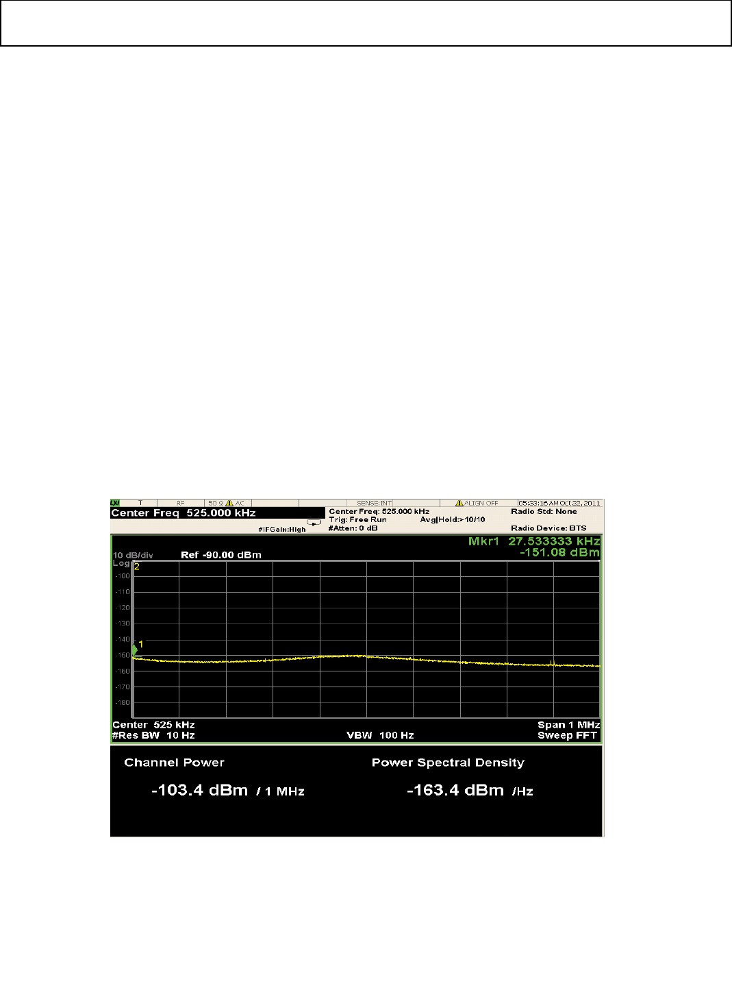
AD9361 Reference Manual UG-570
| Page 121 of 128
Power Up 1.3 V Analog Supply on the AD9361 with an
LDO
The evaluation boards power the 1.3 V analog supply of the
AD9361 with a LDO. The selection of the LDO is important not
only from a power management perspective but also from a
performance perspective. A LDO with poor PSRR will degrade
the RF performance of the part. An LDO with poor noise
characteristics will introduce noise in the receiver spectrum as
well as the transmitter spectrum.
Figure 88 shows the close in noise spectrum of the ADP1755
that we have used to power the 1.3 V analog supply. This
spectrum shows a clean and a low noise floor that is beneficial
to achieving the best performance from the AD9361. Any spurs
or noise from the power supply within a 1 MHz span will
appear on the local oscillator frequency and manifest itself as
transmitter phase noise. Similarly, it will also affect the receiver
down conversion performance. Figure 90 shows the summary
of the effects of power supply noise on the phase noise
performance of the part. The phase noise plot shows that the
AD9361 performance degrades when it is powered with
ADP1706 as compared to the performance with an ADP1755.
Power Up 1.3 V Analog Supply on the AD9361 with
Switching Regulator
Using a switching regulator to power the AD9361 provides
great efficiency that is easily transferrable to an overall cost
reduction. A switching regulator can power the 1.3 V analog
power supply of the AD9361. However, choosing the right
switching regulator is crucial to getting the best performance
from the AD9361. During the selection process, the following
characteristics of the switching regulator are important: noise
floor, output noise spectrum, switching frequency, slew rate,
maximum output capacitance.
Noise Floor
It is beneficial to have a switching regulator with a low noise
floor. The noise floor characteristics of the switching regulator
change with the load. The noise floor is typically worse when
the regulator is not loaded but turned on. 1/f noise affects the
low frequency performance of the regulator. At higher
frequencies, the switching action of the regulator introduces
noise at the switching frequencies and its harmonics; in
addition, rapid transitions of the switching frequency may
excite the parasitic capacitance of the regulation circuit and
create high frequency oscillations, in this respect layout and
passive component selection are also important to minimize the
noise generated by the switching regulator.
Figure 88. Noise Floor of ADP1755 Powering the 1.3 V Analog Plane
11668-089
Rev. A
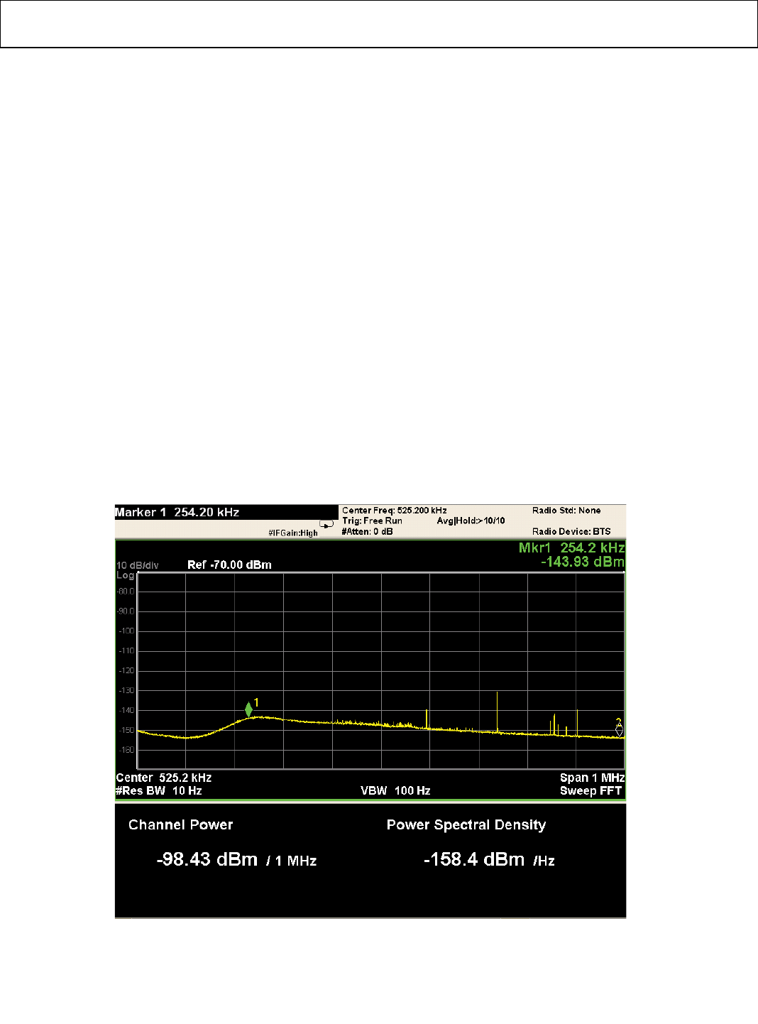
UG-570 AD9361 Reference Manual
| Page 122 of 128
Output Noise Spectrum
Figure 89 shows the output spectrum of the ADP5040 switching
regulator up to 1 MHz. This span is important, as the AD9361
is more sensitive to low frequency noise than it is to high
frequency noise. Switcher noise greater than 1 MHz is also
important. Some switching regulators can have large multiples
of the switching frequency with many sidebands. These spurs
generated by the switcher can couple into other power supplies
or RF balls.
Switching Frequency
The switching frequency of the switching regulator is also an
important characteristic to consider. Figure 90 shows that the
frequency of the power supply noise less than the synthesizer
loop filter bandwidth is the most important. Therefore, choose
a regulator with a switching frequency greater than 1 MHz.
Since the switching frequency of ADP5040 is 3 MHz, it is
relatively quiet ranging from 100 Hz to 500 kHz.
Slew Rate
The slew rate of the regulator is important to control the rise
time and fall times of the switching edges. A switcher regulator
with a high slew rate is preferred as this reduces low frequency
sidebands that can fall below 1 MHz.
Maximum Output Capacitance
In switching regulators with limitation for the maximum
allowable output capacitance, it is important to consider the
effects over the lowest frequency that can be decoupled from
the power supply noise. Two main factors affect the transient
response of a switching regulator: the output capacitor ESR and
the regulator loop bandwidth. To improve the transient
response, it is preferable to add capacitors in parallel instead of
using one larger output capacitor. This is to reduce the total
ESR. Increasing the output capacitance value also changes the
regulator loop characteristics and the phase margin, small phase
margin yields to an under-damped system where oscillation
occurs after a transient. If the phase margin is too large then the
system becomes over-damped where the response to transients
is slow. Transient performance considerations are in the Rx LO
Frequency Deviations Due to Power Supply Transients section.
Figure 89 shows the 1 MHz noise spectrum of the ADP5040. In
this screenshot, the ADP5040 is powering up the 1.3 V analog
power plane with the AD9361 in FDD mode.
Figure 89. Noise Floor at the Buck Output of ADP5040 Powering the1.3 V Analog Plane (The AD9361 in FDD State)
11668-090
Rev. A
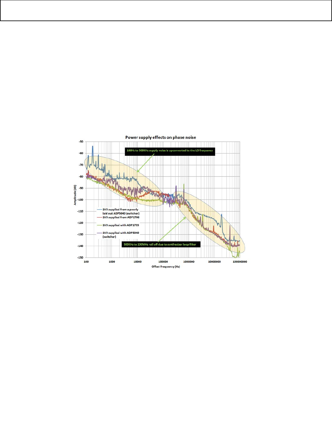
AD9361 Reference Manual UG-570
| Page 123 of 128
Effects on Phase Noise Due to Noise on the Power Supply
Figure 90 shows the effects of power supply noise on the phase
noise of the transmitter local oscillator. The transmitter local
oscillator is set to 5.1 GHz. This plot shows that noise from a
poorly designed power management section will be up-
converted to affect the performance of the transmitter and
similarly have an adverse effect on the receiver performance.
The phase noise performance degrades as the local oscillator
frequency increases. For example, the effects of power supply
noise are not as pronounced if the local oscillator frequency is
700 MHz compared to when the local oscillator frequency is
5.8 GHz. This is because the synthesizer always generates a
frequency between 6 GHz to 12 GHz. To generate a specific LO,
the synthesizer output is divided which also reduces the noise
spectrum. Conversely, the highest frequency designs require the
lowest amount of power supply noise because the divide ratios
are small.
Figure 90 shows the best performance when the ADP1755 LDO
is used. The ADP1755 has better noise characteristics than the
ADP1706 LDO. The phase noise plot compares the perfor-
mance of the ADP5040 in different layout scenarios. The
ADP5040 has a buck convertor that powers up 1.3 V analog
power supply. The ADP5040 also has two LDOs that are used to
power the VDD_GPO supply and the VDD_INTERFACE
supply. For more details on the ADP5040, refer to its data sheet.
Figure 90. Phase Noise vs. Frequency Offset Comparison for Different Power Supply Schemes
11668-091
Rev. A

UG-570 AD9361 Reference Manual
| Page 124 of 128
POWER DISTRIBUTIONS FOR DIFFERENT POWER SUPPLY DOMAINS
The AD9361 has 17 power supply balls. These balls power up different circuits on the part. Table 55 shows the ball number, the ball name,
the recommended routing technique for that ball from the main 1.3 V analog supply plane and a brief description of the block it powers
up in the chip. In some cases, one finger is used to power up two to three 1.3 V power supply balls while in some cases there are some
power supply balls that have a finger just for themselves. Table 55 shows which power supply balls have their own fingers and which balls
are tied together and share one finger. Fingers provide isolation for the concerned 1.3 V power supply balls. Figure 91 shows this
structure.
Table 55. Power Supply Balls on the AD9361
Ball
Ball Name
Recommended Routing
Description
A11 VDDA1P1_TX_VCO Short to B11 with 1µF bypass capacitor
1 Ω series resistance
Powers supply for Tx VCO in the chip
B8 VDD_GPO GPO pull-up voltage (1.3 V to 3.3 V) Power supply for the GPO balls
B9 VDDA1P3_TX_LO 1.3 V separate trace to common supply
point
Power supply for Tx LO Generator and LO divider
B10 VDDA1P3_TX_VCO_LDO Short to B9 Power supply for the Tx VCO LDO
B11 TX_VCO_LDO_OUT Short to A11 Output of the Tx VCO LDO needed to power the Tx VCO on
the chip
D2 VDDA1P3_RX_RF Short to D3 Power supply for the Rx LNAs and the mixer GM stages
D3 VDDA1P3_RX_TX Short to E3 Power supply for Tx Low pass filter, Tx monitor, Rx trans
impedance amplifier, Rx low pass filter, AuxDAC
E2 VDDA1P3_RX_LO Short to F2 Power supply for Rx LO generator and LO divider
E3 VDDA1P3_TX_LO_BUFFER 1.3 V separate trace to common supply
point
Power supply to the Tx LO buffer that goes to the up
converter
F2 VDDA1P3_RX_VCO_LDO 1.3 V separate trace to common supply
point
Power supply input for the Rx VCO LDO
F12 VDDD1P3_DIG 1.3 V separate trace to common supply
point
Powers the digital core
G2
RX_VCO_LDO_OUT
Short to G3
Output of the Rx VCO LDO needed to power the Rx VCO
LDO in the chip
G3 VDDA1P1_RX_VCO Short to G2 with 1µF bypass capacitor
1 Ω series resistance
Power supply for the Rx VCO on the chip
H12 VDD_INTERFACE Interface pull-up voltage (1.3 V to 2.5 V) Powers the digital interface of the chip
J3 VDDA1P3_RX_SYNTH 1.3 V separate trace to common supply
point
Powers the charge pump, sigma delta modulator and the
VCO calibration block of the Rx synthesizer
K3 VDDA1P3_TX_SYNTH 1.3 V separate trace to common supply
point
Powers the charge pump, sigma-delta modulator and the
VCO calibration block of the Tx synthesizer
K4 VDDA1P3_BB 1.3 V separate trace to common supply
point
Powers the Tx DACs, Rx ADCs and AuxADC
Tx1
TX BALUN DC FEED
VIA directly to 1.3 V plane
Provides power to the Tx output on Channel 1
Tx2 TX BALUN DC FEED VIA directly to 1.3 V plane Provides power to the Tx output on Channel 2
Rev. A
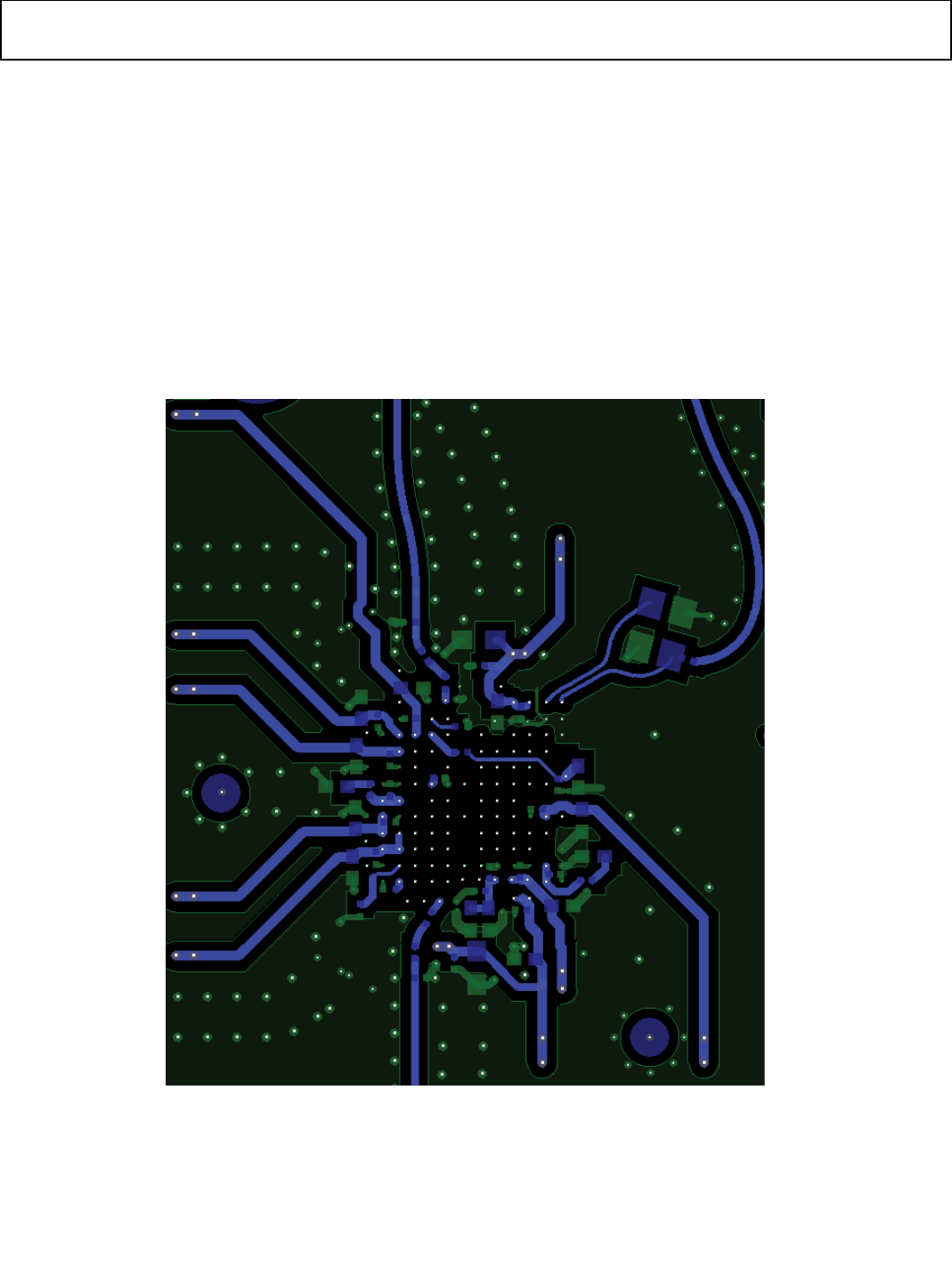
AD9361 Reference Manual UG-570
| Page 125 of 128
Rx and Tx Synthesizer Supplies
The power supply noise rejection on the VDDA1P3_
Rx_SYNTH and VDDA1P3_Tx_SYNTH power domains is
very low. This means that any noise ripple on these balls will
affect the synthesizer performance. The supply noise on the
synthesizers will degrade the phase noise. For the best
performance, in the FDD mode, VDDA1P3_RX_SYNTH,
VDDA1P3_TX_SYNTH, VDDA1P3_RX_LO,
VDDA1P3_RX_VCO_LDO, VDDA1P3_TX_LO,
VDDA1P3_TX_VCO_LDO can be powered up with a
separate low noise LDO. This will also help in mitigating
effects of transients on the 1.3 V analog supply. The evalua-
tion board uses this power design.
Tx Balun DC Feed Supplies
Each transmitter requires 150 mA of current that the DC feed
of the balun supplies. To reduce switching transients when
attenuation settings change, the balun DC feed must be
powered directly by the 1.3 V plane. A 10 μF and a 0.1 μF
capacitors are helpful on the DC feed pin to eliminate spurs on
the Tx spectrum and dampen the transients.
Figure 91. Power Supply Fingers
11668-092
Rev. A
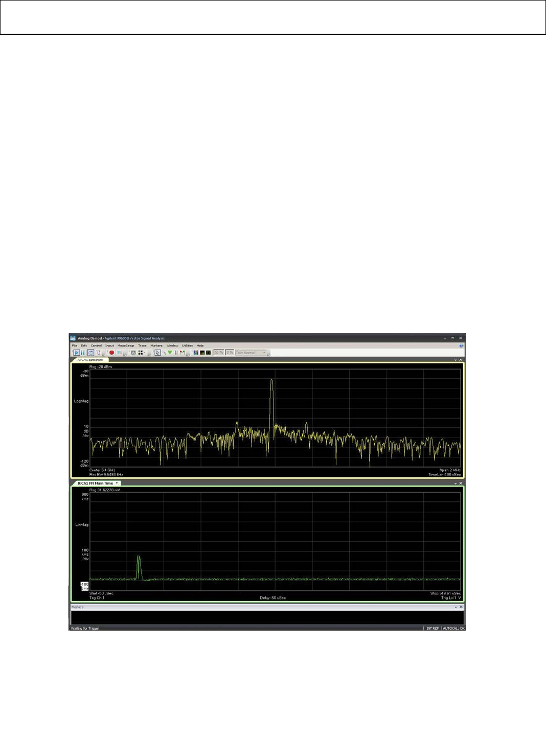
UG-570 AD9361 Reference Manual
| Page 126 of 128
Rx LO FREQUENCY DEVIATIONS DUE TO POWER
SUPPLY TRANSIENTS
The AD9361 is a transceiver that can operate in TDD or in
FDD mode. In FDD mode, there is a need to dynamically
change the transmit power when the receivers are on and
receiving data. This means that the load that the part presents to
the power supply changes, giving rise to transients on the power
supply line. The amplitude and the response time of these
transients depend on board layout and the regulator used to
supply power. These power supply transients are detrimental to
the receiver performance until the transient has died down.
Figure 92 shows the instantaneous deviation in the Rx VCO
frequency due to a voltage transient on the 1.3 V supply. During
this experiment, The AD9361 was in FDD state. The Channel 1
spectrum in Figure 92 is the Rx VCO leakage from the Rx pin
when the Rx LO is 800 MHz. Channel 2 is a FM demodulation
of Channel 1. This means that Channel 2 will show the
instantaneous changes in VCO frequency. The spectrum
analyzer is triggered on the TXNRX signal that turns the
transmitter ON or OFF. This environment simulates the worst
case VCO frequency deviation that can occur on the Rx synth.
The blue trace in Figure 93 shows the voltage transient on the
1.3 V line when the transmitters turn ON. The magenta trace is
the Vtune voltage of the Tx VCO that is probed on the Tx EXT
LO line and the green trace is the Vtune voltage of the Rx VCO
that is probed on the Rx EXT LO line. The instantaneous
frequency deviation shown in Figure 92 is a direct cause of the
instantaneous change in the Vtune voltage. Screenshots in
Figure 92 and Figure 93 were taken simultaneously on one
trigger. The experiment described previously was done with the
ADP1706-1.3V LDO powering the 1.3 V supply.
This issue can be mitigated by powering the Rx synth, Tx synth,
Rx LO and Tx LO supplies from a different LDO. This approach
helps in isolating the synthesizers from the transients on the
1.3 V supply. Figure 94 shows the frequency kick when the Rx
synth, Tx synth, Tx LO, and Rx LO supplies are powered up
externally. The frequency kick decreases to one third of its
initial amplitude. Figure 95 shows the voltage kick on the 1.3 V
supply and the consequent response of Vtune voltage of the Tx
VCO (magenta) and the Vtune voltage of the Rx VCO (green).
Figure 92. Instantaneous Rx VCO Frequency Deviation Seen Due to a Voltage Transient on the 1.3 V Supply
11668-093
Rev. A
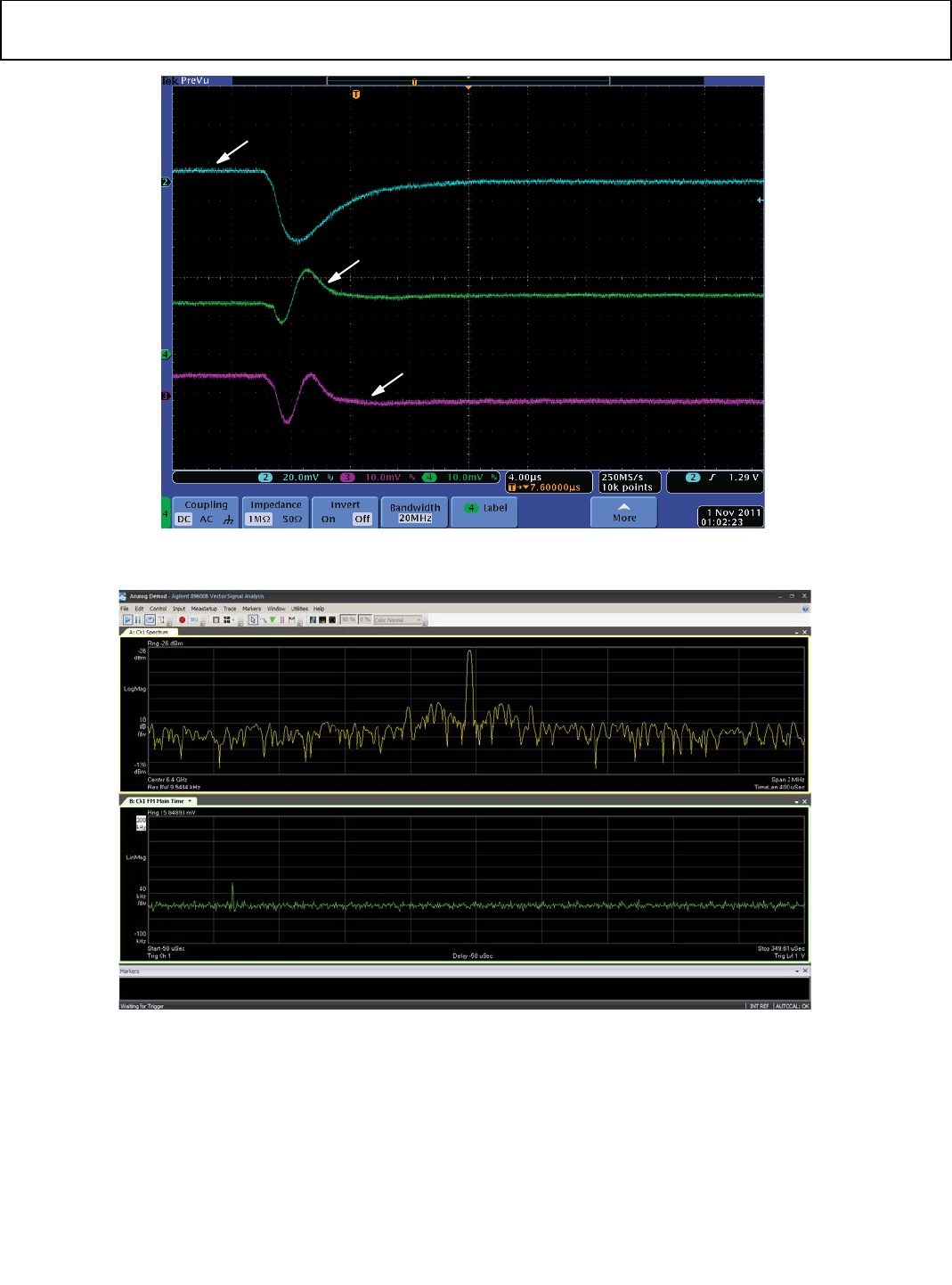
AD9361 Reference Manual UG-570
| Page 127 of 128
Figure 93. Voltage Transient on the 1.3 V Supply and Vtune of the Rx and the Tx VCO
Figure 94. Instantaneous Frequency Deviation Seen Due to a Voltage Transient on the 1.3 V Supply: VDDA1P3_Rx_SYNTH, VDDA1P3_Tx_SYNTHs Supplied Externally
11668-293
VTUNE VOLTAGE OF THE TX VCO THAT IS PROBED ON THE TX EXT LO LINE
VOLTAGE TRANSIENT ON THE 1.3V LINE WHEN THE TRANSMITTERS TURN ON
VTUNE VOLTAGE OF THE RX VCO THAT IS PROBED ON THE RX EXT LO LINE
11668-095
Rev. A
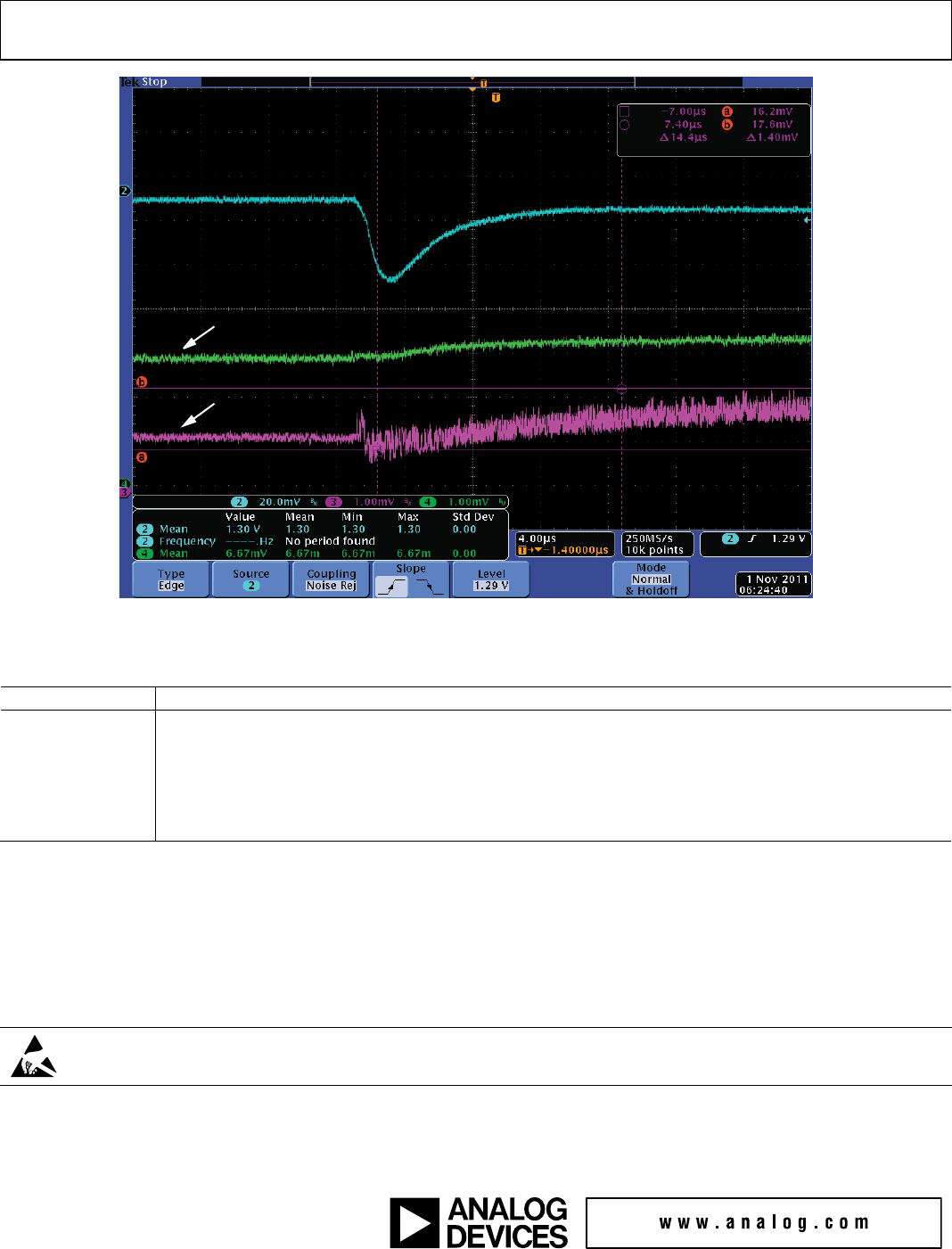
UG-570 AD9361 Reference Manual
Rev. A | Page 128 of 128
Figure 95. Voltage Transient on the 1.3 V Supply and the Vtune of the VCO: VDDA1P3_Rx_SYNTH, VDDA1P3_Tx_SYNTH, Supplied Externally
RELATED LINKS
Resource Description
AD9361 Product Page, AD9361 RF Agile Transceiver
AD9548 Product Page, AD9548 Quad/Octal Input Network Clock Generator/Synchronizer
ADA4851-4 Product Page, ADA4851-4 Low Cost, High Speed, Rail-to-Rail, Output Op Amp (Quad)
ADP1706 Product Page, ADP1706 1 A, Low Dropout, CMOS Linear Regulator
ADP1755 Product Page, ADP1755 1.2 A Low VIN, Adjustable VOUT LDO Linear Regulator
ADP5040 Product Page, ADP5040 Micro PMU with 1.2 A Buck Regulator and Two 300 mA LDOs
Tx VCO VTUNE VOLTAGE
Rx VCO VTUNE VOLTAGE
11668-096
ESD Caution
ESD (electrostatic discharge) sensitive device. Charged devices and circuit boards can discharge without detection. Although this product features patented or proprietary protection
circuitry, damage may occur on devices subjected to high energy ESD. Therefore, proper ESD precautions should be taken to avoid performance degradation or loss of functionality.
Legal Terms and Conditions
Information furnished by Analog Devices is believed to be accurate and reliable. However, no responsibility is assumed by Analog Devices for its use, nor for any infringements of patents or other
rights of third parties that may result from its use. No license is granted by implication or otherwise under any patent or patent rights of Analog Devices. Trademarks and registered trademarks
are the property of their respective owners. Information contained within this document is subject to change without notice. Software or hardware provided by Analog Devices may not be
disassembled, decompiled or reverse engineered. Analog Devices’ standard terms and conditions for products purchased from Analog Devices can be found at:
http://www.analog.com/en/content/analog_devices_terms_and_conditions/fca.html.
©2014–2015 Analog Devices, Inc. All rights reserved. Trademarks and
registered trademarks are the property of their respective owners.
UG11668-0-6/15(A)
