AD9361 Register Map Reference Manual UG 671
User Manual:
Open the PDF directly: View PDF ![]() .
.
Page Count: 72
- General Description
- Table of Contents
- Revision History
- General Setup and Digital Data Port Configuration
- Chip Level Setup Registers (Address 0x000 Through Address 0x007)
- SPI Register 0x000—SPI Configuration
- SPI Register 0x001—Multichip Sync and Tx Monitor Control
- SPI Register 0x002—Tx Enable and Filter Control
- SPI Register 0x003—Rx Enable and Filter Control
- SPI Register 0x004—Input Select
- SPI Register 0x005—RFPLL Dividers
- SPI Register 0x006—Rx Clock and Data Delay
- SPI Register 0x007—Tx Clock and Data Delay
- Clock Control Registers (Address 0x009 Through Address 0x00A)
- Temperature Sensor Registers (Address 0x00C Through Address 0x00F)
- Parallel Port Configuration Registers (Address 0x010 Through Address 0x012)
- Enable State Machine (ENSM) Registers (Address 0x013 Through Address 0x017)
- AuxDAC Registers (Address 0x018 Through Address 0x01B)
- Auxiliary ADC Registers (Address 0x01C Through Address 0x01F)
- GPO, AuxDAC, AGC Delay, and Synth Delay Control Registers (Address 0x020 Through Address 0x033)
- SPI Register 0x020—Auto GPO
- SPI Register 0x021—AGC Gain Lock Delay
- SPI Register 0x022—AGC Attack Delay
- SPI Register 0x023—AuxDAC Enable Control
- SPI Register 0x024—Must be x02
- SPI Register 0x025—Must be x02
- SPI Register 0x026—External LNA Control
- SPI Register 0x027—GPO Force and Init
- SPI Registers 0x028 Through 0x02B—GPOn Rx Delay[7:0]
- SPI Register 0x02C Through SPI Register 0x02F—GPOn Tx Delay[7:0]
- SPI Register 0x030 Through SPI Register 0x033—AuxDACn Rx/Tx Delay[7:0]
- Control Output Registers (Address 0x035 Through Address 0x036)
- Product ID Register (Address 0x037)
- Reference Clock Cycles Register (Address 0x03A)
- Digital IO Control Registers (Address 0x03B Through Address 0x03E)
- BBPLL Control Registers (Address 0x03F Through Address 0x04E)
- SPI Register 0x03F—BBPLL Control 1
- SPI Register 0x040—Must be 0
- SPI Register 0x041[D7:D5]—Set to 0
- SPI Register 0x041[D4:D0] Through SPI Register 0x044—Fractional and Integer BB Freq Words
- SPI Register 0x045—Ref Clock Scaler
- SPI Register 0x046—CP Current
- SPI Register 0x047—MCS Scale
- SPI Register 0x048 through SPI Register 0x04A—Loop Filter
- SPI Register 0x04B—VCO Control
- SPI Register 0x04C—Set to 0x86
- SPI Register 0x04D—BBPLL Control 2
- SPI Register 0x04E—BBPLL Control 3
- Power Down Override Registers (Address 0x050 Through Address 0x058)
- SPI Register 0x050—Rx Synth Power Down Override
- SPI Register 0x051—Tx Synth Power Down Override
- SPI Register 0x052—Control 0
- SPI Register 0x053—Must be 0
- SPI Registers 0x054 and 0x055—Rx1 and Rx2 ADC Power Down Override
- SPI Register 0x056—Tx Analog Power Down Override 1
- SPI Register 0x057—Analog Power Down Override
- SPI Register 0x058—Misc Power Down Override
- Overflow Registers (Address 0x05E Through Address 0x05F)
- Chip Level Setup Registers (Address 0x000 Through Address 0x007)
- Transmitter Configuration
- Tx Programmable FIR Filter Registers (Address 0x060 Through Address 0x065)
- Tx Monitor Registers (Address 0x067 Through Address 0x071)
- SPI Register 0x067—Tx Mon Low Gain
- SPI Register 0x068—Tx Mon High Gain
- SPI Register 0x069 and SPIRegister 0x06A[D1:D0]—Tx Mon Delay Counter
- SPI Register 0x06A—Tx Level Threshold
- SPI Register 0x06B Through SPIRegister 0x06D—Tx RSSI n
- SPI Register 0x06E—TPM Mode Enable
- SPI Register 0x06F—Temp Gain Coefficient[7:0] for Tx Mon
- SPI Register 0x070 and SPI Register 0x071—Tx Mon n Config
- Tx Power Control and Attenuation Registers (Address 0x073 Through Address 0x07C)
- Tx Quadrature Calibration Phase, Gain, and Offset Correction Registers (Address 0x08E Through Address 0x09F)
- SPI Register 0x08E—Tx1 Out 1 Phase Corr
- SPI Register 0x08F—Tx1 Out 1 Gain Corr
- SPI Register 0x090—Tx2 Out 1 Phase Corr
- SPI Register 0x091—Tx2 Out 1 Gain Corr
- SPI Register 0x092—Tx1 Out 1 Offset I
- SPI Register 0x093—Tx1 Out 1 Offset Q
- SPI Register 0x094—Tx2 Out 1 Offset
- SPI Register 0x095—Tx2 Out 1 Offset Q
- SPI Register 0x096—Tx1 Out 2 Phase Corr
- SPI Register 0x097—Tx1 Out 2 Gain Corr
- SPI Register 0x098—Tx2 Out 2 Phase Corr
- SPI Register 0x099—Tx2 Out 2 Gain Corr
- SPI Register 0x9A—Tx1 Out 2 Offset I
- SPI Register 0x09B—Tx1 Out 2 Offset Q
- SPI Register 0x09C—Tx2 Out 2 Offset I
- SPI Register 0x09D—Tx2 Out 2 Offset Q
- SPI Register 0x09F—Force Bits
- Tx Quadrature Calibration Configuration Registers (Address 0x0A0 Through Address 0x0AE)
- SPI Register 0x0A0—Quad Cal NCO Freq and Phase Offset
- SPI Register 0x0A1—Quad Cal Control
- SPI Register 0x0A2—Set to 0x7F
- SPI Register 0x0A3—Tx NCO Frequency
- SPI Register 0x0A4—Set to 0xF0
- SPI Register 0x0A5 and SPI Register 0x0A6—Mag Ftest Thresh and Mag Ftest Thresh2
- SPI Register 0x0A7 and SPI Register 0x0A8 Quad Cal Status Tx1 and Tx2
- SPI Register 0x0A9—Set to 0xFF
- SPI Register 0x0AA—Tx Quad Full/LMT Gain
- SPI Register 0x0AB—Must be 0
- SPI Register 0x0AC— Must be 0
- SPI Register 0x0AD— Must be 0
- SPI Register0x 0AE—Tx Quad LPF Gain
- Tx Baseband Filter Registers (Address 0x0C2 Through Address 0x0CC)
- Tx Secondary Filter Registers (Address 0x0D0 Through Address 0x0D3)
- Tx BBF Tuner Configuration Registers (Address 0x0D6 Through Address 0x0D7)
- Receiver Configuration
- Rx Programmable FIR Filter Registers (Address 0x0F0 Through Address 0x0F6)
- Gain Control General Setup Registers (Address 0x0FA Through Address 0x10E)
- SPI Register 0x0FA—AGC Config 1
- SPI Register 0x0FB—AGC Config 2
- SPI Register 0x0FC—AGC Config 3
- SPI Register 0x0FD—Max LMT/Full Gain
- SPI Register 0x0FE—Peak Wait Time
- SPI Register 0x100—Digital Gain
- SPI Register 0x101—AGC Lock Level
- SPI Register 0x103—Gain Step Config 1
- SPI Register 0x104—ADC Small Overload Threshold
- SPI Register 0x105—ADC Large Overload Threshold
- SPI Register 0x106—Gain Step Config 2
- SPI Register 0x107—Small LMT Overload Threshold
- SPI Register 0x108—Large LMT Overload Threshold
- SPI Register 0x109—Rx1 Manual LMT/Full Gain
- SPI Register 0x10A—Rx1 Manual LPF Gain
- SPI Register 0x10B—Rx1 Manual Digital Gain
- SPI Register 0x10C Through SPI Register 0x10E—Manual Gain Registers
- Fast Attack AGC Setup Registers (Address 0x110 Through Address 0x11B)
- SPI Register 0x110—Config 1
- SPI Register 0x111—Config 2 and Settling Delay
- SPI Register 0x112—Energy Lost Threshold
- SPI Register 0x113—Stronger Signal Threshold
- SPI Register 0x114—Low Power Threshold
- SPI Register 0x115—Don’t Unlock Gain if Stronger Signal
- SPI Register 0x116—Final Overrange and Opt Gain
- SPI Register 0x117—Energy Detect Count
- SPI Register 0x118—AGCLL Max Increase
- SPI Register 0x119—Gain Lock Exit Count
- SPI Register 0x11A—Initial LMT Gain Limit
- SPI Register 0x11B—Increment Time[7:0]
- Slow Attack and Hybrid AGC Registers (Address 0x120 Through Address 0x12A)
- SPI Register 0x120—AGC Inner Lower Threshold
- SPI Register 0x121—LMT End Overload Counters
- SPI Register 0x122—ADC Overload Counters
- SPI Register 0x123—Gain Step 1
- SPI Register 0x124 and SPI Register 0x125—Gain Update Counter
- SPI Register 0x128—Digital Sat Counter
- SPI Register 0x129—Outer Power Thresholds
- SPI Register 0x12A—Gain Step 2
- External LNA Gain Word Registers (Address 0x12C Through Address 0x12D)
- AGC Gain Table Registers (Address 0x130 Through Address 0x137)
- Mixer SubTable Registers (Address 0x138 Through Address 0x13F)
- SPI Register 0x138—Mixer Subtable Word Address
- SPI Register 0x139—Mixer Subtable Gain Word Write
- SPI Register 0x13A—Mixer Subtable Bias Word Write
- SPI Register 0x13B—Mixer Subtable Control Word Write
- SPI Register 0x13C Through Register 0x13E—Mixer Subtable Word Reads
- SPI Register 0x13F—Mixer Subtable Config
- Calibration Gain Table Registers (Address 0x140 Through Address 0x144)
- General Calibration Registers (Address 0x145 Through Address 0x149)
- RSSI Measurement Configuration Registers (Address 0x150 Through Address 0x15D)
- Power Word Registers (Address 0x161 Through Address 0x163)
- Rx Quadrature Calibration Registers (Address 0x169 Through Address 0x16B)
- Rx Phase and Gain Correction Registers (Address 0x170 Through Address 0x182)
- SPI Register 0x170—Rx1A Phase Corr
- SPI Register 0x171—Rx1A Gain Corr
- SPI Register 0x172—Rx2A Phase Corr
- SPI Register 0x173—Rx2A Gain Corr
- SPI Register 0x174 and SPI Register 0x175[D1:D0]—Rx1A Q DC Offset
- SPI Register 0x175[D7:D2] and SPI Register 0x176[D3:D0]—Rx1A Offsets
- SPI Register 0x176[D7:D4] and SPI Register 0x177[D5:D0]—Rx2A Q Offset
- SPI Register 0x177[D7:D6] and SPI Register 0x178[D7:D0]—Rx2A I Offset
- SPI Register 0x179 through SPI Register 0x181—B and C Inputs
- SPI Register 0x182—Force Bits
- Rx DC Offset Control Registers (Address 0x185 Through Address 0x194)
- SPI Register 0x185—Wait Count
- SPI Register 0x186—RF DC Offset Count
- SPI Register 0x187—RF DC Offset Config 1
- SPI Register 0x188—RF DC Offset Attenuation
- SPI Register 0x18B—DC Offset Config2
- SPI Register 0x18C—RF Cal Gain Index
- SPI Register 0x18D—RF SOI Threshold
- SPI Register 0x190—BB DC Offset Shift
- SPI Register 0x191—BB DC Offset Fast Settle Shift
- SPI Register 0x192—BB Tracking Fast Settle Dur
- SPI Register 0x193—Must be x3F
- SPI Register 0x194—BB DC Offset Attenuation
- Rx BB DC Offset Registers (Address 0x19A Through Address 0x1A5)
- RSSI Readback Registers (Address 0x1A7 Through Address 0x1AC)
- Rx TIA Registers (Address 0x1DB Through Address 0x1DF)
- Rx BBF Registers (Address 0x1E0 Through Address 0x1F5)
- SPI Register 0x1E0—Rx1 BBF R1A
- SPI Register 0x1E1—Rx2 BBF R1A
- SPI Register 0x1E2—Rx1 Tune Control
- SPI Register 0x1E3—Rx2 Tune Control
- SPI Register 0x1E4—Rx1 BBF R5
- SPI Register 0x1E5—Rx2 BBF R5
- SPI Register 0x1E6—Rx BBF R2346
- SPI Register 0x1E7 and SPI Register 0x1E9—Rx BBF C1 and C2 MSB
- SPI Register 0x1E8 and SPI Register 0x1EA—Rx BBF C1and C2 LSB
- SPI Register 0x1EB—Rx BBF C3 MSB
- SPI Register 0x1EC—Rx BBF C3 LSB
- SPI Register 0x1ED—Rx BBF CC1 Ctr
- SPI Register 0x1EE—Must be 0x60
- SPI Register 0x1EF—Rx BBF CC2 Ctr
- SPI Register 0x1F0—Rx BBF Pow Rz Byte1
- SPI Register 0x1F1—Rx BBF CC3 Ctr
- SPI Register 0x1F2—Rx BBF R5 Tune
- SPI Register 0x1F3—Rx BBF Tune
- SPI Register 0x1F4 and SPI Register 0x1F5—Rx1/Rx2 BBF Man Gain
- Rx BBF Tuner Configuration Registers (Address 0x1F8 Through Address 0x1FC)
- Rx Analog Registers
- Rx Synthesizer Registers (Address 0x230 Through Address 0x251)
- SPI Register 0x230— PFD Config
- SPI Register 0x231, SPI Register 0x232[D2:D0] and SPI Register 0x233 Through SPI Register 0x235—VCO Frequency Words
- SPI Register 0x232
- SPI Register 0x236—Force ALC
- SPI Register 0x237—Force VCO Tune 0
- SPI Register 0x238—Force VCO Tune 1
- SPI Register 0x239—ALC/Varactor
- SPI Register 0x23A—VCO Output
- SPI Register 0x23B—CP Current
- SPI Register 0x23C—CP Offset
- SPI Register 0x23D—CP Config
- SPI Register 0x23E—Loop Filter 1
- SPI Register 0x23F—Loop Filter 2
- SPI Register 0x240—Loop Filter 3
- SPI Register 0x241—Dither/CP Cal
- SPI Register 0x242—VCO Bias 1
- SPI Register 0x243—Must be 0x0D
- SPI Register 0x244—Cal Status
- SPI Register 0x245—Must be 0x00
- SPI Register 0x246—Must be 0x02
- SPI Register 0x247—CP Ovrge/VCO Lock
- SPI Register 0x248—Must be 0x0B
- SPI Register 0x249—VCO Cal
- SPI Register 0x24A—Lock Detect Config
- SPI Register 0x24B—Must be 0x17
- SPI Register 0x24C—Must be 0
- SPI Register 0x24D—Must be 0
- SPI Register 0x250—Must be 0x70
- SPI Register 0x251—VCO Varactor Control 1
- Rx Fast Lock Registers (Address 0x25A Through Address 0x25F)
- Rx LO Generation Register (Address 0x261)
- Tx Synthesizer Registers (Address 0x270 Through Address 0x291)
- DCXO Registers (Address 0x292 Through Address 0x294)
- Tx Synth Fast Lock Registers (Address 0x29A Through Address 0x29F)
- Tx LO Generation Register (Address 0x2A1)
- Master Bias and Band Gap Configuration Registers (Address 0x2A6 and Address 0x2A8)
- Reference Divider Registers (Address 0x2AB and Address 0x2AC)
- Rx Gain Read Back Registers (Address 0x2B0 Through Address 0x2B9)
- Control Register (Register 0x3DF)
- Digital Test Registers (Address 0x3F4 Through Address 0x3F6)
- Rx Synthesizer Registers (Address 0x230 Through Address 0x251)

AD9361 Register Map Reference Manual
UG-671
One Technology Way • P. O. Box 9106 • Norwood, MA 02062-9106, U.S.A. • Tel: 781.329.4700 • Fax: 781.461.3113 • www.analog.com
AD9361 Register Map
PLEASE SEE THE LAST PAGE FOR AN IMPORTANT
WARNING AND LEGAL TERMS AND CONDITIONS. Rev. 0 | Page 1 of 72
GENERAL DESCRIPTION
This user guide contains a description of all of the user-programmable bits in the AD9361. When applicable, the map lists units, (such as
dBFS) that the bits correspond to, the range of acceptable values, and the resolution of the value (such as 1 dB/LSB).
In many cases, multiple bits or bytes work together to serve a particular function (for example, those used to configure automatic gain
control and those used to configure the digital interface). This section describes each bit but more information is available in the AD9361
Reference Manual.
While the register map is provided as a convenience for those who want to understand the low level operation of the part, it is not
recommended to attempt to create your own software. Analog Devices provides complete drivers for the AD9361 for both bare metal/No-
OS and operating systems (Linux). The AD9361 and AD9364 share the same API. The AD9361 and AD9364 drivers can be found at:
Linux wiki page
No-OS wiki page
Support for these drivers can be found at:
Linux engineer zone page
No-OS engineer zone page
Complete specifications for the AD9361 part can be found in the AD9361 data sheet, which is available from Analog Devices, Inc., and
should be consulted in conjunction with this user guide when using the evaluation board.

UG-671 AD9361 Register Map Reference Manual
Rev. 0 | Page 2 of 72
TABLE OF CONTENTS
General Description ......................................................................... 1
Revision History ............................................................................... 3
General Setup and Digital Data Port Configuration ................... 4
Chip Level Setup Registers (Address 0x000 Through
Address 0x007) ............................................................................. 4
Clock Control Registers (Address 0x009 Through
Address 0x00A)............................................................................. 7
Temperature Sensor Registers (Address 0x00C Through
Address 0x00F) ............................................................................. 8
Parallel Port Configuration Registers (Address 0x010
Through Address 0x012) ............................................................. 9
Enable State Machine (ENSM) Registers (Address 0x013
Through Address 0x017) ........................................................... 11
AuxDAC Registers (Address 0x018 Through
Address 0x01B) ........................................................................... 13
Auxiliary ADC Registers (Address 0x01C Through
Address 0x01F) ........................................................................... 14
GPO, AuxDAC, AGC Delay, and Synth Delay Control
Registers (Address 0x020 Through Address 0x033) .............. 15
Control Output Registers (Address 0x035 Through
Address 0x036) ........................................................................... 17
Product ID Register (Address 0x037) ...................................... 17
Reference Clock Cycles Register (Address 0x03A) ................ 17
Digital IO Control Registers (Address 0x03B Through
Address 0x03E) ........................................................................... 17
BBPLL Control Registers (Address 0x03F Through
Address 0x04E) ........................................................................... 19
Power Down Override Registers (Address 0x050 Through
Address 0x058) ........................................................................... 22
Overflow Registers (Address 0x05E Through
Address 0x05F) ........................................................................... 24
Transmitter Configuration ............................................................ 25
Tx Programmable FIR Filter Registers (Address 0x060
Through Address 0x065) ........................................................... 25
Tx Monitor Registers (Address 0x067 Through
Address 0x071) ........................................................................... 26
Tx Power Control and Attenuation Registers (Address 0x073
Through Address 0x07C) .......................................................... 27
Tx Quadrature Calibration Phase, Gain, and Offset
Correction Registers (Address 0x08E Through
Address 0x09F) ........................................................................... 28
Tx Quadrature Calibration Configuration Registers
(Address 0x0A0 Through Address 0x0AE) ............................ 30
Tx Baseband Filter Registers (Address 0x0C2 Through
Address 0x0CC) .......................................................................... 32
Tx Secondary Filter Registers (Address 0x0D0 Through
Address 0x0D3) .......................................................................... 33
Tx BBF Tuner Configuration Registers (Address 0x0D6
Through Address 0x0D7) .......................................................... 34
Receiver Configuration .................................................................. 35
Rx Programmable FIR Filter Registers (Address 0x0F0
Through Address 0x0F6) .......................................................... 35
Gain Control General Setup Registers (Address 0x0FA
Through Address 0x10E) .......................................................... 36
Fast Attack AGC Setup Registers (Address 0x110 Through
Address 0x11B) ........................................................................... 39
Slow Attack and Hybrid AGC Registers (Address 0x120
Through Address 0x12A) .......................................................... 42
External LNA Gain Word Registers (Address 0x12C Through
Address 0x12D) .......................................................................... 43
AGC Gain Table Registers (Address 0x130 Through
Address 0x137) ........................................................................... 44
Mixer SubTable Registers (Address 0x138 Through
Address 0x13F) ........................................................................... 45
Calibration Gain Table Registers (Address 0x140 Through
Address 0x144) ........................................................................... 46
General Calibration Registers (Address 0x145 Through
Address 0x149) ........................................................................... 47
RSSI Measurement Configuration Registers (Address 0x150
Through Address 0x15D) .......................................................... 48
Power Word Registers (Address 0x161 Through
Address 0x163) ........................................................................... 49
Rx Quadrature Calibration Registers (Address 0x169
Through Address 0x16B) .......................................................... 50
Rx Phase and Gain Correction Registers (Address 0x170
Through Address 0x182) ........................................................... 51
Rx DC Offset Control Registers (Address 0x185 Through
Address 0x194) ........................................................................... 52
Rx BB DC Offset Registers (Address 0x19A Through
Address 0x1A5) .......................................................................... 54
RSSI Readback Registers (Address 0x1A7 Through
Address 0x1AC) .......................................................................... 55
Rx TIA Registers (Address 0x1DB Through
Address 0x1DF) .......................................................................... 56
Rx BBF Registers (Address 0x1E0 Through Address 0x1F5) 57
Rx BBF Tuner Configuration Registers (Address 0x1F8
Through Address 0x1FC) .......................................................... 59
Rx Analog Registers ....................................................................... 60
Rx Synthesizer Registers (Address 0x230 Through
Address 0x251) ........................................................................... 60

AD9361 Register Map Reference Manual UG-671
Rev. 0 | Page 3 of 72
Rx Fast Lock Registers (Address 0x25A Through
Address 0x25F) ............................................................................ 64
Rx LO Generation Register (Address 0x261) .......................... 65
Tx Synthesizer Registers (Address 0x270 Through
Address 0x291) ............................................................................ 65
DCXO Registers (Address 0x292 Through Address 0x294) ...... 67
Tx Synth Fast Lock Registers (Address 0x29A Through
Address 0x29F) ............................................................................ 67
Tx LO Generation Register (Address 0x2A1) ......................... 67
Master Bias and Band Gap Configuration Registers
(Address 0x2A6 and Address 0x2A8) ...................................... 67
Reference Divider Registers (Address 0x2AB and
Address 0x2AC) .......................................................................... 68
Rx Gain Read Back Registers (Address 0x2B0 Through
Address 0x2B9) ........................................................................... 69
Control Register (Register 0x3DF) ........................................... 70
Digital Test Registers (Address 0x3F4 Through
Address 0x3F6) ............................................................................ 71
REVISION HISTORY
3/14—Revision 0: Initial Version
UG-671 AD9361 Register Map Reference Manual
Rev. 0 | Page 4 of 72
GENERAL SETUP AND DIGITAL DATA PORT CONFIGURATION
CHIP LEVEL SETUP REGISTERS (ADDRESS 0x000 THROUGH ADDRESS 0x007)
There are many thousands of filter and divider setting permutations, most of which are not valid operating modes. Analog Devices
strongly recommends that customers use the software to program the AD9361 filters and clock dividers.
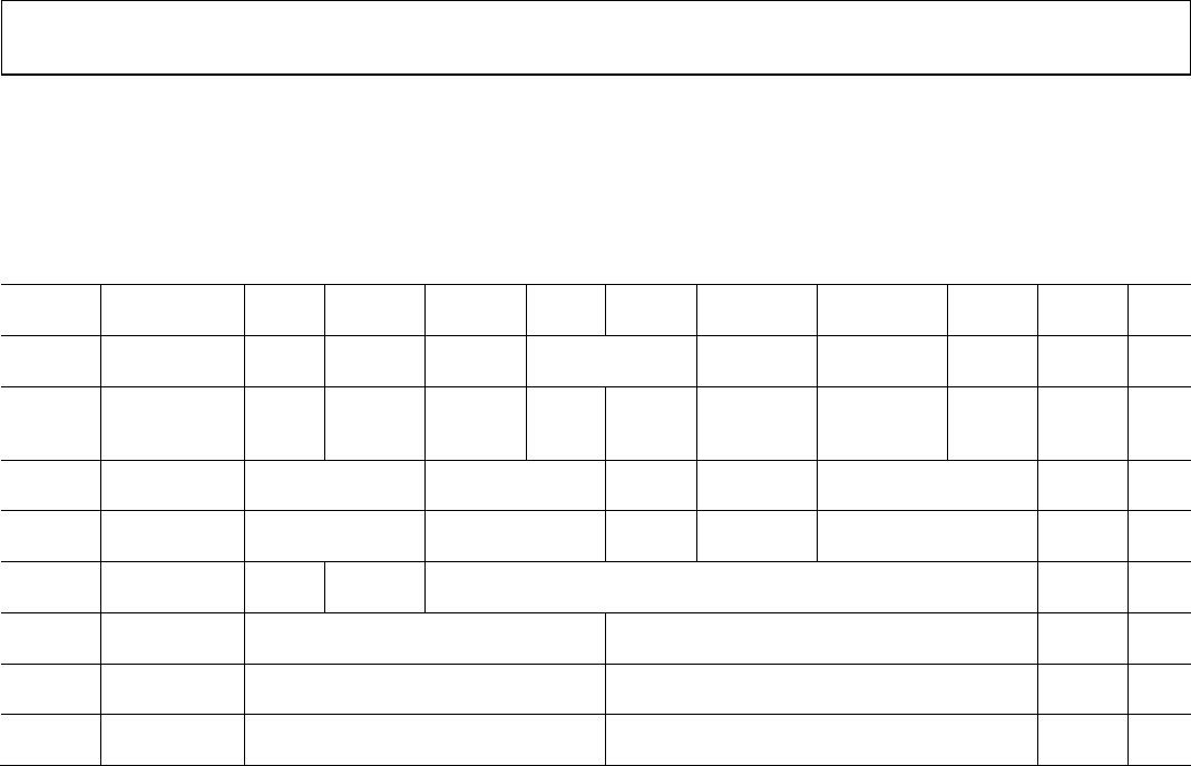
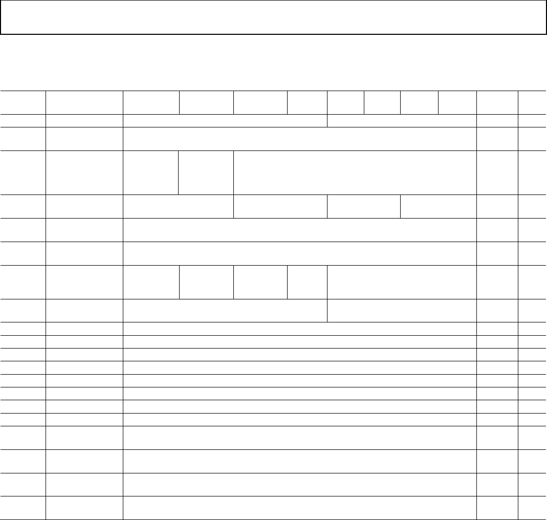
Table 1.
Register
Address Name D7 D6 D5 D4 D3 D2 D1 D0 Default R/W
0x000 SPI
Configuration
Must
be 0
3-Wire
SPI
LSB First Open LSB First 3-Wire SPI Must
be 0
0x00 R/W
0x001 Multichip
Sync and Tx
Mon Control
Open Tx2
Monitor
Enable
Tx1
Monitor
Enable
Open MCS RF
Enable
MCS BBPLL
enable
MCS Digital
CLK Enable
MCS BB
Enable
0x00 R/W
0x002 Tx Enable and
Filter Control
Tx Channel
Enable[1:0]
THB3 Enable and
Interp[1:0]
THB2
Enable
THB1
Enable
Tx FIR Enable and
Interpolation[1:0]
0x5F R/W
0x003 Rx Enable and
Filter Control
Rx Channel
Enable[1:0]
RHB3 Enable and
Decimation[1:0]
RHB2
Enable
RHB1
Enable
Rx FIR Enable and
Decimation[1:0]
0x5F R/W
0x004 Input Select Must
be 0
Tx
Output
Rx Input [5:0] 0x00 R/W
0x005 RFPLL
Dividers
Tx VCO Divider[3:0] Rx VCO Divider[3:0] 0x00 R/W
0x006 Rx Clock and
Data Delay
DATA_CLK Delay[3:0] Rx Data Delay [3:0] 0x00 R/W
0x007 Tx Clock and
Data Delay
FB_CLK Delay[3:0] Tx Data Delay [3:0] 0x00 R/W
SPI Register 0x000—SPI Configuration
This register is symmetrical (for example, Bit D6 is the same as
Bit D1). The AD9361 powers up with a default SPI operation of
MSB first. This register allows the BBP to write any bits in
Register 0x000 without having to reverse the bit order in the SPI
command. Symmetrical bits are OR’ed together so setting one
sets both.
D7 and D0—Must be 0
D6 and D1—3-Wire SPI
When clear, SPI_DI pin is an input pin. When set, SPI_DI is
bidirectional and SPI_DO is high impedance.
D5 and D2—LSB First
When clear, the SPI uses an MSB first format. When set, the SPI
uses an LSB first format.
SPI Register 0x001—Multichip Sync and Tx Monitor
Control
D6—Tx2 Monitor Enable
This bit forces the Tx2 Monitor Path on. This will shut down
the normal receive path. The receive path will not power up
even when the ENSM moves to the Rx state. When this bit is set
the signal at the Tx Mon 2 pin is sent as I and Q data to the Rx
data port. To use transmit power monitoring, see the SPI
Register 0x057—Analog Power Down Override and SPI
Register 0x06E—TPM Mode Enable sections.
D5—Tx1 Monitor Enable
This bit functions the same as Bit D6 but for the Tx_MON1 pin.
D3—MCS RF Enable
Setting this bit keeps the RF LO dividers enabled in Alert mode
so that the phase relationship between multiple devices remains
constant. If the bit is clear, the dividers power down in Alert
mode. The respective LO dividers also power down in FDD
Independent mode when the Rx or Tx paths are disabled if the
bit is clear.
D2—MCS BBPLL Enable
To synchronize the BBPLLs of multiple devices, write this bit
high and then provide a sync pulse to SYNC_IN.
D1—MCS Digital CLK Enable
To synchronize the digital clocks of multiple AD9361 devices,
first synchronize the BBPLLs, then write this bit high and
provide a sync pulse to the SYNC_IN pin.
D0—MCS BB Enable
Setting this bit enables the capability of baseband multichip
digital synchronization. See also 0x001[D2:D1].

AD9361 Register Map Reference Manual UG-671
Rev. 0 | Page 5 of 72
SPI Register 0x002—Tx Enable and Filter Control
[D7:D6]—Tx Channel Enable[1:0]
The ad9361_en_dis_tx function sets these bits. These bits
determine which of the two transmitters is enabled, with Bit D6
corresponding to Tx1 and Bit D7 corresponding to Tx2. Setting
a bit enables a transmitter signal path. Clearing both bits
disables both transmitters.
[D5:D4]—THB3 Enable and Interp[1:0]
Note that there are several functions that calculate digital filter
settings. The ad9361_calculate_rf_clock_chain function
calculates all Rx and Tx rates.
These bits set interpolation of the digital filter that feeds the
DAC per Table 2.
Table 2. THB3 Interpolation Factor
[D5:D4] Interpolation Factor
00 Interpolate by 1, no filtering
01 Interpolate by 2 (half-band filter)
10
Interpolate by 3 and filter
11 Invalid
D3—THB2 Enable
See note in Bits[D5:D4] section. Setting this bit enables the
interpolate-by-2 THB2 half-band filter. Clearing this bit
bypasses the filter.
D2—THB1 Enable
See note in Bits[D5:D4] section. Setting this bit enables the
interpolate-by-2 THB1 half-band filter. Clearing this bit
bypasses the filter.
[D1:D0]—Tx FIR Enable and Interpolation
See note in Bits[D5:D4] section These two bits control the
programmable Tx FIR filter per Table 3.
Table 3. Tx FIR Interpolation and Filter Settings
[D1:D0] Interpolation Factor
00 Interpolate by 1 and bypass filter
01 Interpolate by 1 and enable filter
10
Interpolate by 2 and enable filter
11 Interpolate by 4 and enable filter
SPI Register 0x003—Rx Enable and Filter Control
[D7:D6]—Rx Channel Enable[1:0]
The ad9361_en_dis_rx function sets these bits. These bits
determine which of the two receivers is enabled, with Bit D6
corresponding to Receiver 1 and Bit D7 corresponding to
Receiver 2. Setting a bit enables a receiver signal path. Clearing
both bits disables both receivers.
[D5:D4]—RHB3 Enable and Decimation
See note in 0x002[D5:D4]. These bits set the decimation of the
first filtering stage after the ADC per Table 4.
Table 4. RHB3 Decimation Factor
[D5:D4] Decimation Factor
00 Decimate by 1, no filtering
01 Decimate by 2 (half-band filter)
10
Decimate by 3 and filter
11 Invalid
D3—RHB2 Enable
See note in 0x002[D5:D4]. Setting this bit enables the decimate-
by-2 RHB2 half-band filter. Clearing this bit bypasses the filter.
D2—RHB1 Enable
See note in 0x002[D5:D4]. Setting this bit enables the decimate-
by-2 RHB1 half-band filter. Clearing this bit bypasses the filter.
[D1:D0]—Rx FIR Enable and Decimation [1:0]
See note at 0x002[D5:D4]. These two bits control the
programmable Rx FIR filter per Table 5.
Table 5. Rx FIR Decimation and Filter Settings
[D1:D0] Decimation Factor and Filter Function
00 Decimate by 1 and bypass filter
01 Decimate by 1 and enable filter
10
Decimate by 2 and enable filter
11 Decimate by 4 and enable filter
SPI Register 0x004—Input Select
D7—Must be 0
D6—Tx Output
The ad9361_init configures this bit. Each transmitter signal
path has two RF output ports (A and B). Clearing this bit selects
Tx1A and Tx2A while setting the bit selects Tx1B and Tx2B.
[D5:D0]—Rx Input [5:0]
The ad9361_init configures these bits. Each receiver signal path
has three internal LNAs. In addition, the receivers can operate
in balanced or unbalanced mode. The AD9361 configures both
receiver signal paths the same way, with each of the six bits
activating a particular input. Valid cases shown in Table 6. No
other options are valid.
Table 6. Enabled Rx Inputs
[D5:D0] Enabled Rx Inputs
000001
Rx1A_N and Rx2A_N enabled; unbalanced
000010 Rx1A_P and Rx2A_P enabled; unbalanced
000100 Rx1B_N and Rx2B_N enabled; unbalanced
001000 Rx1B_P and Rx2B_P enabled; unbalanced
010000 Rx1C_N and Rx2C_N enabled; unbalanced
100000 Rx1C_P and Rx2C_P enabled; unbalanced
000011 (Rx1A_N and Rx1A_P) and (Rx2A_N and
Rx2A_P) enabled; balanced
001100 (Rx1B_N and Rx1B_P) and (Rx2B_N and
Rx2B_P) enabled; balanced
110000 (Rx1C_N and Rx1C_P) and (Rx2C_N and
Rx2C_P) enabled; balanced

UG-671 AD9361 Register Map Reference Manual
Rev. 0 | Page 6 of 72
SPI Register 0x005—RFPLL Dividers
[D7:D4]—Tx VCO Divider [2:0]
The ad9361_set_tx_lo_freq function configures these bits. The
internal VCO operating range is 6 GHz to 12 GHz. A divider
after the VCO allows for a wide range of possible Tx Local
Oscillator frequencies. The register value maps per Equation 1.
2(1)
The BBP must program this register correctly for the Tx LO
frequency to be correct. Table 7 shows register vs. desired Tx
LO.
Table 7. Tx VCO Divider
For this Tx LO
Frequency Range Divide by
Set Tx VCO
divider [2:0] to
3000 MHz to 6000 MHz 2 0
1500 MHz to 3000 MHz 4 1
750 MHz to 1500 MHz 8 2
375 MHz to 750 MHz 16 3
187.5 MHz to 375 MHz 32 4
93.75 MHz to 187.5 MHz 64 5
70 MHz to 93.75 MHz 128 6
70 MHz to 4 GHz Use external VCO.
Tx LO = Ext VCO ÷ 2
7
[D3:D0]—Rx VCO Divider
The ad9361_set_rx_lo_freq configures these bits. These bits
function the same as Bits[D7:D4], but program the Rx VCO
divider.
SPI Register 0x006—Rx Clock and Data Delay
These bits affect the DATA_CLK and the Rx data delays. The
typical delay is approximately 0.3 ns/LSB. Rx Frame is delayed
the same amount as the data port bits. Minimum delay setting is
0x0 and maximum delay is 0xF. Set this register so that the data
from the AD9361 meets BBP setup/hold specifications.
SPI Register 0x007—Tx Clock and Data Delay
This register function the same as Register 0x006 but affects the
FB_CLK, Tx_FRAME, and Tx Data bits. Tx frame sync is
delayed the same amount as the data port bits. Set this register
so that the data from the BBP meets the AD9361 setup/hold
specifications.
AD9361 Register Map Reference Manual UG-671
Rev. 0 | Page 7 of 72
CLOCK CONTROL REGISTERS (ADDRESS 0x009 THROUGH ADDRESS 0x00A)
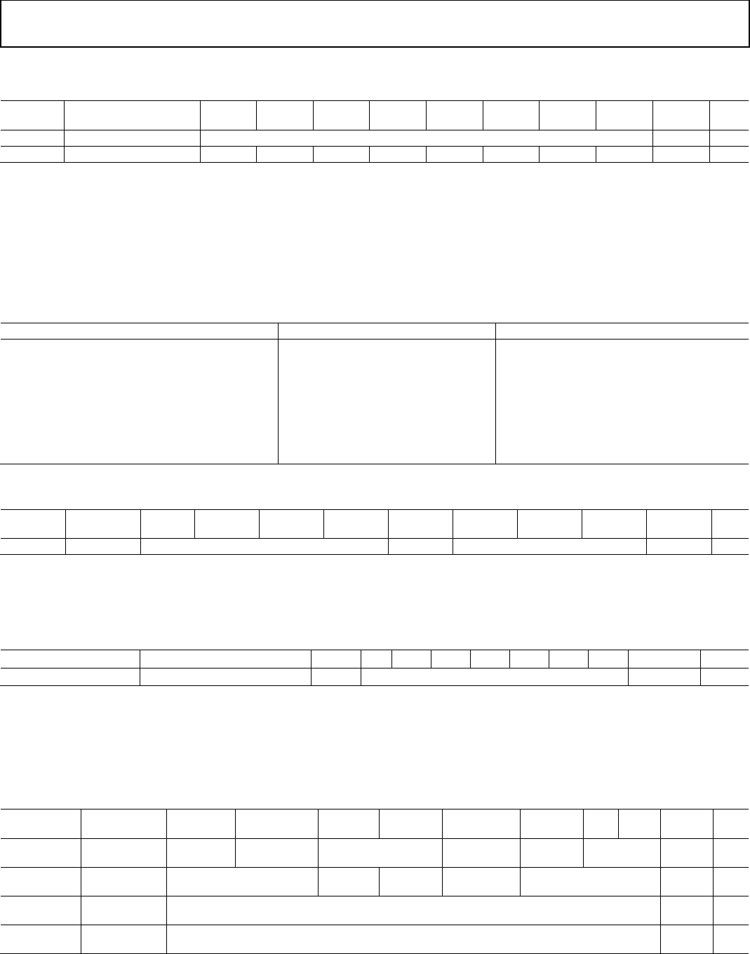
Table 8.
Register
Address Name D7 D6 D5 D4 D3 D2 D1 D0 Default R/W
0x009 Clock
Enable
Open Must be 0 XO Bypass Must be 0 Digital
Power Up
Set
to 1
BBPLL
Enable
0x10 R/W
0x00A BBPLL CLKOUT Select[2:0] CLKOUT
Enable
DAC Clk
div2
BBPLL Divider [2:0] 0x03 RW
SPI Register 0x009—Clock Enable
The ad9361_init function sets up many registers including
Register 0x009.
D5—Must be 0
D4—XO Bypass
This bit controls a MUX that selects between two different
paths while also powering down the unselected path. Set this bit
to use an external reference clock. Clear this bit when using an
external crystal with the DCXO.
D3—Must be 0
D2—Digital Power Up
When clear, the AD9361 shuts down the digital logic clocks.
The BBP may still write to the directly addressable SPI registers.
When set, all digital clocks are operational. The AD9361 powers
up with this bit clear and it is set during initialization.
D1—Set to 1
D0—BBPLL Enable
Clearing this bit disables the BBPLL while setting it enables the
BBPLL. The AD9361 powers up with this bit clear and it is set
during initialization.
SPI Register 0x00A—BBPLL
[D7:D5]—CLKOUT Select[2:0]
The clk_output_mode_select function controls these bits. These
bits set the CLKOUT frequency per Table 9. Set D4 to enable
this function.
Table 9. CLKOUT Frequency
CLKOUT Select[2:0] CLKOUT Frequency
000 XTALN (or DCXO) (buffered)
001 ADC_CLK/2
010 ADC_CLK/3
011 ADC_CLK/4
100 ADC_CLK/8
101 ADC_CLK/16
110 ADC_CLK/32
111 ADC_CLK/64
D4—CLKOUT Enable
The ad9361_clk_output_mode_select function controls this bit.
Setting this bit routes a clock with rate specified in Table 9 to
the CLKOUT ball. When clear, the AD9361 drives out logic
zero.
D3—DAC Clk Div2
The ad9361_calculate_rf_clock_chain function configures this
bit. When clear, the DAC clock rate equals the ADC clock rate.
When set, the DAC clock equals ½ of the ADC rate.
[D2:D0]—BBPLL Divider [2:0]
The ad9361_bbpll_set_rate function controls these bits. The
ADC clock rate equals the BBPLL divided by the factor in this
register, shown in Equation 2.
=
[:]()(2)
BBPLL Divider[2:0] is valid from 1 through 6.
UG-671 AD9361 Register Map Reference Manual
Rev. 0 | Page 8 of 72
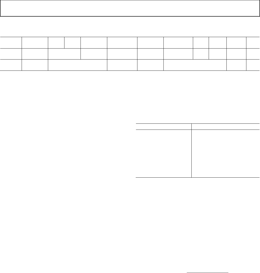
TEMPERATURE SENSOR REGISTERS (ADDRESS 0x00C THROUGH ADDRESS 0x00F)
Table 10.
Register Address Name D7 D6 D5 D4 D3 D2 D1 D0 Default R/W
0x00B
Offset
Temp Sense Offset [7:0]
0x00
R/W
0x00C Start Temp Reading Open Start Temp Reading 0x0- R/W
0x00D Temp Sense2 Measurement Time Interval[6:0] Temp Sense Periodic Enable 0x03 R/W
0x00E Temperature Temperature[7:0] 0x-- R
0x00F Temp Sensor Config Open Temp Sensor Decimation[2:0] 0x04 R/W
The ad9361_auxadc_setup function handles temperature sensor
setup as well as AuxADC setup. The temp sensor is internal to
the AD9361. To determine system temperature, use external
temperature sensors.
SPI Register 0x00B—Temp Sense Offset
See the SPI Register 0x00E—Temperature section.
SPI Register 0x00C—Temp Sense1
D0—Start Temp Reading
Set this bit to manually start a temperature reading; only applies
if 0x00D[D0] is clear. Bit D0 is not self-clearing. To calculate the
temperature again, this bit must be cleared and then set again.
SPI Register 0x00D—Temp Sense2
[D7:D1]—Measurement Time Interval[6:0]
Only applies if Bit D0 is set, in which case the AD9361 takes
temperature readings periodically at the rate per Equation 3.
)(
2]0:6[
)(
29
HzFrequencyClockBBPLL
IntervalTimetMeasuremen
sPeriod
×
=
(3)
D0—Temp Sense Periodic Enable
See 0x00D[D7:D1] and 0x00C[D0].
SPI Register 0x00E—Temperature
The temperature word is proportional to internal die
temperature with a slope of 1.16 × temperature. The value in
Register 0x00E is related to temperature and then added to the
value in Register 0x00B. When reading the temperature, disable
the AuxADC by setting 0x01D[D0] to ensure a valid
temperature reading.
SPI Register 0x00F—Temp Sensor Config
[D2:D0]—Temp Sensor Decimation
Decimation of the AuxADC used to derive the temperature per
Equation 4. The AD9361 uses a sigma delta AuxADC to
perform the temperature measurement. The AuxADC clock
rate is always the BBPLL rate divided by 64 when using the
temperature sensor.
Temp Sensor Decimation = 256 × 2Temp Sensor Decimation[2:0] (4)

AD9361 Register Map Reference Manual UG-671
Rev. 0 | Page 9 of 72
PARALLEL PORT CONFIGURATION REGISTERS (ADDRESS 0x010 THROUGH ADDRESS 0x012)
Table 11.
Register
Address Name D7 D6 D5 D4 D3 D2 D1 D0 Default R/W
0x010
Parallel Port
Configuration 1
PP Tx Swap IQ
PP Rx
Swap IQ
Tx
Channel
Swap
Rx
Channel
Swap
Rx Frame
Pulse
Mode
2R2T
Timing
Invert
data
bus
Invert
DATA CLK
0xC0 R/W
0x011 Parallel Port
Configuration 2
FDD Alt
Word Order
Must be 0 Invert Tx1 Invert Tx2 Invert Rx
Frame
Delay Rx Data[1:0] 0x00 R/W
0x012 Parallel Port
Configuration 3
FDD Rx Rate =
2*Tx Rate
Swap
Ports
Single
Data Rate
LVDS
Mode
Half
Duplex
Mode
Single
Port
Mode
Full
Port
Full
Duplex
Swap Bit
0x04 R/W
SPI Register 0x010—Parallel Port Configuration 1
D7—PP Tx Swap IQ
Clearing this bit swaps I and Q (performs spectral inversion).
D6—PP Rx Swap IQ
This bit functions the same as Bit D7 but for the Rx path.
D5—Tx Channel Swap
Setting this bit swaps the positions of Tx1 and Tx2 samples.
D4—Rx Channel Swap
This bit functions the same as Bit D5 but for the Rx path.
D3—Rx Frame Pulse Mode
The AD9361 outputs an Rx frame sync signal indicating the
beginning of an Rx frame. When this bit is clear, Rx frame goes
high coincident with the first valid receive sample. It stays high
as long as the receivers are enabled. When this bit is set, the Rx
frame signal toggles with a duty cycle of 50%.
D2—2R2T Timing
When set, the data port uses 2R2T timing, regardless of the
number of enabled transmitters and receivers. When clear, the
timing reflects the number of enabled signal paths.
D1—Invert Data Bus
Inverts the data port(s) from [11:0] to [0:11].
D0—Invert DATA CLK
Setting this bit inverts DATA_CLK.
SPI Register 0x011—Parallel Port Configuration 2
D7—FDD Alt Word Order
Valid only in full duplex, dual port, full port mode. When this
bit is set, each port splits into two 6-bit halves. Rx1 uses 6 bits of
a port and Rx2 uses the other 6 bits of the port (receivers are
not interleaved). Tx1 and Tx2 are organized similarly.
[D6:D5]—Must be 0
D4—Invert Tx1
Setting this bit digitally multiplies the Tx1 signal by −1.
D3—Invert Tx2
Setting this bit digitally multiplies the Tx2 signal by −1.
D2—Invert Rx Frame
Setting this bit inverts Rx frame.
[D1:D0]—Delay Rx Data[1:0]
These bits set the delay of the Rx data relative to Rx frame,
measured in ½ DATA_CLK cycles for DDR and full
DATA_CLK cycles for SDR.
SPI Register 0x012—Parallel Port Configuration 3
D7—FDD Rx Rate = 2*Tx Rate
When clear, the Rx sample rate is equal to the Tx sample rate.
When set, the Rx rate is twice the Tx rate. This bit can only be
set when Bit D3 of Register 0x012 is clear (full duplex mode).
D6—Swap Ports
Setting this bit swaps Port 0 and Port 1. Must be clear for LVDS
mode.
D5—Single Data Rate
When clear, both edges of DATA_CLK are used. When set, only
one edge of is used.

UG-671 AD9361 Register Map Reference Manual
Rev. 0 | Page 10 of 72
D4—LVDS Mode
When clear, the data port uses single-ended CMOS. Set this bit
to use LVDS. Full duplex (0x012[D3] clear), DDR (0x012[D5]
clear), and dual port mode (0x012[D2] clear) are required.
D3—Half-Duplex Mode
Clearing the bit allows simultaneous bi-directional data. Setting
the bit allows data to flow in only one direction at a time.
Normally, this bit equals the inverse of 0x013[D0].
D2—Single Port Mode
When clear, P0 and P1 ports are both used. When set, only one
data port is used.
D1—Full Port
Used only in full duplex mode ([D3] clear) and dual port mode
(D2 clear). Setting this bit forces the receivers to be on one port
and the transmitters to be on the on the other port. Clearing the
bit mixes receivers and transmitters on each port.
D0—Full Duplex Swap Bit
This bit toggles between the bits used for receive data and those
used for transmit data with one exception. If the FDD Alt Word
Order bit (0x011[D7]) is set, then the effect is to swap the most
significant 6 bits with the least significant 6 bits. It is not always
valid to set this bit.

AD9361 Register Map Reference Manual UG-671
Rev. 0 | Page 11 of 72
ENABLE STATE MACHINE (ENSM) REGISTERS (ADDRESS 0x013 THROUGH ADDRESS 0x017)
Table 12.
Register
Address Name D7 D6 D5 D4 D3 D2 D1 D0 Default R/W
0x013 ENSM
Mode
Open FDD
Mode
0x01 R/W
0x014 ENSM
Config 1
Enable
Rx Data
Port
Force Rx
On
Force Tx
On
ENSM
Pin
Control
Level
Mode
Force
Alert
State
Auto
Gain
Lock
To Alert 0x13 R/W
0x015 ENSM
Config 2
FDD
External
Control
Enable
Power
Down
Rx Synth
Power
Down Tx
Synth
TXNRX
SPI
Control
Synth
Pin
Control
Mode
Dual
Synth
Mode
Rx Synth
Ready
Mask
Tx Synth
Ready
Mask
0x08 R/W
0x016 Calibration
Control
Rx BB
Tune
Tx BB
Tune
Must be
0
Tx Quad
Cal
Rx Gain
Step Cal
Open DC Cal
RF Start
DC cal
BB Start
0x00 R/W
0x017 State Calibration Sequence State[3:0] ENSM State[3:0] 0x-- R
The ad9361_set_en_state_machine_mode function configures
Register 0x013 through Register 0x015.
SPI Register 0x013—ENSM Mode
Bit D0 controls the ENSM. Clear for TDD mode; set for FDD
mode.
SPI Register 0x014—ENSM Config 1
D7—Enable Rx Data Port for Cal
In TDD mode, during the Tx state, setting this bit enables the
Rx data port. If Tx monitor(s) are also enabled, the Tx monitor
I/Q data will be present on the Rx I/O port.
D6—Force Rx On
Setting this bit puts the ENSM into the Rx state when operating
in TDD mode. It is ignored in FDD mode. Clearing this bit
moves the ENSM back to the alert state via the Rx flush state
and during this state the ENSM ignores SPI commands that
affect it.
D5—Force Tx On
Setting this bit puts the ENSM into the transmit state when
operating in TDD mode. In FDD mode, setting this bit puts the
ENSM into the FDD state. Clearing this bit moves the ENSM
back to the alert state vis the Flush state(s) and during this state,
the ENSM ignores SPI commands that affect it.
D4—ENSM Pin Control
When set, the ENSM responds to the enable and TXNRX
signals and changes states accordingly. When clear, SPI writes to
bits in Register 0x014 to change the state.
D3—Level Mode
When clear, enable pulses move the ENSM among its states.
When this bit is set, the level of the ENABLE pin and (in TDD
mode) the level of the TXNRX signal determines the state.
D2—Force Alert State
If the ENSM is in the wait state, settting this bit forces the
ENSM to the alert state. From any other state, setting this bit
moves the ENSM to the alert state if the To Alert bit (D0) is set,
else it moves the ENSM to the wait state.
D1—Auto Gain Lock
Only applies if the Gain Unlock Control bit (0x0FB[D6]) is set
and only when the AGC is used in fast attack mode. Setting this
bit allows the gain to stay locked even if certain overload
conditions occur.
D0—To Alert
If clear, the ENSM always moves from the Rx, Tx, or FDD states
to the wait state. If this bit is set, the ENSM moves to the alert
state.
SPI Register 0x015—ENSM Config 2
D7—FDD External Control Enable
Only applies when ENSM FDD Mode bit (0x013[D0]) is set.
Setting this bit allows independent control of the receivers and
transmitters using the ENABLE and TXNRX signals, and is
commonly referred to as FDD Independent Control Mode.
D6—Power Down Rx Synth
Test bit, normally clear. Set to power down the Rx RF
synthesizer.
D5—Power Down Tx Synth
Test bit, normally clear. Set to power down the Tx RF
synthesizer.
D4—TXNRX SPI Control
Only used in single synthesizer mode (Bit D2 clear) and Synth
Enable Pin Control Mode (Bit D3) clear. See 0x015[D3].

UG-671 AD9361 Register Map Reference Manual
Rev. 0 | Page 12 of 72
D3—Synth Pin Control Mode
Used in single synthesizer mode (Bit D2 clear). When set, the
TXNRX pin controls which RF synthesizer is enabled. When
clear, Bit D4 controls which synthesizer is enabled.
D2—Dual Synth Mode
If clear, only one RF synthesizer is on at any given time. When
set, both synthesizers are always on.
D1—Rx Synth Ready Mask
Normally clear. When clear, the ENSM won’t move to the Rx
state unless the Rx RF VCO has successfully calibrated. When
set, the ENSM disregards the VCO calibration status.
D0—Tx Synth Ready Mask
This bit functions the same as Bit D1 but for the Tx VCO.
SPI Register 0x016—Calibration Control
D7—Rx BB Tune
The ad9361_rx_rf_bandwidth function configures and runs the
Rx baseband filter calibration. Setting this bit starts the receiver
analog baseband filter calibration and self-clears when the
calibration completes.
D6—Tx BB Tune
The ad9361_tx_rf_bandwidth function configures and runs the
Tx baseband filter calibration. This bit functions the same as Bit
D7 but for the transmit filter.
D5—Must be 0
D4—Tx Quad Cal
The ad9361_tx_quad_calib function configures and runs the
Tx quadrature calibration. Setting this bit starts the transmit
quadrature calibration and self-clears when the calibration
completes.
D3—Rx Gain Step Cal
Setting this bit starts an LNA and mixer gain step calibration
and self-clears when the calibration completes. An external RF
signal must be present at the Rx inputs.
D1—DC Cal RF Start
The ad9361_rf_dc_offset_calib function configures and runs
the RF DC calibration. Setting this bit performs an RF DC
offset calibration of the Rx signal paths and the bit self-clears
when the calibration completes.
D0—DC Cal BB Start
The ad9361_bb_dc_offset_calib function configures and runs
the baseband DC calibration. Setting this bit performs a
baseband DC dffset cal of the Rx signal paths and self-clears
when the calibration completes.
SPI Register 0x017—State—Read-Only
[D7:D4] Calibration Sequence State[3:0]
Table 13 shows the states of the calibration state machine.
Table 13.Calibration State
Calibration State 0x017[7:4]
Calibrations Done 1
Baseband DC Offset Calibration 2
RF DC Offset Calibration 3
Tx1 Quadrature Calibration 4
Tx2 Quadrature Calibration 5
Receiver Gain Step Calibration 9
Baseband Calibration Flush A
RF Calibration Flush B
Transmitter Quadrature Calibration Flush C
Transmitter Power Detector Calibration Flush E
Receiver Gain Step Calibration Flush F
[D3:D0] ENSM State[3:0]
Table 14 shows the states of the enable state machine (ENSM).
Table 14. ENSM State
ENSM State 0x017[3:0] Notes
Sleep 0 AD9361 clocks/BB PLL disabled
Wait 0 Clocks enabled
Alert 5 Synthesizers enabled
Tx 6 Tx signal chain enabled
Tx Flush 7 Tx digital block flush time
Rx 8 Rx signal chain enabled
Rx Flush 9 Rx digital block flush time
FDD A Tx and Rx signal chains enabled
FDD Flush B Flush all digital signal path blocks
AD9361 Register Map Reference Manual UG-671
Rev. 0 | Page 13 of 72
AUXDAC REGISTERS (ADDRESS 0x018 THROUGH ADDRESS 0x01B)
Table 15.
Register
Address Name D7 D6 D5 D4 D3 D2 D1 D0 Default R/W
0x018 AuxDAC 1
Word
AuxDAC 1 Word[9:2] 0x00 R/W
0x019 AuxDAC 2
Word
AuxDAC 2 Word[9:2] 0x00 R/W
0x01A AuxDAC 1
Config
Open Must
be 0
AuxDAC1
Step
Factor
AuxDAC 1 Vref[1:0] AuxDAC 1 Word [1:0] 0x00 R/W
0x01B AuxDAC 2
Config
Open Must
be 0
AuxDAC2
Step
Factor
AuxDAC 2 Vref[1:0] AuxDAC 2 Word [1:0] 0x00 R/W
The ad9361_auxdac_setup function configures the AuxDAC.
Register 0x023, Register 0x026, and Register 0x030 to Register
0x033 determine the AuxDACs enable/disable state. For ease of
use, review the SPI Register 0x023—AuxDAC Enable Control,
SPI Register 0x026—External LNA Control, and SPI Register
0x030 Through SPI Register 0x033—AuxDACn Rx/Tx
Delay[7:0] sections prior to this section.
SPI Register 0x018, SPI Register 0x019, SPI Register
0x01A[D1:D0], and SPI Register 0x01B[D1:D0]—AuxDAC
1(2) Word
The AuxDAC output voltage is defined by Equation 5.
SPI Register 0x01A—AuxDAC 1 Config
D5—Must be 0
D4—AuxDAC1 Step Factor
If this bit is clear, the step factor in Equation 5 = 2. If the bit is
set, the step factor = 1.
[D3:D2]—AuxDAC 1 Vref[1:0]
These bits encode the Vref factor in Equation 5. Table 16 shows
the encoding.
Table 16. AuxADC Vref
Vref[1:0] Vref (V)
00 1.0
01 1.5
10 2.0
11 2.5
SPI Register 0x01B—AuxDAC 2 Config
These bits function the same as Register 0x01A but apply to
AuxDAC 2.
()= 0.97 ×+ (0.000738 + 9 × 10 ×(× 1.6 2))× [9: 0] ×
0.3572 × + 0.05 (5)
where:
Vref is set by 0x01A[D3:D2] (AuxDAC 1) and 0x01B[D3:D2] (AuxDAC 2).
Step Factor is set by Register 0x01A[D4] (Bit AuxDAC 1) and Register 0x01B[D4] (Bit AuxDAC 2).
AuxDAC Words are Register 0x018 through Register 0x01B.
AuxDAC Vout at a maximum is limited to 3 V for VDDA_GPO = 3.3 V.

UG-671 AD9361 Register Map Reference Manual
Rev. 0 | Page 14 of 72
AUXILIARY ADC REGISTERS (ADDRESS 0x01C THROUGH ADDRESS 0x01F)
Table 17.
Register
Address Name D7 D6 D5 D4 D3 D2 D1 D0 Default R/W
0x01C AuxADC
Clock
Divider
Open AuxADC Clock Divider[5:0] 0x10 R/W
0x01D Aux ADC
Config
Open Aux ADC Decimation[2:0] AuxADC
Power Down
0x01 R/W
0x01E AuxADC
Word MSB
AuxADC Word MSB[11:4] 0x-- R
0x01F AuxADC
Word LSB
Open AuxADC Word LSB[3:0] 0x-- R
The ad9361_auxadc_setup function configures the AuxADC.
SPI Register 01C—AuxADC Clock Divider
[D5:D0]—AuxADC Clock Divider[5:0]
The AuxADC clock results from dividing down the BBPLL,
described by Equation 6. A divider value of 0 is invalid.
=
[:] (6)
SPI Register 0x01D—AuxADC Config
[D3:D1]—AuxADC Decimation[2:0]
These bits set the AuxADC decimation per Equation 7.
=256 × 2 [:] (7)
D0—AuxADC Power Down
Setting this bit powers down the AuxADC.
SPI Register 0x01E and SPI Register 0x01F—AuxADC
Word
These registers hold the 12-bit AuxADC word. When reading
the AuxADC word, the temperature sensor should be disabled
or prevented from updating.
AD9361 Register Map Reference Manual UG-671
Rev. 0 | Page 15 of 72
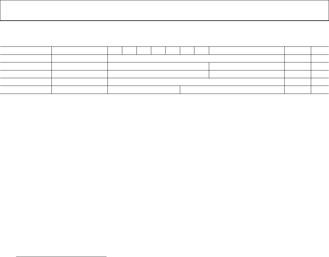
GPO, AUXDAC, AGC DELAY, AND SYNTH DELAY CONTROL REGISTERS (ADDRESS 0x020 THROUGH
ADDRESS 0x033)
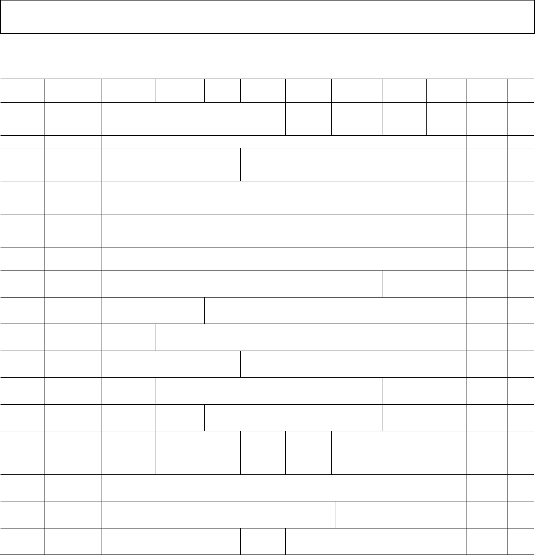
Table 18.
Register
Address Name D7 D6 D5 D4 D3 D2 D1 D0 Default R/W
0x020 Auto GPO GPO Enable Auto Rx[3:0] GPO Enable Auto Tx[3:0] 0x33 R/W
0x021 AGC Gain Lock
Delay
Gain Lock Delay[7:0] 0x0A R/W
0x022 AGC Attack
Delay
Open Invert
Bypassed
LNA
Polarity
AGC Attack Delay[5:0] 0x0A R/W
0x023 AuxDAC Enable
Control
AuxDAC Manual Bar[1:0] AuxDAC Auto Tx
Bar[1:0]
AuxDAC Auto
Rx Bar[1:0]
AuxDAC Initial
Bar[1:0]
0x3f R/W
0x024 Rx Load Synth
Delay
Must be x02 0x02 R/W
0x025 Tx Load Synth
Delay
Must be x02 0x02 R/W
0x026 External LNA
control
AuxDAC
Manual
Select
External
LNA2
Control
External
LNA1
Control
GPO
manual
select
Open[3:0] 0x00 R/W
0x027 GPO Force and
Init
GPO Manual Control[3:0] GPO Init State[3:0] 0x03 R/W
0x028 GPO0 Rx delay GPO0 Rx Delay[7:0] 0x00 R/W
0x029 GPO1 Rx delay GPO1 Rx Delay[7:0] 0x00 R/W
0x02A GPO2 Rx delay GPO2 Rx Delay[7:0] 0x00 R/W
0x02B GPO3 Rx delay GPO3 Rx Delay[7:0] 0x00 R/W
0x02C GPO0 Tx Delay GPO0 Tx Delay[7:0] 0x00 R/W
0x02D GPO1 Tx Delay GPO1 Tx Delay[7:0] 0x00 R/W
0x02E GPO2 Tx Delay GPO2 Tx Delay[7:0] 0x00 R/W
0x02F GPO3 Tx Delay GPO3 Tx Delay[7:0] 0x00 R/W
0x030 AuxDAC1 Rx
Delay
AuxDAC 1 Rx Delay [7:0] 0x00 R/W
0x031 AuxDAC1 Tx
Delay
AuxDAC 1 Tx Delay [7:0] 0x00 R/W
0x032 AuxDAC2 Rx
Delay
AuxDAC 2 Rx Delay [7:0] 0x00 R/W
0x033 AuxDAC2 Tx
Delay
AuxDAC 2 Tx Delay [7:0] 0x00 R/W
The ad9361_gpo_setup function configures the GPOs. See the
AuxADC and AuxDAC sections to configure the auxiliary
converters. (See also the AuxADC/AuxDAC/GPO/ Temp
Sensor section of the AD9361 Reference Manual.) When the
AD9361 powers up into the sleep state, the default register
values define the GPO logic levels. Thus, the GPOs will auto-
toggle and GPO_0 and GPO_1 will be high while GPO_2 and
GPO_3 will be low.
SPI Register 0x020—Auto GPO
[D7:D4]—GPO Enable Auto Rx[3:0]
This nibble controls which GPO pins change state when the
ENSM enters the Rx state. Bit D7 controls GPO_3, Bit D6
controls GPO_2, Bit D5 controls GPO_1, and Bit D4 controls
GPO_0. These bits are ignored if 0x026[D4] is set.
[D3:D0]—GPO Enable Auto Tx[3:0]
These bits function the same as D7:D4 but apply when the
ENSM enters the Tx state. These bits are ignored if Register
0x026[D4] is set.
SPI Register 0x021—AGC Gain Lock Delay
Only applies if 0x014[D1] and 0xFB[D6] are set, allowing the
gain to stay locked even if certain overload conditions occur.
SPI Register 0x022—AGC Attack Delay
D6—Invert Bypassed LNA Polarity
The LNA output phase rotates by approximately 180° when it is
bypassed (index 0). Setting this bit corrects for this rotation.

UG-671 AD9361 Register Map Reference Manual
Rev. 0 | Page 16 of 72
[D5:D0]—AGC Attack Delay
Applies to the fast AGC. The AGC Attack Delay prevents the
AGC from starting its algorithm until the receive path has
settled. The delay counter starts when the ENSM enters the
Rx state. Units: microseconds, resolution: 1 µs/LSB, range: 0
through 31 microseconds. For the value in microseconds to
be accurate, Register 0x03A must be set correctly.
SPI Register 0x023—AuxDAC Enable Control
[D7:D6]—AuxDAC Manual Bar[1:0]
Clearing Bit D7 manually enables AuxDAC2. Clearing Bit D6
manually enables AuxDAC1. These bits are ignored if Register
0x026[D7] is clear.
[D5:D4]—AuxDAC Auto Tx Bar[1:0]
Clearing Bit D5 causes AuxDAC2 to change state when the
ENSM enters the Tx state. Bit D4 controls AuxDAC1 in the
same manner. These bits are ignored if 0x026[D7] is set.
[D3:D2]—AuxDAC Auto Rx Bar[1:0]
Clearing Bit D3 causes AuxDAC2 to change state when the
ENSM enters the Rx state. Bit D2 controls AuxDAC1 in the
same manner. These bits are ignored if 0x026[D7] is set.
[D1:D0]—AuxDAC Initial Bar[1:0]
Clearing Bit D1 sets the state of AuxDAC2 to on when the
ENSM is in the Alert state. Bit D0 controls AuxDAC1 in the
same manner. These bits are ignored if 0x026[D7] is set.
SPI Register 0x024—Must be x02
SPI Register 0x025—Must be x02
SPI Register 0x026—External LNA Control
D7—AuxDAC Manual Select
When clear, the AuxDAC states slaves to the ENSM. When set,
SPI writes to Register 0x023[D7:D6] manually control the state
of the AuxDACs.
D6—External LNA 2 Control
When set, the Ext LNA Ctrl bit in the Rx2 gain table sets the
GPO_1 state.
D5—External LNA 1 Control
This bit functions the same as Bit D6 but applies to the Rx1 gain
table and GPO_0.
D4—GPO Manual Select
When clear, the GPOs slave to the ENSM. When set,
0x027[D7:D4] sets the value of the GPOs.
SPI Register 0x027—GPO Force and Init
[D7:D4]—GPO Manual Control[3:0]
When clear, the GPOs are logic low. When set, the GPOs are
logic high. Bit D7 controls GPO_3, Bit D6 controls GPO_2,
Bit D5 controls GPO_1, and Bit D4 controls GPO_0. Only
applies when Register 0x026[D4] is set.
[D3:D0]—GPO Init State[3:0]
When clear, the GPOs are logic low in the sleep, wait, and alert
states and when set, the GPOs are logic high. Bit D3 controls
GPO_3, D2 controls GPO_2, D1 controls GPO_1, and Bit D0
controls GPO_0. Only applicable when the GPO states are
slaved to the ENSM. Only applicable if 0x026[D4] is clear.
SPI Registers 0x028 Through 0x02B—GPOn Rx
Delay[7:0]
Only applicable if the GPOs are slaved to the ENSM (Register
0x026[D4] clear). These registers set the delay from ENSM
changing to Rx to the time that the GPOs change logic level:
1 µs/LSB with a range from 0 µs to 255 µs. The delay from
ENSM change of Rx to alert is always fixed, allowing for the
Rx flush state before changing the GPO states. Register 0x03A
must be set correctly for the delay resolution to be 1 µs/LSB.
SPI Register 0x02C Through SPI Register 0x02F—GPOn
Tx Delay[7:0]
These registers function the same as Register 0x028 to Register
0x02B but for the transition from the alert state to the Rx state.
SPI Register 0x030 Through SPI Register 0x033—
AuxDACn Rx/Tx Delay[7:0]
These delays affect the state of the AuxDACs similar to how
Register 0x028 through Register 0x02B affect the GPOs. Only
applicable if Register 0x026[D7] is clear.
AD9361 Register Map Reference Manual UG-671
Rev. 0 | Page 17 of 72
CONTROL OUTPUT REGISTERS (ADDRESS 0x035 THROUGH ADDRESS 0x036)
Table 19.
Register
Address Name D7 D6 D5 D4 D3 D2 D1 D0 Default R/W
0x035 Control Output Pointer Control Output Pointer[7:0] 0x00 R/W
0x036 Control Output Enable En ctrl7 En ctrl6 En ctrl5 En ctrl4 En ctrl3 En ctrl2 En ctrl1 En ctrl0 0xFF R/W
The ad9361_ctrl_outs_setup function configures the control outputs.
SPI Register 0x035—Control Output Pointer
This register sets the pointer to a table of control output signals. See the control output portion of the user guide for mapping of control
output signals to pointer value and control output ball.
SPI Register 0x036—Control Output Enable
The bits in this register enable/disable the control output outputs. See Table 20 for mapping.
Table 20. Control Output Bit/Ball Mapping
Control Output Bit Position CTRL_OUT Pin Name AD9361 Pin Designation
7 CTRL_OUT7 G4
6 CTRL_OUT6 F4
5 CTRL_OUT5 F5
4 CTRL_OUT4 F6
3 CTRL_OUT3 E6
2 CTRL_OUT2 E5
1 CTRL_OUT1 E4
0 CTRL_OUT0 D4
PRODUCT ID REGISTER (ADDRESS 0x037)
Table 21.
Register
Address Name D7 D6 D5 D4 D3 D2 D1 D0 Default R/W
0x037 Product ID Open Always 1 Rev[2:0] 0x-- R
SPI Register 0x037—Product ID
Bits[D2:D0] represent the revision of the device.
REFERENCE CLOCK CYCLES REGISTER (ADDRESS 0x03A)
Table 22.
Register Address Name D7 D6 D5 D4 D3 D2 D1 D0 Default R/W
0x03A Reference Clock Cycles Open Reference Clock Cycles per µs[6:0] 0x00 R/W
SPI Register 0x03A—Reference Clock Cycles
The ad9361_set_ref_clk_cycles function configures this register. Many delay settings assume a resolution of 1 LSB/µs. For this to be
correct, Register 0x03A must be programmed with the number of reference clock cycles per microsecond minus 1. The reference clock is
an external reference or the DCXO.
DIGITAL IO CONTROL REGISTERS (ADDRESS 0x03B THROUGH ADDRESS 0x03E)
Table 23.
Register
Address Name D7 D6 D5 D4 D3 D2 D1 D0 Default R/W
0x03B Digital I/O
Control
CLKOUT
Drive
DATACLK
drive
DATACLK slew [1:0] Must be 0 Data Port
Drive
Data Port
Slew[1:0]
0x00 R/W
0x03C LVDS Bias
Control
CLK Out Slew[1:0] Rx On
Chip Term
Bypass
Bias R
LVDS Tx LO
VCM
LVDS Bias [2:0] 0x03 R/W
0x03D
LVDS Invert
control1
LVDS pn Invert[7:0]
0x00
R/W
0x03E LVDS Invert
control2
LVDS pn Invert[15:8] 0x00 R/W

UG-671 AD9361 Register Map Reference Manual
Rev. 0 | Page 18 of 72
SPI Register 0x03B—Digital I/O Control
D7—CLKOUT Drive
CLK_OUT drive strength. Setting this bit increases the drive strength by approximately 20%.
D6—DATACLK Drive
DATA_CLK drive strength. Setting this bit increases the drive strength by approximately 20%.
[D5:D4] DATACLK Slew[1:0]
Slew control for DATA_CLK. 1’b00 for fastest rise/fall times. 1’b11 for slowest rise/fall times.
D3—Must be 0
D2—Data Port Drive
Data port output driver strength. Setting this bit increases the drive strength by approximately 20%.
[D1:D0]—Data Port Slew[1:0]
Slew control for the data ports. 1’b00 for fastest rise/fall times. 1’b11 for slowest rise/fall times.
SPI Register 0x03C—LVDS Bias Control
[D7:D6]—CLK Out Slew[1:0]
Slew control for CLK_OUT. 1’b00 for fastest rise/fall times. 1’b11 for slowest rise/fall times.
D5—Rx On Chip Term
Use LVDS Rx100 on-chip termination for all data path bits, Tx_FRAME, and FB_CLK. Do not set this bit in CMOS mode.
D4—Bypass Bias R
Bypass bias resistor in LVDS Rx comparator.
D3—LVDS Tx LO VCM
Lowers output common-mode voltage by 60 mV.
[D2:D0]—LVDS Bias[2:0]
LVDS driver amplitude control. |VOD| = 75 mV to 450 mV; 75 mV/LSB.
SPI Registers 0x03D and 0x03E—LVDS Invert Control
The phase of any LVDS pair can be inverted from its default configuration by setting bits in these two registers (see Table 24). The default
configuration for the data bits is inverted. Set 0x03D = 0xFF and 0x03E = 0x0F to prevent data inversion. Clock and frame signals are not
inverted in the default case.
Table 24. LVDS Signal Inversion Mapping
Register and Bits Signal Affected Chip Default Bit Value Configuration for Chip Default Recommended Configuration
SPI Register 0x03D
D7 P0[3:2] 0 Inverted 1
D6 P0[1:0] 0 Inverted 1
D5 P1[11:10] 0 Inverted 1
D4 P1[9:8] 0 Inverted 1
D3 P1[7:6] 0 Inverted 1
D2 P1[5:4] 0 Inverted 1
D1 P1[3:2] 0 Inverted 1
D0 P1[2:0] 0 Inverted 1
SPI Register 0x03E
D7 FBCLK 0 Not inverted 0
D6 Tx Frame 0 Not inverted 0
D5 DATACLK 0 Not inverted 0
D4 Rx Frame 0 Not inverted 0
D3 P0[11:10] 0 Inverted 1
D2 P0[9:8] 0 Inverted 1
D1 P0[7:6] 0 Inverted 1
D0 P0[5:4] 0 Inverted 1
AD9361 Register Map Reference Manual UG-671
Rev. 0 | Page 19 of 72
BBPLL CONTROL REGISTERS (ADDRESS 0x03F THROUGH ADDRESS 0x04E)
Table 25.
Register
Address Name D7 D6 D5 D4 D3 D2 D1 D0 Default R/W
0x03F BBPLL
Control 1
Must be 0 BBPLL
SDM
Enable B
Start BB
VCO CAL
BBPLL
SDM
Bypass
BBPLL
Reset
Bar
0x01 R/W
0x040 Must be 0 Must be 0 0x00 R/W
0x041 Fractional
BB Freq
Word 1
Set to 0 Fractional BB Frequency Word[20:16] 0x00 R/W
0x042 Fractional
BB Freq
Word 2
Fractional BB Frequency Word[15:8] 0x00 R/W
0x043 Fractional
BB Freq
Word 3
Fractional BB Frequency Word[7:0] 0x00 R/W
0x044 Integer BB
Freq Word
Integer BB Frequency Word[7:0] 0x10 R/W
0x045
Ref Clock
Scaler
Must be 0
Ref Clock
Scaler[1:0]
0x00
R/W
0x046 CP Current Must be 0 Charge Pump Current[5:0] 0x09 R/W
0x047 MCS Scale MCS refclk
Scale En
Must be 0 0x00 R/W
0x048 Loop Filter 1 C1 Word[2:0] R1 Word[4:0] 0xC5 R/W
0x049
Loop Filter 2
R2 Word[0]
C2 Word[4:0]
C1 Word[4:3]
0xB8
R/W
0x04A Loop Filter 3 Bypass C3 Bypass R2 C3 Word[3:0] R2 Word[2:1] 0x2E R/W
0x04B VCO Control Freq Cal
Enable
Set to 2’b11 Must be
0
Force
VCO
band
enable
Forced VCO band word[2:0] 0xC0 R/W
0x04C Must be
0x86
Set to 0x86 0x00 R/W
0x04D BBPLL
Control 2
Must be 0 See description 0x00 R/W
0x04E BBPLL
Control 3
Must be 0 Set to 1 Must be 0 0x00 R/W

UG-671 AD9361 Register Map Reference Manual
Rev. 0 | Page 20 of 72
The BBPLL registers are completely configured by the
ad9361_bbpll_set_rate function. The RF and BBPLL
Synthesizer section of the AD9361 Reference Manual has
more information about individual functions of the BBPLL.
SPI Register 0x03F—BBPLL Control 1
[D7:D4]—Must be 0
D3—BBPLL SDM EnableB
Test mo de, normally clear. Clearing this bit turns on the clock
to the BBPLL SDM. Set to disable the SDM. Use in conjunction
with the BBPLL SDM bypass bit (D1).
D2—Start BB VCO Cal
Set this bit after writing the BBPLL words to calibrate the VCO.
Bit D7 of Register 0x04B must be set to enable the calibration.
Clear the Start BB VCO Cal bit after setting it (it is not self-
clearing). The set and clear instructions can be consecutive
without waiting for the calibration to complete.
D1—BBPLL SDM Bypass
Test mo de, normally clear. Setting this bit disconnects the SDM
from the BBPLL, making it an integer PLL. Use with the BBPLL
SDM EnableB bit (D3).
D0—BBPLL Reset Bar
When clear, the BBPLL is disabled. Setting this bit enables the
BBPLL. Set this bit after writing the BBPLL words.
SPI Register 0x040—Must be 0
SPI Register 0x041[D7:D5]—Set to 0
SPI Register 0x041[D4:D0] Through SPI Register 0x044—
Fractional and Integer BB Freq Words
See Equation 8, Equation 9, and Equation 10.
= ()
(8)
= ()
()
×2088960 (9)
= × +
(10)
where:
NINTEGER is the BBPLL integer word (decimal).
NFRACTIONAL is the BBPLL fractional word (decimal).

AD9361 Register Map Reference Manual UG-671
Rev. 0 | Page 21 of 72
SPI Register 0x045—Ref Clock Scaler
[D7:D2]—Must be 0
[D1:D0]—Ref Clock Scaler[1:0]
The reference clock frequency is scaled before it enters the
BBPLL. 00: x1; 01: x½; 10: x¼; 11: x2.
SPI Register 0x046—CP Current
[D7:D6]—Must be 0
[D5:D0]—Charge Pump Current[5:0]
Charge pump bleed current setting. Resolution: 25 µA. Offset:
25 µA. Range: 25 µA to 1575 µA.
SPI Register 0x047—MCS Scale
D7—MCS Refclk Scale En
Only applies if using multichip synchronization. Set this bit to
use the BBPLL refclk scaler output as the clock domain that
detects transitions on the SYNC_IN pin.
[D6:D0]—Must be 0
SPI Register 0x048 through SPI Register 0x04A—Loop
Filter
These registers are set by the ad9361_bbpll_set_rate function.
The RF and BBPLL Synthesizer section of the AD9361
Reference Manual has more information about the loop filter.
SPI Register 0x04B—VCO Control
D7—Freq Cal Enable
Set this bit to enable VCO calibration. See also Init BB VCO Cal
bit (0x03F[D2]).
[D6:D5]—Set to 2’b11
D4—Must be 0
D3—Force VCO Band Enable
See Bits[D2:D0].
[D2:D0]—Forced VCO Band Word[2:0]
When a BBPLL VCO calibration completes, the VCO is in one
of 5 bands, coded in this register as 0 through 4. Setting Bit D3
forces the band word to the value written in Bits[D2:D0].
SPI Register 0x04C—Set to 0x86
SPI Register 0x04D—BBPLL Control 2
[D6:D3]—Must be 0
[D2:D0]—See Description
These are internal BBPLL bits. After setting Register 0x04C to
Register 0x086, set Register 0x04D to 0x01 and then to 0x05.
SPI Register 0x04E—BBPLL Control 3
[D7:D5]—Must be 0
D4—Set to 1
[D3:D0]—Must be 0

UG-671 AD9361 Register Map Reference Manual
Rev. 0 | Page 22 of 72
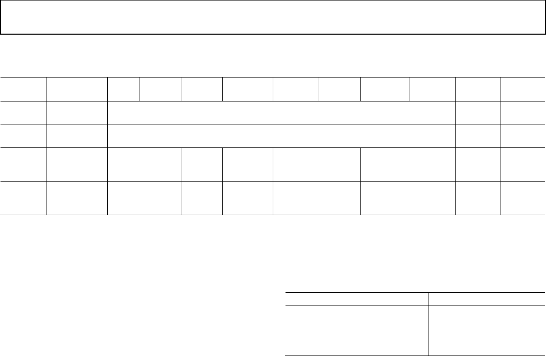
POWER DOWN OVERRIDE REGISTERS (ADDRESS 0x050 THROUGH ADDRESS 0x058)
Table 26.
Register
Address Name D7 D6 D5 D4 D3 D2 D1 D0 Default R/W
0x050 Rx Synth
Power
Down
Override
Open Rx LO
Power
Down
Rx Synth
VCO ALC
Power
Down
Rx Synth
PTAT
Power
Down
Rx Synth
VCO
Power
Down
Rx Synth
VCO LDO
Power
Down
0x00 R/W
0x051 Tx Synth
Power
Down
Override
Open Tx LO
Power
Down
Tx Synth
VCO ALC
Power
Down
Tx Synth
PTAT
Power
Down
Tx Synth
VCO
Power
Down
Tx Synth
VCO LDO
Power
Down
0x00 R/W
0x052 Control 0 Must be 0 Must be 2’b11 0x03 R/W
0x053 Must be 0 Must be 0 0x00 R/W
0x054
Rx1 ADC
Power
Down
Override
Rx1 ADC Power Down[7:0]
0x00
R/W
0x055 Rx2 ADC
Power
Down
Override
Rx2 ADC Power Down[7:0] 0x00 R/W
0x056 Tx Analog
Power
Down
Override 1
Tx Secondary
Filter Power
Down[1:0]
Tx BBF Power
Down[1:0]
Tx DAC Power
Down[1:0]
Tx DAC Bias Power
Down[1:0]
0x00 R/W
0x057 Analog
Power
Down
Override
Open Rx Ext
VCO
Buffer
Power
Down
Tx Ext
VCO
Buffer
Power
Down
Tx Monitor Power
Down[1:0]
Tx Upconverter Power
Down[1:0]
0x3C R/W
0x058 Misc
Power
Down
Override
Rx LNA
Power
Down
Open Rx Calibration Power
Down[1:0]
DCXO
Power
Down
Master Bias
Power
Down
0x30 R/W
SPI Register 0x050—Rx Synth Power Down Override
D4—Rx LO Power Down
Setting this bit powers down the Rx LO dividers if MCS RF is
disabled (Register 0x001[D3] = 0). If MCS RF is enabled, the
ENSM state machine enables and disables the Rx LO dividers.
This state machine also enables and disables the Rx synthesizer.
Thus, if D4 is set and MCS RF is enabled, the Rx LO dividers
power up and down when the Rx synthesizer powers up and
down. The Rx LO dividers are always powered down for
external VCO operation.
D3—Rx Synth VCO ALC Power Down
Setting this bit powers down the Rx synthesizer VCO automatic
level control.
D2—Rx Synth PTAT Power Down
The PTAT is a temperature-compensated current used for the
Rx synthesizer. This bit is OR’ed with the inverse of
0x242[D4:D3]. To turn off PTAT, set 0x050[D2] and clear
0x242[D4:D3]. The synth can still operate but it will not be
temperature-compensated.
D1—Rx Synth VCO Power Down
Setting this bit powers down the Rx synthesizer VCO.
D0—Rx Synth VCO LDO Power Down
Setting this bit powers down the Rx synthesizer VCO LDO.
SPI Register 0x051—Tx Synth Power Down Override
Same as 0x050 but controls the transmitter LO circuits.
SPI Register 0x052—Control 0
[D7:D2]—Must be 0
[D1:D0]—Must be 2’b11

AD9361 Register Map Reference Manual UG-671
Rev. 0 | Page 23 of 72
SPI Register 0x053—Must be 0
SPI Registers 0x054 and 0x055—Rx1 and Rx2 ADC Power
Down Override
These registers control the receive ADCs. Only 0x00 (ADC on)
and 0xFF (ADC off) are valid settings.
SPI Register 0x056—Tx Analog Power Down Override 1
[D7:D6]—Tx Secondary Filter Power Down[1:0]
Setting these bits powers down the Tx secondary filter. Bit D6
applies to Tx1 and Bit D7 applies to Tx2.
[D5:D4]—Tx BBF Power Down[1:0]
Setting these bits powers down the Tx baseband low-pass filters.
Bit D4 applies to Tx1 and Bit D5 applies to Tx2.
[D3:D2]—Tx DAC Power Down[1:0]
Setting these bits powers down the Tx DACs. Bit D2 applies to
Tx1 and Bit D3 applies to Tx2.
[D1:D0]—Tx DAC Bias Power Down[1:0]
Setting these bits powers down the Tx DAC bias supplies. Bit
D0 applies to Tx1 and Bit D1 applies to Tx2.
SPI Register 0x057—Analog Power Down Override
D5—Rx Ext VCO Buffer Power Down
Clear this bit to use an external VCO.
D4—Tx Ext VCO Buffer Power Down
Functions the same as Bit D5 but applies to the Tx VCO.
[D3:D2]—Tx Monitor Power Down[1:0]
Setting these bits powers down the Tx monitor LO circuitry. Bit
D2 = Tx Mon1 and Bit D3 = Tx Mon 2. These bits are set by
default. When the Tx Monitor function is used (see Register
0x001 and Register 0x06E) these bits should be clear to enable
the LO circuitry.
[D1:D0]—Tx Upconverter Power Down[1:0]
Setting these bits powers down the Tx upconverters. Bit D0
applies to Tx1 and Bit D1 applies to Tx2.
SPI Register 0x058—Misc Power Down Override
D6—Rx LNA Power Down
Setting this bit powers down the Rx LNAs.
[D3:D2]—Rx Calibration Power Down[1:0]
Setting these bits powers down the Rx calibration blocks. Bit D3
applies to Rx1 and Bit D4 applies to Rx2.
D1—DCXO Power Down
Set when using an external reference clock to save power.
D0—Master Bias Power Down
Setting this bit powers down all analog bias. Only leakage
current will flow.

UG-671 AD9361 Register Map Reference Manual
Rev. 0 | Page 24 of 72
OVERFLOW REGISTERS (ADDRESS 0x05E THROUGH ADDRESS 0x05F)
Table 27.
Register
Address Name D7 D6 D5 D4 D3 D2 D1 D0 Default R/W
0x05E CH 1
Overflow
BBPLL
Lock
CH1
INT3
CH1
HB3
CH1
HB2
CH1
QEC
CH1
HB1
CH1
TFIR
CH1
RFIR
0x-- R
0x05F CH 2
Overflow
Open CH2
INT3
CH2
HB3
CH2
HB2
CH2
QEC
CH2
HB1
CH2
TFIR
CH2
RFIR
0x-- R
None of the overload bits self-clear. During initialization, some
of these overload bits may show overloads. To read the current
status of the bits, perform two consecutive SPI reads.
SPI Register 0x05E—CH 1 Overflow
D7—BBPLL Lock
If this bit is set, the BBPLL is locked.
D6—CH1 INT3
If this bit is set, a digital overflow occurs in the Tx 1 interpolate
by 3 filter.
D5—CH1 HB3
If this bit is set, a digital overflow occurs in the Tx 1 half-band 3
filter.
D4—CH1 HB2
If this bit is set, a digital overflow occurs in the Tx 1 half-band 2
filter.
D3—CH1 QEC
If this bit is set, a digital overflow occurs in the Tx1 quadrature
error correction filter.
D2—CH1 HB1
If this bit is set, a digital overflow occurs in the Tx 1 half-band 1
filter.
D1—CH1 TFIR
If this bit is set, a digital overflow occurs in the Tx 1 FIR filter.
D0—CH1 RFIR
If this bit is set, a digital overflow occurs in the Rx 1 FIR filter.
SPI Register 0x05F—CH 2 Overflow
This register is the same as Register 0x05E but applies to
Channel 2.
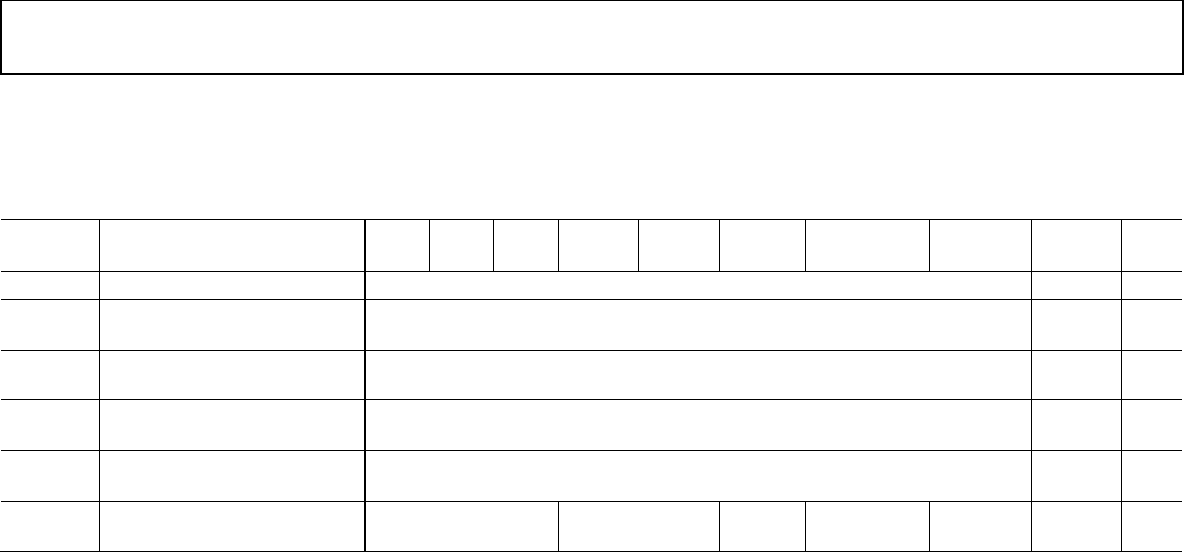
AD9361 Register Map Reference Manual UG-671
Rev. 0 | Page 25 of 72
TRANSMITTER CONFIGURATION
Tx PROGRAMMABLE FIR FILTER REGISTERS (ADDRESS 0x060 THROUGH ADDRESS 0x065)
Table 28.
Register
Address Name D7 D6 D5 D4 D3 D2 D1 D0 Default R/W
0x060 Tx Filter Coefficient Address Tx Filter Coefficient Address[7:0] 0x-- R/W
0x061 Tx Filter Coefficient Write
Data 1
Tx Filter Coefficient Write Data [7:0] 0x-- R/W
0x062 Tx Filter Coefficient Write
Data 2
Tx Filter Coefficient Write Data [15:8] 0x-- R/W
0x063 Tx Filter Coefficient Read
Data 1
Tx Filter Coefficient Read Data[7:0] 0x-- R
0x064
Tx Filter Coefficient Read
Data 2
Tx Filter Coefficient Read Data[15:8]
0x--
R
0x065 Tx Filter Configuration Number of Taps[2:0] Select Tx CH[1:0] Write
Tx
Start Tx
Clock
Filter
Gain
0x00 R/W
The ad9361_set_tx_fir_config function sets up the Tx FIR
coefficients. See the Filter Guide section of the AD9361
Reference Manual section for more information.
SPI Register 0x060—Tx Filter Coefficient Address
The digital filter coefficients are indirectly addressable. The
word in this register is the address of the coefficient.
SPI Register 0x061 and SPI Register 0x062—Tx Filter
Coefficient Write Data n
Write the coefficient value to these registers. Write these
registers (along with Register 0x060) before setting 0x065[D2].
Coefficients are 16-bit words in twos complement format. The
least significant bit is bit 0.
SPI Register 0x063 and SPI Register0x064—Tx Filter
Coefficient Read Data n
To read coefficients, write the address in Register 0x060 and
then read Register 0x063 and Register 0x064. Coefficients are
16-bit words in twos complement format. The least significant
bit is bit 0.
SPI Register 0x065—Tx Filter Configuration
[D7:D5]—Number of Taps[2:0]
The number of taps (see Equation 11) must be correct.
# =16 × ( + 1) (11)
[D4:D3] —Select Tx CH[1:0]
When writing coefficients, Bit D3 causes a write to Tx1, Bit D4
causes a write to Tx2 and both bits set writes to both Tx filters.
When reading coefficients, setting both bits is invalid.
D2—Write Tx
Set this self-clearing bit to write a coefficient. Each write
operation must set this bit. After the table has been
programmed, write to Register 0x065 with the Write Tx bit
cleared and D0 high. Then, write to Register 0x065 again with
D0 clear, thus ensuring that the write bit resets internally before
the clock stops. Wait 4 Tx sample periods after setting D2 high
while the data writes into the table.
D1—Start Tx Clock
Set this bit to start the programming clock when writing
coefficients.
D0—Filter Gain
Setting this bit attenuates the digital samples by 6 dB.
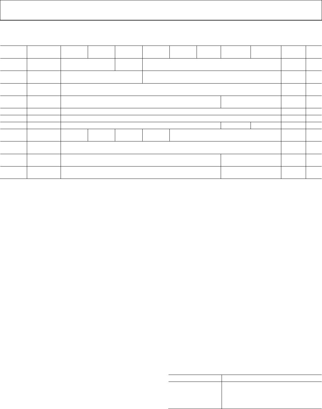
UG-671 AD9361 Register Map Reference Manual
Rev. 0 | Page 26 of 72
Tx MONITOR REGISTERS (ADDRESS 0x067 THROUGH ADDRESS 0x071)
Table 29.
Register
Address Name D7 D6 D5 D4 D3 D2 D1 D0 Default R/W
0x067
Tx Mon Low
Gain
Open
Tx Mon
Track
Tx Mon Low Gain[4:0] 0x13 R/W
0x068 Tx Mon High
Gain
Open Tx Mon High Gain[4:0] 0x18 R/W
0x069 Tx Mon Delay
Counter
Tx Mon Delay Counter[7:0] 0x00 R/W
0x06A Tx Level
Threshold
Tx Level Threshold[5:0] Tx Mon Delay Counter[9:8] 0x00 R/W
0x06B Tx RSSI1 Tx RSSI 1[8:1] 0x-- R
0x06C
Tx RSSI2
Tx RSSI 2[8:1]
0x--
R
0x06D Tx RSSI LSB Open Tx RSSI 2[0] Tx RSSI 1[0] 0x-- R
0x06E
TPM Mode
Enable
Tx Mon
2 Enable
Must be 0
Tx Mon 1
Enable
Open Tx Mon Duration[3:0] 0xA9 R/W
0x06F Temp Gain
Coefficient
Temp Gain Coefficient[7:0] for Tx Mon 0x00 R/W
0x070 Tx Mon 1
Config
Must be 6’b110000 Tx Mon 1 TIA Gain[1:0] 0xc1 R/W
0x071 Tx Mon 2
Config
Must be 6’b110000 Tx Mon 2 TIA Gain[1:0] 0xc1 R/W
SPI Register 0x067—Tx Mon Low Gain
D5—Tx Mon Track
Setting this bit enables DC offset tracking for the Tx monitor.
[D4:D0]—Tx Mon Low Gain[4:0]
This value sets the Rx LPF gain index when the Tx Atten value
in Register 0x073 and Register 0x074 is ≤ to the threshold value
in Register 0x078.
SPI Register 0x068—Tx Mon High Gain
This value sets the Rx LPF gain index when the TxAtten value
in Register 0x073 and Register 0x074 is greater than the
threshold value in Register 0x078.
SPI Register 0x069 and SPIRegister 0x06A[D1:D0]—Tx
Mon Delay Counter
After the ENSM enters the Tx state and if the level threshold
in 0x06A[D7:D2] = 0, the Tx Mon Delay Counter starts. If
0x06A[D7:D2] is nonzero, the AD9361 compares 6 MSBs of
the I and Q samples with 0x06A[D7:D2]. If 0x06A[D7:D2] is
exceeded, the Tx Mon Delay Counter starts. After it expires, the
AD9361 measures Tx RSSI. Resolution is 64 × ADC clocks/LSB.
SPI Register 0x06A—Tx Level Threshold
[D7:D2]—Tx Level Threshold[5:0]
See Register 0x069.
SPI Register 0x06B Through SPIRegister 0x06D—Tx RSSI n
Tx RSSI words. Resolution is 0.25 dB/LSB. Unit is negative dB.
SPI Register 0x06E—TPM Mode Enable
D7—Tx Mon 2 Enable
This bit enables the Tx_MON2 Function. When set, the signal
at the TX_MON2 pin is passed to the TPM block when the ENSM
moves to the Tx state. When the ENSM moves to the Rx state
the receive path operates normally. When clear, the Tx Mon 2
Function is disabled. See Register 0x001 and Register 0x057.
D5—Tx Mon 1 Enable
Same as Bit D7 but for the TX_MON1 pin.
[D3:D0]—Tx Mon Duration[3:0]
This register specifies the duration of the Tx RSSI measurement
per Equation 12.
( )=
16 × 2 [:] (12)
SPI Register 0x06F—Temp Gain Coefficient[7:0] for
Tx Mon
If very high accuracy is required, during system
characterization, the ratio of gain difference per °C would be
determined and then coded in twos complement notation.
Resolution is 0.0078 dB/oC/LSB.
SPI Register 0x070 and SPI Register 0x071—Tx Mon n
Config
[D7:D2]—Must be 6’b110000
[D1:D0]—Tx Mon n Gain[1:0]
These bits control the Tx monitor front-end gain, per Table 30.
Table 30. Tx Monitor Gain
Tx Mon Gain[1:0] Tx Monitor Gain
00 Open
01
0 dB
10 6 dB
11 9.5 dB
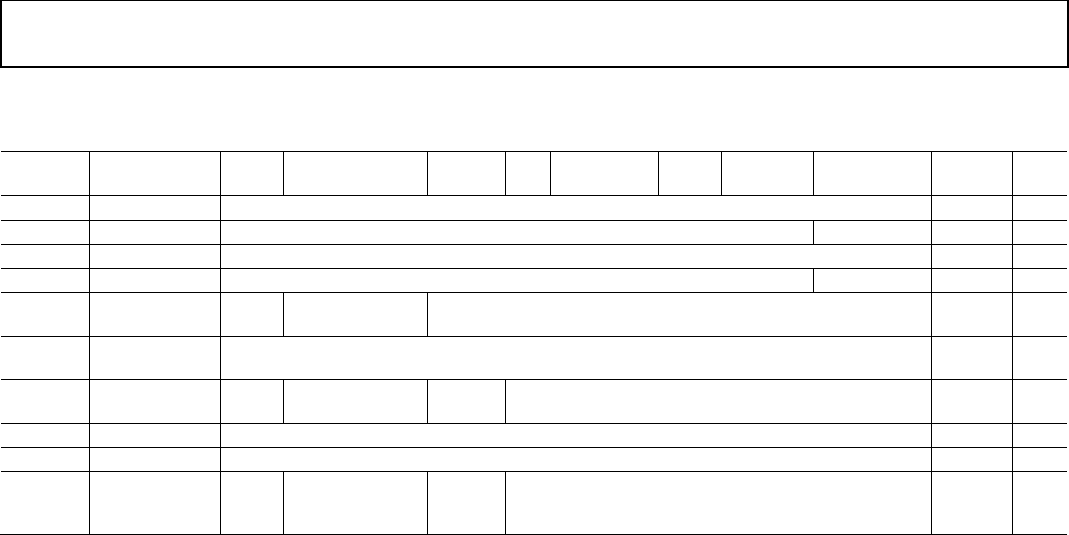
AD9361 Register Map Reference Manual UG-671
Rev. 0 | Page 27 of 72
Tx POWER CONTROL AND ATTENUATION REGISTERS (ADDRESS 0x073 THROUGH ADDRESS 0x07C)
Table 31.
Register
Address Name D7 D6 D5 D4 D3 D2 D1 D0 Default R/W
0x073 Tx1 Atten 0 Tx 1 Atten[7:0] 0x00 R/W
0x074 Tx1 Atten 1 Open Tx 1 Atten[8] 0x00 R/W
0x075 Tx2 Atten 0 Tx 2 Atten[7:0] 0x00 R/W
0x076 Tx2 Atten 1 Open Tx 2 Atten[8] 0x00 R/W
0x077 Tx Atten Offset Open Mask Clr Atten
Update
Tx Atten Offset[5:0] 0x40 R/W
0x078 Tx Atten
Threshold
Tx Atten Thresh[7:0] 0x3c R/W
0x079
Sel Tx1/Tx2
Open
Sel Tx1 and Tx2
Must
be 0
Open
0x00
R/W
0x07A Open Open 0x00 R/W
0x07B Open Open 0x00 R/W
0x07C
Immediate
Update
Open
Immediately
Update TPC
Atten
Must
be 0
Open
0x00
R/W
The ad9361_set_tx_attenuation function configures
attenuation.
SPI Register 0x073 and SPI Register 0x074—Tx 1
Atten[8:0]
This 9-bit word sets the Tx path attenuation. Zero = zero
attenuation. Resolution is 0.25 dB/LSB. Range is 0 to 359 (d).
SPI Register 0x075 and SPI Register 0x076—Tx 2
Atten[8:0]
Tx2 Atten functions the same as Register 0x073 and Register
0x074 but for Tx2.
SPI Register 0x077—Tx Atten Offset
D6—Mask Clr Atten Update
When clear, the Immediately Update TPC Atten bit in Register
0x07C[D6] self-clears. When set, the, the Immediately Update
TPC Atten bit does not self-clear.
[D5:D0]—Tx Atten Offset[5:0]
This unsigned value adds to the words in Register 0x073
through Register 0x076, resulting in new attenuation words.
Resolution is 0.25 dB/LSB.
SPI Register 0x078—Tx Atten Threshold
See 0x067[4:0] and Register 0x068. Resolution is 0.25 dB/LSB.
SPI Register 0x079—Sel Tx1/Tx2
D6—Sel Tx1 and Tx2
Use the Tx1 attenuation value for both Tx1 and Tx2.
D5—Must be 0
SPI Register 0x07C—Immediate Update
D6—Immediately Update TPC Atten
See Register 0x077[D6].
D5—Must be 0
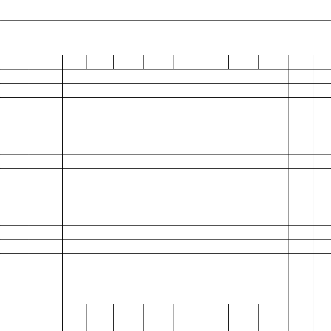
UG-671 AD9361 Register Map Reference Manual
Rev. 0 | Page 28 of 72
Tx QUADRATURE CALIBRATION PHASE, GAIN, AND OFFSET CORRECTION REGISTERS (ADDRESS 0x08E
THROUGH ADDRESS 0x09F)
Table 32.
Register
Address Name D7 D6 D5 D4 D3 D2 D1 D0 Default R/W
0x08E Tx1 Out 1
Phase Corr
Tx1 Output 1 Phase Correction[7:0] 0x-- R/W
0x08F Tx1 Out 1
Gain Corr
Tx1 Output 1 Gain Correction[7:0] 0x-- R/W
0x090 Tx2 Out 1
Phase Corr
Tx2 Output 1 Phase Correction[7:0] 0x-- R/W
0x091 Tx2 Out 1
Gain Corr
Tx2 Output 1 Gain Correction[7:0] 0x-- R/W
0x092 Tx1 Out 1
Offset I
Tx1 Output 1 Offset I[7:0] 0x-- R/W
0x093 Tx1 Out 1
Offset Q
Tx1 Output 1 Offset Q[7:0] 0x-- R/W
0x094 Tx2 Out 1
Offset I
Tx2 Output 1 Offset I[7:0] 0x-- R/W
0x095 Tx2 Out 1
Offset Q
Tx2 Output 1 Offset Q[7:0] 0x-- R/W
0x096 Tx1 Out 2
Phase Corr
Tx1 Output 2 Phase Correction[7:0] 0x-- R/W
0x097 Tx1 Out 2
Gain Corr
Tx1 Output 2 Gain Correction[7:0] 0x-- R/W
0x098 Tx2 Out 2
Phase Corr
Tx2 Output 2 Phase Correction[7:0] 0x-- R/W
0x099 Tx2 Out 2
Gain Corr
Tx2 Output 2 Gain Correction[7:0] 0x-- R/W
0x09A Tx1 Out 2
Offset I
Tx1 Output 2 Offset I[7:0] 0x-- R/W
0x09B Tx1 Out 2
Offset Q
Tx1 Output 2 Offset Q[7:0] 0x-- R/W
0x09C
Tx2 Out 2
Offset I
Tx2 Output 2 Offset I[7:0]
0x--
R/W
0x09D Tx2 Out 2
Offset Q
Tx2 Output 2 Offset Q[7:0] 0x-- R/W
0x09E Open Open 0x--
0x09F Force Bits Force
Out 2
Tx2
Offset
Force
Out 2
Tx1
Offset
Force Out
2 Tx2
Phase
and Gain
Force Out
2 Tx1
Phase
and Gain
Force
Out 1
Tx2
Offset
Force
Out 1
Tx1
Offset
Force Out
1 Tx2
Phase
and Gain
Force Out
1 Tx1
Phase
and Gain
0x00 R/W
SPI Register 0x08E—Tx1 Out 1 Phase Corr
If 0x09F[D0] is clear, after a Tx quadrature calibration
completes, this register holds the phase correction word for
Tx1A. If 0x09F[D0] is set, the value written to this register
is used as the phase correction word.
SPI Register 0x08F—Tx1 Out 1 Gain Corr
If 0x09F[D0] is clear, after a Tx quadrature calibration
completes, this register holds the gain correction word for
Tx1A. If 0x09F[D0] is set, the value written to this register
is used as the gain correction word.
SPI Register 0x090—Tx2 Out 1 Phase Corr
This register functions the same as Register 0x08E but applies to
Tx2 and the force bit is 0x09F[D1].
SPI Register 0x091—Tx2 Out 1 Gain Corr
This register functions the same as Register 0x08F but applies to
Tx2 and the force bit is 0x09F[D1].
SPI Register 0x092—Tx1 Out 1 Offset I
If 0x09F[D2] is clear after a Tx quadrature calibration
completes, this register holds the LO leakage correction word
for I signal path of Tx1A. If 0x09F[D2] is set, the value written
to this register is used as the LO leakage correction word.

AD9361 Register Map Reference Manual UG-671
Rev. 0 | Page 29 of 72
SPI Register 0x093—Tx1 Out 1 Offset Q
This register functions the same as Register 0x092 but applies to
the Q signal path.
SPI Register 0x094—Tx2 Out 1 Offset
This register functions the same as Register 0x092 but applies to
Tx2 and the force bit is 0x09F[D3].
SPI Register 0x095—Tx2 Out 1 Offset Q
This register functions the same as Register 0x092 but applies to
the Q signal path of Tx2 and the force bit is 0x09F[D3].
SPI Register 0x096—Tx1 Out 2 Phase Corr
This register functions the same as Register 0x08E but applies to
Tx1B and the force bit is 0x09F[D4].
SPI Register 0x097—Tx1 Out 2 Gain Corr
This register functions the same as Register 0x08F but applies to
Tx1B and the force bit is 0x09F[D4].
SPI Register 0x098—Tx2 Out 2 Phase Corr
This register functions the same as Register 0x08E but applies to
Tx2B of Tx2 and the force bit is 0x09F[D5].
SPI Register 0x099—Tx2 Out 2 Gain Corr
This register functions the same as Register 0x08F but applies to
Tx2B of Tx2 and the force bit is 0x09F[D5].
SPI Register 0x9A—Tx1 Out 2 Offset I
This register functions the same as Register 0x092 but applies to
Tx1B and the force bit is 0x09F[D6].
SPI Register 0x09B—Tx1 Out 2 Offset Q
This register functions the same as Register 0x092 but applies to
the Tx1B Q signal path and the force bit is 0x09F[D6].
SPI Register 0x09C—Tx2 Out 2 Offset I
This register functions the same as Register 0x092 but applies to
Tx2B of Tx2 and the force bit is 0x09F[D7].
SPI Register 0x09D—Tx2 Out 2 Offset Q
This register functions the same as Register 0x092 but applies to
the Q signal path of Tx2B of Tx2 and the force bit is 0x09F[D7].
SPI Register 0x09F—Force Bits
These bits force the values in Register 0x08E through Register
0x09D to be the Tx quadrature calibration correction words.
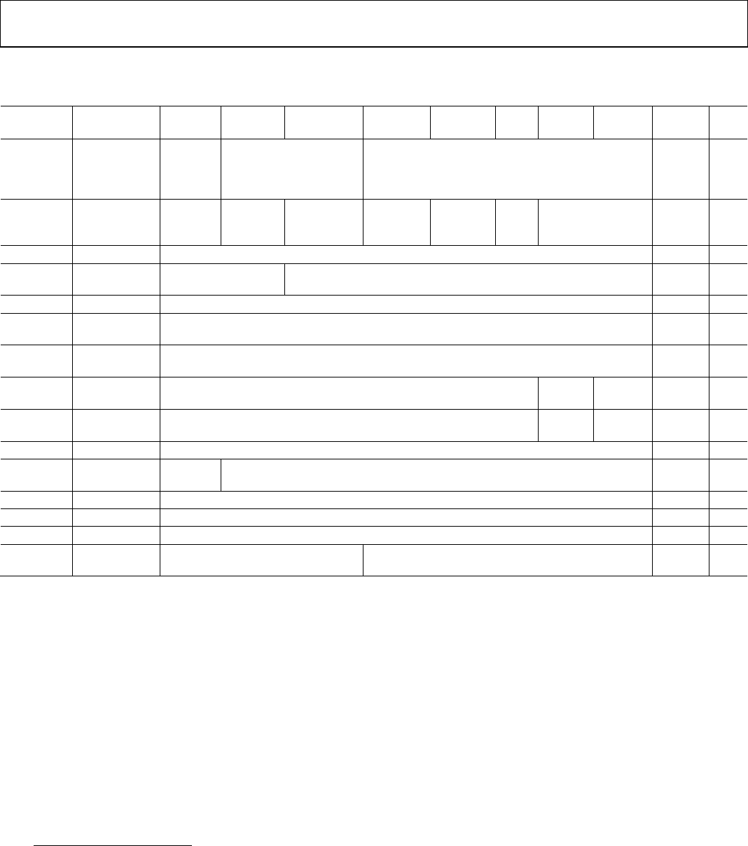
UG-671 AD9361 Register Map Reference Manual
Rev. 0 | Page 30 of 72
Tx QUADRATURE CALIBRATION CONFIGURATION REGISTERS (ADDRESS 0x0A0 THROUGH ADDRESS 0x0AE)
Table 33.
Register
Address Name D7 D6 D5 D4 D3 D2 D1 D0 Default R/W
0x0A0 Quad Cal
NCO Freq
and Phase
Offset
Open Rx NCO Frequency[1:0] Rx NCO Phase Offset[4:0] 0x0C R/W
0x0A1 Quad Cal
Control
Free
Run
Enable
Set to 1 DC Offset
Enable
Gain
Enable
Phase
Enable
Must
be 0
Set to 2’b11 0x78 R/W
0x0A2 Set to 0x7F Set to 0x7F 0x1F R/W
0x0A3 Tx NCO
Frequency
Tx NCO
Frequency[1:0]
Must be 0 0x00 R/W
0x0A4 Set to 0xF0 Set to 0xF0 0x10 R/W
0x0A5 Mag. Ftest
Thresh
Mag Ftest Thresh[7:0] 0x06 R/W
0x0A6 Mag. Ftest
Thresh 2
Mag Ftest Thresh2[7:0] 0x06 R/W
0x0A7 Quad Cal
Status Tx1
Tx1 Convergence Count[5:0] Tx1 LO
Conv
Tx1 SSB
Conv
0x-- R
0x0A8 Quad Cal
Status Tx2
Tx2 Convergence Count[5:0] Tx2 LO
Conv
Tx2 SSB
Conv
0x-- R
0x0A9 Set 0xFF Set to 0xFF 0x20 R/W
0x0AA Tx Quad
Full/LMT Gain
Open Rx Full table/LMT table gain[6:0] 0x0A R/W
0x0AB Must be 0 Must be 0 0x00 R/W
0x0AC Must be 0 Must be 0 0x00 R/W
0x0AD Must be 0 Must be 0 0x00 R/W
0x0AE Tx Quad LPF
Gain
Open Rx LPF gain[4:0] 0x18 R/W
The ad9361_tx_quad_calib function configures these registers
but the NCO phase offset value in Register 0x0A0 must be
determined empirically for many combinations of samling rates
and digital filter configurations. Analog Devices’ Engineer Zone
describes in detail how to configure the registers for a successful
Tx quadrature calibration.
SPI Register 0x0A0—Quad Cal NCO Freq and Phase
Offset
[D6:D5]—Rx NCO Frequency[1:0]
This value sets the test frequency, per Equation 13, for the Rx
path that processes the Tx test tone. The Rx NCO frequency
should equal the Tx NCO frequency (Register 0x0A3[D7:D6]).
=
×( [:] )
(13)
where ClkRF is the clock at the input to the Rx FIR filter.
[D4:D0]—Rx NCO Phase Offset[4:0]
This register compensates for the delay of the test signal through
the signal path. It must be correct and is affected by the digital
filter settings.
SPI Register 0x0A1—Quad Cal Control
D7—Free Run Enable
Normally clear. When this bit is clear, the Tx quadrature
calibration runs until the errors are below the thresholds in
0x0A5 and 0x0A6, up to a maximum time set by the Quad Cal
Count (0x0A9). This mode forces the algorithm to finish. If the
bit is set, the algorithm will not finish until (if) it meets the
thresholds.
D6—Set to 1
D5—DC Offset Enable
Normally set. When set, a Tx quad calibration performs a DC
offset correction. Clearing the bit disables this correction.
D4—Gain Enable
Normally set. When set, a Tx quad calibration performs a gain
offset correction. Clearing this bit disables this correction.
D3—Phase Enable
Normally set. When set, a Tx quad calibration performs a phase
offset correction. Clearing this bit disables this correction.
D2—Must be 0
[D1:D0]—Set to 2’b11

AD9361 Register Map Reference Manual UG-671
Rev. 0 | Page 31 of 72
SPI Register 0x0A2—Set to 0x7F
SPI Register 0x0A3—Tx NCO Frequency
[D7:D6] Tx NCO Frequency[1:0]
These bits sets the test waveform frequency per Equation 14.
NCO Test =
×( [:] )
(14)
where ClkTF is the clock at the output of the Tx FIR filter.
[D5:D0]—Must be 0
SPI Register 0x0A4—Set to 0xF0
SPI Register 0x0A5 and SPI Register 0x0A6—Mag Ftest
Thresh and Mag Ftest Thresh2
These are thresholds for LO leakage and quadrature correction.
Normally set to 0x01 for best performance.
SPI Register 0x0A7 and SPI Register 0x0A8 Quad Cal
Status Tx1 and Tx2
[D7:D2]—Convergence Count[5:0]
These bits indicate the duration of the Tx quadrature
calibration. Higher values indicate longer duration.
D1—LO Conv
If this bit equals one, the LO leakage algorithm converged.
D0—SSB Conv
If this bit equals one, the Quarature Calibratoin algorithm
converged
SPI Register 0x0A9—Set to 0xFF
Set to 0xFF. This register sets the maximum time that the Tx
quad calibration algorithm can run.
SPI Register 0x0AA—Tx Quad Full/LMT Gain
The AD9361 uses some Rx circuitry when for the Tx quadra-
ture calibration. 0x0AA sets Rx gain for the calibration. When
using the full gain table mode, Register 0x0AA specifies the
gain index. When using the split table mode, Register 0x0AA
specifies the LMT index and Register 0x0AE specifies the LPF
index.
SPI Register 0x0AB—Must be 0
SPI Register 0x0AC— Must be 0
SPI Register 0x0AD— Must be 0
SPI Register 0x0AE—Tx Quad LPF Gain
Only applies if the split gain table is used. See Register 0x0AA.
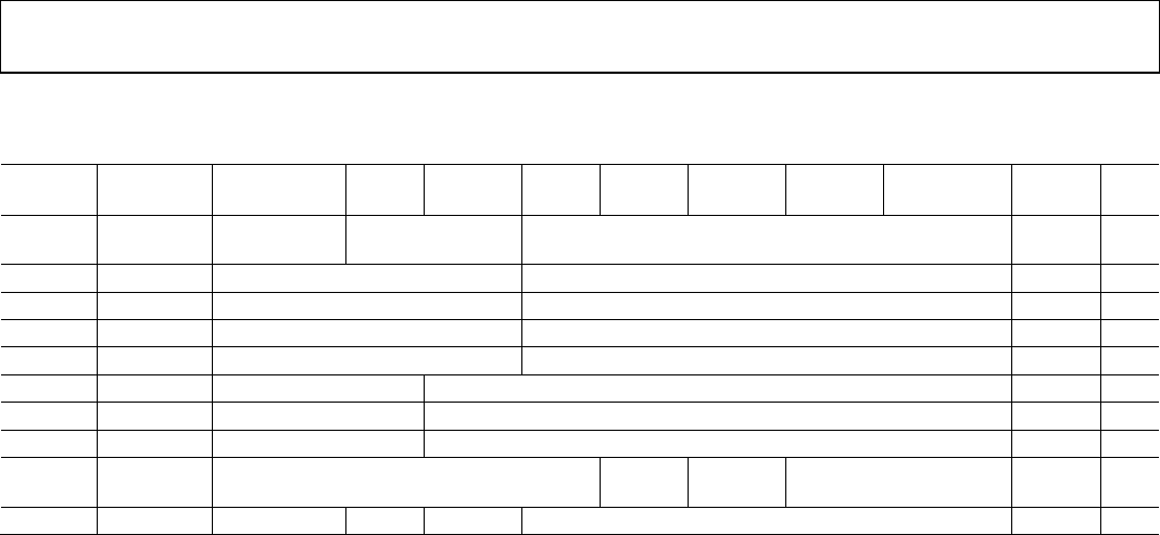
UG-671 AD9361 Register Map Reference Manual
Rev. 0 | Page 32 of 72
Tx BASEBAND FILTER REGISTERS (ADDRESS 0x0C2 THROUGH ADDRESS 0x0CC)
Table 34.
Register
Address Name D7 D6 D5 D4 D3 D2 D1 D0 Default R/W
0x0C2 Tx BBF R1 Override
Enable
Open R1[4:0] 0x1F R/W
0x0C3 Tx BBF R2 Open R2[4:0] 0x1F R/W
0x0C4
Tx BBF R3
Open
R3[4:0]
0x1F
R/W
0x0C5 Tx BBF R4 Open R4[4:0] 0x1F R/W
0x0C6 Tx BBF RP Open RP[4:0] 0x1F R/W
0x0C7 Tx BBF C1 Open C1[5:0] 0x2A R/W
0x0C8 Tx BBF C2 Open C2[5:0] 0x2A R/W
0x0C9 Tx BBF CP Open CP[5:0] 0x2A R/W
0x0CA Tuner PD Must be 0x2 Set to 0 Tuner
PD
Set to 2’b10 0x20 R/W
0x0CB Tx BBF R2b Must be 0 Open R2b Ovr R2b[4:0] 0x00 R/W
The ad9361_set_tx_rf_bandwidth function configures these
registers based on the R F BW.
SPI Registers 0x0C2—Tx BBF R1
D7—Override Enable
Setting this bit forces the baseband filter to use the values
written into Register 0x0C2 through Register 0x0CB.
[D4:D0]—R1[4:0]
Tx baseband filter R1 word.
SPI Register 0x0C3 Through SPI Register 0x0C5—Tx BBF
R2 Through Tx BBF R4
Tx baseband filter R2 through R4 words.
SPI Register 0x0C6—Tx BBF RP
Tx baseband filter real pole word.
SPI Register 0x0C7 and SPI Register 0x0C8—Tx BBF C1
and C2
Tx baseband filter C1 and C2 words.
SPI Register 0x0C9—Tx BBF CP
Tx baseband filter real pole word.
SPI Register 0x0CA—Tuner PD
[D7:D3]—Set to 0x2
D3—Set to 0
D2—Tuner PD
Clear this bit to run a Tx baseband filtercalibration. Set the bit
after the calibration completes.
[D1:D0]—Set to 2’b10
SPI Register 0x0CB—Tx BBF R2b
D7—Must be 0
D5—R2b Ovr
This is a force bit but it only allows the R2b value to be forced.
Use only if performing a manual calibration.
[D4:D0]—R2b[4:0]
Tx baseband filter R2b control word.
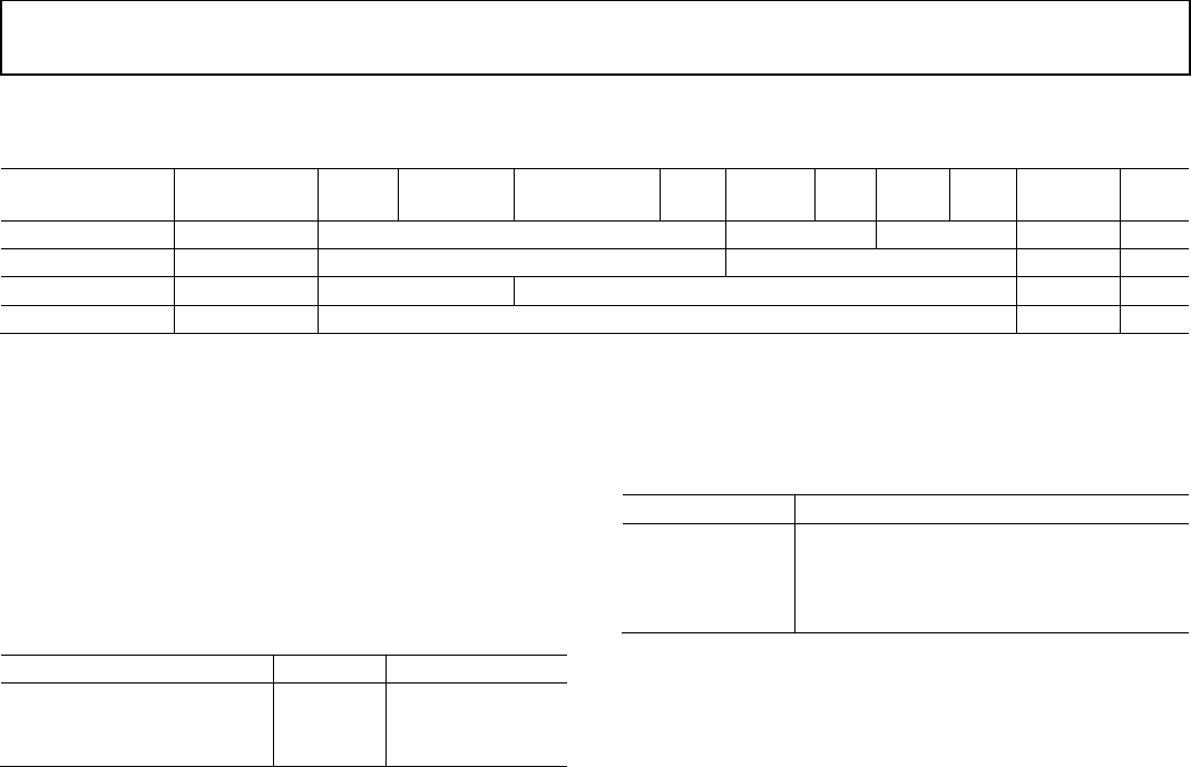
AD9361 Register Map Reference Manual UG-671
Rev. 0 | Page 33 of 72
Tx SECONDARY FILTER REGISTERS (ADDRESS 0x0D0 THROUGH ADDRESS 0x0D3)
Table 35.
Register
Address Name D7 D6 D5 D4 D3 D2 D1 D0 Default R/W
0x0D0 Config0 Must be 0x5 Cc[1:0] AmpBias[1:0] 0x55h R/W
0x0D1 Resistor Open Resistor[3:0] 0x0Fh R/W
0x0D2 Capacitor Open Capacitor[5:0] 0x1Fh R/W
0x0D3 Must be 0x60 Must be 0x60 0x60h R/W
The ad9361_set_tx_rf_bandwidth function configures these
registers based on the RF BW. This register provides filtering for
Tx noise that is far out from the channel. Typically set the filter
corner to 5× the base-band BW.
SPI Register 0x0D0—Config0
[D7:D4]—Must be 0x5
[D3:D2]—Cc[1:0]
Compensation network for the amplifiers. Set per Table 36.
Table 36. Secondary Filter Cc and Amp Bias
RF Bandwidth (RF BW) Cc[1:0] AmpBias[1:0]
≤9 MHz 10 01
9 MHz < RF BW ≤ 24 MHz 01 10
> 24 MHz 01 11
[D1:D0]—AmpBias[1:0]
These bits set amplifier bias current. Set per Table 36. Higher
current equals lower noise and wider BW.
SPI Register 0x0D1—Resistor[3:0]
Secondary filter resistor, which, along with the Capacitor[5:0]
bits, sets the 3 dB, corner (see 0x0D2). Settings per Table 37.
Table 37. Post Secondary Filter Stage Resistance
Resistor[3:0] Post-Filter Stage Resistance (Ω)
0001 800
0011 400
0100 200
1100 100
SPI Register 0x0D2—Capacitor[5:0]
Secondary filter capacitor, which, along with the Resistor, sets
the 3 dB corner (see 0x0D1). Set Capacitor such that Resistor is
as low as possible.
SPI Register 0x0D3—Must be 0x60
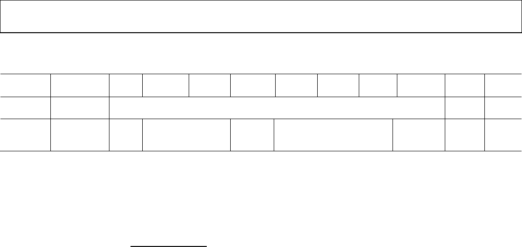
UG-671 AD9361 Register Map Reference Manual
Rev. 0 | Page 34 of 72
Tx BBF TUNER CONFIGURATION REGISTERS (ADDRESS 0x0D6 THROUGH ADDRESS 0x0D7)
Table 38.
Register
Address Name D7 D6 D5 D4 D3 D2 D1 D0 Default R/W
0x0D6 Tx BBF Tune
Divider
Tx BBF Tune Divider[7:0] 0x12 R/W
0x0D7 Tx BBF Tune
Mode
Open Must be 2’b00 Must
be 1
Must be 3’b111 Tx BBF
Tune
Divider[8]
0x1E R/W
The ad9361_set_tx_rf_bandwidth function configures these
registers base d on the RF BW.
SPI Register 0x0D6 and SPI Register 0x0D7[D0]
The Tx BBF uses a clock during calibration, derived by dividing
down the BBPLL per Equation 15.
.
(15)
SPI Register 0x0D7—Tx BBF Tune Mode
[D6:D5]—Must be 2’b00
D4—Must be 1
[D3:D1]—Must be 3’b111
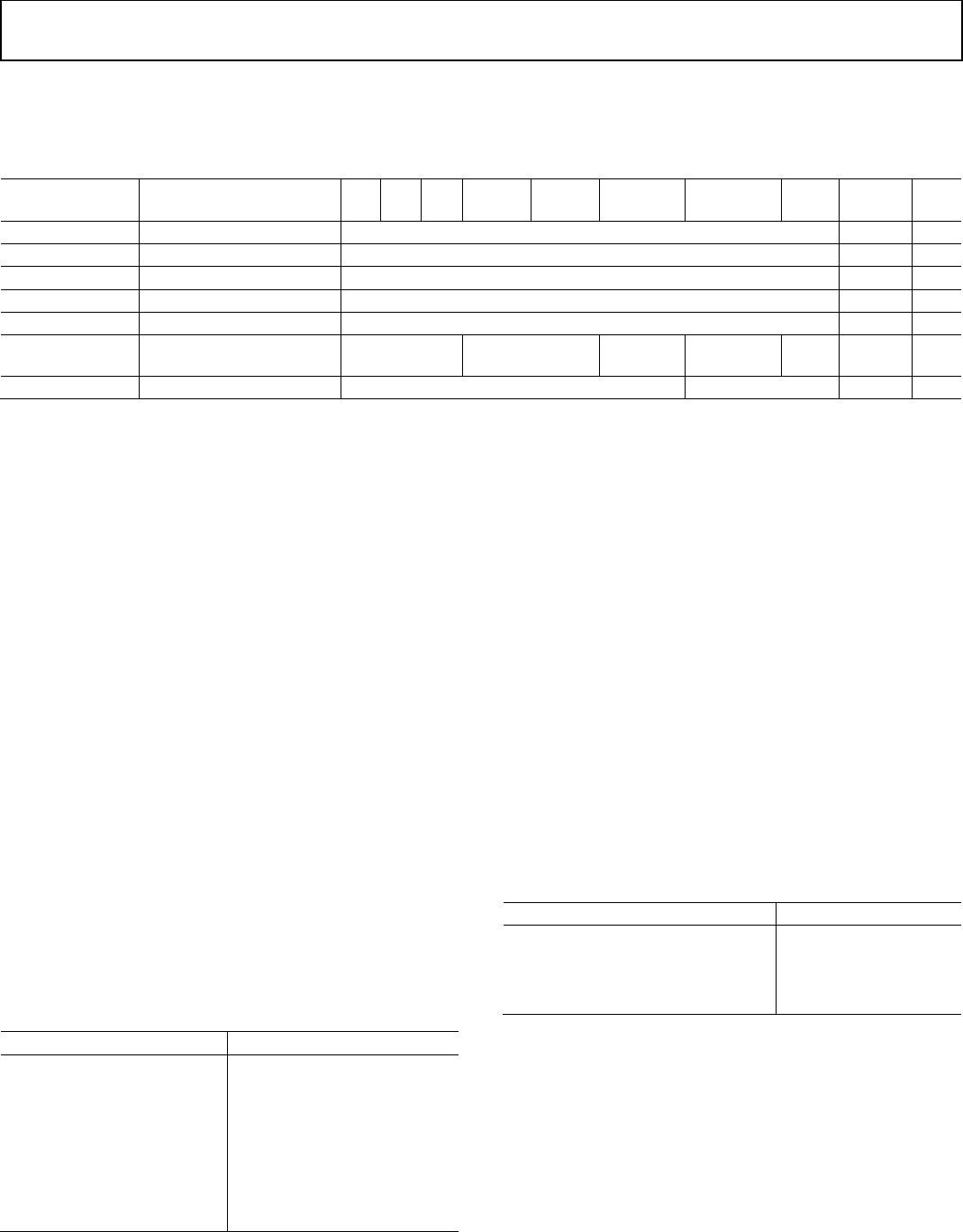
AD9361 Register Map Reference Manual UG-671
Rev. 0 | Page 35 of 72
RECEIVER CONFIGURATION
Rx PROGRAMMABLE FIR FILTER REGISTERS (ADDRESS 0x0F0 THROUGH ADDRESS 0x0F6)
Table 39.
Register
Address Name D7 D6 D5 D4 D3 D2 D1 D0 Default R/W
0x0F0 Rx Filter Coeff Addr Rx Filter Addr[7:0] 0x-- R/W
0x0F1 Rx Filter Coeff Data 1 Rx Filter Coefficient Write Data[7:0] 0x-- R/W
0x0F2 Rx Filter Coeff Data 2 Rx Filter Coefficient Write Data[15:8] 0x-- R/W
0x0F3 Rx Filter Coeff Read Data 1 Rx Filter Coefficient Read Back Data[7:0] 0x-- R
0x0F4 Rx Filter Coeff Read Data 2 Rx Filter Coefficient Read Back Data[15:8] 0x-- R
0x0F5 Rx Filter Configuration Number of
Taps
Select Rx Ch[1:0] Write Rx Start Rx
Clock
Open 0x00 R/W
0x0F6
Rx Filter Gain
Open
Filter Gain[1:0]
0x00
R/W
The ad9361_set_rx_fir_config function loads the FIR filter
coefficients and sets up the other FIR parameters.
SPI Register 0x0F0—Rx Filter Coeff Addr
The digital filter coefficients are indirectly addressable.
Register 0x0F0 holds the address of the coefficient address.
SPI Register 0x0F1 and SPIRegister 0x0F2—Rx Filter
Coeff Data 1 and Data 2
Write the coefficient values to these registers. Write these
registers (along with Register 0x0F0) before setting Register
0x0F5[D5]. Coefficients are in twos complement form, 16-bits
wide.
SPI Register 0x0F3 and Register 0x0F4—Rx Filter Coeff
Read Data 1 and Data 2
When reading coefficients, write the address in 0x0F0, write
Register 0x0F5 to start the programming clock, then read
Register 0x0F3 and Register 0x0F4. Coefficients are in twos
complement form, 16-bits wide.
SPI Register 0x0F5—Rx Filter Configuration
[D7:D5]—Number of Taps[2:0]
The number of taps of the Rx filter must be correct, per
Table 40. The number of taps can be read by first writing to
Register 0x0F5 to turn on the clock, select the correct receiver,
and read Register 0x0F5.
Table 40. Rx Filter Taps
Number of Taps Number of Taps[2:0]
16 000
32 001
48 010
64 011
80 100
96 101
112 110
128 111
[D4:D3]—Select Rx CH[1:0]
When writing coefficients, Bit D3 causes a write to Rx1, Bit D4
causes a write to Rx2 and both bits set writes to both Rx filters.
When reading, setting both bits is an invalid case.
D2—Write Rx
Set this self-clearing bit to write a coefficient. Each write
operation must set this bit. After the table has been pro-
grammed, write to Register 0x0F6 with the Write Tx bit cleared
and D1 high. Then, write to Register 0x0F6 again with D1 clear,
thus ensuring that the write bit resets internally before the clock
stops. Wait 4 Tx sample periods after setting D2 high while the
data writes into the table.
D1—Start Rx Clock
Set this bit to start the programming clock.
SPI Register 0xF6—Rx Filter Gain
These bits affect how much digital gain adds to the digital
samples after the RFIR filter per Table 41.
Table 41. Rx Filter Gain
Rx Filter Gain[1:0] Gain
3 −12 dB
2 −6 dB
1 0 dB (default)
0 +6 dB

UG-671 AD9361 Register Map Reference Manual
Rev. 0 | Page 36 of 72
GAIN CONTROL GENERAL SETUP REGISTERS (ADDRESS 0x0FA THROUGH ADDRESS 0x10E)
Table 42.
Register
Address Name D7 D6 D5 D4 D3 D2 D1 D0 Default R/W
0x0FA AGC Config1 Set to 3’b111
Slow Attack
Hybrid Mode
Rx 2 Gain Control
Setup[1:0]
Rx 1 Gain Control
Setup[1:0]
0xE0 R/W
0x0FB AGC Config2 Must be 0 Gain
Unlock
Control
Open Use Full
Gain Table
Enable
Digital
Gain
Manual
Gain
Control
Rx2
Manual
Gain
Control
Rx1
0x08 R/W
0x0FC AGC Config3 Manual (CTRL_IN) Incr Gain
Step Size[2:0]
Inc/Dec LMT
Gain
Use AGC
for
LMT/LPF
Gain
ADC Overrange Sample Size[2:0] 0x03 R/W
0x0FD
Max LMT/Full
Gain
Open
Maximum Full Table/LMT Table Index[6:0]
0x4C
R/W
0x0FE Peak Wait Time Manual (CTRL_IN) Decr Gain
Step Size[2:0]
Peak Overload Wait Time[4:0] 0x44 R/W
0x0FF Open 0x-- R/W
0x100 Digital Gain Dig Gain Step Size[2:0] Maximum Digital Gain[4:0] 0x6F R/W
0x101 AGC Lock Level Enable
Dig Sat
Ovrg
AGC Lock Level (Fast)/AGC Inner High Threshold (Slow) [6:0] 0x0A R/W
0x102
Open
Open
0x--
R/W
0x103 Gain Step
Config 1
Must be 0 Dec Step Size for: Large LMT
Overload/Full Table Case #3 [2:0]
Open 0x08 R/W
0x104
ADC Small
Overload
Threshold
ADC Small Overload Threshold[7:0] 0x2F R/W
0x105 ADC Large
Overload
Threshold
ADC Large Overload Threshold[7:0] 0x3A R/W
0x106 Gain Step
Config 2
Open Fast Attack Only. Decrement Step
Size for: Small LPF Gain Change/Full
Table Case #2[2:0]
Decrement Step Size for: Large LPF Gain
Change/Full Table Case #1[3:0]
0x25 R/W
0x107
Small LMT
Overload
Threshold
Force PD
Reset Rx2
For PD
Reset Rx1
Small LMT Overload Threshold[5:0]
0x3F
R/W
0x108 Large LMT
Overload
Threshold
Open Large LMT Overload Threshold[5:0] 0x1F R/W
0x109 Rx1 Manual
LMT/Full Gain
Power
Meas in
State 5[3]
Rx1 Manual Full Table/LMT Table Gain Index[6:0] 0x4C R/W
0x10A Rx1 Manual LPF
Gain
Power Meas in State 5[2:0] Rx1 Manual LPF Gain [4:0] 0x58 R/W
0x10B Rx1 Manual
Digital/Forced
Gain
Open Rx1 Manual/Forced Digital Gain[4:0] 0x00 R/W
0x10C Rx2 Manual
LMT/Full Gain
Open Rx2 Manual Full Table/LMT Table Gain Index[6:0] 0x4C R/W
0x10D Rx2 Manual LPF
Gain
Open Rx2 Manual LPF Gain[4:0] 0x18 R/W
0x10E Rx2 Manual
Digital/Forced
Gain
Open Rx2 Manual/Forced Digital Gain[4:0] 0x00 R/W

AD9361 Register Map Reference Manual UG-671
Rev. 0 | Page 37 of 72
These registers are configured by the ad9361_set_rx_gain_
control_mode function. For some applications, register values
may need to be modified. See the Gain Control section of the
AD9361 Reference Manual for more information.
SPI Register 0x0FA—AGC Config 1
[D7:D5]—Set to 3’b111
D4—Slow Attack Hybrid AGC Mode
Set to use hybrid AGC mode. Clear otherwise.
[D3:D2]—Rx2 Gain Control Setup[1:0]
Gain control operation maps to these setup bits per Table 43.
Table 43. Gain Control Setup
Gain Control
Setup[1:0] Gain Control Mode
0 Manual gain
1 Fast attack automatic gain control (AGC)
2 Slow attack AGC
3 Hybrid AGC—also set 0x0FA[D4]
[D1:D0]—Rx1 Gain Control Setup[1:0]
These bits function the same as Bits[D3:D2] but apply to Rx1.
SPI Register 0x0FB—AGC Config 2
D7—Must be 0
D6—Gain Unlock Control
Applies to the fast AGC and allows the gain to stay locked even
under certain overload conditions.
D3—Use Full Gain Table
Set this bit to use the full gain table. Clear to use the split gain
table.
D2—Enable Digital Gain
This bit is used in split table mode to enable the digital gain
pointer.
D1—Manual Gain Control Rx2
Applies to MGC . If this bit is clear, SPI writes change the gain.
When this bit is set, control input pins control the gain. If this
bit transitions high, the gain resets to maximum.
D0—Manual Gain Control Rx1
This bit functions the same as Bit D1 but applies to Rx1.
SPI Register 0x0FC—AGC Config 3
[D7:D5]—Manual (CTRL_IN) Incr Gain Step Size[2:0]
Applies to MGC and if the CTRL_IN signals control gain
(0x0FB[D1:D0] set). The gain index increases by this register +
1 when certain CTRL_IN signals transition high.
D4—Inc/Dec LMT Gain
Applies to MGC, if CTLR_IN signals control gain
(0x0FB[D1:D0] set), if the split gain table is used 0x0FB[D3]
clear) and if [D3] is clear. If this bit is set, LNA, Mixer, and TIA
gain changes. If this bit is clear, LPF gain changes.
D3—Use AGC for LMT/LPF Gain
Applies to MGC, if the CTRL_IN signals control gain,
(0x0FB[D1:D0] set) and to the split gain table (0x0FB[D3]
clear). If this bit is clear, D4 determines where the gain changes.
If this bit is set, the AGC determines where the gain changes.
[D2:D0]—ADC Overrange Sample Size[2:0]
These bits + 1 equals the number of ADC output samples used
to determine an ADC overload.
SPI Register 0x0FD—Max LMT/Full Gain
This register must be set to the maximum gain index of the gain
table.
SPI Register 0x0FE—Peak Wait Time
[D7:D5]—Manual (CTRL_IN) Decr Gain Step Size[2:0]
Applies to MGC and if the CTRL_IN signals control gain
(0x0FB[D1:D0] set). The gain index decreases by these bits + 1
when certain CTRL_IN signals transition high.
[D4:D0]—Peak Overload Wait Time[4:0]
This register sets the wait time in ClkRF cycles that the peak
detectors are held in reset after a gain change and affects all
gain control modes.
SPI Register 0x100—Digital Gain
[D7:D5]—Digital Gain Step Size[2:0]
Applies to AGC modes, if digital gain is enabled (0x0FB[D2]
set), and the split table (0x0FB[D3] clear). If digital saturation
occurs, digital gain reduces by this register +1.
[D4:D0]—Maximum Digital Gain[4:0]
Applies if digital gain is enabled (0x0FB[D2] set), equals the
maximum allowable digital gain, and applies to all gain control
modes. The maximum value is 31 dB. Resolution is 1 dB/LSB.
SPI Register 0x101—AGC Lock Level
D7—Enable Dig Sat Ovrg
Applies to the fast AGC and full gain table. When clear, digital
saturation does not cause a gain decrease. When set, digital
saturation will cause a gain decrease.
[D6:D0]—AGC Lock Level (Fast)/AGC Inner High
Threshold (Slow)[6:0]
Applies to AGC. This register specifies the fast AGC lock level
or specifies the slow AGC inner high threshold. Resolution is
−1 dBFS/LSB.
SPI Register 0x103—Gain Step Config 1
[D7:D5]—Must be 0
[D4:D2]—Step Size for: Large LMT Overload/Full Table
Case #3[2:0]
Apply to AGC and determine how much the gain changes for
large LMT in split tablemode or the small ADC overload for the
full table.

UG-671 AD9361 Register Map Reference Manual
Rev. 0 | Page 38 of 72
SPI Register 0x104—ADC Small Overload Threshold
This register sets the small ADC overload and is one of two that
the AGC compares against ADC output samples. This register
should be smaller than Register 0x105.
SPI Register 0x105—ADC Large Overload Threshold
This register functions the same as Register 0x104 but should
be the larger of the two values.
SPI Register 0x106—Gain Step Config 2
[D6:D4]—Fast Attack Only. Decrement Step Size for:
Small LPF Gain Change/Full Table Case #2[2:0]
Apply to AGC and determine how much the gain changes for
large LPF in split tablemode or the Large LMT or large ADC
overloads in full table mode.
[D3:D0]—Decrement Step Size for: Large LPF Gain
Change/Full Table Case #1
Apply to AGC and determine how much the gain changes for
large LPF in split tablemode or the large LMT and large ADC
overloads in full table mode.
SPI Register 0x107—Small LMT Overload Threshold
D7—Force PD Reset Rx2
Setting this bit forces the Rx2 ADC and LMT peak detectors to
ignore peak overloads.
D6—Force PD Reset Rx1
This bit functions the same as Bit D7 but applies to Rx1.
[D5:D0]—Small LMT Overload Threshold[5:0]
These bits, mapped per Equation 16, set the small LMT
overload threshold and is one of two that the AGC compares
against the signal at the input to the LPF. This register should
be smaller than Register 0x108. The valid range is from 0x07 to
0x31.
()= 16 ×
( [5: 0] + 1) (16)
SPI Register 0x108—Large LMT Overload Threshold
This register functions the same as Register 0x107 (and uses
the same equation) but should be larger than 0x107[D5:D0].
SPI Register 0x109—Rx1 Manual LMT/Full Gain
D7—Power Meas in State 5[3]
Same as Dec Power Measurement Duration in 0x15C[D3:D0]
but apply only to State 5 (gain lock) for the fast AGC.
[D6:D0]—Rx1 Manual Full table/LMT Table Gain
Index[6:0]
For MGC, write this register to set the full table or LMT index.
For AGC, this register holds the current full or LMT index.
SPI Register 0x10A—Rx1 Manual LPF Gain
[D7:D5]—Power Meas in State 5[2:0]
See Register 0x109[D7].
[D4:D0]—Rx1 Manual LPF Gain[4:0]
Applies to split table mode. For MGC, write this register to set
the LPF gain table index value. For AGC, this register holds the
current LPF index.
SPI Register 0x10B—Rx1 Manual Digital Gain
[D4:D0]—Rx1 Manual/Forced Digital Gain
Applies to the split table. In MGC, write this register to set the
digital gain. In AGC mode, these bits hold the digital gain.
SPI Register 0x10C Through SPI Register 0x10E—Manual
Gain Registers
These registers are the same as Registers 0x109 through
Registers 0x10B but apply to Rx2.

AD9361 Register Map Reference Manual UG-671
Rev. 0 | Page 39 of 72
FAST ATTACK AGC SETUP REGISTERS (ADDRESS 0x110 THROUGH ADDRESS 0x11B)
Table 44.
Register
Address Name D7 D6 D5 D4 D3 D2 D1 D0 Default R/W
0x110 Config 1 Enable
Gain Inc
after Gain
Lock
Goto Opt
Gain if
Energy
Lost or
EN_AGC
High
Goto Set
Gain if
EN_AGC
High
Goto
Set
Gain if
Exit Rx
State
Don’t
Unlock
Gain if
Energy
Lost
Goto
Optimized
Gain if Exit
Rx State
Don’t
Unlock
Gain If Lg
ADC or
LMT Ovrg
Enable
Incr
Gain
0x02 R/W
0x111 Config 2
and
Settling
Delay
Use Last
Lock Level
for Set
Gain
Enable LMT
Gain Incr
for Lock
Level
Goto Max
Gain or
Opt Gain if
EN_AGC
High
Settling Delay[4:0] 0xCA R/W
0x112 Energy Lost
Threshold
Post Lock Level Step Size
for: LPF Table/Full Table
[1:0]
Energy Lost Threshold[5:0] 0x4A R/W
0x113 Stronger
Signal
Threshold
Post Lock Level Step for
LMT Table [1:0]
Stronger Signal Threshold[5:0] 0x4A R/W
0x114 Low Power
Threshold
Don’t
unlock
gain if
ADC Ovrg
Low Power Threshold[6:0] 0x80 R/W
0x115 Strong
Signal
Freeze
Don’t
unlock
gain if
Stronger
Signal
Open 0x64 R/W
0x116 Final
Overrange
and Opt
Gain
Final Overrange Count[2:0] Open Optimize Gain Offset[3:0] 0x65 R/W
0x117 Energy
Detect
Count
Increment Gain Step (LPF/LMT)[2:0] Energy Detect Count[4:0] 0x08 R/W
0x118 AGCLL
Upper Limit
Open AGCLL Max Increase[5:0] 0x3F R/W
0x119 Gain Lock
Exit Count
Open Gain Lock Exit Count[5:0] 0x08 R/W
0x11A Initial LMT
Gain Limit
Open Initial LMT Gain Limit[6:0] 0x1C R/W
0x11B Increment
Time
Increment Time[7:0] 0x0A R/W
These registers are configured by the ad9361_set_rx_gain_
control_mode function. For some applications, register values
may need to be modified. Many bits in this section change
operation depending on other bit settings. See the Gain Control
section of the AD9361 Reference Manual for more information.
SPI Register 0x110—Config 1
D7—Enable Gain Inc after Gain Lock
Applies to the fast AGC and if the Enable Gain Incr bit
(0x110[D0]) is set. Set 0x110[D7] to allow gain increases after
the gain has locked but before State 5. Signal power must be
lower than the low power threshold in Register 0x114 for longer
than the increment time duration register (Address 0x11B).
If so, the gain increases by the Increment Gain Step set by
0x117[D7:D5].
D6—Goto Opt Gain if Energy Lost/EN_AGC High
If this bit is set and the fast AGC is in State 5, the gain index will
go to the optimize gain value if an energy lost state occurs or (if
0x0FB[D6] is high) when the EN_AGC signal goes high.
D5—Goto Set Gain if EN_AGC is High
If this bit is set and the fast AGC is in State 5, the gain index will
go to the set gain value if EN_AGC goes high. 0x0FB[D6] must
be set.

UG-671 AD9361 Register Map Reference Manual
Rev. 0 | Page 40 of 72
D4—Goto Set Gain if Exit Rx State
If this bit is set and the fast AGC is in State 5, the gain index will
go to the set gain value when the ENSM exits the Rx state.
D3—Don’t Unlock Gain if Energy Lost
If this bit is set and the fast AGC is in State 5, the gain will not
change even if the average signal power decreases more than the
Energy Lost Threshold regiser (Address 0x112).
D2—Goto Optimized Gain if Exit Rx State
If this bit is set and the fast AGC is in State 5, the gain will go to
the optimize gain value if the ENSM exits the Rx state.
D1—Don’t Unlock Gain if Lg ADC or LMT Ovrg
If this bit is set and the fast AGC is in State 5, the gain will not
change even if large ADC or large LMT overloads occur.
D0—Enable Incr Gain
Setting this bit allows the fast AGC to increase the gain while
optimizing the gain index. Clearing this bit prevents the gain
from increasing in any condition.
SPI Register 0x111—Config 2 and Settling Delay
D7—Use Last Lock Level for Set Gain
Only applies if the fast AGC will uses set gain. Set this bit to use
the last gain index of the previous frame for set gain. Clear to
use the first gain index of the previous frame.
D6—Enable LMT Gain Incr for Lock Level
Applies to the fast AGC and the split gain table. Set this bit to
allow the AGC to use LMT gain if the gain index needs to
increase when moving to the AGC Lock Level in 0x101.
Maximum LMT gain allowed is set by the LMT gain step
(0x103[D4:D2]). The difference (if any) is made up by LPF gain.
D5—Goto Max Gain or Opt Gain if EN_AGC High
If this bit is set and the EN_AGC signal goes high, the fast AGC
will go to either the maximum gain index or the optimize gain
value, dependening on 0x110[D6].
[D4:D0]—Settling Delay[4:0]
Applies to all gain control modes. These bits set the delay
between a gain change a power measurement. Delay equals
this register × 2 in ClkRF cycles.
SPI Register 0x112—Energy Lost Threshold
[D7:D6]—Post Lock Level Step Size for: LPF Table/Full
Table[1:0]
These bits set the reduction to the gain index if a large LMT
or large ADC overload occurs after Lock Level but before fast
AGC state 5. If the number of overloads exceeds the Final
Overrange Count (0x116[D7:D5]), the AGC algorithm restarts.
Depending on various conditions if a split table is used, the gain
may reduce in in the LPF or the LMT (see 0x113[D7:D6]).
[D5:D0]—Energy Lost Threshold[5:0]
Applies if the fast AGC is in State 5. If the signal power
decreases by this threshold and the signal power remains at this
level or lower for a duration that is twice the Gain Lock Exit
Count (0x119), the gain may unlock, depending on other AGC
configuration bits. Resolution is 1 dB/LSB.
SPI Register 0x113—Stronger Signal Threshold
[D7:D6]—Post Lock Level Step for LMT Table[1:0]
See 0x112[D7:D6].
[D5:D0]—Stronger Signal Threshold[5:0]
Applies if the fast AGC is in State 5. If the signal power
increases by this threshold and the signal power remains at this
level or higher for a duration that is twice the Gain Lock Exit
Count (0x119), the gain may unlock, depending on other AGC
configuration bits. Resolution is 1 dB/LSB.
SPI Register 0x114—Low Power Threshold
D7—Don’t unlock gain if ADC Ovrg
If this bit is set and the fast AGC is in State 5, the gain will not
change even if large ADC overloads occur.
[D6:D0]—Low Power Threshold[6:0]
This threshold is used by the fast AGC to determine if the gain
should be increased if 0x110[D0] is set. It can also be used to
trigger a CTRL_OUT signal transition in MGC mode. Units are
negative dBFS; resolution is 0.5 dB/LSB.
SPI Register 0x115—Don’t Unlock Gain if Stronger
Signal
If this bit is set and the fast AGC is in State 5, the gain will not
change even if the signal power increase by more than the
Stronger Signal Threshold in 0x113[D5:D0].

AD9361 Register Map Reference Manual UG-671
Rev. 0 | Page 41 of 72
SPI Register 0x116—Final Overrange and Opt Gain
[D7:D5]—Final Overrange Count[2:0]
See 0x112[D7:D6].
[D3:D0]—Optimize Gain Offset[3:0]
The offset added to the last gain lock level of the previous
frame. The result is the optimize gain index.
SPI Register 0x117—Energy Detect Count
[D7:D5]—Increment Gain Step LPF/LMT[2:0]
The Fast AGC will increase the gain index by this amount if
signal power decreases below the Low Power Threshold as
described in 0x114[D6:D0] and only if the Enable Incr Gain
bit (0x110[D0]) is set.
[D4:D0]—Energy Detect Count[4:0]
The fast AGC delays moving from State 1 to State 2 until no
peak overloads are detected for the value of this counter;
measured in ClkRF cycles. Resolution is 1 ClkRF cycle/LSB.
SPI Register 0x118—AGCLL Max Increase
This register sets the maximum gain index increase that the fast
AGC can use for the lock level adjustment.
SPI Register 0x119—Gain Lock Exit Count
See 0x112[D5:D0].
SPI Register 0x11A—Initial LMT Gain Limit
Applies to AGC modes. The LMT table splits at this value.
SPI Register 0x11B—Increment Time[7:0]
This register sets the time that the signal power must remain
below the Low Power Threshold in 0x114[D6:D0] before the
fast AGC will change gain. Also can be used by the MGC (see
0x114[D6:D0]). Resolution is 1 ClkRF cycle/LSB.
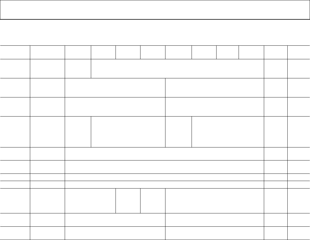
UG-671 AD9361 Register Map Reference Manual
Rev. 0 | Page 42 of 72
SLOW ATTACK AND HYBRID AGC REGISTERS (ADDRESS 0x120 THROUGH ADDRESS 0x12A)
Table 45.
Register
Address Name D7 D6 D5 D4 D3 D2 D1 D0 Default R/W
0x120 AGC Inner
Low
Threshold
Prevent
Gain Inc
AGC Inner Low Threshold[6:0] 0x-- R/W
0x121 LMT
Overload
Counters
Large LMT Overload Exceeded Counter[3:0] Small LMT Overload Exceeded
Counter[3:0]
0x-- R/W
0x122 ADC
Overload
Counters
Large ADC Overload Exceeded
Counter[3:0]
Small ADC Overload Exceeded
Counter[3:0]
0x-- R/W
0x123 Gain Step 1 Immed
Gain
Change
if Lg LMT
Overload
AGC Inner High Threshold
Exceeded Step Size[2:0]
Immed
Gain
Change
if Lg ADC
Overload
AGC Inner Low Threshold
Exceeded Step Size[2:0]
0x-- R/W
0x124 Gain Update
Counter 1
Gain Update Counter[7:0] 0x-- 0x--
0x125 Gain Update
Counter 2
Gain Update Counter[15:8] 0x-- 0x--
0x126 Open 0x-- 0x--
0x127 Open 0x-- 0x--
0x128 Digital Sat
Counter
Open Double
Gain
Counter
Enable
Sync for
Gain
Counter
Dig Saturation Exceeded Counter[3:0] 0x-- R/W
0x129 Outer Power
Thresholds
AGC Outer High Threshold[3:0] AGC Outer Low Threshold[3:0] 0x-- R/W
0x12A
Gain Step 2
AGC Outer High Threshold Exceeded Step
Size[3:0]
AGC Outer Low Threshold Exceeded Step
Size[3:0]
0x--
R/W
These registers are configured by the ad9361_set_rx_gain_
control_mode function. For some applications, register values
may need to be modified. See the Gain Control section of the
AD9361 Reference Manual for more information.
SPI Register 0x120—AGC Inner Lower Threshold
D7—Prevent Gain Incr
Setting this bit prevents a gain increase if a small LMT or small
ADC overload occurs.
[D6:D0]— AGC Inner Low Threshold[6:0]
These bits set the slow AGC inner low window threshold in
negative dBFS and with a resolution of 1 dB/LSB.
SPI Register 0x121—LMT End Overload Counters
[D7:D4]—Large LMT Overload Exceeded Counter[3:0]
This counter specifies the number of large LMT overloads that
must occur before gain decreases by the LMT Gain Step in
0x103[D4:D2].
[D3:D0]—Small LMT Overload Exceeded Counter[3:0]
Applies if Prevent Gain Inc bit in 0x120[D7] is set. This counter
specifies the number of small LMT overloads that much occur
to prevent a gain increase.
SPI Register 0x122—ADC Overload Counters
[D7:D4]—Large ADC Overload Exceeded Counter[3:0]
This counter specifies the number of large ADC overloads that
must occur before the gain will decrease by the large ADC
overload gain step in 0x106[D3:D0].
[D3:D0]—Small ADC Overload Exceeded Counter[3:0]
Applies if the Prevent Gain Incr bit in 0x120[D7] is set. This
counter specifies the number of small ADC overloads that must
occur to prevent a gain increase.
SPI Register 0x123—Gain Step 1
D7—Immed Gain Change if Large LMT Overload
Set this bit to allow large LMT overloads to reduce gain
immediately.
[D6:D4]—AGC Inner High Threshold Exceeded Step[2:0]
These bits set the gain decrease amount when the inner high
threshold is exceeded.
D3—Immed Gain Change if Large ADC Overload
Same operation as that described in 0x123[D7] but applies to
thelarge ADC overload.
AD9361 Register Map Reference Manual UG-671
Rev. 0 | Page 43 of 72
[D2:D0]—AGC Inner Low Threshold Exceeded Step[2:0]
Same as 0x123[D6:D4] but applies to the inner low threshold.
SPI Register 0x124 and SPI Register 0x125—Gain Update
Counter
Applies to the slow AGC. Gain changes can not occur until this
counter expires or unless the immediate update bits are set in
0x123[D7] or 0x123[D3]. The counter clocks at the ClkRF rate
and starts counting 3 ClkRF cycles after the ENSM enters the
Rx state and is clocked at the ClkRF rate. The depth of the
counter is equal to double the value in these registers or, if bit
0x128[D5] is set, it is equal to 4× the value in these registers. If
the Enable Sync for Gain Counter bit in 0x128[D4] is set
CTRL_IN2 transitioning high resets the counter.
SPI Register 0x128—Digital Sat Counter
D5—Double Gain Counter
See Register 0x124 and Register 0x125.
D4—Enable Sync for Gain Counter
See Register 0x124 and Register 0x125.
[D3:D0]—Digital Saturation Exceeded Counter
Applies if Prevent Gain Inc bit in 0x120[D7] is set. This counter
specifies the number of digital saturnation events that much
occur to prevent a gain increase.
SPI Register 0x129—Outer Power Thresholds
[D7:D4]—AGC Outer High Threshold[3:0]
The outer high threshold equals the inner high threshold
(0x101) plus this value. Resolution is 1 dB/LSB.
[D3:D0]—AGC Outer Low Threshold[3:0]
The outer low threshold equals the inner low threshold
(0x120[D6:D0]) plus this value. Resolution is 1 dB/LSB.
SPI Register 0x12A—Gain Step 2
[D7:D4]—AGC Outer High Threshold Exceeded Step[3:0]
The slow AGC changes gain by this amount when the outer
high threshold is exceeded.
[D3:D0]—AGC Outer Low Threshold Exceeded Step[3:0]
The slow AGC changes gain by this amount when the outer low
threshold is exceeded.
EXTERNAL LNA GAIN WORD REGISTERS (ADDRESS 0x12C THROUGH ADDRESS 0x12D)
Table 46.
Register Address Name D7 D6 D5 D4 D3 D2 D1 D0 Default R/W
0x12C Ext LNA High Gain Open Ext LNA High Gain[5:0] 0x-- R/W
0x12D Ext LNA Low Gain Open Ext LNA Low Gain[5:0] 0x00 R/W
SPI Register 0x12C and SPI Register 0x12D—Ext LNA High Gain and Ext LNA Low Gain
These registers should have nonzero values only if an external LNA is used which has two gain modes that it can swtich between and the
external LNA is controlled by GPOs triggered by bits in the gain table. Program Register 0x12C with the high gain (nonbypass) value and
program Register 0x12D with the low gain (bypass) value. The part considers both values to represent positive gain in the front end prior
to the AD9361. Both registers range from 0 dB to 31.5 dB in 0.5 dB steps/LSB.
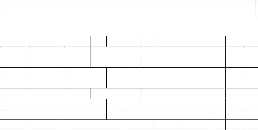
UG-671 AD9361 Register Map Reference Manual
Rev. 0 | Page 44 of 72
AGC GAIN TABLE REGISTERS (ADDRESS 0x130 THROUGH ADDRESS 0x137)
Table 47.
Register
Address Name D7 D6 D5 D4 D3 D2 D1 D0 Default
R/W
0x130 Gain Table
Address
Open Gain Table Address[6:0] 0x-- R/W
0x131 Gain Table Write
Data 1
Ext LNA Ctrl LNA Gain[1:0] Must
be 0
Mixer Gm Gain[3:0] 0x-- R/W
0x132 Gain Table Write
Data 2
Open TIA Gain LPF Gain[4:0] 0x-- R/W
0x133 Gain Table Write
Data 3
Open RF DC
Cal
Digital Gain[4:0] 0x-- R/W
0x134 Gain Table Read
Data 1
Ext LNA Ctrl LNA Gain[1:0] Must
be 0
Mixer Gm Gain[3:0] 0x-- R
0x135 Gain Table Read
Data 2
Open TIA Gain LPF Gain[4:0] 0x-- R
0x136 Gain Table Read
Data 3
Open RF DC
Cal
Digital Gain[4:0] 0x-- R
0x137 Gain Table
Config
Open Receiver
Select[1:0]
Write Gain
Table
Start Gain
Table Clock
Open 0x08 R/W
The ad9361_load_gt function loads Analog Devices standard
gain tables based on configuration and carrier frequency. Gain
tables are written and read back into/out of the AD9361 using
these registers. The gain tables are stored in locations that are
indirectly addressable.
SPI Register 0x130—Gain Table Address
This is the Gain Table Index address. Its maximum range is 0 to
90(d) in full table mode and 0 to 40(d) in split table mode.
SPI Register 0x131—Gain Table Write Data 1
D7—Ext LNA Ctrl
This bit routed to a GPO pin allows can control the bypass pin
on a bypassable external LNA. The external LNA becomes part
of the gain control loop. See also 0x026[D6:D5].
[D6:D5]—LNA Gain[1:0]
Internal LNA gain Index. There are 4 possible values ranging
from 0 through 3. 3 represents maximum gain, 0 is minimum
gain.
D4—Must be 0
[D3:D0]—Mixer Gm Gain[3:0]
The Mixer Gain Index. There are 16 values ranging from 0x0
through 0xF. 0xF represents maximum gain, 0 is minimum
gain.
SPI Register 0x132—Gain Table Write Data 2
D5—TIA Gain
The transimpedance amplifier gain. If this bit is 0, TIA gain
equals −6 dB and if the bit is set, the gain equals 0 dB.
[D4:D0]—LPF Gain[4:0]
Low-pass filter (LPF) index. Range is 0 dB to 24 dB. Resolution
is 1 LSB/1 dB. Full gain table only.
SPI Register 0x133—Gain Table Write Data 3
D5—RF DC Cal
Setting this bit causes the initial RF DC calibration to occur at
the gain index specified in 0x130. Full gain table only.
[D4:D0]—Digital Gain[4:0]
Digital gain maps as 1 dB gain/LSB.
SPI Register 0x134 Through SPI Register 0x136—Gain
Table Read n
Use these reigsters to read gain tables from the AD9361.
SPI Register 0x137—Gain Table Config
[D4:D3]—Receiver Select[1:0]
Bit D3 accesses Rx1, Bit D4 accesses Rx2. When reading the
table, setting both bits is invalid.
D2—Write Gain Table
Set this self-clearing bit to write the values in Register 0x130
through Register 0x133 to the gain table. After writing all table
entries, write 0x137 with the “Write Gain Table” bit cleared but
the Start Gain Table Clock bit high. Then, write Register 0x137
again with the clock start bit cleared. This ensures that the write
bit clears after the last write operation.
D1—Start Gain Table Clock
Set only when writing to the gain table. The gain table requires
four Rx sample periods after the Write Gain Table bit goes high
for the value to write into the table.

AD9361 Register Map Reference Manual UG-671
Rev. 0 | Page 45 of 72
MIXER SUBTABLE REGISTERS (ADDRESS 0x138 THROUGH ADDRESS 0x13F)
Table 48.
Register
Address Name D7 D6 D5 D4 D3 D2 D1 D0 Default R/W
0x138 Mixer Subtable
Address
Must be 0 Mixer Subtable Address[7:0] 0x-- R/W
0x139 Mixer Subtable Gain
Word Write
Open Mixer Subtable Gain Word Write[6:0] 0x-- R/W
0x13A Mixer Subtable Bias
Word Write
Open Mixer Subtable Bias Word Write[4:0] 0x-- R/W
0x13B Mixer Subtable Control
Word Write
Open Mixer Subtable Control Word Write[5:0] 0x-- R/W
0x13C Mixer Subtable Gain
Word Read
Open Mixer Subtable Gain Word Read[6:0] 0x-- R
0x13D Mixer Subtable Bias
Word Read
Open Mixer Subtable Bias Word Read[4:0] 0x-- R
0x13E Mixer Subtable Control
Word Read
Open Mixer Subtable Control Word Read[5:0] 0x-- R
0x13F Mixer Subtable Config Open Write Mixer
Subtable
Start Mixer
Subtable Clock
Open 0x00 R/W
These registers are programmed by the mixer subtable function
ad9361_load_gt. The registers should not be programmed
differently.
SPI Register 0x138—Mixer Subtable Word Address
[D7:D4]—Must be 0
[D3:D0]—Mixer Subable Address[7:0]
The sub table address with valid range of 0 to 0xF.
SPI Register 0x139—Mixer Subtable Gain Word Write
Program the mixer gain in dB × 4 into this register so that the
RSSI algorithm compensates for mixer gain correctly.
SPI Register 0x13A—Mixer Subtable Bias Word Write
Sets the mixer bias word for the mixer subtable.
SPI Register 0x13B—Mixer Subtable Control Word Write
This register sets the mixer subtable control word.
SPI Register 0x13C Through Register 0x13E—Mixer
Subtable Word Reads
Read the mixer subtable using these registers after setting the
address in Register 0x138.
SPI Register 0x13F—Mixer Subtable Config
D2—Write Mixer Subtable
Set this bit when writing to the subtable. Set this bit each time
new words in 0x139 through 0x13B are written to Address
0x138.
D1—Start Mixer Subtable Clock
This bit is used when writing to the mixer subtable. Allow at
least 4 Rx sample periods between consecutive writes.

UG-671 AD9361 Register Map Reference Manual
Rev. 0 | Page 46 of 72
CALIBRATION GAIN TABLE REGISTERS (ADDRESS 0x140 THROUGH ADDRESS 0x144)
Table 49.
Register
Address Name D7 D6 D5 D4 D3 D2 D1 D0 Default R/W
0x140 Word Address Calibration Table Addr[7:0] 0x-- R/W
0x141 Gain Diff
Word/Error
Write
Open Calib Table Gain Diff/Error Word[5:0] 0x-- W
0x142 Gain Error Read Open Calib Table Gain Error[4:0] 0x-- R
0x143 Config Open Calib Table
Select[1:0]
Read
Select
Write
Mixer Error
Table
Write LNA
Error
Table
Write
LNA Gain
Diff
Start Calib
Table
Clock
0x00 R/W
0x144 LNA Gain Diff
Read Back
Open LNA Calib Table Gain Difference Word[5:0] 0x-- R
See the Gain Control section of the AD9361 Reference Manual
for more information about calibrating the Rx RSSI function.
SPI Register 0x140—Word Address
Program the index of the gain stage in this register.
SPI Register 0x141—Gain Diff Word/Error Write
If the Write LNA Gain Diff bit in 0x143[D1] is set, then 0x141 is
the difference between LNA maximum gain and the gain at the
index in 0x140, Resolution is 0.5 dB. If the Write Mixer Error
Table bit in 0x143[D3] or the Write LNA Error Table bit in
0x143[D2]) is set then the error words can be programmed into
this register for the index specified in Register 0x140. Error
word resolution is 0.25 dB/LSB.
SPI Register 0x142—Gain Error Read
This is the gain error determined by the calibration at the index
in Register 0x140. Resolution in 0.25 dB/LSB.
SPI Register 0x143—Config
[D6:D5] Calib Table Select[1:0]
Bit D5 set accesses Rx1 and Bit D6 accesses Rx2. When reading
only one bit may be set.
D4—Read Select
Clear to read mixer errors and set to read LNA errors.
D3—Write Mixer Error Table
Set this self-clearing bit to write a mixer error word. D2 and D1
must be clear. After writing all of the values, clear the Write
Mixer Error Table bit but set Start Calib Table Clock bit. Then,
write to Register 0x143 again with the clock start bit cleared.
This ensures that the write signal resets before the clock stops.
D2—Write LNA Error Table
Set this self-clearing bit to write an LNA error word. D3 and D1
must be clear. After writing all of the values, clear the Write
Mixer Error Table bit but set Start Calib Table Clock bit. Then,
write to Register 0x143 again with the clock start bit cleared.
This ensures that the write signal resets before the clock stops.
D1—Write LNA Gain Diff
Set this self-clearing bit to write a gain difference word. D3 and
D2 must be clear. After writing all of the values, clear the Write
Mixer Error Table bit but set Start Calib Table Clock bit. Then,
write to Register 0x143 again with the clock start bit cleared.
This ensures that the write signal resets before the clock stops.
D0—Start Calib Table Clock
Set this bit to access the calibration gain table registers.
SPI Register 0x144—LNA Gain Diff Read Back
Read back LNA gain difference words from this register after
writing the address of the table into Register 0x140.
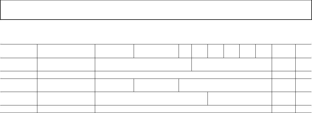
AD9361 Register Map Reference Manual UG-671
Rev. 0 | Page 47 of 72
GENERAL CALIBRATION REGISTERS (ADDRESS 0x145 THROUGH ADDRESS 0x149)
Table 50.
Register
Address Name D7 D6 D5 D4 D3 D2 D1 D0 Default R/W
0x145 Max Mixer Calibration
Gain Index
Open Max Mixer Calibration Gain
Index[4:0]
0x0B R/W
0x146 Temp Gain Coefficient Temp Gain Coefficient[7:0] 0x00 R/W
0x147 Settle Time Enable Dig
Gain Corr
Force Temp
Sensor for Cal
Settle Time[5:0] 0x10 R/W
0x148 Measure Duration Open Gain Cal Meas
Duration[3:0]
0x04 R/W
0x149 Cal Temp Sensor Word Cal Temp Sense Word[7:0] 0x00 R/W
SPI Register 0x145—Max Mixer Calibration Gain Index
Used only when calibrating Rx RSSI using the gain step
calibration, initialized by 0x016[D3]. If so, set this value to 0xF.
SPI Register 0x146—Temp Gain Coefficient
This value is used with RSSI temperature compensation. This
value represents the LNA and mixer dependence on tempera-
ture in dB/°C which is then stored in this register. The value is
coded in twos complement notation and resolution is 0.0078 dB
with an approximate maximum of ±1 dB/°C. Used with the Cal
Temp Sensor Word bit in Register 0x149.
SPI Register 0x147—Settle Time
D7—Enable Dig Gain Corr
Set this bit to enable gain step error correction, after a gain step
calibration has run. See Register 0x140.
D6—Force Temp Sensor for Cal
This bit must be clear when running the Gain Step Calibration
described in Register 0x140 through Register 0x143 but it must
be set to enable temperature compensation during operation.
[D5:D0]—Settle Time[5:0]
This value specifies the time duration in ClkRF cycles before
the power measurement for the gain calibration algorithm at a
specific gain starts. This delay allows the analog circuitry to
settle. The default value of 0x10 is sufficient for most scenarios.
SPI Register 0x148—Measure Duration
This register specifies the duration of the power measurement
used for gain calibration. The duration is per Equation 17.
( )= 2 [:] (17)
SPI Register 0x149—Cal Temp Sensor Word
When gain step calibration occurs, the AD9361 stores the
temperature at which it occurred in this register.
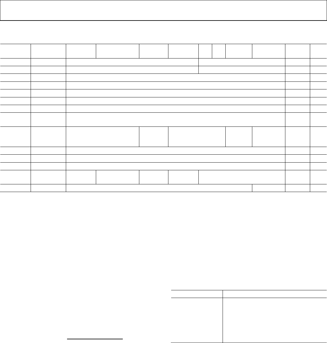
UG-671 AD9361 Register Map Reference Manual
Rev. 0 | Page 48 of 72
RSSI MEASUREMENT CONFIGURATION REGISTERS (ADDRESS 0x150 THROUGH ADDRESS 0x15D)
Table 51.
Register
Address Name D7 D6 D5 D4 D3 D2 D1 D0 Default R/W
0x150 Duration 0, 1 Measurement Duration 1[3:0] Measurement Duration 0[3:0] 0x08 R/W
0x151
Duration 2, 3
Measurement Duration 3[3:0]
Measurement Duration 2[3:0]
0x--
R/W
0x152 Weight 0 Weighted Multiplier 0[7:0] 0x00 R/W
0x153 Weight 1 Weighted multiplier 1[7:0] 0x00 R/W
0x154
Weight 2
Weighted Multiplier 2[7:0]
0x00
R/W
0x155 Weight 3 Weighted Multiplier 3[7:0] 0x00 R/W
0x156 RSSI delay RSSI Delay[7:0] 0x00 R/W
0x157 RSSI wait
time
RSSI Wait[7:0] 0x00 R/W
0x158
RSSI Config
RFIR for RSSI
measurement[1:0]
Start RSSI
Meas
RSSI Mode Select[2:0]
Must be
0
Default
RSSI Meas
Mode
0x01
R/W
0x159
Open
Open
0x--
R/W
0x15A Open Open 0x00 R/W
0x15B Open Open 0x00 R/W
0x15C
Dec Power
Duration
Open
Use HB1 Out for
Dec Pwr Meas
Set to 1
Open
Dec Power Measurement
Duration[3:0]
0x15
R/W
0x15D LNA Gain Max LNA Gain[6:0] Open 0xB1 R/W
The ad9361_rssi_setup function configures RSSI based on
various parameters.
SPI Register 0x150 andSPI Register 0x151—Duration n
If the Default RSSI Meas Mode bit in 0x158[D0] is set, then
Equation 18 sets the RSSI measurement duration.
( ) = 2 [:] (18)
If 0x158[D0] is clear, the duration equals Equation 19.
( ) =
2 [:]
(19)
The maximum value for any nibble is 0xE (not 0xF).
SPI Register 0x152 Through SPI Register 0x155—Weight
0, 1, 2, 3
If 0x158[D0] is clear, calculate weights per Equation 20 and load
into Register 0x152 through Register 0x155. The total of all
weights must equal 0xFF.
= 255 ×
(20)
SPI Register 0x156 and SPI Register 0x157—RSSI Delay
and RSSI Wait
When the RSSI algorithm (re)starts (see 0x158[D4:D2]), the
AD9361 waits for the delay counter to expire before calculating
RSSI. The counter is clocked at the Rx sample rate divided by 8.
For subsequent calculations, the algorithm waits for the wait
counter to expire before recalculating. The counter is clocked at
the Rx sample rate divided by 4.
SPI Register 0x158—RSSI Config
[D7:D6]—RFIR for RSSI Measurement[1:0]
If the data path Rx FIR is bypassed (see 0x003[D1:D0], the RSSI
calculation can still use the RFIR per Table 5.
D5—Enable RSSI Meas
Setting this bit restarts the RSSI algorithm if [D4:D2] = 3’b100
[D4:D2]—RSSI Mode Select[2:0]
The RSSI algorithm (re)starts when event(s) in Table 52 occur.
If the EN_AGC pin is used, RSSI delay in Register 0x156 must be 0.
Table 52. RSSI Mode
[D4:D2]
The RSSI algorithm will (re)start when:
000 AGC in fast attack mode locks the gain
001 EN_AGC pin is pulled high
010 AD9361 enters Rx mode
011 Gain change occurs
100 SPI write to Register 0x158[D5]
101 Gain change occurs or EN_AGC pin high
D1—Must be 0
D0—Default RSSI Meas Mode
See Register 0x150 and Register 0x151.
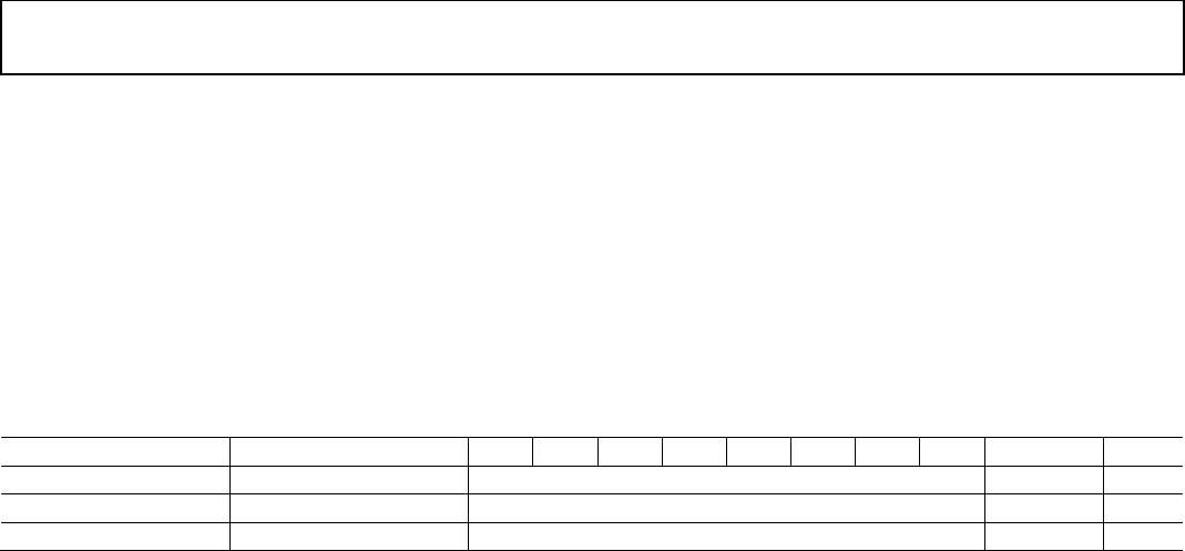
AD9361 Register Map Reference Manual UG-671
Rev. 0 | Page 49 of 72
SPI Register 0x15C—Dec Power Duration
D6—Use HB1 Out for Dec Pwr Meas
Set to use the HB1 output for power measurements. Clear to use
the Rx FIR output.
D5—Set to 1
[D3:D0]—Dec Power Measurement Duration[3:0]
The power measurement duration used by the gain control
algorithm (not RSSI), per Equation 21.
( cycles)=
16 × 2 [:] (21)
SPI Register 0x15D—LNA Gain
[D7:D1]—Max LNA Gain[6:0]
Used by RSSI and should equal maximum LNA gain in decibels
multiplied by 4, and converted to hex. Resolution is 0.25 dB.
POWER WORD REGISTERS (ADDRESS 0x161 THROUGH ADDRESS 0x163)
Table 53.
Register Address Name D7 D6 D5 D4 D3 D2 D1 D0 Default R/W
0x161 CH1 Rx Filter Power CH1 Rx Filter Power[7:0] 0x-- R
0x162 Open Open 0x-- R
0x163 CH2 Rx Filter Power CH2 Rx Filter Power[7:0] 0x-- R
SPI Register 0x161 and SPI Register 0x163—CH1(2) Rx Filter Power
This read-only register holds the Rx1(2) power measured at the output of the RFIR filter or the HB1 filter in negative dBFS with steps of
0.25 dB/LSB. HB1 is used if the Use HB1 Out for Dec Pwr Meas bit (Register 0x15C[D6]) is set.

UG-671 AD9361 Register Map Reference Manual
Rev. 0 | Page 50 of 72
Rx QUADRATURE CALIBRATION REGISTERS (ADDRESS 0x169 THROUGH ADDRESS 0x16B)
Table 54.
Register
Address Name D7 D6 D5 D4 D3 D2 D1 D0 Default R/W
0x169
Calibration
Config 1
Enable
Phase
Corr
Enable
Gain
Corr
Must be 0
Free
Run
Mode
Enable Corr
Word
Decimation
Enable
Tracking
Mode CH2
Enable
Tracking
Mode CH1
0xC0 R/W
0x16A Must be 0x75 Must be 0x75 0x08 R/W
0x16B Must be 0x95 Must be 0x95 0x08
SPI Register 0x169—Calibration Config 1
D7—Enable Phase Corr
Test bit, normally set. Set to enable phase correction.
D6—Enable Gain Corr
Test bit, normally set. Set to enable gain correction.
[D5:D4]—Must be 0
D3—Free Run Mode
Set this bit when enabling tracking.
D2—Enable Corr Word Decimation
Set this bit to decimate the correction word before applying it to
the data.
D1—Enable Tracking Mode CH2
Set to enable Rx quadrature tracking for Rx2.
D0—Enable Tracking Mode CH1
Set to enable Rx quadrature tracking for Rx1
SPI Register 0x16A—Must be 0x75
SPI Register 0x16B—Must be 0x95
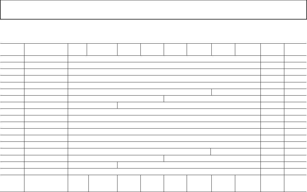
AD9361 Register Map Reference Manual UG-671
Rev. 0 | Page 51 of 72
Rx PHASE AND GAIN CORRECTION REGISTERS (ADDRESS 0x170 THROUGH ADDRESS 0x182)
Table 55.
Register
Address Name D7 D6 D5 D4 D3 D2 D1 D0 Default R/W
0x170 Rx1A Phase Corr Rx1A Phase Correction[7:0] 0x-- R/W
0x171 Rx1A Gain Corr Rx1A Gain Correction[7:0] 0x-- R/W
0x172 Rx2A Phase Corr Rx2A Phase Correction[7:0] 0x-- R/W
0x173 Rx2A Gain Corr Rx2A Gain Correction[7:0] 0x-- R/W
0x174 Rx1A Q Offset Rx1A Q DC Offset[7:0] 0x-- R/W
0x175 Rx1A Offset Rx1A I DC Offset[5:0] Rx1A Q DC Offset[9:8] 0x-- R/W
0x176 Input A Offsets Rx2A Q DC Offset[3:0] Rx1A I DC Offset[9:6] 0x-- R/W
0x177 Rx2A Offset Rx2A I DC Offset[1:0] RxA Q DC Offset[9:4] 0x-- R/W
0x178 Rx2A I Offset Rx2A I DC Offset[9:2] 0x-- R/W
0x179 Rx1B/C Phase Corr Rx1B/C Phase Correction[7:0] 0x-- R/W
0x17A Rx1B/C Gain Corr Rx1B/C Gain Correction[7:0] 0x-- R/W
0x17B
Rx2B/C Phase Corr
Rx2B/C Phase Correction[7:0]
0x--
R/W
0x17C Rx2B/C Gain Corr Rx2B/C Gain Correction[7:0] 0x-- R/W
0x17D Rx1B/C Q Offset Rx1B/C Q DC Offset[7:0] 0x-- R/W
0x17E Rx1B/C I Offset Rx1B/C I DC Offset[5:0] RxB/C Q DC Offset[9:8] 0x-- R/W
0x17F Input B/C Offsets Rx2B/C Q DC Offset[3:0] RxB/C I DC Offset[9:6] 0x-- R/W
0x180 Rx2B/C Offset Rx2B/C I DC offset[1:0] RxB/C Q DC Offset[9:4] 0x-- R/W
0x181 Rx2B/C I Offset Rx2B/C I DC Offset[9:2] 0x-- R/W
0x182 Force Bits Rx2B/C
Force
offset
Rx1B/C
Force
offset
Rx2B/C
Force
Ph/Gain
Rx1B/C
Force
Ph/Gain
Rx2A
Force
offset
Rx1A
Force
offset
Rx2A
Force
Ph/Gain
Rx1A
Force
Ph/Gain
0x00 R/W
SPI Register 0x170—Rx1A Phase Corr
If Register 0x182[D0] is clear, after an Rx quadrature calibration
completes, this register holds the phase correction word for the
Rx1A input in twos complement format. If Register 0x182[D0]
is set, the value written to this register is the forced phase
correction word.
SPI Register 0x171—Rx1A Gain Corr
If Register 0x182[D0] is clear, after an Rx quadrature calibration
completes, this register holds the gain correction word for the
Rx1A signal path in twos compliment format. If Register
0x182[D0] is set, the value written to this register is the forced
phase correction word.
SPI Register 0x172—Rx2A Phase Corr
This register functions the same as Register 0x170 but applies to
Rx2. The force bit is Register 0x182[D1].
SPI Register 0x173—Rx2A Gain Corr
This register functions the same as Register 0x171 but applies to
Rx2. The force bit is Register 0x182[D1].
SPI Register 0x174 and SPI Register 0x175[D1:D0]—
Rx1A Q DC Offset
If 0x182[D2] is clear, after an Rx quadrature calibration
completes, these registers hold Rx1A Q signal path DC offset
correction word at the current gain index in twos complement
format. If 0x182[D2] is set, the value written to this register is
the forced DC offset correction word.
SPI Register 0x175[D7:D2] and SPI Register
0x176[D3:D0]—Rx1A Offsets
These bits function the same as Register 0x174 and
0x175[D1:D0] but refer to the Rx1A I signal path. The force bit
is 0x182[D2].
SPI Register 0x176[D7:D4] and SPI Register
0x177[D5:D0]—Rx2A Q Offset
These bits function the same as Register 0x174 and 0x175[D1:D0]
but refer to the Rx2A Q signal path. The force bit is 0x182[D3].
SPI Register 0x177[D7:D6] and SPI Register
0x178[D7:D0]—Rx2A I Offset
These bits function the same as Register 0x174 and 0x175[D1:D0]
but apply to the Rx2 I signal path. The force bit is 0x182[D3].
SPI Register 0x179 through SPI Register 0x181—B and C
Inputs
These bits function the same as 0x170 through 0x178 but apply
to the B and C LNA inputs. The force bit are in 0x182[D7:D4].
SPI Register 0x182—Force Bits
These bits force the AD9361 to use the values in Register 0x170
through Register 0x181 as the Rx quadrature calibration
correction words.
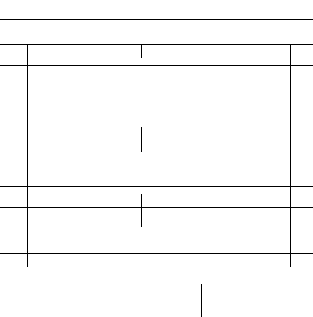
UG-671 AD9361 Register Map Reference Manual
Rev. 0 | Page 52 of 72
Rx DC OFFSET CONTROL REGISTERS (ADDRESS 0x185 THROUGH ADDRESS 0x194)
Table 56.
Register
Address Name D7 D6 D5 D4 D3 D2 D1 D0 Default R/W
0x185 Wait Count Wait Count[7:0] 0x10 R/W
0x186 RF DC Offset
Count
RF DC Offset Count[7:0] 0xB4 R/W
0x187 RF DC Offset
Config1
Open DAC FS[1:0] Must be 0x4 0x1C R/W
0x188 RF DC Offset
Attenuation
RF DC Offset Table Update
Count[2:0]
RF DC Offset Attenuation[4:0] 0x05 R/W
0x189 Must be
0x30
Must be 0x30 0x30 R/W
0x18A Open 0xFF R/W
0x18B DC Offset
Config2
Must
be 1
Enable
Fast
Settle
Mode
Enable
BB DC
Offset
Tracking
Reset Acc
on Gain
Change
Enable
RF Offset
Tracking
DC Offset Update[2:0] 0x8D R/W
0x18C RF Cal Gain
Index
Open RF Minimum Calibration Gain Index[6:0] 0x00 R/W
0x18D SOI
Threshold
Open RF SOI Threshold[6:0] 0x64 R/W
0x18E
Open
0x00
R/W
0x18F Open 0x-- R/W
0x190 BB DC Offset
Shift
Must be
0
BB Tracking
Decimate[1:0]
BB DC M Shift[4:0] 0x0D R/W
0x191 BB DC Offset
Fast Settle
Shift
Read
Back CH
Sel
Update
Tracking
Word
Force Rx
Null
BB DC Tracking Fast Settle M Shift[4:0] 0x06 R/W
0x192 BB Fast
Settle Dur
BB DC Tracking Fast Settle Duration[7:0] 0x03 R/W
0x193 BB DC Offset
Count
Must be x3F 0x3F R/W
0x194
BB DC Offset
Attenuation
Open
BB DC Offset Atten[3:0]
0x01
R/W
The ad9361_bb_dc_offset_calib and the ad9361_rf_dc_offset_
calib functions configure the BB DC and RF DC registers and
run the calibrations.
SPI Register 0x185—Wait Count
This register sets the Rx path settling time delay after gain
changes are made. All calibrations wait for this counter before
starting calculations. ClkRF clocks the counter.
SPI Register 0x186—RF DC Offset Count
This register affects both RF DC offset initialization and
tracking and it sets the number of integrated samples and the
loop gain. The number of samples equals 256 × RF DC Offset
Count[7:0] in ClkRF cycles. Increasing this value increases loop
gain.
SPI Register 0x187—RF DC Offset Config 1
[D5:D4]—DAC FS[1:0]
These bits set the range of current injected by the correction
DAC per Table 57. Increasing this value increases loop gain.
Table 57.DC Offset Correction Step Size
DAC FS[1:0] DC Offset Correction Step Size
00 Default range of offset correction DAC
01 2× range and step-size of offset correction DAC
10 4× range and step-size of offset correction DAC
11 8× range andstep-size of offset correction DAC
[D3:D0]—Must be 0x4
SPI Register 0x188—RF DC Offset Attenuation
[D7:D5]—RF DC Offset Table Update Count[2:0]
These bits determine the number of internal correction word
table entries to update when a correction word is updated in the
RF correction table. This occurs for the initial RF cal and
during tracking. The correction word at the current gain index
m updates along with gain indices m+1, m+2…m+n.

AD9361 Register Map Reference Manual UG-671
Rev. 0 | Page 53 of 72
[D4:D0]—RF DC Offset Attenuation[4:0]
These bits control the attenuator for the initialization and
tracking RF DC offset calibrations. The integrated data shifts by
this twos complement value and ranges from −16 to +15.
SPI Register 0x18B—DC Offset Config2
D7—Must be 1
D6—Enable Fast Settle Mode
Applies to BB DC offset tracking (Bit D5 set). The algorithm
uses the BB DC Tracking Fast Settle Shift M attenuation value
in Register 0x191 for the BB Fast Settle Duration time in 0x192,
followed by the BB DC M Shift attenuation value in Register
0x190. The value in Register 0x190 is used until the gain
changes, at which time this sequence repeats. If the fast settle
attenuation value is lower than other attenuation value, then
the BB DC tracking algorithm will converge more quickly.
Convergence that is too fast can affect subcarriers near DC.
D5—Enable BB DC Offset Tracking
Set this to enable BB DC offset tracking. Correction words
apply at a rate set by the decimation setting (Register
0x190[D6:D5]).
D4—Reset Acc on Gain Change
Applies if using BB DC offset tracking (Bit D5 set). When set,
the DC offset accumulator clears when gain changes occur.
D3—Enable RF Offset Tracking
Setting this bit enables RF DC offset tracking.
[D2:D0]—DC Offset Update[2:0]
These bits specify when correction words apply during RF
DC tracking, per Table 58. See Register 0x18D for the SOI
threshold.
Table 58. DC Offset Update Conditions
D2 D1 D0
Gain change: SOI threshold: Exit Rx mode:
Apply a new
tracking word
when a gain
change occurs
Apply a new tracking
word when the
received signal is less
than the SOI threshold
Apply a new
tracking word
after the ENSM
exits the Rx state
SPI Register 0x18C—RF Cal Gain Index
This register sets the starting gain index for RF DC offset
calibration. This 7-bit word represents the LNA gain (2 bits),
the mixer Gm gain (4 bits), and the TIA gain (1 bit).
SPI Register 0x18D—RF SOI Threshold
This register sets the signal of interest threshold in negative
dBFS with 1 dB/LSB resolution. See 0x18B[D1].
SPI Register 0x190—BB DC Offset Shift
D7—Must be 0
[D6:D5]—BB Tracking Decimation[1:0]
Applies in BB DC offset tracking mode (0x18B[D5] set). These
bits set the correction word update rate per Table 59.
Table 59. Decimation in BB DC Offset Tracking Mode
0x190[D6:D5] Decimation Update Rate
00 No decimation ClkRF
01 By 2 ClkRF/2
10 By 4 ClkRF/4
[D4:D0]—BB DC Shift M[4:0]
Applies to BB DC tracking mode (0x18B[D5] set). These bits
determine the loop gain attenuation. Integrated data shifts by
BB DC M Shift + 1. M ranges from 1 to 32.
SPI Register 0x191—BB DC Offset Fast Settle Shift
D7—Read Back CH Sel
Set to read back Rx1 BB DC tracking correction words in
Register 0x1A2 through Register 0x1A5. Clear to read Rx2
words. See Bit D6.
D6—Update Tracking Words
Toggle this bit to copy the current BB DC tracking words to
Register 0x1A2 through Register 0x1A5. Correction word
updates occur quickly so these words are not copied to the SPI
registers unless this bit transitions high, preventing the words
from changing during the SPI read. The bit is not self-clearing.
D5—Force Rx Null
Test bit. Setting this bit grounds the input to the low-pass filter.
[D4:D0]—BB DC Tr acking Fast Settle Shift M[4:0]
Applies in BB DC fast settle tracking mode (see 0x18B[D5:D6]
set). Range 1 through 32.
SPI Register 0x192—BB Tracking Fast Settle Dur
Applies to BB DC fast settle tracking mode (0x18B[D6:D5] set).
These bits set the fast settle M shift duration. See Register
0x18B[D6]. The total time is this register value × 8 and is
measured in ClkRF cycles.
SPI Register 0x193—Must be x3F
SPI Register 0x194—BB DC Offset Attenuation
[D3:D0]—BB DC Offset Atten[3:0]
These bits set the BB DC offset loop gain attenuation during the
initial calibration. Range is +7 to −8.
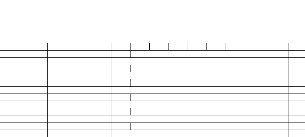
UG-671 AD9361 Register Map Reference Manual
Rev. 0 | Page 54 of 72
Rx BB DC OFFSET REGISTERS (ADDRESS 0x19A THROUGH ADDRESS 0x1A5)
Table 60.
Register Address Name D7 D6 D5 D4 D3 D2 D1 D0 Default R/W
0x19A
Rx1 BB DC Word I MSB
Open
Rx1 BB DC Offset Correction Word I[14:8]
0x--
R
0x19B Rx1 BB DC Word I LSB Rx1 BB DC Offset Correction Word I[7:0] 0x-- R
0x19C Rx1 BB DC Word Q MSB Open Rx1 BB DC Offset Correction Word Q[14:8] 0x-- R
0x19D Rx1 BB DC Word Q LSB Rx1 BB DC Offset Correction Word Q[7:0] 0x-- R
0x19E Rx2 BB DC Word I MSB Open Rx2 BB DC Offset Correction Word I[14:8] 0x-- R
0x19F Rx2 BB DC Word I LSB Rx2 BB DC Offset Correction Word I[7:0] 0x-- R
0x1A0 Rx2 BB DC Word Q MSB Open Rx2 BB DC Offset Correction Word Q[14:8] 0x-- R
0x1A1 Rx2 BB DC Word Q LSB Rx2 BB DC Offset Correction Word Q[7:0] 0x-- R
0x1A2 BB Track Corr Word I MSB Open Rx1/Rx2 BB DC Offset Tracking Correction Word I[14:8] 0x-- R
0x1A3 BB Track Corr Word I LSB Rx1/Rx2 BB DC Offset Tracking Correction Word I[7:0] 0x-- R
0x1A4 BB Track Corr Word Q MSB Open Rx1/Rx2 BB DC Offset Tracking Correction Word Q[14:8] 0x-- R
0x1A5 BB Track Corr Word Q LSB Rx1/Rx2 BB DC Offset Tracking Correction Word Q[7:0] 0x-- R
SPI Register 0x19A through SPIRegister 0x19D—Rx1 BB
DC I/Q Words
Rx1 BB DC Offset I/Q correction words. During calibration,
correction words are calculated for different LPF gains. The
words read back in these registers are the correction words
corresponding to the current LPF gain index.
SPI Register 0x19E through SPI Register 0x1A1—Rx2 BB
DC I/Q Words
These registers function the same as Register 0x19A through
Register 0x19D but apply to Rx2.
SPI Registers 0x1A2 through SPI Register 0x1A5—Rx1/2
BB Tracking Corr I/Q Words
BB DC Offset Tracking I/Q correction words. When the
Read Back CH Sel bit (Register 0x191[7]) is set, the words
correspond to Rx1, else they correspond to Rx2. 0x191[D6]
must transition high to load the latest tracking words into these
registers.
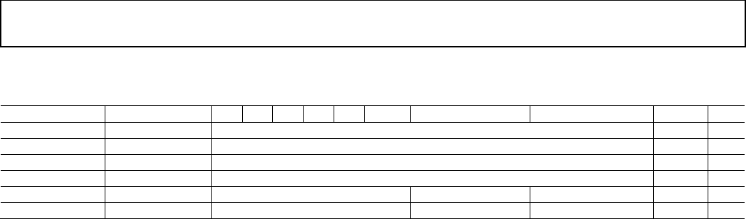
AD9361 Register Map Reference Manual UG-671
Rev. 0 | Page 55 of 72
RSSI READBACK REGISTERS (ADDRESS 0x1A7 THROUGH ADDRESS 0x1AC)
Table 61.
Register Address Name D7 D6 D5 D4 D3 D2 D1 D0 Default R/W
0x1A7 Rx1 RSSI Symbol Rx1 RSSI Symbol[8:1] 0x-- R
0x1A8 Rx1 RSSI Preamble Rx1 RSSI Preamble[8:1] 0x-- R
0x1A9 Rx2 RSSI Symbol Rx2 RSSI Symbol[8:1] 0x-- R
0x1AA Rx2 RSSI Preamble Rx2 RSSI Preamble[8:1] 0x-- R
0x1AB
Symbol LSB
Open
Rx2 RSSI Symbol[0]
Rx1 RSSI Symbol[0]
0x--
R
0x1AC Preamble LSB Open Rx2 RSSI Preamble[0] Rx1 RSSI Preamble[0] 0x-- R
The ad9361_get_rx_rssi function reads the RSSI words.
SPI Register 0x1A7 and Register 0x1AB[D0]—Rx1 RSSI
Symbol
This register updates after every measurement interval. Typical
valid range is 0 to 457(d) (for 9 bits). Resolution is 0.25 dB/LSB
for 9 bits, 0.5 dB/LSB for 8 bits. RSSI compensates for Rx gain.
SPI Register 0x1A8 and Register 0x1AC[D0]—Rx1 RSSI
Preamble
This register updates once after the event set in Register
0x158[D4:D2] with the exception that it does not update after
gain changes. Typical valid range is 0 to 457(d) (for 9 bits).
Resolution is 0.25 dB/LSB for 9 bits, 0.5 dB for 8 bits. RSSI
compensates for Rx gain.
SPI Register 0x1A9 and SPI Register 0x1AB[D1]—Rx2
RSSI Symbol
These registers function the same as Register 0x1A7 and
Register 0x1AB[D0] but apply to Rx2.
SPI Register 0x1AA and SPI Register 0x1AC[D1]—Rx2
RSSI Preamble
These registers function the same as Register 0x1A8 and
Register 0x1AC[D0] but apply to Rx2.
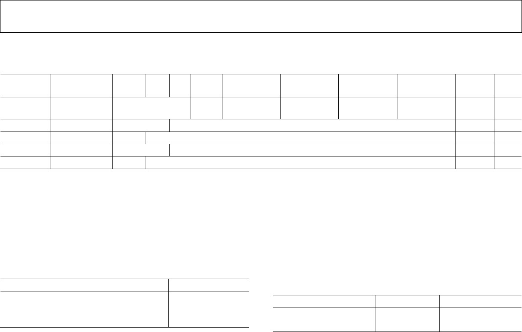
UG-671 AD9361 Register Map Reference Manual
Rev. 0 | Page 56 of 72
Rx TIA REGISTERS (ADDRESS 0x1DB THROUGH ADDRESS 0x1DF)
Table 62.
Register
Address Name D7 D6 D5 D4 D3 D2 D1 D0 Default R/W
0x1DB Rx TIA Config TIA Sel CC[2:0] Open TIA2
Override C
TIA2
Override R
TIA1
Override C
TIA1
Override R
0x60 R/W
0x1DC TIA1 C LSB TIA1 RF[1:0] TIA1 C LSB[5:0] 0x03 R/W
0x1DD
TIA1 C MSB
Open
TIA1 C MSB[6:0]
0x0B
R/W
0x1DE TIA2 C LSB TIA2 RF[1:0] TIA2 C LSB[5:0] 0x03 R/W
0x1DF TIA2 C MSB Open TIA2 C MSB[6:0] 0x0B R/W
The ad9361_set_rx_rf_bandwidth function configures these
registers.
SPI Register 0x1DB—Rx TIA Config
[D7:D5]—TIA Sel CC[2:0]
These bits must be set per Table 63.
Table 63. TIA Sel CC
Baseband (Real) Bandwidth (BBBW) TIA Sel CC[2:0]
BBBW ≤ 3 MHz 7
3 MHz < BBBW < 10 MHz 3
BBBW ≥ 10 MHz 1
D3—TIA 2 Override C
Test bit. Override digital control of the Rx2 TIA feedback
capacitors with TIA2 C LSB and TIA2 C MSB.
D2—TIA 2 Override R
Test bit. Override digital control of the Rx2 TIA feedback
resistor with TIA2 RF CNT.
D1—TIA 1 Override C
Test bit. This bit functions the same as D3 but applies to Rx1.
D0—TIA 1 Override R
Test bit. This bit functions the same as D2 but applies to Rx1.
SPI Register 0x1DC—TIA C LSB
[D7:D6]—TIA1 RF CNT[1:0]
Sets the value of the feedback resistor in the Rx1 TIA per
Table 64. TIA 1 Override R is set (Register 0x1DB[D0]).
Table 64. TIA Forced Feedback Resistor Value
TIA RF[1:0]
R
TIA
Gain (dB)
01
3.50 kΩ
0
11 1.75 kΩ −6
[D5:D0]—TIA C LSB[5:0] and Register 0x1DD
Sets value of the feedback capacitor.
SPI Register 0x1DE and SPIRegister 0x1DF
These registers function the same as Register 0x1DC and
Register 0x1DD but apply to Rx2. The override bit for the
Rx2 feedback resistor is 0x1DB[D2].
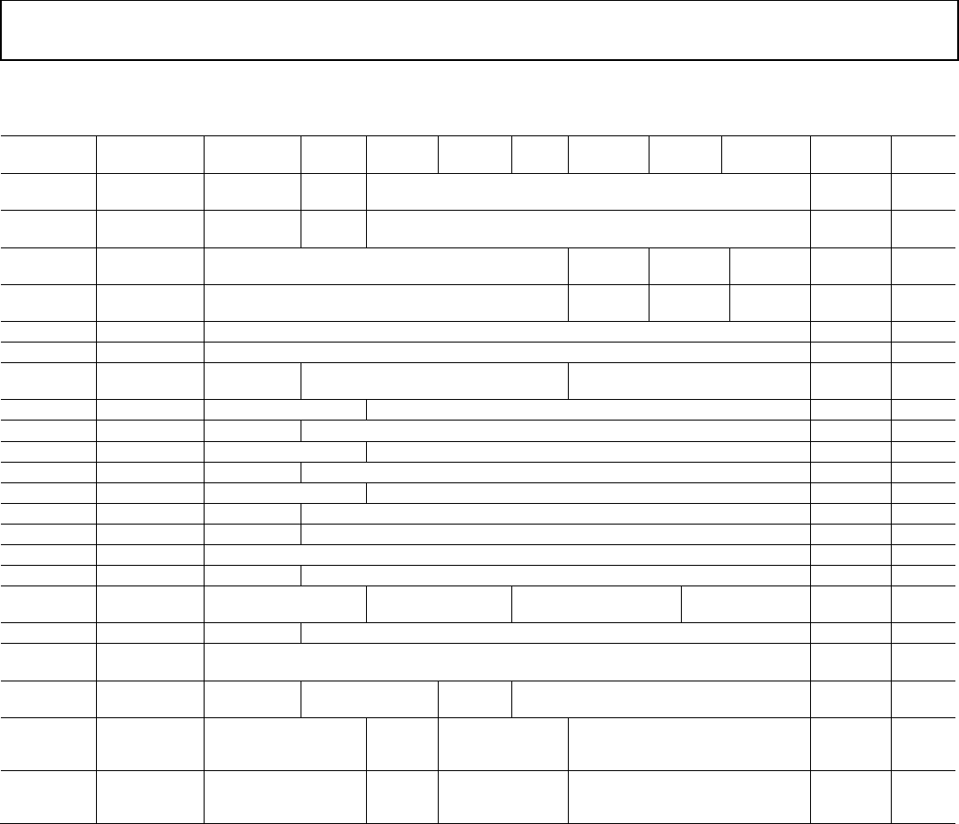
AD9361 Register Map Reference Manual UG-671
Rev. 0 | Page 57 of 72
Rx BBF REGISTERS (ADDRESS 0x1E0 THROUGH ADDRESS 0x1F5)
Table 65.
Register
Address Name D7 D6 D5 D4 D3 D2 D1 D0 Default R/W
0x1E0 Rx1 BBF R1A
Force Rx1
Resistors
Open Rx1 BBF R1A[5:0] 0x03 R/W
0x1E1 Rx2 BBF R1A Force Rx2
Resistors
Open Rx2 BBF R1A[5:0] 0x03 R/W
0x1E2 Rx1 Tune
Control
Open Must be 0 Must be 1 Rx1 PD
Tune
0x00 R/W
0x1E3 Rx2 Tune
Control
Open Must be 0 Must be 1 Rx2 PD
Tune
0x00 R/W
0x1E4 Rx1 BBF R5 Rx1 BBF R5[7:0] 0x01 R/W
0x1E5
Rx2 BBF R5
Rx2 BBF R5[7:0]
0x01
R/W
0x1E6 Rx BBF R2346 Tune
Override
Open Rx BBF R2346[2:0] 0x01 R/W
0x1E7 Rx BBF C1 MSB Open Rx BBF C1 MSB[5:0] 0x00 R/W
0x1E8 Rx BBF C1 LSB Open Rx BBF C1 LSB[6:0] 0x60 R/W
0x1E9 Rx BBF C2 MSB Open Rx BBF C2 MSB[5:0] 0x00 R/W
0x1EA Rx BBF C2 LSB Open Rx BBF C2 LSB[6:0] 0x60 R/W
0x1EB Rx BBF C3 MSB Open Rx BBF C3 MSB[5:0] 0x00 R/W
0x1EC Rx BBF C3 LSB Open Rx BBF C3 LSB[6:0] 0x60 R/W
0x1ED Rx BBF CC1 Ctr Open Rx BBF CC1 Ctr[6:0] 0x07 R/W
0x1EE
Must be 0x60
Must be 0x60
0x60
R/W
0x1EF Rx BBF CC2 Ctr Open Rx BBF CC2 Ctr[6:0] 0x07 R/W
0x1F0 Rx BBF Pow Rz
Byte1
Rx BBF Pow3 Ctr[1:0] Rx BBF Rz3 Ctr[1:0] Rx BBF Pow2 Ctr[1:0] Rx BBF Rz2
Ctr[1:0]
0xCC R/W
0x1F1 Rx BBF CC3 Ctr Open Rx BBF CC3 Ctr[6:0] 0x07 R/W
0x1F2
Rx BBF R5
Tune
Rx BBF R5 Tune[7:0] 0x00 R/W
0x1F3 Rx BBF Tune Must be 0 Must be 2’b01 Rx BBF
R5 Tune
Open 0x20 R/W
0x1F4 Rx1 BBF Man
Gain
Open Rx1 BBF
Force
Gain
Rx1 BBF BQ
Gain[1:0]
Rx1 BBF Pole Gain[2:0] 0x00 R/W
0x1F5
Rx2 BBF Man
Gain
Open
Rx2 BBF
Force
Gain
Rx2 BBF BQ
Gain[1:0]
Rx2 BBF Pole Gain[2:0] 0x00 R/W
The ad9361_set_rx_rf_bandwidth function configures these
registers for the correct filter corner based on the RF BW.
SPI Register 0x1E0—Rx1 BBF R1A
D7—Force Rx1 Resistors
Test bit; should be normally cleared. Setting this bit forces the
use of the resistor register values.
[D5:D0]—Rx1 BBF R1A[5:0]
This register in combination with R4 (Register 0x1E6) sets the
bi-quad signal gain (R4/R1A = Av).
SPI Register 0x1E1—Rx2 BBF R1A
Same as Register 0x1E0 but applies to Rx2.
SPI Register 0x1E2—Rx1 Tune Control
D2—Must be 0
D1—Must be 1
D0—Rx1 P D Tune
Clear this bit before starting a baseband filter calibration. Set
the bit after the calibration completes.
SPI Register 0x1E3—Rx2 Tune Control
Same as Register 0x1E2 but applies to Rx2.
SPI Register 0x1E4—Rx1 BBF R5
This register along with R6 (Register 0x1E6) controls the pole
signal gain (R6/F5 = Av). If this register is nonzero, Register
0x1F2 must be zero.
SPI Register 0x1E5—Rx2 BBF R5
Same as Register 0x1E4 but applies to Rx2.

UG-671 AD9361 Register Map Reference Manual
Rev. 0 | Page 58 of 72
SPI Register 0x1E6—Rx BBF R2346
D7—Tune Override
Normally clear. Setting this bit overrides the calibration values,
forcing the filter to use the R2346 value and all capacitor words.
[D2:D0]—Rx BBF R2346
These bits control the value of Resistors R2, R3, R4, and R6.
SPI Register 0x1E7 and SPI Register 0x1E9—Rx BBF C1
and C2 MSB
These bits affect the C1 and C2 BBF capacitors. Typically, both
registers, along with Register 0x1EB, should use the same word.
SPI Register 0x1E8 and SPI Register 0x1EA—Rx BBF
C1and C2 LSB
These bits affect the C1 and C2 BBF capacitors. Typically,
bothregisters, along with Register 0x1EC, should use the same
word.
SPI Register 0x1EB—Rx BBF C3 MSB
These bits affect the C3 BBF capacitor. Typically equal to
Register 0x1E7 and Register 0x1E9.
SPI Register 0x1EC—Rx BBF C3 LSB
These bits affect the C3 BBF capacitor. Typically equal to 0x1E8
and 0x1EA.
SPI Register 0x1ED—Rx BBF CC1 Ctr
These bits control the Miller compensation capacitor for Op
Amp 1.
SPI Register 0x1EE—Must be 0x60
SPI Register 0x1EF—Rx BBF CC2 Ctr
Same as Register 0x1ED but applies to Op Amp2.
SPI Register 0x1F0—Rx BBF Pow Rz Byte1
[D7:D6]—Rx BBF Pow3 Ctr[1:0]
Op Amp 3 power control.
[D5:D4]—Rx BBF Rz3 Ctr[1:0]
Op Amp 3 zero compensation resistor.
[D3:D2]—Rx BBF Pow2 Ctr[1:0]
Op Amp 2 power control.
[D1:D0]—Rx BBF Rz2 Ctr[1:0]
Op Amp 2 zero compensation resistor.
SPI Register 0x1F1—Rx BBF CC3 Ctr
Same as Register 0x1ED but applies to Op Amp 3.
SPI Register 0x1F2—Rx BBF R5 Tune
This register along with the value of R6 (Register 0x1E6) sets
the pole signal gain during calibration. If this is nonzero,
Register 0x1E4 and Register 0x1E5 must be all zeros.
SPI Register 0x1F3—Rx BBF Tune
D7—Must be 0
[D6:D5]—Must be 2’b01
D4—RxBBF R5 Tune
Setting this bit forces the value in Register 0x1F2 to be used for
tuning.
SPI Register 0x1F4 and SPI Register 0x1F5—Rx1/Rx2 BBF
Man Gain
D5—Rx BBF Force Gain
Forces the values in the lower bits to be used for the bi-quad
and pole gain.
[D4:D3]—Rx BBF BQ Gain[1:0]
Only applicable if D5 is set. These bits force the bi-quad gain.
[D2:D0]—Rx BBF Pole Gain[1:0]
Only applicable if D5 is set. These bits force the pole gain.
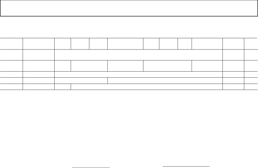
AD9361 Register Map Reference Manual UG-671
Rev. 0 | Page 59 of 72
Rx BBF TUNER CONFIGURATION REGISTERS (ADDRESS 0x1F8 THROUGH ADDRESS 0x1FC)
Table 66.
Register
Address Name D7 D6 D5 D4 D3 D2 D1 D0 Default R/W
0x1F8 Rx BBF Tune
Divide
Rx BBF Tune Divide[7:0] 0x14 R/W
0x1F9 Rx BBF Tune
Config
Open Must be 2’b00 Rx Tune Evaltime Must be 3’b111 Rx BBF Tune
Divide[8]
0x1E R/W
0x1FA Must be 0x01 Must be 0x01 0x01 R/W
0x1FB Rx BBBW MHz Open Rx Tune BBBW MHz[4:0] 0x05 R/W
0x1FC Rx BBBW kHz Open Rx Tune BBBW kHz[6:0] 0x00 R/W
The ad9361_set_rx_rf_bandwidth function configures these
registers for the correct filter corner based on the RF BW.
SPI Register 0x1F8 and SPI Register 0x1F9[D0]—Rx BBF
Tune Divide
The tuning algorithm generates a tune clock derived from the
BBPLL frequency. This register sets a divider that outputs the
tune clock, set per Equation 22. See the Initialization and
Calibration section of the AD9361 Reference Manual for more
information about the tune clock used for the calibration
algorithm.
[8: 0] = × ()
× . × × (22)
The range of the divider is 1 to 511.
SPI Register 0x1F9—Rx BBF Tune Config
[D6:D5]—Must be 2’b00
D4—Rx Tune Evaltime
This bit sets the delay in tune clock cycles (set by the divider
described previously) before the tune comparator outputs
should be sampled. 0 = 16 cycles and 1 = 32 cycles.
[D3:D1]—Must be 3’b111
SPI Register 0x1FA—Must be 0x01
SPI Register 0x1FB—Rx BBBW MHz
Program this register with the floor of the baseband bandwidth
in MHz to set the Rz and Cc of the filter. For example, if the
channel (RF) BW = 10 MHz, Rx BBBW MHz = floor(10/2) =
5 MHz. Range: 0 MHz to 31 MHz. Resolution: 1 MHz/LSB.
SPI Register 0x1FC—Rx BBBW kHz
The BBP must program this register per Equation 23.
[6: 0] =
() ×
. (23)
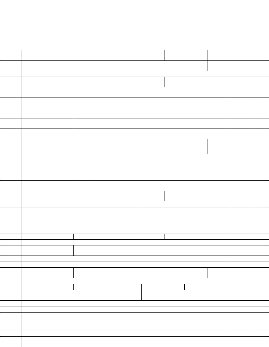
UG-671 AD9361 Register Map Reference Manual
Rev. 0 | Page 60 of 72
Rx ANALOG REGISTERS
Rx SYNTHESIZER REGISTERS (ADDRESS 0x230 THROUGH ADDRESS 0x251)
Table 67.
Register
Address Name D7 D6 D5 D4 D3 D2 D1 D0 Default R/W
0x230 Disable VCO
Cal
Must be 0x5 Must be 3’b010 Disable
VCO Cal
0x54 R/W
0x231
Integer Byte 0
Synthesizer Integer Word[7:0]
0x00
R/W
0x232 Integer Byte 1 SDM
Bypass
SDM PD Open Synthesizer Integer Word[10:8] 0x00 R/W
0x233
Fractional
Byte 0
Synthesizer Fractional Word[7:0] 0x00 R/W
0x234 Fractional
Byte 1
Synthesizer Fractional Word[15:8] 0x00 R/W
0x235 Fractional
Byte 2
Open Synthesizer Fractional Word[22:16] 0x00 R/W
0x236 Force ALC Force ALC
Enable
Force ALC Word[6:0] 0x00 R/W
0x237 Force VCO
Tune 0
Force VCO Tune[7:0] 0x00 R/W
0x238
Force VCO
Tune 1
Must be 0
Force
VCO Tune
Enable
Force
VCO
Tune[8]
0x00 R/W
0x239 ALC/Varactor Init ALC Value[3:0] VCO Varactor[3:0] 0x82 R/W
0x23A VCO Output Open PORb
VCO
Open VCO Output Level[3:0] 0x0A R/W
0x23B CP Current Set to 1 VTune
Out
Charge Pump Current[5:0] 0x00 R/W
0x23C CP Offset Synth Re-
Cal
Open Charge Pump Offset[5:0] 0x00 R/W
0x23D CP Config Must be 0 Dither
Mode
Open Cp Offset
Off
Force Cp
Cal
Cp Cal
Enable
Must be 2’b00 0x80 R/W
0x23E Loop Filter 1 Loop Filter C2[3:0] Loop Filter C1[3:0] 0x00 R/W
0x23F Loop Filter 2 Loop Filter R1[3:0] Loop Filter C3[3:0] 0x00 R/W
0x240 Loop Filter 3 Loop
Filter
Bypass R3
Loop
Filter
Bypass R1
Loop
Filter
Bypass C2
Loop
Filter
Bypass C1
Loop Filter R3[3:0] 0x00 R/W
0x241 Dither/CP Cal Number SDM Dither Bits[3:0] Forced CP Cal Word[3:0] 0x00 R/W
0x242
VCO Bias 1
Open
Must be 0
VCO Bias Tcf[1:0]
VCO Bias Ref[2:0]
0x04
R/W
0x243 Must be 0x0D Must be 0x0D 0x0D R/W
0x244 Cal Status
CP Cal
Valid
Open
CP Cal
Done
VCO Cal
Busy
CP Cal Word[3:0] 0x-- R
0x245 Must be 0x00 Must be 0x00 0x00 R/W
0x246 Set to 0x02 Set to 0x02 0x00 R/W
0x247 CP Ovrg/VCO
Lock
CP Ovrg
High
CP Ovrg
Low
Open Rx PLL
Lock
Open 0x-- R
0x248 Set to 0x0B Set to 0x0B 0x07 R/W
0x249 VCO Cal Set to 1 Must be 3’b000 VCO Cal Count [1:0] Must be 2’b10 0x02 R/W
0x24A Lock Detect
Config
Open Lock Detect
Count[1:0]
Lock Detect Mode[1:0] 0x02 R/W
0x24B Must be 0x17 Must be 0x17 0x17 R/W
0x24C Must be 0x00 Must be 0 0x00 R/W
0x24D Must be 0x00 Must be 0 0x00 R/W
0x24E Open Open 0x00 R/W
0x24F Open Open 0x00 R/W
0x250 Set to 0x70 Set to 0x70 0x63 R/W
0x251
VCO Varactor
Control 1
Open
VCO Varactor Reference[3:0]
0x08
R/W

AD9361 Register Map Reference Manual UG-671
Rev. 0 | Page 61 of 72
The ad9361_txrx_synth_cp_calib function sets up all registers
in this section. The RF and BBPLL Synthesizer section of the
AD9361 Reference Manual has more details.
SPI Register 0x230— PFD Config
[D7:D4]—Must be 0x5
[D3:D1]—Must be 3’b010
D0—Disable VCO Cal
Set this bit to prevent a VCO calibration when (a) the integer
frequency word changes or (b) the ENSM changes from the Tx
state to the Alert state when the ENSM is in TDD mode. Bit D0
in Register 0x270 prevents a VCO cal when the ENSM moves
from the Rx state to the Alert state.
SPI Register 0x231, SPI Register 0x232[D2:D0] and SPI
Register 0x233 Through SPI Register 0x235—VCO
Frequency Words
These words set the VCO frequency, which ranges from 6 GHz
to 12 GHz. The dividers in Register 0x005 divide this frequency
down to the final LO frequency required by the application.
Equation 24 and Equation 25 derive the integer and fractional
words. All frequencies must use the same units (for example,
MHz).
(24)
8,388,593
(25)
where:
FREF = reference clock frequency (external or DCXO). This rate
is after the reference divider in 0x2AB[D0] and 0x2AC[D7].
NInteger = 11-bit integer word programmed in Register 0x231 and
Register 0x232.
NFractional = 23-bit fractional word programmed in Register 0x233
through Register 0x235.
SPI Register 0x232
D7—SDM Bypass
Test bit, normally cleared. Setting this bit bypasses the SDM of
the Rx RFPLL.
D6—SDM PD
Test bit, normally cleared. Setting this bit disables the Rx RFPLL
SDM.
SPI Register 0x236—Force ALC
D7—Force ALC Enable
Setting this bit forces the automatic level control to use the force
word in Bits[D6:D0] instead of the word generated during
calibration. This bit is set when using the fast lock feature of the
VCO. See Register 0x25A through Register 0x25F.
[D6:D0]—Force ALC Word[6:0]
After a VCO calibration, this register holds the resulting VCO
amplitude word.
SPI Register 0x237—Force VCO Tune 0
After a VCO calibration, this register holds the lower 8 bits of
the VCO capacitor word. This register can also be used in a test
mode to force the capacitor word if the Force VCO Tune Enable
bit (0x238[D1]) is set. The AD9361 sets this register automati-
cally when using the fast lock feature.
SPI Register 0x238—Force VCO Tune 1
[D7:D2]—Must be 0
D1—Force VCO Tune Enable
Setting this bit forces the VCO to use the force word in Register
0x237 and 0x238[D0] instead of the word it generates during
calibration. This bit is set when using the fast lock feature of the
VCO. See Register 0x25A through Register 0x25F.
D0—Force VCO Tune[8]
This bit is the most significant bit of the VCO capacitor tune
word. See Register 0x237.
SPI Register 0x239—ALC/Varactor
[D7:D4]—Init ALC Value[3:0]
These bits set the initial ALC value (VCO bias DAC setting)
when running a VCO calibration.
[D3:D0]—VCO Varactor[3:0]
These bits set the varactor size that sets the Kv. Higher register
value equals higher Kv. The total varactor value (0x239[D3:D0]
+ 0x251[D3:D0]) must be 15(d) or less. See Register 0x251 for
other restrictions on the setting of these bits.
SPI Register 0x23A—VCO Output
D6—PORb VCO
Clearing this bit resets the VCO calibration logic. Clear before
running the VCO calibration.
[D3:D0]—VCO Output Level[3:0]
These bits set the VCO output voltage level that sets the VCO
phase noise performance and power consumption. Range: 0.5 V
to 1.5 V, step size = 67 mV.
SPI Register 0x23B—CP Current
D7—Set to 1
D6—VTune Out
Test mode bit, normally clear. If set, the AD9361 outputs VTune
on the external Rx LO pin. This pin is normally an input but if
this bit is set, it is an output.
[D5:D0]—Charge Pump Current[5:0]
These bits set the charge pump current. Range: 0.1 mA to
6.4 mA, resolution = 100 μA/LSB.

UG-671 AD9361 Register Map Reference Manual
Rev. 0 | Page 62 of 72
SPI Register 0x23C—CP Offset
D7—Synth Re-Cal
Setting this self-clearing bit forces the charge pump to re-
calibrate either the next time the synthesizer powers up or when
the Cp Cal Enable bit (0x23D[D2]) is cleared and then set.
Clear for normal operation.
[D5:D0]—Charge Pump Offset[5:0]
Only applies if the Cp Offset Off bit (0x23D[D4]) is cleared.
These bits set the charge pump bleed current. The step size is
12.5 µA/LSB with a range of 0 µA to 787.5 µA.
SPI Register 0x23D—CP Config
D7—Must be 0
D6—Dither Mode
PRBS length. Clear = 17 bits; set = 23 bits.
D4—CP Offset Off
Setting this bit disables the charge pump bleed current. Clear to
use the value in the Charge Pump Offset bits (0x23C[D5:D0])
as the offset current.
D3—Force CP Cal
Setting this bit overrides the calibration result with the value in
0x241[D3:D0]. In this case, CP Cal Word in 0x244[D3:D0]
reflects the value in 0x241[D3:D0]. Clear for normal operation.
D2—CP Cal Enable
Set this bit to start the CP calibration. When this bit is clear, the
charge pump will not calibrate.
SPI Register 0x23E—Loop Filter 1
[D7:D4]—Loop Filter C2[3:0]
These bits set the second pole loop filter capacitor.
[D3:D0]—Loop Filter C1[3:0]
These bits set the capacitor for the loop filter.
SPI Register 0x23F—Loop Filter 2
[D7:D4]—Loop Filter R1[3:0]
These bits set the resistor value for the loop filter zero. There are
16 resistors in parallel. Range: 8.68 kΩ to 543 Ω (all R’s in
parallel with the bits set to zero). Setting the Loop Filter Bypass
R1 bit (0x240[D6]) bit shorts R1.
[D3:D0]—Loop Filter C3[3:0]
These bits set the third pole loop filter capacitor. Range: 2.86 pF
to 47.4 pF; resolution: 2.86 pF at 27°C.
SPI Register 0x240—Loop Filter 3
D7—Loop Filter Bypass R3
Setting this bit bypasses R3 of the loop filter. See Bits[D3:D0].
D6—Loop Filter Bypass R1
Setting this bit bypasses R1 of the loop filter. See 0x23F[D7:D4].
D5—Loop Filter Bypass C2
See 0x23E[D7:D4]. Setting this bit shorts out an additional LSB
of C2.
D4—Loop Filter Bypass C1
See 0x23E[D3:D0]. Setting this bit shorts out an additional LSB
of C1.
[D3:D0]—Loop Filter R3[3:0]
These bits set the third pole loop filter resistor. There are 16
resistors in parallel. Range: 2.79 kΩ to 174 Ω (all resistors in
parallel with all bits set to zero). Setting the Loop Filter Bypass
R3 bit (0x240[D7]) bit shorts R3.
SPI Register 0x241—Dither/CP Cal
[D7:D4]—Number of Dither Bits[3:0]
These bits set the number of dither bits added to the 23-bit
fractional synth word. Range: 0 to 15.
[D3:D0]—Forced CP Cal Word[3:0]
Writing this nibble overwrites the CP calibration word if the
Force Cp Cal bit in 0x23D[D3] is set.
SPI Register 0x242—VCO Bias 1
[D6:D5]—Must be 0
[D4:D3]—VC O Bia s Tcf[1:0]
These bits control the VCO bias DAC temperature coefficient.
[D2:D0]—VCO Bias Ref[2:0]
These bits control the VCO bias reference DAC. Range: 50 µA
to 400 µA; resolution: 50 µA.
SPI Register 0x243—Must be 0x0D
SPI Register 0x244—Cal Status
D7—CP Cal Valid
Set after a successful CP calibration and will remain set and
another CP calibration will not begin, even if the Rx RF PLL
powers down. This bit will clear if the Cp Cal Enable bit in
0x23D[D2] goes low or the Force Cp Cal bit in 0x23D[D3]
goes high.
D5—CP Cal Done
This bit set indicates that a CP calibration was successful. This
bit will clear when the Rx PLL powers down, such as occurs in
TDD mode.
D4—VCO Cal Busy
This bit set indicates that a VCO calibration is running.
[D3:D0]—CP Cal Word[3:0]
This is the charge pump calibration result. If the Force Cp Cal
bit (0x23D[D3]) bit is set, then these bits will be forced by the
Forced CP Cal Word in 0x241[D3:D0]).

AD9361 Register Map Reference Manual UG-671
Rev. 0 | Page 63 of 72
SPI Register 0x245—Must be 0x00
SPI Register 0x246—Must be 0x02
SPI Register 0x247—CP Ovrge/VCO Lock
D7—CP Ovrg High
Applies if 0x24B[D6] is clear. If set, the CP output is above the
value in Register 0x24B.
D6—CP Ovrg Low
Applies if 0x24B[D6] is clear. If set, the CP output is below the
value in Register 0x24B.
D1—Rx PLL Lock
Applies if 0x24A[D1:D0] = 2’b01 or 2’b10. If set, the synth
locked in the number of clock cycles set by the Lock Detect
Count bits (0x24A[D3:D2]).
SPI Register 0x248—Must be 0x0B
SPI Register 0x249—VCO Cal
D7—Set to 1
[D6:D4] Must be 3’b000
[D3:D2] VCO Cal Count[1:0]
These bits set the VCO frequency calibration counter length. 00
= 128, 01 = 256, 10 = 512,11 = 1024.
[D1:D0] Must be 2’b10
SPI Register 0x24A—Lock Detect Config
[D3:D2]—Lock Detect Count[1:0]
If the RF PLL locks within the specified time, the Rx PLL Lock
bit (0x247[D1]) goes high. The time is measured in reference
clock cycles per Table 68.
Table 68.Lock Detect Count
Lock Detect Count[1:0] Reference Clock Cycles
0 0 256
0 1 512
1 0 1024
1 1 2048
[D1:D0]—Lock Detect Mode[1:0]
These bits set the lock detect mode of operation per Table 69.
Table 69. RFPLL Lock Detect Mode
Lock Detect
Mode[1:0] RFPLL Lock Detect Mode
0 0 Disable lock detect
0 1 Run lock detect once, when RFPLL is enabled
1 0 Run lock detect continuously
1 1 Do not use
SPI Register 0x24B—Must be 0x17
SPI Register 0x24C—Must be 0
SPI Register 0x24D—Must be 0
SPI Register 0x250—Must be 0x70
SPI Register 0x251—VCO Varactor Control 1
These bits set the number of varactors connected to the VCO
varactor reference voltage. There are four ports. See Table 70 for
example valid settings. It is never valid to set the same bit in
both words (0x239[D3:D0] and 0x251[D3:D0]).
Table 70.VCO Varactor Connections
0x239[D3:D0] 0x251[D3:D0]
0000 0000
0001 0000
0010 0001

UG-671 AD9361 Register Map Reference Manual
Rev. 0 | Page 64 of 72
Rx FAST LOCK REGISTERS (ADDRESS 0x25A THROUGH ADDRESS 0x25F)
Table 71.
Register
Address Name D7 D6 D5 D4 D3 D2 D1 D0 Default R/W
0x25A Rx Fast Lock
Setup
Rx Fast Lock
Profile[2:0]
Open Rx Fast
Lock Load
Synth
Rx Fast
Lock
Profile Init
Rx Fast Lock
Profile Pin
Select
Rx Fast Lock
Mode Enable
0x00 R/W
0x25B Rx Fast Lock
Setup Init
Delay
Rx Fast Lock Init Delay[7:0] 0x00 R/W
0x25C Rx Fast Lock
Program
Address
Rx Fast Lock Program Address[7:0] 0x-- R/W
0x25D Rx Fast Lock
Program Data
Rx Fast Lock Program Data[7:0] 0x-- R/W
0x25E Rx Fast Lock
Program
Read
Rx Fast Lock Program Read Data[7:0] 0x-- R
0x25F Rx Fast Lock
Program
Control
Open Rx Fast Lock
Program Write
Rx Fast Lock
Program Clock
Enable
0x00 R/W
The Linux and No-OS drivers contain functions for setting up
and using the fast lock function. See the Fast Lock Profiles
section of the AD9361 Reference Manual for more information
and function names.
SPI Register 0x25A—Rx Fast Lock Setup
[D7:D5]—Rx Fast Lock Profile[2:0]
Ignored if Bit D1 is set. These bits select the profile number (0
to 7) when creating or using a profile.
D3—Rx Fast Lock Load Synth
Setting this bit forces a VCO calibration. After calibration
completes, the AD9361 saves the resulting calibration words
and then this bit self-clears. This is only valid when D0 and D2
are set. If the VCO tune and VCO ALC words entries are
written manually into the profile along with the other
parameters, then it is not necessary to set this bit and run a
VCO calibration.
D2—Rx Fast Lock Profile Init
Set this bit when creating a profile. This bit set allows the
calibrated VCO values to be saved to a specific profile. To create
more than one profile, this bit must be set low and then high
again. Only valid when Bit D0 is set. Clear this bit to use saved
profiles (after all fast lock programming completes).
D1—Rx Fast Lock Profile Pin Select
With this bit set, the CTRL_IN0 through CTRL_IN2 pins select
the Rx fast lock profile. With this bit clear, [D7:D5] select the
fast lock profile. Only valid when D0 is set.
D0—Rx Fast Lock Mode Enable
Set this bit when creating or using profiles.
SPI Register 0x25B—Rx Fast Lock Setup Init Delay
These bits set the time that the charge pump current, R1, R3,
and C3 of the loop filter remain at their initial values before
changing to final values during fast lock. Delay is 250 ns/LSB,
range of 0 ns to 63.75 μs. All profiles share this delay setting.
SPI Register 0x25C—Rx Fast Lock Program Address
These bits set the profile calibration word. To write all setup
words for a particular profile into the table, hold the upper
nibble constant and write the lower nibble 13 or 15 times (x0 to
xD or xF), changing the data written to Register 0x25D[D3:D0]
for each write operation.
SPI Register 0x25D—Rx Fast Lock Program Data
This word is the data written to the internal address specified in
Register 0x25C when creating a profile.
SPI Register 0x25E—Rx Fast Lock Program Read Data
Read Register 0x25E to see the programmed word at
Address 0x25C.
SPI Register 0x25F—Rx Fast Lock Program Control
D1—Rx Fast Lock Program Write
Set this self-clearing bit any time a write operation to the fast
lock table is performed. Also, set D0.
D0—Rx Fast Lock Program Clock Enable
Set to 1 to read data from or write data to a profile.
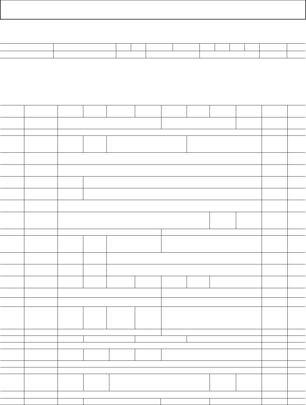
AD9361 Register Map Reference Manual UG-671
Rev. 0 | Page 65 of 72
Rx LO GENERATION REGISTER (ADDRESS 0x261)
Table 72.
Register Address Name D7 D6 D5 D4 D3 D2 D1 D0 Default R/W
0x261
Rx LO Gen Power Mode
Open
Power Mode[1:0]
Open
0x00
R/W
SPI Register 0x261—Rx LO Gen Power Mode
The ad9361_txrx_synth_cp_calib function configures this register. Write 0x00 to Register 0x261 when using the internal VCO and write
it to 0x30 when using an external LO.
Tx SYNTHESIZER REGISTERS (ADDRESS 0x270 THROUGH ADDRESS 0x291)
Table 73.
Register
Address Name D7 D6 D5 D4 D3 D2 D1 D0 Default R/W
0x270 Disable VCO
Cal
Must be 0x05 Must be 3’b010 Disable
VCO Cal
0x54 R/W
0x271
Integer Byte 0
Synthesizer Integer Word[7:0]
0x00
R/W
0x272 Integer Byte 1 SDM
Bypass
SDM
Power
Down
Open Synthesizer Integer Word[10:8] 0x00 R/W
0x273 Fractional
Byte 0
Synthesizer Fractional Word[7:0] 0x00 R/W
0x274 Fractional
Byte 1
Synthesizer Fractional Word[15:8] 0x00 R/W
0x275 Fractional
Byte 2
Open Synthesizer Fractional Word[22:16] 0x00 R/W
0x276 Force ALC
Force ALC
Enable
Force ALC Word[6:0] 0x00 R/W
0x277 Force VCO
Tune 0
Force VCO Tune[7:0] 0x00 R/W
0x278 Force VCO
Tune 1
Must be 0 Force VCO
Tune
Enable
Force
VCO
Tune[8]
0x00 R/W
0x279 ALC/Varactor Init ALC Value[3:0] VCO Varactor[3:0] 0x82 R/W
0x27A VCO Output Open PORb
VCO
Logic
Open VCO Output Level[3:0] 0x0A R/W
0x27B
CP Current
Set to 1
Vtune
Out
Charge Pump Current[5:0]
0x00
R/W
0x27C CP Offset Synth Re-
Cal
Open Charge Pump Offset[5:0] 0x00 R/W
0x27D CP Config Must be 0 Dither
Mode
Open Cp Offset
Off
F Cp Cal Cp Cal
Enable
Must be 2’b00 0x80 R/W
0x27E Loop Filter 1 Loop Filter C2[3:0] Loop Filter C1[3:0] 0x00 R/W
0x27F Loop Filter 2 Loop Filter R1[3:0] Loop Filter C3[3:0] 0x00 R/W
0x280 Loop Filter 3 Loop
Filter
Bypass R3
Loop
Filter
Bypass
R1
Loop Filter
Bypass C2
Loop
Filter
Bypass C1
Loop Filter R3[3:0] 0x00 R/W
0x281 Dither/CP Cal Number SDM Dither Bits[3:0] Forced CP Cal Word[3:0] 0x00 R/W
0x282 VCO Bias 1 Open Must be 0 VCO Bias Tcf[1:0] VCO Bias Ref[2:0] 0x04 R/W
0x283 Must be 0x0D Must be 0x0D 0x0D R/W
0x284
Cal Status
CP Cal
Valid
Open
CP Cal
Done
VCO Cal
Busy
CP Cal Word[3:0]
0x--
R
0x285 Must be 0x00 Must be 0x00 0x00 R/W
0x286 Set to 0x02 Set to 0x02 0x00 R/W
0x287 CP Over
Range/VCO
Lock
CP Ovrg
High
CP Ovrg
Low
Open Tx PLL
Lock
Open 0x-- R
0x288 Set to 0x0B Set to 0x0B 0x07 R/W
0x289 VCO Cal Set to 1 Must be 3’b000 VCO Cal Count[1:0] Must be 2’b10 0x02 R/W
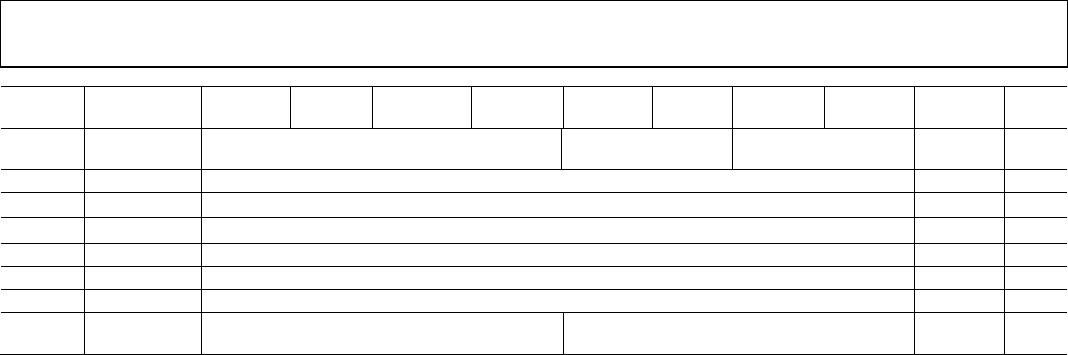
UG-671 AD9361 Register Map Reference Manual
Rev. 0 | Page 66 of 72
Register
Address Name D7 D6 D5 D4 D3 D2 D1 D0 Default R/W
0x28A Lock Detect
Config
Open Lock Detect
Count[1:0]
Lock Detect Mode[1:0] 0x02 R/W
0x28B Must be 0x17 Must be 0x17 0x40 R/W
0x28C Must be 0x00 Must be 0x00 0x00 R/W
0x28D Must be 0x00 Must be 0x00 0x80 R/W
0x28E Open Open 0x00 R/W
0x28F Open Open 0x00 R/W
0x290 Set to 0x70 Set to 0x70 0x63 R/W
0x291 VCO Varactor
Control 1
Open VCO Varactor Reference[3:0] 0x08 R/W
The ad9361_txrx_synth_cp_calib function sets up all registers in this section. See the PLL section of the AD9361 Reference Manual for
more details. Tx registers are identical to the Rx registers in Address 0x230 through Address 0x251. See those registers for definitions. The
description in Register 0x231 refers to the reference divider if an external clock is used. For Tx frequency words in Address 0x271 through
Address 0x275, the reference divider is in 0x2AC[D3:D2].
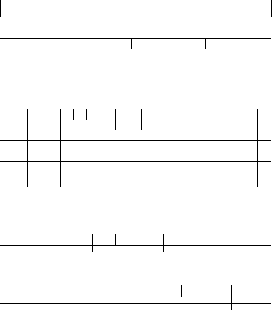
AD9361 Register Map Reference Manual UG-671
Rev. 0 | Page 67 of 72
DCXO REGISTERS (ADDRESS 0x292 THROUGH ADDRESS 0x294)
Table 74.
Register
Address Name D7 D6 D5 D4 D3 D2 D1 D0 Default R/W
0x292 DCXO Coarse Tune Open DCXO Tune Coarse[5:0] 0x00 R/W
0x293 DCXO Fine Tune2 DCXO Tune Fine[12:5] 0x00 R/W
0x294 DCXO Fine Tune1 DCXO Tune Fine[4:0] Open 0x00 R/W
SPI Register 0x292 Through SPI Register 0x294—DCXO Coarse Tune and DCXO Fine Tune
The ad9361_set_dcxo_tune function configures these registers. Valid when the DCXO is used and the XO Bypass bit (0x009[D4]) is
cleared. These words adjust the coarse and fine correction to the DCXO reference clock frequency.
Tx SYNTH FAST LOCK REGISTERS (ADDRESS 0x29A THROUGH ADDRESS 0x29F)
Table 75.
Register
Address Name D7 D6 D5 D4 D3 D2 D1 D0 Default R/W
0x29A Tx Fast Lock
Setup
Tx Fast Lock
Profile[2:0]
Open Tx Fast Lock
Load Synth
Tx Fast Lock
Profile Init
Tx Fast Lock
Profile Pin Select
Tx Fast Lock
Mode Enable
0x00 R/W
0x29B Tx Fast Lock
Setup Init Delay
Tx Fast Lock Init Delay[7:0] 0x00 R/W
0x29C Tx Fast Lock
Program Addr
Tx Fast Lock Program Address[7:0] 0x-- R/W
0x29D Tx Fast Lock
Program Data
Tx Fast Lock Program Data[7:0] 0x-- R/W
0x29E Tx Fast Lock
Program Read
Tx Fast Lock Program Read Data[7:0] 0x-- R
0x29F Tx Fast Lock
Program Ctrl
Open Tx Fast Lock
Program Write
Tx Fast Lock
Program Clock
Enable
0x00 R/W
These registers are identical to the Rx Fast Lock registers (Address 0x25A through Address 0x25F) but apply to the Tx profiles. See the Rx
Fast Lock Registers (Address 0x25A Through Address 0x25F) section. The Linux and No-OS drivers contain functions for setting up and
using the fast lock function. See the Fast Lock Profiles section of the AD9361 Reference Manual for more information and function
names.
Tx LO GENERATION REGISTER (ADDRESS 0x2A1)
Table 76.
Register
Address Name D7 D6 D5 D4 D3 D2 D1 D0 Default R/W
0x2A1 Tx LO Gen Power Mode Power Mode[3:0] Open 0x00 R/W
The ad9361_txrx_synth_cp_calib function configures this register. Write 0x261 to 0x00 when using the internal VCO and write it to 0xF0
when using an external LO.
MASTER BIAS AND BAND GAP CONFIGURATION REGISTERS (ADDRESS 0x2A6 AND ADDRESS 0x2A8)
Table 77.
Register
Address Name D7 D6 D5 D4 D3 D2 D1 D0 Default R/W
0x2A6 Set to 0x0E Set to 0x0E 0x04 R/W
0x2A8 Set to 0x0E Set to 0x0E 0x00 R/W
The ad9361_init function configures these registers correctly. These registers set up the master bias and band gap reference in the
AD9361. Configure these before enabling the clocks in Register 0x009.
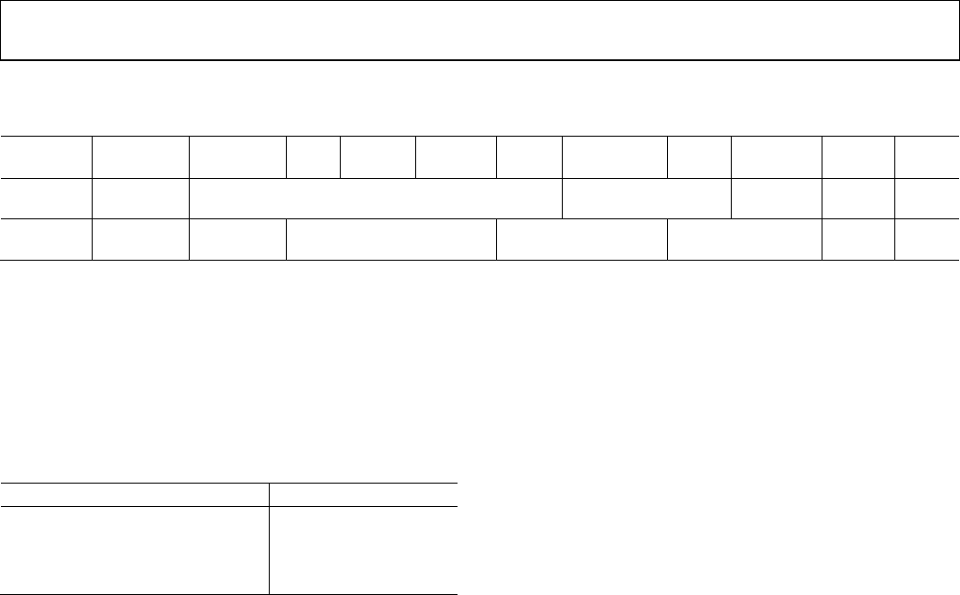
UG-671 AD9361 Register Map Reference Manual
Rev. 0 | Page 68 of 72
REFERENCE DIVIDER REGISTERS (ADDRESS 0x2AB AND ADDRESS 0x2AC)
Table 78.
Register
Address Name D7 D6 D5 D4 D3 D2 D1 D0 Default R/W
0x2AB Ref Divide
Config 1
Open Set to 2’b11 Rx Ref
Divider[1]
0x04 R/W
0x2AC Ref Divide
Config 2
Rx Ref
Divider[0]
Set to 3’b111 Tx Ref Divider[1:0] Set to 2’b11 0x00 R/W
The ad9361_init function configures these registers.
SPI Register 0x2AB—Ref Divide Config 1
[D2:D1]—Set to 2’b11
D0—Rx Ref Divider[1]
This is the most significant bit of the Rx path divider control
bits, mapped per Table 79. The LSB is in 0x2AC[D7].
Table 79. Rx Ref Divider Ratio
Rx Ref Divider[1:0] Divider Ratio
00 1
01 ½
10 ¼
11 2
SPI Register 0x2AC—Ref Divider Config 2
D7—Rx Ref Divider[0]
See 0x2AB[D0].
[D6:D4]—Set to 3’b111
[D3:D2]—Tx Ref Divider[1:0]
These bits control the Tx path divider, per Table 79.
[D2:D1]—Set to 2’b11
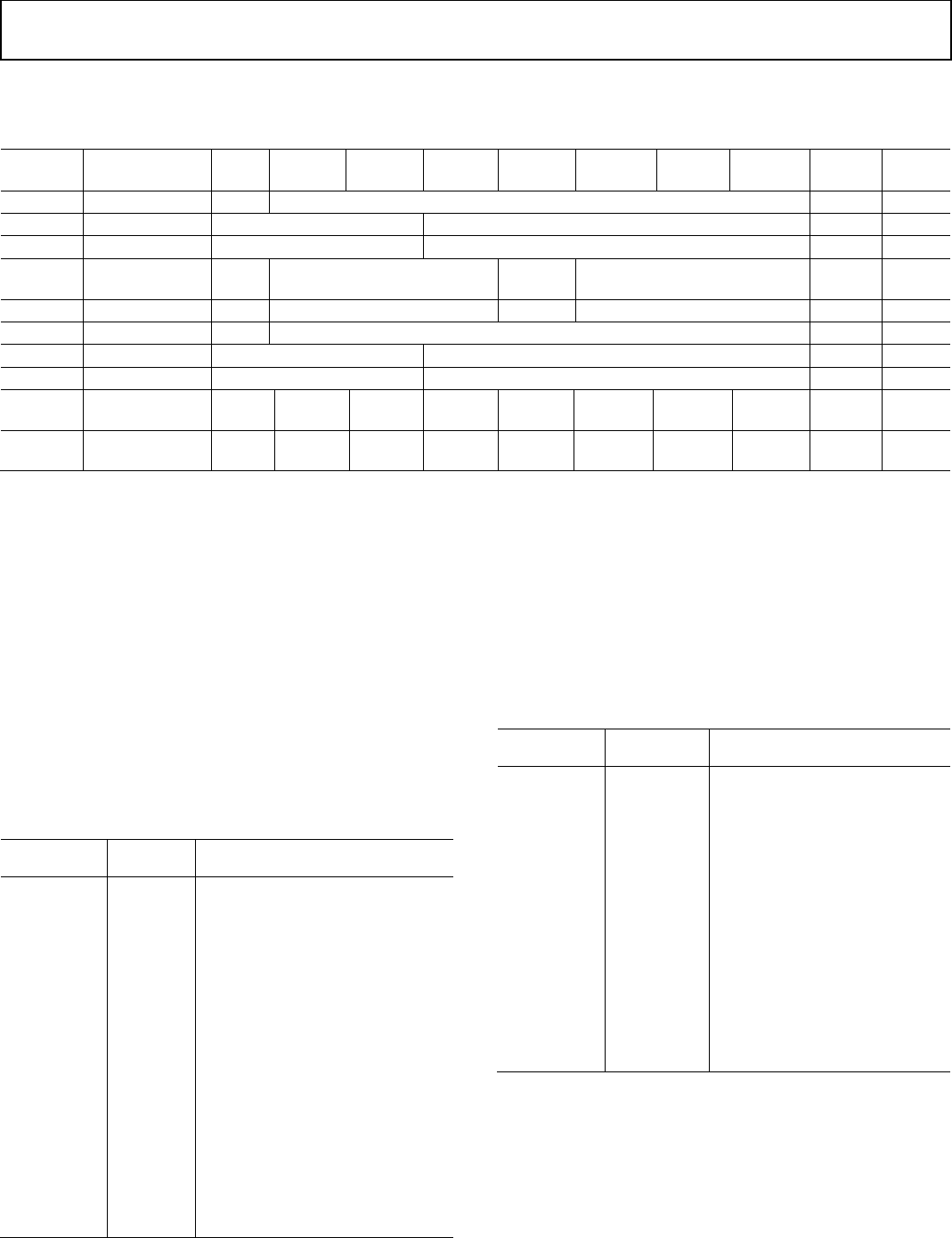
AD9361 Register Map Reference Manual UG-671
Rev. 0 | Page 69 of 72
Rx GAIN READ BACK REGISTERS (ADDRESS 0x2B0 THROUGH ADDRESS 0x2B9)
Table 80.
Register
Address Name D7 D6 D5 D4 D3 D2 D1 D0 Default R/W
0x2B0 Gain Rx1 Open Full Table Gain Index Rx1/LMT Gain Rx1[6:0] 0x-- R
0x2B1 LPF Gain Rx1 Open LPF Gain Rx1[4:0] 0x-- R
0x2B2 Dig Gain Rx1 Open Digital Gain Rx1[4:0] 0x-- R
0x2B3 Fast Attack
State
Open Fast Attack State Rx2[2:0] Open Fast Attack State Rx1[2:0] 0x-- R
0x2B4 Slow Loop State Open Slow Loop State Rx2[2:0] Open Slow Loop State Rx1[2:0] 0x-- R
0x2B5 Gain Rx2 Open Full Table Gain IndexRx2/LMT Gain Rx1[6:0] 0x-- R
0x2B6 LPF Gain Rx2 Open LPF Gain Rx2[4:0] 0x-- R
0x2B7 Dig Gain Rx2 Open Digital Gain Rx2[4:0] 0x-- R
0x2B8 Ovrg Sigs Rx1 Open Gain
Lock
Low
Power
Large
LMT OL
Small
LMT OL
Large
ADC OL
Small
ADC OL
Dig Sat 0x-- R
0x2B9 Ovrg Sigs Rx2 Open Gain
Lock
Low
Power
Large
LMT OL
Small
LMT OL
Large
ADC OL
Small
ADC OL
Dig Sat 0x-- R
SPI Register 0x2B0—Gain Rx1
Register 0x2B0 holds the Rx1 gain index when the AD9361 is in
the Rx or FDD states and is valid in all gain control modes. In
full table mode, Register 0x2B0 holds the full table index. For
split table mode, Register 0x2B0 holds the LMT index.
SPI Register 0x2B1—LPF Gain Rx1
LPF gain for split gain table mode.
SPI Register 0x2B2—Dig Gain Rx1
Digital gain for split gain table mode.
SPI Register 0x2B3—Fast Attack State
[D6:D4]—Fast Attack State Rx2[2:0]
The state of the Rx2 Fast AGC state machine per Table 81.
Table 81. Fast Attack AGC States
Fast Attack
State Rx2[2:0]
State
Name Description
0 Reset Peak
Detectors
The state machine initializes to this
state at the start of RxON. The AD9361
holds all power and peak detectors in
reset.
1 Peak
Detect
In State 1, the AD9361 detects peak
overloads and reduces gain until the
overloads cease.
2 Power
Measurem
ent
The state machine waits for settling
delay, measures power, and then
adjusts gain to match the signal level to
the AGC Lock Level.
3
Final
Settling
If large peak overloads occur, the
AD9361 decreases gain and moves to
final over range state, else it moves to
State 5.
4 Final Over
Range
The state machine resets the peak
detectors and for the peak wait
duration. On expiration of this counter,
the state machine transitions to State 3.
5 Gain Lock The state machine remains in this state
until unlocked.
[D2:D0]—Fast Attack State Rx1[2:0]
Same as Bits[D6:D4] but apply to Rx1.
SPI Register 0x2B4—Slow Loop State
[D6:D4]—Slow Loop State Rx2[1:0]
The state of the Rx2 slow AGC per Table 82.
[D2:D1]—Slow Loop State Rx1[1:0]
Same as Bits[D6:D4] but apply to Rx1.
Table 82. Slow Attack AGC States
Slow Attack
State Rx2[1:0] State Name Description
0 Reset The state machine initializes to this
state at the start of RxON. The gain
update counter and related
functionality resets to 0.
1 Slow
Measurement
Power measurement of the signal
occur. A counter increments until it
reaches the gain update count, at
which time the state machine moves
to the gain change state.
2 Gain Change Based on the results of the previous
slow measurement state, the gain
changes accordingly.
3
Clear Peak
Detectors
The peak detector thresholds clear
and the state machine stays in this
state until the settling delay expires.
This allows the Rx signal to settle
before the AD9361 makes the next
power measurement.
UG-671 AD9361 Register Map Reference Manual
Rev. 0 | Page 70 of 72
SPI Register 0x2B5 Through SPI Register 0x2B7
These registers are the same as Address 0x2B0 through
Address 0x2B2 but apply to Rx2.
SPI Register 0x2B8—Ovrg Sigs Rx1
D6—Gain Lock
This bit set indicates that the Rx1 fast AGC has locked the gain.
D5—Low Power
This bit high indicates that the Rx1 average signal power has
dropped below the low power threshold.
D4—Large LMT OL
This bit set indicates that a large LMT overload occurred in
Rx1.
D3—Small LMT OL
This bit set indicates that a small LMT overload occurred in
Rx1.
D2—Large ADC OL
This bit set indicates that a large ADC overload occurred in
Rx1.
D1—Small ADC OL
This bit set indicates that a small ADC overload occurred in
Rx1.
D0—Digital Sat
This bit set indicates that the signal saturated between HB1
RFIR in Rx1.
SPI Register 0x2B9—Ovrg Sigs Rx2—Test Register
Same as Register 0x2B8 but applies to Rx2.
CONTROL REGISTER (REGISTER 0x3DF)
Table 83.
Register Address Name D7 D6 D5 D4 D3 D2 D1 D0 Default R/W
0x3DF Control Open Set to 1 0x00 R/W
The ad9361_init function sets up this register.
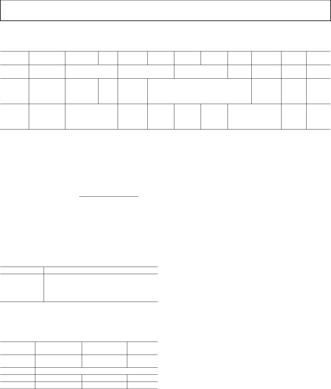
AD9361 Register Map Reference Manual UG-671
Rev. 0 | Page 71 of 72
DIGITAL TEST REGISTERS (ADDRESS 0x3F4 THROUGH ADDRESS 0x3F6)
Table 84.
Register
Address Name D7 D6 D5 D4 D3 D2 D1 D0 Default
R/W
0x3F4 BIST Config Tone Frequency[1:0] Tone Level[1:0] BIST Control Point
[1:0]
Tone/
PRBS
BIST
Enable
0x00 R/W
0x3F5 BIST Config2 Data Port
SP, HD
Loop Test
OE
Rx
Mask
Channel Must be 4’b0000 Data Port
Loop Test
Enable
0x00 R/W
0x3F6 BIST and
Data Port
Test Config
Must be 2’b00 BIST Mask
Channel 2
Q data
BIST
Mask
Channel
2 I data
BIST
Mask
Channel
1 Q data
BIST
Mask
Channel
1 I data
Must be 2’b00 0x00 R/W
See Engineer Zone for a FAQ describing the BIST functions in
more detail.
SPI Register 0x3F4—BIST Config—Test Register
[D7:D6]—Tone Frequency[1:0]
Sets the BIST frequency according to Equation 26.
:
(26)
where:
the Tone Frequency units are the same as for Clk.
Clk is the clock rate shown in Table 86.
[D5:D4]—Tone Level[1:0]
Sets the gain of the tone signal per Table 85. FS represents a full
scale digital output.
Table 85. BIST Tone Level
Tone Level[1:0] Amplitude
00 ±FS
01 ±FS/2
10 ±FS/4
11 ±FS/8
[D3:D2]—BIST Control Point[1:0]
These bits control where the BIST signal is injected per
Table 86.
Table 86.BIST Control Point
Control
Point[1:0] Injection Point
Clk used for BIST
Tone Frequency Comments
00 Input of Tx (output
of data port)
Tx sample rate Tx only
01 Not used
10 Input of data port Rx sample rate Rx only
11 Not used N/A N/A
D1—Tone/PRBS
When this bit is clear, the BIST outputs a PRBS signal. When
set, the BIST outputs a tone.
D0—BIST Enable
Set this bit to enable the BIST generator.
SPI Register 0x3F5—BIST Config2
D7—Data Port SP, HD Loop Test OE
See D0. Setting D7 enables the Rx I/O port even in half duplex
mode when looping Tx data back to the Rx I/O port.
D6—Rx Mask
Set this bit to mask the analog signals from propagating to the
digital blocks.
D5—Channel
When this bit is clear, observe Channel 1. When the bit is set,
observe Channel 2.
[D4:D1]—Must be 4’b0000
D0—Data Port Loop Test Enable
When set, this bit loops Tx I/O data back onto the Rx I/O port.
If in half duplex mode, also set D7.
SPI Register 0x3F6—BIST and Data Port Test Config—
Test Register
[D7:D6]—Must be 2’b00
[D5:D2]—BIST Mask Bits
Setting one of these 4 bits zeros out the data in question. For
example, setting Bit D5 zeros out Channel 2 Q data.
[D1:D0]—Must be 2’b00

UG-671 AD9361 Register Map Reference Manual
Rev. 0 | Page 72 of 72
NOTES
Legal Terms and Conditions
Information furnished by Analog Devices is believed to be accurate and reliable. However, no responsibility is assumed by Analog Devices for its use, nor for any infringements of patents or
other rights of third parties that may result from its use. No license is granted by implication or otherwise under any patent or patent rights of Analog Devices. Trademarks and registered
trademarks are the property of their respective owners. Information contained within this document is subject to change without notice. Software or hardware provided by Analog Devices
may not be disassembled, decompiled or reverse engineered. Analog Devices’ standard terms and conditions for products purchased from Analog Devices can be found at:
http://www.analog.com/en/content/analog_devices_terms_and_conditions/fca.html.
©2014 Analog Devices, Inc. All rights reserved. Trademarks and
registered trademarks are the property of their respective owners.
UG11668-0-3/14(0)
