AD9850
User Manual: AD9850
Open the PDF directly: View PDF ![]() .
.
Page Count: 20
REV. 0
Information furnished by Analog Devices is believed to be accurate and
reliable. However, no responsibility is assumed by Analog Devices for its
use, nor for any infringements of patents or other rights of third parties
which may result from its use. No license is granted by implication or
otherwise under any patent or patent rights of Analog Devices.
a
CMOS, 125 MHz
Complete DDS Synthesizer
AD9850
© Analog Devices, Inc., 1996
One Technology Way, P.O. Box 9106, Norwood, MA 02062-9106, U.S.A.
Tel: 617/329-4700 Fax: 617/326-8703
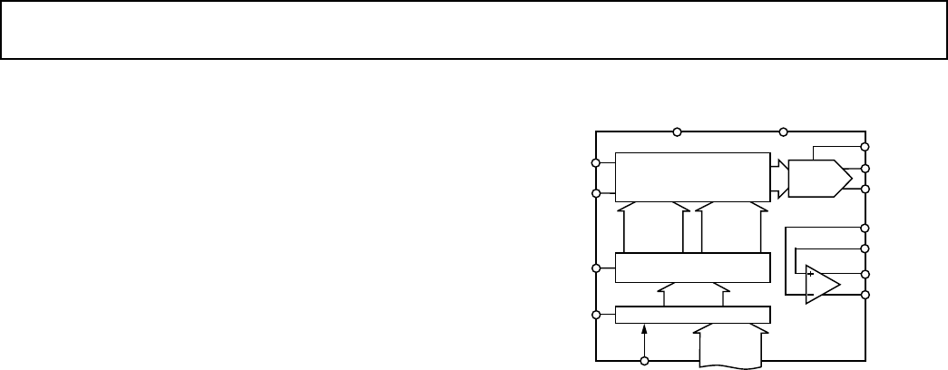
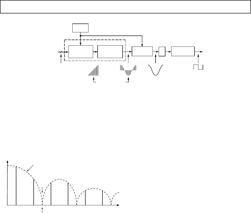
FUNCTIONAL BLOCK DIAGRAM
+V
S
DAC R
SET
ANALOG
OUT
MASTER
RESET
FREQUENCY
UPDATE/
DATA REGISTER
RESET
REF
CLOCK IN
CLOCK OUT
1-BIT x
40 LOADS
AD9850
COMPARATOR
PHASE
AND
CONTROL
WORDS
32-BIT
TUNING
WORD
FREQUENCY/PHASE
DATA REGISTER
SERIAL
LOAD
ANALOG
IN
CLOCK OUT
10-BIT
DAC
PARALLEL
LOAD
DATA INPUT REGISTER
8-BITS x
5 LOADS
WORD LOAD
CLOCK
HIGH SPEED
DDS
GND
FREQUENCY, PHASE, AND CONTROL
DATA INPUT
GENERAL DESCRIPTION
The AD9850 is a highly integrated device that uses advanced
DDS technology, coupled with an internal high speed, high
performance, D/A converter, and comparator, to form a com-
plete digitally programmable frequency synthesizer and clock
generator function. When referenced to an accurate clock
source, the AD9850 generates a spectrally-pure, frequency/
phase-programmable, analog output sine wave. This sine wave
can be used directly as a frequency source, or converted to a
square wave for agile-clock generator applications. The AD9850’s
innovative high speed DDS core provides a 32-bit frequency
tuning word, which results in an output tuning resolution of
0.0291 Hz, for a 125 MHz reference clock input. The
AD9850’s circuit architecture allows the generation of output
frequencies of up to one-half the reference clock frequency, or
62.5 MHz, and the output frequency can be digitally changed
(asynchronously) at a rate of up to 23 million new frequencies
per second. The device also provides 5bits of digitally controlled
phase modulation which enables phase shifting of its output in
increments of 180°, 90°, 45°, 22.5°, 11.25°, and any combination
thereof. The AD9850 also contains a high speed comparator
which can be configured to accept the (externally) filtered
output of the DAC to generate a low jitter square wave output.
This facilitates the device’s use as an agile clock generator
function.
The frequency tuning, control, and phase modulation words are
loaded into the AD9850 via a parallel byte or serial loading for-
mat. The parallel load format consists of five iterative loads of
an 8-bit control word (byte). The first byte controls phase
modulation, power-down enable, and loading format; bytes 2–5
comprise the 32-bit frequency tuning word. Serial loading is
accomplished via a 40-bit serial data stream on a single pin. The
AD9850 Complete-DDS uses advanced CMOS technology to
provide this breakthrough level of functionality and performance
on just 155 mW of power dissipation (+3.3 V supply).
The AD9850 is available in a space saving 28-lead SSOP, sur-
face mount package. It is specified to operate over the extended
industrial temperature range of –40°C to +85°C.
FEATURES
125 MHz Clock Rate
On-Chip High Performance DAC & High Speed
Comparator
DAC SFDR > 50 dB @ 40 MHz AOUT
32-Bit Frequency Tuning Word
Simplified Control Interface: Parallel Byte or Serial
Loading Format
Phase Modulation Capability
+3.3 V or +5 V Single Supply Operation
Low Power: 380 mW @ 125 MHz (+5 V)
Low Power: 155 mW @ 110 MHz (+3.3 V)
Power-Down Function
Ultrasmall 28-Lead SSOP Packaging
APPLICATIONS
Frequency/Phase–Agile Sine-Wave Synthesis
Clock Recovery and Locking Circuitry for Digital
Communications
Digitally Controlled ADC Encode Generator
Agile Local Oscillator Applications

AD9850BRS
Parameter Temp Test Level Min Typ Max Units
CLOCK INPUT CHARACTERISTICS
Frequency Range
+5 V Supply FULL IV 1 125 MHz
+3.3 V Supply FULL IV 1 110 MHz
Pulse Width High/Low
+5 V Supply +25°C IV 3.2 ns
+3.3 V Supply +25°C IV 4.1 ns
DAC OUTPUT CHARACTERISTICS
Full-Scale Output Current
R
SET
= 3.9 kΩ+25°C V 10.24 mA
R
SET
= 1.95 kΩ+25°C V 20.48 mA
Gain Error +25°C I –10 +10 % FS
Gain Temperature Coefficient FULL V 150 ppm/°C
Output Offset +25°CI 10 µA
Output Offset Temperature Coefficient FULL V 50 nA/°C
Differential Nonlinearity +25°C I 0.5 0.75 LSB
Integral Nonlinearity +25°C I 0.5 1 LSB
Output Slew Rate (50 Ω, 2 pF Load) +25°C V 400 V/µs
Output Impedance +25°C IV 50 120 kΩ
Output Capacitance +25°CIV 8 pF
Voltage Compliance +25°C I 1.5 V
Spurious-Free Dynamic Range (SFDR):
Wideband (Nyquist Bandwidth)
1 MHz Analog Out +25°C IV 63 72 dBc
20 MHz Analog Out +25°C IV 50 58 dBc
40 MHz Analog Out +25°C IV 46 54 dBc
Narrowband
40.13579 MHz ± 50 kHz +25°C IV 80 dBc
40.13579 MHz ± 200 kHz +25°C IV 77 dBc
4.513579 MHz ± 50 kHz/20.5 MHz CLK +25°C IV 84 dBc
4.513579 MHz ± 200 kHz/20.5 MHz CLK +25°C IV 84 dBc
COMPARATOR INPUT CHARACTERISTICS
Input Capacitance +25°CV 3 pF
Input Resistance +25°C IV 500 kΩ
Input Current +25°C I –12 +12 µA
Input Voltage Range +25°CIV 0 V
DD
V
Comparator Offset* FULL VI 30 30 mV
COMPARATOR OUTPUT CHARACTERISTICS
Logic “1” Voltage +5 V Supply FULL VI +4.8 V
Logic “1” Voltage +3. 3 V Supply FULL VI +3.1 V
Logic “0” Voltage FULL VI +0.4 V
Propagation Delay, +5 V Supply (15 pF Load) +25°C V 5.5 ns
Propagation Delay, +3.3 V Supply (15 pF Load) +25°CV 7 ns
Rise/Fall Time, +5 V Supply (15 pF Load) +25°CV 3 ns
Rise/Fall Time, +3.3 V Supply (15 pF Load) +25°C V 3.5 ns
Output Jitter (p-p) +25°CV 80 ps
CLOCK OUTPUT CHARACTERISTICS
Clock Output Duty Cycle (Clk Gen. Config.) +25°C IV 50 ± 10 %
REV. 0
–2–
(VS = +5 V 6 5% except as noted, RSET = 3.9 kV)
AD9850–SPECIFICATIONS

AD9850BRS
Parameter Temp Test Level Min Typ Max Units
CMOS LOGIC INPUTS (Including CLKIN)
Logic “1” Voltage, +5 V Supply +25°C I 3.5 V
Logic “1” Voltage, +3.3 V Supply +25°C I 3.0 V
Logic “0” Voltage +25°C I 0.4 V
Logic “1” Current +25°CI 12 µA
Logic “0” Current +25°CI 12 µA
Input Capacitance +25°CV 3 pF
POWER SUPPLY (AOUT = 1/3 CLKIN)
+V
S
Current @:
62.5 MHz Clock, +3.3 V Supply FULL VI 30 48 mA
110 MHz Clock, +3.3 V Supply FULL VI 47 60 mA
62.5 MHz Clock, +5 V Supply FULL VI 44 64 mA
125 MHz Clock, +5 V Supply FULL VI 76 96 mA
P
DISS
@:
62.5 MHz Clock, +3.3 V Supply FULL VI 100 160 mW
110 MHz Clock, +3.3 V Supply FULL VI 155 200 mW
62.5 MHz Clock, +5 V Supply FULL VI 220 320 mW
125 MHz Clock, +5 V Supply FULL VI 380 480 mW
P
DISS
Power-Down Mode
+5 V Supply FULL V 30 mW
+3.3 V Supply FULL V 10 mW
NOTES
*Tested by measuring output duty cycle variation.
Specifications subject to change without notice.
AD9850
–3–
REV. 0
TIMING CHARACTERISTICS*
AD9850BRS
Parameter Temp Test Level Min Typ Max Units
t
DS
(Data Setup Time) FULL IV 3.5 ns
t
DH
(Data Hold Time) FULL IV 3.5 ns
t
WH
(W_CLK min. Pulse Width High) FULL IV 3.5 ns
t
WL
(W_CLK min. Pulse Width Low) FULL IV 3.5 ns
t
WD
(W_CLK Delay After FQ_UD) FULL IV 7.0 ns
t
CD
(CLKIN Delay After FQ_UD) FULL IV 3.5 ns
t
FH
(FQ_UD High) FULL IV 7.0 ns
t
FL
(FQ_UD Low) FULL IV 7.0 ns
t
CF
(Output Latency from FQ_UD)
Frequency Change FULL IV 18 CLKIN Cycles
Phase Change FULL IV 13 CLKIN Cycles
t
FD
(FQ_UD Min. Delay After W_CLK) FULL IV 7.0 ns
t
RH
(CLKIN Delay After RESET Rising Edge) FULL IV 3.5 ns
t
RL
(RESET Falling Edge After CLKIN) FULL IV 3.5 ns
t
RS
(Minimum RESET Width) FULL IV 5 CLKIN Cycles
t
OL
(RESET Output Latency) FULL IV 13 CLKIN Cycles
t
RR
(Recovery from RESET) FULL IV 2 CLKIN Cycles
Wake-Up Time from Power-Down Mode +25°CV 5 µs
NOTES
*Control functions are asynchronous with CLKIN.
Specifications subject to change without notice.
(VS = +5 V 6 5% except as noted, RSET = 3.9 kV)

AD9850
–4– REV. 0
ABSOLUTE MAXIMUM RATINGS*
Maximum Junction Temperature . . . . . . . . . . . . . . . . +165°C
VDD . . . . . . . . . . . . . . . . . . . . . . . . . . . . . . . . . . . . . . . +6 V
Digital Inputs . . . . . . . . . . . . . . . . . . . . . . . . . . –0.7 V to +V
S
Digital Output Continuous Current . . . . . . . . . . . . . . . . 5 mA
DAC Output Current . . . . . . . . . . . . . . . . . . . . . . . . . 30 mA
Storage Temperature . . . . . . . . . . . . . . . . . –65°C to +150°C
Operating Temperature . . . . . . . . . . . . . . . . . –40°C to +85°C
Lead Temperature (Soldering 10 sec) . . . . . . . . . . . . +300°C
SSOP θ
JA
Thermal Impedance . . . . . . . . . . . . . . . . . . 82°C/W
*Absolute maximum ratings are limiting values, to be applied individually, and
beyond which the serviceability of the circuit may be impaired. Functional
operability under any of these conditions is not necessarily implied. Exposure of
absolute maximum rating conditions for extended periods of time may affect
device reliability.
EXPLANATION OF TEST LEVELS
Test Level
I – 100% Production Tested.
III – Sample Tested Only.
IV – Parameter is guaranteed by design and characterization
testing.
V – Parameter is a typical value only.
VI – All devices are 100% production tested at +25°C.
100% production tested at temperature extremes for
military temperature devices; guaranteed by design and
characterization testing for industrial devices.
WARNING!
ESD SENSITIVE DEVICE
CAUTION
ESD (electrostatic discharge) sensitive device. Electrostatic charges as high as 4000 V readily
accumulate on the human body and test equipment and can discharge without detection.
Although the AD9850 features proprietary ESD protection circuitry, permanent damage may
occur on devices subjected to high energy electrostatic discharges. Therefore, proper ESD
precautions are recommended to avoid performance degradation or loss of functionality.
ORDERING GUIDE
Model Temperature Range Package Option*
AD9850BRS –40°C to +85°C RS-28
*RS = Shrink Small Outline (SSOP).
AD9850
–5–
REV. 0
Table I. Lead Function Descriptions
Lead
Mnemonic No. Function
CLKIN 9 Reference Clock Input. This may be a continuous CMOS-level pulse train or sine input biased at
1/2 V supply. The rising edge of this clock initiates operation.
R
SET
12 This is the DAC’s external R
SET
connection. This resistor value sets the DAC full-scale output current. For
normal applications (F
S
I
OUT
= 10 mA), the value for R
SET
is 3.9 kΩ connected to ground. The R
SET
/I
OUT
relationship is: I
OUT
= 32 (1.248 V/R
SET
).
AGND 10, 19 Analog Ground. These leads are the ground return for the analog circuitry (DAC and comparator).
DGND 5, 24 Digital Ground. These are the ground return leads for the digital circuitry.
DVDD 6, 23 Supply Voltage Leads for digital circuitry.
AVDD 11, 18 Supply Voltage for the analog circuitry (DAC and comparator).
W_CLK 7 Word Load Clock. This clock is used to load the parallel or serial frequency/phase/control words.
FQ_UD 8 Frequency Update. On the rising edge of this clock, the DDS will update to the frequency (or phase)
loaded in the data input register, it then resets the pointer to Word 0.
D0–D7 1–4, 8-Bit Data Input. This is the 8-bit data port for iteratively loading the 32-bit frequency and 8-bit phase/
25–28 control word. D7 = MSB; D0 = LSB. D7 (Pin 25) also serves as the input pin for the 40-bit serial data word.
RESET 22 Reset. This is the master reset function; when set high it clears all registers (except the input register) and
the DAC output will go to Cosine 0 after additional clock cycles—see Figure 19.
IOUT 21 Analog Current Output of the DAC.
IOUTB 20 The Complementary Analog Output of the DAC.
DACBL 17 DAC Baseline. This is the DAC baseline voltage reference; this lead is internally bypassed and should
normally be considered a “no connect” for optimum performance.
VIN 16 Noninverting voltage input. This is the comparator’s positive input.
VINN 15 Inverting Voltage Input. This is the comparator’s negative input.
QOUT 14 Output True. This is the comparator’s true output.
QOUTB 13 Output Complement. This is the comparator’s complement output.
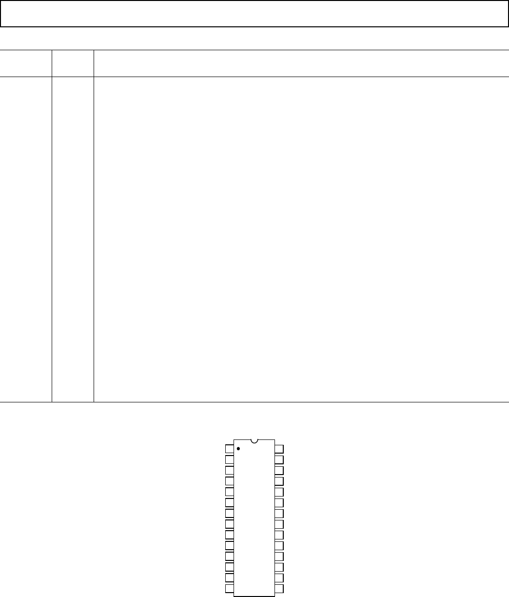
PIN CONFIGURATIONS
17
16
15
20
19
18
28
27
26
25
24
23
22
21
14
13
12
11
10
9
8
1
2
3
4
7
6
5
TOP VIEW
(Not to Scale)
AD9850
D3
D7 MSB/SERIAL LOAD
D6
D5
D4
D2
D1
LSB D0
RESET
DVDD
DGND
DGND
DVDD
W_CLK
FQ_UD
CLKIN
AGND AGND
IOUTB
IOUT
AVDD
R
SET
QOUT
QOUTB
AVDD
VINN
VINP
DACBL (NC)
NC = NO CONNECT
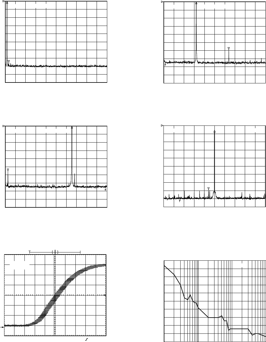
CH1 S Spectrum 10dB/REF –8.6dBm ∆ 76.642 dB
Fxd∆
AD9850 CLOCK _125MHz
RBW # 100Hz
START 0Hz VBW 100Hz ATN # 30dB SWP 762 sec
STOP 62.5MHz
0
Figure 1. SFDR, CLKIN = 125 MHz/FOUT = 1 MHz
CH1 S Spectrum 10dB/REF –10dBm ∆ 54.818 dB
Fxd∆
AD9850 CLOCK _125MHz
RBW # 300Hz
START 0Hz VBW 300Hz ATN # 30dB SWP 182.6 sec
STOP 62.5MHz
0
Figure 2. SFDR, CLKIN = 125 MHz/FOUT = 41 MHz
Tek Run: 100GS/s ET Sample
Ch 1 500mVΩM 20.0ns Ch 1 1.58V
D 500ps Runs After
1
∆: 300ps
@: 25.26ns
Figure 3. Typical Comparator Output Jitter, AD9850
Configured as Clock Generator w/42 MHz LP Filter
(40 MHz AOUT/125 MHz CLKIN)
AD9850–Typical Performance Characteristics
–6– REV. 0
CH1 S Spectrum 10dB/REF –10dBm ∆ 59.925 dB
Fxd∆
AD9850 CLOCK _125MHz
RBW # 300Hz
START 0Hz VBW 300Hz ATN # 30dB SWP 182.6 sec
STOP 62.5MHz
0
Figure 4. SFDR, CLKIN = 125 MHz/FOUT = 20 MHz
CH1 S Spectrum 12dB/REF 0dBm –85.401 dB
∆Mkr
AD9850
RBW # 3Hz
CENTER 4.513579MHz
VBW 3Hz ATN # 20dB SWP 399.5 sec
SPAN 400kHz
0
–23 kHz
Figure 5. SFDR, CLKIN = 20.5 MHz/FOUT = 4.5 MHz
OFFSET FROM 5MHz CARRIER – Hz
–105
–110
–155
–115
–120
–125
–130
–135
–140
–145
–150
100 100k1k
dBc
10k
PN.3RD
Figure 6. Output Phase Noise (5 MHz AOUT/125 MHz
CLKIN)

AD9850
–7–
REV. 0
Tek Run: 50.0GS/s ET Average
Ch1 1.00VΩ M 1.00ns Ch 1 1.74V
Ch 1 Rise
2.870ns
1
Figure 7. Comparator Output Rise Time
(5 V Supply/15 pF Load)
CLKIN – MHz
0 14020 40 60 80 100 120
68
52
SFDR – dB
66
60
58
56
54
64
62
V
CC
= 5V
V
CC
= 3.3V
f
OUT
= 1/3 OF CLKIN
Figure 8. SFDR vs. CLKIN Frequency
(AOUT = 1/3 of CLKIN)
FREQUENCY OUT – MHz
90
80
30 04010
SUPPLY CURRENT – mA
20 30
70
60
50
40
V
CC
= 5V
V
CC
= 3.3V
Figure 9. Supply Current vs. AOUT Frequency
(CLKIN = 125/110 MHz for 5 V/3.3 V Plot)
Tek Run: 50.0GS/s ET Average
Ch1 1.00VΩ M 1.00ns Ch 1 1.74V
Ch 1 Fall
3.202ns
1
Figure 10. Comparator Output Fall Time
(5 V Supply/15 pF Load)
CLOCK FREQUENCY – MHz
0 14020 40 60 80 100 120
90
10
SUPPLY CURRENT – mA
80
50
40
30
20
70
60
V
CC
= 5V
V
CC
= 3.3V
Figure 11. Supply Current vs. CLKIN Frequency
(AOUT = 1/3 of CLKIN)
DAC IOUT – mA
75
70
45 205
SFDR – dB
10 15
65
60
55
50
fOUT = 1MHz
fOUT = 40MHz
fOUT = 20MHz
Figure 12. SFDR vs. DAC IOUT (AOUT = 1/3 of CLKIN)
AD9850
–8– REV. 0
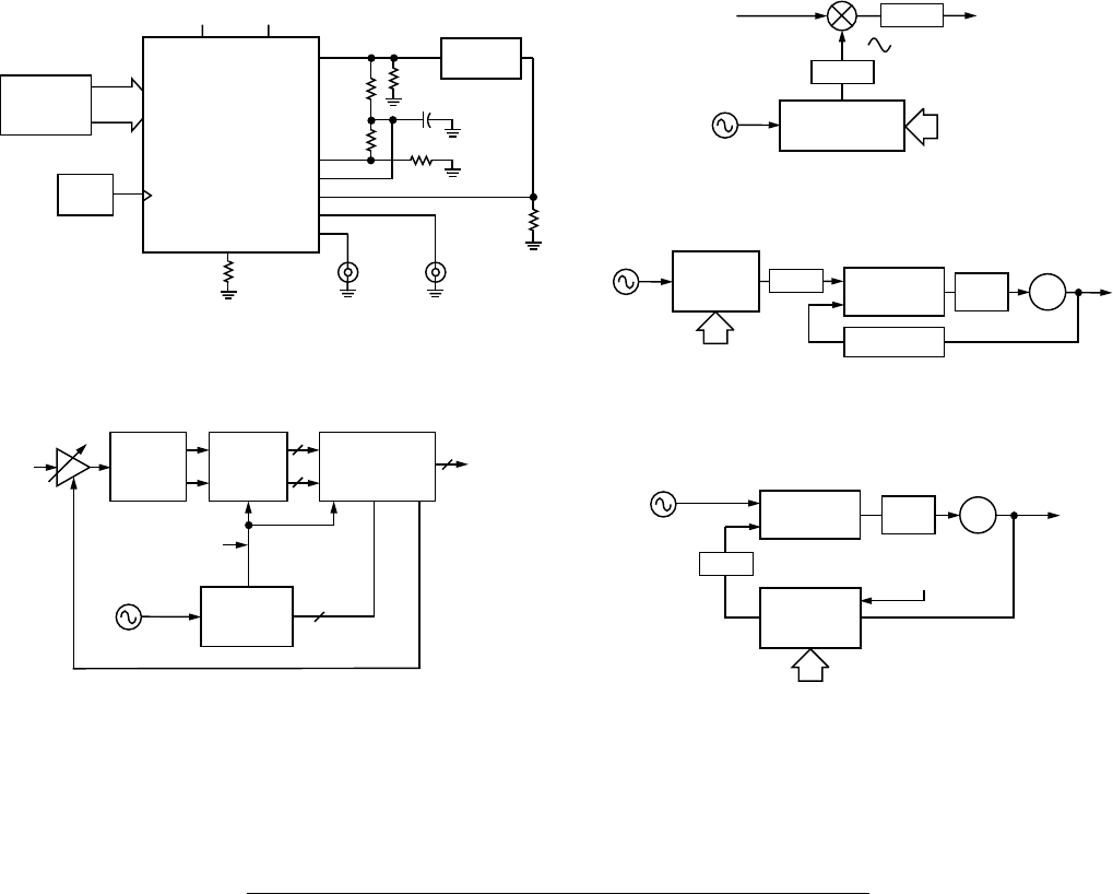
+V
S
DATA
BUS
LOW PASS
FILTER
GND
PROCESSOR
XTAL
OSC
8-b x 5 PARALLEL DATA,
OR 1-b x 40 SERIAL DATA,
RESET, AND 2
CLOCK LINES
CLK
IOUTB
VINN
VINP
QOUT
QOUTB
IOUT
100kΩ
100kΩ
200Ω
100Ω
470pF
200Ω
COMP TRUE
CMOS
CLOCK
OUTPUTS
RSET
AD9850
5-POLE ELLIPTICAL
42MHz LOW PASS
200Ω IMPEDANCE
Figure 13. Basic AD9850 Clock Generator Application
with Low-Pass Filter
VCA
Rx
IF IN
ADC ENCODE
I/Q MIXER
AND
LOW PASS
FILTER
I
Q
8
8
AD9059
DUAL 8-BIT
ADC
DIGITAL
DEMODULATOR
Rx
BASEBAND
DIGITAL
DATA
OUT
ADC CLOCK
FREQUENCY
LOCKED TO Tx CHIP/
SYMBOL PN RATE
AD9850
CLOCK
GENERATOR
32
CHIP/SYMBOL/PN
RATE DATA
125MHz
REFERENCE
CLOCK
AGC
Figure 14. AD9850 Clock Generator Application in a
Spread-Spectrum Receiver
IF
FREQUENCY
IN
TUNING
WORD
AD9850
COMPLETE-DDS
125MHz
REFERENCE
FILTER
FILTER RF
FREQUENCY
OUT
a. Frequency/Phase–Agile Local Oscillator
TUNING
WORD
AD9850
COMPLETE-
DDS
125MHz
REFERENCE
CLOCK
FILTER
RF
FREQUENCY
OUT
PHASE
COMPARATOR LOOP
FILTER VCO
DIVIDE-BY-N
b. Frequency/Phase–Agile Reference for PLL
TUNING WORD
REF
FREQUENCY RF
FREQUENCY
OUT
PHASE
COMPARATOR LOOP
FILTER VCO
FILTER PROGRAMMABLE
“DIVIDE-BY-N”
FUNCTION
AD9850
COMPLETE-
DDS
c. Digitally-Programmable ”Divide-by-N“ Function in PLL
Figure 15. AD9850 Complete-DDS Synthesizer in
Frequency Up-Conversion Applications
THEORY OF OPERATION AND APPLICATION
The AD9850 utilizes direct digital synthesis (DDS) technology,
in the form of a numerically controlled oscillator, to generate a
frequency/phase-agile sine wave. The digital sine wave is con-
verted to analog form via an internal 10-bit high speed D/A con-
verter and an onboard high speed comparator is provided to
translate the analog sine wave into a low-jitter TTL/CMOS-
compatible output square wave. DDS technology is an innova-
tive circuit architecture that allows fast and precise manipulation
of its output frequency, under full digital control. DDS also
enables very high resolution in the incremental selection of out-
put frequency; the AD9850 allows an output frequency resolu-
tion of 0.0291 Hz, with a 125 MHz reference clock applied. The
AD9850’s output waveform is phase-continuous when changed.
The basic functional block diagram and signal flow of the
AD9850 configured as a clock generator is shown in Figure 16.
The DDS circuitry is basically a digital frequency divider function
whose incremental resolution is determined by the frequency of
the reference clock, divided by the 2
N
number of bits in the
tuning word. The phase accumulator is a variable-modulus
counter that increments the number stored in it each time it
receives a clock pulse. When the counter overflows it wraps
around which makes the phase accumulator’s output contigu-
ous. The frequency tuning word sets the modulus of the counter
which effectively determines the size of the increment (∆ Phase)
that gets added to the value in the phase accumulator on the
next clock pulse. The larger the added increment, the faster the
accumulator overflows, which results in a higher output fre-
quency. The AD9850 utilizes an innovative and proprietary
algorithm that mathematically converts the 14-bit truncated
value of the phase accumulator to the appropriate COS value.
This unique algorithm uses a much reduced ROM look-up table
and DSP techniques to perform this function, which contributes
to the small size and low power dissipation of the AD9850. The
relationship of the output frequency, reference clock, and tuning
word of the AD9850 is determined by the formula:
F
OUT
= (∆ Phase × CLKIN)/2
32
where: ∆Phase = value of 32-bit tuning word
CLKIN = input reference clock frequency in MHz
F
OUT
= frequency of the output signal in MHz
The digital sine wave output of the DDS block drives the inter-
nal high speed 10-bit D/A converter which reconstructs the sine
AD9850
–9–
REV. 0
CLK
OUT
PHASE
ACCUMULATOR
TUNING WORD SPECIFIES
OUTPUT FREQUENCY
AS A FRACTION OF REF
CLOCK FREQUENCY
NAMPLITUDE/COS
CONV.
ALGORITHM
DDS CIRCUITRY
D/A
CONVERTER LP COMPARATOR
REF
CLOCK
IN DIGITAL DOMAIN COS (x)
Figure 16. Basic DDS Block Diagram and Signal Flow of AD9850
wave in analog form. This DAC has been optimized for dynamic
performance and low glitch energy as manifested in the low
jitter performance of the AD9850. Since the output of the
AD9850 is a sampled signal, its output spectrum follows the
Nyquist sampling theorem. Specifically, its output spectrum
contains the fundamental plus aliased signals (images) that
occur at multiples of the Reference Clock Frequency ± the
selected output frequency. A graphical representation of the
sampled spectrum, with aliased images, is shown in Figure 17.
20MHz
FUNDAMENTAL 80MHz
1ST IMAGE 120MHz
2ND IMAGE 180MHz
3RD IMAGE 220MHz
4TH IMAGE 280MHz
5TH IMAGE
100MHz
REFERENCE CLOCK
FREQUENCY
fc
fc+fo
fc–fo
2fc–fo
2fc+fo 3fc–fo
fOUT sin(x)/x ENVELOPE x=(pi)fo/fc
SIGNAL AMPLITUDE
Figure 17. Output Spectrum of a Sampled Signal
In this example, the reference clock is 100 MHz and the output
frequency is set to 20 MHz. As can be seen, the aliased images
are very prominent and of a relatively high energy level as deter-
mined by the sin(x)/x roll-off of the quantized D/A converter
output. In fact, depending on the fo/Ref Clk relationship, the
first aliased image can be on the order of –3 dB below the fun-
damental. A low-pass filter is generally placed between the out-
put of the D/A converter and the input of the comparator to
further suppress the effects of aliased images. Obviously, con-
sideration must be given to the relationship of the selected
output frequency and the Reference Clock frequency to avoid
unwanted (and unexpected) output anomalies.
A good rule-of-thumb for applying the AD9850 as a clock
generator is to limit the selected output frequency to <33% of
Reference Clock frequency to avoid generating aliased signals
that fall within, or close to, the output band of interest (gener-
ally dc-selected output frequency). This practice will ease the
complexity (and cost) of the external filter requirement for the
clock generator application.
The reference clock frequency of the AD9850 has a minimum
limitation of 1 MHz. The device has internal circuitry that
senses when the minimum clock rate threshold has been exceeded
and automatically places itself in the power-down mode. When
in this state, if the clock frequency again exceeds the threshold,
the device resumes normal operation. This shutdown mode
prevents excessive current leakage in the dynamic registers of
the device.
The D/A converter output and comparator inputs are available
as differential signals which can be flexibly configured in any
manner desired to achieve the objectives of the end-system. The
typical application of the AD9850 is with single-ended output/
input analog signals, a single low-pass filter, and generating the
comparator reference midpoint from the differential DAC out-
put, as shown in Figure 13.
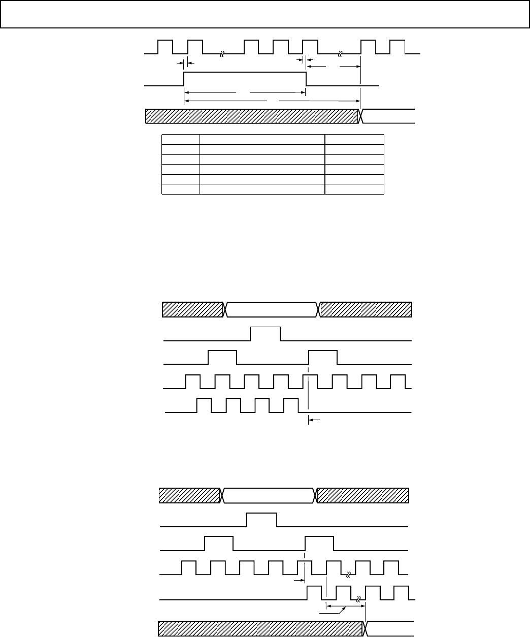
Programming the AD9850
The AD9850 contains a 40-bit register which is used to program
the 32-bit frequency control word, the 5-bit phase modulation
word, and the power-down function. This register can be loaded
in a parallel or serial mode.
In the parallel load mode, the register is loaded via an 8-bit bus;
the full 40-bit word requires five iterations of the 8-bit word.
The W_CLK and FQ_UD signals are used to address and load
the registers. The rising edge of FQ_UD loads the (up to) 40-bit
control data word into the device and resets the address pointer
to the first register. Subsequent W_CLK rising edges load the
8-bit data on words [7:0] and move the pointer to the next reg-
ister. After five loads, W_CLK edges are ignored until either a
reset or an FQ_UD rising edge resets the address pointer to the
first register.
In serial load mode, subsequent rising edges of W_CLK shift
the 1-bit data on Lead 25 (D7) through the 40 bits of program-
ming information. After 40 bits are shifted through, an FQ_UD
pulse is required to update the output frequency (or phase).
The function assignments of the data and control words are
shown in Table III; the detailed timing sequence for updating
the output frequency and/or phase, resetting the device, and
powering-up/down, are shown in the timing diagrams of Figures
18–24.
Note: There are specific control codes, used for factory test
purposes, which render the AD9850 temporarily inoperable.
The user must take deliberate precaution to avoid inputting the
codes listed in Table II.
AD9850
–10– REV. 0
Table II. Factory-Reserved Internal Test Control Codes
Loading Format Factory-Reserved Codes
Parallel 1) W0 = XXXXXX10
2) W0 = XXXXXX01
Serial 1) W32 = 1; W33 = 0
2) W32 = 0; W33 = 1
3) W32 = 1, W33 = 1
Table III. 8-Bit Parallel-Load Data/Control Word Functional Assignment
Word data[7] data[6] data[5] data[4] data[3] data[2] data[1] data[0]
W0 Phase-b4 Phase-b3 Phase-b2 Phase-b1 Phase-b0 Power-Down Control Control
(MSB) (LSB)
W1 Freq-b31 Freq-b30 Freq-b29 Freq-b28 Freq-b27 Freq-b26 Freq-b25 Freq-b24
(MSB)
W2 Freq-b23 Freq-b22 Freq-b21 Freq-b20 Freq-b19 Freq-b18 Freq-b17 Freq-b16
W3 Freq-b15 Freq-b14 Freq-b13 Freq-b12 Freq-b11 Freq-b10 Freq-b9 Freq-b8
W4 Freq-b7 Freq-b6 Freq-b5 Freq-b4 Freq-b3 Freq-b2 Freq-b1 Freq-b0
(LSB)
t
DS
W0* W1 W2 W3 W4
t
DH
t
WH
t
WL
t
WD
t
FD
t
CD
t
FH
t
FL
t
CF
VALID DATA
OLD FREQ (PHASE) NEW FREQ (PHASE)
*OUTPUT UPDATE CAN OCCUR AFTER ANY WORD LOAD
AND IS ASYNCHRONOUS WITH THE REFERENCE CLOCK
DATA
W_CLK
FQ_UD
REF CLK
COS OUT
t
DS
DATA SETUP TIME 3.5ns
t
DH
DATA HOLD TIME 3.5ns
t
WH
W_CLK HIGH 3.5ns
t
WL
W_CLK HIGH 3.5ns
t
WD
W_CLK DELAY AFTER FQ_UD 7.0ns
t
CD
CLK DELAY AFTER FQ_UD 3.5ns
t
FH
FQ_UD HIGH 7.0ns
t
FL
FQ_UD LOW 7.0ns
t
FD
FQ_UD DELAY AFTER W_CLK 7.0ns
t
CF
OUTPUT LATENCY FROM FQ_UD
FREQUENCY CHANGE 18 CLOCK CYCLES
PHASE CHANGE 13 CLOCK CYCLES
SYMBOL DEFINITION MIN
Figure 18. Parallel-Load Frequency/Phase Update Timing Sequence
AD9850
–11–
REV. 0
t
RH
t
RL
t
RR
t
RS
t
OL
COS (0)
REF CLK
COS OUT
RESET
t
RH
CLK DELAY AFTER RESET RISING EDGE 3.5ns
t
RL
RESET FALLING EDGE AFTER CLK 3.5ns
t
RR
RECOVERY FROM RESET 2 CLK CYCLES
t
RS
MINIMUM RESET WIDTH 5 CLK CYCLES
t
OL
RESET OUTPUT LATENCY 13 CLK CYCLES
SYMBOL DEFINITION MIN SPEC
RESULTS OF RESET:
– FREQUENCY/PHASE REGISTER SET TO 0
– ADDRESS POINTER RESET TO W0
– POWER-DOWN BIT RESET TO “0”
– DATA INPUT REGISTER UNEFFECTED
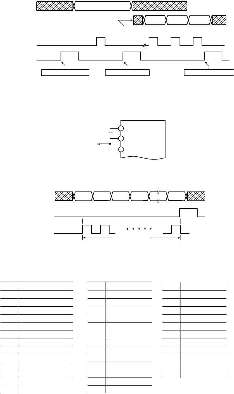
Figure 19. Master Reset Timing Sequence
XXXXX100
DATA (W0)
W_CLK
FQ_UD
REF CLK
INTERNAL CLOCKS DISABLED
DAC STROBE
Figure 20. Parallel-Load Power-Down Sequence/Internal Operation
XXXXX000
DATA (W0)
W_CLK
FQ_UD
REF CLK
INTERNAL CLOCKS ENABLED
DAC STROBE
18 CLOCK CYCLE LATENCY
VALID OUTPUT
COS OUT
Figure 21. Parallel-Load Power-Up Sequence/Internal Operation
AD9850
–12– REV. 0
XXXXX011
DATA (W0)
(PARALLEL)
W_CLK
FQ_UD
NOTE: AT LEAST 1ST 8 BITS OF 40-BIT SERIAL LOAD WORD
IS REQUIRED TO SHIFT IN REQUIRED W32–W34 DATA
RESET ADDRESS TO (W0) ENABLE SERIAL MODE
DATA (SERIAL)
REQUIRED TO RESET CONTROL REGISTERS
RESET CONTROL WORDS
NOTE: FOR DEVICE START-UP IN SERIAL MODE, HARD-WIRE LEAD 2 AT “0," LEAD 3 AT “1," AND LEAD 4 AT “1”
(SEE FIGURE 23).
W32 = 0 W33 = 0 W34 = 0
Figure 22. Serial-Load Enable Sequence
+V SUPPLY
3
4
2
AD9850BRS
Figure 23. Leads 2–4 Connection for Default Serial-Mode Operation
DATA –
W_CLK
FQ_UD
W0 W1 W2 W3 W39
40 W_CLK CYCLES
Figure 24. Serial-Load Frequency/Phase Update Sequence
Table IV. 40-Bit Serial-Load Word Function Assignment
W0 Freq-b0 (LSB)
W1 Freq-b1
W2 Freq-b2
W3 Freq-b3
W4 Freq-b4
W5 Freq-b5
W6 Freq-b6
W7 Freq-b7
W8 Freq-b8
W9 Freq-b9
W10 Freq-b10
W11 Freq-b11
W12 Freq-b12
W13 Freq-b13
W28 Freq-b28
W29 Freq-b29
W30 Freq-b30
W31 Freq-b31 (MSB)
W32 Control
W33 Control
W34 Power-Down
W35 Phase-b0 (LSB)
W36 Phase-b1
W37 Phase-b2
W38 Phase-b3
W39 Phase-b4 (MSB)
W14 Freq-b14
W15 Freq-b15
W16 Freq-b16
W17 Freq-b17
W18 Freq-b18
W19 Freq-b19
W20 Freq-b20
W21 Freq-b21
W22 Freq-b22
W23 Freq-b23
W24 Freq-b24
W25 Freq-b25
W26 Freq-b26
W27 Freq-b27
AD9850
–13–
REV. 0
DATA (7) –
W_CLK
FQ_UD
W32=0 W33=0 W34=1 W35=X W36=X W37=X W38=X W39=X
Figure 25. Serial-Load Power-Down Sequence
V
CC
QOUT/
QOUTB
V
CC
IOUT IOUTB
VINP/
VINN DIGITAL
IN
V
CC
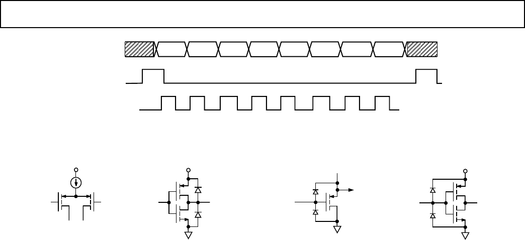
DAC Output Comparator Output Comparator Input Digital Inputs
Figure 26. AD9850 I/O Equivalent Circuits
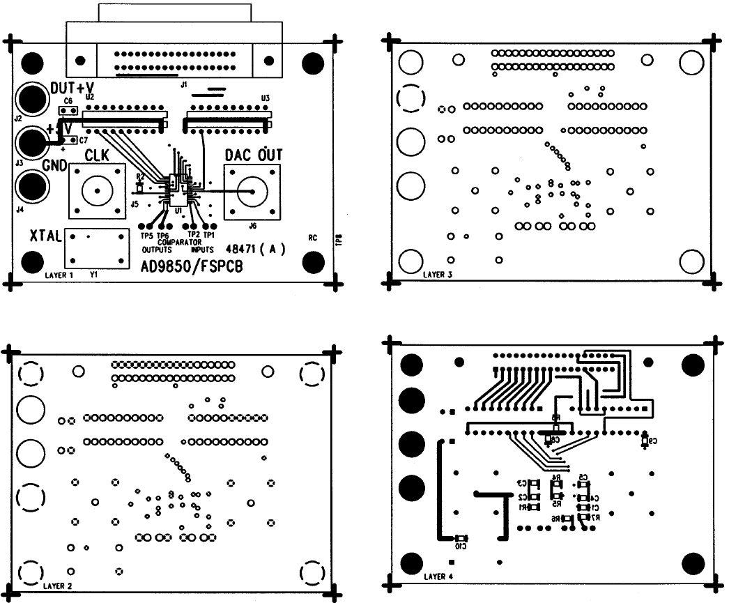
PCB LAYOUT INFORMATION
The AD9850/CGPCB and AD9850/FSPCB evaluation boards
(Figures 27–30) represent typical implementations of the
AD9850 and exemplify the use of high frequency/high resolu-
tion design and layout practices. The printed circuit board that
contains the AD9850 should be a multilayer board that allows
dedicated power and ground planes. The power and ground
planes should be free of etched traces that cause discontinuities
in the planes. It is recommended that the top layer of the multi-
layer board also contain interspatial ground plane which makes
ground available for surface-mount devices. If separate analog
and digital system ground planes exist, they should be con-
nected together at the AD9850 for optimum results.
Avoid running digital lines under the device as these will couple
noise onto the die. The power supply lines to the AD9850
should use as large of a track as possible to provide a low-
impedance path and reduce the effects of glitches on the power
supply line. Fast switching signals like clocks should be shielded
with ground to avoid radiating noise to other sections of the
board. Avoid crossover of digital and analog signal paths. Traces
on opposite sides of the board should run at right angles to each
other. This will reduce the effects of feedthrough through the
circuit board. Use microstrip techniques where possible.
Good decoupling is also an important consideration. The analog
(AVDD) and digital (DVDD) supplies to the AD9850 are
independent and separately pinned out to minimize coupling
between analog and digital sections of the device. All analog
and digital supplies should be decoupled to AGND and DGND
respectively with high quality ceramic capacitors. To achieve
best performance from the decoupling capacitors, they should
be placed as close as possible to the device, ideally right up
against the device. In systems where a common supply is used to
drive both the AVDD and DVDD supplies of the AD9850, it is
recommended that the system’s AVDD supply be used.
Analog Devices, Inc., applications engineering support is avail-
able to answer additional questions on grounding and PCB lay-
out. Call 1-800-ANALOGD.
Evaluation Boards
Two versions of evaluation boards are available for the AD9850
that facilitate the implementation of the device for benchtop analy-
sis, and serve as a reference for PCB layout. The AD9850/FSPCB
is intended for applications where the device will primarily be
used as frequency synthesizer. This version facilitates connec-
tion of the AD9850’s internal D/A converter output to a 50Ω
spectrum analyzer input; the internal comparator on the
AD9850 DUT is not enabled (see Figure 28 for electrical sche-
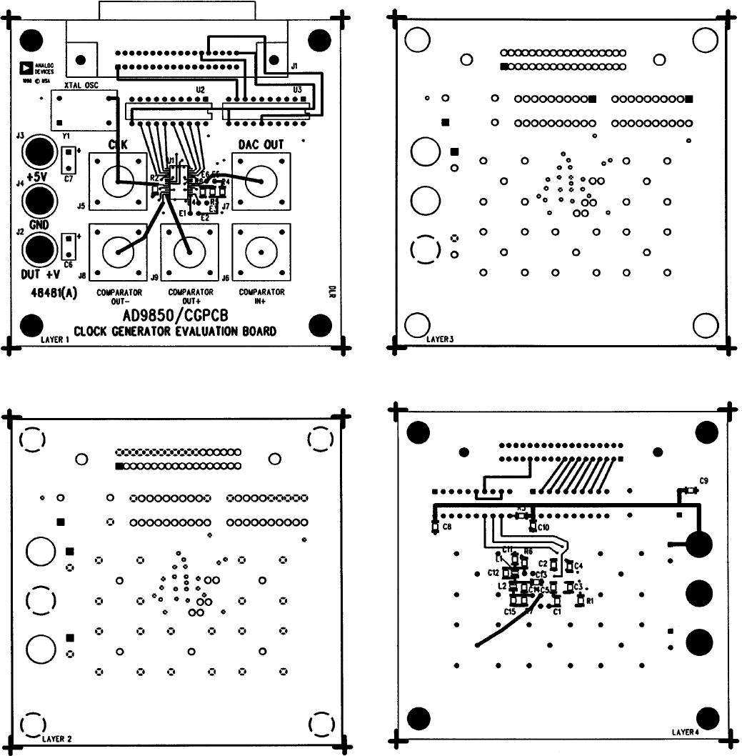
matic of AD9850/FSPCB). The AD9850/CGPCB is intended
for applications using the device in the clock generator mode. It
connects the AD9850’s DAC output to the internal comparator
input via a single-ended, 42 MHz low-pass, 5-pole Elliptical
filter. This model facilitates the access of the AD9850’s com-
parator output for evaluation of the device as a frequency-
and phase-agile clock source (see Figure 29 for electrical sche-
matic of AD9850/CGPCB).
Both versions of the AD9850 evaluation boards are designed to
interface to the parallel printer port of a PC. The operating soft-
ware runs under Microsoft Windows and provides a user-
friendly and intuitive format for controlling the functionality
and observing the performance of the device. The 3.5" floppy
provided with the evaluation board contains an executable file
which loads and displays the AD9850 function-selection screen.
The evaluation board may be operated with +3.3 V or +5 V
supplies. The evaluation boards are configured at the factory for
an external reference clock input; if the onboard crystal clock
source is utilized, remove R2.
AD9850
–14– REV. 0
AD9850/XXPCB Evaluation Board Instructions
Required hardware/software:
IBM compatible computer operating in a Windows™ environment
Printer port and Centronics compatible printer cable
3.5" disk drive
Mouse
AD9850 evaluation board software disk
AD9850/XXPCB evaluation board
XTAL clock or signal generator—if using a signal generator, dc
offset the clock signal to 1/2 the supply voltage and apply at
least 3 V p-p signal across the 50 Ω (R2) input resistor. Remove
R2 for a high Z clock input impedance.
+3.3 V or +5 V supply
Setup:
Copy the contents of the AD9850 disk onto host computer’s
hard drive.
Connect printer cable from computer’s printer port to the
AD9850/XXPCB evaluation board.
Apply power to AD9850/XXPCB evaluation board.
Apply external TTL-compatible reference clock to the AD9850/
XXPCB evaluation board or install crystal clock source in
socket (remember to remove R2).
Locate the WIN9850.EXE file and execute that program.
Your monitor should display a “control panel” to allow opera-
tion of the AD9850/XXPCB evaluation board.
Operation:
On the control panel, locate the box called “COMPUTER I/O.”
With the mouse (or by tabbing over) click on the selection
marked “LPT1” and then click on the “TEST” box. A message
will appear indicating whether or not this choice of output ports
is valid. Choose alternate ports as necessary to achieve a correct
setting.
On the control panel, click on “MASTER RESET” button.
This will reset the AD9850 to 0 Hz, 0° COS phase; the DAC
output should be a dc voltage equal to the full-scale output of
the AD9850.
Place the cursor in the “CLOCK” box and type in the exact
clock frequency in MHz that will be applied to the evaluation
board. Click on the “LOAD” button (or press enter on the
keyboard).
Place the cursor in the “OUTPUT FREQUENCY” box and
type in the desired output frequency in MHz. Click on the
“LOAD” button (or press enter on the keyboard). The BUS
MONITOR display on the control panel will display the hexa-
decimal value of the input 32-bit tuning word. Upon completion
of this step, the AD9850/XXPCB evaluation board should be
generating the desired sine wave. (Note: VER 1.1 of the
AD9850/XXPCB operating software is resolution limited to the
nearest Hz.)
Changing the phase of the AD9850/XXPCB’s output sine
wave is accomplished by clicking on the down arrow in the
“OUTPUT PHASE DELAY” box, selecting the desired delay
increment, and clicking on the “LOAD” button.
Other operational modes available on the control panel are acti-
vated by pointing and clicking.
The AD9850/FSPCB provides access into and out of the on-
chip comparator via test point pairs (each pair has an active in-
put and a ground connection). The two active inputs are labeled
TP1 and TP2. The unmarked hole next to each labeled test
point is a ground connection. The two active outputs are labeled
TP5 and TP6. Adjacent to each of those test points are un-
marked ground connections.
The AD9850/CGPCB provides BNC inputs and outputs associ-
ated with the on-chip comparator and the on-board, 5th order,
200 Ω input/output Z, elliptic 45 MHz low-pass filter. Jumpering
(soldering a wire between) E1 to E2, E3 to E4, and E5 to E6 will
connect the on-board filter and the midpoint switching voltage
to the comparator. Users may elect to insert their own filter and
threshold voltage by removing the jumpers and inserting a filter
between J7 and J6 and providing a threshold voltage at E1.
If you choose to utilize the XTAL socket to supply the clock to
the AD9850 DUT, you must remove R2 (50 Ω chip resistor).
The XTAL oscillator must be either TTL or (preferably)
CMOS compatible.

AD9850
–15–
REV. 0
14
XTAL
OSC
8
GND
VCC
Y1
SW41
7
+5V
OUT
R2
50Ω
J5
CLKIN
REMOVE
WHEN
USING Y1
J6
R1
3.9kΩC1
0.01pF
R5
25Ω
17
16
15
20
19
18
28
27
26
25
24
23
22
21
14
13
12
11
10
9
8
1
2
3
4
7
6
5
U1
AD9850
D3
D2
D1
DGND
VDD
W_CLK
FQ_UD
CLKIN
AGND
AVCC
R
SET
QOUT
QOUTB
D0 D7
D6
D5
D4
RESET
VDD
DGND
AGND
IOUTB
IOUT
AVCC
VINN
VINP
DACBP
D3
D2
D1
D0
GND
+V
D7
D6
D5
D4
+V
GND
RESET
GND
WCLK
CLKIN
GND
+V
FQUD
+V
10mA
RESET
TP5
TP6
TP7
TP8
GND
GND
GND
GND
TP1
TP2
TP3
TP4
R4
50Ω
DAC OUT
TO 50Ω
COMPARATOR
INPUTS
R6
1kΩ
R7
1kΩ
GND
+V
COMPARATOR
OUTPUTS
RESET
WCLK
FQUD
CHECK
RRESET
WWCLK
FFQUD
RRESET
12
13
14
15
16
17
18
19
8Q
7Q
6Q
5Q
4Q
3Q
2Q
1Q
8D
7D
6D
5D
4D
3D
2D
1D
9
8
7
6
5
4
3
2
U3
74HCT574
C,K OE
11 1
STROBE
C36CRPX
J1
D0
D1
D2
D3
D4
D5
D6
D7
12
13
14
15
16
17
18
19
8Q
7Q
6Q
5Q
4Q
3Q
2Q
1Q
8D
7D
6D
5D
4D
3D
2D
1D
9
8
7
6
5
4
3
2
U2
74HCT574
C,K OE
11 1
STROBE
RRESET
1
2
3
4
5
6
7
8
9
10
11
12
13
14
15
16
17
18
19
20
21
22
23
24
25
26
27
28
29
30
31
32
33
34
35
36
FFQUD
WWCLK
STROBE
CHECK
P
O
R
T
1
+V +5V C2
0.1µFC3
0.1µFC4
0.1µFC5
0.1µFC8
0.1µFC9
0.1µFC10
0.1µF
C6
10µFC7
10µF
+V +5V
STROBE
+5V
R3
2.2kΩ
J2
J3
J4
BANANA
JACKS
+V
+5V
GND
H1
#6 H2
#6 H3
#6 H4
#6
MOUNTING
HOLES
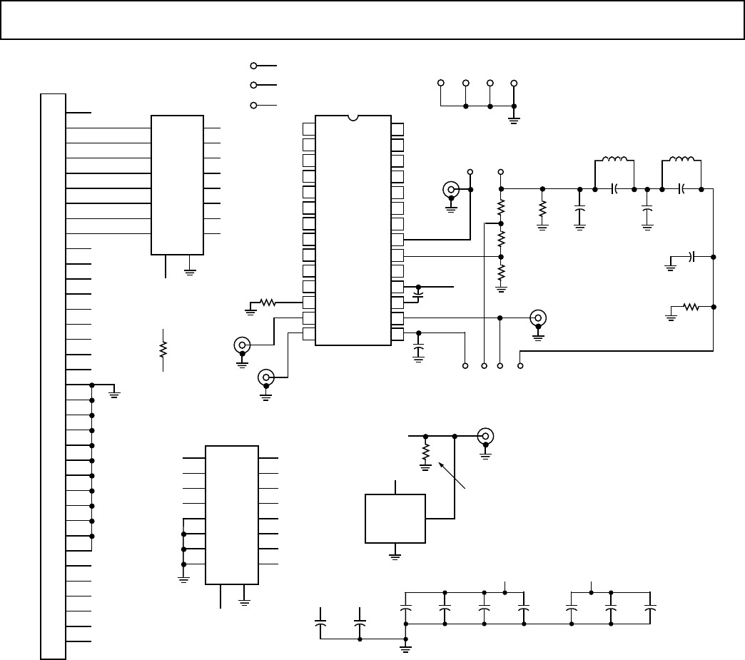
Figure 27. AD9850/FSPCB Electrical Schematic
COMPONENT LIST
Integrated Circuits
U1 AD9850BRS (28-Pin SSOP)
U2, U3 74HCT574 H-CMOS Octal Flip-Flop
Capacitors
C2–C5, C8–C10 0.1 µF Ceramic Chip Capacitor
C6, C7 10 µF Ceramic Chip Capacitor
Resistors
R1 3.9 kΩ Resistor
R2, R4 50 Ω Resistor
R3 2.2 kΩ Resistor
R5 25 Ω Resistor
R6, R7 1 kΩ Resistor
Connectors
J1 36-Pin D Connector
J2, J3 Banana Jack
J5, J6 BNC Connector
AD9850
–16– REV. 0
a. AD9850/FSPCB Top Layer
b. AD9850/FSPCB Ground Plane
c. AD9850/FSPCB Power Plane
d. AD9850/FSPCB Bottom Layer
Figure 28. AD9850/FSPCB Evaluation Board Layout
AD9850
–17–
REV. 0
14
XTAL
OSC
8
GND
VCC
Y1
SW41
7
+5V
OUT
R2
50Ω
J5
CLKIN
REMOVE
WHEN
USING Y1
BNC
R1
3.9kΩC1
0.01pF
100Ω
17
16
15
20
19
18
28
27
26
25
24
23
22
21
14
13
12
11
10
9
8
1
2
3
4
7
6
5
U1
AD9850
D3
D2
D1
DGND
VDD
W_CLK
FQ_UD
CLKIN
AGND
AVCC
RSET
QOUT
QOUTB
D0 D7
D6
D5
D4
RESET
VDD
DGND
AGND
IOUTB
IOUT
AVCC
VINN
VINP
DACBP
D3
D2
D1
D0
GND
+V
D7
D6
D5
D4
+V
GND
RESET
GND
WCLK
CLKIN
GND
+V
FQUD
+V
10mA
RESET
E3E4E2E1
200Ω
200Ω Z
42MHz ELLIPTIC
LOW PASS FILTER
BNC
BNC
470pF
J6
100kΩ
100kΩ
E5
E6
22µF
3.3pF
12
L1
1008CS
910nH
33pF
8.2pF
12
L2
1008CS
680nH
22pF
200Ω
RESET
WCLK
FQUD
CHECK
RRESET
WWCLK
FFQUD
RRESET
12
13
14
15
16
17
18
19
8Q
7Q
6Q
5Q
4Q
3Q
2Q
1Q
8D
7D
6D
5D
4D
3D
2D
1D
9
8
7
6
5
4
3
2
U3
74HCT574
C,K OE
11 1
STROBE
C36CRPX
J1
D0
D1
D2
D3
D4
D5
D6
D7
12
13
14
15
16
17
18
19
8Q
7Q
6Q
5Q
4Q
3Q
2Q
1Q
8D
7D
6D
5D
4D
3D
2D
1D
9
8
7
6
5
4
3
2
U2
74HCT574
C,K OE
11 1
STROBE
RRESET
1
2
3
4
5
6
7
8
9
10
11
12
13
14
15
16
17
18
19
20
21
22
23
24
25
26
27
28
29
30
31
32
33
34
35
36
FFQUD
WWCLK
STROBE
CHECK
P
O
R
T
1
+V +5V C2
0.1µFC3
0.1µFC4
0.1µFC5
0.1µFC8
0.1µFC9
0.1µFC10
0.1µF
C6
10µFC7
10µF
+V +5V
STROBE
+5V
R3
2.2kΩ
J2
J3
J4
BANANA
JACKS
+V
+5V
GND
H1
#6 H2
#6 H3
#6 H4
#6
MOUNTING
HOLES
Figure 29. AD9850/CGPCB Electrical Schematic
COMPONENT LIST
Integrated Circuits
U1 AD9850BRS (28-Pin SSOP)
U2, U3 74HCT574 H-CMOS Octal Flip-Flop
Capacitors
C1 470 pF Ceramic Chip Capacitor
C2–C5, C8–C10 0.1 µF Ceramic Chip Capacitor
C6, C7 10 µF Ceramic Chip Capacitor
C11 22 µF Ceramic Chip Capacitor
C12 3.3 pF Ceramic Chip Capacitor
C13 33 pF Ceramic Chip Capacitor
C14 8.2 pF Ceramic Chip Capacitor
C15 22 pF Ceramic Chip Capacitor
Resistors
R1 3.9 kΩ Resistor
R2 50 Ω Resistor
R3 2.2 kΩ Resistor
R4, R5 100 kΩ Resistor
R6, R7 200 Ω Resistor
R8 100 Ω Resistor
Connectors
J2, J3, J4 Banana Jack
J5–J9 BNC Connector
Inductors
L1 910 nH Surface Mount
L2 680 nH Surface Mount
AD9850
–18– REV. 0
a. AD9850/FSPCB Top Layer
b. AD9850/FSPCB Ground Plane
c. AD9850/FSPCB Power Plane
d. AD9850/FSPCB Bottom Layer
Figure 30. AD9850/FSPCB Evaluation Board Layout
AD9850
–19–
REV. 0
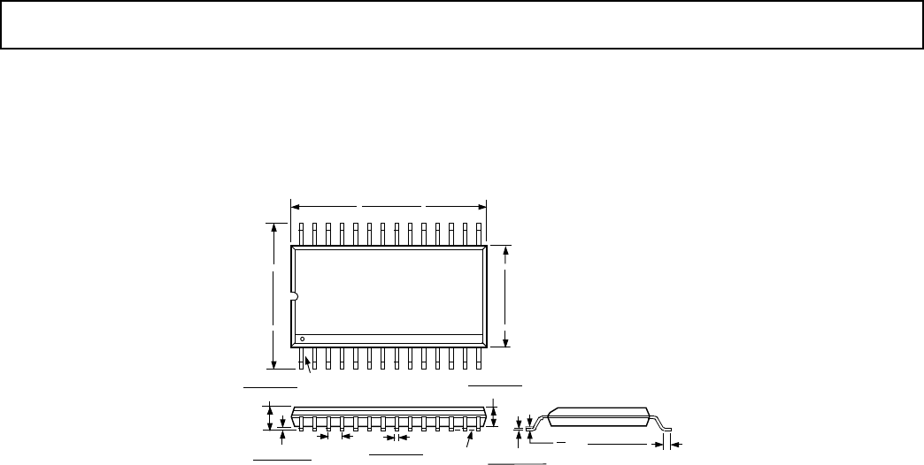
OUTLINE DIMENSIONS
Dimensions shown in inches and (mm).
28-Lead Shrink Small Outline Package
(RS-28)
28 15
141
0.407 (10.34)
0.397 (10.08)
0.311 (7.9)
0.301 (7.64)
0.212 (5.38)
0.205 (5.21)
PIN 1
SEATING
PLANE
0.008 (0.203)
0.002 (0.050)
0.07 (1.79)
0.066 (1.67)
0.0256
(0.65)
BSC
0.078 (1.98)
0.068 (1.73)
0.015 (0.38)
0.010 (0.25) 0.009 (0.229)
0.005 (0.127)
0.03 (0.762)
0.022 (0.558)
8°
0°
–20–
C2155–18–7/96
PRINTED IN U.S.A.
