ADL5801 (Rev. E) RF 3800
User Manual: RF-3800
Open the PDF directly: View PDF ![]() .
.
Page Count: 41
- Features
- Applications
- Functional Block Diagram
- General Description
- Table of Contents
- Specifications
- Absolute Maximum Ratings
- Pin Configuration and Function Descriptions
- Typical Performance Characteristics
- Downconverter Mode with a Broadband Balun
- Downconverter Mode with a Mini-Circuits® TC1-1-43M+ Input Balun
- Downconverter Mode with a Johanson 3.5 GHz Input Balun
- Downconverter Mode with a Johanson 5.7 GHz Input Balun
- Upconverter Mode with a 900 MHz Output Match
- Upconverter Mode with a 2.1 GHz Output Match
- Spur Performance
- Circuit Description
- Applications Information
- Evaluation Board
- Outline Dimensions
High IP3,
10 MHz to 6 GHz, Active Mixer
Data Sheet
ADL5801
FEATURES
Broadband upconverter/downconverter
Power conversion gain of 1.8 dB
Broadband RF, LO, and IF ports
SSB noise figure (NF) of 9.75 dB
Input IP3: 28.5 dBm
Input P1dB: 13.3 dBm
Typical LO drive: 0 dBm
Single-supply operation: 5 V at 130 mA
Adjustable bias for low power operation
Exposed paddle, 4 mm × 4 mm, 24-lead LFCSP package
APPLICATIONS
Cellular base station receivers
Radio link downconverters
Broadband block conversion
Instrumentation
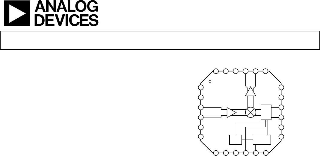
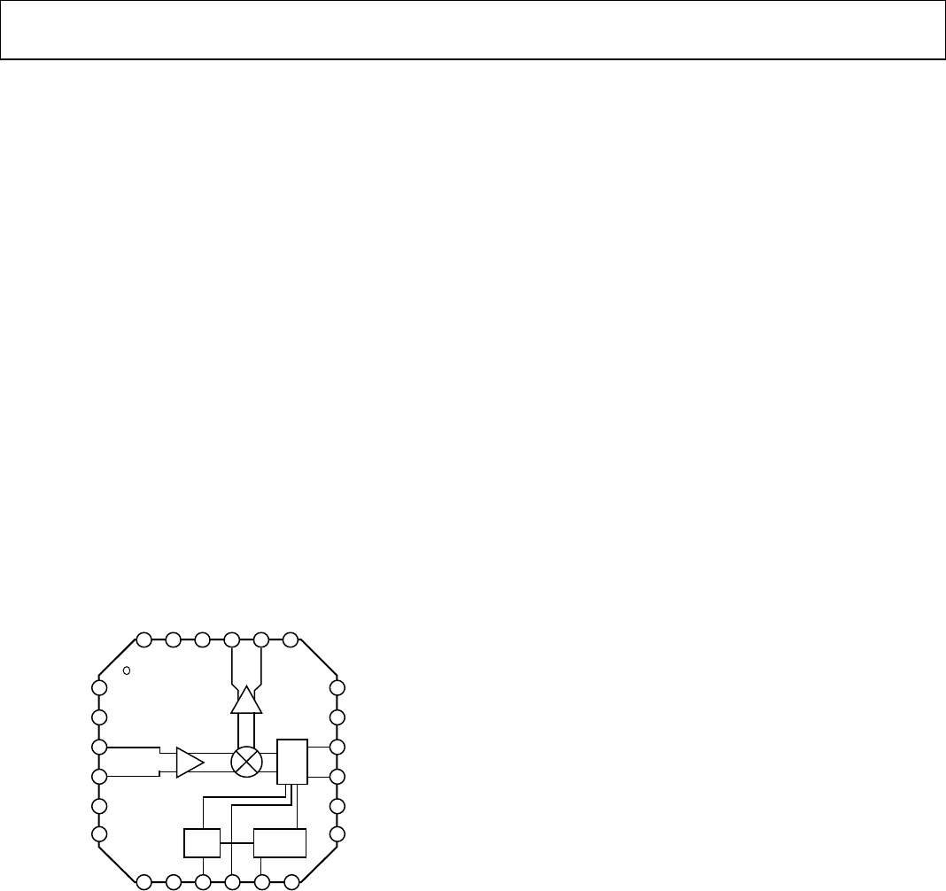
FUNCTIONAL BLOCK DIAGRAM
08079-001
GNDVPLO ENBL VSET
VPDT
GND
RFIP
NC
GND
VPLO
7 8
15
16
17
18
2122
23
ADL5801
19
20
GNDIFON
13
14
DETO GND
VPRF
GND
GND
GND
IFOP
RFIN
GND
GND
LOIP
LOIN
6
5
4
3
2
1
24
910 11 12
DETBIAS
V2I
Figure 1.
GENERAL DESCRIPTION
The ADL5801 uses a high linearity, doubly balanced, active
mixer core with integrated LO buffer amplifier to provide high
dynamic range frequency conversion from 10 MHz to 6 GHz.
The mixer benefits from a proprietary linearization architecture
that provides enhanced input IP3 performance when subject to
high input levels. A bias adjust feature allows the input linearity,
SSB noise figure, and dc current to be optimized using a single
control pin. An optional input power detector is provided for
adaptive bias control. The high input linearity allows the device
to be used in demanding cellular applications where in-band
blocking signals may otherwise result in degradation in dynamic
performance. The adaptive bias feature allows the part to provide
high input IP3 performance when presented with large blocking
signals. When blockers are removed, the ADL5801 can auto-
matically bias down to provide low noise figure and low power
consumption.
The balanced active mixer arrangement provides superb LO-to-
RF and LO-to-IF leakage, typically better than −40 dBm. The IF
outputs are designed to provide a typical voltage conversion
gain of 7.8 dB when loaded into a 200 Ω load. The broad
frequency range of the open-collector IF outputs allows the
ADL5801 to be applied as an upconverter for various transmit
applications.
The ADL5801 is fabricated using a SiGe high performance IC
process. The device is available in a compact 4 mm × 4 mm,
24-lead LFCSP package and operates over a −40°C to +85°C
temperature range. An evaluation board is also available.
Rev. E Document Feedback
Information furnished by Analog Devices is believed to be accurate and reliable. However, no
responsibility is assumed by Analog Devices for its use, nor for any infringements of patents or other
rights of third parties that may result from its use. Specifications subject to change without notice. No
license is granted by implication or otherwise under any patent or patent rights of Analog Devices.
Trademarks and registered trademarks are the property of their respective owners.
One Technology Way, P.O. Box 9106, Norwood, MA 02062-9106, U.S.A.
Tel: 781.329.4700 ©2010–2014 Analog Devices, Inc. All rights reserved.
Technical Support www.analog.com

ADL5801* PRODUCT PAGE QUICK LINKS
Last Content Update: 02/23/2017
COMPARABLE PARTS
View a parametric search of comparable parts.
EVALUATION KITS
•ADL5801 Evaluation Board
DOCUMENTATION
Data Sheet
•ADL5801: High IP3, 10 MHz to 6 GHz, Active Mixer Data
Sheet
TOOLS AND SIMULATIONS
• ADIsimPLL™
•ADIsimRF
REFERENCE DESIGNS
•CN0239
•CN0360
•CN0369
REFERENCE MATERIALS
Press
• Analog Devices’ 4-GHz PLL Synthesizer Offers Leading
Phase Noise Performance
• New Analog Devices’ PLL Synthesizers Deliver Utmost
Flexibility and Phase Noise Performance
•New PLLs Deliver Widest Frequency Range Coverage and
Lowest VCO Phase Noise in a Single Device
Product Selection Guide
•RF Source Booklet
Technical Articles
•MS-2739: High Dynamic IF Receiver Simplifies Design of
Next Generation µW Point-to-Point Modems
DESIGN RESOURCES
•ADL5801 Material Declaration
•PCN-PDN Information
•Quality And Reliability
•Symbols and Footprints
DISCUSSIONS
View all ADL5801 EngineerZone Discussions.
SAMPLE AND BUY
Visit the product page to see pricing options.
TECHNICAL SUPPORT
Submit a technical question or find your regional support
number.
DOCUMENT FEEDBACK
Submit feedback for this data sheet.
This page is dynamically generated by Analog Devices, Inc., and inserted into this data sheet. A dynamic change to the content on this page will not
trigger a change to either the revision number or the content of the product data sheet. This dynamic page may be frequently modified.

ADL5801 Data Sheet
TABLE OF CONTENTS
Features .............................................................................................. 1
Applications ....................................................................................... 1
Functional Block Diagram .............................................................. 1
General Description ......................................................................... 1
Revision History ............................................................................... 2
Specifications ..................................................................................... 3
Absolute Maximum Ratings ............................................................ 6
ESD Caution .................................................................................. 6
Pin Configuration and Function Descriptions ............................. 7
Typical Performance Characteristics ............................................. 8
Downconverter Mode with a Broadband Balun ...................... 8
Downconverter Mode with a Mini-Circuits® TC1-1-43M+
Input Balun .................................................................................. 12
Downconverter Mode with a Johanson 3.5 GHz
Input Balun .................................................................................. 14
Downconverter Mode with a Johanson 5.7 GHz
Input Balun .................................................................................. 16
Upconverter Mode with a 900 MHz Output Match .............. 18
Upconverter Mode with a 2.1 GHz Output Match ................ 20
Spur Performance ....................................................................... 23
Circuit Description......................................................................... 27
LO Amplifier and Splitter.......................................................... 27
RF Voltage-to-Current (V-to-I) Converter ............................. 27
Mixer Core .................................................................................. 27
Mixer Output Load .................................................................... 27
RF Detector ................................................................................. 28
Bias Circuit .................................................................................. 28
Applications Information .............................................................. 31
Basic Connections ...................................................................... 31
RF and LO Ports ......................................................................... 31
IF Port .......................................................................................... 32
Downconverting to Low Frequencies ...................................... 33
Broadband Operation ................................................................ 34
Single-Ended Drive of RF and LO Inputs ............................... 36
Evaluation Board ............................................................................ 38
Outline Dimensions ....................................................................... 40
Ordering Guide .......................................................................... 40
REVISION HISTORY
4/14—Rev. D to Rev. E
Changes to Figure 1 .......................................................................... 1
Changes to Table 1 ............................................................................ 4
Changes to Figure 87 and Deleted Table 4; Renumbered
Sequentially ..................................................................................... 27
Changes to RF Detector Section and Bias Circuit Section;
Added Table 4 and Table 5; Renumbered Sequentially, and
Added Figure 92, Figure 93, Figure 94, and Figure 95;
Renumbered Sequentially .............................................................. 29
3/14—Rev. C to Rev. D
Changes to Pin 9, Table 3 ................................................................. 7
8/13—Rev. B to Rev. C
Changes to Table 8 .......................................................................... 38
7/13—Rev. A to Rev. B
Added Disable Voltage and Enable Voltage; Table 1 .................... 3
Changes to Table 5 and Figure 96 ................................................. 31
Added Downconverting to Low Frequencies Section and
Figure 97; Renumbered Sequentially ........................................... 32
Added Broadband Operation Section and Figure 98 to
Figure 101 ........................................................................................ 33
Added Single-Ended Drive of RF and LO Inputs Section and
Figure 102 to Figure 105 ................................................................ 35
Updated Outline Dimensions ....................................................... 39
7/11—Rev. 0 to Rev. A
Changes to Specifications Section ................................................... 3
Changes to Typical Performance Characteristics Section ........... 8
Changes to Spur Performance Section ........................................ 23
Changes to RF Voltage-to-Current (V-to-I) Converter
Section .............................................................................................. 27
Changes to RF Detector Section ................................................... 28
Changes to RF and LO Ports Section ........................................... 30
2/10—Revision 0: Initial Version
Rev. E | Page 2 of 40

Data Sheet ADL5801
SPECIFICATIONS
VS = 5 V, T A = 25°C, fRF = 900 MHz, fLO = (fRF − 153 MHz), LO power = 0 dBm, Z01 = 50 Ω, VSET = 3.6 V, unless otherwise noted.
Table 1.
Parameter Test Conditions Min Typ Max Unit
RF INPUT INTERFACE
Return Loss Tunable to >20 dB over a limited bandwidth 12 dB
Input Impedance 50 Ω
RF Frequency Range 10 6000 MHz
OUTPUT INTERFACE
Output Impedance Differential impedance, f = 200 MHz 230 Ω
IF Frequency Range Can be matched externally to 3000 MHz LF 600 MHz
DC Bias Voltage2 Externally generated 4.75 VS 5.25 V
LO INTERFACE
LO Power −10 0 +10 dBm
Return Loss 15 dB
Input Impedance 50 Ω
LO Frequency Range 10 6000 MHz
POWER INTERFACE
Supply Voltage 4.75 5 5.25 V
Quiescent Current Resistor programmable 130 200 mA
Disable Current ENBL pin high to disable the device 50 mA
Disable Voltage ENBL pin high to disable the device 2.5 5 V
Enable Voltage ENBL pin low to enable the device 0 1.8 V
Enable Time Time from ENBL pin low to enable 182 ns
Disable Time Time from ENBL pin high to disable 28 ns
DYNAMIC PERFORMANCE at fRF = 900 MHz/1900 MHz3
Power Conversion Gain4 fRF = 900 MHz 1.8 dB
fRF = 1900 MHz 1.8 dB
Voltage Conversion Gain
5
f
RF
= 900 MHz
7.8
dB
fRF = 1900 MHz 7.8 dB
SSB Noise Figure fCENT = 900 MHz, VSET = 2.0 V 9.75 dB
fCENT = 1900 MHz, VSET = 2.0 V 11.5 dB
SSB Noise Figure Under Blocking6 fCENT = 900 MHz 19.5 dB
fCENT = 1900 MHz 20 dB
Input Third-Order Intercept7 fCENT = 900 MHz 28.5 dBm
fCENT = 1900 MHz 26.4 dBm
Input Second-Order Intercept8 fCENT = 900 MHz 63 dBm
fCENT = 1900 MHz 49.7 dBm
Input 1 dB Compression Point fRF = 900 MHz 13.3 dBm
f
RF
= 1900 MHz
12.7
dBm
LO-to-IF Output Leakage Unfiltered IF output −27 dBm
LO-to-RF Input Leakage −30 dBm
RF-to-IF Output Isolation −35 dBc
IF/2 Spurious9 0 dBm input power, fRF = 900 MHz −67.5 dBc
0 dBm input power, fRF = 1900 MHz −53 dBc
IF/3 Spurious9 0 dBm input power, fRF = 900 MHz −65.5 dBc
0 dBm input power, fRF = 1900 MHz −72.6 dBc
Rev. E | Page 3 of 40

ADL5801 Data Sheet
Parameter Test Conditions Min Typ Max Unit
DYNAMIC PERFORMANCE at fRF = 2500 MHz10
Power Conversion Gain11 −6.1 dB
Voltage Conversion Gain5 −0.1 dB
SSB Noise Figure fCENT = 2500 MHz, VSET = 2.0 V 10.6 dB
Input Third-Order Intercept12
f
CENT
= 2500 MHz
25.5
dBm
Input Second-Order Intercept13 fCENT = 2500 MHz 45.3 dBm
Input 1 dB Compression Point fCENT = 2500 MHz 13.8 dBm
LO-to-IF Output Leakage
Unfiltered IF output
−31.5
dBm
LO-to-RF Input Leakage −31.2 dBm
RF-to-IF Output Isolation −42.5 dBc
IF/2 Spurious9 0 dBm input power, fRF = 2600 MHz −50.6 dBc
IF/3 Spurious9 0 dBm input power, fRF = 2600 MHz −59.8 dBc
DYNAMIC PERFORMANCE at fRF = 3500 MHz14
Power Conversion Gain15 −6.44 dB
Voltage Conversion Gain5 −0.44 dB
SSB Noise Figure fCENT = 3500 MHz, VSET = 3.6 V 15.8 dB
Input Third-Order Intercept7 fCENT = 3500 MHz, VSET = 3.6 V 26.5 dBm
Input Second-Order Intercept8 fCENT = 3500 MHz, VSET = 3.6 V 42.3 dBm
Input 1 dB Compression Point 12.5 dBm
LO-to-IF Output Leakage Unfiltered IF output −30.2 dBm
LO-to-RF Input Leakage −29.4 dBm
RF-to-IF Output Isolation
−29.7
dBc
IF/2 Spurious9 0 dBm input power, fRF = 3800 MHz −47.1 dBc
IF/3 Spurious9 0 dBm input power, fRF = 3800 MHz −57.8 dBc
DYNAMIC PERFORMANCE at f
RF
= 5500 MHz16
Power Conversion Gain17 −5.2 dB
Voltage Conversion Gain5 0.8 dB
SSB Noise Figure fCENT = 5500 MHz, VSET = 3.6 V 16.2 dB
Input Third-Order Intercept7 fCENT = 5500 MHz, VSET = 3.6 V 22.7 dBm
Input Second-Order Intercept 8 fCENT = 5500 MHz, VSET = 3.6 V 35.4 dBm
Input 1 dB Compression Point 11.3 dBm
LO-to-IF Output Leakage Unfiltered IF output −42.6 dBm
LO-to-RF Input Leakage −28.9 dBm
RF-to-IF Output Isolation −46.7 dBc
IF/2 Spurious9 0 dBm input power, fRF = 5800 MHz −44 dBc
IF/3 Spurious9
0 dBm input power, f
RF
= 5800 MHz
−47
dBc
DYNAMIC PERFORMANCE at fIF = 900 MHz18
Power Conversion Gain19 −6 dB
Voltage Conversion Gain
5
0
dB
SSB Noise Figure fIF = 900 MHz, fRF = 250 MHz, VSET = 2.0 V 10.6 dB
Output Third-Order Intercept20 fCENT = 153 MHz, VSET = 3.6 V 30.6 dBm
Output Second-Order Intercept 21 fCENT = 153 MHz, VSET = 3.6 V 68.7 dBm
Output 1 dB Compression Point 11.1 dBm
LO-to-IF Output Leakage Unfiltered IF output −33.8 dBm
LO-to-RF Input Leakage −33.4 dBm
IF/2 Spurious9 0 dBm input power, fRF = 140 MHz,
fIF = 806 MHz
−62.6 dBc
IF/3 Spurious9 0 dBm input power, fRF = 140 MHz,
fIF = 806 MHz
−68.9 dBc
Rev. E | Page 4 of 40

Data Sheet ADL5801
Parameter Test Conditions Min Typ Max Unit
DYNAMIC PERFORMANCE at fIF = 2140 MHz22
Power Conversion Gain23 −7.25 dB
Voltage Conversion Gain5 −1.25 dB
SSB Noise Figure fIF = 2140 MHz, fRF = 190 MHz, VSET = 2.0 V 13.6 dB
Output Third-Order Intercept24
f
CENT
= 170 MHz, VSET = 3.6 V
24
dBm
Output Second-Order Intercept25 fCENT = 170 MHz, VSET = 3.6 V 70 dBm
Output 1 dB Compression Point 9.9 dBm
LO-to-IF Output Leakage Unfiltered IF output −23.8 dBm
LO-to-RF Input Leakage −33.2 dBm
IF/2 Spurious9 0 dBm input power, fRF = 140 MHz,
fIF = 2210 MHz
−51.5 dBc
1 Z0 is the characteristic impedance assumed for all measurements and the PCB.
2 Supply voltage must be applied from an external circuit through choke inductors
3 VS = 5 V, TA = 25°C, fRF = 900 MHz/1900 MHz, fLO = (fRF – 153 MHz), LO power = 0 dBm, Z01= 50 Ω, VSET = 3.8 V, unless otherwise noted.
4 Excluding 4:1 IF port transformer (TC4-1W+), RF and LO port transformers (TC1-1-13M+), and PCB loss.
5 ZSOURCE = 50 Ω, differential; ZLOAD = 200 Ω differential; ZSOURCE is the impedance of the source instrument; ZLOAD is the load impedance at the output.
6 fRF = fCENT, fBLOCKER = (fCENT − 5) MHz, fLO = (fCENT − 153) MHz, blocker level = 0 dBm.
7 fRF1 = (fCENT − 1) MHz, fRF2 = (fCENT) MHz, fLO = (fCENT – 153) MHz, each RF tone at −10 dBm.
8 fRF1 = (fCENT ) MHz, fRF2 = (fCENT + 100) MHz, fLO = (fCENT – 153) MHz, each RF tone at −10 dBm.
9 For details, see the Spur Performance section.
10 VS = 5 V, TA = 25°C, fRF = 2500 MHz, fLO = (fRF – 211 MHz), LO power = 0 dBm, Z01 = 50 Ω, VSET = 3.8 V, unless otherwise noted.
11 Including 4:1 IF port transformer (TC4-1W+), RF and LO port transformers (TC1-1-43M+ and TC1-1-13M+ respectively), and PCB loss.
12 fRF1 = (fCENT − 1) MHz, fRF2 = (fCENT) MHz, fLO = (fCENT – 211) MHz, each RF tone at −10 dBm.
13 fRF1 = (fCENT ) MHz, fRF2 = (fCENT + 100) MHz, fLO = (fCENT – 211) MHz, each RF tone at −10 dBm
14 VS = 5 V, TA = 25°C, fRF = 3500 MHz, fLO = (fRF – 153 MHz), LO power = 0 dBm, Z01 = 50 Ω, VSET = 3.6 V, unless otherwise noted.
15 Including 4:1 IF port transformer (TC4-1W+), RF and LO port transformers (3600BL14M050), and PCB loss.
16 VS = 5 V, TA = 25°C, fRF = 5500 MHz, fLO = (fRF – 153 MHz), LO power = 0 dBm, Z01 = 50 Ω, VSET = 3.6 V, unless otherwise noted.
17 Including 4:1 IF port transformer (TC4-1W+), RF and LO port transformers (5400BL14B050), and PCB loss.
18 VS = 5 V, TA = 25°C, fRF = 153 MHz, fLO = (fRF + 900 MHz), LO power = 0 dBm, Z01 = 50 Ω, VSET = 3.6 V, unless otherwise noted.
19 Including 4:1 IF port transformer (TC4-14+), RF and LO transformers (TC1-1-13M+), and PCB loss.
20 fRF1 = (fCENT − 1) MHz, fRF2 = (fCENT) MHz, fLO = (fCENT + 900 MHz), each RF tone at −10 dBm.
21 fRF1 = (fCENT ) MHz, fRF2 = (fCENT + 100) MHz, fLO = (fCENT + 900) MHz, each RF tone at −10 dBm.
22 VS = 5 V, TA = 25°C, fRF = 153MHz, fLO = (fRF + 2140 MHz), LO power = 0 dBm, Z01 = 50 Ω, VSET = 4 V, unless otherwise noted.
23 Including 4:1 IF port transformer (1850BL15B200), RF and LO port transformers (TC1-1-13M+), and PCB loss.
24 fRF1 = (fCENT − 1) MHz, fRF2 = (fCENT) MHz, fLO = (fCENT + 2140 MHz), each RF tone at −10 dBm.
25 fRF1 = (fCENT ) MHz, fRF2 = (fCENT + 100) MHz, fLO = (fCENT + 2140) MHz, each RF tone at −10 dBm.
Rev. E | Page 5 of 40
ADL5801 Data Sheet
ABSOLUTE MAXIMUM RATINGS
Table 2.
Parameter Rating
Supply Voltage, VPOS 5.5 V
VSET, ENBL 5.5 V
IFOP, IFON 5.5 V
RFIN Power 20 dBm
Internal Power Dissipation 1.2 W
θJA (Exposed Paddle Soldered Down)1 26.5°C/W
θJC (at Exposed Paddle) 8.7°C/W
Maximum Junction Temperature
150°C
Operating Temperature Range −40°C to +85°C
Storage Temperature Range −65°C to +150°C
1 As measured on the evaluation board. For details, see the Evaluation Board
section.
Stresses above those listed under Absolute Maximum Ratings
may cause permanent damage to the device. This is a stress
rating only; functional operation of the device at these or any
other conditions above those indicated in the operational
section of this specification is not implied. Exposure to absolute
maximum rating conditions for extended periods may affect
device reliability.
ESD CAUTION
Rev. E | Page 6 of 40

Data Sheet ADL5801
Rev. E | Page 7 of 40
PIN CONFIGURATION AND FUNCTION DESCRIPTIONS
PIN 1
INDICATOR
1GND 2GND 3LOIP 4LOIN 5GND 6GND
15 RFIN
16 RFIP
17 GND
18 VPRF
14 GND
13 VPDT
7
VPLO 8
GND 9
ENBL
11
DETO 12
GND
10
VSET 21 IFON
22 NC
23 GND
24 VPL
O
20 IFOP
19 GND
ADL5801
TOP VIEW
(Not to Scale)
NOTES
1. THERE IS AN EXPOSED PADDLE THAT
MUST BE SOLDERED TO GROUND.
2. NC = NO CONNECT.
0
8079-002
Figure 2. Pin Configuration
Table 3. Pin Function Descriptions
Pin No. Mnemonic Description
1, 2, 5, 6, 8, 12,
14, 17, 19, 23
GND Device Common (DC Ground).
3, 4 LOIP, LOIN Differential LO Input Terminal. Internally matched to 50 Ω. Must be ac-coupled.
7, 24 VPLO Positive Supply Voltage for LO System.
9 ENBL
Detector and Mixer Bias Enable. Pull the pin high to disable the internal detector and mixer bias circuit.
The device can be operated in this mode by setting the bias level using an external supply or connecting
a resistor from the VSET pin to the positive supply. See the Circuit Description section for more details.
Pull the pin low to enable the internal detector and mixer bias circuit.
10 VSET
Input IP3 Bias Adjustment. The voltage presented to the VSET pin sets the internal bias of the mixer core
and allows for adaptive control of the input IP3 and NF characteristics of the mixer core.
11 DETO
Detector Output. The DETO pin should be loaded with a capacitor to ground. The developed voltage is
proportional to the rms input level. When the DETO output voltage is connected to the VSET input pin,
the part auto biases and increases input IP3 performance when presented with large signal input levels.
13 VPDT Positive Supply Voltage for Detector.
15, 16 RFIN, RFIP Differential RF Input Terminal. Internally matched to 50 Ω differential input impedance. Must be
ac-coupled.
18 VPRF Positive Supply Voltage for RF Input System.
20, 21 IFOP, IFON Differential IF Output Terminal. Bias must be applied through pull-up choke inductors or the center tap
of the IF transformer.
22 NC Not Connected.
EPAD The exposed paddle must be soldered to ground.
ADL5801 Data Sheet
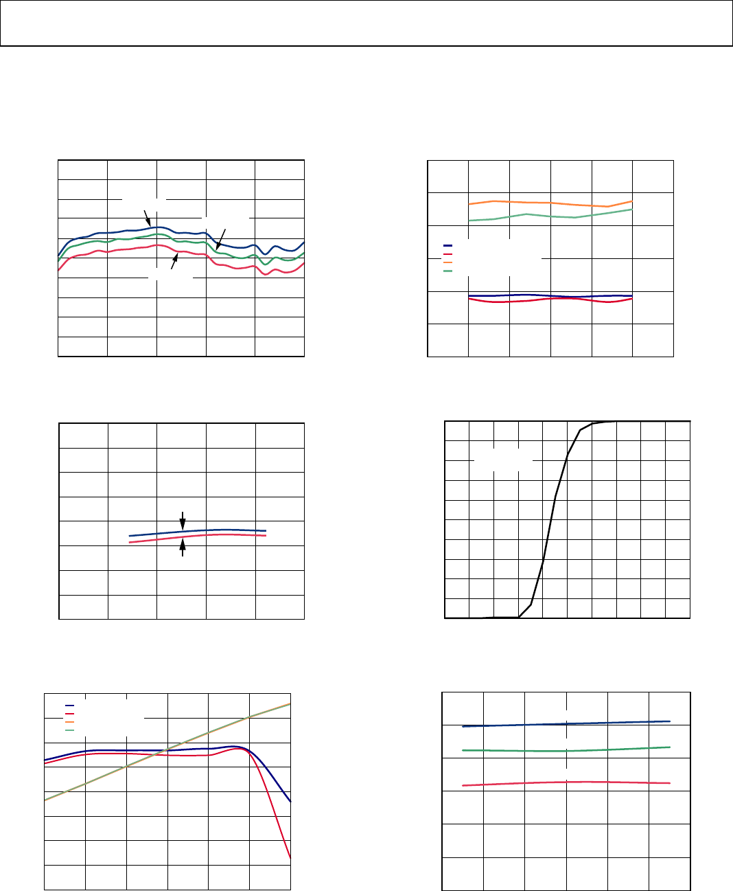
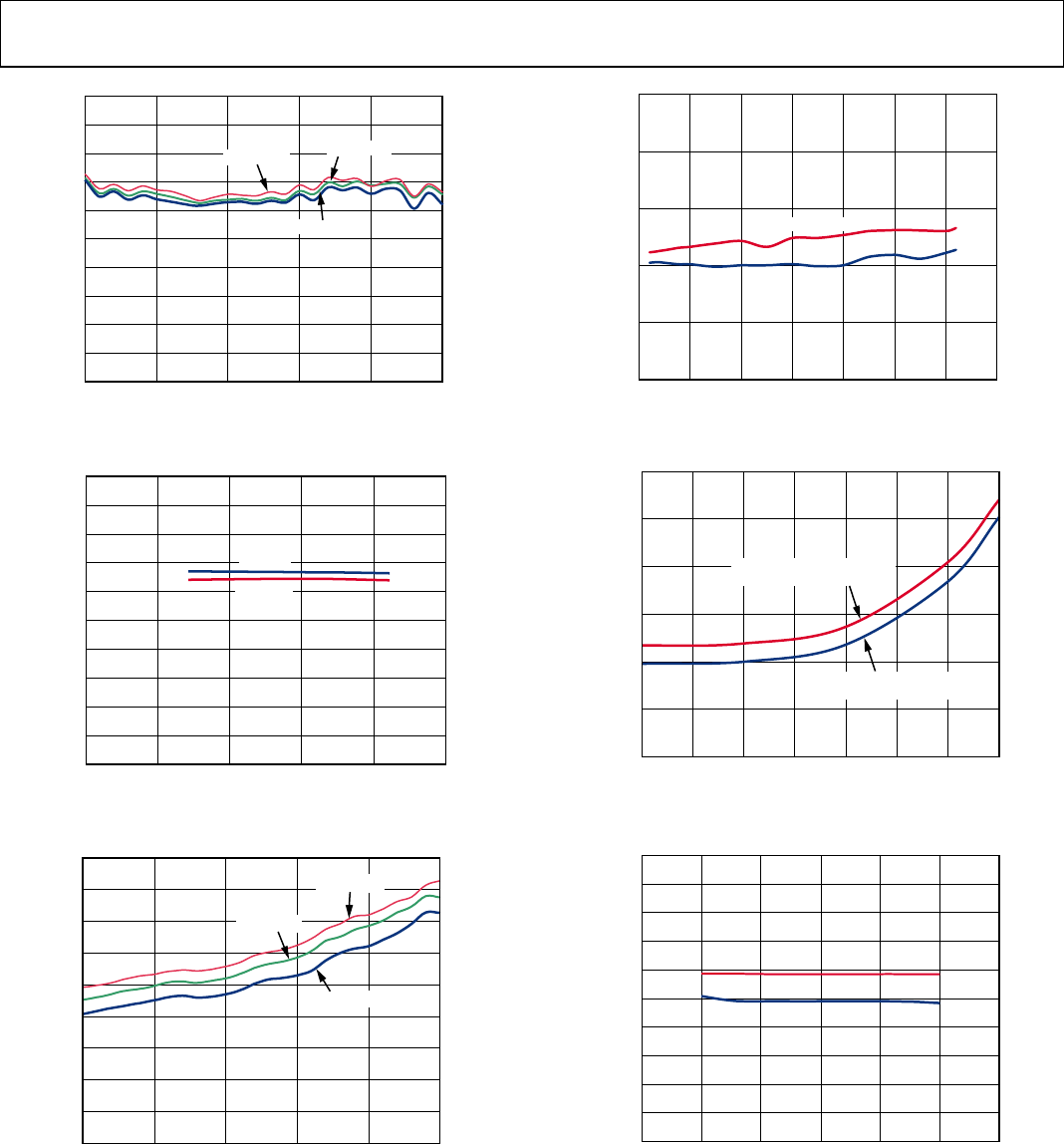
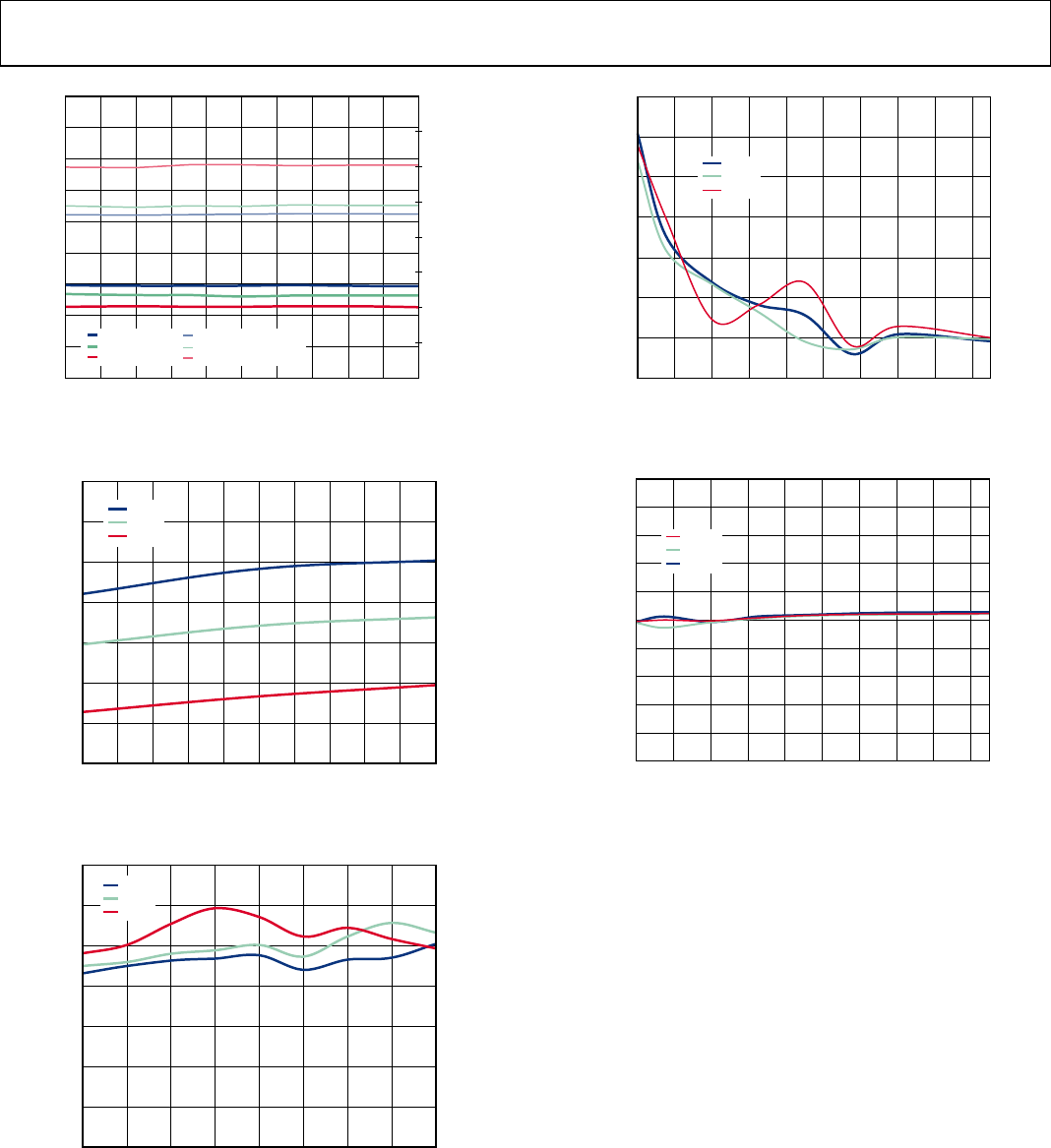
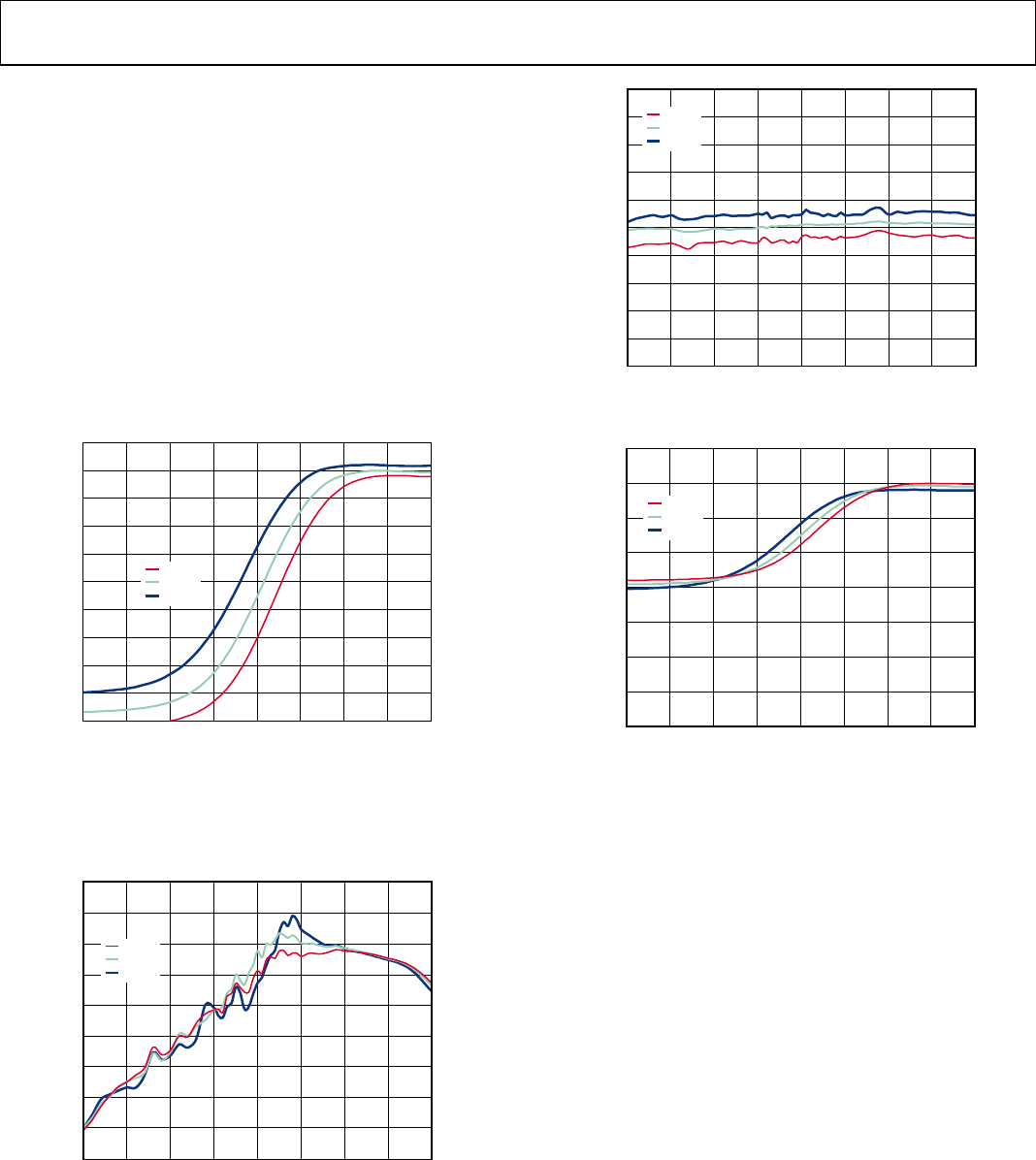
TYPICAL PERFORMANCE CHARACTERISTICS
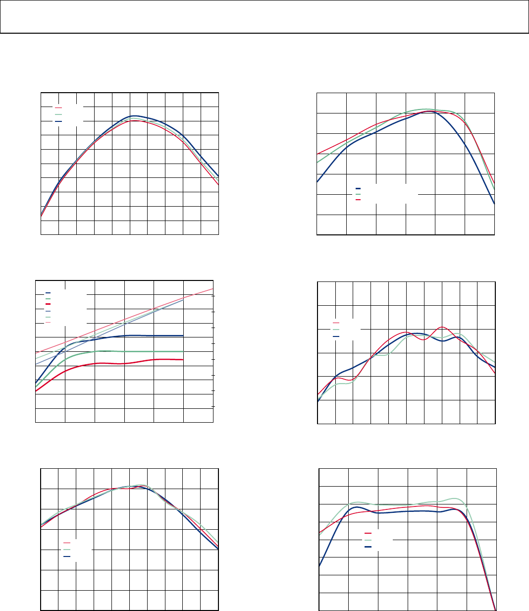
DOWNCONVERTER MODE WITH A BROADBAND BALUN
VS = 5 V, T A = 25°C, VSET = 3.8 V, IF = 153 MHz, as measured using a typical circuit schematic with low-side local oscillator (LO), unless
otherwise noted. Insertion loss of input and output baluns (TC1-1-13M+, TC4-1W+) is extracted from the gain measurement.
–4
–3
–2
–1
0
1
2
3
4
5
6
500 1000 1500 2000 2500 3000
GAIN (dB)
RF FREQUENCY (MHz)
T
A
= –40°C
T
A
= +85°C
T
A
= +25°C
08079-003
Figure 3. Power Conversion Gain vs. RF Frequency
0
0.5
1.0
1.5
2.0
2.5
3.0
3.5
4.0
050 100 150 200 250
GAIN (dB)
IF FREQUENCY (MHz)
1900MHz
900MHz
08079-004
Figure 4. Power Conversion Gain vs. IF Frequency
0.02
0.04
0.06
0.08
0.10
0.12
0.14
0.16
0.18
–1.0
–0.5
0
0.5
1.0
1.5
2.0
2.5
3.0
2.0 3.02.5 3.5 4.0 4.5 5.0
SUPPLY CURRENT (A)
GAIN (dB)
VSET (V)
GAIN = 900MHz
GAIN = 1900MHz
IPOS = 900MHz
IPOS = 1900MHz
08079-005
Figure 5. Power Conversion Gain and Supply Current vs. VSET
5
10
15
20
25
30
35
0
1
2
3
4
5
6
–15 –10 –5 0 5 10 15
INPUT IP3 (dBm)
GAIN (dB)
LO LEVEL (dBm)
GAIN = 900MHz
GAIN = 1900MHz
INPUT IP3 = 900MHz
INPUT IP3 = 1900MHz
08079-006
Figure 6. Power Conversion Gain and Input IP3 vs. LO Power
0
20
40
60
80
100
10
30
50
70
90
FREQUENCY (%)
1.700
1.740
1.780
1.820
1.860
1.900
1.940
1.980
2.020
2.060
2.100
POWER CONVERSION GAIN (dB)
08079-007
MEAN = 1.87
SD = 0.03
Figure 7. Power Conversion Gain Distribution
0
0.5
1.0
1.5
2.0
2.5
3.0
4.7 4.8 4.9 5.0 5.1 5.2 5.3
GAIN (dB)
SUPPLY (V)
T
A
= –40°C
T
A
= +85°C
T
A
= +25°C
08079-008
Figure 8. Power Conversion Gain vs. Supply Voltage
Rev. E | Page 8 of 40
Data Sheet ADL5801
0
5
10
15
20
25
30
35
500 1000 1500 2000 2500 3000
INPUT IP3 (dBm)
RF FREQUENCY (MHz)
TA = –40°C
TA = +85°C
TA = +25°C
08079-009
Figure 9. Input IP3 vs. RF Frequency
10
15
20
25
30
35
40
050 100 150 200 250
INPUT IP3 (dBm)
IF FREQUENCY (MHz)
900MHz
1900MHz
08079-010
Figure 10. Input IP3 vs. IF Frequency
8
10
12
14
16
18
20
0
5
10
15
20
25
30
2.0 2.5 3.0 3.5 4.0 4.5 5.0
NOISE FIGURE (dB)
INPUT IP3 (dBm)
VSET (V)
INPUT IP3 = 900MHz
INPUT IP3 = 1900MHz
NF = 900MHz
NF = 1900MHz
08079-011
Figure 11. Input IP3 and Noise Figure vs. VSET
0
10
20
30
40
50
60
70
500 1000 1500 2000 2500 3000
INPUT IP2 (dBm)
RF FREQUENCY (MHz)
T
A
= –40°C
T
A
= +85°C
T
A
= +25°C
08079-012
Figure 12. Input IP2 vs. RF Frequency
0
10
20
30
40
50
60
70
80
050 100 150 200 250
INPUT IP2 (dBm)
IF FREQUENCY (MHz)
900MHz
1900MHz
08079-013
Figure 13. Input IP2 vs. IF Frequency
0
10
20
30
40
50
60
70
80
2.0 2.5 3.53.0 4.0 4.5 5.0
INPUT IP2 (dBm)
VSET (V)
1900MHz
900MHz
08079-014
Figure 14. Input IP2 vs. VSET
Rev. E | Page 9 of 40
ADL5801 Data Sheet
0
2
4
6
8
10
12
14
16
18
20
500 1000 1500 2000 2500 3000
INPUT P1dB (dBm)
RF FREQUENCY (MHz)
TA = –40°C
TA = +85°C TA = +25°C
08079-015
Figure 15. Input P1dB vs. RF Frequency
0
2
4
6
8
10
12
14
16
18
20
050 100 150 200 250
INPUT P1dB (dBm)
IF FREQUENCY (MHz)
900MHz
1900MHz
08079-016
Figure 16. Input P1dB vs. IF Frequency
0
2
4
6
8
10
12
14
16
18
500 1000 1500
2000 2500 3000
SSB NOISE FIGURE (dB)
RF FREQUENCY (MHz)
T
A
= –40°C
T
A
= +85°C
T
A
= +25°C
08079-017
Figure 17. SSB Noise Figure vs. RF Frequency (VSET = 2.0 V)
0
5
10
15
20
25
0100 200 300 400 500 600 700
SSB NOISE FIGURE (dB)
IF FREQUENCY (MHz)
1900MHz
900MHz
08079-018
Figure 18. SSB Noise Figure vs. IF Frequency (VSET = 2.0 V)
0
5
10
15
20
25
30
–30 –25 –20 –15 –10 –5 0 5
SSB NOISE FIGURE (dB)
BLOCKER LEVEL (dBm)
08079-019
RF = 951MHz, IF = 153 MHz
BLOCKER = 946MHz
RF = 1846MHz, IF = 153 MHz
BLOCKER = 1841MHz
Figure 19. SSB Noise Figure vs. Blocker Level (VSET = 2.0 V)
0
2
4
6
8
10
12
14
16
18
20
–15 –10 –5 0 5 10 15
SSB NOISE FIGURE (dB)
LO LEVEL (dBm)
900MHz
1900MHz
08079-020
Figure 20. SSB Noise Figure vs. LO Power (VSET = 2.0 V)
Rev. E | Page 10 of 40
Data Sheet ADL5801
35
30
25
20
15
10
5
0
0500 1000 1500 2000 2500 3000
RF RETURN LOSS (dB)
RF FREQUENCY (MHz)
08079-021
Figure 21. RF Return Loss vs. RF Frequency
35
30
25
20
15
10
5
0
0500 1000 1500 2000 2500 3000
LO RETURN LOSS (dB)
LO FREQUENCY (MHz)
08079-022
Figure 22. LO Return Loss vs. LO Frequency
08079-023
100 100010 3000
100
200
300
400
0
500
–4
–2
0
2
–6
4
IF FREQUENCY (MHz)
RESISTANCE (Ω)
CAPACITANCE (pF)
Figure 23. IF Differential Output Impedance (R Parallel C Equivalent)
–60
–55
–50
–45
–40
–35
–30
–25
–20
–15
–10
500 1000 1500
2000 2500 3000
LO-TO-IF LEAKAGE (dBm)
LO FREQUENCY (MHz)
T
A
= –40°C
T
A
= +85°C
T
A
= +25°C
08079-024
Figure 24. LO-to-IF Leakage vs. LO Frequency
–60
–55
–50
–45
–40
–35
–30
–25
–20
–15
–10
500 1000 1500 2000 2500 3000
LO-TO-RF LEAKAGE (dBm)
LO FREQUENCY (MHz)
TA = –40°C
TA
= +85°C
T
A
= +25°C
08079-025
Figure 25. LO-to-RF Leakage vs. LO Frequency
–60
–50
–40
–30
–20
–10
0
500 1000 1500 2000 2500 3000
RF-TO-IF OUTPUT ISOLA
TION (dBc)
RF FREQUENCY (MHz)
T
A
= +85°C
T
A
= +25°C
T
A
= –40°C
08079-026
Figure 26. RF-to-IF Leakage vs. RF Frequency
Rev. E | Page 11 of 40
ADL5801 Data Sheet
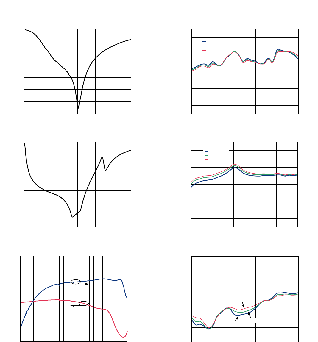
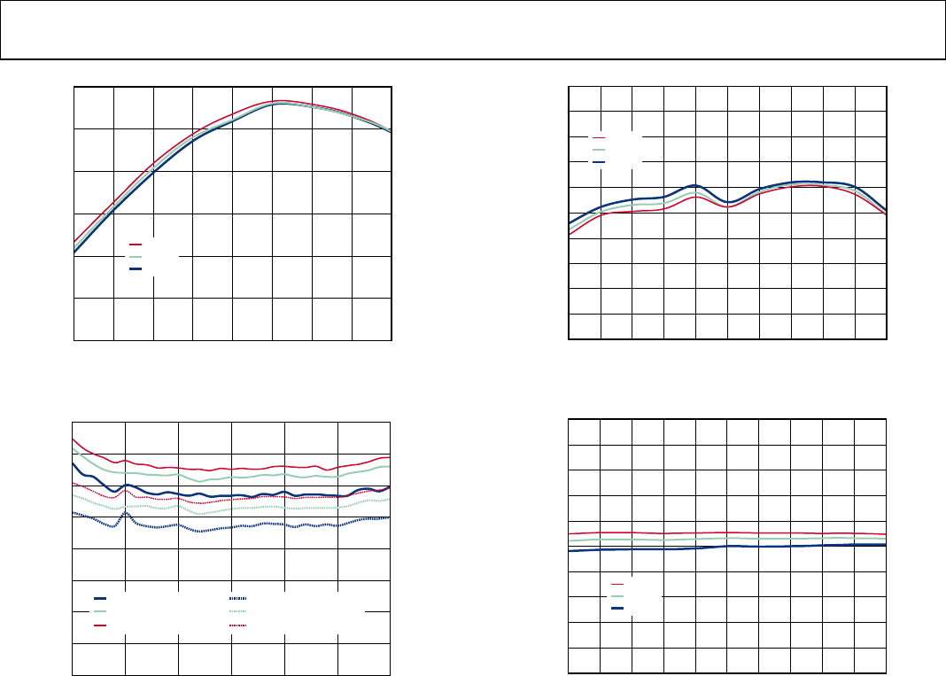
DOWNCONVERTER MODE WITH A MINI-CIRCUITS® TC1-1-43M+ INPUT BALUN
VS = 5 V, T A = 25°C, VSET = 3.8 V, IF = 211 MHz, as measured using a typical circuit schematic with low-side local oscillator (LO), unless
otherwise noted. Insertion loss of input and output baluns (TC1-1-43M+, TC4-1W+) is included in the gain measurement.
–4
–3
–2
–1
0
1
2
3
4
5
6
2000 2100 2200 2300 2400 2500 2600 2700 2800 2900 3000
GAIN (dB)
RF FREQUENCY (MHz)
08079-027
Figure 27. Power Conversion Gain vs. RF Frequency
0
0.02
0.04
0.06
0.08
0.10
0.12
0.14
0.16
0.18
–3.0
–2.5
–2.0
–1.5
–1.0
–0.5
0
0.5
1.0
2.0 2.5 3.0 3.5 4.0 4.5 5.0
SUPPLY CURRENT (A)
GAIN (dB)
V
SET
(V)
GAIN 2500M
IPOS2500M
08079-028
Figure 28. Power Conversion Gain and IPOS vs. VSET
20
21
22
23
24
25
26
27
28
29
30
2000 2100 2200 2300 2400 2500 2600 2700 2800 2900 3000
INPUT IP3 (dBm)
RF FREQUENCY (MHz)
08079-029
Figure 29. Input IP3 vs. RF Frequency
8
10
12
14
16
18
20
0
5
10
15
20
25
30
2.0 2.5 3.0 3.5 4.0 4.5 5.0
NOISE FIGURE (dB)
INPUT IP3 (dBm)
V
SET
(V)
IIP32500MHz
NF2500MHz
08079-030
Figure 30. Input IP3 and Noise Figure vs. VSET
0
10
20
30
40
50
60
2000 2100 2200 2300 2400 2500 2600 2700 2800 2900 3000
INPUT IP2 (dBm)
RF FREQUENCY (MHz)
08079-031
Figure 31. Input IP2 vs. RF Frequency
V
SET
(V)
0
10
20
30
40
50
60
70
80
2.0 2.5 3.0 3.5 4.0 4.5 5.0
INPUT IP2 (dBm)
08079-032
Figure 32. Input IP2 vs. VSET
Rev. E | Page 12 of 40
Data Sheet ADL5801
0
2
4
6
8
10
12
14
16
18
20
2000 2100 2200 2300 2400 2500 2600 2700 2800 2900 3000
INPUT P1dB (dBm)
RF FREQUENCY (MHz)
08079-033
Figure 33. Input P1dB vs. RF Frequency
0
5
10
15
20
25
2000 2100 2200 2300 2400 2500 2600 2700 2800 2900 3000
NOISE FIGURE (dB)
RF FREQUENCY (MHz)
08079-034
–40°C V
SET
2V
+25°C V
SET
2V
+85°C V
SET
2V
–40°C V
SET
3.6V
+25°C V
SET
3.6V
+85°C V
SET
3.6V
Figure 34. Noise Figure vs. RF Frequency
–60
–55
–50
–45
–40
–35
–30
–25
–20
–15
–10
2000 2100 2200 2300 2400 2500 2600 2700 2800 2900 3000
LO TO IF LEAKAGE (dBm)
LO FREQUENCY (MHz)
08079-035
Figure 35. LO to IF Leakage vs. LO Frequency
–60
–55
–50
–45
–40
–35
–30
–25
–20
–15
–10
2000 2100 2200 2300 2400 2500 2600 2700 2800 2900 3000
LO TO RF LEAKAGE (dBm)
LO FREQUENCY (MHz)
08079-036
Figure 36. LO to RF Leakage vs. LO Frequency
–80
–70
–60
–50
–40
–30
–20
2000 2100 2200 2300 2400 2500 2600 2700 2800 2900 3000
RF TO IF OUTPUT ISOLATION (dBc)
RF FREQUENCY (MHz)
08079-037
Figure 37. RF to IF Output Isolation vs. RF Frequency
Rev. E | Page 13 of 40
ADL5801 Data Sheet
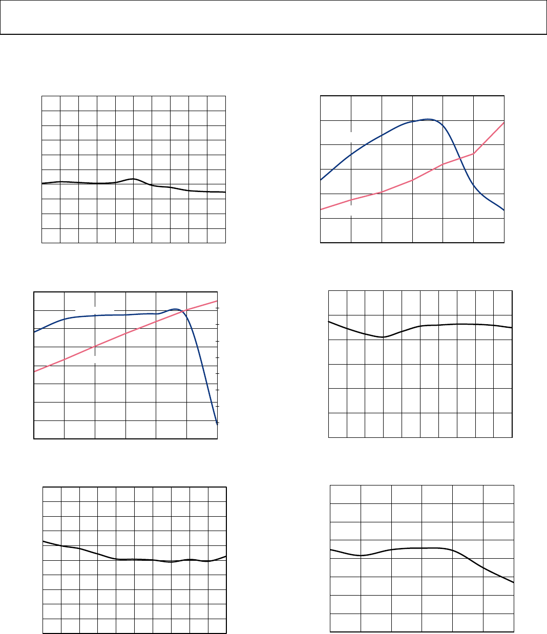
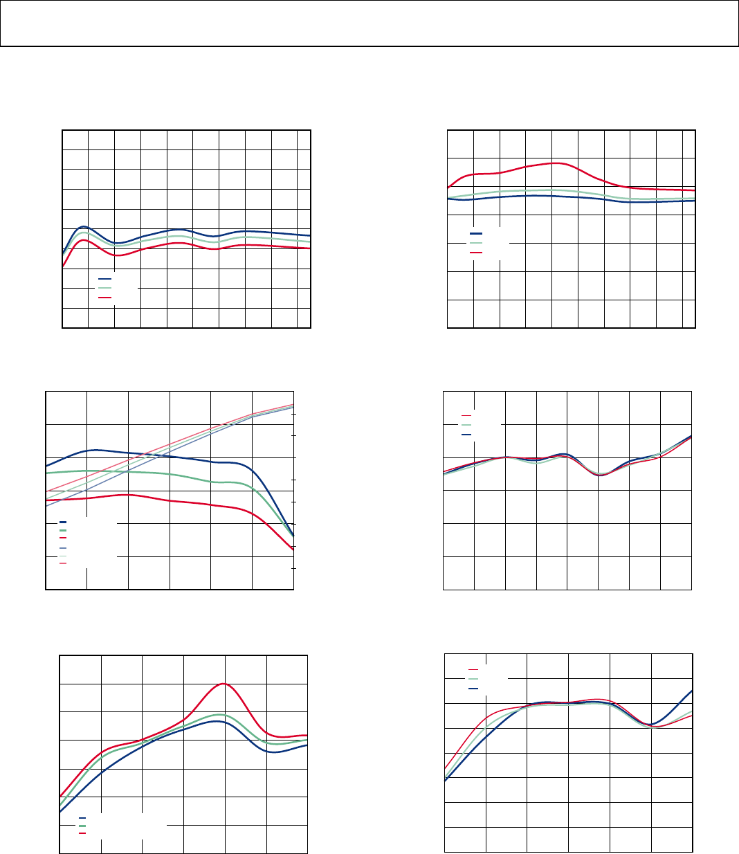
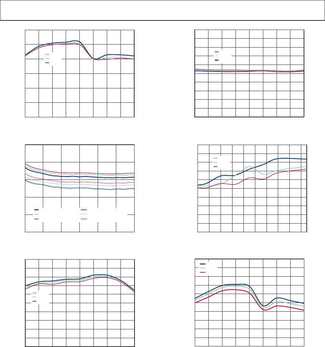
DOWNCONVERTER MODE WITH A JOHANSON 3.5 GHZ INPUT BALUN
VS = 5 V, T A = 25°C, VSET = 3.6 V, IF = 153 MHz, as measured using a typical circuit schematic with low-side local oscillator (LO), unless
otherwise noted. Insertion loss of input and output baluns (3600BL14M050, TC4-1W+) is included in the gain measurement.
–4
–3
–2
–1
0
1
2
3
4
5
6
3000 3100 3200 3300 3400 3500 3600 3700 3800 3900 4000
GAIN (dB)
RF FREQUENCY (MHz)
+25°C
–40°C
+85°C
08079-038
Figure 38. Power Conversion Gain vs. RF Frequency
0
0.02
0.04
0.06
0.08
0.10
0.12
0.14
0.16
0.18
0.20
–12
–10
–8
–6
–4
–2
0
2
2.0 2.5 3.0 3.5 4.0 4.5 5.0
SUPPLY CURRENT (A)
GAIN (dB)
VSET (V)
GAIN +25°C
GAIN –40°C
GAIN +85°C
IPOS +25°C
IPOS –40°C
IPOS +85°C
08079-039
Figure 39. Power Conversion Gain and IPOS vs. VSET
0
5
10
15
20
25
30
3000 3100 3200 3300 3400 3500 3600 3700 3800 3900 4000
INPUT IP3 (dBm)
RF FREQUENCY (MHz)
+25°C
–40°C
+85°C
08079-040
Figure 40. Input IP3 vs. RF Frequency
8
13
18
23
28
NOISE FIGURE (dB)
0
5
10
15
20
25
30
2.0 2.5 3.0 3.5 4.0 4.5 5.0
INPUT IP3 (dBm)
VSET (V)
IIP3, +25°C
IIP3, –40°C
IIP3, +85°C
NF, +25°C
NF, –40°C
NF, +85°C
08079-041
Figure 41. Input IP3 and Noise Figure vs. VSET
20
25
30
35
40
45
50
3000 3100 3200 3300 3400 3500 3600 3700 3800 3900 4000
INPUT IP2 (dBm)
RF FREQUENCY (MHz)
–40°C
+25°C
+85°C
08079-042
Figure 42. Input IP2 vs. RF Frequency
0
10
20
30
40
50
60
70
80
2.0 2.5 3.0 3.5 4.0 4.5 5.0
INPUT IP2 (dBm)
V
SET
(V)
–40°C
+25°C
+85°C
08079-043
Figure 43. Input IP2 vs. VSET
Rev. E | Page 14 of 40
Data Sheet ADL5801
0
2
4
6
8
10
12
14
16
18
20
3000 3100 3200 3300 3400 3500 3600 3700 3800 3900 4000
INPUT P1dB (dBm)
RF FREQUENCY (MHz)
–40°C
+25°C
+85°C
08079-044
Figure 44. Input P1dB vs. RF Frequency
0
5
10
15
20
25
3000 3100 3200 3300
3400 3500 3600 3700 3800 3900 4000
NOISE FIGURE (dB)
RF FREQUENCY (MHz)
08079-045
–40°C, 3.6V
+25°C, 3.6V+85°C, 3.6V
–40°C, 2.0V
+25°C, 2.0V
+85°C, 2.0V
Figure 45. Noise Figure vs. RF Frequency
–60
–55
–50
–45
–40
–35
–30
–25
–20
–15
–10
3000 3100 3200 3300 3400 3500 3600 3700 3800 3900 4000
LO TO IF LEAKAGE (dBm)
LO FREQUENCY (MHz)
–40°C
+25°C
+85°C
08079-046
Figure 46. LO to IF Leakage vs. LO Frequency
–60
–55
–50
–45
–40
–35
–30
–25
–20
–15
–10
3000 3100 3200 3300 3400 3500 3600 3700 3800 3900 4000
LO TO RF LEAKAGE (dBm)
LO FREQUENCY (MHz)
–40°C
+25°C
+85°C
08079-047
Figure 47. LO to RF Leakage vs. LO Frequency
–80
–70
–60
–50
–40
–30
–20
3000 3100 3200 3300 3400 3500 3600 3700 3800 3900 4000
RF TO IF OUTPUT ISOLATION (dBc)
RF FREQUENCY (MHz)
–40°C
+25°C
+85°C
08079-048
Figure 48. RF to IF Output Isolation vs. RF Frequency
Rev. E | Page 15 of 40
ADL5801 Data Sheet
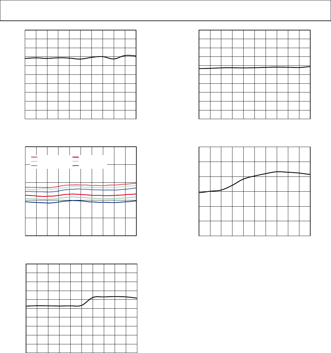
DOWNCONVERTER MODE WITH A JOHANSON 5.7 GHZ INPUT BALUN
VS = 5 V, T A = 25°C, VSET = 3.6 V, IF = 153 MHz, as measured using a typical circuit schematic with low-side local oscillator (LO), unless
otherwise noted. Insertion loss of input and output baluns (5400BL14B050, TC4-1W+) is included in the gain measurement.
–4
–3
–2
–1
0
1
2
3
4
5
6
5000 5100 5200 5300 5400 5500 5600 5700 5800 5900 6000
GAIN (dB)
RF FREQUENCY (MHz)
+25°C
–40°C
+85°C
08079-049
Figure 49. Power Conversion Gain vs. RF Frequency
0
0.02
0.04
0.06
0.08
0.10
0.12
0.14
0.16
0.18
0.20
–16
–14
–12
–10
–8
–6
–4
–2
0
2
2.0 2.5 3.0 3.5 4.0 4.5 5.0
SUPPLY CURRENT (A)
GAIN (dB)
V
SET
(V)
GAIN +25°C
GAIN –40°C
GAIN +85°C
IPOS+25°C
IPOS –40°C
IPOS +85°C
08079-050
Figure 50. Power Conversion Gain and IPOS vs VSET
0
5
10
15
20
25
30
5000 5100 5200 5300 5400 5500 5600 5700 5800 5900 6000
INPUT IP3 (dBm)
RF FREQUENCY (MHz)
+25°C
–40°C
+85°C
08079-051
Figure 51. Input IP3 vs. RF Frequency
5
10
15
20
25
30
35
0
5
10
15
20
25
2.0 2.5 3.0 3.5 4.0 4.5 5.0
INPUT IP3 (dBm)
V
SET
(V)
IIP3, +25°C
IIP3, –40°C
IIP3, +85°C
NF,+25°C
NF, –40°C
NF, +85°C
08079-052
NOISE FIGURE (dB)
Figure 52. Input IP3 and Noise Figure vs. VSET
20
25
30
35
40
45
50
55
60
65
70
5000 5100 5200 5300 5400 5500 5600 5700 5800 5900 6000
INPUT IP2 (dBm)
RF FREQUENCY (MHz)
–40°C
+25°C
+85°C
08079-053
Figure 53. Input IP2 vs. RF Frequency
0
10
20
30
40
50
60
70
80
2.0 2.5 3.0 3.5 4.0 4.5 5.0
INPUT IP2 (dBm)
V
SET
(V)
–40°C
+25°C
+85°C
08079-054
Figure 54. Input IP2 vs. VSET
Rev. E | Page 16 of 40
Data Sheet ADL5801
0
2
4
6
8
10
12
14
16
18
20
5000 5100 5200 5300 5400 5500 5600 5700 5800 5900 6000
INPUT P1dB (dBm)
RF FREQUENCY (MHz)
–40°C
+25°C
+85°C
08079-055
Figure 55. Input P1dB vs. RF Frequency
0
5
10
15
20
25
5000 5100 5200 5300 5400 5500 5600 5700 5800 5900 6000
NOISE FIGURE (dB)
RF FREQUENCY (MHz)
08079-056
–40°C, 3.6V+25°C, 3.6V+85°C, 3.6V
–40°C, 2.0V+25°C, 2.0V
+85°C, 2.0V
Figure 56. Noise Figure vs. RF Frequency, VSET = 3.6 V
–60
–55
–50
–45
–40
–35
–30
–25
–20
–15
–10
5000 5100 5200 5300 5400 5500 5600 5700 5800 5900 6000
LO TO IF LEAKAGE (dBm)
LO FREQUENCY (MHz)
–40°C
+25°C
+85°C
08079-057
Figure 57. LO to IF Leakage vs. LO Frequency
–60
–55
–50
–45
–40
–35
–30
–25
–20
–15
–10
5000 5100 5200 5300 5400 5500 5600 5700 5800 5900 6000
LO TO RF LEAKAGE (dBm)
LO FREQUENCY (MHz)
–40°C
+25°C
+85°C
08079-058
Figure 58. LO to RF Leakage vs. LO Frequency
–80
–70
–60
–50
–40
–30
–20
5000 5100 5200 5300 5400 5500 5600 5700 5800 5900 6000
RF TO IF OUTPUT ISOLATION (dBc)
RF FREQUENCY (MHz)
–40°C
+25°C
+85°C
08079-059
Figure 59. RF to IF Output Isolation vs. RF Frequency
Rev. E | Page 17 of 40
ADL5801 Data Sheet
UPCONVERTER MODE WITH A 900 MHZ OUTPUT MATCH
VS = 5 V, T A = 25°C, VSET = 3.6 V, RF = 153 MHz, as measured using a typical circuit schematic with low-side local oscillator (LO),
unless otherwise noted. Insertion loss of input and output baluns (TC1-1-13M+, TC4-14) is included in the gain measurement.
–8
–7
–6
–5
–4
–3
–2
–1
0
1
2
300 400 500 600 700 800 900 1000 1100 1200 1300
GAIN (dB)
IF FREQUENCY (MHz)
–40°C
+25°C
+85°C
08079-077
Figure 60. Power Conversion Gain vs. IF Frequency
0
0.02
0.04
0.06
0.08
0.1
0.12
0.14
0.16
0.18
–1.0
–0.8
–0.6
–0.4
–0.2
0
0.2
0.4
0.6
0.8
1.0
2.0 2.5 3.0 3.5 4.0 4.5 5.0
GAIN (dB)
VSET (V)
SUPPLY CURRENT (A)
GAIN +25°C
GAIN –40°C
GAIN +85°C
IPOS +25°C
IPOS –40°C
IPOS +85°C
Figure 61. Power Conversion Gain and IPOS vs. VSET
0
5
10
15
20
25
30
35
300 400 500 600 700 800 900 1000 1100 1200 1300
OUTPUT IP3 (dBm)
IF FREQUENCY (MHz)
–40°C
+25°C
+85°C
08079-079
Figure 62. Output IP3 vs. IF Frequency
0
5
10
15
20
25
30
35
2.0 2.5 3.0 3.5 4.0 4.5 5.0
OUTPUT IP3 (dBm)
V
SET
(V)
OUTPUT IP3, +25°C
OUTPUT IP3, –40°C
OUTPUT IP3, +85°C
08079-080
Figure 63. Output IP3 vs. VSET
50
55
60
65
70
75
80
300 400 500 600 700 800 900 1000 1100 1200 1300
OUTPUT IP2 (dBm)
IF FREQUENCY (MHz)
–40°C
+25°C
+85°C
08079-081
Figure 64. Output IP2 vs. IF Frequency
40
45
50
55
60
65
70
75
80
2.0 2.5 3.0 3.5 4.0 4.5 5.0
OUTPUT IP2 (dBm)
V
SET
(V)
–40°C
+25°C
+85°C
08079-082
Figure 65. Output IP2 vs. VSET
Rev. E | Page 18 of 40
Data Sheet ADL5801
0
2
4
6
8
10
12
300 400 500 600 700 800 900 1000 1100
OUTPUT P1dB (dBm)
IF FREQUENCY (MHz)
–40°C
+25°C
+85°C
08079-083
Figure 66. Output P1dB vs. IF Frequency
0
2
4
6
8
10
12
14
16
700 750 800 850 900 950 1000
NOISE FIGURE (dB)
IF FREQUENCY (MHz)
08079-084
NF V
SET
= 3.6V, –40°C NF V
SET
= 2.0V, –40°C
NF V
SET
= 3.6V, +25°C NF V
SET
= 2.0V, +25°C
NF V
SET
= 3.6V, +85°C NF V
SET
= 2.0V, +85°C
Figure 67. Noise Figure vs. IF Frequency, FLO = 650 MHz
–60
–55
–50
–45
–40
–35
–30
–25
–20
–15
–10
453 553 653 753 853 953 1053 1153 1253 1353 1453
LO TO IF LEAKAGE (dBm)
LO FREQUENCY (MHz)
–40°C
+25°C
+85°C
08079-085
Figure 68. LO to IF Leakage vs. LO Frequency
–60
–55
–50
–45
–40
–35
–30
–25
–20
–15
–10
453 553 653 753 853 953 1053 1153 1253 1353 1453
LO TO RF LEAKAGE (dBm)
LO FREQUENCY (MHz)
–40°C
+25°C
+85°C
08079-086
Figure 69. LO to RF Leakage vs. LO Frequency
Rev. E | Page 19 of 40
ADL5801 Data Sheet
UPCONVERTER MODE WITH A 2.1 GHZ OUTPUT MATCH
VS = 5 V, T A = 25°C, VSET = 4 V, RF = 170 MHz, as measured using a typical circuit schematic with low-side local oscillator (LO), unless
otherwise noted. Insertion loss of input and output baluns (TC1-1-13M+, 1850BL15B200) is included in the gain measurement.
–4
–5
–6
–3
–2
–1
4
2
3
1
0
110 130 150 170 190 210 230 250 270 290
GAIN (dB)
RF FREQUENCY (MHz)
+25°C
–40°C
+85°C
08079-060
Figure 70. Power Conversion Gain vs. RF Frequency
0
0.02
0.04
0.06
0.08
0.10
0.12
0.14
0.16
0.18
–3.0
–2.5
–2.0
–1.5
–1.0
–0.5
0
2
.0
2.5 3
.0
3.5 4
.0
4.5 5
.0
SUPPLY CURRENT (A)
GAIN (dB)
V
SET
(V)
GAIN +25°C
GAIN –40°C
GAIN +85°C
IPOS +25°C
IPOS –40°C
IPOS +85°C
08079-062
Figure 71. Power Conversion Gain and IPOS vs. VSET
0
5
10
15
20
25
30
35
2.0 2.5 3.0 3.5 4.0 4.5 5.0
OUTPUT IP3 (dBm)
V
SET
(V)
OUTPUT IP3 +25°C
OUTPUT IP3 –40°C
OUTPUT IP3 +85°C
08079-067
Figure 72. Output IP3 vs. VSET
0
5
10
15
20
25
30
35
110 130 150 170 190 210 230 250 270 290
OUTPUT IP3 (dBm)
RF FREQUENCY (MHz)
+25°C
–40°C
+85°C
08079-065
Figure 73. Output IP3 vs. RF Frequency
50
55
60
65
70
75
80
1900 2000 2100 2200 2300 2400 2500 2600 2700
OUTPUT IP2 (dBm)
IF FREQUENCY (MHz)
–40°C
+25°C
+85°C
08079-069
Figure 74. Output IP2 vs. IF Frequency
40
45
50
55
60
65
70
75
80
2.0 2.5 3.0 3.5 4.0 4.5 5.0
OUTPUT IP2 (dBm)
VSET (V)
–40°C
+25°C
+85°C
08079-070
Figure 75. Output IP2 vs. VSET
Rev. E | Page 20 of 40
Data Sheet ADL5801
0
2
4
6
8
10
12
1900 2000 2100 2200 2300 2400 2500 2600 2700
OUTPUT P1DB (dBm)
IF FREQUENCY (MHz)
–40°C
+25°C
+85°C
08079-072
Figure 76. Output P1dB vs. IF Frequency
0
5
10
15
20
25
2000 2050 2100 2150 2200 2250 2300
NOISE FIGURE (dB)
IF FREQUENCY (MHz)
08079-073
NF VSET = 3.6V, –40°C NF VSET = 2.0V, –40°C
NF VSET = 3.6V, +25°C NF VSET = 2.0V, +25°C
NF VSET = 3.6V, +85°C NF VSET = 2.0V, +85°C
Figure 77. Noise Figure vs. IF Frequency, FLO = 1950 MHz
–60
–55
–50
–45
–40
–35
–30
–25
–20
–15
–10
2070 2170 2270 2370 2470 2570 2670 2770 2870
LO TO IF LEAKAGE (dBm)
LO FREQUENCY (MHz)
–40°C
+25°C
+85°C
08079-074
Figure 78. LO to IF Leakage vs. LO Frequency
–60
–55
–50
–45
–40
–35
–30
–25
–20
–15
–10
2070 2170 2270 2370 2470 2570 2670 2770 2870
LO TO RF LEAKAGE (dBm)
LO FREQUENCY (MHz)
–40°C
+25°C
+85°C
08079-075
Figure 79. LO to RF Leakage vs. LO Frequency
–75
–74
–73
–72
–71
–70
–69
–68
–67
–66
–65
110 130 150 170 190 210 230 250 270 290
RF TO IF OUTPUT ISOLATION (dBc)
RF FREQUENCY (MHz)
–40°C
+25°C
+85°C
08079-076
Figure 80. RF to IF Output Isolation vs. RF Frequency
–8
–7
–6
–5
–4
–3
–2
–1
0
1
2
1900 2000 2100 2200 2300 2400 2500 2600 2700
GAIN (dB)
IF FREQUENCY (MHz)
+25°C
–40°C
+85°C
08079-061
Figure 81. Power Conversion Gain vs. IF Frequency
Rev. E | Page 21 of 40
ADL5801 Data Sheet
0
5
10
15
20
25
30
35
40
–4
–3
–2
–1
0
1
2
3
4
5
–10 –8 –6 –4 –2 0 2 46 8 10
OUTPUT IP3 (dBm)
GAIN (dB)
LO POWER (dBm)
GAIN +25°C
GAIN –40°C
GAIN +85°C OUTPUT IP3 +25°C
OUTPUT IP3 –40°C
OUTPUT IP3 +85°C
08079-063
Figure 82. Power Conversion Gain and Output IP3 vs. LO Power
–1.4
–1.2
–1.0
–0.8
–0.6
–0.4
–0.2
0
4.75 4.80 4.85 4.90 4.95 5.00 5.05 5.10 5.15 5.20 5.25
GAIN (dB)
SUPPLY (V)
+25°C
–40°C
+85°C
08079-064
Figure 83. Power Conversion Gain vs. Supply
0
5
10
15
20
25
30
35
1900 2000 2100 2200 2300 2400 2500 2600 2700
OUTPUT IP3 (dBm)
IF FREQUENCY (MHz)
+25°C
–40°C
+85°C
08079-066
Figure 84. Output IP3 vs. IF Frequency
66
68
70
72
74
76
78
80
110 130 150 170 190 210 230 250 270 290
OUTPUT IP2 (dBm)
RF FREQUENCY (MHz)
+25°C
–40°C
+85°C
08079-068
Figure 85. Output IP2 vs. RF Frequency
0
2
4
6
8
10
12
14
16
18
20
110 130 150 170 190 210 230 250 270 290
OUTPUT P1dB (dBm)
RF FREQUENCY (MHz)
–40°C
+25°C
+85°C
08079-071
Figure 86. Output P1dB vs. RF Frequency
Rev. E | Page 22 of 40

Data Sheet ADL5801
SPUR PERFORMANCE
All spur tables are (N × fRF) − (M × fLO) and were measured using the standard evaluation board (see the Evaluation Board section). Mixer
spurious products are measured in decibels relative to the carrier (dBc) from the IF output power level. Data was measured for frequencies
less than 6 GHz only. The typical noise floor of the measurement system is −100 dBm.
900 MHz Downconvert Performance
VS = 5 V, VSET = 3.8 V, TA = 25°C, RF power = 0 dBm, LO power = 0 dBm, fRF = 900 MHz, fLO = 703 MHz, Z0 = 50 Ω.
M
0 1 2 3 4 5 6 7 8 9 10 11 12 13 14
0 −33.1 −23.3 −45.8 −23.6 −45.9 −30.7 −55.4 −41.5
1 −48.8 0.0 −51.5 −19.0 −65.1 −29.6 −78.0 −50.3 −74.4 −57.7
2 −35.9 −74.9 −67.5 −66.1 −73.5 −80.5 −65.0 −89.8 −71.3 −88.5 −86.8 −98.8
3 −68.8 −64.8 −94.3 −65.9 −86.3 −70.2 −76.3 −70.6 −74.5 −81.4 ≤−100 −99.6 ≤−100
4 −47.5 −80.7 −78.0 −78.4 −95.1 −73.5 −89.4 −87.3 ≤−100 −92.7 −99.5 −99.4 ≤−100 ≤−100
5 −95.6 −74.7 −89.8 −70.7 −84.8 −90.7 −86.7 −86.4 −83.1 −73.7 −78.7 −80.7 −91.1 ≤−100 ≤−100
6 −85.7 −96.4 −83.1 −98.5 −83.3 −96.7 ≤−100 −89.4 −99.6 −96.1 −96.1 −95.4 −95.5 ≤−100 ≤−100
N 7 ≤−100 ≤−100 −95.9 ≤−100 −97.2 −83.1 −84.1 ≤−100 ≤−100 −99.7 −87.9 −88.8 −85.7 ≤−100
8 ≤−100 ≤−100 −99.0 −99.8 −86.0 ≤−100 ≤−100 ≤−100 ≤−100 ≤−100 ≤−100 ≤−100 ≤−100
9 ≤−100 ≤−100 ≤−100 −90.9 −88.4 −83.5 −87.6 ≤−100 ≤−100 ≤−100 ≤−100 ≤−100
10 ≤−100 ≤−100 ≤−100 −97.9 −95.5 −99.0 ≤−100 ≤−100 ≤−100 ≤−100
11 ≤−100 ≤−100 −92.6 −87.4 −88.2 −92.3 −99.3 ≤−100 ≤−100
12 ≤−100 ≤−100 ≤−100 ≤−100 ≤−100 ≤−100 ≤−100 ≤−100
13 ≤−100 ≤−100 −95.1 −96.5 −90.4 ≤−100
14 ≤−100 ≤−100 ≤−100 ≤−100 ≤−100
15 ≤−100 ≤−100 ≤−100 ≤−100
1900 MHz Downconvert Performance
VS = 5 V, VSET = 3.8 V, TA = 25°C, RF power = 0 dBm, LO power = 0 dBm, fRF = 1900 MHz, fLO = 1703 MHz, Z0 = 50 Ω.
M
0 1 2 3 4 5 6 7 8 9 10 11 12 13 14
0 −31.4 −17.1 −51.4
1 −40.4 0.0 −53.6 −38.5 −71.0
2 −38.4 −66.0 −52.9 −68.1 −64.2 −86.8
3 ≤−100 −66.2 −73.2 −72.6 −79.9 −65.2 −92.8
4 ≤−100 −89.4 −86.4 −94.6 −87.4 −81.5 ≤−100
5 −83.7 −66.2 −79.3 −89.0 −75.2 ≤−100 ≤−100
6 ≤−100 −86.4 ≤−100 −99.0 −87.7 ≤−100 ≤−100
N 7 ≤−100 −92.4 −92.7 ≤−100 −98.4 ≤−100 ≤−100
8 ≤−100 ≤−100 −97.5 ≤−100 −95.4 ≤−100 ≤−100
9 ≤−100 ≤−100 ≤−100 ≤−100 ≤−100 ≤−100 ≤−100
10 ≤−100 −97.2 −95.6 ≤−100 ≤−100 ≤−100 ≤−100
11 ≤−100 ≤−100 ≤−100 ≤−100 ≤−100 ≤−100
12 ≤−100 ≤−100 ≤−100 ≤−100 ≤−100
13 ≤−100 ≤−100 ≤−100 ≤−100
14 ≤−100 ≤−100
15 ≤−100
Rev. E | Page 23 of 40
ADL5801 Data Sheet
2600 MHz Downconvert Performance
VS = 5 V, VSET = 3.8 V, TA = 25°C, RF power = 0 dBm, LO power = 0 dBm, fRF = 2600 MHz, fLO = 2350 MHz, Z0 = 50 Ω.
M
0 1 2 3 4 5 6 7 8 9 10 11 12 13 14 15
N
0 −31.5 −30.3
1 −40.3 0.0 −55.8 −33.8
2 −71.7 −73.6 −50.6 −70.4 −64.8
3 −83.9 −66.5 −59.8 −71.3 −84.7
4 −94.7 −77.6 −92.6 −83.8 −90.6
5 −91.4 −71.1 −89.7 −98.2 −96.3 <100
6 −83.1 −90.3 −92.9 −97.3 <100
7 <100 −91.4 <100 <100 <100
8 <100 −96.6 <100 −91.8 <100
9 <100 −97.9 <100 −98.5 <100
10 <100 −93.5 <100 −98.8 <100
11 <100 <100 <100 <100 <100
12 <100 <100 <100 <100 <100
13 <100 <100 <100 <100
14 <100 <100 <100
15 <100
3800 MHz Downconvert Performance
VS = 5 V, VSET = 3.8 V, TA = 25°C, RF power = 0 dBm, LO power = 0 dBm, fRF = 3800 MHz, fLO = 3500 MHz, Z0 = 50 Ω.
M
0 1 2 3 4 5 6 7 8 9 10 11 12 13 14 15
N
0 −27.3
1 −33.7 0.0 −54.9
2 −78.5 −47.1 −66.4
3 −63.6 −57.8 −81.4
4 −89.6 −77.2 −72.2 −99.2
5 <100 −88.0 −80.4 <100
6 <100 −90.0 −90.4 <100
7 <100 −79.1 <100 <100
8 <100 −85.2 <100 <100
9 <100 <100 <100
10 <100 −95.9 <100
11 <100 <100 <100
12 <100 <100 <100
13 <100 <100 <100
14 <100 <100
15 <100
Rev. E | Page 24 of 40
Data Sheet ADL5801
5800 MHz Downconvert Performance
VS = 5 V, VSET = 3.8 V, TA = 25°C, RF power = 0 dBm, LO power = 0 dBm, fRF = 5800 MHz, fLO = 5600 MHz, Z0 = 50 Ω.
M
0 1 2 3 4 5 6 7 8 9 10 11 12 13 14 15
N
0 −44.9
1 −43.9 0.0 −68.9
2 −44.0 −78.0
3 −47.0 −93.3
4 −60.6 −87.8
5 −62.7 −85.7
6 −70.2 −97.8
7 −79.5 −85.3
8 −71.2 <100
9 <100 <100
10 <100 <100
11 <100 <100
12 <100 <100
13 −100.3 <100
14 −95.6 −96.0
15 <100
806 MHz Upconvert Performance
VS = 5 V, VSET = 3.8 V, TA = 25°C, RF power = 0 dBm, LO power = 0 dBm, fRF = 140 MHz, fLO = 946 MHz, Z0 = 50 Ω.
M
0 1 2 3 4 5 6 7 8 9 10 11 12 13 14 15
N
0 −35.2 −22.9 −42.8 −28.4 −59.1 −40.1
1 −66.0 0.0 −67.7 −14.0 −70.0 −37.1 −74.3
2 −67.8 −66.0 −62.9 −65.3 −61.1 −84.1 −81.2
3 −99.2 −66.2 −92.2 −69.2 −84.9 −84.3 <100
4 −77.1 −97.2 −85.1 −97.8 −82.0 <100 <100
5 −88.7 <100 −88.5 −92.9 −96.4 −93.6 <100 <100
6 −86.1 <100 −92.7 −95.8 −87.5 −99.5 <100 <100
7 −90.2 <100 <100 −84.6 <100 −88.0 <100 <100
8 −73.8 <100 −94.8 −96.4 −93.4 −99.6 <100 <100
9 −91.1 −96.3 <100 −91.5 −100.3 −93.3 <100 <100
10 −66.2 <100 <100 <100 −88.3 −100.0 <100 <100
11 −87.7 −93.6 <100 −95.9 <100 <100 <100 <100
12 −69.5 −89.1 <100 <100 −93.8 <100 <100 <100 <100
13 −85.2 −95.7 <100 <100 −97.7 −90.5 −96.0 <100 <100
14 −65.2 −85.9 <100 −93.1 −94.5 <100 <100 <100 <100
15 −91.3 −93.5 <100 −96.6 v98.7 −93.5 −99.6 <100 <100
Rev. E | Page 25 of 40
ADL5801 Data Sheet
2210 MHz Upconvert Performance
VS = 5 V, VSET = 4.0 V, TA = 25°C, RF power = 0 dBm, LO power = 0 dBm, fRF = 140 MHz, fLO = 2350 MHz, Z0 = 50 Ω.
M
0 1 2 3 4 5 6 7 8 9 10 11 12 13 14 15
N
0 −21.0 −12.8
1 −81.3 0.0 −70.1
2 −66.0 −58.8 −51.5
3 <100 −56.7 −78.2
4 −74.4 −86.3 −76.5
5 <100 −75.3 −88.0
6 −90.9 −81.4 −91.5
7 −96.4 −71.2 −85.9
8 −75.8 −89.7 −86.3 <100
9 −92.9 −86.2 −92.2 <100
10 −66.5 <100 −97.5 <100
11 −83.7 −98.4 −97.9 <100
12 −64.8 <100 −93.1 <100
13 −81.2 <100 <100 <100
14 −64.5 <100 −91.0 <100
15 −85.3 <100 <100 −95.4
Rev. E | Page 26 of 40
Data Sheet ADL5801
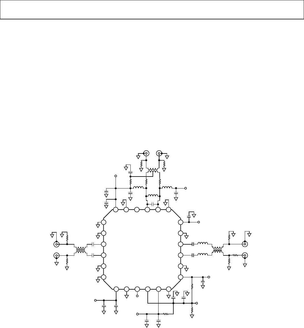
CIRCUIT DESCRIPTION
The ADL5801 includes a double-balanced active mixer with a
50 Ω input impedance and 250 Ω output impedance. In addition,
the ADL5801 integrates a local oscillator (LO) amplifier and
an RF power detector that can be used to optimize the mixer
dynamic range. The RF and LO are differential, providing max-
imum usable bandwidth at the input and output ports. The LO
also operates with a 50 Ω input impedance and can, optionally,
be operated differentially or single ended. The input, output, and
LO ports can be operated over an exceptionally wide frequency
range. The ADL5801 can be configured as a downconvert mixer
or as an upconvert mixer.
The ADL5801 can be divided into the following sections: the
LO amplifier and splitter, the RF voltage-to-current (V-to-I)
converter, the mixer core, the output loads, the RF detector, and
the bias circuit. A simplified block diagram of the device is shown
in Figure 87. The LO block generates a pair of differential LO
signals to drive two mixer cores. The RF input power is converted
into RF currents by the V-to-I converter that then feed into the
two-mixer core. The internal differential load of the mixer
provides a wideband 250 Ω output impedance from the mixer.
Reference currents to each section are generated by the bias
circuit, which can be enabled or disabled using the ENBL pin. A
detailed description of each section of the ADL5801 follows.
GNDVPLO ENBL VSET
VPDT
GND
RFIP
NC
GND
VPLO
7 8
15
16
17
18
21
2223
ADL5801
1920
GNDIFON
13
14
DETO GND
VPRF
GND
GND
GND
IFOP
RFIN
GND
GND
LOIP
LOIN
6
5
4
3
2
1
24
910 11 12
DETBIAS
V2I
08079-127
Figure 87. Block Diagram
LO AMPLIFIER AND SPLITTER
The LO input is conditioned by a series of amplifiers to provide
a well controlled and limited LO swing to the mixer core, resulting
in excellent input IP3. The LO input is amplified using a broadband
low noise amplifier (LNA) and is then followed by LO limiting
amplifiers. The LNA input impedance is nominally 50 Ω. The
LO circuit exhibits low additive noise, resulting in an excellent
mixer noise figure and output noise under RF blocking. For
optimal performance, the LO inputs should be driven differentially
but at lower frequencies; single-ended drive is acceptable.
RF VOLTAGE-TO-CURRENT (V-TO-I) CONVERTER
The differential RF input signal is applied to a V-to-I converter
that converts the differential input voltage to output currents.
The V-to-I converter provides a 50 Ω input impedance. The V-to-I
section bias current can be adjusted up or down using the VSET
pin. Adjusting the current up improves IP3 and P1dB input but
degrades the SSB noise figure. Adjusting the current down improves
the SSB noise figure but degrades IP3 and P1dB input. Conversion
gain remains nearly constant over a wide range of VSET pin
settings, allowing the part to be adjusted dynamically without
affecting conversion gain.
MIXER CORE
The ADL5801 has a double-balanced mixer that uses high per-
formance SiGe NPN transistors. This mixer is based on the
Gilbert cell design of four cross-connected transistors.
MIXER OUTPUT LOAD
The mixer load uses a pair of 125 Ω resistors connected to the
positive supply. This provides a 250 Ω differential output resis-
tance. The mixer output should be pulled to the positive supply
externally using a pair of RF chokes or using an output transformer
with the center tap connected to the positive supply. It is possible
to exclude these components when the mixer core current is
low, but both P1dB input and IP3 input are then reduced.
The mixer load output can operate from direct current (dc) up
to approximately 600 MHz into a 200 Ω load. For upconversion
applications, the mixer load can be matched using off-chip matching
components. Transmit operation up to 3 GHz is possible. See
the Applications Information section for matching circuit details.
Rev. E | Page 27 of 40
ADL5801 Data Sheet
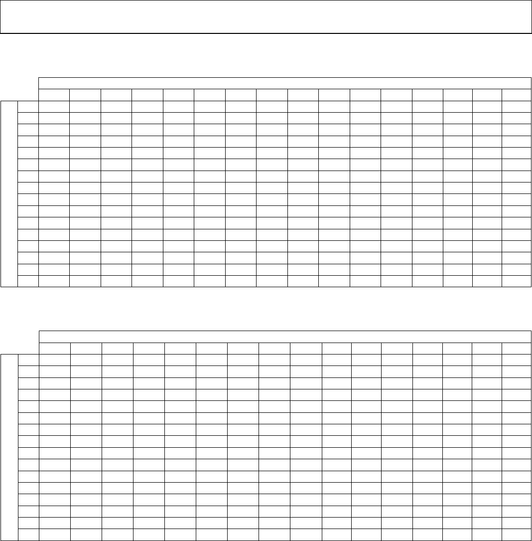
RF DETECTOR
An RF power detector is buffered from the V-to-I converter
section. This detector has a power response range from
approximately −25 dBm up to 0 dBm and provides a current
output. The output current is designed to be connected to the
VSET pin to boost the mixer core current when large RF signals
are present at the mixer input. An external capacitor can be
used to adjust the response time of this function. If not used,
the DETO pin can be left open or connected to ground.
The detector was characterized under the conditions specified
in the Downconverter Mode with a Broadband Balun section.
Pin 11 (DETO) was connected to Pin 10 (VSET), and the voltage
on these pins was plotted vs. the RF input power level over
temperature and a number of devices.
2.0
2.2
2.4
2.6
2.8
3.0
3.2
3.4
3.6
3.8
4.0
–35 –30 –25 –20 –15 –10 –5 05
DETECTOR OUTPUT VOLTAGE (V)
RF INPUT (dBm)
–40°C
+25°C
+85°C
08079-087
Figure 88. Detector Output Voltage vs. RF Input
The input IP3, gain and supply current were also recorded
under these conditions. The result can be seen in Figure 89
through Figure 91.
–5
0
5
10
15
20
25
30
40
35
–35 –30 –25 –20 –15 –10 –5 05
INPUT IP3 (dBm)
RF INPUT (dBm)
–40°C
+25°C
+85°C
08079-088
Figure 89. Input IP3 vs. RF Input
–5.0
–4.0
–3.0
–2.0
–1.0
0
1.0
2.0
3.0
4.0
5.0
–35 –30 –25 –20 –15 –10 –5 0 5
GAIN (dB)
RF INPUT (dBm)
–40°C
+25°C
+85°C
08079-090
Figure 90. Power Conversion Gain vs. RF Input
0
20
40
60
80
100
120
140
160
–35 –30 –25 –20 –15 –10 –5 0 5
SUPPLY CURRENT (mA)
RF INPUT (dBm)
–40°C
+25°C
+85°C
08079-089
Figure 91. Supply Current vs. RF Input
BIAS CIRCUIT
A band gap reference circuit generates the reference currents used
by mixers. The bias circuit and the internal detector can be enabled
and disabled using the ENBL pin. Pulling the ENBL pin high
shuts off the bias circuit and the internal detector. However, the
ENBL pin does not alter the current in the LO section and,
therefore, does not provide a true power-down feature. When
the ENBL pin is pulled high, the device can be operated by applying
an external voltage to the VSET pin or by connecting a resistor
from the VSET pin to the positive supply. Internally, the VSET
pin features a series resistance and diode to ground; therefore, a
simple voltage divider driving the pin is not sufficient. Table 4
lists some typical values for this resistor and the resulting VSET
value and supply current when the ENBL pin is set high. Use
Tabl e 4 to select the appropriate value of R10 (see Figure 110) to
achieve the desired mixer bias level. In this mode of operation,
the VSET pin must not be left floating, and placeholders R7 and
R9 must remain open.
Rev. E | Page 28 of 40
Data Sheet ADL5801
Table 4. Suggested Values of R10 (When ENBL Pin is High)
R10 (Ω) VSET (V) IPOS (mA)1
226 4.14 140
488 4.00 126
562 3.90 123
568 3.89 123
659 3.78 120
665 3.77 120
694 3.74 119
760 3.67 116
768 3.66 116
1000
3.44
109
1100 3.36 107
1150 3.33 106
1200 3.29 105
1300 3.22 102
1400 3.16 100
1500
3.10
99
1600 3.05 97
1700 3.00 95
1800 2.95 94
1900 2.91 92
2000
2.87
91
2300 2.76 87
5900 2.18 68
1 IPOS is the mixer supply current.
If the ENBL pin is pulled low, the bias circuit and internal detector
of the device are enabled. In this mode, the device can be operated
by applying an external voltage to the VSET pin or by connecting
a resistor from the VSET pin to the positive supply. Table 5 lists
some typical values for this resistor and the resulting VSET
value and supply current when the ENBL pin is set low. Use
Tabl e 5 to select the appropriate value of R10 (see Figure 110) to
achieve the desired mixer bias level. In this mode of operation,
R7 and R9 must remain open.
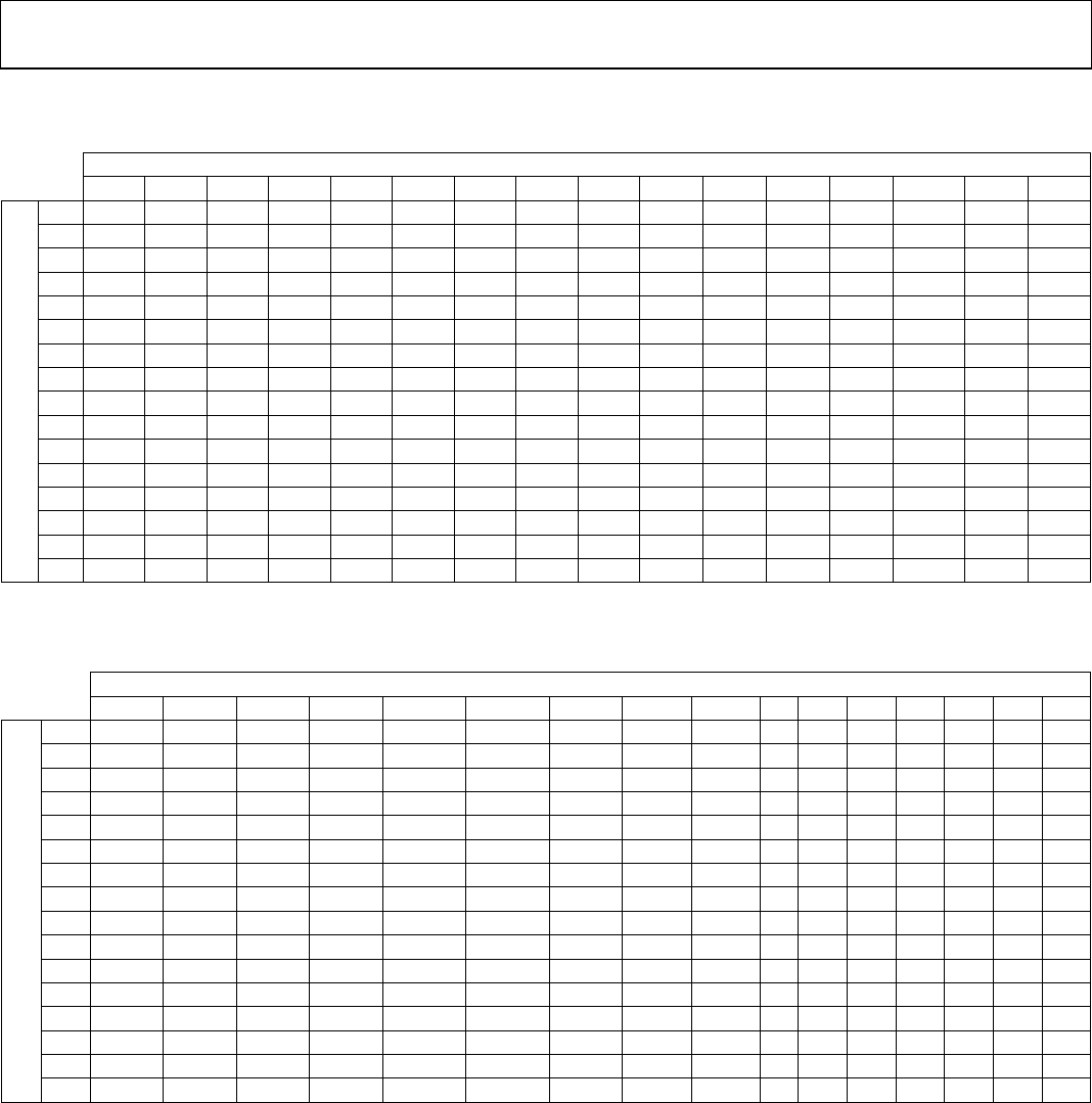
Optionally, the VSET pin can be connected to the DETO pin to
provide dynamic mixer bias control using the internal detector.
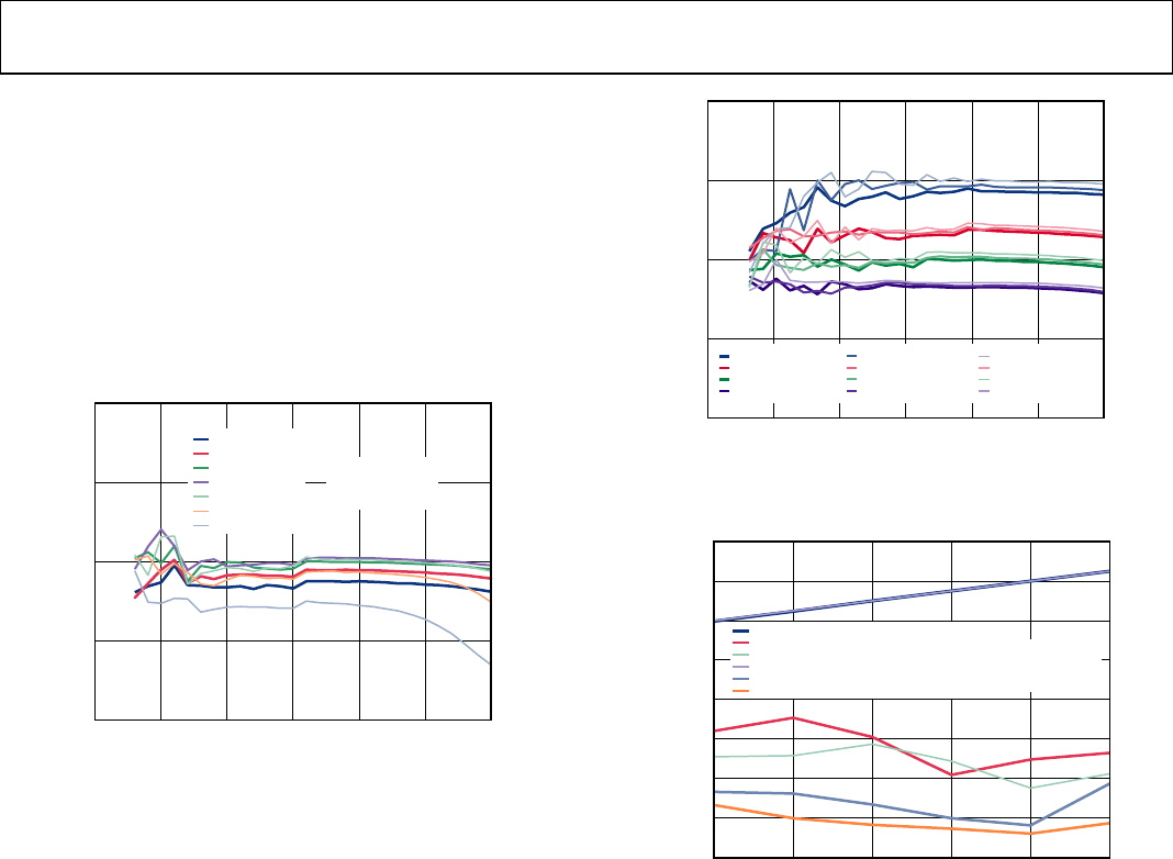
Figure 92 is a comparison of the input IP3 performance vs. RF
input power levels at 2 GHz, when the ENBL pin is pulled high
and low. Pulling ENBL high results in improved linearity across
input power levels, while pulling ENBL low results in enhanced
IP3 performance at higher power levels. The device also exhibits
improved spur performance when the ENBL pin is pulled high.
Figure 95 is a comparison of the 4LO-5RF and 6LO-7RF spurs
vs. RF input power levels at 900 MHz with ENBL high and low.
Table 5. Suggested Values of R10 (When ENBL Pin is Low)
R10 (Ω) VSET (V) IPOS (mA)1
226 4.5 160
562 4.01 146
568 4 145
659 3.9 142
665 3.89 142
694 3.85 142
760 3.8 139
768 3.79 139
1000 3.6 133
1100
3.53
131
1150 3.5 130
1200 3.47 129
1300 3.4 127
1400 3.35 126
1500 3.3 124
1600
3.26
122
1700 3.21 121
1800 3.17 120
1900 3.14 119
2000 3.1 118
2300
3
114
5900 2.5 98
Open 2.03 82
1 IPOS is the mixer supply current.
0
5
10
15
20
25
30
35
–30 –25 –20 –15 –10 –5 0
INPUT IP3 (dBm)
RF INPUT LEVEL (dBm)
ENBL LOW
ENBL HIGH
08079-192
f
RF
= 2000MHz
f
LO
= 1797MHz
f
IF
= 203MHz
Figure 92. Input IP3 vs. RF Input Level at 2 GHz, VSET = 3.8 V,
with ENBL High and Low
Rev. E | Page 29 of 40
ADL5801 Data Sheet
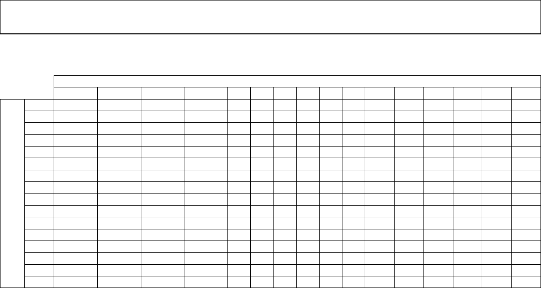
Figure 93 is a plot of the input IP3 vs. RF input power levels for
varying VSET levels at 2 GHz, when the ENBL pin is pulled
high. The device exhibits the best linearity at a VSET level of
4.0 V in this mode of operation. As mentioned previously, the
VSET level can be set using an external voltage or by placing a
resistor from the VSET pin to the positive supply. Figure 94 is a
plot of the input IP3 vs. RF input power levels for a VSET level
of 4.0 V, when the ENBL is pulled high for varying temperature
and frequency conditions. The device is well behaved across
varying frequency levels and exhibits excellent temperature
sensitivity.
–30
–25
–20
–15
–10
–5
0
INPUT IP3 (dBm)
RF INPUT LEVEL (dBm)
VSET = 3.40V
VSET = 3.60V
VSET = 3.80V
VSET = 4.05V
VSET = 4.20V
VSET = 4.40V
VSET = 4.65V
08079-193
15
20
25
30
35
fRF
= 2000MHz
fLO
= 1797MHz
fIF
= 203MHz
Figure 93. Input IP3 vs. RF Input Level at 2 GHz for
Varying VSET levels, ENBL High
–30
–25
–20
–15
–10
–5
0
15
20
25
30
35
INPUT IP3 (dBm)
RF INPUT LEVEL (dBm)
08079-194
–40°C AT 1.0GHz
–40°C AT 1.5GHz
–40°C AT 2.0GHz
–40°C AT 2.5GHz
+25°C AT 1.0GHz
+25°C AT 1.5GHz
+25°C AT 2.0GHz
+25°C AT 2.5GHz
+85°C AT 1.0GHz
+85°C AT 1.5GHz
+85°C AT 2.0GHz
+85°C AT 2.5GHz
Figure 94. Input IP3 vs. RF Input Level for Across Varying Frequency and
Temperature Conditions, VSET = 4.0 V, ENBL High
–140
–120
–100
–80
–60
–40
–20
0
20
–20 –15 –10 –5 0 5
SPUR LEVEL, RELATIVE TO THE CARRIER (dBc)
RF INPUT POWER LEVEL (dBm)
ADL5801 IF, ENBL LOW
ADL5801 4LO-5RF SPUR, ENBL LOW
fRF
= 900MHz
fLO
= 1077MHz
fIF
= 177MHz
ADL5801 6LO-7RF SPUR, ENBL LOW
ADL5801 IF TONE, ENBL HIGH
ADL5801 4LO-5RF SPUR, ENBL HIGH
ADL5801 6LO-7RF SPUR, ENBL HIGH
08079-195
Figure 95. 4LO-5RF and 6LO-7RF Spurs vs. RF Input Level at 900 MHz,
with ENBL High and Low
Rev. E | Page 30 of 40
Data Sheet ADL5801
APPLICATIONS INFORMATION
BASIC CONNECTIONS
The ADL5801 is designed to translate between radio frequencies
(RF) and intermediate frequencies (IF). For both upconversion
and downconversion applications, RFIP (Pin 16) and RFIN
(Pin 15) must be configured as the input interfaces. IFOP
(Pin 20) and IFON (Pin 21) must be configured as the output
interfaces. Individual bypass capacitors are needed in close
proximity to each supply pin (Pin 7, Pin 13, Pin 18, and Pin 24),
the VSET control pin (Pin 10), and the DETO detector output pin
(Pin 11). When the on-chip detector is chosen to form a closed
loop, automatically controlling the VSET pin, R7 can be
populated with a 0 Ω resistor. Alternatively, simply use a jumper
between the VSET and DETO test points for evaluation. Figure 96
illustrates the basic connections for ADL5801 operation.
RF AND LO PORTS
The RF and LO input ports are designed for a differential input
impedance of approximately 50 Ω. Figure 97 and Figure 98
illustrate the RF and LO interfaces, respectively. It is recommended
that each of the RF and LO differential ports be driven through a
balun for optimum performance. It is also necessary to ac couple
both RF and LO ports. Using proper value capacitors may help
improve the input return loss over desired frequencies. Table 6
and Table 9 list the recommended components for various RF
and LO frequency bands in upconvert and downconvert modes.
The characterization data is available in the Typical Performance
Characteristics section.
GND
VPLO ENBL VSET
VPDT
RFIP
NC
GND
GND
VPLO
LOIP
T2
T4
T7
T3
T6
T9
C4
C5
C50
C6
C1 C12
C18
C8
C10
C9
C2
C3
T1
T5
T8
C17
VPOS
VSET
R10
R9
R7
VPOS
VPOS
VPOS
IFOP
LOIP
LOIN
C7
VPOS
DETO
LOIN
GND
GND
ADL5801
GND
GNDIFON
DETO GND
VPRF
GND
GND
IFOP
RFIN
24
1
2
3
4
5
7 8 9 10 11 12
6
18
17
16
15
14
13
23 22 21 20 19
08079-128
IFON
ENBL
R12
R8
RFIP
RFIN
R4
R16
R14
C20
R50
C19
C13
L3
L1
L4
L5
L2
R3
R13
R11
R2
Figure 96. Basic Connections Schematic
Rev. E | Page 31 of 40
ADL5801 Data Sheet
RFIP
T3
C8
C9
RFIP
ADL5801
GND
GND
RFIN
17
16
15
14
08079-129
Figure 97. RF Interface
GND
LOIP
T2
C4
C5
LOIP LOIN
GND
GND
ADL5801
GND
1
2
3
4
5
6
08079-130
Figure 98. LO Interface
Table 6. Suggested Components for the RF and LO Interfaces
in Downconvert Mode
RF and LO
Frequency T2, T3 C8, C9 C4, C5
10 MHz Mini-Circuits TC1-1-13M+ 1 nF 1 nF
900 MHz Mini-Circuits TC1-1-13M+ 5.6 pF 100 pF
1900 MHz Mini-Circuits TC1-1-13M+ 5.6 pF 100 pF
2500 MHz Mini-Circuits TC1-1-43M+ 2 pF 8 pF
3500 MHz 3600BL14M050 1.5 pF 1.5 pF
5500 MHz 5400BL14B050 3 pF 3 pF
10 MHz to
6000 MHz
Mini-Circuits TCM1-63AX+ 1 nF 1 nF
Table 7. Suggested Components for the RF Interface in
Upconvert Mode
RF Frequency T3 C8, C9
153 MHz
TC1-1-13M+
470 pF
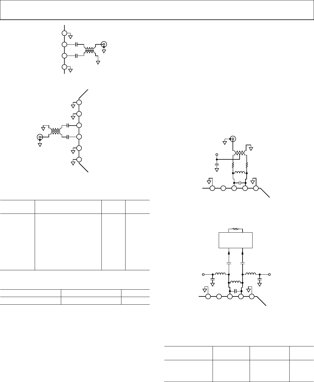
IF PORT
The IF port features an open-collector, differential output interface.
It is necessary to bias the open collector outputs using one of
the schemes presented in Figure 99 and Figure 100.
Figure 99 shows the use of center-tapped impedance transformers.
The turns ratio of the transformer should be selected to provide
the desired impedance transformation. In the case of a 50 Ω
load impedance, a 4:1 impedance ratio transformer should be
used to transform the 50 Ω load into a 200 Ω differential load at
the IF output pins.
Figure 100 shows a differential IF interface where pull-up choke
inductors are used to bias the open-collector outputs. The
shunting impedance of the choke inductors used to couple dc
current into the mixer core should be large enough at the IF
frequency of operation not to load down the output current
before it reaches the intended load. Additionally, the dc current
handling capability of the selected choke inductors must be at
least 45 mA.
The self-resonant frequency of the selected choke inductors
must be higher than the intended IF frequency. A variety of
suitable choke inductors is commercially available from
manufacturers such as Coilcraft® and Murata. An impedance
transforming network may be required to transform the final
load impedance to 200 Ω at the IF outputs.
Tabl e 8 lists suggested components for the IF port in the
upconvert and downconvert modes.
NCGND
C50
C13
L3
R3 R2
T1
T5
T8
VPOS
IFOP
GNDIFON IFOP
23 22 21 20 19
ADL5801
08079-131
Figure 99. Biasing the IF Port Open-Collector Outputs
Using a Center-Tapped Impedance Transformer
NCGND
C20 C19
C13
L3
L1 L2
C3 C2
T1
T5
T8
VPOS VPOS
GNDIFON IFOP
23 22 21 20 19
ADL5801
Z
L
IMPEDANCE
TRANSFORMING
NETWORK
08079-132
Figure 100. Biasing the IF Port Open-Collector Outputs
Using Pull-Up Choke Inductors
Table 8. Suggested Components for the IF Port in Upconvert
and Downconvert Modes
IF Frequency
Mode of
Operation T1 L3
0 MHz to 500 MHz Downconvert TC4-1W+ Open
900 MHz Upconvert TC4-14+ 27 nH
2140 MHz Upconvert 1850BL15B200 3.3 nH
Rev. E | Page 32 of 40
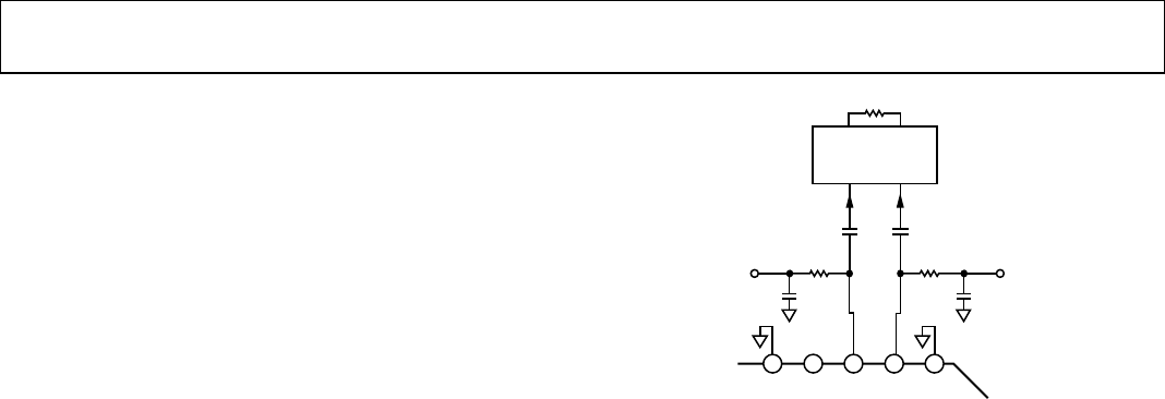
Data Sheet ADL5801
DOWNCONVERTING TO LOW FREQUENCIES
For downconversion to lower frequencies, the device should be
biased at the output with a resistor. The common-mode voltage
at the IF output of the device should be 3.75 V to ensure optimal
performance. Figure 101 provides a sample setup to downconvert
a 900 MHz input signal down to 100 kHz. In the setup depicted
in Figure 101, the output of the device is biased with 50 Ω resistors.
In this mode of operation, the device exhibits 2.0 dB of conversion
gain when a signal at 500 MHz was downcoverted to a 100 kHz,
10 kHz or 1 kHz.
NC
GND
C20
0.1µF C19
0.1µF
10µF 10µF
T1
T5
T8
VPOS VPOS
GND
IFON IFOP
23 22 21 20 19
ADL5801
ZL
IMPEDANCE
TRANSFORMING
NETWORK
08079-136
50Ω 50Ω
Figure 101. Resistive Bias Network to Downconvert Signals to Low
Frequencies
Rev. E | Page 33 of 40
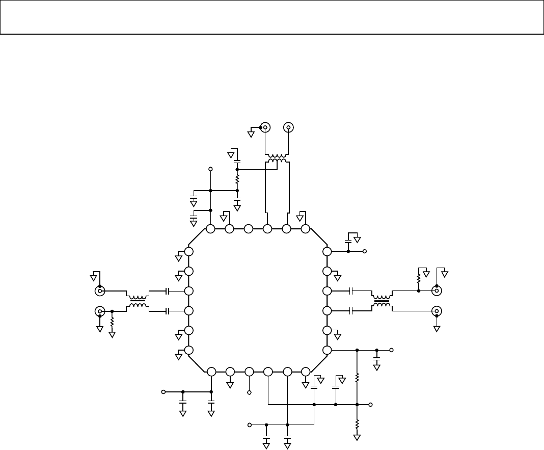
ADL5801 Data Sheet
BROADBAND OPERATION
The ADL5801 can support input frequencies from 10 MHz to 6 GHz. The device can be operated with a broadband balun such as the
MiniCircuits TCM1-63AX+ for applications that need wideband frequency coverage. Figure 102 illustrates a sample setup configuration
with the MiniCircuits TCM1-63AX+ balun populated on the RF and LO ports. This single setup solution provides the option to utilize
the complete input frequency range of the device.
GND
VPLO ENBL VSET
VPDT
RFIP
NC
GND
GNDVPLO
LOIP
R16
0Ω
C4
1nF
C5
1nF
C20
100pF
R50
0Ω
Mini-Circuits
TC4-1W+
Mini-Circuits
TCM1-63AX+ Mini-Circuits
TCM1-63AX+
C50
0.1µF
C6
0.1µF
C1
0.1µF C12
100pF
C18
0.1µF
C8
1nF
C10
0.1µF
C9
1nF
C2
0.1µF
C3
100pF
C17
100pF
C11
0.1µF
R9
R10
R8
0Ω
RFIP
VPOS
VPOS
VSET
VPOS
IFOP
LOIN
LOIP
IFON
RFIN
C7
100pF
VPOS ENBL
DETO
LOIN
GND
GND
ADL5801
GND
GNDIFON
DETO GND
VPRF
GND
GND
IFOP
RFIN
24
1
2
3
4
5
7 8 910 11 12
6
18
17
16
15
14
13
23 22 21 20 19
08079-137
Figure 102. Sample Setup Configuration with the MiniCircuits TCM1-63AX+ Broadband Balun
Rev. E | Page 34 of 40
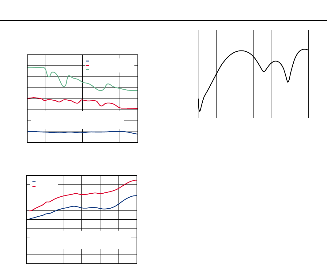
Data Sheet ADL5801
Figure 103 to Figure 105 demonstrate the performance of the
mixer with the MiniCircuits TCM1-63AX+ populated on the
RF and LO ports.
–10
0
10
20
30
40
50
60
70
01000 2000 3000 4000 5000 6000
GAIN, IIP3, IIP2 (dB, dBm)
RF FREQUENCY (MHz)
IIP2 (dBm)
CONVERSION GAIN (dB)
IIP3 (dBm)
fIF
= 153MHz,
fLO
: 163MHz TO 6153MHz (HIGH SIDE LO)
P
RF
= –10dBm, P
LO
= 0dBm
IIP3: 1MHz TONE SPACING BETWEEN CHANNELS
IIP2: 15MHz TONE SPACING BETWEEN CHANNELS
08079-138
Figure 103. Gain, IIP3, IIP2 vs. RF Frequency
0
2
4
6
8
10
12
14
16
18
20
01000 2000 3000 4000 5000 6000
NOISE FIGURE (dB)
RF FREQUENCY (MHz)
V
SET
= 2.0V
V
SET
= 3.6V
f
IF
=153MHz,
f
LO
:163MHz TO6153MHz(HIGHSIDE LO)
P
RF
= –10dBm, P
LO
= 0dBm
IIP3: 1MHz TONE SPACING BETWEENCHANNELS
IIP2:15MHz TONESPACING BETWEEN CHANNELS
08079-139
Figure 104. Noise Figure vs. RF Frequency
–40
–35
–30
–25
–20
–15
–10
–5
0
01000 2000 3000 4000 5000 6000
INPUT RETURN LOSS (dB)
RF FREQUENCY (MHz)
08079-140
Figure 105. Input Return Loss vs. RF Frequency
The device maintains an Input IP3 of 20 dBm or better and
conversion gain of −2 dB or better across the 10 MHz to 6 GHz
frequency band.
Rev. E | Page 35 of 40
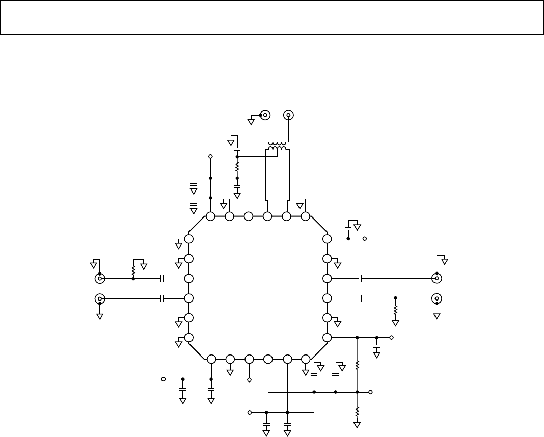
ADL5801 Data Sheet
SINGLE-ENDED DRIVE OF RF AND LO INPUTS
The RF and LO ports of the active mixer can be driven single-ended without baluns for single-ended operation. In this configuration, the
unused RF and LO ports should be ac grounded using a 1 nF capacitor. Figure 106 depicts setup configuration suggested to operate the
device in the single-ended mode.
GND
VPLO ENBL VSET
VPDT
RFIP
NC
GND
GNDVPLO
LOIP
R14
0Ω
C4
1nF
C5
1nF
C20
100pF
R50
0Ω
Mini-Circuits
TC4-1W+
C50
0.1µF
C6
0.1µF
C1
0.1µF C12
100pF
C18
0.1µF
C8
1nF
C10
0.1µF
C9
1nF
C2
0.1µF
C3
100pF
C17
100pF
C11
0.1µF
R9
R10
R1
0Ω
RFIP
VPOS
VPOS
VSET
VPOS
IFOP
LOIN
LOIP
IFON
RFIN
C7
100pF
VPOS ENBL
DETO
LOIN
GND
GND
ADL5801
GND
GNDIFON
DETO GND
VPRF
GND
GND
IFOP
RFIN
24
1
2
3
4
5
78910 11 12
6
18
17
16
15
14
13
23 22 21 20 19
08079-141
Figure 106. Single-Ended Configuration to Operate the ADL5801
Rev. E | Page 36 of 40
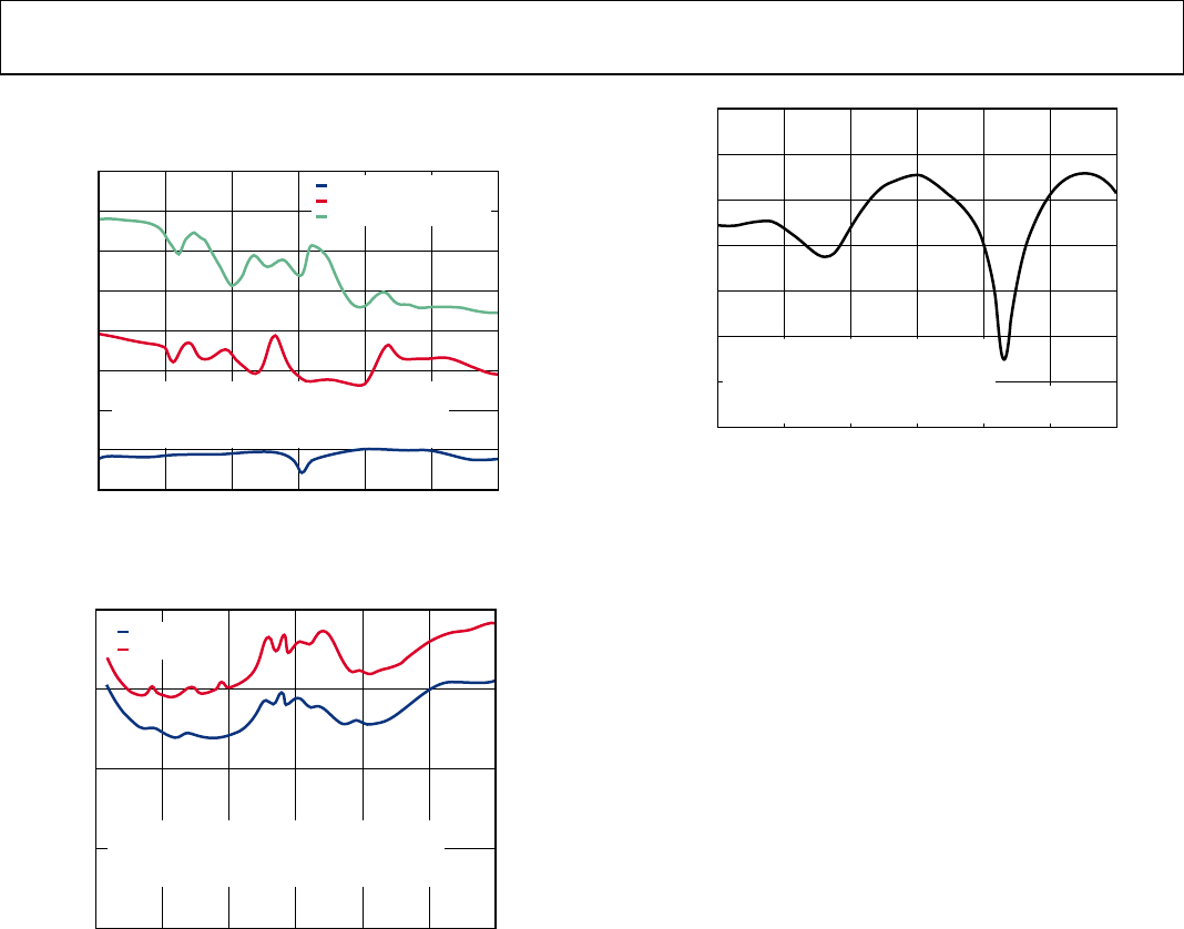
Data Sheet ADL5801
Figure 107 to Figure 109 demonstrate the performance of the
mixer in the single ended mode.
–10
0
10
20
30
40
50
60
70
01000 2000 3000 4000 5000 6000
GAIN, IIP3, IIP2 (dB, dBm)
RF FREQUENCY (MHz)
IIP2 (dBm)
CONVERSION GAIN (dB)
IIP3 (dBm)
08079-142
fIF
= 153MHz,
fLO
: 163MHz TO 6153MHz (HIGH SIDE LO)
P
RF
= –10dBm, P
LO
= 0dBm
IIP3: 1MHz TONE SPACING BETWEEN CHANNELS
IIP2: 15MHz TONE SPACING BETWEEN CHANNELS
Figure 107. Gain, IIP3, IIP2 vs. RF Frequency
0
5
10
15
20
01000 2000 3000 4000 5000 6000
NOISE FIGURE (dB)
RF FREQUENCY (MHz)
V
SET
= 2.0V
V
SET
= 3.6V
08079-143
f
IF
= 153MHz,
f
LO
: 163MHz TO 6153MHz (HIGH SIDE LO)
P
RF
= –10dBm, P
LO
= 0dBm
IIP3: 1MHz TONE SPACING BETWEEN CHANNELS
IIP2: 15MHz TONE SPACING BETWEEN CHANNELS
Figure 108. Noise Figure vs. RF Frequency
–35
–30
–25
–20
–15
–10
–5
0
01000 2000 3000 4000 5000 6000
INPUT RETURN LOSS (dB)
RF FREQUENCY (MHz)
08079-144
fIF
= 153MHz
fLO
: 163MHz TO 6153MHz (HIGH SIDE LO)
P
RF
= –10dBm, P
LO
= 0dBm
IIP3: 1MHz TONE SPACING BETWEEN CHANNELS
IIP2: 15MHz TONE SPACING BETWEEN CHANNELS
Figure 109. Input Return Loss vs. RF Frequency
Rev. E | Page 37 of 40
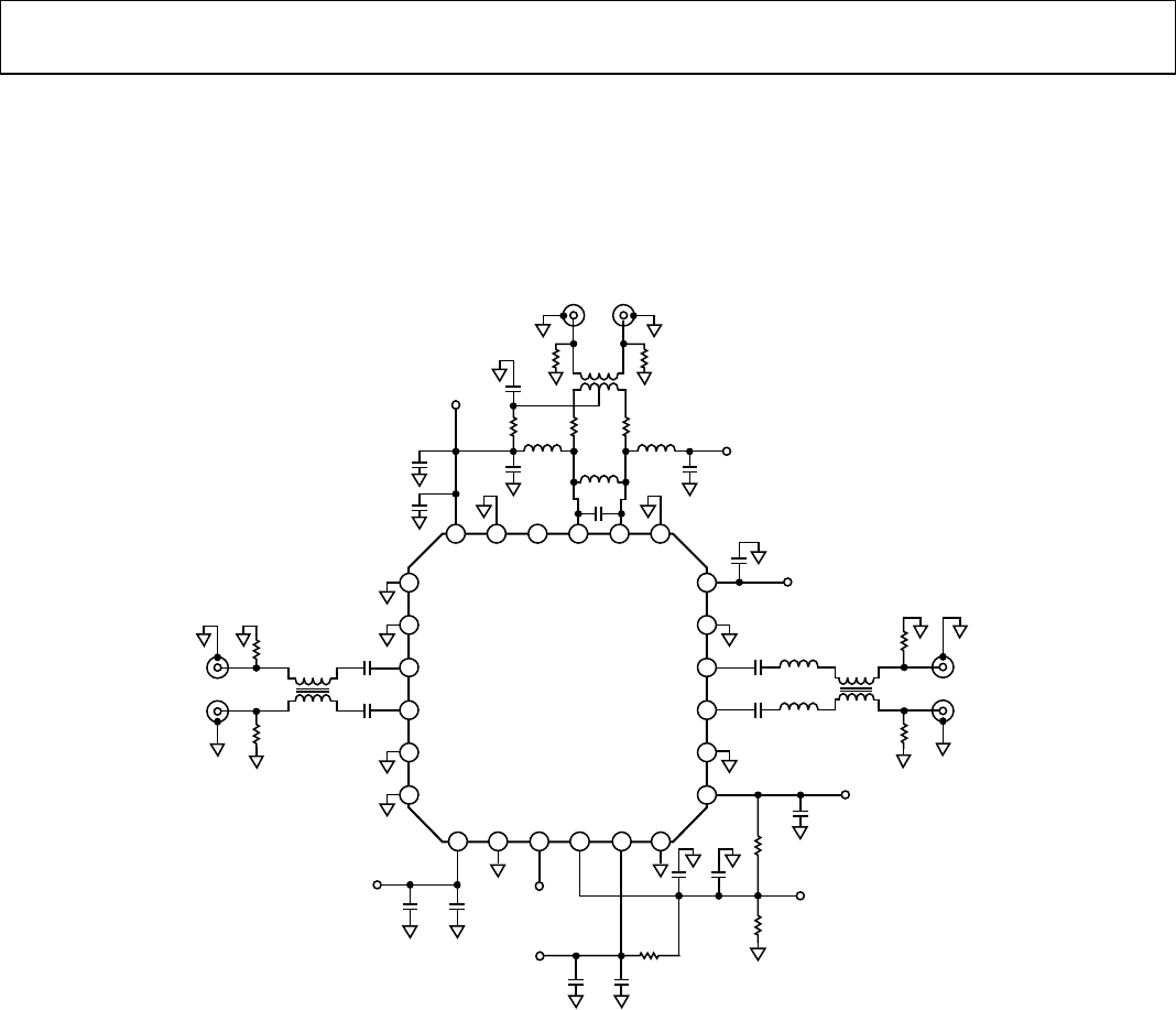
ADL5801 Data Sheet
EVALUATION BOARD
An evaluation board is available for the ADL5801. The standard evaluation board is fabricated using Rogers® RO3003 material. Each RF,
LO, and IF port is configured for single-ended signaling via a balun transformer. The schematic for the evaluation board is shown in
Figure 110. Tabl e 9 describes the various configuration options for the evaluation board. Layout for the board is shown in Figure 111 and
Figure 112.
GND
VPLO ENBL VSET
VPDT
RFIP
NC
GND
GND
VPLO
LOIP
R14
R16
T2
T4
T7
T3
T6
T9
C4
C5
C20
R50
C50
C6
C1 C12
C18
C8
C10
C19
C13
L3
L1 L2
C9
L4
R3
C2
C3
R13R11
R2
T1
T5
T8
L5
C17
C11
R7
R9
R10
R12
R8
RFIP
VPOS
VPOS
VPOS
VSET
VPOS
IFOP
LOIN
LOIP
IFON
RFIN
C7
VPOS ENBL
DETO
LOIN
GND
GND
ADL5801
GND
GNDIFON
DETO GND
VPRF
GND
GND
IFOP
RFIN
24
1
2
3
4
5
78 9 10 11 12
6
18
17
16
15
14
13
23 22 21 20 19
08079-133
Figure 110. Evaluation Board Schematic
Rev. E | Page 38 of 40
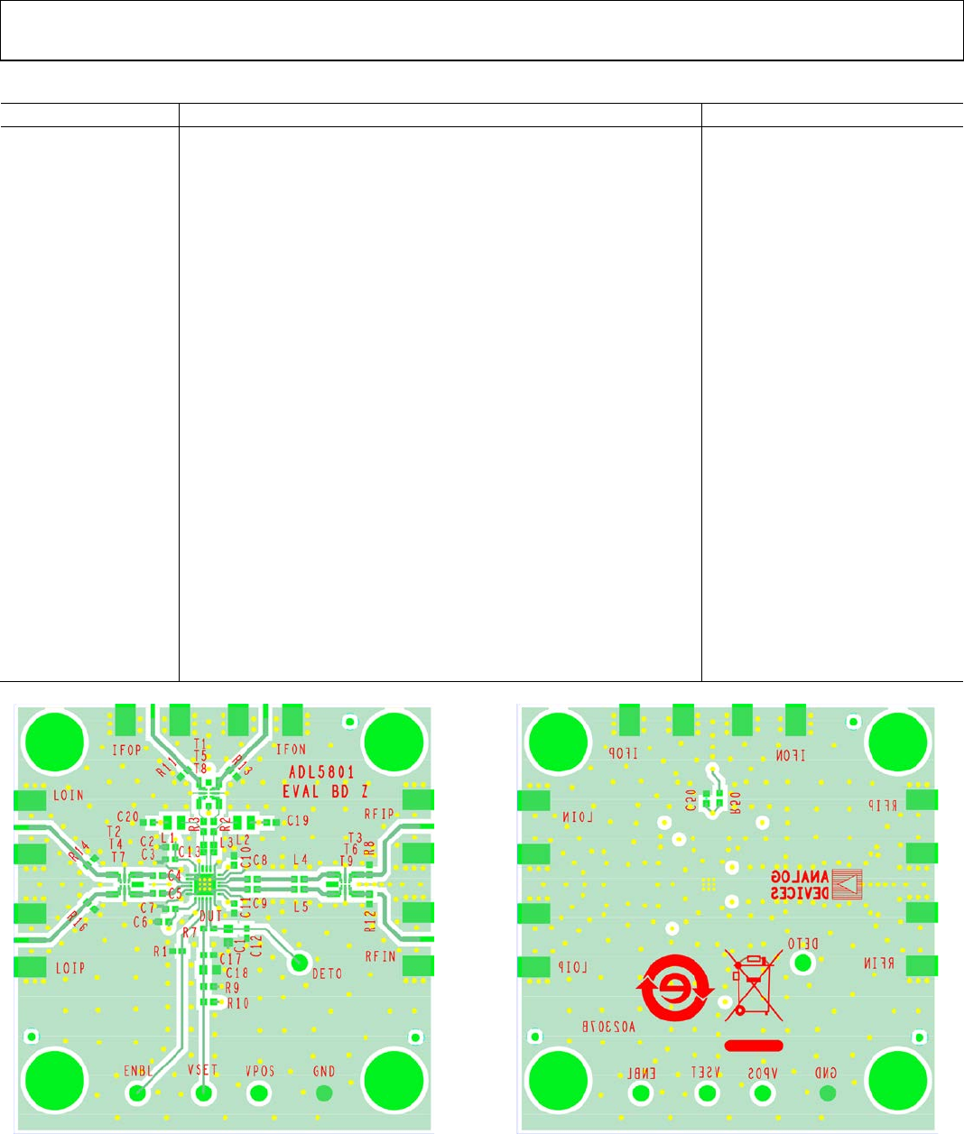
Data Sheet ADL5801
Table 9. Evaluation Board Configuration
Components Function Default Conditions
C2, C3, C6, C7, C10, C11 Power supply decoupling. Nominal supply decoupling consists of a
0.1 µF capacitor to ground in parallel with 100 pF capacitors to ground,
positioned as close to the device as possible. Series resistors are provided
for enhanced supply decoupling using optional ferrite chip inductors.
C2, C6, C10, C11 = 0.1 µF (size 0402)
C3, C7 = 100 pF (size 0402)
C8, C9, L4, L5, R4, R8,
R12, T3, T6, T9, RFIN,
RFIP
RF input interfaces. (Use RFIN for operation
)
.
Input channels are ac-coupled through C8 and C9. R8 and R12 provide
options when additional matching is needed. T3 is a 1:1 balun used to
interface to the 50 Ω differential inputs. T6 and T9 provide options when
high frequency baluns are used and require smaller balun footprints.
C8, C9 = 1 nF (size 0402)
L4, L5 = 0 Ω (size 0402)
R12 = open (size 0402)
R4, R8 = 0 Ω (size 0402)
T3 = TCM1-63AX+ (Mini-Circuits)
C13, C19, C20, C50, L1,
L2, L3, R2, R3, R11, R13,
R50, T1, T5, T8, IFON,
IFOP
IF output interfaces. The 200 Ω open collector IF output interfaces are
biased through the center tap of a 4:1 impedance transformer at T1. C50
provides local bypassing with R50 available for additional supply
bypassing. L1 and L2 provide options when pull-up choke inductors are
used to bias the open-collector outputs. C13, L3, R2, and R3 are provided
for IF filtering and matching options. T5 and T8 provide options when high
frequency baluns are used and require smaller balun footprints.
C13 = open (size 0402)
C19, C20 = 100 pF (size 0402)
C50 = 0.1 µF (size 0402)
L1, L2 = open (size 0805)
L3 = open (size 0402)
R2, R3, R13, R50 = 0 Ω (size 0402)
R11 = open (size 0402)
T1 = TC4-1W+ (Mini-Circuits)
C4, C5, R14, R16, T2, T4,
T7, LOIN, LOIP
LO interface. (Use LOIN for operation).
C4 and C5 provide ac coupling for the local oscillator input. T2 is a 1:1
balun that allows single-ended interfacing to the differential 50 Ω local
oscillator input. T4 and T7 provide options when high frequency baluns
are used and require smaller balun footprints.
C4, C5 = 1 nF (size 0402)
R14 = open (size 0402)
R16 = 0 Ω (size 0402)
T2 = TCM1-63AX+
C1, C12, R7, DETO DETO interface. C1 and C12 provide decoupling for the DETO pin. R7
provides access to the VSET pin when automatic input IP3 control is
needed.
C1 = 0.1 µF (size 0603)
C12 = 100 pF (size 0402)
R7 = open (size 0402)
C17, C18, R9, R10, VSET VSET bias control. C17 and C18 provide decoupling for the VSET pin. R9
and R10 form an optional resistor divider network between VPOS and
GND, allowing for a fixed bias setting. Supply 3.8 V at the VSET pin when
the DETO pin is not connected for automatic input IP3 control.
C17 = 100 pF (size 0402)
C18 = 0.1 µF (size 0603)
R9, R10 = open (size 0402)
08079-134
Figure 111. Evaluation Board Top Layer
08079-135
Figure 112. Evaluation Board Bottom Layer
Rev. E | Page 39 of 40
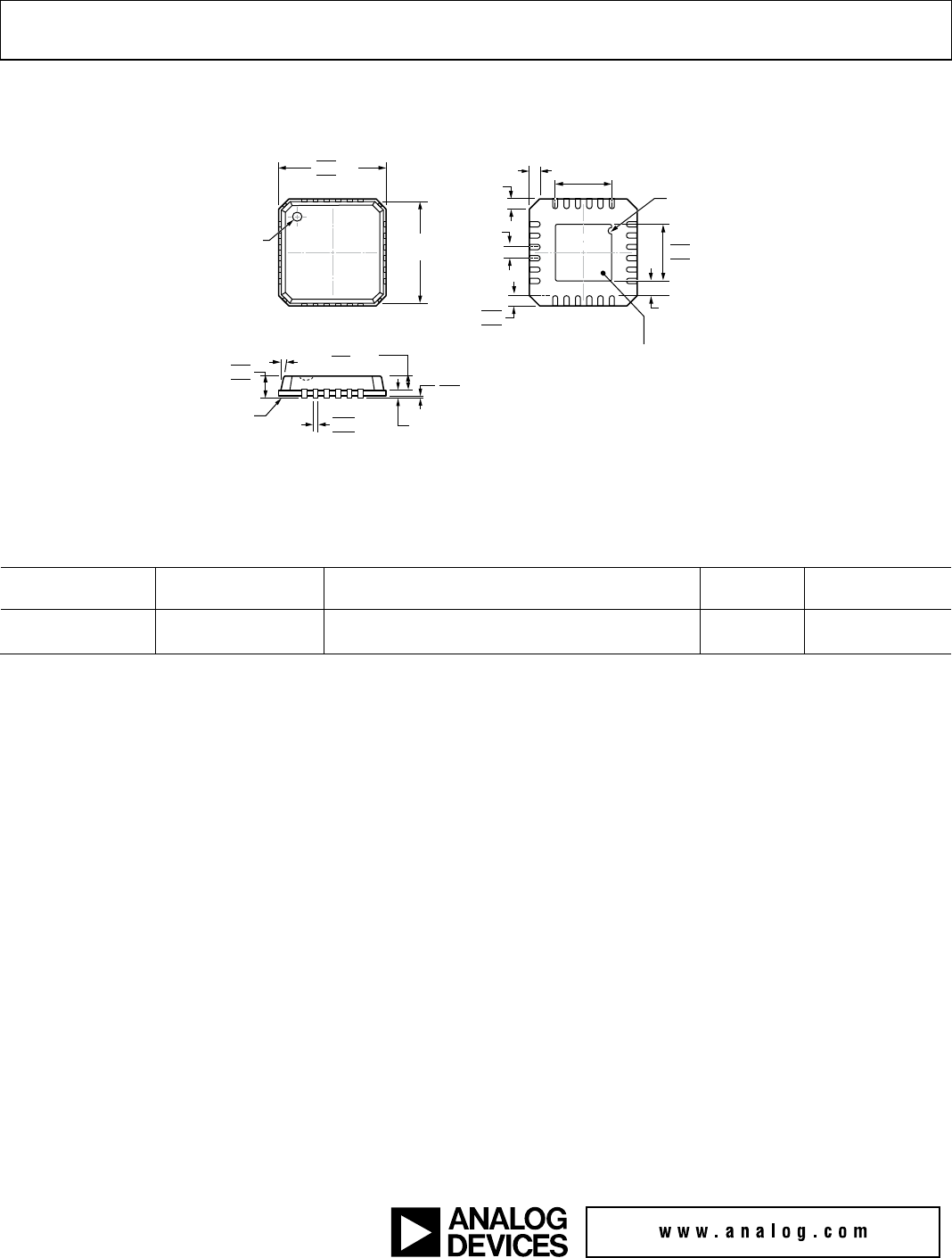
ADL5801
OUTLINE DIMENSIONS
COMPLIANT
TO
JEDEC STANDARDS MO-220-VGGD-8
04-11-2012-A
1
0.50
BSC
PIN 1
INDICATOR
2.50 REF
0.50
0.40
0.30
TOP VIEW
12° MAX 0.80 MAX
0.65 TYP
SEATING
PLANE
COPLANARITY
0.08
1.00
0.85
0.80
0.30
0.23
0.18
0.05 MAX
0.02 NOM
0.20 REF
0.25 MIN
2.65
2.50 SQ
2.35
24
7
19
12
13
18
6
0.60 MAX
0.60 MAX
PIN 1
INDICATOR
4.10
4.00 SQ
3.90
3.75 BSC
SQ
EXPOSED
PAD
FOR PROPER CONNECTION OF
THE EXPOSED PAD, REFER TO
THE PIN CONFIGURATION AND
FUNCTION DESCRIPTIONS
SECTION OF THIS DATA SHEET.
BOTTOM VIEW
Figure 113. 24-Lead Lead Frame Chip Scale Package [LFCSP_VQ]
4 mm × 4 mm Body, Very Thin Quad (CP-24-3)
Dimensions shown in millimeters
ORDERING GUIDE
Model1 Temperature Range Package Description
Package
Option
Ordering
Quantity
ADL5801ACPZ-R7 −40°C to +85°C 24-Lead Lead Frame Chip Scale Package [LFCSP_VQ] CP-24-3 1,500 per Reel
ADL5801-EVALZ
Evaluation Board
1
1 Z = RoHS Compliant Part.
©2010–2014 Analog Devices, Inc. All rights reserved. Trademarks and
registered trademarks are the property of their respective owners.
D08079-0-4/14(E)
Rev. E | Page 40 of 40
