Micropower Circuits Using The LM4250 Programmable Op Amp AN 0071
User Manual: AN-0071
Open the PDF directly: View PDF ![]() .
.
Page Count: 10
TL/H/7382
Micropower Circuits Using the LM4250 Programmable Op Amp AN-71
National Semiconductor
Application Note 71
George Cleveland
July 1972
Micropower Circuits Using
the LM4250 Programmable
Op Amp
INTRODUCTION
The LM4250 is a highly versatile monolithic operational am-
plifier. A single external programming resistor determines
the quiescent power dissipation, input offset and bias cur-
rents, slew rate, gain-bandwidth product, and input noise
characteristics of the amplifier. Since the device is in effect
a different op amp for each externally programmed set cur-
rent, it is possible to use a single stock item for a variety of
circuit functions in a system.
This paper describes the circuit operation of the LM4250,
various methods of biasing the device, frequency response
considerations, and some circuit applications exercising the
unique characteristics of the LM4250.
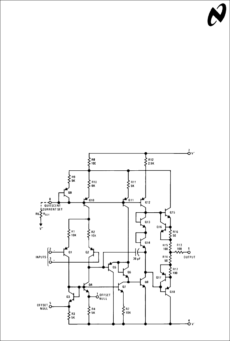
CIRCUIT DESCRIPTION LM4250
The LM4250 has two special features when compared with
other monolithic operational amplifiers. One is the ability to
externally set the bias current levels of the amplifiers, and
the other is the use of PNP transistors as the differential
input pair.
Referring to
Figure 1
,Q
1and Q2are high current gain later-
al PNPs connected as a differential pair. R1and R2provide
emitter degeneration for greater stability at high bias cur-
rents. Q3and Q4are used as active loads for Q1and Q2to
provide high gain and also form a current inverter to provide
the maximum drive for the single ended output into Q5.Q
5is
an emitter follower which prevents loading of the input stage
by the succeeding amplifier stage.
One advantage of this lateral PNP input stage is a common
mode swing to within 200 mV of the negative supply. This
feature is especially useful in single supply operation with
signals referred to ground. Another advantage is the almost
constant input bias current over a wide temperature range.
The input resistance RIN is approximately equal to 2b(RE
are) where bis the current gain, reis the emitter resist-
ance of one of the input lateral PNPs, and REis the resist-
ance of one of the 10 kXemitter resistor. Using a DC beta
of 100 and the normal temperature dependent expression
for regives:
TL/H/7382–1
FIGURE 1. LM4250 Schematic Diagram
C1995 National Semiconductor Corporation RRD-B30M115/Printed in U. S. A.
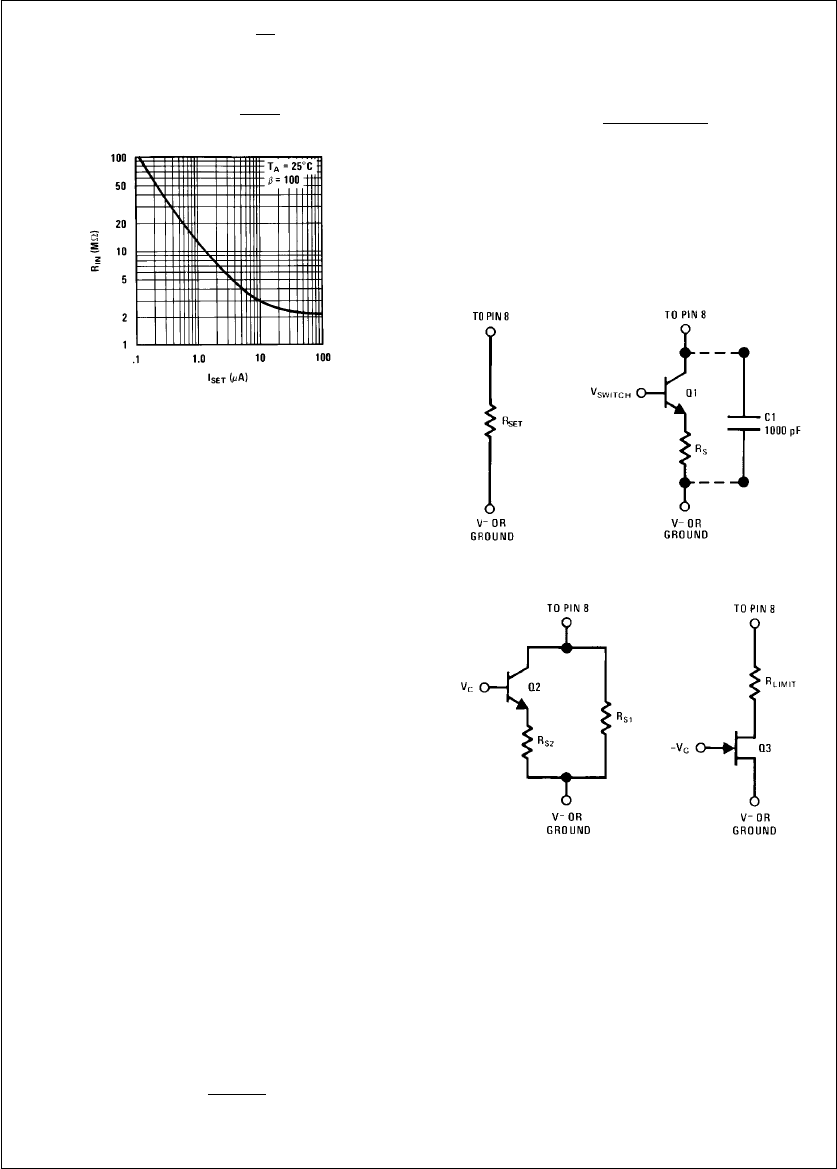
RIN &2MXa2kT
qlB
(1)
where lBis input bias current. At room temperature this for-
mula becomes:
RIN &2MXa52 mV
lB
(2)
TL/H/7382–2
FIGURE 2. Input Resistance vs ISET
Figure 2
gives a typical plot of RIN vs Iset derived from the
above equation.
Continuing with the circuit description, Q6level shifts down-
ward to the base of Q8which is the second stage amplifier.
Q8is run as a common emitter amplifier with a current
source load (Q12) to provide maximum gain. The output of
Q8drives the class B complementary output stage com-
posed of Q15 and Q18.
The bias current levels in the LM4250 are set by the amount
of current (Iset) drawn out of Pin 8. The constant current
sources Q10,Q
11, and Q12 are controlled by the amount of
Iset current through the diode connected transistor Q9and
resistor R9. The constant collector current from Q10 biases
the differential input stage. Therefore, the level Q10 is set at
will control such amplifier characteristics as input bias cur-
rent, input resistance, and amplifier slew rate. Current
source Q11 biases Q5and Q6. The current ratio between Q5
and Q6is controlled by constant current sink Q7. Current
source Q12 sets the currents in diodes Q13 and Q14 which
bias the output stage to the verge of conduction thereby
eliminating the dead zone in the class B output. Q12 also
acts as the load for Q8and limits the drive current to Q15.
The output current limiting is provided by Q16 and Q17 and
their associated resistors R16 and R17. When enough cur-
rent is drawn from the output, Q16 turns on and limits the
base drive of Q15. Similarly Q17 turns on when the LM4250
attempts to sink too much current, limiting the base drive of
Q18 and therefore output current. Frequency compensation
is provided by the 30 pF capacitor across the second stage
amplifier, Q8, of the LM4250. This providesa6dBperoc-
tave rolloff of the open loop gain.
BIAS CURRENT SETTING PROCEDURE
The single set resistor shown in
Figure 3a
offers the most
straightforward method of biasing the LM4250. When the
set resistor is connected from Pin 8 to ground the resistance
value for a given set current is:
RSET eVab0.5
ISET
(3)
The 0.5 volts shown in Equation 3 is the voltage drop of the
master bias current diode connected transistor on the inte-
grated circuit chip. In applications where the regulation of
the Vasupply with respect to the Vbsupply (as in the case
of tracking regulators) is better than the Vasupply with
respect to ground the set resistor should be connected from
Pin8toV
b
.R
SET is then:
RSET eVaa
l
Vb
l
b0.5
ISET
(4)
The transistor and resistor scheme shown in
Figure 3b
al-
lows one to switch the amplifier off without disturbing the
main Vaand Vbpower supply connections. Attaching C1
across the circuit prevents any switching transient from ap-
pearing at the amplifier output. The dual scheme shown in
Figure 3c
has a constant set current flowing through RS1
and a variable current through RS2. Transistor Q2acts as an
emitter follower current sink whose value depends on the
control voltage Vcon the base. This circuit provides a meth-
TL/H/7382–4
TL/H/7382–3
3b
3a
TL/H/7382–5 TL/H/7382–6
3c 3d
FIGURE 3. Biasing Schemes
od of varying the amplifier’s characteristics over a limited
range while the amplifier is in operation. The FET circuit
shown in
Figure 3d
covers the full range of set currents in
response to as little as a 0.5V gate potential change on a
low pinch-off voltage FET such as the 2N3687. The limit
resistor prevents excessive current flow out of the LM4250
when the FET is fully turned on.
FREQUENCY RESPONSE OF A
PROGRAMMABLE OP AMP
This section provides a method of determining the sine and
step voltage response of a programmable op amp. Both the
sine and step voltage responses of an amplifier are modified
when the rate of change of the output voltage reaches the
slew rate limit of the amplifier. The following analysis devel-
2
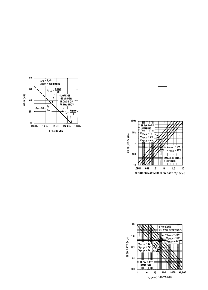
ops the Bode plot as well as the small signal and slew rate
limited responses of an amplifier to these two basic catego-
ries of waveforms.
SMALL SIGNAL SINE WAVE RESPONSE
The key to constructing the Bode plot for a programmable
op amp is to find the gain bandwidth product, GBWP, for a
given set current. Quiescent power drain, input bias current,
or slew rate considerations usually dictate the desired set
current. The data sheet curve relating GBWP to set current
provides the value of GBWP which when divided by one
yields the unity gain crossover of fu. Assuming a set current
of 6 mA gives a GBWP of 200,000 Hz and therefore an fuof
200 kHz for the example shown in
Figure 4
. Since the de-
vice has a single dominant pole, the rolloff slope is b20 dB
of gain per decade of frequency (b6 dB/octave). The dot-
ted line shown on
Figure 4
has this slope and passes
TL/H/7382–7
FIGURE 4. Bode Plot
through the 200 kHz fupoint. Arbitrarily choosing an invert-
ing amplifier with a closed loop gain magnitude of 50 deter-
mines the height of the 34 dB horizontal line shown in
Fig-
ure 4
. Graphically finding the intersection of the sloped line
and the horizontal line or mathematically dividing GBWP by
50 determines the 3 dB down frequency of 4 kHz for the
closed loop response of this amplifier configuration. There-
fore, the amplifier will now apply a gain of b50 to all small
signal sine waves at frequencies up to 4 kHz. For frequen-
cies above 4 kHz, the gain will be as shown on the sloped
portion of the Bode plot.
SMALL SIGNAL STEP INPUT RESPONSE
The amplifier’s response to a positive step voltage change
at the input will be an exponentially rising waveform whose
rise time is a function of the closed loop 3 dB down band-
width of the amplifier. The amplifier may be modeled as a
single pole low pass filter followed by a gain of 50 wideband
amplifier. From basic filter theory*, the 10% to 90% rise
time of a single pole low pass filter is:
tre0.35
f3dB
(5)
For the example shown in
Figure 4
the 4 kHz 3 dB down
frequency would give a rise time of 87.5 ms.
SLEW RATE LIMITED LARGE SIGNAL RESPONSE
The final consideration, which determines the upper speed
limitation on the previous two types of signal responses, is
the amplifier slew rate. The slew rate of an amplifier is the
maximum rate of change of the output signal which the am-
plifier is capable of delivering. In the case of sinosoidal sig-
nals, the maximum rate of change occurs at the zero cross-
ing and may be derived as follows:
*See reference.
VOeVpsin 2qf t (6)
dV
O
dt e2qfV
pcos 2qft (7)
dV
O
dt À
teoe2qfV
p(8)
Sre2qfMAX VP(9)
where:
VOeoutput voltage
Vpepeak output voltage
Sremaximum dV
O
dt
The maximum sine wave frequency an amplifier with a given
slew rate will sustain without causing the output to take on a
triangular shape is therefore a function of the peak ampli-
tude of the output and is expressed as:
fMAX eSr
2qVp
(10)
Figure 5
shows a quick reference graphical presentation of
this formula with the area below any Vpeak line representing
an undistorted small signal sine wave response for a given
frequency and amplifier slew rate and the area above the
Vpeak line representing a distorted sine wave response due
to slew rate limiting for a sine wave with the given Vpeak.
TL/H/7382–8
FIGURE 5. Frequency vs Slew Rate Limit vs Peak
Output Voltage
Large signal step voltage changes at the output will have a
rise time as shown in equation 5 until a signal with a rate of
output voltage change equal to the slew rate of the amplifier
occurs. At this point the output will become a ramp function
with a slope equal to Sr. This action occurs when:
SrsVstep
tr
(11)
TL/H/7382–9
FIGURE 6. Slew Rate vs Rise Time vs Step Voltage
3
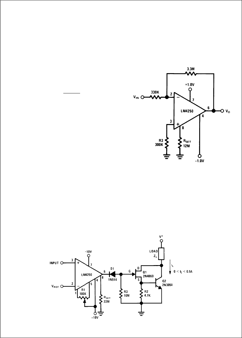
Figure 6
graphically expresses this formula and shows the
maximum amplitude of undistorted step voltage for a given
slew rate and rise time. The area above each step voltage
line represents the undistorted low pass filter type response
mode of the amplifier. If the intersection of the rise time and
slew rate values of a particular amplifier configuration falls
below the expected step voltage amplitude line, the rise
time will be determined by the slew rate of the amplifier. The
rise time will then be equal to the amplitude of the step
divided by the slew rate Sr.
FULL POWER BANDWIDTH
The full power bandwidth often found on amplifier specifica-
tion sheets is the range of frequencies from zero to the
frequency found at the intersection on
Figure 5
of the maxi-
mum rated output voltage and the slew rate Srof the ampli-
fier. Mathematically this is:
ffull power eSr
2qVrated
(12)
The full power bandwidth of a programmable amplifier such
as the LM4250 varies with the master bias set current.
The above analysis of sine wave and step voltage amplifier
responses applies for all single dominant pole op amps
such as the LM101A, LM1107, LM108A, LM112, LM118,
and LM741 as well as the LM4250 programmable op amp.
500 MANO-WATT X10 AMPLIFIER
The X10 inverting amplifier shown in
Figure 7
demonstrates
the low power capability of the LM4250 at extremely low
values of supply voltage and set current. The circuit draws
260 nA from the a1.0V supply of which 50 nA flows
through the 12 MXset resistor. The current into the b1.0V
supply is only 210 nA since the set resistor is tied to ground
rather than Vb. Total quiescent power dissipation is:
PDe(260 nA) (1V) a(210 nA) (1V) (13)
PDe470 nW (14)
The slew rate determined from the data sheet typical per-
formance curve is 1 V/ms for a .05 mA set current. Samples
of actual values observed were 1.2 V/ms for the negative
slew rate and 0.85 V/ms for the positive slew rate. This
difference occurs due to the non-symmetry in the current
sources used for charging and discharging the internal 30
pF compensation capacitor.
The 3 dB down (gain of b7.07) frequency observed for this
configuration was approximately 300 Hz which agrees fairly
closely with the 3.5 kHz GBWP divided by 10 taken from an
extrapolation of the data sheet typical GBWP versus set
current curve.
Peak-to-peak output voltage swing into a 100 kXload is
0.7V or g0.35V peak. An increase in supply voltage to
g1.35V such as delivered by a pair of mercury cells directly
increases the output swing by g0.35V to 1.4V peak-to-
peak. Although this increases the power dissipation to ap-
proximately 1 mW per battery, a power drain of 15 mWor
less will not affect the shelf life of a mercury cell.
TL/H/7382–10
FIGURE 7. 500 nW x 10 Amplifier
MICRO-POWER MONITOR WITH HIGH CURRENT
SWITCH
Figure 8
shows the combination of a micro-power compara-
tor and a high current switch run from a separate supply.
This circuit provides a method of continuously monitoring an
input voltage while dissipating only 100 mW of power and
still being capable of switching a 500 mA load if the input
exceeds a given value. The reference voltage can be any
value between a8.5V and b8.5V. With a minimum gain of
approximately 100,000 the comparator can resolve input
voltage differences down into the 0.2 mV region.
TL/H/7382–11
FIGURE 8. m–Power Comparator with
High Current Switch
4
The bias current for the LM4250 shown in
Figure 8
is set at
0.44 mA by the 200 MXRset resistor. This results in a total
comparator power drain of 100 mW and a slew rate of ap-
proximately 11 V/ms in the positive direction and 12.8 V/ms
in the negative direction. Potentiometer R1provides input
offset nulling capability for high accuracy applications.
When the input voltage is less than the reference voltage,
the output of the LM4250 is at approximately b9.5V caus-
ing diode D1to conduct. The gate of Q1is held at b8.8V by
the voltage developed across R3. With a large negative volt-
age on the gate of Q1it turns off and removes the base
drive from Q2. This results in a high voltage or open switch
condition at the collector of Q2. When the input voltage ex-
ceeds the reference voltage, the LM4250 output goes to
a9.5V causing D1to be reverse biased. Q1turns on as
does Q2, and the collector of Q2drops to approximately 1V
while sinking the 500 mA of load current.
The load denoted as ZLcan be resistor, relay coil, or indica-
tor lamp as required; but the load current should not exceed
500 mA. For Vavalues of less than 15V and ILvalues of
less than 25 mA both Q2and R2may be omitted. With only
the 2N4860 JFET as an output device the circuit is still ca-
pable of driving most common types of indicator lamps.
IC METER AMPLIFIER RUNS ON TWO FLASHLIGHT
BATTERIES
Meter amplifiers normally require one or two 9V transistor
batteries. Due to the heavy current drain on these supplies,
the meters must be switched to the OFF position when not
in use. The meter circuit described here operates on two
1.5V flashlight batteries and has a quiescent power drain so
low that no ON-OFF switch is needed. A pair of Eveready
No. 950 ‘‘D’’ cells will serve for a minimum of one year
without replacement. As a DC ammeter, the circuit will pro-
vide current ranges as low as 100 nA full-scale.
The basic meter amplifier circuit shown in
Figure 9
is a cur-
rent-to-voltage converter. Negative feedback around the
amplifier insures that currents IIN and Ifare always equal,
and the high gain of the op amp insures that the input volt-
age between Pins 2 and 3 is in the microvolt region. Output
TL/H/7382–12
FIGURE 9. Basic Meter Amplifier
voltage Vois therefore equal to bIfRf. Considering the
g1.5V sources (g1.2V end-of-life) a practical value of Vo
for full scale meter deflection is 300 mV. With the master
bias-current setting resistor (Rs) set at 10 MX, the total qui-
escent current drain of the circuit is 0.6 mA for a total power
supply drain of 1.8 mW. The input bias current, required by
the amplifier at this low level of quiescent current, is in the
range of 600 pA.
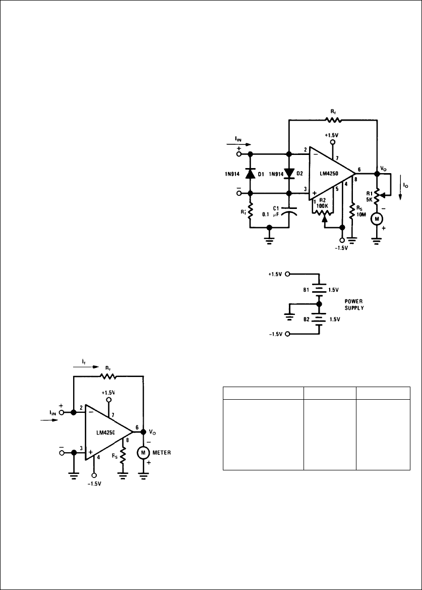
THE COMPLETE NANOAMMETER
The complete meter amplifier shown in
Figure 10
is a differ-
ential current-to-voltage converter with input protection, ze-
roing and full scale adjust provisions, and input resistor bal-
ancing for minimum offset voltage. Resistor R’f(equal in
value to Rffor measurements of less than 1 mA) insures
that the input bias currents for the two input terminals of the
amplifier do not contribute significantly to an output error
voltage. The output voltage Vofor the differential current-to-
voltage converter is equal to b2I
f
R
fsince the floating input
current IIN must flow through Rfand R’f.R’
fmay be omitted
TL/H/7382–13
TL/H/7382–14
FIGURE 10. Complete Meter Amplifier
Resistance Values for
DC Nano and Micro Ammeter
I FULL SCALE Rf[X]R’f[X]
100 nA 1.5M 1.5M
500 nA 300k 300k
1mA 300k 0
5mA 60k 0
10 mA 30k 0
50 mA6k0
100 mA3k0
for Rfvalues of 500 kXor less, since a resistance of this
value contributes an error of less than 0.1% in output volt-
age. Potentiometer R2provides an electrical meter zero by
forcing the input offset voltage Vos to zero. Full scale meter
deflection is set by R1. Both R1and R2only need to be set
once for each op amp and meter combination. For a 50
microamp 2 kXmeter movement, R1should be about 4 kX
to give full scale meter deflection in response to a 300 mV
output voltage. Diodes D1and D2provide full input protec-
tion for overcurrents up to 75 mA.
With an Rfresistor value of 1.5M the circuit in
Figure 10
becomes a nanommeter with a full scale reading capability
5
of 100 nA. Reducing Rfto3kXin steps, as shown in
Figure
10
increases the full scale deflection to 100 mA, the maxi-
mum for this circuit configuration. The voltage drop across
the two input terminals is equal to the output voltage Vo
divided by the open loop gain. Assuming an open loop gain
of 10,000 gives an input voltage drop of 30 mV or less.
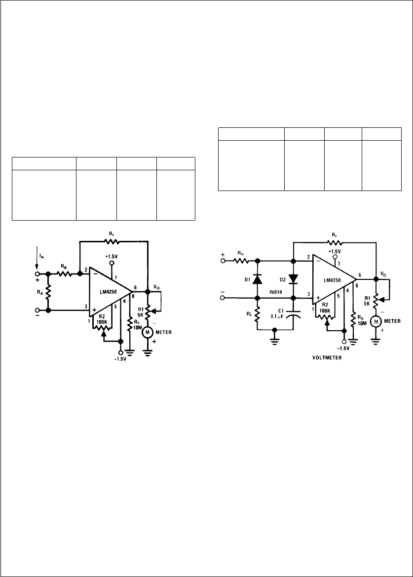
CIRCUIT FOR HIGHER CURRENT READINGS
For DC current readings higher than 100 mA, the inverting
amplifier configuration shown in
Figure 11
provides the re-
quired gain. Resistor RAdevelops a voltage drop in re-
sponse to input current IA. This voltage is amplified by a
factor equal to the ratio of Rf/RB.R
Bmust be sufficiently
larger than RA, so as not to load the input signal.
Figure 11
also shows the proper values of RA,R
Band Rffor full scale
meter deflections of from 1 mA to 10A.
Resistance Values for DC Ammeter
I FULL SCALE RA[X]RB[X]Rf[X]
1 mA 3.0 3k 300k
10 mA .3 3k 300k
100 mA .3 30k 300k
1A .03 30k 300k
10A .03 30k 30k
TL/H/7382–15
FIGURE 11. Ammeter
A 10 mV TO 100V FULL-SCALE VOLTMETER
A resistor inserted in series with one of the input leads of
the basic meter amplifier converts it to a wide range voltme-
ter circuit, as shown in
Figure 12
. This inverting amplifier has
a gain varying from b30 for the 10 mV full scale range to
b0.003 for the 100V full scale range.
Figure 12
also lists
the proper values of Rv,R
f
, and R’ffor each range. Diodes
D1and D2provide complete amplifier protection for input
overvoltages as high as 500V on the 10 mV range, but if
overvoltages of this magnitude are expected under continu-
ous operation, the power rating of Rvshould be adjusted
accordingly.
Resistance Values for a DC Voltmeter
V FULL SCALE RV[X]Rf[X]R’f[X]
10 mV 100k 1.5M 1.5M
100 mV 1M 1.5M 1.5M
1V 10M 1.M 1.5M
10V 10M 300k 0
100V 10M 30k 0
TL/H/7382–16
FIGURE 12. Voltmeter
6
TL/H/7382–17
FIGURE 13. Pulse Generator
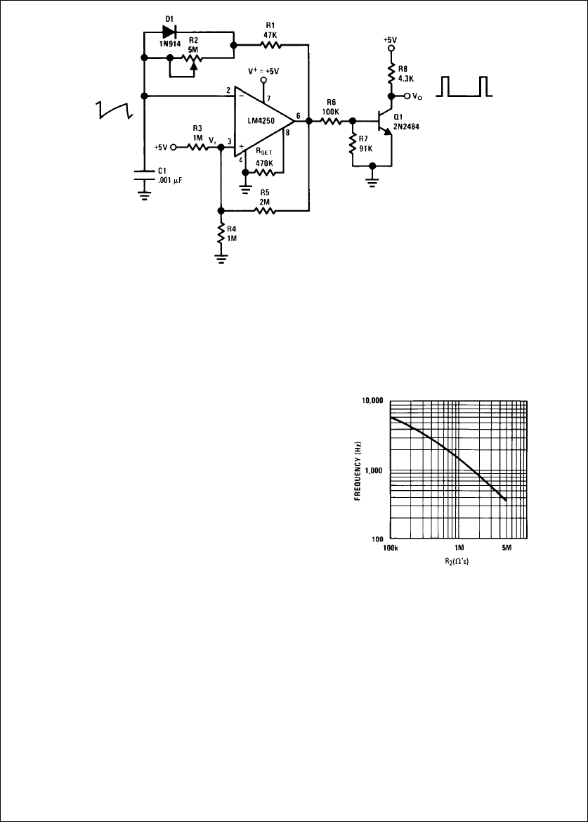
LOW FREQUENCY PULSE GENERATOR USING A
SINGLE a5V SUPPLY
The variable frequency pulse generator shown in
Figure 13
provides an example of the LM4250 operated from a single
supply. The circuit is a buffered output free running multivi-
brator with a constant width output pulse occurring with a
frequency determined by potentiometer R2.
The LM4250 acts as a comparator for the voltages found at
the upper plate of capacitor C1and at the reference point
denoted as Vron
Figure 13
. Capacitor C1charges and dis-
charges with a peak-to-peak amplitude of approximately 1V
determined by the shift in reference voltage Vrat Pin 3 of
the op amp. The charge path of C1is from the amplifier
output, which is at its maximum positive voltage VHIGH (ap-
proximately Vab0.5V), through R1and through the poten-
tiometer R2. Diode D1is reverse biased during the charge
period. When C1charges to the Vrvalue determined by the
net result of VHIGH through resistor R5and Vathrough the
voltage divider made up of resistors R3and R4the amplifier
swings to its lower limit of approximately 0.5V causing C1to
begin discharging. The discharge path is through the for-
ward biased diode D1, through resistor R1, and into Pin 6 of
the op amp. Since the impedance in the discharge path
does not vary for R2settings of from 3 kXto5MX, the
output pulse maintains a constant pulse width of 41 ms
g1.5 ms over this range of potentiometer settings.
Figure
14
shows the output pulse frequency variation from 6 kHz
down to 360 Hz as R2places from 100 kXup to 5 MXof
additional resistance in the charge path of C1. Setting R2to
zero ohms will short out diode D1and cause a symmetrical
square wave output at a frequency of 10 kHz. Increasing the
value of C1will lower the range of frequencies available in
response to the R2variation shown on
Figure 14
. Electrolyt-
ic capacitors may be used for the larger values of C1since it
has only positive voltages applied to it.
The output buffer Q1presents a constant load to the op
amp output thereby preventing frequency variations caused
by VHIGH and VLOW voltages changing as a function of load
current. The output of Q1will interface directly with a stan-
dard TTL or DTL logic device. Reversing diode D1 will invert
the polarity of the generator output providing a series of
negative going pulses dropping from a5V to the saturation
voltage of Q1.
TL/H/7382–18
FIGURE 14. Pulse Frequency vs R2
The change in output frequency as a function of supply volt-
age is less than g4% for a Vachange of from 4V to 10V.
This stability of frequency versus supply voltage is due to
the fact that the reference voltage Vrand the drive voltage
for the capacitor are both direct functions of Va.
The power dissipation of the free running multivibrator is
300 mW and the power dissipation of the buffer circuit is
approximately 5.8 mW.
7
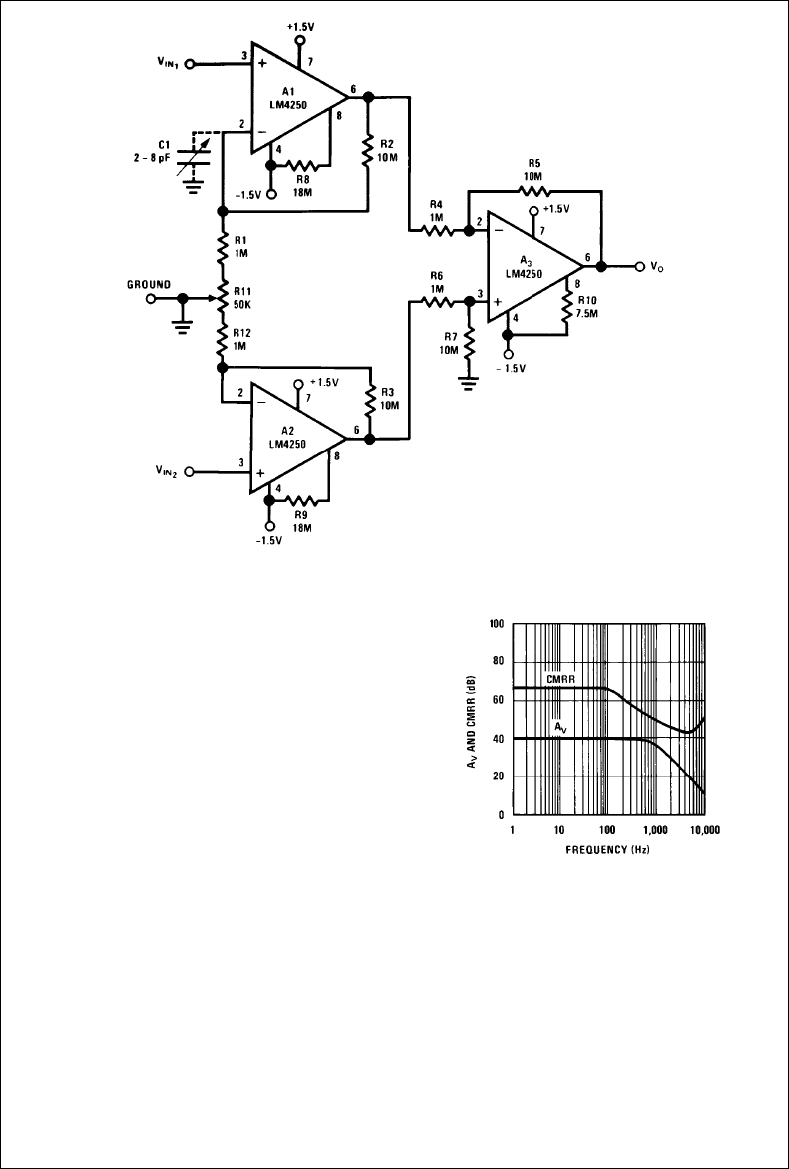
Note 1: Quiescent PDe10 mW
Note 2: R2, R3, R4, R5, R6 and R7 are 1% resistors
Note 3: R11 and C1 are for DC and AC common mode rejection adjustments
TL/H/7382–19
FIGURE 15. c100 Instrumentation Amplifier
X100 INSTRUMENTATION AMPLIFIER
The instrumentation amplifier circuit shown in
Figure 15
has
a full differential input center tapped to ground. With the
bias current set at approximately 0.1 mA, the impedance
looking into either VIN1or VIN2is 100 MXwith respect to
ground, and the input bias current at either terminal is 0.2
nA. The two non-inverting input stages A1and A2apply a
gain of 10 to the input signal, and the differential output
stage applies an additional gain of b10 for a net amplifier
gain of b100:
VOeb
100(VIN1bVIN2). (15)
The entire circuit can run from two 1.5V batteries connected
directly (no power switch) to the Vaand Vbterminals. With
a total current drain of 2.8 mA the quiescent power dissipa-
tion of the circuit is 8.4 mW. This is low enough to have no
significant effect on the shelf life of most batteries.
Potentiometer R11 provides a means for matching the gains
of A1and A2to achieve maximum DC common mode rejec-
tion ratio CMRR. With R11 adjusted to its null point for DC
common mode rejection the small AC CMRR trimmer ca-
pacitor C1will normally give an additional 10 to 20 dB of
CMRR over the operating frequency range. Since C1actual-
ly balances wiring capacitance rather than amplifier fre-
quency characteristics, it may be necessary to attach it to
Pin 2 of either A1or A2as required.
Figure 16
shows the
variation of CMRR (referred to the input) with frequency for
this configuration. Since the circuit applies a gain of 100 or
40 dB to an input signal, the actual observed rejection ratio
TL/H/7382–20
FIGURE 16. AVand CMRR vs Frequency
is the difference between the CMRR curve and AVcurve.
For example, a 60 Hz common mode signal will be attenuat-
ed by 67 dB minus 40 db or 27 dB for an actual rejection
ratio of VIN/VOequal to 22.4.
The maximum peak-to-peak output signal into a 100 kX
load resistor is approximately 1.8V. With no input signal, the
noise seen at the output is approximately 0.8 mVRMS or
8mVRMS referred to the input. When doing power dissipa-
tion measurements on this circuit, it should be kept in mind
that evena1MXoscilloscope probe placed between
a1.5V and b1.5V will more than double the power drawn
from the batteries.
8
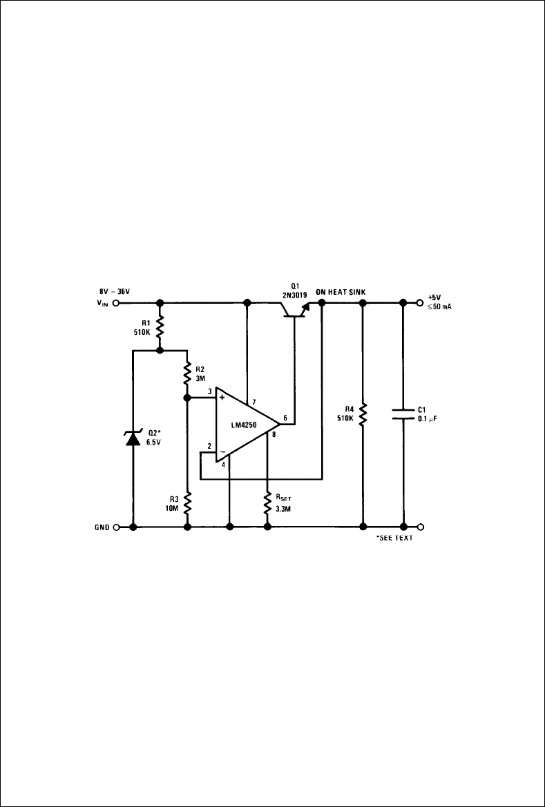
5V REGULATOR FOR CMOS LOGIC CIRCUITS
The ideal regulator for low power CMOS logic elements
should dissipate essentially no power when the CMOS de-
vices are running at low frequencies, but be capable of de-
livering full output power on demand when the CMOS devic-
es are running in the 0.1 MHz to 10 MHz region. With a 10V
input voltage, the regulator shown in
Figure 17
will dissipate
350 mW in the stand-by mode but will deliver up to 50 mA of
continuous load current when required.
The circuit is basically a boosted output voltage-follower ref-
erenced to a low current zener diode. The voltage divider
consisting of R2and R3provides a 5V tap voltage from the
6.5V reference diode to determine the regulator output.
Since a standard 6.5V zener diode does not exhibit good
regulation in the 2 mAto60mA reverse current region, Q2
must be a special device. An NPN transistor with its collec-
tor and base terminals grounded and its emitter tied to the
junction of R1and R2exhibits a well-controlled base emitter
reverse breakdown voltage. A National Semiconductor pro-
cess 25 small signal NPN transistor sorted to a
2N registration such as 2N3252 has a BVEBO at 10 mA
specified as 5.5V minimum, 6.5V typical, and 7.0V maxi-
mum. Using a diode connected 2N3252 as a reference, the
regulator output voltage changed 78 mV in response to an
8V to 36V change in the input voltage. This test was done
under both no load and full load conditions and represents a
line regulation of better than 1.6%.
A load change from 10 mA to 50 mA causeda1mVchange
in output voltage giving a load regulation value of 0.05%.
When operating the regulator at load currents of less than
25 mA, no heat sink is required for Q1. For load currents in
excess of 50 mA, Q1should be replaced by a Darlington
pair with the 2N3019 acting as a driver for a higher power
device such as a 2N3054.
REFERENCES
Millman, J. and Halkias, C.C.:
‘‘Electronic Device and Cir-
cuits,’’
pp. 465– 466, McGraw-Hill Book Company, New
York, 1967.
TL/H/7382–21
FIGURE 17. 350 mW Quiescent Drain 5 Volt Regulator
9

AN-71 Micropower Circuits Using the LM4250 Programmable Op Amp
LIFE SUPPORT POLICY
NATIONAL’S PRODUCTS ARE NOT AUTHORIZED FOR USE AS CRITICAL COMPONENTS IN LIFE SUPPORT
DEVICES OR SYSTEMS WITHOUT THE EXPRESS WRITTEN APPROVAL OF THE PRESIDENT OF NATIONAL
SEMICONDUCTOR CORPORATION. As used herein:
1. Life support devices or systems are devices or 2. A critical component is any component of a life
systems which, (a) are intended for surgical implant support device or system whose failure to perform can
into the body, or (b) support or sustain life, and whose be reasonably expected to cause the failure of the life
failure to perform, when properly used in accordance support device or system, or to affect its safety or
with instructions for use provided in the labeling, can effectiveness.
be reasonably expected to result in a significant injury
to the user.
National Semiconductor National Semiconductor National Semiconductor National Semiconductor
Corporation Europe Hong Kong Ltd. Japan Ltd.
1111 West Bardin Road Fax: (
a
49) 0-180-530 85 86 13th Floor, Straight Block, Tel: 81-043-299-2309
Arlington, TX 76017 Email: cnjwge
@
tevm2.nsc.com Ocean Centre, 5 Canton Rd. Fax: 81-043-299-2408
Tel: 1(800) 272-9959 Deutsch Tel: (
a
49) 0-180-530 85 85 Tsimshatsui, Kowloon
Fax: 1(800) 737-7018 English Tel: (
a
49) 0-180-532 78 32 Hong Kong
Fran3ais Tel: (
a
49) 0-180-532 93 58 Tel: (852) 2737-1600
Italiano Tel: (
a
49) 0-180-534 16 80 Fax: (852) 2736-9960
National does not assume any responsibility for use of any circuitry described, no circuit patent licenses are implied and National reserves the right at any time without notice to change said circuitry and specifications.
