Application Note 1125 Laminate CSP (Chip Scale Package) AN
User Manual: AN-1125
Open the PDF directly: View PDF ![]() .
.
Page Count: 20
Laminate CSP (Chip Scale
Package)
Introduction
CHIP SCALE PACKAGES
Laminate substrate based CSPs are an extension of Na-
tional Semiconductor’s current Plastic Ball Grid Array
(PBGA) technology and are the package of choice for por-
table applications. CSPs are available in two package de-
signs: Laminate CSP and Fine Pitch Ball Grid Array (FBGA).
The interconnection of FBGA to the board is achieved using
solder ball technology, while the Laminate CSP uses periph-
eral nickel-gold pads for the package to board interconnec-
tion. The construction and materials used in these packages
are designed to provide the highest performance and reli-
ability for National Semiconductor’s new miniaturized prod-
ucts. The Laminate CSP is available in a Plastic Thin Fine
Pitch Quad Flat No Lead Package (P-TFQFN) and a Plastic
Thin Shrink Small Outline No Lead Package (P-TSSON) de-
sign.
Surface Mount (SMT) board reliability is a key concern for
CSPs, and an outstanding surface mount reliability is
achieved with the laminate CSPs. The 16, 24, 28L laminate
CSP has a solder joint reliability greater than 1600 cycles
without any solder joint failures for test condition (-40˚C to
125˚C 1 cycle/hr). The 16, 24, 28 lead laminate CSP are
completely qualified at National Semiconductor and are
available for a wide range of products. By designing thermal
vias and pads to enhance power dissipation to the mother-
board, the Laminate CSP provides superior thermal perfor-
mance compared to standard package form factors.
APPLICATIONS
Portable applications, including cellular phone, wireless,
computers, memory, DSP and gate array.
CSP FEATURES
National Semiconductor’s CSP strategy is to make use of
the current PBGA infrastructure for materials, process and
design innovation to provide the best value and ease for
implementing miniature packaging solutions.
•Small outline
•Low profile (1.0 mm for CSP’s, 1.4 mm for FBGA’s)
•Light weight
•Moisture Resistance JEDEC Level 3
•Enhanced Electrical Performance >2.4 GHz
•JEDEC MO-208 Standard Outline for quad package,
P-TFQFN
•JEDEC MO-209 Standard Outline for Dual Inline Pack-
age, P-TSSON
THERMAL CHARACTERISTICS
Thermal performance is measured using a low effective ther-
mal conductivity test board fabricated per EIA/JESD51-3.
Package Body Size (mm) Die Size (mm) θj-a (˚C/Watt)
CSP-16 Lead 3.5 x 3.5 x 1.0 1.45 x 1.40 130
CSP-24 Lead 4.5 x 3.5 x 1.0 1.80 x 1.32 112
CSP-28 Lead 4.5 x 5.5 x 1.0 2.74 x 2.67 72
CSP-48 Lead 8.1 x 12.5 x 1.0 5.18 x 3.72 39 (Note 1)
CSP-96 Lead 8x8x1.0 3.05 x 3.05 89
CSP-48 FBGA 7x7x1.4 2.54 x 2.54 85
CSP-64 FBGA 8 x 8x 1.4 3.00 x 1.80 62
CSP-100 FBGA 10 x 10 x 1.4 7.9 x 7.9 35
Note 1: with thermal pads
Note 2: Simulated data
National Semiconductor
Application Note 1125
Shaw W. Lee and Wayne Lee
June 2000
Laminate CSP (Chip Scale Package) AN-1125
© 2000 National Semiconductor Corporation AN101093 www.national.com
RELIABILITY
•Moisture Sensitivity Level 3 (30˚C/60% RH, 168
hrs floor life)
•Characterization 30˚C/60% RH, 336 Hours
Soak
•Autoclave 121˚C, 100% RH, 15 psi,
168 Hours
•Temperature Cycle - 40˚C to 125˚C, 1000
Cycles
•Dynamic OP Life 125˚C, 1000 Hours
•Temp. Humidity
Bias Test
85˚C/85% RH, 1000 Hours
Laminate CSP ROADMAP
Over the next two years National Semiconductor will bring
on-line laminate CSP’s covering a range of I/O counts to sat-
isfy customer requirements. See
Table 1
.
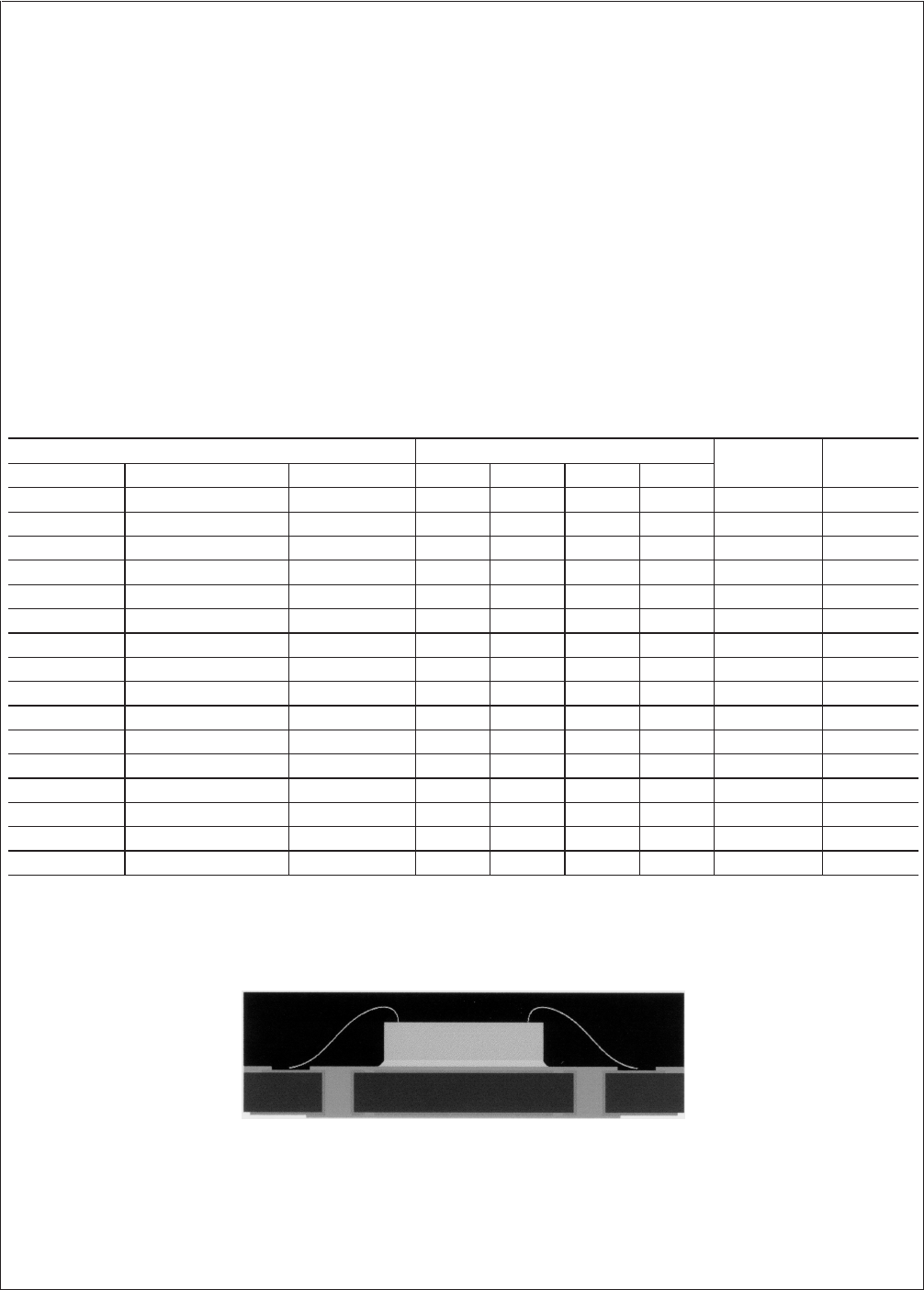
TABLE 1. Laminate CSP Roadmap
Package Information FY2000 (6/99 -5/2k) FY2001 FY2002
I/O Count Body Size (mm) Pitch (mm) Q1 Q2 Q3 Q4
16/20 CSP 3.5 x 3.5 x 1.0 0.5 p
24 CSP 3.5 x 4.5 x 1.0 0.5 p
28/32 CSP 4.5 x 5.5 x 1.0 0.5 p
40 CSP 5.5 x 6.5 x 1.0 0.5 d s q p
48 CSP 12.5 x 8.1 x 1.0 0.5 p
56 CSP 8.0 x 8.0 x 1.0 0.5 d s q p
49 FBGA 7.0 x 7.0 x 1.4 0.8 d, s, q, p
64 FBGA 8.0 x 8.0 x 1.4 0.8 p
81 FBGA 9.0 x 9.0 x 1.4 0,8 d s q p
100 FBGA 10.0 x 10.0 x 1.4 0.8 d s q p
192 FBGA 14.0 x 14.0 x 1.4 0.8 d s q q & p
80 CSP 7.0 x 7.0 x 1.0 0.5 d s q q & p
96 CSP 8.0 x 8.0 x 1.0 0.5 d s q q & p
112 CSP 9.0 x 9.0 x 1.0 0.5 d s q q & p
128 CSP 10.0 x 10.0 x 1.0 0.5 d s q q & p
208 CSP 15.0 x 15.0 x 1.0 0.5 d, s, q, p
d = design, s = sample, q = qualification, p = production
CSP Cross Section
AN101093-1
Cross Section View for 24-Lead Laminate CSP
AN-1125
www.national.com 2
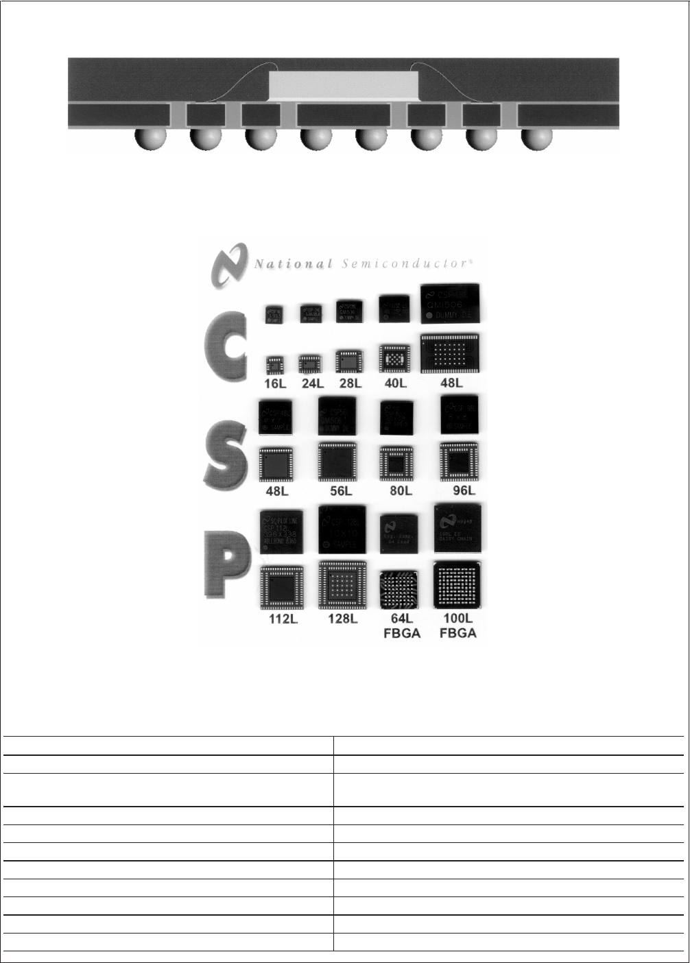
CSP Cross Section (Continued)
CSP & FBGA Packages
Standard Process Flow and Assembly Materials
Assembly and Test Process Flow for Laminate CSPs
Process Flow Equipment
Wafer Mount Nitto 8″Wafer Mount
Wafer Saw and Clean KNS 982-10 and DISCO DAD
651
2nd Optical Manual
Die Attach and Cure ESEC 2007
Plasma Clean Plasma Etch & Balzers
Wire Bond ESEC 3018 & 3006F/XX
3rd Optical Std. Manual 3rd Opt
Mold Yamada
Post Mold Cure Blue M Oven
Solder Ball Attach (>48L) Shibuya
AN101093-2
Cross Section View for 64-Lead CSP (FBGA)
AN101093-30
AN-1125
www.national.com3
Assembly and Test Process Flow for Laminate CSPs (Continued)
Process Flow Equipment
Strip Testing (Developing) MCT Tapestry
Laser Mark GSM
Singulation Saw DISCO DAD 651 & DFD 651
Electrical Test Seiko Epson & Syncro
Visual Mechanic
Inspection
GP3020TCSP
Tape & Reel Laurier
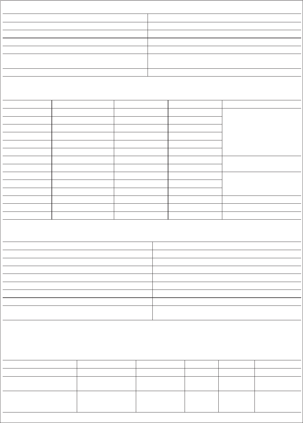
Process flow comparison of PQFP & TSSOP vs. FGBA vs. CSP
Process Steps PQFP & TSSOP FBGA CSP Integrated CSP
1 Die Attach Die Attach Die Attach
Front-End Auto-Line
Assembly from Die Attach to
Mold Cure
2 Die Attach Cure Die Attach Cure Die Attach Cure
3 Wire Bond Plasma Clean Plasma Clean
4 Mold Wire Bond Wire Bond
5 Mold Cure Mold Mold
6 Lead Plating Mold Cure Mold Cure
7 Laser Mark Laser Mark Laser Mark Strip Test & Laser Mark
Integration
8 Trim and Form Ball Attach Saw Singulation
9 Singulated Test Reflow Singulated Test Saw Singulation, Dry Visual
Inspection and Tape &Reel
10 Visual Inspection Flux Cleaning Visual Inspection
11 Tray or Tape & Reel Saw Singulation Tape & Reel
12 Test
13 Visual Inspection
14 Tape & Reel
Assembly Materials List
Wafer Diameter 6, 8″
Wafer Thickness 10 mils
Laminated Substrate Mitsubishi CCL-HL832
Solder Mask Taiyo PSR-4000-AUS5
Die Attach Epoxy QMI506
Mold Compound Nitto HC-100-X2
Wire 1.2 mils diameter Au wire
Solder Ball (for FBGA only) 63Sn/37Pb, 0.46 mm Balls
Packing Tape & Reel and JEDEC
trays (for FBGA)
Material Properties
Laminate CSP
Item Solder Resist Mold Compound Die Attach Substrate Solder Ball
Taiyo PSR4000-AUS5 Nitto HC-100-X2 QMI506 CCL-HC832 63Sn/ 37Pb
Glass Transition Temperature
Tg (˚C)
104 160 -19 190 183 melting temp
Coefficient thermal expansion
(ppm/˚C)
16 (<Tg)
210 ( Tg)
7 ( Tg)
30 ( Tg)
57 (<Tg)
139 ( Tg)
X: 14
Y: 14
Z: 58
24.7 (15 -110 ˚C)
AN-1125
www.national.com 4
Laminate CSP (Continued)
Item Solder Resist Mold Compound Die Attach Substrate Solder Ball
Elastic modulus (Kg/mm2) 2540 6300 2140-2550 N/A
Thermal Conductivity
(W/m-K)
0.26 0.97 0.9 0.34 50
Laminate FBGA
Item Solder Resist Mold Compound Die Attach Substrate Solder Ball
Taiyo PSR4000-AUS5 Plaskon SMT-B-1LV QMI596 CCL-HC832 63Sn/ 37Pb
Glass Transition Temperature
Tg (˚C)
104 225 -19 190 183 melting temp
Coefficient thermal expansion
(ppm/ ˚C)
16 (<Tg)
210 (>Tg)
14 (<Tg)
58 (>Tg)
57 (<Tg)
139 (>Tg)
X: 14
Y: 14
Z: 58
24.7 (15 -110 ˚C)
Elastic modulus (Kg/mm2) 1260 22 ˚C
610 215 ˚C
6300 2140-2550 N/A
Thermal Conductivity (W/m-K) 0.26 0.7 0.9 0.34 50
Design Guidelines
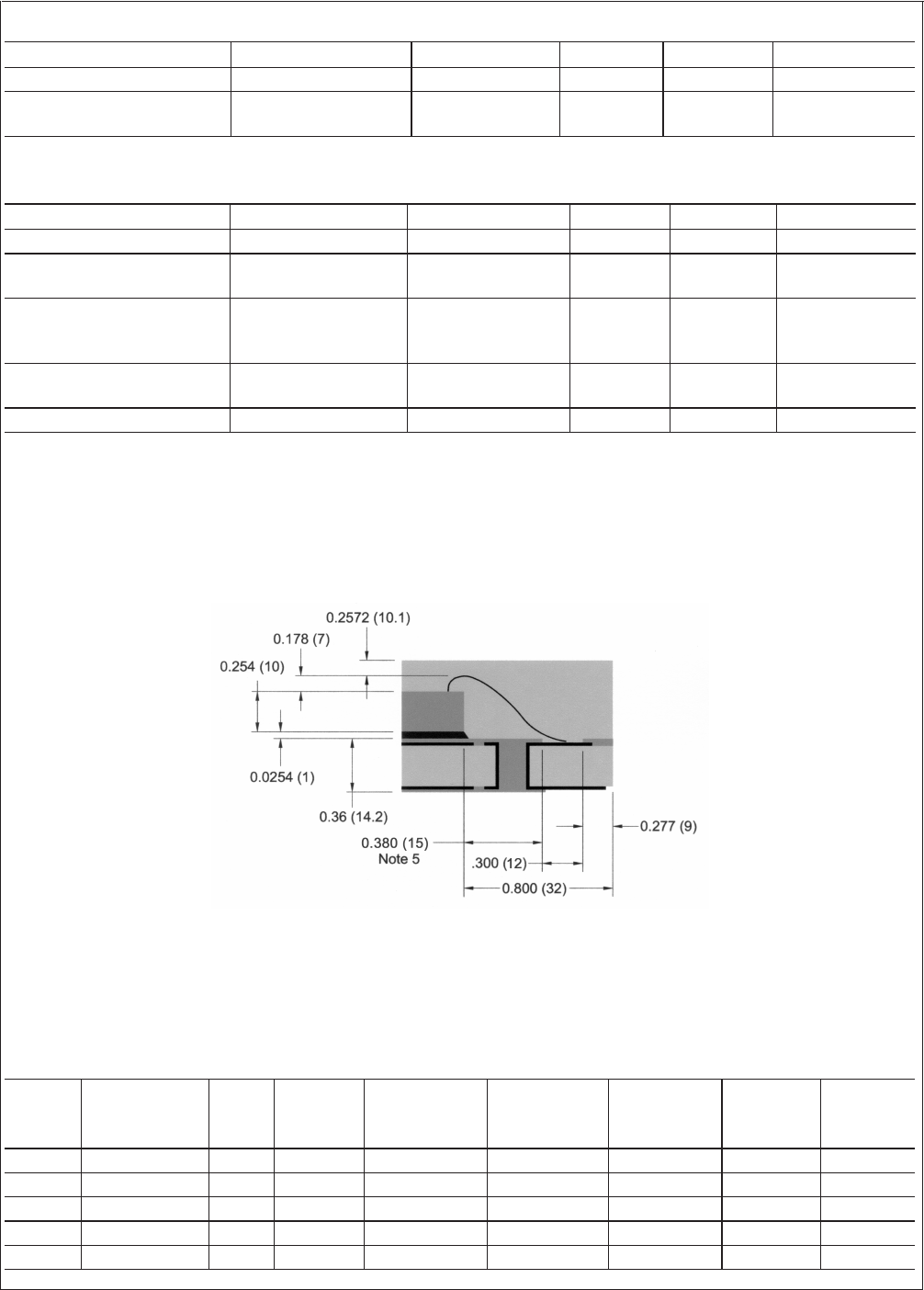
Over the last few years, design guidelines for laminate CSP
have in response to the high demand for smaller packages
with larger die.
Figure 1
shows the most recent update to
laminate CSP design.
Note 3: Note drawn to scale
Note 4: Dimensions in mm & (mils)
Note 5: 15 mils for die size less than 200 mils sq. 20 mils for die size greater than or equal to 200 mils sq.
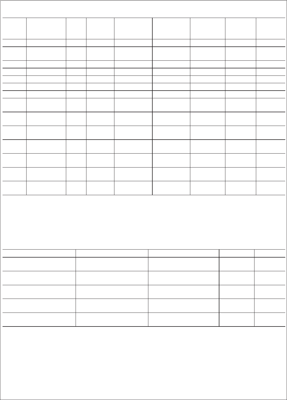
Package Drawing Information
Lead
Count
Body Size
(mm)
Pitch
(mm)
Package
Weight
(grams)
Max Die Size
(mm)
Marketing
Drawing
(SC)
Master
Build Sheet
(MBS)
Substrate
Drawing
Number
Substrate
Stock
Number
CSP-16 3.5 x 3.5 x 1.0 0.5 0.027 1.7 x 1.7 MKT-SLB16A SLB016AA 51-0044 06773
CSP-20 3.5 x 3.5 x 1.0 0.5 0.029 1.7 x 1.7 MKT-SLB20B SLB020AA 51-0074 072982
CSP-24 3.5 x 4.5 x 1.0 0.5 0.037 1.7 x 2.7 MKT-SLB24A SLB024AA 51-0043 066958
CSP-28 4.5 x 5.5 x 1.0 0.5 0.059 2.7 x 3.7 MKT-SLB28A SLB028AA 51-0045 067814
CSP-32 4.5 x 5.5 x 1.0 0.5 0.059 2.7 x 3.7 MKT-SLB32A SLB032AA 51-0073 072874
AN101093-15
FIGURE 1. General design specification for laminate CSP.
AN-1125
www.national.com5
Package Drawing Information (Continued)
Lead
Count
Body Size
(mm)
Pitch
(mm)
Package
Weight
(grams)
Max Die Size
(mm)
Marketing
Drawing
(SC)
Master
Build Sheet
(MBS)
Substrate
Drawing
Number
Substrate
Stock
Number
CSP-40 5.5 x 6.5 x 1.0 0.5 0.086 3.6 x 4.6 MKT-SLB40A SLB040AA 51-0075 073158
CSP-48 8.1 x 12.5 x
1.0
0.5 0.237 5.9 x 6.2 MKT-SLB48A SLB048AA 51-0046 067976
CSP-48 7.0 x 7.0 x 1.0 0.5 0.115 4.9 x 4.9 MKT-SLB48B SLB048AB 51-0058 071755
CSP-56 8.0 x 8.0 x 1.0 0.5 0.146 5.9 x 5.9 MKT-SLB56A SLB056AA 51-0069 072773
CSP-80 7.0 x 7.0 x 1.0 0.5 0.111 3.4 x 3.4 MKT-SLB80A SLB080AA 51-0070 072772
CSP-96 8.0 x 8.0 x 1.0 0.5 0.143 4.5 x 4.5 MKT-SLB96A SLB096AA 51-0059 071923
CSP-112 9.0 x 9.0 x 1.0 0.5 0.182 5.2 x 5.2 MKT-SLB112A SLB112AA 51-0060 071924
CSP-128 10.0 x 10.0 x
1.0
0.5 0.237 6.2 x 6.2 MKT-SLB128A SLB128AA 51-0061 071925
CSP-48
FBGA
7.0 x 7.0 x 1.4 0.8 N/A 5.7 x 5.7 MKT-SLC48A SLC048AA N/A N/A
CSP-64
FBGA
8.0 x 8.0 x 1.4 0.8 0.149 6.7 x 6.7 MKT-SLC64A SLC064AA N/A N/A
CSP-64
FBGA
8.0 x 8.0 x 1.4 0.8 0.149 4.7 x 4.8 MKT-SLC64B SLC064AB N/A N/A
CSP-81
FBGA
9.0 x 9.0 x 1.4 0.8 0.196 4.6 x 4.6 MKT-SLC81A SLC081AA 51-0076 073170
CSP-100
FBGA
10.0 x 10.0 x
1.4
0.8 0.249 6.9 x 6.9 MKT-SLC100A SLC100AA 51-0077 073171
CSP-192 14.0 x 14.0 x
1.4
0.8 N/A 11.1 x 11.1 MKT-SLC192A SLC192AA N/A N/A
Package Reliability Data
PRECONDITION
Preconditioning testing is carried out to simulate product
shipping, storage and surface mount assembly operations.
Packages are subjected to the following preconditioning se-
quence per J-STD-020.
Test Condition Test Point S/S Results
Moisture Sensitivity
Characterization (Precond)
MSL L3 30˚ C/60% RH 336
Hrs Soak 240˚ C Peak Temp
SAT @0 hr. SAT @336 hrs.,
after reflow
100 x 3 lots No Failure
ACLV, Autoclave (Pressure
Cooker Test) W/O Precond
15 psig, 121˚ C, 100% RH 96 & 168 hrs 50 x 3 lots No Failure
TMCL, Temp. Cycle W/MSL
L3 Precond
-40 to 125˚ C 500X & 1000X 100 x 3 lots No Failure
THBT, Temp/Humidity W/MSL
L3 Precond
85˚ C/85% RH 168, 500 & 1000 hrs 50 x 3 lots No Failure
VOPL, Vector Opt. Life
W/MSL L3 Precond
125˚ C 168, 500 & 1000 hrs 100 x 3 lots No Failure
Application Notes
PRINTED CIRCUIT BOARD (PCB) LAYOUT
GUIDELINESS
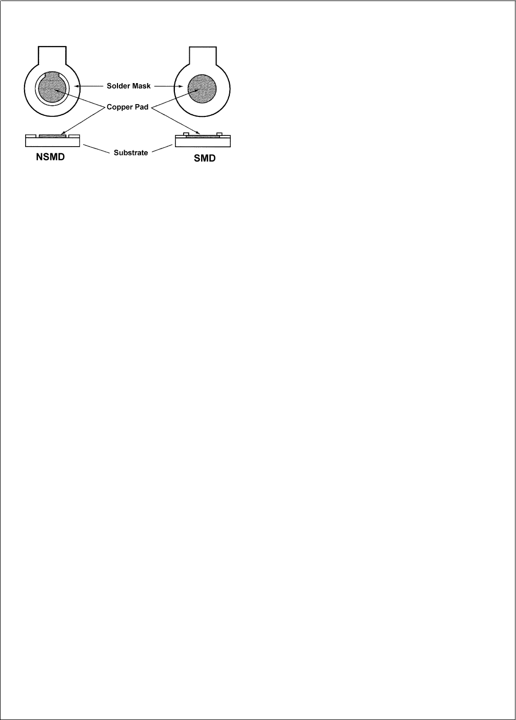
Two types of land patterns are used for surface mount pack-
ages: (1) Solder mask defined (SMD) pads that have the sol-
der mask opening smaller than metal pad and (2) Non-solder
mask defined (NSMD) pads that have the metal pad smaller
than the solder mask opening.
Figure 2
illustrates the two
types of pad geometry.
AN-1125
www.national.com 6
Application Notes (Continued)
NSMD definition is preferred due to tighter control of the cop-
per artwork registration compared to that of the solder mask-
ing process. Moreover, SMD pad definition can introduce
stress concentration points near the solder mask on the PCB
side that may result in solder joint cracking under extreme fa-
tigue conditions. The smaller size of copper pad in the case
of the NSMD definition facilitates escape routing on the PCB.
For optimal reliability, it is recommended to have a 1:1 ratio
between the package pad and the PCB pad size for periph-
eral Laminate CSP. The pad on the peripheral land packages
is 0.45mm x 0.25mm. This translates to a 0.45mm x 0.25mm
copper pad on the PCB.
A 1:0.8 ratio is recommended for the FBGA (to facilitate rout-
ing between pads in the area array package). For NSMD
pads it is necessary to have a clearance around the copper
pad and the solder mask to account for mask registration tol-
erances (typically ±0.075 mm or 3 mils) and to avoid any
overlap between solder joint and the solder mask. The PCB
layout assumes a 0.100 mm (4 mil) wide trace and a 0.5 oz.
copper foil. The recommended ball pad on the PCB is 0.33
mm and solder mask opening is 0.48 mm.
Although, a majority of board level characterization is per-
formed using a PCB with organic solderability preservative
coating (OSP) finish, no significant impact of PCB pad finish
is observed with the assembly and reliability of either the
Laminate CSP or the FBGA. A uniform coating thickness is
key for high assembly yield. For an electroplated nickel-
immersion gold finish, the gold thickness must be less than
0.5mm to avoid solder joint embrittlement.
PACKAGE TO BOARD ASSEMBLY
Package Handling
Handling during board level assembly requires the typical
precautions associated with BGA packages (Reference
J-STD-013). The Laminate CSP and FBGA packages are
compatible with automated pick & place systems. Manual
handling of the packages using a vacuum wand or a non-
metallic tweezers requires the appropriate ESD protection.
The Laminate CSP is shipped in standard polycarbonate
conductive carrier tape with pressure sensitive adhesive
(PSA) cover tape. The FBGA is available in JEDEC trays
and will be available in tape & reel for high volume produc-
tion. Handling damage is minimal due to robust package and
interconnect design.
Surface Mount Considerations
The Laminate CSP and FBGA surface mount assembly op-
erations include screen printing solder paste on the PCB,
package placement using standard SMT placement equip-
ment, reflow and cleaning (depending on flux type). Stan-
dard tape and reel or tray shipping media facilitates package
handling during assembly.
Stencil Printing Solder Paste
The solder paste is stencil printed onto the board, which in-
volves transferring the solder paste through pre-defined ap-
ertures by the application of pressure. Stencil parameters
such as aperture area ratio and fabrication process have sig-
nificant impact on volume of paste deposited onto the pad.
The aperture area ratio is defined as the ratio of stencil aper-
ture cross-section to the aperture wall area. To obtain the de-
sired solder paste transfer an area ratio of ≥0.66 is recom-
mended. Inspection of the stencil prior to placement of the
packages is highly recommended as part of a quality pro-
gram to improve board assembly yields.
Three typical stencil fabrication methods include chem-etch,
laser cut, and metal additive processes. Nickel plated, elec-
tropolished chem-etch stencils or laser cut stencils with ta-
pered aperture walls (5˚ taper is recommended) to facilitate
paste release are recommended. For peripheral packages, a
0.45mm x 0.30mm aperture on a 0.125mm thick stencil have
consistently yielded acceptable results. For FBGAs the rec-
ommended aperture size is 0.1mm larger than the 0.33mm
pad size to allow 50 µm overprinting on each side. This
translates to a 0.43mm aperture on a 0.125mm thick stencil.
Both type 3 or type 4 mesh solder paste is acceptable for ap-
plying the solder paste. To avoid drying out the paste follow
the handling guidelines recommended by the paste supplier.
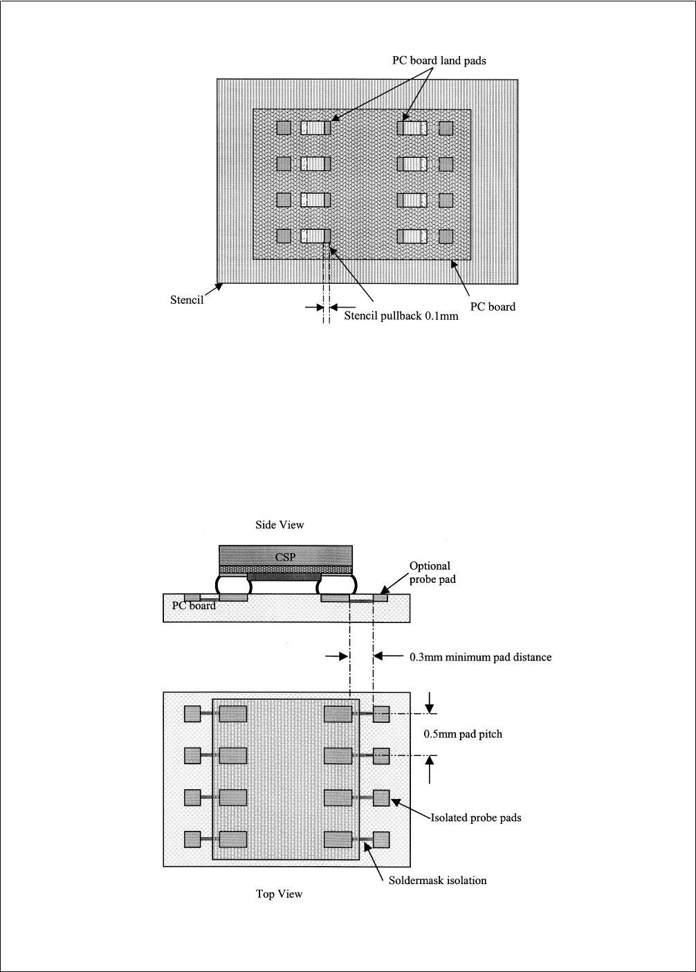
Figure 3
shows the recommended stencil layout for all CSP
footprints. Notice that there is a 0.1mm stencil pull-back that
is recommended to adjust for any soldermask registration er-
rors on the board.
AN101093-9
FIGURE 2. Comparison of NSMD and SMD pads
AN-1125
www.national.com7
Application Notes (Continued)
Part Placement
Laminate CSP and FBGA packages are placed using stan-
dard pick & place equipment with ±0.050mm (±2 mil) place-
ment accuracy. Package pick & place systems comprise of a
vision system to recognize and position the component and
a mechanical system to physically perform the pick and
place operation. Two commonly used types of vision sys-
tems for area array packages are (1) a vision system that lo-
cates package silhouette and (2) a vision system that locates
individual bumps on the interconnect pattern. The latter type
often renders more accurate placement but tends to be more
expensive and time consuming. Both pick & place methods
are acceptable as misaligned packages will self-align during
reflow. A misalignment of 50% of the ball size is tolerable for
the FBGA. The Laminate CSP has a ±0.250mm (±10 mil)
pad spacing, so the ±0.050mm (±2 mil) placement accu-
racy of pick & place equipment is more than acceptable (See
Figure 4
).
AN101093-16
FIGURE 3. Recommended stencil printing layout for laminate CSP.
AN101093-17
FIGURE 4. Recommended part placement for Lamainate CSP.
AN-1125
www.national.com 8
Application Notes (Continued)
Solder Paste Reflow & Cleaning
The Laminate CSP and FBGA are assembled using stan-
dard SMT reflow processes without any special consider-
ations. Both packages are qualified up to three reflow opera-
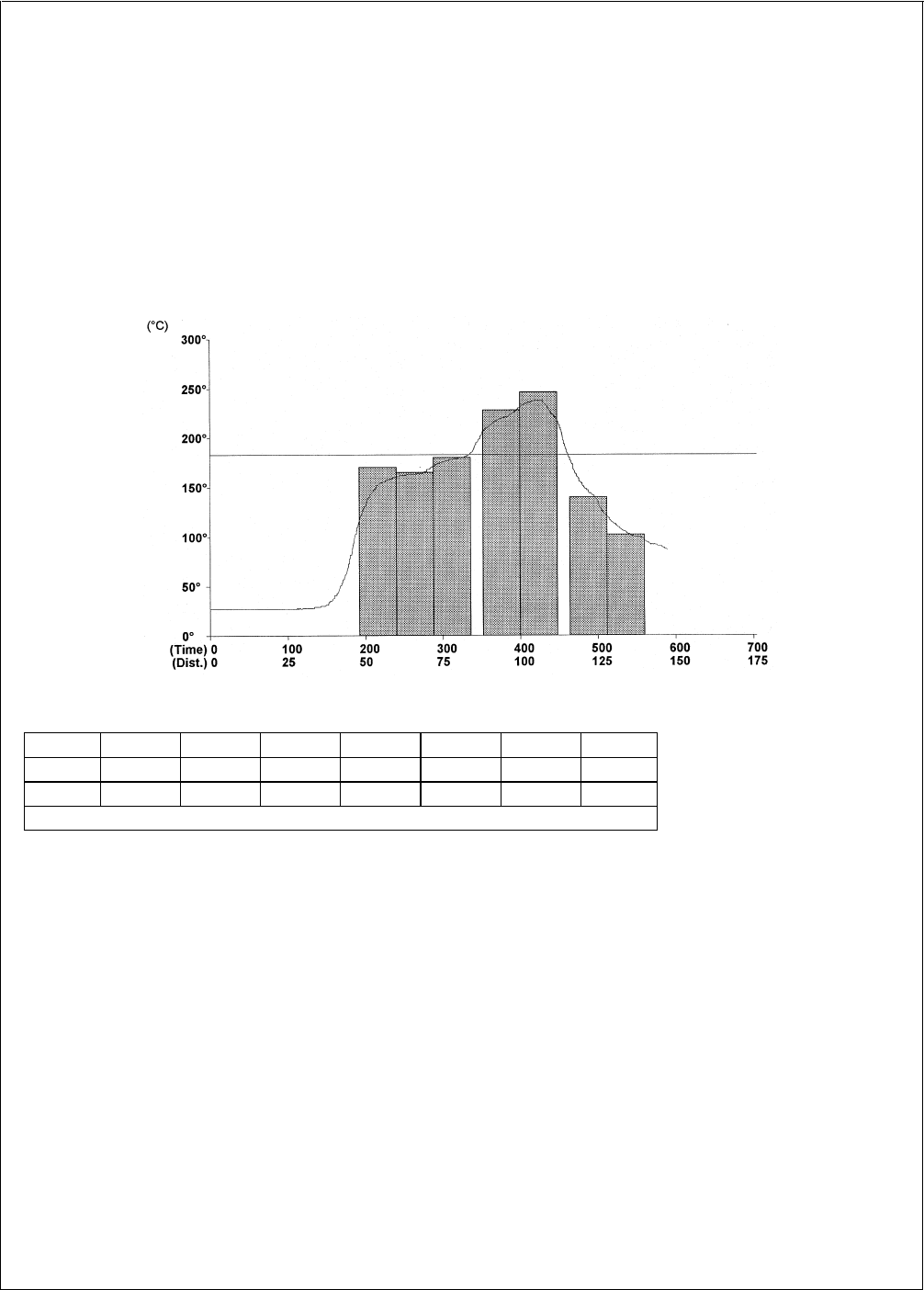
tions (J-STD-020). Recommended peak reflow temperature
is 235˚ C for the Laminate CSP (<6mm x 6mm) and 220˚ C
for the FBGA.
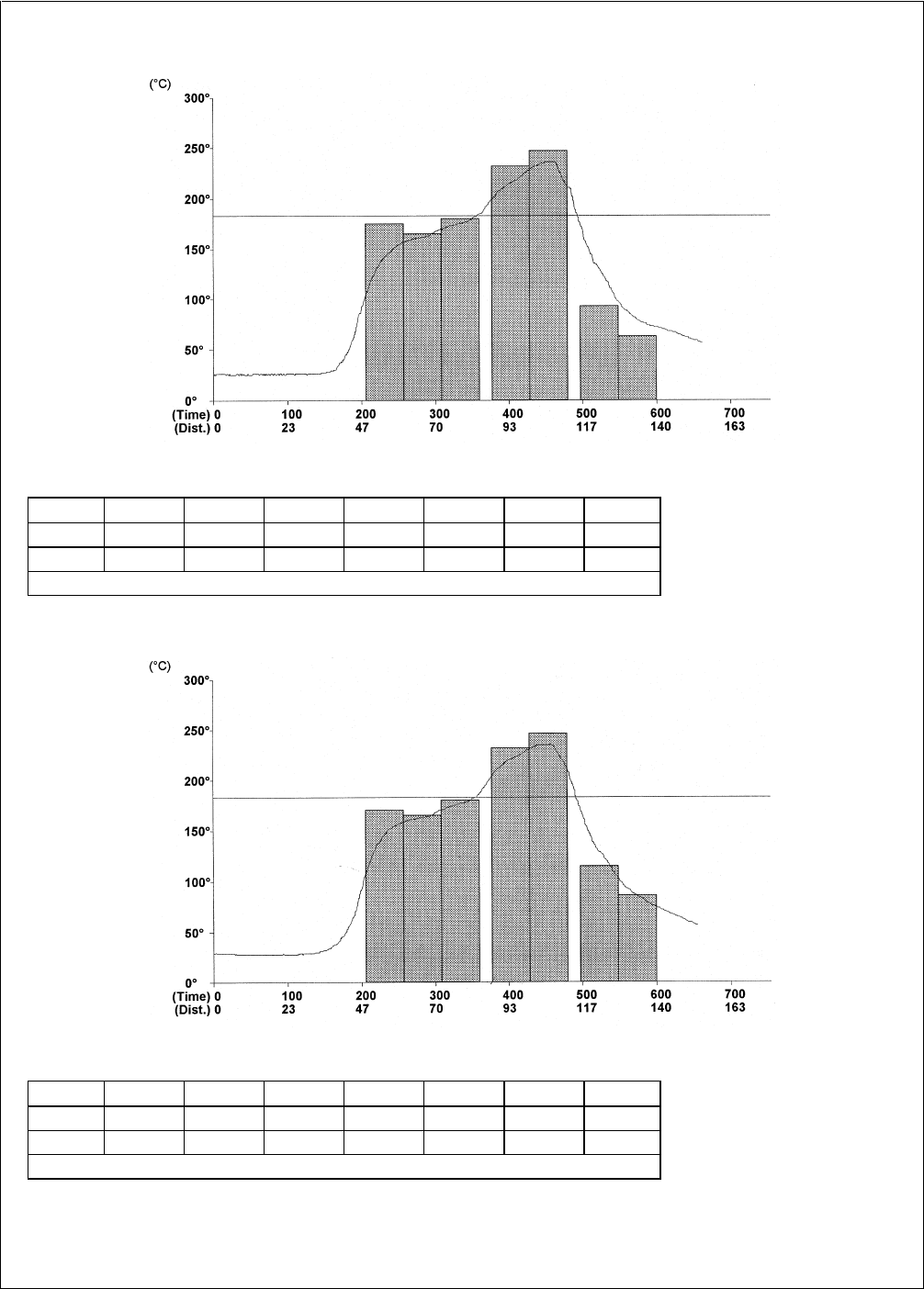
Figure 5
,
Figure 6
, and
Figure 7
illustrate typi-
cal reflow profiles. The actual temperature of the CSP is a
function of component density, component location on the
board, and size of surrounding components. If necessary, it
is recommended that the temperature profile be checked at
various locations on the board.
In some applications, a subcontractor reflows the CSPs on a
module. The module is reflowed by an OEM to the systems
board. In such cases, the component will experience up to
five solder reflow operations. The subcontractor is in control
of handling and is responsible for guaranteeing the integrity
of the CSP. If the CSP and FBGA are out of the dry bag and
exposed to 30˚ C/60% RH environment exceeding 168
hours, baking is required. The recommended baking condi-
tion is 120˚ C for 4 hours.
AN101093-34
16L CSP Process Recipe
Zone 1234567
Top 170˚ C 165˚ C 180˚ C 223˚ C 256˚ C 140˚ C 105˚ C
Bottom 170˚ C 165˚ C 180˚ C 223˚ C 256˚ C 140˚ C 105˚ C
Conveyor Speed: 15 in/min
FIGURE 5. Typical Reflow Profile for 16 Lead CSP
AN-1125
www.national.com9
Application Notes (Continued)
AN101093-35
24L CSP Process Recipe
Zone 1234567
Top 175˚ C 165˚ C 180˚ C 232˚ C 247˚ C 103˚ C 73˚ C
Bottom 175˚ C 165˚ C 180˚ C 232˚ C 247˚ C 103˚ C 73˚ C
Conveyor Speed: 14 in/min
FIGURE 6. Typical Reflow Profile for 24 Lead CSP
AN101093-36
28L CSP Process Recipe
Zone 1234567
Top 170˚ C 165˚ C 180˚ C 232˚ C 246˚ C 110˚ C 80˚ C
Bottom 170˚ C 165˚ C 180˚ C 232˚ C 246˚ C 110˚ C 80˚ C
Conveyor Speed: 15 in/min
FIGURE 7. Typical Reflow Profile for 28 Lead CSP
AN-1125
www.national.com 10

Application Notes (Continued)
Double-Sided Process
The double-sided process follows the same procedure as
the single-sided process: mount and reflow the packages on
one side, turnover the board and repeat the process.
Component Rework Procedures
CSP & FBGA REWORK OVERVIEW
Removing the laminate CSP and FBGA from PCB involves
heating solder joints above liquidus temperature of eutectic
63Sn-37Pb solder using a vacuum gas nozzle. If necessary,
bake PC-board with CSP/FBGA at 125˚C for 4 hours prior to
any rework. This will remove any residual moisture within the
part preventing moisture induced cracking during the de-
mount process. A 1.27 mm (50 mil) keep out zone for adja-
cent components, including discretes, is recommended for
standard rework processing. If adjacent components are
closer than 1.27 mm, custom tools will be required for pack-
age rework and removal. The rework area can be preheated
to 100˚C and the custom tool can hold the CSP and FBGA to
achieve a 0.5mm (20 mils) keep out zone.
Ramp rates and thermal profiles must be controlled to mini-
mize damage to surrounding the components. A ±5˚C gradi-
ent across the heating zone is recommended. Preheating
the PCB to a certain temperature (a uniform and reliable
board temperature of 100˚C is suggested) before heating the
CSP will insure a controlled process. Above the liquidus tem-
perature, the nozzle vacuum is automatically activated and
the component is picked up. After removing the CSP, the
pads may be heated using the same vacuum gas nozzle to
reflow any residual solder, which is removed using a Teflon
tipped vacuum wand. For component replacement, no-clean
flux is applied to the reworked site, and the component is
placed, reflowed, inspected, and electrically tested.
REFLOW PROFILE
The reflow profiles in this application notes is recommended
for the rework process.
REWORK SYSTEMS
The rework systems are available from many suppliers. The
following suppliers have produced the BGA/CSP rework sta-
tions: Austin American Technology (AAT), Air-Vac, Concep-
tronic, Manix Manufacturing, PACE, Semiconductor Equip-
ment Corp. (SEC), and Sierra Research and Technology
(SRT). The heat source for the rework station is based on
hot gas, focus IR or thermode. The component removal and
attachment method is done with vacuum pick-up tool.
The quality of the rework can be controlled by:
1. Directing the thermal energy through the component
body to solder without over heating the adjacent compo-
nents.
2. Heating should ideally take place in an encapsulated ,
inert, gas-purged environment, where temperature gra-
dients do not exceed +/- 5˚ C across the heating zone.
3. Use of a convective bottom side pre-heater will maxi-
mize temperature uniformity for the top and bottom side
of the temperature gradients.
4. Use the interchangeable nozzles designed with different
geometries to accommodate different applications to di-
rect the airflow path.
TEMPERATURE CALIBRATION
Due to the tight space constraint and minimum stand off
height for most CSP & FBGA, it is difficult to mount the ther-
mal couple between the space of the CSP and PCB. If pos-
sible, a small hole (just a little lager than the thermal couple),
can be drilled into the PCB and the thermal couple can be
mounted at the interface between the CSP and PCB for cali-
bration.
SITE PREPARATION
Once the CSP/FBGA is removed from the PCB board, the
site must be cleaned to prepare for package attachment.
Care must be taken to avoid burn, lift-off or damaging the at-
tachment area. The best results will be achieved with a low-
temperature, blade-style conductive tool matching the foot
print area of the CSP, in conjunction with desoldering braid.
No clean flux is recommended throughout the entire rework
process.
SOLDER BUMP DEPOSITION
The FBGA has solder balls at the bottom, no additional sol-
der bumping is needed. Because the NSC CSP is an un-
bumped land grid array package, solder bumping on the
package is needed prior to fluxing and component place-
ment on the PCB. The solder bumped package can then be
created by manual solder ball attachment using a 0.30mm
diameter solder ball as shown in
Figure 8
. Prior to CSP ball
attachment, bake CSP at 125˚C for 4 hours in order to re-
move any residual moisture if not kept in sealed dry bag. A
water-soluble flux is preferred for solder bumping process.
AN101093-18
FIGURE 8. Ball attachment to replacement CSP prior to PCB mounting.
AN-1125
www.national.com11
Component Rework Procedures
(Continued)
After the solder bumping process, the CSP should be
cleaned with DI water to remove the flux residuals. Baking is
needed after flux cleaning. The recommended baking condi-
tion is 125˚C for 4 hours.
Figure 9
shows the pretinned replacement CSP and PCB
prior to reattachment. It is important to remove any residual
moisture prior to reattachment (bake at 125˚C for 4 hours if
necessary).
COMPONENT PLACEMENT
Most CSP rework station will have a pick and place feature
for accurate placement alignment. Manual pick and place
with eye-ball alignment will be difficult or impossible to
achieve consistent placement accuracy. The self-alignment
feature for the NSC CSP and FBGA will correct some place-
ment error.
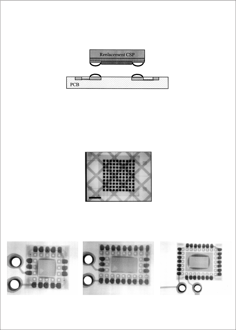
INSPECTION
After surface mount assembly solder joints can be inspected
using transmission X-ray to identify defects such as bridging,
shorts, opens, and voids.
Figure 10
shows a typical X-ray
photograph after assembly of the 100L FBGA.
X-ray photographs of the 16, 24, and 28L CSP are shown in
Figure 11
after board level mounting. The darkened solder
pads give the best indication of proper surface mounting.
AN101093-19
FIGURE 9. CSP replacement part with solder ball addition prior to reattachment on PCB.
AN101093-37
FIGURE 10. X- ray inspection of 100-lead FBGA.
AN101093-20 AN101093-21 AN101093-31
FIGURE 11. X-ray inspection of 16, 24, 28L CSP
AN-1125
www.national.com 12
Solder Joint Reliability
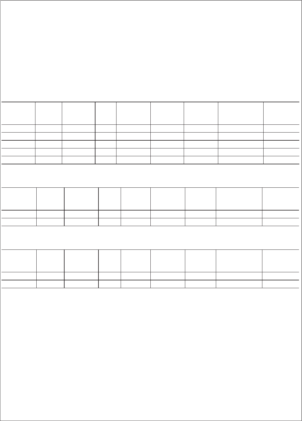
TEMPERATURE CYCLING TESTS
Solder joint reliability is available for the 16/24/28L laminate
CSP and the 64/100L FBGA. Results will be continuously
updated.
•4 Layer, FR-4, Tg >130˚ C, OSP Surface Finish
•Thickness: 20 & 62 mils
The board level reliability is evaluated using two temperature
cycle conditions:
•· TC1: -40 to 125 ˚C, single zone, one hour cycle with 15
minutes each for ramps and dwells. (1cycle/hr.)
•· TC2: -40 to 125 ˚C, dual zone, 30 minutes temperature
cycling with 2-3 minutes ramps and 12 - 13 minutes of
dwells at each temperature extreme. (2 cycles/hr.)
•· TC3: -40 to 125˚C, (30-30 test) dual zone, one-hour
temperature cycling with 2-3 minutes ramps and 28
minute of dwells at each temperature extreme. (1 cycle/
hr.)
TC1 Solder Joint Reliability test for CSP
PKG Sample
Size
Body Size
(mm)
Pitch
(mm)
Die Size
(mm)
Board
Thickness
(mm)
Pad Size
(mm) First Fail Cycle 50% Failure
16L CSP 39 3.5 x 3.5 0.5 1.47 x 1.47 1.6 0.25 x 0.45 1600 >2250
24L CSP 43 3.5 x 4.5 0.5 1.43 x 2.43 1.6 0.25 x 0.45 1600 >2250
28L CSP 39 4.5 x 5.5 0.5 2.43 x 3.43 1.6 0.25 x 0.45 1600 >2250
64L FBGA - 8 x 8 0.8 3.2 x 3.2 0.8 0.33 Dia. 1823 2724
100L FBGA - 10 x 10 0.8 8.2 x 8.2 0.8 0.33 Dia. 1143 1700
TC2 thermal shock test
PKG Sample
Size
Body Size
(mm)
Pitch
(mm)
Die Size
(mm)
Board
Thickness
(mm)
Pad Size
(mm) First Fail Cycle 50% Failure
64L FBGA - 8 x 8 0.8 3.2 x 3.2 0.8 0.33 Dia. 1921 2741
100L FBGA - 10 x 10 0.8 8.2 x 8.2 0.8 0.33 Dia. 1116 1605
TC3 thermal cycle test
PKG Sample
Size
Body Size
(mm)
Pitch
(mm)
Die Size
(mm)
Board
Thickness
(mm)
Pad Size
(mm) First Fail Cycle 50% Failure
64L FBGA 47 8 x 8 0.8 3.2 x 3.2 0.8 0.33 Dia. 750 >2050
100L FBGA 47 10 x 10 0.8 8.2 x 8.2 0.8 0.33 Dia. 1550 >2050
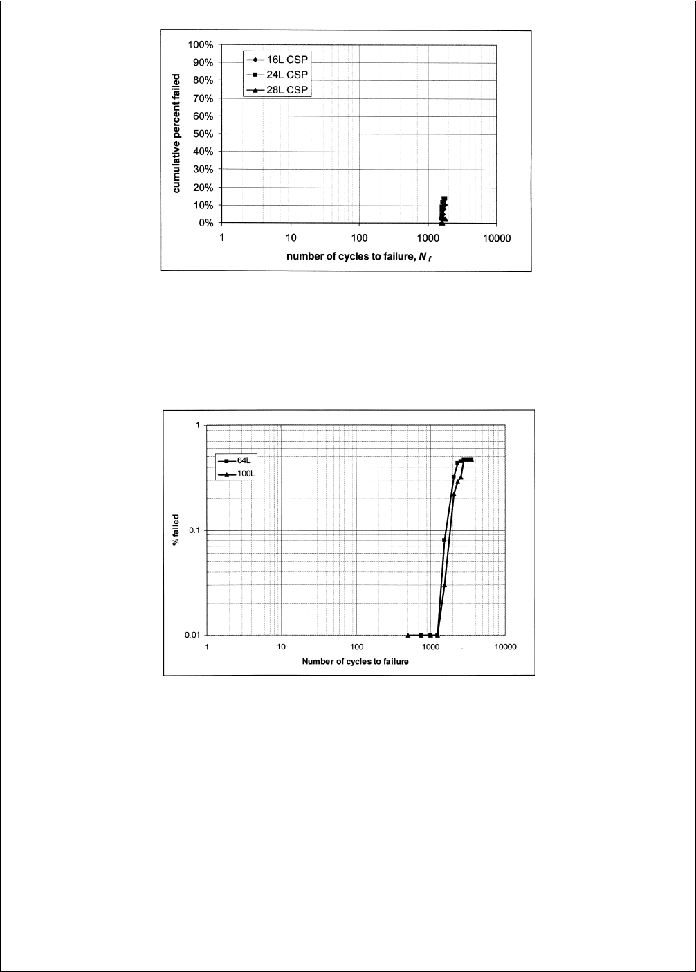
Solder Joint Reliability testing for the 16/24/28L CSP’s were
performed using a -40˚C to 125˚C temperature cycle, 15
minute ramps, and 15 minute dwells (TC1 conditions). Parts
were daisy chained configured between board and part,
forming a continuous electrical continuity loop. To increase
resolution on failure detection, an event detector was used to
continuously monitor all failure points at test temperature. To
date, all parts have passed 1600 cycles with no failures.
AN-1125
www.national.com13
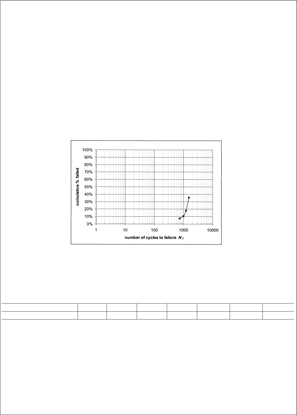
Thermal cycling tests, TC3 conditions, were performed on
the 64 & 100L FBGA was performed using a 30-30 dwell with
a −40˚C to 125˚C thermal profile. Results to date for these
tests are shown below in
Figure 13
.
SOLDER JOINT RELIABILITY TESTING FOR THE 8.1 X
12.5 X 1.0 MM, 48L CSP
Objective
To test the solder joint reliability, number of cycles to failure
(N
f
) for the 48L CSP under worst case SMT conditions.
•Package: 8.1 x 12.5 x 1.0mm, 48L CSP
•Device: daisy chain dummy die
•Molding Compound: Nitto HC100-X2
•Die Attach: Ablebond 8360
•Die size: 252 x 263 mils (5.9 x 6.2mm)
•Assembly Site: SC Assembly
•Sample size: 68 parts
Procedure
Mounting
A″worse case″scenario solder joint reliability test was con-
ducted on the 48L CSP. The 48L CSP was mounted on a
1.6mm thick FR-40 Hot Air Solder Leveled (HASL) boards
using standard 235˚C reflow profile as recommended in the
AN101093-22
FIGURE 12. Fatigue life test for 16, 24, 28L CSP
AN101093-23
FIGURE 13. Solder Joint Fatigue life testing: 30-30 ramp −40˚C to +125˚C (TC3 conditions)
AN-1125
www.national.com 14
CSP product guide. A type 3 eutectic 63Sn-37Pb solder
paste was used. The stencil used was a 1:1 aspect ratio 5
mil laser cut stencil.
Temperature Cycling
Boards were placed in a temperature cycling chamber pro-
filed for 30-30 profile. The cycling temperature range for this
test was −40˚C to 125˚C with 2-3 minute ramps and 28
minute dwells at peak temperatures.
Board Testing
Boards were removed at predetermined cycles and resis-
tance checks performed along the daisy chain of each part.
Failure was defined as open circuit.
Results and Discussion
To test the worse case conditions, three different assembly
parameters were carefully controlled before testing: 1) HASL
boards, 2) large DAP size, 3) Longest Mean Exposure Time
(MET) prior to surface mount (SMT).
HASL boards are typically difficult to perform fine pitch sur-
face mount due to the nature of the leveling process. The dif-
ficulty being in maintaining a leveled surface for the 0.5mm
fine pitch laminate CSP. A typical board finish is a nickel/gold
that typically has better defined and leveled surfaces for fine
pitch surface mount devices.
The largest possible die size was tested in this package. A
20 mil die to dap edge clearance was used in this package in
order to create this situation. Actual die size for the CLC5958
is 147 x 204 mils, approximately 45% of the test die size
used in this solder joint reliability test. The large die size
used in this solder joint test allows for maximum stresses
and strains during thermal cycling to develop and yield the
worst possible results.
Longest MET prior to SMT. This condition was met by hold-
ing parts past the MET of 336 hours and baking at 125˚C for
4 hours prior to surface mounting the device.
Figure 14
shows the result to date for this Solder Joint Reli-
ability Test.
Table 2
summarizes the failure percentage results for this
test.
TABLE 2. Summary of % failed for 30-30 test.
Total Number of Cycles 0 250 500 750 1000 1250 1550
% Failed 0% 0% 0% 7% 10% 18% 35%
Conclusion
By combining the worse case conditions of HASL boards,
largest die size, and longest MET prior to assembly for the
48L CSP, a solder joint fatigue life of greater than 1500
cycles was achieved with less than 50% failure.
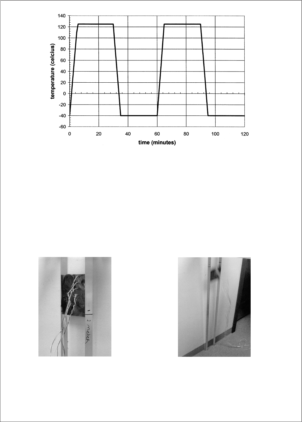
TEMPERATURE CYCLE CONDITION
The following figures show the temperature profiles used for
testing under thermal cycling conditions. In
Figure 15
, a −40
to 125˚C, 15 minutes ramps, 15 minutes dwells, 1
cycle/hour.
AN101093-33
FIGURE 14. Solder Joint Reliability Test for 48L CSP 30-30 (−40˚C to 125˚C), 1 cycle/hr under worst case exposure
conditions - SMT after 336 MET, maximum die size, HASL board.
AN-1125
www.national.com15
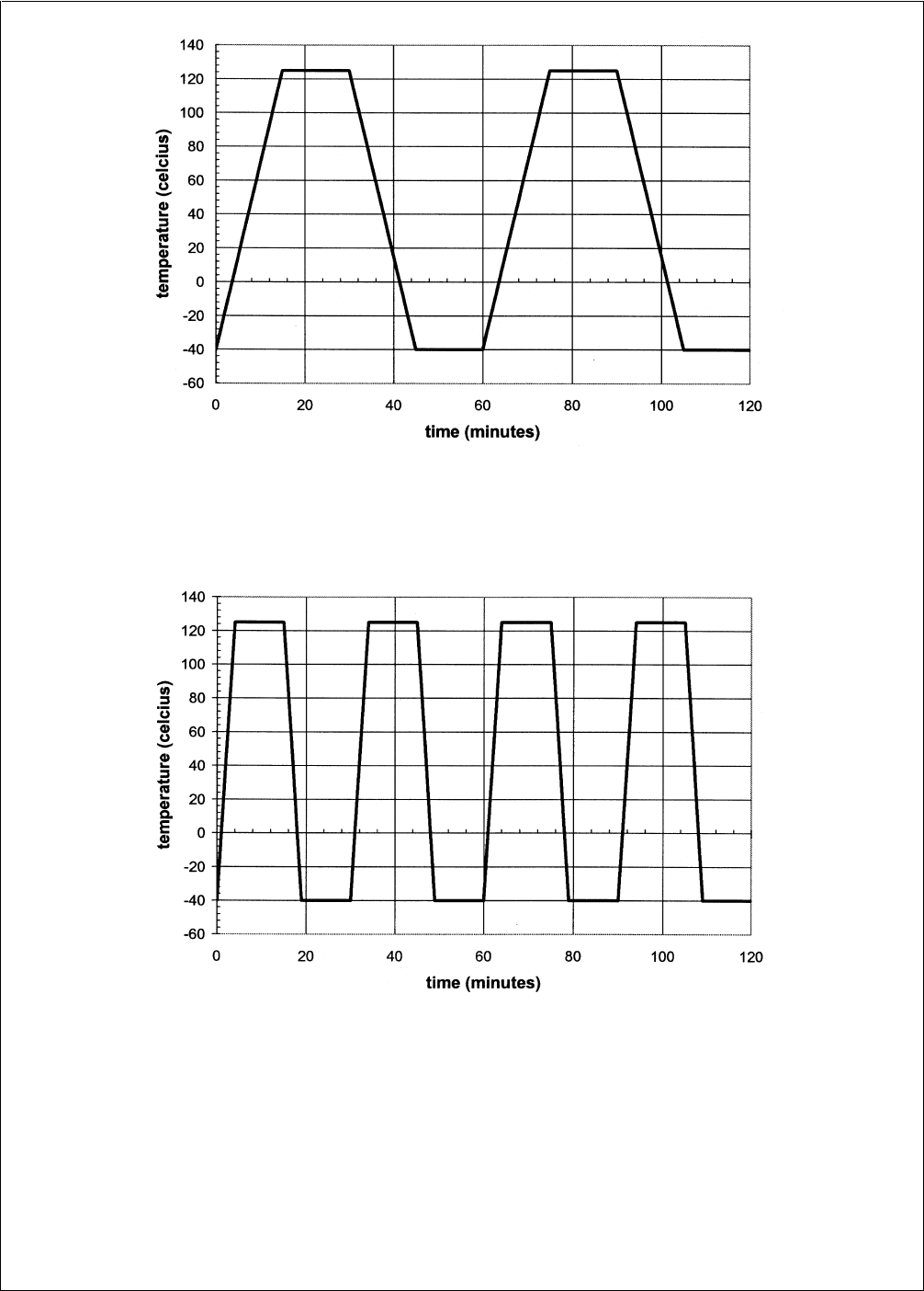
Figure 16
show the test conditions for TC2: −40 to 125˚C,
2-3 minutes ramps, 12 minutes dwells, 2 cycles/hour.
Figure 17
shows the test conditions applied for TC3.
AN101093-24
FIGURE 15. TC1 test condition profile
AN101093-25
FIGURE 16. TC2 test condition profile
AN-1125
www.national.com 16
SOLDER JOINT RELIABILITY: DROP TESTING
Testing was performed on the 24L CSP focusing on solder
joint integrity, reliability, and performance when dropped
from a 1-meter height. These test conditions were selected
based on the most probable customer use. Specifically, ap-
plications involving use in cell phones, laptop computers,
and handheld wireless products where consumer reliability
demands are the highest. National Semiconductor’s CSP
technology benefits the end user by providing a low profile
part that mounts close to the board. This low profile pro-
motes better solder joint reliability due to an extremely low
the standoff height.
The 24L CSP was mounted on five individual 1.6mm thick
FR-4 printed circuit boards. Each board consisted of 4 indi-
vidual 24L CSP units configured for continuous monitoring of
each solder joint. Each board was weighted to 150g and
dropped from a height of 1-meter. The failure criterion was
defined as twice the initial resistance (2xR
o
). Within each
drop test, the resistance was continuously monitored for
changes in solder joint resistance. Each of the five boards
was dropped a total of 15 times, 5 times on each respective
axis (x, y, z).
Results: All of the 24L CSP parts passed with one exception
was found to have insufficient solder paste during SMT and
therefore considered an invalid failure.
SOLDER JOINT RELIABILITY: BEND TESTING
In this test, the 24L CSP was surface mounted using stan-
dard SMT procedures as previously recommended.
AN101093-26
FIGURE 17. TC3 test condition profile
AN101093-27 AN101093-32
FIGURE 18. 1-meter drop testing on 24L CSP
AN-1125
www.national.com17
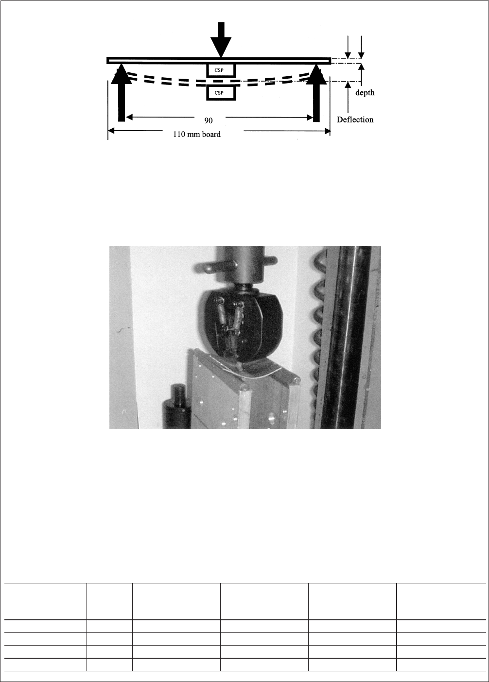
In
Figure 19
, the 24L CSP is shown mounted to a 1.6mm
thick FR-4 board in the neutral position (solid line). A force is
applied as shown by the heavy arrows along the board. The
resulting force causes the board to deflect as shown by the
dashed line. The board is placed with the test part centered
across a 90mm span. The downward force is applied to the
backside of the board causing the soldered joints to deflect.
The board was bent until complete solder joint failure oc-
curred as demonstrated in
Figure 20
.
Results: In all test cases, CSP solder joint part failure was
achieved only after board failure. The FR-4 board fractured
in all cases causing FR-4 traces to fail.
SOLDER JOINT PULL & SHEAR TESTING
CSP solder joint connections were tested under pull and
shear conditions with the following results as shown in Table
10 and Table 11. A 0.2 in/sec pull and shear rate was used
for this test.
Pull Test for laminate CSP & FBGA
Lead Count Sample
Size
High Pull
Strength per Joint
(mN)
Low Pull
Strength per Joint
(mN)
Average Pull
Strength per Joint
(mN)
Standard Deviation
per Joint
16 CSP 11 337 70 180 90
24 CSP 5 356 65 157 112
28 CSP 4 112 81 90 22
48 - 8.1x12.5 CSP 1 126 126 135 -
AN101093-28
FIGURE 19. PCB bend test for the 24L CSP as mounted to 1.6mm thick FR-4 board.
AN101093-29
FIGURE 20. Actual part under flex test conditions.
AN-1125
www.national.com 18
Pull Test for laminate CSP & FBGA (Continued)
Lead Count Sample
Size
High Pull
Strength per Joint
(mN)
Low Pull
Strength per Joint
(mN)
Average Pull
Strength per Joint
(mN)
Standard Deviation
per Joint
64 FBGA 6 164 31 90 45
100 FBGA 10 146 34 90 45
Note 6: Large variances in pull and shear test values are due to statistical nature of pull/shear tests and inherent problems in accurate setup.
Shear Test for laminate CSP & FBGA
Lead Count Sample
Size
High Shear
Strength per Joint
(mN)
Low Shear
Strength per Joint
(mN)
Average Shear
Strength per Joint
(mN)
Standard Deviation
per Joint
16 CSP 17 337 155 210 51
24 CSP 16 506 178 246 85
28 CSP 8 313 104 178 70
48 - 8.1x12.5 CSP 11 389 206 322 60
64 FBGA 16 200 98 161 27
100 FBGA 11 209 101 173 34
Tray, Tape And Reel And Test Socket Info
Package Reel S/N Tape Carrier S/N Tape Cover S/N Tray S/N
16L CSP 017983 068030 025360 071835
20L CSP 017983 068030 025360 071835
24L CSP 017983 066768 025360 071836
28L CSP 017983 068031 025360 071837
32L CSP 017983 068031 025360 071837
64L FBGA 023815 069683 030137 N/A
81L FBGA 023815 072869 030137
100L FBGA 017981 072870 030137 N/A
JEDEC trays for the 49/64/100L CSP are tooled up at KO-
STAT and Peaks Plastic Test and burn in sockets for the 16/
20/24/28/32/40/48/56/80/96/112/128/L CSP are tooled up
with Loranger International Corp.
The test contacts can be tooled up with Johnstech Interna-
tional Corp.
Test and burn in socket for the FBGA are available from 3M
Textool™and other suppliers.
Johnstech International Corp.
Minneapolis, MN
(612)378-2020
KOSTAT Santa Clara, CA
(888)390-0885
Loranger International Corp.
Warren, PA (814)723-2250
Peak International, Inc.
Milipitas, CA (408)934-2480
3M Textool™Austin, TX
(800)328-0411 Advantek Taping Systems
AN-1125
www.national.com19

Notes
LIFE SUPPORT POLICY
NATIONAL’S PRODUCTS ARE NOT AUTHORIZED FOR USE AS CRITICAL COMPONENTS IN LIFE SUPPORT
DEVICES OR SYSTEMS WITHOUT THE EXPRESS WRITTEN APPROVAL OF THE PRESIDENT AND GENERAL
COUNSEL OF NATIONAL SEMICONDUCTOR CORPORATION. As used herein:
1. Life support devices or systems are devices or
systems which, (a) are intended for surgical implant
into the body, or (b) support or sustain life, and
whose failure to perform when properly used in
accordance with instructions for use provided in the
labeling, can be reasonably expected to result in a
significant injury to the user.
2. A critical component is any component of a life
support device or system whose failure to perform
can be reasonably expected to cause the failure of
the life support device or system, or to affect its
safety or effectiveness.
National Semiconductor
Corporation
Americas
Tel: 1-800-272-9959
Fax: 1-800-737-7018
Email: support@nsc.com
National Semiconductor
Europe Fax: +49 (0) 180-530 85 86
Email: europe.support@nsc.com
Deutsch Tel: +49 (0) 69 9508 6208
English Tel: +44 (0) 870 24 0 2171
Français Tel: +33 (0) 1 41 91 8790
National Semiconductor
Asia Pacific Customer
Response Group
Tel: 65-2544466
Fax: 65-2504466
Email: ap.support@nsc.com
National Semiconductor
Japan Ltd.
Tel: 81-3-5639-7560
Fax: 81-3-5639-7507
www.national.com
AN-1125 Laminate CSP (Chip Scale Package)
National does not assume any responsibility for use of any circuitry described, no circuit patent licenses are implied and National reserves the right at any time without notice to change said circuitry and specifications.